_REV1.18 SEC S5P6818X Users Manual Preliminary Ver 0.00
User Manual:
Open the PDF directly: View PDF ![]() .
.
Page Count: 1670 [warning: Documents this large are best viewed by clicking the View PDF Link!]
- S5P6818
- 1 Product Overview
- 1.1 Introduction
- 1.2 Features
- 1.3 Block Diagram
- 1.4 Brief Functional Specification
- 1.4.1 CPU
- 1.4.2 Clock & Power Management
- 1.4.3 DMA
- 1.4.4 Interrupt Controller
- 1.4.5 Timer & Watchdog Timer
- 1.4.6 RTC
- 1.4.7 Memory Controller
- 1.4.8 GPIO Controller
- 1.4.9 Ethernet MAC Controller
- 1.4.10 SD/MMC Controller
- 1.4.11 PPM
- 1.4.12 PWM
- 1.4.13 ADC
- 1.4.14 DAC
- 1.4.15 I2C
- 1.4.16 SPI/SSP
- 1.4.17 MPEG-TS
- 1.4.18 UART& ISO7816 Sim Card Interface
- 1.4.19 USB
- 1.4.20 I2S
- 1.4.21 AC97
- 1.4.22 SPDIF Tx, Rx
- 1.4.23 PDM
- 1.4.24 Display Controller
- 1.4.25 Video Post Processor
- 1.4.26 Video Input Processor
- 1.4.27 Multi Format MPEG codec
- 1.4.28 3D Graphic Controller
- 1.4.29 Security IP
- 1.4.30 Unique Chip ID
- 1.4.31 Operating Conditions
- 1.4.32 Package
- 2 Mechanical Dimension & IO Function Description
- 2.1 Mechanical Dimension
- 2.2 FCBGA Ball Map
- 2.3 I/O Function Description
- 2.4 Ball List Table: sorted by Function
- 2.4.1 MCU-A
- 2.4.2 MCU-S
- 2.4.3 Digital RGB
- 2.4.4 HDMI
- 2.4.5 LVDS
- 2.4.6 MIPI DSI
- 2.4.7 MIPI CSI
- 2.4.8 VIP
- 2.4.9 Ethernet MAC
- 2.4.10 MPEG-TS Interface
- 2.4.11 UART_ISO7816
- 2.4.12 I2C
- 2.4.13 SPI/SSP
- 2.4.14 PWM
- 2.4.15 PPM
- 2.4.16 PDM
- 2.4.17 SPDIF
- 2.4.18 SD/MMC
- 2.4.19 USB 2.0Host
- 2.4.20 USB 2.0 HSIC HOST
- 2.4.21 USB 2.0 OTG
- 2.4.22 I2S & AC97
- 2.4.23 ADC
- 2.4.24 ALIVE GPIO
- 2.4.25 JTAG
- 2.4.26 Crystal PLL & RTC
- 2.4.27 Miscellaneous
- 2.4.28 Not Connect (NC)
- 2.4.29 Video DAC
- 2.4.30 TMU (Temperature Monitor Unit)
- 2.4.31 Power: VDD
- 2.4.32 Power: GND
- 3 System Boot
- 4 System Control
- 4.1 Overview
- 4.2 Features
- 4.3 Block Diagram
- 4.4 Clock Manager Functional Description
- 4.5 Power Manager
- 4.6 Reset Generation
- 4.7 Tie Off
- 4.8 AXI BUS
- 4.9 Register Description
- 4.9.1 Register Map Summary
- 4.9.1.1 CLKMODEREG0
- 4.9.1.2 CLKMODEREG1
- 4.9.1.3 PLLSETREG0
- 4.9.1.4 PLLSETREG1
- 4.9.1.5 PLLSETREG2
- 4.9.1.6 PLLSETREG3
- 4.9.1.7 CLKDIVREG0
- 4.9.1.8 CLKDIVREG1
- 4.9.1.9 CLKDIVREG2
- 4.9.1.10 CLKDIVREG3
- 4.9.1.11 CLKDIVREG4
- 4.9.1.12 CLKDIVREG5
- 4.9.1.13 CLKDIVREG6
- 4.9.1.14 CLKDIVREG7
- 4.9.1.15 CLKDIVREG8
- 4.9.1.16 PLLSETREG0_SSCG
- 4.9.1.17 PLLSETREG1_SSCG
- 4.9.1.18 PLLSETREG2_SSCG
- 4.9.1.19 PLLSETREG3_SSCG
- 4.9.1.20 GPIOWAKEUPRISEENB
- 4.9.1.21 GPIOWAKEUPFALLENB
- 4.9.1.22 GPIORSTENB
- 4.9.1.23 GPIOWKENB
- 4.9.1.24 INTENB
- 4.9.1.25 GPIOINTPEND
- 4.9.1.26 RESETSTATUS
- 4.9.1.27 INTENABLE
- 4.9.1.28 INTPEND
- 4.9.1.29 PWRCONT
- 4.9.1.30 PWRMODE
- 4.9.1.31 PADSTRENGTHGPIOAL
- 4.9.1.32 SYSRSTCONFIG
- 4.9.2 Tieoff
- 4.9.2.1 TIEOFFREG00
- 4.9.2.2 TIEOFFREG01
- 4.9.2.3 TIEOFFREG02
- 4.9.2.4 TIEOFFREG03
- 4.9.2.5 TIEOFFREG04
- 4.9.2.6 TIEOFFREG05
- 4.9.2.7 TIEOFFREG06
- 4.9.2.8 TIEOFFREG07
- 4.9.2.9 TIEOFFREG08
- 4.9.2.10 TIEOFFREG09
- 4.9.2.11 TIEOFFREG10
- 4.9.2.12 TIEOFFREG11
- 4.9.2.13 TIEOFFREG12
- 4.9.2.14 TIEOFFREG13
- 4.9.2.15 TIEOFFREG14
- 4.9.2.16 TIEOFFREG15
- 4.9.2.17 TIEOFFREG16
- 4.9.2.18 TIEOFFREG17
- 4.9.2.19 TIEOFFREG18
- 4.9.2.20 TIEOFFREG19
- 4.9.2.21 TIEOFFREG20
- 4.9.2.22 TIEOFFREG21
- 4.9.2.23 TIEOFFREG22
- 4.9.2.24 TIEOFFREG23
- 4.9.2.25 TIEOFFREG24
- 4.9.2.26 TIEOFFREG25
- 4.9.2.27 TIEOFFREG26
- 4.9.2.28 TIEOFFREG27
- 4.9.2.29 TIEOFFREG28
- 4.9.2.30 TIEOFFREG29
- 4.9.2.31 TIEOFFREG30
- 4.9.2.32 TIEOFFREG31
- 4.9.2.33 TIEOFFREG32
- 4.9.2.34 TIEOFFREG41
- 4.9.2.35 TIEOFFREG42
- 4.9.2.36 TIEOFFREG43
- 4.9.2.37 TIEOFFREG44
- 4.9.2.38 TIEOFFREG45
- 4.9.2.39 TIEOFFREG46
- 4.9.2.40 TIEOFFREG47
- 4.9.2.41 TIEOFFREG48
- 4.9.2.42 TIEOFFREG49
- 4.9.2.43 TIEOFFREG50
- 4.9.2.44 TIEOFFREG51
- 4.9.2.45 TIEOFFREG52
- 4.9.2.46 TIEOFFREG53
- 4.9.2.47 TIEOFFREG54
- 4.9.2.48 TIEOFFREG55
- 4.9.2.49 TIEOFFREG56
- 4.9.2.50 TIEOFFREG57
- 4.9.2.51 TIEOFFREG58
- 4.9.2.52 TIEOFFREG59
- 4.9.2.53 TIEOFFREG60
- 4.9.2.54 TIEOFFREG61
- 4.9.2.55 TIEOFFREG62
- 4.9.2.56 TIEOFFREG63
- 4.9.2.57 TIEOFFREG64
- 4.9.2.58 TIEOFFREG65
- 4.9.2.59 TIEOFFREG66
- 4.9.2.60 TIEOFFREG67
- 4.9.2.61 TIEOFFREG68
- 4.9.2.62 TIEOFFREG69
- 4.9.2.63 TIEOFFREG70
- 4.9.2.64 TIEOFFREG71
- 4.9.2.65 TIEOFFREG72
- 4.9.2.66 TIEOFFREG73
- 4.9.2.67 TIEOFFREG74
- 4.9.2.68 TIEOFFREG75
- 4.9.2.69 TIEOFFREG76
- 4.9.2.70 TIEOFFREG77
- 4.9.2.71 TIEOFFREG78
- 4.9.2.72 TIEOFFREG79
- 4.9.2.73 TIEOFFREG80
- 4.9.2.74 TIEOFFREG81
- 4.9.2.75 TIEOFFREG82
- 4.9.2.76 TIEOFFREG83
- 4.9.2.77 TIEOFFREG84
- 4.9.2.78 TIEOFFREG85
- 4.9.2.79 TIEOFFREG86
- 4.9.2.80 TIEOFFREG87(Write)
- 4.9.2.81 TIEOFFREG87(Read)
- 4.9.2.82 TIEOFFREG88(Write)
- 4.9.2.83 TIEOFFREG88(Read)
- 4.9.2.84 TIEOFFREG89
- 4.9.2.85 TIEOFFREG90
- 4.9.2.86 TIEOFFREG91
- 4.9.2.87 TIEOFFREG92
- 4.9.2.88 TIEOFFREG93
- 4.9.2.89 TIEOFFREG94
- 4.9.2.90 TIEOFFREG95
- 4.9.2.91 TIEOFFREG96
- 4.9.2.92 TIEOFFREG97
- 4.9.2.93 TIEOFFREG98
- 4.9.2.94 TIEOFFREG99
- 4.9.2.95 TIEOFFREG100
- 4.9.2.96 TIEOFFREG101
- 4.9.2.97 TIEOFFREG102
- 4.9.2.98 TIEOFFREG103
- 4.9.2.99 TIEOFFREG104 (Write)
- 4.9.2.100 TIEOFFREG104 (Read)
- 4.9.2.101 TIEOFFREG105 (Read)
- 4.9.2.102 TIEOFFREG106
- 4.9.2.103 TIEOFFREG107
- 4.9.2.104 TIEOFFREG108
- 4.9.2.105 TIEOFFREG109
- 4.9.2.106 TIEOFFREG110
- 4.9.2.107 TIEOFFREG111
- 4.9.2.108 TIEOFFREG112
- 4.9.2.109 TIEOFFREG113
- 4.9.2.110 TIEOFFREG114
- 4.9.2.111 TIEOFFREG115
- 4.9.2.112 TIEOFFREG116
- 4.9.2.113 TIEOFFREG117
- 4.9.2.114 TIEOFFREG118
- 4.9.2.115 TIEOFFREG119
- 4.9.2.116 TIEOFFREG120
- 4.9.2.117 TIEOFFREG121
- 4.9.2.118 TIEOFFREG122
- 4.9.2.119 TIEOFFREG123
- 4.9.2.120 TIEOFFREG124
- 4.9.2.121 TIEOFFREG125
- 4.9.2.122 TIEOFFREG126
- 4.9.2.123 TIEOFFREG127
- 4.9.2.124 TIEOFFREG128
- 4.9.2.125 TIEOFFREG129
- 4.9.2.126 TIEOFFREG130
- 4.9.2.127 TIEOFFREG131
- 4.9.3 AXI BUS
- 4.9.4 IP Reset
- 4.9.1 Register Map Summary
- 5 Clock Generator
- 5.1 IP Clock Generator Overview
- 5.2 Clock Generator Level 0
- 5.3 Clock Generator Level 1
- 5.3.1 Block Diagram
- 5.3.2 Register Description
- 5.3.2.1 Register MAP Summary
- 5.3.2.1.1 MIPICSICLKENB
- 5.3.2.1.2 MIPICSICLKGEN0L
- 5.3.2.1.3 PPMCLKENB
- 5.3.2.1.4 PPMCLKGEN0L
- 5.3.2.1.5 PWMTIMERCLKENB
- 5.3.2.1.6 PWMTIMERCLKGEN0L
- 5.3.2.1.7 SDMMCCLKENB
- 5.3.2.1.8 SDMMCCLKGEN0L
- 5.3.2.1.9 SPDIFTXCLKENB
- 5.3.2.1.10 SPDIFTXCLKGEN0L
- 5.3.2.1.11 SSPCLKENB
- 5.3.2.1.12 SSPCLKEN0L
- 5.3.2.1.13 UARTCLKENB
- 5.3.2.1.14 UARTCLKGEN0L
- 5.3.2.1.15 VIPCLKENB
- 5.3.2.1.16 VIPCLKGEN0L
- 5.3.2.1 Register MAP Summary
- 5.4 Clock Generator Level 2
- 5.4.1 Block Diagram
- 5.4.2 Register Description
- 5.4.2.1 Register Map Summary
- 5.4.2.1.1 GMACCLKENB
- 5.4.2.1.2 GMACCLKGEN0L
- 5.4.2.1.3 GMACCLKGEN1L
- 5.4.2.1.4 I2SCLKENB
- 5.4.2.1.5 I2SCLKGEN0L
- 5.4.2.1.6 I2SCLKGEN1L
- 5.4.2.1.7 USBHOSTOTGCLKENB
- 5.4.2.1.8 USBHOSTOTGCLKGEN0L
- 5.4.2.1.9 USBHOSTOTGCLKGEN1L
- 5.4.2.1.10 DPCCLKENB
- 5.4.2.1.11 DPCCLKGEN0L
- 5.4.2.1.12 DPCCLKGEN1L
- 5.4.2.1.13 LVDSCLKENB
- 5.4.2.1.14 LVDSCLKGEN0L
- 5.4.2.1.15 LVDSCLKGEN1L
- 5.4.2.1.16 HDMICLKENB
- 5.4.2.1.17 HDMICLKGEN0L
- 5.4.2.1.18 HDMICLKGEN1L
- 5.4.2.1.19 MIPIDSICLKENB
- 5.4.2.1.20 MIPIDSICLKGEN0L
- 5.4.2.1.21 MIPIDSICLKGEN1L
- 5.4.2.1 Register Map Summary
- 6 BUS
- 6.1 Overview
- 6.2 Features
- 6.3 Description
- 6.4 Register Description
- 6.4.1 Register Map Summary
- 6.4.1.1 AXI BUS
- 6.4.1.2 CCI BUS
- 6.4.1.2.1 Control Override
- 6.4.1.2.2 Speculation Control
- 6.4.1.2.3 Secure Access
- 6.4.1.2.4 Status
- 6.4.1.2.5 Imprecise Error
- 6.4.1.2.6 PMCR
- 6.4.1.2.7 PeripherallD4
- 6.4.1.2.8 PeripherallD5
- 6.4.1.2.9 PeripherallD6
- 6.4.1.2.10 PeripherallD7
- 6.4.1.2.11 PeripherallD0
- 6.4.1.2.12 PeripherallD1
- 6.4.1.2.13 PeripherallD2
- 6.4.1.2.14 PeripherallD3
- 6.4.1.2.15 ComponentlD0
- 6.4.1.2.16 ComponentlD1
- 6.4.1.2.17 ComponentlD2
- 6.4.1.2.18 ComponentlD3
- 6.4.1.2.19 Snoop Control Slave 0
- 6.4.1.2.20 Snoop Control Slave 1
- 6.4.1.2.21 Snoop Control Slave 2
- 6.4.1.2.22 Snoop Control Slave 3
- 6.4.1.2.23 Snoop Control Slave 4
- 6.4.1.2.24 Shareable Override Slave0
- 6.4.1.2.25 Shareable Override Slave1
- 6.4.1.2.26 Shareable Override Slave2
- 6.4.1.2.27 Shareable Override Slave3
- 6.4.1.2.28 Shareable Override Slave4
- 6.4.1.2.29 Read QoS Slave0
- 6.4.1.2.30 Read QoS Slave1
- 6.4.1.2.31 Read QoS Slave2
- 6.4.1.2.32 Read QoS Slave3
- 6.4.1.2.33 Read QoS Slave4
- 6.4.1.2.34 Write QoS Slave0
- 6.4.1.2.35 Write QoS Slave1
- 6.4.1.2.36 Write QoS Slave2
- 6.4.1.2.37 Write QoS Slave3
- 6.4.1.2.38 Write QoS Slave4
- 6.4.1.2.39 QoS Control Slave0
- 6.4.1.2.40 QoS Control Slave1
- 6.4.1.2.41 QoS Control Slave2
- 6.4.1.2.42 QoS Control Slave3
- 6.4.1.2.43 QoS Control Slave4
- 6.4.1.2.44 MaxOT Slave0
- 6.4.1.2.45 MaxOT Slave1
- 6.4.1.2.46 MaxOT Slave2
- 6.4.1.2.47 MaxOT Slave3
- 6.4.1.2.48 MaxOT Slave4
- 6.4.1.2.49 Regulator Target Slave0
- 6.4.1.2.50 Regulator Target Slave1
- 6.4.1.2.51 Regulator Target Slave2
- 6.4.1.2.52 Regulator Target Slave3
- 6.4.1.2.53 Regulator Target Slave4
- 6.4.1.2.54 Regulator Scale Slave0
- 6.4.1.2.55 Regulator Scale Slave1
- 6.4.1.2.56 Regulator Scale Slave2
- 6.4.1.2.57 Regulator Scale Slave3
- 6.4.1.2.58 Regulator Scale Slave4
- 6.4.1.2.59 Range Slave0
- 6.4.1.2.60 Range Slave1
- 6.4.1.2.61 Range Slave2
- 6.4.1.2.62 Range Slave3
- 6.4.1.2.63 Range Slave4
- 6.4.1.2.64 Cycle Counter
- 6.4.1.2.65 Counter Control
- 6.4.1.2.66 Overflow
- 6.4.1.2.67 Event Select Counter0
- 6.4.1.2.68 Event Select Counter1
- 6.4.1.2.69 Event Select Counter2
- 6.4.1.2.70 Event Select Counter3
- 6.4.1.2.71 PERF_EVENT Counter0
- 6.4.1.2.72 PERF_EVENT Counter1
- 6.4.1.2.73 PERF_EVENT Counter2
- 6.4.1.2.74 PERF_EVENT Counter3
- 6.4.1.2.75 PERF_CONTROL Counter0
- 6.4.1.2.76 PERF_CONTROL Counter1
- 6.4.1.2.77 PERF_CONTROL Counter2
- 6.4.1.2.78 PERF_CONTROL Counter3
- 6.4.1.2.79 PERF_OVERFLOW Counter0
- 6.4.1.2.80 PERF_OVERFLOW Counter1
- 6.4.1.2.81 PERF_OVERFLOW Counter2
- 6.4.1.2.82 PERF_OVERFLOW Counter3
- 6.4.1 Register Map Summary
- 7 TrustZone Protection Controller (TZPC)
- 8 System L2 Cache (PL-310 L2C)
- 8.1 Overview
- 8.2 Features
- 8.3 Block Diagram
- 8.4 Functional Description
- 8.5 Register Description
- 8.5.1 Register Map Summary
- 8.5.1.1 REG0_CACHE_ID
- 8.5.1.2 REG0_CACHE_TYPE
- 8.5.1.3 REG1_CONTROL
- 8.5.1.4 AUX_CONTROL
- 8.5.1.5 REG1_TAG_RAM_CONTROL/REG1_DATA_RAM_CONTROL
- 8.5.1.6 REG2_EV_COUNTER_CTRL
- 8.5.1.7 REG2_EV_COUNTER1_CFG/REG2_EV_COUNTER0_CFG
- 8.5.1.8 REG2_EV_COUNTER1/ REG2_EV_COUNTER0
- 8.5.1.9 REG2_INT_MASK
- 8.5.1.10 REG2_INT_MASK_STATUS
- 8.5.1.11 REG2_INT_RAW_STATUS
- 8.5.1.12 REG2_INT_CLEAR
- 8.5.1.13 REG7_CACHE_SYNC
- 8.5.1.14 REG7_INV_PA
- 8.5.1.15 REG7_INV_WAY
- 8.5.1.16 REG7_CLEAN_PA
- 8.5.1.17 REG7_CLEAN_INDEX
- 8.5.1.18 REG7_CLEAN_WAY
- 8.5.1.19 REG7_CLEAN_INV_PA
- 8.5.1.20 REG7_CLEAN_INV_INDEX
- 8.5.1.21 REG7_CLEAN_INV_WAY
- 8.5.1.22 REG9_D_LOCKDOWNn (n = 0 to 7)
- 8.5.1.23 REG9_I_LOCKDOWNn (n = 0 to 7)
- 8.5.1.24 REG9_LOCK_LINE_EN
- 8.5.1.25 REG9_UNLOCK_WAY
- 8.5.1.26 REG12_ADDR_FILTERING_START
- 8.5.1.27 REG12_ADDR_FILTERING_END
- 8.5.1.28 REG15_DEBUG_CTRL
- 8.5.1.29 REG15_PREFETCH_CTRL
- 8.5.1.30 REG15_POWER_CTRL
- 8.5.1 Register Map Summary
- 9 DMA
- 9.1 Overview
- 9.2 Features
- 9.3 Block Diagram
- 9.4 Functional Description
- 9.5 Register Description
- 9.5.1 Register Map Summary
- 9.5.1.1 Interrupt Status Register
- 9.5.1.2 Interrupt Terminal Count Status Register
- 9.5.1.3 Interrupt Terminal Count Clear Register
- 9.5.1.4 Interrupt Error Status Register
- 9.5.1.5 Interrupt Error Clear Register
- 9.5.1.6 Raw Interrupt Terminal Count Status Register
- 9.5.1.7 Raw Error Interrupt Status Register
- 9.5.1.8 Enabled Channel Register
- 9.5.1.9 Software Burst Request Register
- 9.5.1.10 Software Single Request Register
- 9.5.1.11 Software Last Burst Request Register
- 9.5.1.12 Software Last Single Request Register
- 9.5.1.13 Configuration Register
- 9.5.1.14 Synchronization Register
- 9.5.1.15 Channel Source Address Registers (0 to 7)
- 9.5.1.16 Channel Destination Address Registers (0 to 7)
- 9.5.1.17 Channel Linked List Item Registers (0 to 7)
- 9.5.1.18 Channel Control Registers (0 to 7)
- 9.5.1.19 Channel Configuration Registers (0 to 7)
- 9.5.1 Register Map Summary
- 10 Interrupt Controller
- 10.1 Overview
- 10.2 Features
- 10.3 Security Extensions Support
- 10.4 Virtualization Support
- 10.5 Terminology
- 10.6 Functional Overview
- 10.7 Interrupt Handling and Prioritization
- 10.8 Interrupt Source
- 10.9 Register Description
- 10.9.1 Register Map Summary
- 10.9.1.1 GICD_CTRL
- 10.9.1.2 GICD_TYPER
- 10.9.1.3 GICD_IIDR
- 10.9.1.4 GICD_IGROUPRn (n = 0 to 4)
- 10.9.1.5 GICD_ISENABLERn (n = 0 to 4)
- 10.9.1.6 GICD_ISCENABLERn (n = 0 to 4)
- 10.9.1.7 GICD_ISPENDRn (n = 0 to 4)
- 10.9.1.8 GICD_ICPENDERn (n = 0 to 4)
- 10.9.1.9 GICD_ISACTIVERn (n = 0 to 4)
- 10.9.1.10 GICD_ISCCTIVERn (n = 0 to 4)
- 10.9.1.11 GICD_IPRIORITYRn (n = 0 to 39)
- 10.9.1.12 GICD_ITARGETSRn (n = 0 to 39)
- 10.9.1.13 GICD_ICFGRn (n = 0 to 9)
- 10.9.1.14 GICD_PPISR
- 10.9.1.15 GICD_SPISRn (n = 0 to 3)
- 10.9.1.16 GICD_SGIR
- 10.9.1.17 GICD_CPENDSGIRn (n = 0 to 3)
- 10.9.1.18 GICD_SPENDSGIRn (n = 0 to 3)
- 10.9.1.19 GICC_CTRL
- 10.9.1.20 GICC_PMR
- 10.9.1.21 GICC_BPR
- 10.9.1.22 GICC_IAR
- 10.9.1.23 GICC_EOIR
- 10.9.1.24 GICC_RPR
- 10.9.1.25 GICC_HPPIR
- 10.9.1.26 GICC_ABPR
- 10.9.1.27 GICC_AIAR
- 10.9.1.28 GICC_AEOIR
- 10.9.1.29 GICC_AHIPPIR
- 10.9.1.30 GICC_APR0
- 10.9.1.31 GICC_NSAPR0
- 10.9.1.32 GICC_DIR
- 10.9.1 Register Map Summary
- 11 Watch Dog Timer
- 12 RTC
- 13 Alive
- 13.1 Overview
- 13.2 Features
- 13.3 Power Isolation
- 13.4 Alive Registers
- 13.5 Momentary Power Control
- 13.6 SLEEP Mode
- 13.7 PMU (Power management Unit)
- 13.8 Register Description
- 13.8.1 Register Map Summary
- 13.8.1.1 ALIVEPWRGATEREG
- 13.8.1.2 ALIVEGPIOASYNCDETECTMODERSTREG0
- 13.8.1.3 ALIVEGPIOASYNCDETECTMODERSTREG1
- 13.8.1.4 ALIVEGPIOASYNCDETECTMODESETREG0
- 13.8.1.5 ALIVEGPIOASYNCDETECTMODESETREG1
- 13.8.1.6 ALIVEGPIOLOWASYNCDETECTMODEREADREG
- 13.8.1.7 ALIVEGPIOHIGHASYNCDETECTMODEREADREG
- 13.8.1.8 ALIVEGPIODETECTMODERSTREG0
- 13.8.1.9 ALIVEGPIODETECTMODERSTREG1
- 13.8.1.10 ALIVEGPIODETECTMODERSTREG2
- 13.8.1.11 ALIVEGPIODETECTMODERSTREG3
- 13.8.1.12 ALIVEGPIODETECTMODESETREG0
- 13.8.1.13 ALIVEGPIODETECTMODESETREG1
- 13.8.1.14 ALIVEGPIODETECTMODESETREG2
- 13.8.1.15 ALIVEGPIODETECTMODESETREG3
- 13.8.1.16 ALIVEGPIOFALLDETECTMODEREADREG
- 13.8.1.17 ALIVEGPIORISEDETECTMODEREADREG
- 13.8.1.18 ALIVEGPIOLOWDETECTMODEREADREG
- 13.8.1.19 ALIVEGPIOHIGHDETECTMODEREADREG
- 13.8.1.20 ALIVEGPIODETECTENBRSTREG
- 13.8.1.21 ALIVEGPIODETECTENBSETREG
- 13.8.1.22 ALIVEGPIODETECTENBREADREG
- 13.8.1.23 ALIVEGPIOINTENBRSTREG
- 13.8.1.24 ALIVEGPIODETECTENABLESETREG
- 13.8.1.25 ALIVEGPIOINTENBREADREG
- 13.8.1.26 ALIVEGPIODETECTPENDREG
- 13.8.1.27 ALIVESCRATCHRSTREG
- 13.8.1.28 ALIVESCRATCHSETREG
- 13.8.1.29 ALIVESCRATCHREADREG
- 13.8.1.30 ALIVEGPIOPADOUTENBRSTREG
- 13.8.1.31 ALIVEGPIOPADOUTENBSETREG
- 13.8.1.32 ALIVEGPIOPADOUTENBREADREG
- 13.8.1.33 ALIVEGPIOPADPULLUPRSTREG
- 13.8.1.34 ALIVEGPIOPADPULLUPSETREG
- 13.8.1.35 ALIVEGPIOPADPULLUPREADREG
- 13.8.1.36 ALIVEGPIOPADOUTRSTREG
- 13.8.1.37 ALIVEGPIOPADOUTSETREG
- 13.8.1.38 ALIVEGPIOPADOUTREADREG
- 13.8.1.39 VDDCTRLRSTREG
- 13.8.1.40 VDDCTRLSETREG
- 13.8.1.41 VDDCTRLREADREG
- 13.8.1.42 ALIVECLEARWAKEUPSTATUSREGISTER
- 13.8.1.43 ALIVESLEEPWAKEUPSTATUSREGISTER
- 13.8.1.44 ALIVESCRATCHRSTREG1
- 13.8.1.45 ALIVESCRATCHRSTREG2
- 13.8.1.46 ALIVESCRATCHRSTREG3
- 13.8.1.47 ALIVESCRATCHRSTREG4
- 13.8.1.48 ALIVESCRATCHRSTREG5
- 13.8.1.49 ALIVESCRATCHRSTREG6
- 13.8.1.50 ALIVESCRATCHRSTREG7
- 13.8.1.51 ALIVESCRATCHRSTREG8
- 13.8.1.52 ALIVESCRATCHSETREG1
- 13.8.1.53 ALIVESCRATCHSETREG2
- 13.8.1.54 ALIVESCRATCHSETREG3
- 13.8.1.55 ALIVESCRATCHSETREG4
- 13.8.1.56 ALIVESCRATCHSETREG5
- 13.8.1.57 ALIVESCRATCHSETREG6
- 13.8.1.58 ALIVESCRATCHSETREG7
- 13.8.1.59 ALIVESCRATCHSETREG8
- 13.8.1.60 ALIVESCRATCHREADREG1
- 13.8.1.61 ALIVESCRATCHREADREG2
- 13.8.1.62 ALIVESCRATCHREADREG3
- 13.8.1.63 ALIVESCRATCHREADREG4
- 13.8.1.64 ALIVESCRATCHREADREG5
- 13.8.1.65 ALIVESCRATCHREADREG6
- 13.8.1.66 ALIVESCRATCHREADREG7
- 13.8.1.67 ALIVESCRATCHREADREG8
- 13.8.1.68 VDDOFFDELAYRSTREGISTER
- 13.8.1.69 VDDOFFDELAYSETREGISTER
- 13.8.1.70 VDDOFFDELAYVALUEREGISTER
- 13.8.1.71 VDDOFFDELAYTIMEREGISTER
- 13.8.1.72 ALIVEGPIOINPUTVALUE
- 13.8.1.73 PMUNISOLATE
- 13.8.1.74 PMUNPWRUPPRE
- 13.8.1.75 PMUNPWRUP
- 13.8.1.76 PMUNPWRUPACK
- 13.8.1 Register Map Summary
- 14 ID Register
- 14.1 Overview
- 14.2 Features
- 14.3 Functional Description
- 14.4 Register Description
- 14.4.1 Register Map Summary
- 14.4.1.1 ECID0
- 14.4.1.2 ECID1
- 14.4.1.3 ECID2
- 14.4.1.4 ECID3
- 14.4.1.5 CHIP_NAME_03_00
- 14.4.1.6 CHIP_NAME_07_04
- 14.4.1.7 CHIP_NAME_11_08
- 14.4.1.8 CHIP_NAME_15_12
- 14.4.1.9 CHIP_NAME_19_16
- 14.4.1.10 CHIP_NAME_23_20
- 14.4.1.11 CHIP_NAME_27_24
- 14.4.1.12 CHIP_NAME_31_28
- 14.4.1.13 CHIP_NAME_35_32
- 14.4.1.14 CHIP_NAME_39_36
- 14.4.1.15 CHIP_NAME_43_40
- 14.4.1.16 CHIP_NAME_47_44
- 14.4.1.17 GUID0
- 14.4.1.18 GUID1_2
- 14.4.1.19 GUID3_0
- 14.4.1.20 GUID3_1
- 14.4.1.21 EC0
- 14.4.1.22 EC1
- 14.4.1.23 EC2
- 14.4.1 Register Map Summary
- 14.5 Application Notes
- 15 Memory Controller
- 15.1 Overview
- 15.2 Block Diagram
- 15.3 Functional Description
- 15.3.1 MCU-A Bank Feature
- 15.3.2 MCU-S Bank Feature
- 15.3.3 Memory Map
- 15.3.4 MCU-A Address Mapping
- 15.3.5 Low Power Operation
- 15.3.6 Precharge Policy
- 15.3.7 Quality of Service
- 15.3.8 Trust Zone Address Space Control (TZASC)
- 15.3.9 MCU-A Application Note
- 15.3.10 MCU-S
- 15.3.11 NAND Overview
- 15.4 Register Description
- 15.4.1 Register Map Summary
- 15.4.1.1 DREX
- 15.4.1.1.1 CONCONTROL
- 15.4.1.1.2 MEMCONTROL
- 15.4.1.1.3 CGCONTROL
- 15.4.1.1.4 DIRECTCMD
- 15.4.1.1.5 PRECHCONFIG0
- 15.4.1.1.6 PHYCONTROL0
- 15.4.1.1.7 PRECHCONFIG1
- 15.4.1.1.8 TIMINGRFCBP
- 15.4.1.1.9 PWRDNCONFIG
- 15.4.1.1.10 TIMINGPZQ
- 15.4.1.1.11 TIMINGAREF
- 15.4.1.1.12 TIMINGROW
- 15.4.1.1.13 TIMINGDATA
- 15.4.1.1.14 TIMINGPOWERn
- 15.4.1.1.15 PHYSTATUS
- 15.4.1.1.16 ETCTIMING
- 15.4.1.1.17 CHIPSTATUS
- 15.4.1.1.18 MRSTATUS
- 15.4.1.1.19 QOSCONTROL n (n = 0 to 15)
- 15.4.1.1.20 TIMINGSETSW
- 15.4.1.1.21 WRTRACONFIG
- 15.4.1.1.22 RDLVLCONFIG
- 15.4.1.1.23 BRBRSVCONTROL
- 15.4.1.1.24 BRBRSVCONFIG
- 15.4.1.1.25 BRBQOSCONFIG
- 15.4.1.1.26 WRLVLCONFIG0
- 15.4.1.1.27 WRLVLCONFIG1
- 15.4.1.1.28 WRLVLSTATUS
- 15.4.1.1.29 CTRL_IO_RDATA
- 15.4.1.1.30 CACAL_CONFIG0
- 15.4.1.1.31 CACAL_CONFIG1
- 15.4.1.1.32 CACAL_STATUS
- 15.4.1.1.33 EMERGENT_CONFIG0
- 15.4.1.1.34 EMERGENT_CONFIG1
- 15.4.1.1.35 BP_CONTROLn (Back Pressure control Register for Port n)
- 15.4.1.1.36 BP_CONFIGRn (Back Pressure Configuration Register for Read Port n)
- 15.4.1.1.37 BP_CONFIGWn (Back Pressure Configuration Register for Write Port n)
- 15.4.1.2 TZASC Configuration
- 15.4.1.2.1 TZCONFIG
- 15.4.1.2.2 TZACTION
- 15.4.1.2.3 TZLDRANGE
- 15.4.1.2.4 TZLDSELECT
- 15.4.1.2.5 TZINTSTATUS
- 15.4.1.2.6 TZINTCLEAR
- 15.4.1.2.7 TZFAILADDRLOWRn
- 15.4.1.2.8 TZFAILADDRHIGHRn
- 15.4.1.2.9 TZFAILCTRLRn
- 15.4.1.2.10 TZFAILIDRn
- 15.4.1.2.11 TZFAILADDRLOWWn
- 15.4.1.2.12 TZFAILCTRLWn
- 15.4.1.2.13 TZFAILADDRHIGHWn
- 15.4.1.2.14 TZFAILIDW n
- 15.4.1.2.15 TZRSLOW n
- 15.4.1.2.16 TZRSHIGH n
- 15.4.1.2.17 TZRSATTR n
- 15.4.1.2.18 TZITCRG
- 15.4.1.2.19 TZITIP
- 15.4.1.2.20 TZITOP
- 15.4.1.2.21 MEMBASECONFIG 0
- 15.4.1.2.22 MEMBASECONFIG 1
- 15.4.1.2.23 MEMCONFIG 0
- 15.4.1.2.24 MEMCONFIG 1
- 15.4.1.3 DDRPHY
- 15.4.1.3.1 PHY_CON0
- 15.4.1.3.2 PHY_CON1
- 15.4.1.3.3 PHY_CON2
- 15.4.1.3.4 PHY_CON3
- 15.4.1.3.5 PHY_CON4
- 15.4.1.3.6 PHY_CON5
- 15.4.1.3.7 LP_CON0
- 15.4.1.3.8 RODT_CON0
- 15.4.1.3.9 OFFSETR_CON0
- 15.4.1.3.10 OFFSETR_CON1
- 15.4.1.3.11 OFFSETR_CON2
- 15.4.1.3.12 OFFSETW_CON0
- 15.4.1.3.13 OFFSETW_CON1
- 15.4.1.3.14 OFFSETW_CON2
- 15.4.1.3.15 OFFSETC_CON0
- 15.4.1.3.16 OFFSETC_CON1
- 15.4.1.3.17 OFFSETC_CON2
- 15.4.1.3.18 SHIFTC_CON0
- 15.4.1.3.19 OFFSETD_CON0
- 15.4.1.3.20 LP_DDR_CON0
- 15.4.1.3.21 LP_DDR_CON1
- 15.4.1.3.22 LP_DDR_CON2
- 15.4.1.3.23 LP_DDR_CON3
- 15.4.1.3.24 LP_DDR_CON4
- 15.4.1.3.25 WR_LVL_CON0
- 15.4.1.3.26 WR_LVL_CON1
- 15.4.1.3.27 WR_LVL_CON2
- 15.4.1.3.28 WR_LVL_CON3
- 15.4.1.3.29 CA_DSKEW_CON0
- 15.4.1.3.30 CA_DSKEW_CON1
- 15.4.1.3.31 CA_DSKEW_CON2
- 15.4.1.3.32 CA_DSKEW_CON3
- 15.4.1.3.33 CA_DSKEW_CON4
- 15.4.1.3.34 DRVDS_CON0
- 15.4.1.3.35 DRVDS_CON1
- 15.4.1.3.36 MDLL_CON0
- 15.4.1.3.37 MDLL_CON1
- 15.4.1.3.38 ZQ_CON0
- 15.4.1.3.39 ZQ_CON1
- 15.4.1.3.40 ZQ_CON2
- 15.4.1.3.41 ZQ_CON3
- 15.4.1.3.42 T_RDDATA_CON0
- 15.4.1.3.43 T_RDDATA_CON1
- 15.4.1.3.44 T_RDDATA_CON2
- 15.4.1.3.45 CAL_WL_STAT
- 15.4.1.3.46 CAL_FAIL_STAT0
- 15.4.1.3.47 CAL_FAIL_STAT1
- 15.4.1.3.48 CAL_FAIL_STAT2
- 15.4.1.3.49 CAL_FAIL_STAT3
- 15.4.1.3.50 CAL_GT_VWMC0
- 15.4.1.3.51 CAL_GT_VWMC1
- 15.4.1.3.52 CAL_GT_VWMC2
- 15.4.1.3.53 CAL_GT_CYC
- 15.4.1.3.54 CAL_RD_VWMC0
- 15.4.1.3.55 CAL_RD_VWMC1
- 15.4.1.3.56 CAL_RD_VWMC2
- 15.4.1.3.57 CAL_RD_VWML0
- 15.4.1.3.58 CAL_RD_VWML1
- 15.4.1.3.59 CAL_RD_VWML2
- 15.4.1.3.60 CAL_RD_VWMR0
- 15.4.1.3.61 CAL_RD_VWMR1
- 15.4.1.3.62 CAL_RD_VWMR2
- 15.4.1.3.63 CAL_WR_VWMC0
- 15.4.1.3.64 CAL_WR_VWMC1
- 15.4.1.3.65 CAL_WR_VWMC2
- 15.4.1.3.66 CAL_WR_VWML0
- 15.4.1.3.67 CAL_WR_VWML1
- 15.4.1.3.68 CAL_WR_VWML2
- 15.4.1.3.69 CAL_WR_VWMR0
- 15.4.1.3.70 CAL_WR_VWMR1
- 15.4.1.3.71 CAL_WR_VWMR2
- 15.4.1.3.72 CAL_DM_VWMR0
- 15.4.1.3.73 CAL_DM_VWMR1
- 15.4.1.3.74 CAL_DM_VWMR2
- 15.4.1.3.75 CAL_DM_VWML0
- 15.4.1.3.76 CAL_DM_VWML1
- 15.4.1.3.77 CAL_DM_VWML2
- 15.4.1.3.78 CAL_DM_VWMR0
- 15.4.1.3.79 CAL_DM_VWMR1
- 15.4.1.3.80 CAL_DM_VWMR2
- 15.4.1.4 MCU-S
- 15.4.1.4.1 MEMBW
- 15.4.1.4.2 MEMTIMEACSL
- 15.4.1.4.3 MEMTIMEACSH
- 15.4.1.4.4 MEMTIMECOSL
- 15.4.1.4.5 MEMTIMECOSH
- 15.4.1.4.6 MEMTIMEACC0
- 15.4.1.4.7 MEMTIMEACC1
- 15.4.1.4.8 MEMTIMEACC2
- 15.4.1.4.9 MEMTIMEACC3
- 15.4.1.4.10 MEMTIMESACC0
- 15.4.1.4.11 MEMTIMESACC1
- 15.4.1.4.12 MEMTIMESACC2
- 15.4.1.4.13 MEMTIMESACC3
- 15.4.1.4.14 MEMTIMECOHL
- 15.4.1.4.15 MEMTIMECOHH
- 15.4.1.4.16 MEMTIMECAHL
- 15.4.1.4.17 MEMTIMECAHH
- 15.4.1.4.18 MEMBURSTL
- 15.4.1.4.19 MEMWAIT
- 15.4.1.4.20 NFCONTROL
- 15.4.1.4.21 NFECCTRL
- 15.4.1.4.22 NFCNT
- 15.4.1.4.23 NFECCSTATUS
- 15.4.1.4.24 NFTIMEACS
- 15.4.1.4.25 NFTIMECOS
- 15.4.1.4.26 NFTIMEACC0
- 15.4.1.4.27 NFTIMEOCH
- 15.4.1.4.28 NFTIMECAH
- 15.4.1.4.29 NFECCn (n = 0 to 26)
- 15.4.1.4.30 NFORGECCn (n = 0 to 26)
- 15.4.1.4.31 NFSYNDROMEn (n = 0 to 29)
- 15.4.1.4.32 NFELPn (n = 0 to 29)
- 15.4.1.4.33 NFERRORLOCATIONn (n = 0 to 59)
- 15.4.1.4.34 AUTO SYNDROME REGISTER (AUTOSYND)
- 15.4.1.4.35 NFWSYNDRONEn (n = 0 to 29)
- 15.4.1.5 MCUS_ADDR
- 15.4.1.1 DREX
- 15.4.1 Register Map Summary
- 16 GPIO Controller
- 16.1 Overview
- 16.2 Features
- 16.3 Block Diagram
- 16.4 Functional Description
- 16.5 Register Description
- 16.5.1 Register Map Summary
- 16.5.1.1 GPIOxOUT
- 16.5.1.2 GPIOxOUTENB
- 16.5.1.3 GPIOxDETMODE0
- 16.5.1.4 GPIOxDETMODE1
- 16.5.1.5 GPIOxINTENB
- 16.5.1.6 GPIOxDET
- 16.5.1.7 GPIOxPAD
- 16.5.1.8 GPIOxALTFN0
- 16.5.1.9 GPIOxALTFN1
- 16.5.1.10 GPIOxDETMODEEX
- 16.5.1.11 GPIOxDETENB
- 16.5.1.12 GPIOx_SLEW
- 16.5.1.13 GPIOx_SLEW_DISABLE_DEFAULT
- 16.5.1.14 GPIOx_DRV1
- 16.5.1.15 GPIOx_DRV1_DISABLE_DEFAULT
- 16.5.1.16 GPIOx_DRV0
- 16.5.1.17 GPIOx_DRV0_DISABLE_DEFAULT
- 16.5.1.18 GPIOx_PULLSEL
- 16.5.1.19 GPIOx_PULLSEL_DISABLE_DEFAULT
- 16.5.1.20 GPIOx_PULLENB
- 16.5.1.21 GPIOx_PULLENB_DISABLE_DEFAULT
- 16.5.1 Register Map Summary
- 17 Ethernet MAC
- 17.1 Overview
- 17.2 Features
- 17.3 Block Diagram
- 17.4 Register Description
- 17.4.1 Register Map Summary
- 17.4.1.1 MAC DMA
- 17.4.1.1.1 Ethernet MAC DMA Register 0
- 17.4.1.1.2 Ethernet MAC DMA Register 1
- 17.4.1.1.3 Ethernet MAC DMA Register 2
- 17.4.1.1.4 Ethernet MAC DMA Register 3
- 17.4.1.1.5 Ethernet MAC DMA Register 4
- 17.4.1.1.6 Ethernet MAC DMA Register 5
- 17.4.1.1.7 Ethernet MAC DMA Register 6
- 17.4.1.1.8 Ethernet MAC DMA Register 7
- 17.4.1.1.9 Ethernet MAC DMA Register 8
- 17.4.1.1.10 Ethernet MAC DMA Register 18
- 17.4.1.1.11 Ethernet MAC DMA Register 19
- 17.4.1.1.12 Ethernet MAC DMA Register 20
- 17.4.1.1.13 Ethernet MAC DMA Register 21
- 17.4.1.2 MAC Core
- 17.4.1.2.1 Ethernet MAC Register 0
- 17.4.1.2.2 Ethernet MAC Register 1
- 17.4.1.2.3 Ethernet MAC Register 2
- 17.4.1.2.4 Ethernet MAC Register 3
- 17.4.1.2.5 Ethernet MAC Register 4
- 17.4.1.2.6 Ethernet MAC Register 5
- 17.4.1.2.7 Ethernet MAC Register 6
- 17.4.1.2.8 Ethernet MAC Register 7
- 17.4.1.2.9 Ethernet MAC Register 8
- 17.4.1.2.10 Ethernet MAC Register 9
- 17.4.1.2.11 Ethernet MAC Register 14
- 17.4.1.2.12 Ethernet MAC Register 15
- 17.4.1.2.13 Ethernet MAC Register 16
- 17.4.1.2.14 Ethernet MAC Register 17
- 17.4.1.2.15 Ethernet MAC Register 18
- 17.4.1.2.16 Ethernet MAC Register 19
- 17.4.1.2.17 Ethernet MAC Register 20 to 47
- 17.4.1.2.18 Ethernet MAC Register 48
- 17.4.1.2.19 Ethernet MAC Register 49
- 17.4.1.2.20 Ethernet MAC Register 50
- 17.4.1.2.21 Ethernet MAC Register 51
- 17.4.1.2.22 Ethernet MAC Register 52
- 17.4.1.2.23 Ethernet MAC Register 53
- 17.4.1.2.24 Ethernet MAC Register 54
- 17.4.1.2.25 Ethernet MAC Register 448
- 17.4.1.2.26 Ethernet MAC Register 449
- 17.4.1.2.27 Ethernet MAC Register 450
- 17.4.1.2.28 Ethernet MAC Register 451
- 17.4.1.2.29 Ethernet MAC Register 452
- 17.4.1.2.30 Ethernet MAC Register 453
- 17.4.1.2.31 Ethernet MAC Register 454
- 17.4.1.2.32 Ethernet MAC Register 455
- 17.4.1.2.33 Ethernet MAC Register 456
- 17.4.1.2.34 Ethernet MAC Register 457
- 17.4.1.2.35 Ethernet MAC Register 458
- 17.4.1.2.36 Ethernet MAC Register 512 to 543
- 17.4.1.1 MAC DMA
- 17.4.1 Register Map Summary
- 18 SD/MMC Controller
- 18.1 Overview
- 18.2 Features
- 18.3 Block Diagram
- 18.4 Register Description
- 18.4.1 Register Map Summary
- 18.4.1.1 CTRL
- 18.4.1.2 POWER_ENABLE
- 18.4.1.3 CLKDIV
- 18.4.1.4 CLK_SOURCE
- 18.4.1.5 CLKENA
- 18.4.1.6 TMOUT
- 18.4.1.7 CTYPE
- 18.4.1.8 BLKSIZ
- 18.4.1.9 BYTCNT
- 18.4.1.10 INTMASK
- 18.4.1.11 CMDARG
- 18.4.1.12 CMD
- 18.4.1.13 RESP0
- 18.4.1.14 RESP1
- 18.4.1.15 RESP2
- 18.4.1.16 RESP3
- 18.4.1.17 MINTSTS
- 18.4.1.18 RINTSTS
- 18.4.1.19 STATUS
- 18.4.1.20 FIFOTH
- 18.4.1.21 CDETECT
- 18.4.1.22 WRTPRT
- 18.4.1.23 TCBCNT
- 18.4.1.24 TBBCNT
- 18.4.1.25 DEBNCE
- 18.4.1.26 USRID
- 18.4.1.27 VERID
- 18.4.1.28 UHS_REG
- 18.4.1.29 RST_n
- 18.4.1.30 BMODE
- 18.4.1.31 PLDMND
- 18.4.1.32 DBADDR
- 18.4.1.33 IDSTS
- 18.4.1.34 IDINTEN
- 18.4.1.35 DSCADDR
- 18.4.1.36 BUFADDR
- 18.4.1.37 CARDTHRCTL
- 18.4.1.38 BACK_END_POWER
- 18.4.1.39 EMMC_DDR_REG
- 18.4.1.40 EMMC_DDR_REG
- 18.4.1.41 Data
- 18.4.1 Register Map Summary
- 19 Pulse Period Measurement (PPM)
- 20 Pulse Width Modulation (PWM) Timer
- 21 Analog Digital Converter (ADC)
- 22 I2C Controller
- 23 SPI/SSP
- 23.1 Overview
- 23.2 Features
- 23.3 Block Diagram
- 23.4 Functional Description
- 23.5 Register Description
- 23.5.1 Register Map Summary
- 23.5.1.1 SPI/SSP CONFIGURE
- 23.5.1.2 SPI/SSP FIFO CON
- 23.5.1.3 SPI/SSP SEL SIGNAL CON
- 23.5.1.4 SPI/SSP INT EN
- 23.5.1.5 SPI/SSP STATUS
- 23.5.1.6 SPI/SSP TX DATA
- 23.5.1.7 SPI/SSP RX DATA
- 23.5.1.8 SPI/SSP PACKET COUNT
- 23.5.1.9 SPI/SSP STATUS PENDING CLEAR
- 23.5.1.10 SPI/SSP SWAP CONFIGURE
- 23.5.1.11 SPI/SSP FEEDBACK CLOCK SEL
- 23.5.1 Register Map Summary
- 24 MPEG-TS Interface
- 24.1 Overview
- 24.2 Features
- 24.3 Functional Description
- 24.4 Register Description
- 24.4.1 Register Map Summary
- 24.4.1.1 CAP_CTRL0
- 24.4.1.2 CAP_CTRL1
- 24.4.1.3 CAP_WR_PID_VAL
- 24.4.1.4 CAP_WR_PID_ADDR
- 24.4.1.5 CAP0_CAPDATA
- 24.4.1.6 CAP1_CAPDATA
- 24.4.1.7 CORE_TRDATA
- 24.4.1.8 CORE_CTRL
- 24.4.1.9 IDMA_STATUS
- 24.4.1.10 IDMA_CON
- 24.4.1.11 IDMA_INT
- 24.4.1.12 IDMA0_ADDR
- 24.4.1.13 IDMA1_ADDR
- 24.4.1.14 IDMA2_ADDR
- 24.4.1.15 IDMA3_ADDR
- 24.4.1.16 IDMA0_LEN
- 24.4.1.17 IDMA1_LEN
- 24.4.1.18 IDMA2_LEN
- 24.4.1.19 IDMA3_LEN
- 24.4.1 Register Map Summary
- 24.5 PID Filter Data Structure
- 25 UART_ISO7816
- 25.1 Overview
- 25.2 Features
- 25.3 UART Description
- 25.4 Register Description
- 26 USB2.0 OTG
- 26.1 Overview
- 26.2 Features
- 26.3 Block Diagram
- 26.4 I/O Pin Description
- 26.5 Functional Description
- 26.6 Programming User Configure of PHY and OTG LINK
- 26.7 Register Description
- 26.7.1 Register Map Summary
- 26.7.1.1 Core Global Register
- 26.7.1.1.1 GOTGCTL
- 26.7.1.1.2 GOTGINT
- 26.7.1.1.3 GAHBCFG
- 26.7.1.1.4 GUSBCFG
- 26.7.1.1.5 GRSTCTL
- 26.7.1.1.6 GINTSTS
- 26.7.1.1.7 GINTMSK
- 26.7.1.1.8 GRXSTSR (Host Mode)
- 26.7.1.1.9 GRXSTSP (Device Mode)
- 26.7.1.1.10 GRXFSIZ
- 26.7.1.1.11 GNPTXFSIZ
- 26.7.1.1.12 GNPTXSTS
- 26.7.1.1.13 HPTXFSIZ
- 26.7.1.1.14 DPTXFSIZn (n = 1 to 15)
- 26.7.1.2 Host Mode Register
- 26.7.1.2.1 HCFG
- 26.7.1.2.2 HFIR
- 26.7.1.2.3 HFNUM
- 26.7.1.2.4 HPTXSTS
- 26.7.1.2.5 HAINT
- 26.7.1.2.6 HAINTMSK
- 26.7.1.2.7 HPRT
- 26.7.1.2.8 HCCHARn (n= 0 to 15)
- 26.7.1.2.9 HCSPLTn (n= 0 to 15)
- 26.7.1.2.10 HCINTn (n= 0 to 15)
- 26.7.1.2.11 HCINTMSKn (n= 0 to 15)
- 26.7.1.2.12 HCTSIZn (n= 0 to 15)
- 26.7.1.2.13 HCDMAn (n= 0 to 15)
- 26.7.1.3 Device Mode Register
- 26.7.1.3.1 USB_OTG_DMCSR
- 26.7.1.3.2 DCTL
- 26.7.1.3.3 DSTS
- 26.7.1.3.4 DIEPMSK
- 26.7.1.3.5 DOEPMSK
- 26.7.1.3.6 DAINT
- 26.7.1.3.7 DAINTMSK
- 26.7.1.3.8 DTKNQR1
- 26.7.1.3.9 DTKNQR2
- 26.7.1.3.10 DVBUSDIS
- 26.7.1.3.11 DVBUSPULSE
- 26.7.1.3.12 DTKNQR3
- 26.7.1.3.13 DTKNQR4
- 26.7.1.3.14 DIEPCTL0
- 26.7.1.3.15 DIEPINT0
- 26.7.1.3.16 DIEPTSIZ0
- 26.7.1.3.17 DIEPDMA0
- 26.7.1.3.18 DIEPCTLn (n = 1 to 7)
- 26.7.1.3.19 DIEPINTn (n = 1 to 7)
- 26.7.1.3.20 DIEPTSIZn (n = 1 to 7)
- 26.7.1.3.21 DIEPDMAn (n = 1 to 7)
- 26.7.1.3.22 DOEPCTL0
- 26.7.1.3.23 DOEPINT0
- 26.7.1.3.24 DOEPTSIZ0
- 26.7.1.3.25 DOEPDMA0
- 26.7.1.3.26 DOEPCTLn (n = 1 to 7)
- 26.7.1.3.27 DOEPINTn (n = 1 to 7)
- 26.7.1.3.28 DOEPTSIZn (n = 1 to 7)
- 26.7.1.3.29 DOEPDMAn (n = 1 to 7)
- 26.7.1.4 Power and Clock Gating Register
- 26.7.1.5 Device EP n/Host Channel n FIFO Register
- 26.7.1.1 Core Global Register
- 26.7.1 Register Map Summary
- 27 USB2.0 HOST
- 27.1 Overview
- 27.2 Features
- 27.3 Block Diagram
- 27.4 Functional Description
- 27.5 Register Description
- 27.5.1 Register Map Summary
- 27.5.1.1 HCCAPBASE
- 27.5.1.2 HCSPARAMS
- 27.5.1.3 HCCPARAMS
- 27.5.1.4 USBCMD
- 27.5.1.5 USBSTS
- 27.5.1.6 USBINTR
- 27.5.1.7 FRINDEX
- 27.5.1.8 CTRLDSSEGMEN
- 27.5.1.9 PERIODICLISTBASE
- 27.5.1.10 ASYNCLISTADDR
- 27.5.1.11 CONFIGFLAG
- 27.5.1.12 PORTSC_1 to 15
- 27.5.1.13 INSNREG00
- 27.5.1.14 INSNREG01
- 27.5.1.15 INSNREG02
- 27.5.1.16 INSNREG03
- 27.5.1.17 INSNREG04
- 27.5.1.18 INSNREG05
- 27.5.1.19 INSNREG06
- 27.5.1.20 INSNREG07
- 27.5.1.21 INSNREG08
- 27.5.1 Register Map Summary
- 28 I2S
- 29 AC97
- 30 SPDIF TX
- 31 SPDIF RX
- 31.1 Overview
- 31.2 Features
- 31.3 Block Diagram
- 31.4 Functional Description
- 31.5 Register Description
- 31.5.1 Register Map Summary
- 31.5.1.1 SPDIF_CTRL
- 31.5.1.2 SPDIF_ENBIRQ
- 31.5.1.3 REGUSERA0
- 31.5.1.4 REGUSERA1
- 31.5.1.5 REGUSERA2
- 31.5.1.6 REGUSERA3
- 31.5.1.7 REGUSERA4
- 31.5.1.8 REGUSERA5
- 31.5.1.9 REGUSERB0
- 31.5.1.10 REGUSERB1
- 31.5.1.11 REGUSERB2
- 31.5.1.12 REGUSERB3
- 31.5.1.13 REGUSERB4
- 31.5.1.14 REGUSERB5
- 31.5.1.15 REGSTATA0
- 31.5.1.16 REGSTATA1
- 31.5.1.17 REGSTATA2
- 31.5.1.18 REGSTATA3
- 31.5.1.19 REGSTATA4
- 31.5.1.20 REGSTATA5
- 31.5.1.21 REGSTATB0
- 31.5.1.22 REGSTATB1
- 31.5.1.23 REGSTATB2
- 31.5.1.24 REGSTATB3
- 31.5.1.25 REGSTATB4
- 31.5.1.26 REGSTATB5
- 31.5.1 Register Map Summary
- 32 PDM
- 33 Display Architecture
- 34 Multi Layer Controller (MLC)
- 34.1 Overview
- 34.2 Features
- 34.3 Block Diagram
- 34.4 Dual Register Set Architecture
- 34.5 MLC Global Parameters
- 34.6 Clock Generation
- 34.7 Register Description
- 34.7.1 Register Map Summary
- 34.7.1.1 MLCCONTROLT
- 34.7.1.2 MLCSCREENSIZE
- 34.7.1.3 MLCBGCOLOR
- 34.7.1.4 MLCLEFTRIGHT0
- 34.7.1.5 MLCTOPBOTTOM0
- 34.7.1.6 MLCLEFTRIGHT0_0
- 34.7.1.7 MLCTOPBOTTOM0_0
- 34.7.1.8 MLCLEFTRIGHT0_1
- 34.7.1.9 MLCTOPBOTTOM0_1
- 34.7.1.10 MLCCONTROL0
- 34.7.1.11 MLCHSTRIDE0
- 34.7.1.12 MLCVSTRIDE0
- 34.7.1.13 MLCTPCOLOR0
- 34.7.1.14 MLCINVCOLOR0
- 34.7.1.15 MLCADDRESS0
- 34.7.1.16 MLCLEFTright1
- 34.7.1.17 MLCtopBOTTOM1
- 34.7.1.18 MLCLEFTRIGHT1_0
- 34.7.1.19 MLCTOPBOTTOM1_0
- 34.7.1.20 MLCLEFTRIGHT1_1
- 34.7.1.21 MLCTOPBOTTOM1_1
- 34.7.1.22 MLCCONTROL1
- 34.7.1.23 MLCHSTRIDE1
- 34.7.1.24 MLCVSTRIDE1
- 34.7.1.25 MLCTPCOLOR1
- 34.7.1.26 MLCINVCOLOR1
- 34.7.1.27 MLCADDRESS1
- 34.7.1.28 MLCLEFright2
- 34.7.1.29 MLCtopBOTTOM2
- 34.7.1.30 MLCCONTROL2
- 34.7.1.31 MLCVSTRIDE3
- 34.7.1.32 MLCTPCOLOR3
- 34.7.1.33 MLCADDRESS3
- 34.7.1.34 MLCADDRESSCB
- 34.7.1.35 MLCADDRESSCR
- 34.7.1.36 MLCVSTRIDECB
- 34.7.1.37 MLCVSTRIDECR
- 34.7.1.38 MLCHScALE
- 34.7.1.39 MLCVSCALE
- 34.7.1.40 MLCLUENH
- 34.7.1.41 MLCCHENH0
- 34.7.1.42 MLCCHENH1
- 34.7.1.43 MLCCHENH2
- 34.7.1.44 MLCCHENH3
- 34.7.1.45 MLCGAMMACONT
- 34.7.1.46 MLCRGAMMATABLEWRITE
- 34.7.1.47 MLCGGAMMATABLEWRITE
- 34.7.1.48 MLCBGAMMATABLEWRITE
- 34.7.1.49 MLCCLKENB
- 34.7.1 Register Map Summary
- 35 Display Controller (DPC)
- 35.1 Overview
- 35.2 Features
- 35.3 Block Diagram
- 35.4 Sync Generator
- 35.5 Register Description
- 35.5.1 Register Map Summary
- 35.5.1.1 DPCHTOTAL
- 35.5.1.2 DPCHSWIDTH
- 35.5.1.3 DPCHASTART
- 35.5.1.4 DPCHAEND
- 35.5.1.5 DPCVTOTAL
- 35.5.1.6 DPCVSWIDTH
- 35.5.1.7 DPCVASTART
- 35.5.1.8 DPCVAEND
- 35.5.1.9 DPCCTRL0
- 35.5.1.10 DPCCTRL1
- 35.5.1.11 DPCEVTOTAL
- 35.5.1.12 DPCEVSWIDTH
- 35.5.1.13 DPCEVASTART
- 35.5.1.14 DPCEVAEND
- 35.5.1.15 DPCCTRL2
- 35.5.1.16 DPCVSEOFFSET
- 35.5.1.17 DPCVSSOFFSET
- 35.5.1.18 DPCEVSEOFFSET
- 35.5.1.19 DPCEVSSOFFSET
- 35.5.1.20 DPCDELAY0
- 35.5.1.21 DPUPSCALECON0
- 35.5.1.22 DPUPSCALECON1
- 35.5.1.23 DPCDELAY1
- 35.5.1.24 DPCMPUTIME0
- 35.5.1.25 DPCMPUTIME1
- 35.5.1.26 DPCMPUWRDATAL
- 35.5.1.27 DPCMPUINDEX
- 35.5.1.28 DPCMPUSTATUS
- 35.5.1.29 DPCMPUDATAH
- 35.5.1.30 DPCMPURDATAL
- 35.5.1.31 DPCCMDBUFFERRDATAL
- 35.5.1.32 DPCCMDBUFFERRDATAH
- 35.5.1.33 DPCMPUTIME1
- 35.5.1.34 DPCPADPOSITION0
- 35.5.1.35 DPCPADPOSITION1
- 35.5.1.36 DPCPADPOSITION2
- 35.5.1.37 DPCPADPOSITION3
- 35.5.1.38 DPCPADPOSITION4
- 35.5.1.39 DPCPADPOSITION5
- 35.5.1.40 DPCPADPOSITION6
- 35.5.1.41 DPCPADPOSITION7
- 35.5.1.42 DPCRGBMASK0
- 35.5.1.43 DPCRGBMASK1
- 35.5.1.44 DPCRGBSHIFT
- 35.5.1.45 DPCDATAFLUSH
- 35.5.1.46 DPCCLKENB
- 35.5.1.47 DPCCLKGEN0L
- 35.5.1.48 DPCCLKGEN0H
- 35.5.1.49 DPCCLKGEN1L
- 35.5.1.50 DPCCLKGEN1H
- 35.5.1 Register Map Summary
- 36 De-Interlace
- 36.1 Overview
- 36.2 Features
- 36.3 Operation
- 36.4 Register Description
- 36.4.1 Register Map Summary
- 36.4.1.1 CONTROL
- 36.4.1.2 CONFIG
- 36.4.1.3 INTENB
- 36.4.1.4 INTPEN
- 36.4.1.5 TSPARA
- 36.4.1.6 TMPARA
- 36.4.1.7 TIPARA
- 36.4.1.8 TPARA
- 36.4.1.9 BLENDPARA
- 36.4.1.10 SRCSIZE_Y
- 36.4.1.11 SRCADDRP_Y
- 36.4.1.12 SRCADDRC_Y
- 36.4.1.13 SRCADDRN_Y
- 36.4.1.14 SRCSTRD_Y
- 36.4.1.15 DESTADDRF_Y
- 36.4.1.16 DESTADDRD_Y
- 36.4.1.17 DESTSTRD_Y
- 36.4.1.18 SRCSIZE_CB
- 36.4.1.19 SRCADDRC_CB
- 36.4.1.20 SRCSTRD_CB
- 36.4.1.21 DESTADDRF_CB
- 36.4.1.22 DESTADDRD_CB
- 36.4.1.23 DESTSTRD_CB
- 36.4.1.24 SRCSIZE_CR
- 36.4.1.25 SRCADDRC_CR
- 36.4.1.26 SRCSTRD_CR
- 36.4.1.27 DESTSTRD_CR
- 36.4.1 Register Map Summary
- 37 Scaler
- 37.1 Overview
- 37.2 Features
- 37.3 Block Diagram
- 37.4 Functional Description
- 37.5 Programming Guide
- 37.6 Register Description
- 37.6.1 Register Map Summary
- 37.6.1.1 SCRUNREG
- 37.6.1.2 SCCFGREG
- 37.6.1.3 SCINTREG
- 37.6.1.4 SCSRCADDRREG
- 37.6.1.5 SCSRCADDRREG
- 37.6.1.6 SCSRCSIZEREG
- 37.6.1.7 SCDESTADDR0
- 37.6.1.8 SCDESTSTREDE0
- 37.6.1.9 SCDESTADDR1
- 37.6.1.10 SCDESTADDR1
- 37.6.1.11 SCDESTSIZE
- 37.6.1.12 DELTAXREG
- 37.6.1.13 DELTAYREG
- 37.6.1.14 HVSOFTREG
- 37.6.1.15 CMDBUFADDR
- 37.6.1.16 CMDBUFCON
- 37.6.1.17 YVFILTER[N]_00_03
- 37.6.1.18 YVFILTER[N]_04_07
- 37.6.1.19 YVFILTER[N]_08_11
- 37.6.1.20 YVFILTER[N]_12_15
- 37.6.1.21 YVFILTER[N]_16_19
- 37.6.1.22 YVFILTER[N]_20_23
- 37.6.1.23 YVFILTER[N]_24_27
- 37.6.1.24 YVFILTER[N]_28_31
- 37.6.1.25 YHFILTER[N]_00_01
- 37.6.1.26 YHFILTER[N]_02_03
- 37.6.1.27 YHFILTER[N]_04_05
- 37.6.1.28 YHFILTER[N]_06_07
- 37.6.1.29 YHFILTER[N]_08_09
- 37.6.1.30 YHFILTER[N]_10_11
- 37.6.1.31 YHFILTER[N]_12_13
- 37.6.1.32 YHFILTER[N]_14_15
- 37.6.1.33 YHFILTER[N]_16_17
- 37.6.1.34 YHFILTER[N]_18_19
- 37.6.1.35 YHFILTER[N]_20_21
- 37.6.1.36 YHFILTER[N]_22_23
- 37.6.1.37 YHFILTER[N]_24_25
- 37.6.1.38 YHFILTER[N]_26_27
- 37.6.1.39 YHFILTER[N]_28_29
- 37.6.1.40 YHFILTER[N]_30_31
- 37.6.1 Register Map Summary
- 38 LVDS
- 38.1 Overview
- 38.2 Features
- 38.3 Block Diagram
- 38.4 Functional Description
- 38.5 Register Description
- 38.5.1 Register Map Summary
- 38.5.1.1 LVDSCTRL0
- 38.5.1.2 LVDSCTRL1
- 38.5.1.3 LVDSCTRL2
- 38.5.1.4 LVDSCTRL3
- 38.5.1.5 LVDSCTRL4
- 38.5.1.6 LVDSLOC0
- 38.5.1.7 LVDSLOC1
- 38.5.1.8 LVDSLOC2
- 38.5.1.9 LVDSLOC3
- 38.5.1.10 LVDSLOC4
- 38.5.1.11 LVDSLOC5
- 38.5.1.12 LVDSLOC6
- 38.5.1.13 LVDSLOCMASK0
- 38.5.1.14 LVDSLOCMASK1
- 38.5.1.15 LVDSLOCPOL0
- 38.5.1.16 LVDSLOCPOL1
- 38.5.1.17 LVDSTMODE0
- 38.5.1.18 LVDSTMODE1
- 38.5.2 DisplayTop Register
- 38.5.1 Register Map Summary
- 39 HDMI
- 39.1 Overview
- 39.2 Features
- 39.3 Block Diagram
- 39.4 Functional Description
- 39.5 Register Description
- 39.5.1 Register Map Summary
- 39.5.1.1 Control
- 39.5.1.2 Core
- 39.5.1.2.1 HDMI_CON_0
- 39.5.1.2.2 HDMI_CON_1
- 39.5.1.2.3 HDMI_CON_2
- 39.5.1.2.4 STATUS
- 39.5.1.2.5 STATUS_EN
- 39.5.1.2.6 MODE_SEL
- 39.5.1.2.7 ENC_EN
- 39.5.1.2.8 HDMI_YMAX
- 39.5.1.2.9 HDMI_YMIN
- 39.5.1.2.10 HDMI_CMAX
- 39.5.1.2.11 HDMI_CMIN
- 39.5.1.2.12 H_BLANK_0
- 39.5.1.2.13 H_BLANK_1
- 39.5.1.2.14 V2_BLANK_0
- 39.5.1.2.15 V2_BLANK_1
- 39.5.1.2.16 V1_BLANK_0
- 39.5.1.2.17 V1_BLANK_1
- 39.5.1.2.18 V_LINE_0
- 39.5.1.2.19 V_LINE_1
- 39.5.1.2.20 H_LINE_0
- 39.5.1.2.21 H_LINE_1
- 39.5.1.2.22 HSYNC_POL
- 39.5.1.2.23 VSYNC_POL
- 39.5.1.2.24 INT_PRO_MODE
- 39.5.1.2.25 V_BLANK_F0_0
- 39.5.1.2.26 V_BLANK_F0_1
- 39.5.1.2.27 V_BLANK_F1_0
- 39.5.1.2.28 V_BLANK_F1_1
- 39.5.1.2.29 H_SYNC_START_0
- 39.5.1.2.30 H_SYNC_START_1
- 39.5.1.2.31 H_SYNC_END_0
- 39.5.1.2.32 H_SYNC_END_1
- 39.5.1.2.33 V_SYNC_LINE_BEF_2_0
- 39.5.1.2.34 V_SYNC_LINE_BEF_2_1
- 39.5.1.2.35 V_SYNC_LINE_BEF_1_0
- 39.5.1.2.36 V_SYNC_LINE_BEF_1_1
- 39.5.1.2.37 V_SYNC_LINE_AFT_2_0
- 39.5.1.2.38 V_SYNC_LINE_AFT_2_1
- 39.5.1.2.39 V_SYNC_LINE_AFT_1_0
- 39.5.1.2.40 V_SYNC_LINE_AFT_1_1
- 39.5.1.2.41 V_SYNC_LINE_AFT_PXL_2_0
- 39.5.1.2.42 V_SYNC_LINE_AFT_PXL_2_1
- 39.5.1.2.43 V_SYNC_LINE_AFT_PXL_1_0
- 39.5.1.2.44 V_SYNC_LINE_AFT_PXL_1_1
- 39.5.1.2.45 V_BLANK_F2_0
- 39.5.1.2.46 V_BLANK_F2_1
- 39.5.1.2.47 V_BLANK_F3_0
- 39.5.1.2.48 V_BLANK_F3_1
- 39.5.1.2.49 V_BLANK_F4_0
- 39.5.1.2.50 V_BLANK_F4_1
- 39.5.1.2.51 V_BLANK_F5_0
- 39.5.1.2.52 V_BLANK_F5_1
- 39.5.1.2.53 V_SYNC_LINE_AFT_3_0
- 39.5.1.2.54 V_SYNC_LINE_AFT_3_1
- 39.5.1.2.55 V_SYNC_LINE_AFT_4_0
- 39.5.1.2.56 V_SYNC_LINE_AFT_4_1
- 39.5.1.2.57 V_SYNC_LINE_AFT_5_0
- 39.5.1.2.58 V_SYNC_LINE_AFT_5_1
- 39.5.1.2.59 V_SYNC_LINE_AFT_6_0
- 39.5.1.2.60 V_SYNC_LINE_AFT_6_1
- 39.5.1.2.61 V_SYNC_LINE_AFT_PXL_3_0
- 39.5.1.2.62 V_SYNC_LINE_AFT_PXL_3_1
- 39.5.1.2.63 V_SYNC_LINE_AFT_PXL_4_0
- 39.5.1.2.64 V_SYNC_LINE_AFT_PXL_4_1
- 39.5.1.2.65 V_SYNC_LINE_AFT_PXL_5_0
- 39.5.1.2.66 V_SYNC_LINE_AFT_PXL_5_1
- 39.5.1.2.67 V_SYNC_LINE_AFT_PXL_6_0
- 39.5.1.2.68 V_SYNC_LINE_AFT_PXL_6_1
- 39.5.1.2.69 VACT_SPACE1_0
- 39.5.1.2.70 VACT_SPACE1_1
- 39.5.1.2.71 VACT_SPACE2_0
- 39.5.1.2.72 VACT_SPACE2_1
- 39.5.1.2.73 VACT_SPACE3_0
- 39.5.1.2.74 VACT_SPACE3_1
- 39.5.1.2.75 VACT_SPACE4_0
- 39.5.1.2.76 VACT_SPACE4_1
- 39.5.1.2.77 VACT_SPACE5_0
- 39.5.1.2.78 VACT_SPACE5_1
- 39.5.1.2.79 VACT_SPACE6_0
- 39.5.1.2.80 VACT_SPACE6_1
- 39.5.1.2.81 GCP_CON
- 39.5.1.2.82 GCP_BYTE1
- 39.5.1.2.83 GCP_BYTE2
- 39.5.1.2.84 GCP_BYTE3
- 39.5.1.2.85 ASP_CON
- 39.5.1.2.86 ASP_SP_FLAT
- 39.5.1.2.87 ASP_CHCFG0
- 39.5.1.2.88 ASP_CHCFG1
- 39.5.1.2.89 ASP_CHCFG2
- 39.5.1.2.90 ASP_CHCFG3
- 39.5.1.2.91 ACR_CON
- 39.5.1.2.92 ACR_MCTS0
- 39.5.1.2.93 ACR_MCTS1
- 39.5.1.2.94 ACR_MCTS2
- 39.5.1.2.95 ACR_N0
- 39.5.1.2.96 ACR_N1
- 39.5.1.2.97 ACR_N2
- 39.5.1.2.98 ACP_CON
- 39.5.1.2.99 ACP_TYPE
- 39.5.1.2.100 ACP_DATAx
- 39.5.1.2.101 ISRC_CON
- 39.5.1.2.102 ISRC1_HEADER1
- 39.5.1.2.103 ISRC1_DATAx
- 39.5.1.2.104 ISRC2_DATAx
- 39.5.1.2.105 AVI_CON
- 39.5.1.2.106 AVI_HEADER0
- 39.5.1.2.107 AVI_HEADER1
- 39.5.1.2.108 AVI_HEADER2
- 39.5.1.2.109 AVI_CHECK_SUM
- 39.5.1.2.110 AVI_BYTEx
- 39.5.1.2.111 AUI_CON
- 39.5.1.2.112 AUI_HEADER0
- 39.5.1.2.113 AUI_HEADER1
- 39.5.1.2.114 AUI_HEADER2
- 39.5.1.2.115 AUI_CHECK_SUM
- 39.5.1.2.116 AUI_BYTEx
- 39.5.1.2.117 MPG_CON
- 39.5.1.2.118 MPG_CHECK_SUM
- 39.5.1.2.119 MPG_DATAx
- 39.5.1.2.120 SPD_CON
- 39.5.1.2.121 SPD_HEADER0
- 39.5.1.2.122 SPD_HEADER1
- 39.5.1.2.123 SPD_HEADER2
- 39.5.1.2.124 SPD_DATAx
- 39.5.1.2.125 GAMUT_CON
- 39.5.1.2.126 GAMUT_HEADER0
- 39.5.1.2.127 GAMUT_HEADER1
- 39.5.1.2.128 GAMUT_HEADER2
- 39.5.1.2.129 GAMUT_METADATAx
- 39.5.1.2.130 VSI_CON
- 39.5.1.2.131 VSI_HEADER0
- 39.5.1.2.132 VSI_HEADER1
- 39.5.1.2.133 VSI_HEADER2
- 39.5.1.2.134 VSI_DATAx
- 39.5.1.2.135 DC_CONTROL
- 39.5.1.2.136 VIDEO_PATTERN_GEN
- 39.5.1.2.137 AN_SEED_SEL
- 39.5.1.2.138 AN_SEED_0
- 39.5.1.2.139 AN_SEED_1
- 39.5.1.2.140 An_Seed_2
- 39.5.1.2.141 An_Seed_3
- 39.5.1.2.142 HDCP_SHA1_x
- 39.5.1.2.143 HDCP_KSV_LIST_x
- 39.5.1.2.144 HDCP_KSV_LIST_CON
- 39.5.1.2.145 HDCP_SHA_RESULT
- 39.5.1.2.146 HDCP_CTRL1
- 39.5.1.2.147 HDCP_CTRL2
- 39.5.1.2.148 HDCP_CHECK_RESULT
- 39.5.1.2.149 HDCP_BKSV_x
- 39.5.1.2.150 HDCP_AKSV_x
- 39.5.1.2.151 HDCP_AN_x
- 39.5.1.2.152 HDCP_BCAPS
- 39.5.1.2.153 HDCP_BSTATUS_0
- 39.5.1.2.154 HDCP_BSTATUS_1
- 39.5.1.2.155 HDCP_RI_0
- 39.5.1.2.156 HDCP_Ri_1
- 39.5.1.2.157 HDCP_I2C_INT
- 39.5.1.2.158 HDCP_AN_INT
- 39.5.1.2.159 HDCP_WATCGDOG_INT
- 39.5.1.2.160 HDCP_RI_INT
- 39.5.1.2.161 HDCP_RI_COMPARE_0
- 39.5.1.2.162 HDCP_RI_COMPARE_1
- 39.5.1.2.163 HDCP_FRAME_COUNT
- 39.5.1.2.164 RGB_ROUND_EN
- 39.5.1.2.165 VACT_SPACE_R_0
- 39.5.1.2.166 VACT_SPACE_R_1
- 39.5.1.2.167 VACT_SPACE_G_0
- 39.5.1.2.168 VACT_SPACE_G_1
- 39.5.1.2.169 VACT_SPACE_B_0
- 39.5.1.2.170 VACT_SPACE_B_1
- 39.5.1.2.171 BLUE_SCREEN_R_0
- 39.5.1.2.172 BLUE_SCREEN_R_1
- 39.5.1.2.173 BLUE_SCREEN_G_0
- 39.5.1.2.174 BLUE_SCREEN_G_1
- 39.5.1.2.175 BLUE_SCREEN_B_0
- 39.5.1.2.176 BLUE_SCREEN_B_1
- 39.5.1.3 ASE
- 39.5.1.4 SPDIF
- 39.5.1.4.1 SPDIFIN_CLK_CTRL
- 39.5.1.4.2 SPDIFIN_OP_CTRL
- 39.5.1.4.3 SPDIFIN_IRQ_MASK
- 39.5.1.4.4 SPDIFIN_IRQ_STATUS
- 39.5.1.4.5 SPDIFIN_CONFIG_1
- 39.5.1.4.6 SPDIFIN_CONFIG_2
- 39.5.1.4.7 _USER_VALUE_1
- 39.5.1.4.8 SPDIFIN_USER_VALUE_2
- 39.5.1.4.9 SPDIFIN_USER_VALUE_3
- 39.5.1.4.10 SPDIFIN_USER_VALUE_4
- 39.5.1.4.11 SPDIFIN_CH_STATUS_0_1
- 39.5.1.4.12 SPDIFIN_CH_STATUS_0_2
- 39.5.1.4.13 SPDIFIN_CH_STATUS_0_3
- 39.5.1.4.14 SPDIFIN_CH_STATUS_0_4
- 39.5.1.4.15 SPDIFIN_CH_STATUS_1
- 39.5.1.4.16 SPDIFIN_FRAME_PERIOD_1
- 39.5.1.4.17 SPDIFIN_FRAME_PERIOD_2
- 39.5.1.4.18 SPDIFIN_Pc_INFO_1
- 39.5.1.4.19 SPDIFIN_Pc_INFO_2
- 39.5.1.4.20 SPDIFIN_Pd_INFO_1
- 39.5.1.4.21 SPDIFIN_Pd_INFO_2
- 39.5.1.4.22 SPDIFIN_DATA_BUF_0_1
- 39.5.1.4.23 SPDIFIN_DATA_BUF_0_2
- 39.5.1.4.24 SPDIFIN_DATA_BUF_0_3
- 39.5.1.4.25 SPDIFIN_USER_BUF_0
- 39.5.1.4.26 SPDIFIN_DATA_BUF_1_1
- 39.5.1.4.27 SPDIFIN_DATA_BUF_1_2
- 39.5.1.4.28 SPDIFIN_DATA_BUF_1_3
- 39.5.1.4.29 SPDIFIN_USER_BUF_1
- 39.5.1.5 I2S
- 39.5.1.5.1 I2S_CLK_CON
- 39.5.1.5.2 I2S_CON_1
- 39.5.1.5.3 I2S_CON_2
- 39.5.1.5.4 I2S_PIN_SEL_0
- 39.5.1.5.5 I2S_PIN_SEL_1
- 39.5.1.5.6 I2S_PIN_SEL_2
- 39.5.1.5.7 I2S_PIN_SEL_3
- 39.5.1.5.8 I2S_DSD_CON
- 39.5.1.5.9 I2S_MUX_CON
- 39.5.1.5.10 I2S_CH_ST_CON
- 39.5.1.5.11 I2S_CH_ST_0
- 39.5.1.5.12 I2S_CH_ST_1
- 39.5.1.5.13 I2S_CH_ST_2
- 39.5.1.5.14 I2S_CH_ST_3
- 39.5.1.5.15 I2S_CH_ST_4
- 39.5.1.5.16 I2S_CH_ST_SH_0
- 39.5.1.5.17 I2S_CH_ST_SH_1
- 39.5.1.5.18 I2S_CH_ST_SH_2
- 39.5.1.5.19 I2S_CH_ST_SH_3
- 39.5.1.5.20 I2S_CH_ST_SH_4
- 39.5.1.5.21 I2S_VD_DATA
- 39.5.1.5.22 I2S_MUX_CH
- 39.5.1.5.23 I2S_MUX_CUV
- 39.5.1.5.24 I2S_CH0_L_0
- 39.5.1.5.25 I2S_CH0_L_1
- 39.5.1.5.26 I2S_CH0_L_2
- 39.5.1.5.27 I2S_CH0_R_0
- 39.5.1.5.28 I2S_CH0_R_1
- 39.5.1.5.29 I2S_CH0_R_2
- 39.5.1.5.30 I2S_CH0_R_3
- 39.5.1.5.31 I2S_CH1_L_0
- 39.5.1.5.32 I2S_CH1_L_1
- 39.5.1.5.33 I2S_CH1_L_2
- 39.5.1.5.34 I2S_CH1_L_3
- 39.5.1.5.35 I2S_CH1_R_0
- 39.5.1.5.36 I2S_CH1_R_1
- 39.5.1.5.37 I2S_CH1_R_2
- 39.5.1.5.38 I2S_CH1_R_3
- 39.5.1.5.39 I2S_CH2_L_0
- 39.5.1.5.40 I2S_CH2_L_1
- 39.5.1.5.41 I2S_CH2_L_2
- 39.5.1.5.42 I2S_CH2_L_3
- 39.5.1.5.43 I2S_CH2_R_0
- 39.5.1.5.44 I2S_CH2_R_1
- 39.5.1.5.45 I2S_CH2_R_2
- 39.5.1.5.46 I2S_Ch2_R_3
- 39.5.1.5.47 I2S_CH3_L_0
- 39.5.1.5.48 I2S_CH3_L_1
- 39.5.1.5.49 I2S_CH3_L_2
- 39.5.1.5.50 I2S_CH3_R_0
- 39.5.1.5.51 I2S_CH3_R_1
- 39.5.1.5.52 I2S_CH3_R_2
- 39.5.1.5.53 I2S_CUV_L_R
- 39.5.1.6 CEC
- 39.5.1.6.1 CEC_TX_STATUS_0
- 39.5.1.6.2 CEC_TX_STATUS_1
- 39.5.1.6.3 CEC_RX_STATUS_0
- 39.5.1.6.4 CEC_RX_STATUS_1
- 39.5.1.6.5 CEC_INTR_MASK
- 39.5.1.6.6 CEC_INTR_CLEAR
- 39.5.1.6.7 CEC_LOGIC_ADDR
- 39.5.1.6.8 CEC_DIVISOR_0
- 39.5.1.6.9 CEC_DIVISOR_1
- 39.5.1.6.10 CEC_DIVISOR_2
- 39.5.1.6.11 CEC_DIVISOR_3
- 39.5.1.6.12 CEC_TX_CTRL
- 39.5.1.6.13 CEC_TX_BYTE_NUM
- 39.5.1.6.14 CEC_TX_STATUS_2
- 39.5.1.6.15 CEC_TX_STATUS_3
- 39.5.1.6.16 CEC_TX_BUFFER_x
- 39.5.1.6.17 CEC_RX_CTRL
- 39.5.1.6.18 CEC_RX_STATUS_2
- 39.5.1.6.19 CEC_RX_STATUS_3
- 39.5.1.6.20 CEC_RX_BUFFER_x
- 39.5.1.6.21 CEC_FILTER_CTRL
- 39.5.1.6.22 CEC_FILTER_TH
- 39.5.1 Register Map Summary
- 39.6 HDMI PHY
- 39.6.1 PHY Configuration Change through APB
- 39.6.2 PHY Ready Sequence
- 39.6.3 HDMI PHY Configuration
- 39.6.4 Register Description
- 39.6.4.1 Register Map Summary
- 39.6.4.1.1 PHY
- 39.6.4.1.1.1 HDMIPHY 4H Register
- 39.6.4.1.1.2 HDMIPHY 24H Register
- 39.6.4.1.1.3 HDMIPHY 3CH Register
- 39.6.4.1.1.4 HDMIPHY 40H Register
- 39.6.4.1.1.5 HDMIPHY 5CH Register
- 39.6.4.1.1.6 HDMIPHY 74H Register
- 39.6.4.1.1.7 HDMIPHY 78H Register
- 39.6.4.1.1.8 HDMIPHY 7CH Register
- 39.6.4.1.1.9 HDMI Application Sequences
- 39.6.4.1.2 DisplayTop
- 39.6.4.1.1 PHY
- 39.6.4.1 Register Map Summary
- 40 MIPI
- 40.1 Overview
- 40.2 Features
- 40.3 D-PHY Features
- 40.4 Block Diagram for DSIM
- 40.5 Interfaces and Protocol
- 40.6 Configuration
- 40.7 PLL
- 40.8 Buffer
- 40.9 DSIM
- 40.9.1 Register Description
- 40.9.1.1 Register Map Summary
- 40.9.1.1.1 DSIM_STATUS
- 40.9.1.1.2 DSIM_SWRST
- 40.9.1.1.3 DSIM_CLKCTRL
- 40.9.1.1.4 DSIM_TIMEOUT
- 40.9.1.1.5 DSIM_CONFIG
- 40.9.1.1.6 DSIM_ESCMODE
- 40.9.1.1.7 DSIM_MDRESOL
- 40.9.1.1.8 DSIM_MVPORCH
- 40.9.1.1.9 DSIM_MHPORCH
- 40.9.1.1.10 DSIM_MSYNC
- 40.9.1.1.11 DSIM_SDRESOL
- 40.9.1.1.12 DSIM_INTSRC
- 40.9.1.1.13 DSIM_INTMSK
- 40.9.1.1.14 DSIM_PKTHDR
- 40.9.1.1.15 DSIM_PAYLOAD
- 40.9.1.1.16 DSIM_RXFIFO
- 40.9.1.1.17 DSIM_FIFOTHLD
- 40.9.1.1.18 DSIM_FIFOCTRL
- 40.9.1.1.19 DSIM_MEMACCHR
- 40.9.1.1.20 DSIM_PLLCTRL
- 40.9.1.1.21 DSIM_PLLCTRL1
- 40.9.1.1.22 DSIM_PLLCTRL2
- 40.9.1.1.23 DSIM_PLLTMR
- 40.9.1.1.24 DSIM_PHYCTRL
- 40.9.1.1.25 DSIM_PHYCTRL1
- 40.9.1.1.26 DSIM_PHYTIMING
- 40.9.1.1.27 DSIM_PHYTIMING1
- 40.9.1.1.28 DSIM_PHYTIMING2
- 40.9.1.1.29 DSIM_VERSION
- 40.9.1.1.30 DSIM_S3D_CTL
- 40.9.1.1.31 DSIM_P3D_CTL
- 40.9.1.1.32 DSIM_MIC_CTL
- 40.9.1.1.33 DSIM_P3D_ON_MIC_OFF_HORIZONTAL
- 40.9.1.1.34 DSIM_P3D_OFF_MIC_ON_HORIZONTAL
- 40.9.1.1.35 DSIM_P3D_ON_MIC_ON_HORIZONTAL
- 40.9.1.1.36 DSIM_P3D_ON_MIC_OFF_HFP
- 40.9.1.1.37 DSIM_P3D_OFF_MIC_ON_HFP
- 40.9.1.1.38 DSIM_P3D_ON_MIC_ON_HFP
- 40.9.1.1 Register Map Summary
- 40.9.1 Register Description
- 40.10 CSIS
- 40.10.1 Interfaces and Protocol
- 40.10.2 Configuration
- 40.10.3 Interrupt
- 40.10.4 Clock Specification
- 40.10.5 Register Description
- 40.10.5.1 Register Map Summary
- 40.10.5.1.1 CSIS_CTRL
- 40.10.5.1.2 CSIS_DPHYCTRL
- 40.10.5.1.3 CSIS_CONFIG_CH0
- 40.10.5.1.4 CSIS_DPHYSTS
- 40.10.5.1.5 CSIS_INTMSK
- 40.10.5.1.6 CSIS_INTSRC
- 40.10.5.1.7 CSIS_CTRL2
- 40.10.5.1.8 CSIS_VERSION
- 40.10.5.1.9 B_DPHYCTRL
- 40.10.5.1.10 S_DPHYCTRL
- 40.10.5.1.11 CSIS_RESOL_CH0
- 40.10.5.1.12 SDW_CONFIG_CH0
- 40.10.5.1.13 SDW_RESOL_CH0
- 40.10.5.1.14 Non-Image Data Register
- 40.10.5.1 Register Map Summary
- 40.11 D-PHY
- 40.11.1 Architecture
- 40.11.1.1 PLL and Clock Lane Connection
- 40.11.1.2 Data Lane Connection
- 40.11.1.3 IP Structure
- 40.11.1.4 Power Consumption
- 40.11.1.5 Signals
- 40.11.1.6 Package and Board Connection Guideline
- 40.11.1.7 Core Interface Timing Diagram
- 40.11.1.8 Data Lane: HS-TX and HS-RX Function
- 40.11.1.9 Clock Lane: ULPS Function
- 40.11.1.10 Data Lane: ULPS Function
- 40.11.1.11 Data Lane: LP-TX and LP-RX Function
- 40.11.1.12 Data Lane: Remote Trigger Reset
- 40.11.1.13 Data Lane: Turn Around
- 40.11.1.14 Initialization Sequence
- 40.11.1 Architecture
- 41 Video Input Processor (VIP)
- 41.1 Overview
- 41.2 Features
- 41.3 Block Diagram
- 41.4 VIP Interconnection
- 41.5 Clipper & Decimator
- 41.6 Interrupt Generation
- 41.7 Register Description
- 41.7.1 Register Map Summary
- 41.7.1.1 VIP_CONFIG
- 41.7.1.2 VIP_INTCTRL
- 41.7.1.3 VIP_SYNCCTRL
- 41.7.1.4 VIP_SYNCMON
- 41.7.1.5 VIP_VBEGIN
- 41.7.1.6 VIP_VEND
- 41.7.1.7 VIP_HBEGIN
- 41.7.1.8 VIP_HEND
- 41.7.1.9 VIP_FIFOCTRL
- 41.7.1.10 VIP_HCOUNT
- 41.7.1.11 VIP_VCOUNT
- 41.7.1.12 VIP_EXTCLKINV
- 41.7.1.13 VIP_CDENB
- 41.7.1.14 VIP_ODINT
- 41.7.1.15 VIP_IMGWIDTH
- 41.7.1.16 VIP_IMGHEIGHT
- 41.7.1.17 CLIP_LEFT
- 41.7.1.18 CLIP_RIGHT
- 41.7.1.19 CLIP_TOP
- 41.7.1.20 CLIP_BOTTOM
- 41.7.1.21 DECI_TARGETW
- 41.7.1.22 DECI_TARGETH
- 41.7.1.23 DECI_DELTAW
- 41.7.1.24 DECI_DELTAH
- 41.7.1.25 DECI_CLEARW
- 41.7.1.26 DECI_CLEARH
- 41.7.1.27 DECI_FORMAT
- 41.7.1.28 DECI_LUADDR
- 41.7.1.29 DECI_LUSTRIDE
- 41.7.1.30 DECI_CRADDR
- 41.7.1.31 DECI_CRSTRIDE
- 41.7.1.32 DECI_CBADDR
- 41.7.1.33 DECI_CBSTRIDE
- 41.7.1.34 CLIP_FORMAT
- 41.7.1.35 CLIP_LUADDR
- 41.7.1.36 CLIP_LUSTRIDE
- 41.7.1.37 CLIP_CRADDR
- 41.7.1.38 CLIP_CRSTRIDE
- 41.7.1.39 CLIP_CBADDR
- 41.7.1.40 CLIP_CBSTRIDE
- 41.7.1.41 VIP_SCANMODE
- 41.7.1.42 VIP_PORT_SELECTOR
- 41.7.1 Register Map Summary
- 42 Multi-Format Video Codec
- 42.1 Overview
- 42.2 Functional Description
- 42.2.1 List of Video CODECs
- 42.2.2 Supported Video Encoding Tools
- 42.2.3 Supported Video Decoding Tools
- 42.2.3.1 H.264/AVC Decoder
- 42.2.3.2 VC-1/WMV-9 Decoder
- 42.2.3.3 MPEG-4 Decoder
- 42.2.3.4 Sorenson Spark Decoder
- 42.2.3.5 H.263 V2 (Interactive and Streaming Wireless Profile, Profile 3) Decoder
- 42.2.3.6 MPEG-1/MPEG-2
- 42.2.3.7 AVS Decoder
- 42.2.3.8 Real Video 10 Decoder
- 42.2.3.9 VP8 Decoder
- 42.2.3.10 Theora Decoder
- 42.2.4 Supported JPEG Tools
- 42.2.5 Non-codec related features
- 43 3D Graphic Engine
- 44 Crypto Engine
- 44.1 Overview
- 44.2 Features
- 44.3 Block Diagram
- 44.4 Functional Description
- 44.5 Register Description
- 44.5.1 Register Map Summary
- 44.5.1.1 CRT_CTRL0
- 44.5.1.2 AES_CTRL0
- 44.5.1.3 AES_iv0
- 44.5.1.4 AES_iv1
- 44.5.1.5 AES_iv2
- 44.5.1.6 AES_iv3
- 44.5.1.7 AES_key0
- 44.5.1.8 AES_key1
- 44.5.1.9 AES_key2
- 44.5.1.10 AES_key3
- 44.5.1.11 AES_key4
- 44.5.1.12 AES_key5
- 44.5.1.13 AES_key6
- 44.5.1.14 AES_key7
- 44.5.1.15 AES_TEXTIN0
- 44.5.1.16 AES_TEXTIN1
- 44.5.1.17 AES_TEXTIN2
- 44.5.1.18 AES_TEXTIN3
- 44.5.1.19 AES_TEXTOUT0
- 44.5.1.20 AES_TEXTOUT1
- 44.5.1.21 AES_TEXTOUT2
- 44.5.1.22 AES_TEXTOUT3
- 44.5.1.23 DES_CTRL0
- 44.5.1.24 DES_iv0
- 44.5.1.25 DES_iv1
- 44.5.1.26 DES_KEY0_0
- 44.5.1.27 DES_KEY0_1
- 44.5.1.28 DES_KEY1_0
- 44.5.1.29 DES_KEY1_1
- 44.5.1.30 DES_KEY2_0
- 44.5.1.31 DES_KEY2_1
- 44.5.1.32 DES_TEXTIN0
- 44.5.1.33 DES_TEXTIN1
- 44.5.1.34 DES_TEXTOUT0
- 44.5.1.35 DES_TEXTOUT1
- 44.5.1.36 BDMAR
- 44.5.1.37 BDMAW
- 44.5.1.38 HDMAR
- 44.5.1.39 HASH_CTRL0
- 44.5.1.40 HASH_iv0
- 44.5.1.41 HASH_iv1
- 44.5.1.42 HASH_iv2
- 44.5.1.43 HASH_iv3
- 44.5.1.44 HASH_iv4
- 44.5.1.45 HASH_TEXTOUT0
- 44.5.1.46 HASH_TEXTOUT1
- 44.5.1.47 HASH_TEXTOUT2
- 44.5.1.48 HASH_TEXTOUT3
- 44.5.1.49 HASH_TEXTOUT4
- 44.5.1.50 HASH_TEXTIN
- 44.5.1.51 HASH_MSG_SIZE
- 44.5.1.52 HASH_MSG_SIZE
- 44.5.1 Register Map Summary
- 45 Secure JTAG
- 46 Temperature Monitor Unit (TMU)
- 46.1 Overview
- 46.2 Temperature Sensing Auto Mode with External Clocks
- 46.3 Temperature Code Table
- 46.4 I/O Description
- 46.5 Programming Guide
- 46.6 Register Description
- 46.6.1 Register Map Summary
- 46.6.1.1 TRIMINFO
- 46.6.1.2 TMU_CONTROL
- 46.6.1.3 TMU_CONTROL1
- 46.6.1.4 TMU_STATUS
- 46.6.1.5 SAMPLING_INTERVAL
- 46.6.1.6 COUNTER_VALUE0
- 46.6.1.7 COUNTER_VALUE1
- 46.6.1.8 CURRENT_TEMP0
- 46.6.1.9 CURRENT_TEMP1
- 46.6.1.10 THRESHOLD_TEMP_RISE
- 46.6.1.11 THRESHOLD_TEMP_FALL
- 46.6.1.12 P0_PAST_TEMP3_0
- 46.6.1.13 P0_PAST_TEMP7_4
- 46.6.1.14 P0_PAST_TEMP11_8
- 46.6.1.15 P0_PAST_TEMP15_12
- 46.6.1.16 P0_INTEN
- 46.6.1.17 P0_INTSTAT
- 46.6.1.18 P0_INTCLEAR
- 46.6.1.19 EMUL_CON
- 46.6.1 Register Map Summary
- 47 Electrical Characteristics
S5P6818
Application Processor
Revision 0.00
February 2015
User's Manual
2015 Samsung Electronics Co., Ltd. All rights reserved.
nexell / ys.kim at 2015.02.12
SAMSUNG Confidential

Samsung Confidential
Important Notice
Samsung Electronics Co. Ltd. ("Samsung") reserves the
right to make changes to the information in this publication
at any time without prior notice. All information provided is
for reference purpose only. Samsung assumes no
responsibility for possible errors or omissions, or for any
consequences resulting from the use of the information
contained herein.
This publication on its own does not convey any license,
either express or implied, relating to any Samsung and/or
third-party products, under the intellectual property rights of
Samsung and/or any third parties.
Samsung makes no warranty, representation, or guarantee
regarding the suitability of its products for any particular
purpose, nor does Samsung assume any liability arising out
of the application or use of any product or circuit and
specifically disclaims any and all liability, including without
limitation any consequential or incidental damages.
Customers are responsible for their own products and
applications. "Typical" parameters can and do vary in
different applications. All operating parameters, including
"Typicals" must be validated for each customer application
by the customer's technical experts.
Samsung products are not designed, intended, or authorized
for use in applications intended to support or sustain life, or
for any other application in which the failure of the Samsung
product could reasonably be expected to create a situation
where personal injury or death may occur. Customers
acknowledge and agree that they are solely responsible to
meet all other legal and regulatory requirements regarding
their applications using Samsung products notwithstanding
any information provided in this publication. Customer shall
indemnify and hold Samsung and its officers, employees,
subsidiaries, affiliates, and distributors harmless against all
claims, costs, damages, expenses, and reasonable attorney
fees arising out of, either directly or indirectly, any claim
(including but not limited to personal injury or death) that
may be associated with such unintended, unauthorized
and/or illegal use.
WARNING No part of this publication may be reproduced,
stored in a retrieval system, or transmitted in any form or by
any means, electric or mechanical, by photocopying,
recording, or otherwise, without the prior written consent of
Samsung. This publication is intended for use by designated
recipients only. This publication contains confidential
information (including trade secrets) of Samsung protected
by Competition Law, Trade Secrets Protection Act and other
related laws, and therefore may not be, in part or in whole,
directly or indirectly publicized, distributed, photocopied or
used (including in a posting on the Internet where
unspecified access is possible) by any unauthorized third
party. Samsung reserves its right to take any and all
measures both in equity and law available to it and claim full
damages against any party that misappropriates Samsung's
trade secrets and/or confidential information.
警 告 本文件仅向经韩国三星电子株式会社授权的人员提供,
其内容含有商业秘密保护相关法规规定并受其保护的三星电
子株式会社商业秘密,任何直接或间接非法向第三人披露、
传播、复制或允许第三人使用该文件全部或部分内容的行为
(包括在互联网等公开媒介刊登该商业秘密而可能导致不特
定第三人获取相关信息的行为)皆为法律严格禁止。此等违
法行为一经发现,三星电子株式会社有权根据相关法规对其
采取法律措施,包括但不限于提出损害赔偿请求。
Copyright 2015 Samsung Electronics Co., Ltd.
Samsung Electronics Co., Lt.
1-1, Samsungjeonja-ro, Hwaseong-si,
Gyeonggi-do, Korea 445-330
Contact Us: mobilesol.cs@samsung.com
Home Page: http://www.samsungsemi.com
nexell / ys.kim at 2015.02.12
SAMSUNG Confidential

Samsung Confidential
Trademarks
All brand names, trademarks and registered trademarks belong to their respective owners.
Exynos, Exynos 5410, FlexOneNAND, and OneNAND are trademarks of Samsung Electronics.
ARM, Jazelle, TrustZone, and Thumb are registered trademarks of ARM Limited. Cortex, ETM, ETB,
Coresight, ISA, and Neon are trademarks of ARM Limited.
Java is a trademark of Sun Microsystems, Inc.
SD is a registered trademark of Toshiba Corporation.
MMC and eMMC are trademarks of MultiMediaCard Association.
JTAG is a registered trademark of JTAG Technologies, Inc.
Synopsys is a registered trademark of Synopsys, Inc.
I2S is a trademark of Phillips Electronics.
I2C is a trademark of Phillips Semiconductor Corp.
MIPI and Slimbus are registered trademarks of the Mobile Industry Processor Interface (MIPI) Alliance.
All other trademarks used in this publication are the property of their respective owners.
nexell / ys.kim at 2015.02.12
SAMSUNG Confidential

Samsung Confidential
Chip Handling Guide
Precaution against Electrostatic Discharge
When using semiconductor devices, ensure that the environment is protected against static electricity:
1. Wear antistatic clothes and use earth band.
2. All objects that are in direct contact with devices must be made up of materials that do not produce static
electricity.
3. Ensure that the equipment and work table are earthed.
4. Use ionizer to remove electron charge.
Contamination
Do not use semiconductor products in an environment exposed to dust or dirt adhesion.
Temperature/Humidity
Semiconductor devices are sensitive to:
Environment
Temperature
Humidity
High temperature or humidity deteriorates the characteristics of semiconductor devices. Therefore, do not store or
use semiconductor devices in such conditions.
Mechanical Shock
Do not to apply excessive mechanical shock or force on semiconductor devices.
Chemical
Do not expose semiconductor devices to chemicals because exposure to chemicals leads to reactions that
deteriorate the characteristics of the devices.
Light Protection
In non- Epoxy Molding Compound (EMC) package, do not expose semiconductor IC to bright light. Exposure to
bright light causes malfunctioning of the devices. However, a few special products that utilize light or with security
functions are exempted from this guide.
Radioactive, Cosmic and X-ray
Radioactive substances, cosmic ray, or X-ray may influence semiconductor devices. These substances or rays
may cause a soft error during a device operation. Therefore, ensure to shield the semiconductor devices under
environment that may be exposed to radioactive substances, cosmic ray, or X-ray.
EMS (Electromagnetic Susceptibility)
Strong electromagnetic wave or magnetic field may affect the characteristic of semiconductor devices during the
operation under insufficient PCB circuit design for Electromagnetic Susceptibility (EMS).
nexell / ys.kim at 2015.02.12
SAMSUNG Confidential

Samsung Confidential
Revision History
Revision No.
Date
Description
Author(s)
0.00
Feb. 6, 2015
First draft
Chongkun Lee
nexell / ys.kim at 2015.02.12
SAMSUNG Confidential

Samsung Confidential
Table of Contents
1 PRODUCT OVERVIEW ................................................................................. 1-1
1.1 Introduction .............................................................................................................................................. 1-1
1.2 Features ................................................................................................................................................... 1-2
1.3 Block Diagram .......................................................................................................................................... 1-3
1.4 Brief Functional Specification ................................................................................................................... 1-4
1.4.1 CPU .................................................................................................................................................. 1-4
1.4.2 Clock & Power Management ............................................................................................................ 1-4
1.4.3 DMA .................................................................................................................................................. 1-4
1.4.4 Interrupt Controller ............................................................................................................................ 1-4
1.4.5 Timer & Watchdog Timer .................................................................................................................. 1-5
1.4.6 RTC .................................................................................................................................................. 1-5
1.4.7 Memory Controller ............................................................................................................................ 1-5
1.4.8 GPIO Controller ................................................................................................................................ 1-5
1.4.9 Ethernet MAC Controller .................................................................................................................. 1-6
1.4.10 SD/MMC Controller......................................................................................................................... 1-7
1.4.11 PPM ................................................................................................................................................ 1-7
1.4.12 PWM ............................................................................................................................................... 1-7
1.4.13 ADC ................................................................................................................................................ 1-8
1.4.14 DAC ................................................................................................................................................ 1-8
1.4.15 I2C .................................................................................................................................................. 1-8
1.4.16 SPI/SSP .......................................................................................................................................... 1-9
1.4.17 MPEG-TS ....................................................................................................................................... 1-9
1.4.18 UART& ISO7816 Sim Card Interface ............................................................................................. 1-9
1.4.19 USB .............................................................................................................................................. 1-10
1.4.20 I2S ................................................................................................................................................ 1-11
1.4.21 AC97 ............................................................................................................................................. 1-11
1.4.22 SPDIF Tx, Rx ................................................................................................................................ 1-11
1.4.23 PDM .............................................................................................................................................. 1-12
1.4.24 Display Controller ......................................................................................................................... 1-12
1.4.25 Video Post Processor ................................................................................................................... 1-13
1.4.26 Video Input Processor .................................................................................................................. 1-14
1.4.27 Multi Format MPEG codec ........................................................................................................... 1-14
1.4.28 3D Graphic Controller ................................................................................................................... 1-15
1.4.29 Security IP .................................................................................................................................... 1-16
1.4.30 Unique Chip ID ............................................................................................................................. 1-16
1.4.31 Operating Conditions .................................................................................................................... 1-17
1.4.32 Package ........................................................................................................................................ 1-17
2 MECHANICAL DIMENSION & IO FUNCTION DESCRIPTION ..................... 2-1
2.1 Mechanical Dimension ............................................................................................................................. 2-1
2.2 FCBGA Ball Map ...................................................................................................................................... 2-3
2.3 I/O Function Description .......................................................................................................................... 2-8
2.3.1 Ball List Table ................................................................................................................................... 2-8
2.4 Ball List Table: sorted by Function ......................................................................................................... 2-25
2.4.1 MCU-A ............................................................................................................................................ 2-25
2.4.2 MCU-S ............................................................................................................................................ 2-28
2.4.3 Digital RGB ..................................................................................................................................... 2-30
2.4.4 HDMI ............................................................................................................................................... 2-31
nexell / ys.kim at 2015.02.12
SAMSUNG Confidential

Samsung Confidential
2.4.5 LVDS .............................................................................................................................................. 2-31
2.4.6 MIPI DSI ......................................................................................................................................... 2-32
2.4.7 MIPI CSI ......................................................................................................................................... 2-32
2.4.8 VIP .................................................................................................................................................. 2-33
2.4.9 Ethernet MAC ................................................................................................................................. 2-34
2.4.10 MPEG-TS Interface ...................................................................................................................... 2-35
2.4.11 UART_ISO7816 ............................................................................................................................ 2-36
2.4.12 I2C ................................................................................................................................................ 2-36
2.4.13 SPI/SSP ........................................................................................................................................ 2-37
2.4.14 PWM ............................................................................................................................................. 2-37
2.4.15 PPM .............................................................................................................................................. 2-37
2.4.16 PDM .............................................................................................................................................. 2-38
2.4.17 SPDIF ........................................................................................................................................... 2-38
2.4.18 SD/MMC ....................................................................................................................................... 2-38
2.4.19 USB 2.0Host ................................................................................................................................. 2-39
2.4.20 USB 2.0 HSIC HOST .................................................................................................................... 2-39
2.4.21 USB 2.0 OTG ................................................................................................................................ 2-40
2.4.22 I2S & AC97 ................................................................................................................................... 2-40
2.4.23 ADC .............................................................................................................................................. 2-41
2.4.24 ALIVE GPIO .................................................................................................................................. 2-41
2.4.25 JTAG ............................................................................................................................................. 2-41
2.4.26 Crystal PLL & RTC ....................................................................................................................... 2-42
2.4.27 Miscellaneous ............................................................................................................................... 2-42
2.4.28 Not Connect (NC) ......................................................................................................................... 2-42
2.4.29 Video DAC .................................................................................................................................... 2-42
2.4.30 TMU (Temperature Monitor Unit) ................................................................................................. 2-43
2.4.31 Power: VDD .................................................................................................................................. 2-43
2.4.32 Power: GND .................................................................................................................................. 2-44
3 SYSTEM BOOT ............................................................................................. 3-1
3.1 Overview .................................................................................................................................................. 3-1
3.2 Functional Description ............................................................................................................................. 3-2
3.2.1 System Configuration ....................................................................................................................... 3-2
3.3 External Static Memory Boot ................................................................................................................... 3-5
3.3.1 External Static Memory Boot Features ............................................................................................. 3-5
3.3.2 External Static Memory Boot System Configuration ........................................................................ 3-5
3.3.3 External Static Memory Boot Operation ........................................................................................... 3-5
3.4 Internal ROM Boot ................................................................................................................................... 3-6
3.4.1 Features ............................................................................................................................................ 3-6
3.4.2 System Configuration for the Internal ROM Booting ........................................................................ 3-6
3.4.3 SPI Boot ............................................................................................................................................ 3-7
3.4.4 UART Boot ........................................................................................................................................ 3-8
3.4.5 USB Boot .......................................................................................................................................... 3-9
3.4.6 SDHC Boot ..................................................................................................................................... 3-12
3.4.7 SDFS Boot ...................................................................................................................................... 3-13
3.4.8 NANDBOOT with Error Correction ................................................................................................. 3-14
3.4.9 Additional Information ..................................................................................................................... 3-17
4 SYSTEM CONTROL ...................................................................................... 4-1
4.1 Overview .................................................................................................................................................. 4-1
4.2 Features ................................................................................................................................................... 4-1
4.3 Block Diagram .......................................................................................................................................... 4-2
nexell / ys.kim at 2015.02.12
SAMSUNG Confidential

Samsung Confidential
4.4 Clock Manager Functional Description .................................................................................................... 4-3
4.4.1 PLL (Phase Locked Loop) ................................................................................................................ 4-3
4.4.2 Change PLL Value.......................................................................................................................... 4-10
4.4.3 Clock Generator .............................................................................................................................. 4-10
4.5 Power Manager ...................................................................................................................................... 4-15
4.5.1 Power Manager Overview .............................................................................................................. 4-15
4.5.2 Power Down Mode Operation ........................................................................................................ 4-16
4.6 Reset Generation ................................................................................................................................... 4-20
4.6.1 Power On Reset Sequence ............................................................................................................ 4-20
4.6.2 Sleep Mode Wakeup Sequence ..................................................................................................... 4-22
4.6.3 Power off sequence ........................................................................................................................ 4-23
4.6.4 Software Reset and GPIO Reset .................................................................................................... 4-24
4.6.5 Watchdog Reset ............................................................................................................................. 4-24
4.6.6 nPORST, Software Reset, Watchdog Reset and GPIO Reset ...................................................... 4-24
4.7 Tie Off .................................................................................................................................................... 4-25
4.8 AXI BUS ................................................................................................................................................. 4-25
4.8.1 Programmable Quality of Service (ProgQoS) ................................................................................ 4-25
4.8.2 Arbitration Scheme ......................................................................................................................... 4-27
4.9 Register Description ............................................................................................................................... 4-29
4.9.1 Register Map Summary .................................................................................................................. 4-29
4.9.2 Tieoff ............................................................................................................................................... 4-66
4.9.3 AXI BUS ........................................................................................................................................ 4-178
4.9.4 IP Reset ........................................................................................................................................ 4-182
5 CLOCK GENERATOR ................................................................................... 5-1
5.1 IP Clock Generator Overview .................................................................................................................. 5-1
5.2 Clock Generator Level 0 .......................................................................................................................... 5-2
5.2.1 Block Diagram .................................................................................................................................. 5-2
5.2.2 Register Description ......................................................................................................................... 5-3
5.3 Clock Generator Level 1 .......................................................................................................................... 5-7
5.3.1 Block Diagram .................................................................................................................................. 5-7
5.3.2 Register Description ......................................................................................................................... 5-8
5.4 Clock Generator Level 2 ........................................................................................................................ 5-18
5.4.1 Block Diagram ................................................................................................................................ 5-19
5.4.2 Register Description ....................................................................................................................... 5-20
6 BUS ............................................................................................................... 6-1
6.1 Overview .................................................................................................................................................. 6-1
6.2 Features ................................................................................................................................................... 6-1
6.3 Description ............................................................................................................................................... 6-2
6.3.1 AXI BUS Description......................................................................................................................... 6-2
6.3.2 Programmable Quality of Service (ProgQoS) .................................................................................. 6-2
6.4 Register Description ................................................................................................................................. 6-3
6.4.1 Register Map Summary .................................................................................................................... 6-3
7 TRUSTZONE PROTECTION CONTROLLER (TZPC) ................................... 7-1
7.1 Overview .................................................................................................................................................. 7-1
7.2 Features ................................................................................................................................................... 7-1
7.3 TZPC Configuration ................................................................................................................................. 7-2
7.3.1 TZPC0 .............................................................................................................................................. 7-2
7.3.2 TZPC1 .............................................................................................................................................. 7-3
7.3.3 TZPC2 .............................................................................................................................................. 7-4
nexell / ys.kim at 2015.02.12
SAMSUNG Confidential

Samsung Confidential
7.3.4 TZPC3 .............................................................................................................................................. 7-5
7.3.5 TZPC4 .............................................................................................................................................. 7-7
7.3.6 TZPC5 .............................................................................................................................................. 7-8
7.3.7 TZPC6 .............................................................................................................................................. 7-9
7.4 Register Descriptions ............................................................................................................................. 7-10
7.4.1 Register Map Summary .................................................................................................................. 7-10
8 SYSTEM L2 CACHE (PL-310 L2C) ............................................................... 8-1
8.1 Overview .................................................................................................................................................. 8-1
8.2 Features ................................................................................................................................................... 8-2
8.3 Block Diagram .......................................................................................................................................... 8-3
8.4 Functional Description ............................................................................................................................. 8-4
8.4.1 L2 Cache User Configure ................................................................................................................. 8-4
8.4.2 Initialization Sequence ...................................................................................................................... 8-4
8.5 Register Description ................................................................................................................................. 8-5
8.5.1 Register Map Summary .................................................................................................................... 8-5
9 DMA ............................................................................................................... 9-1
9.1 Overview .................................................................................................................................................. 9-1
9.2 Features ................................................................................................................................................... 9-1
9.3 Block Diagram .......................................................................................................................................... 9-3
9.4 Functional Description ............................................................................................................................. 9-4
9.4.1 Software Considerations .................................................................................................................. 9-4
9.4.2 Programmer's Model ........................................................................................................................ 9-6
9.5 Register Description ............................................................................................................................... 9-23
9.5.1 Register Map Summary .................................................................................................................. 9-23
10 INTERRUPT CONTROLLER ..................................................................... 10-1
10.1 Overview .............................................................................................................................................. 10-1
10.2 Features ............................................................................................................................................... 10-1
10.3 Security Extensions Support ................................................................................................................ 10-2
10.4 Virtualization Support ........................................................................................................................... 10-3
10.5 Terminology ......................................................................................................................................... 10-3
10.5.1 Interrupt States ............................................................................................................................. 10-3
10.5.2 Interrupt Type ............................................................................................................................... 10-4
10.5.3 Model for Handling Interrupt ......................................................................................................... 10-5
10.5.4 Spurious Interrupts ....................................................................................................................... 10-5
10.5.5 Processor Security State and Secure and Non-Secure GIC Accesses ....................................... 10-5
10.5.6 Banking ......................................................................................................................................... 10-6
10.6 Functional Overview ............................................................................................................................ 10-7
10.6.1 Functional Interface ...................................................................................................................... 10-7
10.6.2 The Distributor ............................................................................................................................ 10-11
10.6.3 CPU Interfaces ........................................................................................................................... 10-13
10.7 Interrupt Handling and Prioritization .................................................................................................. 10-14
10.7.1 About Interrupt Handling and Prioritization ................................................................................. 10-14
10.7.2 General Handling of Interrupts ................................................................................................... 10-16
10.8 Interrupt Source ................................................................................................................................. 10-25
10.9 Register Description ........................................................................................................................... 10-28
10.9.1 Register Map Summary .............................................................................................................. 10-28
nexell / ys.kim at 2015.02.12
SAMSUNG Confidential

Samsung Confidential
11 WATCH DOG TIMER ................................................................................. 11-1
11.1 Overview .............................................................................................................................................. 11-1
11.2 Features ............................................................................................................................................... 11-1
11.3 Functional Description ......................................................................................................................... 11-2
11.3.1 Watchdog Timer Operation .......................................................................................................... 11-2
11.3.2 WTDAT & WTCNT........................................................................................................................ 11-2
11.3.3 Consideration of Debugging Environment .................................................................................... 11-2
11.3.4 Special Function Register ............................................................................................................. 11-3
11.4 Register Description ............................................................................................................................. 11-4
11.4.1 Register Map Summary ................................................................................................................ 11-4
12 RTC ........................................................................................................... 12-1
12.1 Overview .............................................................................................................................................. 12-1
12.2 Features ............................................................................................................................................... 12-1
12.3 Block Diagram ...................................................................................................................................... 12-2
12.4 Functional Description ......................................................................................................................... 12-3
12.4.1 Backup Battery Operation ............................................................................................................ 12-3
12.4.2 RTC Operation .............................................................................................................................. 12-3
12.4.3 Accessing the RTC Time Counter Setting/Read Register............................................................ 12-4
12.4.4 Interrupt Pending Register ............................................................................................................ 12-4
12.4.5 Power Manager Reset Time Control ............................................................................................ 12-4
12.5 Register Description ............................................................................................................................. 12-5
12.5.1 Register Map Summary ................................................................................................................ 12-5
13 ALIVE ........................................................................................................ 13-1
13.1 Overview .............................................................................................................................................. 13-1
13.2 Features ............................................................................................................................................... 13-1
13.3 Power Isolation..................................................................................................................................... 13-1
13.3.1 Core Power Off ............................................................................................................................. 13-1
13.3.2 Power Gating ................................................................................................................................ 13-1
13.4 Alive Registers ..................................................................................................................................... 13-2
13.4.1 Alive GPIO Detect Registers ........................................................................................................ 13-2
13.4.2 Scratch Register ........................................................................................................................... 13-3
13.4.3 Alive GPIO Control Registers ....................................................................................................... 13-3
13.5 Momentary Power Control ................................................................................................................... 13-3
13.5.1 CoreVDD Powering On ................................................................................................................ 13-3
13.5.2 CoreVDD Powering Off ................................................................................................................ 13-3
13.6 SLEEP Mode........................................................................................................................................ 13-4
13.7 PMU (Power management Unit) .......................................................................................................... 13-4
13.7.1 Overview ....................................................................................................................................... 13-4
13.7.2 Power Mode Table........................................................................................................................ 13-4
13.7.3 Power Switch Control Sequence .................................................................................................. 13-5
13.8 Register Description ............................................................................................................................. 13-6
13.8.1 Register Map Summary ................................................................................................................ 13-6
14 ID REGISTER ............................................................................................ 14-1
14.1 Overview .............................................................................................................................................. 14-1
14.2 Features ............................................................................................................................................... 14-1
14.3 Functional Description ......................................................................................................................... 14-2
14.3.1 AC Timing ..................................................................................................................................... 14-2
14.3.2 Sense Mode Timing ...................................................................................................................... 14-3
nexell / ys.kim at 2015.02.12
SAMSUNG Confidential

Samsung Confidential
14.3.3 Scan-Latch Mode Timing .............................................................................................................. 14-4
14.3.4 Stand-by Mode Timing ................................................................................................................. 14-4
14.3.5 Program Mode Timing .................................................................................................................. 14-5
14.4 Register Description ............................................................................................................................. 14-7
14.4.1 Register Map Summary ................................................................................................................ 14-7
14.5 Application Notes ............................................................................................................................... 14-16
15 MEMORY CONTROLLER ......................................................................... 15-1
15.1 Overview .............................................................................................................................................. 15-1
15.1.1 Unified Memory Architecture (UMA) ............................................................................................. 15-1
15.2 Block Diagram ...................................................................................................................................... 15-2
15.3 Functional Description ......................................................................................................................... 15-3
15.3.1 MCU-A Bank Feature ................................................................................................................... 15-3
15.3.2 MCU-S Bank Feature ................................................................................................................... 15-4
15.3.3 Memory Map ................................................................................................................................. 15-5
15.3.4 MCU-A Address Mapping ............................................................................................................. 15-6
15.3.5 Low Power Operation ................................................................................................................... 15-8
15.3.6 Precharge Policy........................................................................................................................... 15-9
15.3.7 Quality of Service........................................................................................................................ 15-10
15.3.8 Trust Zone Address Space Control (TZASC) ............................................................................. 15-12
15.3.9 MCU-A Application Note ............................................................................................................. 15-14
15.3.10 MCU-S ...................................................................................................................................... 15-35
15.3.11 NAND Overview........................................................................................................................ 15-38
15.4 Register Description ........................................................................................................................... 15-39
15.4.1 Register Map Summary .............................................................................................................. 15-39
16 GPIO CONTROLLER ................................................................................ 16-1
16.1 Overview .............................................................................................................................................. 16-1
16.2 Features ............................................................................................................................................... 16-1
16.3 Block Diagram ...................................................................................................................................... 16-2
16.4 Functional Description ......................................................................................................................... 16-3
16.4.1 Input Operation ............................................................................................................................. 16-3
16.4.2 Output Operation .......................................................................................................................... 16-4
16.4.3 Alternate Function Operation ........................................................................................................ 16-4
16.5 Register Description ............................................................................................................................. 16-5
16.5.1 Register Map Summary ................................................................................................................ 16-5
17 ETHERNET MAC ....................................................................................... 17-1
17.1 Overview .............................................................................................................................................. 17-1
17.2 Features ............................................................................................................................................... 17-1
17.2.1 MAC Core Features ...................................................................................................................... 17-1
17.2.2 DMA Block Features ..................................................................................................................... 17-2
17.3 Block Diagram ...................................................................................................................................... 17-3
17.4 Register Description ............................................................................................................................. 17-5
17.4.1 Register Map Summary ................................................................................................................ 17-5
18 SD/MMC CONTROLLER ........................................................................... 18-1
18.1 Overview .............................................................................................................................................. 18-1
18.2 Features ............................................................................................................................................... 18-1
18.2.1 Features of Mobile Storage Host .................................................................................................. 18-1
18.3 Block Diagram ...................................................................................................................................... 18-3
nexell / ys.kim at 2015.02.12
SAMSUNG Confidential

Samsung Confidential
18.3.1 Clock Phase Shifter ...................................................................................................................... 18-4
18.4 Register Description ............................................................................................................................. 18-5
18.4.1 Register Map Summary ................................................................................................................ 18-5
19 PULSE PERIOD MEASUREMENT (PPM) ................................................. 19-1
19.1 Overview .............................................................................................................................................. 19-1
19.2 Features ............................................................................................................................................... 19-1
19.3 Block Diagram ...................................................................................................................................... 19-2
19.4 Functional Description ......................................................................................................................... 19-3
19.4.1 IR Remote Protocol Example ....................................................................................................... 19-3
19.4.2 Timing ........................................................................................................................................... 19-4
19.4.3 Flowchart ...................................................................................................................................... 19-5
19.5 Register Description ............................................................................................................................. 19-6
19.5.1 Register Map Summary ................................................................................................................ 19-6
20 PULSE WIDTH MODULATION (PWM) TIMER ......................................... 20-1
20.1 Overview .............................................................................................................................................. 20-1
20.2 Features ............................................................................................................................................... 20-3
20.3 PWM Operation.................................................................................................................................... 20-4
20.3.1 Prescaler & Divider ....................................................................................................................... 20-4
20.3.2 Basic Timer Operation .................................................................................................................. 20-5
20.3.3 Auto-Reload and Double Buffering ............................................................................................... 20-7
20.3.4 Timer Operation ............................................................................................................................ 20-8
20.3.5 Initialize Timer (Setting Manual-Up Data and Inverter) ................................................................ 20-9
20.3.6 Dead Zone Generator ................................................................................................................. 20-11
20.4 Register Description ........................................................................................................................... 20-12
20.4.1 Register Map Summary .............................................................................................................. 20-12
21 ANALOG DIGITAL CONVERTER (ADC) .................................................. 21-1
21.1 Overview .............................................................................................................................................. 21-1
21.2 Features ............................................................................................................................................... 21-1
21.3 Block Diagram ...................................................................................................................................... 21-2
21.4 Functional Description ......................................................................................................................... 21-3
21.4.1 I/O Chart ....................................................................................................................................... 21-3
21.4.2 Timing Diagram ............................................................................................................................ 21-4
21.4.3 Analog Input Selection Table ........................................................................................................ 21-5
21.4.4 Flowchart ...................................................................................................................................... 21-5
21.5 Register Description ............................................................................................................................. 21-7
21.5.1 Register Map Summary ................................................................................................................ 21-7
22 I2C CONTROLLER .................................................................................... 22-1
22.1 Overview .............................................................................................................................................. 22-1
22.2 Features ............................................................................................................................................... 22-2
22.3 Block Diagram ...................................................................................................................................... 22-2
22.4 Functional Description ......................................................................................................................... 22-3
22.4.1 The Concept of the I2C-Bus ......................................................................................................... 22-3
22.4.2 IC Protocol .................................................................................................................................... 22-4
22.4.3 Start/Stop Operation ..................................................................................................................... 22-5
22.4.4 Data Transfer Format ................................................................................................................... 22-6
22.4.5 ACK Signal Transmission ............................................................................................................. 22-7
22.4.6 Read-Write Operation ................................................................................................................... 22-7
nexell / ys.kim at 2015.02.12
SAMSUNG Confidential

Samsung Confidential
22.4.7 Bus Arbitration Procedures ........................................................................................................... 22-8
22.4.8 Abort Conditions ........................................................................................................................... 22-9
22.4.9 Configuring IIC-BUS ..................................................................................................................... 22-9
22.5 Programming Guide ........................................................................................................................... 22-10
22.5.1 Flowcharts of Operations in Each Mode .................................................................................... 22-10
22.6 Register Description ........................................................................................................................... 22-14
22.6.1 Register Map Summary .............................................................................................................. 22-14
23 SPI/SSP ..................................................................................................... 23-1
23.1 Overview .............................................................................................................................................. 23-1
23.2 Features ............................................................................................................................................... 23-1
23.3 Block Diagram ...................................................................................................................................... 23-2
23.4 Functional Description ......................................................................................................................... 23-3
23.4.1 Clock/Reset Configuration ............................................................................................................ 23-3
23.4.2 Operation of Serial Peripheral Interface ....................................................................................... 23-4
23.4.3 FIFO Access ................................................................................................................................. 23-4
23.4.4 Trailing Byte Interrupt ................................................................................................................... 23-4
23.4.5 Packet Number Control ................................................................................................................ 23-4
23.4.6 Chip Select Control ....................................................................................................................... 23-5
23.4.7 High Speed Operation as Slave ................................................................................................... 23-5
23.4.8 Feedback Clock Selection ............................................................................................................ 23-5
23.4.9 SPI Transfer Format ..................................................................................................................... 23-6
23.5 Register Description ............................................................................................................................. 23-7
23.5.1 Register Map Summary ................................................................................................................ 23-7
24 MPEG-TS INTERFACE ............................................................................. 24-1
24.1 Overview .............................................................................................................................................. 24-1
24.2 Features ............................................................................................................................................... 24-1
24.3 Functional Description ......................................................................................................................... 24-2
24.3.1 Timing ........................................................................................................................................... 24-2
24.4 Register Description ............................................................................................................................. 24-4
24.4.1 Register Map Summary ................................................................................................................ 24-4
24.5 PID Filter Data Structure .................................................................................................................... 24-15
25 UART_ISO7816 ......................................................................................... 25-1
25.1 Overview .............................................................................................................................................. 25-1
25.2 Features ............................................................................................................................................... 25-2
25.3 UART Description ................................................................................................................................ 25-3
25.3.1 Data Transmission ........................................................................................................................ 25-3
25.3.2 Data Reception ............................................................................................................................. 25-3
25.3.3 Auto Flow Control (AFC) .............................................................................................................. 25-4
25.3.4 Non Auto-Flow Control (Controlling nRTS and nCTS by Software) ............................................. 25-5
25.3.5 Interrupt/DMA Request Generation .............................................................................................. 25-6
25.3.6 UART Error Status FIFO .............................................................................................................. 25-7
25.3.7 UART Baud Rate ........................................................................................................................ 25-10
25.3.8 ISO-7816 .................................................................................................................................... 25-11
25.4 Register Description ........................................................................................................................... 25-12
25.4.1 Register Map Summary .............................................................................................................. 25-12
nexell / ys.kim at 2015.02.12
SAMSUNG Confidential

Samsung Confidential
26 USB2.0 OTG .............................................................................................. 26-1
26.1 Overview .............................................................................................................................................. 26-1
26.2 Features ............................................................................................................................................... 26-1
26.3 Block Diagram ...................................................................................................................................... 26-2
26.4 I/O Pin Description ............................................................................................................................... 26-3
26.5 Functional Description ......................................................................................................................... 26-4
26.5.1 End Point Packet Size .................................................................................................................. 26-4
26.5.2 USB 5V Power Detection ............................................................................................................. 26-5
26.5.3 Force Power Down ....................................................................................................................... 26-5
26.5.4 External Charge Pump ................................................................................................................. 26-6
26.5.5 Modes of Operation ...................................................................................................................... 26-7
26.6 Programming User Configure of PHY and OTG LINK ......................................................................... 26-8
26.7 Register Description ............................................................................................................................. 26-9
26.7.1 Register Map Summary .............................................................................................................. 26-10
27 USB2.0 HOST ............................................................................................ 27-1
27.1 Overview .............................................................................................................................................. 27-1
27.2 Features ............................................................................................................................................... 27-1
27.3 Block Diagram ...................................................................................................................................... 27-2
27.4 Functional Description ......................................................................................................................... 27-3
27.4.1 Programming User Configure of PHY and LINK in EHCI or OHCI .............................................. 27-3
27.4.2 Programming User Configure of PHY and LINK in HSIC ............................................................. 27-4
27.4.3 Attention Point of HSIC Programming .......................................................................................... 27-5
27.5 Register Description ............................................................................................................................. 27-6
27.5.1 Register Map Summary ................................................................................................................ 27-6
28 I2S ............................................................................................................. 28-1
28.1 Overview .............................................................................................................................................. 28-1
28.2 Features ............................................................................................................................................... 28-1
28.3 Block Diagram ...................................................................................................................................... 28-2
28.4 Functional Description ......................................................................................................................... 28-3
28.4.1 Master/Slave Mode ....................................................................................................................... 28-3
28.4.2 DMA Transfer ............................................................................................................................... 28-4
28.4.3 Audio Serial Data Format ............................................................................................................. 28-4
28.4.4 PCM Word Length and BFS Driver .............................................................................................. 28-6
28.4.5 DFS Divider and RFS Divider ....................................................................................................... 28-6
28.4.6 RFS Divider and ROOT Clock ...................................................................................................... 28-6
28.5 Programming Guide ............................................................................................................................. 28-7
28.5.1 Initialization ................................................................................................................................... 28-7
28.5.2 Play Mode (TX Mode) with DMA .................................................................................................. 28-7
28.5.3 Recording Mode (Rx Mode) with DMA ......................................................................................... 28-7
28.5.4 Example Code .............................................................................................................................. 28-8
28.6 Register Description ........................................................................................................................... 28-13
28.6.1 Register Map Summary .............................................................................................................. 28-13
29 AC97 .......................................................................................................... 29-1
29.1 Overview .............................................................................................................................................. 29-1
29.2 Features ............................................................................................................................................... 29-1
29.3 Block Diagram ...................................................................................................................................... 29-2
29.4 Functional Description ......................................................................................................................... 29-3
29.4.1 Internal Data Path ......................................................................................................................... 29-3
nexell / ys.kim at 2015.02.12
SAMSUNG Confidential

Samsung Confidential
29.4.2 Operation Flow Chart ................................................................................................................... 29-4
29.4.3 AC-link Digital Interface Protocol .................................................................................................. 29-5
29.4.4 AC97 Power-Down ....................................................................................................................... 29-9
29.5 Register Description ........................................................................................................................... 29-12
29.5.1 Register Map Summary .............................................................................................................. 29-12
30 SPDIF TX ................................................................................................... 30-1
30.1 Overview .............................................................................................................................................. 30-1
30.2 Features ............................................................................................................................................... 30-1
30.3 Block Diagram ...................................................................................................................................... 30-2
30.4 Functional Description ......................................................................................................................... 30-3
30.4.1 Data Format of SPDIF .................................................................................................................. 30-3
30.4.2 Frame Format ............................................................................................................................... 30-4
30.4.3 Sub-frame Format (IEC 60958) .................................................................................................... 30-5
30.5 Channel Coding ................................................................................................................................... 30-6
30.6 Preamble .............................................................................................................................................. 30-7
30.7 Non-Linear PCM Encoded Source (IEC 61937) .................................................................................. 30-8
30.8 SPDIF Operation ................................................................................................................................ 30-10
30.9 Shadowed Register ............................................................................................................................ 30-11
30.10 Register Description ......................................................................................................................... 30-12
30.10.1 Register Map Summary ............................................................................................................ 30-12
31 SPDIF RX .................................................................................................. 31-1
31.1 Overview .............................................................................................................................................. 31-1
31.2 Features ............................................................................................................................................... 31-1
31.3 Block Diagram ...................................................................................................................................... 31-2
31.4 Functional Description ......................................................................................................................... 31-3
31.5 Register Description ............................................................................................................................. 31-4
31.5.1 Register Map Summary ................................................................................................................ 31-4
32 PDM ........................................................................................................... 32-1
32.1 Overview .............................................................................................................................................. 32-1
32.2 Features ............................................................................................................................................... 32-1
32.3 Block Diagram ...................................................................................................................................... 32-2
32.4 PDM Application Note .......................................................................................................................... 32-3
32.4.1 Butterworth Filter Configuration .................................................................................................... 32-3
32.5 Register Description ............................................................................................................................. 32-4
32.5.1 Register Map Summary ................................................................................................................ 32-4
33 DISPLAY ARCHITECTURE....................................................................... 33-1
33.1 Overview .............................................................................................................................................. 33-1
33.2 Features ............................................................................................................................................... 33-1
33.3 Block Diagram ...................................................................................................................................... 33-2
33.4 TFT/MPU Interface .............................................................................................................................. 33-3
33.5 Register Description ............................................................................................................................. 33-4
33.5.1 Register Map Summary ................................................................................................................ 33-4
nexell / ys.kim at 2015.02.12
SAMSUNG Confidential

Samsung Confidential
34 MULTI LAYER CONTROLLER (MLC) ...................................................... 34-1
34.1 Overview .............................................................................................................................................. 34-1
34.2 Features ............................................................................................................................................... 34-2
34.3 Block Diagram ...................................................................................................................................... 34-3
34.4 Dual Register Set Architecture............................................................................................................. 34-4
34.5 MLC Global Parameters ...................................................................................................................... 34-5
34.5.1 Screen Size .................................................................................................................................. 34-6
34.5.2 Priority ........................................................................................................................................... 34-6
34.5.3 Field Mode .................................................................................................................................... 34-7
34.5.4 Background Color ......................................................................................................................... 34-7
34.5.5 Per-layer Parameters ................................................................................................................... 34-8
34.5.6 Enable ......................................................................................................................................... 34-10
34.5.7 Lock Control ................................................................................................................................ 34-10
34.5.8 Position ....................................................................................................................................... 34-11
34.5.9 Pixel Format ................................................................................................................................ 34-12
34.5.10 Address Generation .................................................................................................................. 34-17
34.5.11 Video Layer Specific Parameters ............................................................................................. 34-19
34.5.12 Scale Function .......................................................................................................................... 34-20
34.5.13 Gamma Correction ................................................................................................................... 34-26
34.6 Clock Generation ............................................................................................................................... 34-27
34.7 Register Description ........................................................................................................................... 34-28
34.7.1 Register Map Summary .............................................................................................................. 34-28
35 DISPLAY CONTROLLER (DPC) ............................................................... 35-1
35.1 Overview .............................................................................................................................................. 35-1
35.2 Features ............................................................................................................................................... 35-1
35.3 Block Diagram ...................................................................................................................................... 35-2
35.4 Sync Generator .................................................................................................................................... 35-3
35.4.1 Clock Generation .......................................................................................................................... 35-4
35.4.2 Format .......................................................................................................................................... 35-7
35.4.3 Sync Signals ............................................................................................................................... 35-11
35.4.4 Scan Mode .................................................................................................................................. 35-18
35.4.5 Delay ........................................................................................................................................... 35-18
35.4.6 Interrupt ...................................................................................................................................... 35-19
35.4.7 MPU (i80) Type Sync Signals ..................................................................................................... 35-20
35.4.8 Odd/Even Field Flag ................................................................................................................... 35-22
35.4.9 Internal Video encoder and DAC ................................................................................................ 35-23
35.5 Register Description ........................................................................................................................... 35-30
35.5.1 Register Map Summary .............................................................................................................. 35-30
36 DE-INTERLACE ........................................................................................ 36-1
36.1 Overview .............................................................................................................................................. 36-1
36.2 Features ............................................................................................................................................... 36-1
36.3 Operation ............................................................................................................................................. 36-2
36.3.1 Even Operation ............................................................................................................................. 36-2
36.3.2 Odd Operation .............................................................................................................................. 36-3
36.3.3 Y, Cb, Cr Operation ...................................................................................................................... 36-4
36.3.4 De-Interlace Operation Flow ......................................................................................................... 36-5
36.4 Register Description ............................................................................................................................. 36-6
36.4.1 Register Map Summary ................................................................................................................ 36-6
nexell / ys.kim at 2015.02.12
SAMSUNG Confidential

Samsung Confidential
37 SCALER .................................................................................................... 37-1
37.1 Overview .............................................................................................................................................. 37-1
37.2 Features ............................................................................................................................................... 37-1
37.3 Block Diagram ...................................................................................................................................... 37-2
37.4 Functional Description ......................................................................................................................... 37-3
37.4.1 Digital Filter Characteristics .......................................................................................................... 37-3
37.5 Programming Guide ............................................................................................................................. 37-5
37.5.1 Configuration ................................................................................................................................ 37-5
37.5.2 RUN .............................................................................................................................................. 37-6
37.6 Register Description ............................................................................................................................. 37-7
37.6.1 Register Map Summary ................................................................................................................ 37-7
38 LVDS ......................................................................................................... 38-1
38.1 Overview .............................................................................................................................................. 38-1
38.2 Features ............................................................................................................................................... 38-1
38.3 Block Diagram ...................................................................................................................................... 38-2
38.4 Functional Description ......................................................................................................................... 38-3
38.4.1 LVDS Data Packing Format ......................................................................................................... 38-3
38.4.2 LVDS Application Note ................................................................................................................. 38-4
38.4.3 Skew Control between Output Data and Clock ............................................................................ 38-5
38.4.4 Electrical Characteristics .............................................................................................................. 38-6
38.5 Register Description ............................................................................................................................. 38-7
38.5.1 Register Map Summary ................................................................................................................ 38-7
38.5.2 DisplayTop Register ................................................................................................................... 38-18
39 HDMI .......................................................................................................... 39-1
39.1 Overview .............................................................................................................................................. 39-1
39.2 Features ............................................................................................................................................... 39-1
39.3 Block Diagram ...................................................................................................................................... 39-2
39.4 Functional Description ......................................................................................................................... 39-3
39.4.1 Select RGB Video data for HDMI ................................................................................................. 39-3
39.4.2 HDMI Converter ............................................................................................................................ 39-3
39.4.3 HDMI LINK .................................................................................................................................... 39-5
39.5 Register Description ........................................................................................................................... 39-16
39.5.1 Register Map Summary .............................................................................................................. 39-16
39.6 HDMI PHY ........................................................................................................................................ 39-152
39.6.1 PHY Configuration Change through APB ................................................................................. 39-152
39.6.2 PHY Ready Sequence .............................................................................................................. 39-153
39.6.3 HDMI PHY Configuration .......................................................................................................... 39-154
39.6.4 Register Description ................................................................................................................. 39-156
40 MIPI ........................................................................................................... 40-1
40.1 Overview .............................................................................................................................................. 40-1
40.2 Features ............................................................................................................................................... 40-2
40.2.1 DSI Master Features (DSIM) ........................................................................................................ 40-2
40.2.2 CSI Slave Features (CSIS) ........................................................................................................... 40-2
40.3 D-PHY Features ................................................................................................................................... 40-3
40.4 Block Diagram for DSIM ...................................................................................................................... 40-4
40.4.1 Internal Primary FIFOs ................................................................................................................. 40-5
40.4.2 Packet Header Arbitration ............................................................................................................ 40-5
40.4.3 RxFIFO Structure.......................................................................................................................... 40-6
nexell / ys.kim at 2015.02.12
SAMSUNG Confidential

Samsung Confidential
40.5 Interfaces and Protocol ........................................................................................................................ 40-7
40.5.1 Display Controller Interface .......................................................................................................... 40-7
40.5.2 RGB Interface ............................................................................................................................... 40-8
40.5.3 HSA Mode .................................................................................................................................... 40-8
40.5.4 HSE Mode .................................................................................................................................. 40-10
40.5.5 Transfer General Data in Video Mode ........................................................................................ 40-11
40.5.6 MIPI DSIM Converts RGB Interface to Video Mode ................................................................... 40-12
40.6 Configuration ...................................................................................................................................... 40-13
40.7 PLL ..................................................................................................................................................... 40-13
40.8 Buffer .................................................................................................................................................. 40-13
40.9 DSIM .................................................................................................................................................. 40-14
40.9.1 Register Description ................................................................................................................... 40-14
40.10 CSIS ................................................................................................................................................. 40-38
40.10.1 Interfaces and Protocol ............................................................................................................. 40-38
40.10.2 Configuration ............................................................................................................................ 40-43
40.10.3 Interrupt .................................................................................................................................... 40-43
40.10.4 Clock Specification ................................................................................................................... 40-44
40.10.5 Register Description ................................................................................................................. 40-45
40.11 D-PHY .............................................................................................................................................. 40-57
40.11.1 Architecture ............................................................................................................................... 40-57
41 VIDEO INPUT PROCESSOR (VIP)............................................................ 41-1
41.1 Overview .............................................................................................................................................. 41-1
41.2 Features ............................................................................................................................................... 41-1
41.3 Block Diagram ...................................................................................................................................... 41-2
41.4 VIP Interconnection .............................................................................................................................. 41-3
41.4.1 Block Diagram .............................................................................................................................. 41-3
41.4.2 Clock Generation .......................................................................................................................... 41-4
41.4.3 Sync Generation ........................................................................................................................... 41-4
41.4.4 External Data Valid and Field ....................................................................................................... 41-9
41.4.5 Data Order .................................................................................................................................. 41-10
41.4.6 Status .......................................................................................................................................... 41-11
41.4.7 FIFO Controls ............................................................................................................................. 41-11
41.4.8 Recommend Setting for Video Input Port ................................................................................... 41-12
41.5 Clipper & Decimator ........................................................................................................................... 41-13
41.5.1 Clipping & Scale-down ............................................................................................................... 41-13
41.5.2 Output Data Format .................................................................................................................... 41-15
41.5.3 Interlace Scan Mode ................................................................................................................... 41-16
41.5.4 Pixels Alignment ......................................................................................................................... 41-16
41.6 Interrupt Generation ........................................................................................................................... 41-17
41.7 Register Description ........................................................................................................................... 41-18
41.7.1 Register Map Summary .............................................................................................................. 41-18
42 MULTI-FORMAT VIDEO CODEC .............................................................. 42-1
42.1 Overview .............................................................................................................................................. 42-1
42.2 Functional Description ......................................................................................................................... 42-2
42.2.1 List of Video CODECs .................................................................................................................. 42-2
42.2.2 Supported Video Encoding Tools ................................................................................................. 42-3
42.2.3 Supported Video Decoding Tools ................................................................................................. 42-4
42.2.4 Supported JPEG Tools ................................................................................................................. 42-5
42.2.5 Non-codec related features .......................................................................................................... 42-6
nexell / ys.kim at 2015.02.12
SAMSUNG Confidential

Samsung Confidential
43 3D GRAPHIC ENGINE .............................................................................. 43-1
43.1 Overview .............................................................................................................................................. 43-1
43.2 Features ............................................................................................................................................... 43-2
43.2.1 Pixel Processor Features ............................................................................................................. 43-2
43.2.2 Geometry Processor Features ..................................................................................................... 43-2
43.2.3 Level 2 Cache Controller Features ............................................................................................... 43-3
43.2.4 MMU ............................................................................................................................................. 43-3
43.2.5 PMU .............................................................................................................................................. 43-3
43.3 Operation ............................................................................................................................................. 43-4
43.3.1 Clock ............................................................................................................................................. 43-4
43.3.2 Reset ............................................................................................................................................ 43-4
43.3.3 Interrupt ........................................................................................................................................ 43-4
44 CRYPTO ENGINE ..................................................................................... 44-1
44.1 Overview .............................................................................................................................................. 44-1
44.2 Features ............................................................................................................................................... 44-1
44.3 Block Diagram ...................................................................................................................................... 44-2
44.4 Functional Description ......................................................................................................................... 44-4
44.4.1 Polling Mode ................................................................................................................................. 44-4
44.4.2 Mode ............................................................................................................................................. 44-4
44.5 Register Description ............................................................................................................................. 44-5
44.5.1 Register Map Summary ................................................................................................................ 44-5
45 SECURE JTAG .......................................................................................... 45-1
45.1 Overview .............................................................................................................................................. 45-1
45.2 Features ............................................................................................................................................... 45-1
45.3 Block Diagram ...................................................................................................................................... 45-2
45.4 Secure JTAG User Configure .............................................................................................................. 45-2
46 TEMPERATURE MONITOR UNIT (TMU) .................................................. 46-1
46.1 Overview .............................................................................................................................................. 46-1
46.2 Temperature Sensing Auto Mode with External Clocks ...................................................................... 46-3
46.3 Temperature Code Table ..................................................................................................................... 46-4
46.4 I/O Description ..................................................................................................................................... 46-6
46.5 Programming Guide ............................................................................................................................. 46-9
46.5.1 Software Sequence .................................................................................................................... 46-10
46.5.2 Interrupt Service Routine ............................................................................................................ 46-11
46.5.3 Tracing Past Temperature .......................................................................................................... 46-12
46.6 Register Description ........................................................................................................................... 46-13
46.6.1 Register Map Summary .............................................................................................................. 46-13
47 ELECTRICAL CHARACTERISTICS .......................................................... 47-1
47.1 Absolute Maximum Ratings ................................................................................................................. 47-1
47.2 Recommended Operating Conditions .................................................................................................. 47-2
47.3 D.C. Electrical Characteristics ............................................................................................................. 47-4
nexell / ys.kim at 2015.02.12
SAMSUNG Confidential

Samsung Confidential
List of Figures
Figure Title Page
Number Number
Figure 1-1 Block Diagram ................................................................................................................................... 1-3
Figure 2-1 Mechanical Dimension - Top, Side, Bottom View ............................................................................. 2-1
Figure 2-2 Mechanical Dimension - Dimension Value ....................................................................................... 2-2
Figure 2-3 FCBGA Ball Map (Top View) ............................................................................................................ 2-3
Figure 2-4 FCBGA Ball Map (Top View) - Upper Left Side ................................................................................ 2-4
Figure 2-5 FCBGA Ball Map (Top View) - Upper Right Side ............................................................................. 2-5
Figure 2-6 FCBGA Ball Map (Top View) - Lower Left Side ................................................................................ 2-6
Figure 2-7 FCBGA Ball Map (Top View) - Lower Right Side ............................................................................. 2-7
Figure 3-1 External Static Memory Boot ............................................................................................................ 3-5
Figure 3-2 SPI ROM Boot Operation ................................................................................................................. 3-7
Figure 3-3 UART Boot Operation ....................................................................................................................... 3-8
Figure 3-4 USB Boot Operation ......................................................................................................................... 3-9
Figure 3-5 SDHC Boot Operation .................................................................................................................... 3-12
Figure 3-6 NANDBOOTEC Operation .............................................................................................................. 3-14
Figure 4-1 Block Diagram ................................................................................................................................... 4-2
Figure 4-2 Block Diagram of PLL ....................................................................................................................... 4-3
Figure 4-3 CPU Clock ...................................................................................................................................... 4-11
Figure 4-4 System BUS Clock.......................................................................................................................... 4-12
Figure 4-8 System BUS Clock.......................................................................................................................... 4-13
Figure 4-5 System BUS Clock.......................................................................................................................... 4-14
Figure 4-6 System BUS Clock.......................................................................................................................... 4-14
Figure 4-7 Power Management Sequence ...................................................................................................... 4-16
Figure 4-8 Power Down Mode Sequence ........................................................................................................ 4-18
Figure 4-9 Wake Up Block Diagram ................................................................................................................. 4-19
Figure 4-10 Power-On Reset Sequence .......................................................................................................... 4-20
Figure 4-11 Power On Sequence for Wakeup ................................................................................................. 4-22
Figure 4-12 Power Off Sequence ..................................................................................................................... 4-23
Figure 4-13 Example Implementation of ProgQoS Control Registers for 2 1 Interconnect .......................... 4-26
Figure 4-14 Example Operation of RR Arbitration Scheme ............................................................................. 4-28
Figure 5-1 Interconnection Example of Clock Generator ................................................................................... 5-1
Figure 5-2 Block Diagram of Clock Generator Level 0 ...................................................................................... 5-2
Figure 5-3 Block Diagram of Clock Generator Level 1 ...................................................................................... 5-7
Figure 5-4 Block Diagram of Clock Generator Level 2 .................................................................................... 5-19
Figure 6-1 Example Implementation of ProgQoS Control Registers for 2x1 Interconnect ................................ 6-2
Figure 8-1 System L2 Cache Block Diagram ..................................................................................................... 8-3
Figure 9-1 DMAC Block Diagram ....................................................................................................................... 9-3
Figure 9-2 LLI Example .................................................................................................................................... 9-16
nexell / ys.kim at 2015.02.12
SAMSUNG Confidential

Samsung Confidential
Figure 10-1 GIC Overview................................................................................................................................ 10-7
Figure 10-2 Handling Physical Interrupt with the Distributor ............................................................................ 10-9
Figure 10-3 Handling Virtual Interrupts with the Virtual Distributor ................................................................ 10-10
Figure 10-4 Interrupt Handling State Machine ............................................................................................... 10-23
Figure 10-5 GICD_ICFGR Address Mat ........................................................................................................ 10-40
Figure 11-1 Watchdog Timer Block Diagram ................................................................................................... 11-2
Figure 12-1 RTC Block Diagram ...................................................................................................................... 12-2
Figure 13-1 Power Switch Control Sequence .................................................................................................. 13-5
Figure 14-1 Sense mode timing ....................................................................................................................... 14-3
Figure 14-2 Scan-Latch Mode Timing .............................................................................................................. 14-4
Figure 14-3 Fuse Programming Operation Using Single Macro ...................................................................... 14-5
Figure 14-4 Fuse Programming Operation Using Single Macro ...................................................................... 14-6
Figure 15-1 Memory Controller Block Diagram ................................................................................................ 15-2
Figure 15-2 Memory Map ................................................................................................................................. 15-5
Figure 15-3 Split Column Interleaved Mapping ................................................................................................ 15-6
Figure 15-4 Randomized Interleaved Mapping ................................................................................................ 15-7
Figure 15-5 Rank Interleaved Address Mapping (CHIP_MAP = 0X2, BIT_SEL_EN = 0X0) ........................... 15-7
Figure 15-6 Rank Interleaved Address Mapping (CHIP_MAP = 0x2, BIT_SEL_EN = 0x1) ............................ 15-8
Figure 15-7 Timing Diagram of Timeout Precharge ....................................................................................... 15-10
Figure 15-8 Offset Control Example for ctrl_offset0 to ctrl_offset3 ................................................................ 15-33
Figure 15-9 Static Memory Map Shadow ....................................................................................................... 15-35
Figure 15-10 16-bit Data Bus width SDRAM Interface .................................................................................. 15-36
Figure 15-11 16-bit Data Bus width SDRAM Interface .................................................................................. 15-37
Figure 16-1 GPIO Block Diagram .................................................................................................................... 16-2
Figure 17-1 Block Diagram of the Ethernet MAC ............................................................................................. 17-3
Figure 17-2 RGMII Interface between MAC and Gigabit Ethernet PHY .......................................................... 17-4
Figure 18-1 Block Diagram of Mobile Storage Host ......................................................................................... 18-3
Figure 18-2 Block Diagram of Mobile Storage Host ......................................................................................... 18-4
Figure 19-1 PPM Block Diagram ...................................................................................................................... 19-2
Figure 19-2 IR Remote Example Protocol ....................................................................................................... 19-3
Figure 19-3 PPM Timing .................................................................................................................................. 19-4
Figure 19-4 IR Remote Receiver Flowchart ..................................................................................................... 19-5
Figure 20-1 Simple Example of PWM Cycle .................................................................................................... 20-1
Figure 20-2 PWM TIMER Clock Tree Diagram ................................................................................................ 20-2
Figure 20-3 Timer Operations .......................................................................................................................... 20-5
Figure 20-4 Example of Double Buffering Feature .......................................................................................... 20-7
Figure 20-5 Example of Timer Operation ......................................................................................................... 20-8
Figure 20-6 PWM ............................................................................................................................................. 20-9
Figure 20-7 Inverter On/Off ............................................................................................................................ 20-10
Figure 20-8 Waveform when a Dead Zone Feature is Enabled..................................................................... 20-11
Figure 21-1 ADC Block Diagram ...................................................................................................................... 21-2
Figure 21-2 Main Waveform ............................................................................................................................. 21-4
nexell / ys.kim at 2015.02.12
SAMSUNG Confidential

Samsung Confidential
Figure 21-3 Main Waveform ............................................................................................................................. 21-4
Figure 21-4 Main Waveform ............................................................................................................................. 21-4
Figure 21-5 ADC Sequence Flowchart ............................................................................................................ 21-6
Figure 22-1 I2C-Bus Block Diagram ................................................................................................................ 22-2
Figure 22-2 Connection of Devices to the I2C-Bus .......................................................................................... 22-4
Figure 22-3 Bi-Direction PAD Structure of the I2C-Bus ................................................................................... 22-4
Figure 22-4 Start/Stop Condition of I2C-Bus.................................................................................................... 22-5
Figure 22-5 I2C-Bus Interface Data Format ..................................................................................................... 22-6
Figure 22-6 Data Transfer on the I2C-Bus ....................................................................................................... 22-6
Figure 22-7 Acknowledge on the I2C-Bus ....................................................................................................... 22-7
Figure 22-8 Arbitration Procedure between Two Masters ............................................................................... 22-8
Figure 22-9 Operations for Master/Transmitter Mode .................................................................................... 22-10
Figure 22-10 Operations for Master/Receiver Mode ...................................................................................... 22-11
Figure 22-11 Operations for Slave/Transmitter Mode .................................................................................... 22-12
Figure 22-12 Operations for Slave/Receiver Mode ........................................................................................ 22-13
Figure 23-1 SPI/SSP Block Diagram ............................................................................................................... 23-2
Figure 23-2 SPI/SSP Clock Diagram ............................................................................................................... 23-3
Figure 23-3 Auto Chip Select Mode Waveform (CPOL = 0, CPHA = 0, CH_WIDTH = byte) .......................... 23-5
Figure 23-4 SPI/SSP Format ........................................................................................................................... 23-6
Figure 24-1 Basic Transfer Timing Diagram .................................................................................................... 24-2
Figure 24-2 MPEG TS Timing at Parallel Mode ............................................................................................... 24-2
Figure 24-3 Capture I/F PID Structure ........................................................................................................... 24-15
Figure 24-4 Basic AES/CSA PID Structure .................................................................................................... 24-15
Figure 25-1 UART Block Diagram .................................................................................................................... 25-2
Figure 25-2 UART AFC Interface ..................................................................................................................... 25-4
Figure 25-3 UART Receives the Five Characters Including Two Errors ......................................................... 25-7
Figure 25-4 Illustrates the IrDA Function Block Diagram ................................................................................. 25-8
Figure 25-5 Serial I/O Frame Timing Diagram (Normal UART) ....................................................................... 25-8
Figure 25-6 Infra-Red Receive Mode Frame Timing Diagram ......................................................................... 25-9
Figure 25-7 Smart Card Adepter Interface ..................................................................................................... 25-11
Figure 25-8 nCTS and Delta CTS Timing Diagram ....................................................................................... 25-30
Figure 25-9 Block Diagram of UINTS, UINTP and UINTM ............................................................................ 25-30
Figure 26-1 USB 2.0 OTG Block Diagram ....................................................................................................... 26-2
Figure 26-2 Charge Pump Connection ............................................................................................................ 26-6
Figure 27-1 USB2.0 HOST Block Diagram ...................................................................................................... 27-2
Figure 28-1 IIS-Bus Block Diagram .................................................................................................................. 28-2
Figure 28-2 IIS Clock Control Block Diagram .................................................................................................. 28-3
Figure 28-3 I2S Audio Serial Data Formats ..................................................................................................... 28-5
Figure 28-4 Tx FIFO Structure for BLC = 00 or BLC = 01 ............................................................................... 28-8
Figure 28-5 Tx FIFO Structure for BLC = 10 (24 bits/channel) ........................................................................ 28-9
Figure 28-6 Rx FIFO Structure for BLC = 00 or BLC = 01 ............................................................................. 28-11
Figure 28-7 Rx FIFO Structure for BLC = 10 (24 bits/channel) ..................................................................... 28-11
Figure 29-1 AC97 Block Diagram .................................................................................................................... 29-2
Figure 29-2 Internal Data Path ......................................................................................................................... 29-3
Figure 29-3 AC97 Operation Flow Chart .......................................................................................................... 29-4
nexell / ys.kim at 2015.02.12
SAMSUNG Confidential

Samsung Confidential
Figure 29-4 Bi-Directional AC-link Frame with Slot Assignments .................................................................... 29-5
Figure 29-5 AC-Link Output Frame .................................................................................................................. 29-6
Figure 29-6 AC-Link Input Frame ..................................................................................................................... 29-8
Figure 29-7 AC97 Power-Down Timing ........................................................................................................... 29-9
Figure 29-8 AC97 Power Down/Power Up Flow ............................................................................................ 29-10
Figure 29-9 AC97 State Diagram ................................................................................................................... 29-11
Figure 30-1 Block Diagram of SPDIFOUT ....................................................................................................... 30-2
Figure 30-2 SPDIF Frame Format ................................................................................................................... 30-4
Figure 30-3 SPDIF Sub-frame Format ............................................................................................................. 30-5
Figure 30-4 SPDIF Sub-Frame Format ............................................................................................................ 30-6
Figure 30-5 Format of Burst Payload ............................................................................................................... 30-8
Figure 31-1 SPDIF-RX Block Diagram ............................................................................................................. 31-2
Figure 31-2 SPDIF Bi-Phase Mark Encoded Stream ....................................................................................... 31-3
Figure 31-3 SPDIF Sub-Frame Format ............................................................................................................ 31-3
Figure 32-1 PDM Block Diagram ..................................................................................................................... 32-2
Figure 32-2 Filter Characteristics ..................................................................................................................... 32-3
Figure 33-1 S5P6818 Display Architecture Block Diagram ............................................................................. 33-2
Figure 34-1 Concept of Multi Layer Controller ................................................................................................. 34-1
Figure 34-2 MLC Block Diagram ...................................................................................................................... 34-3
Figure 34-3 Dual Register Set Architecture ..................................................................................................... 34-4
Figure 34-4 Layer Priority ................................................................................................................................. 34-6
Figure 34-5 Lock Timing ................................................................................................................................. 34-10
Figure 34-6 Layer Position ............................................................................................................................. 34-11
Figure 34-7 Separated YUV Format .............................................................................................................. 34-14
Figure 34-8 Transparency & Color Inversion ................................................................................................. 34-15
Figure 34-9 Alpha Blending ............................................................................................................................ 34-16
Figure 34-10 Bilinear Filter ............................................................................................................................. 34-20
Figure 34-11 Brightness ................................................................................................................................. 34-21
Figure 34-12 Contrast .................................................................................................................................... 34-22
Figure 34-13 The Basic concept of Hue and Saturation Control ................................................................... 34-23
Figure 34-14 Hue and Saturation ................................................................................................................... 34-25
Figure 34-15 Gamma Correction ................................................................................................................... 34-26
Figure 34-16 Clock Generation ...................................................................................................................... 34-27
Figure 35-1 Display Controller.......................................................................................................................... 35-2
Figure 35-2 Sync Generator ............................................................................................................................. 35-3
Figure 35-3 Peripheral Clock Generation ......................................................................................................... 35-4
Figure 35-4 Video Clock Generation ................................................................................................................ 35-5
Figure 35-5 RGB Dithering ............................................................................................................................... 35-9
Figure 35-6 Horizontal Timing ........................................................................................................................ 35-11
Figure 35-7 Vertical Timing ............................................................................................................................ 35-13
Figure 35-8 Vertical Timing .................................................................................................................................. 15
Figure 35-9 Data stream format with SAV/EAV ................................................................................................... 16
Figure 35-10 Y/C Clip ..................................................................................................................................... 35-17
Figure 35-11 Interrupt Block Diagram and Timing ......................................................................................... 35-19
Figure 35-12 i80Address Write ...................................................................................................................... 35-20
Figure 35-13 i80 Graphic Data Convert ......................................................................................................... 35-21
Figure 35-14 Odd/Even Flag .......................................................................................................................... 35-22
nexell / ys.kim at 2015.02.12
SAMSUNG Confidential

Samsung Confidential
Figure 35-15 Video Encoder and DAC Block Diagram .................................................................................. 35-25
Figure 35-16 Timing Interface ........................................................................................................................ 35-26
Figure 35-16 Luma Bandwidth ....................................................................................................................... 35-28
Figure 35-17 Chroma Bandwidth ................................................................................................................... 35-28
Figure 36-1 Even Field Operation .................................................................................................................... 36-2
Figure 36-2 Odd Field Operation ..................................................................................................................... 36-3
Figure 36-3 Y, Cb, Cr Operation ...................................................................................................................... 36-4
Figure 36-4 De-Interlace Operation Flow ......................................................................................................... 36-5
Figure 37-1 Fine Scaler Filter Block Diagram .................................................................................................. 37-2
Figure 37-2 Horizontal Filter (5-Tab FIR Filter) Frequency Response and Group Delay ................................ 37-3
Figure 37-3 Vertical Filter (3-Tab FIR Filter) Frequency Response and Group Delay .................................... 37-4
Figure 37-4 Scaler Operation Flow .................................................................................................................. 37-6
Figure 38-1 LVDS Block Diagram .................................................................................................................... 38-2
Figure 38-2 De-skewing Timing Diagram at Vertical blank .............................................................................. 38-5
Figure 38-3 Output Common Mode Voltage and Differential Voltage ............................................................. 38-6
Figure 39-1 HDMI Block Diagram .................................................................................................................... 39-2
Figure 39-2 HDMI SYSTEM Block Diagram .................................................................................................... 39-2
Figure 39-3 Video Sync Signal Timing Diagram .............................................................................................. 39-4
Figure 39-4 Video Timing with Respect to Register Values in Progressive Mode (Informative) ..................... 39-5
Figure 39-5 Video Input Interface Timing ......................................................................................................... 39-6
Figure 39-6 Progressive Video Timing ............................................................................................................. 39-7
Figure 39-7 3D Frame Packing Progressive Video Timing .............................................................................. 39-8
Figure 39-8 3D Side by Side (Half) Progressive Video Timing ........................................................................ 39-8
Figure 39-9 3D Top and Bottom Progressive Video Timing ............................................................................ 39-9
Figure 39-10 3D Line Alternative Video Timing ............................................................................................... 39-9
Figure 39-11 3D Side by Side (Full) Progressive Video Timing..................................................................... 39-10
Figure 39-12 3D L + Depth Video .................................................................................................................. 39-10
Figure 39-13 Timing Diagram for HPD Unplug Interrupt ................................................................................ 39-11
Figure 39-14 Timing Diagram for HPD Plug Interrupt .................................................................................... 39-12
Figure 39-15 Block Diagram of HDCP Key Management .............................................................................. 39-13
Figure 39-16 HDMI LINK Interlace Mode Timing ........................................................................................... 39-14
Figure 39-17 2D Interlaced Video Timing ...................................................................................................... 39-14
Figure 39-18 PHY Configuration through APB with MODE_SET_DONE Register ..................................... 39-152
Figure 39-19 PHY Ready Sequence ............................................................................................................ 39-153
Figure 40-1 MIPI-DSI and MIPI-CSI ................................................................................................................. 40-1
Figure 40-2 MIPI DSI System Block Diagram .................................................................................................. 40-4
Figure 40-3 Rx Data Word Alignment .............................................................................................................. 40-6
Figure 40-4 Signal Converting Diagram in Video Mode ................................................................................... 40-7
Figure 40-5 Block Timing Diagram of HSA Mode (HSA mode reset: DSIM_CONFIG[20] = 0) ....................... 40-8
Figure 40-6 Block Timing Diagram of HSA Mode (HSA mode set: DSIM_CONFIG[20] = 1) .......................... 40-8
Figure 40-7 Block Timing Diagram of HBP Mode (HBP Mode Reset: DSIM_CONFIG[21] = 0) ..................... 40-8
Figure 40-8 Block Timing Diagram of HBP Mode (HBP Mode Set: DSIM_CONFIG[21] = 1) ......................... 40-9
Figure 40-9 Block Timing Diagram of HFP Mode (HFP Mode Reset: DSIM_CONFIG[22] = 0) ...................... 40-9
Figure 40-10 Block Timing Diagram of HFP Mode (HFP Mode Set: DSIM_CONFIG[22] = 1) ........................ 40-9
Figure 40-11 Block Timing Diagram of HSE Mode (HSE Mode Reset: DSIM_CONFIG[23] = 0) ................. 40-10
Figure 40-12 Block Timing Diagram of HSE Mode (HSE Mode Set: DSIM_CONFIG[23] = 1) ..................... 40-10
Figure 40-13 Stable VFP Area Before Command Transfer Allowing Area .................................................... 40-11
Figure 40-14 D-PHY Finite State Machine (Tx D-phy of Samsung) .............................................................. 40-38
nexell / ys.kim at 2015.02.12
SAMSUNG Confidential

Samsung Confidential
Figure 40-15 Timing Diagram of High Speed Data Transfer ......................................................................... 40-39
Figure 40-16 Timing Diagram of Ultra Low Power Mode ............................................................................... 40-40
Figure 40-17 Output Protocol of ISP Wrapper of MIPI CSIS V3.0 ................................................................. 40-41
Figure 40-18 Timing Diagram of Output Protocol of ISP Wrapper ................................................................ 40-41
Figure 40-19 Waveform of ISP Interface (CAM I/F) ....................................................................................... 40-42
Figure 40-20 Block Diagram of Clock Domain ............................................................................................... 40-44
Figure 40-21 PLL and Clock Lane Connection .............................................................................................. 40-57
Figure 40-22 Data Lane Connection .............................................................................................................. 40-58
Figure 40-23 IP Structure ............................................................................................................................... 40-59
Figure 40-24 Clock Lane: HS-TX and HS-RX Function ................................................................................. 40-63
Figure 40-25 Data Lane: HS-TX and HS-RX Function .................................................................................. 40-64
Figure 40-26 Clock Lane: ULPS Function ...................................................................................................... 40-64
Figure 40-27 Data Lane: ULPS Function ....................................................................................................... 40-65
Figure 40-28 Data Lane: LP-TX and LP-RX Function ................................................................................... 40-65
Figure 40-29 Data Lane: Remote Trigger Reset ............................................................................................ 40-66
Figure 40-30 Data Lane: Turn Around ........................................................................................................... 40-66
Figure 40-31 Initialization Sequence .............................................................................................................. 40-67
Figure 41-1 Video Input Port Block Diagram.................................................................................................... 41-2
Figure 41-2 Video Input Port Interconnection .................................................................................................. 41-3
Figure 41-3 Generation Internal Video clock.................................................................................................... 41-4
Figure 41-4 Horizontal & Vertical Timings ........................................................................................................ 41-4
Figure 41-5 Generation for ITU-R BT.601 8-bit ............................................................................................... 41-5
Figure 41-6 Data Stream Format with SAV/EAV ............................................................................................. 41-6
Figure 41-7 Sync Generation for ITU-R BT.656............................................................................................... 41-7
Figure 41-8 Frame Structure of ITU656-like .................................................................................................... 41-8
Figure 41-9 Field Information ......................................................................................................................... 41-11
Figure 41-10 Clipping & Decimation .............................................................................................................. 41-13
Figure 41-11 Address Generation for Linear YUV 422 Format...................................................................... 41-15
Figure 41-12 Separated YUV Format ............................................................................................................ 41-16
Figure 44-1 CRYPTO Block Diagram .............................................................................................................. 44-2
Figure 44-2 CRYPTOAES & HASH Operation Scenario ................................................................................. 44-3
Figure 45-1 Secure JTAG Block Diagram ........................................................................................................ 45-2
Figure 46-1 Overview of Operation of TMU ..................................................................................................... 46-1
Figure 46-2 Temperature Sensor Timing diagram ........................................................................................... 46-3
Figure 46-3 Temperature Profile and Interrupt Generation ............................................................................ 46-24
Figure 46-4 Temperature Profile by Using Emulation Mode .......................................................................... 46-25
nexell / ys.kim at 2015.02.12
SAMSUNG Confidential

Samsung Confidential
List of Tables
Table Title Page
Number Number
Table 2-1 Ball Function Table ............................................................................................................................ 2-8
Table 3-1 System Configuration by RST_CFG Pins .......................................................................................... 3-2
Table 3-2 System Configuration by Function ..................................................................................................... 3-3
Table 3-3 Boot Scenario..................................................................................................................................... 3-4
Table 3-4 External Static Memory not System Configuration Setting Description ............................................. 3-5
Table 3-5 iROMBOOT System Configuration .................................................................................................... 3-6
Table 3-6 USB Boot Description ...................................................................................................................... 3-10
Table 3-7 Boot Data Format for SDHC Boot .................................................................................................... 3-13
Table 3-8 NAND Flash memory format for NANDBOOTEC ............................................................................ 3-15
Table 3-9 ALIVE Power Control ....................................................................................................................... 3-18
Table 4-1 Initial PDIV/MDIV/SDIV Value ............................................................................................................ 4-4
Table 4-2 Division Ratio of Scaler ...................................................................................................................... 4-5
Table 4-3 PDIV/ MDIV/ SDIV Value for PLL0 .................................................................................................... 4-6
Table 4-4 PDIV/ MDIV/ SDIV Value for PLL1 .................................................................................................... 4-8
Table 4-5 S5P6818 Clock Summary ................................................................................................................ 4-10
Table 4-6 Recommended Clock Frequency for CPU ....................................................................................... 4-11
Table 4-7 Recommended clock Frequency for System BUS ........................................................................... 4-12
Table 4-9 Recommended Clock Frequency for Memory BUS ......................................................................... 4-13
Table 4-10 Recommended clock Frequency for GPU ..................................................................................... 4-14
Table 4-11 Recommended clock Frequency for MFC ..................................................................................... 4-14
Table 4-12 Wake Up Condition and Power Down Mode Status ...................................................................... 4-17
Table 4-13 Power-On Reset Timing Parameters ............................................................................................. 4-21
Table 4-14 Wakeup Timing Parameters .......................................................................................................... 4-22
Table 4-15 Power Off Timing Parameters........................................................................................................ 4-23
Table 4-16 Reset State .................................................................................................................................... 4-24
Table 4-17 Bit Assignment for Writing Master Interface Channel Arbitration Values .................................... 4-180
Table 4-18 Preliminary write Bit Assignment for an Arbitration Register Read Operation ............................ 4-181
Table 4-19 Bit Assignment for an Arbitration Register Read Operation ........................................................ 4-181
Table 9-1 DMAC0 Register Summary .............................................................................................................. 9-10
Table 9-2 DMAC1 Register Summary .............................................................................................................. 9-12
Table 9-3 Peripheral DMA Request ID ............................................................................................................. 9-14
Table 10-1 Interrupt Sources Description Table ............................................................................................ 10-25
Table 14-1 AC Timing Table [Unit: ns] ............................................................................................................. 14-2
Table 16-1 Pull-up Resister Current ................................................................................................................. 16-3
Table 20-1 Min. and Max. Resolution based on Prescaler and Clock Divider Values ..................................... 20-4
Table 21-1 I/O Chart ......................................................................................................................................... 21-3
Table 21-2 Analog Input Selection Table ......................................................................................................... 21-5
nexell / ys.kim at 2015.02.12
SAMSUNG Confidential

Samsung Confidential
Table 22-1 I/O I2C-Bus Terminology Definition ............................................................................................... 22-3
Table 25-1 Interrupts in Connection with FIFO ................................................................................................ 25-6
Table 25-2 Receive FIFO bit Function ............................................................................................................. 25-7
Table 26-1 USB OTG I/O Pin Description ........................................................................................................ 26-3
Table 26-2 Maximum Packet Size per Endpoint .............................................................................................. 26-4
Table 26-3 USB 5V Power Detection ............................................................................................................... 26-5
Table 26-4 Force Power down configurations.................................................................................................. 26-5
Table 28-1 Allowed BFS Value as BLC ........................................................................................................... 28-6
Table 28-2 Allowed RFS Value as BFS ........................................................................................................... 28-6
Table 28-3 Root Clock Table (MHz) ................................................................................................................. 28-6
Table 29-1 Input Slot 1 Bit Definitions .............................................................................................................. 29-7
Table 30-1 Burst Preamble Words ................................................................................................................... 30-9
Table 32-1 PDM Filter Configuration Example................................................................................................. 32-3
Table 34-1 Dirty Flag ........................................................................................................................................ 34-4
Table 34-2 Top Controller Registers ................................................................................................................ 34-5
Table 34-3 Background Color Format .............................................................................................................. 34-7
Table 34-4 RGB Layer Registers ..................................................................................................................... 34-8
Table 34-5 RGB Layer Format ....................................................................................................................... 34-12
Table 34-6 Video Layer Format ..................................................................................................................... 34-13
Table 34-7 YUYV Format ............................................................................................................................... 34-13
Table 34-8 TPCOLOR & INVCOLOR Format ................................................................................................ 34-15
Table 34-9 RGB Layer Address & Flip ........................................................................................................... 34-17
Table 34-10 Segment Addressing Format ..................................................................................................... 34-18
Table 34-11 Video Layer Specific Parameters .............................................................................................. 34-19
Table 34-12 CONTRAST Parameter ............................................................................................................. 34-21
Table 34-13 PCLK Mode ................................................................................................................................ 34-27
Table 34-14 BCLK Mode ................................................................................................................................ 34-27
Table 35-1 PCLK Mode .................................................................................................................................... 35-4
Table 35-2 Recommend Clock Settings ........................................................................................................... 35-6
Table 35-3 Data format for Primary Sync Generator ....................................................................................... 35-7
Table 35-4 Recommend Setting for RGB Dithering ......................................................................................... 35-9
Table 35-5 Output Order for ITU-R BT. 601 B ............................................................................................... 35-10
Table 35-6 Horizontal Timing Symbols .......................................................................................................... 35-11
Table 35-7 Horizontal Timing Registers ......................................................................................................... 35-12
Table 35-8 Vertical Timing Symbols .............................................................................................................. 35-14
Table 35-9 Vertical Timing Registers ............................................................................................................. 35-14
Table 35-10 Sync Timing Symbols ...................................................................................................................... 15
Table 35-11 Embedded Sync Code ..................................................................................................................... 16
Table 35-12 Registers Relative to Scan Mode............................................................................................... 35-18
Table 35-13 Default Delay Value (Unit: VCLK2) ............................................................................................ 35-18
Table 35-14 i80 Access Types ....................................................................................................................... 35-20
Table 35-15 Default Timing Setting ................................................................................................................ 35-24
Table 35-17 Default Timing Setting ................................................................................................................ 35-26
Table 35-18 Settings for Various Output Formats ......................................................................................... 35-27
Table 35-19 Summary of DAC Voltage and Codes ....................................................................................... 35-29
nexell / ys.kim at 2015.02.12
SAMSUNG Confidential

Samsung Confidential
Table 38-1 VESA Data Packing Format ........................................................................................................... 38-3
Table 38-2 JEIDA Data Packing Format .......................................................................................................... 38-3
Table 38-3 Location Setting Input Format ........................................................................................................ 38-4
Table 38-4 Recommend Configure for LVDS (VESA) ..................................................................................... 38-5
Table 39-1 The Configuration Values for the HDMI Converter ........................................................................ 39-3
Table 39-2 Available Pixel Clock Frequencies of the Integrated Video PLL ................................................ 39-152
Table 39-3 HDMI PHY Configuration Table (8-bit Pixel) .............................................................................. 39-154
Table 40-1 Internal Primary FIFO List .............................................................................................................. 40-5
Table 40-2 Relation between Input Transactions and DSI Transactions ....................................................... 40-12
Table 40-3 Timing Table of Output Protocol of ISP Wrapper ........................................................................ 40-41
Table 40-4 Image Data Format ...................................................................................................................... 40-43
Table 41-1 Horizontal & Vertical Timing Symbols ............................................................................................ 41-5
Table 41-2 Register Settings for ITU-R BT.601 8-bit ....................................................................................... 41-6
Table 41-3 Embedded Sync Code ................................................................................................................... 41-6
Table 41-4 Register Settings for ITU-R BT.656 ............................................................................................... 41-8
Table 41-5 Input Data Order .......................................................................................................................... 41-10
Table 41-6 Recommend Setting for Video Input Port .................................................................................... 41-12
Table 41-7 Registers for Scaling .................................................................................................................... 41-14
Table 41-8 YUYV Format ............................................................................................................................... 41-15
Table 41-9 Interrupt Registers ....................................................................................................................... 41-17
Table 42-1 Supported Video Standards ........................................................................................................... 42-2
Table 46-1 Temperature Code Table ............................................................................................................... 46-4
Table 46-2 I/O Description ............................................................................................................................... 46-6
Table 47-1 Absolute Maximum Ratings ........................................................................................................... 47-1
Table 47-2 Recommended Operating Conditions ............................................................................................ 47-2
Table 47-3 D.C. Electrical Characteristics (3.3 V TOL) ................................................................................... 47-4
nexell / ys.kim at 2015.02.12
SAMSUNG Confidential

Samsung Confidential
List of Examples
Example Title Page
Number Number
Example 3-1 Additional Boot Information ......................................................................................................... 3-17
Example 3-2 iROMBOOT Exception Handlers ................................................................................................ 3-18
Example 3-3 CRC32 FCS Generator Function ................................................................................................ 3-20
nexell / ys.kim at 2015.02.12
SAMSUNG Confidential
Samsung Confidential
List of Conventions
Register RW Access Type Conventions
Type
Definition
Description
R
Read Only
The application has permission to read the Register field. Writes to read-only fields
have no effect.
W
Write Only
The application has permission to write in the Register field.
RW
Read & Write
The application has permission to read and writes in the Register field. The
application sets this field by writing 1'b1 and clears it by writing 1'b0.
Register Value Conventions
Expression
Description
x
Undefined bit
X
Undefined multiple bits
?
Undefined, but depends on the device or pin status
Device dependent
The value depends on the device
Pin value
The value depends on the pin status
Reset Value Conventions
Expression
Description
0
Clears the register field
1
Sets the register field
x
Don't care condition
Warning: Some bits of control registers are driven by hardware or write operation only. As a result the indicated
reset value and the read value after reset might be different.
nexell / ys.kim at 2015.02.12
SAMSUNG Confidential

Samsung Confidential
List of Acronyms
Abbreviations/Acronyms
Expanded Form
ADC
Analog Digital Converter
DMAC
Direct Memory Access Controller
ethernet MAC
ethernet Media Access Control
HDMI
High Definition Multimedia Interface
I2C
Inter-Integrated Circuit
I2S
Inter-IC Sound
JTAG
Joint Test Action Group
LVDS
Low Voltage Differential Signaling
MFC
Multi Format Codec
MPEG-TS
Moving Picture Experts Group-Transport Stream
NFCON
Nand Flash Controller
PDM
Pulse Density Modulation
PPM
Pulse Period Measurement for IR remote receiver
PWM
Pulse Width Modulation
RTC
Real Time Clock
SPDIF
Sony Philips Digital Interconnect Format
SPI
Serial Peripheral Interface
SSP
Synchronous Serial Port
UART
Universal Asynchronous Receiver And Transmitter
VIP
Video Input Processor
nexell / ys.kim at 2015.02.12
SAMSUNG Confidential

Samsung Confidential
S5P6818_UM 1 Product Overview
1-1
Preliminary product information describes products that are in development, for which full characterization data and
associated errata are not yet available. Specifications and information herein are subject to change without notice.
1 Product Overview
1.1 Introduction
S5P6818 is a system-on-a-chip (SoC) based on the 64-bit RISC processor for tablets and cell-phones. Designed
with the 28 nm low power process, features of S5P6818 include:
Cortex-A53 Octa core CPU
Highest memory bandwidth
Full HD display
1080p 60 frame video decoding and 1080p 30 frame encoding hardware
3D graphics hardware
High-speed interfaces such as eMMC4.5 and USB 2.0
S5P6818 uses the Cortex-A53 Octa-cores, which are based on the ARMv8-A architecture and deliver more
performance for ARMv7 32-bit code in AArch32 execution state, and offer support for 64-bit data and larger virtual
addressing space in AArch64 execution state. It provides 6.4 GB/s memory bandwidth for heavy traffic operations
such as 1080p video encoding and decoding, 3D graphics display and high resolution image signal processing
with Full HD display. The application processor supports dynamic virtual address mapping, which helps software
engineers to fully utilize the memory resources with ease.
S5P6818 provides the best 3D graphics performance with wide range of APIs, such as OpenGL ES1.1,
2.0.Superior 3D performance fully supports Full HD display. The native dual display, in particular, supports Full
HD resolution of a main LCD display and 1080p 60 frame HDTV display throughout HDMI, simultaneously.
Separate post processing pipeline enables S5P6818 to make a real display scenario.
nexell / ys.kim at 2015.02.12
SAMSUNG Confidential

Samsung Confidential
S5P6818_UM 1 Product Overview
1-2
Preliminary product information describes products that are in development, for which full characterization data and
associated errata are not yet available. Specifications and information herein are subject to change without notice.
1.2 Features
28 nm, HKMG (High-K Metal Gate) Process Technology
537 pin FCBGA Package, 0.65 mm Ball Pitch, 17 17 mm Body size
Cortex-A53 Octa-Core CPU @ >1.4 GHz (T.B.D.)
High Performance 3D Graphic Accelerator
Full-HD Multi Format Video Codec
Supports various memory
LPDDR2/3, up to 533 MHz (TBD)
LVDDR3 (Low Voltage DDR3), DDR3 up to 800 MHz (TBD)
Supports MLC/SLC NAND Flash with Hardwired ECC algorithm (4/8/12/16/24/40/60-bit)
Supports Dual Display up to 1920 1080, TFT-LCD, LVDS, HDMI 1.4a, MIPI-DSI and CVBS output
Supports 3-ch ITUR.BT 656 Parallel Video Interface and MIPI-CSI
Supports10/100/1000M-bit Ethernet MAC (RGMII I/F)
Supports 3-ch SD/MMC, 6-ch UARTs, 32-ch DMAs, 4-ch Timer, Interrupt Controller, RTC
Supports 3-ch I2S, SPDIF Rx/Tx, 3-ch I2C, 3-ch SPI, 3-ch PWM, 1-ch PPM and GPIOs
Supports 8-ch 12-bit ADC, 1-ch 10-bit DAC for CVBS
Supports MPEG-TS Serial/Parallel Interface and MPEG-TS HW Parser
Supports 1-ch USB 2.0 Host, 1-ch USB 2.0 OTG, 1-ch USB HSIC Host
Supports Security functions (AES, DES/TDES, SHA-1, MD5 and PRNG) and Secure JTAG
Supports ARM TrustZone technology
Supports various Power Mode (Normal, Sleep, Stop)
Supports various boot modes including NAND (with ECC detection and correction), SPI Flash/EEPROM,
NOR, SD (eMMC), USB and UART
nexell / ys.kim at 2015.02.12
SAMSUNG Confidential
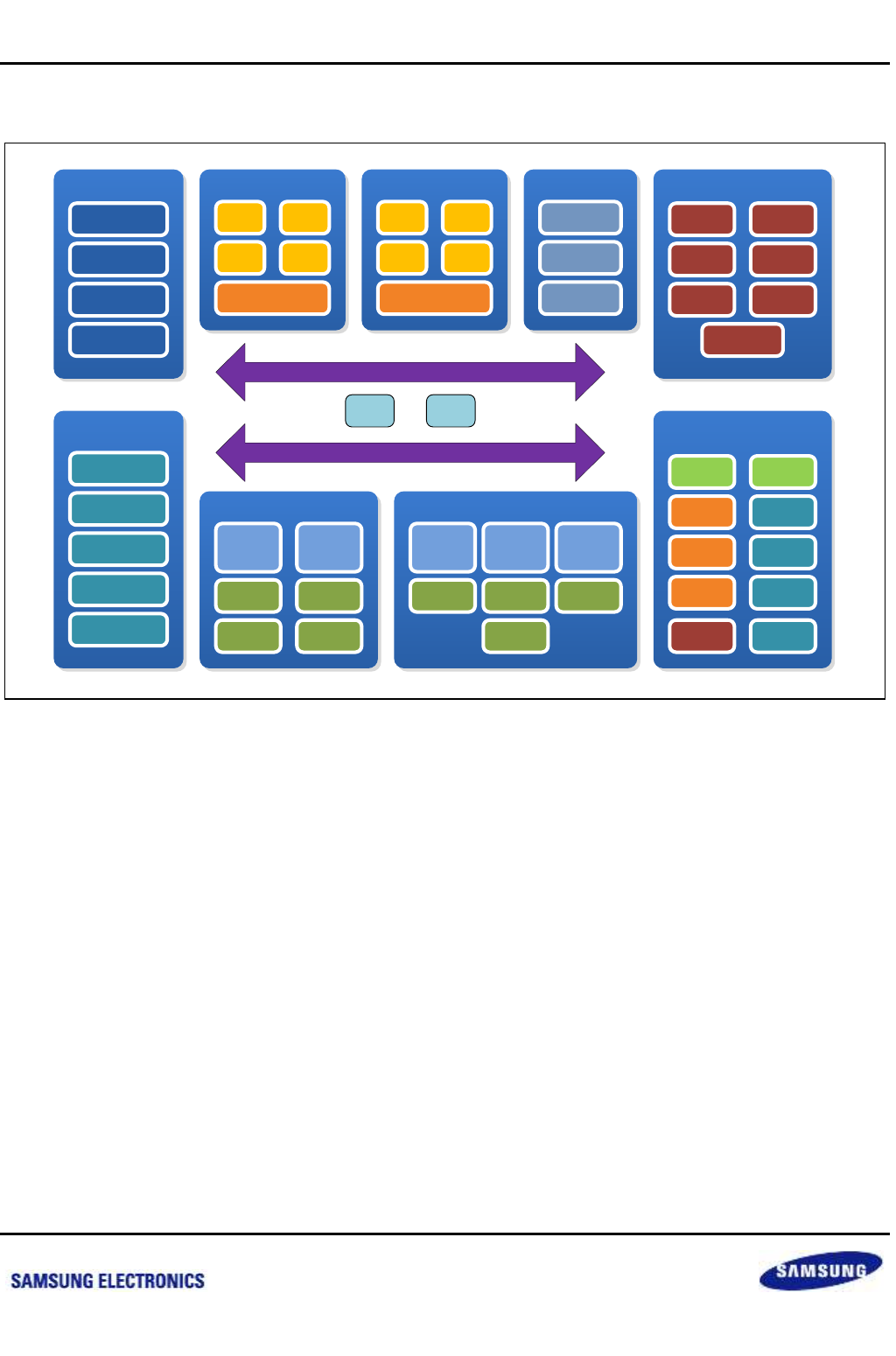
Samsung Confidential
S5P6818_UM 1 Product Overview
1-3
Preliminary product information describes products that are in development, for which full characterization data and
associated errata are not yet available. Specifications and information herein are subject to change without notice.
1.3 Block Diagram
Video Input Interface
Peripherals
CommunicationMultimedia
Display
CPU
System
Memory
3-ch
SD/MMC
DDR/LPDDR
Controller
NAND ECC
Controller
Static Memory
Controller
4-ch
Timer/WDT
Interrupt
Controller
32-ch
DMA Controller
RTC
Power
Management
Cortex
A53
Cortex
A53
L2 Cache
512K Bytes
Primary
Display
Controller
Secondary
Display
Controller
TFT-LCD
Controller HDMI 1.4a
LVDS MIPI-DSI
Video
Input
Controller
Video
Input
Controller
CCIR656 CCIR656
MIPI-CSI
3D Graphic
Accelerator
Full-HD
Video Codec
Video Post
Processor
6-ch UART
3-ch SPI
3-ch I2C
10/100/1000
Ethernet MAC
USB 2.0
Host
USB 2.0
OTG
USB HSIC
3-ch I2S PPM
AC97
SPDIF
Rx/Tx
MPEG-TS
Parser
MPEG-TS
I/F
3-ch PWM
Crypto
Secure
JTAG
64KB
RAM
20KB
ROM
Video
Input
Controller
CCIR656
Cortex
A53
Cortex
A53
CPU
Cortex
A53
Cortex
A53
L2 Cache
512K Bytes
Cortex
A53
Cortex
A53
Cache Coherent BUS
Multi Layer AXI BUS
CVBS
Figure 1-1 Block Diagram
nexell / ys.kim at 2015.02.12
SAMSUNG Confidential

Samsung Confidential
S5P6818_UM 1 Product Overview
1-4
Preliminary product information describes products that are in development, for which full characterization data and
associated errata are not yet available. Specifications and information herein are subject to change without notice.
1.4 Brief Functional Specification
1.4.1 CPU
Cortex-A53 Octa Core @ >1.4 GHz
L1 Cache
32 Kbyte I-Cache, 32 Kbyte D-Cache
L2 Cache
1 Mbyte Shared Cache
Co-Processor
VFP (Vector Floating Point Processor), Neon Processor
1.4.2 Clock & Power Management
4 Spread-Spectrum PLLs
External Crystal: 24 MHz (for PLL), 32.768 kHz (for RTC)
Supports for various power mode
Normal, Idle, Stop
Suspend to RAM (Sleep)
1.4.3 DMA
32-ch DMAs
Operation Mode
Memory-to-Memory Transfer
Memory to IO Transfer, IO to Memory Transfer
1.4.4 Interrupt Controller
Vectored Interrupt Controller
Supports 128-ch Interrupt Sources
Supports following features
fixed hardware interrupt priority levels
programmable interrupt priority levels
hardware interrupt priority level masking
programmable interrupt priority level masking
IRQ and FIQ generation
software interrupt generation
test registers
raw interrupt status
interrupt request status
nexell / ys.kim at 2015.02.12
SAMSUNG Confidential

Samsung Confidential
S5P6818_UM 1 Product Overview
1-5
Preliminary product information describes products that are in development, for which full characterization data and
associated errata are not yet available. Specifications and information herein are subject to change without notice.
1.4.5 Timer & Watchdog Timer
4-ch Timer with Watchdog Timer
Normal interval timer mode with interrupt request
Internal reset signal is activated when the timer count value reaches 0 (time-out)
Level-triggered interrupt mechanism
1.4.6 RTC
32-bit Counter
Support Alarm Interrupt
1.4.7 Memory Controller
System Memory Controller
Supports LPDDR2/LPDDR3/LVDDR3 (Low Voltage DDR3)/DDR3 SDRAM up to 2 Gbytes
Supports 1.2 V to 1.5 V power
Max Operation Frequency: 800 MHz (DDR3, LVDDR3), 533 MHz (LPDDR2, LPDDR3)
Data Bus width: 32-bit
Static Memory Controller
Multiplexed Address: up to 24-bit
SRAM, ROM and NAND Flash
Burst Read/Write
NAND Flash Controller
Supports SLC/MLC NAND Flash
Supports SLC NAND boot
Hardwired ECC Algorithm
o 4/8/12/16/24/40/60-bit BCH Error Correction
1.4.8 GPIO Controller
Various GPIO Interrupt Modes
Rising Edge, Falling Edge, High Level, Low Level Detection
Individual Interrupt Generation
nexell / ys.kim at 2015.02.12
SAMSUNG Confidential

Samsung Confidential
S5P6818_UM 1 Product Overview
1-6
Preliminary product information describes products that are in development, for which full characterization data and
associated errata are not yet available. Specifications and information herein are subject to change without notice.
1.4.9 Ethernet MAC Controller
Standard Compliance
IEEE 802.3az-2010, for Energy Efficient Ethernet (EEE)
RGMII specification version 2.6 from HP/Marvell
MAC supports the following features
10, 100, and 1000 Mbps data transfer rates with the following PHY interfaces:
o RGMII interface to communicate with an external gigabit PHY
Full-duplex operation:
o IEEE 802.3x flow control automatic transmission of zero-quanta Pause frame on flow control input de-
assertion
o Optional forwarding of received Pause frames to the user application
Half-duplex operation:
o CSMA/CD Protocol support
o Flow control using backpressure support
o Frame bursting and frame extension in 1000 Mbps half-duplex operation
Preamble and start of frame data (SFD) insertion in Transmit path
Preamble and SFD deletion in the Receive path
Automatic CRC and pad generation controllable on a per-frame basis
Automatic Pad and CRC Stripping options for receive frames
Flexible address filtering modes, such as:
o Up to 31 additional 48-bit perfect (DA) address filters with masks for each byte
o Up to 96 additional 48-bit perfect (DA) address filters that can be selected in blocks of 32 and 64
registers
o Up to 31 48-bit SA address comparison check with masks for each byte
o 64-bit, 128-bit, or 256-bit Hash filter (optional) for multicast and unicast (DA) addresses
o Option to pass all multicast addressed frames
o Promiscuous mode to pass all frames without any filtering for network monitoring
o Pass all incoming packets (as per filter) with a status report
Programmable frame length to support Standard or Jumbo Ethernet frames with up to 16 KB of size
Programmable Inter Frame Gap (IFG) (40-96 bit times in steps of 8)
Option to transmit frames with reduced preamble size
Separate 32-bit status for transmit and receive packets
IEEE 802.1Q VLAN tag detection for reception frames
Additional frame filtering:
o VLAN tag-based: Perfect match and Hash-based (optional) filtering
o Layer 3 and Layer 4-based: TCP or UDP over IPv4 or IPv6
Separate transmission, reception, and control interfaces to the application
MDIO master interface (optional) for PHY device configuration and management
Standard IEEE 802.3az-2010 for Energy Efficient Ethernet
CRC replacement, Source Address field insertion or replacement, and VLAN insertion, replacement, and
deletion in transmitted frames with per-frame control
Programmable watchdog timeout limit in the receive path
nexell / ys.kim at 2015.02.12
SAMSUNG Confidential

Samsung Confidential
S5P6818_UM 1 Product Overview
1-7
Preliminary product information describes products that are in development, for which full characterization data and
associated errata are not yet available. Specifications and information herein are subject to change without notice.
1.4.10 SD/MMC Controller
3 Independent SD/MMC Controller and Ports
Secure Digital Memory (SD mem- version 3.0)
Secure Digital I/O (SDIO - version 3.0)
Consumer Electronics Advanced Transport Architecture (CE-ATA - version 1.1)
Multimedia Cards (MMC - version 4.41, eMMC 4.5)
Supports features of MMC4.41
Supports features of eMMC4.5
Supports 8-bit DDR mode up to 50 MHz
Supports PIO and DMA mode data transfer
Supports 1/4-bit data bus widths
Overlay SPI signals to same GIOs from SSP/SPI controller
1.4.11 PPM
Pulse Period Measurement for IR remote receiver
1.4.12 PWM
3-ch PWM Controller
Five 32-bit Timers
Two 8-bit Clock Prescalers providing first level of division for the PCLK, Five Clock Dividers and Multiplexers
providing second level of division for the Prescaler clock and Two External Clocks
Programmable Clock Select Logic for individual PWM Channels
Four Independent PWM Channels with Programmable Duty Control and Polarity
Static Configuration: PWM is stopped
Dynamic Configuration: PWM is running
Supports Auto-Reload Mode and One-Shot Pulse Mode
Supports for two external inputs to start PWM
Dead Zone Generator on two PWM Outputs
Supports DMA Transfers
Optional Pulse or Level Interrupt Generation
The PWM has two operation modes:
Auto-Reload Mode
o Continuous PWM pulses are generated based on programmed duty cycle and polarity
One-Shot Pulse Mode
o Only one PWM pulse is generated based on programmed duty cycle and polarity
nexell / ys.kim at 2015.02.12
SAMSUNG Confidential

Samsung Confidential
S5P6818_UM 1 Product Overview
1-8
Preliminary product information describes products that are in development, for which full characterization data and
associated errata are not yet available. Specifications and information herein are subject to change without notice.
1.4.13 ADC
8-ch analog input port
Supports following features
Resolution: 12-bit
Conversion rate: 1 MSPS
Power consumption
o 1.0 mW (Fs = 1 MSPS) @ Normal operation mode Typ.
o 0.005 mW @ Power down mode Typ.
Input range: 0 to AVDD18
Input frequency: up to 100 kHz
1.4.14 DAC
10-bit Current Output 1 channel DAC for CVBS output
Maximum 54 MHz Update Rate
Internal Voltage Reference
1.4.15 I2C
3-ch I2C bus controller
Each device connected to the bus is software addressable by a unique address and simple master/slave
relationships exist at all times; master can operate as master-transmitter or as master-receiver
Serial, 8-bit oriented, bi-directional data transfers can be made at up to 100 kbit/s in the Standard-mode, up to
400 kbit/s in the Fast−mode
The number of ICs that can be connected to the same bus is limited only by a maximum bus capacitance of
400 pF
Repeated START and early termination function are not support
High speed mode, combined format, 10-bit address are not supported
nexell / ys.kim at 2015.02.12
SAMSUNG Confidential

Samsung Confidential
S5P6818_UM 1 Product Overview
1-9
Preliminary product information describes products that are in development, for which full characterization data and
associated errata are not yet available. Specifications and information herein are subject to change without notice.
1.4.16 SPI/SSP
3-ch SPI Controller
Master or slave operation.
Programmable clock bit rate and prescale.
Separate transmit and receive first-in, first-out memory buffers, 16 bits wide, 8 locations deep.
Programmable choice of interface operation, SPI, Microwire, or TI synchronous serial.
SPI Protocol, SSP Protocol, Microwire Protocol
DMA request servicing of the transmit and receive FIFO
Inform the system that a receive FIFO over-run has occurred
Inform the system that data is present in the receive FIFO after an idle period has expired
Only support DMA burst length 4
Maximum SSP CLKGEN’s frequency is 100 MHz
SSP Receive Timeout Period: 64 cycle of SSP CLKGEN’s clock
Max Operation Frequency
Master Mode: 50 MHz ( Receive Data is 20 MHz )
Slave Mode: 8 MHz
1.4.17 MPEG-TS
Supports Parallel MPEG-TS Interface
Supports Hardwired MPEG2-TS parser for Set-top and IPTV
1.4.18 UART& ISO7816 Sim Card Interface
6-ch UART controller
Programmable use of UART or IrDA SIR input/output.
Separate 32 8 transmit and 32 12 receive First-In, First-Out (FIFO) memory buffers to reduce CPU
interrupts.
Programmable FIFO disabling for 1 byte depth.
Programmable baud rate generator. This enables division of the reference clock by (1 16) to (65535 16)
and generates an internal 16 clock. The divisor can be a fractional number enabling you to use any clock
with a frequency >3.6864 MHz as the reference clock.
Standard asynchronous communication bits (start, stop and parity). These are added prior to transmission
and removed on reception.
Independent masking of transmit FIFO, receive FIFO, receive timeout, modem status, and error condition
interrupts.
Support for Direct Memory Access (DMA).
False start bit detection.
Line break generation and detection.
nexell / ys.kim at 2015.02.12
SAMSUNG Confidential

Samsung Confidential
S5P6818_UM 1 Product Overview
1-10
Preliminary product information describes products that are in development, for which full characterization data and
associated errata are not yet available. Specifications and information herein are subject to change without notice.
Support of the modem control functions CTS, DCD, DSR, RTS, DTR, and RI.
Programmable hardware flow control.
Fully-programmable serial interface characteristics:
Data can be 5, 6, 7, or 8 bits
Even, odd, stick, or no-parity bit generation and detection
1 or 2 stop bit generation
Baud rate generation, dc up to UARTCLK/16
IrDA SIR ENDEC block providing:
Programmable use of IrDA SIR or UART input/output
Support of IrDA SIR ENDEC functions for data rates up to 115200 bps half-duplex
Support of normal 3/16 and low-power (1.41-2.23 s) bit durations
Programmable division of the UARTCLK reference clock to generate the appropriate bit duration for low-
power IrDA mode.
Identification registers that uniquely identify the UART. These can be used by an operating system to
automatically configure itself.
1.4.19 USB
1-ch USB 2.0 Host and 1-ch USB2.0 HSIC Host
Fully compliant with the Universal Serial Bus Specification, Revision 1.1, Enhanced Host Controller
Interface Specification for Universal Serial Bus, Revision 2.0, and the openHCI: Open Host Controller
Interface Specification for USB, Release 1.0a. The controller supports high-speed, 480 Mbps transfers (40
times faster than USB 1.1 full-speed mode) using an EHCI Host Controller, as well as full and low speeds
through one or more integrated OHCI Host Controllers.
At the USB 2.0 physical interface, the controller provides the following:
o UTMI: UTMI+ Level 3, Revision 1.0
o High-Speed Inter-Chip (HSIC), Version 1.0
Supports ping and split transactions
UTMI/UTMI+ PHY interface clock supports 30 MHz operation for a 16-bit interface or 60 MHz operation
for an 8-bit interface
Heterogeneous selection of UTMI+ or HSIC interfaces per port using strap pins. In Heterogeneous mode,
only the 8-bit interface (60 MHz) is supported.
1-ch USB 2.0 OTG Controller
Supports both device and host functions and complies fully with the On-The-Go Supplement to the USB
2.0 Specification, Revision 1.3a and Revision 2.0. It can also be configured as a host-only or device-only
controller, fully compliant with the USB 2.0 Specification.
Complies with the On-The-Go Supplement to the USB 2.0 Specification (Revision 1.3)
Complies with the On-The-Go Supplement to the USB 2.0 Specification (Revision 2.0)
Software configurable to OTG1.3 and OTG2.0 modes of operation
Support for the following speeds:
o High-Speed (HS, 480 Mbps),
o Full-Speed (FS, 12 Mbps) and
o Low-Speed (LS, 1.5 Mbps) modes
nexell / ys.kim at 2015.02.12
SAMSUNG Confidential

Samsung Confidential
S5P6818_UM 1 Product Overview
1-11
Preliminary product information describes products that are in development, for which full characterization data and
associated errata are not yet available. Specifications and information herein are subject to change without notice.
Multiple options available for low power operations
Multiple DMA/non DMA mode access support on the application side
Multiple Interface support on the MAC-PHY
Supports 16 bi-directional endpoints, including control endpoint 0.
Supports Session Request Protocol (SRP)
Supports Host Negotiation Protocol (HNP)
Supports up to 16 host channels. In Host mode, when the number of device endpoints to be supported is
more than the number of host channels, software can reprogram the channels to support up to 127
devices, each having 32 endpoints (IN + OUT), for a maximum of 4,064 endpoints.
Includes automatic ping capabilities
1.4.20 I2S
3-ch I2S Controller for 5.1-ch Audio output
16-bit/24-bit Master & Slave Mode
Supports various interface mode
I2S, Left-justified, Right-Justified, DSP mode
Supports TDM mode for Digital MIC interface
Supports SPDIF Rx/Tx
1.4.21 AC97
1-ch AC97
Independent channels for stereo PCM In, stereo PCM Out, mono MIC In
DMA-based operation and interrupt based operation
All of the channels support only 16-bit samples
Variable sampling rate AC97 Codec interface (48 kHz and below)
16-bit, 16 entry FIFOs per channel
Only primary Codec support
1.4.22 SPDIF Tx, Rx
SPDIF Tx
Supports linear PCM up to 24-bit per sample
Supports Non-linear PCM formats such as AC3, MPEG1 and MPEG2
2 24-bit buffers which is alternately filled with data
SPDIF Rx
Serial, unidirectional, self-clocking interface
Single wire-single signal interface
Easy to work because it is polarity independent
nexell / ys.kim at 2015.02.12
SAMSUNG Confidential

Samsung Confidential
S5P6818_UM 1 Product Overview
1-12
Preliminary product information describes products that are in development, for which full characterization data and
associated errata are not yet available. Specifications and information herein are subject to change without notice.
1.4.23 PDM
Supports receiving 2 channel audio data with 1 data pin
1 output clock pin
2 data pins (total 4 channel accepts available)
Fixed output clock frequency
Supports select of the timing of data capture
Supports DMA interface
Supports a user configuration of Coefficient. (Butterworth Low-pass Filter)
1.4.24 Display Controller
Supports Dual Display
Supports 3 Layers, Gamma Correction and Color Control (Brightness, Contrast, Hue and Saturation)
Supports various Pixel Format
RGB/BGR 444, 555, 565, 888 with/without Alpha channel
Resolution
Up to 1920 1080 @60 Hz
Supports CVBS output
Supports various LCD
I80 Interface, RGB, Serial RGB, LVDS output
Supports MIPI-DSI 4 data lanes
HDMI Interface
HDMI 1.4a, HDCP 1.4 Complaint
Supports Video format:
o 480p/480i @59.94 Hz/60 Hz, 576p/576i@50 Hz
o 720p/720i @50 Hz/59.94 Hz/60 Hz
o 1080p/1080i @50 Hz/59.94 Hz/60 Hz
o Primary 3D Video Formats
o Other various formats up to148 MHz Pixel Clock
Supports Color Format: 4:4:4 RGB/YCbCr , 4:2:2 YCbCr
Pixel Repetition: Up to x4
Supports Bit Per Color: 8-bit, 10-bit ,12-bit (Note: 16-bit not supported)
Dedicated block for CEC function
Supports: Linear-PCM, Non-linear PCM and high-bitrate audio formats (Audio Sample packets and HBR
packets for audio transmission)
Integrated HDCP Encryption Engine for Video/Audio content protection (Authentication procedure are
controlled by S/W, not by H/W)
A dedicated CEC module (Separated for power/clock domain separation)
SPDIF Interface and I2S interface for Audio Input
Supports level-triggered Interrupt and SFR for HPD
nexell / ys.kim at 2015.02.12
SAMSUNG Confidential

Samsung Confidential
S5P6818_UM 1 Product Overview
1-13
Preliminary product information describes products that are in development, for which full characterization data and
associated errata are not yet available. Specifications and information herein are subject to change without notice.
Supports AES KEY Decryption Function for external HDCP Key management
LVDS Interface
Output clock range: 30M to 160 MHz
35:7 data channel compression up to 630 Mbps on each LVDS channel
Power down mode
Up to 393.75 Mbytes/sec bandwidth
Max Resolution: 1920 1080 @60 fps
Falling clock edge data strobe
Narrow bus reduces cable size and cost
PLL requires no external component
6 LVDS output channels (5 data channels, 1 clock channel)
MIPI-DSI
Complies to MIPI DSI Standard Specification V1.01r11
o Maximum resolution ranges up to WUXGA (1920 1200)
o Supports 1, 2, 3, or 4 data lanes
o Supports pixel format: 16-bpp, 18-bpp packed, 18-bpp loosely packed (3 byte format), and 24-bpp
Interfaces
o Complies with Protocol-to-PHY Interface (PPI) in 1.5 Gbps MIPI D-PHY
o Supports RGB Interface for Video Image Input from display controller
o Supports I80 Interface for Command Mode Image input from display controller
o Supports PMS control interface for PLL to configure byte clock frequency
o Supports Prescaler to generate escape clock from byte clock
1.4.25 Video Post Processor
3D De-interlace Controller
Fine Scalar for video: Poly-phase filter
nexell / ys.kim at 2015.02.12
SAMSUNG Confidential

Samsung Confidential
S5P6818_UM 1 Product Overview
1-14
Preliminary product information describes products that are in development, for which full characterization data and
associated errata are not yet available. Specifications and information herein are subject to change without notice.
1.4.26 Video Input Processor
Max. 8192 8192 resolution support
Receives 3-ch Camera input simultaneously
Supports x3 8-bit BT656, 601 format
Supports MIPI-CSI
General Features
o Support primary and secondary Image format
- YUV420, YUV420 (Legacy),YUV420 (CSPS), YUV422 of 8 bits and 10 bits
- RGB565, RGB666, RGB888
- RAW6, RAW7, RAW8, RAW10, RAW12, RAW14
- Compressed format: 10-6-10, 10-7-10, 10-8-10
- All of User defined Byte-based Data packet
o Support embedded byte-based non Image data packet and generic short packets.
o Compatible to PPI (Protocol-to-PHY Interface) in MIPI D-PHY Specification
o Support 4 channel virtual channel or data interleave
Standard Compliance
o Compliant to MIPI CSI2 Standard Specification V1.01r06
o D-PHY standard specification V1.0
1.4.27 Multi Format MPEG codec
Decoder
H.264
o BP, MP, HP profile, Level 4.2 up to 1920 1080, 50 Mbps
MPEG4 ASP
o Advanced Simple Profile up to 1920 1080, 40 Mbps
H.263
o Profile3 up to 1920 1080, 20 Mbps
VC-1
o SP/MP/AP profile, Level 3 up to 1920 1080, 2048 1024, 45 Mbps
MPEG-1/2
o Main Profile, High Level up to 1920 1080, 80 Mbps
VP8
o up to 1920 1080, 20 Mbps
Theora
o up to 1280 720, 20 Mbps
AVS
o Jizhun Profile, Level 6.2 up to 1920 1080, 40 Mbps
RV8/9/10
o up to 1920 1080, 40 Mbps
MJPEG
o Baseline profile up to 8192 8192
nexell / ys.kim at 2015.02.12
SAMSUNG Confidential

Samsung Confidential
S5P6818_UM 1 Product Overview
1-15
Preliminary product information describes products that are in development, for which full characterization data and
associated errata are not yet available. Specifications and information herein are subject to change without notice.
Encoder
H.264
o Baseline Profile, Level 4.0 up to 1080p, 20 Mbps
MPEG4
o Simple Profile, Level 5.6 up to 1080p, 20 Mbps
H.263
o Profile3, Level 70 up to 1080p, 20 Mbps
MJPEG
o Baseline Profile up to 8192 8192
1.4.28 3D Graphic Controller
Supports OpenGL ES 1.0 and 2.0
Supports OpenVG 1.1
GPU is a hardware accelerator for 2D and 3D graphics systems.
The GPU consists of:
Four Pixel Processors (PPs)
A Geometry Processor (GP)
A Level 2 Cache Controller (L2)
A Memory Management Unit (MMU) for each GP and PP included in the GPU
A Power Management Unit (PMU).
Pixel processor features
Each pixel processor used processes a different tile, enabling a faster turnaround
Programmable fragment shader
Alpha blending
Complete non-power-of-2 texture support
Cube mapping
Fast dynamic branching
Fast trigonometric functions, including arctangent
Full floating-point arithmetic
Frame buffer blend with destination Alpha
Indexable texture samplers
Line, quad, triangle and point sprites
No limit on program length
Perspective correct texturing
Point sampling, bilinear, and tri-linear filtering
Programmable mipmap level-of-detail biasing and replacement
Stencil buffering, 8-bit
Two-sided stencil
Unlimited dependent texture reads
4-level hierarchical Z and stencil operations
nexell / ys.kim at 2015.02.12
SAMSUNG Confidential

Samsung Confidential
S5P6818_UM 1 Product Overview
1-16
Preliminary product information describes products that are in development, for which full characterization data and
associated errata are not yet available. Specifications and information herein are subject to change without notice.
Up to 512 times Full Scene Anti-Aliasing (FSAA). 4x multisampling times 128x super sampling
4-bit per texel compressed texture format.
Geometry processor features
Programmable vertex shader
Flexible input and output formats
Autonomous operation tile list generation
Indexed and non-indexed geometry input
Primitive constructions with points, lines, triangles and quads.
Level 2 cache controller features
Sizes of 64 KB
4-way set-associative
Supports up to 32 outstanding AXI transactions
Implements a standard pseudo-LRU algorithm
Cache line and line fill burst size is 64 bytes
Supports eight to 64 bytes uncached read bursts and write bursts
128-bit interface to memory sub-system
Support for hit-under-miss and miss-under-miss with the only limitation of AXI ordering rules.
MMU features
Accesses control registers through the bus infrastructure to configure the memory system.
Each processor has its own MMU to control and translate memory accesses that the GPU initiates.
PMU features
Programmable power management
Powers up and down each GP, PP and Level 2 cache controller separately
Controls the clock, isolation and power of each device
Provides an interrupt when all requested devices are powered up
1.4.29 Security IP
On-chip secure boot ROM/RAM
ARM TrustZone: TZPC, TZASC and TZMA
Hardware Crypto Accelerator
DES/TDES, AES, SHA-1, MD5 and PRNG
Supports Secure JTAG
1.4.30 Unique Chip ID
Supports 128-bit Unique Chip ID register
nexell / ys.kim at 2015.02.12
SAMSUNG Confidential

Samsung Confidential
S5P6818_UM 1 Product Overview
1-17
Preliminary product information describes products that are in development, for which full characterization data and
associated errata are not yet available. Specifications and information herein are subject to change without notice.
1.4.31 Operating Conditions
Operation Voltage
Core: 0.95 to 1.1 V
CPU: 0.95 V to 1.35 V
DDR Memory: 1.2 to 1.5 V
I/O: 3.3 V
Operation Temperature
Ambient temperature: –25 °C to 85 °C
Die temperature: –25 °C to 85 °C
1.4.32 Package
537 pin FCBGA
Ball Pitch: 0.65 mm
Body Size: 17 17 mm
nexell / ys.kim at 2015.02.12
SAMSUNG Confidential
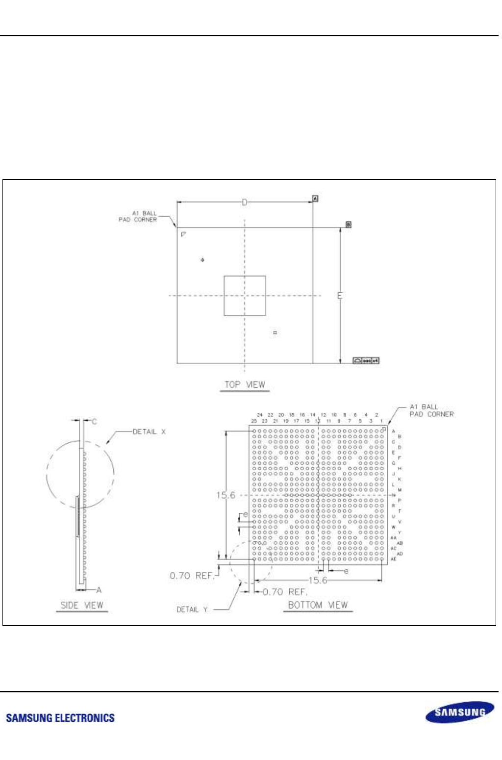
Samsung Confidential
S5P6818_UM 2 Mechanical Dimension & IO Function Description
2-1
Preliminary product information describes products that are in development, for which full characterization data and
associated errata are not yet available. Specifications and information herein are subject to change without notice.
2 Mechanical Dimension & IO Function Description
2.1 Mechanical Dimension
Figure 2-1 Mechanical Dimension - Top, Side, Bottom View
nexell / ys.kim at 2015.02.12
SAMSUNG Confidential
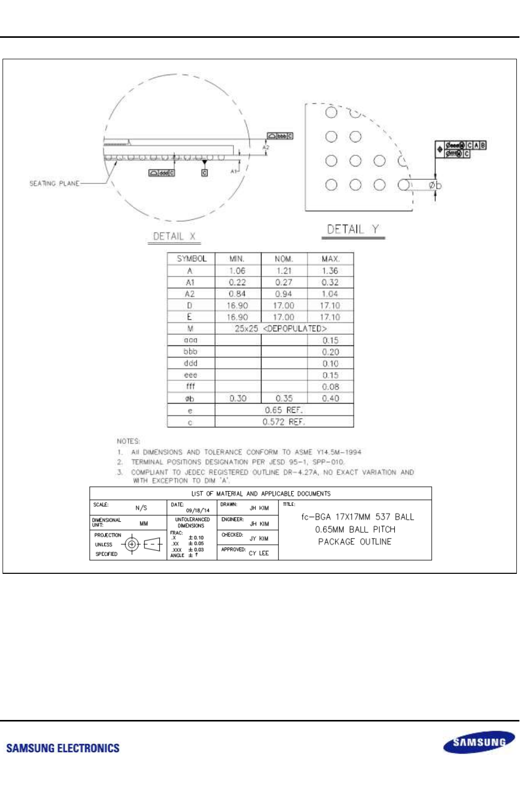
Samsung Confidential
S5P6818_UM 2 Mechanical Dimension & IO Function Description
2-2
Preliminary product information describes products that are in development, for which full characterization data and
associated errata are not yet available. Specifications and information herein are subject to change without notice.
Figure 2-2 Mechanical Dimension - Dimension Value
nexell / ys.kim at 2015.02.12
SAMSUNG Confidential
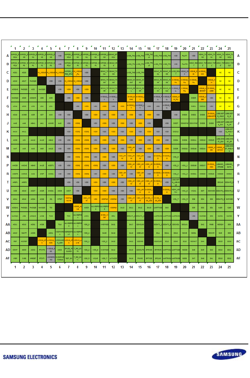
Samsung Confidential
S5P6818_UM 2 Mechanical Dimension & IO Function Description
2-3
Preliminary product information describes products that are in development, for which full characterization data and
associated errata are not yet available. Specifications and information herein are subject to change without notice.
2.2 FCBGA Ball Map
Figure 2-3 FCBGA Ball Map (Top View)
nexell / ys.kim at 2015.02.12
SAMSUNG Confidential
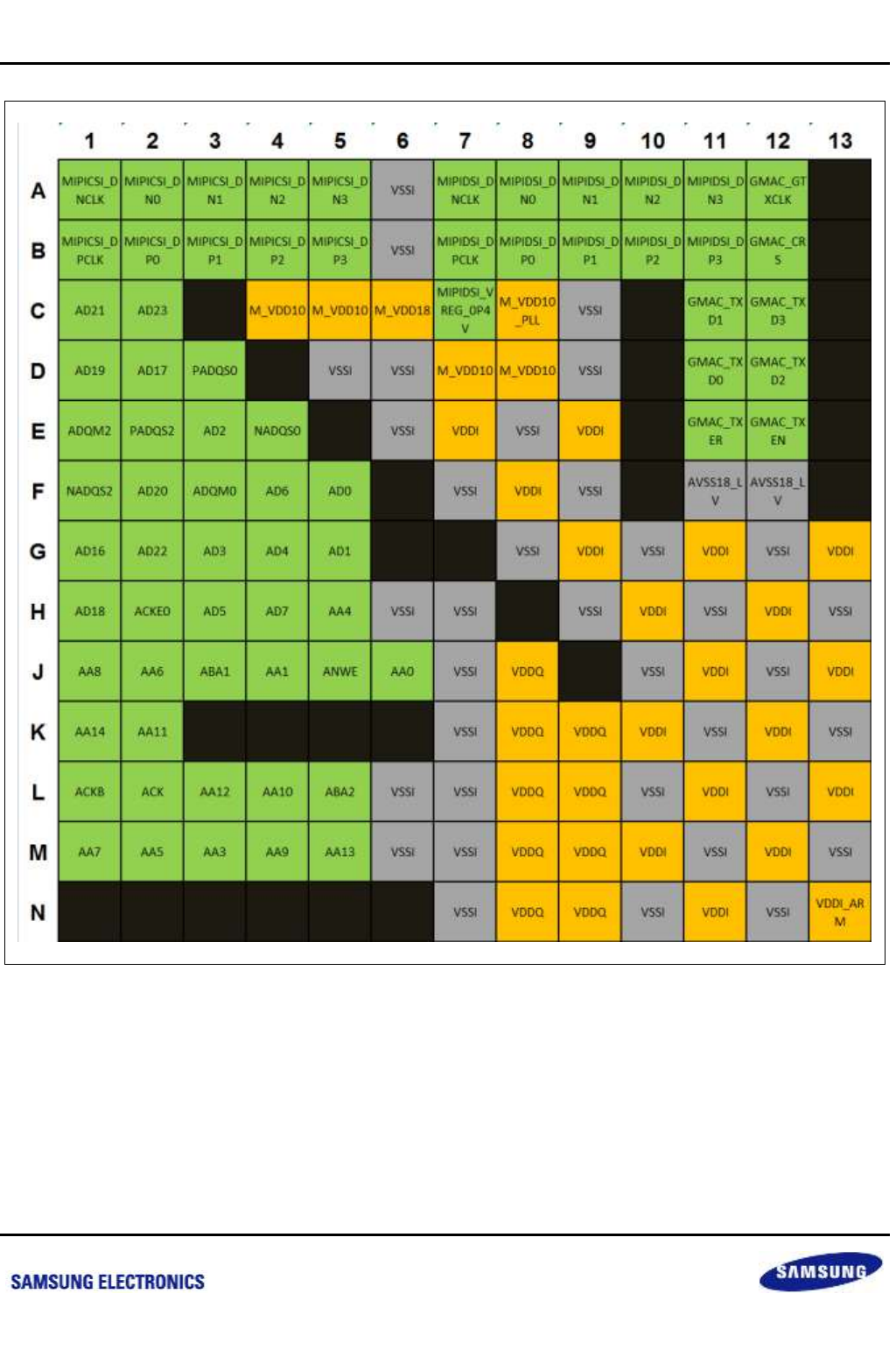
Samsung Confidential
S5P6818_UM 2 Mechanical Dimension & IO Function Description
2-4
Preliminary product information describes products that are in development, for which full characterization data and
associated errata are not yet available. Specifications and information herein are subject to change without notice.
Figure 2-4 FCBGA Ball Map (Top View) - Upper Left Side
nexell / ys.kim at 2015.02.12
SAMSUNG Confidential
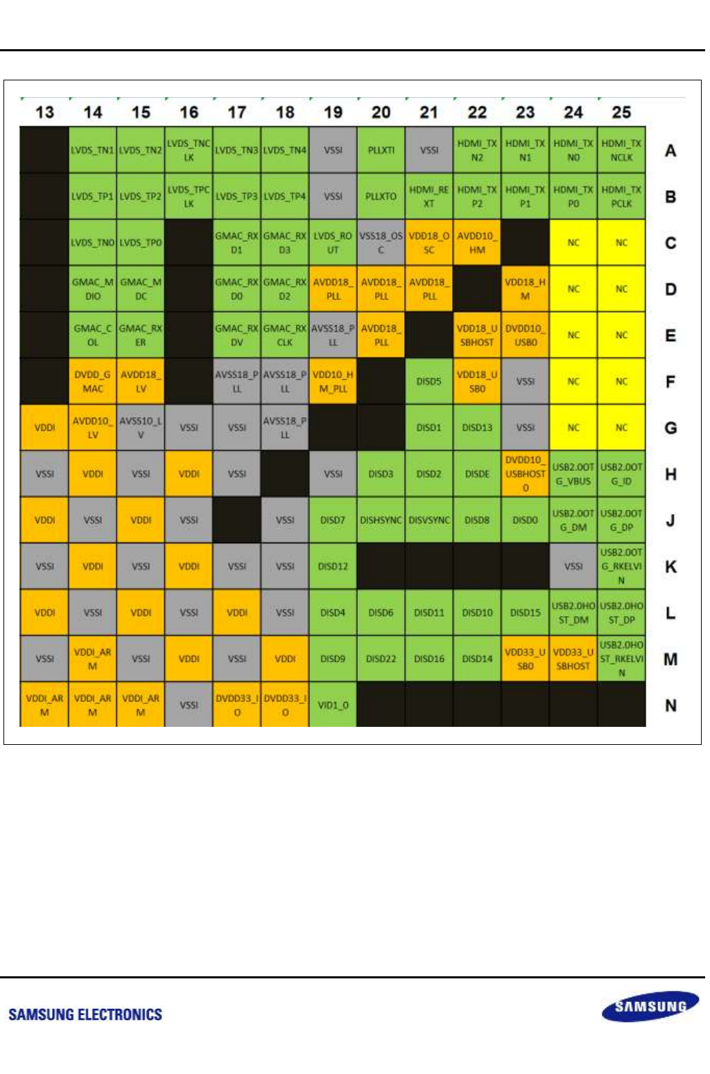
Samsung Confidential
S5P6818_UM 2 Mechanical Dimension & IO Function Description
2-5
Preliminary product information describes products that are in development, for which full characterization data and
associated errata are not yet available. Specifications and information herein are subject to change without notice.
Figure 2-5 FCBGA Ball Map (Top View) - Upper Right Side
nexell / ys.kim at 2015.02.12
SAMSUNG Confidential
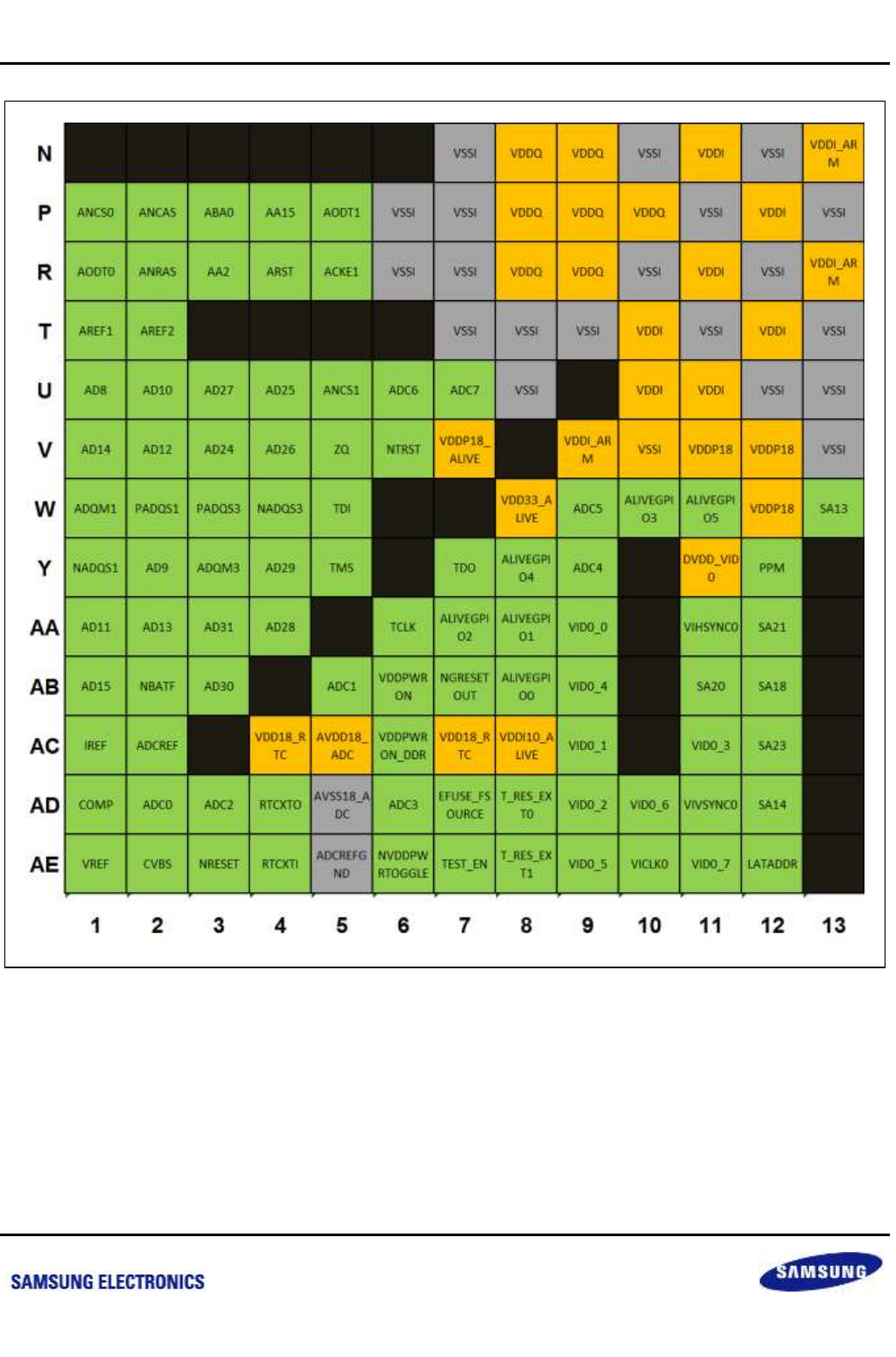
Samsung Confidential
S5P6818_UM 2 Mechanical Dimension & IO Function Description
2-6
Preliminary product information describes products that are in development, for which full characterization data and
associated errata are not yet available. Specifications and information herein are subject to change without notice.
Figure 2-6 FCBGA Ball Map (Top View) - Lower Left Side
nexell / ys.kim at 2015.02.12
SAMSUNG Confidential
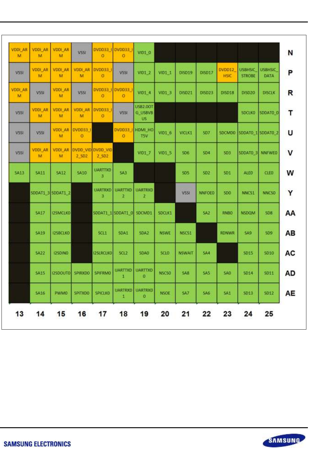
Samsung Confidential
S5P6818_UM 2 Mechanical Dimension & IO Function Description
2-7
Preliminary product information describes products that are in development, for which full characterization data and
associated errata are not yet available. Specifications and information herein are subject to change without notice.
Figure 2-7 FCBGA Ball Map (Top View) - Lower Right Side
nexell / ys.kim at 2015.02.12
SAMSUNG Confidential

Samsung Confidential
S5P6818_UM 2 Mechanical Dimension & IO Function Description
2-8
Preliminary product information describes products that are in development, for which full characterization data and
associated errata are not yet available. Specifications and information herein are subject to change without notice.
2.3 I/O Function Description
2.3.1 Ball List Table
Table 2-1 Ball Function Table
Ball
Name
Type
I/O
PU
/PD
Alternate
Function 0
Alternate
Function 1
Alternate
Function 2
Alternate
Function 3
A1
MIPICSI_DNCLK
S
IO
N
MIPICSI_DNCLK
A2
MIPICSI_DN0
S
IO
N
MIPICSI_DN0
A3
MIPICSI_DN1
S
IO
N
MIPICSI_DN1
A4
MIPICSI_DN2
S
IO
N
MIPICSI_DN2
A5
MIPICSI_DN3
S
IO
N
MIPICSI_DN3
A6
VSSI
G
–
N
A7
MIPIDSI_DNCLK
S
IO
N
MIPIDSI_DNCLK
A8
MIPIDSI_DN0
S
IO
N
MIPIDSI_DN0
A9
MIPIDSI_DN1
S
IO
N
MIPIDSI_DN1
A10
MIPIDSI_DN2
S
IO
N
MIPIDSI_DN2
A11
MIPIDSI_DN3
S
IO
N
MIPIDSI_DN3
A12
GMAC_GTXCLK
S
IO
N
GPIOE24
GMAC_GTXCLK
A14
LVDS_TN1
S
IO
N
LVDS_TN1
A15
LVDS_TN2
S
IO
N
LVDS_TN2
A16
LVDS_TNCLK
S
IO
N
LVDS_TNCLK
A17
LVDS_TN3
S
IO
N
LVDS_TN3
A18
LVDS_TN4
S
IO
N
LVDS_TN4
A19
VSSI
G
–
N
A20
PLLXTI
S
I
N
PLLXTI
A21
VSSI
G
–
N
A22
HDMI_TXN2
S
O
N
HDMI_TXN2
A23
HDMI_TXN1
S
O
N
HDMI_TXN1
A24
HDMI_TXN0
S
O
N
HDMI_TXN0
A25
HDMI_TXNCLK
S
O
N
HDMI_TXNCLK
B1
MIPICSI_DPCLK
S
IO
N
MIPICSI_DPCLK
B2
MIPICSI_DP0
S
IO
N
MIPICSI_DP0
B3
MIPICSI_DP1
S
IO
N
MIPICSI_DP1
B4
MIPICSI_DP2
S
IO
N
MIPICSI_DP2
B5
MIPICSI_DP3
S
IO
N
MIPICSI_DP3
B6
VSSI
G
–
N
nexell / ys.kim at 2015.02.12
SAMSUNG Confidential

Samsung Confidential
S5P6818_UM 2 Mechanical Dimension & IO Function Description
2-9
Preliminary product information describes products that are in development, for which full characterization data and
associated errata are not yet available. Specifications and information herein are subject to change without notice.
Ball
Name
Type
I/O
PU
/PD
Alternate
Function 0
Alternate
Function 1
Alternate
Function 2
Alternate
Function 3
B7
MIPIDSI_DPCLK
S
IO
N
MIPIDSI_DPCLK
B8
MIPIDSI_DP0
S
IO
N
MIPIDSI_DP0
B9
MIPIDSI_DP1
S
IO
N
MIPIDSI_DP1
B10
MIPIDSI_DP2
S
IO
N
MIPIDSI_DP2
B11
MIPIDSI_DP3
S
IO
N
MIPIDSI_DP3
B12
GMAC_CRS
S
IO
N
GPIOE23
GMAC_CRS
B14
LVDS_TP1
S
IO
N
LVDS_TP1
B15
LVDS_TP2
S
IO
N
LVDS_TP2
B16
LVDS_TPCLK
S
IO
N
LVDS_TPCLK
B17
LVDS_TP3
S
IO
N
LVDS_TP3
B18
LVDS_TP4
S
IO
N
LVDS_TP4
B19
VSSI
G
–
N
B20
PLLXTO
S
O
N
PLLXTO
B21
HDMI_REXT
S
N
HDMI_REXT
B22
HDMI_TXP2
S
O
N
HDMI_TXP2
B23
HDMI_TXP1
S
O
N
HDMI_TXP1
B24
HDMI_TXP0
S
O
N
HDMI_TXP0
B25
HDMI_TXPCLK
S
O
N
HDMI_TXPCLK
C1
AD21
S
IO
N
AD21
C2
AD23
S
IO
N
AD23
C4
M_VDD10
P
N
C5
M_VDD10
P
N
C6
M_VDD18
P
N
C7
MIPIDSI_VREG_0P4
V
S
N
MIPIDSI_VREG_0P
4V
C8
M_VDD10_PLL
P
N
C9
VSSI
G
–
N
C11
GMAC_TXD1
S
IO
N
GPIOE8
GMAC_TXD1
C12
GMAC_TXD3
S
IO
N
GPIOE10
GMAC_TXD3
C14
LVDS_TN0
S
IO
N
LVDS_TN0
C15
LVDS_TP0
S
IO
N
LVDS_TP0
C17
GMAC_RXD1
S
IO
N
GPIOE15
GMAC_RXD1
SPIFRM1
C18
GMAC_RXD3
S
IO
N
GPIOE17
GMAC_RXD3
C19
LVDS_ROUT
S
N
LVDS_ROUT
nexell / ys.kim at 2015.02.12
SAMSUNG Confidential

Samsung Confidential
S5P6818_UM 2 Mechanical Dimension & IO Function Description
2-10
Preliminary product information describes products that are in development, for which full characterization data and
associated errata are not yet available. Specifications and information herein are subject to change without notice.
Ball
Name
Type
I/O
PU
/PD
Alternate
Function 0
Alternate
Function 1
Alternate
Function 2
Alternate
Function 3
C20
VSS18_OSC
G
–
N
C21
VDD18_OSC
P
N
C22
AVDD10_HM
P
N
C24
NC
–
–
–
C25
NC
–
–
–
D1
AD19
S
IO
N
AD19
D2
AD17
S
IO
N
AD17
D3
PADQS0
S
IO
N
PADQS0
D5
VSSI
G
N
D6
VSSI
G
N
D7
M_VDD10
P
N
D8
M_VDD10
P
N
D9
VSSI
G
–
N
D11
GMAC_TXD0
S
IO
N
GPIOE7
GMAC_TXD0
VIVSYNC1
D12
GMAC_TXD2
S
IO
N
GPIOE9
GMAC_TXD2
D14
GMAC_MDIO
S
IO
N
GPIOE21
GMAC_MDIO
D15
GMAC_MDC
S
IO
N
GPIOE20
GMAC_MDC
D17
GMAC_RXD0
S
IO
N
GPIOE14
GMAC_RXD0
SPICLK1
D18
GMAC_RXD2
S
IO
N
GPIOE16
GMAC_RXD2
D19
AVDD18_PLL
P
N
D20
AVDD18_PLL
P
N
D21
AVDD18_PLL
P
N
D23
VDD18_HM
P
N
D24
NC
–
–
–
D25
NC
–
–
–
E1
ADQM2
S
O
N
ADQM2
E2
PADQS2
S
IO
N
PADQS2
E3
AD2
S
IO
N
AD2
E4
NADQS0
S
IO
N
NADQS0
E6
VSSI
G
N
E7
VDDI
P
N
E8
VSSI
G
N
E9
VDDI
P
–
N
E11
GMAC_TXER
S
N
GPIOE12
GMAC_TXER
nexell / ys.kim at 2015.02.12
SAMSUNG Confidential

Samsung Confidential
S5P6818_UM 2 Mechanical Dimension & IO Function Description
2-11
Preliminary product information describes products that are in development, for which full characterization data and
associated errata are not yet available. Specifications and information herein are subject to change without notice.
Ball
Name
Type
I/O
PU
/PD
Alternate
Function 0
Alternate
Function 1
Alternate
Function 2
Alternate
Function 3
E12
GMAC_TXEN
S
IO
N
GPIOE11
GMAC_TXEN
E14
GMAC_COL
S
IO
N
GPIOE13
GMAC_COL
VIHSYNC1
E15
GMAC_RXER
S
IO
N
GPIOE22
GMAC_RXER
E17
GMAC_RXDV
S
IO
N
GPIOE19
GMAC_RXDV
SPITXD1
E18
GMAC_RXCLK
S
IO
N
GPIOE18
GMAC_RXCLK
SPIRXD1
E19
AVSS18_PLL
G
–
N
E20
AVDD18_PLL
P
N
E22
VDD18_USBHOST
P
N
E23
DVDD10_USB0
P
N
E24
NC
–
–
–
E25
NC
–
–
–
F1
NADQS2
S
IO
N
NADQS2
F2
AD20
S
IO
N
AD20
F3
ADQM0
S
O
N
ADQM0
F4
AD6
S
IO
N
AD6
F5
AD0
S
IO
N
AD0
F7
VSSI
G
–
N
F8
VDDI
P
–
N
F9
VSSI
G
–
N
F11
AVSS18_LV
G
–
N
F12
AVSS18_LV
G
–
N
F14
DVDD_GMAC
P
N
F15
AVDD18_LV
P
N
F17
AVSS18_PLL
G
–
N
F18
AVSS18_PLL
G
–
N
F19
VDD10_HM_PLL
P
N
F21
DISD5
S
IO
N
GPIOA6
DISD5
F22
VDD18_USB0
P
–
N
F23
VSSI
G
N
F24
NC
–
–
–
F25
NC
–
–
–
G1
AD16
S
IO
N
AD16
G2
AD22
S
IO
N
AD22
G3
AD3
S
IO
N
AD3
nexell / ys.kim at 2015.02.12
SAMSUNG Confidential

Samsung Confidential
S5P6818_UM 2 Mechanical Dimension & IO Function Description
2-12
Preliminary product information describes products that are in development, for which full characterization data and
associated errata are not yet available. Specifications and information herein are subject to change without notice.
Ball
Name
Type
I/O
PU
/PD
Alternate
Function 0
Alternate
Function 1
Alternate
Function 2
Alternate
Function 3
G4
AD4
S
IO
N
AD4
G5
AD1
S
IO
N
AD1
G8
VSSI
G
–
N
G9
VDDI
P
–
N
G10
VSSI
G
–
N
G11
VDDI
P
–
N
G12
VSSI
G
–
N
G13
VDDI
P
–
N
G14
AVDD10_LV
P
–
N
G15
AVSS10_LV
G
–
N
G16
VSSI
G
–
N
G17
VSSI
G
–
N
G18
AVSS18_PLL
G
–
N
G21
DISD1
S
IO
N
GPIOA2
DISD1
G22
DISD13
S
IO
N
GPIOA14
DISD13
G23
VSSI
G
–
N
G24
NC
–
–
–
G25
NC
–
–
–
H1
AD18
S
IO
N
AD18
H2
ACKE0
S
O
N
ACKE0
H3
AD5
S
IO
N
AD5
H4
AD7
S
IO
N
AD7
H5
AA4
S
O
N
AA4
H6
VSSI
G
–
N
H7
VSSI
G
–
N
H9
VSSI
G
–
N
H10
VDDI
P
–
N
H11
VSSI
G
–
N
H12
VDDI
P
–
N
H13
VSSI
G
–
N
H14
VDDI
P
–
N
H15
VSSI
G
–
N
H16
VDDI
P
–
N
H17
VSSI
G
–
N
nexell / ys.kim at 2015.02.12
SAMSUNG Confidential

Samsung Confidential
S5P6818_UM 2 Mechanical Dimension & IO Function Description
2-13
Preliminary product information describes products that are in development, for which full characterization data and
associated errata are not yet available. Specifications and information herein are subject to change without notice.
Ball
Name
Type
I/O
PU
/PD
Alternate
Function 0
Alternate
Function 1
Alternate
Function 2
Alternate
Function 3
H19
VSSI
G
–
N
H20
DISD3
S
IO
N
GPIOA4
DISD3
H21
DISD2
S
IO
N
GPIOA3
DISD2
H22
DISDE
S
IO
N
GPIOA27
DISDE
H23
DVDD10_USBHOST
0
P
N
H24
USB2.0OTG_VBUS
S
IO
N
USB2.0OTG_VBUS
H25
USB2.0OTG_ID
S
IO
N
USB2.0OTG_ID
J1
AA8
S
O
N
AA8
J2
AA6
S
O
N
AA6
J3
ABA1
S
O
N
ABA1
J4
AA1
S
O
N
AA1
J5
ANWE
S
O
N
ANWE
J6
AA0
S
O
N
AA0
J7
VSSI
G
–
N
J8
VDDQ
P
–
N
J10
VSSI
G
–
N
J11
VDDI
P
–
N
J12
VSSI
G
N
J13
VDDI
P
–
N
J14
VSSI
G
N
J15
VDDI
P
–
N
J16
VSSI
G
–
N
J18
VSSI
G
–
N
J19
DISD7
S
IO
N
GPIOA8
DISD7
J20
DISHSYNC
S
IO
N
GPIOA26
DISHSYNC
J21
DISVSYNC
S
IO
N
GPIOA25
DISVSYNC
J22
DISD8
S
IO
N
GPIOA9
DISD8
J23
DISD0
S
IO
N
GPIOA1
DISD0
J24
USB2.0OTG_DM
S
IO
N
USB2.0OTG_DM
J25
USB2.0OTG_DP
S
IO
N
USB2.0OTG_DP
K1
AA14
S
O
N
AA14
K2
AA11
S
O
N
AA11
K7
VSSI
G
–
N
nexell / ys.kim at 2015.02.12
SAMSUNG Confidential

Samsung Confidential
S5P6818_UM 2 Mechanical Dimension & IO Function Description
2-14
Preliminary product information describes products that are in development, for which full characterization data and
associated errata are not yet available. Specifications and information herein are subject to change without notice.
Ball
Name
Type
I/O
PU
/PD
Alternate
Function 0
Alternate
Function 1
Alternate
Function 2
Alternate
Function 3
K8
VDDQ
P
–
N
K9
VDDQ
P
–
N
K10
VDDI
P
–
N
K11
VSSI
G
–
N
K12
VDDI
P
–
N
K13
VSSI
G
N
K14
VDDI
P
–
N
K15
VSSI
G
N
K16
VDDI
P
–
N
K17
VSSI
G
–
N
K18
VSSI
G
–
N
K19
DISD12
S
IO
N
GPIOA13
DISD12
K24
VSSI
G
–
N
K25
USB2.0OTG_RKELVI
N
S
IO
N
USB2.0OTG_RKEL
VIN
L1
ACKB
S
O
N
ACKB
L2
ACK
S
O
N
ACK
L3
AA12
S
O
N
AA12
L4
AA10
S
O
N
AA10
L5
ABA2
S
O
N
ABA2
L6
VSSI
G
–
N
L7
VSSI
G
–
N
L8
VDDQ
P
–
N
L9
VDDQ
P
N
L10
VSSI
G
N
L11
VDDI
P
–
N
L12
VSSI
G
N
L13
VDDI
P
–
N
L14
VSSI
G
–
N
L15
VDDI
P
–
N
L16
VSSI
G
–
N
L17
VDDI
P
N
L18
VSSI
G
–
N
L19
DISD4
S
IO
N
GPIOA5
DISD4
nexell / ys.kim at 2015.02.12
SAMSUNG Confidential

Samsung Confidential
S5P6818_UM 2 Mechanical Dimension & IO Function Description
2-15
Preliminary product information describes products that are in development, for which full characterization data and
associated errata are not yet available. Specifications and information herein are subject to change without notice.
Ball
Name
Type
I/O
PU
/PD
Alternate
Function 0
Alternate
Function 1
Alternate
Function 2
Alternate
Function 3
L20
DISD6
S
IO
N
GPIOA7
DISD6
L21
DISD11
S
IO
N
GPIOA12
DISD11
L22
DISD10
S
IO
N
GPIOA11
DISD10
L23
DISD15
S
IO
N
GPIOA16
DISD15
L24
USB2.0HOST_DM
S
IO
N
USB2.0HOST_DM
L25
USB2.0HOST_DP
S
IO
N
USB2.0HOST_DP
M1
AA7
S
O
N
AA7
M2
AA5
S
O
N
AA5
M3
AA3
S
O
N
AA3
M4
AA9
S
O
N
AA9
M5
AA13
S
O
N
AA13
M6
VSSI
G
–
N
M7
VSSI
G
–
N
M8
VDDQ
P
–
N
M9
VDDQ
P
N
M10
VDDI
P
N
M11
VSSI
G
N
M12
VDDI
P
–
N
M13
VSSI
G
N
M14
VDDI_ARM
P
–
N
M15
VSSI
G
N
M16
VDDI
P
–
N
M17
VSSI
G
–
N
M18
VDDI
P
–
N
M19
DISD9
S
IO
N
GPIOA10
DISD9
M20
DISD22
S
IO
N
GPIOA23
DISD22
M21
DISD16
S
IO
N
GPIOA17
DISD16
M22
DISD14
S
IO
N
GPIOA15
DISD14
M23
VDD33_USB0
P
–
N
M24
VDD33_USBHOST
P
–
N
M25
USB2.0HOST_RKEL
VIN
S
IO
N
USB2.0HOST_RKE
LVIN
N7
VSSI
G
–
N
N8
VDDQ
P
–
N
nexell / ys.kim at 2015.02.12
SAMSUNG Confidential

Samsung Confidential
S5P6818_UM 2 Mechanical Dimension & IO Function Description
2-16
Preliminary product information describes products that are in development, for which full characterization data and
associated errata are not yet available. Specifications and information herein are subject to change without notice.
Ball
Name
Type
I/O
PU
/PD
Alternate
Function 0
Alternate
Function 1
Alternate
Function 2
Alternate
Function 3
N9
VDDQ
P
N
N10
VSSI
G
N
N11
VDDI
P
–
N
N12
VSSI
G
N
N13
VDDI_ARM
P
–
N
N14
VDDI_ARM
P
N
N15
VDDI_ARM
P
–
N
N16
VSSI
G
N
N17
DVDD33_IO
P
–
N
N18
DVDD33_IO
P
–
N
N19
VID1_0
S
IO
N
GPIOA30
VID1_0
SDEX0
I2SBCLK1
P1
ANCS0
S
O
N
ANCS0
P2
ANCAS
S
O
N
ANCAS
P3
ABA0
S
O
N
ABA0
P4
AA15
S
O
N
AA15
P5
AODT1
S
O
N
AODT1
P6
VSSI
G
–
N
P7
VSSI
G
–
N
P8
VDDQ
P
–
N
P9
VDDQ
P
N
P10
VDDQ
P
N
P11
VSSI
G
N
P12
VDDI
P
–
N
P13
VSSI
G
N
P14
VDDI_ARM
P
–
N
P15
VDDI_ARM
P
N
P16
VDDI_ARM
P
N
P17
DVDD33_IO
P
–
N
P18
VSSI
G
–
N
P19
VID1_2
S
IO
N
GPIOB2
VID1_2
SDEX2
I2SBCLK2
P20
VID1_1
S
IO
N
GPIOB0
VID1_1
SDEX1
I2SLRCLK1
P21
DISD19
S
IO
N
GPIOA20
DISD19
P22
DISD17
S
IO
N
GPIOA18
DISD17
P23
DVDD12_HSIC
P
–
N
nexell / ys.kim at 2015.02.12
SAMSUNG Confidential

Samsung Confidential
S5P6818_UM 2 Mechanical Dimension & IO Function Description
2-17
Preliminary product information describes products that are in development, for which full characterization data and
associated errata are not yet available. Specifications and information herein are subject to change without notice.
Ball
Name
Type
I/O
PU
/PD
Alternate
Function 0
Alternate
Function 1
Alternate
Function 2
Alternate
Function 3
P24
USBHSIC_STROBE
S
IO
N
USBHSIC_STROBE
P25
USBHSIC_DATA
S
IO
N
USBHSIC_DATA
R1
AODT0
S
O
N
AODT0
R2
ANRAS
S
O
N
ANRAS
R3
AA2
S
O
N
AA2
R4
ARST
S
O
N
ARST
R5
ACKE1
S
O
N
ACKE1
R6
VSSI
G
–
N
R7
VSSI
G
–
N
R8
VDDQ
P
–
N
R9
VDDQ
P
N
R10
VSSI
G
–
N
R11
VSSI
G
–
N
R12
VDDI
P
–
N
R13
VDDI_ARM
P
N
R14
VSSI
G
–
N
R15
VDDI_ARM
P
N
R16
VSSI
G
–
N
R17
DVDD33_IO
P
–
N
R18
DVDD33_IO
P
N
R19
VID1_4
S
IO
N
GPIOB6
VID1_4
SDEX4
I2SDOUT1
R20
VID1_3
S
IO
N
GPIOB4
VID1_3
SDEX3
I2SLRCLK2
R21
DISD21
S
IO
N
GPIOA22
DISD21
R22
DISD23
S
IO
N
GPIOA24
DISD23
R23
DISD18
S
IO
N
GPIOA19
DISD18
R24
DISD20
S
IO
N
GPIOA21
DISD20
R25
DISCLK
S
IO
N
GPIOA0
DISCLK
T1
AREF1
P
IO
N
AREF1
T2
AREF2
P
IO
N
AREF2
T7
VSSI
G
–
N
T8
VSSI
G
–
N
T9
VSSI
G
–
N
T10
VDDI
P
–
N
T11
VSSI
G
–
N
nexell / ys.kim at 2015.02.12
SAMSUNG Confidential

Samsung Confidential
S5P6818_UM 2 Mechanical Dimension & IO Function Description
2-18
Preliminary product information describes products that are in development, for which full characterization data and
associated errata are not yet available. Specifications and information herein are subject to change without notice.
Ball
Name
Type
I/O
PU
/PD
Alternate
Function 0
Alternate
Function 1
Alternate
Function 2
Alternate
Function 3
T12
VDDI
P
–
N
T13
VSSI
G
–
N
T14
VDDI_ARM
P
N
T15
VDDI_ARM
P
N
T16
VDDI_ARM
P
N
T17
DVDD33_IO
P
–
N
T18
VSSI
G
–
N
T19
USB2.0OTG_USBVB
US
S
I
N
USB2.0OTG_USBV
BUS
T24
SDCLK0
S
IO
N
GPIOA29
SDCLK0
T25
SDDAT0_0
S
IO
N
GPIOB1
SDDAT0_0
U1
AD8
S
IO
N
AD8
U2
AD10
S
IO
N
AD10
U3
AD27
S
IO
N
AD27
U4
AD25
S
IO
N
AD25
U5
ANCS1
S
O
N
ANCS1
U6
ADC6
S
IO
N
ADC6
U7
ADC7
S
IO
N
ADC7
U8
VSSI
G
–
N
U10
VDDI
P
–
N
U11
VDDI
P
–
N
U12
VDDI
P
N
U13
VSSI
G
–
N
U14
VSSI
G
–
N
U15
VDDI_ARM
P
N
U16
DVDD33_IO
P
N
U18
DVDD33_IO
P
N
U19
HDMI_HOT5V
S
I
N
HDMI_HOT5V
U20
VID1_6
S
IO
N
GPIOB9
VID1_6
SDEX6
I2SDIN1
U21
VICLK1
S
IO
N
GPIOA28
VICLK1
I2SMCLK2
I2SMCLK1
U22
SD7
S
IO
N
SD7
GPIOB23
U23
SDCMD0
S
IO
N
GPIOA31
SDCMD0
U24
SDDAT0_1
S
IO
N
GPIOB3
SDDAT0_1
U25
SDDAT0_2
S
IO
N
GPIOB5
SDDAT0_2
nexell / ys.kim at 2015.02.12
SAMSUNG Confidential

Samsung Confidential
S5P6818_UM 2 Mechanical Dimension & IO Function Description
2-19
Preliminary product information describes products that are in development, for which full characterization data and
associated errata are not yet available. Specifications and information herein are subject to change without notice.
Ball
Name
Type
I/O
PU
/PD
Alternate
Function 0
Alternate
Function 1
Alternate
Function 2
Alternate
Function 3
V1
AD14
S
IO
N
AD14
V2
AD12
S
IO
N
AD12
V3
AD24
S
IO
N
AD24
V4
AD26
S
IO
N
AD26
V5
ZQ
S
N
ZQ
V6
NTRST
S
IO
PU
NTRST
GPIOE25
V7
VDDP18_ALIVE
P
N
V9
VDDI_ARM
P
–
N
V10
VSSI
G
–
N
V11
VDDP18
P
N
V12
VDDP18
P
N
V13
VSSI
G
–
N
V14
VDDI_ARM
P
–
N
V15
VDDI_ARM
P
–
N
V16
DVDD_VID2_SD2
P
–
N
V17
DVDD_VID2_SD2
P
–
N
V19
VID1_7
S
IO
N
GPIOB10
VID1_7
SDEX7
I2SDIN2
V20
VID1_5
S
IO
N
GPIOB8
VID1_5
SDEX5
I2SDOUT2
V21
SD6
S
IO
N
SD6
GPIOB22
V22
SD4
S
IO
N
SD4
GPIOB20
V23
SD3
S
IO
N
SD3
GPIOB19
V24
SDDAT0_3
S
IO
N
GPIOB7
SDDAT0_3
V25
NNFWE0
S
IO
N
NNFWE0
nNFWE1
GPIOB18
W1
ADQM1
S
O
N
ADQM1
W2
PADQS1
S
IO
N
PADQS1
W3
PADQS3
S
IO
N
PADQS3
W4
NADQS3
S
IO
N
NADQS3
W5
TDI
S
IO
PU
TDI
GPIOE27
W8
VDD33_ALIVE
P
N
W9
ADC5
S
IO
N
ADC5
W10
ALIVEGPIO3
S
IO
N
ALIVEGPIO3
W11
ALIVEGPIO5
S
IO
N
ALIVEGPIO5
W12
VDDP18
P
–
N
W13
SA13
S
IO
N
SA13
GPIOC13
PWM1
SDnINT2
nexell / ys.kim at 2015.02.12
SAMSUNG Confidential

Samsung Confidential
S5P6818_UM 2 Mechanical Dimension & IO Function Description
2-20
Preliminary product information describes products that are in development, for which full characterization data and
associated errata are not yet available. Specifications and information herein are subject to change without notice.
Ball
Name
Type
I/O
PU
/PD
Alternate
Function 0
Alternate
Function 1
Alternate
Function 2
Alternate
Function 3
W14
SA11
S
IO
N
SA11
GPIOC11
SPIRXD2
USB2.0OTG_
DrvVBUS
W15
SA12
S
IO
N
SA12
GPIOC12
SPITXD2
SDnRST2
W16
SA10
S
IO
PU
SA10
GPIOC10
SPIFRM2
W17
UARTTXD3
S
IO
N
GPIOD21
UARTTXD3
SDnCD1
W18
SA3
S
IO
N
SA3
GPIOC3
HDMI_CEC
SDnRST0
W21
SD5
S
IO
N
SD5
GPIOB21
W22
SD2
S
IO
N
SD2
GPIOB17
W23
SD1
S
IO
N
SD1
GPIOB15
W24
ALE0
S
IO
N
ALE0
ALE1
GPIOB12
W25
CLE0
S
IO
N
CLE0
CLE1
GPIOB11
Y1
NADQS1
S
IO
N
NADQS1
Y2
AD9
S
IO
N
AD9
Y3
ADQM3
S
O
N
ADQM3
Y4
AD29
S
IO
N
AD29
Y5
TMS
S
IO
PU
TMS
GPIOE26
Y7
TDO
S
IO
N
TDO
GPIOE29
Y8
ALIVEGPIO4
S
IO
N
ALIVEGPIO4
Y9
ADC4
S
IO
N
ADC4
Y11
DVDD_VID0
P
–
N
Y12
PPM
S
IO
N
GPIOD8
PPM
Y14
SDDAT1_3
S
IO
N
GPIOD27
SDDAT1_3
Y15
SDDAT1_2
S
IO
N
GPIOD26
SDDAT1_2
Y17
UARTRXD3
S
IO
N
GPIOD17
UARTRXD3
Y18
UARTTXD2
S
IO
N
GPIOD20
UARTTXD2
SDWP1
Y19
UARTRXD2
S
IO
N
GPIOD16
UARTRXD2
Y21
VSSI
G
–
N
Y22
NNFOE0
S
IO
N
NNFOE0
NNFOE1
GPIOB16
Y23
SD0
S
IO
N
SD0
GPIOB13
Y24
NNCS1
S
O
PU
NNCS1
Y25
NNCS0
S
O
N
NNCS0
AA1
AD11
S
IO
N
AD11
AA2
AD13
S
IO
N
AD13
AA3
AD31
S
IO
N
AD31
nexell / ys.kim at 2015.02.12
SAMSUNG Confidential

Samsung Confidential
S5P6818_UM 2 Mechanical Dimension & IO Function Description
2-21
Preliminary product information describes products that are in development, for which full characterization data and
associated errata are not yet available. Specifications and information herein are subject to change without notice.
Ball
Name
Type
I/O
PU
/PD
Alternate
Function 0
Alternate
Function 1
Alternate
Function 2
Alternate
Function 3
AA4
AD28
S
IO
N
AD28
AA6
TCLK
S
IO
PD
TCLK
GPIOE28
AA7
ALIVEGPIO2
S
IO
N
ALIVEGPIO2
AA8
ALIVEGPIO1
S
IO
N
ALIVEGPIO1
AA9
VID0_0
S
IO
N
GPIOD28
VID0_0
TSIDATA1_0
SA24
AA11
VIHSYNC0
S
IO
N
GPIOE5
VIHSYNC0
TSISYNC1
AA12
SA21
S
IO
N
SA21
GPIOC21
SDDAT2_1
VID2_4
AA14
SA17
S
IO
N
SA17
GPIOC17
TSIDP0
VID2_0
AA15
I2SMCLK0
S
IO
N
GPIOD13
I2SMCLK0
AC97_nRST
AA17
SDDAT1_1
S
IO
N
GPIOD25
SDDAT1_1
AA18
SDDAT1_0
S
IO
N
GPIOD24
SDDAT1_0
AA19
SDCMD1
S
IO
N
GPIOD23
SDCMD1
AA20
SDCLK1
S
IO
N
GPIOD22
SDCLK1
AA22
SA2
S
IO
N
SA2
GPIOC2
AA23
RNB0
S
IO
N
RnB0
RnB1
GPIOB14
AA24
NSDQM
S
IO
PU
NSDQM
GPIOC27
PDMDATA1
AA25
SD8
S
IO
N
SD8
GPIOB24
TSIDATA0_0
AB1
AD15
S
IO
N
AD15
AB2
NBATF
S
I
N
NBATF
AB3
AD30
S
IO
N
AD30
AB5
ADC1
S
IO
N
ADC1
AB6
VDDPWRON
S
O
N
VDDPWRON
AB7
NGRESETOUT
S
O
N
NGRESETOUT
AB8
ALIVEGPIO0
S
IO
N
ALIVEGPIO0
AB9
VID0_4
S
IO
N
GPIOE0
VID0_4
TSIDATA1_4
AB11
SA20
S
IO
N
SA20
GPIOC20
SDDAT2_0
VID2_3
AB12
SA18
S
IO
N
SA18
GPIOC18
SDCLK2
VID2_1
AB14
SA19
S
IO
N
SA19
GPIOC19
SDCMD2
VID2_2
AB15
I2SBCLK0
S
IO
N
GPIOD10
I2SBCLK0
AC97_BCLK
AB17
SCL1
S
IO
N
GPIOD4
SCL1
AB18
SDA1
S
IO
N
GPIOD5
SDA1
AB19
SDA2
S
IO
N
GPIOD7
SDA2
AB20
NSWE
S
IO
PU
NSWE
GPIOE31
AB21
NSCS1
S
IO
PU
GPIOC28
NSCS1
UARTnRI1
nexell / ys.kim at 2015.02.12
SAMSUNG Confidential

Samsung Confidential
S5P6818_UM 2 Mechanical Dimension & IO Function Description
2-22
Preliminary product information describes products that are in development, for which full characterization data and
associated errata are not yet available. Specifications and information herein are subject to change without notice.
Ball
Name
Type
I/O
PU
/PD
Alternate
Function 0
Alternate
Function 1
Alternate
Function 2
Alternate
Function 3
AB23
RDNWR
S
IO
PU
RDNWR
GPIOC26
PDMDATA0
AB24
SA9
S
IO
N
SA9
GPIOC9
SPICLK2
PDMStrobe
AB25
SD9
S
IO
N
SD9
GPIOB25
TSIDATA0_1
AC1
IREF
S
I
N
IREF
AC2
ADCREF
P
IO
N
AC4
VDD18_RTC
P
N
AC5
AVDD18_ADC
P
IO
N
AC6
VDDPWRON_DDR
S
O
N
VDDPWRON_DDR
AC7
VDD18_RTC
P
N
AC8
VDDI10_ALIVE
P
N
AC9
VID0_1
S
IO
N
GPIOD29
VID0_1
TSIDATA1_1
AC11
VID0_3
S
IO
N
GPIOD31
VID0_3
TSIDATA1_3
AC12
SA23
S
IO
N
SA23
GPIOC23
SDDAT2_3
VID2_6
AC14
SA22
S
IO
N
SA22
GPIOC22
SDDAT2_2
VID2_5
AC15
I2SDIN0
S
IO
N
GPIOD11
I2SDIN0
AC97_DIN
AC17
I2SLRCLK0
S
IO
N
GPIOD12
I2SLRCLK0
AC97_SYNC
AC18
SCL2
S
IO
N
GPIOD6
SCL2
AC19
SDA0
S
IO
N
GPIOD3
SDA0
ISO7816
AC20
SCL0
S
IO
N
GPIOD2
SCL0
ISO7816
AC21
NSWAIT
S
IO
PU
NSWAIT
GPIOC25
SPDIFTX
AC22
SA4
S
IO
N
SA4
GPIOC4
UARTnDCD1
SDnINT0
AC24
SD15
S
IO
N
SD15
GPIOB31
TSIDATA0_7
UARTTXD5
AC25
SD10
S
IO
N
SD10
GPIOB26
TSIDATA0_2
AD1
COMP
S
I
N
COMP
AD2
ADC0
S
IO
N
ADC0
AD3
ADC2
S
IO
N
ADC2
AD4
RTCXTO
S
O
N
RTCXTO
AD5
AVSS18_ADC
G
–
N
AD6
ADC3
S
IO
N
ADC3
AD7
EFUSE_FSOURCE
S
N
EFUSE_FSOURCE
AD8
T_RES_EXT0
S
I
N
T_RES_EXT0
AD9
VID0_2
S
IO
N
GPIOD30
VID0_2
TSIDATA1_2
AD10
VID0_6
S
IO
N
GPIOE2
VID0_6
TSIDATA1_6
AD11
VIVSYNC0
S
IO
N
GPIOE6
VIVSYNC0
TSIDP1
nexell / ys.kim at 2015.02.12
SAMSUNG Confidential

Samsung Confidential
S5P6818_UM 2 Mechanical Dimension & IO Function Description
2-23
Preliminary product information describes products that are in development, for which full characterization data and
associated errata are not yet available. Specifications and information herein are subject to change without notice.
Ball
Name
Type
I/O
PU
/PD
Alternate
Function 0
Alternate
Function 1
Alternate
Function 2
Alternate
Function 3
AD12
SA14
S
IO
N
SA14
GPIOC14
PWM2
VICLK2
AD14
SA15
S
IO
N
SA15
GPIOC15
TSICLK0
VIHSYNC2
AD15
I2SDOUT0
S
IO
N
GPIOD9
I2SDOUT0
AC97_DOUT
AD16
SPIRXD0
S
IO
N
GPIOD0
SPIRXD0
PWM3
AD17
SPIFRM0
S
IO
N
GPIOC30
SPIFRM0
AD18
UARTTXD1
S
IO
N
GPIOD19
UARTTXD1
ISO7816
SDnCD2
AD19
UARTTXD0
S
IO
N
GPIOD18
UARTTXD0
ISO7816
SDWP2
AD20
NSCS0
S
O
N
NSCS0
AD21
SA8
S
IO
N
SA8
GPIOC8
UARTnDTR1
SDnINT1
AD22
SA5
S
IO
N
SA5
GPIOC5
UARTnCTS1
SDWP0
AD23
SA0
S
IO
N
SA0
GPIOC0
TSERR0
AD24
SD14
S
IO
N
SD14
GPIOB30
TSIDATA0_6
UARTRXD5
AD25
SD11
S
IO
N
SD11
GPIOB27
TSIDATA0_3
AE1
VREF
S
I
N
VREF
AE2
CVBS
S
O
N
CVBS
AE3
NRESET
S
I
N
NRESET
AE4
RTCXTI
S
I
N
RTCXTI
AE5
ADCREFGND
G
–
N
AE6
NVDDPWRTOGGLE
S
I
PU
NVDDPWRTOGGL
E
AE7
TEST_EN
S
I
N
TEST_EN
AE8
T_RES_EXT1
S
N
T_RES_EXT1
AE9
VID0_5
S
IO
N
GPIOE1
VID0_5
TSIDATA1_5
AE10
VICLK0
S
IO
N
GPIOE4
VICLK0
TSICLK1
AE11
VID0_7
S
IO
N
GPIOE3
VID0_7
TSIDATA1_7
AE12
LATADDR
S
IO
N
LATADDR
GPIOC24
SPDIFRX
VID2_7
AE14
SA16
S
IO
N
SA16
GPIOC16
TSISYNC0
VIVSYNC2
AE15
PWM0
S
IO
N
GPIOD1
PWM0
SA25
AE16
SPITXD0
S
IO
N
GPIOC31
SPITXD0
AE17
SPICLK0
S
IO
N
GPIOC29
SPICLK0
AE18
UARTRXD1
S
IO
N
GPIOD15
UARTRXD1
ISO7816
AE19
UARTRXD0
S
IO
N
GPIOD14
UARTRXD0
ISO7816
AE20
NSOE
S
IO
PU
NSOE
GPIOE30
AE21
SA7
S
IO
N
SA7
GPIOC7
UARTnDSR1
SDnRST1
nexell / ys.kim at 2015.02.12
SAMSUNG Confidential
Samsung Confidential
S5P6818_UM 2 Mechanical Dimension & IO Function Description
2-24
Preliminary product information describes products that are in development, for which full characterization data and
associated errata are not yet available. Specifications and information herein are subject to change without notice.
Ball
Name
Type
I/O
PU
/PD
Alternate
Function 0
Alternate
Function 1
Alternate
Function 2
Alternate
Function 3
AE22
SA6
S
IO
N
SA6
GPIOC6
UARTnRTS1
SDnCD0
AE23
SA1
S
IO
N
SA1
GPIOC1
TSERR1
AE24
SD13
S
IO
N
SD13
GPIOB29
TSIDATA0_5
UARTTXD4
AE25
SD12
S
IO
N
SD12
GPIOB28
TSIDATA0_4
UARTRXD4
NOTE:
1. Type definition - S: Signal ball, P: Power ball, G: GND ball
2. IO pad type definition - I: Input, O: Output, IO: Input/Output
3. Internal Pull Up/Down definition - PU: Pull Up, PD: Pull Down, N: no Pull Up/Down
nexell / ys.kim at 2015.02.12
SAMSUNG Confidential

Samsung Confidential
S5P6818_UM 2 Mechanical Dimension & IO Function Description
2-25
Preliminary product information describes products that are in development, for which full characterization data and
associated errata are not yet available. Specifications and information herein are subject to change without notice.
2.4 Ball List Table: sorted by Function
2.4.1 MCU-A
Ball
Name
Type
Alternate
Function 0
Alternate
Function 1
Alternate
Function 2
Alternate
Function 3
F5
AD0
S
AD0
G5
AD1
S
AD1
E3
AD2
S
AD2
G3
AD3
S
AD3
G4
AD4
S
AD4
H3
AD5
S
AD5
F4
AD6
S
AD6
H4
AD7
S
AD7
U1
AD8
S
AD8
Y2
AD9
S
AD9
U2
AD10
S
AD10
AA1
AD11
S
AD11
V2
AD12
S
AD12
AA2
AD13
S
AD13
V1
AD14
S
AD14
AB1
AD15
S
AD15
G1
AD16
S
AD16
D2
AD17
S
AD17
H1
AD18
S
AD18
D1
AD19
S
AD19
F2
AD20
S
AD20
C1
AD21
S
AD21
G2
AD22
S
AD22
C2
AD23
S
AD23
V3
AD24
S
AD24
U4
AD25
S
AD25
V4
AD26
S
AD26
U3
AD27
S
AD27
AA4
AD28
S
AD28
Y4
AD29
S
AD29
AB3
AD30
S
AD30
AA3
AD31
S
AD31
J6
AA0
S
AA0
nexell / ys.kim at 2015.02.12
SAMSUNG Confidential

Samsung Confidential
S5P6818_UM 2 Mechanical Dimension & IO Function Description
2-26
Preliminary product information describes products that are in development, for which full characterization data and
associated errata are not yet available. Specifications and information herein are subject to change without notice.
Ball
Name
Type
Alternate
Function 0
Alternate
Function 1
Alternate
Function 2
Alternate
Function 3
J4
AA1
S
AA1
R3
AA2
S
AA2
M3
AA3
S
AA3
H5
AA4
S
AA4
M2
AA5
S
AA5
J2
AA6
S
AA6
M1
AA7
S
AA7
J1
AA8
S
AA8
M4
AA9
S
AA9
L4
AA10
S
AA10
K2
AA11
S
AA11
L3
AA12
S
AA12
M5
AA13
S
AA13
K1
AA14
S
AA14
P4
AA15
S
AA15
P3
ABA0
S
ABA0
J3
ABA1
S
ABA1
L5
ABA2
S
ABA2
D3
PADQS0
S
PADQS0
W2
PADQS1
S
PADQS1
E2
PADQS2
S
PADQS2
W3
PADQS3
S
PADQS3
E4
NADQS0
S
NADQS0
Y1
NADQS1
S
NADQS1
F1
NADQS2
S
NADQS2
W4
NADQS3
S
NADQS3
F3
ADQM0
S
ADQM0
W1
ADQM1
S
ADQM1
E1
ADQM2
S
ADQM2
Y3
ADQM3
S
ADQM3
R2
ANRAS
S
ANRAS
P2
ANCAS
S
ANCAS
P1
ANCS0
S
ANCS0
U5
ANCS1
S
ANCS1
L2
ACK
S
ACK
L1
ACKB
S
ACKB
nexell / ys.kim at 2015.02.12
SAMSUNG Confidential
Samsung Confidential
S5P6818_UM 2 Mechanical Dimension & IO Function Description
2-27
Preliminary product information describes products that are in development, for which full characterization data and
associated errata are not yet available. Specifications and information herein are subject to change without notice.
Ball
Name
Type
Alternate
Function 0
Alternate
Function 1
Alternate
Function 2
Alternate
Function 3
H2
ACKE0
S
ACKE0
R5
ACKE1
S
ACKE1
J5
ANWE
S
ANWE
R4
ARST
S
ARST
R1
AODT0
S
AODT0
P5
AODT1
S
AODT1
T1
AREF1
P
AREF1
T2
AREF2
P
AREF2
V5
ZQ
S
ZQ
nexell / ys.kim at 2015.02.12
SAMSUNG Confidential

Samsung Confidential
S5P6818_UM 2 Mechanical Dimension & IO Function Description
2-28
Preliminary product information describes products that are in development, for which full characterization data and
associated errata are not yet available. Specifications and information herein are subject to change without notice.
2.4.2 MCU-S
Ball
Name
Type
Alternate
Function 0
Alternate
Function 1
Alternate
Function 2
Alternate
Function 3
Y23
SD0
S
SD0
GPIOB13
–
–
W23
SD1
S
SD1
GPIOB15
–
–
W22
SD2
S
SD2
GPIOB17
–
–
V23
SD3
S
SD3
GPIOB19
–
–
V22
SD4
S
SD4
GPIOB20
–
–
W21
SD5
S
SD5
GPIOB21
–
–
V21
SD6
S
SD6
GPIOB22
–
–
U22
SD7
S
SD7
GPIOB23
–
–
AA25
SD8
S
SD8
GPIOB24
TSIDATA0_0
–
AB25
SD9
S
SD9
GPIOB25
TSIDATA0_1
–
AC25
SD10
S
SD10
GPIOB26
TSIDATA0_2
–
AD25
SD11
S
SD11
GPIOB27
TSIDATA0_3
–
AE25
SD12
S
SD12
GPIOB28
TSIDATA0_4
UARTRXD4
AE24
SD13
S
SD13
GPIOB29
TSIDATA0_5
UARTTXD4
AD24
SD14
S
SD14
GPIOB30
TSIDATA0_6
UARTRXD5
AC24
SD15
S
SD15
GPIOB31
TSIDATA0_7
UARTTXD5
N19
SDEX0
S
GPIOA30
VID1_0
SDEX0
I2SBCLK1
P20
SDEX1
S
GPIOB0
VID1_1
SDEX1
I2SLRCLK1
P19
SDEX2
S
GPIOB2
VID1_2
SDEX2
I2SBCLK2
R20
SDEX3
S
GPIOB4
VID1_3
SDEX3
I2SLRCLK2
R19
SDEX4
S
GPIOB6
VID1_4
SDEX4
I2SDOUT1
V20
SDEX5
S
GPIOB8
VID1_5
SDEX5
I2SDOUT2
U20
SDEX6
S
GPIOB9
VID1_6
SDEX6
I2SDIN1
V19
SDEX7
S
GPIOB10
VID1_7
SDEX7
I2SDIN2
AD23
SA0
S
SA0
GPIOC0
TSERR0
–
AE23
SA1
S
SA1
GPIOC1
TSERR1
–
AA22
SA2
S
SA2
GPIOC2
–
–
W18
SA3
S
SA3
GPIOC3
HDMI_CEC
SDnRST0
AC22
SA4
S
SA4
GPIOC4
UARTnDCD1
SDnINT0
AD22
SA5
S
SA5
GPIOC5
UARTnCTS1
SDWP0
AE22
SA6
S
SA6
GPIOC6
UARTnRTS1
SDnCD0
AE21
SA7
S
SA7
GPIOC7
UARTnDSR1
SDnRST1
AD21
SA8
S
SA8
GPIOC8
UARTnDTR1
SDnINT1
AB24
SA9
S
SA9
GPIOC9
SPICLK2
PDMStrobe
W16
SA10
S
SA10
GPIOC10
SPIFRM2
–
nexell / ys.kim at 2015.02.12
SAMSUNG Confidential

Samsung Confidential
S5P6818_UM 2 Mechanical Dimension & IO Function Description
2-29
Preliminary product information describes products that are in development, for which full characterization data and
associated errata are not yet available. Specifications and information herein are subject to change without notice.
Ball
Name
Type
Alternate
Function 0
Alternate
Function 1
Alternate
Function 2
Alternate
Function 3
W14
SA11
S
SA11
GPIOC11
SPIRXD2
USB2.0OTG_DrvV
BUS
W15
SA12
S
SA12
GPIOC12
SPITXD2
SDnRST2
W13
SA13
S
SA13
GPIOC13
PWM1
SDnINT2
AD12
SA14
S
SA14
GPIOC14
PWM2
VICLK2
AD14
SA15
S
SA15
GPIOC15
TSICLK0
VIHSYNC2
AE14
SA16
S
SA16
GPIOC16
TSISYNC0
VIVSYNC2
AA14
SA17
S
SA17
GPIOC17
TSIDP0
VID2_0
AB12
SA18
S
SA18
GPIOC18
SDCLK2
VID2_1
AB14
SA19
S
SA19
GPIOC19
SDCMD2
VID2_2
AC12
SA23
S
SA23
GPIOC23
SDDAT2_3
VID2_6
AA9
SA24
S
GPIOD28
VID0_0
TSIDATA1_0
SA24
AE15
SA25
S
GPIOD1
PWM0
SA25
–
AD20
NSCS0
S
NSCS0
–
–
–
AB21
NSCS1
S
GPIOC28
NSCS1
UARTnRI1
–
AB20
NSWE
S
NSWE
GPIOE31
–
–
AE20
NSOE
S
NSOE
GPIOE30
–
–
AB23
RDNWR
S
RDNWR
GPIOC26
PDMDATA0
–
AA24
NSDQM
S
NSDQM
GPIOC27
PDMDATA1
–
AC21
NSWAIT
S
NSWAIT
GPIOC25
SPDIFTX
–
AE12
LATADDR
S
LATADDR
GPIOC24
SPDIFRX
VID2_7
W25
CLE0
S
CLE0
CLE1
GPIOB11
–
W24
ALE0
S
ALE0
ALE1
GPIOB12
–
AA23
RNB0
S
RnB0
RnB1
GPIOB14
–
Y22
NNFOE0
S
NNFOE0
NNFOE1
GPIOB16
–
V25
NNFWE0
S
NNFWE0
nNFWE1
GPIOB18
–
Y25
NNCS0
S
NNCS0
–
–
–
Y24
NNCS1
S
NNCS1
–
–
–
nexell / ys.kim at 2015.02.12
SAMSUNG Confidential

Samsung Confidential
S5P6818_UM 2 Mechanical Dimension & IO Function Description
2-30
Preliminary product information describes products that are in development, for which full characterization data and
associated errata are not yet available. Specifications and information herein are subject to change without notice.
2.4.3 Digital RGB
Ball
Name
Type
Alternate
Function 0
Alternate
Function 1
Alternate
Function 2
Alternate
Function 3
J23
DISD0
S
GPIOA1
DISD0
–
–
G21
DISD1
S
GPIOA2
DISD1
–
–
H21
DISD2
S
GPIOA3
DISD2
–
–
H20
DISD3
S
GPIOA4
DISD3
–
–
L19
DISD4
S
GPIOA5
DISD4
–
–
F21
DISD5
S
GPIOA6
DISD5
–
–
L20
DISD6
S
GPIOA7
DISD6
–
–
J19
DISD7
S
GPIOA8
DISD7
–
–
J22
DISD8
S
GPIOA9
DISD8
–
–
M19
DISD9
S
GPIOA10
DISD9
–
–
L22
DISD10
S
GPIOA11
DISD10
–
–
L21
DISD11
S
GPIOA12
DISD11
–
–
K19
DISD12
S
GPIOA13
DISD12
–
–
G22
DISD13
S
GPIOA14
DISD13
–
–
M22
DISD14
S
GPIOA15
DISD14
–
–
L23
DISD15
S
GPIOA16
DISD15
–
–
M21
DISD16
S
GPIOA17
DISD16
–
–
P22
DISD17
S
GPIOA18
DISD17
–
–
R23
DISD18
S
GPIOA19
DISD18
–
–
P21
DISD19
S
GPIOA20
DISD19
–
–
R24
DISD20
S
GPIOA21
DISD20
–
–
R21
DISD21
S
GPIOA22
DISD21
–
–
M20
DISD22
S
GPIOA23
DISD22
–
–
R22
DISD23
S
GPIOA24
DISD23
–
–
R25
DISCLK
S
GPIOA0
DISCLK
–
–
J21
DISVSYNC
S
GPIOA25
DISVSYNC
–
–
J20
DISHSYNC
S
GPIOA26
DISHSYNC
–
–
H22
DISDE
S
GPIOA27
DISDE
–
–
nexell / ys.kim at 2015.02.12
SAMSUNG Confidential
Samsung Confidential
S5P6818_UM 2 Mechanical Dimension & IO Function Description
2-31
Preliminary product information describes products that are in development, for which full characterization data and
associated errata are not yet available. Specifications and information herein are subject to change without notice.
2.4.4 HDMI
Ball
Name
Type
Alternate
Function 0
Alternate
Function 1
Alternate
Function 2
Alternate
Function 3
B24
HDMI_TXP0
S
HDMI_TXP0
A24
HDMI_TXN0
S
HDMI_TXN0
B23
HDMI_TXP1
S
HDMI_TXP1
A23
HDMI_TXN1
S
HDMI_TXN1
B22
HDMI_TXP2
S
HDMI_TXP2
A22
HDMI_TXN2
S
HDMI_TXN2
B25
HDMI_TXPCLK
S
HDMI_TXPCLK
A25
HDMI_TXNCLK
S
HDMI_TXNCLK
Y21
HDMI_CEC
S
SA3
GPIOC3
HDMI_CEC
SDnRST0
A21
HDMI_HOT5V
S
HDMI_HOT5V
B21
HDMI_REXT
S
HDMI_REXT
2.4.5 LVDS
Ball
Name
Type
Alternate
Function 0
Alternate
Function 1
Alternate
Function 2
Alternate
Function 3
C15
LVDS_TP0
S
LVDS_TP0
C14
LVDS_TN0
S
LVDS_TN0
B14
LVDS_TP1
S
LVDS_TP1
A14
LVDS_TN1
S
LVDS_TN1
B15
LVDS_TP2
S
LVDS_TP2
A15
LVDS_TN2
S
LVDS_TN2
B17
LVDS_TP3
S
LVDS_TP3
A17
LVDS_TN3
S
LVDS_TN3
B18
LVDS_TP4
S
LVDS_TP4
A18
LVDS_TN4
S
LVDS_TN4
B16
LVDS_TPCLK
S
LVDS_TPCLK
A16
LVDS_TNCLK
S
LVDS_TNCLK
C19
LVDS_ROUT
S
LVDS_ROUT
nexell / ys.kim at 2015.02.12
SAMSUNG Confidential

Samsung Confidential
S5P6818_UM 2 Mechanical Dimension & IO Function Description
2-32
Preliminary product information describes products that are in development, for which full characterization data and
associated errata are not yet available. Specifications and information herein are subject to change without notice.
2.4.6 MIPI DSI
Ball
Name
Type
Alternate
Function 0
Alternate
Function 1
Alternate
Function 2
Alternate
Function 3
B8
MIPIDSI_DP0
S
MIPIDSI_DP0
A8
MIPIDSI_DN0
S
MIPIDSI_DN0
B9
MIPIDSI_DP1
S
MIPIDSI_DP1
A9
MIPIDSI_DN1
S
MIPIDSI_DN1
B10
MIPIDSI_DP2
S
MIPIDSI_DP2
A10
MIPIDSI_DN2
S
MIPIDSI_DN2
B11
MIPIDSI_DP3
S
MIPIDSI_DP3
A11
MIPIDSI_DN3
S
MIPIDSI_DN3
B7
MIPIDSI_DPCLK
S
MIPIDSI_DPCLK
A7
MIPIDSI_DNCLK
S
MIPIDSI_DNCLK
C7
MIPIDSI_VREG_0P4V
S
MIPIDSI_VREG_0P4V
2.4.7 MIPI CSI
Ball
Name
Type
Alternate
Function 0
Alternate
Function 1
Alternate
Function 2
Alternate
Function 3
B2
MIPICSI_DP0
S
MIPICSI_DP0
A2
MIPICSI_DN0
S
MIPICSI_DN0
B3
MIPICSI_DP1
S
MIPICSI_DP1
A3
MIPICSI_DN1
S
MIPICSI_DN1
B4
MIPICSI_DP2
S
MIPICSI_DP2
A4
MIPICSI_DN2
S
MIPICSI_DN2
B5
MIPICSI_DP3
S
MIPICSI_DP3
A5
MIPICSI_DN3
S
MIPICSI_DN3
B1
MIPICSI_DPCLK
S
MIPICSI_DPCLK
A1
MIPICSI_DNCLK
S
MIPICSI_DNCLK
nexell / ys.kim at 2015.02.12
SAMSUNG Confidential

Samsung Confidential
S5P6818_UM 2 Mechanical Dimension & IO Function Description
2-33
Preliminary product information describes products that are in development, for which full characterization data and
associated errata are not yet available. Specifications and information herein are subject to change without notice.
2.4.8 VIP
Ball
Name
Type
Alternate
Function 0
Alternate
Function 1
Alternate
Function 2
Alternate
Function 3
AA9
VID0_0
S
GPIOD28
VID0_0
TSIDATA1_0
SA24
AC9
VID0_1
S
GPIOD29
VID0_1
TSIDATA1_1
–
AD9
VID0_2
S
GPIOD30
VID0_2
TSIDATA1_2
–
AC11
VID0_3
S
GPIOD31
VID0_3
TSIDATA1_3
–
AB9
VID0_4
S
GPIOE0
VID0_4
TSIDATA1_4
–
AE9
VID0_5
S
GPIOE1
VID0_5
TSIDATA1_5
–
AD10
VID0_6
S
GPIOE2
VID0_6
TSIDATA1_6
–
AE11
VID0_7
S
GPIOE3
VID0_7
TSIDATA1_7
–
AE10
VICLK0
S
GPIOE4
VICLK0
TSICLK1
–
AA11
VIHSYNC0
S
GPIOE5
VIHSYNC0
TSISYNC1
–
AD11
VIVSYNC0
S
GPIOE6
VIVSYNC0
TSIDP1
–
N19
VID1_0
S
GPIOA30
VID1_0
SDEX0
I2SBCLK1
P20
VID1_1
S
GPIOB0
VID1_1
SDEX1
I2SLRCLK1
P19
VID1_2
S
GPIOB2
VID1_2
SDEX2
I2SBCLK2
R20
VID1_3
S
GPIOB4
VID1_3
SDEX3
I2SLRCLK2
R19
VID1_4
S
GPIOB6
VID1_4
SDEX4
I2SDOUT1
V20
VID1_5
S
GPIOB8
VID1_5
SDEX5
I2SDOUT2
U20
VID1_6
S
GPIOB9
VID1_6
SDEX6
I2SDIN1
V19
VID1_7
S
GPIOB10
VID1_7
SDEX7
I2SDIN2
U21
VICLK1
S
GPIOA28
VICLK1
I2SMCLK2
I2SMCLK1
E14
VIHSYNC1
S
GPIOE13
GMAC_COL
VIHSYNC1
–
D11
VIVSYNC1
S
GPIOE7
GMAC_TXD0
VIVSYNC1
–
AA14
VID2_0
S
SA17
GPIOC17
TSIDP0
VID2_0
AB12
VID2_1
S
SA18
GPIOC18
SDCLK2
VID2_1
AB14
VID2_2
S
SA19
GPIOC19
SDCMD2
VID2_2
AB11
VID2_3
S
SA20
GPIOC20
SDDAT2_0
VID2_3
Y11
VID2_4
S
SA21
GPIOC21
SDDAT2_1
VID2_4
AC14
VID2_5
S
SA22
GPIOC22
SDDAT2_2
VID2_5
AC12
VID2_6
S
SA23
GPIOC23
SDDAT2_3
VID2_6
AE12
VID2_7
S
LATADDR
GPIOC24
SPDIFRX
VID2_7
AD12
VICLK2
S
SA14
GPIOC14
PWM2
VICLK2
AD14
VIHSYNC2
S
SA15
GPIOC15
TSICLK0
VIHSYNC2
AE14
VIVSYNC2
S
SA16
GPIOC16
TSISYNC0
VIVSYNC2
nexell / ys.kim at 2015.02.12
SAMSUNG Confidential
Samsung Confidential
S5P6818_UM 2 Mechanical Dimension & IO Function Description
2-34
Preliminary product information describes products that are in development, for which full characterization data and
associated errata are not yet available. Specifications and information herein are subject to change without notice.
2.4.9 Ethernet MAC
Ball
Name
Type
Alternate
Function 0
Alternate
Function 1
Alternate
Function 2
Alternate
Function 3
D11
GMAC_TXD0
S
GPIOE7
GMAC_TXD0
VIVSYNC1
C11
GMAC_TXD1
S
GPIOE8
GMAC_TXD1
C12
GMAC_TXD2
S
GPIOE9
GMAC_TXD2
D12
GMAC_TXD3
S
GPIOE10
GMAC_TXD3
E12
GMAC_TXEN
S
GPIOE11
GMAC_TXEN
E11
GMAC_TXER
S
GPIOE12
GMAC_TXER
E14
GMAC_COL
S
GPIOE13
GMAC_COL
VIHSYNC1
D17
GMAC_RXD0
S
GPIOE14
GMAC_RXD0
SPICLK1
C17
GMAC_RXD1
S
GPIOE15
GMAC_RXD1
SPIFRM1
D18
GMAC_RXD2
S
GPIOE16
GMAC_RXD2
C18
GMAC_RXD3
S
GPIOE17
GMAC_RXD3
E18
GMAC_RXCLK
S
GPIOE18
GMAC_RXCLK
SPIRXD1
E17
GMAC_RXDV
S
GPIOE19
GMAC_RXDV
SPITXD1
D15
GMAC_MDC
S
GPIOE20
GMAC_MDC
D14
GMAC_MDIO
S
GPIOE21
GMAC_MDIO
SDDAT2_4
E15
GMAC_RXER
S
GPIOE22
GMAC_RXER
SDDAT2_5
B12
GMAC_CRS
S
GPIOE23
GMAC_CRS
SDDAT2_6
A12
GMAC_GTXCLK
S
GPIOE24
GMAC_GTXCLK
SDDAT2_7
nexell / ys.kim at 2015.02.12
SAMSUNG Confidential

Samsung Confidential
S5P6818_UM 2 Mechanical Dimension & IO Function Description
2-35
Preliminary product information describes products that are in development, for which full characterization data and
associated errata are not yet available. Specifications and information herein are subject to change without notice.
2.4.10 MPEG-TS Interface
Ball
Name
Type
Alternate
Function 0
Alternate
Function 1
Alternate
Function 2
Alternate
Function 3
AA25
TSIDATA0_0
S
SD8
GPIOB24
TSIDATA0_0
–
AB25
TSIDATA0_1
S
SD9
GPIOB25
TSIDATA0_1
–
AC25
TSIDATA0_2
S
SD10
GPIOB26
TSIDATA0_2
–
AD25
TSIDATA0_3
S
SD11
GPIOB27
TSIDATA0_3
–
AE25
TSIDATA0_4
S
SD12
GPIOB28
TSIDATA0_4
UARTRXD4
AE24
TSIDATA0_5
S
SD13
GPIOB29
TSIDATA0_5
UARTTXD4
AD24
TSIDATA0_6
S
SD14
GPIOB30
TSIDATA0_6
UARTRXD5
AC24
TSIDATA0_7
S
SD15
GPIOB31
TSIDATA0_7
UARTTXD5
AD14
TSICLK0
S
SA15
GPIOC15
TSICLK0
VIHSYNC2
AE14
TSISYNC0
S
SA16
GPIOC16
TSISYNC0
VIVSYNC2
AD23
TSIERR0
S
SA0
GPIOC0
TSIERR0
–
AA14
TSIDP0
S
SA17
GPIOC17
TSIDP0
VID2_0
AA9
TSIDATA1_0
S
GPIOD28
VID0_0
TSIDATA1_0
SA24
AC9
TSIDATA1_1
S
GPIOD29
VID0_1
TSIDATA1_1
–
AD9
TSIDATA1_2
S
GPIOD30
VID0_2
TSIDATA1_2
–
AC11
TSIDATA1_3
S
GPIOD31
VID0_3
TSIDATA1_3
–
AB9
TSIDATA1_4
S
GPIOE0
VID0_4
TSIDATA1_4
–
AE9
TSIDATA1_5
S
GPIOE1
VID0_5
TSIDATA1_5
–
AD10
TSIDATA1_6
S
GPIOE2
VID0_6
TSIDATA1_6
–
AE11
TSIDATA1_7
S
GPIOE3
VID0_7
TSIDATA1_7
–
AE10
TSICLK1
S
GPIOE4
VICLK0
TSICLK1
–
AA11
TSISYNC1
S
GPIOE5
VIHSYNC0
TSISYNC1
–
AD11
TSIDP1
S
GPIOE6
VIVSYNC0
TSIDP1
–
AE23
TSIERR1
S
SA1
GPIOC1
TSIERR1
–
nexell / ys.kim at 2015.02.12
SAMSUNG Confidential
Samsung Confidential
S5P6818_UM 2 Mechanical Dimension & IO Function Description
2-36
Preliminary product information describes products that are in development, for which full characterization data and
associated errata are not yet available. Specifications and information herein are subject to change without notice.
2.4.11 UART_ISO7816
Ball
Name
Type
Alternate
Function 0
Alternate
Function 1
Alternate
Function 2
Alternate
Function 3
AD19
UARTTXD0
S
GPIOD18
UARTTXD0
ISO7816
SDWP2
AE19
UARTRXD0
S
GPIOD14
UARTRXD0
ISO7816
–
AD18
UARTTXD1
S
GPIOD19
UARTTXD1
ISO7816
SDnCD2
AE18
UARTRXD1
S
GPIOD15
UARTRXD1
ISO7816
–
AC22
UARTnDCD1
S
SA4
GPIOC4
UARTnDCD1
SDnINT0
AD22
UARTnCTS1
S
SA5
GPIOC5
UARTnCTS1
SDWP0
AE22
UARTnRTS1
S
SA6
GPIOC6
UARTnRTS1
SDnCD0
AE21
UARTnDSR1
S
SA7
GPIOC7
UARTnDSR1
SDnRST1
AD21
UARTnDTR1
S
SA8
GPIOC8
UARTnDTR1
SDnINT1
AB21
UARTnRI1
S
GPIOC28
NSCS1
UARTnRI1
–
Y18
UARTTXD2
S
GPIOD20
UARTTXD2
–
SDWP1
Y19
UARTRXD2
S
GPIOD16
UARTRXD2
–
–
W17
UARTTXD3
S
GPIOD21
UARTTXD3
–
SDnCD1
Y17
UARTRXD3
S
GPIOD17
UARTRXD3
–
–
AE24
UARTTXD4
S
SD13
GPIOB29
TSIDATA0_5
UARTTXD4
AE25
UARTRXD4
S
SD12
GPIOB28
TSIDATA0_4
UARTRXD4
2.4.12 I2C
Ball
Name
Type
Alternate
Function 0
Alternate
Function 1
Alternate
Function 2
Alternate
Function 3
AC19
SDA0
S
GPIOD3
SDA0
ISO7816
–
AC20
SCL0
S
GPIOD2
SCL0
ISO7816
–
AB18
SDA1
S
GPIOD5
SDA1
–
–
AB17
SCL1
S
GPIOD4
SCL1
–
–
AB19
SDA2
S
GPIOD7
SDA2
–
–
AC18
SCL2
S
GPIOD6
SCL2
–
–
nexell / ys.kim at 2015.02.12
SAMSUNG Confidential
Samsung Confidential
S5P6818_UM 2 Mechanical Dimension & IO Function Description
2-37
Preliminary product information describes products that are in development, for which full characterization data and
associated errata are not yet available. Specifications and information herein are subject to change without notice.
2.4.13 SPI/SSP
Ball
Name
Type
Alternate
Function 0
Alternate
Function 1
Alternate
Function 2
Alternate
Function 3
AE16
SPITXD0
S
GPIOC31
SPITXD0
–
–
AD16
SPIRXD0
S
GPIOD0
SPIRXD0
PWM3
–
AE17
SPICLK0
S
GPIOC29
SPICLK0
–
–
AD17
SPIFRM0
S
GPIOC30
SPIFRM0
–
–
E17
SPITXD1
S
GPIOE19
GMAC_RXDV
SPITXD1
–
E18
SPIRXD1
S
GPIOE18
GMAC_RXCLK
SPIRXD1
–
D17
SPICLK1
S
GPIOE14
GMAC_RXD0
SPICLK1
–
C17
SPIFRM1
S
GPIOE15
GMAC_RXD1
SPIFRM1
–
W15
SPITXD2
S
SA12
GPIOC12
SPITXD2
SDnRST2
W14
SPIRXD2
S
SA11
GPIOC11
SPIRXD2
USB2.0OTG_DrvVBUS
AB24
SPICLK2
S
SA9
GPIOC9
SPICLK2
PDMStrobe
W16
SPIFRM2
S
SA10
GPIOC10
SPIFRM2
–
2.4.14 PWM
Ball
Name
Type
Alternate
Function 0
Alternate
Function 1
Alternate
Function 2
Alternate
Function 3
AE15
PWM0
S
GPIOD1
PWM0
SA25
–
W13
PWM1
S
SA13
GPIOC13
PWM1
SDnINT2
AD12
PWM2
S
SA14
GPIOC14
PWM2
VICLK2
AD16
PWM3
S
GPIOD0
SPIRXD0
PWM3
–
2.4.15 PPM
Ball
Name
Type
Alternate
Function 0
Alternate
Function 1
Alternate
Function 2
Alternate
Function 3
Y12
PPM
S
GPIOD8
PPM
–
–
nexell / ys.kim at 2015.02.12
SAMSUNG Confidential
Samsung Confidential
S5P6818_UM 2 Mechanical Dimension & IO Function Description
2-38
Preliminary product information describes products that are in development, for which full characterization data and
associated errata are not yet available. Specifications and information herein are subject to change without notice.
2.4.16 PDM
Ball
Name
Type
Alternate
Function 0
Alternate
Function 1
Alternate
Function 2
Alternate
Function 3
AB23
PDMDATA0
S
RDNWR
GPIOC26
PDMDATA0
–
AA24
PDMDATA1
S
NSDQM
GPIOC27
PDMDATA1
–
AB24
PDMStrobe
S
SA9
GPIOC9
SPICLK2
PDMStrobe
2.4.17 SPDIF
Ball
Name
Type
Alternate
Function 0
Alternate
Function 1
Alternate
Function 2
Alternate
Function 3
AC21
SPDIFTX
S
NSWAIT
GPIOC25
SPDIFTX
–
AE12
SPDIFRX
S
LATADDR
GPIOC24
SPDIFRX
VID2_7
2.4.18 SD/MMC
Ball
Name
Type
Alternate
Function 0
Alternate
Function 1
Alternate
Function 2
Alternate
Function 3
T25
SDDAT0_0
S
GPIOB1
SDDAT0_0
–
–
U24
SDDAT0_1
S
GPIOB3
SDDAT0_1
–
–
U25
SDDAT0_2
S
GPIOB5
SDDAT0_2
–
–
V24
SDDAT0_3
S
GPIOB7
SDDAT0_3
–
–
T24
SDCLK0
S
GPIOA29
SDCLK0
–
–
U23
SDCMD0
S
GPIOA31
SDCMD0
–
–
AD22
SDWP0
S
SA5
GPIOC5
UARTnCTS1
SDWP0
AE22
SDnCD0
S
SA6
GPIOC6
UARTnRTS1
SDnCD0
W18
SDnRST0
S
SA3
GPIOC3
HDMI_CEC
SDnRST0
AC22
SDnINT0
S
SA4
GPIOC4
UARTnDCD1
SDnINT0
AA18
SDDAT1_0
S
GPIOD24
SDDAT1_0
–
–
AA17
SDDAT1_1
S
GPIOD25
SDDAT1_1
–
–
Y15
SDDAT1_2
S
GPIOD26
SDDAT1_2
–
–
Y14
SDDAT1_3
S
GPIOD27
SDDAT1_3
–
–
AA20
SDCLK1
S
GPIOD22
SDCLK1
–
–
AA19
SDCMD1
S
GPIOD23
SDCMD1
–
–
Y18
SDWP1
S
GPIOD20
UARTTXD2
–
SDWP1
W17
SDnCD1
S
GPIOD21
UARTTXD3
–
SDnCD1
AE21
SDnRST1
S
SA7
GPIOC7
UARTnDSR1
SDnRST1
AD21
SDnINT1
S
SA8
GPIOC8
UARTnDTR1
SDnINT1
AB11
SDDAT2_0
S
SA20
GPIOC20
SDDAT2_0
VID2_3
nexell / ys.kim at 2015.02.12
SAMSUNG Confidential
Samsung Confidential
S5P6818_UM 2 Mechanical Dimension & IO Function Description
2-39
Preliminary product information describes products that are in development, for which full characterization data and
associated errata are not yet available. Specifications and information herein are subject to change without notice.
Ball
Name
Type
Alternate
Function 0
Alternate
Function 1
Alternate
Function 2
Alternate
Function 3
Y11
SDDAT2_1
S
SA21
GPIOC21
SDDAT2_1
VID2_4
AC14
SDDAT2_2
S
SA22
GPIOC22
SDDAT2_2
VID2_5
AC12
SDDAT2_3
S
SA23
GPIOC23
SDDAT2_3
VID2_6
D14
SDDAT2_4
S
GPIOE21
GMAC_MDIO
SDDAT2_4
E15
SDDAT2_5
S
GPIOE22
GMAC_RXER
SDDAT2_5
B12
SDDAT2_6
S
GPIOE23
GMAC_CRS
SDDAT2_6
A12
SDDAT2_7
S
GPIOE24
GMAC_GTXCLK
SDDAT2_7
AB12
SDCLK2
S
SA18
GPIOC18
SDCLK2
VID2_1
AB14
SDCMD2
S
SA19
GPIOC19
SDCMD2
VID2_2
AD19
SDWP2
S
GPIOD18
UARTTXD0
ISO7816
SDWP2
AD18
SDnCD2
S
GPIOD19
UARTTXD1
ISO7816
SDnCD2
W15
SDnRST2
S
SA12
GPIOC12
SPITXD2
SDnRST2
W13
SDnINT2
S
SA13
GPIOC13
PWM1
SDnINT2
2.4.19 USB 2.0Host
Ball
Name
Type
Alternate
Function 0
Alternate
Function 1
Alternate
Function 2
Alternate
Function 3
L25
USB2.0HOST_DP
S
USB2.0HOST_DP
–
–
–
L24
USB2.0HOST_DM
S
USB2.0HOST_DM
–
–
–
M25
USB2.0HOST_RKELVIN
S
USB2.0HOST_RKELVIN
–
–
–
2.4.20 USB 2.0 HSIC HOST
Ball
Name
Type
Alternate
Function 0
Alternate
Function 1
Alternate
Function 2
Alternate
Function 3
P25
USBHSIC_DATA
S
USBHSIC_DATA
–
–
–
P24
USBHSIC_STROBE
S
USBHSIC_STROBE
–
–
–
nexell / ys.kim at 2015.02.12
SAMSUNG Confidential
Samsung Confidential
S5P6818_UM 2 Mechanical Dimension & IO Function Description
2-40
Preliminary product information describes products that are in development, for which full characterization data and
associated errata are not yet available. Specifications and information herein are subject to change without notice.
2.4.21 USB 2.0 OTG
Ball
Name
Type
Alternate
Function 0
Alternate
Function 1
Alternate
Function 2
Alternate
Function 3
J25
USB2.0OTG_DP
S
USB2.0OTG_DP
–
–
–
J24
USB2.0OTG_DM
S
USB2.0OTG_DM
–
–
–
K25
USB2.0OTG_RKELVIN
S
USB2.0OTG_RKELVIN
–
–
–
H25
USB2.0OTG_ID
S
USB2.0OTG_ID
–
–
–
H24
USB2.0OTG_VBUS
S
USB2.0OTG_VBUS
–
–
–
W14
USB2.0OTG_DrvVBUS
S
SA11
GPIOC11
SPIRXD2
USB2.0OTG_DrvVBUS
T19
USB2.0OTG_USBVBUS
S
USB2.0OTG_USBVBUS
–
–
–
2.4.22 I2S & AC97
Ball
Name
Type
Alternate
Function 0
Alternate
Function 1
Alternate
Function 2
Alternate
Function 3
AD15
I2SDOUT0
S
GPIOD9
I2SDOUT0
AC97_DOUT
–
AC15
I2SDIN0
S
GPIOD11
I2SDIN0
AC97_DIN
–
AB15
I2SBCLK0
S
GPIOD10
I2SBCLK0
AC97_BCLK
–
AA15
I2SMCLK0
S
GPIOD13
I2SMCLK0
AC97_nRST
–
AC17
I2SLRCLK0
S
GPIOD12
I2SLRCLK0
AC97_SYNC
–
R19
I2SDOUT1
S
GPIOB6
VID1_4
SDEX4
I2SDOUT1
U20
I2SDIN1
S
GPIOB9
VID1_6
SDEX6
I2SDIN1
N19
I2SBCLK1
S
GPIOA30
VID1_0
SDEX0
I2SBCLK1
U20
I2SMCLK1
S
GPIOA28
VICLK1
I2SMCLK2
I2SMCLK1
P20
I2SLRCLK1
S
GPIOB0
VID1_1
SDEX1
I2SLRCLK1
V20
I2SDOUT2
S
GPIOB8
VID1_5
SDEX5
I2SDOUT2
V19
I2SDIN2
S
GPIOB10
VID1_7
SDEX7
I2SDIN2
P19
I2SBCLK2
S
GPIOB2
VID1_2
SDEX2
I2SBCLK2
U21
I2SMCLK2
S
GPIOA28
VICLK1
I2SMCLK2
I2SMCLK1
R20
I2SLRCLK2
S
GPIOB4
VID1_3
SDEX3
I2SLRCLK2
nexell / ys.kim at 2015.02.12
SAMSUNG Confidential
Samsung Confidential
S5P6818_UM 2 Mechanical Dimension & IO Function Description
2-41
Preliminary product information describes products that are in development, for which full characterization data and
associated errata are not yet available. Specifications and information herein are subject to change without notice.
2.4.23 ADC
Ball
Name
Type
Alternate
Function 0
Alternate
Function 1
Alternate
Function 2
Alternate
Function 3
AD2
ADC0
S
ADC0
–
–
–
AB5
ADC1
S
ADC1
–
–
–
AD3
ADC2
S
ADC2
–
–
–
AD6
ADC3
S
ADC3
–
–
–
Y9
ADC4
S
ADC4
–
–
–
W9
ADC5
S
ADC5
–
–
–
U6
ADC6
S
ADC6
–
–
–
U7
ADC7
S
ADC7
–
–
–
2.4.24 ALIVE GPIO
Ball
Name
Type
Alternate
Function 0
Alternate
Function 1
Alternate
Function 2
Alternate
Function 3
AB8
ALIVEGPIO0
S
ALIVEGPIO0
–
–
–
AA8
ALIVEGPIO1
S
ALIVEGPIO1
–
–
–
AA7
ALIVEGPIO2
S
ALIVEGPIO2
–
–
–
W10
ALIVEGPIO3
S
ALIVEGPIO3
–
–
–
Y8
ALIVEGPIO4
S
ALIVEGPIO4
–
–
–
W11
ALIVEGPIO5
S
ALIVEGPIO5
–
–
–
2.4.25 JTAG
Ball
Name
Type
Alternate
Function 0
Alternate
Function 1
Alternate
Function 2
Alternate
Function 3
V6
NTRST
S
NTRST
GPIOE25
–
–
Y5
TMS
S
TMS
GPIOE26
–
–
W5
TDI
S
TDI
GPIOE27
–
–
AA6
TCLK
S
TCLK
GPIOE28
–
–
Y7
TDO
S
TDO
GPIOE29
–
–
nexell / ys.kim at 2015.02.12
SAMSUNG Confidential
Samsung Confidential
S5P6818_UM 2 Mechanical Dimension & IO Function Description
2-42
Preliminary product information describes products that are in development, for which full characterization data and
associated errata are not yet available. Specifications and information herein are subject to change without notice.
2.4.26 Crystal PLL & RTC
Ball
Name
Type
Alternate
Function 0
Alternate
Function 1
Alternate
Function 2
Alternate
Function 3
A20
PLLXTI
S
PLLXTI
–
–
–
B20
PLLXTO
S
PLLXTO
–
–
–
AE4
RTCXTI
S
RTCXTI
–
–
–
AD4
RTCXTO
S
RTCXTO
–
–
–
2.4.27 Miscellaneous
Ball
Name
Type
Alternate
Function 0
Alternate
Function 1
Alternate
Function 2
Alternate
Function 3
AE3
NRESET
S
NRESET
–
–
–
AB7
NGRESETOUT
S
NGRESETOUT
–
–
–
AB6
VDDPWRON
S
VDDPWRON
–
–
–
AC6
VDDPWRON_DDR
S
VDDPWRON_DDR
–
–
–
AE6
NVDDPWRTOGGLE
S
NVDDPWRTOGGLE
–
–
–
AB2
NBATF
S
NBATF
–
–
–
AE7
TEST_EN
S
TEST_EN
–
–
–
AD7
EFUSE_FSOURCE
S
EFUSE_FSOURCE
–
–
–
2.4.28 Not Connect (NC)
Ball
Name
Type
Description
C24,C25,D24,D25,E24,E25,F24,F25,G24,G25
NC
–
Not Connect (Reserved Pin)
2.4.29 Video DAC
Ball
Name
Type
Alternate
Function 0
Alternate
Function 1
Alternate
Function 2
Alternate
Function 3
AC1
IREF
S
IREF
–
–
–
AD1
COMP
S
COMP
–
–
–
AE1
VREF
S
VREF
–
–
–
AE2
CVBS
S
CVBS
–
–
–
nexell / ys.kim at 2015.02.12
SAMSUNG Confidential

Samsung Confidential
S5P6818_UM 2 Mechanical Dimension & IO Function Description
2-43
Preliminary product information describes products that are in development, for which full characterization data and
associated errata are not yet available. Specifications and information herein are subject to change without notice.
2.4.30 TMU (Temperature Monitor Unit)
Ball
Name
Type
Alternate
Function 0
Alternate
Function 1
Alternate
Function 2
Alternate
Function 3
AD8
T_RES_EXT0
S
T_RES_EXT0
–
–
–
AE8
T_RES_EXT1
S
T_RES_EXT1
–
–
–
2.4.31 Power: VDD
Ball
Name
Type
Description
E7,E9,F8,G9,G11,G13,H10,H12,H14,H16,J
11,J13,J15,K10,K12,K14,K16,L11,L13,L15,
L17,M10,M12,M16,N11,P12,R11,T10,T12,U
11,M18,U10
VDDI
P
1.0 V for CORE
M14,N13,N14,N15,P14,P15,P16,R13,R15,T
14,T15,T16,U15,,V9,V14,V15
VDDI_ARM
P
1.0 V to 1.3 V for CPU.
J8,K8,K9,L8,L9,M8,M9,N8,N9,P8,P9,P10,R
8,R9
VDDQ
P
1.5 V for DDR3 IO
V11,V12,W12
VDDP18
P
1.8 V for Internal IO
N17,N18,P17,R17,R18,T17,U16,U18
DVDD33_IO
P
3.3 V for IO
E23
DVDD10_USB0
P
1.0 V for USB
H23
DVDD10_USBHOST0
P
1.0 V for USB HOST
F22
VDD18_USB0
P
1.8 V for USB
E22
VDD18_USBHOST
P
1.8 V for USB HOST
M23
VDD33_USB0
P
3.3 V for USB
M24
VDD33_USBHOST
P
3.3 V for USB HOST
P23
DVDD12_HSIC
P
1.2 V for USB HSIC HOST
AC8
VDDI10_ALIVE
P
1.0 V for ALIVE
V7
VDDP18_ALIVE
P
1.8 V for Internal IO ALIVE
W8
VDD33_ALIVE
P
3.3 V for ALIVE
AC4, AC7
VDD18_RTC
P
1.8 V for RTC
C21
VDD18_OSC
P
1.8 V for Crystal
G14
AVDD10_LV
P
1.0 V for LVDS
F15
AVDD18_LV
P
1.8 V for LVDS
C22
AVDD10_HM
P
1.0 V for HDMI
F19
VDD10_HM_PLL
P
1.0 V for HDMI PLL
D23
VDD18_HM
P
1.8 V for HDMI
C8
M_VDD10_PLL
P
1.0 V for MIPI PLL
C4, C5, D7, D8
M_VDD10
P
1.0 V for MIPI
C6
M_VDD18
P
1.8 V for MIPI
nexell / ys.kim at 2015.02.12
SAMSUNG Confidential
Samsung Confidential
S5P6818_UM 2 Mechanical Dimension & IO Function Description
2-44
Preliminary product information describes products that are in development, for which full characterization data and
associated errata are not yet available. Specifications and information herein are subject to change without notice.
Ball
Name
Type
Description
AC5
AVDD18_ADC
P
1.8 V for ADC
AC2
ADCREF
P
1.8 V for ADC reference VDD
D19,D20,D21,E20
AVDD18_PLL
P
1.8 V for PLL
V16,V17
DVDD_VID2_SD2
P
2.8 V for VID2/SD2
Y11
DVDD_VID0
P
2.8 V for VID0
F14
DVDD_GMAC
P
2.8 V for Ethernet MAC
2.4.32 Power: GND
Ball
Name
Type
Description
A6,A19,A21,B6,B19,C9,D5,D6,D9,E6,E8,F7,
F9,F23,G8,G10,G12,G16,G17,G23,H6,H7,H9
,H11,H13,H15,H17,
H19,J7,J10,J12,J14,J16,J18,K7,K11,K13,K15
,K17,K18,K24,L6,L7,L10,L12,L14,L16,M6,M7
,M11,M13,M15,M17,N7,N10,N12,N16,P6,P7,
P11,P13,P18,R6,R7,R10,R12,R14,R16,T7,T
8,T11,T13,T18,U12,U13,U14,V10,V13,
L18,T9,U8,Y21
VSSI
G
Digital GND
C20
VSS18_OSC
G
GND for 1.8 V Crystal VDD
G15
AVSS10_LV
G
GND for 1.0 V LVDS VDD
F11, F12
AVSS18_LV
G
GND for 1.8 V LVDS VDD
AD5
AVSS18_ADC
G
GND for 1.8 V ADC VDD
E19, F17, F18, G18
AVSS18_PLL
G
GND for 1.8 V PLL VDD
nexell / ys.kim at 2015.02.12
SAMSUNG Confidential

Samsung Confidential
S5P6818_UM 3 System Boot
3-1
Preliminary product information describes products that are in development, for which full characterization data and
associated errata are not yet available. Specifications and information herein are subject to change without notice.
3 System Boot
3.1 Overview
S5P6818 supports various system boot modes. Boot Mode is determined by System Configuration when boot
reset off.
External Static Memory Boot
Internal ROM Boot
NAND boot with Error Correction
SD/MMC/SDFS (SD FAT File system) boot
SPI Serial EEPROM boot
UART boot
USB boot
nexell / ys.kim at 2015.02.12
SAMSUNG Confidential

Samsung Confidential
S5P6818_UM 3 System Boot
3-2
Preliminary product information describes products that are in development, for which full characterization data and
associated errata are not yet available. Specifications and information herein are subject to change without notice.
3.2 Functional Description
3.2.1 System Configuration
Table 3-1 System Configuration by RST_CFG Pins
Pins
RST_CFG
Static
Memory
SDFS
(TBD)
UART
Serial Flash
SD MMC
USB Device
Nand
SD0
RST_CFG0
0
1
1
0
1
0
1
SD1
RST_CFG1
0
0
1
0
0
1
1
SD2
RST_CFG2
0
0
0
1
1
1
1
SD3
RST_CFG3
Port_Num0
Port_Num0
Port_Num0
Port_Num0
SELCS
SD4
RST_CFG4
ADDRWIDTH0
0
SD5
RST_CFG5
ADDRWIDTH1
0
SD6
RST_CFG6
BAUD
SPEED
SD7
RST_CFG7
DISD0
RST_CFG8
LATADDR
LATADDR
LATADDR
LATADDR
LATADDR
LATADDR
LATADDR
DISD1
RST_CFG9
BUSWIDTH
0
0
0
0
0
0
DISD2
RST_CFG10
NANDPAGE1
DISD3
RST_CFG11
NANDTYPE0
DISD4
RST_CFG12
NANDTYPE1
DISD5
RST_CFG13
NANDPAGE0
DISD6
RST_CFG14
DECRYPT
DECRYPT
DECRYPT
DECRYPT
DECRYPT
DECRYPT
DISD7
RST_CFG15
I-Cache
I-Cache
I-Cache
I-Cache
I-Cache
I-Cache
VID1[0]
RST_CFG16
Next Try
Next Try
Next Try
Next Try
VID1[1]
RST_CFG17
Vbus_Level
VID1[2]
RST_CFG18
Next Port
Next Port
Next Port
Next Port
VID1[3]
RST_CFG19
Port_Num1
Port_Num1
Port_Num1
Port_Num1
VID1[4]
RST_CFG20
USE_FS
USE_FS
USE_FS
VID1[5]
RST_CFG21
VID1[6]
RST_CFG22
VID1[7]
RST_CFG23
CORE_VOL
TAGE
CORE_VOLTAG
E
CORE_VOLTAG
E
CORE_VOLTAG
E
CORE_VOLT
AGE
CORE_VOLTA
GE
nexell / ys.kim at 2015.02.12
SAMSUNG Confidential

Samsung Confidential
S5P6818_UM 3 System Boot
3-3
Preliminary product information describes products that are in development, for which full characterization data and
associated errata are not yet available. Specifications and information herein are subject to change without notice.
Table 3-2 System Configuration by Function
Name
Pin
RST_CFG
Note
NANDTYPE[1:0]
DISD[4:3]
RST_CFG[12:11]
NAND flash Memory Type on SD Bus
0 = Small Block 3 Address
1 = Small block 4 Address
2 = Large 4 Address
3 = Large 5 Address
NANDPAGE [1:0]
DISD[2,5]
RST_CFG[10,13]
Pagesize of Large NAND Flash on
SD Bus
0 = 2K
1 = 4K
2 = 8K
3 = 16K or above
SELCS
DISD2
RST_CFG10
NAND Chip Select
When SD bus
0 = nNCS0
1 = nNCS1
DECRYPT
DISD6
RST_CFG14
AES ECB mode decrypt
0 = Not decrypt
1 = Decrypt
I-Cache
DISD7
RST_CFG15
I-Cache Enable
0 = Disable
1 = Enable
SBZ
SD4
RST_CFG[6:4]
Should Be Zero
ADDRWIDTH[1:0]
SD[5:4]
RST_CFG[5:4]
Serial Flash Address width
0 = 16-bit
1 = 24-bit
2 = 32-bit
BAUD
SD6
RST_CFG6
UART Baudrate
0 = 19200 bps
1 = 115200 bps
SPEED
SD6
RST_CFG6
Serial Flash Speed
0 = 1 MHz
1 = 16 MHz
LATADDR
DISD0
RST_CFG8
Static Latched Address
0 = None
1 = Latched
BootMode[2:0]
SD[2:0]
RST_CFG[2:0]
Boot Mode Select
0 = Static Memory
1 = SDFS
3 = UART
4 = SPI
5 = SDMMC
6 = USB
7 = NAND
Port Num[1:0]
VID1[3],
SD3
RST_CFG[19, 3]
Boot Device Port Number
0 = Port 0
1 = Port 1
2 = Port 2 (when SPI, SD)
Core Voltage
VID1[7]
RST_CFG23
EMA Voltage
0 = 1.0 V
1 = 1.1 V
Vbus_Level
VID1[1]
RST_CFG17
Vbus Detect Host Voltage Level
0 = 5 V
1 = 3.3 V
nexell / ys.kim at 2015.02.12
SAMSUNG Confidential
Samsung Confidential
S5P6818_UM 3 System Boot
3-4
Preliminary product information describes products that are in development, for which full characterization data and
associated errata are not yet available. Specifications and information herein are subject to change without notice.
Table 3-3 Boot Scenario
Next Try
USE_FS
(TBD)
Next Port
Port SEL1
Port SEL0
BOOT MODE
Boot Scenario
x
x
x
x
x
6
USB
0
x
x
0
0
4
SPI0 => USB
1
SPI1 => USB
1
1
SPI2 => USB
1
SPI0hs => USB
1
s
0
0
0
SPI0 => SDs0 => USB
1
SPI1 => SDs1 => USB
1
0
SPI2 => SDs0 => USB
1
SPI0hs => SDs1 => USB
1
0
0
SPI0 => SDs1 => USB
1
SPI1 => SDs0 => USB
1
0
SPI2 => SDs1 => USB
1
SPI0hs => SDs0 => USB
0
x
x
0
0
1, 5
SD0 => USB
1
SD1=> USB
1
0
SD2 => USB
1
SD2hs => USB
1
s
0
0
0
SD0 => SDs2 => USB
1
SD1 => SDs0 => USB
1
0
SD2 => SDs1 => USB
1
SD2hs => SDs1 => USB
1
0
0
SD0 => SDs1 => USB
1
SD1 => SDs2 => USB
1
0
SD2 => SDs0 => USB
1
SD2hs => SDs0 => USB
0
x
x
x
0
7
NAND0 => USB
1
NAND1 => USB
1
s
0
0
0
NAND0 => SDs0 => USB
1
NAND1 => SDs1 => USB
1
0
NAND0 => SDs2 => USB
1
NAND1 => SDs2hs => USB
1
0
0
NAND0 => SDs1 => USB
1
NAND1 => SDs0 => USB
1
0
NAND0 => SDs2hs => USB
1
NAND1 => SDs2 => USB
nexell / ys.kim at 2015.02.12
SAMSUNG Confidential
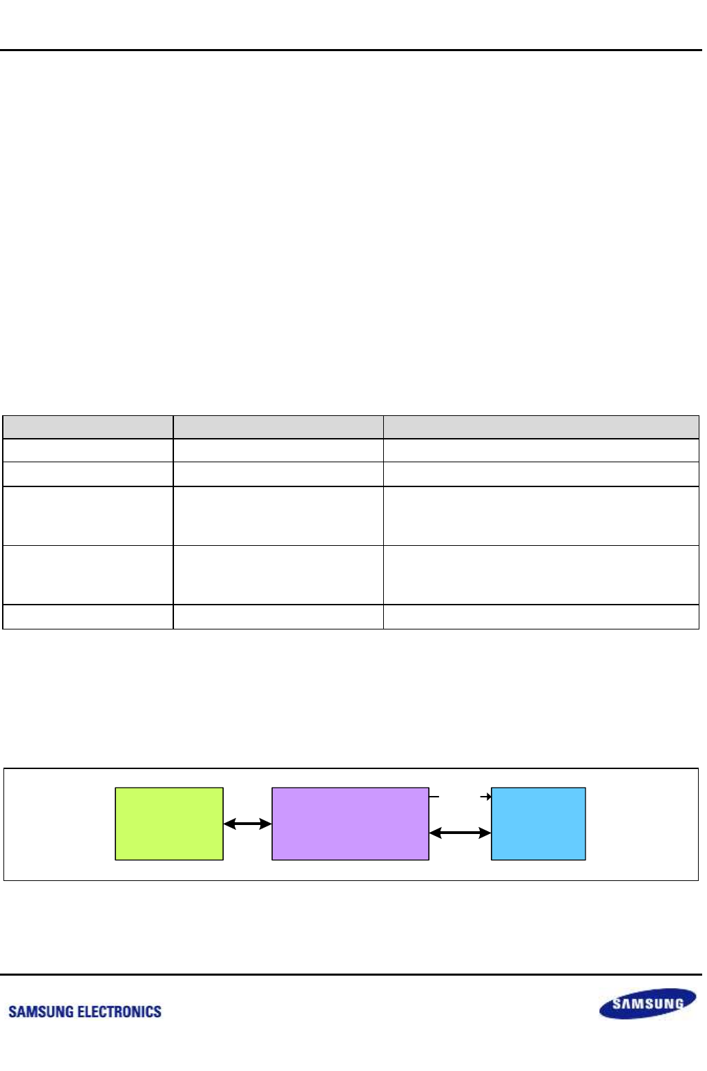
Samsung Confidential
S5P6818_UM 3 System Boot
3-5
Preliminary product information describes products that are in development, for which full characterization data and
associated errata are not yet available. Specifications and information herein are subject to change without notice.
NOTE: s: 0: SD, 1: SDFS
hs: 0: Normal speed, 1: High speed
3.3 External Static Memory Boot
CPU executes External Static Memory Access without CPU Hold.
3.3.1 External Static Memory Boot Features
Supports 16/8-bit Static Memory
3.3.2 External Static Memory Boot System Configuration
Table 3-4 External Static Memory not System Configuration Setting Description
Pin Name
Function Name
Description
RST_CFG[2:0]
BOOTMODE[2:0]
Pull-down
RST_CFG[7:3]
Don’t care
RST_CFG8
CfgSTLATADD
Static Latched Address (user select)
0 = None
1 = Latched
RST_CFG9
CfgSTBUSWidth
Static Bus Width (user select)
0 = 8-bit
1 = 16-bit
RST_CFG[24:10]
Don’t care
3.3.3 External Static Memory Boot Operation
In case of External Static Memory Boot, nSCS[0] is set to Address 0x00000000 by reset configuration and CPU
can access Static Memory through MCU-S.
MCU-Static External Static
Memory
0x00000000
CPU
nSCS[0]
Figure 3-1 External Static Memory Boot
nexell / ys.kim at 2015.02.12
SAMSUNG Confidential
Samsung Confidential
S5P6818_UM 3 System Boot
3-6
Preliminary product information describes products that are in development, for which full characterization data and
associated errata are not yet available. Specifications and information herein are subject to change without notice.
3.4 Internal ROM Boot
The chip has built-in 20 KB ROM. It is possible to set Internal ROM address to 0th address by setting
CfgBOOTMODE of System Configuration to "0 to 2". After Reset, CPU executes instruction fetched from 0th
address of the Internal ROM. Internal ROM has a code supporting various Booting methods. This ROM code
executes User Bootcode by reading it through various media and loading it to specific memory. This Booting
method is defined as internal ROM Booting (which is, from now on, called iROMBOOT).
iROMBOOT uses internal SRAM for storing stack or data. Therefore it is possible for the content of internal SRAM
to change after iROMBOOT is executed.
3.4.1 Features
Supports five booting modes: SPI Serial EEPROM BOOT, UART BOOT, USBBOOT, SDHCBOOT and
NANDBOOT with Error Correction.
Supports CPU Exception Vector Redirection for OS systems without using MMU.
Supports Fast Power Control: Set VDDPWRON and VDDPWRON_DDR as High.
3.4.2 System Configuration for the Internal ROM Booting
iROMBOOT supports 5 Booting modes such as USBBOOT, UART BOOT, SPI Serial EEPROM BOOT,
SDHCBOOT, and NANDBOOT with Error Correction. Every Booting mode supports various booting methods by
referring to Reset states from SD[15:0]. Below Table shows System configuration for each Booting mode.
Table 3-5 iROMBOOT System Configuration
Pins
iROMBOOT
SDFS
UART
SPI Serial Flash
SDMMC
USB Device
NANDBOOT
with Error
Correction
RST_CFG[2:0]
BOOTMODE=1
BOOTMODE=3
BOOTMODE=4
BOOTMODE=5
BOOTMODE=6
BOOTMODE=7
RST_CFG[12:11]
Don't care
NANDTYPE[1:0]
RST_CFG[13, 10]
PAGESIZE[1:0]
RST_CFG[3]
SELCS
RST_CFG[17]
Don't care
OTG Session
Check
Don't care
RST_CFG[6]
Don't care
Baud Rate
Speed
Should be Zero
Don't care
RST_CFG[5:4]
Don't care
ADDRWIDTH[1:0]
Don't care
RST_CFG[19, 3]
Port Number
RST_CFG[14]
DECRYPT
RST_CFG[15]
I-CACHE
RST_CFG[8]
LATADDR
RST_CFG[9]
Should be Zero (BUSWIDTH)
nexell / ys.kim at 2015.02.12
SAMSUNG Confidential
Samsung Confidential
S5P6818_UM 3 System Boot
3-7
Preliminary product information describes products that are in development, for which full characterization data and
associated errata are not yet available. Specifications and information herein are subject to change without notice.
3.4.3 SPI Boot
iROMBOOT can load User Boot code from SPI Flash ROM to memory and execute this code, which Booting
method is called SPIBOOT.
3.4.3.1 Features
Supports Address Step 2, 3, 4
Boot Speed is 16 MHz
Supports SPI port 0, 1, 2
Max Boot Size up to 56 KB
Check Boot signature and boot image CRC
3.4.3.2 Operation
Figure 3-2 SPI ROM Boot Operation
Internal ROM
Internal SRAM
User Bootcode
User boot code ~56Kb
From Flash Address 0
Jump PC to
execute boot code
SIZE=~56KB
Internal RAM = 0xFFFF_0000
SPI #0, 1, 2
Copy User Bootcode from
SPI Flash Rom
nexell / ys.kim at 2015.02.12
SAMSUNG Confidential

Samsung Confidential
S5P6818_UM 3 System Boot
3-8
Preliminary product information describes products that are in development, for which full characterization data and
associated errata are not yet available. Specifications and information herein are subject to change without notice.
3.4.4 UART Boot
iROMBOOT can load User Bootcode via UART to memory and execute this code, which Booting method is called
UARTBOOT.
3.4.4.1 Features
Supports 19200 bps, 115200 bps.
Supports UART port 0, 1.
Check Boot signature and boot image CRC
3.4.4.2 Operation
Internal ROM
(iROMBOOT)
User Bootcode
User Bootcode
Copy boot code through UART
Jump PC to
execute boot code
SIZE =16KBytes
Internal SRAM = 0xFFFF_0000
I
UART Port #0
UART Port
Figure 3-3 UART Boot Operation
nexell / ys.kim at 2015.02.12
SAMSUNG Confidential
Samsung Confidential
S5P6818_UM 3 System Boot
3-9
Preliminary product information describes products that are in development, for which full characterization data and
associated errata are not yet available. Specifications and information herein are subject to change without notice.
3.4.5 USB Boot
iROMBOOT can load User Bootcode via USB to memory and execute this code, which Booting method is called
USBBOOT.
3.4.5.1 Features
Supports Full speed or High Speed USB connection.
Uses the USB Bulk transfer.
Supports 64 bytes for Full speed and 512 bytes for High speed as Max packet size.
3.4.5.2 Operation
Figure 3-4 USB Boot Operation
USB Host Program should transfer User boot code by using bulk transfer through EP2 of USB Device. The max
packet size is changeable according to USB connection speed at Endpoint. In Full speed connection, USB Host
Program can transfer the maximum 64 bytes as one packet and, in High speed connection, the maximum 512
bytes as one packet. USB Host Program should transfer the data packet of even size even though it can transfer
the same packet as the max size or the packet smaller than the max size.
USBBOOT writes User Bootcode from USB Host Program and USBBOOT executes User Bootcode by changing
PC to 0xFFFF0000 after it receives User Bootcode size of max 56 KB.
Internal ROM
(
(iROMBOOT)
User Bootcode
User Bootcode
Copy boot code through USB Bulk transfer
Jump PC to
execute boot code
SIZE= ~56KBytes
Internal SRAM = 0xFFFF_0000
USB 2.0 Device
USB Host
nexell / ys.kim at 2015.02.12
SAMSUNG Confidential
Samsung Confidential
S5P6818_UM 3 System Boot
3-10
Preliminary product information describes products that are in development, for which full characterization data and
associated errata are not yet available. Specifications and information herein are subject to change without notice.
3.4.5.3 USB Descriptors
USB Host Program can get Descriptor of USBBOOT by using Get_Descriptor Request. Table 3-6 shows
Descriptor of USBBOOT. USBBOOT has one configuration, one interface, and two additional Endpoints except
Control Endpoint. However, Endpoint 1 exists only for compatibility. Then USBBOOT only receives data by using
Endpoint2 only.
Table 3-6 USB Boot Description
Offset
Field
Size
USBBOOT Value
Description
Full Speed
High Speed
Device Descriptor
0
bLength
1
18
Size of this descriptor in bytes
1
bDescriptorType
1
01h
Device descriptor type
2
bcdUSB
2
0110h
0200h
USB spec release number in BCD
4
bDeviceClass
1
FFh
Class code
5
bDeviceSubClass
1
FFh
Subclass code
6
bDeviceProtocol
1
FFh
Protocol code
7
bMaxPacketSize0
1
64
Maximum packet size for EP0
8
idVender
2
04E8h
Vender ID
10
idProduct
2
1234h
Product ID
12
bcdDevice
2
0000h
Device release number in BCD
14
iManufacturer
1
0
Index of string descriptor describing manufacturer
15
iProduct
1
0
Index of string descriptor describing product
16
iSerialNumber
1
0
Index of string descriptor describing the device’s
serial number
17
bNumConfiguration
1
1
Number of possible configuration
Configuration Descriptor
0
bLength
1
9
Size of this descriptor in bytes
1
bDescriptorType
1
02h
Configuration descriptor type
2
wTotalLength
2
32
Total length of data returned for this configuration
4
bNumInterfaces
1
1
Number of interfaces
5
bConfigurationValue
1
1
Value to use as an argument to the Set
Configuration
6
iConfiguration
1
0
Index of string descriptor describing this
configuration
7
bmAttribute
1
80h
Configuration characteristics
8
bMaxPower
1
25
Maximum power consumption
Interface Descriptor
0
bLength
1
9
Size of this descriptor in bytes
1
bDescriptorType
1
04h
Interface descriptor type
2
bInterfaceNumber
1
0
Number of this interface
nexell / ys.kim at 2015.02.12
SAMSUNG Confidential
Samsung Confidential
S5P6818_UM 3 System Boot
3-11
Preliminary product information describes products that are in development, for which full characterization data and
associated errata are not yet available. Specifications and information herein are subject to change without notice.
Offset
Field
Size
USBBOOT Value
Description
Full Speed
High Speed
3
bAlternateSetting
1
0
Value used to select this alternate setting
4
bNumEndpoints
1
2
Value used to select this alternate setting for the
interface
5
bInterfaceClass
1
FFh
Class code
6
bInterfaceSubClass
1
FFh
Subclass code
7
bInterfaceProtocol
1
FFh
Protocol code
8
iInterface
1
0
Index of string descriptor describing this interface
Endpoint Descriptor for EP1
0
bLength
1
7
Size of this descriptor in bytes
1
bDescriptorType
1
05h
Endpoint descriptor type
2
bEndpointAddress
1
81h
The address of the endpoint
3
bmAttributes
1
02h
The endpoint’s attributes
4
wMaxPacketSize
2
64
512
Maximum packet size
6
bInterval
1
0
Interval for polling endpoint for data transfers
Endpoint Descriptor for EP2
0
bLength
1
7
Size of this descriptor in bytes
1
bDescriptorType
1
05h
Endpoint descriptor type
2
bEndpointAddress
1
02h
The address of the endpoint
3
bmAttributes
1
02h
The endpoint’s attributes
4
wMaxPacketSize
2
64
512
Maximum packet size
6
bInterval
1
0
Interval for polling endpoint for data transfers
nexell / ys.kim at 2015.02.12
SAMSUNG Confidential
Samsung Confidential
S5P6818_UM 3 System Boot
3-12
Preliminary product information describes products that are in development, for which full characterization data and
associated errata are not yet available. Specifications and information herein are subject to change without notice.
3.4.6 SDHC Boot
iROMBOOT can execute User Bootcode by reading it from SD memory card, MMC memory card, and eMMC and
loading it to memory by using SDHC module. This method is called SDHCBOOT.
3.4.6.1 Features
Supports SD/MMC memory card, and eMMC
Supports High Capacity SD/MMC memory card
Supports SD port 0, 1, 2
Outputs 400 kHz SDCLK for Identification and 24 MHz SDCLK for Data Transfer
3.4.6.2 Operation
Figure 3-5 SDHC Boot Operation
SDHCBOOT uses all SDHC #0, 1, 2 module.
SDHCBOOT provides various Booting methods according to CFG pins, in which the specification of each method
is recommended to refer to [System Configuration by RST_CFG Pins].
Internal ROM
Internal SRAM
User Bootcode
User boot code 56Kb
Jump PC to
execute boot code
SIZE=~56KB
Internal RAM = 0xFFFF_0000
SDHC #0, 1, 2
Don
’
t care (512 bytes)
: Sctor 0
Copy User Bootcode from
SD/MMC/eMMC
nexell / ys.kim at 2015.02.12
SAMSUNG Confidential

Samsung Confidential
S5P6818_UM 3 System Boot
3-13
Preliminary product information describes products that are in development, for which full characterization data and
associated errata are not yet available. Specifications and information herein are subject to change without notice.
User Bootcode should be written as below Table to Storage Device for the use of SDHCBOOT.
Table 3-7 Boot Data Format for SDHC Boot
Sector
Name
Description
0
Reserved
SDHCBOOT don’t care data in 0th Sector. Therefore it is possible to use 0th Sector
for storing MBR (Master Boot record), and to include User Bootcode along with File
System into one Physical Partition.
1 to 32
User Bootcode
Boot code User made has ~56 KB size from 2nd Sector
The SDHCBOOT Booting process is as follows.
Normal SDMMC Booting is executed when CfgSDHCBM is "0".
Go idle state
SDHCBOOT identifies the type of Card and initializes.
The state of Card changes to Data Transfer Mode.
SDHCBOOT reads User Bootcode from Sector #1, and load it to internal SRAM to be executed.
3.4.7 SDFS Boot
iROMBOOT can bootable use FAT32 filesystem. Only can use first partition of SD for FAT filesystem and partition
name string must be "FAT32". And two boot file is need. One is "NXDATA.SBH" another is "NXDATA.SBL". First
boot time, read MBR and search partition and filesystem. If partition is exist and filesystem is FAT32, search first
boot file "NXDATA.SBH". If find the first, search next boot file, "NXDATA.SBL". NXDATA.SBL maximum size is up
to 56 KB.
Supports SD/MMC memory card, and eMMC
Supports High Capacity SD/MMC memory card
Supports SD port 0, 1, 2
Outputs 400 kHz SDCLK for Identification and 24 MHz SDCLK for Data Transfer
Supports FAT12, FAT16, FAT32.
Not Support long file name of FAT32.
nexell / ys.kim at 2015.02.12
SAMSUNG Confidential
Samsung Confidential
S5P6818_UM 3 System Boot
3-14
Preliminary product information describes products that are in development, for which full characterization data and
associated errata are not yet available. Specifications and information herein are subject to change without notice.
3.4.8 NANDBOOT with Error Correction
iROMBOOT provides the booting method which can correct any error in User bootcode stored in NAND Flash
memory. This Booting method is described as NANDBOOT with Error Correction (which is abbreviated to
NANDBOOTEC).
3.4.8.1 Features
Supports Error Correction for up to 24-bit errors per 551 bytes: User Bootcode 512 bytes + parity 39 bytes and
60-bit errors per 1129 bytes: User Boot code 1024 bytes + parity 105 bytes.
Supports 512B, 2 KB, 4 KB, 8 KB, 16 KB and above as the page size of the NAND flash memory.
Supports NAND flash memories required RESET command to initialize them.
Doesn’t support the bad block management.
3.4.8.2 Operation
Figure 3-6 NANDBOOTEC Operation
NANDBOOTEC can correct the errors which occur in User bootcode stored in NAND flash memory. Whenever
NANDBOOTEC reads User Bootcode from NAND flash memory by 512 bytes or 1024 bytes, it gets to know
whether any error of Data exists or not by using Error detection function of H/W BCH decoder included in MCU-S.
In case of any error in Data, the maximum 24 or 60 errors can be corrected through H/W Error Correction.
NAND Flash Memory
NAND flash controller
In MCU
-
Static
Internal ROM
Internal SRAM
User Boot code
User Bootcode
Jump PC to
User boot code
SIZE=~56KBytes
ADDR=0xFFFF_0000
ECC
H
/
W BCH Decoder
Reserved
Main area
0x00000000
Copy Error
-
-Corrected User Bootcode
from NAND Flash memory
nexell / ys.kim at 2015.02.12
SAMSUNG Confidential
Samsung Confidential
S5P6818_UM 3 System Boot
3-15
Preliminary product information describes products that are in development, for which full characterization data and
associated errata are not yet available. Specifications and information herein are subject to change without notice.
3.4.8.3 How to store User boot code into the NAND Flash Memory
Below Table shows the written form of User Bootcode into NAND flash memory. NANDBOOTEC uses the main
memory of NAND flash memory and doesn’t use the spared area of it.
Table 3-8 NAND Flash memory format for NANDBOOTEC
Sector
Data
Page Size
ECC #n
64 bytes 8 = 512 bytes
512B
LSB (312-bit)
MSB (200-bit)
0
ECC #0
page #0
LSB 39 bytes
Reserved
1
Bin #0
page #1
Parity for sector #(n*8+ 1)
Reserved
2
Bin #1
page #2
Parity for sector #(n*8+ 2)
Reserved
3
Bin #2
page #3
Parity for sector #(n*8+ 3)
Reserved
4
Bin #3
page #4
Parity for sector #(n*8+ 4)
Reserved
5
Bin #4
page #5
Parity for sector #(n*8+ 5)
Reserved
6
Bin #5
page #6
Parity for sector #(n*8+ 6)
Reserved
7
Bin #6
page #7
MSB 39 bytes
Parity for sector #(n*8+ 7)
Reserved
8
ECC #1
page #8
9
Bin #7
page #9
10
Bin #8
page #10
11
Bin #9
page #11
12
Bin #10
page #12
13
Bin #11
page #13
14
Bin #12
page #14
15
Bin #13
page #15
16
ECC #2
page #16
17
Bin #14
page #17
18
Bin #15
page #18
19
Bin #16
page #19
20
Bin #17
page #20
21
Bin #18
page #21
22
Bin #19
page #22
23
Bin #20
page #23
24
ECC #3
page #24
25
Bin #21
page #25
26
Bin #22
page #26
27
Bin #23
page #27
28
Bin #24
page #28
29
Bin #25
page #29
30
Bin #26
page #30
31
Bin #27
page #31
nexell / ys.kim at 2015.02.12
SAMSUNG Confidential
Samsung Confidential
S5P6818_UM 3 System Boot
3-16
Preliminary product information describes products that are in development, for which full characterization data and
associated errata are not yet available. Specifications and information herein are subject to change without notice.
Sector
Data
Page Size
ECC #n
64 bytes 8 = 512 bytes
512B
LSB (312-bit)
MSB (200-bit)
32
ECC #4
page #32
33
Bin #28
page #33
34
Bin #29
Page #34
35
Bin #30
page #35
36
Bin #31
page #36
37
Bin #32
page #37
xx
Bin #xx
page #xx
Sector
Data
Page Size
ECC #n
128 bytes 8 = 1024 bytes
2KB
4KB
8K
16K
LSB (840-bit)
MSB (184-bit)
0
ECC #0
page #0
page
#0
page
#0
Page
#0
LSB 105
bytes
Reserved
1
Bin #0
Parity for sector #(n*8+ 1)
Reserved
2
Bin #1
page #1
Parity for sector #(n*8+ 2)
Reserved
3
Bin #2
Parity for sector #(n*8+ 3)
Reserved
4
Bin #3
page #2
page
#1
Parity for sector #(n*8+ 4)
Reserved
5
Bin #4
Parity for sector #(n*8+ 5)
Reserved
6
Bin #5
page #3
Parity for sector #(n*8+ 6)
Reserved
7
Bin #6
MSB 105
bytes
Parity for sector #(n*8+ 7)
Reserved
8
ECC #1
page #4
page
#2
page
#1
9
Bin #7
10
Bin #8
page #5
11
Bin #9
12
Bin #10
page #6
page
#3
13
Bin #11
14
Bin #12
page #7
15
Bin #13
16
ECC #2
page #8
page
#4
page
#xx
Page
#1
17
Bin #14
18
Bin #15
page #xx
xx
Bin #xx
nexell / ys.kim at 2015.02.12
SAMSUNG Confidential

Samsung Confidential
S5P6818_UM 3 System Boot
3-17
Preliminary product information describes products that are in development, for which full characterization data and
associated errata are not yet available. Specifications and information herein are subject to change without notice.
3.4.9 Additional Information
3.4.9.1 Boot Header
All boot (except UART boot) check Boot Header of 512 bytes. This boot header assumed first received or loaded
from boot device to SRAM at 0xFFFF0000. First of all, romboot check boot signature of last of boot header when
received 512 bytes. This signature value must be 0x4849534E. If not equal, romboot try to next boot. And all boot
must valid 3 data LOADSIZE, LOADADDR, LAUNCHADDR. These data is about followed 2nd Boot image
information. Boot image size and load address must be aligned by 16 bytes. If SPI Boot, Romboot check CRC32.
CRC is about boot code except boot header.
Example 3-1 Additional Boot Information
struct NX_NANDBootInfo
{
unsigned char AddrStep;
unsigned char tCOS;
unsigned char tACC;
unsigned char tOCH;
unsigned int PageSize;
unsigned int CRC32;
};
struct NX_SPIBootInfo
{
unsigned char AddrStep;
unsigned char _Reserved0[3];
unsigned int _Reserved1;
unsigned int CRC32;
};
struct NX_SDMMCBootInfo
{
unsigned char PortNumber;
unsigned char _Reserved0[3];
unsigned int _Reserved1;
unsigned int CRC32;
};
union NX_DeviceBootInfo
{
struct NX_NANDBootInfo NANDBI;
struct NX_SPIBootInfo SPIBI;
struct NX_SDMMCBootInfo SDMMCBI;
};
struct NX_SecondBootInfo
{
unsigned int VECTOR[8]; // 0x000 ~ 0x01C
unsigned int VECTOR_Rel[8]; // 0x020 ~ 0x03C
nexell / ys.kim at 2015.02.12
SAMSUNG Confidential

Samsung Confidential
S5P6818_UM 3 System Boot
3-18
Preliminary product information describes products that are in development, for which full characterization data and
associated errata are not yet available. Specifications and information herein are subject to change without notice.
unsigned int DEVICEADDR; // 0x040
unsigned int LOADSIZE; // 0x044
unsigned int LOADADDR; // 0x048
unsigned int LAUNCHADDR; // 0x04C
union NX_DeviceBootInfo DBI; // 0x050~0x058
unsigned int Stub[(0x1F8-0x05C)/4]; // 0x05C ~ 0x1F8
unsigned int SIGNATURE; // 0x1FC "NSIH"
};
3.4.9.2 ALIVE Power Control
iROMBOOT changes VDDPWRON and VDDPWRON_DDR pins to High state after Reset in order to supports the
fast response to nVDDPWRTOGGLE button. Table 3-9 shows ALIVE module states after iROMBOOT Execution.
Table 3-9 ALIVE Power Control
Function
State
Description
VDDPWRON
High
Enable Core Power
VDDPWRON_DDR
High
Enable DDR Memory Power
3.4.9.3 Exception Vector Redirection
Exception Handler of ARM CPU should exist from 0th address by 4 byte one after the other. User generally places
the routine jumping to User’s Exception Handler to the Exception Handler existing from 0th address. However, in
case of iROMBOOT, User’s Exception Handler is impossible to set at 0th address because ROM exists at
0thaddress. CPU Exception can be processed by mapping the arbitrary memory to 0th address when MMU is
being used. However iROMBOOT provides the function redirecting Exception Handler for the System not using
MMU.
iROMBOOT uses 32 bytes from the lowest address of internal SRAM as User Exception Vector Table. When
Exception occurs, ROM Exception Handler in iROMBOOT lets PC jump to the address of User Exception Handler
taken from User Exception Vector Table. Therefore Exception can be processed even at Physical address system
by User’s setting the address of User Exception Handler to User Exception Vector Table present in internal SRAM
and that is equal to High Vector Address.
Example 3-2 iROMBOOT Exception Handlers
#define BASEADDR_SRAM 0xFFFF0000
//;==================================================================
//; Vectors
//;==================================================================
.global Vectors
Vectors:
LDR pc, ResetV //; 00 - Reset
LDR pc, UndefV //; 04 - Undefined instructions
LDR pc, SWIV //; 08 - SWI instructions
nexell / ys.kim at 2015.02.12
SAMSUNG Confidential

Samsung Confidential
S5P6818_UM 3 System Boot
3-19
Preliminary product information describes products that are in development, for which full characterization data and
associated errata are not yet available. Specifications and information herein are subject to change without notice.
LDR pc, PAbortV //; 0C - Instruction fetch aborts
LDR pc, DAbortV //; 10 - Data access aborts
LDR pc, UnusedV //; 14 - Reserved
LDR pc, IRQV //; 18 - IRQ interrupts
LDR pc, FIQV //; 1C - FIQ interrupts
ResetV:
.word Reset_Handler
UndefV:
.word (BASEADDR_SRAM + 0x04) //; 04 - undef
SWIV:
.word (BASEADDR_SRAM + 0x08) //; 08 - software interrupt
PAbortV:
.word (BASEADDR_SRAM + 0x0C) //; 0C - prefectch abort
DAbortV:
.word (BASEADDR_SRAM + 0x10) //; 10 - data abort
UnusedV:
.word 0 //; 14 - will reset if called...
IRQV:
.word (BASEADDR_SRAM + 0x18) //; 18 - IRQ
FIQV:
.word (BASEADDR_SRAM + 0x1C) //; 1C - FIQ
//;==================================================================
//; Imports
//;==================================================================
.global iROMBOOT
//;==================================================================
//; Reset Handler - Generic initialization, run by all CPUs
//;==================================================================
Reset_Handler:
nexell / ys.kim at 2015.02.12
SAMSUNG Confidential

Samsung Confidential
S5P6818_UM 3 System Boot
3-20
Preliminary product information describes products that are in development, for which full characterization data and
associated errata are not yet available. Specifications and information herein are subject to change without notice.
3.4.9.4 CRC32 Error Check
UART and SPI Boot check with CRC32 and if UART Boot, adding CRC32 FCS data to last of transfer of payload
then CRC32 FCS will checking will success. In SPI boot, CRC32 data must be inserted Boot Header. Below code
is CRC32 FCS generator function.
Example 3-3 CRC32 FCS Generator Function
#define POLY 0x04C11DB7L
inline unsigned int iget_fcs(unsigned int fcs, unsigned int data)
{
register int i;
fcs ^= data;
for(i=0; i<32; i++)
{
if(fcs & 0x01)
fcs ^= POLY;
fcs >>= 1;
}
return fcs;
}
inline unsigned int calc_crc32(void *addr, int len)
{
unsigned int *c = (unsigned int *)addr;
unsigned int crc = 0, chkcnt = ((len+3)/4);
unsigned int i;
for (i = 0; chkcnt > i; i++, c++) {
crc = iget_fcs(crc, *c);
}
return crc;
}
3.4.9.5 Data Decryption with AES128 ECB mode to use Hidden Key
All boot mode data will decrypted with AES128 ECB mode to use hidden key by option. Boot mode DISD6 can
select whether data will decrypt or not decrypt.
3.4.9.6 Boot Scenario
If any device boot is fail, all boot try to USB boot finally and you can select whether try to boot from all three SD
devices before USB boot. And you can select SD raw sector boot or SD filesystem boot.
3.4.9.7 Multi CPU Boot
When power up boot, only CPU 0 is boot up and CPU 1, 2, 3, 4, 5, 6, 7 is locked up by reset. You can select other
CPU boot reset vector by CPU 0. So you can select other CPU startup at romboot or SRAM.
nexell / ys.kim at 2015.02.12
SAMSUNG Confidential

Samsung Confidential
S5P6818_UM 4 System Control
4-1
Preliminary product information describes products that are in development, for which full characterization data and
associated errata are not yet available. Specifications and information herein are subject to change without notice.
4 System Control
4.1 Overview
The clock of the S5P6818 is roughly divided into FCLK, HCLK, MCLK, BCLK and PCLK are used for the ARM
CPU core, AXI bus peripherals and APB bus peripherals, respectively. In addition, BCLK is the clock for the
S5P6818 system bus. MCLK is the clock for SDRAM memory. The 2-PLL of the S5P6818 is called PLL0 and
PLL1, respectively. The 2-PLL and EXTCLK are used to generate the above clocks (i.e. FCLK, HCLK, PCLK,
BCLK, MCLK). All PLLs are designed to operate with an X-TAL input of 24MHz.
4.2 Features
Embedded 4-PLL operating independently
Output Frequency Range
PLL0: 40M to 2.5 GHz (non-dithered PLL)
PLL1: 40M to 2.5 GHz (non-dithered PLL)
PLL2: 35M to 2.2 GHz (dithered PLL)
PLL3: 35M to 2.2 GHz (dithered PLL)
Frequency is changed by Programmable Divider (PDIV, MDIV, SDIV)
Clock generation for all blocks in the chip
The PLLs can be switched into Power Down mode by using the program.
32.768 kHz supported for Power Management
Various Power Down Modes
IDLE mode and STOP mode
Various Wake Up sources
nexell / ys.kim at 2015.02.12
SAMSUNG Confidential
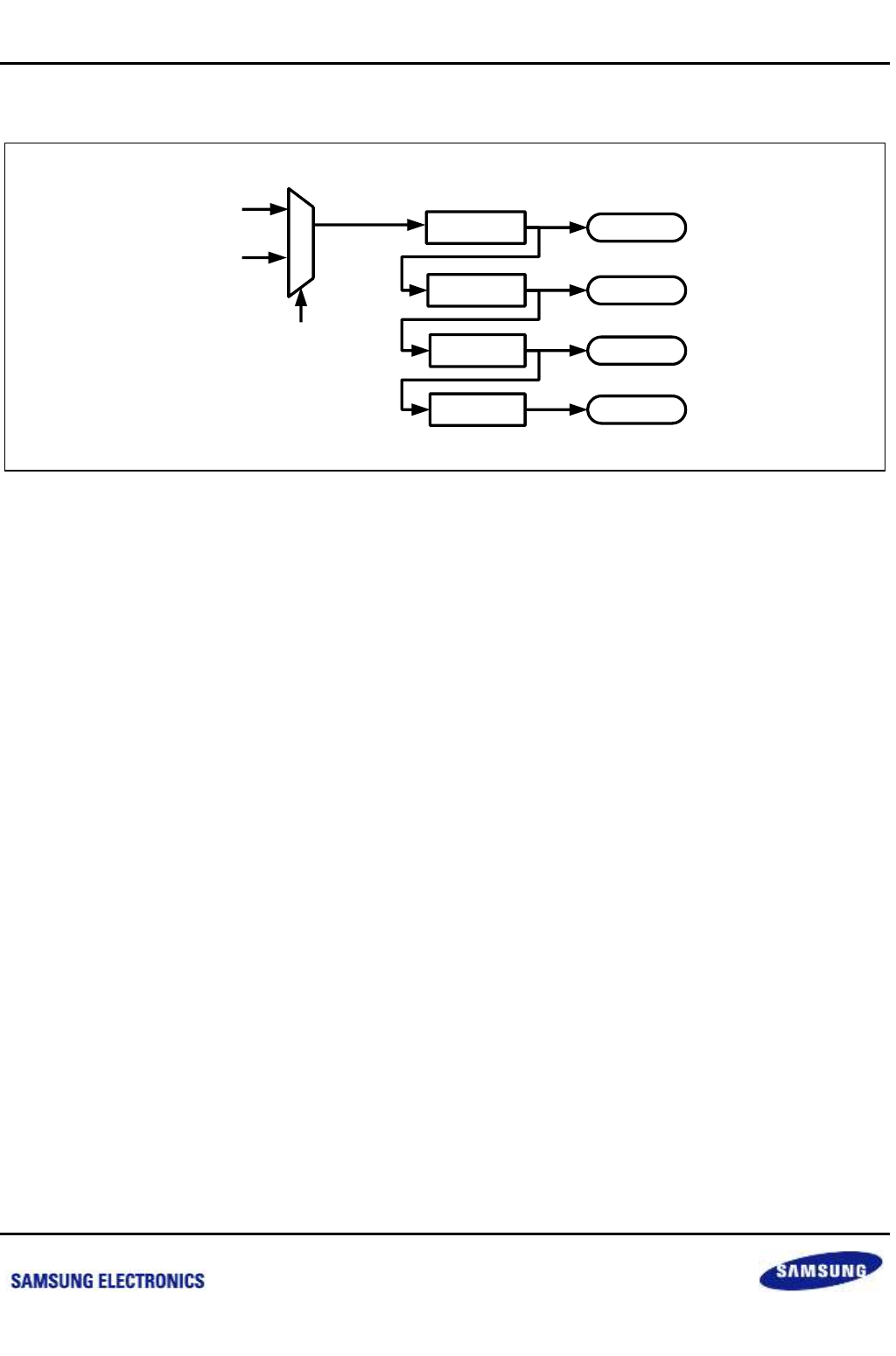
Samsung Confidential
S5P6818_UM 4 System Control
4-2
Preliminary product information describes products that are in development, for which full characterization data and
associated errata are not yet available. Specifications and information herein are subject to change without notice.
4.3 Block Diagram
Figure 4-1 Block Diagram
The above figure shows a diagram for the clock manager in the S5P6818. As shown in the above figure, the
S5P6818 has four PLLs. The S5P6818 receives the output of PLLs and generates all system clocks, the memory
clock and the CPU clock with the output frequency selected among many PLLs.
PLL[0]
…
PLL[n]
Divider1
(CLKMODEREG) CLOCK OUT1
Divider2
(CLKMODEREG) CLOCK OUT2
Divider3
(CLKMODEREG) CLOCK OUT3
Divider4
(CLKMODEREG) CLOCK OUT4
Clock Select
(CLKMODEREG)
nexell / ys.kim at 2015.02.12
SAMSUNG Confidential
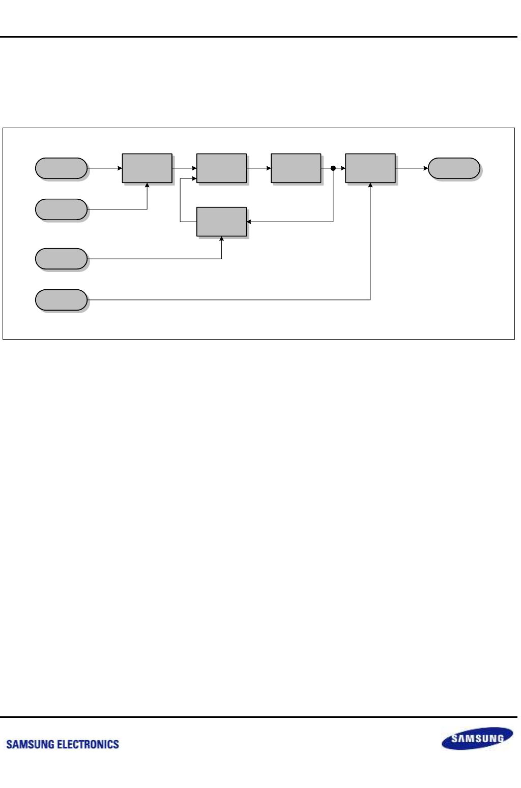
Samsung Confidential
S5P6818_UM 4 System Control
4-3
Preliminary product information describes products that are in development, for which full characterization data and
associated errata are not yet available. Specifications and information herein are subject to change without notice.
4.4 Clock Manager Functional Description
4.4.1 PLL (Phase Locked Loop)
4.4.1.1 PMS Value
Figure 4-2 Block Diagram of PLL
For the aspect of PLL structure, upper figure shows the block diagram for one PLL. Fin and Fout indicate input
frequency and output frequency respectively. The S5P6818 has PLLs and can generate various programmable
clocks by using each PLL.
If the Pre Divider receives a Fin input of 24 MHz, it divides the Fin with "P". After that, Phase Frequency Detector
(PFD) compares the difference between Fin/P (Reference Clock) and Fvco/M (Feedback Clock). The amplitude of
the voltage varies depending on the difference of the values compared between Fin/P and Fvco/M. If the
reference clock is faster feedback block, the Voltage Controlled Oscillator (VCO) increases in proportion to the
difference. If the reference clock is delayed than the feed clock, VCO is decreased, and it generates an Fvco
clock. That is because VCO is a voltage value and plays the role of controlling the clock speed to be faster or
slower. At this point, the voltage value is determined by the difference of the values compared between the
reference clock and the feedback clock. If the Fvco is not a desired clock, the feedback is recreated through the
Main Divider and compared in PFD. These steps are repeated until the reference clock and the feedback clock
become equal. If proper FVCO is out, the final Fout clock is created as the divide value(s) of a Post Scaler.
Finally, the desired clock frequency is determined by the p, m and s values.
As described above, Fout can be variously set by Fin and p/m/s values and the equation to specify p/m/s values is
as follows: (Note that all PLL0/1/2/3 indicate Fout. Equation may vary for each case.)
PLL x = ( m Fin)/(p 2s)
(x = 0,1,2,3, m = MDIV, p = PDIV, s = SDIV = 0, 1, 2, 3)
The range of the MDIV and PDIV values for PLL x are as follows:
Range of MDIV Value: 64 MDIV 1023
Range of PDIV Value: 1 PDIV 63
Fin Pre DIVIDER
(p)
P[5..0]
Phase
Frequency
Detector
Voltage
Controlled
Oscillator
Post Scaler
(s) Fout
Main DIVIDER
(m)
Fvco
Fin/P
M[7..0]
S[1..0]
Fvco/M
nexell / ys.kim at 2015.02.12
SAMSUNG Confidential
Samsung Confidential
S5P6818_UM 4 System Control
4-4
Preliminary product information describes products that are in development, for which full characterization data and
associated errata are not yet available. Specifications and information herein are subject to change without notice.
The PDIV and the MDIV values should be selected by considering the VCO value and S5P6818’s stable
operation. The S5P6818 has PLLs and each PLL has different default values and operation ranges.
The basic frequencies for the S5P6818 are listed in the table below:
Table 4-1 Initial PDIV/MDIV/SDIV Value
PLL
INITIAL
FREQUENCY
RECOMMENDED
FREQUENCY (Fvco)
RECOMMENDED
FREQUENCY (Fout)
INITIAL PDIV/ MDIV/ SDIV VALUE
PDIV
MDIV
SDIV
PLL0
550.000000Mhz
1250 to 2500 MHz
40 to 2500 MHz
3
275
2
PLL1
147.5 MHz
1250 to 2500 MHz
40 to 2500 MHz
3
295
4
PLL2
96 MHz
40 to 2200 MHz
1100 to 2200 MHz
3
192
4
PLL3
125 MHz
40 to 2200 MHz
1100 to 2200 MHz
3
250
4
For all blocks except for CPU, the operation status (Run/Stop) of the memory controller should be checked before
changing the PLL output frequency. In addition, the PLL change bit (PWRMODE.CHGPLL) should be set as "1"
after PLL change (PLLSETREG0, PLLSETREG1).
Setting Guide of PMSK
p, m, s and k are decimal values of P[5:0], M[8:0], S[2:0] and K[15:0], respectively.
p = P[5:0] , m = M[8:0], s = S[2:0], k = K[15:0]
FFVCO and FFOUT are calculated by the following equation.
FFVCO = ((m + k/65536) FFIN)/p
FFOUT = ((m + k/65536) FFIN)/(p 2s)
While range of registers P[5:0], M[8:0] and S[2:0] are unsigned integers, K[15:0] is a two’s complement
integer.
6’b00 0001 P[5:0] 6’b11 1111 and 2 MHz FFREF(FFIN/p) 30 MHz
9’b0 0100 0000 M[8:0] 9’b1 1111 1111
3’b000 S[2:0] 3’b101
16’b1000 0000 0000 0000 K[15:0] 16’b0111 1111 1111 1111
Setting P[5:0] or M[8:0] to all zeros is strictly prohibited while RESETB is logic high. (6’b00 0000/9’b0 0000
0000)
The division ratio of scaler is controlled by S[2:0] as summarized in below table.
Setting S[2:0] to the values in the gray rows in below table is strictly prohibited.
nexell / ys.kim at 2015.02.12
SAMSUNG Confidential

Samsung Confidential
S5P6818_UM 4 System Control
4-5
Preliminary product information describes products that are in development, for which full characterization data and
associated errata are not yet available. Specifications and information herein are subject to change without notice.
Table 4-2 Division Ratio of Scaler
S[2:0]
Division Ratio
000
20 = 1
001
21 = 2
010
22 = 4
011
23 = 8
100
24 = 16
101
25 = 32
110
Prohibited
111
Prohibited
4.4.1.2 Setting Guide of SSCG_EN, SEL_PF, MFR and MRR
When SSCG_EN is set to logic high, the spread spectrum mode is enabled.
sel_pf, mfr and mrr are decimal values of SEL_PF[1:0], MFR[7:0] and MRR[5:0], respectively.
sel_pf = SEL_PF[1:0], mfr = MFR[7:0], mrr = MRR[5:0]
Modulation frequency, MF, is determined by the following equation.
MF = FFIN/ p/ mfr/ 25 Hz
Modulation rate (pk-pk), MR, is determined by the following equation.
MR = mfr mrr/ m/ 26 100 %
Modulation mode is determined by sel_pf.
00: Down spread
01: Up spread
1x: Center spread
Range of registers.
8’b0000 0000 MFR[7:0] 8’b1111 1111
6’b00 0001 MRR[5:0] 6’b11 1111
0 mrr mfr 512
2’b00 SEL_PF[1:0] 2’b10
nexell / ys.kim at 2015.02.12
SAMSUNG Confidential

Samsung Confidential
S5P6818_UM 4 System Control
4-6
Preliminary product information describes products that are in development, for which full characterization data and
associated errata are not yet available. Specifications and information herein are subject to change without notice.
4.4.1.3 PDIV/ MDIV/ SDIV Values for PLL0, PLL1
Table 4-3 PDIV/ MDIV/ SDIV Value for PLL0
Input Frequency
Output Frequency
(MHz)
PDIV/ MDIV/ SDIV Value
Remark
PDIV
MDIV
SDIV
24 MHz
2000.000000
3
250
0
Maximum Available
Frequency
24 MHz
1900.000000
6
475
0
24 MHz
1800.000000
3
255
0
24 MHz
1700.000000
6
425
0
24 MHz
1600.000000
3
200
0
24 MHz
1500.000000
4
250
0
24 MHz
1400.000000
3
175
0
24 MHz
1300.000000
6
325
0
24 MHz
1200.000000
3
300
1
24 MHz
1100.000000
3
275
1
24 MHz
1000.000000
3
250
1
24 MHz
900.000000
3
225
1
24 MHz
800.000000
3
200
1
24 MHz
780.000000
3
195
1
24 MHz
760.000000
3
190
1
24 MHz
740.000000
3
185
1
24 MHz
720.000000
3
180
1
24 MHz
700.000000
3
175
1
24 MHz
666.000000
4
222
1
24 MHz
600.000000
3
300
2
24 MHz
550.000000
3
275
2
PLL0 default
24 MHz
533.000000
6
533
2
24 MHz
500.000000
3
250
2
24 MHz
490.000000
3
245
2
24 MHz
470.000000
3
235
2
24 MHz
460.000000
3
230
2
24 MHz
450.000000
3
225
2
24 MHz
440.000000
3
220
2
24 MHz
430.000000
3
215
2
24 MHz
420.000000
3
210
2
24 MHz
410.000000
3
205
2
24 MHz
400.000000
3
200
2
24 MHz
390.000000
3
190
2
nexell / ys.kim at 2015.02.12
SAMSUNG Confidential
Samsung Confidential
S5P6818_UM 4 System Control
4-7
Preliminary product information describes products that are in development, for which full characterization data and
associated errata are not yet available. Specifications and information herein are subject to change without notice.
Input Frequency
Output Frequency
(MHz)
PDIV/ MDIV/ SDIV Value
Remark
PDIV
MDIV
SDIV
24 MHz
370.000000
3
185
2
24 MHz
350.000000
3
175
2
24 MHz
330.000000
3
165
2
24 MHz
300.000000
3
300
3
24 MHz
266.000000
3
266
3
24 MHz
250.000000
3
250
3
24 MHz
220.000000
3
220
3
24 MHz
200.000000
3
200
3
24 MHz
166.000000
3
166
3
24 MHz
147.500000
3
295
4
PLL1 default
24 MHz
133.000000
3
266
4
24 MHz
125.000000
3
250
4
24 MHz
100.000000
3
200
4
24 MHz
96.000000
3
192
4
24 MHz
48.000000
3
96
4
nexell / ys.kim at 2015.02.12
SAMSUNG Confidential

Samsung Confidential
S5P6818_UM 4 System Control
4-8
Preliminary product information describes products that are in development, for which full characterization data and
associated errata are not yet available. Specifications and information herein are subject to change without notice.
4.4.1.4 PDIV/ MDIV/ SDIV Values for PLL2, PLL3
Table 4-4 PDIV/ MDIV/ SDIV Value for PLL1
Input
Frequency
Output Frequency
(MHz)
PDIV/ MDIV/ SDIV Value
Remark
PDIV
MDIV
SDIV
24 MHz
2000.000000
3
250
0
Maximum Available
Frequency
24 MHz
1900.000000
3
238
0
24 MHz
1800.000000
3
225
0
24 MHz
1700.000000
3
213
0
24 MHz
1600.000000
3
200
0
24 MHz
1500.000000
4
250
0
24 MHz
1400.000000
3
175
0
24 MHz
1300.000000
3
163
0
24 MHz
1200.000000
3
150
0
24 MHz
1100.000000
3
275
1
24 MHz
1000.000000
3
250
1
24 MHz
900.000000
3
225
1
24 MHz
800.000000
3
200
1
24 MHz
780.000000
3
195
1
24 MHz
760.000000
3
190
1
24 MHz
740.000000
3
185
1
24 MHz
720.000000
3
180
1
24 MHz
562.000000
3
141
1
24 MHz
533.000000
3
267
2
24 MHz
490.000000
3
245
2
24 MHz
470.000000
3
235
2
24 MHz
460.000000
3
230
2
24 MHz
450.000000
3
225
2
24 MHz
440.000000
3
220
2
24 MHz
430.000000
3
215
2
24 MHz
420.000000
3
210
2
24 MHz
410.000000
3
205
2
24 MHz
400.000000
3
200
2
24 MHz
399.000000
4
266
2
24 MHz
390.000000
3
195
2
24 MHz
384.000000
3
192
2
24 MHz
350.000000
3
175
2
nexell / ys.kim at 2015.02.12
SAMSUNG Confidential
Samsung Confidential
S5P6818_UM 4 System Control
4-9
Preliminary product information describes products that are in development, for which full characterization data and
associated errata are not yet available. Specifications and information herein are subject to change without notice.
Input
Frequency
Output Frequency
(MHz)
PDIV/ MDIV/ SDIV Value
Remark
PDIV
MDIV
SDIV
24 MHz
330.000000
3
165
2
24 MHz
300.000000
3
150
2
24 MHz
266.000000
3
266
3
24 MHz
250.000000
3
250
3
24 MHz
220.000000
3
220
3
24 MHz
200.000000
3
200
3
24 MHz
166.000000
3
166
3
24 MHz
147.45600
3
147
3
24 MHz
133.000000
3
266
4
24 MHz
125.000000
3
250
4
PLL3 default
24 MHz
100.000000
3
200
4
24 MHz
96.000000
3
192
4
PLL2 default
24 MHz
48.000000
3
96
4
4.4.1.5 PLL Power Down
The S5P6818 supports PLL Power Down mode to minimize power consumption. For example, if all system clocks
are generated with PLL0 and PLL1 does not need to be used. Therefore, power does not need to be supplied to
the PLL1. In such a case, the S5P6818 switches PLL1 into power down mode to reduce the power consumption.
However, PLL0 cannot enter to the power down mode. PLL0 power down can be achieved by writing "1" to the
CLKMODEREG0.PLLPWDN1.
nexell / ys.kim at 2015.02.12
SAMSUNG Confidential
Samsung Confidential
S5P6818_UM 4 System Control
4-10
Preliminary product information describes products that are in development, for which full characterization data and
associated errata are not yet available. Specifications and information herein are subject to change without notice.
4.4.2 Change PLL Value
When CPU want to change the PLL divider value, The PLL Change Bit (PWRMODE.CHGPLL bit) must be set to 1
after setting the PLL Setting Reset (PLLSETREG0, PLLSETREG1) to appropriate value.
Power management and Clock Controller blocks up the clock supplied to internal controllers because PLLs are
unstable when PLL divider value is changed. After locking time, these blocks supply clock. CPU must check
whether the blocks run or stop such as STOP mode.
4.4.3 Clock Generator
4.4.3.1 Clocks Summary
The 5 clocks created in the S5P6818 and the maximum frequencies for each clock are listed in the table below.
The minimum frequency is not limited within the clock frequency limit creatable in PLL.
Table 4-5 S5P6818 Clock Summary
Clock Name
Min
Frequency
Max Frequency
(MHz)
Description
FCLKCPU0
–
1600
CPU CLOCK (1st CPU cluster)
HCLKCPU0
–
250
CPU BUS CLOCK (1st CPU cluster)
FCLKCPU1
–
1600
CPU CLOCK (2nd CPU cluster)
HCLKCPU1
–
250
CPU BUS CLOCK (2nd CPU cluster)
MDCLK
800
Memory DLL clock.
MCLK
NOTE
800
Memory clock.
NOTE: Minimum frequency of MCLK is determined by SDRAM
specification.
MBCLK
400
Memory BUS CLOCK (MCU CLOCK)
MPCLK
200 MHz
Memory Peripheral clock. (Asynchronous to MBCLK, MCLK and MDCLK)
FASTBCLK
–
400 MHz
FAST BUS CLOCK (CCI-BUS)
CCI-Bus operates on the basis of FASTBCLK
BCLK
–
333 MHz
SYSTEM BUS CLOCK(CORE CLOCK)
CORE block operates on the basis of BCLK. (MPEG, DMA, etc…)
PCLK
–
166 MHz
PERIPHERAL BUS CLOCK
CPU accesses a block register via I/O with PCLK.
HDMIPCLK
–
100 MHz
HDMI PHY CLOCK (APB interface clock)
API interface of HDMI PHY operates on the basis of HDMIPCLK
GR3DBCLK
333
GPU clock
GR3DPCLK
Not used
MPEGBCLK
300
MFC clock (BUS and CODEC)
MPEGPCLK
150
MFC clock (Peripheral clock)
In the upper Table, note that the size of PCLK should be the half size of the BCLK when the maximum/minimum
frequency values are specified.
nexell / ys.kim at 2015.02.12
SAMSUNG Confidential
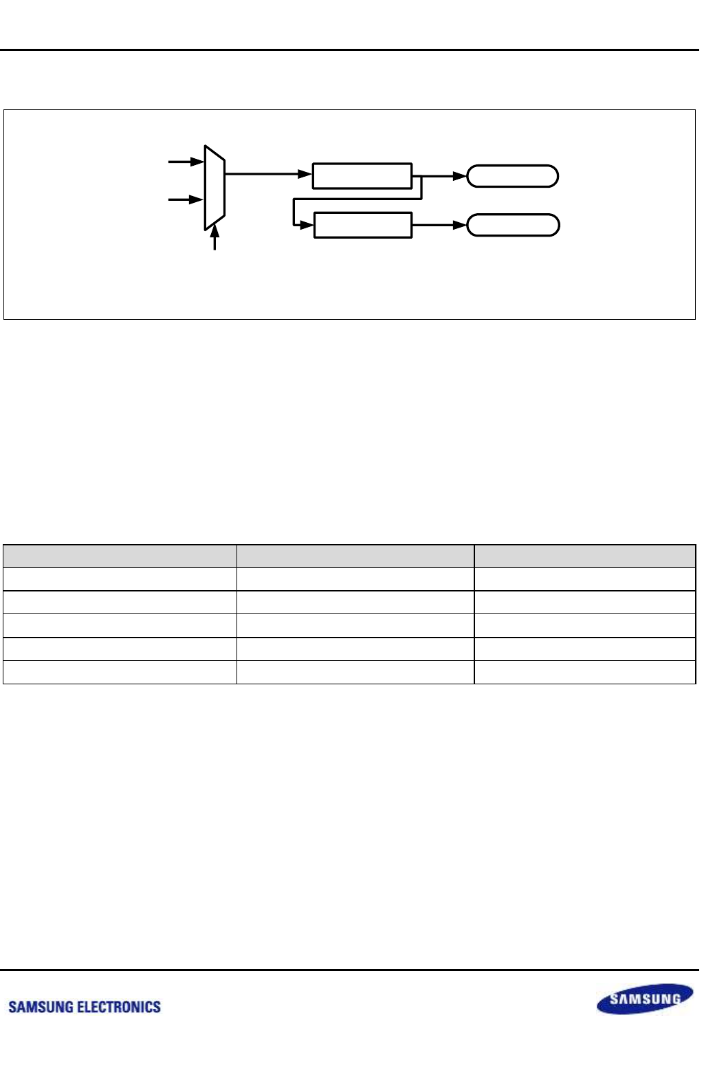
Samsung Confidential
S5P6818_UM 4 System Control
4-11
Preliminary product information describes products that are in development, for which full characterization data and
associated errata are not yet available. Specifications and information herein are subject to change without notice.
4.4.3.2 CPU0 Clock
Figure 4-3 CPU Clock
In the upper Figure, shows a block diagram that creates the clock supplied to FCLKCPU0, which is the main CPU
of the S5P6818. CLKMODEREG0 selects a desired PLL output from among PLLs. With the clock created from the
selected PLL, the CLKDIV_FCLKCPU0 register and CLKDIV_HCLKCPU0 generates FCLKCPU0 to be supplied
to the core block of CPU and HCLKCPU to be supplied to the AXI bus clock. Be careful not to set HCLKCPU over
maximum speed. The frequency of FCLKCPU and HCLKCPU cannot be the same.
Any PLL can be used to generate the CPU clock, but it is recommended to use the PLL0
Recommended clock frequency as follows:
Table 4-6 Recommended Clock Frequency for CPU
CPU Operation Voltage
FCLKCPU0 (MHz)
HCLKCPU0 (MHz)
0.95V
500
125
1.0V
700
175
1.1V
1000
250
TBD
TBD
TBD
TBD
1600
TBD
PLL[0]
…
PLL[n]
CLKDIV_FCLKCPU0
(CLKMODEREG0)
FCLKCPU0
(CPU CLOCK)
CLKDIV_HCLKCPU0
(CLKMODEREG0)
HCLKCPU0
(CPU BUS CLOCK)
CLKSEL_FCLKCPU0
(CLKMODEREG0)
nexell / ys.kim at 2015.02.12
SAMSUNG Confidential
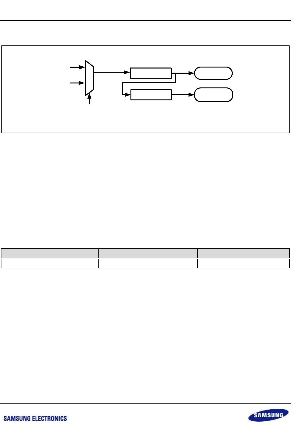
Samsung Confidential
S5P6818_UM 4 System Control
4-12
Preliminary product information describes products that are in development, for which full characterization data and
associated errata are not yet available. Specifications and information herein are subject to change without notice.
4.4.3.3 System Bus Clock (Core clock)
Figure 4-4 System BUS Clock
System bus clock (BCLK) is used as Core clock. The system bus clock is called [BCLK] and the half clock of
BCLK is called [PCLK]. BCLK is the clock for all SOC Core operations. PCLK is used when the CPU accesses
each block register via I/O. Therefore, PCLK should not be applied to the blocks not being used. Every block has
PCLK enable/disable Register. The blocks that PCLK is applied to have (refer to each Section). These registers
decide if PCLK is applied to a block only when the CPU accesses the corresponding block register or when it is
always applied.
Clock frequency ratio should be as follows.
BCLK : PCLK = 2 : 1
Recommended clock frequency as follows:
Table 4-7 Recommended clock Frequency for System BUS
Mode
BCLK (MHz)
PCLK (MHz)
Max operation
333
166
PLL[0]
…
PLL[n]
CLKDIV_BCLK
(CLKDIVREG1)
BCLK
(System Bus or
Core clock)
CLKDIV_PCLK
(CLKDIVREG1)
PCLK
(Peripheral Bus
Clock)
CLKSEL_BCLK
(CLKDIVREG1)
nexell / ys.kim at 2015.02.12
SAMSUNG Confidential
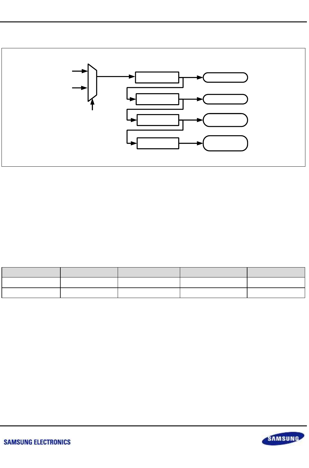
Samsung Confidential
S5P6818_UM 4 System Control
4-13
Preliminary product information describes products that are in development, for which full characterization data and
associated errata are not yet available. Specifications and information herein are subject to change without notice.
4.4.3.4 Memory Bus Clock (MCU Clock)
Figure 4-8 System BUS Clock
Memory bus clock (MCLK) is used as SDRAM, MCU Core clock. MDCLK is the clock for DLL of Memory Control
Unit (MCU). MCLK is the DDR interface clock. MBCLK is bus clock of MCU. MPCLK is peripheral bus clock of
MCU. The MCLK frequency should be the double that of the MBCLK frequency. (BCLK to MCLK is a 1:2 ratio)
Recommended clock frequency ratio is as follows.
MDCLK : MCLK : MBCLK : MPCLK = 4 : 4 : 2 : 1
Recommended clock frequency as follows:
Table 4-9 Recommended Clock Frequency for Memory BUS
Mode
MDCLK (MHz)
MCLK (MHz)
MBCLK (MHz)
MPCLK (MHz)
Fast
800 (NOTE)
800
400
200
Slow
800
200
100
50
NOTE: MDCLK should be divided by 2, i.e. CLKDIV_MDCLK should be 1.
PLL[0]
…
PLL[n]
CLKDIV_MDCLK
(CLKDIVREG2)
MDCLK
(Memory DLL clock)
CLKDIV_MCLK
(CLKDIVREG2)
MCLK
(Memory DDR clock)
CLKDIV_MBCLK
(CLKDIVREG2)
MBCLK
(MCU bus clock)
CLKDIV_MPCLK
(CLKDIVREG2)
MPCLK
(MCU Peripheral Bus
clock)
CLKSEL_MDCLK
(CLKDIVREG2)
nexell / ys.kim at 2015.02.12
SAMSUNG Confidential
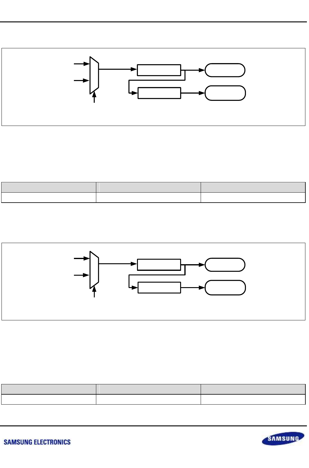
Samsung Confidential
S5P6818_UM 4 System Control
4-14
Preliminary product information describes products that are in development, for which full characterization data and
associated errata are not yet available. Specifications and information herein are subject to change without notice.
4.4.3.5 GPU (Graphic Processing Unit) Clock
Figure 4-5 System BUS Clock
GPU clock (GR3DBCLK) is used as GPU core clock. GR3DPCLK is not used (reserved).
Recommended clock frequency as follows:
Table 4-10 Recommended clock Frequency for GPU
Mode
GR3DBCLK (MHz)
GR3DPCLK (MHz)
Max operation.
333
166 (not used)
4.4.3.6 MFC (Multi Function Codec) Clock
Figure 4-6 System BUS Clock
MFC clock (MPEGBCLK) is used as Multi function codec clock. MPEGPCLK is used peripheral bus clock for MFC
unit.
Recommended clock frequency as follows:
Table 4-11 Recommended clock Frequency for MFC
Mode
MPEGBCLK (MHz)
MPEGPCLK (MHz)
Max operation
300
150
PLL[0]
…
PLL[n]
CLKDIV_GR3DBCLK
(CLKDIVREG3)
GR3DBCLK
(System Bus or
Core clock)
CLKDIV_GR3DPCLK
(CLKDIVREG3)
GR3DPCLK
(Peripheral Bus
Clock)
CLKSEL_GR3DBCLK
(CLKDIVREG3)
PLL[0]
…
PLL[n]
CLKDIV_MPEGBCLK
(CLKDIVREG4)
MPEGBCLK
(System Bus or
Core clock)
CLKDIV_MPEGPCLK
(CLKDIVREG4)
MPEGPCLK
(Peripheral Bus
Clock)
CLKSEL_MPEGBCLK
(CLKDIVREG4)
nexell / ys.kim at 2015.02.12
SAMSUNG Confidential

Samsung Confidential
S5P6818_UM 4 System Control
4-15
Preliminary product information describes products that are in development, for which full characterization data and
associated errata are not yet available. Specifications and information herein are subject to change without notice.
4.5 Power Manager
4.5.1 Power Manager Overview
The power manager of the S5P6818 provides the following functions to operate the system stably and reduce the
power consumption.
Power Up Sequence
Reset Generation
Power Management
Change PLL Value
The key functions of the power manager are to control the Power up Sequence to make the S5P6818 stable after
the power is supplied to the system and to manage the power effectively. Apart from this, it controls the reset
configuration in initial operation.
In addition, this block generates various reset signals, such as External Reset Output (nRSTOUT), AliveGPIO
Reset and Soft Reset.
The S5P6818 provides various Power Down modes to reduce the system power consumption. The three
Power modes provided by the S5P6818 are as follows:
Normal Mode
IDLE Mode
STOP Mode
SLEEP Mode (See the "ALIVE" Section for SLEEP Mode)
nexell / ys.kim at 2015.02.12
SAMSUNG Confidential
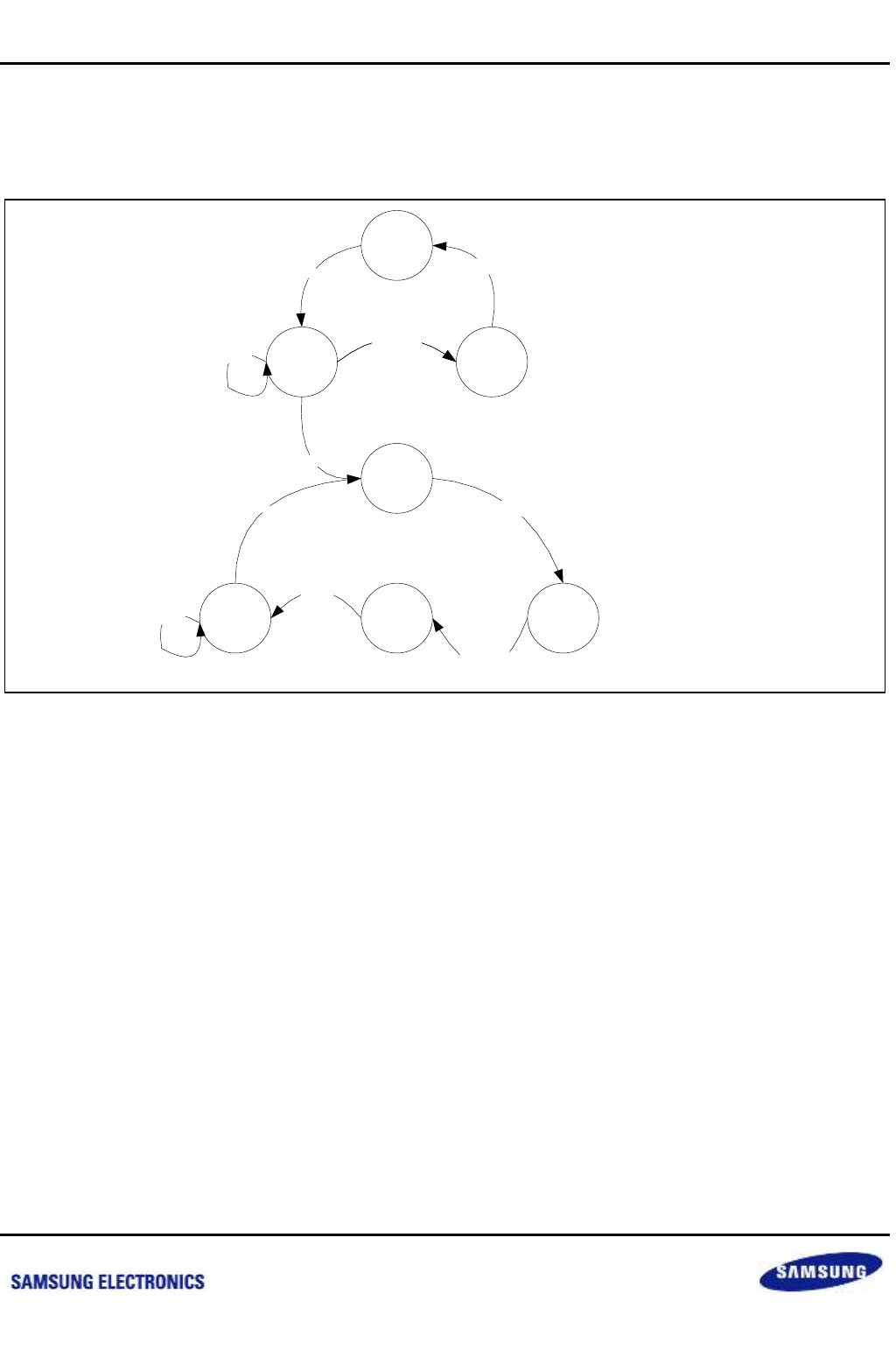
Samsung Confidential
S5P6818_UM 4 System Control
4-16
Preliminary product information describes products that are in development, for which full characterization data and
associated errata are not yet available. Specifications and information herein are subject to change without notice.
4.5.2 Power Down Mode Operation
Below figure shows the state diagram for the Power Management Block. The figure indicates the entry conditions
for each Power Down mode and all Wake Up conditions.
Figure 4-7 Power Management Sequence
S5P6818 State
POR : Power On Reset State
StablePLL : Wait for PLL locking time
NORMAL : Normal Operation State
STOP : Stop Operation Mode
StableX-tal : Wait for Crystal’s stable oscillation
Hold : Wait for nBATF = High
Wake Up Source
SWRST : Software Reset
SWRSTEN : Software Reset Enable
ALIVEGPIOEvent : ALIVE GPIO Wake Up Event
CPUIRQ : Interrupt from CPU (IDLE Mode)
RTCIRQ : Interrupt from RTC
BAFT : Battery Fault
VDDPWRTOGGLE : VDDPWRTOGGLE Switch Push Button
WRST : Watchdog Reset
POR
Stable
PLL0 &
PLL1 Hold1
Normal
Stop
Stable
X-tal
Stable
PLL0 &
PLL1
1
~nBATF
nBATF
1
CPU Request
Wakeup
~nBATF
60ms
1
~nBATF
600us
600us
nexell / ys.kim at 2015.02.12
SAMSUNG Confidential
Samsung Confidential
S5P6818_UM 4 System Control
4-17
Preliminary product information describes products that are in development, for which full characterization data and
associated errata are not yet available. Specifications and information herein are subject to change without notice.
4.5.2.1 IDLE Mode
In the IDLE mode, since the power and clocks are supplied to all blocks except for the CPU clock, power
consumption can be reduced a bit. To enter to IDLE mode, the PWRMODE.IDLE Register should be set as "1". In
IDLE Mode, the CPU clock is not supplied, but the power is normally supplied and PLLs operate normally.
Wake-Up Source can use all the S5P6818 interrupts that can be generated by the Interrupt controller: GPIO
Interrupt, Alive GPIO Interrupt, External Interrupt and RTC Interrupt. The interrupt for the Wake-Up Source should
be enabled before entering to the IDLE Mode. The CPU returns to the previous status immediately after it is
woken up in IDLE Mode.
4.5.2.2 STOP Mode
In STOP mode, the clock is not supplied to all bocks including the ARM Core, because the PLL also does not
operate in the clock controller if the clock is not supplied to all blocks. However, the S5P6818 converts DRAM into
Self Refresh mode to protect memory data before entering to STOP mode. Like IDLE mode, the
PWRMODE.STOP should be set as "1" to enter to STOP mode.
The Wake Up source is slightly limited in STOP mode. The available Wake Up sources are RTC Interrupt, Alive
GPIO Interrupt, etc. The Wake Up source is limited because the clock is not supplied to all the other blocks except
for the power manager and RTC block. Since the RTC block uses a separate power and clock, only interrupts by
the RTC clock can be used as a Wake Up source.
Unlike with IDLE mode, all PLLs stop when the system is woken up in STOP mode so that the system cannot
return to the previous status, immediately. Therefore, the Wake Up time is about 70 ms longer than that of IDLE
mode to stabilize the internal PLLs.
Table 4-12 Wake Up Condition and Power Down Mode Status
Power Down
Mode
Power
Supply
CPU Clock
Supply
Other Clock
Supply
SDRAM Mode
Wake Up Condition
IDLE Mode
ON
OFF
ON
NORMAL
RTC Interrupt, AliveGPIO Interrupt,
All Interrupt to Interrupt Controller,
External IRQ
STOP Mode
ON
OFF
OFF
Self Refresh
RTC Interrupt, AliveGPIO Interrupt
nexell / ys.kim at 2015.02.12
SAMSUNG Confidential
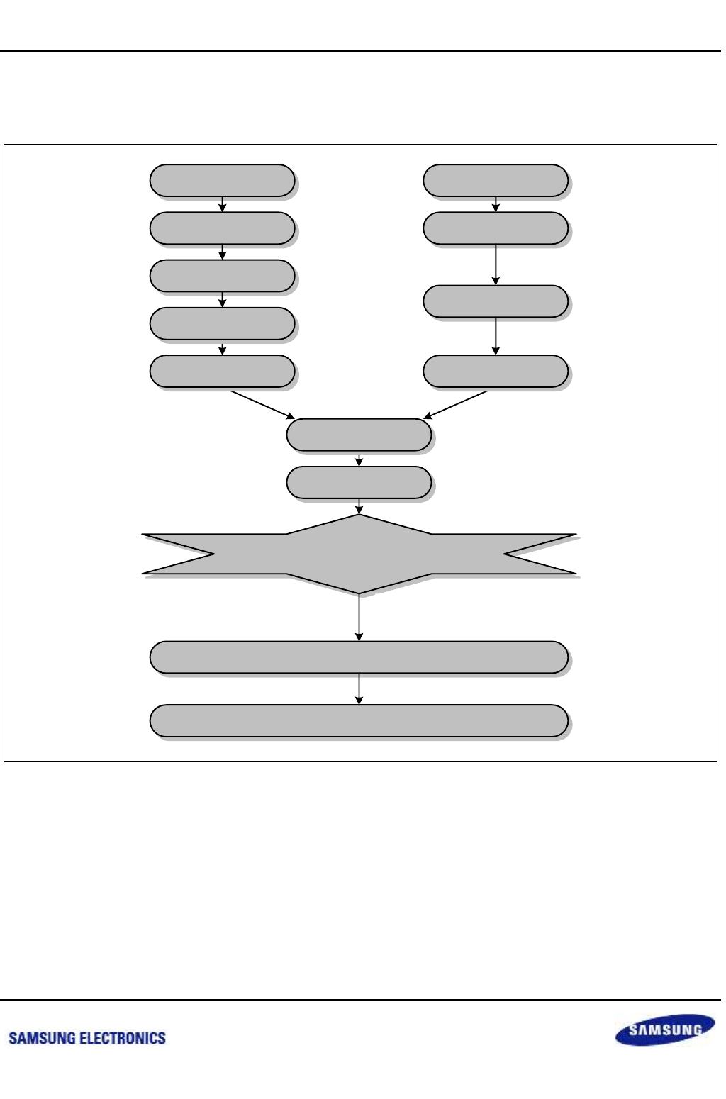
Samsung Confidential
S5P6818_UM 4 System Control
4-18
Preliminary product information describes products that are in development, for which full characterization data and
associated errata are not yet available. Specifications and information herein are subject to change without notice.
4.5.2.3 SLEEP Mode 1, SLEEP Mode 2
See the "ALIVE" Section for SLEEP Mode1 and SLEEP Mode2.
Figure 4-8 Power Down Mode Sequence
Upper figure shows the sequence to enter the Power Down mode and the Wake Up procedure. First, the Wake
Up source selects a desired event (interrupt) and specifies the attribute of the event. If the Wake up Source is
GPIO, the setting is changed into Input and the Pending Clear is performed. In addition, the status to detect that
an event (interrupt) is specified and Software Reset Enb is set as False for the worst case (If the Software Reset
Enb switch is not implemented in terms of Hardware, False does not need to be specified). Finally, the system
enables the relevant interrupt (if an interrupt is used) and enters a Power Down mode.
In this Power Down mode, the S5P6818 a waits a Wake Up event (interrupt). If the Wake Up event (Interrupt)
occurs, the S5P6818 returns to normal mode and clears the relevant interrupt pending in terms of Software.
Wait for Wake Up Event
Normal Mode
Wake Up
from IDLE/
Stop Mode
Pending Clear
GPIO Setting
I/O : Input
GPIO Wake Up Pending Clear
(GPIOINTPEND REG)
Detect Event Register Enable
(GPIOWAKEUPRISEENB or
GPIOWAKEUPFALLENB REG)
GPIO Reset Enb = False
(GPIORSTENB REG)
Wake Up Event Enable
(GPIOWAKEUPENB REG)
RTC Setting
RTC Wake Up Pending Clear
(INTPEND REG)
Wake Up Event Enable
(RTCWAKEUPENB REG)
RTC Wake up Enable
(RTCWKENB REG)
Enter Power Down Mode
(PWRMODE)
Interrupt Enable
(INTENB REG)
nexell / ys.kim at 2015.02.12
SAMSUNG Confidential
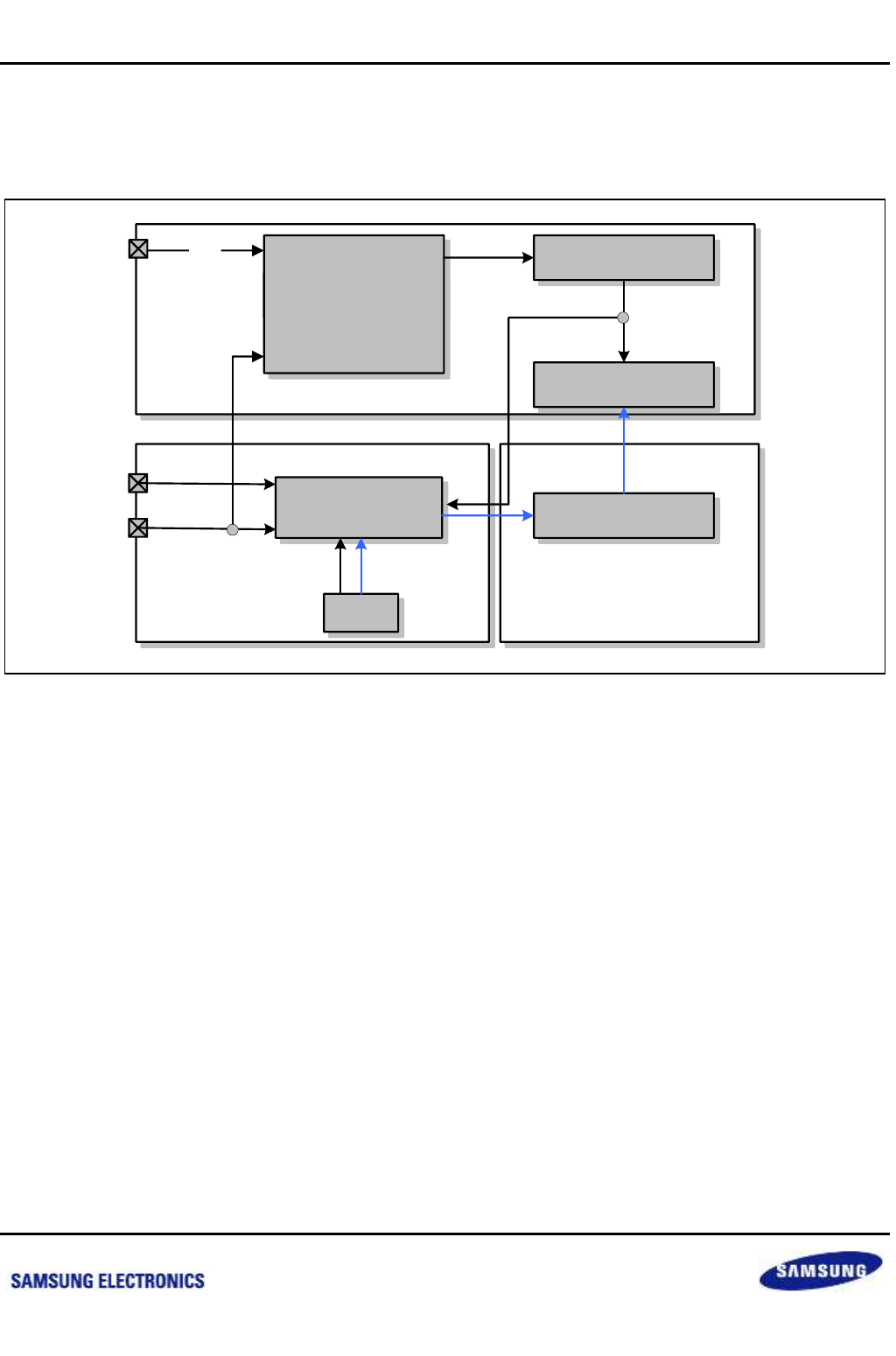
Samsung Confidential
S5P6818_UM 4 System Control
4-19
Preliminary product information describes products that are in development, for which full characterization data and
associated errata are not yet available. Specifications and information herein are subject to change without notice.
4.5.2.4 GPIO as a Wake up Source
GPIO is available for all Power Down modes. However, since the internal power and the clock status are not equal
for each power modes, the operation status is a little different at each power mode.
Figure 4-9 Wake Up Block Diagram
As shown in upper figure (Wake Up Block Diagram), Power Manager use different clock. Since RTC-clock is
always supplied to Power Manager Block, the PADs can be used as a Wake Up Source.
The description of the Wake Up procedures in Power Down mode is as follows:
Wake Up in IDLE Mode
During IDLE mode, clock and the power for the other blocks are supplied normally except CPU clock.
Therefore, the input received in GPIO is applied to the interrupt controller and wakes up the CPU.
Wake Up in STOP Mode
In STOP mode, all clocks except for the RTC clock are not supplied (PLL and XTI are included). The interrupt
controller does not operate in STOP mode. At this time, if a signal is entered to Power Manager, the power
manager wakes up the clock manager, first. As a result of this Wake Up, all clocks, such as the PLL and
PCLK, BCLK, MCLK and FCLK, are enabled and supplied to the CPU and the whole system. In other words,
the system is woken up. The Wake Up time is about 70 ms longer than that of IDLE mode to stabilize the
PLLs.
GPIO B
GPIO
Interrupt Controller
CPU
Power Manager
RTC-Clocked Block
GPIO
PLL-clocked Block
Clock Manager
Clock
Active
VDDPWRTOGGLE
RTC
RTC clock
AliveGPIO
BATF
RTCIRQ
nexell / ys.kim at 2015.02.12
SAMSUNG Confidential
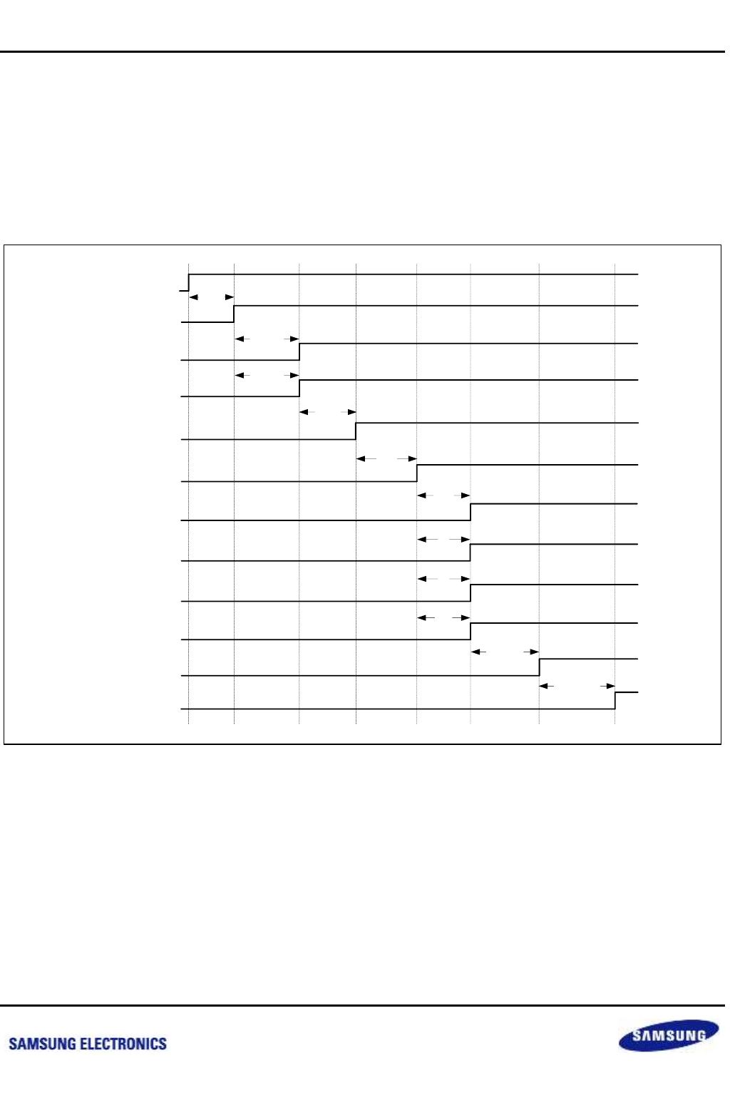
Samsung Confidential
S5P6818_UM 4 System Control
4-20
Preliminary product information describes products that are in development, for which full characterization data and
associated errata are not yet available. Specifications and information herein are subject to change without notice.
4.6 Reset Generation
4.6.1 Power On Reset Sequence
Power management block has the reset generation block. The reset generation block uses the nPORST which is
sampled at RTC clock (32.768 kHz). And the RTC clock is used as main clock for power management. So Even if
the RTC Function is not used, the RTC clock must be supplied.
Below figure shows the clock and reset behavior during the power-on reset sequence.
Figure 4-10 Power-On Reset Sequence
VDD18_RTC
VDDI10_ALIVE
VDDP18_ALIVE
VDD33_ALIVE
VDDI (CORE)
VDDI_ARM
VDDQ (DDR)
**OTHER VDD
NRESET
(input)
NGRESETOUT
(output)
tRESETOUT
tDDR
tRESETIN
tALL
tARM
tCORE
tALIVE
tALIVEIO
tALIVEIO
VDDP18
DVDD33_IO
tIO
tIO
nexell / ys.kim at 2015.02.12
SAMSUNG Confidential
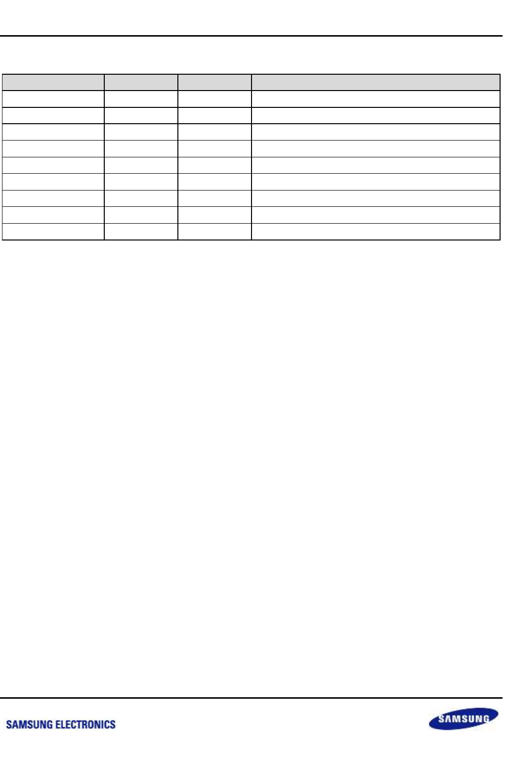
Samsung Confidential
S5P6818_UM 4 System Control
4-21
Preliminary product information describes products that are in development, for which full characterization data and
associated errata are not yet available. Specifications and information herein are subject to change without notice.
Table 4-13 Power-On Reset Timing Parameters
Symbol
Min. (msec)
Max. (msec)
Description
tALIVE
–50
Infinity
RTC to VDDI10_ALIVE
tALIVEIO
0
50
VDDI10_ALIVE to ALIVE IO power
tCORE
0
Infinity
VDDP18_ALIVE/VDD33_ALIVE to VDDI
tARM
0
50
VDDI to VDDI_ARM
tDDR
0
150
VDDI_ARM to VDDQ (DDR IO power)
tIO
0
150
VDDI_ARM to DVDD33_IO (normal IO power)
tALL
0
150
VDDI_ARM to DVDD33_IO (normal IO power)
tRESETIN
0
Infinity
All power on to assert nRESET
tRESETOUT
200
200
NRESET to NGRESETOUT
NOTE: **Other VDD: this mean all other powers like analog power.
nexell / ys.kim at 2015.02.12
SAMSUNG Confidential
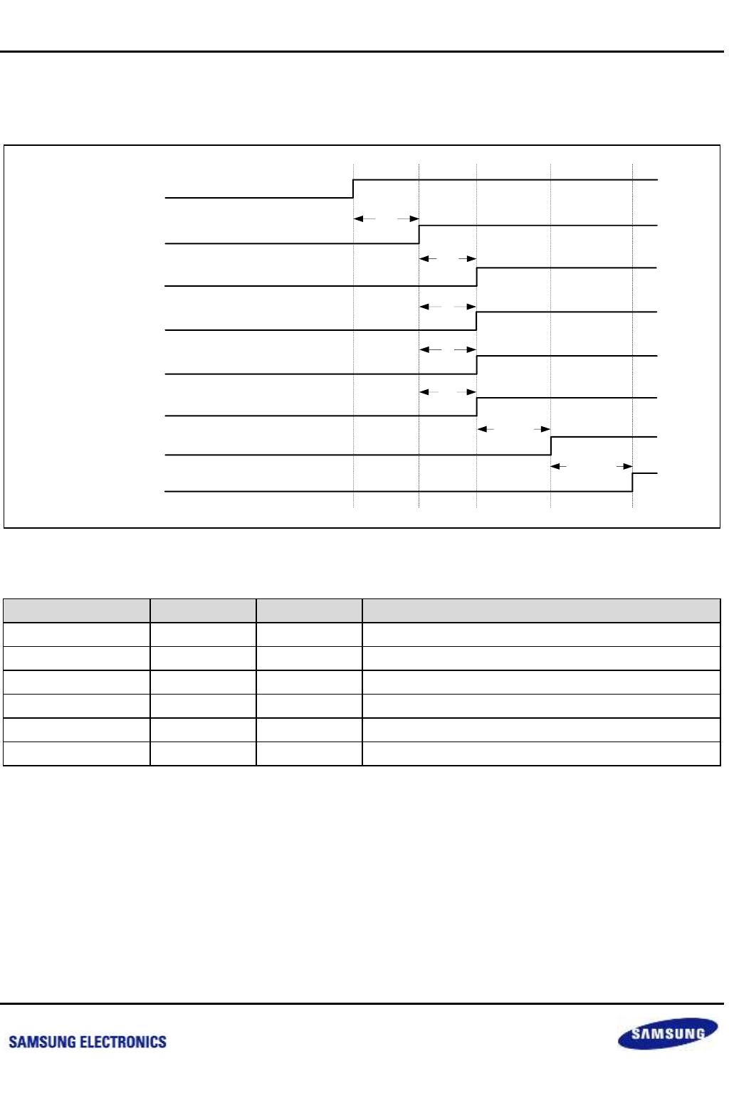
Samsung Confidential
S5P6818_UM 4 System Control
4-22
Preliminary product information describes products that are in development, for which full characterization data and
associated errata are not yet available. Specifications and information herein are subject to change without notice.
4.6.2 Sleep Mode Wakeup Sequence
All ALIVE and RTC power should be powered on before asserting sleep mode wakeup sequence.
Figure 4-11 Power On Sequence for Wakeup
Table 4-14 Wakeup Timing Parameters
Symbol
Min. (msec)
Max. (msec)
Description
tARM
0
50
VDDI to VDDI_ARM
tDDR
0
150
VDDI_ARM to VDDQ (DDR IO power)
tIO
0
150
VDDI_ARM to DVDD33_IO (normal IO power)
tALL
0
150
VDDI_ARM to DVDD33_IO (normal IO power)
tRESETIN
0
Infinity
All power on to assert nRESET
tRESETOUT
200
200
NRESET to NGRESETOUT
NOTE: Other VDD: this mean all other powers like analog power.
VDDI (CORE)
VDDI_ARM
VDDQ (DDR)
**OTHER VDD
NRESET
(input)
NGRESETOUT
(output)
tRESETOUT
tDDR
tRESETIN
tALL
tARM
VDDP18
DVDD33_IO
tIO
tIO
nexell / ys.kim at 2015.02.12
SAMSUNG Confidential
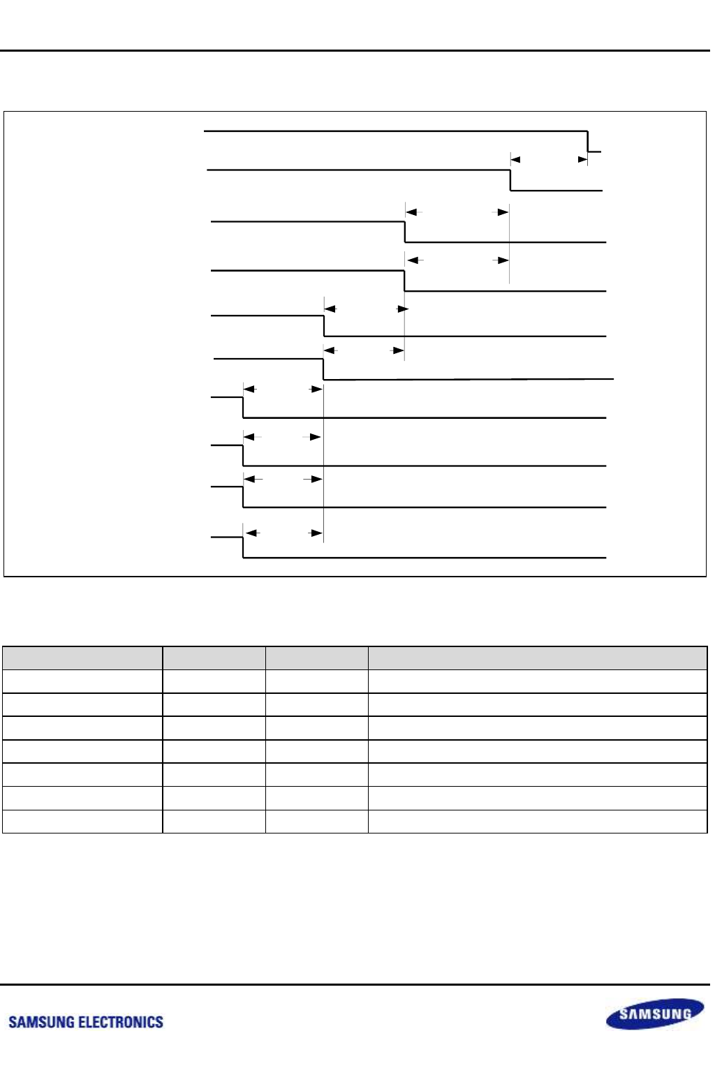
Samsung Confidential
S5P6818_UM 4 System Control
4-23
Preliminary product information describes products that are in development, for which full characterization data and
associated errata are not yet available. Specifications and information herein are subject to change without notice.
4.6.3 Power off sequence
Figure 4-12 Power Off Sequence
Table 4-15 Power Off Timing Parameters
Symbol
Min. (msec)
Max. (msec)
Description
tALIVE_OFF
–50
Infinity
ALIVE IO power to ALIVE CORE
tALIVEIO_OFF
0
50
ALIVE IO power to ALIVE core power
tCORE_OFF
0
Infinity
VDDI to ALIVE power
tARM_OFF
0
Infinity
VDDI_ARM to ALIVE power
tDDR_OFF
0
50
VDDQ(DDR IO power) to VDDI
tIO_OFF
0
50
DVDD33_IO (normal IO power) to VDDI
tALL_OFF
0
50
Other VDD power to VDDI
NOTE: Other VDD: this means all other powers like analog power.
VDD18_RTC
VDDI10_ALIVE
VDDP18_ALIVE
VDD33_ALIVE
VDDI (CORE)
VDDI_ARM
VDDQ (DDR)
**OTHER VDD
tDDR_OFF
tALL_OFF
tARM_OFF
tCORE_OFF
tALIVE_OFF
tALIVEIO_OFF
tALIVEIO_OFF
VDDP18
DVDD33_IO
tIO_OFF
tIO_OFF
nexell / ys.kim at 2015.02.12
SAMSUNG Confidential
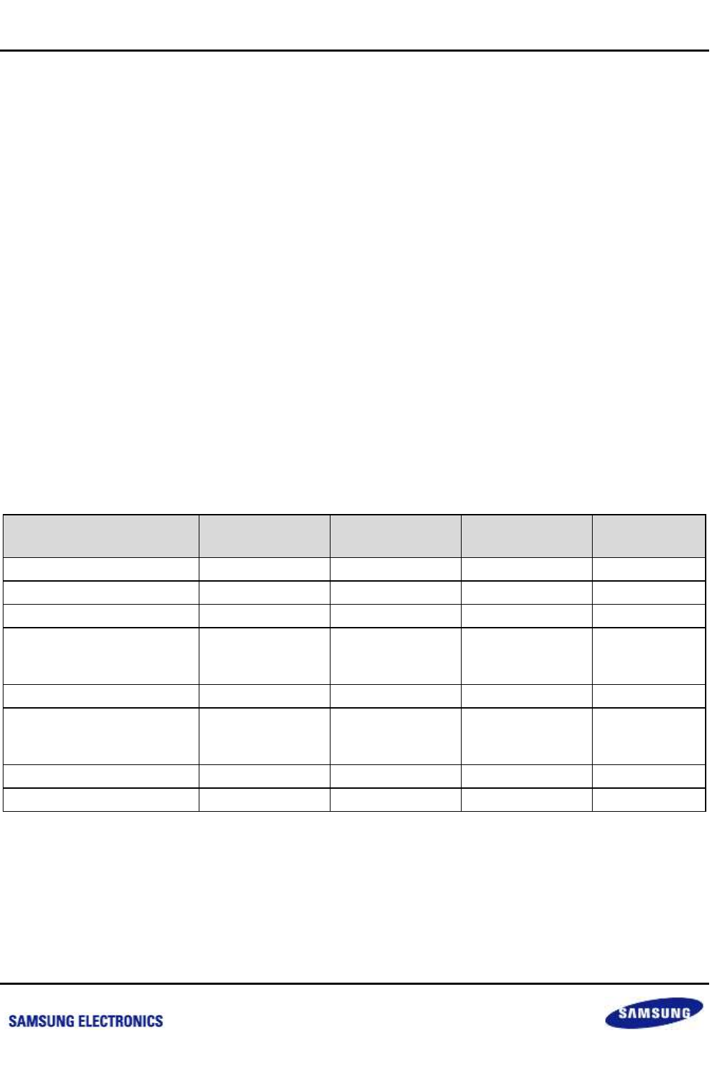
Samsung Confidential
S5P6818_UM 4 System Control
4-24
Preliminary product information describes products that are in development, for which full characterization data and
associated errata are not yet available. Specifications and information herein are subject to change without notice.
4.6.4 Software Reset and GPIO Reset
S5P6818 supports Software Reset that CPU can reset itself with Software reset. To generate Software Reset,
SWRSTENB bit must be set to 1 before setting PWRMODE.SWRST bit. Software Reset mode does not need the
time for stabilization clock because the software reset is requested in stable state differently from power on reset.
S5P6818 supports user defined GPIO Reset. The Power management block generates reset when the AliveGPIO
pad defined as GPIO Reset source is asserted or de-asserted. The AliveGPIO pad is used as GPIO Reset source
are defined at Wakeup Source Register. The GPIORSTENB bit set to 1 enables the AliveGPIO Reset source
feature.
4.6.5 Watchdog Reset
The Watchdog timer block is used to resume the controller operation whenever it is disturbed by malfunctions
such as system error, etc. When power management block detects the event from watchdog timer, it generates
exactly the same reset as power on reset because the watchdog reset event occurs in malfunctions and unknown
state.
4.6.6 nPORST, Software Reset, Watchdog Reset and GPIO Reset
S5P6818 has four reset states as below.
Table 4-16 Reset State
Blocks
Power On Reset
Watchdog Reset
GPIO Reset
(Software Reset)
Wake Up
(Idle, Stop)
Clock Manager
Reset
Reset
Reset
X
All Core (CPU and etc…)
Reset
Reset
Reset
X
GPIO
Reset
Reset
Reset
X
Power Manager
(Except LASTPWRMODE
Register)
Reset
Reset
Reset
X
LASTPWRMODE Register
Reset
X
X
X
RTC Registers
(Except RTCCNTREAD
Register)
Reset
Reset
Reset
X
RTCCNTREAD Register
X
X
X
X
nGRESETOUT (Output to PAD)
Reset
Reset
Reset
X
nexell / ys.kim at 2015.02.12
SAMSUNG Confidential

Samsung Confidential
S5P6818_UM 4 System Control
4-25
Preliminary product information describes products that are in development, for which full characterization data and
associated errata are not yet available. Specifications and information herein are subject to change without notice.
4.7 Tie Off
Tieoff block is a set of registers that includes special registers which don’t need to be set in normal mode
operation. Tieoff block includes special function registers for ARM, HDMI, DRAM controller, UART, USB2.0 HOST
controller/ Phy, USB2.0 OTG controller/ Phy, Ethernet controller, AXI buses and the internal SRAM timing margin
controls.
4.8 AXI BUS
ARM PL301 (AXI3 BUS interconnect) provides programmable function for AXI BUS and which includes QoS and
Programmable Round-Robin.
4.8.1 Programmable Quality of Service (ProgQoS)
The QoS scheme works by tracking the number of outstanding transactions, and when a specified number is
reached, only permits transactions from particular, specified masters.
The QoS scheme only provides support for slaves that have a combined acceptance capability, such as the
PrimeCell Dynamic Memory Controller (PL340).
The QoS scheme has no effect until the AXI bus matrix calculates that, at a particular MI, there are a number of
outstanding transactions equal to the value stored in the QoS tidemark Register. It then accepts transactions only
from slave ports specified in the QoS access control Register. This restriction remains until the number of
outstanding transactions is again less than the value stored in the QoS tidemark Register.
It is recommended that you assign low MI numbers to MIs that require QoS support. This approach aligns well
with the cyclic priority scheme because MIs that require QoS support are typically those that can be considered
high-ranking slaves. See the PrimeCell High-Performance Matrix (PL301) Technical Reference Manual.
nexell / ys.kim at 2015.02.12
SAMSUNG Confidential
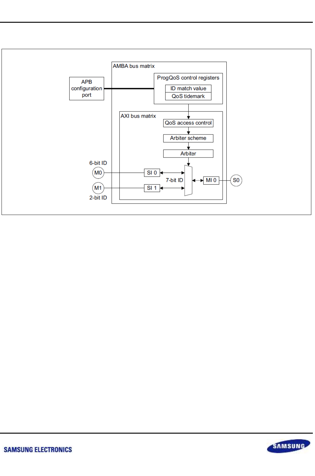
Samsung Confidential
S5P6818_UM 4 System Control
4-26
Preliminary product information describes products that are in development, for which full characterization data and
associated errata are not yet available. Specifications and information herein are subject to change without notice.
Below Figure shows the implementation for an interconnection that supports two masters and one slave.
Figure 4-13 Example Implementation of ProgQoS Control Registers for 2 1 Interconnect
nexell / ys.kim at 2015.02.12
SAMSUNG Confidential

Samsung Confidential
S5P6818_UM 4 System Control
4-27
Preliminary product information describes products that are in development, for which full characterization data and
associated errata are not yet available. Specifications and information herein are subject to change without notice.
4.8.2 Arbitration Scheme
You can configure each MI separately to have an arbitration scheme that is a programmable or fixed Round-robin
(RR) scheme.
The AW and AR channels have separate arbiters and can be programmed, if applicable, and interrogated
separately through the APB programming interface, but both AW and AR channels are configured identically.
Because the AW and AR channels are arbitrated separately, an MI can permit simultaneous read and write
transactions from different SIs.
The arbitration mechanism registers the arbitration decision for use in the subsequent cycle. An arbitration
decision taken in the current cycle does not affect the current cycle.
If no SIs is active, the arbiter adopts default arbitration, that is, the highest priority SI. If this occurs and then the
highest priority interface becomes active in the same cycle as, or before any other SI, then this does not constitute
a grant to an active SI and the arbitration scheme does not change its state as a result of that transfer.
If a QoS provision is enabled and active, only a subset of SIs are permitted to win arbitration, and it cannot be
guaranteed that the default arbitration is among these. In these circumstances, no transaction is permitted to use
the default arbitration, and arbitration must occur when there is an active SI.
4.8.2.1 RR Schemes
In these schemes, you can choose, at design time:
The number of slots that are used
The SI to which they are allocated
Their order.
There must be at least one slot per connected SI and there can be up to 32 slots. By allocating multiple slots for
an SI, you can allocate access to the slave, on average, in proportion to the number of slots. If the slots are
appropriately ordered, this can also reduce the maximum time before a grant is guaranteed. The SI associated
with a slot can be interrogated from the APB programming interface and can be changed if the programmable RR
scheme is chosen.
Whenever arbitration is granted to an active SI, the slots are rotated so that the slot currently in the highest priority
position becomes the lowest, and all other slots move to a higher priority but maintain their relative order. This
means that if an SI is the highest priority active SI, but is not the highest priority interface, then it continues to win
the arbitration until it becomes the highest priority interface, and then the lowest priority interface subsequently.
Because the arbitration value is registered, the arbitration decision made in this cycle is used in the next cycle.
This means that if the SI that currently holds the arbitration is still the highest priority active SI in this cycle, wins
the arbitration again regardless of whether or not it is active in the next cycle as shown by the status of M3 in
stages A, B, and C of below Figure.
nexell / ys.kim at 2015.02.12
SAMSUNG Confidential
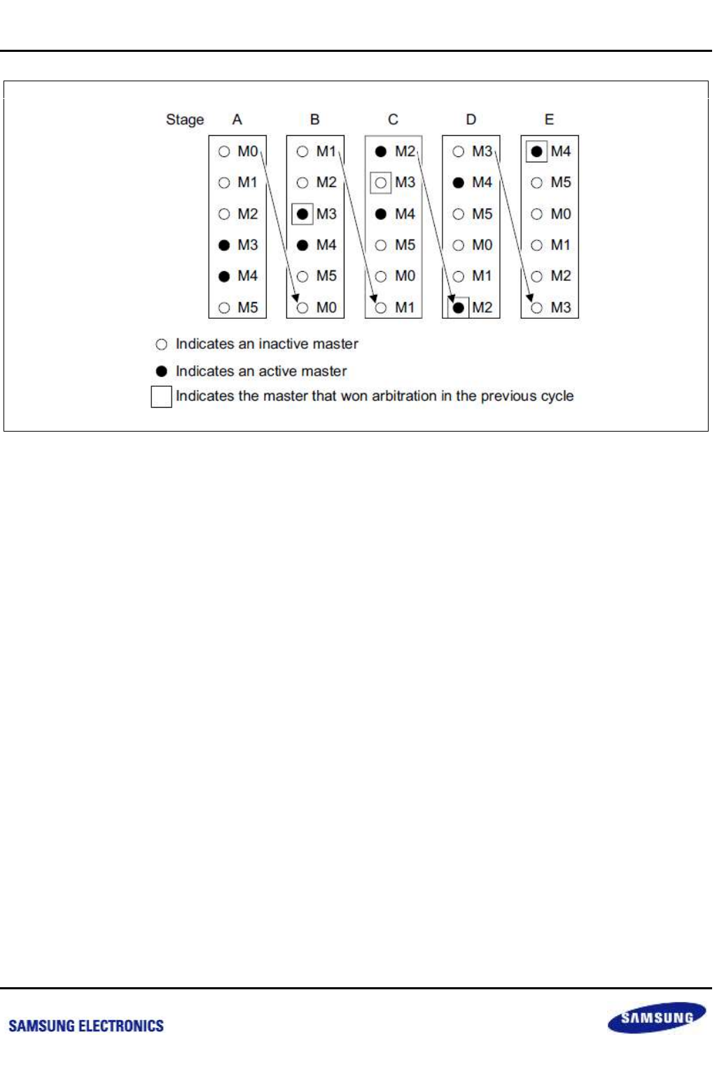
Samsung Confidential
S5P6818_UM 4 System Control
4-28
Preliminary product information describes products that are in development, for which full characterization data and
associated errata are not yet available. Specifications and information herein are subject to change without notice.
Figure 4-14 Example Operation of RR Arbitration Scheme
nexell / ys.kim at 2015.02.12
SAMSUNG Confidential

Samsung Confidential
S5P6818_UM 4 System Control
4-29
Preliminary product information describes products that are in development, for which full characterization data and
associated errata are not yet available. Specifications and information herein are subject to change without notice.
4.9 Register Description
4.9.1 Register Map Summary
Base Address: 0XC001_0000
Register
Offset
Description
Reset Value
CLKMODEREG0
0000h
Clock Mode register 0
0x0000_0000
CLKMODEREG1
0004h
Clock mode register1
0x0000_0000
PLLSETREG0
0008h
PLL0 setting register
0x101A_2602
PLLSETREG1
000Ch
PLL1 setting register
0x101A_4E04
PLLSETREG2
0010h
PLL2 setting register
0x100C_C004
PLLSETREG3
0014h
PLL3 setting register
0x100C_FA04
RSVD
0018h to
001Fh
Reserved
0x0000_0000
CLKDIVREG0
0020h
FCLKCPU0 setting register
0x0000_8208
CLKDIVREG1
0024h
BCLK setting register
0x0000_8208
CLKDIVREG2
0028h
MDCLK setting register
0x0020_8000
CLKDIVREG3
002Ch
GR3DBCLK setting register
0x0000_8208
CLKDIVREG4
0030h
MPEGBCLK setting register
0x0000_8208
CLKDIVREG5
0034h
DISPBCLK setting register
0x0000_8208
CLKDIVREG6
0038H
HDMIPCLK setting register
0x0000_8208
CLKDIVREG7
003ch
FCLKCPU1 setting register
0x0000_8208
CLKDIVREG8
0040H
FASTBCLK setting register
0x0000_8208
RSVD
0044h to
0047h
Reserved
0x0000_0000
PLLSETREG0_SSCG
0048h
PLL0 setting register for spread spectrum
0x0000_0000
PLLSETREG1_SSCG
004Ch
PLL1 setting register for spread spectrum
0x0000_0000
PLLSETREG2_SSCG
0050h
PLL2 setting register for spread spectrum
0x0000_0000
PLLSETREG3_SSCG
0054h
PLL3 setting register for spread spectrum
0x0000_0000
GPIOWAKEUPRISEENB
0200h
Rising edge detect enable register
0x0000_0003
GPIOWAKEUPFALLENB
0204h
Falling edge detect enable register
0x0000_0003
GPIORSTENB
0208h
GPIO reset enable register
0x0000_0000
GPIOWKENB
020Ch
GPIO wakeup enable register
0x0000_0003
INTENB
0210h
GPIO interrupt enable register
0x0000_0003
GPIOINTPEND
0214h
GPIO interrupt pending register
0x0000_0000
RESETSTATUS
0218h
Reset status register
0x0000_0001
INTENABLE
021Ch
Interrupt enable register
0x0000_0000
INTPEND
0220h
Interrupt pending register
0x0000_0000
PWRCONT
0224h
Power management control register
0x0000_FF00
PWRMODE
0228h
Power management mode register
0x0000_0000
nexell / ys.kim at 2015.02.12
SAMSUNG Confidential

Samsung Confidential
S5P6818_UM 4 System Control
4-30
Preliminary product information describes products that are in development, for which full characterization data and
associated errata are not yet available. Specifications and information herein are subject to change without notice.
Register
Offset
Description
Reset Value
RSVD
022Ch
Reserved
0x0000_024D
PADSTRENGTHGPIOAL
0230h to
0238h
Scratch register
0x0000_0000
SYSRSTCONFIG
023Ch
System reset configuration register
Undefined
RSVD
0240h to
03FFh
Reserved
0x0000_0000
Base Address: 0xC001_1000
Register
Offset
Description
Reset Value
Tieoff
RSVD
0x00
Reserved
Undefined
TIEOFFREG01
0x04
AXI Configuration Register
0x1E0D_800C
TIEOFFREG02
0x08
HDMI/ De-Interlace Configuration Register
0xFDB6_C78F
TIEOFFREG03
0x0C
DREX/ DISPLAY/ HDMI Configuration Register
0x98C1_B6C6
TIEOFFREG04
0x10
UART/ SCALER/ MIPI/ DREX Configuration Register
0x0001_FFB7
TIEOFFREG05
0x14
USBHOST Configuration 0 Register
0x0400_83C0
TIEOFFREG06
0x18
USBHOST Configuration 1 Register
0x0000_0000
TIEOFFREG07
0x1C
USBHOST Configuration 2 Register
0x0000_0000
TIEOFFREG08
0x20
USBHOST Configuration 3 Register
0xAC00_6D00
TIEOFFREG09
0x24
USBHOST Configuration 4 Register
0x3E38_0200
TIEOFFREG10
0x28
USBHOST Configuration 5 Register
0x3240_0153
TIEOFFREG11
0x2C
USBHOST Configuration 6 Register
0x0F3A_202B
TIEOFFREG12
0x30
USBOTG Configuration 0 Register
0x0000_0001
TIEOFFREG13
0x34
USBOTG Configuration 1 Register
0xA000_6D00
TIEOFFREG14
0x38
USBOTG Configuration 2 Register
0x3E38_0200
TIEOFFREG15
0x3C
USBOTG Configuration 3 Register
0x3FC0_0153
TIEOFFREG16
0x40
CODA Configuration 0 Register
0x00FF_FFFF
TIEOFFREG17
0x44
CODA Configuration 1 Register
0x3FFF_FFFF
TIEOFFREG18
0x48
CODA Configuration 2 Register
0xFFFF_FFFF
TIEOFFREG19
0x4C
CODA Configuration 3 Register
0x0FFF_FFFF
TIEOFFREG20
0x50
CODA Configuration 4 Register
0x1B6D_BFFF
TIEOFFREG21
0x54
CODA Configuration 5 Register
0x6C86_306C
TIEOFFREG22
0x58
GPU Configuration 0 Register
0xFFFE_18DB
TIEOFFREG23
0x5C
GPU Configuration 1 Register
0x001F_FFFF
TIEOFFREG24
0x60
GPU Configuration 2 Register
0x0000_0000
TIEOFFREG25
0x64
GPU Configuration 3 Register
0xFFFF_FFFF
TIEOFFREG26
0x68
GPU Configuration 4 Register
0x0000_0000
nexell / ys.kim at 2015.02.12
SAMSUNG Confidential

Samsung Confidential
S5P6818_UM 4 System Control
4-31
Preliminary product information describes products that are in development, for which full characterization data and
associated errata are not yet available. Specifications and information herein are subject to change without notice.
Register
Offset
Description
Reset Value
TIEOFFREG27
0x6C
GPU Configuration 5 Register
0xFFFF_FFFF
TIEOFFREG28
0x70
GPU Configuration 6 Register
0x0000_0000
TIEOFFREG29
0x74
GPU Configuration 7 Register
0xFFFF_FFFF
TIEOFFREG30
0x78
GPU Configuration 8 Register
0xFFFF_FFFF
TIEOFFREG31
0x7C
GPU Configuration 9 Register
0xFFFF_FFFF
TIEOFFREG32
0x80
BUS Configuration 0 Register
0x0000_0000
TIEOFFREG41
0xA4
BUS Configuration 1 Register
0x1C00_0000
TIEOFFREG42
0xA8
BUS Configuration 2 Register
0x0000_F800
TIEOFFREG43
0xAC
BUS Configuration 3 Register
0x2000_0000
TIEOFFREG44
0xB0
BUS Configuration 4 Register
0x02AA_A86A
TIEOFFREG45
0xB4
BUS Configuration 5 Register
0x0000_0000
TIEOFFREG46
0xB8
BUS Configuration 6 Register
0x0000_0000
TIEOFFREG47
0xBC
BUS Configuration 7 Register
0x0000_0000
TIEOFFREG48
0xC0
BUS Configuration 8 Register
0x0000_0000
TIEOFFREG49
0xC4
BUS Configuration 9 Register
0x0000_0000
TIEOFFREG50
0xC8
BUS Configuration 10 Register
0x0000_0000
TIEOFFREG51
0xCC
BUS Configuration 11 Register
0x0001_0000
TIEOFFREG52
0xD0
BUS Configuration 12 Register
0x0000_0000
TIEOFFREG53
0xD4
BUS/ DREX Configuration Register
0x0000_3800
TIEOFFREG54
0xD8
DREX Configuration Register
0x0000_0000
TIEOFFREG55
0xDC
DREX Configuration Register
0x0000_0000
TIEOFFREG56
0xE0
DREX Configuration Register
0x0000_0000
TIEOFFREG57
0xE4
DREX/ GMAC/ BUS Configuration Register
0x0000_0000
TIEOFFREG58
0xE8
BUS Configuration Register
0x0000_0000
TIEOFFREG59
0xEC
BUS/ SDMMC Configuration Register
0x0000_0000
TIEOFFREG60
0xF0
SDMMC/ USBOTG/ USBHOST Configuration Register
0x0000_0000
TIEOFFREG61
0xF4
USBHOST/ DMA/ MPEGTSI Configuration Register
0x0000_0000
TIEOFFREG62
0xF8
MPEGTSI/ DAC/ DREX/ BUS Configuration Register
0x0000_0000
TIEOFFREG63
0xFC
BUS/ GPU/ DREX/ CODA Configuration Register
0x0000_0000
TIEOFFREG64
0x100
BUS Configuration Register
0x0000_0000
TIEOFFREG65
0x104
BUS Configuration Register
0x0000_0000
TIEOFFREG66
0x108
BUS Configuration Register
0x0000_0000
TIEOFFREG67
0x10C
BUS Configuration Register
0x0060_0000
TIEOFFREG68
0x110
BUS/ CODA/ GPU/ Core Sight Configuration Register
0x2008_2802
TIEOFFREG69
0x114
Core Sight/ GPU/ CODA/ BUS Configuration Register
0x0000_001E
TIEOFFREG70
0x118
VIP Configuration Register
0x0000_0000
TIEOFFREG71
0x11C
VIP/ Core Sight/ BUS Configuration Register
0x0000_0000
nexell / ys.kim at 2015.02.12
SAMSUNG Confidential

Samsung Confidential
S5P6818_UM 4 System Control
4-32
Preliminary product information describes products that are in development, for which full characterization data and
associated errata are not yet available. Specifications and information herein are subject to change without notice.
Register
Offset
Description
Reset Value
TIEOFFREG72
0x120
BUS/ DISPLAY Configuration Register
0x0000_0000
TIEOFFREG73
0x124
DISPLAY/ GPU/ DEINTERLACE Configuration Register
0x0000_0000
TIEOFFREG74
0x128
DEINTERLACE/ SCALER/ GMAC Configuration Register
0x0000_0000
TIEOFFREG75
0x12C
TMU/ DREX/ GPU/ BUS Configuration Register
0x0000_0000
TIEOFFREG76
0x130
DREX/ ARM/ BUS Configuration Register
0x0000_01C0
TIEOFFREG77
0x134
BUS/ ARM Configuration Register
0x4078_0000
TIEOFFREG78
0x138
ARM Configuration Register
0x0000_0008
TIEOFFREG79
0x13C
ARM Configuration Register
0x0000_0000
TIEOFFREG80
0x140
ARM Configuration Register
0x0000_0000
TIEOFFREG81
0x144
ARM Configuration Register
0x0000_0000
TIEOFFREG82
0x148
ARM Configuration Register
0x0000_0000
TIEOFFREG83
0x14C
ARM Configuration Register
0x0000_0000
TIEOFFREG84
0x150
ARM Configuration Register
0x0000_0000
TIEOFFREG85
0x154
ARM Configuration Register
0x0000_0000
TIEOFFREG86
0x158
ARM Configuration Register
0x0000_0000
TIEOFFREG87
0x15C
(Write) ARM Configuration Register
0x0000_0000
(Read) ARM Configuration Register
0x0078_0000
TIEOFFREG88
0x160
(Write) ARM Configuration Register
0x0003_C000
(Read) ARM Configuration Register
0x0000_0000
TIEOFFREG89
0x164
ARM Configuration Register
0x0000_0000
TIEOFFREG90
0x168
ARM Configuration Register
0x0000_0000
TIEOFFREG91
0x16C
ARM Configuration Register
0x0000_0006
TIEOFFREG92
0x170
ARM Configuration Register
0x0000_0000
TIEOFFREG93
0x174
ARM Configuration Register
0x0000_0000
TIEOFFREG94
0x178
ARM Configuration Register
0x0082_3000
TIEOFFREG95
0x17C
ARM Configuration Register
0x0400_0000
TIEOFFREG96
0x180
ARM Configuration Register
0x0000_0004
TIEOFFREG97
0x184
ARM Configuration Register
0x0000_0000
TIEOFFREG98
0x188
ARM Configuration Register
0x0000_0000
TIEOFFREG99
0x18C
ARM Configuration Register
0x0000_0000
TIEOFFREG100
0x190
ARM Configuration Register
0x0000_0000
TIEOFFREG101
0x194
ARM Configuration Register
0x0000_0000
TIEOFFREG102
0x198
ARM Configuration Register
0x0000_0000
TIEOFFREG103
0x19C
ARM Configuration Register
0x0000_0000
TIEOFFREG104
0x1A0
(Write) ARM Configuration Register
0x0000_0000
(Read) ARM Configuration Register
0x0078_0000
TIEOFFREG105
0x1A4
ARM Configuration Register
0x0000_0000
nexell / ys.kim at 2015.02.12
SAMSUNG Confidential

Samsung Confidential
S5P6818_UM 4 System Control
4-33
Preliminary product information describes products that are in development, for which full characterization data and
associated errata are not yet available. Specifications and information herein are subject to change without notice.
Register
Offset
Description
Reset Value
TIEOFFREG106
0x1A8
ARM Configuration Register
0x0000_0000
TIEOFFREG107
0x1AC
ARM Configuration Register
0x0000_0000
TIEOFFREG108
0x1B0
ARM Configuration Register
0x0000_0000
TIEOFFREG109
0x1B4
ARM Configuration Register
0x0000_0000
TIEOFFREG110
0x1B8
ARM Configuration Register
0x0000_0000
TIEOFFREG111
0x1BC
ARM Configuration Register
0x0080_3000
TIEOFFREG112
0x1C0
ARM Configuration Register
0x0000_0000
TIEOFFREG113
0x1C4
ARM Configuration Register
0x0000_0000
TIEOFFREG114
0x1C8
ARM Configuration Register
0x0000_0000
TIEOFFREG115
0x1CC
ARM Configuration Register
0x0000_0000
TIEOFFREG116
0x1D
ARM Configuration Register
0x0000_0000
TIEOFFREG117
0x1D4
ARM Configuration Register
0x01FF_FFF0
TIEOFFREG118
0x1D8
ARM Configuration Register
0x0000_0000
TIEOFFREG119
0x1DC
ARM Configuration Register
0x0000_0000
TIEOFFREG120
0x1E0
ARM Configuration Register
0x0000_0000
TIEOFFREG121
0x1E4
ARM Configuration Register
0x0000_0000
TIEOFFREG122
0x1E8
ARM Configuration Register
0x0000_0000
TIEOFFREG123
0x1EC
ARM Configuration Register
0x0000_0000
TIEOFFREG124
0x1F0
ARM Configuration Register
0x0000_0000
TIEOFFREG125
0x1F4
ARM Configuration Register
0x01FF_FFF0
TIEOFFREG126
0x1F8
ARM Configuration Register
0x0000_0000
TIEOFFREG127
0x1FC
ARM Configuration Register
0x0000_0000
TIEOFFREG128
0x200
I2S/ ARM Configuration Register
0x3A00_0000
TIEOFFREG129
0x204
I2S/ ARM/ DEINTERLACE/ SCALER Configuration
Register
0x0050_000F
TIEOFFREG130
0x208
CODA Configuration Register
0x0000_0000
TIEOFFREG131
0x20C
BUS/ CODA/ GPU/ DISPLAY Configuration Register
0x0000_0000
NOTE: SRAM EMA signals are for chip test only. Users don't need to control those registers for normal functions.
SRAM EMA: Extra Margin Adjustment
EMA: SRAM read/write margin
EMAW: SRAM write margin
EMAS: SRAM S/A pulse width
nexell / ys.kim at 2015.02.12
SAMSUNG Confidential

Samsung Confidential
S5P6818_UM 4 System Control
4-34
Preliminary product information describes products that are in development, for which full characterization data and
associated errata are not yet available. Specifications and information herein are subject to change without notice.
Base Address: 0xC001_2000
Register
Offset
Description
Reset Value
IP Reset
IP RESET REGISTER 0
0x000h
IP Reset Register 0
0x0000_0000
IP RESET REGISTER 1
0x004h
IP Reset Register 1
0x0000_0000
IP RESET REGISTER 2
0x008h
IP Reset Register 2
0x0000_0000
nexell / ys.kim at 2015.02.12
SAMSUNG Confidential
Samsung Confidential
S5P6818_UM 4 System Control
4-35
Preliminary product information describes products that are in development, for which full characterization data and
associated errata are not yet available. Specifications and information herein are subject to change without notice.
4.9.1.1 CLKMODEREG0
Base Address: 0xC001_0000
Address = Base Address + 0000h, Reset Value = 0x0000_0000
Name
Bit
Type
Description
Reset Value
WAIT_UPDATE_PLL
[31]
RW
Wait flag updating-PLL for several RTC (32768 Hz)
clocks
0 = Done
1 = In-process
1'b0
RSVD
[30:4]
–
Reserved
1'b0
UPDATE_PLL[3]
[3]
RW
Update P,M,S values for PLL[3]
0 = None
1 = Update
1'b0
UPDATE_PLL[2]
[2]
RW
Update P,M,S values for PLL[2]
0 = None
1 = Update
1'b0
UPDATE_PLL[1]
[1]
RW
Update P,M,S values for PLL[1]
0 = None
1 = Update
1'b0
UPDATE_PLL[0]
[0]
RW
Update P,M,S values for PLL[0]
0 = None
1 = Update
1'b0
NOTE: The PMS values of PLL[n] is applied when UPDATE_PLL[n] is set to "1".
4.9.1.2 CLKMODEREG1
Base Address: 0xC001_0000
Address = Base Address + 0004h, Reset Value = 0x0000_0000
Name
Bit
Type
Description
Reset Value
RSVD
[31:0]
–
Reserved
32'h0
nexell / ys.kim at 2015.02.12
SAMSUNG Confidential

Samsung Confidential
S5P6818_UM 4 System Control
4-36
Preliminary product information describes products that are in development, for which full characterization data and
associated errata are not yet available. Specifications and information herein are subject to change without notice.
4.9.1.3 PLLSETREG0
Base Address: 0xC001_0000
Address = Base Address + 0008h, Reset Value = 0x101A_2602
Name
Bit
Type
Description
Reset Value
RSVD
[31]
–
Reserved
1'b0
SSCG_EN
[30]
RW
PLL spread spectrum enable. This register is ignored
for non-dithered PLL
0 = Disable
1 = Enable
1'b0
PD
[29]
RW
PLL Power down
0 = Power on.
1 = Power down
1'b0
NPLLBYPASS
[28]
RW
This register bypass PLL outputs.
0 = X-tal clock (PLL input) is selected as PLL output.
1 = Normal PLL output
1'b1
PLLOUTDIV
[27:24]
RW
PLL output for peripheral is divided by this register.
PLL output for system clock is not affected by this
register.
0 = Divide by one
1 = Divide by two
N-1 = divide by N
4'b0000
PDIV
[23:18]
RW
Pre Divider Value. Divider initially dividing 12 MHz to
make PLL0
1 PDIV 63
6'h6
MDIV
[17:8]
RW
Main Divider Value. If the value of Fvco is not a
desired clock, the value is divided into MDIV again
after feedback. (This loop is continuously circulated
until a desired clock frequency is made.)
64 MDIV 1023
10'h226
SDIV
[7:0]
RW
Post Scale Divider. Divide the value of Fvco by SDIV
to obtain the desired PLL0 value finally.
0 SDIV 5
8'h2
nexell / ys.kim at 2015.02.12
SAMSUNG Confidential

Samsung Confidential
S5P6818_UM 4 System Control
4-37
Preliminary product information describes products that are in development, for which full characterization data and
associated errata are not yet available. Specifications and information herein are subject to change without notice.
4.9.1.4 PLLSETREG1
Base Address: 0xC001_0000
Address = Base Address + 000Ch, Reset Value = 0x101A_4E04
Name
Bit
Type
Description
Reset Value
RSVD
[31]
–
Reserved
1'b0
SSCG_EN
[30]
RW
PLL spread spectrum enable. This register is ignored
for non-dithered PLL
0 = Disable
1 = Enable
1'b0
PD
[29]
RW
PLL Power down
0 = Power on
1 = Power down
1'b0
NPLLBYPASS
[28]
RW
This register bypass PLL outputs.
0 = X-tal clock (PLL input) is selected as PLL output
1 = Normal PLL output
1'b1
PLLOUTDIV
[27:24]
RW
PLL output for peripheral is divided by this register.
PLL output for system clock is not affected by this
register.
0 = Divide by one
1 = Divide by two
N-1 = Divide by N
4'b0
PDIV
[23:18]
RW
Pre Divider Value. Divider initially dividing 12 MHz to
make PLL0
1 PDIV 63
6'h6
MDIV
[17:8]
RW
Main Divider Value. If the value of Fvco is not a
desired clock, the value is divided into MDIV again
after feedback. (This loop is continuously circulated
until a desired clock frequency is made.)
64 MDIV 1023
10'h24E
SDIV
[7:0]
RW
Post Scale Divider. Divide the value of Fvco by SDIV
to obtain the desired PLL0 value finally.
0 SDIV 5
8'h4
nexell / ys.kim at 2015.02.12
SAMSUNG Confidential

Samsung Confidential
S5P6818_UM 4 System Control
4-38
Preliminary product information describes products that are in development, for which full characterization data and
associated errata are not yet available. Specifications and information herein are subject to change without notice.
4.9.1.5 PLLSETREG2
Base Address: 0xC001_0000
Address = Base Address + 0010h, Reset Value = 0x100C_C004
Name
Bit
Type
Description
Reset Value
RSVD
[31]
–
Reserved
1'b0
SSCG_EN
[30]
RW
PLL spread spectrum enable. This register is ignored
for non-dithered PLL
0 = Disable
1 = Enable
1'b0
PD
[29]
RW
PLL Power down
0 = Power on
1 = Power down
1'b0
NPLLBYPASS
[28]
RW
This register bypass PLL outputs.
0 = X-tal clock (PLL input) is selected as PLL output
1 = Normal PLL output
1'b1
PLLOUTDIV
[27:24]
RW
PLL output for peripheral is divided by this register.
PLL output for system clock is not affected by this
register.
0 = Divide by one
1 = Divide by two
N-1 = Divide by N
4'b0
PDIV
[23:18]
RW
Pre Divider Value. Divider initially dividing 12 MHz to
make PLL0
1 PDIV 63
6'h3
MDIV
[17:8]
RW
Main Divider Value. If the value of Fvco is not a
desired clock, the value is divided into MDIV again
after feedback. (This loop is continuously circulated
until a desired clock frequency is made.)
64 MDIV 1023
10'h0C0
SDIV
[7:0]
RW
Post Scale Divider. Divide the value of Fvco by SDIV
to obtain the desired PLL0 value finally.
0 SDIV 5
8'h4
nexell / ys.kim at 2015.02.12
SAMSUNG Confidential

Samsung Confidential
S5P6818_UM 4 System Control
4-39
Preliminary product information describes products that are in development, for which full characterization data and
associated errata are not yet available. Specifications and information herein are subject to change without notice.
4.9.1.6 PLLSETREG3
Base Address: 0xC001_0000
Address = Base Address + 0014h, Reset Value = 0x100C_FA04
Name
Bit
Type
Description
Reset Value
RSVD
[31]
–
Reserved
1'b0
SSCG_EN
[30]
RW
PLL spread spectrum enable. This register is ignored
for non-dithered PLL
0 = Disable
1 = Enable
1'b0
PD
[29]
RW
PLL Power down
0 = Power on
1 = Power down
1'b0
NPLLBYPASS
[28]
RW
This register bypass PLL outputs.
0 = X-tal clock (PLL input) is selected as PLL output
1 = Normal PLL output
1'b1
PLLOUTDIV
[27:24]
RW
PLL output for peripheral is divided by this register.
PLL output for system clock is not affected by this
register.
0 = Divide by one
1 = Divide by two
N-1 = Divide by N
4'b0000
PDIV
[23:18]
RW
Pre Divider Value. Divider initially dividing 12 MHz to
make PLL0
1 PDIV 63
6'h3
MDIV
[17:8]
RW
Main Divider Value. If the value of Fvco is not a
desired clock, the value is divided into MDIV again
after feedback. (This loop is continuously circulated
until a desired clock frequency is made.)
64 MDIV 1023
10'h0FA
SDIV
[7:0]
RW
Post Scale Divider. Divide the value of Fvco by SDIV
to obtain the desired PLL0 value finally.
0 SDIV 5
8'h4
nexell / ys.kim at 2015.02.12
SAMSUNG Confidential

Samsung Confidential
S5P6818_UM 4 System Control
4-40
Preliminary product information describes products that are in development, for which full characterization data and
associated errata are not yet available. Specifications and information herein are subject to change without notice.
4.9.1.7 CLKDIVREG0
Base Address: 0xC001_0000
Address = Base Address + 0020h, Reset Value = 0x0000_8208
Name
Bit
Type
Description
Reset Value
RSVD
[31:27]
RW
Reserved
5'h0
RSVD
[26:21]
RW
Reserved
6'h0
RSVD
[20:15]
RW
Reserved
6'h1
CLKDIV_HCLKCPU0
[14:9]
RW
Divide value to create the clock of HCLKCPU0. For
"N" clock divide, enter an [N-1] value.
Register Set value 000001 to 111111 actual Divide
Value = 2 to 64
Ex) For eight clock divide, set this register to 000111b
Ex) For three clock divide, set this register to 000010b
6'b1
CLKDIV_FCLKCPU0
[8:3]
RW
Divide value to create the clock of FCLKCPU0. For
"N" clock divide, enter an [N-1] value.
Register Set value 000001 to 111111 actual Divide
Value = 2 to 64
Ex) For eight clock divide, set this register to 000111b
For three clock divide, set this register to 000010b
6'h1
CLKSEL_FCLKCPU0
[2:0]
RW
Select a clock source.
If this bits is N, then PLL[N] is selected as clock
source.
3'b000
nexell / ys.kim at 2015.02.12
SAMSUNG Confidential

Samsung Confidential
S5P6818_UM 4 System Control
4-41
Preliminary product information describes products that are in development, for which full characterization data and
associated errata are not yet available. Specifications and information herein are subject to change without notice.
4.9.1.8 CLKDIVREG1
Base Address: 0xC001_0000
Address = Base Address + 0024h, Reset Value = 0x0000_8208
Name
Bit
Type
Description
Reset Value
RSVD
[31:27]
RW
Reserved
5'h0
RSVD
[26:21]
RW
Reserved
6'h0
RSVD
[20:15]
RW
Reserved
6'h1
CLKDIV_PCLK
[14:9]
RW
Divide value to create the clock of PCLK. For "N"
clock divide, enter an [N-1] value.
Register Set value 000001 to 111111 actual Divide
Value = 2 to 64
Ex) For eight clock divide, set this register to 000111b
For three clock divide, set this register to 000010b
6'h1
CLKDIV_BCLK
[8:3]
RW
Divide value to create the clock of BCLK. For "N"
clock divide, enter an [N-1] value.
Register Set value 000001 to 111111 actual Divide
Value = 2 to 64
Ex) For eight clock divide, set this register to 000111b
Ex) For three clock divide, set this register to 000010b
6'h1
CLKSEL_BCLK
[2:0]
RW
Select a clock source.
If this bits is N, then PLL[N] is selected as clock
source.
3'b000
nexell / ys.kim at 2015.02.12
SAMSUNG Confidential

Samsung Confidential
S5P6818_UM 4 System Control
4-42
Preliminary product information describes products that are in development, for which full characterization data and
associated errata are not yet available. Specifications and information herein are subject to change without notice.
4.9.1.9 CLKDIVREG2
Base Address: 0xC001_0000
Address = Base Address + 0028h, Reset Value = 0x0020_8000
Name
Bit
Type
Description
Reset Value
RSVD
[31:27]
RW
Reserved
5'h0
RSVD
[26:21]
RW
Reserved
6'h1
CLKDIV_MBCLK
[20:15]
RW
Divide value to create the clock of MBCLK. For "N"
clock divide, enter an [N-1] value.
Register Set value 000001 to 111111 actual Divide
Value = 2 to 64
Ex) For eight clock divide, set this register to 000111b
For three clock divide, set this register to 000010b
6'h1
CLKDIV_MCLK
[14:9]
RW
Divide value to create the clock of MCLK. For "N"
clock divide, enter an [N-1] value.
Register Set value 000001 to 111111 actual Divide
Value = 2 to 64
Ex) For eight clock divide, set this register to 000111b
For three clock divide, set this register to 000010b
6'h0
CLKDIV_MDCLK
[8:3]
RW
Divide value to create the clock of MDCLK. For "N"
clock divide, enter an [N-1] value.
Register Set value 000001 to 111111 actual Divide
Value = 2 to 64
Ex) For eight clock divide, set this register to 000111b
For three clock divide, set this register to 000010b
6'h0
CLKSEL_MDCLK
[2:0]
RW
Select a clock source.
If this bits is N, then PLL[N] is selected as clock
source.
3'b000
nexell / ys.kim at 2015.02.12
SAMSUNG Confidential

Samsung Confidential
S5P6818_UM 4 System Control
4-43
Preliminary product information describes products that are in development, for which full characterization data and
associated errata are not yet available. Specifications and information herein are subject to change without notice.
4.9.1.10 CLKDIVREG3
Base Address: 0xC001_0000
Address = Base Address + 002Ch, Reset Value = 0x0000_8208
Name
Bit
Type
Description
Reset Value
RSVD
[31:27]
RW
Reserved
5'b0
RSVD
[26:21]
RW
Reserved
6'h0
RSVD
[20:15]
RW
Reserved
6'h1
CLKDIV_GR3DPCLK
[14:9]
RW
Divide value to create the clock of GR3DPCLK. For
"N"' clock divide, enter an [N-1] value.
Register Set value 000001 to 111111 actual Divide
Value = 2 to 64
Ex) For eight clock divide, set this register to 000111b
For three clock divide, set this register to 000010b
6'b1
CLKDIV_GR3DBCLK
[8:3]
RW
Divide value to create the clock of GR3DBCLK. For
"N" clock divide, enter an [N-1] value.
Register Set value 000001 to 111111 actual Divide
Value = 2 to 64
Ex) For eight clock divide, set this register to 000111b
For three clock divide, set this register to 000010b
6'b1
CLKSEL_GR3DBCLK
[2:0]
RW
Select a clock source.
If this bits is N, then PLL[N] is selected as clock
source.
3'b000
nexell / ys.kim at 2015.02.12
SAMSUNG Confidential

Samsung Confidential
S5P6818_UM 4 System Control
4-44
Preliminary product information describes products that are in development, for which full characterization data and
associated errata are not yet available. Specifications and information herein are subject to change without notice.
4.9.1.11 CLKDIVREG4
Base Address: 0xC001_0000
Address = Base Address + 0030h, Reset Value = 0x0000_8208
Name
Bit
Type
Description
Reset Value
RSVD
[31:27]
RW
Reserved
5'h0
RSVD
[26:21]
RW
Reserved
6'h0
RSVD
[20:15]
RW
Reserved
6'h1
CLKDIV_MPEGPCLK
[14:9]
RW
Divide value to create the clock of HC MPEGPCLK.
For "N" clock divide, enter an [N-1] value.
Register Set value 000001 to 111111 actual Divide
Value = 2 to 64
Ex) For eight clock divide, set this register to 000111b
For three clock divide, set this register to 000010b
6'h1
CLKDIV_MPEGBCLK
[8:3]
RW
Divide value to create the clock of MPEGBCLK. For
"N" clock divide, enter an [N-1] value.
Register Set value 000001 to 111111 actual Divide
Value = 2 to 64
Ex) For eight clock divide, set this register to 000111b
For three clock divide, set this register to 000010b
6'h1
CLKSEL_MPEGBCLK
[2:0]
RW
Select a clock source.
If this bits is N, then PLL[N] is selected as clock
source.
3'b000
nexell / ys.kim at 2015.02.12
SAMSUNG Confidential
Samsung Confidential
S5P6818_UM 4 System Control
4-45
Preliminary product information describes products that are in development, for which full characterization data and
associated errata are not yet available. Specifications and information herein are subject to change without notice.
4.9.1.12 CLKDIVREG5
Base Address: 0xC001_0000
Address = Base Address + 0034h, Reset Value = 0x0000_8208
Name
Bit
Type
Description
Reset Value
RSVD
[31:27]
RW
Reserved
5'h0
RSVD
[26:21]
RW
Reserved
6'h0
RSVD
[20:15]
RW
Reserved
6'h1
CLKDIV_dispPCLK
[14:9]
RW
Divide value to create the clock of HC DISPPCLK. For
"N" clock divide, enter an [N-1] value.
Register Set value 000001 to 111111 actual Divide
Value = 2 to 64
Ex) For eight clock divide, set this register to 000111b
For three clock divide, set this register to 000010b
6'h1
CLKDIV_dispBCLK
[8:3]
RW
Divide value to create the clock of DISPBCLK. For "N"
clock divide, enter an [N-1] value.
Register Set value 000001 to 111111 actual Divide
Value = 2 to 64
Ex) For eight clock divide, set this register to 000111b
For three clock divide, set this register to 000010b
6'h1
CLKSEL_dispBCLK
[2:0]
RW
Select a clock source.
If this bits is N, then PLL[N] is selected as clock
source.
3'b000
4.9.1.13 CLKDIVREG6
Base Address: 0xC001_0000
Address = Base Address + 0038h, Reset Value = 0x0000_8208
Name
Bit
Type
Description
Reset Value
RSVD
[31:27]
RW
Reserved
5'h0
RSVD
[26:21]
RW
Reserved
6'h0
RSVD
[20:15]
RW
Reserved
6'h1
RSVD
[14:9]
RW
Reserved
6'h1
CLKDIV_HDMIPCLK
[8:3]
RW
Divide value to create the clock of HDMIPCLK. For
"N" clock divide, enter an [N-1] value.
Register Set value 000001 to 111111 actual Divide
Value = 2 to 64
Ex) For eight clock divide, set this register to 000111b
For three clock divide, set this register to 000010b
6'h1
CLKSEL_HDMIPCLK
[2:0]
RW
Select a clock source.
If this bits is N, then PLL[N] is selected as clock
source.
3'b000
nexell / ys.kim at 2015.02.12
SAMSUNG Confidential

Samsung Confidential
S5P6818_UM 4 System Control
4-46
Preliminary product information describes products that are in development, for which full characterization data and
associated errata are not yet available. Specifications and information herein are subject to change without notice.
4.9.1.14 CLKDIVREG7
Base Address: 0xC001_0000
Address = Base Address + 003Ch, Reset Value = 0x0000_8208
Name
Bit
Type
Description
Reset Value
RSVD
[31:27]
RW
Reserved
5’h0
RSVD
[26:21]
RW
Reserved
6’h0
RSVD
[20:15]
RW
Reserved
6’h1
clkdiv_hclkcpu1
[14:9]
RW
Divide value to create the clock of HCLKCPU1. For
"N" clock divide, enter an [N-1] value.
Register Set value 000011 ~ 111111 Actual Divide
Value = 2 ~ 64
Ex) For eight clock divide, set this register to 000111b
For three clock divide, set this register to 000010b
6’h1
CLKDIV_fclkcpu1
[8:3]
RW
Divide value to create the clock of FCLKCPU1. For
"N" clock divide, enter an [N-1] value.
Register Set value 000001 to 111111 Actual Divide
Value = 2 to 64
Ex) For eight clock divide, set this register to 000111b
For three clock divide, set this register to 000010b
6’h1
CLKSEL_ fclkcpu1
[2:0]
RW
Select a clock source.
If this bits is N, then PLL[N] is selected as clock
source.
3'b000
nexell / ys.kim at 2015.02.12
SAMSUNG Confidential
Samsung Confidential
S5P6818_UM 4 System Control
4-47
Preliminary product information describes products that are in development, for which full characterization data and
associated errata are not yet available. Specifications and information herein are subject to change without notice.
4.9.1.15 CLKDIVREG8
Base Address: 0xC001_0000
Address = Base Address + 0040h, Reset Value = 0x0000_8208
Name
Bit
Type
Description
Reset Value
RSVD
[31:27]
RW
Reserved
5’h0
RSVD
[26:21]
RW
Reserved
6’h0
RSVD
[20:15]
RW
Reserved
6’h1
clkdiv_MPclk
[14:9]
RW
Divide value to create the clock of MPCLK. For "N"
clock divide, enter an [N-1] value.
Register Set value 000011 ~ 111111 Actual Divide
Value = 2 to 64
Ex) For eight clock divide, set this register to 000111b
For three clock divide, set this register to 000010b
6’h1
CLKDIV_fastbclk
[8:3]
RW
Divide value to create the clock of FASTBCLK. For
"N" clock divide, enter an [N-1] value.
Register Set value 000001 to 111111 Actual Divide
Value = 2 to 64
Ex) For eight clock divide, set this register to 000111b
For three clock divide, set this register to 000010b
6’h1
CLKSEL_fastbclk
[2:0]
RW
Select a clock source.
If this bits is N, then PLL[N] is selected as clock
source.
3'b000
4.9.1.16 PLLSETREG0_SSCG
Base Address: 0xC001_0000
Address = Base Address + 0048h, Reset Value = 0x0000_0000
Name
Bit
Type
Description
Reset Value
K
[31:16]
RW
Value of 16-bit DSM.
16'h0
MFR
[15:8]
RW
Modulation frequency control
8'h0
MRR
[7:2]
RW
Modulation rate control
6'h0
SEL_PF
[1:0]
RW
Modulation method
00 = Down spread
01 = Up spread
1x = Center spread
2'b00
NOTE: This register is applied only for dithered-type PLL.
nexell / ys.kim at 2015.02.12
SAMSUNG Confidential
Samsung Confidential
S5P6818_UM 4 System Control
4-48
Preliminary product information describes products that are in development, for which full characterization data and
associated errata are not yet available. Specifications and information herein are subject to change without notice.
4.9.1.17 PLLSETREG1_SSCG
Base Address: 0xC001_0000
Address = Base Address + 004Ch, Reset Value = 0x0000_0000
Name
Bit
Type
Description
Reset Value
K
[31:16]
RW
Value of 16-bit DSM.
16'h0
MFR
[15:8]
RW
Modulation frequency control
8'h0
MRR
[7:2]
RW
Modulation rate control
6'h0
SEL_PF
[1:0]
RW
Modulation method
00 = Down spread
01 = Up spread
1x = Center spread
2'b00
NOTE: This register is applied only for dithered-type PLL.
4.9.1.18 PLLSETREG2_SSCG
Base Address: 0xC001_0000
Address = Base Address + 0050h, Reset Value = 0x0000_0000
Name
Bit
Type
Description
Reset Value
K
[31:16]
RW
Value of 16-bit DSM.
16'h0
MFR
[15:8]
RW
Modulation frequency control
8'h0
MRR
[7:2]
RW
Modulation rate control
6'h0
SEL_PF
[1:0]
RW
Modulation method
00 = Down spread
01 = Up spread
1x = Center spread
2'b00
NOTE: This register is applied only for dithered-type PLL.
nexell / ys.kim at 2015.02.12
SAMSUNG Confidential

Samsung Confidential
S5P6818_UM 4 System Control
4-49
Preliminary product information describes products that are in development, for which full characterization data and
associated errata are not yet available. Specifications and information herein are subject to change without notice.
4.9.1.19 PLLSETREG3_SSCG
Base Address: 0xC001_0000
Address = Base Address + 0054h, Reset Value = 0x0000_0000
Name
Bit
Type
Description
Reset Value
K
[31:16]
RW
Value of 16-bit DSM.
16'h0
MFR
[15:8]
RW
Modulation frequency control
8'h0
MRR
[7:2]
RW
Modulation rate control
6'h0
SEL_PF
[1:0]
RW
Modulation method
00 = Down spread
01 = Up spread
1x = Center spread
2'b00
NOTE: This register is applied only for dithered-type PLL.
4.9.1.20 GPIOWAKEUPRISEENB
Base Address: 0xC001_0000
Address = Base Address + 0200h, Reset Value = 0x0000_0003
Name
Bit
Type
Description
Reset Value
RSVD
[31:15]
–
Reserved
17'h0
RISEWKSRC14
[14]
RW
Wakeup source (USB20OTG.SUSPEND) Rising Edge
Detect Enable
This bit enables wakeup form power down modes,
when UART RX pin toggles.
0 = Disable
1 = Enable
1'b0
RISEWKSRC13
[13]
RW
Wakeup source (USB20OTG.SLEEP) Rising Edge
Detect Enable
This bit enables wakeup form power down modes,
when USB2.0 OTG's Sleep pin toggles.
0 = Disable
1 = Enable
1'b0
RISEWKSRC12
[12]
RW
Reserved.
This bit must be set to "1'b0"
1'b0
RISEWKSRC11
[11]
RW
Reserved.
This bit must be set to "1'b0"
1'b0
RISEWKSRC10
[10]
RW
Wakeup source (UART[3].RX) Rising Edge Detect
Enable
This bit enables wakeup form power down modes,
when UART RX pin toggles.
0 = Disable
1 = Enable
1'b0
RISEWKSRC9
[9]
RW
Wakeup source (UART[2].RX) Rising Edge Detect
1'b0
nexell / ys.kim at 2015.02.12
SAMSUNG Confidential

Samsung Confidential
S5P6818_UM 4 System Control
4-50
Preliminary product information describes products that are in development, for which full characterization data and
associated errata are not yet available. Specifications and information herein are subject to change without notice.
Name
Bit
Type
Description
Reset Value
Enable
This bit enables wakeup form power down modes,
when UART RX pin toggles.
0 = Disable
1 = Enable
RISEWKSRC8
[8]
RW
Wakeup source (UART[1].RX) Rising Edge Detect
Enable
This bit enables wakeup form power down modes,
when UART RX pin toggles.
0 = Disable
1 = Enable
1'b0
RISEWKSRC7
[7]
RW
Wakeup source (UART[0].RX) Rising Edge Detect
Enable
This bit enables wakeup form power down modes,
when UART RX pin toggles.
0 = Disable
1 = Enable
1'b0
RISEWKSRC6
[6]
RW
Wakeup source (VDDPWRTOGGLE) Rising Edge
Detect Enable
This bit enables wakeup form power down modes,
when user pushed VDDPWRTOGGLE PAD.
0 = Disable
1 = Enable
1'b0
RISEWKSRC5
[5]
RW
Wakeup Source (ALIVEGPIO5) Rising Edge Detect
Enable
0 = Disable
1 = Enable
1'b 0
RISEWKSRC4
[4]
RW
Wakeup Source (ALIVEGPIO4) Rising Edge Detect
Enable
0 = Disable
1 = Enable
1'b 0
RISEWKSRC3
[3]
RW
Wakeup Source (ALIVEGPIO3) Rising Edge Detect
Enable
0 = Disable
1 = Enable
1'b 0
RISEWKSRC2
[2]
RW
Wakeup Source (ALIVEGPIO2) Rising Edge Detect
Enable
0 = Disable
1 = Enable
1'b 0
RISEWKSRC1
[1]
RW
Wakeup Source (ALIVEGPIO1) Rising Edge Detect
Enable
0 = Disable
1 = Enable
1'b 1
RISEWKSRC0
[0]
RW
Wakeup Source (ALIVEGPIO0) Rising Edge Detect
Enable
0 = Disable
1'b 1
nexell / ys.kim at 2015.02.12
SAMSUNG Confidential

Samsung Confidential
S5P6818_UM 4 System Control
4-51
Preliminary product information describes products that are in development, for which full characterization data and
associated errata are not yet available. Specifications and information herein are subject to change without notice.
Name
Bit
Type
Description
Reset Value
1 = Enable
4.9.1.21 GPIOWAKEUPFALLENB
Base Address: 0xC001_0000
Address = Base Address + 0204h, Reset Value = 0x0000_0003
Name
Bit
Type
Description
Reset Value
RSVD
[31:15]
–
Reserved
17'h0
FALLWKSRC14
[14]
RW
Wakeup source (USB20OTG.SUSPEND)Falling Edge
Detect Enable
This bit enables wakeup form power down modes,
when UART RX pin toggles.
0 = Disable
1 = Enable
1'b0
FALLWKSRC13
[13]
RW
Wakeup source (USB20OTG.SLEEP)Falling Edge
Detect Enable
This bit enables wakeup form power down modes,
when USB2.0 OTG's Sleep pin toggles.
0 = Disable
1 = Enable
1'b0
RSVD
[12]
RW
Reserved. This bit must be set to 1'b0
1'b0
RSVD
[11]
RW
Reserved. This bit must be set to 1'b0
1'b0
FALLWKSRC10
[10]
RW
Wakeup source (UART[3].RX)Falling Edge Detect
Enable
This bit enables wakeup form power down modes,
when UART RX pin toggles.
0 = Disable
1 = Enable
1'b0
FALLWKSRC9
[9]
RW
Wakeup source (UART[2].RX)Falling Edge Detect
Enable
This bit enables wakeup form power down modes,
when UART RX pin toggles.
0 = Disable
1 = Enable
1'b0
FALLWKSRC8
[8]
RW
Wakeup source (UART[1].RX)Falling Edge Detect
Enable
This bit enables wakeup form power down modes,
when UART RX pin toggles.
0 = Disable
1 = Enable
1'b0
FALLWKSRC7
[7]
RW
Wakeup source (UART[0].RX)Falling Edge Detect
Enable
This bit enables wakeup form power down modes,
when UART RX pin toggles.
1'b0
nexell / ys.kim at 2015.02.12
SAMSUNG Confidential

Samsung Confidential
S5P6818_UM 4 System Control
4-52
Preliminary product information describes products that are in development, for which full characterization data and
associated errata are not yet available. Specifications and information herein are subject to change without notice.
Name
Bit
Type
Description
Reset Value
0 = Disable
1 = Enable
FALLWKSRC6
[6]
RW
Wakeup source (VDDPWRTOGGLE) Falling Edge
Detect Enable
0 = Disable
1 = Enable
1'b0
FALLWKSRC5
[5]
RW
Wakeup Source (ALIVEGPIO5) Falling Edge Detect
Enable
0 = Disable
1 = Enable
1'b 0
FALLWKSRC4
[4]
RW
Wakeup Source (ALIVEGPIO4) Falling Edge Detect
Enable
0 = Disable
1 = Enable
1'b 0
FALLWKSRC3
[3]
RW
Wakeup Source (ALIVEGPIO3) Falling Edge Detect
Enable
0 = Disable
1 = Enable
1'b 0
FALLWKSRC2
[2]
RW
Wakeup Source (ALIVEGPIO2) Falling Edge Detect
Enable
0 = Disable
1 = Enable
1'b 0
FALLWKSRC1
[1]
RW
Wakeup Source (ALIVEGPIO1) Falling Edge Detect
Enable
0 = Disable
1 = Enable
1'b 1
FALLWKSRC0
[0]
RW
Wakeup Source (ALIVEGPIO0) Falling Edge Detect
Enable
0 = Disable
1 = Enable
1'b 1
nexell / ys.kim at 2015.02.12
SAMSUNG Confidential
Samsung Confidential
S5P6818_UM 4 System Control
4-53
Preliminary product information describes products that are in development, for which full characterization data and
associated errata are not yet available. Specifications and information herein are subject to change without notice.
4.9.1.22 GPIORSTENB
Base Address: 0xC001_0000
Address = Base Address + 0208h, Reset Value = 0x0000_0000
Name
Bit
Type
Description
Reset Value
RSVD
[31:15]
RW
Reserved (These bits should always be "0")
17'h0
RSVD
[14:6]
RW
Reserved (These bits should always be "0")
1'b0
GPIO5RSTENB
[5]
RW
ALIVEGPIO5 Reset Source Enable
0 = Disable
1 = Enable
1'b0
GPIO4RSTENB
[4]
RW
ALIVEGPIO4 Reset Source Enable
0 = Disable
1 = Enable
1'b0
GPIO3RSTENB
[3]
RW
ALIVEGPIO3 Reset Source Enable
0 = Disable
1 = Enable
1'b0
GPIO2RSTENB
[2]
RW
ALIVEGPIO2 Reset Source Enable
0 = Disable
1 = Enable
1'b0
GPIO1RSTENB
[1]
RW
ALIVEGPIO1 Reset Source Enable
0 = Disable
1 = Enable
1'b0
GPIO0RSTENB
[0]
RW
ALIVEGPIO0 Reset Source Enable
0 = Disable
1 = Enable
1'b0
NOTE: Wake-up and Reset Enable are not allowed at the same time for the same ALIVEGPIO.
nexell / ys.kim at 2015.02.12
SAMSUNG Confidential

Samsung Confidential
S5P6818_UM 4 System Control
4-54
Preliminary product information describes products that are in development, for which full characterization data and
associated errata are not yet available. Specifications and information herein are subject to change without notice.
4.9.1.23 GPIOWKENB
Base Address: 0xC001_0000
Address = Base Address + 020Ch, Reset Value = 0x0000_0003
Name
Bit
Type
Description
Reset Value
RSVD
[31:15]
RW
Reserved
17'h0
GPIO14WKENB
[14]
RW
Wakeup source (USB20OTG.SUSPEND) Enable
This bit enables wakeup form power down modes,
when UART RX pin toggles.
0 = Disable
1 = Enable
1'b0
GPIO13WKENB
[13]
RW
Wakeup source (USB20OTG.SLEEP) Enable
This bit enables wakeup form power down modes,
when USB2.0 OTG's Sleep pin toggles.
0 = Disable
1 = Enable
1'b0
RSVD
[12]
RW
Reserved. This bit must be set to "1'b0"
1'b0
RSVD
[11]
RW
Reserved. This bit must be set to "1'b0"
1'b0
GPIO10WKENB
[10]
RW
Wakeup source (UART[3].RX) Enable
This bit enables wakeup form power down modes,
when UART RX pin toggles.
0 = Disable
1 = Enable
1'b0
GPIO9WKENB
[9]
RW
Wakeup source (UART[2].RX) Enable
This bit enables wakeup form power down modes,
when UART RX pin toggles.
0 = Disable
1 = Enable
1'b0
GPIO8WKENB
[8]
RW
Wakeup source (UART[1].RX) Enable
This bit enables wakeup form power down modes,
when UART RX pin toggles.
0 = Disable
1 = Enable
1'b0
GPIO7WKENB
[7]
RW
Wakeup source (UART[0].RX) Enable
This bit enables wakeup form power down modes,
when UART RX pin toggles.
0 = Disable
1 = Enable
1'b0
VDDTOGGLEWKENB
[6]
RW
VDDPWRTOGGLE Wakeup Source Enable
0 = Disable
1 = Enable
1'b0
GPIO5WKENB
[5]
RW
ALIVEGPIO5 Wakeup Source Enable
0 = Disable
1 = Enable
1'b0
GPIO4WKENB
[4]
RW
ALIVEGPIO4 Wakeup Source Enable
1'b0
nexell / ys.kim at 2015.02.12
SAMSUNG Confidential

Samsung Confidential
S5P6818_UM 4 System Control
4-55
Preliminary product information describes products that are in development, for which full characterization data and
associated errata are not yet available. Specifications and information herein are subject to change without notice.
Name
Bit
Type
Description
Reset Value
0 = Disable
1 = Enable
GPIO3WKENB
[3]
RW
ALIVEGPIO3 Wakeup Source Enable
0 = Disable
1 = Enable
1'b0
GPIO2WKENB
[2]
RW
ALIVEGPIO2 Wakeup Source Enable
0 = Disable
1 = Enable
1'b0
GPIO1WKENB
[1]
RW
ALIVEGPIO1 Wakeup Source Enable
0 = Disable
1 = Enable
1'b1
GPIO0WKENB
[0]
RW
ALIVEGPIO0 Wakeup Source Enable
0 = Disable
1 = Enable
1'b1
NOTE: Wake-up and Reset Enable are not allowed at the same time for the same ALIVEGPIO.
4.9.1.24 INTENB
Base Address: 0xC001_0000
Address = Base Address + 0210h, Reset Value = 0x0000_0003
Name
Bit
Type
Description
Reset Value
RSVD
[31:15]
–
Reserved
17'h0
GPIO14
[14]
RW
Wakeup source (USB20OTG.SUSPEND) Event
Interrupt Enable
This bit enables wakeup form power down modes,
when UART RX pin toggles.
0 = Disable
1 = Enable
1'b0
GPIO13
[13]
RW
Wakeup source (USB20OTG.SLEEP) Event Interrupt
Enable
This bit enables wakeup form power down modes,
when USB2.0 OTG's Sleep pin toggles.
0 = Disable
1 = Enable
1'b0
RSVD
[12]
RW
Reserved. This bit must be set to "1'b0"
1'b0
RSVD
[11]
RW
Reserved. This bit must be set to "1'b0"
1'b0
GPIO10
[10]
RW
Wakeup source (UART[3].RX) Event Interrupt Enable
This bit enables wakeup form power down modes,
when UART RX pin toggles.
0 = Disable
1 = Enable
1'b0
GPIO9
[9]
RW
Wakeup source (UART[2].RX) Event Interrupt Enable
This bit enables wakeup form power down modes,
1'b0
nexell / ys.kim at 2015.02.12
SAMSUNG Confidential

Samsung Confidential
S5P6818_UM 4 System Control
4-56
Preliminary product information describes products that are in development, for which full characterization data and
associated errata are not yet available. Specifications and information herein are subject to change without notice.
Name
Bit
Type
Description
Reset Value
when UART RX pin toggles.
0 = Disable
1 = Enable
GPIO8
[8]
RW
Wakeup source (UART[1].RX) Event Interrupt Enable
This bit enables wakeup form power down modes,
when UART RX pin toggles.
0 = Disable
1 = Enable
1'b0
GPIO7
[7]
RW
Wakeup source (UART[0].RX) Event Interrupt Enable
This bit enables wakeup form power down modes,
when UART RX pin toggles.
0 = Disable
1 = Enable
1'b0
vddtoggle
[6]
RW
VDDPWRTOGGLE Event Interrupt Enable
0 = Disable
1 = Enable
1'b0
GPIO5
[5]
RW
ALIVEGPIO5 Event Interrupt Enable
0 = Disable
1 = Enable
1'b0
GPIO4
[4]
RW
ALIVEGPIO4 Event Interrupt Enable
0 = Disable
1 = Enable
1'b0
GPIO3
[3]
RW
ALIVEGPIO3 Event Interrupt Enable
0 = Disable
1 = Enable
1'b0
GPIO2
[2]
RW
ALIVEGPIO2 Event Interrupt Enable
0 = Disable
1 = Enable
1'b0
GPIO1
[1]
RW
ALIVEGPIO1 Event Interrupt Enable
0 = Disable
1 = Enable
1'b1
GPIO0
[0]
RW
ALIVEGPIO0 Event Interrupt Enable
0 = Disable
1 = Enable
1'b1
nexell / ys.kim at 2015.02.12
SAMSUNG Confidential

Samsung Confidential
S5P6818_UM 4 System Control
4-57
Preliminary product information describes products that are in development, for which full characterization data and
associated errata are not yet available. Specifications and information herein are subject to change without notice.
4.9.1.25 GPIOINTPEND
Base Address: 0xC001_0000
Address = Base Address + 0214h, Reset Value = 0x0000_0000
Name
Bit
Type
Description
Reset Value
RSVD
[31:15]
R
Reserved
17'h0
GPIO14PEND
[14]
RW
This bit is set as "1" when (USB20OTG. SUSPEND)
Event occurs. And this bit is cleared by setting as "1"
This bit enables wakeup form power down modes,
when UART RX pin toggles.
0 = Disable
1 = Enable
1'b0
GPIO13PEND
[13]
RW
This bit is set as "1" when (USB20OTG.SLEEP) Event
occurs. And this bit is cleared by setting as "1"
This bit enables wakeup form power down modes,
when USB2.0 OTG's Sleep pin toggles.
0 = Disable
1 = Enable
1'b0
RSVD
[12]
RW
Reserved. This bit must be set to "1'b0"
1'b0
RSVD
[11]
RW
Reserved. This bit must be set to "1'b0"
1'b0
GPIO10PEND
[10]
RW
This bit is set as "1" when (UART[3].RX) Event
occurs. And this bit is cleared by setting as "1"
This bit enables wakeup form power down modes,
when UART RX pin toggles.
0 = Disable
1 = Enable
1'b0
GPIO9PEND
[9]
RW
This bit is set as "1" when (UART[2].RX) Event
occurs. And this bit is cleared by setting as "1"
This bit enables wakeup form power down modes,
when UART RX pin toggles.
0 = Disable
1 = Enable
1'b0
GPIO8PEND
[8]
RW
This bit is set as "1" when (UART[1].RX) Event
occurs. And this bit is cleared by setting as "1"
This bit enables wakeup form power down modes,
when UART RX pin toggles.
0 = Disable
1 = Enable
1'b0
GPIO7PEND
[7]
RW
This bit is set as "1" when (UART[0].RX) Event
occurs. And this bit is cleared by setting as "1"
This bit enables wakeup form power down modes,
when UART RX pin toggles.
0 = Disable
1 = Enable
1'b0
VDDTOGGLEPEND
[6]
RW
This bit is set as "1" when VDDPWRTOGGLE Event
occurs. And this bit is cleared by setting as "1"
1'b0
nexell / ys.kim at 2015.02.12
SAMSUNG Confidential

Samsung Confidential
S5P6818_UM 4 System Control
4-58
Preliminary product information describes products that are in development, for which full characterization data and
associated errata are not yet available. Specifications and information herein are subject to change without notice.
Name
Bit
Type
Description
Reset Value
Read
0 = None
1 = Interrupt Pended
Write
0 = Not Clear
1 = Clear
GPIO5PEND
[5]
RW
This bit is set as "1" when ALIVEGPIO5 Event occurs.
And this bit is cleared by setting as "1"
Read
0 = None
1 = Interrupt Pended
Write
0 = Not Clear
1 = Clear
1'b0
GPIO4PEND
[4]
RW
This bit is set as "1" when ALIVEGPIO4 Event occurs.
And this bit is cleared by setting as "1"
Read
0 = None
1 = Interrupt Pended
Write
0 = Not Clear
1 = Clear
1'b0
GPIO3PEND
[3]
RW
This bit is set as "1" when ALIVEGPIO3 Event occurs.
And this bit is cleared by setting as "1"
Read
0 = None
1 = Interrupt Pended
Write
0 = Not Clear
1 = Clear
1'b0
GPIO2PEND
[2]
RW
This bit is set as "1" when ALIVEGPIO2 Event occurs.
And this bit is cleared by setting as "1"
Read
0 = None
1 = Interrupt Pended
Write
0 = Not Clear
1 = Clear
1'b0
GPIO1PEND
[1]
RW
This bit is set as "1" when ALIVEGPIO1 Event occurs.
And this bit is cleared by setting as "1"
Read
0 = None
1 = Interrupt Pended
Write
0 = Not Clear
1 = Clear
1'b0
GPIO0PEND
[0]
RW
This bit is set as "1" when ALIVEGPIO0 Event occurs.
1'b0
nexell / ys.kim at 2015.02.12
SAMSUNG Confidential

Samsung Confidential
S5P6818_UM 4 System Control
4-59
Preliminary product information describes products that are in development, for which full characterization data and
associated errata are not yet available. Specifications and information herein are subject to change without notice.
Name
Bit
Type
Description
Reset Value
And this bit is cleared by setting as "1"
Read
0 = None
1 = Interrupt Pended
Write
0 = Not Clear
1 = Clear
4.9.1.26 RESETSTATUS
Base Address: 0xC001_0000
Address = Base Address + 0218h, Reset Value = 0x0000_0001
Name
Bit
Type
Description
Reset Value
RSVD
[31:4]
–
Reserved
28'h0
SOFTWARERESET
[3]
R
Software Reset Status. This bit is cleared when other
Reset occurs
0 = No Effect
1 = Software Reset
1'b0
WATCHDOGRESET
[2]
R
Watchdog Reset Status. This bit is cleared when other
Reset occurs
0 = No Effect
1 = Watchdog Reset
1'b0
GPIORESET
[1]
R
GPIO Reset Status. This bit is cleared when other
Reset occurs
0 = No Effect
1 = GPIO Reset
1'b0
POR
[0]
R
Power On Reset Status. This bit is cleared when other
Reset occurs
0 = No Effect
1 = Power On Reset
1'b1
NOTE: The priority of Reset: POR > GPIO > Watchdog > Software
nexell / ys.kim at 2015.02.12
SAMSUNG Confidential

Samsung Confidential
S5P6818_UM 4 System Control
4-60
Preliminary product information describes products that are in development, for which full characterization data and
associated errata are not yet available. Specifications and information herein are subject to change without notice.
4.9.1.27 INTENABLE
Base Address: 0xC001_0000
Address = Base Address + 021Ch, Reset Value = 0x0000_0000
Name
Bit
Type
Description
Reset Value
RSVD
[31:2]
–
Reserved
30'h0
BATF
[1]
RW
BATF(Battery Fault) Event Interrupt Enable
Interrupt occurs when BATF is low level.
0 = Disable
1 = Enable
1'b0
RTC
[0]
RW
RTC Event Interrupt Enable
Interrupt occurs when RTC alarm event
0 = Disable
1 = Enable
1'b0
4.9.1.28 INTPEND
Base Address: 0xC001_0000
Address = Base Address + 0220h, Reset Value = 0x0000_0000
Name
Bit
Type
Description
Reset Value
RSVD
[31:2]
R
Reserved
30'h0
BATFWAKEUP
[1]
RW
This bit is set as "1" when BATF (Battery Fault) Event
occurs. And this bit is cleared by setting as "1"
Read
0 = None
1 = Interrupt Pended
Write
0 = Not Clear
1 = Clear
1'b0
RTCWAKEUP
[0]
RW
This bit is set as "1" when RTC Wakeup Event occurs.
And this bit is cleared by setting as "1"
Read
0 = None
1 = Interrupt Pended
Write
0 = Not Clear
1 = Clear
1'b0
nexell / ys.kim at 2015.02.12
SAMSUNG Confidential

Samsung Confidential
S5P6818_UM 4 System Control
4-61
Preliminary product information describes products that are in development, for which full characterization data and
associated errata are not yet available. Specifications and information herein are subject to change without notice.
4.9.1.29 PWRCONT
Base Address: 0xC001_0000
Address = Base Address + 0224h, Reset Value = 0x0000_FF00
Name
Bit
Type
Description
Reset Value
RSVD
[31:16]
R
Reserved
16'h0
USE_WFI
[15:12]
RW
Use STANDBYWFI[n] signal as indicating signal to go
into STOP mode.
4'hF
USE_WFE
[11:8]
RW
Use STANDBYWFE[n] signal as indicating signal to
go into STOP mode.
4'hF
RSVD
[7:5]
R
Reserved
3’b000
XTAL_PWRDN
[4]
RW
X-tal power down mode selection
This controls the power down of X-tal-PAD in stop-
mode.
0 = XTAL is powered down in STOP mode
1 = XTAL is not powered down in STOP mode
1'b0
SWRSTENB
[3]
RW
Software Reset Enable.
0 = Disable
1 = Enable
1'b0
RSVD
[2]
RW
Reserved (This bit always should be "0")
1'b0
RTCWKENB
[1]
RW
RTC Wake-up enable
0 = Disable
1 = Enable
1'b0
RSVD
[0]
RW
Reserved (This bit always should be "0")
1'b0
4.9.1.30 PWRMODE
Base Address: 0xC001_0000
Address = Base Address + 0228h, Reset Value = 0x0000_0000
Name
Bit
Type
Description
Reset Value
RSVD
[31:16]
RW
Reserved
16'h0
CHGPLL
[15]
RW
Change PLL Value with new value defined in PLL
Setting Register (PLL0set, PLL1set) in clock
Controller.
Read
0 = Stable
1 = PLL is Unstable
Write
0 = None
1 = PLL Value Change
1'b0
RSVD
[14:13]
–
Reserved
2'b00
SWRST
[12]
W
This bit is cleared after Software Reset
0 = Do Not Reset
1 = Go to Reset
1'b0
nexell / ys.kim at 2015.02.12
SAMSUNG Confidential

Samsung Confidential
S5P6818_UM 4 System Control
4-62
Preliminary product information describes products that are in development, for which full characterization data and
associated errata are not yet available. Specifications and information herein are subject to change without notice.
Name
Bit
Type
Description
Reset Value
RSVD
[11:6]
R
Reserved
6'h0
LASTPWRSTOP
[5]
R
Indicates that the chip has been in STOP Mode before
in Normal state.(This bit is cleared in case of Reset in
Normal state)
0 = None
1 = Stop mode
1'b0
LASTPWRIDLE
[4]
R
Indicates that the chip has been in STOP Mode before
in Normal state.(This bit is cleared in case of Reset in
Normal state)
0 = None
1 = IDLE mode
1'b0
RSVD
[3]
RW
Reserved
1'b0
RSVD
[2]
RW
Reserved (This bit always should be `0')
1'b0
STOP
[1]
RW
Set New Power Mode STOP. The chip wakes up to be
in Normal mode when RTC, GPIO occurs in STOP
mode, and this bit is cleared.
Read
0 = Normal
1 = Stop mode
Write
0 = None
1 = Go to stop mode
1'b0
IDLE
[0]
RW
Set New Power Mode IDLE. The chip wakes up to be
in Normal mode when RTC, GPIO, Watchdog reset,
and CPU interrupt occurs in STOP mode, and this bit
is cleared.
Read
0 = Normal
1 = IDLE mode
Write
0 = None
1 = Go to Idle mode
1'b0
4.9.1.31 PADSTRENGTHGPIOAL
Base Address : 0xC001_0000
Address = Base Address + 0230h, 0234h, 0238h, Reset Value = 0x0000_0000
Name
Bit
Type
Description
Reset Value
SCRATCH
[31:0]
RW
Register is initialized only in case of CORE Power On
Reset. (size: 8 byte)
0x0000_0000
nexell / ys.kim at 2015.02.12
SAMSUNG Confidential

Samsung Confidential
S5P6818_UM 4 System Control
4-63
Preliminary product information describes products that are in development, for which full characterization data and
associated errata are not yet available. Specifications and information herein are subject to change without notice.
4.9.1.32 SYSRSTCONFIG
Base Address : 0xC001_0000
Address = Base Address + 023Ch, Reset Value = Undefined
Name
Bit
Type
Description
Reset Value
RSVD
[31:22]
R
Reserved
-
CfgICACHE
[21]
R
Indicates L1 Cache enable when (CfgBootMode !=
4’hF)
In the case of internal ROM boot, use this register for
CPU Instruction cache enable
0 = Disable
1 = Enable
VID1_5
CfgDecrypt
[20]
R
Indicates AES ECB mode decrypt when
(CfgBootMode != 4’hF)
0 = Not decrypt
1 = Decrypt
VID1_4
RSVD
[19]
R
Reserved
VID1_3
CfgNANDPage
[18]
R
Indicates External NAND page size when
(CfgBootMode == 4’h7).
0 = 2K or below
1 = 4K or above
VID1_2
CfgNANDType
[17:16]
R
Indicates External NAND type when (CfgBootMode ==
4’hF).
0 = Small Block 3 Address
1 = Small block 4 Address
2 = Large 4 Address
3 = Large 5 Address
2’b{VID1_1,
VID1_0}
CfgBootMode
[15:12]
R
System boot mode.
4’bx000: Nor boot
4’bx011: Internal ROM UART boot
4’bx100: Internal ROM Serial flash boot
4’bx101: Internal ROM SD boot
4’bx110: Internal ROM USB boot
4’b0111: Internal ROM NAND boot
4’b1111: Internal ROM NANDEX boot
4’b{ DISD7,
DISD6, DISD5,
DISD4}
CfgSTBUSWIDTH
[11]
R
Static Memory BUS bit. Internal ROM boot fixed 0.
0 = 8-bit
1 = 16-bit
DISD3
CfgAlternative
[10]
R
Indicates eMMC Alternative Boot mode whem
(CfgBootMode == 4’bx101).
0 = Alternative Boot
1 = Normal Boot
Indicates [1] bit of Serial flash memory address when
(CfgBootMode == 4’bx100)
Indicates UART baudrate when (CfgBootMode ==
4’bx011)
DISD2
nexell / ys.kim at 2015.02.12
SAMSUNG Confidential

Samsung Confidential
S5P6818_UM 4 System Control
4-64
Preliminary product information describes products that are in development, for which full characterization data and
associated errata are not yet available. Specifications and information herein are subject to change without notice.
Name
Bit
Type
Description
Reset Value
0 = 19200bps
1 = 115200bps
Indicates Serial flash memory address width when
(CfgBootMode == 4’bx100).
(CfgAlternative, CfgPARTITION) == 2’b00: 16-bit
address
(CfgAlternative, CfgPARTITION) == 2’b01: 24-bit
address
(CfgAlternative, CfgPARTITION) == 2’b10: 25-bit
address
CfgPARTITION
[9]
R
Indicates Boot Partition on eMMC when
(CfgBootMode == 4’bx101)
0 = Default Partition
1 = Boot Partition (Partition#1)
Used for [0] bit of Serial flash memory address when
(CfgBootMode == 4’bx100).
DISD1
CfgLATADDR
[8]
R
Static Memory Latched Address.
0 = None
1 = Latched
DISD0
CfgeMMCBootMode
[7]
R
Indicates eMMC Boot mode when (CfgBootMode ==
4’bx101).
0 = Normal SD Boot
1 = eMMC Boot
SD7
CfgOTGSessionCheck
[6]
R
Indicates USB OTG Session Check when
(CfgBootMode == 4’bx110).
0 = not check
1 = check
SD6
CfgICACHE
[5]
R
Indicates L1 Cache enable when (CfgBootMode != F).
Used for CPU Instruction cache enable in the case of
internal ROM boot.
0 = disable
1 = enable
SD5
CfgDecrypt
[4]
R
Indicates AES ECB mode decrypt when
(CfgBootMode != F)
0 = not decrypt
1 = decrypt
SD4
CfgNANDSELCS
[3]
R
Select NAND chip 0 or 1 when (CfgBootMode == 7).
0 = nNCS[0]
1 = nNCS[1]
In the case of (CfgBootMode == 4’hF),
CfgNANDSELCS is ignored and nNCS[1] can be used
only
SD3
CfgNANDPage
[2]
R
Indicates External NAND page size when
(CfgBootMode == 7).
0 = 2K or below
SD2
nexell / ys.kim at 2015.02.12
SAMSUNG Confidential

Samsung Confidential
S5P6818_UM 4 System Control
4-65
Preliminary product information describes products that are in development, for which full characterization data and
associated errata are not yet available. Specifications and information herein are subject to change without notice.
Name
Bit
Type
Description
Reset Value
1 = 4K or above
CfgNANDType
[1:0]
R
Indicates External NAND type when (CfgBootMode ==
7).
0 = Small Block 3 Address
1 = Small block 4 Address
2 = Large 4 Address
3 = Large 5 Address
2’b{SD1, SD0}
nexell / ys.kim at 2015.02.12
SAMSUNG Confidential
Samsung Confidential
S5P6818_UM 4 System Control
4-66
Preliminary product information describes products that are in development, for which full characterization data and
associated errata are not yet available. Specifications and information herein are subject to change without notice.
4.9.2 Tieoff
4.9.2.1 TIEOFFREG00
Base Address: 0xC001_1000
Address = Base Address + 0x00, Reset Value = 0x0000_0000
Name
Bit
Type
Description
Reset Value
RSVD
[31:0]
–
Reserved
32’h0
4.9.2.2 TIEOFFREG01
Base Address: 0xC001_1000
Address = Base Address + 0x04, Reset Value = 0x1E0D_800C
Name
Bit
Type
Description
Reset Value
RSVD
[31:30]
RW
Reserved
2’b00
RSVD
[29:27]
RW
Reserved
3’b011
AXISRAM_NSLEEP
[26]
RW
AXISRAM SRAM retention (low active)
1’b1
AXISRAM_NPOWERDOWN
[25]
RW
Reserved
1’b1
AXISRAM_RA2W_EMAWB
[24:23]
RW
AXISRAM EMAWB value
2’b0
AXISRAM_RA2W_EMAWA
[22:21]
RW
AXISRAM EMAWA value
2’b0
AXISRAM_RA2W_EMAB
[20:18]
RW
AXISRAM EMAB value
3’b011
AXISRAM_RA2W_EMAA
[17:15]
RW
AXISRAM EMAA value
3’b011
RSVD
[14:13]
RW
Reserved
2’b00
RSVD
[12:11]
RW
Reserved
2’b00
RSVD
[10:9]
RW
Reserved
2’b00
RSVD
[8:5]
RW
Reserved
4’h0
RSVD
[4:2]
RW
Reserved
3’b011
RSVD
[1:0]
RW
Reserved
2’b00
nexell / ys.kim at 2015.02.12
SAMSUNG Confidential
Samsung Confidential
S5P6818_UM 4 System Control
4-67
Preliminary product information describes products that are in development, for which full characterization data and
associated errata are not yet available. Specifications and information herein are subject to change without notice.
4.9.2.3 TIEOFFREG02
Base Address: 0xC001_1000
Address = Base Address + 0x08, Reset Value = 0xFDB6_C78F
Name
Bit
Type
Description
Reset Value
HDMI_NSLEEP
[31:30]
RW
HDMI SRAM retention (low active)
2’b11
RSVD
[29:28]
RW
Reserved
2’b11
RESCONV_NSLEEP
[27]
RW
Resolution Converter SRAM retention (low active)
1’b1
RSVD
[26]
RW
Reserved
1’b1
DEINTER_RF2W_EMAB
[25:23]
RW
Deinterlacer RF2W SRAM EMAB value
3’b011
DEINTER_RF2W_EMAA
[22:20]
RW
Deinterlacer RF2W SRAM EMAA value
3’b011
DEINTER_RF2_EMAB
[19:17]
RW
Deinterlacer RF2 SRAM EMAB value
3’b011
DEINTER_RF2_EMAA
[16:14]
RW
Deinterlacer RF2 SRAM EMAA value
3’b011
DEINTER_RF1_EMAW
[13:12]
RW
Deinterlacer RF1 SRAM EMAW value
2’b00
DEINTER_RF1_EMA
[11:9]
RW
Deinterlacer RF1 SRAM EMA value
3’b011
RSVD
[8]
RW
Reserved
1’b1
RSVD
[7]
RW
Reserved
1’b1
RSVD
[6:5]
RW
Reserved
2’b00
RSVD
[4:2]
RW
Reserved
3’b011
RSVD
[1]
RW
Reserved
1’b1
RSVD
[0]
RW
Reserved
1’b1
4.9.2.4 TIEOFFREG03
Base Address: 0xC001_1000
Address = Base Address + 0x0C, Reset Value = 0x98C1_B6C6
Name
Bit
Type
Description
Reset Value
DREX_DFI_RESET_N_P0
[31]
RW
DFI reset signal. Reset value for dfi_reset_n_pN[1:0]
are 1. These signals are only required for DDR3
support. dfi_reset_n_p0/p1 is connected to
io_reset_out.
1’b1
DREX_CTRL_HCKE
[30]
RW
This signal decides the reset value of CKE and some
signals.
If this bit is set, reset value of io_cke_out is 1.
Otherwise, reset value of them is 0.
1’b0
RSVD
[29]
RW
Reserved
1’b0
DREX_PAUSE_REQ
[28]
RW
DREX supports pause feature through external ports
called "PAUSE_REQ" and "PAUSE_ACK". When
PAUSE_ACK is set to low, DREX guarantees that there
will be no requests issued to the DRAM until the
external port PAUSE_REQ is driven to high. This
feature is used for switching the clock frequency of the
1’b1
nexell / ys.kim at 2015.02.12
SAMSUNG Confidential

Samsung Confidential
S5P6818_UM 4 System Control
4-68
Preliminary product information describes products that are in development, for which full characterization data and
associated errata are not yet available. Specifications and information herein are subject to change without notice.
Name
Bit
Type
Description
Reset Value
memory interface.
Clock frequency change of memory can be applied
through this pause feature like below procedures.
1. Pause request setting PAUSE_REQ to low.
2. DREX sets AxREADY to low.
3. DREX finishes memory access until queue empty.
4. DREX sets PAUSE_ACK to low.
5. Clock frequency changes.
6. Release pause request setting PAUSE_REQ to high.
7. DREX sets AxREADY and PAUSE_ACK to high.
Master side of this protocol should not change
PAUSE_REQ value before finishing previous
handshaking. It means that PAUSE_REQ should be
waiting for the PAUSE_ACK before change its value.
DREX_CSYSREQ
[27]
RW
AXI Low power interface Request signal.
1’b1
DREX_CA_SWAP
[26]
RW
DREX has an input signal named ca_swap. If this signal
is driven to 1, the DFI interface's address signals will
have its bit locations reversed. (addr[9] and addr[0] will
be swapped, addr[8] and addr[1] will be swapped, etc)
The purpose of this signal is for supporting different
packaging solutions, so that the system level designer
can choose among one of the modes depending on the
routing requirement of the packaging or the PCB using
the SoC with DREX. Please take care since driving the
wrong ca_swap value may render the whole SoC
unusable!
The ca_swap feature is only valid on LPDDR2/LPDDR3
modes, and has no effect on DDR3 modes.
1’b0
DREX_CKE_INIT
[25]
RW
DREX CKE signal initialization.
It sets the state of CKE[MEMORY_CHIPS-1:0] when
resetn is de-asserted.
The default value is set by the state of cke_init, when
resetn goes HIGH.
1’b0
VROM_EMA
[24:22]
RW
ROM EMA value
3’b011
DISPLAY_DPSRAM_EMA
WB
[21:20]
RW
DISPLAY SRAM EMAWB value
2’b00
DISPLAY_DPSRAM_EMA
WA
[19:18]
RW
DISPLAY SRAM EMAWA value
2’b00
DISPLAY_DPSRAM_EMA
B
[17:15]
RW
DISPLAY SRAM EMAB value
3’b011
DISPLAY_DPSRAM_EMA
A
[14:12]
RW
DISPLAY SRAM EMAA value
3’b011
DISPLAY_DPSRAM_1R1
W_EMAB
[11:9]
RW
DISPLAY SRAM EMAB value
3’b011
DISPLAY_DPSRAM_1R1
[8:6]
RW
DISPLAY SRAM EMAA value
3’b011
nexell / ys.kim at 2015.02.12
SAMSUNG Confidential

Samsung Confidential
S5P6818_UM 4 System Control
4-69
Preliminary product information describes products that are in development, for which full characterization data and
associated errata are not yet available. Specifications and information herein are subject to change without notice.
Name
Bit
Type
Description
Reset Value
W_EMAA
DISPLAY_SPSRAM_EMA
W
[5:4]
RW
DISPLAY SRAM EMAW value
2’b00
DISPLAY_SPSRAM_EMA
[3:1]
RW
DISPLAY SRAM EMA value
3’b011
HDMI_PHY_REFCLK_SE
L
[0]
RW
Reference Clock Selection.
REFCLK_SEL is used for PHY reference clock
selection.
REFCLK_SEL = 1'b0: CLKI
REFCLK_SEL = 1'b1: INT_CLK
1’b0
4.9.2.5 TIEOFFREG04
Base Address: 0xC001_1000
Address = Base Address + 0x10, Reset Value = 0x0001_FFB7
Name
Bit
Type
Description
Reset Value
UART3_SMCRXENB
[31]
RW
Smartcard Interface RX mode enable
1’b0
UART3_SMCTXENB
[30]
RW
Smartcard Interface TX mode enable
1’b0
UART3_USESMC
[29]
RW
Use UART for Smartcard Interface
1’b0
UART2_SMCRXENB
[28]
RW
Smartcard Interface RX mode enable
1’b0
UART2_SMCTXENB
[27]
RW
Smartcard Interface TX mode enable
1’b0
UART2_USESMC
[26]
RW
Use UART for Smartcard Interface
1’b0
UART1_SMCRXENB
[25]
RW
Smartcard Interface RX mode enable
1’b0
UART1_SMCTXENB
[24]
RW
Smartcard Interface TX mode enable
1’b0
UART1_USESMC
[23]
RW
Use UART for Smartcard Interface
1’b0
UART0_SMCRXENB
[22]
RW
Smartcard Interface RX mode enable
1’b0
UART0_SMCTXENB
[21]
RW
Smartcard Interface TX mode enable
1’b0
UART0_USESMC
[20]
RW
Use UART for Smartcard Interface
1’b0
SCALER_EMAW
[19:18]
RW
SCALER SRAM EMAW value
2’b0
SCALER_EMA
[17:15]
RW
SCALER SRAM EMA value
3’b011
MIPI_NSLEEP
[14:11]
RW
MIPI SRAM retention (low active)
4’hF
RESERVED
[10:7]
RW
Reserved
4’hF
MIPI_DPSRAM_1R1W_
EMAB
[6:4]
RW
MIPI SRAM EMAB value
3’b011
MIPI_DPSRAM_1R1W_
EMAA
[3:1]
RW
MIPI SRAM EMAA value
3’b011
DREX_DFI_RESET_N_P
1
[0]
RW
DFI reset signal. Reset value for dfi_reset_n_pN[1:0]
are 1. These signals are only required for DDR3
support. dfi_reset_n_p0/p1 is connected to
io_reset_out.
1’b1
nexell / ys.kim at 2015.02.12
SAMSUNG Confidential

Samsung Confidential
S5P6818_UM 4 System Control
4-70
Preliminary product information describes products that are in development, for which full characterization data and
associated errata are not yet available. Specifications and information herein are subject to change without notice.
4.9.2.6 TIEOFFREG05
Base Address: 0xC001_1000
Address = Base Address + 0x14, Reset Value = 0x0400_83C0
Name
Bit
Type
Description
Reset Value
HOST_phy_vstatus_0
[31:29]
RW
Vendor Status
1’b0
HOST_SS_RESUME_UT
MI_PLS_DIS
[28]
RW
Resume Disable
Function: This signal is valid only if
ss_utmi_backward_enb _i is tied low.
ss_resume_utmi_pls_dis_i controls the Resume
termination sequence. If ss_resume_utmi_pls_dis_i is
tied low, then the EHCI simultaneously switches
term_sel[1:0] to 2'b00 and xver_sel to 1'b0. This
transition occurs if either of the following two
conditions is satisfied: SE0 is detected online_state or
255 PHY clocks elapse after tx valid is de-asserted.
Ifss_resume_utmi_pls_dis_i is tied high, at the end of
resume, tx valid is de-asserted and term_sel[1:0] is
switched simultaneously to 2'b00. At this point,
xver_sel is still high. After line_state is SE0 or if 255
PHY clocks elapse after tx valid is de-asserted,
xver_sel switches to 1'b0.
For interfacing with ULPI PHY or UTMI+ PHY, set
ss_resume_utmipls_dis_i == 0
Active State: High
1’b0
HOST_SS_UTMI_BACK
WARD_ENB
[27]
RW
UTMI Backward Enable
Function: This signal controls the Resume termination
sequence as follows:
When this signal is tied high, term_sel is switched to
high-speed when tx valid is de-asserted. Before the
xver_sel signal is switched to high speed, one of the
following two conditions should to be met:
2 us of SE0 is detected on line_state
255 PHY clocks elapse after txvalid is de-asserted
When this signal is tied low, then it is used together
with the strap signal ss_resume_utmi_pls_dis_i and
the behavior of USB 2.0 Host is described in detail
under strap signal ss_resume_utmi_pls_dis_i.
The switching of term_sel is done first followed by
xver_sel to create EOP as part of resume sequence.
Since the term_sel which is xver_sel forUTMI+ PHY is
switched during the last byte of transmit data (for
sending resume, data is transmitted with bit stuff and
NRZ disable) is coming on USB as garbage data and
the device does not see a clean EOP for the resume
sequence.
0 = Disable
1 = Enable
This signal is valid only if the USB 2.0 Host controller
1’b0
nexell / ys.kim at 2015.02.12
SAMSUNG Confidential

Samsung Confidential
S5P6818_UM 4 System Control
4-71
Preliminary product information describes products that are in development, for which full characterization data and
associated errata are not yet available. Specifications and information herein are subject to change without notice.
Name
Bit
Type
Description
Reset Value
is interfaced to Synopsys PHY. If you use any third
party PHY, then this signal needs to be tied low.
For interfacing with ULPI PHY or UTMI+ PHY, set
ss_utmi_backward_enb_i == 0
Active State: High
HOST_SS_WORD_IF
[26]
RW
Word Interface
Function: Selects the data width of the UTMI/UTMI+
PHY interface.
1'b1: 16-bit interface
1'b0: 8-bit interface
NOTE: In ULPI mode, unless the 16-bit ULPI adapter
is selected, you cannot set ss_word_if_i interface to
16-bit mode.
In 8-bit ULPI mode, ss_word_if_i must be tied to 0.
In 16-bit ULPI mode, the ss_word_if_i must reflect
same value asulpi_mode16_en_i.
When ulpi_mode16_en_i is tied to 0, then
ss_word_if_i must also be tied to 0.
In 16-bit ULPI mode, when ulpi_mode16_en_i is tied
to 1, then ss_word_if_i must also be tied to 1.
Active State: High
1’b1
HOST_SS_WORD_IF_E
NB
[25]
RW
Use Tieoff register value instead of controller value
0 = Disable
1 = Enable
1’b0
HOST_HSIC_480M_FR
OM_OTG_PHY
[24]
RW
Select OTG PHY clock
0 = Disable
1 = Enable
1’b0
HOST_HSIC_FREE_CL
OCK_ENB
[23]
RW
Enable HSIC free clock
0 = Disable
1 = Enable
1’b0
HOST_NHOSTHSICRES
ETSYNC
[22]
RW
Disable HSIC reset
0 = Disable
1 = Enable
1’b0
HOST_NHOSTUTMIRES
ETSYNC
[21]
RW
Disable HOST UTMI reset
0 = Disable
1 = Enable
1’b0
HOST_NHOSTPHYRES
ETSYNC
[20]
RW
Disable HOST PHY reset
0 = Disable
1 = Enable
1’b0
HOST_NAUXWELLRES
ETSYNC
[19]
RW
Disable HOST link auxwell reset
0 = Disable
1 = Enable
1’b0
HOST_NRESETSYNC_
OHCI
[18]
RW
Disable OHCI reset
0 = Disable
1 = Enable
1’b0
nexell / ys.kim at 2015.02.12
SAMSUNG Confidential

Samsung Confidential
S5P6818_UM 4 System Control
4-72
Preliminary product information describes products that are in development, for which full characterization data and
associated errata are not yet available. Specifications and information herein are subject to change without notice.
Name
Bit
Type
Description
Reset Value
HOST_NRESETSYNC
[17]
RW
Disable all HOST reset
0 = Disable
1 = Enable
1’b0
HOST_HSIC_EN
[16:14]
RW
Description: HSIC into UTMI+ Interface Enable
Function: This input pin exists only if the HSIC feature
is enabled during core Consultant configuration. The
width of this pin is 'UHC2_N_PORTS, the number of
EHCI PHY ports in the host controller. Each pin is
associated with its port number.
0 = When this pin is tied low, it indicates that the
associated port does not support HSIC.
1 = When this pin is tied high, it indicates that the
associated port supports HSIC.
The pin has to be tied to a valid value. This pin helps
maintain backward compatibility of the controller for
the HSIC feature per port. This pin is quasi static, that
is, it doesn't change during a session and has to be
tied to stable value (preferably) from power-on. If this
pin is external to the core through registers, it must be
stable before the enumeration of the port begins
(before the AHB reset).
This signal is implemented in one of two ways.
If heterogeneous ports is not selected during core
Consultant configuration, this bussed input port should
be driven to the same value homogeneously
externally to the controller.
If heterogeneous ports is selected during core
Consultant configuration, its width is still
UHC2_N_PORTS, each bit is associated to a port in
contiguous order, and each strap pin can
independently and asynchronously enable HSIC per
port.
NOTE: This pin will be constrained as a false path
from this input. It will be constrained from the AHB
clock domain and end up being used in the UTMI+
clock domain. However, since the use model is quasi-
static, this should not be an issue related to clock
domain crossing.
Active State: High
3’b010
HOST_SYS_INTERRUP
T
[13]
RW
System Interrupt, system error indication to host
controller only for non-AHB errors.
Function: DWC_h20ahb detects an error condition on
the AHB and takes the appropriate action. In addition
to AHB error conditions, this signal is active when any
fatal error occurs during a host system access
involving the controller.
In order for the host to detect this signal, the minimum
signal duration is at least one AHB clock pulse
1’b0
nexell / ys.kim at 2015.02.12
SAMSUNG Confidential

Samsung Confidential
S5P6818_UM 4 System Control
4-73
Preliminary product information describes products that are in development, for which full characterization data and
associated errata are not yet available. Specifications and information herein are subject to change without notice.
Name
Bit
Type
Description
Reset Value
(hclk_i).
In PCI-based design, fatal (not recoverable) PCI bus
errors are:
Target Abort
Address Parity Error
Master Abort
NOTE: That when the EHCI and OHCI Host
Controllers sample this signal asserted, the controllers
are halted to prevent further execution of the
scheduled descriptors and send a host System Error
interrupt. The EHCI and OHCI Host Controllers do not
process any lists until the corresponding Host
Controller Driver clears the corresponding error
Active State: High
HOST_NX_RF1_EMAW
[12:11]
RW
USB2.0 HOST SRAM EMAW value
2’b00
HOST_NX_RF1_EMA
[10:8]
RW
USB2.0 HOST SRAM EMA value
3’b011
HOST_NSLEEP
[7]
RW
USB2.0 HOST SRAM retention (low active)
1’b1
HOST_NPOWERDOWN
[6]
RW
USB2.0 HOST SRAM Power Down
0 = Power Down
1 = Power On
1’b1
UART5_SMCRXENB
[5]
RW
Smartcard Interface RX mode enable
0 = Disable
1 = Enable
1’b0
UART5_SMCTXENB
[4]
RW
Smartcard Interface TX mode enable
0 = Disable
1 = Enable
1’b0
UART5_USESMC
[3]
RW
Use UART for Smartcard Interface
0 = Disable
1 = Enable
1’b0
UART4_SMCRXENB
[2]
RW
Smartcard Interface RX mode enable
0 = Disable
1 = Enable
1’b0
UART4_SMCTXENB
[1]
RW
Smartcard Interface TX mode enable
0 = Disable
1 = Enable
1’b0
UART4_USESMC
[0]
RW
Use UART for Smartcard Interface
0 = Disable
1 = Enable
1’b0
nexell / ys.kim at 2015.02.12
SAMSUNG Confidential

Samsung Confidential
S5P6818_UM 4 System Control
4-74
Preliminary product information describes products that are in development, for which full characterization data and
associated errata are not yet available. Specifications and information herein are subject to change without notice.
4.9.2.7 TIEOFFREG06
Base Address: 0xC001_1000
Address = Base Address + 0x18, Reset Value = 0x0000_0000
Name
Bit
Type
Description
Reset Value
RSVD
[31]
–
Reserved
1’b0
HOST_SS_SIMULATION_MO
DE
[30]
RW
Simulation Mode
Function: When set to 1'b1, this bit sets the PHY in
a non-driving mode so the EHCI can detect device
connection. This signal is used only for simulation.
Active State: High
1’b0
HOST_APP_PRT_OVRCUR
[29:27]
RW
Port Over current Indication From Application
Function: When asserted by the application, the
corresponding port enters Disable state. This signal
controls both EHCI and OHCI controller port state
machines. Depending on ownership of the port, the
corresponding EHCI or OHCI controller generates
an Over current Detect interrupt.
That you must implement over current detection
logic and provide input to the host. When an over
current condition exists, port power remains on.
Use the over current condition to control the port
power.
Active State: High
1’b0
HOST_SS_NEXT_POWER_ST
ATE
[26:25]
RW
Next Power Management State
Function: Power management for the next state
output from PCI.
Active State: High
1’b0
HOST_SS_POWER_STATE
[24:23]
RW
Power Management
Function: Power management for the current state
output from PCI.
Active State: High
1’b0
HOST_SS_NXT_POWER_STA
TE_VALID
[22]
RW
Next Power Management State Valid
Function: Due to the difference between the host
AHB and the PCI clocks, the
ss_next_power_state_i may not be in the correct
state when input to the host controller. Therefore,
ss_nxt_power_state_valid_i is used (as
asynchronization signal) to validate the
ss_next_power_state_i signal. When this signal is
asserted, the ss_next_power_state_i input is valid.
Active State: High
1’b0
HOST_SS_POWER_STATE_V
ALID
[21]
RW
Power State Valid
Function: Active high input qualifier signal for
ss_power_state_i.
Active State: High
1’b0
nexell / ys.kim at 2015.02.12
SAMSUNG Confidential

Samsung Confidential
S5P6818_UM 4 System Control
4-75
Preliminary product information describes products that are in development, for which full characterization data and
associated errata are not yet available. Specifications and information herein are subject to change without notice.
Name
Bit
Type
Description
Reset Value
HOST_phy_vstatus_7
[20:18]
RW
Vendor Status
3’b000
HOST_phy_vstatus_6
[17:15]
RW
Vendor Status
3’b000
HOST_phy_vstatus_5
[14:12]
RW
Vendor Status
3’b000
HOST_phy_vstatus_4
[11:9]
RW
Vendor Status
3’b000
HOST_phy_vstatus_3
[8:6]
RW
Vendor Status
3’b000
HOST_phy_vstatus_2
[5:3]
RW
Vendor Status
3’b000
HOST_phy_vstatus_1
[2:0]
RW
Vendor Status
3’b000
4.9.2.8 TIEOFFREG07
Base Address: 0xC001_1000
Address = Base Address + 0x1C, Reset Value = 0x0000_0000
Name
Bit
Type
Description
Reset Value
HOST_OHCI_0_APP_IRQ12
[31]
RW
External Interrupt 12
Function: This external keyboard controller
interrupt 12 causes an emulation interrupt.
Active State: High
1’b0
HOST_OHCI_0_APP_IRQ1
[30]
RW
External Interrupt 1
Function: This external keyboard controller
interrupt 1 causes an emulation interrupt.
Active State: High
1’b0
HOST_OHCI_0_CNTSEL_N
[29]
RW
Count Select
Function: Selects the counter value for simulation
or real time for 1ms.
0 = Count full 1 ms
1 = Simulation time
Active State: Low
1’b0
HOST_SS_ENA_INCRX_ALIG
N
[28]
RW
Burst Alignment Enable
Function: Forces AHB master to start INCR4/8/16
busts only on burst boundaries. AHB requires that
double word width burst be addressed aligned only
to the double-word boundary.
0 = Normal AHB operation; start bursts on any
double word boundary
1 = Start INCRX burst only on burst x-aligned
addresses
When this function is enabled, the burst are started
only when the lowest bits of haddr are:
INCR4: haddr[3:0] == 4'b0000
INCR8: haddr[4:0] == 5'b00000
INCR16: haddr[5:0] == 6'b000000
Active State: High
1’b0
nexell / ys.kim at 2015.02.12
SAMSUNG Confidential

Samsung Confidential
S5P6818_UM 4 System Control
4-76
Preliminary product information describes products that are in development, for which full characterization data and
associated errata are not yet available. Specifications and information herein are subject to change without notice.
Name
Bit
Type
Description
Reset Value
HOST_SS_ENA_INCR4
[27]
RW
AHB Burst Type INCR4 Enable
Function: Enables the AHB master interface to
utilize burst INCR8 when appropriate.
0 = Do not use INCR4; use other enabled INCRX
bursts or un specified length burst INCR
1 = Use INCR4 when appropriate
The AHB INCRX enhancement must be enabled
(during configuration) to utilize INCR4. If not, then
this strap has no effect. The OHCI part of the
controller only supports INCR4 or SINGLE.
Active State: High
1’b0
HOST_SS_ENA_INCR8
[26]
RW
AHB Burst Type INCR8 Enable
Function: Enables the AHB master interface to
utilize burst INCR8 when appropriate.
0 = Do not use INCR8; use other enabled INCRX
bursts or un specified length burst INCR
1 = Use INCR8 when appropriate
The AHB INCRX enhancement must be enabled
(during configuration) to utilize INCR8. If not, then
this strap has no effect. The OHCI does not
support INCR8.
Active State: High
1’b0
HOST_ss_ena_incr16
[25]
RW
AHB Burst Type INCR16 Enable
Function: Enables the AHB master interface to
utilize burst INCR16 when appropriate.
0 = Do not use INCR16; use other enabled INCRX
bursts or unspecified length burst INCR
1 = Use INCR16 when appropriate
The AHB INCRX enhancement must be enabled
(during configuration) to utilize INCR16. If not, then
this strap has no effect. The OHCI does not
support INCR16.
Active State: High
1’b0
HOST_SS_AUTOPPD_ON_O
VERCUR_EN
[24]
RW
Auto Port Power Disable on Over current
Function: This strap signal enables automatic port
power disable in the host controller. When this
signal is active, if an over-current condition is
detected on a powered port and PPC is 1, the PP
bit in each affected port is automatically
transitioned by the host controller from a 1 to 0,
removing power from the port.
If this strap signal is not high, then the software
needs to disable port power when an over current
condition occurs.
Active State: High
1’b0
HOST_SS_FLADJ_VAL_0
[23:21]
RW
Frame Length Adjustment Register for Port 0
Function: This feature adjusts the frame length of
3’b000
nexell / ys.kim at 2015.02.12
SAMSUNG Confidential

Samsung Confidential
S5P6818_UM 4 System Control
4-77
Preliminary product information describes products that are in development, for which full characterization data and
associated errata are not yet available. Specifications and information herein are subject to change without notice.
Name
Bit
Type
Description
Reset Value
the micro frame per port. This value must be the
same as that of ss_fladj_val_host_i, or the EHCI
yields undefined results. See ss_fladj_val_host_i
for the adjustment value.
Active State: High
HOST_SS_FLADJ_VAL _1
[20:18]
RW
Frame Length Adjustment Register for Port 1
Function: This feature adjusts the frame length of
the micro frame per port. This value must be the
same as that of ss_fladj_val_host_i, or the EHCI
yields undefined results. See ss_fladj_val_host_i
for the adjustment value.
Active State: High
3’b000
HOST_SS_FLADJ_VAL _2
[17:15]
RW
Frame Length Adjustment Register for Port 2
Function: This feature adjusts the frame length of
the micro frame per port. This value must be the
same as that of ss_fladj_val_host_i, or the EHCI
yields undefined results. See ss_fladj_val_host_i
for the adjustment value.
Active State: High
3’b000
HOST_SS_FLADJ_VAL _3
[14:12]
RW
Frame Length Adjustment Register for Port 3
Function: This feature adjusts the frame length of
the micro frame per port. This value must be the
same as that of ss_fladj_val_host_i, or the EHCI
yields undefined results. See ss_fladj_val_host_i
for the adjustment value.
Active State: High
3’b000
HOST_SS_FLADJ_VAL _4
[11:9]
RW
Frame Length Adjustment Register for Port 4
Function: This feature adjusts the frame length of
the micro frame per port. This value must be the
same as that of ss_fladj_val_host_i, or the EHCI
yields undefined results. See ss_fladj_val_host_i
for the adjustment value.
Active State: High
3’b000
HOST_SS_FLADJ_VAL _5
[8:6]
RW
Frame Length Adjustment Register for Port 5
Function: This feature adjusts the frame length of
the micro frame per port. This value must be the
same as that of ss_fladj_val_host_i, or the EHCI
yields undefined results. See ss_fladj_val_host_i
for the adjustment value.
Active State: High
3’b000
host_ss_fladj_val_host
[5:0]
RW
Frame Length Adjustment Register
Function: This feature adjusts any offset from the
clock source that drives the μSOF counter. The
μSOF cycle time (number of μSOF counter clock
periods to generate a μSOF micro frame length) is
equal to 59,488 plus this value. The default value is
decimal 32 (0x20), which gives an SOF cycle time
6’h0
nexell / ys.kim at 2015.02.12
SAMSUNG Confidential

Samsung Confidential
S5P6818_UM 4 System Control
4-78
Preliminary product information describes products that are in development, for which full characterization data and
associated errata are not yet available. Specifications and information herein are subject to change without notice.
Name
Bit
Type
Description
Reset Value
of 60,000 (each micro frame has 60,000 bit times).
Frame Length (decimal) FLADJ Value (decimal)
59488 0 (0x00)
59504 1 (0x01)
59520 2 (0x02)
... ...
59984 31 (0x1F)
60000 32 (0x20)
... ...
60496 63 (0x3F)
Note that this register must be modified only when
the HCHalted bit in the USBSTS register is set to 1;
otherwise, the EHCI yields undefined results. The
register must not be reprogrammed by the USB
system software unless the default or BIOS
programmed values are incorrect, or the system is
restoring the register while returning from a
suspended state.
Connect this signal to value 0x20 (32 decimal) for
no offset.
Active State: High
4.9.2.9 TIEOFFREG08
Base Address: 0xC001_1000
Address = Base Address + 0x20, Reset Value = 0xAC00_6D00
Name
Bit
Type
Description
Reset Value
HOST_SLEEPM
[31]
RW
Sleep Assertion
Function: Asserting this signal places the USB 2.0
picoPHY in Sleep mode according to the USB 2.0
Link Power Management (LPM) addendum to the
USB2.0 specification. In Sleep Mode, the transmitter
is tri-stated and the USB 2.0picoPHY circuits are
powered down except for the XO block If the
reference clock is a crystal, the XO block remains
powered when the USB 2.0 picoPHY is placed in
Sleep mode.
0 = Sleep mode
1 = Normal operating mode
If SUSPENDM0 is set to 1'b0, the USB 2.0 picoPHY
will remain in Suspend mode irrespective of the
SLEEPM0 setting.
If the LPM function is not required, SLEEPM0 must
be tied to DVDD. USB 2.0 picoPHY Sleep mode can
be overridden using the test interface.
Voltage Range: 0V ~ DVDD
1’b1
nexell / ys.kim at 2015.02.12
SAMSUNG Confidential

Samsung Confidential
S5P6818_UM 4 System Control
4-79
Preliminary product information describes products that are in development, for which full characterization data and
associated errata are not yet available. Specifications and information herein are subject to change without notice.
Name
Bit
Type
Description
Reset Value
Active State: Low
HOST_SLEEPM_ENB
[30]
RW
Use Tieoff register value instead of controller value
1’b0
HOST_SUSPENDM
[29]
RW
Suspend Assertion
Function: Asserting this signal suspends the USB
2.0 picoPHY by tri-stating the transmitter and
powering down the USB 2.0 picoPHY circuits.
0 = Suspend mode
1 = Normal operating mode
USB 2.0 picoPHY power-down behavior can be
overridden using the test interface.
Voltage Range: 0V to DVDD
Active State: Low
1’b1
HOST_SUSPENDM_ENB
[28]
RW
Use Tieoff register value instead of controller value
1’b0
HOST_DMPULLDOWN
[27]
RW
D- Pull-Down Resistor Enable
Function: This controller signal controls the pull-
down resistance on the D- line.
0 = The pull-down resistance on D- is disabled
1 = The pull-down resistance on D- is enabled
When an A/B device is acting as a host
(downstream-facing port), DPPULLDOWN0 and
DMPULLDOWN0 are enabled.
UTMI+/OTG-compliant controllers are not allowed to
toggleDPPULLDOWN0 and DMPULLDOWN0
during normal operation.
Voltage Range: 0V to DVDD
Active State: High
1’b1
HOST_DPPULLDOWN
[26]
RW
D+ Pull-Down Resistor Enable
Function: This controller signal controls the pull-
down resistance on the D+ line.
0 = The pull-down resistance on D+ is disabled
1 = The pull-down resistance on D+ is enabled
When an A/B device is acting as a host
(downstream-facing port), DPPULLDOWN0 and
DMPULLDOWN0 are enabled.
Note: UTMI+/OTG-compliant controllers are not
allowed to toggle DPPULLDOWN0 and
DMPULLDOWN0 during normal operation.
Voltage Range: 0V ~ DVDD
Active State: High
1’b1
HOST_VBUSVLDEXTSEL
[25]
RW
External VBUS Valid Select
Function: This signal selects either the
VBUSVLDEXT0 input or the internal Session Valid
comparator to generate the OTGSESSVLD0 output.
To avoid potential glitches in DP0,
VBUSVLDEXTSEL0 must be static prior to a power-
on reset and remain static during normal operation.
1’b0
nexell / ys.kim at 2015.02.12
SAMSUNG Confidential

Samsung Confidential
S5P6818_UM 4 System Control
4-80
Preliminary product information describes products that are in development, for which full characterization data and
associated errata are not yet available. Specifications and information herein are subject to change without notice.
Name
Bit
Type
Description
Reset Value
The OTGSESSVLD0 signal, in conjunction with
XCVRSEL0 [1:0], OPMODE0[1:0], TERMSEL0,
DPPULLDOWN0, and DMPULLDOWN0, control the
DP0 pull-up resistor. If VBUSVLDEXT0 and the
internal Session Valid comparator output are
asserted, and VBUSEXTSEL0 changes, it is
possible for OTGSESSVLD0 to glitch low, causing
the DP0 resistor to be temporarily disabled.
0 = The internal Session Valid comparator is used to
generate OTGSESSVLD0 and assert the DP0 pull-
up resistor.
1 = The VBUSVLDEXT0 input is used to generate
OTGSESSVLD0 and assert the DP0 pull-up resistor
This signal is not critical for STA, and any other
timings or loading limits for the pin are specified in
the .lib timing model included in the product
deliverables.
Voltage Range: 0V ~ DVDD
Active State: High
HOST_VBUSVLDEXT
[24]
RW
External VBUS Valid Indicator
Function: This signal is valid in Device mode and
only when theVBUSVLDEXTSEL0 signal is set to
1'b1. VBUSVLDEXT0 indicates whether the VBUS
signal on the USB cable is valid. In addition,
VBUSVLDEXT0 enables the pull-up resistor on the
D+ line.
0 = The VBUS signal is not valid, and the pull-up
resistor on D+ is disabled.
1 = The VBUS signal is valid, and the pull-up
resistor on D+ is enabled
In Host mode, this input is not used and can be tied
to 1'b0.
Voltage Range: 0V ~ DVDD
Active State: N/A
1’b0
HOST_ADPPRBENB
[23]
RW
ADP Probe Enable
Function: Enables/disables the ADP Probe
comparator.
0 = ADP Probe comparator is disabled
1 = ADP Probe comparator is enabled
If this signal is not used, tie it to 1'b0.
Voltage Range: 0V ~ DVDD
Active State: High
1’b0
HOST_ADPDISCHRG
[22]
RW
VBUS Input ADP Discharge Enable
Function: Controls discharging the VBUS input
during ADP.
0 = Disables discharging VBUS during ADP.
1 = Enables discharging VBUS during ADP.
1’b0
nexell / ys.kim at 2015.02.12
SAMSUNG Confidential

Samsung Confidential
S5P6818_UM 4 System Control
4-81
Preliminary product information describes products that are in development, for which full characterization data and
associated errata are not yet available. Specifications and information herein are subject to change without notice.
Name
Bit
Type
Description
Reset Value
If this signal is not used, tie it to 1'b0.
Voltage Range: 0V to DVDD
Active State: High
HOST_ADPCHRG
[21]
RW
VBUS Input ADP Charge Enable
Function: Controls charging the VBUS input during
ADP.
0 = Disables charging VBUS during ADP.
1 = Enables charging VBUS during ADP.
If this signal is not used, tie it to 1'b0.
Voltage Range: 0V to DVDD
Active State: High
1’b0
HOST_DRVVBUS
[20]
RW
Drive VBUS
Function: This controller signal controls the VBUS
Valid comparator. This signal drives 5 V on VBUS
through an external charge pump.
When OTGDISABLE0 is set to 1'b0 and
DRVVBUS0 is asserted, the Band gap circuitry and
VBUS Valid comparator are powered, even in
Suspend or Sleep mode.
0 = The VBUS Valid comparator is disabled.
1 = The VBUS Valid comparator is enabled.
Voltage Range: 0V to DVDD
Active State: High
1’b0
HOST_IDPULLUP
[19]
RW
Analog ID Input Sample Enable
Function: This controller signal controls ID line
sampling.
0 = ID pin sampling is disabled, and the IDDIG0
output is not valid.
1 = ID pin sampling is enabled, and the IDDIG0
output is valid.
Voltage Range: 0V to DVDD
Active State: High
1’b0
HOST_LOOPBACKENB
[18]
RW
Loopback Test Enable
Function: This signal places the USB 2.0 picoPHY in
Loopback mode, which enables the receive and
transmit logic concurrently.
0 = During data transmission, the receive logic is
disabled.
1 = During data transmission, the receive logic is
enabled.
NOTE: Loopback mode is for test purposes only; it
cannot be used for normal operation. In normal
operation, tie this signal low.
If this signal is not used, tie this input to 1'b0.
Voltage Range: 0V to DVDD
Active State: High
1’b0
nexell / ys.kim at 2015.02.12
SAMSUNG Confidential

Samsung Confidential
S5P6818_UM 4 System Control
4-82
Preliminary product information describes products that are in development, for which full characterization data and
associated errata are not yet available. Specifications and information herein are subject to change without notice.
Name
Bit
Type
Description
Reset Value
HOST_OTGDISABLE
[17]
RW
OTG Block Disable
Function: This signal powers down the VBUS Valid
comparator, but not the Session Valid comparator,
ADP probe and sense comparators, nor the ID
detection circuitry. To save power, if the application
does not use the OTG function, this input can be set
high.
0 = The OTG block is powered up.
1 = The OTG block is powered down.
Voltage Range: 0V ~ DVDD
Active State: High
1’b0
HOST_PORTRESET
[16]
RW
Per-Port Reset
Function: When asserted, this signal resets the
corresponding port's transmit and receive logic
without disabling the clocks within the USB 2.0
picoPHY.
0 = The transmit and receive FSMs are operational,
and the line_state logic becomes sequential after 11
PHYCLOCK0 cycles.
1 = The transmit and receive finite state machines
(FSMs) are reset, and the line_state logic
combinatorial reflects the state of the single-ended
receivers.
Asserting PORTRESET0 does not override any
USB 2.0 picoPHY inputs that normally control the
USB state, nor does it cause any transient, illegal
USB states.
Within 100 ns of asserting PORTRESET0, the
controller must set the inputs that control the USB to
values that cause a safe state. A safe state for Host
and Device modes is defined as follows:
Host mode: Non-driving (OPMODE0[1:0] = 2'b01)
with the 15 k pull-down resistors enabled
(DPPULLDOWN0 and DMPULLDOWN0 = 1'b1)
Device mode: Non-driving (OPMODE0[1:0] = 2'b01)
with the 1.5 k pull-up resistor disabled
Voltage Range: 0V to DVDD
Active State: High
1’b0
HOST_RESREQIN
[15]
RW
Reserved
Function: Reserved.
Tie this pin to 1'b0.
Voltage Range: 0V to DVDD
1’b0
HOST_COMMONONN
[14]
RW
Common Block Power-Down Control
Function: This signal controls the power-down
signals in the XO, Bias, and PLL blocks when the
USB 2.0 picoPHY is in Suspend, or Sleep mode.
0 = In Suspend mode, the XO, Bias, and PLL blocks
1’b0
nexell / ys.kim at 2015.02.12
SAMSUNG Confidential

Samsung Confidential
S5P6818_UM 4 System Control
4-83
Preliminary product information describes products that are in development, for which full characterization data and
associated errata are not yet available. Specifications and information herein are subject to change without notice.
Name
Bit
Type
Description
Reset Value
remain powered in Suspend mode. In Sleep mode, if
the reference clock is a crystal, the XO block
remains powered.
1 = In Suspend mode, the XO, Bias, and PLL blocks
are powered down. In Sleep mode, the Bias and
PLL blocks are powered down.
This signal is a strapping option that must be set
prior to a power-on reset and remain static during
normal operation. Strapping options are not critical
for STA, and any other timings or loading limits for
the pin are specified in the .lib timing model included
in the product deliverables.
1. If COMMONONN is set low, CLK48MOHCI and
CLK480M remain available in Suspend or
UART/Auto resume mode.
2. If the reference clock source is a crystal,
CLK12MOHCI remains available in Suspend or
UART/Auto resume mode, only if COMMONONN is
set to 1'b0.
3. If the reference clock source is either an external
clock (connected to XO) or CLKCORE,
CLK12MOHCI will continue to pulse in Suspend or
UART/Auto resume mode, even when
COMMONONN is set to 1'b1.
4. In Sleep mode, CLK48MOHCI and CLK12MOHCI
are always available, irrespective of COMMONONN.
Voltage Range: 0V to DVDD
Active State: Low
HOST_FSEL
[13:11]
RW
Reference Clock Frequency Select
Function: Selects the USB 2.0 picoPHY reference
clock frequency.
000 = 9.6 MHz
001 = 10 MHz
010 = 12 MHz
011 = 19.2 MHz
100 = 20 MHz
101 = 24 MHz
110 = Reserved
111 = 50 MHz
Voltage Range: 0V to DVDD
Active State: N/A
3’b101
HOST_REFCLKSEL
[10:9]
RW
Reference Clock Select for PLL Block
Function: This signal selects the reference clock
source for the PLL block.
00 = The XO block uses the clock from a crystal.
01 = The XO block uses an external, 1.8 V clock
supplied on the XO pin.
10 = The PLL uses CLKCORE as reference.
2’b10
nexell / ys.kim at 2015.02.12
SAMSUNG Confidential

Samsung Confidential
S5P6818_UM 4 System Control
4-84
Preliminary product information describes products that are in development, for which full characterization data and
associated errata are not yet available. Specifications and information herein are subject to change without notice.
Name
Bit
Type
Description
Reset Value
11 = Reserved
This bus is a strapping option that must be set prior
to a power-on reset and remain static during normal
operation. Strapping options are not critical for STA,
and any other timings or loading limits for the pin are
specified in the .lib timing model included in the
product deliverables.
Voltage Range: 0V to DVDD
Active State: N/A
HOST_POR
[8]
RW
Power-On Reset
Function: This signal resets all test registers and
state machines in the USB 2.0 picoPHY.
The POR signal must be asserted for a minimum of
10μs.
Voltage Range: 0V to DVDD
Active State: High
1’b1
HOST_POR_ENB
[7]
RW
Use Tieoff register value instead of controller value
1’b0
HOST_VATESTENB
[6:5]
RW
Analog Test Pin Select
Function: Enables analog test voltages to be placed
on either the ANALOGTEST or ID0 pin.
00 = Analog test voltages cannot be viewed or
applied on either ANALOGTEST or ID0.
01 = Analog test voltages can be viewed or applied
on ID0.
10 = Analog test voltages can be viewed or applied
on ANALOGTEST.
11 = Reserved. Invalid setting.
If this bus is not used, tie these inputs low.
Voltage Range: 0V to DVDD
Active State: N/A
1’b0
HOST_SIDDQ
[4]
RW
IDDQ Test Enable
Function: This test signal enables you to perform
IDDQ testing by powering down all analog blocks.
Before asserting SIDDQ, ensure that
VDATSRCENB0, VDATDETENB0, DCDENB0,
BYPASSSEL0, ADPPRBENB0, and TESTBURNIN
are set to 1'b0.
0 = The analog blocks are powered up.
1 = The analog blocks are powered down.
If this signal is not used, tie it low.
Voltage Range: 0V to DVDD
Active State: High
1’b0
HOST_OHCI_SUSP_LGCY
[3]
RW
OHCI Clock control signal
Function: This is a static strap signal.
When tied HIGH and the USB port is owned by
OHCI, the signal utmi_suspend_o_n reflects the
1’b0
nexell / ys.kim at 2015.02.12
SAMSUNG Confidential

Samsung Confidential
S5P6818_UM 4 System Control
4-85
Preliminary product information describes products that are in development, for which full characterization data and
associated errata are not yet available. Specifications and information herein are subject to change without notice.
Name
Bit
Type
Description
Reset Value
status of the USB port: (suspended or not
suspended).
When tied LOW and the USB port is owned by
OHCI, then
utmi_suspend_o_n asserts (0) if all the OHCI ports
are suspended, or if the OHCI is in global suspend
state (HCFS = USBSUSOPEND).
utmi_suspend_o_n de-asserts (1) if any of the OHCI
ports are not suspended and OHCI is not in global
suspend.
This strap must be tied low if the OHCI 48/12 MHz
clocks must be suspended when the EHCI and
OHCI controllers are not active.
Active State: NA
HOST_APP_START_CLK
[2]
RW
OHCI Clock control signal
Function: This is an asynchronous primary input to
the host core. When the OHCI clocks are
suspended, the system has to assert this signal to
start the clocks (12 and 48 MHz). This should be de-
asserted after the clocks are started and before the
host is suspended again. (Host is suspended means
HCFS = SUSPEND or all the OHCI ports are
suspended).
Active State: High
1’b0
HOST_SS_HUBSETUP_MIN
[1]
RW
Hub setup time control signal
Function: This is static strap signal.
Some FS devices down the hub do not recover
properly after a pre-amble packet, directed at other
LS device, if the hub setup time is four FS clocks.
Four FS clocks just meet the specification. By
adding one extra clock, these FS devices are made
to work better. This strap selects four or five FS
clocks as hub setup time for interoperability with the
various devices. It is recommended to tie low, that
is, for five FS clocks.
When tied HIGH, four FS clocks of hub setup time is
used.
When tied LOW, five FS clocks of hub setup time is
used.
Active State: NA
1’b0
HOST_OHCI_0_APP_IO_HIT
[0]
RW
Application I/O Hit
Function: This signal indicates a PCI I/O cycle
strobe. (This signal is relevant only when using a
PCI controller.)
Active State: High
1’b0
nexell / ys.kim at 2015.02.12
SAMSUNG Confidential

Samsung Confidential
S5P6818_UM 4 System Control
4-86
Preliminary product information describes products that are in development, for which full characterization data and
associated errata are not yet available. Specifications and information herein are subject to change without notice.
4.9.2.10 TIEOFFREG09
Base Address: 0xC001_1000
Address = Base Address + 0x24, Reset Value = 0x3E38_0200
Name
Bit
Type
Description
Reset Value
HOST_TXFSLSTUNE
[31:28]
RW
FS/LS Source Impedance Adjustment
Function: This bus adjusts the low- and full-speed
single-ended source impedance while driving high.
The following adjustment values are based on
nominal process, voltage, and temperature.
0000 = +5 %
0001 = +2.5 %
0011 = Design default
0111 = –2.5 %
1111 = –5 %
All other bit settings are reserved.
Voltage Range: 0V to DVDD
Active State: N/A
4’b0011
HOST_TXHSXVTUNE
[27:26]
RW
Transmitter High-Speed Crossover Adjustment
Function: This bus adjusts the voltage at which the
DP0 and DM0 signals cross while transmitting in HS
mode.
00 = Reserved
01 = –15 mV
10 = +15 mV
11 = Default setting
Voltage Range: 0V to DVDD
Active State: N/A
2’b11
HOST_OTGTUNE
[25:23]
RW
VBUS Valid Threshold Adjustment
Function: This bus adjusts the voltage level for the
VBUS Valid threshold.
000 = –12 %
001 = –9 %
010 = –6 %
011 = –3 %
100 = Design default
101 = +3 %
110 = +6 %
111 = +9 %
If this bus is not used, leave it at the default setting.
Voltage Range: 0V to DVDD
Active State: N/A
3’b100
HOST_SQRXTUNE
[22:20]
RW
Squelch Threshold Adjustment
Function: This bus adjusts the voltage level for the
threshold used to detect valid high-speed data.
000 = +15 %
001 = +10 %
010 = +5 %
3’b011
nexell / ys.kim at 2015.02.12
SAMSUNG Confidential

Samsung Confidential
S5P6818_UM 4 System Control
4-87
Preliminary product information describes products that are in development, for which full characterization data and
associated errata are not yet available. Specifications and information herein are subject to change without notice.
Name
Bit
Type
Description
Reset Value
011 = Design default
100 = –5 %
101 = –10 %
110 = –15 %
111 = –20 %
Voltage Range: 0V to DVDD
Active State: N/A
HOST_COMPDISTUNE
[19:17]
RW
Disconnect Threshold Adjustment
Function: This bus adjusts the voltage level for the
threshold used to detect a disconnect event at the
host.
000 = –6 %
001 = –4.5 %
010 = –3 %
011 = –1.5 %
100 = Design default
101 = +1.5 %
110 = +3 %
111 = +4.5 %
If this bus is not used, leave it at the default setting.
Voltage Range: 0V to DVDD
Active State: N/A
3’b100
HOST_BYPASSSEL
[16]
RW
Transmitter Digital Bypass Select
Function: Enables/disables Transmitter Digital Bypass
mode.
0 = Transmitter Digital Bypass mode is disabled.
1 = Transmitter Digital Bypass mode is enabled.
If Transmitter Digital Bypass mode is not used, tie this
input to 1'b0.
Voltage Range: 0V to DVDD
Active State: High
1’b0
HOST_BYPASSDMEN
[15]
RW
DM0 Transmitter Digital Bypass Enable
Function: Enables/disables the DM0 FS/LS driver in
Transmitter Digital Bypass mode.
0 = DM0 FS/LS driver is disabled in Transmitter
Digital Bypass mode.
1 = DM0 FS/LS driver is enabled and driven with the
BYPASSDPDATA0 signal.
If Transmitter Digital Bypass mode is not used, tie this
input to 1'b0.
Voltage Range: 0V to DVDD
Active State: High
1’b0
HOST_BYPASSDPEN
[14]
RW
DP0 Transmitter Digital Bypass Enable
Function: Enables/disables the DP0 FS/LS driver in
Transmitter Digital Bypass mode.
0 = DP0 FS/LS driver is disabled in Transmitter Digital
1’b0
nexell / ys.kim at 2015.02.12
SAMSUNG Confidential

Samsung Confidential
S5P6818_UM 4 System Control
4-88
Preliminary product information describes products that are in development, for which full characterization data and
associated errata are not yet available. Specifications and information herein are subject to change without notice.
Name
Bit
Type
Description
Reset Value
Bypass mode.
1 = DP0 FS/LS driver is enabled and driven with the
BYPASSDPDATA0 signal.
If Transmitter Digital Bypass mode is not used, tie this
input to 1'b0.
Voltage Range: 0V to DVDD
Active State: High
HOST_BYPASSDMDATA
[13]
RW
Data for DM0 Transmitter Digital Bypass
Function: In Transmitter Digital Bypass mode, this
signal provides the data that is transmitted on DM0.
0 = DM0 FS/LS driver drives to a low state.
1 = DM0 FS/LS driver drives to a high state.
If Transmitter Digital Bypass mode is not used, tie this
input to 1'b0.
Voltage Range: 0V to DVDD
Active State: N/A
1’b0
HOST_BYPASSDPDATA
[12]
RW
Data for DP0 Transmitter Digital Bypass
Function: In Transmitter Digital Bypass mode, this
signal provides the data that is transmitted on DP0.
0 = DP0 FS/LS driver drives to a low state.
1 = DP0 FS/LS driver drives to a high state.
If Transmitter Digital Bypass mode is not used, tie this
input to 1'b0.
Voltage Range: 0V to DVDD
Active State: N/A
1’b0
HOST_TXBITSTUFFENH
[11]
RW
High-Byte Transmit Bit-Stuffing Enable
Function: This controller signal controls bit stuffing on
DATAINH0[7:0] whenOPMODE0[1:0] = 2'b11.
0 = Bit stuffing is disabled.
1 = Bit stuffing is enabled.
Voltage Range: 0V to DVDD
Active State: High
1’b0
HOST_TXBITSTUFFEN
[10]
RW
Low-Byte Transmit Bit-Stuffing Enable
Function: This controller signal controls bit stuffing on
DATAIN0[7:0] whenOPMODE0[1:0] = 2'b11.
0 = Bit stuffing is disabled.
1 = Bit stuffing is enabled.
Voltage Range: 0V to DVDD
Active State: High
1’b0
HOST_WORDINTERFACE
[9]
RW
UTMI+ Data Bus Width and Clock Select
Function: This controller signal selects the data bus
width of the UTMI+ data buses.
0 = 8-bit data interface (PHYCLOCK0 frequency is 60
MHz)
1 = 16-bit data interface (PHYCLOCK0 frequency is
1’b1
nexell / ys.kim at 2015.02.12
SAMSUNG Confidential

Samsung Confidential
S5P6818_UM 4 System Control
4-89
Preliminary product information describes products that are in development, for which full characterization data and
associated errata are not yet available. Specifications and information herein are subject to change without notice.
Name
Bit
Type
Description
Reset Value
30 MHz)
The USB 2.0 picoPHY supports 8/16-bit data
interfaces for all valid USB 2.0picoPHY speed modes.
This signal is a strapping option that must be set prior
to a power-on reset and remain static during normal
operation. Strapping options are not critical for STA,
and any other timings or loading limits for the pin are
specified in the .lib timing model included in the
product deliverables.
Voltage Range: 0V to DVDD
Active State: N/A
HOST_WORDINTERFACE_E
NB
[8]
RW
Use Tieoff WORDINTERFACE instead of using
USB2.0 HOST Controller signal
1’b0
HOST_XCVRSEL
[7:6]
RW
Transceiver Select
Function: This controller bus selects the HS, FS, or
LS Transceiver.
00 = HS Transceiver
01 = FS Transceiver
10 = LS Transceiver
11 = Sends an LS packet on an FS bus or receives
an LS packet.
Due to the power-up time required by the HS
Transmitter, the controller must not transmit a high-
speed packet within 1.6 s after switching
XCVRSEL0[1:0] to HS Transceiver (from any other
setting).
Voltage Range: 0V to DVDD
Active State: N/A
1’b0
HOST_XCVRSEL_ENB
[5]
RW
Use Tieoff register value instead of controller value
1’b0
HOST_TERMSEL
[4]
RW
USB Termination Select
Function: This controller signal sets the USB 2.0
picoPHY's terminations to FS or HS.
0 = High-speed terminations are enabled.
1 = Full-speed terminations are enabled.
Four PHYCLOCK0 cycles are required for internal
synchronous reset generation, and an additional six
cycles are required to enable HS terminations in the
digital core. Therefore, the controller must not
transmit a high-speed packet within 10 PHYCLOCK0
cycles after switching TERMSEL0 to 1'b0.
Voltage Range: 0V to DVDD
Active State: N/A
1’b0
HOST_TERMSEL_ENB
[3]
RW
Use Tieoff register value instead of controller value
1’b0
HOST_OPMODE
[2:1]
RW
UTMI+ Operational Mode
Function: This controller bus selects the UTMI+
operational mode.
1’b0
nexell / ys.kim at 2015.02.12
SAMSUNG Confidential

Samsung Confidential
S5P6818_UM 4 System Control
4-90
Preliminary product information describes products that are in development, for which full characterization data and
associated errata are not yet available. Specifications and information herein are subject to change without notice.
Name
Bit
Type
Description
Reset Value
00 = Normal
01 = Non-Driving
10 = Disable bit stuffing and NRZI encoding
11 = Normal operation without SYNC or EOP
generation. If the XCVRSEL0[1:0]bus is not set to
2'b00 while OPMODE0[1:0] is set to 2'b11, USB 2.0
picoPHY behavior is undefined.
To perform battery charging, the USB 2.0 picoPHY
must be placed in Non-Driving mode.
Voltage Range: 0V to DVDD
Active State: N/A
HOST_OPMODE_ENB
[0]
RW
Use Tieoff register value instead of controller value
1’b0
4.9.2.11 TIEOFFREG10
Base Address: 0xC001_1000
Address = Base Address + 0x28, Reset Value = 0x3240_0153
Name
Bit
Type
Description
Reset Value
HOST_HSIC_LOOPBACKEN
B
[31]
RW
Loopback Test Enable
Function: This signal places the USB 2.0 picoPHY in
Loopback mode, which enables the receive and
transmit logic concurrently.
0 = During data transmission, the receive logic is
disabled.
1 = During data transmission, the receive logic is
enabled.
NOTE: Loopback mode is for test purposes only; it
cannot be used for normal operation. In normal
operation, tie this signal low.
If this signal is not used, tie this input to 1'b0.
Voltage Range: 0V to DVDD
Active State: High
1’b0
HOST_HSIC_PORTRESET
[30]
RW
Per-Port Reset
Function: When asserted, this signal resets the
corresponding port's transmit and receive logic
without disabling the clocks within the USB 2.0
picoPHY.
0 = The transmit and receive FSMs are operational,
and the line_state logic becomes sequential after 11
PHYCLOCK0 cycles.
1 = The transmit and receive finite state machines
(FSMs) are reset, and the line_state logic
combinatorial reflects the state of the single-ended
receivers.
Asserting PORTRESET0 does not override any USB
2.0 picoPHY inputs that normally control the USB
1’b0
nexell / ys.kim at 2015.02.12
SAMSUNG Confidential

Samsung Confidential
S5P6818_UM 4 System Control
4-91
Preliminary product information describes products that are in development, for which full characterization data and
associated errata are not yet available. Specifications and information herein are subject to change without notice.
Name
Bit
Type
Description
Reset Value
state, nor does it cause any transient, illegal USB
states.
Within 100 ns of asserting PORTRESET0, the
controller must set the inputs that control the USB to
values that cause a safe state. A safe state for Host
and Device modes is defined as follows:
Host mode: Non-driving (OPMODE0[1:0] = 2'b01) with
the 15 k pull-down resistors enabled
(DPPULLDOWN0 and DMPULLDOWN0 = 1'b1)
Device mode: Non-driving (OPMODE0[1:0] = 2'b01)
with the 1.5 k pull-up resistor disabled
Voltage Range: 0V to DVDD
Active State: High
HOST_HSIC_COMMONONN
[29]
RW
Common Block Power-Down Control
Function: This signal controls the power-down signals
in the XO, Bias, and PLL blocks when the USB 2.0
picoPHY is in Suspend, or Sleep mode.
0 = In Suspend mode, the XO, Bias, and PLL blocks
remain powered in Suspend mode. In Sleep mode, if
the reference clock is a crystal, the XO block remains
powered.
1 = In Suspend mode, the XO, Bias, and PLL blocks
are powered down. In Sleep mode, the Bias and PLL
blocks are powered down.
This signal is a strapping option that must be set prior
to a power-on reset and remain static during normal
operation. Strapping options are not critical for STA,
and any other timings or loading limits for the pin are
specified in the .lib timing model included in the
product deliverables.
1. If COMMONONN is set low, CLK48MOHCI and
CLK480M remain available in Suspend or UART/Auto
resume mode.
2. If the reference clock source is a crystal,
CLK12MOHCI remains available in Suspend or
UART/Auto resume mode, only if COMMONONN is
set to 1'b0.
3. If the reference clock source is either an external
clock (connected to XO) or CLKCORE, CLK12MOHCI
will continue to pulse in Suspend or UART/Auto
resume mode, even when COMMONONN is set to
1'b1.
4. In Sleep mode, CLK48MOHCI and CLK12MOHCI
are always available, irrespective of COMMONONN.
Voltage Range: 0V to DVDD
Active State: Low
1’b1
HOST_HSIC_REFCLKSEL
[28:27]
RW
Reference Clock Select for PLL Block
Function: This signal selects the reference clock
2’b10
nexell / ys.kim at 2015.02.12
SAMSUNG Confidential

Samsung Confidential
S5P6818_UM 4 System Control
4-92
Preliminary product information describes products that are in development, for which full characterization data and
associated errata are not yet available. Specifications and information herein are subject to change without notice.
Name
Bit
Type
Description
Reset Value
source for the PLL block.
00 = The XO block uses the clock from a crystal.
01 = The XO block uses an external, 1.8 V clock
supplied on the XO pin.
10 = The PLL uses CLKCORE as reference.
11 = Reserved
This bus is a strapping option that must be set prior to
a power-on reset and remain static during normal
operation. Strapping options are not critical for STA,
and any other timings or loading limits for the pin are
specified in the .lib timing model included in the
product deliverables.
Voltage Range: 0V to DVDD
Active State: N/A
HOST_HSIC_REFCLKDIV
[26:20]
RW
This bus selects the HSIC PHY reference clock
frequency
0x24: 12 MHz
0x1C: 15 MHz
0x1A: 16 MHz
0x15: 19.2 MHz
0x14: 20 MHz
Other: Not used
7’h24
HOST_HSIC_POR
[19]
RW
Power-On Reset
Function: This signal resets all test registers and state
machines in the USB 2.0 picoPHY.
The POR signal must be asserted for a minimum of
10 s.
Voltage Range: 0V to DVDD
Active State: High
1’b0
HOST_HSIC_POR_ENB
[18]
RW
Use Tieoff register value instead of controller value
1’b0
HOST_HSIC_SIDDQ
[17]
RW
IDDQ Test Enable
Function: This test signal enables you to perform
IDDQ testing by powering down all analog blocks.
Before asserting SIDDQ, ensure that
VDATSRCENB0, VDATDETENB0, DCDENB0,
BYPASSSEL0, ADPPRBENB0, and TESTBURNIN
are set to 1'b0.
0 = The analog blocks are powered up.
1 = The analog blocks are powered down.
If this signal is not used, tie it low.
Voltage Range: 0V to DVDD
Active State: High
1’b0
HOST_HSIC_MSTRXCVR
[16]
RW
Reserved
1’b0
HOST_ACAENB
[15]
RW
ACA ID_OTG Pin Resistance Detection Enable
Function: Enables detection of resistance on the
ID_OTG pin of an ACA.
1’b0
nexell / ys.kim at 2015.02.12
SAMSUNG Confidential

Samsung Confidential
S5P6818_UM 4 System Control
4-93
Preliminary product information describes products that are in development, for which full characterization data and
associated errata are not yet available. Specifications and information herein are subject to change without notice.
Name
Bit
Type
Description
Reset Value
0 = Disables detection of resistance on the ID_OTG
pin of an ACA.
1 = Enables detection of resistance on the ID_OTG
pin of an ACA.
If this signal is not used, tie this input to 1'b0.
Voltage Range: 0V to DVDD
Active State: High
HOST_DCDENB
[14]
RW
Data Contact Detection Enable
Function: Enables current sourcing on the D+ line and
pull-down resistance on the D- line for Data Contact
Detect (DCD).
0 = IDP_SRC current is disabled, pull-down
resistance on DM0 is disabled.
1 = IDP_SRC current is sourced onto DP0, pull-down
resistance on DM0 is enabled.
During USB 2.0 picoPHY normal operation, set this
signal low.
If this signal is not used, tie this input to 1'b0.
Voltage Range: 0V to DVDD
Active State: High
1’b0
HOST_VDATSRCENB
[13]
RW
Battery Charging Sourcing Select
Function: Enables or disables sourcing for battery
charging.
0 = Data source voltage (VDAT_SRC) is disabled.
1 = Data source voltage (VDAT_SRC) is enabled.
During USB 2.0 picoPHY normal operation, set this
signal low.
If this signal is not used, tie this input to 1'b0.
Voltage Range: 0V to DVDD
Active State: High
1’b0
HOST_VDATDETENB
[12]
RW
Battery Charging Attach/Connect Detection Enable
Function: Enables or disables attach/connect
detection.
0 = Data detect voltage (CHG_DET) is disabled.
1 = Data detect voltage (CHG_DET) is enabled.
During USB 2.0 picoPHY normal operation, set this
signal low.
If this signal is not used, tie this input to 1'b0.
Voltage Range: 0V to DVDD
Active State: High
1’b0
HOST_CHRGSEL
[11]
RW
Battery Charging Source Select
Function: Determines whether current is sourced onto
or sunk from DP0 or DM0.
0 = Data source voltage (VDAT_SRC) is sourced onto
DP0 and sunk from DM0.
1 = Data source voltage (VDAT_SRC) is sourced onto
1’b0
nexell / ys.kim at 2015.02.12
SAMSUNG Confidential

Samsung Confidential
S5P6818_UM 4 System Control
4-94
Preliminary product information describes products that are in development, for which full characterization data and
associated errata are not yet available. Specifications and information herein are subject to change without notice.
Name
Bit
Type
Description
Reset Value
DM0 and sunk from DP0.
If this signal is not used, tie this input to 1'b0.
Voltage Range: 0V to DVDD
Active State: N/A
HOST_TXPREEMPPULSETU
NE
[10]
RW
HS Transmitter Pre-Emphasis Duration Control
Function: This signal controls the duration for which
the HS pre-emphasis current is sourced onto DP0 or
DM0. The HS Transmitter pre-emphasis duration is
defined in terms of unit amounts. One unit of pre-
emphasis duration is approximately 580 ps and is
defined as 1X pre-emphasis duration. This signal is
valid only if either TXPREEMPAMPTUNE0[1] or
TXPREEMPAMPTUNE0[0] is set to 1'b1.
0 (design default) = 2X, long pre-emphasis current
duration
1 = 1X, short pre-emphasis current duration
If TXPREEMPPULSETUNE0 is not used, set it to
1'b0.
Voltage Range: 0V to DVDD
Active State: N/A
1’b0
HOST_TXPREEMPAMPTUN
E
[9:8]
RW
HS Transmitter Pre-Emphasis Current Control
Function: This signal controls the amount of current
sourced to DP0 andDM0 after a J-to-K or K-to-J
transition. The HS Transmitter pre-emphasis current is
defined in terms of unit amounts. One unit amount is
approximately 600μA and is defined as 1X pre-
emphasis current.
00 = HS Transmitter pre-emphasis is disabled.
01 = HS Transmitter pre-emphasis circuit sources 1X
pre-emphasis current. (design default)
10 = HS Transmitter pre-emphasis circuit sources 2X
pre-emphasis current.
11 = HS Transmitter pre-emphasis circuit sources 3X
pre-emphasis current.
If these signals are not used, set them to 2'b00.
Voltage Range: 0 V to DVDD
Active State: N/A
2’b01
HOST_TXRESTUNE
[7:6]
RW
USB Source Impedance Adjustment
Function: In some applications, there can be
significant series resistance on the D+ and D- paths
between the transceiver and cable. This bus adjusts
the driver source impedance to compensate for added
series resistance on the USB.
Any setting other than the default can result in source
impedance variation across process, voltage, and
temperature conditions that does not meet USB 2.0
specification limits.
00 = Source impedance is increased by approximately
2’b01
nexell / ys.kim at 2015.02.12
SAMSUNG Confidential

Samsung Confidential
S5P6818_UM 4 System Control
4-95
Preliminary product information describes products that are in development, for which full characterization data and
associated errata are not yet available. Specifications and information herein are subject to change without notice.
Name
Bit
Type
Description
Reset Value
1.5 .
01 = Design default
10 = Source impedance is decreased by
approximately 2 .
11 = Source impedance is decreased by
approximately 4 .
If this bus is not used, leave it at the default setting.
Voltage Range: 0V to DVDD
Active State: N/A
HOST_TXRISETUNE
[5:4]
RW
HS Transmitter Rise/Fall Time Adjustment
Function: This bus adjusts the rise/fall times of the
high-speed waveform.
00 = –10%
01 = –Design default
10 = +15
11 = +20%
If this bus is not used, leave it at the default setting.
Voltage Range: 0V to DVDD
Active State: N/A
2’b01
HOST_TXVREFTUNE
[3:0]
RW
HS DC Voltage Level Adjustment
Function: This bus adjusts the high-speed DC level
voltage.
0000 = –6 %
0001 = –4 %
0010 = –2 %
0011 = Design default
0100 = +2 %
0101 = +4 %
0101 = +4 %
0110 = +6 %
0111 = +8 %
1000 = +10 %
1001 = +12 %
1010 = +14 %
1011 = +16 %
1100 = +18 %
1101 = +20 %
1110 = +22 %
1111 = +24 %
Voltage Range: 0V to DVDD
Active State: N/A
4’b0011
nexell / ys.kim at 2015.02.12
SAMSUNG Confidential

Samsung Confidential
S5P6818_UM 4 System Control
4-96
Preliminary product information describes products that are in development, for which full characterization data and
associated errata are not yet available. Specifications and information herein are subject to change without notice.
4.9.2.12 TIEOFFREG11
Base Address: 0xC001_1000
Address = Base Address + 0x2C, Reset Value = 0x0F3A_202B
Name
Bit
Type
Description
Reset Value
RSVD
[31]
–
Reserved
1’b0
OTG_NX_RF1_EMAW
[30:29]
RW
USB2.0 OTG SRAM EMAW value
2’b0
OTG_NX_RF1_EMA
[28:26]
RW
USB2.0 OTG SRAM EMAW value
3’b011
RSVD
[25]
RW
Reserved
1’b1
RSVD
[24]
RW
Reserved
1’b1
RSVD
[23:20]
RW
Reserved
4’h3
RSVD
[19:18]
RW
Reserved
2’b10
RSVD
[17:16]
RW
Reserved
2’b10
HOST_HSIC_TXBITSTUFFENH
[15]
RW
High-Byte Transmit Bit-Stuffing Enable
Function: This controller signal controls bit stuffing
on DATAINH0[7:0] when OPMODE0[1:0] = 2'b11.
0 = Bit stuffing is disabled.
1 = Bit stuffing is enabled.
Voltage Range: 0V to DVDD
Active State: High
1’b0
HOST_HSIC_TXBITSTUFFEN
[14]
RW
Low-Byte Transmit Bit-Stuffing Enable
Function: This controller signal controls bit stuffing
on DATAIN0[7:0] whenOPMODE0[1:0] = 2'b11.
0 = Bit stuffing is disabled.
1 = Bit stuffing is enabled.
Voltage Range: 0V to DVDD
Active State: High
1’b0
HOST_HSIC_WORDINTERFAC
E
[13]
RW
UTMI+ Data Bus Width and Clock Select
Function: This controller signal selects the data bus
width of the UTMI+ data buses.
0 = 8-bit data interface (PHYCLOCK0 frequency is
60MHz)
1 = 16-bit data interface (PHYCLOCK0 frequency
is 30 MHz)
The USB 2.0 picoPHY supports 8/16-bit data
interfaces for all valid USB 2.0 picoPHY speed
modes.
This signal is a strapping option that must be set
prior to a power-on reset and remain static during
normal operation. Strapping options are not critical
for STA, and any other timings or loading limits for
the pin are specified in the .lib timing model
included in the product deliverables.
Voltage Range: 0V to DVDD
Active State: N/A
1’b1
nexell / ys.kim at 2015.02.12
SAMSUNG Confidential

Samsung Confidential
S5P6818_UM 4 System Control
4-97
Preliminary product information describes products that are in development, for which full characterization data and
associated errata are not yet available. Specifications and information herein are subject to change without notice.
Name
Bit
Type
Description
Reset Value
HOST_HSIC_WORDINTERFAC
E_ENB
[12]
RW
Use Tieoff register value instead of controller value
1’b0
RSVD
[11]
RW
Reserved
1’b0
RSVD
[10]
RW
Reserved
1’b0
HOST_HSIC_OPMODE
[9:8]
RW
UTMI+ Operational Mode
Function: This controller bus selects the UTMI+
operational mode.
00 = Normal
01 = Non-Driving
10 = Disable bit stuffing and NRZI encoding
11 = Normal operation without SYNC or EOP
generation. If the XCVRSEL0[1:0]bus is not set to
2'b00 while OPMODE0[1:0] is set to 2'b11, USB
2.0 picoPHY behavior is undefined.
To perform battery charging, the USB 2.0 picoPHY
must be placed in Non-Driving mode.
Voltage Range: 0V ~ DVDD
Active State: N/A
2’b00
HOST_HSIC_OPMODE_ENB
[7]
RW
Use Tieoff register value instead of controller value
1’b0
RSVD
[6]
RW
Reserved
1’b0
HOST_HSIC_SLEEPM
[5]
RW
Sleep Assertion
Function: Asserting this signal places the USB 2.0
picoPHY in Sleep mode according to the USB 2.0
Link Power Management (LPM) addendum to the
USB2.0 specification. In Sleep Mode, the
transmitter is tri-stated and the USB 2.0picoPHY
circuits are powered down except for the XO block
If the reference clock is a crystal, the XO block
remains powered when the USB 2.0 picoPHY is
placed in Sleep mode.
0 = Sleep mode
1 = Normal operating mode
If SUSPENDM0 is set to 1'b0, the USB 2.0
picoPHY will remain in Suspend mode irrespective
of the SLEEPM0 setting.
If the LPM function is not required, SLEEPM0 must
be tied to DVDD. USB 2.0picoPHY Sleep mode
can be overridden using the test interface.
Voltage Range: 0V ~ DVDD
Active State: Low
1’b1
HOST_HSIC_SLEEPM_ENB
[4]
RW
Use Tieoff register value instead of controller value
1’b0
HOST_HSIC_SUSPENDM
[3]
RW
Suspend Assertion
Function: Asserting this signal suspends the USB
2.0 picoPHY by tri-stating the transmitter and
powering down the USB 2.0 picoPHY circuits.
0 = Suspend mode
1’b1
nexell / ys.kim at 2015.02.12
SAMSUNG Confidential

Samsung Confidential
S5P6818_UM 4 System Control
4-98
Preliminary product information describes products that are in development, for which full characterization data and
associated errata are not yet available. Specifications and information herein are subject to change without notice.
Name
Bit
Type
Description
Reset Value
1 = Normal operating mode
USB 2.0 picoPHY power-down behavior can be
overridden using the test interface.
Voltage Range: 0V ~ DVDD
Active State: Low
HOST_HSIC_SUSPENDM_ENB
[2]
RW
Use Tieoff register value instead of controller value
1’b0
HOST_HSIC_DMPULLDOWN
[1]
RW
D- Pull-Down Resistor Enable
Function: This controller signal controls the pull-
down resistance on the D- line.
0 = The pull-down resistance on D- is disabled.
1 = The pull-down resistance on D- is enabled.
When an A/B device is acting as a host
(downstream-facing port), DPPULLDOWN0 and
DMPULLDOWN0 are enabled.
UTMI+/OTG-compliant controllers are not allowed
to toggleDPPULLDOWN0 and DMPULLDOWN0
during normal operation.
Voltage Range: 0V to DVDD
Active State: High
1’b1
HOST_HSIC_DPPULLDOWN
[0]
RW
D+ Pull-Down Resistor Enable
Function: This controller signal controls the pull-
down resistance on the D+ line.
0 = The pull-down resistance on D+ is disabled.
1 = The pull-down resistance on D+ is enabled.
When an A/B device is acting as a host
(downstream-facing port), DPPULLDOWN0 and
DMPULLDOWN0 are enabled.
UTMI+/OTG-compliant controllers are not allowed
to toggleDPPULLDOWN0 and DMPULLDOWN0
during normal operation.
Voltage Range: 0V to DVDD
Active State: High
1’b1
nexell / ys.kim at 2015.02.12
SAMSUNG Confidential

Samsung Confidential
S5P6818_UM 4 System Control
4-99
Preliminary product information describes products that are in development, for which full characterization data and
associated errata are not yet available. Specifications and information herein are subject to change without notice.
4.9.2.13 TIEOFFREG12
Base Address: 0xC001_1000
Address = Base Address + 0x30, Reset Value = 0x0000_0001
Name
Bit
Type
Description
Reset Value
OTG_SOF_COUNT
[31:18]
RW
SOF Input Count
Function: Wireless USB Wire Adapter (DWA)
application
Values:
Wireless USB Device Wire Adapter (DWA)
application: Input value to be loaded into Host
Frame Number/Frame Time Remaining Register
(HFNUM) field FrNum.
Non-Wireless USB application: Must be tied to 0.
This signal is not present when parameter
OTG_RM_OPT_FEATURES = Yes.
Active State: High
14’h0
OTG_GP_IN
[17:2]
RW
General Purpose Input Port
Function: Can be used as general purpose inputs.
This bus is not present when parameter
OTG_RM_OPT_FEATURES = Yes.
Active State: High
16’h0
OTG_SS_SCALEDOWN_MODE
[1:0]
RW
Scale-Down Mode
Function:
When this signal is enabled during simulation, the
core uses scaled-down timing values, resulting in
faster simulations.
When it is disabled, actual timing values are used.
This signal must be disabled during synthesis.
This strap signal is tied to one static value.
Values:
00 = Disables all scale-downs. Actual timing values
are used. Required for synthesis.
01 = Enables scale-down of all timing values except
Device mode suspends and resume. These include:
Speed enumeration.
HNP/SRP.
Host mode suspends and resume.
10 = Enables scale-down of Device mode suspend
and resume timing values only.
11 = Enables bit 0 and bit 1 scale-down timing
values.
Active State: N/A
2’b01
nexell / ys.kim at 2015.02.12
SAMSUNG Confidential

Samsung Confidential
S5P6818_UM 4 System Control
4-100
Preliminary product information describes products that are in development, for which full characterization data and
associated errata are not yet available. Specifications and information herein are subject to change without notice.
4.9.2.14 TIEOFFREG13
Base Address: 0xC001_1000
Address = Base Address + 0x34, Reset Value = 0xA000_6D00
Name
Bit
Type
Description
Reset Value
OTG_SLEEPM
[31]
RW
Sleep Assertion
Function: Asserting this signal places the USB 2.0
picoPHY in Sleep mode according to the USB 2.0 Link
Power Management (LPM) addendum to the USB2.0
specification. In Sleep Mode, the transmitter is tri-stated
and the USB 2.0 picoPHY circuits are powered down
except for the XO block If the reference clock is a
crystal, the XO block remains powered when the USB
2.0 picoPHY is placed in Sleep mode.
0 = Sleep mode
1 = Normal operating mode
If SUSPENDM0 is set to 1'b0, the USB 2.0 picoPHY
will remain in Suspend mode irrespective of the
SLEEPM0 setting.
If the LPM function is not required, SLEEPM0 must be
tied to DVDD. USB 2.0 picoPHY Sleep mode can be
overridden using the test interface.
Voltage Range: 0V to DVDD
Active State: Low
1’b1
OTG_SLEEPM_ENB
[30]
RW
Use Tieoff register value instead of controller value
1’b0
OTG_SUSPENDM
[29]
RW
Suspend Assertion
Function: Asserting this signal suspends the USB 2.0
picoPHY by tri-stating the transmitter and powering
down the USB 2.0 picoPHY circuits.
0 = Suspend mode
1 = Normal operating mode
USB 2.0 picoPHY power-down behavior can be
overridden using the test interface.
Voltage Range: 0V ~ DVDD
Active State: Low
1’b1
OTG_SUSPENDM_E
NB
[28]
RW
Use Tieoff register value instead of controller value
1’b0
OTG_DMPULLDOWN
[27]
RW
D- Pull-Down Resistor Enable
Function: This controller signal controls the pull-down
resistance on the D- line.
0 = The pull-down resistance on D- is disabled.
1 = The pull-down resistance on D- is enabled.
When an A/B device is acting as a host (downstream-
facing port), DPPULLDOWN0 and DMPULLDOWN0
are enabled.
UTMI+/OTG-compliant controllers are not allowed to
toggleDPPULLDOWN0 and DMPULLDOWN0 during
1’b0
nexell / ys.kim at 2015.02.12
SAMSUNG Confidential

Samsung Confidential
S5P6818_UM 4 System Control
4-101
Preliminary product information describes products that are in development, for which full characterization data and
associated errata are not yet available. Specifications and information herein are subject to change without notice.
Name
Bit
Type
Description
Reset Value
normal operation.
Voltage Range: 0V to DVDD
Active State: High
OTG_DPPULLDOWN
[26]
RW
D+ Pull-Down Resistor Enable
Function: This controller signal controls the pull-down
resistance on the D+ line.
0 = The pull-down resistance on D+ is disabled.
1 = The pull-down resistance on D+ is enabled.
When an A/B device is acting as a host (downstream-
facing port), DPPULLDOWN0 and DMPULLDOWN0
are enabled.
UTMI+/OTG-compliant controllers are not allowed to
toggleDPPULLDOWN0 and DMPULLDOWN0 during
normal operation.
Voltage Range: 0V to DVDD
Active State: High
1’b0
OTG_VBUSVLDEXTS
EL
[25]
RW
External VBUS Valid Select
Function: This signal selects either the VBUSVLDEXT0
input or the internal Session Valid comparator to
generate the OTGSESSVLD0 output. To avoid
potential glitches in DP0, VBUSVLDEXTSEL0 must be
static prior to a power-on reset and remain static during
normal operation.
The OTGSESSVLD0 signal, in conjunction with
XCVRSEL0[1:0], OPMODE0[1:0], TERMSEL0,
DPPULLDOWN0, and DMPULLDOWN0, control the
DP0 pull-up resistor. If VBUSVLDEXT0 and the internal
Session Valid comparator output are asserted, and
VBUSEXTSEL0 changes, it is possible for
OTGSESSVLD0 to glitch low, causing the DP0resistor
to be temporarily disabled.
0 = The internal Session Valid comparator is used to
generateOTGSESSVLD0 and assert the DP0 pull-up
resistor.
1 = The VBUSVLDEXT0 input is used to generate
OTGSESSVLD0 and assert the DP0 pull-up resistor.
This signal is not critical for STA, and any other timings
or loading limits for the pin are specified in the .lib
timing model included in the product deliverables.
Voltage Range: 0V to DVDD
Active State: High
1’b0
OTG_VBUSVLDEXT
[24]
RW
External VBUS Valid Indicator
Function: This signal is valid in Device mode and only
when theVBUSVLDEXTSEL0 signal is set to 1'b1.
VBUSVLDEXT0 indicates whether the VBUS signal on
the USB cable is valid. In addition, VBUSVLDEXT0
enables the pull-up resistor on the D+ line.
1’b0
nexell / ys.kim at 2015.02.12
SAMSUNG Confidential

Samsung Confidential
S5P6818_UM 4 System Control
4-102
Preliminary product information describes products that are in development, for which full characterization data and
associated errata are not yet available. Specifications and information herein are subject to change without notice.
Name
Bit
Type
Description
Reset Value
0 = The VBUS signal is not valid, and the pull-up
resistor on D+ is disabled.
1 = The VBUS signal is valid, and the pull-up resistor
on D+ is enabled.
In Host mode, this input is not used and can be tied to
1'b0.
Voltage Range: 0V to DVDD
Active State: N/A
OTG_ADPPRBENB
[23]
RW
ADP Probe Enable
Function: Enables/disables the ADP Probe comparator.
0 = ADP Probe comparator is disabled.
1 = ADP Probe comparator is enabled.
If this signal is not used, tie it to 1'b0.
Voltage Range: 0V to DVDD
Active State: High
1’b0
OTG_ADPDISCHRG
[22]
RW
VBUS Input ADP Discharge Enable
Function: Controls discharging the VBUS input during
ADP.
0 = Disables discharging VBUS during ADP.
1 = Enables discharging VBUS during ADP.
If this signal is not used, tie it to 1'b0.
Voltage Range: 0V to DVDD
Active State: High
1’b0
OTG_ADPCHRG
[21]
RW
VBUS Input ADP Charge Enable
Function: Controls charging the VBUS input during
ADP.
0 = Disables charging VBUS during ADP.
1 = Enables charging VBUS during ADP.
If this signal is not used, tie it to 1'b0.
Voltage Range: 0V to DVDD
Active State: High
1’b0
OTG_DRVVBUS
[20]
RW
Drive VBUS
Function: This controller signal controls the VBUS Valid
comparator. This signal drives 5 V on VBUS through an
external charge pump.
When OTGDISABLE0 is set to 1'b0 and DRVVBUS0 is
asserted, the Band gap circuitry and VBUS Valid
comparator are powered, even in Suspend or Sleep
mode.
0 = The VBUS Valid comparator is disabled.
1 = The VBUS Valid comparator is enabled.
Voltage Range: 0V to DVDD
Active State: High
1’b0
OTG_IDPULLUP
[19]
RW
Analog ID Input Sample Enable
Function: This controller signal controls ID line
1’b0
nexell / ys.kim at 2015.02.12
SAMSUNG Confidential

Samsung Confidential
S5P6818_UM 4 System Control
4-103
Preliminary product information describes products that are in development, for which full characterization data and
associated errata are not yet available. Specifications and information herein are subject to change without notice.
Name
Bit
Type
Description
Reset Value
sampling.
0 = ID pin sampling is disabled, and the IDDIG0 output
is not valid.
1 = ID pin sampling is enabled, and the IDDIG0 output
is valid.
Voltage Range: 0V to DVDD
Active State: High
OTG_LOOPBACKENB
[18]
RW
Loopback Test Enable
Function: This signal places the USB 2.0 picoPHY in
Loopback mode, which enables the receive and
transmit logic concurrently.
0 = During data transmission, the receive logic is
disabled.
1 = During data transmission, the receive logic is
enabled.
Loopback mode is for test purposes only; it cannot be
used for normal operation. In normal operation, tie this
signal low.
If this signal is not used, tie this input to 1'b0.
Voltage Range: 0V to DVDD
Active State: High
1’b0
OTG_OTGDISABLE
[17]
RW
OTG Block Disable
Function: This signal powers down the VBUS Valid
comparator, but not the Session Valid comparator, ADP
probe and sense comparators, nor the ID detection
circuitry. To save power, if the application does not use
the OTG function, this input can be set high.
0 = The OTG block is powered up.
1 = The OTG block is powered down.
Voltage Range: 0V ~ DVDD
Active State: High
1’b0
OTG_PORTRESET
[16]
RW
Per-Port Reset
Function: When asserted, this signal resets the
corresponding port's transmit and receive logic without
disabling the clocks within the USB 2.0 picoPHY.
0 = The transmit and receive FSMs are operational,
and the line_state logic becomes sequential after 11
PHYCLOCK0 cycles.
1 = The transmit and receive finite state machines
(FSMs) are reset, and the line_state logic combinatorial
reflects the state of the single-ended receivers.
Asserting PORTRESET0 does not override any USB
2.0 picoPHY inputs that normally control the USB state,
nor does it cause any transient, illegal USB states.
Within 100 ns of asserting PORTRESET0, the
controller must set the inputs that control the USB to
values that cause a safe state. A safe state for Host
1’b0
nexell / ys.kim at 2015.02.12
SAMSUNG Confidential

Samsung Confidential
S5P6818_UM 4 System Control
4-104
Preliminary product information describes products that are in development, for which full characterization data and
associated errata are not yet available. Specifications and information herein are subject to change without notice.
Name
Bit
Type
Description
Reset Value
and Device modes is defined as follows:
Host mode: Non-driving (OPMODE0[1:0] = 2'b01) with
the 15 k pull-down resistors enabled
(DPPULLDOWN0 and DMPULLDOWN0 = 1'b1)
Device mode: Non-driving (OPMODE0[1:0] = 2'b01)
with the 1.5 k pull-up resistor disabled
Voltage Range: 0V to DVDD
Active State: High
OTG_RESREQIN
[15]
RW
Reserved
Function: Reserved.
Tie this pin to 1'b0.
Voltage Range: 0V to DVDD
1’b0
OTG_COMMONONN
[14]
RW
Common Block Power-Down Control
Function: This signal controls the power-down signals
in the XO, Bias, and PLL blocks when the USB 2.0
picoPHY is in Suspend, or Sleep mode.
0 = In Suspend mode, the XO, Bias, and PLL blocks
remain powered in Suspend mode. In Sleep mode, if
the reference clock is a crystal, the XO block remains
powered.
1 = In Suspend mode, the XO, Bias, and PLL blocks
are powered down. In Sleep mode, the Bias and PLL
blocks are powered down.
This signal is a strapping option that must be set prior
to a power-on reset and remain static during normal
operation. Strapping options are not critical for STA,
and any other timings or loading limits for the pin are
specified in the .lib timing model included in the product
deliverables.
1. If COMMONONN is set low, CLK48MOHCI and
CLK480M remain available in Suspend or UART/Auto
resume mode.
2. If the reference clock source is a crystal,
CLK12MOHCI remains available in Suspend or
UART/Auto resume mode, only if COMMONONN is set
to 1'b0.
3. If the reference clock source is either an external
clock (connected to XO) or CLKCORE, CLK12MOHCI
will continue to pulse in Suspend or UART/Auto resume
mode, even when COMMONONN is set to 1'b1.
4. In Sleep mode, CLK48MOHCI and CLK12MOHCI
are always available, irrespective of COMMONONN.
Voltage Range: 0V to DVDD
Active State: Low
1’b1
OTG_FSEL
[13:11]
RW
Reference Clock Frequency Select
Function: Selects the USB 2.0 picoPHY reference clock
frequency.
3’b101
nexell / ys.kim at 2015.02.12
SAMSUNG Confidential

Samsung Confidential
S5P6818_UM 4 System Control
4-105
Preliminary product information describes products that are in development, for which full characterization data and
associated errata are not yet available. Specifications and information herein are subject to change without notice.
Name
Bit
Type
Description
Reset Value
000 = 9.6 MHz
001 = 10 MHz
010 = 12 MHz
011 = 19.2 MHz
100 = 20 MHz
101 = 24 MHz
110 = Reserved
111 = 50 MHz
Voltage Range: 0V to DVDD
Active State: N/A
OTG_REFCLKSEL
[10:9]
RW
Reference Clock Select for PLL Block
Function: This signal selects the reference clock source
for the PLL block.
00 = The XO block uses the clock from a crystal.
01 = The XO block uses an external, 1.8 V clock
supplied on the XO pin.
10 = The PLL uses CLKCORE as reference.
11 = Reserved
This bus is a strapping option that must be set prior to a
power-on reset and remain static during normal
operation. Strapping options are not critical for STA,
and any other timings or loading limits for the pin are
specified in the .lib timing model included in the product
deliverables.
Voltage Range: 0V to DVDD
Active State: N/A
2’b10
OTG_POR
[8]
RW
Power-On Reset
Function: This signal resets all test registers and state
machines in the USB 2.0 picoPHY.
The POR signal must be asserted for a minimum of 10
s.
Voltage Range: 0V to DVDD
Active State: High
1’b1
OTG_POR_ENB
[7]
RW
Use Tieoff register value instead of controller value
1’b0
OTG_VATESTENB
[6:5]
RW
Analog Test Pin Select
Function: Enables analog test voltages to be placed on
either the ANALOGTEST or ID0 pin.
00 = Analog test voltages cannot be viewed or applied
on either ANALOGTEST or ID0.
01 = Analog test voltages can be viewed or applied on
ID0.
10 = Analog test voltages can be viewed or applied on
ANALOGTEST.
11 = Reserved. Invalid setting.
If this bus is not used, tie these inputs low.
Voltage Range: 0V to DVDD
2’b00
nexell / ys.kim at 2015.02.12
SAMSUNG Confidential

Samsung Confidential
S5P6818_UM 4 System Control
4-106
Preliminary product information describes products that are in development, for which full characterization data and
associated errata are not yet available. Specifications and information herein are subject to change without notice.
Name
Bit
Type
Description
Reset Value
Active State: N/A
OTG_SIDDQ
[4]
RW
IDDQ Test Enable
Function: This test signal enables you to perform IDDQ
testing by powering down all analog blocks. Before
asserting SIDDQ, ensure that VDATSRCENB0,
VDATDETENB0, DCDENB0, BYPASSSEL0,
ADPPRBENB0, and TESTBURNIN are set to 1'b0.
0 = The analog blocks are powered up.
1 = The analog blocks are powered down.
If this signal is not used, tie it low.
Voltage Range: 0V to DVDD
Active State: High
1’b0
OTG_RST
[3]
RW
OTG Reset
0 = Disable
1 = Enable
1’b0
OTG_utmi_rst
[2]
RW
OTG UTMI Reset
0 = Disable
1 = Enable
1’b0
OTG_IF_SELECT_HSI
C
[1]
RW
HSIC Interface Select
Function: Used to select the HSIC mode of operation.
Indicates that the HSIC interface is selected. The core
starts to connect/operate in HSIC mode when the
GLPMCFG. HSICCon is programmed to 1, if
GLPMCFG. InvSelHsic = 0.
Active State: High
1’b0
OTG_SYS_DMA_DON
E
[0]
RW
System DMA Done
Function: This signal should be asserted when the
DATA write is completed in the System Memory. It
should be asserted for one AHB clock cycle
synchronous to HCLK. The signal is valid only when
RMS is enabled.
Values:
0 = Data write not complete.
1 = Data Write complete in the system memory for the
current DMA write-transfer from HS OTG
Active State: High
1’b0
nexell / ys.kim at 2015.02.12
SAMSUNG Confidential

Samsung Confidential
S5P6818_UM 4 System Control
4-107
Preliminary product information describes products that are in development, for which full characterization data and
associated errata are not yet available. Specifications and information herein are subject to change without notice.
4.9.2.15 TIEOFFREG14
Base Address: 0xC001_1000
Address = Base Address + 0x38, Reset Value = 0x3E38_0200
Name
Bit
Type
Description
Reset Value
OTG_TXFSLSTUNE
[31:28]
RW
FS/LS Source Impedance Adjustment
Function: This bus adjusts the low- and full-speed
single-ended source impedance while driving high.
The following adjustment values are based on
nominal process, voltage, and temperature.
0000 = +5 %
0001 = +2.5 %
0011 = Design default
0111 = –2.5 %
1111 = –5 %
All other bit settings are reserved.
Voltage Range: 0V to DVDD
Active State: N/A
4’h3
OTG_TXHSXVTUNE
[27:26]
RW
Transmitter High-Speed Crossover Adjustment
Function: This bus adjusts the voltage at which the
DP0 and DM0 signals cross while transmitting in HS
mode.
00 = Reserved
01 = –15 mV
10 = +15 mV
11 = Default setting
Voltage Range: 0V to DVDD
Active State: N/A
2’b11
OTG_OTGTUNE
[25:23]
RW
VBUS Valid Threshold Adjustment
Function: This bus adjusts the voltage level for the
VBUS Valid threshold.
000 = –12 %
001 = –9 %
010 = –6 %
011 = –3 %
100 = Design default
101 = +3 %
110 = +6 %
If this bus is not used, leave it at the default setting.
Voltage Range: 0V to DVDD
Active State: N/A
3’b100
OTG_SQRXTUNE
[22:20]
RW
Squelch Threshold Adjustment
Function: This bus adjusts the voltage level for the
threshold used to detect valid high-speed data.
000 = +15 %
001 = +10 %
010 = +5 %
011 = Design default
3’b011
nexell / ys.kim at 2015.02.12
SAMSUNG Confidential

Samsung Confidential
S5P6818_UM 4 System Control
4-108
Preliminary product information describes products that are in development, for which full characterization data and
associated errata are not yet available. Specifications and information herein are subject to change without notice.
Name
Bit
Type
Description
Reset Value
100 = –5 %
101 = –10 %
110 = –15 %
111 = –20 %
Voltage Range: 0V to DVDD
Active State: N/A
OTG_COMPDISTUNE
[19:17]
RW
Disconnect Threshold Adjustment
Function: This bus adjusts the voltage level for the
threshold used to detect a disconnect event at the
host.
000 = –6 %
001 = –4.5 %
010 = –3 %
011 = –1.5 %
100 = Design default
101 = +1.5 %
110 = +3 %
111 = +4.5 %
If this bus is not used, leave it at the default setting.
Voltage Range: 0V to DVDD
Active State: N/A
3’b100
OTG_BYPASSSEL
[16]
RW
Transmitter Digital Bypass Select
Function: Enables/disables Transmitter Digital Bypass
mode.
0 = Transmitter Digital Bypass mode is disabled.
1 = Transmitter Digital Bypass mode is enabled.
If Transmitter Digital Bypass mode is not used, tie this
input to 1'b0.
Voltage Range: 0V to DVDD
Active State: High
1’b0
OTG_BYPASSDMEN
[15]
RW
DM0 Transmitter Digital Bypass Enable
Function: Enables/disables the DM0 FS/LS driver in
Transmitter Digital Bypass mode.
0 = DM0 FS/LS driver is disabled in Transmitter
Digital Bypass mode.
1 = DM0 FS/LS driver is enabled and driven with the
BYPASSDPDATA0 signal.
If Transmitter Digital Bypass mode is not used, tie this
input to 1'b0.
Voltage Range: 0V to DVDD
Active State: High
1’b0
OTG_BYPASSDPEN
[14]
RW
DP0 Transmitter Digital Bypass Enable
Function: Enables/disables the DP0 FS/LS driver in
Transmitter Digital Bypass mode.
0 = DP0 FS/LS driver is disabled in Transmitter Digital
Bypass mode.
1’b0
nexell / ys.kim at 2015.02.12
SAMSUNG Confidential

Samsung Confidential
S5P6818_UM 4 System Control
4-109
Preliminary product information describes products that are in development, for which full characterization data and
associated errata are not yet available. Specifications and information herein are subject to change without notice.
Name
Bit
Type
Description
Reset Value
1 = DP0 FS/LS driver is enabled and driven with the
BYPASSDPDATA0 signal.
If Transmitter Digital Bypass mode is not used, tie this
input to 1'b0.
Voltage Range: 0V to DVDD
Active State: High
OTG_BYPASSDMDATA
[13]
RW
Data for DM0 Transmitter Digital Bypass
Function: In Transmitter Digital Bypass mode, this
signal provides the data that is transmitted on DM0.
0 = DM0 FS/LS driver drives to a low state.
1 = DM0 FS/LS driver drives to a high state.
If Transmitter Digital Bypass mode is not used, tie this
input to 1'b0.
Voltage Range: 0V to DVDD
Active State: N/A
1’b0
OTG_BYPASSDPDATA
[12]
RW
Data for DP0 Transmitter Digital Bypass
Function: In Transmitter Digital Bypass mode, this
signal provides the data that is transmitted on DP0.
0 = DP0 FS/LS driver drives to a low state.
1 = DP0 FS/LS driver drives to a high state.
If Transmitter Digital Bypass mode is not used, tie this
input to 1'b0.
Voltage Range: 0V to DVDD
Active State: N/A
1’b0
OTG_TXBITSTUFFENH
[11]
RW
High-Byte Transmit Bit-Stuffing Enable
Function: This controller signal controls bit stuffing on
DATAINH0[7:0] whenOPMODE0[1:0] = 2'b11.
0 = Bit stuffing is disabled.
1 = Bit stuffing is enabled.
Voltage Range: 0V ~ DVDD
Active State: High
1’b0
OTG_TXBITSTUFFEN
[10]
RW
Low-Byte Transmit Bit-Stuffing Enable
Function: This controller signal controls bit stuffing on
DATAIN0[7:0] whenOPMODE0[1:0] = 2'b11.
0 = Bit stuffing is disabled.
1 = Bit stuffing is enabled.
Voltage Range: 0V to DVDD
Active State: High
1’b0
OTG_WORDINTERFACE
[9]
RW
UTMI+ Data Bus Width and Clock Select
Function: This controller signal selects the data bus
width of the UTMI+ data buses.
0 = 8-bit data interface (PHYCLOCK0 frequency is 60
MHz)
1 = 16-bit data interface (PHYCLOCK0 frequency is
30 MHz)
1’b1
nexell / ys.kim at 2015.02.12
SAMSUNG Confidential

Samsung Confidential
S5P6818_UM 4 System Control
4-110
Preliminary product information describes products that are in development, for which full characterization data and
associated errata are not yet available. Specifications and information herein are subject to change without notice.
Name
Bit
Type
Description
Reset Value
The USB 2.0 picoPHY supports 8/16-bit data
interfaces for all valid USB 2.0 picoPHY speed
modes.
This signal is a strapping option that must be set prior
to a power-on reset and remain static during normal
operation. Strapping options are not critical for STA,
and any other timings or loading limits for the pin are
specified in the .lib timing model included in the
product deliverables.
Voltage Range: 0V to DVDD
Active State: N/A
OTG_WORDINTERFACE_E
NB
[8]
RW
Use Tieoff register value instead of controller value
1’b0
OTG_XCVRSEL
[7:6]
RW
Transceiver Select
Function: This controller bus selects the HS, FS, or LS
Transceiver.
00 = HS Transceiver
01 = FS Transceiver
10 = LS Transceiver
11 = Sends an LS packet on an FS bus or receives an
LS packet.
Due to the power-up time required by the HS
Transmitter, the controller must not transmit a high-
speed packet within 1.6μs after switching
XCVRSEL0[1:0] to HS Transceiver (from any other
setting).
Voltage Range: 0V to DVDD
Active State: N/A
2’b00
OTG_XCVRSEL_ENB
[5]
RW
Use Tieoff register value instead of controller value
1’b0
OTG_TERMSEL
[4]
RW
USB Termination Select
Function: This controller signal sets the USB 2.0
picoPHY's terminations to FS or HS.
0 = High-speed terminations are enabled.
1 = Full-speed terminations are enabled.
Four PHYCLOCK0 cycles are required for internal
synchronous reset generation, and an additional six
cycles are required to enable HS terminations in the
digital core. Therefore, the controller must not transmit
a high-speed packet within 10 PHYCLOCK0 cycles
after switching TERMSEL0 to 1'b0.
Voltage Range: 0V to DVDD
Active State: N/A
1’b0
OTG_TERMSEL_ENB
[3]
RW
Use Tieoff register value instead of controller value
1’b0
OTG_OPMODE
[2:1]
RW
UTMI+ Operational Mode
Function: This controller bus selects the UTMI+
operational mode.
00 = Normal
2’b00
nexell / ys.kim at 2015.02.12
SAMSUNG Confidential
Samsung Confidential
S5P6818_UM 4 System Control
4-111
Preliminary product information describes products that are in development, for which full characterization data and
associated errata are not yet available. Specifications and information herein are subject to change without notice.
Name
Bit
Type
Description
Reset Value
01 = Non-Driving
10 = Disable bit stuffing and NRZI encoding
11 = Normal operation without SYNC or EOP
generation. If the XCVRSEL0[1:0]bus is not set to
2'b00 while OPMODE0[1:0] is set to 2'b11, USB 2.0
picoPHY behavior is undefined.
To perform battery charging, the USB 2.0 picoPHY
must be placed in Non-Driving mode.
Voltage Range: 0V to DVDD
Active State: N/A
OTG_OPMODE_ENB
[0]
RW
Use Tieoff register value instead of controller value
1’b0
4.9.2.16 TIEOFFREG15
Base Address: 0xC001_1000
Address = Base Address + 0x3C, Reset Value = 0x3FC0_0153
Name
Bit
Type
Description
Reset Value
RSVD
[31:30]
–
Reserved
2’b00
CODA960_NSLEEP00
[29:26]
RW
CODA960 SRAM group 0 retention (low active)
4’hF
CODA960_NPWRDN00
[25:22]
RW
CODA960 SRAM group 0 Power Down
4’hF
OTG_GLITCHLESSMUXCN
TRL
[21]
RW
Enable OTG glitchless MUX control
1’b0
OTG_LPMCLKMUXCNTRL
[20]
RW
Enable LPM clock MUX control
1’b0
OTG_DRVVBUS_ENB
[19]
RW
Use Tieoff register value instead of controller value
1’b0
OTG_DMPULLDOWN_ENB
[18]
RW
Use Tieoff register value instead of controller value
1’b0
OTG_DPPULLDOWN_ENB
[17]
RW
Use Tieoff register value instead of controller value
1’b0
OTG_IDPULLUP_ENB
[16]
RW
Use Tieoff register value instead of controller value
1’b0
OTG_ACAENB
[15]
RW
ACA ID_OTG Pin Resistance Detection Enable
Function: Enables detection of resistance on the
ID_OTG pin of an ACA.
0 = Disables detection of resistance on the ID_OTG
pin of an ACA.
1 = Enables detection of resistance on the ID_OTG
pin of an ACA.
If this signal is not used, tie this input to 1'b0.
Voltage Range: 0V to DVDD
Active State: High
1’b0
OTG_DCDENB
[14]
RW
Data Contact Detection Enable
Function: Enables current sourcing on the D+ line and
pull-down resistance on the D- line for Data Contact
Detect (DCD).
0 = IDP_SRC current is disabled, pull-down
resistance on DM0 is disabled.
1’b0
nexell / ys.kim at 2015.02.12
SAMSUNG Confidential

Samsung Confidential
S5P6818_UM 4 System Control
4-112
Preliminary product information describes products that are in development, for which full characterization data and
associated errata are not yet available. Specifications and information herein are subject to change without notice.
Name
Bit
Type
Description
Reset Value
1 = IDP_SRC current is sourced onto DP0, pull-down
resistance on DM0 is enabled.
During USB 2.0 picoPHY normal operation, set this
signal low.
If this signal is not used, tie this input to 1'b0.
Voltage Range: 0V to DVDD
Active State: High
OTG_VDATSRCENB
[13]
RW
Battery Charging Sourcing Select
Function: Enables or disables sourcing for battery
charging.
0 = Data source voltage (VDAT_SRC) is disabled.
1 = Data source voltage (VDAT_SRC) is enabled.
During USB 2.0 picoPHY normal operation, set this
signal low.
If this signal is not used, tie this input to 1'b0.
Voltage Range: 0V to DVDD
Active State: High
1’b0
OTG_VDATDETENB
[12]
RW
Battery Charging Attach/Connect Detection Enable
Function: Enables or disables attach/connect
detection.
0 = Data detect voltage (CHG_DET) is disabled.
1 = Data detect voltage (CHG_DET) is enabled.
During USB 2.0 picoPHY normal operation, set this
signal low.
If this signal is not used, tie this input to 1'b0.
Voltage Range: 0V to DVDD
Active State: High
1’b0
OTG_CHRGSEL
[11]
RW
Battery Charging Source Select
Function: Determines whether current is sourced onto
or sunk from DP0 or DM0.
0 = Data source voltage (VDAT_SRC) is sourced onto
DP0 and sunk from DM0.
1 = Data source voltage (VDAT_SRC) is sourced onto
DM0 and sunk from DP0.
If this signal is not used, tie this input to 1'b0.
Voltage Range: 0V to DVDD
Active State: N/A
1’b0
OTG_TXPREEMPPULSETU
NE
[10]
RW
HS Transmitter Pre-Emphasis Duration Control
Function: This signal controls the duration for which
the HS pre-emphasis current is sourced onto DP0 or
DM0. The HS Transmitter pre-emphasis duration is
defined in terms of unit amounts. One unit of pre-
emphasis duration is approximately 580 ps and is
defined as 1X pre-emphasis duration. This signal is
valid only if either TXPREEMPAMPTUNE0[1]
orTXPREEMPAMPTUNE0[0] is set to 1'b1.
1’b0
nexell / ys.kim at 2015.02.12
SAMSUNG Confidential

Samsung Confidential
S5P6818_UM 4 System Control
4-113
Preliminary product information describes products that are in development, for which full characterization data and
associated errata are not yet available. Specifications and information herein are subject to change without notice.
Name
Bit
Type
Description
Reset Value
0 = 2X, long pre-emphasis current duration(design
default)
1 = 1X, short pre-emphasis current duration
If TXPREEMPPULSETUNE0 is not used, set it to
1'b0.
Voltage Range: 0V to DVDD
Active State: N/A
OTG_TXPREEMPAMPTUNE
[9:8]
RW
HS Transmitter Pre-Emphasis Current Control
Function: This signal controls the amount of current
sourced to DP0 andDM0 after a J-to-K or K-to-J
transition. The HS Transmitter pre-emphasis current
is defined in terms of unit amounts. One unit amount
is approximately 600 A and is defined as 1X pre-
emphasis current.
00 = HS Transmitter pre-emphasis is disabled.
01 (design default) = HS Transmitter pre-emphasis
circuit sources 1Xpre-emphasis current.
10 = HS Transmitter pre-emphasis circuit sources 2X
pre-emphasis current.
11 = HS Transmitter pre-emphasis circuit sources 3X
pre-emphasis current.
If these signals are not used, set them to 2'b00.
Voltage Range: 0V to DVDD
Active State: N/A
2’b01
OTG_TXRESTUNE
[7:6]
RW
USB Source Impedance Adjustment
Function: In some applications, there can be
significant series resistance on the D+ and D- paths
between the transceiver and cable. This bus adjusts
the driver source impedance to compensate for added
series resistance on the USB.
Any setting other than the default can result in source
impedance variation across process, voltage, and
temperature conditions that does not meet USB 2.0
specification limits.
00 = Source impedance is increased by
approximately 1.5 .
01 = Design default
10 = Source impedance is decreased by
approximately 2 .
11 =: Source impedance is decreased by
approximately 4 .
If this bus is not used, leave it at the default setting.
Voltage Range: 0V to DVDD
Active State: N/A
2’b01
OTG_TXRISETUNE
[5:4]
RW
HS Transmitter Rise/Fall Time Adjustment
Function: This bus adjusts the rise/fall times of the
2’b01
nexell / ys.kim at 2015.02.12
SAMSUNG Confidential
Samsung Confidential
S5P6818_UM 4 System Control
4-114
Preliminary product information describes products that are in development, for which full characterization data and
associated errata are not yet available. Specifications and information herein are subject to change without notice.
Name
Bit
Type
Description
Reset Value
high-speed waveform.
00 = –10 %
01 = –Design default
10 = +15 %
11 = +20 %
If this bus is not used, leave it at the default setting.
Voltage Range: 0V to DVDD
Active State: N/A
OTG_TXVREFTUNE
[3:0]
RW
HS DC Voltage Level Adjustment
Function: This bus adjusts the high-speed DC level
voltage.
0000 = –6 %
0001 = –4 %
0010 = –2 %
0011 = Design default
0100 = +2 %
0101 = +4 %
0110 = +6 %
0111 = +8 %
1000 = +10 %
1001 = +12 %
1010 = +14 %
1011 = +16 %
1100 = +18 %
1101 = +20 %
1110 = +22 %
1111 = +24 %
Voltage Range: 0V to DVDD
Active State: N/A
4’h3
4.9.2.17 TIEOFFREG16
Base Address: 0xC001_1000
Address = Base Address + 0x40, Reset Value = 0x00FF_FFFF
Name
Bit
Type
Description
Reset Value
RSVD
[31:26]
–
Reserved
6’h0
CODA960_nPWRDN02
[25:16]
RW
CODA960 SRAM group2 Power down(low active)
10’hFF
CODA960_nSLEEP01
[15:8]
RW
CODA960 SRAM group 1 retention (low active)
8’hFF
CODA960_nPWRDN01
[7:0]
RW
CODA960 SRAM group 1 power down(low active)
8’hFF
nexell / ys.kim at 2015.02.12
SAMSUNG Confidential
Samsung Confidential
S5P6818_UM 4 System Control
4-115
Preliminary product information describes products that are in development, for which full characterization data and
associated errata are not yet available. Specifications and information herein are subject to change without notice.
4.9.2.18 TIEOFFREG17
Base Address: 0xC001_1000
Address = Base Address + 0x44, Reset Value = 0x00FF_FFFF
Name
Bit
Type
Description
Reset Value
RSVD
[31:30]
–
Reserved
2’b00
coda960_nsleep04
[29:22]
RW
CODA960 SRAM04 Sleep Mode Signal
8’hFF
CODA960_nPWRDN04
[21:14]
RW
CODA960 SRAM04 Power Down Mode Signal
8’hFF
coda960_nsleep03
[13:12]
RW
CODA960 SRAM03 Sleep Mode Signal
2’b11
CODA960_nPWRDN03
[11:10]
RW
CODA960 SRAM03 Power Down Mode Signal
2’b11
coda960_nsleep02
[9:0]
RW
CODA960 SRAM02 Sleep Mode Signal
10’h3FF
4.9.2.19 TIEOFFREG18
Base Address: 0xC001_1000
Address = Base Address + 0x48, Reset Value = 0xFFFF_FFFF
Name
Bit
Type
Description
Reset Value
CODA960_nPWRDN07
[31:20]
RW
CODA960 SRAM07 Power Down Mode Signal(low
active)
12’hFFF
CODA960_nSLEEP06
[19:13]
RW
CODA960 SRAM06 Sleep Mode Signal (low active)
7’h7F
CODA960_nPWRDN06
[12:6]
RW
CODA960 SRAM06 Power Down Mode Signal (low
active)
7’h7F
CODA960_nSLEEP05
[5:3]
RW
CODA960 SRAM05 Sleep Mode Signal (low active)
3’b111
CODA960_nPWRDN05
[2:0]
RW
CODA960 SRAM05 Power Down Mode Signal (low
active)
3’b111
nexell / ys.kim at 2015.02.12
SAMSUNG Confidential
Samsung Confidential
S5P6818_UM 4 System Control
4-116
Preliminary product information describes products that are in development, for which full characterization data and
associated errata are not yet available. Specifications and information herein are subject to change without notice.
4.9.2.20 TIEOFFREG19
Base Address: 0xC001_1000
Address = Base Address + 0x4C, Reset Value = 0x0FFF_FFFF
Name
Bit
Type
Description
Reset Value
RSVD
[31:28]
–
Reserved
4’b0000
CODA960_nPWRDN10
[27:18]
RW
CODA960 SRAM10 Power Down (low active)
10’h3FF
CODA960_nSLEEP09
[17:16]
RW
CODA960 SRAM09 Sleep Mode Signal (low active)
2’b11
CODA960_nPWRDN09
[15:14]
RW
CODA960 SRAM09 Power Down Signal (low active)
2’b11
CODA960_nSLEEP08
[13]
RW
CODA960 SRAM08 Sleep Mode Signal (low active)
1’b1
CODA960_nPWRDN08
[12]
RW
CODA960 SRAM08 Power Down Signal (low active)
1’b1
CODA960_nSLEEP07
[11:0]
RW
CODA960 SRAM07 Sleep Mode Signal(low active)
12’hFFF
4.9.2.21 TIEOFFREG20
Base Address: 0xC001_1000
Address = Base Address + 0x50, Reset Value = 0x1B6D_BFFF
Name
Bit
Type
Description
Reset Value
CODA960_ra2_EMAWA
[31:30]
RW
CODA960 RA2 SRAM EMAW value
2’b00
CODA960_ra2_EMAB
[29:27]
RW
CODA960 RA2 SRAM EMAB value
3’b011
CODA960_ra2_EMAA
[26:24]
RW
CODA960 RA2 SRAM EMAA value
3’b011
CODA960_rf2w_EMAB
[23:21]
RW
CODA960 RF2W SRAM EMAB value
3’b011
CODA960_rf2w_EMAA
[20:18]
RW
CODA960 RF2W SRAM EMAA value
3’b011
CODA960_rf2_EMAB
[17:15]
RW
CODA960 RF2 SRAM EMAB value
3’b011
CODA960_rf2_EMAA
[14:12]
RW
CODA960 RF2 SRAM EMAA value
3’b011
CODA960_nSLEEP11
[11]
RW
CODA960 SRAM11 Sleep Mode Signal (low active)
1’b1
CODA960_nPWRDN11
[10]
RW
CODA960 SRAM11 Power Down Mode Signal (low
active)
1’b1
CODA960_nSLEEP10
[9:0]
RW
CODA960 SRAM10 Sleep Mode Signal (low active)
10’h3FF
nexell / ys.kim at 2015.02.12
SAMSUNG Confidential
Samsung Confidential
S5P6818_UM 4 System Control
4-117
Preliminary product information describes products that are in development, for which full characterization data and
associated errata are not yet available. Specifications and information herein are subject to change without notice.
4.9.2.22 TIEOFFREG21
Base Address: 0xC001_1000
Address = Base Address + 0x54, Reset Value = 0x6C86_306C
Name
Bit
Type
Description
Reset Value
GMAC_RF2_EMAB
[31:29]
RW
GMAC SRAM EMAB value
3’b011
GMAC_RF2_EMAA
[28:26]
RW
GMAC SRAM EMAA value
3’b011
GMAC_PHY_INIF_SEL
[25:23]
RW
PHY Interface Select
Function: These pins select on of the multiple PHY
interface of MAC. This is sampled only during reset
assertion and ignored after that.
000 = GMII or MII
001 = RGMII
010 = SGMII
011 = TBI
100 = RMII
101 = RTBL
110 = SMLL
111 = RevVII
Synchronous to: CSR clock
Caution: This chip supports only RGBMII
3’b001
GMAC_SBD_FLOWCTL
[22]
RW
Side band Flow Control
Function: When set high, instructs the MAC to transmit
Pause frames in Full-Duplex mode, In half-duplex
mode, the MAC enables the backpressure function until
this signal is made low again
Active State: High
Registered: Yes
Synchronous t0: Asynchronous
1’b0
CODA960_rf1w_EMAW
[21:20]
RW
CODA960 SRAM EMAW value
2’b00
CODA960_rf1w_EMA
[19:17]
RW
CODA960 SRAM EMA value
3’b011
CODA960_rf1_EMAW
[16:15]
RW
CODA960 SRAM EMAW value
2’b00
CODA960_rf1_EMA
[14:12]
RW
CODA960 SRAM EMA value
3’b011
CODA960_ra2w_EMAWB
[11:10]
RW
CODA960 SRAM EMAWB value
2’b00
CODA960_ra2w_EMAWA
[9:8]
RW
CODA960 SRAM EMAWA value
2’b0
CODA960_ra2w_EMAB
[7:5]
RW
CODA960 SRAM EMAB value
3’b011
CODA960_ra2w_EMAA
[4:2]
RW
CODA960 SRAM EMAA value
3’b011
CODA960_ra2_EMAWB
[1:0]
RW
CODA960 SRAM EMAWB value
2’b00
nexell / ys.kim at 2015.02.12
SAMSUNG Confidential
Samsung Confidential
S5P6818_UM 4 System Control
4-118
Preliminary product information describes products that are in development, for which full characterization data and
associated errata are not yet available. Specifications and information herein are subject to change without notice.
4.9.2.23 TIEOFFREG22
Base Address: 0xC001_1000
Address = Base Address + 0x58, Reset Value = 0xFFFE_18DB
Name
Bit
Type
Description
Reset Value
3D GPU_GP_NPOWERDOWN
[31:17]
RW
3D GPU SRAM Power Down Signal
15’h7FFF
3D GPU_PWRDNBYPASS
[16]
RW
3D GPU Power Down bypass
1’b0
3D GPU_SPSRAM_BW_EMAW
[15:14]
RW
3D GPU SRAM EMAW value
2’b00
3D GPU_SPSRAM_BW_EMA
[13:11]
RW
3D GPU SRAM EMA value
3’b011
3D GPU_SPSRAM_EMAW
[10:9]
RW
3D GPU SRAM EMAW value
2’b00
3D GPU_SPSRAM_EMA
[8:6]
RW
3D GPU SRAM EMA value
3’b011
3D GPU_DPSRAM_1R1W_EMAB
[5:3]
RW
3D GPU SRAM EMAB value
3’b011
3D GPU_DPSRAM_1R1W_EMAA
[2:0]
RW
3D GPU SRAM EMAA value
3’b011
4.9.2.24 TIEOFFREG23
Base Address: 0xC001_1000
Address = Base Address + 0x5C, Reset Value = 0x001F_FFFF
Name
Bit
Type
Description
Reset Value
RSVD
[31:21]
–
Reserved
11’h0
3D GPU_L2_NSLEEP
[20:18]
RW
3D GPU L2 Cache SRAM Sleep Mode Signal
(low active)
3’b111
3D GPU_L2_NPOWERDOWN
[17:15]
RW
3D GPU SRAM Power Down Signal
3’b111
3D GPU_GP_NSLEEP
[14:0]
RW
3D GPU GP SRAM retention (low active)
15’h7FFF
nexell / ys.kim at 2015.02.12
SAMSUNG Confidential
Samsung Confidential
S5P6818_UM 4 System Control
4-119
Preliminary product information describes products that are in development, for which full characterization data and
associated errata are not yet available. Specifications and information herein are subject to change without notice.
4.9.2.25 TIEOFFREG24
Base Address: 0xC001_1000
Address = Base Address + 0x60, Reset Value = 0x0000_0000
Name
Bit
Type
Description
Reset Value
RSVD
[31:16]
RW
Reserved
15’h0
ARQOS1
[15:12]
RW
DREX slave interface port 1 read channel QoS
4’h0
AWQOS1
[11:8]
RW
DREX slave interface port 1 write channel QoS
4’h0
ARQOS0
[7:4]
RW
DREX slave interface port 0 read channel QoS
4’h0
AWQOS0
[3:0]
RW
DREX slave interface port 0 write channel QoS
4’h0
4.9.2.26 TIEOFFREG25
Base Address: 0xC001_1000
Address = Base Address + 0x64, Reset Value = 0xFFFF_FFFF
Name
Bit
Type
Description
Reset Value
3D GPU_PP0_NSLEEP
[31:0]
RW
3D GPU PP0 SRAM retention (low active)
32’hFFFFFFFF
4.9.2.27 TIEOFFREG26
Base Address: 0xC001_1000
Address = Base Address + 0x68, Reset Value = 0x0000_0000
Name
Bit
Type
Description
Reset Value
TZPCDECPROT0m3
[31:24]
RW
Secure Transaction (Peri BUS)
0 = Secure
1 = Non-Secure
8’h0
TZPCDECPROT1m3
[23:16]
RW
Secure Transaction (Peri BUS)
0 = Secure
1 = Non-Secure
8’h0
RSVD
[15:14]
RW
Reserved
2’b00
TZPCDECPROT0m7
[13]
RW
Secure Transaction (Peri BUS)
0 = Secure
1 = Non-Secure
1’b0
TZPCDECPROT1m7
[12]
RW
Secure Transaction (Peri BUS)
0 = Secure
1 = Non-Secure
1’b0
TZPCDECPROT0m8
[11]
RW
Secure Transaction (Peri BUS)
0 = Secure
1 = Non-Secure
1’b0
TZPCDECPROT1m8
[10]
RW
Secure Transaction (Peri BUS)
0 = Secure
1 = Non-Secure
1’b0
nexell / ys.kim at 2015.02.12
SAMSUNG Confidential

Samsung Confidential
S5P6818_UM 4 System Control
4-120
Preliminary product information describes products that are in development, for which full characterization data and
associated errata are not yet available. Specifications and information herein are subject to change without notice.
Name
Bit
Type
Description
Reset Value
TZPCDECPROT0m10
[9]
RW
Secure Transaction (Peri BUS)
0 = Secure
1 = Non-Secure
1’b0
TZPCDECPROT1m10
[8]
RW
Secure Transaction (Peri BUS)
0 = Secure
1 = Non-Secure
1’b0
TZPCDECPROT0m12
[7]
RW
Secure Transaction (Peri BUS)
0 = Secure
1 = Non-Secure
1’b0
TZPCDECPROT1m12
[6]
RW
Secure Transaction (Peri BUS)
0 = Secure
1 = Non-Secure
1’b0
TZPCDECPROT0m13
[5]
RW
Secure Transaction (Peri BUS)
0 = Secure
1 = Non-Secure
1’b0
TZPCDECPROT1m13
[4]
RW
Secure Transaction (Peri BUS)
0 = Secure
1 = Non-Secure
1’b0
TZPCDECPROT0m14
[3]
RW
Secure Transaction (Peri BUS)
0 = Secure
1 = Non-Secure
1’b0
TZPCDECPROT1m14
[2]
RW
Secure Transaction (Peri BUS)
0 = Secure
1 = Non-Secure
1’b0
TZPCDECPROT0m16
[1]
RW
Secure Transaction (Peri BUS)
0 = Secure
1 = Non-Secure
1’b0
TZPCDECPROT1m16
[0]
RW
Secure Transaction (Peri BUS)
0 = Secure
1 = Non-Secure
1’b0
4.9.2.28 TIEOFFREG27
Base Address: 0xC001_1000
Address = Base Address + 0x6C, Reset Value = 0xFFFF_FFFF
Name
Bit
Type
Description
Reset Value
3D GPU_PP1_NSLEEP
[31:0]
RW
3D GPU PP1 SRAM retention (low active)
32’hFFFFFFFF
nexell / ys.kim at 2015.02.12
SAMSUNG Confidential

Samsung Confidential
S5P6818_UM 4 System Control
4-121
Preliminary product information describes products that are in development, for which full characterization data and
associated errata are not yet available. Specifications and information herein are subject to change without notice.
4.9.2.29 TIEOFFREG28
Base Address: 0xC001_1000
Address = Base Address + 0x70, Reset Value = 0x0000_0000
Name
Bit
Type
Description
Reset Value
ACPARUSER_0
[31]
RW
ACP AR channel user value
1’b0
ACPAWUSER_0
[30]
RW
ACP AW channel user value
1’b0
RSVD
[29:26]
–
Reserved
4’h0
RSVD
[25:24]
–
Reserved
2’b00
MPEGTS_HPROT_3
[23]
RW
AXI Cacheable
1’b0
MPEGTS_HPROT_2
[22]
RW
AXI Bufferable
1’b0
SDMMC_HPROT_3
[21]
RW
AXI Cacheable
1’b0
SDMMC_HPROT_2
[20]
RW
AXI Bufferable
1’b0
TB0_AWCACHE1_VALUE
[19]
RW
TOP BUS m0 AWCACHE[1] value
1’b0
TB0_ARCACHE1_VALUE
[18]
RW
TOP BUS m0 ARCACHE[1] value
1’b0
TB0_AWCACHE1_CTRLEN
[17]
RW
TOP BUS m0 AWCACHE[1] control enable
0 = AWCACHE[1] bit control disable
1 = AWCACHE[1] bit control enable
1’b0
TB0_ARCACHE1_CTRLEN
[16]
RW
TOP BUS m0 ARCACHE[1] control enable
0 = ARCACHE[1] bit control disble
1 = ARCACHE[1] bit control enable
1’b0
HOST_HPROT_3
[15]
RW
AXI Cacheable
1’b0
HOST_HPROT_2
[14]
RW
AXI Bufferable
1’b0
EHCI_HPROT_3
[13]
RW
AXI Cacheable
1’b0
EHCI_HPROT_2
[12]
RW
AXI Bufferable
1’b0
OTG_HPROT_3
[11]
RW
AXI Cacheable
1’b0
OTG_HPROT_2
[10]
RW
AXI Bufferable
1’b0
ACP_AxPROT
[9]
RW
Secure Transaction (AxPROT[1] between TOP bus
<-> ARM)
0 = Secure
1 = Non-Secure
1’b0
GMAC_AxPROT
[8]
RW
Secure Transaction (AxPROT[1] between GMAC <-
> AXI)
0 = Secure
1 = Non-Secure
1’b0
DISP_ARPROT
[7]
RW
Secure Transaction (Display0 & 1)
0 = Secure
1 = Non-Secure
1’b0
VIP_AWPROT
[6]
RW
Secure Transaction (VIP0 & 1)
0 = Secure
1 = Non-Secure
1’b0
SCALER_AxPROT
[5]
RW
Secure Transaction
1’b0
nexell / ys.kim at 2015.02.12
SAMSUNG Confidential

Samsung Confidential
S5P6818_UM 4 System Control
4-122
Preliminary product information describes products that are in development, for which full characterization data and
associated errata are not yet available. Specifications and information herein are subject to change without notice.
Name
Bit
Type
Description
Reset Value
0 = Secure
1 = Non-Secure
CODAS_AxPROT
[4]
RW
Secure Transaction
0 = Secure
1 = Non-Secure
1’b0
CODAP_AxPROT
[3]
RW
Secure Transaction
0 = Secure
1 = Non-Secure
1’b0
DEINT _AxPROT
[2]
RW
Secure Transaction
0 = Secure
1 = Non-Secure
1’b0
T2B_AxPROT
[1]
RW
Secure Transaction
0 = Secure
1 = Non-Secure
1’b0
3D_AxPROT
[0]
RW
Secure Transaction1
0 = Secure
1 = Non-Secure
1’b0
4.9.2.30 TIEOFFREG29
Base Address: 0xC001_1000
Address = Base Address + 0x74, Reset Value = 0xFFFF_FFFF
Name
Bit
Type
Description
Reset Value
3D GPU_PP2_NSLEEP
[31:0]
RW
3D GPU PP2 SRAM retention (low active)
32’hFFFFFFFF
4.9.2.31 TIEOFFREG30
Base Address: 0xC001_1000
Address = Base Address + 0x78, Reset Value = 0xFFFF_FFFF
Name
Bit
Type
Description
Reset Value
RSVD
[31:24]
RW
Reserved
8’hFF
TZPROT_T_M1
[23]
RW
TrustZone Protection (TOP BUS)
0 = Secure
1 = Non-Secure
1’b1
TZPROT_T_M0
[22]
RW
TrustZone Protection (TOP BUS)
0 = Secure
1 = Non-Secure
1’b1
TZPROT_P_M16
[21]
RW
TrustZone Protection (PERI BUS)
0 = Secure
1 = Non-Secure
1’b1
TZPROT_P_M15
[20]
RW
TrustZone Protection (PERI BUS)
0 = Secure
1’b1
nexell / ys.kim at 2015.02.12
SAMSUNG Confidential

Samsung Confidential
S5P6818_UM 4 System Control
4-123
Preliminary product information describes products that are in development, for which full characterization data and
associated errata are not yet available. Specifications and information herein are subject to change without notice.
Name
Bit
Type
Description
Reset Value
1 = Non-Secure
TZPROT_P_M14
[19]
RW
TrustZone Protection (PERI BUS)
0 = Secure
1 = Non-Secure
1’b1
TZPROT_P_M13
[18]
RW
TrustZone Protection (PERI BUS)
0 = Secure
1 = Non-Secure
1’b1
TZPROT_P_M12
[17]
RW
TrustZone Protection (PERI BUS)
0 = Secure
1 = Non-Secure
1’b1
TZPROT_P_M11
[16]
RW
TrustZone Protection (PERI BUS)
0 = Secure
1 = Non-Secure
1’b1
TZPROT_P_M10
[15]
RW
TrustZone Protection (PERI BUS)
0 = Secure
1 = Non-Secure
1’b1
TZPROT_P_M9
[14]
RW
TrustZone Protection (PERI BUS)
0 = Secure
1 = Non-Secure
1’b1
TZPROT_P_M8
[13]
RW
TrustZone Protection (PERI BUS)
0 = Secure
1 = Non-Secure
1’b1
TZPROT_P_M7
[12]
RW
TrustZone Protection (PERI BUS)
0 = Secure
1 = Non-Secure
1’b1
TZPROT_P_M6
[11]
RW
TrustZone Protection (PERI BUS)
0 = Secure
1 = Non-Secure
1’b1
TZPROT_P_M5
[10]
RW
TrustZone Protection (PERI BUS)
0 = Secure
1 = Non-Secure
1’b1
TZPROT_P_M4
[9]
RW
TrustZone Protection (PERI BUS)
0 = Secure
1 = Non-Secure
1’b1
TZPROT_P_M3
[8]
RW
TrustZone Protection (PERI BUS)
0 = Secure
1 = Non-Secure
1’b1
TZPROT_P_M2
[7]
RW
TrustZone Protection (PERI BUS)
0 = Secure
1 = Non-Secure
1’b1
TZPROT_P_M1
[6]
RW
TrustZone Protection (PERI BUS)
0 = Secure
1 = Non-Secure
1’b1
nexell / ys.kim at 2015.02.12
SAMSUNG Confidential
Samsung Confidential
S5P6818_UM 4 System Control
4-124
Preliminary product information describes products that are in development, for which full characterization data and
associated errata are not yet available. Specifications and information herein are subject to change without notice.
Name
Bit
Type
Description
Reset Value
TZPROT_P_M0
[5]
RW
TrustZone Protection (PERI BUS)
0 = Secure
1 = Non-Secure
1’b1
TZPROT_D_DREX
[4]
RW
TrustZone Protection (DISPLAY BUS)
0 = Secure
1 = Non-Secure
1’b1
TZPROT_B_AXISRAM
[3]
RW
TrustZone Protection (BOTTOM BUS)
0 = Secure
1 = Non-Secure
1’b1
TZPROT_B_PBUS
[2]
RW
TrustZone Protection (BOTTOM BUS)
0 = Secure
1 = Non-Secure
1’b1
TZPROT_B_DREX
[1]
RW
TrustZone Protection (BOTTOM BUS)
0 = Secure
1 = Non-Secure
1’b1
TZPROT_B_MCUS
[0]
RW
TrustZone Protection (BOTTOM BUS)
0 = Secure
1 = Non-Secure
1’b1
4.9.2.32 TIEOFFREG31
Base Address: 0xC001_1000
Address = Base Address + 0x7C, Reset Value = 0xFFFF_FFFF
Name
Bit
Type
Description
Reset Value
3D GPU_PP3_NSLEEP
[31:0]
RW
3D GPU PP3 SRAM retention (low active)
32’hFFFFFFFF
nexell / ys.kim at 2015.02.12
SAMSUNG Confidential
Samsung Confidential
S5P6818_UM 4 System Control
4-125
Preliminary product information describes products that are in development, for which full characterization data and
associated errata are not yet available. Specifications and information herein are subject to change without notice.
4.9.2.33 TIEOFFREG32
Base Address: 0xC001_1000
Address = Base Address + 0x80, Reset Value = 0x0000_0000
Name
Bit
Type
Description
Reset Value
AXI_MASTER_BUS_REMAP
[4:3]
RW
TOP AXI BUS Remap
Master Interface - 0 port: Bottom AXI BUS0
0x0000_0000 to 0x3FFF_FFFF
0xC000_0000 to 0xCFFF_FFFF
0xFFFF_0000 to 0xFFFF_FFFF
AXI_MASTER_BUS_REMAP[3]
0 = 0x4000_0000 to 0xBFFF_FFFF
1 = 0xD000_0000 to 0xDFFF_FFFF
Master Interface - 1 port: ARM Cortex-A9 ACP
Port
AXI_MASTER_BUS_REMAP[4]
0 = 0xD000_0000 to 0xDFFF_FFFF
1 = 0x4000_0000 to 0xBFFF_FFFF
2’b0
AXI_PERI_BUS_SYNCMODEREQm16
[2]
RW
DREX & DDRPHY APB Interface clock
synchronizer request
1’b0
AXI_PERI_BUS_SYNCMODEREQm10
[1]
RW
CODA APB Interface clock synchronizer
request
1’b0
AXI_PERI_BUS_SYNCMODEREQm9
[0]
RW
3D GPU AXI (Peripheral interface) Interface
clock synchronizer request
1’b0
nexell / ys.kim at 2015.02.12
SAMSUNG Confidential

Samsung Confidential
S5P6818_UM 4 System Control
4-126
Preliminary product information describes products that are in development, for which full characterization data and
associated errata are not yet available. Specifications and information herein are subject to change without notice.
4.9.2.34 TIEOFFREG41
Base Address: 0xC001_1000
Address = Base Address + 0xA4, Reset Value = 0x1C00_0000
Name
Bit
Type
Description
Reset Value
RSVD
[31]
R
Reserved
1’b0
Inst_ccibus_BROADCASTCACHEMAINT
[30:28]
RW
If HIGH, then cache maintenance operations
are sent downstream. Only if there is a
downstream cache with an ACE-Lite
interface,
One bit exists for each master interface.
3’b001
Inst_ccibus_STRIPING_GRANULE
[27:25]
RW
If HIGH, then barriers are terminated in the
master interface and not propagated
downstream. Set this HIGH if the
downstream slave does not support barrier.
One bit exists for each master interface.
3’b110
Inst_ccibus_PERIPHBASE
[24:0]
RW
Base address for CCI-400 Programmable
registers.
25’h0
4.9.2.35 TIEOFFREG42
Base Address: 0xC001_1000
Address = Base Address + 0xA8, Reset Value = 0x0000_F800
Name
Bit
Type
Description
Reset Value
RSVD
[31:29]
R
Reserved
3’b000
Inst_ccibus_QVNVNETS4
[28:27]
RW
Define the virtual network number used for
transaction from slave interface 4
2’b00
Inst_ccibus_QVNVNETS3
[26:25]
RW
Define the virtual network number used for
transaction from slave interface 3
2’b00
Inst_ccibus_QVNVNETS2
[24:23]
RW
Define the virtual network number used for
transaction from slave interface 2
2’b00
Inst_ccibus_QVNVNETS1
[22:21]
RW
Define the virtual network number used for
transaction from slave interface 1.
2’b00
Inst_ccibus_QVNVNETS0
[20:19]
RW
Define the virtual network number used for
transaction from slave interface 0.
2’b00
Inst_ccibus_QVNENABLEM2
[18]
RW
High to enable the use of virtual networks on a
master interface 2.
Keep LOW if the downstream slave does not
support QVN.
1’b0
Inst_ccibus_QVNENABLEM1
[17]
RW
High to enable the use of virtual networks on a
master interface 1.
Keep LOW if the downstream slave does not
support QVN.
1’b0
Inst_ccibus_QVNENABLEM0
[16]
RW
High to enable the use of virtual networks on a
1’b0
nexell / ys.kim at 2015.02.12
SAMSUNG Confidential

Samsung Confidential
S5P6818_UM 4 System Control
4-127
Preliminary product information describes products that are in development, for which full characterization data and
associated errata are not yet available. Specifications and information herein are subject to change without notice.
Name
Bit
Type
Description
Reset Value
master interface 0.
Keep LOW if the downstream slave does not
support QVN.
Inst_ccibus_ACCHANNELEN
[15:11]
RW
If LOW, then AC requests are never issued on
the corresponding slave interface.
One bit exists for each slave interface.
5’h1F
Inst_ccibus_QOSOVERRIDE
[10:6]
RW
If HIGH, internally generated values override
the ARQOS and AWQOS inputs.
One bit exists for each slave interface.
5’h0
Inst_ccibus_BUFFERABLEOVERRIDE
[5:3]
RW
If HIGH, then all transactions from a master
interface are made non-bufferable by modifying
AWCACHE[0] and ARCACHE[0].
One bit exists for each slave interface.
3’b000
Inst_ccibus_BARRIERTERMINATE
[2:0]
RW
If HIGH, then barriers are terminated in the
master interface and not
propagated downstream. Set this HIGH if the
downstream slave does not
support barriers.
One bit exists for each slave interface.
3’b000
4.9.2.36 TIEOFFREG43
Base Address: 0xC001_1000
Address = Base Address + 0xAC, Reset Value = 0x0000_0000
Name
Bit
Type
Description
Reset Value
RSVD
[31:30]
R
Reserved
2’b00
Inst_ccibus_ADDRMAP2
[29:28]
RW
Defines the decode of each region of the address
map.
One set of inputs exists for each of the 16 regions
in the address map.
2’b10
Inst_ccibus_ADDRMAP1
[27:26]
RW
Defines the decode of each region of the address
map.
One set of inputs exists for each of the 16 regions
in the address map.
2’b00
Inst_ccibus_ADDRMAP0
[25:24]
RW
Defines the decode of each region of the address
map.
One set of inputs exists for each of the 16 regions
in the address map.
2’b00
Inst_ccibus_QVNPREALLOCWM2
[23:20]
RW
HIGH to indicate that the virtual network has a
pre-allocated write token.
One bit per virtual network. Bit[0] represents
virtual network 0, bit[1]
represents to virtual network 1, bit[2] represents
virtual network 2, and bit[3]
4’h0
nexell / ys.kim at 2015.02.12
SAMSUNG Confidential

Samsung Confidential
S5P6818_UM 4 System Control
4-128
Preliminary product information describes products that are in development, for which full characterization data and
associated errata are not yet available. Specifications and information herein are subject to change without notice.
Name
Bit
Type
Description
Reset Value
represents virtual network 3.
Inst_ccibus_QVNPREALLOCWM1
[19:16]
RW
HIGH to indicate that the virtual network has a
pre-allocated write token.
One bit per virtual network. Bit[0] represents
virtual network 0, bit[1]
represents to virtual network 1, bit[2] represents
virtual network 2, and bit[3]
represents virtual network 3.
4’h0
Inst_ccibus_QVNPREALLOCWM0
[15:12]
RW
HIGH to indicate that the virtual network has a
pre-allocated write token.
One bit per virtual network. Bit[0] represents
virtual network 0, bit[1]
represents to virtual network 1, bit[2] represents
virtual network 2, and bit[3]
represents virtual network 3.
4’h0
Inst_ccibus_QVNPREALLOCRM2
[11:8]
RW
HIGH to indicate that the virtual network has a
pre-allocated read token.
One bit per virtual network. Bit[0] represents
virtual network 0, bit[1]
represents to virtual network 1, bit[2] represents
virtual network 2, and bit[3]
represents virtual network 3
4’h0
Inst_ccibus_QVNPREALLOCRM1
[7:4]
RW
HIGH to indicate that the virtual network has a
pre-allocated read token.
One bit per virtual network. Bit[0] represents
virtual network 0, bit[1]
represents to virtual network 1, bit[2] represents
virtual network 2, and bit[3]
represents virtual network 3
4’h0
Inst_ccibus_QVNPREALLOCRM0
[3:0]
RW
HIGH to indicate that the virtual network has a
pre-allocated read token.
One bit per virtual network. Bit[0] represents
virtual network 0, bit[1]
represents to virtual network 1, bit[2] represents
virtual network 2, and bit[3]
represents virtual network 3
4’h0
nexell / ys.kim at 2015.02.12
SAMSUNG Confidential

Samsung Confidential
S5P6818_UM 4 System Control
4-129
Preliminary product information describes products that are in development, for which full characterization data and
associated errata are not yet available. Specifications and information herein are subject to change without notice.
4.9.2.37 TIEOFFREG44
Base Address: 0xC001_1000
Address = Base Address + 0xB0, Reset Value = 0x02AA_A86A
Name
Bit
Type
Description
Reset Value
RSVD
[31:28]
R
Reserved
4’h0
Inst_ccibus_SPNIDEN
[27]
RW
Secure privileged non-invasive debug enable. If HIGH,
enables the counting of both Non-secure and Secure
event.
1’b0
Inst_ccibus_NIDEN
[26]
RW
Non-invasive debug enable. If HIGH, enables the
counting and export of PMU events.
1’b0
Inst_ccibus_ADDRMAP15
[25:24]
RW
Defines the decode of each region of the address
map.
One set of inputs exists for each of the 16 regions in
the address map.
2’b10
Inst_ccibus_ADDRMAP14
[23:22]
RW
Defines the decode of each region of the address
map.
One set of inputs exists for each of the 16 regions in
the address map.
2’b10
Inst_ccibus_ADDRMAP13
[21:20]
RW
Defines the decode of each region of the address
map.
One set of inputs exists for each of the 16 regions in
the address map.
2’b10
Inst_ccibus_ADDRMAP12
[19:18]
RW
Defines the decode of each region of the address
map.
One set of inputs exists for each of the 16 regions in
the address map.
2’b10
Inst_ccibus_ADDRMAP11
[17:16]
RW
Defines the decode of each region of the address
map.
One set of inputs exists for each of the 16 regions in
the address map.
2’b10
Inst_ccibus_ADDRMAP10
[15:14]
RW
Defines the decode of each region of the address
map.
One set of inputs exists for each of the 16 regions in
the address map.
2’b10
Inst_ccibus_ADDRMAP9
[13:12]
RW
Defines the decode of each region of the address
map.
One set of inputs exists for each of the 16 regions in
the address map.
2’b10
Inst_ccibus_ADDRMAP8
[11:10]
RW
Defines the decode of each region of the address
map.
One set of inputs exists for each of the 16 regions in
the address map.
2’b10
Inst_ccibus_ADDRMAP7
[9:8]
RW
Defines the decode of each region of the address
map.
One set of inputs exists for each of the 16 regions in
2’b00
nexell / ys.kim at 2015.02.12
SAMSUNG Confidential
Samsung Confidential
S5P6818_UM 4 System Control
4-130
Preliminary product information describes products that are in development, for which full characterization data and
associated errata are not yet available. Specifications and information herein are subject to change without notice.
Name
Bit
Type
Description
Reset Value
the address map.
Inst_ccibus_ADDRMAP6
[7:6]
RW
Defines the decode of each region of the address
map.
One set of inputs exists for each of the 16 regions in
the address map.
2’b01
Inst_ccibus_ADDRMAP5
[5:4]
RW
Defines the decode of each region of the address
map.
One set of inputs exists for each of the 16 regions in
the address map.
2’b10
Inst_ccibus_ADDRMAP4
[3:2]
RW
Defines the decode of each region of the address
map.
One set of inputs exists for each of the 16 regions in
the address map.
2’b10
Inst_ccibus_ADDRMAP3
[1:0]
RW
Defines the decode of each region of the address
map.
One set of inputs exists for each of the 16 regions in
the address map.
2’b10
4.9.2.38 TIEOFFREG45
Base Address: 0xC001_1000
Address = Base Address + 0xB4, Reset Value = 0x0000_0000
Name
Bit
Type
Description
Reset Value
Inst_ccibus_EVNTBUS
[31:0]
R
CCI-400 events, exported if enabled in the PMCR.
See the ARM CCI400 Technical Reference Manual
32’h0
4.9.2.39 TIEOFFREG46
Base Address: 0xC001_1000
Address = Base Address + 0xB8, Reset Value = 0x0000_0000
Name
Bit
Type
Description
Reset Value
Inst_ccibus_EVNTBUS
[31:0]
R
CCI-400 events, exported if enabled in the PMCR.
See the ARM CCI400 Technical Reference Manual
32’h0
nexell / ys.kim at 2015.02.12
SAMSUNG Confidential
Samsung Confidential
S5P6818_UM 4 System Control
4-131
Preliminary product information describes products that are in development, for which full characterization data and
associated errata are not yet available. Specifications and information herein are subject to change without notice.
4.9.2.40 TIEOFFREG47
Base Address: 0xC001_1000
Address = Base Address + 0xBC, Reset Value = 0x0000_0000
Name
Bit
Type
Description
Reset Value
Inst_ccibus_EVNTBUS
[31:0]
R
CCI-400 events, exported if enabled in the PMCR. See
the ARM CCI400 Technical Reference Manual.
32’h0
4.9.2.41 TIEOFFREG48
Base Address: 0xC001_1000
Address = Base Address + 0xC0, Reset Value = 0x0000_0000
Name
Bit
Type
Description
Reset Value
Inst_ccibus_EVNTBUS
[31:0]
R
CCI-400 events, exported if enabled in the PMCR. See
the ARM CCI400 Technical Reference Manual.
32’h0
4.9.2.42 TIEOFFREG49
Base Address: 0xC001_1000
Address = Base Address + 0xC4, Reset Value = 0x0000_0000
Name
Bit
Type
Description
Reset Value
RSVD
[31]
R
Reserved
1’b0
Inst_ccibus_EVNTBUS
[30:0]
R
CCI-400 events, exported if enabled in the PMCR. See
the ARM CCI400 Technical Reference Manual
31’h0
nexell / ys.kim at 2015.02.12
SAMSUNG Confidential
Samsung Confidential
S5P6818_UM 4 System Control
4-132
Preliminary product information describes products that are in development, for which full characterization data and
associated errata are not yet available. Specifications and information herein are subject to change without notice.
4.9.2.43 TIEOFFREG50
Base Address: 0xC001_1000
Address = Base Address + 0xC8, Reset Value = 0x0000_0000
Name
Bit
Type
Description
Reset Value
RSVD
[31:29]
R
Reserved
3’b000
Inst_ccibus_EVNTAWQOS0
[28:25]
R
Value that the QoS value regulator of slave
interface 0 last applied to AWQOS
4’h0
Inst_ccibus_EVNTARQOS4
[24:21]
R
Value that the QoS value regulator of slave
interface 4 last applied to ARQOS.
4’h0
Inst_ccibus_EVNTARQOS3
[20:17]
R
Value that the QoS value regulator of slave
interface 3 last applied to ARQOS.
4’h0
Inst_ccibus_EVNTARQOS2
[16:13]
R
Value that the QoS value regulator of slave
interface 2 last applied to ARQOS.
4’h0
Inst_ccibus_EVNTARQOS1
[12:9]
R
Value that the QoS value regulator of slave
interface 1 last applied to ARQOS.
4’h0
Inst_ccibus_EVNTARQOS0
[8:5]
R
Value that the QoS value regulator of slave
interface 0 last applied to ARQOS.
4’h0
Inst_ccibus_nEVNTCNTOVERFLOW
[4:0]
R
Event Counter Overflow Bit. One bit exists for
each Counter
5’h0
4.9.2.44 TIEOFFREG51
Base Address: 0xC001_1000
Address = Base Address + 0xCC, Reset Value = 0x0001_0000
Name
Bit
Type
Description
Reset Value
RSVD
[31:30]
R
Reserved
2’b00
Inst_ccibus_ARBARS0
[29:28]
RW
Read barriers. Slave Interface 0.
2’b00
Inst_ccibus_ARSNOOPS0
[27:24]
RW
Read snoop request type. Slave Interface 0.
4’h0
Inst_ccibus_ARDOMAINS0
[23:22]
RW
Read domain. Slave Interface 0.
2’b00
Inst_ccibus_ACTIVEM2
[21]
R
Indicates that the master interface has active
transactions.
You can use it to gate the clock to downstream
components.
1’b0
Inst_ccibus_ACTIVEM1
[20]
R
Indicates that the master interface has active
transactions.
You can use it to gate the clock to downstream
components.
1’b0
Inst_ccibus_ACTIVEM0
[19]
R
Indicates that the master interface has active
transactions.
You can use it to gate the clock to downstream
components.
1’b0
Inst_ccibus_CACTIVE
[18]
R
Indicates that the CCI-400 requires the ACLK input to
1’b0
nexell / ys.kim at 2015.02.12
SAMSUNG Confidential
Samsung Confidential
S5P6818_UM 4 System Control
4-133
Preliminary product information describes products that are in development, for which full characterization data and
associated errata are not yet available. Specifications and information herein are subject to change without notice.
Name
Bit
Type
Description
Reset Value
run.
Inst_ccibus_CSYSACK
[17]
R
Exit low-power state acknowledgement.
A HIGH-to-LOW transition indicates an
acknowledgement of entering the low-power state.
A LOW-to-HIGH transition indicates an
acknowledgement of exiting the low-power state.
1’b0
RSVD
[16]
R
Reserved
1’b1
Inst_ccibus_EVNTAWQOS4
[15:12]
R
Value that the QoS value regulator of slave interface
0 last applied to AWQOS
4’h0
Inst_ccibus_EVNTAWQOS3
[11:8]
R
Value that the QoS value regulator of slave interface
0 last applied to AWQOS
4’h0
Inst_ccibus_EVNTAWQOS2
[7:4]
R
Value that the QoS value regulator of slave interface
0 last applied to AWQOS
4’h0
Inst_ccibus_EVNTAWQOS1
[3:0]
R
Value that the QoS value regulator of slave interface
0 last applied to AWQOS
4’h0
4.9.2.45 TIEOFFREG52
Base Address: 0xC001_1000
Address = Base Address + 0xD0, Reset Value = 0x0000_0000
Name
Bit
Type
Description
Reset Value
RSVD
[31:30]
R
Reserved
2’b00
Inst_ccibus_ARSNOOPS2
[29:26]
RW
Read snoop request type. Slave Interface 2.
4’h0
RSVD
[25:24]
RW
Reserved
2’b00
Inst_ccibus_AWBARS1
[23:22]
RW
Write barriers. Slave Interface 1.
2’b00
Inst_ccibus_AWSNOOPS1
[21:18]
RW
Write snoop request type. Slave Interface 1.
4’h0
Inst_ccibus_AWDOMAINS1
[17:16]
RW
Write domain Slave Interface 1.
2’b00
Inst_ccibus_ARBARS1
[15:14]
RW
Read barriers. Slave Interface 1.
2’b00
Inst_ccibus_ARSNOOPS1
[13:10]
RW
Read snoop request type. Slave Interface 1.
4’h0
Inst_ccibus_ARDOMAINS1
[9:8]
RW
Read domain Slave Interface 1.
2’b00
Inst_ccibus_AWBARS0
[7:6]
RW
Write barriers. Slave Interface 0.
2’b00
Inst_ccibus_AWSNOOPS0
[5:2]
RW
Write snoop request type. Slave Interface 0.
4’h0
Inst_ccibus_AWDOMAINS0
[1:0]
RW
Write domain Slave Interface 0.
2’b00
nexell / ys.kim at 2015.02.12
SAMSUNG Confidential
Samsung Confidential
S5P6818_UM 4 System Control
4-134
Preliminary product information describes products that are in development, for which full characterization data and
associated errata are not yet available. Specifications and information herein are subject to change without notice.
4.9.2.46 TIEOFFREG53
Base Address: 0xC001_1000
Address = Base Address + 0xD4, Reset Value = 0x0000_3800
Name
Bit
Type
Description
Reset Value
RSVD
[31:21]
R
Reserved
11’h0
Inst_MCUYZTOP_timing_set_sw
[20]
RW
DREX Timing Parameter Set Switch
0 = Use timing parameter set #0
1 = Use timing parameter set #1
1’b0
Inst_MCUYZTOP_tzasc_int
[19]
R
Reserved
1’b0
RSVD
[18]
RW
Reserved
1’b0
Inst_MCUYZTOP_cke_init
[17]
RW
Reserved
1’b0
Inst_MCUYZTOP_CACTIVE
[16]
R
DREX clock active. This signal indicates that the
peripheral requires its clock signal:
0 = peripheral clock not required
1 = peripheral clock required.
1’b0
Inst_MCUYZTOP_CSYSACK
[15]
R
DREX low-power request acknowledgement. This
signal is the acknowledgement from a peripheral
of a system Low-power request.
1’b0
RSVD
[14]
R
Reserved
1’b0
RSVD
[13]
RW
Reserved
1’b1
Inst_MCUYZTOP_PAUSE_REQ
[12]
R
Reserved
1’b1
RSVD
[11]
RW
Reserved
1’b1
Inst_MCUYZTOP_perev_trigger
[10]
RW
Reserved
1’b0
Inst_ccibus_AWBARS2
[9:8]
RW
Write barriers. Slave Interface 2.
2’b00
Inst_ccibus_AWSNOOPS2
[7:4]
RW
Write snoop request type. Slave Interface 2.
4’h0
RSVD
[3:2]
RW
Reserved
2’b00
Inst_ccibus_ARBARS2
[1:0]
RW
Read barriers. Slave Interface 2.
2’b00
4.9.2.47 TIEOFFREG54
Base Address: 0xC001_1000
Address = Base Address + 0xD8, Reset Value = 0x0000_0000
Name
Bit
Type
Description
Reset Value
Inst_MCUYZTOP_emergency_r
[31:0]
R
This specifies which class of traffic needs a higher
priority for DREX read channel.
32’h0
nexell / ys.kim at 2015.02.12
SAMSUNG Confidential
Samsung Confidential
S5P6818_UM 4 System Control
4-135
Preliminary product information describes products that are in development, for which full characterization data and
associated errata are not yet available. Specifications and information herein are subject to change without notice.
4.9.2.48 TIEOFFREG55
Base Address: 0xC001_1000
Address = Base Address + 0xDC, Reset Value = 0x0000_0000
Name
Bit
Type
Description
Reset Value
Inst_MCUYZTOP_emergency_W
[31:0]
R
This specifies which class of traffic needs a higher
priority for DREX write channel.
32’h0
4.9.2.49 TIEOFFREG56
Base Address: 0xC001_1000
Address = Base Address + 0xE0, Reset Value = 0x0000_0000
Name
Bit
Type
Description
Reset Value
Inst_MCUYZTOP_AWMARKERs1
[29:25]
RW
These signals are used for identifying they QoS
class of a given request for DREX write channel 1
5’h0
Inst_MCUYZTOP_AWMARKERs0
[24:20]
RW
These signals are used for identifying they QoS
class of a given request for DREX write channel 0
5’h0
Inst_MCUYZTOP_ARMARKERs3
[19:15]
RW
These signals are used for identifying they QoS
class of a given request for DREX read channel 3
5’h0
Inst_MCUYZTOP_ARMARKERs2
[14:10]
RW
These signals are used for identifying they QoS
class of a given request for DREX read channel 2
5’h0
Inst_MCUYZTOP_ARMARKERs1
[9:5]
RW
These signals are used for identifying they QoS
class of a given request for DREX read channel 1
5’h0
Inst_MCUYZTOP_ARMARKERs0
[4:0]
RW
These signals are used for identifying they QoS
class of a given request for DREX read channel 0
5’h0
nexell / ys.kim at 2015.02.12
SAMSUNG Confidential

Samsung Confidential
S5P6818_UM 4 System Control
4-136
Preliminary product information describes products that are in development, for which full characterization data and
associated errata are not yet available. Specifications and information herein are subject to change without notice.
4.9.2.50 TIEOFFREG57
Base Address: 0xC001_1000
Address = Base Address + 0xE4, Reset Value = 0x0000_0000
Name
Bit
Type
Description
Reset Value
Inst_ioperibus_m1_to_Inst_topbus
_s3_xcachem_ARCACHE_MOD_
EN
[29:26]
RW
IOPERI Bus Master 1 Interface to TOP Bus
Slave 3 Interface ARCACHE Override Enable
4’h0
Inst_gmac0_to_Inst_ioperibus_xca
chem_AWCACHE_MOD_VALUE
[25:22]
RW
GMAC0 to IOPERI Bus AWCACHE Override
Value
4’h0
Inst_gmac0_to_Inst_ioperibus_xca
chem_AWCACHE_MOD_EN
[21:18]
RW
GMAC0 to IOPERI Bus AWCACHE Override
Enable
4’h0
Inst_gmac0_to_Inst_ioperibus_xca
chem_ARCACHE_MOD_VALUE
[17:14]
RW
GMAC0 to IOPERI Bus ARCACHE Override
Value
4’h0
Inst_gmac0_to_Inst_ioperibus_xca
chem_ARCACHE_MOD_EN
[13:10]
RW
GMAC0 to IOPERI Bus ARCACHE Override
Enable
4’h0
Inst_MCUYZTOP_AWMARKERs3
[9:5]
RW
These signals are used for identifying they QoS
class of a given request for DREX write channel
3
4’h0
Inst_MCUYZTOP_AWMARKERs2
[4:0]
RW
These signals are used for identifying they QoS
class of a given request for DREX write channel
2
5’h0
nexell / ys.kim at 2015.02.12
SAMSUNG Confidential

Samsung Confidential
S5P6818_UM 4 System Control
4-137
Preliminary product information describes products that are in development, for which full characterization data and
associated errata are not yet available. Specifications and information herein are subject to change without notice.
4.9.2.51 TIEOFFREG58
Base Address: 0xC001_1000
Address = Base Address + 0xE8, Reset Value = 0x0000_0000
Name
Bit
Type
Description
Reset Value
Inst_ioperibus_m2_to_Inst_staticbu
s_s2_xcachem_AWCACHE_MOD_
VALUE
[27:24]
RW
IOPERI Bus Master 2 Interface to STATIC Bus
Slave to AWCACHE Override Value
4’h0
Inst_ioperibus_m2_to_Inst_staticbu
s_s2_xcachem_AWCACHE_MOD_
EN
[23:20]
RW
IOPERI Bus Master 2 Interface to STATIC Bus
Slave to AWCACHE Override Enable
4’h0
Inst_ioperibus_m2_to_Inst_staticbu
s_s2_xcachem_ARCACHE_MOD_
VALUE
[19:16]
RW
IOPERI Bus Master 2 Interface to STATIC Bus
Slave to ARCACHE Override Value
4’h0
Inst_ioperibus_m2_to_Inst_staticbu
s_s2_xcachem_ARCACHE_MOD_
EN
[15:12]
RW
IOPERI Bus Master 2 Interface to STATIC Bus
Slave to ARCACHE Override Enable
4’h0
Inst_ioperibus_m1_to_Inst_topbus_
s3_xcachem_AWCACHE_MOD_V
ALUE
[11:8]
RW
IOPERI Bus Master 1 Interface to TOP Bus
Slave 3 Interface AWCACHE Override Value
4’h0
Inst_ioperibus_m1_to_Inst_topbus_
s3_xcachem_AWCACHE_MOD_E
N
[7:4]
RW
IOPERI Bus Master 1 Interface to TOP Bus
Slave 3 Interface AWCACHE Override Enable
4’h0
Inst_ioperibus_m1_to_Inst_topbus_
s3_xcachem_ARCACHE_MOD_VA
LUE
[3:0]
RW
IOPERI Bus Master 1 Interface to TOP Bus
Slave 3 Interface ARCACHE Override Value
4’h0
nexell / ys.kim at 2015.02.12
SAMSUNG Confidential
Samsung Confidential
S5P6818_UM 4 System Control
4-138
Preliminary product information describes products that are in development, for which full characterization data and
associated errata are not yet available. Specifications and information herein are subject to change without notice.
4.9.2.52 TIEOFFREG59
Base Address: 0xC001_1000
Address = Base Address + 0xEC, Reset Value = 0x0000_0000
Name
Bit
Type
Description
Reset Value
Inst_SDMMC1_to_Inst_ahb3x1_SD
MMC_hprot_HPROT_MOD_EN
[27:24]
RW
SDMMC1 HPROT Override Enable
4’h0
Inst_SDMMC0_to_Inst_ahb3x1_SD
MMC_hprot_HPROT_MOD_VALU
E
[23:20]
RW
SDMMC0 HPROT Override Value
4’h0
Inst_SDMMC0_to_Inst_ahb3x1_SD
MMC_hprot_HPROT_MOD_EN
[19:16]
RW
SDMMC0 HPROT Override Enable
4’h0
Inst_ioperibus_m0_to_Inst_staticbu
s_s1_xcachem_AWCACHE_MOD_
VALUE
[15:12]
RW
IOPERI Bus Master 0 to STATIC Bus Slave 1
Interface AWCACHE Override Value
4’h0
Inst_ioperibus_m0_to_Inst_staticbu
s_s1_xcachem_AWCACHE_MOD_
EN
[11:8]
RW
IOPERI Bus Master 0 to STATIC Bus Slave 1
Interface AWCACHE Override Enable
4’h0
Inst_ioperibus_m0_to_Inst_staticbu
s_s1_xcachem_ARCACHE_MOD_
VALUE
[7:4]
RW
IOPERI Bus Master 0 to STATIC Bus Slave 1
Interface ARCACHE Override Value
4’h0
Inst_ioperibus_m0_to_Inst_staticbu
s_s1_xcachem_ARCACHE_MOD_
EN
[3:0]
RW
IOPERI Bus Master 0 to STATIC Bus Slave 1
Interface ARCACHE Override Enable
4’h0
nexell / ys.kim at 2015.02.12
SAMSUNG Confidential
Samsung Confidential
S5P6818_UM 4 System Control
4-139
Preliminary product information describes products that are in development, for which full characterization data and
associated errata are not yet available. Specifications and information herein are subject to change without notice.
4.9.2.53 TIEOFFREG60
Base Address: 0xC001_1000
Address = Base Address + 0xF0, Reset Value = 0x0000_0000
Name
Bit
Type
Description
Reset Value
Inst_USB20HOST0_m0_to_Inst_ah
b3x1_USB_hprot_HPROT_MOD_V
ALUE
[27:24]
RW
USB HOST0 HPROT Override Value.
4’h0
Inst_USB20HOST0_m0_to_Inst_ah
b3x1_USB_hprot_HPROT_MOD_E
N
[23:20]
RW
USB HOST0 HPROT Override Enable.
4’h0
Inst_USB20OTG0_to_Inst_ahb3x1
_USB_hprot_HPROT_MOD_VALU
E
[19:16]
RW
USB HOST0 HPROT Override Value.
4’h0
Inst_USB20OTG0_to_Inst_ahb3x1
_USB_hprot_HPROT_MOD_EN
[15:12]
RW
USB HOST0 HPROT Override Enable.
4’h0
Inst_SDMMC2_to_Inst_ahb3x1_SD
MMC_hprot_HPROT_MOD_VALU
E
[11:8]
RW
USB HOST0 HPROT Override Value
4’h0
Inst_SDMMC2_to_Inst_ahb3x1_SD
MMC_hprot_HPROT_MOD_EN
[7:4]
RW
USB HOST0 HPROT Override Enable
4’h0
Inst_SDMMC1_to_Inst_ahb3x1_SD
MMC_hprot_HPROT_MOD_VALU
E
[3:0]
RW
USB HOST0 HPROT Override Value
4’h0
nexell / ys.kim at 2015.02.12
SAMSUNG Confidential
Samsung Confidential
S5P6818_UM 4 System Control
4-140
Preliminary product information describes products that are in development, for which full characterization data and
associated errata are not yet available. Specifications and information herein are subject to change without notice.
4.9.2.54 TIEOFFREG61
Base Address: 0xC001_1000
Address = Base Address + 0xF4, Reset Value = 0x0000_0000
Name
Bit
Type
Description
Reset Value
Inst_MPEGTSI00_m0_to_Inst_ahb
3x1_DMA_HPROT_hprot_HPROT_
MOD_EN
[27:24]
RW
MPEGTSI HPROT Override Enable.
4’h0
Inst_Dmac01_m0_to_Inst_ahb3x1_
DMA_HPROT_hprot_HPROT_MO
D_VALUE
[23:20]
RW
MPEGTSI HPROT Override Value.
4’h0
Inst_Dmac01_m0_to_Inst_ahb3x1_
DMA_HPROT_hprot_HPROT_MO
D_EN
[19:16]
RW
MPEGTSI HPROT Override Enable.
4’h0
Inst_Dmac00_m0_to_Inst_ahb3x1_
DMA_HPROT_hprot_HPROT_MO
D_VALUE
[15:12]
RW
MPEGTSI HPROT Override Value
4’h0
Inst_Dmac00_m0_to_Inst_ahb3x1_
DMA_HPROT_hprot_HPROT_MO
D_EN
[11:8]
RW
MPEGTSI HPROT Override Enable.
4’h0
Inst_USB20HOST0_m1_to_Inst_ah
b3x1_USB_hprot_HPROT_MOD_V
ALUE
[7:4]
RW
MPEGTSI HPROT Override Value
4’h0
Inst_USB20HOST0_m1_to_Inst_ah
b3x1_USB_hprot_HPROT_MOD_E
N
[3:0]
RW
MPEGTSI HPROT Override Enable
4’h0
nexell / ys.kim at 2015.02.12
SAMSUNG Confidential

Samsung Confidential
S5P6818_UM 4 System Control
4-141
Preliminary product information describes products that are in development, for which full characterization data and
associated errata are not yet available. Specifications and information herein are subject to change without notice.
4.9.2.55 TIEOFFREG62
Base Address: 0xC001_1000
Address = Base Address + 0xF8, Reset Value = 0x0000_0000
Name
Bit
Type
Description
Reset Value
Inst_sfr1bus_SYNCMODEACKm3
[30]
R
SFR Bus Master 3 Interface SYNCMODE ACK.
1’b0
Inst_sfr1bus_SYNCMODEACKm2
[29]
R
SFR Bus Master 2 Interface SYNCMODE ACK
1’b0
Inst_sfrbus_SYNCMODEACKs0
[28]
R
SFR Bus Slave 3 Interface SYNCMODE ACK
1’b0
Inst_staticbus_SYNCMODEACKs0
[27]
R
SFR BUS SYNCMODE ACK Value 0.
1’b0
Inst_topbus_SYNCMODEACKm0
[26]
R
TOP Bus Master 0 Interface SYNCMODE ACK
1’b0
Inst_bottombus_SYNCMODEREQs
3
[25]
RW
BOTTOM Bus Slave 0 Interface SYNCMODE
Request
1’b0
Inst_bottombus_SYNCMODEREQs
2
[24]
RW
BOTTOM Bus Slave 2 Interface SYNCMODE
Request
1’b0
Inst_displaybus_SYNCMODEREQs
1
[23]
RW
DISPLAY Bus Slave 1 Interface SYNCMODE
Request
1’b0
Inst_displaybus_SYNCMODEREQs
0
[22]
RW
DISPLAY Bus Slave 0 Interface SYNCMODE
Request
1’b0
Inst_ioperibus_SYNCMODEREQm
2
[21]
RW
IOPERI Bus Master 2 Interface SYNCMODE
Request
1’b0
Inst_ioperibus_SYNCMODEREQm
1
[20]
RW
IOPERI Bus Master 1 Interface SYNCMODE
Request
1’b0
Inst_ioperibus_SYNCMODEREQm
0
[19]
RW
IOPERI Bus Master 0 Interface SYNCMODE
Request
1’b0
Inst_ioperibus_SYNCMODEREQs3
[18]
RW
IOPERI Bus Slave 3 Interface SYNCMODE
Request
1’b0
Inst_sfr2bus_SYNCMODEREQm3
[17]
RW
SFR2 Bus Master 3 Interface SYNCMODE
Request
1’b0
Inst_sfr2bus_SYNCMODEREQm2
[16]
RW
SFR2 Bus Master 2 Interface SYNCMODE
Request
1’b0
Inst_sfr1bus_SYNCMODEREQm3
[15]
RW
SFR1 Bus Master 3 Interface SYNCMODE
Request
1’b0
Inst_sfr1bus_SYNCMODEREQm2
[14]
RW
SFR1 Bus Master 2 Interface SYNCMODE
Request
1’b0
Inst_sfrbus_SYNCMODEREQs0
[13]
RW
SFR Bus Slave 0 Interface SYNCMODE
Request
1’b0
Inst_staticbus_SYNCMODEREQs0
[12]
RW
STATIC Bus Slave 0 Interface SYNCMODE
Request
1’b0
Inst_topbus_SYNCMODEREQm0
[11]
RW
TOP Bus Master 0 Interface SYNCMODE
Request
1’b0
Inst_MCUYZTOP_perev_intr
[10]
R
DREX performance events interrupt
1’b0
Inst_MCUYZTOP_PAUSE_ACK
[9]
R
DREX pause ACK
1’b0
Inst_MCUYZTOP_PAUSE_REQ
[8]
RW
DREX pause enable
1’b0
nexell / ys.kim at 2015.02.12
SAMSUNG Confidential
Samsung Confidential
S5P6818_UM 4 System Control
4-142
Preliminary product information describes products that are in development, for which full characterization data and
associated errata are not yet available. Specifications and information herein are subject to change without notice.
Name
Bit
Type
Description
Reset Value
Inst_DAC_FS
[7:5]
RW
DAC Full Scale Output Voltage Control: VFS =
IFS RLOAD
0 = Ratio 60/60, 100 %
1 = Ratio 60/62, 96.8 %
2 = Ratio 60/64, 93.8 %
3 = Ratio 60/66, 90.9 %
4 = Ratio 60/52, 115.4 %
5 = Ratio 60/54, 111.1 %
6 = Ratio 60/56, 107.1 %
7 = Ratio 60/58, 103.4 %
3’b000
Inst_DAC_PD
[4]
RW
DAC Power Down
0 = Power Down
1 = Power On
1’b0
Inst_MPEGTSI00_m0_to_Inst_ahb
3x1_DMA_HPROT_hprot_HPROT_
MOD_VALUE
[3:0]
RW
MPEGTSI0 HPROT Override Value
4’h0
4.9.2.56 TIEOFFREG63
Base Address: 0xC001_1000
Address = Base Address + 0xFC, Reset Value = 0x0000_0000
Name
Bit
Type
Description
Reset Value
RSVD
[27]
RW
Reserved
1’b0
Inst_ccibus_ECOREVNUM
[26:23]
RW
Used to ease the update of the revision field
register in case of an ECO.
4’h0
RSVD
[22]
RW
Reserved
1’b0
RSVD
[21]
RW
Reserved
1’b0
RSVD
[20]
RW
Reserved
1’b0
Inst_coda960_ASYNCXIU1_RCG_
EN
[19]
RW
Instance = Inst_coda960, Port =
ASYNCXIU1_RCG_EN, Port Bit = 0
1’b0
RSVD
[18]
RW
Reserved
1’b0
RSVD
[17]
RW
Reserved
1’b0
RSVD
[16]
RW
Reserved
1’b0
Inst_coda960_ASYNCXIU0_RCG_
EN
[15]
RW
Instance = Inst_coda960, Port =
ASYNCXIU0_RCG_EN, Port Bit = 0
1’b0
Inst_MCUYZTOP_DREXs2_RCG_
EN
[14]
RW
TBD
1’b0
Inst_MCUYZTOP_DREXs1_RCG_
EN
[13]
RW
TBD
1’b0
Inst_MCUYZTOP_DREXs0_RCG_
EN
[12]
RW
TBD
1’b0
Inst_vr_XIU_M_vr_PBUS_XIU_RC
[11]
RW
Instance = Inst_vr, Port =
XIU_M_vr_PBUS_XIU_RCG_enable, Port Bit =
1’b0
nexell / ys.kim at 2015.02.12
SAMSUNG Confidential
Samsung Confidential
S5P6818_UM 4 System Control
4-143
Preliminary product information describes products that are in development, for which full characterization data and
associated errata are not yet available. Specifications and information herein are subject to change without notice.
Name
Bit
Type
Description
Reset Value
G_enable
0
Inst_vr_XIU_S_vr_MBUS_XIU_RC
G_enable
[10]
RW
Instance = Inst_vr, Port =
XIU_S_vr_MBUS_XIU_RCG_enable, Port Bit =
0
1’b0
Inst_bottombus_SYNCMODEACKs
3
[9]
R
BOTTOM Bus Slave 3 Interface SYNCMODE
ACK.
1’b0
Inst_bottombus_SYNCMODEACKs
2
[8]
R
BOTTOM Bus Slave 2 Interface SYNCMODE
ACK.
1’b0
Inst_displaybus_SYNCMODEACKs
1
[7]
R
DISPLAY Bus Slave 1 Interface SYNCMODE
ACK.
1’b0
Inst_displaybus_SYNCMODEACKs
0
[6]
R
DISPLAY Bus Slave 0 Interface SYNCMODE
ACK.
1’b0
Inst_ioperibus_SYNCMODEACKm
2
[5]
R
IOPERI Bus Master 0 Interface SYNCMODE
ACK.
1’b0
Inst_ioperibus_SYNCMODEACKm
1
[4]
R
IOPERI Bus Master 1 Interface SYNCMODE
ACK.
1’b0
Inst_ioperibus_SYNCMODEACKm
0
[3]
R
IOPERI Bus Master 0 Interface SYNCMODE
ACK.
1’b0
Inst_ioperibus_SYNCMODEACKs3
[2]
R
IOPERI Bus Slave 3 Interface SYNCMODE
ACK.
1’b0
Inst_sfr2bus_SYNCMODEACKm3
[1]
R
SFR2 Bus Master 3 Interface SYNCMODE
ACK.
1’b0
Inst_sfr2bus_SYNCMODEACKm2
[0]
R
SFR2 Bus Master 2 Interface SYNCMODE
ACK.
1’b0
nexell / ys.kim at 2015.02.12
SAMSUNG Confidential
Samsung Confidential
S5P6818_UM 4 System Control
4-144
Preliminary product information describes products that are in development, for which full characterization data and
associated errata are not yet available. Specifications and information herein are subject to change without notice.
4.9.2.57 TIEOFFREG64
Base Address: 0xC001_1000
Address = Base Address + 0x100, Reset Value = 0x0000_0000
Name
Bit
Type
Description
Reset Value
Inst_ccibus_AWREGIONS1
[30:27]
RW
CCI Bus Slave 1 Interface AWREGION
4’h0
Inst_ccibus_ARQOSARBS1
[26:23]
RW
CCI Bus Slave 1 Interface ARQOSARB
4’h0
Inst_ccibus_ARREGIONS1
[22:19]
RW
CCI Bus Slave 1 Interface ARREGION
4’h0
Inst_ccibus_CRVALIDS0
[18]
RW
CCI Bus Slave 0 Interface CRVALID
1’b0
Inst_ccibus_CRRESPS0
[17:13]
RW
CCI Bus Slave 0 Interface CRRESP
5’h0
Inst_ccibus_ACREADYS0
[12]
RW
CCI Bus Slave 0 ACREADY
1’b0
Inst_ccibus_AWREGIONS0
[11:8]
RW
CCI Bus Slave 0 Interface AWREGION
4’h0
Inst_ccibus_ARQOSARBS0
[7:4]
RW
CCI Bus Slave 0 Interface ARQOSARB
4’h0
Inst_ccibus_ARREGIONS0
[3:0]
RW
CCI Bus Slave 0 Interface ARREGION
4’h0
4.9.2.58 TIEOFFREG65
Base Address: 0xC001_1000
Address = Base Address + 0x104, Reset Value = 0x0000_0000
Name
Bit
Type
Description
Reset Value
Inst_ccibus_ACREADYS2
[27]
RW
CCI Bus Slave 2 ACREADY
1’b0
RSVD
[26:23]
RW
Reserved
4’h0
Inst_ccibus_AWREGIONS2
[22:19]
RW
CCI Bus Slave 2 Interface AWREGION
4’h0
Inst_ccibus_ARQOSARBS2
[18:15]
RW
CCI Bus Slave 2 Interface ARQOSARB
4’h0
RSVD
[14:11]
RW
Reserved
4’h0
Inst_ccibus_ARREGIONS2
[10:7]
RW
CCI Bus Slave 2 Interface ARREGION
4’h0
Inst_ccibus_CRVALIDS1
[6]
RW
CCI Bus Slave 1 Interface CRVALID
1’b0
Inst_ccibus_CRRESPS1
[5:1]
RW
CCI Bus Slave 1 Interface CRRESP
4’h0
Inst_ccibus_ACREADYS1
[0]
RW
CCI Bus Slave 0 Interface ACREADY
1’b0
nexell / ys.kim at 2015.02.12
SAMSUNG Confidential
Samsung Confidential
S5P6818_UM 4 System Control
4-145
Preliminary product information describes products that are in development, for which full characterization data and
associated errata are not yet available. Specifications and information herein are subject to change without notice.
4.9.2.59 TIEOFFREG66
Base Address: 0xC001_1000
Address = Base Address + 0x108, Reset Value = 0x0000_0000
Name
Bit
Type
Description
Reset Value
Inst_ccibus_VAWREADYVN0M1
[30]
RW
CCI Bus VAWREADYVN0M1
1’b0
Inst_ccibus_VARREADYVN3M1
[29]
RW
CCI Bus VARREADYVN3M1
1’b0
Inst_ccibus_VARREADYVN2M1
[28]
RW
CCI Bus VARREADYVN2M1
1’b0
Inst_ccibus_VARREADYVN1M1
[27]
RW
CCI Bus VARREADYVN1M1
1’b0
Inst_ccibus_VARREADYVN0M1
[26]
RW
CCI Bus VARREADYVN0M1
1’b0
Inst_ccibus_VWREADYVN3M0
[25]
RW
CCI Bus VWREADYVN3M0
1’b0
Inst_ccibus_VWREADYVN2M0
[24]
RW
CCI Bus VWREADYVN2M0
1’b0
Inst_ccibus_VWREADYVN1M0
[23]
RW
CCI Bus VWREADYVN1M0
1’b0
Inst_ccibus_VWREADYVN0M0
[22]
RW
CCI Bus VWREADYVN0M0
1’b0
Inst_ccibus_VAWREADYVN3M0
[21]
RW
CCI Bus VAWREADYVN3M0
1’b0
Inst_ccibus_VAWREADYVN2M0
[20]
RW
CCI Bus VAWREADYVN2M0
1’b0
Inst_ccibus_VAWREADYVN1M0
[19]
RW
CCI Bus VAWREADYVN1M0
1’b0
Inst_ccibus_VAWREADYVN0M0
[18]
RW
CCI Bus VAWREADYVN0M0
1’b0
Inst_ccibus_VARREADYVN3M0
[17]
RW
CCI Bus VARREADYVN3M0
1’b0
Inst_ccibus_VARREADYVN2M0
[16]
RW
CCI Bus VARREADYVN2M0
1’b0
Inst_ccibus_VARREADYVN1M0
[15]
RW
CCI Bus VARREADYVN1M0
1’b0
Inst_ccibus_VARREADYVN0M0
[14]
RW
CCI Bus VARREADYVN0M0
1’b0
Inst_ccibus_ARQOSARBS4
[13:10]
RW
CCI Bus Slave 4 Interface ARQOSARB
4’h0
Inst_ccibus_ARQOSARBS3
[9:6]
RW
CCI Bus Slave 3 Interface ARQOSARB
4’h0
Inst_ccibus_CRVALIDS2
[5]
RW
CCI Bus Slave 2 Interface CRVALID
1’b0
Inst_ccibus_CRRESPS2
[4:0]
RW
CCI Bus Slave 2 Interface CRRESP
5’h0
nexell / ys.kim at 2015.02.12
SAMSUNG Confidential

Samsung Confidential
S5P6818_UM 4 System Control
4-146
Preliminary product information describes products that are in development, for which full characterization data and
associated errata are not yet available. Specifications and information herein are subject to change without notice.
4.9.2.60 TIEOFFREG67
Base Address: 0xC001_1000
Address = Base Address + 0x10C, Reset Value = 0x0060_0000
Name
Bit
Type
Description
Reset Value
Inst_topbus_m0_to_Inst_ccibus_s2
_acedomainm_ACEDOMAIN_WCT
RL
[30:27]
RW
From TOP Bus Master 0 Interface to CCI Slave
2 Interface ACE AWDOMAIN
4’h0
Inst_topbus_m0_to_Inst_ccibus_s2
_acedomainm_ACEDOMAIN_RCT
RL
[26:23]
RW
From TOP Bus Master 0 Interface to CCI Slave
2 Interface ACE ARDOMAIN
4’h0
RSVD
[22]
RW
Reserved
1’b1
RSVD
[21]
RW
Reserved
1’b1
Inst_ccibus_BUSERM1
[20]
RW
CCI Bus Master 1 Interface BUSER
1’b0
Inst_ccibus_RUSERM1
[19]
RW
CCI Bus Master 1 Interface RUSER
1’b0
Inst_ccibus_VWREADYVN3M2
[18]
RW
CCI Bus Virtual Network 3 to Master 2 Interface
VWREADYVN3M2
1’b0
Inst_ccibus_VWREADYVN2M2
[17]
RW
CCI Bus Virtual Network 2 to Master 2 Interface
VWREADYVN3M2
1’b0
Inst_ccibus_VWREADYVN1M2
[16]
RW
CCI Bus Virtual Network 1 to Master 2 Interface
VWREADYVN3M2
1’b0
Inst_ccibus_VWREADYVN0M2
[15]
RW
CCI Bus Virtual Network 0 to Master 2 Interface
VWREADYVN3M2
1’b0
Inst_ccibus_VAWREADYVN3M2
[14]
RW
CCI Bus Virtual Network 3 to Master 2 Interface
VAWREADYVN3M2
1’b0
Inst_ccibus_VAWREADYVN2M2
[13]
RW
CCI Bus Virtual Network 2 to Master 2 Interface
VAWREADYVN2M2
1’b0
Inst_ccibus_VAWREADYVN1M2
[12]
RW
CCI Bus Virtual Network 1 to Master 2 Interface
VAWREADYVN1M2
1’b0
Inst_ccibus_VAWREADYVN0M2
[11]
RW
CCI Bus Virtual Network 0 to Master 2 Interface
VAWREADYVN0M2
1’b0
Inst_ccibus_VARREADYVN3M2
[10]
RW
CCI Bus Virtual Network 3 to Master 2 Interface
VARREADYVN3M2
1’b0
Inst_ccibus_VARREADYVN2M2
[9]
RW
CCI Bus Virtual Network 2 to Master 2 Interface
VARREADYVN2M2
1’b0
Inst_ccibus_VARREADYVN1M2
[8]
RW
CCI Bus Virtual Network 1 to Master 2 Interface
VARREADYVN1M2
1’b0
Inst_ccibus_VARREADYVN0M2
[7]
RW
CCI Bus Virtual Network 0 to Master 2 Interface
VARREADYVN0M2
1’b0
Inst_ccibus_VWREADYVN3M1
[6]
RW
CCI Bus Virtual Network 3 to Master 1 Interface
VWREADYVN3M1
1’b0
Inst_ccibus_VWREADYVN2M1
[5]
RW
CCI Bus Virtual Network 2 to Master 1 Interface
VWREADYVN2M1
1’b0
Inst_ccibus_VWREADYVN1M1
[4]
RW
CCI Bus Virtual Network 1 to Master 1 Interface
1’b0
nexell / ys.kim at 2015.02.12
SAMSUNG Confidential

Samsung Confidential
S5P6818_UM 4 System Control
4-147
Preliminary product information describes products that are in development, for which full characterization data and
associated errata are not yet available. Specifications and information herein are subject to change without notice.
Name
Bit
Type
Description
Reset Value
VWREADYVN1M1
Inst_ccibus_VWREADYVN0M1
[3]
RW
CCI Bus Virtual Network 0 to Master 1 Interface
VWREADYVN0M1
1’b0
Inst_ccibus_VAWREADYVN3M1
[2]
RW
CCI Bus Virtual Network 3 to Master 1 Interface
VAWREADYVN3M1
1’b0
Inst_ccibus_VAWREADYVN2M1
[1]
RW
CCI Bus Virtual Network 2 to Master 1 Interface
VAWREADYVN2M1
1’b0
Inst_ccibus_VAWREADYVN1M1
[0]
RW
CCI Bus Virtual Network 1 to Master 1 Interface
VAWREADYVN1M1
1’b0
4.9.2.61 TIEOFFREG68
Base Address: 0xC001_1000
Address = Base Address + 0x110, Reset Value = 0x2008_2802
Name
Bit
Type
Description
Reset Value
Inst_CSSYS_to_Inst_ccibus_s0_XI
USI_XIU_RCG_enable
[30]
RW
Instance =
Inst_CSSYS_to_Inst_ccibus_s0_XIUSI, Port =
XIU_RCG_enable, Port Bit = 0
1’b0
Inst_CSSYS_to_Inst_ccibus_s0_XI
UMI_CSYSREQ_M
[29]
RW
Core Sight to CCI Bus XIU Exit low-power state
request.
A HIGH-to-LOW transition indicates a request
to enter the low-power state.
A LOW-to-HIGH transition indicates a request
to exit the low-power state.
1’b1
Inst_CSSYS_to_Inst_ccibus_s0_XI
UMI_XIU_RCG_enable
[28]
RW
Instance =
Inst_CSSYS_to_Inst_ccibus_s0_XIUMI, Port =
XIU_RCG_enable, Port Bit = 0
1’b0
Inst_CSSYS_to_Inst_ccibus_s0_U
PSIZER_ARQOS_US_s
[27:24]
RW
Core Sight to CCI Bus Upsizer ARQOS
4’h0
Inst_CSSYS_to_Inst_ccibus_s0_U
PSIZER_AWQOS_US_s
[23:20]
RW
Core Sight to CCI Bus Upsizer AWQOS
4’h0
Inst_vr_m0_to_Inst_bottombus_s0_
XIUMI_CSYSREQ_M
[19]
RW
3D GPU to BOTTOM Bus XIU Exit low-power
state request.
A HIGH-to-LOW transition indicates a request
to enter the low-power state.
A LOW-to-HIGH transition indicates a request
to exit the low-power state.
1’b1
Inst_vr_m0_to_Inst_bottombus_s0_
XIUMI_XIU_RCG_enable
[18]
RW
Instance =
Inst_vr_m0_to_Inst_bottombus_s0_XIUMI, Port
= XIU_RCG_enable, Port Bit = 0
1’b0
RSVD
[17]
RW
Reserved
1’b0
Inst_coda960_m1_to_Inst_ccibus_
s1_XIUMI_CSYSREQ_M
[16]
RW
CODA960 Master 1 Interface to CCI Bus XIU
Exit low-power state request.
A HIGH-to-LOW transition indicates a request
1’b1
nexell / ys.kim at 2015.02.12
SAMSUNG Confidential

Samsung Confidential
S5P6818_UM 4 System Control
4-148
Preliminary product information describes products that are in development, for which full characterization data and
associated errata are not yet available. Specifications and information herein are subject to change without notice.
Name
Bit
Type
Description
Reset Value
to enter the low-power state.
A LOW-to-HIGH transition indicates a request
to exit the low-power state.
Inst_coda960_m1_to_Inst_ccibus_
s1_XIUMI_XIU_RCG_enable
[15]
RW
Instance =
Inst_coda960_m1_to_Inst_ccibus_s1_XIUMI,
Port = XIU_RCG_enable, Port Bit = 0
1’b0
RSVD
[14]
RW
Reserved
1’b0
Inst_coda960_m0_to_Inst_bottomb
us_s1_XIUMI_CSYSREQ_M
[13]
RW
CODA960 Master 0 Interface to CCI Bus XIU
Exit low-power state request.
A HIGH-to-LOW transition indicates a request
to enter the low-power state.
A LOW-to-HIGH transition indicates a request
to exit the low-power state.
1’b1
Inst_coda960_m0_to_Inst_bottomb
us_s1_XIUMI_XIU_RCG_enable
[12]
RW
Instance =
Inst_coda960_m0_to_Inst_bottombus_s1_XIUM
I, Port = XIU_RCG_enable, Port Bit = 0
1’b0
Inst_bottombus_m0_to_Inst_MCUY
ZTOP_s2_XIUSI_CSYSREQ_S
[11]
RW
BOTTOM Bus to DDR Memory XIU Exit low-
power state request.
A HIGH-to-LOW transition indicates a request
to enter the low-power state.
A LOW-to-HIGH transition indicates a request
to exit the low-power state.
1’b1
Inst_bottombus_m0_to_Inst_MCUY
ZTOP_s2_XIUSI_XIU_RCG_enabl
e
[10]
RW
Instance =
Inst_bottombus_m0_to_Inst_MCUYZTOP_s2_XI
USI, Port = XIU_RCG_enable, Port Bit = 0
1’b0
RSVD
[9:6]
RW
Reserved
4’h0
RSVD
[5:2]
RW
Reserved
4’h0
Inst_displaybus_m0_to_Inst_MCUY
ZTOP_s0_XIUSI_CSYSREQ_S
[1]
RW
DISPLAY Bus to DDR Memory XIU Exit low-
power state request.
A HIGH-to-LOW transition indicates a request
to enter the low-power state.
A LOW-to-HIGH transition indicates a request
to exit the low-power state.
1’b1
Inst_displaybus_m0_to_Inst_MCUY
ZTOP_s0_XIUSI_XIU_RCG_enabl
e
[0]
RW
Instance =
Inst_displaybus_m0_to_Inst_MCUYZTOP_s0_X
IUSI, Port = XIU_RCG_enable, Port Bit = 0
1’b0
nexell / ys.kim at 2015.02.12
SAMSUNG Confidential

Samsung Confidential
S5P6818_UM 4 System Control
4-149
Preliminary product information describes products that are in development, for which full characterization data and
associated errata are not yet available. Specifications and information herein are subject to change without notice.
4.9.2.62 TIEOFFREG69
Base Address: 0xC001_1000
Address = Base Address + 0x114, Reset Value = 0x0000_001E
Name
Bit
Type
Description
Reset Value
Inst_sfrbus_HWUSERs1
[28:25]
RW
SFR Bus Slave 1 Interface HWUSER
4’h0
Inst_sfrbus_HAUSERs1
[24:21]
RW
SFR Bus Slave 1 Interface HAUSER
4’h0
Inst_ioperibus_HWUSERs2
[20:17]
RW
IOPERI Bus Slave 2 Interface HWUSER
4’h0
Inst_ioperibus_HAUSERs2
[16:13]
RW
IOPERI Bus Slave 1 Interface HAUSER
4’h0
Inst_ioperibus_HWUSERs0
[12:9]
RW
IOPERI Bus Slave 0 Interface HWUSER
4’h0
Inst_ioperibus_HAUSERs0
[8:5]
RW
IOPERI Bus Slave 1 Interface HAUSER
4’h0
Inst_coda960_ASYNCXIU1_CSYS
REQ
[4]
RW
CODA 960 Master 1 Interface Exit low-power
state request.
A HIGH-to-LOW transition indicates a request
to enter the low-power state.
A LOW-to-HIGH transition indicates a request
to exit the low-power state.
1’b1
Inst_coda960_ASYNCXIU0_CSYS
REQ
[3]
RW
CODA 960 Master 0 Interface Exit low-power
state request.
A HIGH-to-LOW transition indicates a request
to enter the low-power state.
A LOW-to-HIGH transition indicates a request
to exit the low-power state.
1’b1
Inst_VR_VR_PBUS_ASYNCXIU_M
_AXILPI_S0_CSYSREQ
[2]
RW
3D GPU Pbus Interface Exit low-power state
request.
A HIGH-to-LOW transition indicates a request
to enter the low-power state.
A LOW-to-HIGH transition indicates a request
to exit the low-power state.
1’b1
Inst_VR_VR_MBUS_ASYNCXIU_S
_AXILPI_S0_CSYSREQ
[1]
RW
3D GPU Memory Interface Exit low-power state
request.
A HIGH-to-LOW transition indicates a request
to enter the low-power state.
A LOW-to-HIGH transition indicates a request
to exit the low-power state.
1’b1
Inst_CSSYS_to_Inst_ccibus_s0_XI
USI_CSYSREQ_S
[0]
RW
Core Sight Master 0 Interface to CCI XIU Exit
low-power state request.
A HIGH-to-LOW transition indicates a request
to enter the low-power state.
A LOW-to-HIGH transition indicates a request
to exit the low-power state.
1’b0
nexell / ys.kim at 2015.02.12
SAMSUNG Confidential
Samsung Confidential
S5P6818_UM 4 System Control
4-150
Preliminary product information describes products that are in development, for which full characterization data and
associated errata are not yet available. Specifications and information herein are subject to change without notice.
4.9.2.63 TIEOFFREG70
Base Address: 0xC001_1000
Address = Base Address + 0x118, Reset Value = 0x0000_0000
Name
Bit
Type
Description
Reset Value
Inst_vip002_to_Inst_topbus_s2_axi
slice_AWUSER_S
[27:24]
RW
VIP 002 AXI Slice AWUSER
4’h0
Inst_vip001_to_Inst_topbus_s1_axi
slice_ARUSER_S
[23:20]
RW
VIP 002 AXI Slice ARUSER
4’h0
Inst_vip001_to_Inst_topbus_s1_axi
slice_WUSER_S
[19:16]
RW
VIP 002 AXI Slice WUSER
4’h0
Inst_vip001_to_Inst_topbus_s1_axi
slice_AWUSER_S
[15:12]
RW
VIP 001 AXI Slice AWUSER
4’h0
Inst_vip000_to_Inst_topbus_s0_axi
slice_ARUSER_S
[11:8]
RW
VIP 001 AXI Slice ARUSER
4’h0
Inst_vip000_to_Inst_topbus_s0_axi
slice_WUSER_S
[7:4]
RW
VIP 001 AXI Slice WUSER
4’h0
Inst_vip000_to_Inst_topbus_s0_axi
slice_AWUSER_S
[3:0]
RW
VIP 000 AXI Slice AWUSER
4’h0
4.9.2.64 TIEOFFREG71
Base Address: 0xC001_1000
Address = Base Address + 0x11C, Reset Value = 0x0000_0000
Name
Bit
Type
Description
Reset Value
RSVD
[28:26]
RW
Reserved
3’b000
Inst_ccibus_m0_to_Inst_staticbus_
s0_axislice_1_2_WUSER_S
[25:23]
RW
CCI Bus to STATIC Bus WUSER
3’b000
RSVD
[22:20]
RW
Reserved
3’b000
Inst_CSSYS_to_Inst_ccibus_s0_ax
islice_1_2_ARUSER_S
[19:16]
RW
Core Sight to TOP Bus AXI Slice ARUSER
4’h0
Inst_CSSYS_to_Inst_ccibus_s0_ax
islice_1_2_WUSER_S
[15:12]
RW
Core Sight to TOP Bus AXI Slice WUSER
4’h0
Inst_CSSYS_to_Inst_ccibus_s0_ax
islice_1_2_AWUSER_S
[11:8]
RW
Core Sight to TOP Bus AXI Slice AWUSER
4’h0
Inst_vip002_to_Inst_topbus_s2_axi
slice_ARUSER_S
[7:4]
RW
VIP002 to TOP Bus AXI Slice ARUSER
4’h0
Inst_vip002_to_Inst_topbus_s2_axi
slice_WUSER_S
[3:0]
RW
VIP002 to TOP Bus AXI Slice WUSER
4’h0
nexell / ys.kim at 2015.02.12
SAMSUNG Confidential
Samsung Confidential
S5P6818_UM 4 System Control
4-151
Preliminary product information describes products that are in development, for which full characterization data and
associated errata are not yet available. Specifications and information herein are subject to change without notice.
4.9.2.65 TIEOFFREG72
Base Address: 0xC001_1000
Address = Base Address + 0x120, Reset Value = 0x0000_0000
Name
Bit
Type
Description
Reset Value
Inst_DisplayTop_m0_to_Inst_displa
ybus_s0_xprot_ARUSER_S
[30:27]
RW
Display Primary AR QOS[3:0]
4’h0
RSVD
[26:23]
RW
Reserved
4’h0
RSVD
[22:19]
RW
Reserved
4’h0
RSVD
[18:16]
RW
Reserved
3’b000
RSVD
[15:13]
RW
Reserved
3’b000
RSVD
[12:10]
RW
Reserved
3’b000
RSVD
[9:7]
RW
Reserved
3’b000
RSVD
[6:4]
RW
Reserved
3’b000
Inst_ccibus_m1_to_Inst_sfrbus_s0
_axislice_1_2_WUSER_S
[3:0]
RW
CCI Bus to SFR Bus AXI Slice WUSER
4’h0
4.9.2.66 TIEOFFREG73
Base Address: 0xC001_1000
Address = Base Address + 0x124, Reset Value = 0x0000_0000
Name
Bit
Type
Description
Reset Value
Inst_DEINTERLACE_to_Inst_botto
mbus_s3_xprot_WUSER_S
[31:28]
RW
DEINTERLACE to BOTTOM Bus WUSER
4’h0
Inst_DEINTERLACE_to_Inst_botto
mbus_s3_xprot_AWUSER_S
[27:24]
RW
DEINTERLACE to BOTTOM Bus AWUSER
4’h0
Inst_vr_to_Inst_bottombus_s0_xpro
t_ARUSER_S
[23:20]
RW
3D GPU to BOTTOM Bus ARUSER
4’h0
Inst_vr_to_Inst_bottombus_s0_xpro
t_WUSER_S
[19:16]
RW
3D GPU to BOTTOM Bus WUSER
4’h0
Inst_vr_to_Inst_bottombus_s0_xpro
t_AWUSER_S
[15:12]
RW
3D GPU to BOTTOM Bus AWUSER
4’h0
Inst_DisplayTop_m1_to_Inst_displa
ybus_s1_xprot_ARUSER_S
[11:8]
RW
Display Secondary AR QOS[3:0]
4’h0
RSVD
[7:4]
RW
Reserved
4’h0
RSVD
[3:0]
RW
Reserved
4’h0
nexell / ys.kim at 2015.02.12
SAMSUNG Confidential
Samsung Confidential
S5P6818_UM 4 System Control
4-152
Preliminary product information describes products that are in development, for which full characterization data and
associated errata are not yet available. Specifications and information herein are subject to change without notice.
4.9.2.67 TIEOFFREG74
Base Address: 0xC001_1000
Address = Base Address + 0x128, Reset Value = 0x0000_0000
Name
Bit
Type
Description
Reset Value
Inst_gmac0_to_Inst_ioperibus_xca
chem_ARUSER_S
[27:24]
RW
GMAC ARUSER
4’h0
Inst_gmac0_to_Inst_ioperibus_xca
chem_WUSER_S
[23:20]
RW
GMAC WUSER
4’h0
Inst_gmac0_to_Inst_ioperibus_xca
chem_AWUSER_S
[19:16]
RW
GMAC AWUSER
4’h0
Inst_SCALER_to_Inst_bottombus_
s2_xprot_ARUSER_S
[15:12]
RW
SCALER ARUSER
4’h0
Inst_SCALER_to_Inst_bottombus_
s2_xprot_WUSER_S
[11:8]
RW
SCALER WUSER
4’h0
Inst_SCALER_to_Inst_bottombus_
s2_xprot_AWUSER_S
[7:4]
RW
SCALER AWUSER
4’h0
Inst_DEINTERLACE_to_Inst_botto
mbus_s3_xprot_ARUSER_S
[3:0]
RW
DEINTERLACE ARUSER
4’h0
nexell / ys.kim at 2015.02.12
SAMSUNG Confidential
Samsung Confidential
S5P6818_UM 4 System Control
4-153
Preliminary product information describes products that are in development, for which full characterization data and
associated errata are not yet available. Specifications and information herein are subject to change without notice.
4.9.2.68 TIEOFFREG75
Base Address: 0xC001_1000
Address = Base Address + 0x12C, Reset Value = 0x0000_0000
Name
Bit
Type
Description
Reset Value
Inst_sfrb1us_m2_to_Inst_vr_s0_XI
USI_WUSERS
[30]
RW
SFR Bus to 3D PBus WUSER
1’b0
Inst_sfrb1us_m2_to_Inst_vR_s0_XI
USI_AWUSERS
[29]
RW
SFR Bus to 3D PBus AWUSER
1’b0
Inst_sfrb1us_m2_to_Inst_vr_s0_XI
USI_ARUSERS
[28]
RW
SFR Bus to 3D PBus ARUSER
1’b0
RSVD
[27:24]
RW
Reserved
4’h0
Inst_ioperibus_m0_to_Inst_staticbu
s_s1_xcachem_RUSER_M
[23:20]
RW
IOPERI Bus Master 0 Interface to STATIC Bus
Slave 1 Interface RUSER
4’h0
Inst_ioperibus_m0_to_Inst_staticbu
s_s1_xcachem_BUSER_M
[19:16]
RW
IOPERI Bus Master 0 Interface to STATIC Bus
Slave 1 Interface BUSER
4’h0
Inst_ioperibus_m2_to_Inst_staticbu
s_s2_xcachem_RUSER_M
[15:12]
RW
IOPERI Bus Master 2 Interface to STATIC Bus
Slave 2 Interface RUSER
4’h0
Inst_ioperibus_m2_to_Inst_staticbu
s_s2_xcachem_BUSER_M
[11:8]
RW
IOPERI Bus Master 2 Interface to STATIC Bus
Slave 2 Interface BUSER
4’h0
Inst_ioperibus_m1_to_Inst_topbus_
s3_xcachem_RUSER_M
[7:4]
RW
IOPERI Bus Master 1 Interface to STATIC Bus
Slave 3 Interface RUSER
4’h0
Inst_ioperibus_m1_to_Inst_topbus_
s3_xcachem_BUSER_M
[3:0]
RW
IOPERI Bus Master 1 Interface to STATIC Bus
Slave 3 Interface BUSER
4’h0
nexell / ys.kim at 2015.02.12
SAMSUNG Confidential

Samsung Confidential
S5P6818_UM 4 System Control
4-154
Preliminary product information describes products that are in development, for which full characterization data and
associated errata are not yet available. Specifications and information herein are subject to change without notice.
4.9.2.69 TIEOFFREG76
Base Address: 0xC001_1000
Address = Base Address + 0x130, Reset Value = 0x0000_01C0
Name
Bit
Type
Description
Reset Value
Inst_ioperibus_HAUSERs1
[29:26]
RW
IOPERI Bus HAUSER
4’h0
Inst_MCUYZTOP_DREXs2_CACTI
VE_M
[25]
R
DREX slave channel 2 clock active. This signal
indicates that the peripheral requires its clock
signal:
0 = Peripheral clock not required
1 = Peripheral clock required.
1’b0
Inst_MCUYZTOP_DREXs2_CSYS
ACK_M
[24]
R
DREX slave channel 2 Low-power request
acknowledgement. This signal is the
acknowledgement from a peripheral of a system
Low-power request.
1’b0
Inst_MCUYZTOP_DREXs2_HALF_
SYNC_SEL
[23]
R
TBD
1’b0
Inst_MCUYZTOP_DREXs1_CACTI
VE_M
[22]
R
DREX slave channel 1 clock active. This signal
indicates that the peripheral requires its clock
signal:
0 = peripheral clock not required
1 = peripheral clock required.
1’b0
Inst_MCUYZTOP_DREXs1_CSYS
ACK_M
[21]
R
DREX slave channel 1 Low-power request
acknowledgement. This signal is the
acknowledgement from a peripheral of a system
Low-power request.
1’b0
Inst_MCUYZTOP_DREXs1_HALF_
SYNC_SEL
[20]
R
TBD
1’b0
Inst_MCUYZTOP_DREXs0_CACTI
VE_M
[19]
R
DREX slave channel 0 clock active. This signal
indicates that the peripheral requires its clock
signal:
0 = Peripheral clock not required
1 = Peripheral clock required.
1’b0
Inst_MCUYZTOP_DREXs0_CSYS
ACK_M
[18]
R
DREX slave channel 0 Low-power request
acknowledgement. This signal is the
acknowledgement from a peripheral of a system
Low-power request.
1’b0
Inst_MCUYZTOP_DREXs0_HALF_
SYNC_SEL
[17]
R
TBD
1’b1
RSVD
[16:14]
RW
Reserved
1’b0
RSVD
[13:11]
RW
Reserved
1’b0
RSVD
[10]
RW
Reserved
1’b0
RSVD
[9]
RW
Reserved
1’b0
Inst_MCUYZTOP_DREXs2_CSYS
REQ
[8]
RW
DREX slave channel 2 system low-power
request. This signal is a request from the system
1’b1
nexell / ys.kim at 2015.02.12
SAMSUNG Confidential

Samsung Confidential
S5P6818_UM 4 System Control
4-155
Preliminary product information describes products that are in development, for which full characterization data and
associated errata are not yet available. Specifications and information herein are subject to change without notice.
Name
Bit
Type
Description
Reset Value
clock controller for the peripheral to enter a Low-
power state.
Inst_MCUYZTOP_DREXs1_CSYS
REQ
[7]
RW
DREX slave channel 1 system low-power
request. This signal is a request from the system
clock controller for the peripheral to enter a Low-
power state.
1’b1
Inst_MCUYZTOP_DREXs0_CSYS
REQ
[6]
RW
DREX slave channel 0 system low-power
request. This signal is a request from the system
clock controller for the peripheral to enter a Low-
power state.
1’b1
Inst_TMU_2_sensing_done
[5]
R
TMU2 Sensing Done
1’b0
Inst_TMU_1_sensing_done
[4]
R
TMU1 Sensing Done
1’b0
Inst_TMU_0_sensing_done
[3]
R
TMU0 Sensing Done
1’b0
Inst_TMU_2_sensing_start
[2]
RW
TMU2 Sensing Start
1’b0
Inst_TMU_1_sensing_start
[1]
RW
TMU1 Sensing Start
1’b0
Inst_TMU_0_sensing_start
[0]
RW
TMU0 Sensing Start
1’b0
4.9.2.70 TIEOFFREG77
Base Address: 0xC001_1000
Address = Base Address + 0x134, Reset Value = 0x4078_0000
Name
Bit
Type
Description
Reset Value
Inst_ccibus_m2_to_Inst_MCUYZT
OP_s1_XIUSI_CSYSREQ_S
[30]
RW
CCI Bus Master 0 Interface to DDR XIU Exit
low-power state request.
A HIGH-to-LOW transition indicates a request to
enter the low-power state.
A LOW-to-HIGH transition indicates a request to
exit the low-power state.
1’b1
Inst_ccibus_m2_to_Inst_MCUYZT
OP_s1_XIUSI_XIU_RCG_enable
[29]
RW
Instance =
Inst_ccibus_m2_to_Inst_MCUYZTOP_s1_XIUSI
, Port = XIU_RCG_enable, Port Bit = 0
1’b0
Inst_ARMTOP_m1_to_Inst_ccibus_
s3_mst_ace_pwrdnackn_async
[28]
R
ARM Cluster 1 to CCI Bus Power Down
Acknowledge
1’b0
Inst_ARMTOP_m1_to_Inst_ccibus_
s3_mst_ace_cactive_m_to_s_asyn
c
[27]
R
ARM Cluster 1 to CCI Bus Async CACTIVE
1’b0
Inst_ARMTOP_m1_to_Inst_ccibus_
s3_mst_ace_cactivem
[26]
R
ARM Cluster 1 to CCI Bus CACTIVE
1’b0
Inst_ARMTOP_m0_to_Inst_ccibus_
s4_mst_ace_pwrdnackn_async
[25]
R
ARM Cluster 0 to CCI Bus Power Down
Acknowledge
1’b0
Inst_ARMTOP_m0_to_Inst_ccibus_
s4_mst_ace_cactive_m_to_s_asyn
c
[24]
R
ARM Cluster 0 to CCI Bus Async CACTIVE
1’b0
nexell / ys.kim at 2015.02.12
SAMSUNG Confidential

Samsung Confidential
S5P6818_UM 4 System Control
4-156
Preliminary product information describes products that are in development, for which full characterization data and
associated errata are not yet available. Specifications and information herein are subject to change without notice.
Name
Bit
Type
Description
Reset Value
Inst_ARMTOP_m0_to_Inst_ccibus_
s4_mst_ace_cactivem
[23]
R
ARM Cluster 0 to CCI Bus CACTIVE
1’b0
RSVD
[22]
RW
Reserved
1’b1
RSVD
[21]
RW
Reserved
1’b1
RSVD
[20]
RW
Reserved
1’b1
RSVD
[19]
RW
Reserved
1’b1
Inst_MCUYZTOP_dfi_phyupd_ack
[18]
R
Reserved
1’b0
Inst_MCUYZTOP_backpressure_w
[17:14]
R
DREX write back pressure enable
4’h0
Inst_MCUYZTOP_backpressure_r
[13:10]
R
DREX read back pressure enable
4’h0
Inst_MCUYZTOP_perev_en
[9]
R
DREX performance event enable
1’b0
Inst_MCUYZTOP_memif_clk_en
[8]
R
DREX memory interface clock gating enable.
1’b0
Inst_MCUYZTOP_sch_clk_en
[7]
R
DREX scheduler clock gating enable.
1’b0
Inst_MCUYZTOP_busif_wr_clk_en
[6]
R
DREX write bus interface clock gating enable.
1’b0
Inst_MCUYZTOP_busif_rd_clk_en
[5]
R
DREX read bus interface clock gating enable.
1’b0
Inst_MCUYZTOP_phy_clock_en
[4]
R
PHY clock gating enable.
1’b0
Inst_ioperibus_HWUSERs1
[3:0]
RW
Instance = Inst_ioperibus, Port = HWUSERs1,
Port Bit = 3:0
4’h0
4.9.2.71 TIEOFFREG78
Base Address: 0xC001_1000
Address = Base Address + 0x138, Reset Value = 0x0000_0008
Name
Bit
Type
Description
Reset Value
Inst_ARMTOP_CFGTE
[27:24]
RW
CFGTE, Enable T32 Exceptions
4’h0
Inst_ARMTOP_VINITHI
[23:20]
RW
Location of the exception vectors at reset.
0 = Exception vectors start at address 0x0
1 = Exception vectors start at address
0xFFFF0000
4’h0
Inst_ARMTOP_CFGEND
[19:16]
RW
Endianness configuration at reset.
4’h0
Inst_ARMTOP_DBGRSTREQ
[15:12]
R
DBG Reset Request Status
4’h0
Inst_ARMTOP_WARMRSTREQ
[11:8]
R
WARM Reset Request Status
4’h0
Inst_ARMTOP_L2RSTDISABLE
[7]
RW
Disable automatic L2 cache Invalidate at reset
1’b0
Inst_ARMTOP_DBGL1RSTDISABL
E
[6]
RW
Disable automatic L1 data cache Invalidate at
reset
1’b0
Inst_sfrb1us_m2_to_Inst_vr_s0_XI
USI_CACTIVE_S
[5]
R
SFR1 Bus to 3D GPU XIU CACTIVE
1’b0
Inst_sfrb1us_m2_to_Inst_vr_s0_XI
USI_CSYSACK_S
[4]
R
SFR1 Bus to 3D GPU XIU CSYSACK
1’b0
Inst_sfrb1us_m2_to_Inst_vr_s0_XI
[3]
RW
SFR1 Bus to 3D GPU XIU CSYSREQ
1’b1
nexell / ys.kim at 2015.02.12
SAMSUNG Confidential
Samsung Confidential
S5P6818_UM 4 System Control
4-157
Preliminary product information describes products that are in development, for which full characterization data and
associated errata are not yet available. Specifications and information herein are subject to change without notice.
Name
Bit
Type
Description
Reset Value
USI_CSYSREQ_S
Inst_sfrb1us_m2_to_Inst_vr_s0_XI
USI_XIU_RCG_enable
[2]
RW
Instance =
Inst_sfrb1us_m2_to_Inst_vr_s0_XIUSI, Port =
XIU_RCG_enable, Port Bit = 0
1’b0
Inst_ccibus_m2_to_Inst_MCUYZT
OP_s1_XIUSI_CACTIVE_S
[1]
R
CCI Bus to DDR CACTIVE
1’b0
Inst_ccibus_m2_to_Inst_MCUYZT
OP_s1_XIUSI_CSYSACK_S
[0]
R
CCI Bus to DDR CSYSACK
1’b0
4.9.2.72 TIEOFFREG79
Base Address: 0xC001_1000
Address = Base Address + 0x13C, Reset Value = 0x0000_0000
Name
Bit
Type
Description
Reset Value
RSVD
[31:18]
R
Reserved
14’h0
Inst_ARMTOP_P1_efusedone
[17]
R
Efuse Initialization status register of CPU
Cluster1
1’b0
Inst_ARMTOP_efusedone
[16]
R
Efuse Initialization status register of CPU
Cluster0
1’b0
Inst_ARMTOP_AA64nAA32
[15:12]
R/W
Register width state:
0 = AArch32
1 = AArch64
4’h0
Inst_ARMTOP_CLUSTERIDAFF2
[11:8]
R/W
Value read in the Cluster ID Affinity Level 1 field.
4’h0
Inst_ARMTOP_CLUSTERIDAFF1
[7:4]
R/W
Value read in the Cluster ID Affinity Level 2 field.
4’h0
Inst_ARMTOP_CP15SDISABLE
[3:0]
R/W
CP15SDISABLE
4’h0
4.9.2.73 TIEOFFREG80
Base Address: 0xC001_1000
Address = Base Address + 0x140, Reset Value = 0x0000_0000
Name
Bit
Type
Description
Reset Value
Inst_ARMTOP_RVBARADDR0
[31:0]
RW
ARM CPU0 Reset Vector Base Address [33:2]
32’h0
nexell / ys.kim at 2015.02.12
SAMSUNG Confidential
Samsung Confidential
S5P6818_UM 4 System Control
4-158
Preliminary product information describes products that are in development, for which full characterization data and
associated errata are not yet available. Specifications and information herein are subject to change without notice.
4.9.2.74 TIEOFFREG81
Base Address: 0xC001_1000
Address = Base Address + 0x144, Reset Value = 0x0000_0000
Name
Bit
Type
Description
Reset Value
Inst_ARMTOP_RVBARADDR0
[5:0]
RW
ARM CPU0 Reset Vector Base Address [39:34]
6’h0
4.9.2.75 TIEOFFREG82
Base Address: 0xC001_1000
Address = Base Address + 0x148, Reset Value = 0x0000_0000
Name
Bit
Type
Description
Reset Value
Inst_ARMTOP_RVBARADDR1
[31:0]
RW
ARM CPU1 Reset Vector Base Address [33:2]
32’h0
4.9.2.76 TIEOFFREG83
Base Address: 0xC001_1000
Address = Base Address + 0x14C, Reset Value = 0x0000_0000
Name
Bit
Type
Description
Reset Value
Inst_ARMTOP_RVBARADDR1
[5:0]
RW
ARM CPU1Reset Vector Base Address [39:34]
6’h0
4.9.2.77 TIEOFFREG84
Base Address: 0xC001_1000
Address = Base Address + 0x150, Reset Value = 0x0000_0000
Name
Bit
Type
Description
Reset Value
Inst_ARMTOP_RVBARADDR2
[31:0]
RW
ARM CPU2 Reset Vector Base Address [33:2]
32’h0
4.9.2.78 TIEOFFREG85
Base Address: 0xC001_1000
Address = Base Address + 0x154, Reset Value = 0x0000_0000
Name
Bit
Type
Description
Reset Value
Inst_ARMTOP_RVBARADDR2
[5:0]
RW
ARM CPU2Reset Vector Base Address [39:34]
6’h0
nexell / ys.kim at 2015.02.12
SAMSUNG Confidential

Samsung Confidential
S5P6818_UM 4 System Control
4-159
Preliminary product information describes products that are in development, for which full characterization data and
associated errata are not yet available. Specifications and information herein are subject to change without notice.
4.9.2.79 TIEOFFREG86
Base Address: 0xC001_1000
Address = Base Address + 0x158, Reset Value = 0x0000_0000
Name
Bit
Type
Description
Reset Value
Inst_ARMTOP_RVBARADDR3
[31:0]
RW
ARM CPU3 Reset Vector Base Address [33:2]
32’h0
4.9.2.80 TIEOFFREG87(Write)
Base Address: 0xC001_1000
Address = Base Address + 0x15C, Reset Value = 0x0000_0000
Name
Bit
Type
Description
Reset Value
Inst_ARMTOP_RVBARADDR3
[5:0]
W
ARM CPU3 Reset Vector Base Address [39:34]
6’h0
4.9.2.81 TIEOFFREG87(Read)
Base Address: 0xC001_1000
Address = Base Address + 0x15C, Reset Value = 0x0078_0000
Name
Bit
Type
Description
Reset Value
Inst_ARMTOP_RVBARADDR3
[31]
R
ARM CPU3 Reset Vector Base Address [39]
1’b0
Inst_ARMTOP_PERIPHBASE
[30:9]
R
PERIPHBASE Address
22’h3c00
Inst_ARMTOP_CRYPTODISABLE
[8:5]
R
Disable the Cryptography Extensions
4’h0
Inst_ARMTOP_RVBARADDR3
[4:0]
R
ARM CPU3 Reset Vector Base Address [38:34]
5’h0
4.9.2.82 TIEOFFREG88(Write)
Base Address: 0xC001_1000
Address = Base Address + 0x160, Reset Value = 0x0003_C000
Name
Bit
Type
Description
Reset Value
o_Inst_ARMTOP_PERIPHBASE
[25:4]
W
PERIPHBASE Address
22’h3c00
o_Inst_ARMTOP_CRYPTODISABLE
[3:0]
W
Disable the Cryptography Extensions
4’h0
nexell / ys.kim at 2015.02.12
SAMSUNG Confidential
Samsung Confidential
S5P6818_UM 4 System Control
4-160
Preliminary product information describes products that are in development, for which full characterization data and
associated errata are not yet available. Specifications and information herein are subject to change without notice.
4.9.2.83 TIEOFFREG88(Read)
Base Address: 0xC001_1000
Address = Base Address + 0x160, Reset Value = 0x0000_0000
Name
Bit
Type
Description
Reset Value
Inst_ARMTOP_SMPEN
[3:0]
R
Indicates whether a core is taking part in
coherency
0x00
4.9.2.84 TIEOFFREG89
Base Address: 0xC001_1000
Address = Base Address + 0x164, Reset Value = 0x0000_0000
Name
Bit
Type
Description
Reset Value
Inst_ARMTOP_DBGROMADDRV
[28:0]
RW
DebugROM ADDR
0
4.9.2.85 TIEOFFREG90
Base Address: 0xC001_1000
Address = Base Address + 0x168, Reset Value = 0x0000_0000
Name
Bit
Type
Description
Reset Value
Inst_ARMTOP_CPU3PWRDOWNALL
[30]
RW
CPU3PWRDOWNALL
1’b0
Inst_ARMTOP_CPU2PWRDOWNALL
[29]
RW
CPU2PWRDOWNALL
1’b0
Inst_ARMTOP_CPU1PWRDOWNALL
[28]
RW
CPU1PWRDOWNALL
1’b0
Inst_ARMTOP_CPU0PWRDOWNALL
[27]
RW
CPU0PWRDOWNALL
1’b0
Inst_ARMTOP_COREPWRDOWNALL
[26]
RW
COREPWRDOWNALL
1’b0
Inst_ARMTOP_CPU3PWRDOWNPRE
[25]
RW
CPU3PWRDOWNPRE
1’b0
Inst_ARMTOP_CPU2PWRDOWNPRE
[24]
RW
CPU2PWRDOWNPRE
1’b0
Inst_ARMTOP_CPU1PWRDOWNPRE
[23]
RW
CPU1PWRDOWNPRE
1’b0
Inst_ARMTOP_CPU0PWRDOWNPRE
[22]
RW
CPU0PWRDOWNPRE
1’b0
Inst_ARMTOP_COREPWRDOWNPRE
[21]
RW
COREPWRDOWNPRE
1’b0
RESERVED
[20:17]
RW
RESERVED
4’h0
Inst_ARMTOP_DBGPWRUPREQ
[16:13]
R
DBGPWRUPREQ
4’h0
Inst_ARMTOP_DBGNOPWRDWN
[12:9]
R
DBGNOPWRDWN
4’h0
Inst_ARMTOP_STANDBYWFE
[8:5]
R
Indicate whether a core is in WFE low-power
state
4’h0
Inst_ARMTOP_STANDBYWFIL2
[4]
R
Indicate whether the L2 Memory system is in
WFI low-power state
1’b0
Inst_ARMTOP_STANDBYWFI
[3:0]
R
Indicate whether a core is in WFI low-power
state
4’h0
nexell / ys.kim at 2015.02.12
SAMSUNG Confidential
Samsung Confidential
S5P6818_UM 4 System Control
4-161
Preliminary product information describes products that are in development, for which full characterization data and
associated errata are not yet available. Specifications and information herein are subject to change without notice.
4.9.2.86 TIEOFFREG91
Base Address: 0xC001_1000
Address = Base Address + 0x16C, Reset Value = 0x0000_0006
Name
Bit
Type
Description
Reset Value
Inst_ARMTOP_nVCPUMNTIRQ
[30]
R
Virtual CPU interface maintenance interrupt PPI
Output
1’b0
Inst_ARMTOP_nCNTHPIRQ
[29:26]
R
Hypervisor physical timer event.
4’h0
Inst_ARMTOP_nCNTVIRQ
[25:22]
R
Virtual physical timer event.
4’h0
Inst_ARMTOP_nCNTPSIRQ
[21:18]
R
Secure physical timer event.
4’h0
Inst_ARMTOP_nCNTPNSIRQ
[17:14]
R
Non-secure physical timer event.
4’h0
Inst_ARMTOP_CNTCLKEN
[13]
RW
Counter clock enable
1’b0
RSVD
[12:9]
RW
Reserved
4’h0
Inst_ARMTOP_CLAMPL2
[8]
RW
CLAMPL2
1’b0
RSVD
[7]
RW
Reserved
1’b0
RSVD
[6]
RW
Reserved
1’b0
RSVD
[5]
RW
Reserved
1’b0
RSVD
[4]
RW
Reserved
1’b0
RSVD
[3]
RW
Reserved
1’b0
RSVD
[2]
RW
Reserved
1’b1
Inst_ARMTOP_nL2RETENTION1
[1]
RW
nL2RETENTION1
1’b1
Inst_ARMTOP_L2MEMPWRDOWN
[0]
RW
L2MEMPWRDOWN
1’b0
4.9.2.87 TIEOFFREG92
Base Address: 0xC001_1000
Address = Base Address + 0x170, Reset Value = 0x0000_0000
Name
Bit
Type
Description
Reset Value
Inst_ARMTOP_CNTVALUEB
[31:0]
RW
Global system counter value in binary format
LSB
32’h0
4.9.2.88 TIEOFFREG93
Base Address: 0xC001_1000
Address = Base Address + 0x174, Reset Value = 0x0000_0000
Name
Bit
Type
Description
Reset Value
Inst_ARMTOP_CNTVALUEB
[31:0]
RW
Global system counter value in binary format
MSB
32’h0
nexell / ys.kim at 2015.02.12
SAMSUNG Confidential

Samsung Confidential
S5P6818_UM 4 System Control
4-162
Preliminary product information describes products that are in development, for which full characterization data and
associated errata are not yet available. Specifications and information herein are subject to change without notice.
4.9.2.89 TIEOFFREG94
Base Address: 0xC001_1000
Address = Base Address + 0x178, Reset Value = 0x0082_3000
Name
Bit
Type
Description
Reset Value
Inst_ARMTOP_P1_L2RSTDISABLE
[30]
RW
Disable automatic L2 cache Invalidate at
reset CPU Cluster 1
1’b0
Inst_ARMTOP_P1_DBGL1RSTDISAB
LE
[29]
RW
Disable automatic L1 data cache Invalidate
at reset CPU Cluster 1
1’b0
Inst_ARMTOP_EMAS_L2DATA
[28]
RW
EMAS Value L2 Data Cache CPU Cluster 0
1’b0
Inst_ARMTOP_EMAW_L2DATA
[27:26]
RW
EMAW Value L2 Data Cache CPU Cluster
0
2’b00
Inst_ARMTOP_EMA_L2DATA
[25:23]
RW
EMA Value L2 Data Cache CPU Cluster 0
3’b001
Inst_ARMTOP_EMAS
[22]
RW
EMAS Value CPU Cluster 0
1’b0
Inst_ARMTOP_EMAW
[21:20]
RW
EMAW Value CPU Cluster 0
2’b0
Inst_ARMTOP_EMA
[19:17]
RW
EMA Value CPU Cluster 0
3’b001
Inst_ARMTOP_SYSBARDISABLE
[16]
RW
Disable broadcasting of barriers onto the
system bus
1’b0
Inst_ARMTOP_ACINACTM
[15]
RW
Snoop interface is inactive and not
participating in coherency
1’b0
Inst_ARMTOP_BROADCASTCACHE
MAINT
[14]
RW
Enable broadcasting of cache maintenance
operation to downstream cache
1’b0
Inst_ARMTOP_BROADCASTOUTER
[13]
RW
Enable broad casting of Outer shareable
transactions
1’b1
Inst_ARMTOP_BROADCASTINNER
[12]
RW
Enable broad casting of Inner shareable
transactions
1’b1
Inst_ARMTOP_L2FLUSHDONE
[11]
R
L2 hardware flush complete status
1’b0
Inst_ARMTOP_L2FLUSHREQ
[10]
RW
L2 hardware flush request
1’b0
Inst_ARMTOP_EVENTO
[9]
R
Event output. Active when a SEV instruction
is executed
1’b0
Inst_ARMTOP_EVENTI
[8]
RW
Event input for processor wake-up from WFE
state
1’b0
Inst_ARMTOP_CLREXMONACK
[7]
R
Clearing of the external global exclusive
monitor acknowledge
1’b0
Inst_ARMTOP_CLREXMONREQ
[6]
RW
Clearing of the external global exclusive
monitor request
1’b0
Inst_ARMTOP_GICCDISABLE
[5]
RW
Globally stables the GIC CPU interface logic
and routes the “External” signals directly to
the processor
1’b0
Inst_ARMTOP_nEXTERRIRQ
[4]
R
Error indicator for AXI or CHI transactions
with a write response error condition.
1’b0
Inst_ARMTOP_nPMUIRQ
[3:0]
R
PMU Interrupt request
4’h0
nexell / ys.kim at 2015.02.12
SAMSUNG Confidential
Samsung Confidential
S5P6818_UM 4 System Control
4-163
Preliminary product information describes products that are in development, for which full characterization data and
associated errata are not yet available. Specifications and information herein are subject to change without notice.
4.9.2.90 TIEOFFREG95
Base Address: 0xC001_1000
Address = Base Address + 0x17C, Reset Value = 0x0400_0000
Name
Bit
Type
Description
Reset Value
Inst_ARMTOP_P1_CLUSTERIDAFF1
[27:24]
RW
Value read in the Cluster ID affinity Level 1 field,
CPU Cluster 1
4’h4
Inst_ARMTOP_P1_CP15SDISABLE
[23:20]
RW
CP15SDISABLE CPU Cluster1
4’h0
Inst_ARMTOP_P1_CFGTE
[19:16]
RW
CFGTE, Enable T32 Exceptions CPU Cluster 1
4’h0
Inst_ARMTOP_P1_VINITHI
[15:12]
RW
Location of the exception vectors at reset. CPU
Cluster 1
0 = Exception vectors start at address 0x0
1 = Exception vectors start at address 0xffff0000
4’h0
Inst_ARMTOP_P1_CFGEND
[11:8]
RW
Endianness configuration at reset. CPU Cluster
1
4’h0
Inst_ARMTOP_P1_DBGRSTREQ
[7:4]
R
DBG Reset Request Status CPU Cluster 1
4’h0
Inst_ARMTOP_P1_WARMRSTREQ
[3:0]
R
WARM Reset Request Status CPU Cluster 1
4’h0
4.9.2.91 TIEOFFREG96
Base Address: 0xC001_1000
Address = Base Address + 0x180, Reset Value = 0x0000_0004
Name
Bit
Type
Description
Reset Value
Inst_ARMTOP_P1_AA64nAA32
[7:4]
RW
Register width state: CPU Cluster 1
0 = AArch32
1 = AArch64
4’h0
Inst_ARMTOP_P1_CLUSTERIDAFF2
[3:0]
RW
Value read in the Cluster ID Affinity Level 2 field.
CPU Cluster 1
4’h4
4.9.2.92 TIEOFFREG97
Base Address: 0xC001_1000
Address = Base Address + 0x184, Reset Value = 0x0000_0000
Name
Bit
Type
Description
Reset Value
Inst_ARMTOP_P1_RVBARADDR0
[31:0]
RW
ARM CPU0 Reset Vector Base Address [33:2]
CPU Cluster 1
32’h0
nexell / ys.kim at 2015.02.12
SAMSUNG Confidential
Samsung Confidential
S5P6818_UM 4 System Control
4-164
Preliminary product information describes products that are in development, for which full characterization data and
associated errata are not yet available. Specifications and information herein are subject to change without notice.
4.9.2.93 TIEOFFREG98
Base Address: 0xC001_1000
Address = Base Address + 0x188, Reset Value = 0x0000_0000
Name
Bit
Type
Description
Reset Value
Inst_ARMTOP_P1_RVBARADDR0
[5:0]
RW
ARM CPU0 Reset Vector Base Address [39:34]
CPU Cluster 1
32’h0
4.9.2.94 TIEOFFREG99
Base Address: 0xC001_1000
Address = Base Address + 0x18C, Reset Value = 0x0000_0000
Name
Bit
Type
Description
Reset Value
Inst_ARMTOP_P1_RVBARADDR1
[31:0]
RW
ARM CPU1 Reset Vector Base Address [33:2]
CPU Cluster 1
32’h0
4.9.2.95 TIEOFFREG100
Base Address: 0xC001_1000
Address = Base Address + 0x190, Reset Value = 0x0000_0000
Name
Bit
Type
Description
Reset Value
Inst_ARMTOP_P1_RVBARADDR1
[5:0]
RW
ARM CPU1 Reset Vector Base Address [39:34]
CPU Cluster 1
32’h0
4.9.2.96 TIEOFFREG101
Base Address: 0xC001_1000
Address = Base Address + 0x194, Reset Value = 0x0000_0000
Name
Bit
Type
Description
Reset Value
Inst_ARMTOP_P1_RVBARADDR2
[31:0]
RW
ARM CPU2 Reset Vector Base Address [33:2]
CPU Cluster 1
32’h0
nexell / ys.kim at 2015.02.12
SAMSUNG Confidential
Samsung Confidential
S5P6818_UM 4 System Control
4-165
Preliminary product information describes products that are in development, for which full characterization data and
associated errata are not yet available. Specifications and information herein are subject to change without notice.
4.9.2.97 TIEOFFREG102
Base Address: 0xC001_1000
Address = Base Address + 0x198, Reset Value = 0x0000_0000
Name
Bit
Type
Description
Reset Value
Inst_ARMTOP_P1_RVBARADDR2
[5:0]
RW
ARM CPU2 Reset Vector Base Address [39:34]
CPU Cluster 1
32’h0
4.9.2.98 TIEOFFREG103
Base Address: 0xC001_1000
Address = Base Address + 0x19C, Reset Value = 0x0000_0000
Name
Bit
Type
Description
Reset Value
Inst_ARMTOP_P1_RVBARADDR3
[31:0]
RW
ARM CPU3 Reset Vector Base Address [33:2]
CPU Cluster 1
32’h0
4.9.2.99 TIEOFFREG104 (Write)
Base Address: 0xC001_1000
Address = Base Address + 0x1A0, Reset Value = 0x0000_0000
Name
Bit
Type
Description
Reset Value
Inst_ARMTOP_P1_RVBARADDR3
[5:0]
W
ARM CPU3 Reset Vector Base Address [39:34]
CPU Cluster 1
32’h0
4.9.2.100 TIEOFFREG104 (Read)
Base Address: 0xC001_1000
Address = Base Address + 0x1A0, Reset Value = 0x0078_0000
Name
Bit
Type
Description
Reset Value
Inst_ARMTOP_P1_RVBARADDR3
[31]
R
ARM CPU3 Reset Vector Base Address [39:2]
CPU Cluster 1
0
Inst_ARMTOP_P1_PERIPHBASE
[30:9]
RW
PERIPHBASE Address CPU Cluster1
0x3c00
Inst_ARMTOP_P1_CRYPTODISABLE
[8:5]
RW
Disable the Cryptography Extensions CPU
Cluster1
0
Inst_ARMTOP_P1_RVBARADDR3
[4:0]
RW
ARM CPU3 Reset Vector Base Address [38:34]
CPU Cluster 1
0
nexell / ys.kim at 2015.02.12
SAMSUNG Confidential
Samsung Confidential
S5P6818_UM 4 System Control
4-166
Preliminary product information describes products that are in development, for which full characterization data and
associated errata are not yet available. Specifications and information herein are subject to change without notice.
4.9.2.101 TIEOFFREG105 (Read)
Base Address: 0xC001_1000
Address = Base Address + 0x1A4, Reset Value = 0x0000_0000
Name
Bit
Type
Description
Reset Value
Inst_ARMTOP_P1_SMPEN
[3:0]
R
Indicates whether a core is taking part in
coherency CPU Cluster1
0
4.9.2.102 TIEOFFREG106
Base Address: 0xC001_1000
Address = Base Address + 0x1A8, Reset Value = 0x0000_0000
Name
Bit
Type
Description
Reset Value
Inst_ARMTOP_P1_DBGROMADDRV
[28]
RW
DebugROM ADDR CPU Cluster1
0
Inst_ARMTOP_P1_DBGROMADDR
[27:0]
RW
DebugROM ADDR CPU Cluster1
0
4.9.2.103 TIEOFFREG107
Base Address: 0xC001_1000
Address = Base Address + 0x1AC, Reset Value = 0x0000_0000
Name
Bit
Type
Description
Reset Value
Inst_ARMTOP_P1_CPU3PWRDOWNALL
[30]
RW
CPU3PWRDOWNALL CPU Cluster1
0
Inst_ARMTOP_P1_CPU2PWRDOWNALL
[29]
RW
CPU2PWRDOWNALL CPU Cluster1
0
Inst_ARMTOP_P1_CPU1PWRDOWNALL
[28]
RW
CPU1PWRDOWNALL CPU Cluster1
0
Inst_ARMTOP_P1_CPU0PWRDOWNALL
[27]
RW
CPU0PWRDOWNALL CPU Cluster1
0
Inst_ARMTOP_P1_COREPWRDOWNALL
[26]
RW
COREPWRDOWNALL CPU Cluster1
0
Inst_ARMTOP_P1_CPU3PWRDOWNPRE
[25]
RW
CPU3PWRDOWNPRE CPU Cluster1
0
Inst_ARMTOP_P1_CPU2PWRDOWNPRE
[24]
RW
CPU2PWRDOWNPRE CPU Cluster1
0
Inst_ARMTOP_P1_CPU1PWRDOWNPRE
[23]
RW
CPU1PWRDOWNPRE CPU Cluster1
0
Inst_ARMTOP_P1_CPU0PWRDOWNPRE
[22]
RW
CPU0PWRDOWNPRE CPU Cluster1
0
Inst_ARMTOP_P1_COREPWRDOWNPRE
[21]
RW
COREPWRDOWNPRE CPU Cluster1
0
Inst_ARMTOP_P1_DBGPWRDUP
[20:17]
RW
DBGPWRUPREQ CPU Cluster1
0
Inst_ARMTOP_P1_DBGPWRUPREQ
[16:13]
R
DBGNOPWRDWN CPU Cluster1
0
Inst_ARMTOP_P1_DBGNOPWRDWN
[12:9]
R
DBGNOPWRDWN CPU Cluster1
0
Inst_ARMTOP_P1_STANDBYWFE
[8:5]
R
Indicate whether a core is in WFE low-
power state CPU Cluster1
0
Inst_ARMTOP_P1_STANDBYWFIL2
[4]
R
Indicate whether the L2 Memory system
is in WFI low-power state CPU Cluster1
0
Inst_ARMTOP_P1_STANDBYWFI
[3:0]
R
Indicate whether a core is in WFI low-
power state CPU Cluster1
0
nexell / ys.kim at 2015.02.12
SAMSUNG Confidential

Samsung Confidential
S5P6818_UM 4 System Control
4-167
Preliminary product information describes products that are in development, for which full characterization data and
associated errata are not yet available. Specifications and information herein are subject to change without notice.
4.9.2.104 TIEOFFREG108
Base Address: 0xC001_1000
Address = Base Address + 0x1B0, Reset Value = 0x0000_0000
Name
Bit
Type
Description
Reset Value
Inst_ARMTOP_P1_nVCPUMNTIRQ
[30]
R
Virtual CPU interface maintenance interrupt
PPI Output CPU Cluster1
0
Inst_ARMTOP_P1_nCNTHPIRQ
[29:26]
R
Hypervisor physical timer event. CPU Cluster1
0
Inst_ARMTOP_P1_nCNTVIRQ
[25:22]
R
Virtual physical timer event. CPU Cluster1
0
Inst_ARMTOP_P1_nCNTPSIRQ
[21:18]
R
Secure physical timer event. CPU Cluster1
0
Inst_ARMTOP_P1_nCNTPNSIRQ
[17:14]
R
Non-secure physical timer event. CPU
Cluster1
0
Inst_ARMTOP_P1_CNTCLKEN
[13]
RW
Counter clock enable CPU Cluster1
0
RSVD
[12:9]
RW
Reserved
0
Inst_ARMTOP_P1_CLAMPL2
[8]
RW
CLAMPL2 CPU Cluster1
0
RSVD
[7]
RW
Reserved
0
RSVD
[6]
RW
Reserved
0
RSVD
[5]
RW
Reserved
0
RSVD
[4]
RW
Reserved
0
RSVD
[3]
RW
Reserved
0
RSVD
[2]
RW
Reserved
0
Inst_ARMTOP_P1_nL2RETENTION1
[1]
RW
nL2RETENTION1 CPU Cluster1
0
Inst_ARMTOP_P1_L2MEMPWRDOWN
[0]
RW
L2MEMPWRDOWN CPU Cluster1
0
nexell / ys.kim at 2015.02.12
SAMSUNG Confidential
Samsung Confidential
S5P6818_UM 4 System Control
4-168
Preliminary product information describes products that are in development, for which full characterization data and
associated errata are not yet available. Specifications and information herein are subject to change without notice.
4.9.2.105 TIEOFFREG109
Base Address: 0xC001_1000
Address = Base Address + 0x1B4, Reset Value = 0x0000_0000
Name
Bit
Type
Description
Reset Value
Inst_ARMTOP_P1_CNTVALUEB
[31:0]
RW
Global system counter value in binary format
LSB CPU Cluster1
0
4.9.2.106 TIEOFFREG110
Base Address: 0xC001_1000
Address = Base Address + 0x1B8, Reset Value = 0x0000_0000
Name
Bit
Type
Description
Reset Value
Inst_ARMTOP_P1_CNTVALUEB
[31:0]
RW
Global system counter value in binary format
MSB CPU Cluster1
0
4.9.2.107 TIEOFFREG111
Base Address: 0xC001_1000
Address = Base Address + 0x1BC, Reset Value = 0x0080_3000
Name
Bit
Type
Description
Reset Value
Inst_ARMTOP_P1_EMAS_L2DATA
[28]
RW
EMAS Value L2 Data Cache CPU Cluster 0
CPU Cluster1
0
Inst_ARMTOP_P1_EMAW_L2DAT
A
[27:26]
RW
EMAW Value L2 Data Cache CPU Cluster 0
CPU Cluster1
0
Inst_ARMTOP_P1_EMA_L2DATA
[25:23]
RW
EMA Value L2 Data Cache CPU Cluster 0 CPU
Cluster1
1
Inst_ARMTOP_P1_EMAS
[22]
RW
EMAS Value CPU Cluster 0 CPU Cluster1
0
Inst_ARMTOP_P1_EMAW
[21:20]
RW
EMAW Value CPU Cluster 0 CPU Cluster1
0
Inst_ARMTOP_P1_EMA
[19:17]
RW
EMA Value CPU Cluster 0 CPU Cluster1
1
Inst_ARMTOP_P1_SYSBARDISAB
LE
[16]
RW
Disable broadcasting of barriers onto the system
bus CPU Cluster1
0
Inst_ARMTOP_P1_ACINACTM
[15]
RW
Snoop interface is inactive and not participating
in coherency CPU Cluster1
0
Inst_ARMTOP_P1_BROADCASTC
ACHEMAINT
[14]
RW
Enable broadcasting of cache maintenance
operation to downstream cache CPU Cluster1
0
Inst_ARMTOP_P1_BROADCASTO
UTER
[13]
RW
Enable broad casting of Outer shareable
transactions CPU Cluster1
1
Inst_ARMTOP_P1_BROADCASTIN
NER
[12]
RW
Enable broad casting of Inner shareable
transactions CPU Cluster1
1
Inst_ARMTOP_P1_L2FLUSHDON
E
[11]
R
L2 hardware flush complete status CPU
Cluster1
0
nexell / ys.kim at 2015.02.12
SAMSUNG Confidential

Samsung Confidential
S5P6818_UM 4 System Control
4-169
Preliminary product information describes products that are in development, for which full characterization data and
associated errata are not yet available. Specifications and information herein are subject to change without notice.
Name
Bit
Type
Description
Reset Value
Inst_ARMTOP_P1_L2FLUSHREQ
[10]
RW
L2 hardware flush request CPU Cluster1
0
Inst_ARMTOP_P1_EVENTO
[9]
R
Event output. Active when a SEV instruction is
executed CPU Cluster1
0
Inst_ARMTOP_P1_EVENTI
[8]
RW
Event input for processor wake-up from WFE
state CPU Cluster1
0
Inst_ARMTOP_P1_CLREXMONAC
K
[7]
R
Clearing of the external global exclusive monitor
acknowledge CPU Cluster1
0
Inst_ARMTOP_P1_CLREXMONRE
Q
[6]
RW
Clearing of the external global exclusive monitor
request CPU Cluster1
0
Inst_ARMTOP_P1_GICCDISABLE
[5]
RW
Globally stables the GIC CPU interface logic
and routes the “External” signals directly to the
processor CPU Cluster1
0
Inst_ARMTOP_P1_nEXTERRIRQ
[4]
R
Error indicator for AXI or CHI transactions with a
write response error condition. CPU Cluster1
0
Inst_ARMTOP_P1_nPMUIRQ
[3:0]
R
PMU Interrupt request CPU Cluster1
0
4.9.2.108 TIEOFFREG112
Base Address: 0xC001_1000
Address = Base Address + 0x1C0, Reset Value = 0x0000_0000
Name
Bit
Type
Description
Reset Value
Inst_ARMTOP_L2QACCEPTn
[26]
R
Indicates that the L2 data RAMs accept the
power controller retention request
0
Inst_ARMTOP_L2QDENY
[25]
R
Indicates that the L2 data RAMs deny the power
controller retention request
0
Inst_ARMTOP_L2QACTIVE
[24]
R
Indicates whether the L2 data RAMs are active
0
Inst_ARMTOP_NEONQACCEPTn
[23:20]
R
Indicates that the referenced advanced SIMD
and floating point block accepts the power
controller retention request
0
Inst_ARMTOP_NEONQDENY
[19:16]
R
Indicates that the referenced advanced SIMD
and floating point block deny the power
controller retention request
0
Inst_ARMTOP_NEONQACTIVE
[15:12]
R
Indicates whether the referenced advanced
SIMD and floating point block is active
0
Inst_ARMTOP_CPUQACCEPTn
[11:8]
R
Indicates that the referenced advanced core
accepts the power controller retention request
0
Inst_ARMTOP_CPUQDENY
[7:4]
R
Indicates that the core deny the power controller
retention request
0
Inst_ARMTOP_CPUQACTIVE
[3:0]
R
Indicates whether the core are active
0
nexell / ys.kim at 2015.02.12
SAMSUNG Confidential
Samsung Confidential
S5P6818_UM 4 System Control
4-170
Preliminary product information describes products that are in development, for which full characterization data and
associated errata are not yet available. Specifications and information herein are subject to change without notice.
4.9.2.109 TIEOFFREG113
Base Address: 0xC001_1000
Address = Base Address + 0x1C4, Reset Value = 0x0000_0000
Name
Bit
Type
Description
Reset Value
Inst_ARMTOP_PMUEVENT0
[29:0]
R
PMU Event BUS 0
0
4.9.2.110 TIEOFFREG114
Base Address: 0xC001_1000
Address = Base Address + 0x1C8, Reset Value = 0x0000_0000
Name
Bit
Type
Description
Reset Value
Inst_ARMTOP_PMUEVENT1
[29:0]
R
PMU Event BUS 1
0
4.9.2.111 TIEOFFREG115
Base Address: 0xC001_1000
Address = Base Address + 0x1CC, Reset Value = 0x0000_0000
Name
Bit
Type
Description
Reset Value
Inst_ARMTOP_PMUEVENT2
[29:0]
R
PMU Event BUS 2
0
4.9.2.112 TIEOFFREG116
Base Address: 0xC001_1000
Address = Base Address + 0x1D0, Reset Value = 0x0000_0000
Name
Bit
Type
Description
Reset Value
Inst_ARMTOP_PMUEVENT3
[29:0]
R
PMU Event BUS 3
0
nexell / ys.kim at 2015.02.12
SAMSUNG Confidential
Samsung Confidential
S5P6818_UM 4 System Control
4-171
Preliminary product information describes products that are in development, for which full characterization data and
associated errata are not yet available. Specifications and information herein are subject to change without notice.
4.9.2.113 TIEOFFREG117
Base Address: 0xC001_1000
Address = Base Address + 0x1D4, Reset Value = 0x01FF_FFF0
Name
Bit
Type
Description
Reset Value
Inst_ARMTOP_nREI
[24:21]
RW
RAM Error Interrupt Request (active-low )
0xF
Inst_ARMTOP_nVSEI
[20:17]
RW
Virtual System Error Interrupt Request
0xF
Inst_ARMTOP_nSEI
[16:13]
RW
System Error Interrupt Request
0xF
Inst_ARMTOP_L2QREQn
[12]
RW
Indicates that the power controller is ready to enter
or exit retention for the L2 data RAMs
1
Inst_ARMTOP_NEONQREQn
[11:8]
RW
Indicates that the power controller is ready to enter
or exit retention for the referenced advanced SIMD
and Floting-point block
0xF
Inst_ARMTOP_CPUQREQn
[7:4]
RW
Indicates that the power controller is ready to enter
or exit retention for the referenced core
0xF
Inst_ARMTOP_DBGACK
[3:0]
R
Debug Acknowledge
0
4.9.2.114 TIEOFFREG118
Base Address: 0xC001_1000
Address = Base Address + 0x1D8, Reset Value = 0x0000_0000
Name
Bit
Type
Description
Reset Value
Inst_ARMTOP_TSVALUEB
[31:0]
RW
Timestamp in binary Encoding LSB
0
4.9.2.115 TIEOFFREG119
Base Address: 0xC001_1000
Address = Base Address + 0x1DC, Reset Value = 0x0000_0000
Name
Bit
Type
Description
Reset Value
Inst_ARMTOP_tsvalueb
[31:0]
RW
Timestamp in Binary encoding MSB
0
nexell / ys.kim at 2015.02.12
SAMSUNG Confidential
Samsung Confidential
S5P6818_UM 4 System Control
4-172
Preliminary product information describes products that are in development, for which full characterization data and
associated errata are not yet available. Specifications and information herein are subject to change without notice.
4.9.2.116 TIEOFFREG120
Base Address: 0xC001_1000
Address = Base Address + 0x1E0, Reset Value = 0x0000_0000
Name
Bit
Type
Description
Reset Value
Inst_ARMTOP_P1_L2QACCEPTn
[26]
R
Indicates that the L2 data RAMs accept the
power controller retention request CPU Cluster1
0
Inst_ARMTOP_P1_L2QDENY
[25]
R
Indicates that the L2 data RAMs deny the power
controller retention request CPU Cluster1
0
Inst_ARMTOP_P1_L2QACTIVE
[24]
R
Indicates whether the L2 data RAMs are active
CPU Cluster1
0
Inst_ARMTOP_P1_NEONQACCEPTn
[23:20]
R
Indicates that the referenced advanced SIMD
and floating point block accepts the power
controller retention request CPU Cluster1
0
Inst_ARMTOP_P1_NEONQDENY
[19:16]
R
Indicates that the referenced advanced SIMD
and floating point block deny the power
controller retention request CPU Cluster1
0
Inst_ARMTOP_P1_NEONQACTIVE
[15:12]
R
Indicates whether the referenced advanced
SIMD and floating point block is active CPU
Cluster1
0
Inst_ARMTOP_P1_CPUQACCEPTn
[11:8]
R
Indicates that the referenced advanced core
accepts the power controller retention request
CPU Cluster1
0
Inst_ARMTOP_P1_CPUQDENY
[7:4]
R
Indicates that the core deny the power controller
retention request CPU Cluster1
0
Inst_ARMTOP_P1_CPUQACTIVE
[3:0]
R
Indicates whether the core are active CPU
Cluster1
0
4.9.2.117 TIEOFFREG121
Base Address: 0xC001_1000
Address = Base Address + 0x1E4, Reset Value = 0x0000_0000
Name
Bit
Type
Description
Reset Value
Inst_ARMTOP_P1_PMUEVENT0
[29:0]
R
PMU Event BUS 0 CPU Cluster1
0
nexell / ys.kim at 2015.02.12
SAMSUNG Confidential
Samsung Confidential
S5P6818_UM 4 System Control
4-173
Preliminary product information describes products that are in development, for which full characterization data and
associated errata are not yet available. Specifications and information herein are subject to change without notice.
4.9.2.118 TIEOFFREG122
Base Address: 0xC001_1000
Address = Base Address + 0x1E8, Reset Value = 0x0000_0000
Name
Bit
Type
Description
Reset Value
Inst_ARMTOP_P1_PMUEVENT1
[29:0]
R
PMU Event BUS 1 CPU Cluster1
0
4.9.2.119 TIEOFFREG123
Base Address: 0xC001_1000
Address = Base Address + 0x1EC, Reset Value = 0x0000_0000
Name
Bit
Type
Description
Reset Value
Inst_ARMTOP_P1_PMUEVENT2
[29:0]
R
PMU Event BUS 2 CPU Cluster1
0
4.9.2.120 TIEOFFREG124
Base Address: 0xC001_1000
Address = Base Address + 0x1F0, Reset Value = 0x0000_0000
Name
Bit
Type
Description
Reset Value
Inst_ARMTOP_P1_PMUEVENT3
[29:0]
R
PMU Event BUS 3 CPU Cluster1
0
4.9.2.121 TIEOFFREG125
Base Address: 0xC001_1000
Address = Base Address + 0x1F4, Reset Value = 0x01FF_FFF0
Name
Bit
Type
Description
Reset Value
Inst_ARMTOP_P1_nREI
[24:21]
RW
RAM Error Interrupt Request (active-low ) CPU
Cluster1
4’b1111
Inst_ARMTOP_P1_nVSEI
[20:17]
RW
Virtual System Error Interrupt Request CPU
Cluster1
4’b1111
Inst_ARMTOP_P1_nSEI
[16:13]
RW
System Error Interrupt Request CPU Cluster1
4’b1111
Inst_ARMTOP_P1_L2QREQn
[12]
RW
Indicates that the power controller is ready to enter
or exit retention for the L2 data RAMs CPU
Cluster1
1’b1
Inst_ARMTOP_P1_NEONQREQn
[11:8]
RW
Indicates that the power controller is ready to enter
or exit retention for the referenced advanced SIMD
and Floating-point block CPU Cluster1
4’b1111
Inst_ARMTOP_P1_CPUQREQn
[7:4]
RW
Indicates that the power controller is ready to enter
or exit retention for the referenced core CPU
Cluster1
4’b1111
Inst_ARMTOP_P1_DBGACK
[3:0]
R
Debug Acknowledge CPU Cluster1
4’b0
nexell / ys.kim at 2015.02.12
SAMSUNG Confidential
Samsung Confidential
S5P6818_UM 4 System Control
4-174
Preliminary product information describes products that are in development, for which full characterization data and
associated errata are not yet available. Specifications and information herein are subject to change without notice.
4.9.2.122 TIEOFFREG126
Base Address: 0xC001_1000
Address = Base Address + 0x1F8, Reset Value = 0x0000_0000
Name
Bit
Type
Description
Reset Value
Inst_ARMTOP_P1_TSVALUEB_lsb
[31:0]
RW
Timestamp in binary encoding LSB
CPU Cluster1
32’h0
4.9.2.123 TIEOFFREG127
Base Address: 0xC001_1000
Address = Base Address + 0x1FC, Reset Value = 0x0000_0000
Name
Bit
Type
Description
Reset Value
Inst_ARMTOP_P1_TSVALUEB_msb
[31:0]
RW
Timestamp in binary encoding MSB
CPU Cluster1
32’h0
4.9.2.124 TIEOFFREG128
Base Address: 0xC001_1000
Address = Base Address + 0x200, Reset Value = 0x3A00_0000
Name
Bit
Type
Description
Reset Value
Inst_I2S_Mixer_TIEOFF_CON_HDMI_I2S_SD_1
[29:28]
RW
Reserved (do not overwrite)
2’b11
Inst_I2S_Mixer_TIEOFF_CON_HDMI_I2S_SD_0
[27:26]
RW
Reserved (do not overwrite)
2’b10
Inst_I2S_Mixer_TIEOFF_CON_HDMI_I2S_CLK
[25:24]
RW
Reserved (do not overwrite)
2’b10
Inst_I2S_Mixer_TIEOFF_CON_I2S2_SDI
[23:22]
RW
Reserved (do not overwrite)
2’b00
Inst_I2S_Mixer_TIEOFF_CON_I2S2_LRCLKI
[21:20]
RW
Reserved (do not overwrite)
2’b00
Inst_I2S_Mixer_TIEOFF_CON_I2S2_BCLKI
[19:18]
RW
Reserved (do not overwrite)
2’b00
Inst_I2S_Mixer_TIEOFF_CON_I2S2_CODCLKI
[17:16]
RW
Reserved (do not overwrite)
2’b00
Inst_I2S_Mixer_TIEOFF_CON_I2S1_SDI
[15:14]
RW
Reserved (do not overwrite)
2’b00
Inst_I2S_Mixer_TIEOFF_CON_I2S1_LRCLKI
[13:12]
RW
Reserved (do not overwrite)
2’b00
Inst_I2S_Mixer_TIEOFF_CON_I2S1_BCLKI
[11:10]
RW
Reserved (do not overwrite)
2’b00
Inst_I2S_Mixer_TIEOFF_CON_I2S1_CODCLKI
[9:8]
RW
Reserved (do not overwrite)
2’b00
Inst_I2S_Mixer_TIEOFF_CON_I2S0_SDI
[7:6]
RW
Reserved (do not overwrite)
2’b00
Inst_I2S_Mixer_TIEOFF_CON_I2S0_LRCLKI
[5:4]
RW
Reserved (do not overwrite)
2’b00
Inst_I2S_Mixer_TIEOFF_CON_I2S0_BCLKI
[3:2]
RW
Reserved (do not overwrite)
2’b00
Inst_I2S_Mixer_TIEOFF_CON_I2S0_CODCLKI
[1:0]
RW
Reserved (do not overwrite)
2’b00
nexell / ys.kim at 2015.02.12
SAMSUNG Confidential
Samsung Confidential
S5P6818_UM 4 System Control
4-175
Preliminary product information describes products that are in development, for which full characterization data and
associated errata are not yet available. Specifications and information herein are subject to change without notice.
4.9.2.125 TIEOFFREG129
Base Address: 0xC001_1000
Address = Base Address + 0x204, Reset Value = 0x0050_000F
Name
Bit
Type
Description
Reset Value
Inst_SCALER_i_nSleep
[23:22]
RW
Scaler SRAM retention (low active)
2’b01
Inst_DEINTERLACE_i_nSleep
[21:20]
RW
De-interlace SRAM retention (low active)
2’b01
RSVD
[19:18]
RW
Reserved
2’b00
RSVD
[17:16]
RW
Reserved
2’b00
RSVD
[15:14]
RW
Reserved
2’b00
RSVD
[13:12]
RW
Reserved
2’b00
Inst_ARMTOP_P1_PWRDNREQN_ASYN
C
[11:10]
R
PWRDNREQN_ASYNC
2’b00
Inst_ARMTOP_P1_CACTIVE_S_TO_M_
ASYNC
[9:8]
R
CACTIVE_S_TO_M_ASYNC
2’b00
Inst_ARMTOP_PWRDNREQN_ASYNC
[7:6]
R
PWRDNREQN_ASYNC
2’b00
Inst_ARMTOP_CACTIVE_S_TO_M_ASY
NC
[5:4]
R
CACTIVE_S_TO_M_ASYNC
2’b00
Inst_I2S_Mixer_TIEOFF_CON_HDMI_I2S
_SD_3
[3:2]
RW
Reserved (do not overwrite)
2’b11
Inst_I2S_Mixer_TIEOFF_CON_HDMI_I2S
_SD_2
[1:0]
RW
Reserved (do not overwrite)
2’b11
4.9.2.126 TIEOFFREG130
Base Address: 0xC001_1000
Address = Base Address + 0x208, Reset Value = 0x0000_0000
Name
Bit
Type
Description
Reset Value
Inst_coda960_m0_to_Inst_bottombus_s1
_xprot_WUSER_S[3:0]
[7:4]
RW
CODA960 to BOTTOM Bus WUSER
4’h0
Inst_coda960_m0_to_Inst_bottombus_s1
_xprot_AWUSER_S
[3:0]
RW
CODA960 to BOTTOM Bus AWUSER
4’h0
nexell / ys.kim at 2015.02.12
SAMSUNG Confidential

Samsung Confidential
S5P6818_UM 4 System Control
4-176
Preliminary product information describes products that are in development, for which full characterization data and
associated errata are not yet available. Specifications and information herein are subject to change without notice.
4.9.2.127 TIEOFFREG131
Base Address: 0xC001_1000
Address = Base Address + 0x20C, Reset Value = 0x0000_0000
Name
Bit
Type
Description
Reset Value
Inst_vr_vr_MBUS_ASYNCXIU_S_AXILP
I_S0_CSYSACK
[21]
R
3D GPU Memory Bus to AXI CSYSACK
1’b0
Inst_vr_vr_MBUS_ASYNCXIU_S_AXILP
I_S0_CACTIVE
[20]
R
3D GPU Memory Bus to AXI CACTIVE
1’b0
Inst_displaybus_m0_to_Inst_MCUYZTO
P_s0_XIUSI_CACTIVE_S
[19]
R
DISPLAY Bus to DDR CACTIVE
1’b0
Inst_displaybus_m0_to_Inst_MCUYZTO
P_s0_XIUSI_CSYSACK_S
[18]
R
DISPLAY Bus to DDR CSYSACK
1’b0
Inst_coda960_ASYNCXIU1_CACTIVE_
S
[17]
R
CODA960 Master 1 Interface CACTIVE
1’b0
Inst_coda960_ASYNCXIU1_CSYSACK_
S
[16]
R
CODA960 Master 1 Interface CSYSACK
1’b0
Inst_coda960_ASYNCXIU0_CACTIVE_
S
[15]
R
CODA960 Master 0 Interface CACTIVE
1’b0
Inst_coda960_ASYNCXIU0_CSYSACK_
S
[14]
R
CODA960 Master 0 Interface CSYSACK
1’b0
Inst_vr_vr_PBUS_ASYNCXIU_M_AXILP
I_S0_CSYSACK
[13]
R
3D GPU PBus CACTIVE
1’b0
Inst_vr_vr_PBUS_ASYNCXIU_M_AXILP
I_S0_CACTIVE
[12]
R
3D GPU PBus CSYSACK
1’b0
Inst_CSSYS_to_Inst_ccibus_s0_XIUSI_
CACTIVE_S
[11]
R
Core Sight Async Slave CACTIVE
1’b0
Inst_CSSYS_to_Inst_ccibus_s0_XIUSI_
CSYSACK_S
[10]
R
Core Sight Async Slave CSYSACK
1’b0
Inst_CSSYS_to_Inst_ccibus_s0_XIUMI_
CACTIVE_M
[9]
R
Core Sight Async Master CACTIVE
1’b0
Inst_CSSYS_to_Inst_ccibus_s0_XIUMI_
CSYSACK_M
[8]
R
Core Sight Async Master CSYSACK
1’b0
Inst_vr_m0_to_Inst_bottombus_s0_XIU
MI_CACTIVE_M
[7]
R
3D GPU Memory Interface XIU CACTIVE
1’b0
Inst_vr_m0_to_Inst_bottombus_s0_XIU
MI_CSYSACK_M
[6]
R
3D GPU Memory Interface XIU CSYSACK
1’b0
Inst_coda960_m1_to_Inst_ccibus_s1_XI
UMI_CACTIVE_M
[5]
R
CODA960 Master 1 Interface XIU CACTIVE
1’b0
Inst_coda960_m1_to_Inst_ccibus_s1_XI
UMI_CSYSACK_M
[4]
R
CODA960 Master 1 Interface XIU
CSYSACK
1’b0
Inst_coda960_m0_to_Inst_bottombus_s
1_XIUMI_CACTIVE_M
[3]
R
CODA960 Master 0 Interface XIU CACTIVE
1’b0
Inst_coda960_m0_to_Inst_bottombus_s
[2]
R
CODA960 Master 0 Interface XIU
1’b0
nexell / ys.kim at 2015.02.12
SAMSUNG Confidential

Samsung Confidential
S5P6818_UM 4 System Control
4-177
Preliminary product information describes products that are in development, for which full characterization data and
associated errata are not yet available. Specifications and information herein are subject to change without notice.
Name
Bit
Type
Description
Reset Value
1_XIUMI_CSYSACK_M
CSYSACK
Inst_bottombus_m0_to_Inst_MCUYZTO
P_s2_XIUSI_CACTIVE_S
[1]
R
BOTTOM Bus to DDR XIU CACTIVE
1’b0
Inst_bottombus_m0_to_Inst_MCUYZTO
P_s2_XIUSI_CSYSACK_S
[0]
R
BOTTOM Bus to DDR XIU CSYSACK
1’b0
nexell / ys.kim at 2015.02.12
SAMSUNG Confidential
Samsung Confidential
S5P6818_UM 4 System Control
4-178
Preliminary product information describes products that are in development, for which full characterization data and
associated errata are not yet available. Specifications and information herein are subject to change without notice.
4.9.3 AXI BUS
Bottom AXI BUS base address: 0xC005_0000
TOP AXI BUS base address : 0xC005_2000
DISPLAY AXI BUS base address: 0xC005_E000
Name
Offset
Type
Description
Reset Value
QoS_tidemark_MI0
0x400a
RW
QoS tidemark for MI 0
0x0000_0000
QoS_control_MI0
0x404b
RW
QoS access control for MI 0
0x0000_0000
AR_arbitration_MI0
0x408c
RW
AR channel arbitration value for MI 0
Configured
AW_arbitration_MI0
0x40Cd
RW
AW channel arbitration value for MI 0
Configured
a. Address allocation for QoS tidemark Register is 0x400 + 0x20 N, where N is the number of the relevant MI.
b. Address allocation for QoS access control Register is 0x404 + 0x20 N, where N is the number of the
relevant MI.
c. Address allocation for AR channel arbitration control registers is 0x408 + 0x20 N, where N is the number of
the relevant MI.
d. Address allocation for AW channel arbitration control registers is 0x40C + 0x20 N, where N is the number of
the relevant MI.
nexell / ys.kim at 2015.02.12
SAMSUNG Confidential

Samsung Confidential
S5P6818_UM 4 System Control
4-179
Preliminary product information describes products that are in development, for which full characterization data and
associated errata are not yet available. Specifications and information herein are subject to change without notice.
4.9.3.1 Programmable Quality of Service (ProgQoS)
Address Map
The register space for the MIs starts at 0x400 and extends to 0x7FC. Each MI that is configured to support QoS
filtering contains the registers at the following offsets:
0x0: QoS tidemark Register
0x4: QoS access control Register.
When more than one MI with QoS support is included then the MI number controls the register address offset for
that MI.
QoS tidemark Register
You can program this with the number of outstanding transactions that are permitted before the QoS scheme
becomes active.
If a value is written to this register that is larger than the combined acceptance capability of the attached slave,
then the QoS scheme never becomes active for this MI. If a value of 0 is written to this register, then the QoS
scheme is turned off for this MI. This behavior ensures that it is impossible to block all transactions completely by
accidental mis-programming.
If you access a QoS tidemark Register for an MI that has not been configured to support QoS then the HPM
ignores writes and reads are undefined.
QoS Access Control Register
A 1 in any bit of this register indicates that the SI corresponding to the bit position is permitted to use the reserved
slots of the connected combined acceptance capability of the slaves.
The maximum value that you can write to this register is 2^<total number of SIs>^ –1.
NOTE: If you attempt to write a value containing 1s in positions that do not correspond to SIs, then these bits are ignored and
are not set in the register.
Changes to these values occur on the first possible arbitration time after they are written.
If you access a QoS access control Register for an MI that has not been configured to support QoS then the HPM
ignores writes and reads are undefined.
nexell / ys.kim at 2015.02.12
SAMSUNG Confidential
Samsung Confidential
S5P6818_UM 4 System Control
4-180
Preliminary product information describes products that are in development, for which full characterization data and
associated errata are not yet available. Specifications and information herein are subject to change without notice.
4.9.3.2 Arbitration Control
The arbitration schemes for the AR channel and AW channel are set when you configure the HPM, and they
control the arbitration scheme for these channels when the HPM exits from reset. However, the HPM enables you
to change the AR channel and AW channel arbitration schemes by using the APB SI on the HPM to write to the
arbitration control registers.
The HPM provides two arbitration control registers per MI, one for the AR channel and one for the AW channel.
They operate and are programmed in the same way.
As the address map does not have sufficient space for each value to be addressable separately, some addressing
information is encoded in the write data when updating values. When reading registers the extra addressing
information is supplied by a preliminary write command before the read command.
NOTE: When a master interface has connections to only one slave interface its operation is much simpler and as a result the
arbitration mechanism is removed. If you attempt to configure or interrogate the arbitration mechanism for such a
master interface, all writes are ignored, and each read returns zero.
Programmable RR Arbitration Scheme
The following sections describe how to program and read the values for the programmable RR arbitration scheme:
Writing configuration values
Reading configuration values.
Writing Configuration Values
When the programmable RR scheme is selected for a master interface then each of its arbitration slots can have
the slave interface associated with it changed. See below table for the bit assignments used to program a master
interface slot number with its associated slave interface number.
Table 4-17 Bit Assignment for Writing Master Interface Channel Arbitration Values
Name
Bit
Description
slot_number
[31:24]
Arbitration slot number
RSVD
[23:8]
Set to 0x0000
slave_interface_num
[7:0]
Slave interface number
NOTE: No protection is imposed when you program the slots in the programmable RR arbitration scheme. So it is possible
for you to remove a slave interface from all the slots which would make that slave interface inaccessible. However, if
the mechanism for programming the configuration registers uses the interconnect, it is possible to make the
configuration mechanism itself inaccessible.
nexell / ys.kim at 2015.02.12
SAMSUNG Confidential
Samsung Confidential
S5P6818_UM 4 System Control
4-181
Preliminary product information describes products that are in development, for which full characterization data and
associated errata are not yet available. Specifications and information herein are subject to change without notice.
Reading Configuration Values
You must perform a write followed by a read operation to the same address. The write transfer sets the slot
number to be read for that master interface. The following read operation returns the slave interface that is
associated with that slot number.
Below Table lists the bit assignments of the preliminary write operation.
Table 4-18 Preliminary write Bit Assignment for an Arbitration Register Read Operation
Name
Bit
Description
RSVD
[31:24]
Set to 0xFF
RSVD
[23:8]
Set to 0x0000
slot_number
[7:0]
These bits set the slot number for the following read operation
The format of the read data returned has the slave interface number associated with the addressed slot in bits
[7:0]. All other bits are set to zero.
Below Table lists the bit assignments of the arbitration read operation.
Table 4-19 Bit Assignment for an Arbitration Register Read Operation
Name
Bit
Description
RSVD
[31:8]
These bits read as zero
interface_number
[7:0]
Slave interface number associated with the addressed slot number
nexell / ys.kim at 2015.02.12
SAMSUNG Confidential

Samsung Confidential
S5P6818_UM 4 System Control
4-182
Preliminary product information describes products that are in development, for which full characterization data and
associated errata are not yet available. Specifications and information herein are subject to change without notice.
4.9.4 IP Reset
4.9.4.1 IP RESET REGISTER 0
Base Address: 0xC001_2000
Address = Base Address + 0x00h, Reset Value = 0x0000_0000
Name
Bit
Type
Description
Reset Value
MIPITOP_i_PHY_S_RESETN
[31]
RW
MIPI D-PHY Slave channel Reset (Active Low)
0 = Reset
1 = No Reset
1'b0
MIPITOP_i_CSI_I_PRESETn
[30]
RW
MIPI CSI Slave Reset (Active Low)
0 = Reset
1 = No Reset
1'b0
MIPITOP_i_DSI_I_PRESETn
[29]
RW
MIPI DSI Master Reset (Active Low)
0 = Reset
1 = No Reset
1'b0
MIPITOP_i_nRST
[28]
RW
MIPI Register Interface Reset (Active Low)
0 = Reset
1 = No Reset
1'b0
MCUYZTOP_nPRST
[27]
RW
Memory Controller Core Reset (Active Low)
0 = Reset
1 = No Reset
1'b0
MCUYZTOP_ARESETn
[26]
RW
Memory Controller AXI Interface Reset (Active
Low)
0 = Reset
1 = No Reset
1'b0
MCUYZTOP_CRESETn
[25]
RW
Memory Controller APB Interface Reset (Active
Low)
0 = Reset
1 = No Reset
1'b0
I2S2_PRESETn
[24]
RW
I2S2 Reset (Active Low)
0 = Reset
1 = No Reset
1'b0
I2S1_PRESETn
[23]
RW
I2S1 Reset (Active Low)
0 = Reset
1 = No Reset
1'b0
I2S0_PRESETn
[22]
RW
I2S0 Reset (Active Low)
0 = Reset
1 = No Reset
1'b0
I2C2_PRESETn
[21]
RW
I2C2 Reset (Active Low)
0 = Reset
1 = No Reset
1'b0
I2C1_PRESETn
[20]
RW
I2C1 Reset (Active Low)
0 = Reset
1 = No Reset
1'b0
nexell / ys.kim at 2015.02.12
SAMSUNG Confidential

Samsung Confidential
S5P6818_UM 4 System Control
4-183
Preliminary product information describes products that are in development, for which full characterization data and
associated errata are not yet available. Specifications and information herein are subject to change without notice.
Name
Bit
Type
Description
Reset Value
I2C0_PRESETn
[19]
RW
I2C0 Reset (Active Low)
0 = Reset
1 = No Reset
1'b0
DisplayTop_i_LVDS_nRST
[18]
RW
LVDS PHY Reset (Active Low)
0 = Reset
1 = No Reset
1'b0
DisplayTop_i_HDMI_PHY_nRST
[17]
RW
HDMI PHY Reset (Active Low)
0 = Reset
1 = No Reset
1'b0
DisplayTop_i_HDMI_TMDS_nRST
[16]
RW
HDMI LINK TMDS Block Reset (Active Low)
0 = Reset
1 = No Reset
1'b0
DisplayTop_i_HDMI_SPDIF_nRST
[15]
RW
HDMI LINK SPDIF Block Reset (Active Low)
0 = Reset
1 = No Reset
1'b0
DisplayTop_i_HDMI_VIDEO_nRST
[14]
RW
HDMI LINK VIDEO Block Reset (Active Low)
0 = Reset
1 = No Reset
1'b0
DisplayTop_i_HDMI_nRST
[13]
RW
HDMI LINK & CEC Reset (Active Low)
0 = Reset
1 = No Reset
1'b0
RSVD
[12]
RW
This bit should be set to 1
1'b0
RSVD
[11]
RW
This bit should be set to 1
1'b0
DisplayTop_i_DualDisplay_nRST
[10]
RW
Dual Display(MLC & DPC) Reset (Active Low)
0 = Reset
1 = No Reset
1'b0
DisplayTop_i_Top_nRST
[9]
RW
Display Block Total Reset (Active Low)
0 = Reset
1 = No Reset
1'b0
DEINTERLACE_i_nRST
[8]
RW
De-interlace Reset (Active Low)
0 = Reset
1 = No Reset
1'b0
Crypto_i_nRST
[7]
RW
Crypto Engine Reset (Active Low)
0 = Reset
1 = No Reset
1'b0
RSVD
[6]
RW
Reserved
1'b0
RSVD
[5]
RW
Reserved
1'b0
RSVD
[4]
RW
Reserved
1'b0
RSVD
[3]
RW
Reserved
1'b0
RSVD
[2]
RW
Reserved
1'b0
RSVD
[1]
RW
Reserved
1'b0
AC970_PRESETn
[0]
RW
AC97 Reset (Active Low)
1'b0
nexell / ys.kim at 2015.02.12
SAMSUNG Confidential

Samsung Confidential
S5P6818_UM 4 System Control
4-184
Preliminary product information describes products that are in development, for which full characterization data and
associated errata are not yet available. Specifications and information herein are subject to change without notice.
Name
Bit
Type
Description
Reset Value
0 = Reset
1 = No Reset
4.9.4.2 IP RESET REGISTER 1
Base Address: 0xC001_0000
Address = Base Address + 0x04h, Reset Value = 0x0000_0000
Name
Bit
Type
Description
Reset Value
gmac0_aresetn_i
[31]
RW
GMAC Reset (Active Low)
0 = Reset
1 = No Reset
1'b0
coda960_i_creset_n
[30]
RW
Multi-Format Video Codec Core Reset (Active
Low)
0 = Reset
1 = No Reset
1'b0
coda960_i_preset_n
[29]
RW
Multi-Format Video Codec APB Interface Reset
(Active Low)
0 = Reset
1 = No Reset
1'b0
coda960_i_areset_n
[28]
RW
Multi-Format Video Codec AXI Interface Reset
(Active Low)
0 = Reset
1 = No Reset
1'b0
adc_nRST
[27]
RW
ADC Reset (Active Low)
0 = Reset
1 = No Reset
1'b0
WDT00_nPOR
[26]
RW
nRSTOUT Initialization by POReset (Active
Low)
0 = Reset
1 = No Reset
1'b0
WDT00_PRESETn
[25]
RW
WDT APB Reset (Active Low)
0 = Reset
1 = No Reset
1'b0
USB20OTG0_i_nRST
[24]
RW
USB2.0 OTG Reset (Active Low)
0 = Reset
1 = No Reset
1'b0
USB20HOST0_i_nRST
[23]
RW
USB2.0 Host Reset (Active Low)
0 = Reset
1 = No Reset
1'b0
RSVD
[22]
RW
Reserved
1'b0
UART04_nUARTRST
[21]
RW
UART4 Reset (Active Low)
0 = Reset
1 = No Reset
1'b0
nexell / ys.kim at 2015.02.12
SAMSUNG Confidential

Samsung Confidential
S5P6818_UM 4 System Control
4-185
Preliminary product information describes products that are in development, for which full characterization data and
associated errata are not yet available. Specifications and information herein are subject to change without notice.
Name
Bit
Type
Description
Reset Value
UART03_nUARTRST
[20]
RW
UART3 Reset (Active Low)
0 = Reset
1 = No Reset
1'b0
UART02_nUARTRST
[19]
RW
UART2 Reset (Active Low)
0 = Reset
1 = No Reset
1'b0
UART01_nUARTRST
[18]
RW
UART1 Reset (Active Low)
0 = Reset
1 = No Reset
1'b0
UART00_nUARTRST
[17]
RW
UART0 Reset (Active Low)
0 = Reset
1 = No Reset
1'b0
SSP2_nSSPRST
[16]
RW
SSP2 Core Reset (Active Low)
0 = Reset
1 = No Reset
1'b0
SSP2_PRESETn
[15]
RW
SSP2 APB Interface Reset (Active Low)
0 = Reset
1 = No Reset
1'b0
SSP1_nSSPRST
[14]
RW
SSP1 Core Reset (Active Low)
0 = Reset
1 = No Reset
1'b0
SSP1_PRESETn
[13]
RW
SSP1 APB Interface Reset (Active Low)
0 = Reset
1 = No Reset
1'b0
SSP0_nSSPRST
[12]
RW
SSP0 Core Reset (Active Low)
0 = Reset
1 = No Reset
1'b0
SSP0_PRESETn
[11]
RW
SSP0 APB Interface Reset (Active Low)
0 = Reset
1 = No Reset
1'b0
SPDIFTX00_PRESETn
[10]
RW
SPDIFTX Reset (Active Low)
0 = Reset
1 = No Reset
1'b0
SPDIFRX00_PRESETn
[9]
RW
SPDIFRX Reset (Active Low)
0 = Reset
1 = No Reset
1'b0
SDMMC2_i_nRST
[8]
RW
SDMMC Controller 2 Reset (Active Low)
0 = Reset
1 = No Reset
1'b0
SDMMC1_i_nRST
[7]
RW
SDMMC Controller 1 Reset (Active Low)
0 = Reset
1 = No Reset
1'b0
SDMMC0_i_nRST
[6]
RW
SDMMC Controller 0 Reset (Active Low)
1'b0
nexell / ys.kim at 2015.02.12
SAMSUNG Confidential

Samsung Confidential
S5P6818_UM 4 System Control
4-186
Preliminary product information describes products that are in development, for which full characterization data and
associated errata are not yet available. Specifications and information herein are subject to change without notice.
Name
Bit
Type
Description
Reset Value
0 = Reset
1 = No Reset
SCALER_i_nRST
[5]
RW
Scaler Reset (Active Low)
0 = Reset
1 = No Reset
1'b0
PWMTIMER1_PRESETn
[4]
RW
PWMTIMER1 Reset (Active Low)
0 = Reset
1 = No Reset
1'b0
PWMTIMER0_PRESETn
[3]
RW
PWMTIMER0 Reset (Active Low)
0 = Reset
1 = No Reset
1'b0
PDM_i_nRST
[2]
RW
PDM Reset (Active Low)
0 = Reset
1 = No Reset
1'b0
MPEGTSI00_i_nRST
[1]
RW
MPEG-TSI Reset (Active Low)
0 = Reset
1 = No Reset
1'b0
MIPITOP_i_PHY_M_RESETN
[0]
RW
MIPI D-PHY Master Channel Reset (Active
Low)
0 = Reset
1 = No Reset
1'b0
4.9.4.3 IP RESET REGISTER 2
Base Address: 0xC001_r000
Address = Base Address + 0x08h, Reset Value = 0x0000_0000
Name
Bit
Type
Description
Reset Value
RSVD
[31:4]
–
Reserved
28'b0
vip001_i_nRST
[3]
RW
VIP Controller 1 Reset (Active Low)
0 = Reset
1 = No Reset
1'b0
vip000_i_nRST
[2]
RW
VIP Controller 0 Reset (Active Low)
0 = Reset
1 = No Reset
1'b0
ppm_i_nRST
[1]
RW
PPM Reset (Active Low)
0 = Reset
1 = No Reset
1'b0
3D GPU_nRST
[0]
RW
3D GPU Reset (Active Low)
0 = Reset
1 = No Reset
1'b0
nexell / ys.kim at 2015.02.12
SAMSUNG Confidential
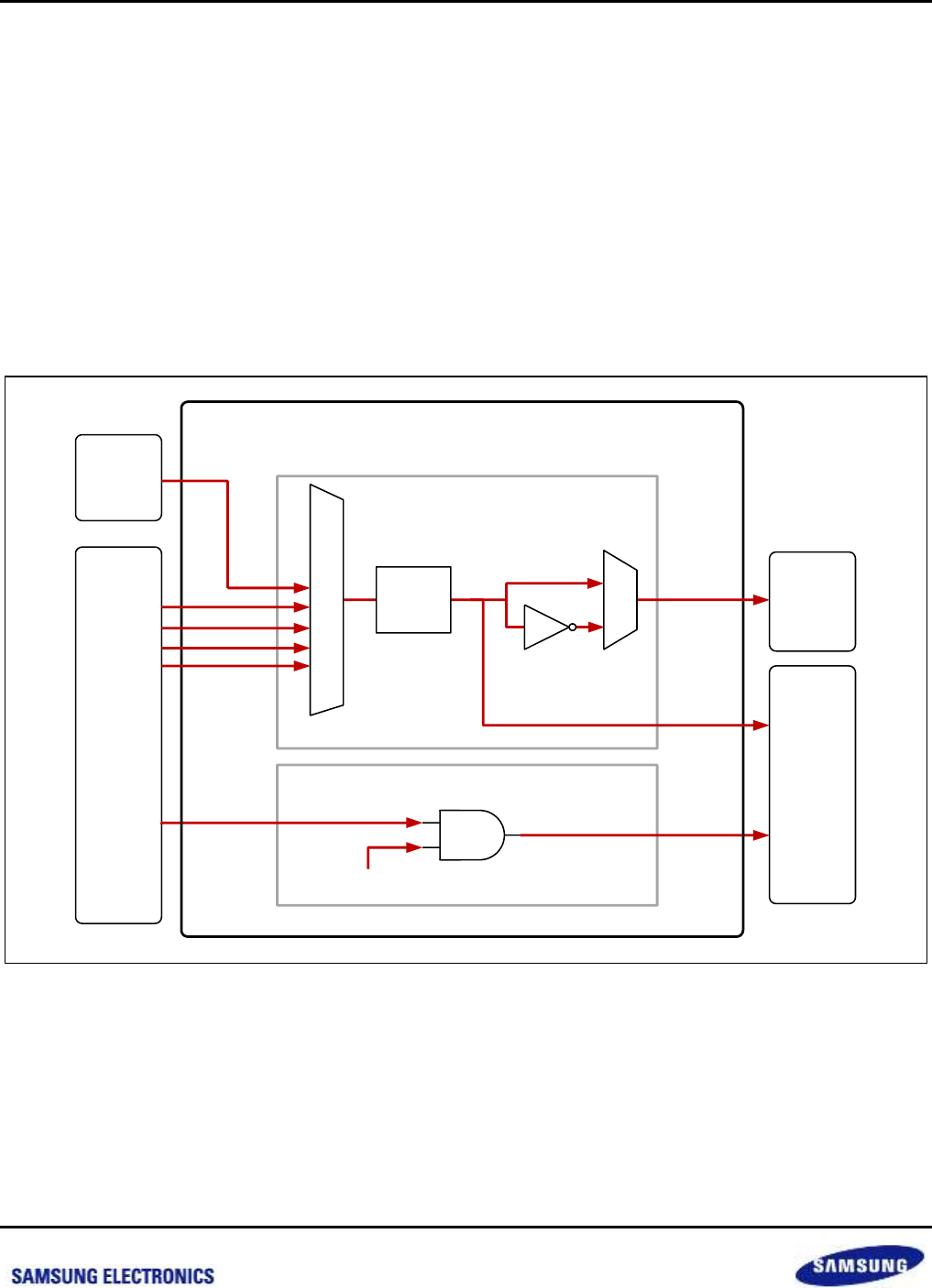
Samsung Confidential
S5P6818_UM 5 Clock Generator
5-1
Preliminary product information describes products that are in development, for which full characterization data and
associated errata are not yet available. Specifications and information herein are subject to change without notice.
5 Clock Generator
5.1 IP Clock Generator Overview
The IP Clock Generator can generate divided clock. Each IP have clocking scheme which requires several
different division ratio simultaneously. Therefore, each of IP Clock Generator supplies required clock to each IP.
These IP Clock Generators uses the PLL from SYSCTRL or External Clock from PAD. And it can divide required
clock of each IP by 2-n divider.
Figure 5-1 Interconnection Example of Clock Generator
SYSTEM
CTRL
EXT PAD
o_BCLKTOP
i_BCLK
BCLKENB
BCLK Gating
6
5
4
3
2
1
0
CLK CHILD 0
o_CLKOUT[0]
o_CLKOUT[1]
CLKGEN 1 Level
CLKSRCSEL0
CLKDIV0 OUTCLKINV0
0
1
1/n
Internal
IP
EXT PAD
i_CLKSRC0[6:0]
nexell / ys.kim at 2015.02.12
SAMSUNG Confidential
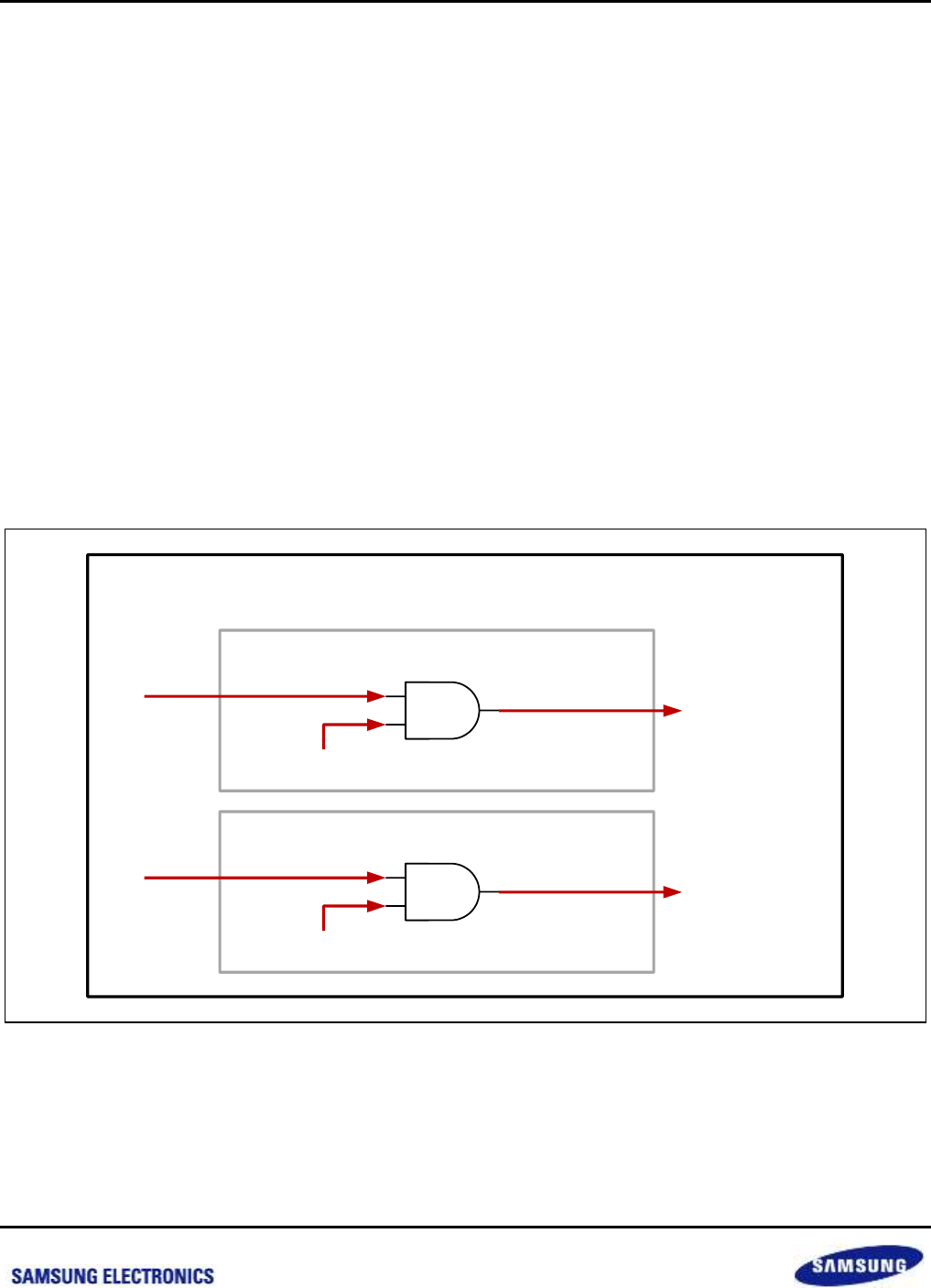
Samsung Confidential
S5P6818_UM 5 Clock Generator
5-2
Preliminary product information describes products that are in development, for which full characterization data and
associated errata are not yet available. Specifications and information herein are subject to change without notice.
5.2 Clock Generator Level 0
Clock Generator Level 0 does not have clock divider. It can only do clock gating. It uses PCLK or BCLK Gating.
Following peripherals use Level 0 Clock Generator:
CODA960
Crypto
I2C
3D GPU
MPEGTSI
PDM
SCALLER
DEINTERLACE
MLC
5.2.1 Block Diagram
Figure 5-2 Block Diagram of Clock Generator Level 0
o_BCLKTOP
i_BCLK
BCLKENB
BCLK Gating
o_GatedPCLK
i_PCLK
PCLKMODE
PCLK Gating
CLKGEN 0 Level
nexell / ys.kim at 2015.02.12
SAMSUNG Confidential

Samsung Confidential
S5P6818_UM 5 Clock Generator
5-3
Preliminary product information describes products that are in development, for which full characterization data and
associated errata are not yet available. Specifications and information herein are subject to change without notice.
5.2.2 Register Description
5.2.2.1 Register Map Summary
Register
Offset
Description
Reset Value
Base Address: 0xC00C_0000
CODA960CLKENB
0x7000
Clock Generator for CODA960 Enable Register
0x0000_0000
CRYPTOCLKENB
0x6000
Clock Generator for CRYPTO Enable Register
0x0000_0000
Base Address: 0xC000_0000
I2CCLKENB
0xAE000
0xAF000
0xB0000
Clock Generator for I2C ch0/1/2 Enable Register
0x0000_0000
Base Address: 0xC00C_0000
3D GPUCLKENB
0x3000
Clock Generator for 3D GPU Enable Register
0x0000_0000
MPEGTSICLKENB
0xB700
Clock Generator for MPEG-TS Enable Register
0x0000_0000
PDMCLKENB
0xB000
Clock Generator for PDM Enable Register
0x0000_0000
Base Address: 0xC00B_0000
SCALERCLKENB
0x6000
Clock Generator for SCALER Enable Register
0x0000_0000
DEINTERLACECLKENB
0x5000
Clock Generator for DEINTERLACE Enable Register
0x0000_0000
Base Address: 0xC010_0000
MLCCLKENB
0x23C0
0x27C0
Clock Generator for MLC Enable Register
0x0000_0000
nexell / ys.kim at 2015.02.12
SAMSUNG Confidential
Samsung Confidential
S5P6818_UM 5 Clock Generator
5-4
Preliminary product information describes products that are in development, for which full characterization data and
associated errata are not yet available. Specifications and information herein are subject to change without notice.
5.2.2.1.1 CODA960CLKENB
Base Address: 0xC00C_0000
Address = Base Address + 0x7000, Reset Value = 0x0000_0000
Name
Bit
Type
Description
Reset Value
RSVD
[31:4]
R
Reserved
28'h0
PCLKMODE
[3]
RW
Specifies PCLK operating mode.
0 = PCLK is only enabled when CPU accesses this module
1 = PCLK is always enabled
1'b0
BCLKENB
[2:0]
R
BCLK Enable
0 = Disable
1 = Reserved
2 = Reserved
3 = Always
2'b0
5.2.2.1.2 CRYPTOCLKENB
Base Address: 0xC00C_0000
Address = Base Address + 0x6000, Reset Value = 0x0000_0000
Name
Bit
Type
Description
Reset Value
RSVD
[31:4]
R
Reserved
28'h0
PCLKMODE
[3]
RW
Specifies PCLK operating mode.
0 = PCLK is only enabled when CPU accesses this module
1 = PCLK is always enabled
1'b0
RSVD
[2:0]
R
Reserved
2'b0
5.2.2.1.3 I2CCLKENB
Base Address: 0xC000_0000
Address = Base Address + 0xAE000, 0xAF000, 0xB0000, Reset Value = 0x0000_0000
Name
Bit
Type
Description
Reset Value
RSVD
[31:4]
R
Reserved
28'h0
PCLKMODE
[3]
RW
Specifies PCLK operating mode.
0 = PCLK is only enabled when CPU accesses this module
1 = PCLK is always enabled
1'b0
RSVD
[3:0]
R
Reserved
3'b0
nexell / ys.kim at 2015.02.12
SAMSUNG Confidential

Samsung Confidential
S5P6818_UM 5 Clock Generator
5-5
Preliminary product information describes products that are in development, for which full characterization data and
associated errata are not yet available. Specifications and information herein are subject to change without notice.
5.2.2.1.4 3D GPCLKENB
Base Address: 0xC00C_0000
Address = Base Address + 0x3000, Reset Value = 0x0000_0000
Name
Bit
Type
Description
Reset Value
RSVD
[31:2]
R
Reserved
30'h0
BCLKENB
[1:0]
R
BCLK Enable
0 = Disable
1 = Reserved
2 = Reserved
3 = Always
2'b0
5.2.2.1.5 MPEGTSICLKENB
Base Address: 0xC00C_0000
Address = Base Address + 0xB700, Reset Value = 0x0000_0000
Name
Bit
Type
Description
Reset Value
RSVD
[31:2]
R
Reserved
30'h0
BCLKENB
[1:0]
R
BCLK Enable
0 = Disable
1 = Reserved
2 = Reserved
3 = Always
2'b0
5.2.2.1.6 PDMCLKENB
Base Address: 0xC00C_0000
Address = Base Address + 0xB000, Reset Value = 0x0000_0000
Name
Bit
Type
Description
Reset Value
RSVD
[31:4]
R
Reserved
28'h0
PCLKMODE
[3]
RW
Specifies PCLK operating mode.
0 = PCLK is only enabled when CPU accesses this module
1 = PCLK is always enabled
1'b0
BCLKENB
[2:0]
R
BCLK Enable
0 = Disable
1 = Reserved
2 = Reserved
3 = Always
3'b0
nexell / ys.kim at 2015.02.12
SAMSUNG Confidential
Samsung Confidential
S5P6818_UM 5 Clock Generator
5-6
Preliminary product information describes products that are in development, for which full characterization data and
associated errata are not yet available. Specifications and information herein are subject to change without notice.
5.2.2.1.7 SCALERCLKENB
Base Address: 0xC00B_0000
Address = Base Address + 0x6000, Reset Value = 0x0000_0000
Name
Bit
Type
Description
Reset Value
RSVD
[31:2]
R
Reserved
30'h0
BCLKENB
[1:0]
R
BCLK Enable
0 = Disable
1 = Reserved
2 = Reserved
3 = Always
2'b0
5.2.2.1.8 DEINTERLACECLKENB
Base Address: 0xC00B_0000
Address = Base Address + 0x5000, Reset Value = 0x0000_0000
Name
Bit
Type
Description
Reset Value
RSVD
[31:2]
R
Reserved
30'h0
BCLKENB
[1:0]
R
BCLK Enable
0 = Disable
1 = Reserved
2 = Reserved
3 = Always
2'b0
5.2.2.1.9 MLCCLKENB
Base Address: 0xC010_0000
Address = Base Address + 0x23C0, 0x27C0, Reset Value = 0x0000_0000
Name
Bit
Type
Description
Reset Value
RSVD
[31:4]
R
Reserved
28'h0
PCLKMODE
[3]
RW
Specifies PCLK operating mode.
0 = PCLK is only enabled when CPU accesses this module
1 = PCLK is always enabled
1'b0
RSVD
[2:0]
R
Reserved
2'b0
BCLKENB
[1:0]
R
BCLK Enable
0 = Disable
1 = Reserved
2 = Reserved
3 = Always
2'b0
nexell / ys.kim at 2015.02.12
SAMSUNG Confidential
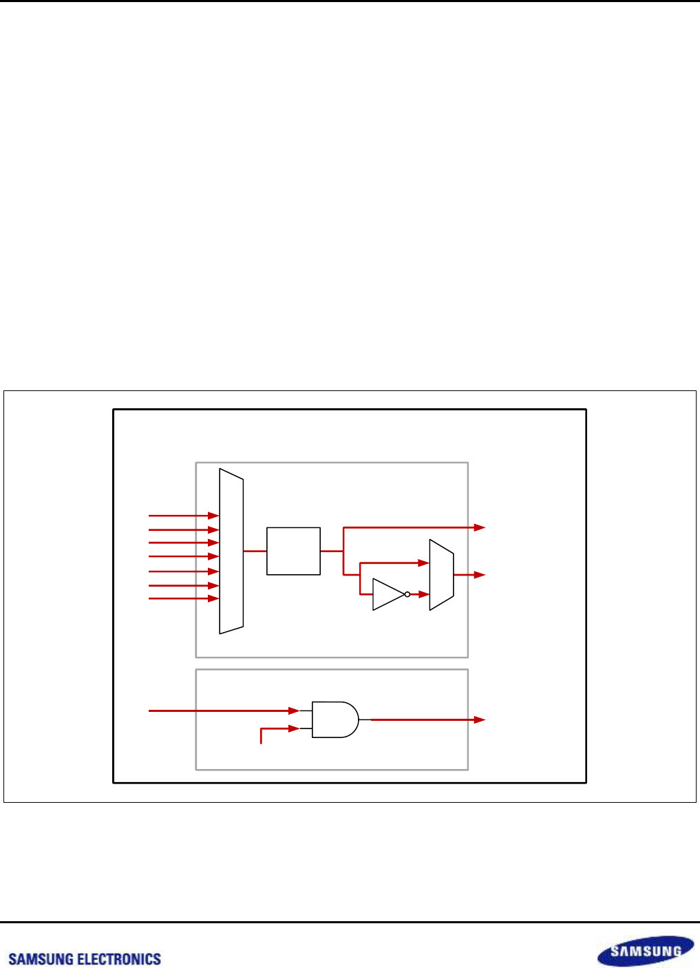
Samsung Confidential
S5P6818_UM 5 Clock Generator
5-7
Preliminary product information describes products that are in development, for which full characterization data and
associated errata are not yet available. Specifications and information herein are subject to change without notice.
5.3 Clock Generator Level 1
The Clock Generator Level-1 has one clock divider. Clock Divider has 8-bit divide registers. Divide registers can
reach to 256 levels and it can divide up to 256 levels.
Following peripherals use Level 1 Clock Generator:
MIPICSI
PPM
PWMTIMER
SDMMC
SPDIFTX
SSP
UART
VIP
5.3.1 Block Diagram
Figure 5-3 Block Diagram of Clock Generator Level 1
o_BCLKTOP
i_BCLK
BCLKENB
BCLK Gating
6
5
4
3
2
1
0
CLK CHILD 0
i_CLKSRC0[6:0]
o_CLKOUT[0]
o_CLKOUT[1]
CLKGEN 1 Level
CLKSRCSEL0
CLKDIV0
OUTCLKINV0
0
1
1/n
nexell / ys.kim at 2015.02.12
SAMSUNG Confidential

Samsung Confidential
S5P6818_UM 5 Clock Generator
5-8
Preliminary product information describes products that are in development, for which full characterization data and
associated errata are not yet available. Specifications and information herein are subject to change without notice.
5.3.2 Register Description
5.3.2.1 Register MAP Summary
Register
Offset
Description
Reset Value
Base Address: 0xC00C_0000
MIPICSICLKENB
0xA000
Clock Generator Enable Register for MIPI CSI
0x0000_0000
MIPICSICLKGEN0L
0xA004
Clock Generator Control 0 Low Register for MIPI CSI
0x0000_0000
PPMCLKENB
0x4000
Clock Generator Enable Register for PPM
0x0000_0000
PPMCLKGEN0L
0x4004
Clock Generator Control 0 Low Register for PPM
0x0000_0000
Base Address: 0xC000_0000
PWMTIMERCLKENB
0xBA000
0xBE000
0xBF000
0xC0000
Clock Generator Enable Register for PWM ch0/1/2/3
0x0000_0000
PWMTIMERCLKGEN0L
0xBA004
0xBE004
0xBF004
0xC0004
Clock Generator Control 0 Low Register for PWM ch0/1/2/3
0x0000_0000
Base Address: 0xC00B_0000
PWMTIMERCLKENB
0x9000
0xB000
0xC000
0xD000
Clock Generator Enable Register for TIMER ch0/1/2/3
0x0000_0000
PWMTIMERCLKGEN0L
0x9004
0xB004
0xC004
0xD004
Clock Generator Control 0 Low Register for TIMER
ch0/1/2/3
0x0000_0000
Base Address: 0xC00C_0000
SDMMCCLKENB
0x5000
0xC000
0xD000
Clock Generator Enable Register for SDMMC ch0/1/2
0x0000_0000
SDMMCCLKGEN0L
0x5004
0xC004
0xD004
Clock Generator Control 0 Low Register for SDMMC
ch0/1/2
0x0000_0000
Base Address: 0xC00B_0000
SPDIFTXCLKENB
0x8000
Clock Generator Enable Register for SPDIF
0x0000_0000
SPDIFTXCLKGEN0L
0x8004
Clock Generator Control 0 Low Register for SPDIF
0x0000_0000
Base Address: 0xC00A_0000
SSPCLKENB
0xC000
0xD000
0x7000
Clock Generator Enable Register for SSP ch0/1/2
0x0000_0000
SSPCLKGEN0L
0xC004
0xD004
0x7004
Clock Generator Control 0 Low Register for SSP ch0/1/2
0x0000_0000
nexell / ys.kim at 2015.02.12
SAMSUNG Confidential

Samsung Confidential
S5P6818_UM 5 Clock Generator
5-9
Preliminary product information describes products that are in development, for which full characterization data and
associated errata are not yet available. Specifications and information herein are subject to change without notice.
Register
Offset
Description
Reset Value
Base Address: 0xC000_0000
UARTCLKENB
0xA9000
0xA8000
0xAA000
0xAB000
0x6E000
0x84000
Clock Generator Enable Register for UART ch0/1/2/3/4/5
0x0000_0000
UARTCLKGEN0L
0xA9004
0xA8004
0xAA004
0xAB004
0x6E004
0x84004
Clock Generator Control 0 Low Register for UART
ch0/1/2/3/4/5
0x0000_0000
Base Address: 0xC00C_0000
VIPCLKENB
0x1000
0x2000
Clock Generator Enable Register for VIP ch0/1
0x0000_0000
VIPCLKGEN0L
0x1004
0x2004
Clock Generator Control 0 Low Register for VIP ch0/1
0x0000_0000
nexell / ys.kim at 2015.02.12
SAMSUNG Confidential
Samsung Confidential
S5P6818_UM 5 Clock Generator
5-10
Preliminary product information describes products that are in development, for which full characterization data and
associated errata are not yet available. Specifications and information herein are subject to change without notice.
5.3.2.1.1 MIPICSICLKENB
Base Address: 0xC00C_0000
Address = Base Address + 0xA000, Reset Value = 0x0000_0000
Name
Bit
Type
Description
Reset Value
RSVD
[31:4]
R
Reserved
29'h0
CLKGENEB
[2]
RW
Enable/Disable to generate a clock
1'b0
RSVD
[1:0]
R
Reserved
2'b0
5.3.2.1.2 MIPICSICLKGEN0L
Base Address: 0xC00C_0000
Address = Base Address + 0xA004, Reset Value = 0x0000_0000
Name
Bit
Type
Description
Reset Value
RSVD
[31:16]
R
Reserved
16'h0
OUTCLKENB
[15]
RW
Specifies the direction of the PADVCLK pad. This bit should
be set when CLKSRCSEL0/1 is 3 or 4.
0 = Enable (Output)
1 = Reserved
1'b0
RSVD
[14:13]
R
Reserved
2'b0
CLKDIV0
[12:5]
RW
Specifies divider value of the source clock.
Divider value = CLKDIV0 + 1
8'h0
CLKSRCSEL0
[4:2]
RW
0 = PLL[0]
1 = PLL[1]
2 = PLL[2]
3'b0
OUTCLKINV0
[1]
RW
Specifies whether to invert the clock output.
0 = Normal (Falling Edge)
1 = Invert (Rising Edge)
1'b0
RSVD
[0]
RW
Reserved (This bit should be set to "0")
1'b0
5.3.2.1.3 PPMCLKENB
Base Address: 0xC00C_0000
Address = Base Address + 0x4000, Reset Value = 0x0000_0000
Name
Bit
Type
Description
Reset Value
RSVD
[31:3]
R
Reserved
29'h0
CLKGENEB
[2]
RW
Enable/Disable to generate a clock
0 = Disable
1 = Enable
1'b0
RSVD
[1:0]
R
Reserved
2'b0
nexell / ys.kim at 2015.02.12
SAMSUNG Confidential

Samsung Confidential
S5P6818_UM 5 Clock Generator
5-11
Preliminary product information describes products that are in development, for which full characterization data and
associated errata are not yet available. Specifications and information herein are subject to change without notice.
5.3.2.1.4 PPMCLKGEN0L
Base Address: 0xC00C_0000
Address = Base Address + 0x4004, Reset Value = 0x0000_0000
Name
Bit
Type
Description
Reset Value
RSVD
[31:16]
R
Reserved
16'h0
OUTCLKENB
[15]
RW
Specifies the direction of the PADVCLK pad. This bit should
be set when CLKSRCSEL0/1 is 3 or 4.
0 = Enable (Output)
1 = Reserved
1'b0
RSVD
[14:13]
R
Reserved
2'b0
CLKDIV0
[12:5]
RW
Specifies divider value of the source clock.
Divider value = CLKDIV0 + 1
8'h0
CLKSRCSEL0
[4:2]
RW
0 = PLL[0]
1 = PLL[1]
2 = PLL[2]
3'b0
OUTCLKINV0
[1]
RW
Specifies whether to invert the clock output.
0 = Normal (Falling Edge)
1 = Invert (Rising Edge)
1'b0
RSVD
[0]
RW
Reserved (This bit should be set to "0")
1'b0
5.3.2.1.5 PWMTIMERCLKENB
Base Address: 0xC000_0000 (PWM)
Base Address: 0xC00B_0000 (TIMER)
Address = Base Address + 0xBA000, 0xBE000, 0xBF000, 0xC0000(PWM), Reset Value = 0x0000_0000
Address = Base Address + 0x9000, 0xB000, 0xC000, 0xD000(TIMER), Reset Value = 0x0000_0000
Name
Bit
Type
Description
Reset Value
RSVD
[31:3]
R
Reserved
29'h0
CLKGENEB
[2]
RW
Enable/Disable to generate a clock
0 = Disable
1 = Enable
1'b0
RSVD
[1:0]
R
Reserved
2'b0
nexell / ys.kim at 2015.02.12
SAMSUNG Confidential
Samsung Confidential
S5P6818_UM 5 Clock Generator
5-12
Preliminary product information describes products that are in development, for which full characterization data and
associated errata are not yet available. Specifications and information herein are subject to change without notice.
5.3.2.1.6 PWMTIMERCLKGEN0L
Base Address: 0xC000_0000 (PWM)
Base Address: 0xC00B_0000 (TIMER)
Address = Base Address + 0xBA004, 0xBE004, 0xBF004, 0xC0004(PWM), Reset Value = 0x0000_0000
Address = Base Address + 0x9004, 0xB004, 0xC004, 0xD004(TIMER), Reset Value = 0x0000_0000
Name
Bit
Type
Description
Reset Value
RSVD
[31:16]
R
Reserved
16'h0
OUTCLKENB
[15]
RW
Specifies the direction of the PADVCLK pad. This bit should
be set when CLKSRCSEL0/1 is 3 or 4.
0 = Enable (Output)
1 = Reserved
1'b0
RSVD
[14:13]
R
Reserved
2'b0
CLKDIV0
[12:5]
RW
Specifies divider value of the source clock.
Divider value = CLKDIV0 + 1
8'h0
CLKSRCSEL0
[4:2]
RW
0 = PLL[0]
1 = PLL[1]
2 = PLL[2]
3'b0
OUTCLKINV0
[1]
RW
Specifies whether to invert the clock output.
0 = Normal (Falling Edge)
1 = Invert (Rising Edge)
1'b0
RSVD
[0]
RW
Reserved (This bit should be set to "0")
1'b0
5.3.2.1.7 SDMMCCLKENB
Base Address: 0xC00C_0000
Address = Base Address + 0x5000, 0xC000, 0xD000, Reset Value = 0x0000_0000
Name
Bit
Type
Description
Reset Value
RSVD
[31:3]
R
Reserved
29'h0
CLKGENEB
[2]
RW
Enable/Disable to generate a clock
0 = Disable
1 = Enable
1'b0
RSVD
[1:0]
R
Reserved
2'b0
nexell / ys.kim at 2015.02.12
SAMSUNG Confidential
Samsung Confidential
S5P6818_UM 5 Clock Generator
5-13
Preliminary product information describes products that are in development, for which full characterization data and
associated errata are not yet available. Specifications and information herein are subject to change without notice.
5.3.2.1.8 SDMMCCLKGEN0L
Base Address: 0xC00C_0000
Address = Base Address + 0x5004, 0xC004, 0xD004, Reset Value = 0x0000_0000
Name
Bit
Type
Description
Reset Value
RSVD
[31:16]
R
Reserved
16'h0
OUTCLKENB
[15]
RW
Specifies the direction of the PADVCLK pad. This bit should
be set when CLKSRCSEL0/1 is 3 or 4.
0 = Enable (Output)
1 = Reserved
1'b0
RSVD
[14:13]
R
Reserved
2'b0
CLKDIV0
[12:5]
RW
Specifies divider value of the source clock.
Divider value = CLKDIV0 + 1
8'h0
CLKSRCSEL0
[4:2]
RW
0 = PLL[0]
1 = PLL[1]
2 = PLL[2]
3'b0
OUTCLKINV0
[1]
RW
Specifies whether to invert the clock output.
0 = Normal (Falling Edge)
1 = Invert (Rising Edge)
1'b0
RSVD
[0]
RW
Reserved (This bit should be set to "0")
1'b0
5.3.2.1.9 SPDIFTXCLKENB
Base Address: 0xC00B_0000
Address = Base Address + 0x8000, Reset Value = 0x0000_0000
Name
Bit
Type
Description
Reset Value
RSVD
[31:3]
R
Reserved
29'h0
CLKGENEB
[2]
RW
Enable/Disable to generate a clock
0 = Disable
1 = Enable
1'b0
RSVD
[1:0]
R
Reserved
2'b0
nexell / ys.kim at 2015.02.12
SAMSUNG Confidential

Samsung Confidential
S5P6818_UM 5 Clock Generator
5-14
Preliminary product information describes products that are in development, for which full characterization data and
associated errata are not yet available. Specifications and information herein are subject to change without notice.
5.3.2.1.10 SPDIFTXCLKGEN0L
Base Address: 0xC00B_0000
Address = Base Address + 0x8004, Reset Value = 0x0000_0000
Name
Bit
Type
Description
Reset Value
RSVD
[31:16]
R
Reserved
16'h0
OUTCLKENB
[15]
RW
Specifies the direction of the PADVCLK pad. This bit should
be set when CLKSRCSEL0/1 is 3 or 4.
0 = Enable (Output)
1 = Reserved
1'b0
RSVD
[14:13]
R
Reserved
2'b0
CLKDIV0
[12:5]
RW
Specifies divider value of the source clock.
Divider value = CLKDIV0 + 1
8'h0
CLKSRCSEL0
[4:2]
RW
0 = PLL[0]
1 = PLL[1]
2 = PLL[2]
3'b0
OUTCLKINV0
[1]
RW
Specifies whether to invert the clock output.
0 = Normal (Falling Edge)
1 = Invert (Rising Edge)
1'b0
RSVD
[0]
RW
Reserved (This bit should be set to "0")
1'b0
5.3.2.1.11 SSPCLKENB
Base Address: 0xC00A_0000
Address = Base Address + 0xC000, 0xD000, 0x7000, Reset Value = 0x0000_0000
Name
Bit
Type
Description
Reset Value
RSVD
[31:3]
R
Reserved
29'h0
CLKGENEB
[2]
RW
Enable/Disable to generate a clock
0 = Disable
1 = Enable
1'b0
RSVD
[1:0]
R
Reserved
2'b0
nexell / ys.kim at 2015.02.12
SAMSUNG Confidential
Samsung Confidential
S5P6818_UM 5 Clock Generator
5-15
Preliminary product information describes products that are in development, for which full characterization data and
associated errata are not yet available. Specifications and information herein are subject to change without notice.
5.3.2.1.12 SSPCLKEN0L
Base Address: 0xC00A_0000
Address = Base Address + 0xC004, 0xD004, 0x7004, Reset Value = 0x0000_0000
Name
Bit
Type
Description
Reset Value
RSVD
[31:16]
R
Reserved
16'h0
OUTCLKENB
[15]
RW
Specifies the direction of the PADVCLK pad. This bit should
be set when CLKSRCSEL0/1 is 3 or 4.
0 = Enable (Output)
1 = Reserved
1'b0
RSVD
[14:13]
R
Reserved
2'b0
CLKDIV0
[12:5]
RW
Specifies divider value of the source clock.
Divider value = CLKDIV0 + 1
8'h0
CLKSRCSEL0
[4:2]
RW
0 = PLL[0]
1 = PLL[1]
2 = PLL[2]
3'b0
OUTCLKINV0
[1]
RW
Specifies whether to invert the clock output.
0 = Normal (Falling Edge)
1 = Invert (Rising Edge)
1'b0
RSVD
[0]
RW
Reserved (This bit should be set to "0")
1'b0
5.3.2.1.13 UARTCLKENB
Base Address: 0xC000_0000
Address = Base Address + 0xA9000, 0xA8000, 0xAA000, 0xAB000, 0x6E000, 0x84000
Reset Value = 0x0000_0000
Name
Bit
Type
Description
Reset Value
RSVD
[31:3]
R
Reserved
29'h0
CLKGENENB
[2]
RW
Enable/Disable to generate a clock.
0 = Disable
1 = Enable
1'b0
RSVD
[1:0]
R
Reserved
2'b0
nexell / ys.kim at 2015.02.12
SAMSUNG Confidential

Samsung Confidential
S5P6818_UM 5 Clock Generator
5-16
Preliminary product information describes products that are in development, for which full characterization data and
associated errata are not yet available. Specifications and information herein are subject to change without notice.
5.3.2.1.14 UARTCLKGEN0L
Base Address: 0xC000_0000
Address = Base Address + 0xA9004, 0xA8004, 0xAA004, 0xAB004, 0x6E004, 0x84004
Reset Value = 0x0000_0000
Name
Bit
Type
Description
Reset Value
RSVD
[31:16]
R
Reserved
16'h0
OUTCLKENB
[15]
RW
Specifies the direction of the PADVCLK pad. This bit should
be set when CLKSRCSEL0/1 is 3 or 4.
0 = Enable (Output)
1 = Reserved
1'b0
RSVD
[14:13]
R
Reserved
2'b0
CLKDIV0
[12:5]
RW
Specifies divider value of the source clock.
Divider value = CLKDIV0 + 1
8'h0
CLKSRCSEL0
[4:2]
RW
0 = PLL[0]
1 = PLL[1]
2 = PLL[2]
3'b0
OUTCLKINV0
[1]
RW
Specifies whether to invert the clock output.
0 = Normal (Falling Edge)
1 = Invert (Rising Edge)
1'b0
RSVD
[0]
RW
Reserved (This bit should be set to "0")
1'b0
5.3.2.1.15 VIPCLKENB
Base Address: 0xC00C_0000
Address = Base Address + 0x1000, 0x2000, Reset Value = 0x0000_0000
Name
Bit
Type
Description
Reset Value
RSVD
[31:3]
R
Reserved
29'h0
CLKGENENB
[2]
RW
Enable/Disable to generate a clock.
0 = Disable
1 = Enable
1'b0
BCLKENB
[1:0]
RW
BCLK Enable
0 = Disable
1 = Reserved
2 = Reserved
3 = Always
2'b0
nexell / ys.kim at 2015.02.12
SAMSUNG Confidential

Samsung Confidential
S5P6818_UM 5 Clock Generator
5-17
Preliminary product information describes products that are in development, for which full characterization data and
associated errata are not yet available. Specifications and information herein are subject to change without notice.
5.3.2.1.16 VIPCLKGEN0L
Base Address: 0xC00C_0000
Address = Base Address + 0x1004, 0x2004, Reset Value = 0x0000_0000
Name
Bit
Type
Description
Reset Value
RSVD
[31:16]
R
Reserved
16'h0
OUTCLKENB
[15]
RW
Specifies the direction of the PADVCLK pad. This bit should
be set when CLKSRCSEL0/1 is 3 or 4.
0 = Enable (Output)
1 = Reserved
1'b0
RSVD
[14:13]
R
Reserved
2'b0
CLKDIV0
[12:5]
RW
Specifies divider value of the source clock.
Divider value = CLKDIV0 + 1
8'h0
CLKSRCSEL0
[4:2]
RW
0 = PLL[0]
1 = PLL[1]
2 = PLL[2]
3 = PLL[3]
4 = CIS External Clock 0
5 = CIS External Clock 1
3'b0
OUTCLKINV0
[1]
RW
Specifies whether to invert the clock output.
0 = Normal (Falling Edge)
1 = Invert (Rising Edge)
1'b0
RSVD
[0]
RW
Reserved (This bit should be set to "0")
1'b0
nexell / ys.kim at 2015.02.12
SAMSUNG Confidential

Samsung Confidential
S5P6818_UM 5 Clock Generator
5-18
Preliminary product information describes products that are in development, for which full characterization data and
associated errata are not yet available. Specifications and information herein are subject to change without notice.
5.4 Clock Generator Level 2
The Clock Generator Level2 has two clock dividers. Clock Divider has 8-bit divide registers. And each divide
registers can reach to 256 levels and it can divide up to 256 levels. The two clock divider is serialized. Therefore
Clock Generator Level-2 can divide up to 65,536.
Following peripherals use Level 2 Clock Generator:
GMAC
I2S
USBHOSTOTG
DPC
LVDS
HDMI
MIPIDSI
nexell / ys.kim at 2015.02.12
SAMSUNG Confidential
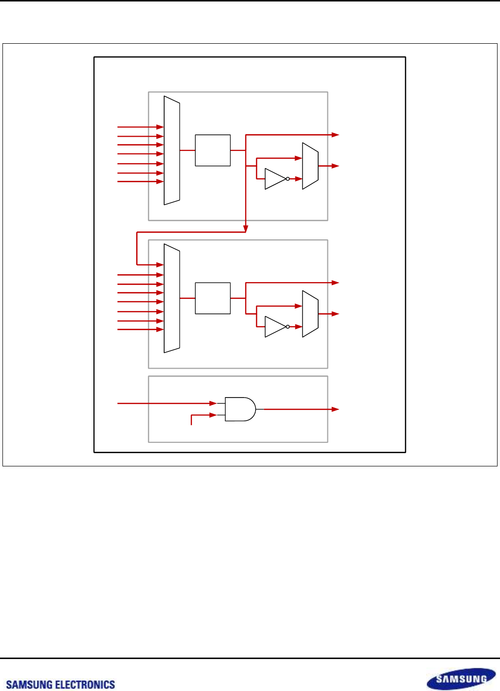
Samsung Confidential
S5P6818_UM 5 Clock Generator
5-19
Preliminary product information describes products that are in development, for which full characterization data and
associated errata are not yet available. Specifications and information herein are subject to change without notice.
5.4.1 Block Diagram
Figure 5-4 Block Diagram of Clock Generator Level 2
6
5
4
3
2
1
0
CLK CHILD 0
i_CLKSRC0[6:0]
o_CLKOUT[0]
o_CLKOUT[1]
o_GatedPCLK
i_PCLK
CLKGEN 2 Level
CLKSRCSEL0
CLKDIV0
OUTCLKINV0
0
1
1/n
7
6
5
4
3
2
1
0
CLK CHILD 1
o_CLKOUT[2]
o_CLKOUT[3]
CLKSRCSEL1
CLKDIV1
OUTCLKINV1
0
1
1/n
i_CLKSRC1[7:0]
PCLKMODE
PCLK Gating
nexell / ys.kim at 2015.02.12
SAMSUNG Confidential

Samsung Confidential
S5P6818_UM 5 Clock Generator
5-20
Preliminary product information describes products that are in development, for which full characterization data and
associated errata are not yet available. Specifications and information herein are subject to change without notice.
5.4.2 Register Description
5.4.2.1 Register Map Summary
Register
Offset
Description
Reset Value
Base Address: 0xC00C_0000
GMACCLKENB
0x8000
Clock Generator Enable Register for GMAC
0x0000_0000
GMACCLKGEN0L
0x8004
Clock Generator Control 0 Low Register for GMAC
0x0000_0000
RSVD
0x8008
Reserved
0x0000_0000
GMACCLKGEN1L
0x800C
Clock Generator Control 1 Low Register for GMAC
0x0000_0000
Base Address: 0xC00B_0000
I2SCLKENB
0x2000
0x3000
0x4000
Clock Generator Enable Register for I2S
0x0000_0000
I2SCLKGEN0L
0x2004
0x3004
0x4004
Clock Generator Control 0 Low Register for I2S
0x0000_0000
RSVD
0x2008
0x3008
0x4008
Reserved
0x0000_0000
I2SCLKGEN1L
0x200C
0x300C
0x400C
Clock Generator Control 1 Low Register for I2S
0x0000_0000
Base Address: 0xC006_0000
USBHOSTOTGCLKENB
0xB000
Clock Generator Enable Register for USBHOSTOTG
0x0000_0000
USBHOSTOTGCLKGEN0L
0xB004
Clock Generator Control 0 Low Register for
USBHOSTOTG
0x0000_0000
RSVD
0xB008
Reserved
0x0000_0000
USBHOSTOTGCLKGEN1L
0xB00C
Clock Generator Control 1 Low Register for
USBHOSTOTG
0x0000_0000
Base Address: 0xC010_0000
DPCCLKENB
0x2BC0
0x2FC0
Clock Generator Enable Register for DPC
0x0000_0000
DPCCLKGEN0L
0x2BC4
0x2FC4
Clock Generator Control 0 Low Register for DPC
0x0000_0000
RSVD
0x2BC8
0x2FC8
Reserved
0x0000_0000
DPCCLKGEN1L
0x2BCC
0x2FCC
Clock Generator Control 1 Low Register for DPC
0x0000_0000
LVDSCLKENB
0x8000
Clock Generator Enable Register for LVDS
0x0000_0000
LVDSCLKGEN0L
0x8004
Clock Generator Control 0 Low Register for LVDS
0x0000_0000
RSVD
0x8008
Reserved
0x0000_0000
LVDSCLKGEN1L
0x800C
Clock Generator Control 1 Low Register for LVDS
0x0000_0000
nexell / ys.kim at 2015.02.12
SAMSUNG Confidential

Samsung Confidential
S5P6818_UM 5 Clock Generator
5-21
Preliminary product information describes products that are in development, for which full characterization data and
associated errata are not yet available. Specifications and information herein are subject to change without notice.
Register
Offset
Description
Reset Value
HDMICLKENB
0x9000
Clock Generator Enable Register for HDMI
0x0000_0000
HDMICLKGEN0L
0x9004
Clock Generator Control 0 Low Register for HDMI
0x0000_0000
RSVD
0x9008
Reserved
0x0000_0000
HDMICLKGEN1L
0x900C
Clock Generator Control 1 Low Register for HDMI
0x0000_0000
MIPIDSICLKENB
0x5000
Clock Generator Enable Register for MIPI
0x0000_0000
MIPIDSICLKGEN0L
0x5004
Clock Generator Control 0 Low Register for MIPI
0x0000_0000
RSVD
0x5008
Reserved
0x0000_0000
MIPIDSICLKGEN1L
0x500C
Clock Generator Control 1 Low Register for MIPI
0x0000_0000
nexell / ys.kim at 2015.02.12
SAMSUNG Confidential

Samsung Confidential
S5P6818_UM 5 Clock Generator
5-22
Preliminary product information describes products that are in development, for which full characterization data and
associated errata are not yet available. Specifications and information herein are subject to change without notice.
5.4.2.1.1 GMACCLKENB
Base Address: 0xC00C_0000
Address = Base Address + 0x8000, Reset Value = 0x0000_0000
Name
Bit
Type
Description
Reset Value
RSVD
[31:3]
R
Reserved
29'h0
CLKGENENB
[2]
RW
Enable/Disable to generate a clock.
0 = Disable
1 = Enable
1'b0
RSVD
[1:0]
R
Reserved
2'b0
5.4.2.1.2 GMACCLKGEN0L
Base Address: 0xC00C_0000
Address = Base Address + 0x8004, Reset Value = 0x0000_0000
Name
Bit
Type
Description
Reset Value
RSVD
[31:16]
R
Reserved
16'h0
OUTCLKENB
[15]
RW
Specifies the direction of the PADVCLK pad. This bit should
be set when CLKSRCSEL0/1 is 3 or 4.
0 = Enable (Output)
1 = Reserved
1'b0
RSVD
[14:13]
R
Reserved
2'b0
CLKDIV0
[12:5]
RW
Specifies divider value of the source clock.
Divider value = CLKDIV0 + 1
8'h0
CLKSRCSEL0
[4:2]
RW
0 = PLL[0]
1 = PLL[1]
2 = PLL[2]
3 = PLL[3]
4 = External RX Clock
3'b0
OUTCLKINV0
[1]
RW
Specifies whether to invert the clock output.
0 = Normal (Falling Edge)
1 = Invert (Rising Edge)
1'b0
RSVD
[0]
RW
Reserved (This bit should be set to "0")
1'b0
nexell / ys.kim at 2015.02.12
SAMSUNG Confidential

Samsung Confidential
S5P6818_UM 5 Clock Generator
5-23
Preliminary product information describes products that are in development, for which full characterization data and
associated errata are not yet available. Specifications and information herein are subject to change without notice.
5.4.2.1.3 GMACCLKGEN1L
Base Address: 0xC00C_0000
Address = Base Address + 0x800C, Reset Value = 0x0000_0000
Name
Bit
Type
Description
Reset Value
RSVD
[31:13]
R
Reserved
19'h0
CLKDIV1
[12:5]
RW
Specifies divider value of the source clock.
Divider value = CLKDIV0 + 1
8'h0
CLKSRCSEL1
[4:2]
RW
0 = Reserved
1 = Reserved
2 = Reserved
3 = Reserved
4 = Reserved
5 = Reserved
6 = Reserved
7 = Divided Clock from Divider 0
3'b0
OUTCLKINV1
[1]
RW
Specifies whether to invert the clock output.
0 = Normal (Falling Edge)
1 = Invert (Rising Edge)
1'b0
OUTCLKSEL
[0]
RW
1/2 ns delay is applied to Out clock from source clock
Can be used only in case of division by even number
0 = Bypass
1 = Source clock/2 ns
1'b0
nexell / ys.kim at 2015.02.12
SAMSUNG Confidential
Samsung Confidential
S5P6818_UM 5 Clock Generator
5-24
Preliminary product information describes products that are in development, for which full characterization data and
associated errata are not yet available. Specifications and information herein are subject to change without notice.
5.4.2.1.4 I2SCLKENB
Base Address: 0xC00B_0000
Address = Base Address + 0x2000, 0x3000, 0x4000, Reset Value = 0x0000_0000
Name
Bit
Type
Description
Reset Value
RSVD
[31:3]
R
Reserved
29'h0
CLKGENENB
[2]
RW
Enable/Disable to generate a clock.
0 = Disable
1 = Enable
1'b0
RSVD
[1:0]
R
Reserved
2'b0
5.4.2.1.5 I2SCLKGEN0L
Base Address: 0xC00B_0000
Address = Base Address + 0x2004, 0x3004, 0x4004, Reset Value = 0x0000_0000
Name
Bit
Type
Description
Reset Value
RSVD
[31:16]
R
Reserved
16’h0
OUTCLKENB
[15]
RW
Specifies the direction of the PADVCLK pad. This bit should
be set when CLKSRCSEL0/1 is 3 or 4.
0 = Enable (Output)
1 = Reserved
1'b0
RSVD
[14:13]
R
Reserved
2'b0
CLKDIV0
[12:5]
RW
Specifies divider value of the source clock.
Divider value = CLKDIV0 + 1
8’h0
CLKSRCSEL0
[4:2]
RW
0 = PLL[0]
1 = PLL[1]
2 = PLL[2]
3 = PLL[3]
4 = External I2S Codec Clock 2
3'b0
OUTCLKINV0
[1]
RW
Specifies whether to invert the clock output.
0 = Normal (Falling Edge)
1 = Invert (Rising Edge)
1'b0
RSVD
[0]
RW
Reserved (This bit should be set to "0")
1'b0
nexell / ys.kim at 2015.02.12
SAMSUNG Confidential

Samsung Confidential
S5P6818_UM 5 Clock Generator
5-25
Preliminary product information describes products that are in development, for which full characterization data and
associated errata are not yet available. Specifications and information herein are subject to change without notice.
5.4.2.1.6 I2SCLKGEN1L
Base Address: 0xC00B_0000
Address = Base Address + 0x200C, 0x300C, 0x400C, Reset Value = 0x0000_0000
Name
Bit
Type
Description
Reset Value
RSVD
[31:13]
R
Reserved
19’h0
CLKDIV1
[12:5]
RW
Specifies divider value of the source clock.
Divider value = CLKDIV0 + 1
8’h0
CLKSRCSEL1
[4:2]
RW
0 = Reserved
1 = Reserved
2 = Reserved
3 = Reserved
4 = Reserved
5 = Reserved
6 = Reserved
7 = Divided Clock from Divider 0
3'b0
OUTCLKINV1
[1]
RW
Specifies whether to invert the clock output.
0 = Normal (Falling Edge)
1 = Invert (Rising Edge)
1'b0
OUTCLKSEL
[0]
RW
1/2 ns delay is applied to Out clock from source clock
Can be used only in case of division by even number
0 = Bypass
1 = Source clock/2 ns
1'b0
nexell / ys.kim at 2015.02.12
SAMSUNG Confidential
Samsung Confidential
S5P6818_UM 5 Clock Generator
5-26
Preliminary product information describes products that are in development, for which full characterization data and
associated errata are not yet available. Specifications and information herein are subject to change without notice.
5.4.2.1.7 USBHOSTOTGCLKENB
Base Address: 0xC006_0000
Address = Base Address + 0xB000, Reset Value = 0x0000_0000
Name
Bit
Type
Description
Reset Value
RSVD
[31:3]
R
Reserved
29’h0
CLKGENENB
[2]
RW
Enable/Disable to generate a clock.
0 = Disable
1 = Enable
1'b0
RSVD
[1:0]
R
Reserved
2'b0
5.4.2.1.8 USBHOSTOTGCLKGEN0L
Base Address: 0xC006_0000
Address = Base Address + 0xB004, Reset Value = 0x0000_0000
Name
Bit
Type
Description
Reset Value
RSVD
[31:16]
R
Reserved
16’h0
OUTCLKENB
[15]
RW
Specifies the direction of the PADVCLK pad. This bit should be
set when CLKSRCSEL0/1 is 3 or 4.
0 = Enable (Output)
1 = Reserved
1'b0
RSVD
[14:13]
R
Reserved
2'b0
CLKDIV0
[12:5]
RW
Specifies divider value of the source clock.
Divider value = CLKDIV0 + 1
8’h0
CLKSRCSEL0
[4:2]
RW
0 = PLL[0]
1 = PLL[1]
2 = PLL[2]
3 = PLL[3]
3'b0
OUTCLKINV0
[1]
RW
Specifies whether to invert the clock output.
0 = Normal (Falling Edge)
1 = Invert (Rising Edge)
1'b0
RSVD
[0]
RW
Reserved (This bit should be set to "0")
1'b0
nexell / ys.kim at 2015.02.12
SAMSUNG Confidential

Samsung Confidential
S5P6818_UM 5 Clock Generator
5-27
Preliminary product information describes products that are in development, for which full characterization data and
associated errata are not yet available. Specifications and information herein are subject to change without notice.
5.4.2.1.9 USBHOSTOTGCLKGEN1L
Base Address: 0xC006_0000
Address = Base Address + 0xB00C, Reset Value = 0x0000_0000
Name
Bit
Type
Description
Reset Value
RSVD
[31:13]
R
Reserved
19’h0
CLKDIV1
[12:5]
RW
Specifies divider value of the source clock.
Divider value = CLKDIV0 + 1
8’h0
CLKSRCSEL1
[4:2]
RW
0 = PLL[0]
1 = PLL[1]
2 = PLL[2]
3 = PLL[3]
4 = External XTI
5 = Reserved
6 = Reserved
7 = Divided Clock from Divider 0
3'b0
OUTCLKINV1
[1]
RW
Specifies whether to invert the clock output.
0 = Normal (Falling Edge)
1 = Invert (Rising Edge)
1'b0
OUTCLKSEL
[0]
RW
1/2 ns delay is applied to Out clock from source clock
Can be used only in case of division by even number
0 = Bypass
1 = Source clock/2 ns
1'b0
nexell / ys.kim at 2015.02.12
SAMSUNG Confidential
Samsung Confidential
S5P6818_UM 5 Clock Generator
5-28
Preliminary product information describes products that are in development, for which full characterization data and
associated errata are not yet available. Specifications and information herein are subject to change without notice.
5.4.2.1.10 DPCCLKENB
Base Address: 0xC010_0000
Address = Base Address + 0x2BC0, 0x2FC0, Reset Value = 0x0000_0000
Name
Bit
Type
Description
Reset Value
RSVD
[31:4]
R
Reserved
28’h0
PCLKMODE
[3]
RW
Specifies PCLK operating mode.
0 = PCLK is only enabled when CPU accesses this module
1 = PCLK is always enabled
1'b0
CLKGENENB
[2]
RW
Enable/Disable to generate a clock.
0 = Disable
1 = Enable
1'b0
RSVD
[1:0]
R
Reserved
2'b0
5.4.2.1.11 DPCCLKGEN0L
Base Address: 0xC010_0000
Address = Base Address + 0x2BC4, 0x2FC4, Reset Value = 0x0000_0000
Name
Bit
Type
Description
Reset Value
RSVD
[31:16]
R
Reserved
16’h0
OUTCLKENB
[15]
RW
Specifies the direction of the PADVCLK pad. This bit should be
set when CLKSRCSEL0/1 is 3 or 4.
0 = Enable (Output)
1 = Reserved
1'b0
RSVD
[14:13]
R
Reserved
2'b0
CLKDIV0
[12:5]
RW
Specifies divider value of the source clock.
Divider value = CLKDIV0 + 1
8’h0
CLKSRCSEL0
[4:2]
RW
0 = PLL[0]
1 = PLL[1]
2 = PLL[2]
3 = Reserved
4 = HDMI PLL Clock
5 = Reserved
6 = PLL[3]
3'b0
OUTCLKINV0
[1]
RW
Specifies whether to invert the clock output.
0 = Normal (Falling Edge)
1 = Invert (Rising Edge)
1'b0
RSVD
[0]
RW
Reserved (This bit should be set to "0")
1'b0
nexell / ys.kim at 2015.02.12
SAMSUNG Confidential

Samsung Confidential
S5P6818_UM 5 Clock Generator
5-29
Preliminary product information describes products that are in development, for which full characterization data and
associated errata are not yet available. Specifications and information herein are subject to change without notice.
5.4.2.1.12 DPCCLKGEN1L
Base Address: 0xC010_0000
Address = Base Address + 0x2BCC, 0x2FCC, Reset Value = 0x0000_0000
Name
Bit
Type
Description
Reset Value
RSVD
[31:13]
R
Reserved
19’h0
CLKDIV1
[12:5]
RW
Specifies divider value of the source clock.
Divider value = CLKDIV0 + 1
8’h0
CLKSRCSEL1
[4:2]
RW
0 = PLL[0]
1 = PLL[1]
2 = PLL[2]
3 = Reserved
4 = HDMI PLL Clock
5 = Reserved
6 = PLL[3]
7 = Divided Clock from Divider 0
3'b0
OUTCLKINV1
[1]
RW
Specifies whether to invert the clock output.
0 = Normal (Falling Edge)
1 = Invert (Rising Edge)
1'b0
OUTCLKSEL
[0]
RW
1/2 ns delay is applied to Out clock from source clock
Can be used only in case of division by even number
0 = Bypass
1 = Source clock/2 ns
1'b0
5.4.2.1.13 LVDSCLKENB
Base Address: 0xC010_0000
Address = Base Address + 0x8000, Reset Value = 0x0000_0000
Name
Bit
Type
Description
Reset Value
RSVD
[31:4]
R
Reserved
28’h0
PCLKMODE
[3]
RW
Specifies PCLK operating mode.
0 = PCLK is only enabled when CPU accesses this module
1 = PCLK is always enabled
1'b0
CLKGENENB
[2]
RW
Enable/Disable to generate a clock.
0 = Disable
1 = Enable
1'b0
RSVD
[1:0]
R
Reserved
2'b0
nexell / ys.kim at 2015.02.12
SAMSUNG Confidential

Samsung Confidential
S5P6818_UM 5 Clock Generator
5-30
Preliminary product information describes products that are in development, for which full characterization data and
associated errata are not yet available. Specifications and information herein are subject to change without notice.
5.4.2.1.14 LVDSCLKGEN0L
Base Address: 0xC010_0000
Address = Base Address + 0x8004, Reset Value = 0x0000_0000
Name
Bit
Type
Description
Reset Value
RSVD
[31:16]
R
Reserved
16’h0
OUTCLKENB
[15]
RW
Specifies the direction of the PADVCLK pad. This bit should be
set when CLKSRCSEL0/1 is 3 or 4.
0 = Enable (Output)
1 = Reserved
1'b0
RSVD
[14:13]
R
Reserved
2'b0
CLKDIV0
[12:5]
RW
Specifies divider value of the source clock.
Divider value = CLKDIV0 + 1
8’h0
CLKSRCSEL0
[4:2]
RW
0 = PLL[0]
1 = PLL[1]
2 = PLL[2]
3 = PLL[3]
4 = HDMI PLL Clock
5 = Reserved
6 = Reserved
3'b0
OUTCLKINV0
[1]
RW
Specifies whether to invert the clock output.
0 = Normal (Falling Edge)
1 = Invert (Rising Edge)
1'b0
RSVD
[0]
RW
Reserved (This bit should be set to "0")
1'b0
nexell / ys.kim at 2015.02.12
SAMSUNG Confidential

Samsung Confidential
S5P6818_UM 5 Clock Generator
5-31
Preliminary product information describes products that are in development, for which full characterization data and
associated errata are not yet available. Specifications and information herein are subject to change without notice.
5.4.2.1.15 LVDSCLKGEN1L
Base Address: 0xC010_0000
Address = Base Address + 0x800C, Reset Value = 0x0000_0000
Name
Bit
Type
Description
Reset Value
RSVD
[31:13]
R
Reserved
19’h0
CLKDIV1
[12:5]
RW
Specifies divider value of the source clock.
Divider value = CLKDIV0 + 1
8’h0
CLKSRCSEL1
[4:2]
RW
0 = PLL[0]
1 = PLL[1]
2 = PLL[2]
3 = PLL[3]
4 = HDMI PLL Clock
5 = Reserved
6 = Reserved
7 = Divided Clock from Divider 0
3'b0
OUTCLKINV1
[1]
RW
Specifies whether to invert the clock output.
0 = Normal (Falling Edge)
1 = Invert (Rising Edge)
1'b0
OUTCLKSEL
[0]
RW
1/2 ns delay is applied to Out clock from source clock
Can be used only in case of division by even number
0 = Bypass
1 = Source clock/2 ns
1'b0
5.4.2.1.16 HDMICLKENB
Base Address: 0xC010_0000
Address = Base Address + 0x9000, Reset Value = 0x0000_0000
Name
Bit
Type
Description
Reset Value
RSVD
[31:4]
R
Reserved
28’h0
PCLKMODE
[3]
RW
Specifies PCLK operating mode.
0 = PCLK is only enabled when CPU accesses this module
1 = PCLK is always enabled
1'b0
CLKGENENB
[2]
RW
Enable/Disable to generate a clock.
0 = Disable
1 = Enable
1'b0
RSVD
[1:0]
R
Reserved
2'b0
nexell / ys.kim at 2015.02.12
SAMSUNG Confidential

Samsung Confidential
S5P6818_UM 5 Clock Generator
5-32
Preliminary product information describes products that are in development, for which full characterization data and
associated errata are not yet available. Specifications and information herein are subject to change without notice.
5.4.2.1.17 HDMICLKGEN0L
Base Address: 0xC010_0000
Address = Base Address + 0x9004, Reset Value = 0x0000_0000
Name
Bit
Type
Description
Reset Value
RSVD
[31:16]
R
Reserved
16’h0
OUTCLKENB
[15]
RW
Specifies the direction of the PADVCLK pad. This bit should be
set when CLKSRCSEL0/1 is 3 or 4.
0 = Enable (Output)
1 = Reserved
1'b0
RSVD
[14:13]
R
Reserved
2'b0
CLKDIV0
[12:5]
RW
Specifies divider value of the source clock.
Divider value = CLKDIV0 + 1
8’h0
CLKSRCSEL0
[4:2]
RW
0 = PLL[0]
1 = PLL[1]
2 = PLL[2]
3 = PLL[3]
4 = Reserved
5 = Reserved
6 = Reserved
3'b0
OUTCLKINV0
[1]
RW
Specifies whether to invert the clock output.
0 = Normal (Falling Edge)
1 = Invert (Rising Edge)
1'b0
RSVD
[0]
RW
Reserved (This bit should be set to "0")
1'b0
nexell / ys.kim at 2015.02.12
SAMSUNG Confidential

Samsung Confidential
S5P6818_UM 5 Clock Generator
5-33
Preliminary product information describes products that are in development, for which full characterization data and
associated errata are not yet available. Specifications and information herein are subject to change without notice.
5.4.2.1.18 HDMICLKGEN1L
Base Address: 0xC010_0000
Address = Base Address + 0x900C, Reset Value = 0x0000_0000
Name
Bit
Type
Description
Reset Value
RSVD
[31:13]
R
Reserved
19’h0
CLKDIV1
[12:5]
RW
Specifies divider value of the source clock.
Divider value = CLKDIV0 + 1
8’h0
CLKSRCSEL1
[4:2]
RW
0 = PLL[0]
1 = PLL[1]
2 = PLL[2]
3 = PLL[3]
4 = Reserved
5 = Reserved
6 = Reserved
7 = Divided Clock from Divider 0
3'b0
OUTCLKINV1
[1]
RW
Specifies whether to invert the clock output.
0 = Normal (Falling Edge)
1 = Invert (Rising Edge)
1'b0
OUTCLKSEL
[0]
RW
1/2 ns delay is applied to Out clock from source clock
Can be used only in case of division by even number
0 = Bypass
1 = Source clock/2 ns
1'b0
5.4.2.1.19 MIPIDSICLKENB
Base Address: 0xC010_0000
Address = Base Address + 0x5000, Reset Value = 0x0000_0000
Name
Bit
Type
Description
Reset Value
RSVD
[31:3]
R
Reserved
29’h0
CLKGENENB
[2]
RW
Enable/Disable to generate a clock.
0 = Disable
1 = Enable
1'b0
RSVD
[1:0]
R
Reserved
2'b0
nexell / ys.kim at 2015.02.12
SAMSUNG Confidential

Samsung Confidential
S5P6818_UM 5 Clock Generator
5-34
Preliminary product information describes products that are in development, for which full characterization data and
associated errata are not yet available. Specifications and information herein are subject to change without notice.
5.4.2.1.20 MIPIDSICLKGEN0L
Base Address: 0xC010_0000
Address = Base Address + 0x5004, Reset Value = 0x0000_0000
Name
Bit
Type
Description
Reset Value
RSVD
[31:16]
R
Reserved
16’h0
OUTCLKENB
[15]
RW
Specifies the direction of the PADVCLK pad. This bit should be
set when CLKSRCSEL0/1 is 3 or 4.
0 = Enable (Output)
1 = Reserved
1'b0
RSVD
[14:13]
R
Reserved
2'b0
CLKDIV0
[12:5]
RW
Specifies divider value of the source clock.
Divider value = CLKDIV0 + 1
8’h0
CLKSRCSEL0
[4:2]
RW
0 = PLL[0]
1 = PLL[1]
2 = PLL[2]
3 = PLL[3]
4 = HDMI PLL Clock
5 = Reserved
6 = Reserved
3'b0
OUTCLKINV0
[1]
RW
Specifies whether to invert the clock output.
0 = Normal (Falling Edge)
1 = Invert (Rising Edge)
1'b0
RSVD
[0]
RW
Reserved (This bit should be set to "0")
1'b0
nexell / ys.kim at 2015.02.12
SAMSUNG Confidential

Samsung Confidential
S5P6818_UM 5 Clock Generator
5-35
Preliminary product information describes products that are in development, for which full characterization data and
associated errata are not yet available. Specifications and information herein are subject to change without notice.
5.4.2.1.21 MIPIDSICLKGEN1L
Base Address: 0xC010_0000
Address = Base Address + 0x500C, Reset Value = 0x0000_0000
Name
Bit
Type
Description
Reset Value
RSVD
[31:13]
R
Reserved
19’h0
CLKDIV1
[12:5]
RW
Specifies divider value of the source clock.
Divider value = CLKDIV0 + 1
8’h0
CLKSRCSEL1
[4:2]
RW
0 = PLL[0]
1 = PLL[1]
2 = PLL[2]
3 = PLL[3]
4 = HDMI PLL Clock
5 = Reserved
6 = Reserved
7 = Divided Clock from Divider 0
3'b0
OUTCLKINV1
[1]
RW
Specifies whether to invert the clock output.
0 = Normal (Falling Edge)
1 = Invert (Rising Edge)
1'b0
OUTCLKSEL
[0]
RW
1/2 ns delay is applied to Out clock from source clock
Can be used only in case of division by even number
0 = Bypass
1 = Source clock/2 ns
1'b0
nexell / ys.kim at 2015.02.12
SAMSUNG Confidential

Samsung Confidential
S5P6818_UM 6 BUS
6-1
Preliminary product information describes products that are in development, for which full characterization data and
associated errata are not yet available. Specifications and information herein are subject to change without notice.
6 BUS
6.1 Overview
ARM PL301 provides AXI3 BUS, AHB BUS, APB BUS.
AXI3 BUS interconnect provides programmable function for AXI BUS and which includes QoS and Programmable
Round-Robin.
CCI-400 (Cache Coherent Interconnect) combines interconnect and coherency functions into a single module.
6.2 Features
TOP BUS: AXI BUS, master 1 channel, slave 4 channel
BOTTOM BUS: AXI BUS, master 1 channel, slave 4 channel
DISPLAY BUS: AXI BUS, master 1 channel, slave 2 channel
STATIC BUS: AXI BUS, master 2 channel, slave 3 channel
IOPERI BUS: AXI BUS, master 3 channel, slave 4 channel
SFR BUS: AXI BUS, master 3 channel, slave 2 channel
SFR0 BUS: AXI to APB BUS, slave 1 channel
SFR1 BUS: AXI to APB BUS, slave 1 channel
SFR2 BUS: AXI to APB BUS, slave 1 channel
CCI BUS: AXI master 3 channel, AXI slave 5 channel
nexell / ys.kim at 2015.02.12
SAMSUNG Confidential
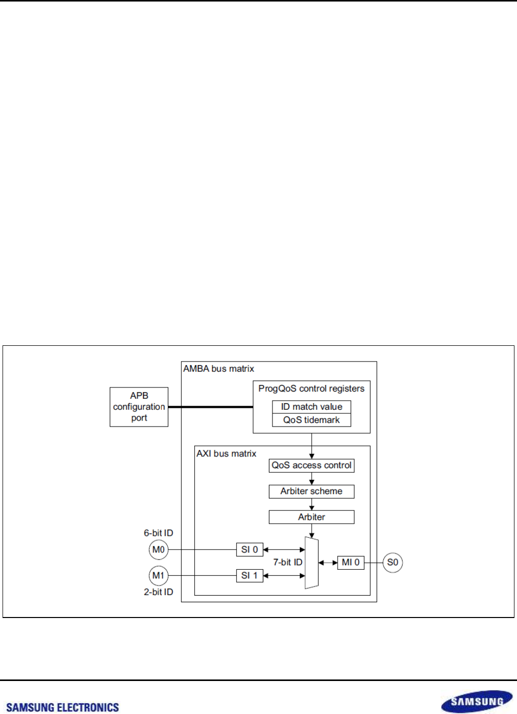
Samsung Confidential
S5P6818_UM 6 BUS
6-2
Preliminary product information describes products that are in development, for which full characterization data and
associated errata are not yet available. Specifications and information herein are subject to change without notice.
6.3 Description
6.3.1 AXI BUS Description
ARM PL301 (AXI3 BUS interconnect) privies programmable function for AXI BUS and which include QoS and
Programmable Round-Robin.
6.3.2 Programmable Quality of Service (ProgQoS)
The QoS scheme works by tracking the number of outstanding transactions, and when a specified number is
reached, only permits transactions from particular, specified masters.
The QoS scheme only provides support for slaves that have a combined acceptance capability, such as the
PrimeCell Dynamic Memory Controller (PL340).
The QoS scheme has no effect until the AXI bus matrix calculates that, at a particular MI, there are a number of
outstanding transactions equal to the value stored in the QoS tidemark Register. It then accepts transactions only
from slave ports specified in the QoS access control Register. This restriction remains until the number of
outstanding transactions is again less than the value stored in the QoS tidemark Register.
It is recommended that you assign low MI numbers to MIs that require QoS support. This approach aligns well
with the cyclic priority scheme because MIs that require QoS support are typically those that can be considered
high-ranking slaves. See the PrimeCell High-Performance Matrix (PL301) Technical Reference Manual.
Below Figure shows the implementation for an interconnection that supports two masters and one slave.
Figure 6-1 Example Implementation of ProgQoS Control Registers for 2x1 Interconnect
nexell / ys.kim at 2015.02.12
SAMSUNG Confidential
Samsung Confidential
S5P6818_UM 6 BUS
6-3
Preliminary product information describes products that are in development, for which full characterization data and
associated errata are not yet available. Specifications and information herein are subject to change without notice.
6.4 Register Description
6.4.1 Register Map Summary
Base Address: 0xC009_2000 (TOP BUS)
Base Address: 0xC009_1000 (BOTTOM BUS)
Base Address: 0xC009_3000 (DISPLAY BUS)
Base Address: 0xC009_5000 (STATIC BUS)
Base Address: 0xC009_0000 (IOPERI BUS)
Base Address: 0xC009_4000 (SFR BUS)
SFR0 BUS is none.
SFR1 BUS is none.
SFR2 BUS is none.
Register
Offset
Description
Reset Value
AXI BUS
QOS_TIDEMARK_MI0
0x400 (1)
QoS tidemark for MI0
32’h0
QOS_CONTROL_MI0
0x404 (2)
QoS access control for MI0
32’h0
AR_ARBITRATION_MI0
0x408 (3)
AR channel arbitration value for MI0
Configured
AW_ARBITRATION_MI0
0x40C (4)
AW channel arbitration value for MI0
Configured
NOTE:
1. Address allocation for QoS tidemark Register is 0x400 + 0x20 N, where N is the number of the relevant MI.
2. Address allocation for QoS access control Register is 0x404 + 0x20 N, where N is the number of the relevant MI.
3. Address allocation for AR channel arbitration control Register is 0x408 + 0x20 N, where N is the number of the relevant
MI.
4. Address allocation for AW channel arbitration control Register is 0x40C + 0x20 N, where N is the number of the relevant
MI.
nexell / ys.kim at 2015.02.12
SAMSUNG Confidential

Samsung Confidential
S5P6818_UM 6 BUS
6-4
Preliminary product information describes products that are in development, for which full characterization data and
associated errata are not yet available. Specifications and information herein are subject to change without notice.
Base Address: 0xF009_0000h
Register
Offset
Description
Reset Value
CCI BUS
Control Override
0x00h
Control Override Register
0x0000_0000
Speculation Control
0x04h
Speculation Control Register
0x0000_0000
Secure Access
0x08h
Secure Access Register
0x0000_0000
Status
0x0Ch
Status Register
0x0000_0000
Imprecise Error
0x10h
Imprecise Error Register
0x0000_0000
PMCR
0x100h
Performance Monitor Control Register
0x0000_0000
PeripherallD4
0xFD0h
Peripheral ID4 Register
0x0000_0044
PeripherallD5
0xFD4h
Peripheral ID5 Register
0x0000_0000
PeripherallD6
0xFD8h
Peripheral ID6 Register
0x0000_0000
PeripherallD7
0xFDCh
Peripheral ID7 Register
0x0000_0000
PeripherallD0
0xFE0h
Peripheral ID0 Register
0x0000_0000
PeripherallD1
0xFE4h
Peripheral ID1 Register
0x0000_0000
PeripherallD2
0xFE8h
Peripheral ID2 Register
0x0000_009B
PeripherallD3
0xFECh
Peripheral ID3 Register
0x0000_0000
ComponentlD0
0xFF0h
Component ID0 Register
0x0000_000D
ComponentlD1
0xFF4h
Component ID1 Register
0x0000_00F0
ComponentlD2
0xFF8h
Component ID2 Register
0x0000_0005
ComponentlD3
0xFFCh
Component ID3 Register
0x0000_00B1
Snoop Control Slave0
0x00h
Snoop Control Register for slave interface 0
0xX000_0000
Snoop Control Slave1
0x00h
Snoop Control Register for slave interface 1
0xX000_0000
Snoop Control Slave2
0x00h
Snoop Control Register for slave interface 2
0xX000_0000
Snoop Control Slave3
0x00h
Snoop Control Register for slave interface 3
0xX000_0000
Snoop Control Slave4
0x00h
Snoop Control Register for slave interface 4
0xX000_0000
Shareable Override Slave0
0x04h
Shareable Override Register for slave interface 0
0x0000_0000
Shareable Override Slave1
0x04h
Shareable Override Register for slave interface 1
0x0000_0000
Shareable Override Slave2
0x04h
Shareable Override Register for slave interface 2
0x0000_0000
Shareable Override Slave3
0x04h
Shareable Override Register for slave interface 3
0x0000_0000
Shareable Override Slave4
0x04h
Shareable Override Register for slave interface 4
0x0000_0000
Read QoS Slave0
0x100h
Read Channel QoS Value Override Register for slave
interface 0
0x0000_0000
Read QoS Slave1
0x100h
Read Channel QoS Value Override Register for slave
interface 1
0x0000_0000
Read QoS Slave2
0x100h
Read Channel QoS Value Override Register for slave
interface 2
0x0000_0000
Read QoS Slave3
0x100h
Read Channel QoS Value Override Register for slave
interface 3
0x0000_0000
nexell / ys.kim at 2015.02.12
SAMSUNG Confidential

Samsung Confidential
S5P6818_UM 6 BUS
6-5
Preliminary product information describes products that are in development, for which full characterization data and
associated errata are not yet available. Specifications and information herein are subject to change without notice.
Register
Offset
Description
Reset Value
Read QoS Slave4
0x100h
Read Channel QoS Value Override Register for slave
interface 4
0x0000_0000
Write QoS Slave0
0x04h
Write Channel QoS Value Override slave interface 0
0x0000_0000
Write QoS Slave1
0x04h
Write Channel QoS Value Override slave interface 1
0x0000_0000
Write QoS Slave2
0x04h
Write Channel QoS Value Override slave interface 2
0x0000_0000
Write QoS Slave3
0x04h
Write Channel QoS Value Override slave interface 3
0x0000_0000
Write QoS Slave4
0x04h
Write Channel QoS Value Override slave interface 4
0x0000_0000
QoS Control Slave0
0x0Ch
QoS Control Register for slave interface 0
0x0000_0000
QoS Control Slave1
0x0Ch
QoS Control Register for slave interface 1
0x0000_0000
QoS Control Slave2
0x0Ch
QoS Control Register for slave interface 2
0x0000_0000
QoS Control Slave3
0x0Ch
QoS Control Register for slave interface 3
0x0000_0000
QoS Control Slave4
0x0Ch
QoS Control Register for slave interface 4
0x0000_0000
MaxOT Slave0
0x10h
Max OT Register for slave interface 0
0x0000_0000
MaxOT Slave1
0x10h
Max OT Register for slave interface 1
0x0000_0000
MaxOT Slave2
0x10h
Max OT Register for slave interface 2
0x0000_0000
MaxOT Slave3
0x10h
Max OT Register for slave interface 3
0x0000_0000
MaxOT Slave4
0x10h
Max OT Register for slave interface 4
0x0000_0000
Regulator Target Slave0
0x30h
Regulator Target Register for slave interface 0
0x0000_0000
Regulator Target Slave1
0x30h
Regulator Target Register for slave interface 1
0x0000_0000
Regulator Target Slave2
0x30h
Regulator Target Register for slave interface 2
0x0000_0000
Regulator Target Slave3
0x30h
Regulator Target Register for slave interface 3
0x0000_0000
Regulator Target Slave4
0x30h
Regulator Target Register for slave interface 4
0x0000_0000
Regulator Scale Slave0
0x34h
Regulator Scale Register for slave interface 0
0x0000_0000
Regulator Scale Slave1
0x34h
Regulator Scale Register for slave interface 1
0x0000_0000
Regulator Scale Slave2
0x34h
Regulator Scale Register for slave interface 2
0x0000_0000
Regulator Scale Slave3
0x34h
Regulator Scale Register for slave interface 3
0x0000_0000
Regulator Scale Slave4
0x34h
Regulator Scale Register for slave interface 4
0x0000_0000
Range Slave0
0x38h
QoS Range Register for slave interface 0
0x0000_0000
Range Slave1
0x38h
QoS Range Register for slave interface 1
0x0000_0000
Range Slave2
0x38h
QoS Range Register for slave interface 2
0x0000_0000
Range Slave3
0x38h
QoS Range Register for slave interface 3
0x0000_0000
Range Slave4
0x38h
QoS Range Register for slave interface 4
0x0000_0000
Cycle Counter
0x04h
Cycle counter register
0x0000_0000
Counter Control
0x08h
Count Control Register for cycle counter
0x0000_0000
Overflow
0x0Ch
Overflow Flag Status Register for cycle counter
0x0000_0000
Event Select Counter0
0x00h
Event Select Register for performance counter 0
0x0000_0000
Event Select Counter1
0x00h
Event Select Register for performance counter 1
0x0000_0000
nexell / ys.kim at 2015.02.12
SAMSUNG Confidential

Samsung Confidential
S5P6818_UM 6 BUS
6-6
Preliminary product information describes products that are in development, for which full characterization data and
associated errata are not yet available. Specifications and information herein are subject to change without notice.
Register
Offset
Description
Reset Value
Event Select Counter2
0x00h
Event Select Register for performance counter 2
0x0000_0000
Event Select Counter3
0x00h
Event Select Register for performance counter 3
0x0000_0000
PERF_EVENT Counter0
0x04h
Event Count Register for performance counter 0
0x0000_0000
PERF_EVENT Counter1
0x04h
Event Count Register for performance counter 1
0x0000_0000
PERF_EVENT Counter2
0x04h
Event Count Register for performance counter 2
0x0000_0000
PERF_EVENT Counter3
0x04h
Event Count Register for performance counter 3
0x0000_0000
PERF_CONTROL Counter0
0x08h
Counter Control Register for performance counter 0
0x0000_0000
PERF_CONTROL Counter1
0x08h
Counter Control Register for performance counter 1
0x0000_0000
PERF_CONTROL Counter2
0x08h
Counter Control Register for performance counter 2
0x0000_0000
PERF_CONTROL Counter3
0x08h
Counter Control Register for performance counter 3
0x0000_0000
PERF_OVERFLOW Counter0
0x0Ch
Overflow Flag Status Register for performance counter
0
0x0000_0000
PERF_OVERFLOW Counter1
0x0Ch
Overflow Flag Status Register for performance counter
1
0x0000_0000
PERF_OVERFLOW Counter2
0x0Ch
Overflow Flag Status Register for performance counter
2
0x0000_0000
PERF_OVERFLOW Counter3
0x0Ch
Overflow Flag Status Register for performance counter
3
0x0000_0000
nexell / ys.kim at 2015.02.12
SAMSUNG Confidential

Samsung Confidential
S5P6818_UM 6 BUS
6-7
Preliminary product information describes products that are in development, for which full characterization data and
associated errata are not yet available. Specifications and information herein are subject to change without notice.
6.4.1.1 AXI BUS
6.4.1.1.1 Address Map
The register apace for the MIs starts at 0x400 and extends to 0x7FC. Each MI that is configured to support QoS
filtering contains the registers at the following offsets:
0x0: QoS tidemark Register
0x4: QoS access control Register
When more than one MI with QoS support is included then the MI number controls the register address offset for
that MI.
6.4.1.1.2 QoS Tidemark Register
You can program this with the number of outstanding transactions that are permitted before the QoS scheme
becomes active.
If a value is written to this register that is larger than the combined acceptance capability of the attached slave,
then the QoS scheme never becomes active for this MI. If a value of 0 is written to this register, then the QoS
scheme is turned off for this MI. This behavior ensures that it is impossible to block all transactions completely by
accidental mis-programming.
If you access a QoS tidemark Register for an MI that has not been configured to support QoS then the HPM
ignores writes and reads are undefined.
6.4.1.1.3 QoS Access Control Register
A1 in any bit of this register indicates that the SI corresponding to the bit position is permitted to use the reserved
slots of the connected combined acceptance capability of the slaves.
The maximum value that you can write to this register is 2<total number of SIs> –1.
NOTE: If you attempt to write a value containing 1s in positions that do not correspond to SIs, then these bits are ignored and
are not set in the register.
Changes to these values occur on the first possible arbitration time after they are written.
If you access a QoS access control Register for an MI that has not been configured to support QoS then the HPM
ignores writes and reads are undefined.
nexell / ys.kim at 2015.02.12
SAMSUNG Confidential

Samsung Confidential
S5P6818_UM 6 BUS
6-8
Preliminary product information describes products that are in development, for which full characterization data and
associated errata are not yet available. Specifications and information herein are subject to change without notice.
6.4.1.2 CCI BUS
6.4.1.2.1 Control Override
Base Address: 0xF009_0000h
Address = Base Address + 0x00h, Reset Value = 0x0000_0000
Name
Bit
Type
Description
Reset Value
RSVD
[31:6]
–
Reserved
–
RETRY_REDUCTION
[5]
RW
RW Disable retry reduction buffers for speculative
fetches
0 = Retry reduction buffers enabled.
1 = Retry reduction buffers disabled.
1’b0
PRIORITY_PROMOTION
[4]
RW
Disable priority promotion:
0 = The CCI-400 uses ARQOSARBS inputs to
promote the priority of earlier requests.
1 = The CCI-400 ignores ARQOSARBS inputs.
1’b0
BARRIER_TRANSACTIONS
[3]
RW
Terminate all barrier transactions.
0 = Master interfaces terminate barriers according to
the BARRIERTERMINATE inputs.
1 = All master interfaces terminate barriers.
1’b0
SPECULATIVE
[2]
RW
Disable speculative fetches:
0 = Send speculative fetches according to the
Speculation Control Register.
1 = Disable speculative fetches from all master
interfaces.
1’b0
DVM
[1]
RW
DVM message disable:
0 = Send DVM messages according to the Snoop
Control Registers.
1 = Disable propagation of all DVM messages.
1’b0
SNOOP
[0]
RW
Snoop disable:
0 = Snoop masters according to the Snoop Control
Registers.
1 = Disable all snoops, but not DVM messages.
1’b0
nexell / ys.kim at 2015.02.12
SAMSUNG Confidential
Samsung Confidential
S5P6818_UM 6 BUS
6-9
Preliminary product information describes products that are in development, for which full characterization data and
associated errata are not yet available. Specifications and information herein are subject to change without notice.
6.4.1.2.2 Speculation Control
Base Address: 0xF009_0000h
Address = Base Address + 0x04h, Reset Value = 0x0000_0000
Name
Bit
Type
Description
Reset Value
RSVD
[31:21]
–
Reserved
–
SLAVE
[20:16]
RW
RW Disable retry reduction buffers for speculative
fetches
0 = Retry reduction buffers enabled.
1 = Retry reduction buffers disabled.
5’h0
RSVD
[15:3]
–
Reserved
–
MASTER
[2:0]
RW
Disable speculative fetches from a master interface.
One bit for each master interface: M2, M1, and M0.
0 = Enable speculative fetches.
1 = Disable speculative fetches.
3’b0
6.4.1.2.3 Secure Access
Base Address: 0xF009_0000h
Address = Base Address + 0x08h, Reset Value = 0x0000_0000
Name
Bit
Type
Description
Reset Value
RSVD
[31:1]
–
Reserved
–
secure
[0]
RW
Non-secure register access override:
0 = Disable Non-secure access to CCI-400 registers.
1 = Enable Non-secure access to CCI-400 registers.
1’b0
6.4.1.2.4 Status
Base Address: 0xF009_0000h
Address = Base Address + 0x0Ch, Reset Value = 0x0000_0000
Name
Bit
Type
Description
Reset Value
RSVD
[31:1]
–
Reserved
–
STATUS
[0]
RW
Indicates whether any changes to the snoop or DVM
enables is pending in the CCI-400:
0 = No change pending.
1 = Change pending
1’b0
nexell / ys.kim at 2015.02.12
SAMSUNG Confidential
Samsung Confidential
S5P6818_UM 6 BUS
6-10
Preliminary product information describes products that are in development, for which full characterization data and
associated errata are not yet available. Specifications and information herein are subject to change without notice.
6.4.1.2.5 Imprecise Error
Base Address: 0xF009_0000h
Address = Base Address + 0x10h, Reset Value = 0x0000_0000
Name
Bit
Type
Description
Reset Value
RSVD
[31:21]
–
Reserved
–
IMPRECISE_S4
[20]
RW
Imprecise error indicator for slave interface 4.
1'b0
IMPRECISE_S3
[19]
RW
Imprecise error indicator for slave interface 3.
1'b0
IMPRECISE_S2
[18]
RW
Imprecise error indicator for slave interface 2.
1'b0
IMPRECISE_S1
[17]
RW
Imprecise error indicator for slave interface 1.
1'b0
IMPRECISE_S0
[16]
RW
Imprecise error indicator for slave interface 0.
1'b0
RSVD
[15:3]
–
Reserved
–
IMPRECISE_M2
[2]
RW
Imprecise error indicator for master interface 2.
1'b0
IMPRECISE_M1
[1]
RW
Imprecise error indicator for master interface 1.
1'b0
IMPRECISE_M0
[0]
RW
Imprecise error indicator for master interface 0.
1'b0
nexell / ys.kim at 2015.02.12
SAMSUNG Confidential

Samsung Confidential
S5P6818_UM 6 BUS
6-11
Preliminary product information describes products that are in development, for which full characterization data and
associated errata are not yet available. Specifications and information herein are subject to change without notice.
6.4.1.2.6 PMCR
Base Address: 0xF009_0000h
Address = Base Address + 0x100h, Reset Value = 0x0000_0000
Name
Bit
Type
Description
Reset Value
RSVD
[31:16]
–
Reserved
–
pmcr_number
[15:11]
RW
Specifies the number of counters
implemented.
5’h0
RSVD
[10:6]
–
Reserved
–
CYCLE_COUNTER
[5]
RW
Disables cycle counter, CCNT, if non-
invasive debug is prohibited:
0 = Count is not disabled when NIDEN input
is LOW.
1 = Count is disabled when NIDEN input is
LOW.
1’b0
EXPORT_EVNT_BUS
[4]
RW
Enable export of the events to the event bus,
EVNTBUS, for an external monitoring
block to trace events:
0 = Do not export EVNTBUS.
1 = Export EVNTBUS.
1’b0
CYCLE_COUNT_DIVIDER
[3]
RW
Cycle count divider:
0 = Count every clock cycle when enabled.
1 = Count every 64th clock cycle when
enabled.
1’b0
CYCLE_COUNTER_RESET
[2]
–
Cycle counter reset:
0 = No action.
1 = Reset cycle counter, CCNT, to zero.
–
PERFORMANCE_COUNTER_RESET
[1]
RW
Performance counter reset:
0 = No action.
1 = Reset all performance counters to zero,
not including CCNT.
1’b0
ENABLE_BIT
[0]
RW
Enable bit:
0 = Disable all counters, including CCNT.
1 = Enable all counters, including CCNT.
1’b0
nexell / ys.kim at 2015.02.12
SAMSUNG Confidential
Samsung Confidential
S5P6818_UM 6 BUS
6-12
Preliminary product information describes products that are in development, for which full characterization data and
associated errata are not yet available. Specifications and information herein are subject to change without notice.
6.4.1.2.7 PeripherallD4
Base Address: 0xF009_0000h
Address = Base Address + 0xFD0h, Reset Value = 0x0000_0044
Name
Bit
Type
Description
Reset Value
RSVD
[31:8]
–
Reserved
–
RREGION_COUNT
[7:4]
R
4 KB region count
4’h4
JEP
[3:0]
R
JEP106 continuation code for ARM
4’h4
6.4.1.2.8 PeripherallD5
Base Address: 0xF009_0000h
Address = Base Address + 0xFD4h, Reset Value = 0x0000_0000
Name
Bit
Type
Description
Reset Value
RSVD
[31:8]
–
Reserved
–
PERIPHERAL_ID5
[7:0]
R
Reserved
8’h0
6.4.1.2.9 PeripherallD6
Base Address: 0xF009_0000h
Address = Base Address + 0xFD8h, Reset Value = 0x0000_0000
Name
Bit
Type
Description
Reset Value
RSVD
[31:8]
–
Reserved
–
PERIPHERAL_ID6
[7:0]
R
Reserved
8’h0
6.4.1.2.10 PeripherallD7
Base Address: 0xF009_0000h
Address = Base Address + 0xFDCh, Reset Value = 0x0000_0000
Name
Bit
Type
Description
Reset Value
RSVD
[31:8]
–
Reserved
–
PERIPHERAL_ID7
[7:0]
R
Reserved
8’h0
nexell / ys.kim at 2015.02.12
SAMSUNG Confidential
Samsung Confidential
S5P6818_UM 6 BUS
6-13
Preliminary product information describes products that are in development, for which full characterization data and
associated errata are not yet available. Specifications and information herein are subject to change without notice.
6.4.1.2.11 PeripherallD0
Base Address: 0xF009_0000h
Address = Base Address + 0xFE0h, Reset Value = 0x0000_0000
Name
Bit
Type
Description
Reset Value
RSVD
[31:8]
–
Reserved
–
PERIPHERAL_ID0
[7:0]
R
Reserved
8’h0
6.4.1.2.12 PeripherallD1
Base Address: 0xF009_0000h
Address = Base Address + 0xFE4h, Reset Value = 0x0000_0000
Name
Bit
Type
Description
Reset Value
RSVD
[31:8]
–
Reserved
–
JEP
[7:4]
R
JEP106ID code[3:0]
4’h0
PART_NEMBER
[3:0]
R
Part number[11:8]
4’h0
6.4.1.2.13 PeripherallD2
Base Address: 0xF009_0000h
Address = Base Address + 0xFE8h, Reset Value = 0x0000_009B
Name
Bit
Type
Description
Reset Value
RSVD
[31:8]
–
Reserved
–
REVISION
[7:4]
R
CCI-400 revision, r1p4.
4’h9
JEDEC
[3]
R
IC uses a manufacturer’s identity code allocated by
JEDEC according to the JEP106 specification.
1’b1
JEP
[2:0]
R
JEP106 ID code[6:4]
3’b011
6.4.1.2.14 PeripherallD3
Base Address: 0xF009_0000h
Address = Base Address + 0xFECh, Reset Value = 0x0000_0000
Name
Bit
Type
Description
Reset Value
RSVD
[31:8]
–
Reserved
–
ECO
[7:4]
R
ARM approved ECO number. Use the ECOREVNUM
inputs to modify this value.
4’h0
CUSTOMER
[3:0]
R
Customer modification number.
4’h0
nexell / ys.kim at 2015.02.12
SAMSUNG Confidential
Samsung Confidential
S5P6818_UM 6 BUS
6-14
Preliminary product information describes products that are in development, for which full characterization data and
associated errata are not yet available. Specifications and information herein are subject to change without notice.
6.4.1.2.15 ComponentlD0
Base Address: 0xF009_0000h
Address = Base Address + 0xFF0h, Reset Value = 0x0000_000D
Name
Bit
Type
Description
Reset Value
RSVD
[31:8]
–
Reserved
–
COMPONENT_ID0
[7:0]
R
These values identify the CCI-400 as an ARM
component.
8’hD
6.4.1.2.16 ComponentlD1
Base Address: 0xF009_0000h
Address = Base Address + 0xFF4h, Reset Value = 0x0000_00F0
Name
Bit
Type
Description
Reset Value
RSVD
[31:8]
–
Reserved
–
COMPONENT_ID1
[7:0]
R
ARM approved ECO number. Use the ECOREVNUM
inputs to modify this value.
8’hF0
6.4.1.2.17 ComponentlD2
Base Address: 0xF009_0000h
Address = Base Address + 0xFF8h, Reset Value = 0x0000_0005
Name
Bit
Type
Description
Reset Value
RSVD
[31:8]
–
Reserved
–
COMPONENT_ID2
[7:0]
R
ARM approved ECO number. Use the ECOREVNUM
inputs to modify this value.
8’h05
6.4.1.2.18 ComponentlD3
Base Address: 0xF009_0000h
Address = Base Address + 0xFFCh, Reset Value = 0x0000_00B1
Name
Bit
Type
Description
Reset Value
RSVD
[31:8]
–
Reserved
–
COMPONENT_ID3
[7:4]
R
ARM approved ECO number. Use the ECOREVNUM
inputs to modify this value.
8’hB1
nexell / ys.kim at 2015.02.12
SAMSUNG Confidential

Samsung Confidential
S5P6818_UM 6 BUS
6-15
Preliminary product information describes products that are in development, for which full characterization data and
associated errata are not yet available. Specifications and information herein are subject to change without notice.
6.4.1.2.19 Snoop Control Slave 0
Base Address: 0xF009_1000h
Address = Base Address + 0x00h, Reset Value = 0xX000_0000
Name
Bit
Type
Description
Reset Value
SET_OVERRIDE1
[31]
RW
Slave interface supports DVM messages.
This is overridden to 0x0 if you set the Control
Override Register [1].
ACCHANNELEN input
SET_OVERRIDE0
[30]
RW
Slave interface supports snoops.
This is overridden to 0x0 if you set the Control
Override Register [0].
ACCHANNELEN input
for S3 and S4, 0x0 for
S0, S1, and S2
RSVD
[29:2]
–
Reserved
–
DVM
[1]
RW
Enable issuing of DVM message requests from this
slave interface.
RAZ/WI for interfaces not supporting DVM
messages:
0 = Disable DVM message requests.
1 = Enable DVM message requests.
1’b0
SNOOP
[0]
RW
Enable issuing of snoop requests from this slave
interface.
RAZ/WI for interfaces not supporting snoops:
0 = Disable snoop requests.
1 = Enable snoop requests.
1’b0
nexell / ys.kim at 2015.02.12
SAMSUNG Confidential

Samsung Confidential
S5P6818_UM 6 BUS
6-16
Preliminary product information describes products that are in development, for which full characterization data and
associated errata are not yet available. Specifications and information herein are subject to change without notice.
6.4.1.2.20 Snoop Control Slave 1
Base Address: 0xF009_2000h
Address = Base Address + 0x00h, Reset Value = 0xX000_0000
Name
Bit
Type
Description
Reset Value
SET_OVERRIDE1
[31]
RW
Slave interface supports DVM messages.
This is overridden to 0x0 if you set the Control
Override Register [1].
ACCHANNELEN input
SET_OVERRIDE0
[30]
RW
Slave interface supports snoops.
This is overridden to 0x0 if you set the Control
Override Register [0].
ACCHANNELEN input
for S3 and S4, 0x0 for
S0, S1, and S2
RSVD
[29:2]
–
Reserved
–
DVM
[1]
RW
Enable issuing of DVM message requests from this
slave interface.
RAZ/WI for interfaces not supporting DVM messages:
0 = Disable DVM message requests.
1 = Enable DVM message requests.
1’b0
SNOOP
[0]
RW
Enable issuing of snoop requests from this slave
interface.
RAZ/WI for interfaces not supporting snoops:
0 = Disable snoop requests.
1 = Enable snoop requests.
1’b0
nexell / ys.kim at 2015.02.12
SAMSUNG Confidential

Samsung Confidential
S5P6818_UM 6 BUS
6-17
Preliminary product information describes products that are in development, for which full characterization data and
associated errata are not yet available. Specifications and information herein are subject to change without notice.
6.4.1.2.21 Snoop Control Slave 2
Base Address: 0xF009_3000h
Address = Base Address + 0x00h, Reset Value = 0xX000_0000
Name
Bit
Type
Description
Reset Value
SET_OVERRIDE1
[31]
RW
Slave interface supports DVM messages.
This is overridden to 0x0 if you set the Control
Override Register [1].
ACCHANNELEN input
SET_OVERRIDE0
[30]
RW
Slave interface supports snoops.
This is overridden to 0x0 if you set the Control
Override Register [0].
ACCHANNELEN input
for S3 and S4, 0x0 for
S0, S1, and S2
RSVD
[29:2]
–
Reserved
–
DVM
[1]
RW
Enable issuing of DVM message requests from this
slave interface.
RAZ/WI for interfaces not supporting DVM messages:
0 = Disable DVM message requests.
1 = Enable DVM message requests.
1’b0
SNOOP
[0]
RW
Enable issuing of snoop requests from this slave
interface.
RAZ/WI for interfaces not supporting snoops:
0 = Disable snoop requests.
1 = Enable snoop requests.
1’b0
nexell / ys.kim at 2015.02.12
SAMSUNG Confidential

Samsung Confidential
S5P6818_UM 6 BUS
6-18
Preliminary product information describes products that are in development, for which full characterization data and
associated errata are not yet available. Specifications and information herein are subject to change without notice.
6.4.1.2.22 Snoop Control Slave 3
Base Address: 0xF009_4000h
Address = Base Address + 0x00h, Reset Value = 0xX000_0000
Name
Bit
Type
Description
Reset Value
SET_OVERRIDE1
[31]
RW
Slave interface supports DVM messages.
This is overridden to 0x0 if you set the Control
Override Register [1].
ACCHANNELEN input
SET_OVERRIDE0
[30]
RW
Slave interface supports snoops.
This is overridden to 0x0 if you set the Control
Override Register [0].
ACCHANNELEN input
for S3 and S4, 0x0 for
S0, S1, and S2
RSVD
[29:2]
–
Reserved
–
DVM
[1]
RW
Enable issuing of DVM message requests from this
slave interface.
RAZ/WI for interfaces not supporting DVM messages:
0 = Disable DVM message requests.
1 = Enable DVM message requests.
1’b0
SNOOP
[0]
RW
Enable issuing of snoop requests from this slave
interface.
RAZ/WI for interfaces not supporting snoops:
0 = Disable snoop requests.
1 = Enable snoop requests.
1’b0
nexell / ys.kim at 2015.02.12
SAMSUNG Confidential

Samsung Confidential
S5P6818_UM 6 BUS
6-19
Preliminary product information describes products that are in development, for which full characterization data and
associated errata are not yet available. Specifications and information herein are subject to change without notice.
6.4.1.2.23 Snoop Control Slave 4
Base Address: 0xF009_5000h
Address = Base Address + 0x00h, Reset Value = 0xX000_0000
Name
Bit
Type
Description
Reset Value
SET_OVERRIDE1
[31]
RW
Slave interface supports DVM messages.
This is overridden to 0x0 if you set the Control
Override Register [1].
ACCHANNELEN
input
SET_OVERRIDE0
[30]
RW
Slave interface supports snoops.
This is overridden to 0x0 if you set the Control
Override Register [0].
ACCHANNELEN
input for S3 and
S4, 0x0 for S0, S1,
and S2
RSVD
[29:2]
–
Reserved
–
DVM
[1]
RW
Enable issuing of DVM message requests from this
slave interface.
RAZ/WI for interfaces not supporting DVM messages:
0 = Disable DVM message requests.
1 = Enable DVM message requests.
1’b0
SNOOP
[0]
RW
Enable issuing of snoop requests from this slave
interface.
RAZ/WI for interfaces not supporting snoops:
0 = Disable snoop requests.
1 = Enable snoop requests.
1’b0
6.4.1.2.24 Shareable Override Slave0
Base Address: 0xF009_1000h
Address = Base Address + 0x04h, Reset Value = 0x0000_0000
Name
Bit
Type
Description
Reset Value
RSVD
[31:1]
–
Reserved
–
SHAREABLE_OVERRIDE
[0]
RW
Shareable override for slave interface.
0x0, 0x1 Do not override AxDOMAIN inputs.
0x2 Override AxDOMAIN inputs to 0b00, all
transactions are treated
as non-shareable:
ReadOnce becomes ReadNoSnoop.
WriteUnique and WriteLineUnique become
WriteNoSnoop.
0x3 Override AxDOMAIN inputs to 0b01, normal
transactions are
treated as shareable:
ReadNoSnoop becomes ReadOnce.
WriteNoSnoop becomes WriteUnique.
1’b0
nexell / ys.kim at 2015.02.12
SAMSUNG Confidential

Samsung Confidential
S5P6818_UM 6 BUS
6-20
Preliminary product information describes products that are in development, for which full characterization data and
associated errata are not yet available. Specifications and information herein are subject to change without notice.
6.4.1.2.25 Shareable Override Slave1
Base Address: 0xF009_2000h
Address = Base Address + 0x04h, Reset Value = 0x0000_0000
Name
Bit
Type
Description
Reset Value
RSVD
[31:1]
–
Reserved
–
SHAREABLE_OVERRIDE
[0]
RW
Shareable override for slave interface.
0x0, 0x1 Do not override AxDOMAIN inputs.
0x2 Override AxDOMAIN inputs to 0b00, all
transactions are treated
as non-shareable:
ReadOnce becomes ReadNoSnoop.
WriteUnique and WriteLineUnique become
WriteNoSnoop.
0x3 Override AxDOMAIN inputs to 0b01, normal
transactions are
treated as shareable:
ReadNoSnoop becomes ReadOnce.
WriteNoSnoop becomes WriteUnique.
1’b0
6.4.1.2.26 Shareable Override Slave2
Base Address: 0xF009_3000h
Address = Base Address + 0x04h, Reset Value = 0x0000_0000
Name
Bit
Type
Description
Reset Value
RSVD
[31:1]
–
Reserved
–
SHAREABLE_OVERRIDE
[0]
RW
Shareable override for slave interface.
0x0, 0x1 Do not override AxDOMAIN inputs.
0x2 Override AxDOMAIN inputs to 0b00, all
transactions are treated
as non-shareable:
ReadOnce becomes ReadNoSnoop.
WriteUnique and WriteLineUnique become
WriteNoSnoop.
0x3 Override AxDOMAIN inputs to 0b01, normal
transactions are
treated as shareable:
ReadNoSnoop becomes ReadOnce.
WriteNoSnoop becomes WriteUnique.
1’b0
nexell / ys.kim at 2015.02.12
SAMSUNG Confidential

Samsung Confidential
S5P6818_UM 6 BUS
6-21
Preliminary product information describes products that are in development, for which full characterization data and
associated errata are not yet available. Specifications and information herein are subject to change without notice.
6.4.1.2.27 Shareable Override Slave3
Base Address: 0xF009_4000h
Address = Base Address + 0x04h, Reset Value = 0x0000_0000
Name
Bit
Type
Description
Reset Value
RSVD
[31:1]
–
Reserved
–
SHAREABLE_OVERRIDE
[0]
RW
Shareable override for slave interface.
0x0, 0x1 Do not override AxDOMAIN inputs.
0x2 Override AxDOMAIN inputs to 0b00, all
transactions are treated
as non-shareable:
ReadOnce becomes ReadNoSnoop.
WriteUnique and WriteLineUnique become
WriteNoSnoop.
0x3 Override AxDOMAIN inputs to 0b01, normal
transactions are
treated as shareable:
ReadNoSnoop becomes ReadOnce.
WriteNoSnoop becomes WriteUnique.
1’b0
6.4.1.2.28 Shareable Override Slave4
Base Address: 0xF009_5000h
Address = Base Address + 0x04h, Reset Value = 0x0000_0000
Name
Bit
Type
Description
Reset Value
RSVD
[31:1]
–
Reserved
–
SHAREABLE_OVERRIDE
[0]
RW
Shareable override for slave interface.
0x0, 0x1 Do not override AxDOMAIN inputs.
0x2 Override AxDOMAIN inputs to 0b00, all
transactions are treated
as non-shareable:
ReadOnce becomes ReadNoSnoop.
WriteUnique and WriteLineUnique become
WriteNoSnoop.
0x3 Override AxDOMAIN inputs to 0b01, normal
transactions are
treated as shareable:
ReadNoSnoop becomes ReadOnce.
WriteNoSnoop becomes WriteUnique.
1’b0
nexell / ys.kim at 2015.02.12
SAMSUNG Confidential
Samsung Confidential
S5P6818_UM 6 BUS
6-22
Preliminary product information describes products that are in development, for which full characterization data and
associated errata are not yet available. Specifications and information herein are subject to change without notice.
6.4.1.2.29 Read QoS Slave0
Base Address: 0xF009_1000h
Address = Base Address + 0x100h, Reset Value = 0x0000_0000
Name
Bit
Type
Description
Reset Value
RSVD
[31:12]
–
Reserved
–
READ
[11:8]
R
Reads what value is currently applied to transactions
with ARQOS = 0, provided QOSOVERRIDE is HIGH
and the QoS value regulator is enabled.
4’h0
RSVD
[7:4]
–
Reserved
–
OVERRIDE
[3:0]
RW
ARQOS value override for the slave interface.
4’h0
6.4.1.2.30 Read QoS Slave1
Base Address: 0xF009_2000h
Address = Base Address + 0x100h, Reset Value = 0x0000_0000
Name
Bit
Type
Description
Reset Value
RSVD
[31:12]
–
Reserved
–
READ
[11:8]
R
Reads what value is currently applied to transactions
with ARQOS = 0, provided QOSOVERRIDE is HIGH
and the QoS value regulator is enabled.
4’h0
RSVD
[7:4]
–
Reserved
–
OVERRIDE
[3:0]
RW
ARQOS value override for the slave interface.
4’h0
6.4.1.2.31 Read QoS Slave2
Base Address: 0xF009_3000h
Address = Base Address + 0x100h, Reset Value = 0x0000_0000
Name
Bit
Type
Description
Reset Value
RSVD
[31:12]
–
Reserved
–
READ
[11:8]
R
Reads what value is currently applied to transactions
with ARQOS = 0, provided QOSOVERRIDE is HIGH
and the QoS value regulator is enabled.
4’h0
RSVD
[7:4]
–
Reserved
–
OVERRIDE
[3:0]
RW
ARQOS value override for the slave interface.
4’h0
nexell / ys.kim at 2015.02.12
SAMSUNG Confidential
Samsung Confidential
S5P6818_UM 6 BUS
6-23
Preliminary product information describes products that are in development, for which full characterization data and
associated errata are not yet available. Specifications and information herein are subject to change without notice.
6.4.1.2.32 Read QoS Slave3
Base Address: 0xF009_4000h
Address = Base Address + 0x100h, Reset Value = 0x0000_0000
Name
Bit
Type
Description
Reset Value
RSVD
[31:12]
–
Reserved
–
READ
[11:8]
R
Reads what value is currently applied to transactions
with ARQOS = 0, provided QOSOVERRIDE is HIGH
and the QoS value regulator is enabled.
4’h0
RSVD
[7:4]
–
Reserved
–
OVERRIDE
[3:0]
RW
ARQOS value override for the slave interface.
4’h0
6.4.1.2.33 Read QoS Slave4
Base Address: 0xF009_5000h
Address = Base Address + 0x100h, Reset Value = 0x0000_0000
Name
Bit
Type
Description
Reset Value
RSVD
[31:12]
–
Reserved
–
READ
[11:8]
R
Reads what value is currently applied to transactions
with ARQOS = 0, provided QOSOVERRIDE is HIGH
and the QoS value regulator is enabled.
4’h0
RSVD
[7:4]
–
Reserved
–
OVERRIDE
[3:0]
RW
ARQOS value override for the slave interface.
4’h0
6.4.1.2.34 Write QoS Slave0
Base Address: 0xF009_1000h
Address = Base Address + 0x04h, Reset Value = 0x0000_0000
Name
Bit
Type
Description
Reset Value
RSVD
[31:12]
–
Reserved
–
QOS
[11:8]
R
Reads what value is currently applied to transactions
with AWQOS = 0, provided QOSOVERRIDE is HIGH
and the QoS value regulator is enabled.
4’h0
RSVD
[7:4]
–
Reserved
–
OVERRIDE
[3:0]
RW
AWQOS value override for the slave interface.
4’h0
nexell / ys.kim at 2015.02.12
SAMSUNG Confidential
Samsung Confidential
S5P6818_UM 6 BUS
6-24
Preliminary product information describes products that are in development, for which full characterization data and
associated errata are not yet available. Specifications and information herein are subject to change without notice.
6.4.1.2.35 Write QoS Slave1
Base Address: 0xF009_2000h
Address = Base Address + 0x04h, Reset Value = 0x0000_0000
Name
Bit
Type
Description
Reset Value
RSVD
[31:12]
–
Reserved
–
QOS
[11:8]
R
Reads what value is currently applied to transactions
with AWQOS = 0, provided QOSOVERRIDE is HIGH
and the QoS value regulator is enabled.
4’h0
RSVD
[7:4]
–
Reserved
–
OVERRIDE
[3:0]
RW
AWQOS value override for the slave interface.
4’h0
6.4.1.2.36 Write QoS Slave2
Base Address: 0xF009_3000h
Address = Base Address + 0x04h, Reset Value = 0x0000_0000
Name
Bit
Type
Description
Reset Value
RSVD
[31:12]
–
Reserved
–
QOS
[11:8]
R
Reads what value is currently applied to transactions
with AWQOS = 0, provided QOSOVERRIDE is HIGH
and the QoS value regulator is enabled.
4’h0
RSVD
[7:4]
–
Reserved
–
OVERRIDE
[3:0]
RW
AWQOS VALUE OVERRIDE FOR THE SLAVE
INTERFACE.
4’h0
6.4.1.2.37 Write QoS Slave3
Base Address: 0xF009_4000h
Address = Base Address + 0x04h, Reset Value = 0x0000_0000
Name
Bit
Type
Description
Reset Value
RSVD
[31:12]
–
Reserved
–
QOS
[11:8]
R
Reads what value is currently applied to transactions
with AWQOS = 0, provided QOSOVERRIDE is HIGH
and the QoS value regulator is enabled.
4’h0
RSVD
[7:4]
–
Reserved
–
OVERRIDE
[3:0]
RW
AWQOS value override for the slave interface.
4’h0
nexell / ys.kim at 2015.02.12
SAMSUNG Confidential

Samsung Confidential
S5P6818_UM 6 BUS
6-25
Preliminary product information describes products that are in development, for which full characterization data and
associated errata are not yet available. Specifications and information herein are subject to change without notice.
6.4.1.2.38 Write QoS Slave4
Base Address: 0xF009_5000h
Address = Base Address + 0x04h, Reset Value = 0x0000_0000
Name
Bit
Type
Description
Reset Value
RSVD
[31:12]
–
Reserved
–
QOS
[11:8]
R
Reads what value is currently applied to transactions
with AWQOS = 0, provided QOSOVERRIDE is HIGH
and the QoS value regulator is enabled.
4’h0
RSVD
[7:4]
–
Reserved
–
OVERRIDE
[3:0]
RW
AWQOS value override for the slave interface.
4’h0
6.4.1.2.39 QoS Control Slave0
Base Address: 0xF009_1000h
Address = Base Address + 0x0Ch, Reset Value = 0x0000_0000
Name
Bit
Type
Description
Reset Value
REGULATION
[31]
R
Determines whether this CCI-400 implementation
supports QoS regulation.
0 = QoS regulation fully supported
1 = QoS regulation not supported, reads and writes to
this register have no effect.
1’b0
RSVD
[30:22]
–
Reserved
–
BANDWIDTH
[21]
RW
Sets the mode for bandwidth regulation:
0 = Normal mode. The QoS value is stable when the
master is idle.
1 = Quiescence High mode.
1’b0
MODE_READ
[20]
RW
Configures the mode of the QoS value regulator for read
transactions.
0 = Latency mode.
1 = Period mode, for bandwidth regulation.
1’b0
RSVD
[19:17]
–
Reserved
–
MODE _WRITE
[16]
RW
Configures the mode of the QoS value regulator for write
transactions:
0 = Latency mode.
1 = Period mode, for bandwidth regulation.
1’b0
RSVD
[15:4]
–
Reserved
–
OUTSTANDING _READ
[3]
RW
Enable regulation of outstanding read transactions for
slave interfaces:
ACE-Lite interfaces only, for example S0, S1, and S2.
RAZ/WI for ACE interfaces, for example S3 and S4.
1’b0
OUTSTANDING _WRITE
[2]
RW
Enable regulation of outstanding write transactions for
slave interfaces.
ACE-Lite interfaces only, for example S0, S1, and S2.
1’b0
nexell / ys.kim at 2015.02.12
SAMSUNG Confidential

Samsung Confidential
S5P6818_UM 6 BUS
6-26
Preliminary product information describes products that are in development, for which full characterization data and
associated errata are not yet available. Specifications and information herein are subject to change without notice.
Name
Bit
Type
Description
Reset Value
RAZ/WI for ACE interfaces, for example S3 and S4.
VALUE_READ
[1]
RW
Enable QoS value regulation on reads for slave
interfaces.
1’b0
VALUE_WRITE
[0]
RW
Enable QoS value regulation on writes for slave
interfaces.
1’b0
nexell / ys.kim at 2015.02.12
SAMSUNG Confidential

Samsung Confidential
S5P6818_UM 6 BUS
6-27
Preliminary product information describes products that are in development, for which full characterization data and
associated errata are not yet available. Specifications and information herein are subject to change without notice.
6.4.1.2.40 QoS Control Slave1
Base Address: 0xF009_2000h
Address = Base Address + 0x0Ch, Reset Value = 0x0000_0000
Name
Bit
Type
Description
Reset Value
REGULATION
[31]
R
Determines whether this CCI-400 implementation
supports QoS regulation.
0 = QoS regulation fully supported
1 = QoS regulation not supported, reads and writes to
this register have no effect.
1’b0
RSVD
[30:22]
–
Reserved
–
BANDWIDTH
[21]
RW
Sets the mode for bandwidth regulation:
0 = Normal mode. The QoS value is stable when the
master is idle.
1 = Quiescence High mode.
1’b0
MODE _READ
[20]
RW
Configures the mode of the QoS value regulator for read
transactions.
0 = Latency mode.
1 = Period mode, for bandwidth regulation.
1’b0
RSVD
[19:17]
–
Reserved
–
MODE _WRITE
[16]
RW
Configures the mode of the QoS value regulator for write
transactions:
0 = Latency mode.
1 = Period mode, for bandwidth regulation.
1’b0
RSVD
[15:4]
–
Reserved
–
OUTSTANDING _READ
[3]
RW
Enable regulation of outstanding read transactions for
slave interfaces:
ACE-Lite interfaces only, for example S0, S1, and S2.
RAZ/WI for ACE interfaces, for example S3 and S4.
1’b0
OUTSTANDING _WRITE
[2]
RW
Enable regulation of outstanding write transactions for
slave interfaces.
ACE-Lite interfaces only, for example S0, S1, and S2.
RAZ/WI for ACE interfaces, for example S3 and S4.
1’b0
VALUE_READ
[1]
RW
Enable QoS value regulation on reads for slave
interfaces.
1’b0
VALUE_WRITE
[0]
RW
Enable QoS value regulation on writes for slave
interfaces.
1’b0
nexell / ys.kim at 2015.02.12
SAMSUNG Confidential

Samsung Confidential
S5P6818_UM 6 BUS
6-28
Preliminary product information describes products that are in development, for which full characterization data and
associated errata are not yet available. Specifications and information herein are subject to change without notice.
6.4.1.2.41 QoS Control Slave2
Base Address: 0xF009_3000h
Address = Base Address + 0x0Ch, Reset Value = 0x0000_0000
Name
Bit
Type
Description
Reset Value
REGULATION
[31]
R
Determines whether this CCI-400 implementation
supports QoS regulation.
0 = QoS regulation fully supported
1 = QoS regulation not supported, reads and writes to
this register have no effect.
1’b0
RSVD
[30:22]
–
Reserved
–
BANDWIDTH
[21]
RW
Sets the mode for bandwidth regulation:
0 = Normal mode. The QoS value is stable when the
master is idle.
1 = Quiescence High mode.
1’b0
MODE _READ
[20]
RW
Configures the mode of the QoS value regulator for read
transactions.
0 = Latency mode.
1 = Period mode, for bandwidth regulation.
1’b0
RSVD
[19:17]
–
Reserved
–
MODE _WRITE
[16]
RW
Configures the mode of the QoS value regulator for write
transactions:
0 = Latency mode.
1 = Period mode, for bandwidth regulation.
1’b0
RSVD
[15:4]
–
Reserved
–
OUTSTANDING _READ
[3]
RW
Enable regulation of outstanding read transactions for
slave interfaces:
ACE-Lite interfaces only, for example S0, S1, and S2.
RAZ/WI for ACE interfaces, for example S3 and S4.
1’b0
OUTSTANDING _WRITE
[2]
RW
Enable regulation of outstanding write transactions for
slave interfaces.
ACE-Lite interfaces only, for example S0, S1, and S2.
RAZ/WI for ACE interfaces, for example S3 and S4.
1’b0
VALUE_READ
[1]
RW
Enable QoS value regulation on reads for slave
interfaces.
1’b0
VALUE_WRITE
[0]
RW
Enable QoS value regulation on writes for slave
interfaces.
1’b0
nexell / ys.kim at 2015.02.12
SAMSUNG Confidential

Samsung Confidential
S5P6818_UM 6 BUS
6-29
Preliminary product information describes products that are in development, for which full characterization data and
associated errata are not yet available. Specifications and information herein are subject to change without notice.
6.4.1.2.42 QoS Control Slave3
Base Address: 0xF009_4000h
Address = Base Address + 0x0Ch, Reset Value = 0x0000_0000
Name
Bit
Type
Description
Reset Value
REGULATION
[31]
R
Determines whether this CCI-400 implementation
supports QoS regulation.
0 = QoS regulation fully supported
1 = QoS regulation not supported, reads and writes to
this register have no effect.
1’b0
RSVD
[30:22]
–
Reserved
–
BANDWIDTH
[21]
RW
Sets the mode for bandwidth regulation:
0 = Normal mode. The QoS value is stable when the
master is idle.
1 = Quiescence High mode.
1’b0
MODE_READ
[20]
RW
Configures the mode of the QoS value regulator for read
transactions.
0 = Latency mode.
1 = Period mode, for bandwidth regulation.
1’b0
RSVD
[19:17]
–
Reserved
–
MODE_WRITE
[16]
RW
Configures the mode of the QoS value regulator for write
transactions:
0 = Latency mode.
1 = Period mode, for bandwidth regulation.
1’b0
RSVD
[15:4]
–
Reserved
–
OUTSTANDING_READ
[3]
RW
Enable regulation of outstanding read transactions for
slave interfaces:
ACE-Lite interfaces only, for example S0, S1, and S2.
RAZ/WI for ACE interfaces, for example S3 and S4.
1’b0
OUTSTANDING_WRITE
[2]
RW
Enable regulation of outstanding write transactions for
slave interfaces.
ACE-Lite interfaces only, for example S0, S1, and S2.
RAZ/WI for ACE interfaces, for example S3 and S4.
1’b0
VALUE_READ
[1]
RW
Enable QoS value regulation on reads for slave
interfaces.
1’b0
VALUE_WRITE
[0]
RW
Enable QoS value regulation on writes for slave
interfaces.
1’b0
nexell / ys.kim at 2015.02.12
SAMSUNG Confidential

Samsung Confidential
S5P6818_UM 6 BUS
6-30
Preliminary product information describes products that are in development, for which full characterization data and
associated errata are not yet available. Specifications and information herein are subject to change without notice.
6.4.1.2.43 QoS Control Slave4
Base Address: 0xF009_5000h
Address = Base Address + 0x0Ch, Reset Value = 0x0000_0000
Name
Bit
Type
Description
Reset Value
REGULATION
[31]
R
Determines whether this CCI-400 implementation
supports QoS regulation.
0 = QoS regulation fully supported
1 = QoS regulation not supported, reads and writes to
this register have no effect.
1’b0
RSVD
[30:22]
–
Reserved
–
BANDWIDTH
[21]
RW
Sets the mode for bandwidth regulation:
0 = Normal mode. The QoS value is stable when the
master is idle.
1 = Quiescence High mode.
1’b0
MODE _READ
[20]
RW
Configures the mode of the QoS value regulator for read
transactions.
0 = Latency mode.
1 = Period mode, for bandwidth regulation.
1’b0
RSVD
[19:17]
–
Reserved
–
MODE _WRITE
[16]
RW
Configures the mode of the QoS value regulator for write
transactions:
0 = Latency mode.
1 = Period mode, for bandwidth regulation.
1’b0
RSVD
[15:4]
–
Reserved
–
OUTSTANDING _READ
[3]
RW
Enable regulation of outstanding read transactions for
slave interfaces:
ACE-Lite interfaces only, for example S0, S1, and S2.
RAZ/WI for ACE interfaces, for example S3 and S4.
1’b0
OUTSTANDING _WRITE
[2]
RW
Enable regulation of outstanding write transactions for
slave interfaces.
ACE-Lite interfaces only, for example S0, S1, and S2.
RAZ/WI for ACE interfaces, for example S3 and S4.
1’b0
VALUE_READ
[1]
RW
Enable QoS value regulation on reads for slave
interfaces.
1’b0
VALUE_WRITE
[0]
RW
Enable QoS value regulation on writes for slave
interfaces.
1’b0
nexell / ys.kim at 2015.02.12
SAMSUNG Confidential

Samsung Confidential
S5P6818_UM 6 BUS
6-31
Preliminary product information describes products that are in development, for which full characterization data and
associated errata are not yet available. Specifications and information herein are subject to change without notice.
6.4.1.2.44 MaxOT Slave0
Base Address: 0xF009_1000h
Address = Base Address + 0x10h, Reset Value = 0x0000_0000
Name
Bit
Type
Description
Reset Value
RSVD
[31:30]
–
Reserved
–
INTEGER_AR
[29:24]
RW
Integer part of the maximum outstanding AR
addresses.
6’h0
FRACTIONAL_AR
[23:16]
R
Fractional part of the maximum outstanding AR
addresses.
8’h0
RSVD
[15:14]
–
Reserved
–
INTEGER_AW
[13:8]
RW
Integer part of the maximum outstanding AW
addresses.
6’h0
FRACTIONAL_AW
[7:0]
RW
Fractional part of the maximum outstanding AW
addresses
8’h0
6.4.1.2.45 MaxOT Slave1
Base Address: 0xF009_2000h
Address = Base Address + 0x10h, Reset Value = 0x0000_0000
Name
Bit
Type
Description
Reset Value
RSVD
[31:30]
–
Reserved
–
INTEGER_AR
[29:24]
RW
Integer part of the maximum outstanding AR
addresses.
6’h0
FRACTIONAL_AR
[23:16]
R
Fractional part of the maximum outstanding AR
addresses.
8’h0
RSVD
[15:14]
–
Reserved
–
INTEGER_AW
[13:8]
RW
Integer part of the maximum outstanding AW
addresses.
6’h0
FRACTIONAL_AW
[7:0]
RW
Fractional part of the maximum outstanding AW
addresses
8’h0
nexell / ys.kim at 2015.02.12
SAMSUNG Confidential
Samsung Confidential
S5P6818_UM 6 BUS
6-32
Preliminary product information describes products that are in development, for which full characterization data and
associated errata are not yet available. Specifications and information herein are subject to change without notice.
6.4.1.2.46 MaxOT Slave2
Base Address: 0xF009_3000h
Address = Base Address + 0x10h, Reset Value = 0x0000_0000
Name
Bit
Type
Description
Reset Value
RSVD
[31:30]
–
Reserved
–
INTEGER_AR
[29:24]
RW
Integer part of the maximum outstanding AR
addresses.
6’h0
FRACTIONAL_AR
[23:16]
R
Fractional part of the maximum outstanding AR
addresses.
8’h0
RSVD
[15:14]
–
Reserved
–
INTEGER_AW
[13:8]
RW
Integer part of the maximum outstanding AW
addresses.
6’h0
FRACTIONAL_AW
[7:0]
RW
Fractional part of the maximum outstanding AW
addresses
8’h0
6.4.1.2.47 MaxOT Slave3
Base Address: 0xF009_4000h
Address = Base Address + 0x10h, Reset Value = 0x0000_0000
Name
Bit
Type
Description
Reset Value
RSVD
[31:30]
–
Reserved
–
INTEGER_AR
[29:24]
RW
Integer part of the maximum outstanding AR
addresses.
6’h0
FRACTIONAL_AR
[23:16]
R
Fractional part of the maximum outstanding AR
addresses.
8’h0
RSVD
[15:14]
–
Reserved
–
INTEGER_AW
[13:8]
RW
Integer part of the maximum outstanding AW
addresses.
6’h0
FRACTIONAL_AW
[7:0]
RW
Fractional part of the maximum outstanding AW
addresses
8’h0
nexell / ys.kim at 2015.02.12
SAMSUNG Confidential
Samsung Confidential
S5P6818_UM 6 BUS
6-33
Preliminary product information describes products that are in development, for which full characterization data and
associated errata are not yet available. Specifications and information herein are subject to change without notice.
6.4.1.2.48 MaxOT Slave4
Base Address: 0xF009_5000h
Address = Base Address + 0x10h, Reset Value = 0x0000_0000
Name
Bit
Type
Description
Reset Value
RSVD
[31:30]
–
Reserved
–
INTEGER_AR
[29:24]
RW
Integer part of the maximum outstanding AR
addresses.
6’h0
FRACTIONAL_AR
[23:16]
R
Fractional part of the maximum outstanding AR
addresses.
8’h0
RSVD
[15:14]
–
Reserved
–
INTEGER_AW
[13:8]
RW
Integer part of the maximum outstanding AW
addresses.
6’h0
FRACTIONAL_AW
[7:0]
RW
Fractional part of the maximum outstanding AW
addresses
8’h0
6.4.1.2.49 Regulator Target Slave0
Base Address: 0xF009_1000h
Address = Base Address + 0x30h, Reset Value = 0x0000_0000
Name
Bit
Type
Description
Reset Value
RSVD
[31:28]
–
Reserved
–
AR
[27:16]
RW
AR channel regulator target.
12’h0
RSVD
[15:12]
–
Reserved
–
AW
[11:0]
RW
AW channel regulator target.
12’h0
6.4.1.2.50 Regulator Target Slave1
Base Address: 0xF009_2000h
Address = Base Address + 0x30h, Reset Value = 0x0000_0000
Name
Bit
Type
Description
Reset Value
RSVD
[31:28]
–
Reserved
–
AR
[27:16]
RW
AR channel regulator target.
12’h0
RSVD
[15:12]
–
Reserved
–
AW
[11:0]
RW
AW channel regulator target.
12’h0
nexell / ys.kim at 2015.02.12
SAMSUNG Confidential
Samsung Confidential
S5P6818_UM 6 BUS
6-34
Preliminary product information describes products that are in development, for which full characterization data and
associated errata are not yet available. Specifications and information herein are subject to change without notice.
6.4.1.2.51 Regulator Target Slave2
Base Address: 0xF009_3000h
Address = Base Address + 0x30h, Reset Value = 0x0000_0000
Name
Bit
Type
Description
Reset Value
RSVD
[31:28]
–
Reserved
–
AR
[27:16]
RW
AR channel regulator target.
12’h0
RSVD
[15:12]
–
Reserved
–
AW
[11:0]
RW
AW channel regulator target.
12’h0
6.4.1.2.52 Regulator Target Slave3
Base Address: 0xF009_4000h
Address = Base Address + 0x30h, Reset Value = 0x0000_0000
Name
Bit
Type
Description
Reset Value
RSVD
[31:28]
–
Reserved
–
AR
[27:16]
RW
AR channel regulator target.
12’h0
RSVD
[15:12]
–
Reserved
–
AW
[11:0]
RW
AW channel regulator target.
12’h0
6.4.1.2.53 Regulator Target Slave4
Base Address: 0xF009_5000h
Address = Base Address + 0x30h, Reset Value = 0x0000_0000
Name
Bit
Type
Description
Reset Value
RSVD
[31:28]
–
Reserved
–
AR
[27:16]
RW
AR channel regulator target.
12’h0
RSVD
[15:12]
–
Reserved
–
AW
[11:0]
RW
AW channel regulator target.
12’h0
nexell / ys.kim at 2015.02.12
SAMSUNG Confidential
Samsung Confidential
S5P6818_UM 6 BUS
6-35
Preliminary product information describes products that are in development, for which full characterization data and
associated errata are not yet available. Specifications and information herein are subject to change without notice.
6.4.1.2.54 Regulator Scale Slave0
Base Address: 0xF009_1000h
Address = Base Address + 0x34h, Reset Value = 0x0000_0000
Name
Bit
Type
Description
Reset Value
RSVD
[31:11]
–
Reserved
–
ARQOS_SCALE0
[10:8]
RW
ARQOS scale factor, power of 2 in the range 2^(–5) to
2^(–12).
3’b0
RSVD
[7:3]
–
Reserved
–
AWQOS_SCALE0
[2:0]
RW
AWQOS scale factor, power of 2 in the range 2^(–5)
to 2^(–12).
3’b0
6.4.1.2.55 Regulator Scale Slave1
Base Address: 0xF009_2000h
Address = Base Address + 0x34h, Reset Value = 0x0000_0000
Name
Bit
Type
Description
Reset Value
RSVD
[31:11]
–
Reserved
–
ARQOS_SCALE1
[10:8]
RW
ARQOS scale factor, power of 2 in the range 2^(–5) to
2^(–12).
3’b0
RSVD
[7:3]
–
Reserved
–
AWQOS_SCALE1
[2:0]
RW
AWQOS scale factor, power of 2 in the range 2^(–5)
to 2^(–12).
3’b0
6.4.1.2.56 Regulator Scale Slave2
Base Address: 0xF009_3000h
Address = Base Address + 0x34h, Reset Value = 0x0000_0000
Name
Bit
Type
Description
Reset Value
RSVD
[31:11]
–
Reserved
–
ARQOS_SCALE2
[10:8]
RW
ARQOS scale factor, power of 2 in the range 2^(–5) to
2^(–12).
3’b0
RSVD
[7:3]
–
Reserved
–
AWQOS_SCALE2
[2:0]
RW
AWQOS scale factor, power of 2 in the range 2^(–5)
to 2^(–12).
3’b0
nexell / ys.kim at 2015.02.12
SAMSUNG Confidential
Samsung Confidential
S5P6818_UM 6 BUS
6-36
Preliminary product information describes products that are in development, for which full characterization data and
associated errata are not yet available. Specifications and information herein are subject to change without notice.
6.4.1.2.57 Regulator Scale Slave3
Base Address: 0xF009_4000h
Address = Base Address + 0x34h, Reset Value = 0x0000_0000
Name
Bit
Type
Description
Reset Value
RSVD
[31:11]
–
Reserved
–
ARQOS_SCALE3
[10:8]
RW
ARQOS scale factor, power of 2 in the range 2^(–5) to
2^(–12).
3’b0
RSVD
[7:3]
–
Reserved
–
AWQOS_SCALE3
[2:0]
RW
AWQOS scale factor, power of 2 in the range 2^(–5)
to 2^(–12).
3’b0
6.4.1.2.58 Regulator Scale Slave4
Base Address: 0xF009_5000h
Address = Base Address + 0x34h, Reset Value = 0x0000_0000
Name
Bit
Type
Description
Reset Value
RSVD
[31:11]
–
Reserved
–
ARQOS_SCALE4
[10:8]
RW
ARQOS scale factor, power of 2 in the range 2^(–5) to
2^(–12).
3’b0
RSVD
[7:3]
–
Reserved
–
AWQOS_SCALE4
[2:0]
RW
AWQOS scale factor, power of 2 in the range 2^(–5)
to 2^(–12).
3’b0
6.4.1.2.59 Range Slave0
Base Address: 0xF009_1000h
Address = Base Address + 0x38h, Reset Value = 0x0000_0000
Name
Bit
Type
Description
Reset Value
RSVD
[31:28]
–
Reserved
–
MAXIMUM_ARQOS
[27:24]
RW
Maximum ARQOS value.
4’h0
RSVD
[23:20]
–
Reserved
–
MINIMUM_ARQOS
[19:16]
RW
Minimum ARQOS value.
4’h0
RSVD
[15:12]
–
Reserved
–
MAXIMUM_AWQOS
[11:8]
RW
Maximum AWQOS value.
4’h0
RSVD
[7:4]
–
Reserved
–
MINIMUM AWQOS
[3:0]
RW
Minimum AWQOS value
4’h0
nexell / ys.kim at 2015.02.12
SAMSUNG Confidential
Samsung Confidential
S5P6818_UM 6 BUS
6-37
Preliminary product information describes products that are in development, for which full characterization data and
associated errata are not yet available. Specifications and information herein are subject to change without notice.
6.4.1.2.60 Range Slave1
Base Address: 0xF009_2000h
Address = Base Address + 0x38h, Reset Value = 0x0000_0000
Name
Bit
Type
Description
Reset Value
RSVD
[31:28]
–
Reserved
–
MAXIMUM_ARQOS
[27:24]
RW
Maximum ARQOS value.
4’h0
RSVD
[23:20]
–
Reserved
–
MINIMUM_ARQOS
[19:16]
RW
Minimum ARQOS value.
4’h0
RSVD
[15:12]
–
Reserved
–
MAXIMUM_AWQOS
[11:8]
RW
Maximum AWQOS value.
4’h0
RSVD
[7:4]
–
Reserved
–
MINIMUM AWQOS
[3:0]
RW
Minimum AWQOS value
4’h0
6.4.1.2.61 Range Slave2
Base Address: 0xF009_3000h
Address = Base Address + 0x38h, Reset Value = 0x0000_0000
Name
Bit
Type
Description
Reset Value
RSVD
[31:28]
–
Reserved
–
MAXIMUM_ARQOS
[27:24]
RW
Maximum ARQOS value.
4’h0
RSVD
[23:20]
–
Reserved
–
MINIMUM_ARQOS
[19:16]
RW
Minimum ARQOS value.
4’h0
RSVD
[15:12]
–
Reserved
–
MAXIMUM_AWQOS
[11:8]
RW
Maximum AWQOS value.
4’h0
RSVD
[7:4]
–
Reserved
–
MINIMUM AWQOS
[3:0]
RW
Minimum AWQOS value
4’h0
nexell / ys.kim at 2015.02.12
SAMSUNG Confidential
Samsung Confidential
S5P6818_UM 6 BUS
6-38
Preliminary product information describes products that are in development, for which full characterization data and
associated errata are not yet available. Specifications and information herein are subject to change without notice.
6.4.1.2.62 Range Slave3
Base Address: 0xF009_4000h
Address = Base Address + 0x38h, Reset Value = 0x0000_0000
Name
Bit
Type
Description
Reset Value
RSVD
[31:28]
–
Reserved
–
MAXIMUM_ARQOS
[27:24]
RW
Maximum ARQOS value.
4’h0
RSVD
[23:20]
–
Reserved
–
MINIMUM_ARQOS
[19:16]
RW
Minimum ARQOS value.
4’h0
RSVD
[15:12]
–
Reserved
–
MAXIMUM_AWQOS
[11:8]
RW
Maximum AWQOS value.
4’h0
RSVD
[7:4]
–
Reserved
–
MINIMUM AWQOS
[3:0]
RW
Minimum AWQOS value
4’h0
6.4.1.2.63 Range Slave4
Base Address: 0xF009_5000h
Address = Base Address + 0x38h, Reset Value = 0x0000_0000
Name
Bit
Type
Description
Reset Value
RSVD
[31:28]
–
Reserved
–
MAXIMUM_ARQOS
[27:24]
RW
Maximum ARQOS value.
4’h0
RSVD
[23:20]
–
Reserved
–
MINIMUM_ARQOS
[19:16]
RW
Minimum ARQOS value.
4’h0
RSVD
[15:12]
–
Reserved
–
MAXIMUM_AWQOS
[11:8]
RW
Maximum AWQOS value.
4’h0
RSVD
[7:4]
–
Reserved
–
MINIMUM AWQOS
[3:0]
RW
Minimum AWQOS value
4’h0
6.4.1.2.64 Cycle Counter
Base Address: 0xF009_9000h
Address = Base Address + 0x04h, Reset Value = 0x0000_0000
Name
Bit
Type
Description
Reset Value
CYCLE_COUNTER
[31:0]
RW
A read and write, 32-bit register for each of the four
event counters and cycle counter. The cycle counter
counts either every CCI-400 clock cycle, or every 64
clock cycles, depending on the PMCR bit[3].
You can reset all event counter values to zero by writing
a 1 to the PMCR bit[1] and reset all clock counter
values by writing a 1 to PMCR bit[2].
32’h0
nexell / ys.kim at 2015.02.12
SAMSUNG Confidential
Samsung Confidential
S5P6818_UM 6 BUS
6-39
Preliminary product information describes products that are in development, for which full characterization data and
associated errata are not yet available. Specifications and information herein are subject to change without notice.
6.4.1.2.65 Counter Control
Base Address: 0xF009_9000h
Address = Base Address + 0x08h, Reset Value = 0x0000_0000
Name
Bit
Type
Description
Reset Value
RSVD
[31:1]
–
Reserved
–
COUNTER_ENABLE
[0]
RW
Counter enable:
0 = Counter disabled.
1 = Counter enabled.
1’b0
6.4.1.2.66 Overflow
Base Address: 0xF009_9000h
Address = Base Address + 0x0Ch, Reset Value = 0x0000_0000
Name
Bit
Type
Description
Reset Value
RSVD
[31:1]
–
Reserved
–
OVERFLOW
[0]
RW
Event counter and cycle counter overflow flag
1’b0
6.4.1.2.67 Event Select Counter0
Base Address: 0xF009_A000h
Address = Base Address + 0x00h, Reset Value = 0x0000_0000
Name
Bit
Type
Description
Reset Value
RSVD
[31:8]
–
Reserved
–
INTERFACE
[7:5]
RW
Event code to define which interface to monitor.
3’b0
EVENT
[4:0]
RW
Event code to define which event to monitor
5’h0
6.4.1.2.68 Event Select Counter1
Base Address: 0xF009_B000h
Address = Base Address + 0x00h, Reset Value =0x0000_0000
Name
Bit
Type
Description
Reset Value
RSVD
[31:8]
–
Reserved
–
INTERFACE
[7:5]
RW
Event code to define which interface to monitor.
3’b0
EVENT
[4:0]
RW
Event code to define which event to monitor
5’h0
nexell / ys.kim at 2015.02.12
SAMSUNG Confidential
Samsung Confidential
S5P6818_UM 6 BUS
6-40
Preliminary product information describes products that are in development, for which full characterization data and
associated errata are not yet available. Specifications and information herein are subject to change without notice.
6.4.1.2.69 Event Select Counter2
Base Address: 0xF009_C000h
Address = Base Address + 0x00h, Reset Value = 0x0000_0000
Name
Bit
Type
Description
Reset Value
RSVD
[31:8]
–
Reserved
–
INTERFACE
[7:5]
RW
Event code to define which interface to monitor.
3’b0
EVENT
[4:0]
RW
Event code to define which event to monitor
5’h0
6.4.1.2.70 Event Select Counter3
Base Address: 0xF009_D000h
Address = Base Address + 0x00h, Reset Value = 0x0000_0000
Name
Bit
Type
Description
Reset Value
RSVD
[31:8]
–
Reserved
–
INTERFACE
[7:5]
RW
Event code to define which interface to monitor.
3’b0
EVENT
[4:0]
RW
Event code to define which event to monitor
5’h0
6.4.1.2.71 PERF_EVENT Counter0
Base Address: 0xF009_A000h
Address = Base Address + 0x04h, Reset Value = 0x0000_0000
Name
Bit
Type
Description
Reset Value
PERF_EVENT
[31:0]
RW
Event Count Register for performance counter
32’h0
6.4.1.2.72 PERF_EVENT Counter1
Base Address: 0xF009_B000h
Address = Base Address + 0x04h, Reset Value = 0x0000_0000
Name
Bit
Type
Description
Reset Value
PERF_EVENT
[31:0]
RW
Event Count Register for performance counter
32’h0
6.4.1.2.73 PERF_EVENT Counter2
Base Address: 0xF009_C000h
Address = Base Address + 0x04h, Reset Value = 0x0000_0000
Name
Bit
Type
Description
Reset Value
PERF_EVENT
[31:0]
RW
Event Count Register for performance counter
32’h0
nexell / ys.kim at 2015.02.12
SAMSUNG Confidential
Samsung Confidential
S5P6818_UM 6 BUS
6-41
Preliminary product information describes products that are in development, for which full characterization data and
associated errata are not yet available. Specifications and information herein are subject to change without notice.
6.4.1.2.74 PERF_EVENT Counter3
Base Address: 0xF009_D000h
Address = Base Address + 0x04h, Reset Value = 0x0000_0000
Name
Bit
Type
Description
Reset Value
PERF_EVENT
[31:0]
RW
Event Count Register for performance counter
32’h0
6.4.1.2.75 PERF_CONTROL Counter0
Base Address: 0xF009_A000h
Address = Base Address + 0x08h, Reset Value = 0x0000_0000
Name
Bit
Type
Description
Reset Value
PERF_CONTROL
[31:0]
RW
Counter Control Register for performance counter
32’h0
6.4.1.2.76 PERF_CONTROL Counter1
Base Address: 0xF009_B000h
Address = Base Address + 0x08h, Reset Value = 0x0000_0000
Name
Bit
Type
Description
Reset Value
PERF_CONTROL
[31:0]
RW
Counter Control Register for performance counter
32’h0
6.4.1.2.77 PERF_CONTROL Counter2
Base Address: 0xF009_C000h
Address = Base Address + 0x08h, Reset Value = 0x0000_0000
Name
Bit
Type
Description
Reset Value
PERF_CONTROL
[31:0]
RW
Counter Control Register for performance counter
32’h0
6.4.1.2.78 PERF_CONTROL Counter3
Base Address: 0xF009_D000h
Address = Base Address + 0x08h, Reset Value = 0x0000_0000
Name
Bit
Type
Description
Reset Value
PERF_CONTROL
[31:0]
RW
Counter Control Register for performance counter
32’h0
nexell / ys.kim at 2015.02.12
SAMSUNG Confidential
Samsung Confidential
S5P6818_UM 6 BUS
6-42
Preliminary product information describes products that are in development, for which full characterization data and
associated errata are not yet available. Specifications and information herein are subject to change without notice.
6.4.1.2.79 PERF_OVERFLOW Counter0
Base Address: 0xF009_A000h
Address = Base Address + 0x0Ch, Reset Value = 0x0000_0000
Name
Bit
Type
Description
Reset Value
RSVD
[31:1]
–
Reserved
–
OVERFLOW
[0]
RW
Event counter and cycle counter overflow flag for
performance counter
1’b0
6.4.1.2.80 PERF_OVERFLOW Counter1
Base Address: 0xF009_B000h
Address = Base Address + 0x0Ch, Reset Value = 0x0000_0000
Name
Bit
Type
Description
Reset Value
RSVD
[31:1]
–
Reserved
–
OVERFLOW
[0]
RW
Event counter and cycle counter overflow flag for
performance counter
1’b0
6.4.1.2.81 PERF_OVERFLOW Counter2
Base Address: 0xF009_C000h
Address = Base Address + 0x0Ch, Reset Value = 0x0000_0000
Name
Bit
Type
Description
Reset Value
RSVD
[31:1]
–
Reserved
–
OVERFLOW
[0]
RW
Event counter and cycle counter overflow flag for
performance counter
1’b0
6.4.1.2.82 PERF_OVERFLOW Counter3
Base Address: 0xF009_F000h
Address = Base Address + 0x0Ch, Reset Value = 0x0000_0000
Name
Bit
Type
Description
Reset Value
RSVD
[31:1]
–
Reserved
–
OVERFLOW
[0]
RW
Event counter and cycle counter overflow flag for
performance counter
1’b0
nexell / ys.kim at 2015.02.12
SAMSUNG Confidential

Samsung Confidential
S5P6818_UM 7 TrustZone Protection Controller (TZPC)
7-1
Preliminary product information describes products that are in development, for which full characterization data and
associated errata are not yet available. Specifications and information herein are subject to change without notice.
7 TrustZone Protection Controller (TZPC)
7.1 Overview
TZPC (TrustZone Protection Controller) controls trust zone of PL301 AXI BUS.
Each AXI-to-APB bridge provides an AXI slave interface and can mediate accesses for up to 16 peripherals on its
local APB bus. The bridge contains address decode logic that generates the APB peripheral select based on the
incoming AXI transaction. The bridge includes a single TZPCDECPROT input signal for each peripheral that is
located on the bus. This signal is used to determine if the peripheral is configured as Secure or Non-secure; the
bridge will reject Non-secure transactions to Secure peripheral address ranges.
7.2 Features
7 TZPC modules
One TZPC module provides TZPCDECPROT0, TZPCDECPROT1, TZPCDECPROT2, TZPCDECPROT3,
TZPCR0SIZE
nexell / ys.kim at 2015.02.12
SAMSUNG Confidential

Samsung Confidential
S5P6818_UM 7 TrustZone Protection Controller (TZPC)
7-2
Preliminary product information describes products that are in development, for which full characterization data and
associated errata are not yet available. Specifications and information herein are subject to change without notice.
7.3 TZPC Configuration
7.3.1 TZPC0
Port Name[bit]
Slave Module
Slave Module Port Name[bit]
TZPCR0SIZE[9:0]
AXISRAM
i_TZPC_R0SIZE[9:0]
TZPCDECPROT0[0]
IOPERIBUS
TZPROT[0]
TZPCDECPROT0[1]
IOPERIBUS
TZPROT[1]
TZPCDECPROT0[2]
IOPERIBUS
TZPROT[2]
TZPCDECPROT0[3]
TOPBUS
TZPROT
TZPCDECPROT0[4]
STATICBUS
TZPROT[0]
TZPCDECPROT0[5]
STATICBUS
TZPROT[1]
TZPCDECPROT0[6]
DISPLAYBUS
TZPROT
TZPCDECPROT0[7]
BOTTOMBUS
TZPROT
TZPCDECPROT1[0]
SFRBUS
TZPROT[0]
TZPCDECPROT1[1]
SFRBUS
TZPROT[1]
TZPCDECPROT1[2]
SFRBUS
TZPROT[2]
TZPCDECPROT1[3]
–
–
TZPCDECPROT1[4]
–
–
TZPCDECPROT1[5]
–
–
TZPCDECPROT1[6]
MCUYZTOP
secure_boot_lock
TZPCDECPROT1[7]
GIC400
CFGSDISABLE
TZPCDECPROT2[0]
SFR0BUS
TZPROT[0]
TZPCDECPROT2[1]
SFR0BUS
TZPROT[1]
TZPCDECPROT2[1]
SFR0BUS
TZPROT[2]
TZPCDECPROT2[3]
SFR0BUS
TZPROT[3]
TZPCDECPROT2[4]
SFR0BUS
TZPROT[4]
TZPCDECPROT2[5]
SFR0BUS
TZPROT[5]
TZPCDECPROT2[6]
SFR0BUS
TZPROT[6]
TZPCDECPROT2[7]
–
–
TZPCDECPROT3[0]
–
–
TZPCDECPROT3[1]
–
–
TZPCDECPROT3[2]
–
–
TZPCDECPROT3[3]
–
–
TZPCDECPROT3[4]
–
–
TZPCDECPROT3[5]
–
–
TZPCDECPROT3[6]
–
–
TZPCDECPROT3[7]
–
–
nexell / ys.kim at 2015.02.12
SAMSUNG Confidential

Samsung Confidential
S5P6818_UM 7 TrustZone Protection Controller (TZPC)
7-3
Preliminary product information describes products that are in development, for which full characterization data and
associated errata are not yet available. Specifications and information herein are subject to change without notice.
7.3.2 TZPC1
Port Name[bit]
Slave Module
Slave Module Port Name[bit]
TZPCR0SIZE[9:0]
–
–
TZPCDECPROT0[0]
SFR1BUS
TZPROT[0]
TZPCDECPROT0[1]
SFR1BUS
TZPROT[1]
TZPCDECPROT0[2]
SFR1BUS
TZPROT[2]
TZPCDECPROT0[3]
SFR1BUS
TZPROT[3]
TZPCDECPROT0[4]
SFR1BUS
TZPROT[4]
TZPCDECPROT0[5]
SFR1BUS
TZPROT[5]
TZPCDECPROT0[6]
SFR1BUS
TZPROT[6]
TZPCDECPROT0[7]
3D_TO_BOTTOMBUS_S0_XPROT
TZINFO
TZPCDECPROT1[0]
–
–
TZPCDECPROT1[1]
–
–
TZPCDECPROT1[2]
–
–
TZPCDECPROT1[3]
–
–
TZPCDECPROT1[4]
–
–
TZPCDECPROT1[5]
–
–
TZPCDECPROT1[6]
–
–
TZPCDECPROT1[7]
–
–
TZPCDECPROT2[0]
SFR2BUS
TZPROT[0]
TZPCDECPROT2[1]
SFR2BUS
TZPROT[1]
TZPCDECPROT2[2]
SFR2BUS
TZPROT[2]
TZPCDECPROT2[3]
SFR2BUS
TZPROT[3]
TZPCDECPROT2[4]
SFR2BUS
TZPROT[4]
TZPCDECPROT2[5]
SFR2BUS
TZPROT[5]
TZPCDECPROT2[6]
DISPLAY_M0_TO_S0
TZINFO
TZPCDECPROT2[7]
DISPLAY_M0_TO_S1
TZINFO
TZPCDECPROT3[0]
–
–
TZPCDECPROT3[1]
–
–
TZPCDECPROT3[2]
–
–
TZPCDECPROT3[3]
–
–
TZPCDECPROT3[4]
–
–
TZPCDECPROT3[5]
–
–
TZPCDECPROT3[6]
–
–
TZPCDECPROT3[7]
–
–
nexell / ys.kim at 2015.02.12
SAMSUNG Confidential

Samsung Confidential
S5P6818_UM 7 TrustZone Protection Controller (TZPC)
7-4
Preliminary product information describes products that are in development, for which full characterization data and
associated errata are not yet available. Specifications and information herein are subject to change without notice.
7.3.3 TZPC2
Port Name[bit]
Slave Module
Slave Module Port Name[bit]
TZPCR0SIZE[9:0]
–
–
TZPCDECPROT0[0]
SFR0BUS
TZPCDECPROT0m3[0]
TZPCDECPROT0[1]
SFR0BUS
TZPCDECPROT0m3[1]
TZPCDECPROT0[2]
SFR0BUS
TZPCDECPROT0m3[2]
TZPCDECPROT0[3]
SFR0BUS
TZPCDECPROT0m3[3]
TZPCDECPROT0[4]
SFR0BUS
TZPCDECPROT0m3[4]
TZPCDECPROT0[5]
SFR0BUS
TZPCDECPROT0m3[5]
TZPCDECPROT0[6]
SFR0BUS
TZPCDECPROT0m3[6]
TZPCDECPROT0[7]
SFR0BUS
TZPCDECPROT0m3[7]
TZPCDECPROT1[0]
SFR0BUS
TZPCDECPROT1m3[0]
TZPCDECPROT1[1]
SFR0BUS
TZPCDECPROT1m3[1]
TZPCDECPROT1[2]
SFR0BUS
TZPCDECPROT1m3[2]
TZPCDECPROT1[3]
SFR0BUS
TZPCDECPROT1m3[3]
TZPCDECPROT1[4]
SFR0BUS
TZPCDECPROT1m3[4]
TZPCDECPROT1[5]
SFR0BUS
TZPCDECPROT1m3[5]
TZPCDECPROT1[6]
SFR0BUS
TZPCDECPROT1m3[6]
TZPCDECPROT1[7]
SFR0BUS
TZPCDECPROT1m3[7]
TZPCDECPROT2[0]
SFR1BUS
TZPCDECPROT0m0[0]
TZPCDECPROT2[1]
SFR1BUS
TZPCDECPROT0m0[1]
TZPCDECPROT2[2]
SFR1BUS
TZPCDECPROT0m0[2]
TZPCDECPROT2[3]
SFR1BUS
TZPCDECPROT0m0[3]
TZPCDECPROT2[4]
SFR1BUS
TZPCDECPROT0m0[4]
TZPCDECPROT2[5]
SFR1BUS
TZPCDECPROT0m0[5]
TZPCDECPROT2[6]
SFR1BUS
TZPCDECPROT0m0[6]
TZPCDECPROT2[7]
SFR1BUS
TZPCDECPROT0m0[7]
TZPCDECPROT3[0]
SFR1BUS
TZPCDECPROT1m0[0]
TZPCDECPROT3[1]
SFR1BUS
TZPCDECPROT1m0[1]
TZPCDECPROT3[2]
SFR1BUS
TZPCDECPROT1m0[2]
TZPCDECPROT3[3]
SFR1BUS
TZPCDECPROT1m0[3]
TZPCDECPROT3[4]
SFR1BUS
TZPCDECPROT1m0[4]
TZPCDECPROT3[5]
SFR1BUS
TZPCDECPROT1m0[5]
TZPCDECPROT3[6]
SFR1BUS
TZPCDECPROT1m0[6]
TZPCDECPROT3[7]
SFR1BUS
TZPCDECPROT1m0[7]
nexell / ys.kim at 2015.02.12
SAMSUNG Confidential

Samsung Confidential
S5P6818_UM 7 TrustZone Protection Controller (TZPC)
7-5
Preliminary product information describes products that are in development, for which full characterization data and
associated errata are not yet available. Specifications and information herein are subject to change without notice.
7.3.4 TZPC3
Port Name[bit]
Slave Module
Slave Module Port Name[bit]
TZPCR0SIZE[9:0]
–
–
TZPCDECPROT0[0]
SFR1BUS
TZPCDECPROT0m1[0]
TZPCDECPROT0[0]
GMAC0_TO_IOPERIBUS_XPROT
TZINFO
TZPCDECPROT0[1]
SFR1BUS
TZPCDECPROT0m1[1]
TZPCDECPROT0[2]
SFR1BUS
TZPCDECPROT0m1[2]
TZPCDECPROT0[3]
SFR1BUS
TZPCDECPROT0m1[3]
TZPCDECPROT0[3]
VIP001_TO_TOPBUS_S1_XPROT
TZINFO
TZPCDECPROT0[4]
SFR1BUS
TZPCDECPROT0m1[4]
TZPCDECPROT0[4]
VIP000_TO_TOPBUS_S0_XPROT
TZINFO
TZPCDECPROT0[5]
SFR1BUS
TZPCDECPROT0m1[5]
TZPCDECPROT0[5]
DEINTERLACE_TO_BOTTOMBUS_S3_XPROT
TZINFO
TZPCDECPROT0[6]
SFR1BUS
TZPCDECPROT0m1[6]
TZPCDECPROT0[6]
SCALER_TO_BOTTOMBUS_S2_XPROT
TZINFO
TZPCDECPROT0[7]
SFR1BUS
TZPCDECPROT0m1[7]
TZPCDECPROT1[0]
SFR1BUS
TZPCDECPROT1m1[0]
TZPCDECPROT1[1]
SFR1BUS
TZPCDECPROT1m1[1]
TZPCDECPROT1[2]
SFR1BUS
TZPCDECPROT1m1[2]
TZPCDECPROT1[3]
SFR1BUS
TZPCDECPROT1m1[3]
TZPCDECPROT1[4]
SFR1BUS
TZPCDECPROT1m1[4]
TZPCDECPROT1[5]
SFR1BUS
TZPCDECPROT1m1[5]
TZPCDECPROT1[6]
SFR1BUS
TZPCDECPROT1m1[6]
TZPCDECPROT1[7]
SFR1BUS
TZPCDECPROT1m1[7]
TZPCDECPROT2[0]
SFR1BUS
TZPCDECPROT0m3[0]
TZPCDECPROT2[1]
SFR1BUS
TZPCDECPROT0m3[1]
TZPCDECPROT2[2]
SFR1BUS
TZPCDECPROT0m3[2]
TZPCDECPROT2[3]
SFR1BUS
TZPCDECPROT0m3[3]
TZPCDECPROT2[4]
SFR1BUS
TZPCDECPROT0m3[4]
TZPCDECPROT2[5]
SFR1BUS
TZPCDECPROT0m3[5]
TZPCDECPROT2[6]
SFR1BUS
TZPCDECPROT0m3[6]
TZPCDECPROT2[7]
CODA960_M0_TO_BOTTOMBUS_S1_XPROT
TZINFO
TZPCDECPROT3[0]
SFR1BUS
TZPCDECPROT1m3[0]
TZPCDECPROT3[1]
SFR1BUS
TZPCDECPROT1m3[1]
TZPCDECPROT3[2]
SFR1BUS
TZPCDECPROT1m3[2]
TZPCDECPROT3[3]
SFR1BUS
TZPCDECPROT1m3[3]
TZPCDECPROT3[4]
SFR1BUS
TZPCDECPROT1m3[4]
nexell / ys.kim at 2015.02.12
SAMSUNG Confidential

Samsung Confidential
S5P6818_UM 7 TrustZone Protection Controller (TZPC)
7-6
Preliminary product information describes products that are in development, for which full characterization data and
associated errata are not yet available. Specifications and information herein are subject to change without notice.
Port Name[bit]
Slave Module
Slave Module Port Name[bit]
TZPCDECPROT3[5]
SFR1BUS
TZPCDECPROT1m3[5]
TZPCDECPROT3[6]
SFR1BUS
TZPCDECPROT1m3[6]
TZPCDECPROT3[7]
SFR1BUS
TZPCDECPROT1m3[7]
nexell / ys.kim at 2015.02.12
SAMSUNG Confidential

Samsung Confidential
S5P6818_UM 7 TrustZone Protection Controller (TZPC)
7-7
Preliminary product information describes products that are in development, for which full characterization data and
associated errata are not yet available. Specifications and information herein are subject to change without notice.
7.3.5 TZPC4
Port Name[bit]
Slave Module
Slave Module Port Name[bit]
TZPCR0SIZE[9:0]
–
–
TZPCDECPROT0[0]
SFR1BUS
TZPCDECPROT0m4[0]
TZPCDECPROT0[1]
SFR1BUS
TZPCDECPROT0m4[1]
TZPCDECPROT0[2]
SFR1BUS
TZPCDECPROT0m4[2]
TZPCDECPROT0[3]
SFR1BUS
TZPCDECPROT0m4[3]
TZPCDECPROT0[4]
SFR1BUS
TZPCDECPROT0m4[4]
TZPCDECPROT0[5]
SFR1BUS
TZPCDECPROT0m4[5]
TZPCDECPROT0[6]
SFR1BUS
TZPCDECPROT0m4[6]
TZPCDECPROT0[7]
SFR1BUS
TZPCDECPROT0m4[7]
TZPCDECPROT1[0]
SFR1BUS
TZPCDECPROT1m4[0]
TZPCDECPROT1[1]
SFR1BUS
TZPCDECPROT1m4[1]
TZPCDECPROT1[1]
VIP002_TO_TOPBUS_S2_XPROT
TZINFO
TZPCDECPROT1[2]
SFR1BUS
TZPCDECPROT1m4[2]
TZPCDECPROT1[3]
SFR1BUS
TZPCDECPROT1m4[3]
TZPCDECPROT1[4]
SFR1BUS
TZPCDECPROT1m4[4]
TZPCDECPROT1[5]
SFR1BUS
TZPCDECPROT1m4[5]
TZPCDECPROT1[6]
SFR1BUS
TZPCDECPROT1m4[6]
TZPCDECPROT1[7]
SFR1BUS
TZPCDECPROT1m4[7]
TZPCDECPROT2[0]
SFR1BUS
TZPCDECPROT0m5[0]
TZPCDECPROT2[1]
SFR1BUS
TZPCDECPROT0m5[1]
TZPCDECPROT2[2]
SFR1BUS
TZPCDECPROT0m5[2]
TZPCDECPROT2[3]
SFR1BUS
TZPCDECPROT0m5[3]
TZPCDECPROT2[4]
SFR1BUS
TZPCDECPROT0m5[4]
TZPCDECPROT2[5]
SFR1BUS
TZPCDECPROT0m5[5]
TZPCDECPROT2[6]
SFR1BUS
TZPCDECPROT0m5[6]
TZPCDECPROT2[7]
SFR1BUS
TZPCDECPROT0m5[7]
TZPCDECPROT3[0]
SFR1BUS
TZPCDECPROT1m5[0]
TZPCDECPROT3[1]
SFR1BUS
TZPCDECPROT1m5[1]
TZPCDECPROT3[2]
SFR1BUS
TZPCDECPROT1m5[2]
TZPCDECPROT3[3]
SFR1BUS
TZPCDECPROT1m5[3]
TZPCDECPROT3[4]
SFR1BUS
TZPCDECPROT1m5[4]
TZPCDECPROT3[5]
SFR1BUS
TZPCDECPROT1m5[5]
TZPCDECPROT3[6]
SFR1BUS
TZPCDECPROT1m5[6]
TZPCDECPROT3[7]
SFR1BUS
TZPCDECPROT1m5[7]
nexell / ys.kim at 2015.02.12
SAMSUNG Confidential

Samsung Confidential
S5P6818_UM 7 TrustZone Protection Controller (TZPC)
7-8
Preliminary product information describes products that are in development, for which full characterization data and
associated errata are not yet available. Specifications and information herein are subject to change without notice.
7.3.6 TZPC5
Port Name[bit]
Slave Module
Slave Module Port Name[bit]
TZPCR0SIZE[9:0]
–
–
TZPCDECPROT0[0]
SFR1BUS
TZPCDECPROT0m6[0]
TZPCDECPROT0[1]
SFR1BUS
TZPCDECPROT0m6[1]
TZPCDECPROT0[2]
SFR1BUS
TZPCDECPROT0m6[2]
TZPCDECPROT0[3]
SFR1BUS
TZPCDECPROT0m6[3]
TZPCDECPROT0[4]
SFR1BUS
TZPCDECPROT0m6[4]
TZPCDECPROT0[5]
SFR1BUS
TZPCDECPROT0m6[5]
TZPCDECPROT0[6]
SFR1BUS
TZPCDECPROT0m6[6]
TZPCDECPROT0[7]
SFR1BUS
TZPCDECPROT0m6[7]
TZPCDECPROT1[0]
SFR1BUS
TZPCDECPROT1m6[0]
TZPCDECPROT1[1]
SFR1BUS
TZPCDECPROT1m6[1]
TZPCDECPROT1[2]
SFR1BUS
TZPCDECPROT1m6[2]
TZPCDECPROT1[3]
SFR1BUS
TZPCDECPROT1m6[3]
TZPCDECPROT1[4]
SFR1BUS
TZPCDECPROT1m6[4]
TZPCDECPROT1[5]
SFR1BUS
TZPCDECPROT1m6[5]
TZPCDECPROT1[6]
SFR1BUS
TZPCDECPROT1m6[6]
TZPCDECPROT1[7]
SFR1BUS
TZPCDECPROT1m6[7]
TZPCDECPROT2[0]
SFR2BUS
TZPCDECPROT0m0[0]
TZPCDECPROT2[1]
SFR2BUS
TZPCDECPROT0m0[1]
TZPCDECPROT2[2]
SFR2BUS
TZPCDECPROT0m0[2]
TZPCDECPROT2[3]
SFR2BUS
TZPCDECPROT0m0[3]
TZPCDECPROT2[4]
SFR2BUS
TZPCDECPROT0m0[4]
TZPCDECPROT2[5]
SFR2BUS
TZPCDECPROT0m0[5]
TZPCDECPROT2[6]
SFR2BUS
TZPCDECPROT0m0[6]
TZPCDECPROT2[7]
SFR2BUS
TZPCDECPROT0m0[7]
TZPCDECPROT3[0]
SFR2BUS
TZPCDECPROT1m0[0]
TZPCDECPROT3[1]
SFR2BUS
TZPCDECPROT1m0[1]
TZPCDECPROT3[2]
SFR2BUS
TZPCDECPROT1m0[2]
TZPCDECPROT3[3]
SFR2BUS
TZPCDECPROT1m0[3]
TZPCDECPROT3[4]
SFR2BUS
TZPCDECPROT1m0[4]
TZPCDECPROT3[5]
SFR2BUS
TZPCDECPROT1m0[5]
TZPCDECPROT3[6]
SFR2BUS
TZPCDECPROT1m0[6]
TZPCDECPROT3[7]
SFR2BUS
TZPCDECPROT1m0[7]
nexell / ys.kim at 2015.02.12
SAMSUNG Confidential

Samsung Confidential
S5P6818_UM 7 TrustZone Protection Controller (TZPC)
7-9
Preliminary product information describes products that are in development, for which full characterization data and
associated errata are not yet available. Specifications and information herein are subject to change without notice.
7.3.7 TZPC6
Port Name[bit]
Slave Module
Slave Module Port Name[bit]
TZPCR0SIZE[9:0]
–
–
TZPCDECPROT0[0]
SFR2BUS
TZPCDECPROT0m2[0]
TZPCDECPROT0[1]
SFR2BUS
TZPCDECPROT0m2[1]
TZPCDECPROT0[2]
SFR2BUS
TZPCDECPROT0m2[2]
TZPCDECPROT0[3]
SFR2BUS
TZPCDECPROT0m2[3]
TZPCDECPROT0[4]
SFR2BUS
TZPCDECPROT0m2[4]
TZPCDECPROT0[5]
SFR2BUS
TZPCDECPROT0m2[5]
TZPCDECPROT0[6]
SFR2BUS
TZPCDECPROT0m2[6]
TZPCDECPROT0[7]
SFR2BUS
TZPCDECPROT0m2[7]
TZPCDECPROT1[0]
SFR2BUS
TZPCDECPROT1m2[0]
TZPCDECPROT1[1]
SFR2BUS
TZPCDECPROT1m2[1]
TZPCDECPROT1[2]
SFR2BUS
TZPCDECPROT1m2[2]
TZPCDECPROT1[3]
SFR2BUS
TZPCDECPROT1m2[3]
TZPCDECPROT1[4]
SFR2BUS
TZPCDECPROT1m2[4]
TZPCDECPROT1[5]
SFR2BUS
TZPCDECPROT1m2[5]
TZPCDECPROT1[6]
SFR2BUS
TZPCDECPROT1m2[6]
TZPCDECPROT1[7]
SFR2BUS
TZPCDECPROT1m2[7]
TZPCDECPROT2[0]
SFR2BUS
TZPCDECPROT0m3[0]
TZPCDECPROT2[1]
SFR2BUS
TZPCDECPROT0m3[1]
TZPCDECPROT2[2]
SFR2BUS
TZPCDECPROT0m3[2]
TZPCDECPROT2[3]
SFR2BUS
TZPCDECPROT0m3[3]
TZPCDECPROT2[4]
SFR2BUS
TZPCDECPROT0m3[4]
TZPCDECPROT2[5]
SFR2BUS
TZPCDECPROT0m3[5]
TZPCDECPROT2[6]
SFR2BUS
TZPCDECPROT0m3[6]
TZPCDECPROT2[7]
SFR2BUS
TZPCDECPROT0m3[7]
TZPCDECPROT3[0]
SFR2BUS
TZPCDECPROT1m3[0]
TZPCDECPROT3[1]
SFR2BUS
TZPCDECPROT1m3[1]
TZPCDECPROT3[2]
SFR2BUS
TZPCDECPROT1m3[2]
TZPCDECPROT3[3]
SFR2BUS
TZPCDECPROT1m3[3]
TZPCDECPROT3[4]
SFR2BUS
TZPCDECPROT1m3[4]
TZPCDECPROT3[5]
SFR2BUS
TZPCDECPROT1m3[5]
TZPCDECPROT3[6]
SFR2BUS
TZPCDECPROT1m3[6]
TZPCDECPROT3[7]
SFR2BUS
TZPCDECPROT1m3[7]
nexell / ys.kim at 2015.02.12
SAMSUNG Confidential
Samsung Confidential
S5P6818_UM 7 TrustZone Protection Controller (TZPC)
7-10
Preliminary product information describes products that are in development, for which full characterization data and
associated errata are not yet available. Specifications and information herein are subject to change without notice.
7.4 Register Descriptions
7.4.1 Register Map Summary
Base Address: 0xC0301000 (TZPC0)
Base Address: 0xC0302000 (TZPC1)
Base Address: 0xC0303000 (TZPC2)
Base Address: 0xC0304000 (TZPC3)
Base Address: 0xC0305000 (TZPC4)
Base Address: 0xC0306000 (TZPC5)
Base Address: 0xC0307000 (TZPC6)
Register
Offset
Description
Reset Value
TZPCR0SIZE
0x000
R0SIZE Register
0x0000_0020
TZPCDECPROT0STAT
0x800
TZPC Decode Port0 Status
0x0000_0000
TZPCDECPROT1STAT
0x80C
TZPC Decode Port1 Status
0x0000_0000
TZPCDECPROT2STAT
0x818
TZPC Decode Port2 Status
0x0000_0000
TZPCDECPROT3STAT
0x824
TZPC Decode Port3 Status
0x0000_0000
TZPCDECPROT0SET
0x804
TZPC Decode Port0 Set
0x0000_0000
TZPCDECPROT1SET
0x810
TZPC Decode Port1 Set
0x0000_0000
TZPCDECPROT2SET
0x81C
TZPC Decode Port2 Set
0x0000_0000
TZPCDECPROT3SET
0x828
TZPC Decode Port3 Set
0x0000_0000
TZPCDECPROT0CLR
0x808
TZPC Decode Port0 Clear
0x0000_0000
TZPCDECPROT1CLR
0x814
TZPC Decode Port1 Clear
0x0000_0000
TZPCDECPROT2CLR
0x820
TZPC Decode Port2 Clear
0x0000_0000
TZPCDECPROT3CLR
0x82C
TZPC Decode Port3 Clear
0x0000_0000
nexell / ys.kim at 2015.02.12
SAMSUNG Confidential
Samsung Confidential
S5P6818_UM 7 TrustZone Protection Controller (TZPC)
7-11
Preliminary product information describes products that are in development, for which full characterization data and
associated errata are not yet available. Specifications and information herein are subject to change without notice.
7.4.1.1 TZPCR0SIZE
Base Address: 0xC030_1000 (TZPC0)
Base Address: 0xC030_2000 (TZPC1)
Base Address: 0xC030_3000 (TZPC2)
Base Address: 0xC030_4000 (TZPC3)
Base Address: 0xC030_5000 (TZPC4)
Base Address: 0xC030_6000 (TZPC5)
Base Address: 0xC030_7000 (TZPC6)
Address = Base Address + 0x000, Reset Value = 0x0000_0020
Name
Bit
Type
Description
Reset Value
TZPCR0SIZE
[9:0]
RW
Secure ram region size in 4 KB steps
0x0000 = No secure region
0x0001 = 4 KB secure region
0x0002 = 8 KB secure region
0x0003 = 12 KB secure region
0x0004 = 16 KB secure region
...
0x0010 = 64 KB secure region
0x0010 = 128 KB secure region
...
0x01ff = 2044 KB secure region
0x0000_0020
7.4.1.2 TZPCDECPROTnSTAT (n = 0 to 3)
Base Address: 0xC030_1000 (TZPC0)
Base Address: 0xC030_2000 (TZPC1)
Base Address: 0xC030_3000 (TZPC2)
Base Address: 0xC030_4000 (TZPC3)
Base Address: 0xC030_5000 (TZPC4)
Base Address: 0xC030_6000 (TZPC5)
Base Address: 0xC030_7000 (TZPC6)
Address = Base Address + 0x800, 0x80C, 0x818, 0x824, Reset Value = 0x0000_0000
Name
Bit
Type
Description
Reset Value
TZPCDECPROTnSTAT
[7:0]
R
Status of the decode-protection output
0x0000_0000
nexell / ys.kim at 2015.02.12
SAMSUNG Confidential
Samsung Confidential
S5P6818_UM 7 TrustZone Protection Controller (TZPC)
7-12
Preliminary product information describes products that are in development, for which full characterization data and
associated errata are not yet available. Specifications and information herein are subject to change without notice.
7.4.1.3 TZPCDECPROnTSET (n = 0 to 3)
Base Address: 0xC030_1000 (TZPC0)
Base Address: 0xC030_2000 (TZPC1)
Base Address: 0xC030_3000 (TZPC2)
Base Address: 0xC030_4000 (TZPC3)
Base Address: 0xC030_5000 (TZPC4)
Base Address: 0xC030_6000 (TZPC5)
Base Address: 0xC030_7000 (TZPC6)
Address = Base Address + 0x804, 0x810, 0x81C, 0x828, Reset Value = 0x0000_0000
Name
Bit
Type
Description
Reset Value
TZPCDECPROnTSET
[0]
W
Set decode protection bits.
0 = Nothing
1 = Set to non-secure
When TZPCDECPROT0SET[0] and PWDATA[0] is "1",
set TZPCDECPROT0[0]
…
When TZPCDECPROT3SET[0] and PWDATA[7] is "1",
set TZPCDECPROT3[7]
0x0000_0000
7.4.1.4 TZPCDECPROnTCLR (n = 0 to 3)
Base Address: 0xC030_1000 (TZPC0)
Base Address: 0xC030_2000 (TZPC1)
Base Address: 0xC030_3000 (TZPC2)
Base Address: 0xC030_4000 (TZPC3)
Base Address: 0xC030_5000 (TZPC4)
Base Address: 0xC030_6000 (TZPC5)
Base Address: 0xC030_7000 (TZPC6)
Address = Base Address + 0x808, 0x814, 0x820, 0x82C, Reset Value = 0x0000_0000
Name
Bit
Type
Description
Reset Value
TZPCDECPROnTCLR
[0]
W
Clear protection
0 = Nothing
1 = Set to secure
When TZPCDECPROT0CLR[0] and PWDATA[0] is "1",
clear TZPCDECPROT0[0]
...
When TZPCDECPROT3SET[0] and PWDATA[7] is "1",
clear TZPCDECPROT3[7]
0x0000_0000
nexell / ys.kim at 2015.02.12
SAMSUNG Confidential

Samsung Confidential
S5P6818_UM 8 System L2 Cache (PL-310 L2C)
8-1
Preliminary product information describes products that are in development, for which full characterization data and
associated errata are not yet available. Specifications and information herein are subject to change without notice.
8 System L2 Cache (PL-310 L2C)
8.1 Overview
The addition of an on-chip secondary cache also referred to as a Level 2 or L2 cache is a recognized method of
improving the performance of ARM-based systems when significant memory traffic is generated by the processor.
By definition a secondary cache assumes the presence of a Level 1 or primary cache, closely coupled or internal
to the processor.
Memory access is fastest to L1 cache, followed closely by L2 cache. Memory access is typically significantly
slower with L3 main memory.
nexell / ys.kim at 2015.02.12
SAMSUNG Confidential

Samsung Confidential
S5P6818_UM 8 System L2 Cache (PL-310 L2C)
8-2
Preliminary product information describes products that are in development, for which full characterization data and
associated errata are not yet available. Specifications and information herein are subject to change without notice.
8.2 Features
The cache controller features:
Slave and master AMBA AXI interfaces designed for high performance systems.
Lockdown format C supported, for data and instructions.
Lockdown by line supported.
Lockdown by master ID supported.
L2 cache available size can be 16 KB to 8 MB, depending on configuration and the use of the lockdown
registers.
Fixed line length of 32 bytes, eight words or 256 bits.
Interface to data RAM is byte writable.
Supports all of the AXI cache modes:
Write-through and write-back
Read allocate, write allocate, read and write allocate.
Force write allocate option to always have cacheable writes allocated to L2 cache, for processors not
supporting this mode.
Normal memory non-cacheable shared reads are treated as cacheable non-allocatable. Normal memory non-
cacheable shared writes are treated as cacheable write-through no write-allocate. There is an option, Shared
Override, to override this behavior.
Critical word first line fill supported.
Pseudo-Random, or round-robin victim selection policy. You can make this deterministic with use of lockdown
registers.
Four 256-bit Line Fill Buffers (LFBs) shared by the master ports. These buffers capture line fill data from main
memory, waiting for a complete line before writing to L2 cache memory.
Two 256-bit Line Read Buffers (LRBs) for each slave port. These buffers hold a line from the L2 memory for a
cache hit.
Three 256-bit Eviction Buffers (EBs). These buffers hold evicted lines from the L2 cache, to be written back to
main memory.
Three 256-bit Store Buffers (STBs). These buffers hold bufferable writes before their draining to main
memory, or the L2 cache. They enable multiple writes to the same line to be merged.
Software option to enable exclusive cache configuration.
Configuration registers accessible using address decoding in the slave ports.
Address filtering in the master ports enabling redirection of a certain address range to one master port while
all other addresses are redirected to the other one.
nexell / ys.kim at 2015.02.12
SAMSUNG Confidential
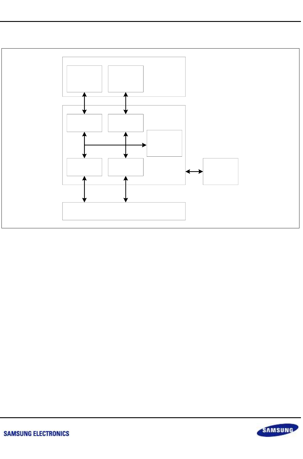
Samsung Confidential
S5P6818_UM 8 System L2 Cache (PL-310 L2C)
8-3
Preliminary product information describes products that are in development, for which full characterization data and
associated errata are not yet available. Specifications and information herein are subject to change without notice.
8.3 Block Diagram
Figure 8-1 System L2 Cache Block Diagram
System BUS
CACHE
RAM
Processor
Cache Controller
Instruction
And/or data
(RW)
Instruction
And/or data
(RW)
AXI Slave0
(RW)AXI Slave1
(RW)
AXI Master0
(RW)AXI Master1
(RW)
Internal
registers
nexell / ys.kim at 2015.02.12
SAMSUNG Confidential

Samsung Confidential
S5P6818_UM 8 System L2 Cache (PL-310 L2C)
8-4
Preliminary product information describes products that are in development, for which full characterization data and
associated errata are not yet available. Specifications and information herein are subject to change without notice.
8.4 Functional Description
8.4.1 L2 Cache User Configure
System L2 Cache Base Address: Base Address: 0xCF000000
Turn off and Turn on L2C:
Turn off offset 0x100 (Base Address + 0x100) set to 0
Turn on offset 0x100 (Base Address + 0x100) set to 1
Early Write Response:
The AXI protocol specifies that the write response can only be sent back to an AXI master when the last
write data has been accepted. This optimization enables the L2C-310 to send the write response of
certain write transactions as soon as the store buffer accepts the write address. This behavior is not
compatible with the AXI protocol and is disabled by default. You enable this optimization by setting the
Early BRESP Enable bit in the Auxiliary Control Register, bit[30]. The L2C-310 slave ports then send an
early write response only if the input signal AWUSERSx[11], x = 0 or 1, is set to 1'b1 for the
corresponding write transaction.
8.4.2 Initialization Sequence
As an example, a typical cache controller start-up programming sequence consists of the following register
operations:
1. Write to the Auxiliary, Tag RAM Latency, Data RAM Latency, Pre-fetch, and Power Control registers using a
read-modify-write to set up global configurations:
Associativity, Way Size
Latencies for RAM accesses
Allocation policy
Pre-fetch and power capabilities.
2. Secure write to the Invalidate by Way, offset 0x77C, to invalidate all entries in cache:
Write 0xFFFF to 0x77C
Poll cache maintenance register until invalidate operation is complete.
3. Write to the Lockdown D and Lockdown I Register 9 if required.
4. Write to interrupt clear register to clear any residual raw interrupts set.
5. Write to the Interrupt Mask Register if you want to enable interrupts.
6. Write to Control Register 1 with the LSB set to 1 to enable the cache.
If you write to the Auxiliary, Tag RAM Latency, or Data RAM Latency Control Register with the L2 cache enabled,
this results in a SLVERR. You must disable the L2 cache by writing to the Control Register 1 before Writing to the
Auxiliary, Tag RAM Latency, or Data RAM Latency Control Register.
nexell / ys.kim at 2015.02.12
SAMSUNG Confidential

Samsung Confidential
S5P6818_UM 8 System L2 Cache (PL-310 L2C)
8-5
Preliminary product information describes products that are in development, for which full characterization data and
associated errata are not yet available. Specifications and information herein are subject to change without notice.
8.5 Register Description
8.5.1 Register Map Summary
Base Address: 0xCF00_0000
Register
Offset
Description
Reset Value
REG0_CACHE_ID
0x0000h
Cache ID and type Register
0x4100_C4C8
REG0_CACHE_TYPE
0x0004h
CACHE Type register
0x1A34_0340
REG1_CONTROL
0x0100h
Control register
0x0000_0000
AUX_CONTROL
0x0104h
Aux control register
0x0207_0000
REG1_TAG_RAM_CONTROL/
REG1_DATA_RAM_CONTROL
0x0108h to
0x010Ch
Tag and data ram control register
0x0000_0777
REG2_EV_COUNTER_CTRL
0x0200h
Event counter control register
0x0000_0000
REG2_EV_COUNTER1_CFG/
REG2_EV_COUNTER0_CFG
0x0204h to
0x0208h
Event counter configuration register 1, 0
0x0000_0000
REG2_EV_COUNTER1/
REG2_EV_COUNTER0
0x020Ch to
0x0210h
Event counter registers 1, 0
0x0000_0000
REG2_INT_MASK
0x0214h
Interrupt mask register
0x0000_0000
REG2_INT_MASK_STATUS
0x0218h
Interrupt mask STATUS register
0x0000_0000
REG2_INT_RAW_STATUS
0x021Ch
Interrupt RAW STATUS register
0x0000_0000
REG2_INT_CLEAR
0x0220h
Interrupt CLEAR register
0x0000_0000
REG7_CACHE_SYNC
0x0730h
CACHE SYNC
0x0000_0000
REG7_INV_PA
0x0770h
INVALIDATE line by pa
0x0000_0000
REG7_INV_WAY
0x077Ch
Invalidate by way
0x0000_0000
REG7_CLEAN_PA
0x07B0h
Clean line by pa
0x0000_0000
REG7_CLEAN_INDEX
0x07B8h
Clean line by set/way
0x0000_0000
REG7_CLEAN_WAY
0x07BCh
Clean by way
0x0000_0000
REG7_CLEAN_INV_PA
0x07F0h
Clean and invalidate line by pa
0x0000_0000
REG7_CLEAN_INV_INDEX
0x07F8h
Clean and 07F8h line by set/way
0x0000_0000
REG7_CLEAN_INV_WAY
0x07FCh
Clean and invalidate by way
0x0000_0000
REG9_D_LOCKDOWN0 to 7
0x0900h
0x0908h
0x0910h
0x0918h
0x0920h
0x0928h
0x0930h
0x0938h
DATA Lockdown 0 to 7
0x0000_0000
REG9_I_LOCKDOWN0 to 7
0x0904h
0x090Ch
0x0914h
0x091Ch
0x0924h
Instruction Lockdown 0 to 7
0x0000_0000
nexell / ys.kim at 2015.02.12
SAMSUNG Confidential
Samsung Confidential
S5P6818_UM 8 System L2 Cache (PL-310 L2C)
8-6
Preliminary product information describes products that are in development, for which full characterization data and
associated errata are not yet available. Specifications and information herein are subject to change without notice.
Register
Offset
Description
Reset Value
0x092Ch
0x0934h
0x093Ch
REG9_LOCK_LINE_EN
0x0950h
Lock down by line enable
0x0000_0000
REG9_UNLOCK_WAY
0x0954h
Unlock lines by way
0x0000_0000
REG12_ADDR_FILTERING_START
0x0C00h
Address filtering start
0x0000_0000
REG12_ADDR_FILTERING_END
0x0C04h
Address filtering end
0x0000_0000
REG15_DEBUG_CTRL
0x0F40h
Debug ctrl
0x0000_0000
REG15_PREFETCH_CTRL
0x0F60h
Prefetch ctrl
0x0000_0004
REG15_POWER_CTRL
0x0F80h
Power ctrl
0x0000_0000
nexell / ys.kim at 2015.02.12
SAMSUNG Confidential
Samsung Confidential
S5P6818_UM 8 System L2 Cache (PL-310 L2C)
8-7
Preliminary product information describes products that are in development, for which full characterization data and
associated errata are not yet available. Specifications and information herein are subject to change without notice.
8.5.1.1 REG0_CACHE_ID
Base Address: 0xCF00_0000
Address = Base Address + 0x0000h, Reset Value = 0x4100_C4C8
Name
Bit
Type
Description
Reset Value
Implementer
[31:24]
R
ARM
8’h41
RSVD
[23:16]
R
Reserved
8’h0
CACHE ID
[15:10]
R
Cache Controller ID
6’hC4
Partnum
[9:6]
R
Part number 0x3 denotes Core Link Level 2 Cache
Controller L2C-310
4’h3
RTL RELEASE
[5:0]
R
RTL release 0x8 denotes r3p2 code of the cache
controller.
6’h8
nexell / ys.kim at 2015.02.12
SAMSUNG Confidential
Samsung Confidential
S5P6818_UM 8 System L2 Cache (PL-310 L2C)
8-8
Preliminary product information describes products that are in development, for which full characterization data and
associated errata are not yet available. Specifications and information herein are subject to change without notice.
8.5.1.2 REG0_CACHE_TYPE
Base Address: 0xCF00_0000
Address = Base Address + 0x0004h, Reset Value = 0x1A34_0340
Name
Bit
Type
Description
Reset Value
DATA BANK
[31]
R
0 = Data banking not implemented
1 = Data banking implemented
1’b0
RSVD
[30:29]
R
Reserved
2’b0
CTYPE
[28:25]
R
4'b11xy
X = 1 if pl310_LOCKDOWN_BY_MASTER is defined,
otherwise 0
Y = 1 if pl310_LOCKDOWN_BY_LINE is defined,
otherwise 0
4’hD
H
[24]
R
0 = Unified
1 = Havard
1’b0
DSIZE
[23:19]
R
[23] SBZ/RAZ
[22:20] Read from Auxiliary Control Register[19:17]
[19] SBZ/RAZ
5’h6
L2 ASSOCIATIVITY
[18]
R
Read from Auxiliary Control Register[16]
1’b1
RSVD
[17:14]
R
Reserved
4’h0
L2 CACHE LINE
LENGTH
[13:12]
R
00 to 32 bytes
2’b0
ISIZE
[11:7]
R
[11] SBZ/RAZ
[10:8] Read from Auxiliary Control Register[19:17]
[7] SBZ/RAZ
5’h6
L2 ASSOCIATIVITY
[6]
R
Read from Auxiliary Control Register[16]
1’b1
RSVD
[5:2]
R
Reserved
4’h0
L2 CACHE LINE
LENGTH
[1:0]
R
00 to 32 bytes
2’b0
8.5.1.3 REG1_CONTROL
Base Address: 0xCF00_0000
Address = Base Address + 0x0100h, Reset Value = 0x0000_0000
Name
Bit
Type
Description
Reset Value
RSVD
[31:1]
R
Reserved
31'h0
Enb
[0]
RW
0 = L2 Cache disabled. Default
1 = L2 Cache Enabled
1'b0
nexell / ys.kim at 2015.02.12
SAMSUNG Confidential

Samsung Confidential
S5P6818_UM 8 System L2 Cache (PL-310 L2C)
8-9
Preliminary product information describes products that are in development, for which full characterization data and
associated errata are not yet available. Specifications and information herein are subject to change without notice.
8.5.1.4 AUX_CONTROL
Base Address: 0xCF00_0000
Address = Base Address + 0x0104h, Reset Value = 0x0207_0000
Name
Bit
Type
Description
Reset Value
RSVD
[31]
RW
Reserved
1’b0
EARLY BRESP
[30]
RW
0 = Early BRESP disabled. This is the default.
1 = Early BRESP enabled.
1’b0
INSTRUCTION
PREFETCH ENABLE
[29]
RW
0 = Instruction pre-fetching disabled. This is the default.
1 = Instruction pre-fetching enabled.
1’b0
DATA PREFETCH
ENABLE
[28]
RW
0 = Data pre-fetching disabled. This is the default.
1 = Data pre-fetching enabled.
1’b0
NS INTERRUPT
ACCESS CONTROL
[27]
RW
0 = Interrupt Clear, 0x220, and Interrupt Mask, 0x214,
can only be modified or read with secure accesses. This
is the default.
1 = Interrupt Clear, 0x220, and Interrupt Mask, 0x214,
can be modified or read with secure or non-secure
accesses.
1’b0
NS LOCKDOWN
[26]
RW
0 = Lockdown registers cannot be modified using non-
secure. This is the default.
1 = Non-secure accesses can write to the lockdown
registers.
1’b0
CACHE REPLACEMENT
POLICY
[25]
RW
0 = Pseudo-random replacement using LFSR.
1 = Round-robin replacement. This is the default.
1’b1
FORCE WRITE
ALLOCATE
[24:23]
RW
2’b00 = Use AWCACHE attributes for WA. This is the
default.
2’b01 = Force no allocate, set WA bit always 0.
2’b10 = Override *AWCACHE *attributes, set WA bit
always 1, all cacheable write misses become write
allocated.
2’b11 = Internally mapped to 00.
2’b00
SHARED ATTRIBUTE
OVERRIDE ENABLE
[22]
RW
0 = Treats shared accesses. This is the default.
1 = Shared attribute internally ignored.
1’b0
PARITY ENABLE
[21]
RW
0 = Disabled. This is the default.
1 = Enabled.
1’b0
EVENT MONITOR BUS
ENABLE
[20]
RW
0 = Disabled. This is the default.
1 = Enabled.
1’b0
WAY-SIZE
[19:17]
RW
3’b000 = Reserved, internally mapped to 16 KB
3’b001 = 16 KB
3’b010 = 32 KB
3’b011 = 64 KB
3’b100 = 128 KB
3’b101 = 256 KB
3’b110 = 512 KB
3’b111 = Reserved, internally mapped to 512 KB
3’b011
ASSOCIATIVITY
[16]
RW
0 = 8-way
1 = 16-way.
1’b1
nexell / ys.kim at 2015.02.12
SAMSUNG Confidential

Samsung Confidential
S5P6818_UM 8 System L2 Cache (PL-310 L2C)
8-10
Preliminary product information describes products that are in development, for which full characterization data and
associated errata are not yet available. Specifications and information herein are subject to change without notice.
Name
Bit
Type
Description
Reset Value
RSVD
[15:14]
RW
SBZ/RAZ
1’b0
SHARED ATTRIBUTE
INVALIDATE ENABLE
[13]
RW
0 = Shared invalidate behavior disabled. This is the
default.
1 = Shared invalidate behavior enabled, if Shared
Attribute
Override Enable bit not set.
1’b0
EXCLUSIVE CACHE
CONFIGURATION
[12]
RW
0 = Disabled. This is the default.
1 = Enabled.
1’b0
STORE BUFFER
DEVICE LIMITATION
ENABLE
[11]
RW
0 = Store buffer device limitation disabled. Device writes
can take all slots in store buffer. This is the default.
1 = Store buffer device limitation enabled. Device writes
cannot take all slots in store buffer when connected to
the Cortex-A9 MP Core
There is always one available slot to service Normal
Memory.
1’b0
HIGH PRIORITY FOR
SO AND DEV READS
ENABLE
[10]
RW
0 = Strongly Ordered and Device reads have lower
priority than cacheable accesses when arbitrated in the
L2CC L2C-310 master
This is the default.
1 = Strongly Ordered and Device reads get the highest
priority when arbitrated in the L2C-310 master ports.
1’b0
RSVD
[9:1]
RW
SBZ/RAZ
8’h0
FULL LINE OF ZERO
ENABLE
[0]
RW
0 = Full line of write zero behavior disabled. This is the
default.
1 = Full line of write zero behavior Enabled.
1’b0
nexell / ys.kim at 2015.02.12
SAMSUNG Confidential

Samsung Confidential
S5P6818_UM 8 System L2 Cache (PL-310 L2C)
8-11
Preliminary product information describes products that are in development, for which full characterization data and
associated errata are not yet available. Specifications and information herein are subject to change without notice.
8.5.1.5 REG1_TAG_RAM_CONTROL/REG1_DATA_RAM_CONTROL
Base Address: 0xCF00_0000
Address = Base Address + 0x0108h, 0x010Ch, Reset Value = 0x0000_0777
Name
Bit
Type
Description
Reset Value
RSVD
[31:11]
RW
Reserved
21’h0
RAM WRITE
ACCESS LATENCY
[10:8]
RW
Default value depends on the value of
pl310_TAG_WRITE_LAT for reg1_tag_ram_control or
pl310_DATA_WRITE_LAT for reg1_data_ram_control.
0b000 = 1 cycle of latency, there is no additional latency
0b001 = 2 cycles of latency
0b010 = 3 cycles of latency
0b011 = 4 cycles of latency
0b100 = 5 cycles of latency
0b101 = 6 cycles of latency
0b110 = 7 cycles of latency
0b111 = 8 cycles of latency
3'b111
RSVD
[7]
RW
Reserved
1'b0
RAM READ ACCESS
LATENCY
[6:4]
RW
0b000 = 1 cycle of latency, there is no additional latency
0b001 = 2 cycles of latency
0b010 = 3 cycles of latency
0b011 = 4 cycles of latency
0b100 = 5 cycles of latency
0b101 = 6 cycles of latency
0b110 = 7 cycles of latency
0b111 = 8 cycles of latency
3'b111
RSVD
[3]
RW
SBZ/RAZ
1'b0
RAM SETUP
LATENCY
[2:0]
RW
0b000 = 1 cycle of latency, there is no additional latency
0b001 = 2 cycles of latency
0b010 = 3 cycles of latency
0b011 = 4 cycles of latency
0b100 = 5 cycles of latency
0b101 = 6 cycles of latency
0b110 = 7 cycles of latency
0b111 = 8 cycles of latency
3'b111
nexell / ys.kim at 2015.02.12
SAMSUNG Confidential
Samsung Confidential
S5P6818_UM 8 System L2 Cache (PL-310 L2C)
8-12
Preliminary product information describes products that are in development, for which full characterization data and
associated errata are not yet available. Specifications and information herein are subject to change without notice.
8.5.1.6 REG2_EV_COUNTER_CTRL
Base Address: 0xCF00_0000
Address = Base Address + 0x0200h, Reset Value = 0x0000_0000
Name
Bit
Type
Description
Reset Value
RSVD
[31:3]
RW
SBZ/RAZ
29'h0
COUNTER RESET
[2:1]
RW
Always Read as zero. The following counters are reset
when a 1 is written to the following bits:
bit[2] = Event Counter1 reset
bit[1] = Event Counter0 reset.
2’b0
EVENT COUNTER
ENABLE
[0]
RW
0 = Event Counting Disable. This is the default.
1 = Event Counting Enable.
1'b0
8.5.1.7 REG2_EV_COUNTER1_CFG/REG2_EV_COUNTER0_CFG
Base Address: 0xCF00_0000
Address = Base Address + 0x0204h, 0x0208h, Reset Value = 0x0000_0000
Name
Bit
Type
Description
Reset Value
RSVD
[31:6]
RW
Reserved
26'h0
COUNTER EVENT
SOURCE
[5:2]
RW
Event Encoding
Counter Disabled : 4’b0000
CO : 4’b0001
DRHIT : 4’b0010
DRREQ : 4’b0011
DWHIT : 4’b0100
DWREQ : 4’b0101
DWTREQ : 4’b0110
IRHIT : 4’b0111
IRREQ : 4’b1000
WA : 4’b1001
IPFALLOC : 4’b1010
EPFHIT : 4’b1011
EPFALLOC : 4’b1100
SRRCVD : 4’b1101
SRCONF : 4’b1110
EPFRCVD : 4’b1111
4'h0
EVENT COUNTER
INTERRUPT
GENERATION
[1:0]
RW
2’b00 = Disabled. This is the default.
2’b01 = Enabled: Increment condition.
2’b10 = Enabled: Overflow condition.
2’b11 = Interrupt generation is disabled.
2'b0
nexell / ys.kim at 2015.02.12
SAMSUNG Confidential
Samsung Confidential
S5P6818_UM 8 System L2 Cache (PL-310 L2C)
8-13
Preliminary product information describes products that are in development, for which full characterization data and
associated errata are not yet available. Specifications and information herein are subject to change without notice.
8.5.1.8 REG2_EV_COUNTER1/ REG2_EV_COUNTER0
Base Address: 0xCF00_0000
Address = Base Address + 020Ch, 0x0210h, Reset Value = 0x0000_0000
Name
Bit
Type
Description
Reset Value
counter
[31:0]
RW
Total of the event selected.
If a counter reaches its maximum value, it saturates at that
value until it is reset.
32’h0
8.5.1.9 REG2_INT_MASK
Base Address: 0xCF00_0000
Address = Base Address + 0x0214h, Reset Value = 0x0000_0000
Name
Bit
Type
Description
Reset Value
RSVD
[31:9]
RW
Reserved
23’h0
DECERR
[8]
RW
DECERR from L3
0 = Masked, Default
1 = Enabled.
1’b0
SLVERR
[7]
RW
SLVERR from L3
0 = Masked, Default
1 = Enabled.
1’b0
ERRRD
[6]
RW
Error on L2 data RAM, Read
0 = Masked, Default
1 = Enabled.
1’b0
ERRRT
[5]
RW
Error on L2 tag RAM, Read
0 = Masked, Default
1 = Enabled.
1’b0
ERRWD
[4]
RW
Error on L2 data RAM, Write
0 = Masked, Default
1 = Enabled.
1’b0
ERRWT
[3]
RW
Error on L2 tag RAM, Write
0 = Masked, Default
1 = Enabled.
1’b0
PARRD
[2]
RW
Parity Error on L2 data RAM, Read
0 = Masked, Default
1 = Enabled.
1’b0
PARRT
[1]
RW
Parity Error on L2 tag RAM, Read
0 = Masked, Default
1 = Enabled.
1’b0
ECNTR
[0]
RW
Even Counter1 and Event Counter 0 Overflow Increment
0 = Masked, Default
1 = Enabled.
1’b0
nexell / ys.kim at 2015.02.12
SAMSUNG Confidential

Samsung Confidential
S5P6818_UM 8 System L2 Cache (PL-310 L2C)
8-14
Preliminary product information describes products that are in development, for which full characterization data and
associated errata are not yet available. Specifications and information herein are subject to change without notice.
8.5.1.10 REG2_INT_MASK_STATUS
Base Address: 0xCF00_0000
Address = Base Address + 0x0218h, Reset Value = 0x0000_0000
Name
Bit
Type
Description
Reset Value
RSVD
[31:9]
R
Reserved
23’h0
DECERR
[8]
R
DECERR from L3
HIGH: If the bits read HIGH, they reflect the status of the
input lines triggering an interrupt.
LOW: If the bits read LOW, either no interrupt has been
generated, or the interrupt is masked.
1’b0
SLVERR
[7]
R
SLVERR from L3
HIGH: If the bits read HIGH, they reflect the status of the
input lines triggering an interrupt.
LOW: If the bits read LOW, either no interrupt has been
generated, or the interrupt is masked.
1’b0
ERRRD
[6]
R
Error on L2 data RAM, Read
HIGH: If the bits read HIGH, they reflect the status of the
input lines triggering an interrupt.
LOW: If the bits read LOW, either no interrupt has been
generated, or the interrupt is masked.
1’b0
ERRRT
[5]
R
Error on L2 tag RAM, Read
HIGH: If the bits read HIGH, they reflect the status of the
input lines triggering an interrupt.
LOW: If the bits read LOW, either no interrupt has been
generated, or the interrupt is masked.
1’b0
ERRWD
[4]
R
Error on L2 data RAM, Write
HIGH: If the bits read HIGH, they reflect the status of the
input lines triggering an interrupt.
LOW: If the bits read LOW, either no interrupt has been
generated, or the interrupt is masked.
1’b0
ERRWT
[3]
R
Error on L2 tag RAM, Write
HIGH: If the bits read HIGH, they reflect the status of the
input lines triggering an interrupt.
LOW: If the bits read LOW, either no interrupt has been
generated, or the interrupt is masked.
1’b0
PARRD
[2]
R
Parity Error on L2 data RAM, Read
HIGH: If the bits read HIGH, they reflect the status of the
input lines triggering an interrupt.
LOW: If the bits read LOW, either no interrupt has been
generated, or the interrupt is masked.
1’b0
PARRT
[1]
R
Parity Error on L2 tag RAM, Read
HIGH: If the bits read HIGH, they reflect the status of the
input lines triggering an interrupt.
LOW: If the bits read LOW, either no interrupt has been
generated, or the interrupt is masked.
1’b0
nexell / ys.kim at 2015.02.12
SAMSUNG Confidential

Samsung Confidential
S5P6818_UM 8 System L2 Cache (PL-310 L2C)
8-15
Preliminary product information describes products that are in development, for which full characterization data and
associated errata are not yet available. Specifications and information herein are subject to change without notice.
Name
Bit
Type
Description
Reset Value
ECNTR
[0]
R
Even Counter1 and Event Counter 0 Overflow Increment
HIGH: If the bits read HIGH, they reflect the status of the
input lines triggering an interrupt.
LOW: If the bits read LOW, either no interrupt has been
generated, or the interrupt is masked.
1’b0
nexell / ys.kim at 2015.02.12
SAMSUNG Confidential

Samsung Confidential
S5P6818_UM 8 System L2 Cache (PL-310 L2C)
8-16
Preliminary product information describes products that are in development, for which full characterization data and
associated errata are not yet available. Specifications and information herein are subject to change without notice.
8.5.1.11 REG2_INT_RAW_STATUS
Base Address: 0xCF00_0000
Address = Base Address + 0x021Ch, Reset Value = 0x0000_0000
Name
Bit
Type
Description
Reset Value
RSVD
[31:9]
R
Reserved
23’h0
DECERR
[8]
R
DECERR from L3
HIGH: If the bits read HIGH, they reflect the status of the input
lines riggering an interrupt.
LOW: If the bits read LOW, no interrupt has been generated.
1’b0
SLVERR
[7]
R
SLVERR from L3
HIGH: If the bits read HIGH, they reflect the status of the input
lines riggering an interrupt.
LOW: If the bits read LOW, no interrupt has been generated.
1’b0
ERRRD
[6]
R
Error on L2 data RAM, Read
HIGH: If the bits read HIGH, they reflect the status of the input
lines riggering an interrupt.
LOW: If the bits read LOW, no interrupt has been generated.
1’b0
ERRRT
[5]
R
Error on L2 tag RAM, Read
HIGH: If the bits read HIGH, they reflect the status of the input
lines riggering an interrupt.
LOW: If the bits read LOW, no interrupt has been generated.
1’b0
ERRWD
[4]
R
Error on L2 data RAM, Write
HIGH: If the bits read HIGH, they reflect the status of the input
lines riggering an interrupt.
LOW: If the bits read LOW, no interrupt has been generated.
1’b0
ERRWT
[3]
R
Error on L2 tag RAM, Write
HIGH: If the bits read HIGH, they reflect the status of the input
lines riggering an interrupt.
LOW: If the bits read LOW, no interrupt has been generated.
1’b0
PARRD
[2]
R
Parity Error on L2 data RAM, Read
HIGH: If the bits read HIGH, they reflect the status of the input
lines riggering an interrupt.
LOW: If the bits read LOW, no interrupt has been generated.
1’b0
PARRT
[1]
R
Parity Error on L2 tag RAM, Read
HIGH: If the bits read HIGH, they reflect the status of the input
lines riggering an interrupt.
LOW: If the bits read LOW, no interrupt has been generated.
1’b0
ECNTR
[0]
R
Even Counter1 and Event Counter 0 Overflow Increment
HIGH: If the bits read HIGH, they reflect the status of the input
lines riggering an interrupt.
LOW: If the bits read LOW, no interrupt has been generated.
1’b0
nexell / ys.kim at 2015.02.12
SAMSUNG Confidential

Samsung Confidential
S5P6818_UM 8 System L2 Cache (PL-310 L2C)
8-17
Preliminary product information describes products that are in development, for which full characterization data and
associated errata are not yet available. Specifications and information herein are subject to change without notice.
8.5.1.12 REG2_INT_CLEAR
Base Address: 0xCF00_0000
Address = Base Address + 0x0220h, Reset Value = 0x0000_0000
Name
Bit
Type
Description
Reset Value
RSVD
[31:9]
W
Reserved
23’h0
DECERR
[8]
W
DECERR from L3
When a bit is written as 1, it clears the corresponding bit in the
Raw Interrupt Status Register. When a bit is written as 0, it has no
effect.
1’b0
SLVERR
[7]
W
SLVERR from L3
When a bit is written as 1, it clears the corresponding bit in the
Raw Interrupt Status Register. When a bit is written as 0, it has no
effect.
1’b0
ERRRD
[6]
W
Error on L2 data RAM, Read
When a bit is written as 1, it clears the corresponding bit in the
Raw Interrupt Status Register. When a bit is written as 0, it has no
effect.
1’b0
ERRRT
[5]
W
Error on L2 tag RAM, Read
When a bit is written as 1, it clears the corresponding bit in the
Raw Interrupt Status Register. When a bit is written as 0, it has no
effect.
1’b0
ERRWD
[4]
W
Error on L2 data RAM, Write
When a bit is written as 1, it clears the corresponding bit in the
Raw Interrupt Status Register. When a bit is written as 0, it has no
effect.
1’b0
ERRWT
[3]
W
Error on L2 tag RAM, Write
When a bit is written as 1, it clears the corresponding bit in the
Raw Interrupt Status Register. When a bit is written as 0, it has no
effect.
1’b0
PARRD
[2]
W
Parity Error on L2 data RAM, Read
When a bit is written as 1, it clears the corresponding bit in the
Raw Interrupt Status Register. When a bit is written as 0, it has no
effect.
1’b0
PARRT
[1]
W
Parity Error on L2 tag RAM, Read
When a bit is written as 1, it clears the corresponding bit in the
Raw Interrupt Status Register. When a bit is written as 0, it has no
effect.
1’b0
ECNTR
[0]
W
Even Counter1 and Event Counter 0 Overflow Increment
When a bit is written as 1, it clears the corresponding bit in the
Raw Interrupt Status Register. When a bit is written as 0, it has no
effect.
1’b0
nexell / ys.kim at 2015.02.12
SAMSUNG Confidential

Samsung Confidential
S5P6818_UM 8 System L2 Cache (PL-310 L2C)
8-18
Preliminary product information describes products that are in development, for which full characterization data and
associated errata are not yet available. Specifications and information herein are subject to change without notice.
8.5.1.13 REG7_CACHE_SYNC
Base Address: 0xCF00_0000
Address = Base Address + 0x0730h, Reset Value = 0x0000_0000
Name
Bit
Type
Description
Reset Value
RSVD
[31:1]
RW
Reserved
31’h0
cachesync
[0]
RW
Cache SYNC
1’b0
8.5.1.14 REG7_INV_PA
Base Address: 0xCF00_0000
Address = Base Address + 0x0770h, Reset Value = 0x0000_0000
Name
Bit
Type
Description
Reset Value
TAG
[31:12]
RW
Tag
20’h0
INDEX
[11:5]
RW
Index
7’h0
RSVD
[4:1]
RW
Reserved
4’h0
Clean
[0]
RW
Invalidate
0 = Idle
1 = Enable Invalidate
1’b0
8.5.1.15 REG7_INV_WAY
Base Address: 0xCF00_0000
Address = Base Address + 0x077Ch, Reset Value = 0x0000_0000
Name
Bit
Type
Description
Reset Value
WAY
[31:28]
RW
Way
4’h0
RSVD
[27:12]
RW
Reserved
16’h0
INDEX
[11:5]
RW
Index
7’h0
RSVD
[4:1]
RW
Reserved
4’h0
CLEAN
[0]
RW
Invalidate
0 = Idle
1 = Enable Invalidate
1’b0
nexell / ys.kim at 2015.02.12
SAMSUNG Confidential
Samsung Confidential
S5P6818_UM 8 System L2 Cache (PL-310 L2C)
8-19
Preliminary product information describes products that are in development, for which full characterization data and
associated errata are not yet available. Specifications and information herein are subject to change without notice.
8.5.1.16 REG7_CLEAN_PA
Base Address: 0xCF00_0000
Address = Base Address + 0x07B0h, Reset Value = 0x0000_0000
Name
Bit
Type
Description
Reset Value
TAG
[31:12]
RW
Tag
20’h0
INDEX
[11:5]
RW
Index
7’h0
RSVD
[4:1]
RW
Reserved
4’h0
CLEAN
[0]
RW
Invalidate
0 = Idle
1 = Enable Invalidate
1’b0
8.5.1.17 REG7_CLEAN_INDEX
Base Address: 0xCF00_0000
Address = Base Address + 0x07B8h, Reset Value = 0x0000_0000
Name
Bit
Type
Description
Reset Value
WAY
[31:28]
RW
Way
4’h0
RSVD
[27:12]
RW
Reserved
16’h0
INDEX
[11:5]
RW
Index
7’h0
RSVD
[4:1]
RW
Reserved
4’h0
Clean
[0]
RW
Clean
0 = Idle
1 = Enable Invalidate
1’h0
8.5.1.18 REG7_CLEAN_WAY
Base Address: 0xCF00_0000
Address = Base Address + 0x07BCh, Reset Value = 0x0000_0000
Name
Bit
Type
Description
Reset Value
RSVD
[31:16]
RW
Reserved
16’h0
WAY BITS
[15:0]
RW
Way Bits
8WAY: 0xFF
16WAY: 0xFFFF
16’h0
nexell / ys.kim at 2015.02.12
SAMSUNG Confidential
Samsung Confidential
S5P6818_UM 8 System L2 Cache (PL-310 L2C)
8-20
Preliminary product information describes products that are in development, for which full characterization data and
associated errata are not yet available. Specifications and information herein are subject to change without notice.
8.5.1.19 REG7_CLEAN_INV_PA
Base Address: 0xCF00_0000
Address = Base Address + 0x07F0h, Reset Value = 0x0000_0000
Name
Bit
Type
Description
Reset Value
TAG
[31:12]
RW
Tag
20’h0
INDEX
[11:5]
RW
Index
7’h0
RSVD
[4:1]
RW
Reserved
4’h0
CLEAN
[0]
RW
Invalidate
0 = Idle
1 = Enable Invalidate
1’b0
8.5.1.20 REG7_CLEAN_INV_INDEX
Base Address: 0xCF00_0000
Address = Base Address + 0x07F8h, Reset Value = 0x0000_0000
Name
Bit
Type
Description
Reset Value
WAY
[31:28]
RW
Way
4’h0
RSVD
[27:12]
RW
Reserved
16’h0
INDEX
[11:5]
RW
Index
7’h0
RSVD
[4:1]
RW
Reserved
4’h0
Clean
[0]
R/W
Clean
0 = Idle
1 = Enable Invalidate
1’h0
8.5.1.21 REG7_CLEAN_INV_WAY
Base Address: 0xCF00_0000
Address = Base Address + 0x07FCh, Reset Value = 0x0000_0000
Name
Bit
Type
Description
Reset Value
RSVD
[31:16]
RW
Reserved
16’h0
WAY BITS
[15:0]
RW
Way Bits
8WAY: 0xFF
16WAY: 0xFFFF
16’h0
nexell / ys.kim at 2015.02.12
SAMSUNG Confidential
Samsung Confidential
S5P6818_UM 8 System L2 Cache (PL-310 L2C)
8-21
Preliminary product information describes products that are in development, for which full characterization data and
associated errata are not yet available. Specifications and information herein are subject to change without notice.
8.5.1.22 REG9_D_LOCKDOWNn (n = 0 to 7)
Base Address: 0xCF00_0000
Address = Base Address + 0x0900h, 0x0908h, 0x0910h, 0x0918h, 0x0920h, 0x0928h, 0x0930h, 0x0938h,
Reset Value = 0x0000_0000
Name
Bit
Type
Description
Reset Value
RSVD
[31:16]
RW
Reserved
16’h0
DATALOCK
[15:0]
RW
Way Bits
8WAY: 0xFF
16WAY: 0xFFFF
16’h0
8.5.1.23 REG9_I_LOCKDOWNn (n = 0 to 7)
Base Address: 0xCF00_0000
Address = Base Address + 0x0904h, 0x090Ch, 0x0914h, 0x091Ch, 0x0924h, 0x092Ch, 0x0934h, 0x093Ch,
Reset Value = 0x0000_0000
Name
Bit
Type
Description
Reset Value
RSVD
[31:16]
RW
Reserved
16’h0
INSTRLOCK
[15:0]
RW
Way Bits
8WAY: 0xFF
16WAY: 0xFFFF
16’h0
8.5.1.24 REG9_LOCK_LINE_EN
Base Address: 0xCF00_0000
Address = Base Address + 0x0950h, Reset Value = 0x0000_0000
Name
Bit
Type
Description
Reset Value
RSVD
[31:1]
RW
Reserved
31’h0
LOCKDOWN by
LINE ENB
[0]
RW
0 = Lockdown by line disabled. This is default
1 = Lockdown by line enabled
1’b0
nexell / ys.kim at 2015.02.12
SAMSUNG Confidential

Samsung Confidential
S5P6818_UM 8 System L2 Cache (PL-310 L2C)
8-22
Preliminary product information describes products that are in development, for which full characterization data and
associated errata are not yet available. Specifications and information herein are subject to change without notice.
8.5.1.25 REG9_UNLOCK_WAY
Base Address: 0xCF00_0000
Address = Base Address + 0x0954h, Reset Value = 0x0000_0000
Name
Bit
Type
Description
Reset Value
RSVD
[31:16]
RW
Reserved
16’h0
UNLOCK ALL LINES
BY WAY
[15:0]
RW
For all bits:
0 = Unlock all lines disabled. This is the default
1 = Unlock all lines operation in progress for the
corresponding way
16’h0
8.5.1.26 REG12_ADDR_FILTERING_START
Base Address: 0xCF00_0000
Address = Base Address + 0x0C00h, Reset Value = 0x0000_0000
Name
Bit
Type
Description
Reset Value
FILTERING START
[31:20]
RW
Address filtering start address for bits[31:20] of the
filtering address
12’h0
RSVD
[19:1]
RW
SBZ/RAZ
19’h0
FILTER ENB
[0]
RW
Address filter enable
1’b0
8.5.1.27 REG12_ADDR_FILTERING_END
Base Address: 0xCF00_0000
Address = Base Address + 0x0C04h, Reset Value = 0x0000_0000
Name
Bit
Type
Description
Reset Value
FILTERING START
[31:20]
RW
Address filtering start address for bits[31:20] of the
filtering address
12’h0
RSVD
[19:0]
RW
SBZ/RAZ
20’h0
nexell / ys.kim at 2015.02.12
SAMSUNG Confidential

Samsung Confidential
S5P6818_UM 8 System L2 Cache (PL-310 L2C)
8-23
Preliminary product information describes products that are in development, for which full characterization data and
associated errata are not yet available. Specifications and information herein are subject to change without notice.
8.5.1.28 REG15_DEBUG_CTRL
Base Address: 0xCF00_0000
Address = Base Address + 0x0F40h, Reset Value = 0x0000_0000
Name
Bit
Type
Description
Reset Value
RSVD
[31:3]
RW
Reserved
29’h0
SPNIDEN
[2]
RW
Reads value of SPNIDEN Input.
1’b0
DWB
[1]
RW
Disable Write-back force WT
0 = Enable write-back behavior. This is the default.
1 = Force write-through behavior
1’b0
DCL
[0]
RW
Disable cache line fill
0 = Enable cache line fills. This is the default
1 = Disable cache line fills
1’b0
8.5.1.29 REG15_PREFETCH_CTRL
Base Address: 0xCF00_0000
Address = Base Address + 0x0F60h, Reset Value = 0x0000_0000
Name
Bit
Type
Description
Reset Value
RSVD
[31]
RW
Reserved
1’b0
DOUBLE LINE FILL
ENABLE
[30]
RW
You can set the following options for this register bit:
0 = The L2CC always issues 4x64-bit read bursts to L3
on reads that miss in the L2cache. This is the default.
1 = The L2CC issues 8x64-bit read bursts to L3 on
reads that miss in the L2 cache.
1’b0
INSTRUCTION
PREFETCH ENABLE
[29]
RW
You can set the following options for this register bit:
0 = Instruction pre-fetching disabled. This is the default.
1 = Instruction pre-fetching enabled.
1’b0
DATA PREFETCH
ENABLE
[28]
RW
You can set the following options for this register bit:
0 = Data pre-fetching disabled. This is the default.
1 = Data pre-fetching enabled.
1’b0
DOUBLE LINE FILL ON
WRAP READ DISABLE
[27]
RW
You can set the following options for this register bit:
0 = Double line fill on WRAP read enabled. This is the
default.
1 = Double line fill on wrap read disabled.
1’b0
RSVD
[26:25]
RW
SBZ/RAZ
2’b0
PREFETCH DROP
ENABLE
[24]
RW
You can set the following options for this register bit:
0 = The L2CC does not discard pre-fetch reads issued
to L3. This is default
1 = The L2CC discards pre-fetch reads issued to L3
when there is a resource conflict with explicit reads.
1’b0
INCR DOUBLE LINEFILL
ENABLE
[23]
RW
0 = The L2CC does not issue INCR 8x64-bit read
bursts to L3 on reads that miss in the L2 cache. This is
the default.
1’b0
nexell / ys.kim at 2015.02.12
SAMSUNG Confidential
Samsung Confidential
S5P6818_UM 8 System L2 Cache (PL-310 L2C)
8-24
Preliminary product information describes products that are in development, for which full characterization data and
associated errata are not yet available. Specifications and information herein are subject to change without notice.
Name
Bit
Type
Description
Reset Value
1 = The L2CC can issue INCR 8x64-bit read bursts to
L3 on reads that miss in the L2cache.
RSVD
[22]
RW
SBZ/RAZ
1’b0
NOT SAME ID ON
EXCLUSIVE SEQUENCE
ENABLE
[21]
RW
You can set following options for this register bit:
0 = Read and write portions of a non cacheable
exclusive sequence have the same AXI ID when issued
to L3. This is the default.
1 = Read and write portions of a non cacheable
exclusive sequence do not have the same AXI ID when
issued to L3.
1’b0
RSVD
[20:5]
RW
SBZ/RAZ
16’h0
PREFETCH OFFSET
[4:0]
RW
Default value = 5’b00000
You must only use the pre-fetch offset values of 0-7,
15, 23, and 31 for these bits. The L2C-310 does not
support the other values.
5’h0
8.5.1.30 REG15_POWER_CTRL
Base Address: 0xCF00_0000
Address = Base Address + 0x0F80h, Reset Value = 0x0000_0000
Name
Bit
Type
Description
Reset Value
RSVD
[31:2]
RW
Reserved
30’h0
DYNAMIC_CLK_GATING
[1]
RW
Dynamic Clock gating Enable.
0 = Disabled
1 = Enabled
1’b0
STANBY MODE EN
[0]
RW
Standby Mode Enable.
0 = Disabled
1 = Enabled
1’b0
nexell / ys.kim at 2015.02.12
SAMSUNG Confidential

Samsung Confidential
S5P6818_UM 9 DMA
9-1
Preliminary product information describes products that are in development, for which full characterization data and
associated errata are not yet available. Specifications and information herein are subject to change without notice.
9 DMA
9.1 Overview
The DMA Controller (DMAC) is an Advanced Microcontroller Bus Architecture (AMBA) block that connects to the
Advanced High-performance Bus (AHB). There is an AHB slave interface for programming the DMAC and 2 AHB
masters for data transfer. There are two DMAC in S5P6818 and each DMAC has eight channels, which can buffer
up to 4 words each. Each channel can transfer data through either of the AHB Master interfaces with the
programmed data width and endianness. The DMAC supports 16 DMA requestors, and generates individually
maskable interrupts for Terminal count and transfer error for each channel.
9.2 Features
16 DMA channels. Each channel can support a unidirectional transfer.
16 DMA requests. The DMAC provides 16 peripheral DMA request lines.
Single DMA and burst DMA request signals. Each peripheral connected to the DMAC can assert either a burst
DMA request or a single DMA request. You set the DMA burst size by programming the DMAC.
Memory-to-memory, memory-to-peripheral, peripheral-to-memory, and peripheral-to-peripheral transfers.
Scatter or gather DMA support through the use of linked lists.
Hardware DMA channels priority. Each DMA channel has a specific hardware priority. DMA channel 0 has the
highest priority and channel 7 has the lowest priority. If requests from two channels become active at the
same time, the channel with the highest priority is serviced first.
AHB slave DMA programming interface. You program the DMAC by writing to the DMA control registers over
the AHB slave interface.
Two AHB bus masters for transferring data. Use these interfaces to transfer data when a DMA request goes
active.
Incrementing or non-incrementing addressing for source and destination.
Programmable DMA burst size. You can program the DMA burst size to transfer data more efficiently. The
burst size is usually set to half the size of the FIFO in the peripheral.
Internal four word FIFO per channel.
Supports eight, 16, and 32-bit wide transactions.
Big-endian and little-endian support. The DMAC defaults to little-endian mode on reset.
nexell / ys.kim at 2015.02.12
SAMSUNG Confidential

Samsung Confidential
S5P6818_UM 9 DMA
9-2
Preliminary product information describes products that are in development, for which full characterization data and
associated errata are not yet available. Specifications and information herein are subject to change without notice.
Separate and combined DMA error and DMA count interrupt requests. You can generate an interrupt to the
processor on a DMA error or when a DMA count has reached 0. This is usually used to indicate that a transfer
has finished. There are three interrupt request signals to do this:
DMACINTTC signals when a transfer has completed.
DMACINTERR signals when an error has occurred.
DMACINTR combines both the DMACINTTC and DMACINTERR interrupt request signals. You can use
the DMACINTR interrupt request in systems that have few interrupt controller request inputs.
Interrupt masking. You can mask the DMA error and DMA terminal count interrupt requests.
Raw interrupt status. You can read the DMA error and DMA count raw interrupt status prior to masking.
Test registers for use in block and integration system level testing.
Identification registers that uniquely identify the DMAC. An operating system can use these to automatically
configure itself.
nexell / ys.kim at 2015.02.12
SAMSUNG Confidential
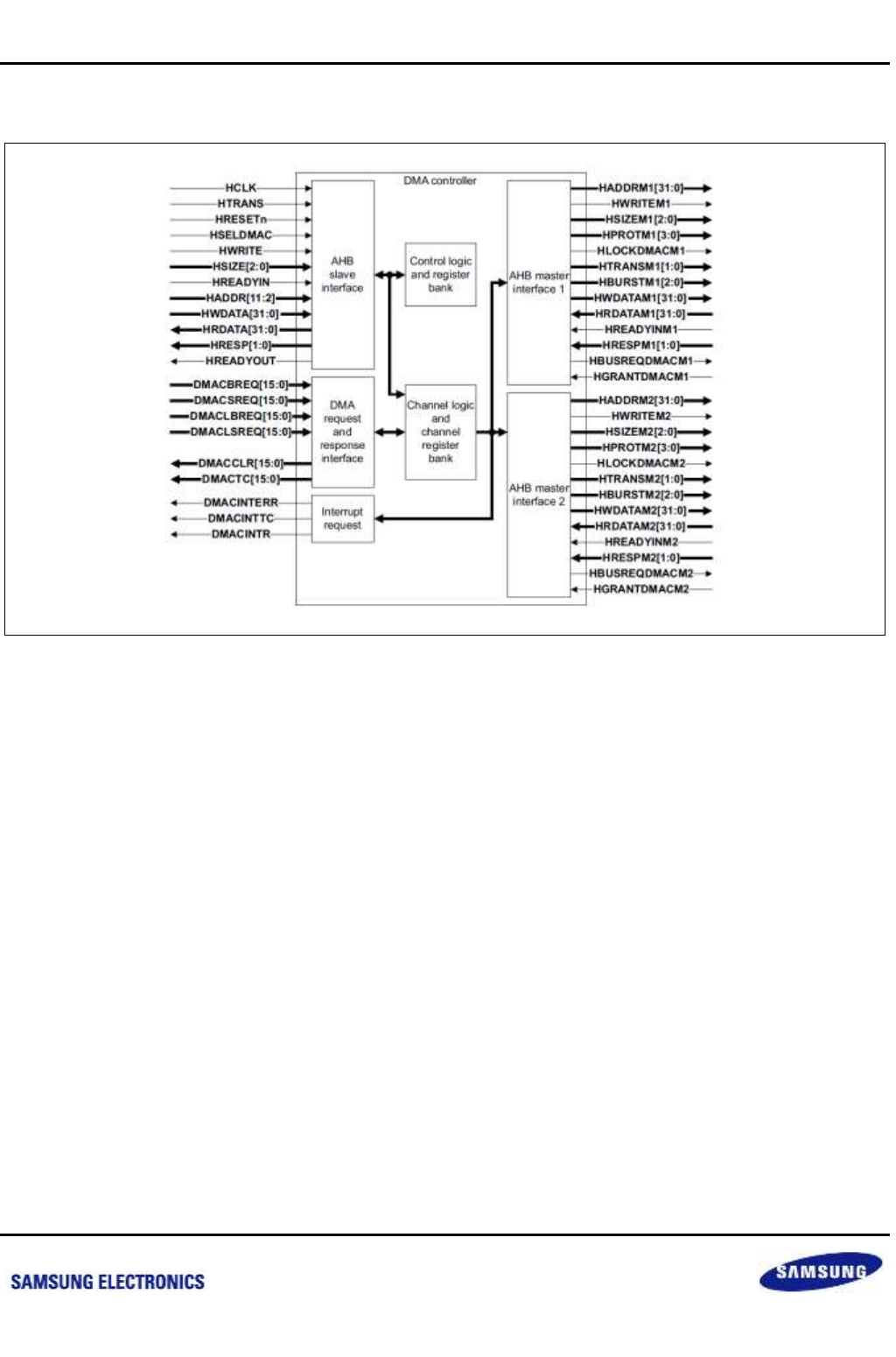
Samsung Confidential
S5P6818_UM 9 DMA
9-3
Preliminary product information describes products that are in development, for which full characterization data and
associated errata are not yet available. Specifications and information herein are subject to change without notice.
9.3 Block Diagram
Figure 9-1 DMAC Block Diagram
nexell / ys.kim at 2015.02.12
SAMSUNG Confidential

Samsung Confidential
S5P6818_UM 9 DMA
9-4
Preliminary product information describes products that are in development, for which full characterization data and
associated errata are not yet available. Specifications and information herein are subject to change without notice.
9.4 Functional Description
9.4.1 Software Considerations
You must take into account the following software considerations when programming the DMAC:
There must not be any write-operation to Channel registers in an active channel after the channel enable is
made HIGH. If you must reprogram any DMAC channel parameters, you must reprogram after disabling the
DMAC channel.
If the source width is less than the destination width, the Transfer Size value multiplied by the source width
must be an integral multiple of the destination width.
When the source peripheral is the flow controller and the source width is less than the destination width, the
number of transfers that the source peripheral performs, before asserting a DMACLSREQ or DMACLBREQ,
must be so that the number of transfers multiplied by the source width is an integral multiple of the destination
width. If this case is violated, the data can get stuck and lost in the FIFO causing UNPREDICTABLE results.
You can abort the transfer by disabling the relevant DMAC channel.
You must not program the SRCPERIPHERAL and DESTPERIPHERAL bit fields in the DMACCxCONFIG
Register with any value greater than 15. See Channel Configuration Registers
The SWIDTH and DWIDTH bit fields in the DMACCxCONTROL Register must not indicate more than a 32-bit
wide peripheral. See Channel Control Registers
After the software disables a channel by clearing the Channel Enable bit in the DMACCxCONFIG Register,
see Channel Configuration Registers, it must re-enable the bit only after it has polled a 0 in the corresponding
DMACENBLDCHNS Register bit, see Enabled Channel. This is because the actual disabling does not
immediately happen with the clearing of Channel Enable bit. You must accommodate the latency of the on
going AHB burst.
The LLI field in the DMACCxLLIREG Register must not indicate an address greater than 0xFFFFFFF0,
otherwise the four-word LLI burst wraps over at 0x00000000 and the LLI data structure is not in contiguous
memory locations. See Channel Linked List Item Registers
When the transfer size programmed in the DMAC is greater than the depth of the FIFO in a source or
destination peripheral, you must only program the DMAC for non-incrementing address generation.
A peripheral is expected to deassert any DMACSREQ, DMACBREQ, DMACLSREQ, or DMACLBREQ signals
on receiving the DMACCLR signal irrespective of the request the DMACCLR was asserted in response to.
This is because DMACCLR is not specific to a single-request signal, DMACSREQ, or burst-request signal,
DMACSBEQ. The handshaking of DMACCLR is achieved with a logical OR of all the DMA requests in the
DMAC.
NOTE: It is illegal for a peripheral to give a new DMACSREQ or DMACBREQ signal while DMACCLR is HIGH.
nexell / ys.kim at 2015.02.12
SAMSUNG Confidential

Samsung Confidential
S5P6818_UM 9 DMA
9-5
Preliminary product information describes products that are in development, for which full characterization data and
associated errata are not yet available. Specifications and information herein are subject to change without notice.
If you program the Transfer Size field in the DMACCxCONTROL Register, see Channel Control Registers, as
zero, and the DMAC is the flow controller, the Transfer Size field has no meaning in other flow-control modes,
then the channel does not initiate any transfers. It is your responsibility to disable the channel by writing into
the channel enable bit of the DMACCxCONFIG Register and reprogramming the channel again.
You must not run the normal read-write tests on the DMACCxCONTROL Register, see Channel Control
Register, because the Transfer Size field is not a typical write and read-back register field. While writing, the
Transfer Size bit-field is like a control register because it determines how many transfers the DMAC performs.
However, during read-back, Transfer Size behaves like a status register because it returns the number of
remaining transfers in terms of source width. So when Transfer Size is read back, it returns the number of
destination-transfer-completed stored in a separate counter called TRFSIZEDST multiplied by a factor. The
same physical register is not being written into and read from, and normal write and read-back tests are not
applicable.
In the destination flow control mode, with peripheral-to-peripheral transfer, if sufficient data is present in the
channel FIFO to service a DMACLSREQ or DMACLBREQ request raised by a destination peripheral without
requiring data to be fetched from the source peripheral, then the source peripheral is issued a DMACTC.
For destination flow controlled case, peripheral-to-peripheral transfer, with DWIDTH < SWIDTH, the number of
data bytes requested by the destination peripheral must be an integral multiple of SWIDTH expressed in
bytes. If you do not ensure this, then the DMAC might fetch more data from the source peripheral than is
required. This can result in data loss.
At the end of accesses corresponding to low-priority channels, an IDLE cycle is inserted on the AHB bus to
enable other masters to access the bus. This ensures that a low-priority channel does not monopolize the
bus. It does, however, mean that the bus might be occupied by transactions corresponding to a low priority for
up to 16 cycles in the worst case. This applies to all transfer configurations, including memory-to-memory
transfers.
NOTE: It is illegal for a peripheral to give a new DMACSREQ or DMACBREQ signal while DMACCLR is HIGH.
nexell / ys.kim at 2015.02.12
SAMSUNG Confidential

Samsung Confidential
S5P6818_UM 9 DMA
9-6
Preliminary product information describes products that are in development, for which full characterization data and
associated errata are not yet available. Specifications and information herein are subject to change without notice.
9.4.2 Programmer's Model
9.4.2.1 About the Programmer's Model
The DMAC enables the following types of transactions:
Memory-to-memory
Memory-to-peripheral
Peripheral-to-memory
Peripheral-to-peripheral
Each DMA stream is configured to provide unidirectional DMA transfers for a single source and destination.
For example, a bidirectional serial port requires one stream for transmit and one for receive. The source and
destination areas can each be either a memory region or a peripheral, and you can access them through the
same AHB master, or one area by each master.
The base address of the DMAC is not fixed, and can be different for any particular system implementation.
However, the offset of any particular register from the base address is fixed.
Register Fields
The following applies to the registers that the DMAC uses:
You must not access reserved or unused address locations because this can result in unpredictable behavior
of the device.
You must write reserved or unused bits of registers as zero, and ignore them on read unless otherwise stated
in the relevant text.
A system or power-on reset resets all register bits to logic 0 unless otherwise stated in the relevant text.
All registers support read and write accesses unless otherwise stated in the relevant text. A write updates the
contents of a register, and a read returns the contents of the register.
You can only access registers defined in this document using word reads and word writes, unless otherwise
stated in the relevant text.
nexell / ys.kim at 2015.02.12
SAMSUNG Confidential

Samsung Confidential
S5P6818_UM 9 DMA
9-7
Preliminary product information describes products that are in development, for which full characterization data and
associated errata are not yet available. Specifications and information herein are subject to change without notice.
9.4.2.2 Programming the DMAC
Enabling the DMAC
Enable the DMAC by setting the DMA Enable, E, and bit in the DMAC Configuration Register. See Configuration
Register.
Disabling DMAC
To disable the DMAC:
1. Read the DMACENBLDCHNS Register and ensure that you have disabled all the DMA channels. If any
channels are active, see disabling a DMA channel.
2. Disable the DMAC by writing 0 to the DMA Enable bit in the DMAC Configuration Register. See Configuration
Register.
Enabling a DMA Channel
Enable the DMA channel by setting the Channel Enable bit in the relevant DMA channel Configuration Register.
See Channel Configuration Registers.
NOTE: You must fully initialize the channel before you enable it. Additionally, you must set the Enable bit of the DMAC before
you enable any channels.
Disabling a DMA Channel
You can disable a DMA channel in the following ways:
1. Write directly to the Channel Enable bit.
NOTE: You lose any outstanding data in the FIFOs if you use this method.
2. Use the Active and Halt bits in conjunction with the Channel Enable bit.
3. Wait until the transfer completes. The channel is then automatically disabled.
Disabling a DMA channel and Losing Data in the FIFO
Clear the relevant Channel Enable bit in the relevant channel Configuration Register.
See Channel Configuration Registers. The current AHB transfer, if one is in progress, completes and the channel
is disabled.
NOTE: You lose any data in the FIFO.
nexell / ys.kim at 2015.02.12
SAMSUNG Confidential

Samsung Confidential
S5P6818_UM 9 DMA
9-8
Preliminary product information describes products that are in development, for which full characterization data and
associated errata are not yet available. Specifications and information herein are subject to change without notice.
Disabling a DMA Channel without Losing Data in the FIFO
To disable a DMA channel without losing data in the FIFO:
1. Set the Halt bit in the relevant channel Configuration Register. See Channel Configuration Registers. This
causes any subsequent DMA requests to be ignored.
2. Poll the Active bit in the relevant channel Configuration Register until it reaches0. This bit indicates whether
there is any data in the channel that has to be transferred.
3. Clear the Channel Enable bit in the relevant channel Configuration Register.
Setting up a new DMA Transfer
To set up a new DMA transfer:
1. If the channel is not set aside for the DMA transaction:
Read the DMACENBLDCHNS Register and determine the channels that are inactive. See Enabled
Channel Register.
Choose an inactive channel that has the necessary priority.
2. Program the DMAC.
Halting a DMA Channel
Set the Halt bit in the relevant DMA channel Configuration Register. The current source request is serviced. Any
subsequent source DMA requests are ignored until the Halt bit is cleared.
nexell / ys.kim at 2015.02.12
SAMSUNG Confidential

Samsung Confidential
S5P6818_UM 9 DMA
9-9
Preliminary product information describes products that are in development, for which full characterization data and
associated errata are not yet available. Specifications and information herein are subject to change without notice.
Programming a DMA Channel
To program a DMA channel:
1. Choose a free DMA channel with the necessary priority. DMA channel 0 has the highest priority and DMA
channel 7 has the lowest priority.
2. Clear any pending interrupts on the channel you want to use by writing to the DMAC INTTCCLEAR and
DMACINTERRCLR Registers. See Interrupt Terminal Count Clear Register and Interrupt Error Clear Register.
The previous channel operation might have left interrupts active.
3. Write the source address into the DMACCxSRCADDR Register. See Channel Source Address Registers.
4. Write the destination address into the DMACCxDESTADDR Register. See Channel Destination Address
Registers.
5. Write the address of the next LLI into the DMACCxLLI Register. See Channel Linked List Item Registers. If
the transfer consists of a single packet of data, you must write 0 into this register.
6. Write the control information into the DMACCxCONTROL Register. See Channel Control Registers.
7. Write the channel configuration information into the DMACCxCONFIGURATION Register. See 'Channel
Configuration Registers. If the Enable bit is set, then the DMA channel is automatically enabled.
nexell / ys.kim at 2015.02.12
SAMSUNG Confidential

Samsung Confidential
S5P6818_UM 9 DMA
9-10
Preliminary product information describes products that are in development, for which full characterization data and
associated errata are not yet available. Specifications and information herein are subject to change without notice.
9.4.2.3 Register Name Description
Table 9-1 DMAC0 Register Summary
Base Address: 0xC000_0000
Name
Offset
Description
Reset value
DMACINTSTATUS
0x000
Interrupt Status Register
0x0000_0000
DMACINTTCSTATUS
0x004
Interrupt Terminal Count Status Register
0x0000_0000
DMACINTTCCLEAR
0x008
Interrupt Terminal Count Clear Register
–
DMACINTERRORSTATUS
0x00C
Interrupt Error Status Register
0x0000_0000
DMACINTERRCLR
0x010
Interrupt Error Clear Register
–
DMACRAWINTTCSTATUS
0x014
Raw Interrupt Terminal Count Status Register
–
DMACRAWINTERRORSTATUS
0x018
Raw Error Interrupt Status Register
–
DMACENBLDCHNS
0x01C
Enabled Channel Register
0x0000_0000
DMACSOFTBREQ
0x020
Software Burst Request Register
0x0000_0000
DMACSOFTSREQ
0x024
Software Single Request Register
0x0000_0000
DMACSOFTLBREQ
0x028
Software Last Burst Request Register
0x0000_0000
DMACSOFTLSREQ
0x02C
Software Last Single Request Register
0x0000_0000
DMACCONFIGURATION
0x030
Configuration Register
0x0000_0000
DMACSYNC
0x034
Synchronization Register
0x0000_0000
DMACC0SRCADDR
0x100
Channel Source Address Registers
0x0000_0000
DMACC0DESTADDR
0x104
Channel Destination Address Registers
0x0000_0000
DMACC0LLI
0x108
Channel Linked List Item Registers
0x0000_0000
DMACC0CONTROL
0x10C
Channel Control Registers
0x0000_0000
DMACC0CONFIGURATION
0x110
Channel Configuration Registers
0x0000_0000
DMACC1SRCADDR
0x120
Channel Source Address Registers
0x0000_0000
DMACC1DESTADDR
0x124
Channel Destination Address Registers
0x0000_0000
DMACC1LLI
0x128
Channel Linked List Item Registers
0x0000_0000
DMACC1CONTROL
0x12C
Channel Control Registers
0x0000_0000
DMACC1CONFIGURATION
0x130
Channel Configuration Registers
0x0000_0000
DMACC2SRCADDR
0x140
Channel Source Address Registers
0x0000_0000
DMACC2DESTADDR
0x144
Channel Destination Address Registers
0x0000_0000
DMACC2LLI
0x148
Channel Linked List Item Registers
0x0000_0000
DMACC2CONTROL
0x14C
Channel Control Registers
0x0000_0000
DMACC2CONFIGURATION
0x150
Channel Configuration Registers
0x0000_0000
DMACC3SRCADDR
0x160
Channel Source Address Registers
0x0000_0000
DMACC3DESTADDR
0x164
Channel Destination Address Registers
0x0000_0000
DMACC3LLI
0x168
Channel Linked List Item Registers
0x0000_0000
DMACC3CONTROL
0x16C
Channel Control Registers
0x0000_0000
nexell / ys.kim at 2015.02.12
SAMSUNG Confidential

Samsung Confidential
S5P6818_UM 9 DMA
9-11
Preliminary product information describes products that are in development, for which full characterization data and
associated errata are not yet available. Specifications and information herein are subject to change without notice.
Name
Offset
Description
Reset value
DMACC3CONFIGURATION
0x170
Channel Configuration Registers
0x0000_0000
DMACC4SRCADDR
0x180
Channel Source Address Registers
0x0000_0000
DMACC4DESTADDR
0x184
Channel Destination Address Registers
0x0000_0000
DMACC4LLI
0x188
Channel Linked List Item Registers
0x0000_0000
DMACC4CONTROL
0x18C
Channel Control Registers
0x0000_0000
DMACC4CONFIGURATION
0x190
Channel Configuration Registers
0x0000_0000
DMACC5SRCADDR
0x1A0
Channel Source Address Registers
0x0000_0000
DMACC5DESTADDR
0x1A4
Channel Destination Address Registers
0x0000_0000
DMACC5LLI
0x1A8
Channel Linked List Item Registers
0x0000_0000
DMACC5CONTROL
0x1AC
Channel Control Registers
0x0000_0000
DMACC5CONFIGURATION
0x1B0
Channel Configuration Registers
0x0000_0000
DMACC6SRCADDR
0x1C0
Channel Source Address Registers
0x0000_0000
DMACC6DESTADDR
0x1C4
Channel Destination Address Registers
0x0000_0000
DMACC6LLI
0x1C8
Channel Linked List Item Registers
0x0000_0000
DMACC6CONTROL
0x1CC
Channel Control Registers
0x0000_0000
DMACC6CONFIGURATION
0x1D0
Channel Configuration Registers
0x0000_0000
DMACC7SRCADDR
0x1E0
Channel Source Address Registers
0x0000_0000
DMACC7DESTADDR
0x1E4
Channel Destination Address Registers
0x0000_0000
DMACC7LLI
0x1E8
Channel Linked List Item Registers
0x0000_0000
DMACC7CONTROL
0x1EC
Channel Control Registers
0x0000_0000
DMACC7CONFIGURATION
0x1F0
Channel Configuration Registers
0x0000_0000
nexell / ys.kim at 2015.02.12
SAMSUNG Confidential

Samsung Confidential
S5P6818_UM 9 DMA
9-12
Preliminary product information describes products that are in development, for which full characterization data and
associated errata are not yet available. Specifications and information herein are subject to change without notice.
Table 9-2 DMAC1 Register Summary
Base Address: 0xC000_1000
Name
Offset
Description
Reset value
DMACINTSTATUS
0x000
Interrupt Status Register
0x0000_0000
DMACINTTCSTATUS
0x004
Interrupt Terminal Count Status Register
0x0000_0000
DMACINTTCCLEAR
0x008
Interrupt Terminal Count Clear Register
–
DMACINTERRORSTATUS
0x00C
Interrupt Error Status Register
0x0000_0000
DMACINTERRCLR
0x010
Interrupt Error Clear Register
–
DMACRAWINTTCSTATUS
0x014
Raw Interrupt Terminal Count Status Register
–
DMACRAWINTERRORSTATUS
0x018
Raw Error Interrupt Status Register
–
DMACENBLDCHNS
0x01C
Enabled Channel Register
0x0000_0000
DMACSOFTBREQ
0x020
Software Burst Request Register
0x0000_0000
DMACSOFTSREQ
0x024
Software Single Request Register
0x0000_0000
DMACSOFTLBREQ
0x028
Software Last Burst Request Register
0x0000_0000
DMACSOFTLSREQ
0x02C
Software Last Single Request Register
0x0000_0000
DMACCONFIGURATION
0x030
Configuration Register
0x0000_0000
DMACSYNC
0x34
Synchronization Register
0x0000_0000
DMACC0SRCADDR
0x100
Channel Source Address Registers
0x0000_0000
DMACC0DESTADDR
0x104
Channel Destination Address Registers
0x0000_0000
DMACC0LLI
0x108
Channel Linked List Item Registers
0x0000_0000
DMACC0CONTROL
0x10C
Channel Control Registers
0x0000_0000
DMACC0CONFIGURATION
0x110
Channel Configuration Registers
0x0000_0000
DMACC1SRCADDR
0x120
Channel Source Address Registers
0x0000_0000
DMACC1DESTADDR
0x124
Channel Destination Address Registers
0x0000_0000
DMACC1LLI
0x128
Channel Linked List Item Registers
0x0000_0000
DMACC1CONTROL
0x12C
Channel Control Registers
0x0000_0000
DMACC1CONFIGURATION
0x130
Channel Configuration Registers
0x0000_0000
DMACC2SRCADDR
0x140
Channel Source Address Registers
0x0000_0000
DMACC2DESTADDR
0x144
Channel Destination Address Registers
0x0000_0000
DMACC2LLI
0x148
Channel Linked List Item Registers
0x0000_0000
DMACC2CONTROL
0x14C
Channel Control Registers
0x0000_0000
DMACC2CONFIGURATION
0x150
Channel Configuration Registers
0x0000_0000
DMACC3SRCADDR
0x160
Channel Source Address Registers
0x0000_0000
DMACC3DESTADDR
0x164
Channel Destination Address Registers
0x0000_0000
DMACC3LLI
0x168
Channel Linked List Item Registers
0x0000_0000
DMACC3CONTROL
0x16C
Channel Control Registers
0x0000_0000
DMACC3CONFIGURATION
0x170
Channel Configuration Registers
0x0000_0000
DMACC4SRCADDR
0x180
Channel Source Address Registers
0x0000_0000
nexell / ys.kim at 2015.02.12
SAMSUNG Confidential

Samsung Confidential
S5P6818_UM 9 DMA
9-13
Preliminary product information describes products that are in development, for which full characterization data and
associated errata are not yet available. Specifications and information herein are subject to change without notice.
Name
Offset
Description
Reset value
DMACC4DESTADDR
0x184
Channel Destination Address Registers
0x0000_0000
DMACC4LLI
0x188
Channel Linked List Item Registers
0x0000_0000
DMACC4CONTROL
0x18C
Channel Control Registers
0x0000_0000
DMACC4CONFIGURATION
0x190
Channel Configuration Registers
0x0000_0000
DMACC5SRCADDR
0x1A0
Channel Source Address Registers
0x0000_0000
DMACC5DESTADDR
0x1A4
Channel Destination Address Registers
0x0000_0000
DMACC5LLI
0x1A8
Channel Linked List Item Registers
0x0000_0000
DMACC5CONTROL
0x1AC
Channel Control Registers
0x0000_0000
DMACC5CONFIGURATION
0x1B0
Channel Configuration Registers
0x0000_0000
DMACC6SRCADDR
0x1C0
Channel Source Address Registers
0x0000_0000
DMACC6DESTADDR
0x1C4
Channel Destination Address Registers
0x0000_0000
DMACC6LLI
0x1C8
Channel Linked List Item Registers
0x0000_0000
DMACC6CONTROL
0x1CC
Channel Control Registers
0x0000_0000
DMACC6CONFIGURATION
0x1D0
Channel Configuration Registers
0x0000_0000
DMACC7SRCADDR
0x1E0
Channel Source Address Registers
0x0000_0000
DMACC7DESTADDR
0x1E4
Channel Destination Address Registers
0x0000_0000
DMACC7LLI
0x1E8
Channel Linked List Item Registers
0x0000_0000
DMACC7CONTROL
0x1EC
Channel Control Registers
0x0000_0000
DMACC7CONFIGURATION
0x1F0
Channel Configuration Registers
0x0000_0000
nexell / ys.kim at 2015.02.12
SAMSUNG Confidential
Samsung Confidential
S5P6818_UM 9 DMA
9-14
Preliminary product information describes products that are in development, for which full characterization data and
associated errata are not yet available. Specifications and information herein are subject to change without notice.
9.4.2.4 Peripheral DMA Request ID
Table 9-3 Peripheral DMA Request ID
Index
Description
Index
Description
0
UART1 Tx
16
I2S2 Tx
1
UART1 Rx
17
I2S2 Rx
2
UART0 Tx
18
AC97 PCMOUT
3
UART0 Rx
19
AC97 PCMIN
4
UART2 Tx
20
AC97 MICIN
5
UART2 Rx
21
SPDIF RX
6
SSP0 Tx
22
SPDIF TX
7
SSP0 Rx
23
MPEGTSI0
8
SSP1 Tx
24
MPEGTSI1
9
SSP1 Rx
25
MPEGTSI2
10
SSP2 Tx
26
MPEGTSI4
11
SSP2 Rx
27
CRYPTO BR
12
I2S0 Tx
28
CRYPTO BW
13
I2S0 Rx
29
CRYPTO HR
14
I2S1 Tx
30
Reserved
15
I2S1 Rx
31
Reserved
9.4.2.5 Address Generation
Address generation can be either incrementing or non-incrementing.
NOTE: Address wrapping is not supported.
Bursts do not cross the 1 KB address boundary.
nexell / ys.kim at 2015.02.12
SAMSUNG Confidential

Samsung Confidential
S5P6818_UM 9 DMA
9-15
Preliminary product information describes products that are in development, for which full characterization data and
associated errata are not yet available. Specifications and information herein are subject to change without notice.
9.4.2.6 Scatter/Gather
Scatter/gather is supported through the use of linked lists. This means that the source and destination areas do
not have to occupy contiguous areas in memory. You must set the DMACCxLLI Register to 0 if you do not require
scatter/gather. For more information about scatter/gather DMA, see Appendix B DMA Interface. Linked list items
An LLI consists of four words. These words are organized in the following order:
1. DMACCxSCRADDR
2. DMACCxDESTADDR
3. DMACCxLLI
4. DMACCxCONTROL
NOTE: The DMACCxCONFIGURATION Channel Configuration Register is not part of the LLI.
Programming the DMAC for Scatter/Gather DMA
To program the DMAC for scatter/gather DMA:
1. Write the LLIs for the complete DMA transfer to memory. Each LLI contains four words:
Source address
Destination address
Pointer to next LLI
Control word
The last LLI has its linked list word pointer set to 0.
1. Choose a free DMA channel with the required priority. DMA channel 0 has the highest priority and DMA
channel 7 the lowest priority.
2. Write the first LLI, previously written to memory, to the relevant channel in the DMAC.
3. Write the channel configuration information to the channel configuration register and set the Channel Enable
bit. The DMAC then transfers the first and then subsequent packets of data as each LLI are loaded.
4. Write the channel configuration information to the channel configuration register and set the Channel Enable
bit. The DMAC then transfers the first and then subsequent packets of data as each LLI are loaded.
5. An interrupt can be generated at the end of each LLI depending on the Terminal Count bit in the
DMACCxCONTROL Register. If this bit is set, an interrupt is generated at the end of the relevant LLI. You
must then service the interrupt request, and you must set the relevant bit in the DMACINTTCCLEAR Register
to clear the interrupt. If so, you must service this interrupt request and you must set the relevant
INTTCCLEAR bit in the DMACINTTCCLR Register to clear the interrupt request interrupt.
nexell / ys.kim at 2015.02.12
SAMSUNG Confidential
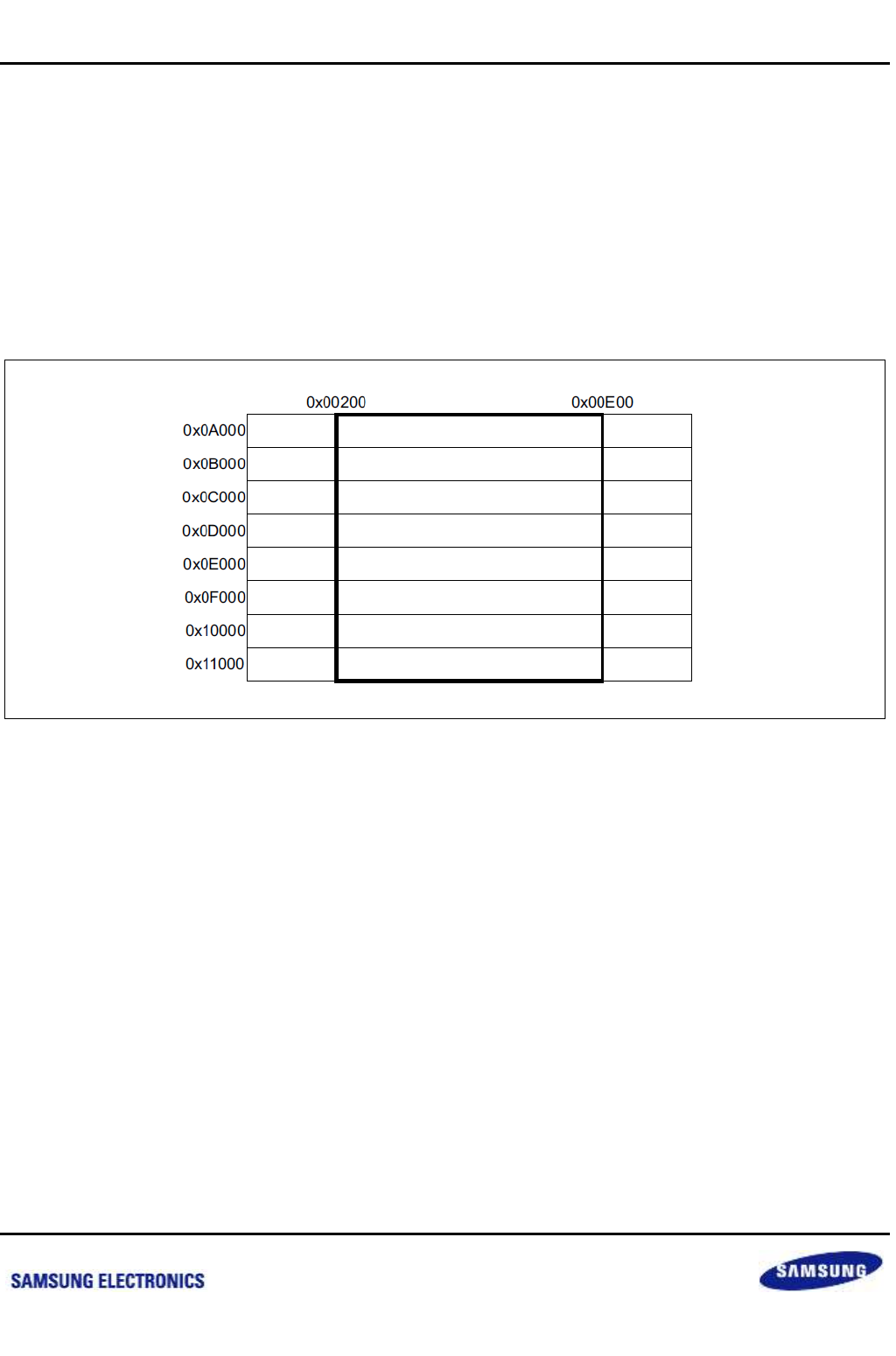
Samsung Confidential
S5P6818_UM 9 DMA
9-16
Preliminary product information describes products that are in development, for which full characterization data and
associated errata are not yet available. Specifications and information herein are subject to change without notice.
Scatter/Gather through Linked List Operation
A series of linked lists define the source and destination data areas. Each LLI controls the transfer of one block of
data, and then optionally loads another LLI to continue the DMA operation, or stops the DMA stream. The first LLI
is programmed into the DMAC.
The data to be transferred described by an LLI, referred to as the packet of data, usually requires one or more
DMA bursts, to each of the source and destination.
The figure below shows an example of an LLI. A rectangle of memory must be transferred to a peripheral. The
addresses of each line of data are given, in hexadecimal, at the left-hand side of the figure. The LLIs describing
the transfer are to be stored contiguously from address 0x20000.
Figure 9-2 LLI Example
The first LLI, stored at 0x20000, defines the first block of data to be transferred. This is the data stored between
addresses 0x0A200 and 0x0AE00:
Source start address 0x0A200
Destination address set to the destination peripheral address
Transfer width, word, 32-bit
Transfer size, 3072 bytes, 0xC00
Source and destination burst sizes, 16 transfers
Next LLI address, 0x20010
nexell / ys.kim at 2015.02.12
SAMSUNG Confidential

Samsung Confidential
S5P6818_UM 9 DMA
9-17
Preliminary product information describes products that are in development, for which full characterization data and
associated errata are not yet available. Specifications and information herein are subject to change without notice.
The second LLI, stored at 0x20010, defines the next block of data to be transferred:
Source start address 0x0B200
Destination address set to the destination peripheral address
Transfer width, word, 32-bit
Transfer size, 3072 bytes, 0xC00
Source and destination burst sizes, 16 transfers
Next LLI address, 0x20020
A chain of descriptors is built up, each one pointing to the next in the series. To initialize the DMA stream, the first
LLI, 0x20000, is programmed into the DMAC. When the first packet of data has been transferred, the next LLI is
automatically loaded.
The final LLI is stored at 0x20070 and contains:
Source start address 0x11200
Destination address set to the destination peripheral address
Transfer width, word, 32-bit
Transfer size, 3072 bytes, 0xC00
Source and destination burst sizes, 16 transfers
Next LLI address, 0x0
Because the next LLI address is set to zero, this is the last descriptor, and the DMA channel is disabled after
transferring the last item of data. The channel is probably set to generate an interrupt at this point to indicate to the
ARM processor that the channel can be reprogrammed.
nexell / ys.kim at 2015.02.12
SAMSUNG Confidential

Samsung Confidential
S5P6818_UM 9 DMA
9-18
Preliminary product information describes products that are in development, for which full characterization data and
associated errata are not yet available. Specifications and information herein are subject to change without notice.
9.4.2.7 Interrupt Requests
Interrupt requests can be generated when an AHB error is encountered, or at the end of a transfer, terminal count,
after all the data corresponding to the current LLI has been transferred to the destination. The interrupts can be
masked by programming the relevant bits on the relevant DMACCxCONTROL and DMACCxCONFIGURATION
Channel Registers.
Interrupt Status Registers are provided. They group the interrupt requests from all the DMA channels prior to
interrupt masking, DMACRAWINTTCSTATUS, DMACRAWINTERRORSTATUS, and after interrupt masking,
DMACINTTCSTATUS, DMACINTERRORSTATUS.
The DMACINTSTATUS Register combines both the DMACINTTCSTATUS and DMACINTERRORSTATUS
requests into a single register to enable the source of an interrupt to be found quickly. Writing to the
DMACINTTCCLEAR or the DMACINTERRCLR Registers with a bit set HIGH enables selective clearing of
interrupts.
The DMAC provides two interrupt request connection schemes. See Interrupt controller connectivity. The simplest
connection scheme has a combined error and end of transfer complete interrupt request. To find the source of an
interrupt, you must read both the DMACINTSTATUS and DMACINTTCSTATUS Registers.
For faster interrupt response, you can use an alternate connection scheme. This scheme uses separate interrupt
requests for the error and transfer complete requests. Read either the DMACINTTCSTATUS or
DMACINTERRORSTATUS Registers to find the source of an interrupt.
Combined Terminal Count and Error Interrupt Sequence Flow
When you use the *DMACINTR *interrupt request:
1. You must wait until the combined interrupt request from the DMAC goes active. Assuming the interrupt is
enabled in the interrupt controller and in the processor, the processor branches to the interrupt vector address
and enters the interrupt service routine.
2. You must read the interrupt controller Status Register and determine whether the source of the request was
the DMAC.
3. You must read the DMACINTSTATUS Register to determine the channel that generated the interrupt. If more
than one request is active, it is recommended that you check the highest priority channels first.
4. You must read the DMACINTTCSTATUS Register to determine whether the interrupt was generated because
of the end of the transfer, terminal count, or because an error occurred. A HIGH bit indicates that the transfer
completed.
5. You must read the DMACINTERRORSTATUS Register to determine whether the interrupt was generated
because of the end of the transfer, terminal count, or because an error occurred. A HIGH bit indicates that an
error occurred.
6. You must write a 1 to the relevant bit in the DMACINTTCCLEAR, or DMACINTERRCLR, Register to clear the
interrupt request.
nexell / ys.kim at 2015.02.12
SAMSUNG Confidential

Samsung Confidential
S5P6818_UM 9 DMA
9-19
Preliminary product information describes products that are in development, for which full characterization data and
associated errata are not yet available. Specifications and information herein are subject to change without notice.
Terminal Count Interrupts Sequence Flow
When the separate, DMACINTTC and DMACINTERR, interrupt requests are used:
1. You must wait until the terminal count DMA interrupt request goes active. Assuming the interrupt is enabled in
the interrupt controller and in the processor, the processor branches to the interrupt vector address and enters
the interrupt service routine.
2. You must read the interrupt controller Status Register to determine if the source of the interrupt request was
the DMAC asserting the DMACINTTC signal.
3. You must read the DMACINTTCSTATUS Register to determine the channel that generated the interrupt. If
more than one request is active, it is recommended that you service the highest priority channel first.
4. You must service the interrupt request.
5. You must write a 1 to the relevant bit in the DMACINTTCCLEAR Register to clear the interrupt request.
Error Interrupt Sequence Flow
When the separate interrupt requests, DMACINTTC and DMACINTERR, are used:
1. You must wait until the interrupt request goes active because of a DMA channel error. Assuming the interrupt
is enabled in the interrupt controller and in the processor, the processor branches to the interrupt vector
address and enters the interrupt service routine.
2. You must read the Interrupt Controllers Status Register to determine if the source of the request was the
DMAC asserting the DMACINTERR signal.
3. You must read the DMACINTERRORSTATUS Register to determine the channel that generated the interrupt.
If more than one request is active it is recommended that you check the highest priority channels first.
4. You must service the interrupt request.
5. You must write a 1 to the relevant bit in the DMACINTERRCLR Register to clear the interrupt request.
Interrupt Polling Sequence Flow
The DMAC interrupt request signal is masked out, disabled in the interrupt controller, or disabled in the processor.
When polling the DMAC, you must:
1. Read the DMACINTSTATUS Register. If none of the bits are HIGH repeat this step, otherwise, go to step 2. If
more than one request is active, it is recommended that you check the highest priority channels first.
2. Read the DMACINTTCSTATUS Register to determine if the interrupt was generated because of the end of
the transfer, terminal count, or because of error occurred. A HIGH bit indicates that the transfer completed.
3. Service the interrupt request.
4. For an error interrupt, write a 1 to the relevant bit of the DMACINTERRCLR Register to clear the interrupt
request. For a terminal count interrupt, write a 1 to the relevant bit of the DMACINTTCCLR Register.
nexell / ys.kim at 2015.02.12
SAMSUNG Confidential

Samsung Confidential
S5P6818_UM 9 DMA
9-20
Preliminary product information describes products that are in development, for which full characterization data and
associated errata are not yet available. Specifications and information herein are subject to change without notice.
9.4.2.8 DMAC Data Flow
Memory-to-memory DMA flow
For a memory-to-memory DMA flow:
1. Program and enable the DMA channel.
2. Transfer data whenever the DMA channel has the highest pending priority and the DMAC gains bus master
ship of the AHB bus.
3. If an error occurs while transferring the data, generate an error interrupt and disable the DMA stream.
4. Decrement the transfer count.
5. If the count has reached zero:
Generate a terminal count interrupt. You can mask the interrupt.
If the DMACCxLLI Register is not 0, then reload the following registers and go to back to step 2:
o DMACCxSRCADDR
o DMACCxDESTADDR
o DMACCxLLI
o DMACCxCONTROL
o However, if DMACCxLLI is 0, the DMA stream is disabled and the flow sequence ends.
Memory-to-peripheral or Peripheral-to-memory DMA Flow
For a peripheral-to-memory or memory-to-peripheral DMA flow:
1. Program and enable the DMA channel.
2. Wait for a DMA request.
3. The DMAC then starts transferring data when:
The DMA request goes active.
The DMA stream has the highest pending priority.
The DMAC is the bus master of the AHB bus.
4. If an error occurs while transferring the data, an error interrupt is generated and the DMA stream is disabled,
and the flow sequence ends.
5. Decrement the transfer count if the DMAC is controlling the flow control.
nexell / ys.kim at 2015.02.12
SAMSUNG Confidential

Samsung Confidential
S5P6818_UM 9 DMA
9-21
Preliminary product information describes products that are in development, for which full characterization data and
associated errata are not yet available. Specifications and information herein are subject to change without notice.
6. If the transfer has completed, indicated by the transfer count reaching 0 if the DMAC is performing flow
control, or by the peripheral setting the DMACLBREQ or DMACLSREQ signals if the peripheral is performing
flow control:
The DMAC asserts the DMACTC signal.
The terminal count interrupt is generated. You can mask this interrupt.
If the DMACCxLLI Register is not 0, then reload the following registers and go to back to step 2:
o DMACCxSRCADDR
o DMACCxDESTADDR
o DMACCxLLI
o DMACCxCONTROL
o However, if DMACCxLLI is 0, the DMA stream is disabled and the flow sequence ends.
Peripheral-to-peripheral DMA Flow
For a peripheral-to-peripheral DMA flow:
1. Program and enable the DMA channel.
2. Wait for a source DMA request.
3. The DMAC then starts transferring data when:
The DMA request goes active.
The DMA stream has the highest pending priority.
The DMAC is the bus master of the AHB bus.
4. If an error occurs while transferring the data, an error interrupt is generated, then finishes.
5. Decrement the transfer count if the DMAC is controlling the flow control.
6. If the transfer has completed, indicated by the transfer count reaching 0 if the DMAC is performing flow
control, or by the peripheral setting the DMACLBREQ or DMACLSREQ signals if the peripheral is performing
flow control:
The DMAC asserts the DMACTC signal to the source peripheral.
Subsequent source DMA requests are ignored.
7. When the destination DMA request goes active and there is data in the DMACFIFO, transfer data into the
destination peripheral.
8. If an error occurs while transferring the data, an error interrupt is generated and the DMA stream is disabled,
and the flow sequence ends.
nexell / ys.kim at 2015.02.12
SAMSUNG Confidential

Samsung Confidential
S5P6818_UM 9 DMA
9-22
Preliminary product information describes products that are in development, for which full characterization data and
associated errata are not yet available. Specifications and information herein are subject to change without notice.
9. If the transfer has completed, it is indicated by the transfer count reaching 0 if the DMAC is performing flow
control, or by the peripheral setting the DMACLBREQ or DMACLSREQ signals if the peripheral is performing
flow control. The following happens:
The DMAC asserts the DMACTC signal to the destination peripheral.
The terminal count interrupt is generated. You can mask this interrupt.
If the DMACCxLLI Register is not 0, then reload the following registers and go to back to step 2:
o DMACCxSRCADDR
o DMACCxDESTADDR
o DMACCxLLI
o DMACCxCONTROL
o However, if DMACCxLLI is 0, the DMA stream is disabled and the flow sequence ends.
nexell / ys.kim at 2015.02.12
SAMSUNG Confidential

Samsung Confidential
S5P6818_UM 9 DMA
9-23
Preliminary product information describes products that are in development, for which full characterization data and
associated errata are not yet available. Specifications and information herein are subject to change without notice.
9.5 Register Description
9.5.1 Register Map Summary
This section describes the DMAC0/1 registers.
Base Address: 0xC000_0000
Base Address: 0xC000_1000
Resister
Offset
Description
Reset Value
Interrupt Status Register
0x00
The read-only DMACINTSTATUS Register, with address
offset of 0x000, shows the status of the interrupts after
masking. A HIGH bit indicates that a specific DMA channel
interrupt request is active. You can generate the request
from either the error or terminal count interrupt requests.
0x0000_0000
Interrupt Terminal Count
Status Register
0x04
The read-only DMACINTTCSTATUS Register, with
address offset of 0x004, indicates the status of the terminal
count after masking. You must use this register in
conjunction with the DMACINTSTATUS Register if you use
the combined interrupt request, DMACINTR, to request
interrupts. If you use the DMACINTTC interrupt request,
then you only have to read the DMACINTTCSTATUS
Register to ascertain the source of the interrupt request.
0x0000_0000
Interrupt Terminal Count
Clear Register
0x08
The write-only DMACINTTCCLEAR Register, with address
offset of 0x008, clears a terminal count interrupt request.
When writing to this register, each data bit that is set HIGH
causes the corresponding bit in the Status Register to be
cleared. Data bits that are LOW have no effect on the
corresponding bit in the register.
0x0000_0000
Interrupt Error Status
Register
0x0C
The read-only DMACINTERRORSTATUS Register, with
address offset of 0x00C, indicates the status of the error
request after masking. You must use this register in
conjunction with the DMACINTSTATUS Register if you use
the combined interrupt request, DMACINTR, to request
interrupts. If you use the DMACINTERR interrupt request,
then only read the DMACINTERRORSTATUS Register.
0x0000_0000
Interrupt Error Clear
Register
0x10
The write-only DMACINTERRCLR Register, with address
offset of 0x010, clears the error interrupt requests. When
writing to this register, each data bit that is HIGH causes
the corresponding bit in the Status Register to be cleared.
Data bits that are LOW have no effect on the
corresponding bit in the register.
0x0000_0000
Raw Interrupt Terminal
Count Status Register
0x14
The read-only DMACRAWINTTCSTATUS Register, with
address offset of 0x014, indicates the DMA channels that
are requesting a transfer complete, terminal count interrupt,
and prior to masking. A HIGH bit indicates that the terminal
count interrupt request is active prior to masking.
0x0000_0000
Raw Error Interrupt Status
Register
0x18
The read-only DMACRAWINTERRORSTATUS Register,
with address offset of 0x018, indicates the DMA channels
that are requesting an error interrupt prior to masking. A
0x0000_0000
nexell / ys.kim at 2015.02.12
SAMSUNG Confidential

Samsung Confidential
S5P6818_UM 9 DMA
9-24
Preliminary product information describes products that are in development, for which full characterization data and
associated errata are not yet available. Specifications and information herein are subject to change without notice.
Resister
Offset
Description
Reset Value
HIGH bit indicates that the error interrupt request is active
prior to masking.
Enabled Channel Register
0x1C
The read-only DMACENBLDCHNS Register, with address
offset of 0x01C, indicates the DMA channels that are
enabled, as indicated by the Enable bit in the
DMACCxCONFIGURATION Register. A HIGH bit indicates
that a DMA channel is enabled. A bit is cleared on
completion of the DMA transfer.
0x0000_0000
Software Burst Request
Register.
0x20
The read/write DMACSOFTBREQ Register, with address
offset of 0x020, enables DMA burst requests to be
generated by software. You can generate a DMA request
for each source by writing a 1 to the corresponding register
bit. A register bit is cleared when the transaction has
completed. Writing 0 to this register has no effect. Reading
the register indicates the sources that are requesting DMA
burst transfers. You can generate a request from either a
peripheral or the software request register.
0x0000_0000
Software Single Request
Register.
0x24
The read/write DMACSOFTSREQ Register, with address
offset of 0x024, enables DMA single requests to be
generated by software. You can generate a DMA request
for each source by writing a 1 to the corresponding register
bit. A register bit is cleared when the transaction has
completed. Writing 0 to this register has no effect. Reading
the register indicates the sources that are requesting single
DMA transfers. You can generate a request from either a
peripheral or the software request register.
0x0000_0000
Software Last Burst Request
Register
0x28
The read/write DMACSOFTLBREQ Register, with address
offset of 0x028, enables software to generate DMA last
burst requests. You can generate a DMA request for each
source by writing a 1 to the corresponding register bit. A
register bit is cleared when the transaction has completed.
Writing 0 to this register has no effect. Reading the register
indicates the sources that are requesting last burst DMA
transfers. You can generate a request from either a
peripheral or the software request register.
0x0000_0000
Software Last Single
Request Register
0x2C
The read/write DMACSOFTLSREQ Register, with address
offset of 0x02C, enables software to generate DMA last
single requests. You can generate a DMA request for each
source by writing a 1 to the corresponding register bit. A
register bit is cleared when the transaction has completed.
Writing 0 to this register has no effect. Reading the register
indicates the sources that are requesting last single DMA
transfers. You can generate a request from either a
peripheral or the software request register.
0x0000_0000
Configuration Register
0x30
The read/write DMACCONFIGURATION Register, with
address offset of 0x030, configures the operation of the
DMAC. You can alter the endianness of the individual AHB
master interfaces by writing to the M1 and M2 bits of this
register. The M1 bit enables you to alter the endianness of
0x0000_0000
nexell / ys.kim at 2015.02.12
SAMSUNG Confidential

Samsung Confidential
S5P6818_UM 9 DMA
9-25
Preliminary product information describes products that are in development, for which full characterization data and
associated errata are not yet available. Specifications and information herein are subject to change without notice.
Resister
Offset
Description
Reset Value
AHB master interface 1. The M2 bit enables you to alter the
endianness of AHB master interface 2. The AHB master
interfaces are set to little-endian mode on reset.
Synchronization Register
0x34
The read/write DMACSYNC Register, with address offset
of 0x034, enables or disables synchronization logic for the
DMA request signals.
The DMA request signals consist of:
DMACBREQ[15:0]
DMACSREQ[15:0]
DMACLBREQ[15:0]
DMACLSREQ[15:0]
A bit set to 0 enables the synchronization logic for a
particular group of DMA requests.
A bit set to 1 disables the synchronization logic for a
particular group of DMA requests.
This register is reset to 0, and synchronization logic
enabled.
NOTE:
1. It is illegal for a peripheral to give a new DMACSREQ or
DMACBREQ signal while DMACCLR is HIGH.
2. You must use synchronization logic when the peripheral
generating the DMA request runs on a different clock to the
DMAC. For peripherals running on the same clock as the
DMAC, disabling the synchronization logic improves the
DMA request response time. If necessary, synchronize the
DMA response signals, DMACCLR and DMACTC, in the
peripheral.
0x0000_0000
Channel Registers
The channel registers are for programming a DMA channel. These registers consist of:
Eight DMACCxSRCADDR registers
Eight DMACCxDESTADDR registers
Eight DMACCxLLI registers
Eight DMACCxCONTROL registers
Eight DMACCxCONFIGURATION registers.
When performing scatter/gather DMA, the first four registers are automatically updated.
NOTE: Unpredictable behavior can result if you update the channel registers when a transfer is taking place. If you want to
change the channel configurations, you must disable the channel first and then reconfigure the relevant register.
CHANNEL SOURCE
ADDRESS REGISTERS
0x100
The eight read/write DMACCxSRCADDR Registers, with
address offsets of 0x100, 0x120, 0x140, 0x160, 0x180,
0x1A0, 0x1C0, and 0x1E0 respectively, contain the current
source address, byte-aligned, of the data to be transferred.
Software programs each register directly before the
appropriate channel is enabled.
When the DMA channel is enabled, this register is updated:
As the source address is incremented
0x0000_0000
nexell / ys.kim at 2015.02.12
SAMSUNG Confidential

Samsung Confidential
S5P6818_UM 9 DMA
9-26
Preliminary product information describes products that are in development, for which full characterization data and
associated errata are not yet available. Specifications and information herein are subject to change without notice.
Resister
Offset
Description
Reset Value
By following the linked list when a complete packet of
data has been transferred.
Reading the register when the channel is active does not
provide useful information. This is because by the time the
software has processed the value read, the channel might
have progressed. It is intended to be read-only when the
channel has stopped, and in such case, it shows the
source address of the last item read.
NOTE: You must align source and destination addresses to
the source and destination widths.
CHANNEL DESTINATION
ADDRESS REGISTER
0x104
Channel Destination Address Registers.
The eight read/write DMACCxDESTADDR Registers, with
address offsets of 0x104, 0x124, 0x144, 0x164, 0x184,
0x1A4, 0x1C4, and 0x1E4 respectively, contain the current
destination address, byte-aligned, of the data to be
transferred.
Software programs each register directly before the
channel is enabled. When the DMA channel is enabled, the
register is updated as the destination address is
incremented and by following the linked list when a
complete packet of data has been transferred. Reading the
register when the channel is active does not provide useful
information. This is because by the time the software has
processed the value read, the channel might have
progressed. It is intended to be read-only when a channel
has stopped. In this case, it shows the destination address
of the last item read.
0x0000_0000
CHANNEL LINKED LIST
ITEM REGISTERS
0x108
Channel Linked List Item Register.
The eight read/write DMACCxLLI Registers, with address
offsets of 0x108, 0x128, 0x148, 0x168, 0x188, 0x1A8,
0x1C8, and 0x1E8 respectively, contain a word-aligned
address of the next LLI. If the LLI is 0, then the current LLI
is the last in the chain, and the DMA channel is disabled
after all DMA transfers associated with it are completed.
NOTE:
1. Programming this register when the DMA channel is
enabled has unpredictable results.
2. To make loading the LLIs more efficient for some
systems, you can make the LLI data structures 4-word
aligned.
0x0000_0000
CHANNEL CONTROL
REGISTERS
0x10C
Refer to below description.
0x0000_0000
nexell / ys.kim at 2015.02.12
SAMSUNG Confidential
Samsung Confidential
S5P6818_UM 9 DMA
9-27
Preliminary product information describes products that are in development, for which full characterization data and
associated errata are not yet available. Specifications and information herein are subject to change without notice.
Resister
Offset
Description
Reset Value
Channel Control Registers
The eight read/write DMACCxCONTROL registers, with address offsets of 0x010c, 0x12c, 0x14c, 0x16c, 0x18c, 0x1ac,
0x1cc, and 0x1ec respectively, contain DMA channel control information such as the transfer size, burst size, and transfer
width. Software programs each register directly before the DMA channel is enabled.
When the channel is enabled, the register is updated by following the linked list when a complete packet of data has been
transferred. Reading the register while the channel is active does not give useful information. This is because by the time
that software has processed the value read, the channel might have progressed. It is intended to be read-only when a
channel has stopped.
Below table lists the values of the DBSIZE or SBSIZE bits and their corresponding burst sizes.
Below table source or destination burst size
Bit value of DBSIZE or SBSIZE
Source or Destination Burst Transfer Request Size
3’b000
1
3’b001
4
3’b010
8
3’b011
16
3’b100
32
3’b101
64
3’b110
128
3’b111
256
Below table lists the value of the SWIDTH or DWIDTH bits and their corresponding widths.
Below table lists the value of the SWIDTH or DWIDTH bits and their corresponding widths.
Bit value of SWIDTH or DWIDTH
Source or destination width
3’b000
Byte, 8-bit
3’b001
Half word, 16-bit
3’b010
Word, 32-bit
3’b011
Reserved
3’b100
Reserved
3’b101
Reserved
3’b110
Reserved
3’b111
Reserved
Protection And Access Information
AHB access information is provided to the source and destination peripherals when a transfer occurs. The transfer
information is provided by programming the DMA channel, the Prot bit of the DMACCxCONTROL register, and the lock bit
of the DMACCxCONFIGURATION register. Software programs these bits, and peripherals can use this information if
necessary. Three bits of information are provided. Below table lists the purposes of the three protection bits.
nexell / ys.kim at 2015.02.12
SAMSUNG Confidential
Samsung Confidential
S5P6818_UM 9 DMA
9-28
Preliminary product information describes products that are in development, for which full characterization data and
associated errata are not yet available. Specifications and information herein are subject to change without notice.
Resister
Offset
Description
Reset Value
Below table protection bits
Bits
Description
Purpose
[0]
PRIVILEGED OR
USER
Indicates whether the access is in user, or privileged mode:
0 = User mode
1 = Privileged mode.
This bit controls the AHB HPROT[1] signal.
[1]
BUFFERABLE OR
NON-BUFFERABLE
Indicates whether or not the access can be buffered:
0 = Non-bufferable
1 = Bufferable.
This bit indicates whether or not the access is bufferable. For example, you can use
this bit to indicate to an AMBA bridge that the read can complete in zero wait states on
the source bus without waiting for it to arbitrate for the destination bus and for the slave
to accept the data. This bit controls the AHB HPROT[2] signal.
[2]
CACHEABLE OR
NON-CACHEABLE
Indicates whether or not the access can be cached:
0 = Non-cacheable
1 = Cacheable.
This bit indicates whether or not the access is cacheable. For example, you can use
this bit to indicate to an AMBA bridge that when it saw the first read of a burst of eight it
can transfer the whole burst of eight reads on the destination bus, rather than pass the
transactions through one at a time. This bit controls the AHB HPROT[3] signal.
Channel Configuration Registers
The eight DMACCxCONFIGURATION Registers, with address offsets of 0x110, 0x130, 0x150, 0x170, 0x190, 0x1B0,
0x1D0, and 0x1F0 respectively, are read/write and configure the DMA channel. The registers are not updated when a new
LLI is requested.
Below Table lists the bit values of the three flow control and transfer type bits.
Below Table Flow control and transfer type bits
Bit Value
Transfer type
Controller
3’b000
Memory-to-memory
DMA
3’b001
Memory-to-peripheral
DMA
3’b010
Peripheral-to-memory
DMA
3’b011
Source peripheral-to-destination peripheral
DMA
3’b100
Source peripheral-to-destination peripheral
Destination peripheral
3’b101
Memory-to-peripheral
Peripheral
3’b110
Peripheral-to-memory
Peripheral
3’b111
Source peripheral-to-destination peripheral
Source peripheral
nexell / ys.kim at 2015.02.12
SAMSUNG Confidential
Samsung Confidential
S5P6818_UM 9 DMA
9-29
Preliminary product information describes products that are in development, for which full characterization data and
associated errata are not yet available. Specifications and information herein are subject to change without notice.
9.5.1.1 Interrupt Status Register
Base Address: 0xC000_0000
Base Address: 0xC000_1000
Address = Base Address + 0x00, Reset Value = 0x0000_0000
Name
Bit
Type
Description
Reset Value
SESREQSCS
[31:8]
R
Read undefined
24’h0
INTSTATUS
[7:0]
R
Status of the DMA interrupts after masking
8’h0
9.5.1.2 Interrupt Terminal Count Status Register
Base Address: 0xC000_0000
Base Address: 0xC000_1000
Address = Base Address + 0x04, Reset Value = 0x0000_0000
Name
Bit
Type
Description
Reset Value
RSVD
[31:8]
R
Read undefined
24’h0
INTTCSTATUS
[7:0]
R
Interrupt terminal count request status
8’h0
9.5.1.3 Interrupt Terminal Count Clear Register
Base Address: 0xC000_0000
Base Address: 0xC000_1000
Address = Base Address + 0x08, Reset Value = x0000_0000
Name
Bit
Type
Description
Reset Value
RSVD
[31:8]
W
Undefined. Write as zero.
24’h0
INTTCCLEAR
[7:0]
W
Terminal count request clear.
8’h0
9.5.1.4 Interrupt Error Status Register
Base Address: 0xC000_0000
Base Address: 0xC000_1000
Address = Base Address + 0xC, Reset Value = 0x0000_0000
Name
Bit
Type
Description
Reset Value
RSVD
[31:8]
R
Read undefined
24’h0
INTERRORSTATUS
[7:0]
R
Interrupt error status
8’h0
nexell / ys.kim at 2015.02.12
SAMSUNG Confidential
Samsung Confidential
S5P6818_UM 9 DMA
9-30
Preliminary product information describes products that are in development, for which full characterization data and
associated errata are not yet available. Specifications and information herein are subject to change without notice.
9.5.1.5 Interrupt Error Clear Register
Base Address: 0xC000_0000
Base Address: 0xC000_1000
Address = Base Address + 0x10, Reset Value = 0x0000_0000
Name
Bit
Type
Description
Reset Value
RSVD
[31:8]
W
Undefined. Write as zero.
24’h0
INTERRCLR
[7:0]
W
Interrupt error clear.
8’h0
9.5.1.6 Raw Interrupt Terminal Count Status Register
Base Address: 0xC000_0000
Base Address: 0xC000_1000
Address = Base Address + 0x14, Reset Value = 0x0000_0000
Name
Bit
Type
Description
Reset Value
RSVD
[31:8]
R
Read undefined
24’h0
RAWINTTCSTATUS
[7:0]
R
Status of the terminal count interrupt prior to
masking
8’h0
9.5.1.7 Raw Error Interrupt Status Register
Base Address: 0xC000_0000
Base Address: 0xC000_1000
Address = Base Address + 0x18, Reset Value = 0x0000_0000
Name
Bit
Type
Description
Reset Value
RSVD
[31:8]
R
Read undefined
24’h0
RAWINTERRORSTATUS
[7:0]
R
Status of the error interrupt prior to masking
8’h0
9.5.1.8 Enabled Channel Register
Base Address: 0xC000_0000
Base Address: 0xC000_1000
Address = Base Address + 0x1C, Reset Value = 0x0000_0000
Name
Bit
Type
Description
Reset Value
RSVD
[31:8]
R
Read undefined
24’h0
ENABLEDCHANNELS
[7:0]
R
Channel enable status
8’h0
nexell / ys.kim at 2015.02.12
SAMSUNG Confidential
Samsung Confidential
S5P6818_UM 9 DMA
9-31
Preliminary product information describes products that are in development, for which full characterization data and
associated errata are not yet available. Specifications and information herein are subject to change without notice.
9.5.1.9 Software Burst Request Register
Base Address: 0xC000_0000
Base Address: 0xC000_1000
Address = Base Address + 0x20, Reset Value = 0x0000_0000
Name
Bit
Type
Description
Reset Value
RSVD
[31:16]
RW
Read undefined. Write as zero.
16’h0
SOFTBREQ
[15:0]
RW
Software burst request.
16’h0
9.5.1.10 Software Single Request Register
Base Address: 0xC000_0000
Base Address: 0xC000_1000
Address = Base Address + 0x24, Reset Value = 0x0000_0000
Name
Bit
Type
Description
Reset Value
RSVD
[31:16]
RW
Read undefined. Write as zero.
16’h0
SOFTSREQ
[15:0]
RW
Software single request.
16’h0
9.5.1.11 Software Last Burst Request Register
Base Address: 0xC000_0000
Base Address: 0xC000_1000
Address = Base Address + 0x28, Reset Value = 0x0000_0000
Name
Bit
Type
Description
Reset Value
RSVD
[31:16]
RW
Read undefined. Write as zero.
16’h0
SOFTLBREQ
[15:0]
RW
Software last burst request.
16’h0
9.5.1.12 Software Last Single Request Register
Base Address: 0xC000_0000
Base Address: 0xC000_1000
Address = Base Address + 0x2C, Reset Value = 0x0000_0000
Name
Bit
Type
Description
Reset Value
RSVD
[31:16]
RW
Read undefined. Write as zero.
16’h0
SOFTLSREQ
[15:0]
RW
Software last single request.
16’h0
nexell / ys.kim at 2015.02.12
SAMSUNG Confidential
Samsung Confidential
S5P6818_UM 9 DMA
9-32
Preliminary product information describes products that are in development, for which full characterization data and
associated errata are not yet available. Specifications and information herein are subject to change without notice.
9.5.1.13 Configuration Register
Base Address: 0xC000_0000
Base Address: 0xC000_1000
Address = Base Address + 0x30, Reset Value = 0x0000_0000
Name
Bit
Type
Description
Reset Value
RSVD
[31:3]
RW
Read undefined. Write as zero.
–
M2
[2]
RW
AHB Master 2 endianness configuration:
0 = Little-endian mode
1 = Big-endian mode
This bit is reset to 0.
1'b0
M1
[1]
RW
AHB Master 1 endianness configuration:
0 = Little-endian mode
1 = Big-endian mode
This bit is reset to 0.
1'b0
E
[0]
RW
DMAC enable:
0 = Disabled
1 = Enabled
This bit is reset to 0. Disabling the DMAC reduces power
consumption.
1'b0
9.5.1.14 Synchronization Register
Base Address: 0xC000_0000
Base Address: 0xC000_1000
Address = Base Address + 0x34, Reset Value = 0x0000_0000
Name
Bit
Type
Description
Reset Value
RSVD
[31:16]
RW
Read undefined. Write as zero.
–
DMACSYNC
[15:0]
RW
DMA synchronization logic for DMA request signals
enabled or disabled.
A LOW bit indicates that the synchronization logic for the
request signals is enabled. A HIGH bit indicates that the
synchronization logic is disabled.
16’h0
nexell / ys.kim at 2015.02.12
SAMSUNG Confidential
Samsung Confidential
S5P6818_UM 9 DMA
9-33
Preliminary product information describes products that are in development, for which full characterization data and
associated errata are not yet available. Specifications and information herein are subject to change without notice.
9.5.1.15 Channel Source Address Registers (0 to 7)
Base Address: 0xC000_0000
Base Address: 0xC000_1000
Address = Base Address + 0x100, 0x120, 0x140, 0x160, 0x180, 0x1A0, 0x1C0, 0x1E0, Reset Value =
0x0000_0000
Name
Bit
Type
Description
Reset Value
SRCADDR
[31:0]
RW
DMA source address
32’h0
9.5.1.16 Channel Destination Address Registers (0 to 7)
Base Address: 0xC000_0000
Base Address: 0xC000_1000
Address = Base Address + 0x104, 0x124, 0x144, 0x164, 0x184, 0x1A4, 0x1C4, 0x1E4, Reset Value =
0x0000_0000
Name
Bit
Type
Description
Reset Value
DESTADDR
[31:0]
RW
DMA destination address
32’h0
9.5.1.17 Channel Linked List Item Registers (0 to 7)
Base Address: 0xC000_0000
Base Address: 0xC000_1000
Address = Base Address + 0x108, 0x128, 0x148, 0x168, 0x188, 0x1A8, 0x1C8, 0x1E8, Reset Value =
0x0000_0000
Name
Bit
Type
Description
Reset Value
LLI
[31:2]
–
Linked list item. Bits [31:2] of the address for the next LLI.
Address bits [1:0] are 0.
30’h0
RSVD
[1]
RW
Read undefined. Write as zero.
1'b0
LM
[0]
–
AHB master select for loading the next LLI
0 = AHB Master 1
1 = AHB Master 2.
1'b0
nexell / ys.kim at 2015.02.12
SAMSUNG Confidential

Samsung Confidential
S5P6818_UM 9 DMA
9-34
Preliminary product information describes products that are in development, for which full characterization data and
associated errata are not yet available. Specifications and information herein are subject to change without notice.
9.5.1.18 Channel Control Registers (0 to 7)
Base Address: 0xC000_0000
Base Address: 0xC000_1000
Address = Base Address + 0x10C, 0x12C, 0x14C, 0x16C, 0x18C, 0x1AC, 0x1CC, 0x1EC, Reset Value =
0x0000_0000
Name
Bit
Type
Description
Reset Value
I
[31]
R
"Terminal count" interrupt enable bit. It controls whether
the current LLI is expected to trigger the terminal count
interrupt.
1'b0
PROT
[30:28]
RW
Protection.
3'b0
DI
[27]
R
Destination increment. When set, the destination address
is incremented after each transfer.
1'b0
SI
[26]
R
Source increment. When set, the source address is
incremented after each transfer.
1'b0
D
[25]
RW
Destination AHB master select:
0 = AHB master 1 selected for the destination transfer
1 = AHB master 2 selected for the destination transfer.
1'b0
S
[24]
RW
Source AHB master select:
0 = AHB master 1 selected for the source transfer
1 = AHB master 2 selected for the source transfer.
1'b0
DWIDTH
[23:21]
RW
Destination transfer width. Transfers wider than the AHB
master bus width are illegal. The source and destination
widths can be different from each other. The hardware
automatically packs and unpacks the data when required.
3'b0
SWIDTH
[20:18]
RW
Source transfer width. Transfers wider than the AHB
master bus width are illegal. The source and destination
widths can be different from each other. The hardware
automatically packs and unpacks the data when required.
3'b0
DBSIZE
[17:15]
RW
Destination burst size. Indicates the number of transfers
that make up a destination burst transfer request. You
must set this value to the burst size of the destination
peripheral, or if the destination is memory, to the memory
boundary size. The burst size is the amount of data that is
transferred when the DMACxBREQ signal goes active in
the destination peripheral. The burst size is not related to
the AHB HBURST signal.
3'b0
SBSIZE
[14:12]
RW
Source burst size. Indicates the number of transfers that
make up a source burst. You must set this value to the
burst size of the source peripheral, or if the source is
memory, to the memory boundary size. The burst size is
the amount of data that is transferred when the
DMACxBREQ signal goes active in the source peripheral.
The burst size is not related to the AHB HBURST signal.
3'b0
TRANSFERSIZE
[11:0]
RW
Transfer size. A write to this field sets the size of the
transfer when the DMAC is the flow controller. This value
counts down from the original value to zero, and so its
11'h0
nexell / ys.kim at 2015.02.12
SAMSUNG Confidential

Samsung Confidential
S5P6818_UM 9 DMA
9-35
Preliminary product information describes products that are in development, for which full characterization data and
associated errata are not yet available. Specifications and information herein are subject to change without notice.
Name
Bit
Type
Description
Reset Value
value indicates the number of transfers left to complete. A
read from this field provides the number of transfers still
to be completed on the destination bus. Reading the
register when the channel is active does not give useful
information because by the time the software has
processed the value read, the channel might have
progressed. Only use it when a channel is enabled, and
then disabled.
Program the transfer size value to zero if the DMAC is not
the flow controller. If you program the Transfer Size to a
non-zero value, the DMAC might attempt to use this value
instead of ignoring the Transfer Size.
9.5.1.19 Channel Configuration Registers (0 to 7)
Base Address: 0xC000_0000
Base Address: 0xC000_1000
Address = Base Address + 0x110, 0x130, 0x150, 0x170, 0x190, 0x1B0, 0x1D0, 0x1F0, Reset Value =
0x0000_0000
Name
Bit
Type
Description
Reset Value
RSVD
[31:19]
–
Read undefined. Write as zero.
–
H
[18]
RW
Halt:
0 = Enable DMA requests
1 = Ignore extra source DMA requests.
The contents of the channels FIFO are drained.
You can use this value with the Active and Channel
Enable bits to cleanly disable a DMA channel.
1'b0
A
[17]
R
Active:
0 = There is no data in the FIFO of the channel
1 = The FIFO of the channel has data.
You can use this value with the Halt and Channel Enable
bits to cleanly disable a DMA channel.
1'b0
L
[16]
RW
Lock. When set, this bit enables locked transfers.
1'b0
ITC
[15]
RW
Terminal count interrupt mask. When cleared, this bit
masks out the terminal count interrupt of the relevant
channel.
1'b0
IE
[14]
RW
Interrupt error mask. When cleared, this bit masks out
the error interrupt of the relevant channel.
1'b0
FLOWCNTRL
[13:11]
RW
Flow control and transfer type. This value indicates the
flow controller and transfer type. The flow controller can
be the DMAC, the source peripheral, or the destination
peripheral. The transfer type can be memory-to-memory,
memory-to-peripheral, peripheral-to-memory, or
peripheral-to-peripheral.
3'b0
RSVD
[10]
–
Read undefined. Write as zero.
1'b0
nexell / ys.kim at 2015.02.12
SAMSUNG Confidential

Samsung Confidential
S5P6818_UM 9 DMA
9-36
Preliminary product information describes products that are in development, for which full characterization data and
associated errata are not yet available. Specifications and information herein are subject to change without notice.
Name
Bit
Type
Description
Reset Value
DESTPERIPHERAL
[9:6]
RW
Destination peripheral. This value selects the DMA
destination request
This field is ignored if the destination of the transfer is to
memory.
4'h0
RSVD
[5]
–
Read undefined. Write as zero.
–
SRCPERIPHERAL
[4:1]
RW
Source peripheral. This value selects the DMA source
request peripheral. This field is ignored if the source of
the transfer is from memory.
4'h0
E
[0]
RW
Channel enables. Reading this bit indicates whether a
channel is currently enabled or disabled:
0 = Channel disabled
1 = Channel enabled
You can also determine the Channel Enable bit status by
reading the DMACENBLDCHNS register.
You enable a channel by setting this bit.
You can disable a channel by clearing the Enable bit.
This causes the current AHB transfer, if one is in
progress, to complete, and the channel is then disabled.
Any data in the channel's FIFO is lost. Restarting the
channel by setting the Channel Enable bit has
unpredictable effects and you must fully re-initialize the
channel.
The channel is also disabled, and the Channel Enable
bit cleared, when the last LLI is reached, or if a channel
error is encountered.
If a channel has to be disabled without losing data in a
channel's FIFO, you must set the Halt bit so that
subsequent DMA requests are ignored. The Active bit
must then be polled until it reaches 0, indicating that
there is no data left in the channel's FIFO. Finally, you
can clear the Channel Enable bit.
1'b0
nexell / ys.kim at 2015.02.12
SAMSUNG Confidential

Samsung Confidential
S5P6818_UM 10 Interrupt Controller
10-1
Preliminary product information describes products that are in development, for which full characterization data and
associated errata are not yet available. Specifications and information herein are subject to change without notice.
10 Interrupt Controller
10.1 Overview
The GIC is a high-performance, area-optimized interrupt controller with an AXI interface. It detects, manages, and
distributes interrupts in S5P6818. The GIC is a centralized resource for supporting and managing interrupts in a
system.
10.2 Features
GIC provides registers for managing interrupt sources, interrupt behavior, and interrupt routing to one or more
processors.
Support for:
The ARM architecture Security Extension
The ARM architecture Virtualization Extension
Enabling, disabling, and generating processor interrupts from hardware (peripheral) interrupt sources
Software-generated Interrupts (SGIs)
Interrupt masking and prioritization
Uniprocessor and multiprocessor environments.
Wakeup events in power-management environments
The GIC includes interrupt grouping functionality that supports:
Configuring each interrupt as either Group 0 or Group 1
Signaling Group 0 interrupts to the target processor using either the IRQ or the FIQ exception request
Signaling Group 1 interrupts to the target processor using the IRQ exception request only
A unified scheme for handling the priority of Group 0 and Group 1 interrupts
Optional lockdown of the configuration of some Group 0 interrupts
nexell / ys.kim at 2015.02.12
SAMSUNG Confidential

Samsung Confidential
S5P6818_UM 10 Interrupt Controller
10-2
Preliminary product information describes products that are in development, for which full characterization data and
associated errata are not yet available. Specifications and information herein are subject to change without notice.
The GIC support for 4 interrupts types:
16 Software Generated Interrupt (SGIs)
6 external Private Peripheral Interrupt (PPIs) for each processor.
1 internal PPI for each processor
128 Shared Peripheral Interrupt (SPIs)
10.3 Security Extensions Support
In an implementation that includes the Security Extensions:
Group 0 interrupts are Secure interrupts, and Group 1 interrupts are Non-secure interrupts.
The behavior of processor accesses to registers in the GIC depends on whether the access is Secure or Non-
secure. Except where this document explicitly indicates otherwise, when accessing GIC registers:
A Non-secure read of a register field holding state information for a Secure interrupt returns zero
The GIC ignores any Non-secure write to a register field holding state information for a Secure interrupt.
Non-secure accesses can only read or write information corresponding to Non-secure interrupts.
Secure accesses can read or write information corresponding to both Non-secure and Secure interrupts.
Secure system software individually defines each implemented interrupt as either Secure or Non-secure.
A Non-secure interrupt signals an IRQ interrupt request to a target processor.
A Secure interrupt can signal either an IRQ or an FIQ interrupt request to a target processor.
Secure software can manage interrupt sources securely without the possibility of interference from Non-
secure software.
Secure systems are backwards-compatible with software written for systems without the Security Extensions.
nexell / ys.kim at 2015.02.12
SAMSUNG Confidential

Samsung Confidential
S5P6818_UM 10 Interrupt Controller
10-3
Preliminary product information describes products that are in development, for which full characterization data and
associated errata are not yet available. Specifications and information herein are subject to change without notice.
10.4 Virtualization Support
The processor Virtualization Extensions provide hardware support for virtualizing the Non-secure state of an
VMSAv7 implementation. The extensions support system use of a virtual machine monitor, known as the
hypervisor, to switch guest operating systems.
Whether implemented in a uniprocessor or in a multiprocessor system, the processor Virtualization Extension
support running multiple virtual machines on a single processor.
Interrupt handling is a major consideration in a virtualization implementation. The hypervisor can either handle a
physical interrupt itself, or generate a corresponding virtual interrupt that is signaled to a virtual machine. It is also
possible for the hypervisor to generate virtual interrupts that do not correspond to physical interrupts.
These extensions support the handling of virtual interrupts, in addition to physical interrupts, in a system that
supports processor virtualization. An example of such a system is one where a GIC is integrated with processors
that implement the ARM processor Virtualization Extensions. The GIC Virtualization Extensions provide
mechanisms to minimize the hypervisor overhead of routing interrupts to virtual machines.
10.5 Terminology
10.5.1 Interrupt States
The following states apply at the interface between the GIC and each processor supported in the system:
Inactive: An interrupt that is not active or pending.
Pending: An interrupt from a source to the GIC that is recognized as asserted in hardware, or generated by
software, and is waiting to be serviced by a target processor.
Active: An interrupt from a source to the GIC that has been acknowledged by a processor, and is being
serviced but has not completed.
Active and pending A processor is servicing the interrupt and the GIC has a pending interrupt from the
same source.
nexell / ys.kim at 2015.02.12
SAMSUNG Confidential

Samsung Confidential
S5P6818_UM 10 Interrupt Controller
10-4
Preliminary product information describes products that are in development, for which full characterization data and
associated errata are not yet available. Specifications and information herein are subject to change without notice.
10.5.2 Interrupt Type
A device that implements this GIC architecture can manage the following types of interrupt:
Peripheral Interrupt
This is an interrupt asserted by a signal to the GIC. The GIC architecture defines the following types of
peripheral interrupt:
Private Peripheral Interrupt (PPI): This is a peripheral interrupt that is specific to a single processor.
Shared Peripheral Interrupt (SPI): This is a peripheral interrupt that the Distributor can route to any of a
specified combination of processors.
Each peripheral interrupt is either:
Edge-triggered: This is an interrupt that is asserted on detection of a rising edge of an interrupt signal and
then, regardless of the state of the signal, remains asserted until it is cleared by the conditions defined by
this specification.
Level-sensitive: This is an interrupt that is asserted whenever the interrupt signal level is active, and
deasserted whenever the level is not active.
Software-Generated Interrupt (SGI)
This is an interrupt generated by software writing to a GICD_SGIR register in the GIC. The system uses SGIs
for inter processor communication.
An SGI has edge-triggered properties. The software triggering of the interrupt is equivalent to the edge
transition of the interrupt request signal.
When an SGI occurs in a multiprocessor implementation, the CPUID field in the Interrupt Acknowledge
Register, GICC_IAR, or the Aliased Interrupt Acknowledge Register, GICC_AIAR, identifies the processor that
requested the interrupt
In an implementation that includes the GIC Virtualization Extensions:
When an SGI occurs, management registers in the GIC virtualization Extensions enable the requesting
processor to be reported to the Guest OS, as required by the GIC specifications
By writing to the management registers in the GIC Virtualization Extensions, a hypervisor can generate a
virtual interrupt that appears to a virtual machine as an SGI.
Virtual Interrupt
In a GIC that implements the GIC Virtualization Extensions, an interrupt that targets a virtual machine running
on a processor, and is typically signaled to the processor by the connected virtual CPU interface.
Maintenance Interrupt
In a GIC that implements the GIC Virtualization Extensions, a level-sensitive interrupt that is used to signal
key events, such as a particular group of interrupts becoming enabled or disabled.
nexell / ys.kim at 2015.02.12
SAMSUNG Confidential

Samsung Confidential
S5P6818_UM 10 Interrupt Controller
10-5
Preliminary product information describes products that are in development, for which full characterization data and
associated errata are not yet available. Specifications and information herein are subject to change without notice.
10.5.3 Model for Handling Interrupt
In a multiprocessor implementation, there are two models for handling interrupts:
1-N model: Only one processor handles this interrupt. The system must implement a mechanism to
determine which processor handles an interrupt that is programmed to target more than one processor.
N-N model: All processors receive the interrupt independently. When a processor acknowledges the interrupt,
the interrupt pending state is cleared only for that processor. The interrupt remains pending for the other
processors.
10.5.4 Spurious Interrupts
It is possible that an interrupt that the GIC has signaled to a processor is no longer required. If this happens, when
the processor acknowledges the interrupt, the GIC returns a special interrupt ID that identifies the interrupt as a
spurious interrupt.
Example reasons for spurious interrupts are:
Prior to the processor acknowledging an interrupt:
Software changes the priority of the interrupt
Software disables the interrupt
Software changes the processor that the interrupt targets
For a 1-N interrupt, another target processor has previously acknowledged that interrupt.
10.5.5 Processor Security State and Secure and Non-Secure GIC Accesses
A processor that implements the ARM Security Extensions has a security state, either Secure or Non-secure:
A processor in Non-secure state can make only Non-secure accesses to a GIC.
A processor in Secure state can make both Secure and Non-secure accesses to a GIC.
Software running in Non-secure state is described as Non-secure software.
Software running in Secure state is described as Secure software.
A multiprocessor system with a GIC that implements the Security Extensions might include one or more
processors that do not implement the Security Extensions. Such a processor is implemented so that either:
It makes only Secure accesses to the GIC, meaning any software running on the processor is Secure
software that can only make Secure accesses to the GIC
It makes only Non-secure accesses to the GIC, meaning any software running on the processor is Non-
secure software.
nexell / ys.kim at 2015.02.12
SAMSUNG Confidential

Samsung Confidential
S5P6818_UM 10 Interrupt Controller
10-6
Preliminary product information describes products that are in development, for which full characterization data and
associated errata are not yet available. Specifications and information herein are subject to change without notice.
10.5.6 Banking
Interrupt Banking
In a multiprocessor implementation, for PPIs and SGIs, the GIC can have multiple interrupts with the same
interrupt ID. Such an interrupt is called a banked interrupt, and is identified uniquely by the combination of its
interrupt ID and its associated CPU interface.
Register Banking
Register banking refers to implementing multiple copies of a register at the same address.
In a multiprocessor implementation, to provide separate copies for each processor of registers
corresponding
In a GIC that implements the Security Extensions, to provide separate Secure and Non-secure copies of
some registers.
nexell / ys.kim at 2015.02.12
SAMSUNG Confidential
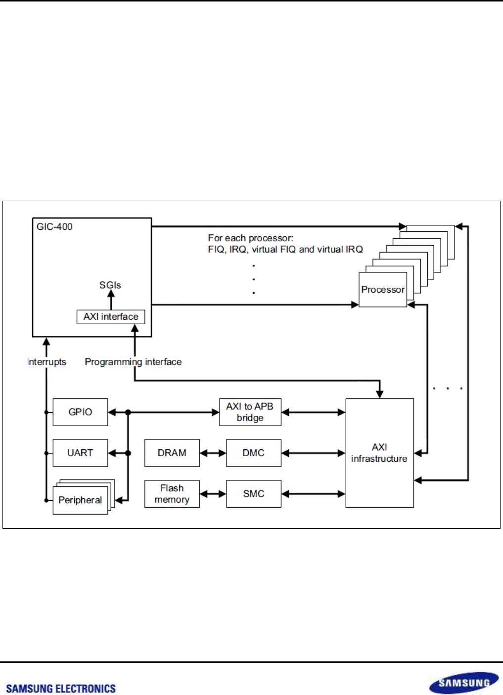
Samsung Confidential
S5P6818_UM 10 Interrupt Controller
10-7
Preliminary product information describes products that are in development, for which full characterization data and
associated errata are not yet available. Specifications and information herein are subject to change without notice.
10.6 Functional Overview
10.6.1 Functional Interface
The main blocks of the GIC are:
AMBA salve interface
Distributor
CPU Interface
Virtual interface control
Virtual CPU interface
Clock and Reset
Figure 10-1 GIC Overview
nexell / ys.kim at 2015.02.12
SAMSUNG Confidential

Samsung Confidential
S5P6818_UM 10 Interrupt Controller
10-8
Preliminary product information describes products that are in development, for which full characterization data and
associated errata are not yet available. Specifications and information herein are subject to change without notice.
10.6.1.1 AMBA Slave Interface
The AMBA slave interfaces provides access to the GIC registers that enable you to program the system
configuration parameters and obtain status information
AXI4 slave interface
The AXI4 slave interface use a 32-bit data bus and consist of the following AXI channels:
Write-Address (AW)
Write-Data (W)
Write-response (B)
Read-Address (AR)
Read-Data (R)
The AWUSER and ARUSER signals are specific to the GIC. They indicate to the GIC which processor is
performing a request. Identifying the requestor is necessary to determine to which CPU interface or virtual CPU
interface an AXI access should be directed. Furthermore this is needed for some Distributor register accesses,
such as the GICD_SGIR, as well. The format of the AWUSER and ARUSER signals is a binary number from 0 to
number of CPU -1, inclusive. The only strict requirement to generate the AWUSER and ARUSER signals is that
the chosen numbering scheme must represent a consistent mapping between the processors and the range of
legal encodings. Processors can discover their ID that the GIC uses by reading from the Interrupt Processor
Targets Register0, GICD_ITARGETSR0.
AXI4 does not support write interleaving. Therefore, an AXI3 master must be set not to interleave writes.
nexell / ys.kim at 2015.02.12
SAMSUNG Confidential
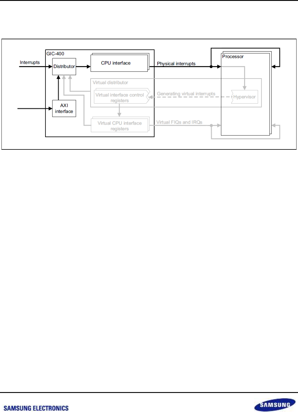
Samsung Confidential
S5P6818_UM 10 Interrupt Controller
10-9
Preliminary product information describes products that are in development, for which full characterization data and
associated errata are not yet available. Specifications and information herein are subject to change without notice.
10.6.1.2 Distributor
The Distributor receives interrupts and presents the highest priority pending interrupt to each CPU interface.
Figure 10-2 Handling Physical Interrupt with the Distributor
Furthermore, the GIC implements the Interrupt Group Registers, GICD_IGROUPRn, that control whether each
interrupt is configured as Group 0 or Group 1. The interrupt group affects whether the interrupt can be forwarded
to the CPU interfaces and it also has an impact on later routing decisions in the CPU interfaces, potentially
including whether it is signaled to the processor as a FIQ or an IRQ exception request.
The Distributor provides 6 external PPI inputs and the internal virtual maintenance PPI for each processor and
from 0 to 223 SPIs in multiples of 32. The PPIs are independent for each processor and the Distributor only
forwards them to the corresponding CPU interface. You can program the Distributor to control the CPU interface
to which it routes each SPI.
10.6.1.3 CPU Interface
Each CPU interface a signal interrupts to the corresponding processor and receives acknowledge and EOI
accesses from that processor. These AXI accesses convey the interrupt ID and other information about the
interrupt, and also trigger updates to the Distributor state.
The CPU interface only signals pending interrupts to the processor if the interrupt has sufficient priority. Whether
an interrupt has sufficient priority is determined by the configuration of the CPU interface and the priority of certain
active interrupts.
nexell / ys.kim at 2015.02.12
SAMSUNG Confidential
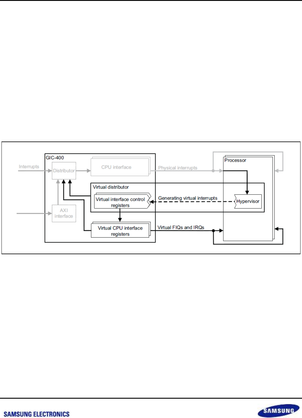
Samsung Confidential
S5P6818_UM 10 Interrupt Controller
10-10
Preliminary product information describes products that are in development, for which full characterization data and
associated errata are not yet available. Specifications and information herein are subject to change without notice.
10.6.1.4 Virtual Interface
The GIC implements the optional GIC Virtualization Extensions. A group of functional components of the GIC and
some software in the processor form a virtual distributor that has a role similar to the physical Distributor.
Together, the hypervisor and the virtual interface control registers form a virtual distributor:
1. The hypervisor creates virtual interrupts for the physical interrupts and assigns them a priority.
2. Each set of virtual CPU interface control registers prioritizes the virtual interrupts and forwards the highest
Priority pending interrupt to its corresponding virtual CPU interface. The hypervisor supports virtualization also by
using address translation tables to trap accesses that the virtual machines make to the virtual distributor. The
hypervisor determines the effect of these accesses and might typically update the virtual interface control registers
as a result.
The figure below shows how the virtual distributor is implemented partly in the GIC, partly in the processor and
how it interacts with the Distributor and the virtual CPU interfaces in the GIC. The GIC implements the virtual
interface control registers, namely the GICH registers and the processor implements the hypervisor.
Figure 10-3 Handling Virtual Interrupts with the Virtual Distributor
Virtual Interface Control Block
The GIC implements the virtual interface control block with all the management registers and with four List
registers. The List registers, GICH_LR0 - GICH_LR3, are a subset of the virtual interface control registers and
define the active and pending virtual interrupts for the virtual CPU interface. The management registers, for
example the Virtual Machine Control Register, GICH_VMCR, and Active Priorities Register, GICH_APR,
enable the hypervisor to manage other aspects of the corresponding virtual CPU interface, and permit it to
save and restore state when switching between virtual machines.
nexell / ys.kim at 2015.02.12
SAMSUNG Confidential

Samsung Confidential
S5P6818_UM 10 Interrupt Controller
10-11
Preliminary product information describes products that are in development, for which full characterization data and
associated errata are not yet available. Specifications and information herein are subject to change without notice.
Virtual CPU Interface
The virtual CPU interface registers are similar to the CPU interface registers. However, the virtual CPU
interfaces receive information from the virtual interface control registers, which are managed by the
hypervisor, rather than from the Distributor.
After receiving a physical interrupt or otherwise, if the hypervisor needs to signal a virtual interrupt to the
current virtual machine, it typically updates the virtual interface control registers. These registers, specifically
the List registers, GICH_LRn, hold a list of the virtual interrupts destined for the current virtual machine. The
signaling, acknowledgement and EOI steps of the virtual interrupt processing can usually be handled in
hardware by the virtual CPU interface. Certain cases might require hypervisor intervention, for example if
there are more virtual interrupts than can be stored in the List registers. The virtual interface control registers
control when an internal PPI, known as the virtual maintenance interrupt, is generated. This virtual
maintenance interrupt, PPI ID 25, is designed to notify the hypervisor of events that it must handle.
The address translation tables for the processor are normally configured so that accesses to the CPU
interface by a virtual machine are directed to the virtual CPU interface. This ensures that the virtualization of
the CPU interface is transparent to the virtual machine.
Hypervisor
The hypervisor is not part of the GIC but it is crucial for its operation. It is software executing on each
processor that is running virtual machines:
It is responsible for translating physical interrupts to virtual interrupts and managing all virtual interrupts by
using the virtual interface control registers.
It can also configure the virtual maintenance interrupt to signal situations when it must manage the virtual
interrupts. It typically sets the stage 2 Non-secure address translation tables so that the virtual machines
access the virtual CPU interfaces instead of the physical interfaces.
The hypervisor is responsible for virtualizing accesses from the virtual machines to the Distributor,
typically by trapping the accesses and handling them in software.
10.6.2 The Distributor
The Distributor centralizes all interrupt sources, determines the priority of each interrupt, and for each CPU
interface dispatches the interrupt with the highest priority to the interface for priority masking and preemption
handling.
The Distributor provides a programming interface for:
Globally enabling the forwarding of interrupts to the CPU interfaces.
Enabling or disabling each interrupt.
Setting the priority level of each interrupt.
Setting the target processor list of each interrupt.
Setting each peripheral interrupt to be level-sensitive or edge-triggered.
Setting each interrupt as either Group or Group 1.
Forwarding an SGI to one or more target processors.
nexell / ys.kim at 2015.02.12
SAMSUNG Confidential

Samsung Confidential
S5P6818_UM 10 Interrupt Controller
10-12
Preliminary product information describes products that are in development, for which full characterization data and
associated errata are not yet available. Specifications and information herein are subject to change without notice.
In addition, the Distributor provides:
Visibility of the state of each interrupt.
A mechanism for software to set or clear the pending state of a peripheral interrupt.
10.6.2.1 Interrupt IDs
Interrupts from sources are identified using ID numbers. Each CPU interface can see up to 1020 interrupts. The
banking of SPIs and PPIs increases the total number of interrupts supported by the Distributor.
The GIC assigns interrupt ID numbers ID0-ID1019 as follows:
Interrupt numbers ID32-ID1019 are used for SPIs.
Interrupt numbers ID0-ID31 are used for interrupts that are private to a CPU interface. These interrupts are
banked in the Distributor.
A banked interrupt is one where the Distributor can have multiple interrupts with the same ID. A banked
interrupt is identified uniquely by its ID number and its associated CPU interface number. Of the banked
interrupt IDs:
ID0-ID15 are used for SGIs
ID16-ID31 are used for PPIs
In a multiprocessor system:
o A PPI is forwarded to a particular CPU interface, and is private to that interface. In prioritizing
interrupts for a CPU interface the Distributor does not consider PPIs that relate to other interfaces.
o Each connected processor issues an SGI by writing to the GICD_SGIR in the Distributor. Ach write
can generate SGIs with the same ID that target multiple processors. In the Distributor, an SGI is
identified uniquely by the combination of its interrupt number, ID0-ID15, the target processor ID,
CPUID0-CPUID7, and the processor source ID, CPUID0-CPUID7, of the processor that issued the
SGI. When the CPU interface communicates the interrupt ID to a targeted processor, it also provides
the processor source ID, so that the targeted processor can uniquely identify the SGI.
o SGI banking means the GIC can handle multiple SGIs simultaneously, without resource conflicts.
o The Distributor ignores any write to the GICD_SGIR that is not from a processor that is connected to
one of the CPU interfaces. How the Distributor determines the processor source ID of a processor
writing to the GICD_SGIR.
In a uniprocessor system, there is no distinction between shared and private interrupts, because all interrupts
are visible to the processor. In this case the processor source ID value is 0.
Interrupt numbers ID1020 to ID1023 are reserved for special purposes.
System software sets the priority of each interrupt. This priority is independent of the interrupt ID number. In
any system that implements the ARM Security Extensions, to support a consistent model for message
passing between processors, ARM strongly recommends that all processors reserve:
ID0 to ID7 for Non-secure interrupts
ID8 to ID15 for Secure interrupts
nexell / ys.kim at 2015.02.12
SAMSUNG Confidential

Samsung Confidential
S5P6818_UM 10 Interrupt Controller
10-13
Preliminary product information describes products that are in development, for which full characterization data and
associated errata are not yet available. Specifications and information herein are subject to change without notice.
10.6.3 CPU Interfaces
Each CPU interface block provides the interface for a processor that is connected to the GIC.
Each CPU interface provides a programming interface for:
Enabling the signaling of interrupt requests to the processor
Acknowledging an interrupt.
Indicating completion of the processing of an interrupt.
Setting an interrupt priority mask for the processor.
Defining the preemption policy for the processor.
Determining the highest priority pending interrupt for the processor.
When enabled, a CPU interface takes the highest priority pending interrupt for its connected processor and
determines whether the interrupt has sufficient priority for it to signal the interrupt request to the processor. To
determine whether to signal the interrupt request to the processor, the CPU interface considers the interrupt
priority mask and the preemption settings for the processor. At any time, the connected processor can read the
priority of its highest priority active interrupt from its GICC_HPPIR, a CPU interface register.
The processor acknowledges the interrupt request by reading the CPU interface Interrupt Acknowledge register.
The read returns one of:
The ID number of the highest priority pending interrupt, if that interrupt is of sufficient priority for it to be
signaled to the processor. This is the normal response to an interrupt acknowledge.
Exceptionally, an ID number that indicates a spurious interrupt.
When the processor acknowledges the interrupt at the CPU interface, the Distributor changes the status of the
interrupt from pending to either active, or active and pending. At this point the CPU interface can signal another
interrupt to the processor, to preempt interrupts that are active on the processor. If there is no pending interrupt
with sufficient priority for signaling to the processor, the interface deasserts the interrupt request signal to the
processor.
When the interrupt handler on the processor has completed the processing of an interrupt, it writes to the CPU
interface to indicate interrupt completion.
There are two stages to interrupt completion:
Priority drop, meaning the priority of the processed interrupt can no longer prevent the signaling of another
interrupt to the processor
Interrupt deactivation, meaning the Distributor removes the active state of the interrupt.
GICC_CTLR.EOI mode bit determines whether:
The two stages happen together, when the processor writes to the CPU interface End of Interrupt register
The two stages are separated, so that:
Priority drop happens when the processor writes to the CPU interface End of Interrupt register
Interrupt deactivation happens later, when the processor writes to the CPU interface Deactivate Interrupt
register.
nexell / ys.kim at 2015.02.12
SAMSUNG Confidential

Samsung Confidential
S5P6818_UM 10 Interrupt Controller
10-14
Preliminary product information describes products that are in development, for which full characterization data and
associated errata are not yet available. Specifications and information herein are subject to change without notice.
10.7 Interrupt Handling and Prioritization
10.7.1 About Interrupt Handling and Prioritization
Interrupt handling describes:
How the GIC recognizes interrupts.
How software can program the GIC to configure and control interrupts.
The state machine the GIC maintains for each interrupt on each CPU interface.
How the exception model of processor interacts with the GIC.
Prioritization describes:
The configuration and control of interrupt priority.
The order of execution of pending interrupts.
The determination of when interrupts are visible to target processor, including:
Interrupt priority masking
Priority grouping
Preemption of an active interrupt
10.7.1.1 Handling Different Interrupt Types in a Multiprocessor System
A GIC supports peripheral interrupts and software-generated interrupts
In a multiprocessor implementation the GIC handles:
Software generated interrupts (SGIs) using an N-N model.
Peripheral (Hardware) interrupts using a 1-N model.
10.7.1.2 Identifying the Supported Interrupt
The GIC defines different ID values for the different types of interrupt. However there is no requirement for the
GIC to implement a continuous block of interrupt IDs for any interrupt type.
To correctly handle interrupts, software must know what interrupt IDs are supported by the GIC. Software can use
the GICD_ISENABLERns to discover this information. If the processor implements the Security Extensions,
Secure software determines which interrupts that are visible to Non-secure software. The Non-secure software
must know which interrupts it can see, and might use this discovery process to find this information.
GICD_ISENABLER0 provides the Set-enables bits for both:
SGIs, using interrupt IDs 15 to 0, corresponding to register bits [15:0].
PPIs, using interrupt IDs 31 to 16, corresponding to register bits [31:16].
nexell / ys.kim at 2015.02.12
SAMSUNG Confidential

Samsung Confidential
S5P6818_UM 10 Interrupt Controller
10-15
Preliminary product information describes products that are in development, for which full characterization data and
associated errata are not yet available. Specifications and information herein are subject to change without notice.
The remaining GICD_ISENABLERns, from GICD_ISENABLER1, provides the Set-enable bits for the SPIs,
starting at interrupt ID 32.
Software discovers which interrupts are supported by:
1. Reading the GICD_TYPER. The GICD_TYPER.IT Lines Number field identifies the number of implemented
GICD_ISENABLERns, and therefore the maximum number of SPIs that might be supported.
2. Writing to the GICD_CTLR to disable forwarding of interrupts from the distributor to the CPU interfaces.
3. For each implemented GICD_ISENABLERn, starting with GICD_ISENABLER0:
Writing 0xFFFFFFFF to the GICD_ISENABLERn.
Reading the value of the GICD_ISENABLERn. Bits that read as 1 correspond to supported interrupt IDs.
Software uses the GICD_ICENABLERns to discover the interrupts that are permanently enabled.
For each implemented GICD_ICENABLERn, starting with GICD_ICENABLER0, software:
1. Writes 0xFFFFFFFF to the GICD_ICENABLERn. This disables all interrupts that can be disabled.
2. Reads the value of the GICD_ICENABLERn. Bits that read as 1 correspond to interrupts that are permanently
enabled.
3. Writes 1 to any GICD_ISENABLERn bits corresponding to interrupts that must be re-enabled.
The GIC implements the same number of GICD_ISENABLERns and GICD_ICENABLERns.
When software has completed its discovery, it typically writes to the GICD_CTLR to re-enable forwarding of
interrupts from the Distributor to the CPU interfaces.
If the GIC implements the Security Extensions, software can use Secure accesses to discover all the supported
interrupt IDs.
Software using Non-secure accesses can discover and control only the interrupts that are configured as Non-
secure. If Secure software changes the security configuration of any interrupts after Non-secure software has
discovered its supported interrupts, it must communicate the effect of those changes to the Non-secure software.
In a GIC that provides interrupt grouping, software can:
Write to the GICD_IGROUPRn registers, to configure interrupts as Group 0 or Group 1
Control the forwarding of Group 0 and Group 1 interrupts independently, using the GICD_CTLR.EnableGrp0 and
GICD_CTLR.EnableGrp1 bits.
nexell / ys.kim at 2015.02.12
SAMSUNG Confidential

Samsung Confidential
S5P6818_UM 10 Interrupt Controller
10-16
Preliminary product information describes products that are in development, for which full characterization data and
associated errata are not yet available. Specifications and information herein are subject to change without notice.
10.7.2 General Handling of Interrupts
The Distributor maintains a state machine for each supported interrupt on each CPU interface.
The possible states of an interrupt are:
Inactive
Pending
Active
Active and pending
When the GIC recognizes an interrupt request, it marks its states as pending. Regenerating a pending interrupt
does not affect the state of the interrupt.
The GIC interrupt handling sequence is:
1. The GIC determines the interrupts that are enabled.
2. For each pending interrupt, the GIC determines the targeted processor or processors.
3. For each CPU interface, the Distributor forwards the highest priority pending interrupt that targets that
interface.
4. Each CPU interface determines whether to signal an interrupt request to its processor, and if required, does
so.
5. The processor acknowledges the interrupt, and the GIC returns the interrupt ID and updates the interrupt
state.
6. After processing the interrupt, the processor signals End of Interrupt (EOI) to the GIC.
In more detail, these steps are as follows:
1. The GIC determines whether each interrupt is enabled. An interrupt that is not enabled has no effect on the
GIC.
2. For each enabled interrupt that is pending. The Distributor determines the targeted processor or processors.
3. For each processor, the Distributor determines the highest priority pending interrupt, based on the priority
information it holds for each interrupt, and forwards the interrupt to the targeted CPU interface.
4. If the distributor is forwarding an interrupt request to a CPU interface, the CPU interface determines whether
the interrupt has sufficient priority to be signaled to the processor. If the interrupt has sufficient priority, the
GIC signals an interrupt request to the processor.
nexell / ys.kim at 2015.02.12
SAMSUNG Confidential

Samsung Confidential
S5P6818_UM 10 Interrupt Controller
10-17
Preliminary product information describes products that are in development, for which full characterization data and
associated errata are not yet available. Specifications and information herein are subject to change without notice.
5. When a processor takes the interrupt exception, it reads the GICC_IAR of its CPU interface to acknowledge
the interrupt. This read returns an Interrupt ID, and for an SGI, the source processor ID, that the processor
uses to select the correct interrupt handler. When it recognizes this read, the GIC changes the state of the
interrupt as follows:
Info the pending state of the interrupt persists when the interrupt becomes active, or if the interrupt is
generated again, from pending to active and pending
Otherwise, from pending to active
6. When the processor has completed handling the interrupt, it must signal this completion to the GIC.
Always requires a valid write to an end of interrupt register (EOIR)
Might also require a subsequent write to the deactivate interrupt register, GICC_DIR.
For each CPU interface, the GIC architecture requires the order of the valid writes to an EOIR to be the reverse of
the order of the reads from the GICC_IAR or GICC_AIAR, so that each valid EOIR write refers to the most recent
interrupt acknowledge.
If, after the EOIR write, there is no pending interrupt of sufficient priority, the CPU interface deasserts the interrupt
exception request to the processor.
A CPU interface never signals to the connected processor any interrupt that is active and pending.
It only signals interrupts that are pending and have sufficient priority:
For PPIs and SGIs, the active status of particular interrupt ID is banked between CPU interfaces. This means
that if a particular interrupt ID is active or active and pending on a CPU interface, then no interrupt with that
same ID is signaled on that CPU interface.
For SPIs, the active status of an interrupt is common to all CPU interfaces. This means that if an interrupt is
active or active and pending on one CPU interface then it is not signaled on any CPU interface.
NOTE:
1. A level-sensitive peripheral interrupt persists when it is acknowledged by the processor, because the interrupt signal to the
GIC remains asserted until the interrupt service routine (ISR) running on the processor accesses the peripheral asserting
the signal.
2. In a multiprocessor implementation, the GIC handles:
PPIs and SGIs using the GIC N-N model, where the acknowledgement of an interrupt by one processor has no effect on
the state of the interrupt on other CPU interfaces
SPIs using the GIC 1-N model, where the acknowledgement of an interrupt by one processor removes the pending status
of the interrupt on any other targeted processors.
3. When using a software model with the GICC_CTLR.ACKCTL bit set to 0, separate registers are used to manage Group 0
and Group 1 interrupts, as follows:
GICC_IAR, GICC_EOIR, and GICC_HPPIR for Group 0 interrupts
GICC_AIAR, GICC_AEOIR, and GICC_AHPPIR for Group 1 interrupts
ARM deprecates the use of GICC_CTLR.ACKCTL, and strongly recommends using a software model where
GICC_CTLR.ACKCTL is set to 0.
nexell / ys.kim at 2015.02.12
SAMSUNG Confidential

Samsung Confidential
S5P6818_UM 10 Interrupt Controller
10-18
Preliminary product information describes products that are in development, for which full characterization data and
associated errata are not yet available. Specifications and information herein are subject to change without notice.
10.7.2.1 Priority Drop and Interrupt Deactivation
When a processor completes the processing of an interrupt, it must signal this completion to the GIC. Interrupt
completion requires the following changes to the GIC state:
Priority drop:
Priority drop is the drop in the Running priority that occurs on a valid write to an EOIR, either the GICC_EOIR
or the GICC_AEOIR. A valid write is a write that is not UNPREDICTABLE, is not ignored, and is not writing an
interrupt ID value greater than 1019.
On priority drop, the running priority is reduced from the priority of the interrupt referenced by the EOIR write
to either:
The priority of the highest-priority active interrupt for which there has been no EOIR write
The Idle priority, if there is no active interrupt for which there has been no EOIR write.
Interrupt deactivation:
Interrupt deactivation is the change of the state of an interrupt, either:
From active and pending, to pending
From active, to idle.
When GICC_CTLR.EOI mode is set to 0, a valid EOIR write also deactivates the interrupt it references.
Setting GICC_CTLR.EOI mode to 1 separates the priority drop and interrupt deactivation operations, and interrupt
handling software must:
1. Perform a valid EOIR write, to cause priority drop on the GIC CPU interface.
2. Subsequently, write to the GICC_DIR, to deactivate the interrupt.
The GIC architecture specification requires that valid EOIR writes are ordered, so that:
A valid GICC_EOIR write corresponds to the most recently acknowledged interrupt
A valid GICC_AEOIR write corresponds to the most recently acknowledged Group 1 interrupt.
Whether a GICC_EOIR write affects Group 0 or Group 1 interrupts depends on both:
The value of the GICC_CTLR.ACKCTL bit
If the GIC implements the GIC Security Extensions, whether the write is Secure or Non-secure.
nexell / ys.kim at 2015.02.12
SAMSUNG Confidential

Samsung Confidential
S5P6818_UM 10 Interrupt Controller
10-19
Preliminary product information describes products that are in development, for which full characterization data and
associated errata are not yet available. Specifications and information herein are subject to change without notice.
There is no ordering requirement for GICC_DIR writes.
However, the effect is UNPREDICTABLE if software writes to GICC_DIR when:
GICC_CTLR.EOI mode is set to 0
GICC_CTLR.EOI mode is set to 1 and there has not been a corresponding write to GICC_EOIR or
GICC_AEOIR.
When virtualizing physical interrupts, ARM recommends that, for each CPU interface that corresponds to a
processor running virtual machines:
GICC_CTLR.EOI mode bit is set to 1
If the GIC implements the GIC Security Extensions, the GICC_CTLR.EOI mode NS bit is set to 1
nexell / ys.kim at 2015.02.12
SAMSUNG Confidential

Samsung Confidential
S5P6818_UM 10 Interrupt Controller
10-20
Preliminary product information describes products that are in development, for which full characterization data and
associated errata are not yet available. Specifications and information herein are subject to change without notice.
10.7.2.2 Interrupt Controls in the GIC
The following sections describe the interrupt controls in the GIC:
Interrupt enables
Setting and clearing pending state of an interrupt
Finding the active or pending state of an interrupt
Generating an SGI
Interrupt Enable
For peripheral interrupts, a processor:
Enables an interrupt by writing to the appropriate GICD_ISENABLERn bit.
Disables an interrupt by writing to the appropriate GICD_ICENABLERn bit.
Whether SGIs are permanently enabled, or can be enabled and disabled by writes to the
GICD_ISENABLERn.
Writes to the GICD_ISENABLERns and GICD_ICENABLERns control whether the Distributor forwards
specific interrupts to the CPU interfaces. Disabling an interrupt by writing to the appropriate
GICD_ICENABLERn does not prevent that interrupt from changing state, for example becoming pending.
Setting and Clearing Pending State of Interrupt
For peripheral interrupts, a processor can:
Set the pending state by writing to the appropriate GICD_ISPENDRn bit
Clear the pending state by writing to the appropriate GICD_ICPENDRn bit.
For a level-sensitive interrupt:
If the hardware signal of an interrupt is asserted when a processor writes to the corresponding
GICD_ICPENDRn bit then the write to the register has no effect on the pending state of the interrupt.
If a processor writes a 1 to a GICD_ISPENDRn bit then the corresponding interrupt becomes pending
regardless of the state of the hardware signal of that interrupt, and remains pending regardless of the
assertion or deassertion of the signal.
For SGIs, the GIC ignores writes to the corresponding GICD_ISPENDRn and GICD_ICPENDRn bits. A
processor cannot change the state of a software-generated interrupt by writing to these registers. Typically, an
SGI is made pending by writing to the GICD_SGIR. The pending state of SGIs can also be modified directly
using the ICD_SPENDSGIRn and GICD_CPENDSGIRn bits.
nexell / ys.kim at 2015.02.12
SAMSUNG Confidential

Samsung Confidential
S5P6818_UM 10 Interrupt Controller
10-21
Preliminary product information describes products that are in development, for which full characterization data and
associated errata are not yet available. Specifications and information herein are subject to change without notice.
Finding the Active or Pending State of an Interrupt
A processor can find:
The pending state of an interrupt by reading the corresponding GICD_ISPENDRn or GICD_ICPENDRn bit
The active state of an interrupt by reading the corresponding GICD_ISACTIVERn or GICD_ICACTIVERn
bit
The corresponding register bit is 1 if the interrupt is pending or active. If an interrupt is pending and active the
corresponding bit is 1 in both registers.
When preserving or restoring GIC state, a processor must take account of the pending and active state of all
interrupts.
For an SGI, the corresponding GICD_ISPENDRn and GICD_ICPENDRn bits RAO if there is a pending
interrupts from at least one generating processor that targets the processor reading the GICD_ISPENDRn or
GICD_ICPENDRn. In GICv2, the processor that issues the SGI can also be determined by reading the
corresponding GICD_SPENDSGIRn or GICD_CPENDSGIRn bits.
Generating an SGI
A processor generates an SGI by writing to a GICD_SGIR. An SGI can target multiple processors, and the
GICD_SGIR write specifies the target processor list. The GICD_SGIR includes optimization for:
Interrupting only the processor that writes to the GICD_SGIR
Interrupting all processors other than the one that writes to the GICD_SGIR.
SGIs from different processors use the same interrupt IDs. Therefore, any target processor can receive
SGIs with the same interrupt ID from different processors.
However, the pending states of any two SGIs are independent if any of the following are different:
Interrupt ID
Source processor
Target processor.
Only one interrupt with a specific interrupt ID can be active on a CPU interface at any time. This means that a
CPU interface cannot have two SGIs with the same interrupt ID active at the same time, even if different
processors have signaled SGIs with the same interrupt ID to that processor.
On the CPU interface of the target processor, reading the GICC_IAR for an SGI returns both the interrupt ID and
the CPU ID of the processor that generated the interrupt, the source processor for the interrupt. The combination
of interrupt ID and source CPU ID uniquely identifies the interrupt to the target processor.
In a multiprocessor implementation, the interrupt priority of each SGI interrupt ID is defined independently for each
target processor, see Interrupt Priority Registers, GICD_IPRIORITYRn. For each CPU interface, all SGIs with a
particular interrupt ID that are pending on that interface have the same priority and must be handled serially. The
order in which the CPU interface serializes these SGIs is IMPLEMENTATION SPECIFIC.
nexell / ys.kim at 2015.02.12
SAMSUNG Confidential

Samsung Confidential
S5P6818_UM 10 Interrupt Controller
10-22
Preliminary product information describes products that are in development, for which full characterization data and
associated errata are not yet available. Specifications and information herein are subject to change without notice.
10.7.2.3 Implications of the 1-N Model
In a multiprocessor implementation, the GIC uses a 1-N model to handle peripheral interrupts that target more
than one processor, that is, SPIs. This means that when the GIC recognizes an interrupt acknowledge from one of
the target processors it clears the pending state of the interrupt on all the other targeted processors. A GIC
implementation must ensure that any interrupt being handled using the 1-N model is only acknowledged by one
CPU interface and that all other interfaces return a spurious interrupt ID.
When multiple target processors attempt to acknowledge the interrupt, the following can occur:
A processor reads the GICC_IAR and obtains the interrupt ID of the interrupt to be serviced.
More than one target processor might have obtained this interrupt ID, if the processors read their GICC_IAR
registers at very similar times. The system might require software on the target processors to ensure that only
one processor runs its interrupt service routine. A typical mechanism to achieve this is implementing, in
shared memory, a lock on the interrupt service routine (ISR).
A processor reads the GICC_IAR and obtains the interrupt ID 1023, indicating a spurious interrupt. The
processor can return from its interrupt service routine without writing to its GICC_EOIR. The spurious interrupt
ID indicates that the original interrupt is no longer pending, typically because another target processor is
handling it.
NOTE: A GIC implementation might ensure that only one processor can make a 1-N interrupt active, removing the need for a
lock on the ISR. This is not required by the architecture, and generic GIC code must not rely on this behaviour. For
any processor, if an interrupt is active and pending, the GIC does not signal an interrupt exception request for the
interrupt to any processor until the active status is cleared.
nexell / ys.kim at 2015.02.12
SAMSUNG Confidential
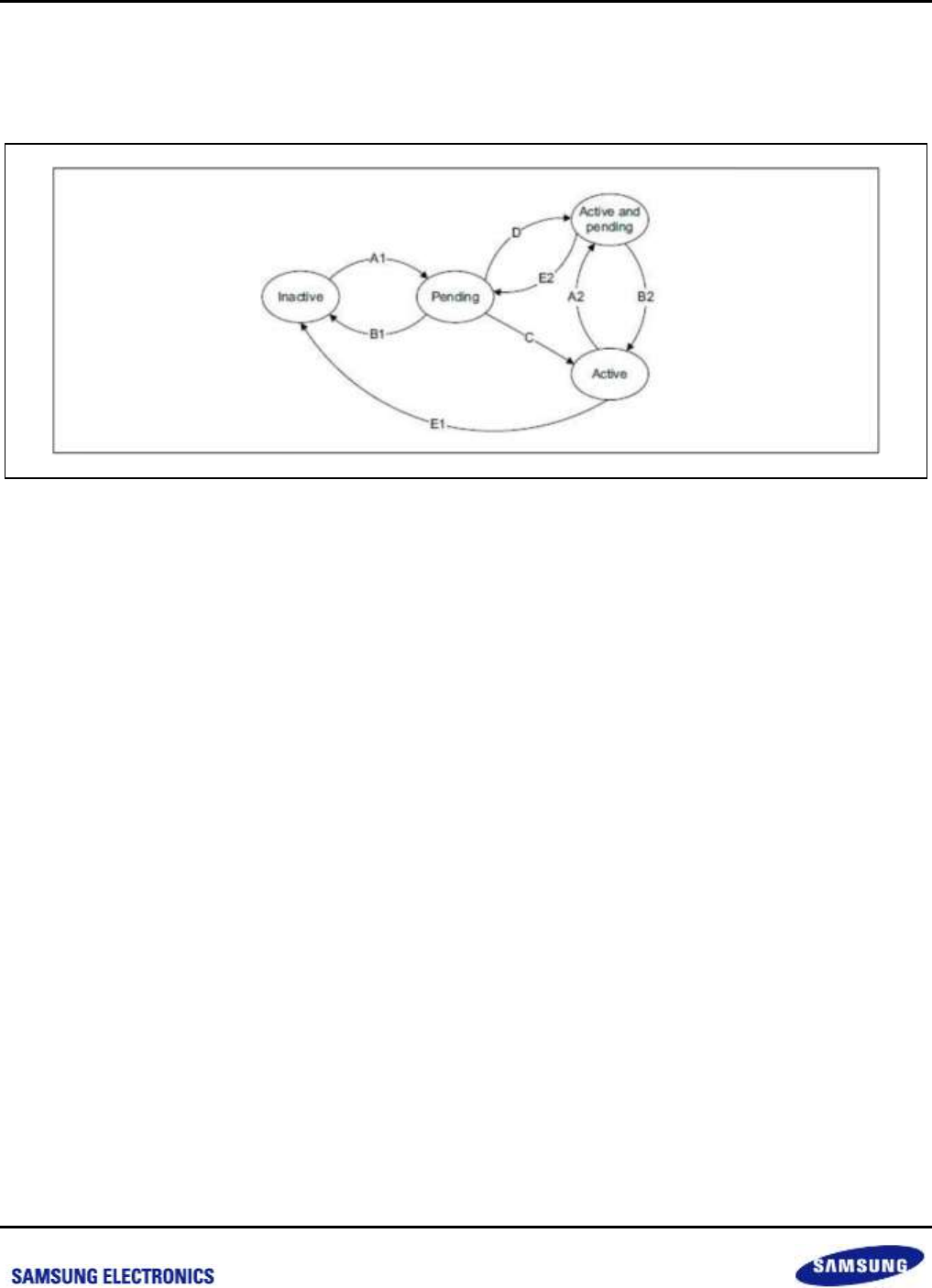
Samsung Confidential
S5P6818_UM 10 Interrupt Controller
10-23
Preliminary product information describes products that are in development, for which full characterization data and
associated errata are not yet available. Specifications and information herein are subject to change without notice.
10.7.2.4 Interrupt Handling State Machine
The GIC maintains a state machine for each supported interrupt on each CPU interface. The figure below shows
an instance of this state machine, and the possible state transitions.
Figure 10-4 Interrupt Handling State Machine
When interrupt forwarding by the Distributor and interrupt signaling by the CPU interface are enabled, the
conditions that cause each of the state transitions are as follows:
Transition A1 or A2, add Pending Status
For an SGI, occurs if either:
Software writes to a GICD_SGIR that specifies the processor as a target.
Software on the target processor writes to the GICD_SPENDSGIRn bit that corresponds to the required
source processor and interrupt ID
For an SPI or PPI, occurs if either:
A peripheral asserts an interrupt request signal
Software writes to an GICD_ISPENDRn.
Transition B1 or B2, Remove Pending Status
For an SGI, occurs if software on the target processor writes to the relevant bit of the GICD_CPENDSGIRn.
For an SPI or PPI, occurs if either:
The level-sensitive interrupt is pending only because of the assertion of an input signal, and that signal is
deasserted
The interrupt is pending only because of the assertion of an edge-triggered interrupt signal, or a write to an
GICD_ISPENDRn, and software writes to the corresponding GICD_ICPENDRn.
nexell / ys.kim at 2015.02.12
SAMSUNG Confidential

Samsung Confidential
S5P6818_UM 10 Interrupt Controller
10-24
Preliminary product information describes products that are in development, for which full characterization data and
associated errata are not yet available. Specifications and information herein are subject to change without notice.
Transition C, Pending to Active
If the interrupt is enabled and of sufficient priority to be signaled to the processor, occurs when software reads
from the GICC_IAR.
Transition D, Pending to Active and Pending
For an SGI, this transition occurs in either of the following circumstances:
If a write to set the SGI state to pending occurs at approximately the same time as a read of GICC_IAR.
When two or more pending SGIs with the same interrupt ID originate from the same source processor and
target the same processor. If one of the SGIs follows transition C, the other SGIs follow transition D
For an SPI or PPI this transition occurs if all the following apply:
The interrupt is enabled.
Software reads from the GICC_IAR. This read adds the active state to the interrupt.
In addition, one of the following conditions applies:
For a level-sensitive interrupt, the interrupt signal remains asserted. This is usually the case, because the
peripheral does not deassert the interrupt until the processor has serviced the interrupt.
For an edge-triggered interrupt, whether this transition occurs depends on the timing of the read of the
GICC_IAR relative to the detection of the reassertion of the interrupt. Otherwise the read of the GICC_IAR
causes transition C, possibly followed by transition A2.
Transition E1 or E2, Remove Active Status
Occurs when software deactivates an interrupt by writing to either GICC_EOIR or GICC_DIR. In a GIC
implementation the includes the Virtualization Extensions, also occurs if the virtual CPU interface signals that
the corresponding physical interrupt has been deactivated.
10.7.2.5 Special Interrupt Numbers
The GIC architecture reserves interrupt ID numbers 1020-1023 for special purposes. In a GIC that does not
implement the Security Extensions, the only one of these used is ID 1023. This value is returned to a processor, in
response to an interrupt acknowledge, if there is no pending interrupt with sufficient priority for it to be signaled to
the processor, it is described as a response to a spurious interrupt.
nexell / ys.kim at 2015.02.12
SAMSUNG Confidential

Samsung Confidential
S5P6818_UM 10 Interrupt Controller
10-25
Preliminary product information describes products that are in development, for which full characterization data and
associated errata are not yet available. Specifications and information herein are subject to change without notice.
10.8 Interrupt Source
Table 10-1 Interrupt Sources Description Table
Interrupt Number
Source
Description
0
MCUSTOP
MCUSTOP interrupt
1
DMA0
DMA0 interrupt
2
DMA1
DMA1 interrupt
3
CLKPWR0
CLKPWRPWR interrupt
4
CLKPWR1
CLKPWRALIVE interrupt
5
CLKPWR2
CLKPWRRTC interrupt
6
UART1
UART1 interrupt
7
UART0
UART0 interrupt
8
UART2
UART2 interrupt
9
UART3
UART3 interrupt
10
UART4
UART4 interrupt
11
UART5
UART5 interrupt
12
SSP0
SSP0 interrupt
13
SSP1
SSP1 interrupt
14
SSP2
SSP2 interrupt
15
I2C0
I2C0 interrupt
16
I2C1
I2C1 interrupt
17
I2C2
I2C2 interrupt
18
DEINTERLACE
DEINTERLACE interrupt
19
SCALER
SCALER interrupt
20
AC97
AC97 interrupt
21
SPDIFRX
SPDIFRX interrupt
22
SPDIFTX
SPDIFTX interrupt
23
TIMER0
TIMER0 interrupt
24
TIMER1
TIMER1 interrupt
25
TIMER2
TIMER2 interrupt
26
TIMER3
TIMER3 interrupt
27
PWM0
PWM0 interrupt
28
PWM1
PWM1 interrupt
29
PWM2
PWM2 interrupt
30
PWM3
PWM3 interrupt
31
WDT
WDT interrupt
nexell / ys.kim at 2015.02.12
SAMSUNG Confidential

Samsung Confidential
S5P6818_UM 10 Interrupt Controller
10-26
Preliminary product information describes products that are in development, for which full characterization data and
associated errata are not yet available. Specifications and information herein are subject to change without notice.
Interrupt Number
Source
Description
32
MPEGTSI
MPEGTSI interrupt
33
DISPLAYTOP0
DISPLAYDUALDISPLAYPRIM interrupt
34
DISPLAYTOP1
DISPLAYDUALDISPLAYSECOND interrupt
35
DISPLAYTOP2
DISPLAYRESCONV interrupt
36
DISPLAYTOP3
DISPLAYHDMI interrupt
37
VIP0
VIP0 interrupt
38
VIP1
VIP1 interrupt
39
MIPI
MIPI interrupt
40
3D GPU
3D GPU interrupt
41
ADC
ADC interrupt
42
PPM
PPM interrupt
43
SDMMC0
SDMMC0 interrupt
44
SDMMC1
SDMMC1 interrupt
45
SDMMC2
SDMMC2 interrupt
46
CODA9600
CODA960HOST interrupt
47
CODA9601
CODA960JPG interrupt
48
GMAC
GMAC interrupt
49
USB20OTG
USB20OTG interrupt
50
USB20HOST
USB20HOST interrupt
51
N/A
N/A
52
N/A
N/A
53
GPIOA
GPIOA interrupt
54
GPIOB
GPIOB interrupt
55
GPIOC
GPIOC interrupt
56
GPIOD
GPIOD interrupt
57
GPIOE
GPIOE interrupt
58
CRYPTO
CRYPTO interrupt
59
PDM
PDM interrupt
60
TMU0
TMU0 interrupt
61
TMU1
TMU1 interrupt
62
N/A
N/A
63
N/A
N/A
64
N/A
N/A
nexell / ys.kim at 2015.02.12
SAMSUNG Confidential

Samsung Confidential
S5P6818_UM 10 Interrupt Controller
10-27
Preliminary product information describes products that are in development, for which full characterization data and
associated errata are not yet available. Specifications and information herein are subject to change without notice.
Interrupt Number
Source
Description
65
N/A
N/A
66
N/A
N/A
67
N/A
N/A
68
N/A
N/A
69
N/A
N/A
70
N/A
N/A
71
N/A
N/A
72
VIP2
VIP2 Interrupt
nexell / ys.kim at 2015.02.12
SAMSUNG Confidential

Samsung Confidential
S5P6818_UM 10 Interrupt Controller
10-28
Preliminary product information describes products that are in development, for which full characterization data and
associated errata are not yet available. Specifications and information herein are subject to change without notice.
10.9 Register Description
10.9.1 Register Map Summary
Base Address: 0xC000_0000
Register
Offset
Description
Reset Value
RSVD
0x8000 to
0x8FFC
Reserved
–
GICD_CTRL
0x9000
distributor Control Register
0x0000_0000
GICD_TYPER
0x9004
Interrupt Controller Type Register
0x0000_FC24
GICD_IIDR
0x9008
Distributor Implementer Identification Register
0x0200_043B
RSVD
0x900C to
0x907C
Reserved
–
GICD_IGROUPRn
(n = 0 to 4)
0x9080 to
0x9090
Interrupt Group Register
0x0000_0000
RSVD
0x9094 to
0x90FC
Reserved
–
GICD_ISENABLERn
(n = 0 to 4)
0x9100 to
0x9110
Interrupt Set-Enable Register
0x0000_0000
RSVD
0x9114 to
0x917C
Reserved
–
GICD_ISCENABLERn
(n = 0 to 4)
0x9180 to
0x9190
Interrupt Clear-Enable Register
0x0000_0000
RSVD
0x9194 to
0x91FC
Reserved
–
GICD_ISPENDRn
(n = 0 to 4)
0x9200 to
0x9210
Interrupt Set-Pending Register
0x0000_0000
RSVD
0x9214 to
0x927C
Reserved
–
GICD_ICPENDERn
(n = 0 to 4)
0x9280 to
0x9290
Interrupt Clear-Pending Register
0x0000_0000
RSVD
0x9294 to
0x92FC
Reserved
–
GICD_ISACTIVERn
(n = 0 to 4)
0x9300 to
0x9310
Interrupt Set-Active Register
0x0000_0000
RSVD
0x9314 to
0x937C
Reserved
–
GICD_ISCCTIVERn
(n = 0 to 4)
0x9380 to
0x9390
Interrupt Clear-Active Register
0x0000_0000
RSVD
0x9394 to
0x93FC
Reserved
–
GICD_IPRIORITYRn
(n = 0 to 39)
0x9400 to
0x949C
Interrupt Priority Register
0x0000_0000
RSVD
0x9500 to
Reserved
–
nexell / ys.kim at 2015.02.12
SAMSUNG Confidential

Samsung Confidential
S5P6818_UM 10 Interrupt Controller
10-29
Preliminary product information describes products that are in development, for which full characterization data and
associated errata are not yet available. Specifications and information herein are subject to change without notice.
Register
Offset
Description
Reset Value
0x97FC
GICD_ITARGETSRn
(n = 0 to 39)
0x9800 to
0x989C
Interrupt Processor Target Register
0x0000_0000
RSVD
0x98A0 to
0x9BFC
Reserved
–
GICD_ICFGRn
(n = 0 to 9)
0x9C00 to
0x9C24
Interrupt Configuration Register
0x0000_0000
RSVD
0x9C28 to
0x9CFC
Reserved
–
GICD_PPISR
0x9D00
Private Peripheral Interrupt Register
0x0000_0000
GICD_SPISRn
(n = 0 to 3)
0x9D04 to
0x9D10
Shared Peripheral Interrupt Status Register
0x0000_0000
RSVD
0x9D14 to
0x9EFC
Reserved
–
GICD_SGIR
0x9F00
Software Generated Interrupt Register
0x0000_0000
RSVD
0x9F04 to
0x9F0C
Reserved
–
GICD_CPENDSGIRn
(n = 0 to 3)
0x9F10 to
0x9F1C
SGI Clear-Pending Register
0x0000_0000
GICD_SPENDSGIRn
(n = 0 to 3)
0x9F20 to
0x9F2C
SGI Set-Pending Register
0x0000_0000
RSVD
0x9F30 to
0x9FFC
Reserved
–
GICC_CTRL
0xA000
CPU Interface Control Register
0x0000_0000
GICC_PMR
0xA004
Interrupt Priority Mask Register
0x0000_0000
GICC_BPR
0xA008
Binary Point Register
0x0000_002D
GICC_IAR
0xA00C
Interrupt Acknowledge Register
0x0000_03FF
GICC_EOIR
0xA010
End of Interrupt Register
0x0000_0000
GICC_RPR
0xA014
Running Priority Register
0x0000_00FF
GICC_HPPIR
0xA018
Highest Priority Pending Interrupt Register
0x0000_03FF
GICC_ABPR
0xA01C
Aliased Binary Point Register
0x0000_0003
GICC_AIAR
0xA020
Aliased Interrupt Acknowledge Register
0x0000_03FF
GICC_AEOIR
0xA024
Aliased End of Interrupt Register
0x0000_0000
GICC_AHIPPIR
0xA028
Aliased Highest Priority Pending Interrupt Register
0x0000_0000
RSVD
0xA02C to
0xA0CC
Reserved
–
GICC_APR0
0xA0D0
Active Priority Register
0x0000_0000
RSVD
0xA0D4 to
0xA0DC
Reserved
–
GICC_NSAPR0
0xA0E0
Non-Secure Active Priority Register
0x0202_043B
nexell / ys.kim at 2015.02.12
SAMSUNG Confidential

Samsung Confidential
S5P6818_UM 10 Interrupt Controller
10-30
Preliminary product information describes products that are in development, for which full characterization data and
associated errata are not yet available. Specifications and information herein are subject to change without notice.
Register
Offset
Description
Reset Value
RSVD
0xA0E4 to
0xAFFC
Reserved
–
GICC_DIR
0xB000
Deactivate Interrupt Register
0x0000_0000
nexell / ys.kim at 2015.02.12
SAMSUNG Confidential

Samsung Confidential
S5P6818_UM 10 Interrupt Controller
10-31
Preliminary product information describes products that are in development, for which full characterization data and
associated errata are not yet available. Specifications and information herein are subject to change without notice.
10.9.1.1 GICD_CTRL
Base Address: 0xC000_0000
Address = Base Address + 0x9000, Reset Value = 0x0000_0000
Name
Bit
Type
Description
Reset Value
RSVD
[31:2]
–
Reserved
–
ENABLEGRP1
[1]
RW
Global enable for forwarding pending Group 1 interrupts
from the Distributor to the CPU interfaces:
0 = Group 1 interrupts not forwarded.
1 = Group 1 interrupts forwarded, subject to the priority
rules.
1'b0
enablegrp0
[0]
RW
Global enable for forwarding pending Group 0 interrupts
from the Distributor to the CPU interfaces:
0 = Group 1 interrupts not forwarded.
1 = Group 1 interrupts forwarded, subject to the priority
rules.
1'b0
nexell / ys.kim at 2015.02.12
SAMSUNG Confidential

Samsung Confidential
S5P6818_UM 10 Interrupt Controller
10-32
Preliminary product information describes products that are in development, for which full characterization data and
associated errata are not yet available. Specifications and information herein are subject to change without notice.
10.9.1.2 GICD_TYPER
Base Address: 0xC000_0000
Address = Base Address + 0x9004, Reset Value = 0x0000_FC24
Name
Bit
Type
Description
Reset Value
RSVD
[31:16]
–
Reserved
–
lspi
[15:11]
R
If the GIC implements the Security Extensions, the value
of this field is the maximum number of implemented
lockable SPIs, from 0 (0b00000) to 31 (0b11111). If this
field is 0b00000 then the GIC does not implement
configuration lockdown. If the GIC does not implement
the Security Extensions, this field is reserved.
5'h1F
securityextn
[10]
R
Indicates whether the GIC implements the Security
Extensions.
0 = Security Extensions not implemented.
1 = Security Extensions implemented.
1'b1
RSVD
[9:8]
–
Reserved
–
cpunumber
[7:5]
R
Indicates the number of implemented CPU interfaces.
The number of implemented CPU interfaces is one more
than the value of this field, for example if this field is
0b011, there are four CPU interfaces. If the GIC
implements the Virtualization Extensions, this is also the
number of virtual CPU interfaces.
3'b1
itlinesnumber
[4:0]
R
Indicates the maximum number of interrupts that the GIC
supports. If IT Lines Number = N, the maximum number
of interrupts is 32 (N + 1). The interrupt ID range is from 0
to
(Number of IDs ? 1).
For example:
0’b00011 = Up to 128 interrupt lines, interrupt IDs 0-127.
The maximum number of interrupts is 1020 (0b11111).
See the text in this section for more information.
Regardless of the range of interrupt IDs defined by this
field, interrupt IDs 1020-1023 are reserved for special
purposes.
5'h4
nexell / ys.kim at 2015.02.12
SAMSUNG Confidential
Samsung Confidential
S5P6818_UM 10 Interrupt Controller
10-33
Preliminary product information describes products that are in development, for which full characterization data and
associated errata are not yet available. Specifications and information herein are subject to change without notice.
10.9.1.3 GICD_IIDR
Base Address: 0xC000_0000
Address = Base Address + 0x9008, Reset Value = 0x0200_043B
Name
Bit
Type
Description
Reset Value
productid
[31:24]
R
An IMPLEMENTATION DEFINED product identifier.
8'h2
RSVD
[23:20]
–
Reserved
–
variant
[19:16]
R
An IMPLEMENTATION DEFINED variant number.
Typically, this field is used to distinguish product variants,
or major revisions of a product.
4'h0
revision
[15:12]
R
An IMPLEMENTATION DEFINED revision number.
Typically, this field is used to distinguish minor revisions
of a product.
4'h0
implementer
[11:0]
R
Contains the JEP106 code of the company that
implemented the GIC Distributor:
Bits[11:8]: The JEP106 continuation code of the
implementer.
For an ARM implementation, this field is 0x4.
Bits[7] Always 0.
Bits[6:0] The JEP106 identity code of the implementer.
For an ARM implementation, bits[7:0] are 0x3B.
12'h43B
10.9.1.4 GICD_IGROUPRn (n = 0 to 4)
Base Address: 0xC000_0000
Address = Base Address + 0x9080, 0x9084, 0x9088, 0x908C, 0x9090, Reset Value = 0x0000_0000
Name
Bit
Type
Description
Reset Value
group status bit
[31:0]
RW
For each bit:
0 = The corresponding interrupt is Group 0.
1 = The corresponding interrupt is Group 1.
–
nexell / ys.kim at 2015.02.12
SAMSUNG Confidential

Samsung Confidential
S5P6818_UM 10 Interrupt Controller
10-34
Preliminary product information describes products that are in development, for which full characterization data and
associated errata are not yet available. Specifications and information herein are subject to change without notice.
10.9.1.5 GICD_ISENABLERn (n = 0 to 4)
Base Address: 0xC000_0000
Address = Base Address + 0x9100, 0x9104, 0x9108, 0x910C, 0x9110, Reset Value = 0x0000_0000
Name
Bit
Type
Description
Reset Value
Set-enable bits
[31:0]
RW
For SPIs and PPIs, each bit controls the forwarding of the
corresponding interrupt from the Distributor to the CPU
interfaces:
Reads
0 = Forwarding of the corresponding interrupt is disabled.
1 = Forwarding of the corresponding interrupt is enabled.
Writes
0 = Has no effect.
1 = Enables the forwarding of the corresponding interrupt.
After a write of 1 to a bit, a subsequent read of the bit
returns the value 1.
For SGIs the behavior of the bit on reads and writes is
IMPLEMENTATION DEFINED.
–
10.9.1.6 GICD_ISCENABLERn (n = 0 to 4)
Base Address: 0xC000_0000
Address = Base Address + 0x9180, 0x9184, 0x9188, 0x918C, 0x9190, Reset Value = 0x0000_0000
Name
Bit
Type
Description
Reset Value
clear-enable bits
[31:0]
RW
For SPIs and PPIs, each bit controls the forwarding of the
corresponding interrupt from the Distributor to the CPU
interfaces:
Reads
0 = Forwarding of the corresponding interrupt is disabled.
1 = Forwarding of the corresponding interrupt is enabled.
Writes
0 = Has no effect.
1 = Disables the forwarding of the corresponding
interrupt.
After a write of 1 to a bit, a subsequent read of the bit
returns the value 0.
For SGIs the behavior of the bit on reads and writes is
IMPLEMENTATION DEFINED.
–
nexell / ys.kim at 2015.02.12
SAMSUNG Confidential
Samsung Confidential
S5P6818_UM 10 Interrupt Controller
10-35
Preliminary product information describes products that are in development, for which full characterization data and
associated errata are not yet available. Specifications and information herein are subject to change without notice.
10.9.1.7 GICD_ISPENDRn (n = 0 to 4)
Base Address: 0xC000_0000
Address = Base Address + 0x9200, 0x9204, 0x9208, 0x920C, 0x9210,Reset Value = 0x0000_0000
Name
Bit
Type
Description
Reset Value
set-pending bits
[31:0]
RW
For each bit:
Reads
0 = The corresponding interrupt is not pending on any
processor.
1 = For PPIs and SGIs, the corresponding interrupt is
pending on this processor. For SPIs, the corresponding
interrupt is pending on at least one processor.
Writes
For SPIs and PPIs:
0 = Has no effect.
1 = The effect depends on whether the interrupt is edge
triggered or level-sensitive:
Edge-triggered
Changes the status of the corresponding interrupt to:
Pending if it was previously inactive active and pending if
it was previously active.
Has no effect if the interrupt is already pending.
Level sensitive
If the corresponding interrupt is not pending, changes the
status of the corresponding interrupt to:
Pending if it was previously inactive active and pending if
it was previously active.
If the interrupt is already pending:
Because of a write to the GICD_ISPENDR, the write has
no effect because the corresponding interrupt signal is
asserted, the write has no effect on the status of the
interrupt, but the interrupt remains pending if the interrupt
signal is deasserted.
For SGIs, the write is ignored. SGIs have their own Set-
Pending registers
32'h0
nexell / ys.kim at 2015.02.12
SAMSUNG Confidential

Samsung Confidential
S5P6818_UM 10 Interrupt Controller
10-36
Preliminary product information describes products that are in development, for which full characterization data and
associated errata are not yet available. Specifications and information herein are subject to change without notice.
10.9.1.8 GICD_ICPENDERn (n = 0 to 4)
Base Address: 0xC000_0000
Address = Base Address + 0x9280, 0x9284, 0x9288, 0x928C, 0x9290, Reset Value = 0x0000_0000
Name
Bit
Type
Description
Reset Value
clear-pending bits
[31:0]
RW
For each bit:
Reads
0 = The corresponding interrupt is not pending on any
processor.
1 = For PPIs and SGIs, the corresponding interrupt is
pending on this processor. For SPIs, the corresponding
interrupt is pending on at least one processor.
Writes
For SPIs and PPIs:
0 = Has no effect.
1 = The effect depends on whether the interrupt is edge
triggered or level-sensitive:
Edge-triggered
Changes the status of the corresponding interrupt to:
Inactive if it was previously pending active if it was
previously active and pending.
Has no effect if the interrupt is not pending.
Level sensitive
If the corresponding interrupt is pending only because of
a write to GICD_ISPENDRn, the write changes the
status of the interrupt to:
Inactive if it was previously pending active if it was
previously active and pending.
Otherwise the interrupt remains pending if the interrupt
signal remains asserted.
For SGIs, the write is ignored. SGIs have their own
Clear- Pending registers
32'h0
nexell / ys.kim at 2015.02.12
SAMSUNG Confidential

Samsung Confidential
S5P6818_UM 10 Interrupt Controller
10-37
Preliminary product information describes products that are in development, for which full characterization data and
associated errata are not yet available. Specifications and information herein are subject to change without notice.
10.9.1.9 GICD_ISACTIVERn (n = 0 to 4)
Base Address: 0xC000_0000
Address = Base Address + 0x9300, 0x9304, 0x9308, 0x930C, 0x9310, Reset Value = 0x0000_0000
Name
Bit
Type
Description
Reset Value
set-active bits
[31:0]
RW
For each bit:
Reads
0 = The corresponding interrupt is not active
1 = The corresponding interrupt is active
Writes
0 = Has no effect.
1 = Activates the corresponding interrupt, if it is not
already active. If the interrupt is already active, the write
has no effect. After a write of 1 to this bit, a subsequent
read of the bit returns the value 1.
32'h0
10.9.1.10 GICD_ISCCTIVERn (n = 0 to 4)
Base Address: 0xC000_0000
Address = Base Address + 0x9380, 0x9384, 0x9388, 0x938C, 0x9390, Reset Value = 0x0000_0000
Name
Bit
Type
Description
Reset Value
clear-active bits
[31:0]
RW
For each bit:
Reads
0 = The corresponding interrupt is not active
1 = The corresponding interrupt is active
Writes
0 = Has no effect.
1 = Deactivates the corresponding interrupt, if the
interrupt is active. If the interrupt is already deactivated,
the write has no effect. After a write of 1 to this bit, a
subsequent read of the bit returns the value 0.
32'h0
nexell / ys.kim at 2015.02.12
SAMSUNG Confidential
Samsung Confidential
S5P6818_UM 10 Interrupt Controller
10-38
Preliminary product information describes products that are in development, for which full characterization data and
associated errata are not yet available. Specifications and information herein are subject to change without notice.
10.9.1.11 GICD_IPRIORITYRn (n = 0 to 39)
Base Address: 0xC000_0000
Address = Base Address + 0x9400 to 0x949C, Reset Value = 0x0000_0000
Name
Bit
Type
Description
Reset Value
priority byte offset 3
[31:24]
RW
Each priority field holds a priority value, from an
IMPLEMENTATION DEFINED range. The lower the
value, the greater the priority of the corresponding
interrupt.
8'h0
priority byte offset 2
[23:16]
RW
8'h0
priority byte offset 1
[15:8]
RW
8'h0
priority byte offset 0
[7:0]
RW
8'h0
10.9.1.12 GICD_ITARGETSRn (n = 0 to 39)
Base Address: 0xC000_0000
Address = Base Address + 0x9800 to 0x989C, Reset Value = 0x0000_0000
Name
Bit
Type
Description
Reset Value
priority byte offset 3
[31:24]
RW
Processors in the system number from 0, and each bit in
a CPU targets field refers to the corresponding
processor. For example, a value of 0x3 means that the
Pending interrupt is sent to processors 0 and 1.
For GICD_ITARGETSR0 to GICD_ITARGETSR7, a read
of any CPU targets field returns the number of the
processor performing the read.
–
priority byte offset 2
[23:16]
RW
–
priority byte offset 1
[15:8]
RW
–
priority byte offset 0
[7:0]
RW
–
nexell / ys.kim at 2015.02.12
SAMSUNG Confidential

Samsung Confidential
S5P6818_UM 10 Interrupt Controller
10-39
Preliminary product information describes products that are in development, for which full characterization data and
associated errata are not yet available. Specifications and information herein are subject to change without notice.
10.9.1.13 GICD_ICFGRn (n = 0 to 9)
Base Address: 0xC000_0000
Address = Base Address + 0x9C00 to 0x9C24, Reset Value = 0x0000_0000
Name
Bit
Type
Description
Reset Value
int_config_field
[2F+1:2F]
RW
For Int_config[1], the most significant bit, bit [2F + 1],
the encoding is:
0 = Corresponding interrupt is level-sensitive.
1 = Corresponding interrupt is edge-triggered.
Int_config[0], the least significant bit, bit [2F], is
reserved.
The encoding of this bit on some early implementations
of this GIC architecture.
For SGIs:
Int_config[1]: Not programmable, RAO/WI.
For PPIs and SPIs:
Int_config[1]: For SPIs, this bit is programmable For
PPIs it is IMPLEMENTATION DEFINED whether this
bit is programmable. A read of this bit always returns
the correct value to indicate whether the corresponding
interrupt is level-sensitive or edge-triggered.
On a GIC where the handling mode of peripheral
interrupts is configurable, the encoding of Int_config[0]
for PPIs and SPIs, is:
0 = Corresponding interrupt is handled using the N-N
model.
1 = Corresponding interrupt is handled using the 1-N
model.
–
nexell / ys.kim at 2015.02.12
SAMSUNG Confidential
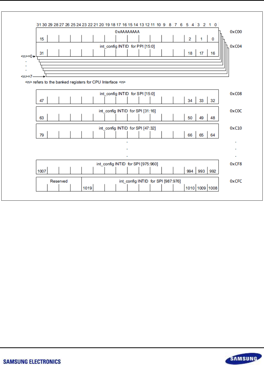
Samsung Confidential
S5P6818_UM 10 Interrupt Controller
10-40
Preliminary product information describes products that are in development, for which full characterization data and
associated errata are not yet available. Specifications and information herein are subject to change without notice.
Figure 10-5 GICD_ICFGR Address Mat
nexell / ys.kim at 2015.02.12
SAMSUNG Confidential

Samsung Confidential
S5P6818_UM 10 Interrupt Controller
10-41
Preliminary product information describes products that are in development, for which full characterization data and
associated errata are not yet available. Specifications and information herein are subject to change without notice.
10.9.1.14 GICD_PPISR
Base Address: 0xC000_0000
Address = Base Address + 0x9D00, Reset Value = 0x0000_0000
Name
Bit
Type
Description
Reset Value
RSVD
[31:16]
–
Reserved
–
ppi_status
[15:0]
R
Returns the status of the ppi_c<n>[15:0] inputs on the
Distributor:
Bit [X] = 0 ppi_c<n>[x] is LOW
Bit [X] = 1 ppi_c<n>[x] is HIGH.b
NOTE: These bits return the actual status of the
ppi_c<n>[15:0] signals. The Pending Set Registers
(ICDISPRn), Pending Clear Registers (ICDICPRn), also
provide the ppi_c<n>[15:0] status but because you can
write to these registers then they might not contain the
actual status of the ppi_c<n>[15:0] signals.
–
10.9.1.15 GICD_SPISRn (n = 0 to 3)
Base Address: 0xC000_0000
Address = Base Address + 0x9D04, 0x9D08, 0x9D0C, 0x9D10, Reset Value = 0x0000_0000
Name
Bit
Type
Description
Reset Value
spi_status
[31:0]
R
Returns the status of the spi[987:0] inputs on the
Distributor:
Bit [x] = 0 spi[x] is LOW
Bit [x] = 1 spi[x] is HIGH.
NOTE: The spi that x refers to, depends on its bit position
and the base address offset of the spi Register shows.
These bits return the actual status of the spi signals. The
Pending Set Registers (ICDISPRn) and Pending Clear
Registers (ICDICPRn) also provide the spi status but
because you can write to these registers then they might
not contain the actual status of the spi signals.
32'h0
nexell / ys.kim at 2015.02.12
SAMSUNG Confidential

Samsung Confidential
S5P6818_UM 10 Interrupt Controller
10-42
Preliminary product information describes products that are in development, for which full characterization data and
associated errata are not yet available. Specifications and information herein are subject to change without notice.
10.9.1.16 GICD_SGIR
Base Address: 0xC000_0000
Address = Base Address + 0x9F00, Reset Value = 0x0000_0000
Name
Bit
Type
Description
Reset Value
RSVD
[31:26]
–
Reserved
–
targetlistfilter
[25:24]
W
Determines how the distributor must process the requested
SGI:
0b00 = Forward the interrupt to the CPU interfaces
specified in the CPUTARGETLIST field.
0b01 = Forward the interrupt to all CPU interfaces except
that of the processor that requested the interrupt.
0b10 = Forward the interrupt only to the CPU interface of
the processor that requested the interrupt.
0b11 = Reserved.
–
cputargetlist
[23:16]
W
When TARGETLISTFILTER = 0b00, defines the CPU
interfaces to which the Distributor must forward the
interrupt.
Each bit of CPUTARGETLIST[7:0] refers to the
corresponding CPU interface, for example
CPUTARGETLIST[0] corresponds to CPU interface 0.
Setting a bit to 1 indicates that the interrupt must be
forwarded to the corresponding interface.
If this field is 0x00 when TARGETLISTFILTER is 0b00, the
Distributor does not forward the interrupt to any CPU
interface.
–
NSATT
[15]
W
Implemented only if the GIC includes the Security
Extensions. Specifies the required security value of the
SGI:
0 = Forward the SGI specified in the SGIINTID field to a
specified CPU interface only if the SGI is configured as
Group 0 on that interface.
1 = Forward the SGI specified in the SGIINTID field to a
specified CPU interfaces only if the SGI is configured as
Group 1 on that interface.
This field is writable only by a Secure access. Any Non-
secure write to the GICD_SGIR generates an SGI only if
the specified SGI is programmed as Group 1, regardless of
the value of bit[15] of the write.
–
RSVD
[14:4]
–
Reserved
–
sgiintid
[3:0]
W
The Interrupt ID of the SGI to forward to the specified CPU
interfaces. The value of this field is the Interrupt ID, in the
range 0-15, for example a value of 0b0011 specifies
Interrupt ID 3.
–
nexell / ys.kim at 2015.02.12
SAMSUNG Confidential

Samsung Confidential
S5P6818_UM 10 Interrupt Controller
10-43
Preliminary product information describes products that are in development, for which full characterization data and
associated errata are not yet available. Specifications and information herein are subject to change without notice.
10.9.1.17 GICD_CPENDSGIRn (n = 0 to 3)
Base Address: 0xC000_0000
Address = Base Address + 0x9F10, 0x9F14, 0x9F18, 0x9F1C, Reset Value = 0x0000_0000
Name
Bit
Type
Description
Reset Value
sgi clear pending bits
[31:0]
RW
For each bit:
Reads
0 = SGI x from the corresponding processor is not
pending.
1 = SGI x from the corresponding processor is pending.
Writes
0 = Has no effect.
1 = Removes the pending state of SGI x for the
corresponding processor
See text for the relation between the SGI number, x,
the GICD_CPENDSGIRn register number, n, and the
field number, y.
32'h0
10.9.1.18 GICD_SPENDSGIRn (n = 0 to 3)
Base Address: 0xC000_0000
Address = Base Address + 0x9F20, 0x9F24, 0x9F28, 0x9F2C, Reset Value = 0x0000_0000
Name
Bit
Type
Description
Reset Value
sgi SET pending bits
[31:0]
RW
For each bit:
Reads
0 = SGI x from the corresponding processor is not
pending.
1 = SGI x from the corresponding processor is pending.
Writes
0 = Has no effect.
1 = Adds the pending state of SGI x for the
corresponding processor, if it is not already pending. If
SGI x is already pending for the corresponding
processor then the write has no effect. See text for the
relation between the SGI number, x, the
GICD_SPENDSGIRn register number, n, and the field
number, y.
32'h0
nexell / ys.kim at 2015.02.12
SAMSUNG Confidential

Samsung Confidential
S5P6818_UM 10 Interrupt Controller
10-44
Preliminary product information describes products that are in development, for which full characterization data and
associated errata are not yet available. Specifications and information herein are subject to change without notice.
10.9.1.19 GICC_CTRL
Base Address: 0xC000_0000
Address = Base Address + 0xA000, Reset Value = 0x0000_0000
Name
Bit
Type
Description
Reset Value
RSVD
[31:11]
–
Reserved
–
eolmodens1
[10]
RW
Alias of EOImodeNS1 from the Non-secure copy of this
register.
1'b0
eolmodens0
[9]
RW
Controls the behavior of Non-secure accesses to the
GICC_EOIR and GICC_DIR registers: In a GIC
implementation that includes the Security Extensions, this
control applies only to Secure accesses, and the
EOIMODENS bit controls the behavior of Non-secure
accesses to these registers:
0 = GICC_EOIR has both priority drop and deactivate
interrupt functionality. Accesses to the GICC_DIR are
UNPREDICTABLE.
1 = GICC_EOIR has priority drop functionality only. The
GICC_DIR register has deactivate interrupt functionality.
1'b0
IRQBypDisGrp1
[8]
RW
Alias of IRQBypDisGrp1 from the Non-secure copy of this
register.
1'b0
FIQBypDisGrp1
[7]
RW
Alias of FIQBypDisGrp1 from the Non-secure copy of this
register.
1'b0
IRQBypDisGrp0
[6]
RW
When the signaling of IRQs by the CPU interface is
disabled, this bit partly controls whether the bypass IRQ
signal is signaled to the processor:
0 = Bypass IRQ signal is signaled to the processor.
1 = Bypass IRQ signal is not signaled to the processor.
1'b0
FIQBypDisGrp0
[5]
RW
When the signaling of FIQs by the CPU interface is
disabled, this bit partly controls whether the bypass FIQ
signal is signaled to the processor:
0 = Bypass FIQ signal is signaled to the processor.
1 = Bypass FIQ signal is not signaled to the processor.
1'b0
cbpr
[4]
RW
Controls whether the GICC_BPR provides common
control to Group 0 and Group 1 interrupts.
0 = To determine any preemption, use:
The GICC_BPR for Group 0 interrupts
The GICC_ABPR for Group 1 interrupts.
1 = To determine any preemption use the GICC_BPR for
both Group 0 and Group 1 interrupts.
1'b0
fiqen
[3]
RW
Controls whether the CPU interface signals Group 0
interrupts to a target processor using the FIQ or the IRQ
signal.
0 = Signal Group 0 interrupts using the IRQ signal.
1 = Signal Group 0 interrupts using the FIQ signal.
The GIC always signals Group 1 interrupts using the IRQ
1'b0
nexell / ys.kim at 2015.02.12
SAMSUNG Confidential

Samsung Confidential
S5P6818_UM 10 Interrupt Controller
10-45
Preliminary product information describes products that are in development, for which full characterization data and
associated errata are not yet available. Specifications and information herein are subject to change without notice.
Name
Bit
Type
Description
Reset Value
signal.
ackctl
[2]
RW
When the highest priority pending interrupt is a Group 1
interrupt, determines both:
Whether a read of GICC_IAR acknowledges the
interrupt, or returns a spurious interrupt ID
Whether a read of GICC_HPPIR returns the ID of the
highest priority pending interrupt, or returns a spurious
interrupt ID.
0 = If the highest priority pending interrupt is a Group 1
interrupt, a read of the GICC_IAR or the GICC_HPPIR
returns an Interrupt ID of 1022. A read of the GICC_IAR
does not acknowledge the interrupt, and has no effect on
the pending status of the interrupt.
1 = If the highest priority pending interrupt is a Group 1
interrupt, a read of the GICC_IAR or the GICC_HPPIR
returns the Interrupt ID of the Group 1 interrupt. A read of
GICC_IAR acknowledges and Activates the interrupt.
1'b0
enablegrp1
[1]
RW
Enable for the signaling of Group 1 interrupts by the CPU
interface to the connected processor.
0 = Disable signaling of Group 1 interrupts.
1 = Enable signaling of Group 1 interrupts.
1'b0
enablegrp0
[0]
RW
Enable for the signaling of Group 0 interrupts by the CPU
interface to the connected processor.
0 = Disable signaling of Group 0 interrupts.
1 = Enable signaling of Group 0 interrupts.
1'b0
10.9.1.20 GICC_PMR
Base Address: 0xC000_0000
Address = Base Address + 0xA004, Reset Value = 0x0000_0000
Name
Bit
Type
Description
Reset Value
RSVD
[31:8]
–
Reserved
–
priority
[7:0]
RW
The priority masks level for the CPU interface. If the
priority of an interrupt is higher than the value indicated
by this field, the interface signals the interrupt to the
processor. If the GIC supports fewer than 256 priority
levels then some bits are RAZ/WI, as follows:
128 supported levels Bit [0] = 0.
64 supported levels Bit [1:0] = 0b00.
32 supported levels Bit [2:0] = 0b000.
16 supported levels Bit [3:0] = 0b0000.
8'b0
nexell / ys.kim at 2015.02.12
SAMSUNG Confidential

Samsung Confidential
S5P6818_UM 10 Interrupt Controller
10-46
Preliminary product information describes products that are in development, for which full characterization data and
associated errata are not yet available. Specifications and information herein are subject to change without notice.
10.9.1.21 GICC_BPR
Base Address: 0xC000_0000
Address = Base Address + 0xA008, Reset Value = 0x0000_002D
Name
Bit
Type
Description
Reset Value
RSVD
[31:3]
–
Reserved
–
binary point
[2:0]
RW
The value of this field controls how the 8-bit interrupt
priority field is split into a group priority field, used to
determine interrupt preemption, and a subpriority field. For
how this field determines the interrupt priority bits assigned
to the group priority field see:
0x2D
10.9.1.22 GICC_IAR
Base Address: 0xC000_0000
Address = Base Address + 0xA00C, Reset Value = 0x0000_03FF
Name
Bit
Type
Description
Reset Value
RSVD
[31:13]
–
Reserved
–
CPUID
[12:10]
R
For SGIs in a multiprocessor implementation, this field
identifies the processor that requested the interrupt. It
returns the number of the CPU interface that made the
request, for example a value of 3 means the request was
generated by a write to the GICD_SGIR on CPU interface
3.
3'b0
interrupt id
[9:0]
R
The interrupt ID
10'h3FF
10.9.1.23 GICC_EOIR
Base Address: 0xC000_0000
Address = Base Address + 0xA010, Reset Value = 0x0000_0000
Name
Bit
Type
Description
Reset Value
RSVD
[31:13]
W
Reserved
–
cpuid
[12:10]
W
On a multiprocessor implementation, if the write refers to
an SGI, this field contains the CPUID value from the
corresponding GICC_IAR access.
–
eoiintid
[9:0]
W
The Interrupt ID value from the corresponding GICC_IAR
access.
–
nexell / ys.kim at 2015.02.12
SAMSUNG Confidential
Samsung Confidential
S5P6818_UM 10 Interrupt Controller
10-47
Preliminary product information describes products that are in development, for which full characterization data and
associated errata are not yet available. Specifications and information herein are subject to change without notice.
10.9.1.24 GICC_RPR
Base Address: 0xC000_0000
Address = Base Address + 0xA014, Reset Value = 0x0000_00FF
Name
Bit
Type
Description
Reset Value
RSVD
[31:8]
–
Reserved
–
priority
[7:0]
R
The current running priority on the CPU interface.
8'hFF
10.9.1.25 GICC_HPPIR
Base Address: 0xC000_0000
Address = Base Address + 0xA018, Reset Value = 0x0000_03FF
Name
Bit
Type
Description
Reset Value
RSVD
[31:13]
–
Reserved
–
Cpuid
[12:10]
R
On a multiprocessor implementation, if the PENDINTID
field returns the ID of an SGI, this field contains the CPUID
value for that interrupt. This identifies the processor that
generated the interrupt.
3'b0
pendintid
[9:0]
R
The interrupt ID of the highest priority pending interrupt.
10'h3FF
10.9.1.26 GICC_ABPR
Base Address: 0xC000_0000
Address = Base Address + 0xA01C, Reset Value = 0x0000_0003
Name
Bit
Type
Description
Reset Value
RSVD
[31:3]
–
Reserved
–
binary point
[2:0]
RW
The value of this field controls how the 8-bit interrupt
priority field is split into a group priority field, used to
determine interrupt preemption, and a subpriority field.
3'b11
nexell / ys.kim at 2015.02.12
SAMSUNG Confidential
Samsung Confidential
S5P6818_UM 10 Interrupt Controller
10-48
Preliminary product information describes products that are in development, for which full characterization data and
associated errata are not yet available. Specifications and information herein are subject to change without notice.
10.9.1.27 GICC_AIAR
Base Address: 0xC000_0000
Address = Base Address + 0xA020, Reset Value = 0x0000_03FF
Name
Bit
Type
Description
Reset Value
RSVD
[31:13]
–
Reserved
–
cpuid
[12:10]
R
For SGIs in a multiprocessor implementation, this field
identifies the processor that requested the interrupt. It
returns the number of the CPU interface that made the
request, for example a value of 3 means the request was
generated by a write to the GICD_SGIR on CPU interface
3.
3'b0
interrupt id
[9:0]
R
The interrupt Id
10'h3FF
10.9.1.28 GICC_AEOIR
Base Address: 0xC000_0000
Address = Base Address + 0xA024, Reset Value = 0x0000_0000
Name
Bit
Type
Description
Reset Value
RSVD
[31:13]
–
Reserved
–
cpuid
[12:10]
W
On a multiprocessor implementation, when processing an
SGI, this field must contain the CPUID value from the
corresponding GICC_AIAR, or Non-secure GICC_IAR,
access.
-
interrupt id
[9:0]
W
The Interrupt ID value from the corresponding
GICC_AIAR, or Non-secure GICC_IAR, access.
-
10.9.1.29 GICC_AHIPPIR
Base Address: 0xC000_0000
Address = Base Address + 0xA028, Reset Value = 0x0000_0000
Name
Bit
Type
Description
Reset Value
RSVD
[31:13]
–
Reserved
–
cpuid
[12:10]
R
On a multiprocessor implementation, if the PENDINTID
field returns the ID of an SGI, this field contains the CPUID
value for that interrupt. This identifies the processor that
generated the interrupt.
–
pendintid
[9:0]
R
The interrupt ID of the highest priority pending interrupt, if
that interrupts is a Group 1 interrupt. Otherwise, the
spurious interrupt ID, 1023.
–
nexell / ys.kim at 2015.02.12
SAMSUNG Confidential

Samsung Confidential
S5P6818_UM 10 Interrupt Controller
10-49
Preliminary product information describes products that are in development, for which full characterization data and
associated errata are not yet available. Specifications and information herein are subject to change without notice.
10.9.1.30 GICC_APR0
Base Address: 0xC000_0000
Address = Base Address + 0xA0D0, Reset Value = 0x0000_0000
Minimum
Value of
secure
GICC_BPR
Minimum
Value of Non-
Secure
GICC_BPR
Maximum
Number of
Group
Priority Bits
Maximum
Number of
Preemption
Levels
GICC_APRn
Implementation
View of Active Priorities
Register for Non-
Secure Access
3
4
4
16
GICC_APR0[15:0]
GICC_NSAPR0[15:8]
appears as
GICC_APR0[7:0]
2
3
5
32
GICC_APR0[31:0]
GICC_NSAPR0[31:16]
appears as
GICC_APR0[15:0]
1
2
6
64
GICC_APR0 -
GICC_APR1
GICC_NSAPR1
appears as
GICC_APR0
0
1
7
128
GICC_APR0 -
GICC_APR3
GICC_NSAPR2-
GICC_NSAPR3
appear as
GICC_APR0-
GICC_APR1
nexell / ys.kim at 2015.02.12
SAMSUNG Confidential

Samsung Confidential
S5P6818_UM 10 Interrupt Controller
10-50
Preliminary product information describes products that are in development, for which full characterization data and
associated errata are not yet available. Specifications and information herein are subject to change without notice.
10.9.1.31 GICC_NSAPR0
Base Address: 0xC000_0000
Address = Base Address + 0xA0E0, Reset Value = 0x0202_043B
Name
Bit
Type
Description
Reset Value
productid
[31:20]
R
An IMPLEMENTATION DEFINED product identifier
12'h20
Architecture version
[19:16]
R
The value of this field depends on the GIC architecture
version, as follows:
0x1 for GICv1
0x2 for GICv2
4'h2
Revision
[15:12]
R
An IMPLEMENTATION DEFINED revision number for
the CPU interface.
4'h0
Implementer
[11:0]
R
Contains the JEP106 code of the company that
implemented the GIC CPU interface:
Bits [11:8]: The JEP106 continuation code of the
implementer.
Bits [7]: Always 0.
Bits [6:0]: The JEP106 identity code of the implementer.
12'h43B
10.9.1.32 GICC_DIR
Base Address: 0xC000_0000
Address = Base Address + 0xB000, Reset Value = 0x0000_0000
Name
Bit
Type
Description
Reset Value
RSVD
[31:13]
–
Reserved
–
cpuid
[12:10]
W
For an SGI in a multiprocessor implementation, this field
identifies the processor that requested the interrupt.
–
interrupt id
[9:0]
W
The interrupt ID
–
nexell / ys.kim at 2015.02.12
SAMSUNG Confidential

Samsung Confidential
S5P6818_UM 11 Watch Dog Timer
11-1
Preliminary product information describes products that are in development, for which full characterization data and
associated errata are not yet available. Specifications and information herein are subject to change without notice.
11 Watch Dog Timer
11.1 Overview
Watchdog timer is used to resume the controller operation whenever it is disturbed by malfunction such as noise
and system error. It can be used as normal 16-bit interval timer to request interrupt service. The watchdog timer
generates the reset signal.
Difference in usage WDT compared with PWM timer is that WDT generates the reset signal.
11.2 Features
Normal interval timer mode with interrupt request
Internal reset signal is activated when the timer count value reaches 0 (time-out).
Level-triggered interrupt mechanism
nexell / ys.kim at 2015.02.12
SAMSUNG Confidential
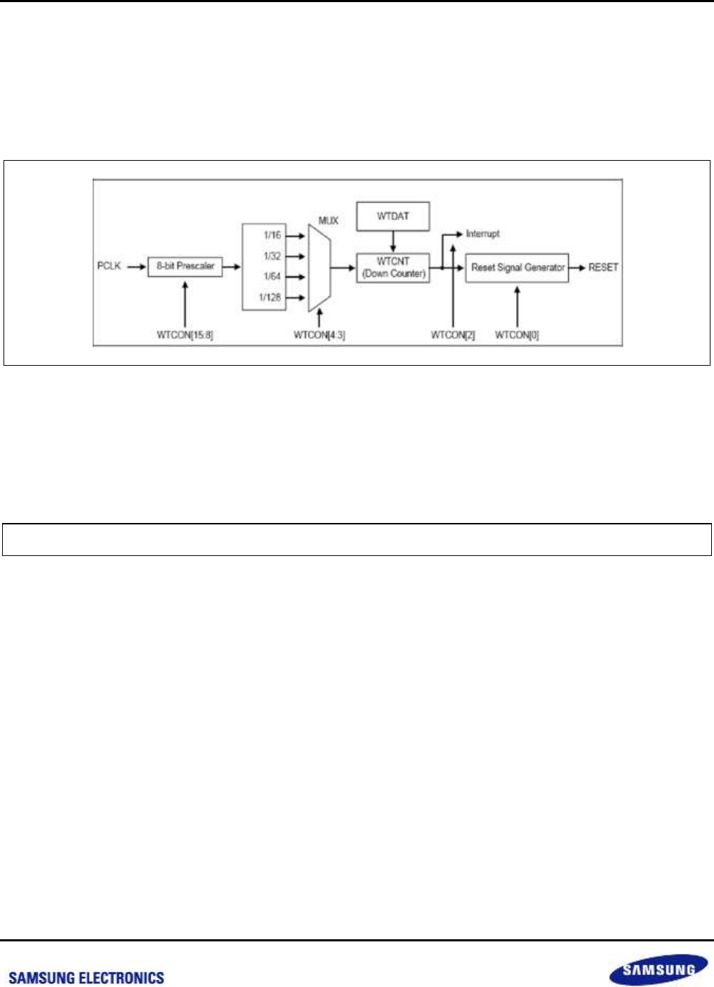
Samsung Confidential
S5P6818_UM 11 Watch Dog Timer
11-2
Preliminary product information describes products that are in development, for which full characterization data and
associated errata are not yet available. Specifications and information herein are subject to change without notice.
11.3 Functional Description
11.3.1 Watchdog Timer Operation
In the Figure below shows the functional block diagram of the watchdog timer. The watchdog timer uses only
PCLK as its source clock. The PCLK frequency is prescaled to generate the corresponding watchdog timer clock,
and the resulting frequency is divided again.
Figure 11-1 Watchdog Timer Block Diagram
The prescaler value and the frequency division factor are specified in the watchdog timer control (WDTCON)
register. Valid prescaler values range from 0 to 28-1. The frequency division factor can be selected as 16, 32, 64
or 128.
Use the following equation to calculate the watchdog timer clock frequency and the duration of each timer clock
cycle:
t_watchdog = 1/(PCLK/(Prescaler value + 1)/Division_factor)
11.3.2 WTDAT & WTCNT
Once the watchdog timer is enabled, the value of watchdog timer data (WTDAT) register cannot be automatically
reloaded into the timer counter (WTCNT). In this reason, an initial value must be written to the watchdog timer
count (WTCNT) register, before the watchdog timer starts.
11.3.3 Consideration of Debugging Environment
When the MDIRAC-III is in debug mode Embedded ICE, the watchdog timer must not operate. The watchdog
timer can determine whether or not it is currently in the debug mode from the CPU core signal (DBGACK signal).
Once the DBGACK signal is asserted, the reset output of the watchdog timer is not activated as the watchdog
timer is expired.
nexell / ys.kim at 2015.02.12
SAMSUNG Confidential

Samsung Confidential
S5P6818_UM 11 Watch Dog Timer
11-3
Preliminary product information describes products that are in development, for which full characterization data and
associated errata are not yet available. Specifications and information herein are subject to change without notice.
11.3.4 Special Function Register
11.3.4.1 Memory map
Register
Type
Description
Reset Value
WTCON
RW
Watchdog timer control register
0x8021
WTDAT
RW
Watchdog timer data register
0x8000
WTCNT
RW
Watchdog timer count register
0x8000
WTCLRINT
W
Watchdog timer interrupt register
–
11.3.4.2 Watchdog Timer Control (WTCON) Register
The WTCON register allows the user to enable/disable the watchdog timer, select the clock signal from 4 different
sources, enable/disable interrupts, and enable/disable the watchdog timer output.
The Watchdog timer is used to resume restart in mal-function after its power on, if controller restart is not desired,
the Watchdog timer should be disabled.
If the user wants to use the normal timer provided by the Watchdog timer, enable the interrupt and disable the
Watchdog timer.
11.3.4.3 Watchdog Timer Data (WTDAT) Register
The WTDAT register is used to specify the time-out duration. The content of WTDAT cannot be automatically
loaded into the timer counter at initial watchdog timer operation. However, using 0x8000(initial value) will drive the
first timeout. In this case, the value of WTDAT will be automatically reloaded into WTCNT.
11.3.4.4 Watchdog Timer Count (WTCNT) Register
The WTCNT register contains the current count values for the watchdog timer during normal operation. Note that
the content of WTDAT register cannot be automatically loaded into the timer count register when the watchdog
timer is enabled initially, so the WTCNT register must be set to initial value before enabling it.
11.3.4.5 Watchdog Timer Interrupt (WTCLRINT) Register
The WTCLRINT register is used to clear the interrupt. Interrupt service routine is responsible for clearing the
relevant interrupt after the interrupt service is completed. Writing any values on this register clears the interrupt.
Reading this register is not allowed.
nexell / ys.kim at 2015.02.12
SAMSUNG Confidential
Samsung Confidential
S5P6818_UM 11 Watch Dog Timer
11-4
Preliminary product information describes products that are in development, for which full characterization data and
associated errata are not yet available. Specifications and information herein are subject to change without notice.
11.4 Register Description
11.4.1 Register Map Summary
Base Address: 0xC001_9000h
Register
Offset
Description
Reset Value
WTCON
0x00h
Watchdog Timer Control register
0x8021
WTDAT
0x04h
Watchdog Timer Data register
0x8000
WTCNT
0x08h
Watchdog Timer Count register
0x8000
WTCLRINT
0x0Ch
Watchdog Timer Interrupt register
–
nexell / ys.kim at 2015.02.12
SAMSUNG Confidential

Samsung Confidential
S5P6818_UM 11 Watch Dog Timer
11-5
Preliminary product information describes products that are in development, for which full characterization data and
associated errata are not yet available. Specifications and information herein are subject to change without notice.
11.4.1.1 WTCON
Base Address: 0xC001_9000h
Address = Base Address + 0x00h, Reset Value = 0x0000_8021
Name
Bit
Type
Description
Reset Value
RSVD
[31:16]
–
Reserved
–
PRESCALER VALUE
[15:8]
RW
Prescaler value.
The valid range is from 0 to (28-1).
8’h80
RSVD
[7:6]
–
Reserved
–
WATCHDOG TIMER
[5]
RW
Enable or disable bit of Watchdog timer.
0 = Disable
1 = Enable
1'b1
CLOCK SELECT
[4:3]
RW
Determine the clock division factor.
00 = 16
01 = 32
10 = 64
11 = 128
2'b0
INTERRUPT
GENERATION
[2]
RW
Enable or disable bit of the interrupt.
0 = Disable
1 = Enable
1'b0
RSVD
[1]
–
Reserved
–
RESET
ENABLE/DISABLE
[0]
RW
Enable or disable bit of Watchdog timer output for reset
signal.
0 = Disable the reset function of the watchdog timer.
1 = Assert reset signal of the S5P6818 at watchdog
time-out.
1'b1
nexell / ys.kim at 2015.02.12
SAMSUNG Confidential
Samsung Confidential
S5P6818_UM 11 Watch Dog Timer
11-6
Preliminary product information describes products that are in development, for which full characterization data and
associated errata are not yet available. Specifications and information herein are subject to change without notice.
11.4.1.2 WTDAT
Base Address: 0xC001_9000h
Address = Base Address + 0x04h, Reset Value = 0x0000_8000
Name
Bit
Type
Description
Reset Value
RSVD
[31:16]
–
Reserved
–
WTDAT
[15:0]
RW
Watchdog timer count value for reload.
16’h8000
11.4.1.3 WTCNT
Base Address: 0xC001_9000h
Address = Base Address + 0x08h, Reset Value = 0x0000_8000
Name
Bit
Type
Description
Reset Value
RSVD
[31:16]
–
Reserved
–
WTCNT
[15:0]
RW
The current value of the watchdog timer
16’h8000
11.4.1.4 WTCLRINT
Base Address: 0xC001_9000h
Address = Base Address + 0x0Ch, Reset Value = Write Only.
Name
Bit
Type
Description
Reset Value
WTCLRINT
[31:0]
W
Write any values clears the interrupt
–
nexell / ys.kim at 2015.02.12
SAMSUNG Confidential

Samsung Confidential
S5P6818_UM 12RTC
12-1
Preliminary product information describes products that are in development, for which full characterization data and
associated errata are not yet available. Specifications and information herein are subject to change without notice.
12 RTC
12.1 Overview
The Real Time Clock (RTC) block can be operated by the Backup Battery while the system power is off. The RTC
block is composed of 32-bit free counter register and works with an external 32.768 kHz Crystal and also can
perform the alarm function.
12.2 Features
32-bit Counter
Alarm Function: Alarm Interrupt or Wake Up from Power Down Mode
Independent power pin (VDD_RTC)
Supports 1 Hz Time interrupt for Power Down Mode
Generates Power Management Reset signal
nexell / ys.kim at 2015.02.12
SAMSUNG Confidential
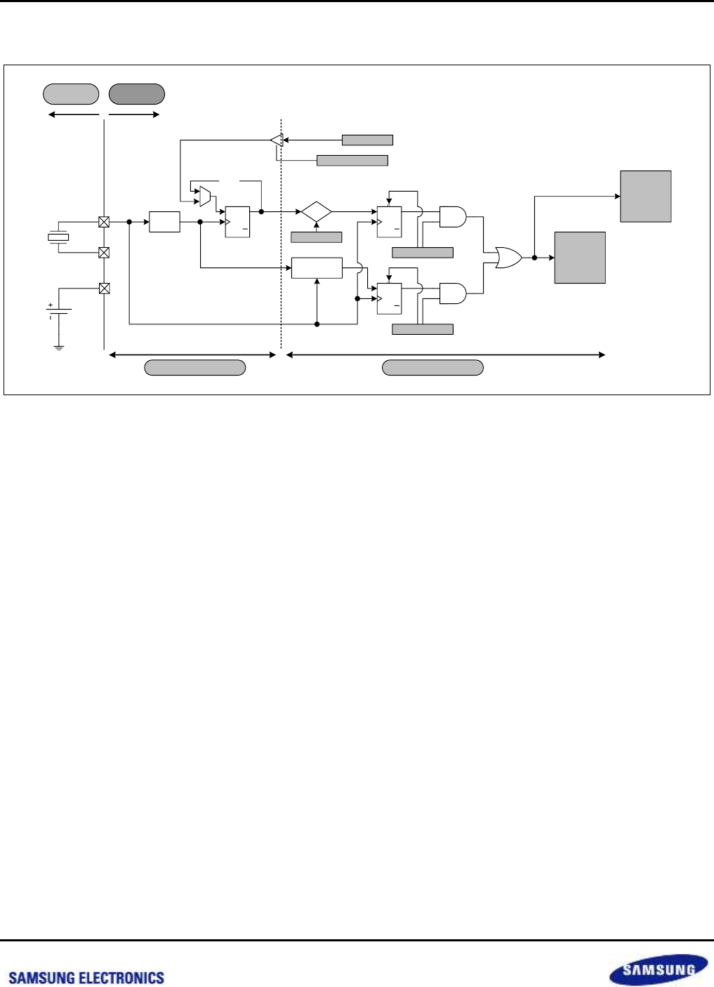
Samsung Confidential
S5P6818_UM 12RTC
12-2
Preliminary product information describes products that are in development, for which full characterization data and
associated errata are not yet available. Specifications and information herein are subject to change without notice.
12.3 Block Diagram
Figure 12-1 RTC Block Diagram
In the upper Figure, shows the RTC block diagram. The RTC block receives an external clock of 32.768 kHz and
divides it into 1 Hz with 32.768 kHz. The RTC Counter operates depending on the external clock.
NOTE: As shown in the upper Figure, the left and right parts of the central dotted line use RTC Power and Normal Power,
separately. The RTC Power Block uses a mercury battery, but the block actually using the mercury battery is the RTC
Counter in the RTC Power Block. The battery life is about five years.
In the upper Figure, the output in point [A] is applied to the Power Manager or the Interrupt Controller. The output
is applied to the Interrupt Controller in Normal mode and applied to the Power Manager in Power mode.
NOTE: Even if RTC is not used, RTC power and RTC clock should be supplied.
Fin/
32768 Q
Q
SET
CLR
D
RTC COUNTER
RTCCNTWRITE
RTCALARM Q
Q
SET
CLR
D
RTCCNTWRITEENB bit
RTC POWER BLOCK NORMAL POWER BLOCK
Q
Q
SET
CLR
D
ALARMINTENB bit
RTCINTENB bit
EXTERNAL INERNAL
Rising Edge
Detector
32.768KHz 1Hz
Power
Manager
+ 1
Yes
3V
Battery
==
Fin
Interrupt
Controller
A
nexell / ys.kim at 2015.02.12
SAMSUNG Confidential

Samsung Confidential
S5P6818_UM 12RTC
12-3
Preliminary product information describes products that are in development, for which full characterization data and
associated errata are not yet available. Specifications and information herein are subject to change without notice.
12.4 Functional Description
12.4.1 Backup Battery Operation
As shown in the upper Figure, since the RTC block uses a separate power source (Coin Battery), the RTC block
operates even when the external power is turned off.
The RTC Logic can be driven by the Backup Battery, which supplies the power through the VDD_RTC pin into the
RTC Block, even if the system power is off. When the system power is off, the interfaces of the CPU and RTC
logic should be blocked and the backup battery only drives the oscillation circuit and the internal 32-bit RTC
counter to minimize power dissipation. In other words, the RTC block can be used as the Wake-Up Source when
the S5P6818 is converted into Power Down mode.
The use of the RTC block as a Wake-Up source requires that the RTCCTRL.ACCESSENB bit is set as '0' before
the system enters Power Down mode. Setting it as '0' is performed to use the RTC as the Wake-Up source even
when the system enters the Power Down Mode.
Even if the RTC block is not used, the RTC Clock must be connected to S5P6818 because the RTC clock is used
as the clock for power management operation.
12.4.2 RTC Operation
The RTC generates an alarm signal at a specified time in the Power Down Mode or Normal Operation Mode. In
Normal Operation Mode, the Alarm Interrupt is activated. In Power Down Mode, the Power Management Wake Up
Signal is activated as well as the RTCALARM. The ALARM Time Set register (RTCALARM) determines the
condition of the alarm time setting and the RTCINTENB.ALARMINTENB bit determines the alarm enable/disable
status.
The procedure to generate an alarm interrupt is as follows:
First, write a counter value to the RTCCNTWRITE register. (To this end, the busy status of the
RTCCTRL.RTCCNTWAIT should be checked in advance. The written value is applied to the register after two
32.768 kHz clock cycles.) After that, write the value of the point at which you wish to generate an interrupt to the
RTCALARM register. The RTC counter increases the counter value at intervals of 1 Hz. If the values of the two
registers (RTCCNTWRITE and RTCAKARM registers) become equal when the RTCINTENB.ALARMINTENB bit
is set as "1", an interrupt occurs.
In a similar way, the RTC interrupt is detected in a rising edge of 1Hz. In this case, the interrupt is generated by
setting the RTCINTENB.RTCINTENB bit as "1".
In addition, The RTCINTENB register contains the Pending Clear function and the Pending Clear is performed by
writing "0".
nexell / ys.kim at 2015.02.12
SAMSUNG Confidential

Samsung Confidential
S5P6818_UM 12RTC
12-4
Preliminary product information describes products that are in development, for which full characterization data and
associated errata are not yet available. Specifications and information herein are subject to change without notice.
12.4.3 Accessing the RTC Time Counter Setting/Read Register
To access RTC Time Count Read Register (RTCCNTREAD) and RTC Time Count Setting Register
(RTCCNTWRITE), the RTCCTRL.RTCCNTWRITEENB bit is set to "1" before accessing these register. When the
CPU completes to access these register, the CPU should set the RTCCTRL.RTCCNTWRITEENB bit to "0" to
protect the content of RTC counter from unknown problem in abnormal state. The RTCCNTWRITEENB bit
determines the reflection of the RCCNTWRITE register value to the RTC counter.
12.4.4 Interrupt Pending Register
Only the "READ" function is available for the RTCINTPND register of the S5P6818, but the current pending status
can be read.
Since the RTCINTPND register only has a "READ" function, the Pending Clear function is controlled by the
RTCINTENB register. The Interrupt Pending status is cleared by disabling the relevant interrupt. Therefore, if the
corresponding bit of the RTCINTENB register is set as "1", the relevant interrupt is enabled. If the corresponding
bit is set as "0", the interrupt is disabled and the pending bit is also cleared.
12.4.5 Power Manager Reset Time Control
RTC controls the time when nPWRMANRST (Power Manager Reset) releases from CorePOR. Refer to
RTCCORERSTIMESEL Register for setting the time when nPWRMANRST releases.
nexell / ys.kim at 2015.02.12
SAMSUNG Confidential
Samsung Confidential
S5P6818_UM 12RTC
12-5
Preliminary product information describes products that are in development, for which full characterization data and
associated errata are not yet available. Specifications and information herein are subject to change without notice.
12.5 Register Description
12.5.1 Register Map Summary
Base Address: 0xC001_0C00h
Register
Offset
Description
Reset Value
RTCCNTWRITE
0x00h
RTC time count setting register
–
RTCCNTREAD
0x04h
RTC time count read register
–
RTCALARM
0x08h
Alarm time count set register
0x0000_0000
RTCCTRL
0x0Ch
RTC control register
0x0000_0000
RTCINTENB
0x10h
RTC interrupt enable register
0x0000_0000
RTCINTPND
0x14h
RTC interrupt pending register
0x0000_0000
RTCCORERSTIMESEL
0x18h
RTC core por time select register
0x0000_0000
RTCSCRATCH
0x1Ch
RTC scratch register
0x0000_0000
nexell / ys.kim at 2015.02.12
SAMSUNG Confidential
Samsung Confidential
S5P6818_UM 12RTC
12-6
Preliminary product information describes products that are in development, for which full characterization data and
associated errata are not yet available. Specifications and information herein are subject to change without notice.
12.5.1.1 RTCCNTWRITE
Base Address: 0xC001_0C00h
Address = Base Address + 0x00h, Reset Value = Undefined
Name
Bit
Type
Description
Reset Value
RTCCNTWRITE
[31:0]
W
Set RTC Counter Value. (Uni: 1 Hz)
The RTCCNTWAIT bit of the RTCCONTROL register
should be checked before a value is written in this bit. If the
RTCCNTWAIT bit is "1", this written value is not reflected.
The written value is reflected to this register at least two
cycles of 32768 Hz after it is changed to "0".
To write a value to this register, the RTCCNTWRITEENB
bit should be set as "1".
–
NOTE: RTC reset to unknown values. If RTC power is first applied
12.5.1.2 RTCCNTREAD
Base Address: 0xC001_0C00h
Address = Base Address + 0x04h, Reset Value = Undefined
Name
Bit
Type
Description
Reset Value
RTCCNTREAD
[31:0]
R
Read Current RTC Counter Value. (Unit: 1 Hz)
The value of the RTC counter is continuously changed.
–
nexell / ys.kim at 2015.02.12
SAMSUNG Confidential
Samsung Confidential
S5P6818_UM 12RTC
12-7
Preliminary product information describes products that are in development, for which full characterization data and
associated errata are not yet available. Specifications and information herein are subject to change without notice.
12.5.1.3 RTCALARM
Base Address: 0xC001_0C00h
Address = Base Address + 0x08h, Reset Value = 0x0000_0000
Name
Bit
Type
Description
Reset Value
RTCALARM
[31:0]
RW
ALARM Time Set Register. (Unit: 1 Hz)
The ALARMCNTWAIT bit of the RTCCONTROL register
should be checked before a value is written in this bit. If the
RTCCNTWAIT bit is "1", this written value is not reflected.
The written value is reflected to this register at least two
cycles of 32768 Hz after it is changed to "0".
32'h0
12.5.1.4 RTCCTRL
Base Address: 0xC001_0C00h
Address = Base Address + 0x0Ch, Reset Value = 0x0000_0000
Name
Bit
Type
Description
Reset Value
RSVD
[31:5]
–
Reserved
27'h0
RTCCNTWAIT
[4]
R
RTCCNTWAIT: Register to check if the previously
requested 'WRITE' is completed when writing a value to
the RTCCNTWRITE register. The bit below indicates the
status of the RTCCNTWRITE*register.
0 = IDLE
1 = Busy
1'b0
ALARMCNTWAIT
[3]
R
ALARMCNTWAIT: Register to check if the previously
requested 'WRITE' is completed when writing a value to
the RTCALARM*register. The bit below indicates the status
of the RTCALARMWRITE*register
0 = IDLE
1 = Busy
1'b0
RSVD
[2]
–
Reserved
1'b0
RSVD
[1]
–
Reserved. However, "0" should be written.
1'b0
RTCCNTWRITEENB
[0]
RW
RTCCNTWRITEENB: Control Power isolation and
connection of RTC block. This bit should be "0" before
Power Down Mode for normal operation of RTC in Power
Down Mode.
0 = Disable (Power Isolation)
1 = Enable (Power Connection)
To access the RTCCNTREAD and RTCCNTWRITE
registers, this bit should be set as "1".
1'b0
nexell / ys.kim at 2015.02.12
SAMSUNG Confidential

Samsung Confidential
S5P6818_UM 12RTC
12-8
Preliminary product information describes products that are in development, for which full characterization data and
associated errata are not yet available. Specifications and information herein are subject to change without notice.
12.5.1.5 RTCINTENB
Base Address: 0xC001_0C00h
Address = Base Address + 0x10h, Reset Value = 0x0000_0000
Name
Bit
Type
Description
Reset Value
RSVD
[31:2]
–
Reserved
30'h0
ALARMINTENB
[1]
RW
ALARMINTENB: Set ALARM Interrupt On/Off and Pending
Clear/Interrupt Enable
Read
0 = Interrupt Disable
1 = Interrupt Enable
Write
0 = Pending Clear & Interrupt Disable
1 = Interrupt Enable
1'b0
RTCINTENB
[0]
RW
RTCINTENB: Set RTC (1 Hz Only) Interrupt On/Off and
Pending Clear/Interrupt Enable
Read
0 = Interrupt Disable
1 = Interrupt Enable
Write
0 = Pending Clear & Interrupt Disable
1 = Interrupt Enable
1'b0
12.5.1.6 RTCINTPND
Base Address: 0xC001_0C00h
Address = Base Address + 0x14h, Reset Value = 0x0000_0000
Name
Bit
Type
Description
Reset Value
RSVD
[31:2]
–
Reserved
30'h0
ALARMINTPEND
[1]
R
ALARMINTEPND: ALARM Interrupt Pending bit.
0 = None
1 = Interrupt Pended
1'b0
RTCINTPEND
[0]
R
RTCINTPEND: Set RTC (1 Hz Only) Interrupt Pending bit.
0 = None
1 = Interrupt Pended
1'b0
nexell / ys.kim at 2015.02.12
SAMSUNG Confidential

Samsung Confidential
S5P6818_UM 12RTC
12-9
Preliminary product information describes products that are in development, for which full characterization data and
associated errata are not yet available. Specifications and information herein are subject to change without notice.
12.5.1.7 RTCCORERSTIMESEL
Base Address: 0xC001_0C00h
Address = Base Address + 0x18h, Reset Value = 0x0000_0000
Name
Bit
Type
Description
Reset Value
RSVD
[31:7]
–
Reserved
25'h0
COREPORTIMESEL6
[6]
RW
CORE POR (Power on Reset) releases with the delay
of about 186 ms after CORE VDD Power is turned on.
0 = None
1 = Select
1'b0
COREPORTIMESEL5
[5]
RW
CORE POR (Power on Reset) releases with the delay
of about 155 ms after CORE VDD Power is turned on.
0 = None
1 = Select
1'b0
COREPORTIMESEL4
[4]
RW
CORE POR (Power on Reset) releases with the delay
of about 124 ms after CORE VDD Power is turned on.
0 = None
1 = Select
1'b0
COREPORTIMESEL3
[3]
RW
CORE POR (Power on Reset) releases with the delay
of about 93 ms after CORE VDD Power is turned on.
0 = None
1 = Select
1'b0
COREPORTIMESEL2
[2]
RW
CORE POR (Power on Reset) releases with the delay
of about 62 ms after CORE VDD Power is turned on.
0 = None
1 = Select
1'b0
COREPORTIMESEL1
[1]
RW
CORE POR (Power on Reset) releases with the delay
of about 31 ms after CORE VDD Power is turned on.
0 = None
1 = Select
1'b0
COREPORTIMESEL0
[0]
RW
CORE POR (Power on Reset) releases without delay
after CORE VDD Power is turned on.
0 = None
1 = Select
1'b0
NOTE: CORE POR releases about 210 ms after CORE VDD Power is turned on when RTCCOREPORIMESEL[6:0] = 7'b0
12.5.1.8 WTCON
Base Address: 0xC001_0C00h
Address = Base Address + 0x1Ch, Reset Value = 0x0000_0000
Name
Bit
Type
Description
Reset Value
RTCSCRATCH
[31:0]
RW
RTC scratch register.
32'h0
nexell / ys.kim at 2015.02.12
SAMSUNG Confidential

Samsung Confidential
S5P6818_UM 13 Alive
13-1
Preliminary product information describes products that are in development, for which full characterization data and
associated errata are not yet available. Specifications and information herein are subject to change without notice.
13 Alive
13.1 Overview
In the status with eliminating core power supply of S5P6818, some PAD need power supply continuously and
should keep driving PAD with certain value.
For example a bit that controlling STN LCD should keep driving PAD with low in the status with eliminating core
power supply. 32-bit value can be saved in Scratch Register and the saved value maintains in the case of core
power off.
User could on/off the system power by pressing toggle switch and ALIVE performs the necessary functions in
these momentary power controls.
13.2 Features
Alive GPIO PADs are all in/output PAD.
The value of ALIVE Block maintains even in power off of Core Power.
Alive Block does not use clock. To change the control register value, need to program set/reset pin of SR-
flipflop directly.
Chip sleep mode wake-up source(AliveGPIO, VDDToggle, RTCIRQ)
Power IC Enable.
Supports the PAD Hold function
Scan chain is not inserted to Alive GPIO.
nexell / ys.kim at 2015.02.12
SAMSUNG Confidential

Samsung Confidential
S5P6818_UM 13 Alive
13-1
Preliminary product information describes products that are in development, for which full characterization data and
associated errata are not yet available. Specifications and information herein are subject to change without notice.
13.3 Power Isolation
13.3.1 Core Power Off
In the case of power off of CoreVDD, Alive Registers maintains its value since Alive VDD keep supplied. Pull-
down register connected to NPOWERGATING performs the function of maintaining control bit of Alive Registers
securely in the interval of core power off or unstable.
13.3.2 Power Gating
The value of set/reset should be kept as low to maintains the value of Alive Registers securely in the case of
power off of CoreVDD. Therefore, it's designed to maintain low value in the case of core power off since
NPOWERGATING register is connected to pull-down register.
nexell / ys.kim at 2015.02.12
SAMSUNG Confidential

Samsung Confidential
S5P6818_UM 13 Alive
13-2
Preliminary product information describes products that are in development, for which full characterization data and
associated errata are not yet available. Specifications and information herein are subject to change without notice.
13.4 Alive Registers
All of the Registers except NPOWERGATING/AliveDetectPending Register of Alive block maintains the value
written in Register when Core power turns off, and are reset when Alive Power turns off. Alive Registers do not
have their own Clock, and these can be read and written when NPOWERGATING register is "1"
(NPOWERGATING = 1). And especially, in write mode, Alive Registers can be written by SET/RST (reset)
Register. The following is the example of the Register function according to Register SET/RST.
Alive Registers remains as the former state when *SET* == 0, *RST*=0
Alive Registers are written as “1” when *SET* == 1, *RST*=0
Alive Registers are written as “0” write “0” when *SET* == 0, *RST*=1
Alive Registers are written as “1” when *SET* == 1, *RST*=1
13.4.1 Alive GPIO Detect Registers
For Alive GPIO input, Alive GPIO Detect Registers can be used as Core Power on, Alive Interrupt, Sleep mode
wakeup source in case of Asynchronous/synchronous detecting mode. And when those events are detected,
ALIVEGPIODETECTPENDREG[n] Register is set to "1". The following are the operating examples according to
Detecting modes.
Ex1) Asynchronous Low Level Detecting
Alive GPIO Detect Registers detect the event when ALIVEGPIOLOWASYNCDETECTMODEREADREG [n] = “1”,
ALIVEGPIODETECTENBREADREG[n] = “1”, and AliveGPIO == "0"
Ex2) Asynchronous High Level Detecting
Alive GPIO Detect Registers detect the event when ALIVEGPIOHIGHASYNCDETECTMODEREADREG [n] = “1”,
ALIVEGPIODETECTENBREADREG[n] = “1”, and AliveGPIO[n] == “1”
Ex3) Synchronous Low Level Detecting
Alive GPIO Detect Registers detect the event when ALIVEGPIOLOWSYNCDETECTMODEREADREG [n] = “1”,
ALIVEGPIODETECTENBREADREG[n] = “1”, AliveGPIO[n] == “0”
Ex4) Synchronous High Level Detecting
Alive GPIO Detect Registers detect the event when ALIVEGPIOHIGHSYNCDETECTMODEREADREG [n] = “1”,
ALIVEGPIODETECTENBREADREG[n] = “1”, AliveGPIO[n] == “1”
Ex5) Synchronous Falling Edge Detecting
Alive GPIO Detect Registers detect the event when ALIVEGPIOFALLDETECTMODEREADREG[n] = “1”,
ALIVEGPIODETECTENBREADREG[n] = “1”, and AliveGPIO[n] bit changes from “1” to “0”
Ex6) Synchronous Rising Edge Detecting
Alive GPIO Detect Registers detect the event when ALIVEGPIORISEDETECTMODEREADREG [n] = “1”,
ALIVEGPIODETECTENBREADREG[n] = “1”, and AliveGPIO[n] bit changes from “0” to “1”
nexell / ys.kim at 2015.02.12
SAMSUNG Confidential

Samsung Confidential
S5P6818_UM 13 Alive
13-3
Preliminary product information describes products that are in development, for which full characterization data and
associated errata are not yet available. Specifications and information herein are subject to change without notice.
13.4.2 Scratch Register
Programmer could save any 32-bit value in Scratch Register. The value of Scratch Register maintains in the case
of power off of CoreVDD.
13.4.3 Alive GPIO Control Registers
Alive GPIO is controlled through Alive Block regardless of GPIO block.
Control Register has AliveGPIO in/out mode enable, pull-up, and AliveGPIOPADOut.
13.5 Momentary Power Control
13.5.1 CoreVDD Powering On
The Core Power can be changed from off-state to on-state by the VDDPWRTOGGLE switch, AliveGPIO
Detecting, RTC interrupt. And in case of Power on, VDDPWRTOGGLE switch, AliveGPIO Detecting, and RTC
interrupt can be processed, after system booting, by setting VDDPWRON_DDR/VDDPWRON Bit. (Power On is
not allowed when Battery Fault occurs.).
13.5.2 CoreVDD Powering Off
The Core Power can be changed from off-state to on-state by clearing VDDPWRON_DDR/VDDPWRON Bit.
Core Block and Alive Block are connected through PowerGating Register, which makes it possible for Alive
Registers to safely sustain their own values even after Core Power turns off with VDDPWRON_
DDR/VDDPWRON Bit cleared.
The following is the example of Chip Power sequence
1. Do not hold the initial Pad state. (NPADHOLDx = 1)
2. Hold the Pad before you turn off the Power. (NPADHOLDx Register = 0)
3. Turn off VDDPWRON
4. Non-Alive POR is set low after power turns off
5. Power starts to be supplied by pressing toggle switch
6. PAD releases from the hold state when internal POR turns on (which provides the stability for preventing pad
hold from releasing after power turns on)
7. VDDPWRON and PadHold Register should be released simultaneously after system booting.
8. VDDPOWRON should be released.
NPADHOLDENBx Register should be set as "0" except Power On Reset.
nexell / ys.kim at 2015.02.12
SAMSUNG Confidential
Samsung Confidential
S5P6818_UM 13 Alive
13-4
Preliminary product information describes products that are in development, for which full characterization data and
associated errata are not yet available. Specifications and information herein are subject to change without notice.
13.6 SLEEP Mode
S5P6818 supports two SLEEP Modes (SleepMode1, SleepMode2). Core power turns off in SLEEP Mode, and the
Chip wakes up from SLEEP Mode by Wake-up sources such as AliveGPIO Detecting, RTC Interrupt, and
nVDDPWRTOGGLE Switch push.(And, No wake-up is possible in case of battery fault)
Alive GPIO Detect Pending Register Clear
Hold the Pad before user turns off Power. (SleepMode1: NPADHOLDx[2:1] = 2'b00, SleepMode2:
NPADHOLDx[2:0] == 3'b000)
VDDPWRON Register Clear
NPOWERGATING Register Clear
S5P6818 STOP Mode Set(Refer to Clock and Power management Section)
13.7 PMU (Power management Unit)
13.7.1 Overview
PMU is a block inside of ALIVE. It controls internal power switch of sub-blocks in chip.
PMU can control the power up and down of these blocks:
GPU (graphic processing unit)
MFC (multi function codec)
13.7.2 Power Mode Table
MODE
PD_RTC
PD_ALIVE
PD_TOP
PD_DREX
PD_CODEC
PD_GR3D
PD_CPU
Num.
Name
1
POWER ON
RESET
ON
ON
ON
ON
ON
ON
ON
2
NORMAL
ON
ON
ON
ON
ON
ON
ON
3
SUB SLEEP - 0
ON
ON
ON
ON
OFF
ON
ON
4
SUB SLEEP - 1
ON
ON
ON
ON
ON
OFF
ON
5
SUB SLEEP -
ALL
ON
ON
ON
ON
OFF
OFF
ON
6
DEEP IDLE
ON
ON
ON
ON
OFF
OFF
OFF
7
TOP SLEEP
ON
ON
OFF
OFF
OFF
OFF
OFF
8
RTC ONLY
ON
OFF
OFF
OFF
OFF
OFF
OFF
nexell / ys.kim at 2015.02.12
SAMSUNG Confidential
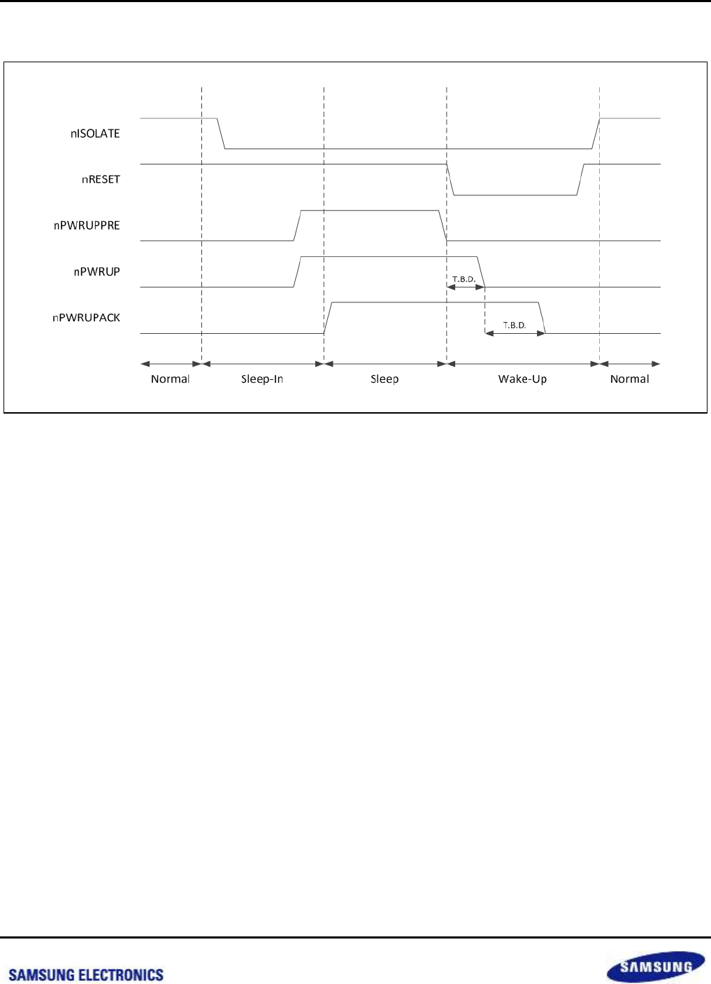
Samsung Confidential
S5P6818_UM 13 Alive
13-5
Preliminary product information describes products that are in development, for which full characterization data and
associated errata are not yet available. Specifications and information herein are subject to change without notice.
13.7.3 Power Switch Control Sequence
Figure 13-1 Power Switch Control Sequence
nexell / ys.kim at 2015.02.12
SAMSUNG Confidential

Samsung Confidential
S5P6818_UM 13 Alive
13-6
Preliminary product information describes products that are in development, for which full characterization data and
associated errata are not yet available. Specifications and information herein are subject to change without notice.
13.8 Register Description
13.8.1 Register Map Summary
Base Address : 0xC001_0000h
Register
Offset
Description
Reset Value
ALIVEPWRGATEREG
0x0800
Alive Power Gating Register
0x0000_0000
ALIVEGPIOASYNCDETECTMODERST
REG0
0x0804
Alive GPIO ASync Detect Mode Reset Register
0
0x0000_0000
ALIVEGPIOASYNCDETECTMODERST
REG1
0x0810
Alive GPIO ASync Detect Mode Reset Register
1
0x0000_0000
ALIVEGPIOASYNCDETECTMODESET
REG0
0x0808
Alive GPIO ASync Detect Mode Set Register 0
0x0000_0000
ALIVEGPIOASYNCDETECTMODESET
REG1
0x0814
Alive GPIO ASync Detect Mode Set Register 1
0x0000_0000
ALIVEGPIOLOWASYNCDETECTMOD
EREADREG
0x080C
Alive GPIO Low Level Async Detect Mode Read
Register
0x0000_0000
ALIVEGPIOHIGHASYNCDETECTMOD
EREADREG
0x0818
Alive GPIO High Level Async Detect Mode
Read Register
0x0000_0000
ALIVEGPIODETECTMODERSTREG0
0x081C
Alive GPIO Detect Mode Reset Register 0
0x0000_0000
ALIVEGPIODETECTMODERSTREG1
0x0828
Alive GPIO Detect Mode Reset Register 1
0x0000_0000
ALIVEGPIODETECTMODERSTREG2
0x0834
Alive GPIO Detect Mode Reset Register 2
0x0000_0000
ALIVEGPIODETECTMODERSTREG3
0x0840
Alive GPIO Detect Mode Reset Register 3
0x0000_0000
ALIVEGPIODETECTMODESETREG0
0x0820
Alive GPIO Detect Mode Set Register 0
0x0000_0000
ALIVEGPIODETECTMODESETREG1
0x082C
Alive GPIO Detect Mode Set Register 1
0x0000_0000
ALIVEGPIODETECTMODESETREG2
0x0838
Alive GPIO Detect Mode Set Register 2
0x0000_0000
ALIVEGPIODETECTMODESETREG3
0x0844
Alive GPIO Detect Mode Set Register 3
0x0000_0000
ALIVEGPIOFALLDETECTMODEREAD
REG
0x0824
Alive GPIO Falling Edge Detect Mode Read
Register
0x0000_0000
ALIVEGPIORISEDETECTMODEREAD
REG
0x0830
Alive GPIO Rising Edge Detect Mode Read
Register
0x0000_0000
ALIVEGPIOLOWDETECTMODEREAD
REG
0x083C
Alive GPIO Low Level Detect Mode Read
Register
0x0000_0000
ALIVEGPIOHIGHDETECTMODEREAD
REG
0x0848
Alive GPIO High Level Detect Mode Read
Register
0x0000_0000
ALIVEGPIODETECTENBRSTREG
0x084C
Alive GPIO Detect Enable Reset Register
0x0000_0000
ALIVEGPIODETECTENBSETREG
0x0850
Alive GPIO Detect Enable Set Register
0x0000_0000
ALIVEGPIODETECTENBREADREG
0x0854
Alive GPIO Detect Enable Read Register
0x0000_0000
ALIVEGPIOINTENBRSTREG
0x0858
Alive GPIO Interrupt Enable Reset Register
0x0000_0000
ALIVEGPIODETECTENABLESETREG
0x085C
Alive GPIO Detect Enable Set Register
0x0000_0000
ALIVEGPIOINTENBREADREG
0x0860
Alive GPIO Interrupt Enable Read Register
0x0000_0000
ALIVEGPIODETECTPENDREG
0x0864
Alive GPIO Detect Pending Register
0x0000_0000
nexell / ys.kim at 2015.02.12
SAMSUNG Confidential

Samsung Confidential
S5P6818_UM 13 Alive
13-7
Preliminary product information describes products that are in development, for which full characterization data and
associated errata are not yet available. Specifications and information herein are subject to change without notice.
Register
Offset
Description
Reset Value
ALIVESCRATCHRSTREG
0x0868
Alive Scratch Reset Register
0x0000_0000
ALIVESCRATCHSETREG
0x086C
Alive Scratch Set Register
0x0000_0000
ALIVESCRATCHREADREG
0x0870
Alive Scratch Read Register
0x0000_0000
ALIVEGPIOPADOUTENBRSTREG
0x0874
Alive GPIO PAD Out Enable Reset Register
0x0000_0000
ALIVEGPIOPADOUTENBSETREG
0x0878
Alive GPIO PAD Out Enable Set Register
0x0000_0000
ALIVEGPIOPADOUTENBREADREG
0x087C
Alive GPIO PAD Out Enable Read Register
0x0000_0000
ALIVEGPIOPADPULLUPRSTREG
0x0880
Alive GPIO PAD Pullup Reset Register
0x0000_0000
ALIVEGPIOPADPULLUPSETREG
0x0884
Alive GPIO PAD Pullup Set Register
0x0000_0000
ALIVEGPIOPADPULLUPREADREG
0x0888
Alive GPIO PAD Pullup Read Register
0x0000_00FF
ALIVEGPIOPADOUTRSTREG
0x088C
Alive GPIO PAD Out Reset Register
0x0000_0000
ALIVEGPIOPADOUTSETREG
0x0890
Alive GPIO PAD Out Set Register
0x0000_0000
ALIVEGPIOPADOUTREADREG
0x0894
Alive GPIO PAD Out Read Register
0x0000_0000
VDDCTRLRSTREG
0x0898
VDD Control reset Register
0x0000_0000
VDDCTRLSETREG
0x089C
VDD Control set Register
0x0000_0000
VDDCTRLREADREG
0x08A0
VDD Control Read Register
0x0000_03FF
ALIVECLEARWAKEUPSTATUSREGIS
TER
0x08A4
Alive Clear Wakeup Status Register
0x0000_0000
ALIVESLEEPWAKEUPSTATUSREGIS
TER
0x08A8
Alive Sleep Wakeup Status Register
0x0000_0000
ALIVESCRATCHRSTREG1
0x08AC
Alive Scratch Reset Register1
0x0000_0000
ALIVESCRATCHRSTREG2
0x08B8
Alive Scratch Reset Register2
0x0000_0000
ALIVESCRATCHRSTREG3
0x08C4
Alive Scratch Reset Register3
0x0000_0000
ALIVESCRATCHRSTREG4
0x08D0
Alive Scratch Reset Register4
0x0000_0000
ALIVESCRATCHRSTREG5
0x08DC
Alive Scratch Reset Register5
0x0000_0000
ALIVESCRATCHRSTREG6
0x08E8
Alive Scratch Reset Register6
0x0000_0000
ALIVESCRATCHRSTREG7
0x08F4
Alive Scratch Reset Register7
0x0000_0000
ALIVESCRATCHRSTREG8
0x0900
Alive Scratch Reset Register8
0x0000_0000
ALIVESCRATCHSETREG1
0x08B0
Alive Scratch Set Register1
0x0000_0000
ALIVESCRATCHSETREG2
0x08BC
Alive Scratch Set Register2
0x0000_0000
ALIVESCRATCHSETREG3
0x08C8
Alive Scratch Set Register3
0x0000_0000
ALIVESCRATCHSETREG4
0x08D4
Alive Scratch Set Register4
0x0000_0000
ALIVESCRATCHSETREG5
0x08E0
Alive Scratch Set Register5
0x0000_0000
ALIVESCRATCHSETREG6
0x08EC
Alive Scratch Set Register6
0x0000_0000
ALIVESCRATCHSETREG7
0x08F8
Alive Scratch Set Register7
0x0000_0000
ALIVESCRATCHSETREG8
0x0904
Alive Scratch Set Register8
0x0000_0000
ALIVESCRATCHREADREG1
0x08B4
Alive Scratch Read Register1
0x0000_0000
ALIVESCRATCHREADREG2
0x08C0
Alive Scratch Read Register2
0x0000_0000
nexell / ys.kim at 2015.02.12
SAMSUNG Confidential

Samsung Confidential
S5P6818_UM 13 Alive
13-8
Preliminary product information describes products that are in development, for which full characterization data and
associated errata are not yet available. Specifications and information herein are subject to change without notice.
Register
Offset
Description
Reset Value
ALIVESCRATCHREADREG3
0x08CC
Alive Scratch Read Register3
0x0000_0000
ALIVESCRATCHREADREG4
0x08D8
Alive Scratch Read Register4
0x0000_0000
ALIVESCRATCHREADREG5
0x08E4
Alive Scratch Read Register5
0x0000_0000
ALIVESCRATCHREADREG6
0x08F0
Alive Scratch Read Register6
0x0000_0000
ALIVESCRATCHREADREG7
0x08FC
Alive Scratch Read Register7
0x0000_0000
ALIVESCRATCHREADREG8
0x0908
Alive Scratch Read Register8
0x0000_0000
VDDOFFDELAYRSTREGISTER
0x090C
VDD Off Delay Reset Register
0x0000_0000
VDDOFFDELAYSETREGISTER
0x0910
VDD Off Delay Set Register
0x0000_0000
VDDOFFDELAYVALUEREGISTER
0x0914
VDD Off Delay Value Register
0x0000_0000
VDDOFFDELAYTIMEREGISTER
0x0918
VDD Off Delay Time Register
0x0000_0000
ALIVEGPIOINPUTVALUE
0x091C
Alive GPIO Input Value Read Register
0x0000_0000
RSVD
~ 0x0BFF
Reserved
–
RTC
0x0C00 to
0x0CFF
See RTC section
–
PMUNISOLATE
0x0D00
PMU nISOLATE Register
0x0000_0003
PMUNPWRUPPRE
0x0D04
PMU nPOWER Up Precharge Register
0x0000_0000
PMUNPWRUP
0x0D08
PMU nPOWER Up Register
0x0000_0000
PMUNPWRUPACK
0x0D0C
PMU nPOWER Up ACK Register
0x0000_0000
nexell / ys.kim at 2015.02.12
SAMSUNG Confidential

Samsung Confidential
S5P6818_UM 13 Alive
13-9
Preliminary product information describes products that are in development, for which full characterization data and
associated errata are not yet available. Specifications and information herein are subject to change without notice.
13.8.1.1 ALIVEPWRGATEREG
Base Address: 0xC001_0000h
Address = Base Address + 0x0800h, Reset Value = 0x0000_0000
Name
Bit
Type
Description
Reset Value
RSVD
[31:1]
–
Reserved
0
NPOWERGATING
[0]
RW
NPOWERGATING (negative active Power Gating).
The default value is 0, disabling writing to Alive
Registers, in order to keep the values of Alive
Registers when Core Power 1.0V is off.
0 = Disable writing data to Alive Register
1 = Enable writing data to Alive Register
1'b0
13.8.1.2 ALIVEGPIOASYNCDETECTMODERSTREG0
Base Address: 0xC001_0000h
Address = Base Address + 0x0804h, Reset Value = 0x0000_0000
Name
Bit
Type
Description
Reset Value
RSVD
[31:8]
–
Reserved
24’h0
ASyncdetectmoderST0_7
[7]
RW
Alive GPIO7 Low Level Async detect mode Register
Reset.
0 = None
1 = Reset
1'b0
ASyncdetectmoderST0_6
[6]
RW
Alive GPIO6 Low Level Async detect mode Register
Reset.
0 = None
1 = Reset
1'b0
ASyncdetectmoderST0_5
[5]
RW
Alive GPIO5 Low Level Async detect mode Register
Reset.
0 = None
1 = Reset
1'b0
ASyncdetectmoderST0_4
[4]
RW
Alive GPIO4 Low Level Async detect mode Register
Reset.
0 = None
1 = Reset
1'b0
ASyncdetectmoderST0_3
[3]
RW
Alive GPIO3 Low Level Async detect mode Register
Reset.
0 = None
1 = Reset
1'b0
ASyncdetectmoderST0_2
[2]
RW
Alive GPIO2 Low Level Async detect mode Register
Reset.
0 = None
1 = Reset
1'b0
ASyncdetectmoderST0_1
[1]
RW
Alive GPIO1 Low Level Async detect mode Register
Reset.
1'b0
nexell / ys.kim at 2015.02.12
SAMSUNG Confidential

Samsung Confidential
S5P6818_UM 13 Alive
13-10
Preliminary product information describes products that are in development, for which full characterization data and
associated errata are not yet available. Specifications and information herein are subject to change without notice.
Name
Bit
Type
Description
Reset Value
0 = None
1 = Reset
ASyncdetectmoderST0_0
[0]
RW
Alive GPIO0 Low Level Async detect mode Register
Reset.
0 = None
1 = Reset
1'b0
nexell / ys.kim at 2015.02.12
SAMSUNG Confidential

Samsung Confidential
S5P6818_UM 13 Alive
13-11
Preliminary product information describes products that are in development, for which full characterization data and
associated errata are not yet available. Specifications and information herein are subject to change without notice.
13.8.1.3 ALIVEGPIOASYNCDETECTMODERSTREG1
Base Address: 0xC001_0000h
Address = Base Address + 0x0810h, Reset Value = 0x0000_0000
Name
Bit
Type
Description
Reset Value
RSVD
[31:8]
–
Reserved
24’h0
ASyncdetecTMODERST1_7
[7]
RW
Alive GPIO7 High Level Async detect mode
Register Reset.
0 = None
1 = Reset
1'b0
ASyncdetecTMODERST1_6
[6]
RW
Alive GPIO6 High Level Async detect mode
Register Reset.
0 = None
1 = Reset
1'b0
ASyncdetecTMODERST1_5
[5]
RW
Alive GPIO5 High Level Async detect mode
Register Reset.
0 = None
1 = Reset
1'b0
ASyncdetecTMODERST1_4
[4]
RW
Alive GPIO4 High Level Async detect mode
Register Reset.
0 = None
1 = Reset
1'b0
ASyncdetecTMODERST1_3
[3]
RW
Alive GPIO3 High Level Async detect mode
Register Reset.
0 = None
1 = Reset
1'b0
ASyncdetecTMODERST1_2
[2]
RW
Alive GPIO2 High Level Async detect mode
Register Reset.
0 = None
1 = Reset
1'b0
ASyncdetecTMODERST1_1
[1]
RW
Alive GPIO1 High Level Async detect mode
Register Reset.
0 = None
1 = Reset
1'b0
ASyncdetecTMODERST1_0
[0]
RW
Alive GPIO0 High Level Async detect mode
Register Reset.
0 = None
1 = Reset
1'b0
nexell / ys.kim at 2015.02.12
SAMSUNG Confidential

Samsung Confidential
S5P6818_UM 13 Alive
13-12
Preliminary product information describes products that are in development, for which full characterization data and
associated errata are not yet available. Specifications and information herein are subject to change without notice.
13.8.1.4 ALIVEGPIOASYNCDETECTMODESETREG0
Base Address: 0xC001_0000h
Address = Base Address + 0x0808h, Reset Value = 0x0000_0000
Name
Bit
Type
Description
Reset Value
RSVD
[31:8]
–
Reserved
24’h0
ASyncdetectMODEset0_7
[7]
RW
Alive GPIO7 Low Level Async detect mode Register
Set.
0 = None
1 = Set
1'b0
ASyncdetectMODEset0_6
[6]
RW
Alive GPIO6 Low Level Async detect mode Register
Set.
0 = None
1 = Set
1'b0
ASyncdetectMODEset0_5
[5]
RW
Alive GPIO5 Low Level Async detect mode Register
Set.
0 = None
1 = Set
1'b0
ASyncdetectMODEset0_4
[4]
RW
Alive GPIO4 Low Level Async detect mode Register
Set.
0 = None
1 = Set
1'b0
ASyncdetectMODEset0_3
[3]
RW
Alive GPIO3 Low Level Async detect mode Register
Set.
0 = None
1 = Set
1'b0
ASyncdetectMODEset0_2
[2]
RW
Alive GPIO2 Low Level Async detect mode Register
Set.
0 = None
1 = Set
1'b0
ASyncdetectMODEset0_1
[1]
RW
Alive GPIO1 Low Level Async detect mode Register
Set.
0 = None
1 = Set
1'b0
ASyncdetectMODEset0_0
[0]
RW
Alive GPIO0 Low Level Async detect mode Register
Set.
0 = None
1 = Set
1'b0
nexell / ys.kim at 2015.02.12
SAMSUNG Confidential

Samsung Confidential
S5P6818_UM 13 Alive
13-13
Preliminary product information describes products that are in development, for which full characterization data and
associated errata are not yet available. Specifications and information herein are subject to change without notice.
13.8.1.5 ALIVEGPIOASYNCDETECTMODESETREG1
Base Address: 0xC001_0000h
Address = Base Address + 0x0814h, Reset Value = 0x0000_0000
Name
Bit
Type
Description
Reset Value
RSVD
[31:8]
–
Reserved
24’h0
ASyncdetectmodeset1_7
[7]
RW
Alive GPIO7 High Level Async detect mode Register
Set.
0 = None
1 = Set
1'b0
ASyncdetectmodeset1_6
[6]
RW
Alive GPIO6 High Level Async detect mode Register
Set.
0 = None
1 = Set
1'b0
ASyncdetectmodeset1_5
[5]
RW
Alive GPIO5 High Level Async detect mode Register
Set.
0 = None
1 = Set
1'b0
ASyncdetectmodeset1_4
[4]
RW
Alive GPIO4 High Level Async detect mode Register
Set.
0 = None
1 = Set
1'b0
ASyncdetectmodeset1_3
[3]
RW
Alive GPIO3 High Level Async detect mode Register
Set.
0 = None
1 = Set
1'b0
ASyncdetecenbset1_2
[2]
RW
Alive GPIO2 High Level Async detect mode Register
Set.
0 = None
1 = Set
1'b0
ASyncdetectmodeset1_1
[1]
RW
Alive GPIO1 High Level Async detect mode Register
Set.
0 = None
1 = Set
1'b0
ASyncdetectmodeset1_0
[0]
RW
Alive GPIO0 High Level Async detect mode Register
Set.
0 = None
1 = Set
1'b0
nexell / ys.kim at 2015.02.12
SAMSUNG Confidential

Samsung Confidential
S5P6818_UM 13 Alive
13-14
Preliminary product information describes products that are in development, for which full characterization data and
associated errata are not yet available. Specifications and information herein are subject to change without notice.
13.8.1.6 ALIVEGPIOLOWASYNCDETECTMODEREADREG
Base Address: 0xC001_0000h
Address = Base Address + 0x080Ch, Reset Value = 0x0000_0000
Name
Bit
Type
Description
Reset Value
RSVD
[31:8]
–
Reserved
24’h0
ALIVEGPIOLOWASYNCDETECTMODE7
[7]
R
Alive GPIO7 Low level Async detect mode
register
0 = Disable
1 = Enable
1'b0
ALIVEGPIOLOWASYNCDETECTMODE6
[6]
R
Alive GPIO6 Low level Async detect mode
register
0 = Disable
1 = Enable
1'b0
ALIVEGPIOLOWASYNCDETECTMODE5
[5]
R
Alive GPIO5 Low level Async detect mode
register
0 = Disable
1 = Enable
1'b0
ALIVEGPIOLOWASYNCDETECTMODE4
[4]
R
Alive GPIO4 Low level Async detect mode
register
0 = Disable
1 = Enable
1'b0
ALIVEGPIOLOWASYNCDETECTMODE3
[3]
R
Alive GPIO3 Low level Async detect mode
register
0 = Disable
1 = Enable
1'b0
ALIVEGPIOLOWASYNCDETECTMODE2
[2]
R
Alive GPIO2 Low level Async detect mode
register
0 = Disable
1 = Enable
1'b0
ALIVEGPIOLOWASYNCDETECTMODE1
[1]
R
Alive GPIO1 Low level Async detect mode
register
0 = Disable
1 = Enable
1'b0
ALIVEGPIOLOWASYNCDETECTMODE0
[0]
R
Alive GPIO0 Low level Async detect mode
register
0 = Disable
1 = Enable
1'b0
NOTE: ALIVEGPIOLOWASYNCDETECTMODE(n) Register operates as follows
It remains as the former state in case of {ASYNCDETECTENBRST0_(n), ASYNCDETECTENBSET0_(n)} = 2'b00
It is set as "1" in case of {ASYNCDETECTENBRST0_(n), ASYNCDETECTENBSET0_(n)} = 2'b01
It is set as "0" in case of {ASYNCDETECTENBRST0_(n), ASYNCDETECTENBSET0_(n)} = 2'b10
It is set as "1" in case of {ASYNCDETECTENBRST0_(n), ASYNCDETECTENBSET0_(n)} = 2'b11
nexell / ys.kim at 2015.02.12
SAMSUNG Confidential

Samsung Confidential
S5P6818_UM 13 Alive
13-15
Preliminary product information describes products that are in development, for which full characterization data and
associated errata are not yet available. Specifications and information herein are subject to change without notice.
13.8.1.7 ALIVEGPIOHIGHASYNCDETECTMODEREADREG
Base Address: 0xC001_0000h
Address = Base Address + 0x0818h, Reset Value = 0x0000_0000
Name
Bit
Type
Description
Reset Value
RSVD
[31:8]
–
Reserved
24’h0
ALIVEGPIOHIGHASYNCDETECTMODE7
[7]
R
Alive GPIO7 High level Async detect mode
register
0 = Disable
1 = Enable
1'b0
ALIVEGPIOHIGHASYNCDETECTMODE6
[6]
R
Alive GPIO6 High level Async detect mode
register
0 = Disable
1 = Enable
1'b0
ALIVEGPIOHIGHASYNCDETECTMODE5
[5]
R
Alive GPIO5 High level Async detect mode
register
0 = Disable
1 = Enable
1'b0
ALIVEGPIOHIGHASYNCDETECTMODE4
[4]
R
Alive GPIO4 High level Async detect mode
register
0 = Disable
1 = Enable
1'b0
ALIVEGPIOHIGHASYNCDETECTMODE3
[3]
R
Alive GPIO3 High level Async detect mode
register
0 = Disable
1 = Enable
1'b0
ALIVEGPIOHIGHASYNCDETECTMODE2
[2]
R
Alive GPIO2 High level Async detect mode
register
0 = Disable
1 = Enable
1'b0
ALIVEGPIOHIGHASYNCDETECTMODE1
[1]
R
Alive GPIO1 High level Async detect mode
register
0 = Disable
1 = Enable
1'b0
ALIVEGPIOHIGHASYNCDETECTMODE0
[0]
R
Alive GPIO0 High level Async detect mode
register
0 = Disable
1 = Enable
1'b0
NOTE: ALIVEGPIOHIGHASYNCDETECTMODE(n) Register operates as follows
It remains as the former state in case of {ASYNCDETECTMODERST1_(n), ASYNCDETECTMODESET1_(n)} = 2'b00
It is set as "1" in case of {ASYNCDETECTMODERST1_(n), ASYNCDETECTMODESET1_(n)} = 2'b01
It is set as "0" in case of {ASYNCDETECTMODERST1_(n), ASYNCDETECTMODESET1_(n)} = 2'b10
It is set as "1" in case of {ASYNCDETECTMODERST1_(n), ASYNCDETECTMODESET1_(n)} = 2'b11
nexell / ys.kim at 2015.02.12
SAMSUNG Confidential

Samsung Confidential
S5P6818_UM 13 Alive
13-16
Preliminary product information describes products that are in development, for which full characterization data and
associated errata are not yet available. Specifications and information herein are subject to change without notice.
13.8.1.8 ALIVEGPIODETECTMODERSTREG0
Base Address: 0xC001_0000h
Address = Base Address + 0x081Ch, Reset Value = 0x0000_0000
Name
Bit
Type
Description
Reset Value
RSVD
[31:8]
–
Reserved
24’h0
DETECTMODERST0_7
[7]
RW
Alive GPIO7 Falling Edge detect mode Register Reset.
0 = None
1 = Reset
1'b0
DETECTMODERST0_6
[6]
RW
Alive GPIO6 Falling Edge detect mode Register Reset.
0 = None
1 = Reset
1'b0
DETECTMODERST0_5
[5]
RW
Alive GPIO5 Falling Edge detect mode Register Reset.
0 = None
1 = Reset
1'b0
DETECTMODERST0_4
[4]
RW
Alive GPIO4 Falling Edge detect mode Register Reset.
0 = None
1 = Reset
1'b0
DETECTMODERST0_3
[3]
RW
Alive GPIO3 Falling Edge detect mode Register Reset.
0 = None
1 = Reset
1'b0
DETECTMODERST0_2
[2]
RW
Alive GPIO2 Falling Edge detect enable Register Reset.
0 = None
1 = Reset
1'b0
DETECTMODERST0_1
[1]
RW
Alive GPIO1 Falling Edge detect mode Register Reset.
0 = None
1 = Reset
1'b0
DETECTMODERST0_0
[0]
RW
Alive GPIO0 Falling Edge detect mode Register Reset.
0 = None
1 = Reset
1'b0
nexell / ys.kim at 2015.02.12
SAMSUNG Confidential

Samsung Confidential
S5P6818_UM 13 Alive
13-17
Preliminary product information describes products that are in development, for which full characterization data and
associated errata are not yet available. Specifications and information herein are subject to change without notice.
13.8.1.9 ALIVEGPIODETECTMODERSTREG1
Base Address: 0xC001_0000h
Address = Base Address + 0x0828h, Reset Value = 0x0000_0000
Name
Bit
Type
Description
Reset Value
RSVD
[31:8]
–
Reserved
24’h0
DETECTMODERST1_7
[7]
RW
Alive GPIO7 Rising Edge detect mode Register Reset.
0 = None
1 = Reset
1'b0
DETECTMODERST1_6
[6]
RW
Alive GPIO6 Rising Edge detect mode Register Reset.
0 = None
1 = Reset
1'b0
DETECTMODERST1_5
[5]
RW
Alive GPIO5 Rising Edge detect mode Register Reset.
0 = None
1 = Reset
1'b0
DETECTMODERST1_4
[4]
RW
Alive GPIO4 Rising Edge detect mode Register Reset.
0 = None
1 = Reset
1'b0
DETECTMODERST1_3
[3]
RW
Alive GPIO3 Rising Edge detect mode Register Reset.
0 = None
1 = Reset
1'b0
DETECTMODERST1_2
[2]
RW
Alive GPIO2 Rising Edge detect enable Register Reset.
0 = None
1 = Reset
1'b0
DETECTMODERST1_1
[1]
RW
Alive GPIO1 Rising Edge detect mode Register Reset.
0 = None
1 = Reset
1'b0
DETECTMODERST1_0
[0]
RW
Alive GPIO0 Rising Edge detect mode Register Reset.
0 = None
1 = Reset
1'b0
nexell / ys.kim at 2015.02.12
SAMSUNG Confidential

Samsung Confidential
S5P6818_UM 13 Alive
13-18
Preliminary product information describes products that are in development, for which full characterization data and
associated errata are not yet available. Specifications and information herein are subject to change without notice.
13.8.1.10 ALIVEGPIODETECTMODERSTREG2
Base Address: 0xC001_0000h
Address = Base Address + 0x0834h, Reset Value = 0x0000_0000
Name
Bit
Type
Description
Reset Value
RSVD
[31:8]
–
Reserved
24’h0
DETECTMODERST2_7
[7]
RW
Alive GPIO7 Low Level detect mode Register Reset.
0 = None
1 = Reset
1'b0
DETECTMODERST2_6
[6]
RW
Alive GPIO6 Low Level detect mode Register Reset.
0 = None
1 = Reset
1'b0
DETECTMODERST2_5
[5]
RW
Alive GPIO5 Low Level detect mode Register Reset.
0 = None
1 = Reset
1'b0
DETECTMODERST2_4
[4]
RW
Alive GPIO4 Low Level detect mode Register Reset.
0 = None
1 = Reset
1'b0
DETECTMODERST2_3
[3]
RW
Alive GPIO3 Low Level detect mode Register Reset.
0 = None
1 = Reset
1'b0
DETECTMODERST2_2
[2]
RW
Alive GPIO2 Low Level detect mode Register Reset.
0 = None
1 = Reset
1'b0
DETECTMODERST2_1
[1]
RW
Alive GPIO1 Low Level detect mode Register Reset.
0 = None
1 = Reset
1'b0
DETECTMODERST2_0
[0]
RW
Alive GPIO0 Low Level detect mode Register Reset.
0 = None
1 = Reset
1'b0
nexell / ys.kim at 2015.02.12
SAMSUNG Confidential

Samsung Confidential
S5P6818_UM 13 Alive
13-19
Preliminary product information describes products that are in development, for which full characterization data and
associated errata are not yet available. Specifications and information herein are subject to change without notice.
13.8.1.11 ALIVEGPIODETECTMODERSTREG3
Base Address: 0xC001_0000h
Address = Base Address + 0x0840h, Reset Value = 0x0000_0000
Name
Bit
Type
Description
Reset Value
RSVD
[31:8]
–
Reserved
24’h0
DETECTMODERST3_7
[7]
RW
Alive GPIO7 High Level detect mode Register Reset.
0 = None
1 = Reset
1'b0
DETECTMODERST3_6
[6]
RW
Alive GPIO6 High Level detect mode Register Reset.
0 = None
1 = Reset
1'b0
DETECTMODERST3_5
[5]
RW
Alive GPIO5 High Level detect mode Register Reset.
0 = None
1 = Reset
1'b0
DETECTMODERST3_4
[4]
RW
Alive GPIO4 High Level detect mode Register Reset.
0 = None
1 = Reset
1'b0
DETECTMODERST3_3
[3]
RW
Alive GPIO3 High Level detect mode Register Reset.
0 = None
1 = Reset
1'b0
DETECTMODERST3_2
[2]
RW
Alive GPIO2 High Level detect mode Register Reset.
0 = None
1 = Reset
1'b0
DETECTMODERST3_1
[1]
RW
Alive GPIO1 High Level detect mode Register Reset.
0 = None
1 = Reset
1'b0
DETECTMODERST3_0
[0]
RW
Alive GPIO0 High Level detect mode Register Reset.
0 = None
1 = Reset
1'b0
nexell / ys.kim at 2015.02.12
SAMSUNG Confidential

Samsung Confidential
S5P6818_UM 13 Alive
13-20
Preliminary product information describes products that are in development, for which full characterization data and
associated errata are not yet available. Specifications and information herein are subject to change without notice.
13.8.1.12 ALIVEGPIODETECTMODESETREG0
Base Address: 0xC001_0000h
Address = Base Address + 0x0820h, Reset Value = 0x0000_0000
Name
Bit
Type
Description
Reset Value
RSVD
[31:8]
–
Reserved
24’h0
DETECTMODESET0_7
[7]
RW
Alive GPIO7 Falling Edge detect mode Register Set.
0 = None
1 = Set
1'b0
DETECTMODESET0_6
[6]
RW
Alive GPIO6 Falling Edge detect mode Register Set.
0 = None
1 = Set
1'b0
DETECTMODESET0_5
[5]
RW
Alive GPIO5 Falling Edge detect mode Register Set.
0 = None
1 = Set
1'b0
DETECTMODESET0_4
[4]
RW
Alive GPIO4 Falling Edge detect mode Register Set.
0 = None
1 = Set
1'b0
DETECTMODESET0_3
[3]
RW
Alive GPIO3 Falling Edge detect mode Register Set.
0 = None
1 = Set
1'b0
DETECTMODESET0_2
[2]
RW
Alive GPIO2 Falling Edge detect mode Register Set.
0 = None
1 = Set
1'b0
DETECTMODESET0_1
[1]
RW
Alive GPIO1 Falling Edge detect mode Register Set.
0 = None
1 = Set
1'b0
DETECTMODESET0_0
[0]
RW
Alive GPIO0 Falling Edge detect mode Register Set.
0 = None
1 = Set
1'b0
nexell / ys.kim at 2015.02.12
SAMSUNG Confidential

Samsung Confidential
S5P6818_UM 13 Alive
13-21
Preliminary product information describes products that are in development, for which full characterization data and
associated errata are not yet available. Specifications and information herein are subject to change without notice.
13.8.1.13 ALIVEGPIODETECTMODESETREG1
Base Address: 0xC001_0000h
Address = Base Address + 0x082Ch, Reset Value = 0x0000_0000
Name
Bit
Type
Description
Reset Value
RSVD
[31:8]
–
Reserved
24’h0
DETECTMODESET1_7
[7]
RW
Alive GPIO7 Rising Edge detect mode Register Set.
0 = None
1 = Set
1'b0
DETECTMODESET1_6
[6]
RW
Alive GPIO6 Rising Edge detect mode Register Set.
0 = None
1 = Set
1'b0
DETECTMODESET1_5
[5]
RW
Alive GPIO5 Rising Edge detect mode Register Set.
0 = None
1 = Set
1'b0
DETECTMODESET1_4
[4]
RW
Alive GPIO4 Rising Edge detect mode Register Set.
0 = None
1 = Set
1'b0
DETECTMODESET1_3
[3]
RW
Alive GPIO3 Rising Edge detect mode Register Set.
0 = None
1 = Set
1'b0
DETECTMODESET1_2
[2]
RW
Alive GPIO2 Rising Edge detect mode Register Set.
0 = None
1 = Set
1'b0
DETECTMODESET1_1
[1]
RW
Alive GPIO1 Rising Edge detect mode Register Set.
0 = None
1 = Set
1'b0
DETECTMODESET1_0
[0]
RW
Alive GPIO0 Rising Edge detect mode Register Set.
0 = None
1 = Set
1'b0
nexell / ys.kim at 2015.02.12
SAMSUNG Confidential

Samsung Confidential
S5P6818_UM 13 Alive
13-22
Preliminary product information describes products that are in development, for which full characterization data and
associated errata are not yet available. Specifications and information herein are subject to change without notice.
13.8.1.14 ALIVEGPIODETECTMODESETREG2
Base Address: 0xC001_0000h
Address = Base Address + 0x0838h, Reset Value = 0x0000_0000
Name
Bit
Type
Description
Reset Value
RSVD
[31:8]
–
Reserved
24’h0
DETECTMODESET2_7
[7]
RW
Alive GPIO7 Low Level detect mode Register Set.
0 = None
1 = Set
1'b0
DETECTMODESET2_6
[6]
RW
Alive GPIO6 Low Level detect mode Register Set.
0 = None
1 = Set
1'b0
DETECTMODESET2_5
[5]
RW
Alive GPIO5 Low Level detect mode Register Set.
0 = None
1 = Set
1'b0
DETECTMODESET2_4
[4]
RW
Alive GPIO4 Low Level detect mode Register Set.
0 = None
1 = Set
1'b0
DETECTMODESET2_3
[3]
RW
Alive GPIO3 Low Level detect mode Register Set.
0 = None
1 = Set
1'b0
DETECTMODESET2_2
[2]
RW
Alive GPIO2 Low Level detect mode Register Set.
0 = None
1 = Set
1'b0
DETECTMODESET2_1
[1]
RW
Alive GPIO1 Low Level detect mode Register Set.
0 = None
1 = Set
1'b0
DETECTMODESET2_0
[0]
RW
Alive GPIO0 Low Level detect mode Register Set.
0 = None
1 = Set
1'b0
nexell / ys.kim at 2015.02.12
SAMSUNG Confidential

Samsung Confidential
S5P6818_UM 13 Alive
13-23
Preliminary product information describes products that are in development, for which full characterization data and
associated errata are not yet available. Specifications and information herein are subject to change without notice.
13.8.1.15 ALIVEGPIODETECTMODESETREG3
Base Address: 0xC001_0000h
Address = Base Address + 0x0844h, Reset Value = 0x0000_0000
Name
Bit
Type
Description
Reset Value
RSVD
[31:8]
–
Reserved
24’h0
DETECTMODESET3_7
[7]
RW
Alive GPIO7 High Level detect mode Register Set.
0 = None
1 = Set
1'b0
DETECTMODESET3_6
[6]
RW
Alive GPIO6 High Level detect mode Register Set.
0 = None
1 = Set
1'b0
DETECTMODESET3_5
[5]
RW
Alive GPIO5 High Level detect mode Register Set.
0 = None
1 = Set
1'b0
DETECTMODESET3_4
[4]
RW
Alive GPIO4 High Level detect mode Register Set.
0 = None
1 = Set
1'b0
DETECTMODESET3_3
[3]
RW
Alive GPIO3 High Level detect mode Register Set.
0 = None
1 = Set
1'b0
DETECTMODESET3_2
[2]
RW
Alive GPIO2 High Level detect mode Register Set.
0 = None
1 = Set
1'b0
DETECTMODESET3_1
[1]
RW
Alive GPIO1 High Level detect mode Register Set.
0 = None
1 = Set
1'b0
DETECTMODESET3_0
[0]
RW
Alive GPIO0 High Level detect mode Register Set.
0 = None
1 = Set
1'b0
nexell / ys.kim at 2015.02.12
SAMSUNG Confidential

Samsung Confidential
S5P6818_UM 13 Alive
13-24
Preliminary product information describes products that are in development, for which full characterization data and
associated errata are not yet available. Specifications and information herein are subject to change without notice.
13.8.1.16 ALIVEGPIOFALLDETECTMODEREADREG
Base Address: 0xC001_0000h
Address = Base Address + 0x0824h, Reset Value = 0x0000_0000
Name
Bit
Type
Description
Reset Value
RSVD
[31:8]
–
Reserved
24’h0
ALIVEGPIOFALLDETECTMODE7
[7]
R
Alive GPIO7 Falling Edge detect mode register
0 = Disable
1 = Enable
1'b0
ALIVEGPIOFALLDETECTMODE6
[6]
R
Alive GPIO6 Falling Edge detect mode register
0 = Disable
1 = Enable
1'b0
ALIVEGPIOFALLDETECTMODE5
[5]
R
Alive GPIO5 Falling Edge detect mode register
0 = Disable
1 = Enable
1'b0
ALIVEGPIOFALLDETECTMODE4
[4]
R
Alive GPIO4 Falling Edge detect mode register
0 = Disable
1 = Enable
1'b0
ALIVEGPIOFALLDETECTMODE3
[3]
R
Alive GPIO3 Falling Edge detect mode register
0 = Disable
1 = Enable
1'b0
ALIVEGPIOFALLDETECTMODE2
[2]
R
Alive GPIO2 Falling Edge detect mode register
0 = Disable
1 = Enable
1'b0
ALIVEGPIOFALLDETECTMODE1
[1]
R
Alive GPIO1 Falling Edge detect mode register
0 = Disable
1 = Enable
1'b0
ALIVEGPIOFALLDETECTMODE0
[0]
R
Alive GPIO0 Falling Edge detect mode register
0 = Disable
1 = Enable
1'b0
NOTE: ALIVEGPIOFALLDETECTMODE(n) Register operates as follows
It remains as the former state in case of {DETECTMODERST0_(n), DETECTMODESET0_(n)} = 2'b00
It is set as "1" in case of {DETECTMODERST0_(n), DETECTMODESET0_(n)} = 2'b01
It is set as "0" in case of {DETECTMODERST0_(n), DETECTMODESET0_(n)} = 2'b10
It is set as "1" in case of {DETECTMODERST0_(n), DETECTMODESET0_(n)} = 2'b11
nexell / ys.kim at 2015.02.12
SAMSUNG Confidential

Samsung Confidential
S5P6818_UM 13 Alive
13-25
Preliminary product information describes products that are in development, for which full characterization data and
associated errata are not yet available. Specifications and information herein are subject to change without notice.
13.8.1.17 ALIVEGPIORISEDETECTMODEREADREG
Base Address: 0xC001_0000h
Address = Base Address + 0x8030h, Reset Value = 0x0000_0000
Name
Bit
Type
Description
Reset Value
RSVD
[31:8]
–
Reserved
24’h0
ALIVEGPIORISEDETECTMODE7
[7]
R
Alive GPIO7 Rising Edge detect mode register
0 = Disable
1 = Enable
1'b0
ALIVEGPIORISEDETECTMODE6
[6]
R
Alive GPIO6 Rising Edge detect mode register
0 = Disable
1 = Enable
1'b0
ALIVEGPIORISEDETECTMODE5
[5]
R
Alive GPIO5 Rising Edge detect mode register
0 = Disable
1 = Enable
1'b0
ALIVEGPIORISEDETECTMODE4
[4]
R
Alive GPIO4 Rising Edge detect mode register
0 = Disable
1 = Enable
1'b0
ALIVEGPIORISEDETECTMODE3
[3]
R
Alive GPIO3 Rising Edge detect mode register
0 = Disable
1 = Enable
1'b0
ALIVEGPIORISEDETECTMODE2
[2]
R
Alive GPIO2 Rising Edge detect mode register
0 = Disable
1 = Enable
1'b0
ALIVEGPIORISEDETECTMODE1
[1]
R
Alive GPIO1 Rising Edge detect mode register
0 = Disable
1 = Enable
1'b0
ALIVEGPIORISEDETECTMODE0
[0]
R
Alive GPIO0 Rising Edge detect mode register
0 = Disable
1 = Enable
1'b0
NOTE: ALIVEGPIORISEDETECTMODE(n) Register operates as follows
It remains as the former state in case of {DETECTMODERST1_(n), DETECTMODESET1_(n)} = 2'b00
It is set as "1" in case of {DETECTMODERST1_(n), DETECTMODESET1_(n)} = 2'b01
It is set as "0" in case of {DETECTMODERST1_(n), DETECTMODESET1_(n)} = 2'b10
It is set as "1" in case of {DETECTMODERST1_(n), DETECTMODESET1_(n)} = 2'b11
nexell / ys.kim at 2015.02.12
SAMSUNG Confidential

Samsung Confidential
S5P6818_UM 13 Alive
13-26
Preliminary product information describes products that are in development, for which full characterization data and
associated errata are not yet available. Specifications and information herein are subject to change without notice.
13.8.1.18 ALIVEGPIOLOWDETECTMODEREADREG
Base Address: 0xC001_0000h
Address = Base Address + 0x083Ch, Reset Value = 0x0000_0000
Name
Bit
Type
Description
Reset Value
RSVD
[31:8]
–
Reserved
24’h0
ALIVEGPIOLOWDETECTMODE7
[7]
R
Alive GPIO7 Low Level detect mode register
0 = Disable
1 = Enable
1'b0
ALIVEGPIOLOWDETECTMODE6
[6]
R
Alive GPIO6 Low Level detect mode register
0 = Disable
1 = Enable
1'b0
ALIVEGPIOLOWDETECTMODE5
[5]
R
Alive GPIO5 Low Level detect mode register
0 = Disable
1 = Enable
1'b0
ALIVEGPIOLOWDETECTMODE4
[4]
R
Alive GPIO4 Low Level detect mode register
0 = Disable
1 = Enable
1'b0
ALIVEGPIOLOWDETECTMODE3
[3]
R
Alive GPIO3 Low Level detect mode register
0 = Disable
1 = Enable
1'b0
ALIVEGPIOLOWDETECTMODE2
[2]
R
Alive GPIO2 Low Level detect mode register
0 = Disable
1 = Enable
1'b0
ALIVEGPIOLOWDETECTMODE1
[1]
R
Alive GPIO1 Low Level detect mode register
0 = Disable
1 = Enable
1'b0
ALIVEGPIOLOWDETECTMODE0
[0]
R
Alive GPIO0 Low Level detect mode register
0 = Disable
1 = Enable
1'b0
NOTE: ALIVEGPIOLOWDETECTMODE(n) Register operates as follows
It remains as the former state in case of {DETECTMODERST2_(n), DETECTMODESET2_(n)} = 2'b00
It is set as "1" in case of {DETECTMODERST2_(n), DETECTMODESET2_(n)} = 2'b01
It is set as "0" in case of {DETECTMODERST2_(n), DETECTMODESET2_(n)} = 2'b10
It is set as "1" in case of {DETECTMODERST2_(n), DETECTMODESET2_(n)} = 2'b11
nexell / ys.kim at 2015.02.12
SAMSUNG Confidential

Samsung Confidential
S5P6818_UM 13 Alive
13-27
Preliminary product information describes products that are in development, for which full characterization data and
associated errata are not yet available. Specifications and information herein are subject to change without notice.
13.8.1.19 ALIVEGPIOHIGHDETECTMODEREADREG
Base Address: 0xC001_0000h
Address = Base Address + 0x0848h, Reset Value = 0x0000_0000
Name
Bit
Type
Description
Reset Value
RSVD
[31:8]
–
Reserved
24’h0
ALIVEGPIOHIGHDETECTMODE7
[7]
R
Alive GPIO7 High Level detect mode register
0 = Disable
1 = Enable
1'b0
ALIVEGPIOHIGHDETECTMODE6
[6]
R
Alive GPIO6 High Level detect mode register
0 = Disable
1 = Enable
1'b0
ALIVEGPIOHIGHDETECTMODE5
[5]
R
Alive GPIO5 High Level detect mode register
0 = Disable
1 = Enable
1'b0
ALIVEGPIOHIGHDETECTMODE4
[4]
R
Alive GPIO4 High Level detect mode register
0 = Disable
1 = Enable
1'b0
ALIVEGPIOHIGHDETECTMODE3
[3]
R
Alive GPIO3 High Level detect mode register
0 = Disable
1 = Enable
1'b0
ALIVEGPIOHIGHDETECTMODE2
[2]
R
Alive GPIO2 High Level detect mode register
0 = Disable
1 = Enable
1'b0
ALIVEGPIOHIGHDETECTMODE1
[1]
R
Alive GPIO1 High Level detect mode register
0 = Disable
1 = Enable
1'b0
ALIVEGPIOHIGHDETECTMODE0
[0]
R
Alive GPIO0 High Level detect mode register
0 = Disable
1 = Enable
1'b0
NOTE: ALIVEGPIOHIGHTDETECTMODE(n) Register operates as follows
It remains as the former state in case of {DETECTMODERST3_(n), DETECTMODESET3_(n)} = 2'b00
It is set as "1" in case of {DETECTMODERST3_(n), DETECTMODESET3_(n)} = 2'b01
It is set as "0" in case of {DETECTMODERST3_(n), DETECTMODESET3_(n)} = 2'b10
It is set as "1" in case of {DETECTMODERST3_(n), DETECTMODESET3_(n)} = 2'b11
nexell / ys.kim at 2015.02.12
SAMSUNG Confidential

Samsung Confidential
S5P6818_UM 13 Alive
13-28
Preliminary product information describes products that are in development, for which full characterization data and
associated errata are not yet available. Specifications and information herein are subject to change without notice.
13.8.1.20 ALIVEGPIODETECTENBRSTREG
Base Address: 0xC001_0000h
Address = Base Address + 0x084Ch, Reset Value = 0x0000_0000
Name
Bit
Type
Description
Reset Value
RSVD
[31:8]
–
Reserved
24’h0
DETECTENBRST7
[7]
RW
Alive GPIO7 Detect Enable Register Reset.
0 = None
1 = Reset
1'b0
DETECTENBRST6
[6]
RW
Alive GPIO6 Detect Enable Register Reset.
0 = None
1 = Reset
1'b0
DETECTENBRST5
[5]
RW
Alive GPIO5 Detect Enable Register Reset.
0 = None
1 = Reset
1'b0
DETECTENBRST4
[4]
RW
Alive GPIO4 Detect Enable Register Reset.
0 = None
1 = Reset
1'b0
DETECTENBRST3
[3]
RW
Alive GPIO3 Detect Enable Register Reset.
0 = None
1 = Reset
1'b0
DETECTENBRST2
[2]
RW
Alive GPIO2 Detect Enable Register Reset.
0 = None
1 = Reset
1'b0
DETECTENBRST1
[1]
RW
Alive GPIO1 Detect Enable Register Reset.
0 = None
1 = Reset
1'b0
DETECTENBRST0
[0]
RW
Alive GPIO0 Detect Enable Register Reset.
0 = None
1 = Reset
1'b0
nexell / ys.kim at 2015.02.12
SAMSUNG Confidential

Samsung Confidential
S5P6818_UM 13 Alive
13-29
Preliminary product information describes products that are in development, for which full characterization data and
associated errata are not yet available. Specifications and information herein are subject to change without notice.
13.8.1.21 ALIVEGPIODETECTENBSETREG
Base Address: 0xC001_0000h
Address = Base Address + 0x0850h, Reset Value = 0x0000_0000
Name
Bit
Type
Description
Reset Value
RSVD
[31:8]
–
Reserved
24’h0
DETECTENBSET7
[7]
RW
Alive GPIO7 Detect Enable Register Set.
0 = None
1 = Set
1'b0
DETECTENBSET6
[6]
RW
Alive GPIO6 Detect Enable Register Set.
0 = None
1 = Set
1'b0
DETECTENBSET5
[5]
RW
Alive GPIO5 Detect Enable Register Set.
0 = None
1 = Set
1'b0
DETECTENBSET4
[4]
RW
Alive GPIO4 Detect Enable Register Set.
0 = None
1 = Set
1'b0
DETECTENBSET3
[3]
RW
Alive GPIO3 Detect Enable Register Set.
0 = None
1 = Set
1'b0
DETECTENBSET2
[2]
RW
Alive GPIO2 Detect Enable Register Set.
0 = None
1 = Set
1'b0
DETECTENBSET1
[1]
RW
Alive GPIO1 Detect Enable Register Set.
0 = None
1 = Set
1'b0
DETECTENBSET0
[0]
RW
Alive GPIO0 Detect Enable Register Set.
0 = None
1 = Set
1'b0
nexell / ys.kim at 2015.02.12
SAMSUNG Confidential

Samsung Confidential
S5P6818_UM 13 Alive
13-30
Preliminary product information describes products that are in development, for which full characterization data and
associated errata are not yet available. Specifications and information herein are subject to change without notice.
13.8.1.22 ALIVEGPIODETECTENBREADREG
Base Address: 0xC001_0000h
Address = Base Address + 0x0854h, Reset Value = 0x0000_0000
Name
Bit
Type
Description
Reset Value
RSVD
[31:8]
–
Reserved
24’h0
ALIVEGPIODETECTENB7
[7]
R
Alive GPIO7 Detect Enable Register
0 = Disable
1 = Enable
1'b0
ALIVEGPIODETECTENB6
[6]
R
Alive GPIO6 Detect Enable Register
0 = Disable
1 = Enable
1'b0
ALIVEGPIODETECTENB5
[5]
R
Alive GPIO5 Detect Enable Register
0 = Disable
1 = Enable
1'b0
ALIVEGPIODETECTENB4
[4]
R
Alive GPIO4 Detect Enable Register
0 = Disable
1 = Enable
1'b0
ALIVEGPIODETECTENB3
[3]
R
Alive GPIO3 Detect Enable Register
0 = Disable
1 = Enable
1'b0
ALIVEGPIODETECTENB2
[2]
R
Alive GPIO2 Detect Enable Register
0 = Disable
1 = Enable
1'b0
ALIVEGPIODETECTENB1
[1]
R
Alive GPIO1 Detect Enable Register
0 = Disable
1 = Enable
1'b0
ALIVEGPIODETECTENB0
[0]
R
Alive GPIO0 Detect Enable Register
0 = Disable
1 = Enable
1'b0
NOTE: ALIVEGPIODETECTENB (n) Register operates as follows
It remains as the former state in case of {DETECTENBRST(n), DETECTENBSET(n)} = 2'b00
It is set as "1" in case of {DETECTENBRST(n), DETECTENBSET(n)} = 2'b01
It is set as "0" in case of {DETECTENBRST(n), DETECTENBSET(n)} = 2'b10
It is set as "1" in case of {DETECTENBRST(n), DETECTENBSET(n)} = 2'b11
nexell / ys.kim at 2015.02.12
SAMSUNG Confidential

Samsung Confidential
S5P6818_UM 13 Alive
13-31
Preliminary product information describes products that are in development, for which full characterization data and
associated errata are not yet available. Specifications and information herein are subject to change without notice.
13.8.1.23 ALIVEGPIOINTENBRSTREG
Base Address: 0xC001_0000h
Address = Base Address + 0x0858h, Reset Value = 0x0000_0000
Name
Bit
Type
Description
Reset Value
RSVD
[31:8]
–
Reserved
24’h0
ALIVEGPIOINTENBRST7
[7]
RW
Alive GPIO7 Interrupt Enable Register Reset.
0 = None
1 = Reset
1'b0
ALIVEGPIOINTENBRST6
[6]
RW
Alive GPIO6 Interrupt Enable Register Reset.
0 = None
1 = Reset
1'b0
ALIVEGPIOINTENBRST5
[5]
RW
Alive GPIO5 Interrupt Enable Register Reset.
0 = None
1 = Reset
1'b0
ALIVEGPIOINTENBRST4
[4]
RW
Alive GPIO4 Interrupt Enable Register Reset.
0 = None
1 = Reset
1'b0
ALIVEGPIOINTENBRST3
[3]
RW
Alive GPIO3 Interrupt Enable Register Reset.
0 = None
1 = Reset
1'b0
ALIVEGPIOINTENBRST2
[2]
RW
Alive GPIO2 Interrupt Enable Register Reset.
0 = None
1 = Reset
1'b0
ALIVEGPIOINTENBRST1
[1]
RW
Alive GPIO1 Interrupt Enable Register Reset.
0 = None
1 = Reset
1'b0
ALIVEGPIOINTENBRST0
[0]
RW
Alive GPIO0 Interrupt Enable Register Reset.
0 = None
1 = Reset
1'b0
nexell / ys.kim at 2015.02.12
SAMSUNG Confidential

Samsung Confidential
S5P6818_UM 13 Alive
13-32
Preliminary product information describes products that are in development, for which full characterization data and
associated errata are not yet available. Specifications and information herein are subject to change without notice.
13.8.1.24 ALIVEGPIODETECTENABLESETREG
Base Address: 0xC001_0000h
Address = Base Address + 0x085Ch, Reset Value = 0x0000_0000
Name
Bit
Type
Description
Reset Value
RSVD
[31:8]
–
Reserved
24’h0
ALIVEGPIOINTENBSET7
[7]
RW
Alive GPIO7 Interrupt Enable Register Set.
0 = None
1 = Set
1'b0
ALIVEGPIOINTENBSET6
[6]
RW
Alive GPIO6 Interrupt Enable Register Set.
0 = None
1 = Set
1'b0
ALIVEGPIOINTENBSET5
[5]
RW
Alive GPIO5 Interrupt Enable Register Set.
0 = None
1 = Set
1'b0
ALIVEGPIOINTENBSET4
[4]
RW
Alive GPIO4 Interrupt Enable Register Set.
0 = None
1 = Set
1'b0
ALIVEGPIOINTENBSET3
[3]
RW
Alive GPIO3 Interrupt Enable Register Set.
0 = None
1 = Set
1'b0
ALIVEGPIOINTENBSET2
[2]
RW
Alive GPIO2 Interrupt Enable Register Set.
0 = None
1 = Set
1'b0
ALIVEGPIOINTENBSET1
[1]
RW
Alive GPIO1 Interrupt Enable Register Set.
0 = None
1 = Set
1'b0
ALIVEGPIOINTENBSET0
[0]
RW
Alive GPIO0 Interrupt Enable Register Set.
0 = None
1 = Set
1'b0
nexell / ys.kim at 2015.02.12
SAMSUNG Confidential

Samsung Confidential
S5P6818_UM 13 Alive
13-33
Preliminary product information describes products that are in development, for which full characterization data and
associated errata are not yet available. Specifications and information herein are subject to change without notice.
13.8.1.25 ALIVEGPIOINTENBREADREG
Base Address: 0xC001_0000h
Address = Base Address + 0x0860h, Reset Value = 0x0000_0000
Name
Bit
Type
Description
Reset Value
RSVD
[31:8]
–
Reserved
24’h0
ALIVEGPIOINTENB7
[7]
R
Alive GPIO7 Interrupt Enable register
0 = Disable
1 = Enable
1'b0
ALIVEGPIOINTENB6
[6]
R
Alive GPIO6 Interrupt Enable register
0 = Disable
1 = Enable
1'b0
ALIVEGPIOINTENB5
[5]
R
Alive GPIO5 Interrupt Enable register
0 = Disable
1 = Enable
1'b0
ALIVEGPIOINTENB4
[4]
R
Alive GPIO4 Interrupt Enable register
0 = Disable
1 = Enable
1'b0
ALIVEGPIOINTENB3
[3]
R
Alive GPIO3 Interrupt Enable register
0 = Disable
1 = Enable
1'b0
ALIVEGPIOINTENB2
[2]
R
Alive GPIO2 Interrupt Enable register
0 = Disable
1 = Enable
1'b0
ALIVEGPIOINTENB1
[1]
R
Alive GPIO1 Interrupt Enable register
0 = Disable
1 = Enable
1'b0
ALIVEGPIOINTENB0
[0]
R
Alive GPIO0 Interrupt Enable register
0 = Disable
1 = Enable
1'b0
NOTE: ALIVEGPIOINTENB (n) Register operates as follows
It remains as the former state in case of {ALIVEGPIOENBRST(n), ALIVEGPIOENBSET(n)} = 2'b00
It is set as "1" in case of {ALIVEGPIOENBRST(n), ALIVEGPIOENBSET (n)} = 2'b01
It is set as "0" in case of {ALIVEGPIOENBRST(n), ALIVEGPIOENBSET (n)} = 2'b10
It is set as "1" in case of {ALIVEGPIOENBRST(n), ALIVEGPIOENBSET (n)} = 2'b11
nexell / ys.kim at 2015.02.12
SAMSUNG Confidential

Samsung Confidential
S5P6818_UM 13 Alive
13-34
Preliminary product information describes products that are in development, for which full characterization data and
associated errata are not yet available. Specifications and information herein are subject to change without notice.
13.8.1.26 ALIVEGPIODETECTPENDREG
Base Address: 0xC001_0000h
Address = Base Address + 0x0864h, Reset Value = 0x0000_0000
Name
Bit
Type
Description
Reset Value
RSVD
[31:8]
–
Reserved
24’h0
ALIVEGPIODETECTPEND7
[7]
R
Alive GPIO7 Detect Pending
Read
0 = None
1 = Interrupt Pending
Write
0 = None
1 = Clear
1'b0
ALIVEGPIODETECTPEND6
[6]
R
Alive GPIO6 Detect Pending
Read
0 = None
1 = Interrupt Pending
Write
0 = None
1 = Clear
1'b0
ALIVEGPIODETECTPEND5
[5]
R
Alive GPIO5 Detect Pending
Read
0 = None
1 = Interrupt Pending
Write
0 = None
1 = Clear
1'b0
ALIVEGPIODETECTPEND4
[4]
R
Alive GPIO4 Detect Pending
Read
0 = None
1 = Interrupt Pending
Write
0 = None
1 = Clear
1'b0
ALIVEGPIODETECTPEND3
[3]
R
Alive GPIO3 Detect Pending
Read
0 = None
1 = Interrupt Pending
Write
0 = None
1 = Clear
1'b0
ALIVEGPIODETECTPEND2
[2]
R
Alive GPIO2 Detect Pending
Read
0 = None
1 = Interrupt Pending
1'b0
nexell / ys.kim at 2015.02.12
SAMSUNG Confidential

Samsung Confidential
S5P6818_UM 13 Alive
13-35
Preliminary product information describes products that are in development, for which full characterization data and
associated errata are not yet available. Specifications and information herein are subject to change without notice.
Name
Bit
Type
Description
Reset Value
Write
0 = None
1 = Clear
ALIVEGPIODETECTPEND1
[1]
R
Alive GPIO1 Detect Pending
Read
0 = None
1 = Interrupt Pending
Write
0 = None
1 = Clear
1'b0
ALIVEGPIODETECTPEND0
[0]
R
Alive GPIO0 Detect Pending
Read
0 = None
1 = Interrupt Pending
Write
0 = None
1 = Clear
1'b0
13.8.1.27 ALIVESCRATCHRSTREG
Base Address: 0xC001_0000h
Address = Base Address + 0x0868h, Reset Value = 0x0000_0000
Name
Bit
Type
Description
Reset Value
ALIVESCRATCHRST
[31:0]
RW
Reset Alive Scratch Register
Each bit of ALIVESCRATCHRST drives Scratch
Register's reset pin.
32’h0
13.8.1.28 ALIVESCRATCHSETREG
Base Address: 0xC001_0000h
Address = Base Address + 0x086Ch, Reset Value = 0x0000_0000
Name
Bit
Type
Description
Reset Value
ALIVESCRATCHSET
[31:0]
RW
Set Alive Scratch Register
Each bit of ALIVESCRATCHSET drives Scratch
Register's set pin
32’h0
nexell / ys.kim at 2015.02.12
SAMSUNG Confidential
Samsung Confidential
S5P6818_UM 13 Alive
13-36
Preliminary product information describes products that are in development, for which full characterization data and
associated errata are not yet available. Specifications and information herein are subject to change without notice.
13.8.1.29 ALIVESCRATCHREADREG
Base Address: 0xC001_0000h
Address = Base Address + 0x0870h, Reset Value = 0x0000_0000
Name
Bit
Type
Description
Reset Value
ALIVESCRATCHREAD
[31:0]
R
Read Alive Scratch Register
32’h0
13.8.1.30 ALIVEGPIOPADOUTENBRSTREG
Base Address: 0xC001_0000h
Address = Base Address + 0x0874h, Reset Value = 0x0000_0000
Name
Bit
Type
Description
Reset Value
RSVD
[31:8]
–
Reserved
24’h0
ALIVEGPIOPADOUTENBRST7
[7]
RW
Alive GPIO7 PAD Out Enable Register Reset.
0 = None
1 = Reset
1'b0
ALIVEGPIOPADOUTENBRST6
[6]
RW
Alive GPIO6 PAD Out Enable Register Reset.
0 = None
1 = Reset
1'b0
ALIVEGPIOPADOUTENBRST5
[5]
RW
Alive GPIO5 PAD Out Enable Register Reset.
0 = None
1 = Reset
1'b0
ALIVEGPIOPADOUTENBRST4
[4]
RW
Alive GPIO4 PAD Out Enable Register Reset.
0 = None
1 = Reset
1'b0
ALIVEGPIOPADOUTENBRST3
[3]
RW
Alive GPIO3 PAD Out Enable Register Reset.
0 = None
1 = Reset
1'b0
ALIVEGPIOPADOUTENBRST2
[2]
RW
Alive GPIO2 PAD Out Enable Register Reset.
0 = None
1 = Reset
1'b0
ALIVEGPIOPADOUTENBRST1
[1]
RW
Alive GPIO1 PAD Out Enable Register Reset.
0 = None
1 = Reset
1'b0
ALIVEGPIOPADOUTENBRST0
[0]
RW
Alive GPIO0 PAD Out Enable Register Reset.
0 = None
1 = Reset
1'b0
nexell / ys.kim at 2015.02.12
SAMSUNG Confidential

Samsung Confidential
S5P6818_UM 13 Alive
13-37
Preliminary product information describes products that are in development, for which full characterization data and
associated errata are not yet available. Specifications and information herein are subject to change without notice.
13.8.1.31 ALIVEGPIOPADOUTENBSETREG
Base Address: 0xC001_0000h
Address = Base Address + 0x0878h, Reset Value = 0x0000_0000
Name
Bit
Type
Description
Reset Value
RSVD
[31:8]
–
Reserved
24’h0
ALIVEGPIOPADOUTENBSET7
[7]
RW
Alive GPIO7 PAD Out Enable Register Set.
0 = None
1 = Set
1'b0
ALIVEGPIOPADOUTENBSET6
[6]
RW
Alive GPIO6 PAD Out Enable Register Set.
0 = None
1 = Set
1'b0
ALIVEGPIOPADOUTENBSET5
[5]
RW
Alive GPIO5 PAD Out Enable Register Set.
0 = None
1 = Set
1'b0
ALIVEGPIOPADOUTENBSET4
[4]
RW
Alive GPIO4 PAD Out Enable Register Set.
0 = None
1 = Set
1'b0
ALIVEGPIOPADOUTENBSET3
[3]
RW
Alive GPIO3 PAD Out Enable Register Set.
0 = None
1 = Set
1'b0
ALIVEGPIOPADOUTENBSET2
[2]
RW
Alive GPIO2 PAD Out Enable Register Set.
0 = None
1 = Set
1'b0
ALIVEGPIOPADOUTENBSET1
[1]
RW
Alive GPIO1 PAD Out Enable Register Set.
0 = None
1 = Set
1'b0
ALIVEGPIOPADOUTENBSET0
[0]
RW
Alive GPIO0 PAD Out Enable Register Set.
0 = None
1 = Set
1'b0
nexell / ys.kim at 2015.02.12
SAMSUNG Confidential

Samsung Confidential
S5P6818_UM 13 Alive
13-38
Preliminary product information describes products that are in development, for which full characterization data and
associated errata are not yet available. Specifications and information herein are subject to change without notice.
13.8.1.32 ALIVEGPIOPADOUTENBREADREG
Base Address: 0xC001_0000h
Address = Base Address + 0x087Ch, Reset Value = 0x0000_0000
Name
Bit
Type
Description
Reset Value
RSVD
[31:8]
–
Reserved
24’h0
ALIVEGPIOPADOUTENB7
[7]
R
Alive GPIO7 PAD Out Enable register
0 = Disable
1 = Enable
1'b0
ALIVEGPIOPADOUTENB6
[6]
R
Alive GPIO6 PAD Out Enable register
0 = Disable
1 = Enable
1'b0
ALIVEGPIOPADOUTENB5
[5]
R
Alive GPIO5 PAD Out Enable register
0 = Disable
1 = Enable
1'b0
ALIVEGPIOPADOUTENB4
[4]
R
Alive GPIO4 PAD Out Enable register
0 = Disable
1 = Enable
1'b0
ALIVEGPIOPADOUTENB3
[3]
R
Alive GPIO3 PAD Out Enable register
0 = Disable
1 = Enable
1'b0
ALIVEGPIOPADOUTENB2
[2]
R
Alive GPIO2 PAD Out Enable register
0 = Disable
1 = Enable
1'b0
ALIVEGPIOPADOUTENB1
[1]
R
Alive GPIO1 PAD Out Enable register
0 = Disable
1 = Enable
1'b0
ALIVEGPIOPADOUTENB0
[0]
R
Alive GPIO0 PAD Out Enable register
0 = Disable
1 = Enable
1'b0
NOTE: ALIVEGPIOPADOUTENB(n) Register operates as follows
It remains as the former state in case of {ALIVEGPIOPADOUTENBRST(n), ALIVEGPIOPADOUTENBSET(n)} = 2'b00
It is set as "1" in case of {ALIVEGPIOPADOUTENBRST(n), ALIVEGPIOPADOUTENBSET(n)} = 2'b01
It is set as "0" in case of {ALIVEGPIOPADOUTENBRST(n), ALIVEGPIOPADOUTENBSET(n)} = 2'b10
It is set as "1" in case of {ALIVEGPIOPADOUTENBRST(n), ALIVEGPIOPADOUTENBSET(n)} = 2'b11
nexell / ys.kim at 2015.02.12
SAMSUNG Confidential

Samsung Confidential
S5P6818_UM 13 Alive
13-39
Preliminary product information describes products that are in development, for which full characterization data and
associated errata are not yet available. Specifications and information herein are subject to change without notice.
13.8.1.33 ALIVEGPIOPADPULLUPRSTREG
Base Address: 0xC001_0000h
Address = Base Address + 0x0880h, Reset Value = 0x0000_0000
Name
Bit
Type
Description
Reset Value
RSVD
[31:8]
–
Reserved
24’h0
ALIVEGPIOPADPULLUPRST7
[7]
RW
Alive GPIO7 PAD Pullup Register Reset.
0 = None
1 = Reset
1'b0
ALIVEGPIOPADPULLUPRST6
[6]
RW
Alive GPIO6 PAD Pullup Register Reset.
0 = None
1 = Reset
1'b0
ALIVEGPIOPADPULLUPRST5
[5]
RW
Alive GPIO5 PAD Pullup Register Reset.
0 = None
1 = Reset
1'b0
ALIVEGPIOPADPULLUPRST4
[4]
RW
Alive GPIO4 PAD Pullup Register Reset.
0 = None
1 = Reset
1'b0
ALIVEGPIOPADPULLUPRST3
[3]
RW
Alive GPIO3 PAD Pullup Register Reset.
0 = None
1 = Reset
1'b0
ALIVEGPIOPADPULLUPRST2
[2]
RW
Alive GPIO2 PAD Pullup Register Reset.
0 = None
1 = Reset
1'b0
ALIVEGPIOPADPULLUPRST1
[1]
RW
Alive GPIO1 PAD Pullup Register Reset.
0 = None
1 = Reset
1'b0
ALIVEGPIOPADPULLUPRST0
[0]
RW
Alive GPIO0 PAD Pullup Register Reset.
0 = None
1 = Reset
1'b0
nexell / ys.kim at 2015.02.12
SAMSUNG Confidential

Samsung Confidential
S5P6818_UM 13 Alive
13-40
Preliminary product information describes products that are in development, for which full characterization data and
associated errata are not yet available. Specifications and information herein are subject to change without notice.
13.8.1.34 ALIVEGPIOPADPULLUPSETREG
Base Address: 0xC001_0000h
Address = Base Address + 0x0884h, Reset Value = 0x0000_0000
Name
Bit
Type
Description
Reset Value
RSVD
[31:8]
–
Reserved
24’h0
ALIVEGPIOPADPULLUPSET7
[7]
RW
Alive GPIO7 PAD Pullup Register Set.
0 = None
1 = Set
1'b0
ALIVEGPIOPADPULLUPSET6
[6]
RW
Alive GPIO6 PAD Pullup Register Set.
0 = None
1 = Set
1'b0
ALIVEGPIOPADPULLUPSET5
[5]
RW
Alive GPIO5 PAD Pullup Register Set.
0 = None
1 = Set
1'b0
ALIVEGPIOPADPULLUPSET4
[4]
RW
Alive GPIO4 PAD Pullup Register Set.
0 = None
1 = Set
1'b0
ALIVEGPIOPADPULLUPSET3
[3]
RW
Alive GPIO3 PAD Pullup Register Set.
0 = None
1 = Set
1'b0
ALIVEGPIOPADPULLUPSET2
[2]
RW
Alive GPIO2 PAD Pullup Register Set.
0 = None
1 = Set
1'b0
ALIVEGPIOPADPULLUPSET1
[1]
RW
Alive GPIO1 PAD Pullup Register Set.
0 = None
1 = Set
1'b0
ALIVEGPIOPADPULLUPSET0
[0]
RW
Alive GPIO0 PAD Pullup Register Set.
0 = None
1 = Set
1'b0
nexell / ys.kim at 2015.02.12
SAMSUNG Confidential

Samsung Confidential
S5P6818_UM 13 Alive
13-41
Preliminary product information describes products that are in development, for which full characterization data and
associated errata are not yet available. Specifications and information herein are subject to change without notice.
13.8.1.35 ALIVEGPIOPADPULLUPREADREG
Base Address: 0xC001_0000h
Address = Base Address + 0x0888h, Reset Value = 0x0000_00FF
Name
Bit
Type
Description
Reset Value
RSVD
[31:8]
–
Reserved
24’h0
ALIVEGPIOPADPULLUP7
[7]
R
Alive GPIO7 PAD Pullup register
0 = Pull-down
1 = Pull-up
1'b1
ALIVEGPIOPADPULLUP6
[6]
R
Alive GPIO6 PAD Pullup register
0 = Pull-down
1 = Pull-up
1'b1
ALIVEGPIOPADPULLUP5
[5]
R
Alive GPIO5 PAD Pullup register
0 = Pull-down
1 = Pull-up
1'b1
ALIVEGPIOPADPULLUP4
[4]
R
Alive GPIO4 PAD Pullup register
0 = Pull-down
1 = Pull-up
1'b1
ALIVEGPIOPADPULLUP3
[3]
R
Alive GPIO3 PAD Pullup register
0 = Pull-down
1 = Pull-up
1'b1
ALIVEGPIOPADPULLUP2
[2]
R
Alive GPIO2 PAD Pullup register
0 = Pull-down
1 = Pull-up
1'b1
ALIVEGPIOPADPULLUP1
[1]
R
Alive GPIO1 PAD Pullup register
0 = Pull-down
1 = Pull-up
1'b1
ALIVEGPIOPADPULLUP0
[0]
R
Alive GPIO0 PAD Pullup register
0 = Pull-down
1 = Pull-up
1'b1
NOTE: ALIVEGPIOPADPULLUP (n) Register operates as follows
It remains as the former state in case of {ALIVEGPIOPADPULLUPRST(n), ALIVEGPIOPADPULLUPSET(n)} = 2'b00
It is set as "1" in case of {ALIVEGPIOPADOPULLUPRST(n), ALIVEGPIOPADPULLUPSET(n)} = 2'b01
It is set as "0" in case of {ALIVEGPIOPADOPULLUPRST(n), ALIVEGPIOPADPULLUPSET(n)} = 2'b10
It is set as "1" in case of {ALIVEGPIOPADOPULLUPRST(n), ALIVEGPIOPADPULLUPSET(n)} = 2'b11
nexell / ys.kim at 2015.02.12
SAMSUNG Confidential

Samsung Confidential
S5P6818_UM 13 Alive
13-42
Preliminary product information describes products that are in development, for which full characterization data and
associated errata are not yet available. Specifications and information herein are subject to change without notice.
13.8.1.36 ALIVEGPIOPADOUTRSTREG
Base Address: 0xC001_0000h
Address = Base Address + 0x088Ch, Reset Value = 0x0000_0000
Name
Bit
Type
Description
Reset Value
RSVD
[31:8]
–
Reserved
24’h0
ALIVEGPIOPADOUTRST7
[7]
RW
Alive GPIO7 PAD Out Register Reset.
0 = None
1 = Reset
1'b0
ALIVEGPIOPADOUTRST6
[6]
RW
Alive GPIO6 PAD Out Register Reset.
0 = None
1 = Reset
1'b0
ALIVEGPIOPADOUTRST5
[5]
RW
Alive GPIO5 PAD Out Register Reset.
0 = None
1 = Reset
1'b0
ALIVEGPIOPADOUTRST4
[4]
RW
Alive GPIO4 PAD Out Register Reset.
0 = None
1 = Reset
1'b0
ALIVEGPIOPADOUTRST3
[3]
RW
Alive GPIO3 PAD Out Register Reset.
0 = None
1 = Reset
1'b0
ALIVEGPIOPADOUTRST2
[2]
RW
Alive GPIO2 PAD Out Register Reset.
0 = None
1 = Reset
1'b0
ALIVEGPIOPADOUTRST1
[1]
RW
Alive GPIO1 PAD Out Register Reset.
0 = None
1 = Reset
1'b0
ALIVEGPIOPADOUTRST0
[0]
RW
Alive GPIO0 PAD Out Register Reset.
0 = None
1 = Reset
1'b0
nexell / ys.kim at 2015.02.12
SAMSUNG Confidential

Samsung Confidential
S5P6818_UM 13 Alive
13-43
Preliminary product information describes products that are in development, for which full characterization data and
associated errata are not yet available. Specifications and information herein are subject to change without notice.
13.8.1.37 ALIVEGPIOPADOUTSETREG
Base Address: 0xC001_0000h
Address = Base Address + 0x0890h, Reset Value = 0x0000_0000
Name
Bit
Type
Description
Reset Value
RSVD
[31:8]
–
Reserved
24’h0
ALIVEGPIOPADOUTSET7
[7]
RW
Alive GPIO7 PAD Out Register Set.
0 = None
1 = Set
1'b0
ALIVEGPIOPADOUTSET6
[6]
RW
Alive GPIO6 PAD Out Register Set.
0 = None
1 = Set
1'b0
ALIVEGPIOPADOUTSET5
[5]
RW
Alive GPIO5 PAD Out Register Set.
0 = None
1 = Set
1'b0
ALIVEGPIOPADOUTSET4
[4]
RW
Alive GPIO4 PAD Out Register Set.
0 = None
1 = Set
1'b0
ALIVEGPIOPADOUTSET3
[3]
RW
Alive GPIO3 PAD Out Register Set.
0 = None
1 = Set
1'b0
ALIVEGPIOPADOUTSET2
[2]
RW
Alive GPIO2 PAD Out Register Set.
0 = None
1 = Set
1'b0
ALIVEGPIOPADOUTSET1
[1]
RW
Alive GPIO1 PAD Out Register Set.
0 = None
1 = Set
1'b0
ALIVEGPIOPADOUTSET0
[0]
RW
Alive GPIO0 PAD Out Register Set.
0 = None
1 = Set
1'b0
nexell / ys.kim at 2015.02.12
SAMSUNG Confidential
Samsung Confidential
S5P6818_UM 13 Alive
13-44
Preliminary product information describes products that are in development, for which full characterization data and
associated errata are not yet available. Specifications and information herein are subject to change without notice.
13.8.1.38 ALIVEGPIOPADOUTREADREG
Base Address: 0xC001_0000h
Address = Base Address + 0x0894h, Reset Value = 0x0000_0000
Name
Bit
Type
Description
Reset Value
RSVD
[31:8]
–
Reserved
24’h0
ALIVEGPIOPADOUT7
[7]
R
Alive GPIO7 PAD Out register
1'b0
ALIVEGPIOPADOUT6
[6]
R
Alive GPIO6 PAD Out register
1'b0
ALIVEGPIOPADOUT5
[5]
R
Alive GPIO5 PAD Out register
1'b0
ALIVEGPIOPADOUT4
[4]
R
Alive GPIO4 PAD Out register
1'b0
ALIVEGPIOPADOUT3
[3]
R
Alive GPIO3 PAD Out register
1'b0
ALIVEGPIOPADOUT2
[2]
R
Alive GPIO2 PAD Out register
1'b0
ALIVEGPIOPADOUT1
[1]
R
Alive GPIO1 PAD Out register
1'b0
ALIVEGPIOPADOUT0
[0]
R
Alive GPIO0 PAD Out register
1'b0
NOTE: ALIVEGPIOPADOUT(n) Register operates as follows
It remains as the former state in case of {ALIVEGPIOPADOUTRST(n), ALIVEGPIOPADOUTSET(n)} = 2'b00
It is set as "1" in case of {ALIVEGPIOPADOUTRST(n), ALIVEGPIOPADOUTSET(n)} = 2'b01
It is set as "0" in case of {ALIVEGPIOPADOUTRST(n), ALIVEGPIOPADOUTSET(n)} = 2'b10
It is set as "1" in case of {ALIVEGPIOPADOUTRST(n), ALIVEGPIOPADOUTSET(n)} = 2'b11
nexell / ys.kim at 2015.02.12
SAMSUNG Confidential

Samsung Confidential
S5P6818_UM 13 Alive
13-45
Preliminary product information describes products that are in development, for which full characterization data and
associated errata are not yet available. Specifications and information herein are subject to change without notice.
13.8.1.39 VDDCTRLRSTREG
Base Address: 0xC001_0000h
Address = Base Address + 0x0898h, Reset Value = 0x0000_0000
Name
Bit
Type
Description
Reset Value
RSVD
[31:10]
–
Reserved
22’h0
PADHOLDENBRST3
[9]
RW
nPADHOLDENB3 Reset
This register is not used in current version. Write to this
register does not affect anything.
0 = None
1 = Set
1'b0
PADHOLDENBRST2
[8]
RW
nPADHOLDENB2 Reset
0 = None
1 = Set
1'b0
PADHOLDENBRST1
[7]
RW
nPADHOLDENB1 Reset
0 = None
1 = Set
1'b0
PADHOLDENBRST0
[6]
RW
nPADHOLDENB0 Reset
0 = None
1 = Set
1'b0
PADHOLDRST3
[5]
RW
nPADHOLD3 Reset
This register is not used in current version. Write to this
register does not affect anything.
0 = None
1 = Set
1'b0
PADHOLDRST2
[4]
RW
nPADHOLD2 Reset
0 = None
1 = Set
1'b0
PADHOLDRST1
[3]
RW
nPADHOLD1 Reset
0 = None
1 = Set
1'b0
PADHOLDRST0
[2]
RW
nPADHOLD0 Reset
0 = None
1 = Set
1'b0
VDDPWRONRST_DDR
[1]
RW
DRAM VDD Power ON Reset
0 = None
1 = Set
1'b0
VDDPWRONRST
[0]
RW
Core VDD Power ON Reset
0 = None
1 = Set
1'b0
nexell / ys.kim at 2015.02.12
SAMSUNG Confidential

Samsung Confidential
S5P6818_UM 13 Alive
13-46
Preliminary product information describes products that are in development, for which full characterization data and
associated errata are not yet available. Specifications and information herein are subject to change without notice.
13.8.1.40 VDDCTRLSETREG
Base Address: 0xC001_0000h
Address = Base Address + 0x089Ch, Reset Value = 0x0000_0000
Name
Bit
Type
Description
Reset Value
RSVD
[31:9]
–
Reserved
23’h0
PADHOLDENBSET3
[9]
RW
nPADHOLDENB3 Set
This register is not used in current version. Write to this
register does not affect anything.
0 = None
1 = Set
1'b0
PADHOLDENBSET2
[8]
RW
nPADHOLDENB2 Set
0 = None
1 = Set
1'b0
PADHOLDENBSET1
[7]
RW
nPADHOLDENB1 Set
0 = None
1 = Set
1'b0
PADHOLDENBSET0
[6]
RW
nPADHOLDENB0 Set
0 = None
1 = Set
1'b0
PADHOLDSET3
[5]
RW
nPADHOLD3 Set
This register is not used in current version. Write to this
register does not affect anything.
0 = None
1 = Set
1'b0
PADHOLDSET2
[4]
RW
nPADHOLD2 Set
0 = None
1 = Set
1'b0
PADHOLDSET1
[3]
RW
nPADHOLD1 Set
0 = None
1 = Set
1'b0
PADHOLDSET0
[2]
RW
nPADHOLD0 Set
0 = None
1 = Set
1'b0
VDDPWRONSET_DDR
[1]
RW
DRAM VDD Power ON Set
0 = None
1 = Set
1'b0
VDDPWRONSET
[0]
RW
Core VDD Power ON Set
0 = None
1 = Set
1'b0
nexell / ys.kim at 2015.02.12
SAMSUNG Confidential

Samsung Confidential
S5P6818_UM 13 Alive
13-47
Preliminary product information describes products that are in development, for which full characterization data and
associated errata are not yet available. Specifications and information herein are subject to change without notice.
13.8.1.41 VDDCTRLREADREG
Base Address: 0xC001_0000h
Address = Base Address + 0x08A0h, Reset Value = 0x0000_03FF
Name
Bit
Type
Description
Reset Value
RSVD
[31:11]
–
Reserved
21’h0
VDDPWRTOGGLE
[10]
R
Read VDDPWRTOGGLE PAD status
0 = User does not pushed VDDPWRTOGGLE PAD
1 = User pushed VDDPWRTOGGLE PAD
–
NPADHOLDENB3
[9]
R
Read nPADHOLDENB3 Register
0 = Pad Retention Enable
1 = Pad Retention Disable
1'b1
NPADHOLDENB2
[8]
R
Read nPADHOLDENB2 Register
0 = Pad Retention Enable
1 = Pad Retention Disable
1'b1
NPADHOLDENB1
[7]
R
Read nPADHOLDENB1 Register
0 = Pad Retention Enable
1 = Pad Retention Disable
1'b1
NPADHOLDENB0
[6]
R
Read nPADHOLDENB0 Register
0 = Pad Retention Enable
1 = Pad Retention Disable
1'b1
NPADHOLD2
[5]
R
Read nPADHOLD3 Register
0 = Pad Retention Enable
1 = Pad Retention Disable
1'b1
NPADHOLD2
[4]
R
Read nPADHOLD2 Register
0 = Pad Retention Enable
1 = Pad Retention Disable
1'b1
NPADHOLD1
[3]
R
Read nPADHOLD1 Register
0 = Pad Retention Enable
1 = Pad Retention Disable
1'b1
NPADHOLD0
[2]
R
Read nPADHOLD0 Register
0 = Pad Retention Enable
1 = Pad Retention Disable
1'b1
VDDPWRON_DDR
[1]
R
Read DRAM Vdd Power On Register
0 = DRAM Power Off
1 = CORE DRAM On
1'b1
VDDPWRON
[0]
R
Read CORE Vdd Power On Register
0 = CORE Power Off
1 = CORE Power On
1'b1
NOTE:
1. Each bit of VDDCTRLREADREG is set or reset by each bit of VDDCTRLSETREG/ VDDCTRLRSTREG
2. The Pad Retention of NPADHOLDx and NPADHOLDENBx operate as follows.
Pad Retention Disable if NPADHOLDx == "1", NPADHOLDENBx == "1" when Core Power turns off
Pad Retention Disable if NPADHOLDx == "0", NPADHOLDENBx == "1" when Core Power turns off
Pad Retention Enable if NPADHOLDx == "1", NPADHOLDENBx == "0" when Core Power turns off
nexell / ys.kim at 2015.02.12
SAMSUNG Confidential
Samsung Confidential
S5P6818_UM 13 Alive
13-48
Preliminary product information describes products that are in development, for which full characterization data and
associated errata are not yet available. Specifications and information herein are subject to change without notice.
Pad Retention Enable if NPADHOLDx == "0", NPADHOLDENBx == "0" when Core Power turns off
Pad Retention Disable if NPADHOLDx == "1", NPADHOLDENBx == "1" when Core Power turns on
Pad Retention Disable if NPADHOLDx == "0", NPADHOLDENBx == "1" when Core Power turns on
Pad Retention Disable if NPADHOLDx == "1", NPADHOLDENBx == "0" when Core Power turns on
Pad Retention Enable if NPADHOLDx == "0", NPADHOLDENBx == "0" when Core Power turns on
13.8.1.42 ALIVECLEARWAKEUPSTATUSREGISTER
Base Address: 0xC001_0000h
Address = Base Address + 0x08A4h, Reset Value = 0x0000_0000
Name
Bit
Type
Description
Reset Value
RSVD
[31:1]
R
Reserved
31'h0
CLRWAKEUP
[0]
W
Clear is wakeup status register
0 = None
1 = Clear
1'b0
13.8.1.43 ALIVESLEEPWAKEUPSTATUSREGISTER
Base Address: 0xC001_0000h
Address = Base Address + 0x08A8h, Reset Value = 0x0000_0000
Name
Bit
Type
Description
Reset Value
RSVD
[31:10]
R
Reserved
22'h0
ALIVEGPIO7
[9]
R
0 = None
1 = wakeup is ALIVEGPIO[7]
1'b0
ALIVEGPIO6
[8]
R
0 = None
1 = wakeup is ALIVEGPIO[6]
1'b0
ALIVEGPIO5
[7]
R
0 = None
1 = wakeup is ALIVEGPIO[5]
1'b0
ALIVEGPIO4
[6]
R
0 = None
1 = wakeup is ALIVEGPIO[4]
1'b0
ALIVEGPIO3
[5]
R
0 = None
1 = wakeup is ALIVEGPIO[3]
1'b0
ALIVEGPIO2
[4]
R
0 = None
1 = wakeup is ALIVEGPIO[2]
1'b0
ALIVEGPIO1
[3]
R
0 = None
1 = wakeup is ALIVEGPIO[1]
1'b0
ALIVEGPIO0
[2]
R
0 = None
1 = wakeup is ALIVEGPIO[0]
1'b0
RTCINTERRUPT
[1]
R
0 = None
1 = wakeup is RTC interrupt
1'b0
NVDDPWRTOGGLE
[0]
R
0 = None
1 = wakeup is VDDPWRTOGGLE
1'b0
nexell / ys.kim at 2015.02.12
SAMSUNG Confidential
Samsung Confidential
S5P6818_UM 13 Alive
13-49
Preliminary product information describes products that are in development, for which full characterization data and
associated errata are not yet available. Specifications and information herein are subject to change without notice.
13.8.1.44 ALIVESCRATCHRSTREG1
Base Address: 0xC001_0000h
Address = Base Address + 0x08ACh, Reset Value = 0x0000_0000
Name
Bit
Type
Description
Reset Value
ALIVESCRATCHRST1
[31:0]
RW
Reset Alive Scratch Register
Each bit of ALIVESCRATCHRST1 drives Scratch
Register's reset pin.
32’h0
13.8.1.45 ALIVESCRATCHRSTREG2
Base Address: 0xC001_0000h
Address = Base Address + 0x08B8h, Reset Value = 0x0000_0000
Name
Bit
Type
Description
Reset Value
ALIVESCRATCHRST2
[31:0]
RW
Reset Alive Scratch Register
Each bit of ALIVESCRATCHRST2 drives Scratch
Register's reset pin.
32’h0
13.8.1.46 ALIVESCRATCHRSTREG3
Base Address: 0xC001_0000h
Address = Base Address + 0x08C4h, Reset Value = 0x0000_0000
Name
Bit
Type
Description
Reset Value
ALIVESCRATCHRST3
[31:0]
RW
Reset Alive Scratch Register
Each bit of ALIVESCRATCHRST3 drives Scratch
Register's reset pin.
32’h0
13.8.1.47 ALIVESCRATCHRSTREG4
Base Address: 0xC001_0000h
Address = Base Address + 0x08D0h, Reset Value = 0x0000_0000
Name
Bit
Type
Description
Reset Value
ALIVESCRATCHRST4
[31:0]
RW
Reset Alive Scratch Register
Each bit of ALIVESCRATCHRST4 drives Scratch
Register's reset pin.
32’h0
nexell / ys.kim at 2015.02.12
SAMSUNG Confidential
Samsung Confidential
S5P6818_UM 13 Alive
13-50
Preliminary product information describes products that are in development, for which full characterization data and
associated errata are not yet available. Specifications and information herein are subject to change without notice.
13.8.1.48 ALIVESCRATCHRSTREG5
Base Address: 0xC001_0000h
Address = Base Address + 0x08DCh, Reset Value = 0x0000_0000
Name
Bit
Type
Description
Reset Value
ALIVESCRATCHRST5
[31:0]
RW
Reset Alive Scratch Register
Each bit of ALIVESCRATCHRST5 drives Scratch
Register's reset pin.
32’h0
13.8.1.49 ALIVESCRATCHRSTREG6
Base Address: 0xC001_0000h
Address = Base Address + 0x08E8h, Reset Value = 0x0000_0000
Name
Bit
Type
Description
Reset Value
ALIVESCRATCHRST6
[31:0]
RW
Reset Alive Scratch Register
Each bit of ALIVESCRATCHRST6 drives Scratch
Register's reset pin.
32’h0
13.8.1.50 ALIVESCRATCHRSTREG7
Base Address: 0xC001_0000h
Address = Base Address + 0x08F4h, Reset Value = 0x0000_0000
Name
Bit
Type
Description
Reset Value
ALIVESCRATCHRST7
[31:0]
RW
Reset Alive Scratch Register
Each bit of ALIVESCRATCHRST7 drives Scratch
Register's reset pin.
32’h0
13.8.1.51 ALIVESCRATCHRSTREG8
Base Address: 0xC001_0000h
Address = Base Address + 0x0900h, Reset Value = 0x0000_0000
Name
Bit
Type
Description
Reset Value
ALIVESCRATCHRST8
[31:0]
RW
Reset Alive Scratch Register
Each bit of ALIVESCRATCHRST3 drives Scratch
Register's reset pin.
32’h0
nexell / ys.kim at 2015.02.12
SAMSUNG Confidential
Samsung Confidential
S5P6818_UM 13 Alive
13-51
Preliminary product information describes products that are in development, for which full characterization data and
associated errata are not yet available. Specifications and information herein are subject to change without notice.
13.8.1.52 ALIVESCRATCHSETREG1
Base Address: 0xC001_0000h
Address = Base Address + 0x08B0h, Reset Value = 0x0000_0000
Name
Bit
Type
Description
Reset Value
ALIVESCRATCHSET1
[31:0]
RW
Set Alive Scratch Register
Each bit of ALIVESCRATCHSET1 drives Scratch
Register's set pin.
32’h0
13.8.1.53 ALIVESCRATCHSETREG2
Base Address: 0xC001_0000h
Address = Base Address + 0x08BCh, Reset Value = 0x0000_0000
Name
Bit
Type
Description
Reset Value
ALIVESCRATCHSET2
[31:0]
RW
Set Alive Scratch Register
Each bit of ALIVESCRATCHSET2 drives Scratch
Register's set pin.
32’h0
13.8.1.54 ALIVESCRATCHSETREG3
Base Address: 0xC001_0000h
Address = Base Address + 0x08C8h, Reset Value = 0x0000_0000
Name
Bit
Type
Description
Reset Value
ALIVESCRATCHSET3
[31:0]
RW
Set Alive Scratch Register
Each bit of ALIVESCRATCHSET3 drives Scratch
Register's set pin.
32’h0
13.8.1.55 ALIVESCRATCHSETREG4
Base Address: 0xC001_0000h
Address = Base Address + 0x08D4h, Reset Value = 0x0000_0000
Name
Bit
Type
Description
Reset Value
ALIVESCRATCHSET4
[31:0]
RW
Set Alive Scratch Register
Each bit of ALIVESCRATCHSET4 drives Scratch
Register's set pin.
32’h0
nexell / ys.kim at 2015.02.12
SAMSUNG Confidential
Samsung Confidential
S5P6818_UM 13 Alive
13-52
Preliminary product information describes products that are in development, for which full characterization data and
associated errata are not yet available. Specifications and information herein are subject to change without notice.
13.8.1.56 ALIVESCRATCHSETREG5
Base Address: 0xC001_0000h
Address = Base Address + 0x08E0h, Reset Value = 0x0000_0000
Name
Bit
Type
Description
Reset Value
ALIVESCRATCHSET5
[31:0]
RW
Set Alive Scratch Register
Each bit of ALIVESCRATCHSET5 drives Scratch
Register's set pin.
32’h0
13.8.1.57 ALIVESCRATCHSETREG6
Base Address: 0xC001_0000h
Address = Base Address + 0x08ECh, Reset Value = 0x0000_0000
Name
Bit
Type
Description
Reset Value
ALIVESCRATCHSET6
[31:0]
RW
Set Alive Scratch Register
Each bit of ALIVESCRATCHSET6 drives Scratch
Register's set pin.
32’h0
13.8.1.58 ALIVESCRATCHSETREG7
Base Address: 0xC001_0000h
Address = Base Address + 0x08F8h, Reset Value = 0x0000_0000
Name
Bit
Type
Description
Reset Value
ALIVESCRATCHSET7
[31:0]
RW
Set Alive Scratch Register
Each bit of ALIVESCRATCHSET7 drives Scratch
Register's set pin.
32’h0
13.8.1.59 ALIVESCRATCHSETREG8
Base Address: 0xC001_0000h
Address = Base Address + 0x0904h, Reset Value = 0x0000_0000
Name
Bit
Type
Description
Reset Value
ALIVESCRATCHSET8
[31:0]
RW
Set Alive Scratch Register
Each bit of ALIVESCRATCHSET8 drives Scratch
Register's set pin.
32’h0
nexell / ys.kim at 2015.02.12
SAMSUNG Confidential
Samsung Confidential
S5P6818_UM 13 Alive
13-53
Preliminary product information describes products that are in development, for which full characterization data and
associated errata are not yet available. Specifications and information herein are subject to change without notice.
13.8.1.60 ALIVESCRATCHREADREG1
Base Address: 0xC001_0000h
Address = Base Address + 0x08B4h, Reset Value = 0x0000_0000
Name
Bit
Type
Description
Reset Value
ALIVESCRATCHREAD1
[31:0]
R
Read Alive Scratch Register
32’h0
13.8.1.61 ALIVESCRATCHREADREG2
Base Address: 0xC001_0000h
Address = Base Address + 0x08C0h, Reset Value = 0x0000_0000
Name
Bit
Type
Description
Reset Value
ALIVESCRATCHREAD2
[31:0]
R
Read Alive Scratch Register
32’h0
13.8.1.62 ALIVESCRATCHREADREG3
Base Address: 0xC001_0000h
Address = Base Address + 0x08CCh, Reset Value = 0x0000_0000
Name
Bit
Type
Description
Reset Value
ALIVESCRATCHREAD3
[31:0]
R
Read Alive Scratch Register
32’h0
13.8.1.63 ALIVESCRATCHREADREG4
Base Address: 0xC001_0000h
Address = Base Address + 0x08D8h, Reset Value = 0x0000_0000
Name
Bit
Type
Description
Reset Value
ALIVESCRATCHREAD4
[31:0]
R
Read Alive Scratch Register
32’h0
nexell / ys.kim at 2015.02.12
SAMSUNG Confidential
Samsung Confidential
S5P6818_UM 13 Alive
13-54
Preliminary product information describes products that are in development, for which full characterization data and
associated errata are not yet available. Specifications and information herein are subject to change without notice.
13.8.1.64 ALIVESCRATCHREADREG5
Base Address: 0xC001_0000h
Address = Base Address + 0x08E4h, Reset Value = 0x0000_0000
Name
Bit
Type
Description
Reset Value
ALIVESCRATCHREAD5
[31:0]
R
Read Alive Scratch Register
32’h0
13.8.1.65 ALIVESCRATCHREADREG6
Base Address: 0xC001_0000h
Address = Base Address + 0x08F0h, Reset Value = 0x0000_0000
Name
Bit
Type
Description
Reset Value
ALIVESCRATCHREAD6
[31:0]
R
Read Alive Scratch Register
32’h0
13.8.1.66 ALIVESCRATCHREADREG7
Base Address: 0xC001_0000h
Address = Base Address + 0x08FCh, Reset Value = 0x0000_0000
Name
Bit
Type
Description
Reset Value
ALIVESCRATCHREAD7
[31:0]
R
Read Alive Scratch Register
32’h0
13.8.1.67 ALIVESCRATCHREADREG8
Base Address: 0xC001_0000h
Address = Base Address + 0x0908h, Reset Value = 0x0000_0000
Name
Bit
Type
Description
Reset Value
ALIVESCRATCHREAD8
[31:0]
R
Read Alive Scratch Register
32’h0
nexell / ys.kim at 2015.02.12
SAMSUNG Confidential
Samsung Confidential
S5P6818_UM 13 Alive
13-55
Preliminary product information describes products that are in development, for which full characterization data and
associated errata are not yet available. Specifications and information herein are subject to change without notice.
13.8.1.68 VDDOFFDELAYRSTREGISTER
Base Address: 0xC001_0000h
Address = Base Address + 0x090Ch, Reset Value = 0x0000_0000
Name
Bit
Type
Description
Reset Value
VDDOFFDELAYRST
[31:0]
RW
ResetVDD Off delay value register
Each bit of VDDOFFDELAYRST drives Vdd off delay
value Register's reset pin.
32’h0
13.8.1.69 VDDOFFDELAYSETREGISTER
Base Address: 0xC001_0000h
Address = Base Address + 0x0910h, Reset Value = 0x0000_0000
Name
Bit
Type
Description
Reset Value
VDDOFFDELAYSET
[31:0]
RW
SetVDD Off delay value register
Each bit of VDDOFFDELAYSET drives Vdd off delay
value Register's set pin.
32’h0
13.8.1.70 VDDOFFDELAYVALUEREGISTER
Base Address: 0xC001_0000h
Address = Base Address + 0x0914h, Reset Value = 0x0000_0000
Name
Bit
Type
Description
Reset Value
VDDOFFDELAYVALUE
[31:0]
R
VDD OFF DELAY VALUE (unit: RTC clock)
32’h0
13.8.1.71 VDDOFFDELAYTIMEREGISTER
Base Address: 0xC001_0000h
Address = Base Address + 0x0918h, Reset Value = 0x0000_0000
Name
Bit
Type
Description
Reset Value
VDDOFFDELAYTIME
[31:0]
R
VDD OFF DELAY TIME (unit: RTC clock)
clear is VDDOFFDELAYRST/set register write
32’h0
nexell / ys.kim at 2015.02.12
SAMSUNG Confidential

Samsung Confidential
S5P6818_UM 13 Alive
13-56
Preliminary product information describes products that are in development, for which full characterization data and
associated errata are not yet available. Specifications and information herein are subject to change without notice.
13.8.1.72 ALIVEGPIOINPUTVALUE
Base Address: 0xC001_0000h
Address = Base Address + 0x091Ch, Reset Value = 0x0000_0000
Name
Bit
Type
Description
Reset Value
ALIVEGPIOINPUTVALUE
[31:0]
R
Nth bit of this register show the value of AliveGPIO[N].
32’h0
13.8.1.73 PMUNISOLATE
Base Address: 0xC001_0000h
Address = Base Address + 0x0D00h, Reset Value = 0x0000_0003
Name
Bit
Type
Description
Reset Value
RSVD
[31:2]
–
Reserved
30’h0
NISOLATE_MFC
[1]
RW
Power isolation (low active Power Isolation) for MFC
block
The default value is 1 (all blocks are connected
normally)
Sub-block must be isolatioted in order to power off the
sub-block
0 = Isolate (ready-to-power-off)
1 = normal mode
1’b1
NISOLATE_GPU
[0]
RW
Power isolation (low active Power Isolation) for GPU
block
The default value is 1 (all blocks are connected
normally)
Sub-block must be isolatioted in order to power off the
sub-blocks
0 = Isolate (ready-to-power-off)
1 = normal mode
1’b1
nexell / ys.kim at 2015.02.12
SAMSUNG Confidential

Samsung Confidential
S5P6818_UM 13 Alive
13-57
Preliminary product information describes products that are in development, for which full characterization data and
associated errata are not yet available. Specifications and information herein are subject to change without notice.
13.8.1.74 PMUNPWRUPPRE
Base Address: 0xC001_0000h
Address = Base Address + 0x0D04h, Reset Value = 0x0000_0000
Name
Bit
Type
Description
Reset Value
RSVD
[31:2]
–
Reserved
30’h0
NPWRUPPRE_MFC
[1]
RW
Power up precharge for MFC block
Sub-block must be precharged before powering up all
power switches.
0 = Power up precharge
1 = Power down precharge
1’b0
NPWRUPPRE_GPU
[0]
RW
Power up precharge for GPU block
Sub-block must be precharged before powering up all
power switches.
0 = Power up precharge
1 = Power down precharge
1’b0
13.8.1.75 PMUNPWRUP
Base Address: 0xC001_0000h
Address = Base Address + 0x0D08h, Reset Value = 0x0000_0000
Name
Bit
Type
Description
Reset Value
RSVD
[31:2]
–
Reserved
30’h0
NPWRUP_MFC
[1]
RW
Power up for MFC block
Sub-blocks must be powered up all switches before
normal operation.
0 = Power up
1 = Power down
1’b0
NPWRUP_GPU
[0]
RW
Power up for GPU block
Sub-blocks must be powered up all switches before
normal operation.
0 = Power up
1 = Power down
1’b0
nexell / ys.kim at 2015.02.12
SAMSUNG Confidential

Samsung Confidential
S5P6818_UM 13 Alive
13-58
Preliminary product information describes products that are in development, for which full characterization data and
associated errata are not yet available. Specifications and information herein are subject to change without notice.
13.8.1.76 PMUNPWRUPACK
Base Address: 0xC001_0000h
Address = Base Address + 0x0D0Ch, Reset Value = 0x0000_0000
Name
Bit
Type
Description
Reset Value
RSVD
[31:2]
–
Reserved
30’h0
NPWRUPACK_MFC
[1]
R
Power up acknowledge for MFC block
This register must be checked after NPWRUP_MFC
register is set to power up.
0 = Power On (Powering Up Sequence is finished)
1 = Power Off
1’b0
NPWRUPACK_GPU
[0]
R
Power up acknowledge for GPU block
This register must be checked after NPWRUP_GPU
register is set to power up.
0 = Power On (Powering Up Sequence is finished)
1 = Power Off
1’b0
nexell / ys.kim at 2015.02.12
SAMSUNG Confidential

Samsung Confidential
S5P6818_UM 14 ID Register
14-1
Preliminary product information describes products that are in development, for which full characterization data and
associated errata are not yet available. Specifications and information herein are subject to change without notice.
14 ID Register
14.1 Overview
ECID module of the S5P6818 stores the 128-bit DIEID information on an e-fuse ROM. Each Chip will have its own
DIEID to identify it.
14.2 Features
Support 128-bit Die ID
Support 128-bit Secure Boot ID
Support 128-bit Secure JTAG ID
Support 128-bit Backdoor JTAG ID
Programmable Secure Boot ID, Secure JTAG ID, Backdoor JTAG ID
nexell / ys.kim at 2015.02.12
SAMSUNG Confidential

Samsung Confidential
S5P6818_UM 14 ID Register
14-2
Preliminary product information describes products that are in development, for which full characterization data and
associated errata are not yet available. Specifications and information herein are subject to change without notice.
14.3 Functional Description
14.3.1 AC Timing
Table 14-1 AC Timing Table [Unit: ns]
Symbol
Description
Symbol
Description
Program Mode
tPCS
CS to PROG setup time (setup rising, rist constraint)
tPCH
CS to PROG hold time (hold falling, fall
constraint)
tFSRCS
FSOURCE to PROG setup time (setup rising, rise
constraint)
tFSRCH
FSOURCE to PROG hold time (hold
falling, fall constraint)
tPRW
PROG pulse width high (rising edge)
tSCW
SCK pulse width high (rising edge)
tPSS
SCK to PROG setup time (setup rising, fall constraint)
tPSH
SCK to PROG hold time (hold falling, rise
constraint)
tSIS
SDI to SCK setup time (setup falling, rise/fall
constraint)
tSIH
SDI to SCK hold time (hold falling, rise/fall
constraint)
tSAS
SDI to A0 setup time (setup rising, rise constraint)
tSAH
SDI to A0 hold time (hold falling, fall
constraint)
tAAS
A2, A1 to A0 setup time (setup rising, rising
constraint)
tAAH
A2, A1 to A0 hold time (hold falling, fall
constraint)
tAWH
A0 pulse width high
tAWL
A0 pulse width low
tPAS
A0 to PROG setup time (setup rising, fall constraint)
tPAH
A0 to PROG hold time (hold falling, rise
constraint)
Sense Mode
tSCS
CS to FSET setup time (setup rising, rise constraint)
tSCH
CS to FSET hold time (hold falling, fall
constraint)
tAS
ADDR[] to FSET setup time (setup rising, rise/fall
constraint)
tAH
ADDR[] to PRCHG hold time (hold falling,
rise/fall constraint)
tPRS
PRCHG to FSET setup time (setup rising, rise
constraint)
tPRH
PRCHG to SIGDEV hold time (hold rising,
rise constraint)
PRCHG to SIGDEV hold time (hold
falling, fall constraint)
tSDS
SIGDEV to FSET setup time (setup rising, rise
constraint)
tSDH
SIGDEV to FSET hold time (hold rising,
fall constraint)
tACC
DOUT[] access time after SIGDEV fall (falling edge)
tFSH
FSET to PRCHG hold time (hold falling,
fall constraint)
Scan Mode
tDCS
CS to SCK setup time (setup rising, rise constraint)
tDCH
CS to SCK hold time (hold falling, fall
constraint)
tPACC
DOUT[] access time after SCK fall (falling edge)
tSACC
SDOUT access time after SCK rise (rising
edge)
nexell / ys.kim at 2015.02.12
SAMSUNG Confidential
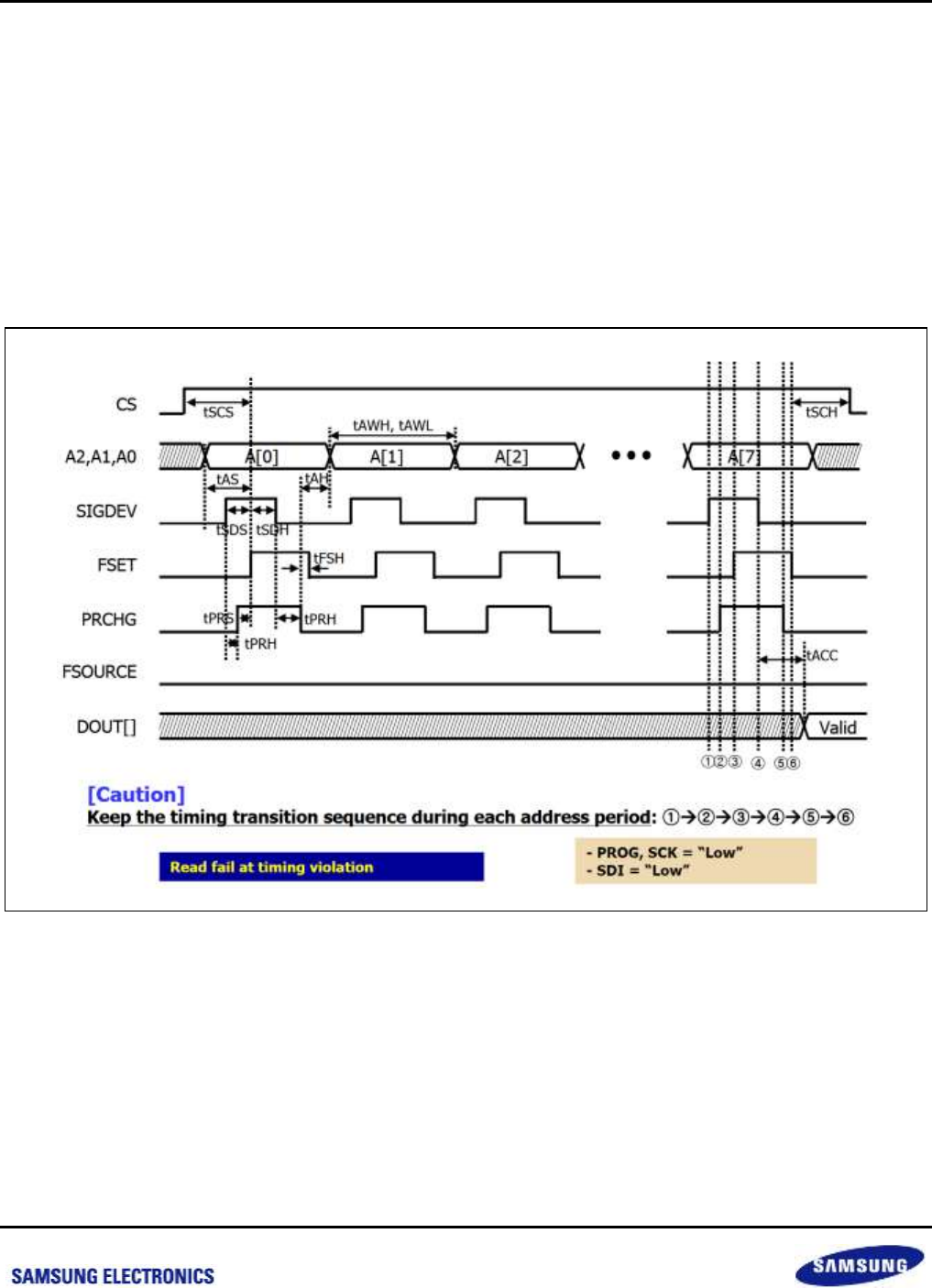
Samsung Confidential
S5P6818_UM 14 ID Register
14-3
Preliminary product information describes products that are in development, for which full characterization data and
associated errata are not yet available. Specifications and information herein are subject to change without notice.
Blue: It will use each program mode and scan mode
Red: It will use each program mode and sense mode
tFSRCS, tFSRCH = 1000 ns, All other timing arcs = 2 ns
tPRW = 10000ns 100 ns (Not allowed out of tPRW range. Must need approval from PTE/DT team if any
change)
14.3.2 Sense Mode Timing
Figure 14-1 Sense mode timing
When SIGDEV is enabled ("H"), sensing current is occurred. So you should reduce SIGDEV pulse width high
period for power saving.
CS should be set high (enable) and A2, A1, A0 states should be set properly before first SIGDEV rising in
sense mode.
After sense operation, DOUT[] have "0" for un-blown fuse cell and "1" for blown fuse cell.
Sense (read) operation would be performed correctly with timing diagram above. The user who wants to have
different timing sequence must have a prior consultation with effuse designer.
nexell / ys.kim at 2015.02.12
SAMSUNG Confidential
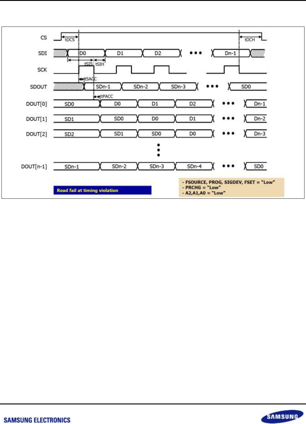
Samsung Confidential
S5P6818_UM 14 ID Register
14-4
Preliminary product information describes products that are in development, for which full characterization data and
associated errata are not yet available. Specifications and information herein are subject to change without notice.
14.3.3 Scan-Latch Mode Timing
Figure 14-2 Scan-Latch Mode Timing
After sense mode, cell's data is shifted to SDOUT by SCK in Scan-latch mode
Scan-latch operation would be performed correctly with timing diagram above. The user who wants to have
different timing sequence must have a prior consultation with effuse designer.
14.3.4 Stand-by Mode Timing
CS pin should be set to ground (= 0.0 V) to reduce unnecessary leakage current.
Other control pins: don't care.
nexell / ys.kim at 2015.02.12
SAMSUNG Confidential
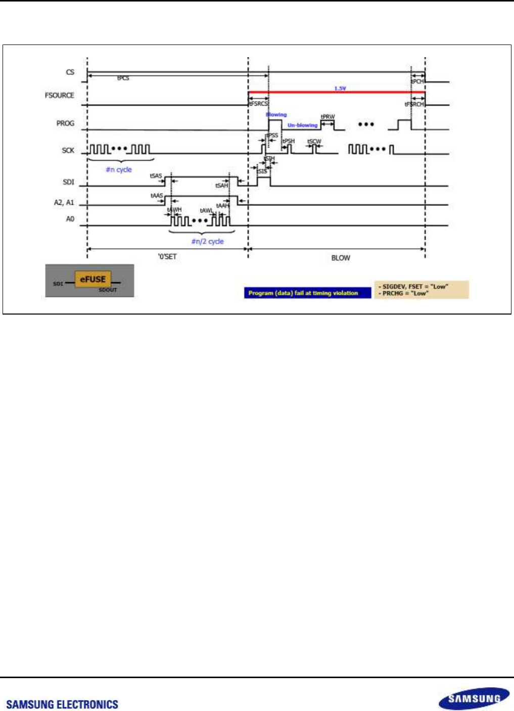
Samsung Confidential
S5P6818_UM 14 ID Register
14-5
Preliminary product information describes products that are in development, for which full characterization data and
associated errata are not yet available. Specifications and information herein are subject to change without notice.
14.3.5 Program Mode Timing
Figure 14-3 Fuse Programming Operation Using Single Macro
nexell / ys.kim at 2015.02.12
SAMSUNG Confidential
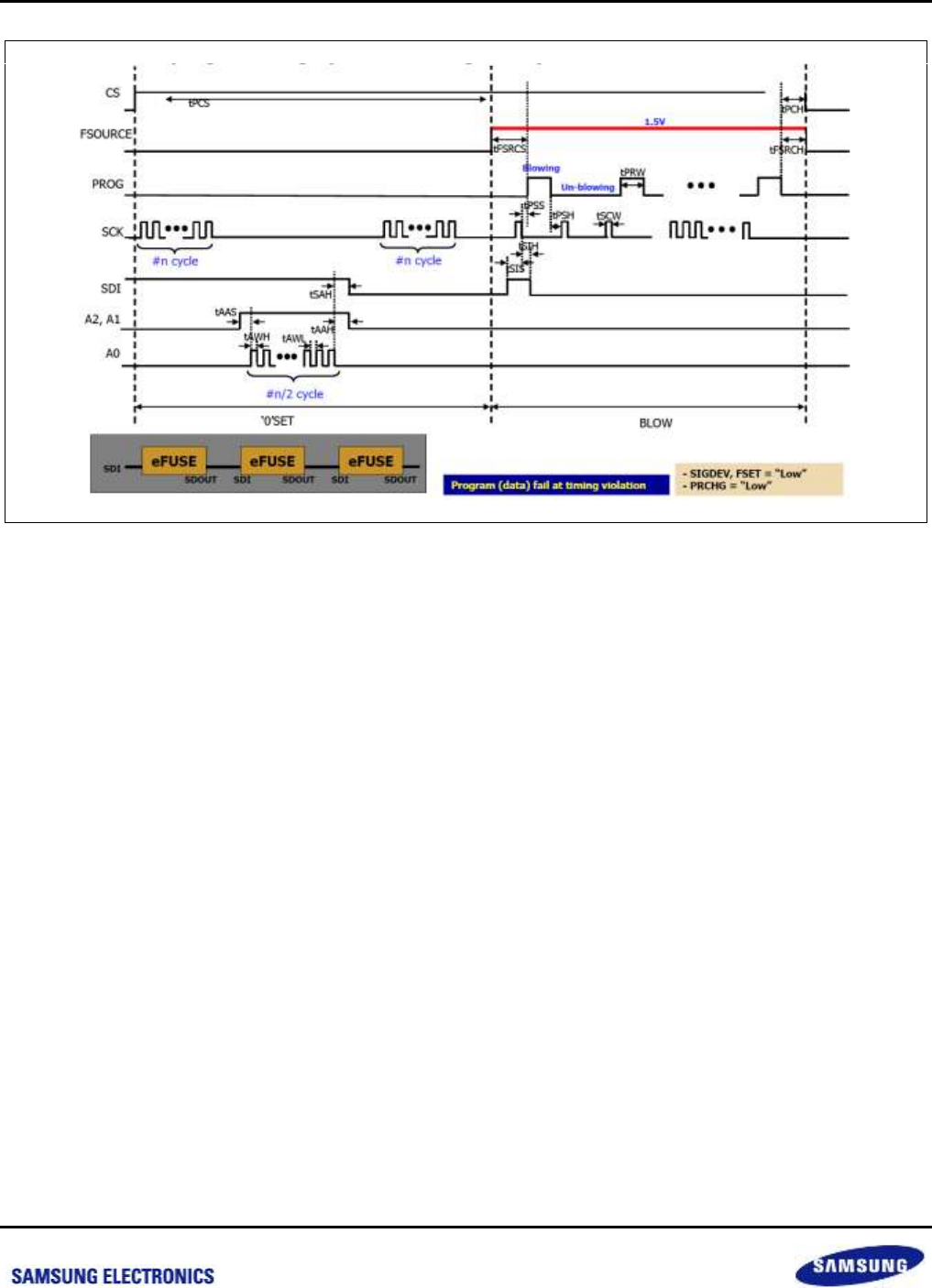
Samsung Confidential
S5P6818_UM 14 ID Register
14-6
Preliminary product information describes products that are in development, for which full characterization data and
associated errata are not yet available. Specifications and information herein are subject to change without notice.
Figure 14-4 Fuse Programming Operation Using Single Macro
Apply tFSRCS 1 s because of prevention leakage current from FSORUCE to ESD protection diode.
Fuse program operation would be performed correctly with timing diagram above. The user who wants to
have different timing sequence must have a prior consultation with effuse designer
nexell / ys.kim at 2015.02.12
SAMSUNG Confidential

Samsung Confidential
S5P6818_UM 14 ID Register
14-7
Preliminary product information describes products that are in development, for which full characterization data and
associated errata are not yet available. Specifications and information herein are subject to change without notice.
14.4 Register Description
14.4.1 Register Map Summary
Base Address: C006_7000h
Register
Offset
Description
Reset Value
ECID0
0x00h
128-bit ECID Register 0
–
ECID1
0x04h
128-bit ECID Register 1
–
ECID2
0x08h
128-bit ECID Register 2
–
ECID3
0x0Ch
128-bit ECID Register 3
–
CHIP_NAME_03_00
0x10h
Chip Name Register 03_00
–
CHIP_NAME_07_04
0x14h
Chip Name Register 07_04
–
CHIP_NAME_11_08
0x18h
Chip Name Register 11_08
–
CHIP_NAME_15_12
0x1Ch
Chip Name Register 15_12
–
CHIP_NAME_19_16
0x20h
Chip Name Register 19_16
–
CHIP_NAME_23_20
0x24h
Chip Name Register 23_20
–
CHIP_NAME_27_24
0x28h
Chip Name Register 27_24
–
CHIP_NAME_31_28
0x2Ch
Chip Name Register 31_28
–
CHIP_NAME_35_32
0x30h
Chip Name Register 35_32
–
CHIP_NAME_39_36
0x34h
Chip Name Register 39_36
–
CHIP_NAME_43_40
0x38h
Chip Name Register 43_40
–
CHIP_NAME_47_44
0x3Ch
Chip Name Register 47_44
–
RSVD
0x40h
Reserved
–
GUID0
0x44h
GUID0
–
GUID1_2
0x48h
GUID1_2
–
GUID3_0
0x4Ch
GUID3_0
–
GUID3_1
0x50h
GUID3_1
–
EC0
0x54h
ECID Control Register 0
0x0000_0000
EC1
0x58h
ECID Control Register 1
0x0000_0000
EC2
0x5Ch
ECID Control Register 2
0x0000_0000
nexell / ys.kim at 2015.02.12
SAMSUNG Confidential

Samsung Confidential
S5P6818_UM 14 ID Register
14-8
Preliminary product information describes products that are in development, for which full characterization data and
associated errata are not yet available. Specifications and information herein are subject to change without notice.
14.4.1.1 ECID0
Base Address: C006_7000h
Address = Base Address + 0x00h, Reset Value = Undefined
Name
Bit
Type
Description
Reset Value
ECID0
[31:0]
R
128-bit ECID Register [31:0]
–
14.4.1.2 ECID1
Base Address: C006_7000h
Address = Base Address + 0x04h, Reset Value = Undefined
Name
Bit
Type
Description
Reset Value
ECID1
[31:0]
R
128-bit ECID Register [63:32]
–
14.4.1.3 ECID2
Base Address: C006_7000h
Address = Base Address + 0x08h, Reset Value = Undefined
Name
Bit
Type
Description
Reset Value
ECID2
[31:0]
R
128-bit ECID Register [95:64]
–
14.4.1.4 ECID3
Base Address: C006_7000h
Address = Base Address + 0x0Ch, Reset Value = Undefined
Name
Bit
Type
Description
Reset Value
ECID3
[31:0]
R
128-bit ECID Register [127:96]
–
nexell / ys.kim at 2015.02.12
SAMSUNG Confidential

Samsung Confidential
S5P6818_UM 14 ID Register
14-9
Preliminary product information describes products that are in development, for which full characterization data and
associated errata are not yet available. Specifications and information herein are subject to change without notice.
14.4.1.5 CHIP_NAME_03_00
Base Address: C006_7000h
Address = Base Address + 0x10h, Reset Value = Undefined
Name
Bit
Type
Description
Reset Value
CHIP_NAME_3
[31:24]
R
Chip name character 3
–
CHIP_NAME_2
[23:16]
R
Chip name character 2
–
CHIP_NAME_1
[15:8]
R
Chip name character 1
–
CHIP_NAME_0
[7:0]
R
Chip name character 0
–
14.4.1.6 CHIP_NAME_07_04
Base Address: C006_7000h
Address = Base Address + 0x14h, Reset Value = Undefined
Name
Bit
Type
Description
Reset Value
CHIP_NAME_7
[31:24]
R
Chip name character 7
–
CHIP_NAME_6
[23:16]
R
Chip name character 6
–
CHIP_NAME_5
[15:8]
R
Chip name character 5
–
CHIP_NAME_4
[7:0]
R
Chip name character 4
–
14.4.1.7 CHIP_NAME_11_08
Base Address: C006_7000h
Address = Base Address + 0x18h, Reset Value = Undefined
Name
Bit
Type
Description
Reset Value
CHIP_NAME_11
[31:24]
R
Chip name character 11
–
CHIP_NAME_10
[23:16]
R
Chip name character 10
–
CHIP_NAME_9
[15:8]
R
Chip name character 9
–
CHIP_NAME_8
[7:0]
R
Chip name character 8
–
nexell / ys.kim at 2015.02.12
SAMSUNG Confidential
Samsung Confidential
S5P6818_UM 14 ID Register
14-10
Preliminary product information describes products that are in development, for which full characterization data and
associated errata are not yet available. Specifications and information herein are subject to change without notice.
14.4.1.8 CHIP_NAME_15_12
Base Address: C006_7000h
Address = Base Address + 0x1Ch, Reset Value = Undefined
Name
Bit
Type
Description
Reset Value
CHIP_NAME_15
[31:24]
R
Chip name character 15
–
CHIP_NAME_14
[23:16]
R
Chip name character 14
–
CHIP_NAME_13
[15:8]
R
Chip name character 13
–
CHIP_NAME_12
[7:0]
R
Chip name character 12
–
14.4.1.9 CHIP_NAME_19_16
Base Address: C006_7000h
Address = Base Address + 0x20h, Reset Value = Undefined
Name
Bit
Type
Description
Reset Value
CHIP_NAME_19
[31:24]
R
Chip name character 19
–
CHIP_NAME_18
[23:16]
R
Chip name character 18
–
CHIP_NAME_17
[15:8]
R
Chip name character 17
–
CHIP_NAME_16
[7:0]
R
Chip name character 16
–
14.4.1.10 CHIP_NAME_23_20
Base Address: C006_7000h
Address = Base Address + 0x24h, Reset Value = Undefined
Name
Bit
Type
Description
Reset Value
CHIP_NAME_23
[31:24]
R
Chip name character 23
–
CHIP_NAME_22
[23:16]
R
Chip name character 22
–
CHIP_NAME_21
[15:8]
R
Chip name character 21
–
CHIP_NAME_20
[7:0]
R
Chip name character 20
–
nexell / ys.kim at 2015.02.12
SAMSUNG Confidential

Samsung Confidential
S5P6818_UM 14 ID Register
14-11
Preliminary product information describes products that are in development, for which full characterization data and
associated errata are not yet available. Specifications and information herein are subject to change without notice.
14.4.1.11 CHIP_NAME_27_24
Base Address: C006_7000h
Address = Base Address + 0x28h, Reset Value = Undefined
Name
Bit
Type
Description
Reset Value
CHIP_NAME_27
[31:24]
R
Chip name character 27
–
CHIP_NAME_26
[23:16]
R
Chip name character 26
–
CHIP_NAME_25
[15:8]
R
Chip name character 25
–
CHIP_NAME_24
[7:0]
R
Chip name character 24
–
14.4.1.12 CHIP_NAME_31_28
Base Address: C006_7000h
Address = Base Address + 0x2Ch, Reset Value = Undefined
Name
Bit
Type
Description
Reset Value
CHIP_NAME_31
[31:24]
R
Chip name character 31
–
CHIP_NAME_30
[23:16]
R
Chip name character 30
–
CHIP_NAME_29
[15:8]
R
Chip name character 29
–
CHIP_NAME_28
[7:0]
R
Chip name character 28
–
14.4.1.13 CHIP_NAME_35_32
Base Address: C006_7000h
Address = Base Address + 0x30h, Reset Value = Undefined
Name
Bit
Type
Description
Reset Value
CHIP_NAME_35
[31:24]
R
Chip name character 35
–
CHIP_NAME_34
[23:16]
R
Chip name character 34
–
CHIP_NAME_33
[15:8]
R
Chip name character 33
–
CHIP_NAME_32
[7:0]
R
Chip name character 32
–
nexell / ys.kim at 2015.02.12
SAMSUNG Confidential

Samsung Confidential
S5P6818_UM 14 ID Register
14-12
Preliminary product information describes products that are in development, for which full characterization data and
associated errata are not yet available. Specifications and information herein are subject to change without notice.
14.4.1.14 CHIP_NAME_39_36
Base Address: C006_7000h
Address = Base Address + 0x34h, Reset Value = Undefined
Name
Bit
Type
Description
Reset Value
CHIP_NAME_39
[31:24]
R
Chip name character 39
–
CHIP_NAME_38
[23:16]
R
Chip name character 38
–
CHIP_NAME_37
[15:8]
R
Chip name character 37
–
CHIP_NAME_36
[7:0]
R
Chip name character 36
–
14.4.1.15 CHIP_NAME_43_40
Base Address: C006_7000h
Address = Base Address + 0x38h, Reset Value = Undefined
Name
Bit
Type
Description
Reset Value
CHIP_NAME_43
[31:24]
R
Chip name character 43
–
CHIP_NAME_42
[23:16]
R
Chip name character 42
–
CHIP_NAME_41
[15:8]
R
Chip name character 41
–
CHIP_NAME_40
[7:0]
R
Chip name character 40
–
14.4.1.16 CHIP_NAME_47_44
Base Address: C006_7000h
Address = Base Address + 0x3Ch, Reset Value = Undefined
Name
Bit
Type
Description
Reset Value
CHIP_NAME_47
[31:24]
R
Chip name character 47
–
CHIP_NAME_46
[23:16]
R
Chip name character 46
–
CHIP_NAME_45
[15:8]
R
Chip name character 45
–
CHIP_NAME_44
[7:0]
R
Chip name character 44
–
nexell / ys.kim at 2015.02.12
SAMSUNG Confidential
Samsung Confidential
S5P6818_UM 14 ID Register
14-13
Preliminary product information describes products that are in development, for which full characterization data and
associated errata are not yet available. Specifications and information herein are subject to change without notice.
14.4.1.17 GUID0
Base Address: C006_7000h
Address = Base Address + 0x44h, Reset Value = Undefined
Name
Bit
Type
Description
Reset Value
GUID0
[31:0]
R
GUID 0
–
14.4.1.18 GUID1_2
Base Address: C006_7000h
Address = Base Address +0x48h, Reset Value = Undefined
Name
Bit
Type
Description
Reset Value
GUID2
[31:16]
R
GUID 2
–
GUID1
[15:0]
R
GUID 1
–
14.4.1.19 GUID3_0
Base Address: C006_7000h
Address = Base Address + 0x4Ch, Reset Value = Undefined
Name
Bit
Type
Description
Reset Value
GUID3_3
[31:24]
R
GUID 3_3
–
GUID3_2
[23:16]
R
GUID 3_2
–
GUID3_1
[15:8]
R
GUID 3_1
–
GUID3_0
[7:0]
R
GUID 3_0
–
14.4.1.20 GUID3_1
Base Address: C006_7000h
Address = Base Address + 0x50h, Reset Value = Undefined
Name
Bit
Type
Description
Reset Value
GUID3_7
[31:24]
R
GUID 3_7
–
GUID3_6
[23:16]
R
GUID 3_6
–
GUID3_5
[15:8]
R
GUID 3_5
–
GUID3_4
[7:0]
R
GUID 3_4
–
nexell / ys.kim at 2015.02.12
SAMSUNG Confidential

Samsung Confidential
S5P6818_UM 14 ID Register
14-14
Preliminary product information describes products that are in development, for which full characterization data and
associated errata are not yet available. Specifications and information herein are subject to change without notice.
14.4.1.21 EC0
Base Address: C006_7000h
Address = Base Address + 0x54h, Reset Value = 0x0000_0000
Name
Bit
Type
Description
Reset Value
RSVD
[31:10]
–
Reserved
–
A_FF
[9:7]
RW
Programmable A
3'b0
CS_FF
[6]
RW
Programmable CS
1'b0
SIGDEV_FF
[5]
RW
Programmable SIGDEV
1'b0
FSET_FF
[4]
RW
Programmable FSET
1'b0
PRCHG_FF
[3]
RW
Programmable PRCHG
1'b0
BONDING_ID
[2:0]
R
Boinding ID
–
14.4.1.22 EC1
Base Address: C006_7000h
Address = Base Address + 0x58h, Reset Value = 0x0000_0000
Name
Bit
Type
Description
Reset Value
RSVD
[31:3]
–
Reserved
–
PROG_FF
[2]
RW
Programmable PROG
1'b0
SCK_FF
[1]
RW
Programmable SCK
1'b0
SDI_FF
[0]
RW
Programmable SDI
1'b0
nexell / ys.kim at 2015.02.12
SAMSUNG Confidential
Samsung Confidential
S5P6818_UM 14 ID Register
14-15
Preliminary product information describes products that are in development, for which full characterization data and
associated errata are not yet available. Specifications and information herein are subject to change without notice.
14.4.1.23 EC2
Base Address: C006_7000h
Address = Base Address + 0x5Ch, Reset Value = 0x0000_0000
Name
Bit
Type
Description
Reset Value
RSVD
[31:16]
–
Reserved
–
HW_DONE
[15]
R
ECID initialize done
1'b0
RSVD
[14:5]
–
Reserved
–
HDCP_EFUSE_SEL
[4]
RW
HDCP Key select
0 = Secure Boot
1 = Secure JTAG
1'b0
RSVD
[3:2]
–
Reserved
–
SEL_BANK
[1:0]
RW
e-FUSE select
0 = ECID
1 = Secure Boot
2 = Secure JTAG
3 = Backdoor JTAG
2'b0
nexell / ys.kim at 2015.02.12
SAMSUNG Confidential

Samsung Confidential
S5P6818_UM 14 ID Register
14-16
Preliminary product information describes products that are in development, for which full characterization data and
associated errata are not yet available. Specifications and information herein are subject to change without notice.
14.5 Application Notes
Permitting Over-the-cell routing. In chip-level layout, over-the-cell routing in EFROM_LP is permitted without
any restrictions over Metal-4 layer.
Incoming power bus should be adjusted to guarantee NOT more than 5 % voltage drop at typical-case current
levels.
Reduce resistance (3 ) between PAD and FSOURCE pin of EFROM_LP.
Connect routing signal to all of the FSOURCE pins.
When using two or more e-fuse sets, FSOURCE line can be shared among e-fuse sets, but program-mode
operation should be applied sequentially. (For example, at first, operate e-fuse0 and then operate e-fuse1 for
program-mode) It applies same during sense-mode, but there is a guideline for multi-sensing, only sense-mode.
Keep the below rules. Refer to integration guide document for further information.
Allowed maximum resistance can be obtained by 3 /# of 128-bit e-fuse box.
If customer wants to run multi-sensing,
3 : 128-bit 1 ea, 1.5 : 128-bit 2 ea, 1 : 128-bit 3 ea, 0.5 : 128-bit 6 ea
nexell / ys.kim at 2015.02.12
SAMSUNG Confidential

Samsung Confidential
S5P6818_UM 15 Memory Controller
15-1
Preliminary product information describes products that are in development, for which full characterization data and
associated errata are not yet available. Specifications and information herein are subject to change without notice.
15 Memory Controller
15.1 Overview
The S5P6818 Memory Controller is based on a Unified Memory Architecture (UMA). This Controller consists of
two control units: MCU-A, MCU-S. Each unit has dedicated control pins.
15.1.1 Unified Memory Architecture (UMA)
Two Separate Memory Controller:
MCU-A: DDR3/LVDDR3 (Low Voltage DDR3)/LPDDR3/LPDDR2
MCU-S: Static Memory
MCU-A features:
MCU-A is organized DREX and DDRPHY
Supports DDR3/LVDDR3 (Low Voltage DDR3)/LPDDR3/LPDDR2 memory
Supports 8/16/32-bit SDRAM of 2 GByte
Single Bank of Memory (32-bit data bus width)
Supports Power down mode
Supports Self Refresh mode
MCU-S features:
Static memory
Two Static Memory Chip Selects
NAND Flash Interface
23-bit address supports using latch address
SLC NAND, MLC NAND with ECC (Supports BCH-algorithm)
Static Memory Map Shadow
nexell / ys.kim at 2015.02.12
SAMSUNG Confidential
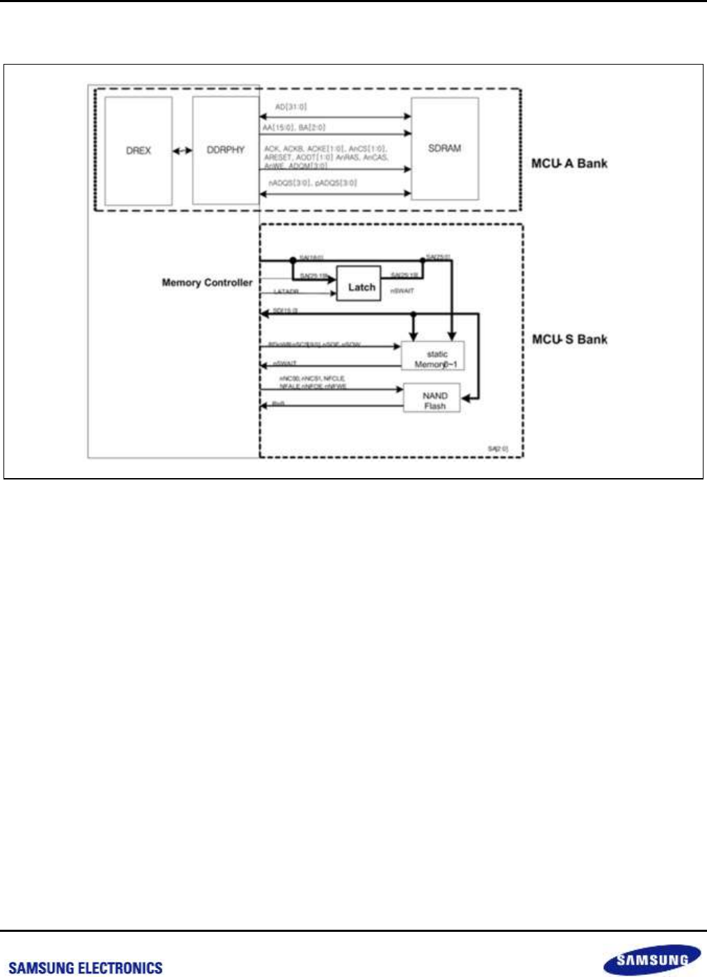
Samsung Confidential
S5P6818_UM 15 Memory Controller
15-2
Preliminary product information describes products that are in development, for which full characterization data and
associated errata are not yet available. Specifications and information herein are subject to change without notice.
15.2 Block Diagram
Figure 15-1 Memory Controller Block Diagram
nexell / ys.kim at 2015.02.12
SAMSUNG Confidential

Samsung Confidential
S5P6818_UM 15 Memory Controller
15-3
Preliminary product information describes products that are in development, for which full characterization data and
associated errata are not yet available. Specifications and information herein are subject to change without notice.
15.3 Functional Description
The memory controller area of the S5P6818 is divided into an MCU-A and MCU-S bank. The MCU-A bank is
connected to DDR3/LVDDR3 (Low Voltage DDR3)/LPDDR3/LPDDR2 which is the main memory of the S5P6818
and 32-bit data bus width.
The MCU-S bank is the static bank and can be connected to Static Memory/Device, NAND.
15.3.1 MCU-A Bank Feature
Compatible with JEDEC standard LPDDR2-S4/LPDDR3/LVDDR3 (Low Voltage DDR3)/DDR3 SDRAMs
Supports 1: 2 synchronous operation between bus clock and Memory clock
Integrated TrustZone address space control unit
Supports up to two memory ranks (chip selects) and 4/8 banks per memory chips
Supports 512 Mb, 1 Gb, 2 Gb, 4 Gb, 8 Gbit and 16 Gbit density per a chip select
Supports QoS scheme to ensure low latency for real-time applications
Out-of order scheduling policy for higher performance
Supports early write response
Supports rank/bank interleaving
Supports outstanding exclusive accesses
Supports bank selective precharge policy
Accommodates the embedded performance monitor
DREX Clock: MBCLK (400 MHz)
DDRPHY Clock: MCLK (800 MHz, TBD), MDCLK (800 MHz, TBD)
MBCLK: MCLK = 1: MBCLKx2
MDCLK: MDCLK 0° phase Master DLL clock (400 to 800 MHz). This clock should be the same frequency
clock with clk2x in normal mode and generated from the same PLL which MCLK is using. But Master DLL is
not able to lock under 400 MHz. If MCLK is under 400 MHz, the double frequency of clk2x can be used for
locking Master DLL for the low frequency operation
nexell / ys.kim at 2015.02.12
SAMSUNG Confidential

Samsung Confidential
S5P6818_UM 15 Memory Controller
15-4
Preliminary product information describes products that are in development, for which full characterization data and
associated errata are not yet available. Specifications and information herein are subject to change without notice.
15.3.2 MCU-S Bank Feature
Latched Addressing
The number of pins that are connected to the outside is ADDR [18:0]. Since, however, the total address of the
MCU-S Bank is 26-bit. ADDR[8:2] and ADDR[25:19] are allotted to the same pin, the system has a structure
in which addresses are output two times. If the system uses ADDR[19] or more, the setting of higher address
(ADDR[25:19]) is possible via System Configuration Pin (CfgSTLATADD). In this event, ADDR[25:19] which is
configured by using external Latch IC first should be latched.
16-bit data bus width
Static memory register except NAND flash (8 bits) has bus width select registers
Static memory Controller
Normal static memory (SRAM and ROM) or static devices are connected.
Up to two Static Chip Select signals exist.
NAND Flash Controller.
It supports both the small and large block NAND flash memories.
Up to two NAND flash memories can be connected.
Supports both SLC and MLC NAND flash memories.
Up to 4/8/16/24/40/60-bit error correction/ (1024 or 512 byte) using Binary-BCH coding
nexell / ys.kim at 2015.02.12
SAMSUNG Confidential
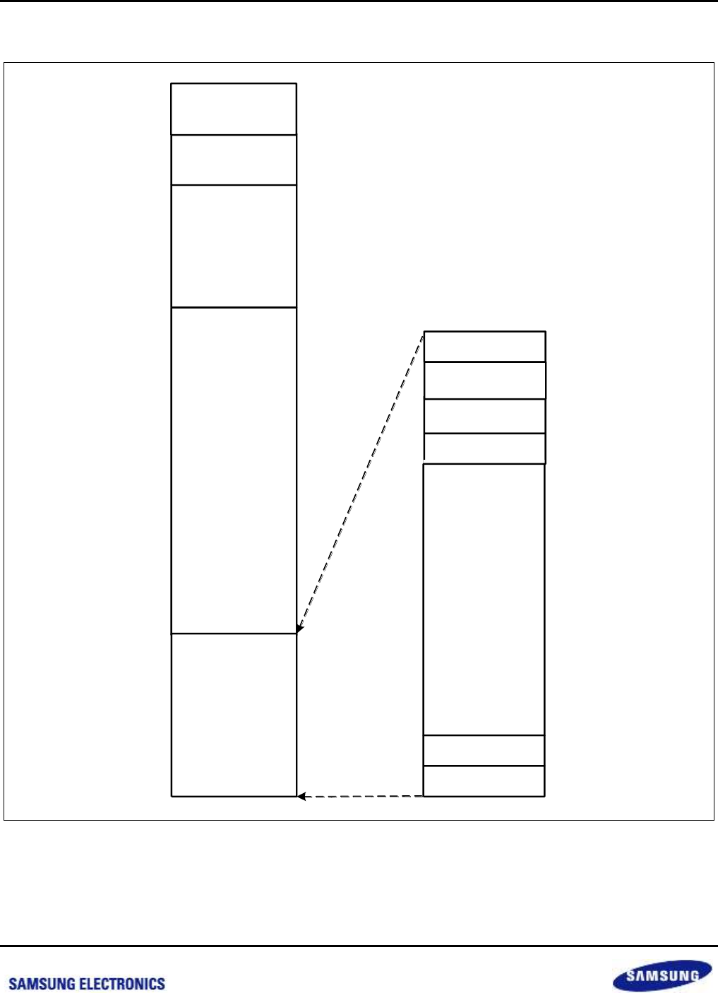
Samsung Confidential
S5P6818_UM 15 Memory Controller
15-5
Preliminary product information describes products that are in development, for which full characterization data and
associated errata are not yet available. Specifications and information herein are subject to change without notice.
15.3.3 Memory Map
Figure 15-2 Memory Map
The memory map is roughly divided into one SDRAM Bank (MCU-A) and one static bank (MCU-S). The static
bank consists of NAND Flash controller, Static Memory controller. The MCU-A bank consist of a Linear Array area
and Display Array area.
NAND
Static #1
Static #0
0x0000_0000
0x0400_0000
0x0800_0000
MCU- A (2GB)
DDR
MCU-S
STATIC
Normal I/O
Reserved
0x0000_0000
0x4000_0000
0xC000_0000
0xE000_0000
Reserved
0x2C00_0000
0x3000_0000
Internal ROM
0x3400_0000
Reserved
Reserved
0xFFFF_0000
Internal SRAM
nexell / ys.kim at 2015.02.12
SAMSUNG Confidential
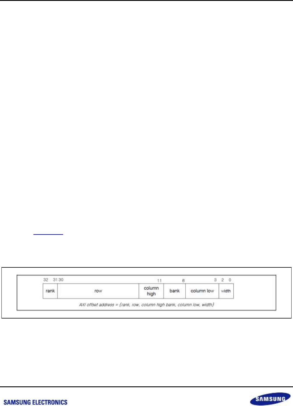
Samsung Confidential
S5P6818_UM 15 Memory Controller
15-6
Preliminary product information describes products that are in development, for which full characterization data and
associated errata are not yet available. Specifications and information herein are subject to change without notice.
15.3.4 MCU-A Address Mapping
DREX modifies the address of the AXI transaction coming from the AXI slave port into a memory address-chip
select, bank address, row address, column address and memory data width. "width" represents the data width of
the DRAM used, which is fixed to 32 bits (4 bytes), and hence, on a byte-addressed address value, the
corresponding width is fixed to 2.
The related SFR is BANK_LSB, CHIP_INTER_EN, BIT_SEL_EN, CHIP_MAP in MEMCONFIG0/1 registers.
In case of chip interleaving, two chips configuration should the same.
To map chip select of memory device to a specific area of the address map, the CHIP_BASE and CHIP_MASK
bit-fields of the MEMCONFIG0 register needs to be set (Refer to Register Descriptions). If chip1 of the memory
device exists, the MEMCONFIG1 register must also be set. Then, the AXI address requested by AXI Masters is
divided into the AXI base address and AXI offset address. The AXI base address activates the appropriate
memory chip select and the AXI offset address is mapped to a memory address according to the bank, row,
column number, and data width set by the MEMCONFIG0/1 and MEMCONTROL register.
There are two ways to map the AXI offset address as shown below:
Simple interleaved mapping
Split column interleaved mapping
Randomized interleaved mapping
Chip interleaved mapping
15.3.4.1 Split Column Interleaved Mapping
CHIP_INTER_EN = 0x0, BIT_SEL_EN = 0x0 and CHIP_MAP = 0x2 means split column interleaved mapping.
As shown in Figure 15-3 the split column interleaved mapping method maps the AXI address in the order of row,
column high, bank, column low and width.
The related SFR is "BANK_LSB" which select column low size. (Refer to Register Descriptions). If BANK_LSB is
the same with the actual memory page size, then column would not be split.
Figure 15-3 Split Column Interleaved Mapping
nexell / ys.kim at 2015.02.12
SAMSUNG Confidential
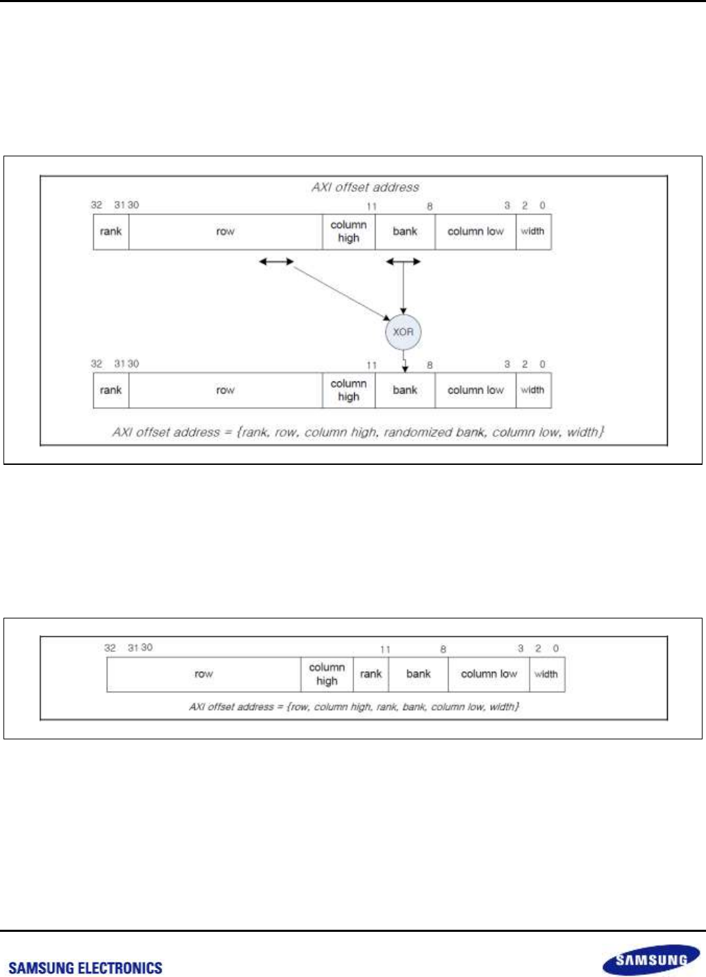
Samsung Confidential
S5P6818_UM 15 Memory Controller
15-7
Preliminary product information describes products that are in development, for which full characterization data and
associated errata are not yet available. Specifications and information herein are subject to change without notice.
15.3.4.2 Randomized Interleaved Mapping
In addition to split column interleaved address mapping, DREX supports randomized interleaved mapping. As
shown in below Figure, bank address is randomized by XORing with additional bits chosen from the AXI address.
It further improves performance by distributing memory accesses to numerous banks more aggressively.
CHIP_INTER_EN = 0x0 and BIT_SEL_EN = 0x1 means randomized interleaved mapping.
Figure 15-4 Randomized Interleaved Mapping
15.3.4.3 Rank Interleaved Mapping
RANK_INTER_EN = 0x1 means rank interleaved mapping. If RANK_INTER_EN is enabled, then above figure are
changed to below respectively.
Figure 15-5 Rank Interleaved Address Mapping (CHIP_MAP = 0X2, BIT_SEL_EN = 0X0)
nexell / ys.kim at 2015.02.12
SAMSUNG Confidential
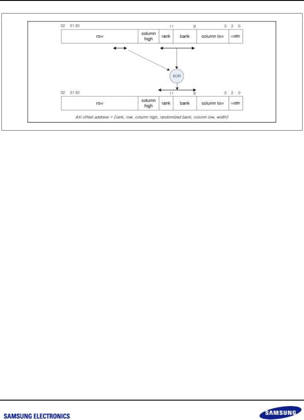
Samsung Confidential
S5P6818_UM 15 Memory Controller
15-8
Preliminary product information describes products that are in development, for which full characterization data and
associated errata are not yet available. Specifications and information herein are subject to change without notice.
Figure 15-6 Rank Interleaved Address Mapping (CHIP_MAP = 0x2, BIT_SEL_EN = 0x1)
15.3.5 Low Power Operation
The controller executes a low power memory operation in five ways as described below. Each feature is
independent of each other and executed at the same time.
When memory is in the SREF state, then the controller issue SRX command automatically, if AXI request is
coming.
15.3.5.1 AXI Low Power Channel
The controller has an AXI low power channel interface to communicate with low power management units such as
the system controller, which makes the memory device go into self refresh mode.
15.3.5.2 Dynamic Power Down
An SDRAM device has an active/precharge power down mode. This mode is triggered by de-asserting CKE to
LOW. When any of the banks is open, it enters active power down mode. Otherwise, it enters precharge power
down mode.
When the request buffers remain empty for certain number of cycles (PWRDNCONFIG.DPWRDN_CYC register),
DREX-1 changes the memory devices state to active/precharge power down automatically. The memory device
enters Active/precharge power down mode or Forced precharge power down mode according to the SFR setting.
The description of the two Power Down Modes are as follows:
1. Active/precharge power down mode: Enter power down w/o considering whether there is a row open or not.
2. Forced precharge power down mode: Enter power down after closing all banks.
When DREX-1 receives a new AXI transaction while memory device is in power down mode, it automatically
wakes up the memory device from power down state and executes in a normal operation state.
nexell / ys.kim at 2015.02.12
SAMSUNG Confidential

Samsung Confidential
S5P6818_UM 15 Memory Controller
15-9
Preliminary product information describes products that are in development, for which full characterization data and
associated errata are not yet available. Specifications and information herein are subject to change without notice.
15.3.5.3 Dynamic Self Refresh
Similarly to the dynamic power down feature, if the request buffers remain empty for certain number of cycles
(PWRDNCONFIG.DSREF_CYC register), DREX-1 changes the memory device's state to self-refresh mode.
Since exiting power down mode requires many cycles, a longer idle cycle threshold is recommended for dynamic
self-refresh entry than the threshold for dynamic power down.
15.3.5.4 Clock Stop
To reduce the I/O power of the memory device and the controller, it is possible to stop the clock if the LPDDR /
LPDDR2-S4 is in idle mode, or self refresh mode and DDR3 is in self refresh mode. If this feature is enabled, the
controller automatically executes the clock stop feature. In DDR3, clock stop feature must be turn-on and off
considering tCKSRX/ tCKSRE/ tCKESR timing by software.
15.3.5.5 Direct Command
Use the direct command feature to send a memory command directly to the memory device through the APB3
port. This way, it is possible to force the memory device to enter active/precharge power down, self-refresh or
deep power down mode
15.3.6 Precharge Policy
There are two options for DREX regarding precharge policy – port-selective precharge and timeout precharge per
port.
15.3.6.1 Post Selective Precharge
Since applications have different page policy preferences, it is hard for the engineer to decide on whether to use
open page policy, or close page (auto precharge) policy. Instead of applying the page policy to all of the ports, the
port selective precharge policy allows the user to choose a precharge policy for each port (refer to
PRECHCONFIG.PORT_POLICY). This way, you assign certain applications to an open page policy, and other
applications to a close page (auto precharge) policy.
Open Page Policy: After a READ or WRITE, the accessed row is left open.
Close Page (Auto Precharge) Policy: When DREX issues the last READ or WRITE CAS command, it
augments the command with an auto precharge flag.
15.3.6.2 Timeout Precharge
If a certain port uses an open page policy, the row is left open after a data access. If this happens and the bank
that is left open is not scheduled for a specific number of cycles (PRECHCONFIG.TP_CNT bit-field) the controller
automatically issues a precharge command to close the bank.
nexell / ys.kim at 2015.02.12
SAMSUNG Confidential
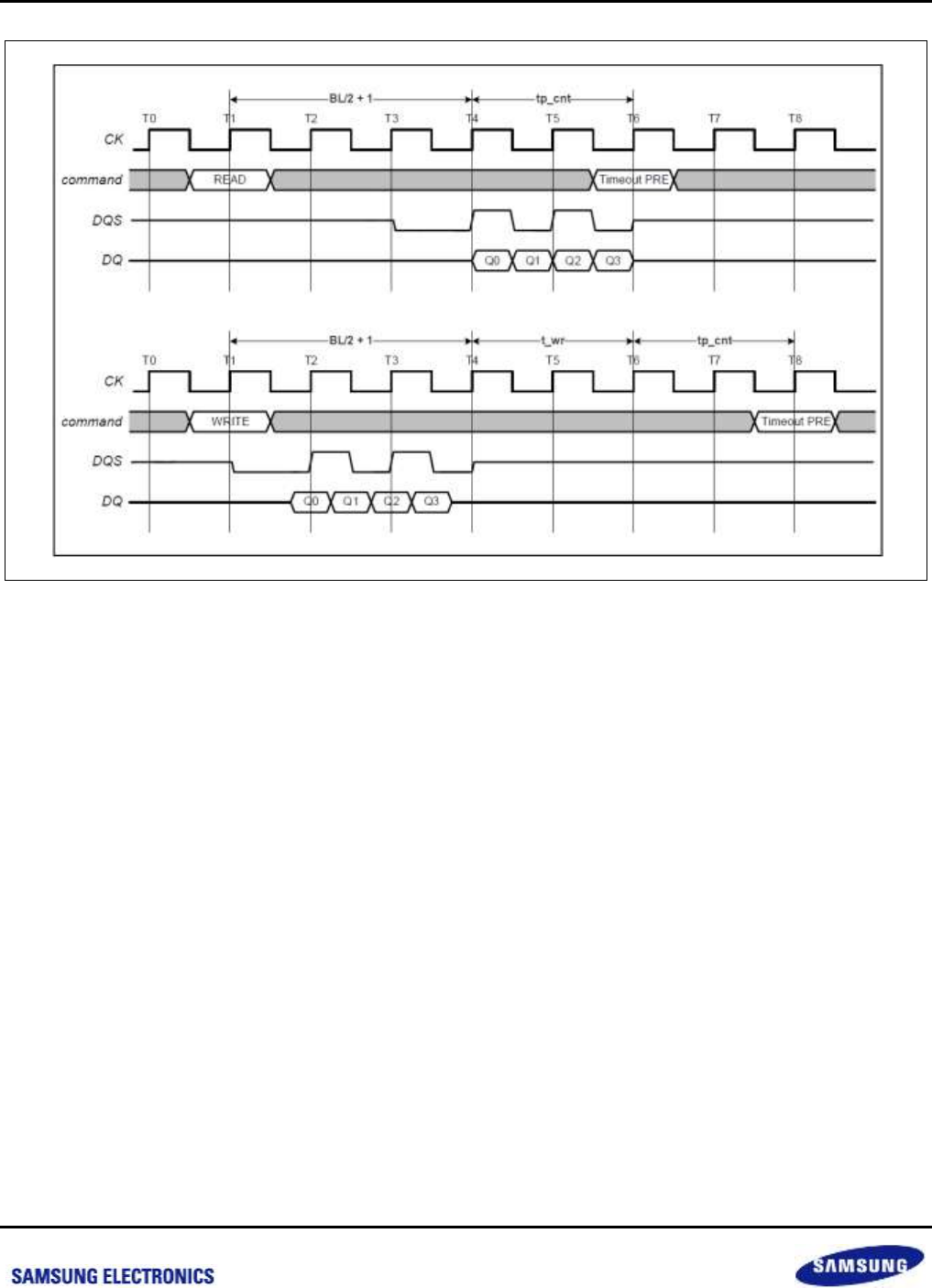
Samsung Confidential
S5P6818_UM 15 Memory Controller
15-10
Preliminary product information describes products that are in development, for which full characterization data and
associated errata are not yet available. Specifications and information herein are subject to change without notice.
Figure 15-7 Timing Diagram of Timeout Precharge
15.3.7 Quality of Service
DREX provides Quality of Service (QoS) feature to ensure low latency for real-time masters. Specifically, DREX
uses timeout based QoS enforcement scheme.
When DREX receives an AXI transaction, a predefined QoS timeout value is assigned to the corresponding
memory request for timeout.
When the timer expires, the request gets promoted to the highest priority for immediate selection during
arbitration stage.
15.3.7.1 BRB Arbitration
The AXI requests of the head of AXI Request FIFO in the ports are arbitrated to Bank Request Buffer (BRB). The
priority of each port is determined by the highest AxQoS value of the AXI requests in the FIFO. When the AXI
Request FIFO timer (CONCONTROL.TIMEOUT_LEVEL0) expires, the port of the FIFO has highest priority to
prevent starvation of low priority port.
nexell / ys.kim at 2015.02.12
SAMSUNG Confidential

Samsung Confidential
S5P6818_UM 15 Memory Controller
15-11
Preliminary product information describes products that are in development, for which full characterization data and
associated errata are not yet available. Specifications and information herein are subject to change without notice.
15.3.7.2 AxQoS Base QoS
When DREX receives an AXI request, it assigns a predefined BRB timeout value (QOSCONTROL_N.CFG_QOS,
n= 0 to 15) according to the AxQoS value (0 to 15). When the BRB timer expires, the request has the highest
priority for the Request Scheduler. When the BRB is full or the data buffer for the request is full, the BRB timer
decrements by predefined value (BRBQOSCONFIG.BRB_QOS_TIMER_DEC) instead of 1.
15.3.7.3 BRB Space Reservation
When BRB space reservation is enabled for a AXI AR/AW port (BRBRSVCONTROL.BRB_RSV_EN_ {W,
R}{0,1,2,3}), the AXI port stops issuing request for BRB arbitration when the occupancy of target BRB exceeds
BRB threshold value (BRBRSVCONFIG.BRB_RSV_TH_ {W, R}{0,1,2,3}).
15.3.7.4 Emergency Priority Escalation
In addition to the conventional QoS schemes, DREX-1 supports emergency signal-based priority escalation. This
feature is implemented using two additional input signals:
Each AXI port has additional ARMARKER[4:0] and AWMARKER[4:0] input signals. These signals are used
for identifying they QoS class of a given request – for example, the master that sent the request, or
communication that happens between two specific masters on a given application scenario.
EMERGENCY_R[30:0] and EMERGENCY_W[30:0] input signals, which specifies which class of traffic needs
a higher priority.
By default, the masters drive the value of EMERGENCY_R and EMERGENCY_W as 31'b0. When a given class
of requests requires higher priority, the master drives the corresponding EMERGENCY_R (for reads) or
EMERGENCY_W (for writes) bit to escalate the priority of all traffics within the given class. To be specific, when
EMERGENCY_R[n] gets driven to 1, all read requests with its ARMARKER value as n + 1 moves to a higher
priority, and when EMERGENCY_W[n] gets driven to 1, all write requests with its AWMARKER value as n + 1
moves to a higher priority.
The priority returns to its original priority as soon as the corresponding EMERGENCY_R/EMERGENCY_W signal
returns to 0. Note that, the timeout counter should be still decrementing regardless of the
EMERGENCY_R/EMERGENCY_W signal.
There are programmable registers (per-AxMARKER value) that determines the priority level to move to in case or
priority escalation. Users can choose between the "timeout" priority and "urgent page miss" priority.
nexell / ys.kim at 2015.02.12
SAMSUNG Confidential

Samsung Confidential
S5P6818_UM 15 Memory Controller
15-12
Preliminary product information describes products that are in development, for which full characterization data and
associated errata are not yet available. Specifications and information herein are subject to change without notice.
15.3.8 Trust Zone Address Space Control (TZASC)
TZASC performs security checks on AXI accesses to memory. This supports configurable number of regions.
Each region is programmable for size, base address, enable, and security parameters. Using the
SECURE_BOOT_LOCK input signal, the programmers view can be locked to prevent erroneous writes. It
provides programmability in reporting faults using AXI response channel, and interrupt.
15.3.8.1 Regions
A region is a contiguous area of address space. The TZASC provides each region with a programmable security
permissions field. The security permissions value is used to enable the TZASC to either accept or deny a
transaction access to that region. The transactions arprots[2:0] or awprots[2:0] signals are used to determine the
security settings of that transaction. The region features are as following:
Minimum region granularity: 64 KB
Number of regions: 8 non-overlapping regions (region 1 to 8) + 1 default region (region 0)
Priority of regions: priority_of_region_1 to 8 > priority_of_region_0
Address space of a region
Base address: aligned to 64 KB
Size of a region: 64 KB N
Maximum size of a region: 4 GB
Region 0 covers entire address space
No support of sub-regions
The feature of security property of regions are as following:
4 bits permission
Each bit represent if (secure read, secure write, non-secure read, non-secure write) are allowed or not
EX) A region with security property b’1100 allows secure access (read and write) but forbids non-secure
access
1-bit region_lock
Region configuration (SFR) is locked after SECURE_BOOT_LOCK is asserted
1-bit region enable
Region 1 to 8 is enabled by SFR
Region 0 is always enable
nexell / ys.kim at 2015.02.12
SAMSUNG Confidential

Samsung Confidential
S5P6818_UM 15 Memory Controller
15-13
Preliminary product information describes products that are in development, for which full characterization data and
associated errata are not yet available. Specifications and information herein are subject to change without notice.
15.3.8.2 Denied AXI Transactions
If an AXI transaction has insufficient security privileges then for:
Read: The TZASC responds to the master by setting all bits of the read data bus, RDATA, to zero.
Writes: The TZASC prevents the data from being written to memory.
The TZASC Action Register controls whether the TZASC signals to the master when a region permission failure
occurs, and if so, the type of response it provides.
15.3.8.3 Preventing Writes to Registers and Using SECURE_BOOT_LOCK
The TZASC expects the SECURE_BOOT_LOCK signal to be asserted for at least one clock cycle. One clock
after the SECURE_BOOT_LOCK is sampled HIGH by TZASC, then the below registers cannot be written, unless
the DREX is reset by asserting ARESETn.
Assert in SECURE_BOOT_LOCK signal makes the following register read only:
TZASC Lockdown Select Register
By suitably programming TZASC Lockdown Select Register and asserting SECURE_BOOT_LOCK signal makes
the following register read only:
TZASC Lockdown Range Register
By programming the TZASC Lockdown Select Register, and TZASC Lockdown Range Register, and asserting the
SECURE_BOOT_LOCK signal, you can lockdown the behavior of the TZASC so that it prevents unintentional or
erroneous write to the regions specified in the TZASC Lockdown Range Register. However, read access to those
regions is permitted:
TZASC Region Setup Low Register n
TZASC Region Setup High Register n
TZASC Region Attribute Register n
15.3.8.4 Using Exclusive Access
If a master performs exclusive accesses to an address region, you must program the TZASC to permit read and
write accesses to that address region, for the expected settings of arprots[1] and awprots[1], otherwise the read or
write transaction might fail. The TZASC permission failed exclusive accesses do not modify the state of exclusive
monitor.
nexell / ys.kim at 2015.02.12
SAMSUNG Confidential

Samsung Confidential
S5P6818_UM 15 Memory Controller
15-14
Preliminary product information describes products that are in development, for which full characterization data and
associated errata are not yet available. Specifications and information herein are subject to change without notice.
15.3.9 MCU-A Application Note
15.3.9.1 DREX Initialization
LPDDR2/3
The following sequence should be used to initialize LPDDR2 devices. Unless specified otherwise, these steps are
mandatory.
1. To provide stable power for memory device, DREX must assert and hold CKE to a logic low level. Then apply
stable clock.
2. Set the PHY for DDR3 operation mode, RL/WL/BL register and processed ZQ calibration. Refer to
"INITIALIZATION" in PHY manual.
3. Assert the CONCONTROL.DFI_INIT_START field to high but leave as default value for other fields.
(AREF_EN and IO_PD_CON should be off.) Clock gating in CGCONTROL should be disabled in initialization
and training sequence.
4. Wait for the PHYSTATUS0.DFI_INIT_COMPLETE field to change to "1".
5. De-assert the CONCONTROL.DFI_INIT_START field to low.
6. Set the PHY for DQS pull-down mode. (Refer to PHY manual)
7. Set the PHYCONTROL0.FP_RESYNC bit-field to "1" to update DLL information.
8. Set the PHYCONTROL0.FP_RESYNC bit-field to "0".
9. Set the MEMBASECONFIG0 register. If there are two external memory chips, set the MEMBASECONFIG1
register.
10. Set the MEMCONFIG0 register. If there are two external memory chips, also set the MEMCONFIG1 register.
11. Set the PRECHCONFIG0/1 and PWRDNCONFIG registers.
12. Set the TIMINGAREF, TIMINGROW, TIMINGDATA and TIMINGPOWER registers according to memory AC
parameters.
13. If QoS scheme is required, set the QosControl0 to 15 and QosConfig0 to 15 registers.
14. Set the PHY for LPDDR2/3 initialization. LPDDR2/3 initialization clock period is 18 ns to 100 ns. If LPDDR2/3
initialization clock period is 20ns, then follow below steps 15 to 21 (refer to PHY manual).
15. Set the PHY CTRL_OFFSETR0 to 3 and CTRL_OFFSETW0 to 3 value to 0x7F
16. Set the PHY CTRL_OFFSETD value to 0x7F.
17. Set the PHY CTRL_FORCE value to 0x7F.
18. Set the PHY CTRL_DLL_ON to low.
19. Wait for 10 PCLK cycles.
20. Set the PHYCONTROL0.FP_RESYNC bit-field to 1 to update DLL information.
nexell / ys.kim at 2015.02.12
SAMSUNG Confidential

Samsung Confidential
S5P6818_UM 15 Memory Controller
15-15
Preliminary product information describes products that are in development, for which full characterization data and
associated errata are not yet available. Specifications and information herein are subject to change without notice.
21. Set the PHYCONTROL0.FP_RESYNC bit-field to 0.
22. Confirm that CKE has been as a logic low level at least 100ns after power on
23. Issue an N OP command using the DIRECTCMD register to assert and to hold CKE to a logic high level.
24. Wait for minimum 200 us.
25. Issue a MRS command using the DIRECTCMD register to reset memory devices and program the operating
parameters.
26. Wait for minimum 10 us.
27. Issue proper lpddr2 initialization commands according to specification such as IO calibration (MR #10), device
feature1, 2 (MR #1, #2). Refer to LPDDR2/3 specification for details.
28. If there are two external memory chips, perform steps 23 to 27 for chip1 memory device.
29. Set the PHY CTRL_OFFSETR0 to 3 and CTRL_OFFSETW0 to 3 value to 0x0
30 Set the PHY CTRL_OFFSETD value to 0x0
31. Set the PHY CTRL_DLL_ON enable
32. Wait for 10 PCLK cycles.
33. Set the PHY CTRL_START value to "0".
34. Set the PHY CTRL_START value to "1".
35. Wait for 10 PCLK cycles.
36. Wait for the PHYSTATUS0.DFI_INIT_COMPLETE field to change to "1".
37. Set the PHYCONTROL0.FP_RESYNC bit-field to "1" to update DLL information.
38. Set the PHYCONTROL0.FP_RESYNC bit-field to "0".
39. If any leveling/training is needed, enable CTRL_ATGATE, P0_CMD_EN, INITDESKEWEN and
BYTE_RDLVL_EN. Disable CTRL_DLL_ON and set CTRL_FORCE value. (Refer to PHY manual)
40. If write leveling for LPDDR3 is not needed, skip this procedure. If write leveling is needed, set LPDDR3 into
write leveling mode using MRS command, set ODT pin high and tWLO using WRLVL_CONFIG0 register
(offset = 0x120) and set the related PHY SFR fields through PHY APB I/F (Refer to PHY manual). To
generate 1 cycle pulse of dfi_wrdata_en_p0, write 0x1 to WRLVL_CONFIG1 register (offset addr = 0x124).
To read the value of memory data, use CTRL_IO_RDATA (offset = 0x150). If write leveling is finished, then
set ODT pin low and disable write leveling mode of LPDDR3
nexell / ys.kim at 2015.02.12
SAMSUNG Confidential

Samsung Confidential
S5P6818_UM 15 Memory Controller
15-16
Preliminary product information describes products that are in development, for which full characterization data and
associated errata are not yet available. Specifications and information herein are subject to change without notice.
41. If CA calibration for LPDDR3 is not needed, skip this procedure. If CA calibration is needed, set the related
PHY SFR fields through PHY APB I/F (Refer to PHY manual). Set LPDDR3 into CA calibration mode through
MR41. For CKE assertion, de-assertion, CA value and tADDR setting, use CACAL_CONFIG0 (offset =
0x160). For Generation 1 cycle pulse of dfi_csn_p0, use CACAL_CONFIG1 (offset = 0x164). To read the
value of memory data, use CTRL_IO_RDATA_CH0/CH1 (offset = 0x150, 0x154). Note that CKE pin should
be asserted when MR41/48/42 command is issued and CKE pin should be de-asserted during CA calibration.
Also note that because CA SDLL code updating needs some cycles to complete, 10 PCLK cycles are needed
before issuing next command.
42. If read leveling is not needed skip this procedure. If read leveling is needed, set proper value to PHY control
register. Do the read leveling. (Refer to PHY manual)
43. If write training is not needed, skip this procedure. If write training is needed, set the related PHY SFR fields
through PHY APB I/F). To issue ACT command, enable and disable
WRTRACONFIG.WRITE_TRAINING_EN. Refer to this register definition for row and bank address. Do write
training. (Refer to PHY manual)
44. After all leveling/training are completed, enable CTRL_DLL_ON. (Refer to PHY manual)
45. Set the PHYCONTROL0.FP_RESYNC bit-field to "1" to update DLL information.
46. Set the PHYCONTROL0.FP_RESYNC bit-field to "0".
47. Disable PHY gating control through PHY APB I/F if necessary (CTRL_ATGATE, see PHY manual).
48. Issue PALL to all chips using direct command. This is an important step if write training has been done.
49. Set the MEMCONTROL and PHYCONTROL0 register.
50. Set the CONCONTROL register. AREF_EN should be turn on.
51. Set the CGCONTROL register for clock gating enable.
nexell / ys.kim at 2015.02.12
SAMSUNG Confidential

Samsung Confidential
S5P6818_UM 15 Memory Controller
15-17
Preliminary product information describes products that are in development, for which full characterization data and
associated errata are not yet available. Specifications and information herein are subject to change without notice.
DDR3
1. Apply power. RESET# pin of memory needs to be maintained for minimum 200us with stable power. CKE is
pulled "Low" anytime before RESET# being de-asserted (min. time 10 ns)
2. Set the PHY for DDR3 operation mode, RL/WL/BL register and processed ZQ calibration. Refer to
"INITIALIZATION" in PHY manual.
3. Assert the CONCONTROL.DFI_INIT_START field to high but leave as default value for other fields.
(AREF_EN and IO_PD_CON should be off) Clock gating in CGCONTROL should be disabled in initialization
and training sequence.
4. Wait for the PHYSTATUS0.DFI_INIT_COMPLETE field to change to "1".
5. De-assert the CONCONTROL.DFI_INIT_START field to low.
6. Set the PHY for DQS pull-down mode. (Refer to PHY manual)
7. Set the PHYCONTROL0.FP_RESYNC bit-field to "1" to update DLL information.
8. Set the PHYCONTROL0.FP_RESYNC bit-field to '0'.
9. Set the MEMBASECONFIG0 register and MEMBASECONFIG1 register if needed.
10. Set the MEMCONFIG0 register and MEMCONFIG1 if needed.
11. Set the PRECHCONFIG and PWRDNCONFIG registers.
12. Set the TIMINGAREF, TIMINGROW, TIMINGDATA and TIMINGPOWER registers according to memory AC
parameters.
13. If QoS scheme is required, set the QosControl0 to 15 and QosConfig0 to 15 registers.
14. Confirm that after RESET# is de-asserted, 500 us have passed before CKE becomes active.
15. Confirm that clocks (CK, CK#) need to be started and stabilized for at least 10 ns or 5 tCK (which is larger)
before CKE goes active.
16. Issue a NOP command using the DIRECTCMD register to assert and to hold CKE to a logic high level.
17. Wait for tXPR (max (5nCK, tRFC (min) + 10 ns)) or set tXP to tXPR value before step 17. If the system set
tXP to tXPR, then the system must set tXP to proper value before normal memory operation.
18. Issue an EMRS2 command using the DIRECTCMD register to program the operating parameters. Dynamic
ODT should be disabled. A10 and A9 should be low.
19. Issue an EMRS3 command using the DIRECTCMD register to program the operating parameters.
20. Issue an EMRS command using the DIRECTCMD register to enable the memory DLL.
21. Issue a MRS command using the DIRECTCMD register to reset the memory DLL.
22. Issues a MRS command using the DIRECTCMD register to program the operating parameters without
resetting the memory DLL.
nexell / ys.kim at 2015.02.12
SAMSUNG Confidential

Samsung Confidential
S5P6818_UM 15 Memory Controller
15-18
Preliminary product information describes products that are in development, for which full characterization data and
associated errata are not yet available. Specifications and information herein are subject to change without notice.
23. Issues a ZQINIT commands using the DIRECTCMD register.
24. If there are more external memory chips, perform steps 17 to 24 procedures for other memory device.
25. If any leveling/training is needed, enable CTRL_ATGATE, P0_CMD_EN, INITDESKEWEN and
BYTE_RDLVL_EN. Disable CTRL_DLL_ON and set CTRL_FORCE value. (Refer to PHY manual)
26. If write leveling is not needed, skip this procedure. If write leveling is needed, set DDR3 into write leveling
mode using MRS direct command, set ODT pin high and tWLO using WRLVL_CONFIG0 register (offset =
0x120) and set the related PHY SFR fields through PHY APB I/F (Refer to PHY manual). To generate 1 cycle
pulse of dfi_wrdata_en_p0, write 0x1 to WRLVL_CONFIG1 register (offset addr = 0x124). To read the value
of memory data, use CTRL_IO_RDATA (offset = 0x150). If write leveling is finished, disable write leveling
mode in PHY register and set ODT pin low and disable write leveling mode of DDR3.
27. If gate leveling is not needed, skip 27 to 28. If gate leveling is needed, set DDR3 into MPR mode using MRS
direct command and set the related PHY SFR fields through PHY APB I/F. Do the gate leveling. (Refer to
PHY manual)
28. If gate leveling is finished, set DDR3 into normal operation mode using MRS command and disable DQS
pull-down mode. (Refer to PHY manual)
29. If read leveling is not needed skip 29 to 30. If read leveling is needed, set DDR3 into MPR mode using MRS
direct command and set proper value to PHY control register. Do the read leveling. (Refer to PHY manual)
30. If read leveling is finished, set DDR3 into normal operation mode using MRS direct command.
31. If write training is not needed, skip 31. If write training is needed, set the related PHY SFR fields through PHY
APB I/F (Refer to PHY manual). To issue ACT command, enable and disable
WRTRACONFIG.WRITE_TRAINING_EN. Refer to this register definition for row and bank address. Do write
training. (Refer to PHY manual)
32. After all leveling/training are completed, enable CTRL_DLL_ON. (Refer to PHY manual)
33. Set the PHYCONTROL0.FP_RESYNC bit-field to "1" to update DLL information.
34. Set the PHYCONTROL0.FP_RESYNC bit-field to "0".
35. Disable PHY gating control through PHY APB I/F if necessary (CTRL_ATGATE, refer to PHY manual).
36. Issue PALL to all chips using direct command. This is an important step if write training has been done.
37. Set the MEMCONTROL and PHYCONTROL0 register.
38. Set the CONCONTROL register. AREF_EN should be turn on.
39. Set the CGCONTROL register for clock gating enable.
nexell / ys.kim at 2015.02.12
SAMSUNG Confidential

Samsung Confidential
S5P6818_UM 15 Memory Controller
15-19
Preliminary product information describes products that are in development, for which full characterization data and
associated errata are not yet available. Specifications and information herein are subject to change without notice.
15.3.9.2 DDR-PHY Initialization
After power-up and system PLL locking time, system reset (rst_n) is released.
1. Select Memory Type (= PHY_CON0[12:11]).
CTRL_DDR_MODE = 2'b11 (LPDDR3)
CTRL_DDR_MODE = 2'b10 (LDDR2)
CTRL_DDR_MODE = 2'b01 (DDR3)
NOTE: If CTRL_DDR_MODE[1] = 1'b1, CMD_ACTIVE = 14'h000E (= LP_DDR_CON3[13:0]),
CMD_DEFAULT = 14'h000F (= LP_DDR_CON4[13:0])
UPD_MODE = 1’b1 (= OFFSETD_CON0[28])
2. Set Read Latency (RL), Burst Length (BL) and Write Latency (WL)
Set RL in PHY_CON4[4:0].
Set BL in PHY_CON4[12:8].
Set WL in PHY_CON4[20:16].
3. ZQ Calibration (Please refer to "SECTION: ZQ I/O CONTROL PROCEDURE" for more details)
Enable and Disable "ZQ_CLK_DIV_EN" in ZQ_CON0[18]
Enable "ZQ_MANUAL_STR " in ZQ_CON0[1]
Wait until "ZQ_CAL_DONE" (= ZQ_CON1[0]) is enabled.
Disable "ZQ_MANUAL_STR" (= ZQ_CON0[1])
4. Memory Controller should assert "DFI_INIT_START" from LOW to HIGH.
5. Memory Controller should wait until "DFI_INIT_COMPLETE" is set
DLL lock will be processed.
Caution: Please don’t change the frequency of "MCLK" or voltage during operation. Those conditions should
be changed without memory access. After changing, "CTRL_START" should be clear and set to lock
again
6. Enable DQS pull down mode
Set "CTRL_PULLD_DQS = 9’h1FF" (= LP_CON0[8:0]) in case of using 72-bit PHY.
Please be careful that DQS pull down can be disabled only after Gate Leveling is done.
7. Memory Controller should assert "DFI_CTRLUPD_REQ" after "DFI_INIT_COMPLETE" is set.
Please keep "Ctrl-Initiated Update" mode until finishing Leveling and Training.
8. Start Memory Initialization by memory controller.
nexell / ys.kim at 2015.02.12
SAMSUNG Confidential

Samsung Confidential
S5P6818_UM 15 Memory Controller
15-20
Preliminary product information describes products that are in development, for which full characterization data and
associated errata are not yet available. Specifications and information herein are subject to change without notice.
9. Skip the following steps if Leveling and Training are not required (optional features).
Constraints during Leveling
o Support BL = 4 or 8 during Leveling. (Don't use BL = 16)
o Not support Memory ODT (On-Die-Termination) during Write DQ Calibration.
o Enable "CTRL_ATGATE" in PHY_CON0[6].
Enable "P0_CMD_EN" in PHY_CON0[14].
Enable "INITDESKEWEN" in PHY_CON2[6].
Enable "BYTE_RDLVL_EN" in PHY_CON0[13].
Recommended that "RDLVL_PASS_ADJ = 4" in PHY_CON1[19:16]
When using DDR3
o Set "CMD_ACTIVE = 14'h105E" as default value (= LP_DDR_CON3[13:0])
o Set "CMD_DEFAULT = 14'h107F" as default value (= LP_DDR_CON4[13:0])
When using LPDDR2 or LPDDR3
o Set "CMD_ACTIVE = 14'h000E" as default value (= LP_DDR_CON3[13:0])
o Set "CMD_DEFAULT = 14'h000F" as default value (= LP_DDR_CON4[13:0])
Recommend that "RDLVL_INCR_ADJ = 7’h01" for the best margin.
o Calibration time can be shorter by adjusting "RDLVL_INCR_ADJ" in PHY_CON2[22:16].
Disable "CTRL_DLL_ON" in MDLL_CON0[5] before Leveling.
o Read "CTRL_LOCK_VALUE[8:0]" in MDLL_CON1[16:8].
o Update "CTRL_FORCE[8:0]" in MDLL_CON0[15:7] by the value of "CTRL_LOCK_VALUE[8:0]".
Write Leveling (refer to WRITE LEVELING)
CA Calibration (refer to CA CALIBRATION)
Gate Leveling (refer to GATE LEVELING)
o It should be used only for DDR3 (800MHz).
Read DQ Calibration(= Read Leveling) (refer to READ DQ CALIBRATION)
Write Leveling Calibration (refer to WRITE LEVELING)
After Read DQ Calibration, refer to "T_RDDATA_EN" to know where "DFI_RDDATA_ENP0/P1" is
enabled.
o Read "T_RDDATA_EN" timing parameters in T_RDDATA_CON0 after Read DQ Cali.
Write DQ Calibration (refer to WRITE DQ CALIBRATION)
Set "CTRL_DLL_ON = 1" (= MDLL_CON0[5]).
Set "DLLDESKEWEN = 1" (= PHY_CON2[12]) to compensate Voltage, Temperature variation during
operation.
Caution: Don’t assert: CTRL_CTRLUPD_REQ: during Leveling or Training.
nexell / ys.kim at 2015.02.12
SAMSUNG Confidential

Samsung Confidential
S5P6818_UM 15 Memory Controller
15-21
Preliminary product information describes products that are in development, for which full characterization data and
associated errata are not yet available. Specifications and information herein are subject to change without notice.
10. Set "UPD_MODE = 0" (= OFFSETD_CON0[28]) for PHY-Initiated Update.
If Ctrl-Initiated Update is used, set "UPD_MODE = 1"
11. Enable and Disable "CTRL_RESYNC" "(= OFFSETD_CON0[24])" to make sure All SDLL is updated.
NOTE: The goal of data eye training (= Read, Write DQ Calibration) is to identify the delay at which the read DQS rising edge
aligns with the beginning and end transitions of the associated DQ data eye. By identifying these delays, the system
can calculate the midpoint between the delays and accurately center the read DQS within the DQ data eye.
nexell / ys.kim at 2015.02.12
SAMSUNG Confidential

Samsung Confidential
S5P6818_UM 15 Memory Controller
15-22
Preliminary product information describes products that are in development, for which full characterization data and
associated errata are not yet available. Specifications and information herein are subject to change without notice.
15.3.9.2.1 Write Leveling
Write Leveling compensates for the additional flight time skew delay introduced by the package, board and on-
chip with respect to strobe (= DQS) and clock.
<H/W Write Leveling>
1. Memory Controller should configure Memory (DDR3, LPDDR3) in Write Level mode.
Set "CMD_DEFAULT[8:7] = 2’b11" (LPDDR_CON4[8:7] to enable "ODT[1:0]" signals during Write
Leveling.
2. Configure PHY in Write Level mode.
Enable "WRLVL_MODE" in PHY_CON0[16].
3. Start write Leveling by setting "wrlvl_start = 1’b1" (= PHY_CON3[16])
4. Wait until "wrlvl_resp = 1’b1" (= PHY_CON3[24])
5. Finish Write Leveling by setting "wrlvl_start = 1’b0" (= PHY_CON3[16])
6. Configure PHY in normal mode
Disable "WRLVL_MODE" in PHY_CON0[16]
7. Set "CMD_DEFAULT[8:7] = 2’b00" (LPDDR_CON4[8:7]) to disable "ODT[1:0]" signals.
8. Set "reg_mode[0] = 1'b1"(= PHY_CON3[0]).
9. Memory Controller should configure Memory (DDR3, LPDDR3) in normal mode.
10. Enable and Disable "CTRL_RESYNC" (= OFFSETD_CON0[24])" to make sure All SDLL is updated.
11. Recommend to set "CTRL_READDURADJ = 1"
nexell / ys.kim at 2015.02.12
SAMSUNG Confidential

Samsung Confidential
S5P6818_UM 15 Memory Controller
15-23
Preliminary product information describes products that are in development, for which full characterization data and
associated errata are not yet available. Specifications and information herein are subject to change without notice.
<S/W Write Leveling>
1. Memory Controller should configure Memory (DDR3, LPDDR3) in Write Level mode.
Memory Controller should assert "dfi_odt_p0/p1" to enable "ODT[1:0]" during Write Leveling.
2. Configure PHY in Write Level mode.
Enable "WRLVL_MODE" in PHY_CON0[16].
"NOP" (CS HIGH at the clock rising edge N) should be used during "WRLVL_MODE" = 1.
3. To find out the optimal Write Level De-skew DLL code for the alignment between CL and DQS
Set Write Level code for all data_slice (WR_LVL_CON0, WR_LVL_CON1, WR_LVL_CON2).(1)
o The start code value should be 0x8.
Update SDLL code (WR_LVL_CON0, WR_LVL_CON1, WR_LVL_CON2).(2)
o Enable "ctrl_wrlvl_resync" (= WR_LVL_CON3[0])
o Disable "ctrl_wrlvl_resync" (= WR_LVL_CON3[0])
Memory Controller should generate 1 cycle pulse of "dif_wrdata_en_p0".(3)
Memory Controller should read the value of "ctrl_io_rddata[8x*]" which is output of PHY.(4)
o If it is zero, Increment "ctrl_wrlvl_code*" by "1" and then go to "2" to update code for "Data_Slice *".
o If it is one with the start code (= 0x8), keep incrementing "ctrl_wrlvl_code*" by "1" until it is zero. Go to
"2" to update code for "Data Slice".
o If it is one with zero at the previous step, "ctrl_wrlvl_code* - 1" will be the optimal code for "Data_Slice
*"
o If the optimal codes for all Data_Slice are searched, go to "5". Otherwise go to "2" to update the
incremented codes.
NOTE: "ctrl_io_rdata" can be also read from DQ_IO_RDATA0, DQ_IO_RDATA1 and DQ_IO_RDATA2
"*" means 0, 1, 2, 3, 4, 5, 6, 7, 8 in case of 72-bit PHY and 0, 1, 2, 3 in case of 32-bit PHY
4. Configure PHY in normal mode after 4 are finished.(5)
Disable "WRLVL_MODE" (= PHY_CON0[16])
5. Memory Controller should configure Memory (DDR3, LPDDR3) in normal mode.(6)
6. Enable and Disable "CTRL_RESYNC" (= OFFSETD_CON0[24])" to make sure All SDLL is updated.
7. Recommend to set "CTRL_READDURADJ = 1"
Caution: Memory Controller should generate 1 cycle pulse of "dfi_wrdata_en_p0".
Memory Controller should add register to read "ctrl_io_rdata[31:0]" if it support Write Leveling.
nexell / ys.kim at 2015.02.12
SAMSUNG Confidential

Samsung Confidential
S5P6818_UM 15 Memory Controller
15-24
Preliminary product information describes products that are in development, for which full characterization data and
associated errata are not yet available. Specifications and information herein are subject to change without notice.
<Write Leveling DLL Manual Setting>
After knowing the board and package delay exactly, you can use the following manual setting instead of Write
Leveling.
1. Set WR_LVL_CON0, WR_LVL_CON1 and WR_LVL_CON2 for each data_slice.
For example, suppose the following conditions
o "CTRL_LOCK_VALUE[8:0] = 0x7F(= 127)"
o The delay of CK is about 118 ps, 295 ps, 512 ns, 704 ps, 920 ps, 1137 ps, 1196 ps, 1329 ps and 861
ps at each DRAM in DIMM.
Fine step delay will be about 9.84 ps by calculating "1250/127" at 800 MHz.
The delay of CK can be represented by 0x0C, 0x1E, 0x34, 0x47, 0x5D, 0x73, 0x79, 0x08, and 0x57 with
Fine step delay unit.
o If the delay of CK at DRAM is greater than 1 or 2 cycle, please ignore that cycle delay when setting
"WR_LVL_CON*". For example, the delay of CK at 7th DRAM is 1329 ns and the fine step delay
should be 0x85, but after ignoring 0x7F (= 1250 ns), the setting value will be 0x08
Please set "WR_LVL_CON0 = 0x47341E0C", "WR_LVL_CON1 = 0x0879735D" and "WR_LVL_CON2 =
0x57"
2. Set "WRLVL_MODE = 1" (= PHY_CON0[16])
3. Set "WRLVL_MODE = 0" (= PHY_CON0[16])
4. Enable and Disable "CTRL_RESYNC" (= OFFSETD_CON0[24])" to make sure All SDLL is updated.
nexell / ys.kim at 2015.02.12
SAMSUNG Confidential

Samsung Confidential
S5P6818_UM 15 Memory Controller
15-25
Preliminary product information describes products that are in development, for which full characterization data and
associated errata are not yet available. Specifications and information herein are subject to change without notice.
15.3.9.2.2 CA Calibration
1. Controller should configure Memory (LPDDR3) in CA Calibration mode.
2. Configure PHY in CA Calibration mode.
Enable "WRLVL_MODE" in PHY_CON0[16].
Enable "ca_cal_mode" in PHY_CON2[23].
3. How to find the optimal CA SDLL code. (= OFFSETD_CON0[7:0])
Change CA SDLL code in OFFSETD_CON0[7:0]. (1)
o The start code value should be 0x8.
Update CA SDLL code in OFFSETD_CON0[7:0]. (2)
o Enable "CTRL_RESYNC" in OFFSETD_CON[24]
o Disable " CTRL_RESYNC" in OFFSETD_CON0[24]
CA to DQ mapping change to calibrate CA[3:0], CA[8:5]. (3)
o Mode Register Write to MR#41 by Controller.
o Memory Controller should disable "dfi_cke_p0" and "dfi_cke_p1". (dfi_cke_p0/p1 = 0)
Memory Controller should generate 1 cycle pulse of "dfi_cs_n_p0" with "dfi_address_p0 = 20'h3FF.
Memory Controller should read and save the value of "ctrl_io_rddata[15:0]" which is output of PHY.
o CA[3:0] at rising edge CK(=CA_L[3:0]) is equal to {ctrl_io_rdata[6], ctrl_io_rdata[4], ctrl_io_rdata[2],
ctrl_io_rdata[0]}
o CA[8:5] at rising edge CK(=CA_L[8:5]) is equal to {ctrl_io_rdata[14], ctrl_io_rdata[12],
ctrl_io_rdata[10], ctrl_io_rdata[8]}.
o CA[3:0] at falling edge CK(=CA_H[3:0]) is equal to {ctrl_io_rdata[7], ctrl_io_rdata[5], ctrl_io_rdata[3],
ctrl_io_rdata[1]}.
o CA[8:5] at falling edge CK(=CA_H[8:5]) is equal to {ctrl_io_rdata[15], ctrl_io_rdata[13],
ctrl_io_rdata[11], ctrl_io_rdata[9]}.
CA to DQ mapping change to calibrate CA[4], CA[9]. (4)
o Memory Controller should enable "dfi_cke_p0" and "dfi_cke_p1". (dfi_cke_p0/p1 = 1)
o Mode Register Write to MR#48 by Controller.
o Memory Controller should disable "dfi_cke_p0" and "dfi_cke_p1". (dfi_cke_p0/p1 = 0)
Memory Controller should generate 1 cycle pulse of "dfi_cs_n_p0" with "dfi_address_p0 = 20'h3FF.
Memory Controller read and save the value of "ctrl_io_rdata[1:0]" and "ctrl_io_rdata[8:9]" which is output
of PHY.
o CA[4] at rising edge CK (= CA_L[4]) is equal to "ctrl_io_rdata[0]"
o CA[9] at rising edge CK (= CA_L[9]) is equal to "ctrl_io_rdata[8]"
o CA[4] at falling edge CK (= CA_H[4]) is equal to "ctrl_io_rdata[1]"
o CA[9] at falling edge CK (= CA_H[9]) is equal to "ctrl_io_rdata[9]"
o Check if "CA_L = 10'h3FF" and "CA_H = 10'h000" or not. (5)
If not equaled,
o Go to "6" until it searches for the leftmost code value. (7)
o If it already saved the leftmost code value, save the current SDLL code by the rightmost code value (=
VWMR). Go to "11". (10)
If equaled,
o If it is matched for the first time, save the current SDLL code by the leftmost code value(=VWML). Go
nexell / ys.kim at 2015.02.12
SAMSUNG Confidential

Samsung Confidential
S5P6818_UM 15 Memory Controller
15-26
Preliminary product information describes products that are in development, for which full characterization data and
associated errata are not yet available. Specifications and information herein are subject to change without notice.
to "6". (8)
o Go to "6" until it searches for the rightmost code value. (9)
Increment SDLL code by "1" and then go to "2" to update SDLL code. (6)
4. Calculate the optimal CA SDLL code (= PHY_CON10[7:0]). (11)
Calculate the optimal CA SDLL code (= VWMC) by the following formula.
VWMC = VWML + (VWMR - VWML)/2
Update CA SDLL code by using "VWMC".
5. Configure PHY in normal mode.
Disable "WRLVL_MODE" in PHY_CON0[16].
6. Memory Controller should configure Memory (LPDDR3) in normal mode.
Caution: Memory Controller should generate 1 cycle pulse of "dif_cs_n_p0".
Memory Controller should add register to read "ctrl_io_rdata[15:0]" if it support CA Calibration. It is
recommended that Memory Controller hold the CA bus stable for one cycle prior to and one cycle
after the issuance of MRW CA Training Entry Command to ensure setup and hold timings on the CA
bus.
nexell / ys.kim at 2015.02.12
SAMSUNG Confidential

Samsung Confidential
S5P6818_UM 15 Memory Controller
15-27
Preliminary product information describes products that are in development, for which full characterization data and
associated errata are not yet available. Specifications and information herein are subject to change without notice.
15.3.9.2.3 Gate Leveling
The goal of gate training is to locate the delay at which the initial read DQS rising edge aligns with the rising edge
of the read DQS gate (= ctrl_gate_p0/p1). Once this point is identified, the read DQS gate can be adjusted prior to
the DQS, to the approximate midpoint of the read DQS preamble. You can use "GATE Leveling" when using
"DDR3 memory" over 800 MHz.
1. Controller should configure Memory (DDR3) in MPR mode. (Please refer to JEDEC Standard.)
2. Set Gate Leveling Mode. (1)
Enable "gate_cal_mode" in PHY_CON2[24]
Enable "ctrl_shgate" in PHY_CON0[8]
Set "ctrl_gateduradj[3:0] (= PHY_CON1[23:20]) in the following way.
o 4'b0000" (DDR3, DDR2)
o 4'b1011" (LPDDR3)
o 4'b1001" (LPDDR2)
Caution: Don’t use Gate Leveling for productions in case of LPDDR2 or LPDDR3
3. Enable "gate_lvl_start (= PHY_CON3[18])" to do read leveling. (2)
4. Wait until "rd_wr_cal_resp" (= PHY_CON3[26]) is set. (3)
The maximum waiting time will be 20 us. If the any command (the refresh or precharge command) is
required within 20 us. Please issue those commands before "(1)"
5. Disable "gate_lvl_start (= PHY_CON3[18])" after "rd_wr_cal_resp" (= PHY_CON3[26]) is disabled.
6. Disable DQS pull down mode. (4)
7. Memory Controller should configure Memory (DDR3) in normal mode
nexell / ys.kim at 2015.02.12
SAMSUNG Confidential

Samsung Confidential
S5P6818_UM 15 Memory Controller
15-28
Preliminary product information describes products that are in development, for which full characterization data and
associated errata are not yet available. Specifications and information herein are subject to change without notice.
15.3.9.2.4 Read DQ Calibration (= Read Leveling, Read Deskewing)
Read DQ Calibration adjusts for the delays introduced by the package, board and on-chip that impact the read
cycle.
1. In case of using DDR3 Memory,
Memory Controller should configure Memory in MPR mode. (Please refer to JEDEC Standard)
Set "PHY_CON1[15:0]" by "0xFF00" if "Pre-defined Data Pattern" is "[0x0000_0000,0x0101_0101,
0x0000_0000,0x0101_0101]" or "[0x0000_0000,0xFFFF_FFFF, 0x0000_0000,0xFFFF_FFFF]" in MPR
mode.
2. In case of using LPDDR3 or LPDDR2 Memory,
Set "PHY_CON1[15:0]" by "0x00FF" if "MRR32 DQ Pattern" is "[0x0101_0101,0x0000_0000,
0x0101_0101, 0x0000_0000]" or "[0xFFFF_FFFF,0x0000_0000, 0xFFFF_FFFF, 0x0000_0000]".
(BYTE_RDLVL_EN = 1)
Set "lpddr2_addr = 20'h208" (= LP_DDR_CON0[19:0]) to issue MR32 during Calibration I wished
o In case of CA swap mode, lpddr2_addr=20'h041 to issue MR32 during Calibration.
3. Set Read Leveling Mode. (1)
Enable "rd_cal_mode" in PHY_CON2[25]
4. Enable "rd_cal_start" (= PHY_CON3[19]) to do read leveling. (2)
5. Wait until "rd_wr_cal_resp" (= PHY_CON3[26]) is set. (3)
The maximum waiting time will be 20 us. If the any command (the refresh or precharge command) is
required within 20 us, please issue those commands before "(1)".
6. Disable "rd_cal_start" (= PHY_CON3[19]) after "rd_wr_cal_resp" (= PHY_CON3[26]) is enabled. (4)
7. In case of using DDR3 Memory
Memory Controller should disable MPR in SDRAM device (MR3:A2 = 0, Please refer to JEDEC Standard)
nexell / ys.kim at 2015.02.12
SAMSUNG Confidential

Samsung Confidential
S5P6818_UM 15 Memory Controller
15-29
Preliminary product information describes products that are in development, for which full characterization data and
associated errata are not yet available. Specifications and information herein are subject to change without notice.
15.3.9.2.5 Write Latency Calibration
Write Latency Calibration can adjust Write Latency for each slice after checking if there are some DQS signals
delayed than CK. To make sure the read operation, Read DQ Calibration is required before Write Leveling
Calibration. When designing Package and Board, the skew between DQS and DQ at each slice should be
minimized for Write Leveling Calibration.
1. Set Write Latency (= ctrl_wrlat) before Write Latency Calibration.
Set "ctrl_wrlat" (= PHY_CON4[20:16])
WL is defined as clock cycles between the write command and the first valid rising edge of DQS
2. Memory Controller should issue "Active Command".
3. PHY will write and read the pattern in "PHY_CON1[15:0]" to know whether Write Leveling is done normally or
not after Read DQ Calibration.(Read DQ Calibration is needed)
In case of using LPDDR2 or LPDDR3 memory
o The column address should be defined in "lpddr2_addr" (= LP_DDR_CON0[19:0])
o "lpddr2_addr[9:0]" correspond to CA[9:0] at the rising edge of CK, and "lpddr2_addr[19:10]" to
CA[19:10] at the falling edge of CK.
o It should be the "READ" command.
In case of using DDR3 memory
o The column address should be defined in "ddr3_addr"(= LP_DDR_CON2[15:0])
o For example, if the column address (= ddr3_addr) is "0x0", PHY will write and read the pre-defined
pattern (= PHY_CON1[15:0]) at "0x0" for DQ Calibration in case of BL = 4.
4. Set "wl_cal_mode = 1" (= PHY_CON3[20]).
5. Set "wl_cal_start = 1" (= PHY_CON3[21]) to do Write Leveling Calibration.
6. Wait until "wl_cal_resp" (= PHY_CON3[27]) is set.
7. Set "wl_cal_start = 0" (= PHY_CON3[21]).
nexell / ys.kim at 2015.02.12
SAMSUNG Confidential

Samsung Confidential
S5P6818_UM 15 Memory Controller
15-30
Preliminary product information describes products that are in development, for which full characterization data and
associated errata are not yet available. Specifications and information herein are subject to change without notice.
15.3.9.2.6 Write DQ Calibration (= Write Deskewing)
Write DQ Calibration adjusts for the delays introduced by the package, board and on-chip that impact the write
cycle.
1. Set Write Latency (WL) before Write Training (1)
Set "ctrl_wrlat" by "WL" (= PHY_CON4[20:16])
WL is defined as clock cycles between the write command and the first valid rising edge of DQS
2. Memory Controller should issue "Active Command".
3. PHY will keep writing and reading the pattern in "PHY_CON1[15:0]" for Write DQ Calibration according to the
following settings.(2)
In case of using LPDDR2 or LPDDR3 memory
o The column address should be defined in “lpddr2_addr” in LP_DDR_CON0[19:0] (LPDDR2,
LPDDR3).
o "lpddr2_addr[9:0]" correspond to CA[9:0] at the rising edge of CK, and "lpddr2_addr[19:10]" to
CA[19:10] at the falling edge of CK.
o It should be the "READ" command. For example, lpddr2_addr will be 0x5 if the column address is 0x0
and bank address is 0x0. In case of CA swap mode, lpddr2_addr = 20'h204 if the column address is
0x0 and bank address is 0x0.
o Set "PHY_CON1[15:0] = 0x0001" and "BYTE_RDLVL_EN = 1" (= PHY_CON0[13]).
o Set "PHY_CON1[15:0] = 0x00FF" and "BYTE_RDLVL_EN = 0" (= PHY_CON0[13]) for Deskewing.
In case of using DDR3 memory
o The column address should be defined in "ddr3_addr" in LP_DDR_CON2[15:0] (DDR3)
o For example, if the column address (= ddr3_addr) is "0x0", PHY will write and read the pre-defined
pattern (= PHY_CON1[15:0]) at "0x0" for DQ Calibration in case of BL = 4.
o Set "PHY_CON1[15:0] = 0x0100" and "BYTE_RDLVL_EN = 1" (= PHY_CON0[13]).
o Set "PHY_CON1[15:0] = 0xFF00" and "BYTE_RDLVL_EN = 0" (= PHY_CON0[13]) for Deskewing.
4. Set Write Training Mode (3)
Set "wr_cal_mode" (= PHY_CON2[26]).
5. Set "wr_cal_start=1" in PHY_CON2[27] to do Write DQ Calibration. (4)
6. Wait until "rd_wr_cal_resp(= PHY_CON3[26])" is set. (5)
The maximum waiting time will be 50 us. If the any command (the refresh or precharge command) is
required within 50 us, please issue those commands before "(3)".
7. Disable "wr_cal_start" in PHY_CON2[27] after "dfi_rdlvl_resp" is enabled. (6)
nexell / ys.kim at 2015.02.12
SAMSUNG Confidential

Samsung Confidential
S5P6818_UM 15 Memory Controller
15-31
Preliminary product information describes products that are in development, for which full characterization data and
associated errata are not yet available. Specifications and information herein are subject to change without notice.
15.3.9.3 Low Frequency Operation
Even if the operation frequency of "clk2x" is out of the range of MDLL Input frequency (400 to 800 MHz), DDR
PHY can operate at the low frequency because MDLL Input clock is separated from PHY Input clock. It is
recommended that Read Leveling should be done in the normal operation. The following sequence is how to
operate PHY at low frequency with the different MDLL clock.
1. If "DFI_INIT_START" = 0, Controller should assert "DFI_INIT_START" from LOW to HIGH.
2. After "DFI_INIT_COMPLETE" is checked by controller, read the value of "CTRL_LOCK_VALUE".
3. Enter Self-Refresh (CKE = 0)
4. Go to the low frequency.
Change "clk2x" to the low frequency, but don't change the frequency of "clkm"(400 to 800 MHz).
5. Write the multiplied value of CTRL_LOCK_VALUE[8:0] to CTRL_FORCE[8:0].
For example, if the operation frequency will be the half of MDLL clock, two multiplied value of
CTRL_LOCK_VALUE should be written to "CTRL_FORCE".
If "the multiplied value" is more than 0x1FF, "CTRL_FORCE" will be "0x1FF".
6. The low frequency is under 100 MHz,
"CTRL_FORCE" = 0x1FF, "CTRL_OFFSETD"=0x7F, CTRL_OFFSETR* = 0x7F, CTRL_OFFSETW* =
0x7F (* means 0 to 3)
CA0DeSkewCode to CA9DeSkewCode = 0x60.
Turn off "CTRL_DLL_ON".
The low frequency is under 100 MHz,
"CTRL_FORCE" = 0x1FF, "CTRL_OFFSETD" = 0x7F, CTRL_OFFSETR* = 0x7F, CTRL_OFFSETW* =
0x7F (* means 0 to 3)
CA0DeSkewCode to CA9DeSkewCode = 0x60.
Turn off "CTRL_DLL_ON".
7. "DFI_CTRLUPD_REQ" should be issued more than 10 cycles after CTRL_DLL_ON is disabled.
8. Exit Self-refresh (CKE = 1).
9. Operate in the low frequency.
Caution: "CTRL_ATGATE" (= PHY_CON0[6]) should be "0" under 400 MHz (= clk2x). "ctrl_gate_p0/p1" and
"ctrl_read_p0/p1" should be generated from controller.
nexell / ys.kim at 2015.02.12
SAMSUNG Confidential

Samsung Confidential
S5P6818_UM 15 Memory Controller
15-32
Preliminary product information describes products that are in development, for which full characterization data and
associated errata are not yet available. Specifications and information herein are subject to change without notice.
If it goes back to the original high frequency again, please refer to the following procedures.
1. Enter Self-Refresh (CKE = 0)
2. If "CTRL_DLL_ON = 0", turn on "CTRL_DLL_ON".
3. "CTRL_OFFSETD" = 0x08, CTRL_OFFSETR* = 0x08, CTRL_OFFSETW* = 0x08 (* means 0 to 3)
4. CA0DeSkewCode to CA9DeSkewCode = 0x8.
5. Wait until "ctrl_clock = 1".
6. Controller should assert "DFI_CTRLUPD_REQ" to apply the new "CTRL_LOCK_VALUE" after
"ctrl_clock = 1".
7. Exit Self-Refresh (CKE = 1)
nexell / ys.kim at 2015.02.12
SAMSUNG Confidential
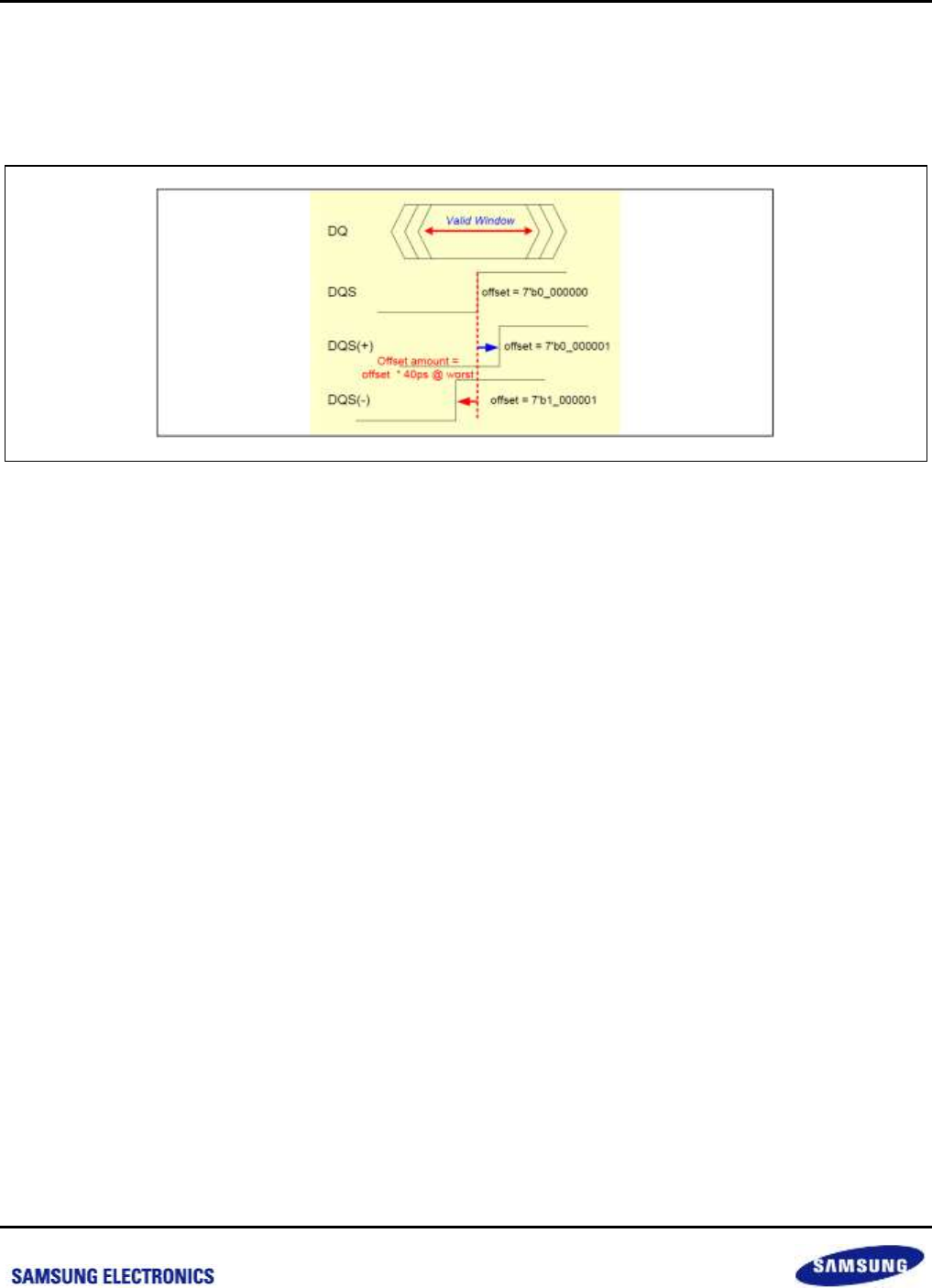
Samsung Confidential
S5P6818_UM 15 Memory Controller
15-33
Preliminary product information describes products that are in development, for which full characterization data and
associated errata are not yet available. Specifications and information herein are subject to change without notice.
15.3.9.4 Offset Control
ctrl_offset0 to 3 control the offset of 90° phase shift of DQS or 270° clock. CTRL_OFFSETD and ctrl_offset0 to
ctrl_offset3 are just used for debug or margin test purpose (after that, it is possible to program offset for the
compensation to maximize the margin).
Figure 15-8 Offset Control Example for ctrl_offset0 to ctrl_offset3
15.3.9.5 DLL Lock Procedure
1. After power-up and system PLL locking time, system reset (rst_n) is released.
2. CPU sets CTRL_OFFSETC*, CTRL_OFFSETR*, CTRL_OFFSETW*, ctrl_shiftc*, CTRL_START_POINT and
ctrl_inc value. Default values can be used normally. (If these values or the frequency are changed during the
normal operation, the following steps should be applied again after CTRL_DLL_ON is cleared. “*” means 0,
1, 2, 3)
CTRL_OFFSETC* = 0x0, ctrl_shiftc* = 0x0
CTRL_OFFSETR* = 0x0, CTRL_OFFSETW*=0x0
CTRL_START_POINT = 0x10, ctrl_inc = 0x10
3. Assert "DFI_INIT_START" from LOW to HIGH.
4. When DLL lock is finished, "DFI_INIT_COMPLETE" is set.
5. Before memory access, "DFI_CTRLUPD_REQ" should be applied. It's recommended that
"DFI_CTRLUPD_REQ" should be set and clear at the start of refresh cycle automatically by the memory
controller to update DLL lock information periodically.
DLL is used to compensate PVT condition. Therefore DLL should not be turned-off for reliable operation except for
the case of frequency scaling. (only to lower frequency scaling is permitted) To turn-off the DLL, follow the next
steps.
1. After DLL locking, CPU reads CTRL_LOCK_VALUE and write CTRL_LOCK_VALUE[8:0] to CTRL_FORCE.
2. DLL can be turned off by clearing CTRL_DLL_ON.
3. "DFI_CTRLUPD_REQ" should be issued 6 cycles after CTRL_DLL_ON was set and cleared.
nexell / ys.kim at 2015.02.12
SAMSUNG Confidential

Samsung Confidential
S5P6818_UM 15 Memory Controller
15-34
Preliminary product information describes products that are in development, for which full characterization data and
associated errata are not yet available. Specifications and information herein are subject to change without notice.
15.3.9.6 ZQ I/O Control Procedure
ZQ I/O calibrates the I/Os to match the driving and termination impedance by referencing resistor value of resister
(RZQ) connected externally from ZQ pin to ground. For DDR2/DDR3, RZQ should be 240 . One-time calibration
is provided for ZQ I/O control procedure. There are two modes for one-time calibration. One is "Long calibration
mode: and the other is "Short calibration mode".
<One-Time Calibration>
1. After power-up and system PLL locking time, system reset (rst_n) is released.
2. Set ctrl_zq_clk_div[31:0] to proper value (= 0x7)
3. Set ZQ_CLK_DIV_EN from 1’b0 to 1’b1 to update divider settings (ctrl_zq_clk_div[31:0] = 0x7).
4. Set zq_manual_mode
Long calibration mode: 2’b01
Short calibration mode: 2’b10
5. Start ZQ I/O calibration by setting ZQ_MANUAL_STR from 1’b0 to 1’b1
6. When calibration is done, zq_done (= PHY_CON17[0]) will be set. For four cycles (system clock)
7. After zq_done (= PHY_CON17[0]) is asserted, clear ZQ_MANUAL_STR
8. Clear ZQ_CLK_DIV_EN
<Manual Setting>
1. After power-up and system PLL locking time, system reset (rst_n) is released.
2. Set ctrl_zq_clk_div[31:0] to proper value (= 0x7)
3. Set ZQ_CLK_DIV_EN from 1’b0 to 1’b1 to update divider settings (ctrl_zq_clk_div[31:0] = 0x7).
4. Set zq_manual_mode = 2'b00 (= Force calibration mode).
5. Start ZQ I/O calibration by setting ZQ_MANUAL_STR from 1’b0 to 1’b1
6. After zq_done (= PHY_CON17[0]) is asserted, clear ZQ_MANUAL_STR.
nexell / ys.kim at 2015.02.12
SAMSUNG Confidential

Samsung Confidential
S5P6818_UM 15 Memory Controller
15-35
Preliminary product information describes products that are in development, for which full characterization data and
associated errata are not yet available. Specifications and information herein are subject to change without notice.
15.3.10 MCU-S
15.3.10.1 Static Memory Map Shadow
Below Figure Static Memory is composed of Static#0 to #1 (External Static Memory), Static#13 (Internal ROM)
and NAND as Figure.
However, base address of internal ROM, and nSCS[0] is changed according to system boot mode. In internal
ROM Boot Mode, base address of internal ROM is supposed to be exchanged with that of nSCS[0].
The previous Base Address remains in case of External Static Boot.
Figure 15-9 Static Memory Map Shadow
Static#13
(Internal ROM 20K)
RESERVED
NAND
RESERVED
Static#1(nSCS[1])
Static#0(nSCS[0])
0x3400_0000
0x3000_0000
0x2C00_0000
0x0800_0000
0x0400_0000
0x0000_0000
CfgBOOTMODE== 4'bx000
(External Static Memory Boot)
Static#13
(nSCS[0])
RESERVED
NAND
RESERVED
Static#1(nSCS[1])
Static#0(Internal ROM)
0x3400_0000
0x3000_0000
0x2C00_0000
0x0800_0000
0x0400_0000
0x0000_0000
CfgBOOTMODE!= 4'bx000
(Internal ROM boot)
nexell / ys.kim at 2015.02.12
SAMSUNG Confidential
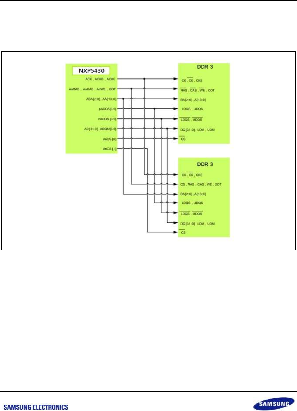
Samsung Confidential
S5P6818_UM 15 Memory Controller
15-36
Preliminary product information describes products that are in development, for which full characterization data and
associated errata are not yet available. Specifications and information herein are subject to change without notice.
15.3.10.2 Interface
32-bit Data bus width SDRAM Interface of MCU-A Bank
MCU-A supports 32-bit data bus width to CS[0] and CS[1] respectively.
Figure 15-10 16-bit Data Bus width SDRAM Interface
nexell / ys.kim at 2015.02.12
SAMSUNG Confidential
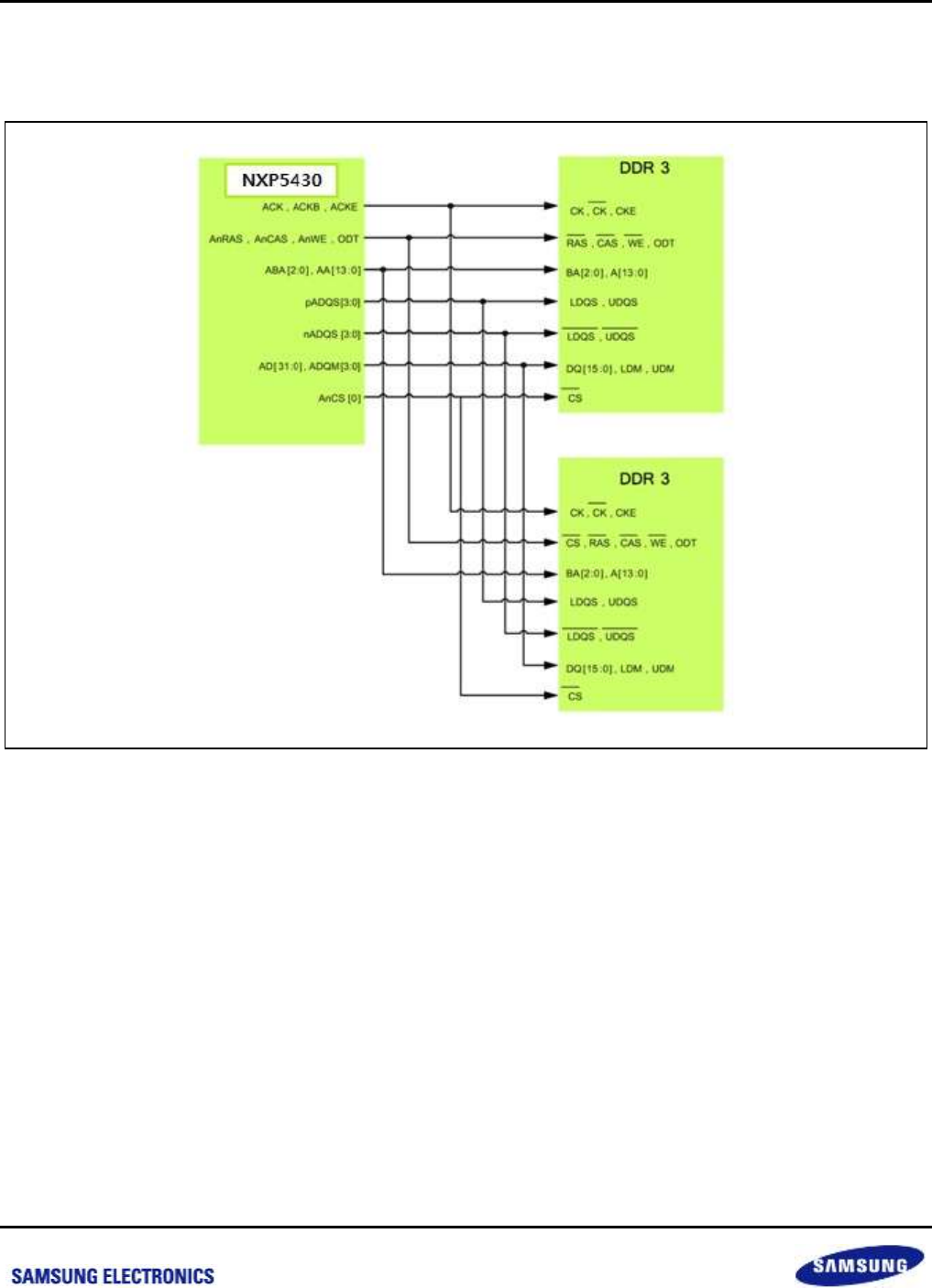
Samsung Confidential
S5P6818_UM 15 Memory Controller
15-37
Preliminary product information describes products that are in development, for which full characterization data and
associated errata are not yet available. Specifications and information herein are subject to change without notice.
16-bit Data bus width SDRAM Interface of MCU-A Bank
16-bit DDR3 SDRAM can add each two Memory to CS[0] and CS[1] respectively, which total four.
Figure 15-11 16-bit Data Bus width SDRAM Interface
nexell / ys.kim at 2015.02.12
SAMSUNG Confidential

Samsung Confidential
S5P6818_UM 15 Memory Controller
15-38
Preliminary product information describes products that are in development, for which full characterization data and
associated errata are not yet available. Specifications and information herein are subject to change without notice.
15.3.11 NAND Overview
15.3.11.1 Normal Access Sequence
<Read Cycle>
Write NAND Flash Command at NFCMD Register.
Write Address to NFADDR Register with respect to NAND Flash Address Type. (Refer to NAND Flash data
book)
Check IRQPEND bit.
Read ECC Data from NAND Flash Spare Array and Write ORGECC Register.
Read Data (512/1024 byte) from NAND Flash Main Array.
Check NFECCDECDONE Register
Check NFCHECKERROR Register
<Write Cycle>
Write NAND Flash Command to NFCMD Register. (Refer to NAND Flash data book)
Access address of memory which tries to access to NFADDR Register by 3 to 5time according to the sort of
NAND Flash. (Refer to NAND Flash data book)
Write data (512/1024 byte) through NFDATA Register.
Check NFECCENCDONE Register.
Read the result of ECC through NFECC Register. (Small block only)
Write NAND Flash Command to NFCMD Register. (Refer to NAND Flash data book)
Check whether NAND Flash is ready or not by reading NFCONTROL.IRQPEND bit. (For the exact sequence
of NAND Flash, Please refer to NAND Flash data book)
15.3.11.2 ECC (BCH)
<Feature>
Hardware ECC generation, detection and indication (software correction) 4/8/16/24/40/60-bit error correction
and detection
Error Detection Code/Error Correction Code (EDC/ECC)
NAND-based MLC flash has error weakness therefore error handling method is required. S5P6818 can
perform EDC (error detecting codes) and ECC (error correction codes) and both based on BCH (Bose-
Chadhuri-Hocquenghem) algorithm.EDC is run by hardware to reduce CPU overload and increase the CPU
performance. In contrast, ECC is run by software. Parity bit is calculated on every 512/1024 byte page.
Syndrome is calculated when each data is read from NAND flash and the value is used in error correction
operation.
Hardware ECC generation reset
This reset is asserted when NAND address or command register is written by any value.
This reset is also asserted when ECCRST bit (NFCONTROL register [11] bit) register is set to 1
This reset initializes NFECCL, NFECCH, NFCNT, NFECCSTATUS, NFSYNDRONE0 to 7 Registers.
nexell / ys.kim at 2015.02.12
SAMSUNG Confidential

Samsung Confidential
S5P6818_UM 15 Memory Controller
15-39
Preliminary product information describes products that are in development, for which full characterization data and
associated errata are not yet available. Specifications and information herein are subject to change without notice.
15.4 Register Description
15.4.1 Register Map Summary
Base Address: 0xC00E_0000
Register
Offset
Description
Reset Value
DREX
CONCONTROL
0x0000
Controller control register
0x0FFF_1100
MEMCONTROL
0x0004
Memory control register
0x0020_2601
cgcontrol
0x0008
Clock Gating Control register
0x0000_0000
RSVD
0x000C
Reserved
0x0000_1312
DIRECTCMD
0x0010
Memory direct command register
0x0000_0000
PRECHCONFIG0
0x0014
Precharge policy configuration0 register
0x0000_0000
PHYCONTROL0
0x0018
PHY control0 register
0x0000_0000
PWRDNCONFIG1
0x001C
Dynamic power down configuration register
0xFFFF_FFFF
timingrfcbp
0x0020
AC Timing Register for per Bank refresh of Memory
0x0000_1818
RSVD
0x0024
Reserved
0x0000_0000
pwrdnconfig
0x0028
Dynamic Power Down Configuration register
0xFFFF_00FF
TIMINGPZQ
0x002C
AC timing register for periodic ZQ(ZQCS) of memory
0x0000_4084
TIMINGAREF
0x0030
AC timing register for auto refresh of memory
0x0005_005D
TIMINGROW
0x0034
AC timing register for the row of memory
0x1F23_3286
TIMINGDATA
0x0038
0x00E8
AC timing register for the data of memory
0x1230_065C
TIMINGPOWER
0x003C
0x00EC
AC timing register for the power modes of memory
0x381B_0422
PHYSTATUS
0x0040
PHY status register
0x0000_0000
etctiming
0x0044
ETC Timing register
0x0000_0000
CHIPSTATUS
0x0048
Memory chip status register
0x0000_0000
RSVD
0x004C to
0x0050
Reserved
0x0000_0000
MRSTATUS
0x0054
Memory mode registers status register
0x0000_0000
RSVD
0x0058 to
0x005C
Reserved
0x0000_0000
QOSCONTROLn
0x0060 to
0x00D8
Quality of service control register n
0x0000_0FFF
RSVD
0x00DC
Reserved
0x0000_0000
timingsetsw
0x00E0
Timing Set Switch Configuration register
0x0000_0000
RSVD
0x00E4 to
0x00F0
Reserved
0x0000_0000
WRTRACONFIG
0x00F4
Write training configuration register
0x0000_0000
nexell / ys.kim at 2015.02.12
SAMSUNG Confidential

Samsung Confidential
S5P6818_UM 15 Memory Controller
15-40
Preliminary product information describes products that are in development, for which full characterization data and
associated errata are not yet available. Specifications and information herein are subject to change without notice.
Register
Offset
Description
Reset Value
RDLVLCONFIG
0x00F8
Read leveling configuration register
0x0000_0000
RSVD
0x00FC
Reserved
0x0000_0000
BRBRSVCONTROL
0x0100
BRB reservation control register
0x0000_0000
BRBRSVCONFIG
0x0104
BRB reservation configuration register
0x8888_8888
BRBQOSCONFIG
0x0108
BRB QoS configuration register
0x0000_0010
RSVD
0x010C to
0x011C
Reserved
0x0000_0000
WRLVLCONFIG0
0x0120
Write leveling configuration register0
0x0000_0010
WRLVLCONFIG1
0x0124
Write leveling configuration register1
0x0000_0000
WRLVLSTATUS
0x0128
Write leveling status register
0x0000_0000
RSVD
0x012C to
0x014C
Reserved
0x0000_0000
CTRL_IO_RDATA
0x0150
CTRL_IO_RDATA register
0x0000_0000
RSVD
0x0154 to
0x015C
Reserved
0x0000_0000
CACAL_CONFIG0
0x0160
CA calibration configuration register0
0x003F_F010
CACAL_CONFIG1
0x0164
CA calibration configuration register1
0x0000_0000
CACAL_STATUS
0x0168
CA calibration status register
0x0000_0000
RSVD
0x016C to
0x01FC
Reserved
0x0000_0000
emergent_config0
0x0200
Emergent Configuration register 0
0x0000_0000
emergent_config1
0x0204
Emergent Configuration register 1
0x0000_0000
RSVD
0x0208 to
0x020C
Reserved
0x0000_0000
bp_controln
0x0210 +
0x10n
Back Pressure Control register for Port n (n = 0 to 3)
0x0000_0002
bp_CONFIGRn
0x0214 +
0x10n
Back pressure Configuration register for Read Port n (n = 0 to 3)
0x0000_0000
bp_CONFIGWn
0x0218 +
0x10n
Back pressure Configuration register for Write Port n (n = 0 to 3)
0x0000_0000
nexell / ys.kim at 2015.02.12
SAMSUNG Confidential

Samsung Confidential
S5P6818_UM 15 Memory Controller
15-41
Preliminary product information describes products that are in development, for which full characterization data and
associated errata are not yet available. Specifications and information herein are subject to change without notice.
Base Address: 0xC00E_5000
Register
Offset
Description
Reset Value
TZASC
tzconfig
0x0000
TZASC configuration register
0x0000_2208
tzaction
0x0004
TZASC Action register
0x0000_0000
tzldrange
0x0008
TZASC Lockdown Range register
0x0000_0000
tzldselect
0x000C
TZASC Lockdown Select register
0x0000_0000
tzintstatus
0x0010
TZASC Interrupt Status register
0x0000_0000
tzintclear
0x0014
TZASC Interrupt Clear register
–
tzfailaddrlowrn
0x0040 +
0x20n
TZASC Read Fail Address Low register n (n = 0 to 3)
0x0000_0000
Tzfailaddrhighrn
0x0044 +
0x20n
TZASC Read Fail Address High register n (n = 0 to 3)
0x0000_0000
tzfailctrlrn
0x0048 +
0x20n
TZASC Read Fail Control register n (n = 0 to 3)
0x0000_0000
tzfailidrn
0x004C +
0x20n
TZASC Read Fail ID register n (n = 0 to 3)
0x0000_0000
tzfailaddrlowwn
0x0050 +
0x20n
TZASC Write Fail Address Low register n (n = 0 to 3)
0x0000_0000
tzfailctrlwn
0x0054 +
0x20n
TZASC Write Fail Address High register n (n = 0 to 3)
0x0000_0000
TZFAILADDRHIGHWn
0x0058 +
0x20n
TZASC Write Fail Control Register n (n = 0 to 3)
0x0100_0000
TZFAILIDWn
0x005C +
0x20n
TZASC Write Fail ID Register n (n = 0 to 3)
0x0000_0000
TZRSLOWn
0x0100 +
0x10n
TZASC Region Setup Low Register n (n = 0 to 8)
0x0000_0000
TZRSHIGHn
0x0104 +
0x10n
TZASC Region Setup High Register n (n = 0 to 8)
0x0000_0000
TZRSATTRn
0x0108 +
0x10n
TZASC Region Attribute Register n (n = 0 to 8)
0xF000_0000
TZITCRG
0x0E00
TZASC Integration Test Control Register
0x0000_0000
TZITIP
0x0E04
TZASC Integration Test Input Register
0x0000_0000
TZITOP
0x0E08
TZASC Integration Test Output Register
0x0000_0000
MemBaseConfig0
0x0F00
Memory Chip0 Base Configuration Register
0x0000_07F8
MemBaseConfig1
0x0F04
Memory Chip1 Base Configuration Register
0x0000_07F8
MemConfig0
0x0F10
Memory Chip0 Configuration Register
0x0002_2312
MemConfig1
0x0F14
Memory Chip1 Configuration Register
0x0002_2312
nexell / ys.kim at 2015.02.12
SAMSUNG Confidential

Samsung Confidential
S5P6818_UM 15 Memory Controller
15-42
Preliminary product information describes products that are in development, for which full characterization data and
associated errata are not yet available. Specifications and information herein are subject to change without notice.
Base Address: 0xC00E_1000
Register
Offset
Description
Reset Value
DDRPHY
PHY_CON0
0x0000
PHY Control Register 0
0x1742_1E40
PHY_CON1
0x0004
PHY Control Register 1
0x2021_0100
PHY_CON2
0x0008
PHY Control Register 2
0x0001_0004
PHY_CON3
0x000C
PHY Control Register 3
0x0000_0000
PHY_CON4
0x0010
PHY Control Register 4
0x0008_0000
PHY_CON5
0x0014
PHY Control Register 5
0x0000_0000
LP_CON0
0x0018
Low Power Control Register 0
0x0000_0000
RODT_CON0
0x001C
Read ODT Control Register 0
0x0100_0000
OFFSETR_CON0
0x0020
Read Code Control Register 0
0x0808_0808
OFFSETR_CON1
0x0024
Read Code Control Register 1
0x0808_0808
OFFSETR_CON2
0x0028
Read Code Control Register 2
0x0000_0008
RSVD
0x002C
Reserved
0x0000_0000
OFFSETW_CON0
0x0030
Write Code Control Register 0
0x0808_0808
OFFSETW_CON1
0x0034
Write Code Control Register 1
0x0808_0808
OFFSETW_CON2
0x0038
Write Code Control Register 2
0x0000_0008
RSVD
0x003C
Reserved
0x0000_0000
OFFSETC_CON0
0x0040
Gate Code Control Register 0
0x0000_0000
OFFSETC_CON1
0x0044
Gate Code Control Register 1
0x0000_0000
OFFSETC_CON2
0x0048
Gate Code Control Register 2
0x0000_0000
SHIFTC_CON0
0x004C
Gate Code Shift Control Register 0
0x0249_2492
OFFSETD_CON0
0x0050
CMD Code Control Register
0x1000_0008
RSVD
0x0054
Reserved
0x0000_0000
LP_DDR_CON0
0x0058
Read Leveling Control Register 0
0x0000_0208
LP_DDR_CON1
0x005C
Read Leveling Control Register 1
0x0000_03FF
LP_DDR_CON2
0x0060
Read Leveling Control Register 2
0x0000_0000
LP_DDR_CON3
0x0064
Read Leveling Control Register 3
0x0000_105F
LP_DDR_CON4
0x0068
Read Leveling Control Register 4
0x0000_107E
WR_LVL_CON0
0x006C
Write Leveling Control Register 0
0x0000_0000
WR_LVL_CON1
0x0070
Write Leveling Control Register 1
0x0000_0000
WR_LVL_CON2
0x0074
Write Leveling Control Register 2
0x0000_0000
WR_LVL_CON3
0x0078
Write Leveling Control Register 3
0x0000_0000
CA_DSKEW_CON0
0x007C
CA Deskew Control Register 0
0x0000_0000
CA_DSKEW_CON1
0x0080
CA Deskew Control Register 1
0x0000_0000
CA_DSKEW_CON2
0x0084
CA Deskew Control Register 2
0x0000_0000
CA_DSKEW_CON3
0x0088
CA Deskew Control Register 3
0x0000_0000
nexell / ys.kim at 2015.02.12
SAMSUNG Confidential

Samsung Confidential
S5P6818_UM 15 Memory Controller
15-43
Preliminary product information describes products that are in development, for which full characterization data and
associated errata are not yet available. Specifications and information herein are subject to change without notice.
Register
Offset
Description
Reset Value
RSVD
0x008C to
0x0090
Reserved
0x0000_0000
CA_DSKEW_CON4
0x0094
CA Deskew Control Register 4
0x0000_0000
RSVD
0x0098
Reserved
0x0000_0000
DRVDS_CON0
0x009C
Driver Strength Control Register 0
0x0000_0000
DRVDS_CON1
0x00A0
Driver Strength Control Register 1
0x0000_0000
RSVD
0x00A4 to
0x00AC
Reserved
0x0000_0007
MDLL_CON0
0x00B0
MDLL Control Register 0
0x1010_0070
MDLL_CON1
0x00B4
MDLL Control Register 1
Undefined
RSVD
0x00B8 to
0x00BC
Reserved
0x0000_0000
ZQ_CON0
0x00C0
ZQ Control Register
0x0000_0000
ZQ_CON1
0x00C4
ZQ Status Register
0x0000_0000
ZQ_CON2
0x00C8
ZQ Divider Control Register
0x0000_0007
ZQ_CON3
0x00CC
ZQ Timer Control Register
0x0000_00F0
T_RDDATA_CON0
0x00D0
Read Data Enable Status Register 0
0x0055_5555
T_RDDATA_CON1
0x00D4
Read Data Enable Status Register 1
0x0055_5555
T_RDDATA_CON2
0x00D8
Read Data Enable Status Register 2
0x0000_0015
CAL_WL_STAT
0x00DC
WL Calibration Fail Status Register
0x0000_0000
CAL_FAIL_STAT0
0x00E0
Calibration Fail Status Register 0
0x0000_0000
CAL_FAIL_STAT1
0x00E4
Calibration Fail Status Register 1
0x0000_0000
CAL_FAIL_STAT2
0x00E8
Calibration Fail Status Register 2
0x0000_0000
CAL_FAIL_STAT3
0x00EC
Calibration Fail Status Register 3
0x0000_0000
CAL_GT_VWMC0
0x00F0
Calibration Gate Training Centering Code 0
Undefined
CAL_GT_VWMC1
0x00F4
Calibration Gate Training Centering Code 1
Undefined
CAL_GT_VWMC2
0x00F8
Calibration Gate Training Centering Code 2
Undefined
CAL_GT_CYC
0x00FC
Calibration Gate Training Cycle
Undefined
CAL_RD_VWMC0
0x0100
Calibration Read Center Code 0
Undefined
CAL_RD_VWMC1
0x0104
Calibration Read Center Code 1
Undefined
CAL_RD_VWMC2
0x0108
Calibration Read Center Code 2
Undefined
RSVD
0x010C
Reserved
Undefined
CAL_RD_VWML0
0x0110
Calibration Read Left Code 0
Undefined
CAL_RD_VWML1
0x0114
Calibration Read Left Code 1
Undefined
CAL_RD_VWML2
0x0118
Calibration Read Left Code 2
Undefined
RSVD
0x011C
Reserved
Undefined
CAL_RD_VWMR0
0x0120
Calibration Read Right Code 0
Undefined
nexell / ys.kim at 2015.02.12
SAMSUNG Confidential

Samsung Confidential
S5P6818_UM 15 Memory Controller
15-44
Preliminary product information describes products that are in development, for which full characterization data and
associated errata are not yet available. Specifications and information herein are subject to change without notice.
Register
Offset
Description
Reset Value
CAL_RD_VWMR1
0x0124
Calibration Read Right Code 1
Undefined
CAL_RD_VWMR2
0x0128
Calibration Read Right Code 2
Undefined
RSVD
0x012C
Reserved
Undefined
CAL_WR_VWMC0
0x0130
Calibration Write Center Code 0
Undefined
CAL_WR_VWMC1
0x0134
Calibration Write Center Code 1
Undefined
CAL_WR_VWMC2
0x0138
Calibration Write Center Code 2
Undefined
RSVD
0x013C
Reserved
Undefined
CAL_WR_VWML0
0x0140
Calibration Write Left Code 0
Undefined
CAL_WR_VWML1
0x0144
Calibration Write Left Code 1
Undefined
CAL_WR_VWML2
0x0148
Calibration Write Left Code 2
Undefined
RSVD
0x014C
Reserved
Undefined
CAL_WR_VWMR0
0x0150
Calibration Write Right Code 0
Undefined
CAL_WR_VWMR1
0x0154
Calibration Write Right Code 1
Undefined
CAL_WR_VWMR2
0x0158
Calibration Write Right Code 2
Undefined
RSVD
0x015C
Reserved
Undefined
CAL_DM_VWMC0
0x0160
Calibration DM Center Code 0
Undefined
CAL_DM_VWMC1
0x0164
Calibration DM Center Code 1
Undefined
CAL_DM_VWMC2
0x0168
Calibration DM Center Code 2
Undefined
RSVD
0x016C
Reserved
Undefined
CAL_DM_VWML0
0x0170
Calibration DM Left Code 0
Undefined
CAL_DM_VWML1
0x0174
Calibration DM Left Code 1
Undefined
CAL_DM_VWML2
0x0178
Calibration DM Left Code 2
Undefined
RSVD
0x017C
Reserved
Undefined
CAL_DM_VWMR0
0x0180
Calibration DM Right Code 0
Undefined
CAL_DM_VWMR1
0x0184
Calibration DM Right Code 1
Undefined
CAL_DM_VWMR2
0x0188
Calibration DM Right Code 2
Undefined
nexell / ys.kim at 2015.02.12
SAMSUNG Confidential

Samsung Confidential
S5P6818_UM 15 Memory Controller
15-45
Preliminary product information describes products that are in development, for which full characterization data and
associated errata are not yet available. Specifications and information herein are subject to change without notice.
Base Address: 0xC005_1000
Register
Offset
Description
Reset Value
MCU-S
MEMBW
0x0000
Memory bus width register
Undefined
MEMTIMEACSL
0x0004
Memory timing for TACS low register
Undefined
MEMTIMEACSH
0x0008
Memory timing for TACS high register
0x0000_0000
MEMTIMECOSL
0x000C
Memory timing for TCOS low register
Undefined
MEMTIMECOSH
0x0010
Memory timing for TCOS high register
0x0000_0000
MEMTIMEACC0
0x0014
Memory timing for TACC 0 register
Undefined
MEMTIMEACC1
0x0018
Memory timing for TACC 1 register (Reserved)
Undefined
MEMTIMEACC2
0x001C
Memory timing for TACC 2 register (Reserved)
Undefined
MEMTIMEACC3
0x0020
Memory timing for TACC 3 register
0x0000_0000
MEMTIMESACC0
0x0024
Memory timing for TSACC 0 register
0x0000_0000
MEMTIMESACC1
0x0028
Memory timing for TSACC 1 register (Reserved)
Undefined
MEMTIMESACC2
0x002C
Memory timing for TSACC 2 register (Reserved)
Undefined
MEMTIMESACC3
0x0030
Memory timing for TSACC 3 register
0x0000_0000
RSVD
0x0034 to
0x0040
Reserved
0x0000_0000
MEMTIMECOHL
0x0044
MEMORY TIMING FOR TCOH low register
Undefined
MEMTIMECOHH
0x0048
MEMORY timing for TCOH high register
0x0000_0000
MEMTIMECAHL
0x004C
MEMORY timing for TCAH low register
Undefined
MEMTIMECAHH
0x0050
MEMORY timing for TCAH high register
0x0000_0000
MEMBURSTL
0x0054
MEMORY burst control low register
0x0000_0010
RESERVED
0x0058
Reserved
Undefined
MEMWAIT
0x005C
Memory wait control register
0x0000_0000
RSVD
0x0060 to
0x0084
Reserved
Undefined
NFCONTROL
0x0088
NAND flash control register
Undefined
NFECCTRL
0x008C
NAND ECC control register
0x0000_0000
NFCNT
0x0090
NAND flash data count register
0x0000_0000
NFECCSTATUS
0x0094
NAND flash ECC status register
0x0000_0000
NFTIMEACS
0x0098
NAND timing for TACS register
0x0000_0007
NFTIMECOS
0x009C
NAND timing for TCOS register
0x0000_0007
NFTIMEACC0
0x00A0
NAND timing for TACC0 register
0x0000_000F
RSVD
0x00A4
Reserved
–
NFTIMEOCH
0x00A8
NAND timing for TOCH register
0x0000_0007
NFTIMECAH
0x00AC
NAND timing for TCAH register
0x0000_0007
NFECC0 to NFECC26
0x00B0 to
0x0118
NAND flash ECC 0 to 26 register
0x0000_0000
nexell / ys.kim at 2015.02.12
SAMSUNG Confidential
Samsung Confidential
S5P6818_UM 15 Memory Controller
15-46
Preliminary product information describes products that are in development, for which full characterization data and
associated errata are not yet available. Specifications and information herein are subject to change without notice.
Register
Offset
Description
Reset Value
NFORGECC0 to
NFORGECC26
0x011C to
0x0184
NAND flash origin ECC 0 to 26 register
0x0000_0000
NFSYNDROME0 to
NFSYNDROME29
0x0188 to
0x01FC
NAND flash ECC syndrome value 0 to 29 register
0x0000_0000
NFELP0 to NFELP59
0x0200 to
0x0274
NAND flash ECC ELP value 0 to 59 register
Undefined
NFERRORLOCATION0 to
NFERRORLOCATION59
0x0278 to
0x02EC
NAND flash error location 0 to 59 register
Undefined
AUTOSYND
0x02F0
AUTO SYNDROM REGISTER
0x0000_0000
NFWSYNDRONE0 to
NFWSYNDRONE29
0x02F4 to
0x0368
NAND flash ECC write syndrome value 0 to 29 register
0x0000_0000
Base Address: 0x2C00_0000
Register
Offset
Description
Reset Value
MCUS_ADDR
NFDATA
0x0000
NAND flash data register
Undefined
NFCMD
0x0010
NAND flash command register
Undefined
NFADDR
0x0018
NAND flash address register
Undefined
nexell / ys.kim at 2015.02.12
SAMSUNG Confidential

Samsung Confidential
S5P6818_UM 15 Memory Controller
15-47
Preliminary product information describes products that are in development, for which full characterization data and
associated errata are not yet available. Specifications and information herein are subject to change without notice.
15.4.1.1 DREX
15.4.1.1.1 CONCONTROL
Base Address: 0xC00E_0000
Address = Base Address + 0x0000, Reset Value = 0x0FFF_1100
Name
Bit
Type
Description
Reset Value
RSVD
[31:29]
–
Reserved (Should be zero)
3’b0
DFI_INIT_START
[28]
RW
DFI PHY initialization start
This field is used to initialize DFI PHY. Set this field to 1 to
initialize DFI PHY and set this field to 0 after received
DFI_INIT_COMPLETE of PHYSTATUS register.
1’b0
TIMEOUT_LEVEL0
[27:16]
RW
Default Timeout Cycles
This counter prevents transactions in the AXI request
FIFO from starvation. This counter starts if a new AXI
transaction comes into the request FIFO. If the counter
becomes zero, the corresponding FIFO has the highest
priority during BRB arbitration. Refer to Section 1.7.
Quality of Service for de-tailed information
12’hFFF
RSVD
[15]
–
Reserved (Should be zero)
1’b0
RD_FETCH
[14:12]
RW
Read Data Fetch Cycles
0xn = n MBCLK cycles (MBCLK: DREX-1 core clock)
The recommended value of this field is 0x2 for LPDDR3
800 MHz memory clock and other cases are 0x1.
This register is for the unpredictable latency of read data
coming from memory devices by tDQSCK variation or the
board flying time. The read fetch delay of PHY read FIFO
must be controlled by this parameter. The controller will
fetch read data from PHY after read_latency + n MBCLK
cycles. Refer to Section 1.3 for detailed information.
1’b1
RSVD
[11:9]
–
Reserved (Should be zero)
3’b0
EMPTY
[8]
R
Empty Status
0 = Not Empty
0x1 = Empty
There is no AXI transaction in memory controller.
1’b1
io_pd_con
[7:6]
RW
I/O Receiver Power down Control
0x0 = Use programmed ctrl_pd
0x1 = Automatic control for ctrl_pd in CKE low
0x2 = Automatic control for ctrl_pd in none read state
0x3 = Reserved
"ctrl_pd" is used for power down of I/O cell receiver.
If this field is set to 0x0, DREX only sends programmed
ctrl_pd value.
If this field is set to 0x1 and memory state is in CKE low
state, DREX automatically set power down enable for
input buffer of I/O.
If this value is set to 0x2 and memory state is in none
2’b0
nexell / ys.kim at 2015.02.12
SAMSUNG Confidential

Samsung Confidential
S5P6818_UM 15 Memory Controller
15-48
Preliminary product information describes products that are in development, for which full characterization data and
associated errata are not yet available. Specifications and information herein are subject to change without notice.
Name
Bit
Type
Description
Reset Value
read, DREX automatically set power down enable for input
buffer of I/O.
Note that this field should be turn off during initialization
and training sequence.
AREF_EN
[5]
RW
Auto Refresh Counter
0 = Disable
0x1 = Enable
Enable this to decrease the auto refresh counter by 1 at
the rising edge of the MPCLK
1’b0
RSVD
[4]
–
Reserved (Should be zero)
1’b0
update_mode
[3]
RW
The kind of Update Interface in DFI
0x0 = PHY initiated update/acknowledge mode
0x1 = MC initiated update/acknowledge mode
In case of wide io memory and PHY V5, this field should
be 1'b1.
1’b0
CLK_RATIO
[2:1]
RW
Clock Ratio of Bus Clock to Memory Clock
0x0 = freq.(MBCLK): freq.(MBCLK) = 1:1
0x1 to 0x3 = Reserved
0x0
ca_swap
[0]
–
CA Swap for LPDDR2-S4/LPDDR3
0x0 = CA swap disable
0x1 = CA swap enable
If this field is enabled, ca[9:0] is reversed to ca[0:9]
1’b0
nexell / ys.kim at 2015.02.12
SAMSUNG Confidential

Samsung Confidential
S5P6818_UM 15 Memory Controller
15-49
Preliminary product information describes products that are in development, for which full characterization data and
associated errata are not yet available. Specifications and information herein are subject to change without notice.
15.4.1.1.2 MEMCONTROL
Base Address: 0xC00E_0000
Address = Base Address + 0x0004, Reset Value = 0x0020_2601
Name
Bit
Type
Description
Reset Value
RSVD
[31:30]
–
Should be zero
2’b0
PAUSE_REF_EN
[29]
RW
Refresh Command Issue Before PAUSE ACKNOLEDGE
0 = Disable
1 = Enable
If this field is enabled, refresh command is issued before PAUSE
acknowledge. If PZQ_EN is enabled, do not enable this field.
1’b0
SP_EN
[28]
RW
Read with Short Preamble in Wide IO Memory
0 = Disable
1 = Enable
Wide IO Memory has read with short preamble command to
support zero-bubble in chip to chip read cycles.
If this field is enabled, t_r2r_c2c is neglected.
1’b0
PB_REF_EN
[27]
RW
Per Bank Refresh for LPDDR2-S4/LPDDR3
0 = Disable
1 = Enable
To use per bank refresh feature, turn on this field before
AREF_EN is enabled in CONCONTROL register.
Per bank refresh is only allowed in LPDDR2-S4 and LPDDR3
devices with 8 banks and PHY update mode (CONCONTROL.
UPDATE_MODE = 0).
1’b0
RSVD
[26:25]
–
Should be zero
2’b0
PZQ_EN
[24]
RW
DDR3 periodic ZQ(ZQCS) enable
Note that after exit from self refresh, ZQ function is required by the
software. The controller does not support ZQ calibration command
to be issued in parallel to DLL lock time when coming out of self
refresh. Turn-on only when using DDR3. The periodic ZQ interval
is defined by t_pzq in TIMINGPZQ
Register
1’b0
RSVD
[23]
–
Should be zero
1’b0
BL
[22:20]
RW
Memory Burst Length
0 = Reserved
1 = 2 (Wide IO Memory use only)
2 = 4
3 = 8
0x4 to 0x7 = Reserved
In case of Wide IO Memory, the controller only supports burst
length 2.
In case of LPDDR2-S4, the controller only supports burst length 4.
In case of DDR3 and LPDDR3, the controller only supports burst
length 8.
3’b010
NUM_CHIP
[19:16]
RW
Number of Memory Chips
4’h0
nexell / ys.kim at 2015.02.12
SAMSUNG Confidential

Samsung Confidential
S5P6818_UM 15 Memory Controller
15-50
Preliminary product information describes products that are in development, for which full characterization data and
associated errata are not yet available. Specifications and information herein are subject to change without notice.
Name
Bit
Type
Description
Reset Value
0 = 1 chip
1 = 2 chips
0x2 to 0xf = Reserved
MEM_WIDTH
[15:12]
RW
Width of Memory Data Bus
0, 1 = Reserved
2 = 32-bit
3 = Reserved
4 = 128-bit (Wide IO Memory use only)
5 to 0xf = Reserved
4’h2
MEM_TYPE
[11:8]
RW
Type of Memory
0x0 to 0x4 = Reserved
0x5 = LPDDR2-S4
0x6 = DDR3
0x7 = LPDDR3
0x8 to 0xf = Reserved
4’h6
ADD_LAT_PALL
[7:6]
RW
Additional Latency for PALL in MBCLK cycle
0x0 = 0 cycle
0x1 = 1 cycle
0x2 = 2 cycle
0x3 = Reserved
If all banks precharge command is issued, the latency of pre-
charging will be tRP + add_lat_pall
2’b0
DSREF_EN
[5]
RW
Dynamic Self Refresh
0 = Disable
1 = Enable
Refer to Section Dynamic power down for detailed information.
In DDR3, this feature is not supported.
1’b0
RSVD
[4]
RW
Should be zero
1’b0
DPWRDN_TYPE
[3:2]
RW
Type of Dynamic Power Down
0x0 = Active/precharge power down
0x1 = Forced precharge power down
0x2 to 0x3 = Reserved
Refer to Section Dynamic power down for detailed information.
2’b0
DPWRDN_EN
[1]
RW
Dynamic Power Down
0x0 = Disable
0x1 = Enable
1’b0
CLK_STOP_EN
[0]
RW
Dynamic Clock Control
0x0 = Always running
0x1 = Stops during idle periods
This feature is only supported with LPDDR2/LPDDR3.
Refer to chapter Clock stop for detailed information.
Note that if phy_cg_en is enabled then this field should be zero.
1’b1
nexell / ys.kim at 2015.02.12
SAMSUNG Confidential

Samsung Confidential
S5P6818_UM 15 Memory Controller
15-51
Preliminary product information describes products that are in development, for which full characterization data and
associated errata are not yet available. Specifications and information herein are subject to change without notice.
15.4.1.1.3 CGCONTROL
Base Address: 0xC00E_0000
Address = Base Address + 0x0008, Reset Value = 0x0000_0000
Name
Bit
Type
Description
Reset Value
RSVD
[31:5]
–
Reserved (Should be zero)
16’h0
phy_cg_en
[4]
RW
PHY Clock Gating
0x0 = PHY clock gating disable
0x1 = PHY clock gating enable
Note that if this field is enabled then CLK_STOP_EN
(MEMCONTROL) should be set to zero.
This feature is not supported in DDR3 (this field should be
zero in case of DDR3.)
1’b0
memif_cg_en
[3]
RW
Memory Controller Internal Clock Gating-Memory I/F
0x0 = Memory I/F clock gating disable
0x1 = Memory I/F clock gating enable
1’b0
scg_cg_en
[2]
RW
Memory Controller Internal Clock Gating-Scheduler
0x0 = Scheduler clock gating disable
0x1 = Scheduler clock gating enable
1’b0
busif_wr_cg_en
[1]
RW
Memory Controller Internal Clock Gating-BUS I/F Write
0x0 = Bus I/F write clock gating disable
0x1 = Bus I/F write clock gating enable
1’b0
busif_rd_cg_en
[0]
RW
Memory Controller Internal Clock Gating-BUS I/F Read
0x0 = Bus I/F read clock gating disable
0x1 = Bus I/F read clock gating enable
1’b0
nexell / ys.kim at 2015.02.12
SAMSUNG Confidential

Samsung Confidential
S5P6818_UM 15 Memory Controller
15-52
Preliminary product information describes products that are in development, for which full characterization data and
associated errata are not yet available. Specifications and information herein are subject to change without notice.
15.4.1.1.4 DIRECTCMD
Base Address: 0xC00E_0000
Address = Base Address + 0x0010, Reset Value = 0x0000_0000
Name
Bit
Type
Description
Reset Value
RSVD
[31:28]
–
Reserved (Should be zero)
4’h0
CMD_TYPE
[27:24]
RW
Type of Direct Command
0x0 = MRS/EMRS (mode register setting)
0x1 = PALL (all banks precharge)
0x2 = PRE (per bank precharge)
0x3 = DPD (deep power down)
0x4 = REFS (self refresh)
0x5 = REFA (auto refresh)
0x6 = CKEL (active/precharge power down)
0x7 = NOP (exit from active/precharge power down or
deep power down
0x8 = REFSX (exit from self refresh)
0x9 = MRR (mode register reading
0xa = ZQINIT (ZQ calibration init.)
0xb = ZQOPER (ZQ calibration long)
0xc = ZQCS (ZQ calibration short)
0xd to 0xf = Reserved
When a direct command is issued, AXI masters must not
access memory. It is strongly recommended to check the
command queue's state by
CONCONTROL.chip0/1_empty and the chip FSM in the
CHIPSTATUS register before issuing a direct command.
The chip status must be checked before issuing a direct
command.
And clk_stop_en, dynamic power down, dynamic self
refresh, force precharge function (MEMCONTROL
register) and sl_dll_dyn_con (PHYCONTROL0 register)
must be disabled.
MRS/EMRS or MRR commands should be issued if all
banks are in idle state.
If MRS/EMRS or MRR is issued to LPDDR2-S4/LPDDR3,
the CA pins must be mapped as follows.
MA[7:0] = {cmd_addr[1:0], cmd_bank[2:0],
cmd_addr[12:10]}
OP[7:0] = cmd_addr[9:2]
In DDR3, self refresh related timing such as tCKESR/
tCKSRE/ tCKSRX should be check by software.
NOTE: That do not write reserved value to this field.
4’h0
RSVD
[23:21]
RW
Reserved (Should be zero)
3’b0
CMD_CHIP
[20]
RW
Chip Number to send the direct command to
0 = Chip 0
1 = Chip 1
1’b0
cmd_addr_16
[19]
–
A16 for Wide IO Memory
1’b0
nexell / ys.kim at 2015.02.12
SAMSUNG Confidential

Samsung Confidential
S5P6818_UM 15 Memory Controller
15-53
Preliminary product information describes products that are in development, for which full characterization data and
associated errata are not yet available. Specifications and information herein are subject to change without notice.
Name
Bit
Type
Description
Reset Value
A16 bit in Wide IO Memory mode register definition
CMD_BANK
[18:16]
RW
Related Bank Address when issuing a direct command
To send a direct command to a chip, additional information
such as the bank address is required. This register is used
in such situations
3’b0
CMD_ADDR
[15:0]
RW
Related Address value when issuing a direct command
To send a direct command to a chip, additional information
such as the address is required. This register is used in
such situations.
16’h0
15.4.1.1.5 PRECHCONFIG0
Base Address: 0xC00E_0000
Address = Base Address + 0x0014, Reset Value = 0x0000_0000
Name
Bit
Type
Description
Reset Value
TP_en
[31:28]
RW
Timeout Precharge per Port
0x0 = Disable
0x1 = Enable
[31:28] is timeout precharge enable bit for port0, 1, 2, 3
respectively.
If TP_EN is enabled, it automatically precharges an open
bank after a specified amount of MCLK cycles (if no
access has been made in between the cycles) in an open
page policy. If PrechConfig1.tp_cnt bit-field is set, it
specifies the amount of MCLK cycles to wait until timeout
precharge precharges the open bank. Refer to chapter
Timeout precharge for detailed information.
4’h0
RSVD
[27:20]
–
Reserved (Should be zero)
8’h0
port_POLICY
[19:16]
RW
Memory Precharge Port Selective Policy
0x0 = Open page policy
0x1 = Close page (auto precharge) policy
PORT_POLICY[n], n is the port number.
4’h0
RSVD
[15:0]
–
Reserved (Should be zero)
16’h0
nexell / ys.kim at 2015.02.12
SAMSUNG Confidential

Samsung Confidential
S5P6818_UM 15 Memory Controller
15-54
Preliminary product information describes products that are in development, for which full characterization data and
associated errata are not yet available. Specifications and information herein are subject to change without notice.
15.4.1.1.6 PHYCONTROL0
Base Address: 0xC00E_0000
Address = Base Address + 0x0018, Reset Value = 0x0000_0000
Name
Bit
Type
Description
Reset Value
MEM_TERM_EN
[31]
RW
Termination Enable for Memory
At high-speed memory operation, it can be necessary to
turn on termination resistance in memory devices. This
register controls an ODT pin for write of memory device.
All ODT pins will be high when any chip is in write state.
This field is only applicable in LPDDR3/DDR3 like below.
– LPDDR3 800 MHz (RL 12, WL 6)
– DDR3 800 MHz
In LPDDR3-800 MHz (RL 12, WL6), if MEM_TERM_EN or
PHY_TERM_EN is enabled, DQSCK in TimingData0/1
register need be set to bigger value than RU (tDQSCK
max/tCK).
1’b0
PHY_TERM_EN
[30]
RW
Termination Enable for PHY
At high-speed memory operation, it can be necessary to
turn on termination resistance in the PHY.
In LPDDR3-800 MHz (RL 12, WL6), if MEM_TERM_EN or
PHY_TERM_EN is enabled, DQSCK in TimingData0/1
register need be set to bigger value than RU (tDQSCK
max/tCK).
1’b0
CTRL_SHGATE
[29]
–
Duration of DQS Gating Signal
This field controls the gate control signal
In LPDDR2-S4/LPDDRD3, this field should be 1‟b0
regard-less of clock frequency.
In DDR3, according to memory clock, set the value like
be-low.
0 = (gate signal length = "burst length / 2" ( 200 MHz))
1 = (gate signal length = "burst length / 2" - 1 ( 200MHz))
1’b0
CTRL_PD
[28:24]
RW
Input Gate for Power Down
If this field is set, input buffer is off for power down. This
field should be 0 for normal operation.
CTRL_PD[4:0] = for each data slice 4.0
5’h0
RSVD
[23:9]
–
Reserved (Should be zero)
17’h0
mem_term_type
[8]
RW
Termination Type for Memory Write ODT
1’b0 = Enable only single chip ODT of write operation
1’b1 = Enable both chip ODT during write operation
1’b0
pause_resync_en
[7]
RW
Resync Enable During PAUSE Handshaking
This field is to enable PHY resync before exiting PAUSE
handshaking.
0 = Disable
1 = Enable
This field should not be changed during PAUSE
1’b0
nexell / ys.kim at 2015.02.12
SAMSUNG Confidential

Samsung Confidential
S5P6818_UM 15 Memory Controller
15-55
Preliminary product information describes products that are in development, for which full characterization data and
associated errata are not yet available. Specifications and information herein are subject to change without notice.
Name
Bit
Type
Description
Reset Value
handshaking.
DQS_DELAY
[6:4]
RW
Delay Cycles for DQS Cleaning
This register is to enable PHY to clean incoming DQS
signals delayed by external circumstances. If DQS is
coming with read latency plus n memory clock cycles, this
registers must be set to n memory clock cycles.
3’b0
FP_RESYNC
[3]
RW
Force DLL Re-synchronization
1’b0
RSVD
[2]
–
Reserved (Should be zero)
1’b0
SL_DLL_DYN_CON
[1]
RW
Turn On PHY Slave DLL Dynamically
0 = Disable
1 = Enable
1’b0
MEM_TERM_CHIPS
[0]
RW
Memory termination between chips
0 = Disable
1 = Enable
This field is only valid when num_chip is 0x1 (2 chips) in
MEMCONTROL register and DDR3.
1’b0
15.4.1.1.7 PRECHCONFIG1
Base Address: 0xC00E_0000
Address = Base Address + 0x001C, Reset Value = 0xFFFF_FFFF
Name
Bit
Type
Description
Reset Value
tp_cnt3
[31:24]
RW
Timeout Precharge Cycles
0xn = n MBCLK cycles
The minimum value of this field is 0x2
8’hFF
tp_cnt2
[23:16]
RW
Timeout Precharge Cycles
0xn = n MBCLK cycles
The minimum value of this field is 0x2
8’hFF
tp_cnt1
[15:8]
RW
Timeout Precharge Cycles
0xn = n MBCLK cycles
The minimum value of this field is 0x2
8’hFF
tp_cnt30
[7:0]
RW
Timeout Precharge Cycles
0xn = n MBCLK cycles
The minimum value of this field is 0x2
If the timeout precharge function
(MEMCONTROL.TP_EN) is enabled and the timeout
precharge counter becomes zero, the controller forces the
activated memory bank into the pre-charged state. Refer
to chapter Timeout precharge for detailed information.
8’hFF
nexell / ys.kim at 2015.02.12
SAMSUNG Confidential

Samsung Confidential
S5P6818_UM 15 Memory Controller
15-56
Preliminary product information describes products that are in development, for which full characterization data and
associated errata are not yet available. Specifications and information herein are subject to change without notice.
15.4.1.1.8 TIMINGRFCBP
Base Address: 0xC00E_0000
Address = Base Address + 0x0020, Reset Value = 0x0000_0000
Name
Bit
Type
Description
Reset Value
RSVD
[31:14]
RW
Reserved (Should be zero)
18’h0
T_RFCPB1
[13:8]
RW
Per Bank Auto refresh to Active / Per Bank Auto refresh
for command period, in MBCLK cycles for timing set #1
T_RFCPB * T (MBCLK) should be greater than or equal to
the mini-mum value of memory tRFCpb.
The minimum value is 3.
6’h18
RSVD
[7:6]
RW
Reserved (Should be zero)
2’b00
T_RFCPB0
[5:0]
RW
Per Bank Auto refresh to Active / Per Bank Auto refresh
command period, in MBCLK cycles for timing set #0
T_RFCPB * T (MBCLK) should be greater than or equal to
the mini-mum value of memory tRFCpb.
The minimum value is 3.
6’h18
15.4.1.1.9 PWRDNCONFIG
Base Address: 0xC00E_0000
Address = Base Address + 0x0028, Reset Value = 0xFFFF_00FF
Name
Bit
Type
Description
Reset Value
DSREF_CYC
[31:16]
RW
Number of Cycles for dynamic self refresh entry
0xn = n MBCLK cycles
The minimum value of this field is 0x2.
If the command queue is empty for n + 1 cycles, the
controller forces memory devices into self refresh state.
Refer to Section Dynamic self refresh for detailed
information.
16’hFFFF
RSVD
[15:8]
–
Reserved (Should be zero)
8’h0
DPWRDN_CYC
[7:0]
RW
Number of Cycles for dynamic power down entry
0xn = n MBCLK cycles
The minimum value of this field is 0x2.
If the command queue is empty for n + 1 cycles, the
controller forces the memory device into active/precharge
power down state. Refer to Section Dynamic power down
for detailed information.
8’hFF
nexell / ys.kim at 2015.02.12
SAMSUNG Confidential

Samsung Confidential
S5P6818_UM 15 Memory Controller
15-57
Preliminary product information describes products that are in development, for which full characterization data and
associated errata are not yet available. Specifications and information herein are subject to change without notice.
15.4.1.1.10 TIMINGPZQ
Base Address: 0xC00E_0000
Address = Base Address + 0x002C, Reset Value = 0x0000_4084
Name
Bit
Type
Description
Reset Value
RSVD
[31:24]
–
Reserved (Should be zero)
8’h0
T_PZQ
[23:0]
RW
Average Periodic ZQ Interval (Only in DDR3)
Trefi (T_REFI T (MPCLK)) T_PZQ should be less than
or equal to the minimum value of memory periodic ZQ
interval,
for example, if MPCLK frequency is 12 MHz, T_REFI is
set to 93 and ZQ interval is 128 ms then the following
value should be programmed into it: 128 ms 12 MHz/93
= 16516
The minimum value is 2.
24’h4084
15.4.1.1.11 TIMINGAREF
Base Address: 0xC00E_0000
Address = Base Address + 0x0030, Reset Value = 0x0005_005D
Name
Bit
Type
Description
Reset Value
T_REFIPB
[31:16]
RW
Average Periodic Refresh Interval
T_REFIPB T (PCLK) should be less than or equal to the
minimum value of memory tREFIPB (per bank),
for example, for the all bank refresh period of 0.4875 us,
and an PCLK frequency of 12 MHz, the following value
should be programmed into it: 0.4875 us 12 MHz = 5
16’h5
T_REFI
[15:0]
RW
Average Periodic Refresh Interval
T_REFI T (MPCLK) should be less than or equal to the
minimum value of memory tREFI (all bank),
for example, for the all bank refresh period of 7.8 us, and
an MPCLK frequency of 12 MHz, the following value
should be programmed into it: 7.8 us 12 MHz = 93
16’h5D
nexell / ys.kim at 2015.02.12
SAMSUNG Confidential

Samsung Confidential
S5P6818_UM 15 Memory Controller
15-58
Preliminary product information describes products that are in development, for which full characterization data and
associated errata are not yet available. Specifications and information herein are subject to change without notice.
15.4.1.1.12 TIMINGROW
Base Address: 0xC00E_0000
Address = Base Address + 0x0034, Reset Value = 0x1F23_3286
Name
Bit
Type
Description
Reset Value
T_RFC
[31:24]
RW
Auto refresh to Active / Auto refresh command period, in
MBCLK cycles
T_RFC T (MBCLK) should be greater than or equal to
the minimum value of memory tRFC and the minimum
value is 17 if PHY is running with dll on. In FPGA with low
frequency and dll is off, the minimum value is 3.
8’h1F
T_RRD
[23:20]
RW
Active bank A to Active bank B delay, in MBCLK cycles
T_RRD T (MBCLK) should be greater than or equal to
the minimum value of memory tRRD.
The minimum value is 2.
4’h2
T_RP
[19:16]
RW
Precharge command period, in MBCLK cycles
T_RP T (MBCLK) should be greater than or equal to the
minimum value of memory tRP.
The minimum value is 2.
4’h3
T_RCD
[15:12]
RW
Active to Read or Write delay, in MBCLK cycles T_RCD
T (MBCLK) should be greater than or equal to the
minimum value of memory tRCD + T (MBCLK)/2.
For example,
tRCD in memory specification is 13.75 ns and MBCLK is
3.0 ns,
T_RCD 3 ns 13.75 ns + 1.5 ns
The right value for T_RCD is 6.
The minimum value is 2.
4’h3
T_RC
[11:6]
RW
Active to Active period, in MBCLK cycles
T_RC T (MBCLK) should be greater than or equal to the
minimum value of memory tRC.
The minimum value is 2.
6’hA
T_RAS
[5:0]
RW
Active to Precharge command period, in MBCLK cycles
T_RAS T (MBCLK) should be greater than or equal to
the minimum value of memory tRAS + T (MBCLK)/2.
For example,
tRAS in memory specification is 35ns and MBCLK is 3.0
ns.
T_RAS 3 ns 35 ns + 1.5 ns
The right value for T_RAS is 13.
The minimum value is 2.
6’h6
nexell / ys.kim at 2015.02.12
SAMSUNG Confidential

Samsung Confidential
S5P6818_UM 15 Memory Controller
15-59
Preliminary product information describes products that are in development, for which full characterization data and
associated errata are not yet available. Specifications and information herein are subject to change without notice.
15.4.1.1.13 TIMINGDATA
Base Address: 0xC00E_0000
Address = Base Address + 0x0038 (n = 0)/0x00E8 (n = 1), Reset Value = 0x1230_360C
Name
Bit
Type
Description
Reset Value
T_WTR
[31:28]
RW
Internal write to Read command delay, in MBCLK cycles
T_WTR T (MBCLK) should be greater than or equal to
the minimum value of memory tWTR
In LPDDR2-S4/LPDDR3 T_WTR is max (2tCK, tWTR) and
In DDR3 T_WTR is max (4tCK, tWTR).
And then this value should be changed in MBCLK cycles.
The minimum value is 2.
4’h1
T_WR
[27:24]
RW
Write recovery time, in MBCLK cycles
T-WR T (MBCLK) should be greater than or equal to the
minimum value of memory tWR.
The minimum value is 2.
4’h2
T_RTP
[23:20]
RW
Internal read to Precharge command delay, in MBCLK
cycles
T_RTP T (MBCLK) should be greater than or equal to
the minimum value of memory tRTP.
The minimum value is 2.
4’h3
RSVD
[19:18]
RW
Reserved (Should be zero)
2’b00
T_PPD
[17]
RW
Precharge to Precharge Delay
0x0 = tPPD is 1 (for LPDDR3e 1600)
0x1 = tPPD is 2 (for LPDDR3e 1866/2133)
1’b0
RSVD
[16:15]
RW
Reserved (Should be zero)
2’b00
T_W2W_C2C
[14]
RW
Additional Write to Write delay in chip to chip case in
MBCLK cycles.
The default value of zero means that DREX puts no idle
MBCLK cycle between write command to one chip and
write command to other chip. Increase t_w2w_c2c value to
put more idle MBCLK cycle.
If MEM_TERM_EN of PhyControl0 register (offset addr =
0x18) is enabled, then set this field to 1 or more.
Note that this parameter should have the same value in
timing parameter register 0 and 1.
1’b0
RSVD
[13]
–
Reserved (Should be zero)
1’b0
T_R2R_C2C
[12]
RW
Additional Read to Read delay in chip to chip case in
MBCLK cycles.
The default value of zero means that DREX puts 1 idle
MBCLK cycle between read command to one chip and
read command to other chip. Increase t_r2r_c2c value to
put more idle MBCLK cycle.
If MEM_TERM_CHIPS of PhyControl0 register (offset
addr = 0x18) is enabled, then set this field to 1 or more.
In case of LPDDR3, if ctrl_read and ctrl_gate is controlled
1’b0
nexell / ys.kim at 2015.02.12
SAMSUNG Confidential

Samsung Confidential
S5P6818_UM 15 Memory Controller
15-60
Preliminary product information describes products that are in development, for which full characterization data and
associated errata are not yet available. Specifications and information herein are subject to change without notice.
Name
Bit
Type
Description
Reset Value
by DREX, then set this field to 1.
Note that this parameter should have the same value in
timing parameter register 0 and 1.
WL
[11:8]
RW
Write data latency (for LPDDR2-S4/LPDDR3/DDR3), in
memory clock cycles.
WL should be greater than or equal to the minimum value
of memory WL.
There is no restriction with LPDDR2-S4 but there is
restriction with LPDDR3 and DDR3 like below.
In LPDDR3, the minimum WL is 5 and in DDR3, the
minimum WL is 6.
4’h6
DQSCK
[7:4]
RW
tDQSCK in memory clock cycles
In DDR3, this value should be set to 0.
In LPDDR2/3 and Wide IO Memory, this value should set
to RU (tDQSCK max/tCK). tDQSCK max is 5.5 ns in
LPDDR2/3 and 5 ns in Wide IO Memory.
In LPDDR3-800 MHz (RL 12, WL6), if MEM_TERM_EN or
PHY_TERM_EN is enabled, DQSCK in TimingData0/1
register need be set to bigger value than RU (tDQSCK
max/tCK).
4’h5
RL
[3:0]
RW
Read data latency (for LPDDR2-S4/LPDDR3/DDR3), in
memory clock cycles
RL should be greater than or equal to the minimum value
of memory RL
In Wide IO memory, RL should be set to 3.
Note that this parameter should have the same value in
timing parameter register 0 and 1.
4’hC
nexell / ys.kim at 2015.02.12
SAMSUNG Confidential

Samsung Confidential
S5P6818_UM 15 Memory Controller
15-61
Preliminary product information describes products that are in development, for which full characterization data and
associated errata are not yet available. Specifications and information herein are subject to change without notice.
15.4.1.1.14 TIMINGPOWERn
Base Address: 0xC00E_0000
Address = Base Address + 0x003C (n = 0)/0x00EC (n = 1), Reset Value = 0x381B_0422
Name
Bit
Type
Description
Reset Value
T_FAW
[31:26]
RW
Four Active Window (for LPDDR2-S4/LPDDR3/DDR3)
T_FAW T (MBCLK) should be greater than or equal to
the minimum value of memory tFAW.
The minimum value is 2.
6’hE
T_XSR
[25:16]
RW
Self refresh exit power down to next valid command delay,
in cycles
T_XSR T (MBCLK) should be greater than or equal to
the minimum value of memory tXSR.
In DDR3, this value should be set to tXSDLL.
The minimum value is 2.
10’h1B
T_XP
[15:8]
RW
Exit power down to next valid command delay, in cycles
T_XP T (MBCLK) should be greater than or equal to the
minimum value of memory tXP
In DDR3, this value should set to tXPDLL. In DDR3 even
though “fast exit” is programmed in MRS, tXPDLL is
applied.
In DDR3, tXPDLL is likely Max. (10nCK, 24 ns). So note
that t_xp should set to Max. (5nMBCLK, 24 ns/MBCLK
period).
The minimum value is 2.
8’h4
T_CKE
[7:4]
RW
CKE minimum pulse width (minimum power down mode
duration), in cycles
T_CKE should be greater than or equal to the minimum
value of memory tCKE.
The minimum value is 2.
4’h2
T_MRD
[3:0]
RW
Mode Register Set command period, in cycles
T_MRD should be greater than or equal to the minimum
value of memory tMRD
In DDR3, this parameter should be set to tMOD value.
The minimum value is 2.
4’h2
nexell / ys.kim at 2015.02.12
SAMSUNG Confidential
Samsung Confidential
S5P6818_UM 15 Memory Controller
15-62
Preliminary product information describes products that are in development, for which full characterization data and
associated errata are not yet available. Specifications and information herein are subject to change without notice.
15.4.1.1.15 PHYSTATUS
Base Address: 0xC00E_0000
Address = Base Address + 0x0040, Reset Value = 0x0000_0000
Name
Bit
Type
Description
Reset Value
RSVD
[31:4]
R
Reserved (Should be zero)
28’h0
DFI_INIT_COMPLETE
[3]
R
DFI PHY initialization complete
0 = Initialization has not been finished
1 = Initialization has been finished
1’b0
RSVD
[2:0]
R
Reserved (Should be zero)
3’b000
15.4.1.1.16 ETCTIMING
Base Address: 0xC00E_0000
Address = Base Address + 0x0044, Reset Value = 0x0000_0000
Name
Bit
Type
Description
Reset Value
RSVD
[31:14]
–
Reserved
18’h0
t_mrr
[13:12]
RW
Mode Register Read Command Period in LPDDR2-
S4/LPDDR3
The minimum value is 2.
2’b10
RSVD
[11:10]
–
Reserved
2’b00
t_srr
[9:8]
RW
Status Register Read command period in MBCLK cycles
(Wide IO Memory)
2’b10
t_src
[7:4]
RW
Read of SRR to next valid command in MBCLK cycles
(Wide IO Memory)
4’h7
RSVD
[3:0]
–
Reserved
4’h0
nexell / ys.kim at 2015.02.12
SAMSUNG Confidential
Samsung Confidential
S5P6818_UM 15 Memory Controller
15-63
Preliminary product information describes products that are in development, for which full characterization data and
associated errata are not yet available. Specifications and information herein are subject to change without notice.
15.4.1.1.17 CHIPSTATUS
Base Address: 0xC00E_0000
Address = Base Address + 0x0048, Reset Value = 0x0000_0000
Name
Bit
Type
Description
Reset Value
RSVD
[31:12]
–
Reserved (Should be zero)
16’h0
CHIP_SREF_STATE
[11:8]
R
Chip is in the self-refresh state
4’h0
CHIP_PD_STATE
[7:4]
R
Chip is in the power down state
4’h0
CHIP_BUSY_STATE
[3:0]
R
Chip is in the busy state
Bit [0] = chip0 busy state
Bit [1] = chip1 busy state
Bit [2] = chip2 busy state
Bit = chip3 busy state
4’h0
15.4.1.1.18 MRSTATUS
Base Address: 0xC00E_0000
Address = Base Address + 0x0054, Reset Value = 0x0000_0000
Name
Bit
Type
Description
Reset Value
RSVD
[31:8]
R
Reserved (Should be zero)
24’h0
MR_STATUS
[7:0]
R
Mode Registers Status
8’h0
15.4.1.1.19 QOSCONTROL n (n = 0 to 15)
Base Address: 0xC00E_0000
Address = Base Address + 0x0060, 0x0068, 0x0070, 0x0078, 0x0080, 0x0088, 0x0090, 0x0098, 0x00A0,
0x00A8, 0x00B0, 0x00B8, 0x00C0, 0x00C8, 0x00D0, 0x00D8, Reset Value = 0x0000_0FFF
Name
Bit
Type
Description
Reset Value
RSVD
[31:28]
RW
Reserved (Should be zero)
20’h0
cfg_qos_th
[27:16]
RW
QoS Threshold Cycles
0xn = n MBCLK cycles
The matched request (with AxQoS) uses this value for its
timeout threshold. If the decreased timeout value is equal to
this field, then the priority of the request is increased to
emergent page miss level.
If this value is set to zero (default value) then emergent page
miss is not applied.
12’h0
RSVD
[15:12]
–
Reserved (Should be zero)
4’h0
CFG_QOS
[11:0]
RW
QoS Cycles
0xn = n MBCLK cycles
The matched ARID uses this value for its timeout counters
instead of CONCONTROL.timeout_cnt.
12’hFFF
nexell / ys.kim at 2015.02.12
SAMSUNG Confidential
Samsung Confidential
S5P6818_UM 15 Memory Controller
15-64
Preliminary product information describes products that are in development, for which full characterization data and
associated errata are not yet available. Specifications and information herein are subject to change without notice.
15.4.1.1.20 TIMINGSETSW
Base Address: 0xC00E_0000
Address = Base Address + 0x00E0, Reset Value = 0x0000_0000
Name
Bit
Type
Description
Reset Value
RSVD
[31:5]
–
Reserved (Should be zero)
27h’0
timing_set_sw
[4]
RW
Timing Parameter Set Switch
0 = Use timing parameter set #0
1 = Use timing parameter set #1
This field only valid when TIMING_SET_SW_CON is 1 which
means timing set usage is controlled by SFR.
Timing parameter set #0 offset address are 0x34, 0x38 and
0x3C.
Timing parameter set #1 offset address are 0xE4, 0xE8,
0xEC.
1’b0
RSVD
[3:1]
–
Should be zero
3’b000
timing_set_sw_con
[0]
R/W
Decision for Timing Parameter Set Switch Control
0 = Switching controlled by external port (port name is
TIMING_SET_SW)
1 = Switching controlled by SFR (TIMINGSETSW.
TIMING_SET_SW)
This field decide that timing parameter set switch control is
done by external port or SFR
1’b0
15.4.1.1.21 WRTRACONFIG
Base Address: 0xC00E_0000
Address = Base Address + 0x00F4, Reset Value = 0x0000_0000
Name
Bit
Type
Description
Reset Value
ROW_ADDR
[31:16]
RW
Row Address for Write Training
16’h0
RSVD
[15:4]
–
Reserved (Should be zero)
12’h0
BANK
[3:1]
RW
Bank Address for Write Training
3’b0
WRITE_TRAINING_EN
[0]
RW
Write Training Enable
Use this field to issue ACT command.
Before setting this field, below things should be finished.
Please see PHY manual.
Set write latency before write training(PHY's control register
26)
Set write training mode(PHY's control register 2)
0 = Disable
1 = Enable (Issue ACT command)
1’b0
nexell / ys.kim at 2015.02.12
SAMSUNG Confidential
Samsung Confidential
S5P6818_UM 15 Memory Controller
15-65
Preliminary product information describes products that are in development, for which full characterization data and
associated errata are not yet available. Specifications and information herein are subject to change without notice.
15.4.1.1.22 RDLVLCONFIG
Base Address: 0xC00E_0000
Address = Base Address + 0x00F8, Reset Value = 0x0000_0000
Name
Bit
Type
Description
Reset Value
RSVD
[31:2]
–
Reserved (Should be zero)
30’h0
CTRL_RDLVL_DATA_EN
[1]
RW
Data eye training enable
1’b0
CTRL_RDLVL_GATE_EN
[0]
RW
Gate training enable
This is only valid for DDR3 case. If LPDDR2-S4/LPDDR3 is
used, this field must be set to 0x0.
When ctrl_rdlvl_gate_en = 1, Read leveling offset values
will be used instead of CTRL_OFFSETR n. If read leveling
is used, this value should be high during operation.
This field should be set after DFI_INIT_COMPLETE is
asserted.
0 = Disable
1 = Enable
1’b0
15.4.1.1.23 BRBRSVCONTROL
Base Address: 0xC00E_0000
Address = Base Address + 0x0100, Reset Value = 0x0000_0000
Name
Bit
Type
Description
Reset Value
RSVD
[31:8]
–
Reserved (Should be zero)
24’h0
BRB_RSV_EN_W3
[7]
RW
Enable Write-BRB reservation for AXI port 3
1’b0
BRB_RSV_EN_W2
[6]
RW
Enable Write-BRB reservation for AXI port 2
1’b0
BRB_RSV_EN_W1
[5]
RW
Enable Write-BRB reservation for AXI port 1
1’b0
BRB_RSV_EN_W0
[4]
RW
Enable Write-BRB reservation for AXI port 0
1’b0
BRB_RSV_EN_R3
[3]
RW
Enable Read-BRB reservation for AXI port 3
1’b0
BRB_RSV_EN_R2
[2]
RW
Enable Read-BRB reservation for AXI port 2
1’b0
BRB_RSV_EN_R1
[1]
RW
Enable Read-BRB reservation for AXI port 1
1’b0
BRB_RSV_EN_R0
[0]
RW
Enable Read-BRB reservation for AXI port 0
1’b0
nexell / ys.kim at 2015.02.12
SAMSUNG Confidential

Samsung Confidential
S5P6818_UM 15 Memory Controller
15-66
Preliminary product information describes products that are in development, for which full characterization data and
associated errata are not yet available. Specifications and information herein are subject to change without notice.
15.4.1.1.24 BRBRSVCONFIG
Base Address: 0xC00E_0000
Address = Base Address + 0x0104, Reset Value = 0x8888_8888
Name
Bit
Type
Description
Reset Value
BRB_RSV_TH_W3
[31:28]
RW
Write-BRB reservation threshold for AXI port 3
Write request from AXI port3 does not serviced when Write-
BRB reservation is enabled for AXI port 3 and the occupancy
of corresponding Write-BRB exceeds brb_rsv_th_w3.
4’h8
BRB_RSV_TH_W2
[27:24]
RW
Enable Write-BRB reservation for AXI port 2
Write request from AXI port2 does not serviced when Write-
BRB reservation is enabled for AXI port 2 and the occupancy
of corresponding Write-BRB exceeds brb_rsv_th_w2.
4’h8
BRB_RSV_TH_W1
[23:20]
RW
Enable Write-BRB reservation for AXI port 1
Write request from AXI port1 does not serviced when Write-
BRB reservation is enabled for AXI port 1 and the occupancy
of corresponding Write-BRB exceeds brb_rsv_th_w1.
4’h8
BRB_RSV_TH_W0
[19:16]
RW
Enable Write-BRB reservation for AXI port 0
Write request from AXI port0 does not serviced when Write-
BRB reservation is enabled for AXI port 0 and the occupancy
of corresponding Write-BRB exceeds brb_rsv_th_w0.
4’h8
BRB_RSV_TH_R3
[15:12]
RW
Enable Read-BRB reservation for AXI port 3
Read request from AXI port3 does not serviced when Read-
BRB reservation is enabled for AXI port 3 and the occupancy
of corresponding Read-BRB exceeds brb_rsv_th_w3.
4’h8
BRB_RSV_TH_R2
[11:8]
RW
Enable Read-BRB reservation for AXI port 2
Read request from AXI port2 does not serviced when Read-
BRB reservation is enabled for AXI port 2 and the occupancy
of corresponding Read-BRB exceeds brb_rsv_th_w2.
4’h8
BRB_RSV_TH_R1
[7:4]
RW
Enable Read-BRB reservation for AXI port 1
Read request from AXI port1 does not serviced when Read-
BRB reservation is enabled for AXI port 1 and the occupancy
of corresponding Read-BRB exceeds brb_rsv_th_w1.
4’h8
BRB_RSV_TH_R0
[3:0]
RW
Enable Read-BRB reservation for AXI port 0
Read request from AXI port0 does not serviced when Read-
BRB reservation is enabled for AXI port 0 and the occupancy
of corresponding Read-BRB exceeds brb_rsv_th_w0.
4’h8
nexell / ys.kim at 2015.02.12
SAMSUNG Confidential
Samsung Confidential
S5P6818_UM 15 Memory Controller
15-67
Preliminary product information describes products that are in development, for which full characterization data and
associated errata are not yet available. Specifications and information herein are subject to change without notice.
15.4.1.1.25 BRBQOSCONFIG
Base Address: 0xC00E_0000
Address = Base Address + 0x0108, Reset Value = 0x0000_0010
Name
Bit
Type
Description
Reset Value
RSVD
[31:12]
R
Reserved (Should be zero)
20’h0
BRB_QOS_TIMER_DEC
[11:0]
RW
BRB timer decrementing size for QoS.
The timer for request in BRB decreases by
BRB_QOS_TIMER_DEC for the following cases.
When the BRB is full
When the request is from the AXI port whose data buffer is
full.
12’h10
15.4.1.1.26 WRLVLCONFIG0
Base Address: 0xC00E_0000
Address = Base Address + 0x0120, Reset Value = 0x0000_0010
Name
Bit
Type
Description
Reset Value
RSVD
[31:8]
–
Reserved (Should be zero)
14’h0
T_WLO
[7:4]
RW
Write Leveling output Delay
T_WLO T (MPCLK) should be greater than or equal to
the minimum value of memory tWLO and the minimum
value is 1.
4’h1
RSVD
[3:1]
–
Reserved (Should be zero)
3’b000
ODT_ON
[0]
RW
Turn On ODT for Write Leveling
0x0 = ODT Turn off
0x1 = ODT Turn on,
This field is only for write leveling. Turn on before write
leveling and turn off after write leveling is finished.
Write leveling procedure is MRS for Write leveling - ODT
on - WRLVL_WRDATA_EN - Read CTRL_IO_RDATA -
Change SDLL code of PHY. Refer to PHY manual for
details.
1’b0
nexell / ys.kim at 2015.02.12
SAMSUNG Confidential
Samsung Confidential
S5P6818_UM 15 Memory Controller
15-68
Preliminary product information describes products that are in development, for which full characterization data and
associated errata are not yet available. Specifications and information herein are subject to change without notice.
15.4.1.1.27 WRLVLCONFIG1
Base Address: 0xC00E_0000
Address = Base Address + 0x0124, Reset Value = 0x0000_0000
Name
Bit
Type
Description
Reset Value
RSVD
[31:1]
–
Reserved (Should be zero)
31’h0
WRLVL_WRDATA_EN
[0]
RW
Generate dfi_wrdata_en_p0 for Write Leveling
Generate 1cycle pulse of dfi_wrdata_en_p0 for write
leveling.
Write leveling is supported in DDR3 and LPDDR3.
NOTE: That if S/W writes this field to 1 then, 1 cycle pulse of
dfi_wrdata_en_p0 would be generated.
Refer to PHY manual for write leveling.
1’b0
15.4.1.1.28 WRLVLSTATUS
Base Address: 0xC00E_0000
Address = Base Address + 0x0128, Reset Value = 0x0000_0000
Name
Bit
Type
Description
Reset Value
RSVD
[31:5]
RW
Reserved (Should be zero)
27’h0
WRLVL_FSM
[4:0]
R
Write Leveling Status
5'b0_0001: FSM IDLE
5'b0_0010: FSM_SETUP
5'b0_0100: FSM_ACCESS
5'b0_1000: FSM_DONE
5'b1_0000: FSM_TWLO
wrlvl_eq is valid only when WRLVL_FSM is FSM_IDLE.
Refer to PHY manual for write leveling.
5’h0
15.4.1.1.29 CTRL_IO_RDATA
Base Address: 0xC00E_0000
Address = Base Address + 0x0150, Reset Value = 0x0000_0000
Name
Bit
Type
Description
Reset Value
CTRL_IO_RDATA
[31:0]
R
CTRL_IO_RDATA from PHY
32’h0
nexell / ys.kim at 2015.02.12
SAMSUNG Confidential

Samsung Confidential
S5P6818_UM 15 Memory Controller
15-69
Preliminary product information describes products that are in development, for which full characterization data and
associated errata are not yet available. Specifications and information herein are subject to change without notice.
15.4.1.1.30 CACAL_CONFIG0
Base Address: 0xC00E_0000
Address = Base Address + 0x0160, Reset Value = 0x003F_F010
Name
Bit
Type
Description
Reset Value
DFI_ADDRESS_P0
[31:12]
RW
DFI_ADDRESS_P0 value for CA Calibration
This value would be the expected value for comparing the
address pattern received from memory.
20’h3FF
RSVD
[11:8]
RW
Reserved (Should be zero)
4’h0
T_ADR
[7:4]
RW
CSN Low to Data Output Delay
T_ADR T (MPCLK) should be greater than or equal to
the minimum value of memory tADR and the minimum
value is 1.
4’h1
RSVD
[3:1]
–
Reserved (Should be zero)
3’b000
DEASSERT_CKE
[0]
RW
De-assert CKE for CA Calibration
0 = Put CKE pin to normal operation
1 = Put CKE pin to low
This field is only for CA calibration. De-assert CKE before
CA calibration and put to normal operation after CA
calibration is finished.
CA calibration procedure is MRS for CA calibration - De-
assert CKE – CACAL_CSN - Read CTRL_IO_RDATA -
Change SDLL code of PHY. Refer to PHY manual for
details.
1’b0
15.4.1.1.31 CACAL_CONFIG1
Base Address: 0xC00E_0000
Address = Base Address + 0x0164, Reset Value = 0x0000_0000
Name
Bit
Type
Description
Reset Value
RSVD
[31:1]
RW
Reserved (Should be zero)
31’h0
CACAL_CSN
[0]
RW
Generate dfi_csn_p0 for CA Calibration
Generate 1cycle pulse of dfi_csn_p0 for CA calibration.
CA calibration is supported in LPDDR3.
NOTE: That if S/W writes this field to 1 then, 1 cycle pulse
of dfi_csn_p0 would be generated.
Refer to PHY manual for CA calibration.
1’b0
nexell / ys.kim at 2015.02.12
SAMSUNG Confidential

Samsung Confidential
S5P6818_UM 15 Memory Controller
15-70
Preliminary product information describes products that are in development, for which full characterization data and
associated errata are not yet available. Specifications and information herein are subject to change without notice.
15.4.1.1.32 CACAL_STATUS
Base Address: 0xC00E_0000
Address = Base Address + 0x0168, Reset Value = 0x0000_0000
Name
Bit
Type
Description
Reset Value
RSVD
[31:5]
R
Should be zero
27’h0
CACAL_FSM
[4:0]
R
Write Leveling Status
5'b0_0001: FSM IDLE
5'b0_0010: FSM_SETUP
5'b0_0100: FSM_ACCESS
5'b0_1000: FSM_DONE
5'b1_0000: FSM_TADR
CTRL_IO_RDATA are valid only when WRLVL_FSM is
FSM_IDLE.
Refer to PHY manual for CA calibration.
5’h0
15.4.1.1.33 EMERGENT_CONFIG0
Base Address: 0xC00E_0000
Address = Base Address + 0x0200, Reset Value = 0x0000_0000
Name
Bit
Type
Description
Reset Value
emergent_r_config
[31:1]
RW
Priority Configuration for Emergent Read Request
0 for each bit position = use timeout priority
1 for each bit position = use emergent page miss priority
If the coming request is emergency request, then that
request including all corresponding requests from the
same master in BRBs have emergent page miss priority or
timeout priority according to this field setting.
31’h0
RSVD
[0]
R
Reserved (Should be zero)
1’b0
nexell / ys.kim at 2015.02.12
SAMSUNG Confidential

Samsung Confidential
S5P6818_UM 15 Memory Controller
15-71
Preliminary product information describes products that are in development, for which full characterization data and
associated errata are not yet available. Specifications and information herein are subject to change without notice.
15.4.1.1.34 EMERGENT_CONFIG1
Base Address: 0xC00E_0000
Address = Base Address + 0x0204, Reset Value = 0x0000_0000
Name
Bit
Type
Description
Reset Value
emergent_w_config
[31:1]
RW
Priority Configuration for Emergent Write Request
0 for each bit position = use timeout priority
1 for each bit position = use emergent page miss priority
If the coming request is emergency request, then that
request including all corresponding requests from the
same master in BRBs have emergent page miss priority or
timeout priority according to this field setting.
31’h0
RSVD
[0]
R
Reserved (Should be zero)
1’b0
15.4.1.1.35 BP_CONTROLn (Back Pressure control Register for Port n)
Base Address: 0xC00E_0000
Address = Base Address + 0x0210 + 0x10n (n = 0 to 3), Reset Value = 0x0000_0002
Name
Bit
Type
Description
Reset Value
RSVD
[31:2]
–
Should be zero
30’h0
bp_under_emergent
[1]
RW
Back Pressure Control Under Emergent Requests
0 = Disable
1 = Enable
If this field is disabled, pure back pressure signal will
present to output port.
If this field is enabled, back pressure signal will present to
output port only when there is emergent request.
1’b1
bp_en
[0]
RW
Back Pressure Control Enable
0 = Disable
1 = Enable
1’b0
nexell / ys.kim at 2015.02.12
SAMSUNG Confidential

Samsung Confidential
S5P6818_UM 15 Memory Controller
15-72
Preliminary product information describes products that are in development, for which full characterization data and
associated errata are not yet available. Specifications and information herein are subject to change without notice.
15.4.1.1.36 BP_CONFIGRn (Back Pressure Configuration Register for Read Port n)
Base Address: 0xC00E_0000
Address = Base Address + 0x0214 + 0x10n (n = 0 to 3), Reset Value = 0x0000_0000
Name
Bit
Type
Description
Reset Value
RSVD
[31:30]
–
Should be zero
2’b00
bp_off_th_data
[29:24]
RW
Back Pressure Off Threshold Configuration For Data
Buffer
0xn = Number of empty data buffer (n = 0x0 to 0x3F)
This field defines the threshold of the number of empty
data buffer for back pressure.
6’h0
RSVD
[23:22]
–
Should be zero
2’b00
bp_on_th_data
[21:16]
RW
Back Pressure On Threshold Configuration For Data
Buffer
0xn = Number of empty data buffer (n = 0x0 to 0x3F)
This field defines the threshold of the number of empty
data buffer for back pressure.
6’h0
RSVD
[15:11]
–
Should be zero
5’h0
bp_off_th_brb
[10:8]
RW
Back Pressure Off Threshold Configuration For BRB
0xn = Number of empty BRB (n = 0x0 to 0x7)
This field defines the threshold of the number of empty
BRB for back pressure.
3’b000
RSVD
[7:3]
RW
Should be zero
5’h0
bp_on_th_brb
[2:0]
RW
Back Pressure On Threshold Configuration For BRB
0xn = Number of empty BRB slots (n = 0x0 to 0x7)
This field defines the threshold of the number of empty
BRB for back pressure.
3’b000
nexell / ys.kim at 2015.02.12
SAMSUNG Confidential

Samsung Confidential
S5P6818_UM 15 Memory Controller
15-73
Preliminary product information describes products that are in development, for which full characterization data and
associated errata are not yet available. Specifications and information herein are subject to change without notice.
15.4.1.1.37 BP_CONFIGWn (Back Pressure Configuration Register for Write Port n)
Base Address: 0xC00E_0000
Address = Base Address + 0x0218 + 0x10n (n = 0 to 3), Reset Value = 0x0000_0000
Name
Bit
Type
Description
Reset Value
RSVD
[31:30]
–
Should be zero
2’b00
bp_off_th_data
[29:24]
RW
Back Pressure Off Threshold Configuration For Data Buffer
0xn = Number of empty data buffer (n = 0x0 to 0x3F)
This field defines the threshold of the number of empty data
buffer for back pressure.
6’h0
RSVD
[23:22]
–
Should be zero
2’b00
bp_on_th_data
[21:16]
RW
Back Pressure On Threshold Configuration For Data Buffer
0xn = Number of empty data buffer (n = 0x0 to 0x3F)
This field defines the threshold of the number of empty data
buffer for back pressure.
6’h0
RSVD
[15:11]
–
Should be zero
5’h0
bp_off_th_brb
[10:8]
RW
Back Pressure Off Threshold Configuration For BRB
0xn = Number of empty BRB (n = 0x0 to 0x7)
This field defines the threshold of the number of empty BRB
for back pressure.
3’b000
RSVD
[7:3]
RW
Should be zero
5’h0
bp_on_th_brb
[2:0]
RW
Back Pressure On Threshold Configuration For BRB
0xn = Number of empty BRB slots (n = 0x0 to 0x7)
This field defines the threshold of the number of empty BRB
for back pressure.
3’b000
nexell / ys.kim at 2015.02.12
SAMSUNG Confidential

Samsung Confidential
S5P6818_UM 15 Memory Controller
15-74
Preliminary product information describes products that are in development, for which full characterization data and
associated errata are not yet available. Specifications and information herein are subject to change without notice.
15.4.1.2 TZASC Configuration
15.4.1.2.1 TZCONFIG
Base Address: 0xC00E_5000
Address = Base Address + 0x0000, Reset Value = 0x0000_2208
Name
Bit
Type
Description
Reset Value
RSVD
[31:14]
–
Reserved (Should be zero)
18’h0
addr_width
[13:8]
R
Address width:
0x22 = 35-bit
Others: Reserved
6’h22
RSVD
[7:4]
–
Reserved (Should be zero)
4’h0
no_op_regions
[3:0]
R
Number of regions
0x8 = 9 regions
Others: Reserved
4’h8
15.4.1.2.2 TZACTION
Base Address: 0xC00E_5000
Address = Base Address + 0x0004, Reset Value = 0x0000_0000
Name
Bit
Type
Description
Reset Value
RSVD
[31:2]
–
Reserved (Should be zero)
30’h0
reaction_value
[1:0]
RW
Controls how the TZASC uses the bresps[1:0], rresps[1:0],
and tzasc_int signals when a region
permission failure occurs:
00 = Sets tzasc_int LOW and issues an OKAY response
01 = Sets tzasc_int LOW and issues a DECERR response
10 = Sets tzasc_int HIGH and issues an OKAY response
11 = Sets tzasc_int HIGH and issues a DECERR response.
2’b00
nexell / ys.kim at 2015.02.12
SAMSUNG Confidential

Samsung Confidential
S5P6818_UM 15 Memory Controller
15-75
Preliminary product information describes products that are in development, for which full characterization data and
associated errata are not yet available. Specifications and information herein are subject to change without notice.
15.4.1.2.3 TZLDRANGE
Base Address: 0xC00E_5000
Address = Base Address + 0x0008, Reset Value = 0x0000_0000
Name
Bit
Type
Description
Reset Value
enable
[31]
RW
When set to 1, it enables the LOCKDOWN_REGION field to
control the regions that are to be locked
1’b0
RSVD
[30:9]
–
Reserved (Should be zero)
22’h0
lockdown_region
[8:0]
RW
Select regions to lockdown
LOCKDOWN_REGION [k] (k = 0, …, 8):
0 = Deselect region k lockdown
1 = Select region k lockdown
9’h0
15.4.1.2.4 TZLDSELECT
Base Address: 0xC00E_5000
Address = Base Address + 0x000C, Reset Value = 0x0000_0000
Name
Bit
Type
Description
Reset Value
RSVD
[31:1]
–
Reserved (Should be zero)
31’h0
LOCKDOWN_SELECT
_REGION
[0]
RW
Modifies the access type of the TZASC Lockdown Range
Register when lockdown is triggered:
0 = No effect. TZASC Lockdown Range Register remains
RW.
1 = TZASC Lockdown Range Register is RO.
1’b0
nexell / ys.kim at 2015.02.12
SAMSUNG Confidential

Samsung Confidential
S5P6818_UM 15 Memory Controller
15-76
Preliminary product information describes products that are in development, for which full characterization data and
associated errata are not yet available. Specifications and information herein are subject to change without notice.
15.4.1.2.5 TZINTSTATUS
Base Address: 0xC00E_5000
Address = Base Address + 0x0010, Reset Value = 0x0000_0000
Name
Bit
Type
Description
Reset Value
RSVD
[31:16]
–
Reserved (Should be zero)
31’h0
overrun_w3
[15]
R
When set to 1, it indicates the occurrence of two or more
region permission failures for write transactions of AXI port 3
since the interrupt was last cleared
1’b0
status_w3
[14]
R
Interrupt status for write transactions of AXI port 3
0 = interrupt is inactive
1 = interrupt is active
1’b0
overrun_r3
[13]
R
When set to 1, it indicates the occurrence of two or more
region permission failures for read transactions of AXI port 3
since the interrupt was last cleared
1’b0
status_r3
[12]
R
Interrupt status for read transactions of AXI port 3
0 = interrupt is inactive
1 = interrupt is active
1’b0
overrun_w2
[11]
R
When set to 1, it indicates the occurrence of two or more
region permission failures for write transactions of AXI port 2
since the interrupt was last cleared
1’b0
status_w2
[10]
R
Interrupt status for write transactions of AXI port 2
0 = interrupt is inactive
1 = interrupt is active
1’b0
overrun_r2
[9]
R
When set to 1, it indicates the occurrence of two or more
region permission failures for read transactions of AXI port 2
since the interrupt was last cleared
1’b0
status_r2
[8]
R
Interrupt status for read transactions of AXI port 2
0 = interrupt is inactive
1 = interrupt is active
1’b0
overrun_w1
[7]
R
When set to 1, it indicates the occurrence of two or more
region permission failures for write transactions of AXI port 1
since the interrupt was last cleared
1’b0
status_w1
[6]
R
Interrupt status for write transactions of AXI port 1
0 = interrupt is inactive
1 = interrupt is active
1’b0
overrun_r1
[5]
R
When set to 1, it indicates the occurrence of two or more
region permission failures for read transactions of AXI port 1
since the interrupt was last cleared
1’b0
status_r1
[4]
R
Interrupt status for read transactions of AXI port 1
0 = interrupt is inactive
1 = interrupt is active
1’b0
overrun_w0
[3]
R
When set to 1, it indicates the occurrence of two or more
region permission failures for write transactions of AXI port 0
since the interrupt was last cleared
1’b0
nexell / ys.kim at 2015.02.12
SAMSUNG Confidential
Samsung Confidential
S5P6818_UM 15 Memory Controller
15-77
Preliminary product information describes products that are in development, for which full characterization data and
associated errata are not yet available. Specifications and information herein are subject to change without notice.
Name
Bit
Type
Description
Reset Value
status_w0
[2]
R
Interrupt status for write transactions of AXI port 0
0 = interrupt is inactive
1 = interrupt is active
1’b0
overrun_r0
[1]
R
When set to 1, it indicates the occurrence of two or more
region permission failures for read transactions of AXI port 0
since the interrupt was last cleared
1’b0
status_r0
[0]
R
Interrupt status for read transactions of AXI port 0
0 = interrupt is inactive
1 = interrupt is active
1’b0
15.4.1.2.6 TZINTCLEAR
Base Address: 0xC00E_5000
Address = Base Address + 0x0014, Reset Value = Undefined
Writing any value to the TZASC Interrupt Clear Register clears interrupt and sets the:
– status bits to 0 in the TZASC Interrupt Status Register
– overrun bits to 0 in the TZASC Interrupt Status Register.
15.4.1.2.7 TZFAILADDRLOWRn
Base Address: 0xC00E_5000
Address = Base Address + 0x0040 + 0x20n (n = 0 to 3), Reset Value = 0x0000_0000
Name
Bit
Type
Description
Reset Value
RSVD
[31]
–
Reserved (Should be zero)
1’b0
fail_addr_low
[30:0]
R
Returns the AXI address bits [31:0] of the first read access
through port n to fail a region permission check after the
interrupt was cleared.
31’h0
15.4.1.2.8 TZFAILADDRHIGHRn
Base Address: 0xC00E_5000
Address = Base Address + 0x0044 + 0x20n (n=0~3), Reset Value = 0x0000_0000
Name
Bit
Type
Description
Reset Value
RSVD
[31:3]
–
Reserved (Should be zero)
29’h0
fail_addr_high
[2:0]
R
Returns the AXI address bits [34:32] of the first read access
through port n to fail a region permission check after the
interrupt was cleared.
3’b000
nexell / ys.kim at 2015.02.12
SAMSUNG Confidential

Samsung Confidential
S5P6818_UM 15 Memory Controller
15-78
Preliminary product information describes products that are in development, for which full characterization data and
associated errata are not yet available. Specifications and information herein are subject to change without notice.
15.4.1.2.9 TZFAILCTRLRn
Base Address: 0xC00E_5000
Address = Base Address + 0x0048 + 0x20n (n = 0 to 3), Reset Value = 0x0000_0000
Name
Bit
Type
Description
Reset Value
RSVD
[31:25]
–
Reserved (Should be zero)
7’h0
write
[24]
R
This bit indicates whether the first read access through port n
to fail a region permission check was a write or read as:
0 = Read access (fixed with this value)
1 = Write access.
1’b0
RSVD
[23:22]
–
Reserved (Should be zero)
2’b00
nonsecure
[21]
R
After clearing the interrupt status, this bit indicates whether
the first read access through port n to fail a region permission
check was non-secure. Read as:
0 = Secure access
1 = Non-secure access.
1’b0
privileged
[20]
R
After clearing the interrupt status, this bit indicates whether
the first read access through port n to fail a region permission
check was privileged. Read as:
0 = Unprivileged access
1 = Privileged access.
1’b0
RSVD
[19:0]
–
Reserved (Should be zero)
20’h0
15.4.1.2.10 TZFAILIDRn
Base Address: 0xC00E_5000
Address = Base Address + 0x004C + 0x20n (n = 0 to 3), Reset Value = 0x0000_0000
Name
Bit
Type
Description
Reset Value
RSVD
[31:16]
–
Reserved (Should be zero)
16’h0
axid
[15:0]
R
Returns the master AXI ID of the first read access through
port n to fail a region permission check after the interrupt was
cleared
16’h0
nexell / ys.kim at 2015.02.12
SAMSUNG Confidential
Samsung Confidential
S5P6818_UM 15 Memory Controller
15-79
Preliminary product information describes products that are in development, for which full characterization data and
associated errata are not yet available. Specifications and information herein are subject to change without notice.
15.4.1.2.11 TZFAILADDRLOWWn
Base Address: 0xC00E_5000
Address = Base Address + 0x0050 + 0x20n (n = 0 to 3), Reset Value = 0x0000_0000
Name
Bit
Type
Description
Reset Value
RSVD
[31]
–
Reserved (Should be zero)
1’b0
fail_addr_low
[30:0]
R
Returns the AXI address bits [31:0] of the first write access
through port n to fail a region permission check after the
interrupt was cleared.
31’h0
15.4.1.2.12 TZFAILCTRLWn
Base Address: 0xC00E_5000
Address = Base Address + 0x0054 + 0x20n (n = 0 to 3), Reset Value = 0x0000_0000
Name
Bit
Type
Description
Reset Value
RSVD
[31:3]
–
Reserved (Should be zero)
30’h0
fail_addr_high
[2:0]
R
Returns the AXI address bits [34:32] of the first write access
through port n to fail a region permission check after the
interrupt was cleared.
3’b000
nexell / ys.kim at 2015.02.12
SAMSUNG Confidential

Samsung Confidential
S5P6818_UM 15 Memory Controller
15-80
Preliminary product information describes products that are in development, for which full characterization data and
associated errata are not yet available. Specifications and information herein are subject to change without notice.
15.4.1.2.13 TZFAILADDRHIGHWn
Base Address: 0xC00E_5000
Address = Base Address + 0x0058 + 0x20n (n = 0 to 3), Reset Value = 0x0100_0000
Name
Bit
Type
Description
Reset Value
RSVD
[31:25]
–
Reserved (Should be zero)
6’h0
write
[24]
R
This bit indicates whether the first write access through port n
to fail a region permission check was a write or read as:
0 = Read access
1 = Write access. (fixed with this value)
1’b1
RSVD
[23:22]
–
Reserved (Should be zero)
2’b00
nonsecure
[21]
R
After clearing the interrupt status, this bit indicates whether
the first write access through port n to fail a region
permission check was non-secure. Read as:
0 = Secure access
1 = Non-secure access.
1’b0
privileged
[20]
R
After clearing the interrupt status, this bit indicates whether
the first write access through port n to fail a region
permission check was privileged. Read as:
0 = Unprivileged access
1 = Privileged access.
1’b0
RSVD
[19:0]
–
Reserved (Should be zero)
20’h0
15.4.1.2.14 TZFAILIDW n
Base Address: 0xC00E_5000
Address = Base Address + 0x005C + 0x20n (n = 0 to 3), Reset Value = 0x0000_0000
Name
Bit
Type
Description
Reset Value
RSVD
[31:16]
–
Reserved (Should be zero)
16’h0
axid
[15:0]
R
Returns the master AXI ID of the first write access through
port n to fail a region permission check after the interrupt was
cleared
1’b0
nexell / ys.kim at 2015.02.12
SAMSUNG Confidential
Samsung Confidential
S5P6818_UM 15 Memory Controller
15-81
Preliminary product information describes products that are in development, for which full characterization data and
associated errata are not yet available. Specifications and information herein are subject to change without notice.
15.4.1.2.15 TZRSLOW n
Base Address: 0xC00E_5000
Address = Base Address + 0x0100 + 0x10n (n = 0 to 8), Reset Value = 0x0000_0000
Name
Bit
Type
Description
Reset Value
base_address_low
[31:15]
RW
The base address [31:15] of region n.
For region 0, this field is Read Only (RO). The base address
of region 0 is fixed as 0x0
17’h0
RSVD
[14:0]
–
Reserved (Should be zero)
15’h0
15.4.1.2.16 TZRSHIGH n
Base Address: 0xC00E_5000
Address = Base Address + 0x0104 + 0x10n (n = 0 to 8), Reset Value = 0x0000_0000
Name
Bit
Type
Description
Reset Value
RSVD
[31:3]
–
Reserved (Should be zero)
29’h0
base_address_high
[2:0]
RW
The base address [34:32] of region n.
For region 0, this field is Read Only (RO). The base address
of region 0 is fixed as 0x0
3’b000
nexell / ys.kim at 2015.02.12
SAMSUNG Confidential

Samsung Confidential
S5P6818_UM 15 Memory Controller
15-82
Preliminary product information describes products that are in development, for which full characterization data and
associated errata are not yet available. Specifications and information herein are subject to change without notice.
15.4.1.2.17 TZRSATTR n
Base Address: 0xC00E_5000
Address = Base Address + 0x0108 + 0x10n (n=0~8), Reset Value = 0x0000_0000
Name
Bit
Type
Description
Reset Value
sp
[31:28]
RW
Permission setting for region n.
SP[3]:
0 = not permits secure read.
1 = permits secure read
SP[2]:
0 = not permits secure write.
1 = permits secure write
SP[1]:
0 = not permits non secure read.
1 = permits non secure read
SP[0]:
0 = not permits non secure write.
1 = permits non secure write
4’hF
RSVD
[27:23]
–
Reserved (Should be zero)
5’h0
size
[22:4]
RW
Controls the size of region n. The region size is size * 64 KB.
The maximum region size is 4 GB.
For region 0, this field is reserved. The region 0 covers entire
address space.
19’h0
RSVD
[3:1]
–
Reserved (Should be zero)
3’b000
EN
[0]
RW
Enables region n.
For region0, this field is reserved. The region0 is always
enabled.
1’b0
15.4.1.2.18 TZITCRG
Base Address: 0xC00E_5000
Address = Base Address + 0x0E00, Reset Value = 0x0000_0000
Name
Bit
Type
Description
Reset Value
RSVD
[31:1]
–
Reserved (Should be zero)
31’h0
int_test_en
[0]
RW
Controls the enabling of, or provides the status of, the
integration test logic:
0 = integration test logic is disabled
1 = integration test logic is enabled.
1’b0
nexell / ys.kim at 2015.02.12
SAMSUNG Confidential
Samsung Confidential
S5P6818_UM 15 Memory Controller
15-83
Preliminary product information describes products that are in development, for which full characterization data and
associated errata are not yet available. Specifications and information herein are subject to change without notice.
15.4.1.2.19 TZITIP
Base Address: 0xC00E_5000
Address = Base Address + 0x0E04, Reset Value = 0x0000_0000
Name
Bit
Type
Description
Reset Value
RSVD
[31:1]
–
Reserved (Should be zero)
31’h0
secure_boot_lock
[0]
RW
Returns the status of SECURE_BOOT_LOCK:
0 = SECURE_BOOT_LOCK is LOW
1 = SECURE_BOOT_LOCK is HIGH.
1’b0
15.4.1.2.20 TZITOP
Base Address: 0xC00E_5000
Address = Base Address + 0x0E08, Reset Value = 0x0000_0000
Name
Bit
Type
Description
Reset Value
RSVD
[31:1]
–
Reserved (Should be zero)
31’h0
ITOP_INT
[0]
RW
Set or reset the value of TZASC_INT port by writing 1 or 0
into ITOP_INT bit. If you read, the written value can be
read back.
0 = TZASC_INT is LOW
1 = TZASC_INT is HIGH.
1’b0
nexell / ys.kim at 2015.02.12
SAMSUNG Confidential

Samsung Confidential
S5P6818_UM 15 Memory Controller
15-84
Preliminary product information describes products that are in development, for which full characterization data and
associated errata are not yet available. Specifications and information herein are subject to change without notice.
15.4.1.2.21 MEMBASECONFIG 0
Base Address: 0xC00E_5000
Address = Base Address + 0x0F00, Reset Value = 0x0000_07F8
Name
Bit
Type
Description
Reset Value
RSVD
[31:27]
–
Should be zero
5’h0
chip_base
[26:16]
RW
AXI Base Address
AXI base address [34:24] = CHIP_BASE,
For example, if CHIP_BASE = 0x20, then AXI base
address of memory chip0 becomes 0x2000_0000.
It is not necessary that CHIP_BASE is aligned with chip
size.
11’h0
RSVD
[15:11]
–
Should be zero
5’h0
chip_mask
[10:0]
RW
AXI Base Address Mask
Upper address bit mask to determine AXI offset address of
memory chip0 in assumption of the CHIP_BASE is
0x0000_0000.
0 = Corresponding address bit is not to be used for
comparison
1 = Corresponding address bit is to be used for
comparison
For example, if CHIP_MASK = 0x7F8, then AXI offset
address be-comes 0x0000_0000 to 0x07FF_FFFF. If AXI
base address of memory chip0 is 0x2000_0000, then
memory chip0 has an ad-dress range of 0x2000_0000 to
0x27FF_FFFF.
Simply put, this register represents the size of the chip.
The chip size can be obtained by inverting the
CHIP_MASK bits, adding 1, and then shifting the value to
the left by 24. For example,
If chip size is 256 MB, then CHIP_MASK is 0x7F0.
If chip size is 512 MB, then CHIP_MASK is 0x7E0.
If chip size is 1 GB, then CHIP_MASK is 0x7C0.
If chip size is 2 GB, then CHIP_MASK is 0x780.
If chip size is 4 GB, then CHIP_MASK is 0x700.
11’h7F8
nexell / ys.kim at 2015.02.12
SAMSUNG Confidential

Samsung Confidential
S5P6818_UM 15 Memory Controller
15-85
Preliminary product information describes products that are in development, for which full characterization data and
associated errata are not yet available. Specifications and information herein are subject to change without notice.
15.4.1.2.22 MEMBASECONFIG 1
Base Address: 0xC00E_5000
Address = Base Address + 0x0F04, Reset Value = 0x0000_07F8
Name
Bit
Type
Description
Reset Value
RSVD
[31:27]
–
Should be zero
5’h0
chip_base
[26:16]
R/W
AXI Base Address
AXI base address [34:24] = CHIP_BASE,
For example, if CHIP_BASE = 0x20, then AXI base
address of memory chip0 becomes 0x2000_0000.
It is not necessary that CHIP_BASE is aligned with chip
size.
11’h0
RSVD
[15:11]
–
Should be zero
5’h0
chip_mask
[10:0]
R/W
AXI Base Address Mask
Upper address bit mask to determine AXI offset address of
memory chip0 in assumption of the CHIP_BASE is
0x0000_0000.
0 = Corresponding address bit is not to be used for
comparison
1 = Corresponding address bit is to be used for
comparison
For example, if CHIP_MASK = 0x7F8, then AXI offset
address be-comes 0x0000_0000 to 0x07FF_FFFF. If AXI
base address of memory chip0 is 0x2000_0000, then
memory chip0 has an ad-dress range of 0x2000_0000 to
0x27FF_FFFF.
Simply put, this register represents the size of the chip.
The chip size can be obtained by inverting the
CHIP_MASK bits, adding 1, and then shifting the value to
the left by 24. For example,
If chip size is 256 MB, then CHIP_MASK is 0x7F0.
If chip size is 512 MB, then CHIP_MASK is 0x7E0.
If chip size is 1 GB, then CHIP_MASK is 0x7C0.
If chip size is 2 GB, then CHIP_MASK is 0x780.
If chip size is 4 GB, then CHIP_MASK is 0x700.
11’h7F8
nexell / ys.kim at 2015.02.12
SAMSUNG Confidential

Samsung Confidential
S5P6818_UM 15 Memory Controller
15-86
Preliminary product information describes products that are in development, for which full characterization data and
associated errata are not yet available. Specifications and information herein are subject to change without notice.
15.4.1.2.23 MEMCONFIG 0
Base Address: 0xC00E_5000
Address = Base Address + 0x0F10, Reset Value = 0x0002_2312
Name
Bit
Type
Description
Reset Value
RSVD
[31:23]
–
Should be zero
9’h0
bank_lsb
[22:20]
RW
LSB of Bank Bit Position in Complex Interleaved Mapping
0x0 = bit position [8] (column low size = 256 B)
0x2 = bit position [10] (column low size = 1 KB)
0x3 = bit position [11] (column low size = 2 KB)
0x4 = bit position [12] (column low size = 4 KB)
0x5 = bit position [13] (column low size = 8 KB)
Note that column low size should not be bigger than actual memory
page size. If RANK_INTER_EN is enabled, then all BANK_LSB field
of MemConfig0/1 should have the same value.
3’b000
rank_inter_en
[19]
RW
Rank Interleaved Address Mapping
This bit enables chip interleaved address mapping.
Note that if this field is 1, two chips configuration should be the
same. All RANK_INTER_EN field of MemConfig0/1 should have the
same value.
1’b0
bit_sel_en
[18]
RW
Enable Bit Selection for Randomized Interleaved Address Mapping
This bit enables randomized interleaved address mapping.
1’b0
bit_sel
[17:16]
RW
Bit Selection for Randomized Interleaved Address Mapping
This field represents the AXI address bit position which will be
XORed with bank bits for randomized interleaved address map-ping.
In case of Wide IO,
0x0: bit position = [13:12] (if RANK_INTER_EN is enabled, [14:12])
0x1: bit position = [19:18] (if RANK_INTER_EN is enabled, [20:18])
0x2: bit position = [23:22] (if RANK_INTER_EN is enabled, [24:22])
0x3: bit position = [27:26] (if RANK_INTER_EN is enabled, [28:26])
In case of Other memory types,
0x0: bit position = [14:12] (if RANK_INTER_EN is enabled, [15:12])
0x1: bit position = [20:18] (if RANK_INTER_EN is enabled, [21:18])
0x2: bit position = [24:22] (if RANK_INTER_EN is enabled, [25:22])
0x3: bit position = [28:26] (if RANK_INTER_EN is enabled, [29:26])
Do not set BIT_SEL 0x0 if bank bit is [14:12]. For example, if
CHIP_COL is 0x3 (col addr width is 10bit) and BANK_LSB is 0x4,
then do not set this field to 0x0.
2’b10
chip_map
[15:12]
RW
Address Mapping Method (AXI to Memory)
0x0 = Reserved
0x1 = Reserved
0x2 = Split column interleaved ({rank, row, column high, bank,
column low, width})
0x3 to 0xf = Reserved
4’h2
chip_col
[11:8]
RW
Number of Column Address Bits
0x0 = 7 bits (Wide IO Memory use only)
0x1 = 8 bits (Wide IO Memory use only)
4’h3
nexell / ys.kim at 2015.02.12
SAMSUNG Confidential

Samsung Confidential
S5P6818_UM 15 Memory Controller
15-87
Preliminary product information describes products that are in development, for which full characterization data and
associated errata are not yet available. Specifications and information herein are subject to change without notice.
Name
Bit
Type
Description
Reset Value
0x2 = 9 bits
0x3 = 10 bits
0x4 = 11 bits
0x5 to 0xf = Reserved
chip_row
[7:4]
RW
Number of Row Address Bits
0x0 = 12 bits
0x1 = 13 bits
0x2 = 14 bits
0x3 = 15 bits
0x4 = 16 bits
0x5 to 0xf = Reserved
4’h1
chip_bank
[3:0]
RW
Number of Banks
0x0 to 0x1 = Reserved
0x2 = 4 banks
0x3 = 8 banks
0x4 to 0xf = Reserved
4’h2
15.4.1.2.24 MEMCONFIG 1
Base Address: 0xC00E_5000
Address = Base Address + 0x0F14, Reset Value = 0x0002_2312
Name
Bit
Type
Description
Reset Value
RSVD
[31:23]
–
Should be zero
9’h0
bank_lsb
[22:20]
RW
LSB of Bank Bit Position in Complex Interleaved Mapping
0x0 = bit position [8] (column low size = 256 B)
0x1 = bit position [9] (column low size = 512 B)
0x2 = bit position [10] (column low size = 1 KB)
0x3 = bit position [11] (column low size = 2 KB)
0x4 = bit position [12] (column low size = 4 KB)
0x5 = bit position [13] (column low size = 8 KB)
Note that column low size should not be bigger than actual memory
page size. If RANK_INTER_EN is enabled, then all BANK_LSB field
of MemConfig0/1 should have the same value.
3’b000
rank_inter_en
[19]
RW
Rank Interleaved Address Mapping
This bit enables chip interleaved address mapping.
Note that if this field is 1, two chips configuration should be the
same. All RANK_INTER_EN field of MemConfig0/1 should have the
same value.
1’b0
bit_sel_en
[18]
RW
Enable Bit Selection for Randomized Interleaved Address Mapping
This bit enables randomized interleaved address mapping.
1’b0
bit_sel
[17:16]
RW
Bit Selection for Randomized Interleaved Address Mapping
This field represents the AXI address bit position which will be
XORed with bank bits for randomized interleaved address map-ping.
In case of Wide IO,
0x0 = bit position = [13:12] (if RANK_INTER_EN is enabled, [14:12])
2’b10
nexell / ys.kim at 2015.02.12
SAMSUNG Confidential

Samsung Confidential
S5P6818_UM 15 Memory Controller
15-88
Preliminary product information describes products that are in development, for which full characterization data and
associated errata are not yet available. Specifications and information herein are subject to change without notice.
Name
Bit
Type
Description
Reset Value
0x1 = bit position = [19:18] (if RANK_INTER_EN is enabled, [20:18])
0x2 = bit position = [23:22] (if RANK_INTER_EN is enabled, [24:22])
0x3 = bit position = [27:26] (if RANK_INTER_EN is enabled, [28:26])
In case of Other memory types,
0x0 = bit position = [14:12] (if RANK_INTER_EN is enabled, [15:12])
0x1 = bit position = [20:18] (if RANK_INTER_EN is enabled, [21:18])
0x2 = bit position = [24:22] (if RANK_INTER_EN is enabled, [25:22])
0x3 = bit position = [28:26] (if RANK_INTER_EN is enabled, [29:26])
Do not set BIT_SEL 0x0 if bank bit is [14:12]. For example, if
CHIP_COL is 0x3 (col addr width is 10bit) and BANK_LSB is 0x4,
then do not set this field to 0x0.
chip_map
[15:12]
RW
Address Mapping Method (AXI to Memory)
0x0 = Reserved
0x1 = Reserved
0x2 = Split column interleaved ({rank, row, column high, bank,
column low, width})
0x3 to 0xf = Reserved
4’h2
chip_col
[11:8]
RW
Number of Column Address Bits
0x0 = 7 bits (Wide IO Memory use only)
0x1 = 8 bits (Wide IO Memory use only)
0x2 = 9 bits
0x3 = 10 bits
0x4 = 11 bits
0x5 to 0xf = Reserved
4’h3
chip_row
[7:4]
RW
Number of Row Address Bits
0x0 = 12 bits
0x1 = 13 bits
0x2 = 14 bits
0x3 = 15 bits
0x4 = 16 bits
0x5 to 0xf = Reserved
4’h1
chip_bank
[3:0]
RW
Number of Banks
0x0 to 0x1 = Reserved
0x2 = 4 banks
0x3 = 8 banks
0x4 to 0xf = Reserved
4’h2
nexell / ys.kim at 2015.02.12
SAMSUNG Confidential

Samsung Confidential
S5P6818_UM 15 Memory Controller
15-89
Preliminary product information describes products that are in development, for which full characterization data and
associated errata are not yet available. Specifications and information herein are subject to change without notice.
15.4.1.3 DDRPHY
15.4.1.3.1 PHY_CON0
Base Address: 0xC00E_1000
Address = Base Address + 0x00, Reset Value = 0x1742_1E40
Name
Bit
Type
Description
Reset Value
RSVD
[31:29]
–
Reserved for future use. This Value has no affect at current
system
3’b000
T_WRWRCMD
[28:24]
RW
It controls the interval between Write and Write during DQ
Calibration. This value should be always kept by 5'h17. It
will be used for debug purpose
5'h17
ctrl_upd_mode
[23:22]
RW
It controls when DLL is updated.
2'b00: Update always
2'b01: To update depending on "CTRL_FLOCK "
2'b10: To update depending on "CTRL_CLOCK "
2'b01: Don't update DLL
2'b01
CTRL_UPD_RANGE
[21:20]
RW
It decides how many differences between the new lock
value and the current lock value which is used in Slave-
DLL is needed for updating lock value.
2'b00: Update when difference is greater than 0
2'b01: Update when difference is greater than 3
2'b10: Update when difference is greater than 7
2'b11: Update when difference is greater than 15
2'b00
T_WRRDCMD
[19:17]
RW
It controls the interval between Write and Read by cycle
unit during Write Calibration. It will be used for debug
purpose.
3'b111: tWTR = 6 cycles (= 3’b001)
3'b110: tWTR = 4 cycles
3'b001
CTRL_WRLVL_EN (=
WRLVL_MODE)
[16]
RW
Write Leveling Mode enable
1'b0
RSVD
[15]
RW
Reserved for future use. This Value has no affect at current
system
1'b0
P0_CMD_EN
[14]
RW
1'b0: Issue Phase1 Read Command during read leveling
1'b1: Issue Phase0 Read Command during read leveling
1'b0
BYTE_RDLVL_EN
[13]
RW
Byte Read Leveling enable. It should be set if memory
supports toggling only 1 DQ bit except for other 7 bits
during read leveling
1'b0
CTRL_DDR_MODE
[12:11]
RW
2’b00: DDR2 and LPDDR1
2’b01: DDR3
2'b10: LPDDR2
2'b11: LPDDR3
3'b011
CTRL_WR_DIS
[10]
RW
Write ODT (On-Die-Termination) Disable Signal during
Write Calibration.
1'b0: drive io*_odt_ou (= ODT) to 1 during Write
Calibration.
1'b1: drive io*_odt_out (= ODT) to 0 during Write
1'b1
nexell / ys.kim at 2015.02.12
SAMSUNG Confidential

Samsung Confidential
S5P6818_UM 15 Memory Controller
15-90
Preliminary product information describes products that are in development, for which full characterization data and
associated errata are not yet available. Specifications and information herein are subject to change without notice.
Name
Bit
Type
Description
Reset Value
Calibration.
CTRL_DFDQS
[9]
RW
1’b0: single-ended DQS
1’b1: differential DQS
1'b1
CTRL_SHGATE
[8]
RW
This field controls the gate control signal
1’b0: gate signal length = "burst length / 2" + N (DQS Pull-
Down mode, ctrl_pulld_dqs[3:0] == 4'b1111, N = 0,1,2…)
1’b1: gate signal length = "burst length / 2" - 1
1'b0
CTRL_CKDIS
[7]
RW
Reserved for future use. This Value has no affect at current
system
1'b0
CTRL_ATGATE
[6]
RW
If ctrl_atgate=0, Controller should generate ctrl_gate_p*,
ctrl_read_p*.
If ctrl_atgate=1, PHY will generate ctrl_gate_p*,
ctrl_read_p*, but it has some constraints. This setting can
be supported only over RL=4, BL and RL should be
properly set to operate with ctrl_atgate = 1.
1'b1
CTRL_READ_DISABLE
[5]
RW
Reserved for future use. This Value has no affect at current
system
1'b0
CTRL_CMOSRCV
[4]
RW
This field controls the input mode of I/O
1’b0: Differential receiver mode for high speed operation
1’b1: CMOS receiver mode for low speed operation (< 200
MHz)
1'b0
CTRL_READ_WIDTH
[3]
RW
Reserved for future use. This Value has no affect at current
system
1'b0
CTRL_FNC_FB
[2:0]
RW
Valid only when {mode_phy, mode_nand, mode_scan,
mode_mux} is 4'b00000.
For normal operation
3'b000: Normal operation mode.
For ATE test purpose
3'b010: External FNC read feedback test mode.
3'b011: Internal FNC read feedback test mode.
For Board test purpose 3’b100:
External PHY read feedback test mode. When memory is
not attached on the board
3’b101: Internal PHY read feedback test mode.
mode_highz should be set.
3’b110: Internal PHY write feedback test mode.
mode_highz should be set.
For Power Down
3'b111: Power Down Mode for SSTL I/O
3'b000
nexell / ys.kim at 2015.02.12
SAMSUNG Confidential

Samsung Confidential
S5P6818_UM 15 Memory Controller
15-91
Preliminary product information describes products that are in development, for which full characterization data and
associated errata are not yet available. Specifications and information herein are subject to change without notice.
15.4.1.3.2 PHY_CON1
Base Address: 0xC00E_1000
Address = Base Address + 0x04, Reset Value = 0x2022_0100
Name
Bit
Type
Description
Reset Value
CTRL_GATEADJ
[31:28]
RW
It adjusts the enable time of "ctrl_gate" on a clock cycle base.
MSB (bit[3]) controls direction: 1'b1(subtract delay), 1'b0(add
delay), Bit[2:0] set delay value
4'h2
RSVD
[27:24]
RW
Reserved for future use. This Value has no affect at current
system
4'h0
CTRL_GATEDURADJ
[23:20]
RW
It adjusts the duration cycle of "ctrl_gate" on a clock cycle
base. MSB (bit[3]) controls direction: 1'b1(subtract delay),
1'b0(add delay), Bit[2:0] set delay value
4'h2
RDLVL_PASS_ADJ
[19:16]
RW
This field controls how many times "Read" should be
operated well to determine if it goes into VWP (Valid Window
Period) or not. (default: 4'h1)
4'h1
RDLVL_RDDATA_ADJ
[15:0]
RW
It decides the pattern to be read during read or write
calibration. (default: 16'h0100)
16'hFF00 = DDR3
16'h00FF = LPDDR3
16'h0100
nexell / ys.kim at 2015.02.12
SAMSUNG Confidential

Samsung Confidential
S5P6818_UM 15 Memory Controller
15-92
Preliminary product information describes products that are in development, for which full characterization data and
associated errata are not yet available. Specifications and information herein are subject to change without notice.
15.4.1.3.3 PHY_CON2
Base Address: 0xC00E_1000
Address = Base Address + 0x08, Reset Value = 0x0001_0004
Name
Bit
Type
Description
Reset Value
RSVD
[31:28]
–
Reserved for future use. This Value has no affect at current
system
4’h0
wr_cal_start
[27]
RW
DQ Calibration Start Signal to align DQ, DM during write
1’b0
wr_cal_mode
[26]
RW
If it is enabled, PHY will use "Write Slave DLL Code" which
has got during Read Leveling.
1’b0
rd_cal_mode
[25]
RW
When RD_CAL_MODE = 1, Read leveling offset values will
be used instead of CTRL_OFFSETR *. If read leveling is
used, this value should be high during operation.
1’b0
gate_cal_mode
[24]
RW
When GATE_CAL_MODE = 1, Gate leveling offset value will
be used instead of CTRL_SHIFTC *. If gate leveling is used,
this value should be high during operation
1’b0
ca_cal_mode
[23]
RW
When CA_CAL_MODE = 1, CA Calibration offset value will
be used and updated
1’b0
rdlvl_incr_adj
[22:16]
RW
It decides the step value of delay line to increase during read
leveling (default: 7'h1, fine step delay). It should be smaller
than 7’hf
[22:21] = 2'b00: The step value will be "RDLVL_INCR_ADJ
[20:16]"
[22:21] = 2'b01: The step value will be "T/16"
[22:21] = 2'b10: The step value will be "T/32"
[22:21] = 2'b11: The step value will be "T/64"
7’h1
RSVD
[15]
–
Reserved for future use. This Value has no affect at current
system
1’b0
WrDeskew_clear
[14]
RW
Clear WRDESKEW_CLEAR after Write Deskewing
1’b0
RdDeskew_clear
[13]
RW
Clear RDDESKEWCODE after Read Deskewing
1’b0
DLLDeskewEn
[12]
RW
Deskew Code is updated with the latest Master DLL lock
value whenever DFI_CTRLUPD_REQ is issued from
controller during DLLDESKEWEN = 1. It is required to
compensate On-chip VT variation
1’b0
rdlvl_start_adj
[11:8]
RW
It decides the most left-shifted point when read leveling is
started and the most right-shifted point when read leveling is
ended.
[9:8] = 2'b00: The most left-shifted code is 8'h00
[9:8] = 2'b01: The most left-shifted code is T/8
[9:8] = 2'b10: The most left-shifted code is T/8 + T/16
[9:8] = 2'b11: The most left-shifted code is T/8 – T/16
[11:10] = 2'b00: The most right-shifted Code is 8'hFF
[11:10] = 2'b01: The most right-shifted Code is T/2 + T/8
[11:10] = 2'b10: The most right-shifted Code is T/2 + T/8 +
T/16
[11:10] = 2'b11: The most right-shifted Code is T/2 + T/8 –
T/16
4’h0
nexell / ys.kim at 2015.02.12
SAMSUNG Confidential

Samsung Confidential
S5P6818_UM 15 Memory Controller
15-93
Preliminary product information describes products that are in development, for which full characterization data and
associated errata are not yet available. Specifications and information herein are subject to change without notice.
Name
Bit
Type
Description
Reset Value
RSVD
[7]
RW
Reserved for future use. This Value has no affect at current
system
1’b0
InitDeskewEn
[6]
RW
This field should be enabled before DQ Calibration is started
1’b0
fastdeskewen
[5]
RW
Fast Deskew Enable signal
1’b0
RSVD
[4:2]
–
Reserved for future use. This Value has no affect at current
system
3’b001
rdlvl_gateadj
[1:0]
RW
It determines how much earlier CTRL_GATE is asserted
than RDQS when the transition of RDQS is detected.
[1:0] = 2'b00: T/2(default)
[1:0] = 2'b01: T/4
[1:0] = 2'b10: T/8
[1:0] = 2'b11: T/16
2’b00
nexell / ys.kim at 2015.02.12
SAMSUNG Confidential

Samsung Confidential
S5P6818_UM 15 Memory Controller
15-94
Preliminary product information describes products that are in development, for which full characterization data and
associated errata are not yet available. Specifications and information herein are subject to change without notice.
15.4.1.3.4 PHY_CON3
Base Address: 0xC00E_1000
Address = Base Address + 0x0C, Reset Value = 0x0000_0000
Name
Bit
Type
Description
Reset Value
RSVD
[31:28]
–
Reserved for future use. This Value has no affect at current
system
1’b0
wl_cal_resp
[27]
RW
Response after Write Leveling Calibration
1’b0
rd_wr_cal_resp
[26]
RW
Response after Read or Write Calibration
1’b0
RSVD
[25]
–
Reserved for future use. This Value has no affect at current
system
1’b0
wrlvl_resp
[24]
RW
Response after Write Leveling
1’b0
RSVD
[23:22]
–
Reserved for future use. This Value has no affect at current
system
1’b0
wl_cal_start
[21]
RW
Start Write Leveling Calibration
1’b0
WL_cal_MODE
[20]
RW
Write Leveling Calibration mode Enable
1’b0
RD_cal_start
[19]
RW
Start Read Calibration signal. It should be disabled after
RD_WR_CAL_RESP is enabled.
1’b0
gate_lvl_start
[18]
RW
Start Gate Leveling signal. It should be disabled after Gate
Leveling Response is asserted.
1’b0
RSVD
[17]
–
Reserved for future use. This Value has no affect at current
system
1’b0
wrlvl_start
[16]
RW
Start Write Leveling signal. It can be enabled when
WRLVL_MODE = 1. It should be disabled after Write
Leveling Response is asserted.
1’b0
RSVD
[15:8]
–
Reserved for future use. This Value has no affect at current
system
1’b0
reg_mode
[7:0]
RW
Register mode control to write the information at each data
slice. Please refer to RD_DESKEW_CON* or
WR_DESKEW_CON* register
1’b0
nexell / ys.kim at 2015.02.12
SAMSUNG Confidential

Samsung Confidential
S5P6818_UM 15 Memory Controller
15-95
Preliminary product information describes products that are in development, for which full characterization data and
associated errata are not yet available. Specifications and information herein are subject to change without notice.
15.4.1.3.5 PHY_CON4
Base Address: 0xC00E_1000
Address = Base Address + 0x10, Reset Value = 0x0008_0000
Name
Bit
Type
Description
Reset Value
RSVD
[31:21]
–
Reserved for future use. This Value has no affect at current
system
0x0
ctrl_wrlat
[20:16]
RW
Clock cycles between write command and the first edge of DQS
which can capture the first valid DQ. For example, if WL is 6, It
should be set as 7 (= WL + 1) in LPDDR3, 6 (= WL) in DDR3.
0x8
RSVD
[15:14]
–
Reserved for future use. This Value has no affect at current
system
0x0
ctrl_bstlen
[12:8]
RW
Burst Length (BL)
0x0
RESERVED
[7:5]
–
Reserved for future use. This Value has no affect at current
system
0x0
ctrl_rdlat
[4:0]
RW
Read Latency (RL)
0x0
15.4.1.3.6 PHY_CON5
Base Address: 0xC00E_1000
Address = Base Address + 0x14, Reset Value = 0x0000_0000
Name
Bit
Type
Description
Reset Value
RSVD
[31:28]
–
Reserved for future use. This Value has no affect at current
system
0x0
ctrl_wrlat_plus9
[27]
RW
This field can control Write Latency (WL) by one cycle.
[0]: Write Latency Decreases by half clock cycle when enabled.
0x0
ctrl_wrlat_plus8
[26:24]
RW
This field can control Write Latency (WL) by half cycle, one or
two cycles for Data_Slice8.
[0]: Write Latency Increases by half clock cycle when enabled.
[1]: Write Latency Increases by one clock cycle when enabled.
[2]: Write Latency Increases by two clock cycle when enabled.
0x0
ctrl_wrlat_plus7
[23:21]
RW
This field can control Write Latency (WL) by half cycle, one or
two cycles for Data_Slice7.
[0]: Write Latency Increases by half clock cycle when enabled.
[1]: Write Latency Increases by one clock cycle when enabled.
[2]: Write Latency Increases by two clock cycle when enabled.
0x0
ctrl_wrlat_plus6
[20:18]
RW
This field can control Write Latency (WL) by half cycle, one or
two cycles for Data_Slice6
[0]: Write Latency Increases by half clock cycle when enabled.
[1]: Write Latency Increases by one clock cycle when enabled.
[2]: Write Latency Increases by two clock cycle when enabled.
0x0
ctrl_wrlat_plus5
[17:15]
RW
This field can control Write Latency(WL) by half cycle, one or
two cycles for Data_Slice5
[0]: Write Latency Increases by half clock cycle when enabled.
0x0
nexell / ys.kim at 2015.02.12
SAMSUNG Confidential

Samsung Confidential
S5P6818_UM 15 Memory Controller
15-96
Preliminary product information describes products that are in development, for which full characterization data and
associated errata are not yet available. Specifications and information herein are subject to change without notice.
Name
Bit
Type
Description
Reset Value
[1]: Write Latency Increases by one clock cycle when enabled.
[2]: Write Latency Increases by two clock cycle when enabled.
ctrl_wrlat_plus4
[14:12]
RW
This field can control Write Latency(WL) by half cycle, one or
two cycles for Data_Slice4
[0]: Write Latency Increases by half clock cycle when enabled.
[1]: Write Latency Increases by one clock cycle when enabled.
[2]: Write Latency Increases by two clock cycle when enabled.
0x0
ctrl_wrlat_plus3
[11:9]
RW
This field can control Write Latency(WL) by half cycle, one or
two cycles for Data_Slice3
[0]: Write Latency Increases by half clock cycle when enabled.
[1]: Write Latency Increases by one clock cycle when enabled.
[2]: Write Latency Increases by two clock cycle when enabled.
0x0
ctrl_wrlat_plus2
[8:6]
RW
This field can control Write Latency(WL) by half cycle, one or
two cycles for Data_Slice2
[0]: Write Latency Increases by half clock cycle when enabled.
[1]: Write Latency Increases by one clock cycle when enabled.
[2]: Write Latency Increases by two clock cycle when enabled.
0x0
ctrl_wrlat_plus1
[5:3]
RW
This field can control Write Latency(WL) by half cycle, one or
two cycles for Data_Slice1
[0]: Write Latency Increases by half clock cycle when enabled.
[1]: Write Latency Increases by one clock cycle when enabled.
[2]: Write Latency Increases by two clock cycle when enabled.
0x0
ctrl_wrlat_plus0
[2:0]
RW
This field can control Write Latency(WL) by half cycle, one or
two cycles for Data_Slice0
[0]: Write Latency Increases by half clock cycle when enabled.
[1]: Write Latency Increases by one clock cycle when enabled.
[2]: Write Latency Increases by two clock cycle when enabled.
0x0
NOTE: When WL_CAL_MODE = 1'b1, PHY_CON5 will show the results of HW Write Latency Calibration. Please don't
change PHY_CON5 during WL_CAL_MODE = 1'b1.
nexell / ys.kim at 2015.02.12
SAMSUNG Confidential

Samsung Confidential
S5P6818_UM 15 Memory Controller
15-97
Preliminary product information describes products that are in development, for which full characterization data and
associated errata are not yet available. Specifications and information herein are subject to change without notice.
15.4.1.3.7 LP_CON0
Base Address: 0xC00E_1000
Address = Base Address + 0x18, Reset Value = 0x0000_0000
Name
Bit
Type
Description
Reset Value
RSVD
[31:25]
–
Reserved for future use. This Value has no affect at current system
0x0
ctrl_pulld_dq
[24:16]
RW
Active HIGH signal to down DQ signals. For normal operation this
field should be zero. When bus is idle, it can be set to pull-down or
up the bus not to make bus high-z state.
0x0
RSVD
[15:9]
–
Reserved for future use. This Value has no affect at current system
0x0
ctrl_pulld_dqs
[8:0]
RW
Active HIGH signal to pull-up or down PDQS/NDQS signals. When
using Gate Leveling in DDR3, this field can be zero. When bus is
idle, it can be set to pull-down or up the bus not to make bus high-z
state (PDQS/NDQS is pulled-down/up). For LPDDR2/LPDDR3
mode, this field should be always set for normal operation to make
P/NDQS signals pull-down/up.
0x0
15.4.1.3.8 RODT_CON0
Base Address: 0xC00E_1000
Address = Base Address + 0x1C, Reset Value = 0x0100_0000
Name
Bit
Type
Description
Reset Value
ctrl_readduradj
[31:28]
RW
It adjusts the duration cycle of "ctrl_read" on a clock cycle base.
MSB(bit3) controls direction: 1'b1(subtract delay), 1'b0(add delay),
Bit[2:0] set delay value
0x0
ctrl_readadj
[27:24]
RW
It adjusts the enable time of "ctrl_read" on a clock cycle base.
MSB(bit3) controls direction: 1'b1 (subtract delay), 1'b0 (add delay),
Bit[2:0] set delay value
0x1
RSVD
[23:17]
–
Reserved
0x0
ctrl_read_dis
[16]
RW
Read ODT (On-Die-Termination) Disable Signal. This signal should
be one in LPDDR2 or LPDDR3 mode.
0 = drive ctrl_read_p* normally.
1 = drive ctrl_read_p* to 0. (If using LPDDR2 or LPDDR3,
ctrl_read_p* will be always 0 by enabling this field.)
0x0
RSVD
[15:NS]
–
Reserved
0x0
ctrl_read_width
[NS-1:0]
RW
The default is 1’b0. We strongly recommend that it should have one
more idle cycle between read and write because the variation of
data arrival time during read can be greater than 1 cycle. If it is 1’b1,
the package and board should be carefully optimized with a short
length and it should be used at the low frequency.
1’b0: Termination on period is (BL/2 + 1.5) cycle (Default)
1’b1: Termination on period is (B/2 + 1) cycle (Not recommended)
0x0
NOTE: NS means the number of slice.
nexell / ys.kim at 2015.02.12
SAMSUNG Confidential

Samsung Confidential
S5P6818_UM 15 Memory Controller
15-98
Preliminary product information describes products that are in development, for which full characterization data and
associated errata are not yet available. Specifications and information herein are subject to change without notice.
15.4.1.3.9 OFFSETR_CON0
Base Address: 0xC00E_1000
Address = Base Address + 0x20, Reset Value = 0x0808_0808
Name
Bit
Type
Description
Reset Value
ctrl_offsetr3
[31:24]
RW
This field can be used to give offset to read DQS.
If this field is fixed, this should not be changed during operation. This
value is valid only after dfi_ctrlupd_req becomes HIGH and LOW. The
right-shifted value is limited by the quarter of the maximum delay in
Master Delay Line.
Read DQS offset amount:
ctrl_offsetr3[7] = 1: (tFS: fine step delay)
Read DQS 90° delay amount - ctrl_offsetr3[6:0] tFS
ctrl_offsetr3[7] = 0: (tFS: fine step delay)
Read DQS 90° delay amount + ctrl_offsetr3[6:0] tFS
8’h8
ctrl_offsetr2
[23:16]
RW
This field can be used to give offset to read DQS.
If this field is fixed, this should not be changed during operation. This
value is valid only after dfi_ctrlupd_req becomes HIGH and LOW. The
right-shifted value is limited by the quarter of the maximum delay in
Master Delay Line.
Read DQS offset amount:
ctrl_offsetr2[7] = 1: (tFS: fine step delay)
Read DQS 90° delay amount - ctrl_offsetr2[6:0] tFS
ctrl_offsetr2[7] = 0: (tFS: fine step delay)
Read DQS 90° delay amount + ctrl_offsetr2[6:0] tFS
8’h8
ctrl_offsetr1
[15:8]
RW
This field can be used to give offset to read DQS.
If this field is fixed, this should not be changed during operation. This
value is valid only after dfi_ctrlupd_req becomes HIGH and LOW. The
right-shifted value is limited by the quarter of the maximum delay in
Master Delay Line.
Read DQS offset amount:
ctrl_offsetr1[7] = 1: (tFS: fine step delay)
Read DQS 90° delay amount - ctrl_offsetr1[6:0] tFS
ctrl_offsetr1[7] = 0: (tFS: fine step delay)
Read DQS 90° delay amount + ctrl_offsetr1[6:0] tFS
8’h8
ctrl_offsetr0
[7:0]
RW
This field can be used to give offset to read DQS.
If this field is fixed, this should not be changed during operation. This
value is valid only after dfi_ctrlupd_req becomes HIGH and LOW. The
right-shifted value is limited by the quarter of the maximum delay in
Master Delay Line.
Read DQS offset amount:
ctrl_offsetr0[7] = 1: (tFS: fine step delay)
Read DQS 90° delay amount - ctrl_offsetr0[6:0] tFS
ctrl_offsetr0[7] = 0: (tFS: fine step delay)
Read DQS 90° delay amount + ctrl_offsetr0[6:0] tFS
8’h8
Caution: Be careful that "ctrl_offsetr*" can be used for the other purpose (= Read Deskew Code Register).
Please refer to read_mode_con (= PHY_CON3[7:0]).
nexell / ys.kim at 2015.02.12
SAMSUNG Confidential

Samsung Confidential
S5P6818_UM 15 Memory Controller
15-99
Preliminary product information describes products that are in development, for which full characterization data and
associated errata are not yet available. Specifications and information herein are subject to change without notice.
15.4.1.3.10 OFFSETR_CON1
Base Address: 0xC00E_1000
Address = Base Address + 0x24, Reset Value = 0x0808_0808
Name
Bit
Type
Description
Reset Value
ctrl_offsetr7
[31:24]
RW
This field can be used to give offset to read DQS.
If this field is fixed, this should not be changed during
operation. This value is valid only after dfi_ctrlupd_req
becomes HIGH and LOW. The right-shifted value is limited
by the quarter of the maximum delay in Master Delay Line.
Read DQS offset amount:
ctrl_offsetr7[7] = 1: (tFS: fine step delay)
Read DQS 90° delay amount - ctrl_offsetr7[6:0] tFS
ctrl_offsetr7[7] = 0: (tFS: fine step delay)
Read DQS 90° delay amount + ctrl_offsetr7[6:0] tFS
0x8
ctrl_offsetr6
[23:16]
RW
This field can be used to give offset to read DQS.
If this field is fixed, this should not be changed during
operation. This value is valid only after dfi_ctrlupd_req
becomes HIGH and LOW. The right-shifted value is limited
by the quarter of the maximum delay in Master Delay Line.
Read DQS offset amount:
ctrl_offsetr6[7] = 1: (tFS: fine step delay)
Read DQS 90° delay amount - ctrl_offsetr6[6:0] tFS
ctrl_offsetr6[7] = 0: (tFS: fine step delay)
Read DQS 90° delay amount + ctrl_offsetr6[6:0] tFS
0x8
ctrl_offsetr5
[15:8]
RW
This field can be used to give offset to read DQS.
If this field is fixed, this should not be changed during
operation. This value is valid only after dfi_ctrlupd_req
becomes HIGH and LOW. The right-shifted value is limited
by the quarter of the maximum delay in Master Delay Line.
Read DQS offset amount:
ctrl_offsetr5[7] = 1: (tFS: fine step delay)
Read DQS 90° delay amount - ctrl_offsetr5[6:0] tFS
ctrl_offsetr5[7] = 0: (tFS: fine step delay)
Read DQS 90° delay amount + ctrl_offsetr5[6:0] tFS
0x8
ctrl_offsetr4
[7:0]
RW
This field can be used to give offset to read DQS.
If this field is fixed, this should not be changed during
operation. This value is valid only after dfi_ctrlupd_req
becomes HIGH and LOW. The right-shifted value is limited
by the quarter of the maximum delay in Master Delay Line.
Read DQS offset amount:
ctrl_offsetr4[7] = 1: (tFS: fine step delay)
Read DQS 90° delay amount - ctrl_offsetr4[6:0] tFS
ctrl_offsetr4[7] = 0: (tFS: fine step delay)
Read DQS 90° delay amount + ctrl_offsetr4[6:0] tFS
0x8
nexell / ys.kim at 2015.02.12
SAMSUNG Confidential

Samsung Confidential
S5P6818_UM 15 Memory Controller
15-100
Preliminary product information describes products that are in development, for which full characterization data and
associated errata are not yet available. Specifications and information herein are subject to change without notice.
15.4.1.3.11 OFFSETR_CON2
Base Address: 0xC00E_1000
Address = Base Address + 0x28, Reset Value = 0x0000_0008
Name
Bit
Type
Description
Reset Value
RSVD
[31:8]
–
Reserved
24’h0
CTRL_OFFSETR8
[7:0]
RW
This field can be used to give offset to read DQS.
If this field is fixed, this should not be changed during operation.
This value is valid only after dfi_ctrlupd_req becomes HIGH and
LOW. The right-shifted value is limited by the quarter of the
maximum delay in Master Delay Line.
Read DQS offset amount:
ctrl_offsetr8[7] = 1: (tFS: fine step delay)
Read DQS 90° delay amount - ctrl_offsetr8[6:0] tFS
ctrl_offsetr8[7] = 0: (tFS: fine step delay)
Read DQS 90° delay amount + ctrl_offsetr8[6:0] tFS
8’h8
15.4.1.3.12 OFFSETW_CON0
Base Address: 0xC00E_1000
Address = Base Address + 0x30, Reset Value = 0x0808_0808
Name
Bit
Type
Description
Reset Value
ctrl_offsetw3
[31:24]
RW
This field can be used to give offset to write DQ.
If this field is fixed, this should not be changed during operation.
This value is valid only after dfi_ctrlupd_req becomes HIGH and
LOW. The right-shifted value is limited by the quarter of the
maximum delay in Master Delay Line.
Write DQ offset amount:
ctrl_offsetw3[7] = 1: (tFS: fine step delay)
Write DQ 270° delay amount - ctrl_offsetw3[6:0] tFS
ctrl_offsetw3[7] = 0:
Write DQ 270° delay amount + ctrl_offsetw3[6:0] tFS
0x8
ctrl_offsetw2
[23:16]
RW
This field can be used to give offset to write DQ.
If this field is fixed, this should not be changed during operation.
This value is valid only after dfi_ctrlupd_req becomes HIGH and
LOW. The right-shifted value is limited by the quarter of the
maximum delay in Master Delay Line.
Write DQ offset amount:
ctrl_offsetw2[7] = 1: (tFS: fine step delay)
Write DQ 270° delay amount - ctrl_offsetw2[6:0] tFS
ctrl_offsetw2[7] = 0:
Write DQ 270° delay amount + ctrl_offsetw2[6:0] tFS
0x8
ctrl_offsetw1
[15:8]
RW
This field can be used to give offset to write DQ.
If this field is fixed, this should not be changed during operation.
This value is valid only after dfi_ctrlupd_req becomes HIGH and
LOW. The right-shifted value is limited by the quarter of the
0x8
nexell / ys.kim at 2015.02.12
SAMSUNG Confidential

Samsung Confidential
S5P6818_UM 15 Memory Controller
15-101
Preliminary product information describes products that are in development, for which full characterization data and
associated errata are not yet available. Specifications and information herein are subject to change without notice.
Name
Bit
Type
Description
Reset Value
maximum delay in Master Delay Line.
Write DQ offset amount:
ctrl_offsetw1[7] = 1: (tFS: fine step delay)
Write DQ 270° delay amount - ctrl_offsetw1[6:0] tFS
ctrl_offsetw1[7] = 0:
Write DQ 270° delay amount + ctrl_offsetw1[6:0] tFS
ctrl_offsetw0
[7:0]
RW
This field can be used to give offset to write DQ.
If this field is fixed, this should not be changed during operation.
This value is valid only after dfi_ctrlupd_req becomes HIGH and
LOW. The right-shifted value is limited by the quarter of the
maximum delay in Master Delay Line.
Write DQ offset amount:
ctrl_offsetw0[7] = 1: (tFS: fine step delay)
Write DQ 270° delay amount - ctrl_offsetw0[6:0] tFS
ctrl_offsetw0[7] = 0:
Write DQ 270° delay amount + ctrl_offsetw0[6:0] tFS
0x8
Caution: Be careful that "CTRL_OFFSETW" can be used for the other purpose (= Write Deskew Code
Register). Please refer to reg_mode (= PHY_CON3[7:0]).
nexell / ys.kim at 2015.02.12
SAMSUNG Confidential

Samsung Confidential
S5P6818_UM 15 Memory Controller
15-102
Preliminary product information describes products that are in development, for which full characterization data and
associated errata are not yet available. Specifications and information herein are subject to change without notice.
15.4.1.3.13 OFFSETW_CON1
Base Address: 0xC00E_1000
Address = Base Address + 0x34, Reset Value = 0x0808_0808
Name
Bit
Type
Description
Reset Value
ctrl_offsetw7
[31:24]
RW
This field can be used to give offset to write DQ.
If this field is fixed, this should not be changed during
operation. This value is valid only after dfi_ctrlupd_req
becomes HIGH and LOW. The right-shifted value is limited
by the quarter of the maximum delay in Master Delay Line.
Write DQ offset amount:
ctrl_offsetw7[7] = 1: (tFS: fine step delay)
Write DQ 270° delay amount – ctrl_offsetw7[6:0] tFS
ctrl_offsetw7[7] = 0:
Write DQ 270° delay amount + ctrl_offsetw7[6:0] tFS
0x8
ctrl_offsetw6
[23:16]
RW
This field can be used to give offset to write DQ.
If this field is fixed, this should not be changed during
operation. This value is valid only after dfi_ctrlupd_req
becomes HIGH and LOW. The right-shifted value is limited
by the quarter of the maximum delay in Master Delay Line.
Write DQ offset amount:
ctrl_offsetw6[7] = 1: (tFS: fine step delay)
Write DQ 270° delay amount – ctrl_offsetw6[6:0] x tFS
ctrl_offsetw6[7] = 0:
Write DQ 270° delay amount + ctrl_offsetw6[6:0] x tFS
0x8
ctrl_offsetw5
[15:8]
RW
This field can be used to give offset to write DQ.
If this field is fixed, this should not be changed during
operation. This value is valid only after dfi_ctrlupd_req
becomes HIGH and LOW. The right-shifted value is limited
by the quarter of the maximum delay in Master Delay Line.
Write DQ offset amount:
ctrl_offsetw5[7] = 1: (tFS: fine step delay)
Write DQ 270° delay amount – ctrl_offsetw5[6:0] tFS
ctrl_offsetw5[7] = 0:
Write DQ 270° delay amount + ctrl_offsetw5[6:0] tFS
0x8
ctrl_offsetw4
[7:0]
RW
This field can be used to give offset to write DQ.
If this field is fixed, this should not be changed during
operation. This value is valid only after dfi_ctrlupd_req
becomes HIGH and LOW. The right-shifted value is limited
by the quarter of the maximum delay in Master Delay Line.
Write DQ offset amount:
ctrl_offsetw4[7] = 1: (tFS: fine step delay)
Write DQ 270° delay amount – ctrl_offsetw4[6:0] tFS
ctrl_offsetw4[7] = 0:
Write DQ 270° delay amount + ctrl_offsetw4[6:0] tFS
0x8
nexell / ys.kim at 2015.02.12
SAMSUNG Confidential

Samsung Confidential
S5P6818_UM 15 Memory Controller
15-103
Preliminary product information describes products that are in development, for which full characterization data and
associated errata are not yet available. Specifications and information herein are subject to change without notice.
15.4.1.3.14 OFFSETW_CON2
Base Address: 0xC00E_1000
Address = Base Address + 0x38, Reset Value = 0x0000_0008
Name
Bit
Type
Description
Reset Value
RSVD
[31:8]
–
Reserved
24’h0
ctrl_offsetw8
[7:0]
RW
This field can be used to give offset to write DQ.
If this field is fixed, this should not be changed during
operation. This value is valid only after dfi_ctrlupd_req
becomes HIGH and LOW. The right-shifted value is limited
by the quarter of the maximum delay in Master Delay Line.
Write DQ offset amount:
ctrl_offsetw8[7] = 1: (tFS: fine step delay)
Write DQ 270° delay amount - ctrl_offsetw8[6:0] tFS
ctrl_offsetw8[7] = 0:
Write DQ 270° delay amount + ctrl_offsetw8[6:0] tFS
8’h8
nexell / ys.kim at 2015.02.12
SAMSUNG Confidential

Samsung Confidential
S5P6818_UM 15 Memory Controller
15-104
Preliminary product information describes products that are in development, for which full characterization data and
associated errata are not yet available. Specifications and information herein are subject to change without notice.
15.4.1.3.15 OFFSETC_CON0
Base Address: 0xC00E_1000
Address = Base Address + 0x40, Reset Value = 0x0000_0000
Name
Bit
Type
Description
Reset Value
ctrl_offsetC3
[31:24]
RW
Gate offset amount for DDR. If this field is fixed, this
should not be changed during operation. This value is
valid only after dfi_ctrlupd_req becomes HIGH and LOW.
ctrl_offsetc3 [7] = 1: (tFS: fine step delay)
GATEout delay amount - ctrl_offsetc3 [6:0] tFS
ctrl_offsetc 3[7] = 0:
GATEout delay amount + ctrl_offsetc3 [6:0] tFS
0x0
ctrl_offsetC2
[32:16]
RW
Gate offset amount for DDR. If this field is fixed, this
should not be changed during operation. This value is
valid only after dfi_ctrlupd_req becomes HIGH and LOW.
ctrl_offsetc2 [7] = 1: (tFS: fine step delay)
GATEout delay amount - ctrl_offsetc2 [6:0] tFS
ctrl_offsetc 2[7] = 0:
GATEout delay amount + ctrl_offsetc2 [6:0] tFS
0x0
ctrl_offsetC1
[15:8]
RW
Gate offset amount for DDR. If this field is fixed, this
should not be changed during operation. This value is
valid only after dfi_ctrlupd_req becomes HIGH and LOW.
ctrl_offsetc1 [7] = 1: (tFS: fine step delay)
GATEout delay amount - ctrl_offsetc1 [6:0] tFS
ctrl_offsetc 1[7] = 0:
GATEout delay amount + ctrl_offsetc1 [6:0] tFS
0x0
ctrl_offsetC0
[7:0]
RW
Gate offset amount for DDR. If this field is fixed, this
should not be changed during operation. This value is
valid only after dfi_ctrlupd_req becomes HIGH and LOW.
ctrl_offsetc0 [7] = 1: (tFS: fine step delay)
GATEout delay amount - ctrl_offsetc0 [6:0] tFS
ctrl_offsetc 0[7] = 0:
GATEout delay amount + ctrl_offsetc0 [6:0] tFS
0x0
nexell / ys.kim at 2015.02.12
SAMSUNG Confidential

Samsung Confidential
S5P6818_UM 15 Memory Controller
15-105
Preliminary product information describes products that are in development, for which full characterization data and
associated errata are not yet available. Specifications and information herein are subject to change without notice.
15.4.1.3.16 OFFSETC_CON1
Base Address: 0xC00E_1000
Address = Base Address + 0x44, Reset Value = 0x0000_0000
Name
Bit
Type
Description
Reset Value
ctrl_offsetC7
[31:24]
RW
Gate offset amount for DDR. If this field is fixed, this
should not be changed during operation. This value is
valid only after dfi_ctrlupd_req becomes HIGH and LOW.
ctrl_offsetc7 [7] = 1: (tFS: fine step delay)
GATEout delay amount – ctrl_offsetc7 [6:0] tFS
ctrl_offsetc 7[7] = 0:
GATEout delay amount + ctrl_offsetc7 [6:0] tFS
0x0
ctrl_offsetC6
[32:16]
RW
Gate offset amount for DDR. If this field is fixed, this
should not be changed during operation. This value is
valid only after dfi_ctrlupd_req becomes HIGH and LOW.
ctrl_offsetc6 [7] = 1: (tFS: fine step delay)
GATEout delay amount – ctrl_offsetc6 [6:0] tFS
ctrl_offsetc 6[7] = 0:
GATEout delay amount + ctrl_offsetc6 [6:0] tFS
0x0
ctrl_offsetC5
[15:8]
RW
Gate offset amount for DDR. If this field is fixed, this
should not be changed during operation. This value is
valid only after dfi_ctrlupd_req becomes HIGH and LOW.
ctrl_offsetc5 [7] = 1: (tFS: fine step delay)
GATEout delay amount – ctrl_offsetc5 [6:0] tFS
ctrl_offsetc5 [7] = 0:
GATEout delay amount + ctrl_offsetc5 [6:0] tFS
0x0
ctrl_offsetC4
[7:0]
RW
Gate offset amount for DDR. If this field is fixed, this
should not be changed during operation. This value is
valid only after dfi_ctrlupd_req becomes HIGH and LOW.
ctrl_offsetc4 [7] = 1: (tFS: fine step delay)
GATEout delay amount – ctrl_offsetc4 [6:0] tFS
ctrl_offsetc4 [7] = 0:
GATEout delay amount + ctrl_offsetc4 [6:0] tFS
0x0
nexell / ys.kim at 2015.02.12
SAMSUNG Confidential

Samsung Confidential
S5P6818_UM 15 Memory Controller
15-106
Preliminary product information describes products that are in development, for which full characterization data and
associated errata are not yet available. Specifications and information herein are subject to change without notice.
15.4.1.3.17 OFFSETC_CON2
Base Address: 0xC00E_1000
Address = Base Address + 0x48, Reset Value = 0x0000_0000
Name
Bit
Type
Description
Reset Value
RSVD
[31:8]
–
Reserved
24’h0
ctrl_offsetc4
[7:0]
RW
Gate offset amount for DDR. If this field is fixed, this
should not be changed during operation. This value is
valid only after dfi_ctrlupd_req becomes HIGH and LOW.
ctrl_offsetc4 [7] = 1: (tFS: fine step delay)
GATEout delay amount – ctrl_offsetc4 [6:0] tFS
ctrl_offsetc4 [7] = 0:
GATEout delay amount + ctrl_offsetc4 [6:0] tFS
8’h0
15.4.1.3.18 SHIFTC_CON0
Base Address: 0xC00E_1000
Address = Base Address + 0x4C, Reset Value = 0x0249_2492
Name
Bit
Type
Description
Reset Value
RSVD
[31:27]
–
Reserved
0x0
ctrl_shiftc8
[26:24]
RW
GATEin signal delay amount for DDR. If this field is fixed,
this should not be changed during operation. This value is
valid only after dfi_ctrlupd_req becomes HIGH and LOW.
This value is limited by the half of the maximum delay in
Master Delay Line. GATEin signal will be delayed by T/16
whenever it increases one.
000 = 0 (0° shift)
001 = T (365° shift)
010 = T/2 (180° shift)
011 = T/4 (90° shift)
100 = T/8 (45° shift)
101 = T/16 (22.5° shift)
0x2
ctrl_shiftc7
[23:21]
RW
GATEin signal delay amount for DDR. If this field is fixed,
this should not be changed during operation. This value is
valid only after dfi_ctrlupd_req becomes HIGH and LOW.
This value is limited by the half of the maximum delay in
Master Delay Line. GATEin signal will be delayed by T/16
whenever it increases one.
000 = 0 (0° shift)
001 = T (365° shift)
010 = T/2 (180° shift)
011 = T/4 (90° shift)
100 = T/8 (45° shift)
101 = T/16 (22.5° shift)
0x2
ctrl_shiftc6
[20:18]
RW
GATEin signal delay amount for DDR. If this field is fixed,
this should not be changed during operation. This value is
valid only after dfi_ctrlupd_req becomes HIGH and LOW.
0x2
nexell / ys.kim at 2015.02.12
SAMSUNG Confidential

Samsung Confidential
S5P6818_UM 15 Memory Controller
15-107
Preliminary product information describes products that are in development, for which full characterization data and
associated errata are not yet available. Specifications and information herein are subject to change without notice.
Name
Bit
Type
Description
Reset Value
This value is limited by the half of the maximum delay in
Master Delay Line. GATEin signal will be delayed by T/16
whenever it increases one.
000 = 0 (0° shift)
001 = T (365° shift)
010 = T/2 (180° shift)
011 = T/4 (90° shift)
100 = T/8 (45° shift)
101 = T/16 (22.5° shift)
ctrl_shiftc5
[17:15]
RW
GATEin signal delay amount for DDR. If this field is fixed,
this should not be changed during operation. This value is
valid only after dfi_ctrlupd_req becomes HIGH and LOW.
This value is limited by the half of the maximum delay in
Master Delay Line. GATEin signal will be delayed by T/16
whenever it increases one.
000 = 0 (0° shift)
001 = T (365° shift)
010 = T/2 (180° shift)
011 = T/4 (90° shift)
100 = T/8 (45° shift)
101 = T/16(22.5° shift)
0x2
ctrl_shiftc4
[14:12]
RW
GATEin signal delay amount for DDR. If this field is fixed,
this should not be changed during operation. This value is
valid only after dfi_ctrlupd_req becomes HIGH and LOW.
This value is limited by the half of the maximum delay in
Master Delay Line. GATEin signal will be delayed by T/16
whenever it increases one.
000 = 0 (0° shift)
001 = T (365° shift)
010 = T/2 (180° shift)
011 = T/4 (90° shift)
100 = T/8 (45° shift)
101 = T/16 (22.5° shift)
0x2
ctrl_shiftc3
[11:9]
RW
GATEin signal delay amount for DDR. If this field is fixed,
this should not be changed during operation. This value is
valid only after dfi_ctrlupd_req becomes HIGH and LOW.
This value is limited by the half of the maximum delay in
Master Delay Line. GATEin signal will be delayed by T/16
whenever it increases one.
000 = 0 (0° shift)
001 = T (365° shift)
010 = T/2 (180° shift)
011 = T/4 (90° shift)
100 = T/8 (45° shift)
101 = T/16 (22.5° shift)
0x2
ctrl_shiftc2
[8:6]
RW
GATEin signal delay amount for DDR. If this field is fixed,
this should not be changed during operation. This value is
valid only after dfi_ctrlupd_req becomes HIGH and LOW.
This value is limited by the half of the maximum delay in
0x2
nexell / ys.kim at 2015.02.12
SAMSUNG Confidential

Samsung Confidential
S5P6818_UM 15 Memory Controller
15-108
Preliminary product information describes products that are in development, for which full characterization data and
associated errata are not yet available. Specifications and information herein are subject to change without notice.
Name
Bit
Type
Description
Reset Value
Master Delay Line. GATEin signal will be delayed by T/16
whenever it increases one.
000 = 0 (0° shift)
001 = T (365° shift)
010 = T/2 (180° shift)
011 = T/4 (90° shift)
100 = T/8 (45° shift)
101 = T/16 (22.5° shift)
ctrl_shiftc1
[5:3]
RW
GATEin signal delay amount for DDR. If this field is fixed,
this should not be changed during operation. This value is
valid only after dfi_ctrlupd_req becomes HIGH and LOW.
This value is limited by the half of the maximum delay in
Master Delay Line. GATEin signal will be delayed by T/16
whenever it increases one.
000 = 0 (0° shift)
001 = T (365° shift)
010 = T/2 (180° shift)
011 = T/4 (90° shift)
100 = T/8 (45° shift)
101 = T/16 (22.5° shift)
0x2
ctrl_shiftc0
[2:0]
R/W
GATEin signal delay amount for DDR. If this field is fixed,
this should not be changed during operation. This value is
valid only after dfi_ctrlupd_req becomes HIGH and LOW.
This value is limited by the half of the maximum delay in
Master Delay Line. GATEin signal will be delayed by T/16
whenever it increases one.
000 = 0 (0° shift)
001 = T (365° shift)
010 = T/2 (180° shift)
011 = T/4 (90° shift)
100 = T/8 (45° shift)
101 = T/16 (22.5° shift)
0x2
nexell / ys.kim at 2015.02.12
SAMSUNG Confidential

Samsung Confidential
S5P6818_UM 15 Memory Controller
15-109
Preliminary product information describes products that are in development, for which full characterization data and
associated errata are not yet available. Specifications and information herein are subject to change without notice.
15.4.1.3.19 OFFSETD_CON0
Base Address: 0xC00E_1000
Address = Base Address + 0x50, Reset Value = 0x1000_0008
Name
Bit
Type
Description
Reset Value
RSVD
[31:29]
–
Reserved
0x0
upd_mode
[28]
RW
This field controls "PHY Update" Mode.
1'b1: MC-Initiated Update Mode
1'b0: PHY-Initiated Update Mode
0x1
RSVD
[27:25]
–
Reserved
0x0
ctrl_resync
[24]
RW
Active RISIG-EDGE signal. This signal should become
LOW after set HIGH for normal operation. When this bit
transits from LOW to HIGH, pointers of FIFO and DLL
information is updated. In general, this bit should be set
during initialization and refresh cycles. Refer to "DLL Code
Update" to use ctrl_resync.
0x0
RSVD
[23:8]
–
Reserved
0x0
ctrl_offsetd
[7:0]
RW
This field is for debug purpose. (For LPDDR2)
If this field is fixed, this should not be changed during
operation. This value is valid only after dfi_ctrlupd_req
becomes HIGH and LOW. The right-shifted value is limited
by the quarter of the maximum delay in Master Delay Line.
offset amount for 270° clock generation:
ctrl_offsetd[7] = 1: (tFS: fine step delay)
270° delay amount – ctrl_offsetd[6:0] tFS
ctrl_offsetd[7] = 0:
270° delay amount + ctrl_offsetd[6:0] tFS
0x8
nexell / ys.kim at 2015.02.12
SAMSUNG Confidential
Samsung Confidential
S5P6818_UM 15 Memory Controller
15-110
Preliminary product information describes products that are in development, for which full characterization data and
associated errata are not yet available. Specifications and information herein are subject to change without notice.
15.4.1.3.20 LP_DDR_CON0
Base Address: 0xC00E_1000
Address = Base Address + 0x58, Reset Value = 0x0000_0208
Name
Bit
Type
Description
Reset Value
RSVD
[31:20]
–
Reserved
12’h0
lpddr2_addr
[19:0]
RW
LPDDR2/LPDDR3 Address. Default value (= 0x208) is
Mode Register Reads to DQ Calibration registers MR32.
Reads to MR32 return DQ Calibration Pattern "1111-0000-
1111-0000" on DQ[0], DQ[8], DQ[16], and DQ[24] for x32
devices. When doing Write Training, This field should be
set by READ command. For example, lpddr2_addr2 will
be 20'h5 if the column address is 11'h0 and bank address
is 3'b000.
According to READ Command definition in LPDDR2 or
LPDDR3 lpddr2_addr[19:0] = "C11-C10-C9-C8-C7-C6-C5-
C4-C3-AP-BA2-BA1-BA0-C2-C1-R-R-H-L-H" (C means
Column Address, BA means Bank Address, R means
Reserved)
In case of CA swap mode, lpddr2_addr = 20'h41 for Read
Training and lpddr2_addr = 20'h204 for Write Training if
the column address is 11'h0 and bank address is 3'b000.
lpddr2_addr[19:0] = "AP-C3-C9-C5-C6-C7-C8-C4-C10-
C11-H-L-BA0-R-R-C1-C2-H-B1-B2" (CA swap mode)
20’h208
15.4.1.3.21 LP_DDR_CON1
Base Address: 0xC00E_1000
Address = Base Address + 0x5C, Reset Value = 0x0000_03FF
Name
Bit
Type
Description
Reset Value
RSVD
[31:20]
R
Reserved
–
LPDDR2_DEFAULT
[19:0]
RW
LPDDR2/LPDDR3 Default Address
20’h3FF
nexell / ys.kim at 2015.02.12
SAMSUNG Confidential

Samsung Confidential
S5P6818_UM 15 Memory Controller
15-111
Preliminary product information describes products that are in development, for which full characterization data and
associated errata are not yet available. Specifications and information herein are subject to change without notice.
15.4.1.3.22 LP_DDR_CON2
Base Address: 0xC00E_1000
Address = Base Address + 0x60, Reset Value = 0x0000_0000
Name
Bit
Type
Description
Reset Value
DDR3_DEFAULT
[31:16]
RW
DDR3 Default Address
16’h0
DDR3_ADDR
[15:1]
RW
DDR3 Address
15’h0
CA_SWAP_MODE
[0]
RW
If CTRL_DDR_MODE[1] = 1 and ca_swap_mode = 1,
PHY will be in "CA swap mode" for POP. In "CA swap
mode", CA[9:0] will be swapped in the following way.
CA[0] CA[9]
CA[1] CA[8]
CA[2] CA[7]
CA[3] CA[6]
CA[4] CA[5]
CA[5] CA[4]
CA[6] CA[3]
CA[7] CA[2]
CA[8] CA[1]
CA[9] CA[0]
Don't use CTRL_ATGATE = 1 in normal operation when
ca_swap_mode = 1. CTRL_ATGATE can be enabled only
during calibration.
1’b0
15.4.1.3.23 LP_DDR_CON3
Base Address: 0xC00E_1000
Address = Base Address + 0x64, Reset Value = 0x0000_105F
Name
Bit
Type
Description
Reset Value
RSVD
[31:13]
–
Reserved
–
cmd_active
[12:0]
RW
This field means "Read command" which should be
executed during calibration.
"16'h000E": LPDDR2 or LPDDR3.
"16'h105E": DDR3
[1:0]: CS[1:0]
[2:3]: CKE[1:0]
[4]: WEN
[5]: CAS
[6]: RAS(should be always "1")
[8:7]: ODT[1:0] (Not applicable)
[11:9]: BANK[2:0]
[12]: RESET
13’h105F
nexell / ys.kim at 2015.02.12
SAMSUNG Confidential
Samsung Confidential
S5P6818_UM 15 Memory Controller
15-112
Preliminary product information describes products that are in development, for which full characterization data and
associated errata are not yet available. Specifications and information herein are subject to change without notice.
15.4.1.3.24 LP_DDR_CON4
Base Address: 0xC00E_1000
Address = Base Address + 0x68, Reset Value = 0x0000_107E
Name
Bit
Type
Description
Reset Value
RSVD
[31:13]
–
Reserved
–
cmd_default
[12:0]
RW
Default Command
16'h000F: LPDDR2, LPDDR3
16'h107F: DDR2, DDR3
[1:0]: CS[1:0]
[2:3]: CKE[1:0]
[4]: WEN
[5]: CAS
[6]: RAS(should be always "1")
[8:7]: ODT[1:0] (Not applicable)
[11:9]: BANK[2:0]
[12]: RESET
13’h107F
15.4.1.3.25 WR_LVL_CON0
Base Address: 0xC00E_1000
Address = Base Address + 0x6C, Reset Value = 0x0000_0000
Name
Bit
Type
Description
Reset Value
ctrl_wrlvl3_code
[31:24]
RW
Write Level Slave DLL Code Value for Data_Slice 3
8’h0
ctrl_wrlvl2_code
[23:16]
RW
Write Level Slave DLL Code Value for Data_Slice 2
8’h0
ctrl_wrlvl1_code
[15:8]
RW
Write Level Slave DLL Code Value for Data_Slice 1
8’h0
ctrl_wrlvl0_code
[7:0]
RW
Write Level Slave DLL Code Value for Data_Slice 0
8’h0
15.4.1.3.26 WR_LVL_CON1
Base Address: 0xC00E_1000
Address = Base Address + 0x70, Reset Value = 0x0000_0000
Name
Bit
Type
Description
Reset Value
ctrl_wrlvl7_code
[31:24]
R
Write Level Slave DLL Code Value for Data_Slice 3
8’h0
ctrl_wrlvl6_code
[23:16]
R
Write Level Slave DLL Code Value for Data_Slice 2
8’h0
ctrl_wrlvl5_code
[15:8]
R
Write Level Slave DLL Code Value for Data_Slice 1
8’h0
ctrl_wrlvl4_code
[7:0]
R
Write Level Slave DLL Code Value for Data_Slice 0
8’h0
nexell / ys.kim at 2015.02.12
SAMSUNG Confidential
Samsung Confidential
S5P6818_UM 15 Memory Controller
15-113
Preliminary product information describes products that are in development, for which full characterization data and
associated errata are not yet available. Specifications and information herein are subject to change without notice.
15.4.1.3.27 WR_LVL_CON2
Base Address: 0xC00E_1000
Address = Base Address + 0x74, Reset Value = 0x0000_0000
Name
Bit
Type
Description
Reset Value
RSVD
[31:8]
–
Reserved
–
ctrl_wrlvl8_code
[7:0]
RW
Write Level Slave DLL Code Value for Data_Slice 8
8’h0
15.4.1.3.28 WR_LVL_CON3
Base Address: 0xC00E_1000
Address = Base Address + 0x78, Reset Value = 0x0000_0000
Name
Bit
Type
Description
Reset Value
RSVD
[31:1]
–
Reserved
2’b00
ctrl_wrlvl_resync
[0]
RW
Write Level DLL Code Update Enable
1’b0
15.4.1.3.29 CA_DSKEW_CON0
Base Address: 0xC00E_1000
Address = Base Address + 0x7C, Reset Value = 0x0000_0000
Name
Bit
Type
Description
Reset Value
ca3deskewcode
[31:24]
RW
DeSkew Code for CA[3] (0x08 to 0xFF)
8’h0
ca2deskewcode
[23:16]
RW
DeSkew Code for CA[2] (0x08 to 0xFF)
8’h0
ca1deskewcode
[15:8]
RW
DeSkew Code for CA[1] (0x08 to 0xFF)
8’h0
ca0deskewcode
[7:0]
RW
DeSkew Code for CA[0] (0x08 to 0xFF)
8’h0
15.4.1.3.30 CA_DSKEW_CON1
Base Address: 0xC00E_1000
Address = Base Address + 0x80, Reset Value = 0x0000_0000
Name
Bit
Type
Description
Reset Value
CA7DESKEWCODE
[31:24]
RW
DeSkew Code for CA[7] (0x08 to 0xFF)
8’h0
CA6DESKEWCODE
[23:16]
RW
DeSkew Code for CA[6] (0x08 to 0xFF)
8’h0
CA5DESKEWCODE
[15:8]
RW
DeSkew Code for CA[5] (0x08 to 0xFF)
8’h0
CA4DESKEWCODE
[7:0]
RW
DeSkew Code for CA[4] (0x08 to 0xFF)
8’h0
nexell / ys.kim at 2015.02.12
SAMSUNG Confidential

Samsung Confidential
S5P6818_UM 15 Memory Controller
15-114
Preliminary product information describes products that are in development, for which full characterization data and
associated errata are not yet available. Specifications and information herein are subject to change without notice.
15.4.1.3.31 CA_DSKEW_CON2
Base Address: 0xC00E_1000
Address = Base Address + 0x84, Reset Value = 0x0000_0000
Name
Bit
Type
Description
Reset Value
Cs0DESKEWCODE
[31:24]
RW
DeSkew Code for CS[0] (0x08 to 0xFF)
8’h0
CkDESKEWCODE
[23:16]
RW
DeSkew Code for CK (0x08 to 0xFF)
8’h0
CA5DESKEWCODE
[15:8]
RW
DeSkew Code for CA[9] (0x08 to 0xFF)
8’h0
CA4DESKEWCODE
[7:0]
RW
DeSkew Code for CA[8] (0x08 to 0xFF)
8’h0
15.4.1.3.32 CA_DSKEW_CON3
Base Address: 0xC00E_1000
Address = Base Address + 0x88, Reset Value = 0x0000_0000
Name
Bit
Type
Description
Reset Value
RSVD
[31:24]
RW
Reserved
8’h0
Cke1DESKEWCODE
[23:16]
RW
DeSkew Code for CKE[1] (0x08 to 0xFF)
8’h0
CKe0DESKEWCODE
[15:8]
RW
DeSkew Code for CKE[0] (0x08 to 0xFF)
8’h0
Cs1DESKEWCODE
[7:0]
RW
DeSkew Code for CS[1] (0x08 to 0xFF)
8’h0
Caution: If the DeSkew Code for CS[1:0], CK is changed, CKE should be always "LOW" during updating. If the
DeSkew Code for CKE[1:0] is changed, Please initialize memory again.
15.4.1.3.33 CA_DSKEW_CON4
Base Address: 0xC00E_1000
Address = Base Address + 0x94, Reset Value = 0x0000_0000
Name
Bit
Type
Description
Reset Value
RSVD
[31:8]
R
Reserved (Should be zero)
–
rstdeskewcode
[7:0]
RW
DeSkew Code for RST (0x08 to 0xFF)
8’h0
nexell / ys.kim at 2015.02.12
SAMSUNG Confidential

Samsung Confidential
S5P6818_UM 15 Memory Controller
15-115
Preliminary product information describes products that are in development, for which full characterization data and
associated errata are not yet available. Specifications and information herein are subject to change without notice.
15.4.1.3.34 DRVDS_CON0
Base Address: 0xC00E_1000
Address = Base Address + 0x9C, Reset Value = 0x0000_0000
Name
Bit
Type
Description
Reset Value
RSVD
[31]
–
Reserved
–
ds4drvrds
[30:28]
RW
Driver Strength for Data Slice 4
3’b000
ds3drvrds
[27:25]
RW
Driver Strength for Data Slice 3
3’b000
ds2drvrds
[24:22]
RW
Driver Strength for Data Slice 2
3’b000
ds1drvrds
[21:19]
RW
Driver Strength for Data Slice 1
3’b000
ds0drvrds
[18:16]
RW
Driver Strength for Data Slice 0
3’b000
RSVD
[15:12]
–
Reserved
–
cackdrvrds
[11:9]
RW
Driver Strength for CK
3’b000
cackedrvrds
[8:6]
RW
Driver Strength for CKE[1:0]
3’b000
cacsdrvrds
[5:3]
RW
Driver Strength for CS[1:0]
3’b000
caadrdrvrds
[2:0]
RW
Driver Strength for CA[9:0], RAS, CAS, WEN, ODT[1:0],
RESET, BANK[2:0]
3’b000
15.4.1.3.35 DRVDS_CON1
Base Address: 0xC00E_1000
Address = Base Address + 0xA0, Reset Value = 0x0000_0000
Name
Bit
Type
Description
Reset Value
RSVD
[31:12]
–
Reserved
–
ds8drvrds
[11:9]
RW
Driver Strength for Data Slice 8
3’b000
ds7drvrds
[8:6]
RW
Driver Strength for Data Slice 7
3’b000
ds6drvrds
[5:3]
RW
Driver Strength for Data Slice 6
3’b000
ds5drvrds
[2:0]
RW
Driver Strength for Data Slice 5
3’b000
NOTE: It recommends that Driver Strength will be one of the following settings instead of 3'h0.
3'b100: 48 Impedance output driver
3'b101: 40 Impedance output driver
3'b110: 34 Impedance output driver
3'b111: 30 Impedance output driver
Caution: When selecting "pblpddr3_dds" and "pblpddr3_dqs_dds" (Refer to User Guide 2. I/O SELECTION),
"DRVDS_CON1" can control Driver Strength. If using "pblpddr3" and "pblpddr3_dqs" instead,
"zq_mode_dds" (= ZQ_CON0[26:24]) will control Driver Strength.
nexell / ys.kim at 2015.02.12
SAMSUNG Confidential

Samsung Confidential
S5P6818_UM 15 Memory Controller
15-116
Preliminary product information describes products that are in development, for which full characterization data and
associated errata are not yet available. Specifications and information herein are subject to change without notice.
15.4.1.3.36 MDLL_CON0
Base Address: 0xC00E_1000
Address = Base Address + 0xB0, Reset Value = 0x1010_0070
Name
Bit
Type
Description
Reset Value
RSVD
[31]
–
Reserved
1’b0
ctrl_start_point
[30:24]
RW
Initial DLL lock start point. This is the number of delay
cells and is the start point where "DLL" start tracing to be
locked. Initial delay time is calculated by multiplying the
unit delay of delay cell and this value.
7’h10
RSVD
[23]
–
Reserved
1’b0
ctrl_inc
[22:16]
RW
Increase amount of start point
7’h10
ctrl_force
[15:7]
RW
This field is used instead of ctrl_lock_value[8:0] found by
the DLL only when ctrl_dll_on is LOW ,i.e. If the DLL is off,
this field is used to generate 270° clock and shift DQS by
90°.
9’h0
ctrl_start
[6]
RW
This field is used to start DLL locking.
1’b1
ctrl_dll_on
[5]
RW
HIGH active start signal to turn on the DLL. This signal
should be kept HIGH for normal operation. If this signal
becomes LOW, DLL is turned off. This bit should be kept
set before ctrl_start is set to turn on the DLL.
1’b1
ctrl_ref
[4:1]
RW
This field determines the period of time when ctrl_locked is
cleared.
4’b0000: Don’t use.
4’b0001: ctrl_flock is de-asserted during 16 clock cycles,
ctrl_locked is deasserted.
4’b0010: ctrl_flock is de-asserted during 24 clock cycles,
ctrl_locked is deasserted.
~
4’b1110: ctrl_flock is de-asserted during 120 clock cycles,
ctrl_locked is deasserted.
4’b1111: Once ctrl_locked and dfi_init_complete are
asserted, those won’t be deasserted until rst_n is
asserted.
4’h8
RSVD
[0]
–
Reserved
1’b0
nexell / ys.kim at 2015.02.12
SAMSUNG Confidential
Samsung Confidential
S5P6818_UM 15 Memory Controller
15-117
Preliminary product information describes products that are in development, for which full characterization data and
associated errata are not yet available. Specifications and information herein are subject to change without notice.
15.4.1.3.37 MDLL_CON1
Base Address: 0xC00E_1000
Address = Base Address + 0xB4, Reset Value = Undefined
Name
Bit
Type
Description
Reset Value
RSVD
[31:17]
–
Reserved
–
ctrl_lock_value
[16:8]
R
Locked delay line encoding value.
ctrl_lock_value[8:2]: number of delay cells for coarse lock.
ctrl_lock_value[1:0]: control value for fine lock.
From ctrl_lock_value[8:0], tFS (fine step delay) can be
calculated.
tFS = tCK/ctrl_lock_value[9:0].
–
RSVD
[7:3]
–
Reserved
–
ctrl_clock
[2]
R
Coarse lock information. According to clock jitter,
ctrl_clock can be de-asserted.
–
ctrl_flock
[1]
R
Fine lock information. According to clock jitter, ctrl_flock
can be de-asserted.
–
ctrl_locked
[0]
R
DLL stable lock information. This field is set after ctrl_flock
is set. This field is cleared when ctrl_flock is de-asserted
for some period of time specified by ctrl_ref[3:0] value.
This field is required for stable lock status check.
–
NOTE: "DLL" is used to get how many delay cells should be passed through the "delay line" to delay a signal to an amount of
one clock period and is controlled by ctrl_start, ctrl_start_point and ctrl_inc. ctrl_start should be set and kept high to
make "DLL" keep tracing one clock period after clock (PHY clock) becomes stable. If ctrl_start becomes LOW, "DLL"
stops tracing one clock period. ctrl_clock and ctrl_flock are status fields indicating whether "DLL" is locked. After
ctrl_start becomes HIGH, DLL starts tracing one clock period and controls (increases or decreases) the number of
delay cells for the clock to pass through. And if ctrl_clock is set ("DLL" is locked), "DLL" changes step delays of the
"delay line" and controls the "delay line" in fine resolution to reduce the "phase offset error". When ctrl_flock is set,
"DLL" is locked with fine resolution. ctrl_lock_value is information field to indicate the number of delay cells to delay a
signal to one clock period through the "delay line".
{ctrl_clock, ctrl_flock = 2'b00}: DLL is not locked.
{ctrl_clock, ctrl_flock = 2'b01}: Impossible value.
{ctrl_clock, ctrl_flock = 2'b10}: Locked.
{ctrl_clock, ctrl_flock = 2'b11}: Locked.
nexell / ys.kim at 2015.02.12
SAMSUNG Confidential

Samsung Confidential
S5P6818_UM 15 Memory Controller
15-118
Preliminary product information describes products that are in development, for which full characterization data and
associated errata are not yet available. Specifications and information herein are subject to change without notice.
15.4.1.3.38 ZQ_CON0
Base Address: 0xC00E_1000
Address = Base Address + 0xC0, Reset Value = 0x0000_0000
Name
Bit
Type
Description
Reset Value
RSVD
[31:28]
–
Reserved
–
zq_clk_en
[27]
RW
ZQ I/O Clock enable
1’b1
zq_mode_dds
[26:24]
RW
Driver strength selection. It recommends one of the
following settings instead of 3'h0.
3'b100: 48 Impedance output driver
3'b101: 40 Impedance output driver
3'b110: 34 Impedance output driver
3'b111: 30 Impedance output driver
3’b111
zq_mode_term
[23:21]
RW
On-die-termination (ODT) resistor value selection.
"pblpddr3_dds" and "pblpddr3_dqs_dds" don't support
ODT.
3'b001: 120 Receiver termination
3'b010: 60 Receiver termination
3'b011: 40 Receiver termination
3'b100: 30 Receiver termination
3’b000
zq_rgddr3
[20]
RW
GDDR3 mode enable signal (High: GDDR3 mode)
1’b0
zq_mode_noterm
[19]
RW
Termination disable selection.
0 = termination enable.
1 = termination disable.
DDR: 1'b1
DDR2/DDR3: 1'b0 (recommended) or 1'b1(when
termination is not used)
DDR3: 1'b0
1’b0
zq_clk_div_en
[18]
RW
Clock dividing enable
1’b0
zq_force_impn
[17:15]
RW
Immediate control code for pull-down.
3’b000
zq_force_impp
[14:12]
RW
Immediate control code for pull-up.
3’b111
zq_udt_dly
[11:4]
RW
ZQ I/O clock enable duration for auto calibration mode.
8’h30
zq_manual_mode
[3:2]
RW
Manual calibration mode selection
2'b00: force calibration
2'b01: long calibration
2;b10: short calibration
2’b01
zq_manual_str
[1]
RW
Manual calibration start
1’b0
zq_auto_en
[0]
RW
Auto calibration enable
1’b0
NOTE: "zq_manual_str" (= ZQ_CON0[1]) should be toggled after ZQ_CON0[17:2] or PHY_CON[26:19] is changed. For
example, if zq_mode_dds is written by 3'b111, "zq_manual_str" should be set and cleared to apply this new strength
value (3'b111).
nexell / ys.kim at 2015.02.12
SAMSUNG Confidential
Samsung Confidential
S5P6818_UM 15 Memory Controller
15-119
Preliminary product information describes products that are in development, for which full characterization data and
associated errata are not yet available. Specifications and information herein are subject to change without notice.
15.4.1.3.39 ZQ_CON1
Base Address: 0xC00E_1000
Address = Base Address + 0xC4, Reset Value = 0x0000_0000
Name
Bit
Type
Description
Reset Value
RSVD
[31:9]
–
Reserved
–
zq_pmon
[8:6]
R
Control code found by auto calibration for pull-up.
–
zq_nmon
[5:3]
R
Control code found by auto calibration for pull-down.
–
zq_error
[2]
R
Calibration fail indication (High: calibration failed)
–
zq_pending
[1]
R
Auto calibration enable status
–
zq_done
[0]
R
ZQ Calibration is finished.
1’b0
15.4.1.3.40 ZQ_CON2
Base Address: 0xC00E_1000
Address = Base Address + 0xC8, Reset Value = 0x0000_0007
Name
Bit
Type
Description
Reset Value
ctrl_zq_clk_div
[31:0]
–
ZQ Clock (= io_zq_clk) divider setting value. The
frequency will be the following formula. "io_zq_clk" (MHz)
= MCLK (MHz)/((ctrl_zq_clk_div + 1) * 4)
32’h7
15.4.1.3.41 ZQ_CON3
Base Address: 0xC00E_1000
Address = Base Address + 0xCC, Reset Value = 0x0000_00F0
Name
Bit
Type
Description
Reset Value
ctrl_zq_timer
[31:0]
–
It controls the interval between each ZQ calibration
32’hF0
nexell / ys.kim at 2015.02.12
SAMSUNG Confidential
Samsung Confidential
S5P6818_UM 15 Memory Controller
15-120
Preliminary product information describes products that are in development, for which full characterization data and
associated errata are not yet available. Specifications and information herein are subject to change without notice.
15.4.1.3.42 T_RDDATA_CON0
Base Address: 0xC00E_1000
Address = Base Address + 0xD0, Reset Value = 0x1555_5555
Name
Bit
Type
Description
Reset Value
RSVD
[31:29]
–
Reserved
–
t_rddata_en
[28:24]
RW
This field will be used by Trddata_en timing parameter during
Calibration.
6’h15
t3_rddata_en
[23:18]
R
Trddata_en timing parameter is read for data slice 3 after Read
Calibration.
6’h15
t2_rddata_en
[17:12]
R
Trddata_en timing parameter is read for data slice 2 after Read
Calibration.
6’h15
t1_rddata_en
[11:6]
R
Trddata_en timing parameter is read for data slice 1 after Read
Calibration.
6’h15
t0_rddata_en
[5:0]
R
Trddata_en timing parameter is read for data slice 0 after Read
Calibration.
6’h15
15.4.1.3.43 T_RDDATA_CON1
Base Address: 0xC00E_1000
Address = Base Address + 0xD4, Reset Value = 0x0055_5555
Name
Bit
Type
Description
Reset Value
RSVD
[31:24]
–
Reserved
–
t7_rddata_en
[23:18]
R
Trddata_en timing parameter is read for data slice 7 after Read
Calibration.
6’h15
t6_rddata_en
[17:12]
R
Trddata_en timing parameter is read for data slice 6 after Read
Calibration.
6’h15
t5_rddata_en
[11:6]
R
Trddata_en timing parameter is read for data slice 5 after Read
Calibration.
6’h15
t4_rddata_en
[5:0]
R
Trddata_en timing parameter is read for data slice 4 after Read
Calibration.
6’h15
nexell / ys.kim at 2015.02.12
SAMSUNG Confidential
Samsung Confidential
S5P6818_UM 15 Memory Controller
15-121
Preliminary product information describes products that are in development, for which full characterization data and
associated errata are not yet available. Specifications and information herein are subject to change without notice.
15.4.1.3.44 T_RDDATA_CON2
Base Address: 0xC00E_1000
Address = Base Address + 0xD8, Reset Value = 0x0000_0015
Name
Bit
Type
Description
Reset Value
RSVD
[31:6]
–
Reserved
–
t8_rddata_en
[5:0]
R
Trddata_en timing parameter is read for data slice 8 after
Read Calibration.
6’h15
15.4.1.3.45 CAL_WL_STAT
Base Address: 0xC00E_1000
Address = Base Address + 0xDC, Reset Value = 0x0000_0000
Name
Bit
Type
Description
Reset Value
RSVD
[31:9]
–
Reserved
–
wl_cal_status
[8:0]
R
It will be disabled if there is a fail status after WL
Calibration. It should be read by all one if Calibration is
done normally.
9’h0
15.4.1.3.46 CAL_FAIL_STAT0
Base Address: 0xC00E_1000
Address = Base Address + 0xE0, Reset Value = 0x0000_0000
Name
Bit
Type
Description
Reset Value
dq_fail_status3
[31:24]
R
It will be enabled if there is no pass period after DQ
Calibration. It should be read by zero if Calibration is done
normally. (slice3)
8’h0
dq_fail_status2
[23:16]
R
It will be enabled if there is no pass period after DQ
Calibration. It should be read by zero if Calibration is done
normally. (slice2)
8’h0
dq_fail_status1
[15:8]
R
It will be enabled if there is no pass period after DQ
Calibration. It should be read by zero if Calibration is done
normally. (slice1)
8’h0
dq_fail_status0
[7:0]
R
It will be enabled if there is no pass period after DQ
Calibration. It should be read by zero if Calibration is done
normally. (slice0)
8’h0
nexell / ys.kim at 2015.02.12
SAMSUNG Confidential
Samsung Confidential
S5P6818_UM 15 Memory Controller
15-122
Preliminary product information describes products that are in development, for which full characterization data and
associated errata are not yet available. Specifications and information herein are subject to change without notice.
15.4.1.3.47 CAL_FAIL_STAT1
Base Address: 0xC00E_1000
Address = Base Address + 0xE4, Reset Value = 0x0000_0000
Name
Bit
Type
Description
Reset Value
dq_fail_status7
[31:24]
R
It will be enabled if there is no pass period after DQ
Calibration. It should be read by zero if Calibration is done
normally. (slice7)
8’h0
dq_fail_status6
[23:16]
R
It will be enabled if there is no pass period after DQ
Calibration. It should be read by zero if Calibration is done
normally. (slice6)
8’h0
dq_fail_status5
[15:8]
R
It will be enabled if there is no pass period after DQ
Calibration. It should be read by zero if Calibration is done
normally. (slice5)
8’h0
dq_fail_status4
[7:0]
R
It will be enabled if there is no pass period after DQ
Calibration. It should be read by zero if Calibration is done
normally. (slice4)
8’h0
15.4.1.3.48 CAL_FAIL_STAT2
Base Address: 0xC00E_1000
Address = Base Address + 0xE8, Reset Value = 0x0000_0000
Name
Bit
Type
Description
Reset Value
RSVD
[31:8]
R
Reserved
–
dq_fail_status8
[7:0]
R
It will be enabled if there is no pass period after DQ
Calibration. It should be read by zero if Calibration is done
normally. (slice8)
8’h0
15.4.1.3.49 CAL_FAIL_STAT3
Base Address: 0xC00E_1000
Address = Base Address + 0xEC, Reset Value = 0x0000_0000
Name
Bit
Type
Description
Reset Value
RSVD
[31:8]
R
Reserved
–
dM_fail_status
[7:0]
R
It will be enabled if there is no pass period after DQ
Calibration. It should be read by zero if Calibration is done
normally.
8’h0
nexell / ys.kim at 2015.02.12
SAMSUNG Confidential
Samsung Confidential
S5P6818_UM 15 Memory Controller
15-123
Preliminary product information describes products that are in development, for which full characterization data and
associated errata are not yet available. Specifications and information herein are subject to change without notice.
15.4.1.3.50 CAL_GT_VWMC0
Base Address: 0xC00E_1000
Address = Base Address + 0xF0, Reset Value = Undefined
Name
Bit
Type
Description
Reset Value
GT_vwmc3
[31:24]
R
Gate Training Centering code for data slice 3.
–
GT_vwmc2
[23:16]
R
Gate Training Centering code for data slice 2
–
GT_vwmc1
[15:8]
R
Gate Training Centering code for data slice 1.
–
GT_vwmc0
[7:0]
R
Gate Training Centering code for data slice 0.
–
15.4.1.3.51 CAL_GT_VWMC1
Base Address: 0xC00E_1000
Address = Base Address + 0xF4, Reset Value = Undefined
Name
Bit
Type
Description
Reset Value
GT_vwmc7
[31:24]
R
Gate Training Centering code for data slice 7
–
GT_vwmc6
[23:16]
R
Gate Training Centering code for data slice 6
–
GT_vwmc5
[15:8]
R
Gate Training Centering code for data slice 5
–
GT_vwmc4
[7:0]
R
Gate Training Centering code for data slice 4
–
15.4.1.3.52 CAL_GT_VWMC2
Base Address: 0xC00E_1000
Address = Base Address + 0xF8, Reset Value = Undefined
Name
Bit
Type
Description
Reset Value
RSVD
[31:8]
–
Reserved
–
GT_vwmc8
[7:0]
R
Gate Training Centering code for data slice 8
–
nexell / ys.kim at 2015.02.12
SAMSUNG Confidential
Samsung Confidential
S5P6818_UM 15 Memory Controller
15-124
Preliminary product information describes products that are in development, for which full characterization data and
associated errata are not yet available. Specifications and information herein are subject to change without notice.
15.4.1.3.53 CAL_GT_CYC
Base Address: 0xC00E_1000
Address = Base Address + 0xFC, Reset Value = Undefined
Name
Bit
Type
Description
Reset Value
RSVD
[31:27]
–
Reserved
–
CT_CYC8
[26:24]
R
Gate Training Centering code for data slice 8.
–
CT_CYC7
[23:21]
R
Gate Training Centering code for data slice 7
–
CT_CYC6
[20:18]
R
Gate Training Centering code for data slice 6.
–
CT_CYC5
[17:15]
R
Gate Training Centering code for data slice 5.
–
CT_CYC4
[14:12]
R
Gate Training Centering code for data slice 4.
–
CT_CYC3
[11:9]
R
Gate Training Centering code for data slice 3.
–
CT_CYC2
[8:6]
R
Gate Training Centering code for data slice 2.
–
CT_CYC1
[5:3]
R
Gate Training Centering code for data slice 1.
–
CT_CYC0
[2:0]
R
Gate Training Centering code for data slice 0.
–
15.4.1.3.54 CAL_RD_VWMC0
Base Address: 0xC00E_1000
Address = Base Address + 0x100, Reset Value = Undefined
Name
Bit
Type
Description
Reset Value
rd_vwmc3
[31:24]
R
DQ Training Centering code for data slice 3
–
rd_vwmc2
[23:16]
R
DQ Training Centering code for data slice 2
–
rd_vwmc1
[15:8]
R
DQ Training Centering code for data slice 1.
–
rd_vwmc0
[7:0]
R
DQ Training Centering code for data slice 0.
–
15.4.1.3.55 CAL_RD_VWMC1
Base Address: 0xC00E_1000
Address = Base Address + 0x104, Reset Value = Undefined
Name
Bit
Type
Description
Reset Value
rd_vwmc7
[31:24]
R
DQ Training Centering code for data slice 7
–
rd_vwmc6
[23:16]
R
DQ Training Centering code for data slice 6
–
rd_vwmc5
[15:8]
R
DQ Training Centering code for data slice 5.
–
rd_vwmc4
[7:0]
R
DQ Training Centering code for data slice 4.
–
nexell / ys.kim at 2015.02.12
SAMSUNG Confidential

Samsung Confidential
S5P6818_UM 15 Memory Controller
15-125
Preliminary product information describes products that are in development, for which full characterization data and
associated errata are not yet available. Specifications and information herein are subject to change without notice.
15.4.1.3.56 CAL_RD_VWMC2
Base Address: 0xC00E_1000
Address = Base Address + 0x108, Reset Value = Undefined
Name
Bit
Type
Description
Reset Value
RSVD
[31:8]
R
Reserved
–
rd_vwmc8
[7:0]
R
DQ Training Centering code for data slice 8
–
15.4.1.3.57 CAL_RD_VWML0
Base Address: 0xC00E_1000
Address = Base Address + 0x110, Reset Value = Undefined
Name
Bit
Type
Description
Reset Value
rd_vwml3
[31:24]
R
Left Code Value in Read Valid Window Margin for data
slice 3
–
rd_vwml2
[23:16]
R
Left Code Value in Read Valid Window Margin for data
slice 2
–
rd_vwml1
[15:8]
R
Left Code Value in Read Valid Window Margin for data
slice 1.
–
rd_vwml0
[7:0]
R
Left Code Value in Read Valid Window Margin for data
slice 0.
–
15.4.1.3.58 CAL_RD_VWML1
Base Address: 0xC00E_1000
Address = Base Address + 0x114, Reset Value = Undefined
Name
Bit
Type
Description
Reset Value
rd_vwml7
[31:24]
R
Left Code Value in Read Valid Window Margin for data
slice 7
–
rd_vwml6
[23:16]
R
Left Code Value in Read Valid Window Margin for data
slice 6
–
rd_vwml5
[15:8]
R
Left Code Value in Read Valid Window Margin for data
slice 5.
–
rd_vwml4
[7:0]
R
Left Code Value in Read Valid Window Margin for data
slice 4.
–
nexell / ys.kim at 2015.02.12
SAMSUNG Confidential
Samsung Confidential
S5P6818_UM 15 Memory Controller
15-126
Preliminary product information describes products that are in development, for which full characterization data and
associated errata are not yet available. Specifications and information herein are subject to change without notice.
15.4.1.3.59 CAL_RD_VWML2
Base Address: 0xC00E_1000
Address = Base Address + 0x118, Reset Value = Undefined
Name
Bit
Type
Description
Reset Value
RSVD
[31:8]
–
Reserved
–
rd_vwml8
[7:0]
R
Left Code Value in Read Valid Window Margin for data
slice 8
–
15.4.1.3.60 CAL_RD_VWMR0
Base Address: 0xC00E_1000
Address = Base Address + 0x120, Reset Value = Undefined
Name
Bit
Type
Description
Reset Value
rd_vwmr3
[31:24]
R
Right Code Value in Read Valid Window Margin for data
slice 3
–
rd_vwmr2
[23:16]
R
Right Code Value in Read Valid Window Margin for data
slice 2
–
rd_vwmr1
[15:8]
R
Right Code Value in Read Valid Window Margin for data
slice 1.
–
rd_vwmr0
[7:0]
R
Right Code Value in Read Valid Window Margin for data
slice 0.
–
15.4.1.3.61 CAL_RD_VWMR1
Base Address: 0xC00E_1000
Address = Base Address + 0x124, Reset Value = Undefined
Name
Bit
Type
Description
Reset Value
rd_vwmr7
[31:24]
R
Right Code Value in Read Valid Window Margin for data
slice 7
–
rd_vwmr6
[23:16]
R
Right Code Value in Read Valid Window Margin for data
slice 6
–
rd_vwmr5
[15:8]
R
Right Code Value in Read Valid Window Margin for data
slice 5
–
rd_vwmr4
[7:0]
R
Right Code Value in Read Valid Window Margin for data
slice 4
–
nexell / ys.kim at 2015.02.12
SAMSUNG Confidential
Samsung Confidential
S5P6818_UM 15 Memory Controller
15-127
Preliminary product information describes products that are in development, for which full characterization data and
associated errata are not yet available. Specifications and information herein are subject to change without notice.
15.4.1.3.62 CAL_RD_VWMR2
Base Address: 0xC00E_1000
Address = Base Address + 0x128, Reset Value = Undefined
Name
Bit
Type
Description
Reset Value
RSVD
[31:8]
–
Reserved
–
rd_vwmR8
[7:0]
R
Right Code Value in Read Valid Window Margin for data
slice 8
–
15.4.1.3.63 CAL_WR_VWMC0
Base Address: 0xC00E_1000
Address = Base Address + 0x130, Reset Value = Undefined
Name
Bit
Type
Description
Reset Value
wr_vwmr3
[31:24]
R
DQ Calibration Centering code for data slice 3
–
wr_vwmr2
[23:16]
R
DQ Calibration Centering code for data slice 2
–
wr_vwmr1
[15:8]
R
DQ Calibration Centering code for data slice 1
–
wr_vwmr0
[7:0]
R
DQ Calibration Centering code for data slice 0
–
15.4.1.3.64 CAL_WR_VWMC1
Base Address: 0xC00E_1000
Address = Base Address + 0x134, Reset Value = Undefined
Name
Bit
Type
Description
Reset Value
wr_vwmr7
[31:24]
R
DQ Calibration Centering code for data slice 7
–
wr_vwmr6
[23:16]
R
DQ Calibration Centering code for data slice 6
–
wr_vwmr5
[15:8]
R
DQ Calibration Centering code for data slice 5
–
wr_vwmr4
[7:0]
R
DQ Calibration Centering code for data slice 4
–
nexell / ys.kim at 2015.02.12
SAMSUNG Confidential
Samsung Confidential
S5P6818_UM 15 Memory Controller
15-128
Preliminary product information describes products that are in development, for which full characterization data and
associated errata are not yet available. Specifications and information herein are subject to change without notice.
15.4.1.3.65 CAL_WR_VWMC2
Base Address: 0xC00E_1000
Address = Base Address + 0x128, Reset Value = Undefined
Name
Bit
Type
Description
Reset Value
RSVD
[31:8]
–
Reserved
–
WR_vwmR8
[7:0]
R
DQ Calibration Centering code for data slice 8
–
15.4.1.3.66 CAL_WR_VWML0
Base Address: 0xC00E_1000
Address = Base Address + 0x140, Reset Value = Undefined
Name
Bit
Type
Description
Reset Value
wr_vwml3
[31:24]
R
Left Code Value in Write Valid Window Margin for data
slice 3
–
wr_vwml2
[23:16]
R
Left Code Value in Write Valid Window Margin for data
slice 2
–
wr_vwml1
[15:8]
R
Left Code Value in Write Valid Window Margin for data
slice 1
–
wr_vwml0
[7:0]
R
Left Code Value in Write Valid Window Margin for data
slice 0
–
15.4.1.3.67 CAL_WR_VWML1
Base Address: 0xC00E_1000
Address = Base Address + 0x144, Reset Value = Undefined
Name
Bit
Type
Description
Reset Value
wr_vwml7
[31:24]
R
Left Code Value in Write Valid Window Margin for data
slice 7
–
wr_vwml6
[23:16]
R
Left Code Value in Write Valid Window Margin for data
slice 6
–
wr_vwml5
[15:8]
R
Left Code Value in Write Valid Window Margin for data
slice 5
–
wr_vwml4
[7:0]
R
Left Code Value in Write Valid Window Margin for data
slice 4
–
nexell / ys.kim at 2015.02.12
SAMSUNG Confidential

Samsung Confidential
S5P6818_UM 15 Memory Controller
15-129
Preliminary product information describes products that are in development, for which full characterization data and
associated errata are not yet available. Specifications and information herein are subject to change without notice.
15.4.1.3.68 CAL_WR_VWML2
Base Address: 0xC00E_1000
Address = Base Address + 0x148, Reset Value = Undefined
Name
Bit
Type
Description
Reset Value
RSVD
[31:8]
–
Reserved
–
WR_vwmL8
[7:0]
R
Left Code Value in Write Valid Window Margin for data
slice 8
–
15.4.1.3.69 CAL_WR_VWMR0
Base Address: 0xC00E_1000
Address = Base Address + 0x150, Reset Value = Undefined
Name
Bit
Type
Description
Reset Value
wr_vwmr3
[31:24]
R
Right Code Value in Write Valid Window Margin for data
slice 3
–
wr_vwmr2
[23:16]
R
Right Code Value in Write Valid Window Margin for data
slice 2
–
wr_vwmr1
[15:8]
R
Right Code Value in Write Valid Window Margin for data
slice 1
–
wr_vwmr0
[7:0]
R
Right Code Value in Write Valid Window Margin for data
slice 0
–
15.4.1.3.70 CAL_WR_VWMR1
Base Address: 0xC00E_1000
Address = Base Address + 0x154, Reset Value = Undefined
Name
Bit
Type
Description
Reset Value
wr_vwmr7
[31:24]
R
Right Code Value in Write Valid Window Margin for data
slice 7
–
wr_vwmr6
[23:16]
R
Right Code Value in Write Valid Window Margin for data
slice 6
–
wr_vwmr5
[15:8]
R
Right Code Value in Write Valid Window Margin for data
slice 5
–
wr_vwmr4
[7:0]
R
Right Code Value in Write Valid Window Margin for data
slice 4
–
nexell / ys.kim at 2015.02.12
SAMSUNG Confidential
Samsung Confidential
S5P6818_UM 15 Memory Controller
15-130
Preliminary product information describes products that are in development, for which full characterization data and
associated errata are not yet available. Specifications and information herein are subject to change without notice.
15.4.1.3.71 CAL_WR_VWMR2
Base Address: 0xC00E_1000
Address = Base Address + 0x158, Reset Value = Undefined
Name
Bit
Type
Description
Reset Value
RSVD
[31:8]
–
Reserved
–
WR_vwmR8
[7:0]
R
Right Code Value in Write Valid Window Margin for data slice 8
–
15.4.1.3.72 CAL_DM_VWMR0
Base Address: 0xC00E_1000
Address = Base Address + 0x160, Reset Value = Undefined
Name
Bit
Type
Description
Reset Value
DM_vwmC3
[31:24]
R
DQ Calibration centering code for data slice 3
–
DM_vwmC2
[23:16]
R
DQ Calibration centering code for data slice 2
–
DM_vwmC1
[15:8]
R
DQ Calibration centering code for data slice 1
–
DM_vwmC0
[7:0]
R
DQ Calibration centering code for data slice 0
–
15.4.1.3.73 CAL_DM_VWMR1
Base Address: 0xC00E_1000
Address = Base Address + 0x164, Reset Value = Undefined
Name
Bit
Type
Description
Reset Value
DM_vwmC7
[31:24]
R
DQ Calibration centering code for data slice 7
–
DM_vwmC6
[23:16]
R
DQ Calibration centering code for data slice 6
–
DM_vwmC5
[15:8]
R
DQ Calibration centering code for data slice 5
–
DM_vwmC4
[7:0]
R
DQ Calibration centering code for data slice 4
–
15.4.1.3.74 CAL_DM_VWMR2
Base Address: 0xC00E_1000
Address = Base Address + 0x168, Reset Value = Undefined
Name
Bit
Type
Description
Reset Value
RSVD
[31:8]
–
Reserved
–
DM_vwmR8
[7:0]
R
DQ Calibration centering code for data slice 8
–
nexell / ys.kim at 2015.02.12
SAMSUNG Confidential
Samsung Confidential
S5P6818_UM 15 Memory Controller
15-131
Preliminary product information describes products that are in development, for which full characterization data and
associated errata are not yet available. Specifications and information herein are subject to change without notice.
15.4.1.3.75 CAL_DM_VWML0
Base Address: 0xC00E_1000
Address = Base Address + 0x170, Reset Value = Undefined
Name
Bit
Type
Description
Reset Value
DM_vwmL3
[31:24]
R
Left Code Value in DM Valid Window Margin for data slice 3
–
DM_vwml2
[23:16]
R
Left Code Value in DM Valid Window Margin for data slice 2
–
DM_vwml1
[15:8]
R
Left Code Value in DM Valid Window Margin for data slice 1
–
DM_vwml0
[7:0]
R
Left Code Value in DM Valid Window Margin for data slice 0
–
15.4.1.3.76 CAL_DM_VWML1
Base Address: 0xC00E_1000
Address = Base Address + 0x174, Reset Value = Undefined
Name
Bit
Type
Description
Reset Value
DM_vwmL7
[31:24]
R
Left Code Value in DM Valid Window Margin for data slice 7
–
DM_vwml6
[23:16]
R
Left Code Value in DM Valid Window Margin for data slice 6
–
DM_vwml5
[15:8]
R
Left Code Value in DM Valid Window Margin for data slice 5
–
DM_vwml4
[7:0]
R
Left Code Value in DM Valid Window Margin for data slice 4
–
15.4.1.3.77 CAL_DM_VWML2
Base Address: 0xC00E_1000
Address = Base Address + 0x178, Reset Value = Undefined
Name
Bit
Type
Description
Reset Value
RSVD
[31:8]
–
Reserved
–
DM_vwmL8
[7:0]
R
Left Code Value in DM Valid Window Margin for data slice 8
–
nexell / ys.kim at 2015.02.12
SAMSUNG Confidential
Samsung Confidential
S5P6818_UM 15 Memory Controller
15-132
Preliminary product information describes products that are in development, for which full characterization data and
associated errata are not yet available. Specifications and information herein are subject to change without notice.
15.4.1.3.78 CAL_DM_VWMR0
Base Address: 0xC00E_1000
Address = Base Address + 0x180, Reset Value = Undefined
Name
Bit
Type
Description
Reset Value
DM_vwmr3
[31:24]
R
Right Code Value in DM Valid Window Margin for data
slice 3
–
DM_vwmr2
[23:16]
R
Right Code Value in DM Valid Window Margin for data
slice 2
–
DM_vwmr1
[15:8]
R
Right Code Value in DM Valid Window Margin for data
slice 1
–
DM_vwmr0
[7:0]
R
Right Code Value in DM Valid Window Margin for data
slice 0
–
15.4.1.3.79 CAL_DM_VWMR1
Base Address: 0xC00E_1000
Address = Base Address + 0x184, Reset Value = Undefined
Name
Bit
Type
Description
Reset Value
DM_vwmr7
[31:24]
R
Right Code Value in DM Valid Window Margin for data
slice 7
–
DM_vwmr6
[23:16]
R
Right Code Value in DM Valid Window Margin for data
slice 6
–
DM_vwmr5
[15:8]
R
Right Code Value in DM Valid Window Margin for data
slice 5
–
DM_vwmr4
[7:0]
R
Right Code Value in DM Valid Window Margin for data
slice 4
–
15.4.1.3.80 CAL_DM_VWMR2
Base Address: 0xC00E_1000
Address = Base Address + 0x188, Reset Value = Undefined
Name
Bit
Type
Description
Reset Value
RSVD
[31:8]
–
Reserved
–
DM_vwmR8
[7:0]
R
Right Code Value in DM Valid Window Margin for data
slice 8
–
nexell / ys.kim at 2015.02.12
SAMSUNG Confidential

Samsung Confidential
S5P6818_UM 15 Memory Controller
15-133
Preliminary product information describes products that are in development, for which full characterization data and
associated errata are not yet available. Specifications and information herein are subject to change without notice.
15.4.1.4 MCU-S
15.4.1.4.1 MEMBW
Base Address: 0xC005_1000
Address = Base Address + 0x00, Reset Value = Undefined
Name
Bit
Type
Description
Reset Value
RSVD
[31]
RW
Reserved (Should be zero)
1'b0
INTSRAMSHADOW1
[30]
RW
Base Address of Internal ROM
0 = Bass address = 0x0000_0000
1 = Bass address = 0x3400_0000
CfgBootMode
RSVD
[29:2]
RW
Reserved
1'b0
SR1BW
[1]
RW
Set data bus width of static #1
0 = Byte (8-bit)
1 = Half-word (16-bit)
1'b0
SR0BW
[0]
RW
Set data bus width of static #0
0 = Byte (8-bit)
1 = Half-word (16-bit)
CfgSTBUSWidth
15.4.1.4.2 MEMTIMEACSL
Base Address: 0xC005_1000
Address = Base Address + 0x04, Reset Value = Undefined
Name
Bit
Type
Description
Reset Value
RSVD
[31:8]
RW
Reserved
24'b0
TACS1
[7:4]
RW
tACS of static #1
tACS = TACS + 1
4'b11
TACS0
[3:0]
RW
tACS of static #0
tACS = TACS + 1
0000 = 1 cycle
0001 = 2 cycle
0010 = 3 cycle
0011 = 4 cycle
0100 = 5 cycle
0101 = 6 cycle
0110 = 7 cycle
0111 = 8 cycle
1000 = 9 cycle
1001 = 10 cycle
1010 = 11 cycle
1011 = 12 cycle
1100 = 13 cycle
1101 = 14 cycle
1110 = 15 cycle
1111 = 0 cycle
CfgBootMode
nexell / ys.kim at 2015.02.12
SAMSUNG Confidential

Samsung Confidential
S5P6818_UM 15 Memory Controller
15-134
Preliminary product information describes products that are in development, for which full characterization data and
associated errata are not yet available. Specifications and information herein are subject to change without notice.
15.4.1.4.3 MEMTIMEACSH
Base Address: 0xC005_1000
Address = Base Address + 0x08, Reset Value = 0x0000_0000
Name
Bit
Type
Description
Reset Value
RSVD
[31:24]
RW
Reserved (Should be zero)
8'b0
TACS13
[23:19]
RW
tACS of static #13
tACS = TACS + 1 (Unit: BCLK)
4'h0
RSVD
[19:0]
RW
Reserved
–
15.4.1.4.4 MEMTIMECOSL
Base Address: 0xC005_1000
Address = Base Address + 0x0C, Reset Value = Undefined
Name
Bit
Type
Description
Reset Value
RSVD
[31:8
RW
Reserved (Should be zero)
–
TCOS1
[7:4]
RW
tCOS of static #1
tCOS = TCOS + 1 (Unit: BCLK)
4'h11
TCOS0
[3:0]
RW
tCOS of static #0
tCOS = TCOS + 1 (Unit: BCLK)
0000 = 1 cycle
0001 = 2 cycle
0010 = 3 cycle
0011 = 4 cycle
0100 = 5 cycle
0101 = 6 cycle
0110 = 7 cycle
0111 = 8 cycle
1000 = 9 cycle
1001 = 10 cycle
1010 = 11 cycle
1011 = 12 cycle
1100 = 13 cycle
1101 = 14 cycle
1110 = 15 cycle
1111 = 0 cycle
CfgBootMode
nexell / ys.kim at 2015.02.12
SAMSUNG Confidential
Samsung Confidential
S5P6818_UM 15 Memory Controller
15-135
Preliminary product information describes products that are in development, for which full characterization data and
associated errata are not yet available. Specifications and information herein are subject to change without notice.
15.4.1.4.5 MEMTIMECOSH
Base Address: 0xC005_1000
Address = Base Address + 0x10, Reset Value = Undefined
Name
Bit
Type
Description
Reset Value
RSVD
[31:24]
RW
Reserved (Should be zero)
–
TCOS13
[23:20]
RW
tCOS of static #13
t COS = TCOS + 1 (Unit: BCLK)
4'h0
TCOS8
[19]
RW
tCOS of static #8
tCOS = TCOS + 1 (Unit: BCLK)
–
15.4.1.4.6 MEMTIMEACC0
Base Address: 0xC005_1000
Address = Base Address + 0x14, Reset Value = Undefined
Name
Bit
Type
Description
Reset Value
RSVD
[31:16]
RW
Reserved (Should be zero)
–
TACC1
[15:8]
RW
tACC of static #1
8'h8
TACC0
[7:0]
RW
tACC of static #0
CfgBootMode
15.4.1.4.7 MEMTIMEACC1
Base Address: 0xC005_1000
Address = Base Address + 0x18, Reset Value = 0x0000_0000
Name
Bit
Type
Description
Reset Value
RSVD
[31:0]
RW
Reserved
–
15.4.1.4.8 MEMTIMEACC2
Base Address: 0xC005_1000
Address = Base Address + 0x1C, Reset Value = 0x0000_0000
Name
Bit
Type
Description
Reset Value
RSVD
[31:0]
RW
Reserved
–
nexell / ys.kim at 2015.02.12
SAMSUNG Confidential
Samsung Confidential
S5P6818_UM 15 Memory Controller
15-136
Preliminary product information describes products that are in development, for which full characterization data and
associated errata are not yet available. Specifications and information herein are subject to change without notice.
15.4.1.4.9 MEMTIMEACC3
Base Address: 0xC005_1000
Address = Base Address + 0x20, Reset Value = 0x0000_0000
Name
Bit
Type
Description
Reset Value
RSVD
[31:16
RW
Reserved (Should be zero)
–
TACC13
[15:8]
RW
tACC of static #13
8'h0
RSVD
[7:0]
RW
Reserved (Should be zero)
–
15.4.1.4.10 MEMTIMESACC0
Base Address: 0xC005_1000
Address = Base Address + 0x24, Reset Value = 0x0000_0000
Name
Bit
Type
Description
Reset Value
RSVD
[31:16]
RW
Reserved (Should be zero)
–
TSACC1
[15:8]
RW
tSACC of static #1
8'h0
TSACC0
[7:0]
RW
tSACC of static #0
8'h0
15.4.1.4.11 MEMTIMESACC1
Base Address: 0xC005_1000
Address = Base Address + 0x28, Reset Value = 0x0000_0000
Name
Bit
Type
Description
Reset Value
RSVD
[31:0]
RW
Reserved (Should be zero)
32’h0000_0000
15.4.1.4.12 MEMTIMESACC2
Base Address: 0xC005_1000
Address = Base Address + 0x2C, Reset Value = 0x0000_0000
Name
Bit
Type
Description
Reset Value
RSVD
[31:0]
RW
Reserved (Should be zero)
32’h0000_0000
nexell / ys.kim at 2015.02.12
SAMSUNG Confidential
Samsung Confidential
S5P6818_UM 15 Memory Controller
15-137
Preliminary product information describes products that are in development, for which full characterization data and
associated errata are not yet available. Specifications and information herein are subject to change without notice.
15.4.1.4.13 MEMTIMESACC3
Base Address: 0xC005_1000
Address = Base Address + 0x30, Reset Value = 0x0000_0000
Name
Bit
Type
Description
Reset Value
RSVD
[31:15]
RW
Reserved (Should be zero)
16'h0
TSACC13
[15:8]
RW
tSACC of static #13
8'h0
RSVD
[7:0]
RW
Reserved (Should be zero)
8'h0
15.4.1.4.14 MEMTIMECOHL
Base Address: 0xC005_1000
Address = Base Address + 0x44, Reset Value = Undefined
Name
Bit
Type
Description
Reset Value
RSVD
[31:8]
RW
Reserved (Should be zero)
24'h0
TCOH1
[7:4]
RW
tCOH of static #1
4'h3
TCOH0
[3:0]
RW
tCOH of static #0
tCOH = TCOH + 1 (Unit: BCLK)
0000 = 1 cycle
0001 = 2 cycle
0010 = 3 cycle
0011 = 4 cycle
0100 = 5 cycle
0101 = 6 cycle
0110 = 7 cycle
0111 = 8 cycle
1000 = 9 cycle
1001 = 10 cycle
1010 = 11 cycle
1011 = 12 cycle
1100 = 13 cycle
1101 = 14 cycle
1110 = 15 cycle
1111 = 0 cycle
CfgBootMode
nexell / ys.kim at 2015.02.12
SAMSUNG Confidential
Samsung Confidential
S5P6818_UM 15 Memory Controller
15-138
Preliminary product information describes products that are in development, for which full characterization data and
associated errata are not yet available. Specifications and information herein are subject to change without notice.
15.4.1.4.15 MEMTIMECOHH
Base Address: 0xC005_1000
Address = Base Address + 0x48, Reset Value = 0x0000_0000
Name
Bit
Type
Description
Reset Value
RSVD
[31::24]
RW
Reserved (Should be zero)
8'h0
TCOH13
[23:20]
RW
tCOH of static #13.
4'h0
RSVD
[19:0]
RW
Reserved
20'h0
15.4.1.4.16 MEMTIMECAHL
Base Address: 0xC005_1000
Address = Base Address + 0x4C, Reset Value = Undefined
Name
Bit
Type
Description
Reset Value
RSVD
[31:8]
RW
Reserved (Should be zero)
24'h0
TCAH1
[7:4]
RW
tCAH of static #1
4'h3
TCAH0
[3:0]
RW
tCAH of static #0
tCAH = TCAH + 1 (Unit: BCLK)
0000 = 1 cycle
0001 = 2 cycle
0010 = 3 cycle
0011 = 4 cycle
0100 = 5 cycle
0101 = 6 cycle
0110 = 7 cycle
0111 = 8 cycle
1000 = 9 cycle
1001 = 10 cycle
1010 = 11 cycle
1011 = 12 cycle
1100 = 13 cycle
1101 = 14 cycle
1110 = 15 cycle
1111 = 0 cycle
CfgBootMode
nexell / ys.kim at 2015.02.12
SAMSUNG Confidential

Samsung Confidential
S5P6818_UM 15 Memory Controller
15-139
Preliminary product information describes products that are in development, for which full characterization data and
associated errata are not yet available. Specifications and information herein are subject to change without notice.
15.4.1.4.17 MEMTIMECAHH
Base Address: 0xC005_1000
Address = Base Address + 0x50, Reset Value = 0x0000_0000
Name
Bit
Type
Description
Reset Value
RSVD
[31:24]
RW
Reserved (Should be zero)
8'h0
TCAH13
[23:20]
RW
tCAH of static #13
4'h0
RSVD
[19:0]
RW
Reserved
20'h0
15.4.1.4.18 MEMBURSTL
Base Address: 0xC005_1000
Address = Base Address + 0x54, Reset Value = 0x0000_0008
Name
Bit
Type
Description
Reset Value
RSVD
[9:8]
RW
Reserved (Should be zero)
2'b00
BWRITE1
[7:6]
RW
Write Access Control of static #1
00 = Disable
01 = 4 byte burst Access
10 = 8 byte burst Access
11 = 16 byte burst Access
2'b00
BREAD1
[5:4]
RW
Read Access Control of static #1
00 = Disable
01 = 4 byte burst Access
10 = 8 byte burst Access
11 = 16 byte burst Access
2'b01
BWRITE0
[3:2]
RW
Write Access Control of static #0
00 = Disable
01 = 4 byte burst Access
10 = 8 byte burst Access
11 = 16 byte burst Access
2'b00
BREAD0
[1:0]
RW
Read Access Control of static #0
00 = Disable
01 = 4 byte burst Access
10 = 8 byte burst Access
11 = 16 byte burst Access
2'b00
nexell / ys.kim at 2015.02.12
SAMSUNG Confidential

Samsung Confidential
S5P6818_UM 15 Memory Controller
15-140
Preliminary product information describes products that are in development, for which full characterization data and
associated errata are not yet available. Specifications and information herein are subject to change without notice.
15.4.1.4.19 MEMWAIT
Base Address: 0xC005_1000
Address = Base Address + 0x5C, Reset Value = 0x0000_0000
Name
Bit
Type
Description
Reset Value
RSVD
[31:4]
RW
Reserved (Should be zero)
28'h0
WAITENB1
[3]
RW
Wait Enable control of static #1
0 = Disable Wait Control
1 = Enable Wait Control
1'b0
WAITPOL1
[2]
RW
Wait Polarity control of static #1
If it is set to low active wait signal, the wait is enabled
when the input signal is low. If it is set to high active wait
signal, the wait is enabled when the input signal is high.
0 = High active wait signal
1 = Low active wait signal
1'b0
WAITENB0
[1]
RW
Wait Enable control of static #0
0 = Disable Wait Control
1 = Enable Wait Control
1'b0
WAITPOL0
[0]
RW
Wait Polarity control of static #0
If it is set to low active wait signal, the wait is enabled
when the input signal is low. If it is set to high active wait
signal, the wait is enabled when the input signal is high.
0 = High active wait signal
1 = Low active wait signal
1'b0
nexell / ys.kim at 2015.02.12
SAMSUNG Confidential

Samsung Confidential
S5P6818_UM 15 Memory Controller
15-141
Preliminary product information describes products that are in development, for which full characterization data and
associated errata are not yet available. Specifications and information herein are subject to change without notice.
15.4.1.4.20 NFCONTROL
Base Address: 0xC005_1000
Address = Base Address + 0x1088, Reset Value = Undefined
Name
Bit
Type
Description
Reset Value
NCSENB
[31]
RW
nNCS Enable
0 = Disable
1 = Enable
1'b0
NFECCAUTORSTENB
[30]
RW
0 = Auto Reset Disable
1 = Auto Reset Enable
1'b1
NFECCMODE
[29:27]
RW
Number of Error correction bit
0 = 4-bit
1 = 8-bit
2 = 12-bit
3 = 16-bit
4 = 24-bit (Only data Size 1024 byte)
5 = 24 bits
6 = 40 bits (Only data Size 1024 byte)
7 = 60 bits (Only data Size 1024 byte)
3'b000
RSVD
[26:16]
R
Reserved (Should be zero)
11'h0
IRQPEND
[15]
RW
Interrupt pending bit of RnB signal detect.
Read:
0 = Not pended
1 = Pended
Write:
0 = No affect
1 = Clear
–
ECCIRQPEND
[14]
RW
Interrupt pending bit of ECC Done signal detect.
Read:
0 = Not pended
1 = Pended
Write:
0 = No affect
1 = Clear
–
RSVD
[14:12]
R
Reserved (Should be zero)
3'b000
ECCRST
[11]
W
HW ECC block reset
NFECCL, NFECCH, NFCNT, NFECCSTATUS,
NFSYNDRONE31/75 Registers Reset
1'b0
RSVD
[10]
R
Reserved (Should be zero)
1'b0
RNB
[9]
R
Ready/Busy check of NAND Flash operation.
0 = Busy
1 = Ready
–
IRQENB
[8]
RW
Set interrupt enable/disable at the rising edge of RnB
signal of NAND Flash.
0 = Disable
1'b0
nexell / ys.kim at 2015.02.12
SAMSUNG Confidential

Samsung Confidential
S5P6818_UM 15 Memory Controller
15-142
Preliminary product information describes products that are in development, for which full characterization data and
associated errata are not yet available. Specifications and information herein are subject to change without notice.
Name
Bit
Type
Description
Reset Value
1 = Enable
ECCIRQENB
[7]
RW
Set interrupt enable/disable ECC done signal of NAND
Flash controller.
0 = Disable
1 = Enable
1'b0
NFCARTRIDEENB
[6:5]
RW
Set NAND Flash Cartridge Enable
Used SDEX bus of NAND access.
Write
00 = Disable
01 = Enable
Read
00 = Disable
10 = Enable
1'b0
NFTYPE
[4:3]
RW
Set NAND Flash Type for NAND Booting.
00 = Small block 3 address NAND
01 = Small block 4 address NAND
10 = Large block 4 address NAND
11 = Large block 5 address NAND
CfgNFType
RSVD
[2]
RW
Reserved (Should be zero)
1'b0
NFBANK
[1:0]
RW
Set NAND Flash bank for access.
This bit determines which one will be selected out of
nNCS[2:0].
Selected nNCS applied after NFBANK is changed and
static memory is accessed.
0 = nNCS[0]
1 = nNCS[1]
2 = nNCS[2]
3 = Reserved
2'b00
nexell / ys.kim at 2015.02.12
SAMSUNG Confidential

Samsung Confidential
S5P6818_UM 15 Memory Controller
15-143
Preliminary product information describes products that are in development, for which full characterization data and
associated errata are not yet available. Specifications and information herein are subject to change without notice.
15.4.1.4.21 NFECCTRL
Base Address: 0xC005_1000
Address = Base Address + 0x108C, Reset Value = 0x0000_0000
Name
Bit
Type
Description
Reset Value
RSVD
[31:29]
R
Reserved (Should be zero)
–
ERROR
[28]
R
Result of Decode
0 = No Error
1 = Error
1'b0
NUMBEROFERROR
[28]
W
Number Of Error
5'h0
DECMODE
[24]
RW
0 = Encoder
1 = Decoder
1'b0
LOADELP
[27]
W
Load ELP Register
–
DECMODE
[26]
W
0 = Encoder
1 = Decoder
1'b0
RSVD
[25]
RW
Reserved (Must be zero)
–
NUMBEROFELP
[24:18]
RW
Number Of ELP
When NFECCMODE Register = 0 then 4
When NFECCMODE Register = 1 then 8
When NFECCMODE Register = 2 then 12
When NFECCMODE Register = 3 then 16
When NFECCMODE Register = 4 then 24
5'h0
PARITYCONUT
[17:10]
RW
Number of Parity byte
When NFECCMODE Register = 0 then 6
When NFECCMODE Register = 1 then 12
When NFECCMODE Register = 2 then 19
When NFECCMODE Register = 3 then 25
When NFECCMODE Register = 4 then 41
6'h0
NFCOUNTVALUE
[9:0]
RW
Number of NAND Read and Write data
When NFECCMODE Register = 0 to 3 then 512
When NFECCMODE Register = 4 then 1024
10'h0
15.4.1.4.22 NFCNT
Base Address: 0xC005_1000
Address = Base Address + 0x90, Reset Value = 0x0000_0000
Name
Bit
Type
Description
Reset Value
RSVD
[31:26]
R
Reserved (Should be zero)
6'h0
NFWRCNT
[25:16]
R
NAND Flash Write Data Count
–
RSVD
[15:10]
R
Reserved (Should be zero)
6'h0
NFRDCNT
[9:0]
R
NAND Flash Read Data Count
–
nexell / ys.kim at 2015.02.12
SAMSUNG Confidential

Samsung Confidential
S5P6818_UM 15 Memory Controller
15-144
Preliminary product information describes products that are in development, for which full characterization data and
associated errata are not yet available. Specifications and information herein are subject to change without notice.
15.4.1.4.23 NFECCSTATUS
Base Address: 0xC005_1000
Address = Base Address + 0x94, Reset Value = 0x0000_0000
Name
Bit
Type
Description
Reset Value
RSVD
[31:22]
R
Reserved (Should be zero)
10'h0
NUMELPERROR
[21:16]
R
Number of ELP Error
–
RSVD
[15:12]
R
Reserved (Should be zero)
4'h0
NFERRFLAG
[11]
R
If ECC check data error occurs, SYNDROMERROR is set as
"1"
When reading ECC Register Data, it's cleared.
0 = No Error
1 = Error
1'b0
NUMECCERROR
[10:4]
R
Number of ECC Error
7'h0
SYNDROMERROR
[3]
R
If syndrome check data error occurs, SYNDROMERROR is
set as "1"
When reading ECC Register Data, it's cleared.
0 = No Error
1 = Error
1'b0
NFCHECKERROR
[2]
R
When completing NAND Read operating, error check on
Read Data.
If Read Data Error occurs, NFCHECKERROR is set as "1".
Then NAND Address/Command writes, the register is
cleared.
0 = No Error
1 =Data Error
1'b0
NFECCDECDONE
[1]
R
When reading NAND Data with 512 byte plus 51 Cycles
(BCLK), NFECCDECDONE is set as "1".
When NAND Address/Command writes, it's cleared.
0 = IDLE or RUN
1 = End
1'b0
NFECCENCDONE
[0]
R
After writing NAND DATA with 512 byte, NFECCENCDONE
is set as "1".
When reading ECC Register Data, it's cleared.
0 = IDLE or RUN
1 = End
1'b0
nexell / ys.kim at 2015.02.12
SAMSUNG Confidential

Samsung Confidential
S5P6818_UM 15 Memory Controller
15-145
Preliminary product information describes products that are in development, for which full characterization data and
associated errata are not yet available. Specifications and information herein are subject to change without notice.
15.4.1.4.24 NFTIMEACS
Base Address: 0xC005_1000
Address = Base Address + 0x98, Reset Value = 0x0000_0007
Name
Bit
Type
Description
Reset Value
RSVD
[31:12]
RW
Reserved (Should be zero)
20'h0
TNFACS2
[11:8]
RW
NAND tNFACS of NAND Bank 2
4'h0
TNFACS1
[7:4]
RW
NAND tNFACS of NAND Bank 1
4'h0
TNFACS0
[3:0]
RW
NAND tNFACS of NAND Bank 0
tNFACS = TNFACS + 1 (Unit: BCLK)
0000 = 1 cycle
0001 = 2 cycle
0010 = 3 cycle
0011 = 4 cycle
0100 = 5 cycle
0101 = 6 cycle
0110 = 7 cycle
0111 = 8 cycle
1000 = 9 cycle
1001 = 10 cycle
1010 = 11 cycle
1011 = 12 cycle
1100 = 13 cycle
1101 = 14 cycle
1110 = 15 cycle
1111 = 0 cycle
4'h7
nexell / ys.kim at 2015.02.12
SAMSUNG Confidential
Samsung Confidential
S5P6818_UM 15 Memory Controller
15-146
Preliminary product information describes products that are in development, for which full characterization data and
associated errata are not yet available. Specifications and information herein are subject to change without notice.
15.4.1.4.25 NFTIMECOS
Base Address: 0xC005_1000
Address = Base Address + 0x9C, Reset Value = 0x0000_0007
Name
Bit
Type
Description
Reset Value
RSVD
[31:12]
RW
Reserved (Should be zero)
20'b0
TNFCOS2
[11:8]
RW
NAND tNFCOS of NAND Bank 2
4'h0
TNFCOS1
[7:4]
RW
NAND tNFCOS of NAND Bank 1
4'h0
TNFCOS0
[3:0]
RW
NAND tNFCOS of NAND Bank 0
tNFCOS = TNFCOS + 1 (Unit: BCLK)
0000 = 1 cycle
0001 = 2 cycle
0010 = 3 cycle
0011 = 4 cycle
0100 = 5 cycle
0101 = 6 cycle
0110 = 7 cycle
0111 = 8 cycle
1000 = 9 cycle
1001 = 10 cycle
1010 = 11 cycle
1011 = 12 cycle
1100 = 13 cycle
1101 = 14 cycle
1110 = 15 cycle
1111 = 0 cycle
4'h7
15.4.1.4.26 NFTIMEACC0
Base Address: 0xC005_1000
Address = Base Address + 0xA0, Reset Value = 0x0000_000F
Name
Bit
Type
Description
Reset Value
RSVD
[31:24]
RW
Reserved (Should be zero)
8'h0
TNFACC2
[23:16]
RW
tANFCC of NAND Bank 2
8'h0
TNFACC1
[15:8]
RW
tANFCC of NAND Bank 1
8'h0
TNFACC0
[7:0]
RW
tANFCC of NAND Bank 0
tNFACC = TNFACC +1 Cycle
8'hF
nexell / ys.kim at 2015.02.12
SAMSUNG Confidential

Samsung Confidential
S5P6818_UM 15 Memory Controller
15-147
Preliminary product information describes products that are in development, for which full characterization data and
associated errata are not yet available. Specifications and information herein are subject to change without notice.
15.4.1.4.27 NFTIMEOCH
Base Address: 0xC005_1000
Address = Base Address + 0xA8, Reset Value = 0x0000_0007
Name
Bit
Type
Description
Reset Value
RSVD
[31:12]
RW
Reserved (Should be zero)
20'h0
TNFOCH2
[11:8]
RW
NAND tNFOCH of NAND Bank 2
4'h0
TNFOCH1
[7:4]
RW
NAND tNFOCH of NAND Bank 1
4'h0
TNFOCH0
[3:0]
RW
NAND tNFOCH of NAND Bank 0
tNFOCH = TNFOCH + 1 (Unit: BCLK)
0000 = 1 cycle
0001 = 2 cycle
0010 = 3 cycle
0011 = 4 cycle
0100 = 5 cycle
0101 = 6 cycle
0110 = 7 cycle
0111 = 8 cycle
1000 = 9 cycle
1001 = 10 cycle
1010 = 11 cycle
1011 = 12 cycle
1100 = 13 cycle
1101 = 14 cycle
1110 = 15 cycle
1111 = 0 cycle
4'h7
nexell / ys.kim at 2015.02.12
SAMSUNG Confidential
Samsung Confidential
S5P6818_UM 15 Memory Controller
15-148
Preliminary product information describes products that are in development, for which full characterization data and
associated errata are not yet available. Specifications and information herein are subject to change without notice.
15.4.1.4.28 NFTIMECAH
Base Address: 0xC005_1000
Address = Base Address + 0xAC, Reset Value = 0x0000_0007
Name
Bit
Type
Description
Reset Value
RSVD
[31:12]
RW
Reserved (Should be zero)
20'h0
TNFCAH2
[11:8]
RW
NAND tNFCOS of NAND Bank 2
4'h0
TNFCAH1
[7:4]
RW
NAND tNFCOS of NAND Bank 1
4'h0
TNFCAH0
[3:0]
RW
NAND tNFCAH of NAND Bank 0
tNFCAH = TNFCAH + 1 (Unit: BCLK)
0000 = 1 cycle
0001 = 2 cycle
0010 = 3 cycle
0011 = 4 cycle
0100 = 5 cycle
0101 = 6 cycle
0110 = 7 cycle
0111 = 8 cycle
1000 = 9 cycle
1001 = 10 cycle
1010 = 11 cycle
1011 = 12 cycle
1100 = 13 cycle
1101 = 14 cycle
1110 = 15 cycle
1111 = 0 cycle
4'h7
15.4.1.4.29 NFECCn (n = 0 to 26)
Base Address: 0xC005_1000
Address = Base Address + 0xB0, 0xB4, 0xB8, 0xBC, 0xC0, 0xC4, 0xC8, 0xCC, 0xD0, 0xD4, 0x10D8, 0xDC,
0xE0, 0xE4, 0xE8, 0xEC, 0xF0, 0xF4, 0xF8, 0xFC, 0x100, 0x104, 0x108, 0x10C, 0x110, 0x114, 0x118,
Reset Value = 0x0000_0000
Name
Bit
Type
Description
Reset Value
ECC[N]
[31:0]
R
Represents 512/1024 byte ECC parity code during Write
operation by H/W ECC generation block
32'h0
nexell / ys.kim at 2015.02.12
SAMSUNG Confidential
Samsung Confidential
S5P6818_UM 15 Memory Controller
15-149
Preliminary product information describes products that are in development, for which full characterization data and
associated errata are not yet available. Specifications and information herein are subject to change without notice.
15.4.1.4.30 NFORGECCn (n = 0 to 26)
Base Address: 0xC005_1000
Address = Base Address + 0x11C, 0x120, 0x124, 0x128, 0x12C, 0x130, 0x134, 0x138, 0x13C, 0x140, 0x144,
0x148, 0x14C, 0x150, 0x154, 0x158, 0x15C, 0x160, 0x164, 0x168, 0x16C, 0x170, 0x174, 0x178, 0x17C,
0x180, 0x184, Reset Value = 0x0000_0000
Name
Bit
Type
Description
Reset Value
ORGECC[N]
[31:0]
RW
When NAND Read operates, firstly read Original ECC
Data already saved in the NAND Spare area and then
wrties in Register.
32'h0
15.4.1.4.31 NFSYNDROMEn (n = 0 to 29)
Base Address: 0xC005_1000
Address = Base Address + 0x188, 0x18C, 0x190, 0x194, 0x198, 0x19C, 0x1A0, 0x1A4, 0x1A8, 0x1AC,
0x1B0, 0x1B4, 0x1B8, 0x1BC, 0x1C0, 0x1C4, 0x1C8, 0x1CC, 0x1D0, 0x1D4, 0x1D8, 0x1DC, 0x1E0, 0x1E4,
0x1E8, 0x1EC, 0x1F0, 0x1F4, 0x1F8, 0x1FC, Reset Value = 0x0000_0000
Name
Bit
Type
Description
Reset Value
RSVD
[31:30]
R
Reserved
2'b00
SYNDROM[3+(NX4)]
[29:16]
R
ECC Decoder Result Odd Syndrome Data3 (offset n x 4)
14'h0
RSVD
[15:14]
R
Reserved (Should be zero)
2'b00
SYNDROM[1+(NX4)]
[13:0]
R
ECC Decoder Result Odd Syndrome Data1 (offset n x 4)
14'h0
15.4.1.4.32 NFELPn (n = 0 to 29)
Base Address: 0xC005_1000
Address = Base Address + 0x200, 0x204, 0x208, 0x20C, 0x210, 0x214, 0x218, 0x21C, 0x220, 0x224, 0x228,
0x22C, 0x230, 0x234, 0x238, 0x23C, 0x240, 0x244, 0x248, 0x24C, 0x250, 0x254, 0x258, 0x25C, 0x260,
0x264, 0x268, 0x26C, 0x270 0x274, Reset Value = Undefined
Name
Bit
Type
Description
Reset Value
RSVD
[31:28]
RW
Reserved (Should be zero)
–
ELP[2+(NX2)
[27:14]
RW
2nd ELP (Error locator polynomial) register
–
ELP[1+(NX2)]
[13:0]
RW
1st t ELP (Error locator polynomial) register
–
nexell / ys.kim at 2015.02.12
SAMSUNG Confidential
Samsung Confidential
S5P6818_UM 15 Memory Controller
15-150
Preliminary product information describes products that are in development, for which full characterization data and
associated errata are not yet available. Specifications and information herein are subject to change without notice.
15.4.1.4.33 NFERRORLOCATIONn (n = 0 to 59)
Base Address: 0xC005_1000
Address = Base Address + 0x278, 0x27C, 0x280, 0x284, 0x288, 0x28C, 0x290, 0x294, 0x298, 0x29C, 0x2A0,
0x2A4, 0x2A8, 0x2AC, 0x2B0, 0x2B4, 0x2B8, 0x2BC, 0x2C0, 0x2C4, 0x2C8, 0x2CC, 0x2D0, 0x2D4, 0x2D8,
0x2DC, 0x2E0, 0x2E4, 0x2E8, 0x2EC, Reset Value = Undefined
Name
Bit
Type
Description
Reset Value
RSVD
[31:28]
R
Reserved (Should be zero)
–
ERROR[2+(NX2)]
[27:14]
R
2nd location of error
–
ERROR[1+(NX2)]
[13:0]
R
1st location of error
–
15.4.1.4.34 AUTO SYNDROME REGISTER (AUTOSYND)
Base Address: 0xC005_1000
Address = Base Address + 0x2F0, Reset Value = 0x0000_0000
Name
Bit
Type
Description
Reset Value
RSVD
[31:2]
R
Reserved (Should be zero)
–
CPUSYND
[1]
W
User can write the SYNDROM value or auto SYNDROM
value.
0 = Auto
1 = User write
1'b0
CPUELP
[0]
W
User can write the ELP value or auto ELP value.
0 = Auto
1 = User write
1'b0
15.4.1.4.35 NFWSYNDRONEn (n = 0 to 29)
Base Address: 0xC005_1000
Address = Base Address + 0x2F4, 0x2F8, 0x2FC, 0x300, 0x304, 0x308, 0x30C, 0x310, 0x314, 0x318, 0x31C,
0x320, 0x324, 0x328, 0x32C, 0x330, 0x334, 0x338, 0x33C, 0x340, 0x344, 0x348, 0x34C, 0x350, 0x354,
0x358, 0x35C, 0x360, 0x364, 0x368, Reset Value = 0x0000_0000
Name
Bit
Type
Description
Reset Value
RSVD
[31:30]
R
Reserved (Should be zero)
2'b00
SYNDROM[3+(NX4)]
[29:16]
W
ECC Decoder Result Odd Syndrome Data3 (offset n x4)
14'h0
RSVD
[15:14]
R
Reserved
2'b00
SYNDROM[1+(NX4)]
[13:0]
W
ECC Decoder Result Odd Syndrome Data1 (offset n x4)
14'h0
nexell / ys.kim at 2015.02.12
SAMSUNG Confidential
Samsung Confidential
S5P6818_UM 15 Memory Controller
15-151
Preliminary product information describes products that are in development, for which full characterization data and
associated errata are not yet available. Specifications and information herein are subject to change without notice.
15.4.1.5 MCUS_ADDR
15.4.1.5.1 NFDATA
Base Address: 0x2C00_0000
Address = Base Address + 0x0000, Reset Value = Undefined
Name
Bit
Type
Description
Reset Value
NFDATA
[31:0]
RW
NAND flash data register. In case of 16-bit access on this
register, it generates 8-bit access cycle in twice
automatically. In case of 32-bit access on this register, it
also generates four 8-bit access cycles automatically.
–
15.4.1.5.2 NFCMD
Base Address: 0x2C00_0000
Address = Base Address + 0x0010, Reset Value = Undefined
Name
Bit
Type
Description
Reset Value
RSVD
[15:8]
–
Reserved (Should be zero)
8'h0
NFCMD
[7:0]
W
NAND flash command register. Writing on this register
generates a command cycle with CLE signal and transfers
this value on data bus automatically. You have to write
only 8-bit data on this register.
Do not access this register with 16/32-bit data.
–
15.4.1.5.3 NFADDR
Base Address: 0x2C00_0000
Address = Base Address + 0x0018, Reset Value = Undefined
Name
Bit
Type
Description
Reset Value
RSVD
[15:8]
–
Reserved (Should be zero)
–
NFADDR
[7:0]
W
NAND flash address register. Writing on this register
generates an address cycle with ALE signal and transfers
this value on data bus automatically. You have to write
only 8-bit data on this register.
Do not access this register with 16/32-bit access. Only
byte access is available.
–
nexell / ys.kim at 2015.02.12
SAMSUNG Confidential

Samsung Confidential
S5P6818_UM 16 GPIO Controller
16-1
Preliminary product information describes products that are in development, for which full characterization data and
associated errata are not yet available. Specifications and information herein are subject to change without notice.
16 GPIO Controller
16.1 Overview
General Purpose Input/Output (GPIO) is a generic pin on S5P6818 whose behavior, including whether it it's an
input or output pin, can be controlled by the user at run time.
16.2 Features
Programmable Pull-Up Control
Edge/Level Detect
Supports programmable Pull-Up resistance.
Supports four event detection modes
Rising Edge Detection
Falling Edge Detection
Low Level Detection
High Level Detection
The number of GPIOs: 160
nexell / ys.kim at 2015.02.12
SAMSUNG Confidential
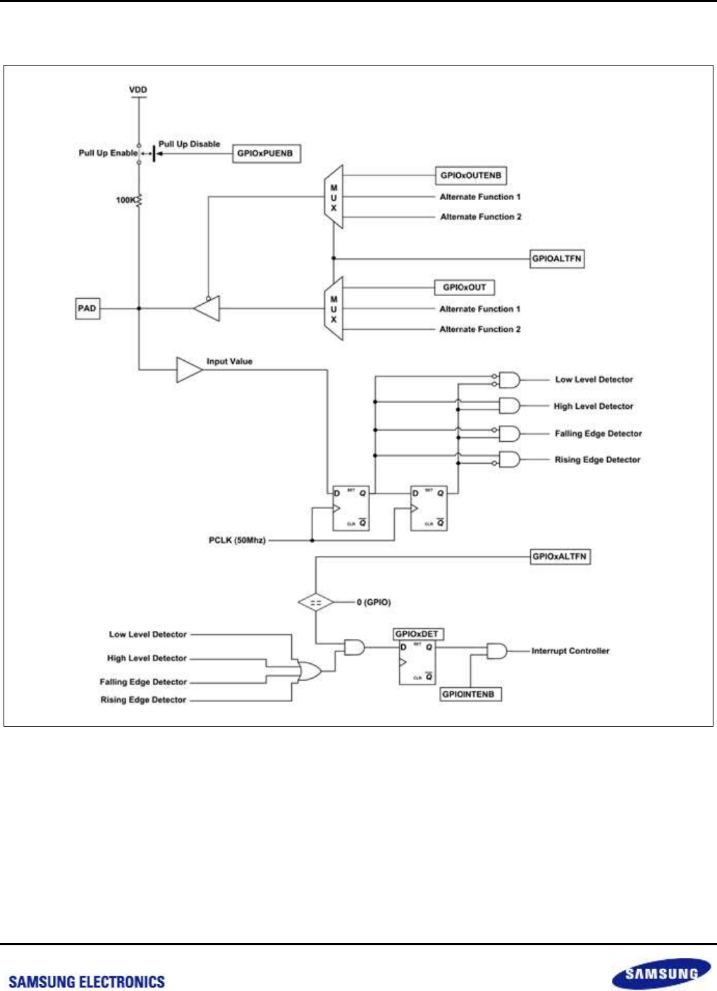
Samsung Confidential
S5P6818_UM 16 GPIO Controller
16-2
Preliminary product information describes products that are in development, for which full characterization data and
associated errata are not yet available. Specifications and information herein are subject to change without notice.
16.3 Block Diagram
Figure 16-1 GPIO Block Diagram
nexell / ys.kim at 2015.02.12
SAMSUNG Confidential
Samsung Confidential
S5P6818_UM 16 GPIO Controller
16-3
Preliminary product information describes products that are in development, for which full characterization data and
associated errata are not yet available. Specifications and information herein are subject to change without notice.
16.4 Functional Description
S5P6818 GPIO Pins have an internal pull-up resistance of 100 k.
The current of the pull-up resistance (for VDD = 3.3 V and V (PAD) = 0 V) is listed in the table below:
Table 16-1 Pull-up Resister Current
Pull Up
Min.
Typ.
Max.
Unit
ENABLE
10
33
72
uA
DISABLE
–
–
0.1
uA
Most S5P6818 GPIO ports contain the Alternate function (some ports supports up to Alternate Function2). All
GPIO ports should be set as GPIO function or Alternate Function suitable for the user's purposes and this setting
can easily be performed with GPIO registers. In addition, all GPIO pull-up resistances are enabled/ disabled. This
setting operates when the system is fully booted and does not affect the system in initial booting. If there is a value
which needs to be determined in system booting, the value is given by inserting a pull up/down resistance from
outside.
16.4.1 Input Operation
To use GPIO for input, the GPIO function should be selected by setting the relevant bit of the GPIO Alternate
Function Select register as b'00 to select the GPIO function. In addition, the GPIO Input mode should be, also,
selected by the GPIOx Output Enable register (GPIOxOUTENB) as "0".
An input signal is detected by selecting a desired detection type with the GPIOx Event Detect Mode register. Four
types of input signal can be detected: Low Level, High Level, Falling edge and Rising edge. The GPIOx Event
Detect Mode registers consist of GPIOx Event Detect Mode register0 (GPIOxDETMODE0) and GPIOx Event
Detect Moderegister1 (GPIOxDETMODE1).
To use interrupt, set the GPIOx Interrupt Enable Register (GPIOxINTENB) as "1".
The GPIOx Event Detect Register (GPIOxDET) enables checking the generation of an event via GPIO and may
be used as the Pending Clear function when an interrupt occurs.
When the GPIOx PAD Status Register (GPIOxPAD) is set as GPIO Input mode, the level of the relevant GPIOx
PAD can be checked.
The Open drain pins (GPIOB[7:4] and GPIOC[8]) operate in Input mode only when the GPIOx Output register
(GPIOxOUT) is set as "1". The Open drain pins are operated by the GPIOx Output Register (GPIOxOUT) even if
the GPIOx Output Enable register (GPIOxOUTENB) is set as Input mode.
nexell / ys.kim at 2015.02.12
SAMSUNG Confidential

Samsung Confidential
S5P6818_UM 16 GPIO Controller
16-4
Preliminary product information describes products that are in development, for which full characterization data and
associated errata are not yet available. Specifications and information herein are subject to change without notice.
16.4.2 Output Operation
To use GPIO for output, the GPIO function should be selected by setting the relevant bit of the GPIOx. Alternate
Function Select register should be set as b'00 to select the GPIO function. In addition, the GPIOx Output mode
should also be selected by setting the GPIOx Output Enable register as "1".
If you set a desired output value (low level: "0", high level: "1") with the GPIOx Output Register (GPIOxOUT), the
value is reflected to the corresponding bit.
The Open drain pins (GPIOB[7:4] and GPIOC[8]) operate in output mode only when the GPIOx Output register
(GPIOxOUT) is set as "0". The Open drain pins are operated by the GPIOx Output Register (GPIOxOUT) even if
the GPIOx Output Enable register (GPIOxOUTENB) is set as Input mode.
16.4.3 Alternate Function Operation
Among the 151 GPIO pins of the S5P6818, most GPIO pins have an Alternate function. However, the Alternate
function and the GPIO function should not be used simultaneously. Therefore, Alternate Function1 and Alternate
Function2 are operated by setting the corresponding bits of the GPIOx Alternate Function Select register as b'01
and b'10, respectively.
nexell / ys.kim at 2015.02.12
SAMSUNG Confidential

Samsung Confidential
S5P6818_UM 16 GPIO Controller
16-5
Preliminary product information describes products that are in development, for which full characterization data and
associated errata are not yet available. Specifications and information herein are subject to change without notice.
16.5 Register Description
16.5.1 Register Map Summary
Base Address: C001_0000h
Register
Offset
Description
Reset Value
GPIOx
GPIOXOUT
A000h, B000h,
C000h, D000h,
E000h
GPIOx output register
0x0000_0000
GPIOXOUTENB
A004h, B004h,
C004h, D004h,
E004h
GPIOx output enable register
0x0000_0000
GPIOXDETMODE0
A008h, B008h,
C008h, D008h,
E008h
GPIOx event detect mode register 0
0x0000_0000
GPIOXDETMODE1
A00Ch, B00Ch,
C00Ch, D00Ch,
E00Ch
GPIOx event detect mode register 1
0x0000_0000
GPIOXINTENB
A010h, B010h,
C010h, D010h,
E010h
GPIOx interrupt enable register
0x0000_0000
GPIOXDET
A014h, B014h,
C014h, D014h,
E014h
GPIOx event detect register
0x0000_0000
GPIOXPAD
A018h, B018h,
C018h, D018h,
E018h
GPIOx PAD status register
0x0000_0000
RSVD
A01Ch, B01Ch,
C01Ch,D01Ch ,E01
Ch
Reserved
–
GPIOXALTFN0
A020h, B020h,
C020h, D020h,
E020h
GPIOx alternate function select register 0
0x0000_0000
GPIOXALTFN1
A024h, B024h,
C024h, D024h,
E024h
GPIOx alternate function select register 1
0x0000_0000
GPIOXDETMODEEX
A028h, B028h,
C028h, D028h,
E028h
GPIOx event detect mode extended register
0x0000_0000
GPIOXDETENB
A03Ch, B03Ch,
C03Ch, D03Ch,
E03Ch
GPIOx detect enable register
0x0000_0000
GPIOX_SLEW
A040h, B040h,
C040h, D040h,
E040h
GPIOx slew register
0xFFFF_FFFF
nexell / ys.kim at 2015.02.12
SAMSUNG Confidential

Samsung Confidential
S5P6818_UM 16 GPIO Controller
16-6
Preliminary product information describes products that are in development, for which full characterization data and
associated errata are not yet available. Specifications and information herein are subject to change without notice.
Register
Offset
Description
Reset Value
GPIOX_SLEW_DISABLE_DEF
AULT
A044h, B044h,
C044h, D044h,
E044h
GPIOx slew disable defaultregister
0xFFFF_FFFF
GPIOX_DRV1
A048h, B048h,
C048h, D048h,
E048h
GPIOx DRV1 register
0x0000_0000
GPIOX_DRV1_DISABLE_DEFA
ULT
A04Ch, B04Ch,
C04Ch, D04Ch,
E04Ch
GPIOx DRV1 disable default register
0xFFFF_FFFF
GPIOX_DRV0
A050h, B050h,
C050h, D050h,
E050h
GPIOx DRV0 register
0x0000_0000
GPIOX_DRV0_DISABLE_DEFA
ULT
A054h, B054h,
C054h, D054h,
E054h
GPIOx DRV0 disable default register
0xFFFF_FFFF
GPIOX_PULLSEL
A058h, B058h,
C058h, D058h,
E058h
GPIOx PULLSEL register
0x0000_0000
GPIOX_PULLSEL_DISABLE_D
EFAULT
A05Ch, B05Ch,
C05Ch, D05Ch,
E05Ch
GPIOx PULLSEL disable default register
0x0000_0000
GPIOX_PULLENB
A060h, B060h,
C060h, D060h,
E060h
GPIOx PULLENB register
0x0000_0000
GPIOX_PULLENB_DISABLE_D
EFAULT
A064h, B064h,
C064h, D064h,
E064h
GPIOx PULLENB disable default register
0x0000_0000
NOTE: GPIOx Register (x = A, B, C, D, E)
nexell / ys.kim at 2015.02.12
SAMSUNG Confidential

Samsung Confidential
S5P6818_UM 16 GPIO Controller
16-7
Preliminary product information describes products that are in development, for which full characterization data and
associated errata are not yet available. Specifications and information herein are subject to change without notice.
16.5.1.1 GPIOxOUT
Base Address: C001_A000h (GPIOA)
Base Address: C001_B000h (GPIOB)
Base Address: C001_C000h (GPIOC)
Base Address: C001_D000h (GPIOD)
Base Address: C001_E000h (GPIOE)
Address = Base Address + A000h, B000h, C000h, D000h, E000h, Reset Value = 0x0000_0000
Name
Bit
Type
Description
Reset Value
GPIOXOUT
[31:0]
RW
GPIOx[31:0]: Specifies the output value in GPIOx output
mode.
This bit should be set as "1" (Input mode) or "0" (Output
mode) to use the Open drain pins in Input/Output mode.
0 = Low Level
1 = High Level
32'h0
16.5.1.2 GPIOxOUTENB
Base Address: C001_A000h (GPIOA)
Base Address: C001_B000h (GPIOB)
Base Address: C001_C000h (GPIOC)
Base Address: C001_D000h (GPIOD)
Base Address: C001_E000h (GPIOE)
Address = Base Address + A004h, B004h, C004h, D004h, E004h, Reset Value = 0x0000_0000
Name
Bit
Type
Description
Reset Value
GPIOXOUTENB
[31:0]
RW
GPIOx[31:0]: Specifies GPIOx In/Out mode.
The Open drain pins are operated in Input/Output mode by
the GPIOxOUTPUT register (GPIOxOUT) and not by this
bit.
0 = Input Mode
1 = Output Mode
32'h0
nexell / ys.kim at 2015.02.12
SAMSUNG Confidential

Samsung Confidential
S5P6818_UM 16 GPIO Controller
16-8
Preliminary product information describes products that are in development, for which full characterization data and
associated errata are not yet available. Specifications and information herein are subject to change without notice.
16.5.1.3 GPIOxDETMODE0
Base Address: C001_A000h (GPIOA)
Base Address: C001_B000h (GPIOB)
Base Address: C001_C000h (GPIOC)
Base Address: C001_D000h (GPIOD)
Base Address: C001_E000h (GPIOE)
Address = Base Address + A008h, B008h, C008h, D008h, E008h, Reset Value = 0x0000_0000
Name
Bit
Type
Description
Reset Value
GPIOXDETMODE0_15
[31:30]
RW
Specifies Detect mode when GPIOx15 is in Input mode.
It is configured the combination of GPIOXDET_EX15 (1-
bit) + GPIOXDETMODE0_15 (2-bit).
Considers GPIOXDET_EX15 as well as
GPIOXDETMODE 0_15.
First bit is GPIOXDET_EX15, Second and third bit is
GPIOXDETMODE0_15
000 = Low Level
001 = High Level
010 = Falling Edge
011 = Rising Edge
100 = Both (Rising & Falling) Edge
101 to 111 = Reserved
2'b0
GPIOXDETMODE0_14
[29:28]
RW
Specifies Detect mode when GPIOx14 is in Input mode.
It is configured the combination of GPIOXDET_EX14 (1-
bit) + GPIOXDETMODE0_14 (2-bit).
Considers GPIOXDET_EX14 as well as
GPIOXDETMODE0_14.
First bit is GPIOXDET_EX14, Second and third bit is
GPIOXDETMODE0_14
000 = Low Level
001 = High Level
010 = Falling Edge
011 = Rising Edge
100 = Both (Rising & Falling) Edge
101 to 111 = Reserved
2'b0
GPIOXDETMODE0_13
[27:26]
RW
Specifies Detect mode when GPIOx13 is in Input mode.
It is configured the combination of GPIOXDET_EX13 (1-
bit) + GPIOXDETMODE0_13 (2-bit).
Considers GPIOXDET_EX13 as well as
GPIOXDETMODE0_13.
First bit is GPIOXDET_EX13, Second and third bit is
GPIOXDETMODE0_13
000 = Low Level
001 = High Level
010 = Falling Edge
011 = Rising Edge
100 = Both(Rising & Falling) Edge
2'b0
nexell / ys.kim at 2015.02.12
SAMSUNG Confidential

Samsung Confidential
S5P6818_UM 16 GPIO Controller
16-9
Preliminary product information describes products that are in development, for which full characterization data and
associated errata are not yet available. Specifications and information herein are subject to change without notice.
Name
Bit
Type
Description
Reset Value
101 to 111 = Reserved
GPIOXDETMODE0_12
[25:24]
RW
Specifies Detect mode when GPIOx12 is in Input mode.
It is configured the combination of GPIOXDET_EX12 (1-
bit) + GPIOXDETMODE0_12 (2-bit).
Considers GPIOXDET_EX12 as well as
GPIOXDETMODE0_12.
First bit is GPIOXDET_EX12, Second and third bit is
GPIOXDETMODE0_12
000 = Low Level
001 = High Level
010 = Falling Edge
011 = Rising Edge
100 = Both (Rising & Falling) Edge
101 to 111 = Reserved
2'b0
GPIOXDETMODE0_11
[23:22]
RW
Specifies Detect mode when GPIOx11 is in Input mode.
It is configured the combination of GPIOXDET_EX11 (1-
bit) + GPIOXDETMODE0_11 (2-bit).
Considers GPIOXDET_EX11 as well as
GPIOXDETMODE0_11.
First bit is GPIOXDET_EX11, Second and third bit is
GPIOXDETMODE0_11
000 = Low Level
001 = High Level
010 = Falling Edge
011 = Rising Edge
100 = Both (Rising & Falling) Edge
101 to 111 = Reserved
2'b0
GPIOXDETMODE0_10
[21:20]
RW
Specifies Detect mode when GPIOx10 is in Input mode.
It is configured the combination of GPIOXDET_EX10 (1-
bit) + GPIOXDETMODE0_10 (2-bit).
Considers GPIOXDET_EX10 as well as
GPIOXDETMODE0_10.
First bit is GPIOXDET_EX10, Second and third bit is
GPIOXDETMODE0_10
000 = Low Level
001 = High Level
010 = Falling Edge
011 = Rising Edge
100 = Both (Rising & Falling) Edge
101 to 111 = Reserved
2'b0
GPIOXDETMODE0_9
[19:18]
RW
Specifies Detect mode when GPIOx9 is in Input mode.
It is configured the combination of GPIOXDET_EX9 (1-bit)
+ GPIOXDETMODE0_9 (2-bit).
Considers GPIOXDET_EX9 as well as
GPIOXDETMODE0_9.
First bit is GPIOXDET_EX9, Second and third bit is
GPIOXDETMODE0_9
2'b0
nexell / ys.kim at 2015.02.12
SAMSUNG Confidential

Samsung Confidential
S5P6818_UM 16 GPIO Controller
16-10
Preliminary product information describes products that are in development, for which full characterization data and
associated errata are not yet available. Specifications and information herein are subject to change without notice.
Name
Bit
Type
Description
Reset Value
000 = Low Level
001 = High Level
010 = Falling Edge
011 = Rising Edge
100 = Both (Rising & Falling) Edge
101 to 111 = Reserved
GPIOXDETMODE0_8
[17:16]
RW
Specifies Detect mode when GPIOx8 is in Input mode.
It is configured the combination of GPIOXDET_EX8 (1-bit)
+ GPIOXDETMODE0_8 (2-bit.).
Considers GPIOXDET_EX8 as well as
GPIOXDETMODE0_8.
First bit is GPIOXDET_EX8, Second and third bit is
GPIOXDETMODE0_8
000 = Low Level
= High Level
010 = Falling Edge
011 = Rising Edge
100 = Both (Rising & Falling) Edge
101 to 111 = Reserved
2'b0
GPIOXDETMODE0_7
[15:14]
RW
Specifies Detect mode when GPIOx7 is in Input mode.
It is configured the combination of GPIOXDET_EX7 (1-bit)
+ GPIOXDETMODE0_7 (2-bit).
Considers GPIOXDET_EX7 as well as
GPIOXDETMODE0_7.
First bit is GPIOXDET_EX7, Second and third bit is
GPIOXDETMODE0_7
000 = Low Level
001 = High Level
010 = Falling Edge
011 = Rising Edge
100 = Both (Rising & Falling) Edge
101 to111 = Reserved
2'b0
GPIOXDETMODE0_6
[13:12]
RW
Specifies Detect mode when GPIOx6 is in Input mode.
It is configured the combination of GPIOXDET_EX6 (1-bit)
+ GPIOXDETMODE0_6 (2-bit).
Considers GPIOXDET_EX6 as well as
GPIOXDETMODE0_6.
First bit is GPIOXDET_EX6, Second and third bit is
GPIOXDETMODE0_6
000 = Low Level
001 = High Level
010 = Falling Edge
011 = Rising Edge
100 = Both (Rising & Falling) Edge
101 to111 = Reserved
2'b0
GPIOXDETMODE0_5
[11:10]
RW
Specifies Detect mode when GPIOx5 is in Input mode.
It is configured the combination of GPIOXDET_EX5 (1-bit)
+ GPIOXDETMODE0_5 (2-bit).
2'b0
nexell / ys.kim at 2015.02.12
SAMSUNG Confidential

Samsung Confidential
S5P6818_UM 16 GPIO Controller
16-11
Preliminary product information describes products that are in development, for which full characterization data and
associated errata are not yet available. Specifications and information herein are subject to change without notice.
Name
Bit
Type
Description
Reset Value
Considers GPIOXDET_EX5 as well as
GPIOXDETMODE0_5.
First bit is GPIOXDET_EX5, Second and third bit is
GPIOXDETMODE0_5
000 = Low Level
001 = High Level
010 = Falling Edge
011 = Rising Edge
100 = Both (Rising & Falling) Edge
101 to111 = Reserved
GPIOXDETMODE0_4
[9:8]
RW
Specifies Detect mode when GPIOx4 is in Input mode.
It is configured the combination of GPIOXDET_EX4 (1-bit)
+ GPIOXDETMODE0_4 (2-bit).
Considers GPIOXDET_EX4 as well as
GPIOXDETMODE0_4.
First bit is GPIOXDET_EX4, Second and third bit is
GPIOXDETMODE0_4
000 = Low Level
001 = High Level
010 = Falling Edge
011 = Rising Edge
100 = Both (Rising & Falling) Edge
101 to111 = Reserved
2'b0
GPIOXDETMODE0_3
[7:6]
RW
Specifies Detect mode when GPIOx3 is in Input mode.
It is configured the combination of GPIOXDET_EX3 (1-bit)
+ GPIOXDETMODE0_3 (2-bit).
Considers GPIOXDET_EX3 as well as
GPIOXDETMODE0_3.
First bit is GPIOXDET_EX3, Second and third bit is
GPIOXDETMODE0_3
000 = Low Level
001 = High Level
010 = Falling Edge
011 = Rising Edge
100 = Both (Rising & Falling) Edge
101 to111 = Reserved
2'b0
GPIOXDETMODE0_2
[5:4]
RW
Specifies Detect mode when GPIOx2 is in Input mode.
It is configured the combination of GPIOXDET_EX2 (1-bit)
+ GPIOXDETMODE0_2 (2-bit).
Considers GPIOXDET_EX2 as well as
GPIOXDETMODE0_2.
First bit is GPIOXDET_EX2, Second and third bit is
GPIOXDETMODE0_2
000 = Low Level
001 = High Level
010 = Falling Edge
011 = Rising Edge
100 = Both (Rising & Falling) Edge
2'b0
nexell / ys.kim at 2015.02.12
SAMSUNG Confidential

Samsung Confidential
S5P6818_UM 16 GPIO Controller
16-12
Preliminary product information describes products that are in development, for which full characterization data and
associated errata are not yet available. Specifications and information herein are subject to change without notice.
Name
Bit
Type
Description
Reset Value
101 to111 = Reserved
GPIOXDETMODE0_1
[3:2]
RW
Specifies Detect mode when GPIOx1 is in Input mode.
It is configured the combination of GPIOXDET_EX1 (1-bit)
+ GPIOXDETMODE0_1 (2-bit).
Considers GPIOXDET_EX1 as well as
GPIOXDETMODE0_1.
First bit is GPIOXDET_EX1, Second and third bit is
GPIOXDETMODE0_1
000 = Low Level
001 = High Level
010 = Falling Edge
011 = Rising Edge
100 = Both (Rising & Falling) Edge
101 to111 = Reserved
2'b0
GPIOXDETMODE0_0
[1:0]
RW
Specifies Detect mode when GPIOx0 is in Input mode.
It is configured the combination of GPIOXDET_EX0 (1-bit)
+ GPIOXDETMODE0_0 (2-bit).
Considers GPIOXDET_EX0 as well as
GPIOXDETMODE0_0.
First bit is GPIOXDET_EX0, Second and third bit is
GPIOXDETMODE0_0
000 = Low Level
001 = High Level
010 = Falling Edge
011 = Rising Edge
100 = Both (Rising & Falling) Edge
101 to111 = Reserved
2'b0
nexell / ys.kim at 2015.02.12
SAMSUNG Confidential

Samsung Confidential
S5P6818_UM 16 GPIO Controller
16-13
Preliminary product information describes products that are in development, for which full characterization data and
associated errata are not yet available. Specifications and information herein are subject to change without notice.
16.5.1.4 GPIOxDETMODE1
Base Address: C001_A000h (GPIOA)
Base Address: C001_B000h (GPIOB)
Base Address: C001_C000h (GPIOC)
Base Address: C001_D000h (GPIOD)
Base Address: C001_E000h (GPIOE)
Address = Base Address + A00Ch, B00Ch, C00Ch, D00Ch, E00Ch, Reset Value = 0x0000_0000
Name
Bit
Type
Description
Reset Value
GPIOXDETMODE1_31
[31:30]
RW
Specifies Detect mode when GPIOx31 is in Input mode.
It is configured the combination of GPIOXDET_EX31 (1-bit)
+ GPIOXDETMODE1_31 (2-bit).
Considers GPIOXDET_EX31 as well as
GPIOXDETMODE1_31.
First bit is GPIOXDET_EX31, Second and third bit is
GPIOXDETMODE1_31
000 = Low Level
001 = High Level
010 = Falling Edge
011 = Rising Edge
100 = Both (Rising & Falling) Edge
101 to 111 = Reserved
2'b0
GPIOXDETMODE1_30
[29:28]
RW
Specifies Detect mode when GPIOx30 is in Input mode.
It is configured the combination of GPIOXDET_EX30 (1-bit)
+ GPIOXDETMODE1_30 (2-bit).
Considers GPIOXDET_EX30 as well as
GPIOXDETMODE1_30.
First bit is GPIOXDET_EX30, Second and third bit is
GPIOXDETMODE1_30
000 = Low Level
001 = High Level
010 = Falling Edge
011 = Rising Edge
100 = Both (Rising & Falling) Edge
101 to 111 = Reserved
2'b0
GPIOXDETMODE1_29
[27:26]
RW
Specifies Detect mode when GPIOx29 is in Input mode.
It is configured the combination of GPIOXDET_EX29 (1-bit)
+ GPIOXDETMODE1_29 (2-bit).
Considers GPIOXDET_EX29 as well as
GPIOXDETMODE1_29.
First bit is GPIOXDET_EX29, Second and third bit is
GPIOXDETMODE1_29
000 = Low Level
001 = High Level
010 = Falling Edge
011 = Rising Edge
100 = Both (Rising & Falling) Edge
2'b0
nexell / ys.kim at 2015.02.12
SAMSUNG Confidential

Samsung Confidential
S5P6818_UM 16 GPIO Controller
16-14
Preliminary product information describes products that are in development, for which full characterization data and
associated errata are not yet available. Specifications and information herein are subject to change without notice.
Name
Bit
Type
Description
Reset Value
101 to 111 = Reserved
GPIOXDETMODE1_28
[25:24]
RW
Specifies Detect mode when GPIOx28 is in Input mode.
It is configured the combination of GPIOXDET_EX28 (1-bit)
+ GPIOXDETMODE1_28 (2-bit).
Considers GPIOXDET_EX28 as well as
GPIOXDETMODE1_28.
First bit is GPIOXDET_EX28, Second and third bit is
GPIOXDETMODE1_28
000 = Low Level
001 = High Level
010 = Falling Edge
011 = Rising Edge
100 = Both (Rising & Falling) Edge
101 to 111 = Reserved
2'b0
GPIOXDETMODE1_27
[23:22]
RW
Specifies Detect mode when GPIOx27 is in Input mode.
It is configured the combination of GPIOXDET_EX27 (1-bit)
+ GPIOXDETMODE1_27 (2-bit).
Considers GPIOXDET_EX27 as well as
GPIOXDETMODE1_27.
First bit is GPIOXDET_EX27, Second and third bit is
GPIOXDETMODE1_27
000 = Low Level
001 = High Level
010 = Falling Edge
011 = Rising Edge
100 = Both (Rising & Falling) Edge
101 to 111 = Reserved
2'b0
GPIOXDETMODE1_26
[21:20]
RW
Specifies Detect mode when GPIOx26 is in Input mode.
It is configured the combination of GPIOXDET_EX26 (1-bit)
+ GPIOXDETMODE1_26 (2-bit).
Considers GPIOXDET_EX26 as well as
GPIOXDETMODE1_ 26.
First bit is GPIOXDET_EX26, Second and third bit is
GPIOXDETMODE1_26
000 = Low Level
001 = High Level
010 = Falling Edge
011 = Rising Edge
100 = Both (Rising & Falling) Edge
101 to 111 = Reserved
2'b0
GPIOXDETMODE1_25
[19:18]
RW
Specifies Detect mode when GPIOx25 is in Input mode.
It is configured the combination of GPIOXDET_EX25 (1-bit)
+ GPIOXDETMODE1_25 (2-bit).
Considers GPIOXDET_EX25 as well as
GPIOXDETMODE1_25.
First bit is GPIOXDET_EX25, Second and third bit is
GPIOXDETMODE1_25
2'b0
nexell / ys.kim at 2015.02.12
SAMSUNG Confidential

Samsung Confidential
S5P6818_UM 16 GPIO Controller
16-15
Preliminary product information describes products that are in development, for which full characterization data and
associated errata are not yet available. Specifications and information herein are subject to change without notice.
Name
Bit
Type
Description
Reset Value
000 = Low Level
001 = High Level
010 = Falling Edge
011 = Rising Edge
100 = Both (Rising & Falling) Edge
101 to 111 = Reserved
GPIOXDETMODE1_24
[17:16]
RW
Specifies Detect mode when GPIOx24 is in Input mode.
It is configured the combination of GPIOXDET_EX24 (1-bit)
+ GPIOXDETMODE1_24 (2-bit).
Considers GPIOXDET_EX24 as well as
GPIOXDETMODE1_24.
First bit is GPIOXDET_EX24, Second and third bit is
GPIOXDETMODE1_24
000 = Low Level
001 = High Level
010 = Falling Edge
011 = Rising Edge
100 = Both (Rising & Falling) Edge
101 to 111 = Reserved
2'b0
GPIOXDETMODE1_23
[15:14]
RW
Specifies Detect mode when GPIOx23 is in Input mode.
It is configured the combination of GPIOXDET_EX23 (1-bit)
+ GPIOXDETMODE1_23 (2-bit).
Considers GPIOXDET_EX23 as well as
GPIOXDETMODE1_ 23.
First bit is GPIOXDET_EX23, Second and third bit is
GPIOXDETMODE1_23
000 = Low Level
001 = High Level
010 = Falling Edge
011 = Rising Edge
100 = Both (Rising & Falling) Edge
101 to 111 = Reserved
2'b0
GPIOXDETMODE1_22
[13:12]
RW
Specifies Detect mode when GPIOx22 is in Input mode.
It is configured the combination of GPIOXDET_EX22 (1-bit)
+ GPIOXDETMODE1_22 (2-bit).
Considers GPIOXDET_EX22 as well as
GPIOXDETMODE1_22.
First bit is GPIOXDET_EX22, Second and third bit is
GPIOXDETMODE1_22
000 = Low Level
001 = High Level
010 = Falling Edge
011 = Rising Edge
100 = Both (Rising & Falling) Edge
101 to 111 = Reserved
2'b0
GPIOXDETMODE1_21
[11:10]
RW
Specifies Detect mode when GPIOx21 is in Input mode.
It is configured the combination of GPIOXDET_EX21 (1-bit)
2'b0
nexell / ys.kim at 2015.02.12
SAMSUNG Confidential

Samsung Confidential
S5P6818_UM 16 GPIO Controller
16-16
Preliminary product information describes products that are in development, for which full characterization data and
associated errata are not yet available. Specifications and information herein are subject to change without notice.
Name
Bit
Type
Description
Reset Value
+ GPIOXDETMODE1_21 (2-bit).
Considers GPIOXDET_EX21 as well as
GPIOXDETMODE1_21.
First bit is GPIOXDET_EX21, Second and third bit is
GPIOXDETMODE1_21
000 = Low Level
001 = High Level
010 = Falling Edge
011 = Rising Edge
100 = Both (Rising & Falling) Edge
101 to 111 = Reserved
GPIOXDETMODE1_20
[9:8]
RW
Specifies Detect mode when GPIOx20 is in Input mode.
It is configured the combination of GPIOXDET_EX20 (1-bit)
+ GPIOXDETMODE1_20 (2-bit).
Considers GPIOXDET_EX20 as well as
GPIOXDETMODE1_ 20.
First bit is GPIOXDET_EX20, Second and third bit is
GPIOXDETMODE1_20
000 = Low Level
001 = High Level
010 = Falling Edge
011 = Rising Edge
100 = Both (Rising & Falling) Edge
101 to 111 = Reserved
2'b0
GPIOXDETMODE1_19
[7:6]
RW
Specifies Detect mode when GPIOx19 is in Input mode.
It is configured the combination of GPIOXDET_EX19 (1-bit)
+ GPIOXDETMODE1_19 (2-bit).
Considers GPIOXDET_EX19 as well as
GPIOXDETMODE1_19.
First bit is GPIOXDET_EX19, Second and third bit is
GPIOXDETMODE1_19
000 = Low Level
001 = High Level
010 = Falling Edge
011 = Rising Edge
100 = Both (Rising & Falling) Edge
101 to 111 = Reserved
2'b0
GPIOXDETMODE1_18
[5:4]
RW
Specifies Detect mode when GPIOx18 is in Input mode.
It is configured the combination of GPIOXDET_EX18 (1-bit)
+ GPIOXDETMODE1_18 (2-bit).
Considers GPIOXDET_EX18 as well as
GPIOXDETMODE1_18.
First bit is GPIOXDET_EX18, Second and third bit is
GPIOXDETMODE1_18
000 = Low Level
001 = High Level
010 = Falling Edge
011 = Rising Edge
2'b0
nexell / ys.kim at 2015.02.12
SAMSUNG Confidential

Samsung Confidential
S5P6818_UM 16 GPIO Controller
16-17
Preliminary product information describes products that are in development, for which full characterization data and
associated errata are not yet available. Specifications and information herein are subject to change without notice.
Name
Bit
Type
Description
Reset Value
100 = Both (Rising & Falling) Edge
101 to 111 = Reserved
GPIOXDETMODE1_17
[3:2]
RW
Specifies Detect mode when GPIOx17 is in Input mode.
It is configured the combination of GPIOXDET_EX17 (1-bit)
+ GPIOXDETMODE1_17 (2-bit).
Considers GPIOXDET_EX17 as well as
GPIOXDETMODE1_ 7.
First bit is GPIOXDET_EX17, Second and third bit is
GPIOXDETMODE1_17
000 = Low Level
001 = High Level
010 = Falling Edge
011 = Rising Edge
100 = Both (Rising & Falling) Edge
101 to 111 = Reserved
2'b0
GPIOXDETMODE1_16
[1:0]
RW
Specifies Detect mode when GPIOx16 is in Input mode.
It is configured the combination of GPIOXDET_EX16 (1-bit)
+ GPIOXDETMODE1_16 (2-bit).
Considers GPIOXDET_EX16 as well as
GPIOXDETMODE1_ 16.
First bit is GPIOXDET_EX16, Second and third bit is
GPIOXDETMODE1_16
000 = Low Level
001 = High Level
010 = Falling Edge
011 = Rising Edge
100 = Both (Rising & Falling) Edge
101 to 111 = Reserved
2'b0
nexell / ys.kim at 2015.02.12
SAMSUNG Confidential

Samsung Confidential
S5P6818_UM 16 GPIO Controller
16-18
Preliminary product information describes products that are in development, for which full characterization data and
associated errata are not yet available. Specifications and information herein are subject to change without notice.
16.5.1.5 GPIOxINTENB
Base Address: C001_A000h (GPIOA)
Base Address: C001_B000h (GPIOB)
Base Address: C001_C000h (GPIOC)
Base Address: C001_D000h (GPIOD)
Base Address: C001_E000h (GPIOE)
Address = Base Address + A010h, B010h, C010h, D010h, E010h, Reset Value = 0x0000_0000
Name
Bit
Type
Description
Reset Value
GPIOXINTENB
[31:0]
RW
GPIOx[31:0]: Specifies the use of an interrupt when a GPIOx
Event occurs. The events specified in GPIOxDETMODE0 and
GPIOxDETMODE1 are used.
0 = Disable
1 = Enable
32'h0
16.5.1.6 GPIOxDET
Base Address: C001_A000h (GPIOA)
Base Address: C001_B000h (GPIOB)
Base Address: C001_C000h (GPIOC)
Base Address: C001_D000h (GPIOD)
Base Address: C001_E000h (GPIOE)
Address = Base Address + A014h, B014h, C014h, D014h, E014h, Reset Value = 0x0000_0000
Name
Bit
Type
Description
Reset Value
GPIOXDET
[31:0]
RW
GPIOx[31:0]: Shows if an event is detected in accordance with
Event Detect mode in GPIOx Input Mode.
Set "1" to clear the relevant bit. GPIOx[31:0] is used as a
Pending register when an interrupt occurs.
Read:
0 = Not Detect
1 = Detected
Write:
0 = Not Clear
1 = Clear
32'h0
nexell / ys.kim at 2015.02.12
SAMSUNG Confidential

Samsung Confidential
S5P6818_UM 16 GPIO Controller
16-19
Preliminary product information describes products that are in development, for which full characterization data and
associated errata are not yet available. Specifications and information herein are subject to change without notice.
16.5.1.7 GPIOxPAD
Base Address: C001_A000h (GPIOA)
Base Address: C001_B000h (GPIOB)
Base Address: C001_C000h (GPIOC)
Base Address: C001_D000h (GPIOD)
Base Address: C001_E000h (GPIOE)
Address = Base Address + A018h, B018h, C018h, D018h, E018h, Reset Value = 0x0000_0000
Name
Bit
Type
Description
Reset Value
GPIOXPAD
[31:0]
R
GPIOx[31:0]: Can read the level of PAD in GPIOx Input
mode.
The data read in this register is the data not passing a filter
and reflects the PAD status itself.
0 = Low Level
1 = High Level
32'h0
16.5.1.8 GPIOxALTFN0
Base Address: C001_A000h (GPIOA)
Base Address: C001_B000h (GPIOB)
Base Address: C001_C000h (GPIOC)
Base Address: C001_D000h (GPIOD)
Base Address: C001_E000h (GPIOE)
Address = Base Address + A020h, B020h, C020h, D020h, E020h, Reset Value = 0x0000_0000
Name
Bit
Type
Description
Reset Value
GPIOXALTFN0_15
[31:30]
RW
GPIOx[15]: Selects the function of GPIOx 15pin.
00 = ALT Function0
01 = ALT Function1
10 = ALT Function2
11 = ALT Function3
2'b0
GPIOXALTFN0_14
[29:28]
RW
GPIOx[14]: Selects the function of GPIOx 14pin.
00 = ALT Function0
01 = ALT Function1
10 = ALT Function2
11 = ALT Function3
2'b0
GPIOXALTFN0_13
[27:26]
RW
GPIOx[13]: Selects the function of GPIOx 13pin.
00 = ALT Function0
01 = ALT Function1
10 = ALT Function2
11 = ALT Function3
2'b0
GPIOXALTFN0_12
[25:24]
RW
GPIOx[12]: Selects the function of GPIOx 12pin.
00 = ALT Function0
01 = ALT Function1
10 = ALT Function2
2'b0
nexell / ys.kim at 2015.02.12
SAMSUNG Confidential

Samsung Confidential
S5P6818_UM 16 GPIO Controller
16-20
Preliminary product information describes products that are in development, for which full characterization data and
associated errata are not yet available. Specifications and information herein are subject to change without notice.
Name
Bit
Type
Description
Reset Value
11 = ALT Function3
GPIOXALTFN0_11
[23:22]
RW
GPIOx[11]: Selects the function of GPIOx 11pin.
00 = ALT Function0
01 = ALT Function1
10 = ALT Function2
11 = ALT Function3
2'b0
GPIOXALTFN0_10
[21:20]
RW
GPIOx[10]: Selects the function of GPIOx 10pin.
00 = ALT Function0
01 = ALT Function1
10 = ALT Function2
11 = ALT Function3
2'b0
GPIOXALTFN0_9
[19:18]
RW
GPIOx[9]: Selects the function of GPIOx 9pin.
00 = ALT Function0
01 = ALT Function1
10 = ALT Function2
11 = ALT Function3
2'b0
GPIOXALTFN0_8
[17:16]
RW
GPIOx[8]: Selects the function of GPIOx 8pin.
00 = ALT Function0
01 = ALT Function1
10 = ALT Function2
11 = ALT Function3
2'b0
GPIOXALTFN0_7
[15:14]
RW
GPIOx[7]: Selects the function of GPIOx 7pin.
00 = ALT Function0
01 = ALT Function1
10 = ALT Function2
11 = ALT Function3
2'b0
GPIOXALTFN0_6
[13:12]
RW
GPIOx[6]: Selects the function of GPIOx 6pin.
00 = ALT Function0
01 = ALT Function1
10 = ALT Function2
11 = ALT Function3
2'b0
GPIOXALTFN0_5
[11:10]
RW
GPIOx[5]: Selects the function of GPIOx 5pin.
00 = ALT Function0
01 = ALT Function1
10 = ALT Function2
11 = ALT Function3
2'b0
GPIOXALTFN0_4
[9:8]
RW
GPIOx[4]: Selects the function of GPIOx 4pin.
00 = ALT Function0
01 = ALT Function1
10 = ALT Function2
11 = ALT Function3
2'b0
GPIOXALTFN0_3
[7:6]
RW
GPIOx[3]: Selects the function of GPIOx 3pin.
00 = ALT Function0
01 = ALT Function1
10 = ALT Function2
11 = ALT Function3
2'b0
nexell / ys.kim at 2015.02.12
SAMSUNG Confidential

Samsung Confidential
S5P6818_UM 16 GPIO Controller
16-21
Preliminary product information describes products that are in development, for which full characterization data and
associated errata are not yet available. Specifications and information herein are subject to change without notice.
Name
Bit
Type
Description
Reset Value
GPIOXALTFN0_2
[5:4]
RW
GPIOx[2]: Selects the function of GPIOx 2pin.
00 = ALT Function0
01 = ALT Function1
10 = ALT Function2
11 = ALT Function3
2'b0
GPIOXALTFN0_1
[3:2]
RW
GPIOx[1]: Selects the function of GPIOx 1pin.
00 = ALT Function0
01 = ALT Function1
10 = ALT Function2
11 = ALT Function3
2'b0
GPIOXALTFN0_0
[1:0]
RW
GPIOx[0]: Selects the function of GPIOx 0pin.
00 = ALT Function0
01 = ALT Function1
10 = ALT Function2
11 = ALT Function3
2'b0
16.5.1.9 GPIOxALTFN1
Base Address: C001_A000h (GPIOA)
Base Address: C001_B000h (GPIOB)
Base Address: C001_C000h (GPIOC)
Base Address: C001_D000h (GPIOD)
Base Address: C001_E000h (GPIOE)
Address = Base Address + A024h, B024h, C024h, D024h, E024h, Reset Value = 0x0000_0000
Name
Bit
Type
Description
Reset Value
GPIOXALTFN1_31
[31:30]
RW
GPIOx[31]: Selects the function of GPIOx 31pin.
00 = ALT Function0
01 = ALT Function1
10 = ALT Function2
11 = ALT Function3
2'b0
GPIOXALTFN1_30
[29:28]
RW
GPIOx[30]: Selects the function of GPIOx 30pin.
00 = ALT Function0
01 = ALT Function1
10 = ALT Function2
11 = ALT Function3
2'b0
GPIOXALTFN1_29
[27:26]
RW
GPIOx[29]: Selects the function of GPIOx 29pin.
00 = ALT Function0
01 = ALT Function1
10 = ALT Function2
11 = ALT Function3
2'b0
GPIOXALTFN1_28
[25:24]
RW
GPIOx[28]: Selects the function of GPIOx 28pin.
00 = ALT Function0
01 = ALT Function1
10 = ALT Function2
2'b0
nexell / ys.kim at 2015.02.12
SAMSUNG Confidential

Samsung Confidential
S5P6818_UM 16 GPIO Controller
16-22
Preliminary product information describes products that are in development, for which full characterization data and
associated errata are not yet available. Specifications and information herein are subject to change without notice.
Name
Bit
Type
Description
Reset Value
11 = ALT Function3
GPIOXALTFN1_27
[23:22]
RW
GPIOx[27]: Selects the function of GPIOx 27pin.
00 = ALT Function0
01 = ALT Function1
10 = ALT Function2
11 = ALT Function3
2'b0
GPIOXALTFN1_26
[21:20]
RW
GPIOx[26]: Selects the function of GPIOx 26pin.
00 = ALT Function0
01 = ALT Function1
10 = ALT Function2
11 = ALT Function3
2'b0
GPIOXALTFN1_25
[19:18]
RW
GPIOx[25]: Selects the function of GPIOx 25pin.
00 = ALT Function0
01 = ALT Function1
10 = ALT Function2
11 = ALT Function3
2'b0
GPIOXALTFN1_24
[17:16]
RW
GPIOx[24]: Selects the function of GPIOx 24pin.
00 = ALT Function0
01 = ALT Function1
10 = ALT Function2
11 = ALT Function3
2'b0
GPIOXALTFN1_23
[15:14]
RW
GPIOx[23]: Selects the function of GPIOx 23pin.
00 = ALT Function0
01 = ALT Function1
10 = ALT Function2
11 = ALT Function3
2'b0
GPIOXALTFN1_22
[13:12]
RW
GPIOx[22]: Selects the function of GPIOx 22pin.
00 = ALT Function0
01 = ALT Function1
10 = ALT Function2
11 = ALT Function3
2'b0
GPIOXALTFN1_21
[11:10]
RW
GPIOx[21]: Selects the function of GPIOx 21pin.
00 = ALT Function0
01 = ALT Function1
10 = ALT Function2
11 = ALT Function3
2'b0
GPIOXALTFN1_20
[9:8]
RW
GPIOx[20]: Selects the function of GPIOx 20pin.
00 = ALT Function0
01 = ALT Function1
10 = ALT Function2
11 = ALT Function3
2'b0
GPIOXALTFN1_19
[7:6]
RW
GPIOx[19]: Selects the function of GPIOx 19pin.
00 = ALT Function0
01 = ALT Function1
10 = ALT Function2
11 = ALT Function3
2'b0
nexell / ys.kim at 2015.02.12
SAMSUNG Confidential

Samsung Confidential
S5P6818_UM 16 GPIO Controller
16-23
Preliminary product information describes products that are in development, for which full characterization data and
associated errata are not yet available. Specifications and information herein are subject to change without notice.
Name
Bit
Type
Description
Reset Value
GPIOXALTFN1_18
[5:4]
RW
GPIOx[18]: Selects the function of GPIOx 18pin.
00 = ALT Function0
01 = ALT Function1
10 = ALT Function2
11 = ALT Function3
2'b0
GPIOXALTFN1_17
[3:2]
RW
GPIOx[17]: Selects the function of GPIOx 17pin.
00 = ALT Function0
01 = ALT Function1
10 = ALT Function2
11 = ALT Function3
2'b0
GPIOXALTFN1_16
[1:0]
RW
GPIOx[16]: Selects the function of GPIOx 16pin.
00 = ALT Function0
01 = ALT Function1
10 = ALT Function2
11 = ALT Function3
2'b0
16.5.1.10 GPIOxDETMODEEX
Base Address: C001_A000h (GPIOA)
Base Address: C001_B000h (GPIOB)
Base Address: C001_C000h (GPIOC)
Base Address: C001_D000h (GPIOD)
Base Address: C001_E000h (GPIOE)
Address = Base Address + A028h, B028h, C028h, D028h, E028h, Reset Value = 0x0000_0000
Name
Bit
Type
Description
Reset Value
GPIOXDET_EX31
[31]
RW
Specifies Detect mode when GPIOx31 is in Input mode.
It is configured the combination of GPIOXDET_EX31 (1-bit)
+ GPIOXDETMODE1_31 (2-bit).
Considers GPIOXDET_EX31 as well as
GPIOXDETMODE1_31.
First bit is GPIOXDET_EX31, Second and third bit is
GPIOXDETMODE1_31
000 = Low Level
001 = High Level
010 = Falling Edge
011 = Rising Edge
100 = Both (Rising & Falling) Edge
101 to 111 = Reserved
1'b0
GPIOXDET_EX30
[30]
RW
Specifies Detect mode when GPIOx30 is in Input mode.
It is configured the combination of GPIOXDET_EX30 (1-bit)
+ GPIOXDETMODE1_30 (2-bit).
Considers GPIOXDET_EX30 as well as
GPIOXDETMODE1_30.
First bit is GPIOXDET_EX30, Second and third bit is
1'b0
nexell / ys.kim at 2015.02.12
SAMSUNG Confidential

Samsung Confidential
S5P6818_UM 16 GPIO Controller
16-24
Preliminary product information describes products that are in development, for which full characterization data and
associated errata are not yet available. Specifications and information herein are subject to change without notice.
Name
Bit
Type
Description
Reset Value
GPIOXDETMODE1_30
000 = Low Level
001 = High Level
010 = Falling Edge
011 = Rising Edge
100 = Both (Rising & Falling) Edge
101 to 111 = Reserved
GPIOXDET_EX29
[29]
RW
Specifies Detect mode when GPIOx29 is in Input mode.
It is configured the combination of GPIOXDET_EX29 (1-bit)
+ GPIOXDETMODE1_29 (2-bit).
Considers GPIOXDET_EX29 as well as
GPIOXDETMODE1_29.
First bit is GPIOXDET_EX29, Second and third bit is
GPIOXDETMODE1_29
000 = Low
001 = High Level
010 = Falling Edge
011 = Rising Edge
100 = Both (Rising & Falling) Edge
101 to 111 = Reserved
1'b0
GPIOXDET_EX28
[28]
RW
Specifies Detect mode when GPIOx28 is in Input mode.
It is configured the combination of GPIOXDET_EX28 (1-bit)
+ GPIOXDETMODE1_28 (2-bit).
Considers GPIOXDET_EX28 as well as
GPIOXDETMODE1_28.
First bit is GPIOXDET_EX28, Second and third bit is
GPIOXDETMODE1_28
000 = Low Level
001 = High Level
010 = Falling Edge
011 = Rising Edge
100 = Both (Rising & Falling) Edge
101 to 111 = Reserved
1'b0
GPIOXDET_EX27
[27]
RW
Specifies Detect mode when GPIOx27 is in Input mode.
It is configured the combination of GPIOXDET_EX27 (1-bit)
+ GPIOXDETMODE1_27 (2-bit).
Considers GPIOXDET_EX27 as well as
GPIOXDETMODE1_27.
First bit is GPIOXDET_EX27, Second and third bit is
GPIOXDETMODE1_27
000 = Low Level
001 = High Level
010 = Falling Edge
011 = Rising Edge
100 = Both (Rising & Falling) Edge
101 to 111 = Reserved
1'b0
GPIOXDET_EX26
[26]
RW
Specifies Detect mode when GPIOx26 is in Input mode.
It is configured the combination of GPIOXDET_EX26 (1-bit)
1'b0
nexell / ys.kim at 2015.02.12
SAMSUNG Confidential

Samsung Confidential
S5P6818_UM 16 GPIO Controller
16-25
Preliminary product information describes products that are in development, for which full characterization data and
associated errata are not yet available. Specifications and information herein are subject to change without notice.
Name
Bit
Type
Description
Reset Value
+ GPIOXDETMODE1_26 (2-bit).
Considers GPIOXDET_EX26 as well as
GPIOXDETMODE1_26.
First bit is GPIOXDET_EX26, Second and third bit is
GPIOXDETMODE1_26
000 = Low Level
001 = High Level
010 = Falling Edge
011 = Rising Edge
100 = Both (Rising & Falling) Edge
101 to 111 = Reserved
GPIOXDET_EX25
[25]
RW
Specifies Detect mode when GPIOx25 is in Input mode.
It is configured the combination of GPIOXDET_EX25 (1-bit)
+ GPIOXDETMODE1_25 (2-bit).
Considers GPIOXDET_EX25 as well as
GPIOXDETMODE1_25.
First bit is GPIOXDET_EX25, Second and third bit is
GPIOXDETMODE1_25
000 = Low Level
001 = High Level
010 = Falling Edge
011 = Rising Edge
100 = Both (Rising & Falling) Edge
101 to 111 = Reserved
1'b0
GPIOXDET_EX24
[24]
RW
Specifies Detect mode when GPIOx24 is in Input mode.
It is configured the combination of GPIOXDET_EX24 (1-bit)
+ GPIOXDETMODE1_24 (2-bit).
Considers GPIOXDET_EX24 as well as
GPIOXDETMODE1_24.
First bit is GPIOXDET_EX24, Second and third bit is
GPIOXDETMODE1_24
000 = Low Level
001 = High Level
010 = Falling Edge
011 = Rising Edge
100 = Both (Rising & Falling) Edge
101 to 111 = Reserved
1'b0
GPIOXDET_EX23
[23]
RW
Specifies Detect mode when GPIOx23 is in Input mode.
It is configured the combination of GPIOXDET_EX23 (1-bit)
+ GPIOXDETMODE1_23 (2-bit).
Considers GPIOXDET_EX23 as well as
GPIOXDETMODE1_23.
First bit is GPIOXDET_EX23, Second and third bit is
GPIOXDETMODE1_23
000 = Low Level
001 = High Level
010 = Falling Edge
011 = Rising Edge
1'b0
nexell / ys.kim at 2015.02.12
SAMSUNG Confidential

Samsung Confidential
S5P6818_UM 16 GPIO Controller
16-26
Preliminary product information describes products that are in development, for which full characterization data and
associated errata are not yet available. Specifications and information herein are subject to change without notice.
Name
Bit
Type
Description
Reset Value
100 = Both (Rising & Falling) Edge
101 to 111 = Reserved
GPIOXDET_EX22
[22]
RW
Specifies Detect mode when GPIOx22 is in Input mode.
It is configured the combination of GPIOXDET_EX22 (1-bit)
+ GPIOXDETMODE1_22 (2-bit).
Considers GPIOXDET_EX22 as well as
GPIOXDETMODE1_22.
First bit is GPIOXDET_EX22, Second and third bit is
GPIOXDETMODE1_22
000 = Low Level
001 = High Level
010 = Falling Edge
011 = Rising Edge
100 = Both (Rising & Falling) Edge
101 to 111 = Reserved
1'b0
GPIOXDET_EX21
[21]
RW
Specifies Detect mode when GPIOx21 is in Input mode.
It is configured the combination of GPIOXDET_EX21 (1-bit)
+ GPIOXDETMODE1_21 (2-bit).
Considers GPIOXDET_EX21 as well as
GPIOXDETMODE1_21.
First bit is GPIOXDET_EX21, Second and third bit is
GPIOXDETMODE1_21
000 = Low Level
001 = High Level
010 = Falling Edge
011 = Rising Edge
100 = Both (Rising & Falling) Edge
101 to 111 = Reserved
1'b0
GPIOXDET_EX20
[20]
RW
Specifies Detect mode when GPIOx20 is in Input mode.
It is configured the combination of GPIOXDET_EX20 (1-bit)
+ GPIOXDETMODE1_20 (2-bit).
Considers GPIOXDET_EX20 as well as
GPIOXDETMODE1_20.
First bit is GPIOXDET_EX20, Second and third bit is
GPIOXDETMODE1_20
000 = Low Level
001 = High Level
010 = Falling Edge
011 = Rising Edge
100 = Both (Rising & Falling) Edge
101 to 111 = Reserved
1'b0
GPIOXDET_EX19
[19]
RW
Specifies Detect mode when GPIOx19 is in Input mode.
It is configured the combination of GPIOXDET_EX19 (1-bit)
+ GPIOXDETMODE1_19 (2-bit).
Considers GPIOXDET_EX19 as well as
GPIOXDETMODE1_19.
First bit is GPIOXDET_EX19, Second and third bit is
1'b0
nexell / ys.kim at 2015.02.12
SAMSUNG Confidential

Samsung Confidential
S5P6818_UM 16 GPIO Controller
16-27
Preliminary product information describes products that are in development, for which full characterization data and
associated errata are not yet available. Specifications and information herein are subject to change without notice.
Name
Bit
Type
Description
Reset Value
GPIOXDETMODE1_19
000 = Low Level
001 = High Level
010 = Falling Edge
011 = Rising Edge
100 = Both (Rising & Falling) Edge
101 to 111 = Reserved
GPIOXDET_EX18
[18]
RW
Specifies Detect mode when GPIOx18 is in Input mode.
It is configured the combination of GPIOXDET_EX18
(1-bit) + GPIOXDETMODE1_18 (2-bit).
Considers GPIOXDET_EX18 as well as
GPIOXDETMODE1_18.
First bit is GPIOXDET_EX18, Second and third bit is
GPIOXDETMODE1_18
000 = Low Level
001 = High Level
010 = Falling Edge
011 = Rising Edge
100 = Both (Rising & Falling) Edge
101 to 111 = Reserved
1'b0
GPIOXDET_EX17
[17]
RW
Specifies Detect mode when GPIOx17 is in Input mode.
It is configured the combination of GPIOXDET_EX17 (1-bit)
+ GPIOXDETMODE1_17 (2-bit).
Considers GPIOXDET_EX17 as well as
GPIOXDETMODE1_17.
First bit is GPIOXDET_EX17, Second and third bit is
GPIOXDETMODE1_17
000 = Low Level
001 = High Level
010 = Falling Edge
011 = Rising Edge
100 = Both (Rising & Falling) Edge
101 to 111 = Reserved
1'b0
GPIOXDET_EX16
[16]
RW
Specifies Detect mode when GPIOx16 is in Input mode.
It is configured the combination of GPIOXDET_EX16 (1-bit)
+ GPIOXDETMODE1_16 (2-bit).
Considers GPIOXDET_EX16 as well as
GPIOXDETMODE1_16.
First bit is GPIOXDET_EX16, Second and third bit is
GPIOXDETMODE1_16
000 = Low Level
001 = High Level
010 = Falling Edge
011 = Rising Edge
100 = Both (Rising & Falling) Edge
101 to 111 = Reserved
1'b0
GPIOXDET_EX15
[15]
RW
Specifies Detect mode when GPIOx15 is in Input mode.
1'b0
nexell / ys.kim at 2015.02.12
SAMSUNG Confidential

Samsung Confidential
S5P6818_UM 16 GPIO Controller
16-28
Preliminary product information describes products that are in development, for which full characterization data and
associated errata are not yet available. Specifications and information herein are subject to change without notice.
Name
Bit
Type
Description
Reset Value
It is configured the combination of GPIOXDET_EX15 (1-bit)
+ GPIOXDETMODE0_15 (2-bit).
Considers GPIOXDET_EX15 as well as
GPIOXDETMODE0_15.
First bit is GPIOXDET_EX15, Second and third bit is
GPIOXDETMODE0_15
000 = Low Level
001 = High Level
010 = Falling Edge
011 = Rising Edge
100 = Both (Rising & Falling) Edge
101 to 111 = Reserved
GPIOXDET_EX14
[14]
RW
Specifies Detect mode when GPIOx14 is in Input mode.
It is configured the combination of GPIOXDET_EX14(1-bit)
+ GPIOXDETMODE0_14(2-bit).
Considers GPIOXDET_EX14 as well as
GPIOXDETMODE0_14.
First bit is GPIOXDET_EX14, Second and third bit is
GPIOXDETMODE0_14
000 = Low Level
001 = High Level
010 = Falling Edge
011 = Rising Edge
100 = Both (Rising & Falling) Edge
101 to 111 = Reserved
1'b0
GPIOXDET_EX13
[13]
RW
Specifies Detect mode when GPIOx13 is in Input mode.
It is configured the combination of GPIOXDET_EX13 (1-bit)
+ GPIOXDETMODE0_13 (2-bit).
Considers GPIOXDET_EX13 as well as
GPIOXDETMODE0_13.
First bit is GPIOXDET_EX13, Second and third bit is
GPIOXDETMODE0_13
000 = Low Level
001 = High Level
010 = Falling Edge
011 = Rising Edge
100 = Both (Rising & Falling) Edge
101 to 111 = Reserved
1'b0
GPIOXDET_EX12
[12]
RW
Specifies Detect mode when GPIOx12 is in Input mode.
It is configured the combination of GPIOXDET_EX12 (1-bit)
+ GPIOXDETMODE0_12 (2-bit).
Considers GPIOXDET_EX12 as well as
GPIOXDETMODE0_12.
First bit is GPIOXDET_EX12, Second and third bit is
GPIOXDETMODE0_12
000 = Low Level
001 = High Level
010 = Falling Edge
1'b0
nexell / ys.kim at 2015.02.12
SAMSUNG Confidential

Samsung Confidential
S5P6818_UM 16 GPIO Controller
16-29
Preliminary product information describes products that are in development, for which full characterization data and
associated errata are not yet available. Specifications and information herein are subject to change without notice.
Name
Bit
Type
Description
Reset Value
011 = Rising Edge
100 = Both (Rising & Falling) Edge
101 to 111 = Reserved
GPIOXDET_EX11
[11]
RW
Specifies Detect mode when GPIOx11 is in Input mode.
It is configured the combination of GPIOXDET_EX11 (1-bit)
+ GPIOXDETMODE0_11 (2-bit).
Considers GPIOXDET_EX11 as well as
GPIOXDETMODE0_11.
First bit is GPIOXDET_EX11, Second and third bit is
GPIOXDETMODE0_11
000 = Low Level
001 = High Level
010 = Falling Edge
011 = Rising Edge
100 = Both (Rising & Falling) Edge
101 to 111 = Reserved
1'b0
GPIOXDET_EX10
[10]
RW
Specifies Detect mode when GPIOx10 is in Input mode.
It is configured the combination of GPIOXDET_EX10 (1-bit)
+ GPIOXDETMODE0_10 (2-bit).
Considers GPIOXDET_EX10 as well as
GPIOXDETMODE0_10.
First bit is GPIOXDET_EX10, Second and third bit is
GPIOXDETMODE0_10
000 = Low Level
001 = High Level
010 = Falling Edge
011 = Rising Edge
100 = Both (Rising & Falling) Edge
101 to 111 = Reserved
1'b0
GPIOXDET_EX9
[9]
RW
Specifies Detect mode when GPIOx9 is in Input mode.
It is configured the combination of GPIOXDET_EX9 (1-bit) +
GPIOXDETMODE0_9 (2-bit).
Considers GPIOXDET_EX9 as well as
GPIOXDETMODE0_9.
First bit is GPIOXDET_EX9, Second and third bit is
GPIOXDETMODE0_9
000 = Low Level
001 = High Level
010 = Falling Edge
011 = Rising Edge
100 = Both (Rising & Falling) Edge
101 to 111 = Reserved
1'b0
GPIOXDET_EX8
[8]
RW
Specifies Detect mode when GPIOx8 is in Input mode.
It is configured the combination of GPIOXDET_EX8 (1-bit) +
GPIOXDETMODE0_8 (2-bit).
Considers GPIOXDET_EX8 as well as
GPIOXDETMODE0_8.
1'b0
nexell / ys.kim at 2015.02.12
SAMSUNG Confidential

Samsung Confidential
S5P6818_UM 16 GPIO Controller
16-30
Preliminary product information describes products that are in development, for which full characterization data and
associated errata are not yet available. Specifications and information herein are subject to change without notice.
Name
Bit
Type
Description
Reset Value
First bit is GPIOXDET_EX8, Second and third bit is
GPIOXDETMODE0_8
000 = Low Level
001 = High Level
010 = Falling Edge
011 = Rising Edge
100 = Both (Rising & Falling) Edge
101 to 111 = Reserved
GPIOXDET_EX7
[7]
RW
Specifies Detect mode when GPIOx7 is in Input mode.
It is configured the combination of GPIOXDET_EX7 (1-bit) +
GPIOXDETMODE0_7 (2-bit).
Considers GPIOXDET_EX7 as well as
GPIOXDETMODE0_7.
First bit is GPIOXDET_EX7, Second and third bit is
GPIOXDETMODE0_7
000 = Low Level
001 = High Level
010 = Falling Edge
011 = Rising Edge
100 = Both (Rising & Falling) Edge
101 to 111 = Reserved
1'b0
GPIOXDET_EX6
[6]
RW
Specifies Detect mode when GPIOx6 is in Input mode.
It is configured the combination of GPIOXDET_EX6 (1-bit) +
GPIOXDETMODE0_6 (2-bit).
Considers GPIOXDET_EX6 as well as
GPIOXDETMODE0_6.
First bit is GPIOXDET_EX6, Second and third bit is
GPIOXDETMODE0_6
000 = Low Level
001 = High Level
010 = Falling Edge
011 = Rising Edge
100 = Both (Rising & Falling) Edge
101 to 111 = Reserved
1'b0
GPIOXDET_EX5
[5]
RW
Specifies Detect mode when GPIOx5 is in Input mode.
It is configured the combination of GPIOXDET_EX5 (1-bit) +
GPIOXDETMODE0_5 (2-bit).
Considers GPIOXDET_EX5 as well as
GPIOXDETMODE0_5.
First bit is GPIOXDET_EX5, Second and third bit is
GPIOXDETMODE0_5
000 = Low Level
001 = High Level
010 = Falling Edge
011 = Rising Edge
100 = Both(Rising & Falling) Edge
101 to 111 = Reserved
1'b0
nexell / ys.kim at 2015.02.12
SAMSUNG Confidential

Samsung Confidential
S5P6818_UM 16 GPIO Controller
16-31
Preliminary product information describes products that are in development, for which full characterization data and
associated errata are not yet available. Specifications and information herein are subject to change without notice.
Name
Bit
Type
Description
Reset Value
GPIOXDET_EX4
[4]
RW
Specifies Detect mode when GPIOx4 is in Input mode.
It is configured the combination of GPIOXDET_EX4 (1-bit) +
GPIOXDETMODE0_4 (2-bit).
Considers GPIOXDET_EX4 as well as
GPIOXDETMODE0_4.
First bit is GPIOXDET_EX4, Second and third bit is
GPIOXDETMODE0_4
000 = Low Level
001 = High Level
010 = Falling Edge
011 = Rising Edge
100 = Both (Rising & Falling) Edge
101 to 111 = Reserved
1'b0
GPIOXDET_EX3
[3]
RW
Specifies Detect mode when GPIOx3 is in Input mode.
It is configured the combination of GPIOXDET_EX3 (1-bit) +
GPIOXDETMODE0_3 (2-bit).
Considers GPIOXDET_EX3 as well as
GPIOXDETMODE0_3.
First bit is GPIOXDET_EX3, Second and third bit is
GPIOXDETMODE0_3
000 = Low Level
001 = High Level
010 = Falling Edge
011 = Rising Edge
100 = Both (Rising & Falling) Edge
101 to 111 = Reserved
1'b0
GPIOXDET_EX2
[2]
RW
Specifies Detect mode when GPIOx2 is in Input mode.
It is configured the combination of GPIOXDET_EX2 (1-bit) +
GPIOXDETMODE0_2 (2-bit).
Considers GPIOXDET_EX2 as well as
GPIOXDETMODE0_2.
First bit is GPIOXDET_EX2, Second and third bit is
GPIOXDETMODE0_2
000 = Low Level
001 = High Level
010 = Falling Edge
011 = Rising Edge
100 = Both (Rising & Falling) Edge
101 to 111 = Reserved
1'b0
GPIOXDET_EX1
[1]
RW
Specifies Detect mode when GPIOx1 is in Input mode.
It is configured the combination of GPIOXDET_EX1 (1-bit) +
GPIOXDETMODE0_1 (2-bit).
Considers GPIOXDET_EX1 as well as
GPIOXDETMODE0_1.
First bit is GPIOXDET_EX1, Second and third bit is
GPIOXDETMODE0_1
000 = Low Level
1'b0
nexell / ys.kim at 2015.02.12
SAMSUNG Confidential

Samsung Confidential
S5P6818_UM 16 GPIO Controller
16-32
Preliminary product information describes products that are in development, for which full characterization data and
associated errata are not yet available. Specifications and information herein are subject to change without notice.
Name
Bit
Type
Description
Reset Value
001 = High Level
010 = Falling Edge
011 = Rising Edge
100 = Both (Rising & Falling) Edge
101 to 111 = Reserved
GPIOXDET_EX0
[0]
RW
Specifies Detect mode when GPIOx0 is in Input mode.
It is configured the combination of GPIOXDET_EX0 (1-bit) +
GPIOXDETMODE0_0 (2-bit).
Considers GPIOXDET_EX0 as well as
GPIOXDETMODE0_0.
First bit is GPIOXDET_EX0, Second and third bit is
GPIOXDETMODE0_0
000 = Low Level
001 = High Level
010 = Falling Edge
011 = Rising Edge
100 = Both (Rising & Falling) Edge
101 to 111 = Reserved
1'b0
16.5.1.11 GPIOxDETENB
Base Address: C001_A000h (GPIOA)
Base Address: C001_B000h (GPIOB)
Base Address: C001_C000h (GPIOC)
Base Address: C001_D000h (GPIOD)
Base Address: C001_E000h (GPIOE)
Address = Base Address + A03Ch, B03Ch, C03Ch, D03Ch, E03Ch, Reset Value = 0x0000_0000
Name
Bit
Type
Description
Reset Value
GPIOXDETENB
[31:0]
RW
GPIOx[31:0]: Decides the use of the detected mode of
GPIOx PAD.
0 = Disable
1 = Enable
32'h0
nexell / ys.kim at 2015.02.12
SAMSUNG Confidential
Samsung Confidential
S5P6818_UM 16 GPIO Controller
16-33
Preliminary product information describes products that are in development, for which full characterization data and
associated errata are not yet available. Specifications and information herein are subject to change without notice.
16.5.1.12 GPIOx_SLEW
Base Address: C001_A000h (GPIOA)
Base Address: C001_B000h (GPIOB)
Base Address: C001_C000h (GPIOC)
Base Address: C001_D000h (GPIOD)
Base Address: C001_E000h (GPIOE)
Address = Base Address + A040h, B040h, C040h, D040h, E040h, Reset Value = 0xFFFF_FFFF
Name
Bit
Type
Description
Reset Value
GPIOX_SLEW
[31:0]
RW
GPIOx[31:0]: Decides the use of the Slew
resistance of GPIOx PAD.
0 = Fast Slew
1 = Normal Slew
32'hFFFF_FFFF
16.5.1.13 GPIOx_SLEW_DISABLE_DEFAULT
Base Address: C001_A000h (GPIOA)
Base Address: C001_B000h (GPIOB)
Base Address: C001_C000h (GPIOC)
Base Address: C001_D000h (GPIOD)
Base Address: C001_E000h (GPIOE)
Address = Base Address + A044h, B044h, C044h, D044h, E044h, Reset Value = 0xFFFF_FFFF
Name
Bit
Type
Description
Reset Value
GPIOX_SLEW_DISABLE_DEFAULT
[31:0]
RW
GPIOx[31:0]: Decides the use of the Slew
resistance of GPIOx PAD.
0 = Use Default Slew
1 = Use GPIOx_SLEW Value
32'hFFFF_FFFF
nexell / ys.kim at 2015.02.12
SAMSUNG Confidential
Samsung Confidential
S5P6818_UM 16 GPIO Controller
16-34
Preliminary product information describes products that are in development, for which full characterization data and
associated errata are not yet available. Specifications and information herein are subject to change without notice.
16.5.1.14 GPIOx_DRV1
Base Address: C001_A000h (GPIOA)
Base Address: C001_B000h (GPIOB)
Base Address: C001_C000h (GPIOC)
Base Address: C001_D000h (GPIOD)
Base Address: C001_E000h (GPIOE)
Address = Base Address + A048h, B048h, C048h, D048h, E048h, Reset Value = 0x0000_0000
Name
Bit
Type
Description
Reset Value
GPIOX_DRV1
[31:0]
RW
GPIOx[31:0]: Decides the use of the Drive
Strength1 resistance of GPIOx PAD.
0 = Drive Strength0 to 0
1= Drive Strength0 to 1
32'h0
16.5.1.15 GPIOx_DRV1_DISABLE_DEFAULT
Base Address: C001_A000h (GPIOA)
Base Address: C001_B000h (GPIOB)
Base Address: C001_C000h (GPIOC)
Base Address: C001_D000h (GPIOD)
Base Address: C001_E000h (GPIOE)
Address = Base Address + A04Ch, B04Ch, C04Ch, D04Ch, E04Ch, Reset Value = 0xFFFF_FFFF
Name
Bit
Type
Description
Reset Value
GPIOX_DRV1_DISABLE_DEFAULT
[31:0]
RW
GPIOx[31:0]: Decides the use of the Drive
Strength1 resistance of GPIOx PAD.
0 = Use Default Drive Strength
1 = Use GPIOx_DRV1 Value
32'hFFFF_FFFF
nexell / ys.kim at 2015.02.12
SAMSUNG Confidential
Samsung Confidential
S5P6818_UM 16 GPIO Controller
16-35
Preliminary product information describes products that are in development, for which full characterization data and
associated errata are not yet available. Specifications and information herein are subject to change without notice.
16.5.1.16 GPIOx_DRV0
Base Address: C001_A000h (GPIOA)
Base Address: C001_B000h (GPIOB)
Base Address: C001_C000h (GPIOC)
Base Address: C001_D000h (GPIOD)
Base Address: C001_E000h (GPIOE)
Address = Base Address + A050h, B050h, C050h, D050h, E050h, Reset Value = 0x0000_0000
Name
Bit
Type
Description
Reset Value
GPIOX_DRV0
[31:0]
RW
GPIOx[31:0]: Decides the use of the Drive
Strength0 resistance of GPIOx PAD.
0 = Drive Strength1 to 0
1 = Drive Strength1 to 1
DC current of output driver(DS: Drive Strength)
32'h0
16.5.1.17 GPIOx_DRV0_DISABLE_DEFAULT
Base Address: C001_A000h (GPIOA)
Base Address: C001_B000h (GPIOB)
Base Address: C001_C000h (GPIOC)
Base Address: C001_D000h (GPIOD)
Base Address: C001_E000h (GPIOE)
Address = Base Address + A054h, B054h, C054h, D054h, E054h, Reset Value = 0xFFFF_FFFF
Name
Bit
Type
Description
Reset Value
GPIOX_DRV0_DISABLE_DEFAULT
[31:0]
RW
GPIOx[31:0]: Decides the use of the Drive
Strength0 resistance of GPIOx PAD.
0 = Use Default Drive Strength
1 = Use GPIOx_DRV0 Value
32'hFFFF_FFFF
nexell / ys.kim at 2015.02.12
SAMSUNG Confidential
Samsung Confidential
S5P6818_UM 16 GPIO Controller
16-36
Preliminary product information describes products that are in development, for which full characterization data and
associated errata are not yet available. Specifications and information herein are subject to change without notice.
16.5.1.18 GPIOx_PULLSEL
Base Address: C001_A000h (GPIOA)
Base Address: C001_B000h (GPIOB)
Base Address: C001_C000h (GPIOC)
Base Address: C001_D000h (GPIOD)
Base Address: C001_E000h (GPIOE)
Address = Base Address + A058h, B058h, C058h, D058h, E058h, Reset Value = 0x0000_0000
Name
Bit
Type
Description
Reset Value
GPIOX_PULLSEL
[31:0]
RW
GPIOx[31:0]: Decides the Pull-up or Pull-down
of GPIOx PAD.
0 = Pull-Down
1 = Pull-Up
32'h0
16.5.1.19 GPIOx_PULLSEL_DISABLE_DEFAULT
Base Address: C001_A000h (GPIOA)
Base Address: C001_B000h (GPIOB)
Base Address: C001_C000h (GPIOC)
Base Address: C001_D000h (GPIOD)
Base Address: C001_E000h (GPIOE)
Address = Base Address + A05Ch, B05Ch, C05Ch, D05Ch, E05Ch, Reset Value = 0x0000_0000
Name
Bit
Type
Description
Reset Value
GPIOX_PULLSEL_DISABLE_DEFAULT
[31:0]
RW
GPIOx[31:0]: Decides the use of the PullSel
resistance of GPIOx PAD.
0 = Use Default Pull Sel
1 = Use GPIOx_PULLSEL Value
32'h0
nexell / ys.kim at 2015.02.12
SAMSUNG Confidential
Samsung Confidential
S5P6818_UM 16 GPIO Controller
16-37
Preliminary product information describes products that are in development, for which full characterization data and
associated errata are not yet available. Specifications and information herein are subject to change without notice.
16.5.1.20 GPIOx_PULLENB
Base Address: C001_A000h (GPIOA)
Base Address: C001_B000h (GPIOB)
Base Address: C001_C000h (GPIOC)
Base Address: C001_D000h (GPIOD)
Base Address: C001_E000h (GPIOE)
Address = Base Address + A060h, B060h, C060h, D060h, E060h, Reset Value = 0x0000_0000
Name
Bit
Type
Description
Reset Value
GPIOX_PULLENB
[31:0]
RW
GPIOx[31:0]: Decides the use of the Pull-up
resistance (100 k) of GPIOx PAD.
0 = Pull-Up Disable
1 = Pull-Up Enable
32'h0
16.5.1.21 GPIOx_PULLENB_DISABLE_DEFAULT
Base Address: C001_A000h (GPIOA)
Base Address: C001_B000h (GPIOB)
Base Address: C001_C000h (GPIOC)
Base Address: C001_D000h (GPIOD)
Base Address: C001_E000h (GPIOE)
Address = Base Address + A064h, B064h, C064h, D064h, E064h, Reset Value = 0x0000_0000
Name
Bit
Type
Description
Reset Value
GPIOX_PULLENB_DISABLE_DEFAULT
[31:0]
RW
GPIOx[31:0]: Decides the use of the PullEnb
resistance of GPIOx PAD.
0 = Use Default Pull Enb
1 = Use GPIOx_PULLENB Value
32'h0
nexell / ys.kim at 2015.02.12
SAMSUNG Confidential

Samsung Confidential
S5P6818_UM 17 Ethernet MAC
17-1
Preliminary product information describes products that are in development, for which full characterization data and
associated errata are not yet available. Specifications and information herein are subject to change without notice.
17 Ethernet MAC
17.1 Overview
The GMAC enables a host to transmit and receive data over Ethernet in compliance with the IEEE802.3-2008
standard.
EMAC supports 10/100/1000 Mbps data transfer rates, and it has Reduced Gigabit Media Independent Interface
(RGMII) with External PHY chip.
17.2 Features
17.2.1 MAC Core Features
Supports 10/100/1000 Mbps data transfer rates with the following phy interfaces:
RGMII interface to communicate with an external gigabit PHY
Supports both full-duplex and half-duplex operation
Automatic CRC and pad generation controllable on receive frames
Programmable frame length to support Standard or Jumbo Ethernet frames with sizes up to 16 KB
Programmable Inter Frame Gap (4096 bit times in steps of 8)
Support a variety of flexible address filtering mode
Separate transmission, reception, and control interface to the Application9
MDIO Master Interface for PHY device configuration and management
Compliant to the following standards:
IEEE802.3-2002 for Ethernet MAC
IEEE1588-2002 standard for precision networked clock synchronization
RGMII specification version 2.0 from HP/Marvell.
nexell / ys.kim at 2015.02.12
SAMSUNG Confidential

Samsung Confidential
S5P6818_UM 17 Ethernet MAC
17-2
Preliminary product information describes products that are in development, for which full characterization data and
associated errata are not yet available. Specifications and information herein are subject to change without notice.
17.2.2 DMA Block Features
32/64/128-bit data transfer
Single-channel Transmit and Receive engines
Optimization for packet-oriented DMA transfers with frame delimiters
Byte-aligned addressing for data buffer support
Descriptor architectures, allowing large blocks of data transfer with minimum CPU intervention; each
descriptor can transfer up to 8 KB of data
Individual programmable burst size for Transmit and Receive DMA Engines for optimal host bus utilization
Programmable interrupt options for different operational conditions
Per-frame Transmit/Receive complete interrupt control
Round-robin or fixed-priority arbitration between Receive and Transmit Engines
Start/Stop mode
Separate port for host CSR (Control and Status Register) access and host data interface
nexell / ys.kim at 2015.02.12
SAMSUNG Confidential
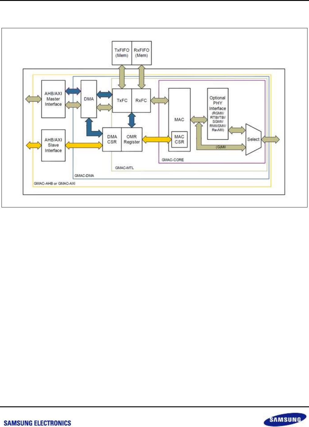
Samsung Confidential
S5P6818_UM 17 Ethernet MAC
17-3
Preliminary product information describes products that are in development, for which full characterization data and
associated errata are not yet available. Specifications and information herein are subject to change without notice.
17.3 Block Diagram
Figure 17-1 Block Diagram of the Ethernet MAC
nexell / ys.kim at 2015.02.12
SAMSUNG Confidential
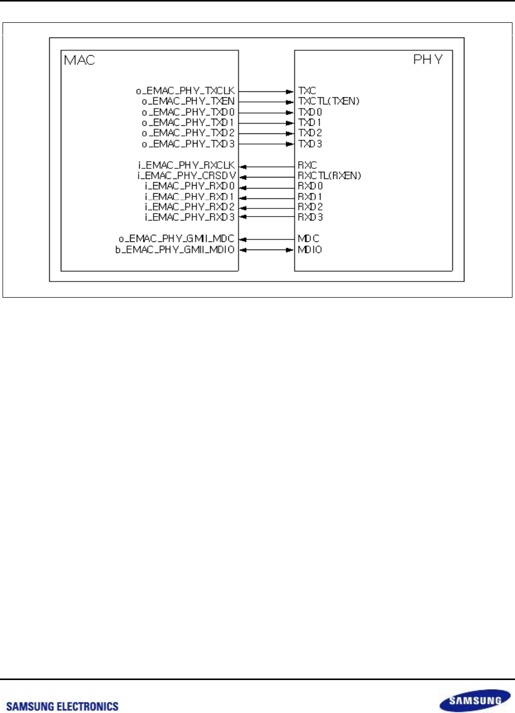
Samsung Confidential
S5P6818_UM 17 Ethernet MAC
17-4
Preliminary product information describes products that are in development, for which full characterization data and
associated errata are not yet available. Specifications and information herein are subject to change without notice.
Figure 17-2 RGMII Interface between MAC and Gigabit Ethernet PHY
nexell / ys.kim at 2015.02.12
SAMSUNG Confidential
Samsung Confidential
S5P6818_UM 17 Ethernet MAC
17-5
Preliminary product information describes products that are in development, for which full characterization data and
associated errata are not yet available. Specifications and information herein are subject to change without notice.
17.4 Register Description
17.4.1 Register Map Summary
Base Address: C006_1000h
Register
Offset
Description
Reset Value
MAC DMA
Ethernet MAC DMA register 0
0x00h
Bus Mode Register
0x0000_0101
Ethernet MAC DMA register 1
0x04h
Transmit Poll Demand Register
0x0000_0000
Ethernet MAC DMA register 2
0x08h
Receive Poll Demand Register
0x0000_0000
Ethernet MAC DMA register 3
0x0Ch
Receive Descriptor List Address Register
0x0000_0000
Ethernet MAC DMA register 4
0x10h
Transmit Descriptor List Address Register
0x0000_0000
Ethernet MAC DMA register 5
0x14h
Status Register
0x0000_0000
Ethernet MAC DMA register 6
0x18h
Operation Mode Register
0x0000_0000
Ethernet MAC DMA register 7
0x1Ch
Interrupt Enable Register
0x0000_0000
Ethernet MAC DMA register 8
0x20h
Missed Frame and Buffer Overflow Control
Register
0x0000_0000
RSVD
0x24h to
0x44h
Reserved
–
Ethernet MAC DMA register 18
0x48h
Current Host Transmit Descriptor Register
0x0000_0000
Ethernet MAC DMA register 19
0x4Ch
Current Host Receive Descriptor Register
0x0000_0000
Ethernet MAC DMA register 20
0x50h
Current Host Transmit Buffer Address Register
0x0000_0000
Ethernet MAC DMA register 21
0x54h
Current Host Receive Buffer Address Register
0x0000_0000
nexell / ys.kim at 2015.02.12
SAMSUNG Confidential

Samsung Confidential
S5P6818_UM 17 Ethernet MAC
17-6
Preliminary product information describes products that are in development, for which full characterization data and
associated errata are not yet available. Specifications and information herein are subject to change without notice.
Base Address: C006_0000h
Register
Offset
Description
Reset Value
MAC Core
Ethernet MAC Register 0
0x00h
MAC Configuration Register
0x0000_0000
Ethernet MAC Register 1
0x04h
MAC Frame Filter Register
0x0000_0000
Ethernet MAC Register 2
0x08h
Hash Table High Register
0x0000_0000
Ethernet MAC Register 3
0x0Ch
Hash Table Low Register
0x0000_0000
Ethernet MAC Register 4
0x10h
GMII Address Register
0x0000_0000
Ethernet MAC Register 5
0x14h
GMII Data Register
0x0000_0000
Ethernet MAC Register 6
0x18h
Flow Control Register
0x0000_0000
Ethernet MAC Register 7
0x1Ch
VALN Tag Register
0x0000_0000
Ethernet MAC Register 8
0x20h
Version Register
0x0000_0037
Ethernet MAC Register 9
0x24h
Debug Register
0x0000_0000
RSVD
0x28h to
0x34h
Reserved
–
Ethernet MAC Register 14
0x38h
Interrupt Status Register
0x0000_0000
Ethernet MAC Register 15
0x3Ch
Interrupt Mask Register
0x0000_0000
Ethernet MAC Register 16
0x40h
MAC Address0 High Register
0x0000_FFFF
Ethernet MAC Register 17
0x44h
MAC Address0 Low Register
0xFFFF_FFFF
Ethernet MAC Register 18
0x48h
MAC Address1 High Register
0x0000_FFFF
Ethernet MAC Register 19
0x4Ch
MAC Address1 Low Register
0xFFFF_FFFF
Ethernet Mac Register 20 to 47
0x50h to
0xBCh
MAC Address1 High Register
MAC Address1 Low Register
0x0000_FFFF
0xFFFF_FFFF
Ethernet MAC Register 48
0xC0h
AN Control Register
0x0000_0000
Ethernet MAC Register 49
0xC4h
AN Status Register
0x0000_0000
Ethernet MAC Register 50
0xC8h
Auto-Negotiation Advertisement Register
0x0000_0000
Ethernet MAC Register 51
0xCCh
Auto-Negotiation Link Partner Ability Register
0x0000_0000
Ethernet MAC Register 52
0xD0h
Auto-Negotiation Expansion Register
0x0000_0000
Ethernet MAC Register 53
0xD4h
TBI Extended Status Register
0x0000_0000
Ethernet MAC Register 54
0xD8h
SGMII/RGMII/SMII Control and Status Register
0x0000_0000
RSVD
0xE0h to
0x6FCh
Reserved
–
Ethernet MAC Register 448
0x700h
Time Stamp Control Register
0x0000_0000
Ethernet MAC Register 449
0x704h
Sub-Second Increment Register
0x0000_0000
Ethernet MAC Register 450
0x708h
System Time - Second Register
0x0000_0000
Ethernet MAC Register 451
0x70Ch
System Time - Nano second Register
0x0000_0000
Ethernet MAC Register 452
0x710h
System Time - Second Update
0x0000_0000
Ethernet MAC Register 453
0x714h
System Time - Nano Second Update Register
0x0000_0000
nexell / ys.kim at 2015.02.12
SAMSUNG Confidential

Samsung Confidential
S5P6818_UM 17 Ethernet MAC
17-7
Preliminary product information describes products that are in development, for which full characterization data and
associated errata are not yet available. Specifications and information herein are subject to change without notice.
Register
Offset
Description
Reset Value
Ethernet MAC Register 454
0x718h
Timestamp Addend Register
0x0000_0000
Ethernet MAC Register 455
0x71Ch
Target Time Second Register
0x0000_0000
Ethernet MAC Register 456
0x720h
Target Time Nano Second Register
0x0000_0000
Ethernet MAC Register 457
0x724h
System Time - Higher Word Seconds Register
0x0000_0000
Ethernet MAC Register 458
0x728h
Timestamp Status Register
0x0000_0000
RSVD
0x72Ch to
0x7FCh
Reserved
–
Ethernet MAC Register 512 to 543
0x800h to
0x87Ch
MAC Address1 High Register
MAC Address1 Low Register
0x0000_FFFF
0xFFFF_FFFF
nexell / ys.kim at 2015.02.12
SAMSUNG Confidential

Samsung Confidential
S5P6818_UM 17 Ethernet MAC
17-8
Preliminary product information describes products that are in development, for which full characterization data and
associated errata are not yet available. Specifications and information herein are subject to change without notice.
17.4.1.1 MAC DMA
17.4.1.1.1 Ethernet MAC DMA Register 0
Base Address: C006_1000h
Address = Base Address + 0x00h, Reset Value = 0x0020_0100
Name
Bit
Type
Description
Reset Value
RIB
[31]
RW
Rebuild INCRx Burst
When this bit is set high and the AHB master gets an EBT
(Retry, Split, or Losing bus grant), the AHB master
interface rebuilds the pending beats of any burst transfer
initiated with INCRx. The AHB master interface rebuilds
the beats with a combination of specified bursts with
INCRx and SINGLE. By default, the AHB master interface
rebuilds pending beats of an EBT with an unspecified
(INCR) burst.
This bit is valid only in the GMAC-AHB configuration. It is
reserved in all other configuration.
1'b0
RSVD
[30]
–
Reserved
1'b0
PRWG
[29:28]
RW
Channel Priority Weights
This field sets the priority weights for Channel 0 during the
round-robin arbitration between the DMA channels for the
system bus.
00 = The priority weight is 1
01 = The priority weight is 2
10 = The priority weight is 3
11 = The priority weight is 4
This field is present in all DWC_GMAC configurations
except GMAC-AXI when you select the AV feature.
Otherwise, this field is reserved and read-only (RO).
2'b0
TXPR
[27]
RW
Transmit Priority
When set, this bit indicates that the transmit DMA has
higher priority than the receive DMA during arbitration for
the system-side bus. In the GMAC-AXI configuration, this
bit is reserved and read-only (RO).
1'b0
MB
[26]
RW
Mixed Burst
When this bit is set high and the FB bit is low, the AHB
master interface starts all bursts of length more than 16
with INCR (undefined burst), whereas it reverts to fixed
burst transfers (INCRx and SINGLE) for burst length of 16
and less.
1'b0
AAL
[25]
RW
Address-Aligned Beats
When this bit is set high and the FB bit is equal to 1, the
AHB or AXI interface generates all bursts aligned to the
start address LS bits. If the FB bit is equal to 0, the first
burst (accessing the start address of data buffer) is not
aligned, but subsequent bursts are aligned to the address.
1'b0
PBLX8
[24]
RW
PBLx8 Mode
1'b0
nexell / ys.kim at 2015.02.12
SAMSUNG Confidential

Samsung Confidential
S5P6818_UM 17 Ethernet MAC
17-9
Preliminary product information describes products that are in development, for which full characterization data and
associated errata are not yet available. Specifications and information herein are subject to change without notice.
Name
Bit
Type
Description
Reset Value
When set high, this bit multiplies the programmed PBL
value (Bits [22:17] and Bits[13:8]) eight times. Therefore,
the DMA transfers the data in 8, 16, 32, 64,128, and 256
beats depending on the PBL value.
USP
[23]
RW
Use Separate PBL
When set high, this bit configures the Rx DMA to use the
value configured in Bits[22:17] as PBL. The PBL value in
Bits[13:8] is applicable only to the Tx DMA operations.
When reset to low, the PBL value in Bits[13:8] is
applicable for both DMA engines.
1'b0
RPBL
[22:17]
RW
Rx DMA PBL
This field indicates the maximum number of beats to be
transferred in one RxDMA transaction. This is the
maximum value that is used in a single block Read or
Write.
The Rx DMA always attempts to burst as specified in the
RPBL bit each time it starts a Burst transfer on the host
bus. You can program RPBL with values of 1, 2, 4, 8, 16,
and 32. Any other value results in undefined behavior.
This field is valid and applicable only when USP is set
high.
6'h10
FB
[16]
RW
Fixed Burst
This bit controls whether the AHB or AXI master interface
performs fixed burst transfers or not. When set, the AHB
interface uses only SINGLE, INCR4, INCR8,or INCR16
during start of the normal burst transfers. When reset, the
AHB or AXI interface uses SINGLE and INCR burst
transfer operations.
For more information, see Bit 0 (UNDEF) of the AXI Bus
Mode register in the GMAC-AXI configuration.
1'b0
PR
[15:14]
RW
Priority Ratio
These bits control the priority ratio in the weighted round-
robin arbitration between the Rx DMA and Tx DMA. These
bits are valid only when Bit 1 (DA) is reset. The priority
ratio is Rx:Tx or Tx:Rx depending on whether Bit 27
(TXPR) is reset or set.
00 = The Priority Ratio is 1:1
01 = The Priority Ratio is 2:1
10 = The Priority Ratio is 3:1
11 = The Priority Ratio is 4:1
In the GMAC-AXI configuration, these bits are reserved
and read-only (RO).
2'b0
PBL
[13:8]
RW
Programmable Burst Length
These bits indicate the maximum number of beats to be
transferred in one DMA transaction. This is the maximum
value that is used in a single block Read or Write. The
DMA always attempts to burst as specified in PBL each
time it starts a Burst transfer on the host bus. PBL can be
6'h01
nexell / ys.kim at 2015.02.12
SAMSUNG Confidential

Samsung Confidential
S5P6818_UM 17 Ethernet MAC
17-10
Preliminary product information describes products that are in development, for which full characterization data and
associated errata are not yet available. Specifications and information herein are subject to change without notice.
Name
Bit
Type
Description
Reset Value
programmed with permissible values of 1, 2, 4, 8, 16 and
32. Any other value results in undefined behavior. When
USP is set high, this PBL value is applicable only for Tx
DMA transactions.
If the number of beats to be transferred is more than 32,
then perform the following steps:
Set the PBLx8 mode.
Set the PBL.
For example, if the maximum number of beats to be
transferred is 64 then first set PBLx8 to 1 and then set
PBL to 8. The PBL values have the following limitation:
The maximum number of possible beats (PBL) is limited
by the size of the Tx FIFO and Rx FIFO in the MTL layer
and the data bus width on the DMA. The FIFO has a
constraint that the maximum beat supported is half the
depth of the FIFO, except when specified.
ATDS
[7]
RW
Alternate Descriptor Size
When set, the size of the alternate descriptor increases to
32 bytes (8 DWORDS). This is required when the
Advanced Timestamp feature or the IPC Full Checksum
Offload Engine (Type 2) is enabled in the receiver. The
enhanced descriptor is not required if the Advanced
Timestamp and IPC Full Checksum Offload Engine (Type
2) features are not enabled. In such case, you can use the
16 bytes descriptor to save 4 bytes of memory.
This bit is present only when you select the Alternate
Descriptor feature and anyone of the following features
during core configuration:
Advanced Timestamp feature
IPC Full Checksum Offload Engine (Type 2) feature
Otherwise, this bit is reserved and is read-only.
When reset, the descriptor size reverts back to 4
DWORDs (16 bytes).
This bit preserves the backward compatibility for the
descriptor size. In versions prior to 3.50a, the descriptor
size is 16 bytes for both normal and enhanced descriptors.
In version 3.50a, descriptor size is increased to 32 bytes
because of the Advanced Timestamp and IPC Full
Checksum Offload Engine (Type 2) features.
1'b0
DSL
[6:2]
RW
Descriptor Skip Length
This bit specifies the number of Word, Dword, or Lword
(depending on the 32-bit, 64-bit, or 128-bit bus) to skip
between two unchained descriptors. The address skipping
starts from the end of current descriptor to the start of next
descriptor. When the DSL value is equal to zero, the
descriptor table is taken as contiguous by the DMA in Ring
mode.
5'h0
DA
[1]
RW
DMA Arbitration Scheme
1'b0
nexell / ys.kim at 2015.02.12
SAMSUNG Confidential

Samsung Confidential
S5P6818_UM 17 Ethernet MAC
17-11
Preliminary product information describes products that are in development, for which full characterization data and
associated errata are not yet available. Specifications and information herein are subject to change without notice.
Name
Bit
Type
Description
Reset Value
This bit specifies the arbitration scheme between the
transmit and receive paths of Channel 0.
0 = Weighted round-robin with Rx:Tx or Tx:Rx - The
priority between the paths is according to the priority
specified in Bits[15:14] (PR) and priority weights specified
in Bit[27] (TXPR).
1 = Fixed priority - The transmit path has priority over
receive path when Bit 27 (TXPR) is set. Otherwise,
receive path has priority over the transmit path.
In the GMAC-AXI configuration, these bits are reserved
and are read-only (RO).
SWR
[0]
RW
Software Reset
When this bit is set, the MAC DMA Controller resets the
logic and all internal registers of the MAC. It is cleared
automatically after the reset operation is complete in all of
the DWC_GMAC clock domains. Before reprogramming
any register of the DWC_GMAC, you should read a zero
(0) value in this bit.
NOTE:
The Software reset function is driven only by this bit. Bit[0]
of Register 64 (Channel 1 Bus Mode Register) or Register
128 (Channel 2 Bus Mode Register) has no impact on the
Software reset function.
The reset operation is completed only when all resets in all
active clock domains are de-asserted. Therefore, it is
essential that all PHY inputs clocks (applicable for the
selected PHY interface) are present for the software reset
completion. The time to complete the software reset
operation depends on the frequency of the slowest active
clock.
1'b1
nexell / ys.kim at 2015.02.12
SAMSUNG Confidential
Samsung Confidential
S5P6818_UM 17 Ethernet MAC
17-12
Preliminary product information describes products that are in development, for which full characterization data and
associated errata are not yet available. Specifications and information herein are subject to change without notice.
17.4.1.1.2 Ethernet MAC DMA Register 1
Base Address: C006_1000h
Address = Base Address + 0x04h, Reset Value = 0x0000_0000
Name
Bit
Type
Description
Reset Value
TPD
[31:0]
RW
Transmit Poll Demand
When these bits are written with any value, the DMA reads
the current descriptor to which the Register 18 (Current
Host Transmit Descriptor Register) is pointing. If that
descriptor is not available (owned by the Host), the
transmission returns to the Suspend state and Bit 2 (TU)
of Register 5 (Status Register) is asserted. If the
descriptor is available, the transmission resumes.
When this register is read, it always returns zero.
32'h0
17.4.1.1.3 Ethernet MAC DMA Register 2
Base Address: C006_1000h
Address = Base Address + 0x08h, Reset Value = 0x0000_0000
Name
Bit
Type
Description
Reset Value
RPD
[31:0]
RW
Receive Poll Demand
When these bits are written with any value, the DMA reads
the current descriptor to which the Register 19 (Current
Host Receive Descriptor Register) is pointing. If that
descriptor is not available (owned by the Host), the
reception returns to the Suspended state and Bit 7 (RU) of
Register 5 (Status Register) is asserted. If the descriptor is
available, the Rx DMA returns to the active state.
When this register is read, it always returns zero.
32'h0
17.4.1.1.4 Ethernet MAC DMA Register 3
Base Address: C006_1000h
Address = Base Address + 0x0Ch, Reset Value = 0x0000_0000
Name
Bit
Type
Description
Reset Value
RDESLA
[31:0]
RW
Start of Receive List
This field contains the base address of the first descriptor
in the Receive Descriptor list. The LSB bits (1:0, 2:0, or
3:0) for 32-bit, 64-bit, or 128-bit bus width are ignored and
internally taken as all-zero by the DMA. Therefore, these
LSB bits are read-only (RO).
32'h0
nexell / ys.kim at 2015.02.12
SAMSUNG Confidential

Samsung Confidential
S5P6818_UM 17 Ethernet MAC
17-13
Preliminary product information describes products that are in development, for which full characterization data and
associated errata are not yet available. Specifications and information herein are subject to change without notice.
17.4.1.1.5 Ethernet MAC DMA Register 4
Base Address: C006_1000h
Address = Base Address + 0x10h, Reset Value = 0x0000_0000
Name
Bit
Type
Description
Reset Value
TDESLA
[31:0]
RW
Start of Transmit List
This field contains the base address of the first descriptor
in the Transmit Descriptor list. The LSB bits (1:0, 2:0, 3:0)
for 32-bit, 64-bit, or 128-bit bus width are ignored and are
internally taken as all-zero by the DMA. Therefore, these
LSB bits are read-only (RO).
32'h0
17.4.1.1.6 Ethernet MAC DMA Register 5
Base Address: C006_1000h
Address = Base Address + 0x14h, Reset Value = 0x0000_0000
Name
Bit
Type
Description
Reset Value
RSVD
[31]
–
Reserved
1'b0
GLPII/GTMSI
[30]
R
GLPII: GMAC LPI Interrupt (for Channel 0)
This bit indicates an interrupt event in the LPI logic of the MAC.
To reset this bit to 1'b0, the software must read the
corresponding registers in the DWC_GMAC to get the exact
cause of the interrupt and clear its source.
NOTE: GLPII status is given only in Channel 0 DMA register
and is applicable only when the Energy Efficient Ethernet
feature is enabled. Otherwise, this bit is reserved. When this
bit is high, the interrupt signal from the MAC (SBD_INTR_O) is
high.
or
GTMSI: GMAC TMS Interrupt (for Channel 1 and Channel 2)
This bit indicates an interrupt event in the traffic manager and
scheduler logic of DWC_GMAC. To reset this bit, the software
must read the corresponding registers (Channel Status
Register) to get the exact cause of the interrupt and clear its
source.
NOTE: GTMSI status is given only in Channel 1 and Channel 2
DMA register when the AV feature is enabled and
corresponding additional transmit channels are present.
Otherwise, this bit is reserved. When this bit is high, the
interrupt signal from the MAC (SBD_INTR_O) is high.
1'b0
TTI
[29]
R
Timestamp Trigger Interrupt
This bit indicates an interrupt event in the Timestamp
Generator block of the DWC_GMAC. The software must read
the corresponding registers in the DWC_GMAC to get the
exact cause of the interrupt and clear its source to reset this bit
to 1'b0. When this bit is high, the interrupt signal from the
DWC_GMAC subsystem (SBD_INTR_O) is high.
1'b0
nexell / ys.kim at 2015.02.12
SAMSUNG Confidential

Samsung Confidential
S5P6818_UM 17 Ethernet MAC
17-14
Preliminary product information describes products that are in development, for which full characterization data and
associated errata are not yet available. Specifications and information herein are subject to change without notice.
Name
Bit
Type
Description
Reset Value
This bit is applicable only when the IEEE 1588 Timestamp
feature is enabled. Otherwise, this bit is reserved.
GPI
[28]
R
GMAC PMT Interrupt
This bit indicates an interrupt event in the PMT module of the
DWC_GMAC. The software must read the PMT Control and
Status Register in the MAC to get the exact cause of interrupt
and clear its source to reset this bit to 1'b0. The interrupt signal
from the DWC_GMAC subsystem (SBD_INTR_O) is high
when this bit is high.
This bit is applicable only when the Power Management
feature is enabled. Otherwise, this bit is reserved.
NOTE: The GPI and pmt_intr_o interrupts are generated in
different clock domains.
1'b0
GMI
[27]
R
GMAC MMC Interrupt
This bit reflects an interrupt event in the MMC module of the
DWC_GMAC. The software must read the corresponding
registers in the DWC_GMAC to get the exact cause of the
interrupt and clear the source of interrupt to make this bit
as1'b0. The interrupt signal from the DWC_GMAC subsystem
(SBD_INTR_O) is high when this bit is high.
This bit is applicable only when the MAC Management
Counters (MMC) are enabled. Otherwise, this bit is reserved.
1'b0
GLI
[26]
R
GMAC Line Interface Interrupt
When set, this bit reflects any of the following interrupt events
in the DWC_GMAC interfaces (if present and enabled in your
configuration):
PCS (TBI, RTBI, or SGMII): Link change or auto-negotiation
complete event
SMII or RGMII: Link change event
General Purpose Input Status (GPIS): Any LL or LH event on
the GPI_I input ports
To identify the exact cause of the interrupt, the software must
first read Bit 11and Bits[2:0] of Register 14 (Interrupt Status
Register) and then to clear the source of interrupt (which also
clears the GLI interrupt), read any of the following
corresponding registers:
PCS (TBI, RTBI, or SGMII): Register 49 (AN Status Register)
SMII or RGMII: Register 54 (SGMII/RGMII/SMII Control and
Status Register)
General Purpose Input (GPI): Register 56 (General Purpose IO
Register)
The interrupt signal from the DWC_GMAC subsystem
(SBD_INTR_O) is high when this bit is high.
1'b0
EB
[25:23]
R
Error Bits
This field indicates the type of error that caused a Bus Error,
for example, error response on the AHB or AXI interface. This
field is valid only when Bit 13 (FBI) is set. This field does not
3'b0
nexell / ys.kim at 2015.02.12
SAMSUNG Confidential

Samsung Confidential
S5P6818_UM 17 Ethernet MAC
17-15
Preliminary product information describes products that are in development, for which full characterization data and
associated errata are not yet available. Specifications and information herein are subject to change without notice.
Name
Bit
Type
Description
Reset Value
generate an interrupt.
000: Error during Rx DMA Write Data Transfer
011: Error during Tx DMA Read Data Transfer
100: Error during Rx DMA Descriptor Write Access
101: Error during Tx DMA Descriptor Write Access
110: Error during Rx DMA Descriptor Read Access
111: Error during Tx DMA Descriptor Read Access
NOTE: 001 and 010 are reserved.
TS
[22:20]
R
Transmit Process State
This field indicates the Transmit DMA FSM state. This field
does not generate an interrupt.
3'b000: Stopped; Reset or Stop Transmit Command issued
3'b001: Running; Fetching Transmit Transfer Descriptor
3'b010: Running; Waiting for status
3'b011: Running; Reading Data from host memory buffer and
queuing it to transmit buffer (Tx FIFO)
3'b100: TIME_STAMP write state
3'b101: Reserved for future use
3'b110: Suspended; Transmit Descriptor Unavailable or
Transmit Buffer Underflow
3'b111: Running; Closing Transmit Descriptor
3'b0
RS
[19:17]
R
Receive Process State
This field indicates the Receive DMA FSM state. This field
does not generate an interrupt.
3'b000: Stopped: Reset or Stop Receive Command issued
3'b001: Running: Fetching Receive Transfer Descriptor
3'b010: Reserved for future use
3'b011: Running: Waiting for receive packet
3'b100: Suspended: Receive Descriptor Unavailable
3'b101: Running: Closing Receive Descriptor
3'b110: TIME_STAMP write state
3'b111: Running: Transferring the receive packet data from
receive buffer to host memory
3'b0
NIS
[16]
RW
Normal Interrupt Summary
Normal Interrupt Summary bit value is the logical OR of the
following bits when the corresponding interrupt bits are
enabled in Register 7 (Interrupt Enable Register):
Register 5[0]: Transmit Interrupt
Register 5[2]: Transmit Buffer Unavailable
Register 5[6]: Receive Interrupt
Register 5[14]: Early Receive Interrupt
Only unmasked bits (interrupts for which interrupt enable is set
in Register 7) affect the Normal Interrupt Summary bit.
This is a sticky bit and must be cleared (by writing 1 to this bit)
each time a corresponding bit, which causes NIS to be set, is
cleared.
1'b0
AIS
[15]
RW
Abnormal Interrupt Summary
Abnormal Interrupt Summary bit value is the logical OR of the
1'b0
nexell / ys.kim at 2015.02.12
SAMSUNG Confidential

Samsung Confidential
S5P6818_UM 17 Ethernet MAC
17-16
Preliminary product information describes products that are in development, for which full characterization data and
associated errata are not yet available. Specifications and information herein are subject to change without notice.
Name
Bit
Type
Description
Reset Value
following when the corresponding interrupt bits are enabled in
Register 7 (Interrupt Enable Register):
Register 5[1]: Transmit Process Stopped
Register 5[3]: Transmit Jabber Timeout
Register 5[4]: Receive FIFO Overflow
Register 5[5]: Transmit Underflow
Register 5[7]: Receive Buffer Unavailable
Register 5[8]: Receive Process Stopped
Register 5[9]: Receive Watchdog Timeout
Register 5[10]: Early Transmit Interrupt
Register 5[13]: Fatal Bus Error
Only unmasked bits affect the Abnormal Interrupt Summary bit.
This is a sticky bit and must be cleared (by writing 1 to this bit)
each time a corresponding bit, which causes AIS to be set, is
cleared.
ERI
[14]
RW
Early Receive Interrupt
This bit indicates that the DMA filled the first data buffer of the
packet. This bit is cleared when the software writes 1 to this bit
or Bit 6 (RI) of this register is set (whichever occurs earlier).
1'b0
TBI
[13]
RW
Fatal Bus Error Interrupt
This bit indicates that a bus error occurred, as described in Bits
[25:23]. When this bit is set, the corresponding DMA engine
disables all of its bus accesses.
1'b0
RSVD
[12:11]
–
Reserved
2'b0
ETI
[10]
RW
Early Transmit Interrupt
This bit indicates that the frame to be transmitted is fully
transferred to the MTL Transmit FIFO.
1'b0
RWT
[9]
RW
Receive Watchdog Timeout
When set, this bit indicates that the Receive Watchdog Timer
expired while receiving the current frame and the current frame
is truncated after the watchdog timeout.
1'b0
RPS
[8]
RW
Receive Process Stopped
This bit is asserted when the Receive Process enters the
Stopped state.
1'b0
RU
[7]
RW
Receive Buffer Unavailable
This bit indicates that the host owns the Next Descriptor in the
Receive List and the DMA cannot acquire it. The Receive
Process is suspended. To resume processing Receive
descriptors, the host should change the ownership of the
descriptor and issue a Receive Poll Demand command. If no
Receive Poll Demand is issued, the Receive Process resumes
when the next recognized incoming frame is received. This bit
is set only when the previous Receive Descriptor is owned by
the DMA.
1'b0
RI
[6]
RW
Receive Interrupt
This bit indicates that the frame reception is complete. When
reception is complete, the Bit 31 of RDES1 (Disable Interrupt
1'b0
nexell / ys.kim at 2015.02.12
SAMSUNG Confidential

Samsung Confidential
S5P6818_UM 17 Ethernet MAC
17-17
Preliminary product information describes products that are in development, for which full characterization data and
associated errata are not yet available. Specifications and information herein are subject to change without notice.
Name
Bit
Type
Description
Reset Value
on Completion) is reset in the last Descriptor, and the specific
frame status information is updated in the descriptor.
The reception remains in the Running state.
UNF
[5]
RW
Transmit Underflow
This bit indicates that the Transmit Buffer had an Underflow
during frame transmission. Transmission is suspended and an
Underflow Error TDES0[1] is set.
1'b0
OVF
[4]
RW
Receive Overflow
This bit indicates that the Receive Buffer had an Overflow
during frame reception. If the partial frame is transferred to the
application, the overflow status is set in RDES0[11].
1'b0
TJT
[3]
RW
Transmit Jabber Timeout
This bit indicates that the Transmit Jabber Timer expired,
which happens when the frame size exceeds 2,048 (10,240
bytes when the Jumbo frame is enabled).When the Jabber
Timeout occurs, the transmission process is aborted and
placed in the Stopped state. This causes the Transmit Jabber
Timeout
TDES0[14] flag to assert.
1'b0
TU
[2]
RW
Transmit Buffer Unavailable
This bit indicates that the host owns the Next Descriptor in the
Transmit List and the DMA cannot acquire it. Transmission is
suspended. Bits[22:20] explain the Transmit Process state
transitions.
To resume processing Transmit descriptors, the host should
change the ownership of the descriptor by setting TDES0[31]
and then issue a Transmit Poll Demand command.
1'b0
RSVD
[1:0]
–
Reserved
2'b0
nexell / ys.kim at 2015.02.12
SAMSUNG Confidential

Samsung Confidential
S5P6818_UM 17 Ethernet MAC
17-18
Preliminary product information describes products that are in development, for which full characterization data and
associated errata are not yet available. Specifications and information herein are subject to change without notice.
17.4.1.1.7 Ethernet MAC DMA Register 6
Base Address: C006_1000h
Address = Base Address + 0x18h, Reset Value = 0x0000_0000
Name
Bit
Type
Description
Reset Value
RSVD
[31:27]
–
Reserved
5'h0
DT
[26]
RW
Disable Dropping of TCP/IP Checksum Error Frames
When this bit is set, the MAC does not drop the frames which only
have errors detected by the Receive Checksum Offload engine.
Such frames do not have any errors (including FCS error) in the
Ethernet frame received by the MAC but have errors only in the
encapsulated payload. When this bit is reset, all error frames are
dropped if the FEF bit is reset.
If the IPC Full Checksum Offload Engine (Type 2) is disabled, this
bit is reserved (RO with value 1'b0).
1'b0
RSF
[25]
RW
Receive Store and Forward
When this bit is set, the MTL reads a frame from the Rx FIFO only
after the complete frame has been written to it, ignoring the RTC
bits. When this bit is reset, the Rx FIFO operates in the cut-
through mode, subject to the threshold specified by the RTC bits.
1'b0
DFF
[24]
RW
Disable Flushing of Received Frames
When this bit is set, the Rx DMA does not flush any frames
because of the unavailability of receive descriptors or buffers as it
does normally when this bit is reset.
This bit is reserved (and RO) in the GMAC-MTL configuration.
1'b0
RFA_2
[23]
RW
MSB of Threshold for Activating Flow Control
If the DWC_GMAC is configured for an Rx FIFO size of 8 KB or
more, this bit (when set) provides additional threshold levels for
activating the flow control in both half duplex and full-duplex
modes. This bit (as Most Significant Bit), along with the RFA (Bits
[10:9]), gives the following thresholds for activating flow control:
100 = Full minus 5 KB, that is, FULL - 5 KB
101 = Full minus 6 KB, that is, FULL - 6 KB
110 = Full minus 7 KB, that is, FULL - 7 KB
111 = Reserved
This bit is reserved (and RO) if the Rx FIFO is 4 KB or less deep.
1'b0
RFD_2
[22]
RW
MSB of Threshold for Deactivating Flow Control
If the DWC_GMAC is configured for Rx FIFO size of 8 KB or more,
this bit (when set) provides additional threshold levels for
deactivating the flow control in both half-duplex and full-duplex
modes. This bit (as Most Significant Bit) along with the RFD
(Bits[12:11]) gives the following thresholds for deactivating flow
control:
100 = Full minus 5 KB, that is, FULL - 5 KB
101 = Full minus 6 KB, that is, FULL - 6 KB
110 = Full minus 7 KB, that is, FULL - 7 KB
111 = Reserved
1'b0
nexell / ys.kim at 2015.02.12
SAMSUNG Confidential

Samsung Confidential
S5P6818_UM 17 Ethernet MAC
17-19
Preliminary product information describes products that are in development, for which full characterization data and
associated errata are not yet available. Specifications and information herein are subject to change without notice.
Name
Bit
Type
Description
Reset Value
This bit is reserved (and RO) if the Rx FIFO is 4 KB or less deep.
TSF
[21]
RW
Transmit Store and Forward
When this bit is set, transmission starts when a full frame resides
in the MTL Transmit FIFO. When this bit is set, the TTC values
specified in Bits [16:14] are ignored. This bit should be changed
only when the transmission is stopped.
1'b0
TFT
[20]
RW
Flush Transmit FIFO
When this bit is set, the transmit FIFO controller logic is reset to its
default values and thus all data in the Tx FIFO is lost or flushed.
This bit is cleared internally when the flushing operation is
complete. The Operation Mode register should not be written to
until this bit is cleared. The data which is already accepted by the
MAC transmitter is not flushed. It is scheduled for transmission
and results in underflow and runt frame transmission.
NOTE: The flush operation is complete only when the Tx FIFO is
emptied of its contents and all the pending Transmit Status of the
transmitted frames are accepted by the host. In order to complete
this flush operation, the PHY transmit clock (clk_tx_i) is required to
be active.
1'b0
RSVD
[19:17]
–
Reserved
3'b0
TTC
[16:14]
RW
Transmit Threshold Control
These bits control the threshold level of the MTL Transmit FIFO.
Transmission
starts when the frame size within the MTL Transmit FIFO is larger
than the
In addition, full frames with a length less than the threshold are
also
These bits are used only when Bit 21 (TSF) is reset.
000 = 64
001 = 128
010 = 192
011 = 256
100 = 40
101 = 32
110 = 24
111 = 16
3'b0
ST
[13]
RW
Start or Stop Transmission Command
When this bit is set, transmission is placed in the Running state,
and the DMA checks the Transmit List at the current position for a
frame to be transmitted. Descriptor acquisition is attempted either
from the current position in the list, which is the Transmit List Base
Address set by Register 4 (Transmit Descriptor List Address
Register), or from the position retained when transmission was
stopped previously. If the DMA does not own the current
descriptor, transmission enters the Suspended state and Bit 2
(Transmit Buffer Unavailable) of Register 5(Status Register) is set.
The Start Transmission command is effective only when
transmission is stopped. If the command is issued before setting
1'b0
nexell / ys.kim at 2015.02.12
SAMSUNG Confidential

Samsung Confidential
S5P6818_UM 17 Ethernet MAC
17-20
Preliminary product information describes products that are in development, for which full characterization data and
associated errata are not yet available. Specifications and information herein are subject to change without notice.
Name
Bit
Type
Description
Reset Value
Register 4(Transmit Descriptor List Address Register), then the
DMA behavior is unpredictable.
When this bit is reset, the transmission process is placed in the
Stopped state after completing the transmission of the current
frame. The Next Descriptor position in the Transmit List is saved,
and it becomes the current position when transmission is
restarted. To change the list address, you need to program
Register 4 (Transmit Descriptor List Address Register) with a new
value when this bit is reset. The new value is considered when this
bit is set again. The stop transmission command is effective only
when the transmission of the current frame is complete or the
transmission is in the Suspended state.
RFD
[12:11]
RW
Threshold for Deactivating Flow Control (in half-duplex and full-
duplex modes)
These bits control the threshold (Fill-level of Rx FIFO) at which the
flow control isde-asserted after activation.
00 = Full minus 1 KB, that is, FULL - 1 KB
01 = Full minus 2 KB, that is, FULL - 2 KB
10 = Full minus 3 KB, that is, FULL - 3 KB
11 = Full minus 4 KB, that is, FULL - 4 KB
The de-assertion is effective only after flow control is asserted. If
the Rx FIFO is 8KB or more, an additional Bit (RFD_2) is used for
more threshold levels as described in Bit 22. These bits are
reserved and read-only when the Rx FIFO depth is less than 4 KB.
NOTE: For proper flow control, the value programmed in the
“RFD_2, RFD” fields
should be equal to or more than the value programmed in the
“RFA_2, RFA” fields.
2'b0
RFA
[10:9]
RW
Threshold for Activating Flow Control (in half-duplex and full-
duplex modes)
These bits control the threshold (Fill level of Rx FIFO) at which the
flow control is activated.
00 = Full minus 1 KB, that is, FULL-1KB
01 = Full minus 2 KB, that is, FULL-2KB
10 = Full minus 3 KB, that is, FULL-3KB
11 = Full minus 4 KB, that is, FULL-4KB
These values are applicable only to Rx FIFOs of 4 KB or more and
when Bit 8(EFC) is set high. If the Rx FIFO is 8 KB or more, an
additional Bit (RFA_2) is used for more threshold levels as
described in Bit 23. These bits are reserved and read-only when
the depth of Rx FIFO is less than 4 KB.
NOTE: When FIFO size is exactly 4 KB, although the
DWC_GMAC allows you to program the value of these bits to 11,
the software should not program these bits to 2'b11. The value
2'b11 means flow control on FIFO empty condition.
2'b0
EFC
[8]
RW
Enable HW Flow Control
When this bit is set, the flow control signal operation based on the
fill-level of RxFIFO is enabled. When reset, the flow control
operation is disabled. This bit is not used (reserved and always
1'b0
nexell / ys.kim at 2015.02.12
SAMSUNG Confidential

Samsung Confidential
S5P6818_UM 17 Ethernet MAC
17-21
Preliminary product information describes products that are in development, for which full characterization data and
associated errata are not yet available. Specifications and information herein are subject to change without notice.
Name
Bit
Type
Description
Reset Value
reset) when the Rx FIFO is less than 4 KB.
FEF
[7]
RW
Forward Error Frames
When this bit is reset, the Rx FIFO drops frames with error status
(CRC error, collision error, GMII_ER, giant frame, watchdog
timeout, or overflow). However, if the start byte (write) pointer of a
frame is already transferred to the read controller side (in
Threshold mode), then the frame is not dropped.
In the GMAC-MTL configuration in which the Frame Length FIFO
is also enabled during core configuration, the Rx FIFO drops the
error frames if that frame's start byte is not transferred (output) on
the ARI bus.
When the FEF bit is set, all frames except runt error frames are
forwarded to the DMA. If the Bit 25 (RSF) is set and the Rx FIFO
overflows when a partial frame is written, then the frame is
dropped irrespective of the FEF bit setting. However, if the Bit 25
(RSF) is reset and the Rx FIFO overflows when a partial frame is
written, then a partial frame may be forwarded to the DMA.
Note: When FEF bit is reset, the giant frames are dropped if the
giant frame status is given in Rx Status in the following
configurations:
The IP checksum engine (Type 1) and full checksum offload
engine (Type 2) are not selected.
The advanced timestamp feature is not selected but the extended
status is selected. The extended status is available with the
following features:
L3-L4 filter in GMAC-CORE or GMAC-MTL configurations
Full checksum offload engine (Type 2) with enhanced descriptor
format in the GMAC-DMA, GMAC-AHB, or GMAC-AXI
configurations.
1'b0
FUF
[6]
RW
Forward Undersized Good Frames
When set, the Rx FIFO forwards Undersized frames (that is,
frames with no Error and length less than 64 bytes) including pad-
bytes and CRC.
When reset, the Rx FIFO drops all frames of less than 64 bytes,
unless a frame is already transferred because of the lower value
of Receive Threshold, for example, RTC = 01.
1'b0
DGF
[5]
RW
Drop Giant Frames
When set, the MAC drops the received giant frames in the Rx
FIFO, that is, frames that are larger than the computed giant frame
limit. When reset, the MAC does not drop the giant frames in the
Rx FIFO.
NOTE: This bit is available in the following configurations in which
the giant frame status is not provided in Rx status and giant
frames are not dropped by default:
Configurations in which IP Checksum Offload (Type 1) is selected
in Rx
Configurations in which the IPC Full Checksum Offload Engine
(Type 2) is selected in Rx with normal descriptor format
1'b0
nexell / ys.kim at 2015.02.12
SAMSUNG Confidential

Samsung Confidential
S5P6818_UM 17 Ethernet MAC
17-22
Preliminary product information describes products that are in development, for which full characterization data and
associated errata are not yet available. Specifications and information herein are subject to change without notice.
Name
Bit
Type
Description
Reset Value
Configurations in which the Advanced Timestamp feature is
selected
In all other configurations, this bit is not used (reserved and
always reset).
RTC
[4:3]
RW
Threshold Control
These two bits control the threshold level of the MTL Receive
FIFO. Transfer (request) to DMA starts when the frame size within
the MTL Receive FIFO is larger than the threshold. In addition, full
frames with length less than the threshold are automatically
transferred.
The value of 11 is not applicable if the configured Receive FIFO
size is 128 bytes.
These bits are valid only when the RSF bit is zero, and are
ignored when the RSF bit is set to 1.
00 = 64
01 = 32
10 = 96
11 = 128
2'b0
OSF
[2]
RW
Operate on Second Frame
When this bit is set, it instructs the DMA to process the second
frame of the Transmit data even before the status for the first
frame is obtained.
2'b0
SR
[1]
RW
Start or Stop Receive
When this bit is set, the Receive process is placed in the Running
state. The DMA attempts to acquire the descriptor from the
Receive list and processes the incoming frames. The descriptor
acquisition is attempted from the current position in the list, which
is the address set by the Register 3 (Receive Descriptor List
Address Register) or the position retained when the Receive
process was previously stopped. If the DMA does not own the
descriptor, reception is suspended and Bit 7 (Receive Buffer
Unavailable) of Register 5 (Status Register)is set. The Start
Receive command is effective only when the reception has
stopped. If the command is issued before setting Register 3
(Receive Descriptor List Address Register), the DMA behavior is
unpredictable.
When this bit is cleared, the Rx DMA operation is stopped after
the transfer of the current frame. The next descriptor position in
the Receive list is saved and becomes the current position after
the Receive process is restarted. The Stop Receive command is
effective only when the Receive process is in either the Running
(waiting for receive packet) or in the Suspended state.
2'b0
RSVD
[0]
–
Reserved
1'b0
nexell / ys.kim at 2015.02.12
SAMSUNG Confidential

Samsung Confidential
S5P6818_UM 17 Ethernet MAC
17-23
Preliminary product information describes products that are in development, for which full characterization data and
associated errata are not yet available. Specifications and information herein are subject to change without notice.
17.4.1.1.8 Ethernet MAC DMA Register 7
Base Address: C006_1000h
Address = Base Address + 0x1Ch, Reset Value = 0x0000_0000
Name
Bit
Type
Description
Reset Value
RSVD
[31:17]
–
Reserved
15'h0
NIE
[16]
RW
Normal Interrupt Summary Enable
When this bit is set, normal interrupt summary is enabled.
When this bit is reset, normal interrupt summary is disabled.
This bit enables the following interrupts in Register 5 (Status
Register):
Register 5[0]: Transmit Interrupt
Register 5[2]: Transmit Buffer Unavailable
Register 5[6]: Receive Interrupt
Register 5[14]: Early Receive Interrupt
1'b0
AIE
[15]
RW
Abnormal Interrupt Summary Enable
When this bit is set, abnormal interrupt summary is enabled.
When this bit is reset, the abnormal interrupt summary is
disabled. This bit enables the following interrupts in Register
5 (Status Register):
Register 5[1]: Transmit Process Stopped
Register 5[3]: Transmit Jabber Timeout
Register 5[4]: Receive Overflow
Register 5[5]: Transmit Underflow
Register 5[7]: Receive Buffer Unavailable
Register 5[8]: Receive Process Stopped
Register 5[9]: Receive Watchdog Timeout
Register 5[10]: Early Transmit Interrupt
Register 5[13]: Fatal Bus Error
1'b0
ERE
[14]
RW
Early Receive Interrupt Enable
When this bit is set with Normal Interrupt Summary Enable
(Bit 16), the Early Receive Interrupt is enabled. When this bit
is reset, the Early Receive Interrupt is disabled.
1'b0
FBE
[13]
RW
Fatal Bus Error Enable
When this bit is set with Abnormal Interrupt Summary Enable
(Bit 15), the Fatal Bus Error Interrupt is enabled. When this
bit is reset, the Fatal Bus Error Enable Interrupt is disabled.
1'b0
RSVD
[12:11]
–
Reserved
2'b0
ETE
[10]
RW
Early Transmit Interrupt Enable
When this bit is set with an Abnormal Interrupt Summary
Enable (Bit 15), the Early Transmit Interrupt is enabled.
When this bit is reset, the Early Transmit Interrupt is
disabled.
1'b0
RWE
[9]
RW
Receive Watchdog Timeout Enable
When this bit is set with Abnormal Interrupt Summary Enable
(Bit 15), the Receive Watchdog Timeout Interrupt is enabled.
When this bit is reset, the Receive Watchdog Timeout
1'b0
nexell / ys.kim at 2015.02.12
SAMSUNG Confidential

Samsung Confidential
S5P6818_UM 17 Ethernet MAC
17-24
Preliminary product information describes products that are in development, for which full characterization data and
associated errata are not yet available. Specifications and information herein are subject to change without notice.
Name
Bit
Type
Description
Reset Value
Interrupt is disabled.
RSE
[8]
RW
Receive Stopped Enable
When this bit is set with Abnormal Interrupt Summary Enable
(Bit 15), the Receive Stopped Interrupt is enabled. When this
bit is reset, the Receive Stopped Interrupt is disabled.
1'b0
RUE
[7]
RW
Receive Buffer Unavailable Enable
When this bit is set with Abnormal Interrupt Summary Enable
(Bit 15), the Receive Buffer Unavailable Interrupt is enabled.
When this bit is reset, the Receive Buffer Unavailable
Interrupt is disabled.
1'b0
RIE
[6]
RW
Receive Interrupt Enable
When this bit is set with Normal Interrupt Summary Enable
(Bit 16), the Receive Interrupt is enabled. When this bit is
reset, the Receive Interrupt is disabled.
1'b0
UNE
[5]
RW
Underflow Interrupt Enable
When this bit is set with Abnormal Interrupt Summary Enable
(Bit 15), the Transmit Underflow Interrupt is enabled. When
this bit is reset, the Underflow Interrupt is disabled.
1'b0
OVE
[4]
RW
Overflow Interrupt Enable
When this bit is set with Abnormal Interrupt Summary Enable
(Bit 15), the Receive Overflow Interrupt is enabled. When this
bit is reset, the Overflow Interrupt is disabled.
1'b0
THE
[3]
RW
Transmit Jabber Timeout Enable
When this bit is set with Abnormal Interrupt Summary Enable
(Bit 15), the Transmit Jabber Timeout Interrupt is enabled.
When this bit is reset, the Transmit Jabber Timeout Interrupt
is disabled.
1'b0
TUE
[2]
RW
Transmit Buffer Unavailable Enable
When this bit is set with Normal Interrupt Summary Enable
(Bit 16), the Transmit Buffer Unavailable Interrupt is enabled.
When this bit is reset, the Transmit Buffer Unavailable
Interrupt is disabled.
1'b0
TSE
[1]
RW
Transmit Stopped Enable
When this bit is set with Abnormal Interrupt Summary Enable
(Bit 15), the Transmission Stopped Interrupt is enabled.
When this bit is reset, the Transmission Stopped Interrupt is
disabled.
1'b0
TIE
[0]
RW
Transmit Interrupt Enable
When this bit is set with Normal Interrupt Summary Enable
(Bit 16), the Transmit Interrupt is enabled. When this bit is
reset, the Transmit Interrupt is disabled.
1'b0
nexell / ys.kim at 2015.02.12
SAMSUNG Confidential

Samsung Confidential
S5P6818_UM 17 Ethernet MAC
17-25
Preliminary product information describes products that are in development, for which full characterization data and
associated errata are not yet available. Specifications and information herein are subject to change without notice.
17.4.1.1.9 Ethernet MAC DMA Register 8
Base Address: C006_1000h
Address = Base Address + 1020h, Reset Value = 0x0000_0000
Name
Bit
Type
Description
Reset Value
RSVD
[31:29]
–
Reserved
3'b0
OVFCNTOVF
[28]
RW
Overflow Bit for FIFO Overflow Counter
This bit is set every time the Overflow Frame Counter
(Bits[27:17])overflows, that is, the Rx FIFO overflows with
the overflow frame counter at maximum value. In such a
scenario, the overflow frame counter is reset to all-zeros
and this bit indicates that the rollover happened.
1'b0
OVFFRMCNT
[27:17]
RW
Overflow Frame Counter
This field indicates the number of frames missed by the
application. This counter is incremented each time the
MTL FIFO overflows. The counter is cleared when this
register is read with MCI_BE_I[2] at 1'b1.
11'h0
MISCNTOVF
[16]
RW
Overflow Bit for Missed Frame Counter
This bit is set every time Missed Frame Counter
(Bits[15:0]) overflows, that is, the DMA discards an
incoming frame because of the Host Receive Buffer being
unavailable with the missed frame counter at maximum
value. In such a scenario, the Missed frame counter is
reset to all-zero sand this bit indicates that the rollover
happened.
1'b0
MISFRMCNT
[15:0]
RW
Missed Frame Counter
This field indicates the number of frames missed by the
controller because of the Host Receive Buffer being
unavailable. This counter is incremented each time the
DMA discards an incoming frame. The counter is cleared
when this register is read with MCI_BE_I[0] at 1'b1.
16'h0
17.4.1.1.10 Ethernet MAC DMA Register 18
Base Address: C006_1000h
Address = Base Address + 0x48h, Reset Value = 0x0000_0000
Name
Bit
Type
Description
Reset Value
CURTDESAPTR
[31:0]
RW
Host Transmit Descriptor Address Pointer
Cleared on Reset. Pointer updated by the DMA during
operation.
32'h0
nexell / ys.kim at 2015.02.12
SAMSUNG Confidential

Samsung Confidential
S5P6818_UM 17 Ethernet MAC
17-26
Preliminary product information describes products that are in development, for which full characterization data and
associated errata are not yet available. Specifications and information herein are subject to change without notice.
17.4.1.1.11 Ethernet MAC DMA Register 19
Base Address: C006_1000h
Address = Base Address + 0x4Ch, Reset Value = 0x0000_0000
Name
Bit
Type
Description
Reset Value
CURRDESAPTR
[31:0]
RW
Host Receive Descriptor Address Pointer
Cleared on Reset. Pointer updated by the DMA during
operation.
32'h0
17.4.1.1.12 Ethernet MAC DMA Register 20
Base Address: C006_1000h
Address = Base Address + 0x50h, Reset Value = 0x0000_0000
Name
Bit
Type
Description
Reset Value
CURTBUFAPTR
[31:0]
RW
Host Transmit Buffer Address Pointer
Cleared on Reset. Pointer updated by the DMA during
operation.
32'h0
17.4.1.1.13 Ethernet MAC DMA Register 21
Base Address: C006_1000h
Address = Base Address + 0x54h, Reset Value = 0x0000_0000
Name
Bit
Type
Description
Reset Value
CURRBUFAPTR
[31:0]
RW
Host Receive Buffer Address Pointer
Cleared on Reset. Pointer updated by the DMA during
operation.
32'h0
nexell / ys.kim at 2015.02.12
SAMSUNG Confidential

Samsung Confidential
S5P6818_UM 17 Ethernet MAC
17-27
Preliminary product information describes products that are in development, for which full characterization data and
associated errata are not yet available. Specifications and information herein are subject to change without notice.
17.4.1.2 MAC Core
17.4.1.2.1 Ethernet MAC Register 0
Base Address: C006_0000h
Address = Base Address + 0x00h, Reset Value = 0x0000_0000
Name
Bit
Type
Description
Reset Value
RSVD
[31]
–
Reserved
1'b0
SARC
[30:28]
RW
Source Address Insertion or Replacement Control
This field controls the source address insertion or replacement for all
transmitted frames. Bit 30 specifies which MAC Address register (0
or 1) is used for source address insertion or replacement based on
the values of Bits [29:28]:
2'b0x: The input signals mti_sa_ctrl_i and ati_sa_ctrl_i control the
SA field generation.
2'b10: If Bit 30 is set to 0, the MAC inserts the content of the MAC
Address 0registers (registers 16 and 17) in the SA field of all
transmitted frames.
If Bit 30 is set to 1 and the Enable MAC Address Register 1 option is
selected during core configuration, the MAC inserts the content of
the MAC Address 1 registers (registers 18 and 19) in the SA field of
all transmitted frames.
2'b11: If Bit 30 is set to 0, the MAC replaces the content of the MAC
Address 0registers (registers 16 and 17) in the SA field of all
transmitted frames.
If Bit 30 is set to 1 and the Enable MAC Address Register 1 option is
selected during core configuration, the MAC replaces the content of
the MAC Address 1 registers (registers 18 and 19) in the SA field of
all transmitted frames.
NOTE: Changes to this field take effect only on the start of a frame.
If you write this register field when a frame is being transmitted, only
the subsequent frame can use the updated value, that is, the current
frame does not use the updated value.
These bits are reserved and RO when the Enable SA, VLAN, and
CRC Insertion on TX feature is not selected during core
configuration.
3'b0
TWOKPE
[27]
RW
IEEE 802.3as Support for 2K Packets
When set, the MAC considers all frames, with up to 2,000 bytes
length, as normal packets.
When Bit 20 (JE) is not set, the MAC considers all received frames
of size more than 2K bytes as Giant frames. When this bit is reset
and Bit 20 (JE) is not set, the MAC considers all received frames of
size more than 1,518 bytes (1,522bytes for tagged) as Giant frames.
When Bit 20 is set, setting this bit has no effect on Giant Frame
status.
1'b0
SFTERR
[26]
RW
SMII Force Transmit Error
When set, this bit indicates to the PHY to force a transmit error in
the SMII frame being transmitted. This bit is reserved if the SMII
PHY port is not selected during core configuration.
1'b0
nexell / ys.kim at 2015.02.12
SAMSUNG Confidential

Samsung Confidential
S5P6818_UM 17 Ethernet MAC
17-28
Preliminary product information describes products that are in development, for which full characterization data and
associated errata are not yet available. Specifications and information herein are subject to change without notice.
Name
Bit
Type
Description
Reset Value
CST
[25]
RW
CRC Stripping for Type Frames
When this bit is set, the last 4 bytes (FCS) of all frames of Ether type
(Length/Type field greater than or equal to 1,536) are stripped and
dropped before forwarding the frame to the application. This function
is not valid when the IP Checksum Engine (Type 1) is enabled in the
MAC receiver. This function is valid when Type 2 Checksum Offload
Engine is enabled.
1'b0
TC
[24]
RW
Transmit Configuration in RGMII, SGMII, or SMII
When set, this bit enables the transmission of duplex mode, link
speed, and linkup or down information to the PHY in the RGMII,
SMII, or SGMII port. When this bit is reset, no such information is
driven to the PHY. This bit is reserved (and RO)if the RGMII, SMII,
or SGMII PHY port is not selected during core configuration.
1'b0
WD
[23]
RW
Watchdog Disable
When this bit is set, the MAC disables the watchdog timer on the
receiver. The MAC can receive frames of up to 16,384 bytes.
When this bit is reset, the MAC does not allow a receive frame
which more than2,048 bytes (10,240 if JE is set high) or the value
programmed in Register 55(Watchdog Timeout Register).
The MAC cuts off any bytes received after the watchdog limit
number of bytes.
1'b0
JD
[22]
RW
Jabber Disable
When this bit is set, the MAC disables the jabber timer on the
transmitter. The MAC can transfer frames of up to 16,384 bytes.
When this bit is reset, the MAC cuts off the transmitter if the
application sends out more than 2,048 bytes of data (10,240 if JE is
set high) during transmission.
1'b0
BE
[21]
RW
Frame Burst Enable
When this bit is set, the MAC allows frame bursting during
transmission in the GMII half-duplex mode. This bit is reserved (and
RO) in the 10/100 Mbps only or full-duplex-only configurations.
1'b0
JE
[20]
RW
Jumbo Frame Enable
When this bit is set, the MAC allows Jumbo frames of 9,018 bytes
(9,022 bytes for VLAN tagged frames) without reporting a giant
frame error in the receive frame status.
1'b0
IFG
[19:17]
RW
Inter-Frame Gap
These bits control the minimum IFG between frames during
transmission.
000 = 96-bit times
001 = 88-bit times
010 = 80-bit times
…
111 = 40-bit times
In the half-duplex mode, the minimum IFG can be configured only
for 64 bit times (IFG = 100). Lower values are not considered. In the
1000-Mbps mode, the minimum IFG supported is 64 bit times (and
above) in the GMAC-CORE configuration and 80 bit times (and
3'b0
nexell / ys.kim at 2015.02.12
SAMSUNG Confidential

Samsung Confidential
S5P6818_UM 17 Ethernet MAC
17-29
Preliminary product information describes products that are in development, for which full characterization data and
associated errata are not yet available. Specifications and information herein are subject to change without notice.
Name
Bit
Type
Description
Reset Value
above) in other configurations.
DCRS
[16]
RW
Disable Carrier Sense During Transmission
When set high, this bit makes the MAC transmitter ignore the (G)
MII CRS signal during frame transmission in the half-duplex mode.
This request results in no errors generated because of Loss of
Carrier or No Carrier during such transmission. When this bit is low,
the MAC transmitter generates such errors because of Carrier
Sense and can even abort the transmissions.
This bit is reserved (and RO) in the full-duplex-only configurations.
1'b0
PS
[15]
RW
Port Select
This bit selects the Ethernet line speed.
0 = For 1000 Mbps operations
1 = For 10 or 100 Mbps operations
In 10 or 100 Mbps operations, this bit, along with FES bit, selects
the exact line speed. In the 10/100 Mbps-only (always 1) or 1000
Mbps-only (always 0) configurations, this bit is read-only with the
appropriate value. In default10/100/1000 Mbps configuration, this bit
is R_W.
The MAC_PORTSELECT_O ORMAC_SPEED_O[1] signal reflects
the value of this bit.
1'b0
FES
[14]
RW
Speed
This bit selects the speed in the MII, RMII, SMII, RGMII, SGMII, or
RevMII interface:
0 = 10 Mbps
1 = 100 Mbps
This bit is reserved (RO) by default and is enabled only when the
parameter SPEED_SELECT = Enabled. This bit generates link
speed encoding when Bit 24 (TC) is set in the RGMII, SMII, or
SGMII mode. This bit is always enabled for RGMII, SGMII, SMII, or
RevMII interface.
In configurations with RGMII, SGMII, SMII, or RevMII interface, this
bit is driven as an output signal (MAC_SPEED_O[0]) to reflect the
value of this bit in the MAC_SPEED_O signal. In configurations with
RMII, MII, or GMII interface, you can optionally drive this bit as an
output signal (MAC_SPEED_O [0]) to reflect its value in the
MAC_SPEED_O signal.
1'b0
DO
[13]
RW
Disable Receive Own
When this bit is set, the MAC disables the reception of frames when
the PHY_TXEN_O is asserted in the half-duplex mode.
When this bit is reset, the MAC receives all packets that are given
by the PHY while transmitting.
This bit is not applicable if the MAC is operating in the full-duplex
mode. This bit is reserved (RO with default value) if the MAC is
configured for the full-duplex-only operation.
1'b0
LM
[12]
RW
Loopback Mode
When this bit is set, the MAC operates in the loopback mode at
GMII or MII. The (G) MII Receive clock input (CLK_RX_I) is required
1'b0
nexell / ys.kim at 2015.02.12
SAMSUNG Confidential

Samsung Confidential
S5P6818_UM 17 Ethernet MAC
17-30
Preliminary product information describes products that are in development, for which full characterization data and
associated errata are not yet available. Specifications and information herein are subject to change without notice.
Name
Bit
Type
Description
Reset Value
for the loopback to work properly, because the Transmit clock is not
looped-back internally.
DM
[11]
RW
Duplex Mode
When this bit is set, the MAC operates in the full-duplex mode
where it can transmit and receive simultaneously. This bit is RO with
default value of 1'b1 in the full-duplex-only configuration.
1'b0
IPC
[10]
RW
Checksum Offload
When this bit is set, the MAC calculates the 16-bit one's
complement of the one's complement sum of all received Ethernet
frame payloads. It also checks whether the IPv4 Header checksum
(assumed to be bytes 25-26 or 29-30 (VLAN tagged)of the received
Ethernet frame) is correct for the received frame and gives the
status in the receive status word. The MAC also appends the 16-
bitchecksum calculated for the IP header datagram payload (bytes
after the IPv4header) and appends it to the Ethernet frame
transferred to the application (when Type 2 COE is deselected).
When this bit is reset, this function is disabled.
When Type 2 COE is selected, this bit, when set, enables the IPv4
header checksum checking and IPv4 or IPv6 TCP, UDP, or ICMP
payload checksum checking. When this bit is reset, the COE
function in the receiver is disabled and the corresponding PCE and
IP HCE status bits are always cleared.
If the IP Checksum Offload feature is not enabled during core
configuration, this bit is reserved (RO with default value).
1'b0
DR
[9]
RW
Disable Retry
When this bit is set, the MAC attempts only one transmission. When
a collision occurs on the GMII or MII interface, the MAC ignores the
current frame transmission and reports a Frame Abort with
excessive collision error in the transmit frame status.
When this bit is reset, the MAC attempts retries based on the
settings of the BL field (Bits [6:5]). This bit is applicable only in the
half-duplex mode and is reserved (RO with default value) in the full-
duplex-only configuration.
1'b0
LUD
[8]
RW
Link Up or Down
This bit indicates whether the link is up or down during the
transmission of configuration in the RGMII, SGMII, or SMII interface:
0 = Link Down
1 = Link Up
This bit is reserved (RO with default value) and is enabled when the
RGMII, SGMII, or SMII interface is enabled during core
configuration.
1'b0
ACS
[7]
RW
Automatic Pad or CRC Stripping
When this bit is set, the MAC strips the Pad or FCS field on the
incoming frames only if the value of the length field is less than
1,536 bytes. All received frames with length field greater than or
equal to 1,536 bytes are passed to the application without stripping
the Pad or FCS field.
1'b0
nexell / ys.kim at 2015.02.12
SAMSUNG Confidential

Samsung Confidential
S5P6818_UM 17 Ethernet MAC
17-31
Preliminary product information describes products that are in development, for which full characterization data and
associated errata are not yet available. Specifications and information herein are subject to change without notice.
Name
Bit
Type
Description
Reset Value
When this bit is reset, the MAC passes all incoming frames, without
modifying them, to the Host.
Note: For information about how the settings of Bit 23 (CST) and
this bit impact the frame length
BL
[6:5]
RW
Back-Off Limit
The Back-Off limit determines the random integer number (r) of slot
time delays (4,096 bit times for 1000 Mbps and 512 bit times for
10/100 Mbps) for which the MAC waits before rescheduling a
transmission attempt during retries after a collision. This bit is
applicable only in the half-duplex mode and is reserved (RO) in the
full-duplex-only configuration.
00: k= min (n, 10)
01: k = min (n, 8)
10: k = min (n, 4)
11: k = min (n, 1)
where n = retransmission attempt. The random integer r takes the
value in the range 0 r 2 k
2'b0
DC
[4]
RW
Deferral Check
When this bit is set, the deferral check function is enabled in the
MAC. The MAC issues a Frame Abort status, along with the
excessive deferral error bit set in the transmit frame status, when
the transmit state machine is deferred for more than24,288 bit times
in the 10 or 100 Mbps mode.
If the MAC is configured for 1000 Mbps operation or if the Jumbo
frame mode is enabled in the 10 or 100 Mbps mode, the threshold
for deferral is 155,680 bits times. Deferral begins when the
transmitter is ready to transmit, but it is prevented because of an
active carrier sense signal (CRS) on GMII or MII.
The defer time is not cumulative. For example, if the transmitter
defers for 10,000bit times because the CRS signal is active and
then the CRS signal becomes inactive, the transmitter transmits and
collision happens. Because of collision, the transmitter needs to
back off and then defer again after back off completion. In such a
scenario, the deferral timer is reset to 0 and it is restarted.
When this bit is reset, the deferral check function is disabled and the
MAC defers until the CRS signal goes inactive. This bit is applicable
only in the half-duplex mode and is reserved (RO) in the full-duplex-
only configuration.
1'b0
TE
[3]
RW
Transmitter Enable
When this bit is set, the trans mit state machine of the MAC is
enabled for transmission on the GMII or MII. When this bit is reset,
the MAC transmit state machine is disabled after the completion of
the transmission of the current frame, and does not transmit any
further frames.
1'b0
RE
[2]
RW
Receiver Enable
When this bit is set, the receiver state machine of the MAC is
enabled for receiving frames from the GMII or MII. When this bit is
reset, the MAC receive state machine is disabled after the
1'b0
nexell / ys.kim at 2015.02.12
SAMSUNG Confidential

Samsung Confidential
S5P6818_UM 17 Ethernet MAC
17-32
Preliminary product information describes products that are in development, for which full characterization data and
associated errata are not yet available. Specifications and information herein are subject to change without notice.
Name
Bit
Type
Description
Reset Value
completion of the reception of the current frame, and does not
receive any further frames from the GMII or MII.
PRELEN
[1:0]
RW
Preamble Length for Transmit frames
These bits control the number of preamble bytes that are added to
the beginning of every Transmit frame. The preamble reduction
occurs only when the MAC is operating in the full-duplex mode.
2'b00 = 7 bytes of preamble
2'b01 = 5 bytes of preamble
2'b10 = 3 bytes of preamble
2'b11 = Reserved
2'b0
17.4.1.2.2 Ethernet MAC Register 1
Base Address: C006_0000h
Address = Base Address + 0x04h, Reset Value = 0x0000_0000
Name
Bit
Type
Description
Reset Value
RA
[31]
RW
Receive All
When this bit is set, the MAC Receiver module passes all received
frames, irrespective of whether they pass the address filter or not, to
the Application. The result of the SA or DA filtering is updated (pass
or fail) in the corresponding bits in the Receive Status Word.
When this bit is reset, the Receiver module passes only those
frames to the Application that pass the SA or DA address filter.
1'b0
RSVD
[30:22]
–
Reserved
9'h0
DNTU
[21]
RW
Drop non-TCP/UDP over IP Frames
When set, this bit enables the MAC to drop the non-TCP or UDP
over IP frames. The MAC forward only those frames that are
processed by the Layer 4 filter. When reset, this bit enables the
MAC to forward all non-TCP or UDP over IP frames.
If the Layer 3 and Layer 4 Filtering feature is not selected during
core configuration, this bit is reserved (RO with default value).
1'b0
IPFE
[20]
RW
Layer 3 and Layer 4 Filter Enable
When set, this bit enables the MAC to drop frames that do not
match the enabled Layer 3 and Layer 4 filters. If Layer 3 or Layer 4
filters are not enabled for matching, this bit does not have any effect.
When reset, the MAC forwards all frames irrespective of the match
status of the Layer 3 and Layer 4 fields.
If the Layer 3 and Layer 4 Filtering feature is not selected during
core configuration, this bit is reserved (RO with default value).
1'b0
RSVD
[19:17]
–
Reserved
3'b0
VTFE
[16]
RW
VLAN Tag Filter Enable
When set, this bit enables the MAC to drop VLAN tagged frames
that do not match the VLAN Tag comparison. When reset, the MAC
forwards all frames irrespective of the match status of the VLAN
Tag.
1'b0
nexell / ys.kim at 2015.02.12
SAMSUNG Confidential

Samsung Confidential
S5P6818_UM 17 Ethernet MAC
17-33
Preliminary product information describes products that are in development, for which full characterization data and
associated errata are not yet available. Specifications and information herein are subject to change without notice.
Name
Bit
Type
Description
Reset Value
RSVD
[15:11]
–
Reserved
5'h0
HPF
[10]
RW
Hash or Perfect Filter
When this bit is set, it configures the address filter to pass a frame if
it matches either the perfect filtering or the hash filtering as set by
the HMC or HUC bits.
When this bit is low and the HUC or HMC bit is set, the frame is
passed only if it matches the Hash filter. This bit is reserved (and
RO) if the Hash filter is not selected during core configuration.
1'b0
SAF
[9]
RW
Source Address Filter Enable
When this bit is set, the MAC compares the SA field of the received
frames with the values programmed in the enabled SA registers. If
the comparison fails, the MAC drops the frame.
When this bit is reset, the MAC forwards the received frame to the
application with updated SAF bit of the Rx Status depending on the
SA address comparison.
NOTE: According to the IEEE specification, Bit 47 of the SA is
reserved and set to 0.However, in DWC_GMAC, the MAC compares
all 48 bits. The software driver should take this into consideration
while programming the MAC address registers for SA.
1'b0
SAIF
[8]
RW
SA Inverse Filtering
When this bit is set, the Address Check block operates in inverse
filtering mode for the SA address comparison. The frames whose
SA matches the SA registers are marked as failing the SA Address
filter.
When this bit is reset, frames whose SA does not match the SA
registers are marked as failing the SA Address filter.
1'b0
PCF
[7:6]
RW
Pass Control Frames
These bits control the forwarding of all control frames (including uni-
cast and multicast Pause frames).
00: MAC filters all control frames from reaching the application.
01: MAC forwards all control frames except Pause frames to
application even ifthey fail the Address filter.
10: MAC forwards all control frames to application even if they fail
the Address Filter.
11: MAC forwards control frames that pass the Address Filter. The
following conditions should be true for the Pause frames processing:
Condition 1: The MAC is in the full-duplex mode and flow control is
enabled by setting Bit 2 (RFE) of Register 6 (Flow Control Register)
to 1.
Condition 2: The destination address (DA) of the received frame
matches the special multicast address or the MAC Address 0 when
Bit 3 (UP) of the Register6 (Flow Control Register) is set.
Condition 3: The Type field of the received frame is 0x8808 and the
OPCODE Field is 0x0001.
NOTE: This field should be set to 01 only when the Condition 1 is
true, that is, the MAC is programmed to operate in the full-duplex
mode and the RFE bit is enabled. Otherwise, the Pause frame
filtering may be inconsistent. When Condition 1 is false, the Pause
2'b0
nexell / ys.kim at 2015.02.12
SAMSUNG Confidential

Samsung Confidential
S5P6818_UM 17 Ethernet MAC
17-34
Preliminary product information describes products that are in development, for which full characterization data and
associated errata are not yet available. Specifications and information herein are subject to change without notice.
Name
Bit
Type
Description
Reset Value
frames are considered as generic control frames. Therefore, to pass
all control frames (including Pause frames) when the full-duplex
mode and flow control is not enabled, you should set the PCF field
to 10 or 11 (as required bythe application).
DBF
[5]
RW
Disable Broadcast Frames
When this bit is set, the AFM module blocks all incoming broadcast
frames. In addition, it overrides all other filter settings.
When this bit is reset, the AFM module passes all received
broadcast frames.
1'b0
PM
[4]
RW
Pass All Multicast
When set, this bit indicates that all received frames with a multicast
destination address (first bit in the destination address field is 1) are
passed.
When reset, filtering of multicast frame depends on HMC bit.
1'b0
DAIF
[3]
RW
DA Inverse Filtering
When this bit is set, the Address Check block operates in inverse
filtering mode for the DA address comparison for both unicast and
multicast frames.
When reset, normal filtering of frames is performed.
1'b0
HMC
[2]
RW
Hash Multicast
When set, MAC performs destination address filtering of received
multicast frames according to the hash table.
When reset, the MAC performs a perfect destination address
filtering for multicast frames, that is, it compares the DA field with
the values programmed in DA registers.
If Hash Filter is not selected during core configuration, this bit is
reserved (and RO).
1'b0
HUC
[1]
RW
Hash Unicast
When set, MAC performs destination address filtering of unicast
frames according to the hash table.
When reset, the MAC performs a perfect destination address
filtering for unicast frames, that is, it compares the DA field with the
values programmed in DA registers.
If Hash Filter is not selected during core configuration, this bit is
reserved (and RO).
1'b0
PR
[0]
RW
Promiscuous Mode
When this bit is set, the Address Filter module passes all incoming
frame sir respective of the destination or source address. The SA or
DA Filter Fails status bits of the Receive Status Word are always
cleared when PR is set.
1'b0
nexell / ys.kim at 2015.02.12
SAMSUNG Confidential

Samsung Confidential
S5P6818_UM 17 Ethernet MAC
17-35
Preliminary product information describes products that are in development, for which full characterization data and
associated errata are not yet available. Specifications and information herein are subject to change without notice.
17.4.1.2.3 Ethernet MAC Register 2
Base Address: C006_0000h
Address = Base Address + 0x08h, Reset Value = 0x0000_0000
Name
Bit
Type
Description
Reset Value
HTH
[31:0]
RW
Hash Table High. This field contains the upper 32 bits of the Hash
table.
32'h0
17.4.1.2.4 Ethernet MAC Register 3
Base Address: C006_0000h
Address = Base Address + 0x0Ch, Reset Value = 0x0000_0000
Name
Bit
Type
Description
Reset Value
HTL
[31:0]
RW
Hash Table Low. This field contains the lower 32 bits of the Hash
table.
32'h0
17.4.1.2.5 Ethernet MAC Register 4
Base Address: C006_0000h
Address = Base Address + 0010h, Reset Value = 0x0000_0000
Name
Bit
Type
Description
Reset Value
RSVD
[31:16]
–
Reserved
16'h0
PA
[15:11]
RW
Physical Layer Address
This field indicates which of the 32 possible PHY devices are being
accessed. For RevMII, this field gives the PHY Address of the
RevMII module.
5'h0
GR
[10:6]
RW
GMII Register
These bits select the desired GMII register in the selected PHY
device. For RevMII, these bits select the desired CSR register in the
RevMII Registers set.
5'h0
CR
[5:2]
RW
CSR Clock Range
The CSR Clock Range selection determines the frequency of the
MDC clock according to the CSR clock frequency used in your
design. The CSR clock corresponding to different GMAC
configurations.
The suggested range of CSR clock frequency applicable for each
value (when Bit[5] = 0) ensures that the MDC clock is approximately
between the frequency range1.0 MHz-2.5MHz.
0000 = The CSR clock frequency is 60-100 MHz and the MDC clock
frequency is CSR clock/42.
0001 = The CSR clock frequency is 100-150 MHz and the MDC
clock frequency is CSR clock/62.
0010 = The CSR clock frequency is 20-35 MHz and the MDC clock
frequency is CSR clock/16.
0011 = The CSR clock frequency is 35-60 MHz and the MDC clock
4'h0
nexell / ys.kim at 2015.02.12
SAMSUNG Confidential

Samsung Confidential
S5P6818_UM 17 Ethernet MAC
17-36
Preliminary product information describes products that are in development, for which full characterization data and
associated errata are not yet available. Specifications and information herein are subject to change without notice.
Name
Bit
Type
Description
Reset Value
frequency is CSR clock/26.
0100 = The CSR clock frequency is 150-250 MHz and the MDC
clock frequency is CSR clock/102.
0101 = The CSR clock frequency is 250-300 MHz and the MDC
clock is CSR clock/124.
0110, 0111 = Reserved
When Bit 5 is set, you can achieve higher frequency of the MDC
clock than the frequency limit of 2.5 MHz (specified in the IEEE Std
802.3) and program a clock divider of lower value. For example,
when CSR clock is of 100 MHz frequency and you program these
bits as 1010, then the resultant MDC clock is of 12.5 MHz which is
outside the limit of IEEE 802.3 specified range. Program the
following values only if the interfacing chips support faster MDC
clocks.
1000 = CSR clock/4
1001 = CSR clock/6
1010 = CSR clock/8
1011 = CSR clock/10
1100 = CSR clock/12
1101 = CSR clock/14
1110 = CSR clock/16
1111 = CSR clock/18
These bits are not used for accessing RevMII. These bits are read-
only if the RevMII interface is selected as single PHY interface.
GW
[1]
RW
GMII Write
When set, this bit indicates to the PHY or RevMII that this is a Write
operation using the GMII Data register. If this bit is not set, it
indicates that this is a Read operation, that is, placing the data in the
GMII Data register.
1'b0
GB
[0]
RW
GMII Busy
This bit should read logic 0 before writing to Register 4 and Register
5. During a PHY or RevMII register access, the software sets this bit
to 1'b1 to indicate that a Read or Write access is in progress.
Register 5 is invalid until this bit is cleared by the MAC. Therefore,
Register 5 (GMII Data) should be kept valid until the MAC clears this
bit during a PHY Write operation. Similarly for a read operation, the
contents of Register 5 are not valid until this bit is cleared.
The subsequent read or write operation should happen only after
the previous operation is complete. Because there is no
acknowledgment from the PHY to MAC after a read or write
operation is completed, there is no change in the functionality of this
bit even when the PHY is not present.
1'b0
nexell / ys.kim at 2015.02.12
SAMSUNG Confidential

Samsung Confidential
S5P6818_UM 17 Ethernet MAC
17-37
Preliminary product information describes products that are in development, for which full characterization data and
associated errata are not yet available. Specifications and information herein are subject to change without notice.
17.4.1.2.6 Ethernet MAC Register 5
Base Address: C006_0000h
Address = Base Address + 0x14h, Reset Value = 0x0000_0000
Name
Bit
Type
Description
Reset Value
RSVD
[31:16]
–
Reserved
16'h0
GD
[15:0]
RW
GMII Data
This field contains the 16-bit data value read from the PHY or
RevMII after a Management Read operation or the 16-bit data value
to be written to the PHY or RevMII before a Management Write
operation.
16'h0
17.4.1.2.7 Ethernet MAC Register 6
Base Address: C006_0000h
Address = Base Address + 0018h, Reset Value = 0x0000_0000
Name
Bit
Type
Description
Reset Value
PT
[31:16]
RW
Pause Time
This field holds the value to be used in the Pause Time field in the
transmit control frame. If the Pause Time bits is configured to be
double-synchronized to the (G)MII clock domain, then consecutive
writes to this register should be performed only after at least four
clock cycles in the destination clock domain
16'h0
RSVD
[15:8]
–
Reserved
8'h0
DZQP
[7]
RW
Disable Zero-Quanta Pause
When this bit is set, it disables the automatic generation of the Zero-
Quanta Pause frames on the de-assertion of the flow-control signal
from the FIFO layer (MTL or external sideband flow control signals
BD_FLOWCTRL_I/MTI_FLOWCTRL_I).
When this bit is reset, normal operation with automatic Zero-Quanta
Pause frame generation is enabled.
1'b0
RSVD
[6]
–
Reserved
1'b0
PLT
[5:4]
RW
Pause Low Threshold
This field configures the threshold of the Pause timer at which the
input flow control signal MTI_FLOWCTRL_I (or SBD_
MTI_FLOWCTRL_I) is checked for automatic retransmission of the
Pause frame.
The threshold values should be always less than the Pause Time
configured in Bits[31:16]. For example, if PT = 100H (256 slot-
times), and PLT = 01, then a second Pause frame is automatically
transmitted if the MTI_FLOWCTRL_I signal is asserted at 228 (256 -
28) slot times after the first Pause frame is transmitted.
The following list provides the threshold values for different values:
00 = The threshold is Pause time minus 4 slot times (PT - 4 slot
times).
01 = The threshold is Pause time minus 28 slot times (PT - 28 slot
2'b0
nexell / ys.kim at 2015.02.12
SAMSUNG Confidential

Samsung Confidential
S5P6818_UM 17 Ethernet MAC
17-38
Preliminary product information describes products that are in development, for which full characterization data and
associated errata are not yet available. Specifications and information herein are subject to change without notice.
Name
Bit
Type
Description
Reset Value
times).
10 = The threshold is Pause time minus 144 slot times (PT - 144
slot times).
11 = The threshold is Pause time minus 256 slot times (PT - 256
slot times).
The slot time is defined as the time taken to transmit 512 bits (64
bytes) on the GMII or MII interface.
UP
[3]
RW
Unicast Pause Frame Detect
A pause frame is processed when it has the unique multicast
address specified in the IEEE Std 802.3. When this bit is set, the
MAC can also detect Pause frames with unicast address of the
station. This unicast address should be as specified in the MAC
Address0 High Register and MAC Address0 Low Register.
When this bit is reset, the MAC only detects Pause frames with
unique multicast address.
NOTE: The MAC does not process a Pause frame if the multicast
address of received frame is different from the unique multicast
address.
1'b0
PFE
[2]
RW
Receive Flow Control Enable
When this bit is set, the MAC decodes the received Pause frame
and disables its transmitter for a specified (Pause) time. When this
bit is reset, the decode function of the Pause frame is disabled.
1'b0
TFE
[1]
RW
Transmit Flow Control Enable
In the full-duplex mode, when this bit is set, the MAC enables the
flow control operation to transmit Pause frames. When this bit is
reset, the flow control operation in the MAC is disabled, and the
MAC does not transmit any Pause frames.
In the half-duplex mode, when this bit is set, the MAC enables the
backpressure operation. When this bit is reset, the backpressure
feature is disabled.
1'b0
FCP_BPA
[0]
RW
Flow Control Busy or Backpressure Activate
This bit initiates a Pause frame in the full-duplex mode and activates
the backpressure function in the half-duplex mode if the TFE bit is
set.
In the full-duplex mode, this bit should be read as 1'b0 before writing
to the Flow Control register. To initiate a Pause frame, the
Application must set this bit to 1'b1. During a transfer of the Control
Frame, this bit continues to be set to signify that a frame
transmission is in progress. After the completion of Pause frame
transmission, the MAC resets this bit to 1'b0. The Flow Control
register should not be written to until this bit is cleared.
In the half-duplex mode, when this bit is set (and TFE is set), then
backpressure is asserted by the MAC. During backpressure, when
the MAC receives a new frame, the transmitter starts sending a JAM
pattern resulting in a collision. This control register bit is logically O
Red with the MTI_FLOWCTRL_I input signal for the backpressure
function. When the MAC is configured for the full-duplex mode, the
BPA is automatically disabled.
1'b0
nexell / ys.kim at 2015.02.12
SAMSUNG Confidential

Samsung Confidential
S5P6818_UM 17 Ethernet MAC
17-39
Preliminary product information describes products that are in development, for which full characterization data and
associated errata are not yet available. Specifications and information herein are subject to change without notice.
17.4.1.2.8 Ethernet MAC Register 7
Base Address: C006_0000h
Address = Base Address + 0x1Ch, Reset Value = 0x0000_0000
Name
Bit
Type
Description
Reset Value
RSVD
[31:20]
–
Reserved
12'h0
VTHM
[19]
RW
VLAN Tag Hash Table Match Enable
When set, the most significant four bits of the VLAN tag's CRC are
used to index the content of Register 354 (VLAN Hash Table
Register). A value of 1 in the VLAN Hash Table register,
corresponding to the index, indicates that the frame matched the
VLAN hash table.
When Bit 16 (ETV) is set, the CRC of the 12-bit VLAN Identifier
(VID) is used for comparison whereas when ETV is reset, the CRC
of the 16-bit VLAN tag is used for comparison.
When reset, the VLAN Hash Match operation is not performed. If the
VLAN Hash feature is not enabled during core configuration, this bit
is reserved (RO with default value).
1'b0
ESVL
[18]
RW
Enable S-VLAN
When this bit is set, the MAC transmitter and receiver also consider
the S-VLAN (Type = 0x88A8) frames as valid VLAN tagged frames.
1'b0
VTIM
[17]
RW
VLAN Tag Inverse Match Enable
When set, this bit enables the VLAN Tag inverse matching. The
frames that do not have matching VLAN Tag are marked as
matched.
When reset, this bit enables the VLAN Tag perfect matching. The
frames with matched VLAN Tag are marked as matched.
1'b0
ETV
[16]
RW
Enable 12-Bit VLAN Tag Comparison
When this bit is set, a 12-bit VLAN identifier is used for comparing
and filtering instead of the complete 16-bit VLAN tag. Bits[11:0] of
VLAN tag are compared with the corresponding field in the received
VLAN-tagged frame. Similarly, when enabled, only 12 bits of the
VLAN tag in the received frame are used for hash-based VLAN
filtering.
When this bit is reset, all 16 bits of the 15th and 16th bytes of the
received VLAN frame are used for comparison and VLAN hash
filtering.
1'b0
VL
[15:0]
RW
VLAN Tag Identifier for Receive Frames
This field contains the 802.1Q VLAN tag to identify the VLAN frames
and is compared to the 15th and 16th bytes of the frames being
received for VLAN frames. The following list describes the bits of
this field:
Bits [15:13]: User Priority
Bit 12: Canonical Format Indicator (CFI) or Drop Eligible Indicator
(DEI)
Bits[11:0]: VLAN tag's VLAN Identifier (VID) field
When the ETV bit is set, only the VID (Bits[11:0]) is used for
comparison. If VL (VL[11:0] if ETV is set) is all zeros, the MAC does
16'h0
nexell / ys.kim at 2015.02.12
SAMSUNG Confidential
Samsung Confidential
S5P6818_UM 17 Ethernet MAC
17-40
Preliminary product information describes products that are in development, for which full characterization data and
associated errata are not yet available. Specifications and information herein are subject to change without notice.
Name
Bit
Type
Description
Reset Value
not check the fifteenth and16th bytes for VLAN tag comparison, and
declares all frames with a Type field value of 0x8100 or 0x88a8 as
VLAN frames.
17.4.1.2.9 Ethernet MAC Register 8
Base Address: C006_0000h
Address = Base Address + 0x20h, Reset Value = 0x0000_0037
Name
Bit
Type
Description
Reset Value
RSVD
[31:16]
–
Reserved
16'h0
USERVER
[15:8]
R
User-defined Version (configured with core Consultant)
8'hX
SNPSVER
[7:0]
R
MAC Version (3.7)
8'h37
17.4.1.2.10 Ethernet MAC Register 9
Base Address: C006_0000h
Address = Base Address + 0x24h, Reset Value = 0x0000_0000
Name
Bit
Type
Description
Reset Value
RSVD
[31:26]
–
Reserved
6'h0
TXSTSFSTS
[25]
R
MTL Tx Status FIFO Full Status
When high, this bit indicates that the MTL Tx Status FIFO is full.
Therefore, the MTL cannot accept any more frames for
transmission. This bit is reserved in the GMAC-AHB and GMAC-
DMA configurations.
1'b0
TXFSTS
[24]
R
MTL Tx FIFO Not Empty Status
When high, this bit indicates that the MTL Tx FIFO is not empty and
some data is left for transmission.
1'b0
RSVD
[23]
–
Reserved
1'b0
TWCSTS
[22]
R
MTL Tx FIFO Write Controller Status
When high, this bit indicates that the MTL Tx FIFO Write Controller
is active and is transferring data to the Tx FIFO.
1'b0
TRCSTS
[21:20]
R
MTL Tx FIFO Read Controller Status
This field indicates the state of the Tx FIFO Read Controller:
00 = IDLE state
01 = READ state (transferring data to the MAC transmitter)
10 = Waiting for Tx Status from the MAC transmitter
11 = Writing the received Tx Status or flushing the Tx FIFO
2'b0
TXPAUSED
[19]
R
MAC Transmitter in Pause
When high, this bit indicates that the MAC transmitter is in the
Pause condition (in the full-duplex-only mode) and hence does not
schedule any frame for transmission.
1'b0
TFCSTS
[18:17]
R
MAC Transmit Frame Controller Status
2'b0
nexell / ys.kim at 2015.02.12
SAMSUNG Confidential

Samsung Confidential
S5P6818_UM 17 Ethernet MAC
17-41
Preliminary product information describes products that are in development, for which full characterization data and
associated errata are not yet available. Specifications and information herein are subject to change without notice.
Name
Bit
Type
Description
Reset Value
This field indicates the state of the MAC Transmit Frame Controller
module:
00 = IDLE state
01 = Waiting for status of previous frame or IFG or back off period to
be over
10 = Generating and transmitting a Pause frame (in the full-duplex
mode)
11 = Transferring input frame for transmission
TPESTS
[16]
R
MAC GMII or MII Transmit Protocol Engine Status
When high, this bit indicates that the MAC GMII or MII transmit
protocol engine is actively transmitting data and is not in the IDLE
state.
1'b0
RSVD
[15:0]
–
Reserved
16'h0
17.4.1.2.11 Ethernet MAC Register 14
Base Address: C006_0000h
Address = Base Address + 0x38h, Reset Value = 0x0000_0000
Name
Bit
Type
Description
Reset Value
RSVD
[31:12]
–
Reserved
20'h0
GPIIS
[11]
R
GPI Interrupt Status
When the GPIO feature is enabled, this bit is set when any active
event (LL or LH) occurs on the GPIS field (Bits[3:0]) of Register 56
(General Purpose IO Register) and the corresponding GPIE bit is
enabled. This bit is cleared on reading lane 0 (GPIS) of Register 56
(General Purpose IO Register). When the GPIO feature is not
enabled, this bit is reserved.
1'b0
LPIIS
[10]
R
LPI Interrupt Status
When the Energy Efficient Ethernet feature is enabled, this bit is set
for any LPI state entry or exit in the MAC Transmitter or Receiver.
This bit is cleared on reading Bit 0 of Register 12 (LPI Control and
Status Register). In all other modes, this bit is reserved.
1'b0
TSIS
[9]
R
Timestamp Interrupt Status
When the Advanced Timestamp feature is enabled, this bit is set
when any of the following conditions is true:
The system time value equals or exceeds the value specified in the
Target Time High and Low registers.
There is an overflow in the seconds register.
The Auxiliary snapshot trigger is asserted.
This bit is cleared on reading Bit 0 of Register 458 (Timestamp
Status Register).
If default Time stamping is enabled, when set, this bit indicates that
the system time value is equal to or exceeds the value specified in
the Target Time registers. In this mode, this bit is cleared after the
completion of the read of this bit. In all other modes, this bit is
1'b0
nexell / ys.kim at 2015.02.12
SAMSUNG Confidential

Samsung Confidential
S5P6818_UM 17 Ethernet MAC
17-42
Preliminary product information describes products that are in development, for which full characterization data and
associated errata are not yet available. Specifications and information herein are subject to change without notice.
Name
Bit
Type
Description
Reset Value
reserved.
RSVD
[8]
–
Reserved
1'b0
MMCRXIPIS
[7]
R
MMC Receive Checksum Offload Interrupt Status
This bit is set high when an interrupt is generated in the MMC
Receive Checksum Offload Interrupt Register. This bit is cleared
when all the bits in this interrupt register are cleared.
This bit is valid only when you select the optional MMC module and
Checksum Offload Engine (Type 2) during core configuration.
1'b0
MMCTXIS
[6]
R
MMC Transmit Interrupt Status
This bit is set high when an interrupt is generated in the MMC
Transmit Interrupt Register. This bit is cleared when all the bits in
this interrupt register are cleared.
This bit is valid only when you select the optional MMC module
during core configuration.
1'b0
MMCRXIS
[5]
R
MMC Receive Interrupt Status
This bit is set high when an interrupt is generated in the MMC
Receive Interrupt Register. This bit is cleared when all the bits in this
interrupt register are cleared.
This bit is valid only when you select the optional MMC module
during core configuration.
1'b0
MMCIS
[4]
R
MMC Interrupt Status
This bit is set high when any of the Bits [7:5] is set high and cleared
only when all of these bits are low.
This bit is valid only when you select the optional MMC module
during core configuration.
1'b0
PMTIS
[3]
R
PMT Interrupt Status
This bit is set when a magic packet or remote wake-up frame is
received in the power-down mode (see Bits 5 and 6 in the PMT
Control and Status Register). This bit is cleared when both Bits[6:5]
are cleared because of a read operation to the PMT Control and
Status register.
This bit is valid only when you select the optional PMT module
during core configuration.
1'b0
PCSANCIS
[2]
R
PCS Auto-Negotiation Complete
This bit is set when the Auto-negotiation is completed in the TBI,
RTBI, or SGMII PHY interface (Bit 5 in Register 49 (AN Status
Register)). This bit is cleared when you perform a read operation to
the AN Status register.
This bit is valid only when you select the optional TBI, RTBI, or
SGMIIPHY interface during core configuration and operation
1'b0
PCSLCHGIS
[1]
R
PCS Link Status Changed
This bit is set because of any change in Link Status in the TBI,
RTBI, or SGMII PHY interface (Bit 2 in Register 49 (AN Status
Register)). This bit is cleared when you perform a read operation on
the AN Status register.
This bit is valid only when you select the optional TBI, RTBI, or
1'b0
nexell / ys.kim at 2015.02.12
SAMSUNG Confidential

Samsung Confidential
S5P6818_UM 17 Ethernet MAC
17-43
Preliminary product information describes products that are in development, for which full characterization data and
associated errata are not yet available. Specifications and information herein are subject to change without notice.
Name
Bit
Type
Description
Reset Value
SGMIIPHY interface during core configuration and operation.
RGSMIIIS
[0]
R
RGMII or SMII Interrupt Status
This bit is set because of any change in value of the Link Status of
RGMII or SMII interface (Bit 3 in Register 54 (SGMII/RGMII/SMII
Control and Status Register)). This bit is cleared when you perform
a read operation on the SGMII/RGMII/SMII Control and Status
Register.
This bit is valid only when you select the optional RGMII or SMII
PHY interface during core configuration and operation.
1'b0
17.4.1.2.12 Ethernet MAC Register 15
Base Address: C006_0000h
Address = Base Address + 0x3Ch, Reset Value = 0x0000_0000
Name
Bit
Type
Description
Reset Value
RSVD
[31:11]
–
Reserved
21'h0
LPIIM
[10]
R
LPI Interrupt Mask
When set, this bit disables the assertion of the interrupt signal
because of the setting of the LPI Interrupt Status bit in Register 14
(Interrupt Status Register).
This bit is valid only when you select the Energy Efficient Ethernet
feature during core configuration. In all other modes, this bit is
reserved.
1'b0
TSIM
[9]
R
Timestamp Interrupt Mask
When set, this bit disables the assertion of the interrupt signal
because of the setting of Timestamp Interrupt Status bit in Register
14 (Interrupt Status Register).
This bit is valid only when IEEE1588 time stamping is enabled. In all
other modes, this bit is reserved.
1'b0
RSVD
[8:4]
–
Reserved
5'h0
PMTIM
[3]
R
PMT Interrupt Mask
When set, this bit disables the assertion of the interrupt signal
because of the setting of PMT Interrupt Status bit in Register 14
(Interrupt Status Register).
1'b0
PCSANCIM
[2]
R
PCS AN Completion Interrupt Mask
When set, this bit disables the assertion of the interrupt signal
because of the setting of PCS Auto-negotiation complete bit in
Register 14 (Interrupt Status Register).
1'b0
PCSLCHGIM
[1]
R
PCS Link Status Interrupt Mask
When set, this bit disables the assertion of the interrupt signal
because of the setting of the PCS Link-status changed bit in
Register 14 (Interrupt Status Register).
1'b0
RGSMIIIM
[0]
R
RGMII or SMII Interrupt Mask
When set, this bit disables the assertion of the interrupt signal
1'b0
nexell / ys.kim at 2015.02.12
SAMSUNG Confidential
Samsung Confidential
S5P6818_UM 17 Ethernet MAC
17-44
Preliminary product information describes products that are in development, for which full characterization data and
associated errata are not yet available. Specifications and information herein are subject to change without notice.
Name
Bit
Type
Description
Reset Value
because of the setting of the RGMII or SMII Interrupt Status bit in
Register 14 (Interrupt Status Register).
17.4.1.2.13 Ethernet MAC Register 16
Base Address: C006_0000h
Address = Base Address + 0x40h, Reset Value = 0x0000_FFFF
Name
Bit
Type
Description
Reset Value
AE
[31]
R
Address Enable
This bit is always set to 1.
1'b0
RSVD
[30:16]
–
Reserved
15'h0
ADDRHI
[15:0]
RW
MAC Address0 [47:32]
This field contains the upper 16 bits (47:32) of the first 6-byte MAC
address. The MAC uses this field for filtering the received frames
and inserting the MAC address in the Transmit Flow Control (Pause)
Frames.
16'hFFFF
nexell / ys.kim at 2015.02.12
SAMSUNG Confidential

Samsung Confidential
S5P6818_UM 17 Ethernet MAC
17-45
Preliminary product information describes products that are in development, for which full characterization data and
associated errata are not yet available. Specifications and information herein are subject to change without notice.
17.4.1.2.14 Ethernet MAC Register 17
Base Address: C006_0000h
Address = Base Address + 0x44h, Reset Value = 0xFFFF_FFFF
Name
Bit
Type
Description
Reset Value
ADDRLO
[31:0]
RW
MAC Address0 [31:0]
This field contains the lower 32 bits of the first 6-byte MAC
address. This is used by the MAC for filtering the received
frames and inserting the MAC address in the Transmit Flow
Control (Pause) Frames.
32'hFFFF_FFFF
17.4.1.2.15 Ethernet MAC Register 18
Base Address: C006_0000h
Address = Base Address + 0x48h, Reset Value = 0x0000_FFFF
Name
Bit
Type
Description
Reset Value
AE
[31]
R
Address Enable
When this bit is set, the address filter module uses the second
MAC address for perfect filtering.
When this bit is reset, the address filter module ignores the
address for filtering.
1'b0
SA
[30]
R
Source Address
When this bit is set, the MAC Address1[47:0] is used to compare
with the SA fields of the received frame.
When this bit is reset, the MAC Address1[47:0] is used to
compare with the DA fields of the received frame.
1'b0
MBC
[29:24]
R
Mask Byte Control
These bits are mask control bits for comparison of each of the
MAC Address bytes. When set high, the MAC does not compare
the corresponding byte of received DA or SA with the contents of
MAC Address1 registers. Each bit controls the masking of the
bytes as follows:
Bit 29: Register 18[15:8]
Bit 28: Register 18[7:0]
Bit 27: Register 19[31:24]
…
Bit 24: Register 19[7:0]
You can filter a group of addresses (known as group address
filtering) by masking one or more bytes of the address.
6'h0
RSVD
[23:16]
–
Reserved
8'h0
ADDRHI
[15:0]
RW
MAC Address1 [47:32]
This field contains the upper 16 bits (47:32) of the second 6-byte
MAC address.
16'hFFFF
nexell / ys.kim at 2015.02.12
SAMSUNG Confidential
Samsung Confidential
S5P6818_UM 17 Ethernet MAC
17-46
Preliminary product information describes products that are in development, for which full characterization data and
associated errata are not yet available. Specifications and information herein are subject to change without notice.
17.4.1.2.16 Ethernet MAC Register 19
Base Address: C006_0000h
Address = Base Address + 0x4Ch, Reset Value = 0xFFFF_FFFF
Name
Bit
Type
Description
Reset Value
ADDRLO
[31:0]
RW
MAC Address1 [31:0]
This field contains the lower 32 bits of the second 6-byte
MAC address. The content of this field is undefined until
loaded by the Application after the initialization process.
32'hFFFFFFFF
17.4.1.2.17 Ethernet MAC Register 20 to 47
Base Address: C006_0000h
Address = Base Address + 0050h to 00BCh,
Reset Value = (High Register) 0x0000_FFFF, (Low Register) 0xFFFF_FFFF
Name
Bit
Type
Description
Reset Value
Ethernet Mac
Register 20 to 47
[31:0]
RW
The descriptions for registers 20, 22, 24, 26, 28, 30, 32,
34, 36, 38, 40, 42, 44, and 46 (MAC Address2 High
Register through MAC Address15 High Register) are the
same as for the Register 18 (MAC Address1 High
Register).
32'h0000FFFF
[31:0]
RW
The descriptions for registers 21, 23, 25, 27, 29, 31, 33,
35, 37, 38, 41, 43, 45, and 47 (MAC Address2 Low
Register through MAC Address15 Low Register) are the
same as for the Register 19 (MAC Address1 Low
Register)
32'hFFFFFFFF
nexell / ys.kim at 2015.02.12
SAMSUNG Confidential

Samsung Confidential
S5P6818_UM 17 Ethernet MAC
17-47
Preliminary product information describes products that are in development, for which full characterization data and
associated errata are not yet available. Specifications and information herein are subject to change without notice.
17.4.1.2.18 Ethernet MAC Register 48
Base Address: C006_0000h
Address = Base Address + 0xC0h, Reset Value = 0x0000_0000
Name
Bit
Type
Description
Reset Value
RSVD
[31:19]
–
Reserved
13'h0
SGMRAL
[18]
RW
SGMII RAL Control
When set, this bit forces the SGMII RAL block to operate
in the speed configured in the Speed and Port Select bits
of the MAC Configuration register. This is useful when the
SGMII interface is used in a direct MAC to MAC
connection (without a PHY) and any MAC must
reconfigure the speed.
When reset, the SGMII RAL block operates according to
the link speed status received on SGMII (from the PHY).
This bit is reserved (and RO) if the SGMII PHY interface is
not selected during core configuration.
1'b0
LR
[17]
RW
Lock to Reference
When set, this bit enables the PHY to lock its PLL to the
125 MHz reference clock. This bit controls the
PCS_CLK_REF_O signal on the TBI, RTBI, or SGMII
interface.
1'b0
ECD
[16]
RW
Enable Comma Detect
When set, this bit enables the PHY for comma detection
and word resynchronization. This bit controls the
PCS_EN_CDET_O signal on the TBI,RTBI, or SGMII
interface.
1'b0
RSVD
[15]
–
Reserved
1'b0
ELE
[14]
RW
External Loopback Enable
When set, this bit causes the PHY to loopback the
transmit data into the receive path. The PCS_EWRAP_O
signal is asserted high when this bit is set.
1'b0
RSVD
[13]
–
Reserved
1'b0
ANE
[12]
RW
External Loopback Enable
When set, this bit causes the PHY to loopback the
transmit data into the receive path. The PCS_EWRAP_O
signal is asserted high when this bit is set.
1'b0
RSVD
[11:10]
–
Reserved
2'b0
RAN
[9]
RW
Restart Auto-Negotiation
When set, this bit causes auto-negotiation to restart if Bit
12 (ANE) is set. This bit is self-clearing after auto-
negotiation starts. This bit should be cleared for normal
operation.
1'b0
RSVD
[8:0]
–
Reserved
9'h0
nexell / ys.kim at 2015.02.12
SAMSUNG Confidential

Samsung Confidential
S5P6818_UM 17 Ethernet MAC
17-48
Preliminary product information describes products that are in development, for which full characterization data and
associated errata are not yet available. Specifications and information herein are subject to change without notice.
17.4.1.2.19 Ethernet MAC Register 49
Base Address: C006_0000h
Address = Base Address + 0xC4h, Reset Value = 0x0000_0000
Name
Bit
Type
Description
Reset Value
RSVD
[31:9]
–
Reserved
23'h0
SGMRAL
[8]
R
Extended Status
This bit is tied to high if the TBI or RTBI interface is
selected during core configuration indicating that the MAC
supports extended status information in Register 53 (TBI
Extended Status Register). This bit is tied to low if the
SGMII interface is selected and the TBI or RTBI interface
is not selected during core configuration indicating that
Register 53 is not present.
1'b0
RSVD
[7:6]
–
Reserved
2'b0
ANC
[5]
R
Auto-Negotiation Complete
When set, this bit indicates that the auto-negotiation
process is complete.
This bit is cleared when auto-negotiation is reinitiated.
1'b0
RSVD
[4]
–
Reserved
1'b0
ANA
[3]
R
Auto-Negotiation Ability
This bit is always high because the MAC supports auto
negotiation.
1'b0
LS
[2]
R
Link Status
When set, this bit indicates that the link is up between the
MAC and the TBI, RTBI, or SGMII interface. When
cleared, this bit indicates that the link is down between the
MAC and the TBI, RTBI, or SGMII interface.
1'b0
RSVD
[1:0]
–
Reserved
2'b0
nexell / ys.kim at 2015.02.12
SAMSUNG Confidential

Samsung Confidential
S5P6818_UM 17 Ethernet MAC
17-49
Preliminary product information describes products that are in development, for which full characterization data and
associated errata are not yet available. Specifications and information herein are subject to change without notice.
17.4.1.2.20 Ethernet MAC Register 50
Base Address: C006_0000h
Address = Base Address + 0xC8h, Reset Value = 0x0000_0000
Name
Bit
Type
Description
Reset Value
RSVD
[31:16]
–
Reserved
16'h0
NP
[15]
R
Next Page Support
This bit is always low because the MAC does not support
the next page.
1'b0
RSVD
[14]
–
Reserved
1'b0
RFE
[13:12]
RW
Remote Fault Encoding
These bits provide a remote fault encoding, indicating to a
link partner that a fault or error condition has occurred.
The encoding of these bits is defined in IEEE802.3z,
Section 37.2.1.5.
2'b0
RSVD
[11:9]
–
Reserved
3'b0
PSE
[8:7]
RW
Pause Encoding
These bits provide an encoding for the Pause bits,
indicating that the MAC is capable of configuring the
Pause function as defined in IEEE 802.3x. The encoding
of these bits is defined in IEEE 802.3z, Section 37.2.1.4.
2'b0
HD
[6]
RW
Half-Duplex
When set high, this bit indicates that the MAC supports the
half-duplex mode. This bit is always low (and RO) when
the MAC is configured for the full-duplex-only mode.
1'b0
FD
[5]
RW
Full-Duplex
When set high, this bit indicates that the MAC supports the
full-duplex mode
1'b0
RSVD
[4:0]
–
Reserved
5'h0
nexell / ys.kim at 2015.02.12
SAMSUNG Confidential

Samsung Confidential
S5P6818_UM 17 Ethernet MAC
17-50
Preliminary product information describes products that are in development, for which full characterization data and
associated errata are not yet available. Specifications and information herein are subject to change without notice.
17.4.1.2.21 Ethernet MAC Register 51
Base Address: C006_0000h
Address = Base Address + 0xCCh, Reset Value = 0x0000_0000
Name
Bit
Type
Description
Reset Value
RSVD
[31:16]
–
Reserved
16'h0
NO
[15]
R
Next Page Support
When set, this bit indicates that more next page
information is available. When cleared, this bit indicates
that next page exchange is not desired.
1'b0
ACK
[14]
R
Acknowledge
When set, the auto-negotiation function uses this bit to
indicate that the link partner has successfully received the
base page of the MAC. When cleared, it indicates that the
link partner did not successfully receive the base page of
the MAC.
1'b0
RFE
[13:12]
R
Remote Fault Encoding
These bits provide a remote fault encoding, indicating a
fault or error condition of the link partner. The encoding of
these bits is defined in IEEE 802.3z, Section37.2.1.5.
2'b0
RSVD
[11:9]
–
Reserved
3'b0
PSE
[8:7]
R
Pause Encoding
These bits provide an encoding for the Pause bits,
indicating that the link partner's capability of configuring
the Pause function as defined in the IEEE
802.3xspecification. The encoding of these bits is defined
in IEEE 802.3z, Section37.2.1.4.
2'b0
HD
[6]
R
Half-Duplex
When set, this bit indicates that the link partner has the
ability to operate in the half-duplex mode. When cleared,
this bit indicates that the link partner does not have the
ability to operate in the half-duplex mode.
1'b0
FD
[5]
R
Full-Duplex
When set, this bit indicates that the link partner has the
ability to operate in the full duplex mode. When cleared,
this bit indicates that the link partner does not have the
ability to operate in the full-duplex mode.
1'b0
RSVD
[4:0]
–
Reserved
5'h0
nexell / ys.kim at 2015.02.12
SAMSUNG Confidential
Samsung Confidential
S5P6818_UM 17 Ethernet MAC
17-51
Preliminary product information describes products that are in development, for which full characterization data and
associated errata are not yet available. Specifications and information herein are subject to change without notice.
17.4.1.2.22 Ethernet MAC Register 52
Base Address: C006_0000h
Address = Base Address + 0xD0h, Reset Value = 0x0000_0000
NAME
Bit
Type
Description
Reset Value
RSVD
[31:3]
–
Reserved
29'h0
NPA
[2]
R
Next Page Ability
This bit is always low because the MAC does not support
the next page function.
1'b0
NPR
[1]
R
New Page Received
When set, this bit indicates that the MAC has received a
new page. This bit is cleared when read.
1'b0
RSVD
[0]
–
Reserved
1'b0
17.4.1.2.23 Ethernet MAC Register 53
Base Address: C006_0000h
Address = Base Address + 0xD4h, Reset Value = 0x0000_0000
NAME
Bit
Type
Description
Reset Value
RSVD
[31:16]
–
Reserved
16'h0
GFD
[15]
R
1000BASE-X Full-Duplex Capable
This bit indicates that the MAC is able to perform the full-
duplex and1000BASE-X operations.
1'b0
GHD
[14]
R
1000BASE-X Half-Duplex Capable
This bit indicates that the MAC is able to perform the half-
duplex and1000BASE-X operations. This bit is always low
when the MAC is configured for the full-duplex-only
operation during core configuration.
1'b0
RSVD
[13:0]
–
Reserved
14'h0
nexell / ys.kim at 2015.02.12
SAMSUNG Confidential

Samsung Confidential
S5P6818_UM 17 Ethernet MAC
17-52
Preliminary product information describes products that are in development, for which full characterization data and
associated errata are not yet available. Specifications and information herein are subject to change without notice.
17.4.1.2.24 Ethernet MAC Register 54
Base Address: C006_0000h
Address = Base Address + 0xD8h, Reset Value = 0x0000_0000
Name
Bit
Type
Description
Reset Value
RSVD
[31:17]
–
Reserved
15'h0
SMIDRXS
[16]
RW
Delay SMII RX Data Sampling with respect to the SMII
SYNC Signal
When set, the first bit of the SMII RX data is sampled one
cycle after the SMII SYNC signal. When reset, the first bit
of the SMII RX data is sampled along with the SMII SYNC
signal.
If the SMII PHY Interface with source synchronous mode
is selected during core configuration, this bit is reserved
(RO with default value).
1'b0
RSVD
[15:6]
–
Reserved
10'h0
FALSCARDET
[5]
R
False Carrier Detected
This bit indicates whether the SMII PHY detected false
carrier (1'b1). This bit is reserved when the MAC is
configured for the SGMII or RGMII PHY interface.
1'b0
JABTO
[4]
R
Jabber Timeout
This bit indicates whether there is jabber timeout error
(1'b1) in the received frame. This bit is reserved when the
MAC is configured for the SGMII or RGMII PHY interface.
1'b0
LNKSTS
[3]
R
Link Status
When set, this bit indicates that the link is up between the
local PHY and the remote PHY. When cleared, this bit
indicates that the link is down between the local PHY and
the remote PHY.
1'b0
LNKSPEED
[2:1]
R
Link Speed
This bit indicates the current speed of the link:
00 = 2.5 MHz
01 = 25 MHz
10 = 125 MHz
Bit 2 is reserved when the MAC is configured for the SMII
PHY interface.
2'b0
LNKMOD
[0]
R
Link Mode
This bit indicates the current mode of operation of the link:
1'b0 = Half-duplex mode
1'b1 = Full-duplex mode
1'b0
nexell / ys.kim at 2015.02.12
SAMSUNG Confidential

Samsung Confidential
S5P6818_UM 17 Ethernet MAC
17-53
Preliminary product information describes products that are in development, for which full characterization data and
associated errata are not yet available. Specifications and information herein are subject to change without notice.
17.4.1.2.25 Ethernet MAC Register 448
Base Address: C006_0000h
Address = Base Address + 0x700h, Reset Value = 0x0000_0000
Name
Bit
Type
Description
Reset Value
RSVD
[31:29]
–
Reserved
3'b0
ATSEN3
[28]
RW
Auxiliary Snapshot 3 Enable
This field controls capturing the Auxiliary Snapshot Trigger
3. When this bit is set, the Auxiliary snapshot of event on
PTP_AUX_TRIG_I[3] input is enabled. When this bit is
reset, the events on this input are ignored.
This bit is reserved when the Add IEEE 1588 Auxiliary
Snapshot option is not selected during core configuration
or the selected number in the Number of IEEE 1588
Auxiliary Snapshot Inputs option is less than four.
1'b0
ATSEN2
[27]
RW
Auxiliary Snapshot 2 Enable
This field controls capturing the Auxiliary Snapshot Trigger
2. When this bit is set, the Auxiliary snapshot of event on
PTP_AUX_TRIG_I[2] input is enabled. When this bit is
reset, the events on this input are ignored.
This bit is reserved when the Add IEEE 1588 Auxiliary
Snapshot option is not selected during core configuration
or the selected number in the Number of IEEE 1588
Auxiliary Snapshot Inputs option is less than three.
1'b0
ATSEN1
[26]
RW
Auxiliary Snapshot 1 Enable
This field controls capturing the Auxiliary Snapshot Trigger
1. When this bit is set, the Auxiliary snapshot of event on
PTP_AUX_TRIG_I[1] input is enabled. When this bit is
reset, the events on this input are ignored.
This bit is reserved when the Add IEEE 1588 Auxiliary
Snapshot option is not selected during core configuration
or the selected number in the Number of IEEE 1588
Auxiliary Snapshot Inputs option is less than two.
1'b0
ATSEN0
[25]
RW
Auxiliary Snapshot 0 Enable
This field controls capturing the Auxiliary Snapshot Trigger
0. When this bit is set, the Auxiliary snapshot of event on
PTP_AUX_TRIG_I[0] input
is enabled. When this bit is reset, the events on this input
are ignored. This bit is reserved when the Add IEEE 1588
Auxiliary Snapshot option is not selected during core
configuration.
1'b0
ATSFC
[24]
RW
Auxiliary Snapshot FIFO Clear
When set, it resets the pointers of the Auxiliary Snapshot
FIFO. This bit is cleared when the pointers are reset and
the FIFO is empty. When this bit is high, auxiliary
snapshots get stored in the FIFO. This bit is reserved
when the Add IEEE 1588 Auxiliary Snapshot option is not
selected during core configuration.
1'b0
nexell / ys.kim at 2015.02.12
SAMSUNG Confidential

Samsung Confidential
S5P6818_UM 17 Ethernet MAC
17-54
Preliminary product information describes products that are in development, for which full characterization data and
associated errata are not yet available. Specifications and information herein are subject to change without notice.
Name
Bit
Type
Description
Reset Value
RSVD
[23:19]
–
Reserved
5'h0
TSENMACADDR
[18]
RW
Enable MAC address for PTP Frame Filtering
When set, the DA MAC address (that matches any MAC
Address register) is used to filter the PTP frames when
PTP is directly sent over Ethernet.
1'b0
SNAPTYPSEL
[17:16]
RW
Select PTP packets for Taking Snapshots
These bits along with Bits 15 and 14 decide the set of PTP
packet types for which snapshot needs to be taken.
2'b0
TSMSTRENA
[15]
RW
Enable Snapshot for Messages Relevant to Master
When set, the snapshot is taken only for the messages
relevant to the master node. Otherwise, the snapshot is
taken for the messages relevant to the slave node.
1'b0
TSEVNTENA
[14]
RW
Enable Timestamp Snapshot for Event Messages
When set, the timestamp snapshot is taken only for event
messages (SYNC, DELAY_REQ, PDELAY_REQ, or
PDELAY_RESP). When reset, the snapshot is taken for all
messages except Announce, Management, and Signaling.
1'b0
TSIPV4ENA
[13]
RW
Enable Processing of PTP Frames Sent over IPv4-UDP
When set, the MAC receiver processes the PTP packets
encapsulated in UDP over IPv4 packets. When this bit is
clear, the MAC ignores the PTP transported over UDP-
IPv4 packets. This bit is set by default.
1'b0
TSIPV6ENA
[12]
RW
Enable Processing of PTP Frames Sent over IPv6-UDP
When set, the MAC receiver processes PTP packets
encapsulated in UDP over IPv6 packets. When this bit is
clear, the MAC ignores the PTP transported over UDP-
IPv6 packets.
1'b0
TSIPENA
[11]
RW
Enable Processing of PTP over Ethernet Frames
When set, the MAC receiver processes the PTP packets
encapsulated directly in the Ethernet frames. When this bit
is clear, the MAC ignores the PTP over Ethernet packets.
1'b0
TSVER2ENA
[10]
RW
Enable PTP packet Processing for Version 2 Format
When set, the PTP packets are processed using the 1588
version 2format. Otherwise, the PTP packets are
processed using the version 1format.
1'b0
TSCTRLSSR
[9]
RW
Timestamp Digital or Binary Rollover Control
When set, the Timestamp Low register rolls over after
0x3B9A_C9FFvalue (that is, 1 nanosecond accuracy) and
increments the timestamp (High) seconds. When reset,
the rollover value of sub-second register is 0x7FFF_FFFF.
The sub-second increment has to be programmed
correctly depending on the PTP reference clock frequency
and the value of this bit.
1'b0
TSENALL
[8]
RW
Enable Timestamp for All Frames
When set, the timestamp snapshot is enabled for all
frames received by the MAC.
1'b0
nexell / ys.kim at 2015.02.12
SAMSUNG Confidential

Samsung Confidential
S5P6818_UM 17 Ethernet MAC
17-55
Preliminary product information describes products that are in development, for which full characterization data and
associated errata are not yet available. Specifications and information herein are subject to change without notice.
Name
Bit
Type
Description
Reset Value
RSVD
[7:6]
–
Reserved
2'b0
TSADDREG
[5]
RW
Addend Reg Update
When set, the content of the Timestamp Addend register
is updated in the PTP block for fine correction. This is
cleared when the update is completed. This register bit
should be zero before setting it.
1'b0
TSTRIG
[4]
RW
Timestamp Interrupt Trigger Enable
When set, the timestamp interrupt is generated when the
System Time becomes greater than the value written in
the Target Time register. This bit is reset after the
generation of the Timestamp Trigger Interrupt.
1'b0
TSUPDT
[3]
RW
Timestamp Update
When set, the system time is updated (added or
subtracted) with the value specified in Register 452
(System Time - Seconds Update Register) and Register
453 (System Time - Nanoseconds Update Register).
This bit should be read zero before updating it. This bit is
reset when the update is completed in hardware. The
Timestamp Higher Word register (if enabled during core
configuration) is not updated.
1'b0
TSINIT
[2]
RW
Timestamp Initialize
When set, the system time is initialized (overwritten) with
the value specified in the Register 452 (System Time -
Seconds Update Register) and Register 453 (System
Time - Nanoseconds Update Register).
This bit should be read zero before updating it. This bit is
reset when the initialization is complete. The “Timestamp
Higher Word” register (if enabled during core
configuration) can only be initialized.
1'b0
TSCFUPDT
[1]
RW
Timestamp Fine or Coarse Update
When set, this bit indicates that the system times update
should be done using the fine update method. When reset,
it indicates the system timestamp update should be done
using the Coarse method.
1'b0
TSENA
[0]
RW
Timestamp Enable
When set, the timestamp is added for the transmit and
receive frames. When disabled, timestamp is not added
for the transmit and receive frames and the Timestamp
Generator is also suspended. You need to initialize the
Timestamp (system time) after enabling this mode.
On the receive side, the MAC processes the 1588 frames
only if this bit is set.
1'b0
nexell / ys.kim at 2015.02.12
SAMSUNG Confidential
Samsung Confidential
S5P6818_UM 17 Ethernet MAC
17-56
Preliminary product information describes products that are in development, for which full characterization data and
associated errata are not yet available. Specifications and information herein are subject to change without notice.
17.4.1.2.26 Ethernet MAC Register 449
Base Address: C006_0000h
Address = Base Address + 0x704h, Reset Value = 0x0000_0000
Name
Bit
Type
Description
Reset Value
RSVD
[31:8]
–
Reserved
24'h0
SSINC
[7:0]
RW
Sub-second Increment Value
The value programmed in this field is accumulated every
clock cycle (OFCLK_PTP_I) with the contents of the sub-
second register. For example, when PTP clock is 50 MHz
(period is 20 ns), you should program 20(0x14) when the
System Time- Nanoseconds register has an accuracy of1
ns [Bit 9 (TSCTRLSSR) is set in Register 448 (Timestamp
Control Register)]. When TSCTRLSSR is clear, the
Nanoseconds register has are solution of ~0.465ns. In this
case, you should program a value of 43(0x2B) that is
derived by 20ns/0.465.
8'h0
17.4.1.2.27 Ethernet MAC Register 450
Base Address: C006_0000h
Address = Base Address + 0x708h, Reset Value = 0x0000_0000
Name
Bit
Type
Description
Reset Value
TSS
[31:0]
R
Timestamp Second
The value in this field indicates the current value in
seconds of the System Time maintained by the MAC.
32'h0
17.4.1.2.28 Ethernet MAC Register 451
Base Address: C006_0000h
Address = Base Address + 0x70Ch, Reset Value = 0x0000_0000
Name
Bit
Type
Description
Reset Value
RSVD
[31]
–
Reserved
1'b0
TSSS
[30:0]
R
Timestamp Sub Seconds
The value in this field has the sub second representation
of time, with an accuracy of 0.46 ns. When Bit 9
(TSCTRLSSR) is set in Register 448 (Timestamp Control
Register), each bit represents 1 ns and the maximum
value is 0x3B9A_C9FF, after which it rolls-over to zero.
31'h0
nexell / ys.kim at 2015.02.12
SAMSUNG Confidential

Samsung Confidential
S5P6818_UM 17 Ethernet MAC
17-57
Preliminary product information describes products that are in development, for which full characterization data and
associated errata are not yet available. Specifications and information herein are subject to change without notice.
17.4.1.2.29 Ethernet MAC Register 452
Base Address: C006_0000h
Address = Base Address + 0x710h, Reset Value = 0x0000_0000
Name
Bit
Type
Description
Reset Value
TSS
[31:0]
RW
Timestamp Second
The value in this field indicates the time in seconds to be
initialized or added to the system time.
32'h0
17.4.1.2.30 Ethernet MAC Register 453
Base Address: C006_0000h
Address = Base Address + 0x714h, Reset Value = 0x0000_0000
Name
Bit
Type
Description
Reset Value
ADDSUB
[31]
RW
Add or Subtract Time
When this bit is set, the time value is subtracted with the
contents of the update register. When this bit is reset, the
time value is added with the contents of the update
register.
1'b0
TSSS
[30:0]
RW
Timestamp Sub Seconds
The value in this field has the sub second representation
of time, with an accuracy of 0.46 ns. When Bit 9
(TSCTRLSSR) is set in Register 448(Timestamp Control
Register), each bit represents 1 ns and the programmed
value should not exceed 0x3B9A_C9FF.
31'h0
17.4.1.2.31 Ethernet MAC Register 454
Base Address: C006_0000h
Address = Base Address + 0x718h, Reset Value = 0x0000_0000
Name
Bit
Type
Description
Reset Value
TSAR
[31:0]
RW
Timestamp Addend Register
This field indicates the 32-bit time value to be added to the
Accumulator register to achieve time synchronization..
32'h0
nexell / ys.kim at 2015.02.12
SAMSUNG Confidential

Samsung Confidential
S5P6818_UM 17 Ethernet MAC
17-58
Preliminary product information describes products that are in development, for which full characterization data and
associated errata are not yet available. Specifications and information herein are subject to change without notice.
17.4.1.2.32 Ethernet MAC Register 455
Base Address: C006_0000h
Address = Base Address + 0x71Ch, Reset Value = 0x0000_0000
Name
Bit
Type
Description
Reset Value
TSTR
[31:0]
RW
Target Time Seconds Register
This register stores the time in seconds. When the
timestamp value matches or exceeds both Target
Timestamp registers, then based on Bits[6:5] of Register
459 (PPS Control Register), the MAC starts or stops the
PPS signal output and generates an interrupt (if enabled).
32'h0
17.4.1.2.33 Ethernet MAC Register 456
Base Address: C006_0000h
Address = Base Address + 0x720h, Reset Value = 0x0000_0000
Name
Bit
Type
Description
Reset Value
TRGTBUSY
[31]
RW
Target Time Register Busy
The MAC sets this bit when the PPSCMD field (Bit [3:0]) in
Register459 (PPS Control Register) is programmed to 010
or 011.Programming the PPSCMD field to 010 or 011,
instructs the MAC to synchronize the Target Time
Registers to the PTP clock domain.
The MAC clears this bit after synchronizing the Target
Time Registers to the PTP clock domain The application
must not update the Target
Time Registers when this bit is read as 1. Otherwise, the
synchronization of the previous programmed time gets
corrupted. This bit is reserved when the Enable Flexible
Pulse-Per-Second Output feature is not selected.
1'b0
TTSLO
[30:0]
RW
Target Timestamp Low Register
This register stores the time in (signed) nanoseconds.
When the value of the timestamp matches the both Target
Timestamp registers, then based on the TRGTMODSEL0
field (Bits[6:5]) in Register 459 (PPSControl Register), the
MAC starts or stops the PPS signal output and generates
an interrupt (if enabled).
This value should not exceed 0x3B9A_C9FF when Bit
9(TSCTRLSSR) is set in Register 448 (Timestamp Control
Register).The actual start or stop time of the PPS signal
output may have an error margin up to one unit of sub-
second increment value.
31'h0
nexell / ys.kim at 2015.02.12
SAMSUNG Confidential

Samsung Confidential
S5P6818_UM 17 Ethernet MAC
17-59
Preliminary product information describes products that are in development, for which full characterization data and
associated errata are not yet available. Specifications and information herein are subject to change without notice.
17.4.1.2.34 Ethernet MAC Register 457
Base Address: C006_0000h
Address = Base Address + 0x724h, Reset Value = 0x0000_0000
Name
Bit
Type
Description
Reset Value
RSVD
[31:16]
–
Reserved
16'h0
TSHWR
[15:0]
RW
Timestamp Higher Word Register
This field contains the most significant 16-bits of the
timestamp seconds value. This register is optional and can
be selected using the Enable IEEE1588 Higher Word
Register option during core configuration. The register is
directly written to initialize the value. This register is
incremented when there is an overflow from the 32-bits of
the System Time - Seconds register.
16'h0
17.4.1.2.35 Ethernet MAC Register 458
Base Address: C006_0000h
Address = Base Address + 0x728h, Reset Value = 0x0000_0000
Name
Bit
Type
Description
Reset Value
RSVD
[31:30]
–
Reserved
2'b0
ATSNS
[29:25]
R
Number of Auxiliary Timestamp Snapshots
This field indicates the number of Snapshots available in
the FIFO. A value equal to the selected depth of FIFO (4,
8, or 16) indicates that the Auxiliary Snapshot FIFO is full.
These bits are cleared (to 00000) when the Auxiliary
snapshot FIFO clear bit is set. This bit is valid only if the
Add IEEE 1588 Auxiliary Snapshot option is selected
during core configuration.
5'h0
ATSSTM
[24]
R
Auxiliary Timestamp Snapshot Trigger Missed
This bit is set when the Auxiliary timestamp snapshot
FIFO is full and external trigger was set. This indicates
that the latest snapshot is not stored in the FIFO. This bit
is valid only if the Add IEEE 1588 Auxiliary Snapshot
option is selected during core configuration.
1'b0
RSVD
[23:20]
–
Reserved
4'h0
ATSSTN
[19:16]
R
Auxiliary Timestamp Snapshot Trigger Identifier
These bits identify the Auxiliary trigger inputs for which the
time stamp available in the Auxiliary Snapshot Register is
applicable. When more than one bit is set at the same
time, it means that corresponding auxiliary triggers were
sampled at the same clock. These bits are applicable only
if the number of Auxiliary snapshots is more than one.
One bit is assigned for each trigger as shown in the
following list:
Bit 16: Auxiliary trigger 0
4'h0
nexell / ys.kim at 2015.02.12
SAMSUNG Confidential

Samsung Confidential
S5P6818_UM 17 Ethernet MAC
17-60
Preliminary product information describes products that are in development, for which full characterization data and
associated errata are not yet available. Specifications and information herein are subject to change without notice.
Name
Bit
Type
Description
Reset Value
Bit 17: Auxiliary trigger 1
Bit 18: Auxiliary trigger 2
Bit 19: Auxiliary trigger 3
The software can read this register to find the triggers that
are set when the timestamp is taken.
RSVD
[15:10]
–
Reserved
6'h0
TSTRGTERR3
[9]
R
Timestamp Target Time Error
This bit is set when the target time, being programmed in
Register 496and Register 497, is already elapsed. This bit
is cleared when read by the application.
1'b0
TSTARGT3
[8]
R
Timestamp Target Time Reached for Target Time PPS3
When set, this bit indicates that the value of system time is
greater than or equal to the value specified in Register 496
(PPS3 Target Time High Register) and Register 497
(PPS3 Target Time Low Register).
1'b0
TSTRGTERR2
[7]
R
Timestamp Target Time Error
This bit is set when the target time, being programmed in
Register 488and Register 489, is already elapsed. This bit
is cleared when read by the application.
1'b0
TSTARGT2
[6]
R
Timestamp Target Time Reached for Target Time PPS2
When set, this bit indicates that the value of system time is
greater than or equal to the value specified in Register 488
(PPS2 Target Time High Register) and Register 489
(PPS2 Target Time Low Register).
1'b0
TSTRGTERR1
[5]
R
Timestamp Target Time Error
This bit is set when the target time, being programmed in
Register 480and Register 481, is already elapsed. This bit
is cleared when read by the application.
1'b0
TSTARGT1
[4]
R
Timestamp Target Time Reached for Target Time PPS1
When set, this bit indicates that the value of system time is
greater than or equal to the value specified in Register 480
(PPS1 Target Time High Register) and Register 481
(PPS1 Target Time Low Register).
1'b0
TSTRGTERR
[3]
R
Timestamp Target Time Error
This bit is set when the target time, being programmed in
Register 455and Register 456, is already elapsed. This bit
is cleared when read by the application.
1'b0
AUXTSTRIG
[2]
R
Auxiliary Timestamp Trigger Snapshot
This bit is set high when the auxiliary snapshot is written to
the FIFO. This bit is valid only if the Enable IEEE 1588
Auxiliary Snapshot feature is selected.
1'b0
TSTARGT
[1]
R
Timestamp Target Time Reached
When set, this bit indicates that the value of system time is
greater than or equal to the value specified in the Register
455 (Target Time Seconds Register) and Register 456
(Target Time Nanoseconds Register).
1'b0
nexell / ys.kim at 2015.02.12
SAMSUNG Confidential

Samsung Confidential
S5P6818_UM 17 Ethernet MAC
17-61
Preliminary product information describes products that are in development, for which full characterization data and
associated errata are not yet available. Specifications and information herein are subject to change without notice.
Name
Bit
Type
Description
Reset Value
TSSOVF
[0]
R
Timestamp Seconds Overflow
When set, this bit indicates that the seconds value of the
time stamp (when supporting version 2 format) has
overflowed beyond32'hFFFF_FFFF.
1'b0
17.4.1.2.36 Ethernet MAC Register 512 to 543
Base Address: C006_0000h
Address = Base Address + 0800h to 087Ch,
Reset Value = (High Register) 0x0000_FFFF, (Low Register) 0xFFFF_FFFF.
Name
Bit
Type
Description
Reset Value
Ethernet MAC
Register 512 to
543
[31:0]
RW
The descriptions for registers 512, 514, 516, 518, 520,
522, 524, 526, 528, 530, 532, 534, 536, 538, 540, and 542
(MAC Address16 High Register through MAC Address31
High Register) are the same as for the Register 18 (MAC
Address1 High Register).
32'h0000_FFFF
[31:0]
RW
The descriptions for registers 513, 515, 517, 519, 521,
523, 525, 527, 529, 531, 533, 535, 537, 539, 541, and 543
(MAC Address16 Low Register through MAC Address31
Low Register) are the same as for the Register 19 (MAC
Address1 Low Register).
32'hFFFF_FFFF
nexell / ys.kim at 2015.02.12
SAMSUNG Confidential

Samsung Confidential
S5P6818_UM 18 SD/MMC Controller
18-1
Preliminary product information describes products that are in development, for which full characterization data and
associated errata are not yet available. Specifications and information herein are subject to change without notice.
18 SD/MMC Controller
18.1 Overview
This Section describes Secure Digital (SD/SDIO), Multimedia Card (MMC), CT-ATA host controller and related
register that S5P6818 supports. The Mobile Storage Host is an interface between system and SD/MMC card.
18.2 Features
Compatible with the Multi-Media Card System Specification, (MMC 4.41, eMMC 4.5)
Compatible with the Secure Digital memory Specification, (SD 3.0)
Compatible with the Secure Digital I/O Specification, (SDIO 3.0)
Supports clock speeds up to 50 MHz
Contains an Internal Clock Pre-Scaler
Contains 32 Bytes of FIFO for data Receive/Transmit
3 Channel of SD/MMC
18.2.1 Features of Mobile Storage Host
The following are features of the Mobile Storage Host:
Supports Secure Digital memory protocol commands
Supports Secure Digital I/O protocol commands
Supports Multimedia Card protocol commands
Supports CE-ATA digital protocol commands
Supports Command Completion signal and interrupt to host processor
Command Completion Signal disable feature
The following features of MMC4.41 are supported:
GO_PRE_IDLE_STATE command (CMD with argument 0xF0F0F0F0)
New EXTCSD registers
Hardware Reset as supported by MMC 4.41
nexell / ys.kim at 2015.02.12
SAMSUNG Confidential

Samsung Confidential
S5P6818_UM 18 SD/MMC Controller
18-2
Preliminary product information describes products that are in development, for which full characterization data and
associated errata are not yet available. Specifications and information herein are subject to change without notice.
The following IP-specific features of eMMC 4.5 are supported:
Support SDR50 (only for SD Channel 2)
Support DDR50 (only for 8 bits of SD Channel 2)
Packed Commands, CMD21, CMD49
Support for 1.2/1.8/3.3 V of operation control
START bit behavior change for DDR modes
The following IP-specific features of MMC 4.41 are not supported:
Boot in DDR mode
nexell / ys.kim at 2015.02.12
SAMSUNG Confidential
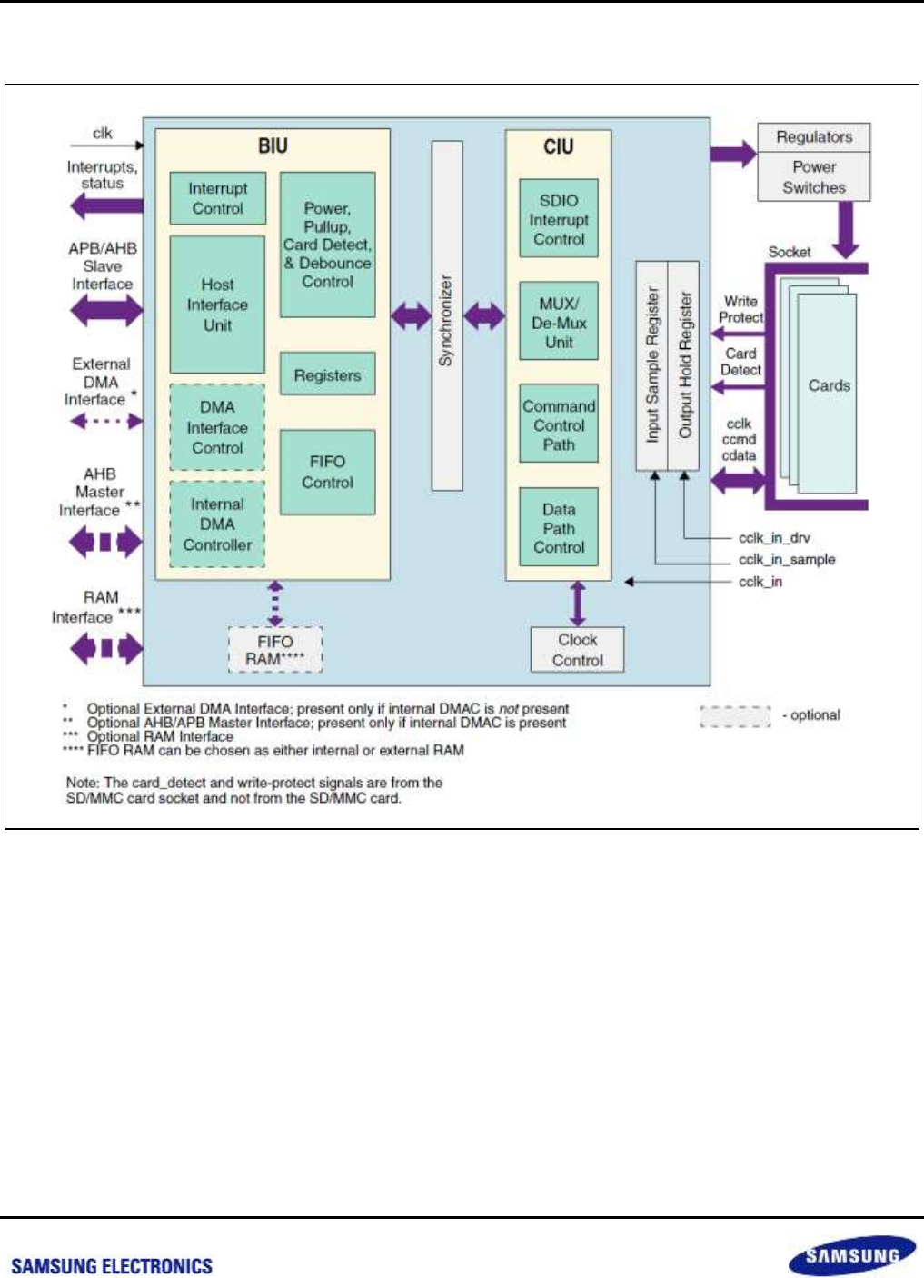
Samsung Confidential
S5P6818_UM 18 SD/MMC Controller
18-3
Preliminary product information describes products that are in development, for which full characterization data and
associated errata are not yet available. Specifications and information herein are subject to change without notice.
18.3 Block Diagram
Figure 18-1 Block Diagram of Mobile Storage Host
In the figure above illustrates the block diagram of Mobile Storage Host.
Bus Interface Unit (BIU): Provides AMBA AHB/APB and DMA interfaces for register and data read/writes
Card Interface Unit (CIU): Takes care of SD_MMC_CEATA protocols and provides clock management.
The BIU provides the host interface to the registers. It also provides the data FIFO through the Host Interface Unit
(HIU). Additionally, it provides independent data FIFO access through a DMA interface. You can configure host
interface as an AMBA APB slave interface.
The IDMAC is responsible for exchanging data between FIFO and the host memory. A set of IDMAC registers is
accessible by host for controlling the IDMAC operation through the AMBA APB slave interface.
nexell / ys.kim at 2015.02.12
SAMSUNG Confidential
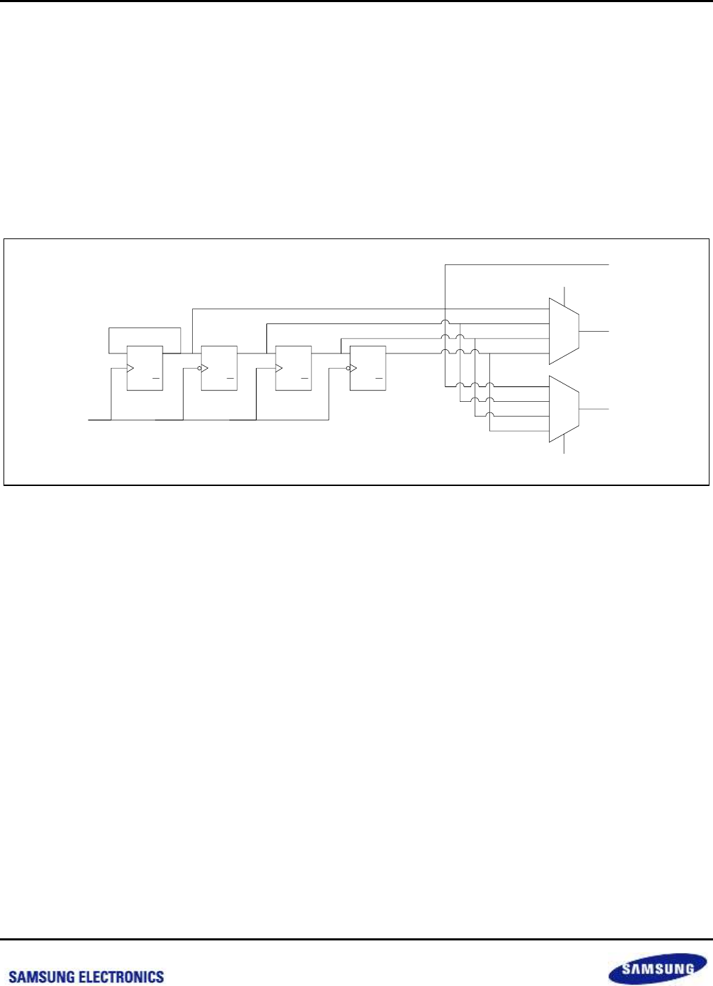
Samsung Confidential
S5P6818_UM 18 SD/MMC Controller
18-4
Preliminary product information describes products that are in development, for which full characterization data and
associated errata are not yet available. Specifications and information herein are subject to change without notice.
The Mobile Storage CIU controls the card-specific protocols. Within CIU, the command path control unit and data
path control unit interface with the controller to the command and data ports of the SD_MMC_CEATA cards. The
CIU also provides clock control.
18.3.1 Clock Phase Shifter
SD/MMC card receives DATA/CMD with card clock from the host controller. To synchronize the clock and
DATA/CMD, it is required that the clock delay is inserted to the Tx/Rx clock path. For this to happen, the logic is
added to the design as illustrated in the figure below and clock selection can be done with CLKSEL register at the
end of this section.
Figure 18-2 Block Diagram of Mobile Storage Host
This clock phase shifter makes 0, 90, 180, 270 phase shifted clocks for Tx/Rx respectively. To make 50 MHz
phase shifted clock, SDCLKIN should be 100 MHz.
Q
Q
SET
CLR
D
/2
SDCLKIN
Q
Q
SET
CLR
D
Q
Q
SET
CLR
D
Q
Q
SET
CLR
D
PHASE_SHIFT_CTRL[9:8]
PHASE_DRV_CTRL[9:8]
0º shift
90º shift
180º shift
270º shift
cclk_in
cclk_in_drv
cclk_in_sample
nexell / ys.kim at 2015.02.12
SAMSUNG Confidential

Samsung Confidential
S5P6818_UM 18 SD/MMC Controller
18-5
Preliminary product information describes products that are in development, for which full characterization data and
associated errata are not yet available. Specifications and information herein are subject to change without notice.
18.4 Register Description
18.4.1 Register Map Summary
Base Address: C006_2000h (SD0)
Base Address: C006_8000h (SD1)
Base Address: C006_9000h (SD2)
Register
Offset
Description
Reset Value
CTRL
00h, 00h, 00h
SD/MMC control register
0x1000_0000
POWER_ENABLE
04h, 04h, 04h
SD/MMC power enable register
0x0000_0000
CLKDIV
08h, 08h, 08h
SD/MMC clock divider register
0x0000_0000
CLK_SOURCE
0Ch, 0Ch, 0Ch
SD/MMC clock source register
0x0000_0000
CLKENA
10h, 10h, 10h
SD/MMC clock enable register
0x0000_0000
TMOUT
14h, 14h, 14h
SD/MMC timeout register
0xFFFF_FF40
CTYPE
18h, 18h, 18h
SD/MMC card type register
0x0000_0000
BLKSIZ
1Ch, 1Ch, 1Ch
SDMMC block size register
0x0000_0000
BYTCNT
20h, 20h, 20h
SD/MMC byte count register
0x0000_0200
INTMASK
24h, 24h, 24h
SD/MMC interrupt mask register
0x0000_0000
CMDARG
28h, 28h, 28h
SD/MMC command argument register
0x0000_0000
CMD
2Ch, 2Ch, 2Ch
SD/MMC command register
0x2000_0000
RESP0
30h, 30h, 30h
SD/MMC response register 0
0x0000_0000
RESP1
34h, 34h, 34h
SD/MMC response register 1
0x0000_0000
RESP2
38h, 38h, 38h
SD/MMC response register 2
0x0000_0000
RESP3
3Ch, 3Ch, 3Ch
SD/MMC response register 3
0x0000_0000
MINTSTS
40h, 40h, 40h
SD/MMC masked interrupt status register
0x0000_0000
RINTSTS
44h, 44h, 44h
SD/MMC raw interrupt status register
0x0000_0000
STATUS
48h, 48h, 48h
SD/MMC status register
0x0000_0006
FIFOTH
4Ch, 4Ch, 4Ch
SD/MMC FIFO threshold watermark register
0x0000_0000
CDETECT
50h, 50h, 50h
SD/MMC card detect register
0x0000_0000
WRTPRT
54h, 54h, 54h
SD/MMC card write protect register
0x0000_0000
RSVD
58h, 58h, 58h
Reserved
0x0000_0000
TCBCNT
5Ch, 5Ch, 5Ch
SD/MMC transferred CIU card byte count register
0x0000_0000
TBBCNT
60h, 60h, 60h
SD/MMC transferred host to BIU-FIFO byte count
register
0x0000_0000
DEBNCE
64h, 64h, 64h
SD/MMC de-bounce count register
0x00FF_FFFF
USRID
68h, 68h, 68h
SD/MMC user ID register
0x0000_0000
VERID
6Ch, 6Ch, 6Ch
SD/MMC version ID register
0x5342_240A
RSVD
70h, 70h, 70h
Reserved
0x0000_0000
UHS_REG
74h, 74h, 74h
SD/MMC UHS-1 register
0x0000_0000
nexell / ys.kim at 2015.02.12
SAMSUNG Confidential

Samsung Confidential
S5P6818_UM 18 SD/MMC Controller
18-6
Preliminary product information describes products that are in development, for which full characterization data and
associated errata are not yet available. Specifications and information herein are subject to change without notice.
Register
Offset
Description
Reset Value
RST_n
78h, 78h, 78h
SD/MMC H/W reset
0x0000_0000
BMODE
80h, 80h, 80h
SD/MMC bus mode register
0x0000_0000
PLDMND
84h, 84h, 84h
SD/MMC poll demand register
0x0000_0000
DBADDR
88h, 88h, 88h
SD/MMC descriptor list base address register
0x0000_0000
IDSTS
8Ch, 8Ch, 8Ch
SD/MMC internal DMAC status register
0x0000_0000
IDINTEN
90h, 90h, 90h
SD/MMC internal DMAC interrupt enable register
0x0000_0000
DSCADDR
94h, 94h, 94h
SD/MMC current host descriptor address register
0x0000_0000
BUFADDR
98h, 98h, 98h
SD/MMC current buffer descriptor address register
0x0000_0000
RSVD
9Ch, 9Ch, 9Ch
Reserved
0x0000_0000
CARDTHRCTL
100h, 100h, 100h
SD/MMC card threshold control register
0x0000_0000
BACK_END_POWER
104h, 104h, 104h
SD/MMC back-end power register
0x0000_0000
RSVD
108h, 108h, 108h
Reserved
0x0000_0000
EMMC_DDR_REG
10Ch, 10Ch, 10Ch
SD/MMC eMMC 4.5 DDR start bit detection control
register
0x0000_0000
RSVD
110h, 110h, 110h
Reserved
0x0000_0000
EMMC_DDR_REG
114h, 114h, 114h
SD/MMC enable phase shift register
0x0000_0000
RSVD
118h to 1FFh,
110h to 1FFh,
110h
Reserved
0x0000_0000
Data
200h, 200h, 200h
SD/MMC data register
Undefined
nexell / ys.kim at 2015.02.12
SAMSUNG Confidential

Samsung Confidential
S5P6818_UM 18 SD/MMC Controller
18-7
Preliminary product information describes products that are in development, for which full characterization data and
associated errata are not yet available. Specifications and information herein are subject to change without notice.
18.4.1.1 CTRL
Base Address: C006_2000h (SD0)
Base Address: C006_8000h (SD1)
Base Address: C006_9000h (SD2)
Address = Base Address + 00h, 00h, 00h, Reset Value = 0x1000_0000
Name
Bit
Type
Description
Reset Value
RSVD
[31:26]
–
Reserved
6'h0
USE_INTERNAL_DM
AC
[25]
RW
Present only for the Internal DMAC configuration; else, it is
reserved.
0 = The host performs data transfers through the slave
interface
1 = Internal DMAC used for data transfer
1'b0
ENABLE_OD_PULLU
P
[24]
RW
External open-drain pull up:
0 = Disable
1 = Enable
Inverted value of this bit is output to ccmd_od_pullup_en_n
port. When bit is set, command output always driven in open-
drive mode; that is, DWC_mobile_storage drives either 0 or
high impedance, and does not drive hard 1.
1'b1
CARD_VOLTAGE_B
[23:20]
RW
Card regulator-B voltage setting; output to card_volt_b port.
Optional feature; ports can be used as general-purpose
outputs.
4'h0
CARD_VOLTAGE_A
[19:16]
RW
Card regulator-A voltage setting; output to card_volt_a port.
Optional feature; ports can be used as general-purpose
outputs.
4'h0
RSVD
[15:12]
RW
Reserved
3'b000
CEATA_DEVICE_INT
ERRUPT_STATUS
[11]
RW
0 = Interrupts not enabled in CE-ATA device (nIEN = 1 in
ATA control register)
1 = Interrupts are enabled in CE-ATA device (nIEN = 0 in
ATA control register)
Software should appropriately write to this bit after power-on
reset or any other reset to CE-ATA device. After reset,
usually CE-ATA device interrupt is disabled (nIEN = 1). If the
host enables CE-ATA device interrupt, then software should
set this bit.
1'b0
SEND_AUTO_STOP
_CCSD
[10]
RW
0 = Clear bit if DWC_mobile_storage does not reset the bit.
1 = Send internally generated STOP after sending CCSD to
CE-ATA device.
NOTE: Always set send_auto_stop_ccsd and send_ccsd bits
together; send_auto_stop_ccsd should not be set
independent of send_ccsd. When set, DWC_Mobile_Storage
automatically sends internally generated STOP command
(CMD12) to CE-ATA device. After sending internally-
generated STOP command, Auto Command Done (ACD) bit
in RINTSTS is set and generates interrupt to host if Auto
Command Done interrupt is not masked. After sending the
1'b0
nexell / ys.kim at 2015.02.12
SAMSUNG Confidential

Samsung Confidential
S5P6818_UM 18 SD/MMC Controller
18-8
Preliminary product information describes products that are in development, for which full characterization data and
associated errata are not yet available. Specifications and information herein are subject to change without notice.
Name
Bit
Type
Description
Reset Value
CCSD, DWC_mobile_storage automatically clears
send_auto_stop_ccsd bit.
SEND_CCSD
[9]
RW
0 = Clear bit if DWC_mobile_storage does not reset the bit.
1 = Send Command Completion Signal Disable (CCSD) to
CE-ATA device
When set, DWC_mobile_storage sends CCSD to CE-ATA
device. Software sets this bit only if current command is
expecting CCS (that is, RW_BLK) and interrupts are enabled
in CE-ATA device. Once the CCSD pattern is sent to device,
DWC_mobile_storage automatically clears send_ccsd bit. It
also sets Command Done (CD) bi tin RINTSTS register and
generates interrupt to host if Command Done interrupt is not
masked.
NOTE: Once send_ccsd bit is set, it takes two card clock
cycles to drive the CCSD on the CMD line. Due to this,
during the boundary conditions it may happen that CCSD is
sent to the CE-ATA device, even if the device signaled CCS.
1'b0
ABORT_READ_DAT
A
[8]
RW
0 = No change
1 = After suspend command is issued during read-transfer,
software polls card to find when suspend happened. Once
suspend occurs, software sets bit to reset data state-
machine, which is waiting for next block of data. Bit
automatically clears once data state machine resets to idle.
Used in SDIO card suspend sequence.
1'b0
SEND_IRQ_RESPO
NSE
[7]
RW
0 = No change
1 = Send auto IRQ response
Bit automatically clears once response is sent.
To wait for MMC card interrupts, host issues CMD40, and
DWC_mobile_storage waits for interrupt response from MMC
card(s). In meantime, if host wants DWC_mobile_storage to
exit waiting for interrupt state, it can set this bit, at which time
DWC_mobile_storage command state-machine sends
CMD40 response on bus and returns to idle state.
1'b0
READ_WAIT
[6]
RW
For sending read-wait to SDIO cards.
0 = Clear read wait
1 = Assert read wait
1'b0
RSVD
[5]
–
Reserved
–
INT_ENABLE
[4]
RW
Global interrupt enable/disable bit
0 = Disable interrupt
1 = Enable interrupt
The int port is 1 only when this bit is 1 and one or more
unmasked interrupts are set.
1'b0
RSVD
[3]
RW
Reserved.
1'b0
DMA_RESET
[2]
RW
0 = No change
1 = Reset internal DMA interface control logic
To reset DMA interface, firmware should set bit to 1. This bit
is auto-cleared after two AHB clocks.
1'b0
nexell / ys.kim at 2015.02.12
SAMSUNG Confidential

Samsung Confidential
S5P6818_UM 18 SD/MMC Controller
18-9
Preliminary product information describes products that are in development, for which full characterization data and
associated errata are not yet available. Specifications and information herein are subject to change without notice.
Name
Bit
Type
Description
Reset Value
FIFO_RESET
[1]
RW
0 = No change
1 = Reset to data FIFO To reset FIFO pointers
To reset FIFO, firmware should set bit to 1. This bit is auto-
cleared after completion of reset operation.
1'b0
CONTROLLER_RES
ET
[0]
RW
0 = No change
1 = Reset DWC_mobile_storage controller
To reset controller, firmware should set bit to 1. This bit is
auto-cleared after two AHB and two cclk_in clock cycles.
This resets:
BIU/CIU interface
CIU and state machines
abort_read_data, send_irq_response, and read_wait bits of
Control register
start_cmd bit of Command register
Does not affect any registers or DMA interface, or FIFO or
host interrupts
1'b0
18.4.1.2 POWER_ENABLE
Base Address: C006_2000h (SD0)
Base Address: C006_8000h (SD1)
Base Address: C006_9000h (SD2)
Address = Base Address + 04h, 04h, 04h, Reset Value = 0x0000_0000
Name
Bit
Type
Description
Reset Value
RSVD
[31:1]
–
Reserved
–
POWER_ENABLE
[0]
RW
Power on/off switch for up to 16 cards; for example, bit[0]
controls card 0.Once power is turned on, firmware should
wait for regulator/switch ramp-uptime before trying to
initialize card.
0 = Power off
1 = Power on
Only NUM_CARDS numbers of bits are implemented.
Bit values output to card_power_en port.
Optional feature; ports can be used as general-purpose
outputs.
1'b0
nexell / ys.kim at 2015.02.12
SAMSUNG Confidential

Samsung Confidential
S5P6818_UM 18 SD/MMC Controller
18-10
Preliminary product information describes products that are in development, for which full characterization data and
associated errata are not yet available. Specifications and information herein are subject to change without notice.
18.4.1.3 CLKDIV
Base Address: C006_2000h (SD0)
Base Address: C006_8000h (SD1)
Base Address: C006_9000h (SD2)
Address = Base Address + 08h, 08h, 08h, Reset Value = 0x0000_0000
NAME
Bit
Type
Description
Reset Value
CLK_DIVIDER3
[31:24]
RW
Clock divider-3 value. Clock division is 2 n. For example,
value of 0 means divide by 2 0 = 0 (no division, bypass),
a value of 1 means divide by 2 1 = 2, a value of "ff"
means divide by 2 255 = 510, and so on.
8'h0
CLK_DIVIDER2
[23:16]
RW
Clock divider-2 value. Clock division is 2 n. For example,
value of 0 means divide by 2 0 = 0 (no division, bypass),
a value of 1 means divide by 2 1 = 2, a value of "ff"
means divide by 2 255 = 510, and so on.
8'h0
CLK_DIVIDER1
[15:8]
RW
Clock divider-1 value. Clock division is 2 n. For example,
value of 0 means divide by 2 0 = 0 (no division, bypass),
a value of 1 means divide by 2 1 = 2, a value of "ff"
means divide by 2 255 = 510, and so on.
8'h0
CLK_DIVIDER0
[7:0]
RW
Clock divider-0 value. Clock division is 2 n. For example,
value of 0 means divide by 2 0 = 0 (no division, bypass),
a value of 1 means divide by 2 1 = 2, a value of "ff"
means divide by 2 255 = 510, and so on.
8'h0
18.4.1.4 CLK_SOURCE
Base Address: C006_2000h (SD0)
Base Address: C006_8000h (SD1)
Base Address: C006_9000h (SD2)
Address = Base Address + 0Ch, 0Ch, 0Ch, Reset Value = 0x0000_0000
Name
Bit
Type
Description
Reset Value
RSVD
[31:2]
–
Reserved
–
CLK_SOURCE
[1:0]
RW
Clock divider source
00 = Clock divider 0
01 = Clock divider 1
10 = Clock divider 2
11 = Clock divider 3
32'h0
nexell / ys.kim at 2015.02.12
SAMSUNG Confidential
Samsung Confidential
S5P6818_UM 18 SD/MMC Controller
18-11
Preliminary product information describes products that are in development, for which full characterization data and
associated errata are not yet available. Specifications and information herein are subject to change without notice.
18.4.1.5 CLKENA
Base Address: C006_2000h (SD0)
Base Address: C006_8000h (SD1)
Base Address: C006_9000h (SD2)
Address = Base Address + 10h, 10h, 10h, Reset Value = 0x0000_0000
Name
Bit
Type
Description
Reset Value
RSVD
[31:17]
–
Reserved
15'h0
CCLK_LOW_POWE
R
[16]
RW
Low power control. If enabled, stop clock when card in idle
status.
0 = Low power disable
1 = Low power enable
1'b0
RSVD
[15:1]
RW
Reserved
15'h0
CCLK_ENABLE
[0]
RW
Clock enable control
0 = Disable SD clock
1 = Enable SD clock
1'b0
18.4.1.6 TMOUT
Base Address: C006_2000h (SD0)
Base Address: C006_8000h (SD1)
Base Address: C006_9000h (SD2)
Address = Base Address + 14h, 14h, 14h, Reset Value = 0xFFFF_FF40
Name
Bit
Type
Description
Reset Value
DATA_TIMEOUT
[31:8]
RW
Value for card Data Read Timeout; same value also used
for Data Starvation by Host timeout. The timeout counter
is started only after the card clock is stopped.
Value is in number of card output clocks - cclk_out of
selected card.
24'hFF_FFFF
RESPONSE_TIMEO
UT
[7:0]
RW
Response timeout value. Value is in number of card output
clocks - cclk_out.
8'h40
nexell / ys.kim at 2015.02.12
SAMSUNG Confidential
Samsung Confidential
S5P6818_UM 18 SD/MMC Controller
18-12
Preliminary product information describes products that are in development, for which full characterization data and
associated errata are not yet available. Specifications and information herein are subject to change without notice.
18.4.1.7 CTYPE
Base Address: C006_2000h (SD0)
Base Address: C006_8000h (SD1)
Base Address: C006_9000h (SD2)
Address = Base Address + 18h, 18h, 18h, Reset Value = 0x0000_0000
Name
Bit
Type
Description
Reset Value
RSVD
[31:17]
–
Reserved
15'h0
CARD_WIDTH
[16]
RW
8-bit interface mode. In S5P6818, this bit must be 0.
1'b0
RSVD
[15:1]
–
Reserved.
15'h0
CARD_WIDTH
[0]
RW
Card bus width.
0 = 1-bit mode
1 = 4-bit mode
1'b0
18.4.1.8 BLKSIZ
Base Address: C006_2000h (SD0)
Base Address: C006_8000h (SD1)
Base Address: C006_9000h (SD2)
Address = Base Address + 1Ch, 1Ch, 1Ch, Reset Value = 0x0000_0000
Name
Bit
Type
Description
Reset Value
RSVD
[31:16]
–
Reserved
16'h0
BLKSIZE
[15:0]
RW
Block size in bytes.
16'h200
18.4.1.9 BYTCNT
Base Address: C006_2000h (SD0)
Base Address: C006_8000h (SD1)
Base Address: C006_9000h (SD2)
Address = Base Address + 20h, 20h, 20h, Reset Value = 0x0000_0200
Name
Bit
Type
Description
Reset Value
BYTE_COUNT
[31:0]
RW
Number of bytes to be transferred; should be integer
multiple of Block Size for block transfers.
For undefined number of byte transfers, byte count should
be set to 0. When byte count is set to 0, it is responsibility
of host to explicitly send stop/abort command to terminate
data transfer.
32'h200
nexell / ys.kim at 2015.02.12
SAMSUNG Confidential

Samsung Confidential
S5P6818_UM 18 SD/MMC Controller
18-13
Preliminary product information describes products that are in development, for which full characterization data and
associated errata are not yet available. Specifications and information herein are subject to change without notice.
18.4.1.10 INTMASK
Base Address: C006_2000h (SD0)
Base Address: C006_8000h (SD1)
Base Address: C006_9000h (SD2)
Address = Base Address 24h, 24h, 24h, Reset Value = 0x0000_0000
Name
Bit
Type
Description
Reset Value
RSVD
[31:17]
–
Reserved
15'h0
SDIO_INT_MASK
[16]
RW
SDIO interrupt mask.
0 = Masked
1 = Enabled
1'b0
MASK_EBE
[15]
RW
End bit error (read), Write no CRC (write) interrupt mask.
1'b0
MASK_ACD
[14]
RW
Auto command done interrupt mask.
1'b0
MASK_SBE
[13]
RW
Start bit error / Busy Complete interrupt mask
1'b0
MASK_HLE
[12]
RW
Hardware locked write error interrupt mask
1'b0
MASK_FRUN
[11]
RW
FIFO under run/overrun error interrupt mask
1'b0
MASK_HTO
[10]
RW
Data starvation by host timeout/Volt_switch_int interrupt
mask
1'b0
MASK_DRTO
[9]
RW
Data read timeout interrupt mask
1'b0
MASK_RTO
[8]
RW
Response timeout interrupt mask
1'b0
MASK_DCRC
[7]
RW
Data CRC error interrupt mask
1'b0
MASK_RCRC
[6]
RW
Response CRC error interrupt mask
1'b0
MASK_RXDR
[5]
RW
Receive FIFO data request interrupt mask
1'b0
MASK_TXDR
[4]
RW
Transmit FIFO data request interrupt mask
1'b0
MASK_DTO
[3]
RW
Data transfer over interrupt mask
1'b0
MASK_CD
[2]
RW
Command done interrupt mask
1'b0
MASK_RE
[1]
RW
Response error interrupt mask
1'b0
MASK_CD
[0]
W
This bit must be "0"
1'b0
nexell / ys.kim at 2015.02.12
SAMSUNG Confidential

Samsung Confidential
S5P6818_UM 18 SD/MMC Controller
18-14
Preliminary product information describes products that are in development, for which full characterization data and
associated errata are not yet available. Specifications and information herein are subject to change without notice.
18.4.1.11 CMDARG
Base Address: C006_2000h (SD0)
Base Address: C006_8000h (SD1)
Base Address: C006_9000h (SD2)
Address = Base Address + 28h, 28h, 28h, Reset Value = 0x0000_0000
Name
Bit
Type
Description
Reset Value
CMDARG
[31:0]
RW
Value indicates command argument to be passed to card.
32'h0
18.4.1.12 CMD
Base Address: C006_2000h (SD0)
Base Address: C006_8000h (SD1)
Base Address: C006_9000h (SD2)
Address = Base Address + 2Ch, 2Ch, 2Ch, Reset Value = 0x0000_0000
Name
Bit
Type
Description
Reset Value
START_CMD
[31]
RW
Start command. Once command is taken by CIU, bit is
cleared.
When bit is set, host should not attempt to write to any
command registers. If write is attempted, hardware lock
error is set in raw interrupt register.
Once command is sent and response is received from
SD_MMC_CEATA cards, Command Done bit is set in raw
interrupt register.
1'b0
RSVD
[30]
–
Reserved
1'b0
USE_HOLD_REG
[29]
RW
Use Hold Register
0 = CMD and DATA sent to card bypassing HOLD
Register
1 = CMD and DATA sent to card through the HOLD
Register
1'b1
VOLT_SWITCH
[28]
RW
Voltage switch bit
0 = No voltage switching
1 = Voltage switching enabled; must be set for CMD11
only
1'b0
BOOT_MODE
[27]
RW
Boot Mode
0 = Mandatory Boot operation
1 = Alternate Boot operation
1'b0
DISABLE_BOOT
[26]
RW
Disable Boot. When software sets this bit along with
start_cmd, CIU terminates the boot operation. Do NOT set
disable_boot and enable_boot together.
1'b0
EXPECT_BOOT_AC
K
[25]
RW
Expect Boot Acknowledge. When Software sets this bit
along with enable_boot, CIU expects a boot acknowledge
start pattern of 0-1-0from the selected card.
1'b0
ENABLE_BOOT
[24]
RW
Enable Boot-this bit should be set only for mandatory boot
1'b0
nexell / ys.kim at 2015.02.12
SAMSUNG Confidential

Samsung Confidential
S5P6818_UM 18 SD/MMC Controller
18-15
Preliminary product information describes products that are in development, for which full characterization data and
associated errata are not yet available. Specifications and information herein are subject to change without notice.
Name
Bit
Type
Description
Reset Value
mode. When Software sets this bit along with start_cmd,
CIU starts the boot sequence for the corresponding card
by asserting the CMD line low. Do NOT set disable_boot
and enable_boot together
CCS_EXPECTED
[23]
RW
0 = Interrupts are not enabled in CE-ATA device (nIEN = 1
inATA control register), or command does not expect CCS
from device
1 = Interrupts are enabled in CE-ATA device (nIEN = 0),
and RW_BLK command expects command completion
signal from CE-ATA device
If the command expects Command Completion Signal
(CCS) from the CE-ATA device, the software should set
this control bit. DWC_mobile_storage sets Data Transfer
Over (DTO) bit in RINTSTS register and generates
interrupt to host if Data Transfer Over interrupt is not
masked.
1'b0
READ_CEATA_DEVI
CE
[22]
RW
0 = Host is not performing read access (RW_REG or
RW_BLK)towards CE-ATA device
1 = Host is performing read access (RW_REG or
RW_BLK)towards CE-ATA device
Software should set this bit to indicate that CE-ATA device
is being accessed for read transfer. This bit is used to
disable read data timeout indication while performing CE-
ATA read transfers. Maximum value of I/O transmission
delay can be no less than10 seconds.
DWC_mobile_storage should not indicate read data
timeout while waiting for data from CE-ATA device.
1'b0
UPDATE_CLOCK_R
EGISTER_ONLY
[21]
RW
0 = Normal command sequence
1 = Do not send commands, just update clock register
value into card clock domain
Following register values transferred into card clock
domain:CLKDIV, CLRSRC, CLKENA.
Changes card clocks (change frequency, truncate off or
on, and set low-frequency mode); provided in order to
change clock frequency or stop clock without having to
send command to cards.
During normal command sequence, when
update_clock_registers_only = 0, following control
registers are transferred from BIU to CIU: CMD,
CMDARG, TMOUT, CTYPE, BLKSIZ, BYTCNT. CIU uses
new register values for new command sequence to
card(s).
When bit is set, there is no Command Done interrupts
because no command is sent to SD_MMC_CEATA cards.
1'b0
CARD_NUMBER
[20:16]
RW
Card number in use. In S5P6818, this value must be 0.
5'h0
SEND_INITIALIZATI
ON
[15]
RW
After power on, 80 clocks must be sent to card for
initialization before sending any commands to card. Bit
should be set while sending first command to card so that
1'b0
nexell / ys.kim at 2015.02.12
SAMSUNG Confidential

Samsung Confidential
S5P6818_UM 18 SD/MMC Controller
18-16
Preliminary product information describes products that are in development, for which full characterization data and
associated errata are not yet available. Specifications and information herein are subject to change without notice.
Name
Bit
Type
Description
Reset Value
controller will initialize clocks before sending command to
card. This bit should not be set for either of the boot
modes (alternate or mandatory).
0 = Do not send initialization sequence before sending
command
1 = Send initialization sequence before sending command
STOP_ABORT_CMD
[14]
RW
0 = Neither stop nor abort command to stop current data
transferrin progress. If abort is sent to function-number
currently selected or not in data-transfer mode, then bit
should be set to 0.
1 = Stop or abort command intended to stop current data
transfer in progress.
When open-ended or predefined data transfer is in
progress, and host issues stop or abort command to stop
data transfer, bit should be set so that command/data
state-machines of CIU can return correctly to idle state.
This is also applicable for Boot mode transfers. To Abort
boot mode, this bit should be set along withCMD[26] =
disable_boot.
1'b0
WAIT_PRVDATA_C
OMPLETE
[13]
RW
0 = Send command at once, even if previous data transfer
has not completed
1 = Wait for previous data transfer completion before
sending command
The wait_prvdata_complete = 0 option typically used to
query status of card during data transfer or to stop current
data transfer;card_number should be same as in previous
command.
1'b0
SEND_AUTO_STOP
[12]
RW
0 = No stop command sent at end of data transfer
1 = Send stop command at end of data transfer
When set, mobile_storage sends stop command
toSD_MMC_CEATA cards at end of data transfer
when send_auto_stop bit should be set, since some data
transfers do not need explicit stop commands
open-ended transfers that software should explicitly send
to stop command
Additionally, when "resume" is sent to resume -
suspended memory access of SD-Combo card - bit should
be set correctly if suspended data transfer needs
send_auto_stop.
Don't care if no data expected from card.
1'b0
TRANSFER_MODE
[11]
RW
Transfer mode. Don't care if no data expected.
0 = Block data transfer mode
1 = Stream data transfer mode
1'b0
READ/WRITE
[10]
RW
Read/Write mode selection. Don't care if no data
expected.
0 = Read from card
1 = Write to card
1'b0
nexell / ys.kim at 2015.02.12
SAMSUNG Confidential
Samsung Confidential
S5P6818_UM 18 SD/MMC Controller
18-17
Preliminary product information describes products that are in development, for which full characterization data and
associated errata are not yet available. Specifications and information herein are subject to change without notice.
Name
Bit
Type
Description
Reset Value
DATA_EXPECTED
[9]
RW
Data transfer expected flag.
0 = No data transfer expected
1 = Data transfer expected
1'b0
CHECK_RESPONSE
_CRC
[8]
RW
0 = Do not check response CRC
1 = Check response CRC
Some of command responses do not return valid CRC
bits. Software should disable CRC checks for those
commands in order to disable CRC checking by controller.
1'b0
RESPONSE_LENGT
H
[7]
RW
Response length selection.
0 = Short response
1 = Long response
1'b0
RESPONSE_EXPEC
T
[6]
RW
Response expected flag.
0 = No response expected
1 = Response expected
1'b0
CMD_INDEX
[5:0]
RW
Command index.
6'h0
18.4.1.13 RESP0
Base Address: C006_2000h (SD0)
Base Address: C006_8000h (SD1)
Base Address: C006_9000h (SD2)
Address = Base Address + 30h, 30h, 30h, Reset Value = 0x0000_0000
Name
Bit
Type
Description
Reset Value
RESPONSE0
[31:0]
R
Bit[31:0] of response
32'h0
18.4.1.14 RESP1
Base Address: C006_2000h (SD0)
Base Address: C006_8000h (SD1)
Base Address: C006_9000h (SD2)
Address = Base Address + 34h, 34h, 34h, Reset Value = 0x0000_0000
Name
Bit
Type
Description
Reset Value
RESPONSE1
[31:0]
R
Bit[63:32] of long response.
32'h0
nexell / ys.kim at 2015.02.12
SAMSUNG Confidential

Samsung Confidential
S5P6818_UM 18 SD/MMC Controller
18-18
Preliminary product information describes products that are in development, for which full characterization data and
associated errata are not yet available. Specifications and information herein are subject to change without notice.
18.4.1.15 RESP2
Base Address: C006_2000h (SD0)
Base Address: C006_8000h (SD1)
Base Address: C006_9000h (SD2)
Address = Base Address + 38h, 38h, 38h, Reset Value = 0x0000_0000
Name
Bit
Type
Description
Reset Value
RESPONSE2
[31:0]
R
Bit[95:64] of long response.
32'h0
18.4.1.16 RESP3
Base Address: C006_2000h (SD0)
Base Address: C006_8000h (SD1)
Base Address: C006_9000h (SD2)
Address = Base Address + 3Ch, 3Ch, 3Ch, Reset Value = 0x0000_0000
Name
Bit
Type
Description
Reset Value
RESPONSE3
[31:0]
R
Bit[127:96] of long response.
32'h0
nexell / ys.kim at 2015.02.12
SAMSUNG Confidential

Samsung Confidential
S5P6818_UM 18 SD/MMC Controller
18-19
Preliminary product information describes products that are in development, for which full characterization data and
associated errata are not yet available. Specifications and information herein are subject to change without notice.
18.4.1.17 MINTSTS
Base Address: C006_2000h (SD0)
Base Address: C006_8000h (SD1)
Base Address: C006_9000h (SD2)
Address = Base Address + 40h, 40h, 40h, Reset Value = 0x0000_0000
Name
Bit
Type
Description
Reset Value
RSVD
[31:17]
–
Reserved
15'h0
SDIO_INTERRUPT
[16]
R
Interrupt from SDIO card; SDIO interrupt for card enabled
only if corresponding sdio_int_mask bit is set in Interrupt
mask register (mask bit 1enables interrupt; 0 masks
interrupt).
0 = No SDIO interrupt from card
1 = SDIO interrupt from card.
1'b0
EBEINT
[15]
R
End bit error (read), Write no CRC (write) interrupt.
1'b0
ACDINT
[14]
R
Auto command done interrupt.
1'b0
SBEINT
[13]
R
Start bit error interrupt (SBE), Busy Complete Interrupt
(BCI)
1'b0
HLEINT
[12]
R
Hardware locked write error interrupt
1'b0
FRUNINT
[11]
R
FIFO under run/overrun error interrupt
1'b0
HTOINT
[10]
R
Data starvation by host timeout interrupt (HTO),
Volt_switch_int
1'b0
DRTOINT
[9]
R
Data read timeout interrupt
1'b0
RTOINT
[8]
R
Response timeout interrupt
1'b0
DCRCINT
[7]
R
Data CRC error interrupt
1'b0
RCRCINT
[6]
R
Response CRC error interrupt
1'b0
RXDRINT
[5]
R
Receive FIFO data request interrupt
1'b0
TXDRINT
[4]
R
Transmit FIFO data request interrupt
1'b0
DTOINT
[3]
R
Data transfer over interrupt
1'b0
CDINT
[2]
R
Command done interrupt
1'b0
REINT
[1]
R
Response error interrupt
1'b0
CDINT
[0]
R
Card detect
1'b0
nexell / ys.kim at 2015.02.12
SAMSUNG Confidential

Samsung Confidential
S5P6818_UM 18 SD/MMC Controller
18-20
Preliminary product information describes products that are in development, for which full characterization data and
associated errata are not yet available. Specifications and information herein are subject to change without notice.
18.4.1.18 RINTSTS
Base Address: C006_2000h (SD0)
Base Address: C006_8000h (SD1)
Base Address: C006_9000h (SD2)
Address = Base Address + 44h, 44h, 44h, Reset Value = 0x0000_0000
Name
Bit
Type
Description
Reset Value
RSVD
[31:17]
–
Reserved
15'h0
SDIO_INTERRUPT
[16]
RW
SDIO interrupt from card
1'b0
EBE
[15]
RW
End bit error (read), Write no CRC (write) interrupt.
1'b0
ACD
[14]
RW
Auto command done interrupt.
1'b0
SBE
[13]
RW
Start bit error interrupt(SBE), Busy Complete Interrupt
(BCI)
1'b0
HLE
[12]
RW
Hardware locked write error interrupt
1'b0
FRUN
[11]
RW
FIFO under run/overrun error interrupt
1'b0
HTO
[10]
RW
Data starvation by host timeout interrupt (HTO),
Volt_switch_int
1'b0
DRTO
[9]
RW
Data read timeout interrupt
1'b0
RTO
[8]
RW
Response timeout interrupt
1'b0
DCRC
[7]
RW
Data CRC error interrupt
1'b0
RCRC
[6]
RW
Response CRC error interrupt
1'b0
RXDR
[5]
RW
Receive FIFO data request interrupt
1'b0
TXDR
[4]
RW
Transmit FIFO data request interrupt
1'b0
DTO
[3]
RW
Data transfer over interrupt
1'b0
CD
[2]
RW
Command done interrupt
1'b0
RE
[1]
RW
Response error interrupt
1'b0
CDINT
[0]
R
Card detect
1'b0
nexell / ys.kim at 2015.02.12
SAMSUNG Confidential

Samsung Confidential
S5P6818_UM 18 SD/MMC Controller
18-21
Preliminary product information describes products that are in development, for which full characterization data and
associated errata are not yet available. Specifications and information herein are subject to change without notice.
18.4.1.19 STATUS
Base Address: C006_2000h (SD0)
Base Address: C006_8000h (SD1)
Base Address: C006_9000h (SD2)
Address = Base Address + 48h, 48h, 48h, Reset Value = 0x0000_0006
Name
Bit
Type
Description
Reset Value
DMA_REQ
[31]
R
DMA request signal state
1'b0
DMA_ACK
[30]
R
DMA acknowledge signal state
1'b0
FIFOCOUNT
[29:17]
R
Number of filled locations in FIFO
13'h0
RESPONSE_INDEX
[16:11]
R
Index of previous response, including any auto-stop sent
by core
6'h0
DATA_STATE_MC_B
USY
[10]
R
Data transmit or receive state-machine is busy
1'b0
DATA_BUSY
[9]
R
Selected card data busy
0 = Card data not busy
1 = Card data busy
1'bx
DATA_3_STATUS
[8]
R
Checks whether card is present
0 = Card not present
1 = Card present
1'bx
COMMAND FSM
STATES
[7:4]
R
Command FSM states.
0 = Idle
1 = Send init sequence
2 = Tx cmd start bit
3 = Tx cmd tx bit
4 = Tx cmd index + arg
5 = Tx cmd crc7
6 = Tx cmd end bit
7 = Rx resp start bit
8 = Rx resp IRQ response
9 = Rx resp tx bit
10 = Rx resp cmd idx
11 = Rx resp data
12 = Rx resp crc7
13 = Rx resp end bit
14 = Cmd path with NCC
15 = Wait
NOTE: The command FSM state is represented using 19
bits.
The STATUS Register (7:4) has 4 bits to represent the
command FSM states. Using these 4 bits, only 16 states
can be represented. Thus three states cannot be
represented in the STATUS (7:4) register. The three
states that are not represented in the STATUS
Register(7:4) are:
Bit[16]: Wait for CCS
Bit[17]: Send CCSD
4'h0
nexell / ys.kim at 2015.02.12
SAMSUNG Confidential

Samsung Confidential
S5P6818_UM 18 SD/MMC Controller
18-22
Preliminary product information describes products that are in development, for which full characterization data and
associated errata are not yet available. Specifications and information herein are subject to change without notice.
Name
Bit
Type
Description
Reset Value
Bit[18]: Boot Mode
Due to this, while command FSM is in "Wait for CCS state"
or "Send CCSD'' or "Boot Mode", the Status register
indicates status as 0 for the bit field 7:4.
FIFO_FULL
[3]
R
FIFO is full
1'b0
FIFO_EMPTY
[2]
R
FIFO is empty
1'b1
FIFO_TX_WATERMA
RK
[1]
R
FIFO reached trans mit watermark level. Not qualified with
data transfer.
1'b1
FIFO_RX_WATERM
ARK
[0]
R
FIFO reached receives watermark level. Not qualified with
data transfer.
1'b0
18.4.1.20 FIFOTH
Base Address: C006_2000h (SD0)
Base Address: C006_8000h (SD1)
Base Address: C006_9000h (SD2)
Address = Base Address + 4Ch, 4Ch, 4Ch, Reset Value = 0x0000_0000
Name
Bit
Type
Description
Reset Value
RSVD
[31]
–
Reserved
1'b0
DMA_MULTIPLE_TR
ANSACTION_SIZE
[30:28]
RW
Burst size of multiple transaction; should be programmed
same as DW-DMA controller multiple-transaction-size
SRC/DEST_MSIZE.
000 = 1 transfers
001 = 4
010 = 8
011 = 16
100 = 32
101 = 64
110 = 128
111 = 256
The units for transfers are the H_DATA_WIDTH
parameter. A single transfer (dw_dma_single assertion in
case of Non DW DMA interface) would be signaled based
on this value.
Value should be sub-multiple of (RX_WMark + 1) x
(F_DATA_WIDTH/H_DATA_WIDTH) and (FIFO_DEPTH -
TX_WMark) x (F_DATA_WIDTH/H_DATA_WIDTH)
For example, if FIFO_DEPTH = 16, FDATA_WIDTH ==
H_DATA_WIDTH
Allowed combinations for MSize and TX_WMark are:
MSize = 1, TX_WMARK = 1-15 MSize = 4, TX_WMark = 8
MSize = 4, TX_WMark = 4 MSize = 4, TX_WMark = 12
MSize = 8, TX_WMark = 8 MSize = 8, TX_WMark = 4
Allowed combinations for MSize and RX_WMark are:
MSize = 1, RX_WMARK = 0-14
3'b0
nexell / ys.kim at 2015.02.12
SAMSUNG Confidential

Samsung Confidential
S5P6818_UM 18 SD/MMC Controller
18-23
Preliminary product information describes products that are in development, for which full characterization data and
associated errata are not yet available. Specifications and information herein are subject to change without notice.
Name
Bit
Type
Description
Reset Value
MSize = 4, RX_WMark = 3
MSize = 4, RX_WMark = 7
MSize = 4, RX_WMark = 11
MSize = 8, RX_WMark = 7
Recommended:
MSize = 8, TX_WMark = 8, RX_WMark = 7
RX_WMARK
[27:16]
RW
FIFO threshold watermark level when receiving data to
card. When FIFO data count reaches greater than this
number, DMA/FIFO request is raised. During end of
packet, request is generated regardless of threshold
programming in order to complete any remaining data.
In non-DMA mode, when receiver FIFO threshold (RXDR)
interrupt is enabled, then interrupt is generated instead of
DMA request.
During end of packet, interrupt is not generated if
threshold programming is larger than any remaining data.
It is responsibility of host to read remaining bytes on
seeing Data Transfer done interrupt.
In DMA mode, at end of packet, even if remaining bytes
are less than threshold, DMA request does single
transfers to flush out any remaining bytes before Data
Transfer Done interrupt is set.
12 bits - 1-bit less than FIFO-count of status register,
which is 13 bits.
Limitation: RX_WMark FIFO_DEPTH-2
Recommended: (FIFO_DEPTH/2) - 1; (means greater
than(FIFO_DEPTH/2) - 1)
NOTE: In DMA mode during CCS time-out, the DMA does
not generate the request at the end of packet, even if
remaining bytes are less than threshold. In this case, there
will be some data left in the FIFO. It is the responsibility of
the application to reset the FIFO after the CCS timeout.
12'h0
RSVD
[15:12]
–
Reserved
4'h0
TX_WMARK
[11:0]
RW
FIFO threshold watermark level when transmitting data to
card. When FIFO data count is less than or equal to this
number, DMA/FIFO request is raised. If Interrupt is
enabled, then interrupt occurs. During end of packet,
request or interrupt is generated, regardless of threshold
programming.
In non-DMA mode, when transmit FIFO threshold (TXDR)
interrupt is enabled, then interrupt is generated instead of
DMA request. During end of packet, on last interrupt, host
is responsible for filling FIFO with only required remaining
bytes (not before FIFO is full or after CIU completes data
transfers, because FIFO may not be empty).
In DMA mode, at end of packet, if last transfer is less than
burst size, DMA controller does single cycles until required
bytes are transferred.
12'h0
nexell / ys.kim at 2015.02.12
SAMSUNG Confidential
Samsung Confidential
S5P6818_UM 18 SD/MMC Controller
18-24
Preliminary product information describes products that are in development, for which full characterization data and
associated errata are not yet available. Specifications and information herein are subject to change without notice.
Name
Bit
Type
Description
Reset Value
12 bits - 1-bit less than FIFO-count of status register,
which is 13 bits.
Limitation: TX_WMark 1;
Recommended: FIFO_DEPTH/2; (means less than or
equal to FIFO_DEPTH/2)
18.4.1.21 CDETECT
Base Address: C006_2000h (SD0)
Base Address: C006_8000h (SD1)
Base Address: C006_9000h (SD2)
Address = Base Address + 50h, 50h, 50h, Reset Value = 0x0000_0000
Name
Bit
Type
Description
Reset Value
RSVD
[31:1]
–
Reserved
31'h0
CARD_DETECT_N
[0]
R
Value on card_detect_n input ports.
1'b0
18.4.1.22 WRTPRT
Base Address: C006_2000h (SD0)
Base Address: C006_8000h (SD1)
Base Address: C006_9000h (SD2)
Address = Base Address + 54h, 54h, 54h, Reset Value = 0x0000_0000
Name
Bit
Type
Description
Reset Value
RSVD
[31:1]
–
Reserved
31'h0
WRITE_PROTECT
[0]
R
Value on card_write_prt input ports
1'b0
18.4.1.23 TCBCNT
Base Address: C006_2000h (SD0)
Base Address: C006_8000h (SD1)
Base Address: C006_9000h (SD2)
Address = Base Address + 5Ch, 5Ch, 5Ch, Reset Value = 0x0000_0000
Name
Bit
Type
Description
Reset Value
TRANS_CARD_BYT
E_COUNT
[31:0]
R
Number of bytes transferred by CIU unit to card.
32'b0
nexell / ys.kim at 2015.02.12
SAMSUNG Confidential
Samsung Confidential
S5P6818_UM 18 SD/MMC Controller
18-25
Preliminary product information describes products that are in development, for which full characterization data and
associated errata are not yet available. Specifications and information herein are subject to change without notice.
18.4.1.24 TBBCNT
Base Address: C006_2000h (SD0)
Base Address: C006_8000h (SD1)
Base Address: C006_9000h (SD2)
Address = Base Address + 60h, 60h, 60h, Reset Value = 0x0000_0000
Name
Bit
Type
Description
Reset Value
TRANS_FIFO_BYTE
_COUNT
[31:0]
R
Number of bytes transferred between host/DMA memory
and BIU FIFO
32'b0
18.4.1.25 DEBNCE
Base Address: C006_2000h (SD0)
Base Address: C006_8000h (SD1)
Base Address: C006_9000h (SD2)
Address = Base Address + 64h, 64h, 64h, Reset Value = 0x00FF_FFFF
Name
Bit
Type
Description
Reset Value
RSVD
[31:24]
–
Reserved
8'h0
DEBOUNCE_COUNT
[23:0]
RW
Number of host clocks (clk) used by de-bounce filter logic;
typical de-bounce time is 5-25 ms.
24'hFFFFFF
18.4.1.26 USRID
Base Address: C006_2000h (SD0)
Base Address: C006_8000h (SD1)
Base Address: C006_9000h (SD2)
Address = Base Address + 68h, 68h, 68h, Reset Value = 0x0000_0000
Name
Bit
Type
Description
Reset Value
USRID
[31:0]
RW
User identification register; value set by user
32'h0
18.4.1.27 VERID
Base Address: C006_2000h (SD0)
Base Address: C006_8000h (SD1)
Base Address: C006_9000h (SD2)
Address = Base Address + 6Ch, 6Ch, 6Ch, Reset Value = 0x5342_240A
Name
Bit
Type
Description
Reset Value
VERID
[31:0]
RW
Version identification register
32'h5342_240A
nexell / ys.kim at 2015.02.12
SAMSUNG Confidential

Samsung Confidential
S5P6818_UM 18 SD/MMC Controller
18-26
Preliminary product information describes products that are in development, for which full characterization data and
associated errata are not yet available. Specifications and information herein are subject to change without notice.
18.4.1.28 UHS_REG
Base Address: C006_2000h (SD0)
Base Address: C006_8000h (SD1)
Base Address: C006_9000h (SD2)
Address = Base Address + 74h, 74h, 74h, Reset Value = 0x0000_0000
Name
Bit
Type
Description
Reset Value
RSVD
[31:17]
–
Reserved
15'h0
DDR_REG
[16]
RW
DDR mode. Determines the voltage fed to the buffers by
an external voltage regulator. (only for 8bits of SD
Channel 2)
0 = Non-DDR mode
1 = DDR mode
1'b0
RSVD
[15:1]
–
Reserved
15'h0
VOLT_REG
[0]
RW
High Voltage mode. Determines the voltage fed to the
buffers by an external voltage regulator. (only for SD
Channel 2)
0 = Buffers supplied with 3.3 V VDD
1 = Buffers supplied with 1.8 V VDD
1'b0
18.4.1.29 RST_n
Base Address: C006_2000h (SD0)
Base Address: C006_8000h (SD1)
Base Address: C006_9000h (SD2)
Address = Base Address + 78h, 78h, 78h, Reset Value = 0x0000_0000
Name
Bit
Type
Description
Reset Value
RSVD
[31:1]
–
Reserved
31'h0
CARD_RESET
[0]
RW
Hardware reset.
0 = Reset
1 = Active mode
These bits cause the cards to enter pre-idle state, which
requires them to be re-initialized.
1'b0
nexell / ys.kim at 2015.02.12
SAMSUNG Confidential

Samsung Confidential
S5P6818_UM 18 SD/MMC Controller
18-27
Preliminary product information describes products that are in development, for which full characterization data and
associated errata are not yet available. Specifications and information herein are subject to change without notice.
18.4.1.30 BMODE
Base Address: C006_2000h (SD0)
Base Address: C006_8000h (SD1)
Base Address: C006_9000h (SD2)
Address = Base Address + 80h, 80h, 80h, Reset Value = 0x0000_0000
Name
Bit
Type
Description
Reset Value
RSVD
[31:1]
–
Reserved
21'h0
PBL
[10:8]
RW
Programmable Burst Length. These bits indicate the
maximum number of beats to be performed in one IDMAC
transaction. The IDMAC will always attempt to burst as
specified in PBL each time it starts a Burst transfer on the
host bus. The permissible values are 1, 4, 8, 16, 32, 64,
128 and 256. This value is the mirror of MSIZE of FIFOTH
register. In order to change this value, write the required
value to FIFOTH register. This is an encode value as
follows.
000 = 1 transfers
001 = 4 transfers
010 = 8 transfers
011 = 16 transfers
100 = 32 transfers
101 = 64 transfers
110 = 128 transfers
111 = 256 transfers
Transfer unit is either 16, 32, or 64 bits, based on
HDATA_WIDTH.
PBL is a read-only value and is applicable only for Data
Access; it does not apply to descriptor accesses.
3'b000
DE
[7]
RW
IDMAC Enable. When set, the IDMAC is enabled.DE is
read/write.
1'b0
DSL
[6:2]
RW
Descriptor Skip Length. Specifies the number of
HWord/Word/Dword (depending on 16/32/64-bit bus) to
skip between two unchained descriptors. This is applicable
only for dual buffer structure.
DSL is read/write.
5'h0
FB
[1]
RW
Fixed Burst. Controls whether the AHB Master interface
performs fixed burst transfers or not. When set, the AHB
will use only SINGLE, INCR4, INCR8 orINCR16 during
start of normal burst transfers. When reset, the AHB will
use SINGLE and INCR burst transfer operations.
FB is read/write.
1'b0
SWR
[0]
RW
Software Reset. When set, the DMA Controller resets all
its internal registers.
SWR is read/write. It is automatically cleared after 1 clock
cycle.
1'b0
nexell / ys.kim at 2015.02.12
SAMSUNG Confidential
Samsung Confidential
S5P6818_UM 18 SD/MMC Controller
18-28
Preliminary product information describes products that are in development, for which full characterization data and
associated errata are not yet available. Specifications and information herein are subject to change without notice.
18.4.1.31 PLDMND
Base Address: C006_2000h (SD0)
Base Address: C006_8000h (SD1)
Base Address: C006_9000h (SD2)
Address = Base Address + 84h, 84h, 84h, Reset Value = 0x0000_0000
Name
Bit
Type
Description
Reset Value
PD
[31:0]
W
Poll Demand. If the OWN bit of a descriptor is not set, the
FSM goes to the Suspend state. The host needs to write
any value into this register for the IDMAC FSM to resume
normal descriptor fetch operation. This is a write only
register.
PD bit is write-only.
32'h0
18.4.1.32 DBADDR
Base Address: C006_2000h (SD0)
Base Address: C006_8000h (SD1)
Base Address: C006_9000h (SD2)
Address = Base Address + 88h, 88h, 88h, Reset Value = 0x0000_0000
Name
Bit
Type
Description
Reset Value
SDL
[31:0]
RW
Start of Descriptor List. Contains the base address of the
First Descriptor. The LSB bits [0/1/2:0] for 16/32/64-bit
bus-width) are ignored and taken as all-zero by the
IDMAC internally. Hence these LSB bits are read-only.
32'h0
18.4.1.33 IDSTS
Base Address: C006_2000h (SD0)
Base Address: C006_8000h (SD1)
Base Address: C006_9000h (SD2)
Address = Base Address + 8Ch, 8Ch, 8Ch, Reset Value = 0x0000_0000
Name
Bit
Type
Description
Reset Value
RSVD
[31:17]
–
Reserved
15'b0
FSM
[16:13]
R
DMAC FSM present state.
0 = DMA_IDLE
1 = DMA_SUSPEND
2 = DESC_RD
3 = DESC_CHK
4 = DMA_RD_REQ_WAIT
5 = DMA_WR_REQ_WAIT
6 = DMA_RD
7 = DMA_WR
4'h0
nexell / ys.kim at 2015.02.12
SAMSUNG Confidential

Samsung Confidential
S5P6818_UM 18 SD/MMC Controller
18-29
Preliminary product information describes products that are in development, for which full characterization data and
associated errata are not yet available. Specifications and information herein are subject to change without notice.
Name
Bit
Type
Description
Reset Value
8 = DESC_CLOSE
This bit is read-only.
EB
[12:10]
R
Error Bits. Indicates the type of error that caused a Bus
Error. Valid only with Fatal Bus Error bit (IDSTS[2]) set.
This field does not generate an interrupt.
3'b001 = Host Abort received during transmission
3'b010 = Host Abort received during reception
Others = Reserved
EB is read-only.
3'b000
AIS
[9]
RW
Abnormal Interrupt Summary. Logical OR of the following:
IDSTS[2]:- Fatal Bus Interrupt
IDSTS[4]: DU bit Interrupt
Only unmasked bits affect this bit.
This is a sticky bit and must be cleared each time a
corresponding bit that causes AIS to be set is cleared.
Writing a 1 clears this bit.
1'b0
NIS
[8]
RW
Normal Interrupt Summary. Logical OR of the following:
IDSTS[0]: Transmit Interrupt
IDSTS[1]: Receive Interrupt
Only unmasked bits affect this bit.
This is a sticky bit and must be cleared each time a
corresponding bit that causes NIS to be set is cleared.
Writing a 1 clears this bit.
1'b0
RSVD
[7:6]
–
Reserved
2'b00
CES
[5]
RW
Card Error Summary. Indicates the status of the
transaction to/from the card; also present in RINTSTS.
Indicates the logical OR of the following bits:
EBE: End Bit Error
RTO: Response Timeout/Boot ACK Timeout
RCRC: Response CRC
SBE: Start Bit Error
DRTO: Data Read Timeout/BDS timeout
DCRC: Data CRC for Receive
RE: Response Error
Writing a 1 clears this bit.
The abort condition of the IDMAC depends on the setting
of this CES bit. If the CES bit is enabled, then the IDMAC
aborts on a “response error”; however, it will not abort if
the CES bit is cleared.
1'b0
DU
[4]
RW
Descriptor Unavailable Interrupt. This bit is set when the
descriptor is unavailable due to OWN bit = 0 (DES0[31]
=0). Writing a 1 clears this bit.
1'b0
RSVD
[3]
–
Reserved
1'b0
FBE
[2]
RW
Fatal Bus Error Interrupt. Indicates that a Bus Error
occurred (IDSTS[12:10]). When this bit is set, the DMA
disables all its bus accesses. Writing a 1 clears this bit.
1'b0
nexell / ys.kim at 2015.02.12
SAMSUNG Confidential

Samsung Confidential
S5P6818_UM 18 SD/MMC Controller
18-30
Preliminary product information describes products that are in development, for which full characterization data and
associated errata are not yet available. Specifications and information herein are subject to change without notice.
Name
Bit
Type
Description
Reset Value
RI
[1]
RW
Receive Interrupt. Indicates the completion of data
reception for a descriptor. Writing a1 clears this bit.
1'b0
TI
[0]
RW
Transmit Interrupt. Indicates that data transmission is
finished for a descriptor. Writing a "1" clears this bit.
1'b0
18.4.1.34 IDINTEN
Base Address: C006_2000h (SD0)
Base Address: C006_8000h (SD1)
Base Address: C006_9000h (SD2)
Address = Base Address + 90h, 90h, 90h, Reset Value = 0x0000_0000
NAME
Bit
Type
Description
Reset Value
RSVD
[31:10]
–
Reserved
22'h0
AI
[9]
RW
Abnormal Interrupt Summary Enable. When set, an
abnormal interrupt is enabled. This bit enables the
following bits:
IDINTEN[2]: Fatal Bus Error Interrupt
IDINTEN[4]: DU Interrupt
1'b0
NI
[8]
RW
Normal Interrupt Summary Enable. When set, a normal
interrupt is enabled. When reset, a normal interrupt is
disabled. This bit enables the following bits:
IDINTEN[0]: Transmit Interrupt
IDINTEN[1]: Receive Interrupt
1'b0
RSVD
[7:6]
–
Reserved
2'b00
CES
[5]
RW
Card Error summary Interrupt Enable. When set, it
enables the Card Interrupt summary.
1'b0
DU
[4]
RW
Descriptor Unavailable Interrupt. When set along with
Abnormal Interrupt Summary Enable, the DU interrupt is
enabled.
1'b0
RSVD
[3]
–
Reserved
1'b0
FBE
[2]
RW
Fatal Bus Error Enable. When set with Abnormal Interrupt
Summary Enable, the Fatal Bus Error Interrupt is enabled.
When reset, Fatal Bus Error Enable Interrupt is disabled.
1'b0
RI
[1]
RW
Receive Interrupt Enable. When set with Normal Interrupt
Summary Enable, Receive Interrupt is enabled. When
reset, Receive Interrupt is disabled.
1'b0
TI
[0]
RW
Transmit Interrupt Enable. When set with Normal Interrupt
Summary Enable, Transmit Interrupt is enabled. When
reset, Transmit Interrupt is disabled.
1'b0
nexell / ys.kim at 2015.02.12
SAMSUNG Confidential
Samsung Confidential
S5P6818_UM 18 SD/MMC Controller
18-31
Preliminary product information describes products that are in development, for which full characterization data and
associated errata are not yet available. Specifications and information herein are subject to change without notice.
18.4.1.35 DSCADDR
Base Address: C006_2000h (SD0)
Base Address: C006_8000h (SD1)
Base Address: C006_9000h (SD2)
Address = Base Address + 94h, 94h, 94h, Reset Value = 0x0000_0000
Name
Bit
Type
Description
Reset Value
HDA
[31:0]
R
Host Descriptor Address Pointer. Cleared on reset. Pointer
updated by IDMAC during operation. This register points
to the start address of the current descriptor read by the
IDMAC.
32'h0
18.4.1.36 BUFADDR
Base Address: C006_2000h (SD0)
Base Address: C006_8000h (SD1)
Base Address: C006_9000h (SD2)
Address = Base Address + 98h, 98h, 98h, Reset Value = 0x0000_0000
Name
Bit
Type
Description
Reset Value
HBA
[31:0]
R
Host Buffer Address Pointer. Cleared on Reset. Pointer
updated by IDMAC during operation. This register points
to the current Data Buffer Address being accessed by the
IDMAC.
32'h0
nexell / ys.kim at 2015.02.12
SAMSUNG Confidential

Samsung Confidential
S5P6818_UM 18 SD/MMC Controller
18-32
Preliminary product information describes products that are in development, for which full characterization data and
associated errata are not yet available. Specifications and information herein are subject to change without notice.
18.4.1.37 CARDTHRCTL
Base Address: C006_2000h (SD0)
Base Address: C006_8000h (SD1)
Base Address: C006_9000h (SD2)
Address = Base Address + 100h, 100h, 100h, Reset Value = 0x0000_0000
Name
Bit
Type
Description
Reset Value
RSVD
[31:27]
–
Reserved
5'h0
CARD_RD_THRESH
OLD
[26:16]
RW
Card Read Threshold size; N depends on the FIFO size.
11'h0
RSVD
[15:2]
–
Reserved
14'h0
BSY_CLR_INTEN
[1]
RW
Busy Clear Interrupt generation:
0 = Busy Clear Interrupt disabled
1 = Busy Clear Interrupt enabled
NOTE: The application can disable this feature if it does
not want to wait for a Busy Clear Interrupt. For example, in
a multi-card scenario, the application can switch to the
other card without waiting for a busy to be completed. In
such cases, the application can use the polling method to
determine the status of busy. By default this feature is
disabled and backward-compatible to the legacy drivers
where polling is used.
1'b0
CARD_RD_THREN
[0]
RW
Card Read Threshold Enable
1'b0 = Card Read Threshold disabled
1'b1 = Card Read Threshold enabled. Host Controller
initiates Read
Transfer only if Card Rd Threshold amount of space is
available in receives FIFO.
1'b0
18.4.1.38 BACK_END_POWER
Base Address: C006_2000h (SD0)
Base Address: C006_8000h (SD1)
Base Address: C006_9000h (SD2)
Address = Base Address + 104h, 104h, 104h, Reset Value = 0x0000_0000
Name
Bit
Type
Description
Reset Value
RSVD
[31:1]
–
Reserved
31'h0
BACK_END_POWER
[0]
RW
Back end power
1'b0 = Off; Reset
1'b1 = Back-end Power supplied to card application; one
pin per card
1'b0
nexell / ys.kim at 2015.02.12
SAMSUNG Confidential
Samsung Confidential
S5P6818_UM 18 SD/MMC Controller
18-33
Preliminary product information describes products that are in development, for which full characterization data and
associated errata are not yet available. Specifications and information herein are subject to change without notice.
18.4.1.39 EMMC_DDR_REG
Base Address: C006_2000h (SD0)
Base Address: C006_8000h (SD1)
Base Address: C006_9000h (SD2)
Address = Base Address + 10Ch, 10Ch, 10Ch, Reset Value = 0x0000_0000
Name
Bit
Type
Description
Reset Value
RSVD
[31:1]
–
Reserved
31'h0
HALF_START_BIT
[0]
RW
Control for start bit detection mechanism inside
DWC_mobile_storage based on duration of start bit;
each bit refers to one slot. For eMMC 4.5, start bit can
be:
Full cycle (HALF_START_BIT = 0)
Less than one full cycle (HALF_START_BIT = 1)
Set HALF_START_BIT=1 for eMMC 4.5 and above; set
to 0 for SD applications.
1'b0
18.4.1.40 EMMC_DDR_REG
Base Address: C006_2000h (SD0)
Base Address: C006_8000h (SD1)
Base Address: C006_9000h (SD2)
Address = Base Address + 114h, 114h, 114h, Reset Value = 0x0000_0000
Name
Bit
Type
Description
Reset Value
RSVD
[31:26]
–
Reserved
6'h0
PHASE_SHIFT_SAMPLE
[25:24]
RW
Sample clock phase shift
0 = 0
1 = 90
2 = 180
3 = 270
2'b00
RSVD
[23:18]
–
Reserved
6'h0
PHASE_SHIFT_DRIVE
[17:16]
RW
Drive clock phase shift
0 = 0
1 = 90
2 = 180
3 = 270
2'b00
DELAY_SAMPLE
[15:8]
RW
Sample clock delay
8'h0
DELAY_DRIVE
[7:0]
RW
Drive clock delay
8'h0
nexell / ys.kim at 2015.02.12
SAMSUNG Confidential

Samsung Confidential
S5P6818_UM 18 SD/MMC Controller
18-34
Preliminary product information describes products that are in development, for which full characterization data and
associated errata are not yet available. Specifications and information herein are subject to change without notice.
18.4.1.41 Data
Base Address: C006_2000h (SD0)
Base Address: C006_8000h (SD1)
Base Address: C006_9000h (SD2)
Address = Base Address + 114h, 114h, 114h, Reset Value = Undefined
Name
Bit
Type
Description
Reset Value
DATA
[31:0]
RW
Data write to or read from FIFO
–
nexell / ys.kim at 2015.02.12
SAMSUNG Confidential

Samsung Confidential
S5P6818_UM 19 Pulse Period Measurement (PPM)
19-1
Preliminary product information describes products that are in development, for which full characterization data and
associated errata are not yet available. Specifications and information herein are subject to change without notice.
19 Pulse Period Measurement (PPM)
19.1 Overview
The Pulse Period Measurement (PPM) measures the period of the high level and the low level of a 1-bit Signal
entered from the outside.
19.2 Features
The PPM provides:
16-bit Pulse Period Measurement Counter
Overflow Check
Control Input Polarity
PPM Clock generator
nexell / ys.kim at 2015.02.12
SAMSUNG Confidential
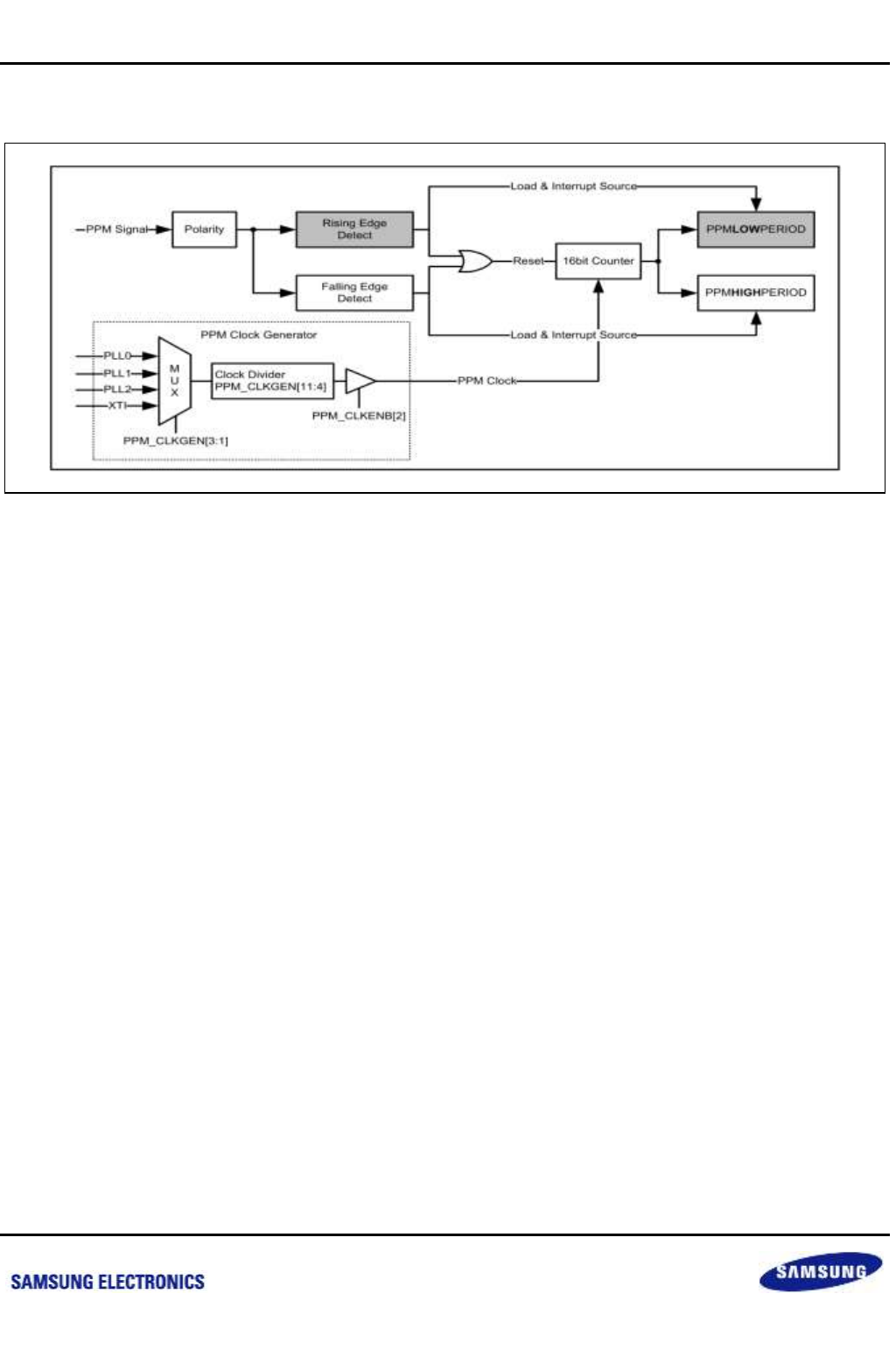
Samsung Confidential
S5P6818_UM 19 Pulse Period Measurement (PPM)
19-2
Preliminary product information describes products that are in development, for which full characterization data and
associated errata are not yet available. Specifications and information herein are subject to change without notice.
19.3 Block Diagram
Figure 19-1 PPM Block Diagram
PPMLOWPERIOD: PPM Low Period Register: If PPM Signal is changed from Low to High (rising edge
detect), the count value of 16-bit Counter is stored at PPMLOWPERIOD Register and 16-bit Counter is reset.
PPMHIGHPERIOD: PPM High Period Register: If PPM Signal is changed from High to Low (falling edge
detect), the count value of 16-bit Counter is stored at PPMHIGHPERIOD Register and 16-bit Counter is reset.
If the high or low period is too long to be measured by the 16-bit Counter, Overflow interrupt occurs.
nexell / ys.kim at 2015.02.12
SAMSUNG Confidential
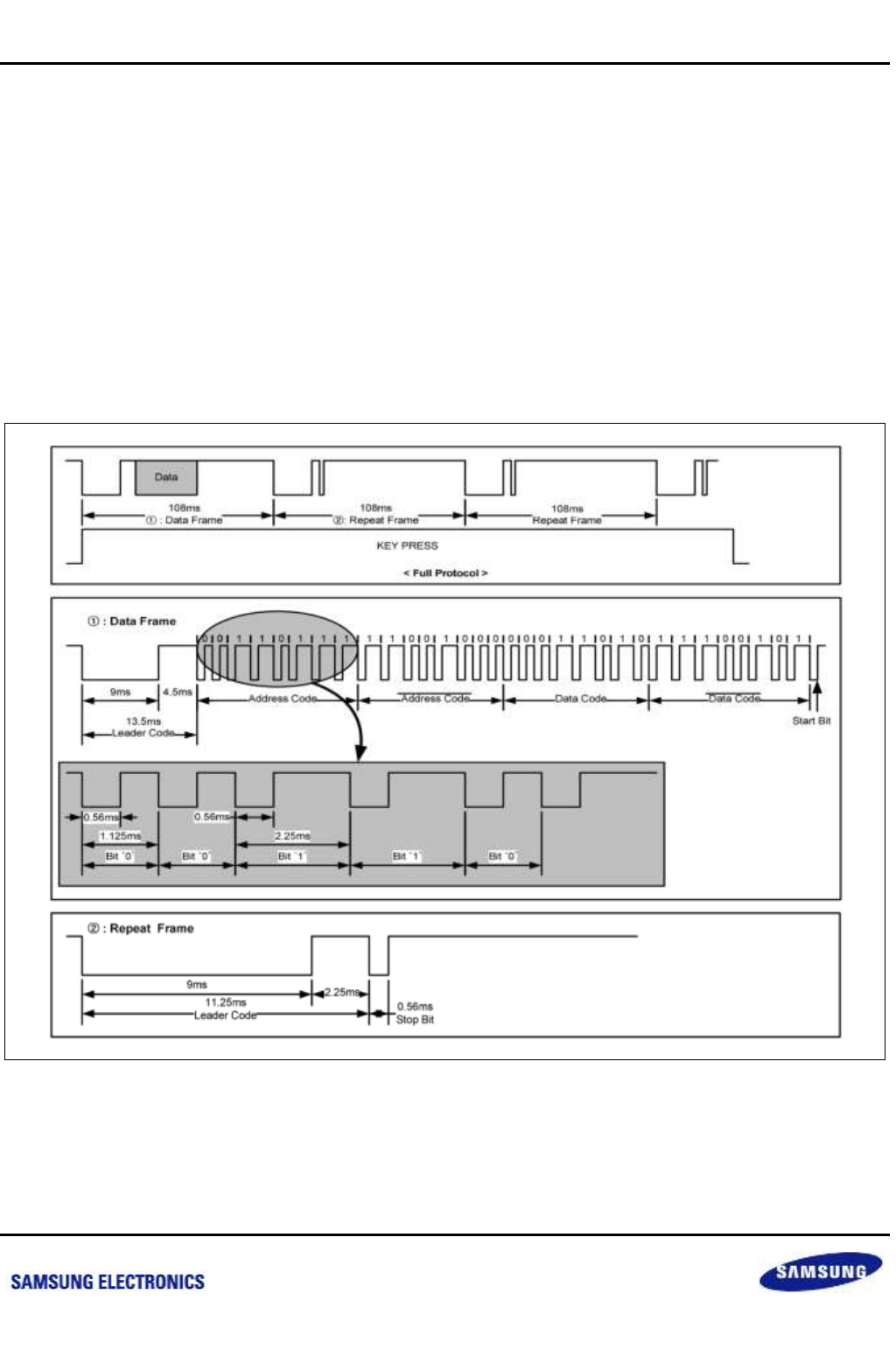
Samsung Confidential
S5P6818_UM 19 Pulse Period Measurement (PPM)
19-3
Preliminary product information describes products that are in development, for which full characterization data and
associated errata are not yet available. Specifications and information herein are subject to change without notice.
19.4 Functional Description
When a PPM signal rising edge or a falling edge is detected, the 16-bit counter is reset after storing the 16-bit
counter value to the PPMLOWPERIOD register or the PPMHIGHPERIOD register. If a falling edge is detected,
the counter value is stored at the PPMHIGHPERIOD register and then the counter is reset. If a rising edge is
detected, the counter value is stored at the PPMLOWPERIOD register and then the counter is reset. If the high or
the low period is too long to be measured by the 16-bit Counter, an Overflow interrupt occurs. Therefore the IP-
Remo on input signal should be checked and an appreciate PPL clock value should be specified to prevent the
occurrence of Overflow interrupts.
19.4.1 IR Remote Protocol Example
The figure below shows a representative waveform of an IP Remote signal being passed IR-Receiver Module.
Figure 19-2 IR Remote Example Protocol
The PPM clock between 850 kHz and 6.75 MHz is suitable to prevent the occurrence of an Overflow interrupt. The
PPM clock can be selected in the range of 843,750 Hz to 13,500,000 Hz via the Clock Divider setting. (1 to 31)
nexell / ys.kim at 2015.02.12
SAMSUNG Confidential
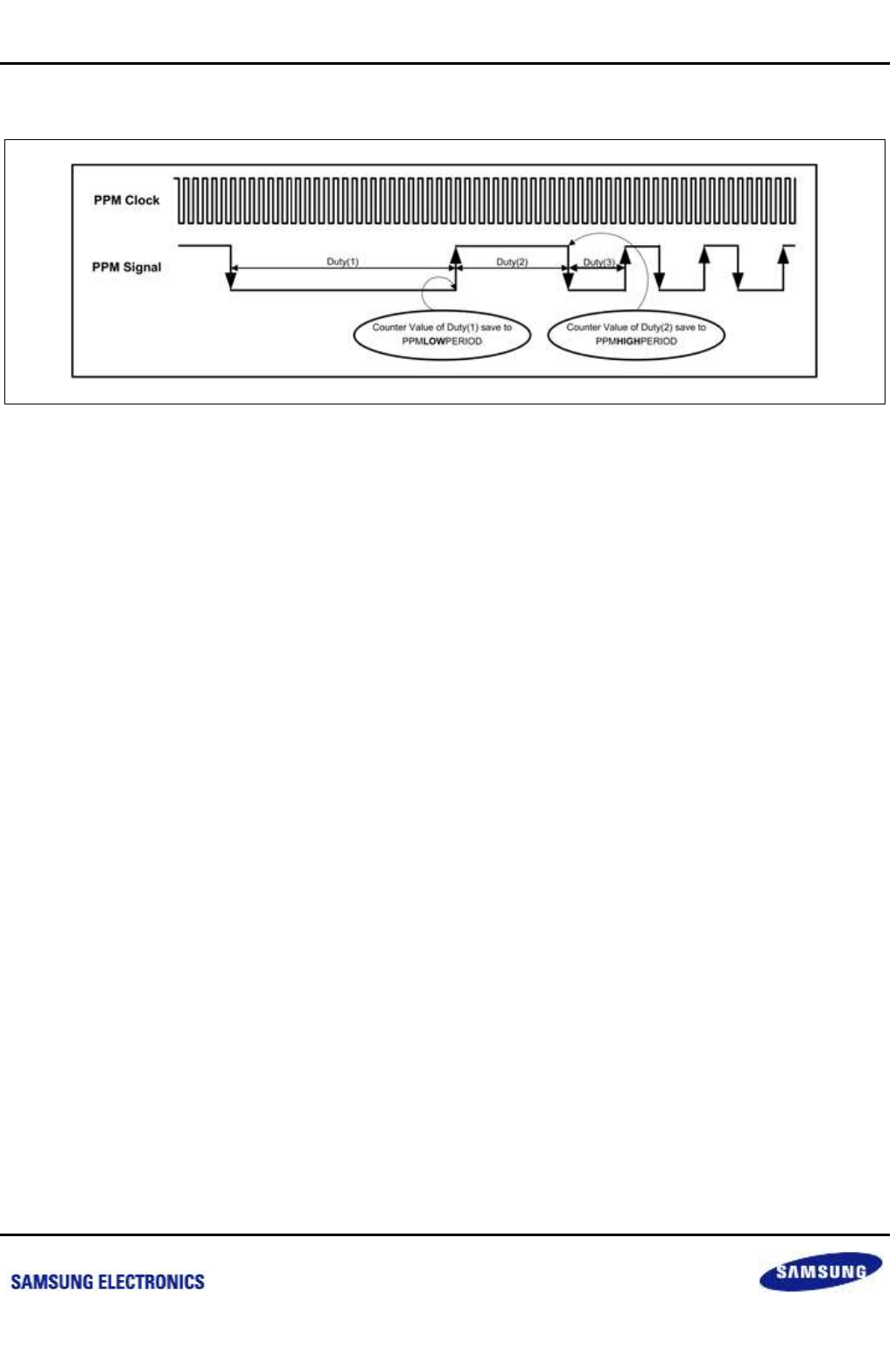
Samsung Confidential
S5P6818_UM 19 Pulse Period Measurement (PPM)
19-4
Preliminary product information describes products that are in development, for which full characterization data and
associated errata are not yet available. Specifications and information herein are subject to change without notice.
19.4.2 Timing
Figure 19-3 PPM Timing
nexell / ys.kim at 2015.02.12
SAMSUNG Confidential
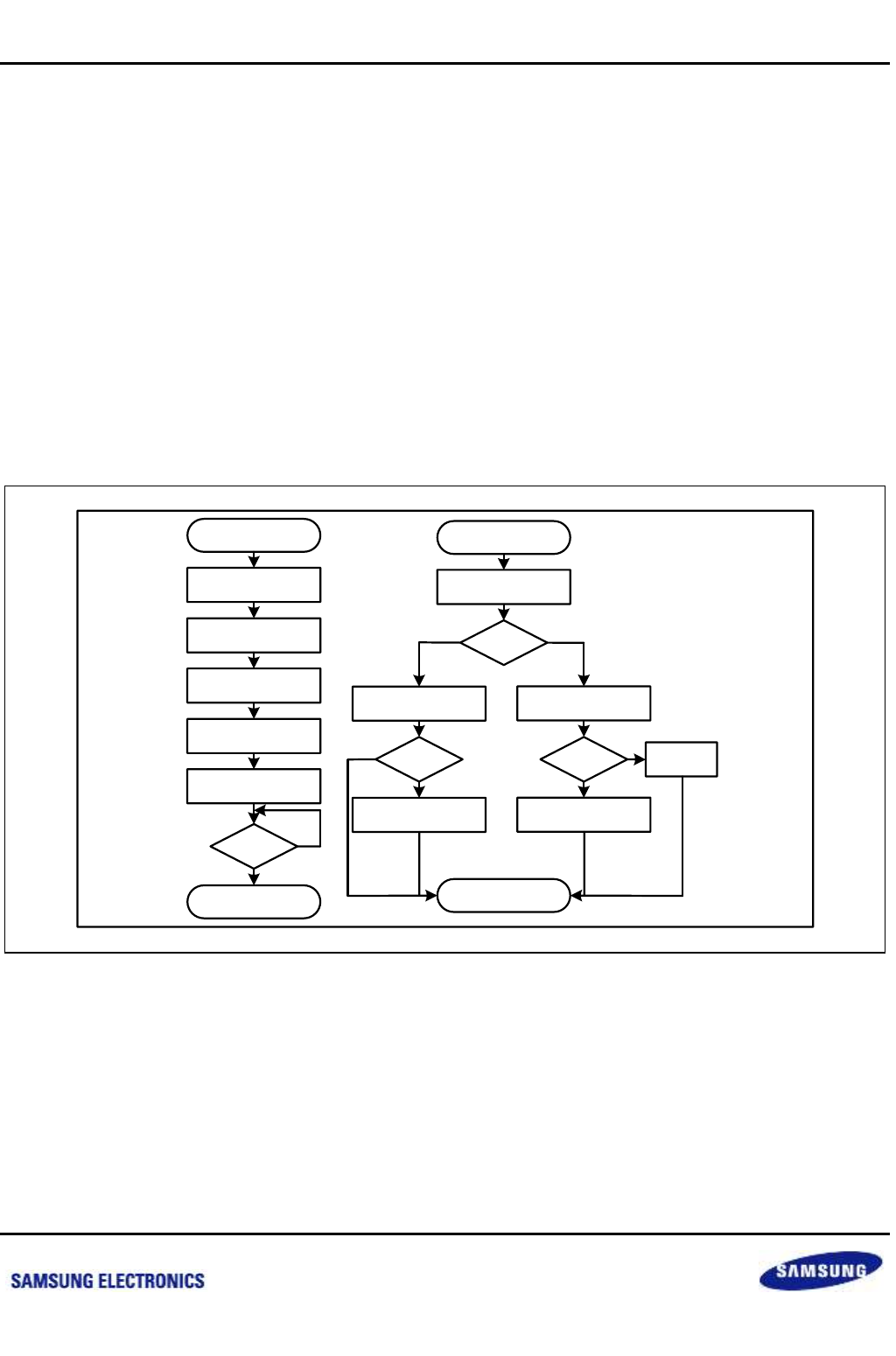
Samsung Confidential
S5P6818_UM 19 Pulse Period Measurement (PPM)
19-5
Preliminary product information describes products that are in development, for which full characterization data and
associated errata are not yet available. Specifications and information herein are subject to change without notice.
19.4.3 Flowchart
The figure below shows an example of a flowchart for checking IR-Remote signals.
Initialization Procedure for PPM:
1. Set GPIO
2. Clock Source Select (XTI)
3. Clock Divider (1 to 31)
4. Set Polarity
5. Set Interrupt mode (Falling Edge, Rising Edge and Overflow)
6. Initialize the PPM Status Register.
7. Enable Interrupt
Figure 19-4 IR Remote Receiver Flowchart
START
Enable pad PPMIN
While(1)
Select Clock Source,
Clock Divider
Set Polarity
Set Interrupt Mode
Interrupt Enable
END
START
Read PPMLOWPERIOD,
PPMHIGHPERIOD Value
Switch
(step)
Step==1
(Start Code Check)
Step==2
(End Code Check)
While(1) While(1)
Save 0x2 to Step Save 0x1 to Step
END
Save Data
NoNo
Yes = Start Code Yes = End Code
nexell / ys.kim at 2015.02.12
SAMSUNG Confidential

Samsung Confidential
S5P6818_UM 19 Pulse Period Measurement (PPM)
19-6
Preliminary product information describes products that are in development, for which full characterization data and
associated errata are not yet available. Specifications and information herein are subject to change without notice.
19.5 Register Description
19.5.1 Register Map Summary
Base Address: 0xC005_4000h
Register
Offset
Description
Reset Value
PPMCTRL
0x00h
PPM control register
0x0000_4000
PPMSTATUS
0x08h
PPM status register
0x0000_0000
PPMLOWPERIOD
0x0Ch
PPM low period register
0x0000_0000
PPMHIGHPERIOD
0x10h
PPM high period register
0x0000_0000
nexell / ys.kim at 2015.02.12
SAMSUNG Confidential

Samsung Confidential
S5P6818_UM 19 Pulse Period Measurement (PPM)
19-7
Preliminary product information describes products that are in development, for which full characterization data and
associated errata are not yet available. Specifications and information herein are subject to change without notice.
19.5.1.1 PPMCTRL
Base Address: 0xC005_4000h
Address = Base Address + 0x00h, Reset Value = 0x0000_4000
Name
Bit
Type
Description
Reset Value
RSVD
[31:16]
–
Reserved
–
PPMENB
[15]
RW
PPM Module Enable
0 = Disable
1 = Enable
1'b0
PPMINPOL
[14]
RW
Control Polarity of PPM Input Signal
0 = Invert
1 = Bypass
1'b1
RSVD
[13:3]
–
Reserved
–
PPMIRQO
[2]
RW
Overflow Interrupt Enable
0 = Disable
1 = Enable
1'b0
PPMIRQF
[1]
RW
Falling Edge Detect Interrupt Enable
0 = Disable
1 = Enable
1'b0
PPMIRQR
[0]
RW
Rising Edge Detect Interrupt Enable
0 = Disable
1 = Enable
1'b0
nexell / ys.kim at 2015.02.12
SAMSUNG Confidential

Samsung Confidential
S5P6818_UM 19 Pulse Period Measurement (PPM)
19-8
Preliminary product information describes products that are in development, for which full characterization data and
associated errata are not yet available. Specifications and information herein are subject to change without notice.
19.5.1.2 PPMSTATUS
Base Address: 0xC005_4000h
Address = Base Address + 0x08h, Reset Value = 0x0000_0000
Name
Bit
Type
Description
Reset Value
RSVD
[31:5]
–
Reserved
–
PPMOVERLOW
[4]
R
Indicate Overflow in Low
0 = Normal
1 = Overflow
1'b0
PPMOVERHIGH
[3]
R
Indicate Overflow in High
0 = Normal
1 = Overflow
1'b0
PPMPENDO
[2]
RW
Overflow Interrupt Pending Bit. Set to 1 to clear this bit
0 = None
1 = Detected
1'b0
PPMPENDF
[1]
RW
Falling Edge Detect Interrupt Pending Bit. Set to 1 to
clear this bit
0 = None
1 = Detected
1'b0
PPMPENDR
[0]
RW
Rising Edge Detect Interrupt Pending Bit. Set to 1 to
clear this bit
0 = None
1 = Detected
1'b0
19.5.1.3 PPMLOWPERIOD
Base Address: 0xC005_4000h
Address = Base Address + 0x0Ch, Reset Value = 0x0000_0000
Name
Bit
Type
Description
Reset Value
RSVD
[31:16]
–
Reserved
–
PPMLOWPERIOD
[15:0]
R
Read Counter Value of Low
16'h0
19.5.1.4 PPMHIGHPERIOD
Base Address: 0xC005_4000h
Address = Base Address + 0x10h, Reset Value = 0x0000_0000
Name
Bit
Type
Description
Reset Value
RSVD
[31:16]
–
Reserved
–
PPMHIGHPERIOD
[15:0]
R
Read Counter Value of High
16'h0
nexell / ys.kim at 2015.02.12
SAMSUNG Confidential
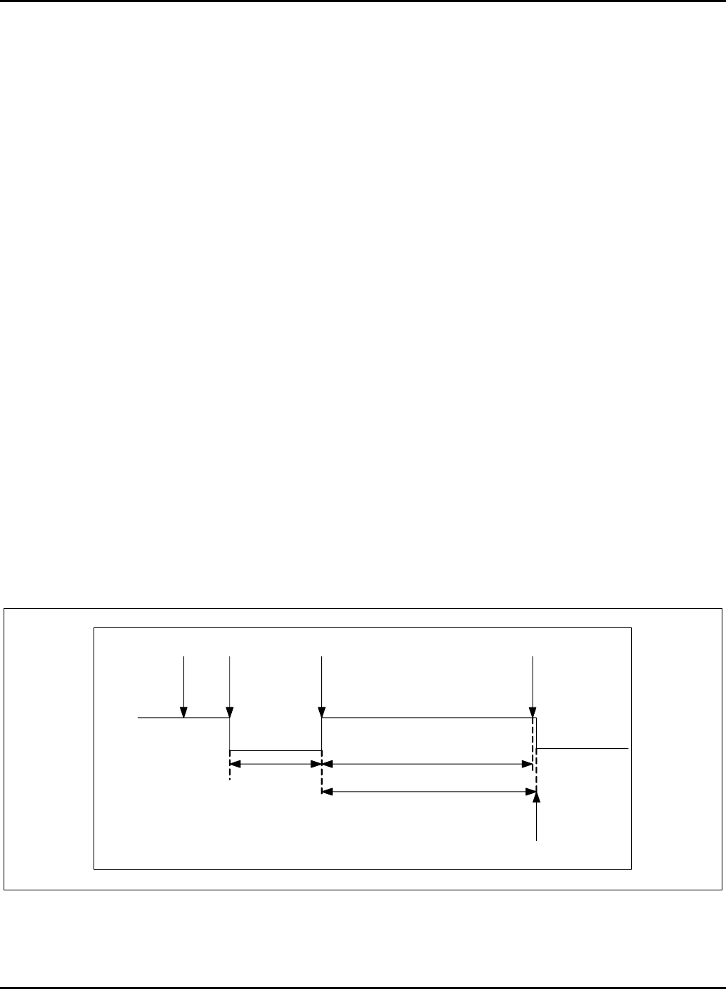
S5P6818_UM 20 Pulse Width Modulation (PWM) Timer
20-1
20 Pulse Width Modulation (PWM) Timer
20.1 Overview
The S5P6818 has five 32-bit Pulse Width Modulation (PWM) timers. These Timers generate internal interrupts for
the ARM subsystem. Additionally, Timers 0, 1, 2 and 3 include a PWM function that drives an external I/O signal.
The PWM in Timer 0 has an optional dead-zone generator capability to support a large current device. Timer 4 is
internal timer without output pins.
The Timers use the APB-PCLK as source clock. Timers 0 and 1 share a programmable 8-bit prescaler that
provides the first level of division for the PCLK. Timers 2, 3, and 4 share a different 8-bit prescaler. Each timer has
its own private clock-divider that provides a second level of clock division (prescaler divided by 2, 4, 8, or 16).
Each Timer has its own 32-bit down-counter which is driven by the timer clock. The down-counter is initially
loaded from the Timer Count Buffer register (TCNTBn). When the down-counter reaches zero, the timer interrupt
request is generated to inform the CPU that the Timer operation is complete. When the Timer down-counter
reaches zero, the value of corresponding TCNTBn automatically reloads into the down-counter to start the next
cycle. However, when the Timer stops, for example, by clearing the timer enable bit of TCONn during the Timer
running mode, the value of TCNTBn is not reloaded into the counter.
The PWM function uses the value of the TCMPBn register. The Timer Control Logic changes the output level if
down-counter value matches the value of the compare register in Timer Control Logic. Therefore, the compare
register determines the turn-on time or turn-off time of a PWM output.
The TCNTBn and TCMPBn registers are double buffered so that it allows the Timer parameters to be updated in
the middle of a cycle. The new values do not take effect until the current Timer cycle is completed. A simple
example of a PWM cycle is shown in the figure below.
Figure 20-1 Simple Example of PWM Cycle
TOUTn
1 2 3 4
5
50 109
110
nexell / ys.kim at 2015.02.12
SAMSUNG Confidential
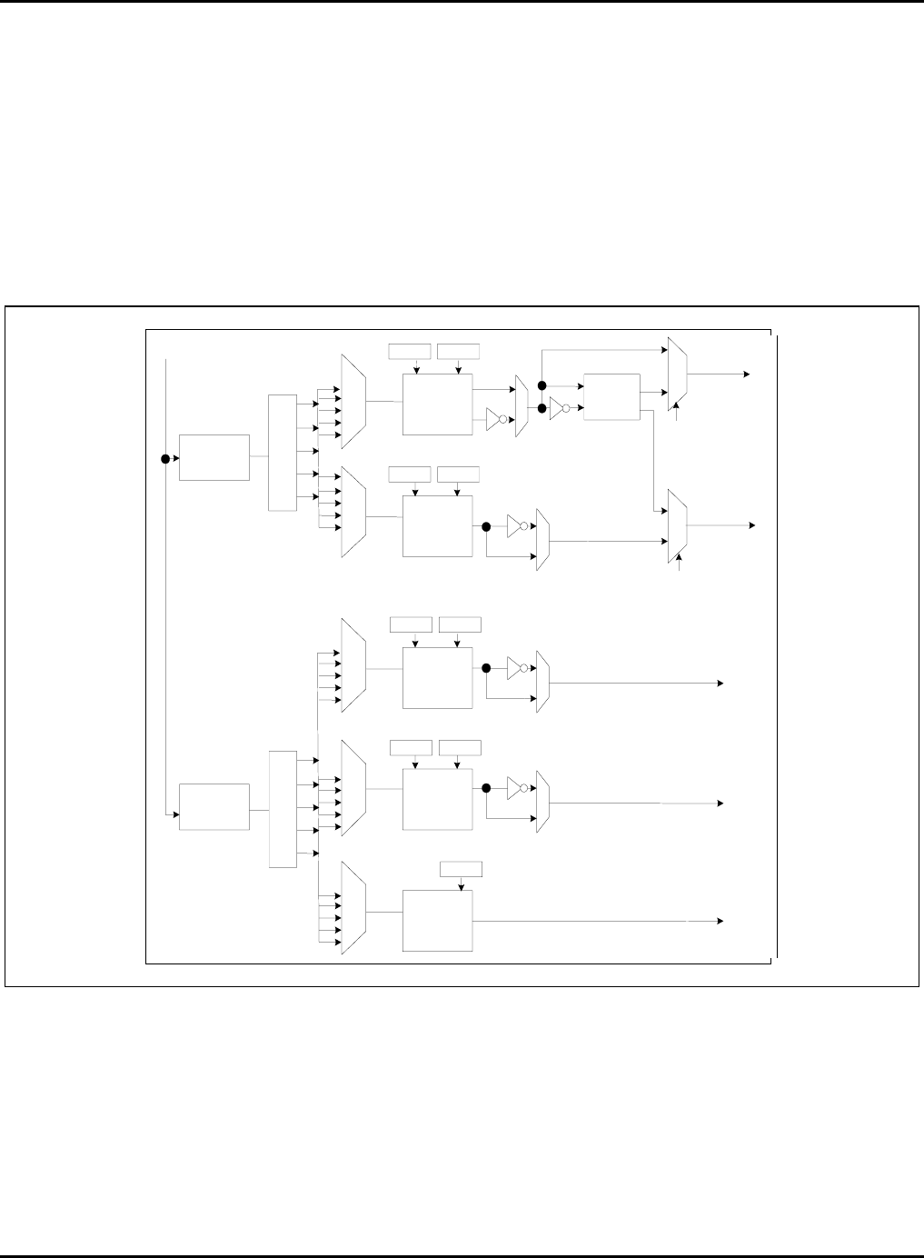
S5P6818_UM 20 Pulse Width Modulation (PWM) Timer
20-2
Initialize the TCNTBn register with 159 (50 + 109) and TCMPBn with 109.
Start Timer: Sets the start bit and manually updates this bit to OFF.
The TCNTBn value of 159 is loaded into the down-counter. Then, the output TOUTn is set to low. When down-
counter counts down the value from TCNTBn to value in the TCMPBn register 109, the output changes from low
to high.
When the down-counter reaches 0, it generates an interrupt request. The down-counter automatically reloads
TCNTBn. This restarts the cycle.
The figure below illustrates the clock generation scheme for individual PWM Channels:
6:1
MUX Control
Logic 0
Control
Logic 4
Control
Logic 3
Control
Logic 2
Control
Logic 1
8BIT
PRESCALER
0
DeadZone
Generator
TCNTB0TCMPB0
TCNTB1
TCMPB1
TCNTB2TCMPB2
TCNTB3TCMPB3
TCNTB4
8BIT
PRESCALER
1
6:1
MUX
6:1
MUX
6:1
MUX
6:1
MUX
PCLK XpwmTOUT0
No pin
DeadZone
1/1
1/2
1/16
1/8
1/4
1/1
1/2
1/16
1/8
1/4
DeadZone
XpwmTOUT1
XpwmTOUT3
XpwmTOUT2
Figure 20-2 PWM TIMER Clock Tree Diagram
The figure above shows the clock generation scheme for individual PWM Channels.
Each Timer can generate level interrupts.
nexell / ys.kim at 2015.02.12
SAMSUNG Confidential

S5P6818_UM 20 Pulse Width Modulation (PWM) Timer
20-3
20.2 Features
PWM supports these features:
Five 32-bit Timers.
Two 8-bit Clock Prescalers that provide first level of division for the PCLK, and five Clock Dividers and
Multiplexers that provide second level of division for the Prescaler clock.
Programmable Clock Select Logic for individual PWM Channels.
Four Independent PWM Channels with Programmable Duty Control and Polarity.
Static Configuration: PWM is stopped.
Dynamic Configuration: PWM is running.
Auto-Reload Mode and One-Shot Pulse Mode.
Dead Zone Generator on two PWM Outputs.
Level Interrupt Generation.
The PWM has two operation modes:
Auto-Reload Mode: In this mode, continuous PWM pulses are generated based on programmed duty cycle
and polarity.
One-Shot Pulse Mode: In this mode, only one PWM pulse is generated based on programmed duty cycle and
polarity.
To control the functionality of PWM, 18 special function registers are provided. The PWM is a programmable
output and a clock input AMBA slave module. It connects to the Advanced Peripheral Bus (APB). These 18
special function registers within PWM are accessed through APB transactions.
nexell / ys.kim at 2015.02.12
SAMSUNG Confidential

S5P6818_UM 20 Pulse Width Modulation (PWM) Timer
20-4
20.3 PWM Operation
20.3.1 Prescaler & Divider
An 8-bit prescaler and 3-bit divider generates these output frequencies. The following table lists the minimum and
maximum resolution based on Prescaler and Clock Divider values:
Table 20-1 Min. and Max. Resolution based on Prescaler and Clock Divider Values
4-bit Divider Settings
Minimum Resolution
(Prescaler = 1)
Maximum Resolution
(Prescaler = 255)
Maximum Interval
(TCNTBn = 4294967295)
1/1 (PCLK = 66 MHz)
0.030us (33.0 MHz)
3.87us (258 kHz)
16659.27s
1/2 (PCLK = 66 MHz)
0.061us (16.5 MHz)
7.75us (129 kHz)
33318.53s
1/4 (PCLK = 66 MHz)
0.121us (8.25 MHz)
15.5us (64.5 kHz)
66637.07s
1/8 (PCLK = 66 MHz)
0.242us (4.13 MHz)
31.0us (32.2 kHz)
133274.14s
1/16 (PCLK = 66 MHz)
0.485us (2.06 MHz)
62.1us (16.1 kHz)
266548.27s
nexell / ys.kim at 2015.02.12
SAMSUNG Confidential
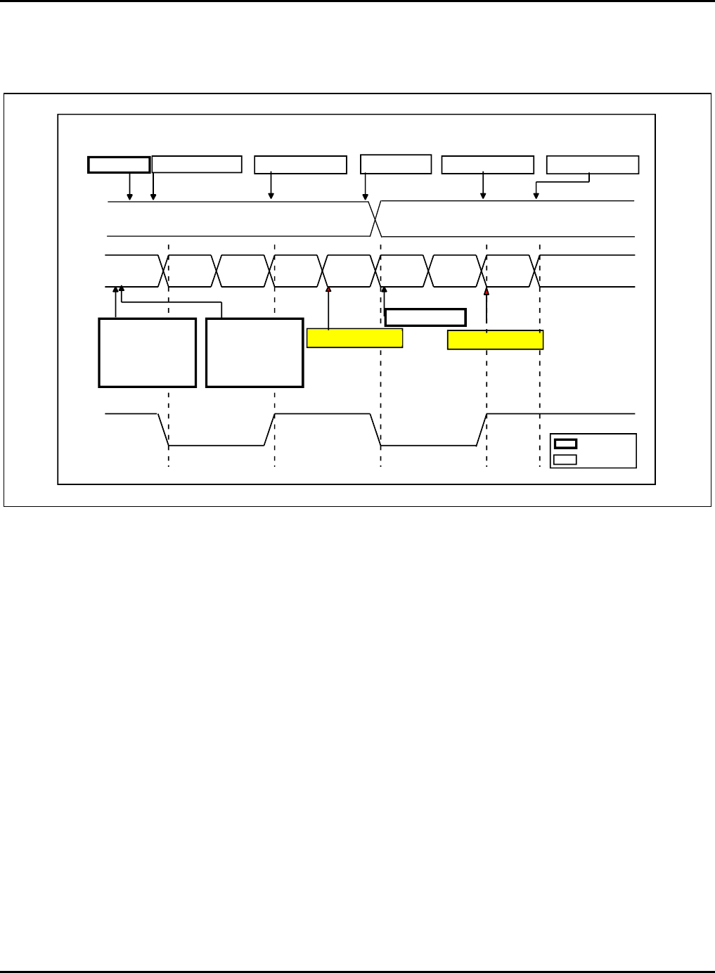
S5P6818_UM 20 Pulse Width Modulation (PWM) Timer
20-5
20.3.2 Basic Timer Operation
The figure below illustrates the Basic Timer Operation:
Figure 20-3 Timer Operations
The Timer (except Timer channel 4) comprises of four registers: TCNTBn, TCNTn, TCMPBn and TCMPn. When
the Timer reaches 0, the TCNTBn and TCMPBn registers are loaded into TCNTn and TCMPn. When TCNTn
reaches 0, the interrupt request occurs if the interrupt is enabled. TCNTn and TCMPn are the names of the
internal registers. The TCNTn register is read from the TCNTOn register.
3
3
2
0
1
1
0
2
1
0
0
TCNTBn=2
TCMPBn=0
manual update=0
auto-reload=1
interrupt request
interrupt request
TCNTBn=3
TCMPBn=1
manual update=1
auto-reload=1
TOUTn
TCMPn
TCNTn
auto-reload=0
command
status
timer is started
TCNTn=TCMPn
auto-reload
s
tart bit=1
TCNTn=TCMPn
timer is stopped.
nexell / ys.kim at 2015.02.12
SAMSUNG Confidential

S5P6818_UM 20 Pulse Width Modulation (PWM) Timer
20-6
To generate interrupt at intervals three-cycle of TOUTn, set TCNTBn, TCMPBn and TCON.
Steps to generate interrupt:
1. Set TCNTBn = 3 and TCMPBn = 1.
2. Set auto-reload = 1 and manual update = 1.
When manual update bit is 1, the TCNTBn and TCMPBn values are loaded to TCNTn and TCMPn.
3. Set TCNTBn = 2 and TCMPBn = 0 for the next operation.
4. Set auto-reload = 1 and manual update = 0.
If you set manual update = 1, TCNTn is changed to 2 and TCMP is changed to 0.
Therefore, interrupt is generated at interval two-cycle instead of three-cycle.
Set auto-reload = 1 automatically, for the next operation.
5. Set start = 1 for starting the operation. Then, TCNTn is down counting.
When TCNTn is 0, interrupt is generated and if auto-reload is enable, TCNTn is loaded 2 (TCNTBn value)
and TCMPn is loaded 0 (TCMPn value).
6. TCNTn is down counting before it stops.
nexell / ys.kim at 2015.02.12
SAMSUNG Confidential
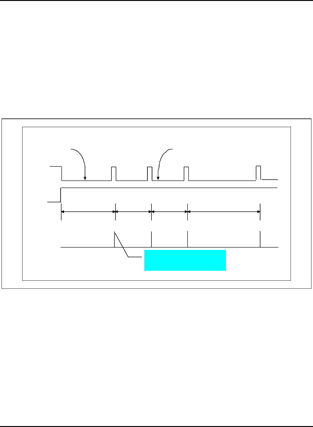
S5P6818_UM 20 Pulse Width Modulation (PWM) Timer
20-7
20.3.3 Auto-Reload and Double Buffering
The PWM Timers includes a double buffering feature, which changes the reload value for the next Timer operation
without stopping the current Timer operation.
The Timer value is written into TCNTBn (Timer Count Buffer register) and the current counter value of the Timer is
read from TCNTOn (Timer Count Observation register). If TCNTBn is Read, the Read value does not reflect the
current state of the counter. It reflects the reload value for the next Timer duration.
Auto-reload copies the TCNTBn into TCNTn, when TCNTn reaches 0. The value written to TCNTBn, is loaded to
TCNTn when the TCNTn reaches 0 and auto-reload is enabled. When the TCNTn is 0 and the auto-reload bit is 0,
the TCNTn does not operate further.
The figure below illustrates an example of Double-Buffering:
Figure 20-4 Example of Double Buffering Feature
Write
TCNTBn=100 Write
TCNTBn=200
Start
auto_reload
TCNTBn=150
150 200100100
interrupt
If TCNT is 0, interrupt signal is
generated and then load the next
TCNTB
nexell / ys.kim at 2015.02.12
SAMSUNG Confidential
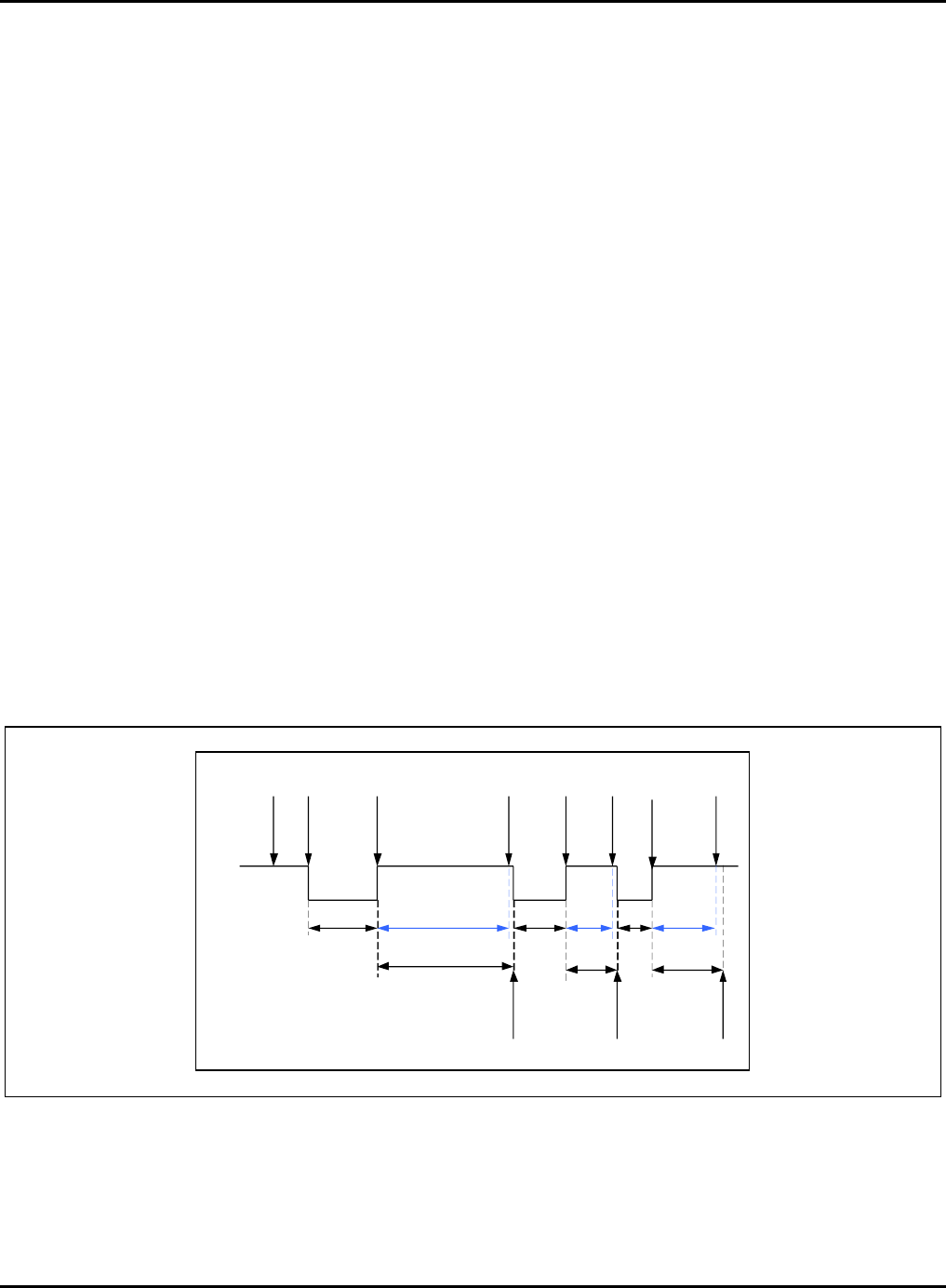
S5P6818_UM 20 Pulse Width Modulation (PWM) Timer
20-8
20.3.4 Timer Operation
Steps in Timer Operation:
1. Enable the Auto-reload feature. Set the TCNTBn as 159 (50+109) and TCMPBn as 109. Set the manual
update bit On and set the manual update bit Off. Set the inverter On/Off bit. The manual update bit sets
TCNTn and TCMPn to the value of TCNTBn and TCMPBn.
2. Set TCNTBn and TCMPBn as 79 (40 + 39) and 39, respectively.
3. Start Timer: Set the start bit in TCON.
4. When TCNTn and TCMPn have the same value, the logic level of TOUTn is changed from low to high.
5. When TCNTn reaches 0, it generates interrupt request.
6. TCNTn and TCMPn are automatically reloaded with TCNTBn and TCMPBn as (79 (40 + 39)) and 39,
respectively. In the Interrupt Service Routine (ISR), the TCNTBn and TCMPBn are set as 79 (20 + 59) and 59,
respectively.
7. When TCNTn and TCMPn have the same value, the logic level of TOUTn is changed from low to high.
8. When TCNTn reaches 0, it generates interrupt request.
9. TCNTn and TCMPn are automatically reloaded with TCNTBn and TCMPBn as (79 (20 + 59)) and 59,
respectively. The Auto-reload and interrupt request are disabled to stop the Timer in the ISR.
10. When TCNTn and TCMPn have the same value, the logic level of TOUTn is changed from low to high.
11. Even if TCNTn reaches 0, no interrupt request is generated.
12. TCNTn is not reloaded and the Timer is stopped because Auto-reload is disabled.
Figure 20-5 Example of Timer Operation
TOUTn
1 2 3 4
5
6 7
8
910
50 109
110
40 39
40
20
60
59
11
nexell / ys.kim at 2015.02.12
SAMSUNG Confidential
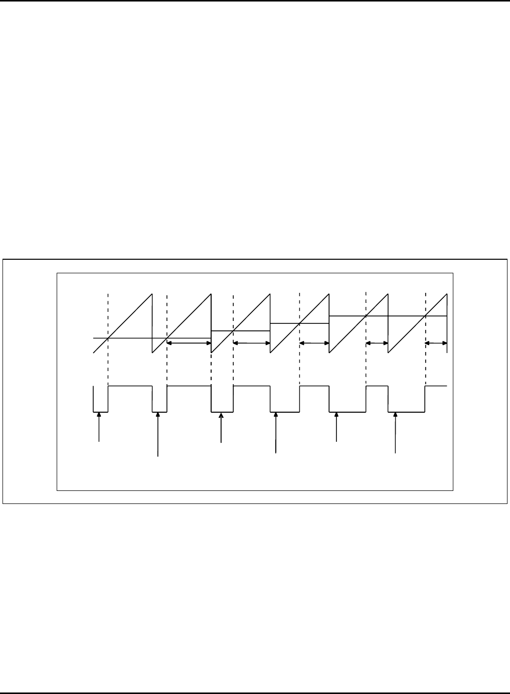
S5P6818_UM 20 Pulse Width Modulation (PWM) Timer
20-9
20.3.5 Initialize Timer (Setting Manual-Up Data and Inverter)
User must define the starting value of the TCNTn, because an Auto-reload operation of the Timer occurs when the
down counter reaches 0. In this case, the starting value must be loaded by manual update bit.
The sequence to start a Timer is:
1. Write the initial value into TCNTBn and TCMPBn.
2. Set the manual update bit and clear only manual update bit of the corresponding Timer.
NOTE: It is recommended to set the inverter On/Off bit (whether inverter is used or not).
3. Set the start bit of the corresponding Timer to start the Timer.
PWM (Pulse Width Modulation)
The figure below illustrates an example of PWM:
Figure 20-6 PWM
Use TCMPBn to implement the Pulse Width Modulation (PWM) feature. PWM frequency is determined by
TCNTBn. A PWM value is determined by TCMPBn as shown in the figure above.
For a higher PWM value, decrease the TCMPBn value. For a lower PWM value, increase the TCMPBn value.
When the output inverter is enabled, the increment/decrement can be reverse.
Due to the Double Buffering feature, TCMPBn, for a next PWM cycle is written by ISR at any point of current PWM
cycle.
Write TCMPBn=60
Write TCMPBn=50
Write TCMPBn=40
Write TCMPBn=30
Write TCMPBn=30
Write TCMPBn
= next PWM
60 50 40 30 30
nexell / ys.kim at 2015.02.12
SAMSUNG Confidential

S5P6818_UM 20 Pulse Width Modulation (PWM) Timer
20-10
Figure 20-7 Inverter On/Off
Steps to maintain TOUT as high or low (assume that inverter is off):
Turn-off the Auto-reload bit. The TOUTn goes to high level and the Timer is stopped after TCNTn reaches 0.
This method is recommended.
Stop the timer by clearing the timer start/stop bit to 0. When TCNTn <= TCMPn, the output level is high.
When TCNTn > TCMPn, the output level is low.
TOUTn is inverted by the inverter on/off bit in TCON. The inverter removes the additional circuit to adjust the
output level.
Initial State
Inverter off
Inverter on
Timer stopPeriod 2Period 1
nexell / ys.kim at 2015.02.12
SAMSUNG Confidential
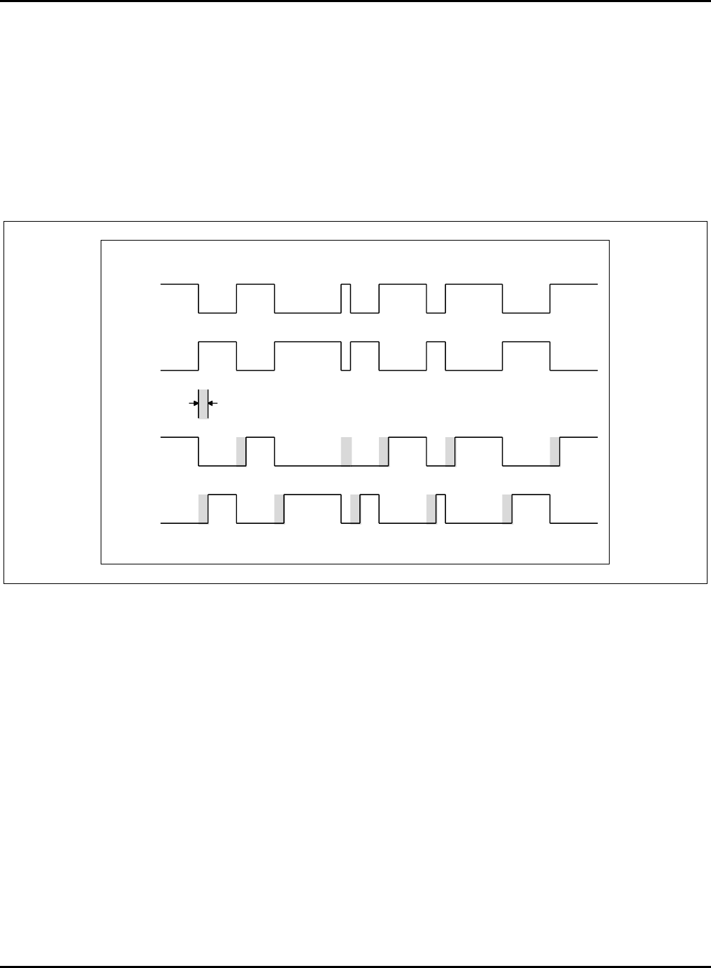
S5P6818_UM 20 Pulse Width Modulation (PWM) Timer
20-11
20.3.6 Dead Zone Generator
This feature inserts the time gap between a Turn-off and Turn-on of two different switching devices. This time gap
prohibits the two switching device turning on simultaneously, even for a very short time.
TOUT_0 specifies the PWM output. nTOUT_0 specifies the inversion of the TOUT_0. When the dead-zone is
enabled, the output wave-form of TOUT_0 and nTOUT_0 is TOUT_0_DZ and nTOUT_0_DZ, respectively.
TOUT0_DZ and nTOUT_0_DZ cannot be turned on simultaneously by the dead zone interval. For functional
correctness, the dead zone length must be set smaller than compare counter value.
The figure below illustrates the waveform when a dead zone feature is enabled:
Figure 20-8 Waveform when a Dead Zone Feature is Enabled
TOUT0
nTOUT0
DEADZONE
INTERVAL
TOUT0_DZ
nTOUT0_DZ
nexell / ys.kim at 2015.02.12
SAMSUNG Confidential

S5P6818_UM 20 Pulse Width Modulation (PWM) Timer
20-12
20.4 Register Description
20.4.1 Register Map Summary
Base Address: 0xC001_7000h (TIMER)
Base Address: 0xC001_8000h (PWM)
Register
Offset
Description
Reset Value
TCFG0
0x00h
Clock-Prescalar and Dead-Zone configurations
0x0000_0101
TCFG1
0x04h
Clock multiplexers and DMA mode select
0x0000_0000
TCON
0x08h
Timer control register
0x0000_0000
TCNTB0
0x0Ch
Timer 0 count buffer register
0x0000_0000
TCMPB0
0x10h
Timer 0 compare buffer register
0x0000_0000
TCNTO0
0x14h
Timer 0 count observation register
0x0000_0000
TCNTB1
0x18h
Timer 1 count buffer register
0x0000_0000
TCMPB1
0x1Ch
Timer 1 compare buffer register
0x0000_0000
TCNTO1
0x20h
Timer 1 count observation register
0x0000_0000
TCNTB2
0x24h
Timer 2 count buffer register
0x0000_0000
TCMPB2
0x28h
Timer 2 compare buffer register
0x0000_0000
TCNTO2
0x2Ch
Timer 2 count observation register
0x0000_0000
TCNTB3
0x30h
Timer 3 count buffer register
0x0000_0000
TCMPB3
0x34h
Timer 3 compare buffer register
0x0000_0000
TCNTO3
0x38h
Timer 3 count observation register
0x0000_0000
TCNTB4
0x3Ch
Timer 4 count buffer register
0x0000_0000
TCNTO4
0x40h
Timer 4 count observation register
0x0000_0000
TINT_CSTAT
0x44h
Timer interrupt control and status register
0x0000_0000
nexell / ys.kim at 2015.02.12
SAMSUNG Confidential

S5P6818_UM 20 Pulse Width Modulation (PWM) Timer
20-13
20.4.1.1 TCFG0
Base Address: 0xC001_7000h (TIMER)
Base Address: 0xC001_8000h (PWM)
Address = Base Address + 0x00h, Reset Value = 0x0000_0101
Name
Bit
Type
Description
Reset Value
RSVD
[31:24]
–
Reserved
–
DEAD ZONE LENGTH
[23:16]
RW
Dead zone length
8'h0
PRESCALER 1
[15:8]
RW
Prescaler 1 value for Timer 2, 3 and 4
8'h1
PRESCALER 0
[7:0]
RW
Prescaler 0 value for timer 0 & 1
8'h1
Timer Input Clock Frequency = PCLK/({prescaler value + 1})/{divider value}
{prescaler value} = 1 to 255
{divider value} = 1, 2, 4, 8, 16
Dead Zone Length = 0 to 254
NOTE: If Dead Zone Length is set as "n", Real Dead Zone Length is "n + 1" (n = 0 to 254). Source clock of PCLK is
BUS_DPLL in BLK_MIF
nexell / ys.kim at 2015.02.12
SAMSUNG Confidential

S5P6818_UM 20 Pulse Width Modulation (PWM) Timer
20-14
20.4.1.2 TCFG1
Base Address: 0xC001_7000h (TIMER)
Base Address: 0xC001_8000h (PWM)
Address = Base Address + 0x04h, Reset Value = 0x0000_0000
Name
Bit
Type
Description
Reset Value
RSVD
[31:24]
–
Reserved
–
DMA MODE
[23:20]
RW
Select DMA Request Channel Select Bit
0000 = No select
0001 = INT0
0010 = INT1
0011 = INT2
0100 = INT3
0101 = INT4
0110 = No select
0111 = No select
4'h0
DIVIDER MUX4
[19:16]
RW
Select Mux input for PWM Timer 4
0000 = 1/1
0001 = 1/2
0010 = 1/4
0011 = 1/8
0100 = 1/16
0101 = External TCLK1
0110 = External TCLK1
0111 = External TCLK1
4'h0
DIVIDER MUX3
[15:12]
RW
Select Mux input for PWM Timer 3
0000 = 1/1
0001 = 1/2
0010 = 1/4
0011 = 1/8
0100 = 1/16
0101 = External TCLK1
0110 = External TCLK1
0111 = External TCLK1
4'h0
DIVIDER MUX2
[11:8]
RW
Select Mux input for PWM Timer 2
0000 = 1/1
0001 = 1/2
0010 = 1/4
0011 = 1/8
0100 = 1/16
0101 = External TCLK1
0110 = External TCLK1
0111 = External TCLK1
4'h0
DIVIDER MUX1
[7:4]
RW
Select Mux input for PWM Timer 1
0000 = 1/1
0001 = 1/2
0010 = 1/4
0011 = 1/8
0100 = 1/16
4'h0
nexell / ys.kim at 2015.02.12
SAMSUNG Confidential

S5P6818_UM 20 Pulse Width Modulation (PWM) Timer
20-15
Name
Bit
Type
Description
Reset Value
0101 = External TCLK1
0110 = External TCLK1
0111 = External TCLK1
DIVIDER MUX0
[3:0]
RW
Select Mux input for PWM Timer 0
0000 = 1/1
0001 = 1/2
0010 = 1/4
0011 = 1/8
0100 = 1/16
0101 = External TCLK1
0110 = External TCLK1
0111 = External TCLK1
4'h0
nexell / ys.kim at 2015.02.12
SAMSUNG Confidential

S5P6818_UM 20 Pulse Width Modulation (PWM) Timer
20-16
20.4.1.3 TCON
Base Address: 0xC001_7000h (TIMER)
Base Address: 0xC001_8000h (PWM)
Address = Base Address + 0x08h, Reset Value = 0x0000_0000
Name
Bit
Type
Description
Reset Value
RSVD
[31:23]
–
Reserved
–
TIMER 4 AUTO RELOAD
ON/OFF
[22]
RW
0 = One-Shot
1 = Interval Mode (Auto-Reload)
1'b0
TIMER 4 MANUAL
UPDATE
[21]
RW
0 = No Operation
1 = Update TCNTB4
1'b0
TIMER 4 START/STOP
[20]
RW
0 = Stop
1 = Start Timer 4
1'b0
TIMER 3 AUTO RELOAD
ON/OFF
[19]
RW
0 = One-Shot
1 = Interval Mode (Auto-Reload)
1'b0
TIMER 3 OUTPUT
INVERTER ON/OFF
[18]
RW
0 = Inverter Off
1 = TOUT3 Inverter-On
1'b0
TIMER 3 MANUAL
UPDATE
[17]
RW
0 = No Operation
1 = Update TCNTB3,TCMPB3
1'b0
TIMER 3 START/STOP
[16]
RW
0 = Stop
1 = Start Timer 3
1'b0
TIMER 2 AUTO RELOAD
ON/OFF
[15]
RW
0 = One-Shot
1 = Interval Mode (Auto-Reload)
1'b0
TIMER 2 OUTPUT
INVERTER ON/OFF
[14]
RW
0 = Inverter Off
1 = TOUT2 Inverter-On
1'b0
TIMER 2 MANUAL
UPDATE
[13]
RW
0 = No Operation
1 = Update TCNTB2,TCMPB2
1'b0
TIMER 2 START/STOP
[12]
RW
0 = Stop
1 = Start Timer 2
1'b0
TIMER 1 AUTO RELOAD
ON/OFF
[11]
RW
0 = One-Shot
1 = Interval Mode (Auto-Reload)
1'b0
TIMER 1 OUTPUT
INVERTER ON/OFF
[10]
RW
0 = Inverter Off
1 = TOUT1 Inverter-On
1'b0
TIMER 1 MANUAL
UPDATE
[9]
RW
0 = No Operation
1 = Update TCNTB1,TCMPB1
1'b0
TIMER 1 START/STOP
[8]
RW
0 = Stop
1 = Start Timer 1
1'b0
RSVD
[7:5]
–
Reserved
-
DEAD ZONE
ENABLE/DISABLE
[4]
RW
Dead zone Generator Enable/Disable
1'b0
TIMER 0 AUTO RELOAD
ON/OFF
[3]
RW
0 = One-Shot
1 = Interval Mode (Auto-Reload)
1'b0
TIMER 0 OUTPUT
INVERTER ON/OFF
[2]
RW
0 = Inverter Off
1 = TOUT0 Inverter-On
1'b0
nexell / ys.kim at 2015.02.12
SAMSUNG Confidential
S5P6818_UM 20 Pulse Width Modulation (PWM) Timer
20-17
Name
Bit
Type
Description
Reset Value
TIMER 0 MANUAL
UPDATE
[1]
RW
0 = No Operation
1 = Update TCNTB0,TCMPB0
1'b0
TIMER 0 START/STOP
[0]
RW
0 = Stop
1 = Start Timer 0
1'b0
20.4.1.4 TCNTB0
Base Address: 0xC001_7000h (TIMER)
Base Address: 0xC001_8000h (PWM)
Address = Base Address + 0x0Ch, Reset Value = 0x0000_0000
Name
Bit
Type
Description
Reset Value
TIMER 0 COUNT
BUFFER
[31:0]
RW
Timer 0 Count Buffer Register
32'h0
20.4.1.5 TCMPB0
Base Address: 0xC001_7000h (TIMER)
Base Address: 0xC001_8000h (PWM)
Address = Base Address + 0x10h, Reset Value = 0x0000_0000
Name
Bit
Type
Description
Reset Value
TIMER 0 COMPARE
BUFFER
[31:0]
RW
Timer 0 Compare Buffer Register
32'h0
nexell / ys.kim at 2015.02.12
SAMSUNG Confidential

S5P6818_UM 20 Pulse Width Modulation (PWM) Timer
20-18
20.4.1.6 TCNTO0
Base Address: 0xC001_7000h (TIMER)
Base Address: 0xC001_8000h (PWM)
Address = Base Address + 0x14h, Reset Value = 0x0000_0000
Name
Bit
Type
Description
Reset Value
TIMER 0 COUNT
OBSERVATION
[31:0]
R
Timer 0 Count Observation Register
32'h0
20.4.1.7 TCNTB1
Base Address: 0xC001_7000h (TIMER)
Base Address: 0xC001_8000h (PWM)
Address = Base Address + 0x18h, Reset Value = 0x0000_0000
Name
Bit
Type
Description
Reset Value
TIMER 1 COUNT
BUFFER
[31:0]
RW
Timer 1 Count Buffer Register
32'h0
20.4.1.8 TCMPB1
Base Address: 0xC001_7000h (TIMER)
Base Address: 0xC001_8000h (PWM)
Address = Base Address + 0x1Ch, Reset Value = 0x0000_0000
Name
Bit
Type
Description
Reset Value
TIMER 1 COMPARE
BUFFER
[31:0]
RW
Timer 1 Compare Buffer Register
32'h0
20.4.1.9 TCNTO1
Base Address: 0xC001_7000h (TIMER)
Base Address: 0xC001_8000h (PWM)
Address = Base Address + 0x20h, Reset Value = 0x0000_0000
Name
Bit
Type
Description
Reset Value
TIMER 1 COUNT
OBSERVATION
[31:0]
R
Timer 1 Count Observation Register
32'h0
nexell / ys.kim at 2015.02.12
SAMSUNG Confidential

S5P6818_UM 20 Pulse Width Modulation (PWM) Timer
20-19
20.4.1.10 TCNTB2
Base Address: 0xC001_7000h (TIMER)
Base Address: 0xC001_8000h (PWM)
Address = Base Address + 0x24h, Reset Value = 0x0000_0000
Name
Bit
Type
Description
Reset Value
TIMER 2 COUNT
BUFFER
[31:0]
RW
Timer 2 Count Buffer Register
32'h0
20.4.1.11 TCMPB2
Base Address: 0xC001_7000h (TIMER)
Base Address: 0xC001_8000h (PWM)
Address = Base Address + 0x28h, Reset Value = 0x0000_0000
Name
Bit
Type
Description
Reset Value
TIMER 2 COMPARE
BUFFER
[31:0]
RW
Timer 2 Compare Buffer Register
32'h0
20.4.1.12 TCNTO2
Base Address: 0xC001_7000h (TIMER)
Base Address: 0xC001_8000h (PWM)
Address = Base Address + 0x2Ch, Reset Value = 0x0000_0000
Name
Bit
Type
Description
Reset Value
TIMER 2 COUNT
OBSERVATION
[31:0]
R
Timer 2 Count Observation Register
32'h0
20.4.1.13 TCNTB3
Base Address: 0xC001_7000h (TIMER)
Base Address: 0xC001_8000h (PWM)
Address = Base Address + 0x30h, Reset Value = 0x0000_0000
Name
Bit
Type
Description
Reset Value
TIMER 3 COUNT
BUFFER
[31:0]
RW
Timer 3 Count Buffer Register
32'h0
nexell / ys.kim at 2015.02.12
SAMSUNG Confidential
S5P6818_UM 20 Pulse Width Modulation (PWM) Timer
20-20
20.4.1.14 TCMPB3
Base Address: 0xC001_7000h (TIMER)
Base Address: 0xC001_8000h (PWM)
Address = Base Address + 0x34h, Reset Value = 0x0000_0000
Name
Bit
Type
Description
Reset Value
TIMER 3 COMPARE
BUFFER
[31:0]
RW
Timer 3 Compare Buffer Register
32'h0
20.4.1.15 TCNTO3
Base Address: 0xC001_7000h (TIMER)
Base Address: 0xC001_8000h (PWM)
Address = Base Address + 0x38h, Reset Value = 0x0000_0000
Name
Bit
Type
Description
Reset Value
TIMER 3 COUNT
OBSERVATION
[31:0]
R
Timer 3 Count Observation Register
32'h0
20.4.1.16 TCNTB4
Base Address: 0xC001_7000h (TIMER)
Base Address: 0xC001_8000h (PWM)
Address = Base Address + 0x3Ch, Reset Value = 0x0000_0000
Name
Bit
Type
Description
Reset Value
TIMER 4 COUNT
BUFFER
[31:0]
RW
Timer 4 Count Buffer Register
32'h0
20.4.1.17 TCNTO4
Base Address: 0xC001_7000h (TIMER)
Base Address: 0xC001_8000h (PWM)
Address = Base Address + 0x40h, Reset Value = 0x0000_0000
Name
Bit
Type
Description
Reset Value
TIMER 4 COUNT
OBSERVATION
[31:0]
R
Timer 4 Count Observation Register
32'h0
nexell / ys.kim at 2015.02.12
SAMSUNG Confidential

S5P6818_UM 20 Pulse Width Modulation (PWM) Timer
20-21
20.4.1.18 TINT_CSTAT
Base Address: 0xC001_7000h (TIMER)
Base Address: 0xC001_8000h (PWM)
Address = Base Address + 0x44h, Reset Value = 0x0000_0000
Name
Bit
Type
Description
Reset Value
RSVD
[31:10]
–
Reserved
–
TIMER 4 INTERRUPT
STATUS
[9]
RW
Timer 4 Interrupt Status Bit. Clears by writing "1" on
this bit.
1'b0
TIMER 3 INTERRUPT
STATUS
[8]
RW
Timer 3 Interrupt Status Bit. Clears by writing "1" on
this bit.
1'b0
TIMER 2 INTERRUPT
STATUS
[7]
RW
Timer 2 Interrupt Status Bit. Clears by writing "1" on
this bit.
1'b0
TIMER 1 INTERRUPT
STATUS
[6]
RW
Timer 1 Interrupt Status Bit. Clears by writing "1" on
this bit.
1'b0
TIMER 0 INTERRUPT
STATUS
[5]
RW
Timer 0 Interrupt Status Bit. Clears by writing "1" on
this bit.
1'b0
TIMER 4 INTERRUPT
ENABLE
[4]
RW
Timer 4 Interrupt Enable.
0 = Disabled
1 = Enabled
1'b0
TIMER 3 INTERRUPT
ENABLE
[3]
RW
Timer 3 Interrupt Enable.
0 = Disabled
1 = Enabled
1'b0
TIMER 2 INTERRUPT
ENABLE
[2]
RW
Timer 2 Interrupt Enable.
0 = Disabled
1 = Enabled
1'b0
TIMER 1 INTERRUPT
ENABLE
[1]
RW
Timer 1 Interrupt Enable.
0 = Disabled
1 = Enabled
1'b0
TIMER 0 INTERRUPT
ENABLE
[0]
RW
Timer 0 Interrupt Enable.
0 = Disabled
1 = Enabled
1'b0
nexell / ys.kim at 2015.02.12
SAMSUNG Confidential

Samsung Confidential
S5P6818_UM 21 Analog Digital Converter (ADC)
21-1
Preliminary product information describes products that are in development, for which full characterization data and
associated errata are not yet available. Specifications and information herein are subject to change without notice.
21 Analog Digital Converter (ADC)
21.1 Overview
The ADC2802A is a 28 nm CMOS 1.8 V 12-bit analog-to-digital converter (ADC) with 8-ch analog input MUX and
level-shifters for low-voltage digital interface. It converts single-ended analog input signal to 12-bit digital output
codes at a maximum conversion rate of 1MSPS.
The device is a cyclic type monolithic ADC, which provides an on-chip sample-and-hold and power down mode.
21.2 Features
28 nm Low Power CMOS Process
Resolution: 12-bit
Maximum Conversion rate (Fs)
1 MSPS (main clock: 6 MHz/sampling clock: 1 MHz)
Power consumption:
1.0 mW (Fs = 1 MSPS) @ Normal operation mode Typ.
0.005 mW @ Power down mode Typ.
Input range: 0 to AVDD18 (Normally 1.8 V)
Input frequency: DC to 100 kHz(@Fs = 1 MSPS)
Operation temperature range (ambient): –25 °C to 8 5°C
nexell / ys.kim at 2015.02.12
SAMSUNG Confidential
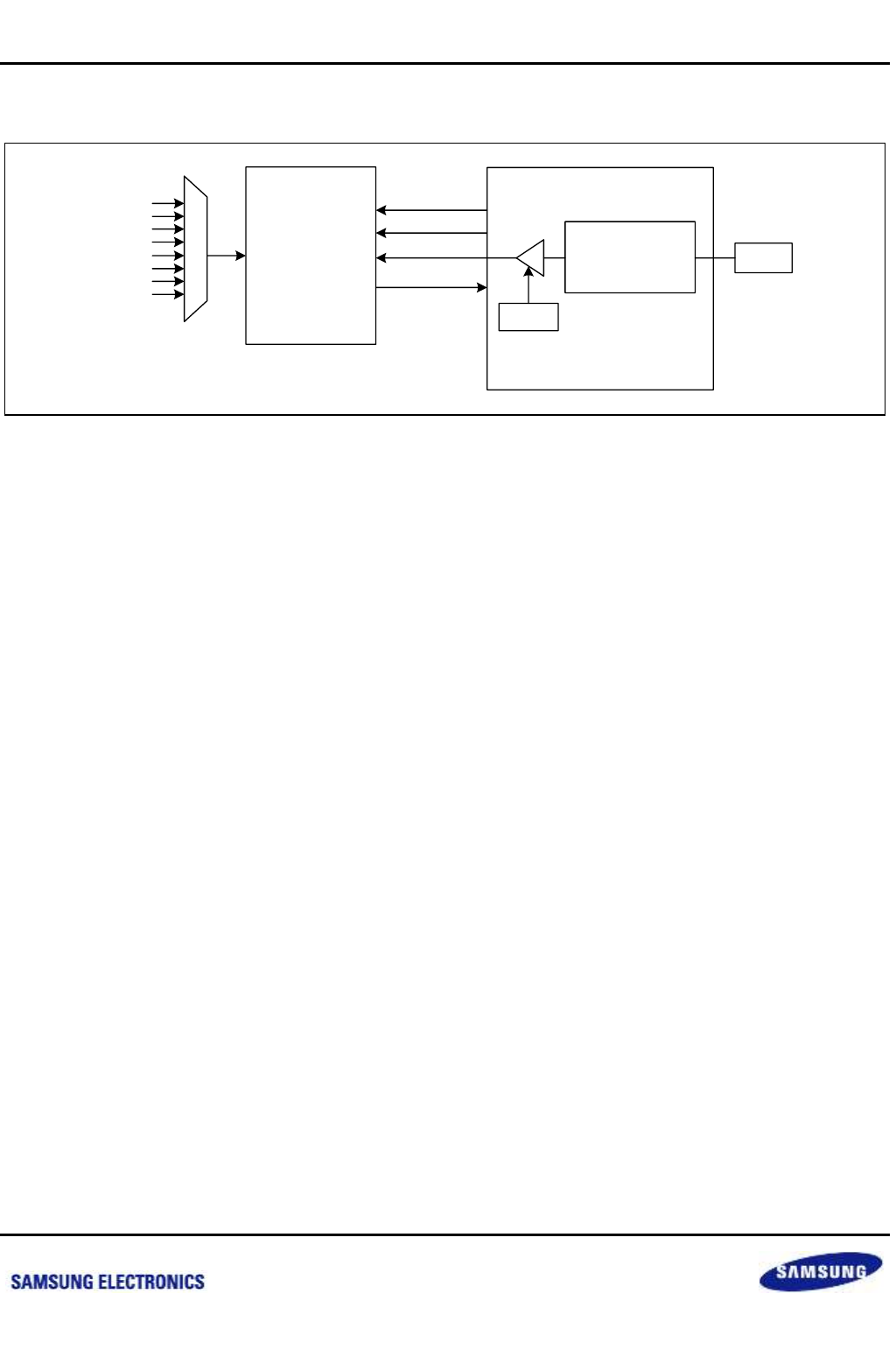
Samsung Confidential
S5P6818_UM 21 Analog Digital Converter (ADC)
21-2
Preliminary product information describes products that are in development, for which full characterization data and
associated errata are not yet available. Specifications and information herein are subject to change without notice.
21.3 Block Diagram
Figure 21-1 ADC Block Diagram
A/D Converter Prescaler
(PCLK / APSV)
APEN
PCLK
ADC IN0
ADC IN1
ADC IN2
ADC IN3
ADC IN4
ADC IN5
ADC IN6
ADC IN7
CLKIN
A/D Controller
ATBY
ADEN
ADCDAT
nexell / ys.kim at 2015.02.12
SAMSUNG Confidential
Samsung Confidential
S5P6818_UM 21 Analog Digital Converter (ADC)
21-3
Preliminary product information describes products that are in development, for which full characterization data and
associated errata are not yet available. Specifications and information herein are subject to change without notice.
21.4 Functional Description
The S5P6818 can receive eight ADC inputs and select one of the ADC inputs by using ADCCON.ASEL[2:0]. The
sizes of the eight ADC inputs depend on the size of VREF.
The ADC controller uses PCLK and the PCLK is divided in the Prescaler and applied to the ADC. At this time, the
ADCCON.APEN bit is used for the application of CLKIN. Clock divide values by the Prescaler are available from
20 to 256. (Actually, since the register input value is [Clock Divide Value –1], smaller divide values make the
sampling more detailed. The clock divide value is determined by *ADCCON.APSV*bit.
If the ADC block continuously accepts after power is applied, it consumes current unnecessarily. In this case, it is
better to power down the A/D converter by using the ADCCON.STBY bit. The ADCCON.STBY bit determines the
power input for the ADC block. If the ADCCON.STBY bit is "0", the ADC block waits for ADC input after power on.
After that, if the ADCCON.ADEN bit is set as "1" to accept ADC input, the ADC operation is actually performed.
On the other hand, if the ADCCON.STBY bit is "1", the ADC block goes to power down status, that is, power is not
applied. This is called Standby mode. (In Standby mode, only about 20uA current is consumed.
If the ADC block is not used, set the ADCCON.STBY bit as "1" and power off the ADC block. In this way,
unnecessary power consumption by the ADC block can be reduced. In addition, since the supply of the clock can
be determined by using the ADCCON.APEN bit, power consumption can be reduced further by stopping the clock
supply when supply is unnecessary.
21.4.1 I/O Chart
Table 21-1 I/O Chart
Index
ADC Input (V)
Digital Output
0
~ 1 LSB
0000_0000_0000
1LSB = (VREF – AGND)/4096
≒ 0.43945 mV
VREF = 1.8 V (Typ.)
AGND = 0.0 V (Typ.)
1
1 LSB ~ 2 LSB
0000_0000_0001
2
2 LSB ~ 3 LSB
0000_0000_0010
~
~
~
2047
2047 LSB ~ 2048 LSB
0111_1111_1111
2048
2048 LSB ~ 2049 LSB
1000_0000_0000
2049
2049 LSB ~ 2050 LSB
1000_0000_0001
~
~
~
4093
4093 LSB ~ 4094 LSB
1111_1111_1101
4094
4094 LSB ~ 4095 LSB
1111_1111_1110
4095
4095 LSB ~ 4096 LSB
1111_1111_1111
nexell / ys.kim at 2015.02.12
SAMSUNG Confidential
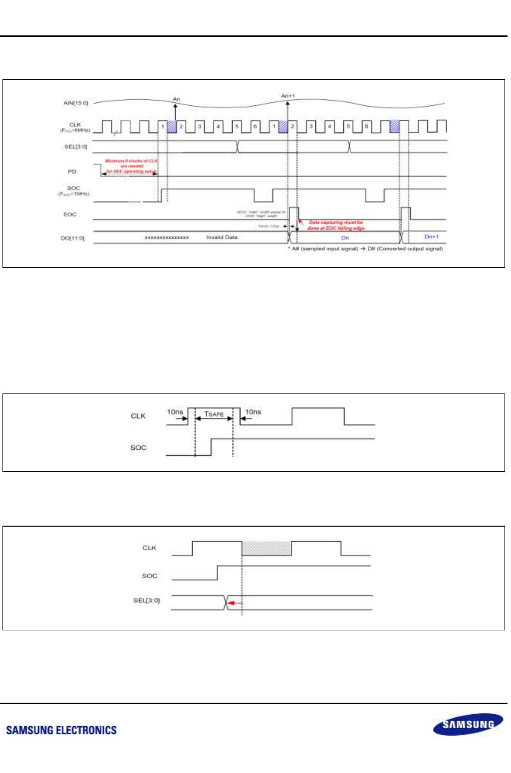
Samsung Confidential
S5P6818_UM 21 Analog Digital Converter (ADC)
21-4
Preliminary product information describes products that are in development, for which full characterization data and
associated errata are not yet available. Specifications and information herein are subject to change without notice.
21.4.2 Timing Diagram
Figure 21-2 Main Waveform
The figure above shows the timing chart for the ADC. AIN[7:0] is continuously input from the outside and CLKIN is
supplied via the ADCCON.APEN bit. After AIN[7:0] is selected, by using ASEL[2:0], the ADCCON.STBY bit is set
as "0" to supply power to the ADC block. Finally, A/D conversion is progressed by setting the ADCCON.ADEN bit
as "1".After the conversion is completed, EDO occurs and the ADCCON.ADEN bit is automatically cleared to
"0".After that, A/D Converted Data (D1) can be read through ADCDAT.ADCDAT. Since it always takes 5-cycles
for 10-bit conversion, the maximum conversion rate of the S5P6818 is 1MSPS.Set the ADCCON.ADEN bit as "1"
to operate the ADC again.
Figure 21-3 Main Waveform
The SOC signal should make a low-to-high transition during the "TSAFE" region of CLK (Above Figure).
Figure 21-4 Main Waveform
The transition of SEL[3:0] signals should be done before the dashed region (CLK's 1st "LOW" level after SOC
rising edge) in the above finger.
nexell / ys.kim at 2015.02.12
SAMSUNG Confidential
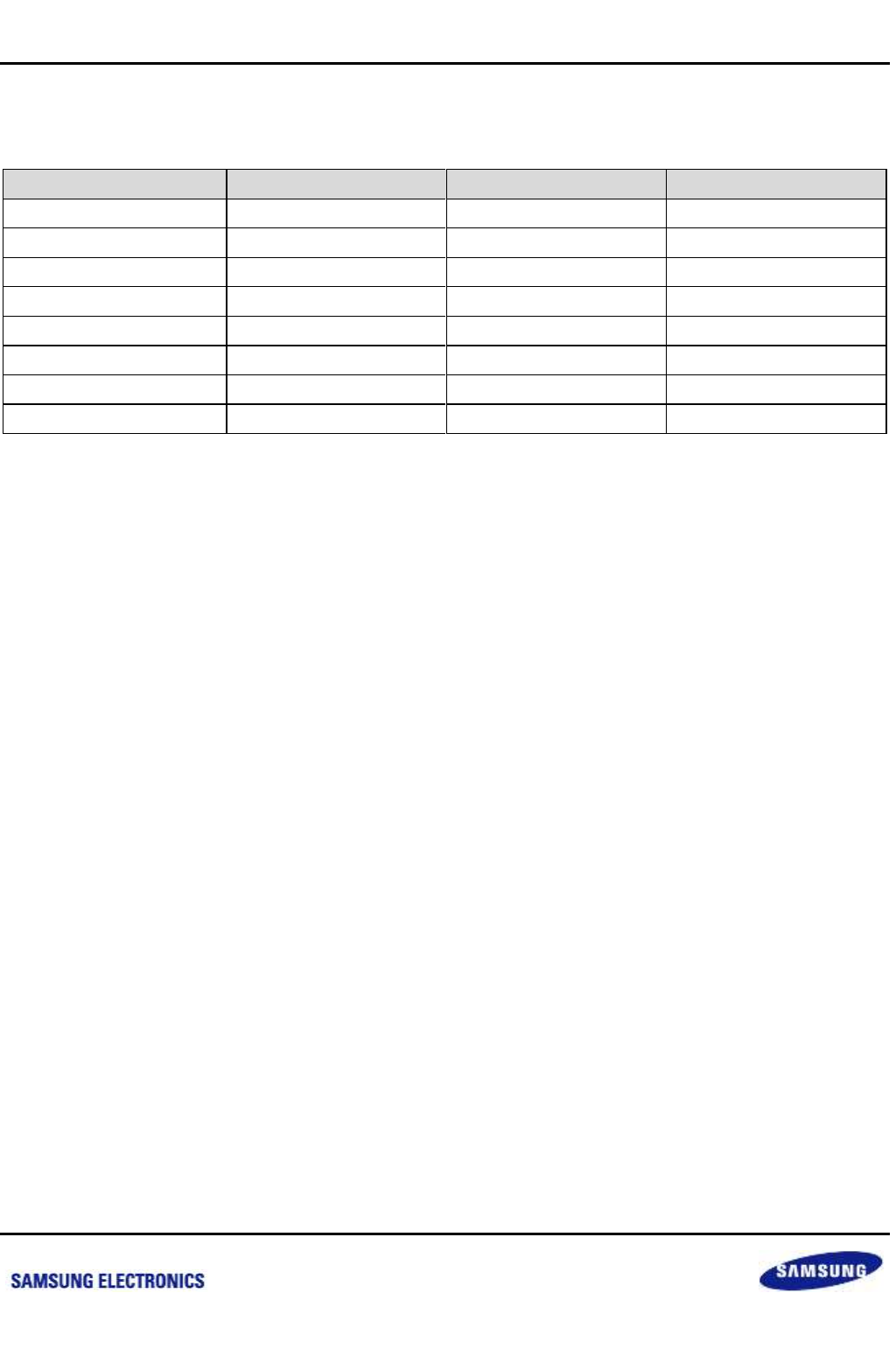
Samsung Confidential
S5P6818_UM 21 Analog Digital Converter (ADC)
21-5
Preliminary product information describes products that are in development, for which full characterization data and
associated errata are not yet available. Specifications and information herein are subject to change without notice.
21.4.3 Analog Input Selection Table
Table 21-2 Analog Input Selection Table
CHANNEL
ASEL[2]
ASEL[1]
ASEL[0]
Analog Input [0]
0
0
0
Analog Input [1]
0
0
1
Analog Input [2]
0
1
0
Analog Input [3]
0
1
1
Analog Input [4]
1
0
0
Analog Input [5]
1
0
1
Analog Input [6]
1
1
0
Analog Input [7]
1
1
1
21.4.4 Flowchart
PCLK Supply: CLKENB.PCLKMODE = 1
Analog Input Select: ADCCON.ASEL
ADC Power On: ADCCON.STBY = 0
CLKIN Divide Value: ADCCON.APSV
CLKIN On: ADCCON.APEN
ADC Enable: ADCCON.ADEN
A/D Conversion Process
Read ADCDAT.ADCDAT
CLKIN Off
ADC Power Off
nexell / ys.kim at 2015.02.12
SAMSUNG Confidential
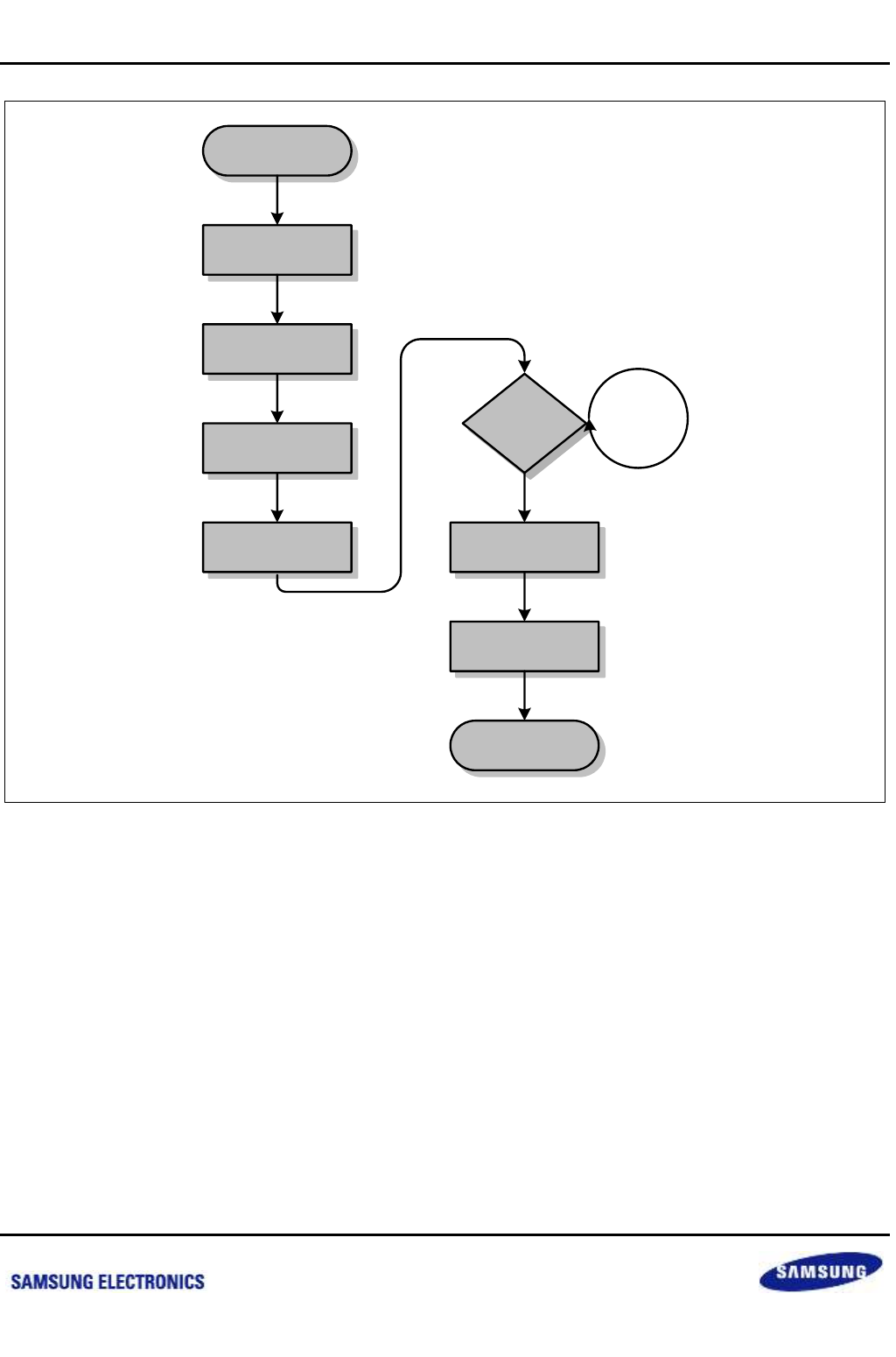
Samsung Confidential
S5P6818_UM 21 Analog Digital Converter (ADC)
21-6
Preliminary product information describes products that are in development, for which full characterization data and
associated errata are not yet available. Specifications and information herein are subject to change without notice.
Figure 21-5 ADC Sequence Flowchart
ASEL SET
APSV, APEN SET
ADEN SET
STBY SET
A/D Conversion
Read
ADCDAT[9:0]
STBY Clear
PCLK Enable
ADEN==0
NO
nexell / ys.kim at 2015.02.12
SAMSUNG Confidential

Samsung Confidential
S5P6818_UM 21 Analog Digital Converter (ADC)
21-7
Preliminary product information describes products that are in development, for which full characterization data and
associated errata are not yet available. Specifications and information herein are subject to change without notice.
21.5 Register Description
21.5.1 Register Map Summary
Base Address: 0xC005_3000h
Register
Offset
Description
Reset Value
ADCCON
3000h
ADC control register
0x0000_0004
ADCDAT
3004h
ADC output data register
0x0000_0000
ADCINTENB
3008h
ADC interrupt enable register
0x0000_0000
ADCINTCLR
300Ch
ADC interrupt pending and clear register
0x0000_0000
PRESCALERCON
3010h
ADC prescaler register
0x0000_0000
nexell / ys.kim at 2015.02.12
SAMSUNG Confidential

Samsung Confidential
S5P6818_UM 21 Analog Digital Converter (ADC)
21-8
Preliminary product information describes products that are in development, for which full characterization data and
associated errata are not yet available. Specifications and information herein are subject to change without notice.
21.5.1.1 ADCCON
Base Address: 0xC005_3000h
Address = Base Address + 3000h, Reset Value = 0x0000_0004
Name
Bit
Type
Description
Reset Value
RSVD
[31:14]
R
Reserved
18’h0
ADC_DATA_SEL
[13:10]
RW
These bits select ADCDATA.
0000 = ADCDATA 5clk delayed by PCLK
0001 = ADCDATA 4clk delayed by PCLK
0010 = ADCDATA 3clk delayed by PCLK
0011 = ADCDATA 2clk delayed by PCLK
0100 = ADCDATA 1clk delayed by PCLK
0101 = ADCDATA which is not delayed
else = ADCDATA 4clk delayed by PCLK
4’h0
TOT_ADC_CLK_Cnt
[9:6]
RW
These bits control the Start Of Conversion (SOC)
timing. SOC signal is synchronized by (ADCCLK x
TOT_ADC_CLK_Cnt).
4’h0
ASEL
[5:3]
RW
These bits select ADCIN.
S5P6818 has four ADCINs and can select one of
them.
000 = ADCIN_0
001 = ADCIN_1
010 = ADCIN_2
011 = ADCIN_3
100 = ADCIN_4
101 = ADCIN_5
110 = ADCIN_6
111 = ADCIN_7
3’b0
STBY
[2]
RW
A/D Converter Standby Mode. If this bit is set as "0",
power is actually applied to the A/D converter.
0 = ADC Power On
1 = ADC Power Off(Standby)
1’b1
RSVD
[1]
–
Reserved
1’b0
ADEN
[0]
RW
A/D Conversion Start
When the A/D conversion ends, this bit is cleared to
"0".
Read > Check the A/D conversion operation.
0 = Idle
1 = Busy
Write > Start the A/D conversion.
0 = None
1 = Start A/D conversion
1’b0
nexell / ys.kim at 2015.02.12
SAMSUNG Confidential

Samsung Confidential
S5P6818_UM 21 Analog Digital Converter (ADC)
21-9
Preliminary product information describes products that are in development, for which full characterization data and
associated errata are not yet available. Specifications and information herein are subject to change without notice.
21.5.1.2 ADCDAT
Base Address: 0xC005_3000h
Address = Base Address + 3004h, Reset Value = 0x0000_0000
Name
Bit
Type
Description
Reset Value
RSVD
[31:12]
–
Reserved
20'h0
ADCDAT
[11:0]
R
These bits are 12-bit data converted via the ADC.
12'h0
21.5.1.3 ADCINTENB
Base Address: 0xC005_3000h
Address = Base Address + 3008h, Reset Value = 0x0000_0000
Name
Bit
Type
Description
Reset Value
RSVD
[31:1]
–
Reserved
31'h0
ADCINTENB
[0]
RW
ADC Interrupt Enable. (This bit determines the
generation of an interrupt when EOC occurs.)
This bit determines if interrupt occurs when the ADEN
bit is "0".
0 = Interrupt Disable
1 = Interrupt Enable
1'b0
21.5.1.4 ADCINTCLR
Base Address: 0xC005_3000h
Address = Base Address + 300Ch, Reset Value = 0x0000_0000
Name
Bit
Type
Description
Reset Value
RSVD
[31:1]
–
Reserved
31'h0
ADCINTCLR
[0]
RW
EOC Interrupt Pending and Clear
Read >
0 = None
1 = Interrupt Pended
Write >
0 = None
1 = Pending Clear
1'b0
nexell / ys.kim at 2015.02.12
SAMSUNG Confidential

Samsung Confidential
S5P6818_UM 21 Analog Digital Converter (ADC)
21-10
Preliminary product information describes products that are in development, for which full characterization data and
associated errata are not yet available. Specifications and information herein are subject to change without notice.
21.5.1.5 PRESCALERCON
Base Address: 0xC005_3000h
Address = Base Address +x3010h, Reset Value = 0x0000_0000
Name
Bit
Type
Description
Reset Value
RSVD
[31:16]
–
Reserved
16’h0
APEN
[15]
RW
Prescaler Enable. This bit determines the supply of
the clock divided by the APSV register for the A/D
converter. Before the APEN bit is enabled, the APSV
register should be set.
0 = Disable
1 = Enable
1’b0
RSVD
[14:10]
–
Reserved
5’h0
PRESCALERCON
[9:0]
RW
A/D Converter Clock Prescaler Value (10-bit)
To write a value to this bit, APEN should be "0".
The maximum value of the ADC CLK divided by
the APSV value is 625 kHz (1600 ns) (where PCLK
is 50 MHz).
The minimum and the maximum value for the
APSV bit are 19 and 255, respectively. (In effect,
the range of the clock divide value is from 7 to
1024).
Input Value = Clock Divide Value -1.
For divide-by-20 and divide-by-100, (20-1) = 19
and (100-1) = 99 are input to APSV, respectively.
10’h0
nexell / ys.kim at 2015.02.12
SAMSUNG Confidential

Samsung Confidential
S5P6818_UM 22 I2C Controller
22-1
Preliminary product information describes products that are in development, for which full characterization data and
associated errata are not yet available. Specifications and information herein are subject to change without notice.
22 I2C Controller
22.1 Overview
The S5P6818 application processor supports 3 multi-master I2C bus serial interfaces. To carry information
between bus masters and peripheral devices connected to the I2C bus, a dedicated Serial Data Line (SDA) and a
Serial Clock Line (SCL) is used. Both SDA and SCL lines are bi-directional.
In multi-master I2C-bus mode, multiple S5P6818 application processors receive or transmit serial data to or from
slave devices. The master S5P6818 application processor initiates and terminates a data transfer over the I2C
bus. The I2C bus in the S5P6818 uses a standard bus arbitration procedure.
To control multi-master I2C-bus operations, values must be written to the following registers:
Multi-master I2C-bus control register: I2CCON
Multi-master I2C-bus control/status register: I2CSTAT
Multi-master I2C-bus Tx/Rx data shift register: I2CDS
Multi-master I2C-bus address register: I2CADD
If the I2C-bus is free, both SDA and SCL lines should be both at High level. A High-to-Low transition of SDA
initiates a Start condition. A Low-to-High transition of SDA initiates a Stop condition while SCL remains steady at
High Level.
The master device always generates Start and Stop conditions. First 7-bit address value in the data byte that is
transferred via SDA line after the Start condition has been initiated, can determine the slave device which the bus
master device has selected. The 8th bit determines the direction of the transfer (read or write).
Every data byte put onto the SDA line should be eight bits in total. There is no limit to send or receive bytes during
the bus transfer operation. Data is always sent from most-significant bit (MSB) first, and every byte should be
immediately followed by acknowledge (ACK) bit.
nexell / ys.kim at 2015.02.12
SAMSUNG Confidential
Samsung Confidential
S5P6818_UM 22 I2C Controller
22-2
Preliminary product information describes products that are in development, for which full characterization data and
associated errata are not yet available. Specifications and information herein are subject to change without notice.
22.2 Features
3 channels Multi-Master, Slave I2C BUS interface (3 channels for general purpose)
7-bit addressing mode
Serial, 8-bit oriented, and bidirectional data transfer.
Supports up to 100 kbit/s in the Standard mode.
Supports up to 400 kbit/s in the Fast mode.
Supports master transmit, master receive, slave transmit and slave receive operation.
Supports interrupt or polling events.
Input frequency: DC to 100 kHz (@Fs = 1 MSPS)
Operation temperature range (ambient): –25 °C to 85 °C
22.3 Block Diagram
Figure 22-1 I2C-Bus Block Diagram
PCLK
Address Register
SDA4-bit Prescaler
I2C-Bus Control Logic
I2CSTATI2CCON
Comparator
Shift Register
Shift Register
(I2CDS)
Data Bus
SCL
nexell / ys.kim at 2015.02.12
SAMSUNG Confidential
Samsung Confidential
S5P6818_UM 22 I2C Controller
22-3
Preliminary product information describes products that are in development, for which full characterization data and
associated errata are not yet available. Specifications and information herein are subject to change without notice.
22.4 Functional Description
22.4.1 The Concept of the I2C-Bus
The S5P6818 I2C-bus interface has 4 operation modes, namely:
Master transmitter mode
Master receiver mode
Slave transmitter mode
Slave receiver mode
The Functional relationships among these operating modes are described below.
The below table shows the basic terminology of I2C Bus.
Table 22-1 I/O I2C-Bus Terminology Definition
Term
Definition
Transmitter
The device which sends data to the bus
Receiver
The device which receives data from the bus
Term
Definition
Master
The device which initiates a transfer, generates clock signals and terminates a
transfer
Multi-Master
More than one master can attempt to control the bus at the same time without
corruption the message
Slave
The device addressed by a master
Arbitration
Procedure to ensure that, if more than one master simultaneously tires to control the
bus, only one is allowed to do so and the winning message is not corrupted
Synchronization
Procedure to synchronize the clock signals of two or more devices
nexell / ys.kim at 2015.02.12
SAMSUNG Confidential
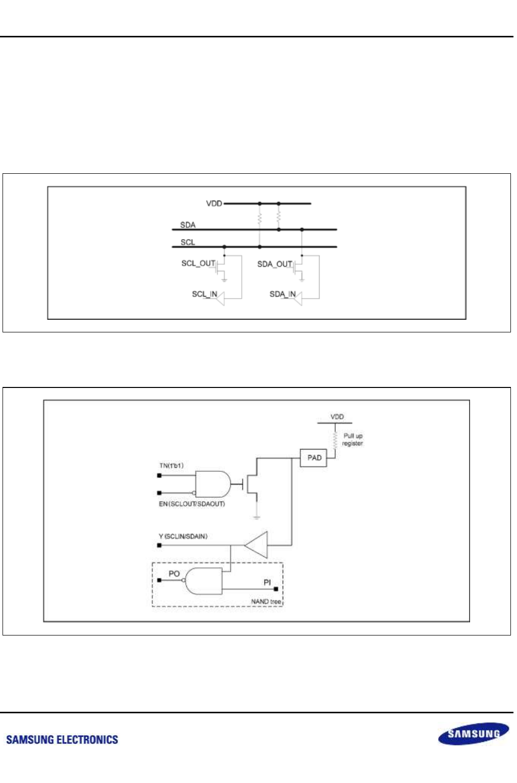
Samsung Confidential
S5P6818_UM 22 I2C Controller
22-4
Preliminary product information describes products that are in development, for which full characterization data and
associated errata are not yet available. Specifications and information herein are subject to change without notice.
22.4.2 IC Protocol
Both SDA and SCL are bi-directional lines, connected to a positive supply voltage via a current-source or pull-up
resistor. The figure below shows the hardware layout of the I2C-bus. When the bus is free, both lines are HIGH.
The output stages of devices connected to the bus must have an open-drain or open-collector to perform the
wired-AND function. Data on the I2C-bus can be transferred at rates of up to 100 kbit/s in the Standard-mode or
up to 400 kbit/s in the Fast-mode.
The figure below shows additional information of I2C-bus pad structure.
Figure 22-2 Connection of Devices to the I2C-Bus
Figure 22-3 Bi-Direction PAD Structure of the I2C-Bus
nexell / ys.kim at 2015.02.12
SAMSUNG Confidential
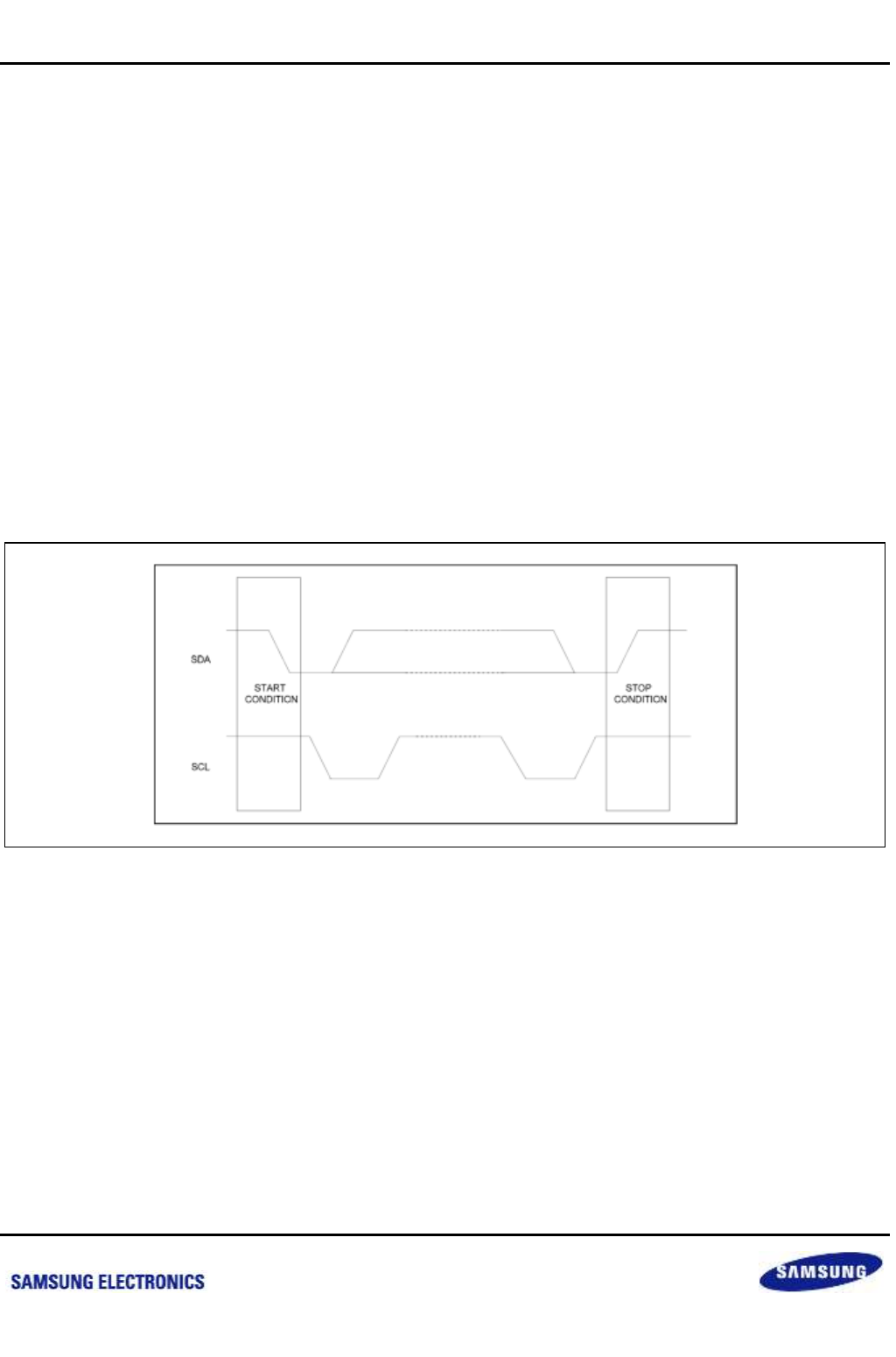
Samsung Confidential
S5P6818_UM 22 I2C Controller
22-5
Preliminary product information describes products that are in development, for which full characterization data and
associated errata are not yet available. Specifications and information herein are subject to change without notice.
22.4.3 Start/Stop Operation
If the I2C-bus interface is inactive, it is usually in Slave mode. In other words, the interface should be in Slave
mode before detecting a Start condition on the SDA line (a Start condition is initiated with a High-to-Low transition
of the SDA line while the clock signal of SCL is high). If the interface state is changed to Master mode, SDA line
initiates data transfer and generates SCL signal.
A Start condition transfers one-byte serial data via SDA line, and a Stop condition terminates the data transfer. A
Stop condition is a Low-to-High transition of the SDA line while SCL is high. The master generates Start and Stop
conditions. The I2C-bus gets busy if a Start condition is generated. On the other hand, a Stop condition frees the
I2C-bus.
If a master initiates a Start condition, it should send a slave address to notify the slave device. One byte of
address field consists of a 7-bit address and a 1-bit transfer direction indicator (that shows write or read).
If bit 8 is 0, it indicates a write operation (Transmit Operation); if bit 8 is 1, it indicates a request for data read
(Receive Operation).
The master transmits Stop condition to complete the transfer operation. If the master wants to continue the data
transmission to the bus, it should generate another Start condition as well as a slave address. In this way, the
read-write operation is performed in various formats.
Figure 22-4 Start/Stop Condition of I2C-Bus
nexell / ys.kim at 2015.02.12
SAMSUNG Confidential
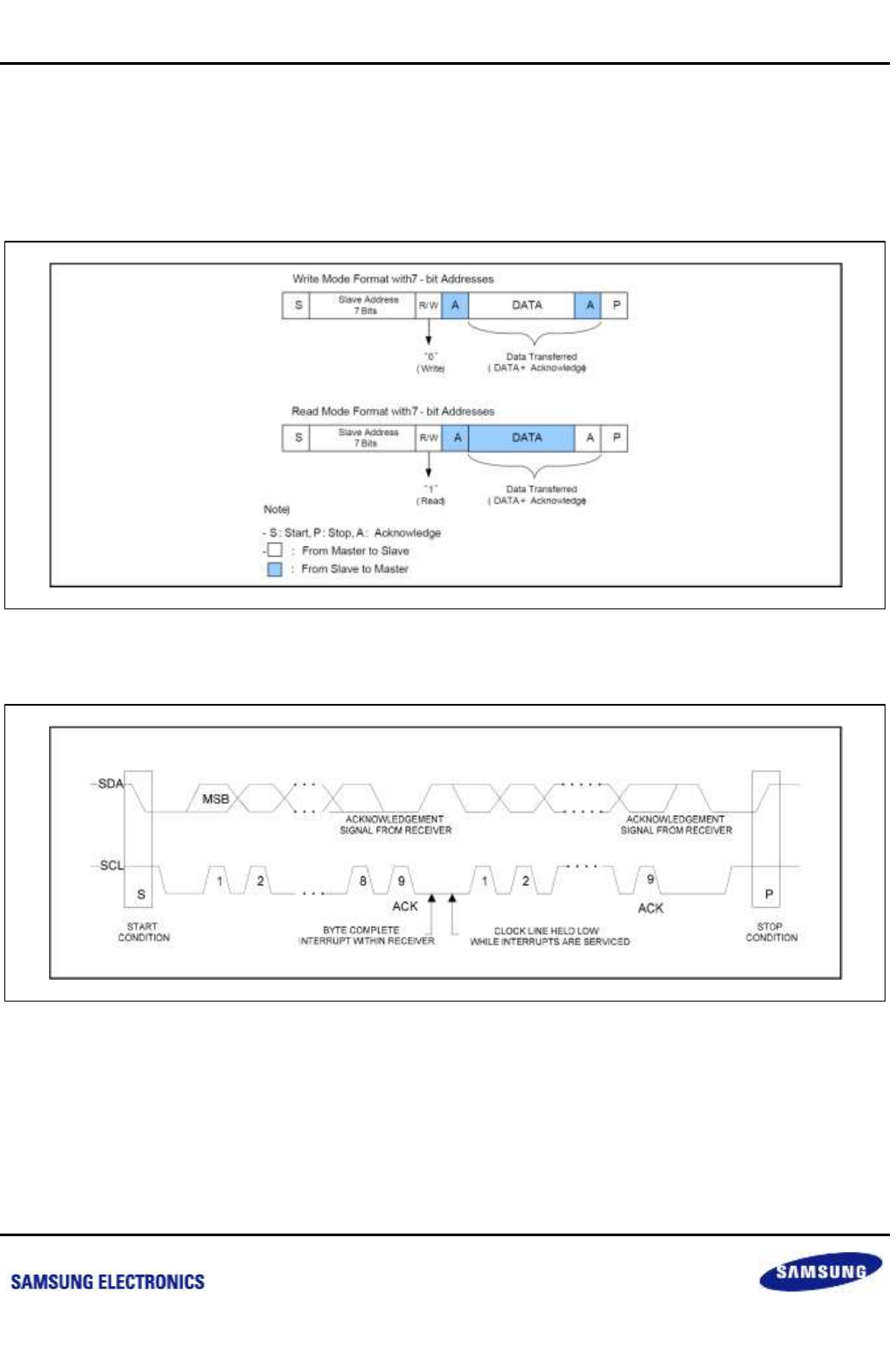
Samsung Confidential
S5P6818_UM 22 I2C Controller
22-6
Preliminary product information describes products that are in development, for which full characterization data and
associated errata are not yet available. Specifications and information herein are subject to change without notice.
22.4.4 Data Transfer Format
Every byte placed on the SDA line should be eight bits in length. There is no limit to transmit bytes per transfer.
The first byte following a Start condition should have the address field. If the I2C-bus is operating in Master mode,
master transmits the address field. Each byte should be followed by an acknowledgement (ACK) bit. The MSB bit
of the serial data and addresses are sent first.
Figure 22-5 I2C-Bus Interface Data Format
Figure 22-6 Data Transfer on the I2C-Bus
nexell / ys.kim at 2015.02.12
SAMSUNG Confidential
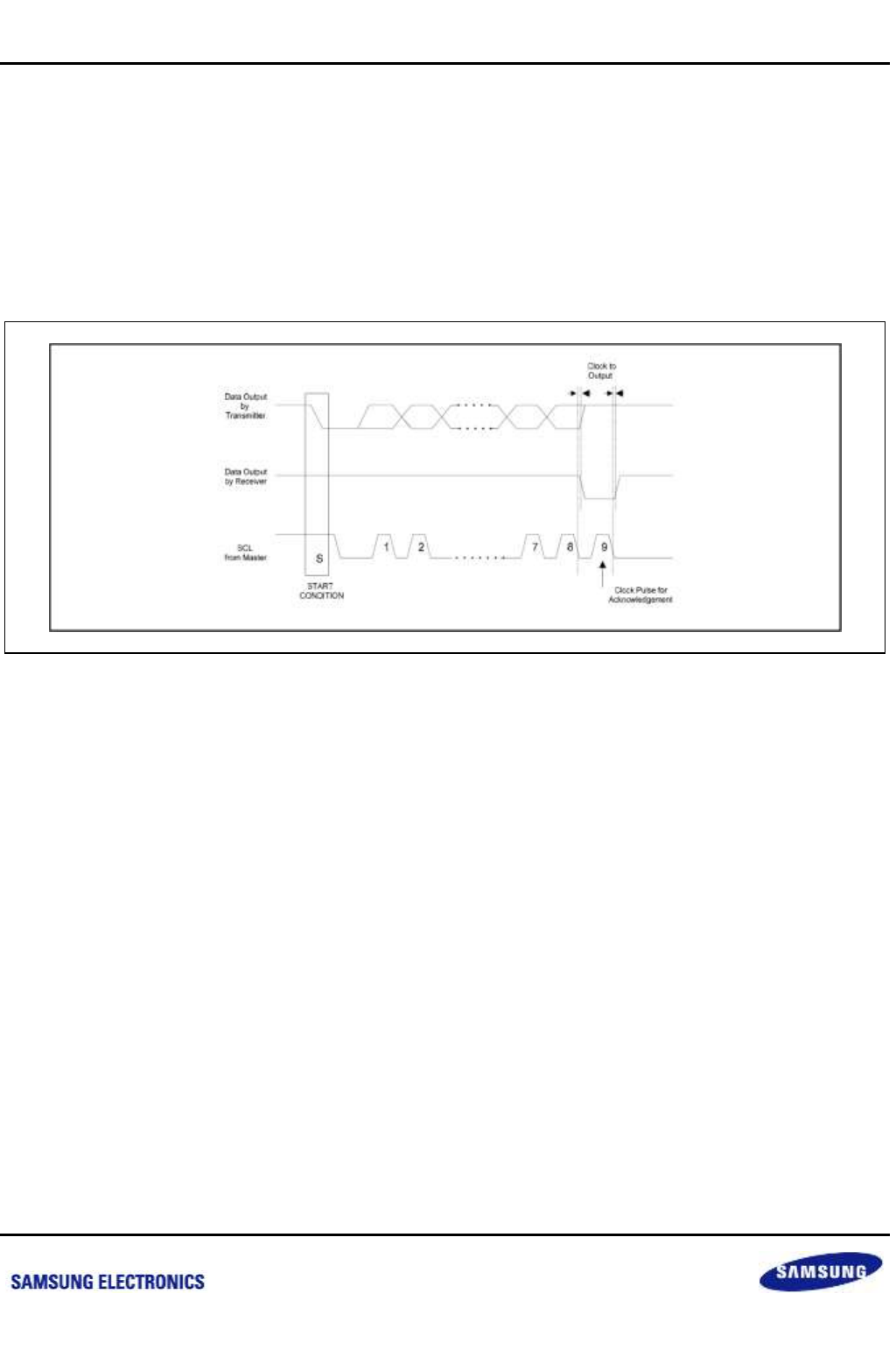
Samsung Confidential
S5P6818_UM 22 I2C Controller
22-7
Preliminary product information describes products that are in development, for which full characterization data and
associated errata are not yet available. Specifications and information herein are subject to change without notice.
22.4.5 ACK Signal Transmission
To complete a one-byte transfer operation, the receiver sends an ACK bit to the transmitter. The ACK pulse
occurs at the ninth clock of the SCL line. Eight clocks are required for the one-byte data transfer. The master
generates clock pulse required to transmit the ACK bit.
The transmitter sets the SDA line to High to release the SDA line if the ACK clock pulse is received. The receiver
drives the SDA line Low during the ACK clock pulse so that the SDA keeps Low during the High period of the
ninth SCL pulse. The software (I2CSTAT) enables or disables ACK bit transmit function. However, the ACK pulse
on the ninth clock of SCL is required to complete the one-byte data transfer operation.
Figure 22-7 Acknowledge on the I2C-Bus
22.4.6 Read-Write Operation
In data is transmitted in Transmitter mode, the I2C-bus interface waits until I2C-bus Data Shift (I2CDS) register
receives the new data. Before the new data is written to the register, the SCL line is held low. The line is only
released after the data has been written. I2C holds the interrupt to identify the completion of current data transfer.
After the CPU receives the interrupt request, it writes new data to the I2CDS register again.
If data is received in Receive mode, the I2C-bus interface waits until I2CDS register is read. Before the new data
is read out, the SCL line is held low. The line is only released after the data has been read. I2C holds the interrupt
to identify the completion of new data reception. After the CPU receives the interrupt request, it reads the data
from the I2CDS register.
nexell / ys.kim at 2015.02.12
SAMSUNG Confidential
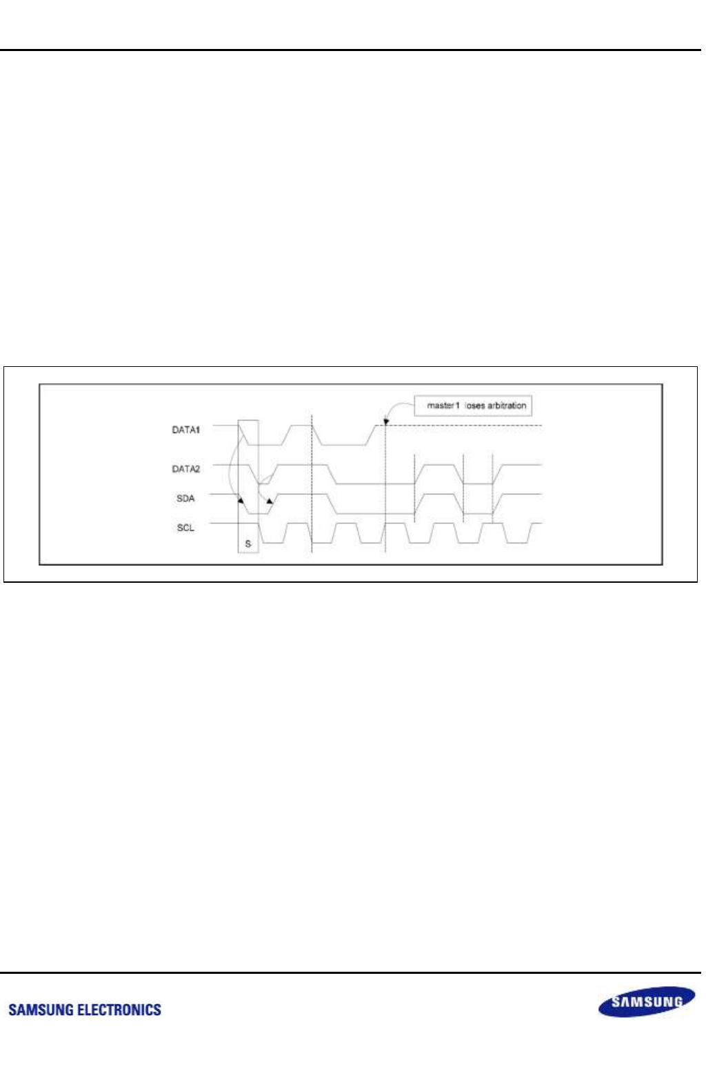
Samsung Confidential
S5P6818_UM 22 I2C Controller
22-8
Preliminary product information describes products that are in development, for which full characterization data and
associated errata are not yet available. Specifications and information herein are subject to change without notice.
22.4.7 Bus Arbitration Procedures
Arbitration takes place on the SDA line to prevent the contention on the bus between two masters. If a master with
a SDA High level detects other master with a SDA active Low level, it does not initiate a data transfer because the
current level on the bus does not correspond to its own. The arbitration procedure extends until the SDA line turns
High.
If the masters lower the SDA line simultaneously, each master evaluates whether the mastership is allocated itself
or not. For the purpose of evaluation each master detects the address bits. While each master generates the
slave address, it detects the address bit on the SDA line because the SDA line is likely to get Low rather than
high.
Assume that one master generates a Low as first address bit, while the other master is maintaining High. In this
case, both masters detect Low on the bus because the Low status is superior to the High status in power. If this
happens, Low (as the first bit of address) generating master gets the mastership while High (as the first bit of
address) generating master withdraws the mastership. If both masters generate Low as the first bit of address,
there is arbitration for the second address bit again. This arbitration continues to the end of last address bit.
Figure 22-8 Arbitration Procedure between Two Masters
nexell / ys.kim at 2015.02.12
SAMSUNG Confidential

Samsung Confidential
S5P6818_UM 22 I2C Controller
22-9
Preliminary product information describes products that are in development, for which full characterization data and
associated errata are not yet available. Specifications and information herein are subject to change without notice.
22.4.8 Abort Conditions
If a slave receiver cannot acknowledge the confirmation of the slave address, it holds the level of the SDA line
High. In this case, the master generates a Stop condition and cancels the transfer.
If a master receiver is involved in the aborted transfer, it signals the end of slave transmit operation by canceling
the generation of an ACK after the last data byte received from the slave. The slave transmitter releases the SDA
to allow a master to generate a Stop condition.
22.4.9 Configuring IIC-BUS
To control the frequency of the serial clock (SCL), the 4-bit prescaler value is programmed in the I2CCON register.
The I2C-bus interface address is stored in the I2C-bus address (I2CADD) register (By default, the I2C-bus
interface address has an unknown value).
nexell / ys.kim at 2015.02.12
SAMSUNG Confidential
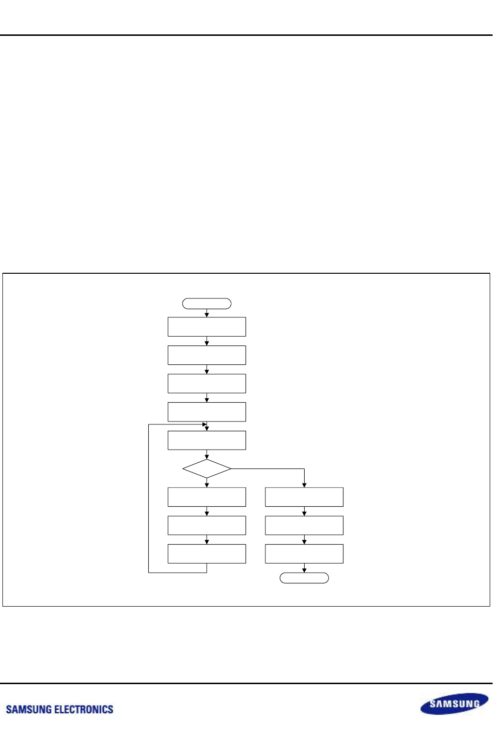
Samsung Confidential
S5P6818_UM 22 I2C Controller
22-10
Preliminary product information describes products that are in development, for which full characterization data and
associated errata are not yet available. Specifications and information herein are subject to change without notice.
22.5 Programming Guide
22.5.1 Flowcharts of Operations in Each Mode
The S5P6818 application processor supports 3 multi-master I2C bus serial interfaces. To carry information
between bus masters and peripheral devices connected to the I2C bus, a dedicated Serial Data Line (SDA) and
an Serial Clock Line (SCL) is used. Both SDA and SCL lines are bi-directional.
Following steps must be executed before any I2C Tx/Rx operations:
1. If required, write own slave address on I2CADD register.
2. Set I2C CON registers
Enable interrupt
Define SCL period
3. Set I2CSTAT to enable Serial Output
Figure 22-9 Operations for Master/Transmitter Mode
Write slave address to
I2CDS.
Write 0xF0 (M/T Start)
to I2CSTAT.
The data of the I2CDS
is transmitted.
After ACK period
interrupt is pending.
Write 0xD0 (M/T Stop)
to I2CSTAT.
Write new data
transmitted to I2CDS.
Stop?
Clear pending bit to
resume.
The data of the I2CDS
is shifted to SDA.
START
Master Tx mode has
been configured.
Clear pending bit.
Wait until the stop
condition takes effect.
END
Y
N
nexell / ys.kim at 2015.02.12
SAMSUNG Confidential
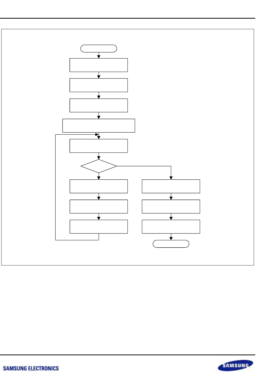
Samsung Confidential
S5P6818_UM 22 I2C Controller
22-11
Preliminary product information describes products that are in development, for which full characterization data and
associated errata are not yet available. Specifications and information herein are subject to change without notice.
Figure 22-10 Operations for Master/Receiver Mode
Write slave address to
I2CDS.
Write 0xB0 (M/R Start)
to I2CSTAT.
The data of the I2CDS
(Slave address) is transmitted.
After ACK period
interrupt is pending.
Write 0x90 (M/R Stop)
to I2CSTAT.
Read a new data from
I2CDS.
Stop ?
Clear pending bit to
resume.
SDA is shifted to I2CDS.
START
Master Rx mode has
been configured.
Clear pending bit.
Wait until the stop
condition takes effect.
END
Y
N
nexell / ys.kim at 2015.02.12
SAMSUNG Confidential
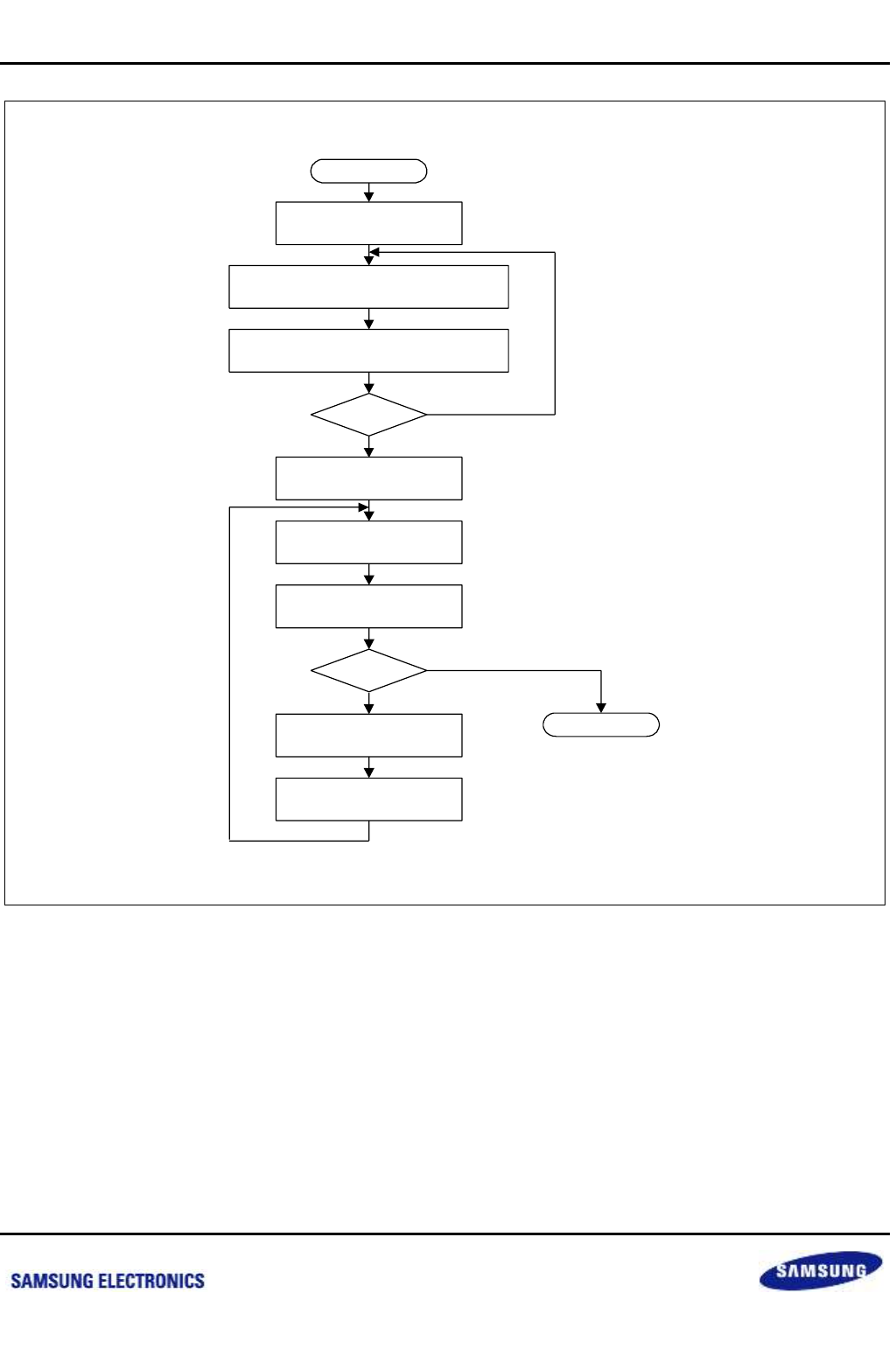
Samsung Confidential
S5P6818_UM 22 I2C Controller
22-12
Preliminary product information describes products that are in development, for which full characterization data and
associated errata are not yet available. Specifications and information herein are subject to change without notice.
Figure 22-11 Operations for Slave/Transmitter Mode
I2C detects start signal. and, I2CDS
receives data.
I2C compares I2CADD and I2CDS
(the received slave address).
Write data to I2CDS.
Clear pending bit to
resume.
The data of the I2CDS
is shifted to SDA.
START
Slave Tx mode has
been configured.
END
Matched ?
N
Y
Stop ?
Interrupt is pending.
N
Y
The I2C address match
interrupt is generated.
nexell / ys.kim at 2015.02.12
SAMSUNG Confidential
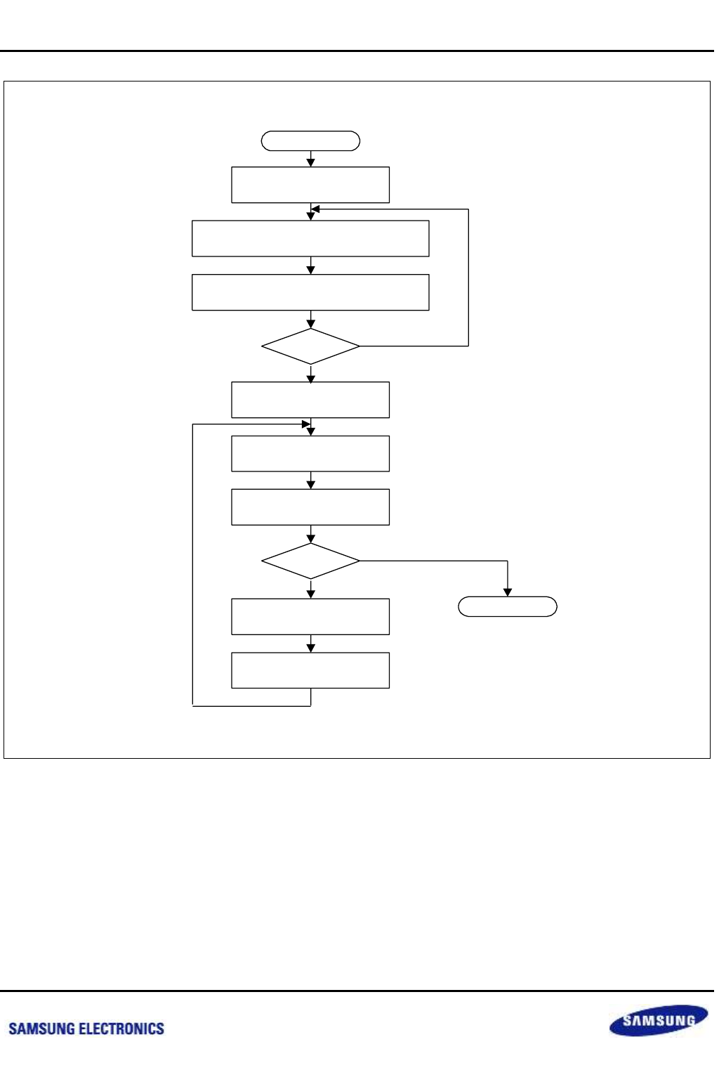
Samsung Confidential
S5P6818_UM 22 I2C Controller
22-13
Preliminary product information describes products that are in development, for which full characterization data and
associated errata are not yet available. Specifications and information herein are subject to change without notice.
Figure 22-12 Operations for Slave/Receiver Mode
I2C detects start signal. and, 12CDS
receives data.
I2C compares I2CADD and I2CDS
(the received slave address).
Read data from I2CDS.
Clear pending bit to
resume.
SDA is shifted to I2CDS.
START
Slave Rx mode has
been configured.
END
Matched ?
N
Y
Stop ?
Interrupt is pending.
N
Y
The I2C address match
interrupt is generated.
nexell / ys.kim at 2015.02.12
SAMSUNG Confidential

Samsung Confidential
S5P6818_UM 22 I2C Controller
22-14
Preliminary product information describes products that are in development, for which full characterization data and
associated errata are not yet available. Specifications and information herein are subject to change without notice.
22.6 Register Description
22.6.1 Register Map Summary
Base Address: 0xC00A_4000h (I2C0)
Base Address: 0xC00A_5000h (I2C1)
Base Address: 0xC00A_6000h (I2C2)
Register
Offset
Description
Reset Value
I2CCON
0x00h
I2C-Bus control register
0x0000_0000
I2CSTAT
0x04h
I2C-Bus control-status register
0x0000_0000
I2CADD
0x08h
I2C-Bus address register
0x0000_0000
I2CDS
0x0Ch
I2C-Bus transmit-receive data shift register
0x0000_0000
I2CLC
0x10h
I2C-bus line control register
0x0000_0000
I2CVR
0x40h
I2C-bus version register
0x8000_0001
nexell / ys.kim at 2015.02.12
SAMSUNG Confidential

Samsung Confidential
S5P6818_UM 22 I2C Controller
22-15
Preliminary product information describes products that are in development, for which full characterization data and
associated errata are not yet available. Specifications and information herein are subject to change without notice.
22.6.1.1 I2CCON
Base Address: 0xC00A_4000h (I2C0)
Base Address: 0xC00A_5000h (I2C1)
Base Address: 0xC00A_6000h (I2C2)
Address = Base Address + 0x00h, Reset Value = 0x0000_0000
Name
Bit
Type
Description
Reset Value
RSVD
[31:8]
–
Reserved
–
INTERRUPT CLEAR
[8]
RW
I2C-bus Interrupt clear bit
0 = No Interrupt (when read)
1 = Interrupt is cleared (when write)
1'b0
ACKNOWLEDGE
ENABLE
[7]
RW
I2C-bus acknowledge enable bit
0 = Disable ACK generation
1 = Enable ACK generation
1'b0
TX CLOCK SOURCE
SELECTION
[6]
RW
Source clock of I2C-bus transmit clock prescaler
selection bit
0 = I2C CCLK = fPCLK/16
1 = I2C CCLK = fPCLK/256
1'b0
TX/RX INTERRUPT
ENALBE
[5]
RW
I2C-bus Tx/Rx interrupt enable/disable bit
0 = Disable interrupt
1 = Enable interrupt
1'b0
INTERRUPT PENDING
FLAG
[4]
RW
I2C-bus Tx/Rx interrupts pending flag. Writing "1" is
impossible
0 = No interrupt pending (when read), This bit is
cleared (when write)
1 = Interrupt is pending (when read), No effect.
Namely "1" doesn't be written to this bit
NOTE:
A I2C-bus interrupt occurs
1. When an 1-byte transmit or receive operation is
terminated
2. When a general call or a slave address match
occurs
3. If bus arbitration fails
1'b0
TRANSMIT CLOCK
VALUE
[3:0]
RW
I2C-bus transmit clock prescaler.
I2C-bus transmit clock frequency is determined by this
4-bit prescaler value, according to the following
formula:
Tx clock = I2C CLK/(ICCR[3:0]+1)
NOTE:
1. I2CCLK is determined by ICCR[6]
2. Tx clock can vary by SCL transition time
3. When ICCR[6] = 0, "ICCR[3:0] = 0x0 or 0x1" is not
available
–
nexell / ys.kim at 2015.02.12
SAMSUNG Confidential

Samsung Confidential
S5P6818_UM 22 I2C Controller
22-16
Preliminary product information describes products that are in development, for which full characterization data and
associated errata are not yet available. Specifications and information herein are subject to change without notice.
NOTE:
1. Interfacing with EEPROM, the ACK generation may be disabled before reading the last data to generate the STOP
condition in Rx mode.
2. An I2C-bus interrupt occurs if 1) if a 1-byte transmit or receive operation is complete. In other words, ack period is
finished. 2) A general call or a slave address match occurs, 3) Bus arbitration fails.
3. To adjust the setup time of SDA before SCL rising edge, I2CDS has to be written before clearing the I2C
interrupt pending bit.
4. I2CCLK is determined by I2CCON[6]. Tx clock can vary by SCL transition time. If I2CCON[6] = 0,
I2CCON[3:0] = 0x0 or 0x1 is not available.
5. If the I2CCON[5] = 0, I2CCON[4] does not operate correctly. Therefore, It is recommended to set I2CCON[5] = 1,
if you do not use the I2C interrupt.
nexell / ys.kim at 2015.02.12
SAMSUNG Confidential

Samsung Confidential
S5P6818_UM 22 I2C Controller
22-17
Preliminary product information describes products that are in development, for which full characterization data and
associated errata are not yet available. Specifications and information herein are subject to change without notice.
22.6.1.2 I2CSTAT
Base Address: 0xC00A_4000h (I2C0)
Base Address: 0xC00A_5000h (I2C1)
Base Address: 0xC00A_6000h (I2C2)
Address = Base Address + 0x04h, Reset Value = 0x0000_0000
Name
Bit
Type
Description
Reset Value
RSVD
[31:6]
–
Reserved
–
BUSY SIGNAL STATUS
[5]
RW
I2C-bus busy signal status bit:
0 = I2C-bus not busy (when read), I2C-bus interface
STOP signal generation (when write)
1 = I2C-bus busy (when read), I2C-bus interface
START signal generation (when write)
1'b0
SERAIL OUTPUT
ENABLE
[4]
RW
I2C-bus data output enable/disable bit:
0 = Disable Rx/Tx
1 = Enable Rx/Tx
1'b0
ARBITRATION STATUS
FLAG
[3]
R
I2C-bus arbitration procedure status flag bit
0 = Bus arbitration status okay
1 = Bus arbitration failed during serial I/O
1'b0
ADDRESS-AS-SLAVE
STATUS FLAG
[2]
R
I2C-bus address-as-slave status flag bit:
0 = START/STOP condition was generated
1 = Received salve address matches the address
value in the IAR
1'b0
ADDRESS ZERO
STATUS FLAG
[1]
R
I2C-bus address zero status flag bit:
0 = START/STOP condition was generated
1 = Received slave address is "0x00"
1'b0
LAST-RECEIVED BIT
STATUS FALG
[0]
R
I2C-bus last-received bit status flag bit
0 = Last-received bit is "0" (ACK was received)
1 = Last-received bit is "1" (ACK was not received)
1'b0
nexell / ys.kim at 2015.02.12
SAMSUNG Confidential
Samsung Confidential
S5P6818_UM 22 I2C Controller
22-18
Preliminary product information describes products that are in development, for which full characterization data and
associated errata are not yet available. Specifications and information herein are subject to change without notice.
22.6.1.3 I2CADD
Base Address: 0xC00A_4000h (I2C0)
Base Address: 0xC00A_5000h (I2C1)
Base Address: 0xC00A_6000h (I2C2)
Address = Base Address + 0x08h, Reset Value = 0x0000_0000
Name
Bit
Type
Description
Reset Value
RSVD
[31:6]
–
Reserved
–
SLAVE ADDRESS
[7:1]
RW
7-bit slave address, latched from the I2C-bus:
When serial output enable = 0 in the ICSR, IAR is
write-enable. You can read the IAR value at any time,
regardless of the current serial output enable bit
(ICSR[4]) setting
Slave address = [7:1]
Not mapped = [0]
–
RSVD
[0]
–
Reserved
–
22.6.1.4 I2CDS
Base Address: 0xC00A_4000h (I2C0)
Base Address: 0xC00A_5000h (I2C1)
Base Address: 0xC00A_6000h (I2C2)
Address = Base Address + 0x0Ch, Reset Value = 0x0000_0000
Name
Bit
Type
Description
Reset Value
RSVD
[31:6]
–
Reserved
–
DATA SHIFT
[7:0]
RW
8-bit data shift register for I2C-bus Tx/Rx operation:
When serial output enable = 1 in the ICSR, IDSR is
write-enabled. You can read the IDSR value at any
time, regardless of the current serial output enable bit
(ICSR[4]) setting
–
nexell / ys.kim at 2015.02.12
SAMSUNG Confidential
Samsung Confidential
S5P6818_UM 22 I2C Controller
22-19
Preliminary product information describes products that are in development, for which full characterization data and
associated errata are not yet available. Specifications and information herein are subject to change without notice.
22.6.1.5 I2CLC
Base Address: 0xC00A_4000h (I2C0)
Base Address: 0xC00A_5000h (I2C1)
Base Address: 0xC00A_6000h (I2C2)
Address = Base Address + 0x10h, Reset Value = 0x0000_0000
Name
Bit
Type
Description
Reset Value
RSVD
[31:3]
–
Reserved
–
FILTER ENABLE
[2]
RW
I2C-Bus filter enable bit.
If SDA port is operating as input, this bit should be
High. This filter prevents error caused by glitch
between two PCLK clock
0 = Disables Filter
1 = Enables Filter
1’b0
STA OUTPUT DELAY
[1:0]
RW
I2C-Bus SDA line delay length selection bits.
SDA line is delayed as following clock time(PCLK)
00 = 0 clocks
01 = 5 clocks
10 = 10 clocks
11 = 15 clocks
2’b00
22.6.1.6 I2CVR
Base Address: 0xC00A_4000h (I2C0)
Base Address: 0xC00A_5000h (I2C1)
Base Address: 0xC00A_6000h (I2C2)
Address = Base Address + 0x40h, Reset Value = 0x8000_0001
Name
Bit
Type
Description
Reset Value
VERSION
[31:0]
R
I2C version information registers.
32’h8000_0001
nexell / ys.kim at 2015.02.12
SAMSUNG Confidential

Samsung Confidential
S5P6818_UM 23 SPI/SSP
23-1
Preliminary product information describes products that are in development, for which full characterization data and
associated errata are not yet available. Specifications and information herein are subject to change without notice.
23 SPI/SSP
23.1 Overview
The SPI/SSP is a full-duplex synchronous serial interface. It supports Serial Peripheral Interface (SPI) and
Synchronous Serial Protocol (SSP). It can connect to a variety of external converter, serial memory and many
other device which use serial protocols for transferring data.
There are 4 I/O pin signals associated with SPI/SSP transfers: The SSPCLK, the SSPRXD data receive line, the
SSPTXD data transfer line, SSPFSS (Chip Select in SPI mode, Frame Indicator in SSP mode).
The S5P6818 has three SPI/SSP port and it can operate in Master and Slave mode.
23.2 Features
Supports the Motorola SPI protocol and National Semiconductor Microwire
Supports 8-bit/16-bit/32-bit bus interface
Master & Slave mode
DMA request servicing of the transmit and receive FIFO
Supports DMA Single or 4 Burst
Maximum SSP CLKGEN's frequency is 100 MHz
Max Operation Frequency
Master Mode: 50 MHz (Receive Data is 20 MHz , or 40 MHz with feedback clock configuration)
Slave Mode: 8 MHz
nexell / ys.kim at 2015.02.12
SAMSUNG Confidential
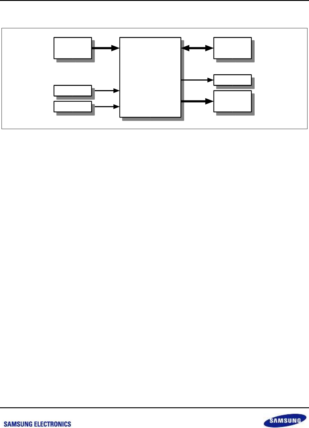
Samsung Confidential
S5P6818_UM 23 SPI/SSP
23-2
Preliminary product information describes products that are in development, for which full characterization data and
associated errata are not yet available. Specifications and information herein are subject to change without notice.
23.3 Block Diagram
Figure 23-1 SPI/SSP Block Diagram
PAD Interface
SSPCLK
SSPFSS
SSPTXD (MOSI: SSPTXD Output/SSPRXD Input)
SSPRXD (MISO: SSPTXD Input/SSPRXD Output)
SPI
SPI
DMA Interface
SPI_EXT_CLK
PAD Interface
PRESETn
SPI CLKGEN
SPI CLKGEN
RSTCON
RSTCON
BUS
BUS External
Device
External
Device
DMA
DMA
SPI_INT
Interrupt Ctrl
Interrupt Ctrl
PCLK
APB Interface
nexell / ys.kim at 2015.02.12
SAMSUNG Confidential
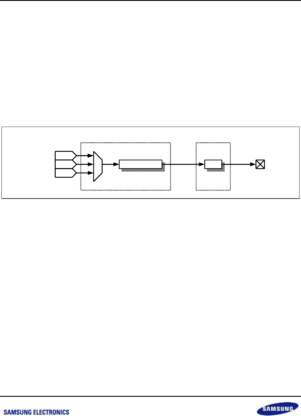
Samsung Confidential
S5P6818_UM 23 SPI/SSP
23-3
Preliminary product information describes products that are in development, for which full characterization data and
associated errata are not yet available. Specifications and information herein are subject to change without notice.
23.4 Functional Description
23.4.1 Clock/Reset Configuration
23.4.1.1 Reset Configuration
The SPI/SSP is reset by the global reset signal PRESETn. In S5P6818, PRESETn is controlled by Reset
Controller. User can set up SPI/SSP reset signals by CPU.
23.4.1.2 Clock Configuration
The SPI_EXT_CLK is used when the SPI/SSP transmit or receive SPI/SSP Protocol. SPI_EXT_CLK is generated
by Clock Generator of the SPI/SSP. Each SPI/SSP has own Clock Generator. Therefore, users must set up the
SPI/SSP Clock Generator before the SPI configuration stage.
Figure 23-2 SPI/SSP Clock Diagram
SPI/SSP provides a variety of clocks. As described in the upper figure, the SPI uses SPI_EXT_CLK, which is from
SPI/SSP Clock Generator. You can also select SPI_EXT_CLK from various clock sources.
SPI has an internal 2x clock divider. SCLK_SPI should be configured to have a double of the SPI operating clock
frequency.
DIV 1~254 (2n)
DIV 1~254 (2n)
PLL 0
PLL 1
PLL 2
SPI_EXT_CLK
DIV 2
DIV 2
SSPCLK
SPI/SSP Clock Generator SPI/SSP
nexell / ys.kim at 2015.02.12
SAMSUNG Confidential

Samsung Confidential
S5P6818_UM 23 SPI/SSP
23-4
Preliminary product information describes products that are in development, for which full characterization data and
associated errata are not yet available. Specifications and information herein are subject to change without notice.
23.4.2 Operation of Serial Peripheral Interface
The SPI transfers 1-bit serial data between and external device. The SPI in supports the CPU or DMA to transmit
or receive FIFOs separately and to transfer data in both directions simultaneously. SPI has two channels, TX
channel and RX channel. TX channel has the path from Tx FIFO to external device. RX channel has the path from
external device to RX FIFO.
CPU (or DMA) must write data on the register SPI_TX_DATA, to write data in FIFO. Data on the register are
automatically moved to Tx FIFOs. To read data from Rx FIFOs, CPU (or DMA) must access the register
SPI_RX_DATA and data are automatically sent to the SPI_RX_DATA register.
SPI operating frequency can be controlled by SPI/SSP Clock Generator. SPI Master's clock frequency is HALF of
SPI_EXT_CLK.
23.4.3 FIFO Access
The SPI supports CPU access and DMA access to FIFOs. Data size of CPU access and DMA access to FIFOs
are selected either from 8-bit, 16-bit, or 32-bit data. If 8-bit data size is selected, valid bits are from 0 bit to 7-bit.
User can define the trigger threshold to raise interrupt to CPU. The trigger level of each FIFO is set by 4 bytes
step from 0 byte to 252 bytes. TxDMAOn or RxDMAOn bit of SPI_MODE_CFG register must be set to use DMA
access. DMA access supports only single transfer and 4-burst transfer. In Tx FIFO, DMA request signal is high
until Tx FIFO is full. In Rx FIFO, DMA request signal is high if FIFO is not empty.
23.4.4 Trailing Byte Interrupt
Rx FIFO can have data which is less than Rx interrupt trigger level in INT mode or less than 4 bytes in DMA4
burst mode. If no more data is received, the remaining data in Rx FIFO cannot be retrieved by INT or DMA. The
remaining data in Rx FIFO is called trailing bytes and it can be handled by trailing byte interrupt.
The SPI has trailing byte counter internally. When Rx FIFO receives a data, the trailing byte counter is set as the
count value TRAILNG_CNT in MODE_CFGn register. The trailing byte counter decreases its count while Rx FIFO
count is less than Rx interrupt trigger level in INT mode or less than 4 bytes in DMA4 burst mode, and trailing byte
interrupt occurs and CPU can remove trailing bytes if the count value is zero.
23.4.5 Packet Number Control
SPI controls the number of packets to be received in master mode. Set SFR (PACKET_CNT_REG) to receive any
number of packets. SPI stops generating SPICLK if the number of packets is the same as PACKET_CNT_REG.
The size of one packet is same as channel width. (One packet is one byte if channel width is configured as byte,
and one packet is four bytes if channel width is configured as word). It is mandatory to follow software or hardware
reset before this function is reloaded. (Software reset can clear all registers except special function registers, but
hardware reset clears all registers).
nexell / ys.kim at 2015.02.12
SAMSUNG Confidential
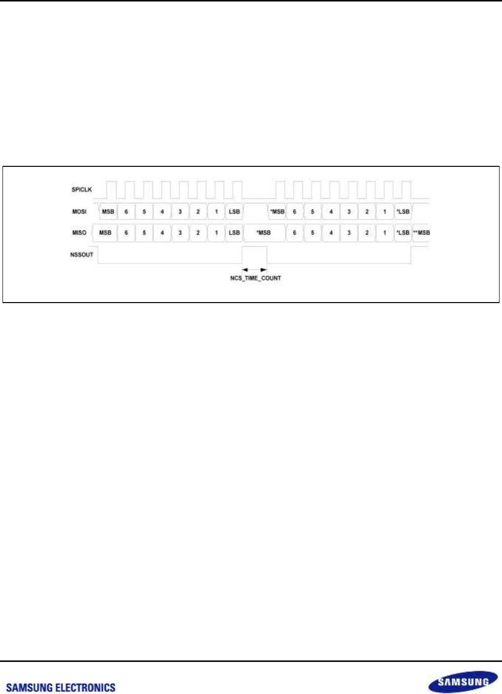
Samsung Confidential
S5P6818_UM 23 SPI/SSP
23-5
Preliminary product information describes products that are in development, for which full characterization data and
associated errata are not yet available. Specifications and information herein are subject to change without notice.
23.4.6 Chip Select Control
Chip select SSPFSS is active low signal. In other words, a chip is selected when SSPFSS input is 0.
SSPFSS can be controlled automatically or manually.
When you use manual control mode, AUTO_N_MANUAL must be cleared (Default value is 0). SSPFSS level is
controlled by NSSOUT bit.
When you use auto control mode, AUTO_N_MANUAL must be set as 1. SSPFSS toggled between packet and
packet automatically. Inactive period of SSPFSS is controlled by NCS_TIME_COUNT. NSSOUT is not available
at this time.
Figure 23-3 Auto Chip Select Mode Waveform (CPOL = 0, CPHA = 0, CH_WIDTH = byte)
23.4.7 High Speed Operation as Slave
SPI supports Tx/Rx operations up to 50 MHz, but there is a limitation. When SPI works as a slave, it consumes
large delay over than 15ns in worst operating condition. Such a large delay can cause setup violation at SPI
master device. To overcome the problem, SPI provides fast slave Tx mode by setting 1 to HIGH_SPEED bit of
CH_CFG register. In that mode, MISO output delay is reduced by half cycle, so that the SPI master device has
more setup margin. However, the fast slave Tx mode can be used only when CPHA = 0.
23.4.8 Feedback Clock Selection
Under SPI protocol spec, SPI master should capture the input data launched by slave (SSPRXD) with its internal
SPICLK. If SPI runs at high operating frequency such as 50 MHz, it is difficult to capture the SSPRXD input
because the required arrival time of MISO, which is an half cycle period in, is shorter than the arrival time of MISO
that consists of SPICLK output delay of SPI master, MISO output delay of SPI slave, and MISO input delay of SPI
master. To overcome the problem, SPI provides 3 feedback clocks that are phase-delayed clock of internal
SPICLK.
nexell / ys.kim at 2015.02.12
SAMSUNG Confidential
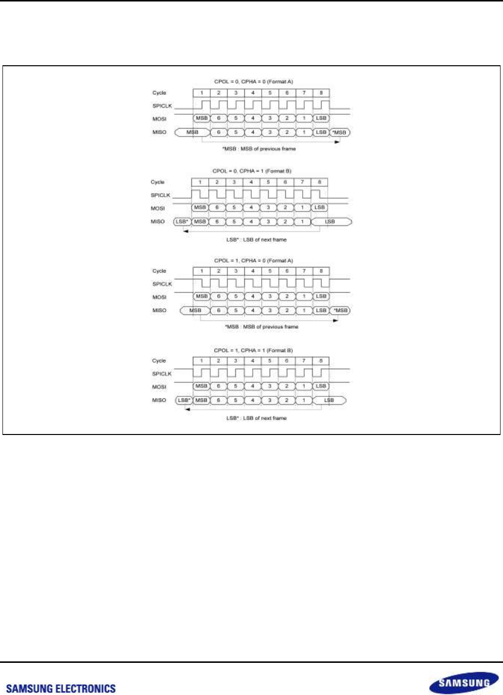
Samsung Confidential
S5P6818_UM 23 SPI/SSP
23-6
Preliminary product information describes products that are in development, for which full characterization data and
associated errata are not yet available. Specifications and information herein are subject to change without notice.
23.4.9 SPI Transfer Format
The supports four different formats for data transfer. Following figure describes four waveforms for SPICLK.
Figure 23-4 SPI/SSP Format
nexell / ys.kim at 2015.02.12
SAMSUNG Confidential

Samsung Confidential
S5P6818_UM 23 SPI/SSP
23-7
Preliminary product information describes products that are in development, for which full characterization data and
associated errata are not yet available. Specifications and information herein are subject to change without notice.
23.5 Register Description
23.5.1 Register Map Summary
Base Address: C005_B000h (SPISSP0)
Base Address: C005_C000h (SPISSP1)
Base Address: C005_F000h (SPISSP2)
Register
Offset
Description
Reset Value
SPI/SSP Configure
B000h
C000h
F000h
SPI/SSP configuration register
0x0000_0000
SPI/SSP FIFO CON
B008h
C008h
F008h
SPI/SSP FIFO control register
0x0000_0000
SPI/SSP SEL SIGNAL
CON
B00Ch
C00Ch
F00Ch
SPI/SSP selection signal(CS) control register
0x0000_0001
SPI/SSP INT EN
B010h
C010h
F010h
SPI/SSP interrupt enable register
0x0000_0000
SPI/SSP STATUS
B014h
C014h
F014h
SPI/SSP status register
0x0000_0000
SPI/SSP TX DATA
B018h
C018h
F018h
SPI/SSP TX data register
0x0000_0000
SPI/SSP RX DATA
B01Ch
C01Ch
F01Ch
SPI/SSP RX data register
0x0000_0000
SPI/SSP PACKET
COUNT
B020h
C020h
F020h
SPI/SSP packet count register
0x0000_0000
SPI/SSP STATUS
PENDING CLEAR
B024h
C024h
F024h
SPI/SSP status pending clear register
0x0000_0000
SPI/SSP SWAP
CONFIGURE
B028h
C028h
F028h
SPI/SSP SWAP configuration register
0x0000_0000
SPI/SSP FEEDBACK
CLOCK SEL
B02Ch
C02Ch
F02Ch
SPI/SSP feedback clock selection register
0x0000_0000
nexell / ys.kim at 2015.02.12
SAMSUNG Confidential

Samsung Confidential
S5P6818_UM 23 SPI/SSP
23-8
Preliminary product information describes products that are in development, for which full characterization data and
associated errata are not yet available. Specifications and information herein are subject to change without notice.
23.5.1.1 SPI/SSP CONFIGURE
Base Address: C005_B000h (SPISSP0)
Base Address: C005_C000h (SPISSP1)
Base Address: C005_F000h (SPISSP2)
Address = Base Address + B000h, C000h, F000h, Reset Value = 0x0000_0000
Name
Bit
Type
Description
Reset Value
RSVD
[31:7]
R
Reserved
25'h0
HIGH_SPEED_EN
[6]
RW
Slave Tx output time control bit. If this bit is enabled,
slave Tx output time is reduced as much as half
period of SPICLKout period. This bit is valid only in
CPHA 0.
0 = Disables
1 = Enables
1'b0
SW_RST
[5]
RW
Software reset. The following registers and bits are
cleared by this bit.
Rx/Tx FIFO Data, SPI_STATUS Once reset, this bit
must be clear manually.
0 = Inactive
1 = Active
1'b0
SLAVE
[4]
RW
Whether SPI Port is Master or Slave
0 = Master
1 = Slave
1'b0
CPOL
[3]
RW
Determines whether active high or active low clock
0 = Active High
1 = Active Low
1'b0
CPHA
[2]
RW
Select one of the two fundamentally different transfer
format
0 = Format A
1 = Format B
1'b0
RX_CH_ON
[1]
RW
SPI Rx Channel On
0 = Channel Off
1 = Channel On
1'b0
TX_CH_ON
[0]
RW
SPI Tx Channel On
0 = Channel Off
1 = Channel On
1'b0
nexell / ys.kim at 2015.02.12
SAMSUNG Confidential

Samsung Confidential
S5P6818_UM 23 SPI/SSP
23-9
Preliminary product information describes products that are in development, for which full characterization data and
associated errata are not yet available. Specifications and information herein are subject to change without notice.
23.5.1.2 SPI/SSP FIFO CON
Base Address: C005_B000h (SPISSP0)
Base Address: C005_C000h (SPISSP1)
Base Address: C005_F000h (SPISSP2)
Address = Base Address + B008h, C008h, F008h, Reset Value = 0x0000_0000
Name
Bit
Type
Description
Reset Value
RSVD
[31]
R
Reserved
1'b0
CH_WIDTH
[30:29]
RW
00 = Byte
01 = Halfword
10 = Word
11 = Reserved
2'b0
TRAILING_CNT
[28:19]
RW
Count value from writing the last data in Rx FIFO to
flush trailing bytes in FIFO
10’h0
BUS_WIDTH
[18:17]
RW
00 = Byte
01 = Halfword
10 = Word
11 = Reserved
2'b0
RX_RDY_LVL
[16:11]
RW
Rx FIFO triggers level in INT mode.
Trigger level (bytes) = 4 N
(N = value of RX_RDY_LVL field)
6'h0
TX_RDY_LVL
[10:5]
RW
Tx FIFO triggers level in INT mode.
Trigger level (bytes) = 4 N
(N = value of TX_RDY_LVL field)
6’h0
RSVD
[4:3]
RW
Reserved
2’b0
RX_DMA_SW
[2]
RW
Rx DMA mode enable/disable
0 = Disables DMA Mode
1 = Enables DMA Mode
1’b0
TX_DMA_SW
[1]
RW
Tx DMA mode enable/disable
0 = Disables DMA Mode
1 = Enables DMA Mode
1’b0
DMA_TYPE
[0]
RW
DMA transfer type, single or 4 bursts.
0 = Single
1 = 4 burst
DMA transfer size must be set as the same size in SPI
DMA.
1’b0
nexell / ys.kim at 2015.02.12
SAMSUNG Confidential

Samsung Confidential
S5P6818_UM 23 SPI/SSP
23-10
Preliminary product information describes products that are in development, for which full characterization data and
associated errata are not yet available. Specifications and information herein are subject to change without notice.
23.5.1.3 SPI/SSP SEL SIGNAL CON
Base Address: C005_B000h (SPISSP0)
Base Address: C005_C000h (SPISSP1)
Base Address: C005_F000h (SPISSP2)
Address = Base Address + B00Ch, C00Ch, F00Ch, Reset Value = 0x0000_0001
Name
Bit
Type
Description
Reset Value
RSVD
[31:10]
R
Reserved
22'h0
NCS_TIME_COUNT
[9:4]
RW
NSSOUT inactive time =
((nCS_time_count + 3)/2) SPICLKout
6'h0
RSVD
[3:2]
R
Reserved
2’b0
AUTO_N_MANUAL
[1]
RW
Chip select toggle manual or auto selection
0 = Manual
1 = Auto
If AUTO_N_MANUAL is set, NSSOUT is controlled by
SPI controller and data transfer is not performed
continuously.
1’b0
NSSOUT
[0]
RW
Slave selection signal (manual only)
0 = Active
1 = Inactive
1’b1
nexell / ys.kim at 2015.02.12
SAMSUNG Confidential

Samsung Confidential
S5P6818_UM 23 SPI/SSP
23-11
Preliminary product information describes products that are in development, for which full characterization data and
associated errata are not yet available. Specifications and information herein are subject to change without notice.
23.5.1.4 SPI/SSP INT EN
Base Address: C005_B000h (SPISSP0)
Base Address: C005_C000h (SPISSP1)
Base Address: C005_F000h (SPISSP2)
Address = Base Address + B010h, C010h, F010h, Reset Value = 0x0000_0000
Name
Bit
Type
Description
Reset Value
RSVD
[31:7]
R
Reserved
27'h0
INT_EN_TRAILING
[6]
RW
Interrupt Enable for trailing count to be 0
0 = Disables
1 = Enables
1'b0
INT_EN_RX_OVERRUN
[5]
RW
Interrupt Enable for Rx Over-run
0 = Disables
1 = Enables
1'b0
INT_EN_RW_UNDERRU
N
[4]
RW
Interrupt Enable for Rx Under-run
0 = Disables
1 = Enables
1'b0
INT_EN_TX_OVERRUN
[3]
RW
Interrupt Enable for Tx Over-run
0 = Disables
1 = Enables
1'b0
INT_EN_TX_UNDERRU
N
[2]
RW
Interrupt Enable for Tx Under-run. In slave mode, this
bit must be clear first after turning on slave Tx path.
0 = Disables
1 = Enables
1'b0
INT_EN_RX_FIFO_RDY
[1]
RW
Interrupt Enable for RxFifoRdy (INT mode)
0 = Disables
1 = Enables
1’b0
IN_EN_TX_FIFO_RDY
[0]
RW
Interrupt Enable for TxFifoRdy (INT mode)
0 = Disables
1 = Enables
1’b0
nexell / ys.kim at 2015.02.12
SAMSUNG Confidential

Samsung Confidential
S5P6818_UM 23 SPI/SSP
23-12
Preliminary product information describes products that are in development, for which full characterization data and
associated errata are not yet available. Specifications and information herein are subject to change without notice.
23.5.1.5 SPI/SSP STATUS
Base Address: C005_B000h (SPISSP0)
Base Address: C005_C000h (SPISSP1)
Base Address: C005_F000h (SPISSP2)
Address = Base Address + B014h, C014h, F014h, Reset Value = 0x0000_0000
Name
Bit
Type
Description
Reset Value
RSVD
[31:26]
R
Reserved
6'h0
TX_DONE
[25]
R
Indication of transfer done in Shift register(master
mode only)
0 = All case except below case
1 = If Tx FIFO and shift register are empty after
transmission start
1’b0
TRAILING_BYTE
[24]
R
Indication that trailing count is 0
1’b0
RX_FIFO_LVL
[23:15]
R
Data level in Rx FIFO
0 to 256 bytes
9’h0
TX_FIFO_LVL
[14:6]
R
Data level in Tx FIFO
0 to 256 bytes
9’h0
RX_OVERRUN
[5]
R
Rx FIFO over-run error
0 = No Error
1 = Overrun Error
1’b0
RX_UNDERRUN
[4]
R
Rx FIFO under-run error
0 = No Error
1 = Under-run Error
1’b0
TX_OVERRUN
[3]
R
Tx FIFO over-run error
0 = No Error
1 = Over-run Error
1’b0
TX_UNDERRUN
[2]
R
Tx FIFO under-run error
0 = No Error
1 = Under-run Error
Tx FIFO under-run error is occurred if Tx FIFO is
empty in slave mode.
1’b0
RX_FIFO_RDY
[1]
R
0 = Data in FIFO less than trigger level
1 = Data in FIFO more than trigger level
1’b0
TX_FIFO_RDY
[0]
R
0 = Data in FIFO more than trigger level
1 = Data in FIFO less than trigger level
1’b0
nexell / ys.kim at 2015.02.12
SAMSUNG Confidential
Samsung Confidential
S5P6818_UM 23 SPI/SSP
23-13
Preliminary product information describes products that are in development, for which full characterization data and
associated errata are not yet available. Specifications and information herein are subject to change without notice.
23.5.1.6 SPI/SSP TX DATA
Base Address: C005_B000h (SPISSP0)
Base Address: C005_C000h (SPISSP1)
Base Address: C005_F000h (SPISSP2)
Address = Base Address + B018h, C018h, F018h, Reset Value = 0x0000_0000
Name
Bit
Type
Description
Reset Value
TX_DATA
[31:0]
W
This field contains the data to be transmitted over the
SPI channel.
32’h0
23.5.1.7 SPI/SSP RX DATA
Base Address: C005_B000h (SPISSP0)
Base Address: C005_C000h (SPISSP1)
Base Address: C005_F000h (SPISSP2)
Address = Base Address + B01Ch, C01Ch, F01Ch, Reset Value = 0x0000_0000
Name
Bit
Type
Description
Reset Value
RX_DATA
[31:0]
R
This field contains the data to be received over the
SPI channel.
32’h0
23.5.1.8 SPI/SSP PACKET COUNT
Base Address: C005_B000h (SPISSP0)
Base Address: C005_C000h (SPISSP1)
Base Address: C005_F000h (SPISSP2)
Address = Base Address + B020h, C020h, F020h, Reset Value = 0x0000_0000
Name
Bit
Type
Description
Reset Value
RSVD
[31:17]
R
Reserved
15’h0
PACKET_CNT_EN
[16]
RW
Enable bit for packet count
0 = Disable
1 = Enable
1’b0
COUNT_VALUE
[15:0]
RW
Packet count value
16’h0
nexell / ys.kim at 2015.02.12
SAMSUNG Confidential

Samsung Confidential
S5P6818_UM 23 SPI/SSP
23-14
Preliminary product information describes products that are in development, for which full characterization data and
associated errata are not yet available. Specifications and information herein are subject to change without notice.
23.5.1.9 SPI/SSP STATUS PENDING CLEAR
Base Address: C005_B000h (SPISSP0)
Base Address: C005_C000h (SPISSP1)
Base Address: C005_F000h (SPISSP2)
Address = Base Address + B024h, C024h, F024h, Reset Value = 0x0000_0000
Name
Bit
Type
Description
Reset Value
RSVD
[31:5]
R
Reserved
27’h0
TX_UNDERRUN_CLR
[4]
RW
Tx under-run pending clear bit
0 = Non-Clear
1 = Clear
1’b0
TX_OVERRUN_CLR
[3]
RW
Tx over-run pending clear bit
0 = Non-Clear
1 = Clear
1’b0
RX_UNDERRUN_CLR
[2]
RW
Rx under-run pending clear bit
0 = Non-Clear
1 = Clear
1’b0
RX_OVERRUN_CLR
[1]
RW
Rx over-run pending clear bit
0 = Non-Clear
1 = Clear
1’b0
TRAILING_CLR
[0]
RW
Trailing pending clear bit
0 = Non-Clear
1 = Clear
1’b0
nexell / ys.kim at 2015.02.12
SAMSUNG Confidential
Samsung Confidential
S5P6818_UM 23 SPI/SSP
23-15
Preliminary product information describes products that are in development, for which full characterization data and
associated errata are not yet available. Specifications and information herein are subject to change without notice.
23.5.1.10 SPI/SSP SWAP CONFIGURE
Base Address: C005_B000h (SPISSP0)
Base Address: C005_C000h (SPISSP1)
Base Address: C005_F000h (SPISSP2)
Address = Base Address + B028h, C028h, F028h, Reset Value = 0x0000_0000
Name
Bit
Type
Description
Reset Value
RSVD
[31:8]
R
Reserved
24’h0
RX_HWORD_SWAP
[7]
RW
0 = Off
1 = Swap
1’b0
RX_BYTE_SWAP
[6]
RW
0 = Off
1 = Swap
1’b0
RX_BIT_SWAP
[5]
RW
0 = Off
1 = Swap
1’b0
RX_SWAP_EN
[4]
RW
0 = Off
1 = Swap
1’b0
TX_HWORD_SWAP
[3]
RW
0 = Off
1 = Swap
1’b0
TX_BYTE_SWAP
[2]
RW
0 = Off
1 = Swap
1’b0
TX_BIT_SWAP
[1]
RW
0 = Off
1 = Swap
1’b0
TX_SWAP_EN
[0]
RW
0 = Off
1 = Swap
1’b0
nexell / ys.kim at 2015.02.12
SAMSUNG Confidential

Samsung Confidential
S5P6818_UM 23 SPI/SSP
23-16
Preliminary product information describes products that are in development, for which full characterization data and
associated errata are not yet available. Specifications and information herein are subject to change without notice.
23.5.1.11 SPI/SSP FEEDBACK CLOCK SEL
Base Address: C005_B000h (SPISSP0)
Base Address: C005_C000h (SPISSP1)
Base Address: C005_F000h (SPISSP2)
Address = Base Address + B02Ch, C02Ch, F02Ch, Reset Value = 0x0000_0000
Name
Bit
Type
Description
Reset Value
RSVD
[31:2]
R
Reserved
30'b0
FB_CLK_SEL
[1:0]
RW
In master mode, SPI uses a clock which is feedback
from the SPICLK. The feedback clock is intended to
capture safely the slave Tx signal which can be
lagged if slave device is very far.
There are four kinds of feedback clocks which
experience different path delays. This register selects
which one is to be used.
Note that this register value is meaningless when SPI
operates in slave mode.
00 = SPICLK bypass (do not use feedback clock)
01 = A feedback clock with 90 degree phase lagging
10 = A feedback clock with 180 degree phase lagging
11 = A feedback clock with 270 degree phase lagging
90 degree phase lagging means 5ns delay in 50MHz
operating frequency.
2’b0
nexell / ys.kim at 2015.02.12
SAMSUNG Confidential

Samsung Confidential
S5P6818_UM 24 MPEG-TS Interface
24-1
Preliminary product information describes products that are in development, for which full characterization data and
associated errata are not yet available. Specifications and information herein are subject to change without notice.
24 MPEG-TS Interface
24.1 Overview
The MPEG I/F block receives the output of the MPEG transport decoder chip and then Store the transmitted data
the Main Memory using the Fast-DMA of the S5P6818.
24.2 Features
Supports 8-bit Parallel Modes
Supports External/Internal DMA
Supports AES/CAS Encoding & Decoding
Supports 2 channel MPEG TS interface input
Supports 1 channel MPEG TS interface output
nexell / ys.kim at 2015.02.12
SAMSUNG Confidential
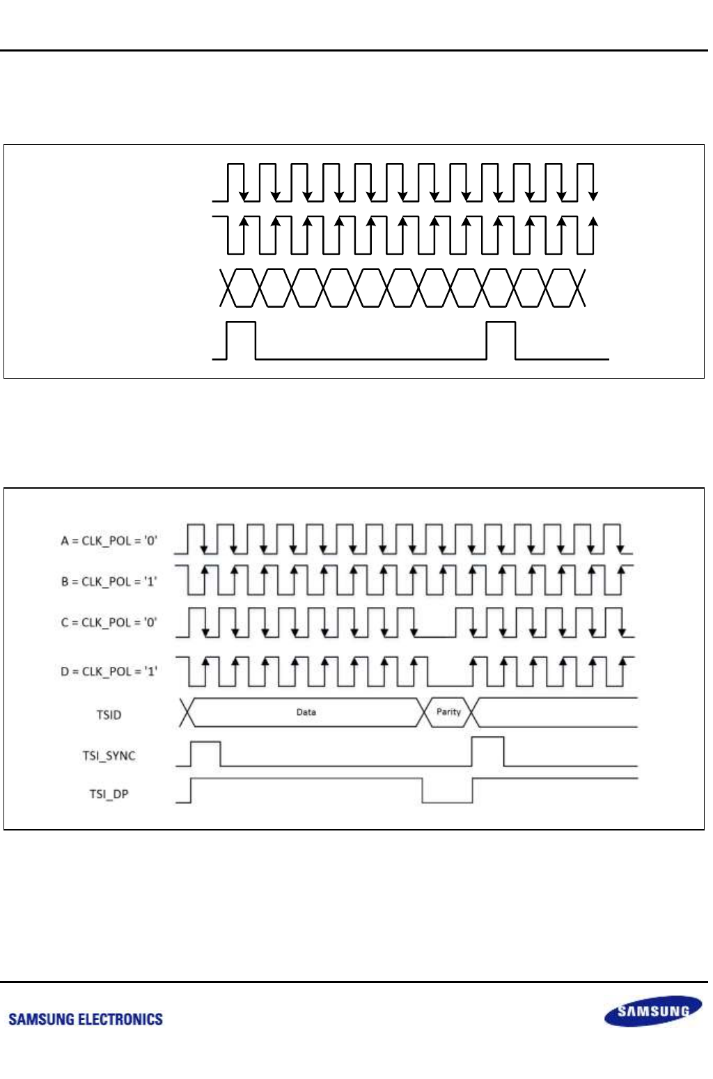
Samsung Confidential
S5P6818_UM 24 MPEG-TS Interface
24-2
Preliminary product information describes products that are in development, for which full characterization data and
associated errata are not yet available. Specifications and information herein are subject to change without notice.
24.3 Functional Description
24.3.1 Timing
Figure 24-1 Basic Transfer Timing Diagram
In the figure above shows the timing chart in which the S5P6818 reads data when an external device sends data
via the MPEG TS interface. If the external device sends data on the rising edge, the S5P6818 actually reads the
data on the falling edge
Figure 24-2 MPEG TS Timing at Parallel Mode
CLK_POL = ‘0’
TSID
TSI_SYNC
0 1 2 3 4 5 6 7
CLK_POL = ‘1’
nexell / ys.kim at 2015.02.12
SAMSUNG Confidential

Samsung Confidential
S5P6818_UM 24 MPEG-TS Interface
24-3
Preliminary product information describes products that are in development, for which full characterization data and
associated errata are not yet available. Specifications and information herein are subject to change without notice.
External devices can provide clocks as well as MPEG TS timing. In the figure above shows the types of clock that
can be provided by external devices. The clock types are determined by the point at which the external devices
output data.
A type devices output data on the rising edge. The value of the CAP_CTRL.CAP_CLK_POL bit is "0", and the
MPEG TSP reads data on the point of the falling edge as above described.
B type devices output data on the falling edge. The value of the CAP_CTRL.CAP_CLK_POL bit is "1".
C type Devices very similar to the A type device is used. The point of difference from an A type device is that
these devices do not check Parity.
D type Devices very similar to the B type device is used. The point of difference from a B type device is that
these devices do not check Parity.
If the value of TSI_DP is "1", the value indicates Data. If the value is "0", the value indicates Parity. However, the
value may have the opposite meaning depending on device properties. In this case, its polarity can be changed by
setting the MPEGIFCONT.DP_POL bit as "1".
nexell / ys.kim at 2015.02.12
SAMSUNG Confidential

Samsung Confidential
S5P6818_UM 24 MPEG-TS Interface
24-4
Preliminary product information describes products that are in development, for which full characterization data and
associated errata are not yet available. Specifications and information herein are subject to change without notice.
24.4 Register Description
24.4.1 Register Map Summary
Base Address: C005_D000h
Register
Offset
Description
Reset Value
CAP_CTRL0
D000h
MPEG TSP capture 0 control register 0
0x0000_0000
CAP_CTRL1
D004h
MPEG TSP capture 1 control register 0
0x0000_0000
CAP_WR_PID_VAL
D008h
MPEG TSP write PID value register
0x0000_0000
CAP_WR_PID_ADDR
D00Ch
MPEG TSP write PID address register
0x0000_0000
CAP0_CAPDATA
D010h
MPEG TSP capture 0 capture data
0x0000_0000
CAP1_CAPDATA
D014h
MPEG TSP capture 1 capture data
0x0000_0000
CORE_TRDATA
D01Ch
MPEG TSP transfer data
0x0000_0000
CORE_CTRL
D020h
MPEG TSP core control register
0x0000_0000
IDMA_STATUS
D024h
MPEG TSP IDMA status register
0x0000_0000
IDMA_CON
D028h
MPEG TSP IDMA control register
0x0000_0000
IDMA_INT
D02Ch
MPEG TSP IDMA interrupt register
0x0000_0000
IDMA0_ADDR
D030h
MPEG TSP internal DMA0 base address register
0x0000_0000
IDMA1_ADDR
D034h
MPEG TSP internal DMA1 base address register
0x0000_0000
IDMA2_AD
D038h
MPEG TSP internal DMA2 base address register
0x0000_0000
IDMA3_ADDR
D03Ch
MPEG TSP internal DMA3 base address register
0x0000_0000
IDMA0_LEN
D040h
MPEG TSP internal DMA0 data length register
0x0000_0000
IDMA1_LEN
D044h
MPEG TSP internal DMA1 data length register
0x0000_0000
IDMA2_LEN
D048h
MPEG TSP internal DMA2 data length register
0x0000_0000
IDMA3_LEN
D04Ch
MPEG TSP internal DMA3 data length register
0x0000_0000
nexell / ys.kim at 2015.02.12
SAMSUNG Confidential

Samsung Confidential
S5P6818_UM 24 MPEG-TS Interface
24-5
Preliminary product information describes products that are in development, for which full characterization data and
associated errata are not yet available. Specifications and information herein are subject to change without notice.
24.4.1.1 CAP_CTRL0
Base Address: C005_D000h
Address = Base Address + D000h, Reset Value = 0x0000_0000
Name
Bit
Type
Description
Reset Value
CAP0_DATA_DUMP_EN
ABLE
[31]
RW
MPEG TSI Data dump enable
0 = Dump only matched data
1 = Dump all input data
1'b0
RSVD
[30:28]
–
Reserved
3'b000
CAP0_LOCK_INT_PEND
[27]
RW
MPEG TS Interface capture 0 interrupt pending
Read
0 = Interrupt not pended
1 = Interrupt pended
Write
0 = Not work
1 = Interrupt clear
1'b0
CAP0_LOCK_INT_MAS
K
[26]
RW
MPEG TS Interface capture 0 interrupt mask
0 = Interrupt masking enabled
1 = Interrupt masking disabled
1'b0
CAP0_LOCK_INT_ENB
[25]
RW
MPEG TS Interface capture 0 interrupt enabled
0 = Interrupt disabled
1 = Interrupt enabled
1'b0
CAP0_LOCK_MODE
[24]
RW
MPEG TS Interface capture 0 lock mode
0 = Unlock (Header not detect)
1 = Lock (Header detect)
1'b0
RSVD
[23:10]
–
Reserved
24'h0
CAP0_SRAM_PWR_EN
B
[9]
RW
MPEG TS Interface capture 0 SRAM power enable
0 = Power disabled
1 = Power enabled
1'b0
CAP0_SRAM_SLEEP
[8]
RW
MPEG TS Interface capture 0 SRAM sleep mode
0 = Sleep
1 = Awake
1'b0
CAP0_ERR_POL
[7]
RW
MPEG TS Interface capture 0 ERR polling mode
0 = Neg-edge capture
1 = Pos-edge capture
1'b0
CAP0_SYNC_POL
[6]
RW
MPEG TS Interface capture 0 SYNC polling mode
0 = Neg-edge capture
1 = Pos-edge capture
1'b0
CAP0_DP_POL
[5]
RW
MPEG TS Interface capture 0 DP polling mode
0 = Neg-edge capture
1 = Pos-edge capture
1'b0
CAP0_CLK_POL
[4]
RW
MPEG TS Interface capture 0 CLK polling mode
0 = Neg-edge capture
1 = Pos-edge capture
1'b0
nexell / ys.kim at 2015.02.12
SAMSUNG Confidential

Samsung Confidential
S5P6818_UM 24 MPEG-TS Interface
24-6
Preliminary product information describes products that are in development, for which full characterization data and
associated errata are not yet available. Specifications and information herein are subject to change without notice.
Name
Bit
Type
Description
Reset Value
RSVD
[3:2]
–
Reserved
2'b00
CAP0_CAP_MODE
[1]
RW
MPEG TS Interface capture 0 capture mode
0 = Byte mode
1 = Reserved
1'b0
CAP0_CAP_ENB
[0]
RW
MPEG TS Interface capture 0 capture enable
0 = Disable
1 = Enable
1'b0
nexell / ys.kim at 2015.02.12
SAMSUNG Confidential

Samsung Confidential
S5P6818_UM 24 MPEG-TS Interface
24-7
Preliminary product information describes products that are in development, for which full characterization data and
associated errata are not yet available. Specifications and information herein are subject to change without notice.
24.4.1.2 CAP_CTRL1
Base Address: C005_D000h
Address = Base Address + D004h, Reset Value = 0x0000_0000
Name
Bit
Type
Description
Reset Value
CAP1_DATA_DUMP_EN
ABLE
[31]
RW
MPEG TSI Data dump enable
0 = Dump only matched data
1 = Dump all input data
1'b0
RSVD
[30:28]
–
Reserved
3'b000
CAP1_LOCK_INT_PEND
[27]
R
MPEG TS Interface capture 1 interrupt pending
Read
0 = Interrupt not pended
1 = Interrupt pended
Write
0 = Not work
1 = Interrupt clear
1'b0
CAP1_LOCK_INT_MAS
K
[26]
RW
MPEG TS Interface capture 1 interrupt mask
0 = Interrupt masking enabled
1 = Interrupt masking disabled
1'b0
CAP1_LOCK_INT_ENB
[25]
RW
MPEG TS Interface capture 1 interrupt enabled
0 = Interrupt disabled
1 = Interrupt enabled
1'b0
CAP1_LOCK_MODE
[24]
RW
MPEG TS Interface capture 1 lock mode
0 = Unlock (Header not detect)
1 = LOCK (Header detect)
1'b0
RSVD
[23:18]
–
Reserved
24'h0
CAP1_OUTCLK_POL
[17]
RW
MPEG TS Interface capture 1 output CLK polling
mode
0 = Neg-edge capture
1 = Pos-edge capture
1'b0
CAP1_OUTENB
[16]
RW
MPEG TS Interface capture 1 direction
0 = Input
1 = Output
1'b0
RSVD
[15:10]
–
Reserved
24'h0
CAP1_SRAM_PWR
[9]
RW
MPEG TS Interface capture 1 SRAM power enable
0 = Power disabled
1 = Power enabled
1'b0
CAP1_SRAM_SLEEP
[8]
RW
MPEG TS Interface capture 1 SRAM sleep mode
0 = Sleep
1 = Awake
1'b0
CAP1_ERR_POL
[7]
RW
MPEG TS Interface capture 1 ERR polling mode
0 = Active low
1 = Active high
1'b0
CAP1_SYNC_POL
[6]
RW
MPEG TS Interface capture 1 SYNC polling mode
1'b0
nexell / ys.kim at 2015.02.12
SAMSUNG Confidential

Samsung Confidential
S5P6818_UM 24 MPEG-TS Interface
24-8
Preliminary product information describes products that are in development, for which full characterization data and
associated errata are not yet available. Specifications and information herein are subject to change without notice.
Name
Bit
Type
Description
Reset Value
0 = Active low
1 = Active high
CAP1_DP_POL
[5]
RW
MPEG TS Interface capture 1 DP polling mode
0 = Active low
1 = Active high
1'b0
CAP1_CLK_POL
[4]
RW
MPEG TS Interface capture 1 CLK polling mode
0 = Neg-edge capture
1 = Pos-edge capture
1'b0
RSVD
[3:2]
–
Reserved
2'b00
CAP1_CAP_MODE
[1]
RW
MPEG TS Interface capture 1 capture mode (this bit
should be set to 0)
0 = Byte mode
1 = Reserved
1'b0
CAP1_CAP_ENB
[0]
RW
MPEG TS Interface capture 1 capture enable
0 = Disable
1 = Enable
1'b0
nexell / ys.kim at 2015.02.12
SAMSUNG Confidential
Samsung Confidential
S5P6818_UM 24 MPEG-TS Interface
24-9
Preliminary product information describes products that are in development, for which full characterization data and
associated errata are not yet available. Specifications and information herein are subject to change without notice.
24.4.1.3 CAP_WR_PID_VAL
Base Address: C005_D000h
Address = Base Address + D008h, Reset Value = 0x0000_0000
Name
Bit
Type
Description
Reset Value
PID_VALUE
[31:0]
RW
MPEG TSP PID value
32'h0
24.4.1.4 CAP_WR_PID_ADDR
Base Address: C005_D000h
Address = Base Address + D00Ch, Reset Value = 0x0000_0000
Name
Bit
Type
Description
Reset Value
RSVD
[31:11]
–
Reserved
21'h0
PID_WR_SEL
[10:9]
RW
PID write module select
0 = MPEG TSP Capture 0
1 = MPEG TSP Capture 1
2 = MPEG TSP Core module
2'b00
PID_WR_ADDR
[8:0]
RW
PID Write Address
9'h0
24.4.1.5 CAP0_CAPDATA
Base Address: C005_D000h
Address = Base Address + D010h, Reset Value = 0x0000_0000
Name
Bit
Type
Description
Reset Value
CAP0_CAPDATA
[31:0]
R
MPEG TS Interface capture data
32'h0
24.4.1.6 CAP1_CAPDATA
Base Address: C005_D000h
Address = Base Address + D014h, Reset Value = 0x0000_0000
Name
Bit
Type
Description
Reset Value
CAP1_CAPDATA
[31:0]
R
MPEG TS Interface capture data
32'h0
24.4.1.7 CORE_TRDATA
Base Address: C005_D000h
Address = Base Address + D01Ch, Reset Value = 0x0000_0000
Name
Bit
Type
Description
Reset Value
CORE_TRDATA
[31:0]
R
MPEG TS Interface transfer data
32'h0
nexell / ys.kim at 2015.02.12
SAMSUNG Confidential

Samsung Confidential
S5P6818_UM 24 MPEG-TS Interface
24-10
Preliminary product information describes products that are in development, for which full characterization data and
associated errata are not yet available. Specifications and information herein are subject to change without notice.
24.4.1.8 CORE_CTRL
Base Address: C005_D000h
Address = Base Address + D020h, Reset Value = 0x0000_0000
Name
Bit
Type
Description
Reset Value
RSVD
[31:19]
–
Reserved
13'h0
CORE_INT_PEND
[18]
R
MPEG TS Core interrupt pending
Read
0 = Interrupt not pended
1 = Interrupt pended
Write
0 = Not work
1 = Interrupt clear
1'b0
CORE_INT_MASK
[17]
RW
MPEG TS Core interrupt mask
1'b0
CORE_INT_ENB
[16]
RW
MPEG TS Core interrupt enable
1'b0
RSVD
[15:8]
–
Reserved
8'h0
CORE_SRAM_PWR
[7]
RW
MPEG TS Core SRAM power
1'b0
CORE_SRAM_SLEEP
[6]
RW
MPEG TS Core SRAM sleep mode
1'b0
RSVD
[5:2]
–
Reserved
4'h0
CORE_ENCR_MODE
[1]
RW
MPEG TS Core Encryption mode
0 = Decoding
1 = Encoding
1'b0
CORE_ENB
[0]
RW
MPEG TS Core Enable
1'b0
nexell / ys.kim at 2015.02.12
SAMSUNG Confidential
Samsung Confidential
S5P6818_UM 24 MPEG-TS Interface
24-11
Preliminary product information describes products that are in development, for which full characterization data and
associated errata are not yet available. Specifications and information herein are subject to change without notice.
24.4.1.9 IDMA_STATUS
Base Address: C005_D000h
Address = Base Address + D024h, Reset Value = 0x0000_0000
Name
Bit
Type
Description
Reset Value
RSVD
[31:20]
–
Reserved
12'h0
IDMA3_BUSY
[19]
R
Internal DMA3 busy
1'b0
IDMA2_BUSY
[18]
R
Internal DMA2 busy
1'b0
IDMA1_BUSY
[17]
R
Internal DMA1 busy
1'b0
IDMA0_BUSY
[16]
R
Internal DMA0 busy
1'b0
RSVD
[15:4]
–
Reserved
12'h0
IDMA3_ENB
[3]
RW
Internal DMA3 Enable
1'b0
IDMA2_ENB
[2]
RW
Internal DMA2 Enable
1'b0
IDMA1_ENB
[1]
RW
Internal DMA1 Enable
1'b0
IDMA0_ENB
[0]
RW
Internal DMA0 Enable
1'b0
24.4.1.10 IDMA_CON
Base Address: C005_D000h
Address = Base Address + D028h, Reset Value = 0x0000_0000
Name
Bit
Type
Description
Reset Value
RSVD
[31:20]
–
Reserved
12'h0
IDMA3_STOP
[19]
W
Internal DMA3 stop
1'b0
IDMA2_STOP
[18]
W
Internal DMA2 stop
1'b0
IDMA1_STOP
[17]
W
Internal DMA1 stop
1'b0
IDMA0_STOP
[16]
W
Internal DMA0 stop
1'b0
RSVD
[15:4]
–
Reserved
12'h0
IDMA3_RUN
[3]
W
0 = Internal DMA3 Initialize
1 = Internal DMA3 run
1'b0
IDMA2_RUN
[2]
W
0 = Internal DMA2 Initialize
1 = Internal DMA2 run
1'b0
IDMA1_RUN
[1]
W
0 = Internal DMA1 Initialize
1 = Internal DMA1 run
1'b0
IDMA0_RUN
[0]
W
0 = Internal DMA0 Initialize
1 = Internal DMA0 run
1'b0
nexell / ys.kim at 2015.02.12
SAMSUNG Confidential

Samsung Confidential
S5P6818_UM 24 MPEG-TS Interface
24-12
Preliminary product information describes products that are in development, for which full characterization data and
associated errata are not yet available. Specifications and information herein are subject to change without notice.
24.4.1.11 IDMA_INT
Base Address: C005_D000h
Address = Base Address + D02Ch, Reset Value = 0x0000_0000
Name
Bit
Type
Description
Reset Value
RSVD
[31:28]
–
Reserved
4'h0
IDMA3_INT_ENB
[27]
RW
Internal DMA3 interrupt enable
1'b0
IDMA2_INT_ENB
[26]
RW
Internal DMA2 interrupt enable
1'b0
IDMA1_INT_ENB
[25]
RW
Internal DMA1 interrupt enable
1'b0
IDMA0_INT_ENB
[24]
RW
Internal DMA0 interrupt enable
1'b0
RSVD
[23:20]
–
Reserved
4'h0
IDMA3_INT_MASK
[19]
RW
Internal DMA3 interrupt mask
0 = Mask
1 = UnMask
1'b0
IDMA2_INT_MASK
[18]
RW
Internal DMA2 interrupt mask
0 = Mask
1 = UnMask
1'b0
IDMA2_INT_MASK
[17]
RW
Internal DMA1 interrupt mask
0 = Mask
1 = UnMask
1'b0
IDMA0_INT_MASK
[16]
RW
Internal DMA0 interrupt mask
0 = Mask
1 = UnMask
1'b0
RSVD
[15:12]
–
Reserved
4'h0
IDMA3_INT_PEND
[11]
RW
Internal DMA3 interrupt pending
1'b0
IDMA2_INT_PEND
[10]
RW
Internal DMA2 interrupt pending
1'b0
IDMA2_INT_PEND
[9]
RW
Internal DMA1 interrupt pending
1'b0
IDMA0_INT_PEND
[8]
RW
Internal DMA0 interrupt pending
1'b0
RSVD
[7:4]
–
Reserved
4'h0
IDMA3_INT_CLR
[3]
W
Internal DMA3 interrupt pending clear
1'b0
IDMA2_INT_CLR
[2]
W
Internal DMA2 interrupt pending clear
1'b0
IDMA2_INT_CLR
[1]
W
Internal DMA1 interrupt pending clear
1'b0
IDMA0_INT_CLR
[0]
W
Internal DMA0 interrupt pending clear
1'b0
nexell / ys.kim at 2015.02.12
SAMSUNG Confidential

Samsung Confidential
S5P6818_UM 24 MPEG-TS Interface
24-13
Preliminary product information describes products that are in development, for which full characterization data and
associated errata are not yet available. Specifications and information herein are subject to change without notice.
24.4.1.12 IDMA0_ADDR
Base Address: C005_D000h
Address = Base Address + D030h, Reset Value = 0x0000_0000
Name
Bit
Type
Description
Reset Value
IDMA0_ADDR
[31:0]
RW
Internal DMA0 Base Address
32'h0
24.4.1.13 IDMA1_ADDR
Base Address: C005_D000h
Address = Base Address + D034h, Reset Value = 0x0000_0000
Name
Bit
Type
Description
Reset Value
IDMA1_ADDR
[31:0]
RW
Internal DMA1 Base Address
32'h0
24.4.1.14 IDMA2_ADDR
Base Address: C005_D000h
Address = Base Address + D038h, Reset Value = 0x0000_0000
Name
Bit
Type
Description
Reset Value
IDMA2_ADDR
[31:0]
RW
Internal DMA2 Base Address
32'h0
24.4.1.15 IDMA3_ADDR
Base Address: C005_D000h
Address = Base Address + D03Ch, Reset Value = 0x0000_0000
Name
Bit
Type
Description
Reset Value
IDMA3_ADDR
[31:0]
RW
Internal DMA3 Base Address
32'h0
nexell / ys.kim at 2015.02.12
SAMSUNG Confidential

Samsung Confidential
S5P6818_UM 24 MPEG-TS Interface
24-14
Preliminary product information describes products that are in development, for which full characterization data and
associated errata are not yet available. Specifications and information herein are subject to change without notice.
24.4.1.16 IDMA0_LEN
Base Address: C005_D000h
Address = Base Address + D040h, Reset Value = 0x0000_0000
Name
Bit
Type
Description
Reset Value
IDMA0_LEN
[31:0]
RW
Internal DMA0 Data Length
32'h0
24.4.1.17 IDMA1_LEN
Base Address: C005_D000h
Address = Base Address + D044h, Reset Value = 0x0000_0000
Name
Bit
Type
Description
Reset Value
IDMA1_LEN
[31:0]
RW
Internal DMA1 Data Length
32'h0
24.4.1.18 IDMA2_LEN
Base Address: C005_D000h
Address = Base Address + D048h, Reset Value = 0x0000_0000
Name
Bit
Type
Description
Reset Value
IDMA2_LEN
[31:0]
RW
Internal DMA2 Data Length
32'h0
24.4.1.19 IDMA3_LEN
Base Address: C005_D000h
Address = Base Address + D04Ch, Reset Value = 0x0000_0000
Name
Bit
Type
Description
Reset Value
IDMA3_LEN
[31:0]
RW
Internal DMA3 Data Length
32'h0
nexell / ys.kim at 2015.02.12
SAMSUNG Confidential
Samsung Confidential
S5P6818_UM 24 MPEG-TS Interface
24-15
Preliminary product information describes products that are in development, for which full characterization data and
associated errata are not yet available. Specifications and information herein are subject to change without notice.
24.5 PID Filter Data Structure
Figure 24-3 Capture I/F PID Structure
Figure 24-4 Basic AES/CSA PID Structure
0: Invalid
1: Valid PID(13bits)
0: AES 0: EVEN
1: ODD 0: FlagHit disable
1: FlagHit enable PID(13bits)
1: CSA Don’t care
nexell / ys.kim at 2015.02.12
SAMSUNG Confidential

Samsung Confidential
S5P6818_UM 25 UART_ISO7816
25-1
Preliminary product information describes products that are in development, for which full characterization data and
associated errata are not yet available. Specifications and information herein are subject to change without notice.
25 UART_ISO7816
25.1 Overview
The Universal Asynchronous Receiver and Transmitter (UART) in S5P6818 provide:
Six independent channels with asynchronous and serial input/output ports for general purpose (Channel 0 to 5),
Two channels without modem and with DMA (NOMODEM_DMA UART Channel 0, 1), one channel with modem
and DMA (MODEM_DMA UART Channel 2), and three channels without modem and DMA (NOMODEM_NODMA
UART Channel 3, 4, 5).
All ports operate in an Interrupt-based or a DMA-based mode. The UART generates an interrupt or a DMA
request to transfer data to and from the CPU and the UART. The UART supports bit rates up to 4 Mbps. Each
UART channel contains two 64 bytes FIFOs to receive and transmit data.
UART includes programmable Baud Rates, Infrared (IR) Transmitter/Receiver, one or two Stop Bit Insertion, 5-bit,
6-bit, 7-bit, or 8-bit Data Width and Parity Checking.
Each UART contains a Baud-rate generator, a Transmitter, a Receiver and a Control Unit. The Baud-rate
generator uses EXT_UCLK. The Transmitter and the Receiver contain FIFOs and data shifters. The data that is
transmitted is written to Tx FIFO, and copied to the transmit shifter. The data is then shifted out by the transmit
data pin (TXD). The received data is shifted from the Receive Data Pin (RXD), and copied to Rx FIFO from the
shifter.
nexell / ys.kim at 2015.02.12
SAMSUNG Confidential
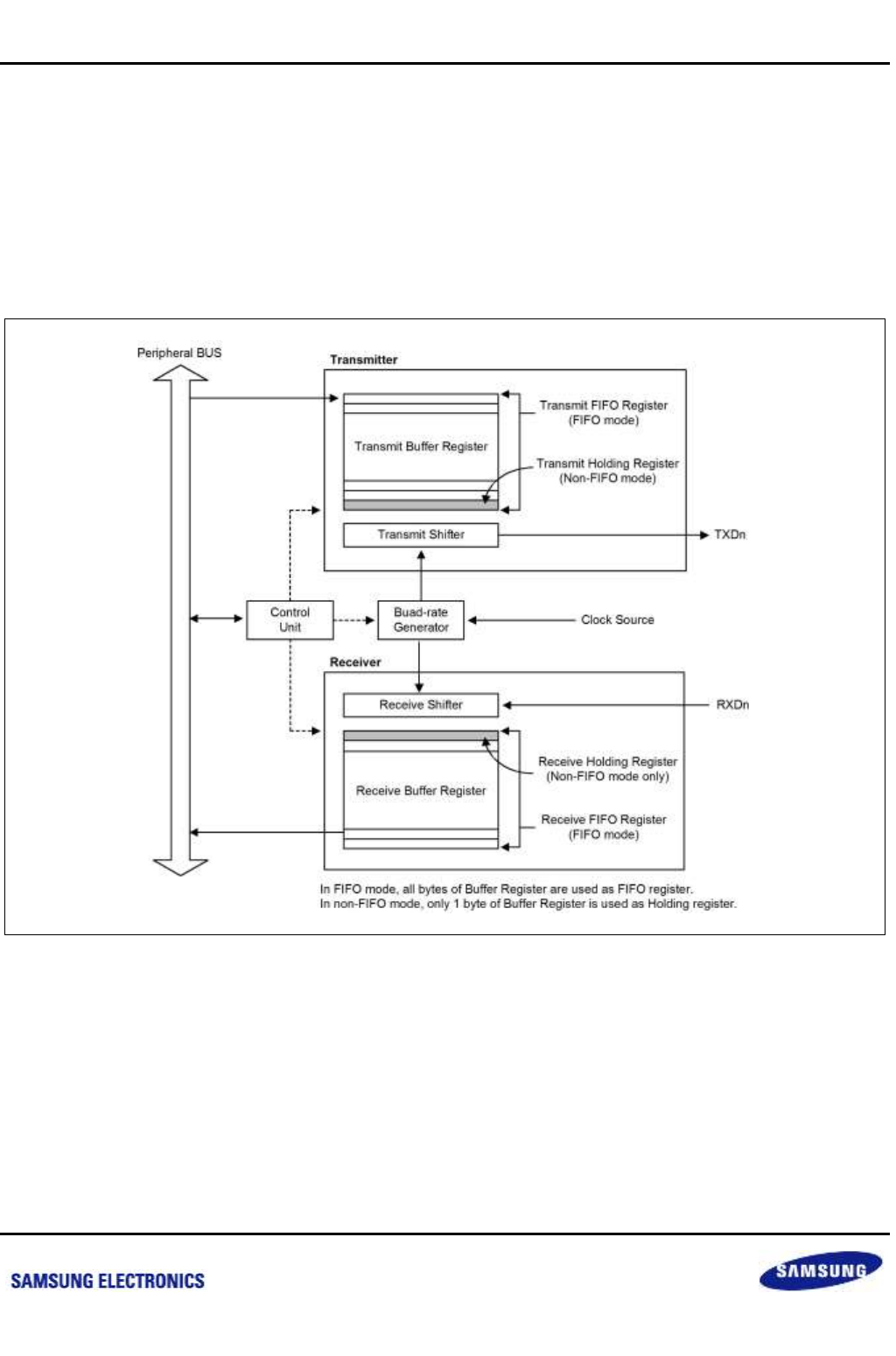
Samsung Confidential
S5P6818_UM 25 UART_ISO7816
25-2
Preliminary product information describes products that are in development, for which full characterization data and
associated errata are not yet available. Specifications and information herein are subject to change without notice.
25.2 Features
All channels support Interrupt-based operation
All channels, except ISP-UART Channel 0, support DMA-based or Interrupt-based operation
All channels, except UART Channel 2, support Auto Flow Control with nRTS and nCTS
Supports Handshake Transmit/Receive
In the following figure illustrates the block diagram of UART.
Figure 25-1 UART Block Diagram
nexell / ys.kim at 2015.02.12
SAMSUNG Confidential

Samsung Confidential
S5P6818_UM 25 UART_ISO7816
25-3
Preliminary product information describes products that are in development, for which full characterization data and
associated errata are not yet available. Specifications and information herein are subject to change without notice.
25.3 UART Description
This section describes UART operations, such as Data Transmission, Data Reception, Interrupt Generation,
Baud-rate Generation, Loop-back mode, Infrared modes, and Auto Flow Control.
25.3.1 Data Transmission
The data frame for transmission is programmable. It consists of a start bit, five to eight data bits, an optional parity
bit and one to two stop bits, specified by the line control register (ULCONn). The transmitter can also produce a
break condition that forces the serial output to logic 0 state, for one frame transmission time. This block transmits
the break signals, after the present transmission word is transmitted completely. After the break signal
transmission, the transmitter continuously transmits data to Tx FIFO (Tx holding register, in case of Non-FIFO
mode).
25.3.2 Data Reception
Similar to data transmission, the data frame for reception is also programmable. It consists of a start bit, five to
eight data bits, an optional parity bit and one to two stop bits in the Line Control Register (ULCONn). The receiver
detects Overrun Error, Parity Error, Frame Error and Break Condition. Each of this error sets an error flag.
Overrun Error indicates that new data has overwritten the old data before it was read
Parity Error indicates that the receiver has detected an unexpected parity condition
Frame Error indicates that the received data does not have a valid stop bit
Break Condition indicates that the RxDn input is held in the logic 0 state for more than one frame transmission
time
Receive time-out condition occurs when the Rx FIFO is not empty in the FIFO mode and no more data is received
during the frame time specified in UCON.
nexell / ys.kim at 2015.02.12
SAMSUNG Confidential
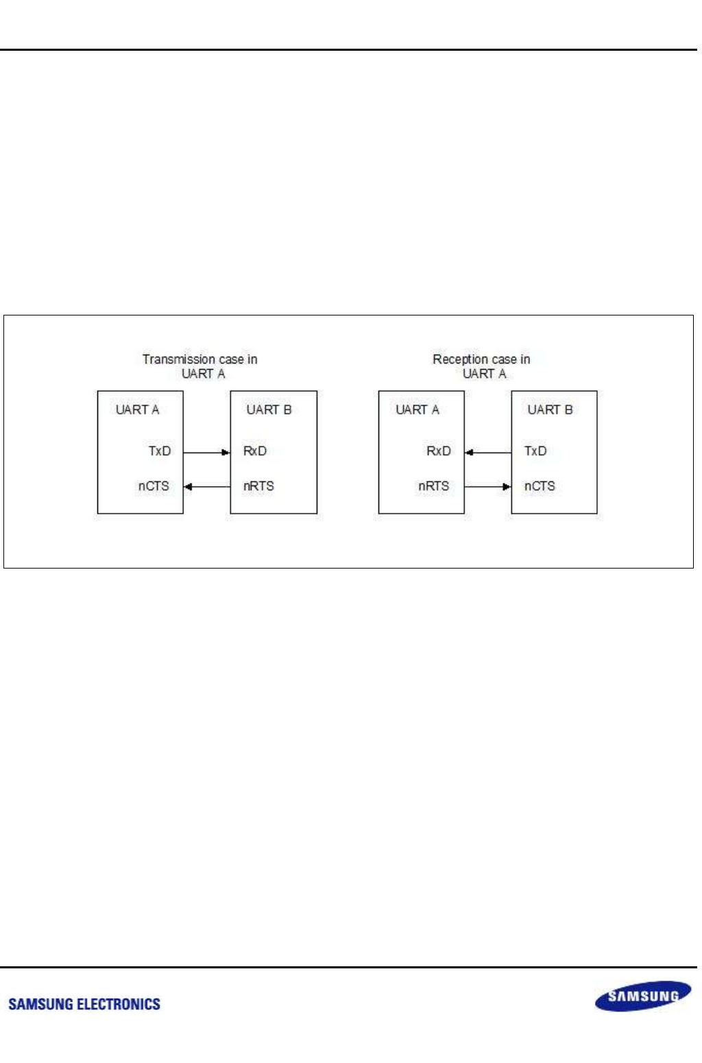
Samsung Confidential
S5P6818_UM 25 UART_ISO7816
25-4
Preliminary product information describes products that are in development, for which full characterization data and
associated errata are not yet available. Specifications and information herein are subject to change without notice.
25.3.3 Auto Flow Control (AFC)
The UART2 and modem UART in S5P6818 support Auto Flow Control (AFC) using nRTS and nCTS signals. In
this case, it can be connected to external UARTs. To connect UART to a Modem, disable the AFC bit in UMCONn
register, and control the signal of nRTS using software.
In AFC, the nRTS signal depends on the condition of the receiver, whereas the nCTS signal controls the operation
of transmitter. The transmitter of UART transfers the data to FIFO when nCTS signals are activated (in AFC,
nCTS signals indicates that FIFO of other UART is ready to receive data). Before UART receives data, the nRTS
signals must be activated when its Receive FIFO has more than 2 byte as spare. The nRTS signals must be
inactivated when its Receive FIFO has less than 1 byte as spare (in AFC, the nRTS signals indicate that its own
Receive FIFO is ready to receive data).
In the following figure illustrates the UART AFC Interface.
Figure 25-2 UART AFC Interface
nexell / ys.kim at 2015.02.12
SAMSUNG Confidential

Samsung Confidential
S5P6818_UM 25 UART_ISO7816
25-5
Preliminary product information describes products that are in development, for which full characterization data and
associated errata are not yet available. Specifications and information herein are subject to change without notice.
25.3.4 Non Auto-Flow Control (Controlling nRTS and nCTS by Software)
25.3.4.1 Rx Operation with FIFO
This procedures describes the Rx Operation with FIFO:
1. Select the transmit mode (Interrupt or DMA mode)
2. Check the value of Rx FIFO count in UFSTATn register. When the value is less than 16, you must set the
value of UMCONn[0] to "1" (activate nRTS). However, when the value is equal to or greater than 16,
you must set the value to "0" (inactivate nRTS).
3. Repeat the Step 2
25.3.4.2 Tx Operation with FIFO
This procedure describes the Tx Operation with FIFO:
1. Select the transmit mode (Interrupt or DMA mode)
2. Check the value of UMSTATn[0]. When the value is "1" (activate nCTS), you must write data to Tx FIFO
register
3. Repeat the Step 2
nexell / ys.kim at 2015.02.12
SAMSUNG Confidential

Samsung Confidential
S5P6818_UM 25 UART_ISO7816
25-6
Preliminary product information describes products that are in development, for which full characterization data and
associated errata are not yet available. Specifications and information herein are subject to change without notice.
25.3.5 Interrupt/DMA Request Generation
Each UART in S5P6818 comprises of seven status (Tx/Rx/Error) signals: Overrun Error, Parity Error, Frame Error,
Break, Receive Buffer Data Ready, Transmit Buffer Empty, and Transmit Shifter Empty. These conditions are
indicated by the corresponding UART status register (UTRSTATn/UERSTATn).
The Overrun Error, Parity Error, Frame Error and Break Condition specify the receive error status. When the
receive-error-status-interrupt-enable bit is set to "1" in the control register (UCONn), the receive error status
generates receive-error-status-interrupt. When a receive-error-status-interrupt-request is detected, you can
identify the source of interrupt by reading the value of UERSTATn.
When the receiver transfers data of the receive shifter to the receive FIFO register in FIFO mode, and the amount
of received data is greater than or equal to the Rx FIFO Trigger Level, Rx interrupt is generated if Receive mode
in control register (UCONn) is set to "1" (Interrupt request or Polling mode).
In Non-FIFO mode, transferring the data of receive shifter to receive holding register causes Rx interrupt in the
Interrupt request and Polling modes.
When the transmitter transfers data from its transmit FIFO register to transmit shifter, and the amount of data left
in transmit FIFO is less than or equal to the Tx FIFO Trigger Level, Tx interrupt is generated (provided Transmit
mode in control register is selected as Interrupt request or Polling mode). In Non-FIFO mode, transferring the data
from transmit holding register to transmit shifter, causes Tx interrupt in the Interrupt request and Polling mode.
The Tx interrupt is always requested when the amount of data in the transmit FIFO is less than the trigger level.
This indicates that an interrupt is requested when you enable the Tx interrupt, unless you fill the Tx buffer.
Therefore, it is recommended to fill the Tx buffer first and then enable the Tx interrupt.
The interrupt controllers of S5P6818 are categorized as the level-triggered type. You must set the interrupt type as
"Level" when you program the UART control registers.
In this situation, when Receive and Transmit modes in control register are selected as DMA request mode, the
DMA request occurs instead of Rx or Tx interrupt.
In the following table describes the interrupts in connection with FIFO.
Table 25-1 Interrupts in Connection with FIFO
Type
FIFO Mode
Non-FIFO Mode0
Rx interrupt
Generated when Rx FIFO count is greater than
or equal to the trigger level of received FIFO.
Generated when the amount of data in FIFO
does not reach Rx FIFO trigger level and does
not receive any data during the time specified
(receive time out) in UCON.
Generated by receive holding register
whenever receive buffer becomes full.
Tx interrupt
Generated when Tx FIFO count is less than or
equal to the trigger level of transmit FIFO (Tx
FIFO trigger Level).
Generated by transmit holding register
whenever transmit buffer becomes empty.
Error interrupt
Generated when Frame Error, Parity Error, or
Break Signal are detected.
Generated if UART receives new data when Rx
FIFO is full (overrun error).
Generated by all errors. However, when
another error occurs at the same time, only
one interrupt is generated.
nexell / ys.kim at 2015.02.12
SAMSUNG Confidential
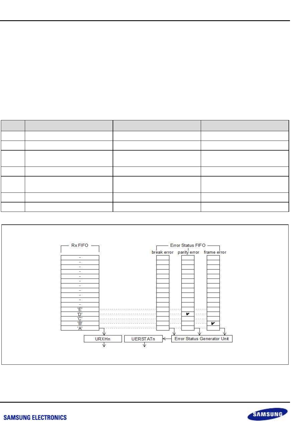
Samsung Confidential
S5P6818_UM 25 UART_ISO7816
25-7
Preliminary product information describes products that are in development, for which full characterization data and
associated errata are not yet available. Specifications and information herein are subject to change without notice.
25.3.6 UART Error Status FIFO
UART contains the error status FIFO besides the Rx FIFO register. The Error Status FIFO indicates the date that
is received with an error, among FIFO registers. An error interrupt is issued only when the data that contains error
is ready to read out. To clear the error status FIFO, URXHn with an error and UERSTATn must be read out.
For example, it is assumed that the UART Rx FIFO receives A, B, C, D, and E characters sequentially, and the
Frame Error occurs when receiving "B" and the Parity Error occurs when receiving "D".
The actual UART receive error does not generate any error interrupt, because the character, which was received
with an error was not read. The error interrupt occurs when the character is read out.
Table 25-2 Receive FIFO bit Function
Time
Sequence Flow
Error Interrupt
Note
#0
When no character is read out
–
–
#1
A, B, C, D, and E is received
–
–
#2
After A is read out
Frame error (in B) interrupt
occurs
The "B" has to be read out
#3
After B is read out
–
–
#4
After C is read out
Parity error (in D) interrupt
occurs
The "D" has to be read out
#5
After D is read out
–
–
#6
After E is read out
–
–
Figure 25-3 UART Receives the Five Characters Including Two Errors
nexell / ys.kim at 2015.02.12
SAMSUNG Confidential
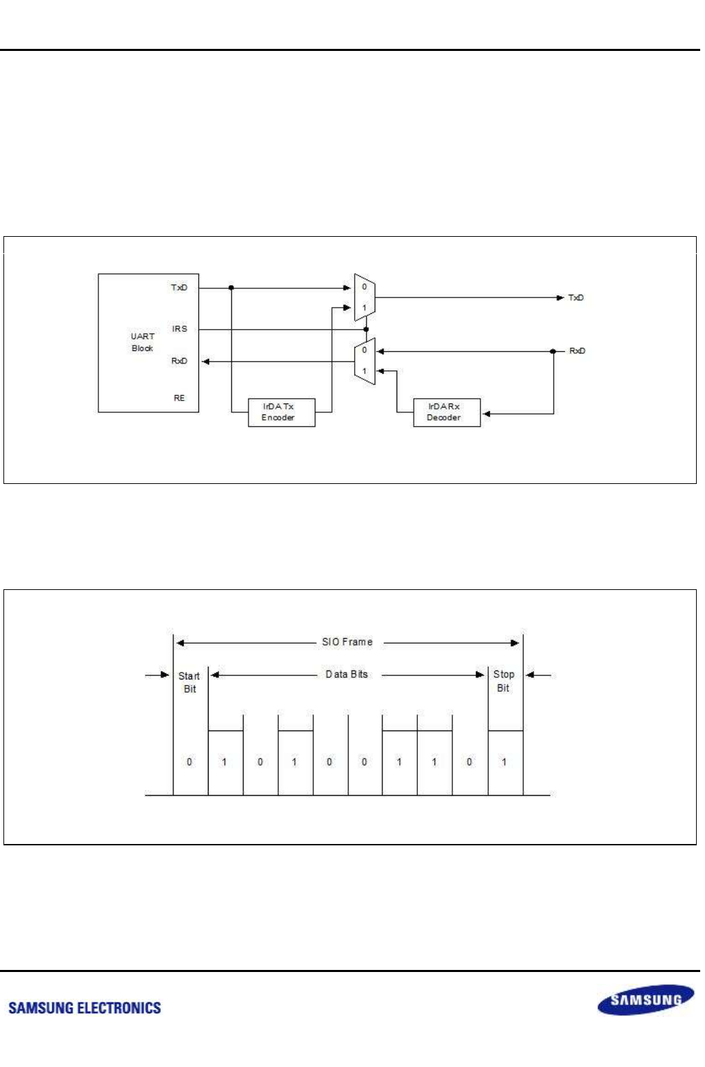
Samsung Confidential
S5P6818_UM 25 UART_ISO7816
25-8
Preliminary product information describes products that are in development, for which full characterization data and
associated errata are not yet available. Specifications and information herein are subject to change without notice.
25.3.6.1 Infra-Red Mode
The S5P6818 UART block supports both Infra-Red (IR) transmission and reception. It is selected by setting the
Infra-red-mode bit in the UART line control register (ULCONn). In the following figure illustrates how to implement
the IR mode.
In IR transmit mode, the transmit pulse comes out at the rate of 3/16, that is, normal serial transmit rate (when the
transmit data bit is 0). However, in IR receive mode, the receiver must detect the 3/16 pulsed period to recognize
a 0 value.
Figure 25-4 Illustrates the IrDA Function Block Diagram
In the following figure illustrates the Serial I/O Frame Timing diagram.
Figure 25-5 Serial I/O Frame Timing Diagram (Normal UART)
nexell / ys.kim at 2015.02.12
SAMSUNG Confidential
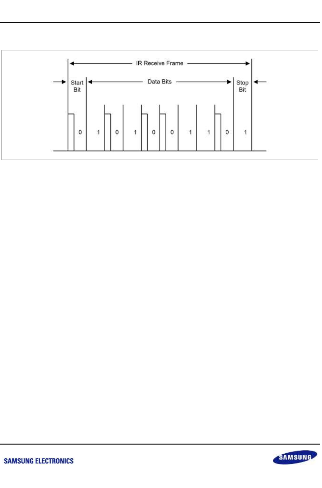
Samsung Confidential
S5P6818_UM 25 UART_ISO7816
25-9
Preliminary product information describes products that are in development, for which full characterization data and
associated errata are not yet available. Specifications and information herein are subject to change without notice.
In the following figure illustrates the Infra-Red Receive Mode Frame Timing diagram.
Figure 25-6 Infra-Red Receive Mode Frame Timing Diagram
nexell / ys.kim at 2015.02.12
SAMSUNG Confidential

Samsung Confidential
S5P6818_UM 25 UART_ISO7816
25-10
Preliminary product information describes products that are in development, for which full characterization data and
associated errata are not yet available. Specifications and information herein are subject to change without notice.
25.3.7 UART Baud Rate
25.3.7.1 UART Baud Rate Configuration
The value stored in the Baud Rate Divisor (UBRDIVn) and Divisor Fractional value (UFRACVALn) is used to
determine the serial Tx/Rx clock rate (baud rate) as:
DIV_VAL = UBRDIVn + UFRACVALn/16
Or
DIV_VAL = (SCLK_UART/(bps x 16)) – 1
Where, the divisor should be from 1 to (216 – 1).
Using UFRACVALn, you can generate the Baud Rate more accurately.
For example, when the Baud Rate is 115200 bps and SCLK_UART is 40 MHz, UBRDIVn and UFRACVALn are:
DIV_VAL = (40000000/(115200 x 16)) – 1
= 21.7 – 1
= 20.7
UBRDIVn = 20 (integer part of DIV_VAL)
UFRACVALn/16 = 0.7
So, UFRACVALn = 11
25.3.7.2 Baud Rate Error Tolerance
UART Frame error should be less than 1.87 % (3/160)
tUPCLK = (UBRDIVn + 1 + UFRACVAL/16) 16 1Frame/SCLK_UART
tUPCLK: Real UART Clock
tEXTUARTCLK = 1Frame/baud-rate
tEXTUARTCLK: Ideal UART Clock
UART error = (tUPCLK – tEXTUARTCLK)/tEXTUARTCLK 100 %
1Frame = start bit + data bit + parity bit + stop bit.
25.3.7.3 UART Clock and PCLK Relation
There is a constraint on the ratio of clock frequencies for PCLK to UARTCLK.
The frequency of UARTCLK must not be more than 5.5/3 times faster than the frequency of PCLK:
FUARTCLK 5.5/3 FPCLK
FUARTCLK = baudrate 16
This allows sufficient time to write the received data to the receive FIFO.
nexell / ys.kim at 2015.02.12
SAMSUNG Confidential
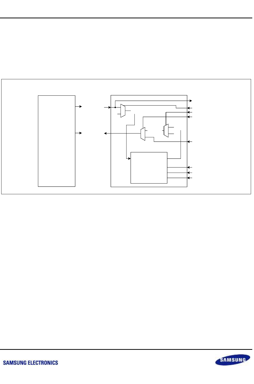
Samsung Confidential
S5P6818_UM 25 UART_ISO7816
25-11
Preliminary product information describes products that are in development, for which full characterization data and
associated errata are not yet available. Specifications and information herein are subject to change without notice.
25.3.8 ISO-7816
In the following figure represents ISO-7816 interface. UARTTXD and UARTRXD signals are connected to external
pads through Smart card Adapter block. Users can select whether to use ISO-7816 through USESMC,
SMCTXENB, SMCRXENB signals, which are controllable by register.
In the case of communicating through ISO-7816 interface, SMC pads are controlled by PAD interface of
NXOpenDrainAdapter.
Figure 25-7 Smart Card Adepter Interface
NXSmartCardAdapter
UARTTXD
Tx_w
NXOpenDrainAdapter
i_A o_Y
o_PAD_EN
i_PAD_Y
o_PAD_A
SMC_Rx Rx_w
‘1’
‘1’
o_UART_TX
i_UART_RX
UARTRXD
SMCTXENB
SMCRXENB
USESMC
o_SMC_EN
i_SMC_Y
o_SMC_A
UART
UARTTXD
UARTRXD
1
0
1
0
1
0
nexell / ys.kim at 2015.02.12
SAMSUNG Confidential

Samsung Confidential
S5P6818_UM 25 UART_ISO7816
25-12
Preliminary product information describes products that are in development, for which full characterization data and
associated errata are not yet available. Specifications and information herein are subject to change without notice.
25.4 Register Description
25.4.1 Register Map Summary
Base Address: C00A_1000 (UART0)
Base Address: C00A_0000 (UART1)
Base Address: C00A_2000 (UART2)
Base Address: C00A_3000 (UART3)
Base Address: C006_D000 (UART4)
Base Address: C006_F000 (UART5)
Register
Offset
Description
Reset Value
ULCONn
0x1000
0x0000
0x2000
0x3000
0xD000
0xF000
Specifies Line Control
0x0000_0000
UCONn
0x1004
0x0004
0x2004
0x3004
0xD004
0xF004
Specifies Control
0x0000_3000
UFCONn
0x1008
0x0008
0x2008
0x3008
0xD008
0xF008
Specifies FIFO Control
0x0000_0000
UMCONn
0x100C
0x000C
0x200C
0x300C
0xD00C
0xF00C
Specifies Modem Control
0x0000_0000
UTRSTATn
0x1010
0x0010
0x2010
0x3010
0xD010
0xF010
Specifies Tx/Rx status
0x0000_0006
UERSTATn
0x1014
0x0014
0x2014
0x3014
0xD014
0xF014
Specifies Rx Error Status
0x0000_0000
nexell / ys.kim at 2015.02.12
SAMSUNG Confidential

Samsung Confidential
S5P6818_UM 25 UART_ISO7816
25-13
Preliminary product information describes products that are in development, for which full characterization data and
associated errata are not yet available. Specifications and information herein are subject to change without notice.
Register
Offset
Description
Reset Value
UFSTATn
0x1018
0x0018
0x2018
0x3018
0xD018
0xF018
Specifies FIFO Status
0x0000_0000
UMSTATn
0x101C
0x001C
0x201C
0x301C
0xD01C
0xF01C
Specifies Modem Status
0x0000_0000
UTXHn
0x1020
0x0020
0x2020
0x3020
0xD020
0xF020
Specifies Transmit Buffer
Undefined
URXHn
0x1024
0x0024
0x2024
0x3024
0xD024
0xF024
Specifies Receive Buffer
0x0000_0000
UBRDIVn
0x1028
0x0028
0x2028
0x3028
0xD028
0xF028
Specifies Baud Rate Divisor
0x0000_0000
UFRACVALn
0x102C
0x002C
0x202C
0x302C
0xD02C
0xF02C
Specifies Divisor Fractional Value
0x0000_0000
UINTPn
0x1030
0x0030
0x2030
0x3030
0xD030
0xF030
Specifies Interrupt Pending
0x0000_0000
UINTSn
0x1034
0x0034
0x2034
0x3034
0xD034
0xF034
Specifies Interrupt Source
0x0000_0000
nexell / ys.kim at 2015.02.12
SAMSUNG Confidential

Samsung Confidential
S5P6818_UM 25 UART_ISO7816
25-14
Preliminary product information describes products that are in development, for which full characterization data and
associated errata are not yet available. Specifications and information herein are subject to change without notice.
Register
Offset
Description
Reset Value
UINTMn
0x1038
0x0038
0x2038
0x3038
0xD038
0xF038
Specifies Interrupt Mask
0x0000_0000
nexell / ys.kim at 2015.02.12
SAMSUNG Confidential

Samsung Confidential
S5P6818_UM 25 UART_ISO7816
25-15
Preliminary product information describes products that are in development, for which full characterization data and
associated errata are not yet available. Specifications and information herein are subject to change without notice.
25.4.1.1 ULCONn
Base Address: C00A_1000 (UART0)
Base Address: C00A_0000 (UART1)
Base Address: C00A_2000 (UART2)
Base Address: C00A_3000 (UART3)
Base Address: C006_D000 (UART4)
Base Address: C006_F000 (UART5)
Address = Base Address + 0x1000, 0x0000, 0x2000, 0x3000, 0xD000, 0xF000, Reset Value = 0x0000_0000
Name
Bit
Type
Description
Reset Value
RSVD
[31:7]
–
Reserved
–
INFRARED MODE
[6]
RW
Determines whether to use the Infrared mode
0 = Normal mode operation
1 = Infrared Tx/Rx mode
1’b0
PARITY MODE
[5:3]
RW
Specifies the type of parity generation to be performed
and checking during UART transmit and receive
operation
0xx = No parity
100 = Odd parity
101 = Even parity
110 = Parity forced/ checked as 1
111 = Parity forced/ checked as 0
3’h0
NUMBER OF STOP BIT
[2]
RW
Specifies the number of stop bits that are used to
signal end-of-frame signal
0 = One stop bit per frame
1 = Two stop bit per frame
1’b0
WORD LENGTH
[1:0]
RW
Indicates the number of data bits to be transmitted or
received per frame
00 = 5-bit
01 = 6-bit
10 = 7-bit
11 = 8-bit
2’b00
nexell / ys.kim at 2015.02.12
SAMSUNG Confidential

Samsung Confidential
S5P6818_UM 25 UART_ISO7816
25-16
Preliminary product information describes products that are in development, for which full characterization data and
associated errata are not yet available. Specifications and information herein are subject to change without notice.
25.4.1.2 UCONn
Base Address: C00A_1000 (UART0)
Base Address: C00A_0000 (UART1)
Base Address: C00A_2000 (UART2)
Base Address: C00A_3000 (UART3)
Base Address: C006_D000 (UART4)
Base Address: C006_F000 (UART5)
Address = Base Address + 0x1004, 0x0004, 0x2004, 0x3004, 0xD004, 0xF004, Reset Value = 0x0000_3000
Name
Bit
Type
Description
Reset Value
RSVD
[31:23]
–
Reserved
–
Tx DMA burst size
[22:20]
RW
Tx DMA Burst Size
Indicates the data transfer size of one DMA
transaction which is triggered by a Tx DMA request.
The DMA program must be programmed to transfer
the same data size as this value for a single Tx DMA
request.
000 = 1 byte (Single)
001 = 4 bytes
010 = 8 bytes
011 = Reserved
100 = Reserved
101 = Reserved
110 = Reserved
111 = Reserved
3’b000
RSVD
[19]
–
Reserved
–
Rx DMA burst size
[18:16]
RW
Rx DMA Burst Size
Indicates the data transfer size of one DMA
transaction that is triggered by a Rx DMA request. The
DMA program must be programmed to transfer the
same data size as this value for a single Rx DMA
request.
000 = 1 byte (Single)
001 = 4 bytes
010 = 8 bytes
011 = 16 bytes
100 = Reserved
101 = Reserved
110 = Reserved
111 = Reserved
3’b000
Rx timeout interrupt
interval
[15:12]
RW
Rx Timeout Interrupt Interval
Rx interrupt occurs when no data is received during 8
(N+1) frame time.
The default value of this field is 3 and it indicates the
timeout interval is 32 frame time.
4’h3
Rx Time-out with empty
[11]
RW
Enables Rx time-out feature when Rx FIFO counter is
8’h0
nexell / ys.kim at 2015.02.12
SAMSUNG Confidential

Samsung Confidential
S5P6818_UM 25 UART_ISO7816
25-17
Preliminary product information describes products that are in development, for which full characterization data and
associated errata are not yet available. Specifications and information herein are subject to change without notice.
Name
Bit
Type
Description
Reset Value
Rx FIFO
"0"
This bit is valid only when UCONn[7] is "1".
0 = Disables Rx time-out feature when Rx FIFO is
empty
1 = Enables Rx time-out feature when Rx FIFO is
empty
Rx Time-out DMA
suspend enable
[10]
RW
Enables Rx DMA FSM to suspend when Rx Time-out
occurs
0 = Disables suspending Rx DMA FSM
1 = Enables suspending Rx DMA FSM
1’b0
Tx Interrupt Type
[9]
RW
Interrupt request type
0 = Pulse (interrupt is requested when the Tx buffer is
empty in the Non-FIFO mode, or when it reaches Tx
FIFO Trigger Level in the FIFO mode)
1 = Level (interrupt is requested when Tx buffer is
empty in the Non-FIFO mode, or when it reaches Tx
FIFO Trigger Level in the FIFO mode)
1’b0
Rx Interrupt Type
[8]
RW
Interrupt request type
0 = Pulse (interrupt is requested when instant Rx
buffer receives data in the Non-FIFO mode, or when it
reaches Rx FIFO Trigger Level in the FIFO mode)
1 = Level (interrupt is requested when Rx buffer
receives data in the Non-FIFO mode, or when it
reaches Rx FIFO Trigger Level in the FIFO mode)
1’b0
Rx Time Out Enable
[7]
RW
Enables/Disables Rx time-out interrupts when UART
FIFO is enabled. The interrupt is a receive interrupt.
0 = Disables Rx Time-out interrupt
1 = Enables Rx Time-out interrupt
1’b0
Rx Error Status Interrupt
Enable
[6]
RW
Enables the UART to generate an interrupt upon an
exception, such as, a Break, Frame Error, Parity Error,
or Overrun Error during a receive operation.
0 = Does not generate receive error status interrupt
1 = Generates receive error status interrupt
1’b0
Loop-back Mode
[5]
RW
Setting loop-back bit to "1" triggers the UART to enter
the loop-back mode. This mode is provided for test
only.
0 = Normal operation
1 = Loop-back mode
1’b0
Send Break Signal
[4]
RW
Setting this bit triggers the UART to send a break
during "1" frame time. This bit is automatically cleared
after sending the break signal.
0 = Normal transmit
1 = Sends the break signal
1’b0
Transmit Mode
[3:2]
RW
Determines which function is able to write Tx data to
the UART transmit buffer
00 = Disables
2’b00
nexell / ys.kim at 2015.02.12
SAMSUNG Confidential

Samsung Confidential
S5P6818_UM 25 UART_ISO7816
25-18
Preliminary product information describes products that are in development, for which full characterization data and
associated errata are not yet available. Specifications and information herein are subject to change without notice.
Name
Bit
Type
Description
Reset Value
01 = Interrupt request or Polling mode
10 = DMA mode
11 = Reserved
Receive Mode
[1:0]
RW
Determines which function is able to read data from
UART receive buffer
00 = Disables
01 = Interrupt request or Polling mode
10 = DMA mode
11 = Reserved
2’b00
nexell / ys.kim at 2015.02.12
SAMSUNG Confidential

Samsung Confidential
S5P6818_UM 25 UART_ISO7816
25-19
Preliminary product information describes products that are in development, for which full characterization data and
associated errata are not yet available. Specifications and information herein are subject to change without notice.
25.4.1.3 UFCONn
Base Address: C00A_1000 (UART0)
Base Address: C00A_0000 (UART1)
Base Address: C00A_2000 (UART2)
Base Address: C00A_3000 (UART3)
Base Address: C006_D000 (UART4)
Base Address: C006_F000 (UART5)
Address = Base Address + 0x1008, 0x0008, 0x2008, 0x3008, 0xD008, 0xF008, Reset Value = 0x0000_0000
Name
Bit
Type
Description
Reset Value
RSVD
[31:11]
–
Reserved
–
Tx FIFO Trigger Level
[10:8]
RW
Determines the trigger level of Tx FIFO. When data
count of Tx FIFO is less than or equal to the trigger
level, Tx interrupt occurs.
000 = 0 byte
001 = 8 bytes
010 = 16 bytes
011 = 24 bytes
100 = 32 bytes
101 = 40 bytes
110 = 48 bytes
111 = 56 bytes
3’b000
RSVD
[7]
–
Reserved
–
Rx FIFO Trigger Level
[6:4]
RW
Determines the trigger level of Rx FIFO. When data
count of Rx FIFO is greater than or equal to the trigger
level, Rx interrupt occurs.
[Channel 0]
000 = 8 byte
001 = 16 bytes
010 = 24 bytes
011 = 32 bytes
100 = 40 bytes
101 = 48 bytes
110 = 56 bytes
111 = 64 bytes
3’b000
RSVD
[3]
–
Reserved
1’b0
Tx FIFO Reset
[2]
RW
Auto-clears after resetting FIFO
0 = Normal
1 = Tx FIFO reset
1’b0
Rx FIFO Reset
[1]
RW
Auto-clears after resetting FIFO
0 = Normal
1 = Rx FIFO reset
1’b0
FIFO Enable
[0]
RW
0 = Disables
1 = Enables
1’b0
nexell / ys.kim at 2015.02.12
SAMSUNG Confidential
Samsung Confidential
S5P6818_UM 25 UART_ISO7816
25-20
Preliminary product information describes products that are in development, for which full characterization data and
associated errata are not yet available. Specifications and information herein are subject to change without notice.
25.4.1.4 UMCONn
Base Address: C00A_1000 (UART0)
Base Address: C00A_0000 (UART1)
Base Address: C00A_2000 (UART2)
Base Address: C00A_3000 (UART3)
Base Address: C006_D000 (UART4)
Base Address: C006_F000 (UART5)
Address = Base Address +0x100C, 0x000C, 0x200C, 0x300C, 0xD00C, 0xF00C, Reset Value =
0x0000_0000
Name
Bit
Type
Description
Reset Value
RSVD
[31:8]
–
Reserved
–
RTS trigger level
[7:5]
RW
Determines the trigger level of Rx FIFO to control
nRTS signal. When AFC bit is enabled and Rx FIFO
have bytes that are greater than or equal to the trigger
level, nRTS signal is deactivated.
[Channel 0]
000 = 63 bytes
001 = 56 bytes
010 = 48 bytes
011 = 40 bytes
100 = 32 bytes
101 = 24 bytes
110 = 16 bytes
111 = 8 bytes
3’b000
Auto flow control (AFC)
[4]
RW
0 = Disables
1 = Enables
1’b0
Modem interrupt enable
[3]
RW
0 = Disables
1 = Enables
1’b0
RSVD
[2:1]
RW
These bits must be "0"
–
Request to send
[0]
RW
When AFC bit is enabled, this value is ignored. In this
case the S5P6818 controls nRTS signals
automatically.
When AFC bit is disabled, the software must control
nRTS signal.
0 = "H" level (Inactivate nRTS)
1 = "L" level (Activate nRTS)
1’b0
nexell / ys.kim at 2015.02.12
SAMSUNG Confidential

Samsung Confidential
S5P6818_UM 25 UART_ISO7816
25-21
Preliminary product information describes products that are in development, for which full characterization data and
associated errata are not yet available. Specifications and information herein are subject to change without notice.
25.4.1.5 UTRSTATn
Base Address: C00A_1000 (UART0)
Base Address: C00A_0000 (UART1)
Base Address: C00A_2000 (UART2)
Base Address: C00A_3000 (UART3)
Base Address: C006_D000 (UART4)
Base Address: C006_F000 (UART5)
Address = Base Address +0x1010, 0x0010, 0x2010, 0x3010, 0xD010, 0xF010, Reset Value = 0x0000_0006
Name
Bit
Type
Description
Reset Value
RSVD
[31:24]
–
Reserved
–
Rx FIFO count in Rx
time-out status
[23:16]
R
Rx FIFO counter capture value when Rx time-out
occurs
8’h0
Tx DMA FSM state
[15:12]
R
Current State of Tx DMA FSM
0x0 = IDLE
0x1 = Burst Request
0x2 = Burst Acknowledgement
0x3 = Burst Next (intermediate state for next request)
0x4 = Single Request
0x5 = Single Acknowledgement
0x6 = Single Next (intermediate state for next request)
0x7 = Last Burst Request
0x8 = Last Burst Acknowledgement
0x9 = Last Single Request
0x10 = Last Single Acknowledgement
4’h0
Rx DMA FSM state
[11:8]
R
Current State of Rx DMA FSM
0x0 = IDLE
0x1 = Burst Request
0x2 = Burst Acknowledgement
0x3 = Burst Next (intermediate state for next request)
0x4 = Single Request
0x5 = Single Acknowledgement
0x6 = Single Next (intermediate state for next request)
0x7 = Last Burst Request
0x8 = Last Burst Acknowledgement
0x9 = Last Single Request
0x10 = Last Single Acknowledgement
4’h0
RSVD
[7:4]
–
Reserved
–
Rx time-out status/clear1
[3]
RW
Rx Time-out status when read
0 = Rx Time out did not occur
1 = Rx Time out
Clear Rx Time-out status when write
0 = No operation
1 = Clears Rx Time-out status
NOTE: If UCONn[10] is set to "1", writing 1 to this bit
resumes Rx DMA FSM that was suspended when Rx
1’b0
nexell / ys.kim at 2015.02.12
SAMSUNG Confidential

Samsung Confidential
S5P6818_UM 25 UART_ISO7816
25-22
Preliminary product information describes products that are in development, for which full characterization data and
associated errata are not yet available. Specifications and information herein are subject to change without notice.
Name
Bit
Type
Description
Reset Value
time-out had occurred.
Transmitter empty
[2]
R
This bit is automatically set to "1" when the transmit
buffer has no valid data to transmit, and the transmit
shift is empty.
0 = Buffer is not empty
1 = Transmitter (that includes transmit buffer and
shifter) empty
1’b1
Transmit buffer empty
[1]
R
This bit is automatically set to "1" when transmit buffer
is empty.
0 = Buffer is not empty
1 = Buffer is empty
In Non-FIFO mode, Interrupt or DMA is requested.
In FIFO mode, Interrupt or DMA is requested, when
Tx
FIFO Trigger Level is set to 00 (empty)
When UART uses FIFO, check Tx FIFO Count bits
and Tx FIFO Full bit in UFSTAT instead of this bit.
1’b1
Receive buffer data
ready
[0]
R
This bit is automatically set to "1" if receive buffer
contains valid data, received through the RXDn port.
0 = Buffer is empty
1 = Buffer has a received data (In Non-FIFO mode,
Interrupt or DMA is requested)
When UART uses the FIFO, check Rx FIFO Count
bits and Rx FIFO Full bit in UFSTAT instead of this bit.
1’b0
nexell / ys.kim at 2015.02.12
SAMSUNG Confidential

Samsung Confidential
S5P6818_UM 25 UART_ISO7816
25-23
Preliminary product information describes products that are in development, for which full characterization data and
associated errata are not yet available. Specifications and information herein are subject to change without notice.
25.4.1.6 UERSTATn
Base Address: C00A_1000 (UART0)
Base Address: C00A_0000 (UART1)
Base Address: C00A_2000 (UART2)
Base Address: C00A_3000 (UART3)
Base Address: C006_D000 (UART4)
Base Address: C006_F000 (UART5)
Address = Base Address +0x1014, 0x0014, 0x2014, 0x3014, 0xD014, 0xF014, Reset Value = 0x0000_0000
Name
Bit
Type
Description
Reset Value
RSVD
[31:4]
–
Reserved
–
Break detect
[3]
R
This bit is automatically set to "1" to indicate that a
break signal has been received.
0 = No break signal is received
1 = Break signal is received (Interrupt is requested)
1’b0
Frame error
[2]
R
This bit is automatically set to "1" when a Frame Error
occurs during the receive operation.
0 = No Frame Error occurs during the receive
operation
1 = Frame Error occurs (interrupt is requested) during
the receive operation
1’b0
Parity error
[1]
R
This bit is automatically set to "1" when a Parity Error
occurs during the receive operation.
0 = No Parity Error occurs during receive operation
1 = Parity Error occurs (interrupt is requested) during
the receive operation
1’b0
Overrun error
[0]
R
This bit is automatically set to "1" automatically when
an Overrun Error occurs during the receive operation.
0 = No Overrun Error occurs during the receive
operation
1 = Overrun Error occurs (interrupt is requested)
during the receive operation
1’b0
nexell / ys.kim at 2015.02.12
SAMSUNG Confidential
Samsung Confidential
S5P6818_UM 25 UART_ISO7816
25-24
Preliminary product information describes products that are in development, for which full characterization data and
associated errata are not yet available. Specifications and information herein are subject to change without notice.
25.4.1.7 UFSTATn
Base Address: C00A_1000 (UART0)
Base Address: C00A_0000 (UART1)
Base Address: C00A_2000 (UART2)
Base Address: C00A_3000 (UART3)
Base Address: C006_D000 (UART4)
Base Address: C006_F000 (UART5)
Address = Base Address +0x1018, 0x0018, 0x2018, 0x3018, 0xD018, 0xF018, Reset Value = 0x0000_0000
Name
Bit
Type
Description
Reset Value
RSVD
[31:25]
–
Reserved
–
Tx FIFO full
[24]
R
This bit is automatically set to "1" when the
transmitted FIFO is full during transmit operation.
0 = Not Full
1 = Full
1’b0
Tx FIFO count
[23:16]
R
Number of data in Tx FIFO
NOTE: This field is set to "0" when Tx FIFO is full.
8’h0
RSVD
[15:10]
–
Reserved
–
Rx FIFO error
[9]
R
This bit is set to "1" when Rx FIFO contains invalid
data which results due to Frame Error, Parity Error, or
Break Signal.
1’b0
Rx FIFO full
[8]
R
This bit is automatically set to "1" when the received
FIFO is full during receive operation.
0 = Not Full
1 = Full
1’b0
Rx FIFO count
[7:0]
R
Number of data in Rx FIFO
NOTE: This field is set to "0" when Rx FIFO is full.
8’h0
nexell / ys.kim at 2015.02.12
SAMSUNG Confidential
Samsung Confidential
S5P6818_UM 25 UART_ISO7816
25-25
Preliminary product information describes products that are in development, for which full characterization data and
associated errata are not yet available. Specifications and information herein are subject to change without notice.
25.4.1.8 UMSTATn
Base Address: C00A_1000 (UART0)
Base Address: C00A_0000 (UART1)
Base Address: C00A_2000 (UART2)
Base Address: C00A_3000 (UART3)
Base Address: C006_D000 (UART4)
Base Address: C006_F000 (UART5)
Address = Base Address +0x101C, 0x001C, 0x201C, 0x301C, 0xD01C, 0xF01C, Reset Value =
0x0000_0000
Name
Bit
Type
Description
Reset Value
RSVD
[31:5]
–
Reserved
–
Delta CTS
[4]
R
This bit indicates that the nCTS input to the S5P6818
has changed its state since the last time it was read
by CPU. (Refer to Figure 24-9 for more information.)
0 = Not changed
1 = Changed
1’b0
RSVD
[3:1]
–
Reserved
–
Clear to send
[0]
R
0 = CTS signal is not activated (nCTS pin is high)
1 = CTS signal is activated (nCTS pin is low)
NOTE: In UMSTATn of ISP-UART, reset value of this
bit is undefined. It depends on the GPIO configuration
of the corresponding CTS port.
1’b0
nexell / ys.kim at 2015.02.12
SAMSUNG Confidential
Samsung Confidential
S5P6818_UM 25 UART_ISO7816
25-26
Preliminary product information describes products that are in development, for which full characterization data and
associated errata are not yet available. Specifications and information herein are subject to change without notice.
25.4.1.9 UTXHn
Base Address: C00A_1000 (UART0)
Base Address: C00A_0000 (UART1)
Base Address: C00A_2000 (UART2)
Base Address: C00A_3000 (UART3)
Base Address: C006_D000 (UART4)
Base Address: C006_F000 (UART5)
Address = Base Address +0x1020, 0x0020, 0x2020, 0x3020, 0xD020, 0xF020, Reset Value = undefined
Name
Bit
Type
Description
Reset Value
RSVD
[31:8]
–
Reserved
–
UTXHn
[7:0]
W
Transmit Data for UARTn
–
25.4.1.10 URXHn
Base Address: C00A_1000 (UART0)
Base Address: C00A_0000 (UART1)
Base Address: C00A_2000 (UART2)
Base Address: C00A_3000 (UART3)
Base Address: C006_D000 (UART4)
Base Address: C006_F000 (UART5)
Address = Base Address +0x1024, 0x0024, 0x2024, 0x3024, 0xD024, 0xF024, Reset Value = 0x0000_0000
Name
Bit
Type
Description
Reset Value
RSVD
[31:8]
–
Reserved
–
URXHn
[7:0]
R
Receive Data for UARTn
8’h0
nexell / ys.kim at 2015.02.12
SAMSUNG Confidential
Samsung Confidential
S5P6818_UM 25 UART_ISO7816
25-27
Preliminary product information describes products that are in development, for which full characterization data and
associated errata are not yet available. Specifications and information herein are subject to change without notice.
25.4.1.11 UBRDIVn
Base Address: C00A_1000 (UART0)
Base Address: C00A_0000 (UART1)
Base Address: C00A_2000 (UART2)
Base Address: C00A_3000 (UART3)
Base Address: C006_D000 (UART4)
Base Address: C006_F000 (UART5)
Address = Base Address +0x1028, 0x0028, 0x2028, 0x3028, 0xD028, 0xF028, Reset Value = 0x0000_0000
Name
Bit
Type
Description
Reset Value
RSVD
[31:16]
–
Reserved
–
UBRDIVn
[15:0]
RW
Baud Rate Division Value
NOTE: UBRDIV value must be greater than 0.
16’h0
25.4.1.12 UFRACVALn
Base Address: C00A_1000 (UART0)
Base Address: C00A_0000 (UART1)
Base Address: C00A_2000 (UART2)
Base Address: C00A_3000 (UART3)
Base Address: C006_D000 (UART4)
Base Address: C006_F000 (UART5)
Address = Base Address +0x102C, 0x002C, 0x202C, 0x302C, 0xD02C, 0xF02C, Reset Value =
0x0000_0000
Name
Bit
Type
Description
Reset Value
RSVD
[31:4]
–
Reserved
–
UFRACVALn
[3:0]
RW
Determines the fractional part of Baud Rate Divisor
4’h0
nexell / ys.kim at 2015.02.12
SAMSUNG Confidential
Samsung Confidential
S5P6818_UM 25 UART_ISO7816
25-28
Preliminary product information describes products that are in development, for which full characterization data and
associated errata are not yet available. Specifications and information herein are subject to change without notice.
25.4.1.13 UINTPn
Base Address: C00A_1000 (UART0)
Base Address: C00A_0000 (UART1)
Base Address: C00A_2000 (UART2)
Base Address: C00A_3000 (UART3)
Base Address: C006_D000 (UART4)
Base Address: C006_F000 (UART5)
Address = Base Address +0x1030, 0x0030, 0x2030, 0x3030, 0xD030, 0xF030, Reset Value = 0x0000_0000
Name
Bit
Type
Description
Reset Value
RSVD
[31:4]
–
Reserved
–
MODEM
[3]
RW
Generates Modem interrupt
1’b0
TXD
[2]
RW
Generates Transmit interrupt
1’b0
ERROR
[1]
RW
Generates Error interrupt
1’b0
RXD
[0]
RW
Generates Receive interrupt
1’b0
Interrupt pending contains information of the interrupts that are generated.
If one of these 4 bits is logical high ("1"), each UART channel generates interrupt.
This must be cleared in the interrupt service routine after clearing interrupt pending in Interrupt Controller (INTC).
Clear specific bits of UINTP by writing "1" to the bits that you want to clear.
nexell / ys.kim at 2015.02.12
SAMSUNG Confidential
Samsung Confidential
S5P6818_UM 25 UART_ISO7816
25-29
Preliminary product information describes products that are in development, for which full characterization data and
associated errata are not yet available. Specifications and information herein are subject to change without notice.
25.4.1.14 UINTSn
Base Address: C00A_1000 (UART0)
Base Address: C00A_0000 (UART1)
Base Address: C00A_2000 (UART2)
Base Address: C00A_3000 (UART3)
Base Address: C006_D000 (UART4)
Base Address: C006_F000 (UART5)
Address = Base Address +0x1034, 0x0034, 0x2034, 0x3034, 0xD034, 0xF034, Reset Value = 0x0000_0000
Name
Bit
Type
Description
Reset Value
RSVD
[31:4]
–
Reserved
–
MODEM
[3]
R
Generates Modem interrupt
1’b0
TXD
[2]
R
Generates Transmit interrupt
1’b0
ERROR
[1]
R
Generates Error interrupt
1’b0
RXD
[0]
R
Generates Receive interrupt
1’b0
Interrupt Source contains information of the interrupt that are generated, regardless of the value of Interrupt Mask.
25.4.1.15 UINTMn
Base Address: C00A_1000 (UART0)
Base Address: C00A_0000 (UART1)
Base Address: C00A_2000 (UART2)
Base Address: C00A_3000 (UART3)
Base Address: C006_D000 (UART4)
Base Address: C006_F000 (UART5)
Address = Base Address +0x1038, 0x0038, 0x2038, 0x3038, 0xD038, 0xF038, Reset Value = 0x0000_0000
Name
Bit
Type
Description
Reset Value
RSVD
[31:4]
–
Reserved
–
MODEM
[3]
RW
Mask Modem interrupt
1’b0
TXD
[2]
RW
Mask Transmit interrupt
1’b0
ERROR
[1]
RW
Mask Error interrupt
1’b0
RXD
[0]
RW
Mask Receive interrupt
1’b0
nexell / ys.kim at 2015.02.12
SAMSUNG Confidential
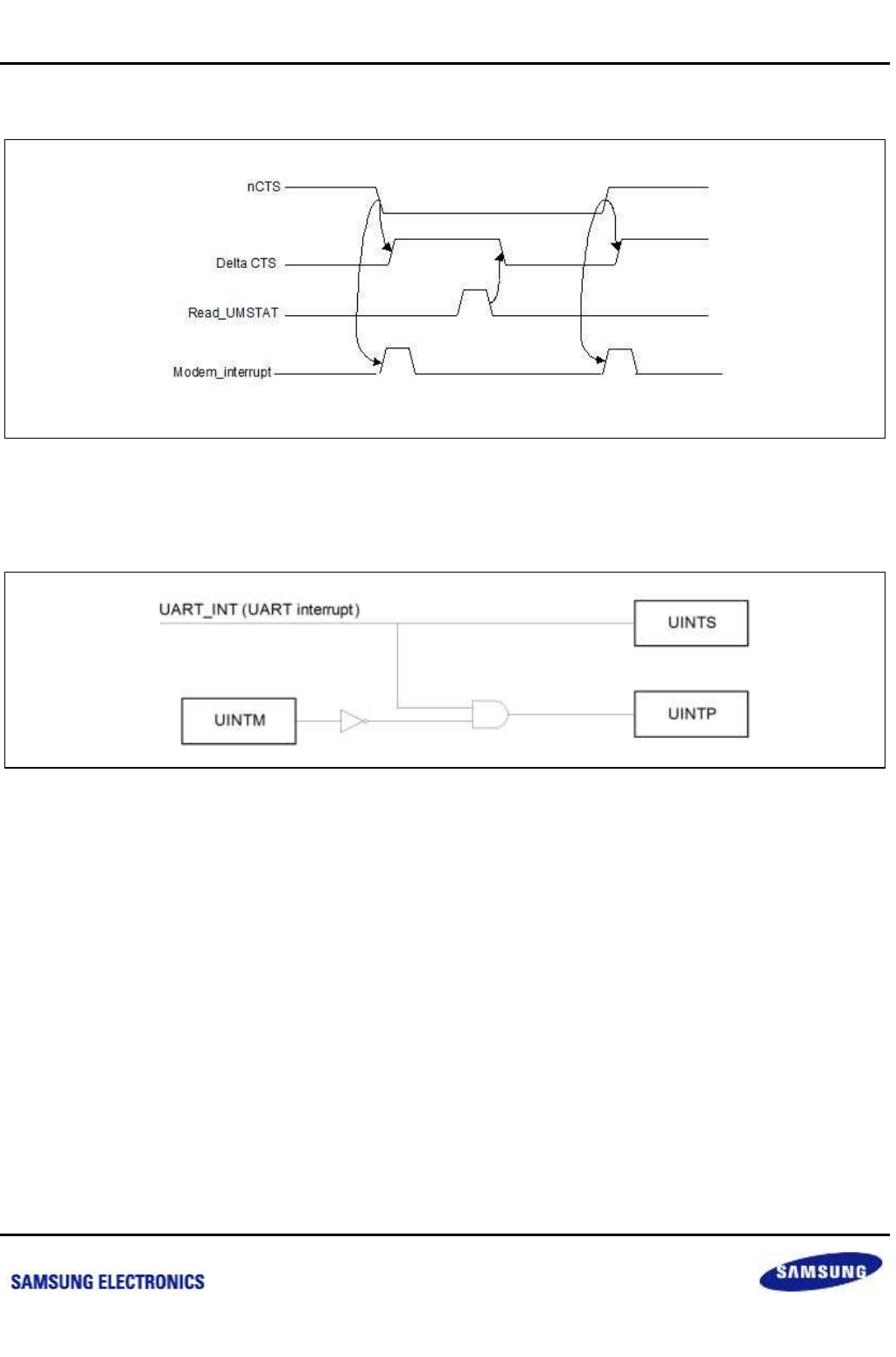
Samsung Confidential
S5P6818_UM 25 UART_ISO7816
25-30
Preliminary product information describes products that are in development, for which full characterization data and
associated errata are not yet available. Specifications and information herein are subject to change without notice.
In the following figure illustrates the nCTS and Delta CTS Timing diagram.
Figure 25-8 nCTS and Delta CTS Timing Diagram
In the following figure illustrates the block diagram of UNITS, UINTP and UINTM.
Figure 25-9 Block Diagram of UINTS, UINTP and UINTM
Interrupt Mask contains information about the interrupt source that is masked. When a specific bit is set to "1",
interrupt request signal to the Interrupt Controller is not generated even though corresponding Interrupt Source is
generated.
If the Mask bit is 0, the interrupt requests are serviced from the corresponding Interrupt Source.
nexell / ys.kim at 2015.02.12
SAMSUNG Confidential

Samsung Confidential
S5P6818_UM 26 USB2.0 OTG
26-1
Preliminary product information describes products that are in development, for which full characterization data and
associated errata are not yet available. Specifications and information herein are subject to change without notice.
26 USB2.0 OTG
26.1 Overview
USB On-The-Go (OTG) is a Dual-Role Device (DRD) controller, which supports both device and host functions. It
is fully compliant with the On-The-Go Supplement to the USB 2.0 Specification, Revision 1.0a. It supports high-
speed (HS, 480 Mbps), full-speed (FS, 12 Mbps), and low-speed (LS, 1.5 Mbps, Host only) transfers. HS OTG
can be configured as a Host-only or Device-only controller.
26.2 Features
The USB2.0 HS OTG features include the following:
Complies with the On-The-Go Supplement to the USB 2.0 Specification (Revision 1.3a)
Operates in High-Speed (480 Mbps), Full-Speed (12 Mbps) and Low-Speed (1.5 Mbps, Host only) modes
Supports UTMI+ Level 3 interface (Revision 1.0)
Supports Session Request Protocol (SRP) and Host Negotiation Protocol (HNP)
Supports only 32-bit data on the AHB
1 Control Endpoint 0 for control transfer
16 Device Mode Endpoints including Control Endpoint 0
Programmable endpoint type: Bulk, Isochronous, or Interrupt
Programmable IN/OUT direction
Supports 16 Host channels
nexell / ys.kim at 2015.02.12
SAMSUNG Confidential
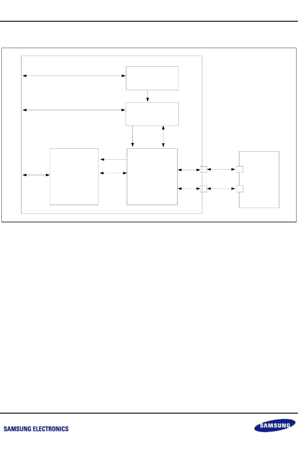
Samsung Confidential
S5P6818_UM 26 USB2.0 OTG
26-2
Preliminary product information describes products that are in development, for which full characterization data and
associated errata are not yet available. Specifications and information herein are subject to change without notice.
26.3 Block Diagram
Figure 26-1 USB 2.0 OTG Block Diagram
The blocks in the USB 2.0 OTG controller are comprising as follows:
USB 2.0 CLOCK GEN
USB 2.0 PHY Control
USB 2.0 PHY Link
Each has an AHB Slave, which provides CPU with read and write access to Control and Status Registers. The
OTG Link has an AHB Master to transfer data on the AHB.
The USB system shown in the upper Figure supports the port:
USB 2.0 OTG 1 Port
USB 2.0
OTG LINK
USB 2.0
PHY CONTROL
USB 2.0
OTG PHY
UTMI interface
PHY Control
Signal
USBDP
USBDM
AHB Interface
AHB Interface
External
USB
Host or Device
USB 2.0 OTG
CLOCK GEN
control clock
(30Mhz)
AHB Interface
PHY clock
(30Mhz)
control clock
(30Mhz)
nexell / ys.kim at 2015.02.12
SAMSUNG Confidential

Samsung Confidential
S5P6818_UM 26 USB2.0 OTG
26-3
Preliminary product information describes products that are in development, for which full characterization data and
associated errata are not yet available. Specifications and information herein are subject to change without notice.
26.4 I/O Pin Description
Table 26-1 USB OTG I/O Pin Description
Pin Name
GPIO No.
GPIO
Function
Type
Description
USB 2.0 OTG Controller
USBDP
–
–
I/O
Data Plus Signal from the USB Cable
USBDM
–
–
I/O
Data Minus Signal from the USB Cable
USBREXT
–
–
I
Connection to the external 200 (+/–1%) resistor. The
signal must not go through a series resistance in the pad
(an ESD resistance is included in the macro). The pad
should have ESD, PMOS and NMOS clamp devices. The
200 (+/–1%) resistor must be referenced to the VSSA
ground supply and placed as close as possible to the chip.
Total capacitance should be less than 8pF, including board
traces.
USBVBUSIO
–
–
I
USB 5V Power detection
This VBUS indicator signal indicates that the VBUS signal
on the USB cable is active. For the serial interface, this
signal controls the Pull-Up resistance on the D+ line in
Device mode only.
0 = Pull-Up resistance on the D+ line is disable.
1 = Pull-Up resistance on the D+ line is enabled based on
the speed of operation.
USBVBUS
–
–
I
Logic Level VBUS Detect. When VBUSVLDEXTSEL of
USB PHY register is set to 1, USBVBUS is used instead of
USBVBUSIO.
This pin is legacy mode.
USBID
*
*
I/O
USB Mini-Receptacle Identifier.
This signal differentiates a mini-A from a mini-B plug.
The ID line is sampled only when the PULLUP signal is
high.
After sampling the ID line, It indicates whether a mini-A or
mini-B cable is connected.
Low: Mini-A connected
High: Mini-B connected
If this signal is not used, internal resistance pulls the
signal's voltage level up to 2.5V.
USBDRVVBUS
GPIOC[11]
Alt3
O
This controller signal enables or disables external charge
pump in host mode.
nexell / ys.kim at 2015.02.12
SAMSUNG Confidential
Samsung Confidential
S5P6818_UM 26 USB2.0 OTG
26-4
Preliminary product information describes products that are in development, for which full characterization data and
associated errata are not yet available. Specifications and information herein are subject to change without notice.
26.5 Functional Description
26.5.1 End Point Packet Size
USB OTG of this chip supports 8 end-points. In device mode, maximum packet size per each EP (Endpoint) is as
follows:
Table 26-2 Maximum Packet Size per Endpoint
EP Number
Max Packet Size (bytes)
EP[0]
64
EP[1]
512
EP[2]
512
EP[3]
1024
EP[4]
1024
EP[5]
512
EP[6]
512
EP[7]
512
EP[9]
512
EP[9]
512
EP[10]
512
EP[11]
64
EP[12]
64
EP[13]
64
EP[14]
64
EP[15]
64
nexell / ys.kim at 2015.02.12
SAMSUNG Confidential

Samsung Confidential
S5P6818_UM 26 USB2.0 OTG
26-5
Preliminary product information describes products that are in development, for which full characterization data and
associated errata are not yet available. Specifications and information herein are subject to change without notice.
26.5.2 USB 5V Power Detection
You can select one of two VBUS by VBUSVLDEXTSEL of USB PHY register.
Table 26-3 USB 5V Power Detection
VBUS Pin
Description
USBVBUSIO
USB2.0 OTG module can operate in device mode when the voltage on USBVBUSIO is
valid. To be valid in device mode, the voltage on USBVBUSIO is required to be between
4.75V and 5.25V.
USBVBUS
When VBUSVLDEXTSEL of USB PHY register is set to 1, USBVBUS is used instead of
USBVBUSIO. The USBVBUS pad is a logic-level input. When the USB2 PHY is operating
as a device, The USBVBUS acts as a gating signal for many of the internal USB2 PHY
modules. Therefore, it is important that transitions on the USBVBUS are clean and well-
defined.
26.5.3 Force Power Down
To reduce power consumption, all analog circuits of the USB 2.0 OTG block can be power downed.
See the following table for setting registers to force power down and power up.
Table 26-4 Force Power down configurations
Operation
Register Setting
Description
Power Up
PHYCTRL.PHYPOR = 0x0237;
PHYCTRL.TESTPARM4 =
0x0000;
Power up USB PHY.
Power Down
PHYCTRL.PHYPOR = 0x023C;
PHYCTRL.TESTPARM4 =
0x0030;
Power Down USB PHY including:
VBUS valid comparator( Bias and Band gap circuits)
PLL
XO
In power down mode, VBUS signal is gated. And USB
PHY does not communicate with external Host/Device
regardless of VBUS.
nexell / ys.kim at 2015.02.12
SAMSUNG Confidential
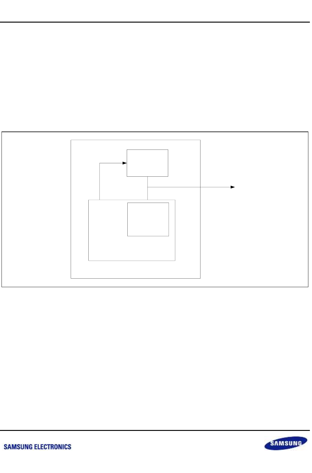
Samsung Confidential
S5P6818_UM 26 USB2.0 OTG
26-6
Preliminary product information describes products that are in development, for which full characterization data and
associated errata are not yet available. Specifications and information herein are subject to change without notice.
26.5.4 External Charge Pump
The USB 2.0 PHY requires an off-chip charge pump to provide power to the USB 2.0 OTG PHY VBUS pin.
In the Figure below shows the charge pump connection to the USB 2.0 PHY.
The charge pump's output is connected directly to VBUS on the device board. The USB 2.0 PHY's VBUS pin
VBUS pin is also connected to VBUS. The charge pump's DRVVBUS input is an output of the OTG HNP finite
state machine and an input to the USB 2.0 PHY.
The VBUS presents a worst-case core-side load of 500pF. This worst-case load is a small addition to the overall
capacitance budget that includes the external capacitive load due to routing, pads, package, board traces, and
receivers.
Figure 26-2 Charge Pump Connection
OTG Board
CHIP
VBUS
USB 2.0
OTG PHY
Off-Chip
Charge Pump
Out
DRVVBUS
VBUS
nexell / ys.kim at 2015.02.12
SAMSUNG Confidential

Samsung Confidential
S5P6818_UM 26 USB2.0 OTG
26-7
Preliminary product information describes products that are in development, for which full characterization data and
associated errata are not yet available. Specifications and information herein are subject to change without notice.
26.5.5 Modes of Operation
The application operates the Link either in DMA mode or in Slave mode. The application cannot operate the core
using DMA and Slave modes simultaneously.
26.5.5.1 DMA Mode
USB OTG host uses the AHB Master interface to transmit packet data fetch (AHB to USB) and receive data
update (USB to AHB). The AHB master uses the programmed DMA address (HCDMAn register in Host mode and
DIEPDMAn/DOEPDMAn register in Device mode) to access the data buffers.
26.5.5.2 Slave Mode
USB OTG can operate either in transaction-level operation or in pipelined transaction-level operation. The
application handles one data packet at a time per channel/endpoint in transaction-level operations. In pipelined
transaction-level operation, the application programs the OTG to perform multiple transactions. The advantage of
pipelined operation is that the application is not interrupted on packet basis.
nexell / ys.kim at 2015.02.12
SAMSUNG Confidential

Samsung Confidential
S5P6818_UM 26 USB2.0 OTG
26-8
Preliminary product information describes products that are in development, for which full characterization data and
associated errata are not yet available. Specifications and information herein are subject to change without notice.
26.6 Programming User Configure of PHY and OTG LINK
1. Release OTG common reset
Program RSTCON1[25] (address: 0xC0012004) to 1'b1
2. Program scale mode to real mode
Program TIEOFFREG12[1:0] (address: 0xC0011030) to 2'b00
3. Select word interface and enable word interface selection
8-bit word interface: Program TIEOFFREG14[9:8] (address: 0xC0011038) to 2'b01
16-bit word interface: Program TIEOFFREG14[9:8] (address: 0xC0011038) to 2'b11
4. Select VBUS
Analog 5V USBVBUSIO: program TIEOFFREG13[25:24] (address: 0xC0011034) to 2'b00
Digital USBVBUS: program TIEOFFREG13[25:24] (address: 0xC0011034) to 2'b11
5. POR (Power On Reset) of PHY
Program TIEOFFREG13[8:7] (address: 0xC0011034) to 2'b01
6. Wait clock of PHY: About 40 micro seconds
7. Release UTMI reset
Program TIEOFFREG13[3] (address: 0xC0011034) to 1'b1
8. Release AHB reset
Program TIEOFFREG13[2] (address: 0xC0011034) to 1'b1
nexell / ys.kim at 2015.02.12
SAMSUNG Confidential
Samsung Confidential
S5P6818_UM 26 USB2.0 OTG
26-9
Preliminary product information describes products that are in development, for which full characterization data and
associated errata are not yet available. Specifications and information herein are subject to change without notice.
26.7 Register Description
The OTG Link registers are classified as follows:
Core Global Registers
Host Mode Registers
Host Global Registers
Host Port CSRs
Host Channel-Specific Registers
Device Mode Registers
Device Global Registers
Device Endpoint-Specific Registers
Register Map Summary Group
Register
Base Address
Description
USBOTG_GCSR
0xC004_0000
Core Global CSRs (1 KB)
USBOTG_HMCSR
0xC004_0400
Host Mode CSRs (1 KB)
USBOTG_DMCSR
0xC004_0800
Device Mode CSRs (1.5 KB)
USBOTG_PCGCCTL
0xC004_0E00
Power and Clock Gating CSRs (0.5 KB)
USBOTG_EPFIFO0
0xC004_1000
Device EP 0/Host Channel 0 FIFO (4 KB)
USBOTG_EPFIFO1
0xC004_2000
Device EP 1/Host Channel 1 FIFO (4 KB)
USBOTG_EPFIFO2
0xC004_3000
Device EP 2/Host Channel 2 FIFO (4 KB)
USBOTG_EPFIFO3
0xC004_4000
Device EP 3/Host Channel 3 FIFO (4 KB)
USBOTG_EPFIFO4
0xC004_5000
Device EP 4/Host Channel 4 FIFO (4 KB)
USBOTG_EPFIFO5
0xC004_6000
Device EP 5/Host Channel 5 FIFO (4 KB)
USBOTG_EPFIFO6
0xC004_7000
Device EP 6/Host Channel 6 FIFO (4 KB)
USBOTG_EPFIFO7
0xC004_8000
Device EP 7/Host Channel 7 FIFO (4 KB)
USBOTG_EPFIFO8
0xC004_9000
Device EP 8/Host Channel 8 FIFO (4 KB)
USBOTG_EPFIFO9
0xC004_A000
Device EP 9/Host Channel 9 FIFO (4 KB)
USBOTG_EPFIFO10
0xC004_B000
Device EP 10/Host Channel 10 FIFO (4 KB)
USBOTG_EPFIFO11
0xC004_C000
Device EP 11/Host Channel 11 FIFO (4 KB)
USBOTG_EPFIFO12
0xC004_D000
Device EP 12/Host Channel 12 FIFO (4 KB)
USBOTG_EPFIFO13
0xC004_E000
Device EP 13/Host Channel 13 FIFO (4 KB)
USBOTG_EPFIFO14
0xC004_F000
Device EP 14/Host Channel 14 FIFO (4 KB)
USBOTG_EPFIFO15
0xC005_0000
Device EP 15/Host Channel 15 FIFO (4 KB)
nexell / ys.kim at 2015.02.12
SAMSUNG Confidential

Samsung Confidential
S5P6818_UM 26 USB2.0 OTG
26-10
Preliminary product information describes products that are in development, for which full characterization data and
associated errata are not yet available. Specifications and information herein are subject to change without notice.
26.7.1 Register Map Summary
Base Address: 0xC004_0000
Register
Offset
Description
Reset Value
Core Global Register
GOTGCTL
0x0000
OTG control and status register
0x0001_0000
GOTGINT
0x0004
OTG interrupt register
0x0000_0000
GAHBCFG
0x0008
Core AHB configuration register
0x0000_0000
GUSBCFG
0x000C
Core USB configuration register
0x0000_1400
GRSTCTL
0x0010
Core reset register
0x8000_0000
GINTSTS
0x0014
Core interrupt register
0x0400_1020
GINTMSK
0x0018
Core interrupt mask register
0x0000_0000
GRXSTSR
0x001C
Receive status debug read register
Undefined
GRXSTSP
0x0020
Receive status read/pop register
0xFFFF_FFFF
GRXFSIZ
0x0024
Receive FIFO size register
0x0000_1800
GNPTXFSIZ
0x0028
Non-Periodic transmit FIFO size register
0x1800_1800
GNPTXSTS
0x002C
Non-Periodic transmit FIFO/Queue status register
0x0008_1800
HPTXFSIZ
0x0100
Host Periodic transmit FIFO size register
0x0300_5A00
DPTXFSIZ1
0x0104
Device periodic transmit FIFO-1 size register
0x0300_1000
DPTXFSIZ2
0x0108
Device periodic transmit FIFO-2 size register
0x0300_3300
DPTXFSIZ3
0x010C
Device periodic transmit FIFO-3 size register
0x0300_3600
DPTXFSIZ4
0x0110
Device periodic transmit FIFO-4 size register
0x0300_3900
DPTXFSIZ5
0x0114
Device periodic transmit FIFO-5 size register
0x0300_3C00
DPTXFSIZ6
0x0118
Device periodic transmit FIFO-6 size register
0x0300_3F00
DPTXFSIZ7
0x011C
Device periodic transmit FIFO-7 size register
0x0300_4200
DPTXFSIZ8
0x0120
Device periodic transmit FIFO-8 size register
0x0300_4500
DPTXFSIZ9
0x0124
Device periodic transmit FIFO-9 size register
0x0300_4800
DPTXFSIZ10
0x0128
Device periodic transmit FIFO-10 size register
0x0300_4B00
DPTXFSIZ11
0x012C
Device periodic transmit FIFO-11 size register
0x0300_4E00
DPTXFSIZ12
0x0130
Device periodic transmit FIFO-12 size register
0x0300_5100
DPTXFSIZ13
0x0134
Device periodic transmit FIFO-13 size register
0x0300_5400
DPTXFSIZ14
0x0138
Device periodic transmit FIFO-14 size register
0x0300_5700
DPTXFSIZ15
0x013C
Device periodic transmit FIFO-15 size register
0x0300_5A00
nexell / ys.kim at 2015.02.12
SAMSUNG Confidential

Samsung Confidential
S5P6818_UM 26 USB2.0 OTG
26-11
Preliminary product information describes products that are in development, for which full characterization data and
associated errata are not yet available. Specifications and information herein are subject to change without notice.
Base Address: 0xC004_0400
Register
Offset
Description
Reset Value
Host Mode Register
Host Global Register
HCFG
0x0400
Host configuration register
0x0020_0000
HFIR
0x0404
Host frame interval register
0x0000_17D7
HFNUM
0x0408
Host frame number/frame time remaining register
0x0000_0000
HPTXSTS
0x0410
Host periodic transmit FIFO/Queue status register
0x0008_0100
HAINT
0x0414
Host All channels interrupt register
0x0000_0000
HAINTMSK
0x0418
Host All channels interrupt mask register
0x0000_0000
Host Port Control and Status Register
HPRT
0x0440
Host port control and status register
0x0000_0000
Host Channel-Specific Register
HCCHAR0
0x0500
Host channel 0 characteristics register
0x0000_0000
HCSPLT0
0x0504
Host channel 0 spilt control register
0x0000_0000
HCINT0
0x0508
Host channel 0 interrupt register
0x0000_0000
HCINTMSK0
0x050C
Host channel 0 interrupt mask register
0x0000_0000
HCTSIZ0
0x0510
Host channel 0 transfer size register
0x0000_0000
HCDMA0
0x0514
Host channel 0 DMA address register
0x0000_0000
HCCHAR1
0x0520
Host channel 1 characteristics register
0x0000_0000
HCSPLT1
0x0524
Host channel 1 spilt control register
0x0000_0000
HCINT1
0x0528
Host channel 1 interrupt register
0x0000_0000
HCINTMSK1
0x052C
Host channel 1 interrupt mask register
0x0000_0000
HCTSIZ1
0x0530
Host channel 1 transfer size register
0x0000_0000
HCDMA1
0x0534
Host channel 1 DMA ADDRESS REGISTER
0x0000_0000
HCCHAR2
0x0540
Host channel 2 characteristics register
0x0000_0000
HCSPLT2
0x0544
Host channel 2 spilt control register
0x0000_0000
HCINT2
0x0548
Host channel 2 interrupt register
0x0000_0000
HCINTMSK2
0x054C
Host channel 2 interrupt mask register
0x0000_0000
HCTSIZ2
0x0550
Host channel 2 transfer size register
0x0000_0000
HCDMA2
0x0554
Host channel 2 DMA address register
0x0000_0000
HCCHAR3
0x0560
Host channel 3 characteristics register
0x0000_0000
HCSPLT3
0x0564
Host channel 3 spilt control register
0x0000_0000
HCINT3
0x0568
Host channel 3 interrupt register
0x0000_0000
HCINTMSK3
0x056C
Host channel 3 interrupt mask register
0x0000_0000
HCTSIZ3
0x0570
Host channel 3 transfer size register
0x0000_0000
HCDMA3
0x0574
Host channel 3 DMA address register
0x0000_0000
HCCHAR4
0x0580
Host channel 4 characteristics register
0x0000_0000
nexell / ys.kim at 2015.02.12
SAMSUNG Confidential

Samsung Confidential
S5P6818_UM 26 USB2.0 OTG
26-12
Preliminary product information describes products that are in development, for which full characterization data and
associated errata are not yet available. Specifications and information herein are subject to change without notice.
Register
Offset
Description
Reset Value
HCSPLT4
0x0584
Host channel 4 spilt control register
0x0000_0000
HCINT4
0x0588
Host channel 4 interrupt register
0x0000_0000
HCINTMSK4
0x058C
Host channel 4 interrupt mask register
0x0000_0000
HCTSIZ4
0x0580
Host channel 4 transfer size register
0x0000_0000
HCDMA4
0x0584
Host channel 4 DMA address register
0x0000_0000
HCCHAR5
0x05A0
Host channel 5 characteristics register
0x0000_0000
HCSPLT5
0x05A4
Host channel 5 spilt control register
0x0000_0000
HCINT5
0x05A8
Host channel 5 interrupt register
0x0000_0000
HCINTMSK5
0x05AC
Host channel 5 interrupt mask register
0x0000_0000
HCTSIZ5
0x05B0
Host channel 5 transfer size register
0x0000_0000
HCDMA5
0x05B4
Host channel 5 DMA address register
0x0000_0000
HCCHAR6
0x05C0
Host channel 6 characteristics register
0x0000_0000
HCSPLT6
0x05C4
Host channel 6 spilt control register
0x0000_0000
HCINT6
0x05C8
Host channel 6 interrupt register
0x0000_0000
HCINTMSK6
0x05CC
Host channel 6 interrupt mask register
0x0000_0000
HCTSIZ6
0x05D0
Host channel 6 transfer size register
0x0000_0000
HCDMA6
0x05D4
Host channel 6 DMA address register
0x0000_0000
HCCHAR7
0x05E0
Host channel 7 characteristics register
0x0000_0000
HCSPLT7
0x05E4
Host channel 7 spilt control register
0x0000_0000
HCINT7
0x05E8
Host channel 7 interrupt register
0x0000_0000
HCINTMSK7
0x05EC
Host channel 7 interrupt mask register
0x0000_0000
HCTSIZ7
0x05F0
Host channel 7 transfer size register
0x0000_0000
HCDMA7
0x05F4
Host channel 7 DMA address register
0x0000_0000
HCCHAR8
0x0600
Host channel 8 characteristics register
0x0000_0000
HCSPLT8
0x0604
Host channel 8 spilt control register
0x0000_0000
HCINT8
0x0608
Host channel 8 interrupt register
0x0000_0000
HCINTMSK8
0x060C
Host channel 8 interrupt mask register
0x0000_0000
HCTSIZ8
0x0610
Host channel 8 transfer size register
0x0000_0000
HCDMA8
0x0614
Host channel 8 DMA address register
0x0000_0000
HCCHAR9
0x0620
Host channel 9 characteristics register
0x0000_0000
HCSPLT9
0x0624
Host channel 9 spilt control register
0x0000_0000
HCINT9
0x0628
Host channel 9 interrupt register
0x0000_0000
HCINTMSK9
0x062C
Host channel 10 interrupt mask register
0x0000_0000
HCTSIZ9
0x0630
Host channel 10 transfer size register
0x0000_0000
HCDMA9
0x0634
Host channel 10 DMA address register
0x0000_0000
HCCHAR10
0x0640
Host channel 10 characteristics register
0x0000_0000
HCSPLT10
0x0644
Host channel 10 Spilt Control Register
0x0000_0000
nexell / ys.kim at 2015.02.12
SAMSUNG Confidential

Samsung Confidential
S5P6818_UM 26 USB2.0 OTG
26-13
Preliminary product information describes products that are in development, for which full characterization data and
associated errata are not yet available. Specifications and information herein are subject to change without notice.
Register
Offset
Description
Reset Value
HCINT10
0x0648
Host channel 10 interrupt register
0x0000_0000
HCINTMSK10
0x064C
Host channel 10 interrupt mask register
0x0000_0000
HCTSIZ10
0x0650
Host channel 10 transfer size register
0x0000_0000
HCDMA10
0x0654
Host channel 10 DMA address register
0x0000_0000
HCCHAR11
0x0660
Host channel 11 characteristics register
0x0000_0000
HCSPLT11
0x0664
Host channel 11 spilt control register
0x0000_0000
HCINT11
0x0668
Host channel 11 interrupt register
0x0000_0000
HCINTMSK11
0x066C
Host channel 11 interrupt mask register
0x0000_0000
HCTSIZ11
0x0670
Host channel 11 transfer size register
0x0000_0000
HCDMA11
0x0674
Host channel 11 DMA address register
0x0000_0000
HCCHAR12
0x0680
Host channel 12 characteristics register
0x0000_0000
HCSPLT12
0x0684
Host channel 12 spilt control register
0x0000_0000
HCINT12
0x0688
Host channel 12 interrupt register
0x0000_0000
HCINTMSK12
0x068C
Host channel 12 interrupt mask register
0x0000_0000
HCTSIZ12
0x0690
Host channel 12 transfer size register
0x0000_0000
HCDMA12
0x0694
Host channel 12 DMA address register
0x0000_0000
HCCHAR13
0x06A0
Host channel 13 characteristics register
0x0000_0000
HCSPLT13
0x06A4
Host channel 13 spilt control register
0x0000_0000
HCINT13
0x06A8
Host channel 13 interrupt register
0x0000_0000
HCINTMSK13
0x06AC
Host channel 4 transfer size register
0x0000_0000
HCTSIZ13
0x06B0
Host channel 4 DMA address register
0x0000_0000
HCDMA13
0x06B4
Host channel 5 characteristics register
0x0000_0000
HCCHAR14
0x06C0
Host channel 5 spilt control register
0x0000_0000
HCSPLT14
0x06C4
Host channel 5 interrupt register
0x0000_0000
HCINT14
0x06C8
Host channel 5 interrupt mask register
0x0000_0000
HCINTMSK14
0x06CC
Host channel 5 transfer size register
0x0000_0000
HCTSIZ14
0x06D0
Host channel 5 DMA address register
0x0000_0000
HCDMA14
0x06D4
Host channel 6 characteristics register
0x0000_0000
HCCHAR15
0x06E0
Host channel 6 spilt control register
0x0000_0000
HCSPLT15
0x06E4
Host channel 6 interrupt register
0x0000_0000
HCINT15
0x06E8
Host channel 6 interrupt mask register
0x0000_0000
HCINTMSK15
0x06EC
Host channel 6 transfer size register
0x0000_0000
HCTSIZ15
0x06F0
Host channel 6 DMA address register
0x0000_0000
HCDMA15
0x06F4
Host channel 7 characteristics register
0x0000_0000
nexell / ys.kim at 2015.02.12
SAMSUNG Confidential

Samsung Confidential
S5P6818_UM 26 USB2.0 OTG
26-14
Preliminary product information describes products that are in development, for which full characterization data and
associated errata are not yet available. Specifications and information herein are subject to change without notice.
Base Address: 0xC004_0800
Register
Offset
Description
Reset Value
Device Mode Register
Device Global Register
DCFG
0x0800
R/W device configuration register
0x0020_0000
DCTL
0x0804
Device control register
0x0000_0000
DSTS
0x0808
Device status register
0x0000_0002
DIEPMSK
0x0810
Device IN endpoint common interrupt mask register
0x0000_0000
DOEPMSK
0x0814
Device OUT endpoint common interrupt mask register
0x0000_0000
DAINT
0x0818
Device ALL endpoints interrupt register
0x0000_0000
DAINTMSK
0x081C
Device ALL endpoints interrupt mask register
0x0000_0000
DTKNQR1
0x0820
Device IN token sequence learning queue read register 1
0x0000_0000
DTKNQR2
0x0824
Device IN token sequence learning queue read register 2
0x0000_0000
DVBUSDIS
0x0828
Device VBUS discharge time register
0x0000_17D7
DVBUSPULSE
0x082C
Device VBUS pulsing time register
0x0000_05B8
DTKNQR3
0x0830
Device IN token sequence learning queue read register 3
0x0000_0000
DTKNQR4
0x0834
Device IN token sequence learning queue read register 4
0x0000_0000
Device Logical In Endpoint-Specific Register
DIEPCTL0
0x0900
Device control in endpoint 0 control register
0x0000_8000
DIEPINT0
0x0908
Device IN endpoint 0 interrupt register
0x0000_0000
DIEPTSIZ0
0x0910
Device IN endpoint 0 transfer size register
0x0000_0000
DIEPDMA0
0x0914
Device IN endpoint 0 DMA address register
0x0000_0000
DIEPCTL1
0x0920
Device control IN endpoint 1 control register
0x0000_0000
DIEPINT1
0x0928
Device IN endpoint 1 interrupt register
0x0000_0080
DIEPTSIZ1
0x0930
Device IN endpoint 1 transfer size register
0x0000_0000
DIEPDMA1
0x0934
Device IN endpoint 1 DMA address register
0x0000_0000
DIEPCTL2
0x0940
Device control IN endpoint 2 control register
0x0000_0000
DIEPINT2
0x0948
Device IN endpoint 2 interrupt register
0x0000_0080
DIEPTSIZ2
0x0950
Device IN endpoint 2 transfer size register
0x0000_0000
DIEPDMA2
0x0954
Device IN endpoint 2 DMA address register
0x0000_0000
DIEPCTL3
0x0960
Device control IN endpoint 3 control register
0x0000_0000
DIEPINT3
0x0968
Device IN endpoint 3 interrupt register
0x0000_0080
DIEPTSIZ3
0x0970
Device IN endpoint 3 transfer size register
0x0000_0000
DIEPDMA3
0x0974
Device IN endpoint 3 DMA address register
0x0000_0000
DIEPCTL4
0x0980
Device control IN endpoint 4 control register
0x0000_0000
DIEPINT4
0x0988
Device IN endpoint 4 interrupt register
0x0000_0080
DIEPTSIZ4
0x0990
Device IN endpoint 4 transfer size register
0x0000_0000
DIEPDMA4
0x0994
Device IN endpoint 4 DMA ADDRESS REGISTER
0x0000_0000
nexell / ys.kim at 2015.02.12
SAMSUNG Confidential

Samsung Confidential
S5P6818_UM 26 USB2.0 OTG
26-15
Preliminary product information describes products that are in development, for which full characterization data and
associated errata are not yet available. Specifications and information herein are subject to change without notice.
Register
Offset
Description
Reset Value
DIEPCTL5
0x09A0
Device control IN endpoint 5 control register
0x0000_0000
DIEPINT5
0x09A8
Device IN endpoint 5 interrupt register
0x0000_0080
DIEPTSIZ5
0x09B0
Device IN endpoint 5 transfer size register
0x0000_0000
DIEPDMA5
0x09B4
Device IN endpoint 5 DMA address register
0x0000_0000
DIEPCTL6
0x09C0
Device control IN endpoint 6 control register
0x0000_0000
DIEPINT6
0x09C8
Device IN endpoint 6 interrupt register
0x0000_0080
DIEPTSIZ6
0x09D0
Device IN endpoint 6 transfer size register
0x0000_0000
DIEPDMA6
0x09D4
Device IN endpoint 6 DMA address register
0x0000_0000
DIEPCTL7
0x09E0
Device control IN endpoint 7 control register
0x0000_0000
DIEPINT7
0x09E8
Device IN endpoint 7 Interrupt register
0x0000_0080
DIEPTSIZ7
0x09F0
Device IN endpoint 7 transfer size register
0x0000_0000
DIEPDMA7
0x09F4
Device IN endpoint 7 DMA address register
0x0000_0000
Device Logical OUT Endpoint-Specific Register
DOEPCTL0
0x0B00
Device control OUT endpoint 0 control register
0x0000_8000
DOEPINT0
0x0B08
Device OUT endpoint 0 interrupt register
0x0000_0000
DOEPTSIZ0
0x0B10
Device OUT endpoint 0 transfer size register
0x0000_0000
DOEPDMA0
0x0B14
Device OUT endpoint 0 DMA address register
0x0000_0000
DOEPCTL1
0x0B20
Device control OUT endpoint 1 control register
0x0000_0000
DOEPINT1
0x0B28
Device OUT endpoint 1 interrupt register
0x0000_0000
DOEPTSIZ1
0x0B30
Device OUT endpoint 1 transfer size register
0x0000_0000
DOEPDMA1
0x0B34
Device OUT endpoint 1 DMA address register
0x0000_0000
DOEPCTL2
0x0B40
Device control OUT endpoint 2 control register
0x0000_0000
DOEPINT2
0x0B48
Device OUT endpoint 2 interrupt register
0x0000_0000
DOEPTSIZ2
0x0B50
Device OUT endpoint 2 transfer size register
0x0000_0000
DOEPDMA2
0x0B54
Device OUT endpoint 2 DMA address register
0x0000_0000
DOEPCTL3
0x0B60
Device control OUT endpoint 3 control register
0x0000_0000
DOEPINT3
0x0B68
Device OUT endpoint 3 interrupt register
0x0000_0000
DOEPTSIZ3
0x0B70
Device OUT endpoint 3 transfer size register
0x0000_0000
DOEPDMA3
0x0B74
Device OUT endpoint 3 DMA address register
0x0000_0000
DOEPCTL4
0x0B80
Device control OUT endpoint 4 control register
0x0000_0000
DOEPINT4
0x0B88
Device OUT endpoint 4 interrupt register
0x0000_0000
DOEPTSIZ4
0x0B90
Device OUT endpoint 4 transfer size register
0x0000_0000
DOEPDMA4
0x0B94
Device OUT endpoint 4 DMA address register
0x0000_0000
DOEPCTL5
0x0BA0
Device control OUT endpoint 5 control register
0x0000_0000
DOEPINT5
0x0BA8
Device OUT endpoint 5 interrupt register
0x0000_0000
DOEPTSIZ5
0x0BB0
Device OUT endpoint 5 transfer size register
0x0000_0000
DOEPDMA5
0x0BB4
Device OUT endpoint 5 DMA address register
0x0000_0000
nexell / ys.kim at 2015.02.12
SAMSUNG Confidential

Samsung Confidential
S5P6818_UM 26 USB2.0 OTG
26-16
Preliminary product information describes products that are in development, for which full characterization data and
associated errata are not yet available. Specifications and information herein are subject to change without notice.
Register
Offset
Description
Reset Value
DOEPCTL6
0x0BC0
Device control OUT endpoint 6 control register
0x0000_0000
DOEPINT6
0x0BC8
Device OUT endpoint 6 interrupt register
0x0000_0000
DOEPTSIZ6
0x0BD0
Device OUT Endpoint 6 transfer size register
0x0000_0000
DOEPDMA6
0x0BD4
Device OUT endpoint 6 DMA address register
0x0000_0000
DOEPCTL7
0x0BE0
Device control OUT endpoint 7 control register
0x0000_0000
DOEPINT7
0x0BE8
Device OUT endpoint 7 interrupt register
0x0000_0000
DOEPTSIZ7
0x0BF0
Device OUT endpoint 7 transfer size register
0x0000_0000
DOEPDMA7
0x0BF4
Device OUT endpoint 7 DMA address register
0x0000_0000
nexell / ys.kim at 2015.02.12
SAMSUNG Confidential
Samsung Confidential
S5P6818_UM 26 USB2.0 OTG
26-17
Preliminary product information describes products that are in development, for which full characterization data and
associated errata are not yet available. Specifications and information herein are subject to change without notice.
Base Address: 0xC004_0E00
Register
Offset
Description
Reset Value
Power and Clock Gating
PCGCCTL
0x0E00
Power and Clock Gating Control Register
0x0000_0000
Base Address: 0xC004_1000 (Device EP0/Host Channel0 FIFO)
Base Address: 0xC004_2000 (Device EP1/Host Channel1 FIFO)
Base Address: 0xC004_3000 (Device EP2/Host Channel2 FIFO)
Base Address: 0xC004_4000 (Device EP3/Host Channel3 FIFO)
Base Address: 0xC004_5000 (Device EP4/Host Channel4 FIFO)
Base Address: 0xC004_6000 (Device EP5/Host Channel5 FIFO)
Base Address: 0xC004_7000 (Device EP6/Host Channel6 FIFO)
Base Address: 0xC004_8000 (Device EP7/Host Channel7 FIFO)
Base Address: 0xC004_9000 (Device EP8/Host Channel8 FIFO)
Base Address: 0xC004_A000 (Device EP9/Host Channel9 FIFO)
Base Address: 0xC004_B000 (Device EP10/Host Channel10 FIFO)
Base Address: 0xC004_C000 (Device EP11/Host Channel11 FIFO)
Base Address: 0xC004_D000 (Device EP12/Host Channel12 FIFO)
Base Address: 0xC004_E000 (Device EP13/Host Channel13 FIFO)
Base Address: 0xC004_F000 (Device EP14/Host Channel14 FIFO)
Base Address: 0xC005_0000 (Device EP15/Host Channel15 FIFO)
Register
Offset
Description
Reset Value
Device EP n/Host Channel n FIFO (n = 0 to 15)
USBOTG_EPFIFO0
~
USBOTG_EPFIFO15
0xC004_1000
~
0xC005_0FFC
Device EP 0/Host Channel 0 FIFO
~
Device EP 15/Host Channel 15 FIFO
0x0000_0000
nexell / ys.kim at 2015.02.12
SAMSUNG Confidential

Samsung Confidential
S5P6818_UM 26 USB2.0 OTG
26-18
Preliminary product information describes products that are in development, for which full characterization data and
associated errata are not yet available. Specifications and information herein are subject to change without notice.
26.7.1.1 Core Global Register
26.7.1.1.1 GOTGCTL
Base Address: 0xC004_0000
Address = Base Address + 0x0000, Reset Value = 0x0001_0000
Name
Bit
Type
Description
Reset Value
RSVD
[31:21]
–
Reserved
–
OTGVER
[20]
RW
OTG Version
Indicates the OTG revision.
1'b0 = OTG Version 1.3. In this version the core
supports Data line pulsing and VBus pulsing for SRP.
1'b1 = OTG Version 2.0. In this version the core
supports only Data line pulsing for SRP.
1'b0
BSESVLD
[19]
RW
B-Session Valid
Indicates the Device mode transceiver status.
0 = B-session is not valid
1 = B-session is valid
1'b0
ASESVLD
[18]
R
A-Session Valid
Indicates the Host mode transceiver status.
0 = A-session is not valid
1 = A-session is valid
1'b0
DBNCTIME
[17]
R
Long/ Short De bounce Time
Indicates the Debounce time of a detected connection.
0 = Long Debounce time, used for physical
connections
1 = Short Debounce time, used for soft connections
1'b0
CONIDSTS
[16]
R
Connector ID Status
Indicates the connector ID status.
0 = The OTG core is in A-device mode
1 = The OTG core is in B-device mode
1'b1
RSVD
[15:12]
–
Reserved
-
DEVHNPEN
[11]
RW
Device HNP Enable
The application sets the bit if it successfully receives a
Set Feature.
0 = HNP is not enabled in the application
1 = HNP is enabled in the application
1'b0
HSTSETHNPEN
[10]
RW
Host Set HNP Enable
The application sets this bit if it has successfully
enabled HNP on the connected device.
0 = Host Set HNP is not enabled
1 = Host Set HNP is enabled
1'b0
HNPREQ
[9]
RW
HNP Request
The application sets this bit to initiate an HNP request
to the connected USB host. The core clears this bit if
1'b0
nexell / ys.kim at 2015.02.12
SAMSUNG Confidential

Samsung Confidential
S5P6818_UM 26 USB2.0 OTG
26-19
Preliminary product information describes products that are in development, for which full characterization data and
associated errata are not yet available. Specifications and information herein are subject to change without notice.
Name
Bit
Type
Description
Reset Value
the HSTNEGSUCSTSCHNG bit is cleared.
0 = No HNP request
1 = HNP request
HSTNEGSCS
[8]
R
Host Negotiation Success
The core sets this bit if host negotiation is successful.
The core clears this bit if the HNP Request (HNPREQ)
bit in this register is set.
0 = Host negotiation failure
1 = Host negotiation success
1'b0
BVALIDOVVAL
[7]
RW
B-Peripheral Session Valid Override Value
This bit is used to set the Override value for Bvalid
signal when GOTGCTL. BVALIDOVEN is set.
1'b0 = Bvalid value is 1'b0 when
GOTGCTL.BVALIDOVEN = 1.
1'b1 = Bvalid value is 1'b1 when
GOTGCTL.BVALIDOVEN = 1.
1'b0-
BVALIDOVEN
[6]
RW
B-Peripheral Session Valid Override Enable
This bit is used to enable/disable the software to
override the Bvalid signal using the
GOTGCTL.BVALIDOVVAL.
1'b1 = Internally Bvalid received from the PHY is
overridden with GOTGCTL.BVALIDOVVAL.
1'b0 = Override is disabled and Bvalid signal from the
respective PHY selected is used internally by the core.
1'b0
AVALIDOVVAL
[5]
RW
A-Peripheral Session Valid Override Value
This bit is used to set the Override value for Avalid
signal when GOTGCTL.AVALIDOVEN is set.
1'b0 = Avalid value is 1'b0 when
GOTGCTL.AVALIDOVEN = 1.
1'b1 = Avalid value is 1'b1 when
GOTGCTL.AVALIDOVEN = 1.
1'b0
AVALIDOVEN
[4]
RW
A-Peripheral Session Valid Override Enable
This bit is used to enable/disable the software to
override the Avalid signal using the
GOTGCTL.AVALIDOVVAL.
1'b1 = Internally Avalid received from the PHY is
overridden with GOTGCTL.AVALIDOVVAL.
1'b0 = Override is disabled and Avalid signal from the
respective PHY is used internally by the core.
1'b0
VBVALIDOVVAL
[3]
RW
VBUS Valid Override Value
This bit is used to set the Override value for Vbus
valid signal when GOTGCTL.VBUSBALIDOVEN is
set.
1'b0 = Vbus valid value is 1'b0 when
OTGCTL.VBVALIDOVEN = 1.
1'b1 = Vbus valid value is 1'b1 when
1'b0
nexell / ys.kim at 2015.02.12
SAMSUNG Confidential

Samsung Confidential
S5P6818_UM 26 USB2.0 OTG
26-20
Preliminary product information describes products that are in development, for which full characterization data and
associated errata are not yet available. Specifications and information herein are subject to change without notice.
Name
Bit
Type
Description
Reset Value
OTGCTL.VBVALIDOVEN = 1.
VBVALIDOVEN
[2]
RW
VBUS Valid Override Enable (VBVALIDOVEN)
This bit is used to enable/disable the software to
override the Vbus-valid signal using the
GOTGCTL.VBVALIDOVVAL.
1'b1 = The Vbus-valid signal received from the PHY is
overridden with GOTGCTL.VBVALIDOVVAL.
1'b0 = Override is disabled and avalid signal from the
respective PHY is used internally by the core.
1'b0
SESREQ
[1]
RW
Session Request
The application sets this bit to initiate a session
request on the USB. The core clears this bit if the
HSTNEGSUCSTSCHNG bit is cleared.
0 = No session request
1 = Session request
1'b0
SESREQSCS
[0]
R
Session Request Success
The core sets this bit if a session request initiation is
successful.
0 = Session request failure
1 = Session request success
1'b0
nexell / ys.kim at 2015.02.12
SAMSUNG Confidential
Samsung Confidential
S5P6818_UM 26 USB2.0 OTG
26-21
Preliminary product information describes products that are in development, for which full characterization data and
associated errata are not yet available. Specifications and information herein are subject to change without notice.
26.7.1.1.2 GOTGINT
Base Address: 0xC004_0000
Address = Base Address + 0x0004, Reset Value = 0x0000_0000
Name
Bit
Type
Description
Reset Value
RSVD
[31:20]
–
Reserved
–
DBNCEDONE
[19]
RW
Debounce Done
The core sets this bit if the debounce is complete after
the device connects. This bit is only valid if the HNP
Capable or SRP Capable bit is set in the Core USB
Configuration register.
1'b0
ADEVTOUTCHG
[18]
RW
A-Device Timeout Change
The core sets this bit to indicate that the A-device has
timed out while waiting for the B-device to connect.
1'b0
HSTNEGDET
[17]
RW
Host Negotiation Detected.
The core sets this bit if it detects a host negotiation
request on the USB.
1'b0
RSVD
[16:10]
–
Reserved
–
HSTNEGSUCSTSCHNG
[9]
RW
Host Negotiation Success Status Change
The core sets this bit on the success or failure of a
USB host negotiation request.
1'b0
SESREQSUCSTSCHNG
[8]
RW
Session Request Success Status Change
The core sets this bit on the success or failure of a
session request.
1'b0
RSVD
[7:3]
–
Reserved
–
SESENDDET
[2]
RW
Session End Detected
The core sets this bit if the b_valid signal is de-
asserted.
1'b0
RSVD
[1:0]
–
Reserved
–
nexell / ys.kim at 2015.02.12
SAMSUNG Confidential

Samsung Confidential
S5P6818_UM 26 USB2.0 OTG
26-22
Preliminary product information describes products that are in development, for which full characterization data and
associated errata are not yet available. Specifications and information herein are subject to change without notice.
26.7.1.1.3 GAHBCFG
Base Address: 0xC004_0000
Address = Base Address + 0x0008, Reset Value = 0x0000_0000
Name
Bit
Type
Description
Reset Value
RSVD
[31:9]
–
Reserved
–
PTXFEMPLVL
[8]
RW
Periodic TxFIFO Empty Level
Indicates if the Periodic TxFIFO Empty Interrupt bit in
the Core Interrupt registers (GINTSTS.PTXFEMP) is
triggered. This bit is used only in Slave mode.
0 = GINTSTS.PTXFEMP interrupt indicates that the
Periodic TxFIFO is half empty.
1 = GINTSTS.PTXFEMP interrupt indicates that the
Periodic TxFIFO is completely empty.
1'b0
NPTXFEMPLVL
[7]
RW
Non-Periodic TxFIFO Empty Level
Indicates if the Non-Periodic TxFIFO Empty Interrupt
bits in the Core Interrupt register
(GINSTS.NPTXFEMP) is triggered. This bitis used
only in Slave mode.
0 = GINTSTS.NPTXFEMP interrupt indicates that the
Non-Periodic TxFIFO is half empty.
1 = GINTSTS.NPTXFEMP interrupt indicates that the
Non-Periodic TxFIFO is completely empty.
1'b0
DMAEN
[5]
RW
DMA Enable
0 = Core operates in Slave mode
1 = Core operates in a DMA mode
1'b0
HBSTLEN
[4:1]
RW
Burst Length/vType
Internal DMA Mode - AHB Master burst type:
0 = Single
1 = INCR
3 = INCR4
5 = INCR8
7 = INCR16
Others = Reserved
4'h0
GLBLINTRMSK
[0]
RW
Global Interrupt Mask
The application uses this bit to mask or unmask the
interrupt line assertion to itself.
0 = Mask the interrupt assertion to the application
1 = Unmask the interrupt assertion to the application
1'b0
nexell / ys.kim at 2015.02.12
SAMSUNG Confidential

Samsung Confidential
S5P6818_UM 26 USB2.0 OTG
26-23
Preliminary product information describes products that are in development, for which full characterization data and
associated errata are not yet available. Specifications and information herein are subject to change without notice.
26.7.1.1.4 GUSBCFG
Base Address: 0xC004_0000
Address = Base Address + 0x000C, Reset Value = 0x0000_1400
Name
Bit
Type
Description
Reset Value
RSVD
[31]
–
Reserved
–
FORCEDEVMODE
[30]
RW
Force Device Mode
Writing a 1 to this bit forces the core to device mode
irrespective of utmiotg_iddig input pin.
1'b0 = Normal Mode
1'b1 = Force Device Mode
After setting the force bit, the application must wait at
least 25 ms before the change to take effect. When
the simulation is in scale down mode, waiting for 500
μs is sufficient.
1'b0
FORCEHSTMODE
[29]
RW
Force Host Mode
Writing a 1 to this bit forces the core to host mode
irrespective of utmiotg_iddig input pin.
1'b0 = Normal Mode
1'b1 = Force Host Mode
After setting the force bit, the application must wait at
least 25 ms before the change to take effect. When
the simulation is in scale down mode, waiting for
500μs is sufficient.
1'b0
RSVD
[27:16]
–
Reserved
-
PHYLOWPOWER
CLOCKSELECT
[15]
RW
PHY Low-Power Clock Select
Selects either 480 MHz or 48 MHz (low-power) PHY
mode. In FS and LS modes, the PHY usually operate
on a 48 MHz clock to save power.
0 = 480 MHz Internal PLL clock
1 = 48 MHz External clock
NOTE: This bit must be configured with OPHYPWR.
pll_powerdown.
1'b0
RSVD
[14:10]
–
Reserved
5'h5
HNPCAP
[9]
RW
HNP-Capable
The application uses this bit to control the OTG
cores's HNP capabilities.
0 = HNP capability is not enabled
1 = HNP capability is enabled
1'b0
SRPCAP
[8]
RW
SRP-Capable
The application uses this bit to control the OTG core's
SRP capabilities.
0 = SRP capability is not enabled
1 = SRP capability is enabled
1'b0
RSVD
[7:4]
–
Reserved
–
PHYIF
[3]
RW
PHY Interface
1'b0
nexell / ys.kim at 2015.02.12
SAMSUNG Confidential

Samsung Confidential
S5P6818_UM 26 USB2.0 OTG
26-24
Preliminary product information describes products that are in development, for which full characterization data and
associated errata are not yet available. Specifications and information herein are subject to change without notice.
Name
Bit
Type
Description
Reset Value
The application uses this bit to configure the core to
support a UTMI+ PHY with an 8- or 16-bit interface.
Only 16-bit interface is supported. This bit must be set
to 1.
0 = 8 bits
1 = 16 bits
TOUTCAL
[2:0]
RW
HS/FS Timeout Calibration
Set this bit to 3'h7.
2'b00
nexell / ys.kim at 2015.02.12
SAMSUNG Confidential

Samsung Confidential
S5P6818_UM 26 USB2.0 OTG
26-25
Preliminary product information describes products that are in development, for which full characterization data and
associated errata are not yet available. Specifications and information herein are subject to change without notice.
26.7.1.1.5 GRSTCTL
Base Address: 0xC004_0000
Address = Base Address + 0x0010, Reset Value = 0x8000_0000
Name
Bit
Type
Description
Reset Value
AHBIDLE
[31]
R
AHB Master Idle
Indicates that the AHB Master State Machine is in the
IDLE condition.
1'b0
DMAREQ
[30]
R
DMA Request Signal
Indicates that the DMA request is in progress. Used
for debug.
1'b0
RSVD
[29:11]
–
Reserved
–
TXFNUM
[10:6]
RW
TxFIFO Number
This is the FIFO number. Use TxFIFO Flush bit to
flush FIFO number. This field must not be changed
until the core clears the TxFIFO Flush bit.
0 = Non-Periodic TxFIFO flush
1 = Periodic TxFIFO 1 flush in Device mode for
Periodic TxFIFO flush in Host mode
2 = Periodic TxFIFO 2 flush in Device mode
15 = Periodic TxFIFO 15 flush in Device mode
16 = Flush all the Periodic and Non-Periodic TxFIFOs
in the core
5'h0
TXFFLSH
[5]
RW
TxFIFO Flush
This bit selectively flushes a single or all transmit
FIFOs, but cannot flush if the core is in the middle of a
transaction. The application must only write this bit
after checking that the core is neither writing to the
TxFIFO nor reading from the TxFIFO. The application
must wait until the core clears this bit before
performing any operations. This bit takes 8 clocks to
clear.
1'b0
RXFFLSH
[4]
RW
RxFIFO Flush
The application flushes the entire RxFIFO using this
bit, but must first ensure that the core is not in the
middle of a transaction. The application must only
write to this bit after checking that the core is neither
reading from the RxFIFO nor writing to the RxFIFO.
The application must wait until the bit is cleared before
performing any other operations. This bit takes 8
clocks to clear.
1'b0
INTKNQFLSH
[3]
RW
IN Token Sequence Learning Queue Flush
The application writes this bit to flush the IN Token
Sequence Learning Queue.
1'b0
FRMCNTRRST
[2]
RW
Host Frame Counter Reset
The application writes this bit to reset the (micro)
frame number counter inside the core. If the (micro)
frame counter is reset, the subsequent SOF sent out
1'b0
nexell / ys.kim at 2015.02.12
SAMSUNG Confidential

Samsung Confidential
S5P6818_UM 26 USB2.0 OTG
26-26
Preliminary product information describes products that are in development, for which full characterization data and
associated errata are not yet available. Specifications and information herein are subject to change without notice.
Name
Bit
Type
Description
Reset Value
by the core will have a (micro) frame number of 0.
HSFTRST
[1]
RW
HClk Soft Reset
The application uses this bit to flush the control logic
in the AHB Clock domain. Only AHB Clock Domain
pipelines are reset.
FIFOs are not flushed with this bit.
All state machines in the AHB clock Domain are reset
to IDLE state after terminating the transactions on the
AHB, following the protocol.
Control bits in the CSRs that the AHB Clock domain
state machines use are cleared.
Status mask bits generated by the AHB Clock domain
state machine that control the interrupt status, are
cleared to clear the interrupt.
Because interrupt status bits are not cleared, the
application gets the status of any core events that
occurred after this bit is set.
This is a self-clearing bit that the core clears after all
necessary logic is reset in the core. This may take
several clocks, depending on the core's current state.
1'b0
CSFTRST
[0]
RW
Core Soft Reset
Resets the hclk and phy_clock domains as follows:
Clears the interrupts and all the CSR registers except
the following register bits:
HCFG.FSLSPDKSEL
DCFG.DEVSPD
All module state machines (except the AHB Slave
Unit) are reset to the IDLE state, and all the transmit
FIFOs and the receive FIFO are flushed.
Any transactions on the AHB Master are terminated
as soon as possible, after gracefully completing the
last data phase of an AHB transfer. Any transactions
on the USB are terminated immediately.
The application can write to this bit any time it wants
to reset the core. This is a self-clearing bit and the
core clears this bit after all the necessary logic is reset
in the core, which may take several clocks, depending
on the current state of the core. Once this bit is
cleared software must wait at least 3 PHY clocks
before doing any access to the PHY domain. Software
must also check that bit 31 of this register is 1 (AHB
Master is IDLE) before starting any operation.
Typically software reset is used during software
development and if you dynamically change the PHY
selection bits in the USB configuration registers listed
above. If you change the PHY, the corresponding
clock for the PHY is selected and used in the PHY
domain. Once a new clock is selected, the PHY
1'b0
nexell / ys.kim at 2015.02.12
SAMSUNG Confidential

Samsung Confidential
S5P6818_UM 26 USB2.0 OTG
26-27
Preliminary product information describes products that are in development, for which full characterization data and
associated errata are not yet available. Specifications and information herein are subject to change without notice.
Name
Bit
Type
Description
Reset Value
domain has to be reset for proper operation.
nexell / ys.kim at 2015.02.12
SAMSUNG Confidential

Samsung Confidential
S5P6818_UM 26 USB2.0 OTG
26-28
Preliminary product information describes products that are in development, for which full characterization data and
associated errata are not yet available. Specifications and information herein are subject to change without notice.
26.7.1.1.6 GINTSTS
Base Address: 0xC004_0000
Address = Base Address + 0x0014, Reset Value = 0x0400_1020
Name
Bit
Type
Description
Reset Value
WKUPINT
[31]
RW
Resume/Remote Wakeup Detected Interrupt
In Device mode, this interrupt is asserted if a resume
is detected on the USB. In Host mode, this interrupt is
asserted if a remote wakeup is detected on the USB.
1'b0
SESSREQINT
[30]
RW
Session Request/ New Session Detected Interrupt
In Host mode, this interrupt is asserted if a session
request is detected from the device. In Device mode,
this interrupt is asserted if the b_valid signal goes
high.
1'b0
DISCONNINT
[29]
RW
Disconnect Detected Interrupt
Asserted when a device disconnect is detected.
1'b0
CONIDSTSCHNG
[28]
RW
Connector ID Status Change
The core sets this bit if there is a change in connector
ID status.
1'b0
RSVD
[27]
–
Reserved
–
PTXFEMP
[26]
R
Periodic TxFIFO Empty
Asserted if the Periodic Transmit FIFO is either half or
completely empty and there is space for at least one
entry to be written in the Periodic Request Queue. The
half or completely empty status is determined by the
Periodic TxFIFO Empty Level bit in the Core AHB
Configuration register.
1'b0
HCHINT
[25]
R
Host Channels Interrupt
The core sets this bit to indicate that an interrupt is
pending on one of the channels of the core (in Host
mode). The application must read the Host All
Channels Interrupt (HAINT) register to determine the
exact number of the channel on which the interrupt
occurred, and then read the corresponding Host
Channel-n Interrupt (HCINTN) register to determine
the exact cause of the interrupt. The application must
clear the appropriate status bit in the HCINTN register
to clear this bit.
1'b0
PRTINT
[24]
R
Host Port Interrupt
The core sets this bit to indicate a change in port
status of one of the OTG core ports in Host mode. The
application must read the Host Port Control and
Status (HPRT) register to determine the exact event
that caused this interrupt. The application must clear
the appropriate status bit in the Host Port Control and
Status register to clear this bit.
1'b0
RSVD
[23]
–
Reserved
–
nexell / ys.kim at 2015.02.12
SAMSUNG Confidential

Samsung Confidential
S5P6818_UM 26 USB2.0 OTG
26-29
Preliminary product information describes products that are in development, for which full characterization data and
associated errata are not yet available. Specifications and information herein are subject to change without notice.
Name
Bit
Type
Description
Reset Value
FETSUSP
[22]
RW
Data Fetch Suspended.
This interrupt is valid only in DMA mode. This interrupt
indicates that the core has stopped fetching data for
IN endpoints due to the unavailability of TxFIFO space
or Request Queue space. This interrupt is used by the
application for an endpoint mismatch algorithm.
For example, after detecting an endpoint mismatch,
the application:
Sets a global non-periodic IN NAK handshake
Disables In endpoints
Flushes the FIFO
Determines the token sequence from the IN Token
Sequence Learning Queue
Re-enables the endpoints
Clears the global non-periodic IN NAK handshake
If the global non-periodic IN NAK is cleared, the core
has not yet fetched data for the IN endpoint, and the
IN token received: the core generates an "IN token
received when FIFO empty'' interrupt. The OTG then
sends the host a NAK response. To avoid this
scenario, the application checks the GINSTS.
FETSUSP interrupt, which ensures that the FIFO is
full before clearing a global NAK handshake.
Alternatively, the application masks the “IN token
received when FIFO empty” interrupt if clearing a
global IN NAK handshake.
1'b0
INCOMPIP
[21]
RW
Incomplete Periodic Transfer.
In Host mode, the core sets this interrupt bit if there
are incomplete periodic transactions still pending
which are scheduled for the current micro frame.
1'b0
INCOMPLSOOUT
Incomplete Isochronous OUT Transfer.
The Device mode, the core sets this interrupt to
indicate that there is at least one isochronous OUT
endpoint on which the transfer is not complete in the
current micro frame. This interrupt is asserted along
with the End of Periodic Frame Interrupt (EOPF) bit in
this register.
INCOMPLETE
[20]
RW
Isochronous IN Transfer.
The core sets this interrupt to indicate that there is at
least one isochronous IN endpoint on which the
transfer is not complete in the current micro frame.
This interrupt is asserted along with the End of
Periodic Frame Interrupt (EOPF) bit in this register.
1'b0
OEPINT
[19]
R
OUT Endpoints Interrupt.
The core sets this bit to indicate that an interrupt is
pending on one of the OUT endpoints of the core (in
Device mode). The application must read the Device
1'b0
nexell / ys.kim at 2015.02.12
SAMSUNG Confidential

Samsung Confidential
S5P6818_UM 26 USB2.0 OTG
26-30
Preliminary product information describes products that are in development, for which full characterization data and
associated errata are not yet available. Specifications and information herein are subject to change without notice.
Name
Bit
Type
Description
Reset Value
All Endpoints Interrupt (DAINT) register to determine
the exact number of the OUT endpoint on which the
interrupt occurred, and then read the corresponding
Device OUT Endpoint-n interrupt (DOEPINTn) register
to determine the exact cause of the interrupt. The
application must clear the appropriate status bit in the
corresponding DOEPINTn register to clear this bit.
IEPINT
[18]
R
IN Endpoints Interrupt
The core sets this bit to indicate that an interrupt is
pending on one of the IN endpoints of the core (in
Device mode). The application must read the Device
All Endpoints Interrupt (DAINT)register to determine
the exact number of the IN endpoint on which the
interrupt occurred, and then read the corresponding
Device IN Endpoint-n Interrupt (DIEPINTn) register to
determine the exact cause of the interrupt. The
application must clear the appropriate status bit in the
corresponding DIEPINTn register to clear this bit.
1'b0
EPMIS
[17]
RW
Endpoint Mismatch Interrupt
Indicates that an IN token has been received for a
non-periodic endpoint, but the data for another
endpoint is present in the top of the Non-Periodic
Transmit FIFO and the IN endpoint mismatch count
programmed by the application has expired.
1'b0
RSVD
[16]
–
Reserved
–
EOPF
[15]
RW
End of Periodic Frame Interrupt
Indicates that the period specified in the Periodic
Frame Interval field of the Device Configuration
register (DCFG.PERFRLNT) has been reached in the
current micro frame.
1'b0
ISOUTDROP
[14]
RW
Isochronous OUT Packet Dropped Interrupt
The core sets this bit if it fails to write an isochronous
OUT packet into the RxFIFO because the RxFIFO
does not have enough space to accommodate a
maximum packet size packet for the isochronous OUT
endpoint.
1'b0
ENUMDONE
[13]
RW
Enumeration Done
The core sets this bit to indicate that speed
enumeration is complete. The application must read
the Device Status (DSTS) register to obtain the
enumerated speed.
1'b0
USBRST
[12]
RW
USB Reset
The core sets this bit to indicate that a reset is
detected on the USB.
1'b1
USBSUSP
[11]
RW
USB Suspend
The core sets this bit to indicate that a suspend was
detected on the USB. The core enters the Suspended
1'b0
nexell / ys.kim at 2015.02.12
SAMSUNG Confidential

Samsung Confidential
S5P6818_UM 26 USB2.0 OTG
26-31
Preliminary product information describes products that are in development, for which full characterization data and
associated errata are not yet available. Specifications and information herein are subject to change without notice.
Name
Bit
Type
Description
Reset Value
state if there is no activity on the line_state signal for
an extended period of time.
ERLYSUSP
[10]
RW
Early Suspend
The core sets this bit to indicate that an Idle state has
been detected on the USB for 3ms.
1'b0
RSVD
[9:8]
–
Reserved
–
GOUTNAKEFF
[7]
R
Global OUT NAK Effective
Indicates that the Set Global OUT NAK bit in the
Device Control register (DCTL.SGOUTNAK), set by
the application, has taken effect in the core. This bit is
cleared by writing the Clear Global OUT NAK bit in the
Device Control register.
1'b0
GINNAKEFF
[6]
R
Global IN Non-Periodic NAK Effective
Indicates that the Set Global Non-Periodic IN NAK bit
in the Device Control register (DCTL.SGNPINNAK),
set by the application, has taken effect in the core.
That is, the core has sampled the Global IN NAK bit
set by the application. This bit is cleared by clearing
the Clear Global Non-Periodic IN NAK bit set by the
application. This bit is cleared by clearing the Clear
Global
Non-Periodic IN NAK bit in the Device Control register
(DCTL.CGNPINNAK). This interrupt does not
necessarily mean that a NAK handshake is sent out
on the USB. The STALL bit takes precedence over the
NAK bit.
1'b0
NPTXFEMP
[5]
R
Non-Periodic TxFIFO Empty
This interrupt is asserted if the Non-Periodic TxFIFO is
either half or completely empty, and there is space for
at least one entry to be written to the Non-Periodic
Transmit Request Queue. The half or completely
empty status is determined by the Non-Periodic
TxFIFO Empty Level bit in the Core AHB
Configuration register (GAHBCFG.NPTXFEMPLVL).
1'b1
RXFLVL
[4]
R
RxFIFO Non-Empty
Indicates that there is at least one packet pending to
be read from the RxFIFO.
1'b0
SOF
[3]
RW
Start of (micro) Frame
In Host mode, the core sets this bit to indicate that an
SOF (FS), micro-SOF (HS), or Keep-Alive (LS) is
transmitted on the USB. The application must write a
1 to this bit to clear the interrupt. In Device mode, in
the core sets this bit to indicate that an SOF token has
been received on the USB. The application reads the
Device Status register to get the current (micro) frame
number. This interrupt is seen if the core is operating
at either HS or FS.
1'b0
nexell / ys.kim at 2015.02.12
SAMSUNG Confidential

Samsung Confidential
S5P6818_UM 26 USB2.0 OTG
26-32
Preliminary product information describes products that are in development, for which full characterization data and
associated errata are not yet available. Specifications and information herein are subject to change without notice.
Name
Bit
Type
Description
Reset Value
OTGINT
[2]
R
OTG Interrupt
The core sets this bit to indicate an OTG protocol
event. The application must read the OTG Interrupt
Status (GOTGINT) register to determine the exact
event that caused this interrupt. The application must
clear the appropriate status bit in the GOTGINT
register to clear this bit.
1'b0
MODEMIS
[1]
RW
Mode Mismatch Interrupt
The core sets this bit if the application is trying to
access:
A Host mode register, if the core is operating in
Device mode
A Device mode register, if the core is operating in
Host mode
1'b0
CURMOD
[0]
R
Current Mode Of Operation
Indicates the current mode of operation.
0 = Device mode
1 = Host mode
1'b0
nexell / ys.kim at 2015.02.12
SAMSUNG Confidential

Samsung Confidential
S5P6818_UM 26 USB2.0 OTG
26-33
Preliminary product information describes products that are in development, for which full characterization data and
associated errata are not yet available. Specifications and information herein are subject to change without notice.
26.7.1.1.7 GINTMSK
Base Address: 0xC004_0000
Address = Base Address + 0x0018, Reset Value = 0x0000_0000
Name
Bit
Type
Description
Reset Value
WKUPINTMSK
[31]
RW
Resume/Remote Wakeup Detected Interrupt Mask
1'b0
SESSREQINTMSK
[30]
RW
Session Request/New Session Detected Interrupt
Mask
1'b0
DISCONNINTMSK
[29]
RW
Disconnect Detected Interrupt Mask
1'b0
CONIDSTSCHNGMSK
[28]
RW
Connector ID Status Change Mask
1'b0
RSVD
[27]
–
Reserved
–
PTXFEMPMSK
[26]
RW
Periodic TxFIFO Empty Mask
1'b0
HCHINTMSK
[25]
RW
Host Channels Interrupt Mask
1'b0
PRTINTMSK
[24]
RW
Host Port Interrupt Mask
1'b0
RSVD
[23]
–
Reserved
–
FETSUSPMSK
[22]
RW
Data Fetch Suspended Mask
1'b0
INCOMPLPMSK
[21]
RW
Incomplete Periodic Transfer Mask RW
1'b0
INCOMPISOOUTMSK
Incomplete Isochronous OUT Transfer Mask
INCOMPISOINMSK
[20]
RW
Incomplete Isochronous IN Transfer Mask
1'b0
OEPINTMSK
[19]
RW
OUT Endpoints Interrupt Mask
1'b0
INEPINTMSK
[18]
RW
IN Endpoints Interrupt Mask
1'b0
EPMISMSK
[17]
RW
Endpoint Mismatch Interrupt Mask
1'b0
RSVD
[16]
–
Reserved
–
EOPFMSK
[15]
RW
End of Periodic Frame Interrupt Mask
1'b0
ISOOUTDROPMSK
[14]
RW
Isochronous OUT Packet Dropped Interrupt Mask
1'b0
ENUMDONEMSK
[13]
RW
Enumeration Done Mask
1'b0
USBRSTMSK
[12]
RW
USB Reset Mask
1'b0
USBSUSPMSK
[11]
RW
USB Suspend Mask
1'b0
ERLYSUSPMSK
[10]
RW
Early Suspend Mask
1'b0
RSVD
[9:8]
–
Reserved
–
GOUTNAKEFFMSK
[7]
RW
Global OUT NAK Effective Mask
1'b0
GINNAKEFFMSK
[6]
RW
Global Non-Periodic IN NAK Effective Mask
1'b0
NPTXFEMPMSK
[5]
RW
Non-Periodic TxFIFO Empty Mask
1'b0
RXFLVLMSK
[4]
RW
Receive FIFO Non-Empty Mask
1'b0
SOFMSK
[3]
RW
Start of (micro)Frame Mask
1'b0
OTGINTMSK
[2]
RW
OTG Interrupt Mask
1'b0
MODEMISMSK
[1]
RW
Mode Mismatch Interrupt Mask
1'b0
RSVD
[0]
–
Reserved
–
nexell / ys.kim at 2015.02.12
SAMSUNG Confidential

Samsung Confidential
S5P6818_UM 26 USB2.0 OTG
26-34
Preliminary product information describes products that are in development, for which full characterization data and
associated errata are not yet available. Specifications and information herein are subject to change without notice.
26.7.1.1.8 GRXSTSR (Host Mode)
Base Address: 0xC004_0000
Address = Base Address + 0x001C, Reset Value = Undefined
Name
Bit
Type
Description
Reset Value
RSVD
[31:21]
–
Reserved
–
PKTSTS
[20:17]
R
Packet Status
Indicates the status of the received packet.
2 = IN data packet received
3 = IN transfer completed (triggers an interrupt)
5 = Data toggle error (triggers an interrupt)
7 = Channel halted (triggers an interrupt)
others = Reserved
–
DPID
[16:15]
R
Data PID
Indicates the Data PID of the received packet.
0 = DATA0
2 = DATA1
1 = DATA2
3 = MDATA
–
BCNT
[14:4]
R
Byte Count
Indicates the byte count of the received IN data
packet.
–
CHNUM
[3:0]
R
Channel number
Indicates the channel number to which the current
received packet belongs.
–
nexell / ys.kim at 2015.02.12
SAMSUNG Confidential

Samsung Confidential
S5P6818_UM 26 USB2.0 OTG
26-35
Preliminary product information describes products that are in development, for which full characterization data and
associated errata are not yet available. Specifications and information herein are subject to change without notice.
26.7.1.1.9 GRXSTSP (Device Mode)
Base Address: 0xC004_0000
Address = Base Address + 0x0020, Reset Value = 0xFFFF_FFFF
Name
Bit
Type
Description
Reset Value
RSVD
[31:25]
–
Reserved
7'hx3F
FN
[24:21]
R
Frame Number
This is the least significant 4 bits of the (micro) frame
number in which the packet is received on the USB.
This field is supported if isochronous OUT endpoints
are supported.
4'hF
PKTSTS
[20:17]
R
Packet Status
Indicates the status of the received packet.
1 = Global OUT NAK (triggers an interrupt)
2 = OUT data packet received
3 = OUT transfer completed (triggers an interrupt)
4 = SETUP transaction completed (triggers an
interrupt)
6 = SETUP data packet received
others = Reserved
4'hF
DPID
[16:15]
R
Data PID
Indicates the Data PID of the received OUT data
packet.
0 = DATA0
2 = DATA1
1 = DATA2
3 = MDATA
2'b11
BCNT
[14:4]
R
Byte Count
Indicates the byte count of the received data packet.
11'h3FF
EPNUM
[3:0]
R
Endpoint number
Indicates the endpoint number to which the current
received packet belongs.
4'hF
nexell / ys.kim at 2015.02.12
SAMSUNG Confidential
Samsung Confidential
S5P6818_UM 26 USB2.0 OTG
26-36
Preliminary product information describes products that are in development, for which full characterization data and
associated errata are not yet available. Specifications and information herein are subject to change without notice.
26.7.1.1.10 GRXFSIZ
Base Address: 0xC004_0000
Address = Base Address + 0x0024, Reset Value = 0x0000_1800
Name
Bit
Type
Description
Reset Value
RSVD
[31:16]
–
Reserved
–
RXFDEP
[15:0]
RW
RxFIFO Depth
This value is in terms of 32-bit words.
Minimum value is 16
Maximum value is 6144
The power-on reset value of this register is specified
as the Largest Rx Data FIFO Depth.
A new value must be written to this field. Programmed
values must not exceed the power-on value set.
16'h1800
26.7.1.1.11 GNPTXFSIZ
Base Address: 0xC004_0000
Address = Base Address + 0x0028, Reset Value = 0x1800_1800
Name
Bit
Type
Description
Reset Value
NPTXFDEP
[31:16]
RW
Non-Periodic TxFIFO Depth
This value is in terms of 32-bit words.
Minimum value is 16
Maximum value is 32768
The power-on reset value of this register is specified
as the Largest Non-Periodic Tx Data FIFO Depth
(6144).
A new value must be written to this field. Programmed
values must not exceed the power-on value set.
16'h1800
NPTXFSTADDR
[15:0]
RW
Non-Periodic Transmit Start Address
This field contains the memory start address for Non-
Periodic Transmit FIFO RAM.
The power-on reset value of this register is specified
as the Largest Rx Data FIFO Depth (6144).
A new value must be written to this field. Programmed
values must not exceed the power-on value set.
16'h1800
nexell / ys.kim at 2015.02.12
SAMSUNG Confidential

Samsung Confidential
S5P6818_UM 26 USB2.0 OTG
26-37
Preliminary product information describes products that are in development, for which full characterization data and
associated errata are not yet available. Specifications and information herein are subject to change without notice.
26.7.1.1.12 GNPTXSTS
Base Address: 0xC004_0000
Address = Base Address + 0x002C, Reset Value = 0x0008_1800
Name
Bit
Type
Description
Reset Value
RSVD
[31]
–
Reserved
–
NPTXQTOP
[30:24]
R
Top of the Non-Periodic Transmit Request Queue.
Entry in the Non-Periodic Tx Request Queue that is
currently being processed by the MAC.
Bits[30:27]: Channel/ endpoint number
Bits[26:25]:
0 = IN/OUT token
1 = Zero-length transmit packet (device IN/host OUT)
2 = PING/CSPLIT token
3 = Channel halt command
Bit[24] = Terminate (last entry for selected
channel/endpoint)
7'h0
NPTXQSPCAVAIL
[23:16]
R
Non-Periodic Transmit Request Queue Space
Available.
Indicates the amount of free space available in the
Non-Periodic Transmit Request Queue. This queue
holds both IN and OUT requests in Host mode. Device
mode has only IN requests.
8'h0 = Non-Periodic Transmit Request Queue is full
8'h1 = 1 location available
8'h2 = 2 locations available
: n locations available(0 n 8)
Others = Reserved
8'h08
NPTXFSPCAVAIL
[15:0]
R
Non-Periodic TxFIFO Space Available
Indicates the amount of free space available in the
Non-Periodic TxFIFO.
Values are in terms of 32-bit words.
0 = Non-Periodic TxFIFO is full
1 = 1 word available
2 = 2 words available
: n words available (where 0 n 32768)
0x8000 = 32768 words available
Others = Reserved
16'h1800
nexell / ys.kim at 2015.02.12
SAMSUNG Confidential
Samsung Confidential
S5P6818_UM 26 USB2.0 OTG
26-38
Preliminary product information describes products that are in development, for which full characterization data and
associated errata are not yet available. Specifications and information herein are subject to change without notice.
26.7.1.1.13 HPTXFSIZ
Base Address: 0xC004_0000
Address = Base Address + 0x0100, Reset Value = 0x0300_5A00
Name
Bit
Type
Description
Reset Value
PTXFSIZE
[31:16]
RW
Host Periodic TxFIFO Depth
This value is in terms of 32-bit words
Minimum value is 16
Maximum value is 6144
A new value must be written to this field. Programmed
values must not exceed the Maximum value.
16'h0300
PTXFSTADDR
[15:0]
RW
Host Periodic TxFIFO Start Address
The power-on reset value of this register is sum of the
Largest Rx Data FIFO Depth and Largest Non -
Periodic TxData FIFO Depth specified.
If you have programmed new values for the RxFIFO
or Non-Periodic TxFIFO, write their sum in this field.
Programmed values must not exceed the power-on
value.
16'h5A00
nexell / ys.kim at 2015.02.12
SAMSUNG Confidential

Samsung Confidential
S5P6818_UM 26 USB2.0 OTG
26-39
Preliminary product information describes products that are in development, for which full characterization data and
associated errata are not yet available. Specifications and information herein are subject to change without notice.
26.7.1.1.14 DPTXFSIZn (n = 1 to 15)
Base Address: 0xC004_0000
Address = Base Address + 0x0104, Reset Value = 0x0300_1000 (DPTXFSIZ1)
Address = Base Address + 0x0108, Reset Value = 0x0300_3300 (DPTXFSIZ2)
Address = Base Address + 0x010C, Reset Value = 0x0300_3600 (DPTXFSIZ3)
Address = Base Address + 0x0110, Reset Value = 0x0300_3900 (DPTXFSIZ4)
Address = Base Address + 0x0114, Reset Value = 0x0300_3C00 (DPTXFSIZ5)
Address = Base Address + 0x0118, Reset Value = 0x0300_3F00 (DPTXFSIZ6)
Address = Base Address + 0x011C, Reset Value = 0x0300_4200 (DPTXFSIZ7)
Address = Base Address + 0x0120, Reset Value = 0x0300_4500 (DPTXFSIZ8)
Address = Base Address + 0x0124, Reset Value = 0x0300_4800 (DPTXFSIZ9)
Address = Base Address + 0x0128, Reset Value = 0x0300_4B00 (DPTXFSIZ10)
Address = Base Address + 0x012C, Reset Value = 0x0300_4E00 (DPTXFSIZ11)
Address = Base Address + 0x0130, Reset Value = 0x0300_5100 (DPTXFSIZ12)
Address = Base Address + 0x0134, Reset Value = 0x0300_5400 (DPTXFSIZ13)
Address = Base Address + 0x0138, Reset Value = 0x0300_5700 (DPTXFSIZ14)
Address = Base Address + 0x013C, Reset Value = 0x0300_5A00 (DPTXFSIZ15)
Name
Bit
Type
Description
Reset Value
DPTXFSIZE
[31:16]
RW
Device Periodic TxFIFO Size
This value is in terms of 32-bit words
Minimum value is 4
Maximum value is 768
The power-on reset value of this register is the
Largest Device Mode Periodic Tx Data FIFO-n
Depth. Write a new value to this field.
n:1 (16'h0300)
n:2 (16'h0300)
n:3 (16'h0300)
n:4 (16'h0300)
n:5 (16'h0300)
n:6 (16'h0300)
n:7 (16'h0300)
n:8 (16'h0300)
n:9 (16'h0300)
n:10(16'h0300)
n:11(16'h0300)
n:12(16'h0300)
n:13(16'h0300)
n:14(16'h0300)
n:15(16'h0300)
DPTXFSTADDR
[15:0]
RW
Device Periodic TxFIFO RAM Start Address
Holds the start address in the RAM for this
periodic FIFO.
The power-on reset value of this register is sum
of the Largest Rx Data FIFO Depth, Largest Non-
Periodic Tx Data FIFO Depth, and all lower
numbered Largest Device Mode Periodic Tx Data
FIFOn Depth specified.
If you have programmed new values for the
n:1 (16'h1000)
n:2 (16'h3300)
n:3 (16'h3600)
n:4 (16'h3900)
n:5 (16'h3C00)
n:6 (16'h3F00)
n:7 (16'h4200)
n:8 (16'h4500)
nexell / ys.kim at 2015.02.12
SAMSUNG Confidential

Samsung Confidential
S5P6818_UM 26 USB2.0 OTG
26-40
Preliminary product information describes products that are in development, for which full characterization data and
associated errata are not yet available. Specifications and information herein are subject to change without notice.
Name
Bit
Type
Description
Reset Value
RxFIFO, Non-Periodic TxFIFO, or device Periodic
TxFIFOs, write their sum in this field.
Programmed values must not exceed the power-
on value set.
n:9 (16'h4800)
n:10(16'h4B00)
n:11(16'h4E00)
n:12(16'h5100)
n:13(16'h5400)
n:14(16'h5700)
n:15(16'h5A00)
nexell / ys.kim at 2015.02.12
SAMSUNG Confidential

Samsung Confidential
S5P6818_UM 26 USB2.0 OTG
26-41
Preliminary product information describes products that are in development, for which full characterization data and
associated errata are not yet available. Specifications and information herein are subject to change without notice.
26.7.1.2 Host Mode Register
26.7.1.2.1 HCFG
Base Address: 0xC004_0400
Address = Base Address + 0x0400, Reset Value = 0x0020_0000
Name
Bit
Type
Description
Reset Value
RSVD
[31:3]
–
Reserved
29'h40000
FSLSSUPP
[2]
RW
FS- and LS- Only Support
The application uses this bit to control the core's
enumeration speed. Using this bit, the application
makes the core enumerate as a FS host, even if the
connected device supports HS traffic. Do not make
changes to this field after initial programming.
0 = HS/FS/LS, based on the maximum speed
supported by the connected device
1 = FS/LS -only, even if the connected device can
support HS
1'b0
FSLSPCLKSEL
[1:0]
RW
FS/ LS PHY Clock Select
If the core is in FS Host mode
0 = PHY clock is 30/60MHz
1 = PHY clock is 48MHz
Others = Reserved
If the core is in LS Host mode
0 = PHY clock is 30/60MHz
1 = PHY clock is 48MHz
2 = PHY clock is 6MHz
3 = Reserved
–
nexell / ys.kim at 2015.02.12
SAMSUNG Confidential

Samsung Confidential
S5P6818_UM 26 USB2.0 OTG
26-42
Preliminary product information describes products that are in development, for which full characterization data and
associated errata are not yet available. Specifications and information herein are subject to change without notice.
26.7.1.2.2 HFIR
Base Address: 0xC004_0400
Address = Base Address + 0x0404, Reset Value = 0x0000_17D7
Name
Bit
Type
Description
Reset Value
RSVD
[31:16]
–
Reserved
–
FRINT
[15:0]
RW
Frame Interval
The value that the application programs to this field
specifies the interval between two consecutive SOFs
(FS) or micro- SOFs (HS) or Keep-Alive tokens (HS).
This field contains the number of PHY clocks that
constitute the required frame interval. The default
value set in this field for a FS operation if the PHY
clock frequency is 60MHz. The application can write a
value to this register only after the Port Enable bit of
the Host Port Control and Status register
(HPRT.PRTENAPORT) has been set. If no value is
programmed, the core calculates the value based on
the PHY clock specified in the FS/LS PHY Clock
Select field of the Host Configuration register
(HCFG.FSLSPCLKSSEL).
Do not change the value of this field after the initial
configuration.
125μs (PHY clock frequency for HS)
1 ms (PHY clock frequency for FS/LS)
16'h17D7
26.7.1.2.3 HFNUM
Base Address: 0xC004_0400
Address = Base Address + 0x0408, Reset Value = 0x0000_0000
Name
Bit
Type
Description
Reset Value
FRREM
[31:16]
R
Frame Time Remaining
Indicates the amount of time remaining in the current
micro frame (HS) or frame (FS/LS), in terms of PHY
clocks. This field decrements on each PHY clock. If it
reaches zero, this field is reloaded with the value in
the Frame Interval register and a new SOF is
transmitted on the USB.
16'h0
FRNUM
[15:0]
R
Frame Number
This field increment if a new SOF is transmitted on the
USB, and is reset to 0 if it reaches 0x3FFF.
16'h0
nexell / ys.kim at 2015.02.12
SAMSUNG Confidential

Samsung Confidential
S5P6818_UM 26 USB2.0 OTG
26-43
Preliminary product information describes products that are in development, for which full characterization data and
associated errata are not yet available. Specifications and information herein are subject to change without notice.
26.7.1.2.4 HPTXSTS
Base Address: 0xC004_0400
Address = Base Address + 0x0410, Reset Value = 0x0008_0100
Name
Bit
Type
Description
Reset Value
PTXQTOP
[31:24]
R
Top of the Periodic Transmit Request Queue
This indicates the entry in the Periodic Tx Request
Queue that is currently being processes by the MAC.
This register is used for debugging.
Bit[31]: Odd/Even (micro) frame
0 = Send in even (micro) frame
1 = Send in odd (micro) frame
Bits[30:27]: Channel/endpoint number
Bits[26:25]: Type
0 = IN/OUT
1 = Zero-length packet
2 = CSPLIT
3 = Disable channel command
Bit[24]: Terminate
8'h0
PTXQSPCAVAIL
[23:16]
R
Periodic Transmit Request Queue Space Available
Indicates the number of free locations available to be
written in the Periodic Transmit Request Queue. This
queue holds both IN and OUT requests.
0 = Periodic Transmit Request Queue is full
1 = 1 location available
2 = 2 location available
: n locations available (0 n 8)
Others = Reserved
8'h08
PTXFSPCAVAIL
[15:0]
R
Periodic Transmit Data FIFO Space Available
Indicates the number of free locations available to be
written to in the Periodic TxFIFO.
Values are in terms of 32-bit words
0 = Periodic TxFIFO is full
1 = 1 word available
2 = 2 words available
n: n words available (0 n 8)
Others = Reserved
16'h0100
nexell / ys.kim at 2015.02.12
SAMSUNG Confidential
Samsung Confidential
S5P6818_UM 26 USB2.0 OTG
26-44
Preliminary product information describes products that are in development, for which full characterization data and
associated errata are not yet available. Specifications and information herein are subject to change without notice.
26.7.1.2.5 HAINT
Base Address: 0xC004_0400
Address = Base Address + 0x0414, Reset Value = 0x0000_0000
Name
Bit
Type
Description
Reset Value
RSVD
[31:16]
–
Reserved
–
HAINT
[15:0]
R
Channel Interrupts
One bit per channel: Bit 0 for Channel 0, bit 15 for
Channel 15
16'h0
26.7.1.2.6 HAINTMSK
Base Address: 0xC004_0400
Address = Base Address + 0x0418, Reset Value = 0x0000_0000
Name
Bit
Type
Description
Reset Value
RSVD
[31:16]
–
Reserved
–
HAINTMSK
[15:0]
RW
Channel Interrupt Mask
One bit per channel: Bit 0 for Channel 0, bit 15 for
Channel 15
16'h0
nexell / ys.kim at 2015.02.12
SAMSUNG Confidential

Samsung Confidential
S5P6818_UM 26 USB2.0 OTG
26-45
Preliminary product information describes products that are in development, for which full characterization data and
associated errata are not yet available. Specifications and information herein are subject to change without notice.
26.7.1.2.7 HPRT
Base Address: 0xC004_0400
Address = Base Address + 0x0440, Reset Value = 0x0000_0000
Name
Bit
Type
Description
Reset Value
RSVD
[31:19]
–
Reserved
–
PRTSPD
[18:17]
R
Port Speed
Indicates the speed of the device attached to this port.
0 = High speed
1 = Full speed
2 = Low speed
3 = Reserved
2'b00
PRTTSTCTL
[16:13]
RW
Port Test Control
The application writes a nonzero value to this field to
put the port into a Test mode, and the corresponding
pattern is signaled on the port.
0 = Test mode disabled
1 = Test_J mode
2 = Test_K mode
3 = Test_SE0_NAK mode
4 = Test_Packet mode
5 = Test_Force_Enable
Others = Reserved
4'h0
PRTPWR
[12]
RW
Port Power
The application uses this field to control power to this
port, and the core clears this bit on an over current
condition.
0 = Power off
1 = Power on
1'b0
PRTLNSTS
[11:10]
R
Port Line Status
Indicates the current logic level USB data lines
Bit[10]: Logic level of D?
Bit[11]: Logic level of D+
2'b00
RSVD
[9]
–
Reserved
–
PRTRST
[8]
RW
Port Reset
If the application sets this bit, a reset sequence is
started on this port. The application must time the
reset period and clear this bit after the reset sequence
is complete.
0 = Port not in reset
1 = Port in reset
The application must leave this bit set for at least a
minimum duration mentioned below to start a reset on
the port. The application can leave it set for another
10ms in addition to the required minimum duration,
before clearing the bit, even though there is no
maximum limit set by the USB standard.
1'b0
nexell / ys.kim at 2015.02.12
SAMSUNG Confidential

Samsung Confidential
S5P6818_UM 26 USB2.0 OTG
26-46
Preliminary product information describes products that are in development, for which full characterization data and
associated errata are not yet available. Specifications and information herein are subject to change without notice.
Name
Bit
Type
Description
Reset Value
High speed: 50ms
Full speed/Low speed: 10ms
PRTSUSP
[7]
RW
Port Suspend
The application sets this bit to put this port in Suspend
mode. The core stops sending SOFs if this is set. To
stop the PHY clock, the application must set the Port
Clock Stop bit, which asserts the suspend input pin of
the PHY.
The read value of this bit reflects the current suspend
status of the port. This bit is cleared by the core after a
remote wakeup signal is detected or the application
sets the Port Reset bit or Port Resume bit in this
register or the Resume/Remote Wakeup Detected
Interrupt bit or Disconnect Detected Interrupt bit in the
Core Interrupt register.
0 = Port not in Suspend mode
1 = Port in Suspend mode
1'b0
PRTRES
[6]
RW
Port Resume
The application sets this bit to drive resume signaling
on the port. The core continues to drive the resume
signal until the application clears this bit. If the core
detects a USB remote wakeup sequence, as indicated
by the Port Resume/Remote Wakeup Detected
Interrupt bit of the Core Interrupt register, the core
starts driving resume signaling without application
intervention and clears this bit if it detects a
disconnect condition. The read value of this bit
indicates whether the core is currently driving resume
signaling.
0 = No resume driven
1 = Resume driven
1'b0
PRTOVRCURRCHNG
[5]
RW
Port Over current Change
The core sets this bit if the status of the Port Over
current Active bit (bit 4) in this register changes.
1'b0
PRTOVRCURRACT
[4]
R
Port Over current Active
Indicates the over current condition of the port.
0 = No over current condition
1 = Over current condition
1'b0
PRTENCHNG
[3]
RW
Port Enable/Disable Change
The core sets this bit if the status of the Port Enable
bit[2] of this register changes.
1'b0
PRTENA
[2]
RW
Port Enable
A port is enabled by the core after a reset sequence,
and is disabled by an over current condition, a
disconnect condition, or by the application clearing
this bit. The application cannot set this bit by a register
write. It clears it to disable the port. This bit does not
1'b0
nexell / ys.kim at 2015.02.12
SAMSUNG Confidential

Samsung Confidential
S5P6818_UM 26 USB2.0 OTG
26-47
Preliminary product information describes products that are in development, for which full characterization data and
associated errata are not yet available. Specifications and information herein are subject to change without notice.
Name
Bit
Type
Description
Reset Value
trigger any interrupt to the application.
0 = Port disabled
1 = Port enabled
PRTCONNDET
[1]
RW
Port Connect Detected
The core sets this bit if a device connection is
detected to trigger an interrupt to the application using
the Host Port Interrupt bit of the Core Interrupt
register. The application must write a 1 to this bit to
clear the interrupt.
1'b0
PRTCONNSTS
[0]
R
Port Connect Status
0 = No device is attached to the port
1 = A device is attached to the port
1'b0
nexell / ys.kim at 2015.02.12
SAMSUNG Confidential

Samsung Confidential
S5P6818_UM 26 USB2.0 OTG
26-48
Preliminary product information describes products that are in development, for which full characterization data and
associated errata are not yet available. Specifications and information herein are subject to change without notice.
26.7.1.2.8 HCCHARn (n= 0 to 15)
Base Address: 0xC004_0400
Address = Base Address + 0x0500, + 0x0520, + 0x0540, + 0x0560, + 0x0580, + 0x05A0, + 0x05C0, +
0x056E0, + 0x0600, + 0x0620, + 0x0640, + 0x0660, + 0x0680, + 0x06A0, + 0x06C0, + 0x06E0, Reset Value
= 0x0000_0000
Name
Bit
Type
Description
Reset Value
CHENA
[31]
RW
Channel Enable
This field is set by the application and cleared by the
OTG host.
0 = Disables Channel
1 = Enables Channel
1'b0
CHDIS
[30]
RW
Channel Disable
The application sets this bit to stop transmitting/
receiving data on a channel, even before the transfer
for that channel is complete. The application must wait
for the Channel Disabled interrupt before treating the
channel as disabled.
1'b0
ODDFRM
[29]
RW
Odd Frame
This field is set (reset) by the application to indicate
that the OTG host must perform a transfer in an odd
(micro) frame. This field is applicable for only periodic
transactions.
0 = Even (micro)frame
1 = Odd (micro)frame
1'b0
DEVADDR
[28:22]
RW
Device Address
This field selects the specific device serving as the
data source or sink.
6'h0
MC/EC
[21:20]
RW
Multi Count/Error Count
If the Split Enable bit of the Host Channel-n Split
Control register is reset (1'b0), this field indicates to
the host the number of transactions that must be
executed per micro frame for this endpoint.
0 = Reserved
1 = 1 transaction
2 = 2 transactions to be issued for this endpoint per
micro frame
3 = 3 transactions to be issued for this endpoint per
micro frame
If HCSPLTN.SPLTENA is set, this field indicates the
number of immediate retries to be performed for a
periodic split transactions on transaction errors. This
field must be set to at least 0x1.
2'b00
EPTYPE
[19:18]
RW
Endpoint Type
Indicates the transfer type selected.
0 = Control
1 = Isochronous
2 = Bulk
2'b00
nexell / ys.kim at 2015.02.12
SAMSUNG Confidential
Samsung Confidential
S5P6818_UM 26 USB2.0 OTG
26-49
Preliminary product information describes products that are in development, for which full characterization data and
associated errata are not yet available. Specifications and information herein are subject to change without notice.
Name
Bit
Type
Description
Reset Value
3 = Interrupt
LSPDDEV
[17]
RW
Low-Speed Device
This field is set by the application to indicate that this
channel is communicating to a low-speed device.
1'b0
RSVD
[16]
–
Reserved
–
EPDIR
[15]
RW
Endpoint Direction Endpoint Type
Indicates the transfer type selected.
0 = OUT
1 = IN
1'b0
EPNUM
[14:11]
RW
Endpoint Number
Indicates the endpoint number on the device serving
as the data source or sink.
4'h0
MPS
[10:0]
RW
Maximum Packet Size
Indicates the maximum packet size of the associated
endpoint.
11'h0
nexell / ys.kim at 2015.02.12
SAMSUNG Confidential

Samsung Confidential
S5P6818_UM 26 USB2.0 OTG
26-50
Preliminary product information describes products that are in development, for which full characterization data and
associated errata are not yet available. Specifications and information herein are subject to change without notice.
26.7.1.2.9 HCSPLTn (n= 0 to 15)
Base Address: 0xC004_0400
Address = Base Address + 0x0504, + 0x0524, + 0x0544, + 0x0564, + 0x0584, + 0x05A4, + 0x05C4, +
0x05E4, + 0x0604, + 0x0624, + 0x0644, + 0x0664, + 0x0684, + 0x06A4, + 0x06C4, + 0x06E4, Reset Value =
0x0000_0000
Name
Bit
Type
Description
Reset Value
SPLTENA
[31]
RW
Split Enable
The application sets this field to indicate that this
channel is enabled to perform split transactions.
1'b0
RSVD
[30:17]
–
Reserved
–
COMPSPLT
[16]
RW
Do Complete Split
The application sets this field to request the OTG host
to perform a complete split transaction.
1'b0
XACTPOS
[15:14]
RW
Transaction Position
This field is used to determine whether to send all,
first, middle, or last payloads with each OUT
transaction.
3 = All. This is the entire data payload is of this
transaction.
2 = Begin. This is the first data payload of this
transaction.
0 = Mid. This is the middle payload of this transaction.
1 = End. This is the last payload of this transaction.
2'b00
HUBADDR
[13:7]
RW
Hub Address
This field holds the device address of the transaction
translator's hub.
6'h0
PRTADDR
[6:0]
RW
Port Address
This field is the port number of the recipient
transaction translator.
7'h0
nexell / ys.kim at 2015.02.12
SAMSUNG Confidential
Samsung Confidential
S5P6818_UM 26 USB2.0 OTG
26-51
Preliminary product information describes products that are in development, for which full characterization data and
associated errata are not yet available. Specifications and information herein are subject to change without notice.
26.7.1.2.10 HCINTn (n= 0 to 15)
Base Address: 0xC004_0400
Address = Base Address + 0x0508, + 0x0528, + 0x0548, + 0x0568, + 0x0588, + 0x05A8, + 0x05C8, +
0x05E8, + 0x0608, + 0x0628, + 0x0648, + 0x0668, + 0x0688, + 0x06A8, + 0x06C8, + 0x06E8, Reset Value =
0x0000_0000
Name
Bit
Type
Description
Reset Value
RSVD
[31:11]
–
Reserved
–
DATATGLERR
[10]
RW
Data Toggle Error
1'b0
FRMOVRUN
[9]
RW
Frame Overrun
1'b0
BBLERR
[8]
RW
Babble Error
1'b0
XACTERR
[7]
RW
Transaction Error
1'b0
NYET
[6]
RW
NYET Response Received Interrupt
1'b0
ACK
[5]
RW
ACK Response Received Interrupt
1'b0
NAK
[4]
RW
NAK Response Received Interrupt
1'b0
STALL
[3]
RW
STALL Response Received Interrupt
1'b0
AHBERR
[2]
RW
AHB Error
This is generated only in Internal DMA mode if there is
an AHB error during AHB read/ writes. The application
reads the corresponding channel's DMA address
register to get the error address.
1'b0
CHHLTD
[1]
RW
Channel Halted
Indicates the incomplete transfer either because of
any USB transaction error or in response to disable
request by the application.
1'b0
XFERCOMPL
[0]
RW
Transfer Completed
Transfer completed normally without any errors.
1'b0
nexell / ys.kim at 2015.02.12
SAMSUNG Confidential
Samsung Confidential
S5P6818_UM 26 USB2.0 OTG
26-52
Preliminary product information describes products that are in development, for which full characterization data and
associated errata are not yet available. Specifications and information herein are subject to change without notice.
26.7.1.2.11 HCINTMSKn (n= 0 to 15)
Base Address: 0xC004_0400
Address = Base Address + 0x050C, + 0x052C, + 0x054C, + 0x056C, + 0x058C, + 0x05AC, + 0x05CC, +
0x05EC, + 0x060C, + 0x062C, + 0x064C, + 0x066C, + 0x068C, + 0x06AC, + 0x06CC, + 0x06EC, Reset
Value = 0x0000_0000
Name
Bit
Type
Description
Reset Value
RSVD
[31:11]
–
Reserved
–
DATATGLERRMSK
[10]
RW
Data Toggle Error Mask
1'b0
FRMOVRUNMSK
[9]
RW
Frame Overrun Mask
1'b0
BBLERRMSK
[8]
RW
Babble Error Mask
1'b0
XACTERRMSK
[7]
RW
Transaction Error Mask
1'b0
NYETMSK
[6]
RW
NYET Response Received Interrupt Mask
1'b0
ACKMSK
[5]
RW
ACK Response Received Interrupt Mask
1'b0
NAKMSK
[4]
RW
NAK Response Received Interrupt Mask
1'b0
STALLMSK
[3]
RW
STALL Response Received Interrupt Mask
1'b0
AHBERRMSK
[2]
RW
AHB Error Mask
1'b0
CHHLTDMSK
[1]
RW
Channel Halted Mask
1'b0
XFERCOMPLMSK
[0]
RW
Transfer Completed Mask
1'b0
nexell / ys.kim at 2015.02.12
SAMSUNG Confidential

Samsung Confidential
S5P6818_UM 26 USB2.0 OTG
26-53
Preliminary product information describes products that are in development, for which full characterization data and
associated errata are not yet available. Specifications and information herein are subject to change without notice.
26.7.1.2.12 HCTSIZn (n= 0 to 15)
Base Address: 0xC004_0400
Address = Base Address + 0x0510, + 0x052430, + 0x0550, + 0x0570, + 0x0580, + 0x05B0, + 0x05D0, +
0x05F0, + 0x0610, + 0x0630, + 0x0650, + 0x0670, + 0x0690, + 0x06B0, + 0x06D0, + 0x06F0, Reset Value =
0x0000_0000
Name
Bit
Type
Description
Reset Value
DOPNG
[31]
RW
Do Ping
Setting this field to 1 directs the host to do PING
protocol.
1'b0
PID
[30:29]
RW
PID
The application programs this field with the type of
PID to use for the initial transaction. The host
maintains this field for the rest of the transfer.
0 = DATA0
1 = DATA1
2 = DATA2
3 = MDATA (non-control)/ SETUP(control)
2b00
PKTCNT
[28:19]
RW
Packet Count
This field is programmed by the application with the
expected number of packets to be transmitted (OUT)
or received (IN).The host decrements this count on
every successful transmission or reception of an OUT/
IN packet. Once this count reaches zero, the
application is interrupted to indicate normal
completion.
10'h0
XFERSIZE
[18:0]
RW
Transfer Size
For an OUT, this field is the number of data bytes the
host sends during the transfer. For an IN, this field is
the buffer size that the application has reserved for the
transfer. The application is expected to program this
field as an integer multiple of the maximum packet
size for IN transactions.
19'h0
nexell / ys.kim at 2015.02.12
SAMSUNG Confidential

Samsung Confidential
S5P6818_UM 26 USB2.0 OTG
26-54
Preliminary product information describes products that are in development, for which full characterization data and
associated errata are not yet available. Specifications and information herein are subject to change without notice.
26.7.1.2.13 HCDMAn (n= 0 to 15)
Base Address: 0xC004_0400
Address = Base Address + 0x0514, + 0x0534, + 0x0554, + 0x0574, + 0x0584, + 0x05B4, + 0x05D4, +
0x05F4, + 0x0614, + 0x0634, + 0x0654, + 0x0674, + 0x0694, + 0x06B4, + 0x06D4, + 0x06F4, Reset Value =
0x0000_0000
Name
Bit
Type
Description
Reset Value
DMAADDR
[31:0]
RW
DMA Address
This field holds the start address in the external
memory from which the data for the endpoint must be
fetched or to which it must be stored. This register is
incremented on every AHB transaction.
32'h0
nexell / ys.kim at 2015.02.12
SAMSUNG Confidential

Samsung Confidential
S5P6818_UM 26 USB2.0 OTG
26-55
Preliminary product information describes products that are in development, for which full characterization data and
associated errata are not yet available. Specifications and information herein are subject to change without notice.
26.7.1.3 Device Mode Register
26.7.1.3.1 USB_OTG_DMCSR
Base Address: 0xC004_0800
Address = Base Address + 0x0800, Reset Value = 0x0020_0000
Name
Bit
Type
Description
Reset Value
RESVALID
[31:26]
RW
Resume Validation Period
This field controls the period when the core resumes
from a suspend. When this bit is set, the core counts
for the Res Valid number of clock cycles to detect a
valid resume.
This field is effective only when DCFG.Ena32kHzSusp
is set.
6'h2
PERSCHINTVL
[25:24]
RW
Periodic Scheduling Interval
PERSCHINTVL must be programmed only for
Scatter/Gather DMA mode.
Description: This field specifies the amount of time the
Internal DMA engine must allocate for fetching
periodic IN endpoint data. Based on the number of
periodic endpoints, this value must be specified as 25,
50 or 75% of (micro) frame.
When any periodic endpoints are active, the internal
DMA engine allocates the specified amount of time in
fetching periodic IN endpoint data.
When no periodic endpoints are active, then the
internal DMA engine services non-periodic endpoints,
ignoring this field.
After the specified time within a (micro) frame, the
DMA switches to fetching for non-periodic endpoints.
2'b00 = 25% of (micro) frame.
2'b01 = 50% of (micro) frame.
2'b10 = 75% of (micro) frame.
2'b11 = Reserved.
2'b00
DESCDMA
[23]
RW
Enable Scatter/Gather DMA in Device mode
When the Scatter/Gather DMA option selected during
configuration of the RTL, the application can set this
bit during initialization to enable the Scatter/Gather
DMA operation.
NOTE: This bit must be modified only once after a
reset.
The following combinations are available for
programming:
GAHBCFG.DMAEn=0,DCFG.DescDMA=0
Slave mode
GAHBCFG.DMAEn=0,DCFG.DescDMA=1
Invalid
GAHBCFG.DMAEn=1,DCFG.DescDMA=0
1b'0
nexell / ys.kim at 2015.02.12
SAMSUNG Confidential

Samsung Confidential
S5P6818_UM 26 USB2.0 OTG
26-56
Preliminary product information describes products that are in development, for which full characterization data and
associated errata are not yet available. Specifications and information herein are subject to change without notice.
Name
Bit
Type
Description
Reset Value
Buffered DMA mode
GAHBCFG.DMAEn=1,DCFG.DescDMA=1
Scatter/Gather DMA mode
EPMISCNT
[22:18]
RW
IN Endpoint Mismatch Count
The application programs this field with a count that
determines when the core generates an Endpoint
Mismatch interrupt. The core loads this value into an
internal counter and decrements it. The counter is
reloaded whenever there is a match or if the counter
expires. The width of this counter depends on the
depth of the Token Queue.
5'h08
RESERVED
[17:13]
–
Reserved
–
PERFRINT
[12:11]
RW
Periodic Frame Interval
Indicates the time within a (micro) frame at which the
application must be notified using the End Of Periodic
Frame Interrupt. This can be used to determine if all
the isochronous traffic for that (micro) frame is
complete.
0 = 80 % of the (micro) frame interval
1 = 85 %
2 = 90 %
3 = 95 %
2'b00
DEVADDR
[10:4]
RW
Device Address
The application must program this field after every Set
Address control command.
7'h0
ENA32KHZS
[3]
RW
Enable 32 kHz Suspend Mode
When the USB 1.1 Full-Speed Serial Transceiver
Interface is chosen and this bit is set, the core expects
the 48 MHz PHY clock to be switched to 32 kHz
during a suspend. This bit can only be set if USB 1.1
Full-Speed Serial Transceiver Interface has been
selected. If USB 1.1 Full-Speed Serial Transceiver
Interface has not been selected, this bit must be zero.
1'b0
NZSTSOUTHSHK
[2]
RW
Non-Zero-Length Status OUT Handshake
The application can use this field to select the
handshake the core sends on receiving a nonzero-
length data packet during the OUT transaction of a
control transfer's Status stage.
1'b1 = Send a STALL handshake on a nonzero-length
status OUT transaction and do not send the received
OUT packet to the application.
1'b0 = Send the received OUT packet to the
application (zero-length or nonzero length) and send a
handshake based on the NAK and STALL bits for the
endpoint in the Device Endpoint Control register.
1'b0
DEVSPD
[1:0]
RW
Device Speed.
Indicates the speed at which the application requires
2'b00
nexell / ys.kim at 2015.02.12
SAMSUNG Confidential

Samsung Confidential
S5P6818_UM 26 USB2.0 OTG
26-57
Preliminary product information describes products that are in development, for which full characterization data and
associated errata are not yet available. Specifications and information herein are subject to change without notice.
Name
Bit
Type
Description
Reset Value
the core to enumerate, or the maximum speed the
application can support. However, the actual bus
speed is determined only after the chirp sequence is
completed, and is based on the speed of the USB
host to which the core is connected.
2'b00 = High speed (USB 2.0 PHY clock is 30 MHz or
60 MHz)
2'b01 = Full speed (USB 2.0 PHY clock is 30 MHz or
60 MHz)
2'b10 = Low speed (USB 1.1 FS transceiver clock is
48 MHz)
2'b11 = Full speed (USB 1.1 FS transceiver clock is
48 MHz)
nexell / ys.kim at 2015.02.12
SAMSUNG Confidential

Samsung Confidential
S5P6818_UM 26 USB2.0 OTG
26-58
Preliminary product information describes products that are in development, for which full characterization data and
associated errata are not yet available. Specifications and information herein are subject to change without notice.
26.7.1.3.2 DCTL
Base Address: 0xC004_0800
Address = Base Address + 0x0804, Reset Value = 0x0020_0000
Name
Bit
Type
Description
Reset Value
RSVD
[31:17]
–
Reserved
–
NAKONBBLE
[16]
RW
Set NAK automatically on babble
The core sets NAK automatically for the endpoint on
which babble is received.
1'b0
IGNRFRMNUM
[15]
RW
Ignore frame number for isochronous endpoints
Slave Mode (GAHBCFG.DMAEn = 0):
This bit is not valid in Slave mode and should not be
programmed to 1.
Non-Scatter/Gather DMA mode (GAHBCFG.DMAEn =
1,DCFG.DescDMA = 0):
This bit is not used when Threshold mode is enabled
and should not be programmed to 1.
In non-Scatter/Gather DMA mode, the application
receives transfer complete interrupt after transfers for
multiple (micro) frames are completed.
When Scatter/Gather DMA mode is disabled, this field
is used by the application to enable periodic transfer
interrupt. The application can program periodic
endpoint transfers for multiple (micro) frames.
0 = Periodic transfer interrupt feature is disabled; the
application must program transfers for periodic
endpoints every (micro) frame
1 = Packets are not flushed when an ISOC IN token is
received for an elapsed frame. The core ignores the
frame number, sending packets as soon as the
packets are ready, and the corresponding token is
received. This field is also used by the application to
enable periodic transfer interrupts.
Scatter/Gather DMA Mode (GAHBCFG.DMAEn =
1,DCFG.DescDMA = 1):
This bit is not applicable to high-speed, high-
bandwidth transfers and should not be programmed to
1.
In addition, this bit is not used when Threshold mode
is enabled and should not be programmed to 1.
0 = The core transmits the packets only in the frame
number in which they are intended to be transmitted.
1 = Packets are not flushed when an ISOC IN token is
received for an elapsed frame. The core ignores the
frame number, sending packets as soon as the
packets are ready, and the corresponding token is
1'b0
nexell / ys.kim at 2015.02.12
SAMSUNG Confidential

Samsung Confidential
S5P6818_UM 26 USB2.0 OTG
26-59
Preliminary product information describes products that are in development, for which full characterization data and
associated errata are not yet available. Specifications and information herein are subject to change without notice.
Name
Bit
Type
Description
Reset Value
received. When this bit is set, there must be only one
packet per descriptor.
GMC
[14:13]
RW
Global Multi Count
GMC must be programmed only once after
initialization.
Applicable only for Scatter/Gather DMA mode. This
indicates the number of packets to be serviced for that
end point before moving to the next end point. It is
only for non periodic endpoints.
2'b00 = Invalid.
2'b01 = 1 packet.
2'b10 = 2 packets.
2'b11 = 3 packets.
The value of this field automatically changes to 2'h1
when DCFG. DescDMA is set to 1. When
Scatter/Gather DMA mode is disabled, this field is
reserved and reads 2'b00.
1'b0
RSVD
[12]
–
Reserved
–
PWRONPRGDONE
[11]
RW
Power-On Programming Done
The application uses this bit to indicate that register
programming is complete after a wake-up from Power
Down mode.
1'b0
CGOUTNAK
[10]
W
Clear Global OUT NAK
A write to this field clears the Global OUT NAK.
1'b0
SGOUTNAK
[9]
W
Set Global OUT NAK
A write to this field sets the Global OUT NAK. The
application uses this bit to send a NAK handshake on
all OUT endpoints. The application must set this bit
after making sure that the Global OUT NAK Effective
bit in Core Interrupt Register is cleared.
1'b0
CGNPINNAK
[8]
W
lear Global Non-Periodic IN NAK
A write to this field clears the Global Non-Periodic IN
NAK.
1'b0
SGNPINNAK
[7]
W
Set Global Non-Periodic IN NAK
A write to this field sets the Global Non-Periodic IN
NAK. The application uses this bit to send a NAK
handshake on all non-periodic IN endpoints. The core
sets this bit if a timeout condition is detected on a non-
periodic endpoint. The application must set this bit
only after making sure that the Global IN NAK
Effective bit in the Core Interrupt Register is cleared.
1'b0
TSTCTL
[6:4]
RW
Test Control
0 = Test mode disabled
1 = Test_J mode
2 = Test_K mode
3 = Test_SE0_NAK mode
4 = Test_Packet mode
3'b0
nexell / ys.kim at 2015.02.12
SAMSUNG Confidential

Samsung Confidential
S5P6818_UM 26 USB2.0 OTG
26-60
Preliminary product information describes products that are in development, for which full characterization data and
associated errata are not yet available. Specifications and information herein are subject to change without notice.
Name
Bit
Type
Description
Reset Value
5 = Test_Force_Enable
Others = Reserved
GOUTNAKSTS
[3]
R
Global OUT NAK Status
0 = A handshake is sent based on the FIFO Status
and the NAK and STALL bit settings.
1 = No data is written to the RxFIFO, irrespective of
space availability. Sends a NAK handshake on all
packets, except on SETUP transactions. All
isochronous OUT packets are dropped.
1'b0
GNPINNAKSTS
[2]
R
Global Non-Periodic IN NAK Status
0 = A handshake is sent based on the data availability
in the transmit FIFO.
1 = A NAK handshake is sent out on all non-periodic
IN endpoints, irrespective of the data availability in the
transmit FIFO.
1'b0
SFTDISCON
[1]
RW
Soft Disconnect
The application uses this bit to signal the OTG core to
do a soft disconnect. As long as this bit is set, the host
does not see that the device is connected, and the
device will not receive signals on the USB. The core
stays in the disconnected state until the application
clears this bit.
0 = Normal operation. If this bit is cleared after a soft
disconnect, the core drives the op mode signal on the
UTMI+ to 0x0, which generates a device connect
event to the USB host. If the device is reconnected,
the USB host restarts device enumeration.
1 = The core drives the op mode signal on the UTMI+
to 0x1, which generates a device disconnect event to
the USB host.
1'b0
RMTWKUPSIG
[0]
RW
Remote Wakeup Signaling
If the application sets this bit, the core initiates remote
signaling to wake up the USB host. The application
must set this bit to instruct the core to exit the
Suspend state.
As specified in the USB 2.0 specification, the
application must clear this bit 1 to 15ms after setting it.
1'b0
nexell / ys.kim at 2015.02.12
SAMSUNG Confidential

Samsung Confidential
S5P6818_UM 26 USB2.0 OTG
26-61
Preliminary product information describes products that are in development, for which full characterization data and
associated errata are not yet available. Specifications and information herein are subject to change without notice.
26.7.1.3.3 DSTS
Base Address: 0xC004_0800
Address = Base Address + 0x0808, Reset Value = 0x0000_0002
Name
Bit
Type
Description
Reset Value
RSVD
[31:22]
–
Reserved
–
SOFFN
[21:8]
R
Frame or Micro frame Number of the Received SOF
If the core is operating at high speed; this field
contains a micro frame number. If the core is
operating at full or low speed, this field contains a
frame number.
14'h0
RSVD
[7:4]
–
Reserved
–
ERRTICERR
[3]
R
The core sets this bit to report any erratic errors seen
on the UTMI+. Due to erratic errors, the OTG core
goes into Suspended state and an interrupt is
generated to the application with Early Suspend bit of
the Core Interrupt register. If the early suspend is
asserted due to an erratic error, the application
performs a soft disconnect recover.
1b'0
ENUMSPD
[2:1]
R
Enumerated Speed
Indicates the speed at which the OTG core has come
up after speed detection through a chirp sequence.
0 = High speed (PHY clock is 30 MHz or 60 MHz)
1 = Full speed (PHY clock is 30 MHz or 60 MHz)
2 = Low speed (PHY clock is 6 MHz).
3 = Full speed (PHY clock is 48 MHz).
Low speed is not supported for devices using a
UTMI+ PHY.
2'b01
SUSPSTS
[0]
R
Suspend Status
In device mode, this bit is set as long as a Suspend
condition is detected on the USB. The core enters the
Suspended state if there is no activity on the
line_state signal for an extended period of time. The
core comes out of the suspend: If there is any activity
on the line_state signal If the application writes to the
Remote Wakeup Signaling bit in the Device Control
register.
1'b0
nexell / ys.kim at 2015.02.12
SAMSUNG Confidential
Samsung Confidential
S5P6818_UM 26 USB2.0 OTG
26-62
Preliminary product information describes products that are in development, for which full characterization data and
associated errata are not yet available. Specifications and information herein are subject to change without notice.
26.7.1.3.4 DIEPMSK
Base Address: 0xC004_0800
Address = Base Address + 0x0810, Reset Value = 0x0000_0000
Name
Bit
Type
Description
Reset Value
RSVD
[31:14]
–
Reserved
–
NAKMSK
[13]
RW
NAK interrupt Mask
1'b0
RSVD
[12:10]
–
Reserved
–
BNAININTRMSK
[9]
RW
BNA Interrupt Mask
This bit is valid only when Device Descriptor DMA is
enabled.
1'b0
TXFIFOUNDRNMSK
[8]
RW
FIFO Under run Mask
1'b0
RSVD
[7]
–
Reserved
–
INEPNAKEFFMSK
[6]
RW
IN Endpoint NAK Effective Mask
1'b0
INTKNEPMISMSK
[5]
RW
IN Token received with EP Mismatch Mask
1'b0
INTKNTXFEMPMSK
[4]
RW
IN Token received with TxFIFO Empty mask
1'b0
TIMEOUTMSK
[3]
RW
Timeout Condition Mask
1'b0
AHBERRMSK
[2]
RW
AHB Error Mask
1'b0
EPDISBLDMSK
[1]
RW
Endpoint Disabled Interrupt Mask
1'b0
XFERCOMPLMSK
[0]
RW
Transfer Completed Interrupt Mask
1'b0
nexell / ys.kim at 2015.02.12
SAMSUNG Confidential

Samsung Confidential
S5P6818_UM 26 USB2.0 OTG
26-63
Preliminary product information describes products that are in development, for which full characterization data and
associated errata are not yet available. Specifications and information herein are subject to change without notice.
26.7.1.3.5 DOEPMSK
Base Address: 0xC004_0800
Address = Base Address + 0x0814, Reset Value = 0x0000_0000
Name
Bit
Type
Description
Reset Value
RSVD
[31:15]
–
Reserved
–
NYETMSK
[14]
RW
NYET Interrupt Mask
1'b0
NAKMSK
[13]
RW
NAK Interrupt Mask
1'b0
BBLEERRMSK
[12]
RW
Babble Interrupt Mask
1'b0
RSVD
[11:10]
–
Reserved
–
BNAOUTINTRMSK
[9]
RW
BNA interrupt Mask
1'b0
OUTPKTERRMSK
[8]
RW
OUT Packet Error Mask
1'b0
RSVD
[7]
–
Reserved
–
BACK2BACKSETUP
[6]
RW
Back-to-Back SETUP Packets Received Mask
Applies to control OUT endpoints only.
1'b0
RSVD
[5]
–
Reserved
–
OUTTKNEPDISMSK
[4]
RW
OUT Token Received When Endpoint Disabled
Applies to control OUT endpoints only.
1'b0
SETUPMSK
[3]
RW
SETUP Phase Done Mask
Applies to control endpoints only.
1'b0
AHBERRMSK
[2]
RW
AHB Error
1'b0
EPDISBLDMSK
[1]
RW
Endpoint Disabled Interrupt Mask
1'b0
XFERCOMPLMSK
[0]
RW
Transfer Completed Interrupt Mask
1'b0
nexell / ys.kim at 2015.02.12
SAMSUNG Confidential

Samsung Confidential
S5P6818_UM 26 USB2.0 OTG
26-64
Preliminary product information describes products that are in development, for which full characterization data and
associated errata are not yet available. Specifications and information herein are subject to change without notice.
26.7.1.3.6 DAINT
Base Address: 0xC004_0800
Address = Base Address + 0x0818, Reset Value = 0x0000_0000
Name
Bit
Type
Description
Reset Value
OUTEPINT
[31:16]
R
OUT Endpoint Interrupt Bits
One bit per OUT endpoint :
Bit 16 for OUT endpoint 0, bit 31 for OUT endpoint 15
16'h0
INEPINT
[15:0]
R
IN Endpoint Interrupt Bits
One bit per IN endpoint :
Bit 0 for IN endpoint 0, bit 15 for endpoint 15
16'h0
26.7.1.3.7 DAINTMSK
Base Address: 0xC004_0800
Address = Base Address + 0x081C, Reset Value = 0x0000_0000
Name
Bit
Type
Description
Reset Value
OUTEPMSK
[31:16]
RW
OUT EP Interrupt Mask Bits
One bit per OUT endpoint :
Bit 16 for OUT EP 0, bit 31 for OUT EP 15
16'h0
INEPMSK
[15:0]
RW
IN EP Interrupt Mask Bits
One bit per IN endpoint :
Bit 0 for IN EP 0, bit 15 for IN EP 15
16'h0
nexell / ys.kim at 2015.02.12
SAMSUNG Confidential

Samsung Confidential
S5P6818_UM 26 USB2.0 OTG
26-65
Preliminary product information describes products that are in development, for which full characterization data and
associated errata are not yet available. Specifications and information herein are subject to change without notice.
26.7.1.3.8 DTKNQR1
Base Address: 0xC004_0800
Address = Base Address + 0x0820, Reset Value = 0x0000_0000
Name
Bit
Type
Description
Reset Value
EPTKN
[31:8]
R
Endpoint Token
Four bits per token represent the endpoint number of
the token:
Bits [31:28]: Endpoint number of Token 5
Bits [27:24]: Endpoint number of Token 4
…
Bits [15:12]: Endpoint number of Token 1
Bits [11:8]: Endpoint number of Token 0
23'h0
WRAPBIT
[7]
R
Wrap Bit
This bit is set if the write pointer wraps. It is cleared if
the learning queue is cleared.
1'b0
RSVD
[6:5]
–
Reserved
–
INTKNWPTR
[4:0]
R
IN Token QUEUE Write Pointer
5'h0
26.7.1.3.9 DTKNQR2
Base Address: 0xC004_0800
Address = Base Address + 0x0824, Reset Value = 0x0000_0000
Name
Bit
Type
Description
Reset Value
EPTKN
[31:0]
R
Endpoint Token
Four bits per token represent the endpoint number of
the token:
Bits [31:28]: Endpoint number of Token 13
Bits [27:24]: Endpoint number of Token 12
…
Bits [7:4]: Endpoint number of Token 7
Bits [3:0]: Endpoint number of Token 6
32'h0
nexell / ys.kim at 2015.02.12
SAMSUNG Confidential
Samsung Confidential
S5P6818_UM 26 USB2.0 OTG
26-66
Preliminary product information describes products that are in development, for which full characterization data and
associated errata are not yet available. Specifications and information herein are subject to change without notice.
26.7.1.3.10 DVBUSDIS
Base Address: 0xC004_0800
Address = Base Address + 0x0828, Reset Value = 0x0000_17D7
Name
Bit
Type
Description
Reset Value
RSVD
[31:16]
–
Reserved
–
DVBUSDIS
[15:0]
RW
Device VBUS Discharge Time
Specifies the VBUS discharge time after VBUS
pulsing during SRP.
This value equals:
VBUS discharge time in PHY clocks/1,024
16'h17D7
26.7.1.3.11 DVBUSPULSE
Base Address: 0xC004_0800
Address = Base Address + 0x082C, Reset Value = 0x0000_05B8
Name
Bit
Type
Description
Reset Value
RSVD
[31:16]
–
Reserved
–
DVBUSPULSE
[15:0]
RW
Device VBUS Pulsing Time
Specifies the VBUS pulsing time during SRP.
This value equals :
VBUS pulse time in PHY clocks/1,024
16'h5B8
26.7.1.3.12 DTKNQR3
Base Address: 0xC004_0800
Address = Base Address + 0x0830, Reset Value = 0x0000_0000
Name
Bit
Type
Description
Reset Value
EPTKN
[31:0]
R
Endpoint Token
Four bits per token represent the endpoint number of
the token:
Bits [31:28]: Endpoint number of Token 21
Bits [27:24]: Endpoint number of Token 20
…
Bits [7:4]: Endpoint number of Token 15
Bits [3:0]: Endpoint number of Token 14
32'h0
nexell / ys.kim at 2015.02.12
SAMSUNG Confidential

Samsung Confidential
S5P6818_UM 26 USB2.0 OTG
26-67
Preliminary product information describes products that are in development, for which full characterization data and
associated errata are not yet available. Specifications and information herein are subject to change without notice.
26.7.1.3.13 DTKNQR4
Base Address: 0xC004_0800
Address = Base Address + 0x0834, Reset Value = 0x0000_0000
Name
Bit
Type
Description
Reset Value
EPTKN
[31:0]
R
Endpoint Token
Four bits per token represent the endpoint number of
the token:
Bits [31:28]: Endpoint number of Token 29
Bits [27:24]: Endpoint number of Token 28
…
Bits [7:4]: Endpoint number of Token 23
Bits [3:0]: Endpoint number of Token 22
32'h0
26.7.1.3.14 DIEPCTL0
Base Address: 0xC004_0800
Address = Base Address + 0x0900, Reset Value = 0x0000_8000
Name
Bit
Type
Description
Reset Value
EPENA
[31]
RW
Endpoint Enable
Indicates that data is ready to be transmitted on the
endpoint.
The core clears this bit before setting any of the
following interrupts on this endpoint.
Endpoint Disabled
Transfer Completed
1'b0
EPDIS
[30]
RW
Endpoint Disable
The application sets this bit to stop transmitting data
on an endpoint, even before the transfer for that
endpoint is complete.
The application must wait for the Endpoint Disabled
interrupt before treating the endpoint as disabled. The
core clears this bit before setting the Endpoint
Disabled Interrupt. The application must set this bit
only if Endpoint Enable is already set for this endpoint.
1'b0
RSVD
[29:28]
–
Reserved
–
SETNAK
[27]
W
Set NAK
A write to this bit sets the NAK bit for the endpoint.
Using this bit, the application controls the transmission
of NAK handshakes on an endpoint. The core also
sets this bit for an endpoint after a SETUP packet is
received on that endpoint.
1'b0
CNAK
[26]
W
Clear NAK
A write to this bit clears the NAK bit for the endpoint.
1'b0
TXFNUM
[25:22]
R
TxFIFO Number
4'h0
nexell / ys.kim at 2015.02.12
SAMSUNG Confidential

Samsung Confidential
S5P6818_UM 26 USB2.0 OTG
26-68
Preliminary product information describes products that are in development, for which full characterization data and
associated errata are not yet available. Specifications and information herein are subject to change without notice.
Name
Bit
Type
Description
Reset Value
This value is always set to 0, indicating that control IN
endpoint0 data is always written in the Non-Periodic
Transmit FIFO.
STALL
[21]
RW
STALL Handshake
The application sets this bit, and the core clears it, if a
SETUP token is received for this endpoint. If a NAK
bit, Global Non-Periodic IN NAK, or Global OUT NAK
is set along with this bit, the STALL bit takes priority.
1'b0
RSVD
[20]
–
Reserved
–
EPTYPE
[19:18]
R
Endpoint Type
Hardcoded to 00 for control
2'b0
NAKSTS
[17]
R
NAK Status
Indicates the following:
0 = The core is transmitting non-NAK handshakes
based on the FIFO status
1 = The core is transmitting NAK handshakes on this
endpoint
If this bit is set, either by the application or core, the
core stops transmitting data, even if there is data
available in the TxFIFO.
Irrespective of this bit's setting, the core always
responds to SETUP data packets with an ACK
handshake.
1'b0
RSVD
[16]
–
Reserved
–
USBACTEP
[15]
R
USB Active Endpoint
This bit is always set to 1, indicating that control
endpoint 0 is always active in all configurations and
interfaces.
1'b01
NEXTEP
[14:11]
RW
Next Endpoint
Indicates the endpoint number to be fetched after the
data for the current endpoint is fetched. The core
accesses this field, even if the Endpoint Enable bit is
not set. This field is not valid in Slave mode operation.
4'h0
RSVD
[10:2]
–
Reserved
–
MPS
[1:0]
RW
Maximum Packet Size
The application must program this field with the
maximum packet size for the current logical endpoint.
0 = 64 bytes
1 = 32 bytes
2 = 16 bytes
3 = 8 bytes
2'b00
nexell / ys.kim at 2015.02.12
SAMSUNG Confidential

Samsung Confidential
S5P6818_UM 26 USB2.0 OTG
26-69
Preliminary product information describes products that are in development, for which full characterization data and
associated errata are not yet available. Specifications and information herein are subject to change without notice.
26.7.1.3.15 DIEPINT0
Base Address: 0xC004_0800
Address = Base Address + 0x0908, Reset Value = 0x0000_0000
Name
Bit
Type
Description
Reset Value
RSVD
[31:7]
–
Reserved
–
INEPNAKEFF
[6]
R
IN Endpoint NAK Effective
Applies to periodic IN endpoints only.
Indicates that the IN endpoint NAK bit set by the
application has taken effect in the core. This bit is
cleared if the application clears the IN endpoint NAK
by writing to DIEPCTLn.CNAK.
This interrupt indicates that the core has sampled the
NAK bit
This interrupt does not necessarily mean that a NAK
handshake is sent on the USB. A STALL bit takes
priority over a NAK bit.
1'b0
INTKNEPMIS
[5]
RW
IN Token Received with EP Mismatch
Applies to periodic IN endpoints only.
Indicates that the data in the top of the non-periodic
TxFIFO belongs to an endpoint other than the one for
which the IN token was received. This interrupt is
asserted on the endpoint for which the IN token was
received.
For OUT endpoints, this bit is reserved.
1'b0
INTKNTXFEMP
[4]
RW
IN Token Received When TxFIFO is Empty
Applies to non-periodic IN endpoints only.
Indicates that an IN token was received when the
associated TxFIFO was empty. This interrupt is
asserted on the endpoint for which the IN token was
received.
1'b0
TIMEOUT
[3]
RW
Timeout Condition
Applies to non-isochronous IN endpoints only.
Indicates that the core has detected a timeout
condition on the USB for the last IN token on this
endpoint.
1'b0
AHBERR
[2]
RW
AHB Error
This is generated only in Internal DMA mode if there is
an AHB error during an AHB read/write. The
application reads the corresponding endpoint DMA
address register to get the error address.
1'b0
EPDISBLD
[1]
RW
Endpoint Disabled Interrupt
This bit indicates that the endpoint is disabled per the
application's request.
1'b0
XFERCOMPL
[0]
RW
Transfer Completed Interrupt
Indicates that the programmed transfer is complete on
1'b0
nexell / ys.kim at 2015.02.12
SAMSUNG Confidential

Samsung Confidential
S5P6818_UM 26 USB2.0 OTG
26-70
Preliminary product information describes products that are in development, for which full characterization data and
associated errata are not yet available. Specifications and information herein are subject to change without notice.
Name
Bit
Type
Description
Reset Value
the AHB as well as on the USB, for this endpoint.
26.7.1.3.16 DIEPTSIZ0
Base Address: 0xC004_0800
Address = Base Address + 0x0910, Reset Value = 0x0000_0000
Name
Bit
Type
Description
Reset Value
RSVD
[31:21]
–
Reserved
–
PKTCNT
[20:19]
RW
Packet Count
Indicates the total number of USB packets that
constitute the Transfer Size amount of data for
endpoint 0.
This field is decremented every time a packet is read
from the TxFIFO.
2'b00
RSVD
[18:7]
–
Reserved
–
XFERSIZE
[6:0]
RW
Transfer Size
Indicates the transfer size in bytes for endpoint 0. The
core interrupts the application only after it has
exhausted the transfer size amount of data. The
transfer size can be set to the maximum packet size of
the endpoint, to be interrupted at the end of each
packet.
The core decrements this field every time a packet
from the external memory is written to the TxFIFO.
7'h0
26.7.1.3.17 DIEPDMA0
Base Address: 0xC004_0800
Address = Base Address + 0x0914, Reset Value = 0x0000_0000
Name
Bit
Type
Description
Reset Value
DMAADDR
[31:0]
RW
DMA Address
Holds the start address of the external memory for
storing or fetching endpoint data. This register is
incremented on every AHB transaction.
NOTE: For control endpoints, this address stores
control OUT data packets as well as SETUP
transaction data packets. If multiple SETUP packets
are received back-to-back, the SETUP data packet in
the memory is overwritten.
32h0
nexell / ys.kim at 2015.02.12
SAMSUNG Confidential

Samsung Confidential
S5P6818_UM 26 USB2.0 OTG
26-71
Preliminary product information describes products that are in development, for which full characterization data and
associated errata are not yet available. Specifications and information herein are subject to change without notice.
26.7.1.3.18 DIEPCTLn (n = 1 to 7)
Base Address: 0xC004_0800
Address = Base Address + 0x0920, + 0x0940, + 0x0960, + 0x0920, + 0x0980, + 0x09A0, + 0x09C0,
Reset Value = 0x0000_0000
Name
Bit
Type
Description
Reset Value
EPENA
[31]
RW
Endpoint Enable
Applies to IN and OUT endpoints.
For IN endpoint, this bit indicates that data is ready to
be transmitted on the endpoint. For OUT endpoints,
this bit indicates that the application has allocated the
memory to start receiving data from the USB. The
core clears this bit before setting any of the following
interrupts on this endpoint:
SETUP Phase Done (OUT only)
Endpoint Disabled
Transfer Complete Transfer Completed
NOTE: For control OUT endpoints in DMA mode, this
bit must be set to be able to transfer SETUP data
packets in memory.
1'b0
EPDIS
[30]
RW
Endpoint Disable
The application sets this bit to stop transmitting data
on an endpoint, even before the transfer for that
endpoint is complete.
The application must wait for the Endpoint Disabled
interrupt before treating the endpoint as disabled. The
core clears this bit before setting the Endpoint
Disabled Interrupt. The application must set this bit
only if Endpoint Enable is already set for this endpoint.
1'b0
SETD1PID
SETODDFR
[29]
W
Set DATA1 PID
Applies to interrupt/ bulk IN and OUT endpoints only.
Writing to this field sets the Endpoint Data PID (DPID)
field in this register to DATA1.
Set Odd (micro) frame
Applies to isochronous IN and OUT endpoints only.
Writing to this field sets the Even/ Odd (micro) frame
field to odd (micro) frame.
1'b0
SETD0PID
SETEVENFR
[28]
W
Set DATA0 PID
Applies to interrupt/ bulk IN and OUT endpoints only.
Writing to this field sets the Endpoint Data PID (DPID)
field in this register to DATA0.
Set Even (micro) frame
Applies to isochronous IN and OUT endpoints only.
Writing to this field sets the Even/ Odd (micro) frame
field to even (micro) frame.
1'b0
SETNAK
[27]
W
Set NAK
A write to this bit sets the NAK bit for the endpoint.
1'b0
nexell / ys.kim at 2015.02.12
SAMSUNG Confidential

Samsung Confidential
S5P6818_UM 26 USB2.0 OTG
26-72
Preliminary product information describes products that are in development, for which full characterization data and
associated errata are not yet available. Specifications and information herein are subject to change without notice.
Name
Bit
Type
Description
Reset Value
Using this bit, the application controls the transmission
of NAK handshakes on an endpoint. The core also
sets this bit for an endpoint after a SETUP packet is
received on that endpoint.
CNAK
[26]
W
Clear NAK
A write to this bit clears the NAK bit for the endpoint.
1'b0
TXFNUM
[25:22]
RW
TxFIFO Number
Applies to IN endpoints only.
Non-periodic endpoints must set this bit to zero.
Periodic endpoints must map this to the corresponding
Periodic TxFIFO number.
0 = Non-Periodic TxFIFO
Others = Specified Periodic TxFIFO number
NOTE: An interrupt IN endpoint could be configured
as a non-periodic endpoint for applications like mass
storage.
4'h0
STALL
[21]
RW
STALL Handshake
Applies to non-control, non-isochronous IN and OUT
endpoints only. The application sets this bit to stall all
tokens from the USB host to this endpoint. If a NAK
bit, Global Non-Periodic In NAK, or Global OUT NAK
is set along with this bit, the STALL bit takes priority.
Only the application clears this bit, never the core.
Applies to control endpoints only
The application sets this bit, and the core clears it, if a
SETUP token is received for this endpoint. If a NAK
bit, Global Non-Periodic IN NAK, or Global OUT NAK
is set along with this bit, the STALL bit takes priority.
Irrespective of this bit's setting, the core always
responds to SETUP data packets with an ACK
handshake.
1'b0
RSVD
[20]
–
Reserved
–
EPTYPE
[19:18]
R
Endpoint Type
This is the transfer type supported by this logical
endpoint.
0 = Control
1 = Isochronous
2 = Bulk
3 = Interrupt
2'b00
NAKSTS
[17]
R
NAK Status
Indicates the following:
0 = The core is transmitting non-NAK handshakes
based on the FIFO status
1 = The core is transmitting NAK handshakes on this
endpoint.
If either the application or the core sets this bit:
The core stops receiving any data on an OUT
1'b0
nexell / ys.kim at 2015.02.12
SAMSUNG Confidential

Samsung Confidential
S5P6818_UM 26 USB2.0 OTG
26-73
Preliminary product information describes products that are in development, for which full characterization data and
associated errata are not yet available. Specifications and information herein are subject to change without notice.
Name
Bit
Type
Description
Reset Value
endpoint, even if there is space in the RxFIFO to
accommodate the incoming packet.
For non-isochronous IN endpoints: The core stops
transmitting any data on an IN endpoint, even if there
data is available in the TxFIFO.
For isochronous IN endpoints: The core sends out a
zero-length data packet, even if there data is available
in the TxFIFO.
Irrespective of this bit's setting, the core always
responds to SETUP data packets with an ACK
handshake.
DPID
EO_FRNUM
[16]
R
Endpoint Data PID
Applies to interrupt/ bulk IN and OUT endpoints only.
Contains the PID of the packet to be received or
transmitted on this endpoint. The application must
program the PID of the first packet to be received or
transmitted on this endpoint, after the endpoint is
activated. Applications use the SetD1PID and
SetD0PID fields of this register to program either
DATA0 or DATA1 PID.
0 = DATA0
1 = DATA1
Even/ Odd (Micro) Frame
Applies to isochronous IN and OUT endpoints only.
Indicates the (micro) frame number in which the core
transmits/receives isochronous data for this endpoint.
The application must program the even/ odd (micro)
frame number in which it intends to transmit/ receive
isochronous data for this endpoint using the
SETEVNFR and SETODDFR fields in this register.
0 = Even (micro) frame
1 = Odd (micro) frame
–
USBACTEP
[15]
RW
USB Active Endpoint
Indicates whether this endpoint is active in the current
configuration and interface. The core clears this bit for
all endpoints after detecting a USB reset. After
receiving the Set Configuration and Set Interface
commands, the application must program endpoint
registers accordingly and set this bit.
1'b0
NEXTEP
[14:11]
RW
Next Endpoint
Applies to non-periodic IN endpoints only.
Indicates the endpoint number to be fetched after the
data for the current endpoint is fetched. The core
accesses this field, even if the Endpoint Enable bit is
not set. This field is not valid in Slave mode operation.
4'h0
MPS
[10:0]
RW
Maximum Packet Size
The application must program this field with the
maximum packet size for the current logical endpoint.
11'h0
nexell / ys.kim at 2015.02.12
SAMSUNG Confidential

Samsung Confidential
S5P6818_UM 26 USB2.0 OTG
26-74
Preliminary product information describes products that are in development, for which full characterization data and
associated errata are not yet available. Specifications and information herein are subject to change without notice.
Name
Bit
Type
Description
Reset Value
This value is in bytes.
nexell / ys.kim at 2015.02.12
SAMSUNG Confidential

Samsung Confidential
S5P6818_UM 26 USB2.0 OTG
26-75
Preliminary product information describes products that are in development, for which full characterization data and
associated errata are not yet available. Specifications and information herein are subject to change without notice.
26.7.1.3.19 DIEPINTn (n = 1 to 7)
Base Address: 0xC004_0800
Address = Base Address + 0x0928, + 0x0948, + 0x0968, + 0x0988, + 0x09A8, + 0x09C8, + 0x09E8, Reset
Value = 0x0000_0000
Name
Bit
Type
Description
Reset Value
RSVD
[31:15]
–
Reserved
–
NYETINTRPT
[14]
R
NYET interrupt
The core generates this interrupt when a NYET
response is transmitted for a non-isochronous OUT
endpoint.
1'b0
NAKINTRPT
[13]
R
NAK interrupt
The core generates this interrupt when a NAK is
transmitted. In case of isochronous IN endpoints the
interrupt gets generated when a zero length packet is
transmitted due to unavailability of data in the TXFifo.
1'b0
BBLEERRINTRPT
[12]
R
BbleErr (Babble Error) interrupt
The core generates this interrupt when babble is
received for the endpoint.
1'b0
PKTDRPSTS
[11]
R
Packet Dropped Status
This bit indicates to the application that an ISOC OUT
packet has been dropped. This bit does not have an
associated mask bit and does not generate an
interrupt.
Dependency: This bit is valid in non Scatter/Gather
DMA mode when periodic transfer interrupt feature is
selected.
1'b0
RSVD
[10]
–
Reserved
–
BNAINTR
[9]
R
PBNA (Buffer Not Available) Interrupt
The core generates this interrupt when the descriptor
accessed is not ready for the Core to process, such as
Host busy or DMA done.
Dependency: This bit is valid only when
Scatter/Gather DMA mode is enabled.
1'b0
TXFIFOUNDRN
[8]
R
FIFO Under run
Applies to IN endpoints only
The core generates this interrupt when it detects a
transmit FIFO under run condition for this endpoint.
Dependency: This interrupt is valid only when both of
the following conditions are true:
Parameter OTG_EN_DED_TX_FIFO=1
Thresholding is enabled
1'b0
TXFEMP
[7]
R
Transmit FIFO Empty
This bit is valid only for IN Endpoints
This interrupt is asserted when the TxFIFO for this
endpoint is either half or completely empty. The half or
1'b0
nexell / ys.kim at 2015.02.12
SAMSUNG Confidential

Samsung Confidential
S5P6818_UM 26 USB2.0 OTG
26-76
Preliminary product information describes products that are in development, for which full characterization data and
associated errata are not yet available. Specifications and information herein are subject to change without notice.
Name
Bit
Type
Description
Reset Value
completely empty status is determined by the TxFIFO
Empty Level bit in the Core AHB Configuration
register (GAHBCFG.NPTXFEMPLVL).
INEPNAKEFF
[6]
R
IN Endpoint NAK Effective
This bit should be cleared by writing a 1'b1 before
writing a 1'b1 to corresponding DIEPCTLn.CNAK.
The interrupt indicates that the IN endpoint NAK bit
set by the application has taken effect in the core.
This interrupt does not guarantee that a NAK
handshake is sent on the USB. A STALL bit takes
priority over a NAK bit.
This bit is applicable only when the endpoint is
enabled.
1'b0
INTKNEPMIS
[5]
RW
IN Token Received with EP Mismatch
Applies to periodic IN endpoints only.
Indicates that the data in the top of the non-periodic
TxFIFO belongs to an endpoint other than the one for
which the IN token was received. This interrupt is
asserted on the endpoint for which the IN token was
received.
1'b0
INTKNTXFEMP
[4]
RW
IN Token Received When TxFIFO is Empty
Indicates that an IN token was received when the
associated TxFIFO (periodic/non-periodic) was empty.
This interrupt is asserted on the endpoint for which the
IN token was received.
1'b0
TIMEOUT
[3]
RW
Timeout Condition
In shared TX FIFO mode, applies to non-isochronous
IN endpoints only.
In dedicated FIFO mode, applies only to Control IN
endpoints.
In Scatter/Gather DMA mode, the Time OUT interrupt
is not asserted.
Indicates that the core has detected a timeout
condition on the USB for the last IN token on this
endpoint.
1'b0
AHBERR
[2]
RW
AHB Error
Applies to IN and OUT endpoints.
This is generated only in Internal DMA mode if there is
an AHB error during an AHB read/write. The
application reads the corresponding endpoint DMA
address register to get the error address.
1'b0
EPDISBLD
[1]
RW
Endpoint Disabled Interrupt
Applies to IN and OUT endpoints.
This bit indicates that the endpoint is disabled per the
application's request.
1'b0
XFERCOMPL
[0]
RW
Transfer Completed Interrupt
1'b0
nexell / ys.kim at 2015.02.12
SAMSUNG Confidential

Samsung Confidential
S5P6818_UM 26 USB2.0 OTG
26-77
Preliminary product information describes products that are in development, for which full characterization data and
associated errata are not yet available. Specifications and information herein are subject to change without notice.
Name
Bit
Type
Description
Reset Value
Applies to IN and OUT endpoints.
When Scatter/Gather DMA mode is enabled
For IN endpoint this field indicates that the
requested data from the descriptor is moved from
external system memory to internal FIFO.
For OUT endpoint this field indicates that the
requested data from the internal FIFO is moved to
external system memory. This interrupt is
generated only when the corresponding endpoint
descriptor is closed, and the IOC bit for the
corresponding descriptor is set.
When Scatter/Gather DMA mode is disabled, this
field indicates that the programmed transfer is
complete on the AHB as well as on the USB, for
this endpoint.
nexell / ys.kim at 2015.02.12
SAMSUNG Confidential

Samsung Confidential
S5P6818_UM 26 USB2.0 OTG
26-78
Preliminary product information describes products that are in development, for which full characterization data and
associated errata are not yet available. Specifications and information herein are subject to change without notice.
26.7.1.3.20 DIEPTSIZn (n = 1 to 7)
Base Address: 0xC004_0800
Address = Base Address + 0x0930, + 0x0950, + 0x0970, + 0x0990, + 0x09B0, + 0x09D0, + 0x09F0, Reset
Value = 0x0000_0000
Name
Bit
Type
Description
Reset Value
RSVD
[31]
–
Reserved
–
MC
[30:29]
RW
Multi Count
For periodic IN endpoints, this field indicates the
number of packets that must be transmitted per micro
frame on the USB. The core uses this field to calculate
the data PID for isochronous
IN endpoints.
1 = 1 packet
2 = 2 packets
3 = 3 packets
For non-periodic IN endpoints, this field is valid only in
Internal DMA mode. It specifies the number of packets
the core must fetch for an IN endpoint before it
switches to the endpoint pointed to by the Next
Endpoint field of the Device Endpoint-n Control
register
2'b00
PKTCNT
[28:19]
RW
Packet Count
Indicates the total number of USB packets that
constitute the Transfer Size amount of data for
endpoint 0.
This field is decremented every time a packet is read
from the TxFIFO.
10'h0
XFERSIZE
[18:0]
RW
Transfer Size
This field contains the transfer size in bytes for the
current endpoint. The core only interrupts the
application after it has exhausted the transfer size
amount of data. The transfer size is set to the
maximum packet size of the endpoint, to be
interrupted at the end of each packet.
The core decrements this field every time a packet
from the external memory is written to the TxFIFO.
19'h0
nexell / ys.kim at 2015.02.12
SAMSUNG Confidential
Samsung Confidential
S5P6818_UM 26 USB2.0 OTG
26-79
Preliminary product information describes products that are in development, for which full characterization data and
associated errata are not yet available. Specifications and information herein are subject to change without notice.
26.7.1.3.21 DIEPDMAn (n = 1 to 7)
Base Address: 0xC004_0800
Address = Base Address + 0x0934, + 0x0954, + 0x0974, + 0x0994, + 0x09B4, + 0x09D4, + 0x09F4, Reset
Value = 0x0000_0000
Name
Bit
Type
Description
Reset Value
DMAADDR
[31:0]
RW
DMA Address
Holds the start address of the external memory
for storing or fetching endpoint data. This
register is incremented on every AHB
transaction.
NOTE: For control endpoints, this address stores
control OUT data packets as well as SETUP
transaction data packets. If multiple SETUP
packets are received back-to-back, the SETUP
data packet in the memory is overwritten.
32'h0
nexell / ys.kim at 2015.02.12
SAMSUNG Confidential

Samsung Confidential
S5P6818_UM 26 USB2.0 OTG
26-80
Preliminary product information describes products that are in development, for which full characterization data and
associated errata are not yet available. Specifications and information herein are subject to change without notice.
26.7.1.3.22 DOEPCTL0
Base Address: 0xC004_0800
Address = Base Address + 0x0B00, Reset Value = 0x0000_8000
Name
Bit
Type
Description
Reset Value
EPENA
[31]
RW
Endpoint Enable
Indicates that the application has allocated the
memory to start receiving data from the USB. The
core clears this bit before setting any of the following
interrupts on this endpoint.
SETUP Phase Done
Endpoint Disabled
Transfer Complete
NOTE: In DMA mode, this bit must be set for the core
to transfer SETUP data packets into memory. Transfer
Completed
1'b0
EPDIS
[30]
RW
Endpoint Disable
The application cannot disable control OUT endpoint
0.
1'b0
RSVD
[29:28]
–
Reserved
–
SETNAK
[27]
W
Set NAK
A write to this bit sets the NAK bit for the endpoint.
Using this bit, the application controls the transmission
of NAK handshakes on an endpoint. The core also
sets this bit for an endpoint after a SETUP packet is
received on that endpoint.
1'b0
CNAK
[26]
W
Clear NAK
A write to this bit clears the NAK bit for the endpoint.
1'b0
RSVD
[25:22]
–
Reserved
–
STALL
[21]
RW
STALL Handshake
The application sets this bit, and the core clears it, if a
SETUP token is received for this endpoint. If a NAK bit
or Global OUTNAK is set along with this bit, the
STALL bit takes priority.
Irrespective of this bit's setting, the core always
responds to SETUP data packets with an ACK
handshake.
1'b0
SNP
[20]
RW
Snoop Mode
This bit configures the endpoint to Snoop mode. In
Snoop mode, the core does not check the correctness
of OUT packets before transferring them to application
memory.
–
EPTYPE
[19:18]
R
Endpoint Type
Hardcoded to 00 for control
2'b00
NAKSTS
[17]
R
NAK Status
Indicates the following:
1'b0
nexell / ys.kim at 2015.02.12
SAMSUNG Confidential

Samsung Confidential
S5P6818_UM 26 USB2.0 OTG
26-81
Preliminary product information describes products that are in development, for which full characterization data and
associated errata are not yet available. Specifications and information herein are subject to change without notice.
Name
Bit
Type
Description
Reset Value
0 = The core is transmitting non-NAK handshakes
based on the FIFO status
1 = The core is transmitting NAK handshakes on this
endpoint
If this bit is set, either by the application or core, the
core stops transmitting data, even if there is data
available in the TxFIFO.
Irrespective of this bit's setting, the core always
responds to SETUP data packets with an ACK
handshake.
RSVD
[16]
–
Reserved
–
USBACTEP
[15]
R
USB Active Endpoint
This bit is always set to 1, indicating that control
endpoint 0 is always active in all configurations and
interfaces.
1'b1
RSVD
[14:2]
–
Reserved
–
MPS
[1:0]
R
Maximum Packet Size
The maximum packet size for control OUT endpoint 0
is the same as what is programmed in control IN
Endpoint 0.
0 = 64 bytes
1 = 32 bytes
2 = 16 bytes
3 = 8 bytes
2'b00
nexell / ys.kim at 2015.02.12
SAMSUNG Confidential

Samsung Confidential
S5P6818_UM 26 USB2.0 OTG
26-82
Preliminary product information describes products that are in development, for which full characterization data and
associated errata are not yet available. Specifications and information herein are subject to change without notice.
26.7.1.3.23 DOEPINT0
Base Address: 0xC004_0800
Address = Base Address + 0x0B08, Reset Value = 0x0000_0000
Name
Bit
Type
Description
Reset Value
RSVD
[31:7]
–
Reserved
25'h1
BACK2BACKSETUP
[6]
R
Back-to-Back SETUP Packets Received
This bit indicates that core has received more than
three back-to-back SETUP packets for this particular
endpoint.
1'b0
RSVD
[5]
–
Reserved
–
OUTTKNEPDIS
[4]
RW
Token Received When Endpoint Disabled
Indicates that an OUT token is received if the endpoint
is not enabled. This interrupt is asserted on the
endpoint for which the OUT token was received.
1'b0
SETUP
[3]
RW
SETUP Phase Done
Indicates that the SETUP phase for the control
endpoint is complete and no more back-to-back
SETUP packets were received for the current control
transfer. On this interrupt, the application decodes the
received SETUP data packet.
1'b0
AHBERR
[2]
RW
AHB Error
This is generated only in Internal DMA mode if there is
an AHB error during an AHB read/write. The
application reads the corresponding endpoint DMA
address register to get the error address.
1'b0
EPDISBLD
[1]
RW
Endpoint Disabled Interrupt
This bit indicates that the endpoint is disabled per the
application's request.
1'b0
XFERCOMPL
[0]
RW
Transfer Completed Interrupt
Indicates that the programmed transfer is complete on
the AHB as well as on the USB, for this endpoint.
1'b0
nexell / ys.kim at 2015.02.12
SAMSUNG Confidential

Samsung Confidential
S5P6818_UM 26 USB2.0 OTG
26-83
Preliminary product information describes products that are in development, for which full characterization data and
associated errata are not yet available. Specifications and information herein are subject to change without notice.
26.7.1.3.24 DOEPTSIZ0
Base Address: 0xC004_0800
Address = Base Address + 0x0B10, Reset Value = 0x0000_0000
Name
Bit
Type
Description
Reset Value
RSVD
[31]
–
Reserved
–
SUPCNT
[30:29]
RW
SETUP Packet Count
This field specifies the number of back-to-back
SETUP data packets the endpoint can receive.
1 = 1 packet
2 = 2 packets
3 = 3 packets
–
RSVD
[28:20]
–
Reserved
–
PKTCNT
[19]
RW
Packet Count
This field is decremented to zero after a packet is
written into the RxFIFO.
1'b0
RSVD
[18:7]
–
Reserved
–
XFERSIZE
[6:0]
RW
Transfer Size
Indicates the transfer size in bytes for endpoint 0. The
core interrupts the application only after it has
exhausted the transfer size amount of data. The
transfer size can be set to the maximum packet size of
the endpoint, to be interrupted at the end of each
packet.
The core decrements this field every time a packet is
read from RxFIFO and written to the external memory.
7'h0
nexell / ys.kim at 2015.02.12
SAMSUNG Confidential

Samsung Confidential
S5P6818_UM 26 USB2.0 OTG
26-84
Preliminary product information describes products that are in development, for which full characterization data and
associated errata are not yet available. Specifications and information herein are subject to change without notice.
26.7.1.3.25 DOEPDMA0
Base Address: 0xC004_0800
Address = Base Address + 0x0B14, Reset Value = 0x0000_0000
Name
Bit
Type
Description
Reset Value
DMAADDR
[31:0]
RW
DMA Address
Holds the start address of the external memory for
storing or fetching endpoint data. This register is
incremented on every AHB transaction.
NOTE: For control endpoints, this address stores
control OUT data packets as well as SETUP
transaction data packets. If multiple SETUP packets
are received back-to-back, the SETUP data packet in
the memory is overwritten.
32'h0
nexell / ys.kim at 2015.02.12
SAMSUNG Confidential

Samsung Confidential
S5P6818_UM 26 USB2.0 OTG
26-85
Preliminary product information describes products that are in development, for which full characterization data and
associated errata are not yet available. Specifications and information herein are subject to change without notice.
26.7.1.3.26 DOEPCTLn (n = 1 to 7)
Base Address: 0xC004_0800
Address = Base Address + 0x0B20, 0x0B40, 0x0B60, 0x0B80, 0x0BA0, 0x0BC0, 0x0BE0,
Reset Value = 0x0000_0000
Name
Bit
Type
Description
Reset Value
EPENA
[31]
RW
Endpoint Enable
For IN endpoint, this bit indicates that data is ready to
be transmitted on the endpoint. For OUT endpoints,
this bit indicates that the application has allocated the
memory to start receiving data from the USB. The
core clears this bit before setting any of the following
interrupts on this endpoint:
SETUP Phase Done (OUT only)
Endpoint Disabled
Transfer Complete Transfer Completed
NOTE: For control OUT endpoints in DMA mode, this
bit must be set to be able to transfer SETUP data
packets in memory.
1'b0
EPDIS
[30]
RW
Endpoint Disable
The application sets this bit to stop transmitting data
on an endpoint, even before the transfer for that
endpoint is complete.
The application must wait for the Endpoint Disabled
interrupt before treating the endpoint as disabled. The
core clears this bit before setting the Endpoint
Disabled Interrupt. The application must set this bit
only if Endpoint Enable is already set for this endpoint.
1'b0
SETD1PID
SETODDFR
[29]
W
Set DATA1 PID
Applies to interrupt/ bulk IN and OUT endpoints only.
Writing to this field sets the Endpoint Data PID (DPID)
field in this register to DATA1.
Set Odd (micro) frame
Applies to isochronous IN and OUT endpoints only.
Writing to this field sets the Even/ Odd (micro) frame
field to odd (micro) frame.
1'b0
SETD0PID
SETEVENFR
[28]
W
Set DATA0 PID
Applies to interrupt/ bulk IN and OUT endpoints only.
Writing to this field sets the Endpoint Data PID (DPID)
field in this register to DATA0.
Set Even (micro) frame
Applies to isochronous IN and OUT endpoints only.
Writing to this field sets the Even/ Odd (micro) frame
field to even (micro) frame.
1'b0
SETNAK
[27]
W
Set NAK
A write to this bit sets the NAK bit for the endpoint.
Using this bit, the application controls the transmission
1'b0
nexell / ys.kim at 2015.02.12
SAMSUNG Confidential

Samsung Confidential
S5P6818_UM 26 USB2.0 OTG
26-86
Preliminary product information describes products that are in development, for which full characterization data and
associated errata are not yet available. Specifications and information herein are subject to change without notice.
Name
Bit
Type
Description
Reset Value
of NAK handshakes on an endpoint. The core also
sets this bit for an endpoint after a SETUP packet is
received on that endpoint.
CNAK
[26]
W
Clear NAK
A write to this bit clears the NAK bit for the endpoint.
1'b0
RSVD
[25:22]
–
Reserved
–
STALL
[21]
RW
STALL Handshake
Applies to non-control, non-isochronous IN and OUT
endpoints only.
The application sets this bit to stall all tokens from the
USB host to this endpoint. If a NAK bit, Global Non-
Periodic In NAK, or Global OUT NAK is set along with
this bit, the STALL bit takes priority. Only the
application clears this bit, never the core.
Applies to control endpoints only
The application sets this bit, and the core clears it, if a
SETUP token is received for this endpoint. If a NAK
bit, Global Non-Periodic IN NAK, or Global OUT NAK
is set along with this bit, the STALL bit takes priority.
Irrespective of this bit's setting, the core always
responds to SETUP data packets with an ACK
handshake.
1'b0
SNP
[20]
RW
Snoop Mode
This bit configures the endpoint to Snoop mode. In
Snoop mode, the core does not check the correctness
of OUT packets before transferring them to application
memory.
–
EPTYPE
[19:18]
R
Endpoint Type
This is the transfer type supported by this logical
endpoint.
0 = Control
1 = Isochronous
2 = Bulk
3 = Interrupt
2'b00
NAKSTS
[17]
R
NAK Status
Indicates the following:
0 = The core is transmitting non-NAK handshakes
based on the FIFO status
1 = The core is transmitting NAK handshakes on this
endpoint.
If either the application or the core sets this bit:
The core stops receiving any data on an OUT
endpoint, even if there is space in the RxFIFO to
accommodate the incoming packet.
For non-isochronous IN endpoints: The core stops
transmitting any data on an IN endpoint, even if there
data is available in theTxFIFO.
1'b0
nexell / ys.kim at 2015.02.12
SAMSUNG Confidential

Samsung Confidential
S5P6818_UM 26 USB2.0 OTG
26-87
Preliminary product information describes products that are in development, for which full characterization data and
associated errata are not yet available. Specifications and information herein are subject to change without notice.
Name
Bit
Type
Description
Reset Value
For isochronous IN endpoints: The core sends out a
zero-length data packet, even if there data is available
in the TxFIFO.
Irrespective of this bit's setting, the core always
responds to
SETUP data packets with an ACK handshake.
DPID
EO_FRNUM
[16]
R
Endpoint Data PID
Applies to interrupt/ bulk IN and OUT endpoints only.
Contains the PID of the packet to be received or
transmitted on this endpoint. The application must
program the PID of the first packet to be received or
transmitted on this endpoint, after the endpoint is
activated. Applications use the SetD1PID
andSetD0PID fields of this register to program either
DATA0 orDATA1 PID.
0 = DATA0
1 = DATA1
Even/ Odd (Micro) Frame
Applies to isochronous IN and OUT endpoints only.
Indicates the (micro) frame number in which the core
transmits/receives isochronous data for this endpoint.
The application must program the even/ odd (micro)
frame number in which it intends to transmit/ receive
isochronous data for this endpoint using the SetEvnFr
and SetOddFr fields in this register.
0 = Even (micro) frame
1 = Odd (micro) frame
–
USBACTEP
[15]
RW
USB Active Endpoint
Indicates whether this endpoint is active in the current
configuration and interface. The core clears this bit for
all endpoints after detecting a USB reset. After
receiving the Set Configuration and Set Interface
commands, the application must program endpoint
registers accordingly and set this bit.
1'b0
RSVD
[14:11]
–
Reserved
–
MPS
[10:0]
RW
Maximum Packet Size
The application must program this field with the
maximum packet size for the current logical endpoint.
This value is in bytes.
11'h0
nexell / ys.kim at 2015.02.12
SAMSUNG Confidential

Samsung Confidential
S5P6818_UM 26 USB2.0 OTG
26-88
Preliminary product information describes products that are in development, for which full characterization data and
associated errata are not yet available. Specifications and information herein are subject to change without notice.
26.7.1.3.27 DOEPINTn (n = 1 to 7)
Base Address: 0xC004_0800
Address = Base Address + 0x0B28, 0x0B48, 0x0B68, 0x0B88, 0x0BA8, 0x0BC8, 0x0BE8,
Reset Value = 0x0000_0000
Name
Bit
Type
Description
Reset Value
RSVD
[31:15]
–
Reserved
–
NYETINTRPT
[14]
R
NYET interrupt
The core generates this interrupt when a NYET
response is transmitted for a non-isochronous OUT
endpoint.
1'b0
NAKINTRPT
[13]
R
NAK interrupt
The core generates this interrupt when a NAK is
transmitted. In case of isochronous IN endpoints the
interrupt gets generated when a zero length packet is
transmitted due to unavailability of data in the TXFifo.
1'b0
BBLEERRINTRPT
[12]
R
BbleErr (Babble Error) interrupt
The core generates this interrupt when babble is
received for the endpoint.
1'b0
PKTDRPSTS
[11]
R
Packet Dropped Status
This bit indicates to the application that an ISOC OUT
packet has been dropped. This bit does not have an
associated mask bit and does not generate an interrupt.
Dependency: This bit is valid in non Scatter/Gather
DMA mode when periodic transfer interrupt feature is
selected.
1'b0
RSVD
[10]
–
Reserved
–
BNAINTR
[9]
R
PBNA (Buffer Not Available) Interrupt
The core generates this interrupt when the descriptor
accessed is not ready for the Core to process, such as
Host busy or DMA done.
Dependency: This bit is valid only when Scatter/Gather
DMA mode is enabled.
1'b0
OUTPKTERR
[8]
R
OUT Packet Error
Applies to OUT endpoints only.
This interrupt is asserted when the core detects an
overflow or a CRC error for an OUT packet.
Dependency: This interrupt is valid only when both of
the following conditions are true:
Parameter OTG_EN_DED_TX_FIFO=1
Thresholding is enabled.
1'b0
RSVD
[7]
–
Reserved
–
BACK2BACKSETUP
[6]
R
Back-to-Back SETUP Packets Received
This bit indicates that core has received more than
three back-to-back SETUP packets for this particular
endpoint.
1'b0
nexell / ys.kim at 2015.02.12
SAMSUNG Confidential

Samsung Confidential
S5P6818_UM 26 USB2.0 OTG
26-89
Preliminary product information describes products that are in development, for which full characterization data and
associated errata are not yet available. Specifications and information herein are subject to change without notice.
Name
Bit
Type
Description
Reset Value
STSPHSERCVD
[5]
R
Status Phase Received For Control Write
This interrupt is valid only for Control OUT endpoints
and only in Scatter Gather DMA mode.
This interrupt is generated only after the core has
transferred all the data that the host has sent during the
data phase of a control write transfer, to the system
memory buffer.
The interrupt indicates to the application that the host
has switched from data phase to the status phase of a
Control Write transfer. The application can use this
interrupt to ACK or STALL the Status phase, after it has
decoded the data phase. This is applicable only in case
of Scatter Gather DMA mode.
1'b0
OUTTKNEPDIS
[4]
RW
Token Received When Endpoint Disabled
Indicates that an OUT token is received if the endpoint
is not enabled. This interrupt is asserted on the
endpoint for which the OUT token was received.
1'b0
SETUP
[3]
RW
SETUP Phase Done
Indicates that the SETUP phase for the control endpoint
is complete and no more back-to-back SETUP packets
were received for the current control transfer. On this
interrupt, the application decodes the received SETUP
data packet.
1'b0
AHBERR
[2]
RW
AHB Error
This is generated only in Internal DMA mode if there is
an AHB error during an AHB read/write. The application
reads the corresponding endpoint DMA address
register to get the error address.
1'b0
EPDISBLD
[1]
RW
Endpoint Disabled Interrupt
This bit indicates that the endpoint is disabled per the
application's request.
1'b0
XFERCOMPL
[0]
RW
Transfer Completed Interrupt
Applies to IN and OUT endpoints.
When Scatter/Gather DMA mode is enabled
For IN endpoint this field indicates that the requested
data from the descriptor is moved from external
system memory to internal FIFO.
For OUT endpoint this field indicates that the
requested data from the internal FIFO is moved to
external system memory. This interrupt is generated
only when the corresponding endpoint descriptor is
closed, and the IOC bit for the corresponding
descriptor is set.
When Scatter/Gather DMA mode is disabled, this
field indicates that the programmed transfer is
complete on the AHB as well as on the USB, for this
endpoint.
1'b0
nexell / ys.kim at 2015.02.12
SAMSUNG Confidential

Samsung Confidential
S5P6818_UM 26 USB2.0 OTG
26-90
Preliminary product information describes products that are in development, for which full characterization data and
associated errata are not yet available. Specifications and information herein are subject to change without notice.
26.7.1.3.28 DOEPTSIZn (n = 1 to 7)
Base Address: 0xC004_0800
Address = Base Address + 0x0B30, 0x0B50, 0x0B70, 0x0B90, 0x0BB0, 0x0BD0, 0x0BF0,
Reset Value = 0x0000_0000
Name
Bit
Type
Description
Reset Value
RSVD
[31]
–
Reserved
–
RXDPID
SUPCNT
[30:29]
RW
Received Data PID
This is the data PID received in the last packet for this
endpoint.
0 = DATA0
1 = DATA1
2 = DATA2
3 = MDATA
SETUP Packet Count
This field specifies the number of back-to-back SETUP
data packets the endpoint can receive.
1 = 1 packet
2 = 2 packets
3 = 3 packets
–
PKTCNT
[28:19]
RW
Packet Count
Indicates the total number of USB packets that
constitute the Transfer Size amount of data for endpoint
0.
This field is decremented every time a packet is read
from the TxFIFO.
10'h0
XFERSIZE
[18:0]
RW
Transfer Size
This field contains the transfer size in bytes for the
current endpoint. The core only interrupts the
application after it has exhausted the transfer size
amount of data. The transfer size is set to the maximum
packet size of the endpoint, to be interrupted at the end
of each packet.
The core decrements this field every time a packet from
the external memory is written to the TxFIFO.
19'h0
nexell / ys.kim at 2015.02.12
SAMSUNG Confidential

Samsung Confidential
S5P6818_UM 26 USB2.0 OTG
26-91
Preliminary product information describes products that are in development, for which full characterization data and
associated errata are not yet available. Specifications and information herein are subject to change without notice.
26.7.1.3.29 DOEPDMAn (n = 1 to 7)
Base Address: 0xC004_0800
Address = Base Address + 0x0B34, 0x0B54, 0x0B74, 0x0B94, 0x0BB4, 0x0BD4, 0x0BF4,
Reset Value = 0x0000_0000
Name
Bit
Type
Description
Reset Value
DMAADDR
[31:0]
RW
DMA Address
Holds the start address of the external memory for
storing or fetching endpoint data. This register is
incremented on every AHB transaction.
NOTE: For control endpoints, this address stores
control OUT data packets as well as SETUP
transaction data packets. If multiple SETUP packets
are received back-to-back, the SETUP data packet in
the memory is overwritten.
32'h0
nexell / ys.kim at 2015.02.12
SAMSUNG Confidential

Samsung Confidential
S5P6818_UM 26 USB2.0 OTG
26-92
Preliminary product information describes products that are in development, for which full characterization data and
associated errata are not yet available. Specifications and information herein are subject to change without notice.
26.7.1.4 Power and Clock Gating Register
26.7.1.4.1 PCGCCTL
Base Address: 0xC004_0000
Address = Base Address + 0x0E00, Reset Value = 0x0000_0000
Name
Bit
Type
Description
Reset Value
RSVD
[31:1]
–
Reserved
–
STOPPCLK
[0]
RW
STOP Pclk
The application sets this bit to stop the PHY clock if
the USB is suspended, the session is not valid, or the
device is disconnected. The application clears this bit
if the USB is resumed or a new session starts.
1b'0
nexell / ys.kim at 2015.02.12
SAMSUNG Confidential
Samsung Confidential
S5P6818_UM 26 USB2.0 OTG
26-93
Preliminary product information describes products that are in development, for which full characterization data and
associated errata are not yet available. Specifications and information herein are subject to change without notice.
26.7.1.5 Device EP n/Host Channel n FIFO Register
26.7.1.5.1 USBOTG_EPFIFOn (n = 0 to 15)
Base Address: 0xC004_0000 ~ 0xC005_0000
Base Address: 0xC004_1000 (Device EP0/Host Channel0 FIFO)
Base Address: 0xC004_2000 (Device EP1/Host Channel1 FIFO)
Base Address: 0xC004_3000 (Device EP2/Host Channel2 FIFO)
Base Address: 0xC004_4000 (Device EP3/Host Channel3 FIFO)
Base Address: 0xC004_5000 (Device EP4/Host Channel4 FIFO)
Base Address: 0xC004_6000 (Device EP5/Host Channel5 FIFO)
Base Address: 0xC004_7000 (Device EP6/Host Channel6 FIFO)
Base Address: 0xC004_8000 (Device EP7/Host Channel7 FIFO)
Base Address: 0xC004_9000 (Device EP8/Host Channel8 FIFO)
Base Address: 0xC004_A000 (Device EP9/Host Channel9 FIFO)
Base Address: 0xC004_B000 (Device EP10/Host Channel10 FIFO)
Base Address: 0xC004_C000 (Device EP11/Host Channel11 FIFO)
Base Address: 0xC004_D000 (Device EP12/Host Channel12 FIFO)
Base Address: 0xC004_E000 (Device EP13/Host Channel13 FIFO)
Base Address: 0xC004_F000 (Device EP14/Host Channel14 FIFO)
Base Address: 0xC005_0000 (Device EP15/Host Channel15 FIFO)
Reset Value = 0x0000_0000
Name
Bit
Type
Description
Reset Value
USBOTG_EPFIFOn
[31:0]
RW
These registers, available in both Host and Device
modes, are used to read or write the FIFO space for a
specific endpoint or a channel, in a given direction. If a
host channel is of type IN, the FIFO can only be read
on the channel. Similarly, if a host channel is of type
OUT, the FIFO can only be written on the channel.
32'h0
nexell / ys.kim at 2015.02.12
SAMSUNG Confidential

Samsung Confidential
S5P6818_UM 27 USB2.0 HOST
27-1
Preliminary product information describes products that are in development, for which full characterization data and
associated errata are not yet available. Specifications and information herein are subject to change without notice.
27 USB2.0 HOST
27.1 Overview
The USB 2.0 EHCI Host Controller is fully compliant with the USB 2.0 specification and the Enhanced Host
Controller Interface (EHCI) specification (revision 2.0). The controller supports high-speed, 480 Mbps transfers (40
times faster than USB 1.1 full- speed mode) as well as companion controller integration with the USB 1.1OHCI
Host Controller. The controller is designed to operate independently of the Bus Interface Unit (BIU) to the
Application, shielding the complexities of the USB 2.0 Host Controller native protocol and providing easy
integration of the EHCI Host Controller with an industry-standard AHB or PCI bus or with your target application.
At the USB 2.0 physical interface, the EHCI Host Controller is designed with USB 2.0 Transceiver Macro cell
Interface. Also the controller provides High-Speed Inter-Chip (HSIC) (version 1.0).
27.2 Features
The host controller is responsible for:
Detecting the attachment and removal of USB devices
Collecting status and activity statistics
Controlling power supply to attached USB devices
Controlling the association to either the Open Host Controller Interface or the Enhanced
Host Controller via a Port Router
Root Hub functionality to supports up/down stream port
Support High-Speed Inter-Chip (HSIC), Version 1.0
nexell / ys.kim at 2015.02.12
SAMSUNG Confidential
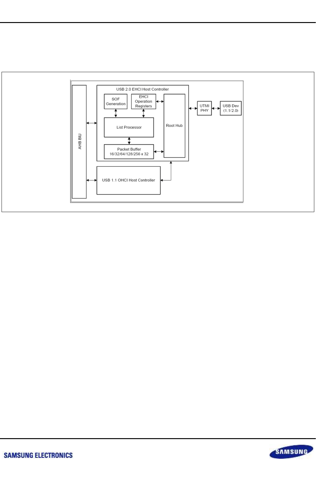
Samsung Confidential
S5P6818_UM 27 USB2.0 HOST
27-2
Preliminary product information describes products that are in development, for which full characterization data and
associated errata are not yet available. Specifications and information herein are subject to change without notice.
27.3 Block Diagram
The architecture of the USB 2.0 EHCI Host Controller with BIU (Bus Interface Unit), along with the major building
blocks and the companion controller (USB 1.1 OHCI Host Controller), is shown in Figure below.
Figure 27-1 USB2.0 HOST Block Diagram
nexell / ys.kim at 2015.02.12
SAMSUNG Confidential

Samsung Confidential
S5P6818_UM 27 USB2.0 HOST
27-3
Preliminary product information describes products that are in development, for which full characterization data and
associated errata are not yet available. Specifications and information herein are subject to change without notice.
27.4 Functional Description
27.4.1 Programming User Configure of PHY and LINK in EHCI or OHCI
1. Release common reset of host controller
Program RSTCON1[24] (address: 0xC0012004) to 1'b1
2. Program AHB Burst type
SINGLE: default. TIEOFFREG7[27:25] (address: 0xC001101C) is 3'b000.
INCR16 (The OHCI does not support INCR16): program TIEOFFREG7[27:25] (address: 0xC001101C) to
3'b111 (recommended)
INCR8 (The OHCI does not support INCR8): program TIEOFFREG7[27:25] (address: 0xC001101C) to
3'b110
INCR4 (The OHCI part of the controller only supports INCR4 or SINGLE): program TIEOFFREG7[27:25]
(address: 0xC001101C) to 3'b100
3. Select word interface and enable word interface selection
8-bit word interface: program TIEOFFREG5[26:25] (address: 0xC0011014) to 2'b01 and
TIEOFFREG9[10:9] (address: 0xC0011024) to 2'b01
16-bit word interface: program TIEOFFREG5[26:25] (address: 0xC0011014) to 2'b11 and
TIEOFFREG9[10:9] (address: 0xC0011024) to 2'b11
4. POR (Power On Reset) of PHY
Program TIEOFFREG8[8:7] (address: 0xC0011020) to 2'b01
5. Wait clock of PHY: About 40 micro seconds
6. Release UTMI reset
Program TIEOFFREG5[21:20](address: 0xC0011014) to 2'b11
7. Release AHB reset of EHCI, OHCI
Program TIEOFFREG13[19:17] (address: 0xC0011034) to 3'b111
nexell / ys.kim at 2015.02.12
SAMSUNG Confidential

Samsung Confidential
S5P6818_UM 27 USB2.0 HOST
27-4
Preliminary product information describes products that are in development, for which full characterization data and
associated errata are not yet available. Specifications and information herein are subject to change without notice.
27.4.2 Programming User Configure of PHY and LINK in HSIC
1. Release common reset of host controller
Program RSTCON1[24] (address: 0xC0012004) to 1'b1
2. Program AHB Burst type
SINGLE: default. TIEOFFREG7[27:25] (address: 0xC001101C) is 3'b000.
INCR16 (The OHCI does not support INCR16): program TIEOFFREG7[27:25] (address: 0xC001101C) to
3'b111
INCR8 (The OHCI does not support INCR8): program TIEOFFREG7[27:25] (address: 0xC001101C) to
3'b110
INCR4 (The OHCI part of the controller only supports INCR4 or SINGLE): program TIEOFFREG7[27:25]
(address: 0xC001101C) to 3'b100
3. Select word interface and enable word interface selection
8-bit word interface: program TIEOFFREG5[26:25] (address: 0xC0011014) to 2'b01 and
TIEOFFREG9[10:9] (address: 0xC0011024) to 2'b01 and TIEOFFREG11[13:12] (address: 0xC001102C)
to 2'b01
16-bit word interface: program TIEOFFREG5[26:25] (address: 0xC0011014) to 2'b11 and
TIEOFFREG9[10:9] (address: 0xC0011024) to 2'b11 and TIEOFFREG11[13:12] (address: 0xC001102C)
to 2'b11
4. POR (Power On Reset) of EHCI PHY
Program TIEOFFREG8[8:7] (address: 0xC0011020) to 2'b01
5. Wait clock of EHCI PHY: about 40 micro seconds
6. Program HSIC Mode
Program TIEOFFREG5[24:23] (address: 0xC0011014) to 2'b11
7. POR (Power On Reset) of HSIC PHY
Program TIEOFFREG10[19:18] (address: 0xC0011028) to 2'b01
8. Wait clock of HSIC PHY: About 40 micro seconds
9. Release UTMI reset
Program TIEOFFREG5[20] (address: 0xC0011014) to 1'b1 and TIEOFFREG5[22] (address:
0xC0011014) to 1'b1
10. Release AHB reset
Program TIEOFFREG5[19:17] (address: 0xC0011014) to 3'b111
nexell / ys.kim at 2015.02.12
SAMSUNG Confidential

Samsung Confidential
S5P6818_UM 27 USB2.0 HOST
27-5
Preliminary product information describes products that are in development, for which full characterization data and
associated errata are not yet available. Specifications and information herein are subject to change without notice.
27.4.3 Attention Point of HSIC Programming
Port Status Control Register:
EHCI uses PORTSC_1 (address: 0xC0030054)
HSIC uses PORTSC_2 (address: 0xC0030058)
How to enable the Port Power Control Switch:
EHCI case: set PORTSC_1[12] (address: 0xC0030054) to 1'b1
HSIC case: set INSNREG08[1] (address: 0x0xC00300B0) to 1'b1
nexell / ys.kim at 2015.02.12
SAMSUNG Confidential

Samsung Confidential
S5P6818_UM 27 USB2.0 HOST
27-6
Preliminary product information describes products that are in development, for which full characterization data and
associated errata are not yet available. Specifications and information herein are subject to change without notice.
27.5 Register Description
27.5.1 Register Map Summary
The USB2.0 Host controller implements all of the necessary EHCI registers. Consult the Enhanced Host
Controller Interface Specification for USB for register details and programming considerations. Registers that differ
from the EHCI specification are described below.
Base Address: 0xC002_0000 (OHCI Controller)
Base Address: 0xC003_0000 (EHCI Controller)
Register
Offset
Description
Reset Value
HCCAPBASE
0000h
Capability register
0x0100_0010
HCSPARAMS
0004h
Structural parameter register
0x0000_1116
HCCPARAMS
0008h
Capability parameter register
0x0000_A010
RSVD
000Ch
Reserved
Undefined
USBCMD
0010h
USB command register
0x0008_0000
USBSTS
0014h
USB status register
0x0000_1000
USBINTR
0018h
USB interrupt Enable Register
0x0000_0000
FRINDEX
001Ch
USB frame index register
0x0000_0000
CTRLDSSEGMEN
0020h
4G Segment Select register
0x0000_0000
PERIODICLISTBASE
0024h
Periodic frame list base address register
0x0000_0000
ASYNCLISTADDR
0028h
Asynchronous list address register
0x0000_0000
RSVD
002Ch
to
004Ch
Reserved
Undefined
CONFIGFLAG
0050h
Configure flag register
0x0000_0000
PORTSC_1 to 15
0054h
to
008Ch
Port status/control register
0x0000_2000
INSNREG00
0090H:
WORD
Micro-Frame counter interface register
0x0000_0000
INSNREG01
0094H: WORD
Packet buffer in/out threshold register
0x0020_0020
INSNREG02
0098H: WORD
Packet buffer depth register
0x0000_0080
INSNREG03
009CH: WORD
Transfer en/disable register
0x0000_0000
INSNREG04
00A0H: WORD
HCC parameters register
0x0000_0000
INSNREG05
00A4H: WORD
UTMI configuration control and status register
0x0000_1000
INSNREG06
00A8H: WORD
AHB error status register
0x0000_0000
INSNREG07
00ACH: WORD
AHB master error address register
0x0000_0000
INSNREG08
0050H: WORD
HSIC enable/disable register
0x0000_0000
nexell / ys.kim at 2015.02.12
SAMSUNG Confidential
Samsung Confidential
S5P6818_UM 27 USB2.0 HOST
27-7
Preliminary product information describes products that are in development, for which full characterization data and
associated errata are not yet available. Specifications and information herein are subject to change without notice.
27.5.1.1 HCCAPBASE
Base Address: 0xC003_0000
Address = Base Address + 0000h, Reset Value = 0x0100_0010
Name
Bit
Type
Description
Reset Value
HCCAPBASE
[31:0]
RW
Capability Register
32'h0100_0010
27.5.1.2 HCSPARAMS
Base Address: 0xC003_0000
Address = Base Address + 0004h, Reset Value = 0x0000_1116
Name
Bit
Type
Description
Reset Value
HCSPARAMS
[31:0]
RW
Structural Parameter Register
32'h1116
27.5.1.3 HCCPARAMS
Base Address: 0xC003_0000
Address = Base Address + 0008h, Reset Value = 0x0000_A010
Name
Bit
Type
Description
Reset Value
HCCPARAMS
[31:0]
RW
Capability Parameter Register
NOTE: The Isochronous Scheduling Threshold value
is set to 1 by default
32'hA010
27.5.1.4 USBCMD
Base Address: 0xC003_0000
Address = Base Address + 0010h, Reset Value = 0x0008_0000
Name
Bit
Type
Description
Reset Value
USBCMD
[31:0]
RW
USB Command
32'h0008_0000
27.5.1.5 USBSTS
Base Address: 0xC003_0000
Address = Base Address + 0014h, Reset Value = 0x0000_1000
Name
Bit
Type
Description
Reset Value
usbsts
[31:0]
RW
USB Status
32'h1000
nexell / ys.kim at 2015.02.12
SAMSUNG Confidential
Samsung Confidential
S5P6818_UM 27 USB2.0 HOST
27-8
Preliminary product information describes products that are in development, for which full characterization data and
associated errata are not yet available. Specifications and information herein are subject to change without notice.
27.5.1.6 USBINTR
Base Address: 0xC003_0000
Address = Base Address + 0018h, Reset Value = 0x0000_0000
Name
Bit
Type
Description
Reset Value
USBINTR
[31:0]
RW
USB Interrupt Enable
32'h0
27.5.1.7 FRINDEX
Base Address: 0xC003_0000
Address = Base Address + 001Ch, Reset Value = 0x0000_0000
Name
Bit
Type
Description
Reset Value
FRINDEX
[31:0]
RW
USB Frame Index
32'h0
27.5.1.8 CTRLDSSEGMEN
Base Address: 0xC003_0000
Address = Base Address + 0020h, Reset Value = 0x0000_0000
Name
Bit
Type
Description
Reset Value
CTRLDSSEGMEN
[31:0]
RW
4G Segment Selector
32'h0
27.5.1.9 PERIODICLISTBASE
Base Address: 0xC003_0000
Address = Base Address + 0024h, Reset Value = 0x0000_0000
Name
Bit
Type
Description
Reset Value
PERIODICLISTBASE
[31:0]
RW
Periodic Frame List Base Address Register
32'h0
27.5.1.10 ASYNCLISTADDR
Base Address: 0xC003_0000
Address = Base Address + 0028h, Reset Value = 0x0000_0000
Name
Bit
Type
Description
Reset Value
ASYNCLISTADDR
[31:0]
RW
Asynchronous List Address Register
32'h0
nexell / ys.kim at 2015.02.12
SAMSUNG Confidential
Samsung Confidential
S5P6818_UM 27 USB2.0 HOST
27-9
Preliminary product information describes products that are in development, for which full characterization data and
associated errata are not yet available. Specifications and information herein are subject to change without notice.
27.5.1.11 CONFIGFLAG
Base Address: 0xC003_0000
Address = Base Address + 0050h, Reset Value = 0x0000_0000
Name
Bit
Type
Description
Reset Value
CONFIGFLAG
[31:0]
RW
Configured Flag Register
32'h0
27.5.1.12 PORTSC_1 to 15
Base Address: 0xC003_0000
Address = Base Address + 0054h to 008Ch, Reset Value = 0x0000_2000
Name
Bit
Type
Description
Reset Value
PORTSC_1 to 15
[31:0]
RW
Port Status/Control
32'h2000
27.5.1.13 INSNREG00
Base Address: 0xC003_0000
Address = Base Address + 0090H: WORD, Reset Value = 0x0000_0000
Name
Bit
Type
Description
Reset Value
RSVD
[31:14]
–
Reserved
17'h0
Bit[8]
[13:12]
RW
This value is used as the 1-microframe counter with
byte interface (8 bits)
2'b00
Bit[16]
[11:1]
RW
This value is used as the 1-microframe counter with
byte interface (16 bits)
11'h0
WRENB
[0]
RW
Write Enable Register
0 = Disable
1 = Enable
1'b0
27.5.1.14 INSNREG01
Base Address: 0xC003_0000
Address = Base Address + 0094H: WORD, Reset Value = 0x0020_0020
Name
Bit
Type
Description
Reset Value
OUTTHRESHOLD
[31:16]
RW
Programmable Packet Buffer OUT Thresholds
16'h20
INTHRESHOLD
[15:0]
RW
Programmable Packet Buffer IN Threshold
16'h20
nexell / ys.kim at 2015.02.12
SAMSUNG Confidential

Samsung Confidential
S5P6818_UM 27 USB2.0 HOST
27-10
Preliminary product information describes products that are in development, for which full characterization data and
associated errata are not yet available. Specifications and information herein are subject to change without notice.
27.5.1.15 INSNREG02
Base Address: 0xC003_0000
Address = Base Address + 0098H: WORD, Reset Value = 0x0000_0080
Name
Bit
Type
Description
Reset Value
INSNREG02
[31:0]
RW
Programmable Packet Buffer Depth
The value specified here is the number of DWORDs
(32-bit entries)
32'h80
27.5.1.16 INSNREG03
Base Address: 0xC003_0000
Address = Base Address + 009CH: WORD, Reset Value = 0x0000_0000
Name
Bit
Type
Description
Reset Value
INSNREG03
[31:0]
RW
Break Memory Transfer Used in conjunction with
INSNREG01 to enable/disable breaking memory
transactions into chunks once the OUT/IN threshold
value is reached.
0 = Disable
1 = Enable
32'h0
27.5.1.17 INSNREG04
Base Address: 0xC003_0000
Address = Base Address + 00A0H: WORD, Reset Value = 0x0000_0000
Name
Bit
Type
Description
Reset Value
RSVD
[31:5]
–
Reserved
27'h0
NAK
[4]
RW
This value is used as the 1-microframe counter with
byte interface (8 bits)
1'b0
RSVD
[3]
–
Reserved
1'b0
SCALESDOWN
[2]
RW
Scales down port enumeration time enable
0 = Disable
1 = Enable
1'b0
M_HCCPARAMS
[1]
RW
Makes the HCCPARAMS register Write Enable
0 = Disable
1 = Enable
1'b0
M_HCSPARAMS
[0]
RW
Makes the HCSPARAMS register Write Enable
0 = Disable
1 = Enable
1'b0
nexell / ys.kim at 2015.02.12
SAMSUNG Confidential
Samsung Confidential
S5P6818_UM 27 USB2.0 HOST
27-11
Preliminary product information describes products that are in development, for which full characterization data and
associated errata are not yet available. Specifications and information herein are subject to change without notice.
27.5.1.18 INSNREG05
Base Address: 0xC003_0000
Address = Base Address + 00A4H: WORD, Reset Value = 0x0000_1000
Name
Bit
Type
Description
Reset Value
RSVD
[31:18]
–
Reserved
14'h0
VBUSY
[17]
RW
VBusy (Software RO). Hardware indicator that a write
to this register has occurred and the hardware is
currently processing the operation defined by the data
written. When processing is finished, this bit is
cleared.
1'b0
VPORT
[16:13]
RW
VPort (Software R/W)
1'b0
VCONTROL_LOADM
[12]
RW
VControl_LoadM
0 = Load
1 = NOP (Software RW)
1'b1
VCONTROL
[11:8]
RW
VControl (Software RW)
4'h0
VSTATUS
[7:0]
RW
VStatus (Software RW)
8'h0
27.5.1.19 INSNREG06
Base Address: 0xC003_0000
Address = Base Address + 00A8H: WORD, Reset Value = 0x0000_0000
Name
Bit
Type
Description
Reset Value
CAPTURED
[31]
RW
AHB Error Captured
Indicator that an AHB error was encountered and
values were captured. To clear this field the
application must write a "0" to it.
1'b0
RSVD
[30:12]
R
Reserved
19'h0
HBURST
[11:9]
R
HBURST value of the control phase at which the AHB
error occurred.
3'b000
NUMBER
[8:4]
R
Number of beats expected in the burst at which the
AHB error occurred. Valid values are "0" to "16"
5'h0
COMPLETED
[3:0]
R
Number of successfully-completed beats in the current
burst before the AHB error occurred.
4'h0
nexell / ys.kim at 2015.02.12
SAMSUNG Confidential
Samsung Confidential
S5P6818_UM 27 USB2.0 HOST
27-12
Preliminary product information describes products that are in development, for which full characterization data and
associated errata are not yet available. Specifications and information herein are subject to change without notice.
27.5.1.20 INSNREG07
Base Address: 0xC003_0000
Address = Base Address + 00ACH: WORD, Reset Value = 0x0000_0000
Name
Bit
Type
Description
Reset Value
ERROR
[31:0]
RW
AHB address of the control phase at which the AHB
error occurred
32'h0
27.5.1.21 INSNREG08
Base Address: 0xC003_0000
Address = Base Address + 0050H: WORD, Reset Value = 0x0000_0000
Name
Bit
Type
Description
Reset Value
RSVD
[31:16]
RW
Reserved for future use. You don't have to write any
value except 0.
16'h0
HSIC_ENB
[15:0]
RW
This register has R/W access to the host driver and
gives control to the host driver to enable/disable the
HSIC interface per port. Each bit in this register
controls the HSIC interface for a particular port. Bit 1
controls PORT 1, Bit 0 controls the HSIC interface for
PORT 0, and so on.
0 = When HSIC support is selected, then a value of 0
on this control register bit will put the corresponding
PORT in the HSIC Disabled state
1 = When HSIC configuration is selected and a value
of 1 in this control bit will put the corresponding port in
HSIC Enabled state
16'h0
nexell / ys.kim at 2015.02.12
SAMSUNG Confidential

Samsung Confidential
S5P6818_UM 28 I2S
28-1
Preliminary product information describes products that are in development, for which full characterization data and
associated errata are not yet available. Specifications and information herein are subject to change without notice.
28 I2S
28.1 Overview
Inter-IC Sound (IIS) is one of the popular digital audio interfaces. The IIS bus handles audio data and other
signals, namely, sub-coding and control, are transferred separately. It is possible to transmit data between two IIS
bus. To minimize the number of pins required and to keep wiring simple, basically, a 3-line serial bus is used. This
consists of a line for two time-multiplexed data channels, a word select line and a clock line.
IIS interface transmits or receives sound data from external stereo audio codec. To transmit and receive data, two
32 64 FIFOs (First-In-First-Out) data structures are included and DMA transfer mode to transmit and receive
samples can be supported. IIS-specific clock can be supplied from internal system clock controller through IIS
clock divider or direct clock source.
28.2 Features
2-ports stereo (2 channel) IIS-bus for audio interface with DMA-based operation
Serial, 8/16/24-bit per channel data transfers
Supports master/slave mode
Supports IIS, MSB-justified and LSB-justified data format
nexell / ys.kim at 2015.02.12
SAMSUNG Confidential
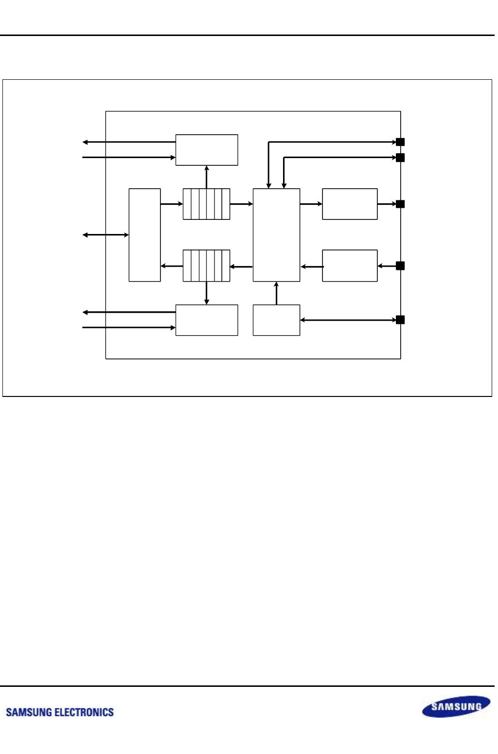
Samsung Confidential
S5P6818_UM 28 I2S
28-2
Preliminary product information describes products that are in development, for which full characterization data and
associated errata are not yet available. Specifications and information herein are subject to change without notice.
28.3 Block Diagram
Figure 28-1 IIS-Bus Block Diagram
TxR
Channel
Control
TxDMA
FSM
RxDMA
FSM Clock
Control
Tx Shift
Register
Rx Shift
Register
TxFIFO
RxFIFO
TxDREQ
TxDACK
System
Bus
RxDREQ
RxDACK
I2SSCLK
I2SLRCLK
I2SSDO
I2SSDI
I2SCDCLK
Register File
nexell / ys.kim at 2015.02.12
SAMSUNG Confidential
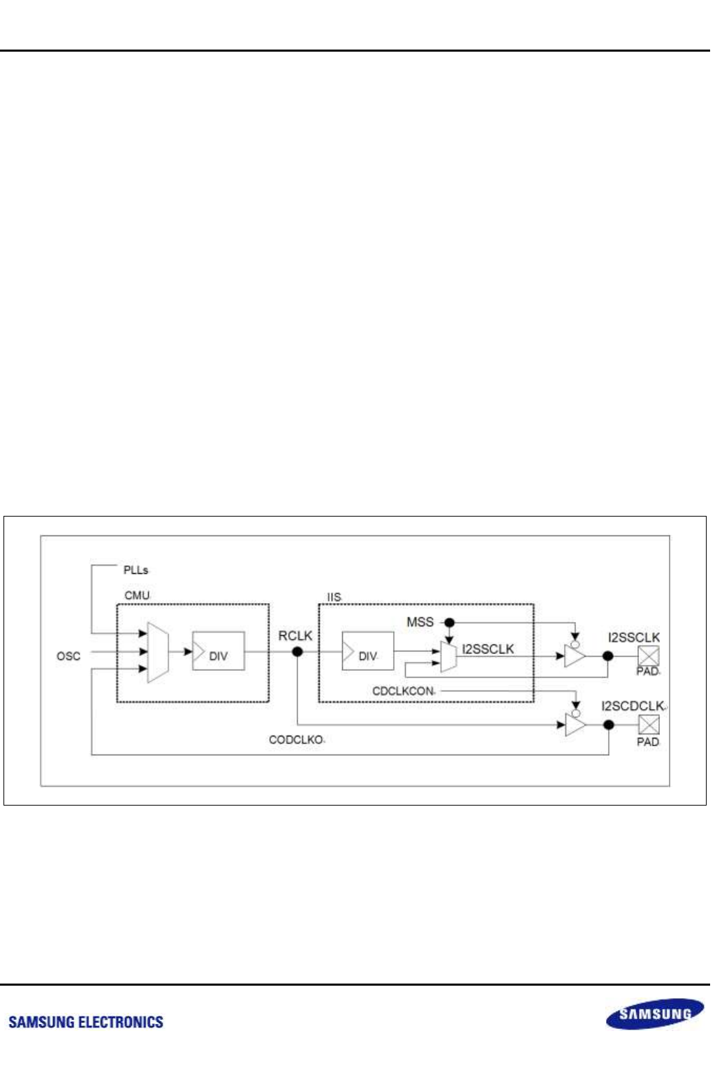
Samsung Confidential
S5P6818_UM 28 I2S
28-3
Preliminary product information describes products that are in development, for which full characterization data and
associated errata are not yet available. Specifications and information herein are subject to change without notice.
28.4 Functional Description
IIS interface consists of register bank, FIFOs, shift registers, clock control, DMA finite state machine, and channel
control block as shown in the figure above. Note that each FIFO has 32-bit width and 64 depth structure, which
contains left/right channel data. Thus, FIFO access and data transfer are handled with left/right pair unit. The
figure above shows the functional block diagram of IIS interface.
28.4.1 Master/Slave Mode
To select master or slave mode, set MSS bit of IISMOD register. In master mode, I2SSCLK and I2SLRCLK are
generated internally and supplied to external device. Therefore, a root clock is required to generate I2SSCLK and
I2SLRCLK. In external master mode, the root clock can be directly fed from IIS external. The I2SSCLK and
I2SLRCLK are supplied from the pin (GPIOs) in slave mode. That is, whatever source clock is, Only Master can
generate I2SLRCLK and I2SSCLK.
Master/Slave mode is different compared to TX/RX. Master/Slave mode presents the direction of I2SLRCLK and
I2SSCLK. The direction of I2SCDCLK (This is only auxiliary.) is not important. If IIS bus interface transmits clock
signals to IIS codec, IIS bus is master mode. But if IIS bus interface receives clock signal from IIS codec, IIS bus
is slave mode. TX/RX mode indicates the direction of data flow. If IIS bus interface transmits data to IIS codec,
this indicates Tx mode. Conversely, IIS bus interface receives data from IIS codec this indicates Rx mode.
The figure below shows the route of the root clock with internal master or external master mode setting in IIS clock
control block and system controller. Note that RCLK indicates root clock and this clock can be supplied to external
IIS codec chip in internal master mode.
Figure 28-2 IIS Clock Control Block Diagram
nexell / ys.kim at 2015.02.12
SAMSUNG Confidential

Samsung Confidential
S5P6818_UM 28 I2S
28-4
Preliminary product information describes products that are in development, for which full characterization data and
associated errata are not yet available. Specifications and information herein are subject to change without notice.
28.4.2 DMA Transfer
In the DMA transfer mode, use external DMA controller to access the transmitter or receiver FIFO. The transmitter
or receiver FIFO state activates the DMA service request internally. The FTXEMPT, FRXEMPT, FTXFULL, and
FRXFULL bits of I2SCON register represent the transmitter or receiver FIFO data state. Especially, FTXEMPT
and FRXFULL bit are the ready flag for DMA service request; the transmit DMA service request is activated when
TXFIFO is not empty and the receiver DMA service request is activated when RXFIFO is not full.
The DMA transfer uses only handshaking method for single data. Note that during DMA acknowledge activation;
the data read or write operation should be performed.
NOTE: Reference: DMA request point
Tx mode: (FIFO is not full) & (TXDMACTIVE is active)
Rx mode: (FIFO is not empty) & (RXDMACTIVE is active)
28.4.3 Audio Serial Data Format
28.4.3.1 IIS-Bus Format
The IIS bus has four lines including serial data input I2SSDI, serial data output I2SSDO, left/right channel select
clock I2SLRCLK, and serial bit clock I2SSCLK; master generates I2SLRCLK and I2SSCLK.
Serial data is transmitted in 2's complement with the MSB first with a fixed position, whereas the position of the
LSB depends on the word length. The transmitter sends the MSB of the next word at one clock period after the
I2SLRCLK is changed. Serial data sent by the transmitter can be synchronized either with the trailing or with the
leading edge of the clock signal. However, the serial data must be latched into the receiver on the leading edge of
the serial clock signal, and so there are some restrictions when transmitting data that is synchronized with the
leading edge.
The LR channel select line indicates the channel being transmitted. I2SLRCLK may be changed either on a
trailing or leading edge of the serial clock, but it does not need to be symmetrical. In the slave, this signal is
latched on the leading edge of the clock signal. The I2SLRCLK line changes one clock period before the MSB is
transmitted. This allows the slave transmitter to derive synchronous timing of the serial data that will be set up for
transmission. Furthermore, it enables the receiver to store the previous word and clear the input for the next word.
28.4.3.2 MSB (Left) Justified
MSB-Justified (Left-Justified) format is similar to I2S bus format, except the in MSB-justified format, the transmitter
always sends the MSB of the next word at the same time whenever the I2SLRCLK is changed.
nexell / ys.kim at 2015.02.12
SAMSUNG Confidential
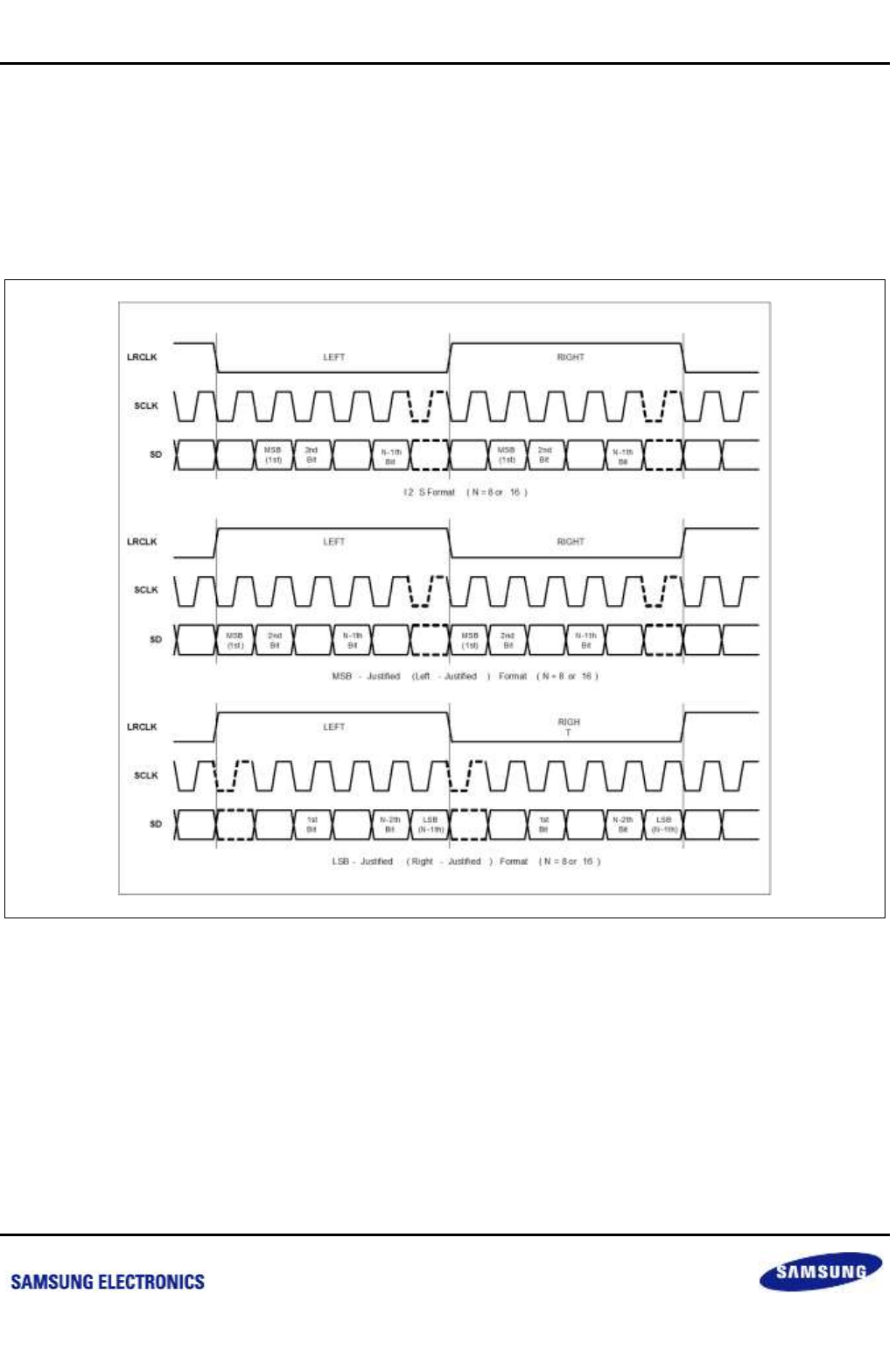
Samsung Confidential
S5P6818_UM 28 I2S
28-5
Preliminary product information describes products that are in development, for which full characterization data and
associated errata are not yet available. Specifications and information herein are subject to change without notice.
28.4.3.3 LSB (Right) Justified
LSB-Justified (Right-Justified) format is opposite to the MSB-justified format. In other word, the transferring serial
data is aligned with ending point of I2SLRCLK transition.
The figure below shows the audio serial format of IIS, MSB-justified, and LSB-justified. Note that in this figure, the
word length is 16-bit and I2SLRCLK makes transition every 24 cycle of I2SSCLK (BFS is 48 fs, where fs is
sampling frequency; I2SLRCLK frequency).
Figure 28-3 I2S Audio Serial Data Formats
28.4.3.4 Sampling Frequency and Master Clock
When IIS interface Controller operates as master, IIS interface Controller generates IISLRCLK and IISSCLK that
are divided as Root Clock by RFS and BFS value. To decide Sampling Frequency - IISLRCLK -, BLC, BFS, and
RFS are selected first. Optionally, IIS interface Controller clocks out Root clock as IISCDCLK for codec master
clock (if source of root clock is not IISEXTCDCLK).
In slave mode, you must set the value of BLC, BFS and RFS similar to master (ex: Codec). Because IIS interface
controller needs these value for correct operation.
nexell / ys.kim at 2015.02.12
SAMSUNG Confidential
Samsung Confidential
S5P6818_UM 28 I2S
28-6
Preliminary product information describes products that are in development, for which full characterization data and
associated errata are not yet available. Specifications and information herein are subject to change without notice.
28.4.4 PCM Word Length and BFS Driver
PCM Word Length (BLC) setting should be preceded before setting the BFS value. The table below shows BFS
available value as BLC.
Table 28-1 Allowed BFS Value as BLC
PCM Bit length (BLC)
8-bit
16-bit
24-bit
Available BFS value
16 fs, 24 fs, 32 fs, 48 fs
32 fs, 48 fs
48 fs
28.4.5 DFS Divider and RFS Divider
PCM Word Length (BLC) setting should be preceded before setting the BFS value. The table below shows BFS
available value as BLC.
Table 28-2 Allowed RFS Value as BFS
BFS Divider
16 fs, 32 fs
24 fs, 48 fs
Available RFS value
256 fs, 384 fs, 512 fs, 768 fs
384 fs, 768 fs
28.4.6 RFS Divider and ROOT Clock
Root Clock is made for sampling frequency proper RFS value as shown in the table below. RCLK is clock divided
by IIS pre-scaler (IISPSR) that is selected by MSS.
Table 28-3 Root Clock Table (MHz)
IISLRCK
RFS
8.000
kHz
11.025
kHz
16.000
kHz
22.050
kHz
32.000
kHz
44.100
kHz
48.000
kHz
64.000
kHz
88.200
kHz
96.000
kHz
256 fs
2.0480
2.8224
4.0960
5.6448
8.1920
11.2896
12.2880
16.3840
22.5792
24.5760
384 fs
3.0720
4.2336
6.1440
8.4672
12.2880
16.9344
18.4320
24.5760
33.8688
36.8640
512 fs
4.0960
5.6448
8.1920
11.2896
16.3840
22.5792
24.5760
32.7680
45.1584
49.1520
768 fs
6.1440
8.4672
12.2880
16.9344
24.5760
33.8688
36.8640
49.1520
67.7376
73.7280
NOTE: Root Clock Frequency = fs (256, 384, 512 or 768)
nexell / ys.kim at 2015.02.12
SAMSUNG Confidential

Samsung Confidential
S5P6818_UM 28 I2S
28-7
Preliminary product information describes products that are in development, for which full characterization data and
associated errata are not yet available. Specifications and information herein are subject to change without notice.
28.5 Programming Guide
The IIS bus interface can be accessed either by the processor using programmed I/O instructions or by the DMA
controller.
28.5.1 Initialization
1. Before you use IIS bus interface, you must configure GPIOs to IIS mode, that is, I2SSDI is input and I2SSDO
is output. I2SLRCLK, I2SSCLK and I2SCDCLK are in/out-type.
2. Select clock source. S5PC210 has three clock sources, namely, PCLK, PLL and external codec.
For more information, refer figure (IIS Clock Control Block Diagram).
28.5.2 Play Mode (TX Mode) with DMA
1. TXFIFO is flushed before operation. If you do not distinguish Master/Slave mode from TX/RX mode,
you must study Master/Slave mode and TX/RX mode. Refer Master/Slave chapter.
2. Configure I2SMOD register and I2SPSR (IIS pre-scaler register).
3. To operate system in stability, the internal TXFIFO should be almost full before transmission.
For TXFIFO to be almost full start DMA operation.
4. IIS bus does not support the interrupt. Therefore, you can only check state by polling through accessing SFR.
5. After TXFIFO is full, then I2SACTIVE must be asserted.
28.5.3 Recording Mode (Rx Mode) with DMA
1. RXFIFO is flushed before operation. Also, if you don't distinguish between Master/Slave mode and TX/RX
mode, you must study Master/Slave mode and TX/RX mode. Refer Master/Slave chapter.
2. Configure I2SMOD register and I2SPSR (IIS pre-scaler register).
3. To operate system in stability, the internal RXFIFO should have at least one data before DMA operation.
You must assert I2SACTIVE before DMA operation.
4. Check RXFIFO state by polling through accessing SFR.
5. If RXFIFO is not empty, start RXDMACTIVE.
nexell / ys.kim at 2015.02.12
SAMSUNG Confidential
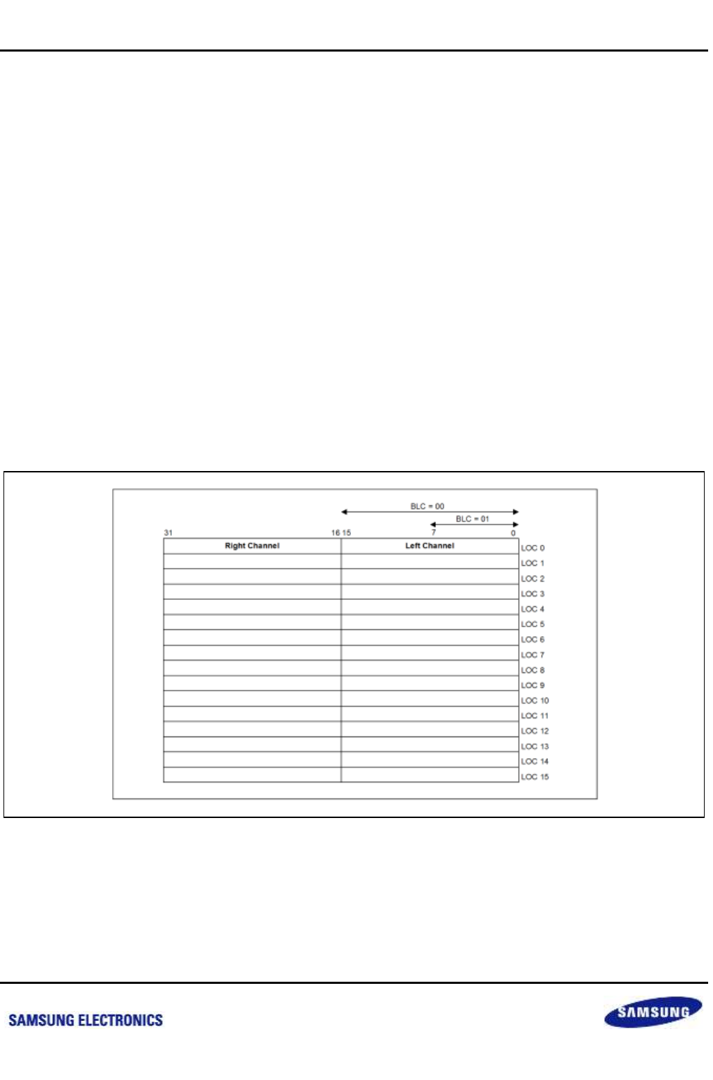
Samsung Confidential
S5P6818_UM 28 I2S
28-8
Preliminary product information describes products that are in development, for which full characterization data and
associated errata are not yet available. Specifications and information herein are subject to change without notice.
28.5.4 Example Code
28.5.4.1 Tx Channel
The I2S Tx channel provides a single stereo compliant output. The transmit channel can operate in master or
Slave mode. Data is transferred between the processor and the I2S controller via an APB access or a DMA
access.
The processor must write words in multiples of two (i.e. for left and right audio sample).The words are serially
shifted out timed with respect to the audio serial BITCLK, SCLK and word select clock, LRCLK.
Tx Channel has 64 32-bit wide FIFO where the processor or DMA can write up to 16 left/right data samples After
enabling the channel for transmission.
An Example sequence is as follows:
Ensure the PCLK and CDCLK are coming correctly to the I2S controller and FLUSH the TX FIFO using the
TFLUSH bit in the Please ensure that I2S Controller is configured in one of the following modes.
Tx mode only
TX/RX simultaneous mode.
The Data is aligned in the Tx FIFO for 8 bits/channel or 16 bits/channel BLC as shown in the figure below.
Figure 28-4 Tx FIFO Structure for BLC = 00 or BLC = 01
nexell / ys.kim at 2015.02.12
SAMSUNG Confidential
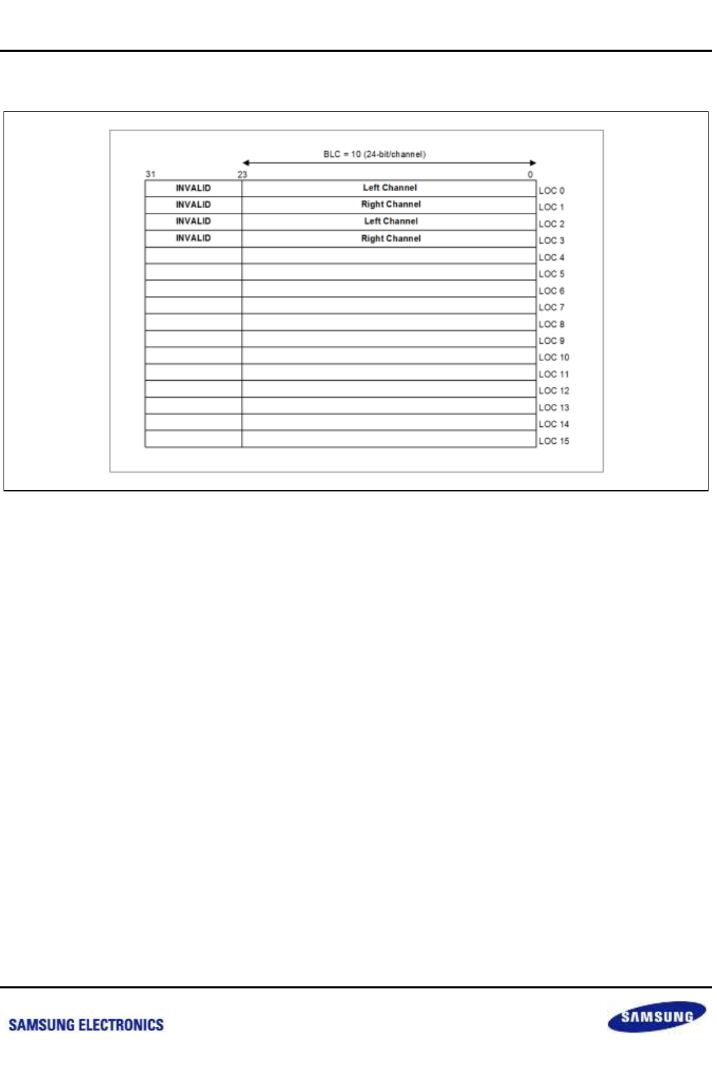
Samsung Confidential
S5P6818_UM 28 I2S
28-9
Preliminary product information describes products that are in development, for which full characterization data and
associated errata are not yet available. Specifications and information herein are subject to change without notice.
The Data is aligned in the Tx FIFO for 24-bit/channel BLC as shown in the figure below.
Figure 28-5 Tx FIFO Structure for BLC = 10 (24 bits/channel)
Once the data is written to the Tx FIFO the Tx channel can be made active by enabling the I2SACTIVE bit in the
I2SCON Register (I2S Control Register).
The data is then serially shifted out with respect to the serial bit clock SCLK and word select clock LRCLK.
The TXCHPAUSE in the I2SCON Register (I2S Control Register) can stop the serial data transmission on the
I2SSDO.The transmission is stopped once the current Left/Right channel is transmitted.
If the control registers in the I2SCON Register (I2S Control Register) and I2SMOD Register (I2S Mode Register)
are to be reprogrammed then it is advisable to disable the Tx channel.
If the Tx channel is enabled while the FIFO is empty, no samples are read from the FIFO.
The Status of Tx FIFO can be checked by checking the bits in the I2SFIC Register (I2S FIFO Control Register).
nexell / ys.kim at 2015.02.12
SAMSUNG Confidential

Samsung Confidential
S5P6818_UM 28 I2S
28-10
Preliminary product information describes products that are in development, for which full characterization data and
associated errata are not yet available. Specifications and information herein are subject to change without notice.
28.5.4.2 Rx Channel
The I2S Rx channel provides a single stereo compliant output. The receive channel can operate in master or slave
mode. Data is received from the input line and transferred into the Rx FIFO. The processor can then read this data
via an APB read or a DMA access can access this data.
Rx Channel has a 64 32-bit wide Rx FIFO where the processor or DMA can read UPTO 16 left/right data
samples after enabling the channel for reception.
An Example sequence is as follows:
Ensure the PCLK and CDCLK are coming correctly to the I2S controller and FLUSH the Rx FIFO using the
RFLUSH bit in the I2SFIC Register (I2S FIFO Control Register) and the I2S controller is configured in any of the
modes
Receive only.
Receive/Transmit simultaneous mode.
This can be done by Programming the TXR bit in the I2SMOD Register (I2S Mode Register).
1. Then Program the following parameters according to the need
MSS
SDF
BFS
BLC
LRP
For Programming, the above mentioned fields please refer I2SMOD Register (I2S Mode Register)
2. Once ensured that the input clocks for I2S controller are up and running and step 1 and 2 have been
completed user must put the I2SACTIVE high to enable any reception of data, the I2S Controller receives
data on the LRCLK change.
Read the data from the Rx FIFO using the I2SRXD Register (I2S Rx FIFO Register) after looking at the Rx FIFO
count in the I2SFIC Register (I2S FIFO Control Register). The count would only increment once the complete left
channel and right have been received.
nexell / ys.kim at 2015.02.12
SAMSUNG Confidential
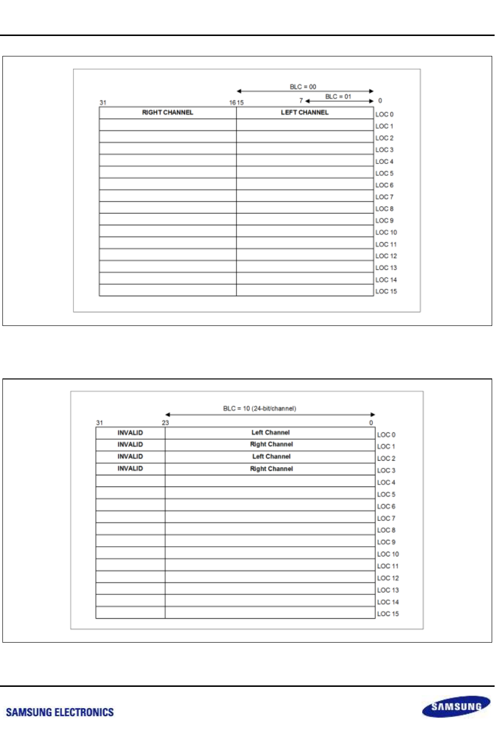
Samsung Confidential
S5P6818_UM 28 I2S
28-11
Preliminary product information describes products that are in development, for which full characterization data and
associated errata are not yet available. Specifications and information herein are subject to change without notice.
Figure 28-6 Rx FIFO Structure for BLC = 00 or BLC = 01
The Data is aligned in the Rx FIFO for 24-bit/channel BLC as shown the figure below.
Figure 28-7 Rx FIFO Structure for BLC = 10 (24 bits/channel)
nexell / ys.kim at 2015.02.12
SAMSUNG Confidential

Samsung Confidential
S5P6818_UM 28 I2S
28-12
Preliminary product information describes products that are in development, for which full characterization data and
associated errata are not yet available. Specifications and information herein are subject to change without notice.
The RXCHPAUSE in the I2SCON register can stop the serial data reception on the I2SSDI.The reception is
stopped once the current Left/Right channel is received.
If the control registers in the I2SCON Register (I2S Control Register) and I2SMOD Register (I2S Mode Register)
are to be reprogrammed then it is advisable to disable the Rx channel.
Check the status of Rx FIFO by checking the bits in the I2SFIC Register (I2S FIFO Control Register).
nexell / ys.kim at 2015.02.12
SAMSUNG Confidential
Samsung Confidential
S5P6818_UM 28 I2S
28-13
Preliminary product information describes products that are in development, for which full characterization data and
associated errata are not yet available. Specifications and information herein are subject to change without notice.
28.6 Register Description
28.6.1 Register Map Summary
Base Address: 0xC005_5000h (I2S0)
Base Address: 0xC005_6000h (I2S1)
Base Address: 0xC005_7000h (I2S2)
Register
Offset
Description
Reset Value
IISCON
0x00h
I2S interface control register
0x0000_0E00
IISMOD
0x04h
I2C-bus mode register
0x0000_0000
IISFIC
0x08h
I2S interface FIFO control register
0x0000_0000
RSVD
0x0Ch
Reserved
Undefined
I2STXD
0x10h
I2S interface transmit data register
0x0000_0000
I2SRXD
0x14h
I2S interface receive data register
0x0000_0000
nexell / ys.kim at 2015.02.12
SAMSUNG Confidential

Samsung Confidential
S5P6818_UM 28 I2S
28-14
Preliminary product information describes products that are in development, for which full characterization data and
associated errata are not yet available. Specifications and information herein are subject to change without notice.
28.6.1.1 IISCON
Base Address: 0xC005_5000h (I2S0)
Base Address: 0xC005_6000h (I2S1)
Base Address: 0xC005_7000h (I2S2)
Address = Base Address + 0x00h, Reset Value = 0x0000_0E00
Name
Bit
Type
Description
Reset Value
RSVD
[31:20]
RW
Reserved. Program to Zero
12'h0
FRXOFSTATUS
[19]
RW
Rx FIFO Overflow Interrupt Status. And this is used by
interrupt clear bit. When this is high, you can do
interrupt clear by writing "1".
0 = Interrupt didn't be occurred.
1 = Interrupt was occurred.
1'b0
FRXOFINTEN
[18]
RW
Rx FIFO Overflow Interrupt Enable
0 = RXFIFO Under-run INT disable
1 = RXFIFO Under-run INT enable
1'b0
FTXURSTATUS
[17]
RW
Tx FIFO under-run interrupts status. And this is used
by interrupt clear bit. When this is high, you can do
interrupt clear by writing '1'.
0 = Interrupt didn't be occurred.
1 = Interrupt was occurred.
1’b0
FTXURINTEN
[16]
RW
Tx FIFO Under-run Interrupt Enable
0 = TXFIFO Under-run INT disable
1 = TXFIFO Under-run INT enable
1'b0
RSVD
[15:12]
–
Reserved. Program to Zero
4’h0
LRI
[11]
R
Left/Right channel clock indication. Note that LRI
meaning is dependent on the value of LRP bit of
I2SMOD register.
0 = Left (when LRP bit is low) or right (when LRP bit is
high)
1 = Right (when LRP bit is low) or left (when LRP bit is
high)
1'b1
FTXEMPT
[10]
R
Tx FIFO empty status indication
0 = Tx FIFO is not empty (Ready to transmit data)
1 = Tx FIFO is empty (Not ready to transmit data)
1'b1
FRXDEMPT
[9]
R
Rx FIFO empty status indication
0 = Rx FIFO is not empty
1 = Rx FIFO is empty
1'b1
FTXFULL
[8]
R
Tx FIFO full status indication
0 = Tx FIFO is not full
1 = Tx FIFO is full
1'b0
FRXFULL
[7]
R
Rx FIFO full status indication
0 = Rx FIFO is not full (Ready to receive data)
1 = Rx FIFO is full (Not ready to receive data)
1'b0
nexell / ys.kim at 2015.02.12
SAMSUNG Confidential

Samsung Confidential
S5P6818_UM 28 I2S
28-15
Preliminary product information describes products that are in development, for which full characterization data and
associated errata are not yet available. Specifications and information herein are subject to change without notice.
Name
Bit
Type
Description
Reset Value
TXDMAPAUSE
[6]
RW
Tx DMA operation pause command. Note that when
this bit is activated at any time, the DMA request will
be halted after current on-going DMA transfer is
completed.
0 = No pause DMA operation
1 = Pause DMA operation
1'b0
RXDMAPAUSE
[5]
RW
Rx DMA operation pause command. Note that when
this bit is activated at any time, the DMA request will
be halted after current on-going DMA transfer is
completed.
0 = No pause DMA operation
1 = Pause DMA operation
1'b0
TXCHPAUSE
[4]
RW
Tx channel operation pause command. Note that
when this bit is activated at any time, the channel
operation will be halted after left-right channel data
transfer is completed.
0 = No pause operation
1 = Pause operation
1'b0
RXCHPAUSE
[3]
RW
Rx channel operation pause command. Note that
when this bit is activated at any time, the channel
operation will be halted after left-right channel data
transfer is completed.
0 = No pause operation
1 = Pause operation
1'b0
TXDMACTIVE
[2]
RW
Tx DMA active (start DMA request). Note that when
this bit is set from high to low, the DMA operation will
be forced to stop immediately.
0 = Inactive
1 = Active
1'b0
RXDMACTIVE
[1]
RW
Rx DMA active (start DMA request). Note that when
this bit is set from high to low, the DMA operation will
be forced to stop immediately.
0 = Inactive
1 = Active
1'b0
I2SACTIVE
[0]
RW
IIS interface active (start operation).
0 = Inactive
1 = Active
1'b0
nexell / ys.kim at 2015.02.12
SAMSUNG Confidential

Samsung Confidential
S5P6818_UM 28 I2S
28-16
Preliminary product information describes products that are in development, for which full characterization data and
associated errata are not yet available. Specifications and information herein are subject to change without notice.
28.6.1.2 IISMOD
Base Address: 0xC005_5000h (I2S0)
Base Address: 0xC005_6000h (I2S1)
Base Address: 0xC005_7000h (I2S2)
Address = Base Address + 0x04h, Reset Value = 0x0000_0000
Name
Bit
Type
Description
Reset Value
RSVD
[31:15]
RW
Reserved. Program to Zero
17'h0
BLC
[14:13]
RW
Bit Length Control Bit Which decides transmission of
8/16 bits per audio channel
00 = 16 Bits per channel
01 = 8 Bits Per Channel
10 = 24 Bits Per Channel
11 = Reserved
2'b0
CDCLKCON
[12]
RW
Determine codec clock source
0 = Use internal codec clock source
1 = Get codec clock source from external codec chip
* 0 means External CDCLK Input pad enable
(Refer to Figure 28-2)
1'b0
IMS
[11]
RW
IIS master or slave mode select.
0 = Master mode
1 = Slave mode
1'b0
RSVD
[10]
–
Reserved. Program to Zero
1'b0
TXR
[9:8]
RW
Transmit or receive mode select.
00 = Transmit only mode
01 = Receive only mode
10 = Transmit and receive simultaneous mode
11 = Reserved
2'b0
LRP
[7]
RW
Left/Right channel clock polarity select.
0 = Low for left channel and high for right channel
1 = High for left channel and low for right channel
1'b0
SDF
[6:5]
RW
Serial data format.
00 = IIS format
01 = MSB-justified (left-justified) format
10 = LSB-justified (right-justified) format
11 = Reserved
2'b0
RFS
[4:3]
RW
IIS root clock (codec clock) frequency select.
00 = 256 fs, where fs is sampling frequency
01 = 512 fs
10 = 384 fs
11 = 768 fs
2'b0
BFS
[2:1]
RW
Bit clock frequency select.
00 = 32 fs, where fs is sampling frequency
01 = 48 fs
10 =16 fs
2'b0
nexell / ys.kim at 2015.02.12
SAMSUNG Confidential
Samsung Confidential
S5P6818_UM 28 I2S
28-17
Preliminary product information describes products that are in development, for which full characterization data and
associated errata are not yet available. Specifications and information herein are subject to change without notice.
Name
Bit
Type
Description
Reset Value
11 = 24 fs
RSVD
[0]
RW
Reserved. Program to Zero.
1'b0
28.6.1.3 IISFIC
Base Address: 0xC005_5000h (I2S0)
Base Address: 0xC005_6000h (I2S1)
Base Address: 0xC005_7000h (I2S2)
Address = Base Address + 0x08h, Reset Value = 0x0000_0000
Name
Bit
Type
Description
Reset Value
RSVD
[31:16]
–
Reserved. Program to Zero.
16'h0
TFULSH
[15]
RW
Tx FIFO flush command.
0 = No flush
1 = Flush
1'b0
FTXCNT
[14:8]
R
Reserved. Program to Zero.
7'h0
FTXCNT
[12:8]
R
Tx FIFO data count. FIFO has 64 dept, so value
ranges from 0 to 64.
N: Data count N of FIFO
5'h0
RFLUSH
[7]
RW
Rx FIFO flush command.
0 = No flush
1 = Flush
1’b0
FRXCNT
[6:0]
R
Rx FIFO data count. FIFO has 64 dept, so value
ranges from 0 to 64.
N: Data count N of FIFO
7’h0
28.6.1.4 I2STXD
Base Address: 0xC005_5000h
Base Address: 0xC005_6000h
Base Address: 0xC005_7000h
Address = Base Address + 0x10h, Reset Value = 0x0000_0000
Name
Bit
Type
Description
Reset Value
IISTXD
[31:0]
W
Tx FIFO writes data. Note that the left/right channel
data is allocated as the following bit fields.
R[31:16], L[15:0] when 16-bit BLC
R[23:16], L[7:0] when 8-bit BLC
32’h0
nexell / ys.kim at 2015.02.12
SAMSUNG Confidential

Samsung Confidential
S5P6818_UM 28 I2S
28-18
Preliminary product information describes products that are in development, for which full characterization data and
associated errata are not yet available. Specifications and information herein are subject to change without notice.
28.6.1.5 I2SRXD
Base Address: 0xC005_5000h
Address = Base Address + 0x14h, Reset Value = 0x0000_0000
Name
Bit
Type
Description
Reset Value
IISRXD
[31:0]
R
Rx FIFO read data. Note that the left/right channel
data is allocated as the following bit fields.
R[31:16], L[15:0] when 16-bit BLC
R[23:16], L[7:0] when 8-bit BLC
32’h0
nexell / ys.kim at 2015.02.12
SAMSUNG Confidential

Samsung Confidential
S5P6818_UM 29 AC97
29-1
Preliminary product information describes products that are in development, for which full characterization data and
associated errata are not yet available. Specifications and information herein are subject to change without notice.
29 AC97
29.1 Overview
The AC97 Controller Unit in the S5P6818 supports the features of AC97 revision 2.0. AC97 Controller uses audio
controller link (AC-link) to communicate with AC97 Codec. Controller sends the stereo PCM data to Codec. The
external digital-to-analog converter (DAC) in the Codec converts the audio sample to an analog audio waveform.
Controller receives the stereo PCM data and the mono MIC data from Codec then store in memories. This Section
describes the programming model for the AC97 Controller Unit. The prerequisite in this Section requires an
understanding of the AC97 revision 2.0 specifications.
29.2 Features
The AC97 Controller includes the following features:
Independent channels for stereo PCM In, stereo PCM Out, mono MIC In.
DMA-based operation and interrupt based operation.
All of the channels support only 16-bit samples.
Variable sampling rate AC97 Codec interface (48 kHz and below)
16-bit, 16 entry FIFOs per channel
Only primary Codec support
nexell / ys.kim at 2015.02.12
SAMSUNG Confidential
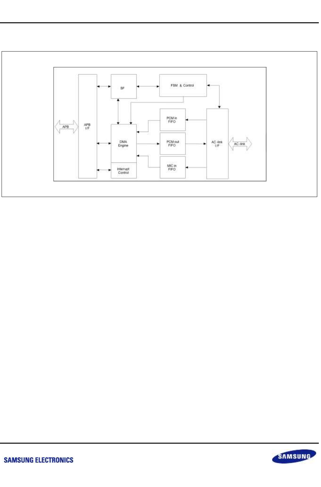
Samsung Confidential
S5P6818_UM 29 AC97
29-2
Preliminary product information describes products that are in development, for which full characterization data and
associated errata are not yet available. Specifications and information herein are subject to change without notice.
29.3 Block Diagram
Figure 29-1 AC97 Block Diagram
nexell / ys.kim at 2015.02.12
SAMSUNG Confidential
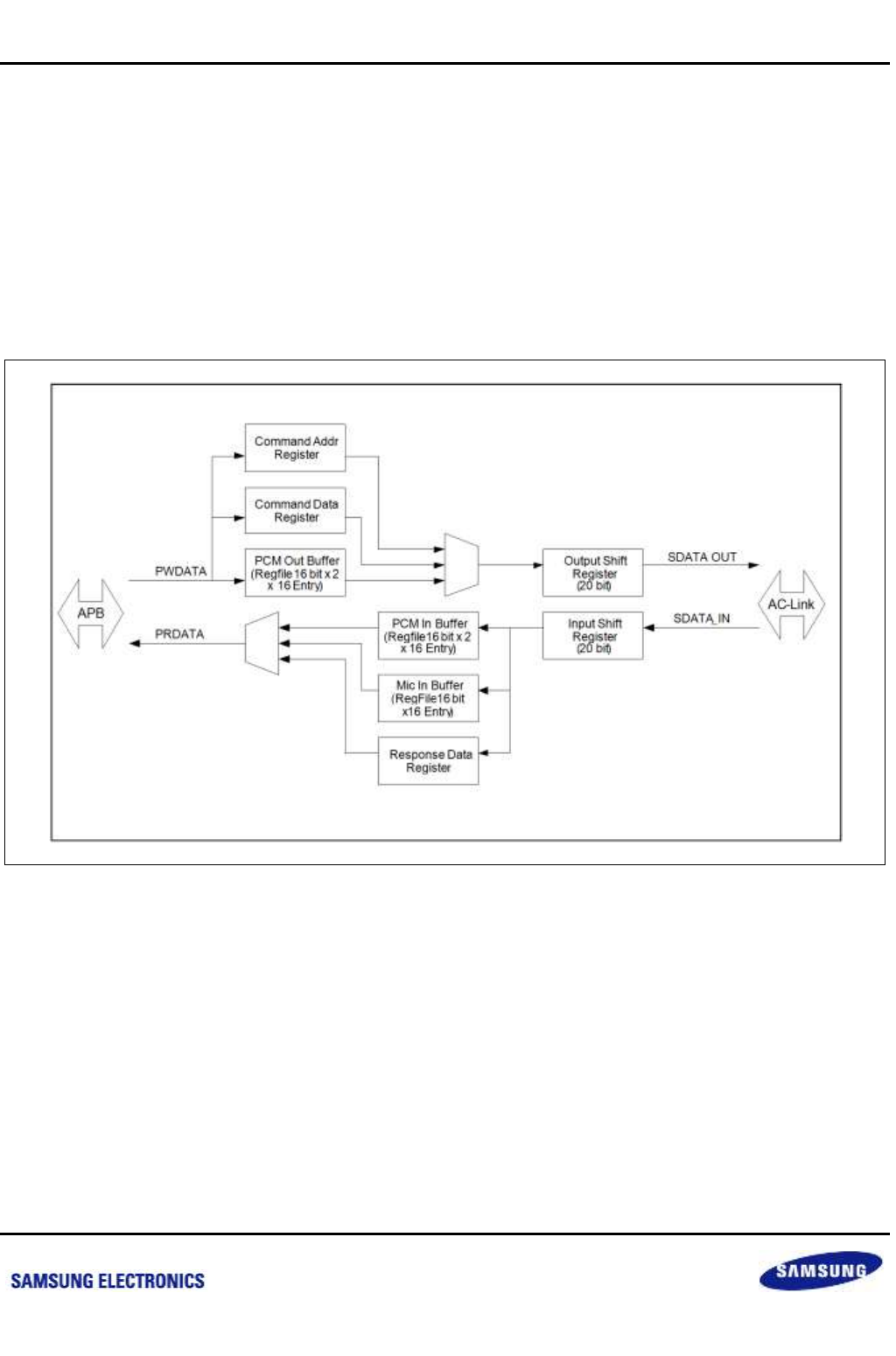
Samsung Confidential
S5P6818_UM 29 AC97
29-3
Preliminary product information describes products that are in development, for which full characterization data and
associated errata are not yet available. Specifications and information herein are subject to change without notice.
29.4 Functional Description
This section explains the AC97 Controller operation, namely, AC-Link, Power-down sequence and Wake-up
sequence.
29.4.1 Internal Data Path
The figure below shows the internal data path of S5P6818 AC97 Controller. It includes stereo Pulse Code
Modulated (PCM) In, Stereo PCM Out and mono MIC-in buffers, which consist of 16-bit and 16 entries buffer. It
also has 20-bit I/O shift register via AC-link.
Figure 29-2 Internal Data Path
nexell / ys.kim at 2015.02.12
SAMSUNG Confidential
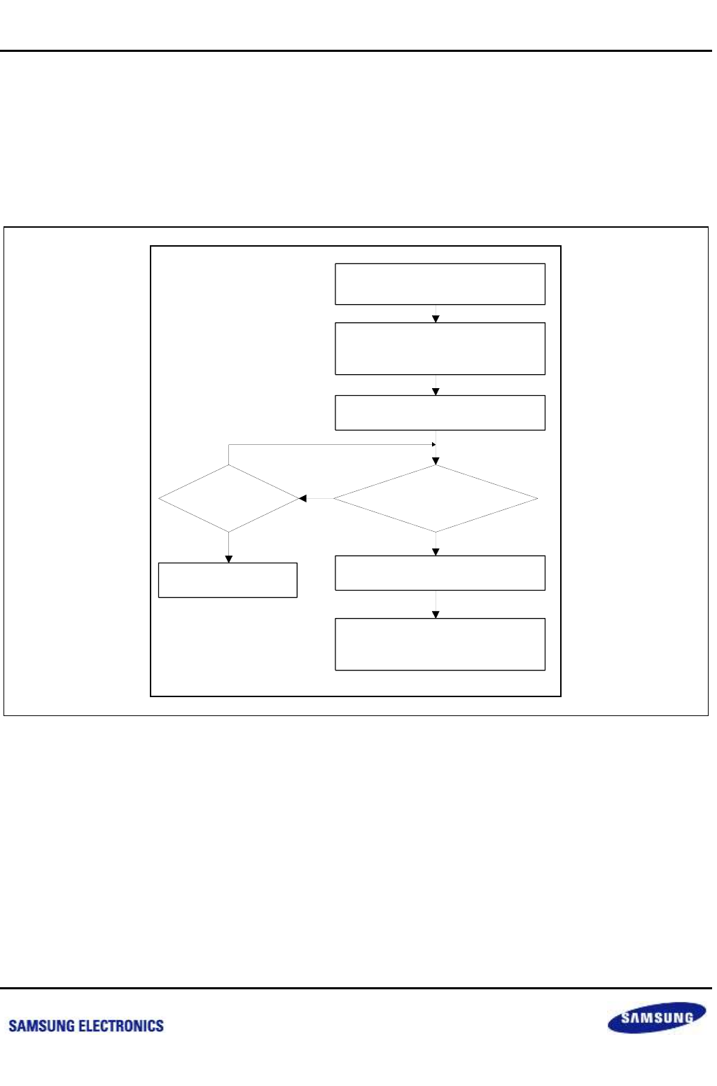
Samsung Confidential
S5P6818_UM 29 AC97
29-4
Preliminary product information describes products that are in development, for which full characterization data and
associated errata are not yet available. Specifications and information herein are subject to change without notice.
29.4.2 Operation Flow Chart
When you initialize the AC97 controller, you must assert system reset or cold reset, because the previous state of
the external AC97 audio-codec is unknown. This assures that GPIO is already ready. Then you enable the codec
ready interrupt. You can check codec ready interrupt by polling or interrupt. When interrupt occurs, you must de-
assert codec ready interrupt. Use DMA or PIO (directly to write data to register) to transmit data from memory to
register or from register to memory. If internal FIFOs (Tx FIFO or Rx FIFO) are not empty, then let data be
transmitted.
Figure 29-3 AC97 Operation Flow Chart
System reset or Cold reset
Set GPIO and Release
INTMSK/SUBINTMSK bits
Enable Codec Ready interrupt
Codec Ready interrupt ?
Time out condition ?
Disable Codec Ready interrupt
DMA operation or
PIO (Interrupt or Polling ) operation
Yes
No
Controller off
No
nexell / ys.kim at 2015.02.12
SAMSUNG Confidential
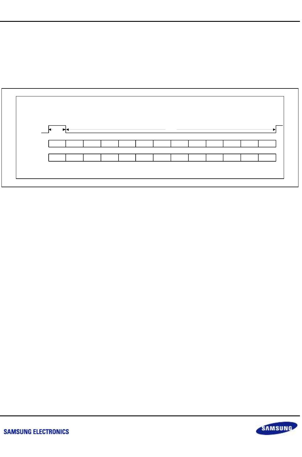
Samsung Confidential
S5P6818_UM 29 AC97
29-5
Preliminary product information describes products that are in development, for which full characterization data and
associated errata are not yet available. Specifications and information herein are subject to change without notice.
29.4.3 AC-link Digital Interface Protocol
Each AC97 Codec incorporates a five-pin digital serial interface that links it to the S5P6818 AC97 Controller. AC-
link is a full-duplex, fixed-clock and PCM digital stream. It employs a time division multiplexed (TDM) scheme to
handle control register accesses and multiple input and output audio streams. The AC-link architecture divides
each audio frame into 12 outgoing and 12 incoming data streams. Each stream has 20-bit sample resolution and
requires a DAC and an analog-to-digital converter (ADC) with a minimum 16-bit resolution.
Figure 29-4 Bi-Directional AC-link Frame with Slot Assignments
The figure above shows the slot definitions supported by S5P6818 AC97 Controller. The S5P6818 AC97
Controller provides synchronization for all data transaction on the AC-link.
A data transaction is made up of 256 bits of information broken into groups of 13 time slots and is called a frame.
Time slot 0 is called the Tag Phase and it is 16 bits long. The other 12 time slots are called the Data Phase. The
Tag Phase contains one bit that identifies a valid frame and 12 bits that identify the time slots in the Data Phase
that contain valid data. Each time slot in the Data Phase is 20 bits long. A frame begins when SYNC goes high.
The amount of time that SYNC is high corresponds to the Tag Phase. AC97 frames occur at fixed 48 kHz intervals
and are synchronous to the 12.288 MHz bit rate clock, BITCLK.
The controller and the Codec use the SYNC and BITCLK to determine when to send transmit data and when to
sample received data. A transmitter transfers the serial data stream on each rising edge of BITCLK and a receiver
samples the serial data stream on falling edges of BITCLK. The transmitter must tag the valid slots in its serial
data stream. The valid slots are tagged in slot 0. Serial data on the AC-link is ordered most significant bit (MSB) to
least significant bit (LSB). The Tag Phase's first bit is bit[15] and the first bit of each slot in Data Phase is bit[19].
The last bit in any slot is bit[0].
SYNC
SDATA_OUT
SDATA _IN
Slot #
TAG CMD
ADDR CMD
DATA PCM PCM RSRVD
TAG STATUS
ADDR STATUS
DATA PCM
LEFT PCM
RIGHT
0 1 2 3 4 5 6 7 8 9 10 11 12
RSRVDRSRVDRSRVDRSRVDRSRVDRSRVDRSRVD
RSRVD RSRVD RSRVD RSRVD RSRVD RSRVD RSRVD
PCM
MIC
LEFT RIGHT
TAG
Phase Data
Phase
nexell / ys.kim at 2015.02.12
SAMSUNG Confidential
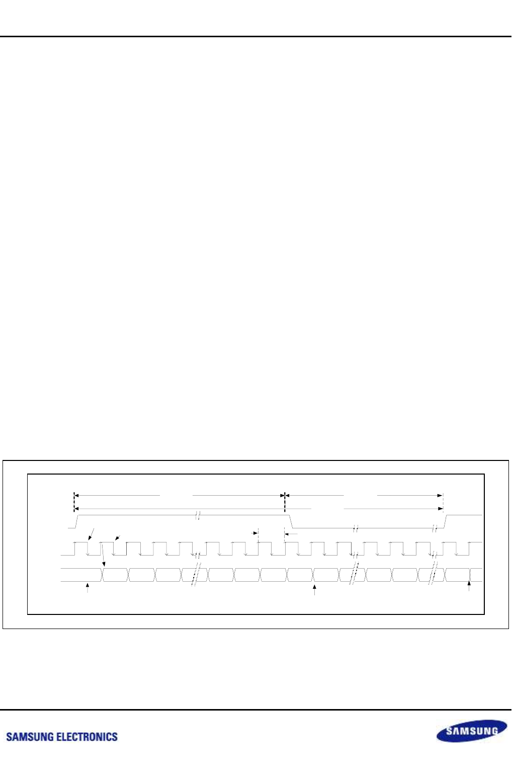
Samsung Confidential
S5P6818_UM 29 AC97
29-6
Preliminary product information describes products that are in development, for which full characterization data and
associated errata are not yet available. Specifications and information herein are subject to change without notice.
29.4.3.1 AC-Link Output Frame (SDATA_OUT)
Slot 0: Tag Phase
In slot 0, the first bit is a bit (SDATA_OUT, bit[15]) which represents the validity of the entire frame. If bit[15] is 1,
the current frame contains at least a valid time slot. The next 12-bit positions correspond each 12 time slot
contains valid data. Bits 0 and 1 of slot 0 are used as CODEC IO bits for I/O reads and writes to the CODEC
registers as described in the next section. In this way, data streams of differing sample rate can be transmitted
across AC-link at its fixed 48 kHz audio frame rate.
Slot 1: Command Address Port
In slot 1, it communicates control register address and write/read command information to the AC97 controller.
When software accesses the primary CODEC, the hardware configures the frame as follows:
In slot 0, the valid bit for 1, 2 slots are set.
In slot 1, bit[19] is set (read) or clear (write). Bits 18-12 (of slot 1) are configured to specify the index to the
CODEC register. Others are filled with 0's (reserved).
In slot 2, it configured with the data which is for writing because of output frame.
Slot 2: Command Data Port
In slot 2, this is the write data with 16-bit resolution ([19:4] is valid data)
Slot 3: PCM Playback Left Channel
Slot 3 is audio output frame is the composite digital audio left stream. If a sample has a resolution that is less than
16 bits, the AC97 controller fills all training non-valid bit positions in the slot with zeroes.
Slot 4: PCM Playback Right Channel
Slot 4 which is audio output frame is the composite digital audio right stream. If a sample has a resolution that is
less than 16 bits, the AC97 controller fills all training non-valid bit positions in the slot with zeroes.
Figure 29-5 AC-Link Output Frame
SDATA_OUT
BIT_CLK
SYNC AC '97 samples SYNC assertion here
AC '97 Controller samples first SDATA_OUT bit of frame here
END of previous Audio Frame
Valid
Frame Slot(1) Slot(2) Slot(12) "0" “0”
ID1
“0”
ID019 0
Tag Phase Data Phase
19 0
START of Data phase
Slot#1
END of Data Frame
Slot# 12
48KHz
12.288MHz
nexell / ys.kim at 2015.02.12
SAMSUNG Confidential
Samsung Confidential
S5P6818_UM 29 AC97
29-7
Preliminary product information describes products that are in development, for which full characterization data and
associated errata are not yet available. Specifications and information herein are subject to change without notice.
29.4.3.2 AC-Link Input Frame (SDATA_IN)
Each AC97 Codec incorporates a five-pin digital serial interface that links it to the S5P6818 AC97 Controller. AC-
link is a full-duplex, fixed-clock and PCM digital stream.
Slot 0: Tag Phase
In slot 0, the first bit (SDATA_OUT, bit[15]) indicates whether the AC97 controller is in the CODEC ready state. If
the CODEC Ready bit is 0, it means that the AC97 controller is not ready for normal operation. This condition is
normal after the power is de-asserted on reset and the AC97 controller voltage references are settling.
Slot 1: Status Address Port/SLOTREQ bits
The status port monitors the status of the AC97 controller functions. It is not limited to mixer settings and power
management. Audio input frame slot 1s stream echoes the control register index for the data to be returned in slot
2, if the controller tags slots 1 and 2 as valid during slot 0. The controller only accepts status data if the
accompanying status address matches the last valid command address issued during the most recent read
command. For multiple sample rate output, the CODEC examines its sample-rate control registers, its FIFOs'
states, and the incoming SDATA_OUT tag bits at the beginning of each audio output frame to determine which
SLOTREQ bits to set active (low). SLOTREQ bits asserted during the current audio input frame indicate which
output slots require data from the controller in the next audio output frame. For fixed 48 kHz operation, the
SLOTREQ bits are set active (low), and a sample is transferred in each frame. For multiple sample-rate input, the
"tag" bit for each input slot indicates whether valid data is present.
Table 29-1 Input Slot 1 Bit Definitions
Bit
Description
[19]
Reserved (Filled with zero)
[18:12]
Control register index (Filled with zeroes if AC97 tags is invalid)
[11]
Slot 3 request: PCM Left channel
[10]
Slot 4 request: PCM Right channel
[9]
Slot 5 request: NA
[8]
Slot 6 request: MIC channel
[7]
Slot 7 request: NA
[6]
Slot 8 request: NA
[5]
Slot 9 request: NA
[4]
Slot 10 request: NA
[3]
Slot 11 request: NA
[2]
Slot 12 request: NA
[1:0]
Reserved (Filled with zero)
nexell / ys.kim at 2015.02.12
SAMSUNG Confidential
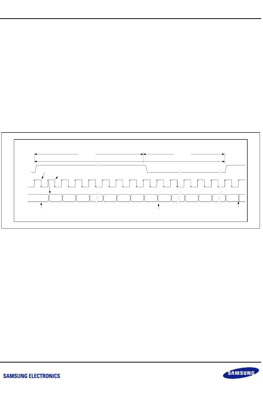
Samsung Confidential
S5P6818_UM 29 AC97
29-8
Preliminary product information describes products that are in development, for which full characterization data and
associated errata are not yet available. Specifications and information herein are subject to change without notice.
Slot 2: Status Data Port
In slot 2, this is the status data with 16-bit resolution ([19:4] is valid data)
Slot 3: PCM Record Left Channel
Slot 3 which is audio input frame is the left channel audio output of the AC97 Codec. If a sample has a resolution
that is less than 16 bits, the AC97 Codec fills all training non-valid bit positions in the slot with zeroes.
Slot 4: PCM Record Right Channel
Slot 4 which is audio input frame is the right channel audio output of the AC97 Codec. If a sample has a resolution
that is less than 16 bits, the AC97 Codec fills all training non-valid bit positions in the slot with zeroes.
Slot 6: Microphone Record Data
The AC97 Controller supports 16-bit resolution for the MIC-in channel.
Figure 29-6 AC-Link Input Frame
SDATA_IN
BIT_CLK
SYNC AC '97 samples SYNC assertion here
AC '97 Controller samples first SDATA _IN bit of frame here
END of previous Audio Frame
Codec
Ready Slot(1) Slot(2) Slot(12) "0" "0" "0" 19 0
Tag Phase Data Phase
19 0
START of Data phase
Slot# 1
END of Data Frame
Slot# 12
nexell / ys.kim at 2015.02.12
SAMSUNG Confidential
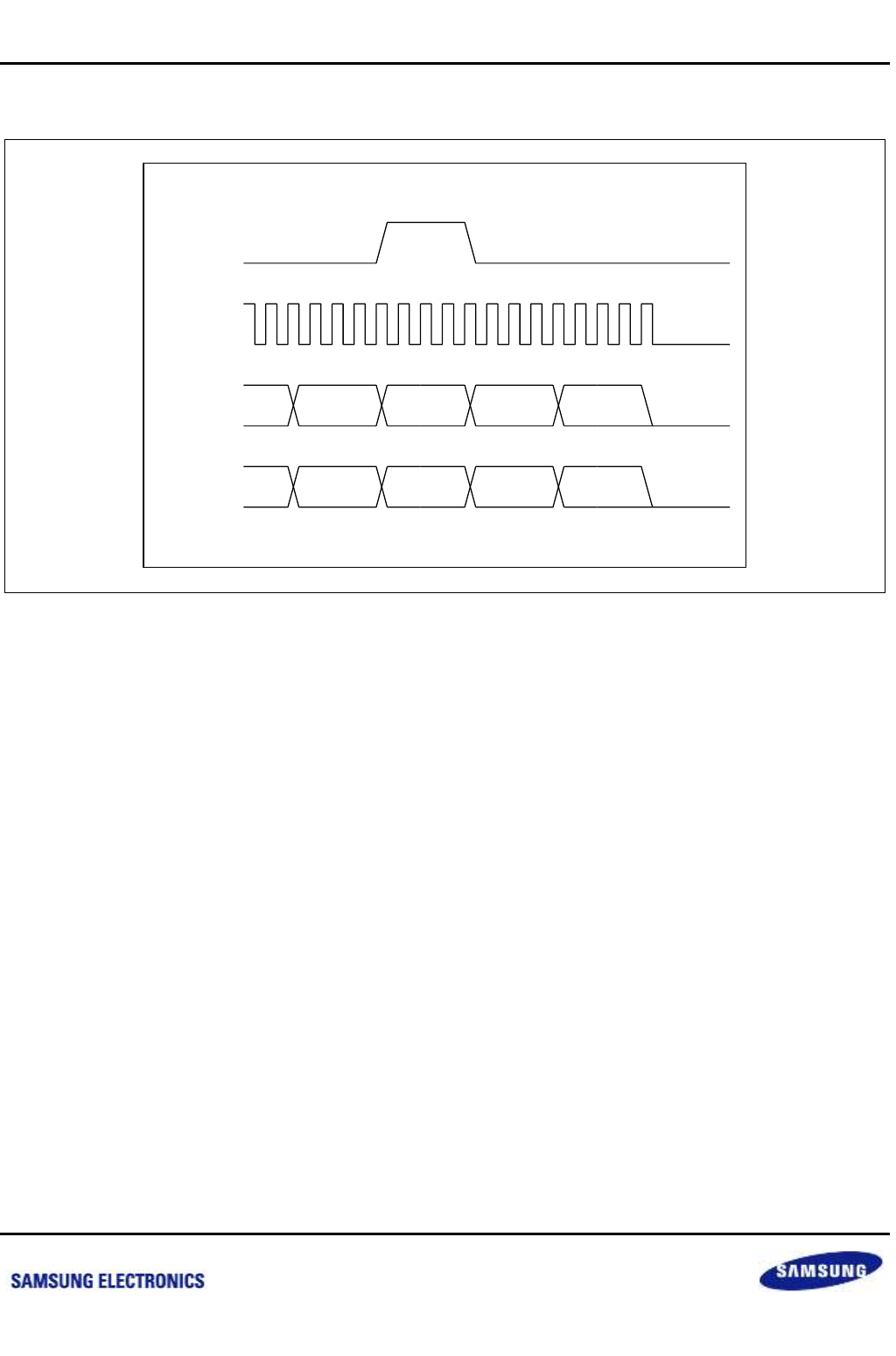
Samsung Confidential
S5P6818_UM 29 AC97
29-9
Preliminary product information describes products that are in development, for which full characterization data and
associated errata are not yet available. Specifications and information herein are subject to change without notice.
29.4.4 AC97 Power-Down
Figure 29-7 AC97 Power-Down Timing
29.4.4.1 Powering Down the AC-Link
The AC-link signals enter a low power mode when the AC97 Codec Power-down register (0x26) bit PR4 is set to 1
(by writing 0x1000). Then the Primary Codec drives both BITCLK and SDATA_IN to a logic low voltage level. The
sequence follows the timing diagram as shown in the figure above.
The AC97 Controller transmits the write to Power-down register (0x26) via AC-link. Set up the AC97 Controller so
that it does not transmit data to slots 3-12 when it writes to the Power-down register bit PR4 (data 0x1000), and it
does not require the Codec to process other data when it receives a power down request. When the Codec
processes the request it immediately transfers BITCLK and SDATA_IN to a logic low level. The AC97 Controller
drives SYNC and SDATA_OUT to a logic low level after programming the AC_GLBCTRL register.
SDATA_OUT
SDATA_IN
BIT_CLK
SYNC
slot 12
prev.frame Write to
0X26
slot 12
prev.frame
TAG
TAG
Data
PR4
nexell / ys.kim at 2015.02.12
SAMSUNG Confidential
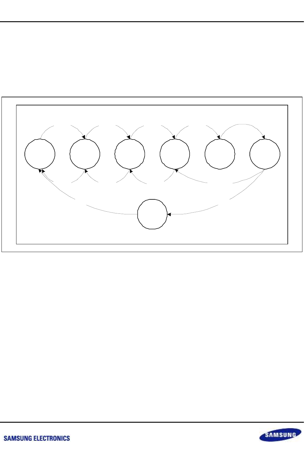
Samsung Confidential
S5P6818_UM 29 AC97
29-10
Preliminary product information describes products that are in development, for which full characterization data and
associated errata are not yet available. Specifications and information herein are subject to change without notice.
29.4.4.2 Waking Up the AC-Link - Wake Up Triggered by the AC97 Controller
AC-link protocol provides a cold AC97 reset and a warm AC97 reset. The current power-down state ultimately
dictates which AC97 reset is used. Registers must stay in the same state during all power-down modes unless a
cold AC97 reset is performed. In a cold AC97 reset, the AC97 registers are initialized to their default values. After
a power down, the AC-link must wait for a minimum of four audio frame times after the frame in which the power
down occurred before it can be reactivated by reasserting the SYNC signal. When AC-link powers up, Codec
ready bit (input slot 0, bit[15]) indicates that AC-link is ready for operation.
Figure 29-8 AC97 Power Down/Power Up Flow
29.4.4.3 Cold AC97 Reset
A cold reset is generated when the nRESET pin is asserted through the AC_GLBCTRL. Asserting and
deasserting nRESET activates BITCLK and SDATA_OUT. A cold reset initializes all of AC97 control registers.
nRESET is an asynchronous AC97 input.
29.4.4.4 Warm AC97 Reset
A Warm AC97 reset reactivates the AC-link without altering the current AC97 register values. A warm reset is
generated when BITCLK is absent and SYNC is driven high. In normal audio frames, SYNC is a synchronous
AC97 input. When BITCLK is absent, SYNC is treated as an asynchronous input used to generate a warm reset to
AC97.The AC97 Controller must not activate BITCLK until it samples SYNC low again. This prevents a new audio
frame being falsely detected.
Normal ADCs off
PR0
DACs off
PR1
Analog
off
PR2 or
PR3
Digitial I/F
off
PR4
Shut off
AC-link
Default
PR0 = 1 PR1 = 1 PR2 = 1 PR4 = 1
Warm Reset
PR2 = 0
&
ANL = 1
PR1 = 0
&
DAC = 1
PR0 = 0
&
ADC = 1
Cold ResetReady = 1
nexell / ys.kim at 2015.02.12
SAMSUNG Confidential
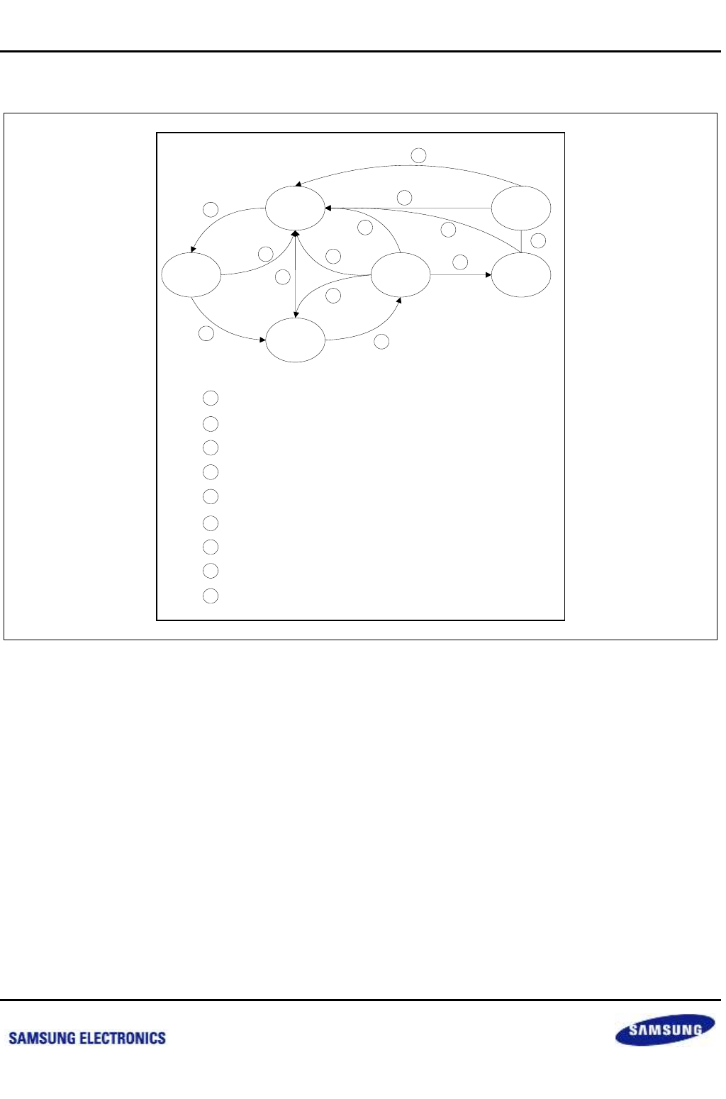
Samsung Confidential
S5P6818_UM 29 AC97
29-11
Preliminary product information describes products that are in development, for which full characterization data and
associated errata are not yet available. Specifications and information herein are subject to change without notice.
29.4.4.5 AC97 State Diagram
Figure 29-9 AC97 State Diagram
The figure above shows the state diagram of AC97 controller. It is useful to check AC97 controller state machine.
State machine shown in above figure is synchronized by peripheral clock (PCLK). Use AC_GLBSTAT register to
monitor state.
IDLE
INIT
READY
ACTIVE LP
WARM
1
2
: ACLINK_ON
: CODEC_READY & TRANS_DATA & NORMAL_SYNC
: PCLK rising
1
: ~CODEC_READY | ~TRANS_DATA
: POWER_DOWN
: WARM_RESET
: !ACLINK_ON
5
: CODEC_WAKEUP
5
4
3
6
8
7
6
7
8
2
3
4
9
9
9
99
9: COLD_RESET | ~PRESETn
nexell / ys.kim at 2015.02.12
SAMSUNG Confidential

Samsung Confidential
S5P6818_UM 29 AC97
29-12
Preliminary product information describes products that are in development, for which full characterization data and
associated errata are not yet available. Specifications and information herein are subject to change without notice.
29.5 Register Description
29.5.1 Register Map Summary
Base Address: 0xC005_8000h
Register
Offset
Description
Reset Value
AC_GLBCTRL
8000h
AC97 global control register
0x0000_0000
AC_GLBSTAT
8004h
AC97 global status register
0x0000_0000
AC_CODEC_CMD
8008h
AC97 codec command register
0x0000_0000
AC_CODEC_STAT
800Ch
AC97 codec status register
0x0000_0000
AC_PCMADDR
8010h
AC97 PCM out/in channel FIFO address register
0x0000_0000
AC_MICADDR
8014h
AC97 MIC In channel FIFO address register
0x0000_0000
AC_PCMDATA
8018h
AC97 PCM out/in channel FIFO data register
0x0000_0000
AC_MICDATA
801Ch
AC97 MIC in channel FIFO data register
0x0000_0000
nexell / ys.kim at 2015.02.12
SAMSUNG Confidential

Samsung Confidential
S5P6818_UM 29 AC97
29-13
Preliminary product information describes products that are in development, for which full characterization data and
associated errata are not yet available. Specifications and information herein are subject to change without notice.
29.5.1.1 AC_GLBCTRL
Base Address: 0xC005_8000h
Address = Base Address + 8000h, Reset Value = 0x0000_0000
Name
Bit
Type
Description
Reset Value
RSVD
[31]
–
Reserved
–
Codec ready interrupt
clear
[30]
RW
1 = Interrupt clear (write only)
1'b0
PCM out channel
underrun interrupt clear
[29]
RW
1 = Interrupt clear (write only)
1'b0
PCM in channel overrun
interrupt clear
[28]
RW
1 = Interrupt clear (write only)
1'b0
MIC in channel overrun
interrupt clear
[27]
RW
1 = Interrupt clear (write only)
1'b0
PCM out channel
threshold interrupt clear
[26]
RW
1 = Interrupt clear (write only)
1'b0
PCM in channel
threshold interrupt clear
[25]
RW
1 = Interrupt clear (write only)
1'b0
MIC in channel threshold
interrupt clear
[24]
RW
1 = Interrupt clear (write only)
1'b0
RSVD
[23]
–
Reserved
–
Codec ready interrupt
enable
[22]
RW
0 = Disables
1 = Enables
1'b0
PCM out channel
underrun interrupt enable
[21]
RW
0 = Disables
1 = Enables (FIFO is empty)
1'b0
PCM in channel overrun
interrupt enable
[20]
RW
0 = Disables
1 = Enables (FIFO is full)
1'b0
Mic in channel overrun
interrupt enable
[19]
RW
0 = Disables
1 = Enables (FIFO is full)
1'b0
PCM out channel
threshold interrupt enable
[18]
RW
0 = Disables
1 = Enables (FIFO is half empty)
1'b0
PCM in channel
threshold interrupt enable
[17]
RW
0 = Disables
1 = Enables (FIFO is half full)
1'b0
MIC in channel threshold
interrupt enable
[16]
RW
0 = Disables
1 = Enables (FIFO is half full)
1'b0
RSVD
[15:14]
–
Reserved
–
PCM out channel transfer
mode
[13:12]
RW
00 = Off
01 = PIO
10 = DMA
11 = Reserved
2'b0
PCM in channel transfer
mode
[11:10]
RW
00 = Off
01 = PIO
10 = DMA
11 = Reserved
2'b0
nexell / ys.kim at 2015.02.12
SAMSUNG Confidential

Samsung Confidential
S5P6818_UM 29 AC97
29-14
Preliminary product information describes products that are in development, for which full characterization data and
associated errata are not yet available. Specifications and information herein are subject to change without notice.
Name
Bit
Type
Description
Reset Value
MIC in channel transfer
mode
[9:8]
RW
00 = Off
01 = PIO
10 = DMA
11 = Reserved
2'b0
RSVD
[7:4]
–
Reserved
–
Transfer data enable
using AC-link
[3]
RW
0 = Disables
1 = Enables
1'b0
AC-Link on
[2]
RW
0 = Off
1 = SYNC signal transfer to Codec
1'b0
Warm reset
[1]
RW
0 = Normal
1 = Wake up codec from power down
1'b0
Cold reset
[0]
RW
0 = Normal
1 = Reset Codec and Controller logic
NOTE:
1. During Cold reset, writing to any AC97 Registers is
not affected.
2. When recovering from Cold reset, writing to any
AC97 Registers is not affected.
Example: For consecutive Cold reset and Warm reset,
first set AC_GLBCTRL = 0x1 then set AC_GLBCTRL
= 0x0.
After recovering from cold reset set AC_GLBCTRL =
0x2 then AC_GLBCTRL = 0x0.
1'b0
nexell / ys.kim at 2015.02.12
SAMSUNG Confidential

Samsung Confidential
S5P6818_UM 29 AC97
29-15
Preliminary product information describes products that are in development, for which full characterization data and
associated errata are not yet available. Specifications and information herein are subject to change without notice.
29.5.1.2 AC_GLBSTAT
Base Address: 0xC005_8000h
Address = Base Address + 8004h, Reset Value = 0x0000_0000
Name
Bit
Type
Description
Reset Value
RSVD
[31:23]
–
Reserved
–
Codec ready interrupt
[22]
R
0 = Not requested
1 = Requested
1'b0
PCM out channel
underrun interrupt
[21]
R
0 = Not requested
1 = Requested
1'b0
PCM in channel overrun
interrupt
[20]
R
0 = Not requested
1 = Requested
1'b0
MIC in channel overrun
interrupt
[19]
R
0 = Not requested
1 = Requested
1'b0
PCM out channel
threshold interrupt
[18]
R
0 = Not requested
1 = Requested
1'b0
PCM in channel
threshold interrupt
[17]
R
0 = Not requested
1 = Requested
1'b0
MIC in channel threshold
interrupt
[16]
R
0 = Not requested
1 = Requested
1'b0
RSVD
[15:3]
–
Reserved
–
Controller main state
[2:0]
R
000 = Idle
001 = Init
010 = Ready
011 = Active
100 = LP
101 = Warm
3'b0
nexell / ys.kim at 2015.02.12
SAMSUNG Confidential
Samsung Confidential
S5P6818_UM 29 AC97
29-16
Preliminary product information describes products that are in development, for which full characterization data and
associated errata are not yet available. Specifications and information herein are subject to change without notice.
29.5.1.3 AC_CODEC_CMD
Base Address: 0xC005_8000h
Address = Base Address + 8008h, Reset Value = 0x0000_0000
Name
Bit
Type
Description
Reset Value
RSVD
[31:24]
–
Reserved
–
Read enable
[23]
RW
0 = Command write
1 = Status read
1'b0
Address
[22:16]
RW
Codec command address
7'h0
Data
[15:0]
RW
Codec command data
16'h0
29.5.1.4 AC_CODEC_STAT
Base Address: 0xC005_8000h
Address = Base Address + 800Ch, Reset Value = 0x0000_0000
Name
Bit
Type
Description
Reset Value
RSVD
[31:23]
–
Reserved
–
Address
[22:16]
R
Codec command address
7'h0
Data
[15:0]
R
Codec command data
16'h0
29.5.1.5 AC_PCMADDR
Base Address: 0xC005_8000h
Address = Base Address + 8010h, Reset Value = 0x0000_0000
Name
Bit
Type
Description
Reset Value
RSVD
[31:28]
–
Reserved
–
Out read address
[27:24]
R
PCM out channel FIFO read address
4'h0
RSVD
[23:20]
–
Reserved
–
In read address
[19:16]
R
PCM in channel FIFO read address
4'h0
RSVD
[15:12]
–
Reserved
–
Out write address
[11:8]
R
PCM out channel FIFO write address
4'h0
RSVD
[7:4]
–
Reserved
–
In write address
[3:0]
R
PCM in channel FIFO write address
4'h0
nexell / ys.kim at 2015.02.12
SAMSUNG Confidential
Samsung Confidential
S5P6818_UM 29 AC97
29-17
Preliminary product information describes products that are in development, for which full characterization data and
associated errata are not yet available. Specifications and information herein are subject to change without notice.
29.5.1.6 AC_MICADDR
Base Address: 0xC005_8000h
Address = Base Address + 8014h, Reset Value = 0x0000_0000
Name
Bit
Type
Description
Reset Value
RSVD
[31:20]
–
Reserved
–
Out write address
[19:16]
R
MIC in channel FIFO read address
4'h0
RSVD
[15:4]
–
Reserved
–
In write address
[3:0]
R
MIC in channel FIFO write address
4'h0
29.5.1.7 AC_PCMDATA
Base Address: 0xC005_8000h
Address = Base Address + 8018h, Reset Value = 0x0000_0000
Name
Bit
Type
Description
Reset Value
Right data
[31:16]
RW
PCM out/in right channel FIFO data
Read = PCM in right channel
Write = PCM out right channel
16'h0
Left data
[15:0]
RW
PCM out/in left channel FIFO data
Read = PCM in left channel
Write = PCM out left channel
16'h0
29.5.1.8 AC_MICDATA
Base Address: 0xC005_8000h
Address = Base Address + 801Ch, Reset Value = 0x0000_0000
Name
Bit
Type
Description
Reset Value
RSVD
[31:16]
–
Reserved
–
Mono data
[15:0]
RW
MIC in mono channel FIFO data
16'h0
nexell / ys.kim at 2015.02.12
SAMSUNG Confidential

Samsung Confidential
S5P6818_UM 30 SPDIF TX
30-1
Preliminary product information describes products that are in development, for which full characterization data and
associated errata are not yet available. Specifications and information herein are subject to change without notice.
30 SPDIF TX
30.1 Overview
The SPDIF transmitter is based on IEC60958. This Section describes a serial, uni-directional, self-clocking
interface to interconnect digital audio equipment in consumer and professional applications.
When you use a consumer digital processing environment in SPDIF standard, the SPDIF interface is primarily
intended to carry stereophonic programs, with a resolution of up to 20 bits per sample, an extension to 24 bits per
sample being possible.
When you use SPDIF in a broadcasting studio environment, the interface is primarily intended to carry
monophonic or stereophonic programs, at a 48 kHz sampling frequency and with a resolution of up to 24 bits per
sample; it can carry one or two signals sampled at 32 kHz.
In both cases, the clock references and auxiliary information are transmitted with the program. IEC60958 enables
the interface to carry software related data.
30.2 Features
Features of SPDIF-TX are:
SPDIFOUT module only supports the consumer application in S5P6818
Supports linear PCM up to 24-bit per sample
Supports Non-linear PCM formats such as AC3, MPEG1 and MPEG2
2 24-bit buffers which is alternately filled with data
nexell / ys.kim at 2015.02.12
SAMSUNG Confidential
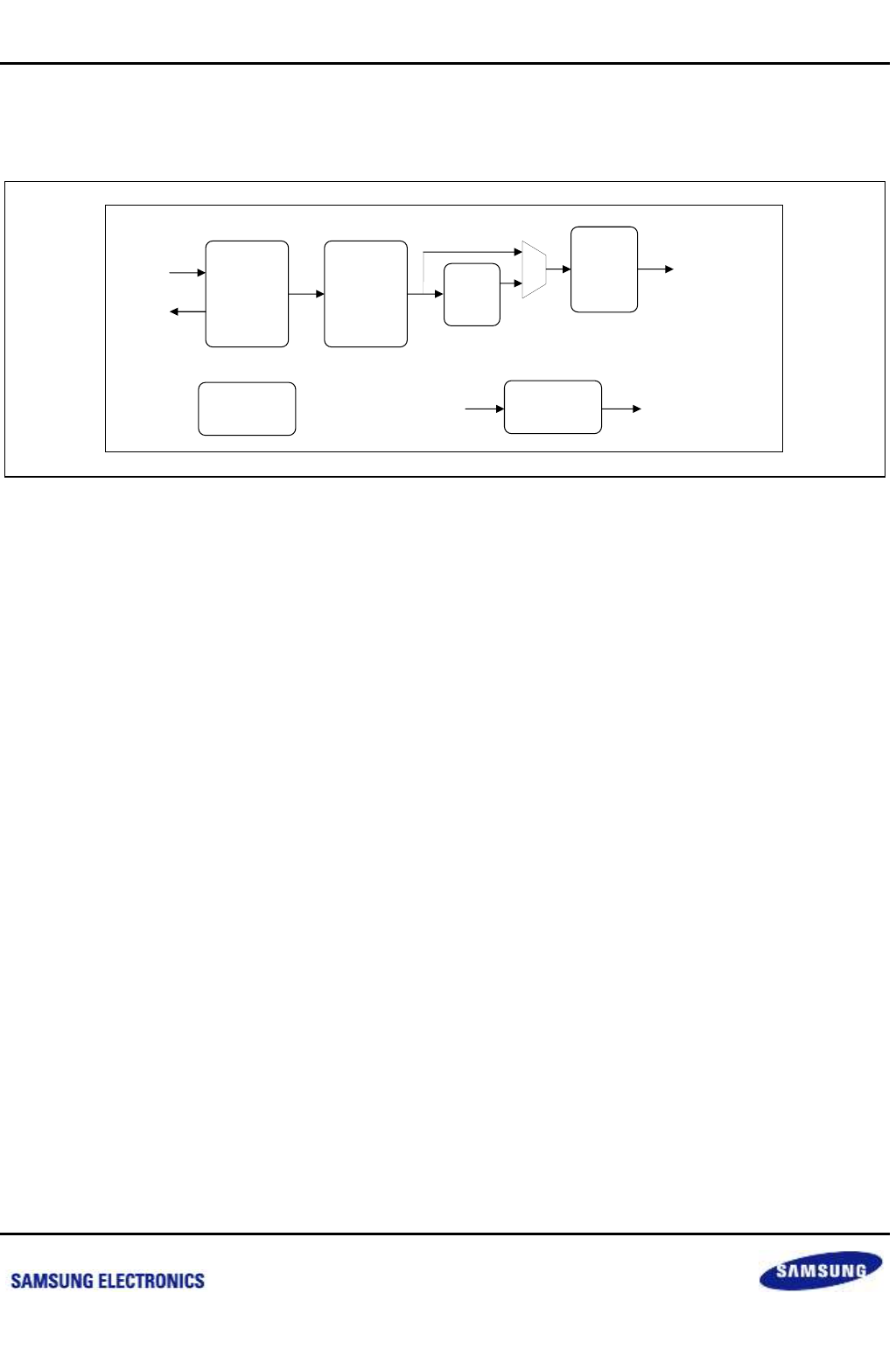
Samsung Confidential
S5P6818_UM 30 SPDIF TX
30-2
Preliminary product information describes products that are in development, for which full characterization data and
associated errata are not yet available. Specifications and information herein are subject to change without notice.
30.3 Block Diagram
The figure below illustrates the block diagram of SPDIFOUT.
Figure 30-1 Block Diagram of SPDIFOUT
Components in SPDIF Transmitter:
APB interface block: This block defines register banks to control the driving of SPDIFOUT module and data
buffers to store linear or non-linear PCM data.
DMA interface block: This block requests DMA service to IODMA that depends on the status of data buffer in
APB Interface block.
Clock Generator block: This block generates 128 fs (sampling frequency) clock that is used in out_spdif block
from system audio clock (MCLK).
Audio_if_core block: This block acts as an interface block between data buffer and out_spdif block. Finite-
state machine controls the flow of PCM data.
spdif_tx block: This block inserts burst preamble and executes zero-stuffing in the nonlinear PCM stream. The
spdif_tx module bypasses the linear PCM data.
out_spdif block: This block generates SPDIF format. It inserts 4-bit preamble, 16- or 20- or 24-bit data, user-
data bit, validity bit, channel status bit, and parity bit into the appropriate position of 32-bit word. It modulates
each bit to bi-phase format.
Apb Interface Audio_if_core
DMA Interface
Spdif_tx
Out_spdif
APB
O_SPDIF_DATA
Clock generator
I_MCLK 128 fs
nexell / ys.kim at 2015.02.12
SAMSUNG Confidential

Samsung Confidential
S5P6818_UM 30 SPDIF TX
30-3
Preliminary product information describes products that are in development, for which full characterization data and
associated errata are not yet available. Specifications and information herein are subject to change without notice.
30.4 Functional Description
This section includes:
Data Format of SPDIF
Channel Coding
Preamble
Non-Linear PCM Encoded Source (IEC 61937)
SPDIF Operation
Shadowed Register
30.4.1 Data Format of SPDIF
This section includes:
Frame Format
Sub-frame Format (IEC 60958)
nexell / ys.kim at 2015.02.12
SAMSUNG Confidential
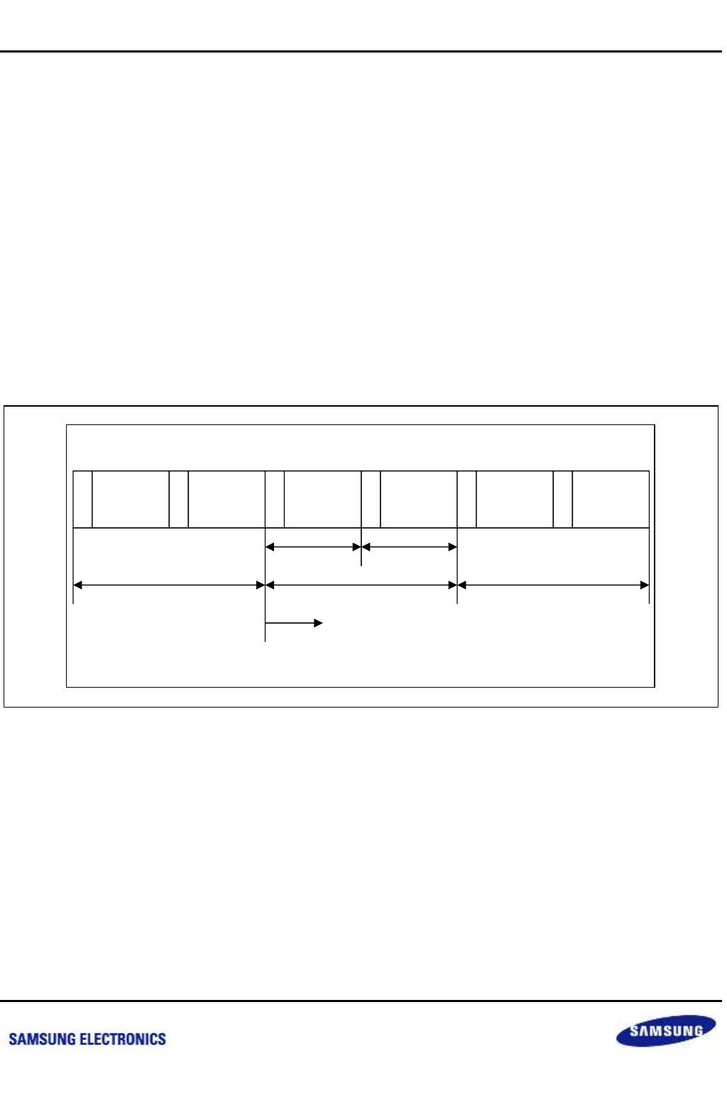
Samsung Confidential
S5P6818_UM 30 SPDIF TX
30-4
Preliminary product information describes products that are in development, for which full characterization data and
associated errata are not yet available. Specifications and information herein are subject to change without notice.
30.4.2 Frame Format
A frame is uniquely composed of two sub-frames. The transmission rate of frames corresponds exactly to the
source sampling frequency.
In the 2 channel operation mode, the time multiplexing transmits samples taken from both channels in consecutive
sub-frames.
The sub-frames related to channel 1 (left or "A" channel in stereophonic operation and primary channel in
monophonic operation) normally use preamble M. However, the preamble is changed to preamble B after every
192 frame. This unit, which is composed of 192 frames, defines the block structure that is used to organize the
channel status information. Sub-frames of channel 2 (right or "B" in stereophonic operation and secondary
channel in monophonic operation) always use preamble W.
In the single-channel operation mode in broadcasting studio environment, the frame format is identical to the 2
channel mode. Data is carried only in channel 1. In the sub-frames allocated to channel 2, time slot 28 (validity
flag) should be set to logical "1" ("1" means not valid).
The figure below illustrates the format of SPDIF frame.
Figure 30-2 SPDIF Frame Format
M Channel1 W Channel 2 B Channel 1 W Channel 2 M Channel 1 W Channel 2
Frame 191 Frame 0 Frame 1
Sub-frame Sub-frame
Start of Block
nexell / ys.kim at 2015.02.12
SAMSUNG Confidential
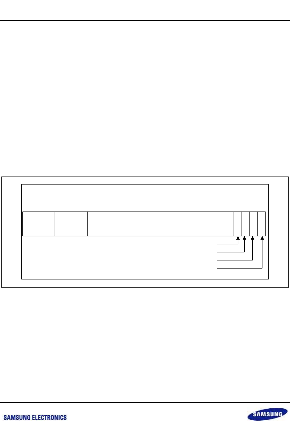
Samsung Confidential
S5P6818_UM 30 SPDIF TX
30-5
Preliminary product information describes products that are in development, for which full characterization data and
associated errata are not yet available. Specifications and information herein are subject to change without notice.
30.4.3 Sub-frame Format (IEC 60958)
Each sub-frame is divided into 32 time slot, numbered from 0 to 31. Time slots 0 to 3 carry one of the three
permitted preambles. These are used to affect synchronization of sub-frames, frames, and blocks. Time slots 4 to
27 carry the audio sample word in linear 2's complement representation. Time slot 27 carries the most significant
bit. When a 24-bit coding range is used, the least significant bit is in time slot 4.
When a 20-bit coding range is sufficient, the least significant bit is in time slot 8. Time slots 4 to 7 may be used for
other application. Under these circumstances, the bits in the time slots 4 to 7 are designated auxiliary sample bits.
If the source provides fewer bits than the interface allows (20 or 24 bits), the unused least significant bits shall be
set to a logical "0". This procedure supports that SPDIF connect equipment by using different numbers of bits.
Time slot 28 carries the validity flag associated with the audio sample word. This flag is set to logical "0" when the
audio sample is reliable. Time slot 29 carries 1 bit of the user data associated with the audio channel that is
transmitted in the same sub-frame. The default value of the user bit is logical "0".
Time slot 30 carries 1-bit of the channel status words associated with the audio channel transmitted in the same
sub-frame. Time slot 31 carries a parity bit such that the time slots, including 4 to 31 carries an even number of
ones and zeros.
The figure below illustrates format of SPDIF sub-frame.
Figure 30-3 SPDIF Sub-frame Format
Sync
Preamble Aux Audio sample word V U C P
03 4 7 8 28 31
L
S
B
L
S
B
M
S
B
Validity flag
User data
Channel Status
Parity bit
nexell / ys.kim at 2015.02.12
SAMSUNG Confidential
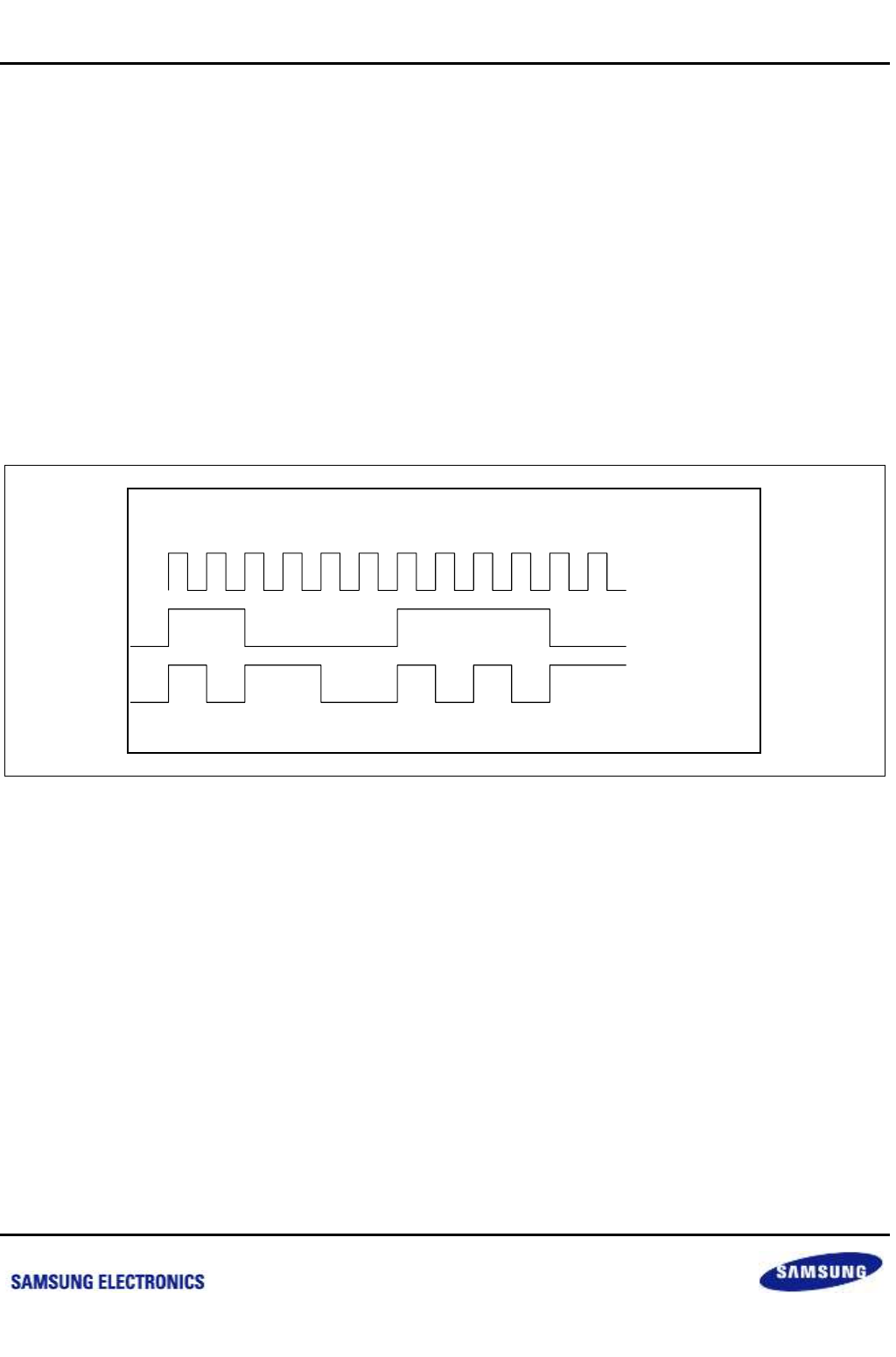
Samsung Confidential
S5P6818_UM 30 SPDIF TX
30-6
Preliminary product information describes products that are in development, for which full characterization data and
associated errata are not yet available. Specifications and information herein are subject to change without notice.
30.5 Channel Coding
Time slots 4 to 31 are encoded in biphase-mark to:
Minimize the dc component on the transmission line
Facilitate clock recovery from the data stream
Make the interface insensitive to the polarity of connections
A symbol comprising two consecutive binary states represents each bit to be transmitted:
The first state of a symbol is always different from the second state of the previous symbol.
The second state of the symbol is identical to the first when the bit to be transmitted is logical "0" and is
different from the first when the bit is logical "1".
The figure below illustrates channel coding.
Figure 30-4 SPDIF Sub-Frame Format
Clock (twice bit rate)
Source coding
Channel coding
(bi-phase mark)
nexell / ys.kim at 2015.02.12
SAMSUNG Confidential

Samsung Confidential
S5P6818_UM 30 SPDIF TX
30-7
Preliminary product information describes products that are in development, for which full characterization data and
associated errata are not yet available. Specifications and information herein are subject to change without notice.
30.6 Preamble
Preambles are specific patterns that provide synchronization and identification of the sub-frames and blocks. A set
of three preambles (M, B, and W) is used. These preambles are transmitted in the time allocated to four time slots
(time slots 0 to 3) and are represented by eight successive states. The first state of the preamble is always
different from the second state of the previous symbol.
Similar to bi-phase code, these preambles are dc free and provide clock recovery. They differ in minimum two
states from any valid bi-phase sequence.
nexell / ys.kim at 2015.02.12
SAMSUNG Confidential
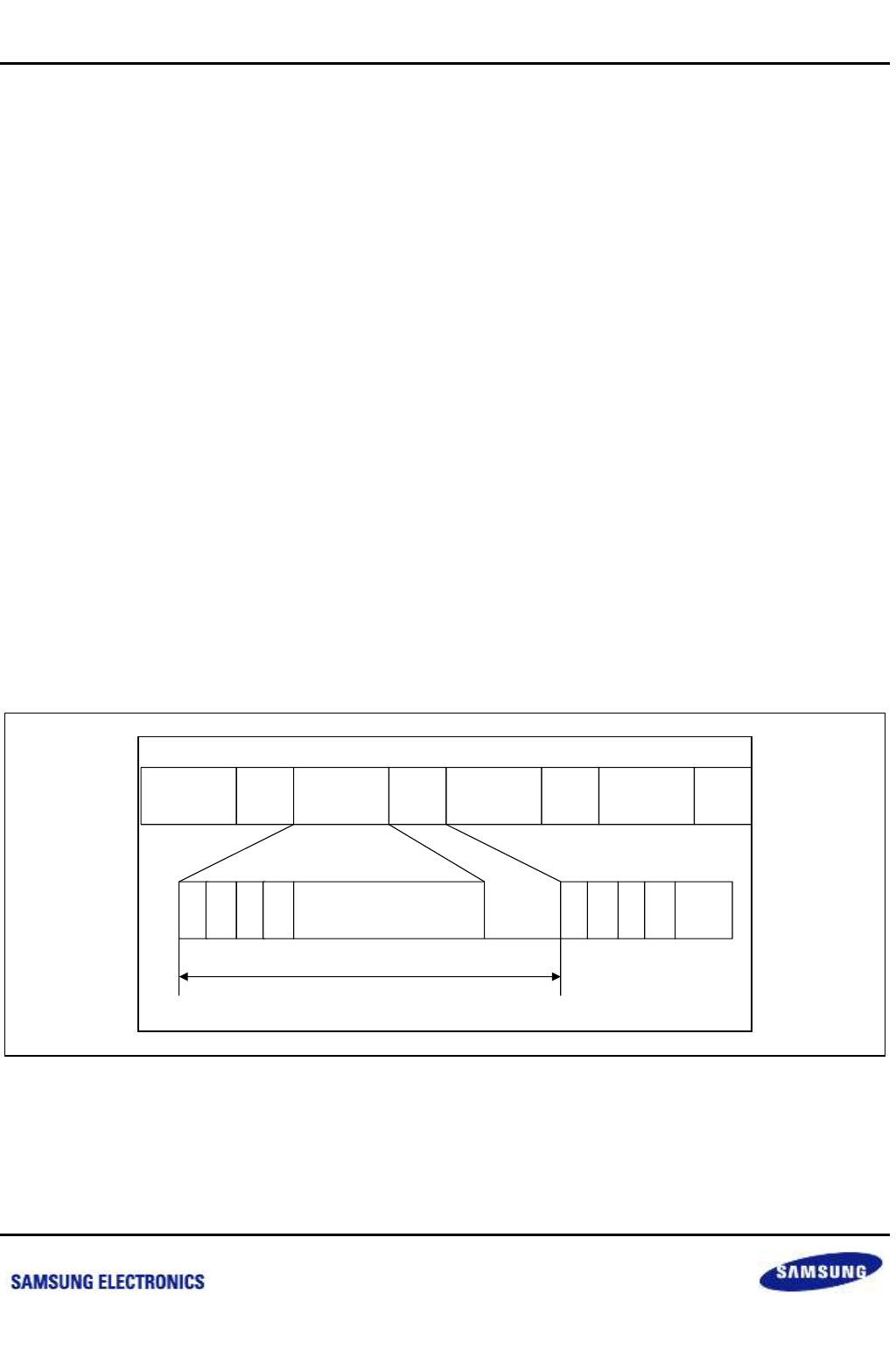
Samsung Confidential
S5P6818_UM 30 SPDIF TX
30-8
Preliminary product information describes products that are in development, for which full characterization data and
associated errata are not yet available. Specifications and information herein are subject to change without notice.
30.7 Non-Linear PCM Encoded Source (IEC 61937)
The non-linear PCM encoded audio bit stream is transferred by using the basic 16-bit data area of the IEC 60958
sub frames, that is, in time slots 12 to 27. Each IEC 60958 frame can transfer 32 bits of the non-PCM data in
consumer application mode.
When the SPDIF bit stream conveys linear PCM audio, the symbol frequency is 64 times the PCM sampling
frequency (32 time slots per two channels of PCM sample time). When a non-linear PCM encoded audio bit
stream is transmitted by the interface, the symbol frequency shall be 64 times the sampling rate of the encoded
audio within that bit stream. If a non-linear PCM encoded audio bit stream is transmitted by the interface
containing audio with low sampling frequency, the symbol frequency shall be 128 times the sampling rate of the
encoded audio within that bit stream.
Each data burst contains a burst-preamble consisting of four 16-bit words (Pa, Pb, Pc, and Pd), followed by the
burst-payload, which contains data of an encoded audio frame.
The burst-preamble consists of four mandatory fields:
Pa and Pb represent a synchronization word.
Pc provides information about the type of data and some information/control for the receiver.
Pd provides the length of the burst-payload, limited to 216 (= 65,535) bits.
The four preamble words are contained in two sequential SPDIF frames. The frame beginning the data-burst
contains preamble word Pa in sub-frame 1 and Pb in sub-frame 2. The next frame contains Pc in sub-frame 1 and
Pd in sub-frame 2. When placed into a SPDIF sub-frame, the MSB of a 16-bit burst-preamble is placed into time
slot 27 and the LSB is placed into time slot 12.
The figure below illustrates format of Burst Payload.
Figure 30-5 Format of Burst Payload
Data-burst Stuffing Data-burst Stuffing Data-burst Stuffing Data-burst ...
Pa Pb PaPc Burst-payload Pb Pc PdPd
Repetition period between two data-bursts
nexell / ys.kim at 2015.02.12
SAMSUNG Confidential
Samsung Confidential
S5P6818_UM 30 SPDIF TX
30-9
Preliminary product information describes products that are in development, for which full characterization data and
associated errata are not yet available. Specifications and information herein are subject to change without notice.
The table below lists the burst preamble words.
Table 30-1 Burst Preamble Words
Preamble Word
Length of Field
Contents
Value MSB LSB
Pa
16 bits
Sync word 1
0xF872
Pb
16 bits
Sync word 2
0x4E1F
Pc
16 bits
Burst-info
Refer to SPDBSTAS_SHD[15:0] for more
information.
Pd
16 bits
Length-code
Refer to SPDBSTAS_SHD[31:16] for more
information.
nexell / ys.kim at 2015.02.12
SAMSUNG Confidential

Samsung Confidential
S5P6818_UM 30 SPDIF TX
30-10
Preliminary product information describes products that are in development, for which full characterization data and
associated errata are not yet available. Specifications and information herein are subject to change without notice.
30.8 SPDIF Operation
The bit frequency of SPDIF is 128fs (fs: sampling frequency). Therefore, divide audio main clock (MCLK)
depending on the frequency of MCLK to make the main clock of SPDIF. You can divide MCLK by:
2 in case of 256 fs
3 in case of 384 fs
4 in case of 512 fs
The SPDIF module in S5P6818 changes the audio sample data format to SPDIF. To change the format, SPDIF
module inserts these into the appropriate time slots:
Preamble data
Channel status data
User data
Error check bit
Parity bit
Preamble data are fixed in the module and inserted depending on sub-frame counter. Channel status data are set
in the SPDCSTAS register and used by 1-bit per frame. User data always have zero values.
For non-linear PCM data, insert burst-preamble, which consists of Pa, Pb, Pc, and Pd before burst-payload and
zero is padded from the end of burst-payload to the repetition count. Pa (= 16'hF872) and Pb (= 16'h4E1F) is fixed
in the module and Pc and Pd is set in the register SPDBSTAS. To stuff zero, the end of burst-payload is
calculated from Pd value and repetition count that depends on data type in the preamble Pc is acquired from
register SPDCNT.
Audio data are justified to the LSB. 16-, 20- or 24-bit PCM data and 16-bit stream data are supported. The
unoccupied upper bits of 32-bit word are ignored.
Data are fetched via DMA request. When one of two data buffers is empty, DMA service is requested. Audio data
that are stored in the data buffers are transformed into SPDIF format and output to the port. For non-linear PCM
data, interrupt is generated after audio data are output up to the value specified in the SPDCNT register. Interrupt
sets the registers such as SPDBSTAS and SPDCNT to new values when the data type of new bit stream is
different from the previous one.
nexell / ys.kim at 2015.02.12
SAMSUNG Confidential

Samsung Confidential
S5P6818_UM 30 SPDIF TX
30-11
Preliminary product information describes products that are in development, for which full characterization data and
associated errata are not yet available. Specifications and information herein are subject to change without notice.
30.9 Shadowed Register
Both SPDBSTAS_SHD and SPDCNT_SHD registers are shadowed registers that are related to SPDBSTAS and
SPDCNT registers, respectively. They are updated from related registers at every stream end interrupt signal. The
usage of shadowed register is as follows.
1. Set burst status and repetition count information to their respective registers.
2. Turn on SPDIF module, and stream end interrupt is asserted immediately.
3. With stream end interrupt, shadowed registers are updated from their related registers and SPDIF starts to
transfer data.
4. The next stream information (burst status and repetition count) can be written to SPDBSTAS and SPDCNT
register because the previous information is copied to their respective shadowed registers.
5. Set next stream information to SPDBSTAS and SPDCNT registers.
6. Wait for stream end interrupt that signals the end of the first stream.
7. With stream end interrupt, the second stream data will start to transfer.
8. Set third stream information to registers.
The usage of user bit registers is similar to stream information registers. However, these registers are not related
to SPDIF end interrupt but to user data interrupt. As soon as SPDIF is on, the shadowed user bit registers are
updated from their related registers and user bit starts to be shifted out with asserted user data interrupt. User can
write the next user data to registers with this interrupt. After entire 96 user bits are shifted out, user data interrupt
will be asserted again and 3rd user bits can be written to registers with second user bits going out.
nexell / ys.kim at 2015.02.12
SAMSUNG Confidential
Samsung Confidential
S5P6818_UM 30 SPDIF TX
30-12
Preliminary product information describes products that are in development, for which full characterization data and
associated errata are not yet available. Specifications and information herein are subject to change without notice.
30.10 Register Description
30.10.1 Register Map Summary
Base Address: 0xC005_9000h
Register
Offset
Description
Reset Value
SPDCLKCON
9000h
Clock control register
0x0000_0000
SPDCON
9004h
Control register
0x0000_0000
SPDBSTAS
9008h
Burst status register
0x0000_0000
SPDCSTAS
900Ch
Channel status register
0x0000_0000
SPDDAT
9010h
SPDIFOUT data buffer
0x0000_0000
SPDCNT
9014h
Repetition count register
0x0000_0000
SPDBSTAS_SHD
9018h
Shadowed burst status register
0x0000_0000
SPDCNT_SHD
901Ch
Shadowed repetition count register
0x0000_0000
USERBIT1
9020h
Sub-code Q1 to Q32
0x0000_0000
USERBIT2
9024h
Sub-code Q33 to Q64
0x0000_0000
USERBIT3
9028h
Sub-code Q65 to Q96
0x0000_0000
USERBIT1_SHD
902Ch
Shadowed register userbit1
0x0000_0000
USERBIT2_SHD
9030h
Shadowed register userbit2
0x0000_0000
USERBIT3_SHD
9034h
Shadowed register userbit3
0x0000_0000
VERSION_INFO
9038h
RTL version information
0x0000_000D
nexell / ys.kim at 2015.02.12
SAMSUNG Confidential

Samsung Confidential
S5P6818_UM 30 SPDIF TX
30-13
Preliminary product information describes products that are in development, for which full characterization data and
associated errata are not yet available. Specifications and information herein are subject to change without notice.
30.10.1.1 SPDCLKCON
Base Address: 0xC005_9000h
Address = Base Address + 9000h, Reset Value = 0x0000_0000
Name
Bit
Type
Description
Reset Value
RSVD
[31:4]
–
Reserved
–
MCLK SEL
[3:2]
RW
Main audio clock selection
0 = Internal Clock (I_MCLK_INT)
1 = External Clock (I_MCLK_EXT0)
2'b0
SPDIFOUT Clock Down
Ready
[1]
R
0 = Clock-down not ready
1 = Clock-down ready
1'b0
SPDIFOUT power on
[0]
RW
0 = Power off
1 = Power on
1'b0
30.10.1.2 SPDCON
Base Address: 0xC005_9000h
Address = Base Address + 9004h, Reset Value = 0x0000_0000
Name
Bit
Type
Description
Reset Value
RSVD
[31]
–
Reserved
–
FIFO level
[26:22]
R
FIFO Level Monitoring (Read Only)
FIFO depth is 16
0 = Empty of FIFO Level
16 = Full of FIFO Level
5'h0
FIFO level threshold
[21:19]
RW
FIFO Threshold Level is controllable
000 = 0-FIFO Level
001 = 1-FIFO Level
010 = 4-FIFO Level
011 = 6-FIFO Level
100 = 10-FIFO Level
101 = 12-FIFO Level
110 = 14-FIFO Level
111 = 15-FIFO Level
3'b000
FIFO transfer mode
[18:17]
RW
00 = DMA transfer mode
01 = Polling mode
10 = Interrupt mode
11 = Reserved
2'b00
FIFO_level interrupt
status
[16]
RW
Read Operation
0 = No interrupt pending
1 = Interrupt pending
Write Operation
0 = No effect
1 = Clear this flag
1'b0
FIFO_level interrupt
enable
[15]
RW
0 = Interrupt masked
1 = Enable interrupt
1'b0
nexell / ys.kim at 2015.02.12
SAMSUNG Confidential

Samsung Confidential
S5P6818_UM 30 SPDIF TX
30-14
Preliminary product information describes products that are in development, for which full characterization data and
associated errata are not yet available. Specifications and information herein are subject to change without notice.
Name
Bit
Type
Description
Reset Value
endian format
[14:13]
RW
00 = big endian
o_data = {in_data[23:0]}
01 = 4 byte swap
o_data={in_data[15:8], in_data[23:16], in_data[31:24]}
10 = 3 byte swap
o_data={in_data[7:0], in_data[15:8], in_data[23:16]}
11 = 2 byte swap
o_data={0x00,in_data[7:0], in_data[15:8]}
*in_data: BUS ->in port of SPDIF
o_data: in port of SPDIF Logic
2'b00
user_data_attach
[12]
RW
0 = User data is stored in USERBIT register.
User data of sub-frame is out from USERBIT1, 2, 3
(96-bit)
1 = User data is stored in 23rd bit of audio data.
User data is out in 23th bit of PCM data.
1'b0
User data interrupt status
[11]
RW
Read Operation
0 = No interrupt pending
1 = Interrupt pending when 96-bit of user data is out.
Write Operation
0 = No effect
1 = Clear this flag
1'b0
User data interrupt
enable
[10]
RW
0 = Interrupt masked
1 = Enables interrupt
1'b0
Buffer empty interrupt
status
[9]
RW
Read Operation
0 = No interrupt pending
1 = Interrupt pending
Write Operation
0 = No effect
1 = Clears this flag
1'b0
Buffer empty interrupt
enable
[8]
RW
0 = Interrupt masked
1 = Enables interrupt
1'b0
Stream end interrupt
status
[7]
RW
Read Operation
0 = No interrupt pending
1 = Interrupt pending when the number of output
audio data reaches repetition count in SPDCNT
register
Write Operation
0 = No effect
1 = Clears this flag.
1'b0
Stream end interrupt
enable
[6]
RW
0 = Interrupt masked
1 = Enables interrupt
1'b0
software reset
[5]
RW
0 = Normal operation
1'b0
nexell / ys.kim at 2015.02.12
SAMSUNG Confidential

Samsung Confidential
S5P6818_UM 30 SPDIF TX
30-15
Preliminary product information describes products that are in development, for which full characterization data and
associated errata are not yet available. Specifications and information herein are subject to change without notice.
Name
Bit
Type
Description
Reset Value
1 = Software reset
Software reset is 1 cycle pulse (auto clear)
Enables I_MCLK before software reset assertion
because SPDIF uses synchronous reset
Main audio clock
frequency
[4:3]
RW
00 = 256 fs
01 = 384 fs
10 = 512 fs
11 = Reserved
If you want to use SPDIF on HDMI, select 512 fs
because HDMI in S5P6818 accepts only 512 fs or
more frequency.
2'b00
PCM data size
[2:1]
RW
00 = 16 bits
01 = 20 bits
10 = 24 bits
11 = Reserved
2'b00
PCM or stream
[0]
RW
0 = Stream
1 = PCM
1'b0
nexell / ys.kim at 2015.02.12
SAMSUNG Confidential
Samsung Confidential
S5P6818_UM 30 SPDIF TX
30-16
Preliminary product information describes products that are in development, for which full characterization data and
associated errata are not yet available. Specifications and information herein are subject to change without notice.
30.10.1.3 SPDBSTAS
Base Address: 0xC005_9000h
Address = Base Address + 9008h, Reset Value = 0x0000_0000
Name
Bit
Type
Description
Reset Value
Burst data length bit
[31:16]
RW
ES size in bits (Burst Preamble Pd)
ES size: Elementary Stream size
This indicates Burst-payload length
16'h0
Bit stream number
[15:13]
RW
Bit_stream_number should be set to 0
3'b0
Data type dependent info
[12:8]
RW
Data type dependent information
5'h0
Error flag
[7]
RW
0 = Error flag indicates a valid burst_payload
1 = Error flag indicates that the burst payload may
contain errors
1'b0
RSVD
[6:5]
–
Reserved
–
Compressed data type
[4:0]
RW
00000 = Null Data
00001 = AC-3
00010 = Reserved
00011 = Pause
00100 = MPEG1 (layer1)
00101 = MPEG1 (layer2, 3), MPEG2-bc
00110 = MPEG2 - extension
00111 = Reserved
01000 = MPEG2 (layer1 - lsf)
01001 = MPEG2 (layer2, layer3 - lsf)
Others = Reserved
5'h0
nexell / ys.kim at 2015.02.12
SAMSUNG Confidential

Samsung Confidential
S5P6818_UM 30 SPDIF TX
30-17
Preliminary product information describes products that are in development, for which full characterization data and
associated errata are not yet available. Specifications and information herein are subject to change without notice.
30.10.1.4 SPDCSTAS
Base Address: 0xC005_9000h
Address = Base Address + 900Ch, Reset Value = 0x0000_0000
Name
Bit
Type
Description
Reset Value
RSVD
[31:30]
–
Reserved
–
Clock accuracy
[29:28]
RW
10 = Level I, 50 ppm
00 = Level II, 1000 ppm
01 = Level III, variable pitch shifted
2’'b00
Sampling frequency
[27:24]
RW
0000 = 44.1 kHz
0010 = 48 kHz
0011 = 32 kHz
1010 = 96 kHz
4'h0
Channel number
[23:20]
RW
Bit[20] is LSB
4'h0
Source number
[19:16]
RW
Bit[16] is LSB
4'h0
Category code
[15:8]
RW
Equipment type
CD player = 0000_0001
DAT player = L000_0011
DCC player = L100_0011
Mini disc = L100_1001
(L: Information about generation status of the material)
8'h0
Channel status mode
[7:6]
RW
00 = Mode 0
Others = Reserved
2'b00
Emphasis
[5:3]
RW
When bit[1] = 0,
000 = 2 Audio channels without pre-emphasis
001 = 2 Audio channels with 50 us / 15 us pre-
emphasis
When bit[1] = 1,
000 = Default state
3'b000
Copyright assertion
[2]
RW
0 = Copyright
1 = No copyright
1'b0
Audio sample word
[1]
RW
0 = Linear PCM
1 = Non-linear PCM
1'b0
Channel status block
[0]
RW
0 = Consumer format
1 = Professional format
1'b0
nexell / ys.kim at 2015.02.12
SAMSUNG Confidential
Samsung Confidential
S5P6818_UM 30 SPDIF TX
30-18
Preliminary product information describes products that are in development, for which full characterization data and
associated errata are not yet available. Specifications and information herein are subject to change without notice.
30.10.1.5 SPDDAT
Base Address: 0xC005_9000h
Address = Base Address + 9010h, Reset Value = 0x0000_0000
Name
Bit
Type
Description
Reset Value
RSVD
[31:24]
–
Reserved
–
SPDIFOUT data
[23:0]
W
PCM or stream data
24'h0
30.10.1.6 SPDCNT
Base Address: 0xC005_9000h
Address = Base Address + 9014h, Reset Value = 0x0000_0000
Name
Bit
Type
Description
Reset Value
RSVD
[31:13]
–
Reserved
–
Stream repetition count
[12:0]
W
Repetition count according to data type.
This bit is valid only for stream data.
13'h0
30.10.1.7 SPDBSTAS_SHD
Base Address: 0xC005_9000h
Address = Base Address + 9018h, Reset Value = 0x0000_0000
Name
Bit
Type
Description
Reset Value
Burst data length bit
[31:16]
R
ES size in bits ( Burst Preamble Pd)
ES size: Elementary Stream size
This indicates Burst-payload length
16'h0
Bit stream number
[15:13]
R
Bit_stream_number should be set to 0
3'b000
Data type dependent info
[12:8]
R
Data type dependent information
5'h0
Error flag
[7]
R
0 = Error flag indicates a valid burst_payload
1 = Error flag indicates that the burst payload may
contain errors
1'b0
RSVD
[6:5]
–
Reserved
–
Compressed data type
[4:0]
R
00000 = Null Data
00001 = AC-3
00010 = Reserved
00011 = Pause
00100 = MPEG1 (layer1)
00101 = MPEG1 (layer2, 3), MPEG2-bc
00110 = MPEG2 - extension
00111 = Reserved
01000 = MPEG2 (layer1 - lsf)
01001 = MPEG2 (layer2, layer3 - lsf)
Others = Reserved
5’'h0
nexell / ys.kim at 2015.02.12
SAMSUNG Confidential
Samsung Confidential
S5P6818_UM 30 SPDIF TX
30-19
Preliminary product information describes products that are in development, for which full characterization data and
associated errata are not yet available. Specifications and information herein are subject to change without notice.
30.10.1.8 SPDCNT_SHD
Base Address: 0xC005_9000h
Address = Base Address + 901Ch, Reset Value = 0x0000_0000
Name
Bit
Type
Description
Reset Value
RSVD
[31:13]
–
Reserved
–
Stream repetition count
[12:0]
R
Repetition count according to data type
This bit is valid only for stream data.
13'h0
30.10.1.9 USERBIT1
Base Address: 0xC005_9000h
Address = Base Address + 9020h, Reset Value = 0x0000_0000
Name
Bit
Type
Description
Reset Value
USER DATA BIT
(SUB-CODE Q FOR CD)
[31:0]
RW
USERBIT1: Q1 to Q32
User Data Bit has the Digital Audio Track information
(Track number, Play Time and so on).
1176 bits of these being taken out in a row.
32'h0
30.10.1.10 USERBIT2
Base Address: 0xC005_9000h
Address = Base Address + 9024h, Reset Value = 0x0000_0000
Name
Bit
Type
Description
Reset Value
USER DATA BIT
(SUB-CODE Q FOR CD)
[31:0]
RW
USERBIT2: Q33 to Q64
User Data Bit has the Digital Audio Track information
(Track number, Play Time and so on).
1176 bits of these being taken out in a row.
32'h0
30.10.1.11 USERBIT3
Base Address: 0xC005_9000h
Address = Base Address + 9028h, Reset Value = 0x0000_0000
Name
Bit
Type
Description
Reset Value
USER DATA BIT
(SUB-CODE Q FOR CD)
[31:0]
RW
USERBIT3: Q65 to Q96
User Data Bit has the Digital Audio Track information
(Track number, Play Time and so on).
1176 bits of these being taken out in a row.
32'h0
nexell / ys.kim at 2015.02.12
SAMSUNG Confidential
Samsung Confidential
S5P6818_UM 30 SPDIF TX
30-20
Preliminary product information describes products that are in development, for which full characterization data and
associated errata are not yet available. Specifications and information herein are subject to change without notice.
30.10.1.12 USERBIT1_SHD
Base Address: 0xC005_9000h
Address = Base Address + 902Ch, Reset Value = 0x0000_0000
Name
Bit
Type
Description
Reset Value
USER DATA BIT
[31:0]
R
USERBIT1_SHD: Q1 to Q32
User Data Bit has the Digital Audio Track information
like (Track number, Play Time etc.).
1176 bits of these being taken out in a row.
32'h0
30.10.1.13 USERBIT2_SHD
Base Address: 0xC005_9000h
Address = Base Address + 9030h, Reset Value = 0x0000_0000
Name
Bit
Type
Description
Reset Value
USER DATA BIT
[31:0]
R
USERBIT2_SHD: Q33 to Q64
User Data Bit has the Digital Audio Track information
like (Track number, Play Time etc.).
1176 bits of these being taken out in a row.
32'h0
30.10.1.14 USERBIT3_SHD
Base Address: 0xC005_9000h
Address = Base Address + 9034h, Reset Value = 0x0000_0000
Name
Bit
Type
Description
Reset Value
USER DATA BIT
[31:0]
R
USERBIT3_SHD: Q65 to Q96
User Data Bit has the Digital Audio Track information
like (Track number, Play Time etc.).
1176 bits of these being taken out in a row.
32'h0
30.10.1.15 VERSION_INFO
Base Address: 0xC005_9000h
Address = Base Address + 9038h, Reset Value = 0x0000_000D
Name
Bit
Type
Description
Reset Value
VERSION
INFORMATION
[31:0]
R
RTL Version Information
32'hD
nexell / ys.kim at 2015.02.12
SAMSUNG Confidential

Samsung Confidential
S5P6818_UM 31 SPDIF RX
31-1
Preliminary product information describes products that are in development, for which full characterization data and
associated errata are not yet available. Specifications and information herein are subject to change without notice.
31 SPDIF RX
31.1 Overview
SPDIF standard defines a serial interface for transferring digital audio data between various audio equipments like
DVD/HD-DVD players, AVRs and amplifiers. When audio is transferred from a DVD player to an audio amplifier
over an analogue link, noise is introduced. Filtering out this noise is a difficult task. This problem is overcome
when audio data is transferred over a digital link instead of an analogue link. The data can be transferred between
devices without having to convert it to an analogue signal. This is the biggest advantage of SPDIF.
31.2 Features
Features of SPDIF-RX are:
Serial, unidirectional, self-clocking interface
Single wire-single signal interface
Easy to work because it is polarity independent
nexell / ys.kim at 2015.02.12
SAMSUNG Confidential
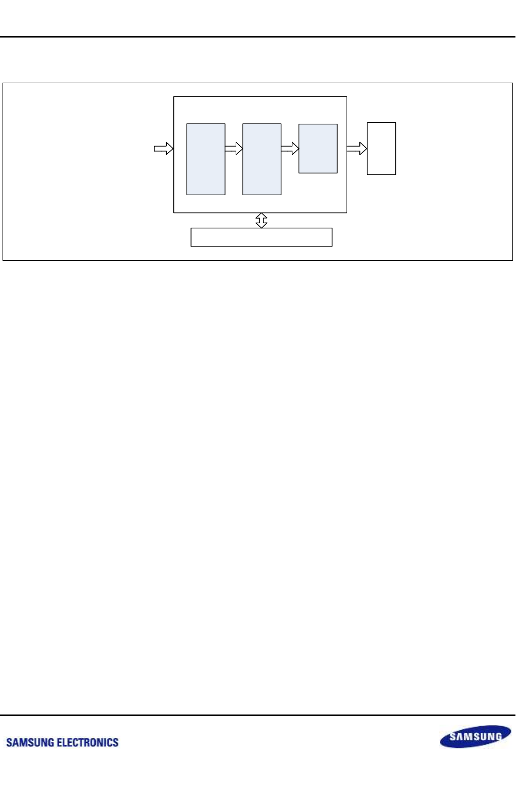
Samsung Confidential
S5P6818_UM 31 SPDIF RX
31-2
Preliminary product information describes products that are in development, for which full characterization data and
associated errata are not yet available. Specifications and information herein are subject to change without notice.
31.3 Block Diagram
Figure 31-1 SPDIF-RX Block Diagram
Phase
Detector
SPDIF
DMA
Decode
DMA
interface
System BUS
spdif in
nexell / ys.kim at 2015.02.12
SAMSUNG Confidential
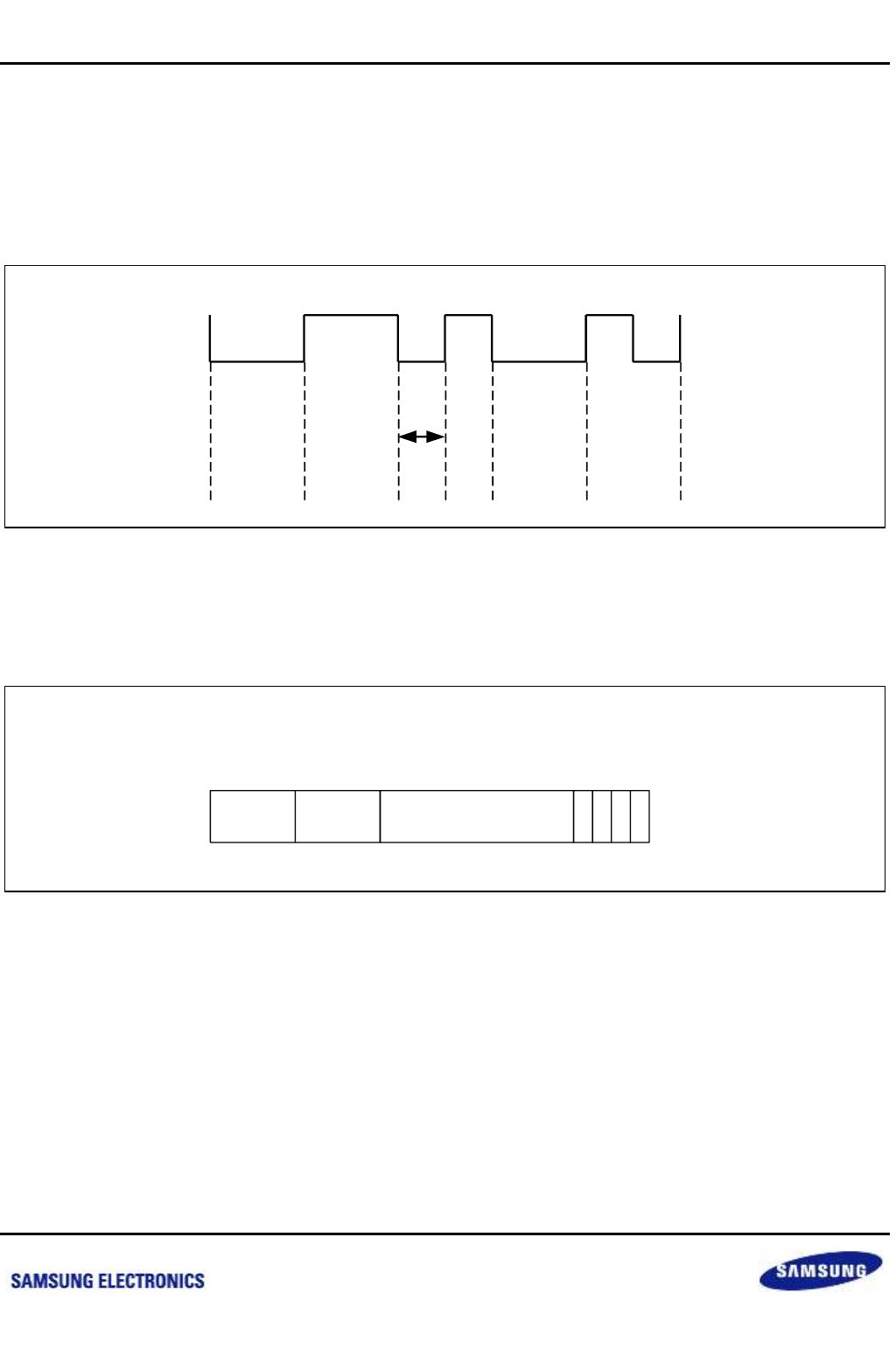
Samsung Confidential
S5P6818_UM 31 SPDIF RX
31-3
Preliminary product information describes products that are in development, for which full characterization data and
associated errata are not yet available. Specifications and information herein are subject to change without notice.
31.4 Functional Description
SPDIF is a single wire serial interface and the clock is embedded within the data. The transmitted data is bi-phase
mark encoded. The clock and frame sync is recovered at the receiver along with bi-phase decoded data stream.
Each data bit in the stream has a time slot. The time slot begins with a transition and ends with a transition. If the
transmitted data bit is "1" then additional transition is made in the middle of the time slot. Data bit "0" does not
have extra transition. The shortest interval between the transitions is called the unit interval (UI).
Figure 31-2 SPDIF Bi-Phase Mark Encoded Stream
The least significant bit of the data is driven first. Each frame is 64 timeslots and has two sub-frames, which are 32
timeslots (The figure below). The sub-frame starts with a preamble followed by 24 bits of data and ends with 4 bits
which carry information such as user data and channel status. The first four time slots of a sub-frame, called
preamble, is used to indicate sub-frame and block starts.
Figure 31-3 SPDIF Sub-Frame Format
There are three preambles, each of which breaks the bi-phase coding rule by containing one or two pulses, which
have duration of 3 UIs. This would mean that the pattern can't occur anywhere else in the stream. Each sub-frame
begins with a 4-bit preamble. Start of a block is indicated by preamble "Z" and the start of sub-frame channel "A".
Preamble "X" indicates the start of a channel "A" sub-frame when not at the start of a block while preamble "Y"
indicates the start of a channel "B" sub-frame.
UI
Time slot
(n+1)
Time slot
(n)
0 0 1 0 1
Sync
Preamble AUX Data Word - 24 bits V U C P
0 3 4 7 8 27 28 31
V -> Validity Flag
U -> User Data
C -> Channel Status
P -> Parity Bit
LSB MSB
nexell / ys.kim at 2015.02.12
SAMSUNG Confidential

Samsung Confidential
S5P6818_UM 31 SPDIF RX
31-4
Preliminary product information describes products that are in development, for which full characterization data and
associated errata are not yet available. Specifications and information herein are subject to change without notice.
31.5 Register Description
31.5.1 Register Map Summary
Base Address: 0xC005_A000h
Register
Offset
Description
Reset Value
SPDIF_CTRL
A000h
SPDIF-RX control register
0x0000_3000
SPDIF_ENBIRQ
A004h
SPDIF-RX interrupt register
0x0000_0000
REGUSERA0
A008h
UserA register[31:0]
0x0000_0000
REGUSERA1
A00Ch
UserA register[63:32]
0x0000_0000
REGUSERA2
A010h
UserA register[95:64]
0x0000_0000
REGUSERA3
A014h
UserA register[127:96]
0x0000_0000
REGUSERA4
A018h
UserA register[159:128]
0x0000_0000
REGUSERA5
A01Ch
UserA register[191:160]
0x0000_0000
REGUSERB0
A020h
UserB register[31:0]
0x0000_0000
REGUSERB1
A024h
UserB register[63:32]
0x0000_0000
REGUSERB2
A028h
UserB register[95:64]
0x0000_0000
REGUSERB3
A02Ch
UserB register[127:96]
0x0000_0000
REGUSERB4
A030h
UserB register[159:128]
0x0000_0000
REGUSERB5
A034h
UserB register[191:160]
0x0000_0000
REGSTATA0
A038h
StatA register[31:0]
0x0000_0000
REGSTATA1
A03Ch
StatA register[63:32]
0x0000_0000
REGSTATA2
A040h
StatA register[95:64]
0x0000_0000
REGSTATA3
A044h
StatA register[127:96]
0x0000_0000
REGSTATA4
A048h
StatA register[159:128]
0x0000_0000
REGSTATA5
A04Ch
StatA register[191:160]
0x0000_0000
REGSTATB0
A050h
StatB register[31:0]
0x0000_0000
REGSTATB1
A054h
StatB register[63:32]
0x0000_0000
REGSTATB2
A058h
StatB register[95:64]
0x0000_0000
REGSTATB3
A05Ch
StatB register[127:96]
0x0000_0000
REGSTATB4
A060h
StatB register[159:128]
0x0000_0000
REGSTATB5
A064h
StatB register[191:160]
0x0000_0000
nexell / ys.kim at 2015.02.12
SAMSUNG Confidential

Samsung Confidential
S5P6818_UM 31 SPDIF RX
31-5
Preliminary product information describes products that are in development, for which full characterization data and
associated errata are not yet available. Specifications and information herein are subject to change without notice.
31.5.1.1 SPDIF_CTRL
Base Address: 0xC005_A000h
Address = Base Address + A000h, Reset Value = 0x0000_3000
Name
Bit
Type
Description
Reset Value
RSVD
[31:17]
–
Reserved
–
CPUHeader
[16]
RW
Setting this bit to add status data when CPU read
SPDIF RX data.
0 = CPU read only data
1 = CPU read status & data
1'b0
DecRate
[15:12]
RW
DECRATE should have different values depending on
the speed of the PCLK.
If PCLK is faster than 100 MHz, set DECRATE greater
than 4, or set DECRATE 3.
4'h3
FillRegUserInv
[11]
RW
User Data filling order.
0 = Fill data from LSB to MSB
1 = Fill data from MSB to LSB
1'b0
lock
[10]
R
Lock to SPDIF input enable or disable.
0 = No-lock
1 = Lock
1'b0
Clr_FIFO
[9]
RW
DMA write/read count clear
0 = Enable
1 = Clear
1'b0
EnbPhaseDet
[8]
RW
Specifies whether the phase detector is enable or
disable.
0 = Disable
1 = Enable
1'b0
Sample_OFFSET
[7:4]
RW
Specifies the valid sampling bit.
4'b0000 = 8
4'b0001 = 7
4'b0010 = 6
4'b0011 = 5
4'b0100 = 4
4'b0101 = 3
4'b0110 = 2
4'b0111 = 1
4'b1000 = 0
4'h0
EnbCapUserStat
[3]
RW
Capture User Data. When start-of-block pulse is
TRUE, RegUserA, RegUserB, RegStatA, RegStatB,
detected rx_data can be captured.
0 = Disable
1 = Enable
1'b0
DMA_DataOnly
[2]
RW
Specifies whether DMA transfer the data only
0 = Data & Status
1 = Data only
1'b1
DMA_Swap
[1]
RW
Specifies the order of ChannelA and ChannelB.
1'b0
nexell / ys.kim at 2015.02.12
SAMSUNG Confidential

Samsung Confidential
S5P6818_UM 31 SPDIF RX
31-6
Preliminary product information describes products that are in development, for which full characterization data and
associated errata are not yet available. Specifications and information herein are subject to change without notice.
Name
Bit
Type
Description
Reset Value
0 = ChannelA first
1 = ChannelB first
DECODE_ENB
[0]
RW
Begin decoder
0 = Disable
1 = Enable
1'b0
nexell / ys.kim at 2015.02.12
SAMSUNG Confidential

Samsung Confidential
S5P6818_UM 31 SPDIF RX
31-7
Preliminary product information describes products that are in development, for which full characterization data and
associated errata are not yet available. Specifications and information herein are subject to change without notice.
31.5.1.2 SPDIF_ENBIRQ
Base Address: 0xC005_A000h
Address = Base Address + A004h, Reset Value = 0x0000_0000
Name
Bit
Type
Description
Reset Value
RSVD
[31:8]
–
Reserved
–
PendLock
[7]
RW
Interrupt pending bit of LOCK detect.
Read:
0 = Not pended
1 = Pended
Write:
0 = No affect
1 = Clear
1'b0
PendErr
[6]
RW
Interrupt pending bit of ERROR detect.
Read:
0 = Not pended
1 = Pended
Write:
0 = No affect
1 = Clear
1'b0
PendParity
[5]
RW
Interrupt pending bit of PARITY detect.
Read:
0 = Not pended
1 = Pended
Write:
0 = No affect
1 = Clear
1'b0
PendBlock
[4]
RW
Interrupt pending bit of BLOCK detect.
Read:
0 = Not pended
1 = Pended
Write:
0 = No affect
1 = Clear
1'b0
EnbIRQLock
[3]
RW
LOCK IRQ Enable
0 = Disable
1 = Enable
1'b0
EnbIRQErr
[2]
RW
ERROR IRQ Enable
0 = Disable
1 = Enable
1'b0
EnbIRQParity
[1]
RW
PARITY IRQ Enable
0 = Disable
1 = Enable
1'b0
EnbIRQBlock
[0]
RW
BLOCK IRQ Enable
0 = Disable
1'b0
nexell / ys.kim at 2015.02.12
SAMSUNG Confidential
Samsung Confidential
S5P6818_UM 31 SPDIF RX
31-8
Preliminary product information describes products that are in development, for which full characterization data and
associated errata are not yet available. Specifications and information herein are subject to change without notice.
Name
Bit
Type
Description
Reset Value
1 = Enable
31.5.1.3 REGUSERA0
Base Address: 0xC005_A000h
Address = Base Address + A008h, Reset Value = 0x0000_0000
Name
Bit
Type
Description
Reset Value
REGUSERA[31:0]
[31:0]
R
Read UserA Register[31:0] when
ENBCAPUSERSTAT is TRUE, start-of-block pulse is
HIGH and user data ch. A enable.
32'h0
31.5.1.4 REGUSERA1
Base Address: 0xC005_A000h
Address = Base Address + A00Ch, Reset Value = 0x0000_0000
Name
Bit
Type
Description
Reset Value
RegUserA[63:32]
[31:0]
R
Read UserA Register[63:32] when
ENBCAPUSERSTAT is TRUE, start-of-block pulse is
HIGH and user data ch. A enable.
32'h0
31.5.1.5 REGUSERA2
Base Address: 0xC005_A000h
Address = Base Address + A010h, Reset Value = 0x0000_0000
Name
Bit
Type
Description
Reset Value
RegUserA[95:64]
[31:0]
R
Read UserA Register[95:64] when
ENBCAPUSERSTAT is TRUE, start-of-block pulse is
HIGH and user data ch. A enable.
32'h0
31.5.1.6 REGUSERA3
Base Address: 0xC005_A000h
Address = Base Address + A014h, Reset Value = 0x0000_0000
Name
Bit
Type
Description
Reset Value
RegUserA[127:96]
[31:0]
R
Read UserA Register[127:96] when
ENBCAPUSERSTAT is TRUE, start-of-block pulse is
HIGH and user data ch. A enable.
32'h0
nexell / ys.kim at 2015.02.12
SAMSUNG Confidential

Samsung Confidential
S5P6818_UM 31 SPDIF RX
31-9
Preliminary product information describes products that are in development, for which full characterization data and
associated errata are not yet available. Specifications and information herein are subject to change without notice.
31.5.1.7 REGUSERA4
Base Address: 0xC005_A000h
Address = Base Address + A014h, Reset Value = 0x0000_0000
Name
Bit
Type
Description
Reset Value
RegUserA[159:128]
[31:0]
R
Read UserA Register[159:128] when
ENBCAPUSERSTAT is TRUE, start-of-block pulse is
HIGH and user data ch. A enable.
32'h0
31.5.1.8 REGUSERA5
Base Address: 0xC005_A000h
Address = Base Address + A018h, Reset Value = 0x0000_0000
Name
Bit
Type
Description
Reset Value
RegUserA[191:160]
[31:0]
R
Read UserA Register[191:160] when
ENBCAPUSERSTAT is TRUE, start-of-block pulse is
HIGH and user data ch. A enable.
32'h0
nexell / ys.kim at 2015.02.12
SAMSUNG Confidential

Samsung Confidential
S5P6818_UM 31 SPDIF RX
31-10
Preliminary product information describes products that are in development, for which full characterization data and
associated errata are not yet available. Specifications and information herein are subject to change without notice.
31.5.1.9 REGUSERB0
Base Address: 0xC005_A000h
Address = Base Address + 0A20h, Reset Value = 0x0000_0000
Name
Bit
Type
Description
Reset Value
RegUserb[31:0]
[31:0]
R
Read UserB Register[31:0] when
ENBCAPUSERSTAT is TRUE, start-of-block pulse is
HIGH and user data ch. B enable.
32'h0
31.5.1.10 REGUSERB1
Base Address: 0xC005_A000h
Address = Base Address + A024h, Reset Value = 0x0000_0000
Name
Bit
Type
Description
Reset Value
RegUserb[63:32]
[31:0]
R
Read UserB Register[63:32] when
ENBCAPUSERSTAT is TRUE, start-of-block pulse is
HIGH and user data ch. B enable.
32'h0
31.5.1.11 REGUSERB2
Base Address: 0xC005_A000h
Address = Base Address + A028h, Reset Value = 0x0000_0000
Name
Bit
Type
Description
Reset Value
RegUserb[95:64]
[31:0]
R
Read UserB Register[95:64] when
ENBCAPUSERSTAT is TRUE, start-of-block pulse is
HIGH and user data ch. B enable.
32'h0
31.5.1.12 REGUSERB3
Base Address: 0xC005_A000h
Address = Base Address + A02Ch, Reset Value = 0x0000_0000
Name
Bit
Type
Description
Reset Value
RegUserb[127:96]
[31:0]
R
Read UserB Register[127:96] when
ENBCAPUSERSTAT is TRUE, start-of-block pulse is
HIGH and user data ch. B enable.
32'h0
nexell / ys.kim at 2015.02.12
SAMSUNG Confidential

Samsung Confidential
S5P6818_UM 31 SPDIF RX
31-11
Preliminary product information describes products that are in development, for which full characterization data and
associated errata are not yet available. Specifications and information herein are subject to change without notice.
31.5.1.13 REGUSERB4
Base Address: 0xC005_A000h
Address = Base Address + A030h, Reset Value = 0x0000_0000
Name
Bit
Type
Description
Reset Value
RegUserb[159:128]
[31:0]
R
Read UserB Register[159:128] when
ENBCAPUSERSTAT is TRUE, start-of-block pulse is
HIGH and user data ch. B enable.
32'h0
31.5.1.14 REGUSERB5
Base Address: 0xC005_A000h
Address = Base Address + A034h, Reset Value = 0x0000_0000
Name
Bit
Type
Description
Reset Value
RegUserb[191:160]
[31:0]
R
Read UserB Register[191:160] when
ENBCAPUSERSTAT is TRUE, start-of-block pulse is
HIGH and user data ch. B enable.
32'h0
nexell / ys.kim at 2015.02.12
SAMSUNG Confidential
Samsung Confidential
S5P6818_UM 31 SPDIF RX
31-12
Preliminary product information describes products that are in development, for which full characterization data and
associated errata are not yet available. Specifications and information herein are subject to change without notice.
31.5.1.15 REGSTATA0
Base Address: 0xC005_A000h
Address = Base Address + A038h, Reset Value = 0x0000_0000
Name
Bit
Type
Description
Reset Value
REGSTATA[31:0]
[31:0]
R
Read StatA Register[31:0] when ENBCAPUSERSTAT
is TRUE, start-of-block pulse is HIGH and channel
status ch. A enable.
32'h0
31.5.1.16 REGSTATA1
Base Address: 0xC005_A000h
Address = Base Address + A03Ch, Reset Value = 0x0000_0000
Name
Bit
Type
Description
Reset Value
REGSTATA[63:32]
[31:0]
R
Read StatA Register[63:32] when
ENBCAPUSERSTAT is TRUE, start-of-block pulse is
HIGH and channel status ch. A enable.
32'h0
31.5.1.17 REGSTATA2
Base Address: 0xC005_A000h
Address = Base Address + A040h, Reset Value = 0x0000_0000
Name
Bit
Type
Description
Reset Value
REGSTATA[95:64]
[31:0]
R
Read StatA Register[95:64] when
ENBCAPUSERSTAT is TRUE, start-of-block pulse is
HIGH and channel status ch. A enable.
32'h0
31.5.1.18 REGSTATA3
Base Address: 0xC005_A000h
Address = Base Address + A044h, Reset Value = 0x0000_0000
Name
Bit
Type
Description
Reset Value
REGSTATA[127:96]
[31:0]
R
Read StatA Register[127:96] when
ENBCAPUSERSTAT is TRUE, start-of-block pulse is
HIGH and channel status ch. A enable.
32'h0
nexell / ys.kim at 2015.02.12
SAMSUNG Confidential

Samsung Confidential
S5P6818_UM 31 SPDIF RX
31-13
Preliminary product information describes products that are in development, for which full characterization data and
associated errata are not yet available. Specifications and information herein are subject to change without notice.
31.5.1.19 REGSTATA4
Base Address: 0xC005_A000h
Address = Base Address + A048h, Reset Value = 0x0000_0000
Name
Bit
Type
Description
Reset Value
REGSTATA[159:128]
[31:0]
R
Read StatA Register[159:128] when
ENBCAPUSERSTAT is TRUE, start-of-block pulse is
HIGH and channel status ch. A enable.
32'h0
31.5.1.20 REGSTATA5
Base Address: 0xC005_A000h
Address = Base Address + A04Ch, Reset Value = 0x0000_0000
Name
Bit
Type
Description
Reset Value
REGSTATA[191:160]
[31:0]
R
Read StatA Register[191:160] when
ENBCAPUSERSTAT is TRUE, start-of-block pulse is
HIGH and channel status ch. A enable.
32'h0
nexell / ys.kim at 2015.02.12
SAMSUNG Confidential

Samsung Confidential
S5P6818_UM 31 SPDIF RX
31-14
Preliminary product information describes products that are in development, for which full characterization data and
associated errata are not yet available. Specifications and information herein are subject to change without notice.
31.5.1.21 REGSTATB0
Base Address: 0xC005_A000h
Address = Base Address + A050h, Reset Value = 0x0000_0000
Name
Bit
Type
Description
Reset Value
REGSTATB[31:0]
[31:0]
R
Read StatA Register[31:0] when ENBCAPUSERSTAT
is TRUE, start-of-block pulse is HIGH and channel
status ch. B enable.
32'h0
31.5.1.22 REGSTATB1
Base Address: 0xC005_A000h
Address = Base Address + A054h, Reset Value = 0x0000_0000
Name
Bit
Type
Description
Reset Value
REGSTATB[63:32]
[31:0]
R
Read StatA Register[63:32] when
ENBCAPUSERSTAT is TRUE, start-of-block pulse is
HIGH and channel status ch. B enable.
32'h0
31.5.1.23 REGSTATB2
Base Address: 0xC005_A000h
Address = Base Address + A058h, Reset Value = 0x0000_0000
Name
Bit
Type
Description
Reset Value
REGSTATB[95:64]
[31:0]
R
Read StatA Register[95:64] when
ENBCAPUSERSTAT is TRUE, start-of-block pulse is
HIGH and channel status ch. B enable.
32'h0
31.5.1.24 REGSTATB3
Base Address: 0xC005_A000h
Address = Base Address + A05Ch, Reset Value = 0x0000_0000
Name
Bit
Type
Description
Reset Value
REGSTATB[127:96]
[31:0]
R
Read StatA Register[127:96] when
ENBCAPUSERSTAT is TRUE, start-of-block pulse is
HIGH and channel status ch. B enable.
32'h0
nexell / ys.kim at 2015.02.12
SAMSUNG Confidential
Samsung Confidential
S5P6818_UM 31 SPDIF RX
31-15
Preliminary product information describes products that are in development, for which full characterization data and
associated errata are not yet available. Specifications and information herein are subject to change without notice.
31.5.1.25 REGSTATB4
Base Address: 0xC005_A000h
Address = Base Address + A060h, Reset Value = 0x0000_0000
Name
Bit
Type
Description
Reset Value
REGSTATB[159:128]
[31:0]
R
Read StatA Register[159:128] when
ENBCAPUSERSTAT is TRUE, start-of-block pulse is
HIGH and channel status ch. B enable.
32'h0
31.5.1.26 REGSTATB5
Base Address: 0xC005_A000h
Address = Base Address + A064h, Reset Value = 0x0000_0000
Name
Bit
Type
Description
Reset Value
REGSTATB[191:160]
[31:0]
R
Read StatA Register[191:160] when
ENBCAPUSERSTAT is TRUE, start-of-block pulse is
HIGH and channel status ch. B enable.
32'h0
nexell / ys.kim at 2015.02.12
SAMSUNG Confidential

Samsung Confidential
S5P6818_UM 32 PDM
32-1
Preliminary product information describes products that are in development, for which full characterization data and
associated errata are not yet available. Specifications and information herein are subject to change without notice.
32 PDM
32.1 Overview
Pulse-density modulation (hereafter, PDM) is a form of modulation used to represent an analog signal with digital
data. In a PDM signal, specific amplitude values are not encoded into pulses of different size as they would be in
PCM. Instead, it is the relative density of the pulses that corresponds to the analog signal’s amplitude. The output
of a 1-bit DAC is the same as the PDM encoding of the signal. The PDM in S5P6818 is a block that receives the
PDM signals from a exterior digital Microphone (with 1-bit I/O) and demodulates the 1bit digital signals and returns
a original amplitude. The PDM supports DMA interface.
32.2 Features
Supports receiving 2 channel audio data with 1 data pin
1 output clock pin
2 data pins ( total 4 channel accepts available )
Fixed output clock frequency
Supports select of the timing of data capture
Supports DMA interface
Supports a user configuration of Coefficient. (Butterworth Low-pass Filter)
nexell / ys.kim at 2015.02.12
SAMSUNG Confidential
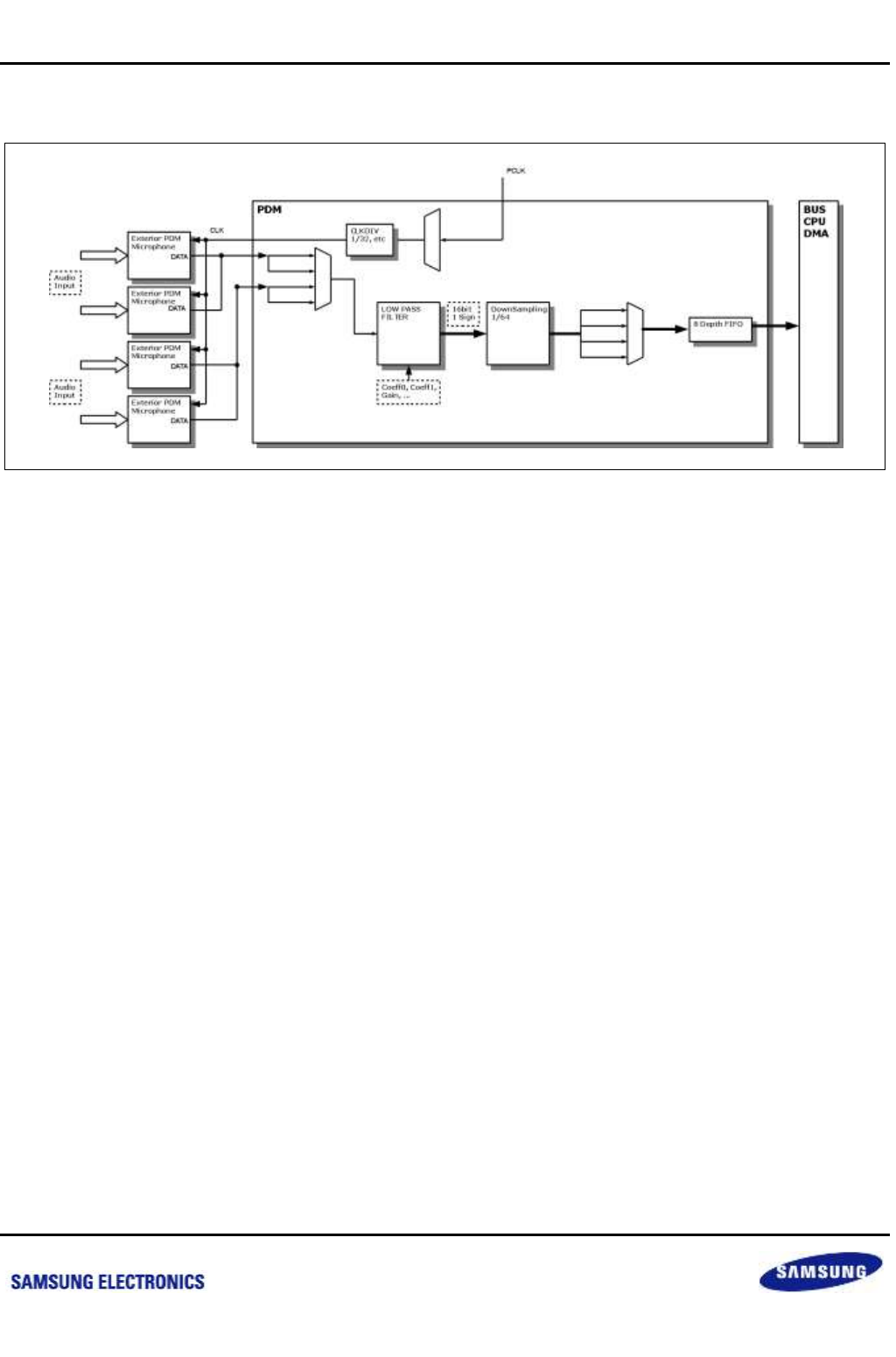
Samsung Confidential
S5P6818_UM 32 PDM
32-2
Preliminary product information describes products that are in development, for which full characterization data and
associated errata are not yet available. Specifications and information herein are subject to change without notice.
32.3 Block Diagram
Figure 32-1 PDM Block Diagram
nexell / ys.kim at 2015.02.12
SAMSUNG Confidential
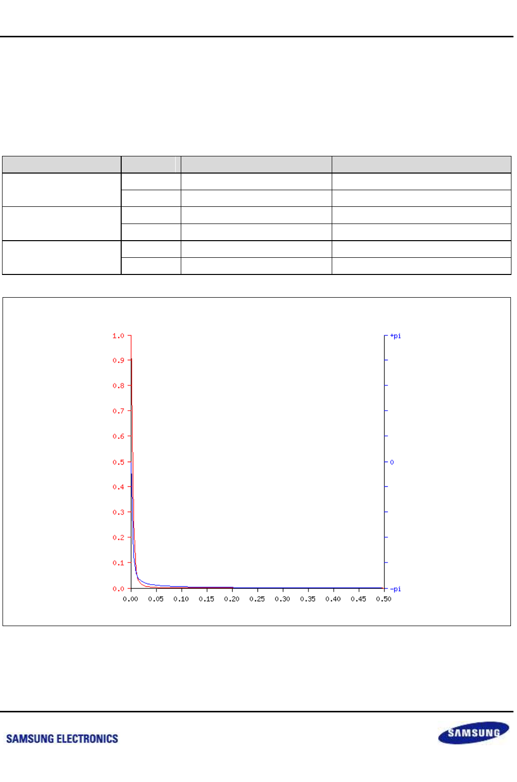
Samsung Confidential
S5P6818_UM 32 PDM
32-3
Preliminary product information describes products that are in development, for which full characterization data and
associated errata are not yet available. Specifications and information herein are subject to change without notice.
32.4 PDM Application Note
32.4.1 Butterworth Filter Configuration
The PDM has registers for the Butterworth Filter coefficients. Users can adjust filter coefficients and use own filter
for PDM Input data.
Table 32-1 PDM Filter Configuration Example
Register Name
Bit
Symbol
Value
PDM_GAIN0
[31:16]
GAIN x (4)
276 (0x0114)
[15:0]
GAIN x (2)
138 (0x008a)
PDM_GAIN1
[31:16]
GAIN x (–4)
–276 (0xfeec)
[15:0]
GAIN x (-2)
–138 (0xff76)
PDM_COEFF
[31:16]
CPU_COEFF1
16194
[15:0]
CPU_COEFF0
–8004
Figure 32-2 Filter Characteristics
nexell / ys.kim at 2015.02.12
SAMSUNG Confidential
Samsung Confidential
S5P6818_UM 32 PDM
32-4
Preliminary product information describes products that are in development, for which full characterization data and
associated errata are not yet available. Specifications and information herein are subject to change without notice.
32.5 Register Description
32.5.1 Register Map Summary
Base Address: 0xC001_4000h
Register
Offset
Description
Reset Value
MAC DMA
PDM_CTRL
4000h
PDM control register
0x0000_0000
PDM_GAIN0
4004h
PDM gain 0 register
0x0000_0000
PDM_gain1
4008h
PDM gain 1 register
0x0000_0000
PDM_coeff
400Ch
PDM coefficient register
0x0000_0000
PDM_data
4010h
PDM data register
Undefined
PDM_ctrl1
4014h
PDM control register 1
0x0000_0000
PDM_irqctrl
4018h
PDM interrupt control register
0x0000_0000
nexell / ys.kim at 2015.02.12
SAMSUNG Confidential
Samsung Confidential
S5P6818_UM 32 PDM
32-5
Preliminary product information describes products that are in development, for which full characterization data and
associated errata are not yet available. Specifications and information herein are subject to change without notice.
32.5.1.1 PDM_CTRL
Base Address: 0xC001_4000h
Address = Base Address + 4000h, Reset Value =0x0000_0000
Name
Bit
Type
Description
Reset Value
RSVD
[31:23]
R
Reserved
9'h0
CPU_OVERSAMPLE
[22:16]
RW
Specifies the value of over sampling.
7'h0
RSVD
[15:12]
R
Reserved
4'h0
CPU_SEL_SHIFT
[11:8]
R/W
Specifies the position of shift strobe. (output clock
position)
4'h0
RSVD
[7:3]
R
Reserved
5'h0
CPU_DMACHMODE
[2]
RW
Enable DMA Mode
0 = Disable
1 = Enable
1'b0
CPU_ENB
[1]
RW
Enable PDM
0 = Disable
1 = Enable
1'b0
CPU_INIT
[0]
RW
Software Reset
1'b0
32.5.1.2 PDM_GAIN0
Base Address: 0xC001_4000h
Address = Base Address + 4004h, Reset Value =0x0000_0000
Name
Bit
Type
Description
Reset Value
GAIN x (4)
[31:16]
RW
Specifies the value of Filter Gain x 4
16'h0
GAIN x (2)
[15:0]
RW
Specifies the value of Filter Gain x 2
16'h0
32.5.1.3 PDM_GAIN1
Base Address: 0xC001_4000h
Address = Base Address + 4008h, Reset Value =0x0000_0000
Name
Bit
Type
Description
Reset Value
GAIN x (–4)
[31:16]
RW
Specifies the value of Filter Gain x (–4)
16'h0
GAIN x (–2)
[15:0]
RW
Specifies the value of Filter Gain x (–2)
16'h0
nexell / ys.kim at 2015.02.12
SAMSUNG Confidential
Samsung Confidential
S5P6818_UM 32 PDM
32-6
Preliminary product information describes products that are in development, for which full characterization data and
associated errata are not yet available. Specifications and information herein are subject to change without notice.
32.5.1.4 PDM_COEFF
Base Address: 0xC001_4000h
Address = Base Address + 400Ch, Reset Value =0x0000_0000
Name
Bit
Type
Description
Reset Value
CPU_COEFF1
[31:16]
RW
Specifies the value of Filter Coefficient 1
16'h0
CPU_COEFF0
[15:0]
RW
Specifies the value of Filter Coefficient 0
16'h0
32.5.1.5 PDM_DATA
Base Address: 0xC001_4000h
Address = Base Address + 4010h, Reset Value =
Name
Bit
Type
Description
Reset Value
PDM_DATA
[31:0]
R
Demodulated amplitude of input PDM signals
Single Mode
1
0
1
0
Dual Mode
1
0
3
2
–
32.5.1.6 PDM_CTRL1
Base Address: 0xC001_4000h
Address = Base Address + 4014h, Reset Value =0x0000_0000
Name
Bit
Type
Description
Reset Value
RSVD
[31:19]
R
Reserved
13'h0
CPU_NUM_SHIFT_CLO
CK
[18:16]
RW
Specifies the number of output clock shift
3'b0
CPU_NUM_CLOCK
[15:8]
RW
Specifies the toggle position of output clock
8'h0
CPU_SAMPLE_POS
[7:0]
RW
Specifies the sampling position for PDM Input data
8'h0
nexell / ys.kim at 2015.02.12
SAMSUNG Confidential
Samsung Confidential
S5P6818_UM 32 PDM
32-7
Preliminary product information describes products that are in development, for which full characterization data and
associated errata are not yet available. Specifications and information herein are subject to change without notice.
32.5.1.7 PDM_IRQCTRLl
Base Address: 0xC001_4000h
Address = Base Address + 4018h, Reset Value =0x0000_0000
Name
Bit
Type
Description
Reset Value
RSVD
[31:7]
R
Reserved
25'h0
INTPEND
[6]
R
Interrupt Pending Bit
–
intpend_CLR
[5]
W
Write 1: Interrupt Pending Clear
–
IRQ_COUNT
[4:0]
RW
Specifies the count for PDM Interrupt. The interrupt is
occurred by internal FIFO write counter. User must
use this count only for PIO mode.
0 = Interrupt Disable
5'h0
nexell / ys.kim at 2015.02.12
SAMSUNG Confidential

Samsung Confidential
S5P6818_UM 33 Display Architecture
33-1
Preliminary product information describes products that are in development, for which full characterization data and
associated errata are not yet available. Specifications and information herein are subject to change without notice.
33 Display Architecture
33.1 Overview
33.2 Features
2 Multi-layer Controller, 2 Display Controller
1 HDMI, 1 LVDS, 1 MIPI DSI
Supports TFT/MPU LCD Interface, HDMI(Progressive/Interlace), LVDS, MIPI DSI, NTSC output formats
Supports that transmits the same image through different outputs at the same time.
nexell / ys.kim at 2015.02.12
SAMSUNG Confidential
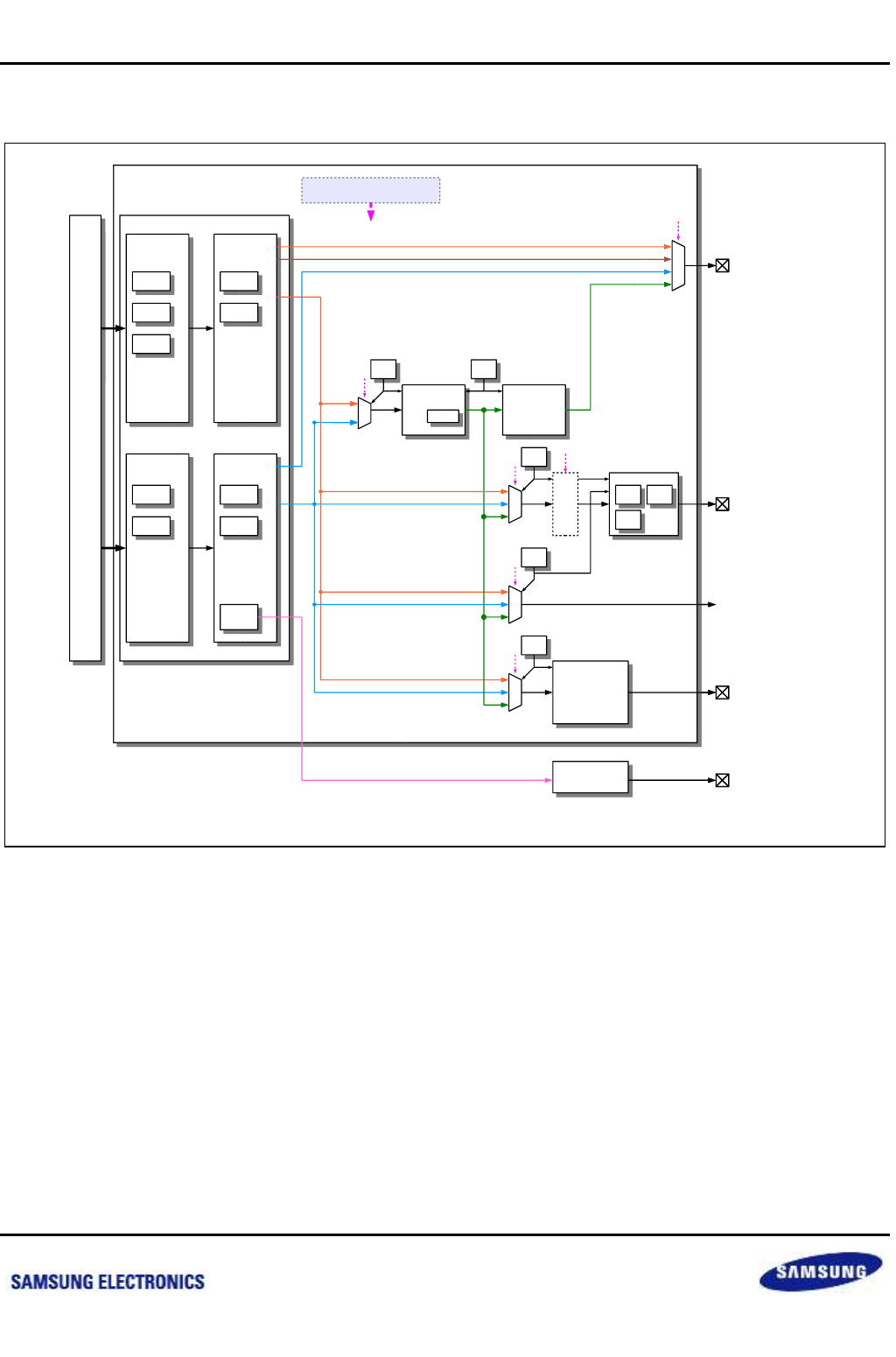
Samsung Confidential
S5P6818_UM 33 Display Architecture
33-2
Preliminary product information describes products that are in development, for which full characterization data and
associated errata are not yet available. Specifications and information herein are subject to change without notice.
33.3 Block Diagram
Figure 33-1 S5P6818 Display Architecture Block Diagram
LF3000 DisplayTop (Display Architecture)
LF3000 DisplayTop (Display Architecture)
DISPLAY TOP REGISTER MAP
Primary MLC
Primary MLC
Secondary MLC
Secondary MLC
Primary DPC
Primary DPC
Secondary DPC
Secondary DPC
Prim DPC
CLKGEN
Prim DPC
CLKGEN
Second DPC
CLKGEN
Second DPC
CLKGEN
MEM
MEM
Converted TFT Signals
TFT RGB888 Signals
TFT RGB888 Signals
ResConv
CLKGEN
ResConv
CLKGEN
Resolution Converter
Resolution Converter
Converted TFT Signals
Converted MPU Signals
LCDIF
LCDIF
LCDIF
CLKGEN
LCDIF
CLKGEN
Converted TFT/MPU Signals
HDMI
HDMIHDMI
CONVERTER
HDMI
CLKGEN
HDMI
CLKGEN
HDMI
LINK
HDMI
LINK
HDMI
CEC
HDMI
CEC
HDMI
PHY
HDMI
PHY
PixelCLK
MIPI
CLKGEN
MIPI
CLKGEN CLK 0
SPDIFCLK
(to MIPI DSI)
VCLK
VSYNC
HSYNC
DE
RGB[23:0]
LVDS
CLKGEN
LVDS
CLKGEN
LVDS
LVDS
LVDS_TXP_A
LVDS_TXN_A
...
LVDS_TXP_CLK
LVDS_TXN_CLK
DisplayTop (Display Architecture)
DisplayTop (Display Architecture)
DISPLAY TOP REGISTER MAP
DualDisplay
DualDisplay
Primary
MLC
Primary
MLC
Secondary
MLC
Secondary
MLC
Primary
DPC
Primary
DPC
Secondary
DPC
Secondary
DPC
Prim DPC
CLKGEN
Prim DPC
CLKGEN
Second DPC
CLKGEN
Second DPC
CLKGEN
MEM
MEM
Converted TFT Signals
TFT RGB888 Signals
TFT RGB888 Signals
ResConv
CLKGEN
ResConv
CLKGEN
Resolution
Converter
Resolution
Converter
Converted TFT Signals
Converted MPU Signals
LCDIF
LCDIF
LCDIF
CLKGEN
LCDIF
CLKGEN
Converted TFT/MPU Signals
VCLK (nCS)
nVSYNC (RS)
nHSYNC (nRD)
DE (nWR)
RGB[23:0]
HDMI
HDMI
HDMI
CONVERTER
HDMI
CLKGEN
HDMI
CLKGEN
TX0P
TX0N
...
TXCP
TXCN
HDMI
LINK
HDMI
LINK
HDMI
CEC
HDMI
CEC
HDMI
PHY
HDMI
PHY
PixelCLK
MIPI
CLKGEN
MIPI
CLKGEN CLK 0
SPDIFCLK
LVDS
CLKGEN
LVDS
CLKGEN
LVDS
LVDS
SyncGen
SyncGen
SyncGen
SyncGen
SyncGen
SyncGen
RGB Layer 0
RGB Layer 0
RGB Layer 1
RGB Layer 1
Video Layer 0v
Video Layer 0v
RGB Layer 0
RGB Layer 0
Video Layer 0v
Video Layer 0v
NTSC
Encoder
NTSC
Encoder
DAC
DAC
DAC_COMP
DAC_IO
DAC_IOB
DAC_IREF
DAC_VREF
nexell / ys.kim at 2015.02.12
SAMSUNG Confidential

Samsung Confidential
S5P6818_UM 33 Display Architecture
33-3
Preliminary product information describes products that are in development, for which full characterization data and
associated errata are not yet available. Specifications and information herein are subject to change without notice.
33.4 TFT/MPU Interface
Things can be output through the LCD Interface as follows.
1. Primary DPC (TFT Interface)
2. Primary DPC (i80 MPU Interface)
3. Secondary DPC (TFT Interface)
NOTE: There is no i80 MPU Interface in Secondary DPC
Users can select one of them by setting the TFT_MUXCTRL register.
nexell / ys.kim at 2015.02.12
SAMSUNG Confidential
Samsung Confidential
S5P6818_UM 33 Display Architecture
33-4
Preliminary product information describes products that are in development, for which full characterization data and
associated errata are not yet available. Specifications and information herein are subject to change without notice.
33.5 Register Description
33.5.1 Register Map Summary
Base Address: 0xC010_1000h
Register
Offset
Description
Reset Value
HDMI_MUXCTRL
1004h
DISPLAY Top HDMI MUX control register
0x0000_0000
LVDS_MUXCTRL
100Ch
Display Top LVDS MUX control register
0x0000_0000
HDMI_SYNCCTRL0
1014h
Display Top HDMI SYNC control register 0
0x0000_0000
HDMI_SYNCCTRL1
1018h
DISPLAY Top HDMI Sync control register 1
0x0000_0000
HDMI_SYNCCTRL2
101Ch
DISPLAY Top HDMI Sync control register 2
0x0000_0000
HDMI_SYNCCTRL3
1020h
DISPLAY Top HDMI Sync control register 3
0x0000_0000
TFT_MUXCTRL
1024h
DISPLAY Top TFT MUX control register
0x0000_0000
nexell / ys.kim at 2015.02.12
SAMSUNG Confidential

Samsung Confidential
S5P6818_UM 33 Display Architecture
33-5
Preliminary product information describes products that are in development, for which full characterization data and
associated errata are not yet available. Specifications and information herein are subject to change without notice.
33.5.1.1 HDMI_MUXCTRL
Base Address: 0xC010_1000h
Address = Base Address + 1004h, Reset Value = 0x0000_0000
Name
Bit
Type
Description
Reset Value
HDMI_MUXENB
[31]
RW
MUX Enable
0 = MUX Disable
1 = MUX Enable
1'b0
RSVD
[30:2]
RW
Reserved
29'h0
HDMI_MUXSEL
[1:0]
RW
MUX Select
0 = Primary DPC
1 = Secondary DPC
2-3 = Reserved
2'b0
33.5.1.2 LVDS_MUXCTRL
Base Address: 0xC010_1000h
Address = Base Address + 100Ch, Reset Value = 0x0000_0000
Name
Bit
Type
Description
Reset Value
LVDS_MUXENB
[31]
RW
MUX Enable
0 = MUX Disable
1 = MUX Enable
1'b0
RSVD
[30:2]
RW
Reserved
29'h0
LVDS_MUXSEL
[1:0]
RW
MUX Select
0 = Primary DPC
1 = Secondary DPC
2-3 = Reserved
2'b0
nexell / ys.kim at 2015.02.12
SAMSUNG Confidential

Samsung Confidential
S5P6818_UM 33 Display Architecture
33-6
Preliminary product information describes products that are in development, for which full characterization data and
associated errata are not yet available. Specifications and information herein are subject to change without notice.
33.5.1.3 HDMI_SYNCCTRL0
Base Address: 0xC010_1000h
Address = Base Address + 1014h, Reset Value = 0x0000_0000
Name
Bit
Type
Description
Reset Value
HDMI_vclk_sel
[31]
RW
Must set this value to 0
0 = HDMI PHY’s pixel clock used for HDMI Operation
1 = Never set this value
1'b0
RSVD
[30:16]
RW
Reserved
15'h0
HDMI_Vsyncstart
[15:0]
RW
Specifies the start line of i_v_sync for the HDMI Link
16'h0
33.5.1.4 HDMI_SYNCCTRL1
Base Address: 0xC010_1000h
Address = Base Address + 1018h, Reset Value = 0x0000_0000
Name
Bit
Type
Description
Reset Value
RSVD
[31:16]
RW
Reserved
16'h0
HDMI_HActivestart
[15:0]
RW
Specifies the start position(h_line) of h_active for the
HDMI Link
16'h0
33.5.1.5 HDMI_SYNCCTRL2
Base Address: 0xC010_1000h
Address = Base Address + 101Ch, Reset Value = 0x0000_0000
Name
Bit
Type
Description
Reset Value
RSVD
[31:16]
RW
Reserved
16'h0
HDMI_HActivesTART
[15:0]
RW
Specifies the end position of h_active for the HDMI
Link
16'h0
33.5.1.6 HDMI_SYNCCTRL3
Base Address: 0xC010_1000h
Address = Base Address + 1020h, Reset Value = 0x0000_0000
Name
Bit
Type
Description
Reset Value
HDMI_VSYNCHSend
[31:16]
RW
Specifies the end position of i_v_sync for the HDMI
Link
16'h0
HDMI_VSYNCHSStart
[15:0]
RW
Specifies the start position of i_v_sync for the HDMI
Link
16'h0
nexell / ys.kim at 2015.02.12
SAMSUNG Confidential

Samsung Confidential
S5P6818_UM 33 Display Architecture
33-7
Preliminary product information describes products that are in development, for which full characterization data and
associated errata are not yet available. Specifications and information herein are subject to change without notice.
33.5.1.7 TFT_MUXCTRL
Base Address: 0xC010_1000h
Address = Base Address + 1024h, Reset Value = 0x0000_0000
Name
Bit
Type
Description
Reset Value
RSVD
[31:2]
RW
Reserved
30'h0
TFT_MUXSEL
[1:0]
RW
MUX Select
0 = Primary DPC (TFT)
1 = Primary DPC (i80 MPU)
2 = Secondary DPC (TFT)
3 = Reserved ( Never use this value )
2'b00
nexell / ys.kim at 2015.02.12
SAMSUNG Confidential
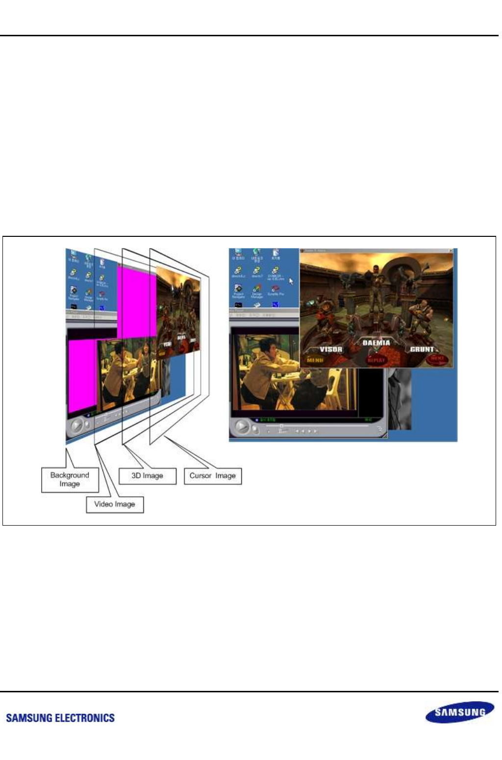
Samsung Confidential
S5P6818_UM 34 Multi Layer Controller (MLC)
34-1
Preliminary product information describes products that are in development, for which full characterization data and
associated errata are not yet available. Specifications and information herein are subject to change without notice.
34 Multi Layer Controller (MLC)
34.1 Overview
The user screen is composed of complex components - RGB pictures, moving pictures, etc. These individual
components have unique formats and are stored in their own memory spaces. The Multi Layer Controller
(hereinafter, MLC) of S5P6818 reads and compounds various screen components in terms of Hardware, to
organize a desired screen and transmits the result to the Display controller.
Figure 34-1 Concept of Multi Layer Controller
nexell / ys.kim at 2015.02.12
SAMSUNG Confidential

Samsung Confidential
S5P6818_UM 34 Multi Layer Controller (MLC)
34-2
Preliminary product information describes products that are in development, for which full characterization data and
associated errata are not yet available. Specifications and information herein are subject to change without notice.
34.2 Features
Dual register-set architecture
Two/One RGB layers and one Video layer
(Primary Display: 2 RGB layer, Secondary Display: 1 RGB layer )
RGB layers can be used as 3D layers.
Various pixel formats
RGB layer: RGB/BGR 332, 444, 555, 565, 888 with/without Alpha
Video layer: 2D Separated YUV 4:4:4, 4:2:2, 4:2:0, Linear YUV 4:2:2(YUYV)
Various blending effects between layers
Per-layer or Per-pixel Alpha blending, Transparency, Inverse color
Free layer position and size in pixel units
Hardware clipping
Vertical flip
Video layer priority
Gamma Correction
Configurable Burst Length (LOCKSIZE, RGB layer)
Scale-up/down (Video layer only)
Bilinear interpolation, Nearest neighbor sampling scale-up/down
Color control (Video layer only)
Brightness, Contrast, Hue, Saturation
nexell / ys.kim at 2015.02.12
SAMSUNG Confidential
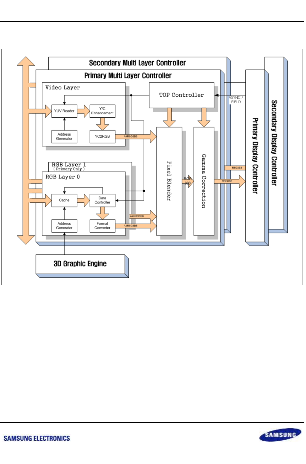
Samsung Confidential
S5P6818_UM 34 Multi Layer Controller (MLC)
34-3
Preliminary product information describes products that are in development, for which full characterization data and
associated errata are not yet available. Specifications and information herein are subject to change without notice.
34.3 Block Diagram
Figure 34-2 MLC Block Diagram
The MLC consists of three RGB layers and one Video layer. In the MLC, positions, pixel formats and various
effects can be configured according to each layer. The Video layer supports the Scale function to display video
images on various screen areas at certain sizes and various color control functions to provide optimal images.
nexell / ys.kim at 2015.02.12
SAMSUNG Confidential
Samsung Confidential
S5P6818_UM 34 Multi Layer Controller (MLC)
34-4
Preliminary product information describes products that are in development, for which full characterization data and
associated errata are not yet available. Specifications and information herein are subject to change without notice.
34.4 Dual Register Set Architecture
The MLC of S5P6818 has dual register set architecture with a current working register group and a user side
register group. All users can set registers via the user side register group. If the dirty flag is set as "1" after the
user writes a desired setting to a register in the user side register group, the MLC copies the user side register
group to the current working register group at the point when vertical sync occurs. Then the dirty flag is cleared to
"0" and the user can continue to progress the next setting. In this way the changes in all registers are
synchronized and applied to vertical sync so that the user can hide any abnormal screen, even if the user changes
a register at any point.
Set by User
Clear by MLC Clear by MLC
VSYNC from DPC
Dirty Flag
Current Working Register Group
User Side Register Group
Register Setting [n]
Register Setting [n]
[n-1] [n+1]
Register Setting [n+1]
Register Update by User
Figure 34-3 Dual Register Set Architecture
The Top controller and three layers of the MLC have separate dirty flag bits. Each dirty flag reflects the changes of
the registers pertaining to the corresponding group.
Table 34-1 Dirty Flag
Dirty Flag
Numbers
Registers to be Affected
Top controller
1
MLCCONTROLT, MLCSCREENSIZE, MLCBGCOLOR
RGB layer
2
MLCLEFTRIGHTn, MLCTOPBOTTOMn, MLCCONTROLn, MLCHSTRIDEn,
MLCVSTRIDEn, MLCTPCOLORn,
MLCINVCOLORn, MLCADDRESSn, MLCLEFTRIGHTn_0,
MLCTOPBOTTOMn_0,
MLCLEFTRIGHTn_1, MLCTOPBOTTOMn_1
Video layer
1
MLCLEFTRIGHT2, MLCTOPBOTTOM2, MLCCONTROL2, MLCVSTRIDE2,
MLCTPCOLOR2,
MLCADDRESS2, MLCADDRESSCB, MLCADDRESSCR, MLCVSTRIDECB,
MLCVSTRIDECR, MLCHSCALE,
MLCVSCALE, MLCLUENH, MLCCHENH0, MLCCHENH1, MLCCHENH2,
MLCCHENH3
nexell / ys.kim at 2015.02.12
SAMSUNG Confidential

Samsung Confidential
S5P6818_UM 34 Multi Layer Controller (MLC)
34-5
Preliminary product information describes products that are in development, for which full characterization data and
associated errata are not yet available. Specifications and information herein are subject to change without notice.
34.5 MLC Global Parameters
This section describes how to set the global parameters of the MLC.
Table 34-2 Top Controller Registers
Function
Symbol
Bit
width
Register
Brief Description
Priority
PRIORITY
2
MLCCONTROLT[9:8]
Specifies the priority of the
Video layer.
Dual register
set
DIRTYFLAGT
1
MLCCONTROLT[3]
Dirty Flag for MLC top
controller.
Enable
MLCENB
1
MLCCONTROLT[1]
Specifies whether or not to
enable MLC
Scan mode
FIEEDENB
1
MLCCONTROLT[0]
Specifies whether or not to
enable Interlace mode
Screen size
SCREENWIDTH
12
MLCSCREENSIZE[11:0]
Specifies "the whole screen
width - 1".
SCREENHEIGHT
12
MLCSCREENSIZE[27:16]
Specifies "the whole screen
height - 1".
Background
color
BGCOLOR
24
MLCBGCOLOR[23:0]
Specifies the background color
to be displayed on the screen
in areas not covered by any of
the layers
RGB Gamma
RGBGAMMAENB
1
MLCGAMMACONT[1]
Gamma Enable for the RGB
region
Dithering
DITHERENB
1
MLCGAMMACONT[0]
Dithering Enable for the result
of Gamma correction
Video Gamma
VIDEOGAMMAENB
1
MLCGAMMACONT[4]
Gamma Enable for the Video
region
Alpha select
ALPAHASELECT
1
MLCGAMMACONT[5]
Allocate the Alpha blended
region of RGB layer and Video
layer to the Video region or the
RGB region
nexell / ys.kim at 2015.02.12
SAMSUNG Confidential
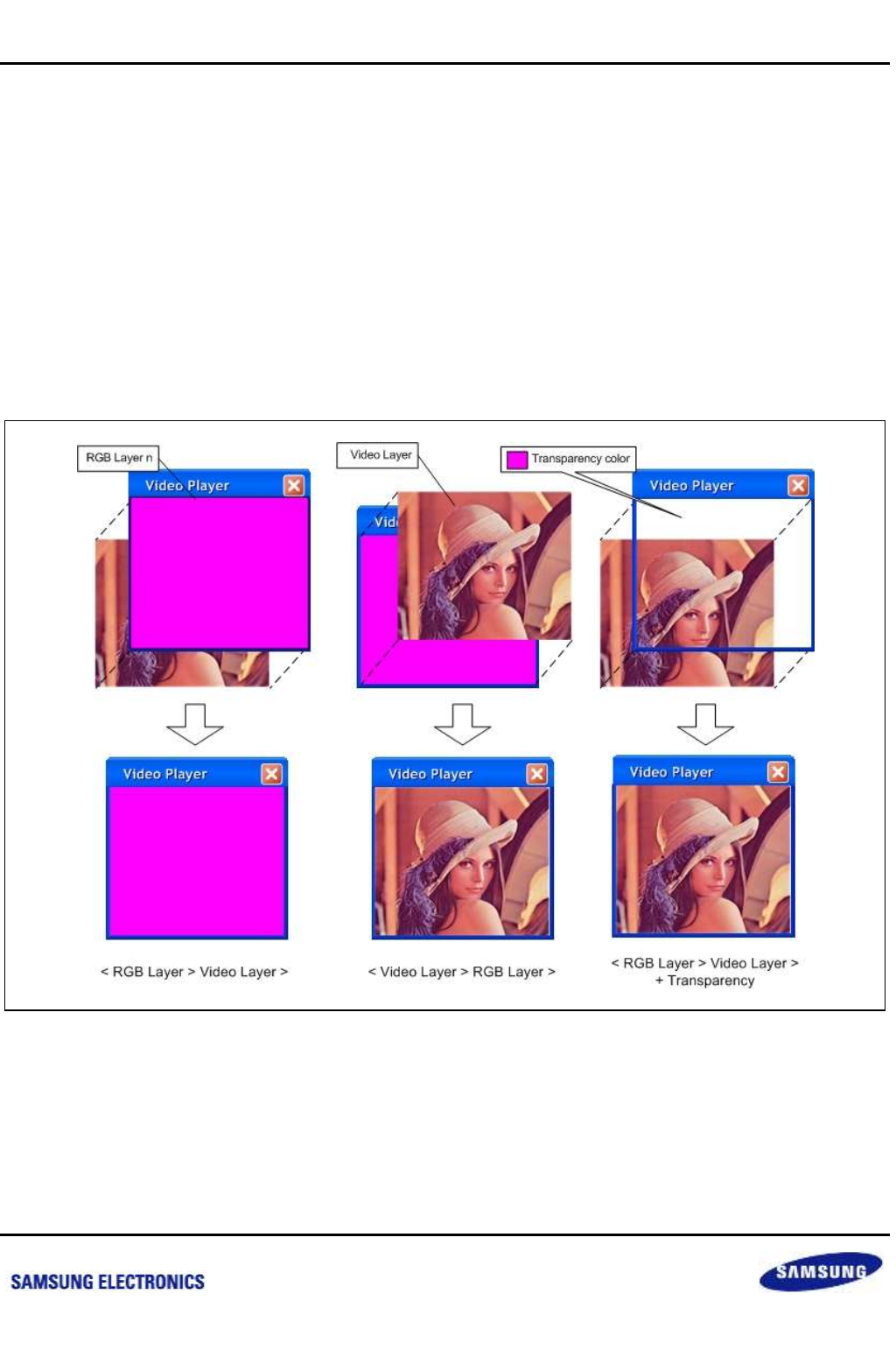
Samsung Confidential
S5P6818_UM 34 Multi Layer Controller (MLC)
34-6
Preliminary product information describes products that are in development, for which full characterization data and
associated errata are not yet available. Specifications and information herein are subject to change without notice.
34.5.1 Screen Size
The Screen size function enables users to specify the width and height of the whole screen to be displayed. The
values of "the whole screen width - 1" and "the whole height - 1" are set to the SCREENWIDTH and
SCREENHEIGHT, respectively. Since each of the SCREENWIDTH and SCREENHEIGHT has 12-bit size units,
the maximum available resolution is 2048 2048 pixels. The screen size is determined by setting the size in
frame units regardless of whether the display is progressive or interlace.
34.5.2 Priority
The MLC consists of three RGB layers and one Video layer. Among the RGB layers, Layer 0 has the highest
priority and Layer 1 has the lowest priority. These priorities cannot be changed, but the priority of the Video layer
can be adjusted via the PRIORITY parameter at the user's discretion.
Figure 34-4 Layer Priority
nexell / ys.kim at 2015.02.12
SAMSUNG Confidential

Samsung Confidential
S5P6818_UM 34 Multi Layer Controller (MLC)
34-7
Preliminary product information describes products that are in development, for which full characterization data and
associated errata are not yet available. Specifications and information herein are subject to change without notice.
34.5.3 Field Mode
The MLC of S5P6818 supports an interlace display as well as a progressive display. All registers of the MLC
should be set in frame units. For the progressive display, the FIELDENB bit of the Top controller should be set as
"0". For the interlace display, the FIELDENB bit of the Top controller should be set as "1". For example, a 720
480 progressive display and a 720 480 interlace display have the same settings, except for the setting of the
FIELDENB bit.
34.5.4 Background Color
Each layer of the MLC can be positioned at any place on the screen. Therefore, it is possible for there to be an
area not contained in any of the layers actually on the screen. The default color displayed in this area is called the
background color and the background color is set to BGCOLOR. If all layers are disabled, only the background
color is displayed on the screen.
The bpp of the BGCOLOR is 24 and has the following format:
Table 34-3 Background Color Format
Bit
23
22
21
20
19
18
17
16
15
14
13
12
11
10
9
8
7
6
5
4
3
2
1
0
Backgroun
d color
R
7
R
6
R
5
R
4
R
3
R
2
R
1
R
0
G
7
G
6
G
5
G
4
G
3
G
2
G
1
G
0
B
7
B
6
B
5
B
4
B
3
B
2
B
1
B
0
nexell / ys.kim at 2015.02.12
SAMSUNG Confidential
Samsung Confidential
S5P6818_UM 34 Multi Layer Controller (MLC)
34-8
Preliminary product information describes products that are in development, for which full characterization data and
associated errata are not yet available. Specifications and information herein are subject to change without notice.
34.5.5 Per-layer Parameters
Table 34-4 RGB Layer Registers
Function
Symbol
Bit
width
Register
Brief Description
Enable
LAYERENB
1
MLCCONTROLn[5]
Specifies whether or not to enable this
layer.
Dual register set
DIRTYFLAG
1
MLCCONTROLn[4]
Dirty flag for this layer
Lock control
LOCKSIZE (1)
2
MLCCONTROLn[13:12]
Specifies lock size for memory access.
Position
LEFT
12
MLCLEFTRIGHTn[27:16]
Specifies x-coordinate of upper-left corner.
TOP
12
MLCTOPBOTTOMn [27:16]
Specifies y-coordinate of upper-left corner.
RIGHT
12
MLCLEFTRIGHTn [11:0]
Specifies x-coordinate of lower-right
corner.
BOTTOM
12
MLCTOPBOTTOMn[11:0]
Specifies y-coordinate of lower-right
corner.
InValid
Position0
INVLIDENB (1)
1
MLCLEFTRIGHTn_0[28]
InValid0 Area Enable
LEFT (1)
12
MLCLEFTRIGHTn_0[26:16]
Specifies x-coordinate of upper-left corner.
TOP (1)
12
MLCTOPBOTTOMn_0[26:16]
Specifies y-coordinate of upper-left corner.
RIGHT (1)
12
MLCLEFTRIGHTn_0[10:0]
Specifies x-coordinate of lower-right
corner.
BOTTOM (1)
12
MLCTOPBOTTOMn_0[10:0]
Specifies y-coordinate of lower-right
corner.
InValid
Position1
INVLIDENB (1)
1
MLCLEFTRIGHTn_1[28]
InValid1 Area Enable
LEFT (1)
12
MLCLEFTRIGHTn_1[26:16]
Specifies x-coordinate of upper-left corner.
TOP (1)
12
MLCTOPBOTTOMn_1[26:16]
Specifies y-coordinate of upper-left corner.
RIGHT (1)
12
MLCLEFTRIGHTn_1[10:0]
Specifies x-coordinate of lower-right
corner.
BOTTOM (1)
12
MLCTOPBOTTOMn_1[10:0]
Specifies y-coordinate of lower-right
corner.
Alpha blending
BLENDENB
1
MLCCONTROLn[2]
Specifies whether or not to enable alpha
blending.
ALPHA
8
MLCTPCOLORn[31:24]
Specifies alpha blending factor.
Color inversion
INVENB (1)
1
MLCCONTROLn[1]
Specifies whether or not to enable color
inversion.
INVCOLOR (1)
24
MLCINVCOLOR[23:0]
Specifies the color to be used for color
inversion.
Transparency
TPENB (1)
1
MLCCONTROLn[0]
Specifies whether or not to enable
transparency.
TPCOLOR (1)
24
MLCTPCOLORn[23:0]
Specifies the color to be used as
transparency color.
Address
generation
ADDRESS
32
MLCADDRESSn[31:0]
Specifies the base address of image
buffer.
nexell / ys.kim at 2015.02.12
SAMSUNG Confidential
Samsung Confidential
S5P6818_UM 34 Multi Layer Controller (MLC)
34-9
Preliminary product information describes products that are in development, for which full characterization data and
associated errata are not yet available. Specifications and information herein are subject to change without notice.
Function
Symbol
Bit
width
Register
Brief Description
HSTRIDE (1)
32
MLCHSTRIDEn[31:0]
Specifies the horizontal stride in bytes.
VSTRIDE
32
MLCVSTRIDEn[31:0]
Specifies the vertical stride in bytes.
ADDRESSCB
(2)
32
MLCADDRESSCB[31:0]
Specifies the base address of Cb image
buffer
ADDRESSCR
(2)
32
MLCADDRESSCR[31:0]
Specifies the base address of Cr image
buffer.
VSTRIDECB
(2)
32
MLCVSTRIDECB[31:0]
Specifies the vertical stride in bytes for Cb
image buffer.
VSTRIDECR
(2)
32
MLCVSTRIDECR[31:0]
Specifies the vertical stride in bytes for Cr
image buffer.
NOTE:
1. Only exists in RGB layers
2. Only exists in Video layer
nexell / ys.kim at 2015.02.12
SAMSUNG Confidential
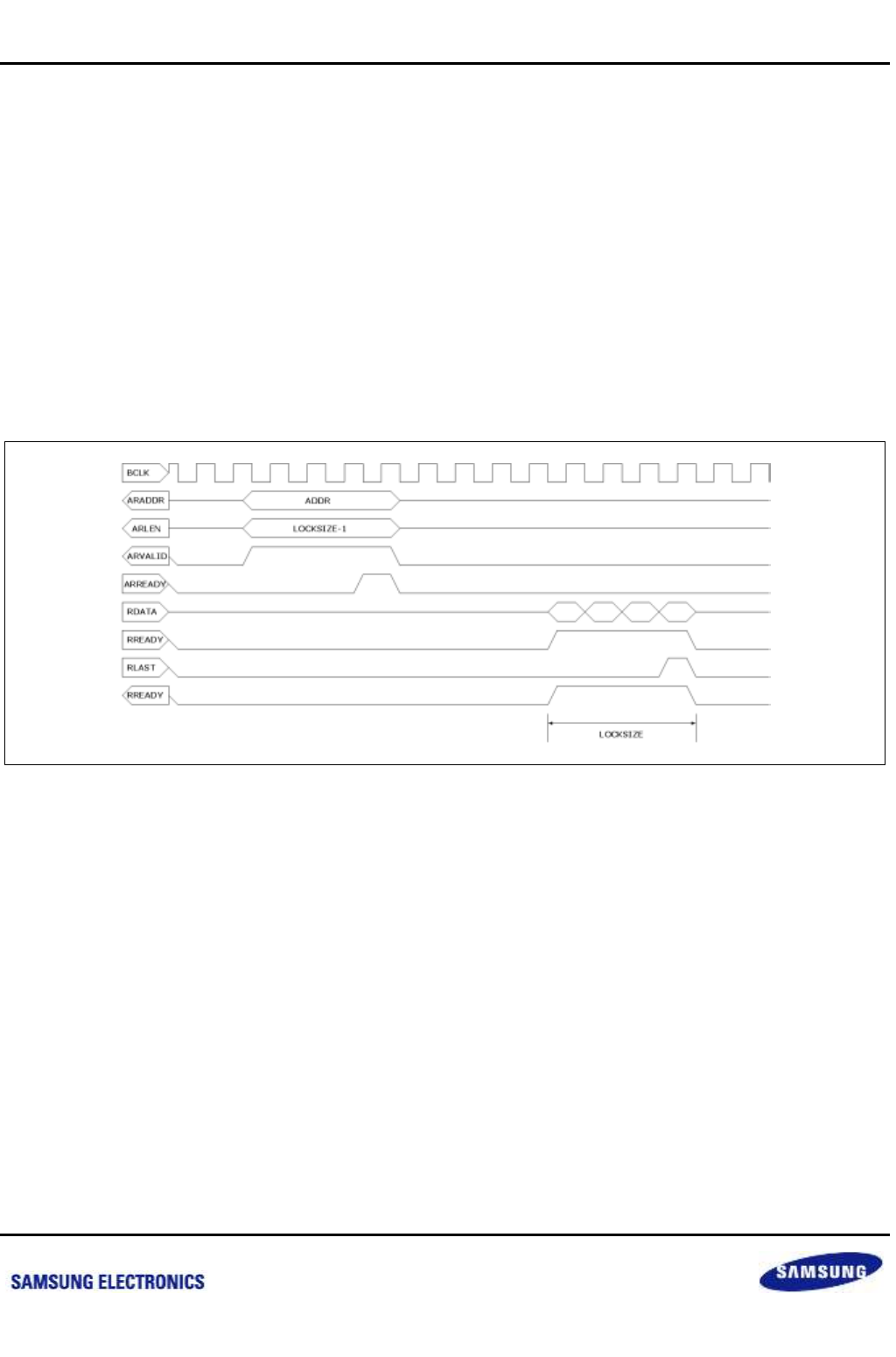
Samsung Confidential
S5P6818_UM 34 Multi Layer Controller (MLC)
34-10
Preliminary product information describes products that are in development, for which full characterization data and
associated errata are not yet available. Specifications and information herein are subject to change without notice.
34.5.6 Enable
Each layer has a LAYERENB bit to enable/disable each layer of S5P6818 at a certain point. If the LAYERENB bit
is set as "1", the relevant layer becomes on. If the LAYERENB bit is set as "0", the relevant layer becomes off and
the other layer setting registers are not used. Since the setting of the LAYERENB bit is reflected by a dirty flag, the
layer is toggled on/off in accordance with a VSYNC signal, even if the user controls the LAYERENB bit at a certain
point.
34.5.7 Lock Control
Each RGB layer can adjust the data size to be read at any one time when a memory read is requested through
the Lock control. The LOCKSIZE can specify 4, 8 or 16 and the unit size is 16 bytes. Therefore, if the LOCKSIZE
is 4, the data size to be read at any one time is 64 bytes. For a resolution of 1280 1024 or higher, it is
recommended to set the LOCKSIZE as 16.
Figure 34-5 Lock Timing
nexell / ys.kim at 2015.02.12
SAMSUNG Confidential
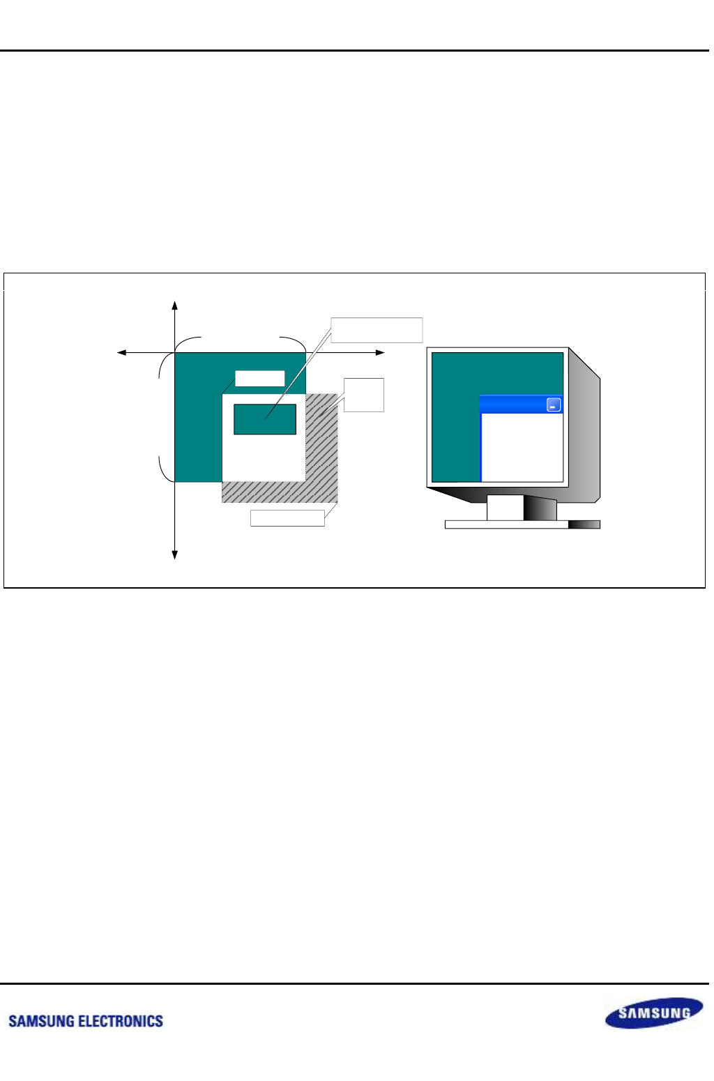
Samsung Confidential
S5P6818_UM 34 Multi Layer Controller (MLC)
34-11
Preliminary product information describes products that are in development, for which full characterization data and
associated errata are not yet available. Specifications and information herein are subject to change without notice.
34.5.8 Position
The Position function enables users to specify the top-left (LEFT*and*TOP) and the bottom-right (RIGHT and
BOTTOM) coordinates. Each coordinate can be positioned at any point within the range from –2048 to 2047, but
only the layer contained in the area from (0, 0) and (ScreenWidth – 1, ScreenHeight – 1) is displayed on the actual
screen. The MLC of S5P6818 supports H/W clipping for any area outside of the screen area, so users do not need
to carry out additional clipping processing. In addition, the MLC does not read the data in the clipped area and the
area hidden by upper layer from memory for effective use of the memory bandwidth.
RGB Layer could appoint three invisible areas without using certain color. Appointed area is not read from
Memory.
LAYER n
SCREENWIDTH + 1
SCREENHEIGHT + 1
(LEFT, TOP)
(RIGHT, BOTTOM)
No
visible
area
X
Y
LAYER n
LAYER n
InValid AREA (not read
from Memory)
Figure 34-6 Layer Position
nexell / ys.kim at 2015.02.12
SAMSUNG Confidential
Samsung Confidential
S5P6818_UM 34 Multi Layer Controller (MLC)
34-12
Preliminary product information describes products that are in development, for which full characterization data and
associated errata are not yet available. Specifications and information herein are subject to change without notice.
34.5.9 Pixel Format
34.5.9.1 RGB Layer Format
Each RGB layer supports various formats and the formats are listed in the following figure.
R: Red, G: Green, B: Blue, A: Alpha, X: Not used
Table 34-5 RGB Layer Format
Pixel Format
FORMAT[15:0]
Bpp
31
30
29
28
27
26
25
24
23
22
21
20
19
18
17
16
15
14
13
12
11
10
9
8
7
6
5
4
3
2
1
0
R5G6B5
4432h
16
R1[4:0]
G1[5:0]
B1[4:0]
R0[4:0]
G0[5:0]
B0[4:0]
B5G6R5
C432h
16
B1[4:0]
G1[5:0]
R1[4:0]
B0[4:0]
G0[5:0]
R0[4:0]
X1R5G5B5
4342h
16
R1[4:0]
G1[4:0]
B1[4:0]
R0[4:0]
G0[4:0]
B0[4:0]
X1B5G5R5
C342h
16
B1[4:0]
G1[4:0]
R1[4:0]
B0[4:0]
G0[4:0]
R0[4:0]
X4R4G4B4
4211h
16
R1[3:0]
G1[3:0]
B1[3:0]
R0[3:0]
G0[3:0]
B0[3:0]
X4B4G4R4
C211h
16
B1[3:0]
G1[3:0]
R1[3:0]
B0[3:0]
G0[3:0]
R0[3:0]
X8R3G3B2
4120h
16
R1[2:0]
G1[2:0]
B1[1:0]
R0[2:0]
G0[2:0]
B0[1:0]
X8B3G3R2
C120h
16
B1[2:0]
G1[2:0]
R1[1:0]
B0[2:0]
G0[2:0]
R0[1:0]
A1R5G5B5
3342h
16
A1
R1[4:0]
G1[4:0]
B1[4:0]
A0
R0[4:0]
G0[4:0]
B0[4:0]
A1B5G5R5
B342h
16
A1
B1[4:0]
G1[4:0]
R1[4:0]
A0
B0[4:0]
G0[4:0]
R0[4:0]
A4R4G4B4
2211h
16
A1[3:0]
R1[3:0]
G1[3:0]
B1[3:0]
A0[3:0]
R0[3:0]
G0[3:0]
B0[3:0]
A4B4G4R4
A211h
16
A1[3:0]
B1[3:0]
G1[3:0]
R1[3:0]
A0[3:0]
B0[3:0]
G0[3:0]
R0[3:0]
A8R3G3B2
1120h
16
A1[7:0]
R1[2 : 0]
G1[2 : 0]
B1[1:0]
A0[7:0]
R0[2:0]
G0[2:0]
B0[1:0]
A8B3G3R2
9120h
16
A1[7:0]
B1[2 : 0]
G1[2 : 0]
R1[1:0]
A0[7:0]
B0[2:0]
G0[2:0]
R0[1:0]
R8G8B8
4653h1)
24
B1[7:0]
R0[7:0]
G0[7:0]
B0[7:0]
B8G8R8
C653h1)
24
R1[7:0]
B0[7:0]
G0[7:0]
R0[7:0]
X8R8G8B8
4653h1)
32
R[7:0]
G[7:0]
B[7:0]
X8B8G8R8
C653h1)
32
B[7:0]
G[7:0]
R[7:0]
A8R8G8B8
0653h
32
A[7:0]
R[7:0]
G[7:0]
B[7:0]
A8B8G8R8
8653h
32
A[7:0]
B[7:0]
G[7:0]
R[7:0]
NOTE: The format settings for R8G8B8 & X8R8G8B8 and B8G8R8 & X8B8G8R8 are the same. However, the HSTRIDEs for R8G8B8 and
B8G8R8 should be set as "3" because they are in 24 bpp modes, while the HSTRIDEs for X8R8G8B8 and X8B8G8R8 should be set as "4".
The above formats are converted into A8R8G8B8 and are managed in each RGB layer. Each color component is
converted into 8-bit size. The color components with the size smaller than 8-bit are extended to 8-bit size from the
highest bit repeatedly. For example, the color with 5-bit size is converted to {[4:0], [4:2]} and the color with 3-bit
size is converted to {[2:0], [2:0], [2:1]}. Each layer compares the color component internally extended with
TPCOLOR or INVCOLOR. Therefore, a user should set the color that each color format is extended in R8G8B8 in
TPCOLOR and INVCOLOR.
nexell / ys.kim at 2015.02.12
SAMSUNG Confidential
Samsung Confidential
S5P6818_UM 34 Multi Layer Controller (MLC)
34-13
Preliminary product information describes products that are in development, for which full characterization data and
associated errata are not yet available. Specifications and information herein are subject to change without notice.
34.5.9.2 Video Layer Format
The Video layer manages YUV data and supports the linear YUV format and the 2D block addressing separated
YUV format.
Table 34-6 Video Layer Format
FORMAT[1:0]
Pack Mode
Type
Y:UV
Addressing Mode
0
Separate Y/U/V
YUV
4:2:0
2D Block
1
Separate Y/U/V
YUV
4:2:2
2D Block
2
Non-separate
YUV
4:2:2
Linear
3
Separate Y/U/V
YUV
4:4:4
2D Block
4
Separate Y/UV
YUV
4:2:2
2D Block
5
Separate Y/UV
YUV
4:2:0
2D Block
The MLC of S5P6818 uses the A4R8G8B8 format internally. Therefore, the Video layer also reads YUV data from
the memory and converts into RGB data internally. The formulas with which the Video layer converts YUV data
into RGB data are as follows:
The formula for YCbCr to RGB conversion
R = Y + (1.4020 Cr)
G = Y - (0.34414 Cb) + (0.71414 Cr)
B = Y + (1.7720 Cb)
Linear YUV 422 Format
The video layer supports the YUYV format as a linear YUV format whose Y data (luminance data) exists at
every pixel, but Cb and Cr (chrominance) data exist separately over two pixels. Therefore two pixels share the
same Cb/Cb data. Hence the Video layer has 2-pixel data per 32-bit and manages it in 2-pixel units.
Table 34-7 YUYV Format
Pixel Format
FORMAT[2:0]
31
30
29
28
27
26
25
24
23
22
21
20
19
18
17
16
15
14
13
12
11
10
9
8
7
6
5
4
3
2
1
0
YUYV
2
Cr[7:0]
Y1[7:0]
Cb[7:0]
Y0[7:0]
2D Block Addressing Separated Y/U/V Format
In the 2D block addressing separated Y/U/V format, each of Y, U and V exists at separate memory spaces.
In addition, the format is divided into 444, 422 and 420 in proportion to U and V for Y. The 2D block
addressing separated YUV format is the 2D block addressing format, and each component has a size of
64 32 and linearity in block units. These features provide S5P6818's unique memory format, to enhance
the effectiveness of memory access when S5P6818 manages data in macro block units through an algorithm
to compress/decompress images like MPEG files.
nexell / ys.kim at 2015.02.12
SAMSUNG Confidential
Samsung Confidential
S5P6818_UM 34 Multi Layer Controller (MLC)
34-14
Preliminary product information describes products that are in development, for which full characterization data and
associated errata are not yet available. Specifications and information herein are subject to change without notice.
According to each format, Y, U and V correspond to 2 2 pixels as follows:
Pixel
0 1
32
0 1
32
0 1
32
0 1
32
Cr
Cb
Y
YCbCr 4:4:4
Pixel
0 1
32
0 1
32
01
32
0 1
32
Cr
Cb
Y
YCbCr 4:2:2
Pixel
0 1
32
0 1
32
01
32
0 1
32
Cr
Cb
Y
YCbCr 4:2:0
Figure 34-7 Separated YUV Format
In the memory, each of Y, U and V exists at separated memory space.
Y VU Y
VU
4:2:2 Y/U/V 4:2:0 Y/U/V
nexell / ys.kim at 2015.02.12
SAMSUNG Confidential
Samsung Confidential
S5P6818_UM 34 Multi Layer Controller (MLC)
34-15
Preliminary product information describes products that are in development, for which full characterization data and
associated errata are not yet available. Specifications and information herein are subject to change without notice.
34.5.9.3 Layer Blending
MLC consists of three RGB layers and one Video layer. Each RGB layer supports Transparency, Color Inversion
and Alpha Blending functions but the Video layer only supports Alpha Blending functions. The Color Inversion and
the Alpha Blending functions are only applied to between layers and not to background.
The Transparency function enables users to specify a particular color and handle the color as a transparent color.
Therefore, an area filled with a transparent color shows through the lower layer and shows the layer as it is. Like
the Transparency function, the Color Inversion function shows through the lower layer and shows the layer as it is,
but the function is different in that it inverts and projects the layer's color. The Transparency and Color Inversion
functions are useful for the implementation of the Cursor layer as shown in the figure below:
Figure 34-8 Transparency & Color Inversion
The Transparency and the Color Inversion effects are applied by setting each of the TPENB and the INVENB bits
of an RGB Layer as "1". Both TPCOLOR and INVCOLOR have R8G8B8 formats.
Table 34-8 TPCOLOR & INVCOLOR Format
Bit
23
22
21
20
19
18
17
16
15
14
13
12
11
10
9
8
7
6
5
4
3
2
1
0
TPCOLOR/INVCOLOR
R7
R6
R5
R4
R3
R2
R1
R0
G7
G6
G5
G4
G3
G2
G1
G0
B7
B6
B5
B4
B3
B2
B1
B0
The Alpha Blending function enables users to adjust the transparency of a desired layer. The Alpha level is
adjusted by ALPHA[7:0] and can be specified in the range between 0 and 255. If the Alpha level is 255, it means it
is fully opaque. If the level is 0, it indicates full transparency. In addition, each RGB layer can use a pixel format
including Alpha and is applied in Alpha per pixel units. In the Per-layer alpha or the Per-pixel Alpha formats, the
Alpha Blending effect can only be applied by setting the BLENDENB bit as "1".
Only one layer can use the alpha blending function at the same time, and when the alpha blending function of one
layer is enabled, the alpha blending function of the other layers must be disabled.
nexell / ys.kim at 2015.02.12
SAMSUNG Confidential
Samsung Confidential
S5P6818_UM 34 Multi Layer Controller (MLC)
34-16
Preliminary product information describes products that are in development, for which full characterization data and
associated errata are not yet available. Specifications and information herein are subject to change without notice.
All layers use the A8R8G8B8 format internally and the formula for Alpha Blending is as follows:
The formula for Alpha blending function
If alpha is 0 then α is 0, else is alpha + 1
Result color = This layer color /256 + lower layer color (256 – )/256
In the A4 format, α = alpha 16 + alpha (0 alpha < 16)
Figure 34-9 Alpha Blending
nexell / ys.kim at 2015.02.12
SAMSUNG Confidential
Samsung Confidential
S5P6818_UM 34 Multi Layer Controller (MLC)
34-17
Preliminary product information describes products that are in development, for which full characterization data and
associated errata are not yet available. Specifications and information herein are subject to change without notice.
34.5.10 Address Generation
34.5.10.1 RGB Layer Address Generation
The Address generation function enables users to specify the address and stride of the memory where images are
stored.
Stride is divided into horizontal stride and vertical stride. The stride is the unit for increasing an address. The
horizontal stride (HSTRIDE) is the value to be added to an address whenever its x-coordinate increases, while the
vertical stride (VSTRIDE) is the value to be added to the address whenever its y-coordinate increases. In general,
the horizontal stride is the number of the bytes per pixel and the vertical stride is the value that is the number of
bytes per pixel multiplied by an image width. The vertical stride has 2's complement format. Thus a vertical flip
function can be implemented by specifying the vertical stride as negative number.
The Image address (ADDRESS) usually specifies an address on the top left corner of the image. If the vertical
stride for the vertical flip function has a negative number, the ADDRESS should specify an address on the bottom
left corner of the image.
Table 34-9 RGB Layer Address & Flip
Vertical Flip
Vertical Stride
Base Address
Off
0
Address on the top left corner of the image
On
< 0
Address on the bottom left corner of the image
nexell / ys.kim at 2015.02.12
SAMSUNG Confidential
Samsung Confidential
S5P6818_UM 34 Multi Layer Controller (MLC)
34-18
Preliminary product information describes products that are in development, for which full characterization data and
associated errata are not yet available. Specifications and information herein are subject to change without notice.
34.5.10.2 Video Layer Address Generation
In the Video layer, the horizontal stride is not separately specified and is fixed internally. In addition, the vertical
stride should always be a positive number. Since the vertical stride is always positive number, the vertical flip
function is not supported.
Linear YUV 422 format (YUYV)
In the linear YUV 422 format, an address can only be specified by setting its base address and vertical stride.
The Base address (ADDRESS) specifies the base address in the YUYV image buffer and the vertical stride
(VSTRIDE) specifies the increment of the address in proportion to the increase of the y-coordinate.
The vertical stride should be a positive number.
2D block addressing separated YUV format
In the separated format, each Y, U and V is stored in different addresses of the memory. Thus the address
for the Y component is specified by the ADDRESS3 and the VSTRIDE3 registers and the address for the
U (Cb) and V (Cr) components is separately specified by the ADDRESSCB & the VSTRIDECB registers
and the ADDRESSCR& the VSTRIDECR registers. Since S5P6818 uses segments with 4096 4096 pixel
sizes in the 2D block addressing format, the vertical stride should be specified as 4096. In addition,
the ADDRESS3/CB/CR registers set the separate format for segment addresses and not for normal linear
addresses. The segment addressing format is listed in the following Table.
Table 34-10 Segment Addressing Format
Bit
31
30
29
28
27
26
25
24
23
22
21
20
19
18
17
16
15
14
13
12
11
10
9
8
7
6
5
4
3
2
1
0
Address
0
0
1
Index of
Segment
Y coordinate in segment [11:0]
X coordinate in segment [11:0]
The display array area on the memory map should be specified as a setting Address [31:29] of 4'b001. In addition,
the Memory controller should be enabled to use the display array area.
nexell / ys.kim at 2015.02.12
SAMSUNG Confidential
Samsung Confidential
S5P6818_UM 34 Multi Layer Controller (MLC)
34-19
Preliminary product information describes products that are in development, for which full characterization data and
associated errata are not yet available. Specifications and information herein are subject to change without notice.
34.5.11 Video Layer Specific Parameters
The Video layer provides the Scale and Color Control functions additionally.
Table 34-11 Video Layer Specific Parameters
Function
Symbol
Bit
width
Register
Brief description
Scale
VFILTERENB
1
MLCVSCALE[28]
Specifies whether or not to vertical scale
enable bilinear filter.( This is only
applicable to the Y component)
VFILTERENB_C
1
MLCVSCALE[29]
Specifies whether or not to vertical scale
enable bilinear filter. (This is only
applicable to the Cb, Cr components)
HFILTERENB
1
MLCHSCALE[28]
Specifies whether or not to horizontal
scale enable bilinear filter. (This is only
applicable to the Y component)
HFILTERENB_C
1
MLCHSCALE[29]
Specifies whether or not to horizontal
scale enable bilinear filter. (This is only
applicable to the Cb, Cr components)
HSCALE
23
MLCHSCALE[22:0]
Specifies the horizontal scale ratio.
VSCALE
23
MLCVSCALE[22:0]
Specifies the vertical scale ratio.
Color
control
BRIGHTNESS
8
MLCLUENH[15:8]
Specifies the brightness value.
CONTRAST
3
MLCLUENH[2:0]
Specifies the contrast value.
HUECBnA
8
MLCCHENHn[7:0]
Specifies the cosine value for Cb
component.
HUECBnB
8
MLCCHENHn[15:8]
Specifies the sine value for Cb
component.
HUECRnA
8
MLCCHENHn[23:16]
Specifies the sine value for Cr
component.
HUECRnB
8
MLCCHENHn[31:24]
Specifies the cosine value for Cr
component.
nexell / ys.kim at 2015.02.12
SAMSUNG Confidential
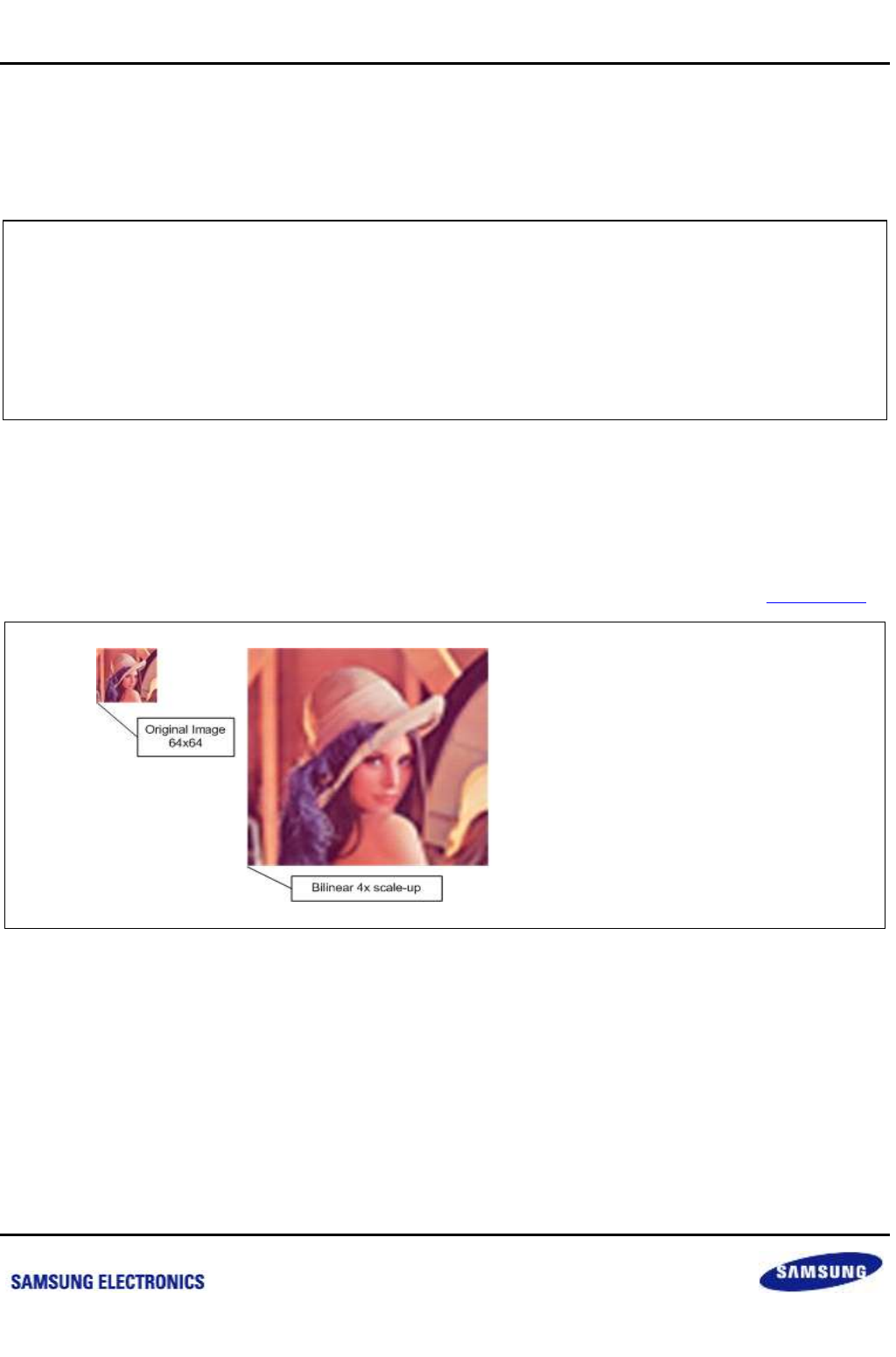
Samsung Confidential
S5P6818_UM 34 Multi Layer Controller (MLC)
34-20
Preliminary product information describes products that are in development, for which full characterization data and
associated errata are not yet available. Specifications and information herein are subject to change without notice.
34.5.12 Scale Function
The scale-up and the scale-down of the Video layer are determined by the HSCALE and VSCALE parameters.
Each parameter finds and sets the ratio between an input image size and an output image size. The setting
formulae for the HSCALE and VSCALE parameters are as follows:
The formula for HSCALE and VSCALE
In case of the enlargement by using a Bilinear filter:
HSCALE = (source width-1) (1<<11)/(destination width-1)
VSCALE = (source height-1) (1<<11)/(destination height-1)
,else
HSCALE = source width (1<<11)/destination width
VSCALE = source height (1<<11)/destination height
Video Layer supports bilinear filtered scaling up and down. Nearest neighbor scaling is also supported. Filter
enable signals are separately allocated for Y and C (Cb, Cr) components in case of scaling up/down
(H/VFILTERENB, H/VFILTERENB_C)
When bilinear scaling up and down is used, H/VFILTERENB and H/VFILTERENB_C should be set to "1" for
bilinear filtered scaling. When nearest neighbor scaling down is used, H/VFILTERENB and H/VFILTERENB_C*
should be set to "0". The difference in images produced by the bilinear filter method is as shown in Figure 34-10.
Figure 34-10 Bilinear Filter
34.5.12.1 Color Control
The Video layer supports the Color Control function for output images. A user can adjust Brightness, Contrast,
Hue and Saturation to compensate video data colors.
nexell / ys.kim at 2015.02.12
SAMSUNG Confidential
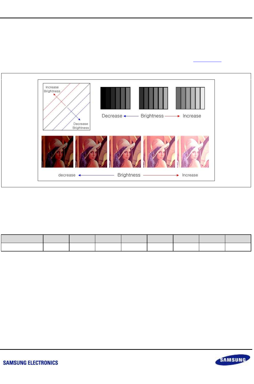
Samsung Confidential
S5P6818_UM 34 Multi Layer Controller (MLC)
34-21
Preliminary product information describes products that are in development, for which full characterization data and
associated errata are not yet available. Specifications and information herein are subject to change without notice.
34.5.12.2 Luminance Enhancement
The Video layer can compensate luminance data by adjusting Brightness and Contrast.
The Brightness consists of 256 levels and is set by the BRIGHTNESS parameter. The BRIGHTNESS parameter
has a 2's complement value and can be set between the –128 level and the +127 level. Figure 34-11 shows the
image change depending on the Brightness change.
Figure 34-11 Brightness
The Contrast consists of 8 levels and is set by the CONTRAST parameter. The Video layer can adjust the contrast
from 1.0 to 1.875 in increments of 0.125, but cannot reduce the contrast of the original image. In the following
Table lists the contrast values corresponding to the CONTRAST parameters.
Table 34-12 CONTRAST Parameter
CONTRAST
0
1
2
3
4
5
6
7
Contrast value
1.0
1.125
1.25
1.375
1.5
1.625
1.75
1.875
nexell / ys.kim at 2015.02.12
SAMSUNG Confidential
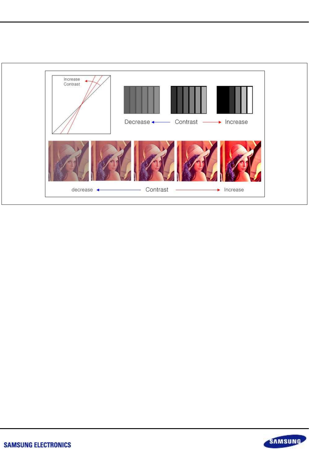
Samsung Confidential
S5P6818_UM 34 Multi Layer Controller (MLC)
34-22
Preliminary product information describes products that are in development, for which full characterization data and
associated errata are not yet available. Specifications and information herein are subject to change without notice.
In the following Figure shows the image change depending on the contrast change. The following figure is
originally intended to explain better about the contrast function as well as to show the effect of contrast reduction.
Actually, the Video layer can increase the contrast, but not reduce it.
Figure 34-12 Contrast
nexell / ys.kim at 2015.02.12
SAMSUNG Confidential

Samsung Confidential
S5P6818_UM 34 Multi Layer Controller (MLC)
34-23
Preliminary product information describes products that are in development, for which full characterization data and
associated errata are not yet available. Specifications and information herein are subject to change without notice.
34.5.12.3 Chrominance Enhancement
The Video layer can compensate Chrominance data by adjusting Hue and Saturation.
The Hue is adjusted by the following formulae:
(B-Y)' = (B-Y) Cos(θ) – (R-Y) Sin(θ)
(R-Y)' = (B-Y) Sin(θ) + (R-Y) Cos(θ)
The Saturation can be adjusted by multiplying a gain value by the above result value.
The Video layer can adjust the Hue and Saturation differently in each quadrant and has HUECBnA/B*and
*HUECRnA/B parameters for each quadrant. Each parameter has the [S.1.6] format and is applied as follows:
Figure 34-13 The Basic concept of Hue and Saturation Control
B-Y
R-Y
¥è
1 2
3 4
nexell / ys.kim at 2015.02.12
SAMSUNG Confidential

Samsung Confidential
S5P6818_UM 34 Multi Layer Controller (MLC)
34-24
Preliminary product information describes products that are in development, for which full characterization data and
associated errata are not yet available. Specifications and information herein are subject to change without notice.
1. 1st quadrant: (B-Y) > 0 and (R-Y) > 0
(B-Y)' = (B-Y) HUECB1A + (R-Y) HUECB1B
(R-Y)' = (B-Y) HUECR1A + (R-Y) HUECR1B
2. 2nd quadrant: (B-Y) < 0 and (R-Y) > 0
(B-Y)' = (B-Y) HUECB2A + (R-Y) HUECB2B
(R-Y)' = (B-Y) HUECR2A + (R-Y) HUECR2B
3. 3rd quadrant: (B-Y) < 0 and (R-Y) < 0
(B-Y)' = (B-Y) HUECB3A + (R-Y) HUECB3B
(R-Y)' = (B-Y) HUECR3A + (R-Y) HUECR3B
4. 4th quadrant: (B-Y) < 0 and (R-Y) < 0
(B-Y)' = (B-Y) HUECB4A + (R-Y) HUECB4B
(R-Y)' = (B-Y) HUECR4A + (R-Y) HUECR4B
Therefore, each parameter can be calculated by using the following formulas:
The formula for Hue and Saturation parameters:
HUECBnA = cos() * 64 * gain, HUECBnB = - sin() * 64 * gain
HUECRnA = sin() * 64 * gain, HUECRnB = cos() * 64 * gain
, where is for hue and gain is for saturation from -2 to 1.99999X.
nexell / ys.kim at 2015.02.12
SAMSUNG Confidential
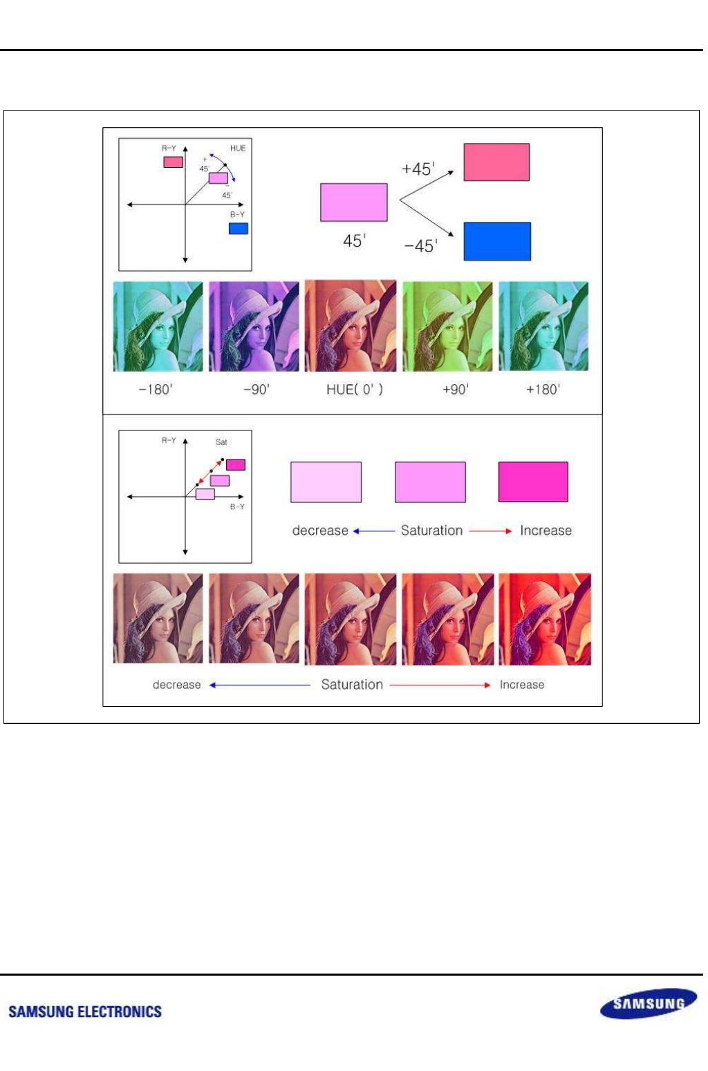
Samsung Confidential
S5P6818_UM 34 Multi Layer Controller (MLC)
34-25
Preliminary product information describes products that are in development, for which full characterization data and
associated errata are not yet available. Specifications and information herein are subject to change without notice.
In the following Figure the image change depending on the changes to Hue and Saturation.
Figure 34-14 Hue and Saturation
nexell / ys.kim at 2015.02.12
SAMSUNG Confidential
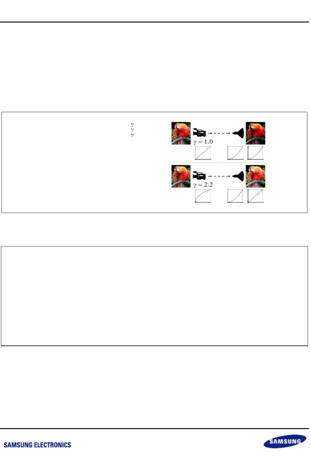
Samsung Confidential
S5P6818_UM 34 Multi Layer Controller (MLC)
34-26
Preliminary product information describes products that are in development, for which full characterization data and
associated errata are not yet available. Specifications and information herein are subject to change without notice.
34.5.13 Gamma Correction
MLC has three Gamma Table (256 10-bit) for Red, Green, and Blue colors. Gamma[9:0] consists of
Gamma[9:2], which are the integers(0 to 255), and Gamma[1:0], which are decimals (0.0, 0.5, 0.25, 0.75). And,
R10, G10, B10, as the result of Gamma correction, are transformed into R8, G8, B8, which then can be used as
input pixel for Display block , and it is possible to apply dithering while 10-bit results is being transformed into 8-bit.
Gamma correction can choose any Gamma region according to 3 different modes (total layer, RGB layer, Video
layer), and also can designate the Alpha-blended regions of Video layer and RGB layer as the region of RGB
layer or Video layer.
Figure 34-15 Gamma Correction
Register Set in case of Gamma correction
Example:
R,G,B Gamma Table Power On (MLCGAMMACONT Register R/G/BGAMMATABLE_PWD bit = "1" )
Gamma Table SLEEP Mode Disable (MLCGAMMACONT Register R/G/BGAMMATABLE_SLD bit = "1")
Write the value of Gamma Table
(Table address: MLCR/G/BGAMMATABLEWRITE[31:24], table data: MLCR/G/BGAMMATABLEWRITE[9:0])
Gamma enable(Refer to MLCGAMMACONT Register)
MLC Enable
Gamma Table R = (255 * (R / 255) ^ ) << 2
Gamma Table G = (255 * (G / 255) ^ ) << 2
Gamma Table B = (255 * (B / 255) ^ ) << 2
nexell / ys.kim at 2015.02.12
SAMSUNG Confidential
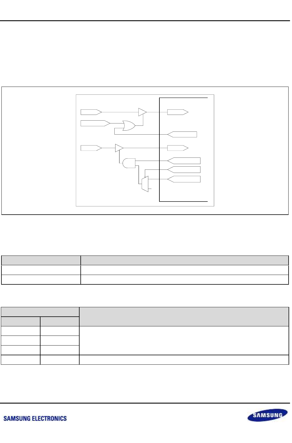
Samsung Confidential
S5P6818_UM 34 Multi Layer Controller (MLC)
34-27
Preliminary product information describes products that are in development, for which full characterization data and
associated errata are not yet available. Specifications and information herein are subject to change without notice.
34.6 Clock Generation
The MLC operates by using the PCLK and the BCLK. The PCLK is used when the CPU accesses the registers of
the MLC. The BCLK is used as an internal clock or when the MLC accesses the memory. The MLC provides
various operation modes for the PCLK and the BCLK. Therefore, users can adjust the clock for the MLC by setting
the PCLKMODE and the BCLKMODE parameters according to their purpose. Users must set Always Mode for
using the MLC. (BCLK and PCLK both)
Figure 34-16 Clock Generation
Table 34-13 PCLK Mode
PCLKMODE
Brief Description
0
Always disabled
1
Always enabled.
Table 34-14 BCLK Mode
BLCKMODE
Brief Description
[1]
[0]
0
0
Always disabled.
0
1
1
0
1
1
Always enabled.
CPU Access
PCLKMODE
PCLK
BCLK
BCLKMODE[1]
BCLKMODE[0]
‘1’
0
1
BCLK Enb
PCLK
BCLK
MLC
nexell / ys.kim at 2015.02.12
SAMSUNG Confidential

Samsung Confidential
S5P6818_UM 34 Multi Layer Controller (MLC)
34-28
Preliminary product information describes products that are in development, for which full characterization data and
associated errata are not yet available. Specifications and information herein are subject to change without notice.
34.7 Register Description
34.7.1 Register Map Summary
Base Address: 0xC010_2000h
Register
Offset
Description
Reset Value
MLCCONTROLT
0x000h (Primary),
0x400h (Secondary)
MLC TOP control register
0x0000_0100
MLCSCREENSIZE
0x004h/0x404h
MLC screen size register
0x0000_0000
MLCBGCOLOR
0x008h/0x408h
MLC background color register
0x0000_0000
MLCLEFTRIGHT0
0x00Ch/0x40Ch
MLC RGB layer 0 LEFT right register
0x0000_0000
MLCTOPBOTTOM0
0x010h/0x410h
MLC RGB layer 0 top bottom register
0x0000_0000
MLCLEFTRIGHT0_0
0x014h/0x414h
MLC RGB layer 0 INVALID AREA 0 LEFT right
Register
0x0000_0000
MLCTOPBOTTOM0_0
0x018h/0x418h
MLC RGB layer 0 INVALID AREA 0 bottom top
Register
0x0000_0000
MLCLEFTRIGHT0_1
0x01Ch/0x41Ch
MLC RGB layer 0 INVALID AREA 1 LEFT right
Register
0x0000_0000
MLCTOPBOTTOM0_1
0x020h/0x420h
MLC RGB layer 0 invalid area 1 bottom top
register
0x0000_0000
MLCCONTROL0
0x024h/0x424h
MLC RGB layer 0 control register
0x0000_0000
MLCHSTRIDE0
0x028h/0x428h
MLC RGB layer 0 HORIZONTAL stride register
0x0000_0000
MLCVSTRIDE0
0x02Ch/0x42Ch
MLC RGB layer 0 VERTICAL stride register
0x0000_0000
MLCTPCOLOR0
0x030h/0x430h
MLC RGB layer 0 TRANSPARENCY color
register
0x0000_0000
MLCINVCOLOR0
0x034h/0x434h
MLC RGB layer 0 INVERSION color register
0x0000_0000
MLCADDRESS0
0x038h/0x438h
MLC RGB layer 0 base address register
0x0000_0000
RSVD
0x03Ch/0x43Ch
Reserved
0x0000_0000
MLCLEFTright1
0x040h
MLC RGB layer 1 left right register
0x0000_0000
MLCTOPBOTTOM1
0x044h
MLC RGB layer 1 top bottom register
0x0000_0000
MLCLEFTRIGHT1_0
0x048h
MLC RGB layer 1INVALID AREA 0 LEFT right
Register
0x0000_0000
MLCTOPBOTTOM1_0
0x04Ch
MLC RGB layer 1INVALID AREA 0 bottom top
Register
0x0000_0000
MLCLEFTRIGHT1_1
0x050h
MLC RGB layer 1INVALID AREA 1 LEFT right
Register
0x0000_0000
MLCTOPBOTTOM1_1
0x054h
MLC RGB layer 1INVALID AREA 1 bottom top
Register
0x0000_0000
MLCCONTROL1
0x058h
MLC RGB layer 1 control register
0x0000_0000
MLCHSTRIDE1
0x05Ch
MLC RGB layer 1 HORIZONTAL stride register
0x0000_0000
MLCVSTRIDE1
0x060h
MLC RGB layer 1 VERTICAL stride register
0x0000_0000
MLCTPCOLOR1
0x064h
MLC RGB layer 1 TRANSPARENCY color
0x0000_0000
nexell / ys.kim at 2015.02.12
SAMSUNG Confidential

Samsung Confidential
S5P6818_UM 34 Multi Layer Controller (MLC)
34-29
Preliminary product information describes products that are in development, for which full characterization data and
associated errata are not yet available. Specifications and information herein are subject to change without notice.
Register
Offset
Description
Reset Value
Register
MLCINVCOLOR1
0x068h
MLC RGB layer 1 INVERSION color register
0x0000_0000
MLCADDRESS1
0x06Ch
MLC RGB layer 1 BASE address register
0x0000_0000
RSVD
0x070h
Reserved
0x0000_0000
MLCLEFright2
0x074h/0x474h
MLC VIDEO layer left right register
0x0000_0000
MLCtopBOTTOM2
0x078h/0x478h
MLC VIDEO layer top bottom register
0x0000_0000
MLCCONTROL2
0x07Ch / 0x47Ch
MLC VIDEO layer control register
0x0000_0000
MLCVSTRIDE3
0x080h/0x480h
MLC VIDEO layer VERTICAL stride register
0x0000_0000
MLCTPCOLOR3
0x084h/0x484h
MLC VIDEO layer TRANSPARENCY color
register
0x0000_0000
RSVD
0x088h/0x488h
Reserved
0x0000_0000
MLCADDRESS3
0x08Ch/0x48Ch
MLC VIDEO layer BASE address register
0x0000_0000
MLCADDRESSCB
0x090h / 0x490h
MLC VIDEO layer Cb BASE Address register
0x0000_0000
MLCADDRESSCR
0x094h/0x494h
MLC VIDEO layer Cr BASE Address register
0x0000_0000
MLCVSTRIDECB
0x098h/0x498h
MLC VIDEO layer Cb VERTICAL stride register
0x0000_0000
MLCVSTRIDECR
0x09Ch/0x49Ch
MLC VIDEO layer Cr VERTICAL stride register
0x0000_0000
MLCHSCALE
0x0A0h/0x4A0h
MLC VIDEO layer horizontal scale register
0x0000_0800
MLCVSCALE
0x0A4h/0x4A4h
MLC VIDEO layer vertical scale register
0x0000_0800
MLCLUENH
0x0A8h/0x4A8h
MLC VIDEO layer luminance enhancement
control register
0x0000_0000
MLCCHENH0
0x0ACh/0x4ACh
MLC VIDEO layer chrominance enhancement
control 0 register
0x4000_0040
MLCCHENH1
0x0B0h/0x4B0h
MLC VIDEO layer chrominance enhancement
control 1 register
0x4000_0040
MLCCHENH2
0x0B4h/0x4B4h
MLC VIDEO layer chrominance enhancement
control 2 register
0x4000_0040
MLCCHENH3
0x0B8h/0x4B8h
MLC VIDEO layer chrominance enhancement
control 3 register
0x4000_0040
MLCGAMMACONT
0x0ECh/0x4ECh
MLC GAMMA control register
0x0000_0000
MLCRGAMMATABLEWRIT
E
0x0F0h/0x4F0h
MLC RED GAMMA table write
Undefined
MLCGGAMMATABLEWRIT
E
0x0F4h/0x4F4h
MLC GREEN GAMMA table write
Undefined
MLCBGAMMATABLEWRIT
E
0x0F8h/0x4F8h
MLC BLUE GAMMA table write
Undefined
RSVD
0x0FCh to 0x3BC/
0x4FCh to 0x7BC
Reserved
0x0000_0000
MLCCLKENB
0x3C0h/0x7C0h
MLC clock generation enable register
0x0000_0000
nexell / ys.kim at 2015.02.12
SAMSUNG Confidential

Samsung Confidential
S5P6818_UM 34 Multi Layer Controller (MLC)
34-30
Preliminary product information describes products that are in development, for which full characterization data and
associated errata are not yet available. Specifications and information herein are subject to change without notice.
34.7.1.1 MLCCONTROLT
Base Address: 0xC010_2000h
Address = Base Address + 0x000h (Primary), 0x400h (Secondary), Reset Value = 0x0000_0100
Name
Bit
Type
Description
Reset Value
RSVD
[31:14]
R
Reserved
18'h0
RSVD
[13:12]
RW
Reserved
2'b0
PIXELBUFFER_PWD
[11]
RW
MLC Pixel Buffer Power On/Off
It should be "On" before MLC Enabled.
0 = Power Off
1 = Power On
1'b0
PIXELBUFFER_SLD
[10]
RW
MLC Pixel Buffer Sleep Mode
It is usable only when Power On.
0 = Sleep Mode Enable
1 = Sleep Mode Disable
1'b0
PRIORITY
[9:8]
RW
Specifies the priority of the Video layer.
00 = video layer > layer0 > layer1 > layer2
01 = layer0 > video layer > layer1 > layer2
10 = layer0 > layer1 > video layer > layer2
11 = layer0 > layer1 > layer2 > video layer
2'b1
RSVD
[7:4]
R
Reserved
4'hx
DITTYFLAG
[3]
RW
Dirty Flag for MLC top controller. If this bit is set as
"1", the register settings concerned with the Top
controller in vertical sync mode are updated and this
bit is cleared as "0" automatically.
Read:
0 = Clean
1 = Dirty
Write:
0 = No affect
1 = Apply modified settings
1'b0
RSVD
[2]
R
Reserved
1'b0
MLCENB
[1]
RW
Specifies whether or not to enable MLC
Set when MLCENB Set/Clear together with set
MLCCONTROLT DITTYFLAG.
0 = Disable
1 = Enable
1'b0
FIELDENB
[0]
RW
Specifies whether or not to enable Interlace mode.
0 = progressive mode
1 = Interlace mode
1'b0
nexell / ys.kim at 2015.02.12
SAMSUNG Confidential
Samsung Confidential
S5P6818_UM 34 Multi Layer Controller (MLC)
34-31
Preliminary product information describes products that are in development, for which full characterization data and
associated errata are not yet available. Specifications and information herein are subject to change without notice.
34.7.1.2 MLCSCREENSIZE
Base Address: 0xC010_2000h
Address = Base Address + 0x004h, 0x404h, Reset Value = 0x0000_0000
Name
Bit
Type
Description
Reset Value
RSVD
[31:28]
R
Reserved
4'h0
SCREENHEIGHT
[27:16]
RW
Specifies "the whole screen height - 1".
12'h0
RSVD
[15:12]
R
Reserved
4'h0
SCREENWIDTH
[11:0]
RW
Specifies "the whole screen width - 1".
12'h0
34.7.1.3 MLCBGCOLOR
Base Address: 0xC010_2000h
Address = Base Address + 0x008h, 0x408h, Reset Value = 0x0000_0000
Name
Bit
Type
Description
Reset Value
RSVD
[31:24]
R
Reserved
8'h0
DEFAULTCOLOR
[23:0]
RW
Specifies the color to be displayed on the screen in
areas not covered by any of the layers Specifies the
R8G8B8 format in 24 bpp mode.
24'h0
34.7.1.4 MLCLEFTRIGHT0
Base Address: 0xC010_2000h
Address = Base Address + 0x00Ch, 0x40Ch, Reset Value = 0x0000_0000
Name
Bit
Type
Description
Reset Value
RSVD
[31:28]
R
Reserved
4'h0
LEFT
[27:16]
RW
Specifies the x-coordinate of the upper-left corner of
the layer. This value has 2's complement and from -
2048 to 2047.
12'h0
RSVD
[15:12]
R
Reserved
4'h0
RIGHT
[11:0]
RW
Specifies the x-coordinate of the lower-right corner of
the layer. This value has 2's complement and from -
2048 to 2047.
12'h0
nexell / ys.kim at 2015.02.12
SAMSUNG Confidential
Samsung Confidential
S5P6818_UM 34 Multi Layer Controller (MLC)
34-32
Preliminary product information describes products that are in development, for which full characterization data and
associated errata are not yet available. Specifications and information herein are subject to change without notice.
34.7.1.5 MLCTOPBOTTOM0
Base Address: 0xC010_2000h
Address = Base Address + 0x010h, 0x410h, Reset Value = 0x0000_0000
Name
Bit
Type
Description
Reset Value
RSVD
[31:28]
R
Reserved
4'h0
TOP
[27:16]
RW
Specifies the y-coordinate of the upper-left corner of
the layer. This value has 2's complement and from -
2048 to 2047.
12'h0
RSVD
[15:12]
R
Reserved
4'h0
BOTTOM
[11:0]
RW
Specifies the y-coordinate of the lower-right corner of
the layer. This value has 2's complement and from -
2048 to 2047.
12'h0
34.7.1.6 MLCLEFTRIGHT0_0
Base Address: 0xC010_2000h
Address = Base Address + 0x014h, 0x414h, Reset Value = 0x0000_0000
Name
Bit
Type
Description
Reset Value
RSVD
[31:29]
R
Reserved
3'b0
INVALIDENB0
[28]
RW
Shows the status of disable/enable about 1st invisible
area of RGB Layer0.
0 = Disable
1 = Enable
1'b0
RSVD
[27]
R
Reserved
1'b0
LEFT
[26:16]
RW
Notify left coordination of X axis from the area to be
invisible of RGB Layer0. Able to set coordination from
0 to 2047.
11'h0
RSVD
[15:11]
R
Reserved
5'h0
RIGHT
[10:0]
RW
Notify right coordination of X axis from the area to be
invisible of RGB Layer0. Able to set coordination from
0 to 2047.
11'h0
nexell / ys.kim at 2015.02.12
SAMSUNG Confidential

Samsung Confidential
S5P6818_UM 34 Multi Layer Controller (MLC)
34-33
Preliminary product information describes products that are in development, for which full characterization data and
associated errata are not yet available. Specifications and information herein are subject to change without notice.
34.7.1.7 MLCTOPBOTTOM0_0
Base Address: 0xC010_2000h
Address = Base Address + 0x018h, 0x418h, Reset Value = 0x0000_0000
Name
Bit
Type
Description
Reset Value
RSVD
[31:27]
R
Reserved
5'h0
TOP
[26:16]
RW
Notify upper coordination of Y axis from the area to be
invisible of RGB Layer0. Able to set coordination from
0 to 2047.
11'h0
RSVD
[15:11]
R
Reserved
5'h0
BOTTOM
[10:0]
RW
Notify lower coordination of Y axis from the area to be
invisible of RGB Layer0. Able to set coordination from
0 to 2047.
11'h0
34.7.1.8 MLCLEFTRIGHT0_1
Base Address: 0xC010_2000h
Address = Base Address + 0x01Ch, 0x41Ch, Reset Value = 0x0000_0000
Name
Bit
Type
Description
Reset Value
RSVD
[31:29]
R
Reserved
3'b0
INVALIDENB1
[28]
RW
Shows the status of disable/enable about 2nd invisible
area of RGB Layer0.
0 = Disable
1 = Enable
1'b0
RSVD
[27]
R
Reserved
1'b0
LEFT
[26:16]
RW
Notify left coordination of X axis from the area to be
invisible of RGB Layer0. Able to set coordination from
0 to 2047.
11'h0
RSVD
[15:11]
R
Reserved
5'h0
RIGHT
[10:0]
RW
Notify right coordination of X axis from the area to be
invisible of RGB Layer0. Able to set coordination from
0 to 2047.
11'h0
nexell / ys.kim at 2015.02.12
SAMSUNG Confidential
Samsung Confidential
S5P6818_UM 34 Multi Layer Controller (MLC)
34-34
Preliminary product information describes products that are in development, for which full characterization data and
associated errata are not yet available. Specifications and information herein are subject to change without notice.
34.7.1.9 MLCTOPBOTTOM0_1
Base Address: 0xC010_2000h
Address = Base Address + 0x020h, 0x420h, Reset Value = 0x0000_0000
Name
Bit
Type
Description
Reset Value
RSVD
[31:27]
R
Reserved
5'h0
TOP
[26:16]
RW
Notify upper coordination of Y axis from the area to be
invisible of RGB Layer0. Able to set coordination from
0 to 2047.
11'h0
RSVD
[15:11]
R
Reserved
5'h0
BOTTOM
[10:0]
RW
Notify lower coordination of Y axis from the area to be
invisible of RGB Layer0. Able to set coordination from
0 to 2047.
11'h0
34.7.1.10 MLCCONTROL0
Base Address: 0xC010_2000h
Address = Base Address + 0x024h, 0x424h, Reset Value = 0x0000_0000
Name
Bit
Type
Description
Reset Value
FORMAT
[31:16]
RW
Specifies the RGB data format. For detailed
information, refer to Table 34-5
16'h0
RSVD
[15:14]
R
Reserved
2'b0
LOCKSIZE
[13:12]
RW
Adjusts the data size to be read at any one time when
a memory read for RGB data is requested.
For a resolution of 1280 1024, it is recommended to
set it as 16.
0 = 4
1 = 8
2 = 16
3 = reserved
2'b0
RSVD
[11:9]
R
Reserved
3'b0
RSVD
[8]
RW
Reserved but it should be written "0"
1'b0
RSVD
[7:6]
R
Reserved
2'b0
LAYERENB
[5]
RW
Enables/disables this layer.
0 = Disable 1 = Enable
1'b0
DIRTYFLAG
[4]
RW
Dirty flag for this layer. If this bit is set as "1", the
register settings concerned with this layer are updated
in vertical sync mode and this bit is cleared as "0"
automatically.
Read:
0 = Clean
1 = Dirty
Write:
0 = No affect
1'b0
nexell / ys.kim at 2015.02.12
SAMSUNG Confidential
Samsung Confidential
S5P6818_UM 34 Multi Layer Controller (MLC)
34-35
Preliminary product information describes products that are in development, for which full characterization data and
associated errata are not yet available. Specifications and information herein are subject to change without notice.
Name
Bit
Type
Description
Reset Value
1 = Apply modified settings
RSVD
[3]
R
Reserved
1'b0
BLENDENB
[2]
RW
Enables/disables the Alpha Blending function in this
layer. In addition, this bit should be set as "enable" to
apply Alpha to a format with an Alpha channel.
0 = Disable
1 = Enable
1'b0
INVENB
[1]
RW
Enables/disables the Color Inversion function in this
layer.
0 = Disable
1 = Enable
1'b0
TPENB
[0]
RW
Enables/disables the Transparency function in this
layer.
0 = Disable
1 = Enable
1'b0
34.7.1.11 MLCHSTRIDE0
Base Address: 0xC010_2000h
Address = Base Address + 0x028h, 0x428h, Reset Value = 0x0000_0000
Name
Bit
Type
Description
Reset Value
RSVD
[31]
RW
Reserved for future use. You have to write `0' only.
1'b0
HSTRIDE
[30:0]
RW
Specifies the horizontal stride in byte units. This value
is the byte offset from the current pixel to the next unit
and has the number of bytes per pixel in general.
31'h0
34.7.1.12 MLCVSTRIDE0
Base Address: 0xC010_2000h
Address = Base Address + 0x02Ch, 0x42Ch, Reset Value = 0x0000_0000
Name
Bit
Type
Description
Reset Value
VSTRIDE
[31:0]
RW
Specifies the vertical stride in byte units. This value is
the byte offset from the current line to the next line
and has the number of bytes per line in general. This
value has the 2's complement format and can be
specified as a negative number for the Vertical Flip
function.
32'h0
nexell / ys.kim at 2015.02.12
SAMSUNG Confidential
Samsung Confidential
S5P6818_UM 34 Multi Layer Controller (MLC)
34-36
Preliminary product information describes products that are in development, for which full characterization data and
associated errata are not yet available. Specifications and information herein are subject to change without notice.
34.7.1.13 MLCTPCOLOR0
Base Address: 0xC010_2000h
Address = Base Address + 0x030h, 0x430h, Reset Value = 0x0000_0000
Name
Bit
Type
Description
Reset Value
ALPHA
[31:24]
RW
Specifies an Alpha Blending factor. This value is valid
only for an RGB format without Alpha channels. The
formula for Alpha Blending is as follows:
If ALPHA is 0 then is 0, else is ALPHA + 1.
color = this layer color a/256 + lower layer color
(256-a)/256
8'h0
TPCOLOR
[23:0]
RW
Specifies the color for the Transparency. These bits
have the R8G8B8 format in 24 bpp mode.
24'h0
34.7.1.14 MLCINVCOLOR0
Base Address: 0xC010_2000h
Address = Base Address + 0x034h, 0x434h, Reset Value = 0x0000_0000
Name
Bit
Type
Description
Reset Value
RSVD
[31:24]
R
Reserved
8'h0
INVCOLOR
[23:0]
RW
Specifies the color to be inverted. These bits have the
R8G8B8 format in 24 bpp mode.
24'h0
34.7.1.15 MLCADDRESS0
Base Address: 0xC010_2000h
Address = Base Address + 0x038h, 0x438h, Reset Value = 0x0000_0000
Name
Bit
Type
Description
Reset Value
ADDRESS
[31:0]
RW
Specifies the memory address where RGB data is
stored. In general, the address on the top left of the
image is specified, but the address on the bottom left
corner is specified for Vertical Flip.
32'h0
nexell / ys.kim at 2015.02.12
SAMSUNG Confidential

Samsung Confidential
S5P6818_UM 34 Multi Layer Controller (MLC)
34-37
Preliminary product information describes products that are in development, for which full characterization data and
associated errata are not yet available. Specifications and information herein are subject to change without notice.
34.7.1.16 MLCLEFTright1
Base Address: 0xC010_2000h
Address = Base Address + 0x040h, Reset Value = 0x0000_0000
Name
Bit
Type
Description
Reset Value
RSVD
[31:28]
R
Reserved
4'h0
LEFT
[11:0]
RW
Specifies the x-coordinate of the upper-left corner of
the layer. This value has 2's complement and from -
2048 to 2047.
12'h0
RSVD
[15:12]
R
Reserved
4'h0
RIGHT
[27:16]
RW
Specifies the x-coordinate of the lower-right corner of
the layer. This value has 2's complement and from -
2048 to 2047.
12'h0
34.7.1.17 MLCtopBOTTOM1
Base Address: 0xC010_2000h
Address = Base Address + 0x044h, Reset Value = 0x0000_0000
Name
Bit
Type
Description
Reset Value
RSVD
[31:28]
R
Reserved
4'h0
TOP
[27:16]
RW
Specifies the y-coordinate of the upper-left corner of
the layer. This value has 2's complement and from -
2048 to 2047.
12'h0
RSVD
[15:12]
R
Reserved
4'h0
BOTTOM
[11:0]
RW
Specifies the y-coordinate of the lower-right corner of
the layer. This value has 2's complement and from -
2048 to 2047.
12'h0
nexell / ys.kim at 2015.02.12
SAMSUNG Confidential
Samsung Confidential
S5P6818_UM 34 Multi Layer Controller (MLC)
34-38
Preliminary product information describes products that are in development, for which full characterization data and
associated errata are not yet available. Specifications and information herein are subject to change without notice.
34.7.1.18 MLCLEFTRIGHT1_0
Base Address: 0xC010_2000h
Address = Base Address + 0x048h, Reset Value = 0x0000_0000
Name
Bit
Type
Description
Reset Value
RSVD
[31:29]
R
Reserved
3'b0
INVALIDENB0
[28]
RW
Shows the status of disable/enable about 1st invisible
area of RGB Layer1.
0 = Disable
1 = Enable
1'b0
RSVD
[27]
R
Reserved
1'b0
LEFT
[26:16]
RW
Notify left coordination of X axis from the area to be
invisible of RGB Layer1. Able to set coordination from
0 to 2047.
11'h0
RSVD
[15:11]
R
Reserved
5'h0
RIGHT
[10:0]
RW
Notify right coordination of X axis from the area to be
invisible of RGB Layer1. Able to set coordination from
0 to 2047.
11'h0
34.7.1.19 MLCTOPBOTTOM1_0
Base Address: 0xC010_2000h
Address = Base Address + 0x04Ch, Reset Value = 0x0000_0000
Name
Bit
Type
Description
Reset Value
RSVD
[31:27]
R
Reserved
5'h0
TOP
[26:16]
RW
Notify upper coordination of Y axis from the area to be
invisible of RGB Layer1. Able to set coordination from
0 to 2047.
11'h0
RSVD
[15:11]
R
Reserved
5'h0
BOTTOM
[10:0]
RW
Notify lower coordination of Y axis from the area to be
invisible of RGB Layer1. Able to set coordination from
0 to 2047.
11'h0
nexell / ys.kim at 2015.02.12
SAMSUNG Confidential
Samsung Confidential
S5P6818_UM 34 Multi Layer Controller (MLC)
34-39
Preliminary product information describes products that are in development, for which full characterization data and
associated errata are not yet available. Specifications and information herein are subject to change without notice.
34.7.1.20 MLCLEFTRIGHT1_1
Base Address: 0xC010_2000h
Address = Base Address + 0x050h, Reset Value = 0x0000_0000
Name
Bit
Type
Description
Reset Value
RSVD
[31:29]
R
Reserved
3'b0
Invalidenb1
[28]
RW
Shows the status of disable/enable about 2nd invisible
area of RGB Layer1.
0 = Disable
1 = Enable
1'b0
RSVD
[27]
R
Reserved
1'b0
LEFT
[26:16]
RW
Notify left coordination of X axis from the area to be
invisible of RGB Layer1.
Able to set coordination from 0 to 2047.
11'h0
RSVD
[15:11]
R
Reserved
5'h0
RIGHT
[10:0]
RW
Notify right coordination of X axis from the area to be
invisible of RGB Layer1.
Able to set coordination from 0 to 2047.
11'h0
34.7.1.21 MLCTOPBOTTOM1_1
Base Address: 0xC010_2000h
Address = Base Address + 0x054h, Reset Value = 0x0000_0000
Name
Bit
Type
Description
Reset Value
RSVD
[31:27]
R
Reserved
5'h0
TOP
[26:16]
RW
Notify upper coordination of Y axis from the area to be
invisible of RGB Layer1.
Able to set coordination from 0 to 2047.
11'h0
RSVD
[15:11]
R
Reserved
5'h0
BOTTOM
[10:0]
RW
Notify lower coordination of Y axis from the area to be
invisible of RGB Layer1.
Able to set coordination from 0 to 2047.
11'h0
nexell / ys.kim at 2015.02.12
SAMSUNG Confidential
Samsung Confidential
S5P6818_UM 34 Multi Layer Controller (MLC)
34-40
Preliminary product information describes products that are in development, for which full characterization data and
associated errata are not yet available. Specifications and information herein are subject to change without notice.
34.7.1.22 MLCCONTROL1
Base Address: 0xC010_2000h
Address = Base Address + 0x058h, Reset Value = 0x0000_0000
Name
Bit
Type
Description
Reset Value
FORMAT
[31:16]
RW
Specifies the RGB data format. For detailed
information, refer to Table 34-5
16'h0
RSVD
[15:14]
R
Reserved
2'b0
LOCKSIZE
[13:12]
RW
Adjusts the data size to be read at any one time when
a memory read for RGB data is requested.
For a resolution of 1280 1024, it is recommended to
set it as 16.
0 = 4
1 = 8
2 = 16
3 = reserved
2'b0
RSVD
[11:9]
R
Reserved
3'b0
RSVD
[8]
RW
Reserved but you have to write 0 only
1'b0
RSVD
[7:6]
R
Reserved
2'b0
LAYERENB
[5]
RW
Enables/disables this layer.
0 = Disable
1 = Enable
1'b0
DIRTYFLAG
[4]
RW
Dirty flag for this layer. If this bit is set as "1", the
register settings concerned with this layer are updated
in vertical sync mode and this bit is cleared as "0"
automatically.
Read:
0 = Clean
1 = Dirty
Write:
0 = No affect
1 = Apply modified settings
1'b0
RSVD
[3]
R
Reserved
1'b0
BLENDENB
[2]
RW
Enables/disables the Alpha Blending function in this
layer. In addition, this bit should be set as "enable" to
apply Alpha to a format with Alpha channels.
0 = Disable
1 = Enable
1'b0
INVENB
[1]
RW
Enables/disables the Color Inversion function in this
layer.
0 = Disable
1 = Enable
1'b0
TPENB
[0]
RW
Enables/disables the Transparency function in this
layer.
0 = Disable
1'b0
nexell / ys.kim at 2015.02.12
SAMSUNG Confidential
Samsung Confidential
S5P6818_UM 34 Multi Layer Controller (MLC)
34-41
Preliminary product information describes products that are in development, for which full characterization data and
associated errata are not yet available. Specifications and information herein are subject to change without notice.
Name
Bit
Type
Description
Reset Value
1 = Enable
34.7.1.23 MLCHSTRIDE1
Base Address: 0xC010_2000h
Address = Base Address + 0x05Ch, Reset Value = 0x0000_0000
Name
Bit
Type
Description
Reset Value
RSVD
[31]
RW
Reserved for future use. You have to write `0' only.
1'b0
HSTRIDE
[30:0]
RW
Specifies the horizontal stride in byte units. This value
is the byte offset from the current pixel to the next unit
and has the number of bytes per pixel in general.
31'h0
34.7.1.24 MLCVSTRIDE1
Base Address: 0xC010_2000h
Address = Base Address + 0x060h, Reset Value = 0x0000_0000
Name
Bit
Type
Description
Reset Value
VSTRIDE
[31:0]
RW
Specifies the vertical stride in byte units. This value is
the byte offset from the current line to the next line
and has the number of bytes per line in general. This
value has the 2's complement format and can be
specified as a negative number for the Vertical Flip
function.
32'h0
34.7.1.25 MLCTPCOLOR1
Base Address: 0xC010_2000h
Address = Base Address + 0x064h, Reset Value = 0x0000_0000
Name
Bit
Type
Description
Reset Value
ALPHA
[31:24]
RW
Specifies an Alpha Blending factor. This value is valid
only for an RGB format without an Alpha channel. The
formula for Alpha Blending is as follows:
If ALPHA is 0 then is 0, else is ALPHA + 1.
color = this layer color a/256 + lower layer color
(256-a)/256
8'h0
TPCOLOR
[23:0]
RW
Specifies the color for the Transparency. These bits
have the R8G8B8 format in 24 bpp mode.
24'h0
nexell / ys.kim at 2015.02.12
SAMSUNG Confidential

Samsung Confidential
S5P6818_UM 34 Multi Layer Controller (MLC)
34-42
Preliminary product information describes products that are in development, for which full characterization data and
associated errata are not yet available. Specifications and information herein are subject to change without notice.
34.7.1.26 MLCINVCOLOR1
Base Address: 0xC010_2000h
Address = Base Address + 0x068h, Reset Value = 0x0000_0000
Name
Bit
Type
Description
Reset Value
RSVD
[31:24]
R
Reserved
8'h0
INVCOLOR
[23:0]
RW
Specifies the color to be inverted. These bits have the
R8G8B8 format in 24 bpp mode.
24'h0
34.7.1.27 MLCADDRESS1
Base Address: 0xC010_2000h
Address = Base Address + 0x06Ch, Reset Value = 0x0000_0000
Name
Bit
Type
Description
Reset Value
ADDRESS
[31:0]
RW
Specifies the memory address where RGB data is
stored. In general, the address on the top left end of
the image is specified, but the address on the bottom
left corner is specified for Vertical Flip.
32"h0
34.7.1.28 MLCLEFright2
Base Address: 0xC010_2000h
Address = Base Address + 0x074h, 0x474h, Reset Value = 0x0000_0000
Name
Bit
Type
Description
Reset Value
RSVD
[31:28]
R
Reserved
4'h0
LEFT
[27:16]
RW
Specifies the x-coordinate of the upper-left corner of
the layer.
This value has 2's complement and from -2048 to
2047.
12'h0
RSVD
[15:12]
R
Reserved
4'h0
RIGHT
[11:0]
RW
Specifies the x-coordinate of the lower-right corner of
the layer.
This value has 2's complement and from -2048 to
2047.
12'h0
nexell / ys.kim at 2015.02.12
SAMSUNG Confidential

Samsung Confidential
S5P6818_UM 34 Multi Layer Controller (MLC)
34-43
Preliminary product information describes products that are in development, for which full characterization data and
associated errata are not yet available. Specifications and information herein are subject to change without notice.
34.7.1.29 MLCtopBOTTOM2
Base Address: 0xC010_2000h
Address = Base Address + 0x078h, 0x478h, Reset Value = 0x0000_0000
Name
Bit
Type
Description
Reset Value
RSVD
[31:28]
R
Reserved
4'h0
TOP
[27:16]
RW
Specifies the y-coordinate of the upper-left corner of
the layer. This value has 2's complement and from -
2048 to 2047.
12'h0
RSVD
[15:12]
R
Reserved
4'h0
BOTTOM
[11:0]
RW
Specifies the y-coordinate of the lower-right corner of
the layer. This value has 2's complement and from -
2048 to 2047.
12'h0
34.7.1.30 MLCCONTROL2
Base Address: 0xC010_2000h
Address = Base Address + 0x07Ch, 0x47Ch, Reset Value = 0x0000_0000
Name
Bit
Type
Description
Reset Value
RSVD
[31:19]
R
Reserved
13'h0
FORMAT
[18:16]
RW
Specifies the YUV data format.
0 = 2D block addressing separated YUV 420 (each
component has 8-bit data width)
1 = 2D block addressing separated YUV 422 (each
component has 8-bit data width)
2 = Linear YUV 422 (YUYV)
3 = 2D block addressing separated YUV 444 (each
component has 8-bit data width)
3'b0
LIENBUFFER_PWD
[15]
RW
Video Layer Line Buffer's Power On/Off
0 = Power Off 1 = Power On
1'b0
LIENBUFFER_SLMD
[14]
RW
Video Layer Line Buffer's Sleep Mode.
It is usable only when lien buffer_pwd = "1"
0 = Sleep Mode Enable
1 = Sleep Mode Disable
1'b0
RSVD
[13 : 6]
R
Reserved
8'h0
LAYERENB
[5]
RW
Enables/disables this layer.
0 = Disable
1 = Enable
1'b0
DIRTYFLAG
[4]
RW
Dirty flag for this layer. If this bit is set as "1", the
register settings concerned with this layer are updated
in vertical sync mode and this bit is cleared as "0"
automatically.
Read:
0 = Clean
1'b0
nexell / ys.kim at 2015.02.12
SAMSUNG Confidential
Samsung Confidential
S5P6818_UM 34 Multi Layer Controller (MLC)
34-44
Preliminary product information describes products that are in development, for which full characterization data and
associated errata are not yet available. Specifications and information herein are subject to change without notice.
Name
Bit
Type
Description
Reset Value
1 = Dirty
Write:
0 = No affect
1 = Apply modified settings
RSVD
[3]
R
Reserved
1'b0
BLENDENB
[2]
RW
Enables/disables the Alpha Blending function in this
layer.
0 = Disable
1 = Enable
1'b0
RSVD
[1:0]
RW
Reserved for future use. You have to write "0" only.
2'b0
34.7.1.31 MLCVSTRIDE3
Base Address: 0xC010_2000h
Address = Base Address + 0x080h, 0x480h, Reset Value = 0x0000_0000
Name
Bit
Type
Description
Reset Value
VSTRIDE
[31:0]
RW
Specifies the vertical stride in byte units. This value is
the byte offset from the current line to the next line
and has the number of bytes per line in general. In the
2D block addressing separated YUV format, this value
only corresponds to the Y component and should be
set as 4096 in general.
32'h0
34.7.1.32 MLCTPCOLOR3
Base Address: 0xC010_2000h
Address = Base Address + 0x084h, 0x484h, Reset Value = 0x0000_0000
Name
Bit
Type
Description
Reset Value
ALPHA
[31:24]
RW
Specifies an Alpha Blending factor. The formula for
Alpha Blending is as follows:
If ALPHA is 0 then is 0, else is ALPHA + 1.
color = this layer color a/256 + lower layer color
(256-a)/256
8'h0
RSVD
[23:0]
R
Reserved
24'h0
nexell / ys.kim at 2015.02.12
SAMSUNG Confidential

Samsung Confidential
S5P6818_UM 34 Multi Layer Controller (MLC)
34-45
Preliminary product information describes products that are in development, for which full characterization data and
associated errata are not yet available. Specifications and information herein are subject to change without notice.
34.7.1.33 MLCADDRESS3
Base Address: 0xC010_2000h
Address = Base Address + 0x08Ch, 0x48Ch, Reset Value = 0x0000_0000
Name
Bit
Type
Description
Reset Value
ADDRESS
[31:0]
RW
Specifies the memory address where YUB data is
stored. In the 2D block addressing separated YUV
format, this value only corresponds to the Y
component and should be set as follows:
ADDRESS[31:24]: the index of segment
ADDRESS[23:12]: y-coordinate in segment
ADDRESS[11:0]: x-coordinate in segment,
ADDRESS[2:0] must be "0"
32'h0
34.7.1.34 MLCADDRESSCB
Base Address: 0xC010_2000h
Address = Base Address + 0x090h, 0x490h, Reset Value = 0x0000_0000
Name
Bit
Type
Description
Reset Value
ADDRESSCB
[31:0]
RW
Specifies the memory address where Cb data is
stored. These bits are valid only for the 2D block
addressing separated YUV format and should be set
as follows:
ADDRESS[31:24]: the index of segment
ADDRESS[23:12]: y-coordinate in segment
ADDRESS[11:0]: x-coordinate in segment,
ADDRESS[2:0] must be "0"
32'h0
34.7.1.35 MLCADDRESSCR
Base Address: 0xC010_2000h
Address = Base Address + 0x094h, 0x494h, Reset Value = 0x0000_0000
Name
Bit
Type
Description
Reset Value
ADDRESSCR
[31:0]
RW
Specifies the memory address where Cr data is
stored. These bits are valid only for the 2D block
addressing separated YUV format and should be set
as follows:
ADDRESS[31:24]: the index of segment
ADDRESS[23:12]: y-coordinate in segment
ADDRESS[11:0]: x-coordinate in segment,
ADDRESS[2:0] must be "0"
32'h0
nexell / ys.kim at 2015.02.12
SAMSUNG Confidential

Samsung Confidential
S5P6818_UM 34 Multi Layer Controller (MLC)
34-46
Preliminary product information describes products that are in development, for which full characterization data and
associated errata are not yet available. Specifications and information herein are subject to change without notice.
34.7.1.36 MLCVSTRIDECB
Base Address: 0xC010_2000h
Address = Base Address + 0x098h, 0x498h, Reset Value = 0x0000_0000
Name
Bit
Type
Description
Reset Value
VSTRIDECB
[31:0]
RW
Specifies the vertical stride for Cr data in byte units.
These bits are valid only for the 2D block addressing
separated YUV format and should be set as 4096 in
general.
32'h0
34.7.1.37 MLCVSTRIDECR
Base Address: 0xC010_2000h
Address = Base Address + 0x09Ch, 0x49Ch, Reset Value = 0x0000_0000
Name
Bit
Type
Description
Reset Value
VSTRIDECR
[31:0]
RW
Specifies the vertical stride for Cr data in byte units.
These bits are valid only for the 2D block addressing
separated YUV format and should be set as 4096 in
general.
32'h0
34.7.1.38 MLCHScALE
Base Address: 0xC010_2000h
Address = Base Address + 0x0A0h, 0x4A0h, Reset Value = 0x0000_0800
Name
Bit
Type
Description
Reset Value
RSVD
[31:30]
R
Reserved
2'b0
HFILTERENB_C
[29]
RW
Decides whether to use bilinear filter when Video
Layer horizontal scale.(Chroma filter enable)
0 = Disable (point sample)
1 = Enable (bilinear filter)
1'b0
HFILTERENB
[28]
RW
Decides whether to use bilinear filter when Video
Layer horizontal scale.(Luminance filter enable)
0 = Disable (point sample)
1 = Enable (bilinear filter)
1'b0
RSVD
[27:23]
R
Reserved
5’h0
HSCALE
[22:0]
RW
Specifies the ratio for the horizontal scale. The
formula to calculate this value is as follows:
When FILTERENB is 1 and the destination width is
wider than the source width:
HSCALE = (source width-1) (1<<11)/(destination
width-1) , else
HSCALE = source width (1<<11)/destination width
23'h800
nexell / ys.kim at 2015.02.12
SAMSUNG Confidential

Samsung Confidential
S5P6818_UM 34 Multi Layer Controller (MLC)
34-47
Preliminary product information describes products that are in development, for which full characterization data and
associated errata are not yet available. Specifications and information herein are subject to change without notice.
34.7.1.39 MLCVSCALE
Base Address: 0xC010_2000h
Address = Base Address + 0x0A4h, 0x4A4h, Reset Value = 0x0000_0800
Name
Bit
Type
Description
Reset Value
RSVD
[31:30]
R
Reserved
2'b0
VFILTERENB_C
[29]
RW
Decides whether to use bilinear filter when Video
Layer vertical scale.(Chroma filter enable)
0 = Disable (Nearest sample)
1 = Enable (bilinear filter)
1'b0
VFILTERENB
[28]
RW
Decides whether to use bilinear filter when Video
Layer vertical scale.(Luminance filter enable)
0 = Disable (Nearest sample)
1 = Enable (bilinear filter)
1'b0
RSVD
[27:23]
R
Reserved
5’'h0
VSCALE
[22:0]
RW
Specifies the ratio for the vertical scale. The formula to
calculate this value is as follows:
When FILTERENB is 1, the destination height is
higher than the source height:
VSCALE = (source height-1) (1<<11)/(destination
height-1) , else
VSCALE = source height (1<<11)/destination
height
23'h800
34.7.1.40 MLCLUENH
Base Address: 0xC010_2000h
Address = Base Address + 0x0A8h, 0x4A8h, Reset Value = 0x0000_0000
Name
Bit
Type
Description
Reset Value
RSVD
[31:16]
R
Reserved
16'h0
BRIGHTNESS
[15:8]
RW
Specifies brightness values in 256 levels. These
values are 2's complements and can be set between -
128 and +127.
8'h0
RSVD
[7:3]
R
Reserved
5'h0
CONTRAST
[2:0]
RW
Specifies contrast levels with 8 levels.
0 = 1.0
1 = 1.125
2 = 1.25
3 = 1.375
4 = 1.5
5 = 1.625
6 = 1.75
7 = 1.875
3'b0
nexell / ys.kim at 2015.02.12
SAMSUNG Confidential

Samsung Confidential
S5P6818_UM 34 Multi Layer Controller (MLC)
34-48
Preliminary product information describes products that are in development, for which full characterization data and
associated errata are not yet available. Specifications and information herein are subject to change without notice.
34.7.1.41 MLCCHENH0
Base Address: 0xC010_2000h
Address = Base Address + 0x0ACh, 0x4ACh, Reset Value = 0x4000_0040
Name
Bit
Type
Description
Reset Value
HUECR1B
[31:24]
RW
Specifies the factors for Hue and Saturation for the
first quadrant. Each value has the 2's complement
format and the format is [S.1.6] (here, S means a sign
bit).
The Hues and Saturations for each quadrant are
determined by the following formulae:
(B-Y) = (B-Y) HUECBnA + (R-Y) HUECBnB
(R-Y) = (B-Y) HUECRnA + (R-Y) HUECRnB
The formulae for each factor are as follows:
HUECBnA = cos() 64 gain
HUECBnB = -sin() 64 gain
HUECRnA = sin() 64 gain
HUECRnB = cos() 64 gain
Where the gain value is between 0 and 2.
8'h40
HUECR1A
[23:16]
RW
8'h0
HUECB1B
[15:8]
RW
8'h0
HUECB1A
[7:0]
RW
8'h40
34.7.1.42 MLCCHENH1
Base Address: 0xC010_2000h
Address = Base Address + 0x0B0h, 0x4B0h, Reset Value = 0x4000_0040
Name
Bit
Type
Description
Reset Value
HUECR2B
[31:24]
RW
Specifies the factors for Hue and Saturation for the
second quadrant. Each value has the 2's complement
format and the format is [S.1.6] (here, S means a sign
bit).
The Hues and Saturations for each quadrant are
determined by the following formulae:
(B-Y) = (B-Y) HUECBnA + (R-Y) HUECBnB
(R-Y) = (B-Y) HUECRnA + (R-Y) HUECRnB
The formulae for each factor are as follows:
HUECBnA = cos() 64 gain
HUECBnB = -sin() 64 gain
HUECRnA = sin() 64 gain
HUECRnB = cos() 64 gain
Where the gain value is between 0 and 2.
8'h40
HUECR2A
[23:16]
RW
8'h0
HUECB2B
[15:8]
RW
8'h0
HUECB2A
[7:0]
RW
8'h40
nexell / ys.kim at 2015.02.12
SAMSUNG Confidential
Samsung Confidential
S5P6818_UM 34 Multi Layer Controller (MLC)
34-49
Preliminary product information describes products that are in development, for which full characterization data and
associated errata are not yet available. Specifications and information herein are subject to change without notice.
34.7.1.43 MLCCHENH2
Base Address: 0xC010_2000h
Address = Base Address + 0x0B4h, 0x4B4h, Reset Value = 0x4000_0040
Name
Bit
Type
Description
Reset Value
HUECR3B
[31:24]
RW
Specifies the factors for Hue and Saturation for the
third quadrant. Each value has the 2's complement
format and the format is [S.1.6] (here, S means a sign
bit).
The Hues and Saturations for each quadrant are
determined by the following formulae:
(B-Y) = (B-Y) HUECBnA + (R-Y) HUECBnB
(R-Y) = (B-Y) HUECRnA + (R-Y) HUECRnB
The formulae for each factor are as follows:
HUECBnA = cos() 64 gain
HUECBnB = -sin() 64 gain
HUECRnA = sin() 64 gain
HUECRnB = cos() 64 gain
Where the gain value is between 0 and 2.
8'h40
HUECR3A
[23:16]
RW
8'h0
HUECB3B
[15:8]
RW
8'h0
HUECB3A
[7:0]
RW
8'h40
34.7.1.44 MLCCHENH3
Base Address: 0xC010_2000h
Address = Base Address + 0x0B8h, 0x4B8h, Reset Value = 0x4000_0040
Name
Bit
Type
Description
Reset Value
HUECR4B
[31:24]
RW
Specifies the factors for Hue and Saturation for the
fourth quadrant. Each value has the 2's complement
format and the format is [S.1.6] (here, S means a sign
bit).
The Hues and Saturations for each quadrant are
determined by the following formulae:
(B-Y) = (B-Y) HUECBnA + (R-Y) HUECBnB
(R-Y) = (B-Y) HUECRnA + (R-Y) HUECRnB
The formulae for each factor are as follows:
HUECBnA = cos() 64 gain
HUECBnB = -sin() 64 gain
HUECRnA = sin() 64 gain
HUECRnB = cos() 64 gain
Where the gain value is between 0 and 2.
8'h40
HUECR4A
[23:16]
RW
8'h0
HUECB4B
[15:8]
RW
8'h0
HUECB4A
[7:0]
RW
8'h40
nexell / ys.kim at 2015.02.12
SAMSUNG Confidential

Samsung Confidential
S5P6818_UM 34 Multi Layer Controller (MLC)
34-50
Preliminary product information describes products that are in development, for which full characterization data and
associated errata are not yet available. Specifications and information herein are subject to change without notice.
34.7.1.45 MLCGAMMACONT
Base Address: 0xC010_2000h
Address = Base Address + 0x0ECh, 0x4ECh, Reset Value = 0x0000_0000
Name
Bit
Type
Description
Reset Value
RSVD
[31:12]
R
Reserved
20’h0
BGAMMATABLE_PWD
[11]
RW
"Blue" Gamma Table Power On/Off
It should be "On" before MLC GAMMA Enabled.
0 = Power Off
1 = Power On
1'b0
BGAMMATABLE_SLD
[10]
RW
"Blue" Gamma Table Sleep Mode
It is usable only when Power On.
0 = Sleep Mode Enable
1 = Sleep Mode Disable
1'b0
GGAMMATABLE_PWD
[9]
RW
"Green" Gamma Table Power On/Off
It should be "On" before MLC GAMMA Enabled.
0 = Power Off
1 = Power On
1'b0
GGAMMATABLE_SLD
[8]
RW
"Green" Gamma Table Sleep Mode
It is usable only when Power On.
0 = Sleep Mode Enable
1 = Sleep Mode Disable
1'b0
RSVD
[7:6]
R
Reserved
2'b0
ALPHASELECT
[5]
RW
Determine whether the Alpha blended region with
RGB layer, in Video layer, should be processed as
Video layer or as RGB layer.
0 = RGB
1 = Video
1'b0
YUVGAMMAENB
[4]
RW
Gamma Enable for the Video region
0 = Disable
1 = Enable
1'b0
RGAMMATABLE_PWD
[3]
RW
"Red" Gamma Table Power On/Off
It should be `On' before MLC GAMMA Enabled.
0 = Power Off
1 = Power On
1'b0
RGAMMATABLE_SLD
[2]
RW
"Red" Gamma Table Sleep Mode
It is usable only when Power On.
0 = Sleep Mode Enable
1 = Sleep Mode Disable
1'b0
RGBGAMMAEMB
[1]
RW
Gamma Enable for the RGB region
0 = Disable
1 = Enable
1'b0
DITHERENB
[0]
RW
Dither Enable
Enables/disables the dithering operation when 10-bit,
as the result of Gamma correction, is transformed to
1'b0
nexell / ys.kim at 2015.02.12
SAMSUNG Confidential
Samsung Confidential
S5P6818_UM 34 Multi Layer Controller (MLC)
34-51
Preliminary product information describes products that are in development, for which full characterization data and
associated errata are not yet available. Specifications and information herein are subject to change without notice.
Name
Bit
Type
Description
Reset Value
8-bit.
0 = Disable
1 = Enable
34.7.1.46 MLCRGAMMATABLEWRITE
Base Address: 0xC010_2000h
Address = Base Address + 0x0F0h, 0x4F0h, Reset Value = Undefined
Name
Bit
Type
Description
Reset Value
TABLEADDR
[31:24]
W
Table Write Address (Size: 10-bit 256)
–
RSVD
[23:10]
–
Reserved
–
TABLEDATA
[9:0]
W
Table Write Data
–
34.7.1.47 MLCGGAMMATABLEWRITE
Base Address: 0xC010_2000h
Address = Base Address + 0x0F4h, 0x4F4h, Reset Value = Undefined
Name
Bit
Type
Description
Reset Value
TABLEADDR
[31:24]
W
Table Write Address
–
RSVD
[23:10]
–
Reserved
–
TABLEDATA
[9:0]
W
Table Write Data
–
34.7.1.48 MLCBGAMMATABLEWRITE
Base Address: 0xC010_2000h
Address = Base Address + 0x0F8h, 0x4F8h, Reset Value = Undefined
Name
Bit
Type
Description
Reset Value
TABLEADDR
[31:24]
W
Table Write Address
–
RSVD
[23:10]
–
Reserved
–
TABLEDATA
[9:0]
W
Table Write Data
–
nexell / ys.kim at 2015.02.12
SAMSUNG Confidential
Samsung Confidential
S5P6818_UM 34 Multi Layer Controller (MLC)
34-52
Preliminary product information describes products that are in development, for which full characterization data and
associated errata are not yet available. Specifications and information herein are subject to change without notice.
34.7.1.49 MLCCLKENB
Base Address: 0xC010_2000h
Address = Base Address + 0x7C0h, 0x4F8h, Reset Value = 0x0000_0000
Name
Bit
Type
Description
Reset Value
RSVD
[31:4]
R
Reserved
28'h0
PCLKMODE
[3]
RW
Specifies PCLK operating mode.
0 = PCLK is always disabled (can access CLKGEN
only)
1 = PCLK is always enabled
1'b0
RSVD
[2]
R
Reserved
1'b0
BCLKMODE
[1:0]
RW
Specifies BCLK operating mode.
0 = BCLK is always disabled
1 = Reserved (Never use this)
2 = Reserved (Never use this)
3 = BCLK is always enabled
2'b0
nexell / ys.kim at 2015.02.12
SAMSUNG Confidential

Samsung Confidential
S5P6818_UM 35 Display Controller (DPC)
35-1
Preliminary product information describes products that are in development, for which full characterization data and
associated errata are not yet available. Specifications and information herein are subject to change without notice.
35 Display Controller (DPC)
35.1 Overview
The Display controller (hereinafter, DPC) is a block that generates the signals to interface with external display
devices, such as a TFT-LCD, or video encoder. The DPC consists of a Sync generator. The Sync generator
transmits control signals to the Multi-Layer Controller (MLC) and receives RGB data from the MLC. Then the Sync
generator converts the received RGB data into a suitable format. In addition, the Sync generator can supports
various types of LCD and video encoders adjusting various output formats and Sync signals.
35.2 Features
Supports RGB, Multiplexed RGB (MRGB), ITU-R BT.601, ITU-R BT.656 and MPU Type (i80)
Programmable HSYNC, VSYNC and DE (Data Enable)
Programmable polarity for Sync signals
Programmable delay for data, Sync signals and clock phase
Supports UP-scaler (Only Secondary Display)
Supports RGB dithering
VCLK (video clock) Max. frequency 150 MHz
Max. resolution 2048 2048
nexell / ys.kim at 2015.02.12
SAMSUNG Confidential
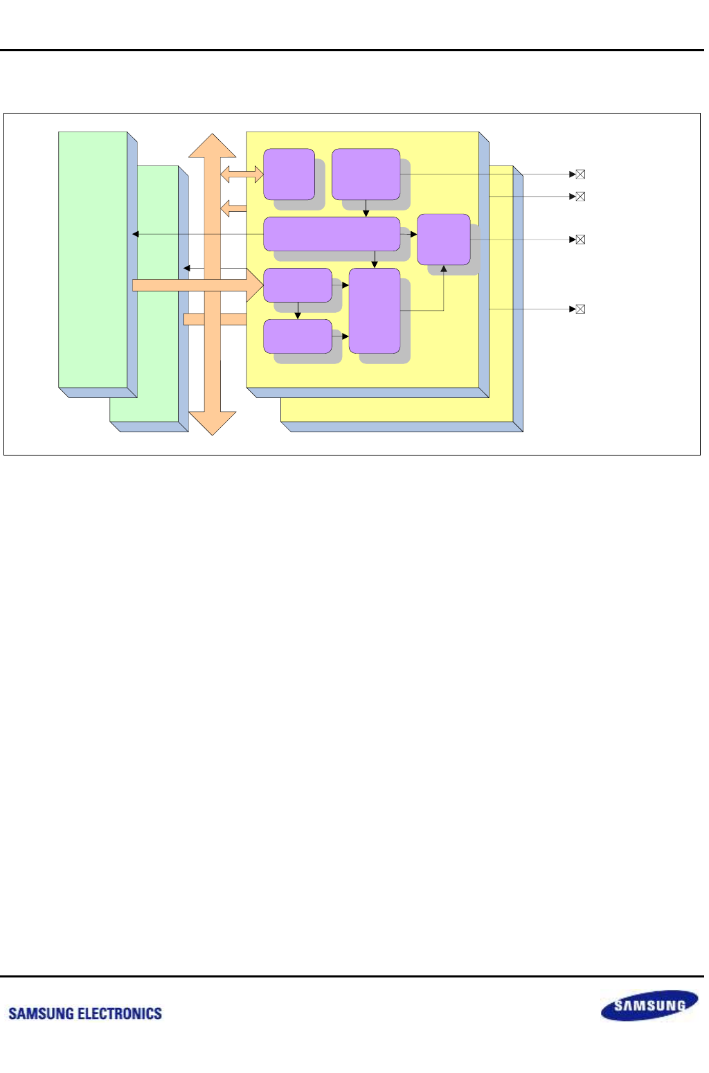
Samsung Confidential
S5P6818_UM 35 Display Controller (DPC)
35-2
Preliminary product information describes products that are in development, for which full characterization data and
associated errata are not yet available. Specifications and information herein are subject to change without notice.
35.3 Block Diagram
Figure 35-1 Display Controller
Peripheral Bus
Secondary Sync Generator
PVCLK
PHSYNC/
PVSYNC/
PDE
Primary Sync Generator
RGB2YC
DITHER
CLOCK GEN
SYNC GEN
Output Format
Contoroller
HOST IF
Secondary Multi-Layer Controller
Primary Multi-Layer Controller
R8G8B8
Delay
Controller
SVCLK
SHSYNC/
SVSYNC/
SDE
SVD
nexell / ys.kim at 2015.02.12
SAMSUNG Confidential
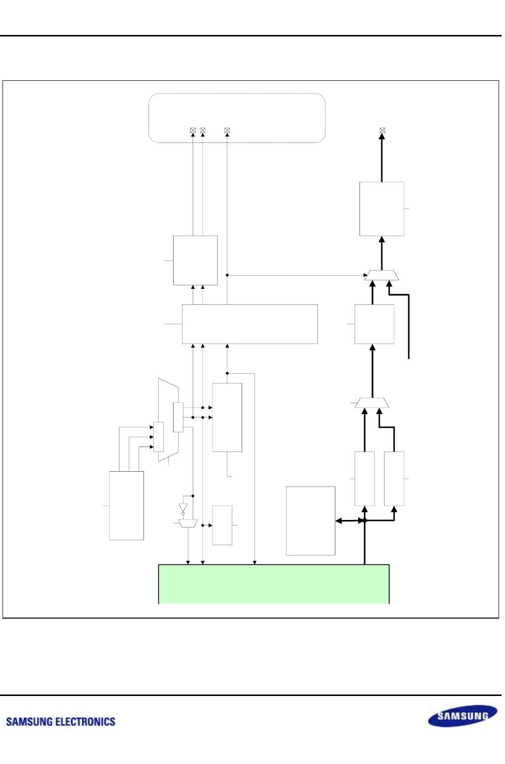
Samsung Confidential
S5P6818_UM 35 Display Controller (DPC)
35-3
Preliminary product information describes products that are in development, for which full characterization data and
associated errata are not yet available. Specifications and information herein are subject to change without notice.
35.4 Sync Generator
Figure 35-2 Sync Generator
Primary DPC
Only
Output Pixel
Format Converter
RGBMODE
HSYNC/VSYNC/FIELD
Generator
DE Generator
Sync Polarity
Interrupt
Controller
0
ENCENB
FIELD
VSYNC
HSYNC
POLFIELD
0
1
FIELD
VSYNC HSYNC
VSYNC
DE
DPCENB/SCANMODE/
HTOTAL/HSWIDTH/HASTART/HAEND/
VTOTAL/VSWIDTH/VASTART/VAEND/
EVTOTAL/EVSWIDTH/EVASTART/EVAEND/
VSSOFFSET/VSEOFFSET/EVSSOFFSET/EVSEOFFSET
HASTART/HAEND
VASTART/VAEND
EVASTART/EVAEND & SCANMODE & ~ENCENB
INTENB/INTPEND
DELAYVS/DELAYHS/
DELAYSP/DELAYLP/DELAYREV
RGBMODE
RGB to YC
Converter
Dithering
POLVSYNC/
POLHSYNC
FORMAT/
SWAPRB & RGBMODE/
YCORDER & ~RGBMODE
YCRANGE
RDITHER/GDITHER/BDITHER
R8G8B8
R8G8B8
Y8U8V8
YUV/RGB
0000
Delay
0
1
0
1Delay
DELAYRGB
DE
HSYNC
VSYNC
DE
Multi-Layer Controller
PVD
PDE
PHSYNC
PVSYNC
Secondary UP scaler
RGB
nexell / ys.kim at 2015.02.12
SAMSUNG Confidential
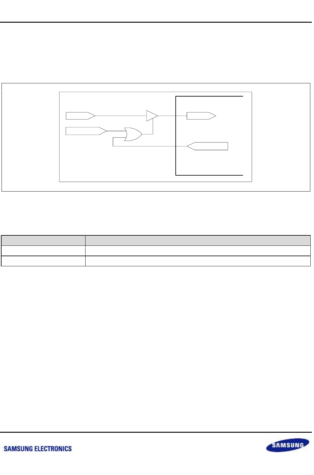
Samsung Confidential
S5P6818_UM 35 Display Controller (DPC)
35-4
Preliminary product information describes products that are in development, for which full characterization data and
associated errata are not yet available. Specifications and information herein are subject to change without notice.
35.4.1 Clock Generation
35.4.1.1 Peripheral Clock Generation
The PCLK is used when the CPU accesses the registers of the DPC. Users can adjust the DPC clock by setting
the PCLKMODE for the user's purpose.
Figure 35-3 Peripheral Clock Generation
Table 35-1 PCLK Mode
PCLKMODE
Brief Description
0
Always Disable
1
Always enabled.
CPU Access
PCLKMODE
PCLK PCLK
DPC
nexell / ys.kim at 2015.02.12
SAMSUNG Confidential
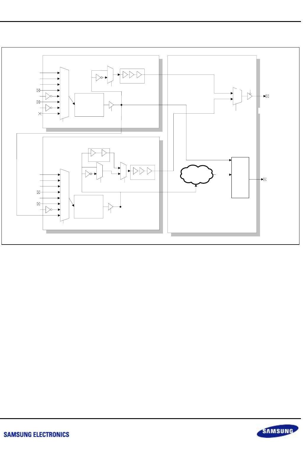
Samsung Confidential
S5P6818_UM 35 Display Controller (DPC)
35-5
Preliminary product information describes products that are in development, for which full characterization data and
associated errata are not yet available. Specifications and information herein are subject to change without notice.
35.4.1.2 Video Clock Generation
Figure 35-4 Video Clock Generation
The DPC can create an output clock via various clock sources. The clocks for creating an output clock are 2-PLL,
PADCLK (P/SCLK, ACLK), etc.
The sync generator uses the VCLK and the VCLK2 as clock sources. The VCLK is a clock for the operation of a
pixel unit. The VCLK2 is a clock for pixel output. Therefore, the VCLK is one clock per pixel and the VCLK2 is 1 to
6 clocks per pixel depending on the output format. In the RGB and ITU-R BT.601A formats, which output one pixel
data per clock, the VCLK and the VCLK2 share the same clock. In the MRGB, the ITU-R BT.601B, the ITU-R
BT.601 (8-bit) and the ITU-R BT.656 formats, which output one pixel data per two clocks, the VCLK should divide
the VCLK2 by 2. Since the VCLK should divide the VCLK2 by 2, Clock Generator1 should use the output of Clock
Generator0 as the clock source. Users can select the output source by using the PADCLKSEL. The selection of
the PADCLKSEL is not related to the operation of the sync generator. In general, VCLK2 is used as the output
clock. If, however, a display device using a dual edge is connected, the VCLK is used as the output clock.
Clock Generator 0 Sync Generator
Clock Generator 1
Divide =
1 /
(CLKDIV0[7:0]+1)
0
1
2
3
4
5
6
7
CLKSRCSEL0[2:0]
0
1
2
3
4
5
6
7
PLL0
PLL1
PLL2
Divide =
1 /
(CLKDIV1[7:0]+1)
CLKSRCSEL1[2:0]
0
1
PADCLKSEL
OUTCLKEN
B
P(S)VCLK
VCLK2
( PixelCLKxN)
Pixel Processing
Output Pixel
Format Converter
RGB/YU
V
P(S)VD
HDMI CLK
PLL3
PLL0
PLL1
PLL2
HDMI CLK
PLL3
CLKGENENB
CLKGENENB
VCLK
( PixelCLK)
0
1
OUTCLKINV1
OUTCLKDELAY1[4:0]
1
0
OUTCLKSET1
Source Clock ½
delay cell
0
1
OUTCLKINV0
OUTCLKDELAY1[4:0]
nexell / ys.kim at 2015.02.12
SAMSUNG Confidential
Samsung Confidential
S5P6818_UM 35 Display Controller (DPC)
35-6
Preliminary product information describes products that are in development, for which full characterization data and
associated errata are not yet available. Specifications and information herein are subject to change without notice.
Table 35-2 Recommend Clock Settings
Format
CLKSRCSEL0
CLKDIV0
CLKSRCSEL1
CLKDIV1
OUTCLKSEL1
PADCLKSEL
RGB, ITU-R BT.601A
0 to 6
0 to 256
7
0
0
1
MRGB, ITU-R
BT.601B,
601 (8-bit), 656,MPU
(i80)
0 to 6
0 to 256
7
1
0
1
MRGB (- Dual edge )
0 to 6
0 to 256
7
1
1
0
SRGB888
0 to 6
0 to 256
7
6
0
2
SRGBD8888
0 to 6
0 to 256
7
4
0
1
The DPC can adjust the polarity and phase of the output clock. The OUTCLKINV adjusts the polarity of the output
clock and the OUTCLKDELAY, OUTCLKSEL adjusts the phase of the output clock.
Basically, the DPC outputs data to be fetched at the falling edge and the OUTCLKINV is set as "0". For a display
device that fetches the clock at the rising edge, the OUTCLKINV should be set as "1" to invert the output clock.
nexell / ys.kim at 2015.02.12
SAMSUNG Confidential

Samsung Confidential
S5P6818_UM 35 Display Controller (DPC)
35-7
Preliminary product information describes products that are in development, for which full characterization data and
associated errata are not yet available. Specifications and information herein are subject to change without notice.
35.4.2 Format
The sync generator can receive RGB888 data from the MLC and display the data in various formats.
The formats that can be displayed by the primary sync generator are listed in below Table.
Table 35-3 Data format for Primary Sync Generator
Outp
ut
form
at
RG
B
MO
DE
FOR
MAT
C
L
K
PVD
2
3
2
2
2
1
2
0
1
9
1
8
1
7
1
6
1
5
1
4
1
3
1
2
1
1
1
0
9
8
7
6
5
4
3
2
1
0
RGB
555
1
0
-
R
4
R
3
R
2
R
1
R
0
G
4
G
3
G
2
G
1
G
0
B
4
B
3
B
2
B
1
B
0
RGB
565
1
-
R
4
R
3
R
2
R
1
R
0
G
5
G
4
G
3
G
2
G
1
G
0
B
4
B
3
B
2
B
1
B
0
RGB
666
2
-
R
5
R
4
R
3
R
2
R
1
R
0
G
5
G
4
G
3
G
2
G
1
G
0
B
5
B
4
B
3
B
2
B
1
B
0
RGB
888
3
-
R
7
R
6
R
5
R
4
R
3
R
2
R
1
R
0
G
7
G
6
G
5
G
4
G
3
G
2
G
1
G
0
B
7
B
6
B
5
B
4
B
3
B
2
B
1
B
0
MRG
B555
A
4
1s
t
G
2
G
1
G
0
B
4
B
3
B
2
B
1
B
0
2
n
d
R
4
R
3
R
2
R
1
R
0
G
4
G
3
MRG
B555
B
5
1s
t
G
2
G
1
G
0
B
4
B
3
B
2
B
1
B
0
2
n
d
R
4
R
3
R
2
R
1
R
0
G
4
G
3
MRG
B565
6
1s
t
G
2
G
1
G
0
B
4
B
3
B
2
B
1
B
0
2
n
d
R
4
R
3
R
2
R
1
R
0
G
5
G
4
G
3
MRG
B666
7
1s
t
G
2
G
1
G
0
B
5
B
4
B
3
B
2
B
1
B
0
2
n
d
R
5
R
4
R
3
R
2
R
1
R
0
G
5
G
4
G
3
MRG
B888
A
8
1s
t
G
3
G
2
G
1
G
0
B
7
B
6
B
5
B
4
B
3
B
2
B
1
B
0
2
n
d
R
7
R
6
R
5
R
4
R
3
R
2
R
1
R
0
G
7
G
6
G
5
G
4
MRG
B888
9
1s
t
G
4
G
3
G
2
B
7
B
6
B
5
B
4
B
3
G
0
B
2
B
1
B
0
nexell / ys.kim at 2015.02.12
SAMSUNG Confidential

Samsung Confidential
S5P6818_UM 35 Display Controller (DPC)
35-8
Preliminary product information describes products that are in development, for which full characterization data and
associated errata are not yet available. Specifications and information herein are subject to change without notice.
Outp
ut
form
at
RG
B
MO
DE
FOR
MAT
C
L
K
PVD
2
3
2
2
2
1
2
0
1
9
1
8
1
7
1
6
1
5
1
4
1
3
1
2
1
1
1
0
9
8
7
6
5
4
3
2
1
0
B
2
n
d
R
7
R
6
R
5
R
4
R
3
G
7
G
6
G
5
R
2
R
1
R
0
G
1
ITU-
R
BT.6
56
BT.6
01(8
bit)
0
10
1s
t
C
b
7
C
b
6
C
b
5
C
b
4
C
b
3
C
b
2
C
b
1
C
b
0
2
n
d
Y
7
Y
6
Y
5
Y
4
Y
3
Y
2
Y
1
Y
0
3r
d
C
r7
C
r6
C
r5
C
r4
C
r3
C
r2
C
r1
C
r0
4t
h
Y
7
Y
6
Y
5
Y
4
Y
3
Y
2
Y
1
Y
0
ITU-
R
BT.6
01A
12
1s
t
Y
7
Y
6
Y
5
Y
4
Y
3
Y
2
Y
1
Y
0
C
b
7
C
b
6
C
b
5
C
b
4
C
b
3
C
b2
C
b
1
C
b
0
2
n
d
Y
7
Y
6
Y
5
Y
4
Y
3
Y
2
Y
1
Y
0
C
r7
C
r6
C
r5
C
r4
C
r3
Cr
2
C
r1
C
r
0
ITU-
R
BT.6
01B
13
1s
t
Y
7
Y
6
Y
5
Y
4
Y
3
Y
2
Y
1
Y
0
C
b
7
C
b
6
C
b
5
C
b
4
C
b
3
C
b2
C
b
1
C
b
0
2
n
d
C
r7
C
r6
C
r5
C
r4
C
r3
Cr
2
C
r1
C
r
0
4096
Color
X
1
-
R
0
G
0
B
0
R
1
B
1
G
1
R
2
G
2
16
Level
Gray
X
3
-
Y
0
Y
1
Y
2
Y
3
Y
4
Y
5
Y
6
Y
7
Up to 24-bit data is available in the primary sync generator. If, however, the display format is not RGB666 or
RGB888, the higher 8-bit is not used.
nexell / ys.kim at 2015.02.12
SAMSUNG Confidential
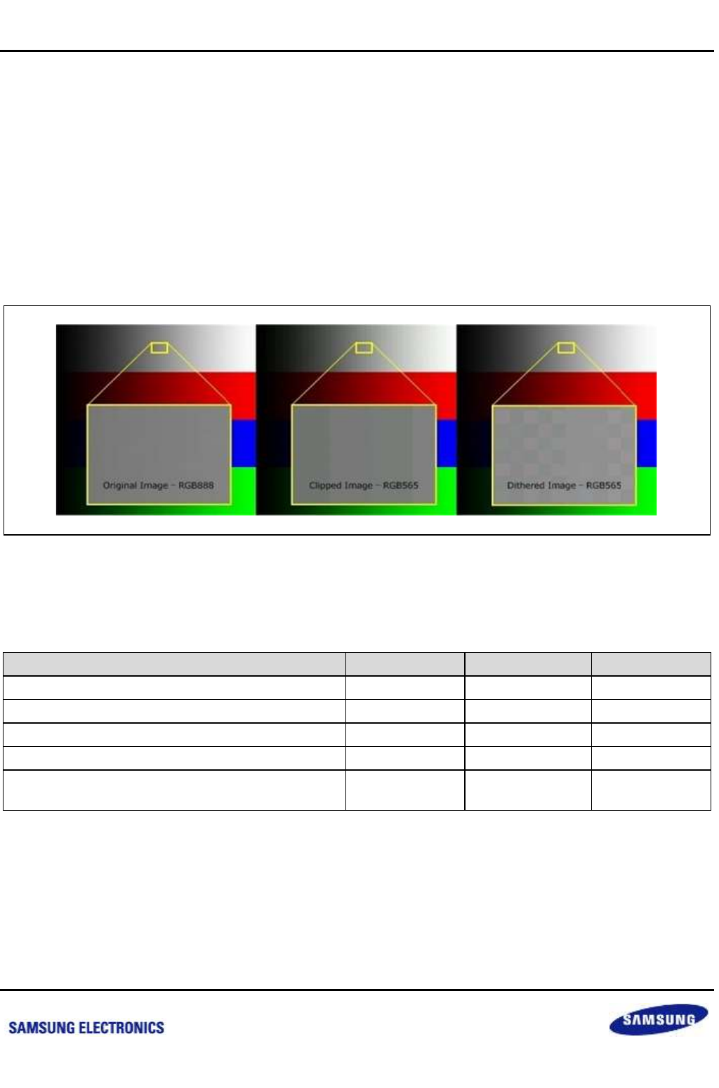
Samsung Confidential
S5P6818_UM 35 Display Controller (DPC)
35-9
Preliminary product information describes products that are in development, for which full characterization data and
associated errata are not yet available. Specifications and information herein are subject to change without notice.
35.4.2.1 RGB Format
In the RGB format, data are displayed in the order of blue components, green components and red components
based on the lower data. However, a user can swap the display of red components and blue components by
setting the SWAPRB as "1".
In addition, the DPC supports the Dithering effect in RGB format. All RGB data transmitted from the MLC have 8-
bit data width. Therefore, if the data width of each component is less than 8-bit, as in RGB565 and RGB666
display, the lower bits are discarded. In such cases, the display quality can be compensated by the Dithering
effect.
When RGB images are displayed as RGB565, the dithered image shows the difference from the image displayed,
as shown in below Figure, after the unused lower bits are simply discarded.
Figure 35-5 RGB Dithering
The RGB Dithering is set by RDITHER, GDITHER and BDITHER and the setting values by output formats are
listed in below Table.
Table 35-4 Recommend Setting for RGB Dithering
Output Format
RDITHER
GDITHER
BDITHER
RGB555, MRGB555A, MRGB555B
5-bit Dither
5-bit Dither
5-bit Dither
RGB565, MRGB565
5-bit Dither
6-bit Dither
5-bit Dither
RGB666, MRGB666
6-bit Dither
6-bit Dither
6-bit Dither
STN - 4096 Color, 16 Level Gray
4-bit Dither
4-bit Dither
4-bit Dither
RGB888, MRGB888A/B, ITU-R BT.656, ITU-R
BT.601A/B
Bypass
Bypass
Bypass
nexell / ys.kim at 2015.02.12
SAMSUNG Confidential
Samsung Confidential
S5P6818_UM 35 Display Controller (DPC)
35-10
Preliminary product information describes products that are in development, for which full characterization data and
associated errata are not yet available. Specifications and information herein are subject to change without notice.
35.4.2.2 YCbCr Format
Since the DPC only receives RGB data from the MLC, it outputs the data after converting the RGB data to YCbCr
data for the ITU-R BT.656 display or the ITU-R BT.601 display.
The DPC converts RGB data to YCbCr data by using the following formulae:
The formula for RGB to YCbCr conversion
Y= 0.229 R + 0.587 G + 0.114 B
Cb = – 0.169 R – 0.331 G + 0.5 B
Cr = 0.5 R – 0.419 G – 0.081 B
When ITU-R BT.601 B external display device is used, the user can change the data output order by adjusting the
YCORDER. The output data for YCORDER can be changed as listed in below Table.
Table 35-5 Output Order for ITU-R BT. 601 B
YCORDER
0
1
CLK
1st
2nd
1st
2nd
VD[15]
Y[7]
Y[7]
VD[14]
Y[6]
Y[6]
VD[13]
Y[5]
Y[5]
VD[12]
Y[4]
Y[4]
VD[11]
Y[3]
Y[3]
VD[10]
Y[2]
Y[2]
VD[9]
Y[1]
Y[1]
VD[8]
Y[0]
Y[0]
VD[7]
Cr[7]
Cb[7]
Cb[7]
Cr[7]
VD[6]
Cr[6]
Cb[6]
Cb[6]
Cr[6]
VD[5]
Cr[5]
Cb[5]
Cb[5]
Cr[5]
VD[4]
Cr[4]
Cb[4]
Cb[4]
Cr[4]
VD[3]
Cr[3]
Cb[3]
Cb[3]
Cr[3]
VD[2]
Cr[2]
Cb[2]
Cb[2]
Cr[2]
VD[1]
Cr[1]
Cb[1]
Cb[1]
Cr[1]
VD[0]
Cr[0]
Cb[0]
Cb[0]
Cr[0]
nexell / ys.kim at 2015.02.12
SAMSUNG Confidential
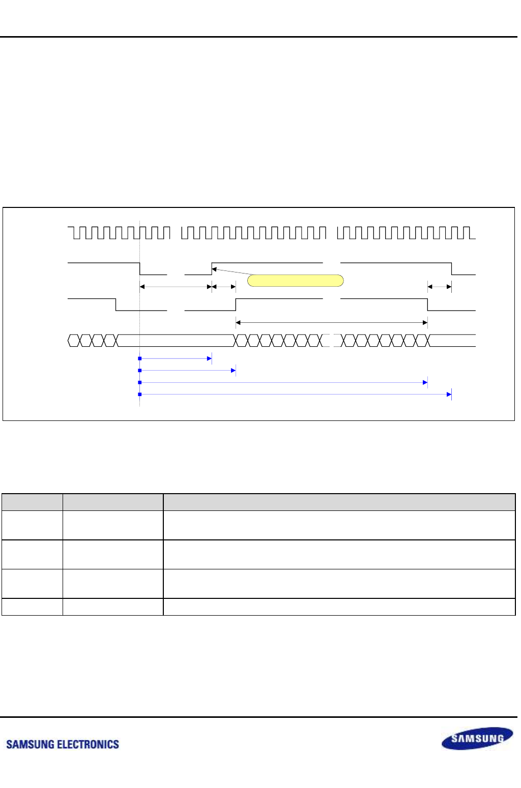
Samsung Confidential
S5P6818_UM 35 Display Controller (DPC)
35-11
Preliminary product information describes products that are in development, for which full characterization data and
associated errata are not yet available. Specifications and information herein are subject to change without notice.
35.4.3 Sync Signals
The sync generator creates sync signals with various timings. The primary sync generator transmits HSYNC,
VSYNC and DE signals to the outside to provide timing interfaces for external display devices. Users can program
each sync signal setting to create the timings required from external display devices.
35.4.3.1 Horizontal Timing Interface
HSYNC and DE signals are used for Horizontal Sync. The horizontal timing consists of tHSW, tHBP, tHFP and
tAVW as shown in below Figure.
Figure 35-6 Horizontal Timing
Each symbol in the above figure is described in below Table.
Table 35-6 Horizontal Timing Symbols
Symbol
Brief
Remark
tHSW
Horizontal Sync
Width
Number of VCLKs in the section where the horizontal sync pulse is active
tHBP
Horizontal Back
Porch
Number of VCLKs in a section from the end point of the horizontal sync
pulse to the start point of the horizontal active
tHFP
Horizontal Front
Porch
Number of VCLKs in a section from the end point of the horizontal active to
the start point of the horizontal sync pulse
tAVW
Active Video Width
Number of VCLKs in a horizontal active section
POLHSYNC = 0 (Low active)
tHSW tHBP tHFP
tAVW
Horizontal Blank
VCLK
HSYNC
DE
PVD
//
//
//
//
//
HSWIDTH+1
HASTART+1
HAEND+1
HTOTOAL+1
//
//
nexell / ys.kim at 2015.02.12
SAMSUNG Confidential
Samsung Confidential
S5P6818_UM 35 Display Controller (DPC)
35-12
Preliminary product information describes products that are in development, for which full characterization data and
associated errata are not yet available. Specifications and information herein are subject to change without notice.
The horizontal timing setting registers are HSWIDTH, HASTART, HAEND and HTOTAL and each register setting
is described in below Table. Each unit of the registers is based on VCLK and each value is set as "total number –
1".
Table 35-7 Horizontal Timing Registers
Register
Formula
Remark
HSWIDTH
tHSW – 1
Number of VCLKs in a section from the start point of the
horizontal sync pulse to the end point of the horizontal sync
pulse – 1
HASTART
tHSW + tHBP – 1
Number of VCLKs in a section from the start point of the
horizontal sync pulse to the start point of the horizontal active – 1
HAEND
tHSW + tHBP + tAVW – 1
Number of VCLKs in a section from the start point of the
horizontal sync pulse to the end point of the horizontal active – 1
HTOTAL
tHSW + tHBP + tAVW + tHFP
– 1
Number of VCLKs in a section from the start point of the
horizontal sync pulse to the start point of the next horizontal sync
pulse – 1
The POLHSYNC is used to change the polarity of the HSYNC signal to be output to the outside. The horizontal
sync pulse is low active when the POLHSYNC is "0", while the horizontal sync pulse is high active when the
POLHSYNC is "1". The polarity of the Data Enable (DE) signal to be output to the outside cannot be changed and
the section that outputs valid data comes into high state.
nexell / ys.kim at 2015.02.12
SAMSUNG Confidential
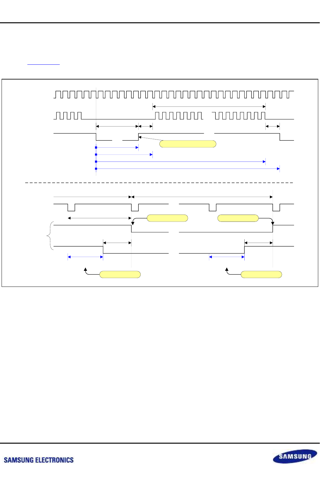
Samsung Confidential
S5P6818_UM 35 Display Controller (DPC)
35-13
Preliminary product information describes products that are in development, for which full characterization data and
associated errata are not yet available. Specifications and information herein are subject to change without notice.
35.4.3.2 Vertical Timing Interface
The VSYNC signal is used for the Vertical Sync. The vertical timing consists of tVSW, tVBP, tVFP and tAVH as
shown in Figure 35-9. In addition, the relation between the Vertical Sync and the Horizontal Sync is established by
tVSSO and tVSEO.
Figure 35-7 Vertical Timing
POLVSYNC = 0 (Low active)
tVSW tVBP tVFP
tAVH
Vertical Blank
//
//
VSWIDTH+1
VASTART+1
VAEND+1
VTOTOAL+1
//
HSYNC
DE
VSYNC
tVSSO tVSEO
VSSOFFSET
= tHTOTAL - tVSSO
VSEOFFSET
= HTOTAL - tVSEO
Vertical Front Porch
//
//
//
Vertical Sync Width
tHTOTAL
HSYNC
VSYNC
VSSOFFSET = 0 VSEOFFSET = 0
VSSOFFSET != 0 VSEOFFSET != 0
nexell / ys.kim at 2015.02.12
SAMSUNG Confidential
Samsung Confidential
S5P6818_UM 35 Display Controller (DPC)
35-14
Preliminary product information describes products that are in development, for which full characterization data and
associated errata are not yet available. Specifications and information herein are subject to change without notice.
Each symbol in the above figure is described in below Table.
Table 35-8 Vertical Timing Symbols
Symbol
Brief
Remark
tVSW
Vertical Sync Width
Number of lines in the section where the vertical sync pulse is active
tVBP
Vertical Back Porch
Number of lines in the section from the end point of the vertical sync pulse to
the start point of the next vertical active
tVFP
Vertical Front
Porch
Number of lines in the section from the end point of the vertical active to the
start point of the vertical sync pulse
tAVH
Active Video Height
Number of lines in the vertical active section
tHTOTAL
Horizontal Total
Number of total VCLKs in a horizontal cycle where the horizontal active
section and the horizontal blank section are added
tVSSO
Vertical Sync Start
Offset
Number of VCLKs in a section from the start point of the vertical sync pulse
to the start point of the horizontal sync pulse
tVSEO
Vertical Sync End
Offset
Number of the VCLKs in a section from the end point of the horizontal sync
pulse to the start point of the horizontal sync pulse
The vertical timing setting registers are VSWIDTH, VASTART, VAEND and VTOTAL and each register setting is
described in below Table. The units of VSWIDTH, VASTART, VAEND and VTOTAL are based on the horizontal
lines and their values are set as total number–1. The units of VSSOFFSET and VSEOFFSET are based on the
VCLK.
Table 35-9 Vertical Timing Registers
Register
Formula
Remark
VSWIDTH
tVSW – 1
Number of lines in a section from the start point of the vertical sync
pulse to the end point of the vertical sync pulse – 1
VASTART
tVSW + tVBP – 1
Number of VCLKs in a section from the start point of the vertical
sync pulse to the start point of the vertical active – 1
VAEND
tVSW + tVBP + tAVH – 1
Number of lines in a section from the start point of the vertical sync
pulse to the end point of the vertical active – 1
VTOTAL
tVSW + tVBP + tAVH +
tVFP – 1
Number of lines in a section from the start point of the vertical sync
pulse to the next point of the vertical sync pulse – 1
VSSOFFSET
If tVSSO is 0 then 0, else
tHTOTAL – tVSSO
Number of VCLKs in a section from the start point of the last
horizontal sync pulse in the Vertical Front Porch to the start point of
the vertical sync pulse. If, however, VSSOFFSET is equal to
tHTOTAL, the value is set as "0".
VSEOFFSET
If tVSEO is 0 then 0, else
tHTOTAL – tVSEO
Number of VCLKs in a section from the start point of the last
horizontal sync pulse in the Vertical Front Porch to the start point of
the vertical sync pulse. If, however, VSEOFFSET is equal to
tHTOTAL, the value is set as "0".
The POLVSYNC is used to change the polarity of the VSYNC signal to be output to the outside. The vertical sync
pulse is low active when the POLVSYNC is "0", while the vertical sync pulse is high active when the POLVSYNC
is "1".
nexell / ys.kim at 2015.02.12
SAMSUNG Confidential
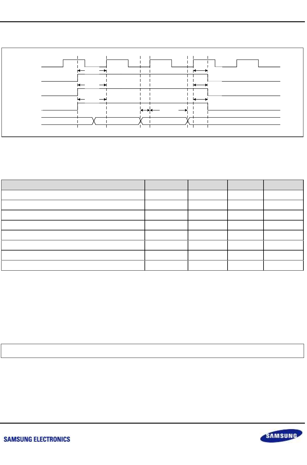
Samsung Confidential
S5P6818_UM 35 Display Controller (DPC)
15
Preliminary product information describes products that are in development, for which full characterization data and
associated errata are not yet available. Specifications and information herein are subject to change without notice.
35.4.3.3 AC Timing
Figure 35-8 Vertical Timing
Condition: VCLK 40 MHz (25 ns)
Table 35-10 Sync Timing Symbols
Description
Symbol
Min.
Max.
Unit
VSync setup time
tVSS
12.13
–
ns
VSync hold time
tVSH
12.28
–
ns
HSync setup time
tHSS
12.27
–
ns
HSync hold time
tHSH
12.26
–
ns
DE setup time
tDES
12.1
–
ns
DE hols time
tDEH
12.4
–
ns
PVD setup time
tPVDS
8.8
–
ns
PVD hold time
tPVDH
12.87
–
ns
35.4.3.4 UPSCALER (Only Secondary Display)
UPSCALER performs the function of horizontal bilinear filter upscale MLC OUT Layer. It is selectable whether to
scale with UPSCALEENB Setting.
UPSCALEENB Setting:
UPSCALE = (MLC Screen Width – 1) (1<<11) / (destination width – 1)
tVSS tVSH
tHSS
tDES
tPVDS tPVDH
tDEH
tHSH
VCLK
VSync
HSync
DE
PVD
nexell / ys.kim at 2015.02.12
SAMSUNG Confidential
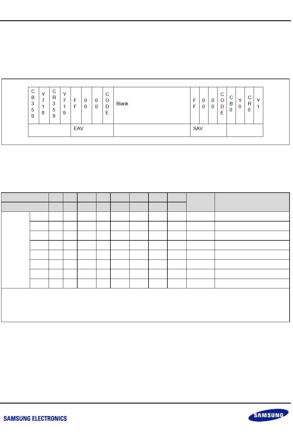
Samsung Confidential
S5P6818_UM 35 Display Controller (DPC)
16
Preliminary product information describes products that are in development, for which full characterization data and
associated errata are not yet available. Specifications and information herein are subject to change without notice.
35.4.3.5 Embedded Sync
The ITU-R BT.656 output does not need the separate Sync Signal pin to transmit signals to the outside. The Sync
information is transmitted along with data via a data pin. At this time, the Sync information is inserted as a
separate code before the start point of the valid data (SAV) and after the end point of the valid data (EAV). The
Sync information included in data is as shown in below Figure.
Figure 35-9 Data stream format with SAV/EAV
The SAV and EAV consist of [FF, 00, 00, CODE]. Each of the SAV and EAV codes contains Field(F), VSYNC(V)
and HSYNC(H) data and each code is composed as follows:
Table 35-11 Embedded Sync Code
Bit
7
6
5
4
3
2
1
0
Hex
Brief Description
Function
1
F
V
H
P3
P2
P1
P0
(FVH)
0
1
0
0
0
0
0
0
0
80h
SAV of odd field
1
1
0
0
1
1
1
0
1
9Dh
EAV of odd field
2
1
0
1
0
1
0
1
1
ABh
SAV of odd blank
3
1
0
1
1
0
1
1
0
B6h
EAV of odd blank
4
1
1
0
0
0
1
1
1
C7h
SAV of even field
5
1
1
0
1
1
0
1
0
DAh
EAV of even field
6
1
1
1
0
1
1
0
0
ECh
SAV of even blank
7
1
1
1
1
0
0
0
1
F1h
EAV of even blank
F: Field select (0 = Odd field, 1 = Even field)
V: Vertical blanking ( 0 = Active, 1 = blank)
H: SAV/EAV (0 = SAV, 1 = EAV)
Parity: P3 = V xor H, P2 = F xor H, P1 = F xor V, P0 = F xor V xor H
nexell / ys.kim at 2015.02.12
SAMSUNG Confidential
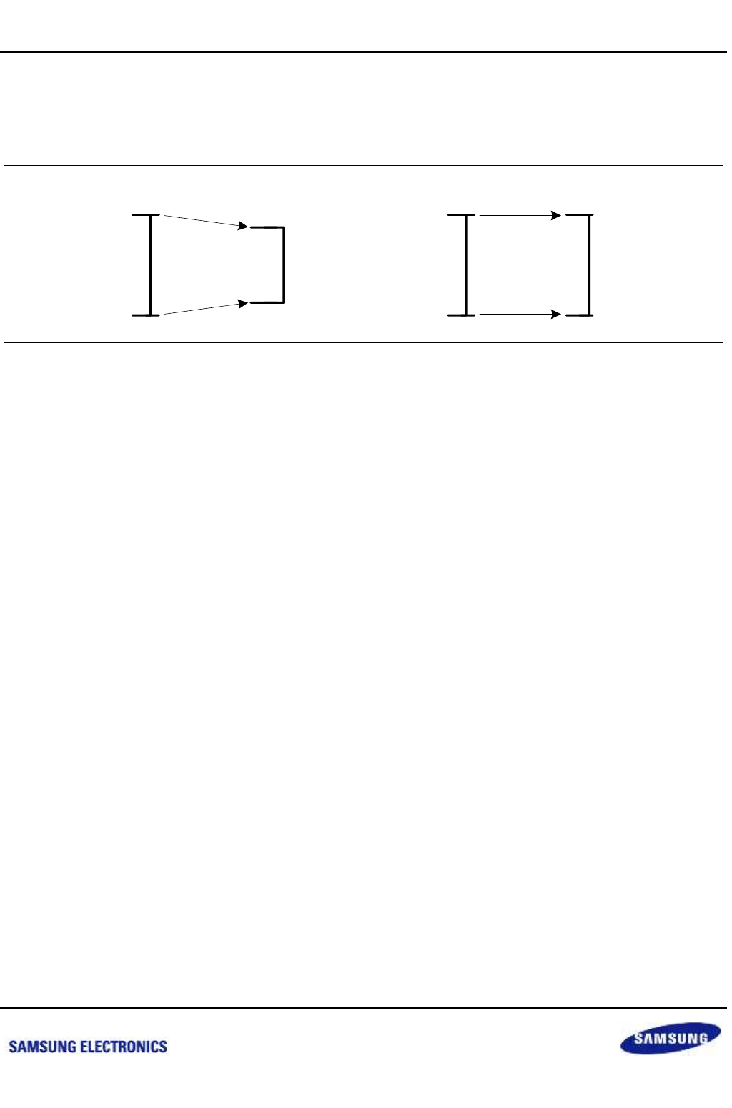
Samsung Confidential
S5P6818_UM 35 Display Controller (DPC)
35-17
Preliminary product information describes products that are in development, for which full characterization data and
associated errata are not yet available. Specifications and information herein are subject to change without notice.
In the ITU-R BT.656 format, SAV/EAV codes are inserted in data by setting the SEAVENB as "1". However, since
the SAV/EAV codes are transmitted via a data pin, the range of the data should be restricted, to distinguish the
codes from the data. Users can restrict the data range by using YCRANGE. Below Figure shows that the result of
the color space conversion changing RGB data to YCbCr data varies depending on YCRANGE.
Figure 35-10 Y/C Clip
If YCRANGE is set as "0", a Y value between 0 and 15 is changed to 16 and a Y value between 236 and 255 is
changed to 235. In a similar way, Cb/Cr values between 0 and 15 are changed to 16 and Cb/Cr values between
241 and 255 are changed to 240. If YCRANGE is set as "1", all Y/Cb/Cr values are bypassed.
255
0
235(Y)
240(Cb/Cr)
16
RGB2YC = 0
YCbCr
255
0
RGB2YC = 1
YCbCr
255
0
nexell / ys.kim at 2015.02.12
SAMSUNG Confidential
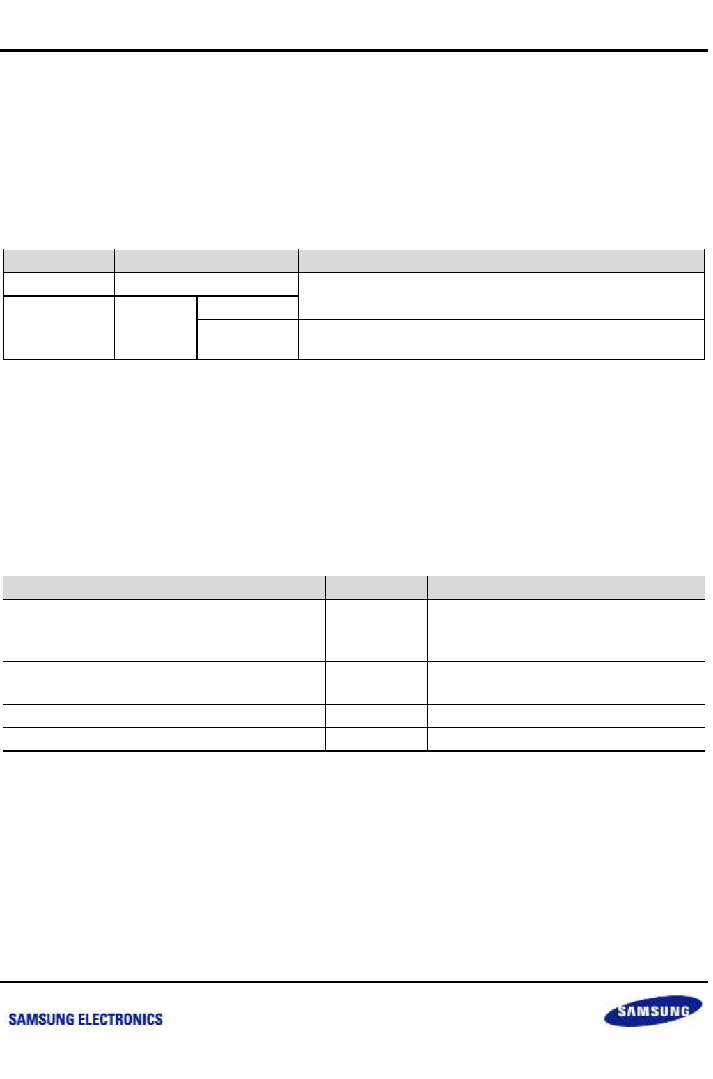
Samsung Confidential
S5P6818_UM 35 Display Controller (DPC)
35-18
Preliminary product information describes products that are in development, for which full characterization data and
associated errata are not yet available. Specifications and information herein are subject to change without notice.
35.4.4 Scan Mode
The sync generator supports interlace display as well as progressive display. The Scan mode is determined by
SCANMODE. If SCANMODE is "0", the sync generator operates in progressive scan mode. If SCANMODE is "1",
the sync generator operates in interlaced scan mode. In interlaced scan mode, the different vertical timing
interfaces can be set in the odd and even fields separately. The odd field display and the progressive display
share same registers and registers for the even field display exists separately. Registers to create vertical timing
in accordance with the scan mode is listed in below Table.
Table 35-12 Registers Relative to Scan Mode
SCANMODE
Scan Mode
Registers
0
Progressive
VTOTAL, VSWIDTH, VASTART, VAEND, VSSOFFSET,
VSEOFFSET
1
Interlace
Odd field
Even field
EVTOTAL, EVSWIDTH, EVASTART, EVAEND,
EVSSOFFSET, EVSEOFFSET
35.4.5 Delay
The pixel data is more delayed than the final output sync signal due to the processing in the sync generator.
Therefore, users should delay Sync signal output to synchronize the Sync signals with the pixel data. When the
Sync generator processes data, 4-clock is consumed for RGB data and 6-clock is consumed for YCbCr data.
Therefore, for synchronization between Sync signals and data, the output of the Sync signals should be delayed.
In RGB format and ITU-R BT.601A format with the same VCLK and VCLK2, delays of 4-clock and 6-clock should
be set in each format, separately. In the MGRB and the ITU-R BT.656/601B formats, where the VCLK2 is twice
the VCLK, delays of 8-clock and 12-clock should be set in each format, separately.
Table 35-13 Default Delay Value (Unit: VCLK2)
Format
VCLK2:VCLK
DELAYRGB
DELAYHS, DELAYVS, DELAYDE
RGB
1:1
0
Primary TFT: 7
Primary STN: 8
Secondary: 7
MRGB
2:1
0
Primary TFT: 14
Secondary: 14
ITU-R BT.601A
1:1
0
6
ITU-R BT.656, ITU-R BT.601B
2:1
0
12
nexell / ys.kim at 2015.02.12
SAMSUNG Confidential
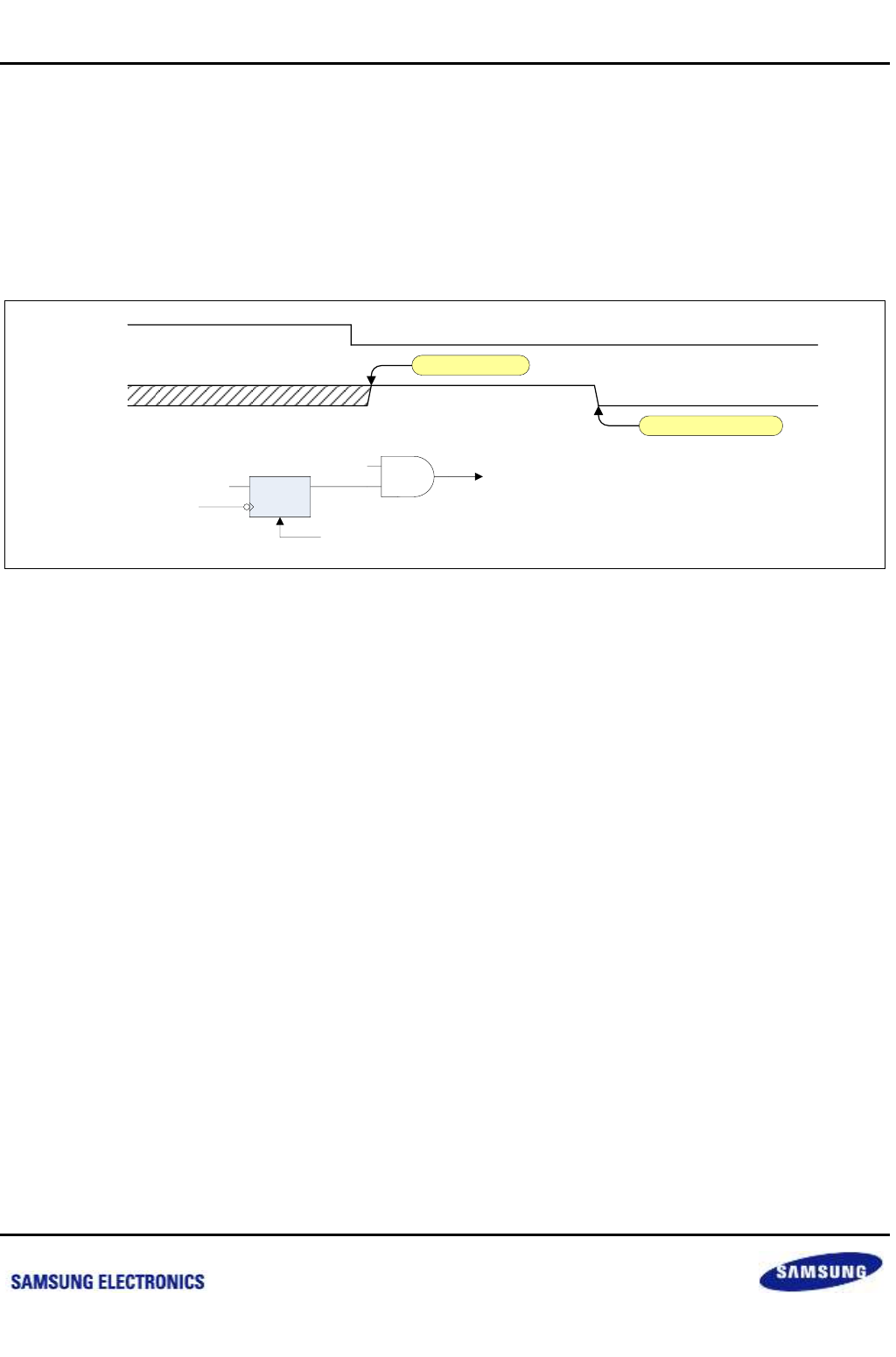
Samsung Confidential
S5P6818_UM 35 Display Controller (DPC)
35-19
Preliminary product information describes products that are in development, for which full characterization data and
associated errata are not yet available. Specifications and information herein are subject to change without notice.
35.4.6 Interrupt
The DPC can generate an interrupt whenever VSYNC occurs.
Interrupt invokes each vertical Sync when TFT LCD Progressive operation. Interrupt invokes each 16 vertical sync
when STN LCD Progressive operation. Interrupt invokes each EVEN field (2 vertical sync) when interlace
operation. The DPC sets INTPEND as "1" if VSYNC occurs and notifies the interrupt generation to the Interrupt
controller if the INTENB is "1". Therefore, users can acknowledge the generation of VSYNC via polling by using
the status of the INTPEND regardless of the generation of interrupts. The INTPEND is cleared by writing "1" to it.
Figure 35-11 Interrupt Block Diagram and Timing
VSYNC
INTPEND
QS
CLR
VSYNC
INTENB
‘1’INTPEND
To Interrupt Controller
INTPEND Clear by CPU
VSYNC interrupt
INTPEND Clear by CPU
nexell / ys.kim at 2015.02.12
SAMSUNG Confidential
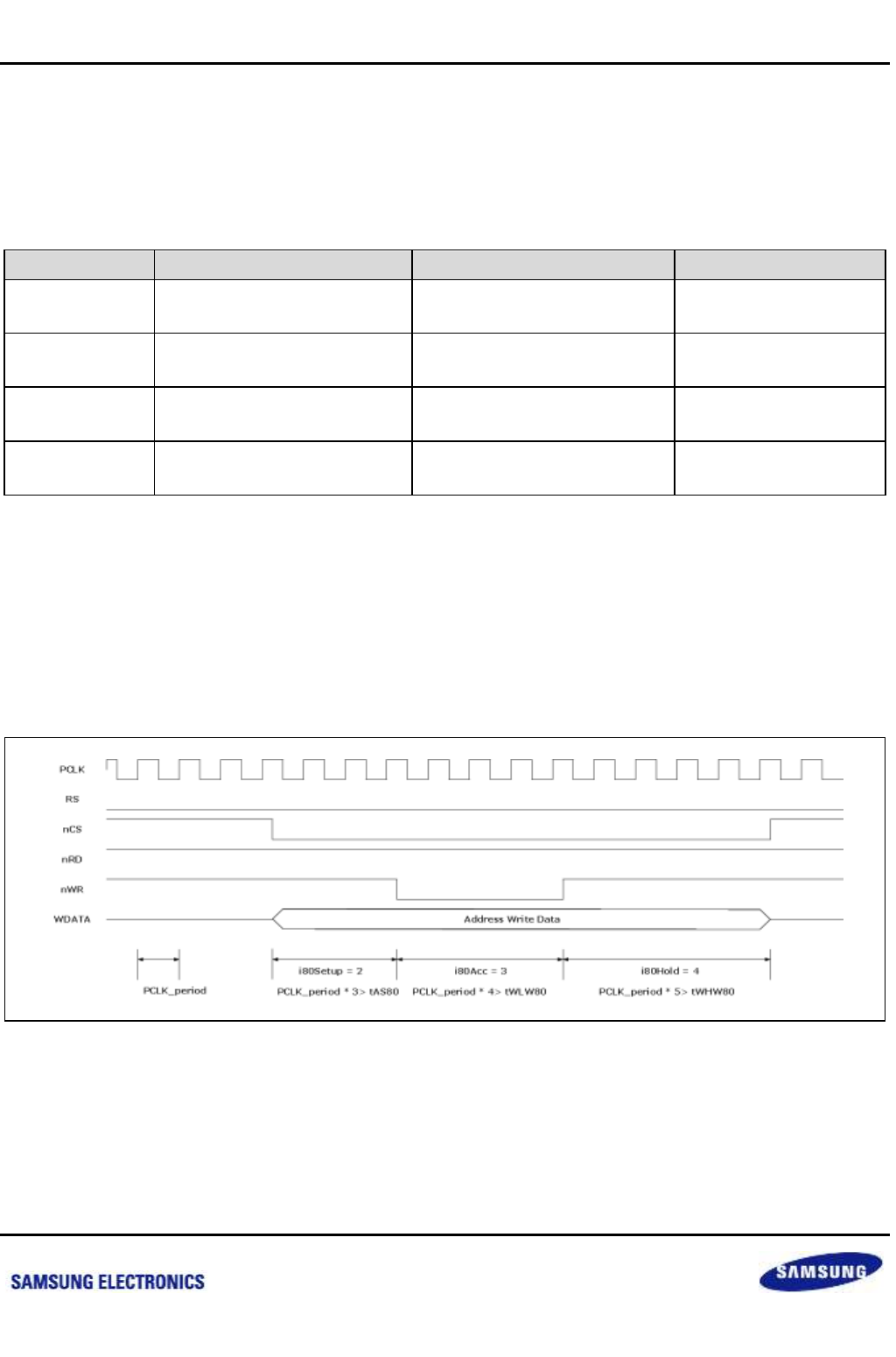
Samsung Confidential
S5P6818_UM 35 Display Controller (DPC)
35-20
Preliminary product information describes products that are in development, for which full characterization data and
associated errata are not yet available. Specifications and information herein are subject to change without notice.
35.4.7 MPU (i80) Type Sync Signals
The sync generator can create signals for MPU LCD interface (i80). MPU LCD interface's signals are consists of
nCS (Chip Select), RS (Register Select), nWR (Write), nRD(Read), and In/Out Data. MPU LCD interface has 4
types of accesses.
Table 35-14 i80 Access Types
Signals
Access Types
Description
Register Address
RS = 0 nWR
Address Write
Write index to IR
[15:0]: C010_2984
[23:16]: C010_2988
RS = 0 nRD
Status Read
Read Internal Status
[23:16]: C010_298C
[15:0]: C010_2994
RS = 1 nWR
Data Write (or Graphic Data
Write )
Write to Control Register and
GRAM
[15:0]: C010_2984
[23:16]: C010_2990
RS = 1 nRD
Data Read
Read from GRAM
[23:16]: C010_2990
[15:0]: C010_2994
S5P6818 has register for communicating with external devices, and it supports 4 types of MPU interface format. In
the case of "writing", lower 16 bits need to be written to C010_2984 address followed by writing upper 8 bits to
C010_2990 address. In the case of "reading", upper 8 bits need to be read from C010_298C address followed by
reading lower 16 bits from C010_2994 address. Actual communication with external devices is occurred when
writing to C010_2990 address and reading from C010_298C address.
To satisfy setup/hold timing of external devices, setting appropriate parameters, which include setup counter,
access counter and hold counter, need to be set in DPCMPUTIME0, DPCMPUTIME1registers. Following is the
timing diagram of write operation.
Figure 35-12 i80Address Write
nexell / ys.kim at 2015.02.12
SAMSUNG Confidential
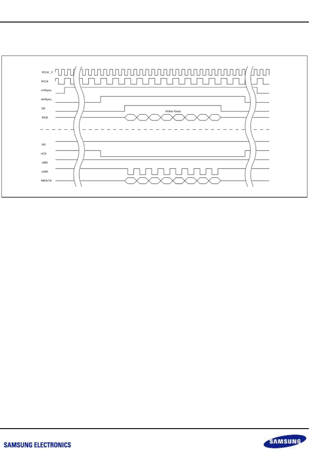
Samsung Confidential
S5P6818_UM 35 Display Controller (DPC)
35-21
Preliminary product information describes products that are in development, for which full characterization data and
associated errata are not yet available. Specifications and information herein are subject to change without notice.
S5P6818 can convert video sync signals to MPU i80 type by setting DPC to i80 mode. Note that VCLK_2 needs to
be 2 times faster than VCLK for MPU i80. Following diagram describes video sync to MPU i80 conversion.
Figure 35-13 i80 Graphic Data Convert
S5P6818 has a "Command Buffer", which is used to send additional information during the VSYNC period.
nexell / ys.kim at 2015.02.12
SAMSUNG Confidential
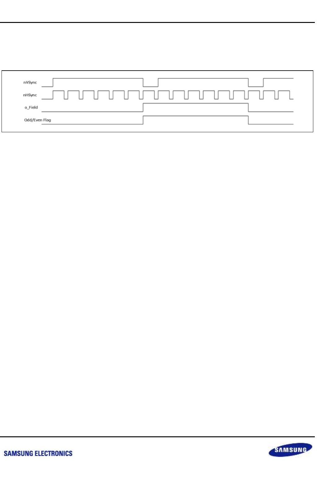
Samsung Confidential
S5P6818_UM 35 Display Controller (DPC)
35-22
Preliminary product information describes products that are in development, for which full characterization data and
associated errata are not yet available. Specifications and information herein are subject to change without notice.
35.4.8 Odd/Even Field Flag
S5P6818 DPC provides DPCRGBSHIFT.FIELDFLAG register which indicates whether currently being displayed
frame is odd or even frame.
Figure 35-14 Odd/Even Flag
nexell / ys.kim at 2015.02.12
SAMSUNG Confidential

Samsung Confidential
S5P6818_UM 35 Display Controller (DPC)
35-23
Preliminary product information describes products that are in development, for which full characterization data and
associated errata are not yet available. Specifications and information herein are subject to change without notice.
35.4.9 Internal Video encoder and DAC
35.4.9.1 Features
Video Encoder
Programmable Luma and Chroma bandwidth
Programmable Saturation, Hue, contrast and Brightness
Support all NTSC and PAL formats (NTSC-M/4.43, PAL-B/D/G/H/I/M/N/Combination N)
Composite output 10 bits to DAC
Video DAC
Maximum 54 MSPS update rate
10-bit current output 1-Channel DAC for CVBS
1.0Vpp single output range
Power down mode (high active)
35.4.9.2 General Description
The video encoder is designed to support all standards and variations of the NTSC and PAL encoding systems.
This includes cross standards pseudo PAL and pseudo NTSC. The video encoder allows independent control of
field rate, chroma subcarrier and the chroma encoding algorithm. Both the luma and chroma bandwidths can be
varied to optimize for various data input conditions. The outputs are separated 10 bits for CVBS (Composite Video
Banking Sync).
The ENCRST signal from the secondary sync generator is connected to RESET pin of the internal video encoder.
Therefore you have to set ENCRST bit to access registers of the internal video encoder. And if ENCRST bit is
clear then all registers of internal video encoder will be reset.
The video DAC is a 10 bit single CMOS Digital-to-Analog Converter for video system. Its maximum conversion
rate is 54 MSPS. It operates at analog power, 3.0 V to 3.6 V and provides full scale output currents of 26.7 mA at
one channel with 37.5 ohmic load for 1.0 V. And it is also adaptable to high-speed application such as video
system.
The ENCRST signal from the secondary sync generator is connected to Power Down pin of the internal video
DAC. Therefore you have to set ENCRST bit to output video signal and clear ENCRST bit to reduce power
consumption when it doesn’t used.
nexell / ys.kim at 2015.02.12
SAMSUNG Confidential
Samsung Confidential
S5P6818_UM 35 Display Controller (DPC)
35-24
Preliminary product information describes products that are in development, for which full characterization data and
associated errata are not yet available. Specifications and information herein are subject to change without notice.
35.4.9.3 Video Encoder Reset Sequence
To reset "Video Encoder", following sequence is needed.
Write "1" at ENCRST Register
Write "1" at CLKGENENB Register
Write "0" at ENCRST Register
Write "0" at CLKGENENB Register
Write "‘1" at ENCRST Register
To power-up DAC PHY, following sequence is needed
Write "1" at 0xC00110F8, [4]
To control Full Scale Output Voltage of DAC PHY, following sequence is needed
Write a value at 0xC00110F8, [7:5]
Table 35-15 Default Timing Setting
Register
Bit
Type
Description
Reset Value
Inst_DAC_FS
[7:5]
RW
DAC Full Scale Output Voltage Control: VFS = IFS *RLOAD
0 = Ratio 60/60, 100 %
1 = Ratio 60/62, 96.8 %
2 = Ratio 60/64, 93.8 %
3 = Ratio 60/66, 90.9 %
4 = Ratio 60/52, 115.4 %
5 = Ratio 60/54, 111.1 %
6 = Ratio 60/56, 107.1 %
7 = Ratio 60/58, 103.4 %
0
Inst_DAC_PD
[4]
RW
DAC Power Down
0 = Power Down
1 = Power On
0
nexell / ys.kim at 2015.02.12
SAMSUNG Confidential
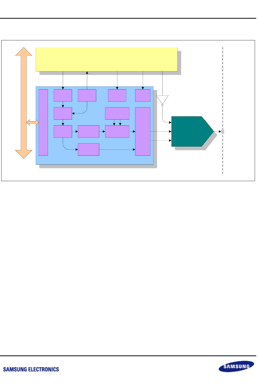
Samsung Confidential
S5P6818_UM 35 Display Controller (DPC)
35-25
Preliminary product information describes products that are in development, for which full characterization data and
associated errata are not yet available. Specifications and information herein are subject to change without notice.
35.4.9.4 Block Diagram
Figure 35-15 Video Encoder and DAC Block Diagram
NTSC/PAL Video Encoder
Data Input
Format
Sync /
Burst
Insert
Timing
Interface
Gain
Offset
Control
Luma
Variable FIR
Filter
Chroma
Variable FIR
Filter
Modulator
Frequency
Gen
QAM chroma
modulation
CLK
control
Output
Format
Control DAC VIDEO
Secondary Sync Generator
CLK
D[9:0]
PowerDown
Reset
Control
Host Interface
Peripheral Bus
Y/C H/V/F VCLK2(27Mhz) ENCRST
Y Y
CCC
SIN COS
ENCRST
nexell / ys.kim at 2015.02.12
SAMSUNG Confidential
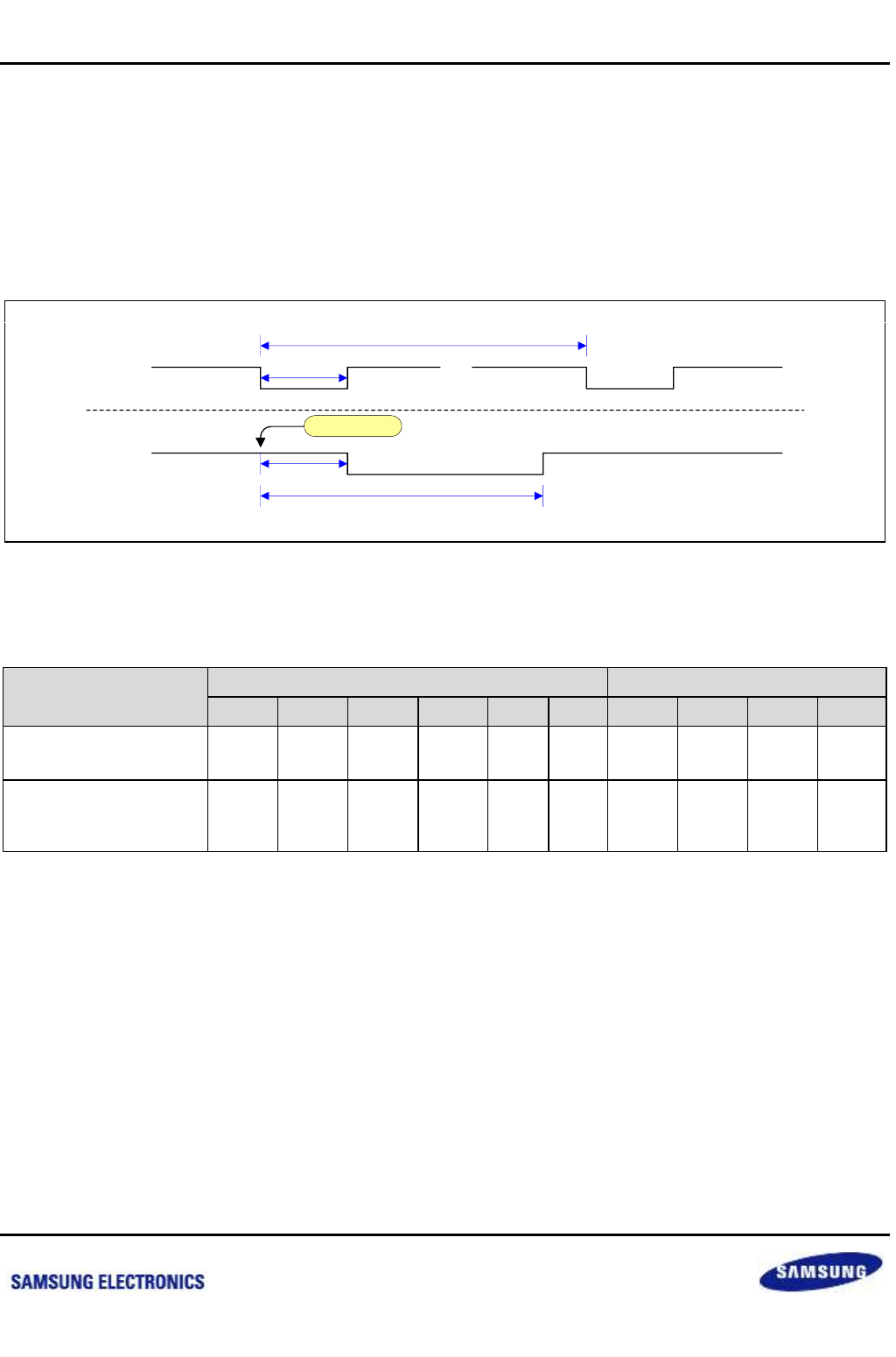
Samsung Confidential
S5P6818_UM 35 Display Controller (DPC)
35-26
Preliminary product information describes products that are in development, for which full characterization data and
associated errata are not yet available. Specifications and information herein are subject to change without notice.
35.4.9.5 Timing Interface
The video encoder has 3 output timing signals (HSO, VSO and FSO) which can be used to extract data from a
sync generator within the system. If ISYNC is programmed to "7", then the encoder will "free run" at the horizontal
and vertical periods defined by the PIXSEL, IFMT combination.
The horizontal timing HSO locations are controlled by the HSOS and HSOE beginning and ending locations. The
programmed value is the pixel number for which the transition will occur. Vertical timing VSO transitions are
controlled by the VSOS and VSOE register.
Figure 35-16 Timing Interface
Table 35-17 Default Timing Setting
Format
Sync Generator
Video Encoder
tHSW
tHBP
tHFP
tVSW
tVBP
tVFP
HSOS
HSOE
VSOS
VSOE
NTSC-M/4.43, PAL-M,
Pseudo PAL
32
90
16
3
15
4
63
1715
0
3
NTSC-N, PAL-
B/D/G/H/I/N/Combination
N, Pseudo NTSC
42
90
12
2
21
3
83
1727
0
2
VSOS
VSOE
HSYNC
VSYNC
Vertical Start
HSOS
HSOE
//
nexell / ys.kim at 2015.02.12
SAMSUNG Confidential
Samsung Confidential
S5P6818_UM 35 Display Controller (DPC)
35-27
Preliminary product information describes products that are in development, for which full characterization data and
associated errata are not yet available. Specifications and information herein are subject to change without notice.
35.4.9.6 Video Standard Selection
The video encoder supports all NTSC and PAL standards throughout the world. The encoder supports
independent control of the Chroma modulation frequency, selection of phase alternating Line encoded chroma
and field frequency. In addition, for non SCH locked standards, the Chroma can be allowed to free run using the
FDRST. If the FSCADJ register is set to any value other than ‘0’, it will not be possible to maintain the SCH
relationship. For these setting it is also recommended that the FDRST bit be set to free run mode.
Table 35-18 Settings for Various Output Formats
Requested Output Format
Required Register Settings
Format
Field Rate
FSC
IFMT
FSCSEL
PHALT
FDRST
NTSC-M
59.95 Hz (525)
3.5795454
0
0
0
1
NTSC-N
50 Hz (625)
3.5795454
1
0
0
0
NTSC-4.43
60 Hz (525)
4.43361875
0
1
0
0
PAL-M
59.952 (525)
3.57561189
0
2
1
0
PAL-combination N
50 Hz (625)
3.58205625
1
3
1
0
PAL-B/D/G/H/I/N
50 Hz (625)
4.43361875
1
1
1
1
Pseudo PAL
60 Hz (525)
4.43361875
0
1
1
0
Pseudo NTSC
50 Hz (625)
3.5795454
1
0
0
0
35.4.9.7 Basic Video Adjustments
The standard video adjustments for Chroma and Luma are included. Chroma controls include Saturation
(VENCSAT) and Hue (VENCHUE). Luma adjustments include Contrast (VENCCRT) and Brightness (VENCBRT).
An additional VENCSCH control is included that changes the Chroma subcarrier phase relative to the horizontal
sync. Note that this feature operates only when FDRST = 0.
nexell / ys.kim at 2015.02.12
SAMSUNG Confidential
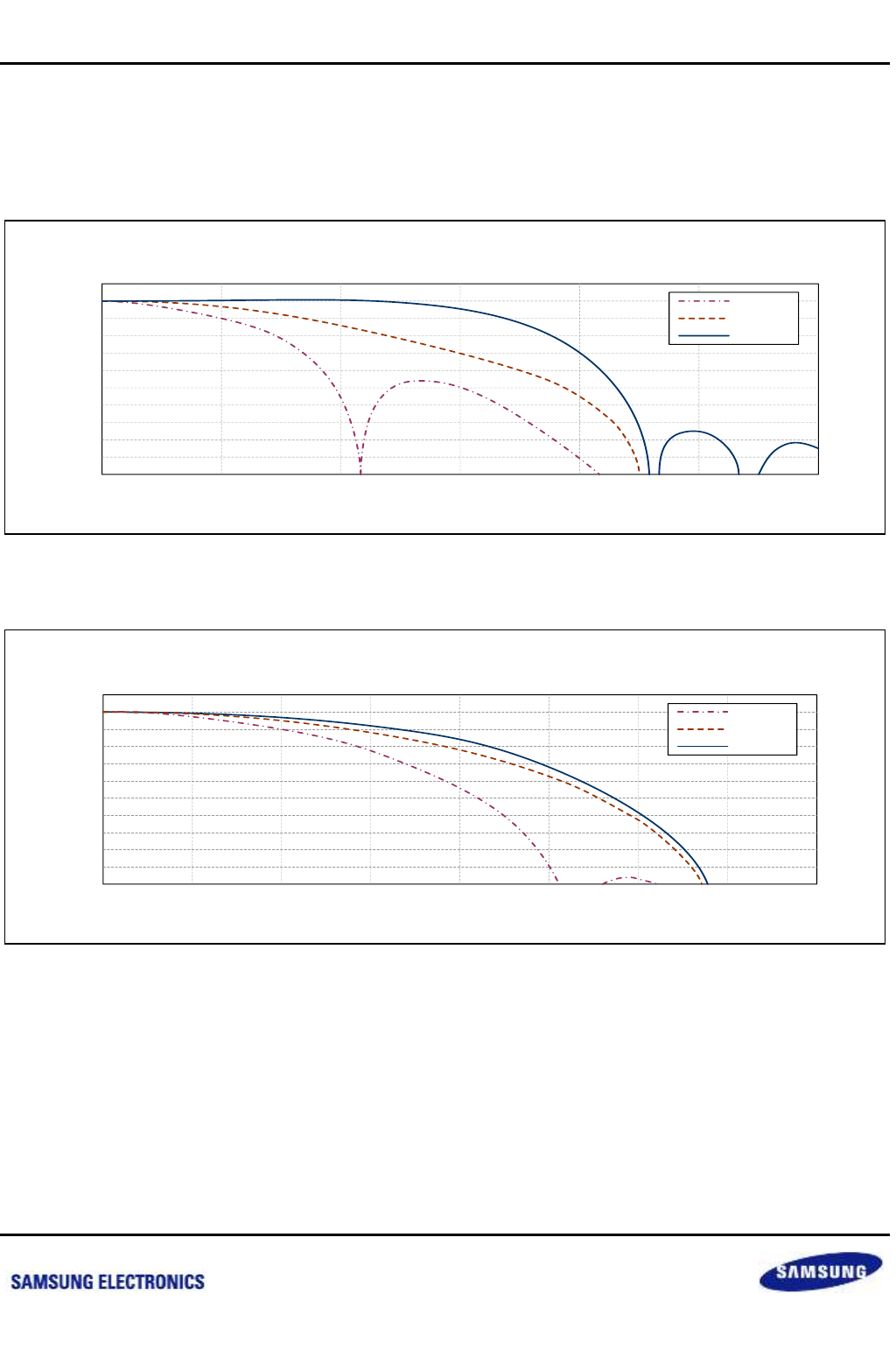
Samsung Confidential
S5P6818_UM 35 Display Controller (DPC)
35-28
Preliminary product information describes products that are in development, for which full characterization data and
associated errata are not yet available. Specifications and information herein are subject to change without notice.
35.4.9.8 Programmable Bandwidth
The data bandwidth for the Luma and chroma paths is shown in the following frequency plots. The YBW control
allows 3 different settings to optimize the output bandwidth to the receiver. The same applies to chroma bandwidth
using the CBW control.
Figure 35-16 Luma Bandwidth
Figure 35-17 Chroma Bandwidth
0
-5
-10
-15
-20
-25
-30
-35
-40
-45
-50 0 2 4 6 8 10 12
Amplitude in dB
Frequency in Mhz
YBW = 2
YBW = 1
YBW = 0
0
-5
-10
-15
-20
-25
-30
-35
-40
-45
-50 0 0.5 1.5 2 2.5 3 4
Amplitude in dB
Frequency in Mhz
1 3.5
CBW = 2
CBW = 1
CBW = 0
nexell / ys.kim at 2015.02.12
SAMSUNG Confidential
Samsung Confidential
S5P6818_UM 35 Display Controller (DPC)
35-29
Preliminary product information describes products that are in development, for which full characterization data and
associated errata are not yet available. Specifications and information herein are subject to change without notice.
35.4.9.9 Analog Video Output Configuration
The video encoder supports composite video output by the register DACSEL. The DAC output levels and the
associated digital codes are summarized below. DAC voltage assumes the standard 140IRE = 1 V. Numbers is
shown for NTSC type video with a pedestal.
Table 35-19 Summary of DAC Voltage and Codes
Signal Level
CVBS/LUMA Value
IRE Value
DAC Voltage
Max. output
1023
105
1.0 V
100 % White
982
100
958 mV
Black
282
5.66
275 mV
Sync
12
–30
11 mV
White – Blank
742
100
724 mV delta
White – sync
970
130
947 mV delta
Color burst
228
30
222 mV delta
nexell / ys.kim at 2015.02.12
SAMSUNG Confidential

Samsung Confidential
S5P6818_UM 35 Display Controller (DPC)
35-30
Preliminary product information describes products that are in development, for which full characterization data and
associated errata are not yet available. Specifications and information herein are subject to change without notice.
35.5 Register Description
35.5.1 Register Map Summary
Base Address: 0xC010_2000
Register
Offset
Description
Reset Value
RSVD
0x800h to 0x8F4h/
0xC70h to 0xCF4h
Reserved
0x0000_0000
DPCHTOTAL
0x8F8h/0xCF8h
DPC horizontal total length register
0x0000_0000
DPCHSWIDTH
0x8FCh/0xCFCh
DPC horizontal sync width register
0x0000_0000
DPCHASTART
0x900h/0xD00h
DPC horizontal active video start register
0x0000_0000
DPCHAEND
0x904h/0xD04h
DPC horizontal active video end register
0x0000_0000
DPCVTOTAL
0x908h/0xD08h
DPC vertical total length register
0x0000_0000
DPCVSWIDTH
0x90Ch/0xD0Ch
DPC vertical sync width register
0x0000_0000
DPCVASTART
0x910h/0xD10h
DPC vertical active video start register
0x0000_0000
DPCVAEND
0x914h/0xD14h
DPC vertical active video end register
0x0000_0000
DPCCTRL0
0x918h/0xD18h
DPC control 0 register
0x0000_0000
DPCCTRL1
0x91Ch/0xD1Ch
DPC control 1 register
0x0000_0000
DPCEVTOTAL
0x920h/0xD20h
DPC even field vertical total length register
0x0000_0000
DPCEVSWIDTH
0x924h/0xD24h
DPC even field vertical sync width register
0x0000_0000
DPCEVASTART
0x928h/0xD28h
DPC even field vertical active video start register
0x0000_0000
DPCEVAEND
0x92Ch/0xD2Ch
DPC even field vertical active video end register
0x0000_0000
DPCCTRL2
0x930h/0xD30h
DPC control 2 register
0x0000_0000
DPCVSEOFFSET
0x934h/0xD34h
DPC vertical sync end offset register
0x0000_0000
DPCVSSOFFSET
0x938h/0xD38h
DPC vertical sync start offset register
0x0000_0000
DPCEVSEOFFSET
0x93Ch/0xD3Ch
DPC even field vertical sync end offset register
0x0000_0000
DPCEVSSOFFSET
0x940h/0xD40h
DPC even field vertical sync start offset register
0x0000_0000
DPCDELAY0
0x944h/0xD44h
DPC Sync Delay 0 register
0x0000_0000
DPUPSCALECON0
Not available/
0xD48h
DPC sync up-scale control register 0
0x0000_0000
DPUPSCALECON1
Not available/
0xD4Ch
DPC sync up-scale control register 1
0x0000_0000
RSVD
0x94Ch to 0x977h/
0xD4Ch to 0xD77h
Reserved
0x0000_0000
DPCDELAY1
0x978h/0xD78h
DPC sync delay control register 1
0x0000_0000
DPCMPUTIME0
0x97Ch/0xD7Ch
DPC MPU i80 timing control register 0
0x0000_0000
DPCMPUTIME1
0x980h/
Not available
DPC MPU i80 timing control register 1
0x0000_0000
DPCMPUWRDATAL
0x984h/
Not available
DPC MPU i80 low bit Write data register
Undefined
DPCMPUINDEX
0x988h/
DPC MPU i80 index Write data register
Undefined
nexell / ys.kim at 2015.02.12
SAMSUNG Confidential

Samsung Confidential
S5P6818_UM 35 Display Controller (DPC)
35-31
Preliminary product information describes products that are in development, for which full characterization data and
associated errata are not yet available. Specifications and information herein are subject to change without notice.
Register
Offset
Description
Reset Value
Not available
DPCMPUSTATUS
0x98Ch/
Not available
DPC MPU i80 status read data register
0x0000_0000
DPCMPUDATAH
0x990h/
Not available
DPC MPU i80 READ/WRITE data register
0x0000_0000
DPCMPURDATAL
0x994h/
Not available
DPC MPU i80 low bit read data register
0x0000_0000
RSVD
0x998h to 0x99Bh/
0xD98h to 0xD9Bh
Reserved
0x0000_0000
DPCCMDBUFFERRDATAL
0x99Ch/
Not available
DPC MPU i80 command buffer low bit data
register
Undefined
DPCCMDBUFFERRDATAH
0x9A0h/
Not available
DPC MPU i80 command buffer high bit data
register
Undefined
DPCMPUTIME1
0x9A4h/0xDA4h
DPC MPU i80 timing CONTROL register 1
0x0000_0000
DPCPADPOSITION0
0x9A8h/
Not available
DPC PAD LOCATION CONTROL register 0
0x0000_0000
DPCPADPOSITION1
0x9ACh/
Not available
DPC PAD LOCATION CONTROL register 1
0x0000_0000
DPCPADPOSITION2
0x9B0h/
Not available
DPC PAD LOCATION CONTROL register 2
0x0000_0000
DPCPADPOSITION3
0x9B4h/
Not available
DPC PAD LOCATION CONTROL register 3
0x0000_0000
DPCPADPOSITION4
0x9B8h/
Not available
DPC PAD LOCATION CONTROL register 4
0x0000_0000
DPCPADPOSITION5
0x9BCh/
Not available
DPC PAD LOCATION CONTROL register 5
0x0000_0000
DPCPADPOSITION6
0x9C0h/
Not available
DPC PAD LOCATION CONTROL register 6
0x0000_0000
DPCPADPOSITION7
C010_0x9C4h/
Not available
DPC PAD LOCATION CONTROL register 7
0x0000_0000
DPCRGBMASK0
0x9C8h/Not
available
DPC PAD LOCATION MASK register 0
0x0000_0000
DPCRGBMASK1
0x9CCh/
Not available
DPC PAD LOCATION MASK register 1
0x0000_0000
DPCRGBSHIFT
0x9D0h/
Not available
DPC RGB SHIFT CONTROL register
0x0000_0000
DPCDATAFLUSH
0x9D4h/
Not available
DPC MPU i80 command buffer FLUSH Control
register
Undefined
RSVD
0x9D8h to 0xBCFh/
0xDD8h to 0xFCFh
Reserved
0x0000_0000
DPCCLKENB
0xBC0h/0xFC0h
DPC Clock Generation Enable Register
0x0000_0000
DPCCLKGEN0L
0xBC4h/0xFC4h
DPC Clock Generation Control 0 Low Register
0x0000_0000
nexell / ys.kim at 2015.02.12
SAMSUNG Confidential

Samsung Confidential
S5P6818_UM 35 Display Controller (DPC)
35-32
Preliminary product information describes products that are in development, for which full characterization data and
associated errata are not yet available. Specifications and information herein are subject to change without notice.
Register
Offset
Description
Reset Value
DPCCLKGEN0H
0xBC8h/0xFC8h
DPC Clock Generation Control 0 high Register
0x0000_0000
DPCCLKGEN1L
0xBCCh/0xFCCh
DPC Clock Generation Control 1 low Register
0x0000_0000
DPCCLKGEN1H
0xBD0h/0xFD0h
DPC Clock Generation Control 1high Register
0x0000_0000
nexell / ys.kim at 2015.02.12
SAMSUNG Confidential

Samsung Confidential
S5P6818_UM 35 Display Controller (DPC)
35-33
Preliminary product information describes products that are in development, for which full characterization data and
associated errata are not yet available. Specifications and information herein are subject to change without notice.
35.5.1.1 DPCHTOTAL
Base Address: 0xC010_2000
Address = Base Address + 0x8F8h, 0xCF8h, Reset Value = 0x0000_0000
Name
Bit
Type
Description
Reset Value
RSVD
[31:16]
R
Reserved
16'h0
HTOTAL
[15:0]
RW
Specifies the number of total VCLK clocks for a
horizontal line.
TFT or Video Encoder: HTOTAL = tHSW + tHBP +
tHFP + tAVW – 1
Color STN: HTOTAL = CL1HW + CL1ToCL2DLY +
{(tAVWx 3)/Bit Width} CPLCYCx2} – 1
Monochrome STN: HTOTAL = CL1HW +
CL1ToCL2DLY + {(tAVWx 1)/Bit Width}
CL2CYCx2} – 1
16'h0
35.5.1.2 DPCHSWIDTH
Base Address: 0xC010_2000
Address = Base Address + 0x8FCh, 0xCFCh, Reset Value = 0x0000_0000
Name
Bit
Type
Description
Reset Value
RSVD
[31:16]
R
Reserved
16'b0
HSWIDTH
[15:0]
RW
TFT or Video Encoder:
Specifies the number of VCLK clocks for the
horizontal sync width. This value must be less than
HASTART.
HSWIDTH = tHSW – 1
STN:
CL1 Height Width HSWIDTH = CL1HW – 1
16'h0
nexell / ys.kim at 2015.02.12
SAMSUNG Confidential
Samsung Confidential
S5P6818_UM 35 Display Controller (DPC)
35-34
Preliminary product information describes products that are in development, for which full characterization data and
associated errata are not yet available. Specifications and information herein are subject to change without notice.
35.5.1.3 DPCHASTART
Base Address: 0xC010_2000
Address = Base Address + 0x900h, 0xD00h, Reset Value = 0x0000_0000
Name
Bit
Type
Description
Reset Value
RSVD
[31:16]
R
Reserved
16'h0
HASTART
[15:0]
RW
TFT or Video Encoder:
Specifies the number of VCLK clocks from start of the
horizontal sync to start of the active video. This value
must be less than HAEND.
HASTART = tHSW + tHBP – 1
STN:
Delay Cycle from pos-edge active of CL1 signal to
CL2 pos-edge active.
HASTART = CL1ToCL2DLY
16'h0
35.5.1.4 DPCHAEND
Base Address: 0xC010_2000
Address = Base Address + 0x904h, 0xD04h, Reset Value = 0x0000_0000
Name
Bit
Type
Description
Reset Value
RSVD
[31:16]
R
Reserved
16'h0
HAEND
[15:0]
RW
TFT or Video Encoder: Specifies the number of VCLK
clocks from start of the horizontal sync to end of the
active video. This value must be less than HTOTAL.
HAEND = tHSW + tHBP + tAVW – 1
STN: Active Width
HAEND = tAVW – 1
16'h0
35.5.1.5 DPCVTOTAL
Base Address: 0xC010_2000
Address = Base Address + 0x908h, 0xD08h, Reset Value = 0x0000_0000
Name
Bit
Type
Description
Reset Value
RSVD
[31:16]
R
Reserved
16'h0
VTOTAL
[15:0]
RW
Specifies the number of total lines for a frame or field.
TFT or Video Encoder: VTOTAL = tVSW + tVBP +
tVFP + tAVH – 1
STN: VTOTAL = BLANKLINE + tAVH – 1
16'h0
nexell / ys.kim at 2015.02.12
SAMSUNG Confidential
Samsung Confidential
S5P6818_UM 35 Display Controller (DPC)
35-35
Preliminary product information describes products that are in development, for which full characterization data and
associated errata are not yet available. Specifications and information herein are subject to change without notice.
35.5.1.6 DPCVSWIDTH
Base Address: 0xC010_2000
Address = Base Address + 0x90Ch, 0xD0Ch, Reset Value = 0x0000_0000
Name
Bit
Type
Description
Reset Value
RSVD
[31:16]
R
Reserved
16'h0
VSWIDTH
[15:0]
RW
TFT or Video Encoder:
Specifies the number of lines for the vertical sync
width. This value must be less than VASTART. When
interlace mode, this value is used for odd field.
VSWIDTH = tVSW – 1
STN:
Blank Line Number
VSWIDTH = BLANKLINE – 1
16'h0
35.5.1.7 DPCVASTART
Base Address: 0xC010_2000
Address = Base Address + 0x910h, 0xD10h, Reset Value = 0x0000_0000
Name
Bit
Type
Description
Reset Value
RSVD
[31:16]
R
Reserved
16'h0
VASTART
[15:0]
RW
Specifies the number of lines from start of the vertical
sync to start of the active video. This value must be
less than VAEND. When interlace mode, this value is
used for odd field.
VASTART = tVSW + tVBP – 1
16'h0
35.5.1.8 DPCVAEND
Base Address: 0xC010_2000
Address = Base Address + 0x914h, 0xD14h, Reset Value = 0x0000_0000
Name
Bit
Type
Description
Reset Value
RSVD
[31:16]
R
Reserved
16'h0
VAEND
[15:0]
RW
Specifies the number of lines from start of the vertical
sync to end of the active video. This value must be
less than VTOTAL. When interlace mode, this value is
used for odd field.
VAEND = tVSW + tVBP + tAVH – 1
16'h0
nexell / ys.kim at 2015.02.12
SAMSUNG Confidential

Samsung Confidential
S5P6818_UM 35 Display Controller (DPC)
35-36
Preliminary product information describes products that are in development, for which full characterization data and
associated errata are not yet available. Specifications and information herein are subject to change without notice.
35.5.1.9 DPCCTRL0
Base Address: 0xC010_2000
Address = Base Address + 0x918h, 0xD18h, Reset Value = 0x0000_0000
Name
Bit
Type
Description
Reset Value
RSVD
[31:16]
R
Reserved
16'h0
DPCENB
[15]
RW
Enable/Disable the display controller (DPC).
0 = Disable
1 = Enable
1'b0
RSVD
[14:13]
RW
Reserved
2'b00
RGBMODE
[12]
RW
Specifies the output pixel format.
0 = YCbCr
1 = RGB
1'b0
INTENB
[11]
RW
Enable/Disable the VSYNC interrupt. The VSYNC
interrupt will be issued at start of the VSYNC pulse.
Therefore an interrupt will be occurred at every frame
in progressive mode or at every field in interlace
mode.
0 = Disable
1 = Enable
1'b0
INTPEND
[10]
RW
Indicates whether the VSYNC interrupt is pended or
not. This bit is always operated regardless of INTENB
bit.
Read:
0 = Not pended
1 = Pended
Write:
0 = No affect
1 = Clear
1'b0
SCANMODE
[9]
RW
Determines whether scan mode is progressive or
interlace.
0 = Progressive scan mode
1 = Interlaced scan mode
1'b0
SEAVENB
[8]
RW
Enable/Disable SAV/EAV signal into the data. This is
used for ITU-R BT.656 format.
0 = Disable embedded sync
1 = Enable embedded sync
1'b0
DELAYRGB
[7:4]
RW
Specifies the delay for RGB PAD output. The unit is
VCLK2. Generally this value has 0 for normal
operation.
4'h0
RSVD
[3]
R
Reserved
1'b0
POLFIELD
[2]
RW
Specifies the polarity of the internal field signal.
0 = Normal (Low is odd field)
1 = Inversion (Low is even field)
1'b0
POLVSYNC
[1]
RW
Specifies the polarity of the vertical sync output. This
1'b0
nexell / ys.kim at 2015.02.12
SAMSUNG Confidential

Samsung Confidential
S5P6818_UM 35 Display Controller (DPC)
35-37
Preliminary product information describes products that are in development, for which full characterization data and
associated errata are not yet available. Specifications and information herein are subject to change without notice.
Name
Bit
Type
Description
Reset Value
bit is only valid in case of primary display controller.
0 = Low active
1 = High active
POLHSYNC
[0]
RW
Specifies the polarity of the horizontal sync output.
This bit is only valid in case of primary display
controller.
0 = Low active
1 = High active
1'b0
35.5.1.10 DPCCTRL1
Base Address: 0xC010_2000
Address = Base Address + 0x91Ch, 0xD1Ch, Reset Value = 0x0000_0000
Name
Bit
Type
Description
Reset Value
RSVD
[31:16]
R
Reserved
16'h0
SWAPRB
[15]
RW
Swap Red and Blue component. This value is only
valid when the output is RGB. This bit is only valid in
case of primary display controller.
0 = RGB
1 = BGR
1'b0
RSVD
[14]
R
Reserved
1'b0
YCRANGE
[13]
RW
Determines the YUV range for RGB to YUV
conversion.
Write 0 set of Video Encoder output
0 = Y = 16 to 235, Cb/Cr = 16 to 240
1 = Y/Cb/Cr = 0 to 255
1'b0
RSVD
[12]
R
Reserved
1'b0
FORMAT
[11:8]
RW
Specifies the data output format.
TFT or Video Encoder :
0 = RGB555
1 = RGB565
2 = RGB666
3 = RGB888
4 = MRGB555A
5 = MRGB555B
6 = MRGB565
7 = MRGB666
8 = MRGB888A
9 = MRGB888B
10 = ITU-R BT.656 or 601 (8-bit)
11 = Reserved
12 = ITU-R BT.601A
13 = ITU-R BT.601B (set YCORDER bit as "1")
14 = Reserved
15 = Reserved
4'h0
nexell / ys.kim at 2015.02.12
SAMSUNG Confidential

Samsung Confidential
S5P6818_UM 35 Display Controller (DPC)
35-38
Preliminary product information describes products that are in development, for which full characterization data and
associated errata are not yet available. Specifications and information herein are subject to change without notice.
Name
Bit
Type
Description
Reset Value
STN:
0 = Reserved
1 = 4096 Color
2 = Reserved
3 = 16 Gray Level
Other = Reserved
RSVD
[7]
RW
Reserved but this bit should be set to "0"
1'b0
YCORDER
[6]
RW
Specifies the data output order in case of ITU-R BT.
601B.
0 = Cb Y Cr Y
1 = Cr Y CbY
1'b0
BDITHER
[5:4]
RW
Specifies the dithering method of Blue component.
This value is only valid in case of primary display
controller.
0 = Bypass
1 = 4-bit dither
2 = 5-bit dither
3 = 6-bit dither
2'b00
GDITHER
[3:2]
RW
Specifies the dithering method of Green component.
This value is only valid in case of primary display
controller.
0 = Bypass
1 = 4-bit dither
2 = 5-bit dither
3 = 6-bit dither
2'b00
RDITHER
[1:0]
RW
Specifies the dithering method of Red component.
This value is only valid in case of primary display
controller.
0 = Bypass
1 = 4-bit dither
2 = 5-bit dither
3 = 6-bit dither
2'b00
nexell / ys.kim at 2015.02.12
SAMSUNG Confidential

Samsung Confidential
S5P6818_UM 35 Display Controller (DPC)
35-39
Preliminary product information describes products that are in development, for which full characterization data and
associated errata are not yet available. Specifications and information herein are subject to change without notice.
35.5.1.11 DPCEVTOTAL
Base Address: 0xC010_2000
Address = Base Address + 0x920h, 0xD20h, Reset Value = 0x0000_0000
Name
Bit
Type
Description
Reset Value
RSVD
[31:16]
R
Reserved
16'h0
EVTOTAL
[15:0]
RW
Specifies the number of total lines for even field. This
register is only used when interlace mode.
EVTOTAL = tEVSW + tEVBP + tEVFP + tEAVH – 1
16'h0
35.5.1.12 DPCEVSWIDTH
Base Address: 0xC010_2000
Address = Base Address + 0x924h, 0xD24h, Reset Value = 0x0000_0000
Name
Bit
Type
Description
Reset Value
RSVD
[31:16]
R
Reserved
16'h0
EVSWIDTH
[15:0]
RW
Specifies the number of lines for the vertical sync width
of even field. This value must be less than EVASTART.
This register is only used when interlace mode.
EVSWIDTH = tEVSW – 1
16'h0
35.5.1.13 DPCEVASTART
Base Address: 0xC010_2000
Address = Base Address + 0x928h, 0xD28h, Reset Value = 0x0000_0000
Name
Bit
Type
Description
Reset Value
RSVD
[31:16]
R
Reserved
16'h0
EVASTART
[15:0]
RW
Specifies the number of lines from start of the vertical
sync to start of the active video when even field. This
value must be less than EVAEND. This register is only
used when interlace mode.
EVASTART = tEVSW + tEVBP – 1
16'h0
nexell / ys.kim at 2015.02.12
SAMSUNG Confidential
Samsung Confidential
S5P6818_UM 35 Display Controller (DPC)
35-40
Preliminary product information describes products that are in development, for which full characterization data and
associated errata are not yet available. Specifications and information herein are subject to change without notice.
35.5.1.14 DPCEVAEND
Base Address: 0xC010_2000
Address = Base Address + 0x92Ch, 0xD2Ch, Reset Value = 0x0000_0000
Name
Bit
Type
Description
Reset Value
RSVD
[31:16]
R
Reserved
16'h0
EVAEND
[15:0]
RW
Specifies the number of lines from start of the vertical
sync to end of the active video when even field. This
value must be less than EVTOTAL. This register is
only used when interlace mode.
EVAEND = tEVSW + tEVBP + tEAVH – 1
16'h0
35.5.1.15 DPCCTRL2
Base Address: 0xC010_2000
Address = Base Address + 0x930h, 0xD30h, Reset Value = 0x0000_0000
Name
Bit
Type
Description
Reset Value
RSVD
[31:16]
R
Reserved
16'h0
CL2CYC
[15:12]
RW
Sets STN LCD CL2 (Shift clock) Cycle (Unit: VCLK)
CL2CYC = CL2CYC – 1
4'h0
RSVD
[11:10]
R
Reserved
2'b00
STNLCDBITWIDTH
[9]
RW
STN LCD Data Bus Bit Width.
0 = Reserved
1 = 8-bit
Scan mode is applicable with Dual view mode set.
1'b0
LCDTYPE
[8:7]
RW
Declares External Display Device Type
0 = TFT or Video Encoder
1 = STN LCD
2 = Dual View mode (TFT or Video Encoder)
3 = Reserved
2'b00
RSVD
[6:5]
R
Reserved
2'b00
I80ENABLE
[4]
RW
Enable MPU i80 Mode.
0 = No i80 Mode
1 = i80 Mode Enable
1'b0
RSVD
[3]
R
Reserved
1'b0
INITPADCLK
[2]
RW
Initial Value of VCLK2 div 2. (for SRGB888)
1'b0
PADCLKSEL
[1:0]
RW
Specifies the PAD output clock.
0 = VCLK
1 = VCLK2
2 = VCLK2 div 2 (for SRGB888)
3 = Reserved
2'b00
nexell / ys.kim at 2015.02.12
SAMSUNG Confidential

Samsung Confidential
S5P6818_UM 35 Display Controller (DPC)
35-41
Preliminary product information describes products that are in development, for which full characterization data and
associated errata are not yet available. Specifications and information herein are subject to change without notice.
35.5.1.16 DPCVSEOFFSET
Base Address: 0xC010_2000
Address = Base Address + 0x934h, 0xD34h, Reset Value = 0x0000_0000
Name
Bit
Type
Description
Reset Value
RSVD
[31:16]
R
Reserved
16'h0
VSEOFFSET
[15:0]
RW
Specifies the number of clocks from start of the
horizontal sync to end of the vertical sync, where the
horizontal sync is last one in the vertical sync. If this
value is 0 then end of the vertical sync synchronizes
with start of the horizontal sync which is new one in
the vertical back porch. This value has to be less than
HTOTAL. When interlace mode, this value is used for
odd field.
If tVSEO is 0 then VSEOFFSET = 0, else
VSEOFFSET = HTOTAL – tVSEO
16'h0
35.5.1.17 DPCVSSOFFSET
Base Address: 0xC010_2000
Address = Base Address + 0x938h, 0xD38h, Reset Value = 0x0000_0000
Name
Bit
Type
Description
Reset Value
RSVD
[31:16]
R
Reserved
16'h0
VSSOFFSET
[15:0]
RW
Specifies the number of clocks from start of the
horizontal sync to start of the vertical sync, where the
horizontal sync is last one in the vertical front porch. If
this value is 0 then start of the vertical sync
synchronizes with start of the horizontal sync which is
new one in the vertical sync. This value has to be less
than HTOTAL. When interlace mode, this value is
used for odd field.
If tVSSO is 0 then VSSOFFSET = 0, else
VSSOFFSET = HTOTAL – tVSSO
16'h0
nexell / ys.kim at 2015.02.12
SAMSUNG Confidential
Samsung Confidential
S5P6818_UM 35 Display Controller (DPC)
35-42
Preliminary product information describes products that are in development, for which full characterization data and
associated errata are not yet available. Specifications and information herein are subject to change without notice.
35.5.1.18 DPCEVSEOFFSET
Base Address: 0xC010_2000
Address = Base Address + 0x93Ch, 0xD3Ch, Reset Value = 0x0000_0000
Name
Bit
Type
Description
Reset Value
RSVD
[31:16]
R
Reserved
16'h0
EVSEOFFSET
[15:0]
RW
Specifies the number of clocks from start of the
horizontal sync to end of the vertical sync, where the
horizontal sync is last one in the vertical sync. If this
value is 0 then end of the vertical sync synchronizes
with start of the horizontal sync which is new one in
the vertical back porch. This value has to be less than
HTOTAL and is used for even field.
If tEVSEO is 0 then EVSEOFFSET = 0, else
EVSEOFFSET = HTOTAL – tEVSEO
16'h0
35.5.1.19 DPCEVSSOFFSET
Base Address: 0xC010_2000
Address = Base Address + 0x940h, 0xD40h, Reset Value = 0x0000_0000
Name
Bit
Type
Description
Reset Value
RSVD
[31:16]
R
Reserved
16'h0
EVSSOFFSET
[15:0]
RW
Specifies the number of clocks from start of the
horizontal sync to start of the vertical sync, where the
horizontal sync is last one in the vertical front porch. If
this value is 0 then start of the vertical sync
synchronizes with start of the horizontal sync which is
new one in the vertical sync. This value has to be less
than HTOTAL and is used for even field.
If tEVSSO is 0 then EVSSOFFSET = 0, else
EVSSOFFSET = HTOTAL – tEVSSO
16'h0
nexell / ys.kim at 2015.02.12
SAMSUNG Confidential
Samsung Confidential
S5P6818_UM 35 Display Controller (DPC)
35-43
Preliminary product information describes products that are in development, for which full characterization data and
associated errata are not yet available. Specifications and information herein are subject to change without notice.
35.5.1.20 DPCDELAY0
Base Address: 0xC010_2000
Address = Base Address + 0x944h, 0xD44h, Reset Value = 0x0000_0000
Name
Bit
Type
Description
Reset Value
RSVD
[31:12]
R
Reserved
20'h0
PADPOLFIELD
[15]
RW
Specifies the polarity of the PAD's field signal.
0 = Normal (Low is odd field)
1 = Inversion (Low is even field)
1'b0
RSVD
[14]
R
Reserved
1'b0
DELAYVS
[13:8]
RW
Specifies delay value of the vertical sync/FRM output.
This value depends on the output format.
The unit is VCLK2.
4'h0
DELAYHS
[5:0]
RW
Specifies delay value of the horizontal sync/CP1
output. This value depends on the output format.
The unit is VCLK2.
4'h0
35.5.1.21 DPUPSCALECON0
Base Address: 0xC010_2000
Address = Base Address + Not available, 0xD48h, Reset Value = 0x0000_0000
Name
Bit
Type
Description
Reset Value
RSVD
[31:16]
R
Reserved
16'h0
UPSCALEL
[15:8]
RW
Specifies the ratio for the horizontal scale. The
formula to calculate this value is as follows:
When FILTERENB is 1 and the destination width is
wider than the source width:
UPSCALE = (source width-1) (1<<11) /
(destination width – 1)
UPSCALEL = UPSCALE[7:0]
8'h0
RSVD
[7:1]
R
Reserved
7'h0
UPSCALERENB
[0]
RW
Decide whether to enlarge Source Image horizontal
width.
0 = Scaler Disable
1 = Scaler Enable
1'b0
nexell / ys.kim at 2015.02.12
SAMSUNG Confidential

Samsung Confidential
S5P6818_UM 35 Display Controller (DPC)
35-44
Preliminary product information describes products that are in development, for which full characterization data and
associated errata are not yet available. Specifications and information herein are subject to change without notice.
35.5.1.22 DPUPSCALECON1
Base Address: 0xC010_2000
Address = Base Address + Not available, 0xD4Ch, Reset Value = 0x0000_0000
Name
Bit
Type
Description
Reset Value
RSVD
[31:15]
R
Reserved
17'h0
UPSCALEH
[14:0]
RW
Specifies the ratio for the horizontal scale. The
formula to calculate this value is as follows:
When FILTERENB is 1 and the destination width is
wider than the source width:
UPSCALE = (MLCScreenwidth-1)
(1<<11)/(destination width – 1)
UPSCALEH = UPSCALE[22:8]
15'h0
35.5.1.23 DPCDELAY1
Base Address: 0xC010_2000
Address = Base Address + 0x978h, 0xD78h, Reset Value = 0x0000_0000
Name
Bit
Type
Description
Reset Value
RSVD
[31:6]
R
Reserved
26'h0
DELAYDE
[5:0]
RW
Specifies delay value of DE (data enable)/CP2 output.
This value depends on the output format. The unit is
VCLK2.
6'h0
nexell / ys.kim at 2015.02.12
SAMSUNG Confidential

Samsung Confidential
S5P6818_UM 35 Display Controller (DPC)
35-45
Preliminary product information describes products that are in development, for which full characterization data and
associated errata are not yet available. Specifications and information herein are subject to change without notice.
35.5.1.24 DPCMPUTIME0
Base Address: 0xC010_2000
Address = Base Address + 0x97Ch, 0xD7Ch, Reset Value = 0x0000_0000
Name
Bit
Type
Description
Reset Value
RSVD
[31:16]
R
Reserved
16'h0
I80HOLDTIME
[15:8]
RW
Specifies value of MPU i80 hold time config. The unit
is PCLK.
8'h0
I80SETUPTIME
[7:0]
RW
Specifies value of MPU i80 setup time config. The unit
is PCLK.
8'h0
35.5.1.25 DPCMPUTIME1
Base Address: 0xC010_2000
Address = Base Address + 0x980h, Not available, Reset Value = 0x0000_0000
Name
Bit
Type
Description
Reset Value
RSVD
[31:8]
R
Reserved
24'h0
I80ACCTIME
[7:0]
RW
Specifies value of MPU i80 hold time config. The unit
is PCLK.
8'h0
35.5.1.26 DPCMPUWRDATAL
Base Address: 0xC010_2000
Address = Base Address + 0x984h, Not available, Reset Value = Undefined
Name
Bit
Type
Description
Reset Value
RSVD
[31:16]
R
Reserved
16'h0
MPUWRDATAL
[15:0]
W
Write low 16-bit write data for MPU i80.
Users must write this register first for MPU i80 access
via CPU.
–
35.5.1.27 DPCMPUINDEX
Base Address: 0xC010_2000
Address = Base Address + 0x988h, Not available, Reset Value = Undefined
Name
Bit
Type
Description
Reset Value
RSVD
[31:8]
R
Reserved
16'h0
MPUINDEX
[7:0]
W
Write high 8-bit write data for MPU i80 index access.
(RS = 0)
–
nexell / ys.kim at 2015.02.12
SAMSUNG Confidential

Samsung Confidential
S5P6818_UM 35 Display Controller (DPC)
35-46
Preliminary product information describes products that are in development, for which full characterization data and
associated errata are not yet available. Specifications and information herein are subject to change without notice.
35.5.1.28 DPCMPUSTATUS
Base Address: 0xC010_2000
Address = Base Address + 0x98Ch, Not available, Reset Value = 0x0000_0000
Name
Bit
Type
Description
Reset Value
RSVD
[31:8]
R
Reserved
16'h0
MPUSTATUS
[7:0]
R
Read high 8-bit write data1 for MPU i80 index access.
(RS = 0)
16'h0
35.5.1.29 DPCMPUDATAH
Base Address: 0xC010_2000
Address = Base Address + 0x990h, Not available, Reset Value = 0x0000_0000
Name
Bit
Type
Description
Reset Value
RSVD
[31:8]
R
Reserved
16'h0
MPUDATAH
[7:0]
RW
Read/Write high 8-bit write data1 for MPU i80 data
access. (RS = 1)
16'h0
35.5.1.30 DPCMPURDATAL
Base Address: 0xC010_2000
Address = Base Address + 0x994h, Not available, Reset Value = 0x0000_0000
Name
Bit
Type
Description
Reset Value
RSVD
[31:16]
R
Reserved
16'h0
MPUWRDATAL
[15:0]
R
Read low 16-bit write data for MPU i80.
Users must read this register after reading
DPCMPUSTATUS or DPCMPUDATAH for MPU i80
access via CPU.
16'h0
35.5.1.31 DPCCMDBUFFERRDATAL
Base Address: 0xC010_2000
Address = Base Address + 0x99Ch, Not available, Reset Value = Undefined
Name
Bit
Type
Description
Reset Value
RSVD
[31:16]
R
Reserved
16'h0
MPUCMDBUFL
[15:0]
W
Write low 16-bit write data for MPU i80.
Users must write this register first for MPU i80
command buffer
–
nexell / ys.kim at 2015.02.12
SAMSUNG Confidential
Samsung Confidential
S5P6818_UM 35 Display Controller (DPC)
35-47
Preliminary product information describes products that are in development, for which full characterization data and
associated errata are not yet available. Specifications and information herein are subject to change without notice.
35.5.1.32 DPCCMDBUFFERRDATAH
Base Address: 0xC010_2000
Address = Base Address + 0x9A0h, Not available, Reset Value = Undefined
Name
Bit
Type
Description
Reset Value
RSVD
[31:8]
R
Reserved
24'h0
MPUCMDBUFH
[7:0]
W
Write high 8-bit write data for MPU i80.
–
35.5.1.33 DPCMPUTIME1
Base Address: 0xC010_2000
Address = Base Address + 0x9A4h, 0xDA4h, Reset Value = 0x0000_0000
Name
Bit
Type
Description
Reset Value
RSVD
[31:6]
R
Reserved
26'h0
POLDE
[5]
RW
Specifies the polarity of the Data Enable output.
0 = Normal (High is data enable)
1 = Inversion (High is data enable)
1'b0
POLNCS
[4]
RW
Specifies the polarity of the nCS signal. (MPU i80
type, primary only)
0 = Normal (Low is chip select)
1 = Inversion (High is chip select)
1'b0
POLNWR
[3]
RW
Specifies the polarity of the nWR signal. (MPU i80
type, primary only)
0 = Normal (neg-edge trigger)
1 = Inversion (pos-edge trigger)
1'b0
POLNRD
[2]
RW
Specifies the polarity of the nRD signal. (MPU i80
type, primary only)
0 = Normal (neg-edge trigger)
1 = Inversion (pos-edge trigger)
1'b0
POLRS
[1]
RW
Specifies the polarity of the RS signal. (MPU i80 type,
primary only)
0 = Normal(Low is index access)
1 = Inversion (High is index access)
1'b0
RSVD
[0]
RW
Must be Set 1'b0
1'b0
nexell / ys.kim at 2015.02.12
SAMSUNG Confidential

Samsung Confidential
S5P6818_UM 35 Display Controller (DPC)
35-48
Preliminary product information describes products that are in development, for which full characterization data and
associated errata are not yet available. Specifications and information herein are subject to change without notice.
35.5.1.34 DPCPADPOSITION0
Base Address: 0xC010_2000
Address = Base Address + 0x9A8h, Not available, Reset Value = 0x0000_0000
Name
Bit
Type
Description
Reset Value
RSVD
[31:15]
R
Reserved
17'h0
PADLOC2
[14:10]
RW
Select a location to go in the video data number 2
outputs. (active when i80 mode )
5'h0
PADLOC1
[9:5]
RW
Select a location to go in the video data number 1
outputs. (active when i80 mode )
5'h0
PADLOC0
[4:0]
RW
Select a location to go in the video data number 0
outputs. (active when i80 mode )
5'h0
35.5.1.35 DPCPADPOSITION1
Base Address: 0xC010_2000
Address = Base Address + 0x9ACh, Not available, Reset Value = 0x0000_0000
Name
Bit
Type
Description
Reset Value
RSVD
[31:15]
R
Reserved
17'h0
PADLOC5
[14:10]
RW
Select a location to go in the video data number 5
outputs. (active when i80 mode )
5'h0
PADLOC4
[9:5]
RW
Select a location to go in the video data number 4
outputs. (active when i80 mode )
5'h0
PADLOC3
[4:0]
RW
Select a location to go in the video data number 3
outputs. (active when i80 mode )
5'h0
35.5.1.36 DPCPADPOSITION2
Base Address: 0xC010_2000
Address = Base Address + 0x9B0h, Not available, Reset Value = 0x0000_0000
Name
Bit
Type
Description
Reset Value
RSVD
[31:15]
R
Reserved
17'h0
PADLOC8
[14:10]
RW
Select a location to go in the video data number 8
outputs. (active when i80 mode )
5'h0
PADLOC7
[9:5]
RW
Select a location to go in the video data number 7
outputs. (active when i80 mode )
5'h0
PADLOC6
[4:0]
RW
Select a location to go in the video data number 6
outputs. (active when i80 mode )
5'h0
nexell / ys.kim at 2015.02.12
SAMSUNG Confidential
Samsung Confidential
S5P6818_UM 35 Display Controller (DPC)
35-49
Preliminary product information describes products that are in development, for which full characterization data and
associated errata are not yet available. Specifications and information herein are subject to change without notice.
35.5.1.37 DPCPADPOSITION3
Base Address: 0xC010_2000
Address = Base Address + 0x9B4h, Not available, Reset Value = 0x0000_0000
Name
Bit
Type
Description
Reset Value
RSVD
[31:15]
R
Reserved
17'h0
PADLOC11
[14:10]
RW
Select a location to go in the video data number 11
outputs. (active when i80 mode )
5'h0
PADLOC10
[9:5]
RW
Select a location to go in the video data number 10
outputs. (active when i80 mode )
5'h0
PADLOC9
[4:0]
RW
Select a location to go in the video data number 9
outputs. (active when i80 mode )
5'h0
35.5.1.38 DPCPADPOSITION4
Base Address: 0xC010_2000
Address = Base Address + 0x9B8h, Not available, Reset Value = 0x0000_0000
Name
Bit
Type
Description
Reset Value
RSVD
[31:15]
R
Reserved
17'h0
PADLOC14
[14:10]
RW
Select a location to go in the video data number 14
outputs. (active when i80 mode )
5'h0
PADLOC13
[9:5]
RW
Select a location to go in the video data number 13
outputs. (active when i80 mode )
5'h0
PADLOC12
[4:0]
RW
Select a location to go in the video data number 12
outputs. (active when i80 mode )
5'h0
35.5.1.39 DPCPADPOSITION5
Base Address: 0xC010_2000
Address = Base Address + 0x9BCh, Not available, Reset Value = 0x0000_0000
Name
Bit
Type
Description
Reset Value
RSVD
[31:15]
R
Reserved
17'h0
PADLOC17
[14:10]
RW
Select a location to go in the video data number 17
outputs. (active when i80 mode )
5'h0
PADLOC16
[9:5]
RW
Select a location to go in the video data number 16
outputs. (active when i80 mode )
5'h0
PADLOC15
[4:0]
RW
Select a location to go in the video data number 15
outputs. (active when i80 mode )
5'h0
nexell / ys.kim at 2015.02.12
SAMSUNG Confidential
Samsung Confidential
S5P6818_UM 35 Display Controller (DPC)
35-50
Preliminary product information describes products that are in development, for which full characterization data and
associated errata are not yet available. Specifications and information herein are subject to change without notice.
35.5.1.40 DPCPADPOSITION6
Base Address: 0xC010_2000
Address = Base Address +0x9C0h, Not available, Reset Value = 0x0000_0000
Name
Bit
Type
Description
Reset Value
RSVD
[31:15]
R
Reserved
17'h0
PADLOC20
[14:10]
RW
Select a location to go in the video data number 20
outputs. (active when i80 mode )
5'h0
PADLOC19
[9:5]
RW
Select a location to go in the video data number 19
outputs. (active when i80 mode )
5'h0
PADLOC18
[4:0]
RW
Select a location to go in the video data number 18
outputs. (active when i80 mode )
5'h0
35.5.1.41 DPCPADPOSITION7
Base Address: 0xC010_2000
Address = Base Address +0x9C4h, Not available, Reset Value = 0x0000_0000
Name
Bit
Type
Description
Reset Value
RSVD
[31:15]
R
Reserved
17'h0
PADLOC23
[14:10]
RW
Select a location to go in the video data number 23
outputs. (active when i80 mode )
5'h0
PADLOC22
[9:5]
RW
Select a location to go in the video data number 22
outputs. (active when i80 mode )
5'h0
PADLOC21
[4:0]
RW
Select a location to go in the video data number 21
outputs. (active when i80 mode )
5'h0
nexell / ys.kim at 2015.02.12
SAMSUNG Confidential
Samsung Confidential
S5P6818_UM 35 Display Controller (DPC)
35-51
Preliminary product information describes products that are in development, for which full characterization data and
associated errata are not yet available. Specifications and information herein are subject to change without notice.
35.5.1.42 DPCRGBMASK0
Base Address: 0xC010_2000
Address = Base Address + 0x9C8h, Not available, Reset Value = 0x0000_0000
Name
Bit
Type
Description
Reset Value
RSVD
[31:16]
R
Reserved
16'h0
RGBMASK[15:0]
[15:0]
RW
Specifies the mask of the video data output (active
when i80 mode)
0 = Masked (output = 0)
1 = Enabled
16'h0
35.5.1.43 DPCRGBMASK1
Base Address: 0xC010_2000
Address = Base Address + 0x9CCh, Not available, Reset Value = 0x0000_0000
Name
Bit
Type
Description
Reset Value
RSVD
[31:8]
R
Reserved
24'h0
RGBMASK[23:16]
[7:0]
RW
Specifies the mask of the video data output (active
when i80 mode)
0 = Masked (output = 0)
1 = Enabled
8'h0
35.5.1.44 DPCRGBSHIFT
Base Address: 0xC010_2000
Address = Base Address + 0x9D0h, Not available, Reset Value = 0x0000_0000
Name
Bit
Type
Description
Reset Value
RSVD
[31:6]
R
Reserved
26'h0
FIELDFLAG
[5]
R
Specifies the field flag of the interlace mode
0 = Odd frame
1 = Even frame
1'b0
RGBSHIFT
[4:0]
RW
Specifies the shift number of the video data output
(active when i80 mode)
PAD video data[23:0] = video data[23:0]<<RGBSHIFT
5'h0
nexell / ys.kim at 2015.02.12
SAMSUNG Confidential

Samsung Confidential
S5P6818_UM 35 Display Controller (DPC)
35-52
Preliminary product information describes products that are in development, for which full characterization data and
associated errata are not yet available. Specifications and information herein are subject to change without notice.
35.5.1.45 DPCDATAFLUSH
Base Address: 0xC010_2000
Address = Base Address + 0x9D4h, Not available, Reset Value = Undefined
Name
Bit
Type
Description
Reset Value
RSVD
[31:4]
R
Reserved
28'h0
REGFLUSH
[4]
W
Register flush manually (primary only)
–
CMDBUFFULL
[3]
R
MPU i80 command buffer's full flag
0 = Not full
1 = Full
1'b0
CMDBUFEMPTY
[2]
R
MPU i80 command buffer's empty flag
0 = Not empty
1 = Empty
1'b0
CMDBUFFLUSH
[1]
RW
Set the dirty flag for MPU i80 command buffer
1 = When vertical sync period, command buffer start
to send data.
1'b0
CMDBUFCLR
[0]
W
Clear the MPU i80 command buffer
–
35.5.1.46 DPCCLKENB
Base Address: 0xC010_2000
Address = Base Address + 0xBC0h, 0xFC0h, Reset Value = 0x0000_0000
Name
Bit
Type
Description
Reset Value
RSVD
[31:4]
R
Reserved
28'h0
PCLKMODE
[3]
RW
Specifies PCLK operating mode.
0 = PCLK is only enabled when CPU accesses this
module
1 = PCLK is always enabled
1'b0
CLKGENENB
[2]
RW
Enable/Disable to generate a clock.
0 = Disable
1 = Enable
1'b0
RSVD
[1:0]
R
Reserved
2'b00
nexell / ys.kim at 2015.02.12
SAMSUNG Confidential

Samsung Confidential
S5P6818_UM 35 Display Controller (DPC)
35-53
Preliminary product information describes products that are in development, for which full characterization data and
associated errata are not yet available. Specifications and information herein are subject to change without notice.
35.5.1.47 DPCCLKGEN0L
Base Address: 0xC010_2000
Address = Base Address + 0xBC4h, 0xFC4h, Reset Value = 0x0000_0000
Name
Bit
Type
Description
Reset Value
RSVD
[31:16]
R
Reserved
16'h0
OUTCLKENB
[15]
RW
Specifies the direction of the PADVCLK pad. This bit
should be set when CLKSRCSEL0/1 is 3 or 4.
0 = Enable (Output)
1 = Reserved
1'b0
RSVD
[14:13]
R
Reserved
2'b00
CLKDIV0
[12:5]
RW
Specifies divider value of the source clock.
Divider value = CLKDIV0 + 1
8'h0
CLKSRCSEL0
[4:2]
RW
Specifies the source clock.
0 = PLL0
1 = PLL1
2 = PLL2
3 = none
4 = HDMI PLL Clock
5 = none
6 = PLL3
7 = Reserved
3'b000
OUTCLKINV0
[1]
RW
Specifies whether to invert the clock output.
0 = Normal (Falling Edge)
1 = Invert (Rising Edge)
1'b0
RSVD
[0]
RW
Reserved (This bit should be set to "0")
1'b0
35.5.1.48 DPCCLKGEN0H
Base Address: 0xC010_2000
Address = Base Address + 0xBC8h, 0xFC8h, Reset Value = 0x0000_0000
Name
Bit
Type
Description
Reset Value
RSVD
[31:5]
RW
Reserved for future use. This bit should be set to "0"
27'h0
OUTCLKDELAY0
[4:0]
RW
Specifies delay value of the clock output. This value is
needed to adjust clock skew with respect to data
signal.
TBD
5'h0
nexell / ys.kim at 2015.02.12
SAMSUNG Confidential
Samsung Confidential
S5P6818_UM 35 Display Controller (DPC)
35-54
Preliminary product information describes products that are in development, for which full characterization data and
associated errata are not yet available. Specifications and information herein are subject to change without notice.
35.5.1.49 DPCCLKGEN1L
Base Address: 0xC010_2000
Address = Base Address + 0xBCCh, 0xFCCh, Reset Value = 0x0000_0000
Name
Bit
Type
Description
Reset Value
RSVD
[31:13]
R
Reserved
19'h0
CLKDIV1
[12:5]
RW
Specifies divider value of the source clock.
Divider value = CLKDIV0 + 1
8'h0
CLKSRCSEL1
[4:2]
RW
Specifies the source clock.
0 = PLL0
1 = PLL1
2 = PLL2
3 = none
4 = HDMI PLL Clock
5 = none
6 = PLL3
7 = CLKGEN0 Clock
3'b000
OUTCLKINV1
[1]
RW
Specifies whether to invert the clock output.
0 = Normal (Falling Edge)
1 = Invert (Rising Edge)
1'b0
OUTCLKSEL
[0]
RW
1/2 ns delay is applied to Out clock from source clock
Can be used only in case of division by even number
0 = Bypass 1 source clock/2 ns
1'b0
35.5.1.50 DPCCLKGEN1H
Base Address: 0xC010_2000
Address = Base Address + 0xBD0h, 0xFD0h, Reset Value = 0x0000_0000
Name
Bit
Type
Description
Reset Value
RSVD
[31:5]
RW
Reserved for future use. You don't have to write any
value except 0.
27'h0
OUTCLKDELAY1
[4:0]
RW
Specifies delay value of the clock output. This value is
needed to adjust clock skew with respect to data
signal.
TBD
5'h0
nexell / ys.kim at 2015.02.12
SAMSUNG Confidential

Samsung Confidential
S5P6818_UM 36 De-Interlace
36-1
Preliminary product information describes products that are in development, for which full characterization data and
associated errata are not yet available. Specifications and information herein are subject to change without notice.
36 De-Interlace
36.1 Overview
The De-interlace block makes a frame data by using a field (Odd/Even) data. If the current field of the image is an
even field, the block creates a new odd field by using the previous odd field and the next odd field.
36.2 Features
Maximum image width of 1920, Height is not limited.
Y, Cb and Cr are executed separately
Separated YUV (420, 422 and 444) format supports
nexell / ys.kim at 2015.02.12
SAMSUNG Confidential
Samsung Confidential
S5P6818_UM 36 De-Interlace
36-2
Preliminary product information describes products that are in development, for which full characterization data and
associated errata are not yet available. Specifications and information herein are subject to change without notice.
36.3 Operation
The De-interlace block operation is divided into the Even operation and the Odd operation based on the current
field status (Odd/Even Field). Each operation is as follows.
36.3.1 Even Operation
The Even operation indicates that the block creates a new Odd field to create a frame data when the current data
is an Even field. The figure below shows the Even operation of the De-interlace block.
Figure 36-1 Even Field Operation
The De-interlace block uses the previous Odd field data and the next Odd field data to create the Odd field data of
a frame data.
Odd Line 1: Provide the average of Even Line 1 and Even Line 2.
De-interlace Data: The De-interlace Odd line is created by using the previous/next Odd line information. At
this time, since the first 8-pixel and the last 8-pixel of a line do not have sufficient De-interlace information, the
De-interlace data is given as the average ((Previous Odd Line + Next Odd Line)/2) of the Odd lines.
Odd Last Line - 1: Provide the value of (Even Last Line + (Even Last Line-1))/2.
Odd Last Line: Copy the last line of the Even filed.
Deinterlace Data Yt = ( Even Line 1 + Even Line 2 ) /2
Yt = ( Even Last Line + ( Even Last Line – 1 ) ) / 2
Copy Even Last Line
Deinterlace Data Y
Deinterlace Data Y
Deinterlace Data Y
Deinterlace Data Y
Deinterlace Data Y
Deinterlace Data Y
Yt Align 8Pixel Yt Align 8Pixel
Yt Align 8Pixel Yt Align 8Pixel
Yt Align 8Pixel Yt Align 8Pixel
Yt Align 8Pixel Yt Align 8Pixel
Yt Align 8Pixel Yt Align 8Pixel
Yt Align 8Pixel Yt Align 8Pixel
Even Line 1
Even Line 2
Even Line 3
Even Line 4
Even Line 5
Even Line 6
Even Last Line - 1
Even Last Line
Even Line + 1
Odd Line 1
Odd Last Line
Deinterlaced Data
Odd Last Line - 1
Odd Line 2
Odd Last Line - 2
Frame Data
Even Field
Data
Current
Next
Previous
Odd Field
Data
Odd Field
Data
Frame Data
nexell / ys.kim at 2015.02.12
SAMSUNG Confidential
Samsung Confidential
S5P6818_UM 36 De-Interlace
36-3
Preliminary product information describes products that are in development, for which full characterization data and
associated errata are not yet available. Specifications and information herein are subject to change without notice.
36.3.2 Odd Operation
The Odd operation indicates that the block creates a new Odd field to create a frame data when the current data
is an Odd field. The figure below shows the Odd operation of the De-interlace block.
Figure 36-2 Odd Field Operation
The De-interlace block uses the previous Even field data and the next Even field data to create the Even field data
of a frame data.
Provide the average of Odd Line 1 and Odd Line 2.
De-interlace Data: The De-interlace Even line is created by using the previous/next Even line information. At
this time, since the first 8-pixel and the last 8-pixel of a line do not have sufficient De-interlace information, the
De-interlace data is given as the average ((Previous Even Line + Next Even Line)/2) of the Even lines.
Even Last Line: Provide the value of (Odd Last Line + (Odd Last Line-1))/2.
Deinterlace Data Yt = ( Odd Line 1 + Odd Line 2 ) / 2
Yt = ( Odd Last Line + ( Odd Last Line -1 ) ) / 2
Copy Odd Line1
Deinterlace Data Y
Yt Align 8Pixel Yt Align 8Pixel
Deinterlace Data Y
Yt Align 8Pixel Yt Align 8Pixel
Deinterlace Data Y
Yt Align 8Pixel Yt Align 8Pixel
Deinterlace Data Y
Yt Align 8Pixel Yt Align 8Pixel
Deinterlace Data Y
Yt Align 8Pixel Yt Align 8Pixel
Deinterlace Data Y
Yt Align 8Pixel Yt Align 8Pixel
Odd Line 1
Odd Line 2
Odd Line 3
Odd Line 4
Odd Line 5
Odd Line 6
Odd Last Line - 1
Odd Last Line
Odd Line + 1
Even Line 1
Even Last Line
Deinterlaced Data
Even Line 2
Even Line 3
Even Last Line - 1
Odd Field
Data
Current
Next
Previous
Frame Data
Even Field
Data
Even Field
Data
Frame Data
nexell / ys.kim at 2015.02.12
SAMSUNG Confidential
Samsung Confidential
S5P6818_UM 36 De-Interlace
36-4
Preliminary product information describes products that are in development, for which full characterization data and
associated errata are not yet available. Specifications and information herein are subject to change without notice.
36.3.3 Y, Cb, Cr Operation
To create the de-interlaced Data (Frame Data) indicates to create each Y, Cb and Cr of the Even field for the
current Odd field or the Odd field for the current Even field. The figure below shows the example to create the
frame data when the current interlace data is the Odd field.
For Y, an Even field is created by using the current Odd field Y (SRCADDRC_Y) information, the previous Even
field Y (SRCADDRP_Y) information and the next Even field Y (SRCADDRN_Y) information. Then the Y
information is stored to the Even field (DESTADDRD_Y) of a destination image. In the Odd field of the image to be
newly created, since the current status is Odd field, the Y information is copied to the Odd field (DESTADDRF_Y)
of the destination image as it is.
For Cb, an Even field is only created by using the current Odd field Cb (SRCADDRC_CB). The created Even field
is stored to the Even field (DESTADDRD_CB) of a destination image. In the Odd field of the image to be newly
created, since the current status is Odd field, the Cb information is copied to the Odd field (DESTADDRF_CB) of a
destination image as it is. Cr data is handled in the same way as Cb data. (For the meaning of each register
name, refer to Register Summary.)
Figure 36-3 Y, Cb, Cr Operation
YCb Cr
SRCADDRP_Y
Even Field( Previous )
YCb Cr
SRCADDRC_Y
Odd Field( Current )
SRCADDRC_CB SRCADDRC_CR
YCb Cr
SRCADDRN_Y
Even Field( Next )
Y
Cb
Cr
DESTADDRD_Y
DESTADDRF_Y
Even Field
Odd Field
Even Field
Odd Field
Even Field
Odd Field
DESTADDRD_CB
DESTADDRF_CB
DESTADDRD_CR
DESTADDRF_CR
nexell / ys.kim at 2015.02.12
SAMSUNG Confidential
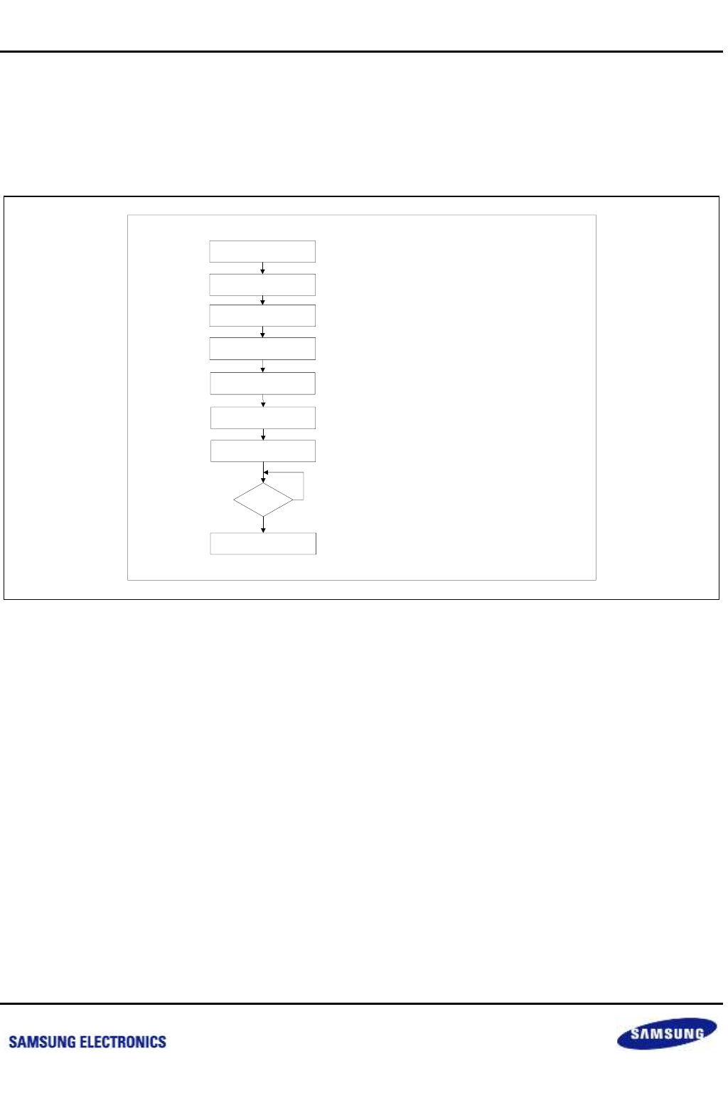
Samsung Confidential
S5P6818_UM 36 De-Interlace
36-5
Preliminary product information describes products that are in development, for which full characterization data and
associated errata are not yet available. Specifications and information herein are subject to change without notice.
36.3.4 De-Interlace Operation Flow
The De-interlace operation requires the setting of the address, width, height, vertical stride and horizontal stride of
the source data. For the address setting of the destination data, the field base address where the current field
data is copied as it is and the De-interlace base address where the de-interlaced data is stored should be set.
(The figure below)
Figure 36-4 De-Interlace Operation Flow
Source Y Image Set
Source CB Image Set
Destination Y Image Set
RUN
STOP
Busy
Source CR Image Set
Destination CB Image Set
Destination CR Image Set
Width, Height [ SRCSIZE_Y ]
Previous, Current, Next Y Base Address [ SRCADDRP/C/N_Y ]
Vertical, Horizontal Stride [ SRCSTRD_Y ]
Width, Height [ SRCSIZE_CB ]
Current Base CB Address [ SRCADDRC_CB ]
Vertical, Horizontal Stride [ SRCSTRD_CB ]
Width, Height [ SRCSIZE_CR ]
Current Base CR Address [ SRCADDRC_CB ]
Vertical, Horizontal Stride [ SRCSTRD_CR ]
Deinterlace Y Base Address [ DESTADDRD_Y ]
Field Y Base Address [ DESTADDRF_Y ]
Vertical Stride [ DESTSTRD_Y ]
Deinterlace CB Base Address [ DESTADDRD_CB ]
Field CB Base Address [ DESTADDRF_CB ]
Vertical Stride [ DESTSTRD_CB ]
Deinterlace CR Base Address [ DESTADDRD_CR ]
Field CR Base Address [ DESTADDRF_CR ]
Vertical Stride [ DESTSTRD_CR ]
No
Yes (Processing)
Deinterlace Start [ MODE ]
nexell / ys.kim at 2015.02.12
SAMSUNG Confidential

Samsung Confidential
S5P6818_UM 36 De-Interlace
36-6
Preliminary product information describes products that are in development, for which full characterization data and
associated errata are not yet available. Specifications and information herein are subject to change without notice.
36.4 Register Description
36.4.1 Register Map Summary
Base Address: 0xC006_5000h
Register
Offset
Description
Reset Value
CONTROL
0x00h
De-Interlace control register
0x0000_0000
CONFIG
0x04h
De-Interlace config register
0x0000_0002
INTENB
0x08h
De-Interlace Interrupt Enable register
0x0000_0000
INTPEN
0x0Ch
De-Interlace Interrupt Pending register
0x0000_0000
TSPARA
0x10h
De-Interlace AS Module Parameter register
0x0018_0010
TMPARA
0x14h
De-Interlace MD SAD Module Parameter register
0x0016_0008
TIPARA
0x18h
De-Interlace MI Module Parameter register
0x0306_0050
TPARA
0x1Ch
De-Interlace YS Module Parameter register
0x0466_0434
BLENDPARA
0x20h
De-Interlace Blend Module Parameter register
0x0000_0003
RSVD
0x24h to
0xFCh
Reserved
–
SRCSIZE_Y
0x100h
De-Interlace Y-Field Source Image Size register
0x0000_0000
SRCADDRP_Y
0x104h
De-Interlace Y-Field Previous Source Image Address register
0x0000_0000
SRCADDRC_Y
0x108h
De-Interlace Y-Field Current Source Image Address register
0x0000_0000
SRCADDRN_Y
0x10Ch
De-Interlace Y-Field Nest Source Image Address register
0x0000_0000
SRCSTRD_Y
0x110h
De-Interlace Y-Field Next Source Image Stride register
0x0000_0000
DESTADDRF_Y
0x114h
De-Interlace Y-Field Destination Image Field Address register
0x0000_0000
DESTADDRD_Y
0x118h
De-Interlace Y-Field Destination Image De-int Y Address
register
0x0000_0000
DESTSTRD_Y
0x11Ch
De-Interlace Y-Field Destination Image Stride register
0x0000_0000
RSVD
0x120h to
0x1FC
Reserved
–
SRCSIZE_CB
0x200h
De-Interlace CB-Field Source Image Size register
0x0000_0000
SRCADDRC_CB
0x204h
De-Interlace CB-Field Source Image Address register
0x0000_0000
SRCSTRD_CB
0x208h
De-Interlace CB-Field Source Image Stride register
0x0000_0000
DESTADDRF_CB
0x20Ch
De-Interlace CB-Field Destination Image Field Address register
0x0000_0000
DESTADDRD_CB
0x210h
De-Interlace CB-Field Destination Image Deinterlace Address
register
0x0000_0000
DESTSTRD_CB
0x214h
De-Interlace CB-Field Destination Image Stride register
0x0000_0000
RSVD
0x218h to
0x2FC
Reserved
–
SRCSIZE_CR
0x300h
De-Interlace Cr-Field Source Image Size register
0x0000_0000
SRCADDRC_CR
0x304h
De-Interlace Cr-Field Source Image Address register
0x0000_0000
SRCSTRD_CR
0x308h
De-Interlace Cr-Field Source Image Stride register
0x0000_0000
nexell / ys.kim at 2015.02.12
SAMSUNG Confidential

Samsung Confidential
S5P6818_UM 36 De-Interlace
36-7
Preliminary product information describes products that are in development, for which full characterization data and
associated errata are not yet available. Specifications and information herein are subject to change without notice.
Register
Offset
Description
Reset Value
DESTADDRF_CR
0x30Ch
De-Interlace Cr-Field Destination Image Address Field register
0x0000_0000
DESTADDRD_CR
0x310h
De-Interlace Cr-Field Destination Image Address Deinterlace
register
0x0000_0000
DESTSTRD_CR
0x314h
De-Interlace Cr-Field Deinterlace Image Stride register
0x0000_0000
nexell / ys.kim at 2015.02.12
SAMSUNG Confidential
Samsung Confidential
S5P6818_UM 36 De-Interlace
36-8
Preliminary product information describes products that are in development, for which full characterization data and
associated errata are not yet available. Specifications and information herein are subject to change without notice.
36.4.1.1 CONTROL
Base Address: 0xC006_5000
Address = Base Address + 0x00h, Reset Value = 0x0000_0000
Name
Bit
Type
Description
Reset Value
RSVD
[31:2]
–
Reserved. Program to Zero
-
SW_RESET
[1]
W
De-interlace SW reset bit
0x0
START
[0]
W
De-interlaced Start bit. This bit is cleared automatically
in Run mode after starting.
0 = None
1 = Start
0x0
36.4.1.2 CONFIG
Base Address: 0xC006_5000
Address = Base Address + 0x04h, Reset Value = 0x0000_0002
Name
Bit
Type
Description
Reset Value
RSVD
[31:15]
–
Reserved. Program to Zero
–
cfg_cr_field
[14]
RW
Cr Field Information
0 = Even field
1 = Odd field
1’b0
CFG_cb_FIELD
[13]
RW
Cb Field Information
0 = Even field
1 = Odd field
1’b0
CFG_y_FIELD
[12]
RW
Y Field Information
0 = Even field
1 = Odd field
1’b0
RSVD
[11]
–
Reserved. Program to Zero
–
cr_field_enb
[10]
RW
Enable Cr Deinterlace
0 = Disable
1 = Enable
1’b0
cb_field_enb
[9]
RW
Enable Cb Deinterlace
0 = Disable
1 = Enable
1’b0
y_field_enb
[8]
RW
Enable Y Deinterlace
0 = Disable
1 = Enable
1’b0
RSVD
[7]
–
Reserved. Program to Zero
–
DE_CUR_STATE
[6:4]
R
De-Interlace Current Status
3’b001: Processing Y Field
3’b010: Processing Cb Field
3’b100: Processing Cr Field
3’b000
RSVD
[3:2]
R
Reserved. Program to Zero
2’b00
nexell / ys.kim at 2015.02.12
SAMSUNG Confidential

Samsung Confidential
S5P6818_UM 36 De-Interlace
36-9
Preliminary product information describes products that are in development, for which full characterization data and
associated errata are not yet available. Specifications and information herein are subject to change without notice.
Name
Bit
Type
Description
Reset Value
DE_IDLE
[1]
R
De-Interlace Idle status
0 = Run
1 = Idle
1’b1
RSVD
[0]
–
Reserved.
–
36.4.1.3 INTENB
Base Address: 0xC006_5000
Address = Base Address + 0x08h, Reset Value =
Name
Bit
Type
Description
Reset Value
RSVD
[31:4]
–
Reserved. Program to Zero.
–
IRQ_EN_TOP
[3]
RW
De-interlace Operation Finish Interrupt Enable. This
bit shows that all configured operations are
completed.
0 = Disable
1 = Enable
1’b0
IRQ_EN_CR
[2]
RW
Cr Operation Finish Interrupt Enable
0 = Disable
1 = Enable
1’b0
IRQ_EN_CB
[1]
RW
Cb Operation Finish Interrupt Enable
0 = Disable
1 = Enable
1’b0
IRQ_EN_Y
[0]
RW
Y Operation Finish Interrupt Enable
0 = Disable
1 = Enable
1’b0
nexell / ys.kim at 2015.02.12
SAMSUNG Confidential

Samsung Confidential
S5P6818_UM 36 De-Interlace
36-10
Preliminary product information describes products that are in development, for which full characterization data and
associated errata are not yet available. Specifications and information herein are subject to change without notice.
36.4.1.4 INTPEN
Base Address: 0xC006_5000
Address = Base Address + 0x0Ch, Reset Value = 0x0000_0000
Name
Bit
Type
Description
Reset Value
RSVD
[31:4]
–
Reserved. Program to Zero.
–
IRQ_EN_TOP
[3]
RW
De-interlace Interrupt Pending
Read >
0 = None
1 = Interrupt Pended
Write >
0 = None
1 = Pending Clear
1’b0
IRQ_EN_CR
[2]
RW
Cr Interrupt Pending
Read >
0 = None
1 = Interrupt Pended
Write >
0 = None
1 = Pending Clear
1’b0
IRQ_EN_CB
[1]
RW
Cb Interrupt Pending
Read >
0 = None
1 = Interrupt Pended
Write >
0 = None
1 = Pending Clear
1’b0
IRQ_EN_Y
[0]
RW
Y Interrupt Pending
Read >
0 = None
1 = Interrupt Pended
Write >
0 = None
1 = Pending Clear
1’b0
nexell / ys.kim at 2015.02.12
SAMSUNG Confidential

Samsung Confidential
S5P6818_UM 36 De-Interlace
36-11
Preliminary product information describes products that are in development, for which full characterization data and
associated errata are not yet available. Specifications and information herein are subject to change without notice.
36.4.1.5 TSPARA
Base Address: 0xC006_5000
Address = Base Address + 0x10h, Reset Value = 0x0018_0010
Name
Bit
Type
Description
Reset Value
RSVD
[31:24]
–
Reserved. Program to Zero.
–
ts2
[23:16]
RW
As module Parameter TS2
8’h18
RSVD
[15:8]
–
Reserved. Program to Zero.
–
ts1
[7:0]
RW
As module Parameter TS1
8’h10
36.4.1.6 TMPARA
Base Address: 0xC006_5000
Address = Base Address + 0x14h, Reset Value = 0x0016_0008
Name
Bit
Type
Description
Reset Value
RSVD
[31:24]
–
Reserved. Program to Zero.
–
tM2
[23:16]
RW
MdSad module Parameter TM2
8’h16
RSVD
[15:8]
–
Reserved. Program to Zero.
–
tM1
[7:0]
RW
MdSad module Parameter TM1
8’h8
36.4.1.7 TIPARA
Base Address: 0xC006_5000
Address = Base Address + 0x18h, Reset Value = 0x0306_0050
Name
Bit
Type
Description
Reset Value
TI2
[31:16]
RW
Mi module Parameter TI2
16’h306
ti1
[15:0]
RW
Mi module Parameter TI1
16’h50
36.4.1.8 TPARA
Base Address: 0xC006_5000
Address = Base Address + 0x1Ch, Reset Value = 0x0466_0434
Name
Bit
Type
Description
Reset Value
RSVD
[31:25]
-
Reserved. Program to Zero.
-
T2
[24:16]
RW
Ys module Parameter T2
9’h466
RSVD
[15:9]
-
Reserved. Program to Zero.
-
T1
[8:0]
RW
Ys module Parameter T1
9’h434
nexell / ys.kim at 2015.02.12
SAMSUNG Confidential
Samsung Confidential
S5P6818_UM 36 De-Interlace
36-12
Preliminary product information describes products that are in development, for which full characterization data and
associated errata are not yet available. Specifications and information herein are subject to change without notice.
36.4.1.9 BLENDPARA
Base Address: 0xC006_5000
Address = Base Address + 0x20h, Reset Value = 0x0000_0003
Name
Bit
Type
Description
Reset Value
RSVD
[31:4]
–
Reserved. Program to Zero.
–
shiftvalue
[3:0]
RW
Blend module Parameter
4’h3
36.4.1.10 SRCSIZE_Y
Base Address: 0xC006_5100
Address = Base Address + 0x00h, Reset Value = 0x0000_0000
Name
Bit
Type
Description
Reset Value
RSVD
[31:27]
–
Reserved. Program to Zero.
–
Y_HEIGHT
[26:16]
RW
Y field pixel height
11’h0
RSVD
[15:11]
–
Reserved. Program to Zero.
–
Y_width
[10:0]
RW
Y field pixel width
11’h0
36.4.1.11 SRCADDRP_Y
Base Address: 0xC006_5100
Address = Base Address + 0x04h, Reset Value = 0x0000_0000
Name
Bit
Type
Description
Reset Value
Y_PREVBASEADDR
[31:0]
RW
Source Base Address: Previous Y Field
32’h0
36.4.1.12 SRCADDRC_Y
Base Address: 0xC006_5100
Address = Base Address + 0x08h, Reset Value = 0x0000_0000
Name
Bit
Type
Description
Reset Value
Y_CURRBASEADDR
[31:0]
RW
Source Base Address: Current Y Field
32’h0
36.4.1.13 SRCADDRN_Y
Base Address: 0xC006_5100
Address = Base Address + 0x0Ch, Reset Value = 0x0000_0000
Name
Bit
Type
Description
Reset Value
Y_NEXTBASEADDR
[31:0]
RW
Source Base Address: Next Y Field
32’h0
nexell / ys.kim at 2015.02.12
SAMSUNG Confidential
Samsung Confidential
S5P6818_UM 36 De-Interlace
36-13
Preliminary product information describes products that are in development, for which full characterization data and
associated errata are not yet available. Specifications and information herein are subject to change without notice.
36.4.1.14 SRCSTRD_Y
Base Address: 0xC006_5100
Address = Base Address + 0x10h, Reset Value = 0x0000_0000
Name
Bit
Type
Description
Reset Value
Y_SRCSTRIDE
[31:0]
RW
Source Stride
32’h0
36.4.1.15 DESTADDRF_Y
Base Address: 0xC006_5100
Address = Base Address + 0x14h, Reset Value = 0x0000_0000
Name
Bit
Type
Description
Reset Value
Y_DESTADDRF
[31:0]
RW
Destination Memory Address: Field Y
32’h0
36.4.1.16 DESTADDRD_Y
Base Address: 0xC006_5100
Address = Base Address + 0x18h, Reset Value = 0x0000_0000
Name
Bit
Type
Description
Reset Value
Y_DESTADDRD
[31:0]
RW
Destination Memory Address: De-Interlaced Y
32’h0
36.4.1.17 DESTSTRD_Y
Base Address: 0xC006_5100
Address = Base Address + 0x1Ch, Reset Value = 0x0000_0000
Name
Bit
Type
Description
Reset Value
Y_DESTSTRIDE
[31:0]
RW
Destination Stride
32’h0
36.4.1.18 SRCSIZE_CB
Base Address: 0xC006_5200
Address = Base Address + 0x00h, Reset Value = 0x0000_0000
Name
Bit
Type
Description
Reset Value
RSVD
[31:27]
-
Reserved. Program to Zero.
-
cb_HEIGHT
[26:16]
RW
Cb field pixel height
11’h0
RSVD
[15:11]
-
Reserved. Program to Zero.
-
CB_width
[10:0]
RW
Cb field pixel width
11’h0
nexell / ys.kim at 2015.02.12
SAMSUNG Confidential
Samsung Confidential
S5P6818_UM 36 De-Interlace
36-14
Preliminary product information describes products that are in development, for which full characterization data and
associated errata are not yet available. Specifications and information herein are subject to change without notice.
36.4.1.19 SRCADDRC_CB
Base Address: 0xC006_5200
Address = Base Address + 0x04h, Reset Value = 0x0000_0000
Name
Bit
Type
Description
Reset Value
CB_CURRBASEADDR
[31:0]
RW
Source Base Address: Current Cb Field
32’h0
36.4.1.20 SRCSTRD_CB
Base Address: 0xC006_5200
Address = Base Address + 0x08h, Reset Value = 0x0000_0000
Name
Bit
Type
Description
Reset Value
CB_SRCSTRIDE
[31:0]
RW
Source Stride: Current Cb Field
32’h0
36.4.1.21 DESTADDRF_CB
Base Address: 0xC006_5200
Address = Base Address + 0x0Ch, Reset Value = 0x0000_0000
Name
Bit
Type
Description
Reset Value
CB_DESTADDRF
[31:0]
RW
Destination Address: Cb Field
32’h0
36.4.1.22 DESTADDRD_CB
Base Address: 0xC006_5200
Address = Base Address + 0x10h, Reset Value = 0x0000_0000
Name
Bit
Type
Description
Reset Value
CB_DESTADDRD
[31:0]
RW
Destination Address: De-interlaced Cb
32’h0
36.4.1.23 DESTSTRD_CB
Base Address: 0xC006_5200
Address = Base Address + 0x14h, Reset Value = 0x0000_0000
Name
Bit
Type
Description
Reset Value
CB_DESTSTRIDE
[31:0]
RW
Source Stride: Current Cb Field
32’h0
nexell / ys.kim at 2015.02.12
SAMSUNG Confidential
Samsung Confidential
S5P6818_UM 36 De-Interlace
36-15
Preliminary product information describes products that are in development, for which full characterization data and
associated errata are not yet available. Specifications and information herein are subject to change without notice.
36.4.1.24 SRCSIZE_CR
Base Address: 0xC006_5300
Address = Base Address + 0x00h, Reset Value = 0x0000_0000
Name
Bit
Type
Description
Reset Value
RSVD
[31:27]
–
Reserved. Program to Zero.
5’h0
cR_HEIGHT
[26:16]
RW
Cr field pixel height
11’h0
RSVD
[15:11]
–
Reserved. Program to Zero.
5’h0
CR_width
[10:0]
RW
Cr field pixel width
11’h0
36.4.1.25 SRCADDRC_CR
Base Address: 0xC006_5300
Address = Base Address + 0x04h, Reset Value = 0x0000_0000
Name
Bit
Type
Description
Reset Value
CR_CURRBASEADDR
[31:0]
RW
Source Base Address: Current Cr Field
32’h0
36.4.1.26 SRCSTRD_CR
Base Address: 0xC006_5300
Address = Base Address + 0x08h, Reset Value = 0x0000_0000
Name
Bit
Type
Description
Reset Value
CR_SRCSTRIDE
[31:0]
RW
Source Stride: Current Cr Field
32’h0
DESTADDRF_CR
Base Address: 0xC006_5300
Address = Base Address + 0x0Ch, Reset Value = 0x0000_0000
Name
Bit
Type
Description
Reset Value
CR_DESTADDRF
[31:0]
RW
Destination Address: Cr Field
32’h0
DESTADDRD_CR
Base Address: 0xC006_5300
Address = Base Address + 0x10h, Reset Value = 0x0000_0000
Name
Bit
Type
Description
Reset Value
CR_DESTADDRD
[31:0]
RW
Destination Address: De-interlaced Cr
32’h0
nexell / ys.kim at 2015.02.12
SAMSUNG Confidential

Samsung Confidential
S5P6818_UM 36 De-Interlace
36-16
Preliminary product information describes products that are in development, for which full characterization data and
associated errata are not yet available. Specifications and information herein are subject to change without notice.
36.4.1.27 DESTSTRD_CR
Base Address: 0xC006_5300
Address = Base Address + 0x14h, Reset Value = 0x0000_0000
Name
Bit
Type
Description
Reset Value
CR_DESTSTRIDE
[31:0]
RW
Source Stride: Current Cr Field
32’h0
nexell / ys.kim at 2015.02.12
SAMSUNG Confidential

Samsung Confidential
S5P6818_UM 37 Scaler
37-1
Preliminary product information describes products that are in development, for which full characterization data and
associated errata are not yet available. Specifications and information herein are subject to change without notice.
37 Scaler
37.1 Overview
The Scaler is the block to change image sizes. The Scaler reads an image from the memory and writes the image
to the memory after Up/Down Scaling and Low-pass Filtering. At this time, the Scaler changes the direction of the
image by using the Flip or Rotation function.
37.2 Features
Source/Destination Image
Format: Separated YUV Format (420, 422, 444), Interleaved UV
Size: (8 to 4096) (8 to 4096) (Width is set as a multiple of eight).
Upscale Ratio: 8 8 4096 4096
Downscale Ratio: 4096 4096 8 8
Lowpass filter available after Upscale or before Downscale.
Horizontal 5-Tab Filter: Coefficients 64 Sets.
Vertical 3-Tab Filter: Coefficients 32 Sets (For Frequency Response, refer to Operation Item).
nexell / ys.kim at 2015.02.12
SAMSUNG Confidential
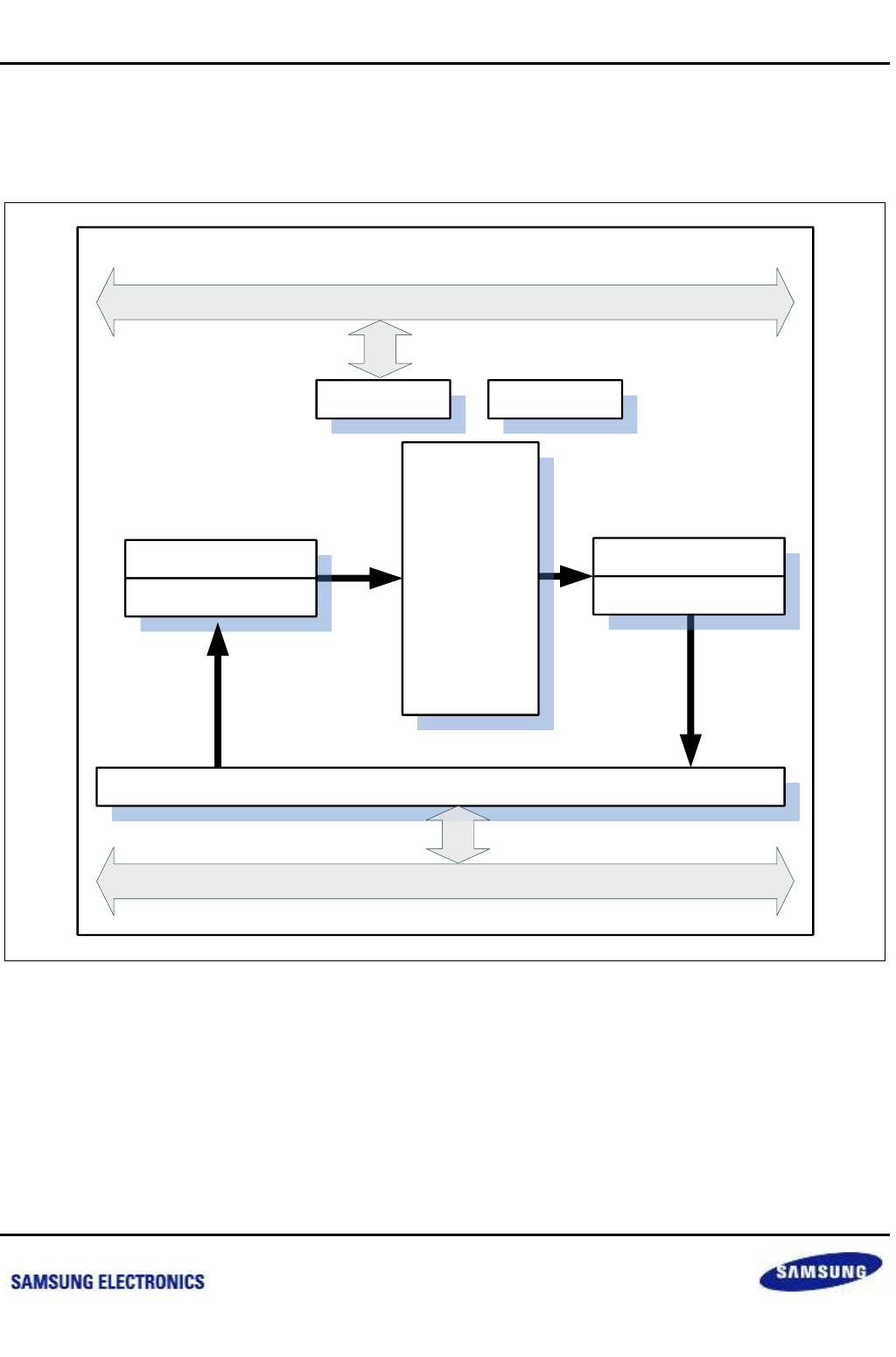
Samsung Confidential
S5P6818_UM 37 Scaler
37-2
Preliminary product information describes products that are in development, for which full characterization data and
associated errata are not yet available. Specifications and information herein are subject to change without notice.
37.3 Block Diagram
The Scaler consists of the blocks (SRC_ADDR_GEN, DEST_ADDR_GEN) to generate addresses, the Filter
block, the FIFO block, and the blocks (CPUIF and POS_GEN2) to exchange data with bus.
Figure 37-1 Fine Scaler Filter Block Diagram
SCALER_CPUIF SCALER_POS_GEN2
SCALER_FILTER
SCALER_SRC_ADDR_GEN
SCALER_SRC_FIFO
MCUARBIT64BIT4CH_SCALER
SCALER_DEST_ADDR_GEN
SCALER_DEST_FIFO
SCALER_TOP
PBUS
MCU BUS
nexell / ys.kim at 2015.02.12
SAMSUNG Confidential
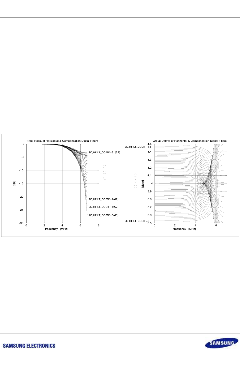
Samsung Confidential
S5P6818_UM 37 Scaler
37-3
Preliminary product information describes products that are in development, for which full characterization data and
associated errata are not yet available. Specifications and information herein are subject to change without notice.
37.4 Functional Description
The Scales enable a user to read a source image in memory, change the image size and store the image in the
memory. The Scaler changes image sizes by using the setting values of the address, width and height of the
source and destination images. A user can use the low-pass filter and rotate functions of the Scaler.
37.4.1 Digital Filter Characteristics
The low-pass filter of the Scaler has the horizontal filter of 5-tab and the vertical filter of 3-tab. The Scaler prevents
image quality deterioration when an image is enlarged by using the low-pass filter.
37.4.1.1 Horizontal Filter (5-Tab FIR Filter) Frequency Response and Group Delay
The figure below shows the characteristics of the horizontal filter of the Scaler and the filter has the setting range
between 0 and 63. The Scaler register, SCCFGREG.SC_HFILT_COEFF, is used for the setting.
Figure 37-2 Horizontal Filter (5-Tab FIR Filter) Frequency Response and Group Delay
nexell / ys.kim at 2015.02.12
SAMSUNG Confidential
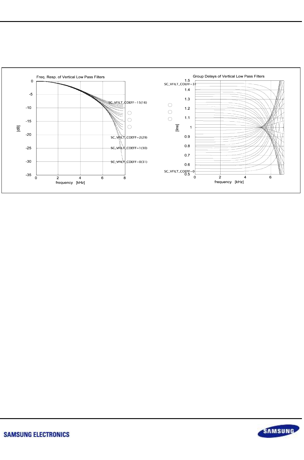
Samsung Confidential
S5P6818_UM 37 Scaler
37-4
Preliminary product information describes products that are in development, for which full characterization data and
associated errata are not yet available. Specifications and information herein are subject to change without notice.
37.4.1.2 Vertical Filter (3-Tab FIR Filter) Frequency Response and Group Delay
The figure below shows the characteristics of the vertical filter of Scaler and the filter has the setting range
between 0 and 31. The Scaler register, SCCFGREG.SC_VFILT_COEFF, is used for the setting.
Figure 37-3 Vertical Filter (3-Tab FIR Filter) Frequency Response and Group Delay
nexell / ys.kim at 2015.02.12
SAMSUNG Confidential

Samsung Confidential
S5P6818_UM 37 Scaler
37-5
Preliminary product information describes products that are in development, for which full characterization data and
associated errata are not yet available. Specifications and information herein are subject to change without notice.
37.5 Programming Guide
37.5.1 Configuration
1. Check the Scaler controller status: SCINTREG.SC_BUSY = 0
2. Set the source address and stride to the SCSRCADDR and SCSRCSTRIDE register respectively.
3. Set SCSRCSIZEREG.SC_SRC_WIDTH and SCSRCSIZEREG.SC_SRC_HEIGHT register. (the width is a
multiple of 8).
4. Set the destination address and stride to the SCDESTADDR0 and SCDESTSTRIDE0 register respectively. If
you need to scale UV interleaved image, set the destination address and stride to the SCDESTADDR1 and
SCDESTSTRIDE1 register respectively.
5. Set SCDESTSIZEREG.SC_DEST_WIDTH and SCDESTSIZEREG.SC_DEST_HEIGHT register. (the width is
a multiple of 8).
6. Delta Image setting: Set DELTAXREG and DELTAYREG register.
7. Soft setting: Set Horizontal/Vertical Set HVSOFTREG register.
8. Set the filter: Set the filter as On/Off by using SCCFGREG.SC_FILT_ENB. Select the Filter Coefficient Set by
using SCCFGREG.SC_HFILT_COEFF and SCCFGREG.SC_VFILT_COEFF.
9. Set the interrupt: SCINTREG.SC_INT_ENB register.
nexell / ys.kim at 2015.02.12
SAMSUNG Confidential
Samsung Confidential
S5P6818_UM 37 Scaler
37-6
Preliminary product information describes products that are in development, for which full characterization data and
associated errata are not yet available. Specifications and information herein are subject to change without notice.
37.5.2 RUN
1. Set the SCRUNREG.SC_RUN bit as "1".
2. Read the SCINTREG.SC_BUSY register to check the operation status.
3. If the SCRUNREG.SC_RUN bit is cleared when SCINTREG.SC_BUSY = 1, the operation halts immediately.
Figure 37-4 Scaler Operation Flow
Busy
Source Image Set
Destination
Image Set
Filter Set
Rotation Set
Run
Stop
Address [ SCSRCADDREG ]
Width [ SCSRCSIZEREG ]
Height
Address [ SCDESTADDRREG ]
Width [ SCDESTSIZEREG ]
Height
Horizontal Coefficient [ SCCFGREG ]
Vertical Coefficient
0', 0H’, 180', 180H’ [ SCCFGREG ]
No ( End or Halt )
Yes ( Running )
Scaler Start [ SCRUNREG ]
nexell / ys.kim at 2015.02.12
SAMSUNG Confidential

Samsung Confidential
S5P6818_UM 37 Scaler
37-7
Preliminary product information describes products that are in development, for which full characterization data and
associated errata are not yet available. Specifications and information herein are subject to change without notice.
37.6 Register Description
37.6.1 Register Map Summary
Base Address: 0xC006_6000
Register
Offset
Description
Reset Value
SCRUNREG
0x000h
Scaler Run Register
0x0000_0000
SCCFGREG
0x004h
Scaler Configuration Register
0x0000_0000
SCINTREG
0x008h
Scaler Interrupt Register
0x0000_0000
SCSRCADDRREG
0x00Ch
Scaler Source Address Register
0x0000_0000
SCSRCADDRREG
0x010h
Scaler Source Stride Register
0x0000_0000
SCSRCSIZEREG
0x014h
Scaler Source Size Register
0x0000_0000
SCDESTADDR0
0x018h
Scaler Destination Address Register 0
0x0000_0000
SCDESTSTREDE0
0x01Ch
Scaler Destination Stride Register 0
0x0000_0000
SCDESTADDR1
0x020h
Scaler Destination Address Register1
0x0000_0000
SCDESTADDR1
0x024h
Scaler Destination Stride Register1
0x0000_0000
SCDESTSIZE
0x028h
Scaler Destination Size Register
0x0000_0000
DELTAXREG
0x02Ch
Scaler Horizontal Delta Register
0x0000_0000
DELTAYREG
0x030h
Scaler Vertical Delta Register
0x0000_0000
HVSOFTREG
0x034h
Scaler Ratio Reset Value Register
0x0000_0000
CMDBUFADDR
0x038h
Scaler Command Buffer Base Address Register
0x0000_0000
CMDBUFCON
0x03Ch
Scaler Command Buffer Control Register
0x0000_0000
YVFILTER[N]_00_03
0x040h (Filter1)
0x060h (Filter2)
0x080h (Filter3)
Scaler YV Filter[N] Value Table Register0
0x0000_0000
YVFILTER[N]_04_07
0x044h (Filter1)
0x064h (Filter2)
0x084h (Filter3)
Scaler YV Filter[N] Value Table Register1
0x0000_0000
YVFILTER[N]_04_07
0x044h (Filter1)
0x064h (Filter2)
0x084h (Filter3)
Scaler YV Filter[N] Value Table Register1
0x0000_0000
YVFILTER[N]_08_11
0x048h (Filter1)
0x068h (Filter2)
0x088h (Filter3)
Scaler YV Filter[N] Value Table Register2
0x0000_0000
YVFILTER[N]_12_15
0x04Ch (Filter1)
0x06Ch (Filter2)
0x08Ch (Filter3)
Scaler YV Filter[N] Value Table Register3
0x0000_0000
YVFILTER[N]_16_19
0x050h (Filter1)
0x070h (Filter2)
0x090h (Filter3)
Scaler YV Filter[N] Value Table Register4
0x0000_0000
YVFILTER[N]_20_23
0x054h (Filter1)
0x074h (Filter2)
0x094h (Filter3)
Scaler YV Filter[N] Value Table Register5
0x0000_0000
nexell / ys.kim at 2015.02.12
SAMSUNG Confidential

Samsung Confidential
S5P6818_UM 37 Scaler
37-8
Preliminary product information describes products that are in development, for which full characterization data and
associated errata are not yet available. Specifications and information herein are subject to change without notice.
Register
Offset
Description
Reset Value
YVFILTER[N]_24_27
0x058h (Filter1)
0x078h (Filter2)
0x098h (Filter23)
Scaler YV Filter[N] Value Table Register6
0x0000_0000
YVFILTER[N]_28_31
0x05Ch (Filter1)
0x07Ch (Filter2)
0x09Ch (Filter23)
Scaler YV Filter[N] Value Table Register7
0x0000_0000
RSVD
0x0A0h to 0x0FC
Reserved
0x0000_0000
YHFILTER[N]_00_01
0x100h (Filter1)
0x140h (Filter2)
0x180h (Filter3)
0x1C0h (Filter4)
0x200h (Filter5)
Scaler YH Filter1 to 5 Value Table Register0
0x0000_0000
YHFILTER[N]_02_03
0x104h (Filter1)
0x144h (Filter2)
0x184h (Filter3)
0x1C4h (Filter4)
0x204h (Filter5)
Scaler YH Filter1 to 5 Value Table Register1
0x0000_0000
YHFILTER[N]_04_05
0x108h (Filter1)
0x148h (Filter2)
0x188h (Filter3)
0x1C8h (Filter4)
0x208h (Filter5)
Scaler YH Filter1 to 5 Value Table Register2
0x0000_0000
YHFILTER[N]_06_07
0x10Ch (Filter1)
0x14Ch (Filter2)
0x18Ch (Filter3)
0x1CCh (Filter4)
0x20Ch (Filter5)
Scaler YH Filter1 to 5 Value Table Register3
0x0000_0000
YHFILTER[N]_08_09
0x110h (Filter1)
0x150h (Filter2)
0x190h (Filter3)
0x1D0h (Filter4)
0x210h (Filter5)
Scaler YH Filter1 to 5 Value Table Register4
0x0000_0000
YHFILTER[N]_10_11
0x114h (Filter1)
0x154h (Filter2)
0x194h (Filter3)
0x1D4h (Filter4)
0x214h (Filter5)
Scaler YH Filter1 to 5 Value Table Register5
0x0000_0000
YHFILTER[N]_12_13
0x118h (Filter1)
0x158h (Filter2)
0x198h (Filter3)
0x1D8h (Filter4)
0x218h (Filter5)
Scaler YH Filter1 to 5 Value Table Register6
0x0000_0000
YHFILTER[N]_14_15
0x11Ch (Filter1)
0x15Ch (Filter2)
0x19Ch (Filter3)
0x1DCh (Filter4)
0x21Ch (Filter5)
Scaler YH Filter1 to 5 Value Table Register7
0x0000_0000
nexell / ys.kim at 2015.02.12
SAMSUNG Confidential

Samsung Confidential
S5P6818_UM 37 Scaler
37-9
Preliminary product information describes products that are in development, for which full characterization data and
associated errata are not yet available. Specifications and information herein are subject to change without notice.
Register
Offset
Description
Reset Value
YHFILTER[N]_16_17
0x120h (Filter1)
0x160h (Filter2)
0x1A0h (Filter3)
0x1E0h (Filter4)
0x220h (Filter5)
Scaler YH Filter1 to 5 Value Table Register8
0x0000_0000
YHFILTER[N]_18_19
0x124h (Filter1)
0x164h (Filter2)
0x1A4h (Filter3)
0x1E4h (Filter4)
0x224h (Filter5)
Scaler YH Filter1 to 5 Value Table Register9
0x0000_0000
YHFILTER[N]_20_21
0x128h (Filter1)
0x168h (Filter2)
0x1A8h (Filter3)
0x1E8h (Filter4)
0x228h (Filter5)
Scaler YH Filter1 to 5 Value Table Register10
0x0000_0000
YHFILTER[N]_22_23
0x12Ch (Filter1)
0x16Ch (Filter2)
0x1ACh (Filter3)
0x1ECh (Filter4)
0x22Ch (Filter5)
Scaler YH Filter1 to 5 Value Table Register11
0x0000_0000
YHFILTER[N]_24_25
0x130h (Filter1)
0x170h (Filter2)
0x1B0h (Filter3)
0x1F0h (Filter4)
0x230h (Filter5)
Scaler YH Filter1 to 5 Value Table Register12
0x0000_0000
YHFILTER[N]_26_27
0x134h (Filter1)
0x174h (Filter2)
0x1B4h (Filter3)
0x1F4h (Filter4)
0x234h (Filter5)
Scaler YH Filter1 to 5 Value Table Register13
0x0000_0000
YHFILTER[N]_28_29
0x138h (Filter1)
0x178h (Filter2)
0x1B8h (Filter3)
0x1F8h (Filter4)
0x238h (Filter5)
Scaler YH Filter1 to 5 Value Table Register13
0x0000_0000
YHFILTER[N]_30_31
0x13Ch (Filter1)
0x17Ch (Filter2)
0x1BCh (Filter3)
0x1FCh (Filter4)
0x23Ch (Filter5)
Scaler YH Filter1 to 5 Value Table Register15
0x0000_0000
nexell / ys.kim at 2015.02.12
SAMSUNG Confidential

Samsung Confidential
S5P6818_UM 37 Scaler
37-10
Preliminary product information describes products that are in development, for which full characterization data and
associated errata are not yet available. Specifications and information herein are subject to change without notice.
37.6.1.1 SCRUNREG
Base Address: 0xC006_6000
Address = Base Address + 0x000h, Reset Value = 0x0000_0000
Name
Bit
Type
Description
Reset Value
RSVD
[31:1]
–
Reserved
31'h0
SC_RUN
[0]
RW
Scaler RUN bit.
When the scaling process is finished, SCALER clears
this bit automatically. While the scale process is
running, it can be halted by clearing this bit.
0 = Stop
1 = Start (Auto Clear)
1'b0
37.6.1.2 SCCFGREG
Base Address: 0xC006_6000
Address = Base Address + 0x004h, Reset Value = 0x0000_0000
Name
Bit
Type
Description
Reset Value
RSVD
[31:21]
–
Reserved
11'h0
SC_VFILT_COEFF
[20:16]
RW
Vertical filter coefficient select.
Range is 0 to 31. (See Frequency Response Graph)
–
RSVD
[15:14]
–
Reserved
2'b00
SC_HFILT_COEFF
[13:8]
RW
Horizontal filter coefficient select.
Range is 0 to 63. (See Frequency Response Graph)
–
RSVD
[7:2]
–
Reserved
6'h0
SC_FILT_ENB
[1:0]
RW
Fine scale filter enable.
00 = Filter Disable
01 = Reserved
10 = Reserved
11 = Filter Enable
NOTE: This bit should be set as "00" or "11"
-
nexell / ys.kim at 2015.02.12
SAMSUNG Confidential
Samsung Confidential
S5P6818_UM 37 Scaler
37-11
Preliminary product information describes products that are in development, for which full characterization data and
associated errata are not yet available. Specifications and information herein are subject to change without notice.
37.6.1.3 SCINTREG
Base Address: 0xC006_6000
Address = Base Address + 0x008h, Reset Value = 0x0000_0000
Name
Bit
Type
Description
Reset Value
RSVD
[31:25]
–
Reserved
7'h0
SC_BUSY
[24]
R
Scaler Busy Check
0 = Scaler Idle
1 = Scaler Busy
1'b0
RSVD
[23:18]
–
Reserved
6'h0
CMD_PROC_INT_E
NB
[17]
RW
Internal Command Processor Interrupt Enable
0 = Disable
1 = Enable
1'b0
SC_INT_ENB
[16]
RW
Scaler Interrupt Enable
0 = Disable
1 = Enable
1'b0
RSVD
[15:10]
RW
Reserved
6'h0
CMD_PROC_INT_C
LR
[9]
W
Clear Internal Command Processor Interrupt Pending Bit
0 = None
1 = Clear Interrupt Pending
1'b0
SC_INT_CLR
[8]
W
Clear Internal Command Processor Interrupt Pending Bit
0 = None
1 = Clear Interrupt Pending
1'b0
RSVD
[7:2]
–
Reserved
6'h0
CMD_PROC_INT_P
END
[1]
R
Command Processor Interrupt Pending Bit
0 = None
1 = Interrupt Pending
1'b0
SC_INT_PEND
[0]
R
Scaler Interrupt Pending Bit
0 = None
1 = Interrupt Pending
1'b0
37.6.1.4 SCSRCADDRREG
Base Address: 0xC006_6000
Address = Base Address + 0x00Ch, Reset Value = 0x0000_0000
Name
Bit
Type
Description
Reset Value
SC_SRC_REG
[31:0]
RW
Source Base Address Register
–
nexell / ys.kim at 2015.02.12
SAMSUNG Confidential
Samsung Confidential
S5P6818_UM 37 Scaler
37-12
Preliminary product information describes products that are in development, for which full characterization data and
associated errata are not yet available. Specifications and information herein are subject to change without notice.
37.6.1.5 SCSRCADDRREG
Base Address: 0xC006_6000
Address = Base Address + 0x010h, Reset Value = 0x0000_0000
Name
Bit
Type
Description
Reset Value
SC_SRC_STR
[31:0]
RW
Source Stride Register
–
37.6.1.6 SCSRCSIZEREG
Base Address: 0xC006_6000
Address = Base Address + 0x014h, Reset Value = 0x0000_0000
Name
Bit
Type
Description
Reset Value
RSVD
[31:28]
–
Reserved
–
SC_SRC_HEIGHT
[27:16]
RW
Source Image Height.
Height's range is 8 to 4096 (Source Height – 1)
12'h0
RSVD
[15:12]
–
Reserved
4'h0
SC_SRC_WIDTH
[11:0]
RW
Set Source Image Width.
Width's range is 8 to 4096. Width must align to 8
(Source width – 1)
–
37.6.1.7 SCDESTADDR0
Base Address: 0xC006_6000
Address = Base Address + 0x018h, Reset Value = 0x0000_0000
Name
Bit
Type
Description
Reset Value
SC_DEST_ADDR0
[31:0]
RW
Destination Base Address0
–
37.6.1.8 SCDESTSTREDE0
Base Address: 0xC006_6000
Address = Base Address + 0x01Ch, Reset Value = 0x0000_0000
Name
Bit
Type
Description
Reset Value
SC_DEST_STRIDE0
[31:0]
RW
Destination Stride
–
nexell / ys.kim at 2015.02.12
SAMSUNG Confidential
Samsung Confidential
S5P6818_UM 37 Scaler
37-13
Preliminary product information describes products that are in development, for which full characterization data and
associated errata are not yet available. Specifications and information herein are subject to change without notice.
37.6.1.9 SCDESTADDR1
Base Address: 0xC006_6000
Address = Base Address + 0x020h, Reset Value = 0x0000_0000
Name
Bit
Type
Description
Reset Value
SC_DEST_ADDR1
[31:0]
RW
Destination Base Address1
NOTE: UV interleaved mode only
–
37.6.1.10 SCDESTADDR1
Base Address: 0xC006_6000
Address = Base Address + 0x024h, Reset Value = 0x0000_0000
Name
Bit
Type
Description
Reset Value
SC_DEST_STRIDE1
[31:0]
RW
Destination Stride
NOTE: UV interleaved mode only
–
37.6.1.11 SCDESTSIZE
Base Address: 0xC006_6000
Address = Base Address + 0x028h, Reset Value = 0x0000_0000
Name
Bit
Type
Description
Reset Value
RSVD
[31:28]
–
Reserved
4'h0
SC_DEST_HEIGHT
[27:16]
RW
Destination Image Height
Height's range is 8 to 4096 (Destination Height -1)
–
RSVD
[15:12]
–
Reserved
4'h0
SC_DEST_WIDTH
[11:0]
RW
Destination Image Width
Image's range is 8 to 4096
–
37.6.1.12 DELTAXREG
Base Address: 0xC006_6000
Address = Base Address + 0x02Ch, Reset Value = 0x0000_0000
Name
Bit
Type
Description
Reset Value
DELTAXREG
[31:0]
RW
Delta X of X-axis DELTA_X = (sc_src_width
h'10000) / (sc_dest_width-1)
32'h0
nexell / ys.kim at 2015.02.12
SAMSUNG Confidential
Samsung Confidential
S5P6818_UM 37 Scaler
37-14
Preliminary product information describes products that are in development, for which full characterization data and
associated errata are not yet available. Specifications and information herein are subject to change without notice.
37.6.1.13 DELTAYREG
Base Address: 0xC006_6000
Address = Base Address + 0x030h, Reset Value = 0x0000_0000
Name
Bit
Type
Description
Reset Value
DELTAYREG
[31:0]
RW
Delta Y of Y-axis DELTA_Y = (sc_src_height
h'10000) / (sc_dest_height-1)
32'h0
37.6.1.14 HVSOFTREG
Base Address: 0xC006_6000
Address = Base Address + 0x034h, Reset Value = 0x0000_0000
Name
Bit
Type
Description
Reset Value
RSVD
[31:21]
–
Reserved
–
V_RATIO
[20:16]
RW
Vertical Filter Ratio
5'h0
RSVD
[15:6]
–
Reserved
–
H_RATIO
[5:0]
RW
Horizontal Filter Ratio
6'h0
37.6.1.15 CMDBUFADDR
Base Address: 0xC006_6000
Address = Base Address + 0x038h, Reset Value = 0x0000_0000
Name
Bit
Type
Description
Reset Value
CMDBUFADDR
[31:0]
RW
Scaler Command Buffer Base Address Register
–
37.6.1.16 CMDBUFCON
Base Address: 0xC006_6000
Address = Base Address + 0x03Ch, Reset Value = 0x0000_0000
Name
Bit
Type
Description
Reset Value
RSVD
[31:2]
–
Reserved
–
CMDBUF_STOP
[1]
RW
Scaler Command Buffer Stop Register
0 = No operation 1 = Stop
1'b0
CMDBUF_START
[0]
RW
Scaler Command Buffer Start Register
0 = No operation 1 = Start
1'b0
nexell / ys.kim at 2015.02.12
SAMSUNG Confidential
Samsung Confidential
S5P6818_UM 37 Scaler
37-15
Preliminary product information describes products that are in development, for which full characterization data and
associated errata are not yet available. Specifications and information herein are subject to change without notice.
37.6.1.17 YVFILTER[N]_00_03
Base Address: 0xC006_6000
Address = Base Address + 0x040h (Filter1), 0x060h (Filter2), 0x080 (Filter3), Reset Value = 0x0000_0000
Name
Bit
Type
Description
Reset Value
FILTER_YVCOEF[N]_03
[31:24]
W
Scaler YVCOEF[N] value
8'h0
FILTER_YVCOEF[N]_02
[23:16]
W
Scaler YVCOEF[N] value
8'h0
FILTER_YVCOEF[N]_01
[15:8]
W
Scaler YVCOEF[N] value
8'h0
FILTER_YVCOEF[N]_00
[7:0]
W
Scaler YVCOEF[N] value
8'h0
37.6.1.18 YVFILTER[N]_04_07
Base Address: 0xC006_6000
Address = Base Address + 0x044h (Filter1), 0x064h (Filter2), 0x084 (Filter3), Reset Value = 0x0000_0000
Name
Bit
Type
Description
Reset Value
FILTER_YVCOEF[N]_07
[31:24]
W
Scaler YVCOEF[N] value
8'h0
FILTER_YVCOEF[N]_06
[23:16]
W
Scaler YVCOEF[N] value
8'h0
FILTER_YVCOEF[N]_05
[15:8]
W
Scaler YVCOEF[N] value
8'h0
FILTER_YVCOEF[N]_04
[7:0]
W
Scaler YVCOEF[N] value
8'h0
37.6.1.19 YVFILTER[N]_08_11
Base Address: 0xC006_6000
Address = Base Address + 0x048h (Filter1), 0x068h (Filter2), 0x088 (Filter3), Reset Value = 0x0000_0000
Name
Bit
Type
Description
Reset Value
FILTER_YVCOEF[N]_11
[31:24]
W
Scaler YVCOEF[N] value
8'h0
FILTER_YVCOEF[N]_10
[23:16]
W
Scaler YVCOEF[N] value
8'h0
FILTER_YVCOEF[N]_09
[15:8]
W
Scaler YVCOEF[N] value
8'h0
FILTER_YVCOEF[N]_08
[7:0]
W
Scaler YVCOEF[N] value
8'h0
nexell / ys.kim at 2015.02.12
SAMSUNG Confidential
Samsung Confidential
S5P6818_UM 37 Scaler
37-16
Preliminary product information describes products that are in development, for which full characterization data and
associated errata are not yet available. Specifications and information herein are subject to change without notice.
37.6.1.20 YVFILTER[N]_12_15
Base Address: 0xC006_6000
Address = Base Address + 0x04Ch (Filter1), 0x06Ch (Filter2), 0x08C (Filter3), Reset Value = 0x0000_0000
Name
Bit
Type
Description
Reset Value
FILTER_YVCOEF[N]_15
[31:24]
W
Scaler YVCOEF[N] value
8'h0
FILTER_YVCOEF[N]_14
[23:16]
W
Scaler YVCOEF[N] value
8'h0
FILTER_YVCOEF[N]_13
[15:8]
W
Scaler YVCOEF[N] value
8'h0
FILTER_YVCOEF[N]_12
[7:0]
W
Scaler YVCOEF[N] value
8'h0
37.6.1.21 YVFILTER[N]_16_19
Base Address: 0xC006_6000
Address = Base Address + 0x050h (Filter1), 0x070h (Filter2), 0x090h (Filter3), Reset Value = 0x0000_0000
Name
Bit
Type
Description
Reset Value
FILTER_YVCOEF[N]_19
[31:24]
W
Scaler YVCOEF[N] value
8'h0
FILTER_YVCOEF[N]_18
[23:16]
W
Scaler YVCOEF[N] value
8'h0
FILTER_YVCOEF[N]_17
[15:8]
W
Scaler YVCOEF[N] value
8'h0
FILTER_YVCOEF[N]_16
[7:0]
W
Scaler YVCOEF[N] value
8'h0
37.6.1.22 YVFILTER[N]_20_23
Base Address: 0xC006_6000
Address = Base Address + 0x054h (Filter1), 0x074h (Filter2), 0x094h (Filter3), Reset Value = 0x0000_0000
Name
Bit
Type
Description
Reset Value
FILTER_YVCOEF[N]_23
[31:24]
W
Scaler YVCOEF[N] value
8'h0
FILTER_YVCOEF[N]_22
[23:16]
W
Scaler YVCOEF[N] value
8'h0
FILTER_YVCOEF[N]_21
[15:8]
W
Scaler YVCOEF[N] value
8'h0
FILTER_YVCOEF[N]_20
[7:0]
W
Scaler YVCOEF[N] value
8'h0
nexell / ys.kim at 2015.02.12
SAMSUNG Confidential

Samsung Confidential
S5P6818_UM 37 Scaler
37-17
Preliminary product information describes products that are in development, for which full characterization data and
associated errata are not yet available. Specifications and information herein are subject to change without notice.
37.6.1.23 YVFILTER[N]_24_27
Base Address: 0xC006_6000
Address = Base Address + 0x058h (Filter1), 0x078h (Filter2), 0x098h (Filter23), Reset Value = 0x0000_0000
Name
Bit
Type
Description
Reset Value
FILTER_YVCOEF[N]_27
[31:24]
W
Scaler YVCOEF[N] value
8'h0
FILTER_YVCOEF[N]_26
[23:16]
W
Scaler YVCOEF[N] value
8'h0
FILTER_YVCOEF[N]_25
[15:8]
W
Scaler YVCOEF[N] value
8'h0
FILTER_YVCOEF[N]_24
[7:0]
W
Scaler YVCOEF[N] value
8'h0
37.6.1.24 YVFILTER[N]_28_31
Base Address: 0xC006_6000
Address = Base Address + 0x05Ch (Filter1), 0x07Ch (Filter2), 0x09Ch (Filter23), Reset Value = 0x0000_0000
Name
Bit
Type
Description
Reset Value
FILTER_YVCOEF[N]_31
[31:24]
W
Scaler YVCOEF[N] value
8'h0
FILTER_YVCOEF[N]_30
[23:16]
W
Scaler YVCOEF[N] value
8'h0
FILTER_YVCOEF[N]_29
[15:8]
W
Scaler YVCOEF[N] value
8'h0
FILTER_YVCOEF[N]_28
[7:0]
W
Scaler YVCOEF[N] value
8'h0
37.6.1.25 YHFILTER[N]_00_01
Base Address: 0xC006_6000
Address = Base Address + 0x100h (Filter1), 0x140 (Filter2), 0x180 (Filter3), 0x1C0 (Filter4), 0x200 (Filter5),
Reset Value = 0x0000_0000
Name
Bit
Type
Description
Reset Value
RSVD
[31:26]
–
Reserved
–
FILTER_YHCOEF[N]_01
[25:16]
W
Scaler YHCOEF[N] value
10'h0
RSVD
[15:10]
–
Reserved
–
FILTER_YHCOEF[n]_00
[9:0]
W
Scaler YHCOEF[N] value
10'h0
nexell / ys.kim at 2015.02.12
SAMSUNG Confidential
Samsung Confidential
S5P6818_UM 37 Scaler
37-18
Preliminary product information describes products that are in development, for which full characterization data and
associated errata are not yet available. Specifications and information herein are subject to change without notice.
37.6.1.26 YHFILTER[N]_02_03
Base Address: 0xC006_6000
Address = Base Address + 0x104h (Filter1), 0x144 (Filter2), 0x184 (Filter3), 0x1C4 (Filter4), 0x204 (Filter5),
Reset Value = 0x0000_0000
Name
Bit
Type
Description
Reset Value
RSVD
[31:26]
–
Reserved
–
FILTER_YHCOEF[n]_03
[25:16]
W
Scaler YHCOEF[N] value
10'h0
RSVD
[15:10]
–
Reserved
–
FILTER_YHCOEF[n]_02
[9:0]
W
Scaler YHCOEF[N] value
10'h0
37.6.1.27 YHFILTER[N]_04_05
Base Address: 0xC006_6000
Address = Base Address + 0x108h (Filter1), 0x148 (Filter2), 0x188 (Filter3), 0x1C8 (Filter4), 0x208 (Filter5),
Reset Value = 0x0000_0000
Name
Bit
Type
Description
Reset Value
RSVD
[31:26]
–
Reserved
–
FILTER_YHCOEF[n]_05
[25:16]
W
Scaler YHCOEF[N] value
10'h0
RSVD
[15:10]
–
Reserved
–
FILTER_YHCOEF[n]_04
[9:0]
W
Scaler YHCOEF[N] value
10'h0
37.6.1.28 YHFILTER[N]_06_07
Base Address: 0xC006_6000
Address = Base Address + 0x10Ch (Filter1), 0x14C (Filter2), 0x18C (Filter3), 0x1CC (Filter4), 0x20C (Filter5),
Reset Value = 0x0000_0000
Name
Bit
Type
Description
Reset Value
RSVD
[31:26]
–
Reserved
–
FILTER_YHCOEF[n]_07
[25:16]
W
Scaler YHCOEF[N] value
10'h0
RSVD
[15:10]
–
Reserved
–
FILTER_YHCOEF[n]_06
[9:0]
W
Scaler YHCOEF[N] value
10'h0
nexell / ys.kim at 2015.02.12
SAMSUNG Confidential
Samsung Confidential
S5P6818_UM 37 Scaler
37-19
Preliminary product information describes products that are in development, for which full characterization data and
associated errata are not yet available. Specifications and information herein are subject to change without notice.
37.6.1.29 YHFILTER[N]_08_09
Base Address: 0xC006_6000
Address = Base Address + 0x110h (Filter1), 0x150 (Filter2), 0x190 (Filter3), 0x1D0 (Filter4), 0x210 (Filter5),
Reset Value = 0x0000_0000
Name
Bit
Type
Description
Reset Value
RSVD
[31:26]
–
Reserved
–
FILTER_YHCOEF[n]_09
[25:16]
W
Scaler YHCOEF[N] value
10'h0
RSVD
[15:10]
–
Reserved
–
FILTER_YHCOEF[n]_08
[9:0]
W
Scaler YHCOEF[N] value
10'h0
37.6.1.30 YHFILTER[N]_10_11
Base Address: 0xC006_6000
Address = Base Address + 0x114h (Filter1), 0x154 (Filter2), 0x194 (Filter3), 0x1D4 (Filter4), 0x214 (Filter5),
Reset Value = 0x0000_0000
Name
Bit
Type
Description
Reset Value
RSVD
[31:26]
–
Reserved
–
FILTER_YHCOEF[n]_11
[25:16]
W
Scaler YHCOEF[N] value
10'h0
RSVD
[15:10]
–
Reserved
–
FILTER_YHCOEF[n]_10
[9:0]
W
Scaler YHCOEF[N] value
10'h0
37.6.1.31 YHFILTER[N]_12_13
Base Address: 0xC006_6000
Address = Base Address + 0x118h (Filter1), 0x158 (Filter2), 0x198 (Filter3), 0x1D8 (Filter4), 0x218 (Filter5),
Reset Value = 0x0000_0000
Name
Bit
Type
Description
Reset Value
RSVD
[31:26]
–
Reserved
–
FILTER_YHCOEF[n]_13
[25:16]
W
Scaler YHCOEF[N] value
10'h0
RSVD
[15:10]
–
Reserved
–
FILTER_YHCOEF[n]_12
[9:0]
W
Scaler YHCOEF[N] value
10'h0
nexell / ys.kim at 2015.02.12
SAMSUNG Confidential
Samsung Confidential
S5P6818_UM 37 Scaler
37-20
Preliminary product information describes products that are in development, for which full characterization data and
associated errata are not yet available. Specifications and information herein are subject to change without notice.
37.6.1.32 YHFILTER[N]_14_15
Base Address: 0xC006_6000
Address = Base Address + 0x11Ch (Filter1), 0x15C (Filter2), 0x19C (Filter3), 0x1DC (Filter4), 0x21C (Filter5),
Reset Value = 0x0000_0000
Name
Bit
Type
Description
Reset Value
RSVD
[31:26]
–
Reserved
–
FILTER_YHCOEF[n]_15
[25:16]
W
Scaler YHCOEF[N] value
10'h0
RSVD
[15:10]
–
Reserved
–
FILTER_YHCOEF[n]_14
[9:0]
W
Scaler YHCOEF[N] value
10'h0
37.6.1.33 YHFILTER[N]_16_17
Base Address: 0xC006_6000
Address = Base Address + 0x120h (Filter1), 0x160 (Filter2), 0x1A0 (Filter3), 0x1E0 (Filter4), 0x220 (Filter5),
Reset Value = 0x0000_0000
Name
Bit
Type
Description
Reset Value
RSVD
[31:26]
–
Reserved
–
FILTER_YHCOEF[n]_17
[25:16]
W
Scaler YHCOEF[N] value
10'h0
RSVD
[15:10]
–
Reserved
–
FILTER_YHCOEF[n]_16
[9:0]
W
Scaler YHCOEF[N] value
10'h0
37.6.1.34 YHFILTER[N]_18_19
Base Address: 0xC006_6000
Address = Base Address + 0x124h (Filter1), 0x164 (Filter2), 0x1A4 (Filter3), 0x1E4 (Filter4), 0x224 (Filter5),
Reset Value = 0x0000_0000
Name
Bit
Type
Description
Reset Value
RSVD
[31:26]
–
Reserved
–
FILTER_YHCOEF[n]_19
[25:16]
W
Scaler YHCOEF[N] value
10'h0
RSVD
[15:10]
–
Reserved
–
FILTER_YHCOEF[n]_18
[9:0]
W
Scaler YHCOEF[N] value
10'h0
nexell / ys.kim at 2015.02.12
SAMSUNG Confidential

Samsung Confidential
S5P6818_UM 37 Scaler
37-21
Preliminary product information describes products that are in development, for which full characterization data and
associated errata are not yet available. Specifications and information herein are subject to change without notice.
37.6.1.35 YHFILTER[N]_20_21
Base Address: 0xC006_6000
Address = Base Address + 0x128h (Filter1), 0x168 (Filter2), 0x1A8 (Filter3), 0x1E8 (Filter4), 0x228 (Filter5),
Reset Value = 0x0000_0000
Name
Bit
Type
Description
Reset Value
RSVD
[31:26]
–
Reserved
–
FILTER_YHCOEF[n]_21
[25:16]
W
Scaler YHCOEF[N] value
10'h0
RSVD
[15:10]
–
Reserved
–
FILTER_YHCOEF[n]_20
[9:0]
W
Scaler YHCOEF[N] value
10'h0
37.6.1.36 YHFILTER[N]_22_23
Base Address: 0xC006_6000
Address = Base Address + 0x12Ch (Filter1), 0x16C (Filter2), 0x1AC (Filter3), 0x1EC (Filter4), 0x22C (Filter5),
Reset Value = 0x0000_0000
Name
Bit
Type
Description
Reset Value
RSVD
[31:26]
–
Reserved
–
FILTER_YHCOEF[n]_23
[25:16]
W
Scaler YHCOEF[N] value
10'h0
RSVD
[15:10]
–
Reserved
–
FILTER_YHCOEF[n]_22
[9:0]
W
Scaler YHCOEF[N] value
10'h0
37.6.1.37 YHFILTER[N]_24_25
Base Address: 0xC006_6000
Address = Base Address + 0x130h (Filter1), 0x170 (Filter2), 0x1B0 (Filter3), 0x1F0 (Filter4), 0x230 (Filter5),
Reset Value = 0x0000_0000
Name
Bit
Type
Description
Reset Value
RSVD
[31:26]
–
Reserved
–
FILTER_YHCOEF[n]_25
[25:16]
W
Scaler YHCOEF[N] value
10'h0
RSVD
[15:10]
–
Reserved
–
FILTER_YHCOEF[n]_24
[9:0]
W
Scaler YHCOEF[N] value
10'h0
nexell / ys.kim at 2015.02.12
SAMSUNG Confidential

Samsung Confidential
S5P6818_UM 37 Scaler
37-22
Preliminary product information describes products that are in development, for which full characterization data and
associated errata are not yet available. Specifications and information herein are subject to change without notice.
37.6.1.38 YHFILTER[N]_26_27
Base Address: 0xC006_6000
Address = Base Address + 0x134h (Filter1), 0x174 (Filter2), 0x1B4 (Filter3), 0x1F4 (Filter4), 0x234 (Filter5),
Reset Value = 0x0000_0000
Name
Bit
Type
Description
Reset Value
RSVD
[31:26]
–
Reserved
–
FILTER_YHCOEF[n]_27
[25:16]
W
Scaler YHCOEF[N] value
10'h0
RSVD
[15:10]
–
Reserved
–
FILTER_YHCOEF[n]_26
[9:0]
W
Scaler YHCOEF[N] value
10'h0
37.6.1.39 YHFILTER[N]_28_29
Base Address: 0xC006_0000
Address = Base Address + 0x138h (Filter1), 0x178 (Filter2), 0x1B8 (Filter3), 0x1F8 (Filter4), 0x238 (Filter5),
Reset Value = 0x0000_0000
Name
Bit
Type
Description
Reset Value
RSVD
[31:26]
–
Reserved
–
FILTER_YHCOEF[n]_29
[25:16]
W
Scaler YHCOEF[N] value
10'h0
RSVD
[15:10]
–
Reserved
–
FILTER_YHCOEF[n]_28
[9:0]
W
Scaler YHCOEF[N] value
10'h0
37.6.1.40 YHFILTER[N]_30_31
Base Address: 0xC006_6000
Address = Base Address + 0x13Ch (Filter1), 0x17C (Filter2), 0x1BC (Filter3), 0x1FC (Filter4), 0x23C (Filter5),
Reset Value = 0x0000_0000
Name
Bit
Type
Description
Reset Value
RSVD
[31:26]
–
Reserved
–
FILTER_YHCOEF[n]_31
[25:16]
W
Scaler YHCOEF[N] value
10'h0
RSVD
[15:10]
–
Reserved
–
FILTER_YHCOEF[n]_30
[9:0]
W
Scaler YHCOEF[N] value
10'h0
nexell / ys.kim at 2015.02.12
SAMSUNG Confidential

Samsung Confidential
S5P6818_UM 38 LVDS
38-1
Preliminary product information describes products that are in development, for which full characterization data and
associated errata are not yet available. Specifications and information herein are subject to change without notice.
38 LVDS
38.1 Overview
The LVDS (Low-Voltage differential signaling) is a block that generates the signals to interface with external LVDS
display devices. The LVDS consists of a LVDS Controller and LVDS PHY block. The LVDS Controller receives
RGB Video data from the DPC (or Resolution Converter) and converts RGB Video Data into a suitable LVDS data
stream format and transmits converted RGB Video data to the LVDS PHY block. And the LVDS Controller
transmits the control signals to the LVDS PHY block. The LVDS PHY block transmits received RGB Video Data
from the LVDS Controller through 6 LVDS output channels.
38.2 Features
Selectable Progressive RGB Video data (2 DPC)
Supports JEIDA and VESA data packing for LVDS output
Programmable data packing for LVDS output (configurable)
Internal Input Video clock range: 30M to 90 MHz
6 LVDS output channels (5 data channels, 1 clock channel)
35:7 data channel compression up to 630Mbps on each LVDS channel
Power down mode
nexell / ys.kim at 2015.02.12
SAMSUNG Confidential
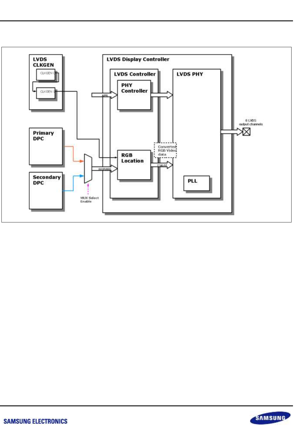
Samsung Confidential
S5P6818_UM 38 LVDS
38-2
Preliminary product information describes products that are in development, for which full characterization data and
associated errata are not yet available. Specifications and information herein are subject to change without notice.
38.3 Block Diagram
Figure 38-1 LVDS Block Diagram
nexell / ys.kim at 2015.02.12
SAMSUNG Confidential
Samsung Confidential
S5P6818_UM 38 LVDS
38-3
Preliminary product information describes products that are in development, for which full characterization data and
associated errata are not yet available. Specifications and information herein are subject to change without notice.
38.4 Functional Description
38.4.1 LVDS Data Packing Format
The LVDS Controller converts received RGB Video Data from DPC into one of three data packing formats and
transmits them to the LVDS PHY block. Following is supported LVDS data packing formats.
VESA data packing format
JEIDA data packing format
User Programmable data packing format
In the VESA and JEIDA data packing formats, four of the five data channel is used for transmission. Following is a
format for each data packing format.
Table 38-1 VESA Data Packing Format
Channel
Bit Position
6
5
4
3
2
1
0
LVDS Channel A
bit 0
bit 5
bit 4
bit 3
bit 2
bit 1
bit 0
LVDS Channel B
bit 1
bit 0
bit 5
bit 4
bit 3
bit 2
bit 1
LVDS Channel C
DE
VSYNC
HSYNC
bit 5
bit 4
bit 3
bit 2
LVDS Channel D
Don't' care
bit 7
bit 6
bit 7
bit 6
bit 7
bit 6
LVDS Channel E
Not used
Not used
Not used
Not used
Not used
Not used
Not used
Table 38-2 JEIDA Data Packing Format
Channel
Bit Position
6
5
4
3
2
1
0
LVDS Channel A
bit 2
bit 7
bit 6
bit 5
bit 4
bit 3
bit 2
LVDS Channel B
bit 3
bit 2
bit 7
bit 6
bit 5
bit 4
bit 3
LVDS Channel C
DE
VSYNC
HSYNC
bit 7
bit 6
bit 5
bit 4
LVDS Channel D
Don't' care
bit 1
bit 0
bit 1
bit 0
bit 1
bit 0
LVDS Channel E
Not used
Not used
Not used
Not used
Not used
Not used
Not used
nexell / ys.kim at 2015.02.12
SAMSUNG Confidential
Samsung Confidential
S5P6818_UM 38 LVDS
38-4
Preliminary product information describes products that are in development, for which full characterization data and
associated errata are not yet available. Specifications and information herein are subject to change without notice.
When users set LCD_FORMAT bit of LVDSCTRL0 register to VESA data packing format, the outputs from the
LVDS has a form of the table above Similarity, when users set them to JEIDA data packing format, the outputs
has a form of the table above.
In the User Programmable data packing format, users can set own data packing format for the LVDS output.
Users determine for each bit of the channel, willing to output what signal. The signal can be a Hsync, Vsync, DE,
or RGB Color bit. In the User Programmable data packing format, the setting value of the register means in the
table below.
Table 38-3 Location Setting Input Format
Bit Position
[34:31]
[30:27]
[26]
[25]
[24]
[23:16]
[15: 8]
[ 7: 0]
4'b1111
4'b0000
VDEN
VSync
HSync
RED[7:0]
GREEN[7:0]
BLUE[7:0]
For examples, if users want to set 0'st bit of the LVDS Channel A to RED[2], users set the LOC_A0 bit of the
LVDSLOC0 register to 17. (Note that 17'th bit position in Table 36-3 is the RED[2]) If users want to set 5'th bit of
the LVDS Channel D to VSync, users set the LOC_D5 bit of the LVDSLOC5 register to 25.
38.4.2 LVDS Application Note
In S5P6818, users can choose one of two RGB Video data.
Primary DPC Video Data
Secondary DPC Video Data
The following sequence should be used to use LVDS device. (Assuming that the sequence uses the Primary DPC
Video Data)
1. Release the Reset of the DisplayTop and DualDisplay
2. Set the configuration of the Primary MLC and the Primary DPC. Set the Vertical, Horizontal Sync width of the
DPC with the same width of the exterior LVSD Display Device's. Set the output format of the DPC to RGB888
format. Assuming that the DPC CLKGEN's clock source is PLL2 and clock divider is 2.
3. Set the LVDS CLKGEN's clock source is PLL2 and clock divider is 2 (same as the DPC CLKGEN).
Recommend Configuration is the following.
CLKGEN 0: SRC(PLL2), DIV(2)
CLKGEN 1: SRC(7), DIV(2)
4. Set the LVDS_MUXSEL bit of the LVDS_MUXCTRL register to 0 (Using the Primary DPC), Set the
LVDS_MUXENB bit of the LVDS_MUXCTRL register to 1 (Enable).
nexell / ys.kim at 2015.02.12
SAMSUNG Confidential
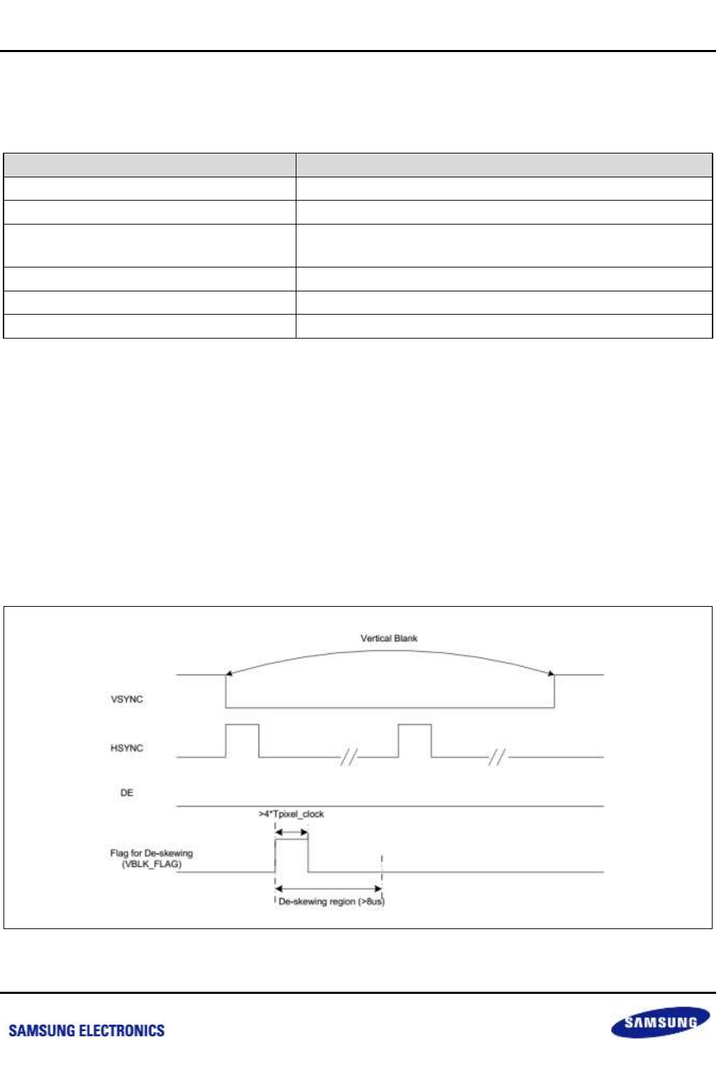
Samsung Confidential
S5P6818_UM 38 LVDS
38-5
Preliminary product information describes products that are in development, for which full characterization data and
associated errata are not yet available. Specifications and information herein are subject to change without notice.
5. Set the LVDS data packing mode, set the configuration for LVDS Control Register. The table below shows a
example of using VESA data packing format.
Table 38-4 Recommend Configure for LVDS (VESA)
Register Name
Value
LVDSCTRL0
0x1003_6C70
LVDSCTRL1
0x0000_36DB
LVDSCTRL2
0x0000_538E (High Speed, > 90MHz)
0x0000_128A (Low Speed, < 90MHz)
LVDSCTRL3
0x0000_0333
LVDSCTRL4
0x003F_FC20
LVDSTMODE0
0x0000_0080
6. Release the reset of the LVDS PHY block.
38.4.3 Skew Control between Output Data and Clock
The LVDS has the auto de-skew control function, If the LVDSCTRL0.I_AUTO_SEL and
LVDSCTRL4.AUTO_DSK_SEL are high. The LVDS could operate the de-skewing function automatically. For the
auto de-skewing, the signal which informs the vertical blank region is injected to the LVDS TX as like the figure
below.
If customer want to implement the auto de-skew function, RX have to support auto de-skew function.
In S5P6818, auto de-skew works only with Using the Primary DPC RGB Video.
Figure 38-2 De-skewing Timing Diagram at Vertical blank
nexell / ys.kim at 2015.02.12
SAMSUNG Confidential
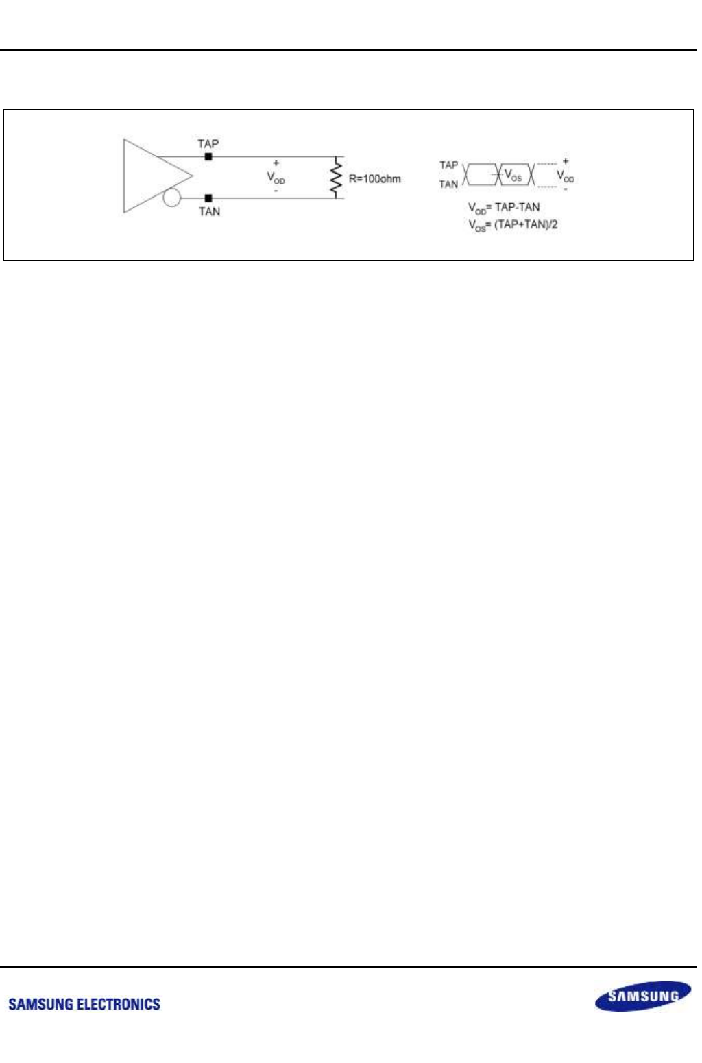
Samsung Confidential
S5P6818_UM 38 LVDS
38-6
Preliminary product information describes products that are in development, for which full characterization data and
associated errata are not yet available. Specifications and information herein are subject to change without notice.
38.4.4 Electrical Characteristics
Figure 38-3 Output Common Mode Voltage and Differential Voltage
nexell / ys.kim at 2015.02.12
SAMSUNG Confidential
Samsung Confidential
S5P6818_UM 38 LVDS
38-7
Preliminary product information describes products that are in development, for which full characterization data and
associated errata are not yet available. Specifications and information herein are subject to change without notice.
38.5 Register Description
38.5.1 Register Map Summary
Base Address: 0xC010_A000
Register
Offset
Description
Reset Value
LVDSCTRL0
0x00h
LVDS Control register 0
0x0003_6C70
LVDSCTRL1
0x04h
LVDS Control register 1
0x0000_0000
LVDSCTRL2
0x08h
LVDS Control register 2
0x0000_028A
LVDSCTRL3
0x0Ch
LVDS Control register 3
0x0000_00C3
LVDSCTRL4
0x10h
LVDS Control register 4
0x003F_FC20
LVDSLOC0
0x20h
LVDS LOCATION register 0
0x0000_0000
LVDSLOC1
0x24h
LVDS LOCATION register 1
0x0000_0000
LVDSLOC2
0x28h
LVDS LOCATION register 2
0x0000_0000
LVDSLOC3
0x2Ch
LVDS LOCATION register 3
0x0000_0000
LVDSLOC4
0x30h
LVDS LOCATION register 4
0x0000_0000
LVDSLOC5
0x34h
LVDS LOCATION register 5
0x0000_0000
LVDSLOC6
0x38h
LVDS LOCATION register 6
0x0000_0000
LVDSLOCMASK0
0x40h
LVDS LOCATION MASK register 0
0x0000_0000
LVDSLOCMASK1
0x44h
LVDS LOCATION MASK register 1
0x0000_0000
LVDSLOCPOL0
0x48h
LVDS LOCATION PORALITY register 0
0x0000_0000
LVDSLOCPOL1
0x4Ch
LVDS LOCATION PORALITY register 1
0x0000_0000
LVDSTMODE0
0x50h
LVDS TEST MODE register 0
0x0000_0000
LVDSTMODE1
0x54h
LVDS TEST MODE register 1
-
Base Address : 0xC010_1000
Register
Offset
Description
Reset Value
DisplayTop Register
LVDS_MUXCTRL
0x0Ch
DISPLAYTOP LVDS MUX Control register
0x0000_0000
nexell / ys.kim at 2015.02.12
SAMSUNG Confidential

Samsung Confidential
S5P6818_UM 38 LVDS
38-8
Preliminary product information describes products that are in development, for which full characterization data and
associated errata are not yet available. Specifications and information herein are subject to change without notice.
38.5.1.1 LVDSCTRL0
Base Address: 0xC010_A000
Address = Base Address + 0x00h, Reset Value = 0x0003_6C70
Name
Bit
Type
Description
Reset Value
RSVD
[31]
R
Reserved
1'b0
CPU_I_VBLK_FLAG_SEL
[30]
RW
Enable/Disable Using CPU_I_VBLK_FLAG
(I_VBLK_FLAG used for de-skew)
0 = Using Input Video's VBLK
1 = Using CPU_I_VBLK
1'b0
CPU_I_VBLK_FLAG
[29]
RW
Specifies the CPU_I_VBLK_FLAG Value
1'b0
SKINI_BST
[28]
RW
Delay initial control pin for BIST
0 = Bypass
1 = Delay control
1'b0
DLYS_BST
[27]
RW
Delay control pin for BIST
0 = 25ps
1 = 50ps
1'b0
I_AUTO_SEL
[26]
RW
Auto de-skew selection pin
0 = Auto de-skew
1 = Not auto de-skew
1'b0
RSVD
[25:24]
R
Reserved
2'b00
DE_POL
[23]
RW
Specifies the polarity of the Data Enable (DE)
(applicable to VESA and JEIDA data packing format
only)
0 = High Active
1 = Low Active
1'b0
HSYNC_POL
[22]
RW
Specifies the polarity of the Horizontal Sync (HSync)
(applicable to VESA and JEIDA data packing format
only) - High Active means HSync is HIGH when
Horizontal Sync Period
0 = High Active
1 = Low Active
1'b0
VSYNC_POL
[21]
RW
Specifies the polarity of the Vertical Sync (VSync)
(applicable to VESA and JEIDA data packing format
only) - High Active means VSync is HIGH when Vertical
Sync Period
0 = High Active
1 = Low Active
1'b0
LCD_FORMAT
[20:19]
RW
Specifies the LVDS data packing format
0 = VESA data packing format
1 = JEIDA data packing format
2 = User Programmable data packing format
3 = Reserved (Undefined data packing format)
2'b00
I_LOCK_PPM_SET
[18:13]
RW
PPM setting for PLL lock
6'h1B
I_DESKEW_CNT_SET
[12:1]
RW
Adjust the period of de-skew region.
12'h638
nexell / ys.kim at 2015.02.12
SAMSUNG Confidential
Samsung Confidential
S5P6818_UM 38 LVDS
38-9
Preliminary product information describes products that are in development, for which full characterization data and
associated errata are not yet available. Specifications and information herein are subject to change without notice.
Name
Bit
Type
Description
Reset Value
I_AUTO_SEL
[0]
RW
Auto de-skew selection pin
0 = auto de-skew
1 = not auto de-skew
1'b0
38.5.1.2 LVDSCTRL1
Base Address: 0xC010_A000
Address = Base Address + 0x04h, Reset Value = 0x0000_0000
Name
Bit
Type
Description
Reset Value
TX4010X_DUMMY
[31:29]
RW
Dummy Pin (for LVDS PHY self test)
3'b0
I_ATE_MODE
[28]
RW
Function or ATE
0 = Function
1 = ATE
1'b0
I_TEST_CON_MODE
[27]
RW
DA or I2C
0 = DA
1 = I2C
1'b0
I_TX4010X_DUMMY
[26:24]
RW
Dummy Pin (for LVDS PHY self test)
3'b000
RSVD
[23:18]
R
Reserved
6'h0
SKCCK
[17:15]
RW
TX output skew control pin at ODD clock ch.(Dft:
3'b011)
3'b000
SKC4
[14:12]
RW
TX output skew control pin at ODD ch4 (Dft: 3'b011)
3'b000
SKC3
[11:9]
RW
TX output skew control pin at ODD ch3 (Dft: 3'b011)
3'b000
SKC2
[8:6]
RW
TX output skew control pin at ODD ch2 (Dft: 3'b011)
3'b000
SKC1
[5:3]
RW
TX output skew control pin at ODD ch1 (Dft: 3'b011)
3'b000
SKC0
[2:0]
RW
TX output skew control pin at ODD ch0 (Dft: 3'b011)
3'b000
nexell / ys.kim at 2015.02.12
SAMSUNG Confidential

Samsung Confidential
S5P6818_UM 38 LVDS
38-10
Preliminary product information describes products that are in development, for which full characterization data and
associated errata are not yet available. Specifications and information herein are subject to change without notice.
38.5.1.3 LVDSCTRL2
Base Address: 0xC010_A000
Address = Base Address + 0x08h, Reset Value = 0x0000_028A
Name
Bit
Type
Description
Reset Value
RSVD
[31:16]
R
Reserved
16'h0
CK_POL_SEL
[15]
RW
Input clock polarity selection pin
0 = Bypass
1 = Inversion
1'b0
VSEL
[14]
RW
VCO Frequency range selection pin
0 = Low speed (40MHz to 90MHz)
1 = High speed (90MHz to 160MHz)
1'b0
S
[13:12]
RW
Post-scaler control pin for PLL
Recommend:
Low speed: 2'b01
High speed: 2'b01
2'b00
M
[11:6]
RW
Main divider control pin for PLL
Recommend:
Low speed: 6'b001010
High speed: 6'b001110
6'hA
P
[5:0]
RW
Pre-divider control pin for PLL
Recommend:
Low speed: 6'b001010
High speed: 6'b001110
6'hA
38.5.1.4 LVDSCTRL3
Base Address: 0xC010_A000
Address = Base Address + 0x0Ch, Reset Value = 0x0000_00C3
Name
Bit
Type
Description
Reset Value
RSVD
[31:10]
R
Reserved
22'h0
SK_BIAS
[9:6]
RW
Bias current control pin for Skew
4'h3
SKEWINI
[5]
RW
Skew selection pin
0 = Bypass
1 = Skew enable
1'b0
SKEW_EN_H
[4]
RW
Skew block power down
0 = Power down
1 = Operating
1'b0
CNTB_TDLY
[3]
RW
Delay control pin for each channel
0 = 25p
1 = 50ps
1'b0
SEL_DATABF
[2]
RW
Input clock 1/2 division control pin
1'b0
SKEW_REG_CUR
[1:0]
RW
Regulator bias current selection pin in SKEW block
2'b11
nexell / ys.kim at 2015.02.12
SAMSUNG Confidential

Samsung Confidential
S5P6818_UM 38 LVDS
38-11
Preliminary product information describes products that are in development, for which full characterization data and
associated errata are not yet available. Specifications and information herein are subject to change without notice.
38.5.1.5 LVDSCTRL4
Base Address: 0xC010_A000
Address = Base Address + 0X10h, Reset Value = 0x003F_FC20
Name
Bit
Type
Description
Reset Value
RSVD
[31:29]
R
Reserved
3'b000
FLT_CNT
[28]
RW
Filter control pin for PLL
1'b0
VOD_ONLY_CNT
[27]
RW
The pre-emphasis's pre-driver control pin (VOD Only)
0 = Disable
1 = Enable
1'b0
CNNCT_MODE_SEL
[26]
RW
Connectivity mode selection pin
0 = TX operating
1 = Connectivity check.
1'b0
CNNCT_CNT
[25:24]
RW
Connectivity control pin
0 = TX operating
1 = Connectivity check
2, 3 = X (Don't care)
2'b00
VOD_HIGH_S
[23]
RW
VOD control pin
0 = Normal w/pre-emphasis
1 = Vod only
1'b0
SRC_TRH
[22]
RW
Source termination resistor selection pin
0 = Off
1 = Termination
1'b0
CNT_VOD_H
[21:14]
RW
TX driver output differential voltage level control pin
8'hFF
CNT_PEN_H
[13:6]
RW
TX driver pre-emphasis level control
(Dft: 8'b0000_0001)
8'hF0
FC_CODE
[5:3]
RW
Vos control pin
3'b100
OUTCON
[2]
RW
TX Driver state selection pin
0 = Hi-z
1 = Low
1'b0
LOCK_CNT
[1]
RW
Lock signal selection pin
0 = Lock enable 1 = Lock disable
1'b0
AUTO_DSK_SEL
[0]
RW
Auto de-skew selection pin for analog
0 = Normal
1 = Auto-de-skew
1'b0
nexell / ys.kim at 2015.02.12
SAMSUNG Confidential

Samsung Confidential
S5P6818_UM 38 LVDS
38-12
Preliminary product information describes products that are in development, for which full characterization data and
associated errata are not yet available. Specifications and information herein are subject to change without notice.
38.5.1.6 LVDSLOC0
Base Address: 0xC010_A000
Address = Base Address + 0x20h, Reset Value = 0x0000_0000
Name
Bit
Type
Description
Reset Value
RSVD
[31:30]
R
Reserved
2'h0
LOC_A4
[29:24]
RW
Select a location to go in LVDS Channel A bit 4.
(applicable to User Programmable data packing format only)
6'h0
LOC_A3
[23:18]
RW
Select a location to go in LVDS Channel A bit 3.
(applicable to User Programmable data packing format only)
6'h0
LOC_A2
[17:12]
RW
Select a location to go in LVDS Channel A bit 2.
(applicable to User Programmable data packing format only)
6'h0
LOC_A1
[11:6]
RW
Select a location to go in LVDS Channel A bit 1.
(applicable to User Programmable data packing format only)
6'h0
LOC_A0
[5:0]
RW
Select a location to go in LVDS Channel A bit 0.
(applicable to User Programmable data packing format only)
6'h0
38.5.1.7 LVDSLOC1
Base Address: 0xC010_A000
Address = Base Address + 0x24h, Reset Value = 0x0000_0000
Name
Bit
Type
Description
Reset Value
RSVD
[31:30]
R
Reserved
2'h0
LOC_B2
[29:24]
RW
Select a location to go in LVDS Channel B bit 2.
(applicable to User Programmable data packing format only)
6'h0
LOC_B1
[23:18]
RW
Select a location to go in LVDS Channel B bit 1.
(applicable to User Programmable data packing format only)
6'h0
LOC_B0
[17:12]
RW
Select a location to go in LVDS Channel B bit 0.
(applicable to User Programmable data packing format only)
6'h0
LOC_A6
[11:6]
RW
Select a location to go in LVDS Channel A bit 6.
(applicable to User Programmable data packing format only)
6'h0
LOC_A5
[5:0]
RW
Select a location to go in LVDS Channel A bit 5.
(applicable to User Programmable data packing format only)
6'h0
nexell / ys.kim at 2015.02.12
SAMSUNG Confidential
Samsung Confidential
S5P6818_UM 38 LVDS
38-13
Preliminary product information describes products that are in development, for which full characterization data and
associated errata are not yet available. Specifications and information herein are subject to change without notice.
38.5.1.8 LVDSLOC2
Base Address: 0xC010_A000
Address = Base Address + 0x28h, Reset Value = 0x0000_0000
Name
Bit
Type
Description
Reset Value
RSVD
[31:30]
R
Reserved
2'h0
LOC_C0
[29:24]
RW
Select a location to go in LVDS Channel C bit 0.
(applicable to User Programmable data packing format only)
6'h0
LOC_B6
[23:18]
RW
Select a location to go in LVDS Channel B bit 6.
(applicable to User Programmable data packing format only)
6'h0
LOC_B5
[17:12]
RW
Select a location to go in LVDS Channel B bit 5.
(applicable to User Programmable data packing format only)
6'h0
LOC_B4
[11:6]
RW
Select a location to go in LVDS Channel B bit 4.
(applicable to User Programmable data packing format only)
6'h0
LOC_B3
[5:0]
RW
Select a location to go in LVDS Channel B bit 3.
(applicable to User Programmable data packing format only)
6'h0
38.5.1.9 LVDSLOC3
Base Address: 0xC010_A000
Address = Base Address + 0x2Ch, Reset Value = 0x0000_0000
Name
Bit
Type
Description
Reset Value
RSVD
[31:30]
R
Reserved
2'h0
LOC_C5
[29:24]
RW
Select a location to go in LVDS Channel C bit 5.
(applicable to User Programmable data packing format only)
6'h0
LOC_C4
[23:18]
RW
Select a location to go in LVDS Channel C bit 4.
(applicable to User Programmable data packing format only)
6'h0
LOC_C3
[17:12]
RW
Select a location to go in LVDS Channel C bit 3.
(applicable to User Programmable data packing format only)
6'h0
LOC_C2
[11:6]
RW
Select a location to go in LVDS Channel C bit 2.
(applicable to User Programmable data packing format only)
6'h0
LOC_C1
[5:0]
RW
Select a location to go in LVDS Channel C bit 1.
(applicable to User Programmable data packing format only)
6'h0
nexell / ys.kim at 2015.02.12
SAMSUNG Confidential

Samsung Confidential
S5P6818_UM 38 LVDS
38-14
Preliminary product information describes products that are in development, for which full characterization data and
associated errata are not yet available. Specifications and information herein are subject to change without notice.
38.5.1.10 LVDSLOC4
Base Address: 0xC010_A000
Address = Base Address + 0x30h, Reset Value = 0x0000_0000
Name
Bit
Type
Description
Reset Value
RSVD
[31:30]
R
Reserved
2'h0
LOC_D3
[29:24]
RW
Select a location to go in LVDS Channel D bit 3.
(applicable to User Programmable data packing format only)
6'h0
LOC_D2
[23:18]
RW
Select a location to go in LVDS Channel D bit 2.
(applicable to User Programmable data packing format only)
6'h0
LOC_D1
[17:12]
RW
Select a location to go in LVDS Channel D bit 1.
(applicable to User Programmable data packing format only)
6'h0
LOC_D0
[11:6]
RW
Select a location to go in LVDS Channel D bit 0.
(applicable to User Programmable data packing format only)
6'h0
LOC_C6
[5:0]
RW
Select a location to go in LVDS Channel C bit 6.
(applicable to User Programmable data packing format only)
6'h0
38.5.1.11 LVDSLOC5
Base Address: 0xC010_A000
Address = Base Address + 0x34h, Reset Value = 0x0000_0000
Name
Bit
Type
Description
Reset Value
RSVD
[31:30]
R
Reserved
2'h0
LOC_E1
[29:24]
RW
Select a location to go in LVDS Channel E bit 1.
(applicable to User Programmable data packing format only)
6'h0
LOC_E0
[23:18]
RW
Select a location to go in LVDS Channel E bit 0.
(applicable to User Programmable data packing format only)
6'h0
LOC_D6
[17:12]
RW
Select a location to go in LVDS Channel D bit 6.
(applicable to User Programmable data packing format only)
6'h0
LOC_D5
[11:6]
RW
Select a location to go in LVDS Channel D bit 5.
(applicable to User Programmable data packing format only)
6'h0
LOC_D4
[5:0]
RW
Select a location to go in LVDS Channel D bit 4.
(applicable to User Programmable data packing format only)
6'h0
nexell / ys.kim at 2015.02.12
SAMSUNG Confidential
Samsung Confidential
S5P6818_UM 38 LVDS
38-15
Preliminary product information describes products that are in development, for which full characterization data and
associated errata are not yet available. Specifications and information herein are subject to change without notice.
38.5.1.12 LVDSLOC6
Base Address: 0xC010_A000
Address = Base Address + 0x38h, Reset Value = 0x0000_0000
Name
Bit
Type
Description
Reset Value
RSVD
[31:30]
R
Reserved
2'h0
LOC_E6
[29:24]
RW
Select a location to go in LVDS Channel E bit 6.
(applicable to User Programmable data packing format only)
6'h0
LOC_E5
[23:18]
RW
Select a location to go in LVDS Channel E bit 5.
(applicable to User Programmable data packing format only)
6'h0
LOC_E4
[17:12]
RW
Select a location to go in LVDS Channel E bit 4.
(applicable to User Programmable data packing format only)
6'h0
LOC_E3
[11:6]
RW
Select a location to go in LVDS Channel E bit 3.
(applicable to User Programmable data packing format only)
6'h0
LOC_E2
[5:0]
RW
Select a location to go in LVDS Channel E bit 2.
(applicable to User Programmable data packing format only)
6'h0
38.5.1.13 LVDSLOCMASK0
Base Address: 0xC010_A000
Address = Base Address + 0x40h, Reset Value = 0x0000_0000
Name
Bit
Type
Description
Reset Value
LOCMASK0
[31:0]
RW
Specifies the mask of the LVDS Channel A0 to E3 output
(applicable to User Programmable data packing format only)
- Each bits (Users must set HIGH to use)
0 = Masked
1 = Output Enable
32'h0
38.5.1.14 LVDSLOCMASK1
Base Address: 0xC010_A000
Address = Base Address + 0x44h, Reset Value = 0x0000_0000
Name
Bit
Type
Description
Reset Value
RSVD
[31:3]
R
Reserved
29'h0
LOCMASK1
[2:0]
RW
Specifies the mask of the LVDS Channel E4 to E5 output
(applicable to User Programmable data packing format only)
- bits (Users must set HIGH to use)
0 = Masked
1 = Output Enable
3'b0
nexell / ys.kim at 2015.02.12
SAMSUNG Confidential
Samsung Confidential
S5P6818_UM 38 LVDS
38-16
Preliminary product information describes products that are in development, for which full characterization data and
associated errata are not yet available. Specifications and information herein are subject to change without notice.
38.5.1.15 LVDSLOCPOL0
Base Address: 0xC010_A000
Address = Base Address + 0x48h, Reset Value = 0x0000_0000
Name
Bit
Type
Description
Reset Value
LOCPOL0
[31:0]
RW
Specifies the polarity of the LVDS Channel A0 to E3
output (applicable to User Programmable data
packing format only) - Each bits
0 = Normal
1 = Inversed Bit
32'h0
38.5.1.16 LVDSLOCPOL1
Base Address: 0xC010_A000
Address = Base Address + 0x4Ch, Reset Value = 0x0000_0000
Name
Bit
Type
Description
Reset Value
RSVD
[31:3]
R
Reserved
29'h0
LOCPOL1
[2:0]
RW
Specifies the polarity of the LVDS Channel E4 to E6
output (applicable to User Programmable data
packing format only) - Each bits
0 = Normal
1 = Inversed Bit
3'b0
nexell / ys.kim at 2015.02.12
SAMSUNG Confidential
Samsung Confidential
S5P6818_UM 38 LVDS
38-17
Preliminary product information describes products that are in development, for which full characterization data and
associated errata are not yet available. Specifications and information herein are subject to change without notice.
38.5.1.17 LVDSTMODE0
Base Address: 0xC010_A000
Address = Base Address + 0x50h, Reset Value = 0x0000_0000
Name
Bit
Type
Description
Reset Value
RSVD
[31:25]
R
Reserved
7'h0
I_BIST_RESETB
[24]
RW
Reset all BIST blocks
0 = Reset enable
1 = Reset disable
1'b0
I_BIST_EN
[23]
RW
Enable BIST operation
0 = BIST Disable
1 = BIST Enable
1'b0
I_BIST_PAT_SEL
[22:21]
RW
Select BIST pattern to perform.
0 = PRBS7
1 = User pat
2 = 1's0 + 1's1
3 = 7's0 + 7's1
2'b0
I_BIST_USER_PATTERN
[20:14]
RW
BIST user pattern setting
7'h0
I_BIST_FORCE_ERROR
[13]
RW
Inserted one error into BIST transmitted pattern
1'b0
I_BIST_SKEW_CTRL
[12:7]
RW
Used the manual skew setting during data comparing
in BIST
5'th bit:
0 = Auto-skew
1 = Manual skew control
6'h0
I_BIST_CLK_INV
[6:5]
RW
Inverted clock during BIST operation. Bit0 is for digital
and bit1 is for Analog, respectively.
2'b0
I_BIST_DATA_INV
[4:3]
RW
Inverted the data order during BIST operation.
Bit0 is for RX and bit1 is for TX, respectively.
2'b0
I_BIST_CH_SEL
[2:0]
RW
Select the channel for BIST operation
3'b0
38.5.1.18 LVDSTMODE1
Base Address: 0xC010_A000
Address = Base Address + 0x54h, Reset Value = 0x0000_0004
Name
Bit
Type
Description
Reset Value
RSVD
[31:16]
R
Reserved
16'h0
O_BIST_ERR_COUNT
[15:8]
R
ODD BIST error count value
8'h0
RSVD
[7:3]
R
Reserved
5'h0
MON_FOR_CNNCT
[2]
R
Monitor pin for connectivity check
1'b1
O_BIST_SYNC
[1]
R
ODD BIST found the expected pattern and started
data comparing
1'b0
O_BIST_STATUS
[0]
R
ODD Indicated whether BIST error occurs
1'b0
nexell / ys.kim at 2015.02.12
SAMSUNG Confidential
Samsung Confidential
S5P6818_UM 38 LVDS
38-18
Preliminary product information describes products that are in development, for which full characterization data and
associated errata are not yet available. Specifications and information herein are subject to change without notice.
38.5.2 DisplayTop Register
User uses this register to select the RGB Video data between the Primary DPC and the Secondary DPC.
38.5.2.1 LVDS_MUXCTRL
Base Address: 0xC010_1000
Address = Base Address + 0x0Ch, Reset Value = 0x0000_0000
Name
Bit
Type
Description
Reset Value
LVDS_MUXENB
[31]
RW
MUX Enable
0 = MUX Disable
1 = MUX Enable
1'b0
RSVD
[30:2]
RW
Reserved
29'h0
LVDS_MUXSEL
[1:0]
RW
MUX Select
0 = Primary DPC
1 = Secondary DPC
2-3 = Reserved (Never use this value)
2'b0
nexell / ys.kim at 2015.02.12
SAMSUNG Confidential

Samsung Confidential
S5P6818_UM 39 HDMI
39-1
Preliminary product information describes products that are in development, for which full characterization data and
associated errata are not yet available. Specifications and information herein are subject to change without notice.
39 HDMI
39.1 Overview
The HDMI (High Definition Multimedia Interface) is compatible with HDMI v1.4 spec and supports up to 1080p
video resolution. It accepts RGB Video data from DPC and transmits them into HDMI cable with a serialized form.
The HDMI consists of a HDMI Link and HDMI PHY. The HDMI Link receives RGB Video data from DPC and
translates them into a sequence of 10-bit signals compliant to HDMI v1.4 specification. The HDMI PHY receives a
sequence of 10-bit signals from the HDMI Link and transmits them into HDMI cable with serialized form. And the
HDMI PHY can generate both pixel clock and TMDS clock from the reference 24 MHz clock. So users can use the
generated pixel clock from the HDMI PHY, instead of external divided PLL clock from CLKGEN.DPC (Display
Controller) also can use the generated pixel clock from the HDMI PHY. All the pixel clock frequency specified in
HDMI v1.4 spec can be generated by the HDMI PHY.
39.2 Features
HDMI 1.4a, HDCP 1.4 Complaint
Supports Video format
480p @59.94 Hz/60 Hz, 576p@50 Hz
720p @50 Hz/59.94 Hz/60 Hz
1080p @50 Hz/59.94 Hz/60 Hz
(not supports for interlace video format)
Supports Color Format: 4:4:4 RGB
Pixel Repetition: Up to x4
Supports Bit Per Color: 8-bit
HDMI CEC (Consumer Electronics Control)
Supports: SPDIF 2Ch, I2C 2Ch, (left/right)
Integrated HDCP Encryption Engine for Video/Audio content protection (Authentication procedure are
controlled by S/W, not by H/W)
Power down mode
NOTE: I2C for DDC channel is not including in the HDMI module, users must use one I2C module for DDC channel in
S5P6818.
nexell / ys.kim at 2015.02.12
SAMSUNG Confidential
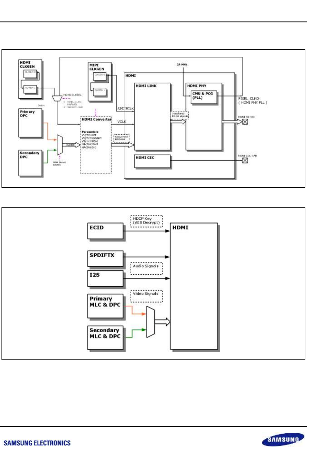
Samsung Confidential
S5P6818_UM 39 HDMI
39-2
Preliminary product information describes products that are in development, for which full characterization data and
associated errata are not yet available. Specifications and information herein are subject to change without notice.
39.3 Block Diagram
Figure 39-1 HDMI Block Diagram
Figure 39-2 HDMI SYSTEM Block Diagram
NOTE: SPDIFCLK (Figure 39-2) is used to latch SDATA of I2S and SPDIFIN of SPDIFTX. SPDIFCLK frequency shall be
eight times higher than that of SDATA and SPDIFIN. In SPDIF, SPDIFCLK must have higher frequency than fs 512.
For example, SPDIF TX uses 48 kHz frequency sampling, and then SPDIFCLK must have 24.576 MHz frequency.
48k 512 = 24576k.
nexell / ys.kim at 2015.02.12
SAMSUNG Confidential
Samsung Confidential
S5P6818_UM 39 HDMI
39-3
Preliminary product information describes products that are in development, for which full characterization data and
associated errata are not yet available. Specifications and information herein are subject to change without notice.
39.4 Functional Description
39.4.1 Select RGB Video data for HDMI
In S5P6818, users can choose one of two RGB Video data.
Primary DPC Video Data
Secondary DPC Video Data
When user want to use the Primary DPC Video Data for HDMI outputs, user set the HDMI_MUXSEL bit of the
HDMI_MUXCTRL register with 0 and set the HDMI_MUXENB bit of the HDMI_MUXCTRL register with 1.
39.4.2 HDMI Converter
The HDMI Converter converts the RGB Video data from DPC into a suitable format for the HDMI Link. Users must
set the HDMI Converter's parameters. The HDMI Converter consists of few registers. The configuration values for
the registers are in following table. The Figure 39-3 shows sync signal timing diagram.
NOTE: Since DPC makes sync signals, users must remember the sync information of current source video data. And users
must calculate the values of V2_BLANK and V_SYNC_LINE_BEF, etc. (Referred to in the figure below)
Table 39-1 The Configuration Values for the HDMI Converter
Register name
Bit
Symbol
Description (Refer Figure 39-3)
HDMI_SYNCCTRL0
[31]
HDMI_VCLK_SEL
This bit must be 0 (In Figure 39-1,
HDMI_CLKSEL)
HDMI_SYNCCTRL0
[15:0]
HDMI_VSYNCSTART
V2_BLANK - V_SYNC_LINE_BEF_1 - 1
HDMI_SYNCCTRL1
[15:0]
HDMI_HACTIVESTART
H_BLANK - H_SYNC_START
HDMI_SYNCCTRL2
[15:0]
HDMI_HACTIVEEND
H_BLANK - H_SYNC_START + 1
HDMI_SYNCCTRL3
[31:16]
HDMI_VSYNCHSEND
H_BLANK - H_SYNC_START
HDMI_SYNCCTRL3
[15:0]
HDMI_VSYNCHSSTART
H_LINE - H_SYNC_START
nexell / ys.kim at 2015.02.12
SAMSUNG Confidential
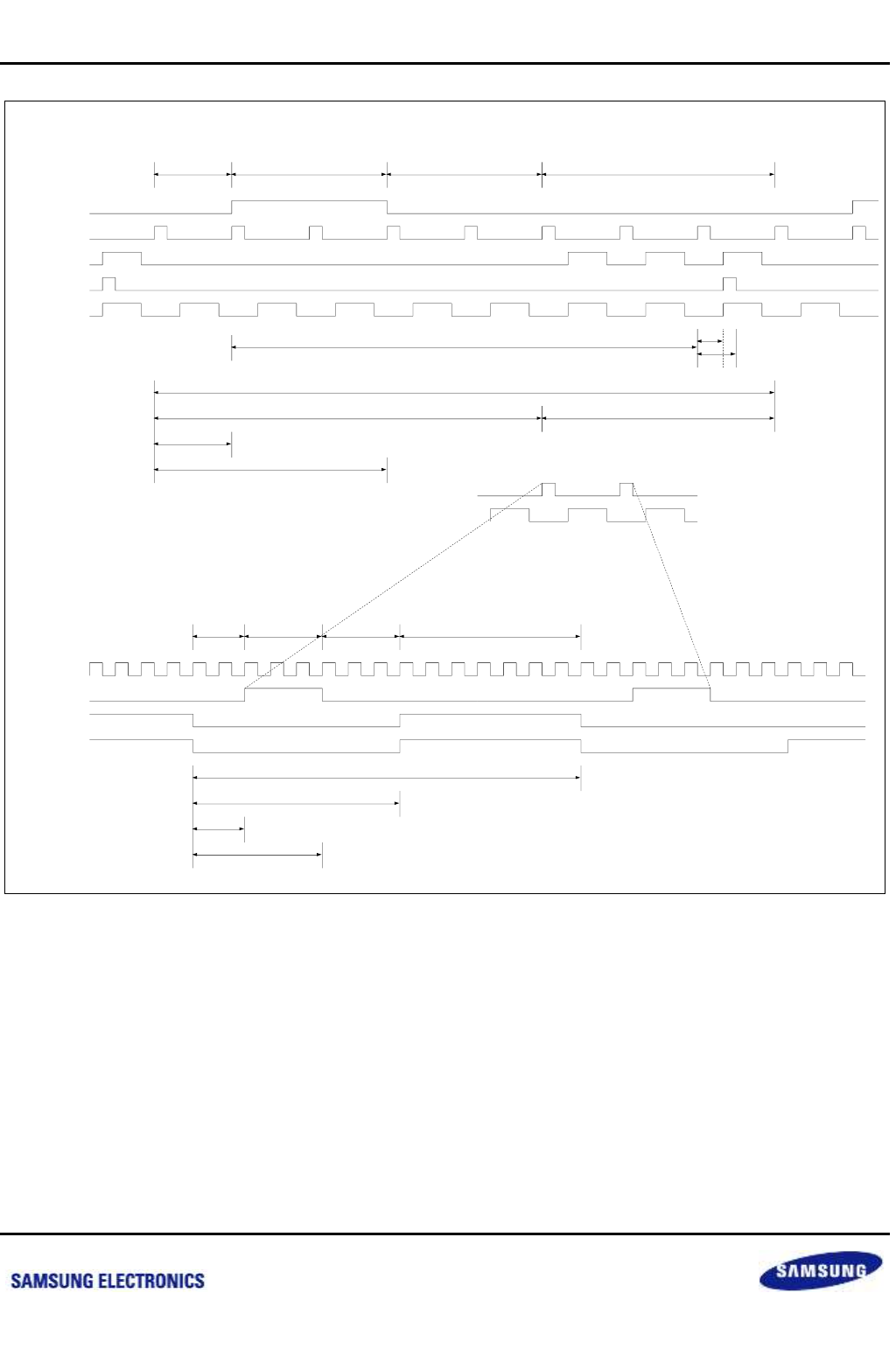
Samsung Confidential
S5P6818_UM 39 HDMI
39-4
Preliminary product information describes products that are in development, for which full characterization data and
associated errata are not yet available. Specifications and information herein are subject to change without notice.
Figure 39-3 Video Sync Signal Timing Diagram
VCLK
HSync
DE
HActive
H_BLANK
HSync
VSync
DE
h_activee
v_sync
VSyncStart VSyncHSStart
VSyncHSEnd
VFP : 1
VSW : 2
VBP : 2
VAct : 3
( HSync의 수로 Count )
VFP VSW VBP VAct
VSyncStart = VSW + VBP + VAct -1
( HSync의 수로 Count )
V2_BLANK = V_LINE = 8
V_BLANK = 5
V_ACTIVVE = 3
V_SYNC_LINE_BEF_1 = 1
V_SYNC_LINE_BEF_2 = 3 V_BLANK V_ACTLINE
V2_BLANK == V_LINE
V_SYNC_LINE_BEF_1
V_SYNC_LINE_BEF_2
HSync
DE
HFP : 2
HSW : 3
HBP : 3
HAct : 7
( VCLK의 수로 Count )
HFP HSW HBP HAct
HActiveStart = HSW + HBP
HActiveEnd = HSW + HBP + HAct
H LINE = 15
H_BLANK = 8
H_SYNC_START = 2
H_SYNC_END = 5
H LINE
H_SYNC_START
H_SYNC_END
nexell / ys.kim at 2015.02.12
SAMSUNG Confidential
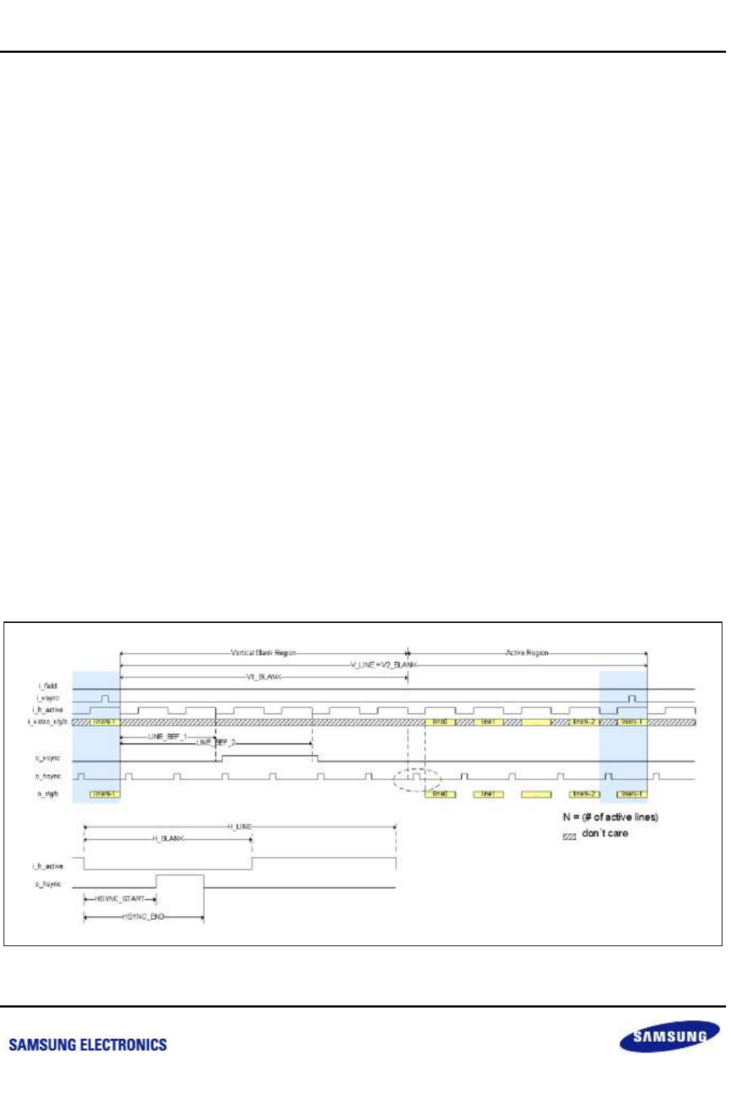
Samsung Confidential
S5P6818_UM 39 HDMI
39-5
Preliminary product information describes products that are in development, for which full characterization data and
associated errata are not yet available. Specifications and information herein are subject to change without notice.
39.4.3 HDMI LINK
The HDMI Link receives a converted Video Data from the HDMI Converter. Also, the HDMI link receives an audio
data from the SPDIFTX or I2S. The HDMI link translates them (video, audio) into a sequence of 10-bit signals
compliant to HDMI v1.4 specification.
Users must set the configuration about video and audio.
39.4.3.1 Video Input Interface
Video input interface receives i_vsync, i_h_active, i_field and pixel data signals to identify the starting of a frame,
the starting of a line and the starting of the top field in case of interlaced video formats. These signals, except for
the pixel data, are different from VSYNC, HSYNC and DE signals in the CEA-861. Note that HSYNC and DE
signal in CEA-861 are not used. Instead, actual Vsync and Vsync signals that are transferred to HDMI Rx side is
generated inside hdmi_14tx_ss according to the register settings.
The i_vsync signal is activated only one cycle during active area period of the last line of the previous frame.
i_h_active is always LOW as the blank period and HIGH during active period regardless of the video format. Note
that i_h_active goes HIGH even in the vertical blank period. The Figure below shows the timing diagrams for the
three signals.
There are two sets of the registers related to video timing. One specifies the input timing and the other specifies
the output timing. Video input/output timing with respect to the register values are also shown in Figure.Users
must set the input-related registers in accordance with the input video timing. Users can use the output-related
registers to control the video timing for display side, such as offset and display specific timing. Note that Figure is
informative and is added to illustrate the relations between register values and video timing. It is recommended
referring to register descriptions for exact timing.
Also, note that o_vsync, o_hsync and o_r/g/b in the figures are video timing signals described in CEA-861. These
signals are generated inside hdmi_14tx_ss and is transferred to HDMI Rx.
Figure 39-4 Video Timing with Respect to Register Values in Progressive Mode (Informative)
nexell / ys.kim at 2015.02.12
SAMSUNG Confidential
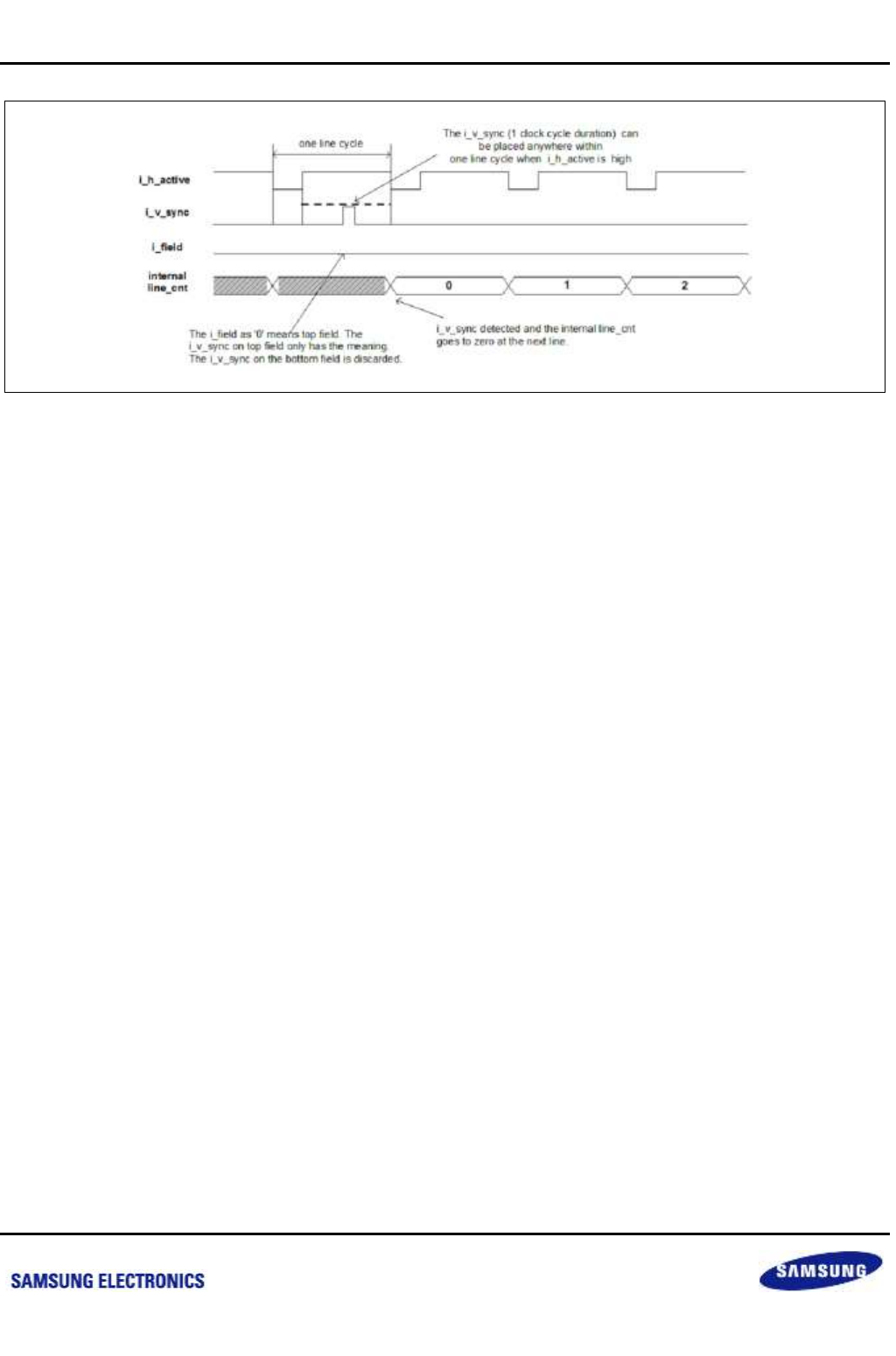
Samsung Confidential
S5P6818_UM 39 HDMI
39-6
Preliminary product information describes products that are in development, for which full characterization data and
associated errata are not yet available. Specifications and information herein are subject to change without notice.
Figure 39-5 Video Input Interface Timing
Below notations are used in the following explanations.
o_h_sync is equal to o_hsync.
o_v_sync is equal to o_vsync.
v_line is equal to V_LINE.
h_line is equal to H_LINE.
h_sync_start is equal to HSYNC_START.
h_sync_end is equal to HSYNC_END.
h_blank is equal to H_BLANK.
v1_blank is equal to V1_BLANK.
v2_blank is equal to V2_BLANK.
v_blank_f0 is equal to V_BLANK_F0.
v_blank_f1 is equal to V_BLANK_F1.
v_blank_f2 is equal to V_BLANK_F2.
v_blank_f3 is equal to V_BLANK_F3.
v_blank_f4 is equal to V_BLANK_F4.
v_blank_f5 is equal to V_BLANK_F5.
line_bef_1 is equal to LINE_BEF_1.
line_bef_2 is equal to LINE_BEF_2.
line_aft_1 is equal to LINE_AFT_1.
line_aft_2 is equal to LINE_AFT_2.
line_aft_3 is equal to LINE_AFT_3.
line_aft_4 is equal to LINE_AFT_4.
line_aft_pxl_1 is equal to LINE_AFT_PXL_1.
line_aft_pxl_2 is equal to LINE_AFT_PXL_2.
nexell / ys.kim at 2015.02.12
SAMSUNG Confidential
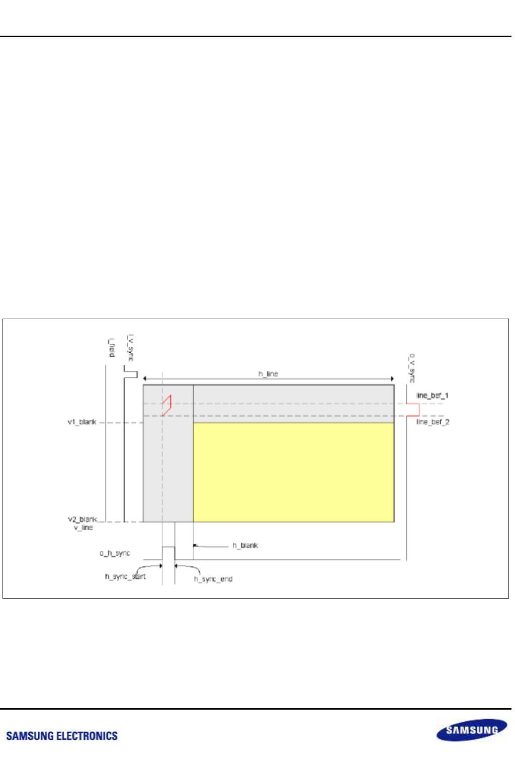
Samsung Confidential
S5P6818_UM 39 HDMI
39-7
Preliminary product information describes products that are in development, for which full characterization data and
associated errata are not yet available. Specifications and information herein are subject to change without notice.
line_aft_pxl_3 is equal to LINE_AFT_PXL_3.
line_aft_pxl_4 is equal to LINE_AFT_PXL_4.
vact_space1 is equal to VACT_SPACE1.
vact_space2 is equal to VACT_SPACE2.
vact_space3 is equal to VACT_SPACE3.
vact_space4 is equal to VACT_SPACE4.
vact_space5 is equal to VACT_SPACE5.
vact_space6 is equal to VACT_SPACE6.
Below figures indicate video timing per each modes.
In 2D Progressive mode, i_field and i_vsync input video signals indicate starting of image frame. When i_vsync
input video signal is active, i_field should be low.
o_v_sync is generated by line_bef_1 and line_bef_2. o_v_sync goes high at h_sync_start pixel in line_bef_1 line
and goes low at h_sync_start pixel in line_bef_2 line.
v2_blank should be equal to v_line.
Figure 39-6 Progressive Video Timing
nexell / ys.kim at 2015.02.12
SAMSUNG Confidential
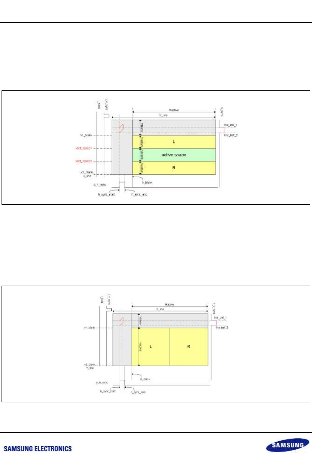
Samsung Confidential
S5P6818_UM 39 HDMI
39-8
Preliminary product information describes products that are in development, for which full characterization data and
associated errata are not yet available. Specifications and information herein are subject to change without notice.
In 3D Frame Packing Progressive mode, i_field and i_vsync input video signals indicate starting of image frame.
When i_vsync input video signal is active, i_field should be low.
o_v_sync is generated by line_bef_1 and line_bef_2. o_v_sync is generated at h_sync_start in the lines. Active
space is indicated by vact_sapce1 line and vact_space2 line.
v2_blank should be equal to v_line.
Figure 39-7 3D Frame Packing Progressive Video Timing
In 3D Side by side (half) Progressive mode, i_field and i_vsync input video signals indicate starting of image
frame.
When i_vsync input video signal is active, i_field should be low.
o_v_sync is generated by line_bef_1 and line_bef_2. o_v_sync is generated at h_sync_start in the lines.
v2_blank should be equal to v_line.
Figure 39-8 3D Side by Side (Half) Progressive Video Timing
nexell / ys.kim at 2015.02.12
SAMSUNG Confidential
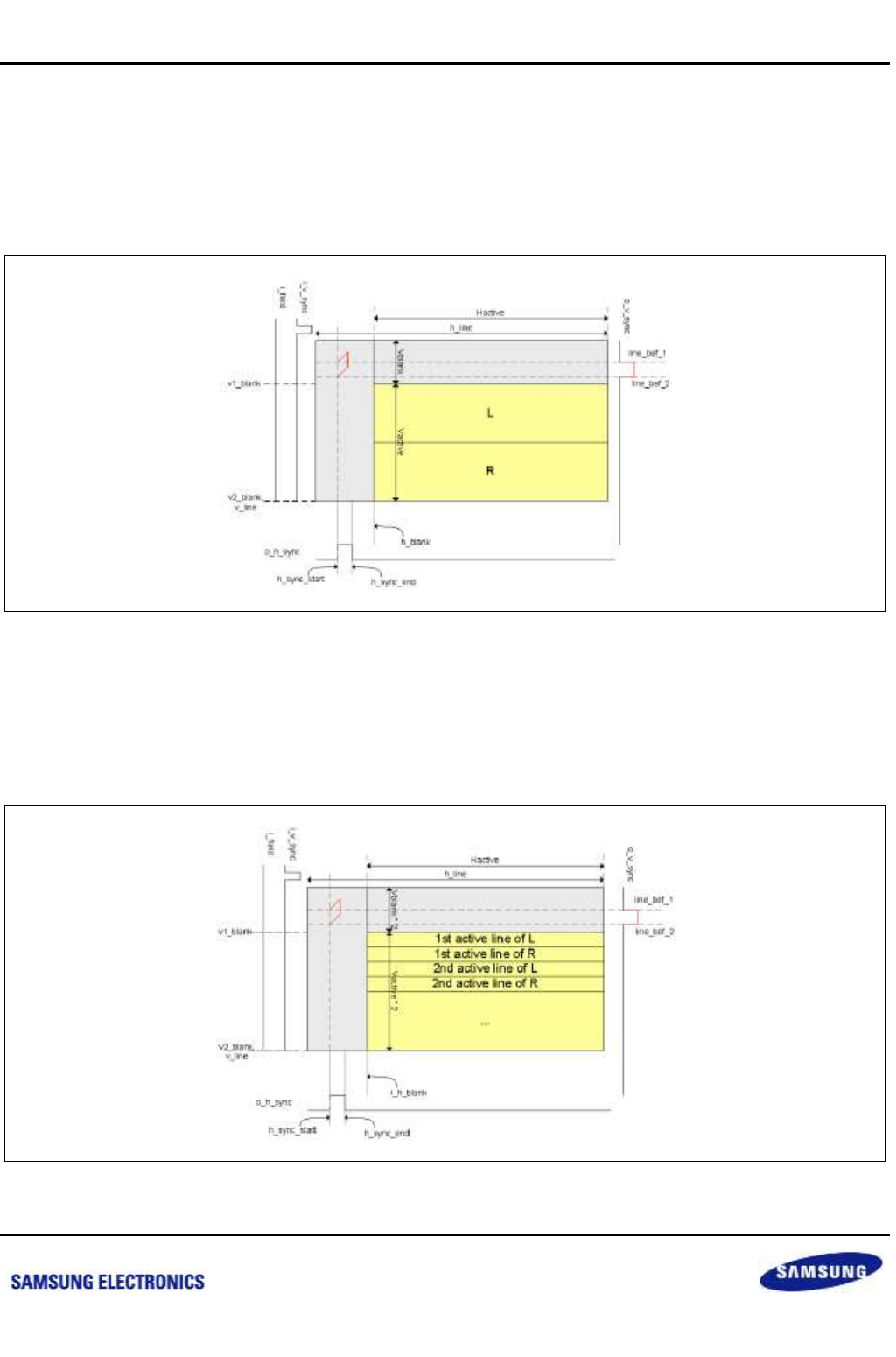
Samsung Confidential
S5P6818_UM 39 HDMI
39-9
Preliminary product information describes products that are in development, for which full characterization data and
associated errata are not yet available. Specifications and information herein are subject to change without notice.
In 3D Top and bottom Progressive mode, i_field and i_vsync input video signals indicate starting of image frame.
When i_vsync input video signal is active, i_field should be low.
o_v_sync is generated by line_bef_1 and line_bef_2. o_v_sync is generated at h_sync_start in the lines.
v2_blank should be equal to v_line.
Figure 39-9 3D Top and Bottom Progressive Video Timing
In 3D Line Alternative mode, i_field and i_vsync input video signals indicate starting of image frame. When
i_vsync input video signal is active, i_field should be low.
o_v_sync is generated by line_bef_1 and line_bef_2. o_v_sync is generated at h_sync_start in the lines.
v2_blank should be equal to v_line.
Figure 39-10 3D Line Alternative Video Timing
nexell / ys.kim at 2015.02.12
SAMSUNG Confidential
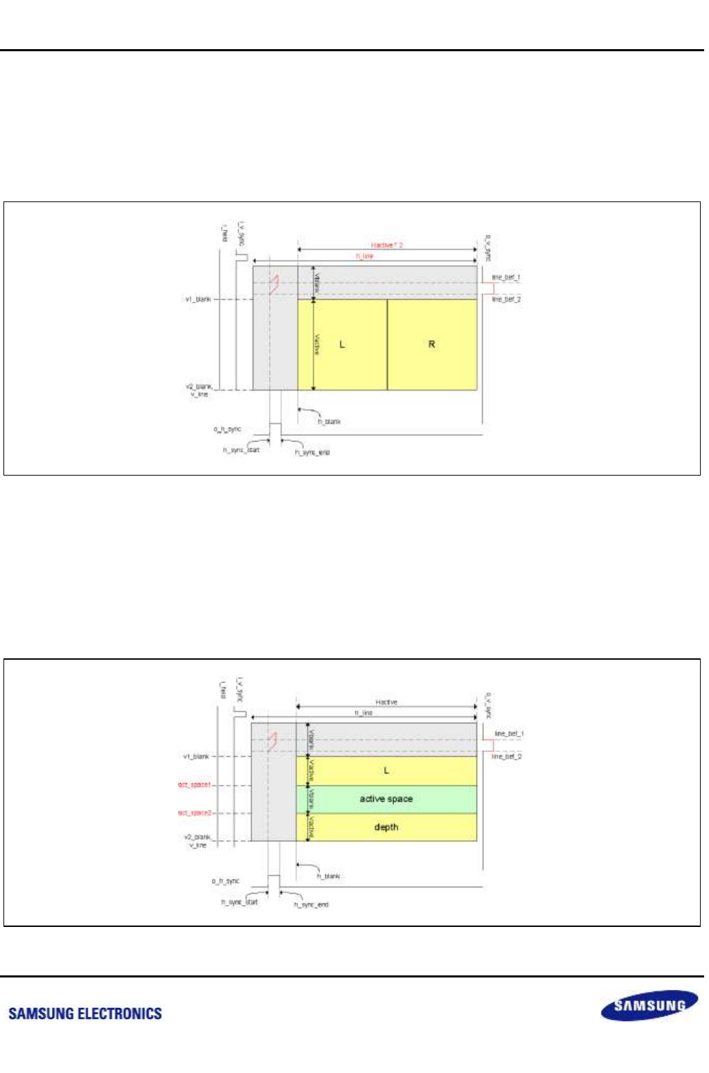
Samsung Confidential
S5P6818_UM 39 HDMI
39-10
Preliminary product information describes products that are in development, for which full characterization data and
associated errata are not yet available. Specifications and information herein are subject to change without notice.
In 3D Side by side (full) Progressive mode, i_field and i_vsync input video signals indicate starting of image frame.
When i_vsync input video signal is active, i_field should be low.
o_v_sync is generated by line_bef_1 and line_bef_2. o_v_sync is generated at h_sync_start in the lines.
v2_blank should be equal to v_line.
Figure 39-11 3D Side by Side (Full) Progressive Video Timing
In 3D L+Depth mode, i_field and i_vsync input video signals indicate starting of image frame. When i_vsync input
video signal is active, i_field should be low.
o_v_sync is generated by line_bef_1 and line_bef_2. o_v_sync is generated at h_sync_start in the lines.
Active space is indicated by vact_sapce1 line and vact_space2 line.
v2_blank should be equal to v_line.
Figure 39-12 3D L + Depth Video
nexell / ys.kim at 2015.02.12
SAMSUNG Confidential
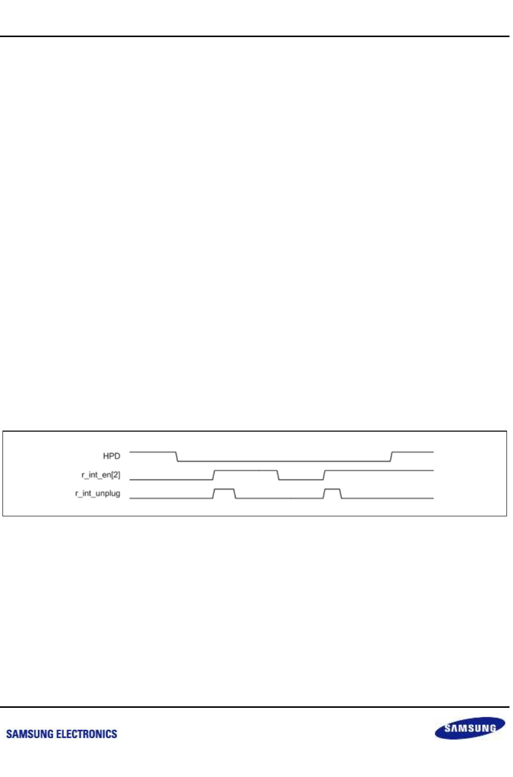
Samsung Confidential
S5P6818_UM 39 HDMI
39-11
Preliminary product information describes products that are in development, for which full characterization data and
associated errata are not yet available. Specifications and information herein are subject to change without notice.
39.4.3.2 Audio Input Interface
The HDMI can decrypt AES-encrypted HDCP key. For HDMI with HDCP function, each device should have a
unique HDCP key set.
HDMI 1.4 Tx Subsystem supports two audio input interfaces: SPDIF Rx, and I2S Rx. Users can use SPDIF
interface for two-channel Linear or Non-linear PCM Audio transmission and I2S interface for up-to eight channel
Linear PCM.
For I2S interface, users can specify the channel status block and the user bit information in registers, which does
not inherently exist in I2S audio format.
SPDIF Interface
HDMI 1.4 Tx Subsystem supports SPDIF Interface format that follows the IEC-60958 and IEC-61937 format.
SPDIF
Interface
I2S Interface
I2S interface supports linear PCM, non-linear PCM
NOTE: Supported HBR audio format.
39.4.3.3 HPD
HPD signal has two transactions: rising (plugged) and falling (unplugged) transition. Users can specify the stage
number of the noise filter to reduce the possible glitches during transition.
Figure 39-13 Timing Diagram for HPD Unplug Interrupt
nexell / ys.kim at 2015.02.12
SAMSUNG Confidential
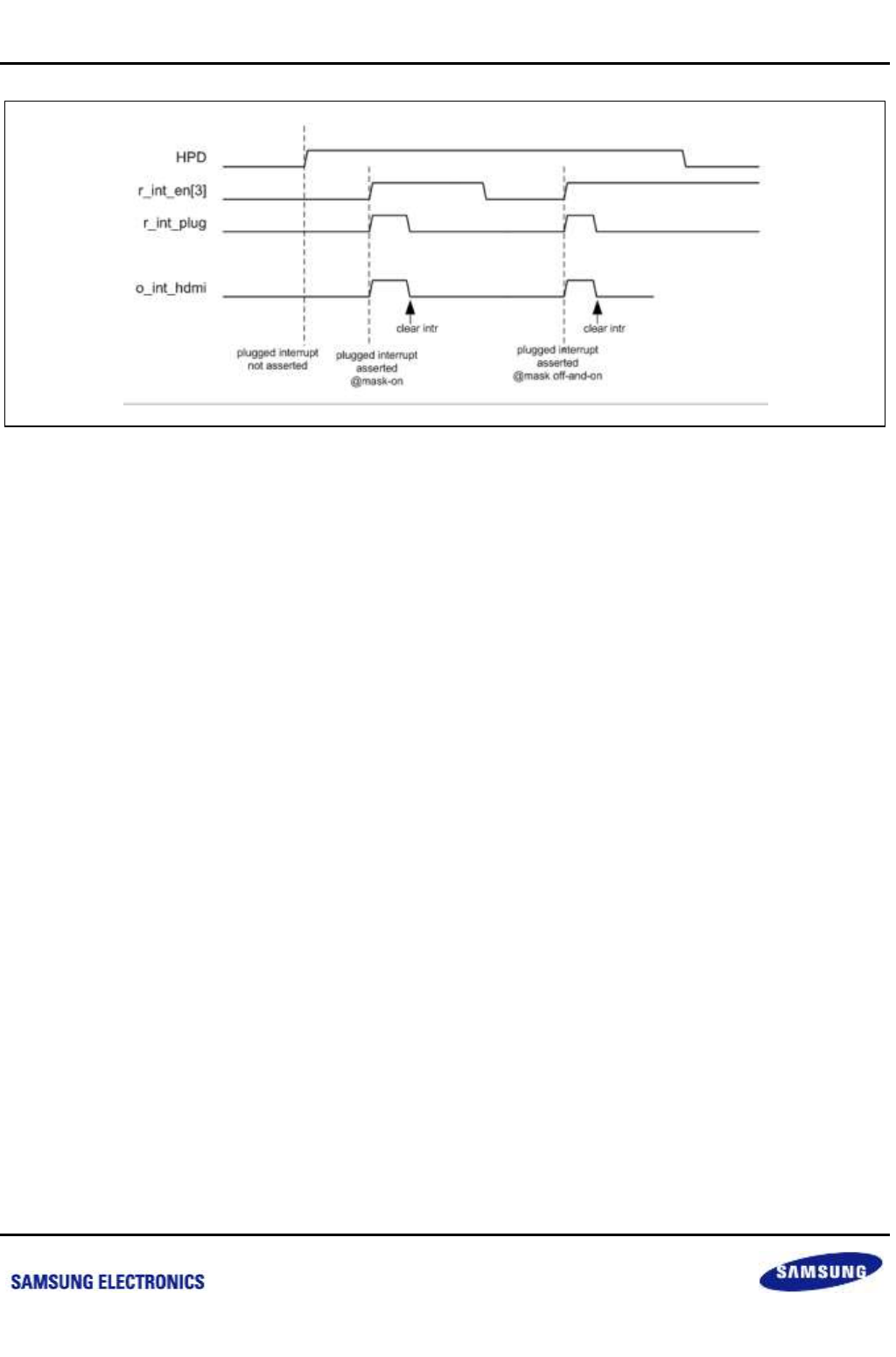
Samsung Confidential
S5P6818_UM 39 HDMI
39-12
Preliminary product information describes products that are in development, for which full characterization data and
associated errata are not yet available. Specifications and information herein are subject to change without notice.
Figure 39-14 Timing Diagram for HPD Plug Interrupt
39.4.3.4 CEC
CEC is abbreviation of Consumer Electronics Control and is used for controlling devices connected to a one-wired
"CEC bus". The CEC output port is a bidirectional port, which should be pulled-up to 3.3 V using external resistor
and voltage supply. (i.e. an open-drain connection)
CEC devices send messages serially (MSB first) via CEC bus and the receiving device sends acknowledge bit by
pulling the bus to low at ACK bit timing. For timing of each bit and structure of a message, refer to HDMI
specification 1.4a, Supplement 1. (CEC specification)
39.4.3.5 Interrupt Timing
HDMI 1.4 Tx Subsystem generates level-triggered interrupts. Interrupts are masked in two levels: each sub
module and controller. On the other hand, interrupt clear happens only in sub module for all interrupts except
HPD. For HPD, every plug and unplug will generate, HPD plug interrupt and HPD unplug interrupt, respectively.
39.4.3.6 HDCP KEY Management
The HDMI can decrypt AES-encrypted HDCP key. For HDMI with HDCP function, each device should have a
unique HDCP key set. This key set is released by Digital Contents Protection. LLC (www.digital-cp.com).
HDCP key is stored outside of the HDMI Link at a non-volatile memory. It is important that the non-volatile
memory does not have original raw-HDCP. The key should be stored safely to prevent the key from
eavesdroppers.
nexell / ys.kim at 2015.02.12
SAMSUNG Confidential
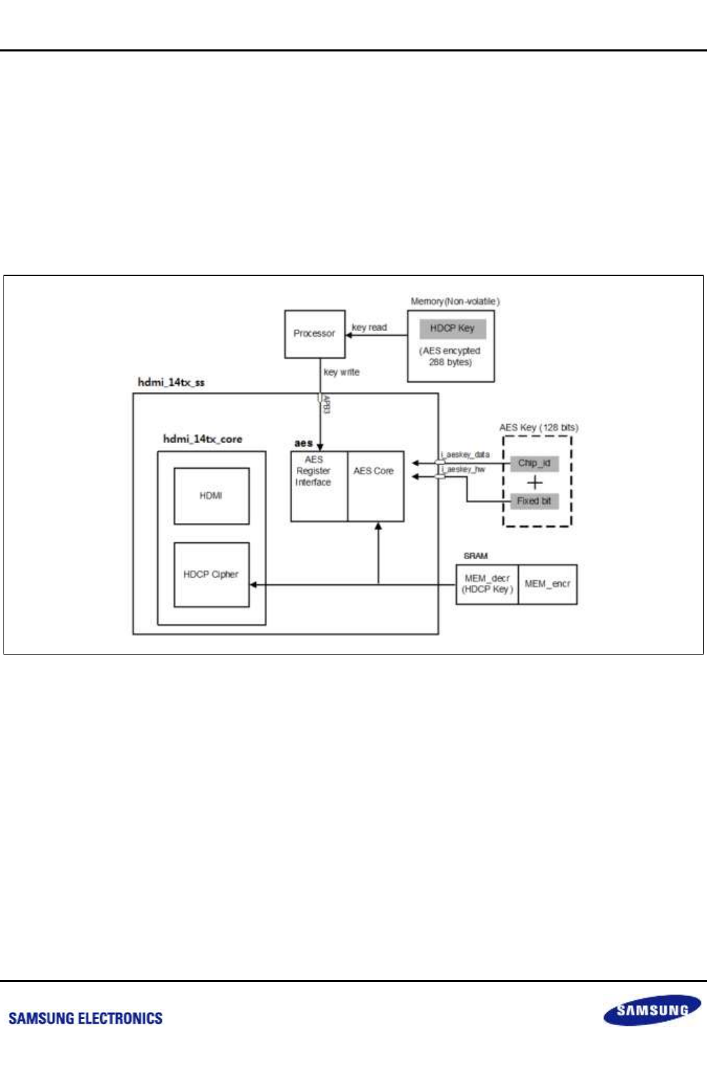
Samsung Confidential
S5P6818_UM 39 HDMI
39-13
Preliminary product information describes products that are in development, for which full characterization data and
associated errata are not yet available. Specifications and information herein are subject to change without notice.
The HDMI Link uses the AES encryption algorithm to protect plain HDCP key. Before starting the HDCP
authentication protocol, The HDMI Link reads encrypts HDCP keys from the memory (MEM_encr), decrypts the
keys using keys and stores the decrypted keys to decryption memory (MEM_decr). The decryption memory can
only be accessed by the HDCP engine inside the HDMI Link. The decryption memory cannot be accessed by
APB3 inter face to protect the decrypted keys. The AES key is supplied via ports (i_aeskey_data, i_aeskey_hw).
For the AES key, various chip id and fixed hardware value can be used. Note that only 128-bit key is supported.
The AES decryption starts by setting AES_Start bit of AES_START register. When the decryption is finished and
the decrypted keys are stored in the decryption memory, the AES_Start bit goes to 0, notifying the decryption is
done. The size of data to decrypt can be set by AES_DATA_SIZE_H/L register. After checking that AES_Start bit
is 0, decrypted data can be used for HDCP key. HDCP cannot operate until the AES_Start bit goes to 0.
Figure 39-15 Block Diagram of HDCP Key Management
nexell / ys.kim at 2015.02.12
SAMSUNG Confidential
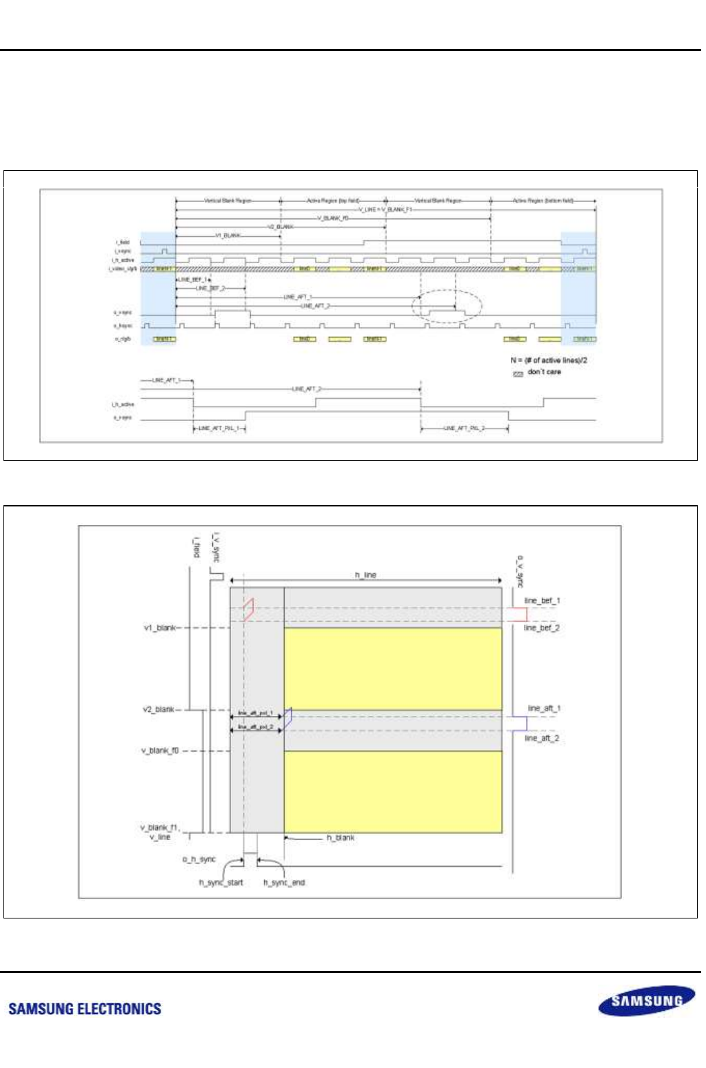
Samsung Confidential
S5P6818_UM 39 HDMI
39-14
Preliminary product information describes products that are in development, for which full characterization data and
associated errata are not yet available. Specifications and information herein are subject to change without notice.
39.4.3.7 HDMI Interlace Mode
S5P6818 HDMI supports Interlace Video Format
To Use HDMI Interlace Mode, HDMI LINK’s sync signals are signaled like below figure.
Figure 39-16 HDMI LINK Interlace Mode Timing
Figure 39-17 2D Interlaced Video Timing
nexell / ys.kim at 2015.02.12
SAMSUNG Confidential

Samsung Confidential
S5P6818_UM 39 HDMI
39-15
Preliminary product information describes products that are in development, for which full characterization data and
associated errata are not yet available. Specifications and information herein are subject to change without notice.
In 2D Interlaced mode, i_field and i_vsync input video signals indicate starting of image frame. When i_vsync input
video signal is active, i_field should be low on top field and be high on bottom field. First o_v_sync is generated by
line_bef_1 and line_bef_2. First o_v_sync is generated at h_sync_start in the lines. Second o_v_sync is
generated by line_aft_1 and line_aft_2. Second o_v_sync goes active at line_aft_pxl_1 pixel in line_aft_1 line and
goes inactive at line_aft_pxl_2 pixel in line_aft_2 line. v1_blank_f1 should be equal to v_line.
To use HDMI Interlace mode, following sequences are needed.
Config MLC & DPC for Interlace mode. you must use DPC's EvenVFP, EvenVSW, EvenVBP, and VSP(Vsync
Set Pixel), VCP(VSync Clear Pixel), Even VSP, EvenVCP
Config HDMI LINK for Interlace mode. Refer to the Figure above
Config HDMI Converter for make HDMI Field Signal
nexell / ys.kim at 2015.02.12
SAMSUNG Confidential
Samsung Confidential
S5P6818_UM 39 HDMI
39-16
Preliminary product information describes products that are in development, for which full characterization data and
associated errata are not yet available. Specifications and information herein are subject to change without notice.
39.5 Register Description
39.5.1 Register Map Summary
Base Address: 0xC020_0000
Register
Offset
Description
Reset Value
Control
INTC_CON_0
0x0000
Interrupt Control Register 0
0x0000_0000
INTC_FLAG_0
0x0004
Interrupt Flag Register 0
0x0000_0000
AESKEY_VALID
0x0008
i_aeskey_valid value
Undefined
HPD
0x000C
HPD signal
Undefined
INTC_CON_1
0x0010
Interrupt Control Register 1
0x0000_0000
INTC_FLAG_1
0x0014
Interrupt Flag Register 1
Undefined
PHY_STATUS_0
0x0020
PHY status Register 0
Undefined
PHY_STATUS_CMU
0x0024
PHY CMU status Register
Undefined
PHY_STATUS_PLL
0x0028
PHY PLL status Register
Undefined
PHY_CON_0
0x0030
PHY Control Register
Undefined
HPD_CTRL
0x0040
HPD Signal Control Register
Undefined
HPD_STATUS
0x0044
HPD Status Register
Undefined
HPD_TH_x
0x0050
HPD Status Register (HPD_TH_0 to 3)
Undefined
nexell / ys.kim at 2015.02.12
SAMSUNG Confidential

Samsung Confidential
S5P6818_UM 39 HDMI
39-17
Preliminary product information describes products that are in development, for which full characterization data and
associated errata are not yet available. Specifications and information herein are subject to change without notice.
Base Address: 0xC021_0000
Register
Offset
Description
Reset Value
Core
HDMI_CON_0
0x0000
HDMI system control register 0
0x0000_0000
HDMI_CON_1
0x0004
HDMI system control register 1
0x0000_0000
HDMI_CON_2
0x0008
HDMI system control register 2
0x0000_0000
STATUS
0x0010
HDMI system status register
0x0000_0000
STATUS_EN
0x0020
HDMI system status enable register
0x0000_0000
MODE_SEL
0x0040
HDMI/DVI mode selection
0x0000_0000
ENC_EN
0x0044
HDCP encryption enable register
0x0000_0000
HDMI_YMAX
0x0060
Maximum Y (or R,G,B) pixel value
0x0000_00EB
HDMI_YMIN
0x0064
Minimum Y (or R,G,B) pixel value
0x0000_0010
HDMI_CMAX
0x0068
Maximum Cb/Cr pixel value
0x0000_00F0
HDMI_CMIN
0x006C
Minimum Cb/Cr pixel value
0x0000_0010
H_BLANK_0
0x00A0
Horizontal blanking setting
0x0000_0000
H_BLANK_1
0x00A4
Horizontal blanking setting
0x0000_0000
V2_BLANK_0
0x00B0
Vertical blanking setting
0x0000_0000
V2_BLANK_1
0x00B4
Vertical blanking setting
0x0000_0000
V1_BLANK_0
0x00B8
Vertical blanking setting
0x0000_0000
V1_BLANK_1
0x00BC
Vertical blanking setting
0x0000_0000
V_LINE_0
0x00C0
vertical line setting
0x0000_0000
V_LINE_1
0x00C4
vertical line setting
0x0000_0000
H_LINE_0
0x00C8
Horizontal line setting
0x0000_0000
H_LINE_1
0x00CC
Horizontal line setting
0x0000_0000
HSYNC_POL
0x00E0
Horizontal sync polarity control register
0x0000_0000
VSYNC_POL
0x00E4
Vertical sync polarity control register
0x0000_0000
INT_PRO_MODE
0x00E8
Interlace/Progressive control register
0x0000_0000
V_BLANK_F0_0
0x0110
Vertical blanking setting for bottom field
0x0000_00FF
V_BLANK_F0_1
0x0114
Vertical blanking setting for bottom field
0x0000_001F
V_BLANK_F1_0
0x0118
Vertical blanking setting for bottom field
0x0000_00FF
V_BLANK_F1_1
0x011C
Vertical blanking setting for bottom field
0x0000_001F
H_SYNC_START_0
0x0120
Horizontal sync generation setting
0x0000_0000
H_SYNC_START_1
0x0124
Horizontal sync generation setting
0x0000_0000
H_SYNC_END_0
0x0128
Horizontal sync generation setting
0x0000_0000
H_SYNC_END_1
0x012C
Horizontal sync generation setting
0x0000_0000
V_SYNC_LINE_BEF_2_0
0x0130
Vertical sync generation for top field or frame
0x0000_00FF
V_SYNC_LINE_BEF_2_1
0x0134
Vertical sync generation for top field or frame
0x0000_001F
V_SYNC_LINE_BEF_1_0
0x0138
Vertical sync generation for top field or frame
0x0000_00FF
nexell / ys.kim at 2015.02.12
SAMSUNG Confidential

Samsung Confidential
S5P6818_UM 39 HDMI
39-18
Preliminary product information describes products that are in development, for which full characterization data and
associated errata are not yet available. Specifications and information herein are subject to change without notice.
Register
Offset
Description
Reset Value
V_SYNC_LINE_BEF_1_1
0x013C
Vertical sync generation for top field or frame
0x0000_001F
V_SYNC_LINE_AFT_2_0
0x0140
Vertical sync generation for bottom field - vertical
position
0x0000_00FF
V_SYNC_LINE_AFT_2_1
0x0144
Vertical sync generation for bottom field - vertical
position
0x0000_001F
V_SYNC_LINE_AFT_1_0
0x0148
Vertical sync generation for bottom field - vertical
position
0x0000_00FF
V_SYNC_LINE_AFT_1_1
0x014C
Vertical sync generation for bottom field - vertical
position
0x0000_001F
V_SYNC_LINE_AFT_PXL_2_0
0x0150
Vertical sync generation for bottom field - horizontal
position
0x0000_00FF
V_SYNC_LINE_AFT_PXL_2_1
0x0154
Vertical sync generation for bottom field - horizontal
position
0x0000_001F
V_SYNC_LINE_AFT_PXL_1_0
0x0158
Vertical sync generation for bottom field - horizontal
position
0x0000_00FF
V_SYNC_LINE_AFT_PXL_1_1
0x015C
Vertical sync generation for bottom field - horizontal
position
0x0000_001F
V_BLANK_F2_0
0x0160
Vertical blanking setting for third field
0x0000_00FF
V_BLANK_F2_1
0x0164
Vertical blanking setting for third field
0x0000_001F
V_BLANK_F3_0
0x0168
Vertical blanking setting for third field
0x0000_00FF
V_BLANK_F3_1
0x016C
Vertical blanking setting for third field
0x0000_001F
V_BLANK_F4_0
0x0170
Vertical blanking setting for fourth field
0x0000_00FF
V_BLANK_F4_1
0x0174
Vertical blanking setting for fourth field
0x0000_001F
V_BLANK_F5_0
0x0178
Vertical blanking setting for fourth field
0x0000_00FF
V_BLANK_F5_1
0x017C
Vertical blanking setting for fourth field
0x0000_001F
V_SYNC_LINE_AFT_3_0
0x0180
Vertical sync generation for third field - vertical position
0x0000_00FF
V_SYNC_LINE_AFT_3_1
0x0184
Vertical sync generation for third field - vertical position
0x0000_001F
V_SYNC_LINE_AFT_4_0
0x0188
Vertical sync generation for third field - vertical position
0x0000_00FF
V_SYNC_LINE_AFT_4_1
0x018C
Vertical sync generation for third field - vertical position
0x0000_001F
V_SYNC_LINE_AFT_5_0
0x0190
Vertical sync generation for fourth field - vertical
position
0x0000_00FF
V_SYNC_LINE_AFT_5_1
0x0194
Vertical sync generation for fourth field - vertical
position
0x0000_001F
V_SYNC_LINE_AFT_6_0
0x0198
Vertical sync generation for fourth field - vertical
position
0x0000_00FF
V_SYNC_LINE_AFT_6_1
0x019C
Vertical sync generation for fourth field - vertical
position
0x0000_001F
V_SYNC_LINE_AFT_PXL_3_0
0x01A0
Vertical sync generation for third field - horizontal
position
0x0000_00FF
V_SYNC_LINE_AFT_PXL_3_1
0x01A4
Vertical sync generation for third field - horizontal
position
0x0000_001F
nexell / ys.kim at 2015.02.12
SAMSUNG Confidential

Samsung Confidential
S5P6818_UM 39 HDMI
39-19
Preliminary product information describes products that are in development, for which full characterization data and
associated errata are not yet available. Specifications and information herein are subject to change without notice.
Register
Offset
Description
Reset Value
V_SYNC_LINE_AFT_PXL_4_0
0x01A8
Vertical sync generation for third field - horizontal
position
0x0000_00FF
V_SYNC_LINE_AFT_PXL_4_1
0x01AC
Vertical sync generation for third field - horizontal
position
0x0000_001F
V_SYNC_LINE_AFT_PXL_5_0
0x01B0
Vertical sync generation for fourth field - horizontal
position
0x0000_00FF
V_SYNC_LINE_AFT_PXL_5_1
0x01B4
Vertical sync generation for fourth field - horizontal
position
0x0000_001F
V_SYNC_LINE_AFT_PXL_6_0
0x01B8
Vertical sync generation for fourth field - horizontal
position
0x0000_00FF
V_SYNC_LINE_AFT_PXL_6_1
0x01BC
Vertical sync generation for fourth field - horizontal
position
0x0000_001F
VACT_SPACE1_0
0x01C0
1st Vertical Active Space start line
0x0000_00FF
VACT_SPACE1_1
0x01C4
1st Vertical Active Space end line
0x0000_001F
VACT_SPACE2_0
0x01C8
1st Vertical Active Space start line
0x0000_00FF
VACT_SPACE2_1
0x01CC
1st Vertical Active Space end line
0x0000_001F
VACT_SPACE3_0
0x01D0
2nd Vertical Active Space start line
0x0000_00FF
VACT_SPACE3_1
0x01D4
2nd Vertical Active Space end line
0x0000_001F
VACT_SPACE4_0
0x01D8
2nd Vertical Active Space start line
0x0000_00FF
VACT_SPACE4_1
0x01DC
2nd Vertical Active Space end line
0x0000_001F
VACT_SPACE5_0
0x01E0
3rd Vertical Active Space start line
0x0000_00FF
VACT_SPACE5_1
0x01E4
3rd Vertical Active Space end line
0x0000_001F
VACT_SPACE6_0
0x01E8
3rd Vertical Active Space start line
0x0000_00FF
VACT_SPACE6_1
0x01EC
3rd Vertical Active Space end line
0x0000_001F
GCP_CON
0x0200
GCP packet control register
0x0000_0004
GCP_BYTE1
0x0210
GCP packet body
0x0000_0000
GCP_BYTE2
0x0214
GCP packet body
0x0000_0000
GCP_BYTE3
0x0218
GCP packet body
0x0000_0000
ASP_CON
0x0300
ASP packet control register
0x0000_0000
ASP_SP_FLAT
0x0304
ASP packet sp_flat bit control
0x0000_0000
ASP_CHCFG0
0x0310
ASP audio channel configuration
0x0000_0008
ASP_CHCFG1
0x0314
ASP audio channel configuration
0x0000_001A
ASP_CHCFG2
0x0318
ASP audio channel configuration
0x0000_002C
ASP_CHCFG3
0x031C
ASP audio channel configuration
0x0000_003E
ACR_CON
0x0400
ACR packet control register
0x0000_0000
ACR_MCTS0
0x0410
Measured CTS value
0x0000_0001
ACR_MCTS1
0x0414
Measured CTS value
0x0000_0000
ACR_MCTS2
0x0418
Measured CTS value
0x0000_0000
nexell / ys.kim at 2015.02.12
SAMSUNG Confidential

Samsung Confidential
S5P6818_UM 39 HDMI
39-20
Preliminary product information describes products that are in development, for which full characterization data and
associated errata are not yet available. Specifications and information herein are subject to change without notice.
Register
Offset
Description
Reset Value
ACR_N0
0x0430
N value for ACR packet
0x0000_00E8
ACR_N1
0x0434
N value for ACR packet
0x0000_0003
ACR_N2
0x0438
N value for ACR packet
0x0000_0000
ACP_CON
0x0500
ACP packet control register
0x0000_0000
ACP_TYPE
0x0514
ACP packet header
0x0000_0000
ACP_DATAx
0x0520
ACP packet body
0x0000_0000
ISRC_CON
0x0600
ACR packet control register
0x0000_0000
ISRC1_HEADER1
0x0614
ISCR1 packet header
0x0000_0000
ISRC1_DATAx
0x0620
ISRC1 packet body
0x0000_0000
ISRC2_DATAx
0x06A0
ISRC2 packet body
0x0000_0000
AVI_CON
0x0700
AVI packet control register
0x0000_0000
AVI_HEADER0
0x0710
AVI packet header
0x0000_0000
AVI_HEADER1
0x0714
AVI packet header
0x0000_0000
AVI_HEADER2
0x0718
AVI packet header
0x0000_0000
AVI_CHECK_SUM
0x071C
AVI packet checksum
0x0000_0000
AVI_BYTEx
0x0720
AVI packet body
0x0000_0000
AUI_CON
0x0800
AUI packet control register
0x0000_0000
AUI_HEADER0
0x0810
AUI packet header
0x0000_0000
AUI_HEADER1
0x0814
AUI packet header
0x0000_0000
AUI_HEADER2
0x0818
AUI packet header
0x0000_0000
AUI_CHECK_SUM
0x081C
AUI packet checksum
0x0000_0000
AUI_BYTEx
0x0820
AUI packet body
0x0000_0000
MPG_CON
0x0900
ACR packet control register
0x0000_0000
MPG_CHECK_SUM
0x091C
MPG packet checksum
0x0000_0000
MPG_DATAx
0x0920
MPG packet body
0x0000_0000
SPD_CON
0x0A00
SPD packet control register
0x0000_0000
SPD_HEADER0
0x0A10
SPD packet header
0x0000_0000
SPD_HEADER1
0x0A14
SPD packet header
0x0000_0000
SPD_HEADER2
0x0A18
SPD packet header
0x0000_0000
SPD_DATAx
0x0A20
SPD packet body
0x0000_0000
GAMUT_CON
0x0B00
GAMUT packet control register
0x0000_0000
GAMUT_HEADER0
0x0B10
GAMUT packet header
0x0000_0000
GAMUT_HEADER1
0x0B14
GAMUT packet header
0x0000_0000
GAMUT_HEADER2
0x0B18
GAMUT packet header
0x0000_0000
GAMUT_METADATAx
0x0B20
GAMUT packet body
0x0000_0000
VSI_CON
0x0C00
VSI packet control register
0x0000_0000
VSI_HEADER0
0x0C10
VSI packet header
0x0000_0000
nexell / ys.kim at 2015.02.12
SAMSUNG Confidential

Samsung Confidential
S5P6818_UM 39 HDMI
39-21
Preliminary product information describes products that are in development, for which full characterization data and
associated errata are not yet available. Specifications and information herein are subject to change without notice.
Register
Offset
Description
Reset Value
VSI_HEADER1
0x0C14
VSI packet header
0x0000_0000
VSI_HEADER2
0x0C18
VSI packet header
0x0000_0000
VSI_DATAx
0x0C20
VSI packet body
0x0000_0000
DC_CONTROL
0x0D00
Deep Color Control Register
0x0000_0000
VIDEO_PATTERN_GEN
0x0D04
Video Pattern Generation Register
0x0000_0000
An_Seed_Sel
0x0E48
An seed selection register.
0x0000_00FF
An_Seed_0
0x0E58
An seed value register
0x0000_0000
An_Seed_1
0x0E5C
An seed value register
0x0000_0000
An_Seed_2
0x0E60
An seed value register
0x0000_0000
An_Seed_3
0x0E64
An seed value register
0x0000_0000
HDCP_SHA1_x
0x7000
SHA-1 value from repeater
0x0000_0000
HDCP_KSV_LIST_x
0x7050
KSV list from repeater
0x0000_0000
HDCP_KSV_LIST_CON
0x7064
KSV list control
0x0000_0000
HDCP_SHA_RESULT
0x7070
SHA-1 checking result register
0x0000_0000
HDCP_CTRL1
0x7080
HDCP control register1
0x0000_0000
HDCP_CTRL2
0x7084
HDCP control register2
0x0000_0000
HDCP_CHECK_RESULT
0x7090
Ri and Pj value checking result
0x0000_0000
HDCP_BKSV_x
0x70A0
KSV of Rx
0x0000_0000
HDCP_AKSV_x
0x70C0
KSV of Tx
0x0000_0000
HDCP_An_x
0x70E0
An value
0x0000_0000
HDCP_BCAPS
0x7100
BCAPS from Rx
0x0000_0000
HDCP_BSTATUS_0
0x7110
BSTATUS from Rx
0x0000_0000
HDCP_BSTATUS_1
0x7114
BSTATUS from Rx
0x0000_0000
HDCP_Ri_0
0x7140
Ri value of Tx
0x0000_0000
HDCP_Ri_1
0x7144
Ri value of Tx
0x0000_0000
HDCP_I2C_INT
0x7180
I2C interrupt flag
0x0000_0000
HDCP_AN_INT
0x7190
An value ready interrupt flag
0x0000_0000
HDCP_WATCGDOG_INT
0x71A0
Watchdog interrupt flag
0x0000_0000
HDCP_Ri_INT
0x71B0
Ri value update interrupt flag
0x0000_0000
HDCP_Ri_Compare_0
0x71D0
HDCP Ri Interrupt Frame number index register 0
0x0000_0080
HDCP_Ri_Compare_1
0x71D4
HDCP Ri Interrupt Frame number index register 1
0x0000_007F
HDCP_Frame_Count
0x71E0
Current value of the frame count index in the hardware
0x0000_0000
RGB_ROUND_EN
0xD500
round enable for 8/10 bit R/G/B in video_receiver
0x0000_0000
VACT_SPACE_R_0
0xD504
vertical active space R
0x0000_0000
VACT_SPACE_R_1
0xD508
vertical active space R
0x0000_0000
VACT_SPACE_G_0
0xD50C
vertical active space G
0x0000_0000
VACT_SPACE_G_1
0xD510
vertical active space G
0x0000_0000
nexell / ys.kim at 2015.02.12
SAMSUNG Confidential

Samsung Confidential
S5P6818_UM 39 HDMI
39-22
Preliminary product information describes products that are in development, for which full characterization data and
associated errata are not yet available. Specifications and information herein are subject to change without notice.
Register
Offset
Description
Reset Value
VACT_SPACE_B_0
0xD514
vertical active space B
0x0000_0000
VACT_SPACE_B_1
0xD518
vertical active space B
0x0000_0000
BLUE_SCREEN_R_0
0xD520
R Pixel values for blue screen[3:0]
0x0000_0000
BLUE_SCREEN_R_1
0xD524
R Pixel values for blue screen[11:4]
0x0000_0000
BLUE_SCREEN_G_0
0xD528
G Pixel values for blue screen[3:0]
0x0000_0000
BLUE_SCREEN_G_1
0xD52C
G Pixel values for blue screen[11:4]
0x0000_0000
BLUE_SCREEN_B_0
0xD530
B Pixel values for blue screen[3:0]
0x0000_0000
BLUE_SCREEN_B_1
0x0D534
B Pixel values for blue screen[11:4]
0x0000_0000
Base Address: 0xC022_0000
Register
Offset
Description
Reset Value
AES
AES_START
0x0000
AES_START
0x0000_0000
AES_DATA_SIZE_L
0x0020
AES_DATA_SIZE_L
0x0000_0020
AES_DATA_SIZE_H
0x0024
AES_DATA_SIZE_H
0x0000_0001
AES_DATA
0x0040
AES_DATA
0x0000_0000
Base Address: 0xC023_0000
Register
Offset
Description
Reset Value
SPDIF
SPDIFIN_CLK_CTRL
0x0000
SPDIFIN Clock Control Register
0x0000_0002
SPDIFIN_OP_CTRL
0x0004
SPDIFIN Operation Control Register 1
0x0000_0000
SPDIFIN_IRQ_MASK
0x0008
SPDIFIN Interrupt Request Mask Register
0x0000_0000
SPDIFIN_IRQ_STATUS
0x000C
SPDIFIN Interrupt Request Status Register
0x0000_0000
SPDIFIN_CONFIG_1
0x0010
SPDIFIN Configuration Register 1
0x0000_0002
SPDIFIN_CONFIG_2
0x0014
SPDIFIN Configuration Register 2
0x0000_0000
SPDIFIN_USER_VALUE_1
0x0020
SPDIFIN User Value Register 1
0x0000_0000
SPDIFIN_USER_VALUE_2
0x0024
SPDIFIN User Value Register 2
0x0000_0000
SPDIFIN_USER_VALUE_3
0x0028
SPDIFIN User Value Register 3
0x0000_0000
SPDIFIN_USER_VALUE_4
0x002C
SPDIFIN User Value Register 4
0x0000_0000
SPDIFIN_CH_STATUS_0_1
0x0030
SPDIFIN Channel Status Register 0-1
0x0000_0000
SPDIFIN_CH_STATUS_0_2
0x0034
SPDIFIN Channel Status Register 0-2
0x0000_0000
SPDIFIN_CH_STATUS_0_3
0x0038
SPDIFIN Channel Status Register 0-3
0x0000_0000
SPDIFIN_CH_STATUS_0_4
0x003C
SPDIFIN Channel Status Register 0-4
0x0000_0000
SPDIFIN_CH_STATUS_1
0x0040
SPDIFIN Channel Status Register 1
0x0000_0000
SPDIFIN_FRAME_PERIOD_1
0x0048
SPDIFIN Frame Period Register 1
0x0000_0000
nexell / ys.kim at 2015.02.12
SAMSUNG Confidential
Samsung Confidential
S5P6818_UM 39 HDMI
39-23
Preliminary product information describes products that are in development, for which full characterization data and
associated errata are not yet available. Specifications and information herein are subject to change without notice.
Register
Offset
Description
Reset Value
SPDIFIN_FRAME_PERIOD_2
0x004C
SPDIFIN Frame Period Register 2
0x0000_0000
SPDIFIN_Pc_INFO_1
0x0050
SPDIFIN Pc Info Register 1
0x0000_0000
SPDIFIN_Pc_INFO_2
0x0054
SPDIFIN Pc Info Register 2
0x0000_0000
SPDIFIN_Pd_INFO_1
0x0058
SPDIFIN Pd Info Register 1
0x0000_0000
SPDIFIN_Pd_INFO_2
0x005C
SPDIFIN Pd Info Register 2
0x0000_0000
SPDIFIN_DATA_BUF_0_1
0x0060
SPDIFIN Data Buffer Register 0_1
0x0000_0000
SPDIFIN_DATA_BUF_0_2
0x0064
SPDIFIN Data Buffer Register 0_2
0x0000_0000
SPDIFIN_DATA_BUF_0_3
0x0068
SPDIFIN Data Buffer Register 0_3
0x0000_0000
SPDIFIN_USER_BUF_0
0x006C
SPDIFIN User Buffer Register 0
0x0000_0000
SPDIFIN_DATA_BUF_1_1
0x0070
SPDIFIN Data Buffer Register 1_1
0x0000_0000
SPDIFIN_DATA_BUF_1_2
0x0074
SPDIFIN Data Buffer Register 1_2
0x0000_0000
SPDIFIN_DATA_BUF_1_3
0x0078
SPDIFIN Data Buffer Register 1_3
0x0000_0000
SPDIFIN_USER_BUF_1
0x007C
SPDIFIN User Buffer Register 1
0x0000_0000
nexell / ys.kim at 2015.02.12
SAMSUNG Confidential

Samsung Confidential
S5P6818_UM 39 HDMI
39-24
Preliminary product information describes products that are in development, for which full characterization data and
associated errata are not yet available. Specifications and information herein are subject to change without notice.
Base Address: 0xC024_0000
Register
Offset
Description
Reset Value
I2S
I2S_CLK_CON
0x0000
I2S Clock Enable Register
0x0000_0000
I2S_CON_1
0x0004
I2S Control Register 1
0x0000_0000
I2S_CON_2
0x0008
I2S Control Register 2
0x0000_0016
I2S_PIN_SEL_0
0x000C
I2S Input Pin Selection Register 0
0x0000_0077
I2S_PIN_SEL_1
0x0010
I2S Input Pin Selection Register 1
0x0000_0077
I2S_PIN_SEL_2
0x0014
I2S Input Pin Selection Register 2
0x0000_0077
I2S_PIN_SEL_3
0x0018
I2S Input Pin Selection Register 3
0x0000_0007
I2S_DSD_CON
0x001C
I2S DSD Control Register
0x0000_0002
I2S_MUX_CON
0x0020
I2S In/Mux Control Register
0x0000_0060
I2S_CH_ST_CON
0x0024
I2S Channel Status Control Register
0x0000_0000
I2S_CH_ST_0
0x0028
I2S Channel Status Block 0
0x0000_0000
I2S_CH_ST_1
0x002C
I2S Channel Status Block 1
0x0000_0000
I2S_CH_ST_2
0x0030
I2S Channel Status Block 2
0x0000_0000
I2S_CH_ST_3
0x0034
I2S Channel Status Block 3
0x0000_0000
I2S_CH_ST_4
0x0038
I2S Channel Status Block 4
0x0000_0000
I2S_CH_ST_SH_0
0x003C
I2S Channel Status Block Shadow Register 0
0x0000_0000
I2S_CH_ST_SH_1
0x0040
I2S Channel Status Block Shadow Register 1
0x0000_0000
I2S_CH_ST_SH_2
0x0044
I2S Channel Status Block Shadow Register 2
0x0000_0000
I2S_CH_ST_SH_3
0x0048
I2S Channel Status Block Shadow Register 3
0x0000_0000
I2S_CH_ST_SH_4
0x004C
I2S Channel Status Block Shadow Register 4
0x0000_0000
I2S_VD_DATA
0x0050
I2S Audio Sample Validity Register
0x0000_0000
I2S_MUX_CH
0x0054
I2S Channel Enable Register
0x0000_0003
I2S_MUX_CUV
0x0058
I2S CUV Enable Register
0x0000_0003
I2S_CH0_L_0
0x0064
I2S PCM Output Data Register
0x0000_0000
I2S_CH0_L_1
0x0068
I2S PCM Output Data Register
0x0000_0000
I2S_CH0_L_2
0x006C
I2S PCM Output Data Register
0x0000_0000
I2S_CH0_R_0
0x0074
I2S PCM Output Data Register
0x0000_0000
I2S_CH0_R_1
0x0078
I2S PCM Output Data Register
0x0000_0000
I2S_CH0_R_2
0x007C
I2S PCM Output Data Register
0x0000_0000
I2S_CH0_R_3
0x0080
I2S PCM Output Data Register
0x0000_0000
I2S_CH1_L_0
0x0084
I2S PCM Output Data Register
0x0000_0000
I2S_CH1_L_1
0x0088
I2S PCM Output Data Register
0x0000_0000
I2S_CH1_L_2
0x008C
I2S PCM Output Data Register
0x0000_0000
I2S_CH1_L_3
0x0090
I2S PCM Output Data Register
0x0000_0000
I2S_CH1_R_0
0x0094
I2S PCM Output Data Register
0x0000_0000
nexell / ys.kim at 2015.02.12
SAMSUNG Confidential
Samsung Confidential
S5P6818_UM 39 HDMI
39-25
Preliminary product information describes products that are in development, for which full characterization data and
associated errata are not yet available. Specifications and information herein are subject to change without notice.
Register
Offset
Description
Reset Value
I2S_CH1_R_1
0x0098
I2S PCM Output Data Register
0x0000_0000
I2S_CH1_R_2
0x009C
I2S PCM Output Data Register
0x0000_0000
I2S_CH1_R_3
0x00A0
I2S PCM Output Data Register
0x0000_0000
I2S_CH2_L_0
0x00A4
I2S PCM Output Data Register
0x0000_0000
I2S_CH2_L_1
0x00A8
I2S PCM Output Data Register
0x0000_0000
I2S_CH2_L_2
0x00AC
I2S PCM Output Data Register
0x0000_0000
I2S_CH2_L_3
0x00B0
I2S PCM Output Data Register
0x0000_0000
I2S_CH2_R_0
0x00B4
I2S PCM Output Data Register
0x0000_0000
I2S_CH2_R_1
0x00B8
I2S PCM Output Data Register
0x0000_0000
I2S_CH2_R_2
0x00BC
I2S PCM Output Data Register
0x0000_0000
I2S_Ch2_R_3
0x00C0
I2S PCM Output Data Register
0x0000_0000
I2S_CH3_L_0
0x00C4
I2S PCM Output Data Register
0x0000_0000
I2S_CH3_L_1
0x00C8
I2S PCM Output Data Register
0x0000_0000
I2S_CH3_L_2
0x00CC
I2S PCM Output Data Register
0x0000_0000
I2S_CH3_R_0
0x00D0
I2S PCM Output Data Register
0x0000_0000
I2S_CH3_R_1
0x00D4
I2S PCM Output Data Register
0x0000_0000
I2S_CH3_R_2
0x00D8
I2S PCM Output Data Register
0x0000_0000
I2S_CUV_L_R
0x00DC
I2S CUV Output Data Register
0x0000_0000
nexell / ys.kim at 2015.02.12
SAMSUNG Confidential
Samsung Confidential
S5P6818_UM 39 HDMI
39-26
Preliminary product information describes products that are in development, for which full characterization data and
associated errata are not yet available. Specifications and information herein are subject to change without notice.
Base Address: 0xC010_0000
Register
Offset
Description
Reset Value
CEC
CEC_TX_STATUS_0
0x0000
CEC Tx status registers 0.
0x0000_0000
CEC_TX_STATUS_1
0x0004
CEC Tx status registers 1. Number of blocks transferred.
0x0000_0000
CEC_RX_STATUS_0
0x0008
CEC Rx status registers 0.
0x0000_0000
CEC_RX_STATUS_1
0x000C
CEC Rx status registers 1. Number of blocks received.
0x0000_0000
CEC_INTR_MASK
0x0010
CEC interrupt mask register
0x0000_0000
CEC_INTR_CLEAR
0x0014
CEC interrupt clear register
0x0000_0000
CEC_LOGIC_ADDR
0x0020
HDMI Tx logical address register
0x0000_000F
CEC_DIVISOR_0
0x0030
Clock divisor for 0.05ms period count ([7:0] of 32-bit)
0x0000_0000
CEC_DIVISOR_1
0x0034
Clock divisor for 0.05ms period count ([15:8] of 32-bit)
0x0000_0000
CEC_DIVISOR_2
0x0038
Clock divisor for 0.05ms period count ([23:16] of 32-bit)
0x0000_0000
CEC_DIVISOR_3
0x003C
Clock divisor for 0.05ms period count ([31:24] of 32-bit)
0x0000_0000
CEC_TX_CTRL
0x0040
CEC Tx control register
0x0000_0010
CEC_TX_BYTE_NUM
0x0044
Number of blocks in a message to be transferred
0x0000_0000
CEC_TX_STATUS_2
0x0060
CEC Tx status register 2
0x0000_0000
CEC_TX_STATUS_3
0x0064
CEC Tx status register 3
0x0000_0000
CEC_TX_BUFFER_x
0x0080
Byte #0 to #15 of CEC message to be transferred. (#0 is
transferred 1st)
0x0000_0000
CEC_RX_CTRL
0x00C0
CEC Rx control register
0x0000_0000
CEC_RX_STATUS_2
0x00E0
CEC Rx status register 2
0x0000_0000
CEC_RX_STATUS_3
0x00E4
CEC Rx status register 3
0x0000_0000
CEC_RX_BUFFER_x
0x0100
Byte #0 to #15 of CEC message received (#0 is received
1st)
0x0000_0000
CEC_FILTER_CTRL
0x0180
CEC Filter control register
0x0000_0081
CEC_FILTER_TH
0x0184
CEC Filter Threshold register
0x0000_0003
nexell / ys.kim at 2015.02.12
SAMSUNG Confidential

Samsung Confidential
S5P6818_UM 39 HDMI
39-27
Preliminary product information describes products that are in development, for which full characterization data and
associated errata are not yet available. Specifications and information herein are subject to change without notice.
39.5.1.1 Control
39.5.1.1.1 INTC_CON_0
Base Address: 0xC020_0000
Address = Base Address + 0x0000, Reset Value = 0x0000_0000
Name
Bit
Type
Description
Reset Value
RSVD
[31:8]
–
Reserved
–
IntrPol
[7]
RW
Interrupt Polarity
0 = Active high
1 = Active low
1'b0
IntrEnGlobal
[6]
RW
0 = All interrupts are disabled
1 = Interrupts are enabled or disabled by
INTC_CON5:0]
1'b0
RSVD
[5]
RW
Reserved
1'b0
IntrEnCEC
[4]
RW
CEC interrupt enable
0 = Disabled
1 = Enabled
1'b0
IntrEnHPDplug
[3]
RW
HPD plugged interrupt enable
0 = Disabled
1 = Enabled
1'b0
IntrEnHPDunplug
[2]
RW
HPD unplugged interrupt enable
0 = Disabled
1 = Enabled
1'b0
IntrEnSPDIF
[1]
RW
SPDIF interrupt enable
0 = Disabled
1 = Enabled
1'b0
IntrEnHDCP
[0]
RW
HDCP interrupt enable
0 = Disabled
1 = Enabled
1'b0
nexell / ys.kim at 2015.02.12
SAMSUNG Confidential
Samsung Confidential
S5P6818_UM 39 HDMI
39-28
Preliminary product information describes products that are in development, for which full characterization data and
associated errata are not yet available. Specifications and information herein are subject to change without notice.
39.5.1.1.2 INTC_FLAG_0
Base Address: 0xC020_0000
Address = Base Address + 0x0004, Reset Value = 0X0000_0000
Name
Bit
Type
Description
Reset Value
RSVD
[31:8]
–
Reserved
–
RSVD
[7:5]
RW
Reserved
1'b0
IntrCEC
[4]
RW
CEC interrupt flag. (read only)
0 = Not occurred
1 = Interrupt occurred
1'b0
IntrHPDplug
[3]
RW
HPD plugged interrupt flag.
If it is written by 1, it is cleared.
0 = Not occurred
1 = HPD plugged
1'b0
IntrHPDunplug
[2]
RW
HPD unplugged interrupt flag.
If it is written by 1, it is cleared.
0 = Not occurred
1 = HPD unplugged
1'b0
IntrSPDIF
[1]
RW
SPDIF interrupt flag. (read only)
0 = Not occurred
1 = Interrupt occurred
1'b0
IntrHDCP
[0]
RW
HDCP interrupt flag. (read only)
0 = Not occurred
1 = Interrupt occurred
1'b0
39.5.1.1.3 AESKEY_VALID
Base Address: 0xC020_0000
Address = Base Address + 0x0008, Reset Value = Undefined
Name
Bit
Type
Description
Reset Value
RSVD
[31:8]
–
Reserved
–
RSVD
[7:1]
R
Reserved
–
aeskey_valid
[0]
R
Reflects i_aeskey_valid signal value.
–
nexell / ys.kim at 2015.02.12
SAMSUNG Confidential
Samsung Confidential
S5P6818_UM 39 HDMI
39-29
Preliminary product information describes products that are in development, for which full characterization data and
associated errata are not yet available. Specifications and information herein are subject to change without notice.
39.5.1.1.4 HPD
Base Address: 0xC020_0000
Address = Base Address + 0x000C, Reset Value = Undefined
Name
Bit
Type
Description
Reset Value
RSVD
[31:8]
–
–
–
RSVD
[7:1]
R
Reserved
–
HPD_Value
[0]
R
Value of HPD signal
0 = Unplugged
1 = Plugged
–
39.5.1.1.5 INTC_CON_1
Base Address: 0xC020_0000
Address = Base Address + 0x0010, Reset Value = 0X0000_0000
Name
Bit
Type
Description
Reset Value
RSVD
[31:8]
–
–
–
RSVD
[7:2]
RW
Reserved
–
IntEnSinkDetect
[1]
RW
SINK_DET interrupt enable. Triggered when SINK_DET signal
from goes PHY high. INTC_CON_1[6] should also be enabled.
0 = Disabled
1 = Enabled
1'b0
IntEnSinknotDetect
[0]
RW
SINK_NOT_DET interrupt enable. Triggered when SINK_DET
signal from PHY goes low. INTC_CON_1[6] should also be
enabled.
0 = Disabled
1 = Enabled
1'b0
nexell / ys.kim at 2015.02.12
SAMSUNG Confidential
Samsung Confidential
S5P6818_UM 39 HDMI
39-30
Preliminary product information describes products that are in development, for which full characterization data and
associated errata are not yet available. Specifications and information herein are subject to change without notice.
39.5.1.1.6 INTC_FLAG_1
Base Address: 0xC020_0000
Address = Base Address + 0x0014, Reset Value = Undefined
Name
Bit
Type
Description
Reset Value
RSVD
[31:8]
–
–
–
RSVD
[7:2]
RW
Reserved
–
IntSinkDetect
[1]
RW
SINK_DET interrupt. Triggered when SINK_DET signal from
PHY goes high. INTC_CON_1[6] should also be enabled.
If it is written by 1, it is cleared.
0 = Not occurred
1 = SINK_DET positive edge occurred.
–
IntSinknotDetect
[0]
RW
SINK_NOT_DET interrupt. Triggered when SINK_DET signal
from PHY goes low. INTC_CON_1[6] should also be enabled. If
it is written by 1, it is cleared.
0 = Not occurred
1 = SINK_DET negative edge occurred.
–
39.5.1.1.7 PHY_STATUS_0
Base Address: 0xC020_0000
Address = Base Address + 0x0020, Reset Value = Undefined
Name
Bit
Type
Description
Reset Value
RSVD
[31:8]
–
–
–
RSVD
[7:2]
R
Reserved
–
Sink_Detect
[1]
R
SINK_DET signal from PHY.
0 = Sink not detected
1 = Sink detected
–
Phy_Ready
[0]
R
PHY_READY signal from PHY.
0 = PHY not ready
1 = PHY ready
–
nexell / ys.kim at 2015.02.12
SAMSUNG Confidential
Samsung Confidential
S5P6818_UM 39 HDMI
39-31
Preliminary product information describes products that are in development, for which full characterization data and
associated errata are not yet available. Specifications and information herein are subject to change without notice.
39.5.1.1.8 PHY_STATUS_CMU
Base Address: 0xC020_0000
Address = Base Address + 0x0024, Reset Value = Undefined
Name
Bit
Type
Description
Reset Value
RSVD
[31:8]
–
–
–
CMU_Code
[7:4]
R
CMU_CODE signal from PHY. CMU_CODE is the AFC
(automatic frequency calibration) code that is used by the
CMU to converge to the target frequency. To lock the CMU,
PLL that generated TMDS clock and the pixel clock generator
should be locked.
–
RSVD
[3:1]
R
Reserved
–
CMU_Lock
[0]
R
CMU_LOCK signal from PHY.
0 = CMU not locked
1 = CMU locked
–
39.5.1.1.9 PHY_STATUS_PLL
Base Address: 0xC020_0000
Address = Base Address + 0x0028, Reset Value = Undefined
Name
Bit
Type
Description
Reset Value
RSVD
[31:8]
–
–
–
PLL_Code
[7:4]
R
VPLL_CODE signal from PHY. VPLL_CODE is the AFC
(automatic frequency calibration) code that is used by the
VPLL to converge to the target TMDS frequency.
–
RSVD
[3:1]
R
Reserved
–
PLL_Lock
[0]
R
VPLL_LOCK signal from PHY.
0 = VPLL not locked
1 = VPLL locked
–
39.5.1.1.10 PHY_CON_0
Base Address: 0xC020_0000
Address = Base Address + 0x0030, Reset Value = Undefined
Name
Bit
Type
Description
Reset Value
RSVD
[31:8]
–
–
–
RSVD
[7:1]
RW
Reserved
–
PHY_Pwr_Off
[0]
RW
PHY power off signal. Value of this bit is propagated to
o_phy_pwroff port of hdmi_14tx_ss and when connected to
PHY appropriately, can power-off the PHY. Refer to PHY
datasheet for more information.
–
nexell / ys.kim at 2015.02.12
SAMSUNG Confidential
Samsung Confidential
S5P6818_UM 39 HDMI
39-32
Preliminary product information describes products that are in development, for which full characterization data and
associated errata are not yet available. Specifications and information herein are subject to change without notice.
39.5.1.1.11 HPD_CTRL
Base Address: 0xC020_0000
Address = Base Address + 0x0040, Reset Value = Undefined
Name
Bit
Type
Description
Reset Value
RSVD
[31:8]
–
–
–
RSVD
[7:1]
RW
Reserved
–
HPD_Deglitch_En
[0]
RW
Enable deglitch logic to wait for a stable HPD signal. The
duration of stable signal is determined by HPD_TH_0 to 3
registers.
–
39.5.1.1.12 HPD_STATUS
Base Address: 0xC020_0000
Address = Base Address + 0x0044, Reset Value = Undefined
Name
Bit
Type
Description
Reset Value
RSVD
[31:8]
–
–
–
RSVD
[7:1]
RW
Reserved
–
HPD_Deglitched
[0]
RW
Current HPD signal status after deglitch logic.
–
39.5.1.1.13 HPD_TH_x
Base Address: 0xC020_0000
Address = Base Address + 0x0050, Reset Value = Undefined
Name
Bit
Type
Description
Reset Value
RSVD
[31:8]
–
–
–
HPD_TH_x
[7:0]
RW
A 32-bit HPD filter threshold value. When filter is enabled, it
filters out signals stable for less than HPD_Th cycles. (based
on APB cycle)
Least significant byte first. For example,
HPD_Th[7:0] <= HPD_TH_0[7:0]
HPD_Th[31:24] <= HPD_TH_3[7:0]
–
nexell / ys.kim at 2015.02.12
SAMSUNG Confidential

Samsung Confidential
S5P6818_UM 39 HDMI
39-33
Preliminary product information describes products that are in development, for which full characterization data and
associated errata are not yet available. Specifications and information herein are subject to change without notice.
39.5.1.2 Core
39.5.1.2.1 HDMI_CON_0
Base Address: 0xC021_0000
Address = Base Address + 0x0000, Reset Value = 0X0000_0000
Name
Bit
Type
Description
Reset Value
RSVD
[31:8]
–
–
–
RSVD
[7:6]
RW
Reserved
–
Blue_Scr_En
[5]
RW
Blue screen mode control. When set, the input video
pixels are discarded and BLUESCREEN register
values are transmitted for all video data period.
0 = Disable
1 = Enable
1'b0
Encoding_Option
[4]
RW
10-bit TMDS encoding bit order option
0 = Bit order reverse among the 10-bit encoding (to be
set to 1 when connecting to the TMDS PHY 1.3)
1 = Bit order as it is
1'b0
YCBCR422_Sel
[3]
RW
Video Input mode control.
0 = 4:4:4 mode
1 = 4:2:2 12-bit YCbCr
When 8-bit mode, the 12-bit inputs are rounded up to
generate 8-bit outputs.
1'b0
Asp_E
[2]
RW
Audio sample packet generation control.
This bit is only valid when SYSTEM_EN is set.
0 = Discard audio sample
1 = When the audio sample is received, the audio
sample packet is generated.
1'b0
Power_Down
[1]
RW
TMDS PHY power down mode. When it's set to 0,
data could not be transferred to a receiver.
0 = Normal operation mode
1 = Power down
1'b0
System_En
[0]
RW
HDMI systems enable.
0 = No op.
1 = HDMI enable
1'b0
nexell / ys.kim at 2015.02.12
SAMSUNG Confidential

Samsung Confidential
S5P6818_UM 39 HDMI
39-34
Preliminary product information describes products that are in development, for which full characterization data and
associated errata are not yet available. Specifications and information herein are subject to change without notice.
39.5.1.2.2 HDMI_CON_1
Base Address: 0xC021_0000
Address = Base Address + 0x0004, Reset Value = 0X0000_0000
Name
Bit
Type
Description
Reset Value
RSVD
[31:8]
–
–
–
RSVD
[7]
RW
Reserved
–
Pxl_Lmt_Ctrl
[6:5]
RW
Pixel value limitation control
0b00: By-pass (Do not limit the pixel value)
0b01: RGB mode
All channel's video input pixels are limited according
to YMAX and YMIN register values.
0b10: YCbCr mode The value of I_VIDEO_G is limited
according to YMAX and YMIN. The values of
I_VIDEO_B and I_VIDEO_R are limited according to
CMAX and CMIN.
0b11: Reserved
2'b0
RSVD
[4:2]
RW
Reserved
–
Pxl_Rep_Ratio
[1:0]
RW
Pixel repetition ratio
0b00: No pixel repetition
0b01: 2 times repetition
0b10: 3 times repetition
0b11: 4 times repetition
Use the resulting video mode setting for pixel
repetition.
e.g. For 720 480p (pixel repetition = 1) Use 1440
480p video mode
2'b0
39.5.1.2.3 HDMI_CON_2
Base Address: 0xC021_0000
Address = Base Address + 0x0008, Reset Value = 0X0000_0000
Name
Bit
Type
Description
Reset Value
RSVD
[31:8]
–
–
–
RSVD
[7:6]
RW
Reserved
–
Vid_Period_En
[5]
RW
Video preamble control.
0 = Video Preamble is applied. (HDMI mode)
1 = Video Preamble is not applied (DVI mode)
1'b0
RSVD
[4:2]
RW
Reserved
–
Dvi_Band_En
[1]
RW
In DIV mode, the leading guard band is not used.
0 = Guard band is applied (HDMI mode)
1 = Guard band is not applied (DVI mode)
1'b0
RSVD
[0]
RW
Reserved
–
nexell / ys.kim at 2015.02.12
SAMSUNG Confidential

Samsung Confidential
S5P6818_UM 39 HDMI
39-35
Preliminary product information describes products that are in development, for which full characterization data and
associated errata are not yet available. Specifications and information herein are subject to change without notice.
39.5.1.2.4 STATUS
Base Address: 0xC021_0000
Address = Base Address + 0x0010, Reset Value = 0X0000_0000
Name
Bit
Type
Description
Reset Value
RSVD
[31:8]
–
–
–
Authen_Ack
[7]
RW
When HDCP is authenticated, it occurs. This bit keeps
the authentication signal constantly. It's not cleared at
all. It's just one delayed signal of authen_ack signal
from HDCP block.
This bit is not an interrupt source. Read Only bit
0 = Not authenticated
1 = Authenticated
1'b0
Aud_Fifo_Ovf
[6]
RW
When audio FIFO is overflowed, this bit will be set.
Once it is set, it should be cleared by host.
0 = Not full
1 = Full
1'b0
RSVD
[5]
RW
Reserved
–
Update_Ri_Int
[4]
RW
Ri Interrupt status bit
If it is written by 1, it is cleared.
0 = Not occurred
1 = Interrupt occurred
1'b0
RSVD
[3]
RW
Reserved
–
An_Write_Int
[2]
RW
Indicates that A randomness value is available, it
occurs. When it occurs, users can get A values by
reading HDCP_An_x registers.
0 = An value is not available
1 = An value is available. Users can read An values
1'b0
Watchdog_Int
[1]
RW
Indicates that 2nd part of HDCP authentication
protocol is initiated and CPU should set a watchdog
timer to check 5 sec interval. If it is written by 1, it is
cleared.
0 = Not occurred
1 = Interrupt occurred
1'b0
I2C_Init_Int
[0]
RW
Indicates that 1st part of HDCP authentication protocol
can start. If it is written by 1, it is cleared.
0 = Not occurred
1 = Interrupt occurred
1'b0
nexell / ys.kim at 2015.02.12
SAMSUNG Confidential

Samsung Confidential
S5P6818_UM 39 HDMI
39-36
Preliminary product information describes products that are in development, for which full characterization data and
associated errata are not yet available. Specifications and information herein are subject to change without notice.
39.5.1.2.5 STATUS_EN
Base Address: 0xC021_0000
Address = Base Address + 0x0020, Reset Value = 0X0000_0000
Name
Bit
Type
Description
Reset Value
RSVD
[31:8]
–
–
–
RSVD
[7]
RW
Reserved
–
Aud_Fido_Ovf_Ee
[6]
RW
Audio buffer overflow interrupt enable
When it is set to 1, interrupt assertion is written on the
STATUS registers.
0 = Disable
1 = Enable
1'b0
RSVD
[5]
RW
Reserved
–
Update_Ri_Int_En
[4]
RW
UPDATE_RI_INT interrupt enable.
0 = Disable
1 = Enable
1'b0
RSVD
[3]
RW
Reserved
–
An_Write_Int_En
[2]
RW
AN_WRITE_INT interrupt enable.
0 = Disable
1 = Enable
1'b0
Watchdog_Int_En
[1]
RW
WATCHDOG_INT interrupt enable.
0 = Disable
1 = Enable
1'b0
I2C_Int_En
[0]
RW
I2C_INT interrupt enable.
0 = Disable
1 = Enable
1'b0
39.5.1.2.6 MODE_SEL
Base Address: 0xC021_0000
Address = Base Address + 0x0040, Reset Value = 0X0000_0000
Name
Bit
Type
Description
Reset Value
RSVD
[31:8]
–
–
–
RSVD
[7:2]
RW
Reserved
–
Hdmi_Mode
[1]
RW
Select a mode.
0 = Disable
1 = Enable
1'b0
Dvi_Mode
[0]
RW
Select a mode.
0 = Disable
1 = Enable
1'b0
nexell / ys.kim at 2015.02.12
SAMSUNG Confidential

Samsung Confidential
S5P6818_UM 39 HDMI
39-37
Preliminary product information describes products that are in development, for which full characterization data and
associated errata are not yet available. Specifications and information herein are subject to change without notice.
39.5.1.2.7 ENC_EN
Base Address: 0xC021_0000
Address = Base Address + 0x0044, Reset Value = 0X0000_0000
Name
Bit
Type
Description
Reset Value
RSVD
[31:8]
–
–
–
RSVD
[7:1]
RW
Reserved
–
Hdcp_Enc_En
[0]
RW
When set, HDCP encryption is applied. Before setting
this bit, the HDCP authentication process has to be
accomplished.
0 = Encryption disable
1 = Enable
1'b0
39.5.1.2.8 HDMI_YMAX
Base Address: 0xC021_0000
Address = Base Address + 0x0060, Reset Value = 0X0000_00EB
Name
Bit
Type
Description
Reset Value
RSVD
[31:8]
–
–
–
HDMI_YMAX
[7:0]
RW
Maximum value of Y (or G for RGB format) value after
pixel limit control.
These registers are used according to
PXL_LMT_CTRL bits in HDMI_CON_1 register.
When PXL_LMT_CTRL bits is 0x1, R and B for RGB
format is also limited by the value of this register.
For RGB mode
if (i_video_x HDMI_YMAX 16)
output = HDMI_YMAX 16
else if (i_video_x < HDMI_YMIN 16)
output = HDMI_YMIN x 16 else output = i_video_x
For YCbCr mode, the Y input is dealt with the same as
above.
For Cb and Cr values,
if (i_video_x HDMI_CMAX 16)
output = HDMI_CMAX 16
else if (i_video_x < HDMI_CMIN 16)
output = HDMI_CMIN 16 else output = i_video_x
NOTE: Value 16 in each line compensates the
difference of bit width between the input pixel and
register value.
8'hEB
nexell / ys.kim at 2015.02.12
SAMSUNG Confidential

Samsung Confidential
S5P6818_UM 39 HDMI
39-38
Preliminary product information describes products that are in development, for which full characterization data and
associated errata are not yet available. Specifications and information herein are subject to change without notice.
39.5.1.2.9 HDMI_YMIN
Base Address: 0xC021_0000
Address = Base Address + 0x0064, Reset Value = 0X0000_0010
Name
Bit
Type
Description
Reset Value
RSVD
[31:8]
–
–
–
HDMI_YMIN
[7:0]
RW
Minimum value of Y (or G for RGB format) value after
pixel limit control.
These registers are used according to
PXL_LMT_CTRL bits in HDMI_CON_1 register.
When PXL_LMT_CTRL bits is 0x1, R and B for RGB
format is also limited by the value of this register.
For RGB mode
if (i_video_x HDMI_YMAX 16)
output = HDMI_YMAX 16
else if (i_video_x < HDMI_YMIN 16)
output = HDMI_YMIN 16 else output = i_video_x
For YCbCr mode, the Y input is dealt with the same as
above. For Cb and Cr values,
if (i_video_x HDMI_CMAX 16)
output = HDMI_CMAX 16
else if (i_video_x < HDMI_CMIN 16)
output = HDMI_CMIN 16 else output = i_video_x
NOTE: Value 16 in each line compensates the
difference of bit width between the input pixel and
register value.
8'h10
nexell / ys.kim at 2015.02.12
SAMSUNG Confidential

Samsung Confidential
S5P6818_UM 39 HDMI
39-39
Preliminary product information describes products that are in development, for which full characterization data and
associated errata are not yet available. Specifications and information herein are subject to change without notice.
39.5.1.2.10 HDMI_CMAX
Base Address: 0xC021_0000
Address = Base Address + 0x0068, Reset Value = 0X0000_00F0
Name
Bit
Type
Description
Reset Value
RSVD
[31:8]
–
–
–
HDMI_CMAX
[7:0]
RW
Maximum value of Cb and Cr (or R and B for RGB
format) value after pixel limit control.
These registers are used according to
PXL_LMT_CTRL bits in HDMI_CON_1 register.
When PXL_LMT_CTRL bits is 0x2, R and B for RGB
format is also limited by the value of this register.
If PXL_LMT_CTRL bits is 0x1, R and B for RGB
format is also limited by
HDMI_YMAX register. For RGB mode
if (i_video_x HDMI_YMAX 16)
output = HDMI_YMAX 16
else if (i_video_x < HDMI_YMIN 16)
output = HDMI_YMIN x 16 else output = i_video_x
For YCbCr mode, the Y input is dealt with the same as
above. For Cb and Cr values,
if (i_video_x HDMI_CMAX 16)
output = HDMI_CMAX 16
else if (i_video_x < HDMI_CMIN 16)
output = HDMI_CMIN 16 else output = i_video_x
NOTE: Value 16 in each line compensates the
difference of bit width between the input pixel and
register value.
8'hF0
39.5.1.2.11 HDMI_CMIN
Base Address: 0xC021_0000
Address = Base Address + 0x006C, Reset Value = 0X0000_0010
Name
Bit
Type
Description
Reset Value
RSVD
[31:8]
–
–
–
HDMI_CMIN
[7:0]
RW
Minimum value of Cb and Cr (or R and B for RGB
format) value after pixel limit control.
These registers are used according to
PXL_LMT_CTRL bits in HDMI_CON_1 register.
When PXL_LMT_CTRL bits is 0x2, R and B for RGB
format is also limited by the value of this register.
If PXL_LMT_CTRL bits is 0x1, R and B for RGB
format is also limited by
HDMI_YMIN register. For RGB mode
if (i_video_x HDMI_YMAX 16)
8'h10
nexell / ys.kim at 2015.02.12
SAMSUNG Confidential
Samsung Confidential
S5P6818_UM 39 HDMI
39-40
Preliminary product information describes products that are in development, for which full characterization data and
associated errata are not yet available. Specifications and information herein are subject to change without notice.
Name
Bit
Type
Description
Reset Value
output = HDMI_YMAX 16
else if (i_video_x < HDMI_YMIN 16)
output = HDMI_YMIN 16 else output = i_video_x
For YCbCr mode, the Y input is dealt with the same as
above. For Cb and Cr values,
if (i_video_x HDMI_CMAX 16)
output = HDMI_CMAX 16
else if (i_video_x < HDMI_CMIN 16)
output = HDMI_CMIN 16 else output = i_video_x
NOTE: Value 16 in each line compensates the
difference of bit width between the input pixel and
register value.
39.5.1.2.12 H_BLANK_0
Base Address: 0xC021_0000
Address = Base Address + 0x00A0, Reset Value = 0X0000_0000
Name
Bit
Type
Description
Reset Value
RSVD
[31:8]
–
–
–
H_BLANK
[7:0]
RW
H_BLANK[7:0] of 13 bits.
Clock Cycles of horizontal Blanking Size. Refer to the
Reference CEA-861D
8'h00
39.5.1.2.13 H_BLANK_1
Base Address: 0xC021_0000
Address = Base Address + 0x00A4, Reset Value = 0x0000_0000
Name
Bit
Type
Description
Reset Value
RSVD
[31:8]
–
–
–
RSVD
[7:5]
RW
Reserved
–
H_BLANK
[4:0]
RW
H_BLANK[12:8] of 13 bits.
Clock Cycles of horizontal Blanking Size. Refer to the
Reference CEA-861D
5'h00
nexell / ys.kim at 2015.02.12
SAMSUNG Confidential
Samsung Confidential
S5P6818_UM 39 HDMI
39-41
Preliminary product information describes products that are in development, for which full characterization data and
associated errata are not yet available. Specifications and information herein are subject to change without notice.
39.5.1.2.14 V2_BLANK_0
Base Address: 0xC021_0000
Address = Base Address + 0x00B0, Reset Value = 0x0000_0000
Name
Bit
Type
Description
Reset Value
RSVD
[31:8]
–
–
–
V2_BLANK
[7:0]
RW
V2_BLANK[7:0] of 13 bits.
V1_BLANK+Active Lines. End Part. This value is the same as
V_LINE value for progressive mode. For interlace mode, use
the reference value in the table. Refer to the Reference CEA-
861D
8'h00
39.5.1.2.15 V2_BLANK_1
Base Address: 0xC021_0000
Address = Base Address + 0x00B4, Reset Value = 0x0000_0000
Name
Bit
Type
Description
Reset Value
RSVD
[31:8]
–
–
–
RSVD
[7:5]
RW
Reserved
–
V2_BLANK
[4:0]
RW
V2_BLANK[12:8] of 13 bits.
V1_BLANK+Active Lines. End Part. This value is the same as
V_LINE value for progressive mode. For interlace mode, use
the reference value in the table. Refer to the Reference CEA-
861D
5'h00
39.5.1.2.16 V1_BLANK_0
Base Address: 0xC021_0000
Address = Base Address + 0x00B8, Reset Value = 0x0000_0000
Name
Bit
Type
Description
Reset Value
RSVD
[31:8]
–
–
–
V1_BLANK
[7:0]
RW
V1_BLANK[7:0] of 13 bits.
Vertical Blanking Line Size. Front Part. Refer to the Reference
CEA-861D
8'h00
nexell / ys.kim at 2015.02.12
SAMSUNG Confidential

Samsung Confidential
S5P6818_UM 39 HDMI
39-42
Preliminary product information describes products that are in development, for which full characterization data and
associated errata are not yet available. Specifications and information herein are subject to change without notice.
39.5.1.2.17 V1_BLANK_1
Base Address: 0xC021_0000
Address = Base Address + 0x00BC, Reset Value = 0x0000_0000
Name
Bit
Type
Description
Reset Value
RSVD
[31:8]
–
–
–
RSVD
[7:5]
RW
Reserved
–
V1_BLANK
[4:0]
RW
V1_BLANK[12:8] of 13 bits.
Vertical Blanking Line Size. Front Part. Refer to the
Reference CEA-861D
5'h00
39.5.1.2.18 V_LINE_0
Base Address: 0xC021_0000
Address = Base Address + 0x00C0, Reset Value = 0x0000_0000
Name
Bit
Type
Description
Reset Value
RSVD
[31:8]
–
–
–
V_LINE
[7:0]
RW
V_LINE[7:0] of 13 bits.
Vertical Line Length. Refer to the Reference CEA-
861D
8'h00
39.5.1.2.19 V_LINE_1
Base Address: 0xC021_0000
Address = Base Address + 0x00C4, Reset Value = 0x0000_0000
Name
Bit
Type
Description
Reset Value
RSVD
[31:8]
–
–
–
RSVD
[7:5]
RW
Reserved
–
V_LINE
[4:0]
RW
V_LINE[12:8] of 13 bits.
Vertical Line Length. Refer to the Reference CEA-
861D
5'h00
nexell / ys.kim at 2015.02.12
SAMSUNG Confidential
Samsung Confidential
S5P6818_UM 39 HDMI
39-43
Preliminary product information describes products that are in development, for which full characterization data and
associated errata are not yet available. Specifications and information herein are subject to change without notice.
39.5.1.2.20 H_LINE_0
Base Address: 0xC021_0000
Address = Base Address + 0x00C8, Reset Value = 0x0000_0000
Name
Bit
Type
Description
Reset Value
RSVD
[31:8]
–
–
–
H_LINE
[7:0]
RW
H_LINE[7:0] of 13 bits.
Horizontal Line Length. Refer to the Reference CEA-
861D
8'h00
39.5.1.2.21 H_LINE_1
Base Address: 0xC021_0000
Address = Base Address + 0x00CC, Reset Value = 0x0000_0000
Name
Bit
Type
Description
Reset Value
RSVD
[31:8]
–
–
–
RSVD
[7:5]
R
Reserved
–
H_LINE
[4:0]
RW
H_LINE[12:8] of 13 bits.
Horizontal Line Length. Refer to the Reference CEA-
861D
5'h00
39.5.1.2.22 HSYNC_POL
Base Address: 0xC021_0000
Address = Base Address + 0x00E0, Reset Value = 0x0000_0000
Name
Bit
Type
Description
Reset Value
RSVD
[31:8]
–
–
–
RSVD
[7:1]
RW
Reserved
–
Hsync_Pol
[0]
RW
Set this bit for inverting the generated signal to meet
the modes. In 720p mode doesn't need to invert the
signal. Others need to be inverted. Refer to the
Reference CEA-861D
0 = Active high
1 = Active low
1'b0
nexell / ys.kim at 2015.02.12
SAMSUNG Confidential
Samsung Confidential
S5P6818_UM 39 HDMI
39-44
Preliminary product information describes products that are in development, for which full characterization data and
associated errata are not yet available. Specifications and information herein are subject to change without notice.
39.5.1.2.23 VSYNC_POL
Base Address: 0xC021_0000
Address = Base Address + 0x00E4, Reset Value = 0x0000_0000
Name
Bit
Type
Description
Reset Value
RSVD
[31:8]
–
–
–
RSVD
[7:1]
RW
Reserved
–
V_Sync_Pol_Sel
[0]
RW
Start point detection polarity selection bit.
720p's sync shapes are different from 480p, 480i, and
576p's. They are inverted shapes.
0 = Active high
1 = Active low
1'b0
39.5.1.2.24 INT_PRO_MODE
Base Address: 0xC021_0000
Address = Base Address + 0x00E8, Reset Value = 0x0000_0000
Name
Bit
Type
Description
Reset Value
RSVD
[31:8]
–
–
–
RSVD
[7:1]
RW
Reserved
–
INT_PRO_MODE
[0]
RW
Interlaced or Progressive Mode Selection. Refer to the
Reference
CEA-861D
0 = Progressive 1 = Interlaced.
1'b0
39.5.1.2.25 V_BLANK_F0_0
Base Address: 0xC021_0000
Address = Base Address + 0x0110, Reset Value = 0x0000_00FF
Name
Bit
Type
Description
Reset Value
RSVD
[31:8]
–
–
–
v_blank_f0
[7:0]
RW
v_blank_f0[7:0] of 13 bits.
The start position of bottom field's active region. This value
is the same as V_LINE value for Interlace mode. For
progressive mode, This value is not used. Refer to the
Reference CEA-861D
8'hFF
nexell / ys.kim at 2015.02.12
SAMSUNG Confidential
Samsung Confidential
S5P6818_UM 39 HDMI
39-45
Preliminary product information describes products that are in development, for which full characterization data and
associated errata are not yet available. Specifications and information herein are subject to change without notice.
39.5.1.2.26 V_BLANK_F0_1
Base Address: 0xC021_0000
Address = Base Address + 0x0114, Reset Value = 0x0000_001F
Name
Bit
Type
Description
Reset Value
RSVD
[31:8]
–
–
–
RSVD
[7:5]
RW
Reserved
–
v_blank_f0
[4:0]
RW
v_blank_f0[12:8] of 13 bits.
The start position of bottom field's active region. This value
is the same as V_LINE value for Interlace mode. For
progressive mode, This value is not used. Refer to the
Reference CEA-861D
5'h1F
39.5.1.2.27 V_BLANK_F1_0
Base Address: 0xC021_0000
Address = Base Address + 0x0118, Reset Value = 0x0000_00FF
Name
Bit
Type
Description
Reset Value
RSVD
[31:8]
–
–
–
v_blank_f1
[7:0]
RW
v_blank_f1[7:0] of 13 bits.
In the interlace mode, v_blank length of even field and odd field
is different. This register specifies the end position of bottom
field's active region. Refer to the Reference CEA-861D
8'hFF
39.5.1.2.28 V_BLANK_F1_1
Base Address: 0xC021_0000
Address = Base Address + 0x011C, Reset Value = 0x0000_001F
Name
Bit
Type
Description
Reset Value
RSVD
[31:8]
–
–
–
RSVD
[7:5]
RW
Reserved
–
v_blank_f1
[4:0]
RW
v_blank_f1[12:8] of 13 bits.
In the interlace mode, v_blank length of even field and odd field
is different. This register specifies the end position of bottom
field's active region. Refer to the Reference CEA-861D
5'h1F
nexell / ys.kim at 2015.02.12
SAMSUNG Confidential
Samsung Confidential
S5P6818_UM 39 HDMI
39-46
Preliminary product information describes products that are in development, for which full characterization data and
associated errata are not yet available. Specifications and information herein are subject to change without notice.
39.5.1.2.29 H_SYNC_START_0
Base Address: 0xC021_0000
Address = Base Address + 0x0120, Reset Value = 0x0000_0000
Name
Bit
Type
Description
Reset Value
RSVD
[31:8]
–
–
–
Hsync_Start
[7:0]
RW
Hsync_Start[7:0] of 11 bits.
Set the start point of H sync. Refer to the Reference CEA-861D
8'h00
39.5.1.2.30 H_SYNC_START_1
Base Address: 0xC021_0000
Address = Base Address + 0x0124, Reset Value = 0x0000_0000
Name
Bit
Type
Description
Reset Value
RSVD
[31:8]
–
–
–
RSVD
[7:5]
RW
Reserved
–
Hsync_Start
[4:0]
RW
Hsync_Start[12:8] of 11 bits.
Set the start point of H sync. Refer to the Reference CEA-861D
5'h00
39.5.1.2.31 H_SYNC_END_0
Base Address: 0xC021_0000
Address = Base Address + 0x0128, Reset Value = 0x0000_0000
Name
Bit
Type
Description
Reset Value
RSVD
[31:8]
–
–
–
Hsync_End
[7:0]
RW
Hsync_End[7:0] of 11 bits.
Set the end point of H sync. Refer to the Reference
CEA-861D
8'h00
39.5.1.2.32 H_SYNC_END_1
Base Address: 0xC021_0000
Address = Base Address + 0x012C, Reset Value = 0x0000_0000
Name
Bit
Type
Description
Reset Value
RSVD
[31:8]
–
–
–
RSVD
[7:5]
RW
Reserved
–
Hsync_End
[4:0]
RW
Hsync_End[12:8] of 11 bits.
Set the end point of H sync. Refer to the Reference
CEA-861D
5'h00
nexell / ys.kim at 2015.02.12
SAMSUNG Confidential
Samsung Confidential
S5P6818_UM 39 HDMI
39-47
Preliminary product information describes products that are in development, for which full characterization data and
associated errata are not yet available. Specifications and information herein are subject to change without notice.
39.5.1.2.33 V_SYNC_LINE_BEF_2_0
Base Address: 0xC021_0000
Address = Base Address + 0x0130, Reset Value = 0x0000_00FF
Name
Bit
Type
Description
Reset Value
RSVD
[31:8]
–
–
–
v_sync_line_bef_2
[7:0]
RW
v_sync_line_bef_2[7:0] of 13 bits.
Top field (or frame) V sync end line number. Refer to
the Reference
CEA-861D
8'hFF
39.5.1.2.34 V_SYNC_LINE_BEF_2_1
Base Address: 0xC021_0000
Address = Base Address + 0x0134, Reset Value = 0x0000_001F
Name
Bit
Type
Description
Reset Value
RSVD
[31:8]
–
–
–
RSVD
[7:5]
RW
Reserved
–
v_sync_line_bef_2
[4:0]
RW
v_sync_line_bef_2[12:8] of 13 bits.
Top field (or frame) V sync end line number. Refer to
the Reference
CEA-861D
5'h1F
39.5.1.2.35 V_SYNC_LINE_BEF_1_0
Base Address: 0xC021_0000
Address = Base Address + 0x0138, Reset Value = 0x0000_00FF
Name
Bit
Type
Description
Reset Value
RSVD
[31:8]
–
–
–
v_sync_line_bef_1
[7:0]
RW
Top field (or frame) V sync starts line number. Refer to
the Reference
CEA-861D
8'hFF
nexell / ys.kim at 2015.02.12
SAMSUNG Confidential

Samsung Confidential
S5P6818_UM 39 HDMI
39-48
Preliminary product information describes products that are in development, for which full characterization data and
associated errata are not yet available. Specifications and information herein are subject to change without notice.
39.5.1.2.36 V_SYNC_LINE_BEF_1_1
Base Address: 0xC021_0000
Address = Base Address + 0x013C, Reset Value = 0x0000_001F
Name
Bit
Type
Description
Reset Value
RSVD
[31:8]
–
–
–
RSVD
[7:5]
RW
Reserved
–
v_sync_line_bef_1
[4:0]
RW
v_sync_line_bef_1[12:8] of 13 bits.
Top field (or frame) V sync starts line number. Refer to
the Reference
CEA-861D
5'h1F
39.5.1.2.37 V_SYNC_LINE_AFT_2_0
Base Address: 0xC021_0000
Address = Base Address + 0x0140, Reset Value = 0x0000_00FF
Name
Bit
Type
Description
Reset Value
RSVD
[31:8]
–
–
–
v_sync_line_aft_2
[7:0]
RW
v_sync_line_aft_2[7:0] of 13 bits.
Bottom field V sync end line number. Refer to the
Reference CEA-861D
8'hFF
39.5.1.2.38 V_SYNC_LINE_AFT_2_1
Base Address: 0xC021_0000
Address = Base Address + 0x0144, Reset Value = 0x0000_001F
Name
Bit
Type
Description
Reset Value
RSVD
[31:8]
–
–
–
RSVD
[7:5]
RW
Reserved
–
v_sync_line_aft_2
[4:0]
RW
v_sync_line_aft_2[12:8] of 13 bits.
Bottom field V sync end line number. Refer to the
Reference CEA-861D
5'h1F
nexell / ys.kim at 2015.02.12
SAMSUNG Confidential
Samsung Confidential
S5P6818_UM 39 HDMI
39-49
Preliminary product information describes products that are in development, for which full characterization data and
associated errata are not yet available. Specifications and information herein are subject to change without notice.
39.5.1.2.39 V_SYNC_LINE_AFT_1_0
Base Address: 0xC021_0000
Address = Base Address + 0x0148, Reset Value = 0x0000_00FF
Name
Bit
Type
Description
Reset Value
RSVD
[31:8]
–
–
–
v_sync_line_aft_1
[7:0]
RW
v_sync_line_aft_1[7:0] of 13 bits.
Bottom field V sync start line number. Refer to the
Reference CEA-861D
8'hFF
39.5.1.2.40 V_SYNC_LINE_AFT_1_1
Base Address: 0xC021_0000
Address = Base Address + 0x014C, Reset Value = 0x0000_001F
Name
Bit
Type
Description
Reset Value
RSVD
[31:8]
–
–
–
RSVD
[7:5]
RW
Reserved
–
v_sync_line_aft_1
[4:0]
RW
v_sync_line_aft_1[12:8] of 13 bits.
Bottom field V sync start line number. Refer to the
Reference CEA-861D
5'h1F
39.5.1.2.41 V_SYNC_LINE_AFT_PXL_2_0
Base Address: 0xC021_0000
Address = Base Address + 0x0150, Reset Value = 0x0000_00FF
Name
Bit
Type
Description
Reset Value
RSVD
[31:8]
–
–
–
v_sync_line_aft_pxl_2
[7:0]
RW
v_sync_line_aft_pxl_2[7:0] of 13 bits.
Bottom field V sync end transition point. Refer to the
Reference
CEA-861D
8'hFF
nexell / ys.kim at 2015.02.12
SAMSUNG Confidential
Samsung Confidential
S5P6818_UM 39 HDMI
39-50
Preliminary product information describes products that are in development, for which full characterization data and
associated errata are not yet available. Specifications and information herein are subject to change without notice.
39.5.1.2.42 V_SYNC_LINE_AFT_PXL_2_1
Base Address: 0xC021_0000
Address = Base Address + 0x0154, Reset Value = 0x0000_001F
Name
Bit
Type
Description
Reset Value
RSVD
[31:8]
–
–
–
RSVD
[7:5]
RW
Reserved
–
v_sync_line_aft_pxl_2
[4:0]
RW
v_sync_line_aft_pxl_2[12:8] of 13 bits.
Bottom field V sync end transition point. Refer to the
Reference
CEA-861D
5'h1F
39.5.1.2.43 V_SYNC_LINE_AFT_PXL_1_0
Base Address: 0xC021_0000
Address = Base Address + 0x0158, Reset Value = 0x0000_00FF
Name
Bit
Type
Description
Reset Value
RSVD
[31:8]
–
–
–
v_sync_line_aft_pxl_1
[7:0]
RW
v_sync_line_aft_pxl_1[7:0] of 13 bits.
Bottom field V sync start transition point. Refer to the
Reference
CEA-861D
8'hFF
39.5.1.2.44 V_SYNC_LINE_AFT_PXL_1_1
Base Address: 0xC021_0000
Address = Base Address + 0x015C, Reset Value = 0x0000_001F
Name
Bit
Type
Description
Reset Value
RSVD
[31:8]
–
–
–
RSVD
[7:5]
RW
Reserved
–
v_sync_line_aft_pxl_1
[4:0]
RW
v_sync_line_aft_pxl_1[12:8] of 13 bits.
Bottom field V sync start transition point. Refer to the
Reference
CEA-861D
5'h1F
nexell / ys.kim at 2015.02.12
SAMSUNG Confidential
Samsung Confidential
S5P6818_UM 39 HDMI
39-51
Preliminary product information describes products that are in development, for which full characterization data and
associated errata are not yet available. Specifications and information herein are subject to change without notice.
39.5.1.2.45 V_BLANK_F2_0
Base Address: 0xC021_0000
Address = Base Address + 0x0160, Reset Value = 0x0000_00FF
Name
Bit
Type
Description
Reset Value
RSVD
[31:8]
–
–
–
v_blank_f2
[7:0]
RW
v_blank_f2[7:0] of 13 bits.
The start position of third field's active region. For 2D
mode, This value is not used.
8'hFF
39.5.1.2.46 V_BLANK_F2_1
Base Address: 0xC021_0000
Address = Base Address + 0x0164, Reset Value = 0x0000_001F
Name
Bit
Type
Description
Reset Value
RSVD
[31:8]
–
–
–
RSVD
[7:5]
RW
Reserved
–
v_blank_f2
[4:0]
RW
v_blank_f2[12:8] of 13 bits.
The start position of third field's active region. For 2D
mode, This value is not used.
5'h1F
39.5.1.2.47 V_BLANK_F3_0
Base Address: 0xC021_0000
Address = Base Address + 0x0168, Reset Value = 0x0000_00FF
Name
Bit
Type
Description
Reset Value
RSVD
[31:8]
–
–
–
v_blank_f3
[7:0]
RW
v_blank_f3[7:0] of 13 bits.
The end position of third field's active region. For 2D
mode, This value is not used.
8'hFF
nexell / ys.kim at 2015.02.12
SAMSUNG Confidential

Samsung Confidential
S5P6818_UM 39 HDMI
39-52
Preliminary product information describes products that are in development, for which full characterization data and
associated errata are not yet available. Specifications and information herein are subject to change without notice.
39.5.1.2.48 V_BLANK_F3_1
Base Address: 0xC021_0000
Address = Base Address + 0x016C, Reset Value = 0x0000_001F
Name
Bit
Type
Description
Reset Value
RSVD
[31:8]
–
–
–
RSVD
[7:5]
RW
Reserved
–
v_blank_f3
[4:0]
RW
v_blank_f3[12:8] of 13 bits.
The end position of third field's active region. For 2D
mode, This value is not used.
5'h1F
39.5.1.2.49 V_BLANK_F4_0
Base Address: 0xC021_0000
Address = Base Address + 0x0170, Reset Value = 0x0000_00FF
Name
Bit
Type
Description
Reset Value
RSVD
[31:8]
–
–
–
v_blank_f4
[7:0]
RW
v_blank_f4[7:0] of 13 bits.
The start position of fourth field's active region. For 2D
mode, This value is not used
8'hFF
39.5.1.2.50 V_BLANK_F4_1
Base Address: 0xC021_0000
Address = Base Address + 0x0174, Reset Value = 0x0000_001F
Name
Bit
Type
Description
Reset Value
RSVD
[31:8]
–
–
–
RSVD
[7:5]
RW
Reserved
–
v_blank_f4
[4:0]
RW
v_blank_f4[12:8] of 13 bits.
The start position of fourth field's active region. For 2D
mode, This value is not used.
5'h1F
nexell / ys.kim at 2015.02.12
SAMSUNG Confidential
Samsung Confidential
S5P6818_UM 39 HDMI
39-53
Preliminary product information describes products that are in development, for which full characterization data and
associated errata are not yet available. Specifications and information herein are subject to change without notice.
39.5.1.2.51 V_BLANK_F5_0
Base Address: 0xC021_0000
Address = Base Address + 0x0178, Reset Value = 0x0000_00FF
Name
Bit
Type
Description
Reset Value
RSVD
[31:8]
–
–
–
v_blank_f5
[7:0]
RW
v_blank_f5[7:0] of 13 bits.
The end position of fourth field's active region. For 2D
mode, This value is not used.
8'hFF
39.5.1.2.52 V_BLANK_F5_1
Base Address: 0xC021_0000
Address = Base Address + 0x017C, Reset Value = 0x0000_001F
Name
Bit
Type
Description
Reset Value
RSVD
[31:8]
–
–
–
RSVD
[7:5]
RW
Reserved
–
v_blank_f5
[4:0]
RW
v_blank_f5[12:8] of 13 bits.
The end position of fourth field's active region. For 2D
mode, This value is not used.
5'h1F
39.5.1.2.53 V_SYNC_LINE_AFT_3_0
Base Address: 0xC021_0000
Address = Base Address + 0x0180, Reset Value = 0x0000_00FF
Name
Bit
Type
Description
Reset Value
RSVD
[31:8]
–
–
–
v_sync_line_aft_3
[7:0]
RW
v_sync_line_aft_3[7:0] of 13 bits. Third field V sync
starts line number.
8'hFF
39.5.1.2.54 V_SYNC_LINE_AFT_3_1
Base Address: 0xC021_0000
Address = Base Address + 0x0184, Reset Value = 0x0000_001F
Name
Bit
Type
Description
Reset Value
RSVD
[31:8]
–
–
–
RSVD
[7:5]
RW
Reserved
–
v_sync_line_aft_3
[4:0]
RW
v_sync_line_aft_3[12:8] of 13 bits. Third field V sync
starts line number.
5'h1F
nexell / ys.kim at 2015.02.12
SAMSUNG Confidential

Samsung Confidential
S5P6818_UM 39 HDMI
39-54
Preliminary product information describes products that are in development, for which full characterization data and
associated errata are not yet available. Specifications and information herein are subject to change without notice.
39.5.1.2.55 V_SYNC_LINE_AFT_4_0
Base Address: 0xC021_0000
Address = Base Address + 0x0188, Reset Value = 0x0000_00FF
Name
Bit
Type
Description
Reset Value
RSVD
[31:8]
-
-
-
v_sync_line_aft_4
[7:0]
RW
v_sync_line_aft_4[7:0] of 13 bits. Third field V sync
end line number.
8'hFF
39.5.1.2.56 V_SYNC_LINE_AFT_4_1
Base Address: 0xC021_0000
Address = Base Address + 0x018C, Reset Value = 0x0000_001F
Name
Bit
Type
Description
Reset Value
RSVD
[31:8]
–
–
–
RSVD
[7:5]
RW
Reserved
–
v_sync_line_aft_4
[4:0]
RW
v_sync_line_aft_4[12:8] of 13 bits. Third field V sync
end line number.
5'h1F
39.5.1.2.57 V_SYNC_LINE_AFT_5_0
Base Address: 0xC021_0000
Address = Base Address + 0x0190, Reset Value = 0x0000_00FF
Name
Bit
Type
Description
Reset Value
RSVD
[31:8]
–
–
–
v_sync_line_aft_5
[7:0]
RW
v_sync_line_aft_5[7:0] of 13 bits. Fourth field V sync
starts line number.
8'hFF
39.5.1.2.58 V_SYNC_LINE_AFT_5_1
Base Address: 0xC021_0000
Address = Base Address + 0x0194, Reset Value = 0x0000_001F
Name
Bit
Type
Description
Reset Value
RSVD
[31:8]
–
–
–
RSVD
[7:5]
RW
Reserved
–
v_sync_line_aft_5
[4:0]
RW
v_sync_line_aft_5[12:8] of 13 bits. Fourth field V sync
starts line number.
5'h1F
nexell / ys.kim at 2015.02.12
SAMSUNG Confidential
Samsung Confidential
S5P6818_UM 39 HDMI
39-55
Preliminary product information describes products that are in development, for which full characterization data and
associated errata are not yet available. Specifications and information herein are subject to change without notice.
39.5.1.2.59 V_SYNC_LINE_AFT_6_0
Base Address: 0xC021_0000
Address = Base Address + 0x0198, Reset Value = 0x0000_00FF
Name
Bit
Type
Description
Reset Value
RSVD
[31:8]
–
–
–
v_sync_line_aft_6
[7:0]
RW
v_sync_line_aft_6[7:0] of 13 bits. Fourth field V sync
end line number.
8'hFF
39.5.1.2.60 V_SYNC_LINE_AFT_6_1
Base Address: 0xC021_0000
Address = Base Address + 0x019C, Reset Value = 0x0000_001F
Name
Bit
Type
Description
Reset Value
RSVD
[31:8]
–
–
–
RSVD
[7:5]
RW
Reserved
–
v_sync_line_aft_6
[4:0]
RW
v_sync_line_aft_6[12:8] of 13 bits. Fourth field V sync
end line number.
5'h1F
39.5.1.2.61 V_SYNC_LINE_AFT_PXL_3_0
Base Address: 0xC021_0000
Address = Base Address + 0x01A0, Reset Value = 0x0000_00FF
Name
Bit
Type
Description
Reset Value
RSVD
[31:8]
–
–
–
v_sync_line_aft_pxl_3
[7:0]
RW
v_sync_line_aft_pxl_3[7:0] of 13 bits. Third field V
sync start transition point.
8'hFF
39.5.1.2.62 V_SYNC_LINE_AFT_PXL_3_1
Base Address: 0xC021_0000
Address = Base Address + 0x01A4, Reset Value = 0x0000_001F
Name
Bit
Type
Description
Reset Value
RSVD
[31:8]
–
–
–
RSVD
[7:5]
RW
Reserved
–
v_sync_line_aft_pxl_3
[4:0]
RW
v_sync_line_aft_pxl_3[12:8] of 13 bits. Third field V
sync start transition point.
5'h1F
nexell / ys.kim at 2015.02.12
SAMSUNG Confidential

Samsung Confidential
S5P6818_UM 39 HDMI
39-56
Preliminary product information describes products that are in development, for which full characterization data and
associated errata are not yet available. Specifications and information herein are subject to change without notice.
39.5.1.2.63 V_SYNC_LINE_AFT_PXL_4_0
Base Address: 0xC021_0000
Address = Base Address + 0x01A8, Reset Value = 0x0000_00FF
Name
Bit
Type
Description
Reset Value
RSVD
[31:8]
–
–
–
v_sync_line_aft_pxl_4
[7:0]
RW
v_sync_line_aft_pxl_4[7:0] of 13 bits. Third field V
sync end transition point.
8'hFF
39.5.1.2.64 V_SYNC_LINE_AFT_PXL_4_1
Base Address: 0xC021_0000
Address = Base Address + 0x01AC, Reset Value = 0x0000_001F
Name
Bit
Type
Description
Reset Value
RSVD
[31:8]
–
–
–
RSVD
[7:5]
RW
Reserved
–
v_sync_line_aft_pxl_4
[4:0]
RW
v_sync_line_aft_pxl_4[12:8] of 13 bits. Third field V
sync end transition point.
5'h1F
39.5.1.2.65 V_SYNC_LINE_AFT_PXL_5_0
Base Address: 0xC021_0000
Address = Base Address + 0x01B0, Reset Value = 0x0000_00FF
Name
Bit
Type
Description
Reset Value
RSVD
[31:8]
–
–
–
v_sync_line_aft_pxl_5
[7:0]
RW
v_sync_line_aft_pxl_5[7:0] of 13 bits. Fourth field V
sync start transition point.
8'hFF
39.5.1.2.66 V_SYNC_LINE_AFT_PXL_5_1
Base Address: 0xC021_0000
Address = Base Address + 0x01B4, Reset Value = 0x0000_001F
Name
Bit
Type
Description
Reset Value
RSVD
[31:8]
–
–
–
RSVD
[7:5]
RW
Reserved
–
v_sync_line_aft_pxl_5
[4:0]
RW
v_sync_line_aft_pxl_5[12:8] of 13 bits. Fourth field V
sync start transition point.
5'h1F
nexell / ys.kim at 2015.02.12
SAMSUNG Confidential

Samsung Confidential
S5P6818_UM 39 HDMI
39-57
Preliminary product information describes products that are in development, for which full characterization data and
associated errata are not yet available. Specifications and information herein are subject to change without notice.
39.5.1.2.67 V_SYNC_LINE_AFT_PXL_6_0
Base Address: 0xC021_0000
Address = Base Address + 0x01B8, Reset Value = 0x0000_00FF
Name
Bit
Type
Description
Reset Value
RSVD
[31:8]
–
–
–
v_sync_line_aft_pxl_6
[7:0]
RW
v_sync_line_aft_pxl_6[7:0] of 13 bits. Fourth field V
sync end transition point.
8'hFF
39.5.1.2.68 V_SYNC_LINE_AFT_PXL_6_1
Base Address: 0xC021_0000
Address = Base Address + 0x01BC, Reset Value = 0x0000_001F
Name
Bit
Type
Description
Reset Value
RSVD
[31:8]
–
–
–
RSVD
[7:5]
RW
Reserved
–
v_sync_line_aft_pxl_6
[4:0]
RW
v_sync_line_aft_pxl_6[12:8] of 13 bits. Fourth field V
sync end transition point.
5'h1F
39.5.1.2.69 VACT_SPACE1_0
Base Address: 0xC021_0000
Address = Base Address + 0x01C0, Reset Value = 0x0000_00FF
Name
Bit
Type
Description
Reset Value
RSVD
[31:8]
–
–
–
vact_space1
[7:0]
RW
vact_space1[7:0] of 13 bits.
first active space start line number
8'hFF
39.5.1.2.70 VACT_SPACE1_1
Base Address: 0xC021_0000
Address = Base Address + 0x01C4, Reset Value = 0x0000_001F
Name
Bit
Type
Description
Reset Value
RSVD
[31:8]
–
–
–
RSVD
[7:5]
RW
Reserved
–
vact_space1
[4:0]
RW
vact_space1[12:8] of 13 bits.
first active space start line number
5'h1F
nexell / ys.kim at 2015.02.12
SAMSUNG Confidential

Samsung Confidential
S5P6818_UM 39 HDMI
39-58
Preliminary product information describes products that are in development, for which full characterization data and
associated errata are not yet available. Specifications and information herein are subject to change without notice.
39.5.1.2.71 VACT_SPACE2_0
Base Address: 0xC021_0000
Address = Base Address + 0x01C8, Reset Value = 0x0000_00FF
Name
Bit
Type
Description
Reset Value
RSVD
[31:8]
–
–
–
vact_space2
[7:0]
RW
vact_space2[7:0] of 13 bits.
first active space end line number
8'hFF
39.5.1.2.72 VACT_SPACE2_1
Base Address: 0xC021_0000
Address = Base Address + 0x01CC, Reset Value = 0x0000_001F
Name
Bit
Type
Description
Reset Value
RSVD
[31:8]
–
–
–
RSVD
[7:5]
RW
Reserved
–
vact_space2
[4:0]
RW
vact_space2[12:8] of 13 bits.
first active space end line number
5'h1F
39.5.1.2.73 VACT_SPACE3_0
Base Address: 0xC021_0000
Address = Base Address + 0x01D0, Reset Value = 0x0000_00FF
Name
Bit
Type
Description
Reset Value
RSVD
[31:8]
–
–
–
vact_space3
[7:0]
RW
vact_space3[7:0] of 13 bits.
second active space start line number
8'hFF
39.5.1.2.74 VACT_SPACE3_1
Base Address: 0xC021_0000
Address = Base Address + 0x01D4, Reset Value = 0x0000_001F
Name
Bit
Type
Description
Reset Value
RSVD
[31:8]
–
–
–
RSVD
[7:5]
RW
Reserved
–
vact_space3
[4:0]
RW
vact_space3[12:8] of 13 bits.
second active space start line number
5'h1F
nexell / ys.kim at 2015.02.12
SAMSUNG Confidential

Samsung Confidential
S5P6818_UM 39 HDMI
39-59
Preliminary product information describes products that are in development, for which full characterization data and
associated errata are not yet available. Specifications and information herein are subject to change without notice.
39.5.1.2.75 VACT_SPACE4_0
Base Address: 0xC021_0000
Address = Base Address + 0x01D8, Reset Value = 0x0000_00FF
Name
Bit
Type
Description
Reset Value
RSVD
[31:8]
–
–
–
vact_space4
[7:0]
RW
vact_space4[7:0] of 13 bits.
second active space end line number
8'hFF
39.5.1.2.76 VACT_SPACE4_1
Base Address: 0xC021_0000
Address = Base Address + 0x01DC, Reset Value = 0x0000_001F
Name
Bit
Type
Description
Reset Value
RSVD
[31:8]
–
–
–
RSVD
[7:5]
RW
Reserved
–
vact_space4
[4:0]
RW
vact_space4[12:8] of 13 bits.
Third active space end line number
5'h1F
39.5.1.2.77 VACT_SPACE5_0
Base Address: 0xC021_0000
Address = Base Address + 0x01E0, Reset Value = 0x0000_00FF
Name
Bit
Type
Description
Reset Value
RSVD
[31:8]
–
–
–
vact_space5
[7:0]
RW
vact_space5[7:0] of 13 bits.
Third active space start line number
8'hFF
39.5.1.2.78 VACT_SPACE5_1
Base Address: 0xC021_0000
Address = Base Address + 0x01E4, Reset Value = 0x0000_001F
Name
Bit
Type
Description
Reset Value
RSVD
[31:8]
–
–
–
RSVD
[7:5]
RW
Reserved
–
vact_space5
[4:0]
RW
vact_space5[12:8] of 13 bits.
Third active space start line number
5'h1F
nexell / ys.kim at 2015.02.12
SAMSUNG Confidential
Samsung Confidential
S5P6818_UM 39 HDMI
39-60
Preliminary product information describes products that are in development, for which full characterization data and
associated errata are not yet available. Specifications and information herein are subject to change without notice.
39.5.1.2.79 VACT_SPACE6_0
Base Address: 0xC021_0000
Address = Base Address + 0x01E8, Reset Value = 0x0000_00FF
Name
Bit
Type
Description
Reset Value
RSVD
[31:8]
–
–
–
vact_space6
[7:0]
RW
vact_space6[7:0] of 13 bits.
Third active space end line number
8'hFF
39.5.1.2.80 VACT_SPACE6_1
Base Address: 0xC021_0000
Address = Base Address + 0x01EC, Reset Value = 0x0000_001F
Name
Bit
Type
Description
Reset Value
RSVD
[31:8]
–
–
–
RSVD
[7:5]
RW
Reserved
–
vact_space6
[4:0]
RW
vact_space6[12:8] of 13 bits.
Third active space end line number
5'h1F
39.5.1.2.81 GCP_CON
Base Address: 0xC021_0000
Address = Base Address + 0x0200, Reset Value = 0x0000_0004
Name
Bit
Type
Description
Reset Value
RSVD
[31:8]
–
–
–
RSVD
[7:4]
RW
Reserved
–
ENABLE_1st_VSYNC
[3]
RW
Enable this bit to transfer the GCP packet on the 1st
VSYNC in a frame
0 = Do not transfer GCP packet
1 = Transfer GCP packet
1'b0
ENABLE_2nd_VSYNC
[2]
RW
For Interlace mode, Enable this bit to transfer the GCP
packet on the 2nd VSYNC in a frame
0 = Do not transfer GCP packet
1 = Transfer GCP packet
1'b1
GCP_CON
[1:0]
RW
00 = Do not transmit
01 = Transmit once
1x =Transmit every vsync.
GCP packet will be transmitted within 384 cycles after
active vsync. After transferring first GCP packet,
GCP_CON[0] is changed to 0.
2'b0
nexell / ys.kim at 2015.02.12
SAMSUNG Confidential
Samsung Confidential
S5P6818_UM 39 HDMI
39-61
Preliminary product information describes products that are in development, for which full characterization data and
associated errata are not yet available. Specifications and information herein are subject to change without notice.
39.5.1.2.82 GCP_BYTE1
Base Address: 0xC021_0000
Address = Base Address + 0x0210, Reset Value = 0x0000_0000
Name
Bit
Type
Description
Reset Value
RSVD
[31:8]
–
–
–
GCP_BYTE1
[7:0]
RW
GCP packet's first data byte. It shall be either 0x10
(Clear AVMUTE) or 0x01 (Set AVMUTE). Refer to
Table 5-17 of HDMI v1.3 specification
8'h00
39.5.1.2.83 GCP_BYTE2
Base Address: 0xC021_0000
Address = Base Address + 0x0214, Reset Value = 0x0000_0000
Name
Bit
Type
Description
Reset Value
RSVD
[31:8]
–
–
–
PP
[7:4]
RW
PP (Packing Phase), Read Only
4'h0
CD
[3:0]
RW
CD (Color Depth)
4'h0
39.5.1.2.84 GCP_BYTE3
Base Address: 0xC021_0000
Address = Base Address + 0x0218, Reset Value = 0x0000_0000
Name
Bit
Type
Description
Reset Value
RSVD
[31:8]
–
–
–
RSVD
[7:1]
RW
Reserved
–
GCP_BYTE3
[0]
RW
Default State
1'b0
nexell / ys.kim at 2015.02.12
SAMSUNG Confidential
Samsung Confidential
S5P6818_UM 39 HDMI
39-62
Preliminary product information describes products that are in development, for which full characterization data and
associated errata are not yet available. Specifications and information herein are subject to change without notice.
39.5.1.2.85 ASP_CON
Base Address: 0xC021_0000
Address = Base Address + 0x0300, Reset Value = 0x0000_0000
Name
Bit
Type
Description
Reset Value
RSVD
[31:8]
–
–
–
DST_Double
[7]
RW
DST double
1'b0
Aud_Type
[6:5]
RW
Packet type instead of audio type
00 = Audio Sample Packet
01 = One-bit audio packet
10 = HBR packet
11 = DST packet
2'b0
Aud_Mode
[4]
RW
Two channel or multi-channel mode selection
This bit will be also used for layout bit in ASP header.
0 = 2 channel mode
1 = Multi-channel mode. Set this bit to transmit HBR packets.
1'b0
SP_Pre
[3:0]
RW
Control sub-packet usage for multi-channel mode only. When
two-channel mode, this register value is not used.
4'h0
39.5.1.2.86 ASP_SP_FLAT
Base Address: 0xC021_0000
Address = Base Address + 0x0304, Reset Value = 0x0000_0000
Name
Bit
Type
Description
Reset Value
RSVD
[31:8]
–
–
–
RSVD
[7:4]
RW
Reserved
–
SP_Flat
[3:0]
RW
The sp_flat/sample_invalid value in the ASP header. Refer to
the HDMI specification v1.3 (5.3.4 and 5.3.9)
4'h0
nexell / ys.kim at 2015.02.12
SAMSUNG Confidential
Samsung Confidential
S5P6818_UM 39 HDMI
39-63
Preliminary product information describes products that are in development, for which full characterization data and
associated errata are not yet available. Specifications and information herein are subject to change without notice.
39.5.1.2.87 ASP_CHCFG0
Base Address: 0xC021_0000
Address = Base Address + 0x0310, Reset Value = 0x0000_0008
Name
Bit
Type
Description
Reset Value
RSVD
[31:8]
–
–
–
RSVD
[7:6]
RW
Reserved
–
Spk0R_Sel
[5:3]
RW
Audio channel Selection for sub packet 0 right channel data in
multi-channel mode.
The meaning is the same as SPK3R_SEL
3'b1
Spk0L_Sel
[2:0]
RW
Audio channel Selection for sub packet 0 right channel data in
multi-channel mode.
The meaning is the same as SPK3R_SEL
3'b0
39.5.1.2.88 ASP_CHCFG1
Base Address: 0xC021_0000
Address = Base Address + 0x0314, Reset Value = 0x0000_001A
Name
Bit
Type
Description
Reset Value
RSVD
[31:8]
–
–
–
RSVD
[7:6]
RW
Reserved
–
SPK1R_SEL
[5:3]
RW
Audio channel Selection for sub packet 1 right channel
data in multi-channel mode.
The meaning is the same as SPK3R_SEL
3'b3
Spk1L_Sel
[2:0]
RW
Audio channel Selection for sub packet 1 left channel
data in multi-channel mode.
The meaning is the same as SPK3R_SEL
3'b2
39.5.1.2.89 ASP_CHCFG2
Base Address: 0xC021_0000
Address = Base Address + 0x0318, Reset Value = 0x0000_002C
Name
Bit
Type
Description
Reset Value
RSVD
[31:8]
–
–
–
RSVD
[7:6]
RW
Reserved
–
Spk2R_Sel
[5:3]
RW
Audio channel Selection for sub packet 2 right channel
data in multi-channel mode.
The meaning is the same as SPK3R_SEL
3'b5
Spk2L_Sel
[2:0]
RW
Audio channel Selection for sub packet 2 left channel
data in multi-channel mode.
The meaning is the same as SPK3R_SEL
3'b4
nexell / ys.kim at 2015.02.12
SAMSUNG Confidential
Samsung Confidential
S5P6818_UM 39 HDMI
39-64
Preliminary product information describes products that are in development, for which full characterization data and
associated errata are not yet available. Specifications and information herein are subject to change without notice.
39.5.1.2.90 ASP_CHCFG3
Base Address: 0xC021_0000
Address = Base Address + 0x031C, Reset Value = 0x0000_003E
Name
Bit
Type
Description
Reset Value
RSVD
[31:8]
–
–
–
RSVD
[7:6]
RW
Reserved
–
Spk3R_Sel
[5:3]
RW
Audio channel Selection for sub packet 3 right channel
data in multi-channel mode.
000 = i_pcm0L is used for sub packet 0 Left channel
001 = i_pcm0R is used for sub packet 0 Left channel
010 = i_pcm1L is used for sub packet 0 Left channel
011 = i_pcm1R is used for sub packet 0 Left channel
100 = i_pcm2L is used for sub packet 0 Left channel
101 = i_pcm2R is used for sub packet 0 Left channel
110 = i_pcm3L is used for sub packet 0 Left channel
111 = i_pcm3R is used for sub packet 0 Left channel
3'b7
Spk3L_Sel
[2:0]
RW
Audio channel Selection for sub packet 3 left channel
data in multi-channel mode.
The meaning is the same as SPK3R_SEL
3'b6
39.5.1.2.91 ACR_CON
Base Address: 0xC021_0000
Address = Base Address + 0x0400, Reset Value = 0x0000_0000
Name
Bit
Type
Description
Reset Value
RSVD
[31:8]
–
–
–
RSVD
[7:5]
RW
Reserved
–
RSVD
[4:3]
R
Reserved
–
ACR_Tx_Mode
[2:0]
RW
000 = Do not Tx (Transfer) the ACR packet.
100 = Measured CTS mode. Make ACR packet with
CTS value by counting
TMDS clock for
Fs 128/N duration. In this case, the 7 LSBs of N value
(ACR_N register) should be all zero.
3'b0
nexell / ys.kim at 2015.02.12
SAMSUNG Confidential
Samsung Confidential
S5P6818_UM 39 HDMI
39-65
Preliminary product information describes products that are in development, for which full characterization data and
associated errata are not yet available. Specifications and information herein are subject to change without notice.
39.5.1.2.92 ACR_MCTS0
Base Address: 0xC021_0000
Address = Base Address + 0x0410, Reset Value = 0x0000_0001
Name
Bit
Type
Description
Reset Value
RSVD
[31:8]
–
–
–
ACR_MCTS
[7:0]
R
ACR_MCTS[7:0] of 20 bits.
This value is the TMDS clock cycles for N[19:7]
number of audio sample inputs. It is only valid when
measured CTS mode is set on ACR_CON register
8'h01
39.5.1.2.93 ACR_MCTS1
Base Address: 0xC021_0000
Address = Base Address + 0x0414, Reset Value = 0x0000_0000
Name
Bit
Type
Description
Reset Value
RSVD
[31:8]
–
–
–
ACR_MCTS
[7:0]
R
ACR_MCTS[15:8] of 20 bits.
This value is the TMDS clock cycles for N[19:7]
number of audio sample inputs. It is only valid when
measured CTS mode is set on ACR_CON register
8'h00
39.5.1.2.94 ACR_MCTS2
Base Address: 0xC021_0000
Address = Base Address + 0x0418, Reset Value = 0x0000_0000
Name
Bit
Type
Description
Reset Value
RSVD
[31:8]
–
–
–
RSVD
[7:4]
R
Reserved
–
ACR_MCTS
[3:0]
R
ACR_MCTS[19:16] of 20 bits.
This value is the TMDS clock cycles for N[19:7]
number of audio sample inputs. It is only valid when
measured CTS mode is set on ACR_CON register
4'h0
nexell / ys.kim at 2015.02.12
SAMSUNG Confidential
Samsung Confidential
S5P6818_UM 39 HDMI
39-66
Preliminary product information describes products that are in development, for which full characterization data and
associated errata are not yet available. Specifications and information herein are subject to change without notice.
39.5.1.2.95 ACR_N0
Base Address: 0xC021_0000
Address = Base Address + 0x0430, Reset Value = 0x0000_00E8
Name
Bit
Type
Description
Reset Value
RSVD
[31:8]
–
–
–
ACR_N
[7:0]
RW
ACR_N[7:0] of 20 bits.
The N value in ACR packet
8'hE8
39.5.1.2.96 ACR_N1
Base Address: 0xC021_0000
Address = Base Address + 0x0434, Reset Value = 0x0000_0003
Name
Bit
Type
Description
Reset Value
RSVD
[31:8]
–
–
–
ACR_N
[7:0]
RW
ACR_N[15:8] of 20 bits. The N value in ACR packet
8'h03
39.5.1.2.97 ACR_N2
Base Address: 0xC021_0000
Address = Base Address + 0x0438, Reset Value = 0x0000_0000
Name
Bit
Type
Description
Reset Value
RSVD
[31:8]
–
–
–
RSVD
[7:4]
RW
Reserved
–
ACR_N
[3:0]
RW
ACR_N[19:16] of 20 bits. The N value in ACR packet
4'h0
39.5.1.2.98 ACP_CON
Base Address: 0xC021_0000
Address = Base Address + 0x0500, Reset Value = 0x0000_0000
Name
Bit
Type
Description
Reset Value
RSVD
[31:8]
–
–
–
ACP_FR_RATE
[7:3]
RW
Transmit ACP packet once per every
ACP_FR_RATE+1 frames (or fields).
5'h0
RSVD
[2]
RW
Reserved
1'b0
ACP_TX_CON
[1:0]
RW
00 = Do not transmit
01 = Transmit once
1x = Transmit every vsync with ACP_FR_RATE
2'b0
nexell / ys.kim at 2015.02.12
SAMSUNG Confidential
Samsung Confidential
S5P6818_UM 39 HDMI
39-67
Preliminary product information describes products that are in development, for which full characterization data and
associated errata are not yet available. Specifications and information herein are subject to change without notice.
39.5.1.2.99 ACP_TYPE
Base Address: 0xC021_0000
Address = Base Address + 0x0514, Reset Value = 0x0000_0000
Name
Bit
Type
Description
Reset Value
RSVD
[31:8]
–
–
–
ACP_TYPE
[7:0]
RW
ACP packet header. (HB1 of ACP packet header) See
Table 5-18 in HDMI v1.3 specification
8'h00
39.5.1.2.100 ACP_DATAx
Base Address: 0xC021_0000
Address = Base Address + 0x0520, Reset Value = 0x0000_0000
Name
Bit
Type
Description
Reset Value
RSVD
[31:8]
–
–
–
ACP_DATAx
[7:0]
RW
ACP packet body data. (PB0 to PB16 of ACP packet
body) See 9.3 in HDMI v1.3 specification
8'h0
39.5.1.2.101 ISRC_CON
Base Address: 0xC021_0000
Address = Base Address + 0x0600, Reset Value = 0x0000_0000
Name
Bit
Type
Description
Reset Value
RSVD
[31:8]
–
–
–
ISRC_FR_RATE
[7:3]
RW
Transmit ISRC1 (with ISRC2 or not) packet once per
every ISRC_FR_RATE+1 frames (or fields).
5'h0
ISRC2_EN
[2]
RW
Transmit ISRC2 packet with ISRC1 packet
1'b0
ISRC_TX_CON
[1:0]
RW
00 = Do not transmit
01 = Transmit once
1x = Transmit every vsync with ISRC_FR_RATE
2'b0
nexell / ys.kim at 2015.02.12
SAMSUNG Confidential
Samsung Confidential
S5P6818_UM 39 HDMI
39-68
Preliminary product information describes products that are in development, for which full characterization data and
associated errata are not yet available. Specifications and information herein are subject to change without notice.
39.5.1.2.102 ISRC1_HEADER1
Base Address: 0xC021_0000
Address = Base Address + 0x0614, Reset Value = 0x0000_0000
Name
Bit
Type
Description
Reset Value
RSVD
[31:8]
–
–
–
ISRC_Cont
[7]
RW
ISRC Continued (in next packet).
See table 5-20 in HDMI v1.3specification
1'b0
ISRC_Valid
[6]
RW
This bit is set only when data located in ISRC_Status
field and UPC_EAN_ISRC field are valid. When
Source cannot obtain complete data for these fields,
ISRC_Valid may be '0'
See table 5-20 in HDMI v1.3 specification
1'b0
RSVD
[5:3]
RW
Reserved
-
ISRC_status
[2:0]
RW
Status Field.
001 = Starting position
010 = Intermediate position
100 = Ending position
See table 5-20 in HDMI v1.3 specification
3'b0
39.5.1.2.103 ISRC1_DATAx
Base Address: 0xC021_0000
Address = Base Address + 0x0620, Reset Value = 0x0000_0000
Name
Bit
Type
Description
Reset Value
RSVD
[31:8]
–
–
–
ISRC1_DATAx
[7:0]
RW
ISRC1 packet body data. (PB0 to 15 of ISRC1 packet
body). See Table 5-21 in HDMI v1.3 specification.
8'h0
39.5.1.2.104 ISRC2_DATAx
Base Address: 0xC021_0000
Address = Base Address + 0x06A0, Reset Value = 0x0000_0000
Name
Bit
Type
Description
Reset Value
RSVD
[31:8]
–
–
–
ISRC2_DATAx
[7:0]
RW
ISRC2 packet body data. (PB0 to 15 of ISRC2 packet
body). See Table 5-23 in HDMI v1.3 specification.
8'h0
nexell / ys.kim at 2015.02.12
SAMSUNG Confidential
Samsung Confidential
S5P6818_UM 39 HDMI
39-69
Preliminary product information describes products that are in development, for which full characterization data and
associated errata are not yet available. Specifications and information herein are subject to change without notice.
39.5.1.2.105 AVI_CON
Base Address: 0xC021_0000
Address = Base Address + 0x0700, Reset Value = 0x0000_0000
Name
Bit
Type
Description
Reset Value
RSVD
[31:8]
–
–
–
RSVD
[7:2]
RW
Reserved
–
AVI_TX_CON
[1:0]
RW
00 = Do not transmit
01 = Transmit once
1x = Transmit every vsync
2'b0
39.5.1.2.106 AVI_HEADER0
Base Address: 0xC021_0000
Address = Base Address + 0x0710, Reset Value = 0x0000_0000
Name
Bit
Type
Description
Reset Value
RSVD
[31:8]
–
–
–
AVI_HEADER0
[7:0]
RW
HB0 byte of AVI packet header
8'h0
39.5.1.2.107 AVI_HEADER1
Base Address: 0xC021_0000
Address = Base Address + 0x0714, Reset Value = 0x0000_0000
Name
Bit
Type
Description
Reset Value
RSVD
[31:8]
–
–
–
AVI_HEADER1
[7:0]
RW
HB1 byte of AVI packet header
8'h0
39.5.1.2.108 AVI_HEADER2
Base Address: 0xC021_0000
Address = Base Address + 0x0718, Reset Value = 0x0000_0000
Name
Bit
Type
Description
Reset Value
RSVD
[31:8]
–
–
–
AVI_HEADER2
[7:0]
RW
HB2 byte of AVI packet header
8'h0
nexell / ys.kim at 2015.02.12
SAMSUNG Confidential
Samsung Confidential
S5P6818_UM 39 HDMI
39-70
Preliminary product information describes products that are in development, for which full characterization data and
associated errata are not yet available. Specifications and information herein are subject to change without notice.
39.5.1.2.109 AVI_CHECK_SUM
Base Address: 0xC021_0000
Address = Base Address + 0x071C, Reset Value = 0x0000_0000
Name
Bit
Type
Description
Reset Value
RSVD
[31:8]
–
–
–
AVI_CHECK_SUM
[7:0]
RW
AVI Info Frame checksum byte. (PB0 byte of AVI
packet body)
8'h0
39.5.1.2.110 AVI_BYTEx
Base Address: 0xC021_0000
Address = Base Address + 0x0720, Reset Value = 0x0000_0000
Name
Bit
Type
Description
Reset Value
RSVD
[31:8]
–
–
–
AVI_BYTEx
[7:0]
RW
AVI Info frame packet data registers. (PB1 to PB13
bytes of AVI packet body)
8'h0
39.5.1.2.111 AUI_CON
Base Address: 0xC021_0000
Address = Base Address + 0x0800, Reset Value = 0x0000_0000
Name
Bit
Type
Description
Reset Value
RSVD
[31:8]
–
–
–
RSVD
[7:2]
RW
Reserved
–
AUI_TX_CON
[1:0]
RW
00 = Do not transmit
01 = Transmit once
1x = Transmit every vsync
2'b0
39.5.1.2.112 AUI_HEADER0
Base Address: 0xC021_0000
Address = Base Address + 0x0810, Reset Value = 0x0000_0000
Name
Bit
Type
Description
Reset Value
RSVD
[31:8]
–
–
–
AUI_HEADER0
[7:0]
RW
HB0 byte of AUI packet header
8'h0
nexell / ys.kim at 2015.02.12
SAMSUNG Confidential
Samsung Confidential
S5P6818_UM 39 HDMI
39-71
Preliminary product information describes products that are in development, for which full characterization data and
associated errata are not yet available. Specifications and information herein are subject to change without notice.
39.5.1.2.113 AUI_HEADER1
Base Address: 0xC021_0000
Address = Base Address + 0x0814, Reset Value = 0x0000_0000
Name
Bit
Type
Description
Reset Value
RSVD
[31:8]
–
–
–
AUI_HEADER1
[7:0]
RW
HB1 byte of AUI packet header
8'h0
39.5.1.2.114 AUI_HEADER2
Base Address: 0xC021_0000
Address = Base Address + 0x0818, Reset Value = 0x0000_0000
Name
Bit
Type
Description
Reset Value
RSVD
[31:8]
–
–
–
AUI_HEADER2
[7:0]
RW
HB2 byte of AUI packet header
8'h0
39.5.1.2.115 AUI_CHECK_SUM
Base Address: 0xC021_0000
Address = Base Address + 0x081C, Reset Value = 0x0000_0000
Name
Bit
Type
Description
Reset Value
RSVD
[31:8]
–
–
–
AUI_CHECK_SUM
[7:0]
RW
AUI Info-frame checksum data. (PB0 byte of AUI
packet body)
8'h0
39.5.1.2.116 AUI_BYTEx
Base Address: 0xC021_0000
Address = Base Address + 0x0820, Reset Value = 0x0000_0000
Name
Bit
Type
Description
Reset Value
RSVD
[31:8]
–
–
–
AUI_BYTEx
[7:0]
RW
AUI Info-frame packet body. (PB1 to PB12 bytes of
AUI packet body)
8'h0
nexell / ys.kim at 2015.02.12
SAMSUNG Confidential
Samsung Confidential
S5P6818_UM 39 HDMI
39-72
Preliminary product information describes products that are in development, for which full characterization data and
associated errata are not yet available. Specifications and information herein are subject to change without notice.
39.5.1.2.117 MPG_CON
Base Address: 0xC021_0000
Address = Base Address + 0x0900, Reset Value = 0x0000_0000
Name
Bit
Type
Description
Reset Value
RSVD
[31:8]
–
–
–
RSVD
[7:2]
RW
Reserved
–
MPG_TX_CON
[1:0]
RW
00 = Do not transmit
01 = Transmit once
1x = Transmit every vsync
2'b0
39.5.1.2.118 MPG_CHECK_SUM
Base Address: 0xC021_0000
Address = Base Address + 0x091C, Reset Value = 0x0000_0000
Name
Bit
Type
Description
Reset Value
RSVD
[31:8]
–
–
–
MPG_CHECK_SUM
[7:0]
RW
MPG info-frame checksum register (PB0 byte of MPG
packet body)
8'h0
39.5.1.2.119 MPG_DATAx
Base Address: 0xC021_0000
Address = Base Address + 0x0920, Reset Value = 0x0000_0000
Name
Bit
Type
Description
Reset Value
RSVD
[31:8]
–
–
–
MPG_DTATx
[7:0]
RW
MPG Info-frame packet data. (PB1 to PB5 bytes of
MPG packet body)
8'h0
39.5.1.2.120 SPD_CON
Base Address: 0xC021_0000
Address = Base Address + 0x0A00, Reset Value = 0x0000_0000
Name
Bit
Type
Description
Reset Value
RSVD
[31:8]
–
–
–
RSVD
[7:2]
RW
Reserved
–
SPD_TX_CON
[1:0]
RW
00 = Do not transmit
01 = Transmit once
1x = Transmit every vsync
2'b0
nexell / ys.kim at 2015.02.12
SAMSUNG Confidential
Samsung Confidential
S5P6818_UM 39 HDMI
39-73
Preliminary product information describes products that are in development, for which full characterization data and
associated errata are not yet available. Specifications and information herein are subject to change without notice.
39.5.1.2.121 SPD_HEADER0
Base Address: 0xC021_0000
Address = Base Address + 0x0A10, Reset Value = 0x0000_0000
Name
Bit
Type
Description
Reset Value
RSVD
[31:8]
–
–
–
SPD_HEADER0
[7:0]
RW
HB0 byte of SPD packet header
8'h0
39.5.1.2.122 SPD_HEADER1
Base Address: 0xC021_0000
Address = Base Address + 0x0A14, Reset Value = 0x0000_0000
Name
Bit
Type
Description
Reset Value
RSVD
[31:8]
–
–
–
SPD_HEADER1
[7:0]
RW
HB1 byte of SPD packet header
8'h0
39.5.1.2.123 SPD_HEADER2
Base Address: 0xC021_0000
Address = Base Address + 0x0A18, Reset Value = 0x0000_0000
Name
Bit
Type
Description
Reset Value
RSVD
[31:8]
–
–
–
SPD_HEADER2
[7:0]
RW
HB2 byte of SPD packet header
8'h0
39.5.1.2.124 SPD_DATAx
Base Address: 0xC021_0000
Address = Base Address + 0x0A20, Reset Value = 0x0000_0000
Name
Bit
Type
Description
Reset Value
RSVD
[31:8]
–
–
–
SPD_DATAx
[7:0]
RW
SPD packet data registers. (PB0 to PB27 bytes)
8'h0
nexell / ys.kim at 2015.02.12
SAMSUNG Confidential
Samsung Confidential
S5P6818_UM 39 HDMI
39-74
Preliminary product information describes products that are in development, for which full characterization data and
associated errata are not yet available. Specifications and information herein are subject to change without notice.
39.5.1.2.125 GAMUT_CON
Base Address: 0xC021_0000
Address = Base Address + 0x0B00, Reset Value = 0x0000_0000
Name
Bit
Type
Description
Reset Value
RSVD
[31:8]
–
–
–
RSVD
[7:2]
RW
Reserved
–
GAMUT_CON
[1:0]
RW
00 = Do not transmit
01 = Transmit once
1x = Transmit every vsync
2'b0
39.5.1.2.126 GAMUT_HEADER0
Base Address: 0xC021_0000
Address = Base Address + 0x0B10, Reset Value =0x0000_0000
Name
Bit
Type
Description
Reset Value
RSVD
[31:8]
–
–
–
HB0
[7:0]
RW
HB0 value in the table 5-30 in HDMI 1.3 specification
8'h0
39.5.1.2.127 GAMUT_HEADER1
Base Address: 0xC021_0000
Address = Base Address + 0x0B14, Reset Value = 0x0000_0000
Name
Bit
Type
Description
Reset Value
RSVD
[31:8]
–
–
–
Next_Field
[7]
RW
Set to indicate that the GBD carried in this packet will
be effective on the next video field.
1'b0
GBD_profile
[6:4]
RW
Transmission profile number (We only support profile 0)
3'b0
Affected_Gamut_Seq_Num
[3:0]
RW
Indicates which video fields are relevant for this
metadata
4'h0
nexell / ys.kim at 2015.02.12
SAMSUNG Confidential
Samsung Confidential
S5P6818_UM 39 HDMI
39-75
Preliminary product information describes products that are in development, for which full characterization data and
associated errata are not yet available. Specifications and information herein are subject to change without notice.
39.5.1.2.128 GAMUT_HEADER2
Base Address: 0xC021_0000
Address = Base Address + 0x0B18, Reset Value = 0x0000_0000
Name
Bit
Type
Description
Reset Value
RSVD
[31:8]
–
–
–
No_Crnt_GBD
[7]
RW
Set to indicate that there is no gamut metadata
available for the currently transmitted video
1'b0
RSVD
[6]
RW
Reserved
–
Packet_Seq
[5:4]
RW
Indicates whether this packet is the only, the first, an
intermediate or the last packet in a Gamut metadata
packet sequence
2'b0
Current_Gamut_Seq_Num
[3:0]
RW
Indicates the gamut number of the currently
transmitted video stream
4'b0
39.5.1.2.129 GAMUT_METADATAx
Base Address: 0xC021_0000
Address = Base Address + 0x0B20, Reset Value = 0x0000_0000
Name
Bit
Type
Description
Reset Value
RSVD
[31:8]
–
–
–
GAMUT_METADATAx
[7:0]
RW
Gamut Metadata Packet body for P0 transmission
profile
8'h0
39.5.1.2.130 VSI_CON
Base Address: 0xC021_0000
Address = Base Address + 0x0C00, Reset Value = 0x0000_0000
Name
Bit
Type
Description
Reset Value
RSVD
[31:8]
–
–
–
RSVD
[7:2]
RW
Reserved
–
VSI_TX_CON
[1:0]
RW
00 = Do not transmit
01 = Transmit once
1x = Transmit every vsync
2'b0
nexell / ys.kim at 2015.02.12
SAMSUNG Confidential

Samsung Confidential
S5P6818_UM 39 HDMI
39-76
Preliminary product information describes products that are in development, for which full characterization data and
associated errata are not yet available. Specifications and information herein are subject to change without notice.
39.5.1.2.131 VSI_HEADER0
Base Address: 0xC021_0000
Address = Base Address + 0x0C10, Reset Value = 0x0000_0000
Name
Bit
Type
Description
Reset Value
RSVD
[31:8]
–
–
–
VSI_HEADER0
[7:0]
RW
HB0 byte of VSI packet header
8'h0
39.5.1.2.132 VSI_HEADER1
Base Address: 0xC021_0000
Address = Base Address + 0x0C14, Reset Value = 0x0000_0000
Name
Bit
Type
Description
Reset Value
RSVD
[31:8]
–
–
–
VSI_HEADER1
[7:0]
RW
HB1 byte of VSI packet header
8'h0
39.5.1.2.133 VSI_HEADER2
Base Address: 0xC021_0000
Address = Base Address + 0x0C18, Reset Value = 0x0000_0000
Name
Bit
Type
Description
Reset Value
RSVD
[31:8]
–
–
–
VSI_HEADER2
[7:0]
RW
HB2 byte of VSI packet header
8'h0
39.5.1.2.134 VSI_DATAx
Base Address: 0xC021_0000
Address = Base Address + 0x0C20, Reset Value = 0x0000_0000
Name
Bit
Type
Description
Reset Value
RSVD
[31:8]
–
–
–
VSI_DATAx
[7:0]
RW
VSI packet data registers. (PB0 to PB27 bytes)
8'h0
nexell / ys.kim at 2015.02.12
SAMSUNG Confidential
Samsung Confidential
S5P6818_UM 39 HDMI
39-77
Preliminary product information describes products that are in development, for which full characterization data and
associated errata are not yet available. Specifications and information herein are subject to change without notice.
39.5.1.2.135 DC_CONTROL
Base Address: 0xC021_0000
Address = Base Address + 0x0D00, Reset Value = 0x0000_0000
Name
Bit
Type
Description
Reset Value
RSVD
[31:8]
–
–
–
RSVD
[7:2]
RW
Reserved
–
Deep_Color_Mode
[1:0]
RW
00 = 8 bits /pixel
01 = 10 bits /pixel
10 = 12 bits /pixel
11 = Not Used
2'b0
39.5.1.2.136 VIDEO_PATTERN_GEN
Base Address: 0xC021_0000
Address = Base Address + 0x0D04, Reset Value = 0x0000_0000
Name
Bit
Type
Description
Reset Value
RSVD
[31:8]
–
–
–
RSVD
[7:2]
RW
Reserved
–
Ext_Video_En
[1]
RW
0 = Ext Off
1 = Ext En
1'b0
Video_Pattern_Enable
[0]
RW
0 = Disable
1 = Use Internally generated video pattern
1'b0
39.5.1.2.137 AN_SEED_SEL
Base Address: 0xC021_0000
Address = Base Address + 0x0E48, Reset Value = 0x0000_00FF
Name
Bit
Type
Description
Reset Value
RSVD
[31:8]
-
-
-
RSVD
[7:1]
RW
Reserved
-
An_Seed_Sel
[0]
RW
0 = Use An_Seed_0 to 3 registers as a seed.
1 = Use input R/G/B as a seed.
1'b1
nexell / ys.kim at 2015.02.12
SAMSUNG Confidential
Samsung Confidential
S5P6818_UM 39 HDMI
39-78
Preliminary product information describes products that are in development, for which full characterization data and
associated errata are not yet available. Specifications and information herein are subject to change without notice.
39.5.1.2.138 AN_SEED_0
Base Address: 0xC021_0000
Address = Base Address + 0x0E58, Reset Value = 0x0000_0000
Name
Bit
Type
Description
Reset Value
RSVD
[31:8]
–
–
–
An_Seed
[7:0]
RW
[23:16] of An seed value
8'h0
39.5.1.2.139 AN_SEED_1
Base Address: 0xC021_0000
Address = Base Address + 0x0E5C, Reset Value = 0x0000_0000
Name
Bit
Type
Description
Reset Value
RSVD
[31:8]
–
–
–
RSVD
[7:4]
RW
Reserved
–
An_Seed
[3:0]
RW
[15:12] of An seed value
4'h0
39.5.1.2.140 An_Seed_2
Base Address: 0xC021_0000
Address = Base Address + 0x0E60, Reset Value = 0x0000_0000
Name
Bit
Type
Description
Reset Value
RSVD
[31:8]
–
–
–
An_Seed
[7:0]
RW
[11:4] of An seed value
8'h0
39.5.1.2.141 An_Seed_3
Base Address: 0xC021_0000
Address = Base Address + 0x0E64, Reset Value = 0x0000_0000
Name
Bit
Type
Description
Reset Value
RSVD
[31:8]
–
–
–
RSVD
[7:4]
RW
Reserved
–
An_Seed
[3:0]
RW
[3:0] of An seed value
4'h0
nexell / ys.kim at 2015.02.12
SAMSUNG Confidential
Samsung Confidential
S5P6818_UM 39 HDMI
39-79
Preliminary product information describes products that are in development, for which full characterization data and
associated errata are not yet available. Specifications and information herein are subject to change without notice.
39.5.1.2.142 HDCP_SHA1_x
Base Address: 0xC021_0000
Address = Base Address + 0x7000, Reset Value = 0x0000_0000
Name
Bit
Type
Description
Reset Value
RSVD
[31:8]
–
–
–
HDCP_SHA1_x
[7:0]
RW
An 160-bit HDCP repeater's SHA-1 value. Least significant
byte first. For example,
SHA-1 Value[7:0] <= HDCP_SHA1_00[7:0]
SHA-1 Value[159:152] <= HDCP_SHA1_19[7:0]
These registers are readable but they are not modified by
HDCP H/W.
NOTE: Writing to HDCP_SHA1_00 to 19 register (any byte),
regardless of the write value, triggers the SHA1 module to
start the calculation.
Do not write these register for RW testing. Write only when
calculating SHA1 value.
8'h0
39.5.1.2.143 HDCP_KSV_LIST_x
Base Address: 0xC021_0000
Address = Base Address + 0x7050, Reset Value = 0x0000_0000
Name
Bit
Type
Description
Reset Value
RSVD
[31:8]
–
–
–
HDCP_KSV_LIST_x
[7:0]
RW
One 40-bit KSV value of the HDCP repeater's KSV list.
These registers are readable.
Least significant byte first. For example,
KSV value[7:0] <= HDCP_KSV_LIST_0[7:0]
KSV value[39:32] <= HDCP_KSV_LIST_4[7:0]
8'h0
nexell / ys.kim at 2015.02.12
SAMSUNG Confidential

Samsung Confidential
S5P6818_UM 39 HDMI
39-80
Preliminary product information describes products that are in development, for which full characterization data and
associated errata are not yet available. Specifications and information herein are subject to change without notice.
39.5.1.2.144 HDCP_KSV_LIST_CON
Base Address: 0xC021_0000
Address = Base Address + 0x7064, Reset Value = 0x0000_0000
Name
Bit
Type
Description
Reset Value
RSVD
[31:8]
–
–
–
RSVD
[7:4]
RW
Reserved
–
Hdcp_Ksv_Write_Done
[3]
RW
After writing KSV data into HDCP_KSV_LIST_X
registers and then writing the value "1" to this register,
HW processes the written KSV value and clears this
bit to "0"
0 = Not yet written
1 = Written
1'b0
Hdcp_Ksv_List_Empty
[2]
RW
If the number of KSV list is zero, set this value to
make SHA-1 module to start to calculate without KSV
list.
0 = Not empty
1 = Empty
1'b0
Hdcp_Ksv_End
[1]
RW
It is used to indicate that current KSV value in
HDCP_KSV_LIST_X registers is the last one.
0 = Not End
1 = End
1'b0
Hdcp_Ksv_Read
[0]
RW
After writing KSV data into HDCP_KSV_LIST_X
registers HD- CP SHA-1 module keeps that KSV
value into internal buffer and set this flag into "1" to
notify that it has been read. After checking that it is set
to "1", SW clears to "0" at the same time when writing
the HDCP_KSV_WRITE_DONE bit for next KSV list
value.
0 = Not Read
1 = Read
1'b0
nexell / ys.kim at 2015.02.12
SAMSUNG Confidential
Samsung Confidential
S5P6818_UM 39 HDMI
39-81
Preliminary product information describes products that are in development, for which full characterization data and
associated errata are not yet available. Specifications and information herein are subject to change without notice.
39.5.1.2.145 HDCP_SHA_RESULT
Base Address: 0xC021_0000
Address = Base Address + 0x7070, Reset Value = 0x0000_0000
Name
Bit
Type
Description
Reset Value
RSVD
[31:8]
–
–
–
RSVD
[7:2]
RW
Reserved
–
Hdcp_Sha_Valid_Ready
[1]
RW
Indicates that the SHA comparison has been done by
the HW. Must be cleared by SW by writing 0
0 = Not ready
1 = Ready
1'b0
Hdcp_Sha_Valid
[0]
RW
Indicates that the SHA-1 comparison succeeds. Must
be cleared by SW by writing 0
0 = Not Valid
1 = Valid
1'b0
39.5.1.2.146 HDCP_CTRL1
Base Address: 0xC021_0000
Address = Base Address + 0x7080, Reset Value = 0x0000_0000
Name
Bit
Type
Description
Reset Value
RSVD
[31:8]
–
–
–
RSVD
[7:4]
RW
Reserved
–
RSVD
[3]
RW
Reserved
–
imeout
[2]
RW
Set when Rx is repeater and its KSV list is not ready
until 5 sec waiting.
0 = Not timeout
1 = Timeout (KSV Ready bit in the HDCP_BCAPS
register is not high until 5 sec) and restart the 1st
authentication.
1'b0
CP_Desired
[1]
RW
HDCP enable
0 = Not Desired
1 = Desired
1'b0
RSVD
[0]
RW
Reserved
–
nexell / ys.kim at 2015.02.12
SAMSUNG Confidential
Samsung Confidential
S5P6818_UM 39 HDMI
39-82
Preliminary product information describes products that are in development, for which full characterization data and
associated errata are not yet available. Specifications and information herein are subject to change without notice.
39.5.1.2.147 HDCP_CTRL2
Base Address: 0xC021_0000
Address = Base Address + 0x7084, Reset Value = 0x0000_0000
Name
Bit
Type
Description
Reset Value
RSVD
[31:8]
–
–
–
RSVD
[7:1]
RW
Reserved
–
Revocation_Set
[0]
RW
KSV list is on the revocation list & Fail the 2nd
authentication.
0 = Revocation Not set
1 = Revocation Set
1'b0
39.5.1.2.148 HDCP_CHECK_RESULT
Base Address: 0xC021_0000
Address = Base Address + 0x7090, Reset Value = 0x0000_0000
Name
Bit
Type
Description
Reset Value
RSVD
[31:8]
–
–
–
RSVD
[7:2]
RW
Reserved
–
Ri_Match_Result
[1:0]
RW
Write the result of comparison between Ri of Rx and
Tx as the following values. (Ri : Tx, Ri' : Rx)
Must be cleared by SW after setting 10 or 11 before
next Ri Interrupt oc- curs.
0x = don't care
10 = Ri ` Ri'
11 = Ri = Ri'
2'b0
39.5.1.2.149 HDCP_BKSV_x
Base Address: 0xC021_0000
Address = Base Address + 0x70A0, Reset Value = 0x0000_0000
Name
Bit
Type
Description
Reset Value
RSVD
[31:8]
–
–
–
HDCP_BKSV_x
[7:0]
RW
Key selection vector (KSV) value from receiver.
HDCP_BKSV[7:0] <= HDCP_BKSV_0[7:0]
HDCP_BKSV[15:8] <= HDCP_BKSV_1[7:0]
HDCP_BKSV[23:16] <= HDCP_BKSV_2[7:0]
HDCP_BKSV[31:24] <= HDCP_BKSV_3[7:0]
HDCP_BKSV[39:32] <= HDCP_BKSV_4[7:0]
8'h0
nexell / ys.kim at 2015.02.12
SAMSUNG Confidential

Samsung Confidential
S5P6818_UM 39 HDMI
39-83
Preliminary product information describes products that are in development, for which full characterization data and
associated errata are not yet available. Specifications and information herein are subject to change without notice.
39.5.1.2.150 HDCP_AKSV_x
Base Address: 0xC021_0000
Address = Base Address + 0x70C0, Reset Value = 0x0000_0000
Name
Bit
Type
Description
Reset Value
RSVD
[31:8]
–
–
–
HDCP_AKSV_x
[7:0]
RW
KSV value of transmitter
HDCP_AKSV[7:0] <= HDCP_AKSV_0[7:0]
HDCP_AKSV[15:8] <= HDCP_AKSV_1[7:0]
HDCP_AKSV[23:16] <= HDCP_AKSV_2[7:0]
HDCP_AKSV[31:24] <= HDCP_AKSV_3[7:0]
HDCP_AKSV[39:32] <= HDCP_AKSV_4[7:0]
8'h0
39.5.1.2.151 HDCP_AN_x
Base Address: 0xC021_0000
Address = Base Address + 0x70E0, Reset Value = 0x0000_0000
Name
Bit
Type
Description
Reset Value
RSVD
[31:8]
–
–
–
HDCP_An_x
[7:0]
RW
64-bit Random number generated by Tx (An)
HDCP_An[7:0] <= HDCP_An_0_0[7:0]
HDCP_An[15:8] <= HDCP_An_1[7:0]
HDCP_An[23:16] <= HDCP_An_2[7:0]
HDCP_An[31:24] <= HDCP_An_3[7:0]
HDCP_An[39:32] <= HDCP_An_4[7:0]
HDCP_An[47:40] <= HDCP_An_5[7:0]
HDCP_An[55:48] <= HDCP_An_6[7:0]
HDCP_An[63:56] <= HDCP_An_7[7:0]
8'h0
nexell / ys.kim at 2015.02.12
SAMSUNG Confidential

Samsung Confidential
S5P6818_UM 39 HDMI
39-84
Preliminary product information describes products that are in development, for which full characterization data and
associated errata are not yet available. Specifications and information herein are subject to change without notice.
39.5.1.2.152 HDCP_BCAPS
Base Address: 0xC021_0000
Address = Base Address + 0x7100, Reset Value = 0x0000_0000
Name
Bit
Type
Description
Reset Value
RSVD
[31:8]
–
–
–
RSVD
[7]
RW
Reserved
–
Repeater
[6]
RW
The receiver supports downstream connections
0 = Not Repeater
1 = Repeater
1'b0
Ready
[5]
RW
KSV FIFO, SHA-1 calculation ready
0 = Not Ready
1 = Ready
1'b0
Fast
[4]
RW
The receiver devices supports 400 kHz transfer
0 = Not Fast
1 = Fast
1'b0
RSVD
[3:2]
RW
Must be 0's
–
v1p1_Features
[1]
RW
Supports EESS, Advance cipher, Enhanced link
verification
0 = Un-set
1 = Set
1'b0
Fast_Reauthentication
[0]
RW
ALL HDMI receiver should be capable of
reauthentication
0 = Un-set
1 = Set
1'b0
39.5.1.2.153 HDCP_BSTATUS_0
Base Address: 0xC021_0000
Address = Base Address + 0x7110, Reset Value = 0x0000_0000
Name
Bit
Type
Description
Reset Value
RSVD
[31:8]
–
–
–
Max_Devs_Exceeded
[7]
RW
Topology error indicator
0 = No Error
1 = Error
1'b0
Device_Count
[6:0]
RW
Total number of attached downstream devices
7'h0
nexell / ys.kim at 2015.02.12
SAMSUNG Confidential
Samsung Confidential
S5P6818_UM 39 HDMI
39-85
Preliminary product information describes products that are in development, for which full characterization data and
associated errata are not yet available. Specifications and information herein are subject to change without notice.
39.5.1.2.154 HDCP_BSTATUS_1
Base Address: 0xC021_0000
Address = Base Address + 0x7114, Reset Value = 0x0000_0000
Name
Bit
Type
Description
Reset Value
RSVD
[31:8]
–
–
–
RSVD
[7:5]
RW
Reserved
3'b0
Hdmi_Mode
[4]
RW
HDMI mode indication. If set, HDCP is in HDMI mode.
1'b0
Max_Cascade_Exceeded
[3]
RW
Topology error
1'b0
Depth
[2:0]
RW
Cascade depth
3'b0
39.5.1.2.155 HDCP_RI_0
Base Address: 0xC021_0000
Address = Base Address + 0x7140, Reset Value = 0x0000_0000
Name
Bit
Type
Description
Reset Value
RSVD
[31:8]
–
–
–
HDCP_Ri
[7:0]
R
HDCP Ri value of the transmitter. HDCP_Ri[7:0] of 16
bits.
8'h0
39.5.1.2.156 HDCP_Ri_1
Base Address: 0xC021_0000
Address = Base Address + 0x7144, Reset Value = 0x0000_0000
Name
Bit
Type
Description
Reset Value
RSVD
[31:8]
–
–
–
HDCP_Ri
[7:0]
R
HDCP Ri value of the transmitter. HDCP_Ri[15:8] of
16 bits.
8'h0
39.5.1.2.157 HDCP_I2C_INT
Base Address: 0xC021_0000
Address = Base Address + 0x7180, Reset Value = 0x0000_0000
Name
Bit
Type
Description
Reset Value
RSVD
[31:8]
–
–
–
RSVD
[7:1]
RW
Reserved
–
HDCP_I2C_INT
[0]
RW
HDCP I2C Interrupt status. Active high. It indicates the
start of I2C transaction when it is set. After active, it
should be cleared by S/W by writing 0.
0 = Not Occurred
1 = Occurred
1'b0
nexell / ys.kim at 2015.02.12
SAMSUNG Confidential
Samsung Confidential
S5P6818_UM 39 HDMI
39-86
Preliminary product information describes products that are in development, for which full characterization data and
associated errata are not yet available. Specifications and information herein are subject to change without notice.
39.5.1.2.158 HDCP_AN_INT
Base Address: 0xC021_0000
Address = Base Address + 0x7190, Reset Value = 0x0000_0000
Name
Bit
Type
Description
Reset Value
RSVD
[31:8]
–
–
–
RSVD
[7:1]
RW
Reserved
–
HDCP_AN_INT
[0]
RW
HDCP An Interrupt status. Active high. If An value is
available, it is set. After active, it should be cleared by
S/W by writing 0.
0 = Not Occurred
1 = Occurred
1'b0
39.5.1.2.159 HDCP_WATCGDOG_INT
Base Address: 0xC021_0000
Address = Base Address + 0x71A0, Reset Value = 0x0000_0000
Name
Bit
Type
Description
Reset Value
RSVD
[31:8]
–
–
–
RSVD
[7:1]
RW
Reserved
–
HDCP_WATCHDOG_INT
[0]
RW
HDCP Watchdog Interrupt status. Active high. If
Repeater bit value is set after 1st authentication
success, it is set. After active, it should be cleared by
S/W by writing 0.
0 = Not Occurred
1 = Occurred
1'b0
39.5.1.2.160 HDCP_RI_INT
Base Address: 0xC021_0000
Address = Base Address + 0x71B0, Reset Value = 0x0000_0000
Name
Bit
Type
Description
Reset Value
RSVD
[31:8]
–
–
–
RSVD
[7:1]
RW
Reserved
–
HDCP_Ri_INT
[0]
RW
If Ri value is updated internally (at every 128 video
frames), it is set to high. After set, it should be cleared
by S/W by writing 0.
0 = Not Occurred
1 = Occurred
1'b0
nexell / ys.kim at 2015.02.12
SAMSUNG Confidential
Samsung Confidential
S5P6818_UM 39 HDMI
39-87
Preliminary product information describes products that are in development, for which full characterization data and
associated errata are not yet available. Specifications and information herein are subject to change without notice.
39.5.1.2.161 HDCP_RI_COMPARE_0
Base Address: 0xC021_0000
Address = Base Address + 0x71D0, Reset Value = 0x0000_0080
Name
Bit
Type
Description
Reset Value
RSVD
[31:8]
–
–
–
Enable
[7]
RW
Enable the interrupt for this frame number index
1'b1
Frame_Number_index
[6:0]
RW
When the Frame count reaches this "Frame number
index", an Ri
Link integrity check interrupt occurs
7'b0
39.5.1.2.162 HDCP_RI_COMPARE_1
Base Address: 0xC021_0000
Address = Base Address + 0x71D4, Reset Value = 0x0000_007F
Name
Bit
Type
Description
Reset Value
RSVD
[31:8]
–
–
–
Enable
[7]
RW
Enable the interrupt for this frame number index
1'b0
Frame_Number_index
[6:0]
RW
When the Frame count reaches this "Frame number
index", an Ri
Link integrity check interrupt occurs
7'h7F
39.5.1.2.163 HDCP_FRAME_COUNT
Base Address: 0xC021_0000
Address = Base Address + 0x71E0, Reset Value = 0x0000_0000
Name
Bit
Type
Description
Reset Value
RSVD
[31:8]
–
–
–
RSVD
[7]
R
Reserved
–
Frame_Count
[6:0]
R
Current value of the frame count index in the
hardware
7'h0
39.5.1.2.164 RGB_ROUND_EN
Base Address: 0xC021_0000
Address = Base Address + 0xD500, Reset Value = 0x0000_0000
Name
Bit
Type
Description
Reset Value
RSVD
[31:8]
–
–
–
RSVD
[7:1]
R
Reserved
–
rgb_round_en
[0]
RW
RGB Rounding enable
1'b0
nexell / ys.kim at 2015.02.12
SAMSUNG Confidential

Samsung Confidential
S5P6818_UM 39 HDMI
39-88
Preliminary product information describes products that are in development, for which full characterization data and
associated errata are not yet available. Specifications and information herein are subject to change without notice.
39.5.1.2.165 VACT_SPACE_R_0
Base Address: 0xC021_0000
Address = Base Address + 0xD504, Reset Value = 0x0000_0000
Name
Bit
Type
Description
Reset Value
RSVD
[31:8]
–
–
–
vact_space_r
[7:0]
RW
vact_space_r[7:0] of 12 bits. Constant pixel color in
vact space.
8'h0
39.5.1.2.166 VACT_SPACE_R_1
Base Address: 0xC021_0000
Address = Base Address + 0x D508, Reset Value = 0x0000_0000
Name
Bit
Type
Description
Reset Value
RSVD
[31:8]
–
–
–
RSVD
[7:4]
R
Reserved
–
vact_space_r
[3:0]
RW
vact_space_r[11:8] of 12 bits. Constant pixel color in
vact space.
4'h0
39.5.1.2.167 VACT_SPACE_G_0
Base Address: 0xC021_0000
Address = Base Address + 0xD50C, Reset Value = 0x0000_0000
Name
Bit
Type
Description
Reset Value
RSVD
[31:8]
–
–
–
vact_space_g
[7:0]
RW
vact_space_g[7:0] of 12 bits. Constant pixel color in
vact space.
8'h0
39.5.1.2.168 VACT_SPACE_G_1
Base Address: 0xC021_0000
Address = Base Address + 0xD510, Reset Value = 0x0000_0000
Name
Bit
Type
Description
Reset Value
RSVD
[31:8]
–
–
–
RSVD
[7:4]
R
Reserved
–
vact_space_g
[3:0]
RW
vact_space_g[11:8] of 12 bits. Constant pixel color in
vact space.
4'h0
nexell / ys.kim at 2015.02.12
SAMSUNG Confidential
Samsung Confidential
S5P6818_UM 39 HDMI
39-89
Preliminary product information describes products that are in development, for which full characterization data and
associated errata are not yet available. Specifications and information herein are subject to change without notice.
39.5.1.2.169 VACT_SPACE_B_0
Base Address: 0xC021_0000
Address = Base Address + 0xD514, Reset Value = 0x0000_0000
Name
Bit
Type
Description
Reset Value
RSVD
[31:8]
–
–
–
vact_space_b
[7:0]
RW
vact_space_b[7:0] of 12 bits. Constant pixel color in
vact space.
8'h0
39.5.1.2.170 VACT_SPACE_B_1
Base Address: 0xC021_0000
Address = Base Address + 0xD518, Reset Value = 0x0000_0000
Name
Bit
Type
Description
Reset Value
RSVD
[31:8]
–
–
–
RSVD
[7:4]
R
Reserved
–
vact_space_b
[3:0]
RW
vact_space_b[11:8] of 12 bits. Constant pixel color in
vact space.
4'h0
39.5.1.2.171 BLUE_SCREEN_R_0
Base Address: 0xC021_0000
Address = Base Address + 0xD520, Reset Value = 0x0000_0000
Name
Bit
Type
Description
Reset Value
RSVD
[31:8]
–
–
–
blue_screen_r
[7:0]
RW
blue_screen_r[7:0] of 12 bits.
8'h0
39.5.1.2.172 BLUE_SCREEN_R_1
Base Address: 0xC021_0000
Address = Base Address + 0xD524, Reset Value = 0x0000_0000
Name
Bit
Type
Description
Reset Value
RSVD
[31:8]
–
–
–
RSVD
[7:4]
R
Reserved
–
blue_screen_r
[3:0]
RW
blue_screen_r[11:8] of 12 bits.
4'h0
nexell / ys.kim at 2015.02.12
SAMSUNG Confidential
Samsung Confidential
S5P6818_UM 39 HDMI
39-90
Preliminary product information describes products that are in development, for which full characterization data and
associated errata are not yet available. Specifications and information herein are subject to change without notice.
39.5.1.2.173 BLUE_SCREEN_G_0
Base Address: 0xC021_0000
Address = Base Address + 0xD528, Reset Value = 0x0000_0000
Name
Bit
Type
Description
Reset Value
RSVD
[31:8]
-
-
-
blue_screen_g
[7:0]
RW
blue_screen_g[7:0] of 12 bits.
8'h0
39.5.1.2.174 BLUE_SCREEN_G_1
Base Address: 0xC021_0000
Address = Base Address + 0xD52C, Reset Value = 0x0000_0000
Name
Bit
Type
Description
Reset Value
RSVD
[31:8]
–
–
–
RSVD
[7:4]
R
Reserved
–
blue_screen_g
[3:0]
RW
blue_screen_g[11:8] of 12 bits.
4'h0
39.5.1.2.175 BLUE_SCREEN_B_0
Base Address: 0xC021_0000
Address = Base Address + 0xD530, Reset Value = 0x0000_0000
Name
Bit
Type
Description
Reset Value
RSVD
[31:8]
–
–
–
blue_screen_b
[7:0]
RW
blue_screen_b[7:0] of 12 bits.
8'h0
39.5.1.2.176 BLUE_SCREEN_B_1
Base Address: 0xC021_0000
Address = Base Address + 0xD534, Reset Value = 0x0000_0000
Name
Bit
Type
Description
Reset Value
RSVD
[31:8]
–
–
–
RSVD
[7:4]
R
Reserved
–
blue_screen_b
[3:0]
RW
blue_screen_b[11:8] of 12 bits.
4'h0
nexell / ys.kim at 2015.02.12
SAMSUNG Confidential
Samsung Confidential
S5P6818_UM 39 HDMI
39-91
Preliminary product information describes products that are in development, for which full characterization data and
associated errata are not yet available. Specifications and information herein are subject to change without notice.
39.5.1.3 ASE
39.5.1.3.1 AES_START
Base Address: 0xC022_0000
Address = Base Address + 0x0000, Reset Value = 0x0000_0000
Name
Bit
Type
Description
Reset Value
RSVD
[31:8]
–
–
–
RSVD
[7:1]
RW
Reserved
–
AES_Start
[0]
RW
AES Start signal
If specified amount of data is decrypted and written in
memory, then AES start signal goes to 0.
0 = AES does not decrypt data. (AES decryption
completed)
1 = AES starts to decrypt data from memory.
1'b0
39.5.1.3.2 AES_DATA_SIZE_L
Base Address: 0xC022_0000
Address = Base Address + 0x0020, Reset Value = 0x0000_0020
Name
Bit
Type
Description
Reset Value
RSVD
[31:8]
–
–
–
AES_Data_Size_L
[7:0]
RW
AES data size (in bytes) to decrypt
If the data size is not the multiple of 128 bits, zeros
should be padded, 128 bits align
Maximum number is 120h (internal memory size limits
the maximum data size
Default value: 288 bytes
8'h20
39.5.1.3.3 AES_DATA_SIZE_H
Base Address: 0xC022_0000
Address = Base Address + 0x0024, Reset Value = 0x0000_0001
Name
Bit
Type
Description
Reset Value
RSVD
[31:8]
–
–
–
AES_Data_Size_H
[7:0]
RW
AES data size (in bytes) to decrypt
If the data size is not the multiple of 128 bits, zeros
should be padded
128 bits align
Maximum number is 120h (internal memory size limits
the maximum data size
Default value: 288 bytes
8'h01
nexell / ys.kim at 2015.02.12
SAMSUNG Confidential

Samsung Confidential
S5P6818_UM 39 HDMI
39-92
Preliminary product information describes products that are in development, for which full characterization data and
associated errata are not yet available. Specifications and information herein are subject to change without notice.
39.5.1.3.4 AES_DATA
Base Address: 0xC022_0000
Address = Base Address + 0x0040, Reset Value = 0x0000_0000
Name
Bit
Type
Description
Reset Value
RSVD
[31:8]
–
–
–
AES_Data
[7:0]
RW
Write buffer to store AES-encrypted data in memory
before starting decryption Memory address is
automatically increased. Zeros should be padded for
128 bits align.
8'h0
nexell / ys.kim at 2015.02.12
SAMSUNG Confidential

Samsung Confidential
S5P6818_UM 39 HDMI
39-93
Preliminary product information describes products that are in development, for which full characterization data and
associated errata are not yet available. Specifications and information herein are subject to change without notice.
39.5.1.4 SPDIF
39.5.1.4.1 SPDIFIN_CLK_CTRL
Base Address: 0xC023_0000
Address = Base Address + 0x0000, Reset Value = 0x0000_0002
Name
Bit
Type
Description
Reset Value
RSVD
[31:8]
–
–
–
RSVD
[7:2]
RW
Reserved
–
ready_clk_down
[1]
RW
0 = Clock is enabled
1 = Ready for disabling clock (default)
1'b1
power_on
[0]
RW
0 = Clock will be disabled (default)
1 = Clock will be activated
If this bit is reset, SPDIFIN stops checking the input
signal just before next "sub-frame" of SPDIF signal
format and wait the "acknowledge" signal from HDMI
for unresolved previous 'request' toward HDMI. Then
asserts "READY_CLK_DOWN" as HIGH.
To initialize internal states, you have to assert S/W
reset, i.e. SPDIFIN_OP_CTRL. op_ctrl = 00b right
after activating clock again.
1'b0
39.5.1.4.2 SPDIFIN_OP_CTRL
Base Address: 0xC023_0000
Address = Base Address + 0x0004, Reset Value = 0x0000_0000
Name
Bit
Type
Description
Reset Value
RSVD
[31:8]
–
–
–
RSVD
[7:2]
RW
Reserved
–
op_ctrl
[1:0]
RW
00b = Software reset
01b = Status checking mode (run)
11b = Status checking + HDMI operation mode (run
with HDMI)
Others = undefined, do not use
00b = During a software reset, all state machines are
set to the idle or init state and all internal registers are
set to their initial values. Interrupt status registers are
cleared, all other registers that are writable by the
system processor keep their values.
01b = This command should be asserted after
SPDIFIN_CLK_CTRL.power_on is set. SPDIFIN starts
clock recovery. When recovery is done, SPDIFIN
begins detecting preambles of SPDIF signal format
and stream data header, abnormal time signal input,
abnormal signal input, and also reports this status via
interrupts in SPDIFIN_IRQ_STATUS.
2'b0
nexell / ys.kim at 2015.02.12
SAMSUNG Confidential
Samsung Confidential
S5P6818_UM 39 HDMI
39-94
Preliminary product information describes products that are in development, for which full characterization data and
associated errata are not yet available. Specifications and information herein are subject to change without notice.
Name
Bit
Type
Description
Reset Value
11b = "01b" case operations + checking internal buffer
overflow + write received data, which can be either
audio sample word of PCM or payload of stream. Data
will be transferred via HDMI.
You should assert op_ctrl = 11b after
SPDIFIN_IRQ_STATUS.
CH_STATUS_RECOVERED_IR was asserted at least
once for linear PCM data. Or you should assert op_ctrl
= 11b after SPDIFIN_IRQ_STATUS.
stream_header_detected_ir was asserted at least
once for non-linear PCM stream data.
39.5.1.4.3 SPDIFIN_IRQ_MASK
Base Address: 0xC023_0000
Address = Base Address + 0x0008, Reset Value = 0x0000_0000
Name
Bit
Type
Description
Reset Value
RSVD
[31:8]
–
–
–
buf_overflow_ir_en
[7]
RW
Mask bit for Interrupt 7
1'b0
RSVD
[6]
RW
Reserved
–
RSVD
[5]
RW
Reserved
–
stream_hdr_det_ir_en
[4]
RW
Mask bit for Interrupt 4 (stream header detected
interrupt enable)
1'b0
stream_hdr_not_det_ir_en
[3]
RW
Mask bit for Interrupt 3 (stream header not
detected interrupt enable)
1'b0
wrong_preamble_ir_en
[2]
RW
Mask bit for Interrupt 2
1'b0
ch_status_recovered_ir_en
[1]
RW
Mask bit for Interrupt 1
1'b0
wrong_signal_ir_en
[0]
RW
Mask bit for Interrupt 0
1'b0
39.5.1.4.4 SPDIFIN_IRQ_STATUS
Base Address: 0xC023_0000
Address = Base Address + 0x000C, Reset Value = 0x0000_0000
Name
Bit
Type
Description
Reset Value
RSVD
[31:8]
–
–
–
buf_overflow_ir
[7]
RW
0 = No interrupt
1 = Internal buffer overflow
SPDIFIN internal buffer(s) (SPDIFIN_DATA_BUF_x)
was overflowed because HDMI did not transfer the
data in the buffer(s) to memory in time.
This interrupt will be asserted only if
SPDIFIN_OP_CTRL.op_ctrl was set as "011".
1'b0
nexell / ys.kim at 2015.02.12
SAMSUNG Confidential

Samsung Confidential
S5P6818_UM 39 HDMI
39-95
Preliminary product information describes products that are in development, for which full characterization data and
associated errata are not yet available. Specifications and information herein are subject to change without notice.
Name
Bit
Type
Description
Reset Value
If user does not handle this interrupt, SPDIFIN will
over write next subframe data to the internal data
buffer (SPDIFIN_DATA_BUF_x) and continue data
transfer via HDMI.
RSVD
[6]
RW
Reserved
–
RSVD
[5]
RW
Reserved
–
stream_hdr_det_ir
[4]
RW
0 = No interrupt
1 = Stream data header (Pa to Pd) detected
This interrupt will be asserted when
SPDIFIN_OP_CTRL.op_ctrl = 001b or 011b.
Cases for interrupt
case1: Initially after power_on
case2: Next stream header at right time when
receiving stream da- ta with
SPDIFIN_CONFIG.data_type set as stream mode.
case3: Initially detected stream header when receiving
stream data with SPDIFIN_CONFIG.data_type set as
PCM mode.
1'b0
stream_hdr_not_det_ir
[3]
RW
0 = No interrupt
1 = Stream data header not detected for 4096
repetition time
This interrupt will be asserted when
SPDIFIN_OP_CTRL.op_ctrl = 001b or 011b.
Cases for interrupt
case1: Initially after power_on
case2: SPDIFIN was receiving stream but could not
find next stream header for 4096 repetition time since
previous stream header
case3: Could not find stream header for 4096
repetition time since previous reset of repetition time
counter after previous interrupt of
stream_header_not_detected_ir.
1'b0
wrong_preamble_ir
[2]
RW
0 = No interrupt
1 = Preamble was detected but there is a problem
with detected time
This interrupt will be asserted when
SPDIFIN_OP_CTRL.op_ctrl = 001b or 011b.
Meaningless until CH_STATUS_RECOVERED_IR is
asserted initially af- ter
SPDIFIN_OP_CTRL.op_ctrl=01b
Cases for interrupt
case1: preamble was detected in the middle of a sub-
frame audio sample word time
case2: next preamble was not detected at exact time
after a sub-frame duration
case3: it was time for preamble B (or M or W) to be
detected but other preamble was detected at that time
1'b0
nexell / ys.kim at 2015.02.12
SAMSUNG Confidential
Samsung Confidential
S5P6818_UM 39 HDMI
39-96
Preliminary product information describes products that are in development, for which full characterization data and
associated errata are not yet available. Specifications and information herein are subject to change without notice.
Name
Bit
Type
Description
Reset Value
ch_status_recovered_ir
[1]
RW
0 = No interrupt
1 = Recovered channel status
Detected preamble of 2 consecutive B-preamble thus
recovered 192-bit wide channel status.
Only supports consumer mode, so just 36 bits will be
reconstructed. If a user wants to see the channel
status bits through SPDIFIN_CH_STATUS_x, you'd
better read two consecutive
"CH_STATUS_RECOVERED_IR" and read that
register each time; if these two channel status value
are same, you can rely on that value.
1'b0
wrong_signal_ir
[0]
RW
0 = No interrupt
1 = Clock recovery fail
Can not recover clock from input because of tolerable
range violation(unlock) or because of no signal from
outside or because of non-biphase in non-preamble
duration
Meaningless until CH_STATUS_RECOVERED_IR is
asserted initially after SPDIFIN_OP_CTRL.op_ctrl =
01b
1'b0
For every bit the following holds: Reading returns interrupt request status. Writing "0" has no effect. Writing "1"
clears the interrupt request. Detection of stream header Wait for matching of Pa, Pb; 0xF872, 0x4E1F respectively
Wait for their petition time (FromdecodedPcvalueorfromuser-
setPcinSPDIFIN_USER_VALUE.repetition_time_manual according to SPDIFIN_CONFIG. PCPD_VALUE_MODE)
Check for matching of Pa, Pb on right time.
nexell / ys.kim at 2015.02.12
SAMSUNG Confidential

Samsung Confidential
S5P6818_UM 39 HDMI
39-97
Preliminary product information describes products that are in development, for which full characterization data and
associated errata are not yet available. Specifications and information herein are subject to change without notice.
39.5.1.4.5 SPDIFIN_CONFIG_1
Base Address: 0xC023_0000
Address = Base Address + 0x0010, Reset Value = 0x0000_0002
Name
Bit
Type
Description
Reset Value
RSVD
[31:8]
–
–
–
RSVD
[7]
RW
Reserved
–
noise_filter_samples
[6]
RW
0 = Filtering with 3 consecutive samples
1 = Filtering with 2 consecutive samples
Noise filtering is done for over-sampled SPDIF input
signal. This operation will be done as follows.
If "noise_filter_samples" is 0, 3 consecutive over-
sampled signals will be regarded as a high or low only
when those 3 samples are all high or low respectively.
If 1 or 2 samples are low or high respectively for 3
over-sample duration, that noise filtered signal will
keep previous value.
If "noise_filter_samples" is 1, 2 consecutive
oversampled signals will be regarded as a high or low
only when those 2 samples are all high or low
respectively.
This setting can be used for reduced over-sampling
ratio; recommended over-sampling ratio is 10 (see
also clk_divisor)
1'b0
RSVD
[5]
RW
Reserved (Must be 0)
1'b0
PcPd_value_mode
[4]
RW
0 = Automatically set
1 = Manually set
If 0 for automatic setting, Pc, Pd values will be chosen
by value of Pc, Pd from decoded stream header
reported as in SPDIFIN_Px_INFO.
If user sets this register, the receiver will use
SPDIFIN_USER_VALUE[31:16],
SPDIFIN_USER_VALUE[15:4] value as Pc, Pd
respectively instead of decoded data from stream
header as reported in SPDIFIN_Px_INFO.
(cf) Burst payload length, whether it is automatically
set or manually set, will affect the data size to be
written in memory via HD- MI by dumping the full sub-
frame for the last bit for burst payload length.
For example, if burst payload length is 257-bit, i.e. (16
sub-frame 16-bit + 1-bit), then HDMI will write data in
17 consecutive sub-frames.
1'b0
word_length_value_mode
[3]
RW
0 = Automatically set
1 = Manually set
If 0 for automatic setting, word length value will be
chosen by value of channel status from decoded
SPDIF format as reported in
SPDIFIN_CH_STATUS_1. word_length.
1'b0
nexell / ys.kim at 2015.02.12
SAMSUNG Confidential

Samsung Confidential
S5P6818_UM 39 HDMI
39-98
Preliminary product information describes products that are in development, for which full characterization data and
associated errata are not yet available. Specifications and information herein are subject to change without notice.
Name
Bit
Type
Description
Reset Value
If user sets this register, the receiver will use
SPDIFIN_USER_VALUE[3:0] value as word length
instead of decoded data from channel status as
reported in SPDIFIN_CH_STATUS_1.word_length.
U_V_C_P_report
[2]
RW
0 = Neglects user_bit, validity_bit, channel status
parity_bit of SPDIF format.
1 = Reports user_bit, validity_bit, channel status
parity_bit of SPDIF format
Report will be via HDMI for each sub-frame. Valid only
if SPDIFIN_CONFIG. data_align is set for 32-bit
mode; see also SPDIFIN_DATA_BUF_x.
1'b0
RSVD
[1]
RW
Reserved (Must be 1)
1'b1
data_align
[0]
RW
0 = 16-bit mode
1 = 32-bit mode
16-bit: only takes 16 bits from MSB in a sub frame of
SPDIF format then concatenates two consecutive 16-
bit data in one 32-bit register of
SPDIFIN_DATA_BUF_x.
32-bit: data from one sub-frame with zero padding to
MSB part. (ex: 0x00ffffff for 24-bit data) When stream
mode, you should set
"WORD_LENGTH_VALUE_MODE" as 1 and set
SPDIFIN_USER_VALUE.WORD_LENGTH_MANUAL
as 0b000.
These two modes will be applied to both modes of
SPDIFIN_CONFIG. data_type, i.e. PCM or stream;
see also SPDIFIN_DATA_BUF_x.
1'b0
39.5.1.4.6 SPDIFIN_CONFIG_2
Base Address: 0xC023_0000
Address = Base Address + 0x0014, Reset Value = 0x0000_0000
Name
Bit
Type
Description
Reset Value
RSVD
[31:8]
–
–
–
RSVD
[7:4]
RW
Reserved
–
clk_divisor
[3:0]
RW
SPDIFIN_internal_clock = system_clock/(clk_divisor + 1)
(SPDIFIN_internal_clock 135 MHz)
SPDIFIN over-samples the SPDIF input signal with internally
made clock which is divided from system clock.
Recommended over-sampling ratio is 8 to 10, thus following
calculation holds. Recommended SPDIFIN_internal_clock
(ex) 48 kHz 64 bits 10 times-over-sampling = 31 MHz
4'h0
nexell / ys.kim at 2015.02.12
SAMSUNG Confidential

Samsung Confidential
S5P6818_UM 39 HDMI
39-99
Preliminary product information describes products that are in development, for which full characterization data and
associated errata are not yet available. Specifications and information herein are subject to change without notice.
39.5.1.4.7 _USER_VALUE_1
Base Address: 0xC023_0000
Address = Base Address + 0x0020, Reset Value = 0x0000_0000
Name
Bit
Type
Description
Reset Value
RSVD
[31:8]
–
–
–
repetition_time_manual_low
[7:4]
R
Repetition time[3:0]
Repetition_time_manual register 12 bits value. This
register is low 4 bits.
Will be used for counting one block of stream data;
valid only when
SPDIFIN_CONFIG.PCPD_VALUE_MODE is set for
manual mode.
(Unit: frames (1 frame = 2 sub-frames) of SPDIF
format)
The value should be (actual repetition time – 1). For
example, if you want to use 1536 as manually set
repetition time, you should write 1535.
4'h0
word_length_manual
[3:0]
R
Word length
Will be used as size for transferring da- ta to memory
via HDMI; valid only when
SPDIFIN_CONFIG.word_length_value_mode is set
for man- ual mode; see also
SPDIFIN_DATA_BUF_x.[0] is 1[0] is 0[3:1]
101 = 24 bits 20 bits
001 = 23 bits 19 bits
010 = 22 bits 18 bits
011 = 21 bits 17 bits
100 = 20 bits 16 bits
4'h0
nexell / ys.kim at 2015.02.12
SAMSUNG Confidential

Samsung Confidential
S5P6818_UM 39 HDMI
39-100
Preliminary product information describes products that are in development, for which full characterization data and
associated errata are not yet available. Specifications and information herein are subject to change without notice.
39.5.1.4.8 SPDIFIN_USER_VALUE_2
Base Address: 0xC023_0000
Address = Base Address + 0x0024, Reset Value = 0x0000_0000
Name
Bit
Type
Description
Reset Value
RSVD
[31:8]
–
–
–
repetition_time_manual_
high
[7:0]
R
Repetition time[11:4]
Repetition_time_manual register 12 bits value. This
register is high 8 bits.
Will be used for counting one block of stream data;
valid only when
SPDIFIN_CONFIG.PCPD_VALUE_MODE is set for
manual mode.
(Unit: frames (1 frame = 2 sub-frames) of SPDIF
format) The value should be (actual repetition time –
1). For example, if you want to use 1536 as manually
set repetition time, you should write 1535.
8'h0
39.5.1.4.9 SPDIFIN_USER_VALUE_3
Base Address: 0xC023_0000
Address = Base Address + 0x0028, Reset Value = 0x0000_0000
Name
Bit
Type
Description
Reset Value
RSVD
[31:8]
–
–
–
burst_payload_len_manu
al_low
[7:0]
R
Burst_payload_length_manual[7:0]
BURST_PAYLOAD_LENGTH register is 16 bits value.
This register is low 8 bits
Valid only when
SPDIFIN_CONFIG.PcPd_value_mode is set for
manual mode. (Unit: bits)
8'h0
39.5.1.4.10 SPDIFIN_USER_VALUE_4
Base Address: 0xC023_0000
Address = Base Address + 0x002C, Reset Value = 0x0000_0000
Name
Bit
Type
Description
Reset Value
RSVD
[31:8]
–
–
–
burst_payload_len_manu
al_high
[7:0]
R
Burst_payload_length_manual[15:8]
BURST_PAYLOAD_LENGTH register is 16 bits value.
this register is high 8 bits
Valid only when
SPDIFIN_CONFIG.PCPD_VALUE_MODE is set for
manual mode. (Unit: bits)
8'h0
nexell / ys.kim at 2015.02.12
SAMSUNG Confidential
Samsung Confidential
S5P6818_UM 39 HDMI
39-101
Preliminary product information describes products that are in development, for which full characterization data and
associated errata are not yet available. Specifications and information herein are subject to change without notice.
39.5.1.4.11 SPDIFIN_CH_STATUS_0_1
Base Address: 0xC023_0000
Address = Base Address + 0x0030, Reset Value = 0x0000_0000
Name
Bit
Type
Description
Reset Value
RSVD
[31:8]
–
–
–
channel_status_mode
[7:6]
R
00 = Mode 0
Others = reserved
2'b0
emphasis
[5:3]
R
000 = Emphasis not indicated
100 = Emphasis - CD type
2'b0
copyright_assertion
[2]
R
0 = Copyright
1 = No copyright
1'b0
audio_sample_word
[1]
R
0 = Linear PCM
1 = Non-linear PCM
1'b0
channel_status_block
[0]
R
0 = Consumer format
1 = Professional format
1'b0
This register will be updated every 192 frames (1 block) of SPDIF format. SPDIFIN_CH_STATUS_0_1[7:0]is
matched internal register SPDIFIN_CH_STATUS_0[7:0].
39.5.1.4.12 SPDIFIN_CH_STATUS_0_2
Base Address: 0xC023_0000
Address = Base Address + 0x0034, Reset Value = 0x0000_0000
Name
Bit
Type
Description
Reset Value
RSVD
[31:8]
–
–
–
category_code
[7:0]
R
Equipment type:[8:15]
CD player: 1000_0000
DAT player: 1100_000L
DCC player: 1100_001L
Mini disc: 1001_001L
(L: information about generation status of the material)
8'h0
nexell / ys.kim at 2015.02.12
SAMSUNG Confidential
Samsung Confidential
S5P6818_UM 39 HDMI
39-102
Preliminary product information describes products that are in development, for which full characterization data and
associated errata are not yet available. Specifications and information herein are subject to change without notice.
39.5.1.4.13 SPDIFIN_CH_STATUS_0_3
Base Address: 0xC023_0000
Address = Base Address + 0x0038, Reset Value = 0x0000_0000
Name
Bit
Type
Description
Reset Value
RSVD
[31:8]
–
–
–
channel_number
[7:4]
R
Channel Number (bit 20 is LSB)
4'h0
source_number
[3:0]
R
Source Number (bit 16 is LSB)
4'h0
39.5.1.4.14 SPDIFIN_CH_STATUS_0_4
Base Address: 0xC023_0000
Address = Base Address + 0x003C, Reset Value = 0x0000_0000
Name
Bit
Type
Description
Reset Value
RSVD
[31:8]
–
–
–
RSVD
[7:6]
R
Reserved
–
clock_accuracy
[5:4]
R
Clock accuracy
00 = Level II, 1000 ppm
01 = Level I, 50 ppm
10 = Level III, variable pitch shifted
2'b0
sampling_frequency
[3:0]
R
Sampling Frequency
0100 = 22.05 kHz
0000 = 44.1 kHz
1000 = 88.2 kHz
1100 = 176.4 kHz
0110 = 24 kHz
0010 = 48 kHz
1010 = 96 kHz
1110 = 192 kHz
0011 = 32 kHz
4'h0
nexell / ys.kim at 2015.02.12
SAMSUNG Confidential

Samsung Confidential
S5P6818_UM 39 HDMI
39-103
Preliminary product information describes products that are in development, for which full characterization data and
associated errata are not yet available. Specifications and information herein are subject to change without notice.
39.5.1.4.15 SPDIFIN_CH_STATUS_1
Base Address: 0xC023_0000
Address = Base Address + 0x0040, Reset Value = 0x0000_0000
Name
Bit
Type
Description
Reset Value
RSVD
[31:8]
–
–
–
RSVD
[7:4]
R
Reserved
–
word_length
[3:1]
R
Word Length (field_size = 1) (field_size = 0)
000 = Not indicated not indicated
101 = 24 bits 20 bits
100 = 23 bits 19 bits
010 = 22 bits 18 bits
110 = 21 bits 17 bits
001 = 20 bits 16 bits
3'b0
field_size
[0]
R
Field Size
0 = Maximum length 20 bits
1 = Maximum length 24 bits
1'b0
39.5.1.4.16 SPDIFIN_FRAME_PERIOD_1
Base Address: 0xC023_0000
Address = Base Address + 0x0048, Reset Value = 0x0000_0000
Name
Bit
Type
Description
Reset Value
RSVD
[31:8]
–
–
–
frame_cnt_low
[7:0]
R
Frame count value[7:0]
Frame_cnt register is 16 bits value. This is low 8 bits.
The period of a frame (2 sub-frames), thus this register
will be updated every 2 sub-frames. It will be measured
by "SPDIFIN_internal_clk" made with
SPDIFIN_CONFIG.clk_divisor.
(Unit: SPDIF_internal_clk Cycles)
(Recommended value for locking incoming signals:
Over 0x220 (8.5 times 64 bits))
8'h0
nexell / ys.kim at 2015.02.12
SAMSUNG Confidential
Samsung Confidential
S5P6818_UM 39 HDMI
39-104
Preliminary product information describes products that are in development, for which full characterization data and
associated errata are not yet available. Specifications and information herein are subject to change without notice.
39.5.1.4.17 SPDIFIN_FRAME_PERIOD_2
Base Address: 0xC023_0000
Address = Base Address + 0x004C, Reset Value = 0x0000_0000
Name
Bit
Type
Description
Reset Value
RSVD
[31:8]
–
–
–
frame_cnt_high
[7:0]
R
Frame count value[15:8]
Frame_cnt register is 16 bits value. This is high 8 bits.
The period of a frame (2 sub-frames), thus this register
will be updated every 2 sub-frames. It will be measured
by "SPDIFIN_internal_clk" made with
SPDIFIN_CONFIG.clk_divisor.
(Unit: SPDIF_internal_clk Cycles)
(Recommended value for locking incoming signals:
Over 0x220 (8.5 times 64 bits))
8'h0
39.5.1.4.18 SPDIFIN_Pc_INFO_1
Base Address: 0xC023_0000
Address = Base Address + 0x0050, Reset Value = 0x0000_0000
Name
Bit
Type
Description
Reset Value
RSVD
[31:8]
–
–
–
error_flag
[7]
R
0 = Valid burst payload
1 = Burst payload may contain errors
1'b0
RSVD
[6:5]
R
Reserved
–
compressed_data_type
[4:0]
R
0d: Null data
1d: Dolby AC-3
2d: Reserved
3d: Pause
4d: MPEG-1 layer 1
5d: MPEG-1 layer 2 or 3 or MPEG-2 w/o extension
6d: MPEG-2 w/ extension
7d: reserved
8d: MPEG-2 layer 1 low sampling freq.
9d: MPEG-2 layer 2 or 3 low sampling freq.
10d: Reserved
11d, 12d, 13d: DTS
14d to 31d: Reserved
5'h0
nexell / ys.kim at 2015.02.12
SAMSUNG Confidential
Samsung Confidential
S5P6818_UM 39 HDMI
39-105
Preliminary product information describes products that are in development, for which full characterization data and
associated errata are not yet available. Specifications and information herein are subject to change without notice.
39.5.1.4.19 SPDIFIN_Pc_INFO_2
Base Address: 0xC023_0000
Address = Base Address + 0x0054, Reset Value = 0x0000_0000
Name
Bit
Type
Description
Reset Value
RSVD
[31:8]
–
–
–
bit_stream_number
[7:5]
R
Bit stream number.
3'b0
data_type_dependent_info
[4:0]
R
Data type dependent information.
5'h0
39.5.1.4.20 SPDIFIN_Pd_INFO_1
Base Address: 0xC023_0000
Address = Base Address + 0x0058, Reset Value = 0x0000_0000
Name
Bit
Type
Description
Reset Value
RSVD
[31:8]
–
–
–
burst_payload_length_low
[7:0]
R
Length of burst payload[7:0] (Unit: bits)
8'h0
39.5.1.4.21 SPDIFIN_Pd_INFO_2
Base Address: 0xC023_0000
Address = Base Address + 0x005C, Reset Value = 0x0000_0000
Name
Bit
Type
Description
Reset Value
RSVD
[31:8]
–
–
–
burst_payload_length_high
[7:0]
R
length of burst payload[15:8] (Unit: bits)
8'h0
nexell / ys.kim at 2015.02.12
SAMSUNG Confidential

Samsung Confidential
S5P6818_UM 39 HDMI
39-106
Preliminary product information describes products that are in development, for which full characterization data and
associated errata are not yet available. Specifications and information herein are subject to change without notice.
39.5.1.4.22 SPDIFIN_DATA_BUF_0_1
Base Address: 0xC023_0000
Address = Base Address + 0x0060, Reset Value = 0x0000_0000
Name
Bit
Type
Description
Reset Value
RSVD
[31:8]
–
–
–
received_data_0_1
[7:0]
R
PCM or stream data for 1st burst of HDMI
SPDIFIN_DATA_BUF_0_1 =
SPDIFIN_DATA_BUF_0[7:0]
SPDIFIN_DATA_BUF_0_2 =
SPDIFIN_DATA_BUF_0[15:8]
SPDIFIN_DATA_BUF_0_3 =
SPDIFIN_DATA_BUF_0[23:16]
When SPDIFIN_CONFIG.data_align is 0 for 16-bit
received_data = {data_(N)th, data_(N+1)th}
When SPDIFIN_CONFIG.data_align is 1 for 32-bit
received_data = {U, V, C, P, zero-padding, data[n:0]}
received_data = {zero-padding, data[n:0]}
(if SPDIFIN_CONFIG.U_V_P_report is 0)
("n" is dependent on SPDIFIN_CH_STATUS_1.
word_length when SPDIFIN_CONFIG. data_type is 0
for PCM. Or "n" is 15 when
SPDIFIN_CONFIG.data_type is 1 for stream)
If SPDIFIN_CONFIG.HDMI_burst_size is 1 burst,
HDMI accesses only this data register.
8'h0
39.5.1.4.23 SPDIFIN_DATA_BUF_0_2
Base Address: 0xC023_0000
Address = Base Address + 0x0064, Reset Value = 0x0000_0000
Name
Bit
Type
Description
Reset Value
RSVD
[31:8]
–
–
–
received_data_0_2
[7:0]
R
PCM or stream data for 1st burst of HDMI
SPDIFIN_DATA_BUF_0_1 =
SPDIFIN_DATA_BUF_0[7:0]
SPDIFIN_DATA_BUF_0_2 =
SPDIFIN_DATA_BUF_0[15:8]
SPDIFIN_DATA_BUF_0_3 =
SPDIFIN_DATA_BUF_0[23:16] When
SPDIFIN_CONFIG.data_align is 0 for 16-bit
received_data = {data_(N)th, data_(N+1)th}
When SPDIFIN_CONFIG.data_align is 1 for 32-bit
received_data = {U, V, C, P, zero-padding, data[n:0]}
received_data = {zero-padding, data[n:0]} (if
SPDIFIN_CONFIG.U_V_P_report is 0)
("n" is dependent on SPDIFIN_CH_STATUS_1.
word_length when SPDIFIN_CONFIG. data_type is 0
8'h0
nexell / ys.kim at 2015.02.12
SAMSUNG Confidential
Samsung Confidential
S5P6818_UM 39 HDMI
39-107
Preliminary product information describes products that are in development, for which full characterization data and
associated errata are not yet available. Specifications and information herein are subject to change without notice.
Name
Bit
Type
Description
Reset Value
for PCM. Or "n" is 15 when
SPDIFIN_CONFIG.data_type is 1 for stream)
If SPDIFIN_CONFIG.HDMI_burst_size is 1 burst,
HDMI accesses only this data register.
39.5.1.4.24 SPDIFIN_DATA_BUF_0_3
Base Address: 0xC023_0000
Address = Base Address + 0x0068, Reset Value = 0x0000_0000
Name
Bit
Type
Description
Reset Value
RSVD
[31:8]
–
–
–
received_data_0_3
[7:0]
R
PCM or stream data for 1st burst of HDMI
SPDIFIN_DATA_BUF_0_1 =
SPDIFIN_DATA_BUF_0[7:0]
SPDIFIN_DATA_BUF_0_2 =
SPDIFIN_DATA_BUF_0[15:8]
SPDIFIN_DATA_BUF_0_3 =
SPDIFIN_DATA_BUF_0[23:16] When
SPDIFIN_CONFIG.data_align is 0 for 16-bit
received_data = {data_(N)th, data_(N+1)th}
When SPDIFIN_CONFIG.data_align is 1 for 32-bit
received_data = {U, V, C, P, zero-padding, data[n:0]}
received_data = {zero-padding, data[n:0]}
(if SPDIFIN_CONFIG.U_V_P_report is 0)
("n" is dependent on SPDIFIN_CH_STATUS_1.
word_length when SPDIFIN_CONFIG. data_type is 0
for PCM. Or "n" is 15 when
SPDIFIN_CONFIG.data_type is 1 for stream)
If SPDIFIN_CONFIG.HDMI_burst_size is 1 burst,
HDMI accesses only this data register.
8'h0
39.5.1.4.25 SPDIFIN_USER_BUF_0
Base Address: 0xC023_0000
Address = Base Address + 0x006C, Reset Value = 0x0000_0000
Name
Bit
Type
Description
Reset Value
RSVD
[31:8]
–
–
–
received_data_user_0
[7:4]
R
User bit of 1st burst of HDMI
Received_data[7:4] = SPDIFIN_DATA_BUF_0[31:28]
4'h0
RSVD
[3:0]
R
Reserved
–
nexell / ys.kim at 2015.02.12
SAMSUNG Confidential

Samsung Confidential
S5P6818_UM 39 HDMI
39-108
Preliminary product information describes products that are in development, for which full characterization data and
associated errata are not yet available. Specifications and information herein are subject to change without notice.
39.5.1.4.26 SPDIFIN_DATA_BUF_1_1
Base Address: 0xC023_0000
Address = Base Address + 0x0070, Reset Value = 0x0000_0000
Name
Bit
Type
Description
Reset Value
RSVD
[31:8]
–
–
–
received_data_data_1_1
[7:0]
R
PCM or stream data for 2nd burst of HDMI
SPDIFIN_DATA_BUF_0_1 =
SPDIFIN_DATA_BUF_0[7:0]
SPDIFIN_DATA_BUF_0_2 =
SPDIFIN_DATA_BUF_0[15:8]
SPDIFIN_DATA_BUF_0_3 =
SPDIFIN_DATA_BUF_0[23:16] When
SPDIFIN_CONFIG.data_align is 0 for 16-bit
received_data = {data_(N)th, data_(N+1)th}
When SPDIFIN_CONFIG.data_align is 1 for 32-bit
received_data = {U, V, C, P, zero-padding, data[n:0]}
received_data = {zero-padding, data[n:0]}
(if SPDIFIN_CONFIG.U_V_P_report is 0)
("n" is dependent on SPDIFIN_CH_STATUS_1.
word_length when SPDIFIN_CONFIG. data_type is 0
for PCM. Or "n" is 15 when
SPDIFIN_CONFIG.data_type is 1 for stream)
If SPDIFIN_CONFIG.HDMI_burst_size is 1 burst,
HDMI accesses only this data register.
8'h0
39.5.1.4.27 SPDIFIN_DATA_BUF_1_2
Base Address: 0xC023_0000
Address = Base Address + 0x0074, Reset Value = 0x0000_0000
Name
Bit
Type
Description
Reset Value
RSVD
[31:8]
–
–
–
received_data_data_1_2
[7:0]
R
PCM or stream data for 2nd burst of HDMI
SPDIFIN_DATA_BUF_0_1 =
SPDIFIN_DATA_BUF_0[7:0]
SPDIFIN_DATA_BUF_0_2 =
SPDIFIN_DATA_BUF_0[15:8]
SPDIFIN_DATA_BUF_0_3 =
SPDIFIN_DATA_BUF_0[23:16] When
SPDIFIN_CONFIG.data_align is 0 for 16-bit
received_data = {data_(N)th, data_(N+1)th}
When SPDIFIN_CONFIG.data_align is 1 for 32-bit
received_data = {U, V, C, P, zero-padding, data[n:0]}
received_data = {zero-padding, data[n:0]}
(if SPDIFIN_CONFIG.U_V_P_report is 0)
("n" is dependent on SPDIFIN_CH_STATUS_1.
word_length when SPDIFIN_CONFIG. data_type is 0
8'h0
nexell / ys.kim at 2015.02.12
SAMSUNG Confidential
Samsung Confidential
S5P6818_UM 39 HDMI
39-109
Preliminary product information describes products that are in development, for which full characterization data and
associated errata are not yet available. Specifications and information herein are subject to change without notice.
Name
Bit
Type
Description
Reset Value
for PCM. Or "n" is 15 when
SPDIFIN_CONFIG.data_type is 1 for stream)
If SPDIFIN_CONFIG.HDMI_burst_size is 1 burst,
HDMI accesses only this data register.
39.5.1.4.28 SPDIFIN_DATA_BUF_1_3
Base Address: 0xC023_0000
Address = Base Address + 0x0078, Reset Value = 0x0000_0000
Name
Bit
Type
Description
Reset Value
RSVD
[31:8]
–
–
–
received_data_data_1_3
[7:0]
R
PCM or stream data for 2nd burst of HDMI
SPDIFIN_DATA_BUF_0_1 =
SPDIFIN_DATA_BUF_0[7:0]
SPDIFIN_DATA_BUF_0_2 =
SPDIFIN_DATA_BUF_0[15:8]
SPDIFIN_DATA_BUF_0_3 =
SPDIFIN_DATA_BUF_0[23:16] When
SPDIFIN_CONFIG.data_align is 0 for 16-bit
received_data = {data_(N)th, data_(N+1)th}
When SPDIFIN_CONFIG.data_align is 1 for 32-bit
received_data = {U, V, C, P, zero-padding, data[n:0]}
received_data = {zero-padding, data[n:0]}
(if SPDIFIN_CONFIG.U_V_P_report is 0)
("n" is dependent on SPDIFIN_CH_STATUS_1.
word_length when SPDIFIN_CONFIG. data_type is 0
for PCM. Or "n" is 15 when
SPDIFIN_CONFIG.data_type is 1 for stream)
If SPDIFIN_CONFIG.HDMI_burst_size is 1 burst,
HDMI accesses only this data register.
8'h0
39.5.1.4.29 SPDIFIN_USER_BUF_1
Base Address: 0xC023_0000
Address = Base Address + 0x007C, Reset Value = 0x0000_0000
Name
Bit
Type
Description
Reset Value
RSVD
[31:8]
–
–
–
received_data_user_1
[7:4]
R
User bit of 2nd burst of HDMI
received_data[7:4] = SPDIFIN_DATA_BUF_1[31:28]
4'h0
RSVD
[3:0]
R
Reserved
–
nexell / ys.kim at 2015.02.12
SAMSUNG Confidential
Samsung Confidential
S5P6818_UM 39 HDMI
39-110
Preliminary product information describes products that are in development, for which full characterization data and
associated errata are not yet available. Specifications and information herein are subject to change without notice.
39.5.1.5 I2S
39.5.1.5.1 I2S_CLK_CON
Base Address: 0xC024_0000
Address = Base Address + 0x0000, Reset Value = 0x0000_0000
Name
Bit
Type
Description
Reset Value
RSVD
[31:8]
–
–
–
RSVD
[7:1]
RW
Reserved
7'h0
I2S_en
[0]
RW
I2S Clock Enable
0 = I2S will be disabled (default)
1 = I2S will be activated
You must set I2S_en, after other registers are
configured. When you want to reset the I2S, this
register is 0 – 1.
1'b0
39.5.1.5.2 I2S_CON_1
Base Address: 0xC024_0000
Address = Base Address + 0x0004, Reset Value = 0x0000_0000
Name
Bit
Type
Description
Reset Value
RSVD
[31:8]
–
–
–
RSVD
[7:2]
RW
Reserved
–
r_sc_pol
[1]
RW
SDATA is synchronous to
0 = SCLK falling edge
1 = SCLK rising edge
1'b0
r_ch_pol
[0]
RW
LRCLK polarity
0 = Left Channel for Low polarity
1 = Left Channel for High polarity
1'b0
39.5.1.5.3 I2S_CON_2
Base Address: 0xC024_0000
Address = Base Address + 0x0008, Reset Value = 0x0000_0016
Name
Bit
Type
Description
Reset Value
RSVD
[31:8]
–
–
–
RSVD
[7]
RW
Reserved
–
mlsb
[6]
RW
0 = MSB first mode
1 = LSB first mode
1'b0
bit_ch
[5:4]
RW
Bit clock per Frame( Frame = left + right)
0b00 = 32fs
0b01 = 48fs
0b10 = 64fs
2'b1
nexell / ys.kim at 2015.02.12
SAMSUNG Confidential

Samsung Confidential
S5P6818_UM 39 HDMI
39-111
Preliminary product information describes products that are in development, for which full characterization data and
associated errata are not yet available. Specifications and information herein are subject to change without notice.
Name
Bit
Type
Description
Reset Value
data_num
[3:2]
RW
Serial data bit per channel
0b01 = 16-bit
0b10 = 20-bit
0b11 = 24-bit
2'b1
I2S_mode
[1:0]
RW
0b00 = I2S basic format
0b10 = Left justified format
0b11 = Right justified format
2'b10
39.5.1.5.4 I2S_PIN_SEL_0
Base Address: 0xC024_0000
Address = Base Address + 0x000C, Reset Value = 0x0000_0077
Name
Bit
Type
Description
Reset Value
RSVD
[31:8]
–
–
–
RSVD
[7]
RW
Reserved
–
pin_sel_1
[6:4]
RW
SCLK(I2S) & DSD_D0(DSD) selection
0b111 = i_I2S_in[1]
0b110 = i_I2S_in[6]
0b101 = i_I2S_in[5]
0b100 = i_I2S_in[4]
0b011 = i_I2S_in[3]
0b010 = i_I2S_in[2]
0b001 = i_I2S_in[1]
0b000 = i_I2S_in[0]
3'b111
RSVD
[3]
RW
Reserved
–
pin_sel_0
[2:0]
RW
LRCK(I2S) & DSD_CLK(DSD) selection
0b111 = i_I2S_in[0]
0b110 = i_I2S_in[6]
0b101 = i_I2S_in[5]
0b100 = i_I2S_in[4]
0b011 = i_I2S_in[3]
0b010 = i_I2S_in[2]
0b001 = i_I2S_in[1]
0b000 = i_I2S_in[0]
3'b111
nexell / ys.kim at 2015.02.12
SAMSUNG Confidential

Samsung Confidential
S5P6818_UM 39 HDMI
39-112
Preliminary product information describes products that are in development, for which full characterization data and
associated errata are not yet available. Specifications and information herein are subject to change without notice.
39.5.1.5.5 I2S_PIN_SEL_1
Base Address: 0xC024_0000
Address = Base Address + 0x0010, Reset Value = 0x0000_0077
Name
Bit
Type
Description
Reset Value
RSVD
[31:8]
–
–
–
RSVD
[7]
RW
Reserved
–
pin_sel_3
[6:4]
RW
SDATA_1(I2S) & DSD_D2(DSD) selection
0b111 = i_I2S_in[3]
0b110 = i_I2S_in[6]
0b101 = i_I2S_in[5]
0b100 = i_I2S_in[4]
0b011 = i_I2S_in[3]
0b010 = i_I2S_in[2]
0b001 = i_I2S_in[1]
0b000 = i_I2S_in[0]
3'b111
RSVD
[3]
RW
0
–
pin_sel_2
[2:0]
RW
SDATA_0(I2S) & DSD_D1(DSD) selection
0b111 = i_I2S_in[2]
0b110 = i_I2S_in[6]
0b101 = i_I2S_in[5]
0b100 = i_I2S_in[4]
0b011 = i_I2S_in[3]
0b010 = i_I2S_in[2]
0b001 = i_I2S_in[1]
0b000 = i_I2S_in[0]
3'b111
39.5.1.5.6 I2S_PIN_SEL_2
Base Address: 0xC024_0000
Address = Base Address + 0x0014, Reset Value = 0x0000_0077
Name
Bit
Type
Description
Reset Value
RSVD
[31:8]
–
–
–
RSVD
[7]
RW
Reserved
–
pin_sel_5
[6:4]
RW
SDATA_3(I2S) & DSD_D4(DSD) selection
0b111 = i_I2S_in[5]
0b110 = i_I2S_in[6]
0b101 = i_I2S_in[5]
0b100 = i_I2S_in[4]
0b011 = i_I2S_in[3]
0b010 = i_I2S_in[2]
0b001 = i_I2S_in[1]
0b000 = i_I2S_in[0]
3'b111
RSVD
[3]
RW
Reserved
–
pin_sel_4
[2:0]
RW
SDATA_2(I2S) & DSD_D3(DSD) selection
3'b111
nexell / ys.kim at 2015.02.12
SAMSUNG Confidential
Samsung Confidential
S5P6818_UM 39 HDMI
39-113
Preliminary product information describes products that are in development, for which full characterization data and
associated errata are not yet available. Specifications and information herein are subject to change without notice.
Name
Bit
Type
Description
Reset Value
0b111 = i_I2S_in[4]
0b110 = i_I2S_in[6]
0b101 = i_I2S_in[5]
0b100 = i_I2S_in[4]
0b011 = i_I2S_in[3]
0b010 = i_I2S_in[2]
0b001 = i_I2S_in[1]
0b000 = i_I2S_in[0]
39.5.1.5.7 I2S_PIN_SEL_3
Base Address: 0xC024_0000
Address = Base Address + 0x0018, Reset Value = 0x0000_0007
Name
Bit
Type
Description
Reset Value
RSVD
[31:8]
–
–
–
RSVD
[7:3]
RW
Reserved
–
pin_sel_6
[2:0]
RW
DSD_D5(DSD) selection
0b111 = i_I2S_in[6]
0b110 = i_I2S_in[6]
0b101 = i_I2S_in[5]
0b100 = i_I2S_in[4]
0b011 = i_I2S_in[3]
0b010 = i_I2S_in[2]
0b001 = i_I2S_in[1]
0b000 = i_I2S_in[0]
3'b111
nexell / ys.kim at 2015.02.12
SAMSUNG Confidential
Samsung Confidential
S5P6818_UM 39 HDMI
39-114
Preliminary product information describes products that are in development, for which full characterization data and
associated errata are not yet available. Specifications and information herein are subject to change without notice.
39.5.1.5.8 I2S_DSD_CON
Base Address: 0xC024_0000
Address = Base Address + 0x001C, Reset Value = 0x0000_0002
Name
Bit
Type
Description
Reset Value
RSVD
[31:8]
–
–
–
RSVD
[7:2]
RW
Reserved
–
r_dsd_pol
[1]
RW
0 = DSD_DATA change at DSD_CLK falling edge
1 = DSD_DATA change at DSD_CLK rising edge
–
dsd_en
[0]
RW
0 = DSD module disable
1 = DSD module enable
1'b0
39.5.1.5.9 I2S_MUX_CON
Base Address: 0xC024_0000
Address = Base Address + 0x0020, Reset Value = 0x0000_0060
Name
Bit
Type
Description
Reset Value
RSVD
[31:8]
–
–
–
f_num
[7:5]
RW
Number of stage of noise filter for I2S input pins
000 = No filtering
001 = 2 stage filter
010 = 3 stage filter
011 = 4 stage filter
100 = 5 stage filter
others = Reserved
3'b110
in_en
[4]
RW
Enable I2S_in, a sub-module at the input stage.
0 = I2S_in module disable
1 = I2S_in module enable
All output data is "0" if disabled.
1'b0
audio_sel
[3:2]
RW
Audio selection
0b00 = SPDIF audio data enable
0b01 = I2S audio data enable
0b10 = DSD audio data enable
2'b0
CUV_sel
[1]
RW
C.U.V. Selection
0 = SPDIF C.U.V. data enable
1 = I2S C.U.V. data enable
1'b0
mux_en
[0]
RW
Enable I2S_mux, a sub-module for audio selection.
0 = I2S_mux module disable
1 = I2S_mux module enable
All output data is "0" if disabled.
1'b0
nexell / ys.kim at 2015.02.12
SAMSUNG Confidential
Samsung Confidential
S5P6818_UM 39 HDMI
39-115
Preliminary product information describes products that are in development, for which full characterization data and
associated errata are not yet available. Specifications and information herein are subject to change without notice.
39.5.1.5.10 I2S_CH_ST_CON
Base Address: 0xC024_0000
Address = Base Address + 0x0024, Reset Value = 0x0000_0000
Name
Bit
Type
Description
Reset Value
RSVD
[31:8]
–
–
–
RSVD
[7:1]
RW
Reserved
–
channel_status_reload
[0]
RW
0 = The shadow channel status registers are updated.
1 = Set this bit to update the shadow channel status
registers with the values updated in I2S_CH_ST_0 to
I2S_CH_ST_4.
When the shadow channel status registers are
updated, this bit is cleared.
1'b0
Channel status information needs to be applied to the audio stream at the IEC 60958 block boundary. For this
synchronization, there are two register sets for channel status block. Users can set the channel status registers,
I2S_CH_ST_0 to I2S_CH_ST_4, while the I2S Rx module still refers to the shadow channel status registers,
I2S_CH_ST_SH_0 to I2S_CH_ST_CH4.To reflect the user configuration in the channel status registers, users
should set CHANNEL_STATUS_RELOAD bit in I2S_CH_ST_CON then I2S Rx module copies the channel status
registers into the shadow channel status registers at the beginning of an IEC-60958 block.
39.5.1.5.11 I2S_CH_ST_0
Base Address: 0xC024_0000
Address = Base Address + 0x0028, Reset Value = 0x0000_0000
Name
Bit
Type
Description
Reset Value
RSVD
[31:8]
–
–
–
hannel_status_mode
[7:6]
RW
0b00 = Mode 0
others = Reserved
2'b0
emphasis
[5:3]
RW
When bit1 = 0,
0b000 = 2 audio channels without pre-emphasis*
0b001 = 2 audio channels with 50us/15us pre
emphasis
When bit1 = 1,
0b000 = Default state
3'b0
copyright
[2]
RW
0 = Copyright
1 = No copyright
1'b0
audio_sample_word
[1]
RW
0 = linear PCM
1 = Non-linear PCM
1'b0
channel_status_block
[0]
RW
0 = Consumer format
1 = Professional format
1'b0
Note that bits listed here in Channel Status Registers look swapped from those in IEC-60958-3 Specification, as
the bit order is different (LSB is right-most bit)
nexell / ys.kim at 2015.02.12
SAMSUNG Confidential
Samsung Confidential
S5P6818_UM 39 HDMI
39-116
Preliminary product information describes products that are in development, for which full characterization data and
associated errata are not yet available. Specifications and information herein are subject to change without notice.
39.5.1.5.12 I2S_CH_ST_1
Base Address: 0xC024_0000
Address = Base Address + 0x002C, Reset Value = 0x0000_0000
Name
Bit
Type
Description
Reset Value
RSVD
[31:8]
–
–
–
category
[7:0]
RW
Equipment type
CD player: 0000_0001
DAT player: L000_0011
DCC player: L100_0011
Mini disc: L100_1001
(L: information about generation status of the material)
8'h0
39.5.1.5.13 I2S_CH_ST_2
Base Address: 0xC024_0000
Address = Base Address + 0x0030, Reset Value = 0x0000_0000
Name
Bit
Type
Description
Reset Value
RSVD
[31:8]
–
–
–
channel_number
[7:4]
RW
Channel Number
NOTE: that bit4 is LSB.
4'h0
source_number
[3:0]
RW
Source Number
NOTE: that bit0 is LSB.
4'h0
39.5.1.5.14 I2S_CH_ST_3
Base Address: 0xC024_0000
Address = Base Address + 0x0034, Reset Value = 0x0000_0000
Name
Bit
Type
Description
Reset Value
RSVD
[31:8]
–
–
–
RSVD
[7:6]
RW
Reserved
-
Clock_Accuracy
[5:4]
RW
Clock Accuracy as specified in IEC-60958-3
0b01 = Level I, 50 ppm
0b00 = Level II, 1000 ppm
0b10 = Level III, variable pitch shifted
2'b0
Sampling_Frequency
[3:0]
RW
Sampling Frequency as specified in IEC-60958-3
0b0000 = 44.1 kHz
0b0010 = 48 kHz
0b0011 = 32 kHz
0b1010 = 96 kHz &
4'h0
nexell / ys.kim at 2015.02.12
SAMSUNG Confidential

Samsung Confidential
S5P6818_UM 39 HDMI
39-117
Preliminary product information describes products that are in development, for which full characterization data and
associated errata are not yet available. Specifications and information herein are subject to change without notice.
39.5.1.5.15 I2S_CH_ST_4
Base Address: 0xC024_0000
Address = Base Address + 0x0038, Reset Value = 0x0000_0000
Name
Bit
Type
Description
Reset Value
RSVD
[31:8]
–
–
–
Org_Sampling_Freq
[7:4]
RW
Original Sampling Frequency
0b1111 = 44.1 kHz
0b0111 = 88.2 kHz
0b1011 = 22.05 kHz
0b0011 = 176.4 kHz
&
For other frequencies, refer to original sampling frequency
specified in IEC-60958-3
4'h0
Word_Length
[3:1]
RW
Word length
Max. length 24 bits 24 bits
0b000 = Not defined not defined
0b001 = 20 bits 16 bits
0b010 = 22 bits 18 bits
0b100 = 23 bits 19 bits
0b101 = 24 bits 20 bits
0b110 = 21 bits 17 bits
3'b0
Max_Word_Length
[0]
RW
Maximum sample word length
0 = 20 bits
1 = 24 bits
1'b0
nexell / ys.kim at 2015.02.12
SAMSUNG Confidential
Samsung Confidential
S5P6818_UM 39 HDMI
39-118
Preliminary product information describes products that are in development, for which full characterization data and
associated errata are not yet available. Specifications and information herein are subject to change without notice.
39.5.1.5.16 I2S_CH_ST_SH_0
Base Address: 0xC024_0000
Address = Base Address + 0x003C, Reset Value = 0x0000_0000
Name
Bit
Type
Description
Reset Value
RSVD
[31:8]
–
–
–
channel_status_mode
[7:6]
R
0b00 = Mode 0
Others = Reserved
2'b0
emphasis
[5:3]
R
When bit1 = 0,
0b000 = 2 audio channels without pre-emphasis*
0b001 = 2 audio channels with 50us/15us pre-emphasis
When bit1 = 1,
0b000 = Default state
3'b0
copyright
[2]
R
0 = Copyright
1 = No copyright
1'b0
audio_sample_word
[1]
R
0 = Linear PCM
1 = Non-linear PCM
1'b0
channel_status_block
[0]
R
0 = Consumer format
1 = Professional format
1'b0
39.5.1.5.17 I2S_CH_ST_SH_1
Base Address: 0xC024_0000
Address = Base Address + 0x0040, Reset Value =0x0000_0000
Name
Bit
Type
Description
Reset Value
RSVD
[31:8]
–
–
–
category
[7:0]
R
Equipment type
CD player: 0000_0001
DAT player: L000_0011
DCC player: L100_0011
Mini disc: L100_1001
(L: information about generation status of the material)
8'h0
nexell / ys.kim at 2015.02.12
SAMSUNG Confidential

Samsung Confidential
S5P6818_UM 39 HDMI
39-119
Preliminary product information describes products that are in development, for which full characterization data and
associated errata are not yet available. Specifications and information herein are subject to change without notice.
39.5.1.5.18 I2S_CH_ST_SH_2
Base Address: 0xC024_0000
Address = Base Address + 0x0044, Reset Value = 0x0000_0000
Name
Bit
Type
Description
Reset Value
RSVD
[31:8]
–
–
–
channel_number
[7:4]
R
Channel Number
NOTE: that bit4 is LSB.
4'h0
source_number
[3:0]
R
Source Number
NOTE: that bit0 is LSB.
4'h0
39.5.1.5.19 I2S_CH_ST_SH_3
Base Address: 0xC024_0000
Address = Base Address + 0x0048, Reset Value = 0x0000_0000
Name
Bit
Type
Description
Reset Value
RSVD
[31:8]
–
–
–
RSVD
[7:6]
R
Reserved
–
Clock_Accuracy
[5:4]
R
Clock Accuracy as specified in IEC-60958-3
0b01 = Level I, 50 ppm
0b00 = Level II, 1000 ppm
0b10 = Level III, variable pitch shifted
2'b0
Sampling_Frequency
[3:0]
R
Sampling Frequency as specified in IEC-60958-3
0b0000 = 44.1 kHz
0b0010 = 48 kHz
0b0011 = 32 kHz
0b1010 = 96 kHz &
4'h0
nexell / ys.kim at 2015.02.12
SAMSUNG Confidential

Samsung Confidential
S5P6818_UM 39 HDMI
39-120
Preliminary product information describes products that are in development, for which full characterization data and
associated errata are not yet available. Specifications and information herein are subject to change without notice.
39.5.1.5.20 I2S_CH_ST_SH_4
Base Address: 0xC024_0000
Address = Base Address + 0x004C, Reset Value = 0x0000_0000
Name
Bit
Type
Description
Reset Value
RSVD
[31:8]
–
–
–
Org_Sampling_Freq
[7:4]
RW
Original Sampling Frequency
0b1111 = 44.1 kHz
0b0111 = 88.2 kHz
0b1011 = 22.05 kHz
0b0011 = 176.4 kHz
&
For other frequencies, refer to original sampling
frequency specified in IEC-60958-3
4'h0
Word_Length
[3:1]
RW
Word length
Max. length 24 bits 20 bits
0b000 = Not defined not defined
0b001 = 20 bits 16 bits
0b010 = 22 bits 18 bits
0b100 = 23 bits 19 bits
0b101 = 24 bits 20 bits
0b110 = 21 bits 17 bits
3'b0
Max_Word_Length
[0]
RW
Maximum sample word length
0 = 20 bits
1 = 24 bits
1'b0
nexell / ys.kim at 2015.02.12
SAMSUNG Confidential
Samsung Confidential
S5P6818_UM 39 HDMI
39-121
Preliminary product information describes products that are in development, for which full characterization data and
associated errata are not yet available. Specifications and information herein are subject to change without notice.
39.5.1.5.21 I2S_VD_DATA
Base Address: 0xC024_0000
Address = Base Address + 0x0050, Reset Value = 0x0000_0000
Name
Bit
Type
Description
Reset Value
RSVD
[31:8]
–
–
–
RSVD
[7:1]
RW
Reserved
–
validity_flag
[0]
RW
Validity bit
0 = Audio sample is reliable
1 = Audio sample is unreliable
1'b0
39.5.1.5.22 I2S_MUX_CH
Base Address: 0xC024_0000
Address = Base Address + 0x0054, Reset Value = 0x0000_0003
Name
Bit
Type
Description
Reset Value
RSVD
[31:8]
–
–
–
CH3_R_en
[7]
RW
0 = Channel 3 right audio data output is disable
1 = Channel 3 right audio data output is enable
1'b0
CH3_L_en
[6]
RW
0 = Channel 3 left audio data output is disable
1 = Channel 3 left audio data output is enable
1'b0
CH2_R_en
[5]
RW
0 = Channel 2 right audio data output is disable
1 = Channel 2 right audio data output is enable
1'b0
CH2_L_en
[4]
RW
0 = Channel 2 left audio data output is disable
1 = Channel 2 left audio data output is enable
1'b0
CH1_R_en
[3]
RW
0 = Channel 1 right audio data output is disable
1 = Channel 1 right audio data output is enable
1'b0
CH1_L_en
[2]
RW
0 = Channel 1 left audio data output is disable
1 = Channel 1 left audio data output is enable
1'b0
CH0_R_en
[1]
RW
0 = Channel 0 right audio data output is disable
1 = Channel 0 right audio data output is enable
1'b1
CH0_L_en
[0]
RW
0 = Channel 0 left audio data output is disable
1 = Channel 0 left audio data output is enable
1'b1
nexell / ys.kim at 2015.02.12
SAMSUNG Confidential

Samsung Confidential
S5P6818_UM 39 HDMI
39-122
Preliminary product information describes products that are in development, for which full characterization data and
associated errata are not yet available. Specifications and information herein are subject to change without notice.
39.5.1.5.23 I2S_MUX_CUV
Base Address: 0xC024_0000
Address = Base Address + 0x0058, Reset Value = 0x0000_0003
Name
Bit
Type
Description
Reset Value
RSVD
[31:8]
–
–
–
RSVD
[7:2]
RW
Reserved
–
CUV_R_en
[1]
RW
0 = Right channel CUV data is disable
1 = Right channel CUV data is enable
1'b1
CUV_L_en
[0]
RW
0 = Left channel CUV data is disable
1 = Left channel CUV data is enable
1'b1
39.5.1.5.24 I2S_CH0_L_0
Base Address: 0xC024_0000
Address = Base Address + 0x0064, Reset Value = 0x0000_0000
Name
Bit
Type
Description
Reset Value
RSVD
[31:8]
–
–
–
I2S_CHX_Y_Z
[7:0]
R
PCM output data from I2S Rx module.
X: Channel = 0, 1, 2
Y: Left/Right = L, R
Z: Byte number
I2S_CHX_Y_0 = PCMX_Y[7:0] I2S_CHX_Y_1 =
PCMX_Y[15:8] I2S_CHX_Y_2 = PCMX_Y[23:16]
I2S_CHX_Y_3 = PCMX_Y[27:24] Channel 3 has 24-bit width.
I2S_CH3_Y_0 = PCM3_Y[7:0] I2S_CH3_Y_1 =
PCM3_Y[15:8] I2S_CH3_Y_2 = PCM3_Y[23:16]
8'h0
nexell / ys.kim at 2015.02.12
SAMSUNG Confidential
Samsung Confidential
S5P6818_UM 39 HDMI
39-123
Preliminary product information describes products that are in development, for which full characterization data and
associated errata are not yet available. Specifications and information herein are subject to change without notice.
39.5.1.5.25 I2S_CH0_L_1
Base Address: 0xC024_0000
Address = Base Address + 0x0068, Reset Value = 0x0000_0000
Name
Bit
Type
Description
Reset Value
RSVD
[31:8]
–
–
–
I2S_CHX_Y_Z
[7:0]
R
PCM output data from I2S Rx module.
X: Channel = 0, 1, 2
Y: Left/Right = L, R
Z: Byte number
I2S_CHX_Y_0 = PCMX_Y[7:0] I2S_CHX_Y_1 =
PCMX_Y[15:8] I2S_CHX_Y_2 = PCMX_Y[23:16]
I2S_CHX_Y_3 = PCMX_Y[27:24] Channel 3 has 24-bit width.
I2S_CH3_Y_0 = PCM3_Y[7:0] I2S_CH3_Y_1 =
PCM3_Y[15:8] I2S_CH3_Y_2 = PCM3_Y[23:16]
8'h0
39.5.1.5.26 I2S_CH0_L_2
Base Address: 0xC024_0000
Address = Base Address + 0x006C, Reset Value = 0x0000_0000
Name
Bit
Type
Description
Reset Value
RSVD
[31:8]
–
–
–
I2S_CHX_Y_Z
[7:0]
R
PCM output data from I2S Rx module.
X: Channel = 0, 1, 2
Y: Left/Right = L, R
Z: Byte number
I2S_CHX_Y_0 = PCMX_Y[7:0] I2S_CHX_Y_1 =
PCMX_Y[15:8] I2S_CHX_Y_2 = PCMX_Y[23:16]
I2S_CHX_Y_3 = PCMX_Y[27:24] Channel 3 has 24-bit width.
I2S_CH3_Y_0 = PCM3_Y[7:0] I2S_CH3_Y_1 =
PCM3_Y[15:8] I2S_CH3_Y_2 = PCM3_Y[23:16]
8'h0
nexell / ys.kim at 2015.02.12
SAMSUNG Confidential

Samsung Confidential
S5P6818_UM 39 HDMI
39-124
Preliminary product information describes products that are in development, for which full characterization data and
associated errata are not yet available. Specifications and information herein are subject to change without notice.
39.5.1.5.27 I2S_CH0_R_0
Base Address: 0xC024_0000
Address = Base Address + 0x0074, Reset Value = 0x0000_0000
Name
Bit
Type
Description
Reset Value
RSVD
[31:8]
–
–
–
I2S_CHX_Y_Z
[7:0]
R
PCM output data from I2S Rx module.
X: Channel = 0, 1, 2
Y: Left/Right = L, R
Z: Byte number
I2S_CHX_Y_0 = PCMX_Y[7:0] I2S_CHX_Y_1 =
PCMX_Y[15:8] I2S_CHX_Y_2 = PCMX_Y[23:16]
I2S_CHX_Y_3 = PCMX_Y[27:24] Channel 3 has 24-bit width.
I2S_CH3_Y_0 = PCM3_Y[7:0] I2S_CH3_Y_1 =
PCM3_Y[15:8] I2S_CH3_Y_2 = PCM3_Y[23:16]
8'h0
39.5.1.5.28 I2S_CH0_R_1
Base Address: 0xC024_0000
Address = Base Address + 0x0078, Reset Value = 0x0000_0000
Name
Bit
Type
Description
Reset Value
RSVD
[31:8]
–
–
–
I2S_CHX_Y_Z
[7:0]
R
PCM output data from I2S Rx module.
X: Channel = 0, 1, 2
Y: Left/Right = L, R
Z: Byte number
I2S_CHX_Y_0 = PCMX_Y[7:0] I2S_CHX_Y_1 =
PCMX_Y[15:8] I2S_CHX_Y_2 = PCMX_Y[23:16]
I2S_CHX_Y_3 = PCMX_Y[27:24] Channel 3 has 24-bit width.
I2S_CH3_Y_0 = PCM3_Y[7:0] I2S_CH3_Y_1 =
PCM3_Y[15:8] I2S_CH3_Y_2 = PCM3_Y[23:16]
8'h0
nexell / ys.kim at 2015.02.12
SAMSUNG Confidential
Samsung Confidential
S5P6818_UM 39 HDMI
39-125
Preliminary product information describes products that are in development, for which full characterization data and
associated errata are not yet available. Specifications and information herein are subject to change without notice.
39.5.1.5.29 I2S_CH0_R_2
Base Address: 0xC024_0000
Address = Base Address + 0x007C, Reset Value = 0x0000_0000
Name
Bit
Type
Description
Reset Value
RSVD
[31:8]
–
–
–
I2S_CHX_Y_Z
[7:0]
R
PCM output data from I2S Rx module.
X: Channel = 0, 1, 2
Y: Left/Right = L, R
Z: Byte number
I2S_CHX_Y_0 = PCMX_Y[7:0] I2S_CHX_Y_1 =
PCMX_Y[15:8] I2S_CHX_Y_2 = PCMX_Y[23:16]
I2S_CHX_Y_3 = PCMX_Y[27:24] Channel 3 has 24-bit width.
I2S_CH3_Y_0 = PCM3_Y[7:0] I2S_CH3_Y_1 =
PCM3_Y[15:8] I2S_CH3_Y_2 = PCM3_Y[23:16]
8'h0
39.5.1.5.30 I2S_CH0_R_3
Base Address: 0xC024_0000
Address = Base Address + 0x0080, Reset Value = 0x0000_0000
Name
Bit
Type
Description
Reset Value
RSVD
[31:8]
–
–
–
I2S_CHX_Y_Z
[7:0]
R
PCM output data from I2S Rx module.
X: Channel = 0, 1, 2
Y: Left/Right = L, R
Z: Byte number
I2S_CHX_Y_0 = PCMX_Y[7:0] I2S_CHX_Y_1 =
PCMX_Y[15:8] I2S_CHX_Y_2 = PCMX_Y[23:16]
I2S_CHX_Y_3 = PCMX_Y[27:24] Channel 3 has 24-bit
width. I2S_CH3_Y_0 = PCM3_Y[7:0] I2S_CH3_Y_1 =
PCM3_Y[15:8] I2S_CH3_Y_2 = PCM3_Y[23:16]
8'h0
nexell / ys.kim at 2015.02.12
SAMSUNG Confidential

Samsung Confidential
S5P6818_UM 39 HDMI
39-126
Preliminary product information describes products that are in development, for which full characterization data and
associated errata are not yet available. Specifications and information herein are subject to change without notice.
39.5.1.5.31 I2S_CH1_L_0
Base Address: 0xC024_0000
Address = Base Address + 0x0084, Reset Value = 0x0000_0000
Name
Bit
Type
Description
Reset Value
RSVD
[31:8]
–
–
–
I2S_CHX_Y_Z
[7:0]
R
PCM output data from I2S Rx module.
X: Channel = 0, 1, 2
Y: Left/Right = L, R
Z: Byte number
I2S_CHX_Y_0 = PCMX_Y[7:0] I2S_CHX_Y_1 =
PCMX_Y[15:8] I2S_CHX_Y_2 = PCMX_Y[23:16]
I2S_CHX_Y_3 = PCMX_Y[27:24] Channel 3 has 24-bit
width. I2S_CH3_Y_0 = PCM3_Y[7:0] I2S_CH3_Y_1 =
PCM3_Y[15:8] I2S_CH3_Y_2 = PCM3_Y[23:16]
8'h0
39.5.1.5.32 I2S_CH1_L_1
Base Address: 0xC024_0000
Address = Base Address + 0x0088, Reset Value = 0x0000_0000
Name
Bit
Type
Description
Reset Value
RSVD
[31:8]
–
–
–
I2S_CHX_Y_Z
[7:0]
R
PCM output data from I2S Rx module.
X: Channel = 0, 1, 2
Y: Left/Right = L, R
Z: Byte number
I2S_CHX_Y_0 = PCMX_Y[7:0] I2S_CHX_Y_1 =
PCMX_Y[15:8] I2S_CHX_Y_2 = PCMX_Y[23:16]
I2S_CHX_Y_3 = PCMX_Y[27:24] Channel 3 has 24-bit
width. I2S_CH3_Y_0 = PCM3_Y[7:0] I2S_CH3_Y_1 =
PCM3_Y[15:8] I2S_CH3_Y_2 = PCM3_Y[23:16]
8'h0
nexell / ys.kim at 2015.02.12
SAMSUNG Confidential

Samsung Confidential
S5P6818_UM 39 HDMI
39-127
Preliminary product information describes products that are in development, for which full characterization data and
associated errata are not yet available. Specifications and information herein are subject to change without notice.
39.5.1.5.33 I2S_CH1_L_2
Base Address: 0xC024_0000
Address = Base Address + 0x008C, Reset Value = 0x0000_0000
Name
Bit
Type
Description
Reset Value
RSVD
[31:8]
–
–
–
I2S_CHX_Y_Z
[7:0]
R
PCM output data from I2S Rx module.
X: Channel = 0, 1, 2
Y: Left/Right = L, R
Z: Byte number
I2S_CHX_Y_0 = PCMX_Y[7:0] I2S_CHX_Y_1 =
PCMX_Y[15:8] I2S_CHX_Y_2 = PCMX_Y[23:16]
I2S_CHX_Y_3 = PCMX_Y[27:24] Channel 3 has 24-bit
width. I2S_CH3_Y_0 = PCM3_Y[7:0] I2S_CH3_Y_1 =
PCM3_Y[15:8] I2S_CH3_Y_2 = PCM3_Y[23:16]
8'h0
39.5.1.5.34 I2S_CH1_L_3
Base Address: 0xC024_0000
Address = Base Address + 0x0090, Reset Value = 0x0000_0000
Name
Bit
Type
Description
Reset Value
RSVD
[31:8]
–
–
–
I2S_CHX_Y_Z
[7:0]
R
PCM output data from I2S Rx module.
X: Channel = 0, 1, 2
Y: Left/Right = L, R
Z: Byte number
I2S_CHX_Y_0 = PCMX_Y[7:0] I2S_CHX_Y_1 =
PCMX_Y[15:8] I2S_CHX_Y_2 = PCMX_Y[23:16]
I2S_CHX_Y_3 = PCMX_Y[27:24] Channel 3 has 24-bit width.
I2S_CH3_Y_0 = PCM3_Y[7:0] I2S_CH3_Y_1 =
PCM3_Y[15:8] I2S_CH3_Y_2 = PCM3_Y[23:16]
8'h0
nexell / ys.kim at 2015.02.12
SAMSUNG Confidential

Samsung Confidential
S5P6818_UM 39 HDMI
39-128
Preliminary product information describes products that are in development, for which full characterization data and
associated errata are not yet available. Specifications and information herein are subject to change without notice.
39.5.1.5.35 I2S_CH1_R_0
Base Address: 0xC024_0000
Address = Base Address + 0x0094, Reset Value = 0x0000_0000
Name
Bit
Type
Description
Reset Value
RSVD
[31:8]
–
–
–
I2S_CHX_Y_Z
[7:0]
R
PCM output data from I2S Rx module.
X: Channel = 0, 1, 2
Y: Left/Right = L, R
Z: Byte number
I2S_CHX_Y_0 = PCMX_Y[7:0] I2S_CHX_Y_1 =
PCMX_Y[15:8] I2S_CHX_Y_2 = PCMX_Y[23:16]
I2S_CHX_Y_3 = PCMX_Y[27:24] Channel 3 has 24-bit width.
I2S_CH3_Y_0 = PCM3_Y[7:0] I2S_CH3_Y_1 =
PCM3_Y[15:8] I2S_CH3_Y_2 = PCM3_Y[23:16]
8'h0
39.5.1.5.36 I2S_CH1_R_1
Base Address: 0xC024_0000
Address = Base Address + 0x0098, Reset Value = 0x0000_0000
Name
Bit
Type
Description
Reset Value
RSVD
[31:8]
–
–
–
I2S_CHX_Y_Z
[7:0]
R
PCM output data from I2S Rx module.
X: Channel = 0, 1, 2
Y: Left/Right = L, R
Z: Byte number
I2S_CHX_Y_0 = PCMX_Y[7:0] I2S_CHX_Y_1 =
PCMX_Y[15:8] I2S_CHX_Y_2 = PCMX_Y[23:16]
I2S_CHX_Y_3 = PCMX_Y[27:24] Channel 3 has 24-bit
width. I2S_CH3_Y_0 = PCM3_Y[7:0] I2S_CH3_Y_1 =
PCM3_Y[15:8] I2S_CH3_Y_2 = PCM3_Y[23:16]
8'h0
nexell / ys.kim at 2015.02.12
SAMSUNG Confidential

Samsung Confidential
S5P6818_UM 39 HDMI
39-129
Preliminary product information describes products that are in development, for which full characterization data and
associated errata are not yet available. Specifications and information herein are subject to change without notice.
39.5.1.5.37 I2S_CH1_R_2
Base Address: 0xC024_0000
Address = Base Address + 0x009C, Reset Value = 0x0000_0000
Name
Bit
Type
Description
Reset Value
RSVD
[31:8]
–
–
–
I2S_CHX_Y_Z
[7:0]
R
PCM output data from I2S Rx module.
X: Channel = 0, 1, 2
Y: Left/Right = L, R
Z: Byte number
I2S_CHX_Y_0 = PCMX_Y[7:0] I2S_CHX_Y_1 =
PCMX_Y[15:8] I2S_CHX_Y_2 = PCMX_Y[23:16]
I2S_CHX_Y_3 = PCMX_Y[27:24] Channel 3 has 24-bit
width. I2S_CH3_Y_0 = PCM3_Y[7:0] I2S_CH3_Y_1 =
PCM3_Y[15:8] I2S_CH3_Y_2 = PCM3_Y[23:16]
8'h0
39.5.1.5.38 I2S_CH1_R_3
Base Address: 0xC024_0000
Address = Base Address + 0x00A0, Reset Value = 0x0000_0000
Name
Bit
Type
Description
Reset Value
RSVD
[31:8]
–
–
–
I2S_CHX_Y_Z
[7:0]
R
PCM output data from I2S Rx module.
X: Channel = 0, 1, 2
Y: Left/Right = L, R
Z: Byte number
I2S_CHX_Y_0 = PCMX_Y[7:0] I2S_CHX_Y_1 =
PCMX_Y[15:8] I2S_CHX_Y_2 = PCMX_Y[23:16]
I2S_CHX_Y_3 = PCMX_Y[27:24] Channel 3 has 24-bit
width. I2S_CH3_Y_0 = PCM3_Y[7:0] I2S_CH3_Y_1 =
PCM3_Y[15:8] I2S_CH3_Y_2 = PCM3_Y[23:16]
8'h0
nexell / ys.kim at 2015.02.12
SAMSUNG Confidential

Samsung Confidential
S5P6818_UM 39 HDMI
39-130
Preliminary product information describes products that are in development, for which full characterization data and
associated errata are not yet available. Specifications and information herein are subject to change without notice.
39.5.1.5.39 I2S_CH2_L_0
Base Address: 0xC024_0000
Address = Base Address + 0x00A4, Reset Value = 0x0000_0000
Name
Bit
Type
Description
Reset Value
RSVD
[31:8]
–
–
–
I2S_CHX_Y_Z
[7:0]
R
PCM output data from I2S Rx module.
X: Channel = 0, 1, 2
Y: Left/Right = L, R
Z: Byte number
I2S_CHX_Y_0 = PCMX_Y[7:0] I2S_CHX_Y_1 =
PCMX_Y[15:8] I2S_CHX_Y_2 = PCMX_Y[23:16]
I2S_CHX_Y_3 = PCMX_Y[27:24] Channel 3 has 24-bit
width. I2S_CH3_Y_0 = PCM3_Y[7:0] I2S_CH3_Y_1 =
PCM3_Y[15:8] I2S_CH3_Y_2 = PCM3_Y[23:16]
8'h0
39.5.1.5.40 I2S_CH2_L_1
Base Address: 0xC024_0000
Address = Base Address + 0x00A8, Reset Value = 0x0000_0000
Name
Bit
Type
Description
Reset Value
RSVD
[31:8]
–
–
–
I2S_CHX_Y_Z
[7:0]
R
PCM output data from I2S Rx module.
X: Channel = 0, 1, 2
: Left/Right = L, R
Z: Byte number
I2S_CHX_Y_0 = PCMX_Y[7:0] I2S_CHX_Y_1 =
PCMX_Y[15:8] I2S_CHX_Y_2 = PCMX_Y[23:16]
I2S_CHX_Y_3 = PCMX_Y[27:24] Channel 3 has 24-bit
width. I2S_CH3_Y_0 = PCM3_Y[7:0] I2S_CH3_Y_1 =
PCM3_Y[15:8] I2S_CH3_Y_2 = PCM3_Y[23:16]
8'h0
nexell / ys.kim at 2015.02.12
SAMSUNG Confidential

Samsung Confidential
S5P6818_UM 39 HDMI
39-131
Preliminary product information describes products that are in development, for which full characterization data and
associated errata are not yet available. Specifications and information herein are subject to change without notice.
39.5.1.5.41 I2S_CH2_L_2
Base Address: 0xC024_0000
Address = Base Address + 0x00AC, Reset Value = 0x0000_0000
Name
Bit
Type
Description
Reset Value
RSVD
[31:8]
–
–
–
I2S_CHX_Y_Z
[7:0]
R
PCM output data from I2S Rx module.
X: Channel = 0, 1, 2
Y: Left/Right = L, R
Z: Byte number
I2S_CHX_Y_0 = PCMX_Y[7:0] I2S_CHX_Y_1 =
PCMX_Y[15:8] I2S_CHX_Y_2 = PCMX_Y[23:16]
I2S_CHX_Y_3 = PCMX_Y[27:24] Channel 3 has 24-bit
width. I2S_CH3_Y_0 = PCM3_Y[7:0] I2S_CH3_Y_1 =
PCM3_Y[15:8] I2S_CH3_Y_2 = PCM3_Y[23:16]
8'h0
39.5.1.5.42 I2S_CH2_L_3
Base Address: 0xC024_0000
Address = Base Address + 0x00B0, Reset Value = 0x0000_0000
Name
Bit
Type
Description
Reset Value
RSVD
[31:8]
–
–
–
I2S_CHX_Y_Z
[7:0]
R
PCM output data from I2S Rx module.
X: Channel = 0, 1, 2
Y: Left/Right = L, R
Z: Byte number
I2S_CHX_Y_0 = PCMX_Y[7:0] I2S_CHX_Y_1 =
PCMX_Y[15:8] I2S_CHX_Y_2 = PCMX_Y[23:16]
I2S_CHX_Y_3 = PCMX_Y[27:24] Channel 3 has 24-bit
width. I2S_CH3_Y_0 = PCM3_Y[7:0] I2S_CH3_Y_1 =
PCM3_Y[15:8] I2S_CH3_Y_2 = PCM3_Y[23:16]
8'h0
nexell / ys.kim at 2015.02.12
SAMSUNG Confidential

Samsung Confidential
S5P6818_UM 39 HDMI
39-132
Preliminary product information describes products that are in development, for which full characterization data and
associated errata are not yet available. Specifications and information herein are subject to change without notice.
39.5.1.5.43 I2S_CH2_R_0
Base Address: 0xC024_0000
Address = Base Address + 0x00B4, Reset Value = 0x0000_0000
Name
Bit
Type
Description
Reset Value
RSVD
[31:8]
–
–
–
I2S_CHX_Y_Z
[7:0]
R
PCM output data from I2S Rx module.
X: Channel = 0, 1, 2
Y: Left/Right = L, R
Z: Byte number
I2S_CHX_Y_0 = PCMX_Y[7:0] I2S_CHX_Y_1 =
PCMX_Y[15:8] I2S_CHX_Y_2 = PCMX_Y[23:16]
I2S_CHX_Y_3 = PCMX_Y[27:24] Channel 3 has 24-bit
width. I2S_CH3_Y_0 = PCM3_Y[7:0] I2S_CH3_Y_1 =
PCM3_Y[15:8] I2S_CH3_Y_2 = PCM3_Y[23:16]
8'h0
39.5.1.5.44 I2S_CH2_R_1
Base Address: 0xC024_0000
Address = Base Address + 0x00B8, Reset Value = 0x0000_0000
Name
Bit
Type
Description
Reset Value
RSVD
[31:8]
–
–
–
I2S_CHX_Y_Z
[7:0]
R
PCM output data from I2S Rx module.
X: Channel = 0, 1, 2
Y: Left/Right = L, R
Z: Byte number
I2S_CHX_Y_0 = PCMX_Y[7:0] I2S_CHX_Y_1 =
PCMX_Y[15:8] I2S_CHX_Y_2 = PCMX_Y[23:16]
I2S_CHX_Y_3 = PCMX_Y[27:24] Channel 3 has 24-bit
width. I2S_CH3_Y_0 = PCM3_Y[7:0] I2S_CH3_Y_1 =
PCM3_Y[15:8] I2S_CH3_Y_2 = PCM3_Y[23:16]
8'h0
nexell / ys.kim at 2015.02.12
SAMSUNG Confidential

Samsung Confidential
S5P6818_UM 39 HDMI
39-133
Preliminary product information describes products that are in development, for which full characterization data and
associated errata are not yet available. Specifications and information herein are subject to change without notice.
39.5.1.5.45 I2S_CH2_R_2
Base Address: 0xC024_0000
Address = Base Address + 0x00BC, Reset Value = 0x0000_0000
Name
Bit
Type
Description
Reset Value
RSVD
[31:8]
–
–
–
I2S_CHX_Y_Z
[7:0]
R
PCM output data from I2S Rx module.
X: Channel = 0, 1, 2
Y: Left/Right = L, R
Z: Byte number
I2S_CHX_Y_0 = PCMX_Y[7:0] I2S_CHX_Y_1 =
PCMX_Y[15:8] I2S_CHX_Y_2 = PCMX_Y[23:16]
I2S_CHX_Y_3 = PCMX_Y[27:24] Channel 3 has 24-bit
width. I2S_CH3_Y_0 = PCM3_Y[7:0] I2S_CH3_Y_1 =
PCM3_Y[15:8] I2S_CH3_Y_2 = PCM3_Y[23:16]
8'h0
39.5.1.5.46 I2S_Ch2_R_3
Base Address: 0xC024_0000
Address = Base Address + 0x00C0, Reset Value = 0x0000_0000
Name
Bit
Type
Description
Reset Value
RSVD
[31:8]
–
–
–
I2S_CHX_Y_Z
[7:0]
R
PCM output data from I2S Rx module.
X: Channel = 0, 1, 2
Y: Left/Right = L, R
Z: Byte number
I2S_CHX_Y_0 = PCMX_Y[7:0] I2S_CHX_Y_1 =
PCMX_Y[15:8] I2S_CHX_Y_2 = PCMX_Y[23:16]
I2S_CHX_Y_3 = PCMX_Y[27:24] Channel 3 has 24-bit
width. I2S_CH3_Y_0 = PCM3_Y[7:0] I2S_CH3_Y_1 =
PCM3_Y[15:8] I2S_CH3_Y_2 = PCM3_Y[23:16]
8'h0
nexell / ys.kim at 2015.02.12
SAMSUNG Confidential

Samsung Confidential
S5P6818_UM 39 HDMI
39-134
Preliminary product information describes products that are in development, for which full characterization data and
associated errata are not yet available. Specifications and information herein are subject to change without notice.
39.5.1.5.47 I2S_CH3_L_0
Base Address: 0xC024_0000
Address = Base Address + 0x00C4, Reset Value = 0x0000_0000
Name
Bit
Type
Description
Reset Value
RSVD
[31:8]
–
–
–
I2S_CHX_Y_Z
[7:0]
R
PCM output data from I2S Rx module.
X: Channel = 0, 1, 2
Y: Left/Right = L, R
Z: Byte number
I2S_CHX_Y_0 = PCMX_Y[7:0] I2S_CHX_Y_1 =
PCMX_Y[15:8] I2S_CHX_Y_2 = PCMX_Y[23:16]
I2S_CHX_Y_3 = PCMX_Y[27:24] Channel 3 has 24-bit
width. I2S_CH3_Y_0 = PCM3_Y[7:0] I2S_CH3_Y_1 =
PCM3_Y[15:8] I2S_CH3_Y_2 = PCM3_Y[23:16]
8'h0
39.5.1.5.48 I2S_CH3_L_1
Base Address: 0xC024_0000
Address = Base Address + 0x00C8, Reset Value = 0x0000_0000
Name
Bit
Type
Description
Reset Value
RSVD
[31:8]
–
–
–
I2S_CHX_Y_Z
[7:0]
R
PCM output data from I2S Rx module.
X: Channel = 0, 1, 2
Y: Left/Right = L, R
Z: Byte number
I2S_CHX_Y_0 = PCMX_Y[7:0] I2S_CHX_Y_1 =
PCMX_Y[15:8] I2S_CHX_Y_2 = PCMX_Y[23:16]
I2S_CHX_Y_3 = PCMX_Y[27:24] Channel 3 has 24-bit
width. I2S_CH3_Y_0 = PCM3_Y[7:0] I2S_CH3_Y_1 =
PCM3_Y[15:8] I2S_CH3_Y_2 = PCM3_Y[23:16]
8'h0
nexell / ys.kim at 2015.02.12
SAMSUNG Confidential

Samsung Confidential
S5P6818_UM 39 HDMI
39-135
Preliminary product information describes products that are in development, for which full characterization data and
associated errata are not yet available. Specifications and information herein are subject to change without notice.
39.5.1.5.49 I2S_CH3_L_2
Base Address: 0xC024_0000
Address = Base Address + 0x00CC, Reset Value = 0x0000_0000
Name
Bit
Type
Description
Reset Value
RSVD
[31:8]
–
–
–
I2S_CHX_Y_Z
[7:0]
R
PCM output data from I2S Rx module.
X: Channel = 0, 1, 2
Y: Left/Right = L, R
Z: Byte number
I2S_CHX_Y_0 = PCMX_Y[7:0] I2S_CHX_Y_1 =
PCMX_Y[15:8] I2S_CHX_Y_2 = PCMX_Y[23:16]
I2S_CHX_Y_3 = PCMX_Y[27:24] Channel 3 has 24-bit
width. I2S_CH3_Y_0 = PCM3_Y[7:0] I2S_CH3_Y_1 =
PCM3_Y[15:8] I2S_CH3_Y_2 = PCM3_Y[23:16]
8'h0
39.5.1.5.50 I2S_CH3_R_0
Base Address: 0xC024_0000
Address = Base Address + 0x00D0, Reset Value = 0x0000_0000
Name
Bit
Type
Description
Reset Value
RSVD
[31:8]
–
–
–
I2S_CHX_Y_Z
[7:0]
R
PCM output data from I2S Rx module.
X: Channel = 0, 1, 2
Y: Left/Right = L, R
Z: Byte number
I2S_CHX_Y_0 = PCMX_Y[7:0] I2S_CHX_Y_1 =
PCMX_Y[15:8] I2S_CHX_Y_2 = PCMX_Y[23:16]
I2S_CHX_Y_3 = PCMX_Y[27:24] Channel 3 has 24-bit
width. I2S_CH3_Y_0 = PCM3_Y[7:0] I2S_CH3_Y_1 =
PCM3_Y[15:8] I2S_CH3_Y_2 = PCM3_Y[23:16]
8'h0
nexell / ys.kim at 2015.02.12
SAMSUNG Confidential

Samsung Confidential
S5P6818_UM 39 HDMI
39-136
Preliminary product information describes products that are in development, for which full characterization data and
associated errata are not yet available. Specifications and information herein are subject to change without notice.
39.5.1.5.51 I2S_CH3_R_1
Base Address: 0xC024_0000
Address = Base Address + 0x00D4, Reset Value = 0x0000_0000
Name
Bit
Type
Description
Reset Value
RSVD
[31:8]
–
–
–
I2S_CHX_Y_Z
[7:0]
R
PCM output data from I2S Rx module.
X: Channel = 0, 1, 2
Y: Left/Right = L, R
Z: Byte number
I2S_CHX_Y_0 = PCMX_Y[7:0] I2S_CHX_Y_1 =
PCMX_Y[15:8] I2S_CHX_Y_2 = PCMX_Y[23:16]
I2S_CHX_Y_3 = PCMX_Y[27:24] Channel 3 has 24-bit
width. I2S_CH3_Y_0 = PCM3_Y[7:0] I2S_CH3_Y_1 =
PCM3_Y[15:8] I2S_CH3_Y_2 = PCM3_Y[23:16]
8'h0
39.5.1.5.52 I2S_CH3_R_2
Base Address: 0xC024_0000
Address = Base Address + 0x00D8, Reset Value = 0x0000_0000
Name
Bit
Type
Description
Reset Value
RSVD
[31:8]
-
-
-
I2S_CHX_Y_Z
[7:0]
R
PCM output data from I2S Rx module.
X: Channel = 0, 1, 2
: Left/Right = L, R
Z: Byte number
I2S_CHX_Y_0 = PCMX_Y[7:0] I2S_CHX_Y_1 =
PCMX_Y[15:8] I2S_CHX_Y_2 = PCMX_Y[23:16]
I2S_CHX_Y_3 = PCMX_Y[27:24] Channel 3 has 24-bit
width. I2S_CH3_Y_0 = PCM3_Y[7:0] I2S_CH3_Y_1 =
PCM3_Y[15:8] I2S_CH3_Y_2 = PCM3_Y[23:16]
8'h0
nexell / ys.kim at 2015.02.12
SAMSUNG Confidential
Samsung Confidential
S5P6818_UM 39 HDMI
39-137
Preliminary product information describes products that are in development, for which full characterization data and
associated errata are not yet available. Specifications and information herein are subject to change without notice.
39.5.1.5.53 I2S_CUV_L_R
Base Address: 0xC024_0000
Address = Base Address + 0x00DC, Reset Value = 0x0000_0000
Name
Bit
Type
Description
Reset Value
RSVD
[31:8]
–
–
–
RSVD
[7]
R
Reserved
–
CUV_R
[6:4]
RW
VUCP data of Right channel
CUV_R[3:0] = {valid bit, user bit, channel state bit, parity bit}
3'b0
RSVD
[3]
RW
Reserved
–
CUV_L
[2:0]
RW
VUCP data of Left channel
CUV_L[3:0] = {valid bit, user bit, channel state bit, parity bit}
3'b0
nexell / ys.kim at 2015.02.12
SAMSUNG Confidential

Samsung Confidential
S5P6818_UM 39 HDMI
39-138
Preliminary product information describes products that are in development, for which full characterization data and
associated errata are not yet available. Specifications and information herein are subject to change without notice.
39.5.1.6 CEC
39.5.1.6.1 CEC_TX_STATUS_0
Base Address: 0xC010_0000
Address = Base Address + 0x0000, Reset Value = 0x0000_0000
Name
Bit
Type
Description
Reset Value
RSVD
[31:8]
–
–
–
RSVD
[7:4]
R
Reserved
–
Tx_Error
[3]
R
CEC Tx_Error interrupts flag. This bit field also
indicates the status of
Tx_Error interrupt. This bit is valid only when Tx_Done
bit is set.
0 = No error has occurred.
1 = An error has occurred during CEC Tx transfer.
It will be cleared:
when set to 0 Tx_Enable bit of CEC_TX_CTRL
register when set CLEAR_INTR_TX_DONE or
CLEAR_INTR_TX_ERROR bit in
CEC_INTR_CLEAR register
1'b0
Tx_Done
[2]
R
CEC Tx_Done interrupts flag. This bit field also
indicates the status of
Tx_Done interrupt.
0 = Running or Idle
1 = CEC Tx transfer finished. It will be cleared:
When reset Tx_Enable bit of CEC_TX_CTRL_0
When set CLEAR_INTR_TX_DONE or
CLEAR_INTR_TX_ERROR bit in
CEC_INTR_CLEAR register
1'b0
Tx_Transferring
[1]
R
If set RX-Running, this field is valid
0 = Tx is waiting for CEC Bus
1 = CEC Tx is transferring data via CEC Bus.
1'b0
Tx_Running
[0]
R
0 = Tx Idle
1 = CEC Tx is enabled and is either waiting for the
CEC bus or transferring message.
1'b0
nexell / ys.kim at 2015.02.12
SAMSUNG Confidential

Samsung Confidential
S5P6818_UM 39 HDMI
39-139
Preliminary product information describes products that are in development, for which full characterization data and
associated errata are not yet available. Specifications and information herein are subject to change without notice.
39.5.1.6.2 CEC_TX_STATUS_1
Base Address: 0xC010_0000
Address = Base Address + 0x0004, Reset Value = 0x0000_0000
Name
Bit
Type
Description
Reset Value
RSVD
[31:8]
–
–
–
Tx_Bytes_Transferred
[7:0]
R
Number of blocks transferred (1 byte = 1 block in a
CEC message). After sending CEC message, field will
be updated.
It will be cleared when set CLEAR_INTR_TX_DONE
or CLEAR_INTR_TX_ERROR bit in
CEC_INTR_CLEAR register.
8'h0
39.5.1.6.3 CEC_RX_STATUS_0
Base Address: 0xC010_0000
Address = Base Address + 0x0008, Reset Value = 0x0000_0000
Name
Bit
Type
Description
Reset Value
RSVD
[31:8]
–
–
–
RSVD
[7:5]
R
Reserved
–
Rx_BCast
[4]
R
Broadcast message flag
0 = Received CEC message is address to a single
device.
1 = Received CEC message is a broadcast message.
It will be cleared:
When reset RX_ENABLE bit of CEC_RX_CTRL_0
When set CLEAR_INTR_RX_DONE or
CLEAR_INTR_RX_ERROR bit in CEC_INTR_CLEAR
register
1'b0
Rx_Error
[3]
R
CEC Rx_Error interrupts flag. This bit field also
indicates the status of
Rx_Error interrupt. This bit is valid only when
Rx_Done bit is set.
0 = No error has occurred.
1 = An error has occurred in receiving a CEC
message
It will be cleared:
When reset RX_ENABLE bit of CEC_RX_CTRL_0
When set CLEAR_INTR_RX_DONE or
CLEAR_INTR_RX_ERROR bit in
CEC_INTR_CLEAR register
1'b0
Rx_Done
[2]
R
CEC Rx done interrupt Flag. This bit field also
indicates the status of
Rx_Done interrupt.
0 = Running or Idle
1'b0
nexell / ys.kim at 2015.02.12
SAMSUNG Confidential
Samsung Confidential
S5P6818_UM 39 HDMI
39-140
Preliminary product information describes products that are in development, for which full characterization data and
associated errata are not yet available. Specifications and information herein are subject to change without notice.
Name
Bit
Type
Description
Reset Value
1 = CEC Rx transfer finished
It will be cleared:
When reset RX_ENABLE bit of CEC_RX_CTRL_0
When set CLEAR_INTR_RX_DONE or
CLEAR_INTR_RX_ERROR bit in CEC_INTR_CLEAR
register
Rx_Receiving
[1]
R
0 = Rx is waiting for a CEC message.
1 = Rx is currently receiving data via CEC Bus.
1'b0
Rx_Running
[0]
R
0 = Rx disabled
1 = CEC Rx is enabled and is either waiting for a
message on the CEC bus.
1'b0
39.5.1.6.4 CEC_RX_STATUS_1
Base Address: 0xC010_0000
Address = Base Address + 0x000C, Reset Value = 0x0000_0000
Name
Bit
Type
Description
Reset Value
RSVD
[31:8]
–
–
–
Rx_Bytes_Received
[7:0]
R
Number of blocks received (1 byte = 1 block in a CEC
message). After receiving CEC message, field will be
updated.
It will be cleared when set CLEAR_INTR_RX_DONE
or Clear_Intr_Rx_Error bit in CEC_INTR_CLEAR
register.
8'h0
nexell / ys.kim at 2015.02.12
SAMSUNG Confidential

Samsung Confidential
S5P6818_UM 39 HDMI
39-141
Preliminary product information describes products that are in development, for which full characterization data and
associated errata are not yet available. Specifications and information herein are subject to change without notice.
39.5.1.6.5 CEC_INTR_MASK
Base Address: 0xC010_0000
Address = Base Address + 0x0010, Reset Value = 0x0000_0000
Name
Bit
Type
Description
Reset Value
RSVD
[31:8]
–
–
–
RSVD
[7:6]
R
Reserved
–
Mask_Intr_Rx_Error
[5]
RW
Rx_Error interrupt mask bit.
0 = Enabled
1 =Disabled.
1'b0
Mask_Intr_Rx_Done
[4]
RW
Rx_Done interrupt mask bit.
0 = Enabled
1 = Disabled.
1'b0
RSVD
[3:2]
RW
Reserved
–
Mask_Intr_Tx_Error
[1]
RW
Tx_Error interrupt mask bit.
0 = Enabled
1 = Disabled.
1'b0
Mask_Intr_Tx_Done
[0]
RW
Tx_Done interrupt mask bit.
0 = Enabled
1 = Disabled
1'b0
39.5.1.6.6 CEC_INTR_CLEAR
Base Address: 0xC010_0000
Address = Base Address + 0x0014, Reset Value = 0x0000_0000
Name
Bit
Type
Description
Reset Value
RSVD
[31:8]
–
–
–
RSVD
[7:6]
R
Reserved
–
Clear_Intr_Rx_Error
[5]
R/W1C
Rx_Error interrupt clear bit. Writing following values will
result in:
0 = No effect
1 = Clear Rx_Error and Rx_Bytes_Received fields in
CEC_RX_STATUS_0 and 1 register. It will be cleared
after one clock.
1'b0
Clear_Intr_Rx_Done
[4]
R/W1C
Rx_Done interrupt clear bit. Writing following values will
result in:
0 = No effect
1 = Clears Rx_Done and Rx_Bytes_Received fields in
CEC_RX_STATUS_0 and 1 register. Resets to 0 after
one clock.
1'b0
RSVD
[3:2]
R
Reserved
–
Clear_Intr_Tx_Error
[1]
R/W1C
Tx_Error interrupt clear bit. Writing following values will
result in:
0 = No effect
1'b0
nexell / ys.kim at 2015.02.12
SAMSUNG Confidential
Samsung Confidential
S5P6818_UM 39 HDMI
39-142
Preliminary product information describes products that are in development, for which full characterization data and
associated errata are not yet available. Specifications and information herein are subject to change without notice.
Name
Bit
Type
Description
Reset Value
1 = Clears Tx_Error and Tx_Bytes_Received fields in
CEC_TX_STATUS_0 and 1 register. Resets to 0 after
one clock.
Clear_Intr_Tx_Done
[0]
R/W1C
Tx_Done interrupt clear bit. Writing following values will
result in:
0 = No effect
1 = Clears Tx_Done and Tx_Bytes_Received fields in
CEC_TX_STATUS_0 and 1 register. Resets to 0 after
one clock.
1'b0
39.5.1.6.7 CEC_LOGIC_ADDR
Base Address: 0xC010_0000
Address = Base Address + 0x0020, Reset Value =0x0000_000F
Name
Bit
Type
Description
Reset Value
RSVD
[31:8]
–
–
–
RSVD
[7:4]
R
Reserved
–
Logic_Addr
[3:0]
RW
HDMI Tx logical address (0 to 15)
4'hF
39.5.1.6.8 CEC_DIVISOR_0
Base Address: 0xC010_0000
Address = Base Address + 0x0030, Reset Value = 0x0000_0000
Name
Bit
Type
Description
Reset Value
RSVD
[31:8]
–
–
–
CEC_Divisor
[7:0]
RW
(CEC_Divisor[7:0] of 32-bit)
A divisor used in counting 0.05ms period. This divisor
should satisfy the following equation:
(CEC_DIVISOR) (clock cycle time(ns)) = 0.05ms
8'h0
nexell / ys.kim at 2015.02.12
SAMSUNG Confidential
Samsung Confidential
S5P6818_UM 39 HDMI
39-143
Preliminary product information describes products that are in development, for which full characterization data and
associated errata are not yet available. Specifications and information herein are subject to change without notice.
39.5.1.6.9 CEC_DIVISOR_1
Base Address: 0xC010_0000
Address = Base Address + 0x0034, Reset Value = 0x0000_0000
Name
Bit
Type
Description
Reset Value
RSVD
[31:8]
–
–
–
CEC_Divisor
[7:0]
RW
(CEC_Divisor[15:8] of 32-bit)
A divisor used in counting 0.05ms period. This divisor
should satisfy the following equation:
(CEC_DIVISOR) (clock cycle time(ns)) = 0.05ms
8'h0
39.5.1.6.10 CEC_DIVISOR_2
Base Address: 0xC010_0000
Address = Base Address + 0x0038, Reset Value = 0x0000_0000
Name
Bit
Type
Description
Reset Value
RSVD
[31:8]
–
–
–
CEC_Divisor
[7:0]
RW
(CEC_Divisor[23:16] of 32-bit)
A divisor used in counting 0.05ms period. This divisor
should satisfy the following equation:
(CEC_DIVISOR) (clock cycle time(ns)) = 0.05ms
8'h0
39.5.1.6.11 CEC_DIVISOR_3
Base Address: 0xC010_0000
Address = Base Address + 0x003C, Reset Value = 0x0000_0000
Name
Bit
Type
Description
Reset Value
RSVD
[31:8]
–
–
–
CEC_Divisor
[7:0]
RW
(CEC_Divisor[31:24] of 32-bit)
A divisor used in counting 0.05ms period. This divisor
should satisfy the following equation:
(CEC_DIVISOR) (clock cycle time(ns)) = 0.05ms
8'h0
nexell / ys.kim at 2015.02.12
SAMSUNG Confidential
Samsung Confidential
S5P6818_UM 39 HDMI
39-144
Preliminary product information describes products that are in development, for which full characterization data and
associated errata are not yet available. Specifications and information herein are subject to change without notice.
39.5.1.6.12 CEC_TX_CTRL
Base Address: 0xC010_0000
Address = Base Address + 0x0040, Reset Value = 0x0000_0010
Name
Bit
Type
Description
Reset Value
RSVD
[31:8]
–
–
–
Reset
[7]
R/W1C
CEC Tx reset bit. Writing following values will result in:
0 = No effect
1 = Immediately resets CEC Tx related registers and
state machines to its reset value. Resets to 0 after one
clock.
1'b0
Tx_Retrans_Num
[6:4]
RW
Number of retransmissions tried when situations in CEC
spec. page
CEC-13 occurs. According to the specification, it should
be set to 5.
3'b001
RSVD
[3:2]
R
Reserved
–
Tx_BCast
[1]
RW
CEC Tx broadcast message bit. This bit indicates
whether a CEC message in CEC_TX_BUFFER_00 to 15
is direcly-addressed (ad- dressed to a single device) or
broadcast. This bit has effect on determining whether a
block transfer is acknowledged or not. (following ACK
scheme in CEC Spec.(section CEC 6.1.2))
0 = Directly-addressed message
1 = Broadcast message.
1'b0
Tx_Start
[0]
R/W1C
CEC Tx start bit. Writing following values will result in:
0 = Tx idle.
1 = Start CEC message transfer (Resets to 0 after start)
1'b0
WhenResetfieldissetto1, CEC_TX_CTRL, CEC_TX_STATUS_03, CEC_TX_BUFFER015 will be set to their reset
values.
39.5.1.6.13 CEC_TX_BYTE_NUM
Base Address: 0xC010_0000
Address = Base Address + 0x0044, Reset Value = 0x0000_0000
Name
Bit
Type
Description
Reset Value
RSVD
[31:8]
–
–
–
Tx_Byte_Num
[7:0]
RW
Number of blocks in a message to be sent. (1 byte = 1
block in a CEC message).
8'h0
nexell / ys.kim at 2015.02.12
SAMSUNG Confidential

Samsung Confidential
S5P6818_UM 39 HDMI
39-145
Preliminary product information describes products that are in development, for which full characterization data and
associated errata are not yet available. Specifications and information herein are subject to change without notice.
39.5.1.6.14 CEC_TX_STATUS_2
Base Address: 0xC010_0000
Address = Base Address + 0x0060, Reset Value = 0x0000_0000
Name
Bit
Type
Description
Reset Value
RSVD
[31:8]
–
–
–
Tx_Wait
[7]
R
CEC Tx signal free time waiting flag bit
0 = Tx is in other state
1 = CEC Tx is waiting for a signal free time (time to
stop sending messages after previous attempt to send
a message).
1'b0
Tx_Sending_Start_Bit
[6]
R
CEC Tx start bit sending flag bit
0 = Tx is in other state
1 = CEC Tx is currently sending a start bit.
1'b0
Tx_Sending_Hdr_Blk
[5]
R
CEC Tx header block sending flag bit
0 = Tx is in other state
1 = CEC Tx is currently sending the header block.
1'b0
Tx_Sending_Data_Blk
[4]
R
CEC Tx data block sending flag bit
0 = Tx is in other state
1 = CEC Tx is currently sending data blocks.
1'b0
Tx_Latest_Initiator
[3]
R
CEC Tx last initiator flag bit
0 = This device is not the latest initiator on the CEC
bus.
1 = This CEC device is the latest initiator to send a
CEC message and no other CEC device sent a
message.
It will be cleared if Rx detects a start bit on the CEC
line or
Tx_Enable bit of CEC_Tx_Ctrl_0 is set (i.e. becomes
a new initiator)
1'b0
RSVD
[2:0]
R
Reserved
–
nexell / ys.kim at 2015.02.12
SAMSUNG Confidential

Samsung Confidential
S5P6818_UM 39 HDMI
39-146
Preliminary product information describes products that are in development, for which full characterization data and
associated errata are not yet available. Specifications and information herein are subject to change without notice.
39.5.1.6.15 CEC_TX_STATUS_3
Base Address: 0xC010_0000
Address = Base Address + 0x0064, Reset Value = 0x0000_0000
Name
Bit
Type
Description
Reset Value
RSVD
[31:8]
–
–
–
RSVD
[7]
R
Reserved
–
Tx_Wait_SFT_Succ
[6]
R
CEC Tx signal free time for successive message
transfer waiting flag bit
0 = Tx is in other state
1 = Tx is waiting for a signal free time (SFT) with a
precondition that Tx is the most recent initiator on the
CEC bus and wants to send another frame
immediately after its previous frame. (SFT 7
2.4ms)
1'b0
Tx_Wait_SFT_New
[5]
R
CEC Tx signal free time for a new initiator waiting flag
bit
0 = Tx is in other state
1 = Tx is waiting for a signal free time (SFT) with a
precondition that Tx is a new initiator and wants to
send a frame.
(SFT 5 2.4ms)
1'b0
Tx_Wait_SFT_Retran
[4]
R
CEC Tx signal free time for a new initiator waiting flag
bit
0 = Tx is in other state
1 = Tx is waiting for a signal free time (SFT) with a
precondition that Tx is attempting a retransmission of
the message. (SFT 3 2.4ms)
1'b0
Tx_Retrans_Cnt
[3:1]
R
It indicates current retransmissions count. If 0, no
retransmission occurred.
It will be cleared when set CLEAR_INTR_TX_DONE
or CLEAR_INTR_TX_ERROR bit in
CEC_INTR_CLEAR register.
3'b0
Tx_ACK_Failed
[0]
R
CEC Tx acknowledge failed flag bit
0 = Tx is in other state
1 = Tx is not acknowledged. This bit is set when
ACK bit in a block is logical 1 in a directly-addressed
message
ACK bit in a block is logical 0 in a broadcast message
1'b0
nexell / ys.kim at 2015.02.12
SAMSUNG Confidential

Samsung Confidential
S5P6818_UM 39 HDMI
39-147
Preliminary product information describes products that are in development, for which full characterization data and
associated errata are not yet available. Specifications and information herein are subject to change without notice.
39.5.1.6.16 CEC_TX_BUFFER_x
Base Address: 0xC010_0000
Address = Base Address + 0x0080, Reset Value = 0x0000_0000
Name
Bit
Type
Description
Reset Value
RSVD
[31:8]
–
–
–
Tx_Block_x
[7:0]
RW
Byte #0 to #15 of CEC message. Each byte
corresponds to a block in a message. Block_0 is the
header block and Block_1 to 15 are data blocks. Note
that initiator and destination logical address in a
header block should written by S/W.
8'h0
39.5.1.6.17 CEC_RX_CTRL
Base Address: 0xC010_0000
Address = Base Address + 0x00C0, Reset Value = 0x0000_0000
Name
Bit
Type
Description
Reset Value
RSVD
[31:8]
–
–
–
Reset
[7]
R/W1C
CEC Rx reset bit. Writing following values will result
in:
0 = No effect
1 = Immediately resets CEC Rx related registers and
state machines to its reset value. It will be cleared
after one clock.
1'b0
Check_Sampling_Error
[6]
RW
CEC Rx sampling error check enable bit. Writing
following values will result in:
0 = Do not check sampling error.
1 = Check sampling error while receiving data bits.
CEC Rx samples the CEC bus three times (at 1.00,
1.05, 1.10 ms) and checks whether three samples are
identical.
1'b0
Check_Low_Time_Error
[5]
RW
CEC Rx low-time error check enable bit. Writing
following values will result in:
0 = Do not check low-time error.
1 = Check low-time error while receiving data bits. In
receiving each bit from the CEC bus, CEC Rx checks
the duration of logical 0 from the starting of one bit
transfer (falling edge on the CEC bus). Rx checks
whether the duration is longer than the maximum time
the CEC bus can be in logical 0 (max 1.7 ms).
1'b0
Check_Start_Bit_Error
[4]
RW
CEC Rx start bit error check enable bit. Writing
following values will result in:
0 = Do not check start bit error.
1 = Check start bit error while receiving a start bit. In
receiving a start bit from the CEC bus, CEC Rx
checks the duration of logical 0 and 1 of a starting bit
as specified in CEC spec. page CEC-8. Rx checks
1'b0
nexell / ys.kim at 2015.02.12
SAMSUNG Confidential

Samsung Confidential
S5P6818_UM 39 HDMI
39-148
Preliminary product information describes products that are in development, for which full characterization data and
associated errata are not yet available. Specifications and information herein are subject to change without notice.
Name
Bit
Type
Description
Reset Value
whether the duration meets the specification.
RSVD
[3:2]
R
Reserved
–
Rx_Host_Busy
[1]
RW
CEC Rx host busy bit. Writing following values will
result in:
0 = Rx receives incoming message and send
acknowledges.
1 = A host processor is unavailable to receive and
process CEC messages. Rx sends not acknowledged
signal to a message initiator to indicate that a host
processor is unavailable to receive and process CEC
messages.
1'b0
Rx_Enable
[0]
RW
CEC Rx start bit. Writing following values will result in:
0 = Rx disabled.
1 = Enable CEC Rx module to receive a message.
This bit is cleared after receiving a message.
1'b0
When Reset field is set to 1, CEC_RX_CTRL, CEC_RX_STATUS_0 to 3, CEC_RX_BUFFER0 to 15 will be set to
their reset values.
39.5.1.6.18 CEC_RX_STATUS_2
Base Address: 0xC010_0000
Address = Base Address + 0x00E0, Reset Value = 0x0000_0000
Name
Bit
Type
Description
Reset Value
RSVD
[31:8]
–
–
–
Rx_Waiting
[7]
R
CEC Rx waiting flag bit
0 = Rx is in other state
1 = CEC Rx is waiting for a message.
1'b0
Rx_Receiving_Start_Bit
[6]
R
CEC Rx start bit receiving flag bit
0 = Rx is in other state
1 = CEC Rx is currently receiving a start bit.
1'b0
Rx_Receiving_Hdr_Blk
[5]
R
CEC Rx header block receiving flag bit
0 = Rx is in other state
1 = CEC Rx is currently receiving a header block.
1'b0
Rx_Receiving_Data_Blk
[4]
R
CEC Rx data block receiving flag bit
0 = Rx is in other state
1 = CEC Rx is currently receiving data blocks.
1'b0
RSVD
[3:0]
R
Reserved
–
nexell / ys.kim at 2015.02.12
SAMSUNG Confidential

Samsung Confidential
S5P6818_UM 39 HDMI
39-149
Preliminary product information describes products that are in development, for which full characterization data and
associated errata are not yet available. Specifications and information herein are subject to change without notice.
39.5.1.6.19 CEC_RX_STATUS_3
Base Address: 0xC010_0000
Address = Base Address + 0x00E4, Reset Value = 0x0000_0000
Name
Bit
Type
Description
Reset Value
RSVD
[31:8]
–
–
–
RSVD
[7]
R
Reserved
–
Sampling_Error
[6]
R
CEC Rx sampling error flag bit
0 = No sampling error has occurred.
1 = A sampling error has occurred in receiving a message.
CEC Rx samples the CEC bus three times (at 1.00, 1.05,
1.10 ms) and sets this bit if
Check_Sampling_Error bit in CEC_RX_CTRL_0 is set and
Three samples are not identical.
It will be cleared when set to 0 when
CLEAR_INTR_RX_DONE or
CLEAR_INTR_RX_ERROR bit in CEC_INTR_CLEAR
register.
1'b0
Low_Time_Error
[5]
R
CEC Rx low-time error flag bit
0 = No low-time error has occurred.
1 = A low-time error has occurred in receiving a message.
In receiving each bit from the CEC bus, CEC Rx checks
the duration of logical 0 from the starting of one-bit transfer
(falling edge on the CEC bus). If the duration of longer
than the maximum time the CEC bus can be in logical 0
(max 1.7 ms), CEC RX sets this bit.
This bit field will be set to 0 when
CLEAR_INTR_RX_DONE or
CLEAR_INTR_RX_ERROR bit in CEC_INTR_CLEAR
register is set.
1'b0
Start_Bit_Error
[4]
R
CEC Rx start bit error flag bit
0 = No start bit error has occurred.
1 = A start bit error has occurred in receiving a message.
In receiving a start bit from the CEC bus, CEC Rx checks
the duration of logical 0 and 1 of a starting bit as specified
in CEC spec. page CEC-8. If the duration does not meet
the spec., CEC RX sets this bit.
This bit field will be set to 0 when
CLEAR_INTR_RX_DONE or
CLEAR_INTR_RX_ERROR bit in CEC_INTR_CLEAR
register is set.
1'b0
RSVD
[3:1]
R
Reserved
–
CEC_Line_Error
[0]
R
CEC Rx line error flag bit
0 = No line error has occurred.
1 = A start bit error line error has occurred in receiving a
message.
In CEC spec. page CEC-13, CEC line error is defined as a
1'b0
nexell / ys.kim at 2015.02.12
SAMSUNG Confidential
Samsung Confidential
S5P6818_UM 39 HDMI
39-150
Preliminary product information describes products that are in development, for which full characterization data and
associated errata are not yet available. Specifications and information herein are subject to change without notice.
Name
Bit
Type
Description
Reset Value
situation that period between two consecutive falling edges
is smaller than a minimum data bit period. Rx checks for
this condition and if it occurs, sends line error notification,
i.e. sending logical 0 for more than 1.4 to 1.6 times of the
nominal data bit period (2.4ms).
This bit will be cleared:
When set RX_ENABLE bit of CEC_RX_CTRL_0
When set CLEAR_INTR_RX_DONE or
CLEAR_INTR_RX_ERROR bit in CEC_INTR_CLEAR
register.
39.5.1.6.20 CEC_RX_BUFFER_x
Base Address: 0xC010_0000
Address = Base Address + 0x0100, Reset Value = 0x0000_0000
Name
Bit
Type
Description
Reset Value
RSVD
[31:8]
–
–
–
Rx_Block_x
[7:0]
R
Byte #0 to #15 of CEC message. Each byte corresponds to
a block in a message. Block_0 is the header block and
Block_1 to 15 are data blocks.
8'h0
39.5.1.6.21 CEC_FILTER_CTRL
Base Address: 0xC010_0000
Address = Base Address + 0x0180, Reset Value = 0x0000_0081
Name
Bit
Type
Description
Reset Value
RSVD
[31:8]
–
–
–
Filter_Cur_Val
[7]
RW
CEC filter current value bit. Indicates current value fed to
CEC Tx, Rx. When filter is enabled, this bit is the latest
value on the CEC bus that is stable for more than Filter_Th
cycles.
1'b1
RSVD
[6:1]
R
Reserved
–
Filter_Enable
[0]
RW
CEC filter enable bit.
0 = Filter disabled. Directly passes CEC input to CEC Tx,
Rx.
1 = Enable Filter. Filter propagates signals stable for more
Filter_Th cycles.
1'b1
nexell / ys.kim at 2015.02.12
SAMSUNG Confidential

Samsung Confidential
S5P6818_UM 39 HDMI
39-151
Preliminary product information describes products that are in development, for which full characterization data and
associated errata are not yet available. Specifications and information herein are subject to change without notice.
39.5.1.6.22 CEC_FILTER_TH
Base Address: 0xC010_0000
Address = Base Address + 0x0184, Reset Value = 0x0000_0003
Name
Bit
Type
Description
Reset Value
RSVD
[31:8]
–
–
–
Filter_Th
[7:0]
RW
Filter threshold value. When filter is enabled, it filters out
signals stable for less than Filter_Th cycles
8'h03
nexell / ys.kim at 2015.02.12
SAMSUNG Confidential
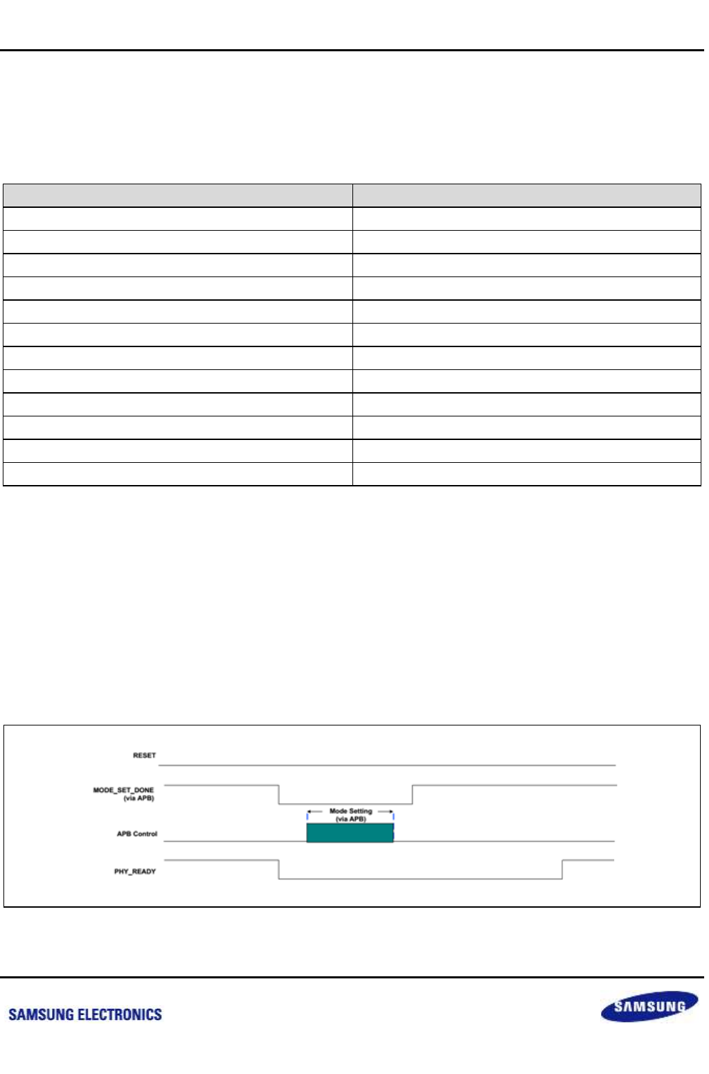
Samsung Confidential
S5P6818_UM 39 HDMI
39-152
Preliminary product information describes products that are in development, for which full characterization data and
associated errata are not yet available. Specifications and information herein are subject to change without notice.
39.6 HDMI PHY
The HDMI PHY can generate a pixel clock for HDMI 1.4 spec with own PCG (Pixel clock generator) that used 24
MHz reference clock. Following is genera table pixel clock frequency table.
Table 39-2 Available Pixel Clock Frequencies of the Integrated Video PLL
Available Pixel Clock Frequency for DTV (MHz)
Available Pixel Clock Frequency for Monitor (MHz)
25.2
25
25.175
65
27
108
27.027
162
54
54.054
74.25
74.176
148.5
148.352
108.108
72
39.6.1 PHY Configuration Change through APB
The HDMI PHY has many internal registers to change its configuration, like pixel clock frequency or analog
characteristics. Users can access these registers through APB port. For secure configuration of the PHY core,
MODE_SET_DONE register (REG_7C<7>) is used for an indicator of APB setting state as shown in the Figure
below. (MODE_SET_DONE register is also controlled by APB.)
If users want store configure the HDMI PHY by new register setting, it should write 00h on MODE_SET_DONE
register (0xC010047C) instead of asserting overall RESET signal. Then PHY_READY signal goes to low state
and PHY waits for new register setting. After new values are written on PHY registers; MODE_SET_DONE
register should be set to 80h again letting PHY start to configure its state with new register values. Once
configuration is done, PHY_READY signal is automatically asserted.
Figure 39-18 PHY Configuration through APB with MODE_SET_DONE Register
nexell / ys.kim at 2015.02.12
SAMSUNG Confidential
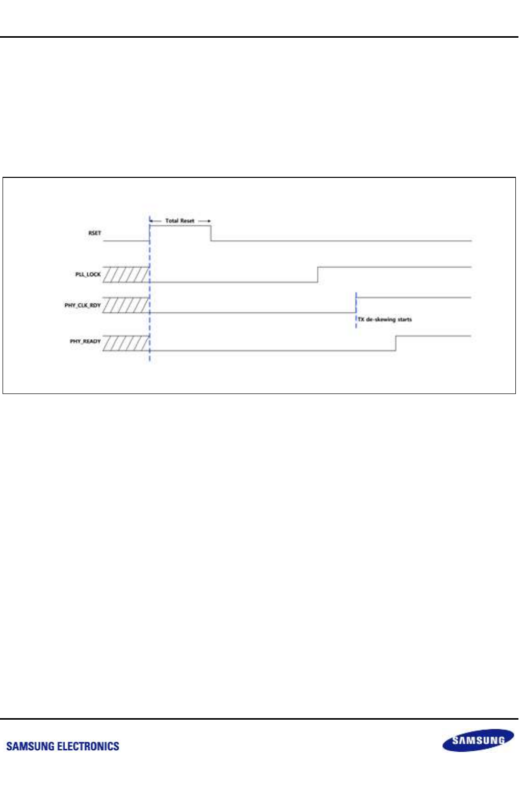
Samsung Confidential
S5P6818_UM 39 HDMI
39-153
Preliminary product information describes products that are in development, for which full characterization data and
associated errata are not yet available. Specifications and information herein are subject to change without notice.
39.6.2 PHY Ready Sequence
To assert PHY_READY signal, the HDMI PHY have to precede several steps shown in the Figure below. The
HDMI PHY core has a CMU and PCG for TMDS and pixel clock generation. Both of them should be locked and
clock de-skewing between TMDS_CLKHI and TMDS_CLKO should be finished before PHY_READY assertion.
Thus, TMDS_CLKHI should be supplied to PHY before PHY_READY signal assertion. The HDMI PHY ready
sequence is ignited by PHY_RESET signal which is external reset or in version of MODE_SET_DONE signal.
Once PLL_LOCK and CMU_LOCK signals go high, the de-skewing process starts. After de-skewing is finished,
the PHY_READY signal goes high meaning The HDMI PHY is ready to correctly send TMDS data.
Figure 39-19 PHY Ready Sequence
nexell / ys.kim at 2015.02.12
SAMSUNG Confidential

Samsung Confidential
S5P6818_UM 39 HDMI
39-154
Preliminary product information describes products that are in development, for which full characterization data and
associated errata are not yet available. Specifications and information herein are subject to change without notice.
39.6.3 HDMI PHY Configuration
Users need to set the HDMI PHY configuration to get a generated pixel clock. Following is a sequence of setting
the HDMI PHY configuration.
1. Set the HDMI CLKGEN's PCLKMODE with "1" (enable). (RESETREG[0].[10] release need.)
2. Set the TIEOFFREG[3].[0] with "1".
3. Release resets of RESETREG[0].[13] and RESETREG[0].[17] (HDMI PHY reset release).
4. Set the HDMI PHY's registers with the table below to generate a pixel clock
5. Check the *PHY_READY*bit of the *PHY_STATUS_0*register (HDMI Link) whether the HDMI PHY's
HY_READY is HIGH.
Table 39-3 HDMI PHY Configuration Table (8-bit Pixel)
Register
Address
Pixel Clock Frequency
25.2
25.175
27
27.027
54
54.054
74.25
74.176
148.5
148.352
25
65
108
162
0xC0100404
52h
D1h
D1h
D1h
51h
D1h
D1h
D1h
D1h
D1h
D1h
D1h
D1h
D1h
0xC0100408
3Fh
1Fh
22h
2Dh
2Dh
2Dh
1Fh
1Fh
1Fh
1Fh
27h
2Eh
1Fh
27h
0xC010040C
55h
50h
51h
72h
35h
32h
10h
10h
00h
00h
11h
12h
10h
14h
0xC0100410
40h
40h
40h
40h
40h
40h
40h
40h
40h
40h
51h
61h
40h
51h
0xC0100414
01h
20h
08h
64h
01h
64h
40h
5Bh
40h
5Bh
40h
40h
5Bh
5Bh
0xC0100418
00h
1Eh
FCh
12h
00h
12h
F8h
EFh
F8h
EFh
D6h
34h
EFh
A7h
0xC010041C
C8h
C8h
E0h
C8h
C8h
C8h
C8h
C8h
C8h
C8h
C8h
C8h
C8h
C8h
0xC0100420
82h
81h
98h
43h
82h
43h
81h
81h
81h
81h
81h
82h
81h
84h
0xC0100424
C8h
E8h
E8h
E8h
C8h
E8h
E8h
E8h
E8h
E8h
E8h
E8h
E8h
E8h
0xC0100428
BDh
BDh
CBh
0Eh
0Eh
0Eh
BAh
B9h
BAh
B9h
E8h
16h
B9h
E8h
0xC010042C
D8h
D8h
D8h
D9h
D9h
D9h
D8h
D8h
D8h
D8h
D8h
D9h
D8h
D8h
0xC0100430
45h
45h
45h
45h
45h
45h
45h
45h
45h
45h
45h
45h
45h
45h
0xC0100434
A0h
A0h
A0h
A0h
A0h
A0h
A0h
A0h
A0h
A0h
A0h
A0h
A0h
A0h
0xC0100438
ACh
ACh
ACh
ACh
ACh
ACh
ACh
ACh
ACh
ACh
ACh
ACh
ACh
ACh
0xC010043C
80h
80h
80h
80h
80h
80h
80h
80h
80h
80h
80h
80h
80h
80h
0xC0100440
06h
06h
06h
06h
06h
06h
56h
56h
66h
66h
56h
56h
56h
56h
0xC0100444
80h
80h
80h
80h
80h
80h
80h
80h
80h
80h
80h
80h
80h
80h
0xC0100448
01h
09h
09h
09h
09h
09h
09h
09h
09h
09h
09h
09h
09h
09h
0xC010044C
84h
84h
84h
84h
84h
84h
84h
84h
84h
84h
84h
84h
84h
84h
0xC0100450
05h
05h
05h
05h
05h
05h
05h
05h
05h
05h
05h
05h
05h
05h
0xC0100454
22h
22h
22h
22h
22h
22h
22h
22h
22h
22h
22h
22h
22h
22h
0xC0100458
24h
24h
24h
24h
24h
24h
24h
24h
24h
24h
24h
24h
24h
24h
0xC010045C
86h
86h
86h
86h
86h
86h
86h
86h
86h
86h
86h
86h
86h
86h
0xC0100460
54h
54h
54h
54h
54h
54h
54h
54h
54h
54h
54h
54h
54h
54h
nexell / ys.kim at 2015.02.12
SAMSUNG Confidential

Samsung Confidential
S5P6818_UM 39 HDMI
39-155
Preliminary product information describes products that are in development, for which full characterization data and
associated errata are not yet available. Specifications and information herein are subject to change without notice.
Register
Address
Pixel Clock Frequency
25.2
25.175
27
27.027
54
54.054
74.25
74.176
148.5
148.352
25
65
108
162
0xC0100464
F4h
F4h
E4h
E3h
E4h
E3h
A5h
A6h
4Bh
4Bh
84h
B9h
A6h
85h
0xC0100468
24h
24h
24h
24h
24h
24h
24h
24h
25h
25h
24h
25h
24h
24h
0xC010046C
00h
00h
00h
00h
01h
01h
01h
01h
03h
03h
01h
03h
01h
01h
0xC0100470
00h
00h
00h
00h
00h
00h
00h
00h
00h
00h
00h
00h
00h
00h
0xC0100474
00h
00h
00h
00h
00h
00h
00h
00h
00h
00h
00h
00h
00h
00h
0xC0100478
01h
01h
01h
01h
01h
01h
01h
01h
01h
01h
01h
01h
01h
01h
0xC010047C
80h
80h
80h
80h
80h
80h
80h
80h
80h
80h
80h
80h
80h
80h
0xC010048C
10h
10h
10h
10h
10h
10h
10h
10h
10h
10h
10h
10h
10h
10h
nexell / ys.kim at 2015.02.12
SAMSUNG Confidential
Samsung Confidential
S5P6818_UM 39 HDMI
39-156
Preliminary product information describes products that are in development, for which full characterization data and
associated errata are not yet available. Specifications and information herein are subject to change without notice.
39.6.4 Register Description
39.6.4.1 Register Map Summary
Base Address: 0xC010_0000
Register
Offset
Description
Reset Value
PHY
HDMIPHY 4H register
0x0404h
HDMI TX PHY internal PLL Input Clock Selection
0x0000_0091
HDMIPHY 24H register
0x0424h
REF_CKO Selection
0x0000_0028
HDMIPHY 3CH register
0x043Ch
TMDS Data Amplitude Control
0x0000_0090
HDMIPHY 40H register
0x0440h
TMDS Data Amplitude Control
0x0000_0008
HDMIPHY 5CH register
0x045Ch
TMDS Clock Amplitude Control
0x0000_0086
HDMIPHY 74h register
0x0474h
PHY APB Mode Control register
0x0000_0000
HDMIPHY 78H register
0x0478h
PHY Test Mode Enable register
0x0000_0001
HDMIPHY 7CH register
0x047Ch
An Indicator of APB setting state register
0x0000_0008
DisplayTop
HDMI_MUXCTRL
0x1004h
DISPLAYTOP HDMI MUX Control register
0x0000_0000
HDMI_SYNCCTRL0
0x1014h
DISPLAYTOP HDMI sync Control register 0
0x0000_0001
HDMI_SYNCCTRL1
0x1018h
DISPLAYTOP HDMI sync Control register 1
0x0000_0000
HDMI_SYNCCTRL2
0x101Ch
DISPLAYTOP HDMI sync Control register 2
0x0000_0000
HDMI_SYNCCTRL3
0x1020h
DISPLAYTOP HDMI sync Control register 3
0x0000_0000
HDMI Converter FIELD Control0
0x1028h
HDMI Converter FIELD Control0
0x0000_0000
HDMI Converter FIELD Control1
0x102Ch
HDMI Converter FIELD Control1
0x0000_0000
nexell / ys.kim at 2015.02.12
SAMSUNG Confidential
Samsung Confidential
S5P6818_UM 39 HDMI
39-157
Preliminary product information describes products that are in development, for which full characterization data and
associated errata are not yet available. Specifications and information herein are subject to change without notice.
39.6.4.1.1 PHY
HDMI PHY's register has own mean. Following is for user reference.
39.6.4.1.1.1 HDMIPHY 4H Register
Base Address: 0xC010_0000
Address = Base Address + 0x0404h, Reset Value = 0x0000_0091
Name
Bit
Type
Description
Reset Value
RSVD
[31:6]
R
Reserved
26'h2
CLK_SEL
[5:4]
RW
Select the HDMI PHY reference clock
Users must set both of TIEOFF's register and this
Register.
This register must be 0.
2'b01
RSVD
[3:0]
–
Reserved
4'h1
39.6.4.1.1.2 HDMIPHY 24H Register
Base Address: 0xC010_0000
Address = Base Address + 0x0424h, Reset Value = 0x0000_0028
Name
Bit
Type
Description
Reset Value
RSVD
[31:8]
R
Reserved
24'h0
ref_cko_sel
[7]
RW
0 = REF_OCS
1 = Internal Reference Clock
1'b0
RSVD
[6:0]
–
Reserved
7'h28
39.6.4.1.1.3 HDMIPHY 3CH Register
Base Address: 0xC010_0000
Address = Base Address + 0x043Ch, Reset Value = 0x0000_0090
Name
Bit
Type
Description
Reset Value
RSVD
[31:8]
R
Reserved
24'h0
TX_AMP_LVL[0]
[7]
RW
TX_AMP_LVL[0] bit
1'b1
TX_RES[1:0]
[5:4]
RW
TMDS Data Source Termination Resistor Control
0 = Source Termination OFF
1 = 300
2 = 150
3 = 100
2'b01
RSVD
[3:0]
–
Reserved
–
nexell / ys.kim at 2015.02.12
SAMSUNG Confidential
Samsung Confidential
S5P6818_UM 39 HDMI
39-158
Preliminary product information describes products that are in development, for which full characterization data and
associated errata are not yet available. Specifications and information herein are subject to change without notice.
39.6.4.1.1.4 HDMIPHY 40H Register
Base Address: 0xC010_0000
Address = Base Address + 0x0440h, Reset Value = 0x0000_0008
Name
Bit
Type
Description
Reset Value
RSVD
[31:8]
R
Reserved
24'h0
TX_EMP_LVL[3:0]
[7:4]
R/W
TMDS Data Pre-emphasis Control
0000 = 400mV diff (Min Value)
1111 = 750mV diff (Max Value)
4'h0
TX_AMP_LVL[4:1]
[3:0]
R/W
TX_AMP_LVL[4:1] bit
TMDS Data Amplitude Control.
1LSB corresponds to 50 mV diff amplitude level.
00000 = 400 mV diff (Min Value)
11111 = 1950 mV diff (Max Value)
4'h8
39.6.4.1.1.5 HDMIPHY 5CH Register
Base Address: 0xC010_0000
Address = Base Address + 0x045Ch, Reset Value = 0x0000_0086
Name
Bit
Type
Description
Reset Value
RSVD
[31:8]
R
Reserved
24'h0
TX_CLK_LVL[4:0]
[7:3]
R/W
TMDS Clock Amplitude Control
1LSB corresponds to 50 mV diff amplitude level.
00000 = 400 mV diff (Min Value)
11111 = 1950 mV diff (Max Value)
5'h8
RSVD
[2:0]
R
Reserved
3'b110
nexell / ys.kim at 2015.02.12
SAMSUNG Confidential
Samsung Confidential
S5P6818_UM 39 HDMI
39-159
Preliminary product information describes products that are in development, for which full characterization data and
associated errata are not yet available. Specifications and information herein are subject to change without notice.
39.6.4.1.1.6 HDMIPHY 74H Register
Base Address: 0xC010_0000
Address = Base Address + 0x0474h, Reset Value = 0x0000_0000
Name
Bit
Type
Description
Reset Value
RSVD
[31:8]
R
Reserved
24'h0
APB_PDEN
[7]
RW
If APB_PDEN = 1, power down of each building
blocks of PHY can be controlled APB Reg74 bit[6:4],
bit[2:0]
0 = Disable
1 = Enable
1'b0
PLL_PD
[6]
RW
0 = Normal Status
1 = Power Down Status
PLL & Bias Block Power Down
1'b0
TX_CLKSER_PD
[5]
RW
Clock Serializer Power Down
1'b0
TX_CLKDRV_PD
[4]
RW
TMDS Clock Driver Power Down
1'b0
TX_DRV_PD
[2]
RW
TMDS Data Driver Power Down
1'b0
TX_SER_PD
[1]
RW
TMDS Data Serializer Power Down
1'b0
TX_CLK_PD
[0]
RW
TX Internal Clock Buffer/Divider Power Down
1'b0
39.6.4.1.1.7 HDMIPHY 78H Register
Base Address: 0xC010_0000
Address = Base Address + 0x0478h, Reset Value = 0x0000_0001
Name
Bit
Type
Description
Reset Value
RSVD
[31:8]
R
Reserved
24'h0
TESTEN
[7]
RW
PHY Test Mode Enable
0 = Normal Operation Mode
1 = PHY Test Mode
1'b0
TEST
[6:0]
RW
PHY Test Mode Control Signal
7'h1
39.6.4.1.1.8 HDMIPHY 7CH Register
Base Address: 0xC010_0000
Address = Base Address + 0x047Ch, Reset Value = 0x0000_0008
Name
Bit
Type
Description
Reset Value
RSVD
[31:8]
R
Reserved
24'h0
MODE_SET_DONE
[7]
RW
An indicator of APB setting state. Refer to the Section
39.6.1 PHY Configuration Change through APB
1'b1
RSVD
[6:0]
R
Reserved
7'h0
nexell / ys.kim at 2015.02.12
SAMSUNG Confidential

Samsung Confidential
S5P6818_UM 39 HDMI
39-160
Preliminary product information describes products that are in development, for which full characterization data and
associated errata are not yet available. Specifications and information herein are subject to change without notice.
39.6.4.1.1.9 HDMI Application Sequences
Users must be set to the following sequence in order to user HDMI.
HDMI PHY configuration
I2S (or SPDIFTX) configuration for the source audio data
DPC (or Resolution Converter) configuration for the source video data
HDMI Link configuration
HDMI Converter configuration
nexell / ys.kim at 2015.02.12
SAMSUNG Confidential
Samsung Confidential
S5P6818_UM 39 HDMI
39-161
Preliminary product information describes products that are in development, for which full characterization data and
associated errata are not yet available. Specifications and information herein are subject to change without notice.
39.6.4.1.2 DisplayTop
User used this register to select the RGB Video data between the Primary DPC and the Secondary DPC.
39.6.4.1.2.1 HDMI_MUXCTRL
Base Address: 0xC010_0000
Address = Base Address + 0x1004h, Reset Value = 0x0000_0000
Name
Bit
Type
Description
Reset Value
HDMI_MUXENB
[31]
RW
MUX Enable
0 = MUX Disable
1 = MUX Enable
1'b0
RSVD
[30:2]
RW
Reserved
29'h0
HDMI_MUXSEL
[1:0]
RW
MUX Select
0 = Primary DPC
1 = Secondary DPC
2 – 3 = Reserved ( Never use this value )
2'b0
39.6.4.1.2.2 HDMI_SYNCCTRL0
Base Address: 0xC010_0000
Address = Base Address + 0x1014h, Reset Value = 0x0000_0000
Name
Bit
Type
Description
Reset Value
HDMI_vclk_sel
[31]
RW
Must set this value to 0
0 = HDMI PHY's pixel clock used for HDMI Operation
1 = Never set this value
1'b0
RSVD
[30:16]
RW
Reserved
15'h0
HDMI_Vsyncstart
[15:0]
RW
Specifies the start line of i_v_sync for the HDMI Link.
Refer Table 39-1. The Configuration Values for the
HDMI converter.
16'h1
nexell / ys.kim at 2015.02.12
SAMSUNG Confidential
Samsung Confidential
S5P6818_UM 39 HDMI
39-162
Preliminary product information describes products that are in development, for which full characterization data and
associated errata are not yet available. Specifications and information herein are subject to change without notice.
39.6.4.1.2.3 HDMI_SYNCCTRL1
Base Address: 0xC010_0000
Address = Base Address + 0x1018h, Reset Value = 0x0000_0000
Name
Bit
Type
Description
Reset Value
RSVD
[31:16]
RW
Reserved
16'h0
HDMI_HActivestart
[15:0]
RW
Specifies the start position (h_line) of h_active for the
HDMI Link. Refer Table 39-1.
16'h0
39.6.4.1.2.4 HDMI_SYNCCTRL2
Base Address: 0xC010_0000
Address = Base Address + 0x101Ch, Reset Value = 0x0000_0000
Name
Bit
Type
Description
Reset Value
RSVD
[31:16]
RW
Reserved
16'h0
HDMI_HActiveend
[15:0]
RW
Specifies the end position of h_active for the HDMI
Link. Refer Table 39-1.
16'h0
39.6.4.1.2.5 HDMI_SYNCCTRL3
Base Address: 0xC010_0000
Address = Base Address + 0x1020h, Reset Value = 0x0000_0000
Name
Bit
Type
Description
Reset Value
HDMI_VSYNCHSend
[31:16]
RW
Specifies the end position of i_v_sync for the HDMI
Link. Refer Table 39-1.
16'h0
HDMI_VSYNCHSStart
[15:0]
RW
Specifies the start position of i_v_sync for the HDMI
Link. Refer Table 39-1.
16'h0
nexell / ys.kim at 2015.02.12
SAMSUNG Confidential
Samsung Confidential
S5P6818_UM 39 HDMI
39-163
Preliminary product information describes products that are in development, for which full characterization data and
associated errata are not yet available. Specifications and information herein are subject to change without notice.
39.6.4.1.2.6 HDMI Converter FIELD Control0
Base Address: C010_0000h
Address = Base Address + 0x1028h, Reset Value = 0x0000_0000
Name
Bit
Type
Description
Reset Value
HSynctoggle
[31:17]
R/W
Field Clear Position in HSYNC (use HSync posCnt)
15'h0
vsynctoggle
[16:2]
R/W
Field Clear Position in VSYNC (use VSync posCnt)
15'h0
toggleinit
[1]
R/W
HDMI filed signal's toggle start value
(not use DPC's field value): do not use this option
1'b0
fieldenable
[0]
R/W
HDMI LINK's field signal enable
0 = not use (always 0, progressive)
1 = use (toggle with setting)
1'b0
39.6.4.1.2.7 HDMI Converter FIELD control1
Base Address:C010_0000h
Address=Base Address + 0x102Ch, Reset Value = 0x0000_0000
Name
Bit
Type
Description
Reset Value
fielduse
[31]
R/W
DPC's field signal use (recommended 1 in interlace
mode)
0 = not use DPC's field
1 = use DPC's filed
1'b0
muxsel
[30]
R/W
HDMI LINK's field source select
0 = Primary DPC
1 = Secondary DPC
1'b0
hsyncfieldclr
[29:15]
R/W
Field Clear Position in HSYNC (use HSync posCnt)
15'h0
vsyncfieldclr
[14:0]
R/W
Field Clear Position in VSYNC (use VSync posCnt)
15'h0
nexell / ys.kim at 2015.02.12
SAMSUNG Confidential
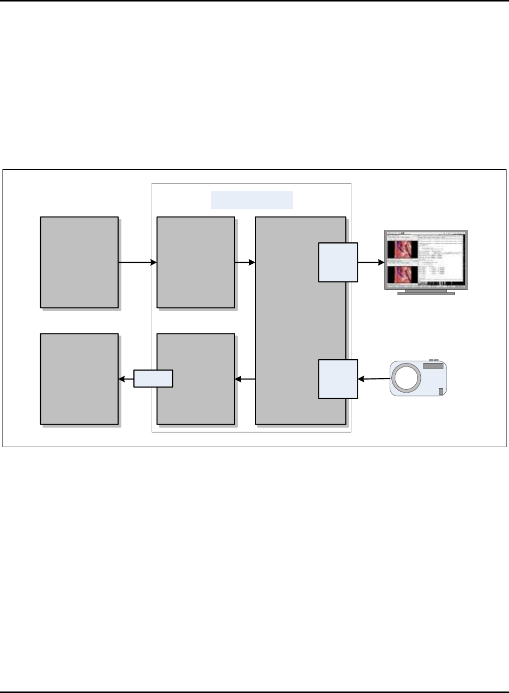
S5P6818_UM 40 MIPI
40-1
40 MIPI
40.1 Overview
The S5P6818 has a MIPI-DSI master and a MIPI-CSI slave.
Figure 40-1 MIPI-DSI and MIPI-CSI
D-PHY
Master
PAD
Slave
PAD
DISM
CSIS
Display
Controller
VIP
Controller
MIPI
Channel 1
nexell / ys.kim at 2015.02.12
SAMSUNG Confidential

S5P6818_UM 40 MIPI
40-2
40.2 Features
40.2.1 DSI Master Features (DSIM)
The key features of MIPI DSIM include:
MIPI DSI Standard Specification V1.01r11
Maximum resolution ranges up to WUXGA (1920 1200)
Supports 1, 2, 3, or 4 data lanes
Supports pixel format: 16-bpp, 18-bpp packed, 18-bpp loosely packed (3 byte format), and 24-bpp
Interfaces
Supports RGB Interface for Video Image Input from display controller
Supports PMS control interface for PLL to configure byte clock frequency
Supports Pre-scaler to generate escape clock from byte clock
40.2.2 CSI Slave Features (CSIS)
Support YUV422 of 8 bits only. See VIP for more information.
nexell / ys.kim at 2015.02.12
SAMSUNG Confidential

S5P6818_UM 40 MIPI
40-3
40.3 D-PHY Features
The features of MIPI D-PHY are:
The maximum high speed clock frequency of MIPI D-PHY core is 1GHz.
D-PHY spec v1.00 compatible.
Synchronous link between Master (data source) and Slave (data sink).
All lanes support high-speed transmission in forward direction.
Bi-directional data transmission in Low-Power mode at the Master Data Lane 0 only.
Use token passing to control the communication direction of the link.
High-Speed mode for fast data traffics and Low-Power mode for controls and low speed data transmission.
High-Speed mode: differential and terminated, 200mV swing: 80 to 1000Mbps
Low-Power mode: single-ended and non-terminated, 1.2V swing: 10Mbps maximum
(Use this mode for low-speed asynchronous data communications or controls)
nexell / ys.kim at 2015.02.12
SAMSUNG Confidential
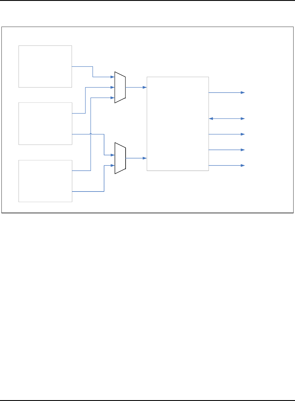
S5P6818_UM 40 MIPI
40-4
40.4 Block Diagram for DSIM
Figure 40-2 MIPI DSI System Block Diagram
DSIM gets data from the three different IPs, namely, MIE, MDNIE, and Display Controller.
You can select one of above data paths by setting MDNIE registers.
i80_DISPCON
i80_MDNIE
RGB_DISPCON
RGB_MDNIE
RGB_MIE
MIE
MDNIE
Display Controller
MIPI DSIM
CLK lane
Data lane0
Data lane1
Data lane2
Data lane3
nexell / ys.kim at 2015.02.12
SAMSUNG Confidential

S5P6818_UM 40 MIPI
40-5
40.4.1 Internal Primary FIFOs
Below Table describes configurable-sized primary FIFOs.
Table 40-1 Internal Primary FIFO List
Port
FIFO Type
Size
Description
Main display
Packet Header FIFO
3 byte 128 depth
Specifies the packet header FIFO for main
display.
Payload FIFO
4 byte 2048 depth
Specifies the payload FIFO for main display
image.
Sub display for
I80 INTERFACE
image data
Packet Header FIFO
3 byte 4 depth
Specifies the packet header FIFO for I80
INTERFACE sub display.
Payload FIFO
4 byte 512 depth
Specifies the payload FIFO for I80
INTERFACE sub display image.
Command for
I80 INTERFACE
command
Packet Header FIFO
3 byte 16 depth
Specifies the packet header FIFO for I80
INTERFACE command packet.
Payload FIFO
4 byte 16 depth
Specifies the payload FIFO for I80
INTERFACE command long packet payload.
SFR for general
packets
Packet Header FIFO
3 byte 16 depth
Specifies the packet header FIFO for
general packet.
Payload FIFO
4 byte 512 depth
Specifies the payload FIFO for general long
packet.
RX FIFO
Packet header and
Payload FIFO
4 byte 64 depth
Specifies Rx FIFO for LPDR. This FIFO is
common for packet header and payload.
40.4.2 Packet Header Arbitration
There are four-packet headers FIFOs for Tx, namely, main display, sub display, I80 INTERFACE command, and
SFR FIFO. The main and sub display FIFO packet headers contain the image data, while the I80 INTERFACE
command FIFO packet header contains the command packets. On the other hand, the SFR FIFO packet header
contains command packets, sub display image data (in Video mode), and so on.
The packet header arbiter has a "Fixed priority" algorithm. Priority order is fixed as main display, sub display, I80
INTERFACE command, and SFR FIFO packet header.
In the Video mode, sub display and I80 INTERFACE command FIFO are not used. The SFR FIFO packet header
checks if the main display FIFO is empty (no request) in not-active image region and then sends its request.
nexell / ys.kim at 2015.02.12
SAMSUNG Confidential
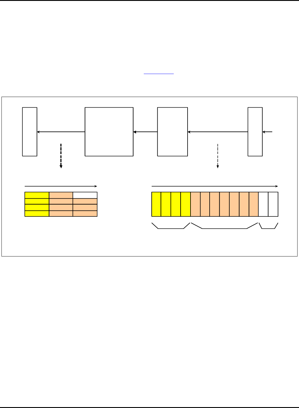
S5P6818_UM 40 MIPI
40-6
40.4.3 RxFIFO Structure
To read the packets received via low power data receiving mode, RxFIFO acts like an SFR. RxFIFO is an
asynchronous FIFO with ByteClk and PCLK domains as input clock and output clock domains respectively. The
Rx data is synchronized to RxClk. RXBUF has four Rx Byte buffers for aligning byte to word.
The packet headers of all the packets stored in RXFIFO are word-aligned, that is, the first byte of a packet is
always stored in LSB. For example, if a long packet has 7 byte payload, the last byte is filled with dummy byte and
the next packet is stored in the next word, as shown in Figure 40-3.
NOTE: CRC data is not stored in RXFIFO.
Figure 40-3 Rx Data Word Alignment
P
H
b0
P
H
b1
P
H
b2
E
C
C
PL
b0
PL
b1
PL
b2
PL
b3
PL
b4
PL
b5
PL
b6
C
R
C
0
C
R
C
1
RXBUF
(with
synchronizer
between ByteClk
and RxClk)
RXFIFO
(Asynchronous
FIFO )
Packet
header Payload Packet
footer
MIPI DSIM data receiving time
D -
PHY
ByteClk
domain
RxClk
domain
PH b 0
PH b 1
PH b 2
ECC
PL b 0
PL b 1
PL b 2
PL b 3
PL b4
PL b5
PL b6
dummy
Data reading time
0
31
DSI
channel
PCLK
domain
APB
I/ F
nexell / ys.kim at 2015.02.12
SAMSUNG Confidential
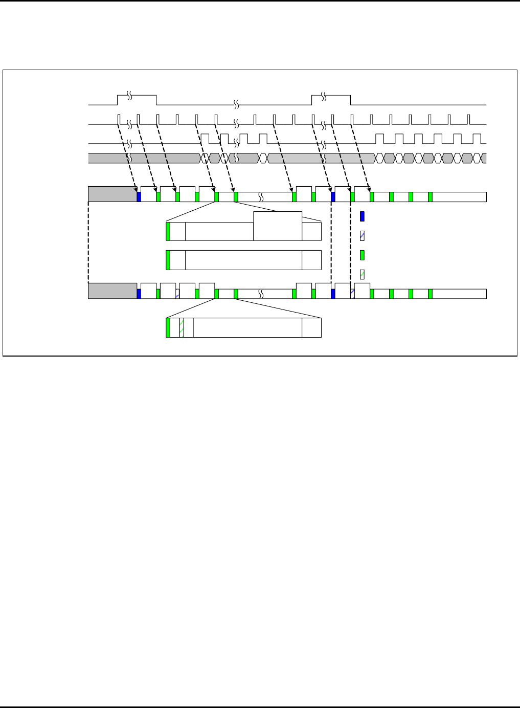
S5P6818_UM 40 MIPI
40-7
40.5 Interfaces and Protocol
Display Controller-to-DSI Conceptual Signal Converting Diagram in Video Mode
Figure 40-4 Signal Converting Diagram in Video Mode
40.5.1 Display Controller Interface
MIPI DSI Master has two-display controller interfaces, namely, RGB INTERFACE for main display and CPU
INTERFACE (I80 INTERFACE) for main/ sub display. The Video mode uses RGB INTERFACE while the
Command mode uses CPU INTERFACE.
The RGB image data is loaded on the data bus of RGB INTERFACE and I80 INTERFACE with the same order:
RGB_VD[23:0] or SYS_VDOUT[23:0] is {R[7:0],G[7:0],B[7:0]}. Each byte aligns to the most significant bit. For
instance, in the 12-bit mode, only three 4-bit values are valid as R, G, and B each, that is, data[23:20],
data[15:12], and data[7:4]. The DSIM ignores rest of the bits.
BLLP BLLP
LP
RGB_VSYNC
RGB_HSYNC
RGB_VDEN
BLLP BLLP
Vsync start packet
Hsync start packet
BLLP BLLPBLLP BLLP
RGB_DATA
DSI_channel
BLLP BLLP
LP BLLP BLLP BLLP BLLPBLLP BLLP
Vsync end packet
Hsync end packet
DSI_channel
Burst mode
Non burst mode
with Sync event
Non burst mode
with Sync pulses
H
S
ARGB HFP
H
B
P
HBP RGB HFP
HBP RGB HFP
BLLP
nexell / ys.kim at 2015.02.12
SAMSUNG Confidential
S5P6818_UM 40 MIPI
40-8
40.5.2 RGB Interface
Vsync, Hsync, and VDEN are active high signals. Among the three signals, Vsync and Hsync are pulse types that
spend several video clocks. RGB_VD[23:0] is {R[7:0],G[7:0],B[7:0]}. All sync signals are synchronized to the rising
edge of RGB_VCLK. The display controller sends minimum one horizontal line length of Vsync pulse, V back
porch, and V front porch. Hsync pulse width should be longer than 1 byte clock cycle.
40.5.3 HSA Mode
HSA mode specifies the Horizontal Sync Pulse area disable mode.
Figure 40-5 Block Timing Diagram of HSA Mode (HSA mode reset: DSIM_CONFIG[20] = 0)
Figure 40-6 Block Timing Diagram of HSA Mode (HSA mode set: DSIM_CONFIG[20] = 1)
HBP mode HBP mode specifies the Horizontal Back Porch disable mode.
Figure 40-7 Block Timing Diagram of HBP Mode (HBP Mode Reset: DSIM_CONFIG[21] = 0)
Hsync start packet
Hsync end packet
Non burst mode
with Sync pulses
(HSAmode)
RGB HFPHBP
HS
ARGB HFPHBP
HS
A
Hsync start packet
Hsync end packet
Non burst mode
with Sync pulses
(HSAmode)
RGB HFPHBP RGB HFPHBP
Burst mode
(HBPmode) RGB HFP
STOP state
HBP
Hsync start packet
RGB HFP
STOP state
HBP
EoT packet
nexell / ys.kim at 2015.02.12
SAMSUNG Confidential
S5P6818_UM 40 MIPI
40-9
Figure 40-8 Block Timing Diagram of HBP Mode (HBP Mode Set: DSIM_CONFIG[21] = 1)
HFP mode HFP mode specifies the Horizontal Front Porch disable mode.
Figure 40-9 Block Timing Diagram of HFP Mode (HFP Mode Reset: DSIM_CONFIG[22] = 0)
Figure 40-10 Block Timing Diagram of HFP Mode (HFP Mode Set: DSIM_CONFIG[22] = 1)
Burst mode
(HBPmode) RGB HFP
STOP state HFP
Hsync start packet
RGB STOP state
EoT packet
Hsync start packet
Burst mode
(HFPmode) RGB
HBP STOP state HFP RGB
HBP STOP state HFP
EoT packet
Hsync start packet
Burst mode
(HFPmode) RGB
HBP STOP state RGB
HBP STOP state
EoT packet
nexell / ys.kim at 2015.02.12
SAMSUNG Confidential
S5P6818_UM 40 MIPI
40-10
40.5.4 HSE Mode
HSE mode specifies the Horizontal Sync End Packet Enable mode in Vsync pulse or Vporch area.
Figure 40-11 Block Timing Diagram of HSE Mode (HSE Mode Reset: DSIM_CONFIG[23] = 0)
Figure 40-12 Block Timing Diagram of HSE Mode (HSE Mode Set: DSIM_CONFIG[23] = 1)
Hsync start packet
Hsync end packet
BLLP BLLP
LP BLLP BLLP BLLP BLLPBLLP BLLP
DSI_channel
Non burst mode
with Sync pulses
(HBPmode)
H
S
ARGB HFP
BLLP BLLP
Non burst mode
with Sync pulses
(HSAmode)
Vsync pulse or
Vporch area
Vsync start packet
Vsync end packet
EoT packet
Hsync start packet
Hsync end packet
BLLP BLLP
LP BLLP BLLP BLLP BLLPBLLP BLLP
DSI_channel
Non burst mode
with Sync pulses
(HBPmode)
H
S
ARGB HFP
H
S
A
STOP state H
S
A
STOP state
Non burst mode
with Sync pulses
(HSAmode)
Vsync pulse or
Vporch area
Vsync start packet
Vsync end packet
H
S
A
STOP state
EoT packet
nexell / ys.kim at 2015.02.12
SAMSUNG Confidential
S5P6818_UM 40 MIPI
40-11
40.5.5 Transfer General Data in Video Mode
Figure 40-13 Stable VFP Area Before Command Transfer Allowing Area
Command
masked area
(VBP + active region)
Vsync
Vsync
Stable VFP area
(register
configuration)
Command masked area
(protecting Vsync start) Only this area can be started
command through LPDT or HS
(register configuration)
nexell / ys.kim at 2015.02.12
SAMSUNG Confidential

S5P6818_UM 40 MIPI
40-12
40.5.6 MIPI DSIM Converts RGB Interface to Video Mode
Vsync and Hsync packets are extremely important to protect image in Video mode. MIPI DSIM allows several
lines in VFP area to transfer general data transfer. As shown in upper Figure, the vertical front porch is divided
into three areas, namely, stable VFP area, command allowed area, and command masked area.
The register configures stable VFP area. Configuration boundary is 11'h000 to 11'h7FFF in DSIM_MVPORCH.
The register also configures the command allowed area. Configuration boundary is 4'h0 to 4'hF in
DSIM_MVPORCH. Only this area is allowed to start "command transfer" through HS mode or LPDT. In LPDT,
data transferring takes a long time to complete (approximately hundreds of microseconds or more). In this time,
Hsync packet does not arrive due to LPDT long packet. MIPI DSIM comprises of big size FIFO for lost Hsync
packet. After LPDT, MIPI DSIM transfers these Hsync packets immediately through HS mode.
To protect Vsync, command masked area is masked area. This area is calculated using LPDT bandwidth. For
example, if EscClk is 10 MHz, the maximum long packet payload size is 1KB and LPDT, LPDT transferring time is
824us (packet size: 1030 byte, LPDT maximum bandwidth: 10Mbps). If one line time is 20us, the line timing
violation occurs in 42 lines. Therefore, command masked area is larger than 42 + a. This "a" is transferring time of
the violated Hsync packets.
Display controller should be configured in such a way that VFP lines are sum of stable vfp, command allowed
area, and command masked area.
Relation between Input Transactions and DSI Transactions
Table 40-2 Relation between Input Transactions and DSI Transactions
Input Interface
Input transaction
DSI Transaction
RGB
RGB transaction
Specifies the RGB Packet.
888, 666, 666 (loosely packed), and 565 should be
specified via register configuration.
I80
I80 Image Transaction
Specifies the Data type, that is, "DCS Long Write packet".
(DCS command is "memory write start/continue".)
I80
I80 Command Transaction
Specifies any DSI packet. Bytes in I80 transaction should
be the same bytes in DSI packets.
SFR
Header and Payload FIFO
access
Specifies any DSI Packets. Bytes in APB transaction should
be the same bytes in DSI packets.
nexell / ys.kim at 2015.02.12
SAMSUNG Confidential

S5P6818_UM 40 MIPI
40-13
40.6 Configuration
Video Mode versus Command Mode
MIPI DSI Master Block supports two modes, namely, Video mode and Command mode.
40.7 PLL
To transmit Image data, MIPI DSI Master Block needs high frequency clock (80 MHz to 1 GHz) generated by PLL.
To configure PLL, MIPI DSI Master comprises of SFRs and corresponding interface signals. PLL is embedded in
PHY module. You should use other PLL in SoC if it meets the timing specification.
40.8 Buffer
In MIPI DSI standard specification, DSI Master sends image stream in burst mode. The image stream transmits in
high-speed and bit-clock frequency. This mode allows the device to stay in stop state longer to reduce power
consumption. For this mode, MIPI DSI Master has a dual line buffer to store one complete line and send it faster
at the next line time.
nexell / ys.kim at 2015.02.12
SAMSUNG Confidential

S5P6818_UM 40 MIPI
40-14
40.9 DSIM
40.9.1 Register Description
40.9.1.1 Register Map Summary
Base Address: 0xC00D_0100
Register
Offset
Description
Reset Value
DSIMs
DSIM_STATUS
0x0000
Specifies the status register.
0x0010_010F
DSIM_SWRST
0x0004
Specifies the software reset register.
0x0000_0000
DSIM_CLKCTRL
0x0008
Specifies the clock control register.
0x0000_FFFF
DSIM_TIMEOUT
0x000C
Specifies the time out register.
0x00FF_FFFF
DSIM_CONFIG
0x0010
Specifies the configuration register.
0x0200_0000
DSIM_ESCMODE
0x0014
Specifies the escape mode register.
0x0000_0000
DSIM_MDRESOL
0x0018
Specifies the main display image resolution register.
0x0300_0400
DSIM_MVPORCH
0x001C
Specifies the main display Vporch register.
0xF000_0000
DSIM_MHPORCH
0x0020
Specifies the main display Hporch register.
0x0000_0000
DSIM_MSYNC
0x0024
Specifies the main display Sync Area register.
0x0000_0000
DSIM_SDRESOL
0x0028
Specifies the sub display image resolution register.
0x0300_0400
DSIM_INTSRC
0x002C
Specifies the interrupt source register.
0x0000_0000
DSIM_INTMSK
0x0030
Specifies the interrupt mask register.
0xBB37_FFFF
DSIM_PKTHDR
0x0034
Specifies the packet header FIFO register.
0x0000_0000
DSIM_PAYLOAD
0x0038
Specifies the payload FIFO register.
0x0000_0000
DSIM_RXFIFO
0x003C
Specifies the read FIFO register.
0xXXXX_XXXX
DSIM_FIFOTHLD
0x0040
Specifies the FIFO threshold level register.
0x0000_01FF
DSIM_FIFOCTRL
0x0044
Specifies the FIFO status and control register.
0x0155_551F
DSIM_MEMACCHR
0x0048
Specifies the FIFO memory AC characteristic register.
0x0000_4040
DSIM_PLLCTRL
0x004C
Specifies the PLL control register.
0x0000_0000
DSIM_PLLCTRL1
0x0050
Specifies the PLL control register 1.
0x0000_0000
DSIM_PLLCTRL2
0x0054
Specifies the PLL control register 2.
0x0000_0000
DSIM_PLLTMR
0x0058
Specifies the PLL timer register.
0xFFFF_FFFF
DSIM_PHYCTRL
0x005C
Specifies the D-PHY control register
0x0000_0000
DSIM_PHYCTRL1
0x0060
Specifies the D-PHY control register 1
0x0000_0000
DSIM_PHYTIMING
0x0064
Specifies the D-PHY timing register
0x0000_0000
DSIM_PHYTIMING1
0x0068
Specifies the D-PHY timing register 1
0x0000_0000
DSIM_PHYTIMING2
0x006C
Specifies the D-PHY timing register 2
0x0000_0000
DSIM_VERSION
0x0070
Specifies the DSIM version register
0x8000_0001
DSIM_S3D_CTL
0x0080
Stereo Scope 3D Register
0x0000_0000
DSIM_P3D_CTL
0x0084
Proprietary 3D Register
0x0023_4D00
nexell / ys.kim at 2015.02.12
SAMSUNG Confidential

S5P6818_UM 40 MIPI
40-15
Register
Offset
Description
Reset Value
DSIM_MIC_CTL
0x0088
MIC Register
0x0023_4D00
DSIM_P3D_ON_MIC_OF
F_HORIZONTAL
0x008C
Proprietary On MIC Off Horizontal
0x0000_0400
DSIM_P3D_OFF_MIC_O
N_HORIZONTAL
0x0090
Proprietary Off MIC On Horizontal
0x0000_0400
DSIM_P3D_ON_MIC_O
N_HORIZONTAL
0x0094
Proprietary On MIC On Horizontal Register
0x0000_0400
DSIM_P3D_ON_MIC_OF
F_HFP
0x0098
Proprietary On MIC Off HFP Register
0x0000_0000
DSIM_P3D_OFF_MIC_O
N_HFP
0x009C
Proprietary Off MIC On HFP Register
0x0000_0000
DSIM_P3D_ON_MIC_O
N_HFP
0x00A0
Proprietary On MIC On HFP Register
0x0000_0000
nexell / ys.kim at 2015.02.12
SAMSUNG Confidential

S5P6818_UM 40 MIPI
40-16
40.9.1.1.1 DSIM_STATUS
Base Address: 0xC00D_0100
Address = Base Address + 0x0000, Reset Value = 0x0010_010F
Name
Bit
Type
Description
Reset Value
PLLSTABLE
[31]
R
D-phy PLL generates stable byteclk.
1’b0
RSVD
[30:21]
–
Reserved
10’h0
SWRSTRLS
[20]
R
Specifies the software reset status.
0 = Reset state
1 = Release state
1’b1
RSVD
[19:17]
–
Reserved
3’b000
DIRECTION
[16]
R
Specifies the data direction indicator.
0 = Forward direction
1 = Backward direction
1’b0
RSVD
[15:11]
–
Reserved
5’h0
TXREADYHSCLK
[10]
R
Specifies the HS clock ready at clock lane.
0 = Not ready for transmitting HS data at clock lane
1 = Ready for transmitting HS data at clock lane
1’b0
ULPSCLK
[9]
R
Specifies the ULPS indicator at clock lane.
0 = No ULPS in clock lane
1 = ULSP in clock lane
1’b0
STOPSTATECLK
[8]
R
Specifies the stop state indicator at clock lane.
0 = No stop state in clock lane
1 = Stop state in clock lane
1’b1
ULPSDAT[3:0]
[7:4]
R
Specifies the ULPS indicator at data lanes.
ULPSDAT [0]: Data lane 0
ULPSDAT [1]: Data lane 1
ULPSDAT [2]: Data lane 2
ULPSDAT [3]: Data lane 3
0 = No ULPS in each data lane
1 = ULPS in each data lane
4’h0
STOPSTATEDAT[3:0]
[3:0]
R
Specifies the stop state indicator at data lane.
STOPSTATEDAT [0]: Data lane 0
STOPSTATEDAT [1]: Data lane 1
STOPSTATEDAT [2]: Data lane 2
STOPSTATEDAT [3]: Data lane 3
0 = No stop state in each data lane
1 = Stop state in each data lane
4’hF
This register reads and checks internal and interface status. It also checks FSM status, Line buffer status, current
image line number, and so on.
nexell / ys.kim at 2015.02.12
SAMSUNG Confidential

S5P6818_UM 40 MIPI
40-17
40.9.1.1.2 DSIM_SWRST
Base Address: 0xC00D_0100
Address = Base Address + 0x0004, Reset Value = 0x0000_0000
Name
Bit
Type
Description
Reset Value
RSVD
[31:17]
–
Reserved
–
FUNCRST
[16]
RW
Specifies the software reset (High active).
"Software reset" resets all FF in MIPI DSIM (except
SFRs: STATUS, SWRST, CLKCTRL, TIMEOUT,
CONFIG, ESCMODE (1), MDRESOL, MDVPORCH,
MHPORCH, MSYNC, INTMSK, SDRESOL,
FIFOTHLD, FIFOCTRL (2), MEMACCHR, PLLCTRL,
PLLTMR, PHYACCHR, and VERINFORM).
0 = Standby
1 = Reset
NOTE:
1. FORCESTOPSTATE, CMDLPDT, TXLPDT,
2. NINITRX, NINITSFR, nInitI80, NINITSUB, NINITMD
1’b0
RSVD
[15:1]
–
Reserved
–
SWRST
[0]
RW
Specifies the software reset (High active).
"Software reset" resets all FF in MIPI DSIM (except
some SFRs: STATUS, SWRST, CLKCTRL,
PLLCTRL, PLLTMR, and PHYTUNE).
0 = Standby
1 = Reset
1’b0
40.9.1.1.3 DSIM_CLKCTRL
Base Address: 0xC00D_0100
Address = Base Address + 0x0008, Reset Value = 0x0000_FFFF
Name
Bit
Type
Description
Reset Value
TXREQUESTHSCLK
[31]
RW
Specifies the HS clock request for HS transfer at clock
lane (Turn on HS clock)
1’b0
RSVD
[30:29]
–
Reserved
–
ESCCLKEN
[28]
RW
Enables the escape clock generating pre-scaler.
0 = Disables
1 = Enables
1’b0
PLLBYPASS
[27]
RW
Sets the PLLBYPASS signal connected to D-PHY
module input for selecting clock source bit.
0 = PLL output
1 = External Serial clock
This bit must be set to 0.
1’b0
BYTECLKSRC
[26:25]
RW
Selects byte clock source. (It must be 00.)
00 = D-PHY PLL (default).
PLL_out clock is used to generate ByteClk by dividing 8.
2’b00
nexell / ys.kim at 2015.02.12
SAMSUNG Confidential

S5P6818_UM 40 MIPI
40-18
Name
Bit
Type
Description
Reset Value
BYTECLKEN
[24]
RW
Enables byte clock.
0 = Disables
1 = Enables
1’b0
LANEESCCLKEN
[23:19]
RW
Enables escape clock for D-phy lane.
LANEESCCLKEN [0] = Clock lane
LANEESCCLKEN [1] = Data lane 0
LANEESCCLKEN [2] = Data lane 1
LANEESCCLKEN [3] = Data lane 2
LANEESCCLKEN [4] = Data lane 3
0 = Disables
1 = Enables
4’h0
RSVD
[18:16]
–
Reserved
–
ESCPRESCALER
[15:0]
RW
Specifies the escape clock pre-scaler value.
The escape clock frequency range varies up to 20MHz.
NOTE: The requirement for BTA is that the Host Escclk
frequency should range between 66.7 to 150% of the
peripheral escape clock frequency.
EscClk = ByteClk/(EscPrescaler)
16’hFFFF
40.9.1.1.4 DSIM_TIMEOUT
Base Address: 0xC00D_0100
Address = Base Address + 0x000C, Reset Value = 0x00FF_FFFF
Name
Bit
Type
Description
Reset Value
RSVD
[31:24]
–
Reserved
–
BTATOUT
[23:16]
RW
Specifies the timer for BTA.
This register specifies time out from BTA request to
change the direction with respect to Tx escape clock.
8’hFF
LPDRTOUT
[15:0]
RW
Specifies the timer for LP Rx mode timeout. This
register specifies time out on how long RxValid de-
asserts, after RxLpdt asserts with respect to Tx escape
clock.
RxValid specifies Rx data valid indicator.
RxLpdt specifies an indicator that D-phy is under
RxLpdt mode.
RxValid and RxLpdt specifies signal from D-phy.
16’hFFFF
nexell / ys.kim at 2015.02.12
SAMSUNG Confidential

S5P6818_UM 40 MIPI
40-19
40.9.1.1.5 DSIM_CONFIG
Base Address: 0xC00D_0100
Address = Base Address + 0x0010, Reset Value = 0x0200_0000
Name
Bit
Type
Description
Reset Value
RSVD
[31:30]
–
Reserved
–
MFLUSH_VS
[29]
RW
Auto flush of MD FIFO using Vsync pulse.
It needs that Main display FIFO should be flushed for
deleting garbage data.
0 = Enable (default)
1 = Disable
1’b0
EOT_R03
[28]
RW
Disables EoT packet in HS mode.
0 = Enables EoT packet generation for V1.01r11
1 = Disables EoT packet generation for V1.01r03
1’b0
SYNCINFORM
[27]
RW
Selects Sync Pulse or Event mode in Video mode.
0 = Event mode (non burst, burst)
1 = Pulse mode (non burst only)
In command mode, this bit is ignored.
1’b0
BURSTMODE
[26]
RW
Selects Burst mode in Video mode
In Non-burst mode, RGB data area is filled with RGB data
and Null packets, according to input bandwidth of RGB
interface.
In Burst mode, RGB data area is filled with RGB data only.
0 = Non-burst mode
1 = Burst mode
In command mode, this bit is ignored.
1’b0
VIDEOMODE
[25]
RW
Specifies display configuration.
0 = Command mode
1 = Video mode
1’b1
AUTOMODE
[24]
RW
Specifies auto vertical count mode.
In Video mode, the vertical line transition uses line counter
configured by VSA, VBP, and Vertical resolution. If this bit
is set to "1", the line counter does not use VSA and VBP
registers.
0 = Configuration mode
1 = Auto mode
In command mode, this bit is ignored.
1’b0
HSEMODE
[23]
RW
In Vsync pulse and Vporch area, MIPI DSI master
transfers only Hsync start packet to MIPI DSI slave at MIPI
DSI spec 1.1r02. This bit transfers Hsync end packet in
Vsync pulse and Vporch area (optional).
0 = Disables transfer
1 = Enables transfer
In command mode, this bit is ignored.
1’b0
HFPMODE
[22]
RW
Specifies HFP disable mode. If this bit set, DSI master
ignores HFP area in Video mode.
1’b0
nexell / ys.kim at 2015.02.12
SAMSUNG Confidential

S5P6818_UM 40 MIPI
40-20
Name
Bit
Type
Description
Reset Value
0 = Enables
1 = Disables
In command mode, this bit is ignored.
HBPMODE
[21]
RW
Specifies HBP disable mode. If this bit set, DSI master
ignores HBP area in Video mode.
0 = Enables
1 = Disables
In command mode, this bit is ignored.
1’b0
HSAMODE
[20]
RW
Specifies HSA disable mode. If this bit set, DSI master
ignores HSA area in Video mode.
0 = Enables
1 = Disables
In command mode, this bit is ignored.
1’b0
MAINVC
[19:18]
RW
Specifies virtual channel number for main display.
2’b00
SUBVC
[17:16]
RW
Specifies virtual channel number for sub display.
2’b00
RSVD
[15]
–
Reserved
–
MAINPIXFORMAT
[14:12]
RW
Specifies pixel stream format for main display.
000 = 3bpp (for Command mode only)
001 = 8bpp (for Command mode only)
010 = 12bpp (for Command mode only)
011 = 16bpp (for Command mode only)
100 = 16-bit RGB (565) (for Video mode only)
101 = 18-bit RGB (666: packed pixel stream) (for Video
mode only)
110 = 18-bit RGB (666: loosely packed pixel stream) for
Common
111 = 24-bit RGB (888) for common
3’b000
RSVD
[11]
–
Reserved
–
SUBPIXFORMAT
[10:8]
RW
Specifies pixel stream format for sub display.
000 = 3bpp (for Command mode only)
001 = 8bpp (for Command mode only)
010 = 12bpp (for Command mode only)
011 = 16bpp (for Command mode only)
100 = 16-bit RGB (565) (for Video mode only)
101 = 18-bit RGB (666: packed pixel stream) for Video
mode only)
110 = 18-bit RGB (666: loosely packed pixel stream) for
common)
111 = 24-bit RGB (888) (for Common)
3’b000
RSVD
[7]
–
Reserved
–
NUMOFDATLANE
[6:5]
RW
Sets the data lane number.
00 = Data lane 0 ( 1 data lane)
01 = Data lane 0 to 1 (2 data lanes)
10 = Data lane 0 to 2 (3 data lanes)
11 = Data lane 0 to 3 (4 data lanes)
2’b00
LANEEN[4:0]
[4:0]
RW
Enables the lane. If Lane_EN is disabled, the lane ignores
5’h0
nexell / ys.kim at 2015.02.12
SAMSUNG Confidential

S5P6818_UM 40 MIPI
40-21
Name
Bit
Type
Description
Reset Value
input and drives initial value through output port.
0 = Lane is off.
1 = Lane is on.
+ LANEEN [0] = Clock lane enabler + LANEEN [1] = Data
lane 0 enabler + LANEEN [2] = Data lane 1 enabler +
LANEEN [3] = Data lane 2 enabler + LANEEN [4] = Data
lane 3 enabler
This register configures MIPI DSI master such as data lane number, input interface, porch area, frame rate, BTA,
LPDT, ULPS, and so on.
40.9.1.1.6 DSIM_ESCMODE
Base Address: 0xC00D_0100
Address = Base Address + 0x0014, Reset Value = 0x0000_0000
Name
Bit
Type
Description
Reset Value
STOPSTATE_CNT
[31:21]
RW
After transmitting read packet or write "set_tear_on"
command, BTA requests to D-phy automatically. This
counter value specifies the interval value between
transmitting read packet (or write "set_tear_on" command)
and BTA request.
11'h000 = 2 EscClk
11'h001 = 2 EscClk + 1 EscClk
~ 11'h3FF = 2 EscClk + 1023 EscClk
11’h0
FORCESTOPSTAT
E
[20]
RW
Forces Stop state for D-PHY.
1’b0
RSVD
[19:17]
–
Reserved
–
FORCEBTA
[16]
RW
Forces Bus Turn Around.
1 = Sends the protocol layer request to D-PHY. MIPI DSI
peripheral becomes master after BTA sequence.
This bit clears automatically after receiving BTA
acknowledge from MIPI DSI peripheral.
1’b0
RSVD
[15:8]
–
Reserved
–
CMDLPDT
[7]
RW
Specifies LPDT transfers command in SFR FIFO.
0 = HS Mode
1 = LP Mode
1’b0
TXLPDT
[6]
RW
Specifies data transmission in LP mode (all data transfer in
LPDT).
0 = HS Mode
1 = LP Mode
1’b0
RSVD
[5]
–
Reserved
–
TXTRIGGERRST
[4]
RW
Specifies remote reset trigger function. After trigger
operation, these bits will be cleared automatically.
1’b0
TXULPSDAT
[3]
RW
Specifies ULPS request for data lane. Manually clears
1’b0
nexell / ys.kim at 2015.02.12
SAMSUNG Confidential
S5P6818_UM 40 MIPI
40-22
Name
Bit
Type
Description
Reset Value
after ULPS exit.
TXULPSEXIT
[2]
RW
Specifies ULPS exit request for data lane. Manually clears
after ULPS exit.
1’b0
TXULPSCLK
[1]
RW
Specifies ULPS request for clock lane. Manually clears
after ULPS exit.
1’b0
TXULPSCLKEXIT
[0]
RW
Specifies ULPS exit request for clock lane. Manually clears
after ULPS exit.
1’b0
This register configures MIPI DSI master.
40.9.1.1.7 DSIM_MDRESOL
Base Address: 0xC00D_0100
Address = Base Address + 0x0018, Reset Value = 0x0300_0400
Name
Bit
Type
Description
Reset Value
MAINSTANDBY
[31]
RW
Specifies standby for receiving DISPCON output in
Command mode after setting all configuration.
0 = Not ready
1 = Stand by
Standby should be set after configuration (resolution,
req type, pixel form, and so on) is set for command
mode.
In Video mode, if this bit value is 0, data is not
transferred.
1’b0
RSVD
[30:28]
–
Reserved
–
MAINVRESOL[11:0]
[27:16]
RW
Specifies Vertical resolution (1 to 1024).
12’h300
RSVD
[15:12]
–
Reserved
–
MAINHRESOL[11:0]
[11:0]
RW
Specifies Horizontal resolution (1 to 2047).
12’h400
nexell / ys.kim at 2015.02.12
SAMSUNG Confidential

S5P6818_UM 40 MIPI
40-23
40.9.1.1.8 DSIM_MVPORCH
Base Address: 0xC00D_0100
Address = Base Address + 0x001C, Reset Value = 0xF000_0000
Name
Bit
Type
Description
Reset Value
CMDALLOW
[31:28]
RW
Specifies the number of horizontal lines, where
command packet transmission is allowed after Stable
VFP period.
4’hF
RSVD
[27]
–
Reserved
–
STABLEVFP[10:0]
[26:16]
RW
Specifies the number of horizontal lines, where
command packet transmission is not allowed after end
of active region.
NOTE: In Command mode, these bits are ignored.
11’h0
RSVD
[15:11]
–
Reserved
–
MAINVBP[10:0]
[10:0]
RW
Specifies vertical back porch width for Video mode
(line count). In Command mode, these bits are
ignored.
11’h0
Transfers command packets after Stable VFP area. Display controller VFP lines should be set based on sum of
these values: Stable VFP, command allowing area and command masked area. See the section for transferring
general data in Video mode.
40.9.1.1.9 DSIM_MHPORCH
Base Address: 0xC00D_0100
Address = Base Address + 0x0020, Reset Value = 0x0000_0000
Name
Bit
Type
Description
Reset Value
MAINHFP[15:0]
[31:16]
RW
Specifies the horizontal front porch width for Video
mode. HFP is specified using blank packet.
These bits specify the word counts for blank packet in
HFP. In Command mode, these bits are ignored.
16’h0
MAINHBP[15:0]
[15:0]
RW
Specifies the horizontal back porch width for Video
mode. HBP is specified using blank packet.
These bits specify the word counts for blank packet in
HBP. In Command mode, these bits are ignored.
16’h0
nexell / ys.kim at 2015.02.12
SAMSUNG Confidential
S5P6818_UM 40 MIPI
40-24
40.9.1.1.10 DSIM_MSYNC
Base Address: 0xC00D_0100
Address = Base Address + 0x0024, Reset Value = 0x0000_0000
Name
Bit
Type
Description
Reset Value
MAINVSA[9:0]
[31:22]
RW
Specifies the vertical sync pulse width for Video mode
(Line count). In command mode, these bits are
ignored.
10’h0
RSVD
[21:16]
–
Reserved
–
MAINHSA[15:0]
[15:0]
RW
Specifies the horizontal sync pulse width for Video
mode. HSA is specified using blank packet.
These bits specify word counts for blank packet in
HSA.
In command mode, these bits are ignored.
16’h0
40.9.1.1.11 DSIM_SDRESOL
Base Address: 0xC00D_0100
Address = Base Address + 0x0028, Reset Value = 0x0300_0400
Name
Bit
Type
Description
Reset Value
SUBSTANDBY
[31]
RW
Specifies standby for receiving DISPCON output in
Command mode after setting all configuration.
0 = Not ready
1 = Standby
Standby should be set after configuration (resolution,
req type, pixel form, and so on) is set for command
mode.
In Video mode, this bit is ignored.
1’b0
RSVD
[30:27]
–
Reserved
–
SUBVRESOL[10:0]
[26:16]
RW
Specifies the Vertical resolution (1 to 1024).
11’h300
RSVD
[15:11]
–
Reserved
–
SUBHRESOL[10:0]
[10:0]
RW
Specifies the Horizontal resolution (1 to 1024).
11’h400
nexell / ys.kim at 2015.02.12
SAMSUNG Confidential

S5P6818_UM 40 MIPI
40-25
40.9.1.1.12 DSIM_INTSRC
Base Address: 0xC00D_0100
Address = Base Address + 0x002C, Reset Value = 0x0000_0000
Name
Bit
Type
Description
Reset Value
PLLSTABLE
[31]
RW
Indicates that D-PHY PLL is stable.
1’b0
SWRSTRELEASE
[30]
RW
Releases the software reset.
1’b0
SFRPLFIFOEMPTY
[29]
RW
Specifies the SFR payload FIFO empty.
1’b0
SFRPHFIFOEMPTY
[28]
RW
Specifies the SFR Packet Header FIFO empty
1’b0
SYNCOVERRIDE
[27]
RW
Indicates that other DSI command transfer have
overridden sync timing.
1’b0
RSVD
[26]
RW
Reserved
–
BUSTURNOVER
[25]
RW
Indicates when bus grant turns over from DSI slave to
DSI master.
1’b0
FRAMEDONE
[24]
RW
Indicates when MIPI DSIM transfers the whole image
frame.
NOTE: If Hsync is not received during two line times,
internal timer is timed out and this bit is flagged.
1’b0
RSVD
[23:22]
RW
Reserved
–
LPDRTOUT
[21]
RW
Specifies the LP Rx timeout. See time out register (0x10).
1’b0
TATOUT
[20]
RW
Turns around Acknowledge Timeout. See time out
register (0x10).
1’b0
RSVD
[19]
–
Reserved
–
RXDATDONE
[18]
RW
Completes receiving data.
1’b0
RXTE
[17]
RW
Receives TE Rx trigger.
1’b0
RXACK
[16]
RW
Receives ACK Rx trigger.
1’b0
ERRRXECC
[15]
RW
Specifies the ECC multi bit error in LPDR.
1’b0
ERRRXCRC
[14]
RW
Specifies the CRC error in LPDR.
1’b0
ERRESC3
[13]
RW
Specifies the escape mode entry error lane 3. For more
information, refer to standard D-PHY specification.
1’b0
ERRESC2
[12]
RW
Specifies the escape mode entry error lane 2. For more
information, refer to standard D-PHY specification.
1’b0
ERRESC1
[11]
RW
Specifies the escape mode entry error lane 1. For more
information, refer to standard D-PHY specification.
1’b0
ERRESC0
[10]
RW
Specifies the escape mode entry error lane 0. For more
information, refer to standard D-PHY specification.
1’b0
ERRSYNC2
[9]
RW
Specifies the LPDT sync error lane 3. For more
information, refer to standard D-PHY specification.
1’b0
ERRSYNC2
[8]
RW
Specifies the LPDT Sync Error lane2. For more
information, refer to standard D-PHY specification.
1’b0
ERRSYNC1
[7]
RW
Specifies the LPDT Sync Error lane1. For more
information, refer to standard D-PHY specification.
1’b0
nexell / ys.kim at 2015.02.12
SAMSUNG Confidential
S5P6818_UM 40 MIPI
40-26
Name
Bit
Type
Description
Reset Value
ERRSYNC0
[6]
RW
Specifies the LPDT Sync Error lane0. For more
information, refer to standard D-PHY specification.
1’b0
ERRCONTROL2
[5]
RW
Controls Error lane3. For more information, refer to
standard D-PHY specification.
1’b0
ERRCONTROL2
[4]
RW
Controls Error lane2. For more information, refer to
standard D-PHY specification.
1’b0
ERRCONTROL1
[3]
RW
Controls Error lane1. For more information, refer to
standard D-PHY specification.
1’b0
ERRCONTROL0
[2]
RW
Controls Error lane0. For more information, refer to
standard D-PHY specification.
1’b0
ERRCONTENTLP0
[1]
RW
Specifies the LP0 Contention Error (only lane0, because
BTA occurs at lane0 only). For more information, refer to
standard D-PHY specification.
1’b0
ERRCONTENTLP1
[0]
RW
Specifies the LP1 Contention Error (only lane0, because
BTA occurs at lane0 only). For more information, refer to
standard D-PHY specification.
1’b0
This register identifies interrupt sources.
Internal block error, data transmit interrupt, inter-layer (D_PHY) error, etc.
The bits are set even if they are masked off by DSIM_INTMSK_REG.
Write "1" to clear the Interrupt.
40.9.1.1.13 DSIM_INTMSK
Base Address: 0xC00D_0100
Address = Base Address + 0x0030, Reset Value = 0xBB37_FFFF
Name
Bit
Type
Description
Reset Value
MSKPLLSTABLE
[31]
RW
Indicates that D-PHY PLL is stable.
1’b1
MSKSWRSTRELEASE
[30]
RW
Releases software reset.
1’b0
MSKSFRPLFIFOEMPTY
[29]
RW
Empties SFR payload FIFO.
1’b1
MSKSFRPHFIFOEMPTY
[28]
RW
Interrupt Mask for SFR packet header FIFO empty
1’b1
MSKSYNCOVERRIDE
[27]
RW
Indicates that other DSI command transfer have
overridden sync timing.
1’b1
RSVD
[26]
–
Reserved
–
MSKBUSTURNOVER
[25]
RW
Indicates when bus grant turns over from DSI slave to
DSI master.
1’b1
MSKFRAMEDONE
[24]
RW
Indicates when MIPI DSIM transfers whole image
frame.
1’b1
RSVD
[23:22]
–
Reserved
–
MSKLPDRTOUT
[21]
RW
Specifies LP Rx timeout. See time out register (0x10).
1’b1
nexell / ys.kim at 2015.02.12
SAMSUNG Confidential

S5P6818_UM 40 MIPI
40-27
Name
Bit
Type
Description
Reset Value
MSKTATOUT
[20]
RW
Specifies turnaround acknowledge timeout. See time
out register (0x10)
1’b1
RSVD
[19]
–
Reserved
–
MSKRXDATDONE
[18]
RW
Specifies completion of data receiving.
1’b1
MSKRXTE
[17]
RW
Specifies receipt of TE Rx trigger.
1’b1
MSKRXACK
[16]
RW
Specifies receipt of ACK Rx trigger.
1’b1
MSKRXECC
[15]
RW
Specifies ECC multi bit error in LPDR.
1’b1
MSKRXCRC
[14]
RW
Specifies CRC error in LPDR.
1’b1
MSKESC3
[13]
RW
Specifies escape mode entry error in lane3. For more
information, refer to standard D-PHY specification.
1’b1
MSKESC2
[12]
RW
Specifies escape mode entry error in lane2. For more
information, refer to standard D-PHY specification.
1’b1
MSKESC1
[11]
RW
Specifies escape mode entry error in lane1. For more
information, refer to standard D-PHY specification.
1’b1
MSKESC0
[10]
RW
Specifies escape mode entry error in lane0. For more
information, refer to standard D-PHY specification.
1’b1
MSKSYNC3
[9]
RW
Specifies LPDT sync error in lane3. For more
information, refer to standard D-PHY specification.
1’b1
MSKSYNC2
[8]
RW
Specifies LPDT sync error in lane2. For more
information, refer to standard D-PHY specification.
1’b1
MSKSYNC1
[7]
RW
Specifies LPDT sync error in lane1. For more
information, refer to standard D-PHY specification.
1’b1
MSKSYNC0
[6]
RW
Specifies LPDT sync error in lane0. For more
information, refer to standard D-PHY specification.
1’b1
MSKCONTROL3
[5]
RW
Controls error in lane3. For more information, refer to
standard D-PHY specification.
1’b1
MSKCONTROL2
[4]
RW
Controls error in lane2. For more information, refer to
standard D-PHY specification.
1’b1
MSKCONTROL1
[3]
RW
Controls error in lane1. For more information, refer to
standard D-PHY specification.
1’b1
MSKCONTROL0
[2]
RW
Controls error in lane0. For more information, refer to
standard D-PHY specification.
1’b1
MSKCONTENTLP0
[1]
RW
Specifies LP0 contention error. For more information,
refer to standard D-PHY specification.
1’b1
MSKCONTENTLP1
[0]
RW
Specifies LP1 contention error. For more information,
refer to standard D-PHY specification.
1’b1
This register masks interrupt sources.
nexell / ys.kim at 2015.02.12
SAMSUNG Confidential
S5P6818_UM 40 MIPI
40-28
40.9.1.1.14 DSIM_PKTHDR
Base Address: 0xC00D_0100
Address = Base Address + 0x0034, Reset Value = 0x0000_0000
Name
Bit
Type
Description
Reset Value
RSVD
[31:24]
–
Reserved
–
PACKETHEADER
[23:0]
W
Writes the packet header of Tx packet.
[7:0] = DI
[15:8] = Dat0 (Word Count lower byte for long packet)
[23:16] = Dat1 (Word Count upper byte for long packet)
24’h0
This register is the FIFO for packet header to send DSI packets.
40.9.1.1.15 DSIM_PAYLOAD
Base Address: 0xC00D_0100
Address = Base Address + 0x0038, Reset Value = 0x0000_0000
Name
Bit
Type
Description
Reset Value
PAYLOAD
[31:0]
W
Writes the Payload of Tx packet.
32’h0
This register specifies the FIFO for payload to send DSI packets.
40.9.1.1.16 DSIM_RXFIFO
Base Address: 0xC00D_0100
Address = Base Address + 0x003C, Reset Value = Undefined
Name
Bit
Type
Description
Reset Value
RXDAT
[31:0]
R
In the Rx mode, you can read Rx data through this
register. Note that the CRC in packet is not stored in
RxFIFO.
Undefined
This register is the gate of FIFO read
nexell / ys.kim at 2015.02.12
SAMSUNG Confidential
S5P6818_UM 40 MIPI
40-29
40.9.1.1.17 DSIM_FIFOTHLD
Base Address: 0xC00D_0100
Address = Base Address + 0x0040, Reset Value = 0x0000_01FF
Name
Bit
Type
Description
Reset Value
RSVD
[31:9]
–
Reserved
23’h0
WFULLLEVELSFR
[8:0]
RW
Almost full level of SFR payload FIFO
9’h1FF
40.9.1.1.18 DSIM_FIFOCTRL
Base Address: 0xC00D_0100
Address = Base Address + 0x0044, Reset Value = 0x0155_551F
Name
Bit
Type
Description
Reset Value
RSVD
[31:26]
–
Reserved
6’h0
FULLRX
[25]
R
Rx FIFO full
1’b0
EMPTYRX
[24]
R
Rx FIFO empty
1’b1
FULLHSFR
[23]
R
SFR packet header FIFO full
1’b0
EMPTYHSFR
[22]
R
SFR packet header FIFO empty
1’b1
FULLLSFR
[21]
R
SFR payload FIFO full
1’b0
EMPTYLSFR
[20]
R
SFR payload FIFO empty
1’b1
FULLHI80
[19]
R
I80 packet header FIFO full
1’b0
EMPTYHI80
[18]
R
I80 packet header FIFO empty
1’b1
FULLLI80
[17]
R
I80 payload FIFO full
1’b0
EMPTYLI80
[16]
R
I80 payload FIFO empty
1’b1
FULLHSUB
[15]
R
Sub display packet header FIFO full
1’b0
EMPTYHSUB
[14]
R
Sub display packet header FIFO empty
1’b1
FULLLSUB
[13]
R
Sub display payload FIFO full
1’b0
EMPTYLSUB
[12]
R
Sub display payload FIFO empty
1’b1
FULLHMAIN
[11]
R
Main display packet header FIFO full
1’b0
EMPTYHMAIN
[10]
R
Main display packet header FIFO empty
1’b1
FULLLMAIN
[9]
R
Main display payload FIFO full
1’b0
EMPTYLMAIN
[8]
R
Main display payload FIFO empty
1’b1
RSVD
[7:5]
–
Reserved
1’b0
NINITRX
[4]
RW
MD FIFO read point initialize
1’b1
NINITSFR
[3]
RW
SFR FIFO write point initialize
1’b1
NINITI80
[2]
RW
I80 FIFO write point initialize
1’b1
NINITSUB
[1]
RW
SD FIFO write point initialize
1’b1
NINITMAIN
[0]
RW
MD FIFO write point initialize
1’b1
nexell / ys.kim at 2015.02.12
SAMSUNG Confidential
S5P6818_UM 40 MIPI
40-30
40.9.1.1.19 DSIM_MEMACCHR
Base Address: 0xC00D_0100
Address = Base Address + 0x0048, Reset Value = 0x0000_4040
Name
Bit
Type
Description
Reset Value
RSVD
[31:16]
–
Reserved
16’h0
PGEN_SD
[15]
RW
Sub display FIFO memory power gating
1’b0
RETN_SD
[14]
RW
Sub display FIFO memory Retention
1’b1
EMAB_SD
[13:11]
RW
Sub display FIFO memory B port margin adjustment
3’b000
EMAA_SD
[10:8]
RW
Sub display FIFO memory A port margin adjustment
3’b000
PGEN_MD
[7]
RW
Main display FIFO memory power gating
1’b0
RETN_MD
[6]
RW
Main display FIFO memory Retention
1’b1
EMAB_MD
[5:3]
RW
Main display FIFO memory B port margin adjustment
3’b000
EMAA_MD
[2:0]
RW
Main display FIFO memory A port margin adjustment
3’b000
In current design, these memory port control was disabled. User can ignore the function of this register.
40.9.1.1.20 DSIM_PLLCTRL
Base Address: 0xC00D_0100
Address = Base Address + 0x004C, Reset Value = 0x0000_0000
Name
Bit
Type
Description
Reset Value
RSVD
[31:28]
–
Should be 0.
–
BANDCTRL
[27:24]
RW
Each bandwidth control registers for Global Operation
Timing.
0xF: 1 GHz
0xC: 750 MHz
PLLEN
[23]
RW
Enables PLL.
0
RSVD
[22:20]
–
Should be 0.
–
PMS[19:1]
[19:1]
RW
Specifies the PLL PMS value.
0x33E8: 1 GHz
0x43E8: 750 MHz
0
RSVD
[0]
–
Reserved
0
This register configures PLL control, D-PHY, clock range indication, and so on.
nexell / ys.kim at 2015.02.12
SAMSUNG Confidential
S5P6818_UM 40 MIPI
40-31
40.9.1.1.21 DSIM_PLLCTRL1
Base Address: 0xC00D_0100
Address = Base Address + 0x0050, Reset Value = 0x0000_0000
Name
Bit
Type
Description
Reset Value
M_PLLCTL0
[31:0]
RW
It must be 0
32’h0
This register configures D-PHY PLL control (M_PLLCTL[31:0])
40.9.1.1.22 DSIM_PLLCTRL2
Base Address: 0xC00D_0100
Address = Base Address + 0x0054, Reset Value = 0x0000_0000
Name
Bit
Type
Description
Reset Value
RSVD
[31:8]
–
Reserved
24’h0
M_PLLCTL1
[7:0]
RW
It must be 0
8’h0
This register configures D-PHY PLL control (M_PLLCTL[39:32])
40.9.1.1.23 DSIM_PLLTMR
Base Address: 0xC00D_0100
Address = Base Address + 0x0058, Reset Value = 0xFFFF_FFFF
Name
Bit
Type
Description
Reset Value
PLLTIMER
[31:0]
RW
Specifies the PLL Timer for stability of the generated
clock (System clock cycle base).
If the timer value goes to 0x00000000, the clock
stable bit of status and interrupt register is set.
32’hFFFFFFFF
40.9.1.1.24 DSIM_PHYCTRL
Base Address: 0xC00D_0100
Address = Base Address + 0x005C, Reset Value = 0x0000_0000
Name
Bit
Type
Description
Reset Value
B_DPHYCTL
[31:0]
RW
B_DPHYCTL[31:0] to D-PHY
32’h0
D-PHY Master & Slave Analog block characteristics control registers (B_DPHYCTL).
nexell / ys.kim at 2015.02.12
SAMSUNG Confidential
S5P6818_UM 40 MIPI
40-32
40.9.1.1.25 DSIM_PHYCTRL1
Base Address: 0xC00D_0100
Address = Base Address + 0x0060, Reset Value = 0x0000_0000
Name
Bit
Type
Description
Reset Value
M_DPHYCTL
[31:0]
RW
M_DPHYCTL[31:0] to D-PHY
32’h0
D-PHY Master Analog block characteristics control registers (M_DPHYCTL).
40.9.1.1.26 DSIM_PHYTIMING
Base Address: 0xC00D_0100
Address = Base Address + 0x0064, Reset Value = 0x0000_0000
Name
Bit
Type
Description
Reset Value
RSVD
[31:16]
–
Reserved
16’h0
M_TLPXCTL
[15:8]
RW
M_TLPXCTL[7:0] to D-PHY
8’h0
M_THSEXITCTL
[7:0]
RW
M_THSEXITCTL[7:0] to D-PHY
8’h0
D-PHY Master global operating timing register.
40.9.1.1.27 DSIM_PHYTIMING1
Base Address: 0xC00D_0100
Address = Base Address + 0x0068, Reset Value = 0x0000_0000
Name
Bit
Type
Description
Reset Value
M_TCLKPRPRCTL
[31:24]
RW
M_TCLKPRPRCTL[7:0] to D-PHY
8’h0
M_TCLKZEROCTL
[23:16]
RW
M_TCLKZEROCTL[7:0] to D-PHY
8’h0
M_TCLKPOSTCTL
[15:8]
RW
M_TCLKPOSTCTL[7:0] to D-PHY
8’h0
M_TCLKTRAILCTL
[7:0]
RW
M_TCLKTRAILCTL[7:0] to D-PHY
8’h0
D-PHY Master global operating timing register.
nexell / ys.kim at 2015.02.12
SAMSUNG Confidential
S5P6818_UM 40 MIPI
40-33
40.9.1.1.28 DSIM_PHYTIMING2
Base Address: 0xC00D_0100
Address = Base Address + 0x006C, Reset Value = 0x0000_0000
Name
Bit
Type
Description
Reset Value
RSVD
[31:24]
–
Reserved
8’h0
M_THSPRPRCTL
[23:16]
RW
M_THSPRPRCTL[7:0] to D-PHY
8’h0
M_THSZEROCTL
[15:8]
RW
M_THSZEROCTL[7:0] to D-PHY
8’h0
M_THSTRAILCTL
[7:0]
RW
M_THSTRAILCTL[7:0] to D-PHY
8’h0
D-PHY Master global operating timing register.
40.9.1.1.29 DSIM_VERSION
Base Address: 0xC00D_0100
Address = Base Address + 0x0070, Reset Value = 0x8000_0001
Name
Bit
Type
Description
Reset Value
VERSION
[31:0]
R
Specifies the DSIM version information
32’h8000_0001
40.9.1.1.30 DSIM_S3D_CTL
Base Address: 0xC00D_0100
Address = Base Address + 0x0080, Reset Value = 0x0000_0000
Name
Bit
Type
Description
Reset Value
RSVD
[31:12]
–
Reserved
20’h0
3DPRESENT
[11]
RW
Stereo Scope 3D control payload is present
1’b0
RSVD
[10:6]
–
Reserved
5’h0
3DL/R
[5]
RW
Left/Right Order
0 = Data sent left eye first, right eye next.
1 = Data sent right eye first, left eye next.
1’b0
3DVSYNC
[4]
RW
Second VSYNC Enabled between Left and Right
Images
0 = No sync pulses between left and right data.
1 = Sync pulse (HSYNC, VSYNC, blanking) between
left and right data.
1’b0
3DFMT
[3:2]
RW
3D Image Format
00 = Line (alternating lines of left and right data).
01 = Frame (alternating frames of left and right data).
10 = Pixel (alternating pixels of left and right data).
11 = Reserved
2’b00
3DMODE
[1:0]
RW
3D Mode On/Off, Display Orientation
00 = 3D Mode Off (2D Mode On).
2’b00
nexell / ys.kim at 2015.02.12
SAMSUNG Confidential
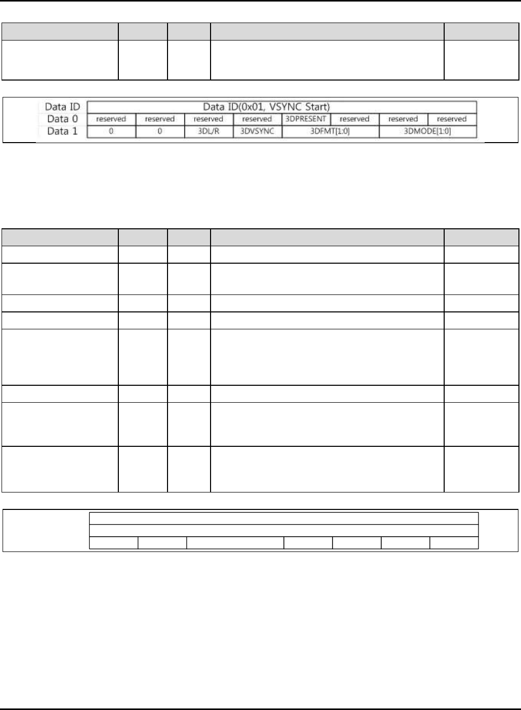
S5P6818_UM 40 MIPI
40-34
Name
Bit
Type
Description
Reset Value
01 = 3D Mode On, Portrait Orientation.
10 = 3D Mode On, Landscape Orientation.
11 = Reserved.
40.9.1.1.31 DSIM_P3D_CTL
Base Address: 0xC00D_0100
Address = Base Address + 0x0084, Reset Value = 0x0023_4D00
Name
Bit
Type
Description
Reset Value
RSVD
[31:24]
–
Reserved
8’h0
DATA_ID
[23:16]
RW
Data type for processor-sourced packet data type
0x23 is generic short write, 2 parameters
8’h23
P3D_ID
[15:8]
RW
Proprietary 3D ID
8’h4D
RSVD
[7:6]
–
Reserved
2’b00
P3D_MODE
[5:4]
RW
Proprietary 3D mode
00 = Sub-pixel mode
01 = Side-by-Side mode
10 and 11 = Reserved
2’b00
RSVD
[3:2]
–
Reserved
2’b00
P3D_EN
[1]
RW
Proprietary 3D enable/disable
If this bit is 0, the peripheral may ignore the
Proprietary 3D Register.
1’b0
P3D_ON_OFF
[0]
RW
Proprietary 3D On/Off
If 3D On from FIMD, It can be change to 1.
This bit is read only.
1’b0
Data ID
Data 0
Data 1
Data ID(default : 0x23, Generic short write, 2parameters)
SEC_3D_CTRL(default : 0x4D)
reserved reserved proprietary 3d mode reserved reserved On / Off
Enable /
Disable
nexell / ys.kim at 2015.02.12
SAMSUNG Confidential
S5P6818_UM 40 MIPI
40-35
40.9.1.1.32 DSIM_MIC_CTL
Base Address: 0xC00D_0100
Address = Base Address + 0x0088, Reset Value = 0x0023_4D00
Name
Bit
Type
Description
Reset Value
RSVD
[31:24]
–
Reserved
8’h0
DATA_ID
[23:16]
RW
Data type for processor-sourced packet data type
0x23 is generic short write, 2 parameters
8’h23
MIC_ID
[15:8]
RW
MIC ID
8’h4D
RSVD
[7:2]
–
Reserved
6’h00
MIC_EN
[1]
RW
MIC enable/disable
If this bit is 0, the peripheral may ignore the MIC
Register.
1’b0
MIC_ON_OFF
[0]
RW
MIC On/Off
If MIC On from FIMD, It can be change to 1.
This bit is read only.
1’b0
Data ID
Data 0
Data 1
Data ID(default : 0x23, Generic short write, 2parameters)
SEC_MIC_CTRL(default : 0x4F)
reserved reserved reserved reserved On / Offreserved reserved Enable /
Disable
nexell / ys.kim at 2015.02.12
SAMSUNG Confidential
S5P6818_UM 40 MIPI
40-36
40.9.1.1.33 DSIM_P3D_ON_MIC_OFF_HORIZONTAL
Base Address: 0xC00D_0100
Address = Base Address + 0x008C, Reset Value = 0x0000_0400
Name
Bit
Type
Description
Reset Value
RSVD
[31:12]
RW
Reserved
20’h0
H_SIZE
[11:0]
RW
Horizontal size when Proprietary 3D On, MIC Off
12’h400
40.9.1.1.34 DSIM_P3D_OFF_MIC_ON_HORIZONTAL
Base Address: 0xC00D_0100
Address = Base Address + 0x0090, Reset Value = 0x0000_0400
Name
Bit
Type
Description
Reset Value
RSVD
[31:12]
–
Reserved
20’h0
H_SIZE
[11:0]
RW
Horizontal size when Proprietary 3D Off, MIC On
12’h400
40.9.1.1.35 DSIM_P3D_ON_MIC_ON_HORIZONTAL
Base Address: 0xC00D_0100
Address = Base Address + 0x0094, Reset Value = 0x0000_0400
Name
Bit
Type
Description
Reset Value
RSVD
[31:12]
–
Reserved
20’h0
H_SIZE
[11:0]
RW
Horizontal size when Proprietary 3D On, MIC On
12’h400
40.9.1.1.36 DSIM_P3D_ON_MIC_OFF_HFP
Base Address: 0xC00D_0100
Address = Base Address + 0x0098, Reset Value = 0x0000_0000
Name
Bit
Type
Description
Reset Value
RSVD
[31:16]
–
Reserved
16’h0
HFP_SIZE
[15:0]
RW
HFP size when Proprietary 3D On, MIC Off for Video
mode.
HFP is specified using blank packet.
In Command mode, these bits are ignored.
16’h0
nexell / ys.kim at 2015.02.12
SAMSUNG Confidential

S5P6818_UM 40 MIPI
40-37
40.9.1.1.37 DSIM_P3D_OFF_MIC_ON_HFP
Base Address: 0xC00D_0100
Address = Base Address + 0x009C, Reset Value = 0x0000_0000
Name
Bit
Type
Description
Reset Value
RSVD
[31:16]
–
Reserved
16’h0
HFP_SIZE
[15:0]
RW
HFP size when Proprietary 3D Off, MIC On for Video
mode.
HFP is specified using blank packet.
In Command mode, these bits are ignored.
16’h0
40.9.1.1.38 DSIM_P3D_ON_MIC_ON_HFP
Base Address: 0xC00D_0100
Address = Base Address + 0x00A0, Reset Value = 0x0000_0000
Name
Bit
Type
Description
Reset Value
RSVD
[31:16]
–
Reserved
16’h0
HFP_SIZE
[15:0]
RW
HFP size when Proprietary 3D On, MIC On for Video
mode.
HFP is specified using blank packet.
In Command mode, these bits are ignored.
16’h0
nexell / ys.kim at 2015.02.12
SAMSUNG Confidential
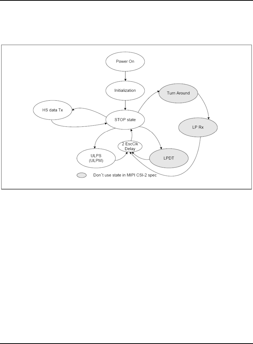
S5P6818_UM 40 MIPI
40-38
40.10 CSIS
40.10.1 Interfaces and Protocol
40.10.1.1 D-PHY layer FSM
Figure 40-14 D-PHY Finite State Machine (Tx D-phy of Samsung)
MIPI CSIS V3.0 system supports HSDT (High Speed Data transfer) and ULPS (ULPM - Ultra-Low Power State or
Mode) only. There is no trigger function, LPDT and BTA.
40.10.1.2 PPI Interface Timing & Protocol
MIPI CSIS V3.0 supports HSDT and ULPM.
nexell / ys.kim at 2015.02.12
SAMSUNG Confidential
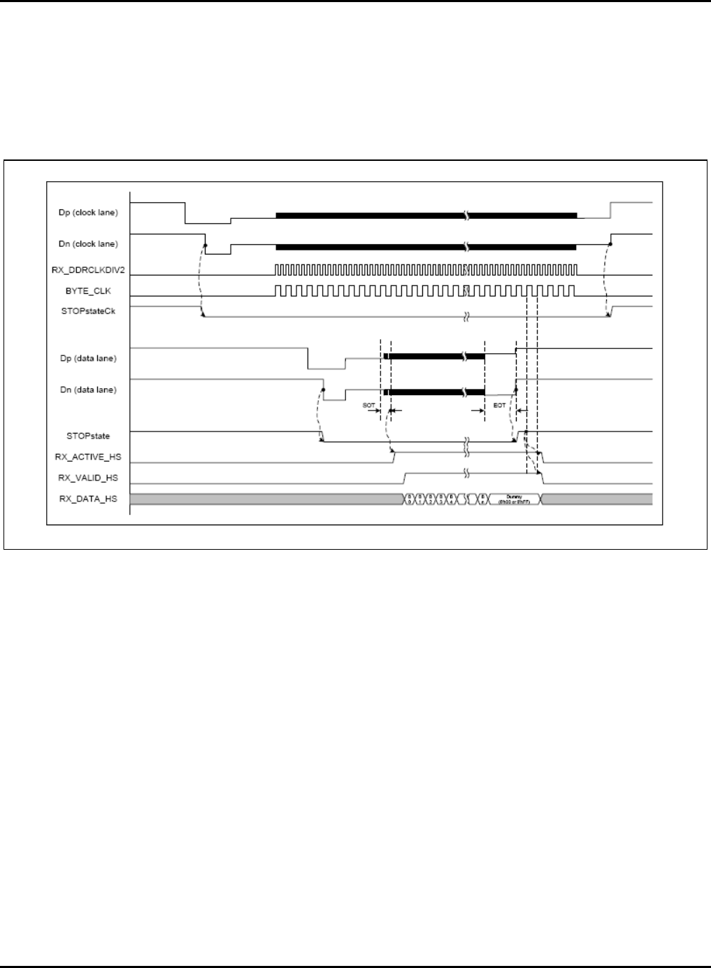
S5P6818_UM 40 MIPI
40-39
40.10.1.2.1 High Speed Data Transfer
In below Figure, the upper 5 signals are related with clock lane and the lower 6 signals are related with data lane.
DP and DN of upper signals are D-phy channel of clock lane. RX_DDRCLKDIV2 is in PPI. BYTE_CLK is
generated clock that is generated in link layer (MIPI CSIS V3.0) and divided by 2 from RX_DDRCLKDIV2. DP and
DN of lower signals are D-phy channel of Data lane. Another signal of lower is PPI. STOP state (and
STOPstateClk) indicates that differential channel state of D-phy is LP11 (the voltage level of DP and DN is 1.2 V)
Figure 40-15 Timing Diagram of High Speed Data Transfer
nexell / ys.kim at 2015.02.12
SAMSUNG Confidential
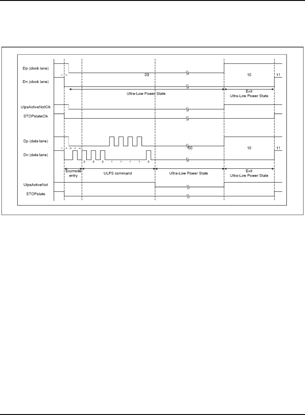
S5P6818_UM 40 MIPI
40-40
40.10.1.2.2 Ultra-Low Power Mode
In below Figure, UlpsActiveNot and STOPstate is in PPI. ULPS command in Data lane is only D-phy command
that is generated Tx D-phy. Rx D-phy decodes this ULPS command and generates ULPS
Figure 40-16 Timing Diagram of Ultra Low Power Mode
nexell / ys.kim at 2015.02.12
SAMSUNG Confidential
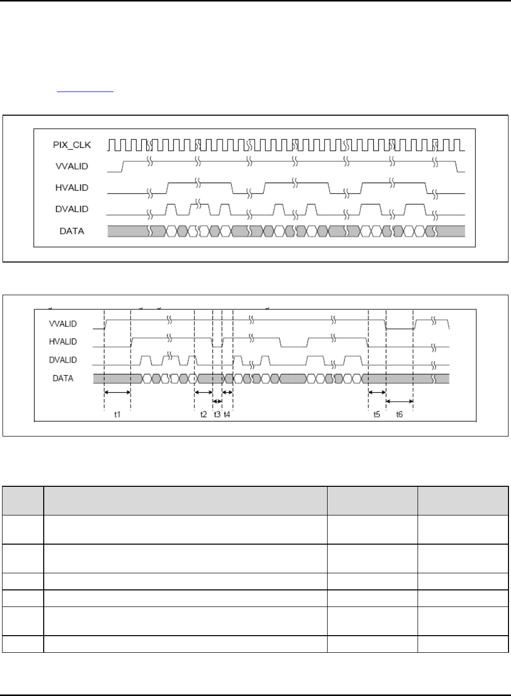
S5P6818_UM 40 MIPI
40-41
40.10.1.2.3 ISP (CAM I/F) Interface
MIPI CSIS V3.0 output signals are PIX_CLK, VVALID, HVALID, and DATA. PIX_CLK is output pixel clock what is
generated from HCLK, BYTE_CLK or EXTCLK. VVALID is vertical sync signal. HVALID is horizontal sync signal.
DATA is image data bus. DATA bus width is dependent on Image format. Maximum bus width is 24 bits because
of RGB888. Figure 40-17 describes the output protocol of MIPI CSIS. All signals are synchronized with the rising
edge of PIX_CLK.
Figure 40-17 Output Protocol of ISP Wrapper of MIPI CSIS V3.0
Figure 40-18 Timing Diagram of Output Protocol of ISP Wrapper
Table 40-3 Timing Table of Output Protocol of ISP Wrapper
Description
Minimum Cycle
of Pixel Clock
Maximum Cycle
of Pixel Clock
t1
Interval between rising of VVALID and first rising of HVALID
Vsync_SIntv + 1
(1 to 64)
–
t2
Interval between last falling of DVALID and falling of HVALID
Hsync_LIntv + 2
(2 to 66)
–
t3
Interval between falling of HVALID and rising of next HVALID
1
–
t4
Interval between rising of HVALID and first rising of DVALID
0
–
t5
Interval between last falling of HVALID and falling of VVALID
Vsync_EIntv
(0 to 4095)
–
t6
Interval between falling of VVALID and rising of next VVALID
1
–
nexell / ys.kim at 2015.02.12
SAMSUNG Confidential
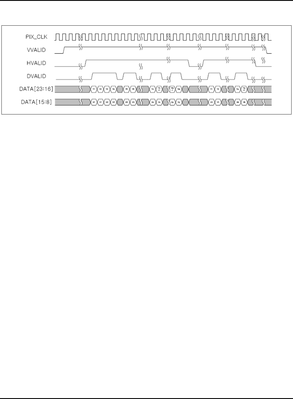
S5P6818_UM 40 MIPI
40-42
40.10.1.3 Description of Output Protocol
Figure 40-19 Waveform of ISP Interface (CAM I/F)
nexell / ys.kim at 2015.02.12
SAMSUNG Confidential

S5P6818_UM 40 MIPI
40-43
40.10.2 Configuration
40.10.2.1 Image Resolution
MIPI CSI Slave block needs the configuration of Image resolution to measure Hsync pulse length exactly and
detect frame end.
Vertical resolution register has 16 bits (16'h0001 to 16'hFFFF)
Horizontal resolution register has 16 bits (16'h0001 to 16'hFFFF).
40.10.2.2 Image Data Format
S5P6818 supports YUV422 8-bit format only.
Table 40-4 Image Data Format
Data Type
Description
0x18
YUV420 8-bit
0x19
YUV420 10-bit
0x1A
Legacy YUV420 8-bit
0x1B
Reserved
0x1C
YUV420 8-bit CSPS (Chroma Shifted Pixel Sampling)
0x1D
YUV420 10-bit CSPS (Chroma Shifted Pixel Sampling)
0x1E
YUV422 8-bit
0x1F
YUV422 10-bit
40.10.3 Interrupt
MIPI CSIS V3.0 has many interrupts for checking status, indicating error case and receiving generic data.
Odd_Before/Odd_After/Even_Before/Even_After
These interrupts are related with generic and embedded data.
Odd_Before and Odd_After interrupts are generated in odd frame. Even_Before and Even_After interrupts are
generated in even frame. Odd_Before and Even_Before interrupts are generated when Generic Short packet or
Embedded 8-bit based packet is received before image data (Vertical Back porch area)
nexell / ys.kim at 2015.02.12
SAMSUNG Confidential
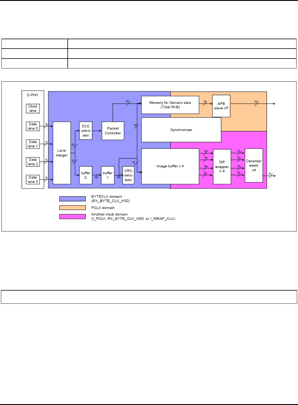
S5P6818_UM 40 MIPI
40-44
40.10.4 Clock Specification
MIPI CSI may have 3 clock sources: RX_BYTE_CLK_HS0, I_PCLK, and I_WRAP_CLK.
I_PCLK
PCLK is system clock generated by general processor PLL.(APB clock)
RX_BYTE_CLK_HS0
This signal comes from data lane 0 of D-phy.
I_WRAP_CLK
I_WRAP_CLK is generated by clock generator. Refer to CSI clock in clock controller.
Figure 40-20 Block Diagram of Clock Domain
All clock domains are asynchronous each other. Pixel clock for transmitting image data to ISP is same with HCLK
or Wrapper clock.
The relationship between input and output bandwidth is that the output bandwidth should be faster than input
bandwidth. There is an equation of previous relationship:
(freq. of RX_BYTE_CLK_HS) (number of data lane) 8 bits (freq. of Pixel clock) (bit width of image format)
nexell / ys.kim at 2015.02.12
SAMSUNG Confidential

S5P6818_UM 40 MIPI
40-45
40.10.5 Register Description
40.10.5.1 Register Map Summary
Base Address: 0xC00D_0000
Register
Offset
Description
Reset Value
CSISs
CSIS_CTRL
0x0000
Control register
0x0010_0000
CSIS_DPHYCTRL
0x0004
DPHY Analog Control register
0x0000_0000
CSIS_CONFIG_CH0
0x0008
Configuration register of CH0
0x0000_00FC
CSIS_DPHYSTS
0x000C
DPHY Status register
0x0000_00F1
CSIS_INTMSK
0x0010
Interrupt mask register
0x0000_0000
CSIS_INTSRC
0x0014
Interrupt source register Control
0x0000_0000
CSIS_CTRL2
0x0018
Control register about ch1 to 3
0x00E0_0000
CSIS_VERSION
0x001C
CSIS version register
0x8000_0000
CSIS_DPHYCTRL_0
0x0020
DPHY Analog Control register0
0x0000_0000
CSIS_DPHYCTRL_1
0x0024
DPHY Analog Control register1
0x0000_0000
RSVD
0x0028
Reserved
0x0000_0000
CSIS_RESOL_CH0
0x002C
Image Resolution register of CH0
0x8000_8000
RSVD
0x0030
Reserved
0x0000_0000
RSVD
0x0034
Reserved
0x8000_8000
SDW_CONFIG_CH0
0x0038
Shadow register of CH0 Configuration
0x0000_00FC
SDW_RESOL_CH0
0x003C
Shadow register of CH0 Resolution
0x8000_8000
CSIS_CONFIG_CH1
0x0040
Configuration register of CH1
0x0000_00FC
CSIS_RESOL_CH1
0x0044
Image Resolution register of CH1
0x8000_8000
SDW_CONFIG_CH1
0x0048
Shadow register of CH1 Configuration
0x0000_00FC
SDW_RESOL_CH1
0x004C
Shadow register of CH1 Resolution
0x8000_8000
CSIS_CONFIG_CH2
0x0050
Configuration register of CH2
0x0000_00FC
CSIS_RESOL_CH2
0x0054
Image Resolution register of CH2
0x8000_8000
SDW_CONFIG_CH2
0x0058
Shadow register of CH2 Configuration
0x0000_00FC
SDW_RESOL_CH2
0x005C
Shadow register of CH2 Resolution
0x8000_8000
CSIS_CONFIG_CH3
0x0060
Configuration register of CH3
0x0000_00FC
CSIS_RESOL_CH3
0x0064
Image Resolution register of CH3
0x8000_8000
SDW_CONFIG_CH3
0x0068
Shadow register of CH3 Configuration
0x0000_00FC
SDW_RESOL_CH3
0x006C
Shadow register of CH3 Resolution
0x8000_8000
DSIM
0x0100 to
0x01FF
Refer to DSIM register map
–
CSIS_NONIMG_ODD
0x2000 to
0x2FFF
Memory area for storing non-image data. Odd frame
Undefined
CSIS_NONIMG_EVEN
0x3000 to
Memory area for storing non-image data. Even frame
Undefined
nexell / ys.kim at 2015.02.12
SAMSUNG Confidential

S5P6818_UM 40 MIPI
40-46
Register
Offset
Description
Reset Value
0x3FFF
nexell / ys.kim at 2015.02.12
SAMSUNG Confidential

S5P6818_UM 40 MIPI
40-47
40.10.5.1.1 CSIS_CTRL
Base Address: 0xC005_0000
Address = Base Address + 0000h, Reset Value = 0x0010_0000
Name
Bit
Type
Description
Reset Value
S_DPDN_SWAP_CLK
[31]
RW
Swapping DP and DN channel of clock lane.
0 = Default
1 = Swapped
1’b0
S_DPDN_SWAP_DAT
[30]
RW
Swapping DP and DN channel of data lanes.
0 = Default
1 = Swapped
1’b0
RSVD
[29:28]
–
read as zero, do not modify
2’b0
DECOMP_FORM
[27:26]
RW
Decompress format
00 = 10-bit compressed format
01 = Reserved for 12-bit compressed format Do not
modify
1x = Reserved
This register field related with Data format field in
CSIS_CONFIG register
2’b0
DECOMP_PREDICT
[25]
RW
Decompress prediction mode of CH0
0 = Simple prediction
1 = Advanced prediction
1’b0
DECOMP_EN
[24]
RW
Decompress enable
0 = Disable (default)
1 = Enable
When default value, input data of de-compressor is
bypassed with all protocol signals (Vvalid, Hvalid,
Dvalid and Bvalid)
1’b0
INTERLEAVE_MODE
[23:22]
RW
Select Interleave mode, VC(Virtual channel) and
DT(Data type)
0 = CH0 only, no data interleave
1 = DT only
2 = VC only
3 = VC and DT
2’b0
DOUBLE_CMPNT
[21]
RW
Double component per clock cycle in YUV422
formats, CH0
0 = single component per clock cycle (half pixel per
clock cycle)
1 = double component per clock cycle (a pixel per
clock cycle)
1’b0
PARALLEL
[20]
RW
Output bus width of CH0 is 32 bits.
0 = Normal output
1 = 32-bit data alignment
When this bit is set, the outer bus width of MIPI CSIS
V3.0 is 32.
1’b1
UPDATE_SHADOW
[19:16]
RW
Strobe of updating shadow registers
4’h0
nexell / ys.kim at 2015.02.12
SAMSUNG Confidential

S5P6818_UM 40 MIPI
40-48
Name
Bit
Type
Description
Reset Value
0 = default
1 = update the shadow registers.
After configuration, User has to set this bit for updating
shadow registers.
This bit is cleared automatically after updating shadow
registers.
Bit [19] CH3 to Bit[16]CH0
RGB_SWAP
[15:12]
RW
Swapping RGB sequence
0 = MSB is R and LSB is B.
1 = MSB is B and LSB is R. (swapped)0
Bit [15] CH3 to Bit[12]CH0
4’h0
WCLK_SRC
[11:8]
RW
Wrapper clock source
0 = PCLK
1 = I_WRAP_CLK
This bit determines source of Pixel clock which is
clock of transferring image data to ISP or CAM I/F.
When data format is "User defined packet", this bit is
ignored.
Bit [11] CH3 to Bit[8]CH0
4’h0
RSVD
[7:5]
–
read as zero, do not modify
3’b000
SW_RST
[4]
W
Software reset
0 = Ready
1 = Reset
All writable registers in CSI2 go back to initial state.
After this bit is active for 3 cycles, this bit will be de-
asserted automatically
NOTE: Almost MIPI CSI2 block uses "ByteClk" from
D-phy. This "ByteClk" is not continuous clock. User
has to assert software reset when Camera module is
turned off.
1’b0
NUMOFDATALANE
[3:2]
RW
Number of data lane
00 = 1 data lane
01 = 2 data lane
10 = 3 data lane
11 = 4 data lane
2’b00
RSVD
[1]
–
read as zero, do not modify
1’b0
CSI_EN
[0]
RW
MIPI CSI2 system enable
0 = Disable
1 = Enable
1’b0
nexell / ys.kim at 2015.02.12
SAMSUNG Confidential

S5P6818_UM 40 MIPI
40-49
40.10.5.1.2 CSIS_DPHYCTRL
Base Address: 0xC005_0000
Address = Base Address + 0004h, Reset Value = 0x0000_0000
Name
Bit
Type
Description
Reset Value
HSSETTLE
[31:24]
RW
HS-RX settle time(THS-SETTLE) control register.
You should pre-set it before HS-RX operation.
Refer to the latest
LN28LPP_MIPIDPHYCore1Gbps_Suppliement file for
more information
8'h0
S_CLKSETTLECT
[23:22]
RW
TCLK-SETTLE parameter control register
You should pre-set it before HS-RX operation.
2'b0x: 110 ns to 280 ns (v0.87 to v1.00)
2'b10: 150 ns to 430 ns (v0.83 to v0.86)
2'b11: 60 ns to 140 ns (v0.82)
2'b0
RSVD
[21:5]
–
Reserved. Do not modify.
17'h0
DPHY_ON
[4:0]
RW
D-PHY enable
[4]: data lane 3
[3]: data lane 2
[2]: data lane 1
[1]: data lane 0
[0]: clock lane
0 = Disable
1 = Enable
40.10.5.1.3 CSIS_CONFIG_CH0
Base Address: 0xC005_0000
Address = Base Address + 0008h, Reset Value = 0x0000_00FC
Name
Bit
Type
Description
Reset Value
HSYNC_LINTV_CH0
[31:26]
RW
Interval between Hsync falling and Hsync rising (Line
interval)
6'h00 to 6'h3F cycle of Pixel clock
6’h0
VSYNC_SINTV_CH0
[25:20]
RW
Interval between Vsync rising and first Hsync rises.
6'h00 to 6'h3F cycle of Pixel clock
6’h0
VSYNC_EINTV_CH0
[19:8]
RW
Interval between last Hsync falling and Vsync falling.
12'h000 to 12'hFFF cycle of Pixel clock
12’h0
DATAFORMAT_CH0
[7:2]
RW
Image Data Format
YUV420 (8-bit): 0x18
YUV420 (10-bit): 0x19
YUV420 (8-bit legacy): 0x1A
YUV420 (8-bit CSPS): 0x1C
YUV420 (10-bit CSPS): 0x1D
YUV422 (8-bit): 0x1E
6’h3F
nexell / ys.kim at 2015.02.12
SAMSUNG Confidential

S5P6818_UM 40 MIPI
40-50
Name
Bit
Type
Description
Reset Value
YUV422 (10-bit): 0x1F
RGB565: 0x22
RGB666: 0x23
RGB888: 0x24
RAW6: 0x28
RAW7: 0x29
RAW8: 0x2A
RAW10: 0x2B
RAW12: 0x2C
RAW14: 0x2D
User defined 1: 0x30
User defined 2: 0x31
User defined 3: 0x32
User defined 4: 0x33
VIRTUAL_CHANNEL_C
H0
[1:0]
RW
Set Virtual channel for data interleave.
00: VC = 0
01: VC = 1
10: VC = 2
11: VC = 3
2’b00
40.10.5.1.4 CSIS_DPHYSTS
Base Address: 0xC005_0000
Address = Base Address + 000Ch, Reset Value = 0x0000_00F1
Name
Bit
Type
Description
Reset Value
RSVD
[31:12]
–
Reserved
20’h0
ULPSDAT
[11:8]
R
Data lane [3:0] is in ULPS
[7]: Data lane 3
[6]: Data lane 2
[5]: Data lane 1
[4]: Data lane 0
0 = Not ULPS
1 = ULPS
4’h0
STOPSTATEDAT
[7:4]
R
Data lane [3:0] is in Stop State
[7]: Data lane 3
[6]: Data lane 2
[5]: Data lane 1
[4]: Data lane 0
0 = Not Stop state
1 = Stop state
4’h1F
RSVD
[3:2]
–
Reserved
2’b00
ULPSCLK
[1]
R
Clock lane is in ULPS
0 = Not ULPS
1 = ULPS
1’b0
nexell / ys.kim at 2015.02.12
SAMSUNG Confidential

S5P6818_UM 40 MIPI
40-51
Name
Bit
Type
Description
Reset Value
STOPSTATECLK
[0]
R
Clock lane is in Stop State
0 = Not Stop state
1 = Stop state
1’b1
40.10.5.1.5 CSIS_INTMSK
Base Address: 0xC005_0000
Address = Base Address + 0010h, Reset Value = 0x0000_0000
Name
Bit
Type
Description
Reset Value
MSK_EVENBEFORE
[31]
RW
Non Image data are received at Even frame and
Before Image
0 = Disable (masked)
1 = Enable (unmasked)
1’b0
MSK_EVENAFTER
[30]
RW
Non Image data are received at Even frame and After
Image
0 = Disable (masked)
1 = Enable (unmasked)
1’b0
MSK_ODDBEFORE
[29]
RW
Non Image data are received at Odd
frame and Before Image
0 = Disable (masked)
1 = Enable (unmasked)
1’b0
MSK_ODDAFTER
[28]
RW
Non Image data are received at Odd frame and After
Image
0 = Disable (masked)
1 = Enable (unmasked)
1’b0
MSK_FRAMESTART
[27:24]
RW
FS packet is received, [CH3,CH2,CH1,CH0]
0 = Disable (masked)
1 = Enable (unmasked)
4’h0
MSK_FRAMEEND
[23:20]
RW
FE packet is received, [CH3,CH2,CH1,CH0]
0 = Disable (masked)
1 = Enable (unmasked)
4’h0
RSVD
[19:17]
–
read as zero, do not modify
3’b000
MSK_ERR_SOT_HS
[16]
RW
Start of transmission error
0 = Disable (masked)
1 = Enable (unmasked)
1’b0
MSK_ERR_LOST_FS
[15:12]
RW
Lost of Frame Start packet, [CH3,CH2,CH1,CH0]
0 = Disable (masked)
1 = Enable (unmasked)
4’h0
MSK_ERR_LOST_FE
[11:8]
RW
Lost of Frame End packet, [CH3,CH2,CH1,CH0]
0 = Disable (masked)
1 = Enable (unmasked)
4’h0
MSK_ERR_OVER
[7:4]
RW
Image FIFO overflow interrupt, [CH3,CH2,CH1,CH0]
0 = Disable (masked)
4’h0
nexell / ys.kim at 2015.02.12
SAMSUNG Confidential

S5P6818_UM 40 MIPI
40-52
Name
Bit
Type
Description
Reset Value
1 = Enable (unmasked)
RSVD
[3]
–
read as zero, do not modify
1’b0
MSK_ERR_ECC
[2]
RW
ECC error
0 = Disable (masked)
1 = Enable (unmasked)
1’b0
MSK_ERR_CRC
[1]
RW
CRC error
0 = Disable (masked)
1 = Enable (unmasked)
1’b0
MSK_ERR_ID
[0]
RW
Unknown ID error
0 = Disable (masked)
1 = Enable (unmasked)
1’b0
40.10.5.1.6 CSIS_INTSRC
Base Address: 0xC005_0000
Address = Base Address + 0014h, Reset Value = 0x0000_0000
Name
Bit
Type
Description
Reset Value
EVENBEFORE
[31]
RW
Non Image data are received at Even frame and
Before Image
1’b0
EVENAFTER
[30]
RW
Non Image data are received at Even frame and After
Image
1’b0
ODDBEFORE
[29]
RW
Non Image data are received at Odd frame and
Before Image
1’b0
ODDAFTER
[28]
RW
Non Image data are received at Odd frame and After
Image
1’b0
FRAMESTART
[27:24]
RW
FS packet is received, [CH3,CH2,CH1,CH0]
4’h0
FRAMEEND
[23:20]
RW
FE packet is received, [CH3,CH2,CH1,CH0]
4’h0
ERR_SOT_HS
[19:16]
RW
Start of transmission error, [CH3,CH2,CH1,CH0]
4’h0
ERR_LOST_FS
[15:12]
RW
Indication of lost of Frame Start packet,
[CH3,CH2,CH1,CH0]
4’h0
ERR_LOST_FE
[11:8]
RW
Indication of lost of Frame End packet,
[CH3,CH2,CH1,CH0]
4’h0
ERR_OVER
[7:4]
RW
Overflow is caused in image FIFO.
[CH3,CH2,CH1,CH0]
Outer bandwidth has to be faster than imputer
bandwidth.
But image FIFO can be overflow because of users
fault.
There are 2 ways for preventing overflow.
Tune output pixel clock faster than current.
Tune input byte clock slowr than current.
First case: WCLK_Src in CSIS_CTRL register should
be set 1, and then assign faster clock
4’h0
nexell / ys.kim at 2015.02.12
SAMSUNG Confidential

S5P6818_UM 40 MIPI
40-53
Name
Bit
Type
Description
Reset Value
Second case: user can set register in camera module
through I2C channel.
When this interrupt is generated,
Turn camera off
Assert software reset, if you didn.t assert software
reset, MIPI CSIS could not receive any more data.
Tune the clock frequency and re-configure all related
registers.
MIPI CSIS module is ready for operating.
RSVD
[3]
–
read as zero, do not modify
1’b0
ERR_ECC
[2]
RW
ECC error
1’b0
ERR_CRC
[1]
RW
CRC error
1’b0
ERR_ID
[0]
RW
Unknown ID error
1’b0
40.10.5.1.7 CSIS_CTRL2
Base Address: 0xC005_0000
Address = Base Address + 0018h, Reset Value = 0x00E0_0000
Name
Bit
Type
Description
Reset Value
DECOMP_PREDICT
[31:29]
RW
Decompress prediction mode of CH3 to CH1
0 = Simple prediction
1 = Advanced prediction
Bit [31]: CH3,
Bit [30]: CH2,
Bit [29]: CH1
3’b000
RSVD
[28]
–
read as zero, do not modify
1’b0
DOUBLE_CMPNT
[27:25]
RW
Double component per clock cycle in YUV422 formats
0 = Single component per clock cycle (half pixel per
clock cycle)
1 = Double component per clock cycle (a pixel per
clock cycle)
Bit [27]: CH3,
Bit [26]: CH2,
Bit [25]: CH1
3’b000
RSVD
[24]
–
read as zero, do not modify
1’b0
PARALLEL
[23:21]
RW
Output bus width of CH0 is 32 bits.
0 = Normal output 1 = 32-bit data alignment
When this bit is set, the outer bus width of MIPI CSIS
V3.0 is 32.
Bit [23]: CH3,
Bit [22]: CH2,
Bit [21]: CH1
3’b111
RSVD
[20:0]
–
read as zero, do not modify
21’h0
nexell / ys.kim at 2015.02.12
SAMSUNG Confidential
S5P6818_UM 40 MIPI
40-54
40.10.5.1.8 CSIS_VERSION
Base Address: 0xC005_0000
Address = Base Address + 001Ch, Reset Value = 0x8000_0000
Name
Bit
Type
Description
Reset Value
CSIS_VERSION
[31:0]
R
CSIS version information
32’h8000_0000
40.10.5.1.9 B_DPHYCTRL
Base Address: 0xC005_0000
Address = Base Address + 0020h, Reset Value = 0x0000_0000
Name
Bit
Type
Description
Reset Value
B_DPHYCTRL
[31:0]
RW
D-PHY Slave analog block characteristics control register.
Do not modify this.
32’h0
40.10.5.1.10 S_DPHYCTRL
Base Address: 0xC005_0000
Address = Base Address + 0024h, Reset Value = 0x0000_0000
Name
Bit
Type
Description
Reset Value
S_DPHYCTRL
[31:0]
RW
D-PHY Slave analog block characteristics control register.
It must be 0.
32’h0
40.10.5.1.11 CSIS_RESOL_CH0
Base Address: 0xC005_0000
Address = Base Address + 002Ch, Reset Value = 0x8000_8000
Name
Bit
Type
Description
Reset Value
HRESOL_CH0
[31:16]
RW
Horizontal Image resolution
Input boundary of each image format
YUV420 (8-bit): 0x0001 to 0xFFFF
YUV420 (10-bit): 4n (n is 1, 2, 3, …)
YUV420 (8-bit legacy): 0x0001 ~ 0xFFFF
YUV420 (8-bit CSPS): 0x0001 ~ 0xFFFF
YUV420 (10-bit CSPS): 4n (n is 1, 2, 3, …)
YUV422 (8-bit): 0x0001 to 0xFFFF
YUV422 (10-bit): 4n (n is 1, 2, 3, …)
RGB565: 0x0001 to 0xFFFF
RGB666: 4n (n is 1, 2, 3, …)
RGB888: 0x0001 to 0xFFFF
RAW8: 0x0001 to 0xFFFF
RAW10: 4n (n is 1, 2, 3, …)
16’h8000
nexell / ys.kim at 2015.02.12
SAMSUNG Confidential
S5P6818_UM 40 MIPI
40-55
Name
Bit
Type
Description
Reset Value
RAW12: 2n (n is 1, 2, 3, …)
RAW14: 4n (n is 1, 2, 3, …)
System LSI Division, Semiconductor Business
26 Confidential Property of Samsung Electronics Co., Ltd.
Internal User Only
VRESOL_CH0
[15:0]
RW
Vertical Image resolution
Input boundary: 0x0001 to 0xFFFF
16’h8000
40.10.5.1.12 SDW_CONFIG_CH0
Base Address: 0xC005_0000
Address = Base Address + 0038h, Reset Value = 0x0000_00FC
Name
Bit
Type
Description
Reset Value
SDW_HSYNC_LINTV_CH0
[31:26]
R
Current interval between Hsync falling and Hsync
rising (Line interval)
6’h0
SDW_VSYNC_SINTV_CH0
[25:20]
R
Current interval between Vsync rising and first Hsync
rising.
6’h0
SDW_VSYNC_EINTV_CH0
[19:8]
R
Current interval between last Hsync falling and Vsync
falling.
12’h0
SDW_DATAFORMAT_CH0
[7:2]
R
Current image Data Format
6’h0
SDW_VIRTUAL_CHANNEL
_CH0
[1:0]
R
Set Virtual channel for data interleave
2’b00
40.10.5.1.13 SDW_RESOL_CH0
Base Address: 0xC005_0000
Address = Base Address + 003Ch, Reset Value = 0x8000_8000
Name
Bit
Type
Description
Reset Value
SDW_HResol_CH0
[31:16]
R
Current Horizontal Image resolution
16’h8000
SDW_VResol_CH0
[15:0]
R
Current Vertical Image resolution
16’h8000
Channel 1 registers (CSIS_CONFIG_CH1, CSIS_RESOL_CH1, SDW_CONFIG_CH1, SDW_RESOL_CH1)
Address: C00D_0040h, C00D_0044h, C00D_0048h, C00D_004Ch: WORD
Each register has same format with channel 0 register.
nexell / ys.kim at 2015.02.12
SAMSUNG Confidential

S5P6818_UM 40 MIPI
40-56
40.10.5.1.14 Non-Image Data Register
Base Address: 0xC005_0000
Address = Base Address + 0x2000 ~ 0x3FFC, Reset Value = Undefined
Name
Bit
Type
Description
Reset Value
NONIMGDATA
[31:0]
R
Non Image Data memory
- CSIS_NONIMG_ODD: Memory area for storing non-
image data (0x2000 ~ 0x2FFC: Odd Frame)
- CSIS_NONIMG_EVEN: Memory area for storing
non-image data(0x3000 ~ 0x3FFC: Even Frame)
-
nexell / ys.kim at 2015.02.12
SAMSUNG Confidential
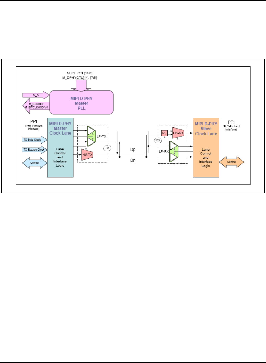
S5P6818_UM 40 MIPI
40-57
40.11 D-PHY
40.11.1 Architecture
40.11.1.1 PLL and Clock Lane Connection
The following figure illustrates the PLL and Clock Lane connection.
Figure 40-21 PLL and Clock Lane Connection
nexell / ys.kim at 2015.02.12
SAMSUNG Confidential
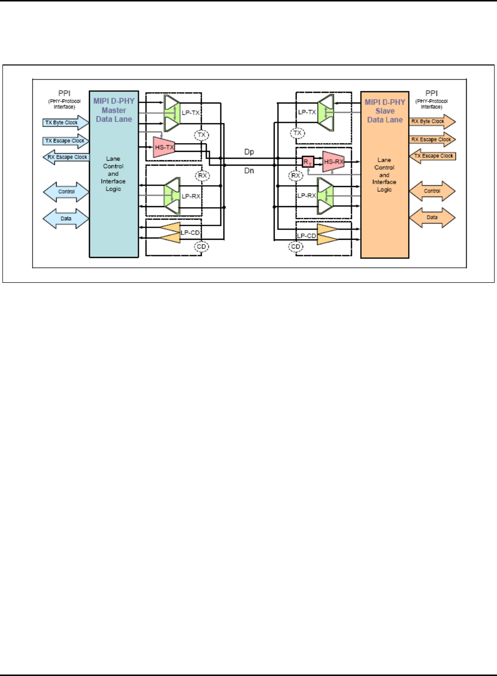
S5P6818_UM 40 MIPI
40-58
40.11.1.2 Data Lane Connection
The following figure illustrates the Data Lane connection.
Figure 40-22 Data Lane Connection
40.11.1.3 IP Structure
The MIPI D-PHY core consists of five modules. The modules are:
Master PLL
Master Clock lane
Master Data lane
Slave Clock lane
Slave Data lane
You can configure the modules depending on customer requirements.
For example:
Expanding the number of data lanes up to four lanes
Omitting the Master PLL when using another PLL for serial clock source
Providing core in Hard Macro including IO and Power Pads.
nexell / ys.kim at 2015.02.12
SAMSUNG Confidential
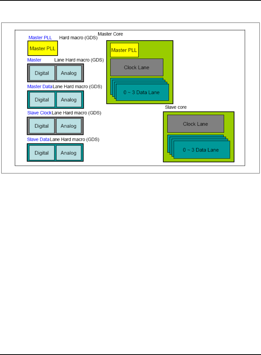
S5P6818_UM 40 MIPI
40-59
We strongly recommend using Master and Slave lane in pair for loop-back test.
Figure 40-23 IP Structure
nexell / ys.kim at 2015.02.12
SAMSUNG Confidential
S5P6818_UM 40 MIPI
40-60
40.11.1.4 Power Consumption
LN28LPP Process (without PAD)
Operation Voltage conditions = 1.0 V 5 %, 1.8 V 5 %
Recommended Operation Temperature range = –20 C to 85 C
Master and slave lanes are assumed to have 1 clock + 1 data lane
The following table describes the simulation result >> condition: FF, –20 C, 1.05 V, 1.89 V
Mode
Master PLL
Master Lane
Slave Lane
HS (500 MHz)
2.8 mW
9 mW
3 mW
HS (1 GHz)
3.3 mW
12 mW
3.3 mW
LP (20 MHz)
–
1.2 mW
0.7 mW
ULPS
20 uW
20 uW
20 uW
Mode
AVDD10
AVDD10_PLL
AVDD18
HS (500 MHz)
12.8 mW
2.8 mW
0.3 mW
HS (1 GHz)
16 mW
3.3 mW
0.3 mW
LP (20 MHz)
2.8 mW
–
2 mW
The following table describes the simulation result >> condition: NN, 25 C, 1.0 V, 1.8 V
Mode
Master PLL
Master Lane
Slave Lane
HS (500 MHz)
2.5 mW
7.5 mW
2.1 mW
HS (1 GHz)
3 mW
10.3 mW
2.4 mW
LP (20 MHz)
–
0.6 mW
0.4 mW
ULPS
10 uW
10 uW
10 uW
Mode
AVDD10
AVDD10_PLL
AVDD18
HS (500 MHz)
10.2 mW
2.5 mW
0.2 mW
HS (1 GHz)
13.5 mW
3 mW
0.2 mW
LP (20 MHz)
1.8 mW
–
1.3 mW
nexell / ys.kim at 2015.02.12
SAMSUNG Confidential

S5P6818_UM 40 MIPI
40-61
40.11.1.5 Signals
The following table describes the Pad signals.
Name
Description
M_VREG_0P4V
Regulator capacitor connection
M_DPCLK
Master CLK Lane DP
M_DNCLK
Master CLK Lane DN
M_DNDATA0/1/2/3
Master DATA Lanes DP
M_DNDATA0/1/2/3
Master DATA Lanes DN
S_DPCLK
Slave CLK Lane DP
S_DNCLK
Slave CLK Lane DN
S_DPDATA0/1/2/3
Slave DATA Lanes DP
S_DNDATA0/1/2/3
Slave DATA Lanes DN
M_VDD10_PLL
1.0 V Power for PLL
MS_VDD10
1.0 V Power for Internal Logic
MS_VDD18
1.8 V Power for Analog
MS_VSS
Ground
VREG12_EXTPWR
External 1.2 V power connection port. This is not a pad.
If you use the Internal 1.2 V Regulator, VREG12_EXTPWR power port should float.
Refer to description of B_DPHYCTL[20] of DSIM for mode setting information.
nexell / ys.kim at 2015.02.12
SAMSUNG Confidential

S5P6818_UM 40 MIPI
40-62
40.11.1.6 Package and Board Connection Guideline
Package and Board Connection Guideline section provides implementation information regarding package and
board connections of MIPI D-PHY.
The following table describes the package and board requirements.
Signal Name
Description
Bonding Pad Requirements
M_VREG_0P4V
Analog Signal
Connect a 2 nF capacitor between this pin and MS_VSS.
Place capacitor closely to chip.
M_DPCLK
M_DNCLK
M_DPDATA0/1/2/3
M_DNDATA0/1/2/3
S_DPCLK
S_DNCLK
S_DPDATA0/1/2/3
S_DNDATA0/1/2/3
Analog Signal
The peak current through DP and DN pads is 5.5 mA (0.44 V/80
), for a maximum duty cycle of 4 % during a short-to-ground
condition.
Make the total resistance of the package, ESD pad, and pad-
macro connection 0.5 to 1.0 .
To reduce inductance and via in an array-type package, route
these signals through shortest traces that reach outer contacts
of array.
Total capacitance of package, ESD pad, and pad-macro
connection should be <2 pF.
Match delays of trace lines as close as possible to minimize
skew between CLK's and DATA's.
Require adjacent ball assignment to minimize intra-pair
differential signals skew.
Match CLK and DATA pairs for routing the path to minimize
intra-pair differential signals skew. Therefore, you should
consider symmetrical allocation for CLK and DATA pairs.
M_VDD10_PLL
PLL 1.0 V Supply
Capable of handling 10 mA.
Make the resistance from the I/O pad (s) to the macro < 0.5 ,
with < 5 % voltage variation at the macro.
The VDD and VSS connections require dedicated off-chip
supplies.
MS_VDD10
D-PHY 1.0 V Supply
Capable of handling 5 mA per Lane.
Make the resistance from the I/O pad (s) to the macro < 0.5 ,
with < 5 % voltage variation at the macro.
The VDD and VSS connections require dedicated off-chip
supplies.
MS_VDD18
D-PHY 1.8 V Supply
Capable of handling 2 mA.
Make the resistance from the I/O pad (s) to the macro < 0.5 ,
with < 10 % voltage variation at the macro.
The VDD and VSS connections require dedicated off-chip
supplies.
MS_VSS
Ground
Common Ground
nexell / ys.kim at 2015.02.12
SAMSUNG Confidential
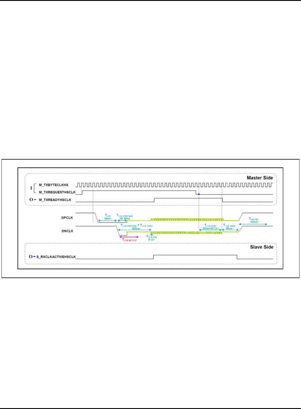
S5P6818_UM 40 MIPI
40-63
The followings are RC Guide Line for PKG.
Differential Signals: R<0.5 and C<1 pF
Power Signals: R <1 and C<1 pF
You should consider bump arrangement and package PCB design to ensure high speed differential pair
signals goes out to last outer ball (PKG).
CLK/DATA pairs should have the same routing length (difference < 20 um).
PAD to BUMP metal line should be straight as possible.
You should not place the other signals which does not relate to MIPI near MIPI differential signals.(S/W >10,
S: Line Space, W: Line Width)
40.11.1.7 Core Interface Timing Diagram
Clock Lane: HS-TX and HX-RX fiction
The following figure illustrates the HS-TX and HS-RX function of Clock Lane.
Figure 40-24 Clock Lane: HS-TX and HS-RX Function
nexell / ys.kim at 2015.02.12
SAMSUNG Confidential
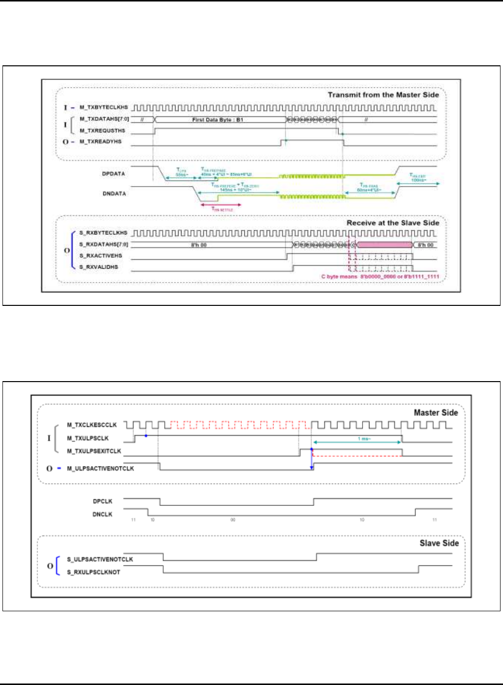
S5P6818_UM 40 MIPI
40-64
40.11.1.8 Data Lane: HS-TX and HS-RX Function
The following figure illustrates the HS-TX and HS-RX function of Data Lane.
Figure 40-25 Data Lane: HS-TX and HS-RX Function
40.11.1.9 Clock Lane: ULPS Function
The following figure illustrates the ULPS function of Clock Lane.
Figure 40-26 Clock Lane: ULPS Function
nexell / ys.kim at 2015.02.12
SAMSUNG Confidential
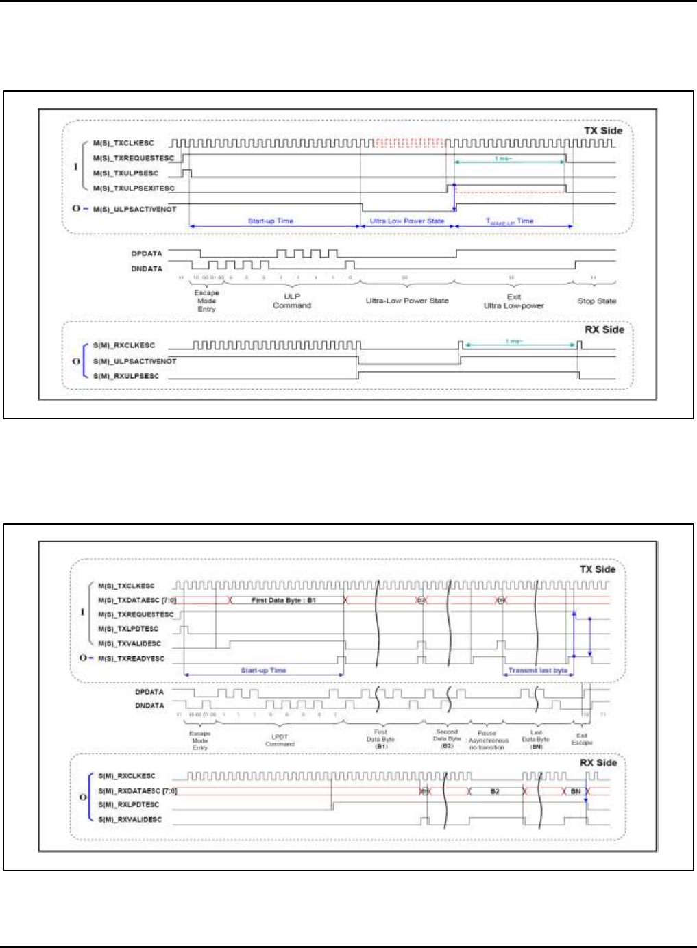
S5P6818_UM 40 MIPI
40-65
40.11.1.10 Data Lane: ULPS Function
The following figure illustrates the ULPS function of Data Lane.
Figure 40-27 Data Lane: ULPS Function
40.11.1.11 Data Lane: LP-TX and LP-RX Function
The following figure illustrates the LP-TX and LP-RX function of Data Lane.
Figure 40-28 Data Lane: LP-TX and LP-RX Function
nexell / ys.kim at 2015.02.12
SAMSUNG Confidential
S5P6818_UM 40 MIPI
40-66
40.11.1.12 Data Lane: Remote Trigger Reset
The following figure illustrates the remote trigger reset of Data Lane.
Figure 40-29 Data Lane: Remote Trigger Reset
40.11.1.13 Data Lane: Turn Around
The following figure illustrates the turnaround of Data Lane.
Figure 40-30 Data Lane: Turn Around
nexell / ys.kim at 2015.02.12
SAMSUNG Confidential
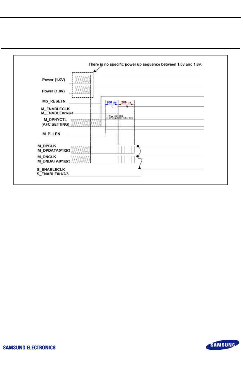
Samsung Confidential
S5P6818_UM 40 MIPI
40-67
Preliminary product information describes products that are in development, for which full characterization data and
associated errata are not yet available. Specifications and information herein are subject to change without notice.
40.11.1.14 Initialization Sequence
The following figure illustrates the initialization sequence.
Figure 40-31 Initialization Sequence
nexell / ys.kim at 2015.02.12
SAMSUNG Confidential

S5P6818_UM 41 Video Input Processor (VIP)
41-1
41 Video Input Processor (VIP)
41.1 Overview
The Video Input Processor (hereinafter VIP) of the S5P6818 can receive images directly from external camera
modules or video decoders. In addition, it can clip or scale down the input images and store them to the memory.
The images stored from the VIP can be used for encoding by using MPEG Hardware, and as preview images by
using the Multi-Layer Controller (MLC). In addition, the images can be converted to texture images for the 3D
Graphics Accelerator by using the Color Space Converter.
41.2 Features
The Video Input Port features:
ITU-R BT.656 (External CIS) and ITU-R BT.601 (External CIS and MIPI, External 8-bit, MIPI 16-bit) interface
supports
Clock, HSYNC, VSYNC and 8-bit data port (External CIS)
Clock, HVALID, VVALID, DVALID and 16-bit data port (Internal MIPI CSI)
External DVALID pin or Field pin supports
Maximum 8192 8192 image supports
Clipping and Scale-down
YUV 420/422/444 memory format and Linear YUV 422 memory format
Horizontal & Vertical Interrupt and Operation Done Interrupt
Internal Decoder and External interface supports
3 Inputs from External CIS and 1 Input from MIPI CSI
nexell / ys.kim at 2015.02.12
SAMSUNG Confidential
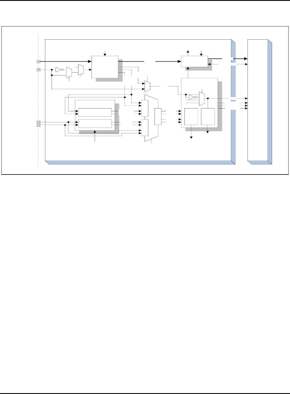
S5P6818_UM 41 Video Input Processor (VIP)
41-2
41.3 Block Diagram
Figure 41-1 Video Input Port Block Diagram
Video Input Port
Sync Gen
SAV/EAV
Decoder
ID[7:0]
DVALIDPOL
IFIELD /
IDVALID
H/VSYNC Gen
H/VBLANK Gen
IHSYNC
IVSYNC HBLANK
VBLANK
CURVSYNC
CURHSYNC
0
1
HBLANK
Y/Cb/Cr
0
1
IFIELD
FIELD
Post I/F
FIFO
EXTDVENB
VBLANK
HSYNC
VSYNC
HBLANK
VBLANK
FIELD
0
1
EXTFIELDENB
EXTSYNCENB
FIELD
FrameStart
FrameEnd
HSYNCEnd
0
2
1
3
‘0’
‘1’
FIELDSEL
Y/Cb/Cr
HBEGIN / HEND /
VBEGIN / VEND
DORDER
HCOUNT /
VCOUNT
FIFOWRENB / FIFORDENB /
FIFOEMPTY / FIFOFULL
RESETFIFOSEL /
RESETFIFO
FIFO Control
Separator
0
1
‘1’
H/V
Counter
Field
Capture
LASTFIELD
nexell / ys.kim at 2015.02.12
SAMSUNG Confidential
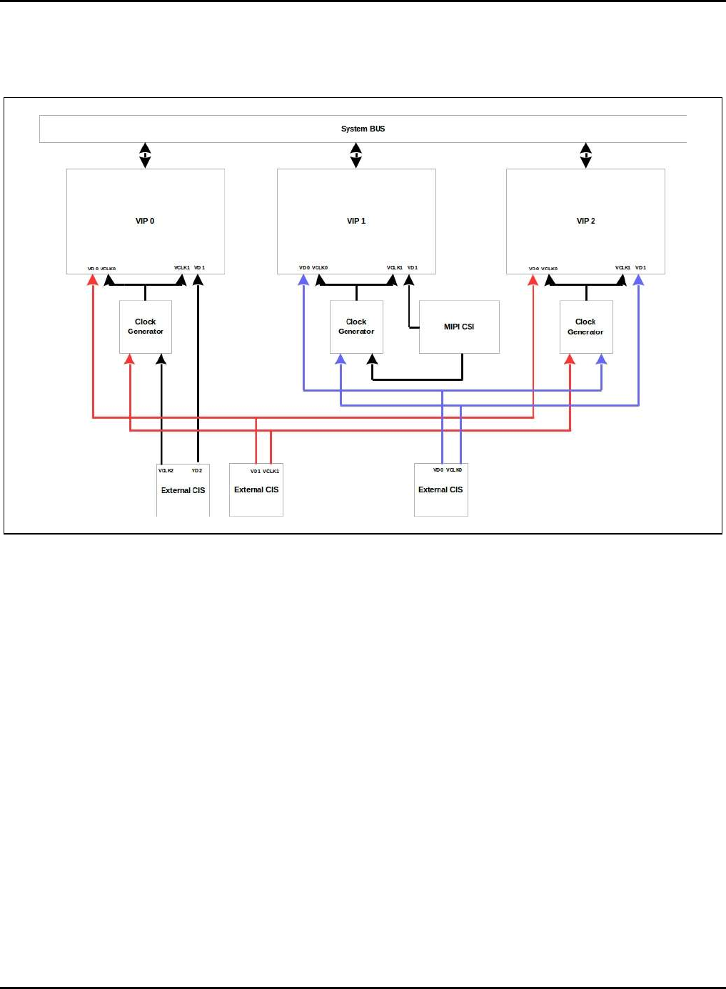
S5P6818_UM 41 Video Input Processor (VIP)
41-3
41.4 VIP Interconnection
41.4.1 Block Diagram
Figure 41-2 Video Input Port Interconnection
The VIP Interconnected with 3 External CIS modules and 1 MIPI CSI module as shown as in the above figure.
nexell / ys.kim at 2015.02.12
SAMSUNG Confidential
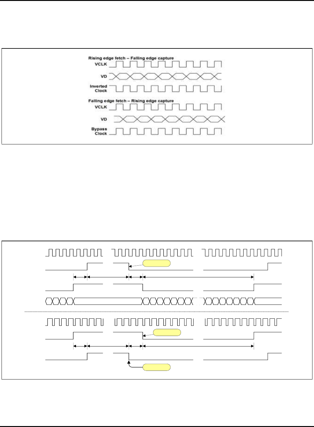
S5P6818_UM 41 Video Input Processor (VIP)
41-4
41.4.2 Clock Generation
The VIP can create the video in clock by using an internal PLL or an external VCLK pin as a clock source. The
created video in clock is used for sync signal creation and data interface in the Video Input Port block.
Figure 41-3 Generation Internal Video clock
In general, the Video Input port is designed to capture data on the rising edge. Therefore, if the video clolck
fetches data at falling edge, you can invert input clock in VIP. If External CSI fetches video data at rising edge, the
VIP_EXTCLKINV should be set as "1". Or if External CSI fetches video data at falling edge, the VIP_EXTCLKINV
should be set to '0' as shown as in the above figure.
41.4.3 Sync Generation
The horizontal and vertical timing interfaces for the video input port are as shown in the following figure.
Figure 41-4 Horizontal & Vertical Timings
////
tHSW tHBPtHFP
tAVW
ICLK
HSYNC
HBLANK
ID[7:0]
//
//
//
//
//
//
//
tVSW tVBPtVFP
tAVH
//
//
//
HSYNC
VBLANK
VSYNC
FrameStart
//
FrameEnd
HSYNCEnd
Horizontal Active
Vertical Blank
Horizontal Blank
Vertical Active
nexell / ys.kim at 2015.02.12
SAMSUNG Confidential
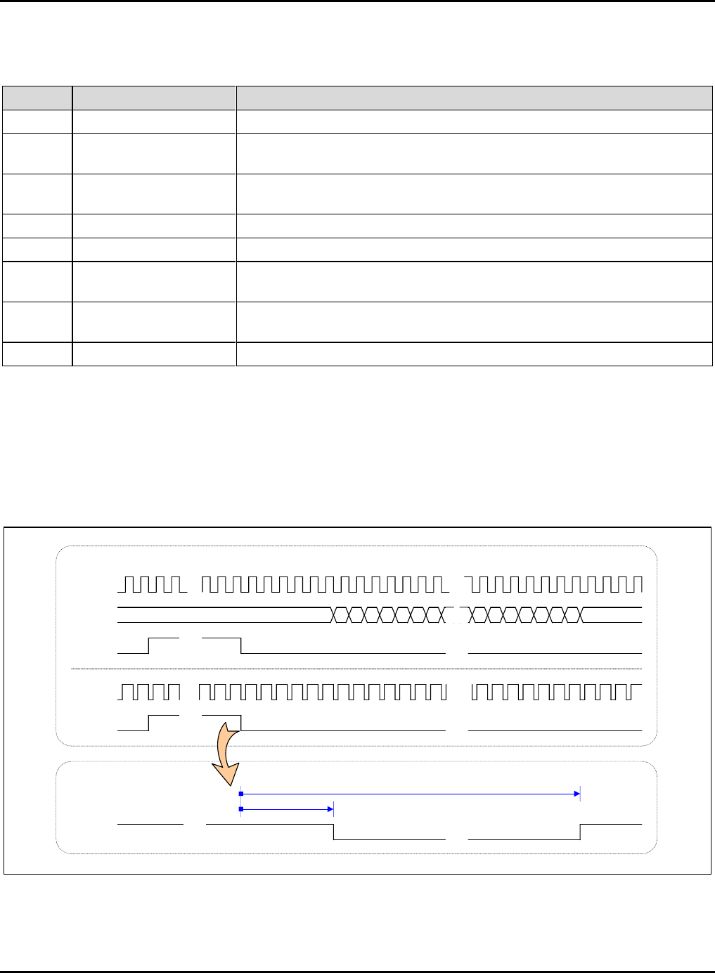
S5P6818_UM 41 Video Input Processor (VIP)
41-5
Each symbol in the above figure is described in the following table.
Table 41-1 Horizontal & Vertical Timing Symbols
Symbol
Brief
Remark
tHSW
Horizontal Sync Width
Number of ICLKs in the section where the horizontal sync pulse is active
tHBP
Horizontal Back Porch
Number of ICLKs in a section from the end point of the horizontal sync
pulse to the start point of the horizontal active
tHFP
Horizontal Front Porch
Number of ICLKs in a section from the end point of the horizontal active to
the start point of the horizontal sync pulse
tAVW
Active Video Width
Number of ICLKs in a horizontal active section
tVSW
Vertical Sync Width
Number of lines in a section where the vertical sync pulse is active
tVBP
Vertical Back Porch
Number of lines in a section from the end point of the vertical sync pulse
to the start point of the next vertical active
tVFP
Vertical Front Porch
Number of lines in a section from the end point of the vertical active to the
start point of the vertical sync pulse
tAVH
Active Video Height
Number of lines in the vertical active section
41.4.3.1 ITU-R BT.601 8-bit
The video input port has an 8-bit data bus and HSYNC and VSYNC pins, and supports ITU-R BT.601 8-bit input. If
the port uses an external HSYNC or VSYNC, the EXTSYNCENB bit should be set as "1". If the EXTSYNCENB bit
is "1", the port receives the HSYNC and VSYNC from the outside, and creates the HBLANK and VBLANK
internally. The polarity of the external H(V)SYNC only supports high active. In the following figure shows the
relationship between the HBLANK and the VBLANK generated from external HSYNC and VSYNC inputs.
Figure 41-5 Generation for ITU-R BT.601 8-bit
External Input
////// //
Sync Gen
//
Horizontal Blank
ICLK
HSYNC
H(V)BLANK
ID[7:0]
//
//
//
//
//
//
//
HSYNC
VSYNC
H(V)BEGIN
H(V)END
//
nexell / ys.kim at 2015.02.12
SAMSUNG Confidential
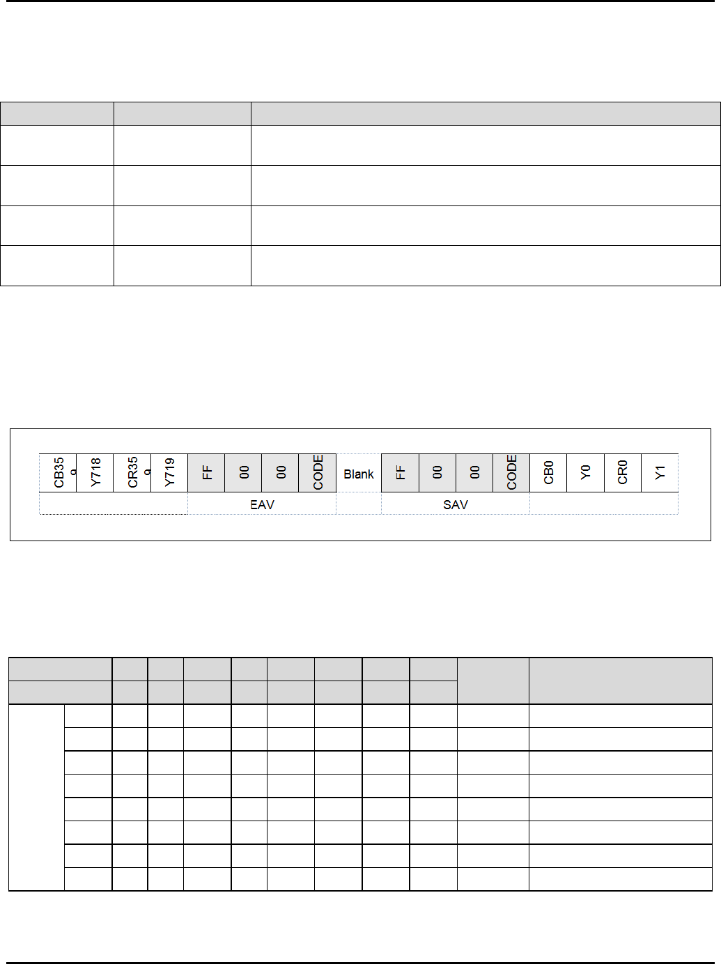
S5P6818_UM 41 Video Input Processor (VIP)
41-6
The HBEGIN and the HEND are used to generate the HBLANK from the HSYNC. The VBEGIN and the VEND are
used to generate the VBLANK from the VSYNC. The settings for each register are listed in the following Table.
Table 41-2 Register Settings for ITU-R BT.601 8-bit
Register
Formula
Remark
VBEGIN
tVBP - 1
Number of lines in a section from the end point of the VSYNC to the start
point of the vertical active video - 1
VEND
tVBP + tAVH - 1
Number of lines in a section from the end point of the VSYNC to the end
point of the vertical active video - 1
HBEGIN
tHBP - 1
Number of clocks in a section from the end point of the HSYNC to the
start point of the horizontal active video - 1
HEND
tHBP + tAVW - 1
Number of clocks in a section from the end point of the HSYNC to the
start point of the horizontal active video - 1
41.4.3.2 ITU-R BT.656
In the ITU-R BT.656 format, there is no additional sync signal pin, and the sync information is transmitted along
with data via data pins. At this time, the Sync information is inserted as an additional code before the start point of
the valid data (SAV) and after the end of the valid data (EAV). Sync information included in data is as shown in the
following figure.
Figure 41-6 Data Stream Format with SAV/EAV
The SAV and the EAV consists of [FF, 00, 00, CODE]. Each code contains Field (F), VSYNC (V) and HSYNC (H)
data, and each code is composed as follows:
Table 41-3 Embedded Sync Code
Bit
7
6
5
4
3
2
1
0
Hex
Brief Description
Function
1
F
V
H
P3
P2
P1
P0
(FVH)
0
1
0
0
0
0
0
0
0
80h
SAV of odd field
1
1
0
0
1
1
1
0
1
9Dh
EAV of odd field
2
1
0
1
0
1
0
1
1
ABh
SAV of odd blank
3
1
0
1
1
0
1
1
0
B6h
EAV of odd blank
4
1
1
0
0
0
1
1
1
C7h
SAV of even field
5
1
1
0
1
1
0
1
0
DAh
EAV of even field
6
1
1
1
0
1
1
0
0
ECh
SAV of even blank
7
1
1
1
1
0
0
0
1
F1h
EAV of even blank
nexell / ys.kim at 2015.02.12
SAMSUNG Confidential
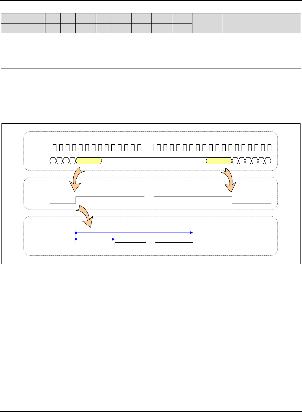
S5P6818_UM 41 Video Input Processor (VIP)
41-7
Bit
7
6
5
4
3
2
1
0
Hex
Brief Description
Function
1
F
V
H
P3
P2
P1
P0
F: Field select (0: odd field, 1: even field)
V: Vertical blanking (0: Active, 1: blank)
H: SAV/EAV (0: SAV, 1: EAV)
Parity: P3 = V xor H, P2 = F xor H, P1 = F xor V, P0 = F xor V xor H
To create the HBLANK and VBLANK from the sync information contained in the data, the EXTSYNCENB should
be set as "0". The SAV/EAV decoder blocks generate the HBLANK and VBLANK from the sync information
contained in the data. The Sync Gen block generates the HSYNC and the VSYNC based on the HBLANK and
VBLANK signals. In the following figure shows the relationship that generates the H(V)BLANK and H(V)SYNC
from the SAV/EAV contained in the data.
Figure 41-7 Sync Generation for ITU-R BT.656
Sync Gen
SAV/EAV decoder
External Input
//
ICLK
H(V)SYNC //
//
Horizontal BlankID[7:0]
H(V)BLANK //
H(V)BEGIN
H(V)END
EAV SAV
//
nexell / ys.kim at 2015.02.12
SAMSUNG Confidential
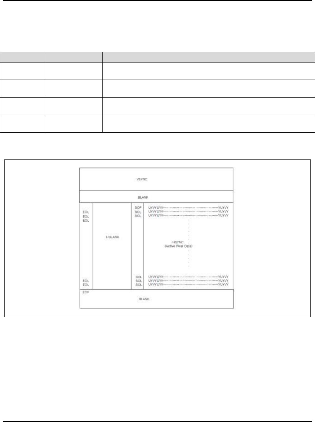
S5P6818_UM 41 Video Input Processor (VIP)
41-8
If the EXTSYNCENB is "0", the HBEGIN and HEND*are used to generate the HSYNC signal from the HBLANK.
The VBEGIN and VEND are used to generate the VSYNC signal from the VBLANK. The settings for each register
are listed in the following table.
Table 41-4 Register Settings for ITU-R BT.656
Register
Formula
Remark
VBEGIN
tVFP + 1
Number of lines in a section from the end point of the vertical active video to
the start point of the VSYNC - 1
VEND
tVFP + tVSW + 1
Number of lines in a section from the end point of the vertical active video to
the end point of the VSYNC + 1
HBEGIN
tHFP - 7
Number of clocks in a section from the end point of the horizontal active
video to the start point of the HSYNC - 7
HEND
tHFP+ tHSW - 7
Number of clocks in a section from the end point of the horizontal active
video to the end point of the HSYNC - 7
41.4.3.3 ITU BT.656-like support
Figure 41-8 Frame Structure of ITU656-like
Our VIP supports ITU656-like which could be configurable as follows:
SOF = 0xFF00_0080
EOF = 0xFF00_00B6
SOL = 0xFF00_0080
EOL = 0xFF00_009D
nexell / ys.kim at 2015.02.12
SAMSUNG Confidential

S5P6818_UM 41 Video Input Processor (VIP)
41-9
41.4.4 External Data Valid and Field
The video input port can receive data valid signals or field signals from the outside. Since the IDVALID and the
IFIELD share a pin, users can use only one of them.
41.4.4.1 External Data Valid
If the EXTDVENB is set as "1", users can use the input signal from the IFIELD/IDVALID pad as the IDVALID
signal. In this case, the polarity is determined by the DVALIDPOL. The video input port is designed to use the
IDVALID signal of active high mode internally. Therefore, if the polarity of an external IDVALID signal is active low,
the input signal should be inverted by setting the DVALIDPOL as "0". If the polarity of an external IDVALID signal
is active high, the input signal should be bypassed by setting the DVALIDPOL as "1".
Even though an external IDVALID signal is used, the internal HBLANK and VBLANK signals are used. Therefore,
the user should set the H(V)BEGIN and the H(V)END.
41.4.4.2 External Field
If an external field signal is used, the EXTFIELDENB should be set as "1". In the ITU-R BT.656 format, the input
signal from the IFIELD/IDVALID pad can be used as an external field signal by setting the EXTFIELDENB as "1".
The video input port internally considers it as an odd field if the polarity of the field signal is low. If the polarity of a
field signal is high, the port considers it as an even field. The user can select the polarity of a field signal by using
FIELDSEL, or can fix the polarity as "0" or "1".
nexell / ys.kim at 2015.02.12
SAMSUNG Confidential

S5P6818_UM 41 Video Input Processor (VIP)
41-10
41.4.5 Data Order
The video input port can select the order of input data. Basically, the ITU-R BT.656 format or the ITU-R BT.601 8-
bit format has the order [Cb, Y0, Cr, Y1]. If the order of the input data is different from the default order, users can
change the order via DORDER. The data orders supported by the video input port are listed in the following table.
Table 41-5 Input Data Order
DORDER
0
1
2
3
ICLK
1st
2nd
3rd
4th
1st
2nd
3rd
4th
1st
2nd
3rd
4th
1st
2nd
3rd
4th
ID[7]
Cb[7]
YN[7]
Cr[7]
YN+1[7]
Cr[7]
YN+1[7]
Cb[7]
YN[7]
YN[7]
Cb[7]
YN+1[7]
Cr[7]
YN+1[7]
Cr[7]
YN[7]
Cb[7]
ID[6]
Cb[6]
YN[6]
Cr[6]
YN+1[6]
Cr[6]
YN+1[6]
Cb[6]
YN[6]
YN[6]
Cb[6]
YN+1[6]
Cr[6]
YN+1[6]
Cr[6]
YN[6]
Cb[6]
ID[5]
Cb[5]
YN[5]
Cr[5]
YN+1[5]
Cr[5]
YN+1[5]
Cb[5]
YN[5]
YN[5]
Cb[5]
YN+1[5]
Cr[5]
YN+1[5]
Cr[5]
YN[5]
Cb[5]
ID[4]
Cb[4]
YN[4]
Cr[4]
YN+1[4]
Cr[4]
YN+1[4]
Cb[4]
YN[4]
YN[4]
Cb[4]
YN+1[4]
Cr[4]
YN+1[4]
Cr[4]
YN[4]
Cb[4]
ID[3]
Cb[3]
YN[3]
Cr[3]
YN+1[3]
Cr[3]
YN+1[3]
Cb[3]
YN[3]
YN[3]
Cb[3]
YN+1[3]
Cr[3]
YN+1[3]
Cr[3]
YN[3]
Cb[3]
ID[2]
Cb[2]
YN[2]
Cr[2]
YN+1[2]
Cr[2]
YN+1[2]
Cb[2]
YN[2]
YN[2]
Cb[2]
YN+1[2]
Cr[2]
YN+1[2]
Cr[2]
YN[2]
Cb[2]
ID[1]
Cb[1]
YN[1]
Cr[1]
YN+1[1]
Cr[1]
YN+1[1]
Cb[1]
YN[1]
YN[1]
Cb[1]
YN+1[1]
Cr[1]
YN+1[1]
Cr[1]
YN[1]
Cb[1]
ID[0]
Cb[0]
YN[0]
Cr[0]
YN+1[0]
Cr[0]
YN+1[0]
Cb[0]
YN[0]
YN[0]
Cb[0]
YN+1[0]
Cr[0]
YN+1[0]
Cr[0]
YN[0]
Cb[0]
nexell / ys.kim at 2015.02.12
SAMSUNG Confidential
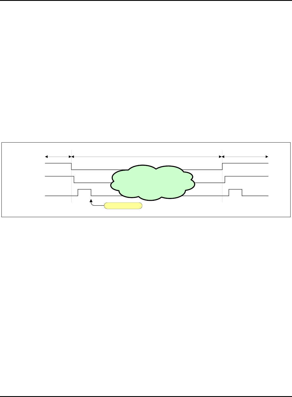
S5P6818_UM 41 Video Input Processor (VIP)
41-11
41.4.6 Status
41.4.6.1 Horizontal & Vertical Counter
The video input port can inform the user of the size of the active section. The HCOUNT*indicates the total clock
numbers of a line in the active video section. The *VCOUNT indicates the total line numbers in the active video
section.
41.4.6.2 Current HSYNC & VSYNC Status
When the EXTSYNCENB is "0" the CURHSYNC and the CURVSYNC bits are provided to show the HSYNC and
VSYNC states.
41.4.6.3 Current Field Status
Users can display the status of the current field signal by using the LASTFIELD bit as shown in the following
figure.
Figure 41-9 Field Information
LASTFIELD is updated whenever a field signal is changed. In addition, when a VSYNC interrupt occurs, the user
can get the field status of the next data by using LASTFIELD. Since LASTFIELD is updated by using the PCLK,
the PCLK should be always enabled by setting the PCLKMODE as "1" to obtain a proper field status.
41.4.7 FIFO Controls
The video input port block can inform the user of the current status of the internal FIFO. The FIFOWRENB
indicates if data is being written to the FIFO. The FIFORDENB indicates if data is being read from the FIFO. If the
FIFO is empty, the FIFOEMPTY is set as "1". If the FIFO is full, the FIFOFULL is set as "1".
In addition, users can reset the FIFO at a specific point. According to the RESETFIFOSELsetting, the reset point
of the FIFO can be controlled by selecting either FrameEnd (the end of VSYNC, RESETFIFOSEL is "0"),
FrameStart (the start of vertical active video, RESETFIFOSEL is "1") or the RESETFIFO bit (RESETFIFOSEL is
"2"), or by selecting all of them (RESETFIFOSEL is "3"). The RESETFIFO bit is valid only when the
RESETFIFOSELis "2" or "3". If the FIFO is reset by setting the RESETFIFO as "1", the RESETFIFO should be set
as "0" again.
FIELD
LASTFIELD
VSYNC interrupt
VSYNC
Odd fieldEven field Even field
Data Processing
nexell / ys.kim at 2015.02.12
SAMSUNG Confidential

S5P6818_UM 41 Video Input Processor (VIP)
41-12
41.4.8 Recommend Setting for Video Input Port
In the following table lists the recommend settings for the video input port by input formats.
Table 41-6 Recommend Setting for Video Input Port
Register
ITU-R BT.656
ITU-R BT.601 8-bit
Progressive
Interlace
EXTSYNCENB
0
1
DWIDTH
1
1
DORDER
0 (default)
0 (default)
EXTFIELDENB
0
0
1
FIELDSEL
0
3
0 or 1
EXTDVENB
0
0 or 1
0
DVALIDPOL
Not used
0 or 1
Not used
VBEGIN
tVFP + 1
tVBP - 1
VEND
tVFP + tVSW + 1
tVBP + tAVH - 1
HBEGIN
tHFP - 7
tHBP - 1
HEND
tHFP+ tHSW - 7
tHBP + tAVW - 1
nexell / ys.kim at 2015.02.12
SAMSUNG Confidential
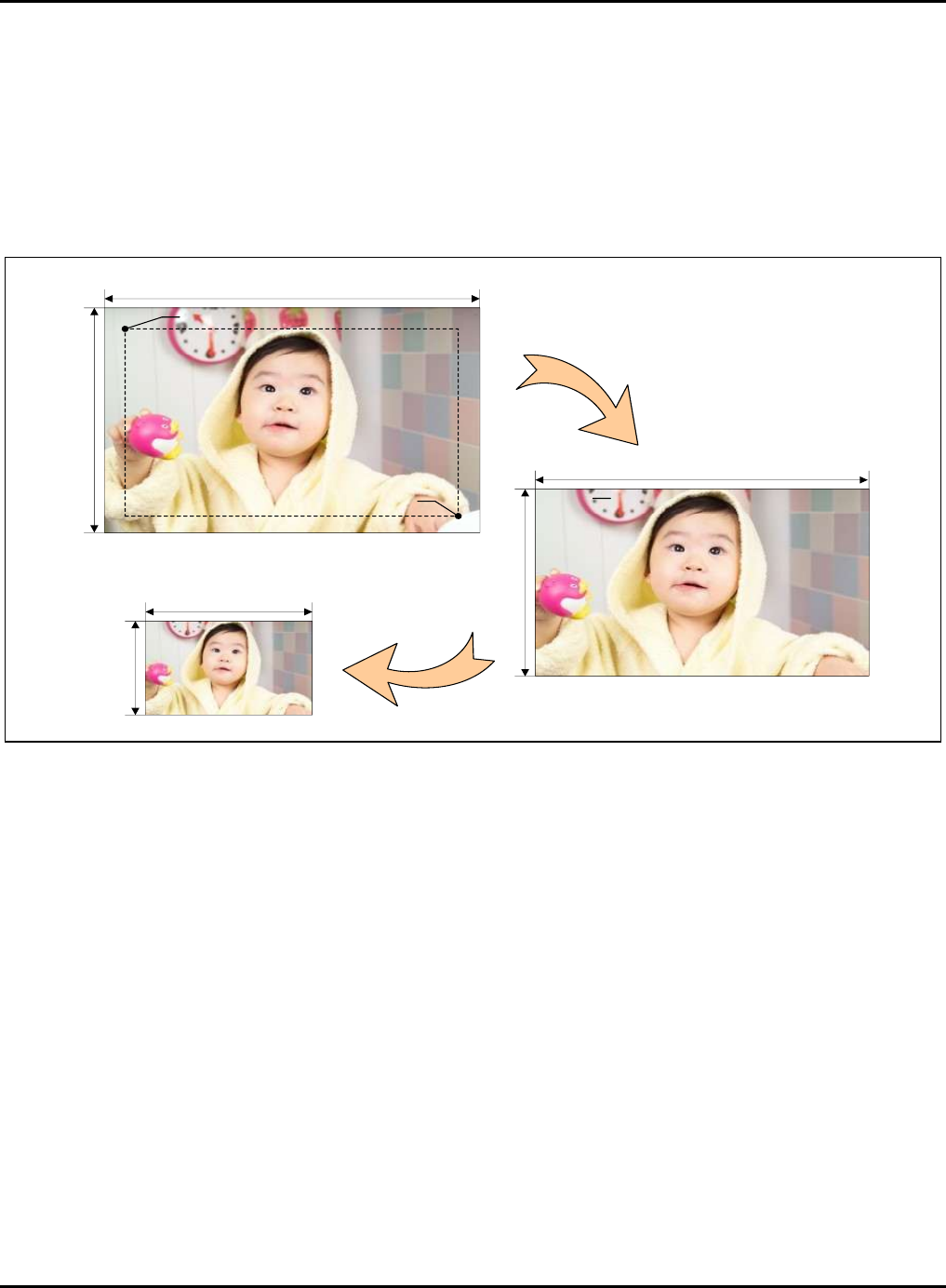
S5P6818_UM 41 Video Input Processor (VIP)
41-13
41.5 Clipper & Decimator
41.5.1 Clipping & Scale-down
The VIP can store input images to the memory after clipping or scaling down. An input image is transmitted to the
Clipper through the video input port and the Separator. The Clipper clips a specific area from the input image, and
then stores the result in the memory and transmits the result to the Decimator. The Decimator can store the image
transmitted from the Clipper in the memory after scaling down the image. In the following figure shows the
procedure for clipping and scaling down an input image.
Figure 41-10 Clipping & Decimation
(CLIPLEFT, CLIPTOP)
(CLIPRIGHT, CLIPBOTTOM)
IMGWIDTH
IMGHEIGHT
CLIPWIDTH
CLIPHEIGHT
TARGETW
TARGETH
CLIPPER
DECIMATOR
nexell / ys.kim at 2015.02.12
SAMSUNG Confidential

S5P6818_UM 41 Video Input Processor (VIP)
41-14
Users can enable the Clipper to clip an input image by specifying the relevant area, using CLIPLEFT, CLIPRIGHT,
CLIPTOP and CLIPBOTTOM.
The Decimator scales down the clipped image by using the Bresenham algorithm. To this end, TARGETW,
TARGETH, DELTAW, DELTAH, CLEARW, and *CLEARH*are used. In the following table lists the settings for
each register.
Table 41-7 Registers for Scaling
Register
Formula
Range
Unit
Remark
TARGETW
–
0 to 8191
Pixel
Width of a scaled-down image
TARGETH
–
0 to 8191
Pixel
Height of a scaled-down image
DELTAW
CLIPWIDTH -
TARGETW
0 to 8191
Pixel
Width difference between the original image and the
result image
DELTAH
CLIPHEIGHT -
TARGETH
0 to 8191
Pixel
Height difference between the original image and the
result image
CLEARW
TARGETW -
DELTAW
–8192 to
8191
Pixel
Difference between the width of the result image and the
DELTAW
CLEARH
TARGETH -
DELTAH
–8192 to
8191
Pixel
Difference between the height of the result image and the
DELTAH
nexell / ys.kim at 2015.02.12
SAMSUNG Confidential

S5P6818_UM 41 Video Input Processor (VIP)
41-15
41.5.2 Output Data Format
The VIP can store input images in separated YUV format and linear YUV 4:2:2 format. The Clipper supports both
separated YUV format and linear YUV 4:2:2 format. If the YUYVENB is set as "0", data is stored in separated YUV
format. If the YUYVENB is set as "1", data is stored in linear YUV 4:2:2 format. The Decimator only supports
separated YUV format.
Linear YUV 4:2:2 format
Linear YUV format is the YUYV format, and Y (luminance) exists in each pixel. Cb and Cr (Chrominance)
separately exist in each of two pixels, and two pixels share the Cr and the Cb (Chrominance). The VIP has 2-pixel
information per 32-bit and is managed in 2-pixel units. Table 41-8 shows the memory format that Y/Cb/Cr data are
stored in.
Table 41-8 YUYV Format
Pixel Format
YUYVENB
31
30
29
28
27
26
25
24
23
22
21
20
19
18
17
16
15
14
13
12
11
10
9
8
7
6
5
4
3
2
1
0
YUYV
1
Cr[7:0]
Y1[7:0]
Cb[7:0]
Y0[7:0]
The BASEADDRL(H)*and the*STRIDEL(H)*are used for the addressing of the linear YUV 4:2:2 format. The
*BASEADDR*is a 32-bit linear address, and specifies the memory address where output images from the Clipper
are stored. The *STRIDE is the memory offset from one scan line in the image buffer to the next. The STRIDE is
expressed in byte units and is also called pitch. If there is no-memory gap between lines in the image buffer, the
stride can be specified as CLIPWIDTH * 2.
Figure 41-11 Address Generation for Linear YUV 422 Format
The linear YUV 4:2:2 format is only supported by the Clipper, and YUYVENB should be set as "1".
Memory Gap
Linear YUV 4:2:2 Image
Image Buffer
Linear Address
Memory Map
BASEADDR
Cb CrY1Y0 ……
……
CLIPHEIGHT (Pixels)
CLIPWIDTH (Pixels)
STRIDE (Bytes)
nexell / ys.kim at 2015.02.12
SAMSUNG Confidential
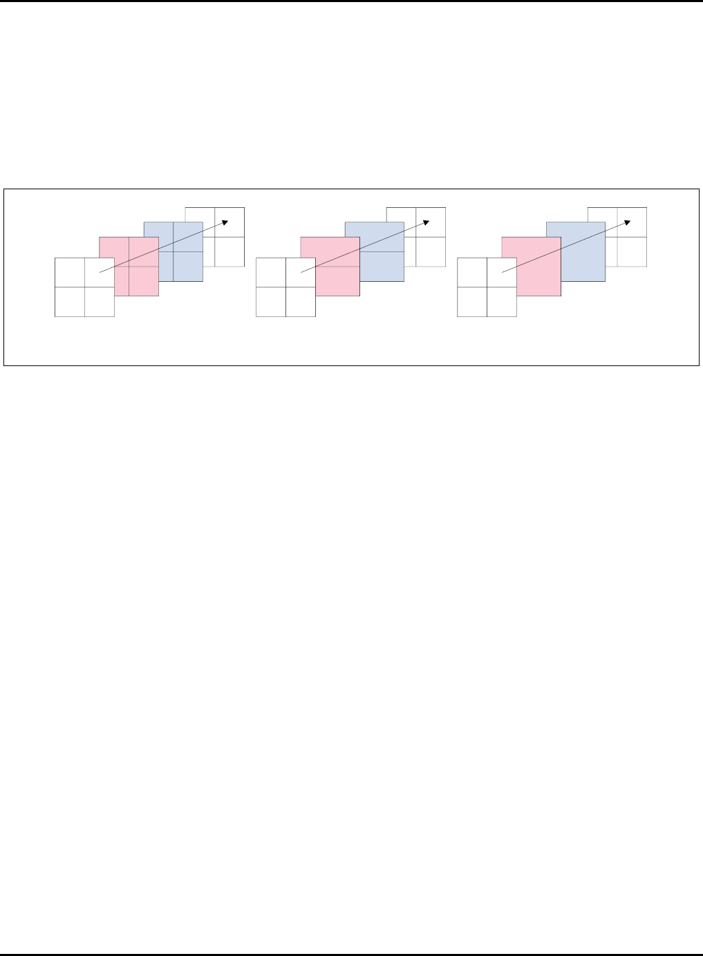
S5P6818_UM 41 Video Input Processor (VIP)
41-16
41.5.2.1 Separated YUV format
In separated YUV format, each of Y, U and V exists at separate memory spaces. In addition, separated YUV
format is divided into 4:4:4, 4:2:2 and 4:2:0 in proportion to U and V for Y. Separated YUV format is the
addressing format, and each component has a size of 64 32 and linearity in block units. These features provide
the S5P6818's unique memory format, to enhance the effectiveness of memory access when the S5P6818
manages data in macro block units through an algorithm to compress/decompress images such as MPEG files.
According to each format, Y, U and V correspond to 2 2 pixels as follows:
Figure 41-12 Separated YUV Format
Users can select wither 4:4:4, 4:2:2 or 4:2:0 format by using DECI_FORMAT, CLIP_FORMAT in the Clipper.
In the Separator YUV addressing format, the memory address to which data is stored is specified by stride. The
Clipper stride has 16-bit width and it is up to 65535. And this valus set by CLIP_LUSTRIDE, CLIP_CBSTRIDE,
CLIP_CRSTRIDE. In Decimation, DECI_LUSTRIDE, DECI_CBSTRIDE, DECI_CRSTRIDE register uses stride of
decimator.
41.5.3 Interlace Scan Mode
If the INTERLACENB is set as "1" for interlace scan mode, the Clipper and Decimator store output images by field
signals. The Clipper and Decimator can also select the polarity of a field signal by using FIELDINV. The Clipper
supports frame-based output images, and outputs the images after automatically adjusting the start address and
the start line depending on the field signal. For interlaced images, the Decimator only handles and stores even
field data.
41.5.4 Pixels Alignment
The VIP Input and output image size should be aligned to 64 pixels.
Pixel
0 1
32
0 1
32
0 1
32
0 1
32
Cr
Cb
Y
YCbCr 4:4:4
Pixel
0 1
32
0 1
32
01
32
0 1
32
Cr
Cb
Y
YCbCr 4:2:2
Pixel
0 1
32
0 1
32
01
32
0 1
32
Cr
Cb
Y
YCbCr 4:2:0
nexell / ys.kim at 2015.02.12
SAMSUNG Confidential

S5P6818_UM 41 Video Input Processor (VIP)
41-17
41.6 Interrupt Generation
The VIP has three interrupt sources. The three interrupt sources are the HSINT, which generates an interrupt at
the end of a horizontal sync, the VSINT, which generates an interrupt at the end of a vertical sync, and the
ODINT, which generates an interrupt when the Clipper and Decimator operations are finished. The Pending bits
and the Enable bits for each interrupt exist, and each register is listed in the following table.
Table 41-9 Interrupt Registers
Interrupt
Enable bit
Pending bit
Condition
HSINT
HSINTENB
HSINTPEND
End of a horizontal sync pulse
VSINT
VSINTENB
VSINTPEND
End of a vertical sync pulse
ODINT
ODINTENB
ODINTPEND
Completion of the Clipper and Decimator operations
nexell / ys.kim at 2015.02.12
SAMSUNG Confidential

S5P6818_UM 41 Video Input Processor (VIP)
41-18
41.7 Register Description
41.7.1 Register Map Summary
Base Address: 0xC006_4000 (VIP 0)
Base Address: 0xC006_3000 (VIP 1)
Base Address: 0xC009_9000 (VIP 2)
Register
Offset
Description
Reset Value
VIP_CONFIG
0x00 (VIP0)/
0x00 (VIP1)/
0x00 (VIP2)
VIP Configuration Register
0x0000_0000
VIP_INTCTRL
0x04 (VIP0)/
0x04 (VIP1)/
0x04 (VIP2)
VIP Interrupt Control Register
0x0000_0000
VIP_SYNCCTRL
0x08 (VIP0)/
0x08 (VIP1)/
0x08 (VIP2)
VIP Sync Control Register
0x0000_0000
VIP_SYNCMON
0x0C (VIP0)/
0x0C (VIP1)/
0x0C (VIP2)
VIP Sync Monitor Register
0x0000_0003
VIP_VBEGIN
0x10 (VIP0)/
0x10 (VIP1)/
0x10 (VIP2)
VIP Vertical Sync Start Register
0x0000_0000
VIP_VEND
0x14(VIP0)/
0x14 (VIP1)/
0x14 (VIP2)
VIP Vertical Sync End Register
0x0000_0000
VIP_HBEGIN
0x18 (VIP0)/
0x18 (VIP1)/
0x18 (VIP2)
VIP Horizontal Sync Start Register
0x0000_0000
VIP_HEND
0x1C (VIP0)/
0x1C (VIP1)/
0x1C (VIP2)
VIP Horizontal Sync End Register
0x0000_0000
VIP_FIFOCTRL
0x20 (VIP0)/
0x20 (VIP1)/
0x20 (VIP2)
VIP FIFO Control Register
0x0000_0000
VIP_HCOUNT
0x24 (VIP0)/
0x24 (VIP1)/
0x24 (VIP2)
VIP Horizontal Counter Register
0x0000_0000
VIP_VCOUNT
0x28 (VIP0)/
0x28 (VIP1)/
0x28 (VIP2)
VIP Vertical Counter Register
0x0000_0000
VIP_EXTCLKINV
0x2C(VIP0)/
0x2C(VIP1)/
0x2C(VIP2)
VIP External Clock Invert
0x0000_0000
RSVD
0x30 to 0xFF (VIP0)/
0x2C to 0xFF (VIP1)/
Reserved
-
nexell / ys.kim at 2015.02.12
SAMSUNG Confidential

S5P6818_UM 41 Video Input Processor (VIP)
41-19
Register
Offset
Description
Reset Value
0x2C to 0xFF (VIP2)
VIP_CDENB
0x200 (VIP0)/
0x200 (VIP1)/
0x200 (VIP2)
VIP Clipper & Decimator Enable Register
0x0000_0000
VIP_ODINT
0x204 (VIP0)/
0x204 (VIP1)/
0x204 (VIP2)
VIP Operation Done Interrupt Register
0x0000_0000
VIP_IMGWIDTH
0x208 (VIP0)/
0x208 (VIP1)/
0x208 (VIP2)
VIP Image Width Register
0x0000_0000
VIP_IMGHEIGHT
0x20C (VIP0)/
0x20C (VIP1)/
0x20C (VIP2)
VIP Image Height Register
0x0000_0000
CLIP_LEFT
0x210 (VIP0)/
0x210 (VIP1)/
0x210 (VIP2)
VIP Clipper Left Register
0x0000_0000
CLIP_RIGHT
0x214 (VIP0)/
0x214 (VIP1)/
0x214 (VIP2)
VIP Clipper Right Register
0x0000_0000
CLIP_TOP
0x218 (VIP0)/
0x218 (VIP1)/
0x218 (VIP2)
VIP Clipper Top Register
0x0000_0000
CLIP_BOTTOM
0x21C (VIP0)/
0x21C (VIP1)/
0x21C (VIP2)
VIP Clipper Bottom Register
0x0000_0000
DECI_TARGETW
0x220 (VIP0)/
0x220 (VIP1)/
0x220 (VIP2)
VIP Decimator Target Width Register
0x0000_0000
DECI_TARGETH
0x224 (VIP0)/
0x224 (VIP1)/
0x224 (VIP2)
VIP Decimator Target Height Register
0x0000_0000
DECI_DELTAW
0x228 (VIP0)/
0x228 (VIP1)/
0x228 (VIP2)
VIP Decimator Delta Width Register
0x0000_0000
DECI_DELTAH
0x22C (VIP0)/
0x22C (VIP1)/
0x22C (VIP2)
VIP Decimator Delta Height Register
0x0000_0000
DECI_CLEARW
0x230 (VIP0)/
0x230 (VIP1)/
0x230 (VIP2)
VIP Decimator Clear Width Register
0x0000_0000
DECI_CLEARH
0x234 (VIP0)/
0x234 (VIP1)/
0x234 (VIP2)
VIP Decimator Clear Height Register
0x0000_0000
DECI_LUSEG
0x238~0x240 (VIP0)/
0x238~0x240 (VIP1)/
0x238~0x240 (VIP2)
VIP Decimator Lu Segment Register
0x0000_0000
nexell / ys.kim at 2015.02.12
SAMSUNG Confidential

S5P6818_UM 41 Video Input Processor (VIP)
41-20
Register
Offset
Description
Reset Value
DECI_FORMAT
0x244 (VIP0)/
0x244 (VIP1)/
0x244 (VIP2)
VIP Decimator Format Register
0x0000_0000
DECI_LUADDR
0x248 (VIP0)/
0x248 (VIP1)/
0x248 (VIP2)
VIP Decimator Lu Address Register
0x0000_0000
DECI_LUSTRIDE
0x24C (VIP0)/
0x24C (VIP1)/
0x24C (VIP2)
VIP Decimator Lu Stride Register
0x0000_0000
DECI_CRADDR
0x250 (VIP0)/
0x250 (VIP1)/
0x250 (VIP2)
VIP Decimator Cr Address Register
0x0000_0000
DECI_CRSTRIDE
0x254 (VIP0)/
0x254 (VIP1)/
0x254 (VIP2)
VIP Decimator Cr Stride Register
0x0000_0000
DECI_CBADDR
0x258 (VIP0)/
0x258 (VIP1)/
0x258 (VIP2)
VIP Decimator Cb Address Register
0x0000_0000
DECI_CBSTRIDE
0x25C (VIP0)/
0x25C (VIP1)/
0x25C (VIP2)
VIP Decimator Cb Stride Register
0x0000_0000
RSVD
0x260~0x284 (VIP0)/
0x260~0x284 (VIP1)/
0x260~0x284 (VIP2)
Reserved
0x0000_0000
CLIP_FORMAT
0x288 (VIP0)/
0x288 (VIP1)/
0x288 (VIP2)
VIP Clipper Format Register
0x0000_0000
CLIP_LUADDR
0x28C (VIP0)/
0x28C (VIP1)/
0x28C (VIP2)
VIP Clipper Lu Address Register
0x0000_0000
CLIP_LUSTRIDE
0x290 (VIP0)/
0x290 (VIP1)/
0x290 (VIP2)
VIP Clipper Lu Stride Register
0x0000_0000
CLIP_CRADDR
0x294 (VIP0)/
0x294 (VIP1)/
0x294 (VIP2)
VIP Clipper Cr Address Register
0x0000_0000
CLIP_CRSTRIDE
0x298 (VIP0)/
0x298 (VIP1)/
0x298 (VIP2)
VIP Clipper Cr Stride Register
0x0000_0000
CLIP_CBADDR
0x29C (VIP0)/
0x29C (VIP1)/
0x29C (VIP2)
VIP Clipper Cb Address Register
0x0000_0000
CLIP_CBSTRIDE
0x2A0 (VIP0)/
0x2A0 (VIP1)/
0x2A0 (VIP2)
VIP Clipper Cb Stride Register
0x0000_0000
RSVD
0x2A4~2BC (VIP0)/
Reserved
0x0000_0000
nexell / ys.kim at 2015.02.12
SAMSUNG Confidential

S5P6818_UM 41 Video Input Processor (VIP)
41-21
Register
Offset
Description
Reset Value
0x2A4~2BC (VIP1)/
0x2A4~2BC (VIP2)
VIP_SCANMODE
0x2C0 (VIP0)/
0x2C0 (VIP1)/
0x2C0 (VIP2)
VIP Scan Mode Register
0x0000_0000
RSVD
0x2C4~2D4 (VIP0)/
0x2C4~2D4 (VIP1)/
0x2C4~2D4 (VIP2)
Reserved
0x0000_0000
VIP_PORTSEL
0x2D8 (VIP0)/
0x2D8 (VIP1)/
0x2D8 (VIP2)
VIP Port Selector
0x0000_0000
nexell / ys.kim at 2015.02.12
SAMSUNG Confidential

S5P6818_UM 41 Video Input Processor (VIP)
41-22
41.7.1.1 VIP_CONFIG
Base Address: 0xC006_4000 (VIP 0)
Base Address: 0xC006_3000 (VIP 1)
Base Address: 0xC009_9000 (VIP 2)
Address = Base Address + 0x00, 0x00, 0x00 Reset Value = 0x0000_0000
Name
Bit
Type
Description
Reset Value
RSVD
[31:10]
R
Reserved for future use.
22'h0
RSVD
[9]
RW
Reserved for future use. You have to write "0" only.
1'b0
EXTSYNCENB
[8]
RW
Specifies the use of external sync signals.
0 = Embedded Sync
1 = External Sync
1'b0
RSVD
[7:4]
R
Reserved for future use.
4'h0
DORDER
[3:2]
RW
Specifies the order of input video data.
00 = Cb, Y0, Cr, Y1
01 = Cr, Y1, Cb, Y0
10 = Y0, Cb, Y1, Cr
11 = Y1, Cr, Y0, Cb
2'b0
DWIDTH
[1]
RW
Specifies the bit-width of an input video signal
0 = 16-bit
1 = 8-bit
1'b0
VIPENB
[0]
RW
VIP Enable
0 = Disable
1 = Enable
1'b0
nexell / ys.kim at 2015.02.12
SAMSUNG Confidential

S5P6818_UM 41 Video Input Processor (VIP)
41-23
41.7.1.2 VIP_INTCTRL
Base Address: 0xC006_4000 (VIP 0)
Base Address: 0xC006_3000 (VIP 1)
Base Address: 0xC009_9000 (VIP 2)
Address = Base Address + 0x04, 0x04, 0x04 Reset Value = 0x0000_0000
Name
Bit
Type
Description
Reset Value
RSVD
[31:10]
R
Reserved for future use.
22'h0
HSINTENB
[9]
RW
Specifies the generation of an interrupt when an
HSYNC event occurs. HSYNC events occur at the
end of the HSYNC pulse.
0 = Disable
1 = Enable
1'b0
VSINTENB
[8]
RW
Specifies the generation of an interrupt when a
VSYNC event occurs. VSYNC events occur at the end
of the VSYNC pulse. Therefore, the event occurs at
every frame for Progressive input, and at every field
for Interlace input.
0 = Disable
1 = Enable
1'b0
RSVD
[7:2]
R
Reserved for future use.
6'h0
HSINTPEND
[1]
RW
Indicates the Pending status of the HSYNC interrupt.
This bit always works regardless of the setting of the
HSINTENB bit.
Read>
0 = Not pended
1 = Pended
Write>
0 = No affect
1 = Clear
1'b0
VSINTPEND
[0]
RW
Indicates the Pending status of the VSYNC interrupt.
This bit always works regardless of the setting of the
VSINTENB bit.
Read>
0 = Not pended
1 = Pended
Write>
0 = No affect
1 = Clear
1'b0
nexell / ys.kim at 2015.02.12
SAMSUNG Confidential

S5P6818_UM 41 Video Input Processor (VIP)
41-24
41.7.1.3 VIP_SYNCCTRL
Base Address: 0xC006_4000 (VIP 0)
Base Address: 0xC006_3000 (VIP 1)
Base Address: 0xC009_9000 (VIP 2)
Address = Base Address + 0x08, 0x08, 0x08 Reset Value = 0x0000_0000
Name
Bit
Type
Description
Reset Value
RSVD
[31:13]
R
Reserved for future use.
19'h0
VSYNCGENSOURCE
[12]
RW
VSYNC Generation Source
0 = H-SYNC
1 = Video-Clock
1'b0
EXTVSYNCMODE
[11]
RW
External Vertical Sync Mode
0 = Sync
1 = Blank
1'b0
EXTHSYNCMODE
[10]
RW
External Horizontal Sync Mode
0 = Sync
1 = Blank
1'b0
VSYNCPOL
[9]
RW
External Vertical Sync Polarity.
0 = V Sync Polarity is Low Active
1 = V Sync Polarity is High Active
1'b0
HSYNCPOL
[8]
RW
External Horizontal Sync Polarity.
0 = H Sync Polarity is Low Active
1 = H Sync Polarity is High Active
1'b0
RSVD
[7:6]
R
Reserved for future use.
2'b0
LASTFIELD
[5]
R
Indicates the status of the internal Field signal that is
updated at every Frame Start (the start of vertical
active video). For the operation of this bit, the
PCLKMODE is set as "1".
0 = The last field is an odd field.
1 = The last field is an even field.
1'b0
DVALIDPOL (MIPI only)
[4]
RW
In case of MIPI, this bit should be set to 1. Other case
should be set to 0.
1'b0
RSVD
[3]
RW
This bit should be set to 0.
1'b0
EXTDVENB (MIPI only)
[2]
RW
In case of MIPI, this bit should be set to 1. Other case
should be set to 0.
1'b0
FIELDSEL
[1:0]
RW
Selects a field signal.
00 = Bypass (Low is odd field)
01 = Invert (Low is even field)
10 = Fix 0 (odd field)
11 = Fix 1 (even field)
2'b0
nexell / ys.kim at 2015.02.12
SAMSUNG Confidential

S5P6818_UM 41 Video Input Processor (VIP)
41-25
41.7.1.4 VIP_SYNCMON
Base Address: 0xC006_4000 (VIP 0)
Base Address: 0xC006_3000 (VIP 1)
Base Address: 0xC009_9000 (VIP 2)
Address = Base Address + 0x0C, 0x0C, 0x00 Reset Value = 0x0000_0003
Name
Bit
Type
Description
Reset Value
RSVD
[31:2]
R
Reserved for future use.
30'hx
CURHSYNC
[1]
R
Indicates the status of the VSYNC created by the
internal sync generator in Embedded Sync mode. This
bit is valid only when the EXTSYNCENB is "0".
0 = Inactivate
1 = Activate
1'b1
CURVSYNC
[0]
R
Indicates the status of the VSYNC created by the
internal sync generator in Embedded Sync mode. This
bit is valid only when the EXTSYNCENB is "0".
0 = Inactivate
1 = Activate
1'b1
41.7.1.5 VIP_VBEGIN
Base Address: 0xC006_4000 (VIP 0)
Base Address: 0xC006_3000 (VIP 1)
Base Address: 0xC009_9000 (VIP 2)
Address = Base Address + 0x10, 0x10, 0x10 Reset Value = 0x0000_0000
Name
Bit
Type
Description
Reset Value
RSVD
[31:16]
R
Reserved for future use.
16'hx
VBEGIN
[15:0]
RW
When the EXTSYNCENB is "1", this value is used for
the creation of an internal vertical blank. This value
specifies the number of lines in a section from the end
of the vertical sync pulse to the end of the vertical
blank.
VBEGIN = tVBP – 1
When the EXTSYNCENB is "0", this value is used for
the creation of an internal vertical sync pulse. This
value specifies the number of lines in a section from
the start of the vertical blank to the start of the vertical
sync pulse.
VBEGIN = tVFP + 1
16'h0
nexell / ys.kim at 2015.02.12
SAMSUNG Confidential

S5P6818_UM 41 Video Input Processor (VIP)
41-26
41.7.1.6 VIP_VEND
Base Address: 0xC006_4000 (VIP 0)
Base Address: 0xC006_3000 (VIP 1)
Base Address: 0xC009_9000 (VIP 2)
Address = Base Address + 0x14, 0x14, 0x14 Reset Value = 0x0000_0000
Name
Bit
Type
Description
Reset Value
RSVD
[31:16]
R
Reserved for future use.
16'bx
VEND
[15:0]
RW
When the EXTSYNCENB is "1", this value is used for
the creation of an internal vertical blank. This value
specifies the number of lines in a section from the end
of the vertical sync pulse to the start of the vertical
blank.
VBEGIN = tVBP + tAVH – 1
When the EXTSYNCENB is "0", this value is used for
the creation and the internal vertical sync pulse. This
value specifies the number of lines in a section from
the start of the vertical blank to the end of the vertical
sync pulse.
VBEGIN = tVFP + tVSW + 1
16'h0
41.7.1.7 VIP_HBEGIN
Base Address: 0xC006_4000 (VIP 0)
Base Address: 0xC006_3000 (VIP 1)
Base Address: 0xC009_9000 (VIP 2)
Address = Base Address + 0x18, 0x18, 0x18 Reset Value = 0x0000_0000
Name
Bit
Type
Description
Reset Value
RSVD
[31:16]
R
Reserved for future use.
16'hx
HBEGIN
[15:0]
RW
When the EXTSYNCENB is "1", this value is used for
the creation of an internal horizontal blank. This value
specifies the number of clocks in a section from the
end of the horizontal sync pulse to the end of the
horizontal blank.
HBEGIN = tHBP – 1
When the EXTSYNCENB is "0", this value is used for
the creation of an internal horizontal sync pulse. This
value specifies the number of clocks in a section from
the start of the horizontal blank to the start of the
horizontal sync pulse.
HBEGIN = tHFP – 7
16'h0
nexell / ys.kim at 2015.02.12
SAMSUNG Confidential

S5P6818_UM 41 Video Input Processor (VIP)
41-27
41.7.1.8 VIP_HEND
Base Address: 0xC006_4000 (VIP 0)
Base Address: 0xC006_3000 (VIP 1)
Base Address: 0xC009_9000 (VIP 2)
Address = Base Address + 0x1C, 0x1C, 0x1C Reset Value = 0x0000_0000
Name
Bit
Type
Description
Reset Value
RSVD
[31:16]
R
Reserved for future use.
16'hx
HEND
[15:0]
RW
When the EXTSYNCENB is "1", this value is used for
the creation of an internal horizontal blank. This value
specifies the number of clocks in a section from the
end of the horizontal sync pulse to the start of the
horizontal blank.
HBEGIN = tHBP + tAVW – 1
When the EXTSYNCENB is "0", this value is used for
the creation of an internal horizontal sync pulse. This
value specifies the number of clocks in a section from
the start of the horizontal blank to the end of the
horizontal sync pulse.
HBEGIN = tHFP + tHSW – 7
16'h0
41.7.1.9 VIP_FIFOCTRL
Base Address: 0xC006_4000 (VIP 0)
Base Address: 0xC006_3000 (VIP 1)
Base Address: 0xC009_9000 (VIP 2)
Address = Base Address + 0x20, 0x20, 0x20 Reset Value = 0x0000_0000
Name
Bit
Type
Description
Reset Value
RSVD
[31:12]
R
Reserved for future use.
4'h0
FIFOWRENB
[11]
R
Indicates the data write status of the internal FIFO of the
VIP.
0 = No write
1 = Writing
1'b0
FIFORDENB
[10]
R
Indicates the data read status of the internal FIFO of the
VIP.
0 = No read
1 = Reading
1'b0
FIFOEMPTY
[9]
R
Indicates whether the internal FIFO of the VIP is empty or
not.
0 = Not empty
1 = Empty
1'b1
FIFOFULL
[8]
R
Indicates whether the internal FIFO of the VIP is full or not.
0 = Not full
1 = Full
1'b0
nexell / ys.kim at 2015.02.12
SAMSUNG Confidential
S5P6818_UM 41 Video Input Processor (VIP)
41-28
Name
Bit
Type
Description
Reset Value
RSVD
[7:3]
R
Reserved for future use.
5'h0
RESETFIFOSEL
[2:1]
RW
Controls the point at which the FIFO of the VIP is reset.
00 = Frame End (the end of the vertical sync pulse)
01 = Frame Start (the start of the vertical active video)
10 = RESETFIFO bit (Clear by user)
11 = ALL (Frame End or Frame Start or RESETFIFO bit)
2'b0
RESETFIFO
[0]
W
Resets the internal FIFO of the VIP. This bit should be reset
as "0" after being set as "1" and it is valid only when the
RESETFIFOSEL is "2" or "3".
0 = Release FIFO Reset
1 = Reset FIFO
1'b0
41.7.1.10 VIP_HCOUNT
Base Address: 0xC006_4000 (VIP 0)
Base Address: 0xC006_3000 (VIP 1)
Base Address: 0xC009_9000 (VIP 2)
Address = Base Address + 0x24, 0x24, 0x24 Reset Value = 0x0000_0000
Name
Bit
Type
Description
Reset Value
RSVD
[31:16]
R
Reserved for future use.
16'hx
HCOUNT
[15:0]
RW
Indicates the total number of clocks in the horizontal active video
section. When EXTSYNCENB is "0", this value has "horizontal
active video clocks + 4".
16'h0
41.7.1.11 VIP_VCOUNT
Base Address: 0xC006_4000 (VIP 0)
Base Address: 0xC006_3000 (VIP 1)
Base Address: 0xC009_9000 (VIP 2)
Address = Base Address + 0x28, 0x28, 0x28 Reset Value = 0x0000_0000
Name
Bit
Type
Description
Reset Value
RSVD
[31:16]
R
Reserved for future use.
16'hx
VCOUNT
[15:0]
RW
Indicates the total number of lines in the vertical active video
section.
16'h0
nexell / ys.kim at 2015.02.12
SAMSUNG Confidential

S5P6818_UM 41 Video Input Processor (VIP)
41-29
41.7.1.12 VIP_EXTCLKINV
Base Address: 0xC006_4000(VIP0)
Base Address: 0xC006_3000(VIP1)
Base Address: 0xC006_9000(VIP2)
Address = Base Address + 0x02C, 0x02C, 0x02C Reset Value = 0x0000_0000
Name
Bit
Type
Description
Reset Value
RSVD
[31:2]
R
Reserved for future use.
30'h0
vip_extclkinv
[1]
RW
VIP Input Clock Invert
0 = Bypass
1 = Invert
1'b0
RSVD
[0]
R
Reserved for future use.
1'b0
41.7.1.13 VIP_CDENB
Base Address: 0xC006_4000 (VIP 0)
Base Address: 0xC006_3000 (VIP 1)
Base Address: 0xC009_9000 (VIP 2)
Address = Base Address + 0x200, 0x200, 0x200 Reset Value = 0x0000_0000
Name
Bit
Type
Description
Reset Value
RSVD
[31:9]
R
rhdwnsla
23'h0
SEPENB
[8]
RW
Enables/disables the Separator.
0 = Disable
1 = Enable
1'b0
RSVD
[7:2]
R
Reserved for future use.
6'h0
CLIPENB
[1]
RW
Enables/disables the memory writing function of the Clipper block.
This bit is valid only when the SEPENB is "1".
0 = Disable
1 = Enable
1'b0
DECIENB
[0]
RW
Enables/disables the memory writing function of the Decimator
block. This bit is valid only when the SEPENB is "1".
0 = Disable
1 = Enable
1'b0
nexell / ys.kim at 2015.02.12
SAMSUNG Confidential

S5P6818_UM 41 Video Input Processor (VIP)
41-30
41.7.1.14 VIP_ODINT
Base Address: 0xC006_4000 (VIP 0)
Base Address: 0xC006_3000 (VIP 1)
Base Address: 0xC009_9000 (VIP 2)
Address = Base Address + 0x204, 0x204, 0x204 Reset Value = 0x0000_0000
Name
Bit
Type
Description
Reset Value
RSVD
[31:9]
R
Reserved for future use.
23'h0
ODINTENB
[8]
RW
Specifies the generation of an interrupt when the
Clipper/Decimator complete a frame/field.
0 = Disable
1 = Enable
1'b0
RSVD
[7:1]
R
Reserved for future use.
7'h0
ODINTPEND
[0]
RW
Indicates the Pending status of Clipper & Decimator
Operation Done events. This bit always operates regardless
of the setting of the ODINTENB bit.
Read>
0 = Not pended
1 = Pended
Write>
0 = No affect
1 = Clear
1'b0
41.7.1.15 VIP_IMGWIDTH
Base Address: 0xC006_4000 (VIP 0)
Base Address: 0xC006_3000 (VIP 1)
Base Address: 0xC009_9000 (VIP 2)
Address = Base Address + 0x208, 0x208, 0x208 Reset Value = 0x0000_0000
Name
Bit
Type
Description
Reset Value
RSVD
[31:15]
R
Reserved for future use.
17'h0
IMGWIDTH
[14:0]
RW
Specifies the width of input images in pixel units. When
EXSYNCENB is "0", you have to set it as "image width + 2".
15'h0
nexell / ys.kim at 2015.02.12
SAMSUNG Confidential
S5P6818_UM 41 Video Input Processor (VIP)
41-31
41.7.1.16 VIP_IMGHEIGHT
Base Address: 0xC006_4000 (VIP 0)
Base Address: 0xC006_3000 (VIP 1)
Base Address: 0xC009_9000 (VIP 2)
Address = Base Address + 0x20C, 0x20C, 0x20C Reset Value = 0x0000_0000
Name
Bit
Type
Description
Reset Value
RSVD
[31:15]
R
Reserved for future use.
17'h0
IMGHEIGHT
[14:0]
RW
Specifies the height of input images in line units.
15'h0
41.7.1.17 CLIP_LEFT
Base Address: 0xC006_4000 (VIP 0)
Base Address: 0xC006_3000 (VIP 1)
Base Address: 0xC009_9000 (VIP 2)
Address = Base Address + 0x210, 0x210, 0x210 Reset Value = 0x0000_0000
Name
Bit
Type
Description
Reset Value
RSVD
[31:15]
R
Reserved for future use.
17'h0
CLIPLEFT
[14:0]
RW
Specifies the X-coordinate on the top left corner of the area
to be clipped, in pixels. The clipping width (CLIPRIGHT –
CLIPLEFT) must be a multiple of 16.
15'h0
41.7.1.18 CLIP_RIGHT
Base Address: 0xC006_4000 (VIP 0)
Base Address: 0xC006_3000 (VIP 1)
Base Address: 0xC009_9000 (VIP 2)
Address = Base Address + 0x214, 0x214, 0x214 Reset Value = 0x0000_0000
Name
Bit
Type
Description
Reset Value
RSVD
[31:15]
R
Reserved for future use.
17'h0
CLIPRIGHT
[14:0]
RW
Specifies the X-coordinate on the bottom right corner of the
area to be clipped, in pixels. It should have a greater value
than the CLIPLEFT. The clipping width (CLIPRIGHT –
CLIPLEFT) must be a multiple of 16.
15'h0
nexell / ys.kim at 2015.02.12
SAMSUNG Confidential
S5P6818_UM 41 Video Input Processor (VIP)
41-32
41.7.1.19 CLIP_TOP
Base Address: 0xC006_4000 (VIP 0)
Base Address: 0xC006_3000 (VIP 1)
Base Address: 0xC009_9000 (VIP 2)
Address = Base Address + 0x218, 0x218, 0x218 Reset Value = 0x0000_0000
Name
Bit
Type
Description
Reset Value
RSVD
[31:15]
R
Reserved for future use.
17'h0
CLIPTOP
[14:0]
RW
Specifies the Y-coordinate on the top left corner of the area to
be clipped, in pixels. The clipping height (CLIPBOTTOM –
CLIPTOP) must be an even number.
15'h0
41.7.1.20 CLIP_BOTTOM
Base Address: 0xC006_4000 (VIP 0)
Base Address: 0xC006_3000 (VIP 1)
Base Address: 0xC009_9000 (VIP 2)
Address = Base Address + 0x21C, 0x21C, 0x21C Reset Value = 0x0000_0000
Name
Bit
Type
Description
Reset Value
RSVD
[31:15]
R
Reserved for future use.
17'h0
CLIPBOTTOM
[14:0]
RW
Specifies the Y-coordinate on the bottom right corner of the
area to be clipped, in pixels. It should have a greater value
than the CLIPTOP. The clipping height (CLIPBOTTOM –
CLIPTOP) must be an even number.
15'h0
41.7.1.21 DECI_TARGETW
Base Address: 0xC006_4000 (VIP 0)
Base Address: 0xC006_3000 (VIP 1)
Base Address: 0xC009_9000 (VIP 2)
Address = Base Address + 0x220, 0x220, 0x220 Reset Value = 0x0000_0000
Name
Bit
Type
Description
Reset Value
RSVD
[31:15]
R
Reserved for future use.
17'h0
TARGETW
[14:0]
RW
Specifies the width of the Decimator output image, in pixels.
The width of the output image should be narrower than that of
the clipped input image and be a multiple of 16.
15'h0
nexell / ys.kim at 2015.02.12
SAMSUNG Confidential
S5P6818_UM 41 Video Input Processor (VIP)
41-33
41.7.1.22 DECI_TARGETH
Base Address: 0xC006_4000 (VIP 0)
Base Address: 0xC006_3000 (VIP 1)
Base Address: 0xC009_9000 (VIP 2)
Address = Base Address + 0x224, 0x224, 0x224 Reset Value = 0x0000_0000
Name
Bit
Type
Description
Reset Value
RSVD
[31:15]
R
Reserved for future use.
17'h0
TARGETH
[14:0]
RW
Specifies the height of the Decimator output image, in lines.
The height of the output image should be lower than that of
the clipped input image and be an even number.
15'h0
41.7.1.23 DECI_DELTAW
Base Address: 0xC006_4000 (VIP 0)
Base Address: 0xC006_3000 (VIP 1)
Base Address: 0xC009_9000 (VIP 2)
Address = Base Address + 0x228, 0x228, 0x228 Reset Value = 0x0000_0000
Name
Bit
Type
Description
Reset Value
RSVD
[31:15]
R
Reserved for future use.
17'h0
DELTAW
[14:0]
RW
Specifies the width difference between the input image and
the output image of the Decimator in pixel units.
DELTAW = (CLIPRIGHT – CLIPLEFT) – TARGETW
15'h0
41.7.1.24 DECI_DELTAH
Base Address: 0xC006_4000 (VIP 0)
Base Address: 0xC006_3000 (VIP 1)
Base Address: 0xC009_9000 (VIP 2)
Address = Base Address + 0x22C, 0x22C, 0x22C Reset Value = 0x0000_0000
Name
Bit
Type
Description
Reset Value
RSVD
[31:15]
R
Reserved for future use.
17'h0
DELTAH
[14:0]
RW
Specifies the line difference between the input image and
the output image of the Decimator in line units.
DELTAH = (CLIPBOTTOM – CLIPTOP) – TARGETH
15'h0
nexell / ys.kim at 2015.02.12
SAMSUNG Confidential
S5P6818_UM 41 Video Input Processor (VIP)
41-34
41.7.1.25 DECI_CLEARW
Base Address: 0xC006_4000 (VIP 0)
Base Address: 0xC006_3000 (VIP 1)
Base Address: 0xC009_9000 (VIP 2)
Address = Base Address + 0x230, 0x230, 0x230 Reset Value = 0x0000_0000
Name
Bit
Type
Description
Reset Value
RSVD
[31:16]
R
Reserved for future use.
16'h0
CLEARW
[15:0]
RW
Specifies the difference between the width of the
Decimator output image and the DELTAW in pixel units.
This value has 2's complement format.
CLEARW = TARGETW – DELTAW
16'h0
41.7.1.26 DECI_CLEARH
Base Address: 0xC006_4000 (VIP 0)
Base Address: 0xC006_3000 (VIP 1)
Base Address: 0xC009_9000 (VIP 2)
Address = Base Address + 0x234, 0x234, 0x234 Reset Value = 0x0000_0000
Name
Bit
Type
Description
Reset Value
RSVD
[31:16]
R
Reserved for future use.
16'h0
CLEARH
[15:0]
RW
Specifies the difference between the height of the
Decimator output image and the DELTAH in line units.
This value has 2's complement format.
CLEARH = TARGETH – DELTAH
16'h0
nexell / ys.kim at 2015.02.12
SAMSUNG Confidential
S5P6818_UM 41 Video Input Processor (VIP)
41-35
41.7.1.27 DECI_FORMAT
Base Address: 0xC006_4000 (VIP 0)
Base Address: 0xC006_3000 (VIP 1)
Base Address: 0xC009_9000 (VIP 2)
Address = Base Address + 0x244, 0x244, 0x244 Reset Value = 0x0000_0000
Name
Bit
Type
Description
Reset Value
RSVD
[31:4]
R
Reserved for future use.
28'h0
FORMATSEL
[3:0]
RW
Specifies the output format of the Decimator.
0000 = Separated YUV 4:2:0
0001 = Separated YUV 4:2:2
0010 = Separated YUV 4:4;4
0011 = YUV2 (Non-Separated YUV422)
0100 = Separated YUV 4:2:0 (CBCR packed)
0101 = Separated YUV 4:2:2 (CBCR packed)
0110 = Separated YUV 4:4:4 (CBCR packed)
0111 = Reserved
1000 = Separated YUV 4:2:0 (CRCB packed)
1001 = Separated YUV 4:2:2 (CRCB packed)
1010 = Separated YUV 4:4:4 (CRCB packed)
1011 ~ 1111 = Reserved
4'h0
41.7.1.28 DECI_LUADDR
Base Address: 0xC006_4000 (VIP 0)
Base Address: 0xC006_3000 (VIP 1)
Base Address: 0xC009_9000 (VIP 2)
Address = Base Address + 0x248, 0x248, 0x248 Reset Value = 0x0000_0000
Name
Bit
Type
Description
Reset Value
DECI_LUADDR
[31:0]
RW
Decimator Lu Address
32'h0
41.7.1.29 DECI_LUSTRIDE
Base Address: 0xC006_4000 (VIP 0)
Base Address: 0xC006_3000 (VIP 1)
Base Address: 0xC009_9000 (VIP 2)
Address = Base Address + 0x24C, 0x24C, 0x24C Reset Value = 0x0000_0000
Name
Bit
Type
Description
Reset Value
DECI_LUSTRIDE
[31:0]
RW
Decimator Lu Stride (0 ~ 8192) should be aligned to
64 pixel.
32'h0
nexell / ys.kim at 2015.02.12
SAMSUNG Confidential

S5P6818_UM 41 Video Input Processor (VIP)
41-36
41.7.1.30 DECI_CRADDR
Base Address: 0xC006_4000 (VIP 0)
Base Address: 0xC006_3000 (VIP 1)
Base Address: 0xC009_9000 (VIP 2)
Address = Base Address + 0x250, 0x250, 0x250 Reset Value = 0x0000_0000
Name
Bit
Type
Description
Reset Value
deci_craddr
[31:0]
RW
Decimator CR Address
32'h0
41.7.1.31 DECI_CRSTRIDE
Base Address: 0xC006_4000 (VIP 0)
Base Address: 0xC006_3000 (VIP 1)
Base Address: 0xC009_9000 (VIP 2)
Address = Base Address + 0x254, 0x254, 0x254 Reset Value = 0x0000_0000
Name
Bit
Type
Description
Reset Value
deci_crstride
[31:0]
RW
Decimator CR Stride (0 ~ 8192) should be aligned to
64 pixel
32'h0
41.7.1.32 DECI_CBADDR
Base Address: 0xC006_4000 (VIP 0)
Base Address: 0xC006_3000 (VIP 1)
Base Address: 0xC009_9000 (VIP 2)
Address = Base Address + 0x258, 0x258, 0x258 Reset Value = 0x0000_0000
Name
Bit
Type
Description
Reset Value
deci_cbaddr
[31:0]
RW
Decimator CB Address
32'h0
41.7.1.33 DECI_CBSTRIDE
Base Address: 0xC006_4000 (VIP 0)
Base Address: 0xC006_3000 (VIP 1)
Base Address: 0xC009_9000 (VIP 2)
Address = Base Address + 0x25C, 0x25C, 0x25C Reset Value = 0x0000_0000
Name
Bit
Type
Description
Reset Value
deci_cbstride
[31:0]
RW
Decimator CB Stride (0 ~ 8192) should be aligned to
64 pixel.
32'h0
nexell / ys.kim at 2015.02.12
SAMSUNG Confidential
S5P6818_UM 41 Video Input Processor (VIP)
41-37
41.7.1.34 CLIP_FORMAT
Base Address: 0xC006_4000 (VIP 0)
Base Address: 0xC006_3000 (VIP 1)
Base Address: 0xC009_9000 (VIP 2)
Address = Base Address + 0x288, 0x288, 0x288 Reset Value = 0x0000_0000
Name
Bit
Type
Description
Reset Value
RSVD
[31:2]
R
Reserved for future use.
30'h0
FORMATSEL
[1:0]
RW
Specifies the output format of the Clipper.
00 = Separated YUV 4:2:0
01 = Separated YUV 4:2:2
10 = Separated YUV 4:4;4
11 = Non-separated YUV 4:2:2
2'b0
41.7.1.35 CLIP_LUADDR
Base Address: 0xC006_4000 (VIP 0)
Base Address: 0xC006_3000 (VIP 1)
Base Address: 0xC009_9000 (VIP 2)
Address = Base Address + 0x28C, 0x28C, 0x28C Reset Value = 0x0000_0000
Name
Bit
Type
Description
Reset Value
clip_luaddr
[31:0]
RW
Clipper Lu Address
32'h0
41.7.1.36 CLIP_LUSTRIDE
Base Address: 0xC006_4000 (VIP 0)
Base Address: 0xC006_3000 (VIP 1)
Base Address: 0xC009_9000 (VIP 2)
Address = Base Address + 0x290, 0x290, 0x290 Reset Value = 0x0000_0000
Name
Bit
Type
Description
Reset Value
clip_lustride
[31:0]
RW
Clipper Lu Stride (0 ~ 8192) should be aligned to 64
pixel.
32'h0
nexell / ys.kim at 2015.02.12
SAMSUNG Confidential
S5P6818_UM 41 Video Input Processor (VIP)
41-38
41.7.1.37 CLIP_CRADDR
Base Address: 0xC006_4000 (VIP 0)
Base Address: 0xC006_3000 (VIP 1)
Base Address: 0xC009_9000 (VIP 2)
Address = Base Address + 0x294, 0x294, 0x294 Reset Value = 0x0000_0000
Name
Bit
Type
Description
Reset Value
clip_craddr
[31:0]
RW
Clipper Cr Address
32'h0
41.7.1.38 CLIP_CRSTRIDE
Base Address: 0xC006_4000 (VIP 0)
Base Address: 0xC006_3000 (VIP 1)
Base Address: 0xC009_9000 (VIP 2)
Address = Base Address + 0x298, 0x298, 0x298 Reset Value = 0x0000_0000
Name
Bit
Type
Description
Reset Value
clip_crstride
[31:0]
RW
Clipper Cr Stride (0 ~ 8192) should be aligned to 64
pixel.
32'h0
41.7.1.39 CLIP_CBADDR
Base Address: 0xC006_4000 (VIP 0)
Base Address: 0xC006_3000 (VIP 1)
Base Address: 0xC009_9000 (VIP 2)
Address = Base Address + 0x29C, 0x29C, 0x29C Reset Value = 0x0000_0000
Name
Bit
Type
Description
Reset Value
clip_cbaddr
[31:0]
RW
Clipper Cb Address
32'h0
41.7.1.40 CLIP_CBSTRIDE
Base Address: 0xC006_4000 (VIP 0)
Base Address: 0xC006_3000 (VIP 1)
Base Address: 0xC009_9000 (VIP 2)
Address = Base Address + 0x2A0, 0x2A0, 0x2A0 Reset Value = 0x0000_0000
Name
Bit
Type
Description
Reset Value
clip_cbstride
[31:0]
RW
Clipper Cb Stride (0 ~ 8192) should be aligned to 64
pixel.
32'h0
41.7.1.41 VIP_SCANMODE
Base Address: 0xC006_4000 (VIP 0)
nexell / ys.kim at 2015.02.12
SAMSUNG Confidential
Samsung Confidential
S5P6818_UM 41 Video Input Processor (VIP)
41-39
Preliminary product information describes products that are in development, for which full characterization data and
associated errata are not yet available. Specifications and information herein are subject to change without notice.
Base Address: 0xC006_3000 (VIP 1)
Base Address: 0xC009_9000 (VIP 2)
Address = Base Address + 0x2C0, 0x2C0, 0x2C0 Reset Value = 0x0000_0000
Name
Bit
Type
Description
Reset Value
RSVD
[31:2]
R
Reserved for future use.
30'h0
INTERLACEENB
[1]
RW
Specifies the scan mode of an input image.
0 = Progressive scan mode
1 = Interlace scan mode
1'b0
FIELDINV
[0]
RW
Specifies the polarity of the field signal transmitted
from the VIP block to the Clipper and to the
Decimator.
0 = Bypass (Low is odd field)
1 = Invert (Low is even field)
1'b0
41.7.1.42 VIP_PORT_SELECTOR
Base Address: 0xC006_4000 (VIP 0)
Base Address: 0xC006_3000 (VIP 1)
Base Address: 0xC009_9000 (VIP 2)
Address = Base Address + 0x2D8, 0x2D8, 0x2D8 Reset Value = 0x0000_0000
Name
Bit
Type
Description
Reset Value
RSVD
[31:1]
R
Reserved for future use.
31'hx
SIPENB
[0]
RW
Specifies the port select bit.
VIP0>
0 = use VD 1 port
1 = use VD 2port
VIP1>
0 = use VD 0port
1 = use MIPI CSI
VIP 2>
0 = use VD 0port
1 = use VD 1port
1'b0
nexell / ys.kim at 2015.02.12
SAMSUNG Confidential

Samsung Confidential
S5P6818_UM 42 Multi-Format Video Codec
42-1
Preliminary product information describes products that are in development, for which full characterization data and
associated errata are not yet available. Specifications and information herein are subject to change without notice.
42 Multi-Format Video Codec
42.1 Overview
The multi format video codec (hereinafter referred to as "VPU") is a full HD multi-standard video IP for consumer
multimedia products such as HDTVs, HD set-top boxes, and HD DVD players. It can decode compressed video in
a format of H.264 BP/MP/HP, VC-1 SP/MP/AP, MPEG-1/2, MPEG-4 SP/ASP, H.263P3, VP8,Theora, AVS, RV-
8/9/10, and JPEG (max. 8192 8192) It can also perform H.264, MPEG-4, and H.263 encoding up to Full-HD
1920 1088 (max. 8192 8192 JPEG) resolution. The VPU can perform simultaneous multiple real time
encoding, decoding, or both encoding and decoding of different format video streams at multiple resolutions.
The VPU contains a 16-bit DSP called BIT processor. The BIT processor communicates with a host CPU through
a host interface and controls the other sub-blocks of the VPU. The host CPU require slow resources under 1
MIPS, because all of the functions such as bit stream parsing, video hardware sub- blocks control and error
resilience are implemented in the BIT processor. Moreover it is designed to optimally share most of the sub-blocks
that are used in common for video processing, which contributes to the ultra low power and low gate count.
It is connected with a host CPU system via 32-bit AMBA 3 APB bus for system control and 128-bit AMBA3 AXI for
data. There are two 128-bit AXI buses: primary and secondary. The secondary bus can be connected to on-chip
memories to achieve high performance.
nexell / ys.kim at 2015.02.12
SAMSUNG Confidential
Samsung Confidential
S5P6818_UM 42 Multi-Format Video Codec
42-2
Preliminary product information describes products that are in development, for which full characterization data and
associated errata are not yet available. Specifications and information herein are subject to change without notice.
42.2 Functional Description
42.2.1 List of Video CODECs
The following table shows many different video standards supported by VPU.
Table 42-1 Supported Video Standards
–
Standard
Profile
Level
Max.
Resolution
Min.
Resolution
Bitrate
Encoder
H.264
Baseline
4.0
1920 1088
96 16
20Mbps
MPEG-4
SP
5/6
1920 1088
96 16
20Mbps
H.263
Profile3
70
1920 1088
96 16
20Mbps
Decoder
H.264
BP/MP/HP
4.2
1920 1088
16 16
50Mbps
MPEG-4
ASP
1920 1088
16 16
40Mbps
H.263
Profile3
1920 1088
16 16
20Mbps
VC-1
SP/MP/AP
3
1920 1088
16 16
45Mbps
MPEG-1/2
MP
High
1920 1088
16 16
80Mbps
VP8
1920 1088
16 16
20Mbps
Theora
1280 720
16 16
20Mbps
AVS
Jizhun
6.2
1920 1088
16 16
40Mbps
RV
8/9/10
1920 1088
16 16
40Mbps
Encoder
MJPEG
Baseline
8192 8192
16 16
160Mpel/s
atYUV422
Decoder
MJPEG
Baseline
1920 1088
16 16
120Mpel/s
atYUV444
nexell / ys.kim at 2015.02.12
SAMSUNG Confidential

Samsung Confidential
S5P6818_UM 42 Multi-Format Video Codec
42-3
Preliminary product information describes products that are in development, for which full characterization data and
associated errata are not yet available. Specifications and information herein are subject to change without notice.
42.2.2 Supported Video Encoding Tools
42.2.2.1 H.264/AVC BP/CBP Encoder
Compatible with the ITU-T Recommendation H.264 specification
The encoder uses only one reference frame for the motion estimation.
1/4-pel accuracy motion estimation with programmable search range up to [128, 64]
Search range is reconfigurable by SW
Horizontal (–128 to 127), Vertical (–64 to 63)
Horizontal (–64 to 63), Vertical (–32 to 31)
Horizontal (–32 to 31), Vertical (–16 to 15)
Horizontal (–16 to 15), Vertical (–16 to 15)
16 16, 16 8, 8 16 and 8 8 block sizes are supported.
Available block sizes can be configurable.
Intra-prediction
Luma I4 4 Mode: 9 modes
Luma I16 16 Mode: 3 modes (Vertical, Horizon, DC)
Chroma Mode: 3 modes (Vertical, Horizon, DC)
Minimum encoding image size is 96 pixels in horizontal and 16 pixels in vertical.
The encoder supports the following error resilience tools: video packet (fixed number of bits, and fixed number
of macro blocks), CIR (Cyclic Intra Refresh), and multi-slice structure.
FMO/ASO tool of H.264 is not supported.
The encoder rate control is configurable for low-delay and long-delay, and configurable from macro block-level
rate control to frame-level rate control.
Field encoding is available without PAFF, MBAFF.
42.2.2.2 MPEG4-SP Encoder
Compatible with the ISO/IEC 14496-2 specification
MV with unrestricted motion vector
AC/DC prediction
1/2-pel accuracy motion estimation with search range up to [128, 64]
Search range is reconfigurable by SW
Horizontal (–128 to 127), Vertical (–64 to 63)
Horizontal (–64 to 63), Vertical (–32 to 31)
Horizontal (–32 to 31), Vertical (–16 to 15)
Horizontal (–16 to 15), Vertical (–16 to 15)
Error resilience tools such as re-sync marker, data-partitioning with reversible VLC.
nexell / ys.kim at 2015.02.12
SAMSUNG Confidential

Samsung Confidential
S5P6818_UM 42 Multi-Format Video Codec
42-4
Preliminary product information describes products that are in development, for which full characterization data and
associated errata are not yet available. Specifications and information herein are subject to change without notice.
42.2.2.3 H.263 P0/P3 (Interactive and Streaming Wireless Profile) Encoder
MV with unrestricted motion vector mode compliant to Annex D
Search range is –16 to 15 in horizontal and –16 to 15 in vertical
H.263 Baseline profile + Annex J, K (RS = 0 and ASO = 0), and T
42.2.3 Supported Video Decoding Tools
42.2.3.1 H.264/AVC Decoder
Fully compatible with the ITU-T Recommendation H.264 specification in BP, MP and HP.
Supports MVC Stereo High profile
Supports CABAC/CAVLC
Variable block size (16 16, 16 8, 8 16, 8 8, 8 4, 4 8 and 4 4)
Error detection, concealment and error resilience tools with FMO/ASO support
42.2.3.2 VC-1/WMV-9 Decoder
Supports all VC-1 profile features - SMPTE Proposed SMPTE Standard for Television: VC-1 Compressed
Video Bit stream format and Decoding Process
Supports Simple/Main/Advanced Profile
Supports multi-resolution (Dynamic resolution) without scaling that returns related information
42.2.3.3 MPEG-4 Decoder
Fully compatible with the ISO/IEC 14496-2 specification in SP/ASP except GMC(Global motion
compensation)
Full XviD compatibility
Support for short video header
42.2.3.4 Sorenson Spark Decoder
Fully compatible with Sorenson Spark decoder specification
42.2.3.5 H.263 V2 (Interactive and Streaming Wireless Profile, Profile 3) Decoder
H.263 Baseline profile + Annex I, J, K (except RS/ASO), and T
nexell / ys.kim at 2015.02.12
SAMSUNG Confidential

Samsung Confidential
S5P6818_UM 42 Multi-Format Video Codec
42-5
Preliminary product information describes products that are in development, for which full characterization data and
associated errata are not yet available. Specifications and information herein are subject to change without notice.
42.2.3.6 MPEG-1/MPEG-2
Fully compatible with ISO/IEC 13818-2 MPEG2 specification in Main Profile
Support I, P and B frame
Support field coded picture (interlaced) and fame coded picture
42.2.3.7 AVS Decoder
Supports Jizhun profile level 6.2 (exclude 422 case)
42.2.3.8 Real Video 10 Decoder
Fully compatible with RV-8/9/10 except re-sampling feature
Minimum decoding size is 32 32 pixels.
42.2.3.9 VP8 Decoder
Fully compatible with VP8 decoder specification
Supporting both simple and normal in-loop de-blocking
42.2.3.10 Theora Decoder
Fully compatible with Theora decoder specification
42.2.4 Supported JPEG Tools
42.2.4.1 MJPEG Baseline Process Encoder and Decoder
Baseline ISO/IEC 10918-1 JPEG compliance
Support 1 or 3 color components
3 component in a scan (interleaved only)
8-bit samples for each component
Support 4:2:0, 4:2:2, 2:2:4, 4:4:4 and 4:0:0 color format (max. six 8 8 blocks in one MCU)
Minimum encoding size is 16 16 pixels.
nexell / ys.kim at 2015.02.12
SAMSUNG Confidential

Samsung Confidential
S5P6818_UM 42 Multi-Format Video Codec
42-6
Preliminary product information describes products that are in development, for which full characterization data and
associated errata are not yet available. Specifications and information herein are subject to change without notice.
42.2.5 Non-codec related features
42.2.5.1 Value Added Features
De-ringing (MPEG-2/4 only), rotator/mirroring
Built-in de-blocking filter for MPEG-2/MPEG-4
Pre/Post rotator/mirror
42.2.5.2 Programmability
The VPU embeds 16-bit DSP processor dedicated to processing bit stream and controlling their video
hardware.
General purpose registers and interrupt for communication between a host processor and the video IP
42.2.5.3 Optimal External Memory Accesses
Configurable frame buffer formats (linear or tiled) for longer burst-length
2D cache for motion estimation and compensation to reduce external memory accesses
Secondary AXI port for on-chip memory to enhance performance
nexell / ys.kim at 2015.02.12
SAMSUNG Confidential

Samsung Confidential
S5P6818_UM 43 3D Graphic Engine
43-1
Preliminary product information describes products that are in development, for which full characterization data and
associated errata are not yet available. Specifications and information herein are subject to change without notice.
43 3D Graphic Engine
43.1 Overview
S5P6818 has powerful 3D GPU engine. 3D GPU is a hardware accelerator for 2D and 3D graphics systems.
The GPU consist of:
Two Pixel Processors (PPs)
A Geometry Processor (GP)
A 32 Kbyte Level 2 Cache (L2)
A Memory Management Unit (MMU) for each GP and PP
A Power Management Unit (PMU).
The GPU and its associated software is compatible with the following graphics standards:
OpenGL ES 2.0
OpenGL ES 1.1
OpenVG 1.1.
nexell / ys.kim at 2015.02.12
SAMSUNG Confidential

Samsung Confidential
S5P6818_UM 43 3D Graphic Engine
43-2
Preliminary product information describes products that are in development, for which full characterization data and
associated errata are not yet available. Specifications and information herein are subject to change without notice.
43.2 Features
43.2.1 Pixel Processor Features
The pixel processor features are:
Each pixel processor used processes a different tile, enabling a faster turnaround
Programmable fragment shader
Alpha blending
Complete non-power-of-2 texture support
Cube mapping
Fast dynamic branching
Fast trigonometric functions, including arctangent
Full floating-point arithmetic
Frame buffer blend with destination Alpha
Indexable texture samplers
Line, quad, triangle and point sprites
No limit on program length
Perspective correct texturing
Point sampling, bilinear, and tri-linear filtering
Programmable mipmap level-of-detail biasing and replacement
Stencil buffering, 8-bit
Two-sided stencil
Unlimited dependent texture reads
4-level hierarchical Z and stencil operations
Up to 512 times Full Scene Anti-Aliasing (FSAA). 4x multisampling times 128x super sampling
4-bit per texel compressed texture format
43.2.2 Geometry Processor Features
The geometry processor features are:
Programmable vertex shader
Flexible input and output formats
Autonomous operation tile list generation
Indexed and non-indexed geometry input
Primitive constructions with points, lines, triangles and quads.
nexell / ys.kim at 2015.02.12
SAMSUNG Confidential

Samsung Confidential
S5P6818_UM 43 3D Graphic Engine
43-3
Preliminary product information describes products that are in development, for which full characterization data and
associated errata are not yet available. Specifications and information herein are subject to change without notice.
43.2.3 Level 2 Cache Controller Features
The L2 cache controller features are:
32 KB 4-way set-associative
Supports up to 32 outstanding AXI transactions
Implements a standard pseudo-LRU algorithm
Cache line and line fill burst size is 64 bytes
Supports eight to 64 bytes un-cached read bursts and write bursts
128-bit interface to memory sub-system
Support for hit-under-miss and miss-under-miss with the only limitation of AXI ordering rules
43.2.4 MMU
The MMU features are:
Accesses control registers through the bus infrastructure to configure the memory system
Each processor has its own MMU to control and translate memory accesses that the GPU initiates
43.2.5 PMU
The PMU features are:
Programmable power management
Powers up and down each GP, PP and Level 2 cache controller separately
Controls the clock, isolation and power of each device
Provides an interrupt when all requested devices are powered up
nexell / ys.kim at 2015.02.12
SAMSUNG Confidential

Samsung Confidential
S5P6818_UM 43 3D Graphic Engine
43-4
Preliminary product information describes products that are in development, for which full characterization data and
associated errata are not yet available. Specifications and information herein are subject to change without notice.
43.3 Operation
43.3.1 Clock
The S5P6818 has a clock for 3D GPU. The operation frequency can be up to 333 MHz. See the system controller
and clock controller for setting up the 3D GPU clock.
43.3.2 Reset
The S5P6818 has a reset for 3D GPU. See the reset controller for setting up the 3D GPU reset.
43.3.3 Interrupt
The S5P6818 has an interrupt number for 3D GPU. See the interrupt controller for setting up the 3D GPU
interrupt.
nexell / ys.kim at 2015.02.12
SAMSUNG Confidential

Samsung Confidential
S5P6818_UM 44 Crypto Engine
44-1
Preliminary product information describes products that are in development, for which full characterization data and
associated errata are not yet available. Specifications and information herein are subject to change without notice.
44 Crypto Engine
44.1 Overview
Crypto Engine block executes AES, DES, HASH Encryption and Decryption.
44.2 Features
Big-endian Encryption & Decryption
Supports DMA Interface
Supports AES ECB, CBC, CTR -128,192, 256 Mode
Supports DES ECB, CBC -64 Mode
Supports 3DES -64 Mode
Supports HASH Mode (SHA1, MD5)
Supports input share Mode (AES & HASH)
Supports AES and HASH working at the same time (refer in the following figure)
nexell / ys.kim at 2015.02.12
SAMSUNG Confidential
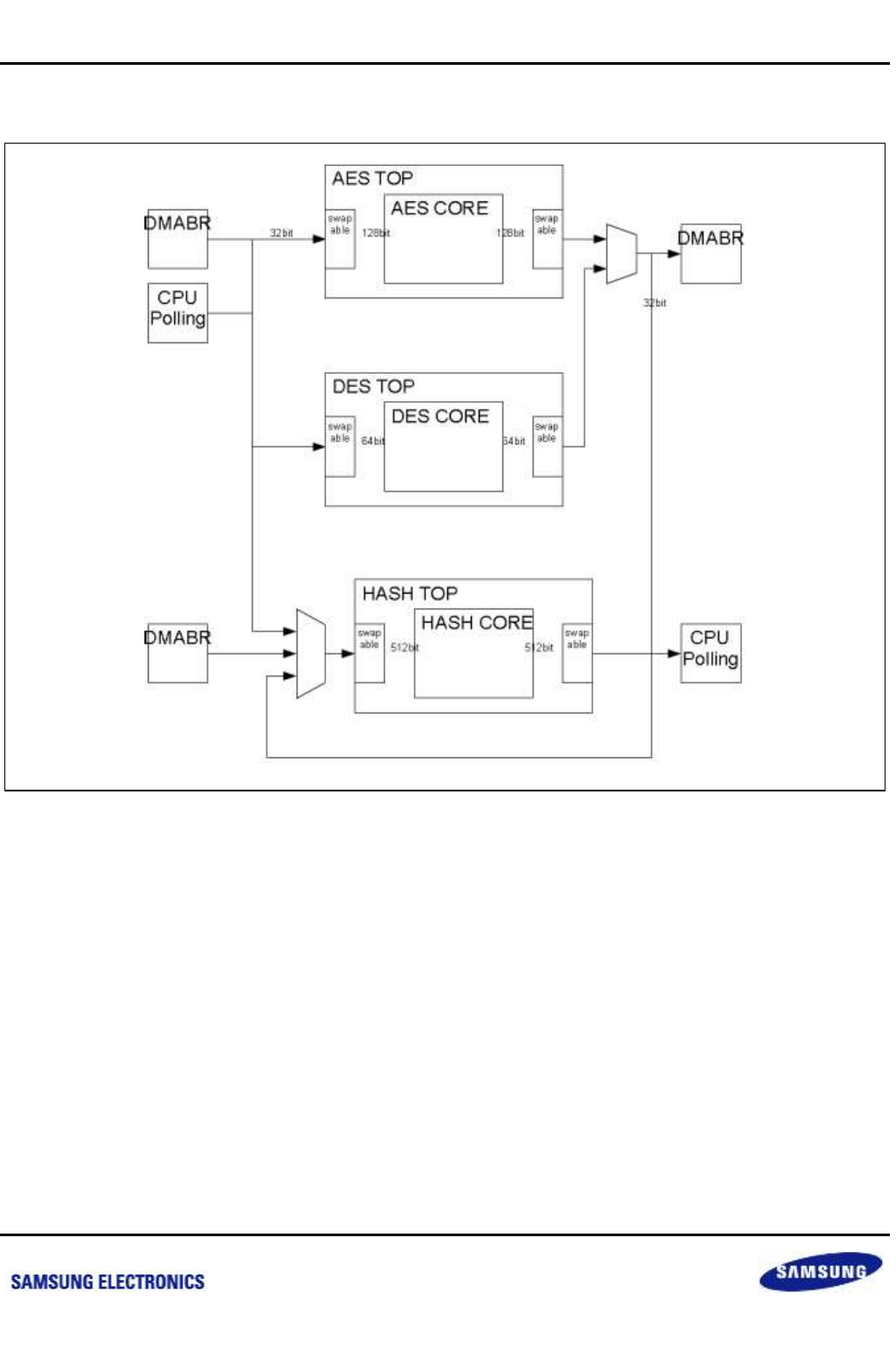
Samsung Confidential
S5P6818_UM 44 Crypto Engine
44-2
Preliminary product information describes products that are in development, for which full characterization data and
associated errata are not yet available. Specifications and information herein are subject to change without notice.
44.3 Block Diagram
Figure 44-1 CRYPTO Block Diagram
nexell / ys.kim at 2015.02.12
SAMSUNG Confidential
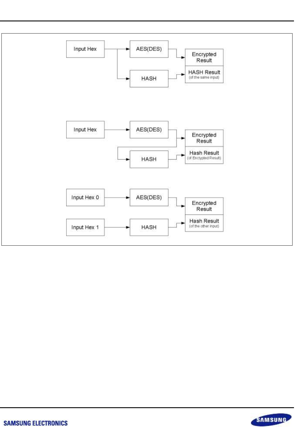
Samsung Confidential
S5P6818_UM 44 Crypto Engine
44-3
Preliminary product information describes products that are in development, for which full characterization data and
associated errata are not yet available. Specifications and information herein are subject to change without notice.
Figure 44-2 CRYPTOAES & HASH Operation Scenario
nexell / ys.kim at 2015.02.12
SAMSUNG Confidential

Samsung Confidential
S5P6818_UM 44 Crypto Engine
44-4
Preliminary product information describes products that are in development, for which full characterization data and
associated errata are not yet available. Specifications and information herein are subject to change without notice.
44.4 Functional Description
44.4.1 Polling Mode
In polling mode, CPU can write/read the register directly.
Access Sequence:
1. Set AES Key
2. Set Initial Vector and Set CPU_AES_LOADCNT with 1
3. Set AES_TESTIN
4. Set AES Control Register & Enable
5. Set CPU_AES_LOADCNT with 0
6. Set IDLC_ANNY WITH 1 (AES_START)
7. WAIT FOR IDLE_AES=1
8. Get Result Vector
44.4.2 Mode
In Channel DMA mode, users need to DMA Mode Enable.
nexell / ys.kim at 2015.02.12
SAMSUNG Confidential

Samsung Confidential
S5P6818_UM 44 Crypto Engine
44-5
Preliminary product information describes products that are in development, for which full characterization data and
associated errata are not yet available. Specifications and information herein are subject to change without notice.
44.5 Register Description
44.5.1 Register Map Summary
Base Address: 0xC001_5000
Register
Offset
Description
Reset Value
CRT_CTRL0
0x00h
CRYPTO Control register
0x0000_0000
AES_CTRL0
0x0Ch
CRYPTO AES Control register
0x0000_0000
AES_iv0
0x10h
CRYPTO AES INIT vector register 0
0x0000_0000
AES_iv1
0x14h
CRYPTO AES INIT vector register 1
0x0000_0000
AES_iv2
0x18h
CRYPTO AES INIT vector register 2
0x0000_0000
AES_iv3
0x1Ch
CRYPTO AES INIT vector register 3
0x0000_0000
AES_key0
0x30h
CRYPTO AES key register 0
0x0000_0000
AES_key1
0x34h
CRYPTO AES key register 1
0x0000_0000
AES_key2
0x38h
CRYPTO AES key register 2
0x0000_0000
AES_key3
0x3Ch
CRYPTO AES key register 3
0x0000_0000
AES_key4
0x40h
CRYPTO AES key register 4
0x0000_0000
AES_key5
0x44h
CRYPTO AES key register 5
0x0000_0000
AES_key6
0x48h
CRYPTO AES key register 6
0x0000_0000
AES_key7
0x4Ch
CRYPTO AES key register 7
0x0000_0000
AES_TEXTIN0
0x50h
CRYPTO AES TEXTIN register 0
0x0000_0000
AES_TEXTIN1
0x54h
CRYPTO AES TEXTIN register 1
0x0000_0000
AES_TEXTIN2
0x58h
CRYPTO AES TEXTIN register 2
0x0000_0000
AES_TEXTIN3
0x5Ch
CRYPTO AES TEXTIN register 3
0x0000_0000
AES_TEXTOUT0
0x60h
CRYPTO AES TEXTOUT register 0
0x0000_0000
AES_TEXTOUT1
0x64h
CRYPTO AES TEXTOUT register 1
0x0000_0000
AES_TEXTOUT2
0x68h
CRYPTO AES TEXTOUT register 2
0x0000_0000
AES_TEXTOUT3
0x6Ch
CRYPTO AES TEXTOUT register 3
0x0000_0000
DES_CTRL0
0x70h
CRYPTO DES Control register
0x0000_0000
DES_iv0
0x74h
CRYPTO DES INIT vector register 0
0x0000_0000
DES_iv1
0x78h
CRYPTO DES INIT vector register 1
0x0000_0000
DES_KEY0_0
0x7Ch
CRYPTO DES KEY register 0_0
0x0000_0000
DES_KEY0_1
0x80h
CRYPTO DES KEY register 0_1
0x0000_0000
DES_KEY1_0
0x84h
CRYPTO DES KEY register 1_0
0x0000_0000
DES_KEY1_1
0x88h
CRYPTO DES KEY register 1_1
0x0000_0000
DES_KEY2_0
0x8Ch
CRYPTO DES KEY register 2_0
0x0000_0000
DES_KEY2_1
0x90h
CRYPTO DES KEY register 2_1
0x0000_0000
DES_TEXTIN0
0x94h
CRYPTO DES TEXTIN register
0x0000_0000
DES_TEXTIN1
0x98h
CRYPTO DES TEXTIN register 1
0x0000_0000
nexell / ys.kim at 2015.02.12
SAMSUNG Confidential
Samsung Confidential
S5P6818_UM 44 Crypto Engine
44-6
Preliminary product information describes products that are in development, for which full characterization data and
associated errata are not yet available. Specifications and information herein are subject to change without notice.
Register
Offset
Description
Reset Value
DES_TEXTOUT0
0x9Ch
CRYPTO DES TEXTOUT register 0
0x0000_0000
DES_TEXTOUT1
0xA0h
CRYPTO DES TEXTOUT register 1
0x0000_0000
BDMAR
0xA4h
CRYPTO DMA BDMAR register
0x0000_0000
BDMAW
0xA8h
CRYPTO DMA BDMAW register
0x0000_0000
HDMAR
0xACh
CRYPTO DMA HDMAR register
0x0000_0000
HASH_CTRL0
0xB0h
CRYPTO HASH Control register 0
0x0000_0000
HASH_iv0
0xB4h
CRYPTO HASH INIT TABLE register 0
0x0000_0000
HASH_iv1
0xB8h
CRYPTO HASH INIT table register 1
0x0000_0000
HASH_iv2
0xBCh
CRYPTO HASH INIT table register 2
0x0000_0000
HASH_iv3
0xC0h
CRYPTO HASH INIT table register 3
0x0000_0000
HASH_iv4
0xC4h
CRYPTO HASH INIT table register 4
0x0000_0000
HASH_TEXTOUT0
0xC8h
CRYPTO HASH TEXTOUT register 0
0x0000_0000
HASH_TEXTOUT1
0xCCh
CRYPTO HASH TEXTOUT register 1
0x0000_0000
HASH_TEXTOUT2
0xD0h
CRYPTO HASH TEXTOUT register 2
0x0000_0000
HASH_TEXTOUT3
0xD4h
CRYPTO HASH TEXTOUT register 3
0x0000_0000
HASH_TEXTOUT4
0xD8h
CRYPTO HASH TEXTOUT register 4
0x0000_0000
HASH_TEXTIN
0xDCh
CRYPTO HASH TEXTIN register 0
0x0000_0000
HASH_MSG_SIZE
0xE0h
CRYPTO HASH TMSG SIZE register 0
0x0000_0000
HASH_MSG_SIZE
0xE4h
CRYPTO HASH TMSG SIZE register 1
0x0000_0000
nexell / ys.kim at 2015.02.12
SAMSUNG Confidential

Samsung Confidential
S5P6818_UM 44 Crypto Engine
44-7
Preliminary product information describes products that are in development, for which full characterization data and
associated errata are not yet available. Specifications and information herein are subject to change without notice.
44.5.1.1 CRT_CTRL0
Base Address: 0xC001_5000
Address = Base Address + 0x00h, Reset Value = 0x0000_0000
Name
Bit
Type
Description
Reset Value
RSVD
[31:11]
R
Reserved
21’h0
CPU_INT_ENB
[10]
RW
Enable the Interrupt
0 = Disable
1 = Enable
1'b0
CPU_INT_MASK
[9]
RW
Masking the Interrupt
0 = Masked
1 = Not Masked
1'b0
CPU_DMAW_SRC
[8]
RW
Specifies the DMA En/Decryption Mode
0 = AES
1 = DES
1'b0
IDLE_HASHCORE
[7]
R
Indicates the HASH CORE is Idle
0 = Not Idle
1 = Idle
1'b0
RSVD
[6]
R
Reserved
1'b0
INTPEND
[5]
RW
Read: Interrupt Pending Bit
Write 1: Interrupt Pending Clear
1'b0
CPU_DES_LOADCNT
[4]
W
Users must this bit to 1 after users set the DES
Initial Value.
-
CPU_AES_LOADCNT
[3]
W
Users must this bit to 1 after users set the AES
Initial Value.
-
IDLE_HASH
[2]
RW
Indicates the HASH is Idle
Write 1: HASH Start
1'b0
IDLE_DES
[1]
RW
Indicates the DES is Idle
Write 1: DES Start
1'b0
IDLE_AES
[0]
RW
Indicates the AES is Idle
Write 1: AES Start
1'b0
nexell / ys.kim at 2015.02.12
SAMSUNG Confidential

Samsung Confidential
S5P6818_UM 44 Crypto Engine
44-8
Preliminary product information describes products that are in development, for which full characterization data and
associated errata are not yet available. Specifications and information herein are subject to change without notice.
44.5.1.2 AES_CTRL0
Base Address: 0xC001_5000
Address = Base Address + 0x0Ch, Reset Value = 0x0000_0000
Name
Bit
Type
Description
Reset Value
RSVD
[31:16]
R
Reserved
16’h0
AES_SELKEY
[15]
RW
Select the AES KEY Mode
0 = CPU configuration
1 = ECID AESKEY
1'b0
RSVD
[14:10]
R
Reserved
5’h0
AES_SWAPOUT
[9]
RW
Enable the AES Output Swap
0 = Not Swap
1 = Masked
1'b0
AES_SWAPIN
[8]
RW
Enable the AES Input Swap
0 = Not Swap
1 = Masked
1'b0
AES_BLKMODE
[7:6]
RW
Specifies the AES Block Mode
0 = ECB
1 = CBC
2 = CTR
3 = Reserved
2'b0
AES_MODE
[5:4]
RW
Specifies the AES bit Mode
0 = 128-bit
1 = 192-bit
2 = 256-bit
3 = Reserved
2'b0
AES_128CNT
[3]
RW
Enable the AES 128-bit Counter
1'b0
AES_DMAMODE
[2]
RW
Enable the AES DMA Interface
0 = Disable
1 = Enable
1'b0
AES_ENC
[1]
RW
Specifies the AES Encoding Mode
(Encryption/Decryption)
0 = Decryption
1 = Modulation
1'b0
AES_ENB
[0]
RW
Enable the AES Mode
0 = Disable
1 = Enable
1'b0
nexell / ys.kim at 2015.02.12
SAMSUNG Confidential
Samsung Confidential
S5P6818_UM 44 Crypto Engine
44-9
Preliminary product information describes products that are in development, for which full characterization data and
associated errata are not yet available. Specifications and information herein are subject to change without notice.
44.5.1.3 AES_iv0
Base Address: 0xC001_5000
Address = Base Address + 0x10h, Reset Value = 0x0000_0000
Name
Bit
Type
Description
Reset Value
O_CPU_AES_IV
[31:0]
RW
O_CPU_AES_IV[127:96]. AES Initial vector
32’h0
44.5.1.4 AES_iv1
Base Address: 0xC001_5000
Address = Base Address + 0x14h, Reset Value = 0x0000_0000
Name
Bit
Type
Description
Reset Value
O_CPU_AES_IV
[31:0]
RW
O_CPU_AES_IV[95:64]. AES Initial vector
32’h0
44.5.1.5 AES_iv2
Base Address: 0xC001_5000
Address = Base Address + 0x18h, Reset Value = 0x0000_0000
Name
Bit
Type
Description
Reset Value
O_CPU_AES_IV
[31:0]
RW
O_CPU_AES_IV[63:32]. AES Initial vector
32’h0
44.5.1.6 AES_iv3
Base Address: 0xC001_5000
Address = Base Address + 0x1Ch, Reset Value = 0x0000_0000
Name
Bit
Type
Description
Reset Value
O_CPU_AES_IV
[31:0]
RW
O_CPU_AES_IV[31:0]. AES Initial vector
32’h0
44.5.1.7 AES_key0
Base Address: 0xC001_5000
Address = Base Address + 0x30h, Reset Value = 0x0000_0000
Name
Bit
Type
Description
Reset Value
O_CPU_AES_IV
[31:0]
RW
O_CPU_AES_key[255:224]. AES Key
(AES_SELKEY = 0)
32’h0
nexell / ys.kim at 2015.02.12
SAMSUNG Confidential

Samsung Confidential
S5P6818_UM 44 Crypto Engine
44-10
Preliminary product information describes products that are in development, for which full characterization data and
associated errata are not yet available. Specifications and information herein are subject to change without notice.
44.5.1.8 AES_key1
Base Address: 0xC001_5000
Address = Base Address + 0x34h, Reset Value = 0x0000_0000
Name
Bit
Type
Description
Reset Value
O_CPU_AES_IV
[31:0]
RW
O_CPU_AES_key[223:192]. AES Key
(AES_SELKEY = 0)
32’h0
44.5.1.9 AES_key2
Base Address: 0xC001_000
Address = Base Address + 0x38h, Reset Value = 0x0000_0000
Name
Bit
Type
Description
Reset Value
O_CPU_AES_IV
[31:0]
RW
O_CPU_AES_key[192:160]. AES Key
(AES_SELKEY = 0)
32’h0
44.5.1.10 AES_key3
Base Address: 0xC001_5000
Address = Base Address + 0x3Ch, Reset Value = 0x0000_0000
Name
Bit
Type
Description
Reset Value
O_CPU_AES_IV
[31:0]
RW
O_CPU_AES_key[159:128]. AES Key
(AES_SELKEY = 0)
32’h0
44.5.1.11 AES_key4
Base Address: 0xC001_5000
Address = Base Address + 0x40h, Reset Value = 0x0000_0000
Name
Bit
Type
Description
Reset Value
O_CPU_AES_IV
[31:0]
RW
O_CPU_AES_key[127:96]. AES Key
(AES_SELKEY = 0)
32’h0
44.5.1.12 AES_key5
Base Address: 0xC001_5000
Address = Base Address + 0x44h, Reset Value = 0x0000_0000
Name
Bit
Type
Description
Reset Value
O_CPU_AES_IV
[31:0]
RW
O_CPU_AES_key[95:64]. AES Key
(AES_SELKEY = 0)
32’h0
nexell / ys.kim at 2015.02.12
SAMSUNG Confidential

Samsung Confidential
S5P6818_UM 44 Crypto Engine
44-11
Preliminary product information describes products that are in development, for which full characterization data and
associated errata are not yet available. Specifications and information herein are subject to change without notice.
44.5.1.13 AES_key6
Base Address: 0xC001_5000
Address = Base Address + 0x48h, Reset Value = 0x0000_0000
Name
Bit
Type
Description
Reset Value
O_CPU_AES_IV
[31:0]
RW
O_CPU_AES_key[63:32]. AES Key
(AES_SELKEY = 0)
32’h0
44.5.1.14 AES_key7
Base Address: 0xC001_5000
Address = Base Address + 0x4Ch, Reset Value = 0x0000_0000
Name
Bit
Type
Description
Reset Value
O_CPU_AES_IV
[31:0]
RW
O_CPU_AES_key[31:0]. AES Key
(AES_SELKEY = 0)
32’h0
44.5.1.15 AES_TEXTIN0
Base Address: 0xC001_5000
Address = Base Address + 0x50h, Reset Value = 0x0000_0000
Name
Bit
Type
Description
Reset Value
CPU_AES_TEXTIN
[31:0]
RW
CPU_AES_TESTIN[127:96]. AES Input Vector in
PIO mode (Not DMA Mode)
32’h0
44.5.1.16 AES_TEXTIN1
Base Address: 0xC001_5000
Address = Base Address + 0x54h, Reset Value = 0x0000_0000
Name
Bit
Type
Description
Reset Value
CPU_AES_TEXTIN
[31:0]
RW
CPU_AES_TESTIN[95:64]. AES Input Vector in
PIO mode (Not DMA Mode)
32’h0
44.5.1.17 AES_TEXTIN2
Base Address: 0xC001_5000
Address = Base Address + 0x58h, Reset Value = 0x0000_0000
Name
Bit
Type
Description
Reset Value
CPU_AES_TEXTIN
[31:0]
RW
CPU_AES_TESTIN[63:32]. AES Input Vector in
PIO mode (Not DMA Mode)
32’h0
nexell / ys.kim at 2015.02.12
SAMSUNG Confidential

Samsung Confidential
S5P6818_UM 44 Crypto Engine
44-12
Preliminary product information describes products that are in development, for which full characterization data and
associated errata are not yet available. Specifications and information herein are subject to change without notice.
44.5.1.18 AES_TEXTIN3
Base Address: 0xC001_5000
Address = Base Address + 0x5Ch, Reset Value = 0x0000_0000
Name
Bit
Type
Description
Reset Value
CPU_AES_TEXTIN
[31:0]
RW
CPU_AES_TESTIN[31:0]. AES Input Vector in PIO
mode (Not DMA Mode)
32’h0
44.5.1.19 AES_TEXTOUT0
Base Address: 0xC001_5000
Address = Base Address + 0x60h, Reset Value = 0x0000_0000
Name
Bit
Type
Description
Reset Value
CPU_AES_TEXTOUT
[31:0]
RW
CPU_AES_TESTOUT[127:96]. AES Result Vector
in PIO mode (Not DMA Mode)
32’h0
44.5.1.20 AES_TEXTOUT1
Base Address: 0xC001_5000
Address = Base Address + 0x64h, Reset Value = 0x0000_0000
Name
Bit
Type
Description
Reset Value
CPU_AES_TEXTOUT
[31:0]
RW
CPU_AES_TESTOUT[95:64]. AES Result Vector
in PIO mode (Not DMA Mode)
32’h0
44.5.1.21 AES_TEXTOUT2
Base Address: 0xC001_5000
Address = Base Address + 0x68h, Reset Value = 0x0000_0000
Name
Bit
Type
Description
Reset Value
CPU_AES_TEXTOUT
[31:0]
RW
CPU_AES_TESTOUT[63:32]. AES Result Vector
in PIO mode (Not DMA Mode)
32’h0
44.5.1.22 AES_TEXTOUT3
Base Address: 0xC001_5000
Address = Base Address + 0x6Ch, Reset Value = 0x0000_0000
Name
Bit
Type
Description
Reset Value
CPU_AES_TEXTOUT
[31:0]
RW
CPU_AES_TESTOUT[31:0]. AES Result Vector in
PIO mode (Not DMA Mode)
32’h0
nexell / ys.kim at 2015.02.12
SAMSUNG Confidential

Samsung Confidential
S5P6818_UM 44 Crypto Engine
44-13
Preliminary product information describes products that are in development, for which full characterization data and
associated errata are not yet available. Specifications and information herein are subject to change without notice.
44.5.1.23 DES_CTRL0
Base Address: 0xC001_5000
Address = Base Address + 0x70h, Reset Value = 0x0000_0000
Name
Bit
Type
Description
Reset Value
RSVD
[31:11]
R
Reserved
21’h0
DES_TMODE
[10:8]
RW
3DES Mode Setting
[8]: 1st stage Mode
0 = Decoding
1 = Encoding
[9]: 2nd stage Mode
0 = Decoding
1 = Encoding
[10]: 3th stage Mode
0 = Decoding
1 = Encoding
3'b0
RSVD
[7]
R
Reserved
1'b0
DES_SWAPOUT
[6]
RW
Enable the DES Output Swap
0 = Not Swap
1 = Masked
1'b0
DES_SWAPIN
[5]
RW
Enable the DES Input Swap
0 = Not Swap
1 = Masked
1'b0
DES_BLKMODE
[4]
RW
Specifies the DES Block Mode
0 = ECB
1 = CBC
1'b0
DES_DMAMODE
[3]
RW
Enable the DES DMA Interface
0 = Disable
1 = Enable
1'b0
DES_MODE
[2]
RW
Specifies the DES Mode
0 = DES
1 = 3DES
1'b0
DES_ENC
[1]
RW
Specifies the DES Encoding Mode
(Encryption/Decryption)
0 = Decryption
1 = Modulation
1'b0
DES_ENB
[0]
RW
Enable the DES Mode
0 = Disable
1 = Enable
1'b0
nexell / ys.kim at 2015.02.12
SAMSUNG Confidential
Samsung Confidential
S5P6818_UM 44 Crypto Engine
44-14
Preliminary product information describes products that are in development, for which full characterization data and
associated errata are not yet available. Specifications and information herein are subject to change without notice.
44.5.1.24 DES_iv0
Base Address: 0xC001_5000
Address = Base Address + 0x74h, Reset Value = 0x0000_0000
Name
Bit
Type
Description
Reset Value
O_CPU_DES_IV
[31:0]
RW
O_CPU_DES_IV[63:32]. DES Initial vector
32’h0
44.5.1.25 DES_iv1
Base Address: 0xC001_0000
Address = Base Address + 5078h, Reset Value = 0x0000_0000
Name
Bit
Type
Description
Reset Value
O_CPU_DES_IV
[31:0]
RW
O_CPU_DES_IV[31:0]. DES Initial vector
32’h0
44.5.1.26 DES_KEY0_0
Base Address: 0xC001_0000
Address = Base Address + 507Ch, Reset Value = 0x0000_0000
Name
Bit
Type
Description
Reset Value
O_CPU_DES_KEY0
[31:0]
RW
O_CPU_DES_KEY0[63:32]. DES Key (DES and
1st stage of 3DES)
32’h0
44.5.1.27 DES_KEY0_1
Base Address: 0xC001_0000
Address = Base Address + 5080h, Reset Value = 0x0000_0000
Name
Bit
Type
Description
Reset Value
O_CPU_DES_KEY0
[31:0]
RW
O_CPU_DES_KEY0[31:0]. DES Key (DES and 1st
stage of 3DES)
32’h0
44.5.1.28 DES_KEY1_0
Base Address: 0xC001_5000
Address = Base Address + 0x84h, Reset Value = 0x0000_0000
Name
Bit
Type
Description
Reset Value
O_CPU_DES_KEY1
[31:0]
RW
O_CPU_DES_KEY1[63:32]. DES Key (2nd stage
of 3DES)
32’h0
nexell / ys.kim at 2015.02.12
SAMSUNG Confidential
Samsung Confidential
S5P6818_UM 44 Crypto Engine
44-15
Preliminary product information describes products that are in development, for which full characterization data and
associated errata are not yet available. Specifications and information herein are subject to change without notice.
44.5.1.29 DES_KEY1_1
Base Address: 0xC001_5000
Address = Base Address + 0x88h, Reset Value = 0x0000_0000
Name
Bit
Type
Description
Reset Value
O_CPU_DES_KEY1
[31:0]
RW
O_CPU_DES_KEY1[31:0]. DES Key (2nd stage of
3DES)
32’h0
44.5.1.30 DES_KEY2_0
Base Address: 0xC001_5000
Address = Base Address + 0x8Ch, Reset Value = 0x0000_0000
Name
Bit
Type
Description
Reset Value
O_CPU_DES_KEY2
[31:0]
RW
O_CPU_DES_KEY2[63:32]. DES Key (3th stage of
3DES)
32’h0
44.5.1.31 DES_KEY2_1
Base Address: 0xC001_5000
Address = Base Address + 0x90h, Reset Value = 0x0000_0000
Name
Bit
Type
Description
Reset Value
O_CPU_DES_KEY2
[31:0]
RW
O_CPU_DES_KEY2[31:0]. DES Key (3th stage of
3DES)
32’h0
44.5.1.32 DES_TEXTIN0
Base Address: 0xC001_5000
Address = Base Address + 0x94h, Reset Value = 0x0000_0000
Name
Bit
Type
Description
Reset Value
CPU_DES_TESTIN
[31:0]
RW
CPU_DES_TESTIN[63:32]. DES Input vector in
PIO mode (Not DMA Mode)
32’h0
44.5.1.33 DES_TEXTIN1
Base Address: 0xC001_5000
Address = Base Address + 0x98h, Reset Value = 0x0000_0000
Name
Bit
Type
Description
Reset Value
CPU_DES_TESTIN
[31:0]
RW
CPU_DES_TESTIN[31:0]. DES Input vector in PIO
mode (Not DMA Mode)
32’h0
nexell / ys.kim at 2015.02.12
SAMSUNG Confidential
Samsung Confidential
S5P6818_UM 44 Crypto Engine
44-16
Preliminary product information describes products that are in development, for which full characterization data and
associated errata are not yet available. Specifications and information herein are subject to change without notice.
44.5.1.34 DES_TEXTOUT0
Base Address: 0xC001_5000
Address = Base Address + 0x9Ch, Reset Value = 0x0000_0000
Name
Bit
Type
Description
Reset Value
CPU_DES_TESTOUT
[31:0]
RW
CPU_DES_TESTOUT[63:32]. DES Input vector in
PIO mode (Not DMA Mode)
32’h0
44.5.1.35 DES_TEXTOUT1
Base Address: 0xC001_5000
Address = Base Address + 0xA0h, Reset Value = 0x0000_0000
Name
Bit
Type
Description
Reset Value
CPU_DES_TESTOUT
[31:0]
RW
CPU_DES_TESTOUT [31:0]. DES Input vector in
PIO mode (Not DMA Mode)
32’h0
44.5.1.36 BDMAR
Base Address: 0xC001_5000
Address = Base Address + 0xA4h, Reset Value = 0x0000_0000
Name
Bit
Type
Description
Reset Value
REG_CRT_BDMAR
[31:0]
W
DMA Access register for AES, DES Input Vectors.
44.5.1.37 BDMAW
Base Address: 0xC001_5000
Address = Base Address + 0xA8h, Reset Value = 0x0000_0000
Name
Bit
Type
Description
Reset Value
REG_CRT_BDMAW
[31:0]
R
DMA Access register for AES, DES Output
Vectors. (Result Vector)
44.5.1.38 HDMAR
Base Address: 0xC001_5000
Address = Base Address + 0xACh, Reset Value = 0x0000_0000
Name
Bit
Type
Description
Reset Value
REG_CRT_BDMAR
[31:0]
W
DMA Access register for HASH Input Vectors
nexell / ys.kim at 2015.02.12
SAMSUNG Confidential
Samsung Confidential
S5P6818_UM 44 Crypto Engine
44-17
Preliminary product information describes products that are in development, for which full characterization data and
associated errata are not yet available. Specifications and information herein are subject to change without notice.
44.5.1.39 HASH_CTRL0
Base Address: 0xC001_5000
Address = Base Address + 0xB0h, Reset Value = 0x0000_0000
Name
Bit
Type
Description
Reset Value
RSVD
[31:7]
R
Reserved
25’h0
HASH_INSRC
[6:5]
RW
Specifies the Input of HASH
0 = AES input share
1 = DES input share
2 = HRDMA
3 = BWDMA
3'b0
HASH_SWAPIN
[4]
RW
Enable the HASH Input Swap
0 = Not Swap
1 = Masked
1'b0
HASH_MODE
[3]
RW
Specifies the HASH Mode
0 = SHA1
1 = MD5
1'b0
RSVD
[2]
R
Reserved
1'b0
HASH_DMAMODE
[1]
RW
Enable the HASH DMA Interface
0 = Disable
1 = Enable
1'b0
HASH_ENB
[0]
RW
Enable the HASH Mode
0 = Disable
1 = Enable
1'b0
44.5.1.40 HASH_iv0
Base Address: 0xC001_5000
Address = Base Address + 0xB4h, Reset Value = 0x0000_0000
Name
Bit
Type
Description
Reset Value
O_CPU_HASH_IV
[31:0]
RW
O_CPU_HASH_IV[159:128]. HASH Initial table
32’h0
44.5.1.41 HASH_iv1
Base Address: 0xC001_5000
Address = Base Address + 0xB8h, Reset Value = 0x0000_0000
Name
Bit
Type
Description
Reset Value
O_CPU_HASH_IV
[31:0]
RW
O_CPU_HASH_IV[127:96]. HASH Initial table
32’h0
nexell / ys.kim at 2015.02.12
SAMSUNG Confidential
Samsung Confidential
S5P6818_UM 44 Crypto Engine
44-18
Preliminary product information describes products that are in development, for which full characterization data and
associated errata are not yet available. Specifications and information herein are subject to change without notice.
44.5.1.42 HASH_iv2
Base Address: 0xC001_5000
Address = Base Address + 0xBCh, Reset Value = 0x0000_0000
Name
Bit
Type
Description
Reset Value
O_CPU_HASH_IV
[31:0]
RW
O_CPU_HASH_IV[95:64]. HASH Initial table
32’h0
44.5.1.43 HASH_iv3
Base Address: 0xC001_5000
Address = Base Address + 0xC0h, Reset Value = 0x0000_0000
Name
Bit
Type
Description
Reset Value
O_CPU_HASH_IV
[31:0]
RW
O_CPU_HASH_IV[63:32]. HASH Initial table
32’h0
44.5.1.44 HASH_iv4
Base Address: 0xC001_5000
Address = Base Address + 0xC4h, Reset Value = 0x0000_0000
Name
Bit
Type
Description
Reset Value
O_CPU_HASH_IV
[31:0]
RW
O_CPU_HASH_IV[31:0]. HASH Initial table
32’h0
44.5.1.45 HASH_TEXTOUT0
Base Address: 0xC001_5000
Address = Base Address + 0xC8h, Reset Value = 0x0000_0000
Name
Bit
Type
Description
Reset Value
CPU_HASH_TEXTOUT
[31:0]
RW
CPU_HASH_TESTOUT[159:128]. HASH result
output
32’h0
44.5.1.46 HASH_TEXTOUT1
Base Address: 0xC001_5000
Address = Base Address + 0xCCh, Reset Value = 0x0000_0000
Name
Bit
Type
Description
Reset Value
CPU_HASH_TEXTOUT
[31:0]
RW
CPU_HASH_TESTOUT[127:96]. HASH result
output
32’h0
nexell / ys.kim at 2015.02.12
SAMSUNG Confidential

Samsung Confidential
S5P6818_UM 44 Crypto Engine
44-19
Preliminary product information describes products that are in development, for which full characterization data and
associated errata are not yet available. Specifications and information herein are subject to change without notice.
44.5.1.47 HASH_TEXTOUT2
Base Address: 0xC001_5000
Address = Base Address + 0xD0h, Reset Value = 0x0000_0000
Name
Bit
Type
Description
Reset Value
CPU_HASH_TEXTOUT
[31:0]
RW
CPU_HASH_TESTOUT[96:64]. HASH result
output
32’h0
44.5.1.48 HASH_TEXTOUT3
Base Address: 0xC001_5000
Address = Base Address + 0xD4h, Reset Value = 0x0000_0000
Name
Bit
Type
Description
Reset Value
CPU_HASH_TEXTOUT
[31:0]
RW
CPU_HASH_TESTOUT[63:32]. HASH result
output
32’h0
44.5.1.49 HASH_TEXTOUT4
Base Address: 0xC001_5000
Address = Base Address + 0xD8h, Reset Value = 0x0000_0000
Name
Bit
Type
Description
Reset Value
CPU_HASH_TEXTOUT
[31:0]
RW
CPU_HASH_TESTOUT[31:0]. HASH result output
32’h0
44.5.1.50 HASH_TEXTIN
Base Address: 0xC001_5000
Address = Base Address + 0xDCh, Reset Value = 0x0000_0000
Name
Bit
Type
Description
Reset Value
CPU_HASH_TEXTIN
[31:0]
RW
CPU_HASH_TESTIN[127:0]. For DMA and PIO
mode
32’h0
44.5.1.51 HASH_MSG_SIZE
Base Address: 0xC001_5000
Address = Base Address + 0xE0h, Reset Value = 0x0000_0000
Name
Bit
Type
Description
Reset Value
CPU_HASH_MSGSIZE
[31:0]
RW
CPU_HASH_MSGSIZE[63:32]. HASH result output
32’h0
nexell / ys.kim at 2015.02.12
SAMSUNG Confidential

Samsung Confidential
S5P6818_UM 44 Crypto Engine
44-20
Preliminary product information describes products that are in development, for which full characterization data and
associated errata are not yet available. Specifications and information herein are subject to change without notice.
44.5.1.52 HASH_MSG_SIZE
Base Address: 0xC001_5000
Address = Base Address + 0xE4h, Reset Value = 0x0000_0000
Name
Bit
Type
Description
Reset Value
CPU_HASH_MSGSIZE
[31:0]
RW
CPU_HASH_MSGSIZE[31:0]. HASH result output
32’h0
nexell / ys.kim at 2015.02.12
SAMSUNG Confidential

Samsung Confidential
S5P6818_UM 45 Secure JTAG
45-1
Preliminary product information describes products that are in development, for which full characterization data and
associated errata are not yet available. Specifications and information herein are subject to change without notice.
45 Secure JTAG
45.1 Overview
The Secure JTAG consists of an Authentication & Authorization module an Access Provider. Secure JTAG Device
support protection by user password can be unlocked by providing the correct password. Secure JTAG
Connected with CoreSight at AHB AP. To activate the password unlock mechanism, the password exchange
request must be applied to the AHB AP of CoreSight
45.2 Features
The Secure JTAG features: Authentication & Authorization Debug Module.
nexell / ys.kim at 2015.02.12
SAMSUNG Confidential
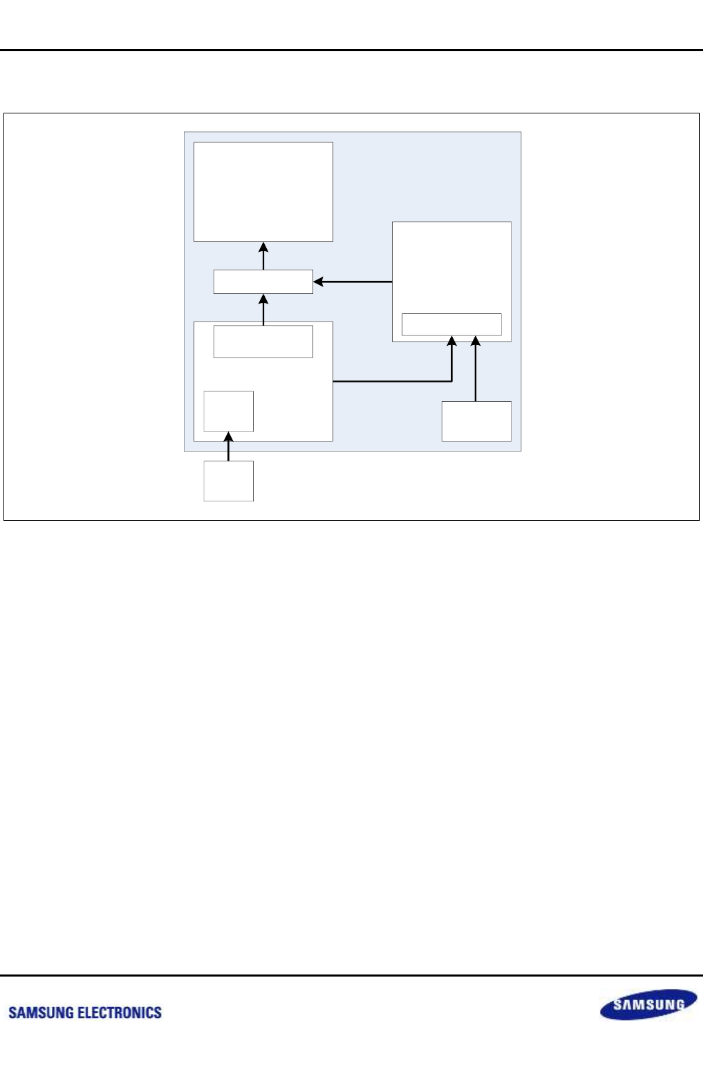
Samsung Confidential
S5P6818_UM 45 Secure JTAG
45-2
Preliminary product information describes products that are in development, for which full characterization data and
associated errata are not yet available. Specifications and information herein are subject to change without notice.
45.3 Block Diagram
Figure 45-1 Secure JTAG Block Diagram
45.4 Secure JTAG User Configure
System L2 Cache Base Address: JTAG AHB-AP BASE Address 0x00000000
Coresight
JTAG
DAP
Secure JTAG
CPU
Password Write
Debug
Hashed
Password
Authentication
Authorization
Ext.
JTAG
nexell / ys.kim at 2015.02.12
SAMSUNG Confidential
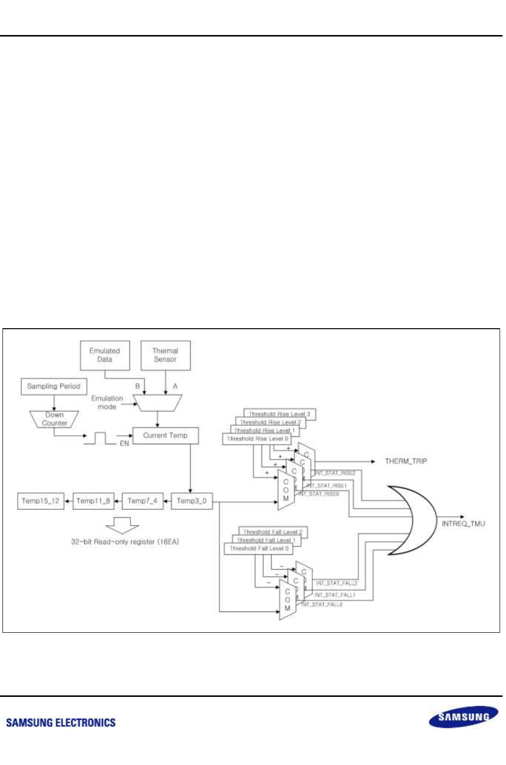
Samsung Confidential
S5P6818_UM 46 Temperature Monitor Unit (TMU)
46-1
Preliminary product information describes products that are in development, for which full characterization data and
associated errata are not yet available. Specifications and information herein are subject to change without notice.
46 Temperature Monitor Unit (TMU)
46.1 Overview
In deep sub-micron era, the high temperature due to dynamic dissipation may incur the malfunction of a chip, and
leads to expensive cost such as package, cooling device, .etc. To alleviate the phenomenon, it is necessary to
manage on-chip temperature so that a chip maintains the proper temperature to continue operation while reducing
performance or suspending operation in a specific IP.
The TMU in S5P6818 provides software-controlled (denoted thermal throttling) and hardware-controlled (denoted
thermal tripping) management scheme. TMU monitors temperature variation in a chip by measuring on-chip
temperature, and generates interrupt to CPU when temperature exceeds or goes below pre-defined threshold. At
the point of CPU's side, CPU can obtain on-chip temperature information by reading the related register field, i.e.
by using polling scheme. The TMU operating clock is the oscillation clock OSCCLK.
The overview of operation of TMU is shown in the picture below.
Figure 46-1 Overview of Operation of TMU
nexell / ys.kim at 2015.02.12
SAMSUNG Confidential

Samsung Confidential
S5P6818_UM 46 Temperature Monitor Unit (TMU)
46-2
Preliminary product information describes products that are in development, for which full characterization data and
associated errata are not yet available. Specifications and information herein are subject to change without notice.
The temperature data obtained by temperature sensor may contain the measuring error, and therefore, for a
normal operation, temperature data should be calibrated. The calibration of temperature data is performed by
software. The calibration consists of reading the measured data from e-fuse and writing the calibrated threshold
temperature to generate interrupts into THRESHOLD_TEMP_RISE or THRESHOLD_TEMP_FALL register by
using calibration equation. When current temperature exceeds or goes down a threshold temperature, then the
corresponding interrupt is generated. After reading interrupt status register, the proper task for that interrupt
should be performed by software.
When temperature exceeds a extremely high threshold temperature denoted as THRES_LEVEL_RISE3 field of
THRESHOLD_TEMP_RISE register, then S5P6818 should not be damaged by the hot temperature. In this case,
TMU urgently sends active-high signal (THERM_TRIP) to PMU, and thermal tripping by hardware logic i.e PMU
(Power Management Unit) is performed. Thermal tripping means that PMU cut off the whole power of S5P6818 by
controlling external voltage regulator.
nexell / ys.kim at 2015.02.12
SAMSUNG Confidential
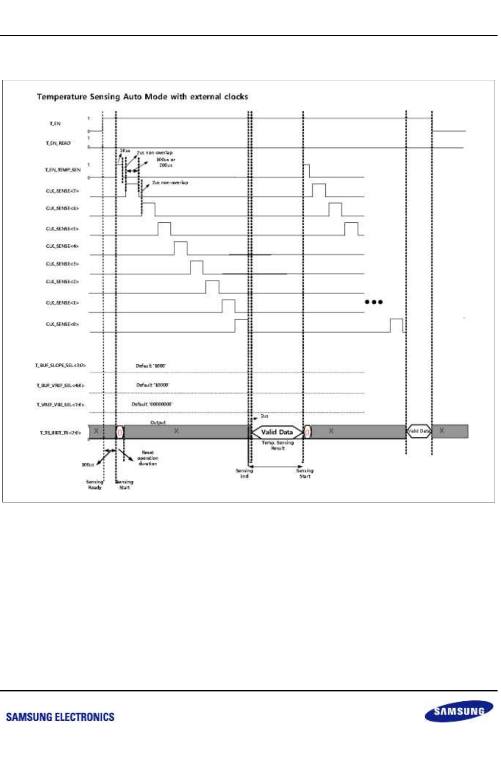
Samsung Confidential
S5P6818_UM 46 Temperature Monitor Unit (TMU)
46-3
Preliminary product information describes products that are in development, for which full characterization data and
associated errata are not yet available. Specifications and information herein are subject to change without notice.
46.2 Temperature Sensing Auto Mode with External Clocks
Figure 46-2 Temperature Sensor Timing diagram
Above figure shows the timing diagram of remote temperature sensor (TEM2803X). To activate temperature-
sensing operation, T_EN should be applied for sensing period. For the temperature sensing output code
generation, T_EN_TEMP_SEN first needs to be activated at least for 20 us to reset the temperature sensing block
and then 8 bits non-overlap pulses, CLK_SENSE<7:0>, are applied. The 8 bits of CLK_SENSE<7:0> are applied
to the temperature sensing block and then the block produces reference level decision codes for the Reference
Voltage Gen. Block and generates output temperature conversion code according to SAR type decision method.
The valid output data can be obtained after the final clock signal CLK_SENSE<0> is activated.
nexell / ys.kim at 2015.02.12
SAMSUNG Confidential

Samsung Confidential
S5P6818_UM 46 Temperature Monitor Unit (TMU)
46-4
Preliminary product information describes products that are in development, for which full characterization data and
associated errata are not yet available. Specifications and information herein are subject to change without notice.
46.3 Temperature Code Table
The sensing temperature range of TEM2803X is from 25 C to 125 C with 1 C resolution. Temperature data is
represented with 8 bits binary word with a Least Significant Bit (LSB) equal to 1 C.
Table 46-1 Temperature Code Table
8BIT CODE
Temp.(°C)
8BIT CODE
Temp.(°C)
8BIT CODE
Temp.(°C)
101110
25
1010000
59
1110010
93
101111
26
1010001
60
1110011
94
110000
27
1010010
61
1110100
95
110001
28
1010011
62
1110101
96
110010
29
1010100
63
1110110
97
110011
30
1010101
64
1110111
98
110100
31
1010110
65
1111000
99
110101
32
1010111
66
1111001
100
110110
33
1011000
67
1111010
101
110111
34
1011001
68
1111011
102
111000
35
1011010
69
1111100
103
111001
36
1011011
70
1111101
104
111010
37
1011100
71
1111110
105
111011
38
1011101
72
1111111
106
111100
39
1011110
73
10000000
107
111101
40
1011111
74
10000001
108
111110
41
1100000
75
10000010
109
111111
42
1100001
76
10000011
110
1000000
43
1100010
77
10000100
111
1000001
44
1100011
78
10000101
112
1000010
45
1100100
79
10000110
113
1000011
46
1100101
80
10000111
114
1000100
47
1100110
81
10001000
115
1000101
48
1100111
82
10001001
116
1000110
49
1101000
83
10001010
117
1000111
50
1101001
84
10001011
118
1001000
51
1101010
85
10001100
119
1001001
52
1101011
86
10001101
120
1001010
53
1101100
87
10001110
121
1001011
54
1101101
88
10001111
122
1001100
55
1101110
89
10010000
123
1001101
56
1101111
90
10010001
124
nexell / ys.kim at 2015.02.12
SAMSUNG Confidential

Samsung Confidential
S5P6818_UM 46 Temperature Monitor Unit (TMU)
46-5
Preliminary product information describes products that are in development, for which full characterization data and
associated errata are not yet available. Specifications and information herein are subject to change without notice.
8BIT CODE
Temp.(°C)
8BIT CODE
Temp.(°C)
8BIT CODE
Temp.(°C)
1001110
57
1110000
91
10010010
125
1001111
58
1110001
92
nexell / ys.kim at 2015.02.12
SAMSUNG Confidential

Samsung Confidential
S5P6818_UM 46 Temperature Monitor Unit (TMU)
46-6
Preliminary product information describes products that are in development, for which full characterization data and
associated errata are not yet available. Specifications and information herein are subject to change without notice.
46.4 I/O Description
Table 46-2 I/O Description
Signal
I/O
Description
Pad
Type
RETN_TOP
INPUT
Top domain retention mode enable (active
low)
–
–
TCLK33
INPUT
Test mode clock (33 MHz)
–
–
TEST_MODE
INPUT
Temperature sensor test mode
–
–
TEST_MODE_SCAN
INPUT
Scan test mode
–
–
TEST_RESETn
INPUT
Test mode reset
–
–
CLK
INPUT
Main clock from oscillation pad
XXTI
dedicated
RESETn
INPUT
Main reset from reset generator
–
–
ADDR__TMU_APBIF[15:0]
INPUT
Address for special function register
(handshaking protocol with SFR_APBIF in
PERIS_BLK)
–
–
WDATA__TMU_APBIF[31:0]
INPUT
Write data to special function register
(handshaking protocol with SFR_APBIF in
PERIS_BLK)
–
–
RDATA__TMU_APBIF[31:0]
OUTPUT
Read data from special function register
(handshaking protocol with SFR_APBIF in
PERIS_BLK)
–
–
WR_REQ__TMU_APBIF
INPUT
Write request to special function register
(handshaking protocol with SFR_APBIF in
PERIS_BLK)
–
–
WR_ACK__TMU_APBIF
OUTPUT
Write acknowledge from special function
register (handshaking protocol with
SFR_APBIF in PERIS_BLK)
–
–
RD_REQ__TMU_APBIF
INPUT
Read request to special function register
(handshaking protocol with SFR_APBIF in
PERIS_BLK)
–
–
RD_ACK__TMU_APBIF
OUTPUT
Read acknowledge from special function
register (handshaking protocol with
SFR_APBIF in PERIS_BLK)
–
–
INTREQ_TMU
OUTPUT
Interrupt request to interrupt controller
(combined interrupt)
–
–
THERM_TRIP
OUTPUT
Thermal tripping signal to power
management unit (active high, level
triggering)
–
–
WDRAM_TQ[7:0]
INPUT
TQ pin from Wide-IO DRAM. Each 2-bit is
assigned to the maximum four wide-IO
DRAMs.
–
–
T_TS_8BIT_TS[7:0]
INPUT
Temperature information from main
temperature sensor (TEM3203X)
–
–
T_TS_OUT_TS
INPUT
Manual mode output checking port from main
temperature sensor (TEM3203X), only used
–
–
nexell / ys.kim at 2015.02.12
SAMSUNG Confidential

Samsung Confidential
S5P6818_UM 46 Temperature Monitor Unit (TMU)
46-7
Preliminary product information describes products that are in development, for which full characterization data and
associated errata are not yet available. Specifications and information herein are subject to change without notice.
Signal
I/O
Description
Pad
Type
for debugging purpose
DFTMUX_T_EN
INPUT
Test mode muxing with T_EN
–
–
DFTMUX_T_EN_READ
INPUT
Test mode muxing with T_EN_READ
–
–
DFTMUX_T_EN_TEMP_SEN
INPUT
Test mode muxing with T_EN_TEMP_SEN
–
–
DFTMUX_T_BUF_SLOPE_SEL[3:0]
INPUT
Test mode muxing with
T_BUF_SLOPE_SEL[3:0]
–
–
DFTMUX_T_CLK_SENSE[7:0]
INPUT
Test mode muxing with T_CLK_SENSE[7:0]
–
–
DFTMUX_T_MUX_ADDR[2:0]
INPUT
Test mode muxing with T_MUX_ADDR[2:0]
–
–
DFTMUX_T_BUF_VREF_SEL[4:0]
INPUT
Test mode muxing with
T_BUF_VREF_SEL[4:0]
–
–
DFTMUX_T_VREF_VBE_SEL[7:0]
INPUT
Test mode muxing with
T_VREF_VBE_SEL[7:0]
–
–
MUX_EN
OUTPUT
EN muxed with T_EN
–
–
MUX_EN_READ
OUTPUT
EN_READ muxed with T_EN_READ
–
–
MUX_EN_TEMP_SEN
OUTPUT
EN_TEMP_SEN muxed with
T_EN_TEMP_SEN
–
–
MUX_BUF_SLOPE_SEL[3:0]
OUTPUT
BUF_SLOPE_SEL[3:0] muxed with
T_BUF_SLOPE_SEL[3:0]
–
–
MUX_CLK_SENSE[7:0]
OUTPUT
CLK_SENSE[7:0] muxed with
T_CLK_SENSE[7:0]
–
–
MUX_MUX_ADDR[2:0]
OUTPUT
MUX_ADDR[2:0] muxed with
T_MUX_ADDR[7:0]
–
–
MUX_BUF_VREF_SEL[4:0]
OUTPUT
BUF_VREF_SEL[4:0] muxed with
T_BUF_VREF_SEL[4:0]
–
–
MUX_VREF_VBE_SEL[7:0]
OUTPUT
VREF_VBE_SEL[7:0] muxed with
T_VREF_VBE_SEL[7:0]
–
–
TEST_TRIM
INPUT
Test mode for EFROM (storing sensing error
information)
–
–
TRIM_CS
INPUT
Chip select enable to EFROM (from
DFTMUX)
–
–
TRIM_A[2:0]
INPUT
Sensing bit select [2:0] to EFROM (from
DFTMUX)
–
–
TRIM_SCK
INPUT
Scan mode clock to EFROM (from DFTMUX)
–
–
TRIM_PROG
INPUT
Enable signal to EFROM to program fuse
selected by SDI shift (from DFTMUX)
–
–
TRIM_PRCHG
INPUT
Signal to EFROM to pre-charge reference
nodes of sense amplifier (from DFTMUX)
–
–
TRIM_SIGDEV
INPUT
Signal to open up both fuse and reference
nodes to the sense amplifier of EFROM (from
DFTMUX)
–
–
nexell / ys.kim at 2015.02.12
SAMSUNG Confidential

Samsung Confidential
S5P6818_UM 46 Temperature Monitor Unit (TMU)
46-8
Preliminary product information describes products that are in development, for which full characterization data and
associated errata are not yet available. Specifications and information herein are subject to change without notice.
Signal
I/O
Description
Pad
Type
TRIM_FSET
INPUT
Signal to enable sense amplifier of EFROM
(from DFTMUX)
–
–
TRIM_SDI
INPUT
The data scan-in port of the fuse latch of
EFROM (from DFTMUX)
–
–
TMU_EFROM_SDOUT
INPUT
The serial output of fuse sense operation of
EFROM (from EFROM)
–
–
TMU_EFROM_DOUT[23:0]
INPUT
The parallel outputs of fuse sense operation
of EFROM (from EFROM)
–
–
trim_CS
OUTPUT
Chip select enable to EFROM muxed with
TRIM_CS (to EFROM)
–
–
trim_A[2:0]
OUTPUT
Sensing bit select [2:0] to EFROM EFROM
muxed with TRIM_A[2:0] (to EFROM)
–
–
trim_SCK
OUTPUT
Scan mode clock to EFROM EFROM muxed
with TRIM_SCK (to EFROM)
–
–
trim_PROG
OUTPUT
Enable signal to EFROM to program fuse
selected by SDI shift muxed with
TRIM_PROG (to EFROM)
–
–
trim_PRCHG
OUTPUT
Signal to EFROM to pre-charge reference
nodes of sense amplifier muxed with
TRIM_PRCHG (to EFROM)
–
–
trim_SIGDEV
OUTPUT
Signal to open up both fuse and reference
nodes to the sense amplifier of EFROM
muxed with TRIM_SIGDEV (to EFROM)
–
–
trim_FSET
OUTPUT
Signal to enable sense amplifier of EFROM
muxed with TRIM_FSET (to EFROM)
–
–
trim_SDI
OUTPUT
The data scan-in port of the fuse latch of
EFROM muxed with TRIM_SDI (to EFROM)
–
–
TRIM_SDOUT
OUTPUT
Serial data out from EFROM muxed with
TMU_EFROM_SDOUT (to DFTMUX)
–
–
sensing_start
INPUT
EFROM sensing start from power
management unit
–
–
sensing_done
OUTPUT
EFROM sensing done to power management
unit
–
–
nexell / ys.kim at 2015.02.12
SAMSUNG Confidential

Samsung Confidential
S5P6818_UM 46 Temperature Monitor Unit (TMU)
46-9
Preliminary product information describes products that are in development, for which full characterization data and
associated errata are not yet available. Specifications and information herein are subject to change without notice.
46.5 Programming Guide
Calibration equation
For calibration of temperature sensor, there are two kinds of trimming method, i.e. one is 1-point trimming, and the
other is 2-point trimming. 1-point trimming uses only the measured data at 25 C, and calibrates the offset
between the measured temperature and 25 C. In contrast, 2-point trimming uses both the measured data at at 25
C and 85 C, and calibrates both the offset and the slope of a measured data.
The calibration consists of reading the measured data from e-fuse and writing the calibrated threshold
temperature to generate interrupts into threshold/trigger level0-3 register by using calibration equation. The
calibration equation for 2-point trimming as follows:
Tnew = (Torg – 25) (TE2 - TE1)/(85 – 25) + TE1
where,
Tnew: calibrated threshold temperature rewritten to THRES_TEMP and TRIG_LEVEL0-3 register.
Torg: original threshold temperature
TE1: temperature value corresponding to the temperature code stored in TRIMINFO_25 of TRIMINFO
@0x1006_0000
TE2: temperature value corresponding to the temperature code stored in TRIMINFO_85 of TRIMINFO
@0x1006_0000
For example, we want to set threshold temperature to 50(C) (=Torg), and TE = 35(C), TE2 = 105(C), then Tnew
is:
Tnew = (50 – 25) (105 – 35)/(85 – 25) + 35 = 64 (C)
This value is rewritten to THRES_TEMP_RISE (@1006_0050) and THRES_TEMP_FALL (@0x1006_0054).
And, if 1-point trimming is used, the calibration equation becomes:
Tnew = Torg + (TE1 – 25).
nexell / ys.kim at 2015.02.12
SAMSUNG Confidential

Samsung Confidential
S5P6818_UM 46 Temperature Monitor Unit (TMU)
46-10
Preliminary product information describes products that are in development, for which full characterization data and
associated errata are not yet available. Specifications and information herein are subject to change without notice.
46.5.1 Software Sequence
The example of software sequence as follows:
The parameter may be changed according to an application.
/* Read the measured data from e-fuse */
Triminfo_85 = TRIMINFO[15:8]
Triminfo_25 = TRIMINFO[7:0]
/* Calibrated threshold temperature is written into THRES_TEMP_RISE and THRES_TEMP_FALL */
/* Refer to 1.6.1 */
THRES_TEMP_RISE0 = 0x40;
THRES_TEMP_RISE1 = 0x50;
THRES_TEMP_RISE2 = 0x60;
THRES_TEMP_RISE3 = 0x70;
THRES_TEMP_FALL0 = 0x3A;
THRES_TEMP_FALL1 = 0x4A;
THRES_TEMP_FALL2 = 0x5A;
/* Parameter for sampling interval is set */
SAMPLING_INTERVAL = 0x1;
/* Interrupt enable */
P(0~4)_INTEN[28] =0x1; // for P(0~4)_INTEN_FALL3
P(0~4)_INTEN[24] =0x1; // for P(0~4)_INTEN_FALL2
P(0~4)_INTEN[20] =0x1; // for P(0~4)_INTEN_FALL1
P(0~4)_INTEN[16] =0x1; // for P(0~4)_INTEN_FALL0
P(0~4)_INTEN[12] =0x1; // for P(0~4)_INTEN_RISE3
P(0~4)_INTEN[8] =0x1; // for P(0~4)_INTEN_RISE2
P(0~4)_INTEN[4] =0x1; // for P(0~4)_INTEN_RISE1
P(0~4)_INTEN[0] =0x1; // for P(0~4)_INTEN_RISE0
/* Thermal tripping mode selection */
THERM_TRIP_MODE = 0x4;
/* Thermal tripping enable */
THERM_TRIP_EN = 0x1;
/* Check sensing operation is idle */
tmu_idle = 0;
while(tmu_idle&1) {
tmu_idle = TMU_STATUS[0];
}
/* Start sensing operation */
TMU_CONTROL[0] = 1;
nexell / ys.kim at 2015.02.12
SAMSUNG Confidential

Samsung Confidential
S5P6818_UM 46 Temperature Monitor Unit (TMU)
46-11
Preliminary product information describes products that are in development, for which full characterization data and
associated errata are not yet available. Specifications and information herein are subject to change without notice.
46.5.2 Interrupt Service Routine
ISR_INTREQ_TMU () {
/* Read interrupt status register */
int_status = P(0~4)_INTSTAT;
if(int_status[24]) {
ISR_INT_FALL2();
}
else if(int_status[20]) {
ISR_INT_FALL1();
}
else if(int_status[16]) {
ISR_INT_FALL0();
}
Else if(int_status[8]) {
ISR_INT_RISE2();
}
else if(int_status[4]) {
ISR_INT_RISE1();
}
else if(int_status[0]) {
ISR_INT_RISE0();
}
else {
$display("Some error occurred..!");
}
ISR_INT0 () {
/* Perform proper task for decrease temperature */
P(0~4)_INTCLEAR[0] = 0x1;
}
nexell / ys.kim at 2015.02.12
SAMSUNG Confidential

Samsung Confidential
S5P6818_UM 46 Temperature Monitor Unit (TMU)
46-12
Preliminary product information describes products that are in development, for which full characterization data and
associated errata are not yet available. Specifications and information herein are subject to change without notice.
46.5.3 Tracing Past Temperature
To trace the past temperature, read the following registers.
P0_PAST_TEMP3_0 (@0x1006_0060)
P0_PAST_TEMP7_4 (@0x1006_0064)
P0_PAST_TEMP11_8 (@0x1006_0068)
P0_PAST_TEMP15_12 (@0x1006_006C)
P1_PAST_TEMP3_0 (@0x1006_0070)
P1_PAST_TEMP7_4 (@0x1006_0074)
P1_PAST_TEMP11_8 (@0x1006_0078)
P1_PAST_TEMP15_12 (@0x1006_007C)
P2_PAST_TEMP3_0 (@0x1006_0080)
P2_PAST_TEMP7_4 (@0x1006_0084)
P2_PAST_TEMP11_8 (@0x1006_0088)
P2_PAST_TEMP15_12 (@0x1006_008C)
P3_PAST_TEMP3_0 (@0x1006_0090)
P3_PAST_TEMP7_4 (@0x1006_0094)
P3_PAST_TEMP11_8 (@0x1006_0098)
P3_PAST_TEMP15_12 (@0x1006_009C)
P4_PAST_TEMP3_0 (@0x1006_00A0)
P4_PAST_TEMP7_4 (@0x1006_00A4)
P4_PAST_TEMP11_8 (@0x1006_00A8)
P4_PAST_TEMP15_12 (@0x1006_00AC)
nexell / ys.kim at 2015.02.12
SAMSUNG Confidential
Samsung Confidential
S5P6818_UM 46 Temperature Monitor Unit (TMU)
46-13
Preliminary product information describes products that are in development, for which full characterization data and
associated errata are not yet available. Specifications and information herein are subject to change without notice.
46.6 Register Description
46.6.1 Register Map Summary
Base Address: 0x0000_0000h
Name
Offset
Description
Reset Value
TRIMINFO
0x000h
E-fuse information for trimming sensor data
–
TMU_CONTROL
0x020h
TMU control register
0x1000_9800
TMU_CONTROL1
0x024h
TMU control register1
0x0000_0000
TMU_STATUS
0x028h
TMU status register
0x0000_0001
SAMPLING_INTERVAL
0x02Ch
TMU sampling interval control between adjacent sampling
points
0x0001_D71A
COUNTER_VALUE0
0x030h
Set time to control EN_TEMP_SEN_ON/OFF
0x01E0_0960
COUNTER_VALUE1
0x034h
Set time to control CLK_SENSE_ON/OFF
0x0960_0030
CURRENT_TEMP0
0x040h
Current temperature information for internal probe
0x0000_0000
CURRENT_TEMP1
0x044h
Current temperature information for remote probes
0x0000_0000
THRESHOLD_TEMP_RISE
0x050h
Threshold for temperature rising
0x645A_5046
THRESHOLD_TEMP_FALL
0x054h
Threshold for temperature falling
0x6451_5046
P0_PAST_TEMP3_0
0x006h
Probe #0 Past temperature 3-0 for tracing temperature
0x0000_0000
P0_PAST_TEMP7_4
0x064h
Probe #0 Past temperature 7-4 for tracing temperature
0x0000_0000
P0_PAST_TEMP11_8
0x068h
Probe #0 Past temperature 11-8 for tracing temperature
0x0000_0000
P0_PAST_TEMP15_12
0x06Ch
Probe #0 Past temperature 15-12 for tracing temperature
0x0000_0000
P0_INTEN
0x0B0h
P0_Interrupt enable register
0x0000_0000
P0_INTSTAT
0x0B4h
P0_Interrupt status register
0x0000_0000
P0_INTCLEAR
0x0B8h
P0_Interrupt clear register
0x0000_0000
EMUL_CON
0x100h
Emulation control register
0x0001_0000
nexell / ys.kim at 2015.02.12
SAMSUNG Confidential
Samsung Confidential
S5P6818_UM 46 Temperature Monitor Unit (TMU)
46-14
Preliminary product information describes products that are in development, for which full characterization data and
associated errata are not yet available. Specifications and information herein are subject to change without notice.
46.6.1.1 TRIMINFO
Base Address: 0x0000_0000
Address = Base Address + 0x000h, Reset Value = Undefined
Name
Bit
Type
Description
Reset Value
RSVD
[31:16]
–
Reserved
–
TRIMINFO_85
[15:8]
R
E-fuse information for trimming temperature sensor
error for 85 C. This field is necessary for 2-point
trimming.
–
TRIMINFO_25
[7:0]
R
E-fuse information for trimming temperature sensor
error for 25 C
–
46.6.1.2 TMU_CONTROL
Base Address: 0x0000_0000
Address = Base Address + 0x20h, Reset Value = 0x1000_9800
Name
Bit
Type
Description
Reset Value
RSVD
[31:29]
–
Reserved
–
BUF_VREF_SEL
[28:24]
RW
Setting the reference voltage of amplifier in the
positive-TC generator block. Default value may be
changed after analyzing the property of mass data.
5'h10
RSVD
[23:16]
–
Reserved
–
THERM_TRIP_MODE
[15:13]
RW
Select thermal tripping mode.
Value of 000 means that noise by power supply, .etc
is not considered. And values of 100, 101, 110, and
111 means that noise cancellation mode is enabled,
and defines the range of data which is considered.
If noise cancellation mode is enabled, thermal
tripping event is triggered when all data considered
exceeds THRES_LEVEL_RISE3 field of
THRESHOLD_TEMP_RISE.
000 = only CURRENT_TEMP is considered
100 = CURRENT_TEMP and PAST_TEMP3_0
101 = CURRENT_TEMP and PAST_TEMP7_4,
PAST_TEMP3_0.
110 = CURRENT_TEMP and PAST_TEMP11_8,
PAST_TEMP7_4, PAST_TEMP3_0.
111 = CURRENT_TEMP and PAST_TEMP15_12,
PAST_TEMP11_8, PAST_TEMP7_4, PAST_TEMP0-
3
3'b100
THERM_TRIP_EN
[12]
RW
Thermal tripping enable
0 = Disable
1 = Enable
1'b0
BUF_SLOPE_SEL
[11:8]
RW
Setting the gain of amplifier in the positive-TC
generator block. Default value may be changed after
4'h8
nexell / ys.kim at 2015.02.12
SAMSUNG Confidential

Samsung Confidential
S5P6818_UM 46 Temperature Monitor Unit (TMU)
46-15
Preliminary product information describes products that are in development, for which full characterization data and
associated errata are not yet available. Specifications and information herein are subject to change without notice.
Name
Bit
Type
Description
Reset Value
analyzing the property of mass data.
RSVD
[7]
–
Reserved
–
THERM_TRIP_BY_TQ_EN
[6]
RW
Thermal tripping by TQ pin enable/disable
0 = Disable
1 = Enable
1'b0
RSVD
[5:1]
–
Reserved
–
CORE_EN
[0]
RW
TMU core (state machine) enable/disable
0 = Disable
1 = Enable
1'b0
46.6.1.3 TMU_CONTROL1
Base Address: 0x0000_0000
Address = Base Address + 0x24h, Reset Value = 0x0000_0000
Name
Bit
Type
Description
Reset Value
RSVD
[31:19]
–
Reserved
–
NUM_PROBE
[18:16]
RW
The number of extern am probe
000 = None (default)
001 = 1 Probe (It must be connected to probe port
#1)
010 = 2 probes (Those must be connected to probe
port #1 & #2)
011 = 3 probes (Those must be connected to probe
port #1, #2 & #3)
100 = 4 probes
3'b0
RSVD
[15]
–
Reserved
–
NEXT_PROBE
[14:12]
RW
Next probe to sense the temperature (available only
on specific probe selection mode)
000 = Probe inside digitizer
001 = probe port #1
010 = probe port #2
011 = probe port #3
100 = probe port #4
3'b0
RSVD
[11:10]
–
Reserved
–
PROBE_SEL_MODE
[9:8]
RW
Setting the probe selection mode
00 = automatic rotation (default)
01 = specific probe selection
2'b0
VREF_VBE_SEL
[7:0]
RW
Setting a reference voltage for sensing temperature
at
8'h0
nexell / ys.kim at 2015.02.12
SAMSUNG Confidential
Samsung Confidential
S5P6818_UM 46 Temperature Monitor Unit (TMU)
46-16
Preliminary product information describes products that are in development, for which full characterization data and
associated errata are not yet available. Specifications and information herein are subject to change without notice.
46.6.1.4 TMU_STATUS
Base Address: 0x0000_0000
Address = Base Address + 0x28h, Reset Value = 0x0000_0001
Name
Bit
Type
Description
Reset Value
RSVD
[31:11]
–
Reserved
–
CUR_SENSING_PROBE
[10:8]
R
Chosen probe which is currently sensing
temperature
000 = probe inside a digitizer
001 = probe that is connected to port #1
010 = probe that is connected to port #2
011 = probe that is connected to port #3
100 = probe that is connected to port #4
3'b0
TMU_STATE
[7:4]
R
For debugging purpose to monitor internal FSM.
4'h0
RSVD
[3:1]
–
Reserved
–
TMU_IDLE
[0]
R
Indicate that sensing operation is idle.
0 = BUSY
1 = IDLE
1'b1
46.6.1.5 SAMPLING_INTERVAL
Base Address: 0x0000_0000
Address = Base Address + 0x2Ch, Reset Value = 0x0001_D71A
Name
Bit
Type
Description
Reset Value
SampleInterval
[31:0]
RW
Sampling interval control for sensing temperature
sensor
T_sample = SAMPLE_INTERVAL x Input Oscillator
Clock Period
SAMPLE_INTERVAL should be equal to or greater
than 0x1.
32'h0001_D71A
nexell / ys.kim at 2015.02.12
SAMSUNG Confidential
Samsung Confidential
S5P6818_UM 46 Temperature Monitor Unit (TMU)
46-17
Preliminary product information describes products that are in development, for which full characterization data and
associated errata are not yet available. Specifications and information herein are subject to change without notice.
46.6.1.6 COUNTER_VALUE0
Base Address: 0x0000_0000
Address = Base Address + 0x30h, Reset Value = 0x01E0_0960
Name
Bit
Type
Description
Reset Value
EN_TEMP_SEN_ON
[31:16]
RW
Timing control between T_EN_TEMP_SEN_ON (rising
edge ) and T_EN_TEMP_SEN_ON (falling edge)
T0_ON = EN_TEMP_SEN_ON x Input Clock Period
T0_ON should be equal or greater than 20 us.
16'h01E0
EN_TEMP_SEN_OFF
[15:0]
RW
Timing control between T_EN (rising edge) and
T_EN_TEMP_SEN_ON (rising edge)
T0_OFF = EN_TEMP_SEN_OFF x Input Clock Period
T0_OFF should be equal or greater than 100us.
16'h0960
46.6.1.7 COUNTER_VALUE1
Base Address: 0x0000_0000
Address = Base Address + 0x34h, Reset Value = 0x0960_0030
Name
Bit
Type
Description
Reset Value
CLK_SENSE_ON
[31:16]
RW
Timing control between CLK_SENSE_ON[7:0] (rising
edge ) and CLK_SENSE_ON[7:0] (falling edge)
T1_ON = CLK_SENSE_ON x Input Clock Period
T1_ON should be equal or greater than 100us.
16'h0960
CLK_SENSE_OFF
[15:0]
RW
Timing control between CLK_SENSE_ON[7:0] (falling
edge) and CLK_SENSE_ON[7:0] (falling edge)
T1_OFF = CLK_SENSE_OFF x Input Clock Period
T1_OFF should be equal or greater than 2us.
16'h0030
46.6.1.8 CURRENT_TEMP0
Base Address: 0x0000_0000
Address = Base Address + 0x40h, Reset Value = 0x0000_0000
Name
Bit
Type
Description
Reset Value
RSVD
[31:8]
–
Reserved
–
CurrentTemp_P0
[7:0]
R
Current temperature of Probe #0(one inside digitizer)
8'h0
nexell / ys.kim at 2015.02.12
SAMSUNG Confidential
Samsung Confidential
S5P6818_UM 46 Temperature Monitor Unit (TMU)
46-18
Preliminary product information describes products that are in development, for which full characterization data and
associated errata are not yet available. Specifications and information herein are subject to change without notice.
46.6.1.9 CURRENT_TEMP1
Base Address: 0x0000_0000
Address = Base Address + 0x44h, Reset Value = 0x0000_0000
Name
Bit
Type
Description
Reset Value
CurrentTemp_P4
[31:24]
R
Current temperature of Probe #4
8'h0
CurrentTemp_P3
[23:16]
R
Current temperature of Probe #3
8'h0
CurrentTemp_P2
[15:8]
R
Current temperature of Probe #2
8'h0
CurrentTemp_P1
[7:0]
R
Current temperature of Probe #1
8'h0
46.6.1.10 THRESHOLD_TEMP_RISE
Base Address: 0x0000_0000
Address = Base Address + 0x50h, Reset Value = 0x645A_5046
Name
Bit
Type
Description
Reset Value
ThresholdLevel_Rise3
[31:24]
RW
Thresh hold level 3 for generating
INTREQ_TMU_RISE3
8'h64
ThresholdLevel_Rise2
[23:16]
RW
Thresh hold level 2 for generating
INTREQ_TMU_RISE2
8'h5A
ThresholdLevel_Rise1
[15:8]
RW
Thresh hold level 1 for generating
INTREQ_TMU_RISE1
8'h50
ThresholdLevel_Rise0
[7:0]
RW
Thresh hold level 0 for generating
INTREQ_TMU_RISE0
8'h46
46.6.1.11 THRESHOLD_TEMP_FALL
Base Address: 0x0000_0000
Address = Base Address + 0x54h, Reset Value = 0x6451_5046
Name
Bit
Type
Description
Reset Value
ThresoldLevel_Fall3
[31:24]
RW
Thresh hold level 3 for generating
INTREQ_TMU_FALL3
8'h64
ThresoldLevel_Fall2
[23:16]
RW
Thresh hold level 2 for generating
INTREQ_TMU_FALL2
8'h5A
ThresoldLevel_Fall1
[15:8]
RW
Thresh hold level 1 for generating
INTREQ_TMU_FALL1
8'h50
ThresoldLevel_Fall0
[7:0]
RW
Thresh hold level 0 for generating
INTREQ_TMU_FALL0
8'h46
nexell / ys.kim at 2015.02.12
SAMSUNG Confidential
Samsung Confidential
S5P6818_UM 46 Temperature Monitor Unit (TMU)
46-19
Preliminary product information describes products that are in development, for which full characterization data and
associated errata are not yet available. Specifications and information herein are subject to change without notice.
46.6.1.12 P0_PAST_TEMP3_0
Base Address: 0x0000_0000
Address = Base Address + 0x60h, Reset Value = 0x0000_0000
Name
Bit
Type
Description
Reset Value
PAST_TEMP3
[31:24]
R
Past temperature 3
8'h0
PAST_TEMP2
[23:16]
R
Past temperature 2
8'h0
PAST_TEMP1
[15:8]
R
Past temperature 1
8'h0
PAST_TEMP0
[7:0]
R
Past temperature 0
8'h0
46.6.1.13 P0_PAST_TEMP7_4
Base Address: 0x0000_0000
Address = Base Address + 0x64h, Reset Value = 0x0000_0000
Name
Bit
Type
Description
Reset Value
PAST_TEMp7
[31:24]
R
Past temperature 7
8'h0
PAST_TEMP6
[23:16]
R
Past temperature 6
8'h0
PAST_TEMP5
[15:8]
R
Past temperature 5
8'h0
PAST_TEMP4
[7:0]
R
Past temperature 4
8'h0
46.6.1.14 P0_PAST_TEMP11_8
Base Address: 0x0000_0000
Address = Base Address + 0x68h, Reset Value = 0x0000_0000
Name
Bit
Type
Description
Reset Value
PAST_TEMP11
[31:24]
R
Past temperature 11
8'h0
PAST_TEMP10
[23:16]
R
Past temperature 10
8'h0
PAST_TEMP9
[15:8]
R
Past temperature 9
8'h0
PAST_TEMP8
[7:0]
R
Past temperature 8
8'h0
nexell / ys.kim at 2015.02.12
SAMSUNG Confidential
Samsung Confidential
S5P6818_UM 46 Temperature Monitor Unit (TMU)
46-20
Preliminary product information describes products that are in development, for which full characterization data and
associated errata are not yet available. Specifications and information herein are subject to change without notice.
46.6.1.15 P0_PAST_TEMP15_12
Base Address: 0x0000_0000
Address = Base Address + 0x6Ch, Reset Value = 0x0000_0000
Name
Bit
Type
Description
Reset Value
PAST_TEMP15
[31:24]
R
Past temperature 15
8'h0
PAST_TEMP14
[23:16]
R
Past temperature 14
8'h0
PAST_TEMP13
[15:8]
R
Past temperature 13
8'b0
PAST_TEMP12
[7:0]
R
Past temperature 12
8'h0
46.6.1.16 P0_INTEN
Base Address: 0x0000_0000
Address = Base Address + 0xB0h, Reset Value = 0x0000_0000
Name
Bit
Type
Description
Reset Value
RSVD
[31:25]
–
Reserved
–
INTEN_FALL2
[24]
RW
INTREQ_FALL[2] enable
1'b0
RSVD
[23:21]
–
Reserved
–
INTEN_FALL1
[20]
RW
INTREQ_FALL[1] enable
1'b0
RSVD
[19:17]
–
Reserved
–
INTEN_FALL0
[16]
RW
INTREQ_FALL[0] enable
1'b0
RSVD
[15:9]
–
Reserved
–
INTEN_RISE2
[8]
RW
INTREQ_RISE[2] enable
1'b0
RSVD
[7:5]
–
Reserved
–
INTEN_RISE1
[4]
RW
INTREQ_RISE[1] enable
1'b0
RSVD
[3:1]
–
Reserved
–
INTEN_RISE0
[0]
RW
INTREQ_RISE[0] enable
1'b0
nexell / ys.kim at 2015.02.12
SAMSUNG Confidential

Samsung Confidential
S5P6818_UM 46 Temperature Monitor Unit (TMU)
46-21
Preliminary product information describes products that are in development, for which full characterization data and
associated errata are not yet available. Specifications and information herein are subject to change without notice.
46.6.1.17 P0_INTSTAT
Base Address: 0x0000_0000
Address = Base Address + 0xB4h, Reset Value = 0x0000_0000
Name
Bit
Type
Description
Reset Value
RSVD
[31:25]
–
Reserved
–
INTSTAT_FALL2
[24]
R
INTREQ_FALL[2] status
0 = Not pending
1 = Pending
1'b0
RSVD
[23:21]
–
Reserved
–
INTSTAT_FALL1
[20]
R
INTREQ_FALL[1] status
0 = Not pending
1 = Pending
1'b0
RSVD
[19:17]
–
Reserved
–
INTSTAT_FALL0
[16]
R
INTREQ_FALL[0] status
0 = Not pending
1 = Pending
1'b0
RSVD
[15:9]
–
Reserved
–
INTSTAT_RISE2
[8]
R
INTREQ_RISE[2] status
0 = Not pending
1 = Pending
1'b0
RSVD
[7:5]
–
Reserved
–
INTSTAT_RISE1
[4]
R
INTREQ_RISE[1] status
0 = Not pending
1 = Pending
1'b0
RSVD
[3:1]
–
Reserved
–
INTSTAT_RISE0
[0]
R
INTREQ_RISE[0] status
0 = Not pending
1 = Pending
1'b0
nexell / ys.kim at 2015.02.12
SAMSUNG Confidential
Samsung Confidential
S5P6818_UM 46 Temperature Monitor Unit (TMU)
46-22
Preliminary product information describes products that are in development, for which full characterization data and
associated errata are not yet available. Specifications and information herein are subject to change without notice.
46.6.1.18 P0_INTCLEAR
Base Address: 0x0000_0000
Address = Base Address + 0xB8h, Reset Value = 0x0000_0000
Name
Bit
Type
Description
Reset Value
RSVD
[31:25]
–
Reserved
–
INTCLEAR_FALL2
[24]
RW
Clear interrupt pending bit of INTREQ_FALL[2].
This bit will be automatically cleared after writing 1'b1.
1 = Clear pending interrupt status
1'b0
RSVD
[23:21]
–
Reserved
–
INTCLEAR_FALL1
[20]
RW
Clear interrupt pending bit of INTREQ_FALL[1].
This bit will be automatically cleared after writing 1'b1.
1 = Clear pending interrupt status
1'b0
RSVD
[19:17]
–
Reserved
–
INTCLEAR_FALL0
[16]
RW
Clear interrupt pending bit of INTREQ_FALL[0].
This bit will be automatically cleared after writing 1'b1.
1 = Clear pending interrupt status
1'b0
RSVD
[15:9]
–
Reserved
–
INTCLEAR_RISE2
[8]
RW
Clear interrupt pending bit of INTREQ_RISE[2].
This bit will be automatically cleared after writing 1'b1.
1 = Clear pending interrupt status
1'b0
RSVD
[7:5]
–
Reserved
–
INTCLEAR_RISE1
[4]
RW
Clear interrupt pending bit of INTREQ_RISE[1].
This bit will be automatically cleared after writing 1'b1.
1 = Clear pending interrupt status
1'b0
RSVD
[3:1]
–
Reserved
–
INTCLEAR_RISE0
[0]
RW
Clear interrupt pending bit of INTREQ_RISE[0].
This bit will be automatically cleared after writing 1'b1.
1 = Clear pending interrupt status
1'b0
nexell / ys.kim at 2015.02.12
SAMSUNG Confidential
Samsung Confidential
S5P6818_UM 46 Temperature Monitor Unit (TMU)
46-23
Preliminary product information describes products that are in development, for which full characterization data and
associated errata are not yet available. Specifications and information herein are subject to change without notice.
46.6.1.19 EMUL_CON
Base Address: 0x0000_0100
Address = Base Address + 0x00h, Reset Value = 0x0001_0000
Name
Bit
Type
Description
Reset Value
NEXT_TIME
[31:16]
RW
Emulation data occurs after Tnext.
Tnext = NEXT_TIME x Input Clock Period
NOTE: This field should not be set to 16'h0.
16'h1
NEXT_DATA
[15:8]
RW
Next emulation data value.
New data for NEXT_DATA field should be written after
reading CURRENT_TEMP field of CURRENT_TEMP
register, and check that previous NEXT_DATA is
updated in CURRENT_TEMP field.
8'h0
RSVD
[7:1]
–
Reserved
–
EMUL_EN
[0]
RW
Emulation mode enable
0= Disable
1= Enable
1'b0
nexell / ys.kim at 2015.02.12
SAMSUNG Confidential
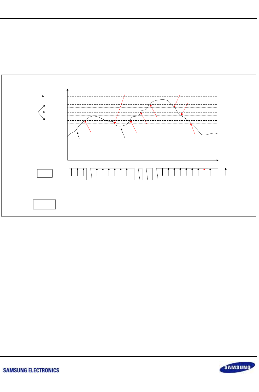
Samsung Confidential
S5P6818_UM 46 Temperature Monitor Unit (TMU)
46-24
Preliminary product information describes products that are in development, for which full characterization data and
associated errata are not yet available. Specifications and information herein are subject to change without notice.
When current temperature exceeds a threshold rise temperature, then the corresponding interrupt
(INTREQ_RISE[2:0]) is generated.
And when current temperature goes below a threshold fall temperature, the corresponding interrupt
(INTREQ_FALL[2:0] is generated.
The illustrative example of the temperature profile and interrupt generation is shown in the picture below.
Figure 46-3 Temperature Profile and Interrupt Generation
Emulation mode can be used to develop software code and debug the operation of TMU. By using emulation
mode, software developer can generate the temperature profile as one needs.
If you want to apply the same time delay as sensing time, i.e. 938 us, then you should set NEXT_TIME field to
0x57F0.
The illustrative example of emulation mode operation is shown in the picture below.
Temperature
Time
INT_RISE0
generated
TH_RISE0
TH_RISE1
TH_RISE2
TH_RISE3
CPU
1.0GHz
operation
Decrease CPU
frequency
INT_RISE0
generated
INT_RISE1
generated
INT_RISE2
generated
MFC,
G3D
operation
begins
Decrease
G3D
frequency
MFC
shutdown
G3D
shutdown
Restart CPU
1.0GHZ, MFC, G3D
operation
OS
ISR
Normal
DVFS tick
TMU SFR When Interrupt occurs : INTCLEAR register write
Thermal
Tripping
Thermal
Throttling
TH_FALL2
TH_FALL1
TH_FALL0
INT_FALL0
generated
INT_FALL2
generated
INT_FALL1
generated
INT_FALL0
generated
nexell / ys.kim at 2015.02.12
SAMSUNG Confidential
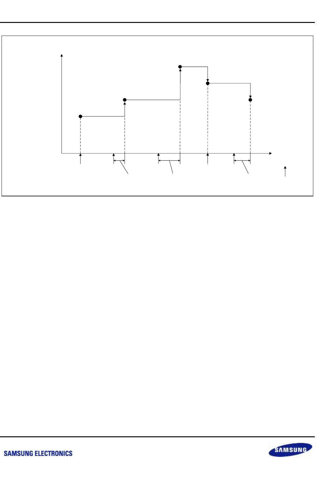
Samsung Confidential
S5P6818_UM 46 Temperature Monitor Unit (TMU)
46-25
Preliminary product information describes products that are in development, for which full characterization data and
associated errata are not yet available. Specifications and information herein are subject to change without notice.
Figure 46-4 Temperature Profile by Using Emulation Mode
When software write new emulated data (NEXT_DATA[15:8]), this data is updated after (NEXT_TIME) X (OSC
period) time delay. Current temperature is kept until new emulated data is written.
Temperature
Time
S/W write
NEXT_DATA
NEXT_TIME
0x50 0x60 0x70
0x0 0x10 0x0
0x60
0x40
0x70
0x80
0x50
0x30
(NEXT_TIME) X
(OSC period)
0x80
0x20
(NEXT_TIME) X
(OSC period)
0x40
0x15
(NEXT_TIME) X
(OSC period)
nexell / ys.kim at 2015.02.12
SAMSUNG Confidential
Samsung Confidential
S5P6818_UM 47 Electrical Characteristics
47-1
Preliminary product information describes products that are in development, for which full characterization data and
associated errata are not yet available. Specifications and information herein are subject to change without notice.
47 Electrical Characteristics
47.1 Absolute Maximum Ratings
Table 47-1 Absolute Maximum Ratings
Parameter
Symbol
Rating
Min.
Max.
Unit
DC Supply Voltage
VDD
1.0 V VDD
–0.5
1.5
V
1.8 V VDD
–0.5
2.5
V
1.5 V VDD
–0.5
3.6
V
3.3 V VDD
–0.5
3.8
V
DC Input Voltage
VIN
1.8 V Input Buffer
–0.5
2.5
V
2.5 V Input Buffer
–0.5
3.6
V
3.3 V Input Buffer
–0.5
3.8
V
DC Output Voltage
VOUT
1.8 V Output Buffer
–0.5
2.5
V
2.5 V Output Buffer
–0.5
3.6
V
3.3 V Output Buffer
–0.5
3.8
V
DC In/Out Current
IINOUT
–
–20
20
mA
Storage Temperature
TSA
–
–50 to 150
C
nexell / ys.kim at 2015.02.12
SAMSUNG Confidential

Samsung Confidential
S5P6818_UM 47 Electrical Characteristics
47-2
Preliminary product information describes products that are in development, for which full characterization data and
associated errata are not yet available. Specifications and information herein are subject to change without notice.
47.2 Recommended Operating Conditions
Table 47-2 Recommended Operating Conditions
Pin Name/Symbol
Description
Min.
Typ.
Max.
Unit
Note
VDDI_ARM
DC supply voltage for Cortex-A53 CPU
0.95
1.0
TBD
V
–
VDDI
DC supply voltage for CORE
0.95
1.0
TBD
V
–
VDDP18
DC supply voltage for 1.8 V Internal IO
1.7
1.8
1.9
V
–
DVDD33_IO
DC supply voltage for 3.3 V IO
3.0
3.3
3.6
V
–
VDDQ
DC supply voltage for DRAM IP (LPDDR2)
1.14
1.2
1.26
V
–
DC supply voltage for DRAM IP (LPDDR3)
1.14
1.2
1.26
V
–
DC supply voltage for DRAM IP
(1.35 V DDR3)
1.283
1.35
1.417
V
–
DC supply voltage for DRAM IP
(1.5 V DDR3)
1.425
1.5
1.575
V
–
VDDI10_ALIVE
DC supply voltage for CORE ALIVE
0.95
1.0
1.05
V
–
VDDP18_ALIVE
DC supply voltage for 1.8 V Internal IO ALIVE
1.7
1.8
1.9
V
–
VDD33_ALIVE
DC supply voltage for 3.3 V ALIVE
3.0
3.3
3.6
V
–
DVDD10_USB0
DC supply voltage for 1.0 V USB OTG
0.95
1.0
1.05
V
–
VDD18_USB0
DC supply voltage for 1.8 V USB OTG
1.7
1.8
1.9
V
–
VDD33_USB0
DC supply voltage for 3.3 V USB OTG
3.0
3.3
3.6
V
–
DVDD10_USBHOST0
DC supply voltage for 1.0 V USB HOST
0.95
1.0
1.05
V
–
VDD18_USBHOST
DC supply voltage for 1.8 V USB HOST
1.7
1.8
1.9
V
–
VDD33_USBHOST
DC supply voltage for 3.3 V USB HOST
3.0
3.3
3.6
V
–
DVDD12_HSIC
DC supply voltage for 1.2 V USB HSIC HOST
1.15
1.2
1.25
V
(NOTE)
VDD18_RTC
DC supply voltage for 1.8 V RTC Crystal
1.7
1.8
1.9
V
–
VDD18_OSC
DC supply voltage for 1.8 V PLL Crystal
1.7
1.8
1.9
V
–
AVDD10_LV
DC supply voltage for 1.0 V LVDS
0.95
1.0
1.05
V
(NOTE)
AVDD18_LV
DC supply voltage for 1.8 V LVDS
1.71
1.8
1.89
V
(NOTE)
AVDD10_HM
DC supply voltage for 1.0 V HDMI
0.95
1.0
1.05
V
(NOTE)
VDD10_HM_PLL
DC supply voltage for 1.0 V HDMI PLL
0.95
1.0
1.05
V
(NOTE)
VDD18_HM
DC supply voltage for 1.8 V HDMI
1.71
1.8
1.89
V
(NOTE)
M_VDD10
DC supply voltage for 1.0 V MIPI (DSI/CSI)
0.95
1.0
1.05
V
(NOTE)
M_VDD10_PLL
DC supply voltage for 1.0 V MIPI (DSI/CSI) PLL
0.95
1.0
1.05
V
(NOTE)
M_VDD18
DC supply voltage for 1.8 V MIPI (DSI/CSI)
1.7
1.8
1.9
V
(NOTE)
AVDD18_ADC
DC supply voltage for 1.8 V ADC
1.7
1.8
1.9
V
–
ADCREF
Reference 1.8 V for ADC
1.7
1.8
1.9
V
–
AVDD18_PLL
DC supply voltage for 1.8 V PLL
1.7
1.8
1.9
V
–
DVDD_VID0
DC supply voltage for 2.8 V VID0
1.7
2.8
3.6
V
–
DVDD_VID2_SD2
DC supply voltage for 2.8 V VID2/SD2
1.7
2.8
3.6
V
–
nexell / ys.kim at 2015.02.12
SAMSUNG Confidential
Samsung Confidential
S5P6818_UM 47 Electrical Characteristics
47-3
Preliminary product information describes products that are in development, for which full characterization data and
associated errata are not yet available. Specifications and information herein are subject to change without notice.
Pin Name/Symbol
Description
Min.
Typ.
Max.
Unit
Note
DVDD_GMAC
DC supply voltage for 2.8 V Ethernet MAC
1.7
2.8
3.6
V
(NOTE)
Temperature
Operating Ambient Temperature
–25 to 85
C
–
Operating Die Temperature
–25 to 85
C
–
NOTE: This power pin can be tied to GND when this function is not used
nexell / ys.kim at 2015.02.12
SAMSUNG Confidential
Samsung Confidential
S5P6818_UM 47 Electrical Characteristics
47-4
Preliminary product information describes products that are in development, for which full characterization data and
associated errata are not yet available. Specifications and information herein are subject to change without notice.
47.3 D.C. Electrical Characteristics
Table 47-3 D.C. Electrical Characteristics (3.3 V TOL)
(VDD = 1.65 V to 3.60 V, Vext = 3.0 to 3.6 V, Tj = –40 to 125 C)
Parameter
Condition
Min.
Typ.
Max.
Unit
VTOL
Tolerant external
voltage (NOTE)
VDD Power Off& On
3.6
V
VIH
High Level Input Voltage
CMOS Interface
0.7VDD
VDD+0.3
V
VIL
Low Level Input Voltage
CMOS Interface
VDD = 2.5 V 10 %, 3.3 V 10 %
–0.3
0.7
V
VDD = 1.8 V 10 %
–0.3
0.3VDD
V
Hysteresis Voltage
0.15
V
IIH
High Level Input Current
Input Buffer
Vin = VDD
VDD Power ON
–3
3
uA
VDD Power Off & SNS = 0
–5
5
uA
Input Buffer with pull-
down
Vin = VDD
VDD = 3.3 V 10 %
15
40
80
uA
VDD = 2.5 V 10 %
15
40
80
uA
VDD = 1.8 V 10 %
15
40
80
uA
IIL
Low Level Input Current
Input Buffer
Vin = VSS
VDD Power ON & Off
–3
3
uA
Input Buffer with pull-
down
Vin = VSS
VDD = 3.3 V 10 %
–15
–40
–110
uA
VDD = 2.5 V 10 %
–15
–40
–110
uA
VDD = 1.8 V 10 %
–15
–40
–110
uA
VOH
Output High Voltage
Ioh = –1.8 mA, –3.6 mA, –7.2 mA, –10.8 mA
0.8VDD
VDD
V
VOL
Output Low Voltage
Ioh = –1.8 mA, –3.6 mA, –7.2 mA, –10.8 mA
0
0.2VDD
V
IOZ
Output Hi-z Current
–5
5
uA
CIN
Input Capacitance
Any input and Bi-directional buffers
5
pF
COUT
Output capacitance
Any output buffer
5
pF
NOTE: Specification is only available on tolerant cells
nexell / ys.kim at 2015.02.12
SAMSUNG Confidential
