SMA1301_GUI_User_Manual_Rev0.0.2x SMA1301 GUI User Manual Rev0.0.2
User Manual:
Open the PDF directly: View PDF ![]() .
.
Page Count: 19
© 2017 Silicon Mitus, Inc. www.siliconmitus.com
December 2017 –Rev0.0.2 1 / 19
GUI User Manual
Revision 0.0.2
*Technology by
GUI User Manual
www.siliconmitus.com © 2017 Silicon Mitus, Inc.
2 / 19 December 2017 – Rev0.0.2
1. Purpose
Graphic User Interface (GUI) is a software program that verifies and tests the function of the Silicon Mitus product. This
document is based on SMA1301 GUI.
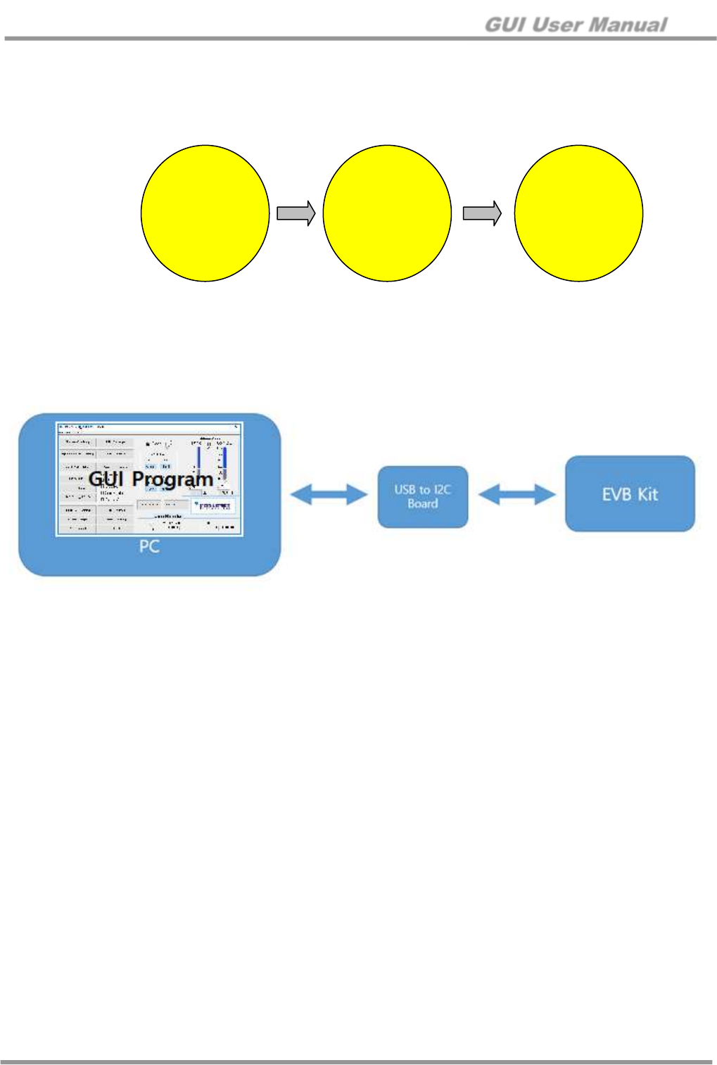
SMA1301.exe
Run
USB to I2C
board
Connection
Control register
data &
Read/Write with
device
Figure 1. Active Flow
The Silicon Mitus evaluation system has an I2C port, so the user can control the action via the GUI program. The diagram
below describes the connection for the Silicon Mitus evaluation system using the GUI Program with test equipment, USB to
I2C Board, PC, USB cable and Silicon Mitus Evaluation Board (EVB) Kit.
Figure 2. Connection Diagram
GUI User Manual
© 2017 Silicon Mitus, Inc. www.siliconmitus.com
December 2017 – Rev0.0.2 3 / 19
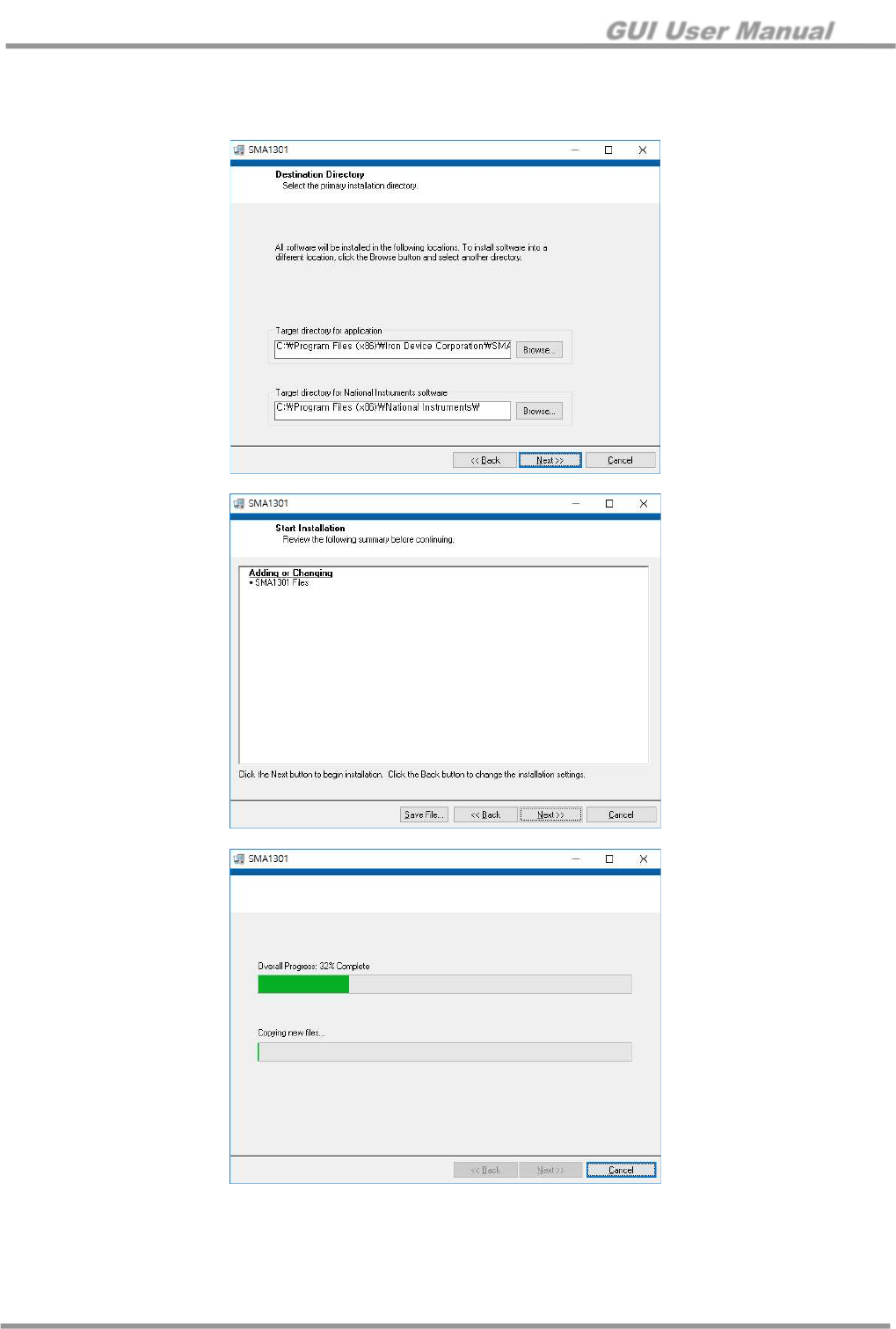
2. Installation
Unzip SMA1301_Control_Panel.zip to a local PC. To install the program, run “Setup.exe” file.
GUI User Manual
www.siliconmitus.com © 2017 Silicon Mitus, Inc.
4 / 19 December 2017 – Rev0.0.2
Installation Path
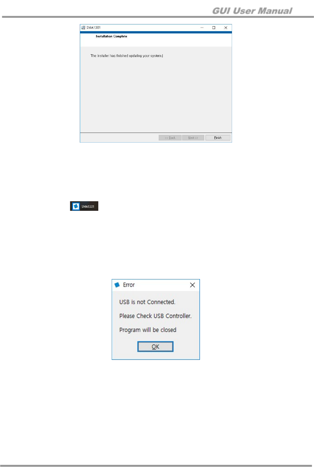
1. Windows Start → Click “ “ SMA1301
2. C:\Program Files (x86)\Iron Device Corporation\SMA1301 folder. Run with SMA1301.exe
3. Device Configuration
Connect ‘USB to I2C Board’ to the ‘Evaluation Board Kit.’
1. Run SMA1301 GUI Program
2. If the USB to I2C Board is not connected normally, an error message pop-up window will appear.
Figure 3. Error Message Pop-up
GUI User Manual
© 2017 Silicon Mitus, Inc. www.siliconmitus.com
December 2017 – Rev0.0.2 5 / 19
4. Board Manual
4.1 Introduction
The SMA1301 Evaluation (EV) Board is a demonstration and evaluation board that shows the capabilities and features
of the SMA1301 chipset designed by Silicon Mitus (Iron Device). This board has an I2S interface for digital input and
differential analog output with a 2.54 mm pitch header. This board can operate the Class-D amplifier with an integrated
boost converter. The boost converter converts output voltage into the digital amplifier to produce stable large sound
pressure levels. It has a typical output voltage of 5.5 V to 6.1 V and class-G control by digital feed-forward processing.
4.2 Board Package Content
The SMA1301 EV Board package includes the following:
1. SMA1301 EV Board
2. USB to I2C Control Board
3. Cable set to connect the board in lab conditions
4. Control S/W (Released by e-mail. Please contact Silicon Mitus separately.)
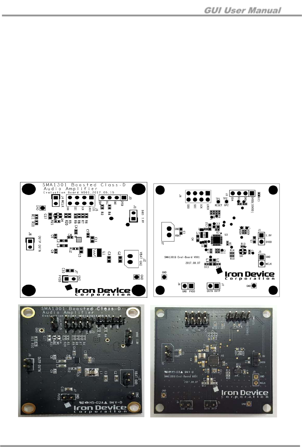
4.3 EV Board Overview
Figure 4. SMA1301 EV Board Placement (left: WLCSP / right: QFN)
Figure 5. SMA1301 EV Board (left: WLCSP / right: QFN)
GUI User Manual
www.siliconmitus.com © 2017 Silicon Mitus, Inc.
6 / 19 December 2017 – Rev0.0.2
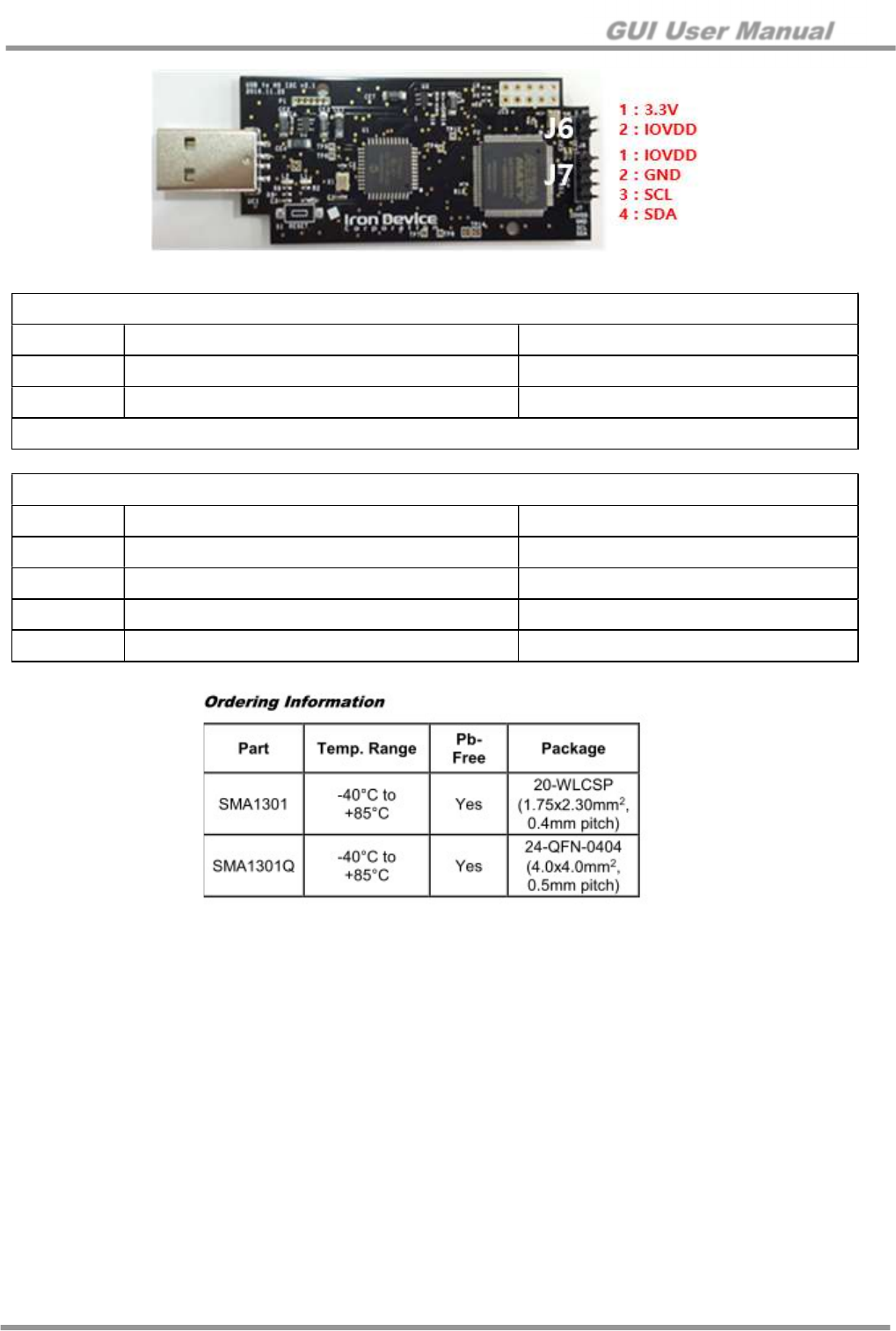
Figure 6. USB to High Speed I2C Control Board
Figure 7. SMA1301 Ordering Information
Type: 2.54 mm Pitch Pin Header for J6
Pin Description Value
1 3.3 V LDO Output +3.3 V
2 IOVDD IOVDD
Do not connect Pin 1 and Pin 2 for SMA1301 (IO voltage should be +1.8 V)
Type: 2.54 mm Pitch Pin Deader for J7
Pin Description Value
1 IOVDD IOVDD (+1.8 V from EV board)
2 GND GND
3 SCL 0 V to +1.8 V
4 SDA 0 V to +1.8 V
GUI User Manual
© 2017 Silicon Mitus, Inc. www.siliconmitus.com
December 2017 – Rev0.0.2 7 / 19
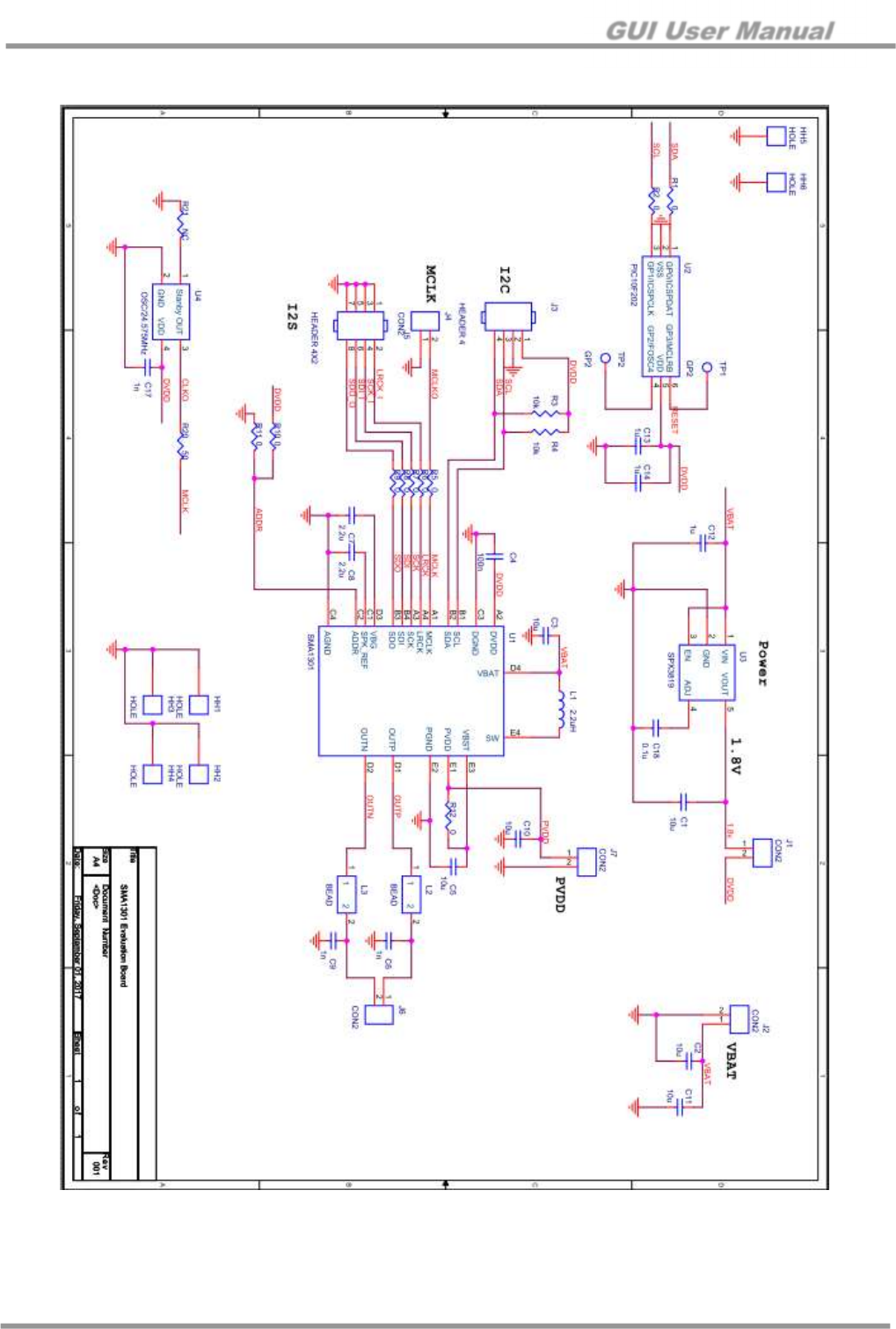
4.4 Board Schematic
Figure 8. SMA1301 EV Board Schematic (WLCSP)
GUI User Manual
www.siliconmitus.com © 2017 Silicon Mitus, Inc.
8 / 19 December 2017 – Rev0.0.2
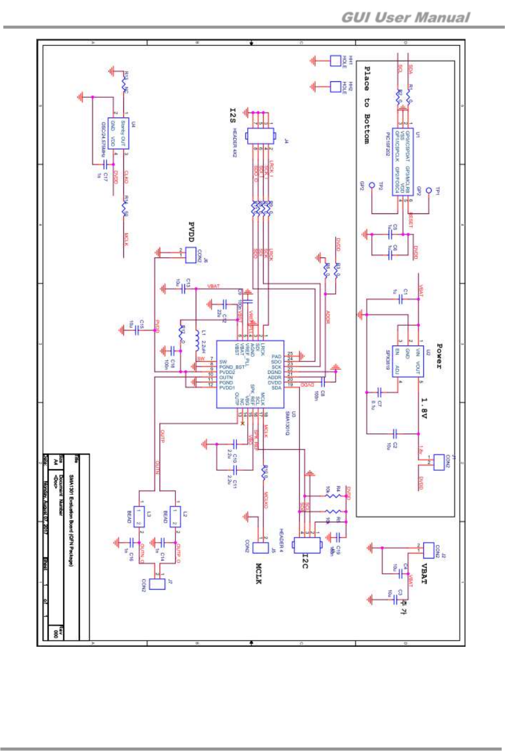
Figure 9. SMA1301 EV Board Schematic (QFN)
GUI User Manual
© 2017 Silicon Mitus, Inc. www.siliconmitus.com
December 2017 – Rev0.0.2 9 / 19
4.5 Connectors
J1: DVDD / 1.8 V
J2: VBAT
J3: I2C Control Pin
J5 (WLCSP) / J4 (QFN): I2S Input Port
J6 (WLCSP) / J7 (QFN): Output
J4 (WLCSP) / J5 (QFN) : External Clock Input
Type: 2.54 mm Pitch Pin Header
Pin Description Value
1 1.8 V +1.8 V (LDO on board)
2 DVDD +1.8 V (external power supply)
Pin 1 and Pin 2 should be connected when using LDO on board for DVDD.
Type: 2.54 mm Pitch Pin Header
Pin Description Value
1 VBAT (battery voltage) Typical +3.6 V / Maximum +4.2 V
2 GND GND
Type: 2.54 mm Pitch Pin Header
Pin Description Value
1 DVDD DVDD (+1.8 V)
2 GND GND
3 SCL 0V to +1.8 V
4 SDA 0V to +1.8 V
Type: 2.54 mm Pitch Pin Header
Pin Description Value
1, 3, 5, 7 GND GND
2 LRCK 0V to +1.8 V
4 SCK 0V to +1.8 V
6 SDI (input data from source) 0V to +1.8 V
8 SDO (output data from chipset) 0V to +1.8 V
Type: 2.54 mm Pitch Pin Header
Pin Description Value
1 SPK Output P Max +6.1 V
2 SPK Output N Max +6.1 V
Type: 2.54 mm Pitch Pin Header
Pin Description Value
1 GND GND
2 MCLKO External Clock
GUI User Manual
www.siliconmitus.com © 2017 Silicon Mitus, Inc.
10 / 19 December 2017 – Rev0.0.2
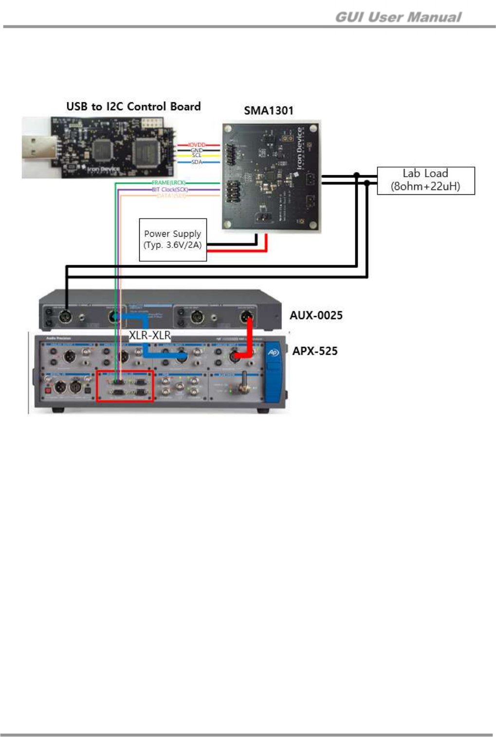
4.6 Measurement Set Up (APX525)
This set up is for the evaluation of SMA1301. Reference equipment is APX-525 from Audio Precision.
4.6.1 Connection
Figure 10. Measurement Connection (I2S input)
GUI User Manual
© 2017 Silicon Mitus, Inc. www.siliconmitus.com
December 2017 – Rev0.0.2 11 / 19
5. Detail Controls
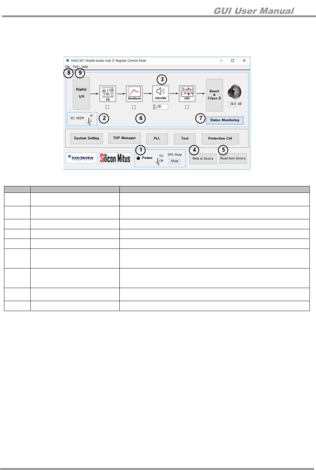
5.1 Control Panel Overview (Main Panel)
Figure 11. SMA1301 Mobile Audio Hub IC Register Control Panel
No. Item Description
①
Power On/Off with Sequence Power On: Power-up Speaker Output On De-mute
Power Off: Mute Speaker Output Off Power Off
②
I2C ADDR High: I2C Slave Address with 0x3E
Low: I2C Slave Address with 0x1E
③
Volume Control Master Volume Control
④
Write to Device Read Set Value from Panels and Write to DUT
⑤
Read from Device R Read I2C from DUT and Set Panel
⑥
DSP On/Off
EQ: On/Off
BassBoost: On/Off
DRC: On/Off
⑦
Status Monitoring
Open Status Monitoring Panel
Reads status register and updates display every 0.2 seconds
Stops monitoring when clicked again
⑧
Menu Bar – File Load Register: Register Load from .dat file
Save Register: Register Save to .dat file and datx file
⑨
Menu Bar – Tool Direct Register Control Panel – Open Direct Register Control Panel
GUI User Manual
www.siliconmitus.com © 2017 Silicon Mitus, Inc.
12 / 19 December 2017 – Rev0.0.2
5.2 Digital I/O
Figure 12. Digital IO Control Panel
No. Item Description
①
Input1 CTRL 1 I2S Input Format Settings
②
Input1 CTRL 2 PCM Input Format Settings
③
Input1 CTRL 3,4 PCM Slot Settings
④
SRC Bypass Sample Rate Converter turns off when checked
⑤
Port Config. Port Configuration
Use only “OUT: Port3, IN: Port 1-DAC”
⑥
Port Output Format SDO Signal Format
⑦
Port Select
Select signal to output only when in master mode (see TOP Manager Panel)
Format Convert Input
Mixer Output (48 KHz)
SPK Path after DSP (48 KHz)
⑧
Input Gain Digital Input Gain
GUI User Manual
© 2017 Silicon Mitus, Inc. www.siliconmitus.com
December 2017 – Rev0.0.2 13 / 19
5.3 EQ
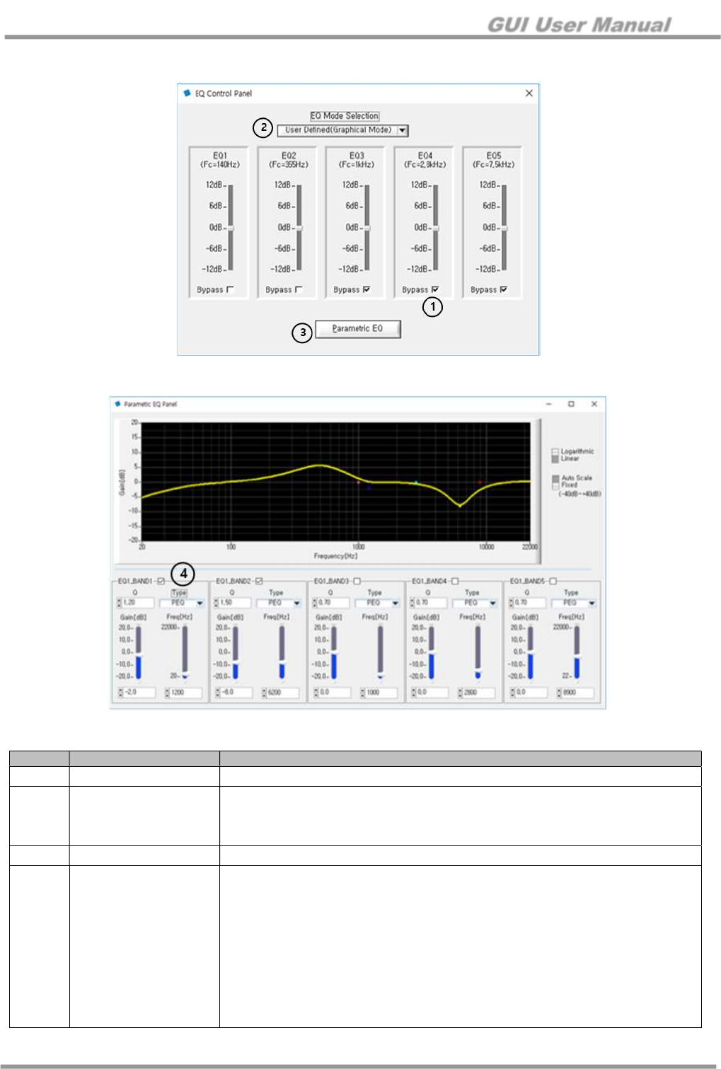
Figure 13. EQ Control Panel
Figure 14. Parametric EQ Panel
No. Item Description
①
EQ EQ is bypassed if checked
②
EQ Filters
User Defined
User can change/tune filter
Pre-defined
Classic / Rock & Pop / Jazz / R&B / Dance / Speech
③
Parametric EQ Graphical display that user can tune
④
EQ Band
Q Factor
Biquad Filter Type
PEQ
Butter Worth HPF
Butter Worth LPF
Gain
(-20 dB to +20 dB)
Frequency
20 Hz to 20 KHz
Check Box
Checked: On
GUI User Manual
www.siliconmitus.com © 2017 Silicon Mitus, Inc.
14 / 19 December 2017 – Rev0.0.2
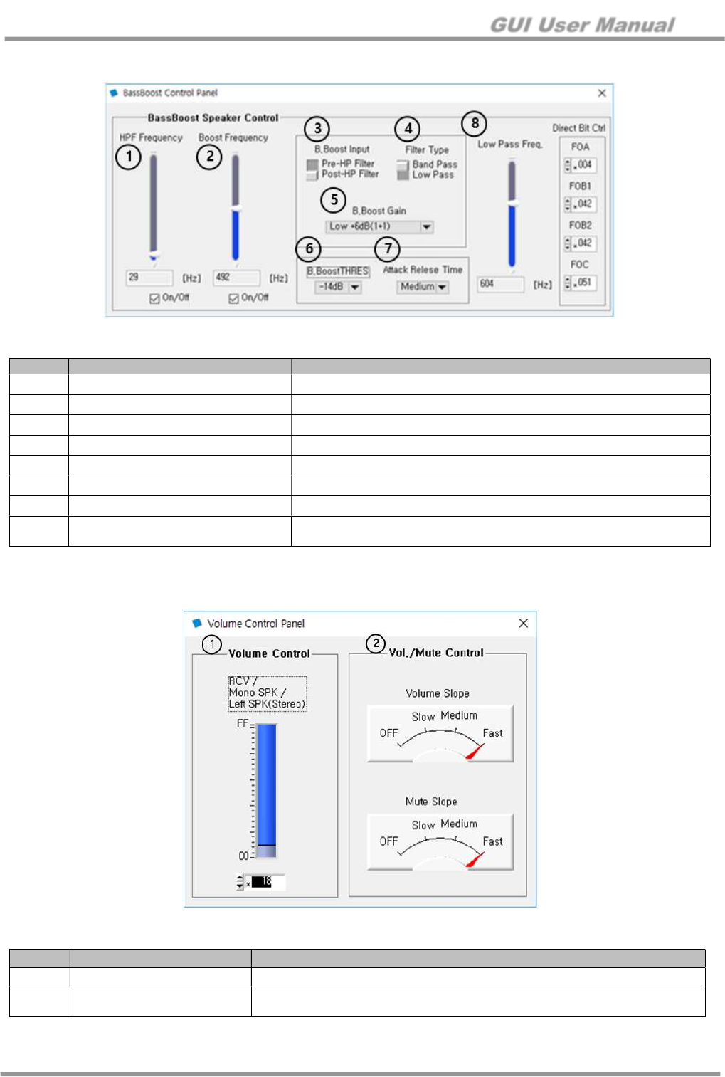
5.4 BassBoost
Figure 15. BassBoost Control Panel
No. Item Description
①
HPF Frequency 1st Order High Pass Filter Frequency Setting. “0” is off
②
Boost Frequency Boost Frequency Setting: 20 Hz to 1 KHz
③
B.Boost input Select input of Bass Boost Block (Pre or Post HPF)
④
Filter Type Band Pass Filter or Low Pass Filter Type
⑤
B.Boost Gain Bass Boost Gain Setting
⑥
B.BoostTHRES (Boost Trigger) Set the starting limit of Bass Boost
⑦
Attack Release Time (Boost Trigger)
Set the attack/release time limit of Bass Boost
⑧
Low Pass Frequency
(Boost Trigger)
Low pass filter of the signal that controls the attack release function
Should be set above boost frequency
5.5 Volume
Figure 16. Volume Control Panel
No. Item Description
①
Volume Control Master Volume for RCV/Mono SPK/Left SPK for Stereo
②
Vol./Mute Control Volume and Mute Slope Control
Fade In / Fade Out Effect
GUI User Manual
© 2017 Silicon Mitus, Inc. www.siliconmitus.com
December 2017 – Rev0.0.2 15 / 19
5.6 Boost & Class D
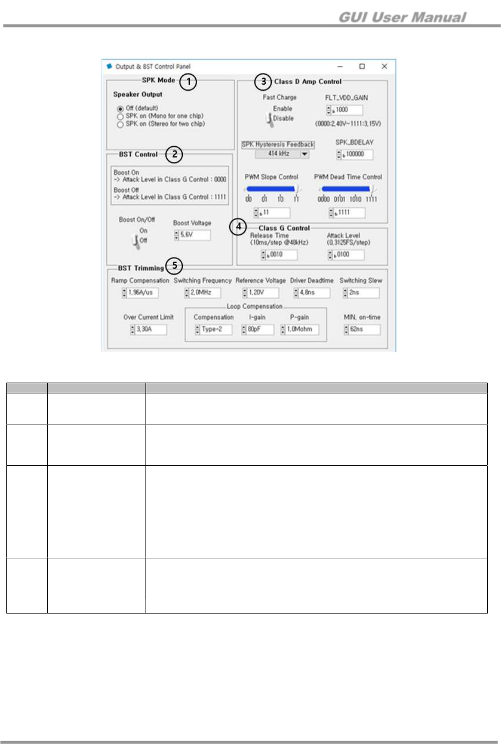
Figure 17. Output & BST Control Panel
No. Item Description
①
SPK mode
Off (default)
SPK On (mono for one chip)
SPK On (stereo for two chips)
②
BST Control
Boost On/Off
On: Set to attack level with b’0000
Off: Set to attach level with b’1111
Boost Voltage: +5.5 V to +6.1 V
③
Class D Amp Control
Fast Charge
Enable / Disable
FLT_VDD_GAIN
b’0000: 2.40 V to b’1111: 3.115 V
SPK Hysteresis Feedback
PWM Frequency of Speaker Output
SPK_BDELAY / PWM Slope Control / PWM Dead Time Control
Do not control this value.
This value should be provided by and used accordingly to Silicon Mitus
④
Class G Control
Release Time
Attack Level
On: b’0000
Off: b’1111
⑤
BST Trimming Do not edit. Please use recommended values.
GUI User Manual
www.siliconmitus.com © 2017 Silicon Mitus, Inc.
16 / 19 December 2017 – Rev0.0.2
5.7 System Setting
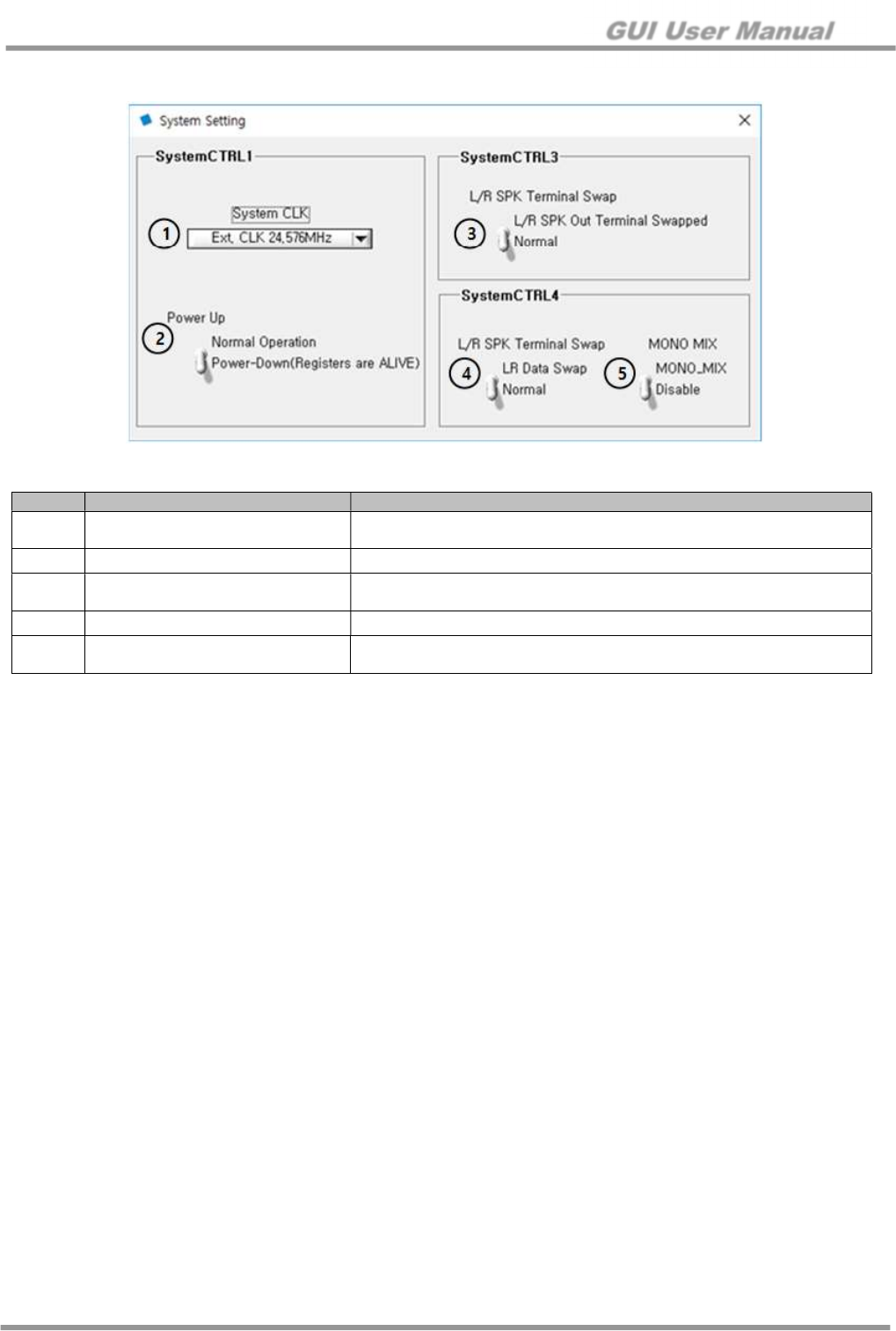
Figure 18. System Setting
No. Item Description
①
System CLK Ext. CLK 19.2 MHz
Ext. CLK 24.576 MHz
②
Power Up Analog Block Power On
③
L/R SPK Terminal Swap Normal
LR SPK Out Terminal Swapped
④
L/R Data Swap Data Swap for Left and Right Channels
⑤
Mono Mix Disable
Mono Mixing
GUI User Manual
© 2017 Silicon Mitus, Inc. www.siliconmitus.com
December 2017 – Rev0.0.2 17 / 19
5.8 TOP Manager
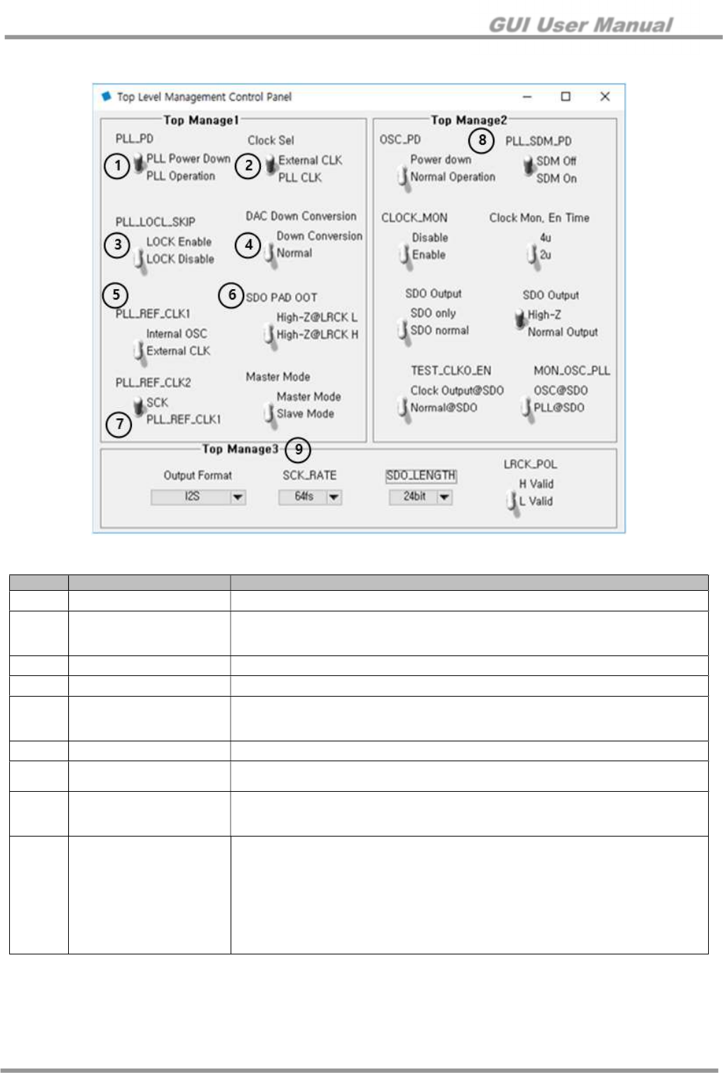
Figure 19. Top Level Management Control Panel
No. Item Description
①
PLL_PD PLL On/Off
②
Clock Sel
System Clock Selection
External CLK
PLL CLK
③
PLL_LOCK_SKIP PLL_LOCK_SKIP: Enable / Disable
④
DAC Down Conversion Down Conversion or Normal
⑤
PLL_REF_CLK1
PLL Input Source
Internal OSC
External CLK
⑥
SDO PAD OOT High-Z@LRCK L or High-Z@LRCL H
⑦
PLL_REF_CLK2 SCK from External
PLLREF_CLK1
⑧
Top Manage2
There are 2ch(port)s at DAC input internally
ADC: ADC output connect to CH2
Input Port “L”: DAC Only Mode (ADC output is not connected)
⑨
Top Manage3
Output Format for I2S
LJ / RJ / I2S / SPI / PCM Short / PCM Long
SCK_RATE
64 fs or 32 fs
SDO_LENGTH
24-bit / 20-bit / 16-bit
LRCK_POL
H Valid or L Valid
GUI User Manual
www.siliconmitus.com © 2017 Silicon Mitus, Inc.
18 / 19 December 2017 – Rev0.0.2
5.9 Protection Control
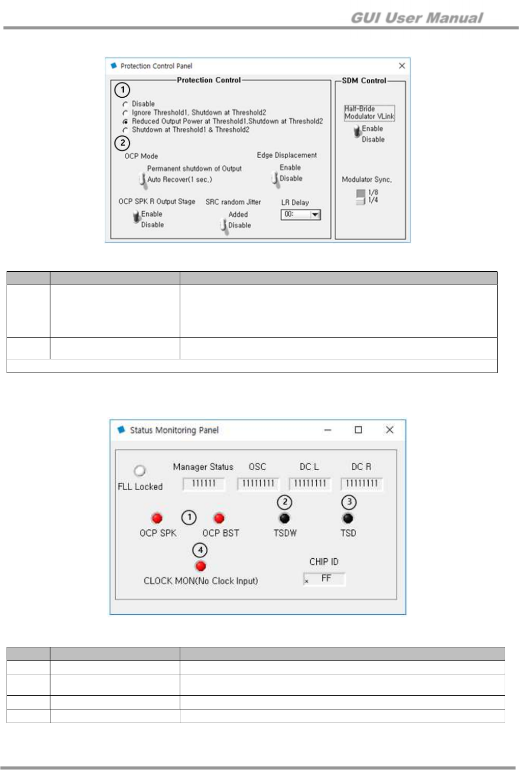
Figure 20. Protection Control Panel
5.10 Status Monitoring
Figure 21. Status Monitoring Panel
No. Item Description
①
Thermal Protection Option
Disable
Ignore Threshold1 (TSDW), Shutdown at Threshold2 (TSD)
Reduced 6 dB Output at Threshold1 (TSDW), Shutdown at Threshold2
(TSD)
Shutdown at Threshold1 (TSDW) and Threshold2 (TSD)
②
OCP Mode Permanent Shutdown of Output
Auto Recover (1 sec)
Other controls are not used
No. Item Description
①
OCP SPK or OCP BST Over Current Protection at Output SPK or BST
②
TSDW Thermal Shutdown Warning Protection (Threshold1)
Output level is reduced by -6 dB (default option)
③
TSD Thermal Shutdown Protection (Threshold2)
④
CLOCK MON Clock Fault Monitoring

GUI User Manual
© 2017 Silicon Mitus, Inc. www.siliconmitus.com
December 2017 – Rev0.0.2 19 / 19
Revision History
Rev
DATE
CHANGES
Issued by
Notes
0.0
.0
09/05
/201
7
Initial
Release
Review with Richard and SM
Brian
Pyun
0.0.1
09/11/20
1
7
Update
d
T
ypo
and Figure10
Brian Pyun
0.0.2
10/20/2017
Reviewed with Esther
Brian Pyun
─────────────────────────────────────────────────────────────────────────────
Silicon Mitus cannot assume any responsibility for the consequence of use of information furnished nor for any infringement of patents or
other rights of third parties which may result from its use. No circuit patent licenses are implied. Silicon Mitus reserves the right to change the
circuitry and specifications without notice at any time. This publication supersedes and replaces all information previously supplied. Silicon
Mitus products are not authorized for use as critical components in life support devices or systems without the express written approval of
Silicon Mitus.
© 2017 Silicon Mitus, Inc. - Printed in Korea - All Rights Reserved
