STM32F413/423 Advanced Arm® Based 32 Bit MCUs Reference Manual STM32F4xxxx
User Manual:
Open the PDF directly: View PDF ![]() .
.
Page Count: 1324 [warning: Documents this large are best viewed by clicking the View PDF Link!]
- 1 Documentation conventions
- 2 System and memory overview
- 3 Embedded Flash memory interface
- 3.1 Introduction
- 3.2 Main features
- 3.3 Embedded Flash memory
- 3.4 Read interface
- 3.5 Erase and program operations
- 3.6 Option bytes
- 3.7 One-time programmable bytes
- 3.8 Flash interface registers
- 4 CRC calculation unit
- 5 Power controller (PWR)
- 5.1 Power supplies
- 5.2 Power supply supervisor
- 5.3 Low-power modes
- 5.4 Power control registers
- 5.5 PWR register map
- 6 Reset and clock control (RCC) for STM32F413/423
- 6.1 Reset
- 6.2 Clocks
- 6.3 RCC registers
- 6.3.1 RCC clock control register (RCC_CR)
- 6.3.2 RCC PLL configuration register (RCC_PLLCFGR)
- 6.3.3 RCC clock configuration register (RCC_CFGR)
- 6.3.4 RCC clock interrupt register (RCC_CIR)
- 6.3.5 RCC AHB1 peripheral reset register (RCC_AHB1RSTR)
- 6.3.6 RCC AHB2 peripheral reset register (RCC_AHB2RSTR) for STM32F413xx
- 6.3.7 RCC AHB2 peripheral reset register (RCC_AHB2RSTR) for STM32F423xx
- 6.3.8 RCC AHB3 peripheral reset register (RCC_AHB3RSTR)
- 6.3.9 RCC APB1 peripheral reset register for (RCC_APB1RSTR)
- 6.3.10 RCC APB2 peripheral reset register (RCC_APB2RSTR)
- 6.3.11 RCC AHB1 peripheral clock enable register (RCC_AHB1ENR)
- 6.3.12 RCC AHB2 peripheral clock enable register (RCC_AHB2ENR) for STM32F413xx
- 6.3.13 RCC AHB2 peripheral clock enable register (RCC_AHB2ENR) for STM32F423xx
- 6.3.14 RCC AHB3 peripheral clock enable register (RCC_AHB3ENR)
- 6.3.15 RCC APB1 peripheral clock enable register (RCC_APB1ENR)
- 6.3.16 RCC APB2 peripheral clock enable register (RCC_APB2ENR)
- 6.3.17 RCC AHB1 peripheral clock enable in low power mode register (RCC_AHB1LPENR)
- 6.3.18 RCC AHB2 peripheral clock enable in low power mode register (RCC_AHB2LPENR) for STM32F413xx
- 6.3.19 RCC AHB2 peripheral clock enable in low power mode register (RCC_AHB2LPENR) for STM32F423xx
- 6.3.20 RCC AHB3 peripheral clock enable in low power mode register (RCC_AHB3LPENR)
- 6.3.21 RCC APB1 peripheral clock enable in low power mode register (RCC_APB1LPENR)
- 6.3.22 RCC APB2 peripheral clock enabled in low power mode register (RCC_APB2LPENR)
- 6.3.23 RCC Backup domain control register (RCC_BDCR)
- 6.3.24 RCC clock control & status register (RCC_CSR)
- 6.3.25 RCC spread spectrum clock generation register (RCC_SSCGR)
- 6.3.26 RCC PLLI2S configuration register (RCC_PLLI2SCFGR)
- 6.3.27 RCC Dedicated Clocks Configuration Register (RCC_DCKCFGR)
- 6.3.28 RCC clocks gated enable register (CKGATENR)
- 6.3.29 RCC Dedicated Clocks Configuration Register (RCC_DCKCFGR2)
- 6.3.30 RCC register map
- 7 General-purpose I/Os (GPIO)
- 7.1 GPIO introduction
- 7.2 GPIO main features
- 7.3 GPIO functional description
- Figure 17. Basic structure of a five-volt tolerant I/O port bit
- Table 25. Port bit configuration table
- 7.3.1 General-purpose I/O (GPIO)
- 7.3.2 I/O pin multiplexer and mapping
- 7.3.3 I/O port control registers
- 7.3.4 I/O port data registers
- 7.3.5 I/O data bitwise handling
- 7.3.6 GPIO locking mechanism
- 7.3.7 I/O alternate function input/output
- 7.3.8 External interrupt/wakeup lines
- 7.3.9 Input configuration
- 7.3.10 Output configuration
- 7.3.11 Alternate function configuration
- 7.3.12 Analog configuration
- 7.3.13 Using the OSC32_IN/OSC32_OUT pins as GPIO PC14/PC15 port pins
- 7.3.14 Using the OSC_IN/OSC_OUT pins as GPIO PH0/PH1 port pins
- 7.3.15 Selection of RTC additional functions
- 7.4 GPIO registers
- 7.4.1 GPIO port mode register (GPIOx_MODER) (x = A...H)
- 7.4.2 GPIO port output type register (GPIOx_OTYPER) (x = A...H)
- 7.4.3 GPIO port output speed register (GPIOx_OSPEEDR) (x = A...H)
- 7.4.4 GPIO port pull-up/pull-down register (GPIOx_PUPDR) (x = A...H)
- 7.4.5 GPIO port input data register (GPIOx_IDR) (x = A...H)
- 7.4.6 GPIO port output data register (GPIOx_ODR) (x = A...H)
- 7.4.7 GPIO port bit set/reset register (GPIOx_BSRR) (x = A...H)
- 7.4.8 GPIO port configuration lock register (GPIOx_LCKR) (x = A...H)
- 7.4.9 GPIO alternate function low register (GPIOx_AFRL) (x = A...H)
- 7.4.10 GPIO alternate function high register (GPIOx_AFRH) (x = A...H)
- 7.4.11 GPIO register map
- 8 System configuration controller (SYSCFG)
- 8.1 I/O compensation cell
- 8.2 SYSCFG registers
- 8.2.1 SYSCFG memory remap register (SYSCFG_MEMRMP)
- 8.2.2 SYSCFG peripheral mode configuration register (SYSCFG_PMC)
- 8.2.3 SYSCFG external interrupt configuration register 1 (SYSCFG_EXTICR1)
- 8.2.4 SYSCFG external interrupt configuration register 2 (SYSCFG_EXTICR2)
- 8.2.5 SYSCFG external interrupt configuration register 3 (SYSCFG_EXTICR3)
- 8.2.6 SYSCFG external interrupt configuration register 4 (SYSCFG_EXTICR4)
- 8.2.7 SYSCFG configuration register 2 (SYSCFG_CFGR2)
- 8.2.8 Compensation cell control register (SYSCFG_CMPCR)
- 8.2.9 SYSCFG configuration register (SYSCFG_CFGR)
- 8.2.10 DFSDM Multi-channel delay control register (SYSCFG_MCHDLYCR)
- 8.2.11 SYSCFG register map
- 9 Direct memory access controller (DMA)
- 9.1 DMA introduction
- 9.2 DMA main features
- 9.3 DMA functional description
- 9.3.1 DMA block diagram
- 9.3.2 DMA overview
- 9.3.3 DMA transactions
- 9.3.4 Channel selection
- 9.3.5 Arbiter
- 9.3.6 DMA streams
- 9.3.7 Source, destination and transfer modes
- 9.3.8 Pointer incrementation
- 9.3.9 Circular mode
- 9.3.10 Double-buffer mode
- 9.3.11 Programmable data width, packing/unpacking, endianness
- 9.3.12 Single and burst transfers
- 9.3.13 FIFO
- 9.3.14 DMA transfer completion
- 9.3.15 DMA transfer suspension
- 9.3.16 Flow controller
- 9.3.17 Summary of the possible DMA configurations
- 9.3.18 Stream configuration procedure
- 9.3.19 Error management
- 9.4 DMA interrupts
- 9.5 DMA registers
- 9.5.1 DMA low interrupt status register (DMA_LISR)
- 9.5.2 DMA high interrupt status register (DMA_HISR)
- 9.5.3 DMA low interrupt flag clear register (DMA_LIFCR)
- 9.5.4 DMA high interrupt flag clear register (DMA_HIFCR)
- 9.5.5 DMA stream x configuration register (DMA_SxCR)
- 9.5.6 DMA stream x number of data register (DMA_SxNDTR)
- 9.5.7 DMA stream x peripheral address register (DMA_SxPAR)
- 9.5.8 DMA stream x memory 0 address register (DMA_SxM0AR)
- 9.5.9 DMA stream x memory 1 address register (DMA_SxM1AR)
- 9.5.10 DMA stream x FIFO control register (DMA_SxFCR)
- 9.5.11 DMA register map
- 10 Interrupts and events
- 10.1 Nested vectored interrupt controller (NVIC)
- 10.2 External interrupt/event controller (EXTI)
- 10.3 EXTI registers
- 11 Flexible static memory controller (FSMC)
- 11.1 FSMC main features
- 11.2 FMC block diagram
- 11.3 AHB interface
- 11.4 External device address mapping
- 11.5 NOR Flash/PSRAM controller
- Table 44. Programmable NOR/PSRAM access parameters
- 11.5.1 External memory interface signals
- 11.5.2 Supported memories and transactions
- 11.5.3 General timing rules
- 11.5.4 NOR Flash/PSRAM controller asynchronous transactions
- Figure 33. Mode1 read access waveforms
- Figure 34. Mode1 write access waveforms
- Table 50. FSMC_BCRx bit fields
- Table 51. FSMC_BTRx bit fields
- Figure 35. ModeA read access waveforms
- Figure 36. ModeA write access waveforms
- Table 52. FSMC_BCRx bit fields
- Table 53. FSMC_BTRx bit fields
- Table 54. FSMC_BWTRx bit fields
- Figure 37. Mode2 and mode B read access waveforms
- Figure 38. Mode2 write access waveforms
- Figure 39. ModeB write access waveforms
- Table 55. FSMC_BCRx bit fields
- Table 56. FSMC_BTRx bit fields
- Table 57. FSMC_BWTRx bit fields
- Figure 40. ModeC read access waveforms
- Figure 41. ModeC write access waveforms
- Table 58. FSMC_BCRx bit fields
- Table 59. FSMC_BTRx bit fields
- Table 60. FSMC_BWTRx bit fields
- Figure 42. ModeD read access waveforms
- Figure 43. ModeD write access waveforms
- Table 61. FSMC_BCRx bit fields
- Table 62. FSMC_BTRx bit fields
- Table 63. FSMC_BWTRx bit fields
- Figure 44. Muxed read access waveforms
- Figure 45. Muxed write access waveforms
- Table 64. FSMC_BCRx bit fields
- Table 65. FSMC_BTRx bit fields
- Figure 46. Asynchronous wait during a read access waveforms
- Figure 47. Asynchronous wait during a write access waveforms
- 11.5.5 Synchronous transactions
- Figure 48. Wait configuration waveforms
- Figure 49. Synchronous multiplexed read mode waveforms - NOR, PSRAM (CRAM)
- Table 66. FSMC_BCRx bit fields
- Table 67. FSMC_BTRx bit fields
- Figure 50. Synchronous multiplexed write mode waveforms - PSRAM (CRAM)
- Table 68. FSMC_BCRx bit fields
- Table 69. FSMC_BTRx bit fields
- 11.5.6 NOR/PSRAM controller registers
- 11.6 FSMC register map
- 12 Quad-SPI interface (QUADSPI)
- 12.1 Introduction
- 12.2 QUADSPI main features
- 12.3 QUADSPI functional description
- 12.3.1 QUADSPI block diagram
- 12.3.2 QUADSPI pins
- 12.3.3 QUADSPI command sequence
- 12.3.4 QUADSPI signal interface protocol modes
- 12.3.5 QUADSPI indirect mode
- 12.3.6 QUADSPI status flag polling mode
- 12.3.7 QUADSPI memory-mapped mode
- 12.3.8 QUADSPI Flash memory configuration
- 12.3.9 QUADSPI delayed data sampling
- 12.3.10 QUADSPI configuration
- 12.3.11 QUADSPI usage
- 12.3.12 Sending the instruction only once
- 12.3.13 QUADSPI error management
- 12.3.14 QUADSPI busy bit and abort functionality
- 12.3.15 nCS behavior
- 12.4 QUADSPI interrupts
- 12.5 QUADSPI registers
- 12.5.1 QUADSPI control register (QUADSPI_CR)
- 12.5.2 QUADSPI device configuration register (QUADSPI_DCR)
- 12.5.3 QUADSPI status register (QUADSPI_SR)
- 12.5.4 QUADSPI flag clear register (QUADSPI_FCR)
- 12.5.5 QUADSPI data length register (QUADSPI_DLR)
- 12.5.6 QUADSPI communication configuration register (QUADSPI_CCR)
- 12.5.7 QUADSPI address register (QUADSPI_AR)
- 12.5.8 QUADSPI alternate bytes registers (QUADSPI_ABR)
- 12.5.9 QUADSPI data register (QUADSPI_DR)
- 12.5.10 QUADSPI polling status mask register (QUADSPI _PSMKR)
- 12.5.11 QUADSPI polling status match register (QUADSPI _PSMAR)
- 12.5.12 QUADSPI polling interval register (QUADSPI _PIR)
- 12.5.13 QUADSPI low-power timeout register (QUADSPI_LPTR)
- 12.5.14 QUADSPI register map
- 13 Analog-to-digital converter (ADC)
- 13.1 ADC introduction
- 13.2 ADC main features
- 13.3 ADC functional description
- 13.4 Data alignment
- 13.5 Channel-wise programmable sampling time
- 13.6 Conversion on external trigger and trigger polarity
- 13.7 Fast conversion mode
- 13.8 Data management
- 13.9 Temperature sensor
- 13.10 Battery charge monitoring
- 13.11 ADC interrupts
- 13.12 ADC registers
- 13.12.1 ADC status register (ADC_SR)
- 13.12.2 ADC control register 1 (ADC_CR1)
- 13.12.3 ADC control register 2 (ADC_CR2)
- 13.12.4 ADC sample time register 1 (ADC_SMPR1)
- 13.12.5 ADC sample time register 2 (ADC_SMPR2)
- 13.12.6 ADC injected channel data offset register x (ADC_JOFRx) (x=1..4)
- 13.12.7 ADC watchdog higher threshold register (ADC_HTR)
- 13.12.8 ADC watchdog lower threshold register (ADC_LTR)
- 13.12.9 ADC regular sequence register 1 (ADC_SQR1)
- 13.12.10 ADC regular sequence register 2 (ADC_SQR2)
- 13.12.11 ADC regular sequence register 3 (ADC_SQR3)
- 13.12.12 ADC injected sequence register (ADC_JSQR)
- 13.12.13 ADC injected data register x (ADC_JDRx) (x= 1..4)
- 13.12.14 ADC regular data register (ADC_DR)
- 13.12.15 ADC Common status register (ADC_CSR)
- 13.12.16 ADC common control register (ADC_CCR)
- 13.12.17 ADC register map
- 14 Digital-to-analog converter (DAC)
- 14.1 DAC introduction
- 14.2 DAC main features
- 14.3 DAC functional description
- 14.4 Dual DAC channel conversion
- 14.4.1 Independent trigger without wave generation
- 14.4.2 Independent trigger with single LFSR generation
- 14.4.3 Independent trigger with different LFSR generation
- 14.4.4 Independent trigger with single triangle generation
- 14.4.5 Independent trigger with different triangle generation
- 14.4.6 Simultaneous software start
- 14.4.7 Simultaneous trigger without wave generation
- 14.4.8 Simultaneous trigger with single LFSR generation
- 14.4.9 Simultaneous trigger with different LFSR generation
- 14.4.10 Simultaneous trigger with single triangle generation
- 14.4.11 Simultaneous trigger with different triangle generation
- 14.5 DAC registers
- 14.5.1 DAC control register (DAC_CR)
- 14.5.2 DAC software trigger register (DAC_SWTRIGR)
- 14.5.3 DAC channel1 12-bit right-aligned data holding register (DAC_DHR12R1)
- 14.5.4 DAC channel1 12-bit left aligned data holding register (DAC_DHR12L1)
- 14.5.5 DAC channel1 8-bit right aligned data holding register (DAC_DHR8R1)
- 14.5.6 DAC channel2 12-bit right aligned data holding register (DAC_DHR12R2)
- 14.5.7 DAC channel2 12-bit left aligned data holding register (DAC_DHR12L2)
- 14.5.8 DAC channel2 8-bit right-aligned data holding register (DAC_DHR8R2)
- 14.5.9 Dual DAC 12-bit right-aligned data holding register (DAC_DHR12RD)
- 14.5.10 DUAL DAC 12-bit left aligned data holding register (DAC_DHR12LD)
- 14.5.11 DUAL DAC 8-bit right aligned data holding register (DAC_DHR8RD)
- 14.5.12 DAC channel1 data output register (DAC_DOR1)
- 14.5.13 DAC channel2 data output register (DAC_DOR2)
- 14.5.14 DAC status register (DAC_SR)
- 14.5.15 DAC register map
- 15 Digital filter for sigma delta modulators (DFSDM)
- 15.1 Introduction
- 15.2 DFSDM main features
- 15.3 DFSDM implementation
- 15.4 DFSDM functional description
- 15.4.1 DFSDM block diagram
- 15.4.2 DFSDM pins and internal signals
- 15.4.3 DFSDM reset and clocks
- 15.4.4 Serial channel transceivers
- 15.4.5 Configuring the input serial interface
- 15.4.6 Parallel data inputs
- 15.4.7 Channel selection
- 15.4.8 Digital filter configuration
- 15.4.9 Integrator unit
- 15.4.10 Analog watchdog
- 15.4.11 Short-circuit detector
- 15.4.12 Extreme detector
- 15.4.13 Data unit block
- 15.4.14 Signed data format
- 15.4.15 Launching conversions
- 15.4.16 Continuous and fast continuous modes
- 15.4.17 Request precedence
- 15.4.18 Power optimization in run mode
- 15.5 DFSDM interrupts
- 15.6 DFSDM DMA transfer
- 15.7 DFSDM channel y registers (y=0..7)
- 15.7.1 DFSDM channel y configuration register (DFSDM_CHyCFGR1)
- 15.7.2 DFSDM channel y configuration register (DFSDM_CHyCFGR2)
- 15.7.3 DFSDM channel y analog watchdog and short-circuit detector register (DFSDM_CHyAWSCDR)
- 15.7.4 DFSDM channel y watchdog filter data register (DFSDM_CHyWDATR)
- 15.7.5 DFSDM channel y data input register (DFSDM_CHyDATINR)
- 15.8 DFSDM filter x module registers (x=0..3)
- 15.8.1 DFSDM filter x control register 1 (DFSDM_FLTxCR1)
- 15.8.2 DFSDM filter x control register 2 (DFSDM_FLTxCR2)
- 15.8.3 DFSDM filter x interrupt and status register (DFSDM_FLTxISR)
- 15.8.4 DFSDM filter x interrupt flag clear register (DFSDM_FLTxICR)
- 15.8.5 DFSDM filter x injected channel group selection register (DFSDM_FLTxJCHGR)
- 15.8.6 DFSDM filter x control register (DFSDM_FLTxFCR)
- 15.8.7 DFSDM filter x data register for injected group (DFSDM_FLTxJDATAR)
- 15.8.8 DFSDM filter x data register for the regular channel (DFSDM_FLTxRDATAR)
- 15.8.9 DFSDM filter x analog watchdog high threshold register (DFSDM_FLTxAWHTR)
- 15.8.10 DFSDM filter x analog watchdog low threshold register (DFSDM_FLTxAWLTR)
- 15.8.11 DFSDM filter x analog watchdog status register (DFSDM_FLTxAWSR)
- 15.8.12 DFSDM filter x analog watchdog clear flag register (DFSDM_FLTxAWCFR)
- 15.8.13 DFSDM filter x extremes detector maximum register (DFSDM_FLTxEXMAX)
- 15.8.14 DFSDM filter x extremes detector minimum register (DFSDM_FLTxEXMIN)
- 15.8.15 DFSDM filter x conversion timer register (DFSDM_FLTxCNVTIMR)
- 15.8.16 DFSDM register map
- 16 True random number generator (RNG)
- 17 Advanced-control timers (TIM1&TIM8)
- 17.1 TIM1&TIM8 introduction
- 17.2 TIM1&TIM8 main features
- 17.3 TIM1&TIM8 functional description
- 17.3.1 Time-base unit
- 17.3.2 Counter modes
- Figure 90. Counter timing diagram, internal clock divided by 1
- Figure 91. Counter timing diagram, internal clock divided by 2
- Figure 92. Counter timing diagram, internal clock divided by 4
- Figure 93. Counter timing diagram, internal clock divided by N
- Figure 94. Counter timing diagram, update event when ARPE=0 (TIMx_ARR not preloaded)
- Figure 95. Counter timing diagram, update event when ARPE=1 (TIMx_ARR preloaded)
- Figure 96. Counter timing diagram, internal clock divided by 1
- Figure 97. Counter timing diagram, internal clock divided by 2
- Figure 98. Counter timing diagram, internal clock divided by 4
- Figure 99. Counter timing diagram, internal clock divided by N
- Figure 100. Counter timing diagram, update event when repetition counter is not used
- Figure 101. Counter timing diagram, internal clock divided by 1, TIMx_ARR = 0x6
- Figure 102. Counter timing diagram, internal clock divided by 2
- Figure 103. Counter timing diagram, internal clock divided by 4, TIMx_ARR=0x36
- Figure 104. Counter timing diagram, internal clock divided by N
- Figure 105. Counter timing diagram, update event with ARPE=1 (counter underflow)
- Figure 106. Counter timing diagram, update event with ARPE=1 (counter overflow)
- 17.3.3 Repetition counter
- 17.3.4 Clock selection
- 17.3.5 Capture/compare channels
- 17.3.6 Input capture mode
- 17.3.7 PWM input mode
- 17.3.8 Forced output mode
- 17.3.9 Output compare mode
- 17.3.10 PWM mode
- 17.3.11 Complementary outputs and dead-time insertion
- 17.3.12 Using the break function
- 17.3.13 Clearing the OCxREF signal on an external event
- 17.3.14 6-step PWM generation
- 17.3.15 One-pulse mode
- 17.3.16 Encoder interface mode
- 17.3.17 Timer input XOR function
- 17.3.18 Interfacing with Hall sensors
- 17.3.19 TIMx and external trigger synchronization
- 17.3.20 Timer synchronization
- 17.3.21 Debug mode
- 17.4 TIM1&TIM8 registers
- 17.4.1 TIM1&TIM8 control register 1 (TIMx_CR1)
- 17.4.2 TIM1&TIM8 control register 2 (TIMx_CR2)
- 17.4.3 TIM1&TIM8 slave mode control register (TIMx_SMCR)
- 17.4.4 TIM1&TIM8 DMA/interrupt enable register (TIMx_DIER)
- 17.4.5 TIM1&TIM8 status register (TIMx_SR)
- 17.4.6 TIM1&TIM8 event generation register (TIMx_EGR)
- 17.4.7 TIM1&TIM8 capture/compare mode register 1 (TIMx_CCMR1)
- 17.4.8 TIM1&TIM8 capture/compare mode register 2 (TIMx_CCMR2)
- 17.4.9 TIM1&TIM8 capture/compare enable register (TIMx_CCER)
- 17.4.10 TIM1&TIM8 counter (TIMx_CNT)
- 17.4.11 TIM1&TIM8 prescaler (TIMx_PSC)
- 17.4.12 TIM1 auto-reload register (TIMx_ARR)
- 17.4.13 TIM1&TIM8 repetition counter register (TIMx_RCR)
- 17.4.14 TIM1&TIM8 capture/compare register 1 (TIMx_CCR1)
- 17.4.15 TIM1 capture/compare register 2 (TIMx_CCR2)
- 17.4.16 TIM1&TIM8 capture/compare register 3 (TIMx_CCR3)
- 17.4.17 TIM1&TIM8 capture/compare register 4 (TIMx_CCR4)
- 17.4.18 TIM1&TIM8 break and dead-time register (TIMx_BDTR)
- 17.4.19 TIM1&TIM8 DMA control register (TIMx_DCR)
- 17.4.20 TIM1&TIM8 DMA address for full transfer (TIMx_DMAR)
- 17.4.21 TIM1&TIM8 register map
- 18 General-purpose timers (TIM2 to TIM5)
- 18.1 TIM2 to TIM5 introduction
- 18.2 TIM2 to TIM5 main features
- 18.3 TIM2 to TIM5 functional description
- 18.3.1 Time-base unit
- 18.3.2 Counter modes
- Figure 138. Counter timing diagram, internal clock divided by 1
- Figure 139. Counter timing diagram, internal clock divided by 2
- Figure 140. Counter timing diagram, internal clock divided by 4
- Figure 141. Counter timing diagram, internal clock divided by N
- Figure 142. Counter timing diagram, Update event when ARPE=0 (TIMx_ARR not preloaded)
- Figure 143. Counter timing diagram, Update event when ARPE=1 (TIMx_ARR preloaded)
- Figure 144. Counter timing diagram, internal clock divided by 1
- Figure 145. Counter timing diagram, internal clock divided by 2
- Figure 146. Counter timing diagram, internal clock divided by 4
- Figure 147. Counter timing diagram, internal clock divided by N
- Figure 148. Counter timing diagram, Update event
- Figure 149. Counter timing diagram, internal clock divided by 1, TIMx_ARR=0x6
- Figure 150. Counter timing diagram, internal clock divided by 2
- Figure 151. Counter timing diagram, internal clock divided by 4, TIMx_ARR=0x36
- Figure 152. Counter timing diagram, internal clock divided by N
- Figure 153. Counter timing diagram, Update event with ARPE=1 (counter underflow)
- Figure 154. Counter timing diagram, Update event with ARPE=1 (counter overflow)
- 18.3.3 Clock selection
- 18.3.4 Capture/compare channels
- 18.3.5 Input capture mode
- 18.3.6 PWM input mode
- 18.3.7 Forced output mode
- 18.3.8 Output compare mode
- 18.3.9 PWM mode
- 18.3.10 One-pulse mode
- 18.3.11 Clearing the OCxREF signal on an external event
- 18.3.12 Encoder interface mode
- 18.3.13 Timer input XOR function
- 18.3.14 Timers and external trigger synchronization
- 18.3.15 Timer synchronization
- Figure 175. Master/Slave timer example
- Figure 176. Gating timer 2 with OC1REF of timer 1
- Figure 177. Gating timer 2 with Enable of timer 1
- Figure 178. Triggering timer 2 with update of timer 1
- Figure 179. Triggering timer 2 with Enable of timer 1
- Figure 180. Triggering timer 1 and 2 with timer 1 TI1 input
- 18.3.16 Debug mode
- 18.4 TIM2 to TIM5 registers
- 18.4.1 TIMx control register 1 (TIMx_CR1)
- 18.4.2 TIMx control register 2 (TIMx_CR2)
- 18.4.3 TIMx slave mode control register (TIMx_SMCR)
- 18.4.4 TIMx DMA/Interrupt enable register (TIMx_DIER)
- 18.4.5 TIMx status register (TIMx_SR)
- 18.4.6 TIMx event generation register (TIMx_EGR)
- 18.4.7 TIMx capture/compare mode register 1 (TIMx_CCMR1)
- 18.4.8 TIMx capture/compare mode register 2 (TIMx_CCMR2)
- 18.4.9 TIMx capture/compare enable register (TIMx_CCER)
- 18.4.10 TIMx counter (TIMx_CNT)
- 18.4.11 TIMx prescaler (TIMx_PSC)
- 18.4.12 TIMx auto-reload register (TIMx_ARR)
- 18.4.13 TIMx capture/compare register 1 (TIMx_CCR1)
- 18.4.14 TIMx capture/compare register 2 (TIMx_CCR2)
- 18.4.15 TIMx capture/compare register 3 (TIMx_CCR3)
- 18.4.16 TIMx capture/compare register 4 (TIMx_CCR4)
- 18.4.17 TIMx DMA control register (TIMx_DCR)
- 18.4.18 TIMx DMA address for full transfer (TIMx_DMAR)
- 18.4.19 TIM2 option register (TIM2_OR)
- 18.4.20 TIM5 option register (TIM5_OR)
- 18.4.21 TIMx register map
- 19 General-purpose timers (TIM9 to TIM14)
- 19.1 TIM9 to TIM14 introduction
- 19.2 TIM9 to TIM14 main features
- 19.3 TIM9 to TIM14 functional description
- 19.3.1 Time-base unit
- 19.3.2 Counter modes
- Figure 185. Counter timing diagram, internal clock divided by 1
- Figure 186. Counter timing diagram, internal clock divided by 2
- Figure 187. Counter timing diagram, internal clock divided by 4
- Figure 188. Counter timing diagram, internal clock divided by N
- Figure 189. Counter timing diagram, update event when ARPE=0 (TIMx_ARR not preloaded)
- Figure 190. Counter timing diagram, update event when ARPE=1 (TIMx_ARR preloaded)
- 19.3.3 Clock selection
- 19.3.4 Capture/compare channels
- 19.3.5 Input capture mode
- 19.3.6 PWM input mode (only for TIM9/12)
- 19.3.7 Forced output mode
- 19.3.8 Output compare mode
- 19.3.9 PWM mode
- 19.3.10 One-pulse mode
- 19.3.11 TIM9/12 external trigger synchronization
- 19.3.12 Timer synchronization (TIM9/12)
- 19.3.13 Debug mode
- 19.4 TIM9 and TIM12 registers
- 19.4.1 TIM9/12 control register 1 (TIMx_CR1)
- 19.4.2 TIM9/12 slave mode control register (TIMx_SMCR)
- 19.4.3 TIM9/12 Interrupt enable register (TIMx_DIER)
- 19.4.4 TIM9/12 status register (TIMx_SR)
- 19.4.5 TIM9/12 event generation register (TIMx_EGR)
- 19.4.6 TIM9/12 capture/compare mode register 1 (TIMx_CCMR1)
- 19.4.7 TIM9/12 capture/compare enable register (TIMx_CCER)
- 19.4.8 TIM9/12 counter (TIMx_CNT)
- 19.4.9 TIM9/12 prescaler (TIMx_PSC)
- 19.4.10 TIM9/12 auto-reload register (TIMx_ARR)
- 19.4.11 TIM9/12 capture/compare register 1 (TIMx_CCR1)
- 19.4.12 TIM9/12 capture/compare register 2 (TIMx_CCR2)
- 19.4.13 TIM9/12 register map
- 19.5 TIM10/11/13/14 registers
- 19.5.1 TIM10/11/13/14 control register 1 (TIMx_CR1)
- 19.5.2 TIM10/11/13/14 Interrupt enable register (TIMx_DIER)
- 19.5.3 TIM10/11/13/14 status register (TIMx_SR)
- 19.5.4 TIM10/11/13/14 event generation register (TIMx_EGR)
- 19.5.5 TIM10/11/13/14 capture/compare mode register 1 (TIMx_CCMR1)
- 19.5.6 TIM10/11/13/14 capture/compare enable register (TIMx_CCER)
- 19.5.7 TIM10/11/13/14 counter (TIMx_CNT)
- 19.5.8 TIM10/11/13/14 prescaler (TIMx_PSC)
- 19.5.9 TIM10/11/13/14 auto-reload register (TIMx_ARR)
- 19.5.10 TIM10/11/13/14 capture/compare register 1 (TIMx_CCR1)
- 19.5.11 TIM11 option register 1 (TIM11_OR)
- 19.5.12 TIM10/11/13/14 register map
- 20 Basic timers (TIM6/7)
- 20.1 Introduction
- 20.2 TIM6/7 main features
- 20.3 TIM6/7 functional description
- 20.3.1 Time-base unit
- 20.3.2 Counting mode
- Figure 207. Counter timing diagram, internal clock divided by 1
- Figure 208. Counter timing diagram, internal clock divided by 2
- Figure 209. Counter timing diagram, internal clock divided by 4
- Figure 210. Counter timing diagram, internal clock divided by N
- Figure 211. Counter timing diagram, update event when ARPE = 0 (TIMx_ARR not preloaded)
- Figure 212. Counter timing diagram, update event when ARPE=1 (TIMx_ARR preloaded)
- 20.3.3 Clock source
- 20.3.4 Debug mode
- 20.4 TIM6/7 registers
- 20.4.1 TIM6/7 control register 1 (TIMx_CR1)
- 20.4.2 TIM6/7 control register 2 (TIMx_CR2)
- 20.4.3 TIM6/7 DMA/Interrupt enable register (TIMx_DIER)
- 20.4.4 TIM6/7 status register (TIMx_SR)
- 20.4.5 TIM6/7 event generation register (TIMx_EGR)
- 20.4.6 TIM6/7 counter (TIMx_CNT)
- 20.4.7 TIM6/7 prescaler (TIMx_PSC)
- 20.4.8 TIM6/7 auto-reload register (TIMx_ARR)
- 20.4.9 TIM6/7 register map
- 21 Low-power timer (LPTIM)
- 21.1 Introduction
- 21.2 LPTIM main features
- 21.3 LPTIM implementation
- 21.4 LPTIM functional description
- 21.4.1 LPTIM block diagram
- 21.4.2 LPTIM trigger mapping
- 21.4.3 LPTIM input1 multiplexing
- 21.4.4 LPTIM reset and clocks
- 21.4.5 Glitch filter
- 21.4.6 Prescaler
- 21.4.7 Trigger multiplexer
- 21.4.8 Operating mode
- 21.4.9 Timeout function
- 21.4.10 Waveform generation
- 21.4.11 Register update
- 21.4.12 Counter mode
- 21.4.13 Timer enable
- 21.4.14 Encoder mode
- 21.4.15 Debug mode
- 21.5 LPTIM interrupts
- 21.6 LPTIM registers
- 21.6.1 LPTIM interrupt and status register (LPTIM_ISR)
- 21.6.2 LPTIM interrupt clear register (LPTIM_ICR)
- 21.6.3 LPTIM interrupt enable register (LPTIM_IER)
- 21.6.4 LPTIM configuration register (LPTIM_CFGR)
- 21.6.5 LPTIM control register (LPTIM_CR)
- 21.6.6 LPTIM compare register (LPTIM_CMP)
- 21.6.7 LPTIM autoreload register (LPTIM_ARR)
- 21.6.8 LPTIM counter register (LPTIM_CNT)
- 21.6.9 LPTIM1 option register (LPTIM1_OPTR)
- 21.6.10 LPTIM register map
- 22 Independent watchdog (IWDG)
- 23 Window watchdog (WWDG)
- 24 AES hardware accelerator (AES)
- 24.1 Introduction
- 24.2 AES main features
- 24.3 AES implementation
- 24.4 AES functional description
- 24.4.1 AES block diagram
- 24.4.2 AES internal signals
- 24.4.3 AES cryptographic core
- Figure 225. ECB encryption and decryption principle
- Figure 226. CBC encryption and decryption principle
- Figure 227. CTR encryption and decryption principle
- Figure 228. GCM encryption and authentication principle
- Figure 229. GMAC authentication principle
- Figure 230. CCM encryption and authentication principle
- 24.4.4 AES procedure to perform a cipher operation
- 24.4.5 AES decryption key preparation
- 24.4.6 AES ciphertext stealing and data padding
- 24.4.7 AES task suspend and resume
- 24.4.8 AES basic chaining modes (ECB, CBC)
- 24.4.9 AES counter (CTR) mode
- 24.4.10 AES Galois/counter mode (GCM)
- 24.4.11 AES Galois message authentication code (GMAC)
- 24.4.12 AES counter with CBC-MAC (CCM)
- 24.4.13 .AES data registers and data swapping
- 24.4.14 AES key registers
- 24.4.15 AES initialization vector registers
- 24.4.16 AES DMA interface
- 24.4.17 AES error management
- 24.5 AES interrupts
- 24.6 AES processing latency
- 24.7 AES registers
- 24.7.1 AES control register (AES_CR)
- 24.7.2 AES status register (AES_SR)
- 24.7.3 AES data input register (AES_DINR)
- 24.7.4 AES data output register (AES_DOUTR)
- 24.7.5 AES key register 0 (AES_KEYR0)
- 24.7.6 AES key register 1 (AES_KEYR1)
- 24.7.7 AES key register 2 (AES_KEYR2)
- 24.7.8 AES key register 3 (AES_KEYR3)
- 24.7.9 AES initialization vector register 0 (AES_IVR0)
- 24.7.10 AES initialization vector register 1 (AES_IVR1)
- 24.7.11 AES initialization vector register 2 (AES_IVR2)
- 24.7.12 AES initialization vector register 3 (AES_IVR3)
- 24.7.13 AES key register 4 (AES_KEYR4)
- 24.7.14 AES key register 5 (AES_KEYR5)
- 24.7.15 AES key register 6 (AES_KEYR6)
- 24.7.16 AES key register 7 (AES_KEYR7)
- 24.7.17 AES suspend registers (AES_SUSPxR)
- 24.7.18 AES register map
- 25 Real-time clock (RTC)
- 25.1 Introduction
- 25.2 RTC main features
- 25.3 RTC functional description
- 25.3.1 Clock and prescalers
- 25.3.2 Real-time clock and calendar
- 25.3.3 Programmable alarms
- 25.3.4 Periodic auto-wakeup
- 25.3.5 RTC initialization and configuration
- 25.3.6 Reading the calendar
- 25.3.7 Resetting the RTC
- 25.3.8 RTC synchronization
- 25.3.9 RTC reference clock detection
- 25.3.10 RTC coarse digital calibration
- 25.3.11 RTC smooth digital calibration
- 25.3.12 Timestamp function
- 25.3.13 Tamper detection
- 25.3.14 Calibration clock output
- 25.3.15 Alarm output
- 25.4 RTC and low power modes
- 25.5 RTC interrupts
- 25.6 RTC registers
- 25.6.1 RTC time register (RTC_TR)
- 25.6.2 RTC date register (RTC_DR)
- 25.6.3 RTC control register (RTC_CR)
- 25.6.4 RTC initialization and status register (RTC_ISR)
- 25.6.5 RTC prescaler register (RTC_PRER)
- 25.6.6 RTC wakeup timer register (RTC_WUTR)
- 25.6.7 RTC calibration register (RTC_CALIBR)
- 25.6.8 RTC alarm A register (RTC_ALRMAR)
- 25.6.9 RTC alarm B register (RTC_ALRMBR)
- 25.6.10 RTC write protection register (RTC_WPR)
- 25.6.11 RTC sub second register (RTC_SSR)
- 25.6.12 RTC shift control register (RTC_SHIFTR)
- 25.6.13 RTC time stamp time register (RTC_TSTR)
- 25.6.14 RTC time stamp date register (RTC_TSDR)
- 25.6.15 RTC timestamp sub second register (RTC_TSSSR)
- 25.6.16 RTC calibration register (RTC_CALR)
- 25.6.17 RTC tamper and alternate function configuration register (RTC_TAFCR)
- 25.6.18 RTC alarm A sub second register (RTC_ALRMASSR)
- 25.6.19 RTC alarm B sub second register (RTC_ALRMBSSR)
- 25.6.20 RTC backup registers (RTC_BKPxR)
- 25.6.21 RTC register map
- 26 Fast-mode Plus Inter-integrated circuit (FMPI2C) interface
- 26.1 Introduction
- 26.2 FMPI2C main features
- 26.3 FMPI2C implementation
- 26.4 FMPI2C functional description
- 26.4.1 FMPI2C block diagram
- 26.4.2 FMPI2C clock requirements
- 26.4.3 Mode selection
- 26.4.4 FMPI2C initialization
- 26.4.5 Software reset
- 26.4.6 Data transfer
- 26.4.7 FMPI2C slave mode
- Figure 261. Slave initialization flowchart
- Figure 262. Transfer sequence flowchart for FMPI2C slave transmitter, NOSTRETCH=0
- Figure 263. Transfer sequence flowchart for FMPI2C slave transmitter, NOSTRETCH=1
- Figure 264. Transfer bus diagrams for FMPI2C slave transmitter
- Figure 265. Transfer sequence flowchart for slave receiver with NOSTRETCH=0
- Figure 266. Transfer sequence flowchart for slave receiver with NOSTRETCH=1
- Figure 267. Transfer bus diagrams for FMPI2C slave receiver
- 26.4.8 FMPI2C master mode
- Figure 268. Master clock generation
- Table 142. I2C-SMBUS specification clock timings
- Figure 269. Master initialization flowchart
- Figure 270. 10-bit address read access with HEAD10R=0
- Figure 271. 10-bit address read access with HEAD10R=1
- Figure 272. Transfer sequence flowchart for FMPI2C master transmitter for N≤255 bytes
- Figure 273. Transfer sequence flowchart for FMPI2C master transmitter for N>255 bytes
- Figure 274. Transfer bus diagrams for FMPI2C master transmitter
- Figure 275. Transfer sequence flowchart for FMPI2C master receiver for N≤255 bytes
- Figure 276. Transfer sequence flowchart for FMPI2C master receiver for N >255 bytes
- Figure 277. Transfer bus diagrams for FMPI2C master receiver
- 26.4.9 FMPI2C_TIMINGR register configuration examples
- 26.4.10 SMBus specific features
- 26.4.11 SMBus initialization
- 26.4.12 SMBus: FMPI2C_TIMEOUTR register configuration examples
- 26.4.13 SMBus slave mode
- Figure 279. Transfer sequence flowchart for SMBus slave transmitter N bytes + PEC
- Figure 280. Transfer bus diagrams for SMBus slave transmitter (SBC=1)
- Figure 281. Transfer sequence flowchart for SMBus slave receiver N Bytes + PEC
- Figure 282. Bus transfer diagrams for SMBus slave receiver (SBC=1)
- Figure 283. Bus transfer diagrams for SMBus master transmitter
- Figure 284. Bus transfer diagrams for SMBus master receiver
- 26.4.14 Error conditions
- 26.4.15 DMA requests
- 26.4.16 Debug mode
- 26.5 FMPI2C low-power modes
- 26.6 FMPI2C interrupts
- 26.7 FMPI2C registers
- 26.7.1 Control register 1 (FMPI2C_CR1)
- 26.7.2 Control register 2 (FMPI2C_CR2)
- 26.7.3 Own address 1 register (FMPI2C_OAR1)
- 26.7.4 Own address 2 register (FMPI2C_OAR2)
- 26.7.5 Timing register (FMPI2C_TIMINGR)
- 26.7.6 Timeout register (FMPI2C_TIMEOUTR)
- 26.7.7 Interrupt and status register (FMPI2C_ISR)
- 26.7.8 Interrupt clear register (FMPI2C_ICR)
- 26.7.9 PEC register (FMPI2C_PECR)
- 26.7.10 Receive data register (FMPI2C_RXDR)
- 26.7.11 Transmit data register (FMPI2C_TXDR)
- 26.7.12 FMPI2C register map
- 27 Inter-integrated circuit (I2C) interface
- 27.1 I2C introduction
- 27.2 I2C main features
- 27.3 I2C functional description
- 27.4 I2C interrupts
- 27.5 I2C debug mode
- 27.6 I2C registers
- 27.6.1 I2C Control register 1 (I2C_CR1)
- 27.6.2 I2C Control register 2 (I2C_CR2)
- 27.6.3 I2C Own address register 1 (I2C_OAR1)
- 27.6.4 I2C Own address register 2 (I2C_OAR2)
- 27.6.5 I2C Data register (I2C_DR)
- 27.6.6 I2C Status register 1 (I2C_SR1)
- 27.6.7 I2C Status register 2 (I2C_SR2)
- 27.6.8 I2C Clock control register (I2C_CCR)
- 27.6.9 I2C TRISE register (I2C_TRISE)
- 27.6.10 I2C FLTR register (I2C_FLTR)
- 27.6.11 I2C register map
- 28 Universal synchronous receiver transmitter (USART) /universal asynchronous receiver transmitter (UART)
- 28.1 USART introduction
- 28.2 USART main features
- 28.3 USART implementation
- 28.4 USART functional description
- Figure 292. USART block diagram
- 28.4.1 USART character description
- 28.4.2 Transmitter
- 28.4.3 Receiver
- 28.4.4 Fractional baud rate generation
- Table 159. Error calculation for programmed baud rates at fPCLK = 8 MHz or fPCLK = 12 MHz, oversampling by 16
- Table 160. Error calculation for programmed baud rates at fPCLK = 8 MHz or fPCLK = 12 MHz, oversampling by 8
- Table 161. Error calculation for programmed baud rates at fPCLK = 16 MHz or fPCLK = 24 MHz, oversampling by 16
- Table 162. Error calculation for programmed baud rates at fPCLK = 16 MHz or fPCLK = 24 MHz, oversampling by 8
- Table 163. Error calculation for programmed baud rates at fPCLK = 8 MHz or fPCLK = 16 MHz, oversampling by 16
- Table 164. Error calculation for programmed baud rates at fPCLK = 8 MHz or fPCLK = 16 MHz, oversampling by 8
- Table 165. Error calculation for programmed baud rates at fPCLK = 30 MHz or fPCLK = 60 MHz, oversampling by 16
- Table 166. Error calculation for programmed baud rates at fPCLK = 30 MHz or fPCLK = 60 MHz, oversampling by 8
- Table 167. Error calculation for programmed baud rates at fPCLK = 42 MHz or fPCLK = 84 Hz, oversampling by 16
- Table 168. Error calculation for programmed baud rates at fPCLK = 42 MHz or fPCLK = 84 MHz, oversampling by 8
- 28.4.5 USART receiver tolerance to clock deviation
- 28.4.6 Multiprocessor communication
- 28.4.7 Parity control
- 28.4.8 LIN (local interconnection network) mode
- 28.4.9 USART synchronous mode
- 28.4.10 Single-wire half-duplex communication
- 28.4.11 Smartcard
- 28.4.12 IrDA SIR ENDEC block
- 28.4.13 Continuous communication using DMA
- 28.4.14 Hardware flow control
- 28.5 USART interrupts
- 28.6 USART registers
- 29 Serial peripheral interface/ inter-IC sound (SPI/I2S)
- 29.1 Introduction
- 29.2 SPI/I2S implementation
- 29.3 SPI functional description
- 29.3.1 General description
- 29.3.2 Communications between one master and one slave
- 29.3.3 Standard multi-slave communication
- 29.3.4 Multi-master communication
- 29.3.5 Slave select (NSS) pin management
- 29.3.6 Communication formats
- 29.3.7 SPI configuration
- 29.3.8 Procedure for enabling SPI
- 29.3.9 Data transmission and reception procedures
- 29.3.10 Procedure for disabling the SPI
- 29.3.11 Communication using DMA (direct memory addressing)
- 29.3.12 SPI status flags
- 29.3.13 SPI error flags
- 29.4 SPI special features
- 29.5 SPI interrupts
- 29.6 I2S functional description
- 29.6.1 I2S general description
- 29.6.2 I2S full-duplex
- 29.6.3 Supported audio protocols
- Figure 332. I2S Philips protocol waveforms (16/32-bit full accuracy, CPOL = 0)
- Figure 333. I2S Philips standard waveforms (24-bit frame with CPOL = 0)
- Figure 334. Transmitting 0x8EAA33
- Figure 335. Receiving 0x8EAA33
- Figure 336. I2S Philips standard (16-bit extended to 32-bit packet frame with CPOL = 0)
- Figure 337. Example of 16-bit data frame extended to 32-bit channel frame
- Figure 338. MSB Justified 16-bit or 32-bit full-accuracy length with CPOL = 0
- Figure 339. MSB justified 24-bit frame length with CPOL = 0
- Figure 340. MSB justified 16-bit extended to 32-bit packet frame with CPOL = 0
- Figure 341. LSB justified 16-bit or 32-bit full-accuracy with CPOL = 0
- Figure 342. LSB justified 24-bit frame length with CPOL = 0
- Figure 343. Operations required to transmit 0x3478AE
- Figure 344. Operations required to receive 0x3478AE
- Figure 345. LSB justified 16-bit extended to 32-bit packet frame with CPOL = 0
- Figure 346. Example of 16-bit data frame extended to 32-bit channel frame
- Figure 347. PCM standard waveforms (16-bit)
- Figure 348. PCM standard waveforms (16-bit extended to 32-bit packet frame)
- 29.6.4 Clock generator
- 29.6.5 I2S master mode
- 29.6.6 I2S slave mode
- 29.6.7 I2S status flags
- 29.6.8 I2S error flags
- 29.6.9 I2S interrupts
- 29.6.10 DMA features
- 29.7 SPI and I2S registers
- 29.7.1 SPI control register 1 (SPI_CR1) (not used in I2S mode)
- 29.7.2 SPI control register 2 (SPI_CR2)
- 29.7.3 SPI status register (SPI_SR)
- 29.7.4 SPI data register (SPI_DR)
- 29.7.5 SPI CRC polynomial register (SPI_CRCPR) (not used in I2S mode)
- 29.7.6 SPI RX CRC register (SPI_RXCRCR) (not used in I2S mode)
- 29.7.7 SPI TX CRC register (SPI_TXCRCR) (not used in I2S mode)
- 29.7.8 SPI_I2S configuration register (SPI_I2SCFGR)
- 29.7.9 SPI_I2S prescaler register (SPI_I2SPR)
- 29.7.10 SPI register map
- 30 Serial audio interface (SAI)
- 30.1 Introduction
- 30.2 Main features
- 30.3 Functional block diagram
- 30.4 Main SAI modes
- 30.5 SAI synchronization mode
- 30.6 Audio data size
- 30.7 Frame synchronization
- 30.8 Slot configuration
- 30.9 SAI clock generator
- 30.10 Internal FIFOs
- 30.11 AC’97 link controller
- 30.12 Specific features
- 30.13 Error flags
- 30.14 Interrupt sources
- 30.15 Disabling the SAI
- 30.16 SAI DMA interface
- 30.17 SAI registers
- 30.17.1 SAI xConfiguration register 1 (SAI_xCR1) where x is A or B
- 30.17.2 SAI xConfiguration register 2 (SAI_xCR2) where x is A or B
- 30.17.3 SAI xFrame configuration register (SAI_XFRCR) where x is A or B
- 30.17.4 SAI xSlot register (SAI_xSLOTR) where x is A or B
- 30.17.5 SAI xInterrupt mask register2(SAI_xIM) where x is A or B
- 30.17.6 SAI xStatus register (SAI_xSR) where x is A or B
- 30.17.7 SAI xClear flag register (SAI_xCLRFR) where X is A or B
- 30.17.8 SAI xData register (SAI_xDR) where x is A or B
- 30.17.9 SAI register map
- 31 Secure digital input/output interface (SDIO)
- 31.1 SDIO main features
- 31.2 SDIO bus topology
- 31.3 SDIO functional description
- Figure 369. SDIO block diagram
- Table 182. SDIO I/O definitions
- 31.3.1 SDIO adapter
- Figure 370. SDIO adapter
- Figure 371. Control unit
- Figure 372. SDIO_CK clock dephasing (BYPASS = 0)
- Figure 373. SDIO adapter command path
- Figure 374. Command path state machine (SDIO)
- Figure 375. SDIO command transfer
- Table 183. Command format
- Table 184. Short response format
- Table 185. Long response format
- Table 186. Command path status flags
- Figure 376. Data path
- Figure 377. Data path state machine (DPSM)
- Table 187. Data token format
- Table 188. DPSM flags
- Table 189. Transmit FIFO status flags
- Table 190. Receive FIFO status flags
- 31.3.2 SDIO APB2 interface
- 31.4 Card functional description
- 31.4.1 Card identification mode
- 31.4.2 Card reset
- 31.4.3 Operating voltage range validation
- 31.4.4 Card identification process
- 31.4.5 Block write
- 31.4.6 Block read
- 31.4.7 Stream access, stream write and stream read (MultiMediaCard only)
- 31.4.8 Erase: group erase and sector erase
- 31.4.9 Wide bus selection or deselection
- 31.4.10 Protection management
- 31.4.11 Card status register
- 31.4.12 SD status register
- 31.4.13 SD I/O mode
- 31.4.14 Commands and responses
- 31.5 Response formats
- 31.6 SDIO I/O card-specific operations
- 31.7 HW flow control
- 31.8 SDIO registers
- 31.8.1 SDIO power control register (SDIO_POWER)
- 31.8.2 SDIO clock control register (SDIO_CLKCR)
- 31.8.3 SDIO argument register (SDIO_ARG)
- 31.8.4 SDIO command register (SDIO_CMD)
- 31.8.5 SDIO command response register (SDIO_RESPCMD)
- 31.8.6 SDIO response 1..4 register (SDIO_RESPx)
- 31.8.7 SDIO data timer register (SDIO_DTIMER)
- 31.8.8 SDIO data length register (SDIO_DLEN)
- 31.8.9 SDIO data control register (SDIO_DCTRL)
- 31.8.10 SDIO data counter register (SDIO_DCOUNT)
- 31.8.11 SDIO status register (SDIO_STA)
- 31.8.12 SDIO interrupt clear register (SDIO_ICR)
- 31.8.13 SDIO mask register (SDIO_MASK)
- 31.8.14 SDIO FIFO counter register (SDIO_FIFOCNT)
- 31.8.15 SDIO data FIFO register (SDIO_FIFO)
- 31.8.16 SDIO register map
- 32 Controller area network (bxCAN)
- 32.1 Introduction
- 32.2 bxCAN main features
- 32.3 bxCAN general description
- 32.4 bxCAN operating modes
- 32.5 Test mode
- 32.6 Behavior in debug mode
- 32.7 bxCAN functional description
- 32.8 bxCAN interrupts
- 32.9 CAN registers
- 33 USB on-the-go full-speed (OTG_FS)
- 33.1 Introduction
- 33.2 OTG main features
- 33.3 OTG implementation
- 33.4 OTG functional description
- 33.5 OTG dual role device (DRD)
- 33.6 USB peripheral
- 33.7 USB host
- 33.8 SOF trigger
- 33.9 OTG low-power modes
- 33.10 Dynamic update of the OTG_HFIR register
- 33.11 USB data FIFOs
- 33.12 OTG_FS system performance
- 33.13 OTG_FS interrupts
- 33.14 OTG_FS control and status registers
- 33.15 OTG_FS registers
- 33.15.1 OTG control and status register (OTG_GOTGCTL)
- 33.15.2 OTG interrupt register (OTG_GOTGINT)
- 33.15.3 OTG AHB configuration register (OTG_GAHBCFG)
- 33.15.4 OTG USB configuration register (OTG_GUSBCFG)
- 33.15.5 OTG reset register (OTG_GRSTCTL)
- 33.15.6 OTG core interrupt register (OTG_GINTSTS)
- 33.15.7 OTG interrupt mask register (OTG_GINTMSK)
- 33.15.8 OTG receive status debug read/OTG status read and pop registers (OTG_GRXSTSR/OTG_GRXSTSP)
- 33.15.9 OTG receive FIFO size register (OTG_GRXFSIZ)
- 33.15.10 OTG host non-periodic transmit FIFO size register (OTG_HNPTXFSIZ)/Endpoint 0 Transmit FIFO size (OTG_DIEPTXF0)
- 33.15.11 OTG non-periodic transmit FIFO/queue status register (OTG_HNPTXSTS)
- 33.15.12 OTG general core configuration register (OTG_GCCFG)
- 33.15.13 OTG core ID register (OTG_CID)
- 33.15.14 OTG core LPM configuration register (OTG_GLPMCFG)
- 33.15.15 OTG host periodic transmit FIFO size register (OTG_HPTXFSIZ)
- 33.15.16 OTG device IN endpoint transmit FIFO size register (OTG_DIEPTXFx) (x = 1..5, where x is the FIFO number)
- 33.15.17 Host-mode registers
- 33.15.18 OTG host configuration register (OTG_HCFG)
- 33.15.19 OTG host frame interval register (OTG_HFIR)
- 33.15.20 OTG host frame number/frame time remaining register (OTG_HFNUM)
- 33.15.21 OTG_Host periodic transmit FIFO/queue status register (OTG_HPTXSTS)
- 33.15.22 OTG host all channels interrupt register (OTG_HAINT)
- 33.15.23 OTG host all channels interrupt mask register (OTG_HAINTMSK)
- 33.15.24 OTG host port control and status register (OTG_HPRT)
- 33.15.25 OTG host channel x characteristics register (OTG_HCCHARx) (x = 0..11, where x = Channel number)
- 33.15.26 OTG host channel x interrupt register (OTG_HCINTx) (x = 0..11, where x = Channel number)
- 33.15.27 OTG host channel x interrupt mask register (OTG_HCINTMSKx) (x = 0..11, where x = Channel number)
- 33.15.28 OTG host channel x transfer size register (OTG_HCTSIZx) (x = 0..11, where x = Channel number)
- 33.15.29 Device-mode registers
- 33.15.30 OTG device configuration register (OTG_DCFG)
- 33.15.31 OTG device control register (OTG_DCTL)
- 33.15.32 OTG device status register (OTG_DSTS)
- 33.15.33 OTG device IN endpoint common interrupt mask register (OTG_DIEPMSK)
- 33.15.34 OTG device OUT endpoint common interrupt mask register (OTG_DOEPMSK)
- 33.15.35 OTG device all endpoints interrupt register (OTG_DAINT)
- 33.15.36 OTG all endpoints interrupt mask register (OTG_DAINTMSK)
- 33.15.37 OTG device VBUS discharge time register (OTG_DVBUSDIS)
- 33.15.38 OTG device VBUS pulsing time register (OTG_DVBUSPULSE)
- 33.15.39 OTG device IN endpoint FIFO empty interrupt mask register (OTG_DIEPEMPMSK)
- 33.15.40 OTG device control IN endpoint 0 control register (OTG_DIEPCTL0)
- 33.15.41 OTG device IN endpoint x control register (OTG_DIEPCTLx) (x = 1..5 , where x = endpoint number)
- 33.15.42 OTG device IN endpoint x interrupt register (OTG_DIEPINTx) (x = 0..5, where x = Endpoint number)
- 33.15.43 OTG device IN endpoint 0 transfer size register (OTG_DIEPTSIZ0)
- 33.15.44 OTG device IN endpoint transmit FIFO status register (OTG_DTXFSTSx) (x = 0..5, where x = endpoint number)
- 33.15.45 OTG device IN endpoint x transfer size register (OTG_DIEPTSIZx) (x = 1..5, where x = endpoint number)
- 33.15.46 OTG device control OUT endpoint 0 control register (OTG_DOEPCTL0)
- 33.15.47 OTG device OUT endpoint x interrupt register (OTG_DOEPINTx) (x = 0..5, where x = Endpoint number)
- 33.15.48 OTG device OUT endpoint 0 transfer size register (OTG_DOEPTSIZ0)
- 33.15.49 OTG device OUT endpoint x control register (OTG_DOEPCTLx) (x = 1..5, where x = endpoint number)
- 33.15.50 OTG device OUT endpoint x transfer size register (OTG_DOEPTSIZx) (x = 1..5, where x = Endpoint number)
- 33.15.51 OTG power and clock gating control register (OTG_PCGCCTL)
- 33.15.52 OTG_FS register map
- 33.16 OTG_FS programming model
- 34 Debug support (DBG)
- 34.1 Overview
- 34.2 Reference Arm® documentation
- 34.3 SWJ debug port (serial wire and JTAG)
- 34.4 Pinout and debug port pins
- 34.5 JTAG TAP connection
- 34.6 ID codes and locking mechanism
- 34.7 JTAG debug port
- 34.8 SW debug port
- 34.9 AHB-AP (AHB access port) - valid for both JTAG-DP and SW-DP
- 34.10 Core debug
- 34.11 Capability of the debugger host to connect under system reset
- 34.12 FPB (Flash patch breakpoint)
- 34.13 DWT (data watchpoint trigger)
- 34.14 ITM (instrumentation trace macrocell)
- 34.15 ETM (Embedded trace macrocell)
- 34.16 MCU debug component (DBGMCU)
- 34.17 TPIU (trace port interface unit)
- 34.17.1 Introduction
- 34.17.2 TRACE pin assignment
- 34.17.3 TPUI formatter
- 34.17.4 TPUI frame synchronization packets
- 34.17.5 Transmission of the synchronization frame packet
- 34.17.6 Synchronous mode
- 34.17.7 Asynchronous mode
- 34.17.8 TRACECLKIN connection
- 34.17.9 TPIU registers
- 34.17.10 Example of configuration
- 34.18 DBG register map
- 35 Device electronic signature
- 36 Revision history

May 2018 RM0430 Rev 8 1/1324
1
RM0430
Reference manual
STM32F413/423 advanced Arm®-based 32-bit MCUs
Introduction
This reference manual targets application developers. It provides complete information on
how to use the memory and the peripherals of the STM32F413/423 microcontrollers.
The STM32F413/423 is a line of microcontrollers with different memory sizes, packages and
peripherals.
For ordering information, mechanical and electrical device characteristics refer to the
datasheet.
For information on the Arm® Cortex®-M4 with FPU core, refer to the Cortex®-M4 Technic al
Reference Manual.
Related documents
Available from STMicroelectronics web site www.st.com:
•STM32F413/423xG/xH datasheet
•PM0214 “STM32F3 and STM32F4 Series Cortex®-M4 with FPU-M4 programming
manual” for information on the Arm®Cortex®-M4 with FPU.
www.st.com

Contents RM0430
2/1324 RM0430 Rev 8
Contents
1 Documentation conventions . . . . . . . . . . . . . . . . . . . . . . . . . . . . . . . . . 52
1.1 General information . . . . . . . . . . . . . . . . . . . . . . . . . . . . . . . . . . . . . . . . . 52
1.2 List of abbreviations for registers . . . . . . . . . . . . . . . . . . . . . . . . . . . . . . . 52
1.3 Glossary . . . . . . . . . . . . . . . . . . . . . . . . . . . . . . . . . . . . . . . . . . . . . . . . . . 53
1.4 Availability of peripherals . . . . . . . . . . . . . . . . . . . . . . . . . . . . . . . . . . . . . 53
2 System and memory overview . . . . . . . . . . . . . . . . . . . . . . . . . . . . . . . . 54
2.1 System architecture . . . . . . . . . . . . . . . . . . . . . . . . . . . . . . . . . . . . . . . . . 54
2.1.1 I-bus . . . . . . . . . . . . . . . . . . . . . . . . . . . . . . . . . . . . . . . . . . . . . . . . . . . . 55
2.1.2 D-bus . . . . . . . . . . . . . . . . . . . . . . . . . . . . . . . . . . . . . . . . . . . . . . . . . . . 55
2.1.3 S-bus . . . . . . . . . . . . . . . . . . . . . . . . . . . . . . . . . . . . . . . . . . . . . . . . . . . 55
2.1.4 DMA memory bus . . . . . . . . . . . . . . . . . . . . . . . . . . . . . . . . . . . . . . . . . 55
2.1.5 DMA peripheral bus . . . . . . . . . . . . . . . . . . . . . . . . . . . . . . . . . . . . . . . . 56
2.1.6 BusMatrix . . . . . . . . . . . . . . . . . . . . . . . . . . . . . . . . . . . . . . . . . . . . . . . . 56
2.1.7 AHB/APB bridges (APB) . . . . . . . . . . . . . . . . . . . . . . . . . . . . . . . . . . . . 56
2.2 Memory organization . . . . . . . . . . . . . . . . . . . . . . . . . . . . . . . . . . . . . . . . 57
2.2.1 Introduction . . . . . . . . . . . . . . . . . . . . . . . . . . . . . . . . . . . . . . . . . . . . . . 57
2.2.2 Memory map and register boundary addresses . . . . . . . . . . . . . . . . . . 58
2.3 Embedded SRAM . . . . . . . . . . . . . . . . . . . . . . . . . . . . . . . . . . . . . . . . . . . 62
2.4 Flash memory overview . . . . . . . . . . . . . . . . . . . . . . . . . . . . . . . . . . . . . . 62
2.5 Bit banding . . . . . . . . . . . . . . . . . . . . . . . . . . . . . . . . . . . . . . . . . . . . . . . . 62
2.6 Boot configuration . . . . . . . . . . . . . . . . . . . . . . . . . . . . . . . . . . . . . . . . . . 63
3 Embedded Flash memory interface . . . . . . . . . . . . . . . . . . . . . . . . . . . . 66
3.1 Introduction . . . . . . . . . . . . . . . . . . . . . . . . . . . . . . . . . . . . . . . . . . . . . . . 66
3.2 Main features . . . . . . . . . . . . . . . . . . . . . . . . . . . . . . . . . . . . . . . . . . . . . . 66
3.3 Embedded Flash memory . . . . . . . . . . . . . . . . . . . . . . . . . . . . . . . . . . . . 67
3.4 Read interface . . . . . . . . . . . . . . . . . . . . . . . . . . . . . . . . . . . . . . . . . . . . . 68
3.4.1 Relation between CPU clock frequency and Flash memory read time . 68
3.4.2 Adaptive real-time memory accelerator (ART Accelerator™) . . . . . . . . 69
3.5 Erase and program operations . . . . . . . . . . . . . . . . . . . . . . . . . . . . . . . . . 71
3.5.1 Unlocking the Flash control register . . . . . . . . . . . . . . . . . . . . . . . . . . . 71
3.5.2 Program/erase parallelism . . . . . . . . . . . . . . . . . . . . . . . . . . . . . . . . . . . 72

RM0430 Rev 8 3/1324
RM0430 Contents
36
3.5.3 Erase . . . . . . . . . . . . . . . . . . . . . . . . . . . . . . . . . . . . . . . . . . . . . . . . . . . 72
3.5.4 Programming . . . . . . . . . . . . . . . . . . . . . . . . . . . . . . . . . . . . . . . . . . . . . 73
3.5.5 Interrupts . . . . . . . . . . . . . . . . . . . . . . . . . . . . . . . . . . . . . . . . . . . . . . . . 74
3.6 Option bytes . . . . . . . . . . . . . . . . . . . . . . . . . . . . . . . . . . . . . . . . . . . . . . . 74
3.6.1 Description of user option bytes . . . . . . . . . . . . . . . . . . . . . . . . . . . . . . 74
3.6.2 Programming user option bytes . . . . . . . . . . . . . . . . . . . . . . . . . . . . . . . 76
3.6.3 Read protection (RDP) . . . . . . . . . . . . . . . . . . . . . . . . . . . . . . . . . . . . . 76
3.6.4 Write protections . . . . . . . . . . . . . . . . . . . . . . . . . . . . . . . . . . . . . . . . . . 78
3.6.5 Proprietary code readout protection (PCROP) . . . . . . . . . . . . . . . . . . . 79
3.7 One-time programmable bytes . . . . . . . . . . . . . . . . . . . . . . . . . . . . . . . . . 81
3.8 Flash interface registers . . . . . . . . . . . . . . . . . . . . . . . . . . . . . . . . . . . . . . 82
3.8.1 Flash access control register (FLASH_ACR) . . . . . . . . . . . . . . . . . . . . 82
3.8.2 Flash key register (FLASH_KEYR) . . . . . . . . . . . . . . . . . . . . . . . . . . . . 83
3.8.3 Flash option key register (FLASH_OPTKEYR) . . . . . . . . . . . . . . . . . . . 83
3.8.4 Flash status register (FLASH_SR) . . . . . . . . . . . . . . . . . . . . . . . . . . . . 84
3.8.5 Flash control register (FLASH_CR) . . . . . . . . . . . . . . . . . . . . . . . . . . . . 85
3.8.6 Flash option control register (FLASH_OPTCR) . . . . . . . . . . . . . . . . . . . 86
3.8.7 Flash interface register map . . . . . . . . . . . . . . . . . . . . . . . . . . . . . . . . . 89
4 CRC calculation unit . . . . . . . . . . . . . . . . . . . . . . . . . . . . . . . . . . . . . . . . 90
4.1 CRC introduction . . . . . . . . . . . . . . . . . . . . . . . . . . . . . . . . . . . . . . . . . . . 90
4.2 CRC main features . . . . . . . . . . . . . . . . . . . . . . . . . . . . . . . . . . . . . . . . . . 90
4.3 CRC functional description . . . . . . . . . . . . . . . . . . . . . . . . . . . . . . . . . . . . 90
4.4 CRC registers . . . . . . . . . . . . . . . . . . . . . . . . . . . . . . . . . . . . . . . . . . . . . . 91
4.4.1 Data register (CRC_DR) . . . . . . . . . . . . . . . . . . . . . . . . . . . . . . . . . . . . 91
4.4.2 Independent data register (CRC_IDR) . . . . . . . . . . . . . . . . . . . . . . . . . 92
4.4.3 Control register (CRC_CR) . . . . . . . . . . . . . . . . . . . . . . . . . . . . . . . . . . 92
4.4.4 CRC register map . . . . . . . . . . . . . . . . . . . . . . . . . . . . . . . . . . . . . . . . . 93
5 Power controller (PWR) . . . . . . . . . . . . . . . . . . . . . . . . . . . . . . . . . . . . . 94
5.1 Power supplies . . . . . . . . . . . . . . . . . . . . . . . . . . . . . . . . . . . . . . . . . . . . . 94
5.1.1 Independent A/D converter supply and reference voltage . . . . . . . . . . . 95
5.1.2 Battery backup domain . . . . . . . . . . . . . . . . . . . . . . . . . . . . . . . . . . . . . 95
5.1.3 Voltage regulator . . . . . . . . . . . . . . . . . . . . . . . . . . . . . . . . . . . . . . . . . . 97
5.2 Power supply supervisor . . . . . . . . . . . . . . . . . . . . . . . . . . . . . . . . . . . . . 98
5.2.1 Power-on reset (POR)/power-down reset (PDR) . . . . . . . . . . . . . . . . . . 98

Contents RM0430
4/1324 RM0430 Rev 8
5.2.2 Brownout reset (BOR) . . . . . . . . . . . . . . . . . . . . . . . . . . . . . . . . . . . . . . 98
5.2.3 Programmable voltage detector (PVD) . . . . . . . . . . . . . . . . . . . . . . . . . 99
5.3 Low-power modes . . . . . . . . . . . . . . . . . . . . . . . . . . . . . . . . . . . . . . . . . 100
5.3.1 Slowing down system clocks . . . . . . . . . . . . . . . . . . . . . . . . . . . . . . . . 102
5.3.2 Peripheral clock gating . . . . . . . . . . . . . . . . . . . . . . . . . . . . . . . . . . . . 102
5.3.3 Sleep mode . . . . . . . . . . . . . . . . . . . . . . . . . . . . . . . . . . . . . . . . . . . . . 103
5.3.4 Batch acquisition mode . . . . . . . . . . . . . . . . . . . . . . . . . . . . . . . . . . . . 104
5.3.5 Stop mode . . . . . . . . . . . . . . . . . . . . . . . . . . . . . . . . . . . . . . . . . . . . . . 105
5.3.6 Standby mode . . . . . . . . . . . . . . . . . . . . . . . . . . . . . . . . . . . . . . . . . . . 108
5.3.7 Programming the RTC alternate functions to wake up the device from
the Stop and Standby modes . . . . . . . . . . . . . . . . . . . . . . . . . . . . . . . . 109
5.4 Power control registers . . . . . . . . . . . . . . . . . . . . . . . . . . . . . . . . . . . . . . .112
5.4.1 PWR power control register (PWR_CR) . . . . . . . . . . . . . . . . . . . . . . . 112
5.4.2 PWR power control/status register (PWR_CSR) . . . . . . . . . . . . . . . . . 114
5.5 PWR register map . . . . . . . . . . . . . . . . . . . . . . . . . . . . . . . . . . . . . . . . . .116
6 Reset and clock control (RCC) for STM32F413/423 . . . . . . . . . . . . . . 117
6.1 Reset . . . . . . . . . . . . . . . . . . . . . . . . . . . . . . . . . . . . . . . . . . . . . . . . . . . .117
6.1.1 System reset . . . . . . . . . . . . . . . . . . . . . . . . . . . . . . . . . . . . . . . . . . . . 117
6.1.2 Power reset . . . . . . . . . . . . . . . . . . . . . . . . . . . . . . . . . . . . . . . . . . . . . 118
6.1.3 Backup domain reset . . . . . . . . . . . . . . . . . . . . . . . . . . . . . . . . . . . . . . 119
6.2 Clocks . . . . . . . . . . . . . . . . . . . . . . . . . . . . . . . . . . . . . . . . . . . . . . . . . . . .119
6.2.1 HSE clock . . . . . . . . . . . . . . . . . . . . . . . . . . . . . . . . . . . . . . . . . . . . . . 121
6.2.2 HSI clock . . . . . . . . . . . . . . . . . . . . . . . . . . . . . . . . . . . . . . . . . . . . . . . 122
6.2.3 PLL configuration . . . . . . . . . . . . . . . . . . . . . . . . . . . . . . . . . . . . . . . . . 123
6.2.4 LSE clock . . . . . . . . . . . . . . . . . . . . . . . . . . . . . . . . . . . . . . . . . . . . . . . 123
6.2.5 LSI clock . . . . . . . . . . . . . . . . . . . . . . . . . . . . . . . . . . . . . . . . . . . . . . . 124
6.2.6 System clock (SYSCLK) selection . . . . . . . . . . . . . . . . . . . . . . . . . . . . 124
6.2.7 Clock security system (CSS) . . . . . . . . . . . . . . . . . . . . . . . . . . . . . . . . 124
6.2.8 RTC/AWU clock . . . . . . . . . . . . . . . . . . . . . . . . . . . . . . . . . . . . . . . . . . 125
6.2.9 Watchdog clock . . . . . . . . . . . . . . . . . . . . . . . . . . . . . . . . . . . . . . . . . . 125
6.2.10 Clock-out capability . . . . . . . . . . . . . . . . . . . . . . . . . . . . . . . . . . . . . . . 126
6.2.11 Internal/external clock measurement using TIM5/TIM11 . . . . . . . . . . . 126
6.3 RCC registers . . . . . . . . . . . . . . . . . . . . . . . . . . . . . . . . . . . . . . . . . . . . . 129
6.3.1 RCC clock control register (RCC_CR) . . . . . . . . . . . . . . . . . . . . . . . . . 129
6.3.2 RCC PLL configuration register (RCC_PLLCFGR) . . . . . . . . . . . . . . . 131
6.3.3 RCC clock configuration register (RCC_CFGR) . . . . . . . . . . . . . . . . . 133

RM0430 Rev 8 5/1324
RM0430 Contents
36
6.3.4 RCC clock interrupt register (RCC_CIR) . . . . . . . . . . . . . . . . . . . . . . . 136
6.3.5 RCC AHB1 peripheral reset register (RCC_AHB1RSTR) . . . . . . . . . . 138
6.3.6 RCC AHB2 peripheral reset register (RCC_AHB2RSTR)
for STM32F413xx . . . . . . . . . . . . . . . . . . . . . . . . . . . . . . . . . . . . . . . . 140
6.3.7 RCC AHB2 peripheral reset register (RCC_AHB2RSTR)
for STM32F423xx . . . . . . . . . . . . . . . . . . . . . . . . . . . . . . . . . . . . . . . . 141
6.3.8 RCC AHB3 peripheral reset register (RCC_AHB3RSTR) . . . . . . . . . . 142
6.3.9 RCC APB1 peripheral reset register for (RCC_APB1RSTR) . . . . . . . 142
6.3.10 RCC APB2 peripheral reset register (RCC_APB2RSTR) . . . . . . . . . . 146
6.3.11 RCC AHB1 peripheral clock enable register (RCC_AHB1ENR) . . . . . 149
6.3.12 RCC AHB2 peripheral clock enable register (RCC_AHB2ENR)
for STM32F413xx . . . . . . . . . . . . . . . . . . . . . . . . . . . . . . . . . . . . . . . . 151
6.3.13 RCC AHB2 peripheral clock enable register (RCC_AHB2ENR)
for STM32F423xx . . . . . . . . . . . . . . . . . . . . . . . . . . . . . . . . . . . . . . . . 152
6.3.14 RCC AHB3 peripheral clock enable register (RCC_AHB3ENR) . . . . . 153
6.3.15 RCC APB1 peripheral clock enable register (RCC_APB1ENR) . . . . . 153
6.3.16 RCC APB2 peripheral clock enable register
(RCC_APB2ENR) . . . . . . . . . . . . . . . . . . . . . . . . . . . . . . . . . . . . . . . . 157
6.3.17 RCC AHB1 peripheral clock enable in low power mode register
(RCC_AHB1LPENR) . . . . . . . . . . . . . . . . . . . . . . . . . . . . . . . . . . . . . . 160
6.3.18 RCC AHB2 peripheral clock enable in low power mode register
(RCC_AHB2LPENR) for STM32F413xx . . . . . . . . . . . . . . . . . . . . . . . 162
6.3.19 RCC AHB2 peripheral clock enable in low power mode register
(RCC_AHB2LPENR) for STM32F423xx . . . . . . . . . . . . . . . . . . . . . . . 163
6.3.20 RCC AHB3 peripheral clock enable in low power mode register
(RCC_AHB3LPENR) . . . . . . . . . . . . . . . . . . . . . . . . . . . . . . . . . . . . . . 163
6.3.21 RCC APB1 peripheral clock enable in low power mode register
(RCC_APB1LPENR) . . . . . . . . . . . . . . . . . . . . . . . . . . . . . . . . . . . . . . 165
6.3.22 RCC APB2 peripheral clock enabled in low power mode register
(RCC_APB2LPENR) . . . . . . . . . . . . . . . . . . . . . . . . . . . . . . . . . . . . . . 168
6.3.23 RCC Backup domain control register (RCC_BDCR) . . . . . . . . . . . . . . 171
6.3.24 RCC clock control & status register (RCC_CSR) . . . . . . . . . . . . . . . . 172
6.3.25 RCC spread spectrum clock generation register (RCC_SSCGR) . . . . 174
6.3.26 RCC PLLI2S configuration register (RCC_PLLI2SCFGR) . . . . . . . . . 175
6.3.27 RCC Dedicated Clocks Configuration Register (RCC_DCKCFGR) . . 177
6.3.28 RCC clocks gated enable register (CKGATENR) . . . . . . . . . . . . . . . . 179
6.3.29 RCC Dedicated Clocks Configuration Register (RCC_DCKCFGR2) . 180
6.3.30 RCC register map . . . . . . . . . . . . . . . . . . . . . . . . . . . . . . . . . . . . . . . . 181
7 General-purpose I/Os (GPIO) . . . . . . . . . . . . . . . . . . . . . . . . . . . . . . . . 184

Contents RM0430
6/1324 RM0430 Rev 8
7.1 GPIO introduction . . . . . . . . . . . . . . . . . . . . . . . . . . . . . . . . . . . . . . . . . . 184
7.2 GPIO main features . . . . . . . . . . . . . . . . . . . . . . . . . . . . . . . . . . . . . . . . 184
7.3 GPIO functional description . . . . . . . . . . . . . . . . . . . . . . . . . . . . . . . . . . 184
7.3.1 General-purpose I/O (GPIO) . . . . . . . . . . . . . . . . . . . . . . . . . . . . . . . . 186
7.3.2 I/O pin multiplexer and mapping . . . . . . . . . . . . . . . . . . . . . . . . . . . . . 187
7.3.3 I/O port control registers . . . . . . . . . . . . . . . . . . . . . . . . . . . . . . . . . . . 190
7.3.4 I/O port data registers . . . . . . . . . . . . . . . . . . . . . . . . . . . . . . . . . . . . . 190
7.3.5 I/O data bitwise handling . . . . . . . . . . . . . . . . . . . . . . . . . . . . . . . . . . . 190
7.3.6 GPIO locking mechanism . . . . . . . . . . . . . . . . . . . . . . . . . . . . . . . . . . 190
7.3.7 I/O alternate function input/output . . . . . . . . . . . . . . . . . . . . . . . . . . . . 191
7.3.8 External interrupt/wakeup lines . . . . . . . . . . . . . . . . . . . . . . . . . . . . . . 191
7.3.9 Input configuration . . . . . . . . . . . . . . . . . . . . . . . . . . . . . . . . . . . . . . . . 191
7.3.10 Output configuration . . . . . . . . . . . . . . . . . . . . . . . . . . . . . . . . . . . . . . 192
7.3.11 Alternate function configuration . . . . . . . . . . . . . . . . . . . . . . . . . . . . . . 193
7.3.12 Analog configuration . . . . . . . . . . . . . . . . . . . . . . . . . . . . . . . . . . . . . . 194
7.3.13 Using the OSC32_IN/OSC32_OUT pins as GPIO PC14/PC15
port pins . . . . . . . . . . . . . . . . . . . . . . . . . . . . . . . . . . . . . . . . . . . . . . . . 194
7.3.14 Using the OSC_IN/OSC_OUT pins as GPIO PH0/PH1 port pins . . . . 194
7.3.15 Selection of RTC additional functions . . . . . . . . . . . . . . . . . . . . . . . . . 195
7.4 GPIO registers . . . . . . . . . . . . . . . . . . . . . . . . . . . . . . . . . . . . . . . . . . . . 196
7.4.1 GPIO port mode register (GPIOx_MODER) (x = A...H) . . . . . . . . . . . . 196
7.4.2 GPIO port output type register (GPIOx_OTYPER)
(x = A...H) . . . . . . . . . . . . . . . . . . . . . . . . . . . . . . . . . . . . . . . . . . . . . . . 196
7.4.3 GPIO port output speed register (GPIOx_OSPEEDR)
(x = A...H) . . . . . . . . . . . . . . . . . . . . . . . . . . . . . . . . . . . . . . . . . . . . . . . 197
7.4.4 GPIO port pull-up/pull-down register (GPIOx_PUPDR)
(x = A...H) . . . . . . . . . . . . . . . . . . . . . . . . . . . . . . . . . . . . . . . . . . . . . . . 197
7.4.5 GPIO port input data register (GPIOx_IDR) (x = A...H) . . . . . . . . . . . . 198
7.4.6 GPIO port output data register (GPIOx_ODR) (x = A...H) . . . . . . . . . . 198
7.4.7 GPIO port bit set/reset register (GPIOx_BSRR) (x = A...H) . . . . . . . . . 198
7.4.8 GPIO port configuration lock register (GPIOx_LCKR)
(x = A...H) . . . . . . . . . . . . . . . . . . . . . . . . . . . . . . . . . . . . . . . . . . . . . . . 199
7.4.9 GPIO alternate function low register (GPIOx_AFRL) (x = A...H) . . . . . 200
7.4.10 GPIO alternate function high register (GPIOx_AFRH)
(x = A...H) . . . . . . . . . . . . . . . . . . . . . . . . . . . . . . . . . . . . . . . . . . . . . . . 201
7.4.11 GPIO register map . . . . . . . . . . . . . . . . . . . . . . . . . . . . . . . . . . . . . . . . 201
8 System configuration controller (SYSCFG) . . . . . . . . . . . . . . . . . . . . 204

RM0430 Rev 8 7/1324
RM0430 Contents
36
8.1 I/O compensation cell . . . . . . . . . . . . . . . . . . . . . . . . . . . . . . . . . . . . . . . 204
8.2 SYSCFG registers . . . . . . . . . . . . . . . . . . . . . . . . . . . . . . . . . . . . . . . . . 204
8.2.1 SYSCFG memory remap register (SYSCFG_MEMRMP) . . . . . . . . . . 204
8.2.2 SYSCFG peripheral mode configuration register (SYSCFG_PMC) . . 205
8.2.3 SYSCFG external interrupt configuration register 1
(SYSCFG_EXTICR1) . . . . . . . . . . . . . . . . . . . . . . . . . . . . . . . . . . . . . 206
8.2.4 SYSCFG external interrupt configuration register 2
(SYSCFG_EXTICR2) . . . . . . . . . . . . . . . . . . . . . . . . . . . . . . . . . . . . . 206
8.2.5 SYSCFG external interrupt configuration register 3
(SYSCFG_EXTICR3) . . . . . . . . . . . . . . . . . . . . . . . . . . . . . . . . . . . . . 207
8.2.6 SYSCFG external interrupt configuration register 4
(SYSCFG_EXTICR4) . . . . . . . . . . . . . . . . . . . . . . . . . . . . . . . . . . . . . 208
8.2.7 SYSCFG configuration register 2 (SYSCFG_CFGR2) . . . . . . . . . . . . 208
8.2.8 Compensation cell control register (SYSCFG_CMPCR) . . . . . . . . . . . 209
8.2.9 SYSCFG configuration register (SYSCFG_CFGR) . . . . . . . . . . . . . . . 210
8.2.10 DFSDM Multi-channel delay control register (SYSCFG_MCHDLYCR) 210
8.2.11 SYSCFG register map . . . . . . . . . . . . . . . . . . . . . . . . . . . . . . . . . . . . . 213
9 Direct memory access controller (DMA) . . . . . . . . . . . . . . . . . . . . . . . 214
9.1 DMA introduction . . . . . . . . . . . . . . . . . . . . . . . . . . . . . . . . . . . . . . . . . . 214
9.2 DMA main features . . . . . . . . . . . . . . . . . . . . . . . . . . . . . . . . . . . . . . . . . 214
9.3 DMA functional description . . . . . . . . . . . . . . . . . . . . . . . . . . . . . . . . . . . 216
9.3.1 DMA block diagram . . . . . . . . . . . . . . . . . . . . . . . . . . . . . . . . . . . . . . . 216
9.3.2 DMA overview . . . . . . . . . . . . . . . . . . . . . . . . . . . . . . . . . . . . . . . . . . . 216
9.3.3 DMA transactions . . . . . . . . . . . . . . . . . . . . . . . . . . . . . . . . . . . . . . . . 217
9.3.4 Channel selection . . . . . . . . . . . . . . . . . . . . . . . . . . . . . . . . . . . . . . . . 217
9.3.5 Arbiter . . . . . . . . . . . . . . . . . . . . . . . . . . . . . . . . . . . . . . . . . . . . . . . . . 219
9.3.6 DMA streams . . . . . . . . . . . . . . . . . . . . . . . . . . . . . . . . . . . . . . . . . . . . 219
9.3.7 Source, destination and transfer modes . . . . . . . . . . . . . . . . . . . . . . . 219
9.3.8 Pointer incrementation . . . . . . . . . . . . . . . . . . . . . . . . . . . . . . . . . . . . . 222
9.3.9 Circular mode . . . . . . . . . . . . . . . . . . . . . . . . . . . . . . . . . . . . . . . . . . . 223
9.3.10 Double-buffer mode . . . . . . . . . . . . . . . . . . . . . . . . . . . . . . . . . . . . . . . 223
9.3.11 Programmable data width, packing/unpacking, endianness . . . . . . . . 224
9.3.12 Single and burst transfers . . . . . . . . . . . . . . . . . . . . . . . . . . . . . . . . . . 226
9.3.13 FIFO . . . . . . . . . . . . . . . . . . . . . . . . . . . . . . . . . . . . . . . . . . . . . . . . . . . 226
9.3.14 DMA transfer completion . . . . . . . . . . . . . . . . . . . . . . . . . . . . . . . . . . . 229
9.3.15 DMA transfer suspension . . . . . . . . . . . . . . . . . . . . . . . . . . . . . . . . . . 230
9.3.16 Flow controller . . . . . . . . . . . . . . . . . . . . . . . . . . . . . . . . . . . . . . . . . . . 230

Contents RM0430
8/1324 RM0430 Rev 8
9.3.17 Summary of the possible DMA configurations . . . . . . . . . . . . . . . . . . . 231
9.3.18 Stream configuration procedure . . . . . . . . . . . . . . . . . . . . . . . . . . . . . . 232
9.3.19 Error management . . . . . . . . . . . . . . . . . . . . . . . . . . . . . . . . . . . . . . . . 233
9.4 DMA interrupts . . . . . . . . . . . . . . . . . . . . . . . . . . . . . . . . . . . . . . . . . . . . 234
9.5 DMA registers . . . . . . . . . . . . . . . . . . . . . . . . . . . . . . . . . . . . . . . . . . . . . 235
9.5.1 DMA low interrupt status register (DMA_LISR) . . . . . . . . . . . . . . . . . . 235
9.5.2 DMA high interrupt status register (DMA_HISR) . . . . . . . . . . . . . . . . . 236
9.5.3 DMA low interrupt flag clear register (DMA_LIFCR) . . . . . . . . . . . . . . 237
9.5.4 DMA high interrupt flag clear register (DMA_HIFCR) . . . . . . . . . . . . . 237
9.5.5 DMA stream x configuration register (DMA_SxCR) . . . . . . . . . . . . . . . 238
9.5.6 DMA stream x number of data register (DMA_SxNDTR) . . . . . . . . . . 241
9.5.7 DMA stream x peripheral address register (DMA_SxPAR) . . . . . . . . . 242
9.5.8 DMA stream x memory 0 address register (DMA_SxM0AR) . . . . . . . . 242
9.5.9 DMA stream x memory 1 address register (DMA_SxM1AR) . . . . . . . . 242
9.5.10 DMA stream x FIFO control register (DMA_SxFCR) . . . . . . . . . . . . . . 243
9.5.11 DMA register map . . . . . . . . . . . . . . . . . . . . . . . . . . . . . . . . . . . . . . . . 245
10 Interrupts and events . . . . . . . . . . . . . . . . . . . . . . . . . . . . . . . . . . . . . . 249
10.1 Nested vectored interrupt controller (NVIC) . . . . . . . . . . . . . . . . . . . . . . 249
10.1.1 NVIC features . . . . . . . . . . . . . . . . . . . . . . . . . . . . . . . . . . . . . . . . . . . 249
10.1.2 SysTick calibration value register . . . . . . . . . . . . . . . . . . . . . . . . . . . . 249
10.1.3 Interrupt and exception vectors . . . . . . . . . . . . . . . . . . . . . . . . . . . . . . 249
10.2 External interrupt/event controller (EXTI) . . . . . . . . . . . . . . . . . . . . . . . . 249
10.2.1 EXTI main features . . . . . . . . . . . . . . . . . . . . . . . . . . . . . . . . . . . . . . . 254
10.2.2 EXTI block diagram . . . . . . . . . . . . . . . . . . . . . . . . . . . . . . . . . . . . . . . 254
10.2.3 Wakeup event management . . . . . . . . . . . . . . . . . . . . . . . . . . . . . . . . 254
10.2.4 Functional description . . . . . . . . . . . . . . . . . . . . . . . . . . . . . . . . . . . . . 256
10.2.5 External interrupt/event line mapping . . . . . . . . . . . . . . . . . . . . . . . . . 257
10.3 EXTI registers . . . . . . . . . . . . . . . . . . . . . . . . . . . . . . . . . . . . . . . . . . . . . 258
10.3.1 Interrupt mask register (EXTI_IMR) . . . . . . . . . . . . . . . . . . . . . . . . . . . 258
10.3.2 Event mask register (EXTI_EMR) . . . . . . . . . . . . . . . . . . . . . . . . . . . . 258
10.3.3 Rising trigger selection register (EXTI_RTSR) . . . . . . . . . . . . . . . . . . 259
10.3.4 Falling trigger selection register (EXTI_FTSR) . . . . . . . . . . . . . . . . . . 260
10.3.5 Software interrupt event register (EXTI_SWIER) . . . . . . . . . . . . . . . . 261
10.3.6 Pending register (EXTI_PR) . . . . . . . . . . . . . . . . . . . . . . . . . . . . . . . . 262
10.3.7 EXTI register map . . . . . . . . . . . . . . . . . . . . . . . . . . . . . . . . . . . . . . . . 263

RM0430 Rev 8 9/1324
RM0430 Contents
36
11 Flexible static memory controller (FSMC) . . . . . . . . . . . . . . . . . . . . . 264
11.1 FSMC main features . . . . . . . . . . . . . . . . . . . . . . . . . . . . . . . . . . . . . . . 264
11.2 FMC block diagram . . . . . . . . . . . . . . . . . . . . . . . . . . . . . . . . . . . . . . . . 265
11.3 AHB interface . . . . . . . . . . . . . . . . . . . . . . . . . . . . . . . . . . . . . . . . . . . . . 266
11.3.1 Supported memories and transactions . . . . . . . . . . . . . . . . . . . . . . . . 266
11.4 External device address mapping . . . . . . . . . . . . . . . . . . . . . . . . . . . . . 267
11.4.1 NOR/PSRAM address mapping . . . . . . . . . . . . . . . . . . . . . . . . . . . . . 267
11.5 NOR Flash/PSRAM controller . . . . . . . . . . . . . . . . . . . . . . . . . . . . . . . . 268
11.5.1 External memory interface signals . . . . . . . . . . . . . . . . . . . . . . . . . . . . 269
11.5.2 Supported memories and transactions . . . . . . . . . . . . . . . . . . . . . . . . 271
11.5.3 General timing rules . . . . . . . . . . . . . . . . . . . . . . . . . . . . . . . . . . . . . . . 273
11.5.4 NOR Flash/PSRAM controller asynchronous transactions . . . . . . . . . 273
11.5.5 Synchronous transactions . . . . . . . . . . . . . . . . . . . . . . . . . . . . . . . . . . 290
11.5.6 NOR/PSRAM controller registers . . . . . . . . . . . . . . . . . . . . . . . . . . . . 297
11.6 FSMC register map . . . . . . . . . . . . . . . . . . . . . . . . . . . . . . . . . . . . . . . . 305
12 Quad-SPI interface (QUADSPI) . . . . . . . . . . . . . . . . . . . . . . . . . . . . . . 307
12.1 Introduction . . . . . . . . . . . . . . . . . . . . . . . . . . . . . . . . . . . . . . . . . . . . . . 307
12.2 QUADSPI main features . . . . . . . . . . . . . . . . . . . . . . . . . . . . . . . . . . . . 307
12.3 QUADSPI functional description . . . . . . . . . . . . . . . . . . . . . . . . . . . . . . 307
12.3.1 QUADSPI block diagram . . . . . . . . . . . . . . . . . . . . . . . . . . . . . . . . . . . 307
12.3.2 QUADSPI pins . . . . . . . . . . . . . . . . . . . . . . . . . . . . . . . . . . . . . . . . . . . 308
12.3.3 QUADSPI command sequence . . . . . . . . . . . . . . . . . . . . . . . . . . . . . . 309
12.3.4 QUADSPI signal interface protocol modes . . . . . . . . . . . . . . . . . . . . . 311
12.3.5 QUADSPI indirect mode . . . . . . . . . . . . . . . . . . . . . . . . . . . . . . . . . . . 313
12.3.6 QUADSPI status flag polling mode . . . . . . . . . . . . . . . . . . . . . . . . . . . 315
12.3.7 QUADSPI memory-mapped mode . . . . . . . . . . . . . . . . . . . . . . . . . . . 315
12.3.8 QUADSPI Flash memory configuration . . . . . . . . . . . . . . . . . . . . . . . . 316
12.3.9 QUADSPI delayed data sampling . . . . . . . . . . . . . . . . . . . . . . . . . . . . 316
12.3.10 QUADSPI configuration . . . . . . . . . . . . . . . . . . . . . . . . . . . . . . . . . . . . 316
12.3.11 QUADSPI usage . . . . . . . . . . . . . . . . . . . . . . . . . . . . . . . . . . . . . . . . . 317
12.3.12 Sending the instruction only once . . . . . . . . . . . . . . . . . . . . . . . . . . . . 319
12.3.13 QUADSPI error management . . . . . . . . . . . . . . . . . . . . . . . . . . . . . . . 319
12.3.14 QUADSPI busy bit and abort functionality . . . . . . . . . . . . . . . . . . . . . . 320
12.3.15 nCS behavior . . . . . . . . . . . . . . . . . . . . . . . . . . . . . . . . . . . . . . . . . . . . 320
12.4 QUADSPI interrupts . . . . . . . . . . . . . . . . . . . . . . . . . . . . . . . . . . . . . . . . 322

Contents RM0430
10/1324 RM0430 Rev 8
12.5 QUADSPI registers . . . . . . . . . . . . . . . . . . . . . . . . . . . . . . . . . . . . . . . . 323
12.5.1 QUADSPI control register (QUADSPI_CR) . . . . . . . . . . . . . . . . . . . . . 323
12.5.2 QUADSPI device configuration register (QUADSPI_DCR) . . . . . . . . . 326
12.5.3 QUADSPI status register (QUADSPI_SR) . . . . . . . . . . . . . . . . . . . . . 327
12.5.4 QUADSPI flag clear register (QUADSPI_FCR) . . . . . . . . . . . . . . . . . . 328
12.5.5 QUADSPI data length register (QUADSPI_DLR) . . . . . . . . . . . . . . . . 328
12.5.6 QUADSPI communication configuration register (QUADSPI_CCR) . . 329
12.5.7 QUADSPI address register (QUADSPI_AR) . . . . . . . . . . . . . . . . . . . . 331
12.5.8 QUADSPI alternate bytes registers (QUADSPI_ABR) . . . . . . . . . . . . 332
12.5.9 QUADSPI data register (QUADSPI_DR) . . . . . . . . . . . . . . . . . . . . . . . 332
12.5.10 QUADSPI polling status mask register (QUADSPI _PSMKR) . . . . . . . 333
12.5.11 QUADSPI polling status match register (QUADSPI _PSMAR) . . . . . . 333
12.5.12 QUADSPI polling interval register (QUADSPI _PIR) . . . . . . . . . . . . . . 334
12.5.13 QUADSPI low-power timeout register (QUADSPI_LPTR) . . . . . . . . . . 334
12.5.14 QUADSPI register map . . . . . . . . . . . . . . . . . . . . . . . . . . . . . . . . . . . . 335
13 Analog-to-digital converter (ADC) . . . . . . . . . . . . . . . . . . . . . . . . . . . . 336
13.1 ADC introduction . . . . . . . . . . . . . . . . . . . . . . . . . . . . . . . . . . . . . . . . . . 336
13.2 ADC main features . . . . . . . . . . . . . . . . . . . . . . . . . . . . . . . . . . . . . . . . . 336
13.3 ADC functional description . . . . . . . . . . . . . . . . . . . . . . . . . . . . . . . . . . . 336
13.3.1 ADC on-off control . . . . . . . . . . . . . . . . . . . . . . . . . . . . . . . . . . . . . . . . 338
13.3.2 ADC clock . . . . . . . . . . . . . . . . . . . . . . . . . . . . . . . . . . . . . . . . . . . . . . 338
13.3.3 Channel selection . . . . . . . . . . . . . . . . . . . . . . . . . . . . . . . . . . . . . . . . 338
13.3.4 Single conversion mode . . . . . . . . . . . . . . . . . . . . . . . . . . . . . . . . . . . 339
13.3.5 Continuous conversion mode . . . . . . . . . . . . . . . . . . . . . . . . . . . . . . . 339
13.3.6 Timing diagram . . . . . . . . . . . . . . . . . . . . . . . . . . . . . . . . . . . . . . . . . . 340
13.3.7 Analog watchdog . . . . . . . . . . . . . . . . . . . . . . . . . . . . . . . . . . . . . . . . . 340
13.3.8 Scan mode . . . . . . . . . . . . . . . . . . . . . . . . . . . . . . . . . . . . . . . . . . . . . . 341
13.3.9 Injected channel management . . . . . . . . . . . . . . . . . . . . . . . . . . . . . . . 341
13.3.10 Discontinuous mode . . . . . . . . . . . . . . . . . . . . . . . . . . . . . . . . . . . . . . 342
13.4 Data alignment . . . . . . . . . . . . . . . . . . . . . . . . . . . . . . . . . . . . . . . . . . . . 343
13.5 Channel-wise programmable sampling time . . . . . . . . . . . . . . . . . . . . . 344
13.6 Conversion on external trigger and trigger polarity . . . . . . . . . . . . . . . . 345
13.7 Fast conversion mode . . . . . . . . . . . . . . . . . . . . . . . . . . . . . . . . . . . . . . 346
13.8 Data management . . . . . . . . . . . . . . . . . . . . . . . . . . . . . . . . . . . . . . . . . 347
13.8.1 Using the DMA . . . . . . . . . . . . . . . . . . . . . . . . . . . . . . . . . . . . . . . . . . . 347

RM0430 Rev 8 11/1324
RM0430 Contents
36
13.8.2 Managing a sequence of conversions without using the DMA . . . . . . 347
13.8.3 Conversions without DMA and without overrun detection . . . . . . . . . . 348
13.9 Temperature sensor . . . . . . . . . . . . . . . . . . . . . . . . . . . . . . . . . . . . . . . . 348
13.10 Battery charge monitoring . . . . . . . . . . . . . . . . . . . . . . . . . . . . . . . . . . . 349
13.11 ADC interrupts . . . . . . . . . . . . . . . . . . . . . . . . . . . . . . . . . . . . . . . . . . . . 350
13.12 ADC registers . . . . . . . . . . . . . . . . . . . . . . . . . . . . . . . . . . . . . . . . . . . . . 351
13.12.1 ADC status register (ADC_SR) . . . . . . . . . . . . . . . . . . . . . . . . . . . . . . 351
13.12.2 ADC control register 1 (ADC_CR1) . . . . . . . . . . . . . . . . . . . . . . . . . . . 352
13.12.3 ADC control register 2 (ADC_CR2) . . . . . . . . . . . . . . . . . . . . . . . . . . . 354
13.12.4 ADC sample time register 1 (ADC_SMPR1) . . . . . . . . . . . . . . . . . . . . 356
13.12.5 ADC sample time register 2 (ADC_SMPR2) . . . . . . . . . . . . . . . . . . . . 357
13.12.6 ADC injected channel data offset register x (ADC_JOFRx) (x=1..4) . . 357
13.12.7 ADC watchdog higher threshold register (ADC_HTR) . . . . . . . . . . . . . 357
13.12.8 ADC watchdog lower threshold register (ADC_LTR) . . . . . . . . . . . . . . 358
13.12.9 ADC regular sequence register 1 (ADC_SQR1) . . . . . . . . . . . . . . . . . 358
13.12.10 ADC regular sequence register 2 (ADC_SQR2) . . . . . . . . . . . . . . . . . 359
13.12.11 ADC regular sequence register 3 (ADC_SQR3) . . . . . . . . . . . . . . . . . 360
13.12.12 ADC injected sequence register (ADC_JSQR) . . . . . . . . . . . . . . . . . . 361
13.12.13 ADC injected data register x (ADC_JDRx) (x= 1..4) . . . . . . . . . . . . . . 361
13.12.14 ADC regular data register (ADC_DR) . . . . . . . . . . . . . . . . . . . . . . . . . 362
13.12.15 ADC Common status register (ADC_CSR) . . . . . . . . . . . . . . . . . . . . . 362
13.12.16 ADC common control register (ADC_CCR) . . . . . . . . . . . . . . . . . . . . . 363
13.12.17 ADC register map . . . . . . . . . . . . . . . . . . . . . . . . . . . . . . . . . . . . . . . . 364
14 Digital-to-analog converter (DAC) . . . . . . . . . . . . . . . . . . . . . . . . . . . . 366
14.1 DAC introduction . . . . . . . . . . . . . . . . . . . . . . . . . . . . . . . . . . . . . . . . . . 366
14.2 DAC main features . . . . . . . . . . . . . . . . . . . . . . . . . . . . . . . . . . . . . . . . . 366
14.3 DAC functional description . . . . . . . . . . . . . . . . . . . . . . . . . . . . . . . . . . . 368
14.3.1 DAC channel enable . . . . . . . . . . . . . . . . . . . . . . . . . . . . . . . . . . . . . . 368
14.3.2 DAC output buffer enable . . . . . . . . . . . . . . . . . . . . . . . . . . . . . . . . . . 368
14.3.3 DAC data format . . . . . . . . . . . . . . . . . . . . . . . . . . . . . . . . . . . . . . . . . 368
14.3.4 DAC conversion . . . . . . . . . . . . . . . . . . . . . . . . . . . . . . . . . . . . . . . . . . 369
14.3.5 DAC output voltage . . . . . . . . . . . . . . . . . . . . . . . . . . . . . . . . . . . . . . . 370
14.3.6 DAC trigger selection . . . . . . . . . . . . . . . . . . . . . . . . . . . . . . . . . . . . . . 370
14.3.7 DMA request . . . . . . . . . . . . . . . . . . . . . . . . . . . . . . . . . . . . . . . . . . . . 371
14.3.8 Noise generation . . . . . . . . . . . . . . . . . . . . . . . . . . . . . . . . . . . . . . . . . 371

Contents RM0430
12/1324 RM0430 Rev 8
14.3.9 Triangle-wave generation . . . . . . . . . . . . . . . . . . . . . . . . . . . . . . . . . . 372
14.4 Dual DAC channel conversion . . . . . . . . . . . . . . . . . . . . . . . . . . . . . . . . 373
14.4.1 Independent trigger without wave generation . . . . . . . . . . . . . . . . . . . 374
14.4.2 Independent trigger with single LFSR generation . . . . . . . . . . . . . . . . 374
14.4.3 Independent trigger with different LFSR generation . . . . . . . . . . . . . . 374
14.4.4 Independent trigger with single triangle generation . . . . . . . . . . . . . . . 375
14.4.5 Independent trigger with different triangle generation . . . . . . . . . . . . . 375
14.4.6 Simultaneous software start . . . . . . . . . . . . . . . . . . . . . . . . . . . . . . . . . 375
14.4.7 Simultaneous trigger without wave generation . . . . . . . . . . . . . . . . . . 376
14.4.8 Simultaneous trigger with single LFSR generation . . . . . . . . . . . . . . . 376
14.4.9 Simultaneous trigger with different LFSR generation . . . . . . . . . . . . . 376
14.4.10 Simultaneous trigger with single triangle generation . . . . . . . . . . . . . . 377
14.4.11 Simultaneous trigger with different triangle generation . . . . . . . . . . . . 377
14.5 DAC registers . . . . . . . . . . . . . . . . . . . . . . . . . . . . . . . . . . . . . . . . . . . . . 378
14.5.1 DAC control register (DAC_CR) . . . . . . . . . . . . . . . . . . . . . . . . . . . . . 378
14.5.2 DAC software trigger register (DAC_SWTRIGR) . . . . . . . . . . . . . . . . . 381
14.5.3 DAC channel1 12-bit right-aligned data holding register
(DAC_DHR12R1) . . . . . . . . . . . . . . . . . . . . . . . . . . . . . . . . . . . . . . . . 381
14.5.4 DAC channel1 12-bit left aligned data holding register
(DAC_DHR12L1) . . . . . . . . . . . . . . . . . . . . . . . . . . . . . . . . . . . . . . . . . 382
14.5.5 DAC channel1 8-bit right aligned data holding register
(DAC_DHR8R1) . . . . . . . . . . . . . . . . . . . . . . . . . . . . . . . . . . . . . . . . . 382
14.5.6 DAC channel2 12-bit right aligned data holding register
(DAC_DHR12R2) . . . . . . . . . . . . . . . . . . . . . . . . . . . . . . . . . . . . . . . . 383
14.5.7 DAC channel2 12-bit left aligned data holding register
(DAC_DHR12L2) . . . . . . . . . . . . . . . . . . . . . . . . . . . . . . . . . . . . . . . . . 383
14.5.8 DAC channel2 8-bit right-aligned data holding register
(DAC_DHR8R2) . . . . . . . . . . . . . . . . . . . . . . . . . . . . . . . . . . . . . . . . . 383
14.5.9 Dual DAC 12-bit right-aligned data holding register
(DAC_DHR12RD) . . . . . . . . . . . . . . . . . . . . . . . . . . . . . . . . . . . . . . . . 384
14.5.10 DUAL DAC 12-bit left aligned data holding register
(DAC_DHR12LD) . . . . . . . . . . . . . . . . . . . . . . . . . . . . . . . . . . . . . . . . 384
14.5.11 DUAL DAC 8-bit right aligned data holding register
(DAC_DHR8RD) . . . . . . . . . . . . . . . . . . . . . . . . . . . . . . . . . . . . . . . . . 385
14.5.12 DAC channel1 data output register (DAC_DOR1) . . . . . . . . . . . . . . . . 385
14.5.13 DAC channel2 data output register (DAC_DOR2) . . . . . . . . . . . . . . . . 385
14.5.14 DAC status register (DAC_SR) . . . . . . . . . . . . . . . . . . . . . . . . . . . . . . 386
14.5.15 DAC register map . . . . . . . . . . . . . . . . . . . . . . . . . . . . . . . . . . . . . . . . 386
15 Digital filter for sigma delta modulators (DFSDM) . . . . . . . . . . . . . . . 388

RM0430 Rev 8 13/1324
RM0430 Contents
36
15.1 Introduction . . . . . . . . . . . . . . . . . . . . . . . . . . . . . . . . . . . . . . . . . . . . . . 388
15.2 DFSDM main features . . . . . . . . . . . . . . . . . . . . . . . . . . . . . . . . . . . . . . 389
15.3 DFSDM implementation . . . . . . . . . . . . . . . . . . . . . . . . . . . . . . . . . . . . . 390
15.4 DFSDM functional description . . . . . . . . . . . . . . . . . . . . . . . . . . . . . . . . 391
15.4.1 DFSDM block diagram . . . . . . . . . . . . . . . . . . . . . . . . . . . . . . . . . . . . . 391
15.4.2 DFSDM pins and internal signals . . . . . . . . . . . . . . . . . . . . . . . . . . . . 392
15.4.3 DFSDM reset and clocks . . . . . . . . . . . . . . . . . . . . . . . . . . . . . . . . . . . 393
15.4.4 Serial channel transceivers . . . . . . . . . . . . . . . . . . . . . . . . . . . . . . . . . 394
15.4.5 Configuring the input serial interface . . . . . . . . . . . . . . . . . . . . . . . . . . 407
15.4.6 Parallel data inputs . . . . . . . . . . . . . . . . . . . . . . . . . . . . . . . . . . . . . . . 407
15.4.7 Channel selection . . . . . . . . . . . . . . . . . . . . . . . . . . . . . . . . . . . . . . . . 409
15.4.8 Digital filter configuration . . . . . . . . . . . . . . . . . . . . . . . . . . . . . . . . . . . 410
15.4.9 Integrator unit . . . . . . . . . . . . . . . . . . . . . . . . . . . . . . . . . . . . . . . . . . . . 411
15.4.10 Analog watchdog . . . . . . . . . . . . . . . . . . . . . . . . . . . . . . . . . . . . . . . . . 411
15.4.11 Short-circuit detector . . . . . . . . . . . . . . . . . . . . . . . . . . . . . . . . . . . . . . 414
15.4.12 Extreme detector . . . . . . . . . . . . . . . . . . . . . . . . . . . . . . . . . . . . . . . . . 414
15.4.13 Data unit block . . . . . . . . . . . . . . . . . . . . . . . . . . . . . . . . . . . . . . . . . . . 415
15.4.14 Signed data format . . . . . . . . . . . . . . . . . . . . . . . . . . . . . . . . . . . . . . . 416
15.4.15 Launching conversions . . . . . . . . . . . . . . . . . . . . . . . . . . . . . . . . . . . . 416
15.4.16 Continuous and fast continuous modes . . . . . . . . . . . . . . . . . . . . . . . . 417
15.4.17 Request precedence . . . . . . . . . . . . . . . . . . . . . . . . . . . . . . . . . . . . . . 417
15.4.18 Power optimization in run mode . . . . . . . . . . . . . . . . . . . . . . . . . . . . . 418
15.5 DFSDM interrupts . . . . . . . . . . . . . . . . . . . . . . . . . . . . . . . . . . . . . . . . . . 418
15.6 DFSDM DMA transfer . . . . . . . . . . . . . . . . . . . . . . . . . . . . . . . . . . . . . . 420
15.7 DFSDM channel y registers (y=0..7) . . . . . . . . . . . . . . . . . . . . . . . . . . . 420
15.7.1 DFSDM channel y configuration register (DFSDM_CHyCFGR1) . . . . 420
15.7.2 DFSDM channel y configuration register (DFSDM_CHyCFGR2) . . . . 423
15.7.3 DFSDM channel y analog watchdog and short-circuit detector register
(DFSDM_CHyAWSCDR) . . . . . . . . . . . . . . . . . . . . . . . . . . . . . . . . . . . 423
15.7.4 DFSDM channel y watchdog filter data register
(DFSDM_CHyWDATR) . . . . . . . . . . . . . . . . . . . . . . . . . . . . . . . . . . . . 424
15.7.5 DFSDM channel y data input register (DFSDM_CHyDATINR) . . . . . . 425
15.8 DFSDM filter x module registers (x=0..3) . . . . . . . . . . . . . . . . . . . . . . . . 426
15.8.1 DFSDM filter x control register 1 (DFSDM_FLTxCR1) . . . . . . . . . . . . 426
15.8.2 DFSDM filter x control register 2 (DFSDM_FLTxCR2) . . . . . . . . . . . . 429
15.8.3 DFSDM filter x interrupt and status register (DFSDM_FLTxISR) . . . . . 430
15.8.4 DFSDM filter x interrupt flag clear register (DFSDM_FLTxICR) . . . . . 432

Contents RM0430
14/1324 RM0430 Rev 8
15.8.5 DFSDM filter x injected channel group selection register
(DFSDM_FLTxJCHGR) . . . . . . . . . . . . . . . . . . . . . . . . . . . . . . . . . . . . 433
15.8.6 DFSDM filter x control register (DFSDM_FLTxFCR) . . . . . . . . . . . . . . 433
15.8.7 DFSDM filter x data register for injected group
(DFSDM_FLTxJDATAR) . . . . . . . . . . . . . . . . . . . . . . . . . . . . . . . . . . . 434
15.8.8 DFSDM filter x data register for the regular channel
(DFSDM_FLTxRDATAR) . . . . . . . . . . . . . . . . . . . . . . . . . . . . . . . . . . . 435
15.8.9 DFSDM filter x analog watchdog high threshold register
(DFSDM_FLTxAWHTR) . . . . . . . . . . . . . . . . . . . . . . . . . . . . . . . . . . . . 436
15.8.10 DFSDM filter x analog watchdog low threshold register
(DFSDM_FLTxAWLTR) . . . . . . . . . . . . . . . . . . . . . . . . . . . . . . . . . . . . 436
15.8.11 DFSDM filter x analog watchdog status register
(DFSDM_FLTxAWSR) . . . . . . . . . . . . . . . . . . . . . . . . . . . . . . . . . . . . . 437
15.8.12 DFSDM filter x analog watchdog clear flag register
(DFSDM_FLTxAWCFR) . . . . . . . . . . . . . . . . . . . . . . . . . . . . . . . . . . . . 438
15.8.13 DFSDM filter x extremes detector maximum register
(DFSDM_FLTxEXMAX) . . . . . . . . . . . . . . . . . . . . . . . . . . . . . . . . . . . . 438
15.8.14 DFSDM filter x extremes detector minimum register
(DFSDM_FLTxEXMIN) . . . . . . . . . . . . . . . . . . . . . . . . . . . . . . . . . . . . 439
15.8.15 DFSDM filter x conversion timer register (DFSDM_FLTxCNVTIMR) . . 439
15.8.16 DFSDM register map . . . . . . . . . . . . . . . . . . . . . . . . . . . . . . . . . . . . . . 440
16 True random number generator (RNG) . . . . . . . . . . . . . . . . . . . . . . . . 450
16.1 Introduction . . . . . . . . . . . . . . . . . . . . . . . . . . . . . . . . . . . . . . . . . . . . . . 450
16.2 RNG main features . . . . . . . . . . . . . . . . . . . . . . . . . . . . . . . . . . . . . . . . . 450
16.3 RNG functional description . . . . . . . . . . . . . . . . . . . . . . . . . . . . . . . . . . . 451
16.3.1 RNG block diagram . . . . . . . . . . . . . . . . . . . . . . . . . . . . . . . . . . . . . . . 451
16.3.2 RNG internal signals . . . . . . . . . . . . . . . . . . . . . . . . . . . . . . . . . . . . . . 451
16.3.3 Random number generation . . . . . . . . . . . . . . . . . . . . . . . . . . . . . . . . 452
16.3.4 RNG initialization . . . . . . . . . . . . . . . . . . . . . . . . . . . . . . . . . . . . . . . . . 454
16.3.5 RNG operation . . . . . . . . . . . . . . . . . . . . . . . . . . . . . . . . . . . . . . . . . . . 454
16.3.6 RNG clocking . . . . . . . . . . . . . . . . . . . . . . . . . . . . . . . . . . . . . . . . . . . . 455
16.3.7 Error management . . . . . . . . . . . . . . . . . . . . . . . . . . . . . . . . . . . . . . . . 455
16.4 RNG low-power usage . . . . . . . . . . . . . . . . . . . . . . . . . . . . . . . . . . . . . . 456
16.5 RNG interrupts . . . . . . . . . . . . . . . . . . . . . . . . . . . . . . . . . . . . . . . . . . . . 456
16.6 RNG processing time . . . . . . . . . . . . . . . . . . . . . . . . . . . . . . . . . . . . . . . 456
16.7 Entropy source validation . . . . . . . . . . . . . . . . . . . . . . . . . . . . . . . . . . . . 457
16.7.1 Introduction . . . . . . . . . . . . . . . . . . . . . . . . . . . . . . . . . . . . . . . . . . . . . 457
16.7.2 Validation conditions . . . . . . . . . . . . . . . . . . . . . . . . . . . . . . . . . . . . . . 457

RM0430 Rev 8 15/1324
RM0430 Contents
36
16.7.3 Data collection . . . . . . . . . . . . . . . . . . . . . . . . . . . . . . . . . . . . . . . . . . . 457
16.8 RNG registers . . . . . . . . . . . . . . . . . . . . . . . . . . . . . . . . . . . . . . . . . . . . . 458
16.8.1 RNG control register (RNG_CR) . . . . . . . . . . . . . . . . . . . . . . . . . . . . . 458
16.8.2 RNG status register (RNG_SR) . . . . . . . . . . . . . . . . . . . . . . . . . . . . . . 459
16.8.3 RNG data register (RNG_DR) . . . . . . . . . . . . . . . . . . . . . . . . . . . . . . . 460
16.8.4 RNG register map . . . . . . . . . . . . . . . . . . . . . . . . . . . . . . . . . . . . . . . . 461
17 Advanced-control timers (TIM1&TIM8) . . . . . . . . . . . . . . . . . . . . . . . . 462
17.1 TIM1&TIM8 introduction . . . . . . . . . . . . . . . . . . . . . . . . . . . . . . . . . . . . . 462
17.2 TIM1&TIM8 main features . . . . . . . . . . . . . . . . . . . . . . . . . . . . . . . . . . . 462
17.3 TIM1&TIM8 functional description . . . . . . . . . . . . . . . . . . . . . . . . . . . . . 464
17.3.1 Time-base unit . . . . . . . . . . . . . . . . . . . . . . . . . . . . . . . . . . . . . . . . . . . 464
17.3.2 Counter modes . . . . . . . . . . . . . . . . . . . . . . . . . . . . . . . . . . . . . . . . . . 466
17.3.3 Repetition counter . . . . . . . . . . . . . . . . . . . . . . . . . . . . . . . . . . . . . . . . 475
17.3.4 Clock selection . . . . . . . . . . . . . . . . . . . . . . . . . . . . . . . . . . . . . . . . . . . 478
17.3.5 Capture/compare channels . . . . . . . . . . . . . . . . . . . . . . . . . . . . . . . . . 481
17.3.6 Input capture mode . . . . . . . . . . . . . . . . . . . . . . . . . . . . . . . . . . . . . . . 484
17.3.7 PWM input mode . . . . . . . . . . . . . . . . . . . . . . . . . . . . . . . . . . . . . . . . . 485
17.3.8 Forced output mode . . . . . . . . . . . . . . . . . . . . . . . . . . . . . . . . . . . . . . . 485
17.3.9 Output compare mode . . . . . . . . . . . . . . . . . . . . . . . . . . . . . . . . . . . . . 486
17.3.10 PWM mode . . . . . . . . . . . . . . . . . . . . . . . . . . . . . . . . . . . . . . . . . . . . . 487
17.3.11 Complementary outputs and dead-time insertion . . . . . . . . . . . . . . . . 490
17.3.12 Using the break function . . . . . . . . . . . . . . . . . . . . . . . . . . . . . . . . . . . 492
17.3.13 Clearing the OCxREF signal on an external event . . . . . . . . . . . . . . . 495
17.3.14 6-step PWM generation . . . . . . . . . . . . . . . . . . . . . . . . . . . . . . . . . . . . 496
17.3.15 One-pulse mode . . . . . . . . . . . . . . . . . . . . . . . . . . . . . . . . . . . . . . . . . 497
17.3.16 Encoder interface mode . . . . . . . . . . . . . . . . . . . . . . . . . . . . . . . . . . . . 498
17.3.17 Timer input XOR function . . . . . . . . . . . . . . . . . . . . . . . . . . . . . . . . . . . 501
17.3.18 Interfacing with Hall sensors . . . . . . . . . . . . . . . . . . . . . . . . . . . . . . . . 501
17.3.19 TIMx and external trigger synchronization . . . . . . . . . . . . . . . . . . . . . . 503
17.3.20 Timer synchronization . . . . . . . . . . . . . . . . . . . . . . . . . . . . . . . . . . . . . 506
17.3.21 Debug mode . . . . . . . . . . . . . . . . . . . . . . . . . . . . . . . . . . . . . . . . . . . . 506
17.4 TIM1&TIM8 registers . . . . . . . . . . . . . . . . . . . . . . . . . . . . . . . . . . . . . . . 507
17.4.1 TIM1&TIM8 control register 1 (TIMx_CR1) . . . . . . . . . . . . . . . . . . . . . 507
17.4.2 TIM1&TIM8 control register 2 (TIMx_CR2) . . . . . . . . . . . . . . . . . . . . . 508
17.4.3 TIM1&TIM8 slave mode control register (TIMx_SMCR) . . . . . . . . . . . 510
17.4.4 TIM1&TIM8 DMA/interrupt enable register (TIMx_DIER) . . . . . . . . . . 512

Contents RM0430
16/1324 RM0430 Rev 8
17.4.5 TIM1&TIM8 status register (TIMx_SR) . . . . . . . . . . . . . . . . . . . . . . . . 514
17.4.6 TIM1&TIM8 event generation register (TIMx_EGR) . . . . . . . . . . . . . . 515
17.4.7 TIM1&TIM8 capture/compare mode register 1 (TIMx_CCMR1) . . . . . 517
17.4.8 TIM1&TIM8 capture/compare mode register 2 (TIMx_CCMR2) . . . . . 520
17.4.9 TIM1&TIM8 capture/compare enable register (TIMx_CCER) . . . . . . . 521
17.4.10 TIM1&TIM8 counter (TIMx_CNT) . . . . . . . . . . . . . . . . . . . . . . . . . . . . 525
17.4.11 TIM1&TIM8 prescaler (TIMx_PSC) . . . . . . . . . . . . . . . . . . . . . . . . . . . 525
17.4.12 TIM1 auto-reload register (TIMx_ARR) . . . . . . . . . . . . . . . . . . . . . . . . 525
17.4.13 TIM1&TIM8 repetition counter register (TIMx_RCR) . . . . . . . . . . . . . . 526
17.4.14 TIM1&TIM8 capture/compare register 1 (TIMx_CCR1) . . . . . . . . . . . . 526
17.4.15 TIM1 capture/compare register 2 (TIMx_CCR2) . . . . . . . . . . . . . . . . . 527
17.4.16 TIM1&TIM8 capture/compare register 3 (TIMx_CCR3) . . . . . . . . . . . . 527
17.4.17 TIM1&TIM8 capture/compare register 4 (TIMx_CCR4) . . . . . . . . . . . . 528
17.4.18 TIM1&TIM8 break and dead-time register (TIMx_BDTR) . . . . . . . . . . 528
17.4.19 TIM1&TIM8 DMA control register (TIMx_DCR) . . . . . . . . . . . . . . . . . . 530
17.4.20 TIM1&TIM8 DMA address for full transfer (TIMx_DMAR) . . . . . . . . . . 531
17.4.21 TIM1&TIM8 register map . . . . . . . . . . . . . . . . . . . . . . . . . . . . . . . . . . . 532
18 General-purpose timers (TIM2 to TIM5) . . . . . . . . . . . . . . . . . . . . . . . . 534
18.1 TIM2 to TIM5 introduction . . . . . . . . . . . . . . . . . . . . . . . . . . . . . . . . . . . 534
18.2 TIM2 to TIM5 main features . . . . . . . . . . . . . . . . . . . . . . . . . . . . . . . . . . 534
18.3 TIM2 to TIM5 functional description . . . . . . . . . . . . . . . . . . . . . . . . . . . . 535
18.3.1 Time-base unit . . . . . . . . . . . . . . . . . . . . . . . . . . . . . . . . . . . . . . . . . . . 535
18.3.2 Counter modes . . . . . . . . . . . . . . . . . . . . . . . . . . . . . . . . . . . . . . . . . . 537
18.3.3 Clock selection . . . . . . . . . . . . . . . . . . . . . . . . . . . . . . . . . . . . . . . . . . . 546
18.3.4 Capture/compare channels . . . . . . . . . . . . . . . . . . . . . . . . . . . . . . . . . 549
18.3.5 Input capture mode . . . . . . . . . . . . . . . . . . . . . . . . . . . . . . . . . . . . . . . 551
18.3.6 PWM input mode . . . . . . . . . . . . . . . . . . . . . . . . . . . . . . . . . . . . . . . . . 552
18.3.7 Forced output mode . . . . . . . . . . . . . . . . . . . . . . . . . . . . . . . . . . . . . . . 553
18.3.8 Output compare mode . . . . . . . . . . . . . . . . . . . . . . . . . . . . . . . . . . . . . 554
18.3.9 PWM mode . . . . . . . . . . . . . . . . . . . . . . . . . . . . . . . . . . . . . . . . . . . . . 555
18.3.10 One-pulse mode . . . . . . . . . . . . . . . . . . . . . . . . . . . . . . . . . . . . . . . . . 558
18.3.11 Clearing the OCxREF signal on an external event . . . . . . . . . . . . . . . 559
18.3.12 Encoder interface mode . . . . . . . . . . . . . . . . . . . . . . . . . . . . . . . . . . . . 560
18.3.13 Timer input XOR function . . . . . . . . . . . . . . . . . . . . . . . . . . . . . . . . . . . 563
18.3.14 Timers and external trigger synchronization . . . . . . . . . . . . . . . . . . . . 563
18.3.15 Timer synchronization . . . . . . . . . . . . . . . . . . . . . . . . . . . . . . . . . . . . . 566

RM0430 Rev 8 17/1324
RM0430 Contents
36
18.3.16 Debug mode . . . . . . . . . . . . . . . . . . . . . . . . . . . . . . . . . . . . . . . . . . . . 571
18.4 TIM2 to TIM5 registers . . . . . . . . . . . . . . . . . . . . . . . . . . . . . . . . . . . . . . 572
18.4.1 TIMx control register 1 (TIMx_CR1) . . . . . . . . . . . . . . . . . . . . . . . . . . 572
18.4.2 TIMx control register 2 (TIMx_CR2) . . . . . . . . . . . . . . . . . . . . . . . . . . 574
18.4.3 TIMx slave mode control register (TIMx_SMCR) . . . . . . . . . . . . . . . . . 575
18.4.4 TIMx DMA/Interrupt enable register (TIMx_DIER) . . . . . . . . . . . . . . . . 577
18.4.5 TIMx status register (TIMx_SR) . . . . . . . . . . . . . . . . . . . . . . . . . . . . . . 578
18.4.6 TIMx event generation register (TIMx_EGR) . . . . . . . . . . . . . . . . . . . . 580
18.4.7 TIMx capture/compare mode register 1 (TIMx_CCMR1) . . . . . . . . . . . 581
18.4.8 TIMx capture/compare mode register 2 (TIMx_CCMR2) . . . . . . . . . . . 584
18.4.9 TIMx capture/compare enable register (TIMx_CCER) . . . . . . . . . . . . . 585
18.4.10 TIMx counter (TIMx_CNT) . . . . . . . . . . . . . . . . . . . . . . . . . . . . . . . . . . 587
18.4.11 TIMx prescaler (TIMx_PSC) . . . . . . . . . . . . . . . . . . . . . . . . . . . . . . . . 587
18.4.12 TIMx auto-reload register (TIMx_ARR) . . . . . . . . . . . . . . . . . . . . . . . . 587
18.4.13 TIMx capture/compare register 1 (TIMx_CCR1) . . . . . . . . . . . . . . . . . 588
18.4.14 TIMx capture/compare register 2 (TIMx_CCR2) . . . . . . . . . . . . . . . . . 588
18.4.15 TIMx capture/compare register 3 (TIMx_CCR3) . . . . . . . . . . . . . . . . . 589
18.4.16 TIMx capture/compare register 4 (TIMx_CCR4) . . . . . . . . . . . . . . . . . 589
18.4.17 TIMx DMA control register (TIMx_DCR) . . . . . . . . . . . . . . . . . . . . . . . 590
18.4.18 TIMx DMA address for full transfer (TIMx_DMAR) . . . . . . . . . . . . . . . 590
18.4.19 TIM2 option register (TIM2_OR) . . . . . . . . . . . . . . . . . . . . . . . . . . . . . 591
18.4.20 TIM5 option register (TIM5_OR) . . . . . . . . . . . . . . . . . . . . . . . . . . . . . 592
18.4.21 TIMx register map . . . . . . . . . . . . . . . . . . . . . . . . . . . . . . . . . . . . . . . . 593
19 General-purpose timers (TIM9 to TIM14) . . . . . . . . . . . . . . . . . . . . . . . 595
19.1 TIM9 to TIM14 introduction . . . . . . . . . . . . . . . . . . . . . . . . . . . . . . . . . . 595
19.2 TIM9 to TIM14 main features . . . . . . . . . . . . . . . . . . . . . . . . . . . . . . . . . 595
19.2.1 TIM9/TIM12 main features . . . . . . . . . . . . . . . . . . . . . . . . . . . . . . . . . . 595
19.2.2 TIM10/TIM11 and TIM13/TIM14 main features . . . . . . . . . . . . . . . . . . 596
19.3 TIM9 to TIM14 functional description . . . . . . . . . . . . . . . . . . . . . . . . . . . 598
19.3.1 Time-base unit . . . . . . . . . . . . . . . . . . . . . . . . . . . . . . . . . . . . . . . . . . . 598
19.3.2 Counter modes . . . . . . . . . . . . . . . . . . . . . . . . . . . . . . . . . . . . . . . . . . 600
19.3.3 Clock selection . . . . . . . . . . . . . . . . . . . . . . . . . . . . . . . . . . . . . . . . . . . 603
19.3.4 Capture/compare channels . . . . . . . . . . . . . . . . . . . . . . . . . . . . . . . . . 605
19.3.5 Input capture mode . . . . . . . . . . . . . . . . . . . . . . . . . . . . . . . . . . . . . . . 606
19.3.6 PWM input mode (only for TIM9/12) . . . . . . . . . . . . . . . . . . . . . . . . . . 607
19.3.7 Forced output mode . . . . . . . . . . . . . . . . . . . . . . . . . . . . . . . . . . . . . . . 608

Contents RM0430
18/1324 RM0430 Rev 8
19.3.8 Output compare mode . . . . . . . . . . . . . . . . . . . . . . . . . . . . . . . . . . . . . 609
19.3.9 PWM mode . . . . . . . . . . . . . . . . . . . . . . . . . . . . . . . . . . . . . . . . . . . . . 610
19.3.10 One-pulse mode . . . . . . . . . . . . . . . . . . . . . . . . . . . . . . . . . . . . . . . . . 611
19.3.11 TIM9/12 external trigger synchronization . . . . . . . . . . . . . . . . . . . . . . . 613
19.3.12 Timer synchronization (TIM9/12) . . . . . . . . . . . . . . . . . . . . . . . . . . . . . 616
19.3.13 Debug mode . . . . . . . . . . . . . . . . . . . . . . . . . . . . . . . . . . . . . . . . . . . . 616
19.4 TIM9 and TIM12 registers . . . . . . . . . . . . . . . . . . . . . . . . . . . . . . . . . . . 616
19.4.1 TIM9/12 control register 1 (TIMx_CR1) . . . . . . . . . . . . . . . . . . . . . . . . 616
19.4.2 TIM9/12 slave mode control register (TIMx_SMCR) . . . . . . . . . . . . . . 618
19.4.3 TIM9/12 Interrupt enable register (TIMx_DIER) . . . . . . . . . . . . . . . . . 619
19.4.4 TIM9/12 status register (TIMx_SR) . . . . . . . . . . . . . . . . . . . . . . . . . . . 620
19.4.5 TIM9/12 event generation register (TIMx_EGR) . . . . . . . . . . . . . . . . . 622
19.4.6 TIM9/12 capture/compare mode register 1 (TIMx_CCMR1) . . . . . . . . 622
19.4.7 TIM9/12 capture/compare enable register (TIMx_CCER) . . . . . . . . . . 626
19.4.8 TIM9/12 counter (TIMx_CNT) . . . . . . . . . . . . . . . . . . . . . . . . . . . . . . . 627
19.4.9 TIM9/12 prescaler (TIMx_PSC) . . . . . . . . . . . . . . . . . . . . . . . . . . . . . . 627
19.4.10 TIM9/12 auto-reload register (TIMx_ARR) . . . . . . . . . . . . . . . . . . . . . 627
19.4.11 TIM9/12 capture/compare register 1 (TIMx_CCR1) . . . . . . . . . . . . . . . 628
19.4.12 TIM9/12 capture/compare register 2 (TIMx_CCR2) . . . . . . . . . . . . . . . 628
19.4.13 TIM9/12 register map . . . . . . . . . . . . . . . . . . . . . . . . . . . . . . . . . . . . . . 629
19.5 TIM10/11/13/14 registers . . . . . . . . . . . . . . . . . . . . . . . . . . . . . . . . . . . . 631
19.5.1 TIM10/11/13/14 control register 1 (TIMx_CR1) . . . . . . . . . . . . . . . . . . 631
19.5.2 TIM10/11/13/14 Interrupt enable register (TIMx_DIER) . . . . . . . . . . . . 632
19.5.3 TIM10/11/13/14 status register (TIMx_SR) . . . . . . . . . . . . . . . . . . . . . 632
19.5.4 TIM10/11/13/14 event generation register (TIMx_EGR) . . . . . . . . . . . 633
19.5.5 TIM10/11/13/14 capture/compare mode register 1
(TIMx_CCMR1) . . . . . . . . . . . . . . . . . . . . . . . . . . . . . . . . . . . . . . . . . . 634
19.5.6 TIM10/11/13/14 capture/compare enable register
(TIMx_CCER) . . . . . . . . . . . . . . . . . . . . . . . . . . . . . . . . . . . . . . . . . . . 637
19.5.7 TIM10/11/13/14 counter (TIMx_CNT) . . . . . . . . . . . . . . . . . . . . . . . . . 638
19.5.8 TIM10/11/13/14 prescaler (TIMx_PSC) . . . . . . . . . . . . . . . . . . . . . . . . 638
19.5.9 TIM10/11/13/14 auto-reload register (TIMx_ARR) . . . . . . . . . . . . . . . . 638
19.5.10 TIM10/11/13/14 capture/compare register 1 (TIMx_CCR1) . . . . . . . . . 639
19.5.11 TIM11 option register 1 (TIM11_OR) . . . . . . . . . . . . . . . . . . . . . . . . . . 639
19.5.12 TIM10/11/13/14 register map . . . . . . . . . . . . . . . . . . . . . . . . . . . . . . . . 640
20 Basic timers (TIM6/7) . . . . . . . . . . . . . . . . . . . . . . . . . . . . . . . . . . . . . . 642

RM0430 Rev 8 19/1324
RM0430 Contents
36
20.1 Introduction . . . . . . . . . . . . . . . . . . . . . . . . . . . . . . . . . . . . . . . . . . . . . . 642
20.2 TIM6/7 main features . . . . . . . . . . . . . . . . . . . . . . . . . . . . . . . . . . . . . . . 642
20.3 TIM6/7 functional description . . . . . . . . . . . . . . . . . . . . . . . . . . . . . . . . . 643
20.3.1 Time-base unit . . . . . . . . . . . . . . . . . . . . . . . . . . . . . . . . . . . . . . . . . . . 643
20.3.2 Counting mode . . . . . . . . . . . . . . . . . . . . . . . . . . . . . . . . . . . . . . . . . . 645
20.3.3 Clock source . . . . . . . . . . . . . . . . . . . . . . . . . . . . . . . . . . . . . . . . . . . . 648
20.3.4 Debug mode . . . . . . . . . . . . . . . . . . . . . . . . . . . . . . . . . . . . . . . . . . . . 649
20.4 TIM6/7 registers . . . . . . . . . . . . . . . . . . . . . . . . . . . . . . . . . . . . . . . . . . . 650
20.4.1 TIM6/7 control register 1 (TIMx_CR1) . . . . . . . . . . . . . . . . . . . . . . . . . 650
20.4.2 TIM6/7 control register 2 (TIMx_CR2) . . . . . . . . . . . . . . . . . . . . . . . . . 651
20.4.3 TIM6/7 DMA/Interrupt enable register (TIMx_DIER) . . . . . . . . . . . . . . 651
20.4.4 TIM6/7 status register (TIMx_SR) . . . . . . . . . . . . . . . . . . . . . . . . . . . . 652
20.4.5 TIM6/7 event generation register (TIMx_EGR) . . . . . . . . . . . . . . . . . . 652
20.4.6 TIM6/7 counter (TIMx_CNT) . . . . . . . . . . . . . . . . . . . . . . . . . . . . . . . . 652
20.4.7 TIM6/7 prescaler (TIMx_PSC) . . . . . . . . . . . . . . . . . . . . . . . . . . . . . . . 653
20.4.8 TIM6/7 auto-reload register (TIMx_ARR) . . . . . . . . . . . . . . . . . . . . . . 653
20.4.9 TIM6/7 register map . . . . . . . . . . . . . . . . . . . . . . . . . . . . . . . . . . . . . . . 654
21 Low-power timer (LPTIM) . . . . . . . . . . . . . . . . . . . . . . . . . . . . . . . . . . . 655
21.1 Introduction . . . . . . . . . . . . . . . . . . . . . . . . . . . . . . . . . . . . . . . . . . . . . . 655
21.2 LPTIM main features . . . . . . . . . . . . . . . . . . . . . . . . . . . . . . . . . . . . . . . 655
21.3 LPTIM implementation . . . . . . . . . . . . . . . . . . . . . . . . . . . . . . . . . . . . . . 655
21.4 LPTIM functional description . . . . . . . . . . . . . . . . . . . . . . . . . . . . . . . . . 656
21.4.1 LPTIM block diagram . . . . . . . . . . . . . . . . . . . . . . . . . . . . . . . . . . . . . . 656
21.4.2 LPTIM trigger mapping . . . . . . . . . . . . . . . . . . . . . . . . . . . . . . . . . . . . 656
21.4.3 LPTIM input1 multiplexing . . . . . . . . . . . . . . . . . . . . . . . . . . . . . . . . . . 657
21.4.4 LPTIM reset and clocks . . . . . . . . . . . . . . . . . . . . . . . . . . . . . . . . . . . . 657
21.4.5 Glitch filter . . . . . . . . . . . . . . . . . . . . . . . . . . . . . . . . . . . . . . . . . . . . . . 657
21.4.6 Prescaler . . . . . . . . . . . . . . . . . . . . . . . . . . . . . . . . . . . . . . . . . . . . . . . 658
21.4.7 Trigger multiplexer . . . . . . . . . . . . . . . . . . . . . . . . . . . . . . . . . . . . . . . . 659
21.4.8 Operating mode . . . . . . . . . . . . . . . . . . . . . . . . . . . . . . . . . . . . . . . . . . 659
21.4.9 Timeout function . . . . . . . . . . . . . . . . . . . . . . . . . . . . . . . . . . . . . . . . . 661
21.4.10 Waveform generation . . . . . . . . . . . . . . . . . . . . . . . . . . . . . . . . . . . . . . 661
21.4.11 Register update . . . . . . . . . . . . . . . . . . . . . . . . . . . . . . . . . . . . . . . . . . 662
21.4.12 Counter mode . . . . . . . . . . . . . . . . . . . . . . . . . . . . . . . . . . . . . . . . . . . 663
21.4.13 Timer enable . . . . . . . . . . . . . . . . . . . . . . . . . . . . . . . . . . . . . . . . . . . . 663

Contents RM0430
20/1324 RM0430 Rev 8
21.4.14 Encoder mode . . . . . . . . . . . . . . . . . . . . . . . . . . . . . . . . . . . . . . . . . . . 664
21.4.15 Debug mode . . . . . . . . . . . . . . . . . . . . . . . . . . . . . . . . . . . . . . . . . . . . 665
21.5 LPTIM interrupts . . . . . . . . . . . . . . . . . . . . . . . . . . . . . . . . . . . . . . . . . . . 665
21.6 LPTIM registers . . . . . . . . . . . . . . . . . . . . . . . . . . . . . . . . . . . . . . . . . . . 666
21.6.1 LPTIM interrupt and status register (LPTIM_ISR) . . . . . . . . . . . . . . . . 666
21.6.2 LPTIM interrupt clear register (LPTIM_ICR) . . . . . . . . . . . . . . . . . . . . 667
21.6.3 LPTIM interrupt enable register (LPTIM_IER) . . . . . . . . . . . . . . . . . . . 668
21.6.4 LPTIM configuration register (LPTIM_CFGR) . . . . . . . . . . . . . . . . . . . 670
21.6.5 LPTIM control register (LPTIM_CR) . . . . . . . . . . . . . . . . . . . . . . . . . . 672
21.6.6 LPTIM compare register (LPTIM_CMP) . . . . . . . . . . . . . . . . . . . . . . . 673
21.6.7 LPTIM autoreload register (LPTIM_ARR) . . . . . . . . . . . . . . . . . . . . . . 674
21.6.8 LPTIM counter register (LPTIM_CNT) . . . . . . . . . . . . . . . . . . . . . . . . . 674
21.6.9 LPTIM1 option register (LPTIM1_OPTR) . . . . . . . . . . . . . . . . . . . . . . 675
21.6.10 LPTIM register map . . . . . . . . . . . . . . . . . . . . . . . . . . . . . . . . . . . . . . . 676
22 Independent watchdog (IWDG) . . . . . . . . . . . . . . . . . . . . . . . . . . . . . . 678
22.1 IWDG introduction . . . . . . . . . . . . . . . . . . . . . . . . . . . . . . . . . . . . . . . . . 678
22.2 IWDG main features . . . . . . . . . . . . . . . . . . . . . . . . . . . . . . . . . . . . . . . . 678
22.3 IWDG functional description . . . . . . . . . . . . . . . . . . . . . . . . . . . . . . . . . . 678
22.3.1 Hardware watchdog . . . . . . . . . . . . . . . . . . . . . . . . . . . . . . . . . . . . . . . 678
22.3.2 Register access protection . . . . . . . . . . . . . . . . . . . . . . . . . . . . . . . . . 678
22.3.3 Debug mode . . . . . . . . . . . . . . . . . . . . . . . . . . . . . . . . . . . . . . . . . . . . 679
22.4 IWDG registers . . . . . . . . . . . . . . . . . . . . . . . . . . . . . . . . . . . . . . . . . . . . 680
22.4.1 Key register (IWDG_KR) . . . . . . . . . . . . . . . . . . . . . . . . . . . . . . . . . . . 680
22.4.2 Prescaler register (IWDG_PR) . . . . . . . . . . . . . . . . . . . . . . . . . . . . . . 681
22.4.3 Reload register (IWDG_RLR) . . . . . . . . . . . . . . . . . . . . . . . . . . . . . . . 682
22.4.4 Status register (IWDG_SR) . . . . . . . . . . . . . . . . . . . . . . . . . . . . . . . . . 682
22.4.5 IWDG register map . . . . . . . . . . . . . . . . . . . . . . . . . . . . . . . . . . . . . . . 683
23 Window watchdog (WWDG) . . . . . . . . . . . . . . . . . . . . . . . . . . . . . . . . . 684
23.1 WWDG introduction . . . . . . . . . . . . . . . . . . . . . . . . . . . . . . . . . . . . . . . . 684
23.2 WWDG main features . . . . . . . . . . . . . . . . . . . . . . . . . . . . . . . . . . . . . . 684
23.3 WWDG functional description . . . . . . . . . . . . . . . . . . . . . . . . . . . . . . . . 684
23.4 How to program the watchdog timeout . . . . . . . . . . . . . . . . . . . . . . . . . . 686
23.5 Debug mode . . . . . . . . . . . . . . . . . . . . . . . . . . . . . . . . . . . . . . . . . . . . . . 687
23.6 WWDG registers . . . . . . . . . . . . . . . . . . . . . . . . . . . . . . . . . . . . . . . . . . 688

RM0430 Rev 8 21/1324
RM0430 Contents
36
23.6.1 Control register (WWDG_CR) . . . . . . . . . . . . . . . . . . . . . . . . . . . . . . . 688
23.6.2 Configuration register (WWDG_CFR) . . . . . . . . . . . . . . . . . . . . . . . . . 689
23.6.3 Status register (WWDG_SR) . . . . . . . . . . . . . . . . . . . . . . . . . . . . . . . . 689
23.6.4 WWDG register map . . . . . . . . . . . . . . . . . . . . . . . . . . . . . . . . . . . . . . 690
24 AES hardware accelerator (AES) . . . . . . . . . . . . . . . . . . . . . . . . . . . . . 691
24.1 Introduction . . . . . . . . . . . . . . . . . . . . . . . . . . . . . . . . . . . . . . . . . . . . . . 691
24.2 AES main features . . . . . . . . . . . . . . . . . . . . . . . . . . . . . . . . . . . . . . . . . 691
24.3 AES implementation . . . . . . . . . . . . . . . . . . . . . . . . . . . . . . . . . . . . . . . . 692
24.4 AES functional description . . . . . . . . . . . . . . . . . . . . . . . . . . . . . . . . . . . 692
24.4.1 AES block diagram . . . . . . . . . . . . . . . . . . . . . . . . . . . . . . . . . . . . . . . 692
24.4.2 AES internal signals . . . . . . . . . . . . . . . . . . . . . . . . . . . . . . . . . . . . . . . 692
24.4.3 AES cryptographic core . . . . . . . . . . . . . . . . . . . . . . . . . . . . . . . . . . . . 693
24.4.4 AES procedure to perform a cipher operation . . . . . . . . . . . . . . . . . . . 698
24.4.5 AES decryption key preparation . . . . . . . . . . . . . . . . . . . . . . . . . . . . . 702
24.4.6 AES ciphertext stealing and data padding . . . . . . . . . . . . . . . . . . . . . . 703
24.4.7 AES task suspend and resume . . . . . . . . . . . . . . . . . . . . . . . . . . . . . . 704
24.4.8 AES basic chaining modes (ECB, CBC) . . . . . . . . . . . . . . . . . . . . . . . 705
24.4.9 AES counter (CTR) mode . . . . . . . . . . . . . . . . . . . . . . . . . . . . . . . . . . 710
24.4.10 AES Galois/counter mode (GCM) . . . . . . . . . . . . . . . . . . . . . . . . . . . . 712
24.4.11 AES Galois message authentication code (GMAC) . . . . . . . . . . . . . . 717
24.4.12 AES counter with CBC-MAC (CCM) . . . . . . . . . . . . . . . . . . . . . . . . . . 719
24.4.13 .AES data registers and data swapping . . . . . . . . . . . . . . . . . . . . . . . . 724
24.4.14 AES key registers . . . . . . . . . . . . . . . . . . . . . . . . . . . . . . . . . . . . . . . . 726
24.4.15 AES initialization vector registers . . . . . . . . . . . . . . . . . . . . . . . . . . . . 726
24.4.16 AES DMA interface . . . . . . . . . . . . . . . . . . . . . . . . . . . . . . . . . . . . . . . 726
24.4.17 AES error management . . . . . . . . . . . . . . . . . . . . . . . . . . . . . . . . . . . . 729
24.5 AES interrupts . . . . . . . . . . . . . . . . . . . . . . . . . . . . . . . . . . . . . . . . . . . . 729
24.6 AES processing latency . . . . . . . . . . . . . . . . . . . . . . . . . . . . . . . . . . . . . 730
24.7 AES registers . . . . . . . . . . . . . . . . . . . . . . . . . . . . . . . . . . . . . . . . . . . . . 731
24.7.1 AES control register (AES_CR) . . . . . . . . . . . . . . . . . . . . . . . . . . . . . . 731
24.7.2 AES status register (AES_SR) . . . . . . . . . . . . . . . . . . . . . . . . . . . . . . 734
24.7.3 AES data input register (AES_DINR) . . . . . . . . . . . . . . . . . . . . . . . . . 735
24.7.4 AES data output register (AES_DOUTR) . . . . . . . . . . . . . . . . . . . . . . 736
24.7.5 AES key register 0 (AES_KEYR0) . . . . . . . . . . . . . . . . . . . . . . . . . . . . 736
24.7.6 AES key register 1 (AES_KEYR1) . . . . . . . . . . . . . . . . . . . . . . . . . . . . 737

Contents RM0430
22/1324 RM0430 Rev 8
24.7.7 AES key register 2 (AES_KEYR2) . . . . . . . . . . . . . . . . . . . . . . . . . . . . 737
24.7.8 AES key register 3 (AES_KEYR3) . . . . . . . . . . . . . . . . . . . . . . . . . . . . 738
24.7.9 AES initialization vector register 0 (AES_IVR0) . . . . . . . . . . . . . . . . . . 738
24.7.10 AES initialization vector register 1 (AES_IVR1) . . . . . . . . . . . . . . . . . . 738
24.7.11 AES initialization vector register 2 (AES_IVR2) . . . . . . . . . . . . . . . . . . 739
24.7.12 AES initialization vector register 3 (AES_IVR3) . . . . . . . . . . . . . . . . . . 739
24.7.13 AES key register 4 (AES_KEYR4) . . . . . . . . . . . . . . . . . . . . . . . . . . . . 740
24.7.14 AES key register 5 (AES_KEYR5) . . . . . . . . . . . . . . . . . . . . . . . . . . . . 740
24.7.15 AES key register 6 (AES_KEYR6) . . . . . . . . . . . . . . . . . . . . . . . . . . . . 740
24.7.16 AES key register 7 (AES_KEYR7) . . . . . . . . . . . . . . . . . . . . . . . . . . . . 741
24.7.17 AES suspend registers (AES_SUSPxR) . . . . . . . . . . . . . . . . . . . . . . . 741
24.7.18 AES register map . . . . . . . . . . . . . . . . . . . . . . . . . . . . . . . . . . . . . . . . . 742
25 Real-time clock (RTC) . . . . . . . . . . . . . . . . . . . . . . . . . . . . . . . . . . . . . . 744
25.1 Introduction . . . . . . . . . . . . . . . . . . . . . . . . . . . . . . . . . . . . . . . . . . . . . . 744
25.2 RTC main features . . . . . . . . . . . . . . . . . . . . . . . . . . . . . . . . . . . . . . . . . 744
25.3 RTC functional description . . . . . . . . . . . . . . . . . . . . . . . . . . . . . . . . . . . 746
25.3.1 Clock and prescalers . . . . . . . . . . . . . . . . . . . . . . . . . . . . . . . . . . . . . . 746
25.3.2 Real-time clock and calendar . . . . . . . . . . . . . . . . . . . . . . . . . . . . . . . 746
25.3.3 Programmable alarms . . . . . . . . . . . . . . . . . . . . . . . . . . . . . . . . . . . . . 747
25.3.4 Periodic auto-wakeup . . . . . . . . . . . . . . . . . . . . . . . . . . . . . . . . . . . . . 747
25.3.5 RTC initialization and configuration . . . . . . . . . . . . . . . . . . . . . . . . . . . 748
25.3.6 Reading the calendar . . . . . . . . . . . . . . . . . . . . . . . . . . . . . . . . . . . . . . 750
25.3.7 Resetting the RTC . . . . . . . . . . . . . . . . . . . . . . . . . . . . . . . . . . . . . . . . 751
25.3.8 RTC synchronization . . . . . . . . . . . . . . . . . . . . . . . . . . . . . . . . . . . . . . 751
25.3.9 RTC reference clock detection . . . . . . . . . . . . . . . . . . . . . . . . . . . . . . 752
25.3.10 RTC coarse digital calibration . . . . . . . . . . . . . . . . . . . . . . . . . . . . . . . 752
25.3.11 RTC smooth digital calibration . . . . . . . . . . . . . . . . . . . . . . . . . . . . . . . 753
25.3.12 Timestamp function . . . . . . . . . . . . . . . . . . . . . . . . . . . . . . . . . . . . . . . 755
25.3.13 Tamper detection . . . . . . . . . . . . . . . . . . . . . . . . . . . . . . . . . . . . . . . . . 756
25.3.14 Calibration clock output . . . . . . . . . . . . . . . . . . . . . . . . . . . . . . . . . . . . 757
25.3.15 Alarm output . . . . . . . . . . . . . . . . . . . . . . . . . . . . . . . . . . . . . . . . . . . . 758
25.4 RTC and low power modes . . . . . . . . . . . . . . . . . . . . . . . . . . . . . . . . . . 758
25.5 RTC interrupts . . . . . . . . . . . . . . . . . . . . . . . . . . . . . . . . . . . . . . . . . . . . 759
25.6 RTC registers . . . . . . . . . . . . . . . . . . . . . . . . . . . . . . . . . . . . . . . . . . . . . 760
25.6.1 RTC time register (RTC_TR) . . . . . . . . . . . . . . . . . . . . . . . . . . . . . . . . 760

RM0430 Rev 8 23/1324
RM0430 Contents
36
25.6.2 RTC date register (RTC_DR) . . . . . . . . . . . . . . . . . . . . . . . . . . . . . . . . 761
25.6.3 RTC control register (RTC_CR) . . . . . . . . . . . . . . . . . . . . . . . . . . . . . . 762
25.6.4 RTC initialization and status register (RTC_ISR) . . . . . . . . . . . . . . . . . 764
25.6.5 RTC prescaler register (RTC_PRER) . . . . . . . . . . . . . . . . . . . . . . . . . 766
25.6.6 RTC wakeup timer register (RTC_WUTR) . . . . . . . . . . . . . . . . . . . . . . 767
25.6.7 RTC calibration register (RTC_CALIBR) . . . . . . . . . . . . . . . . . . . . . . . 767
25.6.8 RTC alarm A register (RTC_ALRMAR) . . . . . . . . . . . . . . . . . . . . . . . . 769
25.6.9 RTC alarm B register (RTC_ALRMBR) . . . . . . . . . . . . . . . . . . . . . . . . 770
25.6.10 RTC write protection register (RTC_WPR) . . . . . . . . . . . . . . . . . . . . . 771
25.6.11 RTC sub second register (RTC_SSR) . . . . . . . . . . . . . . . . . . . . . . . . . 771
25.6.12 RTC shift control register (RTC_SHIFTR) . . . . . . . . . . . . . . . . . . . . . . 772
25.6.13 RTC time stamp time register (RTC_TSTR) . . . . . . . . . . . . . . . . . . . . 773
25.6.14 RTC time stamp date register (RTC_TSDR) . . . . . . . . . . . . . . . . . . . . 773
25.6.15 RTC timestamp sub second register (RTC_TSSSR) . . . . . . . . . . . . . . 774
25.6.16 RTC calibration register (RTC_CALR) . . . . . . . . . . . . . . . . . . . . . . . . . 774
25.6.17 RTC tamper and alternate function configuration register
(RTC_TAFCR) . . . . . . . . . . . . . . . . . . . . . . . . . . . . . . . . . . . . . . . . . . . 775
25.6.18 RTC alarm A sub second register (RTC_ALRMASSR) . . . . . . . . . . . . 777
25.6.19 RTC alarm B sub second register (RTC_ALRMBSSR) . . . . . . . . . . . . 778
25.6.20 RTC backup registers (RTC_BKPxR) . . . . . . . . . . . . . . . . . . . . . . . . . 779
25.6.21 RTC register map . . . . . . . . . . . . . . . . . . . . . . . . . . . . . . . . . . . . . . . . 779
26 Fast-mode Plus Inter-integrated circuit (FMPI2C) interface . . . . . . . 782
26.1 Introduction . . . . . . . . . . . . . . . . . . . . . . . . . . . . . . . . . . . . . . . . . . . . . . 782
26.2 FMPI2C main features . . . . . . . . . . . . . . . . . . . . . . . . . . . . . . . . . . . . . . 782
26.3 FMPI2C implementation . . . . . . . . . . . . . . . . . . . . . . . . . . . . . . . . . . . . . 783
26.4 FMPI2C functional description . . . . . . . . . . . . . . . . . . . . . . . . . . . . . . . . 783
26.4.1 FMPI2C block diagram . . . . . . . . . . . . . . . . . . . . . . . . . . . . . . . . . . . . 784
26.4.2 FMPI2C clock requirements . . . . . . . . . . . . . . . . . . . . . . . . . . . . . . . . 785
26.4.3 Mode selection . . . . . . . . . . . . . . . . . . . . . . . . . . . . . . . . . . . . . . . . . . . 785
26.4.4 FMPI2C initialization . . . . . . . . . . . . . . . . . . . . . . . . . . . . . . . . . . . . . . 786
26.4.5 Software reset . . . . . . . . . . . . . . . . . . . . . . . . . . . . . . . . . . . . . . . . . . . 790
26.4.6 Data transfer . . . . . . . . . . . . . . . . . . . . . . . . . . . . . . . . . . . . . . . . . . . . 791
26.4.7 FMPI2C slave mode . . . . . . . . . . . . . . . . . . . . . . . . . . . . . . . . . . . . . . 793
26.4.8 FMPI2C master mode . . . . . . . . . . . . . . . . . . . . . . . . . . . . . . . . . . . . . 802
26.4.9 FMPI2C_TIMINGR register configuration examples . . . . . . . . . . . . . . 814
26.4.10 SMBus specific features . . . . . . . . . . . . . . . . . . . . . . . . . . . . . . . . . . . 815

Contents RM0430
24/1324 RM0430 Rev 8
26.4.11 SMBus initialization . . . . . . . . . . . . . . . . . . . . . . . . . . . . . . . . . . . . . . . 818
26.4.12 SMBus: FMPI2C_TIMEOUTR register configuration examples . . . . . 820
26.4.13 SMBus slave mode . . . . . . . . . . . . . . . . . . . . . . . . . . . . . . . . . . . . . . . 820
26.4.14 Error conditions . . . . . . . . . . . . . . . . . . . . . . . . . . . . . . . . . . . . . . . . . . 827
26.4.15 DMA requests . . . . . . . . . . . . . . . . . . . . . . . . . . . . . . . . . . . . . . . . . . . 829
26.4.16 Debug mode . . . . . . . . . . . . . . . . . . . . . . . . . . . . . . . . . . . . . . . . . . . . 830
26.5 FMPI2C low-power modes . . . . . . . . . . . . . . . . . . . . . . . . . . . . . . . . . . . 830
26.6 FMPI2C interrupts . . . . . . . . . . . . . . . . . . . . . . . . . . . . . . . . . . . . . . . . . 831
26.7 FMPI2C registers . . . . . . . . . . . . . . . . . . . . . . . . . . . . . . . . . . . . . . . . . . 831
26.7.1 Control register 1 (FMPI2C_CR1) . . . . . . . . . . . . . . . . . . . . . . . . . . . . 831
26.7.2 Control register 2 (FMPI2C_CR2) . . . . . . . . . . . . . . . . . . . . . . . . . . . . 834
26.7.3 Own address 1 register (FMPI2C_OAR1) . . . . . . . . . . . . . . . . . . . . . . 837
26.7.4 Own address 2 register (FMPI2C_OAR2) . . . . . . . . . . . . . . . . . . . . . . 838
26.7.5 Timing register (FMPI2C_TIMINGR) . . . . . . . . . . . . . . . . . . . . . . . . . . 839
26.7.6 Timeout register (FMPI2C_TIMEOUTR) . . . . . . . . . . . . . . . . . . . . . . . 840
26.7.7 Interrupt and status register (FMPI2C_ISR) . . . . . . . . . . . . . . . . . . . . 841
26.7.8 Interrupt clear register (FMPI2C_ICR) . . . . . . . . . . . . . . . . . . . . . . . . . 843
26.7.9 PEC register (FMPI2C_PECR) . . . . . . . . . . . . . . . . . . . . . . . . . . . . . . 844
26.7.10 Receive data register (FMPI2C_RXDR) . . . . . . . . . . . . . . . . . . . . . . . 845
26.7.11 Transmit data register (FMPI2C_TXDR) . . . . . . . . . . . . . . . . . . . . . . . 845
26.7.12 FMPI2C register map . . . . . . . . . . . . . . . . . . . . . . . . . . . . . . . . . . . . . . 846
27 Inter-integrated circuit (I2C) interface . . . . . . . . . . . . . . . . . . . . . . . . . 848
27.1 I2C introduction . . . . . . . . . . . . . . . . . . . . . . . . . . . . . . . . . . . . . . . . . . . . 848
27.2 I2C main features . . . . . . . . . . . . . . . . . . . . . . . . . . . . . . . . . . . . . . . . . . 849
27.3 I2C functional description . . . . . . . . . . . . . . . . . . . . . . . . . . . . . . . . . . . . 850
27.3.1 Mode selection . . . . . . . . . . . . . . . . . . . . . . . . . . . . . . . . . . . . . . . . . . . 850
27.3.2 I2C slave mode . . . . . . . . . . . . . . . . . . . . . . . . . . . . . . . . . . . . . . . . . . 851
27.3.3 I2C master mode . . . . . . . . . . . . . . . . . . . . . . . . . . . . . . . . . . . . . . . . . 854
27.3.4 Error conditions . . . . . . . . . . . . . . . . . . . . . . . . . . . . . . . . . . . . . . . . . . 860
27.3.5 Programmable noise filter . . . . . . . . . . . . . . . . . . . . . . . . . . . . . . . . . . 861
27.3.6 SDA/SCL line control . . . . . . . . . . . . . . . . . . . . . . . . . . . . . . . . . . . . . . 862
27.3.7 SMBus . . . . . . . . . . . . . . . . . . . . . . . . . . . . . . . . . . . . . . . . . . . . . . . . . 862
27.3.8 DMA requests . . . . . . . . . . . . . . . . . . . . . . . . . . . . . . . . . . . . . . . . . . . 865
27.3.9 Packet error checking . . . . . . . . . . . . . . . . . . . . . . . . . . . . . . . . . . . . . 866
27.4 I2C interrupts . . . . . . . . . . . . . . . . . . . . . . . . . . . . . . . . . . . . . . . . . . . . . 867

RM0430 Rev 8 25/1324
RM0430 Contents
36
27.5 I2C debug mode . . . . . . . . . . . . . . . . . . . . . . . . . . . . . . . . . . . . . . . . . . . 869
27.6 I2C registers . . . . . . . . . . . . . . . . . . . . . . . . . . . . . . . . . . . . . . . . . . . . . . 869
27.6.1 I2C Control register 1 (I2C_CR1) . . . . . . . . . . . . . . . . . . . . . . . . . . . . . 869
27.6.2 I2C Control register 2 (I2C_CR2) . . . . . . . . . . . . . . . . . . . . . . . . . . . . . 871
27.6.3 I2C Own address register 1 (I2C_OAR1) . . . . . . . . . . . . . . . . . . . . . . . 873
27.6.4 I2C Own address register 2 (I2C_OAR2) . . . . . . . . . . . . . . . . . . . . . . . 873
27.6.5 I2C Data register (I2C_DR) . . . . . . . . . . . . . . . . . . . . . . . . . . . . . . . . . 874
27.6.6 I2C Status register 1 (I2C_SR1) . . . . . . . . . . . . . . . . . . . . . . . . . . . . . . 874
27.6.7 I2C Status register 2 (I2C_SR2) . . . . . . . . . . . . . . . . . . . . . . . . . . . . . . 878
27.6.8 I2C Clock control register (I2C_CCR) . . . . . . . . . . . . . . . . . . . . . . . . . 879
27.6.9 I2C TRISE register (I2C_TRISE) . . . . . . . . . . . . . . . . . . . . . . . . . . . . . 880
27.6.10 I2C FLTR register (I2C_FLTR) . . . . . . . . . . . . . . . . . . . . . . . . . . . . . . . 881
27.6.11 I2C register map . . . . . . . . . . . . . . . . . . . . . . . . . . . . . . . . . . . . . . . . . 882
28 Universal synchronous receiver transmitter (USART)
/universal asynchronous receiver transmitter (UART) . . . . . . . . . . . 883
28.1 USART introduction . . . . . . . . . . . . . . . . . . . . . . . . . . . . . . . . . . . . . . . . 883
28.2 USART main features . . . . . . . . . . . . . . . . . . . . . . . . . . . . . . . . . . . . . . 884
28.3 USART implementation . . . . . . . . . . . . . . . . . . . . . . . . . . . . . . . . . . . . . 885
28.4 USART functional description . . . . . . . . . . . . . . . . . . . . . . . . . . . . . . . . 885
28.4.1 USART character description . . . . . . . . . . . . . . . . . . . . . . . . . . . . . . . 888
28.4.2 Transmitter . . . . . . . . . . . . . . . . . . . . . . . . . . . . . . . . . . . . . . . . . . . . . . 889
28.4.3 Receiver . . . . . . . . . . . . . . . . . . . . . . . . . . . . . . . . . . . . . . . . . . . . . . . . 892
28.4.4 Fractional baud rate generation . . . . . . . . . . . . . . . . . . . . . . . . . . . . . . 897
28.4.5 USART receiver tolerance to clock deviation . . . . . . . . . . . . . . . . . . . . 906
28.4.6 Multiprocessor communication . . . . . . . . . . . . . . . . . . . . . . . . . . . . . . 907
28.4.7 Parity control . . . . . . . . . . . . . . . . . . . . . . . . . . . . . . . . . . . . . . . . . . . . 909
28.4.8 LIN (local interconnection network) mode . . . . . . . . . . . . . . . . . . . . . . 910
28.4.9 USART synchronous mode . . . . . . . . . . . . . . . . . . . . . . . . . . . . . . . . . 912
28.4.10 Single-wire half-duplex communication . . . . . . . . . . . . . . . . . . . . . . . . 914
28.4.11 Smartcard . . . . . . . . . . . . . . . . . . . . . . . . . . . . . . . . . . . . . . . . . . . . . . 915
28.4.12 IrDA SIR ENDEC block . . . . . . . . . . . . . . . . . . . . . . . . . . . . . . . . . . . . 917
28.4.13 Continuous communication using DMA . . . . . . . . . . . . . . . . . . . . . . . . 919
28.4.14 Hardware flow control . . . . . . . . . . . . . . . . . . . . . . . . . . . . . . . . . . . . . 921
28.5 USART interrupts . . . . . . . . . . . . . . . . . . . . . . . . . . . . . . . . . . . . . . . . . . 923
28.6 USART registers . . . . . . . . . . . . . . . . . . . . . . . . . . . . . . . . . . . . . . . . . . 924

Contents RM0430
26/1324 RM0430 Rev 8
28.6.1 Status register (USART_SR) . . . . . . . . . . . . . . . . . . . . . . . . . . . . . . . . 924
28.6.2 Data register (USART_DR) . . . . . . . . . . . . . . . . . . . . . . . . . . . . . . . . . 927
28.6.3 Baud rate register (USART_BRR) . . . . . . . . . . . . . . . . . . . . . . . . . . . . 927
28.6.4 Control register 1 (USART_CR1) . . . . . . . . . . . . . . . . . . . . . . . . . . . . . 928
28.6.5 Control register 2 (USART_CR2) . . . . . . . . . . . . . . . . . . . . . . . . . . . . . 930
28.6.6 Control register 3 (USART_CR3) . . . . . . . . . . . . . . . . . . . . . . . . . . . . . 931
28.6.7 Guard time and prescaler register (USART_GTPR) . . . . . . . . . . . . . . 933
28.6.8 USART register map . . . . . . . . . . . . . . . . . . . . . . . . . . . . . . . . . . . . . . 934
29 Serial peripheral interface/ inter-IC sound (SPI/I2S) . . . . . . . . . . . . . 935
29.1 Introduction . . . . . . . . . . . . . . . . . . . . . . . . . . . . . . . . . . . . . . . . . . . . . . 935
29.1.1 SPI main features . . . . . . . . . . . . . . . . . . . . . . . . . . . . . . . . . . . . . . . . 936
29.1.2 SPI extended features . . . . . . . . . . . . . . . . . . . . . . . . . . . . . . . . . . . . . 937
29.1.3 I2S features . . . . . . . . . . . . . . . . . . . . . . . . . . . . . . . . . . . . . . . . . . . . . 937
29.2 SPI/I2S implementation . . . . . . . . . . . . . . . . . . . . . . . . . . . . . . . . . . . . . 937
29.3 SPI functional description . . . . . . . . . . . . . . . . . . . . . . . . . . . . . . . . . . . . 938
29.3.1 General description . . . . . . . . . . . . . . . . . . . . . . . . . . . . . . . . . . . . . . . 938
29.3.2 Communications between one master and one slave . . . . . . . . . . . . . 939
29.3.3 Standard multi-slave communication . . . . . . . . . . . . . . . . . . . . . . . . . . 942
29.3.4 Multi-master communication . . . . . . . . . . . . . . . . . . . . . . . . . . . . . . . . 943
29.3.5 Slave select (NSS) pin management . . . . . . . . . . . . . . . . . . . . . . . . . . 943
29.3.6 Communication formats . . . . . . . . . . . . . . . . . . . . . . . . . . . . . . . . . . . . 945
29.3.7 SPI configuration . . . . . . . . . . . . . . . . . . . . . . . . . . . . . . . . . . . . . . . . . 947
29.3.8 Procedure for enabling SPI . . . . . . . . . . . . . . . . . . . . . . . . . . . . . . . . . 947
29.3.9 Data transmission and reception procedures . . . . . . . . . . . . . . . . . . . 948
29.3.10 Procedure for disabling the SPI . . . . . . . . . . . . . . . . . . . . . . . . . . . . . . 950
29.3.11 Communication using DMA (direct memory addressing) . . . . . . . . . . 951
29.3.12 SPI status flags . . . . . . . . . . . . . . . . . . . . . . . . . . . . . . . . . . . . . . . . . . 953
29.3.13 SPI error flags . . . . . . . . . . . . . . . . . . . . . . . . . . . . . . . . . . . . . . . . . . . 954
29.4 SPI special features . . . . . . . . . . . . . . . . . . . . . . . . . . . . . . . . . . . . . . . . 955
29.4.1 TI mode . . . . . . . . . . . . . . . . . . . . . . . . . . . . . . . . . . . . . . . . . . . . . . . . 955
29.4.2 CRC calculation . . . . . . . . . . . . . . . . . . . . . . . . . . . . . . . . . . . . . . . . . . 956
29.5 SPI interrupts . . . . . . . . . . . . . . . . . . . . . . . . . . . . . . . . . . . . . . . . . . . . . 958
29.6 I2S functional description . . . . . . . . . . . . . . . . . . . . . . . . . . . . . . . . . . . . 959
29.6.1 I2S general description . . . . . . . . . . . . . . . . . . . . . . . . . . . . . . . . . . . . 959
29.6.2 I2S full-duplex . . . . . . . . . . . . . . . . . . . . . . . . . . . . . . . . . . . . . . . . . . . 960

RM0430 Rev 8 27/1324
RM0430 Contents
36
29.6.3 Supported audio protocols . . . . . . . . . . . . . . . . . . . . . . . . . . . . . . . . . . 961
29.6.4 Clock generator . . . . . . . . . . . . . . . . . . . . . . . . . . . . . . . . . . . . . . . . . . 967
29.6.5 I2S master mode . . . . . . . . . . . . . . . . . . . . . . . . . . . . . . . . . . . . . . . . . 970
29.6.6 I2S slave mode . . . . . . . . . . . . . . . . . . . . . . . . . . . . . . . . . . . . . . . . . . 972
29.6.7 I2S status flags . . . . . . . . . . . . . . . . . . . . . . . . . . . . . . . . . . . . . . . . . . . 973
29.6.8 I2S error flags . . . . . . . . . . . . . . . . . . . . . . . . . . . . . . . . . . . . . . . . . . . . 974
29.6.9 I2S interrupts . . . . . . . . . . . . . . . . . . . . . . . . . . . . . . . . . . . . . . . . . . . . 975
29.6.10 DMA features . . . . . . . . . . . . . . . . . . . . . . . . . . . . . . . . . . . . . . . . . . . . 975
29.7 SPI and I2S registers . . . . . . . . . . . . . . . . . . . . . . . . . . . . . . . . . . . . . . . 976
29.7.1 SPI control register 1 (SPI_CR1) (not used in I2S mode) . . . . . . . . . . 976
29.7.2 SPI control register 2 (SPI_CR2) . . . . . . . . . . . . . . . . . . . . . . . . . . . . . 978
29.7.3 SPI status register (SPI_SR) . . . . . . . . . . . . . . . . . . . . . . . . . . . . . . . . 979
29.7.4 SPI data register (SPI_DR) . . . . . . . . . . . . . . . . . . . . . . . . . . . . . . . . . 981
29.7.5 SPI CRC polynomial register (SPI_CRCPR) (not used in I2S
mode) . . . . . . . . . . . . . . . . . . . . . . . . . . . . . . . . . . . . . . . . . . . . . . . . . . 981
29.7.6 SPI RX CRC register (SPI_RXCRCR) (not used in I2S mode) . . . . . . 982
29.7.7 SPI TX CRC register (SPI_TXCRCR) (not used in I2S mode) . . . . . . 982
29.7.8 SPI_I2S configuration register (SPI_I2SCFGR) . . . . . . . . . . . . . . . . . . 983
29.7.9 SPI_I2S prescaler register (SPI_I2SPR) . . . . . . . . . . . . . . . . . . . . . . . 984
29.7.10 SPI register map . . . . . . . . . . . . . . . . . . . . . . . . . . . . . . . . . . . . . . . . . 986
30 Serial audio interface (SAI) . . . . . . . . . . . . . . . . . . . . . . . . . . . . . . . . . . 987
30.1 Introduction . . . . . . . . . . . . . . . . . . . . . . . . . . . . . . . . . . . . . . . . . . . . . . 987
30.2 Main features . . . . . . . . . . . . . . . . . . . . . . . . . . . . . . . . . . . . . . . . . . . . . 988
30.3 Functional block diagram . . . . . . . . . . . . . . . . . . . . . . . . . . . . . . . . . . . . 988
30.4 Main SAI modes . . . . . . . . . . . . . . . . . . . . . . . . . . . . . . . . . . . . . . . . . . . 990
30.5 SAI synchronization mode . . . . . . . . . . . . . . . . . . . . . . . . . . . . . . . . . . . 991
30.6 Audio data size . . . . . . . . . . . . . . . . . . . . . . . . . . . . . . . . . . . . . . . . . . . . 991
30.7 Frame synchronization . . . . . . . . . . . . . . . . . . . . . . . . . . . . . . . . . . . . . . 991
30.7.1 Frame length . . . . . . . . . . . . . . . . . . . . . . . . . . . . . . . . . . . . . . . . . . . . 992
30.7.2 Frame synchronization polarity . . . . . . . . . . . . . . . . . . . . . . . . . . . . . . 992
30.7.3 Frame synchronization active level length . . . . . . . . . . . . . . . . . . . . . . 993
30.7.4 Frame synchronization offset . . . . . . . . . . . . . . . . . . . . . . . . . . . . . . . . 993
30.7.5 FS signal role . . . . . . . . . . . . . . . . . . . . . . . . . . . . . . . . . . . . . . . . . . . . 993
30.8 Slot configuration . . . . . . . . . . . . . . . . . . . . . . . . . . . . . . . . . . . . . . . . . . 994
30.9 SAI clock generator . . . . . . . . . . . . . . . . . . . . . . . . . . . . . . . . . . . . . . . . 996

Contents RM0430
28/1324 RM0430 Rev 8
30.10 Internal FIFOs . . . . . . . . . . . . . . . . . . . . . . . . . . . . . . . . . . . . . . . . . . . . 997
30.11 AC’97 link controller . . . . . . . . . . . . . . . . . . . . . . . . . . . . . . . . . . . . . . . 1000
30.12 Specific features . . . . . . . . . . . . . . . . . . . . . . . . . . . . . . . . . . . . . . . . . . 1000
30.12.1 Mute mode . . . . . . . . . . . . . . . . . . . . . . . . . . . . . . . . . . . . . . . . . . . . . 1001
30.12.2 MONO/STEREO function . . . . . . . . . . . . . . . . . . . . . . . . . . . . . . . . . 1001
30.12.3 Companding mode . . . . . . . . . . . . . . . . . . . . . . . . . . . . . . . . . . . . . . 1002
30.12.4 Output data line management on an inactive slot . . . . . . . . . . . . . . . 1003
30.13 Error flags . . . . . . . . . . . . . . . . . . . . . . . . . . . . . . . . . . . . . . . . . . . . . . . 1005
30.13.1 FIFO overrun/underrun (OVRUDR) . . . . . . . . . . . . . . . . . . . . . . . . . . 1005
30.13.2 Anticipated frame synchronisation detection (AFSDET) . . . . . . . . . . 1007
30.13.3 Late frame synchronization detection . . . . . . . . . . . . . . . . . . . . . . . . 1007
30.13.4 Codec not ready (CNRDY AC’97) . . . . . . . . . . . . . . . . . . . . . . . . . . . 1008
30.13.5 Wrong clock configuration in master mode (with NODIV = 0) . . . . . . 1008
30.14 Interrupt sources . . . . . . . . . . . . . . . . . . . . . . . . . . . . . . . . . . . . . . . . . 1008
30.15 Disabling the SAI . . . . . . . . . . . . . . . . . . . . . . . . . . . . . . . . . . . . . . . . . 1009
30.16 SAI DMA interface . . . . . . . . . . . . . . . . . . . . . . . . . . . . . . . . . . . . . . . . 1010
30.17 SAI registers . . . . . . . . . . . . . . . . . . . . . . . . . . . . . . . . . . . . . . . . . . . . . .1011
30.17.1 SAI xConfiguration register 1 (SAI_xCR1) where x is A or B . . . . . . 1011
30.17.2 SAI xConfiguration register 2 (SAI_xCR2) where x is A or B . . . . . . 1014
30.17.3 SAI xFrame configuration register (SAI_XFRCR) where x is A or B . 1016
30.17.4 SAI xSlot register (SAI_xSLOTR) where x is A or B . . . . . . . . . . . . . 1018
30.17.5 SAI xInterrupt mask register2(SAI_xIM) where x is A or B . . . . . . . . 1019
30.17.6 SAI xStatus register (SAI_xSR) where x is A or B . . . . . . . . . . . . . . . 1021
30.17.7 SAI xClear flag register (SAI_xCLRFR) where X is A or B . . . . . . . . 1023
30.17.8 SAI xData register (SAI_xDR) where x is A or B . . . . . . . . . . . . . . . . 1024
30.17.9 SAI register map . . . . . . . . . . . . . . . . . . . . . . . . . . . . . . . . . . . . . . . . 1024
31 Secure digital input/output interface (SDIO) . . . . . . . . . . . . . . . . . . . 1026
31.1 SDIO main features . . . . . . . . . . . . . . . . . . . . . . . . . . . . . . . . . . . . . . . 1026
31.2 SDIO bus topology . . . . . . . . . . . . . . . . . . . . . . . . . . . . . . . . . . . . . . . . 1026
31.3 SDIO functional description . . . . . . . . . . . . . . . . . . . . . . . . . . . . . . . . . 1028
31.3.1 SDIO adapter . . . . . . . . . . . . . . . . . . . . . . . . . . . . . . . . . . . . . . . . . . . 1030
31.3.2 SDIO APB2 interface . . . . . . . . . . . . . . . . . . . . . . . . . . . . . . . . . . . . . 1041
31.4 Card functional description . . . . . . . . . . . . . . . . . . . . . . . . . . . . . . . . . . 1042
31.4.1 Card identification mode . . . . . . . . . . . . . . . . . . . . . . . . . . . . . . . . . . 1042
31.4.2 Card reset . . . . . . . . . . . . . . . . . . . . . . . . . . . . . . . . . . . . . . . . . . . . . 1043

RM0430 Rev 8 29/1324
RM0430 Contents
36
31.4.3 Operating voltage range validation . . . . . . . . . . . . . . . . . . . . . . . . . . 1043
31.4.4 Card identification process . . . . . . . . . . . . . . . . . . . . . . . . . . . . . . . . 1043
31.4.5 Block write . . . . . . . . . . . . . . . . . . . . . . . . . . . . . . . . . . . . . . . . . . . . . 1044
31.4.6 Block read . . . . . . . . . . . . . . . . . . . . . . . . . . . . . . . . . . . . . . . . . . . . . 1045
31.4.7 Stream access, stream write and stream read
(MultiMediaCard only) . . . . . . . . . . . . . . . . . . . . . . . . . . . . . . . . . . . . 1045
31.4.8 Erase: group erase and sector erase . . . . . . . . . . . . . . . . . . . . . . . . 1047
31.4.9 Wide bus selection or deselection . . . . . . . . . . . . . . . . . . . . . . . . . . . 1047
31.4.10 Protection management . . . . . . . . . . . . . . . . . . . . . . . . . . . . . . . . . . . 1047
31.4.11 Card status register . . . . . . . . . . . . . . . . . . . . . . . . . . . . . . . . . . . . . . 1051
31.4.12 SD status register . . . . . . . . . . . . . . . . . . . . . . . . . . . . . . . . . . . . . . . 1054
31.4.13 SD I/O mode . . . . . . . . . . . . . . . . . . . . . . . . . . . . . . . . . . . . . . . . . . . 1058
31.4.14 Commands and responses . . . . . . . . . . . . . . . . . . . . . . . . . . . . . . . . 1059
31.5 Response formats . . . . . . . . . . . . . . . . . . . . . . . . . . . . . . . . . . . . . . . . 1062
31.5.1 R1 (normal response command) . . . . . . . . . . . . . . . . . . . . . . . . . . . . 1063
31.5.2 R1b . . . . . . . . . . . . . . . . . . . . . . . . . . . . . . . . . . . . . . . . . . . . . . . . . . 1063
31.5.3 R2 (CID, CSD register) . . . . . . . . . . . . . . . . . . . . . . . . . . . . . . . . . . . 1063
31.5.4 R3 (OCR register) . . . . . . . . . . . . . . . . . . . . . . . . . . . . . . . . . . . . . . . 1064
31.5.5 R4 (Fast I/O) . . . . . . . . . . . . . . . . . . . . . . . . . . . . . . . . . . . . . . . . . . . 1064
31.5.6 R4b . . . . . . . . . . . . . . . . . . . . . . . . . . . . . . . . . . . . . . . . . . . . . . . . . . 1064
31.5.7 R5 (interrupt request) . . . . . . . . . . . . . . . . . . . . . . . . . . . . . . . . . . . . . 1065
31.5.8 R6 . . . . . . . . . . . . . . . . . . . . . . . . . . . . . . . . . . . . . . . . . . . . . . . . . . . 1065
31.6 SDIO I/O card-specific operations . . . . . . . . . . . . . . . . . . . . . . . . . . . . 1066
31.6.1 SDIO I/O read wait operation by SDIO_D2 signalling . . . . . . . . . . . . 1066
31.6.2 SDIO read wait operation by stopping SDIO_CK . . . . . . . . . . . . . . . 1067
31.6.3 SDIO suspend/resume operation . . . . . . . . . . . . . . . . . . . . . . . . . . . 1067
31.6.4 SDIO interrupts . . . . . . . . . . . . . . . . . . . . . . . . . . . . . . . . . . . . . . . . . 1067
31.7 HW flow control . . . . . . . . . . . . . . . . . . . . . . . . . . . . . . . . . . . . . . . . . . 1067
31.8 SDIO registers . . . . . . . . . . . . . . . . . . . . . . . . . . . . . . . . . . . . . . . . . . . 1068
31.8.1 SDIO power control register (SDIO_POWER) . . . . . . . . . . . . . . . . . . 1068
31.8.2 SDIO clock control register (SDIO_CLKCR) . . . . . . . . . . . . . . . . . . . 1068
31.8.3 SDIO argument register (SDIO_ARG) . . . . . . . . . . . . . . . . . . . . . . . . 1070
31.8.4 SDIO command register (SDIO_CMD) . . . . . . . . . . . . . . . . . . . . . . . 1070
31.8.5 SDIO command response register (SDIO_RESPCMD) . . . . . . . . . . 1071
31.8.6 SDIO response 1..4 register (SDIO_RESPx) . . . . . . . . . . . . . . . . . . 1071
31.8.7 SDIO data timer register (SDIO_DTIMER) . . . . . . . . . . . . . . . . . . . . 1072
31.8.8 SDIO data length register (SDIO_DLEN) . . . . . . . . . . . . . . . . . . . . . 1073

Contents RM0430
30/1324 RM0430 Rev 8
31.8.9 SDIO data control register (SDIO_DCTRL) . . . . . . . . . . . . . . . . . . . . 1073
31.8.10 SDIO data counter register (SDIO_DCOUNT) . . . . . . . . . . . . . . . . . . 1076
31.8.11 SDIO status register (SDIO_STA) . . . . . . . . . . . . . . . . . . . . . . . . . . . 1076
31.8.12 SDIO interrupt clear register (SDIO_ICR) . . . . . . . . . . . . . . . . . . . . . 1077
31.8.13 SDIO mask register (SDIO_MASK) . . . . . . . . . . . . . . . . . . . . . . . . . . 1079
31.8.14 SDIO FIFO counter register (SDIO_FIFOCNT) . . . . . . . . . . . . . . . . . 1081
31.8.15 SDIO data FIFO register (SDIO_FIFO) . . . . . . . . . . . . . . . . . . . . . . . 1082
31.8.16 SDIO register map . . . . . . . . . . . . . . . . . . . . . . . . . . . . . . . . . . . . . . . 1083
32 Controller area network (bxCAN) . . . . . . . . . . . . . . . . . . . . . . . . . . . . 1085
32.1 Introduction . . . . . . . . . . . . . . . . . . . . . . . . . . . . . . . . . . . . . . . . . . . . . 1085
32.2 bxCAN main features . . . . . . . . . . . . . . . . . . . . . . . . . . . . . . . . . . . . . . 1085
32.3 bxCAN general description . . . . . . . . . . . . . . . . . . . . . . . . . . . . . . . . . . 1086
32.3.1 CAN 2.0B active core . . . . . . . . . . . . . . . . . . . . . . . . . . . . . . . . . . . . 1086
32.3.2 Control, status and configuration registers . . . . . . . . . . . . . . . . . . . . 1087
32.3.3 Tx mailboxes . . . . . . . . . . . . . . . . . . . . . . . . . . . . . . . . . . . . . . . . . . . 1087
32.3.4 Acceptance filters . . . . . . . . . . . . . . . . . . . . . . . . . . . . . . . . . . . . . . . 1087
32.4 bxCAN operating modes . . . . . . . . . . . . . . . . . . . . . . . . . . . . . . . . . . . 1089
32.4.1 Initialization mode . . . . . . . . . . . . . . . . . . . . . . . . . . . . . . . . . . . . . . . 1089
32.4.2 Normal mode . . . . . . . . . . . . . . . . . . . . . . . . . . . . . . . . . . . . . . . . . . . 1090
32.4.3 Sleep mode (low-power) . . . . . . . . . . . . . . . . . . . . . . . . . . . . . . . . . . 1090
32.5 Test mode . . . . . . . . . . . . . . . . . . . . . . . . . . . . . . . . . . . . . . . . . . . . . . . 1091
32.5.1 Silent mode . . . . . . . . . . . . . . . . . . . . . . . . . . . . . . . . . . . . . . . . . . . . 1091
32.5.2 Loop back mode . . . . . . . . . . . . . . . . . . . . . . . . . . . . . . . . . . . . . . . . 1092
32.5.3 Loop back combined with silent mode . . . . . . . . . . . . . . . . . . . . . . . . 1092
32.6 Behavior in debug mode . . . . . . . . . . . . . . . . . . . . . . . . . . . . . . . . . . . 1093
32.7 bxCAN functional description . . . . . . . . . . . . . . . . . . . . . . . . . . . . . . . . 1093
32.7.1 Transmission handling . . . . . . . . . . . . . . . . . . . . . . . . . . . . . . . . . . . . 1093
32.7.2 Time triggered communication mode . . . . . . . . . . . . . . . . . . . . . . . . . 1095
32.7.3 Reception handling . . . . . . . . . . . . . . . . . . . . . . . . . . . . . . . . . . . . . . 1095
32.7.4 Identifier filtering . . . . . . . . . . . . . . . . . . . . . . . . . . . . . . . . . . . . . . . . 1096
32.7.5 Message storage . . . . . . . . . . . . . . . . . . . . . . . . . . . . . . . . . . . . . . . . 1100
32.7.6 Error management . . . . . . . . . . . . . . . . . . . . . . . . . . . . . . . . . . . . . . . 1102
32.7.7 Bit timing . . . . . . . . . . . . . . . . . . . . . . . . . . . . . . . . . . . . . . . . . . . . . . 1102
32.8 bxCAN interrupts . . . . . . . . . . . . . . . . . . . . . . . . . . . . . . . . . . . . . . . . . .1105
32.9 CAN registers . . . . . . . . . . . . . . . . . . . . . . . . . . . . . . . . . . . . . . . . . . . . .1106

RM0430 Rev 8 31/1324
RM0430 Contents
36
32.9.1 Register access protection . . . . . . . . . . . . . . . . . . . . . . . . . . . . . . . . 1106
32.9.2 CAN control and status registers . . . . . . . . . . . . . . . . . . . . . . . . . . . . 1106
32.9.3 CAN mailbox registers . . . . . . . . . . . . . . . . . . . . . . . . . . . . . . . . . . . . 1116
32.9.4 CAN filter registers . . . . . . . . . . . . . . . . . . . . . . . . . . . . . . . . . . . . . . . 1123
32.9.5 bxCAN register map . . . . . . . . . . . . . . . . . . . . . . . . . . . . . . . . . . . . . 1127
33 USB on-the-go full-speed (OTG_FS) . . . . . . . . . . . . . . . . . . . . . . . . . 1131
33.1 Introduction . . . . . . . . . . . . . . . . . . . . . . . . . . . . . . . . . . . . . . . . . . . . . .1131
33.2 OTG main features . . . . . . . . . . . . . . . . . . . . . . . . . . . . . . . . . . . . . . . . .1132
33.2.1 General features . . . . . . . . . . . . . . . . . . . . . . . . . . . . . . . . . . . . . . . . 1132
33.2.2 Host-mode features . . . . . . . . . . . . . . . . . . . . . . . . . . . . . . . . . . . . . . 1133
33.2.3 Peripheral-mode features . . . . . . . . . . . . . . . . . . . . . . . . . . . . . . . . . 1133
33.2.4 Split rail for USB . . . . . . . . . . . . . . . . . . . . . . . . . . . . . . . . . . . . . . . . . 1133
33.3 OTG implementation . . . . . . . . . . . . . . . . . . . . . . . . . . . . . . . . . . . . . . .1134
33.4 OTG functional description . . . . . . . . . . . . . . . . . . . . . . . . . . . . . . . . . . .1135
33.4.1 OTG block diagram . . . . . . . . . . . . . . . . . . . . . . . . . . . . . . . . . . . . . . 1135
33.4.2 USB OTG pin and internal signals . . . . . . . . . . . . . . . . . . . . . . . . . . . 1135
33.4.3 OTG core . . . . . . . . . . . . . . . . . . . . . . . . . . . . . . . . . . . . . . . . . . . . . . 1136
33.4.4 Full-speed OTG PHY . . . . . . . . . . . . . . . . . . . . . . . . . . . . . . . . . . . . . 1136
33.5 OTG dual role device (DRD) . . . . . . . . . . . . . . . . . . . . . . . . . . . . . . . . .1137
33.5.1 ID line detection . . . . . . . . . . . . . . . . . . . . . . . . . . . . . . . . . . . . . . . . . 1137
33.5.2 HNP dual role device . . . . . . . . . . . . . . . . . . . . . . . . . . . . . . . . . . . . . 1138
33.5.3 SRP dual role device . . . . . . . . . . . . . . . . . . . . . . . . . . . . . . . . . . . . . 1138
33.6 USB peripheral . . . . . . . . . . . . . . . . . . . . . . . . . . . . . . . . . . . . . . . . . . . .1138
33.6.1 SRP-capable peripheral . . . . . . . . . . . . . . . . . . . . . . . . . . . . . . . . . . . 1139
33.6.2 Peripheral states . . . . . . . . . . . . . . . . . . . . . . . . . . . . . . . . . . . . . . . . 1139
33.6.3 Peripheral endpoints . . . . . . . . . . . . . . . . . . . . . . . . . . . . . . . . . . . . . 1140
33.7 USB host . . . . . . . . . . . . . . . . . . . . . . . . . . . . . . . . . . . . . . . . . . . . . . . .1142
33.7.1 SRP-capable host . . . . . . . . . . . . . . . . . . . . . . . . . . . . . . . . . . . . . . . 1143
33.7.2 USB host states . . . . . . . . . . . . . . . . . . . . . . . . . . . . . . . . . . . . . . . . . 1143
33.7.3 Host channels . . . . . . . . . . . . . . . . . . . . . . . . . . . . . . . . . . . . . . . . . . 1145
33.7.4 Host scheduler . . . . . . . . . . . . . . . . . . . . . . . . . . . . . . . . . . . . . . . . . . 1146
33.8 SOF trigger . . . . . . . . . . . . . . . . . . . . . . . . . . . . . . . . . . . . . . . . . . . . . . .1147
33.8.1 Host SOFs . . . . . . . . . . . . . . . . . . . . . . . . . . . . . . . . . . . . . . . . . . . . . 1147
33.8.2 Peripheral SOFs . . . . . . . . . . . . . . . . . . . . . . . . . . . . . . . . . . . . . . . . 1147
33.9 OTG low-power modes . . . . . . . . . . . . . . . . . . . . . . . . . . . . . . . . . . . . .1148

Contents RM0430
32/1324 RM0430 Rev 8
33.10 Dynamic update of the OTG_HFIR register . . . . . . . . . . . . . . . . . . . . . .1149
33.11 USB data FIFOs . . . . . . . . . . . . . . . . . . . . . . . . . . . . . . . . . . . . . . . . . . .1149
33.11.1 Peripheral FIFO architecture . . . . . . . . . . . . . . . . . . . . . . . . . . . . . . . 1150
33.11.2 Host FIFO architecture . . . . . . . . . . . . . . . . . . . . . . . . . . . . . . . . . . . 1151
33.11.3 FIFO RAM allocation . . . . . . . . . . . . . . . . . . . . . . . . . . . . . . . . . . . . . 1152
33.12 OTG_FS system performance . . . . . . . . . . . . . . . . . . . . . . . . . . . . . . . .1154
33.13 OTG_FS interrupts . . . . . . . . . . . . . . . . . . . . . . . . . . . . . . . . . . . . . . . . .1154
33.14 OTG_FS control and status registers . . . . . . . . . . . . . . . . . . . . . . . . . . .1156
33.14.1 CSR memory map . . . . . . . . . . . . . . . . . . . . . . . . . . . . . . . . . . . . . . . 1156
33.15 OTG_FS registers . . . . . . . . . . . . . . . . . . . . . . . . . . . . . . . . . . . . . . . . .1160
33.15.1 OTG control and status register (OTG_GOTGCTL) . . . . . . . . . . . . . 1161
33.15.2 OTG interrupt register (OTG_GOTGINT) . . . . . . . . . . . . . . . . . . . . . 1164
33.15.3 OTG AHB configuration register (OTG_GAHBCFG) . . . . . . . . . . . . . 1165
33.15.4 OTG USB configuration register (OTG_GUSBCFG) . . . . . . . . . . . . . 1166
33.15.5 OTG reset register (OTG_GRSTCTL) . . . . . . . . . . . . . . . . . . . . . . . . 1168
33.15.6 OTG core interrupt register (OTG_GINTSTS) . . . . . . . . . . . . . . . . . . 1171
33.15.7 OTG interrupt mask register (OTG_GINTMSK) . . . . . . . . . . . . . . . . . 1175
33.15.8 OTG receive status debug read/OTG status read and
pop registers (OTG_GRXSTSR/OTG_GRXSTSP) . . . . . . . . . . . . . . 1178
33.15.9 OTG receive FIFO size register (OTG_GRXFSIZ) . . . . . . . . . . . . . . 1180
33.15.10 OTG host non-periodic transmit FIFO size register
(OTG_HNPTXFSIZ)/Endpoint 0 Transmit FIFO size
(OTG_DIEPTXF0) . . . . . . . . . . . . . . . . . . . . . . . . . . . . . . . . . . . . . . . 1180
33.15.11 OTG non-periodic transmit FIFO/queue status register
(OTG_HNPTXSTS) . . . . . . . . . . . . . . . . . . . . . . . . . . . . . . . . . . . . . . 1181
33.15.12 OTG general core configuration register (OTG_GCCFG) . . . . . . . . . 1182
33.15.13 OTG core ID register (OTG_CID) . . . . . . . . . . . . . . . . . . . . . . . . . . . 1184
33.15.14 OTG core LPM configuration register (OTG_GLPMCFG) . . . . . . . . . 1184
33.15.15 OTG host periodic transmit FIFO size register
(OTG_HPTXFSIZ) . . . . . . . . . . . . . . . . . . . . . . . . . . . . . . . . . . . . . . . 1188
33.15.16 OTG device IN endpoint transmit FIFO size register
(OTG_DIEPTXFx) (x = 1..5, where x is the
FIFO number) . . . . . . . . . . . . . . . . . . . . . . . . . . . . . . . . . . . . . . . . . . 1188
33.15.17 Host-mode registers . . . . . . . . . . . . . . . . . . . . . . . . . . . . . . . . . . . . . 1189
33.15.18 OTG host configuration register (OTG_HCFG) . . . . . . . . . . . . . . . . . 1189
33.15.19 OTG host frame interval register (OTG_HFIR) . . . . . . . . . . . . . . . . . 1190
33.15.20 OTG host frame number/frame time remaining register
(OTG_HFNUM) . . . . . . . . . . . . . . . . . . . . . . . . . . . . . . . . . . . . . . . . . 1191

RM0430 Rev 8 33/1324
RM0430 Contents
36
33.15.21 OTG_Host periodic transmit FIFO/queue status register
(OTG_HPTXSTS) . . . . . . . . . . . . . . . . . . . . . . . . . . . . . . . . . . . . . . . 1191
33.15.22 OTG host all channels interrupt register (OTG_HAINT) . . . . . . . . . . 1192
33.15.23 OTG host all channels interrupt mask register
(OTG_HAINTMSK) . . . . . . . . . . . . . . . . . . . . . . . . . . . . . . . . . . . . . . 1193
33.15.24 OTG host port control and status register (OTG_HPRT) . . . . . . . . . . 1194
33.15.25 OTG host channel x characteristics register (OTG_HCCHARx)
(x = 0..11, where x = Channel number) . . . . . . . . . . . . . . . . . . . . . . . 1196
33.15.26 OTG host channel x interrupt register (OTG_HCINTx)
(x = 0..11, where x = Channel number) . . . . . . . . . . . . . . . . . . . . . . . 1197
33.15.27 OTG host channel x interrupt mask register (OTG_HCINTMSKx)
(x = 0..11, where x = Channel number) . . . . . . . . . . . . . . . . . . . . . . . 1198
33.15.28 OTG host channel x transfer size register (OTG_HCTSIZx)
(x = 0..11, where x = Channel number) . . . . . . . . . . . . . . . . . . . . . . . 1199
33.15.29 Device-mode registers . . . . . . . . . . . . . . . . . . . . . . . . . . . . . . . . . . . . 1200
33.15.30 OTG device configuration register (OTG_DCFG) . . . . . . . . . . . . . . . 1200
33.15.31 OTG device control register (OTG_DCTL) . . . . . . . . . . . . . . . . . . . . 1201
33.15.32 OTG device status register (OTG_DSTS) . . . . . . . . . . . . . . . . . . . . . 1204
33.15.33 OTG device IN endpoint common interrupt mask register
(OTG_DIEPMSK) . . . . . . . . . . . . . . . . . . . . . . . . . . . . . . . . . . . . . . . 1205
33.15.34 OTG device OUT endpoint common interrupt mask register
(OTG_DOEPMSK) . . . . . . . . . . . . . . . . . . . . . . . . . . . . . . . . . . . . . . . 1206
33.15.35 OTG device all endpoints interrupt register (OTG_DAINT) . . . . . . . . 1207
33.15.36 OTG all endpoints interrupt mask register
(OTG_DAINTMSK) . . . . . . . . . . . . . . . . . . . . . . . . . . . . . . . . . . . . . . 1208
33.15.37 OTG device VBUS discharge time register
(OTG_DVBUSDIS) . . . . . . . . . . . . . . . . . . . . . . . . . . . . . . . . . . . . . . 1208
33.15.38 OTG device VBUS pulsing time register
(OTG_DVBUSPULSE) . . . . . . . . . . . . . . . . . . . . . . . . . . . . . . . . . . . 1209
33.15.39 OTG device IN endpoint FIFO empty interrupt mask register
(OTG_DIEPEMPMSK) . . . . . . . . . . . . . . . . . . . . . . . . . . . . . . . . . . . . 1209
33.15.40 OTG device control IN endpoint 0 control register
(OTG_DIEPCTL0) . . . . . . . . . . . . . . . . . . . . . . . . . . . . . . . . . . . . . . . 1210
33.15.41 OTG device IN endpoint x control register (OTG_DIEPCTLx)
(x = 1..5 , where x = endpoint number) . . . . . . . . . . . . . . . . . . . . . . . 1211
33.15.42 OTG device IN endpoint x interrupt register (OTG_DIEPINTx)
(x = 0..5, where x = Endpoint number) . . . . . . . . . . . . . . . . . . . . . . . 1214
33.15.43 OTG device IN endpoint 0 transfer size register
(OTG_DIEPTSIZ0) . . . . . . . . . . . . . . . . . . . . . . . . . . . . . . . . . . . . . . 1215
33.15.44 OTG device IN endpoint transmit FIFO status register
(OTG_DTXFSTSx) (x = 0..5, where
x = endpoint number) . . . . . . . . . . . . . . . . . . . . . . . . . . . . . . . . . . . . . 1216

Contents RM0430
34/1324 RM0430 Rev 8
33.15.45 OTG device IN endpoint x transfer size register (OTG_DIEPTSIZx)
(x = 1..5, where x = endpoint number) . . . . . . . . . . . . . . . . . . . . . . . . 1217
33.15.46 OTG device control OUT endpoint 0 control register
(OTG_DOEPCTL0) . . . . . . . . . . . . . . . . . . . . . . . . . . . . . . . . . . . . . . 1218
33.15.47 OTG device OUT endpoint x interrupt register (OTG_DOEPINTx)
(x = 0..5, where x = Endpoint number) . . . . . . . . . . . . . . . . . . . . . . . 1219
33.15.48 OTG device OUT endpoint 0 transfer size register
(OTG_DOEPTSIZ0) . . . . . . . . . . . . . . . . . . . . . . . . . . . . . . . . . . . . . . 1221
33.15.49 OTG device OUT endpoint x control register (OTG_DOEPCTLx)
(x = 1..5, where x = endpoint number) . . . . . . . . . . . . . . . . . . . . . . . . 1222
33.15.50 OTG device OUT endpoint x transfer size register
(OTG_DOEPTSIZx) (x = 1..5,
where x = Endpoint number) . . . . . . . . . . . . . . . . . . . . . . . . . . . . . . . 1224
33.15.51 OTG power and clock gating control register (OTG_PCGCCTL) . . . 1225
33.15.52 OTG_FS register map . . . . . . . . . . . . . . . . . . . . . . . . . . . . . . . . . . . . 1226
33.16 OTG_FS programming model . . . . . . . . . . . . . . . . . . . . . . . . . . . . . . . 1234
33.16.1 Core initialization . . . . . . . . . . . . . . . . . . . . . . . . . . . . . . . . . . . . . . . . 1234
33.16.2 Host initialization . . . . . . . . . . . . . . . . . . . . . . . . . . . . . . . . . . . . . . . . 1234
33.16.3 Device initialization . . . . . . . . . . . . . . . . . . . . . . . . . . . . . . . . . . . . . . 1235
33.16.4 Host programming model . . . . . . . . . . . . . . . . . . . . . . . . . . . . . . . . . 1236
33.16.5 Device programming model . . . . . . . . . . . . . . . . . . . . . . . . . . . . . . . . 1257
33.16.6 Worst case response time . . . . . . . . . . . . . . . . . . . . . . . . . . . . . . . . . 1276
33.16.7 OTG programming model . . . . . . . . . . . . . . . . . . . . . . . . . . . . . . . . . 1278
34 Debug support (DBG) . . . . . . . . . . . . . . . . . . . . . . . . . . . . . . . . . . . . . 1284
34.1 Overview . . . . . . . . . . . . . . . . . . . . . . . . . . . . . . . . . . . . . . . . . . . . . . . 1284
34.2 Reference Arm® documentation . . . . . . . . . . . . . . . . . . . . . . . . . . . . . 1285
34.3 SWJ debug port (serial wire and JTAG) . . . . . . . . . . . . . . . . . . . . . . . . 1285
34.3.1 Mechanism to select the JTAG-DP or the SW-DP . . . . . . . . . . . . . . . 1286
34.4 Pinout and debug port pins . . . . . . . . . . . . . . . . . . . . . . . . . . . . . . . . . 1286
34.4.1 SWJ debug port pins . . . . . . . . . . . . . . . . . . . . . . . . . . . . . . . . . . . . . 1287
34.4.2 Flexible SWJ-DP pin assignment . . . . . . . . . . . . . . . . . . . . . . . . . . . 1287
34.4.3 Internal pull-up and pull-down on JTAG pins . . . . . . . . . . . . . . . . . . . 1288
34.4.4 Using serial wire and releasing the unused debug pins as GPIOs . . 1289
34.5 JTAG TAP connection . . . . . . . . . . . . . . . . . . . . . . . . . . . . . . . . . . . . . 1289
34.6 ID codes and locking mechanism . . . . . . . . . . . . . . . . . . . . . . . . . . . . . 1291
34.6.1 MCU device ID code . . . . . . . . . . . . . . . . . . . . . . . . . . . . . . . . . . . . . 1291
34.6.2 Boundary scan TAP . . . . . . . . . . . . . . . . . . . . . . . . . . . . . . . . . . . . . . 1291

RM0430 Rev 8 35/1324
RM0430 Contents
36
34.6.3 Cortex®-M4 with FPU TAP . . . . . . . . . . . . . . . . . . . . . . . . . . . . . . . . . 1291
34.6.4 Cortex®-M4 with FPU JEDEC-106 ID code . . . . . . . . . . . . . . . . . . . . 1292
34.7 JTAG debug port . . . . . . . . . . . . . . . . . . . . . . . . . . . . . . . . . . . . . . . . . 1292
34.8 SW debug port . . . . . . . . . . . . . . . . . . . . . . . . . . . . . . . . . . . . . . . . . . . 1294
34.8.1 SW protocol introduction . . . . . . . . . . . . . . . . . . . . . . . . . . . . . . . . . . 1294
34.8.2 SW protocol sequence . . . . . . . . . . . . . . . . . . . . . . . . . . . . . . . . . . . . 1294
34.8.3 SW-DP state machine (reset, idle states, ID code) . . . . . . . . . . . . . . 1295
34.8.4 DP and AP read/write accesses . . . . . . . . . . . . . . . . . . . . . . . . . . . . 1295
34.8.5 SW-DP registers . . . . . . . . . . . . . . . . . . . . . . . . . . . . . . . . . . . . . . . . 1296
34.8.6 SW-AP registers . . . . . . . . . . . . . . . . . . . . . . . . . . . . . . . . . . . . . . . . 1297
34.9 AHB-AP (AHB access port) - valid for both JTAG-DP
and SW-DP . . . . . . . . . . . . . . . . . . . . . . . . . . . . . . . . . . . . . . . . . . . . . 1297
34.10 Core debug . . . . . . . . . . . . . . . . . . . . . . . . . . . . . . . . . . . . . . . . . . . . . 1298
34.11 Capability of the debugger host to connect under system reset . . . . . 1299
34.12 FPB (Flash patch breakpoint) . . . . . . . . . . . . . . . . . . . . . . . . . . . . . . . . 1299
34.13 DWT (data watchpoint trigger) . . . . . . . . . . . . . . . . . . . . . . . . . . . . . . . 1300
34.14 ITM (instrumentation trace macrocell) . . . . . . . . . . . . . . . . . . . . . . . . . 1300
34.14.1 General description . . . . . . . . . . . . . . . . . . . . . . . . . . . . . . . . . . . . . . 1300
34.14.2 Time stamp packets, synchronization and overflow packets . . . . . . . 1300
34.15 ETM (Embedded trace macrocell) . . . . . . . . . . . . . . . . . . . . . . . . . . . . 1302
34.15.1 General description . . . . . . . . . . . . . . . . . . . . . . . . . . . . . . . . . . . . . . 1302
34.15.2 Signal protocol, packet types . . . . . . . . . . . . . . . . . . . . . . . . . . . . . . . 1302
34.15.3 Main ETM registers . . . . . . . . . . . . . . . . . . . . . . . . . . . . . . . . . . . . . . 1302
34.15.4 Configuration example . . . . . . . . . . . . . . . . . . . . . . . . . . . . . . . . . . . . 1303
34.16 MCU debug component (DBGMCU) . . . . . . . . . . . . . . . . . . . . . . . . . . 1303
34.16.1 Debug support for low-power modes . . . . . . . . . . . . . . . . . . . . . . . . . 1303
34.16.2 Debug support for timers, watchdog, bxCAN and I2C . . . . . . . . . . . . 1304
34.16.3 Debug MCU configuration register . . . . . . . . . . . . . . . . . . . . . . . . . . 1304
34.16.4 Debug MCU APB1 freeze register (DBGMCU_APB1_FZ) . . . . . . . . 1305
34.16.5 Debug MCU APB2 Freeze register (DBGMCU_APB2_FZ) . . . . . . . . 1307
34.17 TPIU (trace port interface unit) . . . . . . . . . . . . . . . . . . . . . . . . . . . . . . . 1307
34.17.1 Introduction . . . . . . . . . . . . . . . . . . . . . . . . . . . . . . . . . . . . . . . . . . . . 1307
34.17.2 TRACE pin assignment . . . . . . . . . . . . . . . . . . . . . . . . . . . . . . . . . . . 1309
34.17.3 TPUI formatter . . . . . . . . . . . . . . . . . . . . . . . . . . . . . . . . . . . . . . . . . . 1310
34.17.4 TPUI frame synchronization packets . . . . . . . . . . . . . . . . . . . . . . . . . 1311
34.17.5 Transmission of the synchronization frame packet . . . . . . . . . . . . . . 1311

Contents RM0430
36/1324 RM0430 Rev 8
34.17.6 Synchronous mode . . . . . . . . . . . . . . . . . . . . . . . . . . . . . . . . . . . . . . 1311
34.17.7 Asynchronous mode . . . . . . . . . . . . . . . . . . . . . . . . . . . . . . . . . . . . . 1312
34.17.8 TRACECLKIN connection . . . . . . . . . . . . . . . . . . . . . . . . . . . . . . . . . 1312
34.17.9 TPIU registers . . . . . . . . . . . . . . . . . . . . . . . . . . . . . . . . . . . . . . . . . . 1312
34.17.10 Example of configuration . . . . . . . . . . . . . . . . . . . . . . . . . . . . . . . . . . 1313
34.18 DBG register map . . . . . . . . . . . . . . . . . . . . . . . . . . . . . . . . . . . . . . . . . 1314
35 Device electronic signature . . . . . . . . . . . . . . . . . . . . . . . . . . . . . . . . 1315
35.1 Unique device ID register (96 bits) . . . . . . . . . . . . . . . . . . . . . . . . . . . . 1315
35.2 Flash size . . . . . . . . . . . . . . . . . . . . . . . . . . . . . . . . . . . . . . . . . . . . . . . 1316
35.3 Package data register . . . . . . . . . . . . . . . . . . . . . . . . . . . . . . . . . . . . . 1316
36 Revision history . . . . . . . . . . . . . . . . . . . . . . . . . . . . . . . . . . . . . . . . . 1318

RM0430 Rev 8 37/1324
RM0430 List of tables
42
List of tables
Table 1. Register boundary addresses . . . . . . . . . . . . . . . . . . . . . . . . . . . . . . . . . . . . . . . . . . . . . . . 59
Table 2. Boot modes. . . . . . . . . . . . . . . . . . . . . . . . . . . . . . . . . . . . . . . . . . . . . . . . . . . . . . . . . . . . . 63
Table 3. Embedded bootloader interfaces . . . . . . . . . . . . . . . . . . . . . . . . . . . . . . . . . . . . . . . . . . . . 64
Table 4. Memory mapping vs. Boot mode/physical remap in STM32F413/423 . . . . . . . . . . . . . . . . 65
Table 5. Flash module organization . . . . . . . . . . . . . . . . . . . . . . . . . . . . . . . . . . . . . . . . . . . . . . . . . 67
Table 6. Number of wait states according to CPU clock (HCLK) frequency . . . . . . . . . . . . . . . . . . . 68
Table 7. Program/erase parallelism . . . . . . . . . . . . . . . . . . . . . . . . . . . . . . . . . . . . . . . . . . . . . . . . . 72
Table 8. Flash interrupt request . . . . . . . . . . . . . . . . . . . . . . . . . . . . . . . . . . . . . . . . . . . . . . . . . . . . 74
Table 9. Option byte organization. . . . . . . . . . . . . . . . . . . . . . . . . . . . . . . . . . . . . . . . . . . . . . . . . . . 74
Table 10. Description of the option bytes . . . . . . . . . . . . . . . . . . . . . . . . . . . . . . . . . . . . . . . . . . . . . . 75
Table 11. Access versus read protection level . . . . . . . . . . . . . . . . . . . . . . . . . . . . . . . . . . . . . . . . . . 78
Table 12. OTP area organization . . . . . . . . . . . . . . . . . . . . . . . . . . . . . . . . . . . . . . . . . . . . . . . . . . . . 81
Table 13. Flash register map and reset values. . . . . . . . . . . . . . . . . . . . . . . . . . . . . . . . . . . . . . . . . . 89
Table 14. CRC calculation unit register map and reset values. . . . . . . . . . . . . . . . . . . . . . . . . . . . . . 93
Table 15. Low-power mode summary . . . . . . . . . . . . . . . . . . . . . . . . . . . . . . . . . . . . . . . . . . . . . . . 102
Table 16. Sleep-now entry and exit . . . . . . . . . . . . . . . . . . . . . . . . . . . . . . . . . . . . . . . . . . . . . . . . . 103
Table 17. Sleep-on-exit entry and exit . . . . . . . . . . . . . . . . . . . . . . . . . . . . . . . . . . . . . . . . . . . . . . . 103
Table 18. BAM-now entry and exit . . . . . . . . . . . . . . . . . . . . . . . . . . . . . . . . . . . . . . . . . . . . . . . . . . 104
Table 19. BAM-on-exit entry and exit . . . . . . . . . . . . . . . . . . . . . . . . . . . . . . . . . . . . . . . . . . . . . . . . 105
Table 20. Stop operating modes. . . . . . . . . . . . . . . . . . . . . . . . . . . . . . . . . . . . . . . . . . . . . . . . . . . . 106
Table 21. Stop mode entry and exit . . . . . . . . . . . . . . . . . . . . . . . . . . . . . . . . . . . . . . . . . . . . . . . . . 107
Table 22. Standby mode entry and exit . . . . . . . . . . . . . . . . . . . . . . . . . . . . . . . . . . . . . . . . . . . . . . 109
Table 23. PWR - register map and reset values . . . . . . . . . . . . . . . . . . . . . . . . . . . . . . . . . . . . . . . . 116
Table 24. RCC register map and reset values for STM32F413/423. . . . . . . . . . . . . . . . . . . . . . . . . 181
Table 25. Port bit configuration table . . . . . . . . . . . . . . . . . . . . . . . . . . . . . . . . . . . . . . . . . . . . . . . . 185
Table 26. Flexible SWJ-DP pin assignment . . . . . . . . . . . . . . . . . . . . . . . . . . . . . . . . . . . . . . . . . . . 188
Table 27. RTC additional functions. . . . . . . . . . . . . . . . . . . . . . . . . . . . . . . . . . . . . . . . . . . . . . . . . . 195
Table 28. GPIO register map and reset values . . . . . . . . . . . . . . . . . . . . . . . . . . . . . . . . . . . . . . . . 201
Table 29. SYSCFG register map and reset values. . . . . . . . . . . . . . . . . . . . . . . . . . . . . . . . . . . . . . 213
Table 30. DMA1 request mapping . . . . . . . . . . . . . . . . . . . . . . . . . . . . . . . . . . . . . . . . . . . . . . . . . . 218
Table 31. DMA2 request mapping . . . . . . . . . . . . . . . . . . . . . . . . . . . . . . . . . . . . . . . . . . . . . . . . . . 218
Table 32. Source and destination address . . . . . . . . . . . . . . . . . . . . . . . . . . . . . . . . . . . . . . . . . . . . 219
Table 33. Source and destination address registers in double-buffer mode (DBM = 1) . . . . . . . . . . 224
Table 34. Packing/unpacking and endian behavior (bit PINC = MINC = 1) . . . . . . . . . . . . . . . . . . . 225
Table 35. Restriction on NDT versus PSIZE and MSIZE . . . . . . . . . . . . . . . . . . . . . . . . . . . . . . . . . 225
Table 36. FIFO threshold configurations . . . . . . . . . . . . . . . . . . . . . . . . . . . . . . . . . . . . . . . . . . . . . 227
Table 37. Possible DMA configurations . . . . . . . . . . . . . . . . . . . . . . . . . . . . . . . . . . . . . . . . . . . . . . 231
Table 38. DMA interrupt requests . . . . . . . . . . . . . . . . . . . . . . . . . . . . . . . . . . . . . . . . . . . . . . . . . . . 234
Table 39. DMA register map and reset values . . . . . . . . . . . . . . . . . . . . . . . . . . . . . . . . . . . . . . . . . 245
Table 40. Vector table for STM32F413/423 . . . . . . . . . . . . . . . . . . . . . . . . . . . . . . . . . . . . . . . . . . . 250
Table 41. External interrupt/event controller register map and reset values. . . . . . . . . . . . . . . . . . . 263
Table 42. NOR/PSRAM bank selection . . . . . . . . . . . . . . . . . . . . . . . . . . . . . . . . . . . . . . . . . . . . . . 267
Table 43. NOR/PSRAM External memory address . . . . . . . . . . . . . . . . . . . . . . . . . . . . . . . . . . . . . 268
Table 44. Programmable NOR/PSRAM access parameters . . . . . . . . . . . . . . . . . . . . . . . . . . . . . . 269
Table 45. Non-multiplexed I/O NOR Flash memory . . . . . . . . . . . . . . . . . . . . . . . . . . . . . . . . . . . . . 270
Table 46. 16-bit multiplexed I/O NOR Flash memory . . . . . . . . . . . . . . . . . . . . . . . . . . . . . . . . . . . . 270
Table 47. Non-multiplexed I/Os PSRAM/SRAM . . . . . . . . . . . . . . . . . . . . . . . . . . . . . . . . . . . . . . . . 270
Table 48. 16-Bit multiplexed I/O PSRAM . . . . . . . . . . . . . . . . . . . . . . . . . . . . . . . . . . . . . . . . . . . . . 271

List of tables RM0430
38/1324 RM0430 Rev 8
Table 49. NOR Flash/PSRAM: example of supported memories and transactions . . . . . . . . . . . . . 272
Table 50. FSMC_BCRx bit fields . . . . . . . . . . . . . . . . . . . . . . . . . . . . . . . . . . . . . . . . . . . . . . . . . . . 275
Table 51. FSMC_BTRx bit fields . . . . . . . . . . . . . . . . . . . . . . . . . . . . . . . . . . . . . . . . . . . . . . . . . . . 275
Table 52. FSMC_BCRx bit fields . . . . . . . . . . . . . . . . . . . . . . . . . . . . . . . . . . . . . . . . . . . . . . . . . . . 277
Table 53. FSMC_BTRx bit fields . . . . . . . . . . . . . . . . . . . . . . . . . . . . . . . . . . . . . . . . . . . . . . . . . . . 277
Table 54. FSMC_BWTRx bit fields . . . . . . . . . . . . . . . . . . . . . . . . . . . . . . . . . . . . . . . . . . . . . . . . . . 278
Table 55. FSMC_BCRx bit fields . . . . . . . . . . . . . . . . . . . . . . . . . . . . . . . . . . . . . . . . . . . . . . . . . . . 280
Table 56. FSMC_BTRx bit fields . . . . . . . . . . . . . . . . . . . . . . . . . . . . . . . . . . . . . . . . . . . . . . . . . . . 280
Table 57. FSMC_BWTRx bit fields . . . . . . . . . . . . . . . . . . . . . . . . . . . . . . . . . . . . . . . . . . . . . . . . . . 281
Table 58. FSMC_BCRx bit fields . . . . . . . . . . . . . . . . . . . . . . . . . . . . . . . . . . . . . . . . . . . . . . . . . . . 282
Table 59. FSMC_BTRx bit fields . . . . . . . . . . . . . . . . . . . . . . . . . . . . . . . . . . . . . . . . . . . . . . . . . . . 283
Table 60. FSMC_BWTRx bit fields . . . . . . . . . . . . . . . . . . . . . . . . . . . . . . . . . . . . . . . . . . . . . . . . . . 283
Table 61. FSMC_BCRx bit fields . . . . . . . . . . . . . . . . . . . . . . . . . . . . . . . . . . . . . . . . . . . . . . . . . . . 285
Table 62. FSMC_BTRx bit fields . . . . . . . . . . . . . . . . . . . . . . . . . . . . . . . . . . . . . . . . . . . . . . . . . . . 285
Table 63. FSMC_BWTRx bit fields . . . . . . . . . . . . . . . . . . . . . . . . . . . . . . . . . . . . . . . . . . . . . . . . . . 286
Table 64. FSMC_BCRx bit fields . . . . . . . . . . . . . . . . . . . . . . . . . . . . . . . . . . . . . . . . . . . . . . . . . . . 287
Table 65. FSMC_BTRx bit fields . . . . . . . . . . . . . . . . . . . . . . . . . . . . . . . . . . . . . . . . . . . . . . . . . . . 288
Table 66. FSMC_BCRx bit fields . . . . . . . . . . . . . . . . . . . . . . . . . . . . . . . . . . . . . . . . . . . . . . . . . . . 293
Table 67. FSMC_BTRx bit fields . . . . . . . . . . . . . . . . . . . . . . . . . . . . . . . . . . . . . . . . . . . . . . . . . . . 294
Table 68. FSMC_BCRx bit fields . . . . . . . . . . . . . . . . . . . . . . . . . . . . . . . . . . . . . . . . . . . . . . . . . . . 295
Table 69. FSMC_BTRx bit fields . . . . . . . . . . . . . . . . . . . . . . . . . . . . . . . . . . . . . . . . . . . . . . . . . . . 296
Table 70. FSMC register map. . . . . . . . . . . . . . . . . . . . . . . . . . . . . . . . . . . . . . . . . . . . . . . . . . . . . . 305
Table 71. QUADSPI pins . . . . . . . . . . . . . . . . . . . . . . . . . . . . . . . . . . . . . . . . . . . . . . . . . . . . . . . . . 308
Table 72. QUADSPI interrupt requests. . . . . . . . . . . . . . . . . . . . . . . . . . . . . . . . . . . . . . . . . . . . . . . 322
Table 73. QUADSPI register map and reset values . . . . . . . . . . . . . . . . . . . . . . . . . . . . . . . . . . . . . 335
Table 74. ADC pins. . . . . . . . . . . . . . . . . . . . . . . . . . . . . . . . . . . . . . . . . . . . . . . . . . . . . . . . . . . . . . 338
Table 75. Analog watchdog channel selection . . . . . . . . . . . . . . . . . . . . . . . . . . . . . . . . . . . . . . . . . 341
Table 76. Configuring the trigger polarity . . . . . . . . . . . . . . . . . . . . . . . . . . . . . . . . . . . . . . . . . . . . . 345
Table 77. External trigger for regular channels. . . . . . . . . . . . . . . . . . . . . . . . . . . . . . . . . . . . . . . . . 345
Table 78. External trigger for injected channels . . . . . . . . . . . . . . . . . . . . . . . . . . . . . . . . . . . . . . . . 346
Table 79. ADC interrupts . . . . . . . . . . . . . . . . . . . . . . . . . . . . . . . . . . . . . . . . . . . . . . . . . . . . . . . . . 350
Table 80. ADC global register map. . . . . . . . . . . . . . . . . . . . . . . . . . . . . . . . . . . . . . . . . . . . . . . . . . 364
Table 81. ADC register map and reset values . . . . . . . . . . . . . . . . . . . . . . . . . . . . . . . . . . . . . . . . . 364
Table 82. ADC register map and reset values (common ADC registers) . . . . . . . . . . . . . . . . . . . . . 365
Table 83. DAC pins. . . . . . . . . . . . . . . . . . . . . . . . . . . . . . . . . . . . . . . . . . . . . . . . . . . . . . . . . . . . . . 367
Table 84. External triggers . . . . . . . . . . . . . . . . . . . . . . . . . . . . . . . . . . . . . . . . . . . . . . . . . . . . . . . . 370
Table 85. DAC register map . . . . . . . . . . . . . . . . . . . . . . . . . . . . . . . . . . . . . . . . . . . . . . . . . . . . . . . 386
Table 86. DFSDMx implementation . . . . . . . . . . . . . . . . . . . . . . . . . . . . . . . . . . . . . . . . . . . . . . . . . 390
Table 87. DFSDM external pins . . . . . . . . . . . . . . . . . . . . . . . . . . . . . . . . . . . . . . . . . . . . . . . . . . . . 392
Table 88. DFSDM internal signals . . . . . . . . . . . . . . . . . . . . . . . . . . . . . . . . . . . . . . . . . . . . . . . . . . 392
Table 89. DFSDM1 triggers connection . . . . . . . . . . . . . . . . . . . . . . . . . . . . . . . . . . . . . . . . . . . . . . 392
Table 90. DFSDM2 triggers connection . . . . . . . . . . . . . . . . . . . . . . . . . . . . . . . . . . . . . . . . . . . . . . 393
Table 91. DFSDM break connection. . . . . . . . . . . . . . . . . . . . . . . . . . . . . . . . . . . . . . . . . . . . . . . . . 393
Table 92. Demultiplexers (DM[6:1]) operation . . . . . . . . . . . . . . . . . . . . . . . . . . . . . . . . . . . . . . . . . 406
Table 93. Use-cases examples for beamforming applications . . . . . . . . . . . . . . . . . . . . . . . . . . . . . 406
Table 94. Filter maximum output resolution (peak data values from filter output)
for some FOSR values . . . . . . . . . . . . . . . . . . . . . . . . . . . . . . . . . . . . . . . . . . . . . . . . . . . 411
Table 95. Integrator maximum output resolution (peak data values from integrator
output) for some IOSR values and FOSR = 256 and Sinc3 filter type (largest data) . . . . 411
Table 96. DFSDM interrupt requests . . . . . . . . . . . . . . . . . . . . . . . . . . . . . . . . . . . . . . . . . . . . . . . . 419
Table 97. DFSDM register map and reset values. . . . . . . . . . . . . . . . . . . . . . . . . . . . . . . . . . . . . . . 440
Table 98. RNG internal input/output signals . . . . . . . . . . . . . . . . . . . . . . . . . . . . . . . . . . . . . . . . . . . 451

RM0430 Rev 8 39/1324
RM0430 List of tables
42
Table 99. RNG interrupt requests . . . . . . . . . . . . . . . . . . . . . . . . . . . . . . . . . . . . . . . . . . . . . . . . . . . 456
Table 100. RNG register map and reset map . . . . . . . . . . . . . . . . . . . . . . . . . . . . . . . . . . . . . . . . . . . 461
Table 101. Counting direction versus encoder signals . . . . . . . . . . . . . . . . . . . . . . . . . . . . . . . . . . . . 499
Table 102. TIMx Internal trigger connection . . . . . . . . . . . . . . . . . . . . . . . . . . . . . . . . . . . . . . . . . . . . 512
Table 103. Output control bits for complementary OCx and OCxN channels
with break feature . . . . . . . . . . . . . . . . . . . . . . . . . . . . . . . . . . . . . . . . . . . . . . . . . . . . . . 524
Table 104. TIM1&TIM8 register map and reset values. . . . . . . . . . . . . . . . . . . . . . . . . . . . . . . . . . . . 532
Table 105. Counting direction versus encoder signals . . . . . . . . . . . . . . . . . . . . . . . . . . . . . . . . . . . . 561
Table 106. TIMx internal trigger connections . . . . . . . . . . . . . . . . . . . . . . . . . . . . . . . . . . . . . . . . . . . 576
Table 107. Output control bit for standard OCx channels. . . . . . . . . . . . . . . . . . . . . . . . . . . . . . . . . . 586
Table 108. TIM2 to TIM5 register map and reset values . . . . . . . . . . . . . . . . . . . . . . . . . . . . . . . . . . 593
Table 109. TIMx internal trigger connections . . . . . . . . . . . . . . . . . . . . . . . . . . . . . . . . . . . . . . . . . . . 619
Table 110. Output control bit for standard OCx channels. . . . . . . . . . . . . . . . . . . . . . . . . . . . . . . . . . 627
Table 111. TIM9/12 register map and reset values . . . . . . . . . . . . . . . . . . . . . . . . . . . . . . . . . . . . . . 629
Table 112. Output control bit for standard OCx channels. . . . . . . . . . . . . . . . . . . . . . . . . . . . . . . . . . 637
Table 113. TIM10/11/13/14 register map and reset values . . . . . . . . . . . . . . . . . . . . . . . . . . . . . . . . 640
Table 114. TIM6 register map and reset values . . . . . . . . . . . . . . . . . . . . . . . . . . . . . . . . . . . . . . . . . 654
Table 115. STM32F413/423 LPTIM features . . . . . . . . . . . . . . . . . . . . . . . . . . . . . . . . . . . . . . . . . . . 655
Table 116. LPTIM1 external trigger connection . . . . . . . . . . . . . . . . . . . . . . . . . . . . . . . . . . . . . . . . . 656
Table 117. Prescaler division ratios . . . . . . . . . . . . . . . . . . . . . . . . . . . . . . . . . . . . . . . . . . . . . . . . . . 658
Table 118. Encoder counting scenarios . . . . . . . . . . . . . . . . . . . . . . . . . . . . . . . . . . . . . . . . . . . . . . . 664
Table 119. Interrupt events. . . . . . . . . . . . . . . . . . . . . . . . . . . . . . . . . . . . . . . . . . . . . . . . . . . . . . . . . 666
Table 120. LPTIM register map and reset values. . . . . . . . . . . . . . . . . . . . . . . . . . . . . . . . . . . . . . . . 676
Table 121. Min/max IWDG timeout period at 32 kHz (LSI). . . . . . . . . . . . . . . . . . . . . . . . . . . . . . . . . 679
Table 122. IWDG register map and reset values . . . . . . . . . . . . . . . . . . . . . . . . . . . . . . . . . . . . . . . . 683
Table 123. WWDG register map and reset values . . . . . . . . . . . . . . . . . . . . . . . . . . . . . . . . . . . . . . . 690
Table 124. AES internal input/output signals. . . . . . . . . . . . . . . . . . . . . . . . . . . . . . . . . . . . . . . . . . . 692
Table 125. CTR mode initialization vector definition. . . . . . . . . . . . . . . . . . . . . . . . . . . . . . . . . . . . . . 711
Table 126. GCM last block definition . . . . . . . . . . . . . . . . . . . . . . . . . . . . . . . . . . . . . . . . . . . . . . . . . 713
Table 127. GCM mode IVI bitfield initialization . . . . . . . . . . . . . . . . . . . . . . . . . . . . . . . . . . . . . . . . . . 714
Table 128. Initialization of AES_IVRx registers in CCM mode . . . . . . . . . . . . . . . . . . . . . . . . . . . . . . 721
Table 129. Key endianness in AES_KEYRx registers (128- or 256-bit key length) . . . . . . . . . . . . . . 726
Table 130. DMA channel configuration for memory-to-AES data transfer . . . . . . . . . . . . . . . . . . . . . 727
Table 131. DMA channel configuration for AES-to-memory data transfer . . . . . . . . . . . . . . . . . . . . . 728
Table 132. AES interrupt requests . . . . . . . . . . . . . . . . . . . . . . . . . . . . . . . . . . . . . . . . . . . . . . . . . . . 730
Table 133. Processing latency (in clock cycle) for ECB, CBC and CTR. . . . . . . . . . . . . . . . . . . . . . . 730
Table 134. Processing latency for GCM and CCM (in clock cycle) . . . . . . . . . . . . . . . . . . . . . . . . . . 730
Table 135. AES register map and reset values . . . . . . . . . . . . . . . . . . . . . . . . . . . . . . . . . . . . . . . . . 742
Table 136. Effect of low power modes on RTC . . . . . . . . . . . . . . . . . . . . . . . . . . . . . . . . . . . . . . . . . 758
Table 137. Interrupt control bits . . . . . . . . . . . . . . . . . . . . . . . . . . . . . . . . . . . . . . . . . . . . . . . . . . . . . 759
Table 138. RTC register map and reset values . . . . . . . . . . . . . . . . . . . . . . . . . . . . . . . . . . . . . . . . . 779
Table 139. STM32F413/423 FMPI2C implementation . . . . . . . . . . . . . . . . . . . . . . . . . . . . . . . . . . . . 783
Table 140. I2C-SMBUS specification data setup and hold times . . . . . . . . . . . . . . . . . . . . . . . . . . . . 789
Table 141. FMPI2C configuration . . . . . . . . . . . . . . . . . . . . . . . . . . . . . . . . . . . . . . . . . . . . . . . . . . . . 793
Table 142. I2C-SMBUS specification clock timings . . . . . . . . . . . . . . . . . . . . . . . . . . . . . . . . . . . . . . 804
Table 143. Examples of timing settings for fI2CCLK = 8 MHz . . . . . . . . . . . . . . . . . . . . . . . . . . . . . . 814
Table 144. Examples of timings settings for fI2CCLK = 16 MHz . . . . . . . . . . . . . . . . . . . . . . . . . . . . 814
Table 145. SMBus timeout specifications . . . . . . . . . . . . . . . . . . . . . . . . . . . . . . . . . . . . . . . . . . . . . . 817
Table 146. SMBUS with PEC configuration . . . . . . . . . . . . . . . . . . . . . . . . . . . . . . . . . . . . . . . . . . . . 819
Table 147. Examples of TIMEOUTA settings for various FMPI2CCLK frequencies
(max tTIMEOUT = 25 ms) . . . . . . . . . . . . . . . . . . . . . . . . . . . . . . . . . . . . . . . . . . . . . . . . . . 820
Table 148. Examples of TIMEOUTB settings for various FMPI2CCLK frequencies. . . . . . . . . . . . . . 820

List of tables RM0430
40/1324 RM0430 Rev 8
Table 149. Examples of TIMEOUTA settings for various FMPI2CCLK frequencies
(max tIDLE = 50 µs) . . . . . . . . . . . . . . . . . . . . . . . . . . . . . . . . . . . . . . . . . . . . . . . . . . . . . . 820
Table 150. Low-power modes . . . . . . . . . . . . . . . . . . . . . . . . . . . . . . . . . . . . . . . . . . . . . . . . . . . . . . 830
Table 151. FMPI2C Interrupt requests . . . . . . . . . . . . . . . . . . . . . . . . . . . . . . . . . . . . . . . . . . . . . . . . 831
Table 152. FMPI2C register map and reset values . . . . . . . . . . . . . . . . . . . . . . . . . . . . . . . . . . . . . . 846
Table 153. Maximum DNF[3:0] value to be compliant with Thd:dat(max) . . . . . . . . . . . . . . . . . . . . . 861
Table 154. SMBus vs. I2C . . . . . . . . . . . . . . . . . . . . . . . . . . . . . . . . . . . . . . . . . . . . . . . . . . . . . . . . . 863
Table 155. I2C Interrupt requests . . . . . . . . . . . . . . . . . . . . . . . . . . . . . . . . . . . . . . . . . . . . . . . . . . . . 867
Table 156. I2C register map and reset values . . . . . . . . . . . . . . . . . . . . . . . . . . . . . . . . . . . . . . . . . . 882
Table 157. USART features . . . . . . . . . . . . . . . . . . . . . . . . . . . . . . . . . . . . . . . . . . . . . . . . . . . . . . . . 885
Table 158. Noise detection from sampled data . . . . . . . . . . . . . . . . . . . . . . . . . . . . . . . . . . . . . . . . . 895
Table 159. Error calculation for programmed baud rates at fPCLK = 8 MHz or fPCLK = 12 MHz,
oversampling by 16. . . . . . . . . . . . . . . . . . . . . . . . . . . . . . . . . . . . . . . . . . . . . . . . . . . . . . 899
Table 160. Error calculation for programmed baud rates at fPCLK = 8 MHz or fPCLK = 12 MHz,
oversampling by 8. . . . . . . . . . . . . . . . . . . . . . . . . . . . . . . . . . . . . . . . . . . . . . . . . . . . . . . 899
Table 161. Error calculation for programmed baud rates at fPCLK = 16 MHz or fPCLK = 24 MHz,
oversampling by 16. . . . . . . . . . . . . . . . . . . . . . . . . . . . . . . . . . . . . . . . . . . . . . . . . . . . . . 900
Table 162. Error calculation for programmed baud rates at fPCLK = 16 MHz or fPCLK = 24 MHz,
oversampling by 8. . . . . . . . . . . . . . . . . . . . . . . . . . . . . . . . . . . . . . . . . . . . . . . . . . . . . . . 901
Table 163. Error calculation for programmed baud rates at fPCLK = 8 MHz or fPCLK = 16 MHz,
oversampling by 16. . . . . . . . . . . . . . . . . . . . . . . . . . . . . . . . . . . . . . . . . . . . . . . . . . . . . . 901
Table 164. Error calculation for programmed baud rates at fPCLK = 8 MHz or fPCLK = 16 MHz,
oversampling by 8. . . . . . . . . . . . . . . . . . . . . . . . . . . . . . . . . . . . . . . . . . . . . . . . . . . . . . . 902
Table 165. Error calculation for programmed baud rates at fPCLK = 30 MHz or fPCLK = 60 MHz,
oversampling by 16. . . . . . . . . . . . . . . . . . . . . . . . . . . . . . . . . . . . . . . . . . . . . . . . . . . . . . 903
Table 166. Error calculation for programmed baud rates at fPCLK = 30 MHz or fPCLK = 60 MHz,
oversampling by 8 . . . . . . . . . . . . . . . . . . . . . . . . . . . . . . . . . . . . . . . . . . . . . . . . . . . . . . 903
Table 167. Error calculation for programmed baud rates at fPCLK = 42 MHz or fPCLK = 84 Hz,
oversampling by 16. . . . . . . . . . . . . . . . . . . . . . . . . . . . . . . . . . . . . . . . . . . . . . . . . . . . . . 904
Table 168. Error calculation for programmed baud rates at fPCLK = 42 MHz or fPCLK = 84 MHz,
oversampling by 8. . . . . . . . . . . . . . . . . . . . . . . . . . . . . . . . . . . . . . . . . . . . . . . . . . . . . . . 905
Table 169. USART receiver tolerance when DIV fraction is 0 . . . . . . . . . . . . . . . . . . . . . . . . . . . . . . 906
Table 170. USART receiver tolerance when DIV_Fraction is different from 0 . . . . . . . . . . . . . . . . . . 907
Table 171. Frame formats . . . . . . . . . . . . . . . . . . . . . . . . . . . . . . . . . . . . . . . . . . . . . . . . . . . . . . . . . 909
Table 172. USART interrupt requests. . . . . . . . . . . . . . . . . . . . . . . . . . . . . . . . . . . . . . . . . . . . . . . . . 923
Table 173. USART register map and reset values . . . . . . . . . . . . . . . . . . . . . . . . . . . . . . . . . . . . . . . 934
Table 174. STM32F413/423 SPI implementation. . . . . . . . . . . . . . . . . . . . . . . . . . . . . . . . . . . . . . . . 937
Table 175. SPI interrupt requests . . . . . . . . . . . . . . . . . . . . . . . . . . . . . . . . . . . . . . . . . . . . . . . . . . . . 958
Table 176. Audio-frequency precision using standard 8 MHz HSE . . . . . . . . . . . . . . . . . . . . . . . . . . 969
Table 177. I2S interrupt requests . . . . . . . . . . . . . . . . . . . . . . . . . . . . . . . . . . . . . . . . . . . . . . . . . . . . 975
Table 178. SPI register map and reset values . . . . . . . . . . . . . . . . . . . . . . . . . . . . . . . . . . . . . . . . . . 986
Table 179. Example of possible audio frequency sampling range . . . . . . . . . . . . . . . . . . . . . . . . . . . 997
Table 180. Interrupt sources . . . . . . . . . . . . . . . . . . . . . . . . . . . . . . . . . . . . . . . . . . . . . . . . . . . . . . . 1009
Table 181. SAI register map and reset values . . . . . . . . . . . . . . . . . . . . . . . . . . . . . . . . . . . . . . . . . 1024
Table 182. SDIO I/O definitions . . . . . . . . . . . . . . . . . . . . . . . . . . . . . . . . . . . . . . . . . . . . . . . . . . . . 1029
Table 183. Command format . . . . . . . . . . . . . . . . . . . . . . . . . . . . . . . . . . . . . . . . . . . . . . . . . . . . . . 1034
Table 184. Short response format . . . . . . . . . . . . . . . . . . . . . . . . . . . . . . . . . . . . . . . . . . . . . . . . . . 1035
Table 185. Long response format. . . . . . . . . . . . . . . . . . . . . . . . . . . . . . . . . . . . . . . . . . . . . . . . . . . 1035
Table 186. Command path status flags . . . . . . . . . . . . . . . . . . . . . . . . . . . . . . . . . . . . . . . . . . . . . . 1035
Table 187. Data token format . . . . . . . . . . . . . . . . . . . . . . . . . . . . . . . . . . . . . . . . . . . . . . . . . . . . . . 1038
Table 188. DPSM flags. . . . . . . . . . . . . . . . . . . . . . . . . . . . . . . . . . . . . . . . . . . . . . . . . . . . . . . . . . . 1039
Table 189. Transmit FIFO status flags . . . . . . . . . . . . . . . . . . . . . . . . . . . . . . . . . . . . . . . . . . . . . . . 1040

RM0430 Rev 8 41/1324
RM0430 List of tables
42
Table 190. Receive FIFO status flags . . . . . . . . . . . . . . . . . . . . . . . . . . . . . . . . . . . . . . . . . . . . . . . 1040
Table 191. Card status . . . . . . . . . . . . . . . . . . . . . . . . . . . . . . . . . . . . . . . . . . . . . . . . . . . . . . . . . . . 1051
Table 192. SD status . . . . . . . . . . . . . . . . . . . . . . . . . . . . . . . . . . . . . . . . . . . . . . . . . . . . . . . . . . . . 1054
Table 193. Speed class code field . . . . . . . . . . . . . . . . . . . . . . . . . . . . . . . . . . . . . . . . . . . . . . . . . . 1055
Table 194. Performance move field . . . . . . . . . . . . . . . . . . . . . . . . . . . . . . . . . . . . . . . . . . . . . . . . . 1056
Table 195. AU_SIZE field . . . . . . . . . . . . . . . . . . . . . . . . . . . . . . . . . . . . . . . . . . . . . . . . . . . . . . . . . 1056
Table 196. Maximum AU size . . . . . . . . . . . . . . . . . . . . . . . . . . . . . . . . . . . . . . . . . . . . . . . . . . . . . . 1056
Table 197. Erase size field . . . . . . . . . . . . . . . . . . . . . . . . . . . . . . . . . . . . . . . . . . . . . . . . . . . . . . . . 1057
Table 198. Erase timeout field . . . . . . . . . . . . . . . . . . . . . . . . . . . . . . . . . . . . . . . . . . . . . . . . . . . . . 1057
Table 199. Erase offset field . . . . . . . . . . . . . . . . . . . . . . . . . . . . . . . . . . . . . . . . . . . . . . . . . . . . . . . 1057
Table 200. Block-oriented write commands . . . . . . . . . . . . . . . . . . . . . . . . . . . . . . . . . . . . . . . . . . . 1060
Table 201. Block-oriented write protection commands . . . . . . . . . . . . . . . . . . . . . . . . . . . . . . . . . . . 1061
Table 202. Erase commands . . . . . . . . . . . . . . . . . . . . . . . . . . . . . . . . . . . . . . . . . . . . . . . . . . . . . . 1061
Table 203. I/O mode commands . . . . . . . . . . . . . . . . . . . . . . . . . . . . . . . . . . . . . . . . . . . . . . . . . . . 1061
Table 204. Lock card . . . . . . . . . . . . . . . . . . . . . . . . . . . . . . . . . . . . . . . . . . . . . . . . . . . . . . . . . . . . 1062
Table 205. Application-specific commands . . . . . . . . . . . . . . . . . . . . . . . . . . . . . . . . . . . . . . . . . . . 1062
Table 206. R1 response . . . . . . . . . . . . . . . . . . . . . . . . . . . . . . . . . . . . . . . . . . . . . . . . . . . . . . . . . . 1063
Table 207. R2 response . . . . . . . . . . . . . . . . . . . . . . . . . . . . . . . . . . . . . . . . . . . . . . . . . . . . . . . . . . 1063
Table 208. R3 response . . . . . . . . . . . . . . . . . . . . . . . . . . . . . . . . . . . . . . . . . . . . . . . . . . . . . . . . . . 1064
Table 209. R4 response . . . . . . . . . . . . . . . . . . . . . . . . . . . . . . . . . . . . . . . . . . . . . . . . . . . . . . . . . . 1064
Table 210. R4b response . . . . . . . . . . . . . . . . . . . . . . . . . . . . . . . . . . . . . . . . . . . . . . . . . . . . . . . . . 1064
Table 211. R5 response . . . . . . . . . . . . . . . . . . . . . . . . . . . . . . . . . . . . . . . . . . . . . . . . . . . . . . . . . . 1065
Table 212. R6 response . . . . . . . . . . . . . . . . . . . . . . . . . . . . . . . . . . . . . . . . . . . . . . . . . . . . . . . . . . 1066
Table 213. Response type and SDIO_RESPx registers. . . . . . . . . . . . . . . . . . . . . . . . . . . . . . . . . . 1072
Table 214. SDIO register map . . . . . . . . . . . . . . . . . . . . . . . . . . . . . . . . . . . . . . . . . . . . . . . . . . . . . 1083
Table 215. CAN implementation. . . . . . . . . . . . . . . . . . . . . . . . . . . . . . . . . . . . . . . . . . . . . . . . . . . . 1086
Table 216. Transmit mailbox mapping . . . . . . . . . . . . . . . . . . . . . . . . . . . . . . . . . . . . . . . . . . . . . . . 1101
Table 217. Receive mailbox mapping. . . . . . . . . . . . . . . . . . . . . . . . . . . . . . . . . . . . . . . . . . . . . . . . 1101
Table 218. bxCAN register map and reset values . . . . . . . . . . . . . . . . . . . . . . . . . . . . . . . . . . . . . . 1127
Table 219. OTG_FS speeds supported . . . . . . . . . . . . . . . . . . . . . . . . . . . . . . . . . . . . . . . . . . . . . . 1131
Table 220. OTG implementation. . . . . . . . . . . . . . . . . . . . . . . . . . . . . . . . . . . . . . . . . . . . . . . . . . . . 1134
Table 221. OTG_FS input/output pins . . . . . . . . . . . . . . . . . . . . . . . . . . . . . . . . . . . . . . . . . . . . . . . 1135
Table 222. OTG_FS input/output signals . . . . . . . . . . . . . . . . . . . . . . . . . . . . . . . . . . . . . . . . . . . . . 1136
Table 223. Compatibility of STM32 low power modes with the OTG . . . . . . . . . . . . . . . . . . . . . . . . 1148
Table 224. Core global control and status registers (CSRs). . . . . . . . . . . . . . . . . . . . . . . . . . . . . . . 1156
Table 225. Host-mode control and status registers (CSRs) . . . . . . . . . . . . . . . . . . . . . . . . . . . . . . . 1157
Table 226. Device-mode control and status registers . . . . . . . . . . . . . . . . . . . . . . . . . . . . . . . . . . . 1158
Table 227. Data FIFO (DFIFO) access register map . . . . . . . . . . . . . . . . . . . . . . . . . . . . . . . . . . . . 1160
Table 228. Power and clock gating control and status registers . . . . . . . . . . . . . . . . . . . . . . . . . . . 1160
Table 229. TRDT values (FS) . . . . . . . . . . . . . . . . . . . . . . . . . . . . . . . . . . . . . . . . . . . . . . . . . . . . . . 1168
Table 230. Minimum duration for soft disconnect . . . . . . . . . . . . . . . . . . . . . . . . . . . . . . . . . . . . . . . 1203
Table 231. OTG_FS register map and reset values . . . . . . . . . . . . . . . . . . . . . . . . . . . . . . . . . . . . . 1226
Table 232. SWJ debug port pins . . . . . . . . . . . . . . . . . . . . . . . . . . . . . . . . . . . . . . . . . . . . . . . . . . . 1287
Table 233. Flexible SWJ-DP pin assignment . . . . . . . . . . . . . . . . . . . . . . . . . . . . . . . . . . . . . . . . . . 1287
Table 234. JTAG debug port data registers . . . . . . . . . . . . . . . . . . . . . . . . . . . . . . . . . . . . . . . . . . . 1292
Table 235. 32-bit debug port registers addressed through the shifted value A[3:2] . . . . . . . . . . . . . 1293
Table 236. Packet request (8-bits) . . . . . . . . . . . . . . . . . . . . . . . . . . . . . . . . . . . . . . . . . . . . . . . . . . 1294
Table 237. ACK response (3 bits). . . . . . . . . . . . . . . . . . . . . . . . . . . . . . . . . . . . . . . . . . . . . . . . . . . 1295
Table 238. DATA transfer (33 bits) . . . . . . . . . . . . . . . . . . . . . . . . . . . . . . . . . . . . . . . . . . . . . . . . . . 1295
Table 239. SW-DP registers . . . . . . . . . . . . . . . . . . . . . . . . . . . . . . . . . . . . . . . . . . . . . . . . . . . . . . . 1296
Table 240. Cortex®-M4 with FPU AHB-AP registers . . . . . . . . . . . . . . . . . . . . . . . . . . . . . . . . . . . . 1297
Table 241. Core debug registers . . . . . . . . . . . . . . . . . . . . . . . . . . . . . . . . . . . . . . . . . . . . . . . . . . . 1298

List of tables RM0430
42/1324 RM0430 Rev 8
Table 242. Main ITM registers . . . . . . . . . . . . . . . . . . . . . . . . . . . . . . . . . . . . . . . . . . . . . . . . . . . . . 1301
Table 243. Main ETM registers. . . . . . . . . . . . . . . . . . . . . . . . . . . . . . . . . . . . . . . . . . . . . . . . . . . . . 1303
Table 244. Asynchronous TRACE pin assignment. . . . . . . . . . . . . . . . . . . . . . . . . . . . . . . . . . . . . . 1309
Table 245. Synchronous TRACE pin assignment . . . . . . . . . . . . . . . . . . . . . . . . . . . . . . . . . . . . . . 1309
Table 246. Flexible TRACE pin assignment . . . . . . . . . . . . . . . . . . . . . . . . . . . . . . . . . . . . . . . . . . . 1310
Table 247. Important TPIU registers. . . . . . . . . . . . . . . . . . . . . . . . . . . . . . . . . . . . . . . . . . . . . . . . . 1312
Table 248. DBG register map and reset values . . . . . . . . . . . . . . . . . . . . . . . . . . . . . . . . . . . . . . . . 1314
Table 249. Document revision history . . . . . . . . . . . . . . . . . . . . . . . . . . . . . . . . . . . . . . . . . . . . . . . 1318

RM0430 Rev 8 43/1324
RM0430 List of figures
51
List of figures
Figure 1. System architecture . . . . . . . . . . . . . . . . . . . . . . . . . . . . . . . . . . . . . . . . . . . . . . . . . . . . . . 55
Figure 2. Memory map . . . . . . . . . . . . . . . . . . . . . . . . . . . . . . . . . . . . . . . . . . . . . . . . . . . . . . . . . . . . 58
Figure 3. Flash memory interface connection inside system architecture . . . . . . . . . . . . . . . . . . . . . 66
Figure 4. Sequential 32-bit instruction execution . . . . . . . . . . . . . . . . . . . . . . . . . . . . . . . . . . . . . . . . 70
Figure 5. RDP levels . . . . . . . . . . . . . . . . . . . . . . . . . . . . . . . . . . . . . . . . . . . . . . . . . . . . . . . . . . . . . 78
Figure 6. PCROP levels. . . . . . . . . . . . . . . . . . . . . . . . . . . . . . . . . . . . . . . . . . . . . . . . . . . . . . . . . . . 80
Figure 7. CRC calculation unit block diagram . . . . . . . . . . . . . . . . . . . . . . . . . . . . . . . . . . . . . . . . . . 90
Figure 8. Power supply overview . . . . . . . . . . . . . . . . . . . . . . . . . . . . . . . . . . . . . . . . . . . . . . . . . . . . 95
Figure 9. Power-on reset/power-down reset waveform . . . . . . . . . . . . . . . . . . . . . . . . . . . . . . . . . . . 98
Figure 10. BOR thresholds . . . . . . . . . . . . . . . . . . . . . . . . . . . . . . . . . . . . . . . . . . . . . . . . . . . . . . . . . 99
Figure 11. PVD thresholds. . . . . . . . . . . . . . . . . . . . . . . . . . . . . . . . . . . . . . . . . . . . . . . . . . . . . . . . . 100
Figure 12. Simplified diagram of the reset circuit . . . . . . . . . . . . . . . . . . . . . . . . . . . . . . . . . . . . . . . . 118
Figure 13. Clock tree . . . . . . . . . . . . . . . . . . . . . . . . . . . . . . . . . . . . . . . . . . . . . . . . . . . . . . . . . . . . . 120
Figure 14. HSE/ LSE clock sources . . . . . . . . . . . . . . . . . . . . . . . . . . . . . . . . . . . . . . . . . . . . . . . . . . 122
Figure 15. Frequency measurement with TIM5 in Input capture mode . . . . . . . . . . . . . . . . . . . . . . . 127
Figure 16. Frequency measurement with TIM11 in Input capture mode . . . . . . . . . . . . . . . . . . . . . . 128
Figure 17. Basic structure of a five-volt tolerant I/O port bit . . . . . . . . . . . . . . . . . . . . . . . . . . . . . . . . 185
Figure 18. Selecting an alternate function on STM32F413/423 . . . . . . . . . . . . . . . . . . . . . . . . . . . . 189
Figure 19. Input floating/pull up/pull down configurations . . . . . . . . . . . . . . . . . . . . . . . . . . . . . . . . . 192
Figure 20. Output configuration . . . . . . . . . . . . . . . . . . . . . . . . . . . . . . . . . . . . . . . . . . . . . . . . . . . . . 193
Figure 21. Alternate function configuration . . . . . . . . . . . . . . . . . . . . . . . . . . . . . . . . . . . . . . . . . . . . 193
Figure 22. High impedance-analog configuration . . . . . . . . . . . . . . . . . . . . . . . . . . . . . . . . . . . . . . . 194
Figure 23. DMA block diagram . . . . . . . . . . . . . . . . . . . . . . . . . . . . . . . . . . . . . . . . . . . . . . . . . . . 216
Figure 24. Channel selection . . . . . . . . . . . . . . . . . . . . . . . . . . . . . . . . . . . . . . . . . . . . . . . . . . . . . . 217
Figure 25. Peripheral-to-memory mode . . . . . . . . . . . . . . . . . . . . . . . . . . . . . . . . . . . . . . . . . . . . . . 220
Figure 26. Memory-to-peripheral mode . . . . . . . . . . . . . . . . . . . . . . . . . . . . . . . . . . . . . . . . . . . . . . 221
Figure 27. Memory-to-memory mode . . . . . . . . . . . . . . . . . . . . . . . . . . . . . . . . . . . . . . . . . . . . . . . . 222
Figure 28. FIFO structure. . . . . . . . . . . . . . . . . . . . . . . . . . . . . . . . . . . . . . . . . . . . . . . . . . . . . . . . . . 227
Figure 29. External interrupt/event controller block diagram . . . . . . . . . . . . . . . . . . . . . . . . . . . . . . . 254
Figure 30. External interrupt/event GPIO mapping . . . . . . . . . . . . . . . . . . . . . . . . . . . . . . . . . . . . . . 257
Figure 31. FSMC block diagram . . . . . . . . . . . . . . . . . . . . . . . . . . . . . . . . . . . . . . . . . . . . . . . . . . . . 265
Figure 32. FSMC memory banks . . . . . . . . . . . . . . . . . . . . . . . . . . . . . . . . . . . . . . . . . . . . . . . . . . . . 267
Figure 33. Mode1 read access waveforms . . . . . . . . . . . . . . . . . . . . . . . . . . . . . . . . . . . . . . . . . . . . 274
Figure 34. Mode1 write access waveforms . . . . . . . . . . . . . . . . . . . . . . . . . . . . . . . . . . . . . . . . . . . . 274
Figure 35. ModeA read access waveforms . . . . . . . . . . . . . . . . . . . . . . . . . . . . . . . . . . . . . . . . . . . . 276
Figure 36. ModeA write access waveforms . . . . . . . . . . . . . . . . . . . . . . . . . . . . . . . . . . . . . . . . . . . . 276
Figure 37. Mode2 and mode B read access waveforms . . . . . . . . . . . . . . . . . . . . . . . . . . . . . . . . . . 278
Figure 38. Mode2 write access waveforms . . . . . . . . . . . . . . . . . . . . . . . . . . . . . . . . . . . . . . . . . . . . 279
Figure 39. ModeB write access waveforms . . . . . . . . . . . . . . . . . . . . . . . . . . . . . . . . . . . . . . . . . . . . 279
Figure 40. ModeC read access waveforms . . . . . . . . . . . . . . . . . . . . . . . . . . . . . . . . . . . . . . . . . . . . 281
Figure 41. ModeC write access waveforms . . . . . . . . . . . . . . . . . . . . . . . . . . . . . . . . . . . . . . . . . . . . 282
Figure 42. ModeD read access waveforms . . . . . . . . . . . . . . . . . . . . . . . . . . . . . . . . . . . . . . . . . . . . 284
Figure 43. ModeD write access waveforms . . . . . . . . . . . . . . . . . . . . . . . . . . . . . . . . . . . . . . . . . . . . 284
Figure 44. Muxed read access waveforms . . . . . . . . . . . . . . . . . . . . . . . . . . . . . . . . . . . . . . . . . . . . 286
Figure 45. Muxed write access waveforms . . . . . . . . . . . . . . . . . . . . . . . . . . . . . . . . . . . . . . . . . . . . 287
Figure 46. Asynchronous wait during a read access waveforms. . . . . . . . . . . . . . . . . . . . . . . . . . . . 289
Figure 47. Asynchronous wait during a write access waveforms. . . . . . . . . . . . . . . . . . . . . . . . . . . . 290
Figure 48. Wait configuration waveforms. . . . . . . . . . . . . . . . . . . . . . . . . . . . . . . . . . . . . . . . . . . . . . 292

List of figures RM0430
44/1324 RM0430 Rev 8
Figure 49. Synchronous multiplexed read mode waveforms - NOR, PSRAM (CRAM) . . . . . . . . . . . 293
Figure 50. Synchronous multiplexed write mode waveforms - PSRAM (CRAM). . . . . . . . . . . . . . . . 295
Figure 51. QUADSPI block diagram when dual-flash mode is disabled . . . . . . . . . . . . . . . . . . . . . . 307
Figure 52. QUADSPI block diagram when dual-flash mode is enabled . . . . . . . . . . . . . . . . . . . . . . 308
Figure 53. An example of a read command in quad mode . . . . . . . . . . . . . . . . . . . . . . . . . . . . . . . . 309
Figure 54. An example of a DDR command in quad mode . . . . . . . . . . . . . . . . . . . . . . . . . . . . . . . . 312
Figure 55. nCS when CKMODE = 0 (T = CLK period). . . . . . . . . . . . . . . . . . . . . . . . . . . . . . . . . . . . 320
Figure 56. nCS when CKMODE = 1 in SDR mode (T = CLK period) . . . . . . . . . . . . . . . . . . . . . . . . 320
Figure 57. nCS when CKMODE = 1 in DDR mode (T = CLK period) . . . . . . . . . . . . . . . . . . . . . . . . 321
Figure 58. nCS when CKMODE = 1 with an abort (T = CLK period) . . . . . . . . . . . . . . . . . . . . . . . . . 321
Figure 59. Single ADC block diagram . . . . . . . . . . . . . . . . . . . . . . . . . . . . . . . . . . . . . . . . . . . . . . . . 337
Figure 60. Timing diagram . . . . . . . . . . . . . . . . . . . . . . . . . . . . . . . . . . . . . . . . . . . . . . . . . . . . . . . . 340
Figure 61. Analog watchdog’s guarded area . . . . . . . . . . . . . . . . . . . . . . . . . . . . . . . . . . . . . . . . . . . 340
Figure 62. Injected conversion latency . . . . . . . . . . . . . . . . . . . . . . . . . . . . . . . . . . . . . . . . . . . . . . . 342
Figure 63. Right alignment of 12-bit data . . . . . . . . . . . . . . . . . . . . . . . . . . . . . . . . . . . . . . . . . . . . . . 344
Figure 64. Left alignment of 12-bit data . . . . . . . . . . . . . . . . . . . . . . . . . . . . . . . . . . . . . . . . . . . . . . . 344
Figure 65. Left alignment of 6-bit data . . . . . . . . . . . . . . . . . . . . . . . . . . . . . . . . . . . . . . . . . . . . . . . . 344
Figure 66. Temperature sensor and VREFINT channel block diagram . . . . . . . . . . . . . . . . . . . . . . 348
Figure 67. DAC channel block diagram . . . . . . . . . . . . . . . . . . . . . . . . . . . . . . . . . . . . . . . . . . . . . . . 367
Figure 68. Data registers in single DAC channel mode . . . . . . . . . . . . . . . . . . . . . . . . . . . . . . . . . . . 369
Figure 69. Data registers in dual DAC channel mode . . . . . . . . . . . . . . . . . . . . . . . . . . . . . . . . . . . . 369
Figure 70. Timing diagram for conversion with trigger disabled TEN = 0 . . . . . . . . . . . . . . . . . . . . . 370
Figure 71. DAC LFSR register calculation algorithm . . . . . . . . . . . . . . . . . . . . . . . . . . . . . . . . . . . . . 372
Figure 72. DAC conversion (SW trigger enabled) with LFSR wave generation. . . . . . . . . . . . . . . . . 372
Figure 73. DAC triangle wave generation . . . . . . . . . . . . . . . . . . . . . . . . . . . . . . . . . . . . . . . . . . . . . 373
Figure 74. DAC conversion (SW trigger enabled) with triangle wave generation . . . . . . . . . . . . . . . 373
Figure 75. Single DFSDM block diagram. . . . . . . . . . . . . . . . . . . . . . . . . . . . . . . . . . . . . . . . . . . . . . 391
Figure 76. Input channel pins redirection . . . . . . . . . . . . . . . . . . . . . . . . . . . . . . . . . . . . . . . . . . . . . . 395
Figure 77. Channel transceiver timing diagrams . . . . . . . . . . . . . . . . . . . . . . . . . . . . . . . . . . . . . . . . 397
Figure 78. Clock absence timing diagram for SPI . . . . . . . . . . . . . . . . . . . . . . . . . . . . . . . . . . . . . . . 398
Figure 79. Clock absence timing diagram for Manchester coding . . . . . . . . . . . . . . . . . . . . . . . . . . . 399
Figure 80. First conversion for Manchester coding (Manchester synchronization) . . . . . . . . . . . . . . 401
Figure 81. Multi-channel delay block for pulse skipping . . . . . . . . . . . . . . . . . . . . . . . . . . . . . . . . . . 404
Figure 82. Pulses skipper operation . . . . . . . . . . . . . . . . . . . . . . . . . . . . . . . . . . . . . . . . . . . . . . . . . 405
Figure 83. DFSDM_CHyDATINR registers operation modes and assignment . . . . . . . . . . . . . . . . . 409
Figure 84. Example: Sinc3 filter response . . . . . . . . . . . . . . . . . . . . . . . . . . . . . . . . . . . . . . . . . . . . . 410
Figure 85. RNG block diagram . . . . . . . . . . . . . . . . . . . . . . . . . . . . . . . . . . . . . . . . . . . . . . . . . . . . . 451
Figure 86. Entropy source model. . . . . . . . . . . . . . . . . . . . . . . . . . . . . . . . . . . . . . . . . . . . . . . . . . . . 452
Figure 87. Advanced-control timer block diagram . . . . . . . . . . . . . . . . . . . . . . . . . . . . . . . . . . . . . . . 463
Figure 88. Counter timing diagram with prescaler division change from 1 to 2 . . . . . . . . . . . . . . . . . 465
Figure 89. Counter timing diagram with prescaler division change from 1 to 4 . . . . . . . . . . . . . . . . . 465
Figure 90. Counter timing diagram, internal clock divided by 1 . . . . . . . . . . . . . . . . . . . . . . . . . . . . . 466
Figure 91. Counter timing diagram, internal clock divided by 2 . . . . . . . . . . . . . . . . . . . . . . . . . . . . . 467
Figure 92. Counter timing diagram, internal clock divided by 4 . . . . . . . . . . . . . . . . . . . . . . . . . . . . . 467
Figure 93. Counter timing diagram, internal clock divided by N. . . . . . . . . . . . . . . . . . . . . . . . . . . . . 467
Figure 94. Counter timing diagram, update event when ARPE=0
(TIMx_ARR not preloaded) . . . . . . . . . . . . . . . . . . . . . . . . . . . . . . . . . . . . . . . . . . . . . . . . 468
Figure 95. Counter timing diagram, update event when ARPE=1
(TIMx_ARR preloaded) . . . . . . . . . . . . . . . . . . . . . . . . . . . . . . . . . . . . . . . . . . . . . . . . . . . 468
Figure 96. Counter timing diagram, internal clock divided by 1 . . . . . . . . . . . . . . . . . . . . . . . . . . . . . 470
Figure 97. Counter timing diagram, internal clock divided by 2 . . . . . . . . . . . . . . . . . . . . . . . . . . . . . 470
Figure 98. Counter timing diagram, internal clock divided by 4 . . . . . . . . . . . . . . . . . . . . . . . . . . . . . 471

RM0430 Rev 8 45/1324
RM0430 List of figures
51
Figure 99. Counter timing diagram, internal clock divided by N. . . . . . . . . . . . . . . . . . . . . . . . . . . . . 471
Figure 100. Counter timing diagram, update event when repetition counter is not used . . . . . . . . . . . 472
Figure 101. Counter timing diagram, internal clock divided by 1, TIMx_ARR = 0x6 . . . . . . . . . . . . . . 473
Figure 102. Counter timing diagram, internal clock divided by 2 . . . . . . . . . . . . . . . . . . . . . . . . . . . . . 473
Figure 103. Counter timing diagram, internal clock divided by 4, TIMx_ARR=0x36 . . . . . . . . . . . . . . 474
Figure 104. Counter timing diagram, internal clock divided by N. . . . . . . . . . . . . . . . . . . . . . . . . . . . . 474
Figure 105. Counter timing diagram, update event with ARPE=1 (counter underflow) . . . . . . . . . . . . 475
Figure 106. Counter timing diagram, update event with ARPE=1 (counter overflow) . . . . . . . . . . . . . 475
Figure 107. Update rate examples depending on mode and TIMx_RCR register settings . . . . . . . . . 477
Figure 108. Control circuit in normal mode, internal clock divided by 1. . . . . . . . . . . . . . . . . . . . . . . . 478
Figure 109. TI2 external clock connection example. . . . . . . . . . . . . . . . . . . . . . . . . . . . . . . . . . . . . . . 479
Figure 110. Control circuit in external clock mode 1 . . . . . . . . . . . . . . . . . . . . . . . . . . . . . . . . . . . . . . 480
Figure 111. External trigger input block . . . . . . . . . . . . . . . . . . . . . . . . . . . . . . . . . . . . . . . . . . . . . . . . 480
Figure 112. Control circuit in external clock mode 2 . . . . . . . . . . . . . . . . . . . . . . . . . . . . . . . . . . . . . . 481
Figure 113. Capture/compare channel (example: channel 1 input stage) . . . . . . . . . . . . . . . . . . . . . . 482
Figure 114. Capture/compare channel 1 main circuit . . . . . . . . . . . . . . . . . . . . . . . . . . . . . . . . . . . . . 482
Figure 115. Output stage of capture/compare channel (channels 1 to 3) . . . . . . . . . . . . . . . . . . . . . . 483
Figure 116. Output stage of capture/compare channel (channel 4). . . . . . . . . . . . . . . . . . . . . . . . . . . 483
Figure 117. PWM input mode timing . . . . . . . . . . . . . . . . . . . . . . . . . . . . . . . . . . . . . . . . . . . . . . . . . . 485
Figure 118. Output compare mode, toggle on OC1. . . . . . . . . . . . . . . . . . . . . . . . . . . . . . . . . . . . . . . 487
Figure 119. Edge-aligned PWM waveforms (ARR=8) . . . . . . . . . . . . . . . . . . . . . . . . . . . . . . . . . . . . . 488
Figure 120. Center-aligned PWM waveforms (ARR=8) . . . . . . . . . . . . . . . . . . . . . . . . . . . . . . . . . . . . 489
Figure 121. Complementary output with dead-time insertion. . . . . . . . . . . . . . . . . . . . . . . . . . . . . . . . 491
Figure 122. Dead-time waveforms with delay greater than the negative pulse. . . . . . . . . . . . . . . . . . 491
Figure 123. Dead-time waveforms with delay greater than the positive pulse. . . . . . . . . . . . . . . . . . . 491
Figure 124. Output behavior in response to a break.. . . . . . . . . . . . . . . . . . . . . . . . . . . . . . . . . . . . . . 494
Figure 125. Clearing TIMx OCxREF . . . . . . . . . . . . . . . . . . . . . . . . . . . . . . . . . . . . . . . . . . . . . . . . . . 495
Figure 126. 6-step generation, COM example (OSSR=1) . . . . . . . . . . . . . . . . . . . . . . . . . . . . . . . . . . 496
Figure 127. Example of one pulse mode. . . . . . . . . . . . . . . . . . . . . . . . . . . . . . . . . . . . . . . . . . . . . . . 497
Figure 128. Example of counter operation in encoder interface mode. . . . . . . . . . . . . . . . . . . . . . . . . 500
Figure 129. Example of encoder interface mode with TI1FP1 polarity inverted. . . . . . . . . . . . . . . . . . 500
Figure 130. Example of Hall sensor interface . . . . . . . . . . . . . . . . . . . . . . . . . . . . . . . . . . . . . . . . . . . 502
Figure 131. Control circuit in reset mode . . . . . . . . . . . . . . . . . . . . . . . . . . . . . . . . . . . . . . . . . . . . . . . 503
Figure 132. Control circuit in gated mode . . . . . . . . . . . . . . . . . . . . . . . . . . . . . . . . . . . . . . . . . . . . . . 504
Figure 133. Control circuit in trigger mode. . . . . . . . . . . . . . . . . . . . . . . . . . . . . . . . . . . . . . . . . . . . . . 505
Figure 134. Control circuit in external clock mode 2 + trigger mode . . . . . . . . . . . . . . . . . . . . . . . . . . 506
Figure 135. General-purpose timer block diagram . . . . . . . . . . . . . . . . . . . . . . . . . . . . . . . . . . . . . . . 535
Figure 136. Counter timing diagram with prescaler division change from 1 to 2 . . . . . . . . . . . . . . . . . 536
Figure 137. Counter timing diagram with prescaler division change from 1 to 4 . . . . . . . . . . . . . . . . . 537
Figure 138. Counter timing diagram, internal clock divided by 1 . . . . . . . . . . . . . . . . . . . . . . . . . . . . . 538
Figure 139. Counter timing diagram, internal clock divided by 2 . . . . . . . . . . . . . . . . . . . . . . . . . . . . . 538
Figure 140. Counter timing diagram, internal clock divided by 4 . . . . . . . . . . . . . . . . . . . . . . . . . . . . . 538
Figure 141. Counter timing diagram, internal clock divided by N. . . . . . . . . . . . . . . . . . . . . . . . . . . . . 539
Figure 142. Counter timing diagram, Update event when ARPE=0 (TIMx_ARR not preloaded). . . . . 539
Figure 143. Counter timing diagram, Update event when ARPE=1 (TIMx_ARR preloaded). . . . . . . . 540
Figure 144. Counter timing diagram, internal clock divided by 1 . . . . . . . . . . . . . . . . . . . . . . . . . . . . . 541
Figure 145. Counter timing diagram, internal clock divided by 2 . . . . . . . . . . . . . . . . . . . . . . . . . . . . . 541
Figure 146. Counter timing diagram, internal clock divided by 4 . . . . . . . . . . . . . . . . . . . . . . . . . . . . . 541
Figure 147. Counter timing diagram, internal clock divided by N. . . . . . . . . . . . . . . . . . . . . . . . . . . . . 542
Figure 148. Counter timing diagram, Update event . . . . . . . . . . . . . . . . . . . . . . . . . . . . . . . . . . . . . . . 542
Figure 149. Counter timing diagram, internal clock divided by 1, TIMx_ARR=0x6 . . . . . . . . . . . . . . . 543
Figure 150. Counter timing diagram, internal clock divided by 2 . . . . . . . . . . . . . . . . . . . . . . . . . . . . . 544

List of figures RM0430
46/1324 RM0430 Rev 8
Figure 151. Counter timing diagram, internal clock divided by 4, TIMx_ARR=0x36 . . . . . . . . . . . . . . 544
Figure 152. Counter timing diagram, internal clock divided by N. . . . . . . . . . . . . . . . . . . . . . . . . . . . . 544
Figure 153. Counter timing diagram, Update event with ARPE=1 (counter underflow). . . . . . . . . . . . 545
Figure 154. Counter timing diagram, Update event with ARPE=1 (counter overflow) . . . . . . . . . . . . . 545
Figure 155. Control circuit in normal mode, internal clock divided by 1. . . . . . . . . . . . . . . . . . . . . . . . 546
Figure 156. TI2 external clock connection example. . . . . . . . . . . . . . . . . . . . . . . . . . . . . . . . . . . . . . . 547
Figure 157. Control circuit in external clock mode 1 . . . . . . . . . . . . . . . . . . . . . . . . . . . . . . . . . . . . . . 548
Figure 158. External trigger input block . . . . . . . . . . . . . . . . . . . . . . . . . . . . . . . . . . . . . . . . . . . . . . . . 548
Figure 159. Control circuit in external clock mode 2 . . . . . . . . . . . . . . . . . . . . . . . . . . . . . . . . . . . . . . 549
Figure 160. Capture/compare channel (example: channel 1 input stage) . . . . . . . . . . . . . . . . . . . . . . 550
Figure 161. Capture/compare channel 1 main circuit . . . . . . . . . . . . . . . . . . . . . . . . . . . . . . . . . . . . . 550
Figure 162. Output stage of capture/compare channel (channel 1). . . . . . . . . . . . . . . . . . . . . . . . . . . 551
Figure 163. PWM input mode timing . . . . . . . . . . . . . . . . . . . . . . . . . . . . . . . . . . . . . . . . . . . . . . . . . . 553
Figure 164. Output compare mode, toggle on OC1 . . . . . . . . . . . . . . . . . . . . . . . . . . . . . . . . . . . . . . . 555
Figure 165. Edge-aligned PWM waveforms (ARR=8) . . . . . . . . . . . . . . . . . . . . . . . . . . . . . . . . . . . . . 556
Figure 166. Center-aligned PWM waveforms (ARR=8) . . . . . . . . . . . . . . . . . . . . . . . . . . . . . . . . . . . . 557
Figure 167. Example of one-pulse mode . . . . . . . . . . . . . . . . . . . . . . . . . . . . . . . . . . . . . . . . . . . . . . . 558
Figure 168. Clearing TIMx OCxREF . . . . . . . . . . . . . . . . . . . . . . . . . . . . . . . . . . . . . . . . . . . . . . . . . . 560
Figure 169. Example of counter operation in encoder interface mode . . . . . . . . . . . . . . . . . . . . . . . . 562
Figure 170. Example of encoder interface mode with TI1FP1 polarity inverted . . . . . . . . . . . . . . . . . 562
Figure 171. Control circuit in reset mode . . . . . . . . . . . . . . . . . . . . . . . . . . . . . . . . . . . . . . . . . . . . . . . 563
Figure 172. Control circuit in gated mode . . . . . . . . . . . . . . . . . . . . . . . . . . . . . . . . . . . . . . . . . . . . . . 564
Figure 173. Control circuit in trigger mode. . . . . . . . . . . . . . . . . . . . . . . . . . . . . . . . . . . . . . . . . . . . . . 565
Figure 174. Control circuit in external clock mode 2 + trigger mode . . . . . . . . . . . . . . . . . . . . . . . . . . 566
Figure 175. Master/Slave timer example . . . . . . . . . . . . . . . . . . . . . . . . . . . . . . . . . . . . . . . . . . . . . . . 566
Figure 176. Gating timer 2 with OC1REF of timer 1 . . . . . . . . . . . . . . . . . . . . . . . . . . . . . . . . . . . . . . 567
Figure 177. Gating timer 2 with Enable of timer 1 . . . . . . . . . . . . . . . . . . . . . . . . . . . . . . . . . . . . . . . . 568
Figure 178. Triggering timer 2 with update of timer 1 . . . . . . . . . . . . . . . . . . . . . . . . . . . . . . . . . . . . . 569
Figure 179. Triggering timer 2 with Enable of timer 1 . . . . . . . . . . . . . . . . . . . . . . . . . . . . . . . . . . . . . 570
Figure 180. Triggering timer 1 and 2 with timer 1 TI1 input . . . . . . . . . . . . . . . . . . . . . . . . . . . . . . . . . 571
Figure 181. General-purpose timer block diagram (TIM9 and TIM12) . . . . . . . . . . . . . . . . . . . . . . . . 596
Figure 182. General-purpose timer block diagram (TIM10/11/13/14) . . . . . . . . . . . . . . . . . . . . . . . . . 597
Figure 183. Counter timing diagram with prescaler division change from 1 to 2 . . . . . . . . . . . . . . . . . 599
Figure 184. Counter timing diagram with prescaler division change from 1 to 4 . . . . . . . . . . . . . . . . . 599
Figure 185. Counter timing diagram, internal clock divided by 1 . . . . . . . . . . . . . . . . . . . . . . . . . . . . . 600
Figure 186. Counter timing diagram, internal clock divided by 2 . . . . . . . . . . . . . . . . . . . . . . . . . . . . . 601
Figure 187. Counter timing diagram, internal clock divided by 4 . . . . . . . . . . . . . . . . . . . . . . . . . . . . . 601
Figure 188. Counter timing diagram, internal clock divided by N. . . . . . . . . . . . . . . . . . . . . . . . . . . . . 601
Figure 189. Counter timing diagram, update event when ARPE=0
(TIMx_ARR not preloaded) . . . . . . . . . . . . . . . . . . . . . . . . . . . . . . . . . . . . . . . . . . . . . . . 602
Figure 190. Counter timing diagram, update event when ARPE=1
(TIMx_ARR preloaded) . . . . . . . . . . . . . . . . . . . . . . . . . . . . . . . . . . . . . . . . . . . . . . . . . . 602
Figure 191. Control circuit in normal mode, internal clock divided by 1. . . . . . . . . . . . . . . . . . . . . . . . 603
Figure 192. TI2 external clock connection example. . . . . . . . . . . . . . . . . . . . . . . . . . . . . . . . . . . . . . . 604
Figure 193. Control circuit in external clock mode 1 . . . . . . . . . . . . . . . . . . . . . . . . . . . . . . . . . . . . . . 604
Figure 194. Capture/compare channel (example: channel 1 input stage) . . . . . . . . . . . . . . . . . . . . . . 605
Figure 195. Capture/compare channel 1 main circuit . . . . . . . . . . . . . . . . . . . . . . . . . . . . . . . . . . . . . 606
Figure 196. Output stage of capture/compare channel (channel 1). . . . . . . . . . . . . . . . . . . . . . . . . . . 606
Figure 197. PWM input mode timing . . . . . . . . . . . . . . . . . . . . . . . . . . . . . . . . . . . . . . . . . . . . . . . . . . 608
Figure 198. Output compare mode, toggle on OC1. . . . . . . . . . . . . . . . . . . . . . . . . . . . . . . . . . . . . . . 610
Figure 199. Edge-aligned PWM waveforms (ARR=8) . . . . . . . . . . . . . . . . . . . . . . . . . . . . . . . . . . . . . 611
Figure 200. Example of one pulse mode. . . . . . . . . . . . . . . . . . . . . . . . . . . . . . . . . . . . . . . . . . . . . . . 612

RM0430 Rev 8 47/1324
RM0430 List of figures
51
Figure 201. Control circuit in reset mode . . . . . . . . . . . . . . . . . . . . . . . . . . . . . . . . . . . . . . . . . . . . . . . 614
Figure 202. Control circuit in gated mode . . . . . . . . . . . . . . . . . . . . . . . . . . . . . . . . . . . . . . . . . . . . . . 615
Figure 203. Control circuit in trigger mode. . . . . . . . . . . . . . . . . . . . . . . . . . . . . . . . . . . . . . . . . . . . . . 615
Figure 204. Basic timer block diagram. . . . . . . . . . . . . . . . . . . . . . . . . . . . . . . . . . . . . . . . . . . . . . . . . 642
Figure 205. Counter timing diagram with prescaler division change from 1 to 2 . . . . . . . . . . . . . . . . . 644
Figure 206. Counter timing diagram with prescaler division change from 1 to 4 . . . . . . . . . . . . . . . . . 644
Figure 207. Counter timing diagram, internal clock divided by 1 . . . . . . . . . . . . . . . . . . . . . . . . . . . . . 645
Figure 208. Counter timing diagram, internal clock divided by 2 . . . . . . . . . . . . . . . . . . . . . . . . . . . . . 646
Figure 209. Counter timing diagram, internal clock divided by 4 . . . . . . . . . . . . . . . . . . . . . . . . . . . . . 646
Figure 210. Counter timing diagram, internal clock divided by N. . . . . . . . . . . . . . . . . . . . . . . . . . . . . 647
Figure 211. Counter timing diagram, update event when ARPE = 0 (TIMx_ARR not
preloaded). . . . . . . . . . . . . . . . . . . . . . . . . . . . . . . . . . . . . . . . . . . . . . . . . . . . . . . . . . . . . 647
Figure 212. Counter timing diagram, update event when ARPE=1 (TIMx_ARR
preloaded). . . . . . . . . . . . . . . . . . . . . . . . . . . . . . . . . . . . . . . . . . . . . . . . . . . . . . . . . . . . . 648
Figure 213. Control circuit in normal mode, internal clock divided by 1. . . . . . . . . . . . . . . . . . . . . . . . 649
Figure 214. Low-power timer block diagram . . . . . . . . . . . . . . . . . . . . . . . . . . . . . . . . . . . . . . . . . . . . 656
Figure 215. Glitch filter timing diagram . . . . . . . . . . . . . . . . . . . . . . . . . . . . . . . . . . . . . . . . . . . . . . . . 658
Figure 216. LPTIM output waveform, single counting mode configuration . . . . . . . . . . . . . . . . . . . . . 660
Figure 217. LPTIM output waveform, Single counting mode configuration
and Set-once mode activated (WAVE bit is set) . . . . . . . . . . . . . . . . . . . . . . . . . . . . . . . . 660
Figure 218. LPTIM output waveform, Continuous counting mode configuration . . . . . . . . . . . . . . . . . 661
Figure 219. Waveform generation . . . . . . . . . . . . . . . . . . . . . . . . . . . . . . . . . . . . . . . . . . . . . . . . . . . . 662
Figure 220. Encoder mode counting sequence . . . . . . . . . . . . . . . . . . . . . . . . . . . . . . . . . . . . . . . . . . 665
Figure 221. Independent watchdog block diagram . . . . . . . . . . . . . . . . . . . . . . . . . . . . . . . . . . . . . . . 679
Figure 222. Watchdog block diagram . . . . . . . . . . . . . . . . . . . . . . . . . . . . . . . . . . . . . . . . . . . . . . . . . 685
Figure 223. Window watchdog timing diagram . . . . . . . . . . . . . . . . . . . . . . . . . . . . . . . . . . . . . . . . . . 686
Figure 224. AES block diagram . . . . . . . . . . . . . . . . . . . . . . . . . . . . . . . . . . . . . . . . . . . . . . . . . . . . . . 692
Figure 225. ECB encryption and decryption principle . . . . . . . . . . . . . . . . . . . . . . . . . . . . . . . . . . . . . 694
Figure 226. CBC encryption and decryption principle . . . . . . . . . . . . . . . . . . . . . . . . . . . . . . . . . . . . . 695
Figure 227. CTR encryption and decryption principle . . . . . . . . . . . . . . . . . . . . . . . . . . . . . . . . . . . . . 696
Figure 228. GCM encryption and authentication principle . . . . . . . . . . . . . . . . . . . . . . . . . . . . . . . . . . 697
Figure 229. GMAC authentication principle . . . . . . . . . . . . . . . . . . . . . . . . . . . . . . . . . . . . . . . . . . . . . 697
Figure 230. CCM encryption and authentication principle . . . . . . . . . . . . . . . . . . . . . . . . . . . . . . . . . . 698
Figure 231. STM32 cryptolib AES flowchart examples . . . . . . . . . . . . . . . . . . . . . . . . . . . . . . . . . . . . 699
Figure 232. STM32 cryptolib AES flowchart examples (continued). . . . . . . . . . . . . . . . . . . . . . . . . . . 700
Figure 233. Encryption key derivation for ECB/CBC decryption (Mode 2). . . . . . . . . . . . . . . . . . . . . . 703
Figure 234. Example of suspend mode management . . . . . . . . . . . . . . . . . . . . . . . . . . . . . . . . . . . . . 704
Figure 235. ECB encryption . . . . . . . . . . . . . . . . . . . . . . . . . . . . . . . . . . . . . . . . . . . . . . . . . . . . . . . . . 705
Figure 236. ECB decryption . . . . . . . . . . . . . . . . . . . . . . . . . . . . . . . . . . . . . . . . . . . . . . . . . . . . . . . . . 705
Figure 237. CBC encryption. . . . . . . . . . . . . . . . . . . . . . . . . . . . . . . . . . . . . . . . . . . . . . . . . . . . . . . . . 706
Figure 238. CBC decryption. . . . . . . . . . . . . . . . . . . . . . . . . . . . . . . . . . . . . . . . . . . . . . . . . . . . . . . . . 706
Figure 239. ECB/CBC encryption (Mode 1) . . . . . . . . . . . . . . . . . . . . . . . . . . . . . . . . . . . . . . . . . . . . . 707
Figure 240. ECB/CBC decryption (Mode 3) . . . . . . . . . . . . . . . . . . . . . . . . . . . . . . . . . . . . . . . . . . . . . 708
Figure 241. Message construction in CTR mode. . . . . . . . . . . . . . . . . . . . . . . . . . . . . . . . . . . . . . . . . 710
Figure 242. CTR encryption . . . . . . . . . . . . . . . . . . . . . . . . . . . . . . . . . . . . . . . . . . . . . . . . . . . . . . . . . 711
Figure 243. CTR decryption . . . . . . . . . . . . . . . . . . . . . . . . . . . . . . . . . . . . . . . . . . . . . . . . . . . . . . . . . 711
Figure 244. Message construction in GCM . . . . . . . . . . . . . . . . . . . . . . . . . . . . . . . . . . . . . . . . . . . . . 713
Figure 245. GCM authenticated encryption . . . . . . . . . . . . . . . . . . . . . . . . . . . . . . . . . . . . . . . . . . . . . 714
Figure 246. Message construction in GMAC mode . . . . . . . . . . . . . . . . . . . . . . . . . . . . . . . . . . . . . . . 718
Figure 247. GMAC authentication mode . . . . . . . . . . . . . . . . . . . . . . . . . . . . . . . . . . . . . . . . . . . . . . . 718
Figure 248. Message construction in CCM mode . . . . . . . . . . . . . . . . . . . . . . . . . . . . . . . . . . . . . . . . 719
Figure 249. CCM mode authenticated decryption . . . . . . . . . . . . . . . . . . . . . . . . . . . . . . . . . . . . . . . . 721

List of figures RM0430
48/1324 RM0430 Rev 8
Figure 250. 128-bit block construction with respect to data swap . . . . . . . . . . . . . . . . . . . . . . . . . . . . 725
Figure 251. DMA transfer of a 128-bit data block during input phase . . . . . . . . . . . . . . . . . . . . . . . . . 727
Figure 252. DMA transfer of a 128-bit data block during output phase . . . . . . . . . . . . . . . . . . . . . . . . 728
Figure 253. AES interrupt signal generation . . . . . . . . . . . . . . . . . . . . . . . . . . . . . . . . . . . . . . . . . . . . 729
Figure 254. RTC block diagram . . . . . . . . . . . . . . . . . . . . . . . . . . . . . . . . . . . . . . . . . . . . . . . . . . . . . 745
Figure 255. FMPI2C block diagram . . . . . . . . . . . . . . . . . . . . . . . . . . . . . . . . . . . . . . . . . . . . . . . . . . 784
Figure 256. I2C bus protocol . . . . . . . . . . . . . . . . . . . . . . . . . . . . . . . . . . . . . . . . . . . . . . . . . . . . . . . . 786
Figure 257. Setup and hold timings . . . . . . . . . . . . . . . . . . . . . . . . . . . . . . . . . . . . . . . . . . . . . . . . . . . 787
Figure 258. FMPI2C initialization flowchart . . . . . . . . . . . . . . . . . . . . . . . . . . . . . . . . . . . . . . . . . . . . 790
Figure 259. Data reception . . . . . . . . . . . . . . . . . . . . . . . . . . . . . . . . . . . . . . . . . . . . . . . . . . . . . . . . . 791
Figure 260. Data transmission . . . . . . . . . . . . . . . . . . . . . . . . . . . . . . . . . . . . . . . . . . . . . . . . . . . . . . . 792
Figure 261. Slave initialization flowchart . . . . . . . . . . . . . . . . . . . . . . . . . . . . . . . . . . . . . . . . . . . . . . . 795
Figure 262. Transfer sequence flowchart for FMPI2C slave transmitter, NOSTRETCH=0 . . . . . . . . . 797
Figure 263. Transfer sequence flowchart for FMPI2C slave transmitter, NOSTRETCH=1 . . . . . . . . . 798
Figure 264. Transfer bus diagrams for FMPI2C slave transmitter . . . . . . . . . . . . . . . . . . . . . . . . . . . . 799
Figure 265. Transfer sequence flowchart for slave receiver with NOSTRETCH=0 . . . . . . . . . . . . . . 800
Figure 266. Transfer sequence flowchart for slave receiver with NOSTRETCH=1 . . . . . . . . . . . . . . 801
Figure 267. Transfer bus diagrams for FMPI2C slave receiver . . . . . . . . . . . . . . . . . . . . . . . . . . . . . . 801
Figure 268. Master clock generation . . . . . . . . . . . . . . . . . . . . . . . . . . . . . . . . . . . . . . . . . . . . . . . . . . 803
Figure 269. Master initialization flowchart . . . . . . . . . . . . . . . . . . . . . . . . . . . . . . . . . . . . . . . . . . . . . . 805
Figure 270. 10-bit address read access with HEAD10R=0 . . . . . . . . . . . . . . . . . . . . . . . . . . . . . . . . . 805
Figure 271. 10-bit address read access with HEAD10R=1 . . . . . . . . . . . . . . . . . . . . . . . . . . . . . . . . . 806
Figure 272. Transfer sequence flowchart for FMPI2C master transmitter for N≤255 bytes. . . . . . . . . 807
Figure 273. Transfer sequence flowchart for FMPI2C master transmitter for N>255 bytes. . . . . . . . . 808
Figure 274. Transfer bus diagrams for FMPI2C master transmitter. . . . . . . . . . . . . . . . . . . . . . . . . . . 809
Figure 275. Transfer sequence flowchart for FMPI2C master receiver for N≤255 bytes. . . . . . . . . . . 811
Figure 276. Transfer sequence flowchart for FMPI2C master receiver for N >255 bytes . . . . . . . . . . 812
Figure 277. Transfer bus diagrams for FMPI2C master receiver. . . . . . . . . . . . . . . . . . . . . . . . . . . . . 813
Figure 278. Timeout intervals for tLOW:SEXT, tLOW:MEXT. . . . . . . . . . . . . . . . . . . . . . . . . . . . . . . . . . . . 817
Figure 279. Transfer sequence flowchart for SMBus slave transmitter N bytes + PEC. . . . . . . . . . . . 821
Figure 280. Transfer bus diagrams for SMBus slave transmitter (SBC=1) . . . . . . . . . . . . . . . . . . . . . 822
Figure 281. Transfer sequence flowchart for SMBus slave receiver N Bytes + PEC . . . . . . . . . . . . . 823
Figure 282. Bus transfer diagrams for SMBus slave receiver (SBC=1). . . . . . . . . . . . . . . . . . . . . . . . 824
Figure 283. Bus transfer diagrams for SMBus master transmitter. . . . . . . . . . . . . . . . . . . . . . . . . . . . 825
Figure 284. Bus transfer diagrams for SMBus master receiver . . . . . . . . . . . . . . . . . . . . . . . . . . . . . . 827
Figure 285. I2C bus protocol . . . . . . . . . . . . . . . . . . . . . . . . . . . . . . . . . . . . . . . . . . . . . . . . . . . . . . . . 850
Figure 286. I2C block diagram . . . . . . . . . . . . . . . . . . . . . . . . . . . . . . . . . . . . . . . . . . . . . . . . . . . . . . . 851
Figure 287. Transfer sequence diagram for slave transmitter . . . . . . . . . . . . . . . . . . . . . . . . . . . . . . . 853
Figure 288. Transfer sequence diagram for slave receiver . . . . . . . . . . . . . . . . . . . . . . . . . . . . . . . . . 854
Figure 289. Transfer sequence diagram for master transmitter. . . . . . . . . . . . . . . . . . . . . . . . . . . . . . 857
Figure 290. Transfer sequence diagram for master receiver . . . . . . . . . . . . . . . . . . . . . . . . . . . . . . . 859
Figure 291. I2C interrupt mapping diagram . . . . . . . . . . . . . . . . . . . . . . . . . . . . . . . . . . . . . . . . . . . . 868
Figure 292. USART block diagram . . . . . . . . . . . . . . . . . . . . . . . . . . . . . . . . . . . . . . . . . . . . . . . . . . . 887
Figure 293. Word length programming . . . . . . . . . . . . . . . . . . . . . . . . . . . . . . . . . . . . . . . . . . . . . . . . 888
Figure 294. Configurable stop bits . . . . . . . . . . . . . . . . . . . . . . . . . . . . . . . . . . . . . . . . . . . . . . . . . . . . 890
Figure 295. TC/TXE behavior when transmitting . . . . . . . . . . . . . . . . . . . . . . . . . . . . . . . . . . . . . . . . . 891
Figure 296. Start bit detection when oversampling by 16 or 8. . . . . . . . . . . . . . . . . . . . . . . . . . . . . . . 892
Figure 297. Data sampling when oversampling by 16 . . . . . . . . . . . . . . . . . . . . . . . . . . . . . . . . . . . . . 895
Figure 298. Data sampling when oversampling by 8 . . . . . . . . . . . . . . . . . . . . . . . . . . . . . . . . . . . . . . 895
Figure 299. Mute mode using Idle line detection . . . . . . . . . . . . . . . . . . . . . . . . . . . . . . . . . . . . . . . . . 908
Figure 300. Mute mode using address mark detection . . . . . . . . . . . . . . . . . . . . . . . . . . . . . . . . . . . . 908
Figure 301. Break detection in LIN mode (11-bit break length - LBDL bit is set) . . . . . . . . . . . . . . . . . 911

RM0430 Rev 8 49/1324
RM0430 List of figures
51
Figure 302. Break detection in LIN mode vs. Framing error detection. . . . . . . . . . . . . . . . . . . . . . . . . 912
Figure 303. USART example of synchronous transmission. . . . . . . . . . . . . . . . . . . . . . . . . . . . . . . . . 913
Figure 304. USART data clock timing diagram (M=0) . . . . . . . . . . . . . . . . . . . . . . . . . . . . . . . . . . . . . 913
Figure 305. USART data clock timing diagram (M=1) . . . . . . . . . . . . . . . . . . . . . . . . . . . . . . . . . . . . . 914
Figure 306. RX data setup/hold time . . . . . . . . . . . . . . . . . . . . . . . . . . . . . . . . . . . . . . . . . . . . . . . . . . 914
Figure 307. ISO 7816-3 asynchronous protocol . . . . . . . . . . . . . . . . . . . . . . . . . . . . . . . . . . . . . . . . . 915
Figure 308. Parity error detection using the 1.5 stop bits . . . . . . . . . . . . . . . . . . . . . . . . . . . . . . . . . . 916
Figure 309. IrDA SIR ENDEC- block diagram . . . . . . . . . . . . . . . . . . . . . . . . . . . . . . . . . . . . . . . . . . . 918
Figure 310. IrDA data modulation (3/16) -Normal mode . . . . . . . . . . . . . . . . . . . . . . . . . . . . . . . . . . . 918
Figure 311. Transmission using DMA . . . . . . . . . . . . . . . . . . . . . . . . . . . . . . . . . . . . . . . . . . . . . . . . . 920
Figure 312. Reception using DMA . . . . . . . . . . . . . . . . . . . . . . . . . . . . . . . . . . . . . . . . . . . . . . . . . . . . 921
Figure 313. Hardware flow control between 2 USARTs . . . . . . . . . . . . . . . . . . . . . . . . . . . . . . . . . . . 921
Figure 314. RTS flow control . . . . . . . . . . . . . . . . . . . . . . . . . . . . . . . . . . . . . . . . . . . . . . . . . . . . . . . . 922
Figure 315. CTS flow control . . . . . . . . . . . . . . . . . . . . . . . . . . . . . . . . . . . . . . . . . . . . . . . . . . . . . . . . 922
Figure 316. USART interrupt mapping diagram . . . . . . . . . . . . . . . . . . . . . . . . . . . . . . . . . . . . . . . . . 924
Figure 317. SPI block diagram. . . . . . . . . . . . . . . . . . . . . . . . . . . . . . . . . . . . . . . . . . . . . . . . . . . . . . . 938
Figure 318. Full-duplex single master/ single slave application. . . . . . . . . . . . . . . . . . . . . . . . . . . . . . 939
Figure 319. Half-duplex single master/ single slave application . . . . . . . . . . . . . . . . . . . . . . . . . . . . . 940
Figure 320. Simplex single master/single slave application (master in transmit-only/
slave in receive-only mode) . . . . . . . . . . . . . . . . . . . . . . . . . . . . . . . . . . . . . . . . . . . . . . . 941
Figure 321. Master and three independent slaves. . . . . . . . . . . . . . . . . . . . . . . . . . . . . . . . . . . . . . . . 942
Figure 322. Multi-master application . . . . . . . . . . . . . . . . . . . . . . . . . . . . . . . . . . . . . . . . . . . . . . . . . . 943
Figure 323. Hardware/software slave select management . . . . . . . . . . . . . . . . . . . . . . . . . . . . . . . . . 944
Figure 324. Data clock timing diagram . . . . . . . . . . . . . . . . . . . . . . . . . . . . . . . . . . . . . . . . . . . . . . . . 946
Figure 325. TXE/RXNE/BSY behavior in master / full-duplex mode (BIDIMODE=0,
RXONLY=0) in the case of continuous transfers . . . . . . . . . . . . . . . . . . . . . . . . . . . . . . . 949
Figure 326. TXE/RXNE/BSY behavior in slave / full-duplex mode (BIDIMODE=0,
RXONLY=0) in the case of continuous transfers . . . . . . . . . . . . . . . . . . . . . . . . . . . . . . . 950
Figure 327. Transmission using DMA . . . . . . . . . . . . . . . . . . . . . . . . . . . . . . . . . . . . . . . . . . . . . . . . . 952
Figure 328. Reception using DMA . . . . . . . . . . . . . . . . . . . . . . . . . . . . . . . . . . . . . . . . . . . . . . . . . . . . 953
Figure 329. TI mode transfer . . . . . . . . . . . . . . . . . . . . . . . . . . . . . . . . . . . . . . . . . . . . . . . . . . . . . . . . 956
Figure 330. I2S block diagram . . . . . . . . . . . . . . . . . . . . . . . . . . . . . . . . . . . . . . . . . . . . . . . . . . . . . . 959
Figure 331. I2S full-duplex block diagram . . . . . . . . . . . . . . . . . . . . . . . . . . . . . . . . . . . . . . . . . . . . . . 960
Figure 332. I2S Philips protocol waveforms (16/32-bit full accuracy, CPOL = 0). . . . . . . . . . . . . . . . . 962
Figure 333. I2S Philips standard waveforms (24-bit frame with CPOL = 0) . . . . . . . . . . . . . . . . . . . . . 962
Figure 334. Transmitting 0x8EAA33 . . . . . . . . . . . . . . . . . . . . . . . . . . . . . . . . . . . . . . . . . . . . . . . . . . 962
Figure 335. Receiving 0x8EAA33 . . . . . . . . . . . . . . . . . . . . . . . . . . . . . . . . . . . . . . . . . . . . . . . . . . . . 963
Figure 336. I2S Philips standard (16-bit extended to 32-bit packet frame with CPOL = 0) . . . . . . . . . 963
Figure 337. Example of 16-bit data frame extended to 32-bit channel frame . . . . . . . . . . . . . . . . . . . 963
Figure 338. MSB Justified 16-bit or 32-bit full-accuracy length with CPOL = 0 . . . . . . . . . . . . . . . . . . 964
Figure 339. MSB justified 24-bit frame length with CPOL = 0 . . . . . . . . . . . . . . . . . . . . . . . . . . . . . . . 964
Figure 340. MSB justified 16-bit extended to 32-bit packet frame with CPOL = 0 . . . . . . . . . . . . . . . . 964
Figure 341. LSB justified 16-bit or 32-bit full-accuracy with CPOL = 0 . . . . . . . . . . . . . . . . . . . . . . . . 965
Figure 342. LSB justified 24-bit frame length with CPOL = 0. . . . . . . . . . . . . . . . . . . . . . . . . . . . . . . . 965
Figure 343. Operations required to transmit 0x3478AE. . . . . . . . . . . . . . . . . . . . . . . . . . . . . . . . . . . . 965
Figure 344. Operations required to receive 0x3478AE . . . . . . . . . . . . . . . . . . . . . . . . . . . . . . . . . . . . 966
Figure 345. LSB justified 16-bit extended to 32-bit packet frame with CPOL = 0 . . . . . . . . . . . . . . . . 966
Figure 346. Example of 16-bit data frame extended to 32-bit channel frame . . . . . . . . . . . . . . . . . . . 966
Figure 347. PCM standard waveforms (16-bit) . . . . . . . . . . . . . . . . . . . . . . . . . . . . . . . . . . . . . . . . . . 967
Figure 348. PCM standard waveforms (16-bit extended to 32-bit packet frame). . . . . . . . . . . . . . . . . 967
Figure 349. Audio sampling frequency definition . . . . . . . . . . . . . . . . . . . . . . . . . . . . . . . . . . . . . . . . . 968
Figure 350. I2S clock generator architecture . . . . . . . . . . . . . . . . . . . . . . . . . . . . . . . . . . . . . . . . . . . . 968

List of figures RM0430
50/1324 RM0430 Rev 8
Figure 351. Functional block diagram . . . . . . . . . . . . . . . . . . . . . . . . . . . . . . . . . . . . . . . . . . . . . . . . . 989
Figure 352. Audio frame . . . . . . . . . . . . . . . . . . . . . . . . . . . . . . . . . . . . . . . . . . . . . . . . . . . . . . . . . . . 991
Figure 353. FS role is start of frame + channel side identification (FSDEF = TRIS = 1) . . . . . . . . . . . 993
Figure 354. FS role is start of frame (FSDEF = 0) . . . . . . . . . . . . . . . . . . . . . . . . . . . . . . . . . . . . . . . . 994
Figure 355. Slot size configuration with FBOFF = 0 in SAI_xSLOTR . . . . . . . . . . . . . . . . . . . . . . . . . 995
Figure 356. First bit offset . . . . . . . . . . . . . . . . . . . . . . . . . . . . . . . . . . . . . . . . . . . . . . . . . . . . . . . . . . 995
Figure 357. Audio block clock generator overview . . . . . . . . . . . . . . . . . . . . . . . . . . . . . . . . . . . . . . . 996
Figure 358. AC’97 audio frame . . . . . . . . . . . . . . . . . . . . . . . . . . . . . . . . . . . . . . . . . . . . . . . . . . . . . 1000
Figure 359. Data companding hardware in an audio block in the SAI . . . . . . . . . . . . . . . . . . . . . . . . 1002
Figure 360. Tristate strategy on SD output line on an inactive slot . . . . . . . . . . . . . . . . . . . . . . . . . . 1004
Figure 361. Tristate on output data line in a protocol like I2S . . . . . . . . . . . . . . . . . . . . . . . . . . . . . . 1005
Figure 362. Overrun detection error. . . . . . . . . . . . . . . . . . . . . . . . . . . . . . . . . . . . . . . . . . . . . . . . . . 1006
Figure 363. FIFO underrun event . . . . . . . . . . . . . . . . . . . . . . . . . . . . . . . . . . . . . . . . . . . . . . . . . . . 1007
Figure 364. “No response” and “no data” operations . . . . . . . . . . . . . . . . . . . . . . . . . . . . . . . . . . . . . 1027
Figure 365. (Multiple) block read operation . . . . . . . . . . . . . . . . . . . . . . . . . . . . . . . . . . . . . . . . . . . . 1027
Figure 366. (Multiple) block write operation . . . . . . . . . . . . . . . . . . . . . . . . . . . . . . . . . . . . . . . . . . . . 1027
Figure 367. Sequential read operation. . . . . . . . . . . . . . . . . . . . . . . . . . . . . . . . . . . . . . . . . . . . . . . . 1028
Figure 368. Sequential write operation . . . . . . . . . . . . . . . . . . . . . . . . . . . . . . . . . . . . . . . . . . . . . . . 1028
Figure 369. SDIO block diagram . . . . . . . . . . . . . . . . . . . . . . . . . . . . . . . . . . . . . . . . . . . . . . . . . . . . 1028
Figure 370. SDIO adapter . . . . . . . . . . . . . . . . . . . . . . . . . . . . . . . . . . . . . . . . . . . . . . . . . . . . . . . . . 1030
Figure 371. Control unit . . . . . . . . . . . . . . . . . . . . . . . . . . . . . . . . . . . . . . . . . . . . . . . . . . . . . . . . . . . 1031
Figure 372. SDIO_CK clock dephasing (BYPASS = 0) . . . . . . . . . . . . . . . . . . . . . . . . . . . . . . . . . . . 1031
Figure 373. SDIO adapter command path . . . . . . . . . . . . . . . . . . . . . . . . . . . . . . . . . . . . . . . . . . . . . 1032
Figure 374. Command path state machine (SDIO) . . . . . . . . . . . . . . . . . . . . . . . . . . . . . . . . . . . . . . 1033
Figure 375. SDIO command transfer . . . . . . . . . . . . . . . . . . . . . . . . . . . . . . . . . . . . . . . . . . . . . . . . . 1034
Figure 376. Data path . . . . . . . . . . . . . . . . . . . . . . . . . . . . . . . . . . . . . . . . . . . . . . . . . . . . . . . . . . . . 1036
Figure 377. Data path state machine (DPSM) . . . . . . . . . . . . . . . . . . . . . . . . . . . . . . . . . . . . . . . . . . 1037
Figure 378. CAN network topology . . . . . . . . . . . . . . . . . . . . . . . . . . . . . . . . . . . . . . . . . . . . . . . . . . 1086
Figure 379. Dual-CAN block diagram . . . . . . . . . . . . . . . . . . . . . . . . . . . . . . . . . . . . . . . . . . . . . . . . 1088
Figure 380. Single-CAN block diagram . . . . . . . . . . . . . . . . . . . . . . . . . . . . . . . . . . . . . . . . . . . . . . . 1089
Figure 381. bxCAN operating modes. . . . . . . . . . . . . . . . . . . . . . . . . . . . . . . . . . . . . . . . . . . . . . . . . 1091
Figure 382. bxCAN in silent mode . . . . . . . . . . . . . . . . . . . . . . . . . . . . . . . . . . . . . . . . . . . . . . . . . . . 1092
Figure 383. bxCAN in loop back mode . . . . . . . . . . . . . . . . . . . . . . . . . . . . . . . . . . . . . . . . . . . . . . . 1092
Figure 384. bxCAN in combined mode . . . . . . . . . . . . . . . . . . . . . . . . . . . . . . . . . . . . . . . . . . . . . . . 1093
Figure 385. Transmit mailbox states . . . . . . . . . . . . . . . . . . . . . . . . . . . . . . . . . . . . . . . . . . . . . . . . . 1094
Figure 386. Receive FIFO states . . . . . . . . . . . . . . . . . . . . . . . . . . . . . . . . . . . . . . . . . . . . . . . . . . . . 1095
Figure 387. Filter bank scale configuration - register organization . . . . . . . . . . . . . . . . . . . . . . . . . . 1098
Figure 388. Example of filter numbering . . . . . . . . . . . . . . . . . . . . . . . . . . . . . . . . . . . . . . . . . . . . . . 1099
Figure 389. Filtering mechanism - example. . . . . . . . . . . . . . . . . . . . . . . . . . . . . . . . . . . . . . . . . . . . 1100
Figure 390. CAN error state diagram. . . . . . . . . . . . . . . . . . . . . . . . . . . . . . . . . . . . . . . . . . . . . . . . . 1101
Figure 391. Bit timing . . . . . . . . . . . . . . . . . . . . . . . . . . . . . . . . . . . . . . . . . . . . . . . . . . . . . . . . . . . . . 1103
Figure 392. CAN frames . . . . . . . . . . . . . . . . . . . . . . . . . . . . . . . . . . . . . . . . . . . . . . . . . . . . . . . . . . 1104
Figure 393. Event flags and interrupt generation . . . . . . . . . . . . . . . . . . . . . . . . . . . . . . . . . . . . . . . . 1105
Figure 394. CAN mailbox registers . . . . . . . . . . . . . . . . . . . . . . . . . . . . . . . . . . . . . . . . . . . . . . . . . . 1117
Figure 395. OTG full-speed block diagram . . . . . . . . . . . . . . . . . . . . . . . . . . . . . . . . . . . . . . . . . . . . 1135
Figure 396. OTG_FS A-B device connection. . . . . . . . . . . . . . . . . . . . . . . . . . . . . . . . . . . . . . . . . . . 1137
Figure 397. USB_FS peripheral-only connection. . . . . . . . . . . . . . . . . . . . . . . . . . . . . . . . . . . . . . . . 1139
Figure 398. USB_FS host-only connection . . . . . . . . . . . . . . . . . . . . . . . . . . . . . . . . . . . . . . . . . . . . 1143
Figure 399. SOF connectivity (SOF trigger output to TIM and ITR1 connection) . . . . . . . . . . . . . . . 1147
Figure 400. Updating OTG_HFIR dynamically (RLDCTRL = 0) . . . . . . . . . . . . . . . . . . . . . . . . . . . . 1149
Figure 401. Device-mode FIFO address mapping and AHB FIFO access mapping . . . . . . . . . . . . . 1150
Figure 402. Host-mode FIFO address mapping and AHB FIFO access mapping. . . . . . . . . . . . . . . 1151

RM0430 Rev 8 51/1324
RM0430 List of figures
51
Figure 403. Interrupt hierarchy. . . . . . . . . . . . . . . . . . . . . . . . . . . . . . . . . . . . . . . . . . . . . . . . . . . . . . 1155
Figure 404. Transmit FIFO write task . . . . . . . . . . . . . . . . . . . . . . . . . . . . . . . . . . . . . . . . . . . . . . . . 1237
Figure 405. Receive FIFO read task . . . . . . . . . . . . . . . . . . . . . . . . . . . . . . . . . . . . . . . . . . . . . . . . . 1238
Figure 406. Normal bulk/control OUT/SETUP . . . . . . . . . . . . . . . . . . . . . . . . . . . . . . . . . . . . . . . . . . 1239
Figure 407. Bulk/control IN transactions . . . . . . . . . . . . . . . . . . . . . . . . . . . . . . . . . . . . . . . . . . . . . . 1243
Figure 408. Normal interrupt OUT . . . . . . . . . . . . . . . . . . . . . . . . . . . . . . . . . . . . . . . . . . . . . . . . . . . 1246
Figure 409. Normal interrupt IN . . . . . . . . . . . . . . . . . . . . . . . . . . . . . . . . . . . . . . . . . . . . . . . . . . . . . 1251
Figure 410. Isochronous OUT transactions . . . . . . . . . . . . . . . . . . . . . . . . . . . . . . . . . . . . . . . . . . . . 1253
Figure 411. Isochronous IN transactions . . . . . . . . . . . . . . . . . . . . . . . . . . . . . . . . . . . . . . . . . . . . . . 1256
Figure 412. Receive FIFO packet read . . . . . . . . . . . . . . . . . . . . . . . . . . . . . . . . . . . . . . . . . . . . . . . 1260
Figure 413. Processing a SETUP packet . . . . . . . . . . . . . . . . . . . . . . . . . . . . . . . . . . . . . . . . . . . . . 1262
Figure 414. Bulk OUT transaction . . . . . . . . . . . . . . . . . . . . . . . . . . . . . . . . . . . . . . . . . . . . . . . . . . . 1269
Figure 415. TRDT max timing case . . . . . . . . . . . . . . . . . . . . . . . . . . . . . . . . . . . . . . . . . . . . . . . . . . 1277
Figure 416. A-device SRP . . . . . . . . . . . . . . . . . . . . . . . . . . . . . . . . . . . . . . . . . . . . . . . . . . . . . . . . . 1278
Figure 417. B-device SRP . . . . . . . . . . . . . . . . . . . . . . . . . . . . . . . . . . . . . . . . . . . . . . . . . . . . . . . . . 1279
Figure 418. A-device HNP . . . . . . . . . . . . . . . . . . . . . . . . . . . . . . . . . . . . . . . . . . . . . . . . . . . . . . . . . 1280
Figure 419. B-device HNP . . . . . . . . . . . . . . . . . . . . . . . . . . . . . . . . . . . . . . . . . . . . . . . . . . . . . . . . . 1282
Figure 420. Block diagram of STM32 MCU and Cortex®-M4 with FPU-level
debug support. . . . . . . . . . . . . . . . . . . . . . . . . . . . . . . . . . . . . . . . . . . . . . . . . . . . . . . . . 1284
Figure 421. SWJ debug port . . . . . . . . . . . . . . . . . . . . . . . . . . . . . . . . . . . . . . . . . . . . . . . . . . . . . . . 1286
Figure 422. JTAG TAP connections . . . . . . . . . . . . . . . . . . . . . . . . . . . . . . . . . . . . . . . . . . . . . . . . . 1290
Figure 423. TPIU block diagram . . . . . . . . . . . . . . . . . . . . . . . . . . . . . . . . . . . . . . . . . . . . . . . . . . . . 1308

Documentation conventions RM0430
52/1324 RM0430 Rev 8
1 Documentation conventions
1.1 General information
The STM32F413/423 devices have an Arm®(a) Cortex®-M4 with FPU core
1.2 List of abbreviations for registers
The following abbreviations(b) are used in register descriptions:
a. Arm is a registered trademark of Arm Limited (or its subsidiaries) in the US and/or elsewhere.
b. This is an exhaustive list of all abbreviations applicable to STM microcontrollers, some of them may not be
used in the current document.
read/write (rw) Software can read and write to this bit.
read-only (r) Software can only read this bit.
write-only (w) Software can only write to this bit. Reading this bit returns the reset value.
read/clear write0 (rc_w0) Software can read as well as clear this bit by writing 0. Writing 1 has no
effect on the bit value.
read/clear write1 (rc_w1) Software can read as well as clear this bit by writing 1. Writing 0 has no
effect on the bit value.
read/clear write (rc_w) Software can read as well as clear this bit by writing to the register. The
value written to this bit is not important.
read/clear by read (rc_r) Software can read this bit. Reading this bit automatically clears it to 0.
Writing this bit has no effect on the bit value.
read/set by read (rs_r) Software can read this bit. Reading this bit automatically sets it to 1.
Writing this bit has no effect on the bit value.
read/set (rs) Software can read as well as set this bit. Writing 0 has no effect on the bit
value.
read/write once (rwo) Software can only write once to this bit and can also read it at any time.
Only a reset can return the bit to its reset value.
toggle (t) The software can toggle this bit by writing 1. Writing 0 has no effect.
read-only write trigger (rt_w1) Software can read this bit. Writing 1 triggers an event but has no effect on
the bit value.
Reserved (Res.) Reserved bit, must be kept at reset value.

RM0430 Rev 8 53/1324
RM0430 Documentation conventions
53
1.3 Glossary
This section gives a brief definition of acronyms and abbreviations used in this document:
•Word: data of 32-bit length.
•Half-word: data of 16-bit length.
•Byte: data of 8-bit length.
•IAP (in-application programming): IAP is the ability to re-program the Flash memory
of a microcontroller while the user program is running.
•ICP (in-circuit programming): ICP is the ability to program the Flash memory of a
microcontroller using the JTAG protocol, the SWD protocol or the bootloader while the
device is mounted on the user application board.
•Option bytes: product configuration bits stored in the Flash memory.
•AHB: advanced high-performance bus.
1.4 Availability of peripherals
For availability of peripherals and their number across all sales types, refer to the particular
device datasheet.

System and memory overview RM0430
54/1324 RM0430 Rev 8
2 System and memory overview
2.1 System architecture
In STM32F413/423, the main system consists of 32-bit multilayer AHB bus matrix that
interconnects:
•Six masters:
–Cortex
®-M4 with FPU core I-bus, D-bus and S-bus
– DMA1 memory bus
– DMA2 memory bus
– DMA2 peripheral bus
•Seven slaves:
– Internal Flash memory ICode bus
– Internal Flash memory DCode bus
– Main internal SRAM1 (256 KB)
– Auxiliary internal SRAM2 (64 KB)
– AHB1 peripherals including AHB to APB bridges and APB peripherals
– AHB2 peripherals
– FSMC / QuadSPI
The bus matrix provides access from a master to a slave, enabling concurrent access and
efficient operation even when several high-speed peripherals work simultaneously. This
architecture is shown in Figure 1.
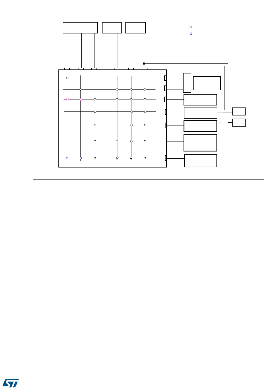
RM0430 Rev 8 55/1324
RM0430 System and memory overview
56
Figure 1. System architecture
2.1.1 I-bus
This bus connects the Instruction bus of the Cortex®-M4 with FPU core to the BusMatrix.
This bus is used by the core to fetch instructions. The target of this bus is a memory
containing code (internal Flash memory/SRAM1/SRAM2).
2.1.2 D-bus
This bus connects the databus of the Cortex®-M4 with FPU to the BusMatrix. This bus is
used by the core for literal load and debug access. The target of this bus is a memory
containing code or data (internal Flash memory/SRAM1/SRAM2).
2.1.3 S-bus
This bus connects the system bus of the Cortex®-M4 with FPU core to a BusMatrix. This
bus is used to access data located in a peripheral or in SRAM1 or in SRAM2. Instructions
may also be fetch on this bus (less efficient than ICode). The targets of this bus are the
internal SRAM1/SRAM2, the AHB1 peripherals including the APB peripherals, the AHB2
peripherals and the external memories through the FSMC and the QUADSPI.
2.1.4 DMA memory bus
This bus connects the DMA memory bus master interface to the BusMatrix. It is used by the
DMA to perform transfer to/from memories. The targets of this bus are data memories:
internal Flash memory, internal SRAM1/SRAM2 and additionally for S4 the AHB1/AHB2
peripherals including the APB peripherals.
06Y9
$50
&RUWH[0
*3
'0$
*3
'0$
)ODVK
8SWR0%
%XVPDWUL[6
6 6 6 6 6 6 ,&2'(
'&2'(
$&&(/
0
0
0
,EXV
'EXV
6EXV
'0$B3,
'0$B0(0
'0$B0(0
'0$B3
$+%
SHULSK
0
$3%
$3%
$+%
SHULSK
0
)60&H[WHUQDO
0HP&WUO
4XDG63,
0
$FFHVVWKURXJKUHPDS
$FFHVVE\DOLDVLQJ
65$0
.%
0
65$0
.%

System and memory overview RM0430
56/1324 RM0430 Rev 8
2.1.5 DMA peripheral bus
This bus connects the DMA peripheral master bus interface to the BusMatrix. This bus is
used by the DMA to access AHB peripherals or to perform memory-to-memory transfers.
The targets of this bus are the AHB and APB peripherals plus data memories: Flash
memory and internal SRAM1/SRAM2.
2.1.6 BusMatrix
The BusMatrix manages the access arbitration between masters. The arbitration uses a
round-robin algorithm.
2.1.7 AHB/APB bridges (APB)
The two AHB/APB bridges, APB1 and APB2, provide full synchronous connections between
the AHB and the two APB buses, allowing flexible selection of the peripheral frequency.
Refer to the device datasheets for more details on APB1 and APB2 maximum frequencies,
and to Table 1 for the address mapping of AHB and APB peripherals.
After each device reset, all peripheral clocks are disabled (except for the SRAM and Flash
memory interface). Before using a peripheral you have to enable its clock in the
RCC_AHBxENR or RCC_APBxENR register.
Note: When a 16- or an 8-bit access is performed on an APB register, the access is transformed
into a 32-bit access: the bridge duplicates the 16- or 8-bit data to feed the 32-bit vector.

RM0430 Rev 8 57/1324
RM0430
65
2.2 Memory organization
2.2.1 Introduction
Program memory, data memory, registers and I/O ports are organized within the same linear
4-Gbyte address space.
The bytes are coded in memory in Little Endian format. The lowest numbered byte in a word
is considered the word’s least significant byte and the highest numbered byte the most
significant.
The addressable memory space is divided into eight main blocks, of 512 Mbytes each.
The access to some part of the address space is master dependent, see Section 2: Memory
and bus architecture for details.
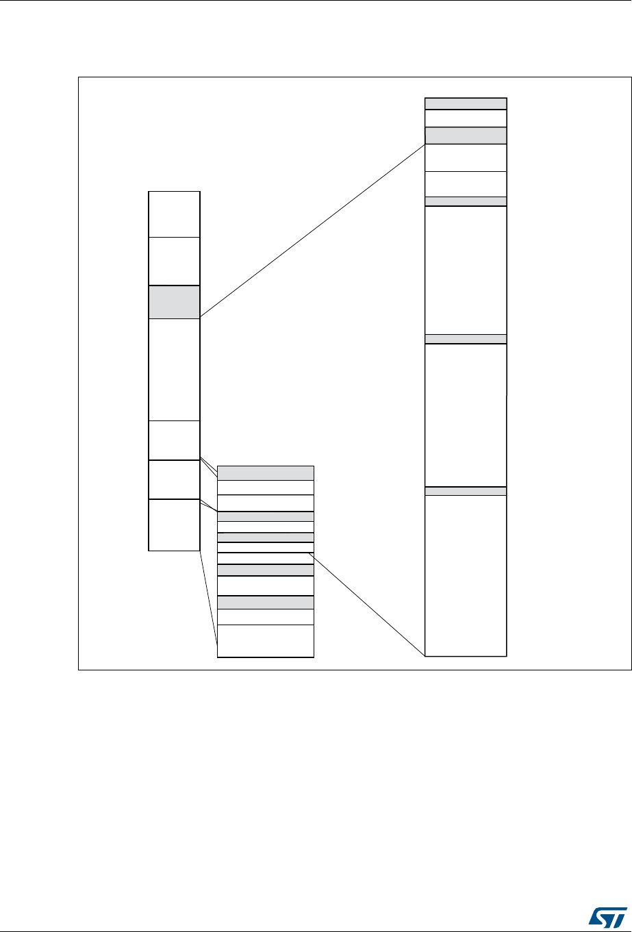
RM0430
58/1324 RM0430 Rev 8
2.2.2 Memory map and register boundary addresses
Figure 2. Memory map
All the memory map areas that are not allocated to on-chip memories and peripherals are
considered “Reserved”. For the detailed mapping of available memory and register areas,
refer to the following table.
5HVHUYHG
06Y9
0E\WH
EORFN
LQWHUQDO
SHULSKHUDOV
0E\WH
EORFN
1RWXVHG
0E\WH
EORFNLQF
65$065$0
[
[)))))))
[
[)))))))
[)))))))
[&
[')))))))
[(
[))))))))
0E\WH
EORFN
&RGH
[[)))))))
[
5HVHUYHG
[)))
[[))))
[
[$±'))))))
$+%
5HVHUYHG
[)))))))
[
65$0.%DOLDVHG
E\ELWEDQGLQJ [[))))
$3%
$3%
[))
[[))))
5HVHUYHG
[[)))))))
[))
$+%
5HVHUYHG
)ODVKPHPRU\
[)))[)))))
[)))&[)))))))
[[))))
[[)))))))
[[))))))
5HVHUYHG
$OLDVHGWR)ODVKV\VWHP
PHPRU\RU65$0
GHSHQGLQJRQWKH%227SLQV
273DUHDORFN
[[))))
[)))&[)))&)
[)))$[)))%)))
8VHURSWLRQE\WHV
[
&RUWH[ą0LQWHUQDO
SHULSKHUDOV [([()))))
5HVHUYHG [([))))))))
[%)))))))
5HVHUYHG
65$0.%DOLDVHG
E\ELWEDQGLQJ
5HVHUYHG
$+%
[)))[)))$)
$)))
[
5HVHUYHG
6\VWHPPHPRU\
65$0.%DFFHVVHGE\
&38YLD,EXVDQG'EXV [[))))
[$
[$)))
[
0E\WH
EORFN
SHULSKHUDOV
[
)0&
$QG
4XDG63,
5HVHUYHG [[))())))

RM0430 Rev 8 59/1324
RM0430
65
The following table gives the boundary addresses of the peripherals available in the
devices.
Table 1. Register boundary addresses
Bus Boundary address Peripheral
-0xE010 0000 - 0xFFFF FFFF Reserved
Cortex®-M4 0xE000 0000 - 0xE00F FFFF Cortex-M4 internal peripherals
AHB3
0xA000 2000 - 0xDFFF FFFF Reserved
0xA000 1000 - 0xA000 1FFF QuadSPI control register
0xA000 0000 - 0xA000 0FFF FSMC control register
0x9000 0000 - 0x9FFF FFFF QUADSPI
0x7000 0000 - 0x08FFF FFFF Reserved
0x6000 0000 - 0x6FFF FFFF FSMC
AHB2
0x5006 0C00 - 0x5FFF FFFF Reserved
0x5006 0800 0x5006 0BFF RNG
0x5006 0400 - 0x5006 07FF Reserved
0x5006 0000 - 0x5006 03FF AES(1)
0x5004 0000 - 0x5005 FFFF Reserved
0x5000 0000 - 0x5003 FFFF USB OTG FS
AHB1
0x4002 6800 - 0x4FFF FFFF Reserved
0x4002 6400 - 0x4002 67FF DMA2
0x4002 6000 - 0x4002 63FF DMA1
0x4002 4000 - 0X4002 5FFF Reserved
0x4002 3C00 - 0x4002 3FFF Flash interface register
0x4002 3800 - 0x4002 3BFF RCC
0x4002 3400 - 0x4002 37FF Reserved
0x4002 3000 - 0x4002 33FF CRC
0x4002 2000 - 0x4002 2FFF Reserved
0x4002 1C00 - 0x4002 1FFF GPIOH
0x4002 1800 - 0x4002 1BFF GPIOG
0x4002 1400 - 0x4002 17FF GPIOF
0x4002 1000 - 0x4002 13FF GPIOE
0x4002 0C00 - 0x4002 0FFF GPIOD
0x4002 0800 - 0x4002 0BFF GPIOC
0x4002 0400 - 0x4002 07FF GPIOB
0x4002 0000 - 0x4002 03FF GPIOA

RM0430
60/1324 RM0430 Rev 8
APB2
0x4001 6800 - 0x4001 FFFF Reserved
0x4001 6400 - 0x4001 67FF DFSDM2
0x4001 6000 - 0x4001 63FF DFSDM1
0x4001 5C00 - 0x4001 5FFF Reserved
0x4001 5800 - 0x4001 5BFF SAI1
0x4001 5400 - 0x4001 57FF Reserved
0x4001 5000 - 0x4001 53FF SPI5/I2S5
0x4001 4C00 - 0x4001 4FFF Reserved
0x4001 4800 - 0x4001 4BFF TIM11
0x4001 4400 - 0x4001 47FF TIM10
0x4001 4000 - 0x4001 43FF TIM9
0x4001 3C00 - 0x4001 3FFF EXTI
0x4001 3800 - 0x4001 3BFF SYSCFG
0x4001 3400 - 0x4001 37FF SPI4/I2S4
0x4001 3000 - 0x4001 33FF SPI1/I2S1
0x4001 2C00 - 0x4001 2FFF SDIO
0x4001 2400 - 0x4001 2BFF Reserved
0x4001 2000 - 0x4001 23FF ADC1
0x4001 1C00 - 0x4001 1FFF UART10
0x4001 1800 - 0x4001 1BFF UART9
0x4001 1400 - 0x4001 17FF USART6
0x4001 1000 - 0x4001 13FF USART1
0x4001 0800 - 0x4001 0FFF Reserved
0x4001 0400 - 0x4001 07FF TIM8
0x4001 0000 - 0x4001 03FF TIM1
Table 1. Register boundary addresses (continued)
Bus Boundary address Peripheral

RM0430 Rev 8 61/1324
RM0430
65
APB1
0x4000 8000 - 0x4000 FFFF Reserved
0x4000 7C00 - 0x4000 7FFF UART8
0x4000 7800 - 0x4000 7BFF UART7
0x4000 7400 - 0x4000 77FF DAC
0x4000 7000 - 0x4000 73FF PWR
0x4000 6C00 - 0x4000 6FFF CAN3
0x4000 6800 - 0x4000 6BFF CAN2
0x4000 6400 - 0x4000 67FF CAN1
0x4000 6000 - 0x4000 63FF I2CFMP1
0x4000 5C00 - 0x4000 5FFF I2C3
0x4000 5800 - 0x4000 5BFF I2C2
0x4000 5400 - 0x4000 57FF I2C1
0x4000 5000 - 0x4000 53FF UART5
0x4000 4C00 - 0x4000 4FFF UART4
0x4000 4800 - 0x4000 4BFF USART3
0x4000 4400 - 0x4000 47FF USART2
0x4000 4000 - 0x4000 43FF I2S3ext
0x4000 3C00 - 0x4000 3FFF SPI3 / I2S3
0x4000 3800 - 0x4000 3BFF SPI2 / I2S2
0x4000 3400 - 0x4000 37FF I2S2ext
0x4000 3000 - 0x4000 33FF IWDG
0x4000 2C00 - 0x4000 2FFF WWDG
0x4000 2800 - 0x4000 2BFF RTC & BKP Registers
0x4000 2400 - 0x4000 27FF LPTIM1
0x4000 2000 - 0x4000 23FF TIM14
0x4000 1C00 - 0x4000 1FFF TIM13
0x4000 1800 - 0x4000 1BFF TIM12
0x4000 1400 - 0x4000 17FF TIM7
0x4000 1000 - 0x4000 13FF TIM6
0x4000 0C00 - 0x4000 0FFF TIM5
0x4000 0800 - 0x4000 0BFF TIM4
0x4000 0400 - 0x4000 07FF TIM3
0x4000 0000 - 0x4000 03FF TIM2
1. AES is only available for STM32F423xx. This boundary address is reserved for STM32F413xx.
Table 1. Register boundary addresses (continued)
Bus Boundary address Peripheral

RM0430
62/1324 RM0430 Rev 8
2.3 Embedded SRAM
STM32F413/423 devices feature 320 Kbytes of system SRAM.
The embedded SRAM can be accessed as bytes, half-words (16 bits) or full words (32 bits).
Read and write operations are performed at CPU speed with 0 wait state.
The embedded SRAM is divided into two blocks:
•SRAM1 mapped at address 0x2000 0000 and accessible by all AHB masters.
•SRAM2 mapped at address 0x2004 0000 and accessible by all AHB masters.
The CPU can access the embedded SRAM1, through the System Bus or through the I-
Code/D-Code buses when boot from SRAM1 is selected or when physical remap is
selected (See Section 8.2.1: SYSCFG memory remap register (SYSCFG_MEMRMP)).
To get the max performance on SRAM1 execution, physical remap should be selected (boot
or software selection).
The CPU can access the embedded SRAM2, through the System Bus or through the I-
Code/D-Code buses when SRAM2 is mapped at the address range: 0x1000 0000 to
0x1000 FFFF. To get the max performance on SRAM2 execution, mapping at the address
0x1000 0000 should be selected.
To get the max performance on embedded SRAM, use SRAM1/SRAM2 to execute code via
I-code and SRAM2/SRAM1 to store data
2.4 Flash memory overview
The Flash memory interface manages CPU AHB I-Code and D-Code accesses to the Flash
memory. It implements the erase and program Flash memory operations and the read and
write protection mechanisms. It accelerates code execution with a system of instruction
prefetch and cache lines.
The Flash memory is organized as follows:
•A main memory block divided into sectors.
•System memory from which the device boots in System memory boot mode
•512 OTP (one-time programmable) bytes for user data.
•Option bytes to configure read and write protection, BOR level, watchdog
software/hardware and reset when the device is in Standby or Stop mode.
Refer to Section 3: Embedded Flash memory interface for more details.
2.5 Bit banding
The Cortex®-M4 with FPU memory map includes two bit-band regions. These regions map
each word in an alias region of memory to a bit in a bit-band region of memory. Writing to a
word in the alias region has the same effect as a read-modify-write operation on the
targeted bit in the bit-band region.
In the STM32F4x3xx devices both the peripheral registers and the SRAM1 are mapped to a
bit-band region, so that single bit-band write and read operations are allowed. The
operations are only available for Cortex®-M4 with FPU accesses, and not from other bus
masters (e.g. DMA).

RM0430 Rev 8 63/1324
RM0430
65
A mapping formula shows how to reference each word in the alias region to a corresponding
bit in the bit-band region. The mapping formula is:
bit_word_addr = bit_band_base + (byte_offset x 32) + (bit_number × 4)
where:
–bit_word_addr is the address of the word in the alias memory region that maps to
the targeted bit
–bit_band_base is the starting address of the alias region
–byte_offset is the number of the byte in the bit-band region that contains the
targeted bit
–bit_number is the bit position (0-7) of the targeted bit
Example
The following example shows how to map bit 2 of the byte located at SRAM1 address
0x20000300 to the alias region:
0x22006008 = 0x22000000 + (0x300*32) + (2*4)
Writing to address 0x22006008 has the same effect as a read-modify-write operation on bit
2 of the byte at SRAM1 address 0x20000300.
Reading address 0x22006008 returns the value (0x01 or 0x00) of bit 2 of the byte at SRAM1
address 0x20000300 (0x01: bit set; 0x00: bit reset).
For more information on bit-banding, refer to the Cortex®-M4 with FPU programming
manual (see Related documents on page 1.
2.6 Boot configuration
Due to its fixed memory map, the code area starts from address 0x0000 0000 (accessed
through the ICode/DCode buses) while the data area (SRAM) starts from address
0x2000 0000 (accessed through the system bus). The Cortex®-M4 with FPU CPU always
fetches the reset vector on the ICode bus, which implies to have the boot space available
only in the code area (typically, Flash memory). STM32F4xx microcontrollers implement a
special mechanism to be able to boot from other memories (like the internal SRAM).
In the STM32F4x3xx, three different boot modes can be selected through the BOOT[1:0]
pins as shown in Table 2.
The values on the BOOT pins are latched on the 4th rising edge of SYSCLK after a reset. It
is up to the user to set the BOOT1 and BOOT0 pins after reset to select the required boot
mode.
Table 2. Boot modes
Boot mode selection pins
Boot mode Aliasing
BOOT1 BOOT0
x 0 Main Flash memory Main Flash memory is selected as the boot space
0 1 System memory System memory is selected as the boot space
1 1 Embedded SRAM Embedded SRAM is selected as the boot space

RM0430
64/1324 RM0430 Rev 8
BOOT0 is a dedicated pin while BOOT1 is shared with a GPIO pin. Once BOOT1 has been
sampled, the corresponding GPIO pin is free and can be used for other purposes.
The BOOT pins are also resampled when the device exits the Standby mode. Consequently,
they must be kept in the required Boot mode configuration when the device is in the Standby
mode. After this startup delay is over, the CPU fetches the top-of-stack value from address
0x0000 0000, then starts code execution from the boot memory starting from 0x0000 0004.
Note: When the device boots from SRAM, in the application initialization code, you have to
relocate the vector table in SRAM using the NVIC exception table and the offset register.
Embedded bootloader
The embedded bootloader mode is used to reprogram the Flash memory using one of the
interface described in Table 32. The availability of the interface is package dependent.
The USART peripherals operate at the internal 16 MHz oscillator (HSI) frequency, while the
CAN and USB OTG FS require an external clock (HSE) multiple of 1 MHz (ranging from 4 to
26 MHz).
The embedded bootloader code is located in system memory. It is programmed by ST
during production. For additional information, refer to application note AN2606.
Physical remap in STM32F413/423
Once the boot pins are selected, the application software can modify the memory
accessible in the code area (in this way the code can be executed through the ICode bus in
place of the System bus). This modification is performed by programming the Section 8.2.1:
SYSCFG memory remap register (SYSCFG_MEMRMP) in the SYSCFG controller.
The following memories can thus be remapped:
•Main Flash memory
•System memory
•Embedded SRAM
Table 3. Embedded bootloader interfaces
Package
USART1
PA9/
PA10
USART2
PD6/
PD5
USART3
PB11/
PB10
I2C1
PB6/
PB7
I2C2
PF0/
PF1
I2C3
PA8/
PB4
I2C
FMP1
PB14/
PB15
SPI1
PA4/
PA5/
PA6/
PA7
SPI3
PA15/
PC10/
PC11/
PC12
SPI4
PE11/
PE12/
PE13/
PE14
CAN2
PB5/
PB13
USB
PA11
/P12
UFQFPN48 Y - - Y - Y Y Y - - Y Y
LQFP64 Y - - Y - Y Y Y Y - Y Y
WLCSP81 Y - - Y - Y Y Y Y Y Y Y
LQFP100Y Y - Y-YYYYYYY
LQFP144YYYYYYYYYYYY
UFBGA100 Y Y Y Y - Y Y Y Y Y Y Y
UFBGA144 Y Y Y Y Y Y Y Y Y Y Y Y

RM0430 Rev 8 65/1324
RM0430
65
Table 4. Memory mapping vs. Boot mode/physical remap in STM32F413/423
Addresses Boot/Remap in main
Flash memory
Boot/Remap in
embedded SRAM
Boot/Remap in
System memory
0x2000 0000 - 0x2003 FFFF SRAM (256 KB) SRAM (256KB) SRAM (256KB)
0x1FFF 0000 - 0x1FFF 77FF System memory System memory System memory
0x0802 0000 - 0x1FFE FFFF Reserved Reserved Reserved
0x0800 0000 - 0x080F FFFF Flash memory Flash memory Flash memory
0x0400 000 - 0x07FF FFFF Reserved Reserved Reserved
0x0000 0000 - 0x0003 FFFF(1)
1. Even when aliased in the boot memory space, the related memory is still accessible at its original memory
space.
Flash (1M) Aliased SRAM1 (256 KB)
Aliased
System memory
(30 KB) Aliased
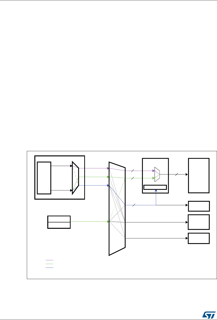
Embedded Flash memory interface RM0430
66/1324 RM0430 Rev 8
3 Embedded Flash memory interface
3.1 Introduction
The Flash memory interface manages CPU AHB I-Code and D-Code accesses to the Flash
memory. It implements the erase and program Flash memory operations and the read and
write protection mechanisms.
The Flash memory interface accelerates code execution with a system of instruction
prefetch and cache lines.
3.2 Main features
•Flash memory read operations
•Flash memory program/erase operations
•Read / write protections
•Prefetch on I-Code
•64 cache lines of 128 bits on I-Code
•8 cache lines of 128 bits on D-Code
Figure 3 shows the Flash memory interface connection inside the system architecture.
Figure 3. Flash memory interface connection inside system architecture
&RUWH[
FRUH
'0$
'0$
'FRGHEXV
,&RGHEXV
&RUWH[0ZLWK)38
,&RGH
'&RGH
6EXV
$+%
SHULSK
)ODVK
PHPRU\
)ODVKLQWHUIDFH
65$0DQG
([WHUQDO
PHPRULHV
$+%
SHULSK
)/,7)UHJLVWHUV
$+%
ELW
LQVWUXFWLRQ
EXV
$FFHVVWRLQVWUXFWLRQLQ)ODVKPHPRU\
$FFHVVWRGDWDDQGOLWHUDOSRROLQ)ODVKPHPRU\
)/,7)UHJLVWHUDFFHVV
069
$+%
ELW
GDWDEXV
$+%
ELW
V\VWHPEXV
)ODVK
PHPRU\
EXV
ELWV

RM0430 Rev 8 67/1324
RM0430 Embedded Flash memory interface
89
3.3 Embedded Flash memory
The Flash memory has the following main features:
•Capacity up to 1.5 Mbyte
•128 bits wide data read
•Byte, half-word, word and double word write
•Sector and mass erase
•Memory organization
The Flash memory is organized as follows:
– A main memory block divided into 4 sectors of 16 Kbyte, plus 1 sector of 64 Kbyte
and plus 11 sector of 128 Kbyte.
– System memory from which the device boots in System memory boot mode
– 512 OTP (one-time programmable) bytes for user data
The OTP area contains 32 additional bits used to lock the corresponding OTP
data block.
– Option bytes to configure read and write protection, BOR level, watchdog
software/hardware and reset when the device is in Standby or Stop mode.
•Low-power modes (for details refer to the Power control (PWR) section of the reference
manual)
Table 5. Flash module organization
Block Name Block base addresses Size
Main memory
Sector 0 0x0800 0000 - 0x0800 3FFF 16 Kbyte
Sector 1 0x0800 4000 - 0x0800 7FFF 16 Kbyte
Sector 2 0x0800 8000 - 0x0800 BFFF 16 Kbyte
Sector 3 0x0800 C000 - 0x0800 FFFF 16 Kbyte
Sector 4 0x0801 0000 - 0x0801 FFFF 64 Kbyte
Sector 5 0x0802 0000 - 0x0803 FFFF 128 Kbyte
Sector 6 0x0804 0000 - 0x0805 FFFF 128 Kbyte
Sector 7 0x0806 0000 - 0x0807 FFFF 128 Kbyte
Sector 8 0x0808 0000 - 0x0809 FFFF 128 Kbyte
Sector 9 0x080A 0000 - 0x080B FFFF 128 Kbyte
Sector 10 0x080C 0000 - 0x080D FFFF 128 Kbyte
Sector 11 0x080E 0000 - 0x080F FFFF 128 Kbyte
Sector 12 0x08010 0000 - 0x0811 FFFF 128 Kbyte
Sector 13 0x0812 0000 - 0x0813 FFFF 128 Kbyte
Sector 14 0x0814 0000 - 0x0815 FFFF 128 Kbyte
Sector 15 0x0816 0000 - 0x0817 FFFF 128 Kbyte
System memory 0x1FFF 0000 - 0x1FFF 77FF 30 Kbyte
Embedded Flash memory interface RM0430
68/1324 RM0430 Rev 8
3.4 Read interface
3.4.1 Relation between CPU clock frequency and Flash memory read time
To correctly read data from Flash memory, the number of wait states (LATENCY) must be
correctly programmed in the Flash access control register (FLASH_ACR) according to the
frequency of the CPU clock (HCLK) and the supply voltage of the device.
•When VOS[1:0] = 0x01, the maximum value of fHCLK = 64 MHz.
•When VOS[1:0] = 0x10, the maximum value of fHCLK = 84 MHz.
•When VOS[1:0] = 0x11, the maximum value of fHCLK = 100 MHz.
After reset, the CPU clock frequency is 16 MHz and 0 wait state (WS) is configured in the
FLASH_ACR register.
It is highly recommended to use the following software sequences to tune the number of
wait states needed to access the Flash memory with the CPU frequency.
OTP area 0x1FFF 7800 - 0x1FFF 7A0F 528 byte
Option bytes 0x1FFF C000 - 0x1FFF C00F 16 byte
Table 5. Flash module organization (continued)
Block Name Block base addresses Size
Table 6. Number of wait states according to CPU clock (HCLK) frequency
Wait states (WS)
(LATENCY)
HCLK (MHz)
Voltage range
2.7 V - 3.6 V
Voltage range
2.4 V - 2.7 V
Voltage range
2.1 V - 2.4 V
Voltage range
1.7 V - 2.1 V
0 WS (1 CPU cycle) 0 < HCLK ≤ 25 0 < HCLK ≤ 20 0 < HCLK ≤ 18 0 < HCLK ≤ 16
1 WS (2 CPU cycles) 25 < HCLK ≤ 50 20 < HCLK ≤ 40 18 < HCLK ≤ 36 16 <HCLK ≤ 32
2 WS (3 CPU cycles) 50 < HCLK ≤ 75 40 < HCLK ≤ 60 36 < HCLK ≤ 54 32 < HCLK ≤ 48
3 WS (4 CPU cycles) 75 < HCLK ≤ 100 60 < HCLK ≤ 80 54 < HCLK ≤ 72 48 < HCLK ≤ 64
4 WS (5 CPU cycles) - 80 < HCLK ≤ 100 72 < HCLK ≤ 90 64 < HCLK ≤ 80
5 WS (6 CPU cycles) - - 90 < HCLK ≤ 100 80 < HCLK ≤ 96
6 WS (7 CPU cycles) - - - 96 < HCLK ≤ 100

RM0430 Rev 8 69/1324
RM0430 Embedded Flash memory interface
89
Increasing the CPU frequency
1. Program the new number of wait states to the LATENCY bits in the FLASH_ACR
register
2. Check that the new number of wait states is taken into account to access the Flash
memory by reading the FLASH_ACR register
3. Modify the CPU clock source by writing the SW bits in the RCC_CFGR register
4. If needed, modify the CPU clock prescaler by writing the HPRE bits in RCC_CFGR
5. Check that the new CPU clock source or/and the new CPU clock prescaler value is/are
taken into account by reading the clock source status (SWS bits) or/and the AHB
prescaler value (HPRE bits), respectively, in the RCC_CFGR register.
Decreasing the CPU frequency
1. Modify the CPU clock source by writing the SW bits in the RCC_CFGR register
2. If needed, modify the CPU clock prescaler by writing the HPRE bits in RCC_CFGR
3. Check that the new CPU clock source or/and the new CPU clock prescaler value is/are
taken into account by reading the clock source status (SWS bits) or/and the AHB
prescaler value (HPRE bits), respectively, in the RCC_CFGR register
4. Program the new number of wait states to the LATENCY bits in FLASH_ACR
5. Check that the new number of wait states is used to access the Flash memory by
reading the FLASH_ACR register
Note: A change in CPU clock configuration or wait state (WS) configuration may not be effective
straight away. To make sure that the current CPU clock frequency is the one you have
configured, you can check the AHB prescaler factor and clock source status values. To
make sure that the number of WS you have programmed is effective, you can read the
FLASH_ACR register.
3.4.2 Adaptive real-time memory accelerator (ART Accelerator™)
The proprietary Adaptive real-time (ART) memory accelerator is optimized for STM32
industry-standard Arm® Cortex®-M4 with FPU processors. It balances the inherent
performance advantage of the Arm® Cortex®-M4 with FPU over Flash memory
technologies, which normally requires the processor to wait for the Flash memory at higher
operating frequencies.
To release the processor full performance, the accelerator implements an instruction
prefetch queue and branch cache which increases program execution speed from the 128-
bit Flash memory. Based on CoreMark benchmark, the performance achieved thanks to the
ART accelerator is equivalent to 0 wait state program execution from Flash memory at a
CPU frequency up to 100 MHz.
Instruction prefetch
Each Flash memory read operation provides 128 bits from either four instructions of 32 bits
or 8 instructions of 16 bits according to the program launched. So, in case of sequential
code, at least four CPU cycles are needed to execute the previous read instruction line.
Prefetch on the I-Code bus can be used to read the next sequential instruction line from the
Flash memory while the current instruction line is being requested by the CPU. Prefetch is
enabled by setting the PRFTEN bit in the FLASH_ACR register. This feature is useful if at
least one wait state is needed to access the Flash memory.
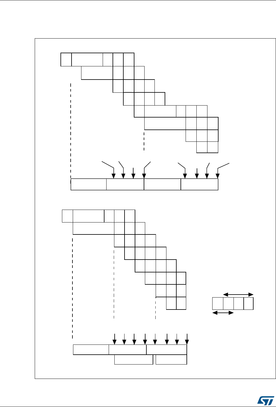
Embedded Flash memory interface RM0430
70/1324 RM0430 Rev 8
Figure 4 shows the execution of sequential 32-bit instructions with and without prefetch
when 3 WSs are needed to access the Flash memory.
Figure 4. Sequential 32-bit instruction execution
&
&
&
&
$
$
$
$
%
%
%
%
&
&
&
&
$
$
$
%
%
2EADINS 'IVESINS 2EADINS 'IVESINS
INS
FETCH
INS
FETCH
INS
FETCH
INS
FETCH
INS
FETCH
INS
FETCH
INS
FETCH
INS
FETCH
7!)4
7!)4
$%
&
&
&
&
$
$
$
%
%
&
&
&
&
$
$
$
%
%
7AITDATA
%
2EADINS 'IVESINS 'IVESINS
2EADINS 2EADINS
INS INS
FETCH
INS INS
7ITHOUTPREFETCH
7ITHPREFETCH
&$%
#ORTEX-PIPELINE
!("PROTOCOL
ADDRESSREQUESTED
&&ETCHSTAGE
$$ECODESTAGE
%%XECUTESTAGE
INS
FETCH
INS
FETCH
INS
FETCH FETCH FETCH FETCH
INS
FETCH
-36

RM0430 Rev 8 71/1324
RM0430 Embedded Flash memory interface
89
When the code is not sequential (branch), the instruction may not be present in the currently
used instruction line or in the prefetched instruction line. In this case (miss), the penalty in
terms of number of cycles is at least equal to the number of wait states.
Instruction cache memory
To limit the time lost due to jumps, it is possible to retain 64 lines of 128 bits in an instruction
cache memory. This feature can be enabled by setting the instruction cache enable (ICEN)
bit in the FLASH_ACR register. Each time a miss occurs (requested data not present in the
currently used instruction line, in the prefetched instruction line or in the instruction cache
memory), the line read is copied into the instruction cache memory. If some data contained
in the instruction cache memory are requested by the CPU, they are provided without
inserting any delay. Once all the instruction cache memory lines have been filled, the LRU
(least recently used) policy is used to determine the line to replace in the instruction memory
cache. This feature is particularly useful in case of code containing loops.
Data management
Literal pools are fetched from Flash memory through the D-Code bus during the execution
stage of the CPU pipeline. The CPU pipeline is consequently stalled until the requested
literal pool is provided. To limit the time lost due to literal pools, accesses through the AHB
databus D-Code have priority over accesses through the AHB instruction bus I-Code.
If some literal pools are frequently used, the data cache memory can be enabled by setting
the data cache enable (DCEN) bit in the FLASH_ACR register. This feature works like the
instruction cache memory, but the retained data size is limited to 8 rows of 128 bits.
Note: Data in user configuration sector are not cacheable.
3.5 Erase and program operations
For any Flash memory program operation (erase or program), the CPU clock frequency
(HCLK) must be at least 1 MHz. The contents of the Flash memory are not guaranteed if a
device reset occurs during a Flash memory operation.
Any attempt to read the Flash memory on STM32F4xx while it is being written or erased,
causes the bus to stall. Read operations are processed correctly once the program
operation has completed. This means that code or data fetches cannot be performed while
a write/erase operation is ongoing.
3.5.1 Unlocking the Flash control register
After reset, write is not allowed in the Flash control register (FLASH_CR) to protect the
Flash memory against possible unwanted operations due, for example, to electric
disturbances. The following sequence is used to unlock this register:
1. Write KEY1 = 0x45670123 in the Flash key register (FLASH_KEYR)
2. Write KEY2 = 0xCDEF89AB in the Flash key register (FLASH_KEYR)
Any wrong sequence will return a bus error and lock up the FLASH_CR register until the
next reset.
The FLASH_CR register can be locked again by software by setting the LOCK bit in the
FLASH_CR register.

Embedded Flash memory interface RM0430
72/1324 RM0430 Rev 8
Note: The FLASH_CR register is not accessible in write mode when the BSY bit in the FLASH_SR
register is set. Any attempt to write to it with the BSY bit set will cause the AHB bus to stall
until the BSY bit is cleared.
3.5.2 Program/erase parallelism
The Parallelism size is configured through the PSIZE field in the FLASH_CR register. It
represents the number of bytes to be programmed each time a write operation occurs to the
Flash memory. PSIZE is limited by the supply voltage and by whether the external VPP
supply is used or not. It must therefore be correctly configured in the FLASH_CR register
before any programming/erasing operation.
A Flash memory erase operation can only be performed by sector or for the whole Flash
memory (mass erase). The erase time depends on PSIZE programmed value. For more
details on the erase time, refer to the electrical characteristics section of the device
datasheet.
Table 7 provides the correct PSIZE values.
Note: Any program or erase operation started with inconsistent program parallelism/voltage range
settings may lead to unpredicted results. Even if a subsequent read operation indicates that
the logical value was effectively written to the memory, this value may not be retained.
To use VPP
, an external high-voltage supply (between 8 and 9 V) must be applied to the VPP
pad. The external supply must be able to sustain this voltage range even if the DC
consumption exceeds 10 mA. It is advised to limit the use of VPP to initial programming on
the factory line. The VPP supply must not be applied for more than an hour, otherwise the
Flash memory might be damaged.
3.5.3 Erase
The Flash memory erase operation can be performed at sector level or on the whole Flash
memory (Mass Erase). Mass Erase does not affect the OTP sector or the configuration
sector.
Sector Erase
To erase a sector, follow the procedure below:
1. Check that no Flash memory operation is ongoing by checking the BSY bit in the
FLASH_SR register
2. Set the SER bit and select the sector out of the 16 sectors in the main memory block
you wish to erase (SNB) in the FLASH_CR register
3. Set the STRT bit in the FLASH_CR register
4. Wait for the BSY bit to be cleared
Table 7. Program/erase parallelism
Voltage range 2.7 - 3.6 V
with External VPP
Voltage range
2.7 - 3.6 V
Voltage range
2.4 - 2.7 V
Voltage range
2.1 - 2.4 V
Voltage range
1.7 V - 2.1 V
Parallelism size x64 x32 x16 x8
PSIZE(1:0)11100100

RM0430 Rev 8 73/1324
RM0430 Embedded Flash memory interface
89
Mass Erase
To perform Mass Erase, the following sequence is recommended:
1. Check that no Flash memory operation is ongoing by checking the BSY bit in the
FLASH_SR register
2. Set the MER bit in the FLASH_CR register
3. Set the STRT bit in the FLASH_CR register
4. Wait for the BSY bit to be cleared
Note: If MERx and SER bits are both set in the FLASH_CR register, mass erase is performed.
If both MERx and SER bits are reset and the STRT bit is set, an unpredictable behavior may
occur without generating any error flag. This condition should be forbidden.
3.5.4 Programming
Standard programming
The Flash memory programming sequence is as follows:
1. Check that no main Flash memory operation is ongoing by checking the BSY bit in the
FLASH_SR register.
2. Set the PG bit in the FLASH_CR register
3. Perform the data write operation(s) to the desired memory address (inside main
memory block or OTP area):
– Byte access in case of x8 parallelism
– Half-word access in case of x16 parallelism
– Word access in case of x32 parallelism
– Double word access in case of x64 parallelism
4. Wait for the BSY bit to be cleared.
Note: Successive write operations are possible without the need of an erase operation when
changing bits from ‘1’ to ‘0’. Writing ‘1’ requires a Flash memory erase operation.
If an erase and a program operation are requested simultaneously, the erase operation is
performed first.
Programming errors
It is not allowed to program data to the Flash memory that would cross the 128-bit row
boundary. In such a case, the write operation is not performed and a program alignment
error flag (PGAERR) is set in the FLASH_SR register.
The write access type (byte, half-word, word or double word) must correspond to the type of
parallelism chosen (x8, x16, x32 or x64). If not, the write operation is not performed and a
program parallelism error flag (PGPERR) is set in the FLASH_SR register.
If the standard programming sequence is not respected (for example, if there is an attempt
to write to a Flash memory address when the PG bit is not set), the operation is aborted and
a program sequence error flag (PGSERR) is set in the FLASH_SR register.
Embedded Flash memory interface RM0430
74/1324 RM0430 Rev 8
Programming and caches
If a Flash memory write access concerns some data in the data cache, the Flash write
access modifies the data in the Flash memory and the data in the cache.
If an erase operation in Flash memory also concerns data in the data or instruction cache,
you have to make sure that these data are rewritten before they are accessed during code
execution. If this cannot be done safely, it is recommended to flush the caches by setting the
DCRST and ICRST bits in the FLASH_CR register.
Note: The I/D cache should be flushed only when it is disabled (I/DCEN = 0).
3.5.5 Interrupts
Setting the end of operation interrupt enable bit (EOPIE) in the FLASH_CR register enables
interrupt generation when an erase or program operation ends, that is when the busy bit
(BSY) in the FLASH_SR register is cleared (operation completed, correctly or not). In this
case, the end of operation (EOP) bit in the FLASH_SR register is set.
If an error occurs during a program, an erase, or a read operation request, one of the
following error flags is set in the FLASH_SR register:
•PGAERR, PGPERR, PGSERR (Program error flags)
•WRPERR (Protection error flag)
In this case, if the error interrupt enable bit (ERRIE) is set in the FLASH_CR register, an
interrupt is generated and the operation error bit (OPERR) is set in the FLASH_SR register.
Note: If several successive errors are detected (for example, in case of DMA transfer to the Flash
memory), the error flags cannot be cleared until the end of the successive write requests.
3.6 Option bytes
3.6.1 Description of user option bytes
The option bytes are configured by the end user depending on the application requirements.
Table 9 shows the organization of these bytes inside the user configuration sector.
Table 8. Flash interrupt request
Interrupt event Event flag Enable control bit
End of operation EOP EOPIE
Write protection error WRPERR ERRIE
Programming error PGAERR, PGPERR, PGSERR ERRIE
Table 9. Option byte organization
Address [63:16] [15:0]
0x1FFF C0000 Reserved ROP & user option bytes (RDP & USER)
0x1FFF C008 Reserved Write protection nWRP bits for sectors 0 to 15

RM0430 Rev 8 75/1324
RM0430 Embedded Flash memory interface
89
Table 10. Description of the option bytes
Option bytes (word, address 0x1FFF C000)
RDP: Read protection option byte.
The read protection is used to protect the software code stored in Flash memory.
Bits 15:8
0xAA: Level 0, no protection
0xCC: Level 2, chip protection (debug and boot from RAM features disabled)
Others: Level 1, read protection of memories (debug features limited)
USER: User option byte
This byte is used to configure the following features:
– Select the watchdog event: Hardware or software
– Reset event when entering the Stop mode
– Reset event when entering the Standby mode
Bit 7
nRST_STDBY
0: Reset generated when entering the Standby mode
1: No reset generated
Bit 6
nRST_STOP
0: Reset generated when entering the Stop mode
1: No reset generated
Bit 5
WDG_SW
0: Hardware independent watchdog
1: Software independent watchdog
Bit 4 0x1: Not used
Bits 3:2
BOR_LEV: BOR reset Level
These bits contain the supply level threshold that activates/releases the reset.
They can be written to program a new BOR level value into Flash memory.
00: BOR Level 3 (VBOR3), brownout threshold level 3
01: BOR Level 2 (VBOR2), brownout threshold level 2
10: BOR Level 1 (VBOR1), brownout threshold level 1
11: BOR off, POR/PDR reset threshold level is applied
Note: For full details on BOR characteristics, refer to the “Electrical characteristics”
section of the product datasheet.
Bits 1:0 0x1: Not used
Option bytes (word, address 0x1FFF C008)
Bit 15
SPRMOD: Selection of Protection Mode of nWPRi bits
0: nWPRi bits used for sector i write protection (Default)
1: nWPRi bits used for sector i PCROP protection (Sector)
nWRP: Flash memory write protection option bytes
sector 0 to 15 can be write protected

Embedded Flash memory interface RM0430
76/1324 RM0430 Rev 8
3.6.2 Programming user option bytes
To run any operation on this sector, the option lock bit (OPTLOCK) in the Flash option
control register (FLASH_OPTCR) must be cleared. To be allowed to clear this bit, you have
to perform the following sequence:
1. Write OPTKEY1 = 0x0819 2A3B in the Flash option key register (FLASH_OPTKEYR)
2. Write OPTKEY2 = 0x4C5D 6E7F in the Flash option key register (FLASH_OPTKEYR)
The user option bytes can be protected against unwanted erase/program operations by
setting the OPTLOCK bit by software.
Modifying user option bytes
To modify the user option value, follow the sequence below:
1. Check that no Flash memory operation is ongoing by checking the BSY bit in the
FLASH_SR register
2. Write the desired option value in the FLASH_OPTCR register.
3. Set the option start bit (OPTSTRT) in the FLASH_OPTCR register
4. Wait for the BSY bit to be cleared.
Note: The value of an option is automatically modified by first erasing the user configuration sector
and then programming all the option bytes with the values contained in the FLASH_OPTCR
register.
3.6.3 Read protection (RDP)
The user area in the Flash memory can be protected against read operations by an
entrusted code. Three read protection levels are defined:
•Level 0: no read protection
When the read protection level is set to Level 0 by writing 0xAA into the read protection
option byte (RDP), all read/write operations (if no write protection is set) from/to the
Bit 14
nWRP15_14: Non Write Protection of sector 15 and 14
If SPRMOD is reset (default value):
0: Write protection active on sector 15 and 14.
1: Write protection not active on sector 15 and 14.
If SPRMOD is set (active):
0: PCROP protection not active on sector 15 and 14.
1: PCROP protection active on sector 15 and 14.
Bits 13:0
nWRPi
If SPRMOD is reset (default value):
0: Write protection active on sector i.
1: Write protection not active on sector i.
If SPRMOD is set (active):
0: PCROP protection not active on sector i.
1: PCROP protection active on sector i.
Table 10. Description of the option bytes

RM0430 Rev 8 77/1324
RM0430 Embedded Flash memory interface
89
Flash memory are possible in all boot configurations (Flash user boot, debug or boot
from RAM).
•Level 1: read protection enabled
It is the default read protection level after option byte erase. The read protection Level
1 is activated by writing any value (except for 0xAA and 0xCC used to set Level 0 and
Level 2, respectively) into the RDP option byte. When the read protection Level 1 is set:
– No access (read, erase, program) to Flash memory can be performed while the
debug feature is connected or while booting from RAM or system memory
bootloader. A bus error is generated in case of read request.
– When booting from Flash memory, accesses (read, erase, program) to Flash
memory from user code are allowed.
When Level 1 is active, programming the protection option byte (RDP) to Level 0
causes the Flash memory to be mass-erased. As a result the user code area is cleared
before the read protection is removed. The mass erase only erases the user code area.
The other option bytes including write protections remain unchanged from before the
mass-erase operation. The OTP area is not affected by mass erase and remains
unchanged. Mass erase is performed only when Level 1 is active and Level 0
requested. When the protection level is increased (0->1, 1->2, 0->2) there is no mass
erase.
•Level 2: debug/chip read protection disabled
The read protection Level 2 is activated by writing 0xCC to the RDP option byte. When
the read protection Level 2 is set:
– All protections provided by Level 1 are active.
– Booting from RAM or system memory bootloader is no more allowed.
– JTAG, SWV (single-wire viewer), ETM, and boundary scan are disabled.
– User option bytes can no longer be changed.
– When booting from Flash memory, accesses (read, erase and program) to Flash
memory from user code are allowed.
Memory read protection Level 2 is an irreversible operation. When Level 2 is activated,
the level of protection cannot be decreased to Level 0 or Level 1.
Note: The JTAG port is permanently disabled when Level 2 is active (acting as a JTAG fuse). As a
consequence, boundary scan cannot be performed. STMicroelectronics is not able to
perform analysis on defective parts on which the Level 2 protection has been set.
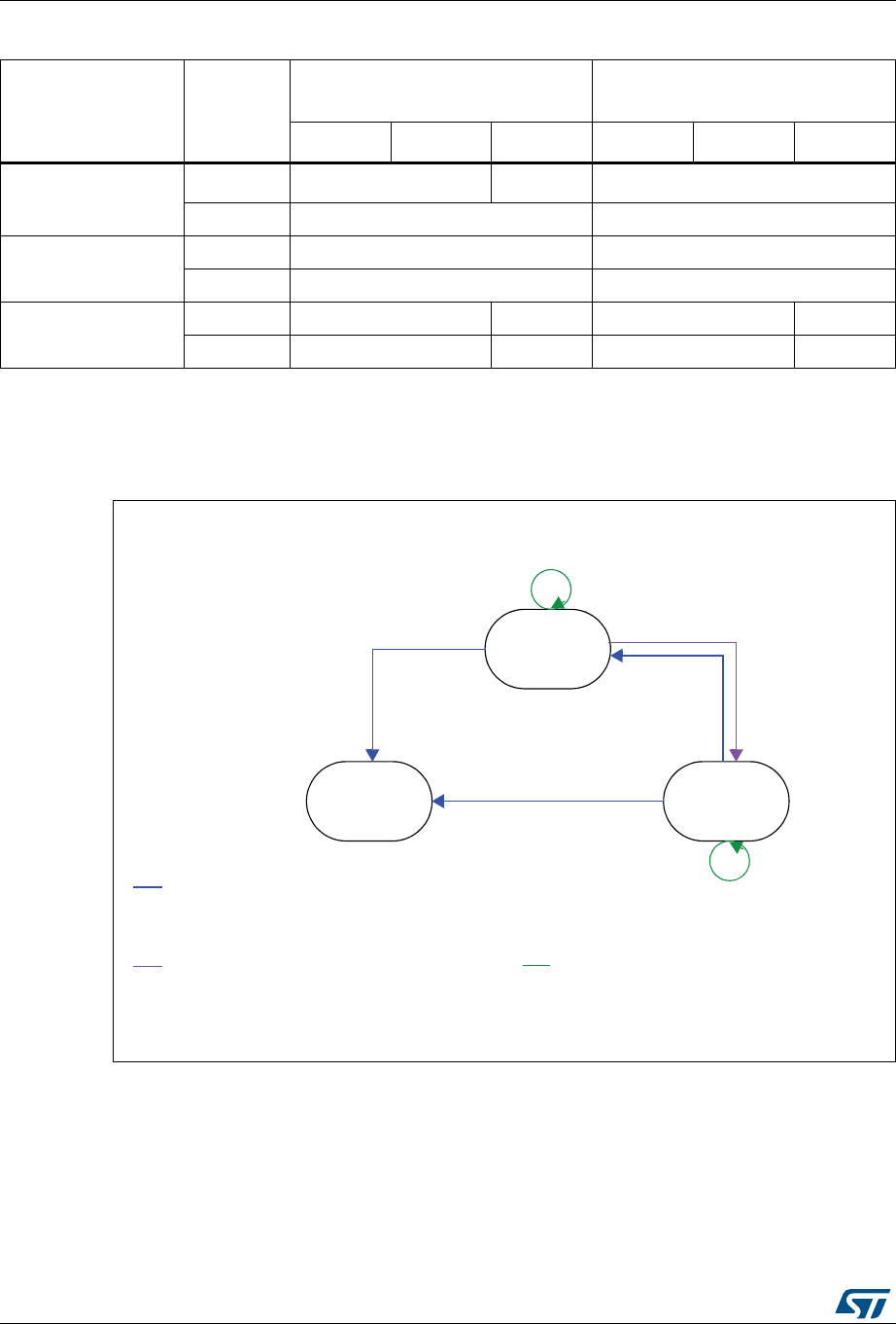
Embedded Flash memory interface RM0430
78/1324 RM0430 Rev 8
--
Figure 5 shows how to go from one RDP level to another.
Figure 5. RDP levels
3.6.4 Write protections
Up to 16 user sectors in Flash memory can be protected against unwanted write operations
due to loss of program counter contexts. When the non-write protection nWRPi bit
(0 ≤i≤14) in the FLASH_OPTCR registers is low, the corresponding sector cannot be
erased or programmed. Consequently, a mass erase cannot be performed if one of the
sectors is write-protected.
Table 11. Access versus read protection level
Memory area Protection
Level
Debug features, Boot from RAM or
from System memory bootloader Booting from Flash memory
Read Write Erase Read Write Erase
Main Flash Memory
Level 1 NO NO(1) YES
Level 2 NO YES
Option Bytes
Level 1 YES YES
Level 2 NO NO
OTP
Level 1 NO NA YES NA
Level 2 NO NA YES NA
1. The main Flash memory is only erased when the RDP changes from level 1 to 0. The OTP area remains unchanged.
,EVEL
LEVE,LEVE,
H!!0$2H##0$2
2$0!!H
2$0##H
DEFAULT
/PTIONSWRITE2$0LEVELINCREASEINCLUDES
/PTIONSERASE
.EWOPTIONSPROGRAM
/PTIONSWRITE2$0LEVELDECREASEINCLUDES
-ASSERASE
/PTIONSERASE
.EWOPTIONSPROGRAM
/PTIONSWRITE2$0LEVELIDENTICALINCLUDES
/PTIONSERASE
.EWOPTIONSPROGRAM
2$0!!H
/THERSOPTIONSMODIFIED
2$0!!H##H
/THERSOPTIONSMODIFIED
7RITEOPTIONS
INCLUDING
2$0!!H
7RITEOPTIONS
INCLUDING
2$0##H
7RITEOPTIONS
INCLUDING
2$0##H
7RITEOPTIONSINCLUDING
2$0##H!!H
AI

RM0430 Rev 8 79/1324
RM0430 Embedded Flash memory interface
89
If an erase/program operation to a write-protected part of the Flash memory is attempted
(sector protected by write protection bit, OTP part locked or part of the Flash memory that
can never be written like the ICP), the write protection error flag (WRPERR) is set in the
FLASH_SR register.
Note: When the memory read protection level is selected (RDP level = 1), it is not possible to
program or erase Flash memory sector i if the CPU debug features are connected (JTAG or
single wire) or boot code is being executed from RAM, even if nWRPi = 1.
Sector 14 and 15 are linked together and cannot be write-protected separately.
Write protection error flag
If an erase/program operation to a write protected area of the Flash memory is performed,
the Write Protection Error flag (WRPERR) is set in the FLASH_SR register.
If an erase operation is requested, the WRPERR bit is set when:
•Mass, sector erase are configured (MER or MER/MER1 and SER = 1)
•A sector erase is requested and the Sector Number SNB field is not valid
•A mass erase is requested while at least one of the user sector is write protected by
option bit (MER or MER/MER1 = 1 and nWRPi = 0 with 0 ≤i≤14 bits in the
FLASH_OPTCRx register
•A sector erase is requested on a write protected sector. (SER = 1, SNB = i and
nWRPi = 0 with 0 ≤i≤14 bits in the FLASH_OPTCRx register)
•The Flash memory is readout protected and an intrusion is detected.
If a program operation is requested, the WRPERR bit is set when:
•A write operation is performed on system memory or on the reserved part of the user
specific sector.
•A write operation is performed to the user configuration sector
•A write operation is performed on a sector write protected by option bit.
•A write operation is requested on an OTP area which is already locked
•The Flash memory is read protected and an intrusion is detected.
3.6.5 Proprietary code readout protection (PCROP)
Flash memory user sectors (0 to 15) can be protected against D-bus read accesses by
using the proprietary readout protection (PCROP).
The PCROP protection is selected as follows, through the SPRMOD option bit in the
FLASH_CR register:
•SPRMOD = 0: nWRPi control the write protection of respective user sectors
•SPRMOD = 1: nWRPi control the read and write protection (PCROP) of respective
user sectors.
When a sector is readout protected (PCROP mode activated), it can only be accessed for
code fetch through ICODE Bus on Flash interface:
•Any read access performed through the D-bus triggers a RDERR flag error.
•Any program/erase operation on a PCROPed sector triggers a WRPERR flag error.
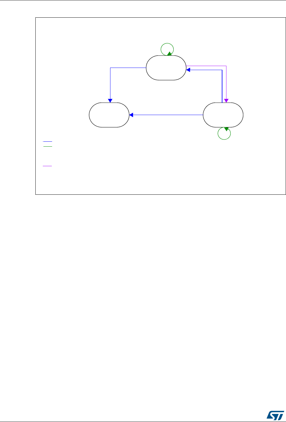
Embedded Flash memory interface RM0430
80/1324 RM0430 Rev 8
Figure 6. PCROP levels
The deactivation of the SPRMOD and/or the unprotection of PCROPed user sectors can
only occur when, at the same time, the RDP level changes from 1 to 0. If this condition is not
respected, the user option byte modification is canceled and the write error WRPERR flag is
set. The modification of the users option bytes (BOR_LEV, RST_STDBY, ..) is allowed since
none of the active nWRPi bits is reset and SPRMOD is kept active.
Note: The active value of nWRPi bits is inverted when PCROP mode is active (SPRMOD =1).
,EVEL
,EVEL
2$0X##
2$0X!!
2$0X##
DEFAULT
5SEROPTIONSECTORERASE
0ROGRAMNEWOPTIONS
'LOBALMASSERASE
5SEROPTIONSECTIONERASE
0ROGRAMNEWOPTIONS
7RITEOPTIONS
30-/$ACTIVE
ANDVALIDN720I
.ORESTRICTIONON
7RITEOPTIONS
7RITEOPTIONS
30-/$ACTIVE
ANDVALIDN720I
,EVEL
2$0X!!
7RITEOPTIONS
30-/$ACTIVE
ANDVALIDN720I
7RITEOPTIONS
30-/$ACTIVE
ANDVALIDN720I 7RITEOPTIONS
30-/$ACTIVE
ANDVALIDN720I
6ALIDN720IMEANSTHATNONEOFTHEN720BITSSETCANBERESETTRANSITIONFROMTO
-36

RM0430 Rev 8 81/1324
RM0430 Embedded Flash memory interface
89
3.7 One-time programmable bytes
Table 12 shows the organization of the one-time programmable (OTP) part of the OTP area.
The OTP area is divided into 16 OTP data blocks of 32 bytes and one lock OTP block of 16
bytes. The OTP data and lock blocks cannot be erased. The lock block contains 16 bytes
LOCKBi (0 ≤ i ≤ 15) to lock the corresponding OTP data block (blocks 0 to 15). Each OTP
data block can be programmed until the value 0x00 is programmed in the corresponding
OTP lock byte. The lock bytes must only contain 0x00 and 0xFF values, otherwise the OTP
bytes might not be taken into account correctly.
Table 12. OTP area organization
Block [128:96] [95:64] [63:32] [31:0] Address byte 0
0
OTP0 OTP0 OTP0 OTP0 0x1FFF 7800
OTP0 OTP0 OTP0 OTP0 0x1FFF 7810
1
OTP1 OTP1 OTP1 OTP1 0x1FFF 7820
OTP1 OTP1 OTP1 OTP1 0x1FFF 7830
.
.
.
.
.
.
.
.
.
15
OTP15 OTP15 OTP15 OTP15 0x1FFF 79E0
OTP15 OTP15 OTP15 OTP15 0x1FFF 79F0
Lock block LOCKB15 ...
LOCKB12
LOCKB11 ...
LOCKB8
LOCKB7 ...
LOCKB4
LOCKB3 ...
LOCKB0 0x1FFF 7A00

Embedded Flash memory interface RM0430
82/1324 RM0430 Rev 8
3.8 Flash interface registers
3.8.1 Flash access control register (FLASH_ACR)
The Flash access control register is used to enable/disable the acceleration features and
control the Flash memory access time according to CPU frequency.
Address offset: 0x00
Reset value: 0x0000 0000
Access: no wait state, word, half-word and byte access
31 30 29 28 27 26 25 24 23 22 21 20 19 18 17 16
Res. Res. Res. Res. Res. Res. Res. Res. Res. Res. Res. Res. Res. Res. Res. Res.
15 14 13 12 11 10 9 8 7 6 5 4 3 2 1 0
Res. Res. Res. DCRST ICRST DCEN ICEN PRFTEN Res. Res. Res. Res. LATENCY
rwwrwrw rw rwrwrwrw
Bits 31:13 Reserved, must be kept cleared.
Bit 12 DCRST: Data cache reset
0: Data cache is not reset
1: Data cache is reset
This bit can be written only when the D cache is disabled.
Bit 11 ICRST: Instruction cache reset
0: Instruction cache is not reset
1: Instruction cache is reset
This bit can be written only when the I cache is disabled.
Bit 10 DCEN: Data cache enable
0: Data cache is disabled
1: Data cache is enabled
Bit 9 ICEN: Instruction cache enable
0: Instruction cache is disabled
1: Instruction cache is enabled
Bit 8 PRFTEN: Prefetch enable
0: Prefetch is disabled
1: Prefetch is enabled
Bits 7:4 Reserved, must be kept cleared.
Bits 3:0 LATENCY: Latency
These bits represent the ratio of the CPU clock period to the Flash memory access time.
0000: Zero wait state
0001: One wait state
0010: Two wait states
-
-
-
1110: Fourteen wait states
1111: Fifteen wait states

RM0430 Rev 8 83/1324
RM0430 Embedded Flash memory interface
89
3.8.2 Flash key register (FLASH_KEYR)
The Flash key register is used to allow access to the Flash control register and so, to allow
program and erase operations.
Address offset: 0x04
Reset value: 0x0000 0000
Access: no wait state, word access
3.8.3 Flash option key register (FLASH_OPTKEYR)
The Flash option key register is used to allow program and erase operations in the user
configuration sector.
Address offset: 0x08
Reset value: 0x0000 0000
Access: no wait state, word access
31 30 29 28 27 26 25 24 23 22 21 20 19 18 17 16
KEY[31:16]
wwwwww w w w w w w w w w w
1514131211109876543210
KEY[15:0]
wwwwww w w w w w w w w w w
Bits 31:0 FKEYR: FPEC key
The following values must be programmed consecutively to unlock the FLASH_CR register
and allow programming/erasing it:
a) KEY1 = 0x45670123
b) KEY2 = 0xCDEF89AB
31 30 29 28 27 26 25 24 23 22 21 20 19 18 17 16
OPTKEYR[31:16
wwwwww w w w w w ww w w w
15 14 13 12 11 10 9 8 7 6 5 4 3 2 1 0
OPTKEYR[15:0]
wwwwww w w w w w ww w w w
Bits 31:0 OPTKEYR: Option byte key
The following values must be programmed consecutively to unlock the FLASH_OPTCR
register and allow programming it:
a) OPTKEY1 = 0x08192A3B
b) OPTKEY2 = 0x4C5D6E7F

Embedded Flash memory interface RM0430
84/1324 RM0430 Rev 8
3.8.4 Flash status register (FLASH_SR)
The Flash status register gives information on ongoing program and erase operations.
Address offset: 0x0C
Reset value: 0x0000 0000
Access: no wait state, word, half-word and byte access
31 30 29 28 27 26 25 24 23 22 21 20 19 18 17 16
Res. Res. Res. Res. Res. Res. Res. Res. Res. Res. Res. Res. Res. Res. Res. BSY
r
15 14 13 12 11 10 9 8 7 6 5 4 3 2 1 0
Res. Res. Res. Res. Res. Res. Res. RDERR PGSERR PGPERR PGAERR WRPERR Res. Res. OPERR EOP
rw rc_w1 rc_w1 rc_w1 rc_w1 rc_w1 rc_w1
Bits 31:17 Reserved, must be kept cleared.
Bit 16 BSY: Busy
This bit indicates that a Flash memory operation is in progress. It is set at the beginning of a
Flash memory operation and cleared when the operation finishes or an error occurs.
0: no Flash memory operation ongoing
1: Flash memory operation ongoing
Bits 15:9 Reserved, must be kept cleared.
Bit 8 RDERR: Read Protection Error (PCROP)
Set by hardware when an address to be read through the Dbus belongs to a read protected
part of the flash.
Reset by writing 1.
Bit 7 PGSERR: Programming sequence error
Set by hardware when a write access to the Flash memory is performed by the code while
the control register has not been correctly configured.
Cleared by writing 1.
Bit 6 PGPERR: Programming parallelism error
Set by hardware when the size of the access (byte, half-word, word, double word) during the
program sequence does not correspond to the parallelism configuration PSIZE (x8, x16,
x32, x64).
Cleared by writing 1.
Bit 5 PGAERR: Programming alignment error
Set by hardware when the data to program cannot be contained in the same 128-bit Flash
memory row.
Cleared by writing 1.
Bit 4 WRPERR: Write protection error
Set by hardware when an address to be erased/programmed belongs to a write-protected
part of the Flash memory.
Cleared by writing 1.

RM0430 Rev 8 85/1324
RM0430 Embedded Flash memory interface
89
3.8.5 Flash control register (FLASH_CR)
The Flash control register is used to configure and start Flash memory operations.
Address offset: 0x10
Reset value: 0x8000 0000
Access: no wait state when no Flash memory operation is ongoing, word, half-word and
byte access.
Bits 3:2 Reserved, must be kept cleared.
Bit 1 OPERR: Operation error
Set by hardware when a flash operation (programming / erase /read) request is detected and
can not be run because of parallelism, alignment, or write protection error. This bit is set only
if error interrupts are enabled (ERRIE = 1).
Bit 0 EOP: End of operation
Set by hardware when one or more Flash memory operations (program/erase) has/have
completed successfully. It is set only if the end of operation interrupts are enabled (EOPIE =
1).
Cleared by writing a 1.
31 30 29 28 27 26 25 24 23 22 21 20 19 18 17 16
LOCK Res. Res. Res. Res. Res. ERRIE EOPIE Res. Res. Res. Res. Res. Res. Res. STRT
rs rw rw rs
15 14 13 12 11 10 9 8 7 6 5 4 3 2 1 0
Res. Res. Res. Res. Res. Res. PSIZE[1:0] Res. SNB[3:0] MER SER PG
rw rw rw rw rw rw rw rw rw
Bit 31 LOCK: Lock
Write to 1 only. When it is set, this bit indicates that the FLASH_CR register is locked. It is
cleared by hardware after detecting the unlock sequence.
In the event of an unsuccessful unlock operation, this bit remains set until the next reset.
Bits 30:26 Reserved, must be kept cleared.
Bit 25 ERRIE: Error interrupt enable
This bit enables the interrupt generation when the OPERR bit in the FLASH_SR register is
set to 1.
0: Error interrupt generation disabled
1: Error interrupt generation enabled
Bit 24 EOPIE: End of operation interrupt enable
This bit enables the interrupt generation when the EOP bit in the FLASH_SR register goes
to 1.
0: Interrupt generation disabled
1: Interrupt generation enabled
Bits 23:17 Reserved, must be kept cleared.
Bit 16 STRT: Start
This bit triggers an erase operation when set. It is set only by software and cleared when the
BSY bit is cleared.
Bits 15:10 Reserved, must be kept cleared.

Embedded Flash memory interface RM0430
86/1324 RM0430 Rev 8
3.8.6 Flash option control register (FLASH_OPTCR)
The FLASH_OPTCR register is used to modify the user option bytes.
Address offset: 0x14
Reset value: 0x0FFF FFED. The option bits are loaded with values from Flash memory at
reset release.
Access: no wait state when no Flash memory operation is ongoing, word, half-word and
byte access.
Bits 9:8 PSIZE: Program size
These bits select the program parallelism.
00 program x8
01 program x16
10 program x32
11 program x64
Bit 7 Reserved, must be kept cleared.
Bits 6:3 SNB: Sector number
These bits select the sector to erase.
0000 sector 0
0001 sector 1
...
1010 sector 10
1011 sector 11
1100 sector 12
1101 sector 13
1110 sector 14
1111 sector 15
Bit 2 MER: Mass Erase
Erase activated for all user sectors.
Bit 1 SER: Sector Erase
Sector Erase activated.
Bit 0 PG: Programming
Flash programming activated.
31 30 29 28 27 26 25 24 23 22 21 20 19 18 17 16
SPR
MOD
nWRP
14_15 nWRP[13:0]
rw rw rw rw rw rw rw rw rw rw rw rw rw rw rw rw
1514131211109876543210
RDP[7:0] nRST_
STDBY
nRST_
STOP
WDG_
SW Res. BOR_LEV OPT
STRT
OPT
LOCK
rw rw rw rw rw rw rw rw rw rw rw rw rw rs rs

RM0430 Rev 8 87/1324
RM0430 Embedded Flash memory interface
89
Bit 31 SPRMOD: Selection of Protection Mode of nWPRi bits
0: PCROP disabled, nWPRi bits used for Write Protection on sector i
1: PCROP enabled, nWPRi bits used for PCROP Protection on sector i
Bit 30 nWRP14_15: Not write protect
This bit contains the value of the write-protection option byte of sectors 14 and 15. They can
be written to program a new write protect value into Flash memory. Sectors 14 and 15 are
linked together and cannot be programmed separately
0: Write protection active on sectors 14 and 15
1: Write protection not active on sectors 14 and 15
These bits contain the value of the write-protection and read-protection (PCROP) option
bytes for sectors 14 and 15 after reset. They can be written to program a new write-protect or
PCROP value into Flash memory.
If SPRMOD is reset:
0: Write protection active on sectors 14 and 15
1: Write protection not active on sectors 14 and 15
If SPRMOD is set:
0: PCROP protection not active on sectors 14 and 15
1: PCROP protection active on sectors 14 and 15
Bits 29:16 nWRP[13:0]: Not write protect
These bits contain the value of the write-protection option bytes of sectors after reset. They
can be written to program a new write protect value into Flash memory.
0: Write protection active on selected sector
1: Write protection not active on selected sector
These bits contain the value of the write-protection and read-protection (PCROP) option
bytes for sectors 0 to 13 after reset. They can be written to program a new write-protect or
PCROP value into Flash memory.
If SPRMOD is reset:
0: Write protection active on sector i
1: Write protection not active on sector i
If SPRMOD is set:
0: PCROP protection not active on sector i
1: PCROP protection active on sector i
Bits 15:8 RDP: Read protect
These bits contain the value of the read-protection option level after reset. They can be
written to program a new read protection value into Flash memory.
0xAA: Level 0, read protection not active
0xCC: Level 2, chip read protection active
Others: Level 1, read protection of memories active
Bits 7:5 USER: User option bytes
These bits contain the value of the user option byte after reset. They can be written to
program a new user option byte value into Flash memory.
Bit 7: nRST_STDBY
Bit 6: nRST_STOP
Bit 5: WDG_SW
Note: When changing the WDG mode from hardware to software or from software to
hardware, a system reset is required to make the change effective.
Bit 4 Reserved, must be kept cleared. Always read as “0”.

Embedded Flash memory interface RM0430
88/1324 RM0430 Rev 8
Bits 3:2 BOR_LEV: BOR reset Level
These bits contain the supply level threshold that activates/releases the reset. They can be
written to program a new BOR level. By default, BOR is off. When the supply voltage (VDD)
drops below the selected BOR level, a device reset is generated.
00: BOR Level 3 (VBOR3), brownout threshold level 3
01: BOR Level 2 (VBOR2), brownout threshold level 2
10: BOR Level 1 (VBOR1), brownout threshold level 1
11: BOR off, POR/PDR reset threshold level is applied
Note: For full details about BOR characteristics, refer to the “Electrical characteristics” section
in the device datasheet.
Bit 1 OPTSTRT: Option start
This bit triggers a user option operation when set. It is set only by software and cleared when
the BSY bit is cleared.
Bit 0 OPTLOCK: Option lock
Write to 1 only. When this bit is set, it indicates that the FLASH_OPTCR register is locked.
This bit is cleared by hardware after detecting the unlock sequence.
In the event of an unsuccessful unlock operation, this bit remains set until the next reset.

RM0430 Rev 8 89/1324
RM0430 Embedded Flash memory interface
89
3.8.7 Flash interface register map
Table 13. Flash register map and reset values
Offset Register
31
30
29
28
27
26
25
24
23
22
21
20
19
18
17
16
15
14
13
12
11
10
9
8
7
6
5
4
3
2
1
0
0x00
FLASH_ACR
Res.
Res.
Res.
Res.
Res.
Res.
Res.
Res.
Res.
Res.
Res.
Res.
Res.
Res.
Res.
Res.
Res.
Res.
Res.
DCRST
ICRST
DCEN
ICEN
PRFTEN
Res.
Res.
Res.
Res.
LATENCY
Reset value 00000 0 0 0 0
0x04
FLASH_KEYR KEY[31:16] KEY[15:0]
Reset value 00000000000000000000000000000 0 0 0
0x08
FLASH_
OPTKEYR OPTKEYR[31:16] OPTKEYR[15:0]
Reset value 00000000000000000000000000000 0 0 0
0x0C
FLASH_SR
Res.
Res.
Res.
Res.
Res.
Res.
Res.
Res.
Res.
Res.
Res.
Res.
Res.
Res.
Res.
BSY
Res.
Res.
Res.
Res.
Res.
Res.
Res.
RDERR
PGSERR
PGPERR
PGAERR
WRPERR
Res.
Res.
OPERR
EOP
Reset value 0 00000 0 0
0x10
FLASH_CR
LOCK
Res.
Res.
Res.
Res.
Res.
ERRIE
EOPIE
Res.
Res.
Res.
Res.
Res.
Res.
Res.
STRT
Res.
Res.
Res.
Res.
Res.
Res.
PSIZE[1:0]
Res.
SNB[3:0]
MER
SER
PG
Reset value 1 00 0 00 00000 0 0
0x14
FLASH_OPTCR
SPRMOD
nWRP14_15
nWRP[13:0] RDP[7:0]
nRST_STDBY
nRST_STOP
WDG_SW
Res.
BOR_LEV
OPTSTRT
OPTLOCK
Reset value 011111111111111110101010111 1 1 0 1
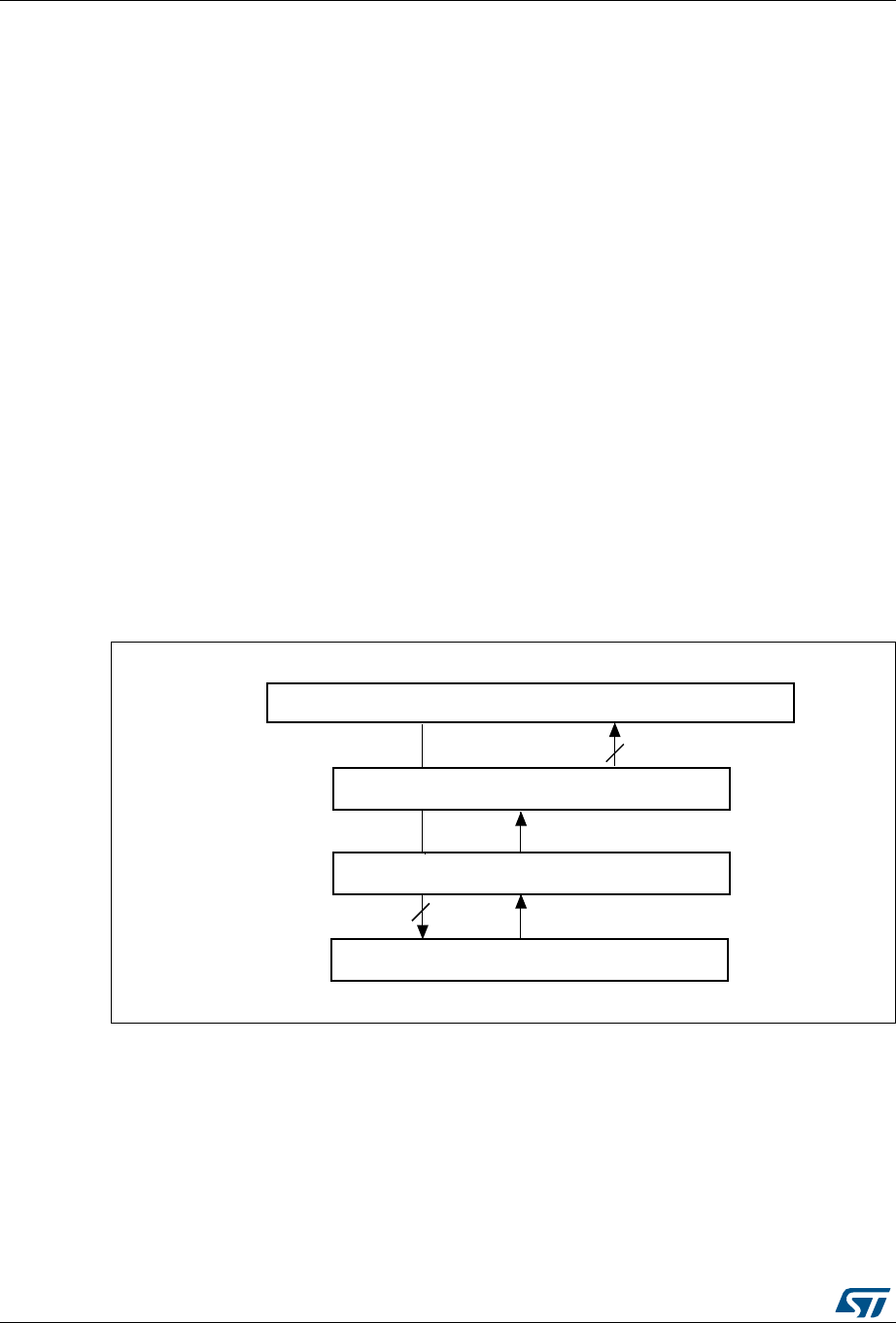
CRC calculation unit RM0430
90/1324 RM0430 Rev 8
4 CRC calculation unit
4.1 CRC introduction
The CRC (cyclic redundancy check) calculation unit is used to get a CRC code from a 32-bit
data word and a fixed generator polynomial.
Among other applications, CRC-based techniques are used to verify data transmission or
storage integrity. In the scope of the EN/IEC 60335-1 standard, they offer a way of verifying
the Flash memory integrity. The CRC calculation unit helps compute a signature of the
software during runtime, to be compared with a reference signature generated at link-time
and stored at a given memory location.
4.2 CRC main features
•Uses CRC-32 (Ethernet) polynomial: 0x4C11DB7
–X
32 + X26 + X23 + X22 + X16 + X12 + X11 + X10 +X8 + X7 + X5 + X4 + X2+ X +1
•Single input/output 32-bit data register
•CRC computation done in four AHB clock cycles (HCLK)
•General-purpose 8-bit register (can be used for temporary storage)
The block diagram is shown in Figure 7.
Figure 7. CRC calculation unit block diagram
4.3 CRC functional description
The CRC calculation unit mainly consists of a single 32-bit data register, which:
•is used as an input register to enter new data in the CRC calculator (when writing into
the register)
•holds the result of the previous CRC calculation (when reading the register)
$+%EXV
ELWUHDGDFFHVV
'DWDUHJLVWHURXWSXW
&5&FRPSXWDWLRQSRO\QRPLDO[&'%
ELWZULWHDFFHVV
'DWDUHJLVWHULQSXW
DL

RM0430 Rev 8 91/1324
RM0430 CRC calculation unit
93
Each write operation into the data register creates a combination of the previous CRC value
and the new one (CRC computation is done on the whole 32-bit data word, and not byte per
byte).
The write operation is stalled until the end of the CRC computation, thus allowing back-to-
back write accesses or consecutive write and read accesses.
The CRC calculator can be reset to 0xFFFF FFFF with the RESET control bit in the
CRC_CR register. This operation does not affect the contents of the CRC_IDR register.
4.4 CRC registers
The CRC calculation unit contains two data registers and a control register.The peripheral
The CRC registers have to be accessed by words (32 bits).
4.4.1 Data register (CRC_DR)
Address offset: 0x00
Reset value: 0xFFFF FFFF
31 30 29 28 27 26 25 24 23 22 21 20 19 18 17 16
DR [31:16]
rw rw rw rw rw rw rw rw rw rw rw rw rw rw rw rw
15 14 13 12 11 10 9 8 7 6 5 4 3 2 1 0
DR [15:0]
rw rw rw rw rw rw rw rw rw rw rw rw rw rw rw rw
Bits 31:0 Data register bits
Used as an input register when writing new data into the CRC calculator.
Holds the previous CRC calculation result when it is read.

CRC calculation unit RM0430
92/1324 RM0430 Rev 8
4.4.2 Independent data register (CRC_IDR)
Address offset: 0x04
Reset value: 0x0000 0000
4.4.3 Control register (CRC_CR)
Address offset: 0x08
Reset value: 0x0000 0000
31 30 29 28 27 26 25 24 23 22 21 20 19 18 17 16
Res. Res. Res. Res. Res. Res. Res. Res. Res. Res. Res. Res. Res. Res. Res. Res.
1514131211109876543210
Res. Res. Res. Res. Res. Res. Res. Res. IDR[7:0]
rw rw rw rw rw rw rw rw
Bits 31:8 Reserved, must be kept at reset value.
Bits 7:0 General-purpose 8-bit data register bits
Can be used as a temporary storage location for one byte.
This register is not affected by CRC resets generated by the RESET bit in the CRC_CR
register.
31 30 29 28 27 26 25 24 23 22 21 20 19 18 17 16
Res. Res. Res. Res. Res. Res. Res. Res. Res. Res. Res. Res. Res. Res. Res. Res.
15 14 13 12 11 10 9 8 7 6 5 4 3 2 1 0
Res. Res. Res. Res. Res. Res. Res. Res. Res. Res. Res. Res. Res. Res. Res. RESET
w
Bits 31:1 Reserved, must be kept at reset value.
Bit 0 RESET bit
Resets the CRC calculation unit and sets the data register to 0xFFFF FFFF.
This bit can only be set, it is automatically cleared by hardware.

RM0430 Rev 8 93/1324
RM0430 CRC calculation unit
93
4.4.4 CRC register map
Table 14. CRC calculation unit register map and reset values
Offset Register
31
30
29
28
27
26
25
24
23
22
21
20
19
18
17
16
15
14
13
12
11
10
9
8
7
6
5
4
3
2
1
0
0x00
CRC_DR Data register
Reset value 0xFFFF FFFF
0x04
CRC_IDR
Res.
Res.
Res.
Res.
Res.
Res.
Res.
Res.
Res.
Res.
Res.
Res.
Res.
Res.
Res.
Res.
Res.
Res.
Res.
Res.
Res.
Res.
Res.
Res.
Independent data register
Reset value 0x0000
0x08
CRC_CR
Res.
Res.
Res.
Res.
Res.
Res.
Res.
Res.
Res.
Res.
Res.
Res.
Res.
Res.
Res.
Res.
Res.
Res.
Res.
Res.
Res.
Res.
Res.
Res.
Res.
Res.
Res.
Res.
Res.
Res.
Res.
RESET
Reset value 0

Power controller (PWR) RM0430
94/1324 RM0430 Rev 8
5 Power controller (PWR)
5.1 Power supplies
There are two main power supply schemes:
•VDD = 1.7 to 3.6 V: external power supply for I/Os with the internal regulator disabled,
provided externally through VDD pins. Requires the use of an external power supply
supervisor connected to the VDD and PDR_ON pins.
•VDD = 1.8 to 3.6 V: external power supply for I/Os and the internal regulator (when
enabled), provided externally through VDD pins.
•VDD_USB = 3.0 to 3.6 V
VDD_USB is a dedicated independent USB power supply for full speed transceivers.
Note: VDD_USB value does not dependent on VDD and VDDA. However, VDD_USB must be the last
supply to be delivered to the device and the first to be switched off. When the three power
supplies are shut down, if VDD_USB remains active for a short period of time and VDDA/VDDIO
fall below the functional range, the device is not be damaged.
The device is still functional when VDD_USB is switched off.
The real-time clock (RTC), and the RTC backup registers can be powered from the VBAT
voltage when the main VDD supply is powered off.
Note: Depending on the operating power supply range, some peripheral may be used with limited
functionality and performance. For more details refer to section "General operating
conditions" in the datasheet.
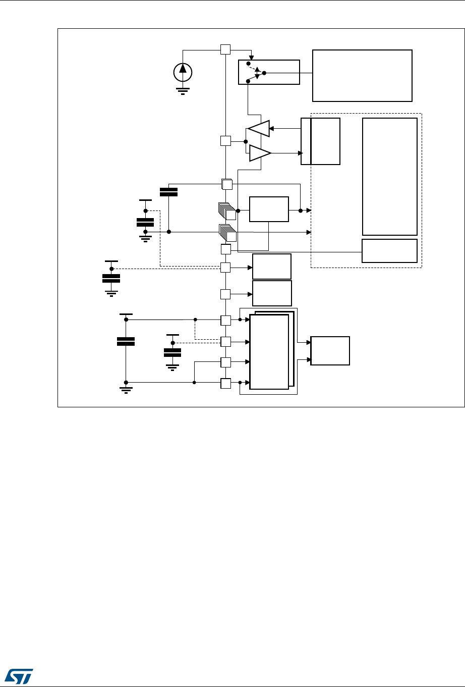
RM0430 Rev 8 95/1324
RM0430 Power controller (PWR)
116
Figure 8. Power supply overview
1. VDDA and VSSA must be connected to VDD and VSS, respectively.
5.1.1 Independent A/D converter supply and reference voltage
To improve conversion accuracy, the ADC has an independent power supply which can be
separately filtered and shielded from noise on the PCB.
•The ADC voltage supply input is available on a separate VDDA pin.
•An isolated supply ground connection is provided on pin VSSA.
To ensure a better accuracy of low voltage inputs, the user can connect a separate external
reference voltage ADC input on VREF
. The voltage on VREF ranges from 1.7 V to VDDA.
5.1.2 Battery backup domain
Backup domain description
To retain the content of the RTC backup registers and supply the RTC when VDD is turned
off, VBAT pin can be connected to an optional standby voltage supplied by a battery or by
another source.
06Y9
%DFNXSFLUFXLWU\
26&.57&
:DNHXSORJLF
%DFNXSUHJLVWHUV
.HUQHOORJLF
&38GLJLWDO
5$0
$QDORJ
5&V
3//
3RZHU
VZLWFK
9%$7
*3,2V
287
,1
îQ)
î)
9%$7
WR9
9ROWDJH
UHJXODWRU
9''$
$'&
/HYHOVKLIWHU
,2
/RJLF
9''
Q)
)
)ODVKPHPRU\
9&$3B
9&$3B
î)
%<3$66B5(*
3'5B21 5HVHW
FRQWUROOHU
9''
966
9''
95()
95()
966$
95()
Q)
)
27*
)6
3+<
9''B86%
Q)
)
9''B86%

Power controller (PWR) RM0430
96/1324 RM0430 Rev 8
To allow the RTC to operate even when the main digital supply (VDD) is turned off, the VBAT
pin powers the following blocks:
•The RTC
•The LSE oscillator
•PC13 to PC15 I/Os
The switch to the VBAT supply is controlled by the power-down reset embedded in the Reset
block.
Warning: During tRSTTEMPO (temporization at VDD startup) or after a PDR
is detected, the power switch between VBAT and VDD remains
connected to VBAT
.
During the startup phase, if VDD is established in less than
tRSTTEMPO (Refer to the datasheet for the value of tRSTTEMPO)
and VDD > VBAT + 0.6 V, a current may be injected into VBAT
through an internal diode connected between VDD and the
power switch (VBAT).
If the power supply/battery connected to the VBAT pin cannot
support this current injection, it is strongly recommended to
connect an external low-drop diode between this power
supply and the VBAT pin.
If no external battery is used in the application, it is recommended to connect the VBAT pin to
VDD with a 100 nF external decoupling ceramic capacitor in parallel.
When the backup domain is supplied by VDD (analog switch connected to VDD), the
following functions are available:
•PC14 and PC15 can be used as either GPIO or LSE pins
•PC13 can be used as a GPIO or additional functions can be configured (refer to
Table 27: RTC additional functions for more details about this pin configuration)
Note: Due to the fact that the switch only sinks a limited amount of current (3 mA), the use of
PC13 to PC15 GPIOs in output mode is restricted: the speed has to be limited to 2 MHz with
a maximum load of 30 pF and these I/Os must not be used as a current source (e.g. to drive
an LED).
When the backup domain is supplied by VBAT (analog switch connected to VBAT because
VDD is not present), the following functions are available:
•PC14 and PC15 can be used as LSE pins only
•PC13 can be used as the RTC additional function pin (refer to Table 27: RTC additional
functions for more details about this pin configuration)

RM0430 Rev 8 97/1324
RM0430 Power controller (PWR)
116
Backup domain access
After reset, the backup domain (RTC registers, and RTC backup register) is protected
against possible unwanted write accesses. To enable access to the backup domain,
proceed as follows:
•Access to the RTC and RTC backup registers
1. Enable the power interface clock by setting the PWREN bits in the RCC_APB1ENR
register (see Section 6.3.14: RCC AHB3 peripheral clock enable register
(RCC_AHB3ENR))
2. Set the DBP bit in the Section 5.4.1 to enable access to the backup domain
3. Select the RTC clock source: see Section 6.2.8: RTC/AWU clock
4. Enable the RTC clock by programming the RTCEN [15] bit in the Section 6.3.23: RCC
Backup domain control register (RCC_BDCR)
RTC and RTC backup registers
The real-time clock (RTC) is an independent BCD timer/counter. The RTC provides a time-
of-day clock/calendar, two programmable alarm interrupts, and a periodic programmable
wakeup flag with interrupt capability. The RTC contains 20 backup data registers (80 bytes)
which are reset when a tamper detection event occurs. For more details refer to Section 25:
Real-time clock (RTC).
5.1.3 Voltage regulator
An embedded linear voltage regulator supplies all the digital circuitries except for the backup
domain and the Standby circuitry. The regulator output voltage is around 1.2 V.
This voltage regulator requires one or two external capacitors to be connected to one or two
dedicated pins, VCAP_1 and for some packages VCAP_2. Specific pins must be connected
either to VSS or VDD to activate or deactivate the voltage regulator. These pins depend on
the package.
When activated by software, the voltage regulator is always enabled after Reset. It works in
three different modes depending on the application modes.
•In Run mode, the regulator supplies full power to the 1.2 V domain (core, memories
and digital peripherals). In this mode, the regulator output voltage (around 1.2 V) can
be scaled by software to different voltage values, Scale 1, scale 2, or scale 3, that can
be configured through the VOS[1:0] bits of the PWR_CR register. After reset the VOS
register is set to scale 2. When the PLL is OFF, the voltage regulator is set to scale 3
independently of the VOS register content. The VOS register content is only taken into
account once the PLL is activated and the HSI or HSE is selected as clock source.
The voltage scaling allows optimizing the power consumption when the device is
clocked below the maximum system frequency.
•In Stop mode, the main regulator or the low-power regulator supplies low power to the
1.2 V domain, thus preserving the content of registers and internal SRAM. The voltage
regulator can be put either in main regulator mode (MR) or in low-power mode (LPR).
The programmed voltage scale remains the same during Stop mode:
Voltage scale 3 is automatically selected when the microcontroller enters Stop mode
(see Section 5.4.1: PWR power control register (PWR_CR)).
•In Standby mode, the regulator is powered down. The content of the registers and
SRAM are lost except for the Standby circuitry and the backup domain.
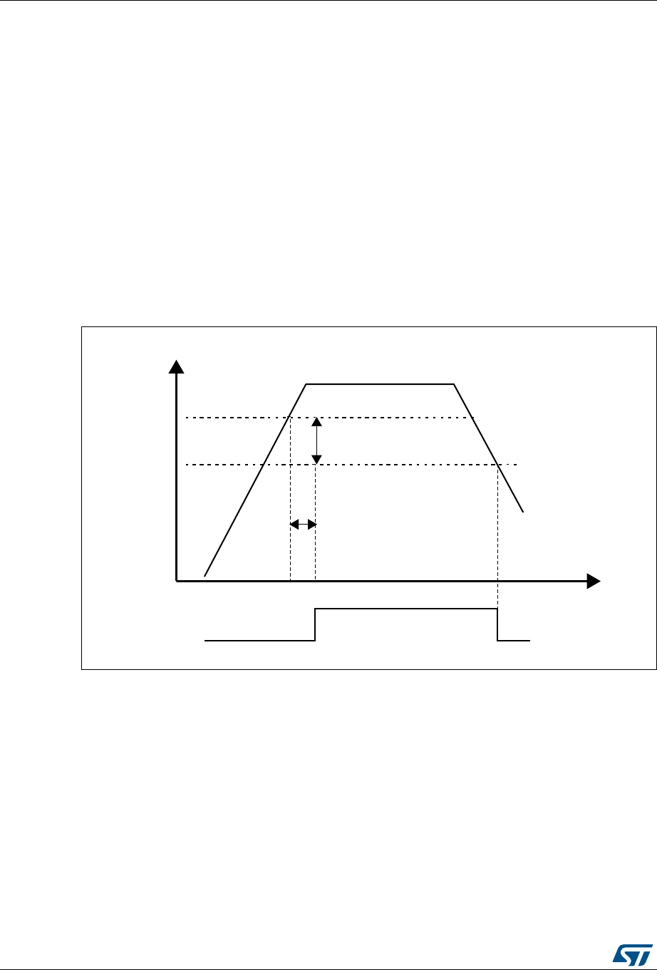
Power controller (PWR) RM0430
98/1324 RM0430 Rev 8
Note: For more details, refer to the voltage regulator section in the STM32F413/423 datasheet.
5.2 Power supply supervisor
5.2.1 Power-on reset (POR)/power-down reset (PDR)
The device has an integrated POR/PDR circuitry that allows proper operation starting
from 1.8 V.
To use the device below 1.8 V, the internal power supervisor must be switched off using the
PDR_ON pin (please refer to section Power supply supervisor of the STM32F413/423
datasheet). The device remains in Reset mode when VDD/VDDA is below a specified
threshold, VPOR/PDR, without the need for an external reset circuit. For more details
concerning the power on/power-down reset threshold, refer to the electrical characteristics
of the datasheet.
Figure 9. Power-on reset/power-down reset waveform
5.2.2 Brownout reset (BOR)
During power on, the Brownout reset (BOR) keeps the device under reset until the supply
voltage reaches the specified VBOR threshold.
VBOR is configured through device option bytes. By default, BOR is off. 3 programmable
VBOR threshold levels can be selected:
•BOR Level 3 (VBOR3). Brownout threshold level 3.
•BOR Level 2 (VBOR2). Brownout threshold level 2.
•BOR Level 1 (VBOR1). Brownout threshold level 1.
Note: For full details about BOR characteristics, refer to the "Electrical characteristics" section in
the device datasheet.
6$$6$$!
M6
HYSTERESIS
0$2
0$2
-36
2ESET
4EMPORIZATION
T2344%-0/
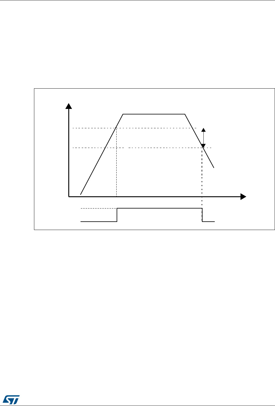
RM0430 Rev 8 99/1324
RM0430 Power controller (PWR)
116
When the supply voltage (VDD) drops below the selected VBOR threshold, a device reset is
generated.
The BOR can be disabled by programming the device option bytes. In this case, the
power-on and power-down is then monitored by the POR/ PDR or by an external power
supervisor if the PDR is switched off through the PDR_ON pin (see Section 5.2.1: Power-on
reset (POR)/power-down reset (PDR)).
The BOR threshold hysteresis is ~100 mV (between the rising and the falling edge of the
supply voltage).
Figure 10. BOR thresholds
5.2.3 Programmable voltage detector (PVD)
You can use the PVD to monitor the VDD power supply by comparing it to a threshold
selected by the PLS[2:0] bits in the PWR power control register (PWR_CR).
The PVD is enabled by setting the PVDE bit.
A PVDO flag is available, in the PWR power control/status register (PWR_CSR), to indicate
if VDD is higher or lower than the PVD threshold. This event is internally connected to the
EXTI line16 and can generate an interrupt if enabled through the EXTI registers. The PVD
output interrupt can be generated when VDD drops below the PVD threshold and/or when
VDD rises above the PVD threshold depending on EXTI line16 rising/falling edge
configuration. As an example the service routine could perform emergency shutdown tasks.
-36
6$$6$$!
M6
HYSTERESIS
"/2THRESHOLD
2ESET
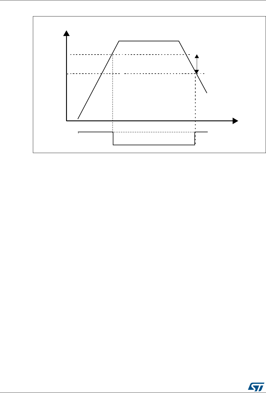
Power controller (PWR) RM0430
100/1324 RM0430 Rev 8
Figure 11. PVD thresholds
5.3 Low-power modes
By default, the microcontroller is in Run mode after a system or a power-on reset. In Run
mode the CPU is clocked by HCLK and the program code is executed. Several low-power
modes are available to save power when the CPU does not need to be kept running, for
example when waiting for an external event. It is up to the user to select the mode that gives
the best compromise between low-power consumption, short startup time and available
wakeup sources.
The devices feature four low-power modes:
•Sleep mode (Cortex®-M4 with FPU core stopped, peripherals kept running)
•Stop mode (all clocks are stopped)
•Standby mode (1.2 V domain powered off)
•Batch acquisition mode (BAM): the devices are in Sleep mode, the Flash memory is off,
needed peripheral are kept running, data transfer are still possible through DMA.
In addition, the power consumption in Run mode can be reduce by one of the following
means:
•Slowing down the system clocks
•Gating the clocks to the APBx and AHBx peripherals when they are unused.
Entering low-power mode
Low-power modes are entered by the MCU by executing the WFI (Wait For Interrupt), or
WFE (Wait for Event) instructions, or when the SLEEPONEXIT bit in the Cortex®-M4 with
FPU System Control register is set on Return from ISR.
Entering Low-power mode through WFI or WFE will be executed only if no interrupt is
pending or no event is pending.
069
9''
P9
K\VWHUHVLV
39'WKUHVKROG
39'RXWSXW

RM0430 Rev 8 101/1324
RM0430 Power controller (PWR)
116
Exiting low-power mode
The MCU exits from Sleep and Stop modes low-power mode depending on the way the low-
power mode was entered:
•If the WFI instruction or Return from ISR was used to enter the low-power mode, any
peripheral interrupt acknowledged by the NVIC can wake up the device.
•If the WFE instruction is used to enter the low-power mode, the MCU exits the low-
power mode as soon as an event occurs. The wakeup event can be generated either
by:
– NVIC IRQ interrupt:
When SEVONPEND = 0 in the Cortex®-M4 with FPU System Control register: by
enabling an interrupt in the peripheral control register and in the NVIC. When the
MCU resumes from WFE, the peripheral interrupt pending bit and the NVIC
peripheral IRQ channel pending bit (in the NVIC interrupt clear pending register)
have to be cleared. Only NVIC interrupts with sufficient priority will wakeup and
interrupt the MCU.
When SEVONPEND = 1 in the Cortex®-M4 with FPU System Control register: by
enabling an interrupt in the peripheral control register and optionally in the NVIC.
When the MCU resumes from WFE, the peripheral interrupt pending bit and when
enabled the NVIC peripheral IRQ channel pending bit (in the NVIC interrupt clear
pending register) have to be cleared. All NVIC interrupts will wakeup the MCU,
even the disabled ones.Only enabled NVIC interrupts with sufficient priority will
wakeup and interrupt the MCU.
–Event
This is done by configuring a EXTI line in event mode. When the CPU resumes
from WFE, it is not necessary to clear the EXTI peripheral interrupt pending bit or
the NVIC IRQ channel pending bit as the pending bits corresponding to the event
line is not set. It may be necessary to clear the interrupt flag in the peripheral.
The MCU exits from Standby low-power mode through an external reset (NRST pin), an
IWDG reset, a rising edge on one of the enabled WKUPx pins or a RTC event occurs (see
Figure 254: RTC block diagram).
After waking up from Standby mode, program execution restarts in the same way as after a
Reset (boot pin sampling, option bytes loading, reset vector is fetched, etc.).

Power controller (PWR) RM0430
102/1324 RM0430 Rev 8
Only enabled NVIC interrupts with sufficient priority will wakeup and interrupt the MCU.
5.3.1 Slowing down system clocks
In Run mode the speed of the system clocks (SYSCLK, HCLK, PCLK1, PCLK2) can be
reduced by programming the prescaler registers. These prescalers can also be used to slow
down peripherals before entering Sleep mode.
For more details refer to Section 6.3.3: RCC clock configuration register (RCC_CFGR).
5.3.2 Peripheral clock gating
In Run mode, the HCLKx and PCLKx for individual peripherals and memories can be
stopped at any time to reduce power consumption.
To further reduce power consumption in Sleep mode the peripheral clocks can be disabled
prior to executing the WFI or WFE instructions.
Peripheral clock gating is controlled by the AHB1 peripheral clock enable register
(RCC_AHB1ENR), AHB2 peripheral clock enable register (RCC_AHB2ENR) (see
Section 6.3.11: RCC AHB1 peripheral clock enable register (RCC_AHB1ENR),
Section 6.3.12: RCC AHB2 peripheral clock enable register (RCC_AHB2ENR) for
STM32F413xx and Section 6.3.14: RCC AHB3 peripheral clock enable register
(RCC_AHB3ENR)).
Disabling the peripherals clocks in Sleep mode can be performed automatically by resetting
the corresponding bit in RCC_AHBxLPENR and RCC_APBxLPENR registers.
Table 15. Low-power mode summary
Mode name Entry Wakeup Effect on 1.2 V
domain clocks
Effect on
VDD
domain
clocks
Voltage regulator
Sleep and
BAM(1)
(Sleep now or
Sleep-on-
exit)
WFI or Return
from ISR Any interrupt CPU CLK OFF
no effect on other
clocks or analog
clock sources
None ON
WFE Wakeup event
Stop
SLEEPDEEP bit
+ WFI, Return
from ISR or WFE
Any EXTI line (configured
in the EXTI registers,
internal and external lines)
All 1.2 V domain
clocks OFF
HSI and
HSE
oscillator
s OFF
Main regulator or
Low-Power
regulator (depends
on PWR power
control register
(PWR_CR)
Standby
PDDS bit +
SLEEPDEEP bit
+ WFI, Return
from ISR or WFE
WKUP pin rising edge,
RTC alarm (Alarm A or
Alarm B), RTC Wakeup
event, RTC tamper
events, RTC time stamp
event, external reset in
NRST pin, IWDG reset
OFF
1. Refer to Section 5.3.4: Batch acquisition mode for specific BAM entry and exit requirements.

RM0430 Rev 8 103/1324
RM0430 Power controller (PWR)
116
5.3.3 Sleep mode
Entering Sleep mode
The Sleep mode is entered according to Entering low-power mode, when the SLEEPDEEP
bit in the Cortex®-M4 with FPU System Control register is cleared.
Refer to Table 16 and Table 17 for details on how to enter Sleep mode.
Note: All interrupt pending bits must be cleared before the sleep mode entry.
Exiting Sleep mode
The Sleep mode is exited according to Exiting low-power mode.
Refer to Table 16 and Table 17 for more details on how to exit Sleep mode.
Table 16. Sleep-now entry and exit
Sleep-now mode Description
Mode entry
WFI (Wait for Interrupt) or WFE (Wait for Event) while:
– SLEEPDEEP = 0, and
– No interrupt (for WFI) or event (for WFE) is pending.
Refer to the Cortex®-M4 with FPU System Control register.
On Return from ISR while:
– SLEEPDEEP = 0 and
– SLEEPONEXIT = 1,
– No interrupt is pending.
Refer to the Cortex®-M4 with FPU System Control register.
Mode exit
If WFI or Return from ISR was used for entry:
Interrupt: Refer to Table 40: Vector table for STM32F413/423
If WFE was used for entry and SEVONPEND = 0
Wakeup event: Refer to Section 10.2.3: Wakeup event management
f WFE was used for entry and SEVONPEND = 1
Interrupt even when disabled in NVIC: refer to Table 40: Vector table for
STM32F413/423 or Wakeup event (see Section 10.2.3: Wakeup event
management).
Wakeup latency None
Table 17. Sleep-on-exit entry and exit
Sleep-on-exit Description
Mode entry
WFI (Wait for Interrupt) or WFE (Wait for Event) while:
– SLEEPDEEP = 0, and
– No interrupt (for WFI) or event (for WFE) is pending.
Refer to the Cortex®-M4 with FPU System Control register.
On Return from ISR while:
– SLEEPDEEP = 0, and
– SLEEPONEXIT = 1, and
– No interrupt is pending.
Refer to the Cortex®-M4 with FPU System Control register.

Power controller (PWR) RM0430
104/1324 RM0430 Rev 8
5.3.4 Batch acquisition mode
Entering BAM
The BAM is entered according to Section : Entering low-power mode, when the
SLEEPDEEP bit in the Cortex®-M4 with FPU System Control register is cleared.
Refer to Table 18 and Table 19 for details on how to enter Sleep mode.
Before entering Sleep mode, the Flash memory must be configured by software to operate
in the required low- power mode. If data need to be transferred from peripheral to RAM
during BAM, the DMA must be enabled before entering Sleep mode.
Exiting BAM
The BAM is exited according to Section : Exiting low-power mode.
Refer to Table 18 and Table 19 for more details on how to exit Sleep mode.
After waking up from BAM, the Flash memory must first to be waked up if code execution
restarts from Flash memory.
This wakeup time must be managed by software running from the internal SRAM.
Mode exit Interrupt: refer to Table 40: Vector table for STM32F413/423
Wakeup latency None
Table 17. Sleep-on-exit entry and exit (continued)
Sleep-on-exit Description
Table 18. BAM-now entry and exit
Sleep-now mode Description
Mode entry
Set the Flash memory in low-power mode:
– FISSR/FMSSR and FPDS bits of the PWR_CR register
WFI (Wait for Interrupt) or WFE (Wait for Event) while:
– SLEEPDEEP = 0 and
– SLEEPONEXIT = 0
Refer to the Cortex®-M4 with FPU System Control register.
Mode exit
If WFI was used for entry:
Interrupt: Refer to Table 40: Vector table for STM32F413/423
If WFE was used for entry
Wakeup event: Refer to Section 10.2.3: Wakeup event management
If Flash memory wakeup time is needed, FISSR/FMSSR bits of PWR_CR
register must be set
Wakeup latency
None if code executed from RAM
Low-power mode Flash memory wakeup time, before restarting code
execution from Flash memory (refer to the Flash memory wakeup time in
the Electrical characteristics section of the datasheet).

RM0430 Rev 8 105/1324
RM0430 Power controller (PWR)
116
Note: The BAM has been enhanced by adding SRAM2 that allows SRAM code to be executed
through the Ibus and Dbus, thus improving code execution performance.
5.3.5 Stop mode
The Stop mode is based on the Cortex®-M4 with FPU deepsleep mode combined with
peripheral clock gating. The voltage regulator can be configured either in normal or low-
power mode. In Stop mode, all clocks in the 1.2 V domain are stopped, the PLLs, the HSI
and the HSE RC oscillators are disabled. Internal SRAM and register contents are
preserved.
Some settings in the PWR_CR register allow to further reduce the power consumption.
When the Flash memory is in power-down mode, an additional startup delay is incurred
when waking up from Stop mode (see Table 20: Stop operating modes and Section 5.4.1:
PWR power control register (PWR_CR)).
Table 19. BAM-on-exit entry and exit
Sleep-on-exit Description
Mode entry
Set the Flash memory in low-power mode:
– FISSR/FMSSR and FPDS bits of the PWR_CR register
WFI (wait for interrupt) while:
– SLEEPDEEP = 0 and
– SLEEPONEXIT = 1
Refer to the Cortex®-M4 with FPU System Control register.
Mode exit
Interrupt: refer to Table 40: Vector table for STM32F413/423
If Flash memory wakeup time is needed, FISSR/FMSSR bits of PWR_CR
register must be set
Wakeup latency
None when code executed from internal SRAM
Low-power mode Flash memory wakeup time, before restarting code
execution from Flash memory (refer to the Flash memory wakeup time in
the Electrical characteristics section of the datasheet).

Power controller (PWR) RM0430
106/1324 RM0430 Rev 8
Entering Stop mode
The Stop mode is entered according to Section : Entering low-power mode, when the
SLEEPDEEP bit in the Cortex®-M4 with FPU System Control register is set.
Refer to Table 21 for details on how to enter the Stop mode.
To further reduce power consumption in Stop mode, the internal voltage regulator can be put
in low-power mode. This is configured by the LPDS bit of the PWR power control register
(PWR_CR).
If Flash memory programming is ongoing, the Stop mode entry is delayed until the memory
access is finished.
If an access to the APB domain is ongoing, The Stop mode entry is delayed until the APB
access is finished.
In Stop mode, the following features can be selected by programming individual control bits:
•Independent watchdog (IWDG): the IWDG is started by writing to its Key register or by
hardware option. Once started it cannot be stopped except by a Reset. See
Table 20. Stop operating modes
Stop mode MRLV bit LPLV bit FPDS bit LPDS bit Wakeup latency
Normal mode
STOP MR 0 - 0 0 HSI RC startup time
STOP MRFPD 0 - 1 0
HSI RC startup time +
Flash wakeup time from Deep
Power Down mode
STOP LP0001
HSI RC startup time +
regulator wakeup time from LP
mode
STOP LPFPD - 0 1 1
HSI RC startup time +
Flash wakeup time from Deep
Power Down mode +
regulator wakeup time from LP
mode
STOP MRLV 1 - - 0
HSI RC startup time +
Flash wakeup time from Deep
Power Down mode +
Main regulator from low voltage
mode
STOP LPLV-1-1
HSI RC startup time +
Flash wakeup time from Deep
Power Down mode +
regulator wakeup time from Low
Voltage LP mode

RM0430 Rev 8 107/1324
RM0430 Power controller (PWR)
116
Section 23.3 in Section 23: Window watchdog (WWDG).
•Real-time clock (RTC): this is configured by the RTCEN bit in the Section 6.3.23: RCC
Backup domain control register (RCC_BDCR)
•Internal RC oscillator (LSI RC): this is configured by the LSION bit in the
Section 6.3.24: RCC clock control & status register (RCC_CSR).
•External 32.768 kHz oscillator (LSE OSC): this is configured by the LSEON bit in the
Section 6.3.23: RCC Backup domain control register (RCC_BDCR).
The ADC can also consume power during the Stop mode, unless it is disabled before
entering it. To disable it, the ADON bit in the ADC_CR2 register must be written to 0.
Note: If the application needs to disable the external clock before entering Stop mode, the HSEON
bit must first be disabled and the system clock switched to HSI.
Otherwise, if the HSEON bit is kept enabled while the external clock (external oscillator) can
be removed before entering stop mode, the clock security system (CSS) feature must be
enabled to detect any external oscillator failure and avoid a malfunction behavior when
entering stop mode.
Exiting Stop mode
The Stop mode is exited according to Section : Exiting low-power mode.
Refer to Table 21 for more details on how to exit Stop mode.
When exiting Stop mode by issuing an interrupt or a wakeup event, the HSI RC oscillator is
selected as system clock.
When the voltage regulator operates in low-power mode, an additional startup delay is
incurred when waking up from Stop mode. By keeping the internal regulator ON during Stop
mode, the consumption is higher although the startup time is reduced.
Table 21. Stop mode entry and exit
Stop mode Description
Mode entry
WFI (Wait for Interrupt) or WFE (Wait for Event) while:
– No interrupt (for WFI) or event (for WFE) is pending,
– SLEEPDEEP bit is set in Cortex®-M4 with FPU System Control register,
– PDDS bit is cleared in Power Control register (PWR_CR),
– Select the voltage regulator mode by configuring LPDS bit in PWR_CR.
On Return from ISR:
– No interrupt is pending,
– SLEEPDEEP bit is set in Cortex®-M4 with FPU System Control register,
– SLEEPONEXIT = 1,
– PDDS bit is cleared in Power Control register (PWR_CR).
Note: To enter Stop mode, all EXTI Line pending bits (in Section 10.3.6:
Pending register (EXTI_PR)), all peripheral interrupts pending bits,
the RTC Alarm (Alarm A and Alarm B), RTC wakeup, RTC tamper,
and RTC time stamp flags, must be reset. Otherwise, the Stop
mode entry procedure is ignored and program execution continues.

Power controller (PWR) RM0430
108/1324 RM0430 Rev 8
5.3.6 Standby mode
The Standby mode allows to achieve the lowest power consumption. It is based on the
Cortex®-M4 with FPU deepsleep mode, with the voltage regulator disabled. The 1.2 V
domain is consequently powered off. The PLLs, the HSI oscillator and the HSE oscillator are
also switched off. SRAM and register contents are lost except for registers in the backup
domain (RTC registers and RTC backup register), and Standby circuitry (see Figure 8).
Entering Standby mode
The Standby mode is entered according to Section : Entering low-power mode, when the
SLEEPDEEP bit in the Cortex®-M4 with FPU System Control register is set.
Refer to Table 22 for more details on how to enter Standby mode.
In Standby mode, the following features can be selected by programming individual control
bits:
•Independent watchdog (IWDG): the IWDG is started by writing to its Key register or by
hardware option. Once started it cannot be stopped except by a reset. See
Section 22.3 in Section 22: Independent watchdog (IWDG).
•Real-time clock (RTC): this is configured by the RTCEN bit in the backup domain
control register (RCC_BDCR)
•Internal RC oscillator (LSI RC): this is configured by the LSION bit in the Control/status
register (RCC_CSR).
•External 32.768 kHz oscillator (LSE OSC): this is configured by the LSEON bit in the
backup domain control register (RCC_BDCR)
Exiting Standby mode
The Standby mode is exited according to Section : Exiting low-power mode. The SBF status
flag in PWR_CR (see Section 5.4.2: PWR power control/status register (PWR_CSR))
indicates that the MCU was in Standby mode. All registers are reset after wakeup from
Standby except for PWR_CR.
Mode exit
If WFI or Return from ISR was used for entry:
Any EXTI lines configured in Interrupt mode (the corresponding EXTI
Interrupt vector must be enabled in the NVIC). The interrupt source can
be external interrupts or peripherals with wakeup capability. Refer to
Table 40: Vector table for STM32F413/423.
If WFE was used for entry and SEVONPEND = 0
Any EXTI lines configured in event mode. Refer to Section 10.2.3:
Wakeup event management.
If WFE was used for entry and SEVONPEND = 1:
– Any EXTI lines configured in Interrupt mode (even if the corresponding
EXTI Interrupt vector is disabled in the NVIC). The interrupt source can
be an external interrupt or a peripheral with wakeup capability. Refer to
Table 40: Vector table for STM32F413/423.
– Wakeup event: refer to Section 10.2.3: Wakeup event management.
Wakeup latency See Table 20: Stop operating modes
Table 21. Stop mode entry and exit
Stop mode Description

RM0430 Rev 8 109/1324
RM0430 Power controller (PWR)
116
Refer to Table 22 for more details on how to exit Standby mode.
I/O states in Standby mode
In Standby mode, all I/O pins are high impedance except for:
•Reset pad (still available)
•RTC_AF1 pin (PC13) if configured for tamper, time stamp, RTC Alarm out, or RTC
clock calibration out
•WKUP pin (PA0/PC0/PC1), if enabled
Debug mode
By default, the debug connection is lost if the application puts the MCU in Stop or Standby
mode while the debug features are used. This is due to the fact that the Cortex®-M4 with
FPU core is no longer clocked.
However, by setting some configuration bits in the DBGMCU_CR register, the software can
be debugged even when using the low-power modes extensively. For more details, refer to
Section 34.16.1: Debug support for low-power modes.
5.3.7 Programming the RTC alternate functions to wake up the device from
the Stop and Standby modes
The MCU can be woken up from a low-power mode by an RTC alternate function.
The RTC alternate functions are the RTC alarms (Alarm A and Alarm B), RTC wakeup, RTC
tamper event detection and RTC time stamp event detection.
Table 22. Standby mode entry and exit
Standby mode Description
Mode entry
WFI (Wait for Interrupt) or WFE (Wait for Event) while:
– SLEEPDEEP is set in Cortex®-M4 with FPU System Control register,
– PDDS bit is set in Power Control register (PWR_CR),
– No interrupt (for WFI) or event (for WFE) is pending,
– WUF bit is cleared in Power Control register (PWR_CR),
– the RTC flag corresponding to the chosen wakeup source (RTC Alarm A,
RTC Alarm B, RTC wakeup, Tamper or Timestamp flags) is cleared
On return from ISR while:
– SLEEPDEEP bit is set in Cortex®-M4 with FPU System Control register,
and
– SLEEPONEXIT = 1, and
– PDDS bit is set in Power Control register (PWR_CR), and
– No interrupt is pending,
– WUF bit is cleared in Power Control/Status register (PWR_SR),
– The RTC flag corresponding to the chosen wakeup source (RTC Alarm
A, RTC Alarm B, RTC wakeup, Tamper or Timestamp flags) is cleared.
Mode exit WKUP pin rising edge, RTC alarm (Alarm A and Alarm B), RTC wakeup,
tamper event, time stamp event, external reset in NRST pin, IWDG reset.
Wakeup latency Reset phase.

Power controller (PWR) RM0430
110/1324 RM0430 Rev 8
These RTC alternate functions can wake up the system from the Stop and Standby low-
power modes.
The system can also wake up from low-power modes without depending on an external
interrupt (Auto-wakeup mode), by using the RTC alarm or the RTC wakeup events.
The RTC provides a programmable time base for waking up from the Stop or Standby mode
at regular intervals.
For this purpose, two of the three alternate RTC clock sources can be selected by
programming the RTCSEL[1:0] bits in the Section 6.3.23: RCC Backup domain control
register (RCC_BDCR):
•Low-power 32.768 kHz external crystal oscillator (LSE OSC)
This clock source provides a precise time base with a very low-power consumption
(additional consumption of less than 1 µA under typical conditions)
•Low-power internal RC oscillator (LSI RC)
This clock source has the advantage of saving the cost of the 32.768 kHz crystal. This
internal RC oscillator is designed to use minimum power.
RTC alternate functions to wake up the device from the Stop mode
•To wake up the device from the Stop mode with an RTC alarm event, it is necessary to:
a) Configure the EXTI Line 17 to be sensitive to rising edges (Interrupt or Event
modes)
b) Enable the RTC Alarm Interrupt in the RTC_CR register
c) Configure the RTC to generate the RTC alarm
•To wake up the device from the Stop mode with an RTC tamper or time stamp event, it
is necessary to:
a) Configure the EXTI Line 21 to be sensitive to rising edges (Interrupt or Event
modes)
b) Enable the RTC time stamp Interrupt in the RTC_CR register or the RTC tamper
interrupt in the RTC_TAFCR register
c) Configure the RTC to detect the tamper or time stamp event
•To wake up the device from the Stop mode with an RTC wakeup event, it is necessary
to:
a) Configure the EXTI Line 22 to be sensitive to rising edges (Interrupt or Event
modes)
b) Enable the RTC wakeup interrupt in the RTC_CR register
c) Configure the RTC to generate the RTC Wakeup event
RTC alternate functions to wake up the device from the Standby mode
•To wake up the device from the Standby mode with an RTC alarm event, it is necessary
to:
a) Enable the RTC alarm interrupt in the RTC_CR register
b) Configure the RTC to generate the RTC alarm
•To wake up the device from the Standby mode with an RTC tamper or time stamp
event, it is necessary to:
a) Enable the RTC time stamp interrupt in the RTC_CR register or the RTC tamper
interrupt in the RTC_TAFCR register

RM0430 Rev 8 111/1324
RM0430 Power controller (PWR)
116
b) Configure the RTC to detect the tamper or time stamp event
•To wake up the device from the Standby mode with an RTC wakeup event, it is
necessary to:
a) Enable the RTC wakeup interrupt in the RTC_CR register
b) Configure the RTC to generate the RTC wakeup event
Safe RTC alternate function wakeup flag clearing sequence
If the selected RTC alternate function is set before the PWR wakeup flag (WUTF) is cleared,
it will not be detected on the next event as detection is made once on the rising edge.
To avoid bouncing on the pins onto which the RTC alternate functions are mapped, and exit
correctly from the Stop and Standby modes, it is recommended to follow the sequence
below before entering the Standby mode:
•When using RTC alarm to wake up the device from the low-power modes:
a) Disable the RTC alarm interrupt (ALRAIE or ALRBIE bits in the RTC_CR register)
b) Clear the RTC alarm (ALRAF/ALRBF) flag
c) Clear the PWR Wakeup (WUF) flag
d) Enable the RTC alarm interrupt
e) Re-enter the low-power mode
•When using RTC wakeup to wake up the device from the low-power modes:
a) Disable the RTC Wakeup interrupt (WUTIE bit in the RTC_CR register)
b) Clear the RTC Wakeup (WUTF) flag
c) Clear the PWR Wakeup (WUF) flag
d) Enable the RTC Wakeup interrupt
e) Re-enter the low-power mode
•When using RTC tamper to wake up the device from the low-power modes:
a) Disable the RTC tamper interrupt (TAMPIE bit in the RTC_TAFCR register)
b) Clear the Tamper (TAMP1F/TSF) flag
c) Clear the PWR Wakeup (WUF) flag
d) Enable the RTC tamper interrupt
e) Re-enter the low-power mode
•When using RTC time stamp to wake up the device from the low-power modes:
a) Disable the RTC time stamp interrupt (TSIE bit in RTC_CR)
b) Clear the RTC time stamp (TSF) flag
c) Clear the PWR Wakeup (WUF) flag
d) Enable the RTC TimeStamp interrupt
e) Re-enter the low-power mode

Power controller (PWR) RM0430
112/1324 RM0430 Rev 8
5.4 Power control registers
5.4.1 PWR power control register (PWR_CR)
Address offset: 0x00
Reset value: 0x0000 8000 (reset by wakeup from Standby mode)
31 30 29 28 27 26 25 24 23 22 21 20 19 18 17 16
Res. Res. Res. Res. Res. Res. Res. Res. Res. Res. FISSR FMSSR Res. Res. Res. Res.
rw rw
1514131211109876543210
VOS ADCDC1 Res. MRLV
DS
LPLV
DS FPDS DBP PLS[2:0] PVDE CSBF CWUF PDDS LPDS
rw rw rw rw rw rw rw rw rw rw rw w w rw rw
Bits 31:22 Reserved, must be kept at reset value.
Bit 21 FISSR: Flash Interface Stop while System Run
0: Flash Interface clock run (Default value).
1: Flash Interface clock off.
Note: This bit could not be set while executing with the Flash itself. It should be done with
specific routine executed from RAM.
Bit 20 FMSSR: Flash Memory Sleep System Run.
0: Flash standard mode (Default value)
1: Flash forced to be in STOP or DeepPower Down mode (depending of FPDS value bit) by
hardware.
Note: This bit could not be set while executing with the Flash itself. It should be done with
specific routine executed from RAM.
Bits 19:16 Reserved, must be kept at reset value.
Bits 15:14 VOS[1:0]: Regulator voltage scaling output selection
These bits control the main internal voltage regulator output voltage to achieve a trade-off
between performance and power consumption when the device does not operate at the
maximum frequency (refer to the corresponding datasheet for more details).
These bits can be modified only when the PLL is OFF. The new value programmed is active
only when the PLL is ON. When the PLL is OFF, the voltage regulator is set to scale 3
independently of the VOS register content.
00: Reserved (Scale 3 mode selected)
01: Scale 3 mode <= 64 MHz
10: Scale 2 mode (reset value) <= 84 MHz
11: Scale 1 mode <= 100 MHz
Bit 13 ADCDC1:
0: No effect.
1: Refer to AN4073 for details on how to use this bit.
Note: This bit can only be set when operating at supply voltage range 2.7 to 3.6V and when
the Prefetch is OFF.

RM0430 Rev 8 113/1324
RM0430 Power controller (PWR)
116
Bit 12 Reserved, must be kept at reset value.
Bit 11 MRLVDS: Main regulator Low Voltage in Deep Sleep
0: Main regulator in Voltage scale 3 when the device is in Stop mode.
1: Main regulator in Low Voltage and Flash memory in Deep Sleep mode when the device is
in Stop mode.
Bit 10 LPLVDS: Low-power regulator Low Voltage in Deep Sleep
0: Low-power regulator on if LPDS bit is set when the device is in Stop mode.
1: Low-power regulator in Low Voltage and Flash memory in Deep Sleep mode if LPDS bit is
set when device is in Stop mode.
Bit 9 FPDS: Flash power-down in Stop mode
When set, the Flash memory enters power-down mode when the device enters Stop mode.
This allows to achieve a lower consumption in stop mode but a longer restart time.
0: Flash memory not in power-down when the device is in Stop mode
1: Flash memory in power-down when the device is in Stop mode
Bit 8 DBP: Disable backup domain write protection
In reset state, the RCC_BDCR register, the RTC registers (including the backup registers),
and the BRE bit of the PWR_CSR register, are protected against parasitic write access. This
bit must be set to enable write access to these registers.
0: Access to RTC and RTC Backup registers.
1: Access to RTC and RTC Backup registers.
Bits 7:5 PLS[2:0]: PVD level selection
These bits are written by software to select the voltage threshold detected by the Power
Voltage Detector
000: 2.2 V
001: 2.3 V
010: 2.4 V
011: 2.5 V
100: 2.6 V
101: 2.7 V
110: 2.8 V
111: 2.9 V
Note: Refer to the electrical characteristics of the datasheet for more details.
Bit 4 PVDE: Power voltage detector enable
This bit is set and cleared by software.
0: PVD disabled
1: PVD enabled
Bit 3 CSBF: Clear standby flag
This bit is always read as 0.
0: No effect.
1: Clear the SBF Standby Flag (write).
Bit 2 CWUF: Clear wakeup flag
This bit is always read as 0.
0: No effect.
1: Clear the WUF Wakeup Flag after 2 System clock cycles.

Power controller (PWR) RM0430
114/1324 RM0430 Rev 8
5.4.2 PWR power control/status register (PWR_CSR)
Address offset: 0x04
Reset value: 0x0000 0000 (not reset by wakeup from Standby mode)
Additional APB cycles are needed to read this register versus a standard APB read.
Bit 1 PDDS: Power-down deepsleep
This bit is set and cleared by software. It works together with the LPDS bit.
0: Enter Stop mode when the CPU enters deepsleep. The regulator status depends on the
LPDS bit.
1: Enter Standby mode when the CPU enters deepsleep.
Bit 0 LPDS: Low-power deepsleep
This bit is set and cleared by software. It works together with the PDDS bit.
0: Voltage regulator on during Stop mode.
1: Low-power Voltage regulator on during Stop mode.
31 30 29 28 27 26 25 24 23 22 21 20 19 18 17 16
Res. Res. Res. Res. Res. Res. Res. Res. Res. Res. Res. Res. Res. Res. Res. Res.
14131211109876543210
Res. VOS
RDY Res. Res. Res. Res. BRE EWUP
1
EWUP
2
EWUP
3Res. Res. BRR PVDO SBF WUF
r rwrwrwrw r r r r
Bits 31:15 Reserved, must be kept at reset value.
Bit 14 VOSRDY: Regulator voltage scaling output selection ready bit
0: Not ready
1: Ready
Bits 13:10 Reserved, must be kept at reset value.
Bit 9 BRE: Backup regulator enable
When set, the Backup regulator (used to maintain the backup domain content) is enabled. If
BRE is reset, the backup regulator is switched off. Once set, the application must wait that
the Backup Regulator Ready flag (BRR) is set to indicate that the data written into the
backup registers will be maintained in the Standby and VBAT modes.
0: Backup regulator disabled
1: Backup regulator enabled
Note: This bit is not reset when the device wakes up from Standby mode, by a system reset,
or by a power reset.
Bit 8 EWUP1: Enable WKUP1 pin (PA0)
This bit is set and cleared by software.
0: WKUP1 pin is used for general purpose I/O. An event on the WKUP1 pin does not
wakeup the device from Standby mode.
1: WKUP1 pin is used for wakeup from Standby mode and forced in input pull down
configuration (rising edge on WKUP1 pin wakes-up the system from Standby mode).
Note: This bit is reset by a system reset.

RM0430 Rev 8 115/1324
RM0430 Power controller (PWR)
116
Bit 7 EWUP2: Enable WKUP2 pin (PC0)
This bit is set and cleared by software.
0: WKUP2 pin is used for general purpose I/O. An event on the WKUP2 pin does not
wakeup the device from Standby mode.
1: WKUP2 pin is used for wakeup from Standby mode and forced in input pull down
configuration (rising edge on WKUP2 pin wakes-up the system from Standby mode).
Note: This bit is reset by a system reset.
Bit 6 EWUP3: Enable WKUP3 pin (PC1)
This bit is set and cleared by software.
0: WKUP3 pin is used for general purpose I/O. An event on the WKUP3 pin does not
wakeup the device from Standby mode.
1: WKUP3 pin is used for wakeup from Standby mode and forced in input pull down
configuration (rising edge on WKUP3 pin wakes-up the system from Standby mode).
Note: This bit is reset by a system reset.
Bits 5:4 Reserved, must be kept at reset value.
Bit 3 BRR: Backup regulator ready
Set by hardware to indicate that the Backup Regulator is ready.
0: Backup Regulator not ready
1: Backup Regulator ready
Note: This bit is not reset when the device wakes up from Standby mode or by a system reset
or power reset.
Bit 2 PVDO: PVD output
This bit is set and cleared by hardware. It is valid only if PVD is enabled by the PVDE bit.
0: VDD is higher than the PVD threshold selected with the PLS[2:0] bits.
1: VDD is lower than the PVD threshold selected with the PLS[2:0] bits.
Note: The PVD is stopped by Standby mode. For this reason, this bit is equal to 0 after
Standby or reset until the PVDE bit is set.
Bit 1 SBF: Standby flag
This bit is set by hardware and cleared only by a POR/PDR (power-on reset/power-down
reset) or by setting the CSBF bit in the PWR_CR register.
0: Device has not been in Standby mode
1: Device has been in Standby mode
Bit 0 WUF: Wakeup flag
This bit is set by hardware and cleared either by a system reset or by setting the CWUF bit in
the PWR_CR register.
0: No wakeup event occurred
1: A wakeup event was received from the WKUP pin or from the RTC alarm (Alarm A or
Alarm B), RTC Tamper event, RTC TimeStamp event or RTC Wakeup).
Note: An additional wakeup event is detected if the WKUP pin is enabled (by setting the
EWUP bit) when the WKUP pin level is already high.

Power controller (PWR) RM0430
116/1324 RM0430 Rev 8
5.5 PWR register map
The following table summarizes the PWR registers.
Refer to Section 2.2.2 on page 58 for the register boundary addresses.
Table 23. PWR - register map and reset values
Offset Register
31
30
29
28
27
26
25
24
23
22
21
20
19
18
17
16
15
14
13
12
11
10
9
8
7
6
5
4
3
2
1
0
0x000 PWR_CR
Res.
Res.
Res.
Res.
Res.
Res.
Res.
Res.
Res.
Res.
FISSR
FMSSR
Res.
Res.
Res.
Res.
VOS[1:0]
ADCDC1
Res.
MRLVDS
LPLVDS
FPDS
DBP
PLS[2:0]
PVDE
CSBF
CWUF
PDDS
LPDS
Reset value 00 110 000000000000
0x004 PWR_CSR
Res.
Res.
Res.
Res.
Res.
Res.
Res.
Res.
Res.
Res.
Res.
Res.
Res.
Res.
Res.
Res.
Res.
VOSRDY
Res.
Res.
Res.
Res.
BRE
EWUP1
EWUP2
EWUP3
Res.
Res.
BRR
PVDO
SBF
WUF
Reset value 0 0 0 0 0 0 0 0 0

RM0430 Rev 8 117/1324
RM0430 Reset and clock control (RCC) for STM32F413/423
183
6 Reset and clock control (RCC) for STM32F413/423
6.1 Reset
There are three types of reset, defined as system Reset, power Reset and backup domain
Reset.
6.1.1 System reset
A system reset sets all registers to their reset values except the reset flags in the clock
controller CSR register and the registers in the Backup domain.
A system reset is generated when one of the following events occurs:
1. A low level on the NRST pin (external reset)
2. Window watchdog end of count condition (WWDG reset)
3. Independent watchdog end of count condition (IWDG reset)
4. A software reset (SW reset) (see Software reset)
5. Low-power management reset (see Low-power management reset)
Software reset
The reset source can be identified by checking the reset flags in the RCC clock control &
status register (RCC_CSR).
The SYSRESETREQ bit in Cortex®-M4 with FPU Application Interrupt and Reset Control
Register must be set to force a software reset on the device. Refer to the Cortex®-M4 with
FPU technical reference manual for more details.
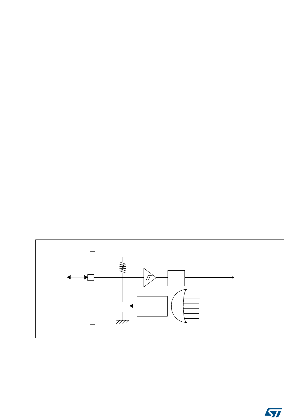
Reset and clock control (RCC) for STM32F413/423 RM0430
118/1324 RM0430 Rev 8
Low-power management reset
There are two ways of generating a low-power management reset:
1. Reset generated when entering the Standby mode:
This type of reset is enabled by resetting the nRST_STDBY bit in the user option bytes.
In this case, whenever a Standby mode entry sequence is successfully executed, the
device is reset instead of entering the Standby mode.
2. Reset when entering the Stop mode:
This type of reset is enabled by resetting the nRST_STOP bit in the user option bytes.
In this case, whenever a Stop mode entry sequence is successfully executed, the
device is reset instead of entering the Stop mode.
For further information on the user option bytes, refer to the STM32F413/423 Flash
programming manual available from your ST sales office.
6.1.2 Power reset
A power reset is generated when one of the following events occurs:
1. Power-on/power-down reset (POR/PDR reset) or brownout (BOR) reset
2. When exiting the Standby mode
A power reset sets all registers to their reset values except the Backup domain.
These sources act on the NRST pin and it is always kept low during the delay phase. The
RESET service routine vector is fixed at address 0x0000_0004 in the memory map.
The system reset signal provided to the device is output on the NRST pin. The pulse
generator guarantees a minimum reset pulse duration of 20 µs for each internal reset
source. In case of an external reset, the reset pulse is generated while the NRST pin is
asserted low.
Figure 12. Simplified diagram of the reset circuit
1567
5
38
9
''
9
''$
::'*UHVHW
,:'*UHVHW
3XOVH
JHQHUDWRU 3RZHUUHVHW
([WHUQDO
UHVHW
PLQV
6\VWHPUHVHW
)LOWHU
6RIWZDUHUHVHW
/RZSRZHUPDQDJHPHQWUHVHW
DLF

RM0430 Rev 8 119/1324
RM0430 Reset and clock control (RCC) for STM32F413/423
183
6.1.3 Backup domain reset
The backup domain reset sets all RTC registers and the RCC_BDCR register to their reset
values.
A backup domain reset is generated when one of the following events occurs:
1. Software reset, triggered by setting the BDRST bit in the RCC Backup domain control
register (RCC_BDCR).
2. VDD or VBAT power on, if both supplies have previously been powered off.
6.2 Clocks
Three different clock sources can be used to drive the system clock (SYSCLK):
•HSI oscillator clock
•HSE oscillator clock
•Main PLL (PLL) clock
The devices have the two following secondary clock sources:
•32 kHz low-speed internal RC (LSI RC) which drives the independent watchdog and,
optionally, the RTC used for Auto-wakeup from the Stop/Standby mode.
•32.768 kHz low-speed external crystal (LSE crystal) which optionally drives the RTC
clock (RTCCLK)
Each clock source can be switched on or off independently when it is not used, to optimize
power consumption.
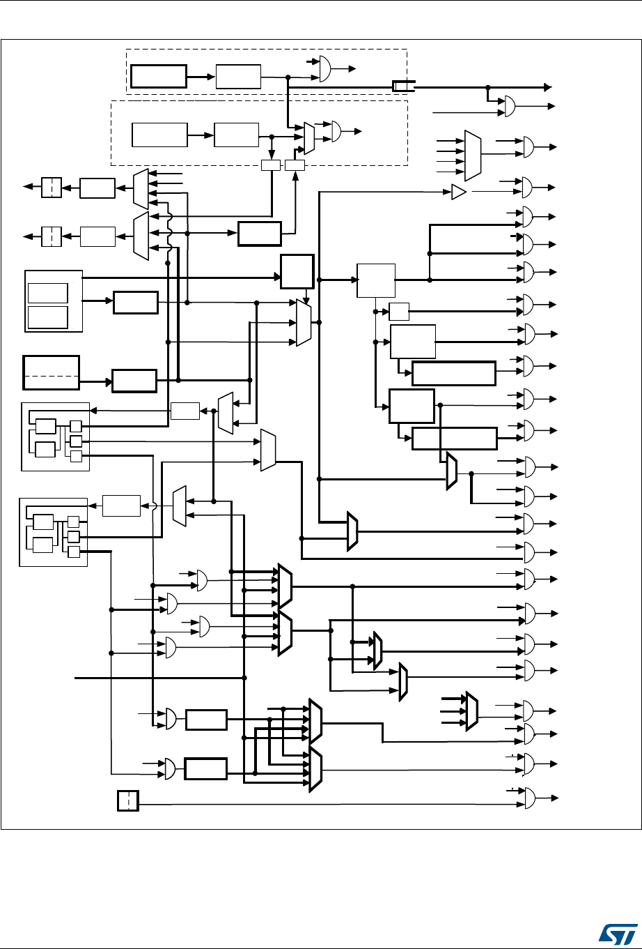
Reset and clock control (RCC) for STM32F413/423 RM0430
120/1324 RM0430 Rev 8
Figure 13. Clock tree
1. For full details about the internal and external clock source characteristics, refer to the Electrical characteristics section in
the device datasheet.
06Y9
/6,5&
57&$:8
/6
:DWFKGRJ
:DWFKGRJ
HQDEOH
57&$:8HQDEOH
/6,WHPSR
#9
#9VZ
+6,5&
#9
OHYHOVKLIWHUV
+6(
26&
#9
#9
OHYHOVKLIWHUV
'HWHFWRU
&ORFN
+6,WHPSR
+6(WHPSR
#9
/
6
3$'
#9 #9
6RXUFH
&RQWURO
&ORFN
$+%
35(6&
$3%
35(6&
$3%
35(6&
6\VWHP
&ORFN
LI$3%SUHVF [
HOVH [
LI$3%SUHVF [
HOVH [
/
6
3$'
#9 #9
2
FNBKVH
FNBKVL
FNBSOO
FNBOVH
FNBV\V
FNBUFKV
FNB[WKV
FNB[WOV
FNBUFOV
FORFN
FORFN
FNBMWFN
FNBSOOT
FSXFORFN
6\VWLFN
FORFN
$3%SHULSKHUDO
FORFNV
$3%WLPHU
FORFNV
$+%3HULSKHUDO
FORFNV
$3%SHULSKHUDO
FORFNV
$3%WLPHU
FORFNV
-7$*
FORFNV
FNBKVHB0
0&2
QRWVOHHSRUGHHSVOHHS
QRWGHHSVOHHS
,SHQDEOH
,SHQDEOH
,SHQDEOH
,SHQDEOH
,SHQDEOH
,SHQDEOH
GLVDEOHBGHEXJ
/
6
3$'
#9 #9
0&2
!
FNBV\V
FNBSOOU
3//
FNBSOOS
FNBSOOU
FNBSOOLVBH[W
6',2
FORFN
,SHQDEOH
,6
FORFN
,SHQDEOH
FNBSOOLQ
FNBSOT
FNBKVL
86%)6
51*
,SHQDEOH
FNBSOOU
L6
FORFNV
,SHQDEOH
,SHQDEOH
FNBKVL
FNBV\V
FNBDSE
')6'0
FORFNV
,SHQDEOH
FNBLVBDSE
FNBLVBDSE
&.6',26(/
&.06(/
,665&
,665&
&.')6'0$6(/
3//65&
FNBSOOLVBH[W
3//,665&
,&6(/
/6
FNBOVL
DGSBFON
DGSBFONBUHT
IURP86%)6,S
')6'0
FORFN
,SHQDEOH
FNBV\V
&.')6'06(/
/SWLPHU
FORFN
,SHQDEOH
FNBKVL
FNBOVH
FNBOVL
FNBDSE
')6'0
FORFN
,SHQDEOH
')6'0
,SHQDEOH
&.')6'0$6(/
6$,B$
FORFNV
,SHQDEOH
,SHQDEOH
6$,B%
FORFNV
GLYWR
GLYWR
+6BFN
5
5
,6B&.,1
6$,$65&
6$,%65&
3//',95
3//,6',95
,SHQDEOH
,SHQDEOH
,SHQDEOH
,SHQDEOH
,SHQDEOH
,SHQDEOH
,&
FORFNV
3RZHUFWUO
FORFN
/6/6
/6(26& /6(WHPSR
3
5
[1
9&2
4
3//0
3//
5
[1
9&2
4
3//,60
3
!
!
/HYHOVKLIWHU

RM0430 Rev 8 121/1324
RM0430 Reset and clock control (RCC) for STM32F413/423
183
The clock controller provides a high degree of flexibility to the application in the choice of the
external crystal or the oscillator to run the core and peripherals at the highest frequency
and, guarantee the appropriate frequency for peripherals that need a specific clock like USB
OTG FS, I2S and SDIO.
Several prescalers are used to configure the AHB frequency, the high-speed APB (APB2)
and the low-speed APB (APB1) domains. The maximum frequency of the AHB domain is
100 MHz. The maximum allowed frequency of the high-speed APB2 domain is 100 MHz.
The maximum allowed frequency of the low-speed APB1 domain is 50 MHz
All peripheral clocks are derived from the system clock (SYSCLK) except for:
•The USB OTG FS clock (48 MHz) and the SDIO clock (≤ 48 MHz) which are coming
from a specific output of PLL (PLL48CLK)
•The I2S clock
To achieve high-quality audio performance, the I2S clock can be derived either from a
specific PLL (PLLI2S) or from an external clock mapped on the I2S_CKIN pin. For
more information about I2S clock frequency and precision, refer to Section 29.6.4:
Clock generator.
•I2CFMP1 clock which can also be generated from HSI, SYSCLK or APB1 clock.
The RCC feeds the external clock of the Cortex System Timer (SysTick) with the AHB clock
(HCLK) divided by 8. The SysTick can work either with this clock or with the Cortex clock
(HCLK), configurable in the SysTick control and status register.
The timer clock frequencies are automatically set by hardware. There are two cases
depending on the value of TIMPRE bit in RCC_DCKCFGR register:
•If TIMPRE bit is reset:
If the APB prescaler is configured to a division factor of 1, the timer clock frequencies
(TIMxCLK) are set to HCLK. Otherwise, the timer clock frequencies are twice the
frequency of the APB domain to which the timers are connected: TIMxCLK = 2xPCLKx.
•If TIMPRE bit is set:
If the APB prescaler is configured to a division factor of 1 or 2, the timer clock
frequencies (TIMxCLK) are set to HCLK. Otherwise, the timer clock frequencies is four
times the frequency of the APB domain to which the timers are connected: TIMxCLK =
4xPCLKx.
FCLK acts as Cortex®-M4 with FPU free-running clock. For more details, refer to the
Cortex®-M4 with FPU technical reference manual.
6.2.1 HSE clock
The high speed external clock signal (HSE) can be generated from two possible clock
sources:
•HSE external crystal/ceramic resonator
•HSE external user clock
The resonator and the load capacitors have to be placed as close as possible to the
oscillator pins in order to minimize output distortion and startup stabilization time. The
loading capacitance values must be adjusted according to the selected oscillator.
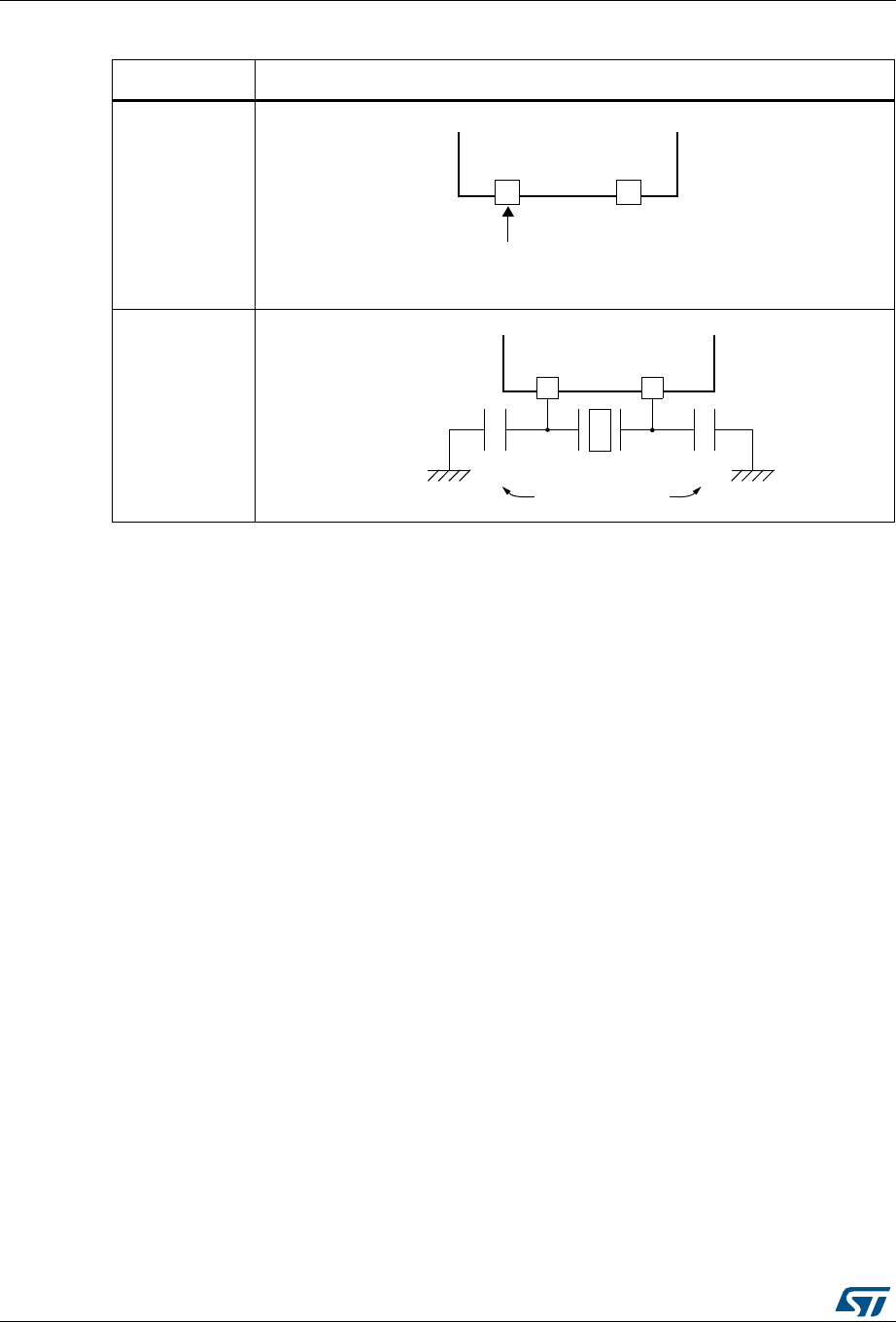
Reset and clock control (RCC) for STM32F413/423 RM0430
122/1324 RM0430 Rev 8
External source (HSE bypass)
In this mode, an external clock source must be provided. You select this mode by setting the
HSEBYP and HSEON bits in the RCC clock control register (RCC_CR). The external clock
signal (square, sinus or triangle) with ~50% duty cycle has to drive the OSC_IN pin while the
OSC_OUT pin should be left HI-Z. See Figure 14.
External crystal/ceramic resonator (HSE crystal)
The HSE has the advantage of producing a very accurate rate on the main clock.
The associated hardware configuration is shown in Figure 14. Refer to the electrical
characteristics section of the datasheet for more details.
The HSERDY flag in the RCC clock control register (RCC_CR) indicates if the high-speed
external oscillator is stable or not. At startup, the clock is not released until this bit is set by
hardware. An interrupt can be generated if enabled in the RCC clock interrupt register
(RCC_CIR).
The HSE Crystal can be switched on and off using the HSEON bit in the RCC clock control
register (RCC_CR).
6.2.2 HSI clock
The HSI clock signal is generated from an internal 16 MHz RC oscillator and can be used
directly as a system clock, or used as PLL input.
The HSI RC oscillator has the advantage of providing a clock source at low cost (no external
components). It also has a faster startup time than the HSE crystal oscillator however, even
with calibration the frequency is less accurate than an external crystal oscillator or ceramic
resonator.
Figure 14. HSE/ LSE clock sources
Hardware configuration
External clock
Crystal/ceramic
resonators
OSC_OUT
External
source
(HI-Z)
OSC_IN OSC_OUT
Load
capacitors
CL2
CL1

RM0430 Rev 8 123/1324
RM0430 Reset and clock control (RCC) for STM32F413/423
183
Calibration
RC oscillator frequencies can vary from one chip to another due to manufacturing process
variations, this is why each device is factory calibrated by ST for 1% accuracy at TA= 25 °C.
After reset, the factory calibration value is loaded in the HSICAL[7:0] bits in the RCC clock
control register (RCC_CR).
If the application is subject to voltage or temperature variations this may affect the RC
oscillator speed. You can trim the HSI frequency in the application using the HSITRIM[4:0]
bits in the RCC clock control register (RCC_CR).
The HSIRDY flag in the RCC clock control register (RCC_CR) indicates if the HSI RC is
stable or not. At startup, the HSI RC output clock is not released until this bit is set by
hardware.
The HSI RC can be switched on and off using the HSION bit in the RCC clock control
register (RCC_CR).
The HSI signal can also be used as a backup source (Auxiliary clock) if the HSE crystal
oscillator fails. Refer to Section 6.2.7: Clock security system (CSS) on page 124.
6.2.3 PLL configuration
The STM32F413/423 devices feature two PLLs:
•A main PLL (PLL) clocked by the HSE or HSI oscillator and featuring two different
output clocks:
– The first output is used to generate the high speed system clock (up to 100 MHz)
– The second output is used to generate the clock for the USB OTG FS (48 MHz),
RNG and the SDIO (≤ 50 MHz).
•A dedicated PLL (PLLI2S) used to generate an accurate clock to achieve high-quality
audio performance on the I2S interface.
Since the main-PLL configuration parameters cannot be changed once PLL is enabled, it is
recommended to configure PLL before enabling it (selection of the HSI or HSE oscillator as
PLL clock source, and configuration of division factors M, P, Q and multiplication factor N).
The PLLI2S uses the same input clock as the main PLL (HSI or HSE). However, the PLLI2S
has dedicated enable/disable and division factors configuration bits. Refer to Section 6.3.1:
RCC clock control register (RCC_CR), Section 6.3.2: RCC PLL configuration register
(RCC_PLLCFGR) and Section 6.3.26: RCC PLLI2S configuration register
(RCC_PLLI2SCFGR). Once the PLLI2S is enabled, the configuration parameters cannot be
changed.
The two PLLs are disabled by hardware when entering Stop and Standby modes, or when
an HSE failure occurs when HSE or PLL (clocked by HSE) are used as system clock. RCC
PLL configuration register (RCC_PLLCFGR) and RCC clock configuration register
(RCC_CFGR) can be used to configure PLL and PLLI2S, respectively.
6.2.4 LSE clock
The LSE clock is generated using a 32.768kHz low speed external crystal or ceramic
resonator. It has the advantage providing a low-power but highly accurate clock source to
the real-time clock peripheral (RTC) for clock/calendar or other timing functions.

Reset and clock control (RCC) for STM32F413/423 RM0430
124/1324 RM0430 Rev 8
The LSE oscillator is switched on and off using the LSEON bit in RCC Backup domain
control register (RCC_BDCR).
The LSERDY flag in the RCC Backup domain control register (RCC_BDCR) indicates if the
LSE crystal is stable or not. At startup, the LSE crystal output clock signal is not released
until this bit is set by hardware. An interrupt can be generated if enabled in the RCC clock
interrupt register (RCC_CIR).
External source (LSE bypass)
In this mode, an external clock source must be provided. It must have a frequency up to
1 MHz. You select this mode by setting the LSEBYP and LSEON bits in the RCC Backup
domain control register (RCC_BDCR). The external clock signal (square, sinus or triangle)
with ~50% duty cycle has to drive the OSC32_IN pin while the OSC32_OUT pin should be
left HI-Z. See Figure 14.
6.2.5 LSI clock
The LSI RC acts as an low-power clock source that can be kept running in Stop and
Standby mode for the independent watchdog (IWDG) and Auto-wakeup unit (AWU). The
clock frequency is around 32 kHz. For more details, refer to the electrical characteristics
section of the datasheets.
The LSI RC can be switched on and off using the LSION bit in the RCC clock control &
status register (RCC_CSR).
The LSIRDY flag in the RCC clock control & status register (RCC_CSR) indicates if the low-
speed internal oscillator is stable or not. At startup, the clock is not released until this bit is
set by hardware. An interrupt can be generated if enabled in the RCC clock interrupt register
(RCC_CIR).
6.2.6 System clock (SYSCLK) selection
After a system reset, the HSI oscillator is selected as the system clock. When a clock source
is used directly or through PLL as the system clock, it is not possible to stop it.
A switch from one clock source to another occurs only if the target clock source is ready
(clock stable after startup delay or PLL locked). If a clock source that is not yet ready is
selected, the switch occurs when the clock source is ready. Status bits in the RCC clock
control register (RCC_CR) indicate which clock(s) is (are) ready and which clock is currently
used as the system clock.
6.2.7 Clock security system (CSS)
The clock security system can be activated by software. In this case, the clock detector is
enabled after the HSE oscillator startup delay, and disabled when this oscillator is stopped.
If a failure is detected on the HSE clock, this oscillator is automatically disabled, a clock
failure event is sent to the break inputs of advanced-control timer TIM1, and an interrupt is
generated to inform the software about the failure (clock security system interrupt CSSI),
allowing the MCU to perform rescue operations. The CSSI is linked to the Cortex®-M4 with
FPU NMI (non-maskable interrupt) exception vector.
Note: When the CSS is enabled, if the HSE clock happens to fail, the CSS generates an interrupt,
which causes the automatic generation of an NMI. The NMI is executed indefinitely unless
the CSS interrupt pending bit is cleared. As a consequence, the application has to clear the

RM0430 Rev 8 125/1324
RM0430 Reset and clock control (RCC) for STM32F413/423
183
CSS interrupt in the NMI ISR by setting the CSSC bit in the Clock interrupt register
(RCC_CIR).
If the HSE oscillator is used directly or indirectly as the system clock (indirectly meaning that
it is directly used as PLL input clock, and that PLL clock is the system clock) and a failure is
detected, then the system clock switches to the HSI oscillator and the HSE oscillator is
disabled.
If the HSE oscillator clock was the clock source of PLL used as the system clock when the
failure occurred, PLL is also disabled. In this case, if the PLLI2S was enabled, it is also
disabled when the HSE fails.
6.2.8 RTC/AWU clock
Once the RTCCLK clock source has been selected, the only possible way of modifying the
selection is to reset the power domain.
The RTCCLK clock source can be either the HSE 1 MHz (HSE divided by a programmable
prescaler), the LSE or the LSI clock. This is selected by programming the RTCSEL[1:0] bits
in the RCC Backup domain control register (RCC_BDCR) and the RTCPRE[4:0] bits in RCC
clock configuration register (RCC_CFGR). This selection cannot be modified without
resetting the Backup domain.
If the LSE is selected as the RTC clock, the RTC will work normally if the backup or the
system supply disappears. If the LSI is selected as the AWU clock, the AWU state is not
guaranteed if the system supply disappears. If the HSE oscillator divided by a value
between 2 and 31 is used as the RTC clock, the RTC state is not guaranteed if the backup
or the system supply disappears.
The LSE clock is in the Backup domain, whereas the HSE and LSI clocks are not. As a
consequence:
•If LSE is selected as the RTC clock:
– The RTC continues to work even if the VDD supply is switched off, provided the
VBAT supply is maintained.
– The RTC remains clocked and functional under system reset.
•If LSI is selected as the Auto-wakeup unit (AWU) clock:
– The AWU state is not guaranteed if the VDD supply is powered off. Refer to
Section 6.2.5: LSI clock for more details on LSI calibration.
•If the HSE clock is used as the RTC clock:
– The RTC state is not guaranteed if the VDD supply is powered off or if the internal
voltage regulator is powered off (removing power from the 1.2 V domain).
Note: To read the RTC calendar register when the APB1 clock frequency is less than seven times
the RTC clock frequency (fAPB1 < 7xfRTCLCK), the software must read the calendar time and
date registers twice. The data are correct if the second read access to RTC_TR gives the
same result than the first one. Otherwise a third read access must be performed.
6.2.9 Watchdog clock
If the independent watchdog (IWDG) is started by either hardware option or software
access, the LSI oscillator is forced ON and cannot be disabled. After the LSI oscillator
temporization, the clock is provided to the IWDG.

Reset and clock control (RCC) for STM32F413/423 RM0430
126/1324 RM0430 Rev 8
6.2.10 Clock-out capability
Two microcontroller clock output (MCO) pins are available:
•MCO1
You can output four different clock sources onto the MCO1 pin (PA8) using the
configurable prescaler (from 1 to 5):
–HSI clock
– LSE clock
– HSE clock
– PLL clock
The desired clock source is selected using the MCO1PRE[2:0] and MCO1[1:0] bits in
the RCC clock configuration register (RCC_CFGR).
•MCO2
You can output four different clock sources onto the MCO2 pin (PC9) using the
configurable prescaler (from 1 to 5):
– HSE clock
– PLL clock
– System clock (SYSCLK)
– PLLI2S clock
The desired clock source is selected using the MCO2PRE[2:0] and MCO2 bits in the
RCC clock configuration register (RCC_CFGR).
For the different MCO pins, the corresponding GPIO port has to be programmed in alternate
function mode.
The selected clock to output onto MCO must not exceed 100 MHz (the maximum I/O
speed).
6.2.11 Internal/external clock measurement using TIM5/TIM11
It is possible to indirectly measure the frequencies of all on-board clock source generators
by means of the input capture of TIM5 channel4 and TIM11 channel1 as shown in Figure 15
and Figure 16.
Internal/external clock measurement using TIM5 channel4
TIM5 has an input multiplexer which allows choosing whether the input capture is triggered
by the I/O or by an internal clock. This selection is performed through the TI4_RMP [1:0] bits
in the TIM5_OR register.
The primary purpose of having the LSE connected to the channel4 input capture is to be
able to precisely measure the HSI (this requires to have the HSI used as the system clock
source). The number of HSI clock counts between consecutive edges of the LSE signal
provides a measurement of the internal clock period. Taking advantage of the high precision
of LSE crystals (typically a few tens of ppm) we can determine the internal clock frequency
with the same resolution, and trim the source to compensate for manufacturing-process
and/or temperature- and voltage-related frequency deviations.
The HSI oscillator has dedicated, user-accessible calibration bits for this purpose.
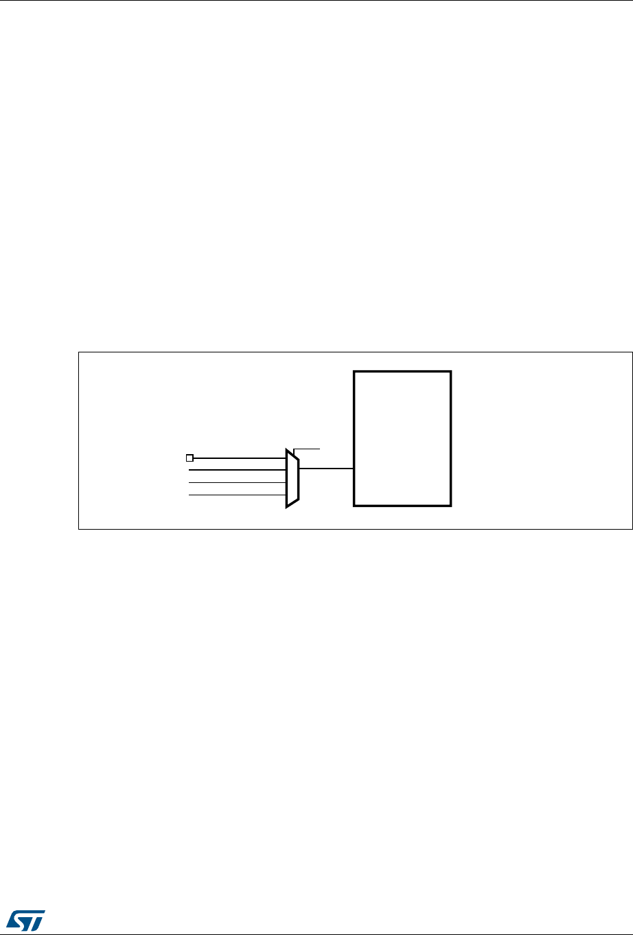
RM0430 Rev 8 127/1324
RM0430 Reset and clock control (RCC) for STM32F413/423
183
The basic concept consists in providing a relative measurement (e.g. HSI/LSE ratio): the
precision is therefore tightly linked to the ratio between the two clock sources. The greater
the ratio, the better the measurement.
It is also possible to measure the LSI frequency: this is useful for applications that do not
have a crystal. The ultralow-power LSI oscillator has a large manufacturing process
deviation: by measuring it versus the HSI clock source, it is possible to determine its
frequency with the precision of the HSI. The measured value can be used to have more
accurate RTC time base timeouts (when LSI is used as the RTC clock source) and/or an
IWDG timeout with an acceptable accuracy.
Use the following procedure to measure the LSI frequency:
1. Enable the TIM5 timer and configure channel4 in Input capture mode.
2. Set the TI4_RMP bits in the TIM5_OR register to 0x01 to connect the LSI clock
internally to TIM5 channel4 input capture for calibration purposes.
3. Measure the LSI clock frequency using the TIM5 capture/compare 4 event or interrupt.
4. Use the measured LSI frequency to update the prescaler of the RTC depending on the
desired time base and/or to compute the IWDG timeout.
Figure 15. Frequency measurement with TIM5 in Input capture mode
4)-
4)
4)?2-0;=
'0)/
24#?7AKE5P?)4
,3%
,3)
AI6
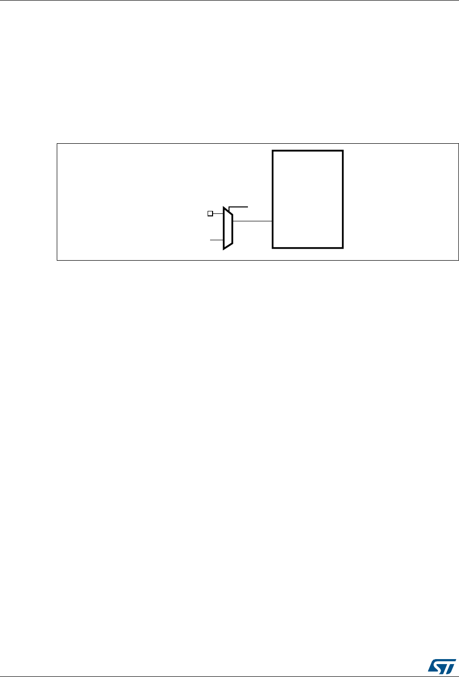
Reset and clock control (RCC) for STM32F413/423 RM0430
128/1324 RM0430 Rev 8
Internal/external clock measurement using TIM11 channel1
TIM11 has an input multiplexer which allows choosing whether the input capture is triggered
by the I/O or by an internal clock. This selection is performed through TI1_RMP [1:0] bits in
the TIM11_OR register. The HSE_RTC clock (HSE divided by a programmable prescaler) is
connected to channel 1 input capture to have a rough indication of the external crystal
frequency. This requires that the HSI is the system clock source. This can be useful for
instance to ensure compliance with the IEC 60730/IEC 61335 standards which require to be
able to determine harmonic or subharmonic frequencies (–50/+100% deviations).
Figure 16. Frequency measurement with TIM11 in Input capture mode
4)-
4)
4)?2-0;=
'0)/
(3%?24#-(Z
AI

RM0430 Rev 8 129/1324
RM0430 Reset and clock control (RCC) for STM32F413/423
183
6.3 RCC registers
Refer to Section 1.2: List of abbreviations for registers for a list of abbreviations used in
register descriptions.
6.3.1 RCC clock control register (RCC_CR)
Address offset: 0x00
Reset value: 0x0000 XX81 where X is undefined.
Access: no wait state, word, half-word and byte access
31 30 29 28 27 26 25 24 23 22 21 20 19 18 17 16
Res. Res. Res. Res. PLLI2S
RDY
PLLI2S
ON PLLRDY PLLON Res. Res. Res. Res. CSS
ON
HSE
BYP
HSE
RDY HSE ON
r rw r rw rw rw r rw
15 14 13 12 11 10 9 8 7 6 5 4 3 2 1 0
HSICAL[7:0] HSITRIM[4:0] Res. HSI
RDY HSION
rrrrrr r rrwrwrwrwrw rrw
Bits 31:28 Reserved, must be kept at reset value.
Bit 27 PLLI2SRDY: PLLI2S clock ready flag
Set by hardware to indicate that the PLLI2S is locked.
0: PLLI2S unlocked
1: PLLI2S locked
Bit 26 PLLI2SON: PLLI2S enable
Set and cleared by software to enable PLLI2S.
Cleared by hardware when entering Stop or Standby mode.
0: PLLI2S OFF
1: PLLI2S ON
Bit 25 PLLRDY: Main PLL (PLL) clock ready flag
Set by hardware to indicate that PLL is locked.
0: PLL unlocked
1: PLL locked
Bit 24 PLLON: Main PLL (PLL) enable
Set and cleared by software to enable PLL.
Cleared by hardware when entering Stop or Standby mode. This bit cannot be reset if PLL
clock is used as the system clock.
0: PLL OFF
1: PLL ON
Bits 23:20 Reserved, must be kept at reset value.
Bit 19 CSSON: Clock security system enable
Set and cleared by software to enable the clock security system. When CSSON is set, the
clock detector is enabled by hardware when the HSE oscillator is ready, and disabled by
hardware if an oscillator failure is detected.
0: Clock security system OFF (Clock detector OFF)
1: Clock security system ON (Clock detector ON if HSE oscillator is stable, OFF if not)

Reset and clock control (RCC) for STM32F413/423 RM0430
130/1324 RM0430 Rev 8
Bit 18 HSEBYP: HSE clock bypass
Set and cleared by software to bypass the oscillator with an external clock. The external
clock must be enabled with the HSEON bit, to be used by the device.
The HSEBYP bit can be written only if the HSE oscillator is disabled.
0: HSE oscillator not bypassed
1: HSE oscillator bypassed with an external clock
Bit 17 HSERDY: HSE clock ready flag
Set by hardware to indicate that the HSE oscillator is stable. After the HSEON bit is cleared,
HSERDY goes low after 6 HSE oscillator clock cycles.
0: HSE oscillator not ready
1: HSE oscillator ready
Bit 16 HSEON: HSE clock enable
Set and cleared by software.
Cleared by hardware to stop the HSE oscillator when entering Stop or Standby mode. This
bit cannot be reset if the HSE oscillator is used directly or indirectly as the system clock.
0: HSE oscillator OFF
1: HSE oscillator ON
Bits 15:8 HSICAL[7:0]: Internal high-speed clock calibration
These bits are initialized automatically at startup.
Bits 7:3 HSITRIM[4:0]: Internal high-speed clock trimming
These bits provide an additional user-programmable trimming value that is added to the
HSICAL[7:0] bits. It can be programmed to adjust to variations in voltage and temperature
that influence the frequency of the internal HSI RC.
Bit 2 Reserved, must be kept at reset value.
Bit 1 HSIRDY: Internal high-speed clock ready flag
Set by hardware to indicate that the HSI oscillator is stable. After the HSION bit is cleared,
HSIRDY goes low after 6 HSI clock cycles.
0: HSI oscillator not ready
1: HSI oscillator ready
Bit 0 HSION: Internal high-speed clock enable
Set and cleared by software.
Set by hardware to force the HSI oscillator ON when leaving the Stop or Standby mode or in
case of a failure of the HSE oscillator used directly or indirectly as the system clock. This bit
cannot be cleared if the HSI is used directly or indirectly as the system clock.
0: HSI oscillator OFF
1: HSI oscillator ON

RM0430 Rev 8 131/1324
RM0430 Reset and clock control (RCC) for STM32F413/423
183
6.3.2 RCC PLL configuration register (RCC_PLLCFGR)
Address offset: 0x04
Reset value: 0x2400 3010
Access: no wait state, word, half-word and byte access.
This register is used to configure the PLL clock outputs according to the formulas:
•f(VCO clock) = f(PLL clock input) × (PLLN / PLLM)
•f(PLL general clock output) = f(VCO clock) / PLLP
•f(USB OTG FS, SDIO, RNG clock output) = f(VCO clock) / PLLQ
•f(I2S, DFSDM clock output) = f(VCO clock)/ PLLR
31 30 29 28 27 26 25 24 23 22 21 20 19 18 17 16
Res. PLLR[2:0] PLLQ[3:0] Res. PLLSRC Res. Res. Res. Res. PLLP[1:0]
rw rw rw rw rw rw rw rw rw rw
15 14 13 12 11 10 9 8 7 6 5 4 3 2 1 0
Res. PLLN[8:0] PLLM[5:0]
rw rw rw rw rw rw rw rw rw rw rw rw rw rw rw
Bit 31 Reserved, must be kept at reset value.
Bits 30:28 PLLR[2:0]: Main PLL (PLL) division factor for I2S, DFSDM clocks
Set and cleared by software to control the frequency of the clock. These bits should be
written only if PLL is disabled.
Clock frequency = VCO frequency / PLLR with 2 ≤ PLLR ≤ 7
000: PLLR = 0, wrong configuration
001: PLLR = 1, wrong configuration
010: PLLR = 2
011: PLLR = 3
...
111: PLLR = 7
Bits 27:24 PLLQ[3:0]: Main PLL (PLL) division factor for USB OTG FS, SDIO and random number
generator clocks.
Set and cleared by software to control the frequency of USB OTG FS clock, the random
number generator clock and the SDIO clock. These bits should be written only if PLL is
disabled.
Caution: The USB OTG FS requires a 48 MHz clock to work correctly. The SDIO and the
random number generator need a frequency lower than or equal to 48 MHz to work
correctly.
USB OTG FS clock frequency = VCO frequency / PLLQ with 2 ≤ PLLQ ≤ 15
0000: PLLQ = 0, wrong configuration
0001: PLLQ = 1, wrong configuration
0010: PLLQ = 2
0011: PLLQ = 3
0100: PLLQ = 4
...
1111: PLLQ = 15
Bit 23 Reserved, must be kept at reset value.

Reset and clock control (RCC) for STM32F413/423 RM0430
132/1324 RM0430 Rev 8
Bit 22 PLLSRC: Main PLL(PLL) and audio PLL (PLLI2S) entry clock source
Set and cleared by software to select PLL and PLLI2S clock source. This bit can be written
only when PLL and PLLI2S are disabled.
0: HSI clock selected as PLL and PLLI2S clock entry
1: HSE oscillator clock selected as PLL and PLLI2S clock entry
Bits 21:18 Reserved, must be kept at reset value.
Bits 17:16 PLLP[1:0]: Main PLL (PLL) division factor for main system clock
Set and cleared by software to control the frequency of the general PLL output clock. These
bits can be written only if PLL is disabled.
Caution: The software has to set these bits correctly not to exceed 100 MHz on this domain.
PLL output clock frequency = VCO frequency / PLLP with PLLP = 2, 4, 6, or 8
00: PLLP = 2
01: PLLP = 4
10: PLLP = 6
11: PLLP = 8
Bits 14:6 PLLN[8:0]: Main PLL (PLL) multiplication factor for VCO
Set and cleared by software to control the multiplication factor of the VCO. These bits can
be written only when PLL is disabled. Only half-word and word accesses are allowed to
write these bits.
Caution: The software has to set these bits correctly to ensure that the VCO output
frequency is between 100 and 432 MHz. (check also Section 6.3.26: RCC PLLI2S
configuration register (RCC_PLLI2SCFGR))
VCO output frequency = VCO input frequency × PLLN with 50 ≤ PLLN ≤ 432
000000000: PLLN = 0, wrong configuration
000000001: PLLN = 1, wrong configuration
...
000110010: PLLN = 50
...
001100011: PLLN = 99
001100100: PLLN = 100
...
110110000: PLLN = 432
110110001: PLLN = 433, wrong configuration
...
111111111: PLLN = 511, wrong configuration
Note: Multiplication factors possible for VCO input frequency higher than 1 MHz but care
must be taken to fulfill the VCO output frequency range as specified above.

RM0430 Rev 8 133/1324
RM0430 Reset and clock control (RCC) for STM32F413/423
183
6.3.3 RCC clock configuration register (RCC_CFGR)
Address offset: 0x08
Reset value: 0x0000 0000
Access: 0 ≤ wait state ≤ 2, word, half-word and byte access
1 or 2 wait states inserted only if the access occurs during a clock source switch.
Bits 5:0 PLLM[5:0]: Division factor for the main PLL (PLL) input clock
Set and cleared by software to divide the PLL and PLLI2S input clock before the VCO.
These bits can be written only when the PLL and PLLI2S are disabled.
Caution: The software has to set these bits correctly to ensure that the VCO input frequency
ranges from 1 to 2 MHz. It is recommended to select a frequency of 2 MHz to limit
PLL jitter.
VCO input frequency = PLL input clock frequency / PLLM with 2 ≤ PLLM ≤ 63
000000: PLLM = 0, wrong configuration
000001: PLLM = 1, wrong configuration
000010: PLLM = 2
000011: PLLM = 3
000100: PLLM = 4
...
111110: PLLM = 62
111111: PLLM = 63
31 30 29 28 27 26 25 24 23 22 21 20 19 18 17 16
MCO2[1:0] MCO2 PRE[2:0] MCO1 PRE[2:0] Res. MCO1[1:0] RTCPRE[4:0]
rw rw rw rw rw rw rw rw rw rw rw rw rw rw
15 14 13 12 11 10 9 8 7 6 5 4 3 2 1 0
PPRE2[2:0] PPRE1[2:0] Res. Res. HPRE[3:0] SWS[1:0] SW[1:0]
rw rw rw rw rw rw rw rw rw rw r r rw rw
Bits 31:30 MCO2[1:0]: Microcontroller clock output 2
Set and cleared by software. Clock source selection may generate glitches on MCO2. It is
highly recommended to configure these bits only after reset before enabling the external
oscillators and the PLLs.
00: System clock (SYSCLK) selected
01: PLLI2S clock selected
10: HSE oscillator clock selected
11: PLL clock selected

Reset and clock control (RCC) for STM32F413/423 RM0430
134/1324 RM0430 Rev 8
Bits 29:27 MCO2PRE[1:0]: MCO2 prescaler
Set and cleared by software to configure the prescaler of the MCO2. Modification of this
prescaler may generate glitches on MCO2. It is highly recommended to change this
prescaler only after reset before enabling the external oscillators and the PLLs.
0xx: no division
100: division by 2
101: division by 3
110: division by 4
111: division by 5
Bits 26:24 MCO1PRE[1:0]: MCO1 prescaler
Set and cleared by software to configure the prescaler of the MCO1. Modification of this
prescaler may generate glitches on MCO1. It is highly recommended to change this
prescaler only after reset before enabling the external oscillators and the PLL.
0xx: no division
100: division by 2
101: division by 3
110: division by 4
111: division by 5
Bit 23 Reserved, always read as 0.
Bits 22:21 MCO1[1:0]: Microcontroller clock output 1
Set and cleared by software. Clock source selection may generate glitches on MCO1. It is
highly recommended to configure these bits only after reset before enabling the external
oscillators and PLL.
00: HSI clock selected
01: LSE oscillator selected
10: HSE oscillator clock selected
11: PLL clock selected
Bits 20:16 RTCPRE[4:0]: HSE division factor for RTC clock
Set and cleared by software to divide the HSE clock input clock to generate a 1 MHz clock
for RTC.
Caution: The software has to set these bits correctly to ensure that the clock supplied to the
RTC is 1 MHz. These bits must be configured if needed before selecting the RTC
clock source.
00000: no clock
00001: no clock
00010: HSE/2
00011: HSE/3
00100: HSE/4
...
11110: HSE/30
11111: HSE/31
Bits 15:13 PPRE2[2:0]: APB high-speed prescaler (APB2)
Set and cleared by software to control APB high-speed clock division factor.
Caution: The software has to set these bits correctly not to exceed 100 MHz on this domain.
The clocks are divided with the new prescaler factor from 1 to 16 AHB cycles after
PPRE2 write.
0xx: AHB clock not divided
100: AHB clock divided by 2
101: AHB clock divided by 4
110: AHB clock divided by 8
111: AHB clock divided by 16

RM0430 Rev 8 135/1324
RM0430 Reset and clock control (RCC) for STM32F413/423
183
Bits 12:10 PPRE1[2:0]: APB Low speed prescaler (APB1)
Set and cleared by software to control APB low-speed clock division factor.
Caution: The software has to set these bits correctly not to exceed 50 MHz on this domain.
The clocks are divided with the new prescaler factor from 1 to 16 AHB cycles after
PPRE1 write.
0xx: AHB clock not divided
100: AHB clock divided by 2
101: AHB clock divided by 4
110: AHB clock divided by 8
111: AHB clock divided by 16
Bits 9:8 Reserved, must be kept at reset value.
Bits 7:4 HPRE[3:0]: AHB prescaler
Set and cleared by software to control AHB clock division factor.
Caution: The clocks are divided with the new prescaler factor from 1 to 16 AHB cycles after
HPRE write.
Caution: The AHB clock frequency must be at least 25 MHz when the Ethernet is used.
0xxx: system clock not divided
1000: system clock divided by 2
1001: system clock divided by 4
1010: system clock divided by 8
1011: system clock divided by 16
1100: system clock divided by 64
1101: system clock divided by 128
1110: system clock divided by 256
1111: system clock divided by 512
Bits 3:2 SWS[1:0]: System clock switch status
Set and cleared by hardware to indicate which clock source is used as the system clock.
00: HSI oscillator used as the system clock
01: HSE oscillator used as the system clock
10: PLL used as the system clock
11: not applicable
Bits 1:0 SW[1:0]: System clock switch
Set and cleared by software to select the system clock source.
Set by hardware to force the HSI selection when leaving the Stop or Standby mode or in
case of failure of the HSE oscillator used directly or indirectly as the system clock.
00: HSI oscillator selected as system clock
01: HSE oscillator selected as system clock
10: PLL selected as system clock
11: not allowed

Reset and clock control (RCC) for STM32F413/423 RM0430
136/1324 RM0430 Rev 8
6.3.4 RCC clock interrupt register (RCC_CIR)
Address offset: 0x0C
Reset value: 0x0000 0000
Access: no wait state, word, half-word and byte access
31 30 29 28 27 26 25 24 23 22 21 20 19 18 17 16
Res. Res. Res. Res. Res. Res. Res. Res. CSSC Res. PLLI2S
RDYC
PLL
RDYC
HSE
RDYC
HSI
RDYC
LSE
RDYC
LSI
RDYC
w w www w w
15 14 13 12 11 10 9 8 7 6 5 4 3 2 1 0
Res. Res. PLLI2S
RDYIE
PLL
RDYIE
HSE
RDYIE
HSI
RDYIE
LSE
RDYIE
LSI
RDYIE CSSF Res. PLLI2S
RDYF
PLL
RDYF
HSE
RDYF
HSI
RDYF
LSE
RDYF
LSI
RDYF
rw rw rw rw rw rw r r r r r r r
Bits 31:24 Reserved, must be kept at reset value.
Bit 23 CSSC: Clock security system interrupt clear
This bit is set by software to clear the CSSF flag.
0: No effect
1: Clear CSSF flag
Bit 22 Reserved, must be kept at reset value.
Bit 21 PLLI2SRDYC: PLLI2S ready interrupt clear
This bit is set by software to clear the PLLI2SRDYF flag.
0: No effect
1: PLLI2SRDYF cleared
Bit 20 PLLRDYC: Main PLL(PLL) ready interrupt clear
This bit is set by software to clear the PLLRDYF flag.
0: No effect
1: PLLRDYF cleared
Bit 19 HSERDYC: HSE ready interrupt clear
This bit is set by software to clear the HSERDYF flag.
0: No effect
1: HSERDYF cleared
Bit 18 HSIRDYC: HSI ready interrupt clear
This bit is set software to clear the HSIRDYF flag.
0: No effect
1: HSIRDYF cleared
Bit 17 LSERDYC: LSE ready interrupt clear
This bit is set by software to clear the LSERDYF flag.
0: No effect
1: LSERDYF cleared
Bit 16 LSIRDYC: LSI ready interrupt clear
This bit is set by software to clear the LSIRDYF flag.
0: No effect
1: LSIRDYF cleared

RM0430 Rev 8 137/1324
RM0430 Reset and clock control (RCC) for STM32F413/423
183
Bits 15:14 Reserved, must be kept at reset value.
Bit 13 PLLI2SRDYIE: PLLI2S ready interrupt enable
Set and cleared by software to enable/disable interrupt caused by PLLI2S lock.
0: PLLI2S lock interrupt disabled
1: PLLI2S lock interrupt enabled
Bit 12 PLLRDYIE: Main PLL (PLL) ready interrupt enable
Set and cleared by software to enable/disable interrupt caused by PLL lock.
0: PLL lock interrupt disabled
1: PLL lock interrupt enabled
Bit 11 HSERDYIE: HSE ready interrupt enable
Set and cleared by software to enable/disable interrupt caused by the HSE oscillator
stabilization.
0: HSE ready interrupt disabled
1: HSE ready interrupt enabled
Bit 10 HSIRDYIE: HSI ready interrupt enable
Set and cleared by software to enable/disable interrupt caused by the HSI oscillator
stabilization.
0: HSI ready interrupt disabled
1: HSI ready interrupt enabled
Bit 9 LSERDYIE: LSE ready interrupt enable
Set and cleared by software to enable/disable interrupt caused by the LSE oscillator
stabilization.
0: LSE ready interrupt disabled
1: LSE ready interrupt enabled
Bit 8 LSIRDYIE: LSI ready interrupt enable
Set and cleared by software to enable/disable interrupt caused by LSI oscillator
stabilization.
0: LSI ready interrupt disabled
1: LSI ready interrupt enabled
Bit 7 CSSF: Clock security system interrupt flag
Set by hardware when a failure is detected in the HSE oscillator.
Cleared by software setting the CSSC bit.
0: No clock security interrupt caused by HSE clock failure
1: Clock security interrupt caused by HSE clock failure
Bit 6 Reserved, must be kept at reset value.
Bit 5 PLLI2SRDYF: PLLI2S ready interrupt flag
Set by hardware when the PLLI2S locks and PLLI2SRDYDIE is set.
Cleared by software setting the PLLRI2SDYC bit.
0: No clock ready interrupt caused by PLLI2S lock
1: Clock ready interrupt caused by PLLI2S lock
Bit 4 PLLRDYF: Main PLL (PLL) ready interrupt flag
Set by hardware when PLL locks and PLLRDYDIE is set.
Cleared by software setting the PLLRDYC bit.
0: No clock ready interrupt caused by PLL lock
1: Clock ready interrupt caused by PLL lock

Reset and clock control (RCC) for STM32F413/423 RM0430
138/1324 RM0430 Rev 8
6.3.5 RCC AHB1 peripheral reset register (RCC_AHB1RSTR)
Address offset: 0x10
Reset value: 0x0000 0000
Access: no wait state, word, half-word and byte access.
Bit 3 HSERDYF: HSE ready interrupt flag
Set by hardware when External High Speed clock becomes stable and HSERDYDIE is set.
Cleared by software setting the HSERDYC bit.
0: No clock ready interrupt caused by the HSE oscillator
1: Clock ready interrupt caused by the HSE oscillator
Bit 2 HSIRDYF: HSI ready interrupt flag
Set by hardware when the Internal High Speed clock becomes stable and HSIRDYDIE is
set.
Cleared by software setting the HSIRDYC bit.
0: No clock ready interrupt caused by the HSI oscillator
1: Clock ready interrupt caused by the HSI oscillator
Bit 1 LSERDYF: LSE ready interrupt flag
Set by hardware when the External Low Speed clock becomes stable and LSERDYDIE is
set.
Cleared by software setting the LSERDYC bit.
0: No clock ready interrupt caused by the LSE oscillator
1: Clock ready interrupt caused by the LSE oscillator
Bit 0 LSIRDYF: LSI ready interrupt flag
Set by hardware when the internal low speed clock becomes stable and LSIRDYDIE is set.
Cleared by software setting the LSIRDYC bit.
0: No clock ready interrupt caused by the LSI oscillator
1: Clock ready interrupt caused by the LSI oscillator
31 30 29 28 27 26 25 24 23 22 21 20 19 18 17 16
Res. Res. Res. Res. Res. Res. Res. Res. Res. DMA2
RST
DMA1
RST Res. Res. Res. Res. Res.
rw rw
15 14 13 12 11 10 9 8 7 6 5 4 3 2 1 0
Res. Res. Res. CRCRST Res. Res. Res. Res. GPIOH
RST
GPIOG
RST
GPIOF
RST
GPIOE
RST
GPIOD
RST
GPIOC
RST
GPIOB
RST
GPIOA
RST
rw rw rw rw rw rw rw rw rw
Bits 31:23 Reserved, must be kept at reset value.
Bit 22 DMA2RST: DMA2 reset
Set and cleared by software.
0: does not reset DMA2
1: resets DMA2
Bit 21 DMA1RST: DMA1 reset
Set and cleared by software.
0: does not reset DMA1
1: resets DMA1
Bits 20:13 Reserved, must be kept at reset value.

RM0430 Rev 8 139/1324
RM0430 Reset and clock control (RCC) for STM32F413/423
183
Bit 12 CRCRST: CRC reset
Set and cleared by software.
0: does not reset CRC
1: resets CRC
Bits 11:8 Reserved, must be kept at reset value.
Bit 7 GPIOHRST: IO port H reset
Set and cleared by software.
0: does not reset IO port H
1: resets IO port H
Bit 6 GPIOGRST: IO port G reset
Set and cleared by software.
0: does not reset IO port G
1: resets IO port G
Bit 5 GPIOFRST: IO port F reset
Set and cleared by software.
0: does not reset IO port F
1: resets IO port F
Bit 4 GPIOERST: IO port E reset
Set and cleared by software.
0: does not reset IO port E
1: resets IO port E
Bit 3 GPIODRST: IO port D reset
Set and cleared by software.
0: does not reset IO port D
1: resets IO port D
Bit 2 GPIOCRST: IO port C reset
Set and cleared by software.
0: does not reset IO port C
1: resets IO port C
Bit 1 GPIOBRST: IO port B reset
Set and cleared by software.
0: does not reset IO port B
1:resets IO port B
Bit 0 GPIOARST: IO port A reset
Set and cleared by software.
0: does not reset IO port A
1: resets IO port A

Reset and clock control (RCC) for STM32F413/423 RM0430
140/1324 RM0430 Rev 8
6.3.6 RCC AHB2 peripheral reset register (RCC_AHB2RSTR)
for STM32F413xx
Address offset: 0x14
Reset value: 0x0000 0000
Access: no wait state, word, half-word and byte access
31 30 29 28 27 26 25 24 23 22 21 20 19 18 17 16
Res. Res. Res. Res. Res. Res. Res. Res. Res. Res. Res. Res. Res. Res. Res. Res.
15 14 13 12 11 10 9 8 7 6 5 4 3 2 1 0
Res. Res. Res. Res. Res. Res. Res. Res. OTGFS
RST
RNG
RST Res. Res. Res. Res. Res. Res.
rw rw
Bits 31:8 Reserved, must be kept at reset value.
Bit 7 OTGFSRST: USB OTG FS module reset
Set and cleared by software.
0: does not reset the USB OTG FS module
1: resets the USB OTG FS module
Bit 6 RNGSRST: RNG module reset
Set and cleared by software.
0: does not reset RNG module
1: resets RNG module
Bits 5:0 Reserved, must be kept at reset value.

RM0430 Rev 8 141/1324
RM0430 Reset and clock control (RCC) for STM32F413/423
183
6.3.7 RCC AHB2 peripheral reset register (RCC_AHB2RSTR)
for STM32F423xx
Address offset: 0x14
Reset value: 0x0000 0000
Access: no wait state, word, half-word and byte access
31 30 29 28 27 26 25 24 23 22 21 20 19 18 17 16
Res. Res. Res. Res. Res. Res. Res. Res. Res. Res. Res. Res. Res. Res. Res. Res.
15 14 13 12 11 10 9 8 7 6 5 4 3 2 1 0
Res. Res. Res. Res. Res. Res. Res. Res. OTGFS
RST
RNG
RST Res. CRYP
RST Res. Res. Res. Res.
rw rw rw
Bits 31:8 Reserved, must be kept at reset value.
Bit 7 OTGFSRST: USB OTG FS module reset
Set and cleared by software.
0: does not reset the USB OTG FS module
1: resets the USB OTG FS module
Bit 6 RNGSRST: RNG module reset
Set and cleared by software.
0: does not reset RNG module
1: resets RNG module
Bit 5 Reserved, must be kept at reset value.
Bit 4 CRYPRST: CRYP module reset
Set and reset by software.
0: does not reset CRYP module
1: resets CRYP module
Bits 3:0 Reserved, must be kept at reset value.

Reset and clock control (RCC) for STM32F413/423 RM0430
142/1324 RM0430 Rev 8
6.3.8 RCC AHB3 peripheral reset register (RCC_AHB3RSTR)
Address offset: 0x18
Reset value: 0x0000 0000
Access: no wait state, word, half-word and byte access
6.3.9 RCC APB1 peripheral reset register for (RCC_APB1RSTR)
Address offset: 0x20
Reset value: 0x0000 0000
Access: no wait state, word, half-word and byte access.
31 30 29 28 27 26 25 24 23 22 21 20 19 18 17 16
Res. Res. Res. Res. Res. Res. Res. Res. Res. Res. Res. Res. Res. Res. Res. Res.
15 14 13 12 11 10 9 8 7 6 5 4 3 2 1 0
Res. Res. Res. Res. Res. Res. Res. Res. Res. Res. Res. Res. Res. Res. QSPIRST FSMC
RST
rw rw
Bits 31:2 Reserved, must be kept at reset value.
Bit 1 QSPIRST: QUADSPI module reset
Set and cleared by software.
0: does not reset QUADSPI module
1: resets QUADSPI module
Bit 0 FSMCRST: Flexible memory controller module reset
Set and cleared by software.
0: does not reset the FSMC module
1: resets the FSMC module
31 30 29 28 27 26 25 24 23 22 21 20 19 18 17 16
UART8
RST
UART7
RST
DAC
RST
PWR
RST
CAN3
RST
CAN2
RST
CAN1
RST
I2C4
RST
I2C3
RST
I2C2
RST
I2C1
RST
UART5
RST
UART4
RST
USART3
RST
USART2
RST Res.
rw rw rw rw rw rw rw rw rw rw rw rw rw rw rw
15 14 13 12 11 10 9 8 7 6 5 4 3 2 1 0
SPI3
RST
SPI2
RST Res. Res. WWDG
RST Res. LPTIMER1
RST
TIM14
RST
TIM13
RST
TIM12
RST
TIM7
RST
TIM6
RST
TIM5
RST
TIM4
RST
TIM3
RST
TIM2
RST
rw rw rw rw rw rw rw rw rw rw rw rw rw

RM0430 Rev 8 143/1324
RM0430 Reset and clock control (RCC) for STM32F413/423
183
Bit 31 UART8RST: UART 8 reset
Set and reset by software.
0: does not reset UART 8
1: resets the UART 8
Bit 30 UART7RST: UART 7 reset
Set and reset by software.
0: does not reset UART 7
1: resets the UART 7
Bit 29 DACRST: DAC reset
Set and reset by software.
0: does not reset DAC
1: resets DAC
Bit 28 PWRRST: Power interface reset
Set and reset by software.
0: does not reset the power interface
1: resets the power interface
Bit 27 CAN3RST: CAN 3 reset
Set and reset by software.
0: does not reset CAN 3
1: resets CAN 3
Bit 26 CAN2RST: CAN2 reset
Set and cleared by software.
0: does not reset CAN2
1: resets CAN2
Bit 25 CAN1RST: CAN1 reset
Set and cleared by software.
0: does not reset CAN1
1: resets CAN1
Bit 24 I2C4RST: I2C4 reset
Set and reset by software.
0: does not reset I2C4
1: resets I2C4
Bit 23 I2C3RST: I2C3 reset
Set and reset by software.
0: does not reset I2C3
1: resets I2C3
Bit 22 I2C2RST: I2C2 reset
Set and cleared by software.
0: does not reset I2C2
1: resets I2C2
Bit 21 I2C1RST: I2C1 reset
Set and reset by software.
0: does not reset I2C1
1: resets I2C1

Reset and clock control (RCC) for STM32F413/423 RM0430
144/1324 RM0430 Rev 8
Bit 20 UART5RST: UART5 reset
Set and reset by software.
0: does not reset UART5
1: resets UART5
Bit 19 UART4RST: UART4 reset
Set and reset by software.
0: does not reset UART4
1: resets UART4
Bit 18 USART3RST: USART3 reset
Set and cleared by software.
0: does not reset USART3
1: resets USART3
Bit 17 USART2RST: USART2 reset
Set and cleared by software.
0: does not reset USART2
1: resets USART2
Bit 16 Reserved, must be kept at reset value.
Bit 15 SPI3RST: SPI3 reset
Set and cleared by software.
0: does not reset SPI3
1: resets SPI3
Bit 14 SPI2RST: SPI2 reset
Set and cleared by software.
0: does not reset SPI2
1: resets SPI2
Bits 13:12 Reserved, must be kept at reset value.
Bit 11 WWDGRST: Window watchdog reset
Set and cleared by software.
0: does not reset the window watchdog
1: resets the window watchdog
Bit 10 Reserved, must be kept at reset value.
Bit 9 LPTIMER1RST: LPTimer1 reset
Set and reset by software.
0: does not reset timer 1
1: resets timer 1
Bit 8 TIM14RST: TIM14 reset
Set and cleared by software.
0: does not reset TIM14
1: resets TIM14
Bit 7 TIM13RST: TIM13 reset
Set and cleared by software.
0: does not reset TIM13
1: resets TIM13

RM0430 Rev 8 145/1324
RM0430 Reset and clock control (RCC) for STM32F413/423
183
Bit 6 TIM12RST: TIM12 reset
Set and cleared by software.
0: does not reset TIM12
1: resets TIM12
Bit 5 TIM7RST: TIM7 reset
Set and cleared by software.
0: does not reset TIM7
1: resets TIM7
Bit 4 TIM6RST: TIM6 reset
Set and cleared by software.
0: does not reset TIM6
1: resets TIM6
Bit 3 TIM5RST: TIM5 reset
Set and cleared by software.
0: does not reset TIM5
1: resets TIM5
Bit 2 TIM4RST: TIM4 reset
Set and cleared by software.
0: does not reset TIM4
1: resets TIM4
Bit 1 TIM3RST: TIM3 reset
Set and cleared by software.
0: does not reset TIM3
1: resets TIM3
Bit 0 TIM2RST: TIM2 reset
Set and cleared by software.
0: does not reset TIM2
1: resets TIM2

Reset and clock control (RCC) for STM32F413/423 RM0430
146/1324 RM0430 Rev 8
6.3.10 RCC APB2 peripheral reset register (RCC_APB2RSTR)
Address offset: 0x24
Reset value: 0x0000 0000
Access: no wait state, word, half-word and byte access.
31 30 29 28 27 26 25 24 23 22 21 20 19 18 17 16
Res. Res. Res. Res. Res. Res. DFSDM2
RST
DFSDM1
RST Res. SAI1
RST Res. SPI5
RST Res. TIM11
RST
TIM10
RST
TIM9
RST
rw rw rw rw rw rw rw
15 14 13 12 11 10 9 8 7 6 5 4 3 2 1 0
Res. SYSCFG
RST
SPI4
RST
SPI1
RST
SDIO
RST Res. Res. ADC
RST
UART10
RST
UART9
RST
USART6
RST
USART1
RST Res. Res. TIM8
RST
TIM1
RST
rw rw rw rw rw rw rw rw rw rw rw
Bits 31:26 Reserved, must be kept at reset value.
Bit 25 DFSDM2RST: DFSDM2 reset
Set and cleared by software.
0: does not reset DFSDM2
1: resets DFSDM2
Bit 24 DFSDM1RST: DFSDM1 reset
Set and cleared by software.
0: does not reset DFSDM1
1: resets DFSDM1
Bit 23 Reserved, always read as 0.
Bit 22 SAI1RST: SAI1 reset
Set and reset by software.
0: does not reset SAI1
1: resets SAI1
Bit 21 Reserved, always read as 0.
Bit 20 SPI5RST: SPI5RST
This bit is set and cleared by software.
0: does not reset SPI5
1: resets SPI5
Bit 19 Reserved, must be kept at reset value.
Bit 18 TIM11RST: TIM11 reset
Set and cleared by software.
0: does not reset TIM11
1: resets TIM11
Bit 17 TIM10RST: TIM10 reset
Set and cleared by software.
0: does not reset TIM10
1: resets TIM10
Bit 16 TIM9RST: TIM9 reset
Set and cleared by software.
0: does not reset TIM9
1: resets TIM9

RM0430 Rev 8 147/1324
RM0430 Reset and clock control (RCC) for STM32F413/423
183
Bit 15 Reserved, must be kept at reset value.
Bit 14 SYSCFGRST: System configuration controller reset
Set and cleared by software.
0: does not reset the System configuration controller
1: resets the System configuration controller
Bit 13 SPI4RST: SPI4 reset
Set and reset by software.
0: does not reset SPI4
1: resets SPI4
Bit 12 SPI1RST: SPI1 reset
Set and cleared by software.
0: does not reset SPI1
1: resets SPI1
Bit 11 SDIORST: SDIO reset
Set and cleared by software.
0: does not reset the SDIO module
1: resets the SDIO module
Bits 10:9 Reserved, must be kept at reset value.
Bit 8 ADCRST: ADC interface reset
Set and cleared by software.
0: does not reset the ADC interface
1: resets the ADC interface
Bit 7 UART10RST: UART10 reset
Set and cleared by software.
0: does not reset UART10
1: resets UART10
Bit 6 UART9RST: UART9 reset
Set and cleared by software.
0: does not reset UART9
1: resets UART9
Bit 5 USART6RST: USART6 reset
Set and cleared by software.
0: does not reset USART6
1: resets USART6
Bit 4 USART1RST: USART1 reset
Set and cleared by software.
0: does not reset USART1
1: resets USART1

Reset and clock control (RCC) for STM32F413/423 RM0430
148/1324 RM0430 Rev 8
Bits 3:2 Reserved, must be kept at reset value.
Bit 1 TIM8RST: TIM8 reset
Set and cleared by software.
0: does not reset TIM8
1: resets TIM8
Bit 0 TIM1RST: TIM1 reset
Set and cleared by software.
0: does not reset TIM1
1: resets TIM1

RM0430 Rev 8 149/1324
RM0430 Reset and clock control (RCC) for STM32F413/423
183
6.3.11 RCC AHB1 peripheral clock enable register (RCC_AHB1ENR)
Address offset: 0x30
Reset value: 0x0000 0000
Access: no wait state, word, half-word and byte access.
31 30 29 28 27 26 25 24 23 22 21 20 19 18 17 16
Res. Res. Res. Res. Res. Res. Res. Res. Res. DMA2EN DMA1EN Res. Res. Res. Res. Res.
rw rw
15 14 13 12 11 10 9 8 7 6 5 4 3 2 1 0
Res. Res. Res. CRCEN Res. Res. Res. Res. GPIOH
EN
GPIOG
EN
GPIOF
EN
GPIOE
EN
GPIOD
EN
GPIOC
EN
GPIOB
EN
GPIOA
EN
rw rw rw rw rw rw rw rw rw
Bits 31:23 Reserved, must be kept at reset value.
Bit 22 DMA2EN: DMA2 clock enable
Set and cleared by software.
0: DMA2 clock disabled
1: DMA2 clock enabled
Bit 21 DMA1EN: DMA1 clock enable
Set and cleared by software.
0: DMA1 clock disabled
1: DMA1 clock enabled
Bits 20:13 Reserved, must be kept at reset value.
Bit 12 CRCEN: CRC clock enable
Set and cleared by software.
0: CRC clock disabled
1: CRC clock enabled
Bits 11:8 Reserved, must be kept at reset value.
Bit 7 GPIOHEN: IO port H clock enable
Set and reset by software.
0: IO port H clock disabled
1: IO port H clock enabled
Bit 6 GPIOGEN: IO port G clock enable
Set and cleared by software.
0: IO port G clock disabled
1: IO port G clock enabled
Bit 5 GPIOFEN: IO port F clock enable
Set and cleared by software.
0: IO port F clock disabled
1: IO port F clock enabled
Bit 4 GPIOEEN: IO port E clock enable
Set and cleared by software.
0: IO port E clock disabled
1: IO port E clock enabled

Reset and clock control (RCC) for STM32F413/423 RM0430
150/1324 RM0430 Rev 8
Bit 3 GPIODEN: IO port D clock enable
Set and cleared by software.
0: IO port D clock disabled
1: IO port D clock enabled
Bit 2 GPIOCEN: IO port C clock enable
Set and cleared by software.
0: IO port C clock disabled
1: IO port C clock enabled
Bit 1 GPIOBEN: IO port B clock enable
Set and cleared by software.
0: IO port B clock disabled
1: IO port B clock enabled
Bit 0 GPIOAEN: IO port A clock enable
Set and cleared by software.
0: IO port A clock disabled
1: IO port A clock enabled

RM0430 Rev 8 151/1324
RM0430 Reset and clock control (RCC) for STM32F413/423
183
6.3.12 RCC AHB2 peripheral clock enable register (RCC_AHB2ENR)
for STM32F413xx
Address offset: 0x34
Reset value: 0x0000 0000
Access: no wait state, word, half-word and byte access.
31 30 29 28 27 26 25 24 23 22 21 20 19 18 17 16
Res. Res. Res. Res. Res. Res. Res. Res. Res. Res. Res. Res. Res. Res. Res. Res.
15 14 13 12 11 10 9 8 7 6 5 4 3 2 1 0
Res. Res. Res. Res. Res. Res. Res. Res. OTGFS
EN
RNG
EN Res. Res. Res. Res. Res. Res.
rw rw
Bits 31:8 Reserved, must be kept at reset value.
Bit 7 OTGFSEN: USB OTG FS clock enable
Set and cleared by software.
0: USB OTG FS clock disabled
1: USB OTG FS clock enabled
Bit 6 RNGEN: RNG clock enable
Set and cleared by software.
0: RNG clock disabled
1: RNG clock enabled
Bits 5:0 Reserved, always read as 0.

Reset and clock control (RCC) for STM32F413/423 RM0430
152/1324 RM0430 Rev 8
6.3.13 RCC AHB2 peripheral clock enable register (RCC_AHB2ENR)
for STM32F423xx
Address offset: 0x34
Reset value: 0x0000 0000
Access: no wait state, word, half-word and byte access.
31 30 29 28 27 26 25 24 23 22 21 20 19 18 17 16
Res. Res. Res. Res. Res. Res. Res. Res. Res. Res. Res. Res. Res. Res. Res. Res.
15 14 13 12 11 10 9 8 7 6 5 4 3 2 1 0
Res. Res. Res. Res. Res. Res. Res. Res. OTGFS
EN MGEN Res. CRYP
EN Res. Res. Res. Res.
rw rw rw
Bits 31:8 Reserved, must be kept at reset value.
Bit 7 OTGFSEN: USB OTG FS clock enable
Set and cleared by software.
0: USB OTG FS clock disabled
1: USB OTG FS clock enabled
Bit 6 RNGEN: RNG clock enable
Set and cleared by software.
0: RNG clock disabled
1: RNG clock enabled
Bit 5 Reserved, always read as 0.
Bit 4 CRYPEN: CRYP clock enable
Set and reset by software.
0: CRYP clock disabled
1: CRYP clock enabled
Bits 3:0 Reserved, always read as 0.

RM0430 Rev 8 153/1324
RM0430 Reset and clock control (RCC) for STM32F413/423
183
6.3.14 RCC AHB3 peripheral clock enable register (RCC_AHB3ENR)
Address offset: 0x38
Reset value: 0x0000 0000
Access: no wait state, word, half-word and byte access.
6.3.15 RCC APB1 peripheral clock enable register (RCC_APB1ENR)
Address offset: 0x40
Reset value: 0x0000 0400
Access: no wait state, word, half-word and byte access.
31 30 29 28 27 26 25 24 23 22 21 20 19 18 17 16
Res. Res. Res. Res. Res. Res. Res. Res. Res. Res. Res. Res. Res. Res. Res. Res.
15 14 13 12 11 10 9 8 7 6 5 4 3 2 1 0
Res. Res. Res. Res. Res. Res. Res. Res. Res. Res. Res. Res. Res. Res. QSPI
EN
FSMC
EN
rw rw
Bits 31:2 Reserved, must be kept at reset value.
Bit 1 QSPIEN: QUADSPI memory controller module clock enable
Set and cleared by software.
0: QUADSPI clock disabled
1: QUADSPI clock enabled
Bit 0 FSMCEN: Flexible memory controller module clock enable
Set and cleared by software.
0: FSMC module clock disabled
1: FSMC module clock enabled
31 30 29 28 27 26 25 24 23 22 21 20 19 18 17 16
UART8
EN
UART7
EN
DAC
EN
PWR
EN
CAN3
EN
CAN2
EN
CAN1
EN
I2CFMP1
EN
I2C3
EN
I2C2
EN
I2C1
EN
UART4
EN
UART4
EN
USART3
EN
USART2
EN Res.
rw rw rw rw rw rw rw rw rw rw rw rw rw rw rw
15 14 13 12 11 10 9 8 7 6 5 4 3 2 1 0
SPI3
EN
SPI2
EN Res. Res. WWDG
EN
RTCAPB
EN
LPTIMER1
EN
TIM14
EN
TIM13
EN
TIM12
EN
TIM7
EN
TIM6
EN
TIM5
EN
TIM4
EN
TIM3
EN
TIM2
EN
rw rw rw rw rw rw rw rw rw rw rw rw rw rw

Reset and clock control (RCC) for STM32F413/423 RM0430
154/1324 RM0430 Rev 8
Bit 31 UART8EN: UART8 clock enable
Set and reset by software.
0: UART8 clock disabled
1: UART8 clock enable
Bit 30 UART7EN: UART7 clock enable
Set and reset by software.
0: UART7 clock disabled
1: UART7 clock enable
Bit 29 DACEN: DAC clock enable
Set and reset by software.
0: DAC clock disabled
1: DAC clock enable
Bit 28 PWREN: Power interface clock enable
Set and reset by software.
0: Power interface clock disabled
1: Power interface clock enable
Bit 27 CAN3EN: CAN 3 clock enable
This bit is set and cleared by software.
0: CAN 3 clock disabled
1: CAN 3 clock enabled
Bit 26 CAN2EN: CAN 2 clock enable
This bit is set and cleared by software.
0: CAN 2 clock disabled
1: CAN 2 clock enabled
Bit 25 CAN1EN: CAN 1 clock enable
This bit is set and cleared by software.
0: CAN 1 clock disabled
1: CAN 1 clock enabled
Bit 24 I2CFMP1EN: I2CFMP1 clock enable
This bit is set and cleared by software.
0: I2CFMP1 clock disabled
1: I2CFMP1 clock enabled
Bit 23 I2C3EN: I2C3 clock enable
Set and cleared by software.
0: I2C3 clock disabled
1: I2C3 clock enabled
Bit 22 I2C2EN: I2C2 clock enable
Set and cleared by software.
0: I2C2 clock disabled
1: I2C2 clock enabled
Bit 21 I2C1EN: I2C1 clock enable
Set and cleared by software.
0: I2C1 clock disabled
1: I2C1 clock enabled

RM0430 Rev 8 155/1324
RM0430 Reset and clock control (RCC) for STM32F413/423
183
Bit 20 UART5EN: UART 5 clock enable
Set and RESET by software.
0: UART 5 clock disabled
1: UART 5 clock enabled
Bit 19 UART4EN: UART 4 clock enable
Set and cleared by software.
0: UART 4 clock disabled
1: UART 4 clock enabled
Bit 18 USART3EN: USART3 clock enable
Set and cleared by software.
0: USART3 clock disabled
1: USART3 clock enabled
Bit 17 USART2EN: USART2 clock enable
Set and cleared by software.
0: USART2 clock disabled
1: USART2 clock enabled
Bit 16 Reserved, must be kept at reset value.
Bit 15 SPI3EN: SPI3 clock enable
Set and cleared by software.
0: SPI3 clock disabled
1: SPI3 clock enabled
Bit 14 SPI2EN: SPI2 clock enable
Set and cleared by software.
0: SPI2 clock disabled
1: SPI2 clock enabled
Bits 13:12 Reserved, must be kept at reset value.
Bit 11 WWDGEN: Window watchdog clock enable
Set and cleared by software.
0: Window watchdog clock disabled
1: Window watchdog clock enabled
Bit 10 RTC APB: clock enable
Set and cleared by software.
0: RTC APB clock disabled
1: RTC APB clock enabled (default value).
Bit 9 LPTIMER1EN: LPTimer 1 clock enable
Set and reset by software.
0: LPTimer 1 clock disabled
1: LPTimer 1 clock enabled
Bit 8 TIM14EN: TIM14 reset
Set and cleared by software.
0: does not reset TIM14
1: resets TIM14
Bit 7 TIM13EN: TIM13 reset
Set and cleared by software.
0: does not reset TIM13
1: resets TIM13

Reset and clock control (RCC) for STM32F413/423 RM0430
156/1324 RM0430 Rev 8
Bit 6 TIM12EN: TIM12 reset
Set and cleared by software.
0: does not reset TIM12
1: resets TIM12
Bit 5 TIM7EN: TIM7 reset
Set and cleared by software.
0: does not reset TIM7
1: resets TIM7
Bit 4 TIM6EN: TIM6 reset
Set and cleared by software.
0: does not reset TIM6
1: resets TIM6
Bit 3 TIM5EN: TIM5 clock enable
Set and cleared by software.
0: TIM5 clock disabled
1: TIM5 clock enabled
Bit 2 TIM4EN: TIM4 clock enable
Set and cleared by software.
0: TIM4 clock disabled
1: TIM4 clock enabled
Bit 1 TIM3EN: TIM3 clock enable
Set and cleared by software.
0: TIM3 clock disabled
1: TIM3 clock enabled
Bit 0 TIM2EN: TIM2 clock enable
Set and cleared by software.
0: TIM2 clock disabled
1: TIM2 clock enabled

RM0430 Rev 8 157/1324
RM0430 Reset and clock control (RCC) for STM32F413/423
183
6.3.16 RCC APB2 peripheral clock enable register
(RCC_APB2ENR)
Address offset: 0x44
Reset value: 0x0000 8000
Access: no wait state, word, half-word and byte access.
31 30 29 28 27 26 25 24 23 22 21 20 19 18 17 16
Res. Res. Res. Res. Res. Res. DFSDM2
EN
DFSDM1
EN Res. SAI1
EN Res. SPI5
EN Res. TIM11
EN
TIM10
EN
TIM9
EN
rw rw rw rw rw
15 14 13 12 11 10 9 8 7 6 5 4 3 2 1 0
EXTIT
EN
SYSCFG
EN SPI4EN SPI1
EN
SDIO
EN Res. Res. ADC1
EN
UART10
EN
UART9
EN
USART6
EN
USART1
EN Res. Res. TIM8
EN
TIM1
EN
rw rw rw rw rw rw rw rw rw rw rw rw
Bits 31:26 Reserved, always read as 0.
Bit 25 DFSDM2EN: DFSDM2 clock enable
Set and cleared by software
0: DFSDM2 clock disabled
1: DFSDM2 clock enabled
Bit 24 DFSDM1EN: DFSDM1 clock enable
Set and cleared by software
0: DFSDM1 clock disabled
1: DFSDM1 clock enabled
Bit 23 Reserved, always read as 0.
Bit 22 SAI1EN:SAI 1 clock enable
Set and cleared by software
0: SAI 1 clock disabled
1: SAI 1 clock enabled
Bit 21 Reserved, always read as 0.
Bit 20 SPI5EN:SPI5 clock enable
Set and cleared by software
0: SPI5 clock disabled
1: SPI5 clock enabled
Bit 19 Reserved, always read as 0.
Bit 18 TIM11EN: TIM11 clock enable
Set and cleared by software.
0: TIM11 clock disabled
1: TIM11 clock enabled
Bit 17 TIM10EN: TIM10 clock enable
Set and cleared by software.
0: TIM10 clock disabled
1: TIM10 clock enabled

Reset and clock control (RCC) for STM32F413/423 RM0430
158/1324 RM0430 Rev 8
Bit 16 TIM9EN: TIM9 clock enable
Set and cleared by software.
0: TIM9 clock disabled
1: TIM9 clock enabled
Bit 15 EXITEN: Extit Apb sysctrl pfree clock enable
Set and cleared by software.
0: Extit Apb sysctrl pfree clock disabled
1: Extit Apb sysctrl pfree clock enabled
Bit 14 SYSCFGEN: System configuration controller clock enable
Set and cleared by software.
0: System configuration controller clock disabled
1: System configuration controller clock enabled
Bit 13 SPI4EN: SPI4 clock enable
Set and reset by software.
0: SPI4 clock disabled
1: SPI4 clock enable
Bit 12 SPI1EN: SPI1 clock enable
Set and cleared by software.
0: SPI1 clock disabled
1: SPI1 clock enabled
Bit 11 SDIOEN: SDIO clock enable
Set and cleared by software.
0: SDIO module clock disabled
1: SDIO module clock enabled
Bit 8 ADC1EN: ADC1 clock enable
Set and cleared by software.
0: ADC1 clock disabled
1: ADC1 clock disabled
Bit 7 UART10EN: UART10 clock enable
Set and cleared by software.
0: UART10 clock disabled
1: UART10 clock enabled
Bit 5 UART9EN: UART9 clock enable
Set and cleared by software.
0: UART9 clock disabled
1: UART9 clock enabled
Bit 5 USART6EN: USART6 clock enable
Set and cleared by software.
0: USART6 clock disabled
1: USART6 clock enabled
Bit 4 USART1EN: USART1 clock enable
Set and cleared by software.
0: USART1 clock disabled
1: USART1 clock enabled

RM0430 Rev 8 159/1324
RM0430 Reset and clock control (RCC) for STM32F413/423
183
Bits 3:2 Reserved, must be kept at reset value.
Bit 1 TIM8EN: TIM8 clock enable
Set and cleared by software.
0: TIM8 clock disabled
1: TIM8 clock enabled
Bit 0 TIM1EN: TIM1 clock enable
Set and cleared by software.
0: TIM1 clock disabled
1: TIM1 clock enabled

Reset and clock control (RCC) for STM32F413/423 RM0430
160/1324 RM0430 Rev 8
6.3.17 RCC AHB1 peripheral clock enable in low power mode register
(RCC_AHB1LPENR)
Address offset: 0x50
Reset value: 0x0063 90FF
Access: no wait state, word, half-word and byte access.
31 30 29 28 27 26 25 24 23 22 21 20 19 18 17 16
Res. Res. Res. Res. Res. Res. Res. Res. Res. DMA2
LPEN
DMA1
LPEN Res. Res. Res. SRAM2
LPEN
SRAM1
LPEN
rw rw rw
15 14 13 12 11 10 9 8 7 6 5 4 3 2 1 0
FLITF
LPEN Res. Res. CRC
LPEN Res. Res. Res. Res. GPIOH
LPEN
GPIOG
LPEN
GPIOF
LPEN
GPIOE
LPEN
GPIOD
LPEN
GPIOC
LPEN
GPIOB
LPEN
GPIOA
LPEN
rw rw rw rw rw rw rw rw rw rw
Bits 31:23 Reserved, must be kept at reset value.
Bit 22 DMA2LPEN: DMA2 clock enable during Sleep mode
Set and cleared by software.
0: DMA2 clock disabled during Sleep mode
1: DMA2 clock enabled during Sleep mode
Bit 21 DMA1LPEN: DMA1 clock enable during Sleep mode
Set and cleared by software.
0: DMA1 clock disabled during Sleep mode
1: DMA1 clock enabled during Sleep mode
Bits 20:18 Reserved, must be kept at reset value.
Bit 17 SRAM2LPEN: SRAM2interface clock enable during Sleep mode
Set and cleared by software.
0: SRAM2 interface clock disabled during Sleep mode
1: SRAM2 interface clock enabled during Sleep mode
Bit 16 SRAM1LPEN: SRAM1interface clock enable during Sleep mode
Set and cleared by software.
0: SRAM1 interface clock disabled during Sleep mode
1: SRAM1 interface clock enabled during Sleep mode
Bit 15 FLITFLPEN: Flash interface clock enable during Sleep mode
Set and cleared by software.
0: Flash interface clock disabled during Sleep mode
1: Flash interface clock enabled during Sleep mode
Bits 14:13 Reserved, must be kept at reset value.
Bit 12 CRCLPEN: CRC clock enable during Sleep mode
Set and cleared by software.
0: CRC clock disabled during Sleep mode
1: CRC clock enabled during Sleep mode
Bits 11:8 Reserved, must be kept at reset value.

RM0430 Rev 8 161/1324
RM0430 Reset and clock control (RCC) for STM32F413/423
183
Bit 7 GPIOHLPEN: IO port H clock enable during sleep mode
Set and reset by software.
0: IO port H clock disabled during sleep mode
1: IO port H clock enabled during sleep mode
Bit 6 GPIOGLPEN: IO port G clock enable during Sleep mode
Set and cleared by software.
0: IO port G clock disabled during Sleep mode
1: IO port G clock enabled during Sleep mode
Bit 5 GPIOFLPEN: IO port F clock enable during Sleep mode
Set and cleared by software.
0: IO port F clock disabled during Sleep mode
1: IO port F clock enabled during Sleep mode
Bit 4 GPIOELPEN: IO port E clock enable during Sleep mode
Set and cleared by software.
0: IO port E clock disabled during Sleep mode
1: IO port E clock enabled during Sleep mode
Bit 3 GPIODLPEN: IO port D clock enable during Sleep mode
Set and cleared by software.
0: IO port D clock disabled during Sleep mode
1: IO port D clock enabled during Sleep mode
Bit 2 GPIOCLPEN: IO port C clock enable during Sleep mode
Set and cleared by software.
0: IO port C clock disabled during Sleep mode
1: IO port C clock enabled during Sleep mode
Bit 1 GPIOBLPEN: IO port B clock enable during Sleep mode
Set and cleared by software.
0: IO port B clock disabled during Sleep mode
1: IO port B clock enabled during Sleep mode
Bit 0 GPIOALPEN: IO port A clock enable during sleep mode
Set and cleared by software.
0: IO port A clock disabled during Sleep mode
1: IO port A clock enabled during Sleep mode

Reset and clock control (RCC) for STM32F413/423 RM0430
162/1324 RM0430 Rev 8
6.3.18 RCC AHB2 peripheral clock enable in low power mode register
(RCC_AHB2LPENR) for STM32F413xx
Address offset: 0x54
Reset value: 0x0000 00C0
Access: no wait state, word, half-word and byte access.
31 30 29 28 27 26 25 24 23 22 21 20 19 18 17 16
Res. Res. Res. Res. Res. Res. Res. Res. Res. Res. Res. Res. Res. Res. Res. Res.
15 14 13 12 11 10 9 8 7 6 5 4 3 2 1 0
Res. Res. Res. Res. Res. Res. Res. Res. OTGFS
LPEN
RNG
LPEN Res. Res. Res. Res. Res. Res.
rw rw
Bits 31:8 Reserved, must be kept at reset value.
Bit 7 OTGFSLPEN: USB OTG FS clock enable during Sleep mode
Set and cleared by software.
0: USB OTG FS clock disabled during Sleep mode
1: USB OTG FS clock enabled during Sleep mode
Bit 6 RNGLPEN: RNG clock enable during Sleep mode
Set and cleared by software.
0: RNG clock disabled during Sleep mode
1: RNG clock enabled during Sleep mode
Bits 5:0 Reserved, must be kept at reset value.

RM0430 Rev 8 163/1324
RM0430 Reset and clock control (RCC) for STM32F413/423
183
6.3.19 RCC AHB2 peripheral clock enable in low power mode register
(RCC_AHB2LPENR) for STM32F423xx
Address offset: 0x54
Reset value: 0x0000 00D0
Access: no wait state, word, half-word and byte access.
6.3.20 RCC AHB3 peripheral clock enable in low power mode register
(RCC_AHB3LPENR)
Address offset: 0x58
Reset value: 0x0000 0003
Access: no wait state, word, half-word and byte access.
31 30 29 28 27 26 25 24 23 22 21 20 19 18 17 16
Res. Res. Res. Res. Res. Res. Res. Res. Res. Res. Res. Res. Res. Res. Res. Res.
15 14 13 12 11 10 9 8 7 6 5 4 3 2 1 0
Res. Res. Res. Res. Res. Res. Res. Res. OTGFS
LPEN
RNG
LPEN Res. CRYP
LPEN Res. Res. Res. Res.
rw rw rw
Bits 31:8 Reserved, must be kept at reset value.
Bit 7 OTGSLPEN: USB OTG FS clock enable during sleep mode
Set and cleared by software.
0: USB OTG FS clock disabled during Sleep mode
1: USB OTG FS clock enabled during Sleep mode
Bit 6 RNGLPEN: RNG clock enable during sleep mode
Set and cleared by software.
0: RNG clock disabled during Sleep mode
1: RNG clock enabled during Sleep mode
Bit 5 Reserved, always read as 0.
Bit 4 CRYPLPEN: CRYPG clock enable during sleep mode
Set and cleared by software.
0: CRYP clock disabled during Sleep mode
1: CRYP clock enabled during Sleep mode
Bits 3:0 Reserved, must be kept at reset value.
31 30 29 28 27 26 25 24 23 22 21 20 19 18 17 16
Res. Res. Res. Res. Res. Res. Res. Res. Res. Res. Res. Res. Res. Res. Res. Res.
15 14 13 12 11 10 9 8 7 6 5 4 3 2 1 0
Res. Res. Res. Res. Res. Res. Res. Res. Res. Res. Res. Res. Res. Res. QSPI
LPEN
FSMC
LPEN
rw rw

Reset and clock control (RCC) for STM32F413/423 RM0430
164/1324 RM0430 Rev 8
Bits 31:2 Reserved, must be kept at reset value.
Bit 1 QSPILPEN: QUADSPI memory controller module clock enable during Sleep mode
Set and cleared by software.
0: QUADSPI module clock disabled during Sleep mode
1: QUADSPI module clock enabled during Sleep mode
Bit 0 FSMCLPEN: Flexible memory controller module clock enable during Sleep mode
Set and cleared by software.
0: FSMC clock disabled during Sleep mode
1: FSMC clock enabled during Sleep mode

RM0430 Rev 8 165/1324
RM0430 Reset and clock control (RCC) for STM32F413/423
183
6.3.21 RCC APB1 peripheral clock enable in low power mode register
(RCC_APB1LPENR)
Address offset: 0x60
Reset value: 0xFFFF CFFF
Access: no wait state, word, half-word and byte access.
31 30 29 28 27 26 25 24 23 22 21 20 19 18 17 16
UART8
LPEN
UART7
LPEN
DACLP
LPEN
PWR
LPEN
CAN3
LPEN
CAN2
LPEN
CAN1
LPEN
I2C4
LPEN
I2C3
LPEN
I2C2
LPEN
I2C1
LPEN
UART5
LPEN
UART4
LPEN
USART3
LPEN
USART2
LPEN Res.
rw rw rw rw rw rw rw rw rw
15 14 13 12 11 10 9 8 7 6 5 4 3 2 1 0
SPI3
LPEN
SPI2
LPEN Res. Res. WWDG
LPEN
RTCAPB
LPEN
IPTIMER1
LPEN
TIM14
LPEN
TIM13
LPEN
TIM12
LPEN
TIM7
LPEN
TIM6
LPEN
TIM5
LPEN
TIM4
LPEN
TIM3
LPEN
TIM2
LPEN
rw rw rw rw rw rw rw rw rw rw rw rw rw rw
Bit 31 UART8LPEN: UART8 clock enable during Sleep mode
Set and cleared by software.
0: UART8 clock disabled during Sleep mode
1: UART8 clock enabled during Sleep mode
Bit 30 UART7LPEN: UART7 clock enable during Sleep mode
Set and cleared by software.
0: UART7 clock disabled during Sleep mode
1: UART7 clock enabled during Sleep mode
Bit 29 DACLPEN: DAC clock enable during Sleep mode
Set and cleared by software.
0: DAC clock disabled during Sleep mode
1: DAC clock enabled during Sleep mode
Bit 28 PWRLPEN: Power interface clock enable during Sleep mode
Set and cleared by software.
0: Power interface clock disabled during Sleep mode
1: Power interface clock enabled during Sleep mode
Bit 27 CAN3LPEN: CAN3 clock enable during Sleep mode
Set and cleared by software.
0: CAN3 clock disabled during Sleep mode
1: CAN3 clock enabled during Sleep mode
Bit 26 CAN2LPEN: CAN2 clock enable during Sleep mode
Set and cleared by software.
0: CAN2 clock disabled during Sleep mode
1: CAN2 clock enabled during Sleep mode
Bit 25 CAN1LPEN: CAN1 clock enable during Sleep mode
Set and cleared by software.
0: CAN1 clock disabled during Sleep mode
1: CAN1 clock enabled during Sleep mode
Bit 24 I2CFMP1LPEN: I2CFMP1 clock enable during Sleep mode
Set and cleared by software.
0: I2CFMP1 clock disabled during Sleep mode
1: I2CFMP1 clock enabled during Sleep mode

Reset and clock control (RCC) for STM32F413/423 RM0430
166/1324 RM0430 Rev 8
Bit 23 I2C3LPEN: I2C3 clock enable during Sleep mode
Set and cleared by software.
0: I2C3 clock disabled during Sleep mode
1: I2C3 clock enabled during Sleep mode
Bit 22 I2C2LPEN: I2C2 clock enable during Sleep mode
Set and cleared by software.
0: I2C2 clock disabled during Sleep mode
1: I2C2 clock enabled during Sleep mode
Bit 21 I2C1LPEN: I2C1 clock enable during Sleep mode
Set and cleared by software.
0: I2C1 clock disabled during Sleep mode
1: I2C1 clock enabled during Sleep mode
Bit 20 UART5LPEN: UART5 clock enable during Sleep mode
Set and cleared by software.
0: UART5 clock disabled during Sleep mode
1: UART5 clock enabled during Sleep mode
Bit 19 UART4LPEN: UART4 clock enable during Sleep mode
Set and cleared by software.
0: UART4 clock disabled during Sleep mode
1: UART4 clock enabled during Sleep mode
Bit 18 USART3LPEN: USART3 clock enable during Sleep mode
Set and cleared by software.
0: USART3 clock disabled during Sleep mode
1: USART3 clock enabled during Sleep mode
Bit 17 USART2LPEN: USART2 clock enable during Sleep mode
Set and cleared by software.
0: USART2 clock disabled during Sleep mode
1: USART2 clock enabled during Sleep mode
Bit 16 Reserved, must be kept at reset value.
Bit 15 SPI3LPEN: SPI3 clock enable during Sleep mode
Set and cleared by software.
0: SPI3 clock disabled during Sleep mode
1: SPI3 clock enabled during Sleep mode
Bit 14 SPI2LPEN: SPI2 clock enable during Sleep mode
Set and cleared by software.
0: SPI2 clock disabled during Sleep mode
1: SPI2 clock enabled during Sleep mode
Bits 13:12 Reserved, must be kept at reset value.
Bit 11 WWDGLPEN: Window watchdog clock enable during Sleep mode
Set and cleared by software.
0: Window watchdog clock disabled during sleep mode
1: Window watchdog clock enabled during sleep mode
Bit 10 RTCAPBEN: RTC APB clock enable during Sleep mode
Set and cleared by software.
0: RTC APB clock disabled during sleep mode
1: RTC APB watchdog clock enabled during sleep mode

RM0430 Rev 8 167/1324
RM0430 Reset and clock control (RCC) for STM32F413/423
183
Bit 9 LPTIMER1LPEN: TIM14 clock enable during Sleep mode
Set and cleared by software.
0: LPTimer 1 clock disabled during Sleep mode
1: LPTimer 1 clock enabled during Sleep mode
Bit 8 TIM14LPEN: TIM14 clock enable during Sleep mode
Set and cleared by software.
0: TIM14 clock disabled during Sleep mode
1: TIM14 clock enabled during Sleep mode
Bit 7 TIM13LPEN: TIM13 clock enable during Sleep mode
Set and cleared by software.
0: TIM13 clock disabled during Sleep mode
1: TIM13 clock enabled during Sleep mode
Bit 6 TIM12LPEN: TIM12 clock enable during Sleep mode
Set and cleared by software.
0: TIM12 clock disabled during Sleep mode
1: TIM12 clock enabled during Sleep mode
Bit 5 TIM7LPEN: TIM7 clock enable during Sleep mode
Set and cleared by software.
0: TIM7 clock disabled during Sleep mode
1: TIM7 clock enabled during Sleep mode
Bit 4 TIM6LPEN: TIM6 clock enable during Sleep mode
Set and cleared by software.
0: TIM6 clock disabled during Sleep mode
1: TIM6 clock enabled during Sleep mode
Bit 3 TIM5LPEN: TIM5 clock enable during Sleep mode
Set and cleared by software.
0: TIM5 clock disabled during Sleep mode
1: TIM5 clock enabled during Sleep mode
Bit 2 TIM4LPEN: TIM4 clock enable during Sleep mode
Set and cleared by software.
0: TIM4 clock disabled during Sleep mode
1: TIM4 clock enabled during Sleep mode
Bit 1 TIM3LPEN: TIM3 clock enable during Sleep mode
Set and cleared by software.
0: TIM3 clock disabled during Sleep mode
1: TIM3 clock enabled during Sleep mode
Bit 0 TIM2LPEN: TIM2 clock enable during Sleep mode
Set and cleared by software.
0: TIM2 clock disabled during Sleep mode
1: TIM2 clock enabled during Sleep mode

Reset and clock control (RCC) for STM32F413/423 RM0430
168/1324 RM0430 Rev 8
6.3.22 RCC APB2 peripheral clock enabled in low power mode register
(RCC_APB2LPENR)
Address offset: 0x64
Reset value: 0x0317 F9F3h
Access: no wait state, word, half-word and byte access.
31 30 29 28 27 26 25 24 23 22 21 20 19 18 17 16
Res. Res. Res. Res. Res. Res. DFSDM2
LPEN
DFSDM1
LPEN Res. SAI1
IPEN Res. SPI5
LPEN Res. TIM11
LPEN
TIM10
LPEN
TIM9
LPEN
rw rw rw rw rw
15 14 13 12 11 10 9 8 7 6 5 4 3 2 1 0
EXTIT
LPEN
SYSC
FG
LPEN
SPI4LP
EN
SPI1
LPEN
SDIO
LPEN Res. Res. ADC1
LPEN
UART10
LPEN
UART9
LPEN
USART6
LPEN
USART1
LPEN Res. Res. TIM8
LPEN
TIM1
LPEN
rw rw rw rw rw rw rw rw rw rw rw rw
Bits 31:26 Reserved, must be kept at reset value.
Bit 25 DFSDM2LPEN: DFSDM2 clock enable during Sleep mode
This bit is set and cleared by software
0: DFSDM2 clock disabled during Sleep mode
1: DFSDM2 clock enabled during Sleep mode
Bit 24 DFSDM1LPEN: DFSDM1 clock enable during Sleep mode
This bit is set and cleared by software
0: DFSDM1 clock disabled during Sleep mode
1: DFSDM1 clock enabled during Sleep mode
Bit 23 Reserved, must be kept at reset value.
Bit 22 SAI1LPEN: SAI1 clock enable during Sleep mode
This bit is set and cleared by software
0: SAI1 clock disabled during Sleep mode
1: SAI1 clock enabled during Sleep mode
Bit 21 Reserved, must be kept at reset value.
Bit 20 SPI5LPEN: SPI5 clock enable during Sleep mode
This bit is set and cleared by software
0: SPI5 clock disabled during Sleep mode
1: SPI5 clock enabled during Sleep mode
Bit 19 Reserved, must be kept at reset value.
Bit 18 TIM11LPEN: TIM11 clock enable during Sleep mode
Set and cleared by software.
0: TIM11 clock disabled during Sleep mode
1: TIM11 clock enabled during Sleep mode
Bit 17 TIM10LPEN: TIM10 clock enable during Sleep mode
Set and cleared by software.
0: TIM10 clock disabled during Sleep mode
1: TIM10 clock enabled during Sleep mode

RM0430 Rev 8 169/1324
RM0430 Reset and clock control (RCC) for STM32F413/423
183
Bit 16 TIM9LPEN: TIM9 clock enable during sleep mode
Set and cleared by software.
0: TIM9 clock disabled during Sleep mode
1: TIM9 clock enabled during Sleep mode
Bit 15 EXTITLPEN: EXTIT APB and SYSCTRL PFREE clock enable during Sleep mode
Set and cleared by software.
0: EXTIT APB and SYSCTRL PFREE clock disabled during Sleep mode
1: EXTIT APB and SYSCTRL PFREE clock enabled during Sleep mode
Bit 14 SYSCFGLPEN: System configuration controller clock enable during Sleep mode
Set and cleared by software.
0: System configuration controller clock disabled during Sleep mode
1: System configuration controller clock enabled during Sleep mode
Bit 13 SPI4LPEN: SPI4 clock enable during sleep mode
Set and reset by software.
0: SPI4 clock disabled during sleep mode
1: SPI4 clock enabled during sleep mode
Bit 12 SPI1LPEN: SPI1 clock enable during Sleep mode
Set and cleared by software.
0: SPI1 clock disabled during Sleep mode
1: SPI1 clock enabled during Sleep mode
Bit 11 SDIOLPEN: SDIO clock enable during Sleep mode
Set and cleared by software.
0: SDIO module clock disabled during Sleep mode
1: SDIO module clock enabled during Sleep mode
Bits 10:9 Reserved, must be kept at reset value.
Bit 8 ADC1LPEN: ADC1 clock enable during Sleep mode
Set and cleared by software.
0: ADC1 clock disabled during Sleep mode
1: ADC1 clock disabled during Sleep mode
Bit 7 UART10LPEN: UART10 clock enable during Sleep mode
Set and cleared by software.
0: UART10 clock disabled during Sleep mode
1: UART10 clock enabled during Sleep mode
Bit 6 UART9LPEN: UART9 clock enable during Sleep mode
Set and cleared by software.
0: UART9 clock disabled during Sleep mode
1: UART9 clock enabled during Sleep mode
Bit 5 USART6LPEN: USART6 clock enable during Sleep mode
Set and cleared by software.
0: USART6 clock disabled during Sleep mode
1: USART6 clock enabled during Sleep mode
Bit 4 USART1LPEN: USART1 clock enable during Sleep mode
Set and cleared by software.
0: USART1 clock disabled during Sleep mode
1: USART1 clock enabled during Sleep mode

Reset and clock control (RCC) for STM32F413/423 RM0430
170/1324 RM0430 Rev 8
Bits 3:2 Reserved, must be kept at reset value.
Bit 1 TIM8LPEN: TIM8 clock enable during Sleep mode
Set and cleared by software.
0: TIM8 clock disabled during Sleep mode
1: TIM8 clock enabled during Sleep mode
Bit 0 TIM1LPEN: TIM1 clock enable during Sleep mode
Set and cleared by software.
0: TIM1 clock disabled during Sleep mode
1: TIM1 clock enabled during Sleep mode

RM0430 Rev 8 171/1324
RM0430 Reset and clock control (RCC) for STM32F413/423
183
6.3.23 RCC Backup domain control register (RCC_BDCR)
Address offset: 0x70
Reset value: 0x0000 0000, reset by Backup domain reset.
Access: 0 ≤ wait state ≤ 3, word, half-word and byte access
Wait states are inserted in case of successive accesses to this register.
The LSEON, LSEBYP, RTCSEL and RTCEN bits in the RCC Backup domain control
register (RCC_BDCR) are in the Backup domain. As a result, after Reset, these bits are
write-protected and the DBP bit in the Section 5.4.1: PWR power control register
(PWR_CR) has to be set before these can be modified. Refer to Section 5.4.2: PWR power
control/status register (PWR_CSR) for further information. These bits are only reset after a
Backup domain Reset (see Section 6.1.3: Backup domain reset). Any internal or external
Reset will not have any effect on these bits.
31 30 29 28 27 26 25 24 23 22 21 20 19 18 17 16
Res. Res. Res. Res. Res. Res. Res. Res. Res. Res. Res. Res. Res. Res. Res. BDRST
rw
15 14 13 12 11 10 9 8 7 6 5 4 3 2 1 0
RTCEN Res. Res. Res. Res. Res. RTCSEL[1:0] Res. Res. Res. Res. LSEMOD LSEBYP LSERDY LSEON
rw rw rw rw rw r rw
Bits 31:17 Reserved, must be kept at reset value.
Bit 16 BDRST: Backup domain software reset
Set and cleared by software.
0: Reset not activated
1: Resets the entire Backup domain
Bit 15 RTCEN: RTC clock enable
Set and cleared by software.
0: RTC clock disabled
1: RTC clock enabled
Bits 14:10 Reserved, must be kept at reset value.
Bits 9:8 RTCSEL[1:0]: RTC clock source selection
Set by software to select the clock source for the RTC. Once the RTC clock source has been
selected, it cannot be changed anymore unless the Backup domain is reset. The BDRST bit
can be used to reset them.
00: No clock
01: LSE oscillator clock used as the RTC clock
10: LSI oscillator clock used as the RTC clock
11: HSE oscillator clock divided by a programmable prescaler (selection through the
RTCPRE[4:0] bits in the RCC clock configuration register (RCC_CFGR)) used as the RTC
clock
Bits 7:4 Reserved, must be kept at reset value.
Bit 3 LSEMOD: External low-speed oscillator bypass
Set and reset by software to select crystal mode for low speed oscillator. Two power modes
are available.
0: LSE oscillator “low power” mode selection
1: LSE oscillator “high drive” mode selection

Reset and clock control (RCC) for STM32F413/423 RM0430
172/1324 RM0430 Rev 8
6.3.24 RCC clock control & status register (RCC_CSR)
Address offset: 0x74
Reset value: 0x0E00 0000, reset by system reset, except reset flags by power reset only.
Access: 0 ≤ wait state ≤ 3, word, half-word and byte access
Wait states are inserted in case of successive accesses to this register.
Bit 2 LSEBYP: External low-speed oscillator bypass
Set and cleared by software to bypass oscillator in debug mode. This bit can be written only
when the LSE clock is disabled.
0: LSE oscillator not bypassed
1: LSE oscillator bypassed
Bit 1 LSERDY: External low-speed oscillator ready
Set and cleared by hardware to indicate when the external 32 kHz oscillator is stable. After
the LSEON bit is cleared, LSERDY goes low after 6 external low-speed oscillator clock
cycles.
0: LSE clock not ready
1: LSE clock ready
Bit 0 LSEON: External low-speed oscillator enable
Set and cleared by software.
0: LSE clock OFF
1: LSE clock ON
31 30 29 28 27 26 25 24 23 22 21 20 19 18 17 16
LPWR
RSTF
WWDG
RSTF
IWDG
RSTF
SFT
RSTF
POR
RSTF
PIN
RSTF
BORRS
TF RMVF Res. Res. Res. Res. Res. Res. Res. Res.
rrrrrr rrt_w
15 14 13 12 11 10 9 8 7 6 5 4 3 2 1 0
Res. Res. Res. Res. Res. Res. Res. Res. Res. Res. Res. Res. Res. Res. LSIRDY LSION
rrw
Bit 31 LPWRRSTF: Low-power reset flag
Set by hardware when a Low-power management reset occurs.
Cleared by writing to the RMVF bit.
0: No Low-power management reset occurred
1: Low-power management reset occurred
For further information on Low-power management reset, refer to Low-power management
reset.
Bit 30 WWDGRSTF: Window watchdog reset flag
Set by hardware when a window watchdog reset occurs.
Cleared by writing to the RMVF bit.
0: No window watchdog reset occurred
1: Window watchdog reset occurred
Bit 29 IWDGRSTF: Independent watchdog reset flag
Set by hardware when an independent watchdog reset from VDD domain occurs.
Cleared by writing to the RMVF bit.
0: No watchdog reset occurred
1: Watchdog reset occurred

RM0430 Rev 8 173/1324
RM0430 Reset and clock control (RCC) for STM32F413/423
183
Bit 28 SFTRSTF: Software reset flag
Set by hardware when a software reset occurs.
Cleared by writing to the RMVF bit.
0: No software reset occurred
1: Software reset occurred
Bit 27 PORRSTF: POR/PDR reset flag
Set by hardware when a POR/PDR reset occurs.
Cleared by writing to the RMVF bit.
0: No POR/PDR reset occurred
1: POR/PDR reset occurred
Bit 26 PINRSTF: PIN reset flag
Set by hardware when a reset from the NRST pin occurs.
Cleared by writing to the RMVF bit.
0: No reset from NRST pin occurred
1: Reset from NRST pin occurred
Bit 25 BORRSTF: BOR reset flag
Cleared by software by writing the RMVF bit.
Set by hardware when a POR/PDR or BOR reset occurs.
0: No POR/PDR or BOR reset occurred
1: POR/PDR or BOR reset occurred
Bit 24 RMVF: Remove reset flag
Set by software to clear the reset flags.
0: No effect
1: Clear the reset flags
Bits 23:2 Reserved, must be kept at reset value.
Bit 1 LSIRDY: Internal low-speed oscillator ready
Set and cleared by hardware to indicate when the internal RC 40 kHz oscillator is stable.
After the LSION bit is cleared, LSIRDY goes low after 3 LSI clock cycles.
0: LSI RC oscillator not ready
1: LSI RC oscillator ready
Bit 0 LSION: Internal low-speed oscillator enable
Set and cleared by software.
0: LSI RC oscillator OFF
1: LSI RC oscillator ON
Reset and clock control (RCC) for STM32F413/423 RM0430
174/1324 RM0430 Rev 8
6.3.25 RCC spread spectrum clock generation register (RCC_SSCGR)
Address offset: 0x80
Reset value: 0x0000 0000
Access: no wait state, word, half-word and byte access.
The spread spectrum clock generation is available only for the main PLL.
The RCC_SSCGR register must be written either before the main PLL is enabled or after
the main PLL disabled.
Note: For full details about PLL spread spectrum clock generation (SSCG) characteristics, refer to
the “Electrical characteristics” section in your device datasheet.
31 30 29 28 27 26 25 24 23 22 21 20 19 18 17 16
SSCG
EN
SPREAD
SEL Res. Res. INCSTEP[14:3]
rw rw rw rw rw rw rw rw rw rw rw rw rw rw
15 14 13 12 11 10 9 8 7 6 5 4 3 2 1 0
INCSTEP[2:0] MODPER[11:0]
rw rw rw rw rw rw rw rw rw rw rw rw rw rw rw rw
Bit 31 SSCGEN: Spread spectrum modulation enable
Set and cleared by software.
0: Spread spectrum modulation DISABLE. (To write after clearing CR[24]=PLLON bit)
1: Spread spectrum modulation ENABLE. (To write before setting CR[24]=PLLON bit)
Bit 30 SPREADSEL: Spread Select
Set and cleared by software.
To write before to set CR[24]=PLLON bit.
0: Center spread
1: Down spread
Bits 29:28 Reserved, must be kept at reset value.
Bits 27:13 INCSTEP[14:0]: Incrementation step
Set and cleared by software. To write before setting CR[24]=PLLON bit.
Configuration input for modulation profile amplitude.
Bits 12:0 MODPER[11:0]: Modulation period
Set and cleared by software. To write before setting CR[24]=PLLON bit.
Configuration input for modulation profile period.

RM0430 Rev 8 175/1324
RM0430 Reset and clock control (RCC) for STM32F413/423
183
6.3.26 RCC PLLI2S configuration register (RCC_PLLI2SCFGR)
Address offset: 0x84
Reset value: 0x2400 3010
Access: no wait state, word, half-word and byte access.
This register is used to configure the PLLI2S clock outputs according to the formulas:
•f(VCO clock) = f(PLLI2S clock input) × (PLLI2SN / PLLI2SM)
•f(USB OTG FS, SDIO, RNG clock output) = f(VCO clock) / PLLQ
•f(DFSDM, I2S clock output) = f(VCO clock) / PLLR
31 30 29 28 27 26 25 24 23 22 21 20 19 18 17 16
Res. PLLI2SR[2:0] PLLI2SQ[3:0] Res. PLLI2SSRC Res
.
Res
.
Res
.
Res
.Res. Res.
rw rw rw rw rw rw rw rw
15 14 13 12 11 10 9 8 7 6 5 4 3 2 1 0
Res. PLLI2SN[8:0] PLLI2SM[5:0]
rw rw rw rw rw rw rw rw rw rw rw rw rw rw rw
Bit 31 Reserved, must be kept at reset value.
Bits 30:28 PLLI2SR[2:0]: PLLI2S division factor for I2S clocks
Set and cleared by software to control the I2S clock frequency. These bits should be written
only if the PLLI2S is disabled. The factor must be chosen in accordance with the prescaler
values inside the I2S peripherals, to reach 0.3% error when using standard crystals and 0%
error with audio crystals. For more information about I2S clock frequency and precision, refer
to Section 29.6.4: Clock generator in the I2S chapter.
Caution: The I2Ss requires a frequency lower than or equal to 192 MHz to work correctly.
I2S clock frequency = VCO frequency / PLLR with 2 ≤ PLLR ≤ 7
000: PLLR = 0, wrong configuration
001: PLLR = 1, wrong configuration
010: PLLR = 2
...
111: PLLR = 7
Bits 27:24 PLLI2SQ[3:0]: PLLI2S division factor for USB OTG FS/SDIO/RNG clock
Set and cleared by software to control the USB OTG FS/SDIO/RNG clock frequency. These
bits can be written only when the PLLI2S is disabled.
USB OTG FS/SDIO/RNG clock frequency = VCO frequency / PLLI2SQ with 2 ≤ PLLI2SQ ≤
15
0000: PLLI2SQ = 0, wrong configuration
0001: PLLI2SQ = 1, wrong configuration
0010: PLLI2SQ = 2
0011: PLLI2SQ = 3
0100: PLLI2SQ = 4
0101: PLLI2SQ = 5
...
1111: PLLI2SQ = 15
Bit 23 Reserved, must be kept at reset value.

Reset and clock control (RCC) for STM32F413/423 RM0430
176/1324 RM0430 Rev 8
Bit 22 PLLI2SSRC: PLLI2S entry clock source
Set and cleared by software to select PLLI2S clock source. This bit can be written only when
PLLI2S is disabled.
0: HSE or HSI depending on PLLSRC of PLLCFGR
1: external AFI clock (CK_I2S_EXT) selected as PLL clock entry
Bits 21:15 Reserved, must be kept at reset value.
Bits 14:6 PLLI2SN[8:0]: PLLI2S multiplication factor for VCO
Set and cleared by software to control the multiplication factor of the VCO. These bits can be
written only when the PLLI2S is disabled. Only half-word and word accesses are allowed to
write these bits.
Caution: The software has to set these bits correctly to ensure that the VCO output frequency
is between 100 and 432 MHz. With VCO input frequency ranges from 1 to 2 MHz
(refer to Figure 14 and divider factor M of the RCC PLL configuration register
(RCC_PLLCFGR))
VCO output frequency = VCO input frequency × PLLI2SN with 50 ≤ PLLI2SN ≤ 432
000000000: PLLI2SN = 0, wrong configuration
000000001: PLLI2SN = 1, wrong configuration
...
001100010: PLLI2SN = 50
...
001100011: PLLI2SN = 99
001100100: PLLI2SN = 100
001100101: PLLI2SN = 101
001100110: PLLI2SN = 102
...
110110000: PLLI2SN = 432
110110000: PLLI2SN = 433, wrong configuration
...
111111111: PLLI2SN = 511, wrong configuration
Note: Between 50 and 99 multiplication factors are possible for VCO input frequency higher
than 1 MHz. However care must be taken to fulfill the minimum VCO output frequency
as specified above.
Bits 5:0 PLLI2SM[5:0]: Division factor for the main PLL (PLL) and audio PLL (PLLI2S) input clock
Set and cleared by software to divide the PLL and PLLI2S input clock before the VCO.
These bits can be written only when the PLL and PLLI2S are disabled.
Caution: The software has to set these bits correctly to ensure that the VCO input frequency
ranges from 1 to 2 MHz.It is recommended to select a frequency of 2 MHz to limit
PLL jitter.
VCO input frequency = PLL input clock frequency / PLLI2SM with 2 ≤ PLLI2SM ≤ 63
000000: PLLI2SM = 0, wrong configuration
000001: PLLI2SM = 1, wrong configuration...
000010: PLLI2SM = 2
000011: PLLI2SM = 3
000100: PLLI2SM = 4
.......
111110: PLLI2SM = 62
111111: PLLI2SM = 63

RM0430 Rev 8 177/1324
RM0430 Reset and clock control (RCC) for STM32F413/423
183
6.3.27 RCC Dedicated Clocks Configuration Register (RCC_DCKCFGR)
Address offset: 0x8C
Reset value: 0x0000 0000
Access: no wait state, word, half-word and byte access.
31 30 29 28 27 26 25 24 23 22 21 20 19 18 17 16
CKDFSD
M1SEL Res. Res. I2S2RC[1:0] I2S1RC[1:0] TIMPRE SAI1BSRC SAI1ASRC Res. Res. Res. Res.
rw rw rw rw rw rw
15 14 13 12 11 10 9 8 7 6 5 4 3 2 1 0
CKDFSD
M1ASEL
CKDFSD
M2ASEL PLLDIVR Res. Res. Res. Res. PLL2SDIVR
rw rw rw rw
Bit 31 CKDFSDMSEL: DFSDM1 & DFSDM2 Kernel clock selection.
0: APB2 clock USED as Kernel clock
1: System clock used as Kernel clock
Bits 30:29 Reserved, must be kept at reset value.
Bits 28:27 I2S2SRC: I2S APB2 clocks source selection (I2S1/4/5)
Set and reset by software.
These bits should be written when the PLL and PLLI2S are disabled.
00: I2S APB2 clock frequency = f(PLLI2S_R)
01: I2S APB2 clock frequency = external I2S clock from pads - Alternate function input
frequency
10: I2S APB2 clock frequency = f(PLL_R)
11: I2S APB2 clock frequency = HSI/HSE depending on PLLSRC (PLLCFGR(22))
Bits 26:25 I2S1SRC: I2S APB1 clocks source selection (I2S2/3)
Set and reset by software to control the frequency of the APB1 I2S clock.
These bits should be written when the PLL and PLLI2S are disabled.
00: I2S APB1 clock frequency = f(PLLI2S_R)
01: I2S APB1 clock frequency = external I2S clock from pads - alternate function input
frequency
10: I2S APB1 clock frequency = f(PLL_R)
11: I2S APB1 clock frequency = HSI/HSE depending on PLLSRC (PLLCFGR(22))
Bit 24 TIMPRE: Timers clocks prescalers selection
Set and reset by software to control the clock frequency of all the timers kernels
(ck_tim & ck_tgo) either on APB1 or APB2 domain.
0: The Timers kernels clock prescaler is equal to HPRE if PPREx is corresponding to division
by 1 or 2, else it is equal to [(HPRE * PPREx) / 2] if PPREx is corresponding to division by 4
or more. (Fck_tim = 2*Fck_pclk).
1: The Timers kernels clock prescaler is equal to HPRE if PPREx is corresponding to division
by 1, 2 or 4, else it is equal to [(HPRE * PPREx) / 4] if PPREx is corresponding to division by
8 or more. (Fck_tim = 4 * Fck_pclk).

Reset and clock control (RCC) for STM32F413/423 RM0430
178/1324 RM0430 Rev 8
Bits 23:22 SAII1BSRC: SAI1 B clock selection
Set and reset by software.
00: PLLI2S_R divided (R2) as SAI1 B clock
01: I2S_CLIN as SAI1 B clock
00: PLL_R divided (R1) as SAI1 B clock
11: HS_CK as SAI1 B clock
Bits 21:20 SAII1ASRC: SAI1 A clock selection
Set and reset by software.
00: PLLI2S_R divided (R2) as SAI1 A clock
01: I2S_CLIN as SAI1 A clock
00: PLL_R divided (R1) as SAI1 A clock
11: HS_CK as SAI1 A clock
Bits 19: 16 Reserved, must be kept at reset value.
Bit 15 CKDFSDM1ASEL: DFSDM1 audio clock selection.
0: CK_I2S_APB1 selected as audio clock
1: CK_I2S_APB2 selected as audio clock
Bit 14 CKDFSDM2ASEL: DFSDM2 audio clock selection.
0: CK_I2S_APB1 selected as audio clock
1: CK_I2S_APB2 selected as audio clock
Bit 13 Reserved, must be kept at reset value.
Bits 12:8 PLLDIVR: PLL division factor for SAI1 A/B clock
Set and reset by software to control the division factor of PLL_R1 clock.
These bits should be written when the PLL is disabled.
00000: PLL_R1 = wrong configuration
00001: PLL_R1 = div/1
....
10000: PLL_R1 = div/16
....
11111: PLL_R1 = div/31
Bits 7:5 Reserved, must be kept at reset value.
Bits 4:0 PLLI2SDIVR: PLLI2S division factor for SAI1 A/B clock
Set and reset by software to control the division factor of PLLI2S_R2 clock.
These bits should be written when the PLLI2S is disabled.
00000: PLLI2S_R2 = wrong configuration
00001: PLLI2S_R2 = div/1
....
10000: PLLI2S_R2 = div/16
....
11111: PLLI2S_R2 = div/31

RM0430 Rev 8 179/1324
RM0430 Reset and clock control (RCC) for STM32F413/423
183
6.3.28 RCC clocks gated enable register (CKGATENR)
Address offset: 0x90
Reset value: 0x0000 0000
Access: no wait state, word, half-word and byte access.
This register allows to enable or disable the clock gating for the specified IPs.
31 30 29 28 27 26 25 24 23 22 21 20 19 18 17 16
Res. Res. Res. Res. Res. Res. Res. Res. Res. Res. Res. Res. Res. Res. Res. Res.
1514131211109876543 2 1 0
Res. Res. Res. Res. Res. Res. Res. Res. EVTCL
_CKEN
RCC
_CKEN
FLITF
_CKEN
SRAM
_CKEN
SPARE
_CKEN
CM4DBG
_CKEN
AHB2APB2
_CKEN
AHB2APB1
_CKEN
rw rw rw rw rw rw rw rw
Bits 31:8 Reserved, must be kept at reset value.
Bit 7 EVTCL_CKEN
0: the clock gating is enabled
1: the cock gating is disabled, the clock is always enabled
Bit 6 RCC_CKEN: RCC clock enable
0: the clock gating is enabled
1: the clock gating is disabled, the clock is always enabled.
Bit 5 FLITF_CKEN: Flash Interface clock enable
0: the clock gating is enabled
1: the clock gating is disabled, the clock is always enabled.
Bit 4 SRAM_CKEN: SRAM (SRAM1 and SRAM2) controller clock enable
0: the clock gating is enabled
1: the clock gating is disabled, the clock is always enabled.
Bit 3 SPARE_CKEN: Spare clock enable
0: the clock gating is enabled
1: the clock gating is disabled, the clock is always enabled.
Bit 2 CM4DBG_CKEN: Cortex M4 ETM clock enable
0: the clock gating is enabled
1: the clock gating is disabled, the clock is always enabled.
Bit 1 AHB2APB2_CKEN: AHB to APB2 Bridge clock enable
0: the clock gating is enabled
1: the clock gating is disabled, the clock is always enabled.
Bit 0 AHB2APB1_CKEN: AHB to APB1 Bridge clock enable
0: the clock gating is enabled
1: the clock gating is disabled, the clock is always enabled.

Reset and clock control (RCC) for STM32F413/423 RM0430
180/1324 RM0430 Rev 8
6.3.29 RCC Dedicated Clocks Configuration Register (RCC_DCKCFGR2)
Address offset: 0x94
Reset value: 0x0000 0000
This register allows to enable or disable the clock gating for the specified IPs.
31 30 29 28 27 26 25 24 23 22 21 20 19 18 17 16
LPTIMER1
SEL Res. SDIO
SEL
CK48M
SEL Res. I2CFMP1
SEL[1:0] Res. Res. Res. Res. Res. Res.
rw rw rw rw
15 14 13 12 11 10 9 8 7 6 5 4 3 2 1 0
Res. Res. Res. Res. Res. Res. Res. Res. Res. Res. Res. Res. Res. Res. Res. Res.
Bits 31:30 LPTIMER1SEL: LPTIMER1 kernel clock source selection.
00: APB clock selected as LPTIMER1 clock
01: HSI clock selected as LPTIMER1 clock
10: LSI clock selected as LPTIMER1 clock
11: LSE clock selected as LPTIMER1 clock
Bit:29 Reserved, must be kept at reset value.
Bit 28 CKSDIOSEL: SDIO clock selection.
0: CK_48MHz (see CK48MSEL bit definition)
1: clock system
Bit 27 CK48MSEL: SDIO/USBFS clock selection.
0: f(PLL_Q)
1: f(PLLI2S_Q)
Bits 26:24 Reserved, must be kept at reset value.
Bits 23:22 I2CFMP1SEL[1:0]: I2CFMP1 kernel clock source selection
00: APB clock selected as I2CFMP1 clock
01: System clock selected as I2CFMP1 clock
10: HSI clock selected as I2CFMP1 clock
11: APB clock selected as I2CFMP1 (same as “00”)
Bits 21: 0 Reserved, must be kept at reset value.

RM0430 Rev 8 181/1324
RM0430 Reset and clock control (RCC) for STM32F413/423
183
6.3.30 RCC register map
Table 24 gives the register map and reset values
Table 24. RCC register map and reset values for STM32F413/423
Addr.
offset
Register
name
31
30
29
28
27
26
25
24
23
22
21
20
19
18
17
16
15
14
13
12
11
10
9
8
7
6
5
4
3
2
1
0
0x00 RCC_
CR
Res.
Res.
Res.
Res.
PLL I2SRDY
PLL I2SON
PLL RDY
PLL ON
Res.
Res.
Res.
Res.
CSSON
HSEBYP
HSERDY
HSEON
HSICAL[7:0] HSITRIM[4:0]
Res.
HSIRDY
HSION
0x04 RCC_
PLLCFGR
Res.
PLLR[2:0] PLLQ[3:0]
Res.
PLLSRC
Res.
Res.
Res.
Res.
PLLP[1:0]
Res.
PLLN[8:0] PLLM[5:0]
0x08 RCC_
CFGR
MCO2[1:0]
MCO2PRE[2:0]
MCO1PRE[2:0]
Res.
MCO1[1:0]
RTCPRE[4:0]
PPRE2[2:0]
PPRE1[2:0]
Res.
Res.
HPRE[3:0]
SWS[1:0]
SW[1:0]
0x0C RCC_
CIR
Res.
Res.
Res.
Res.
Res.
Res.
Res.
Res.
CSSC
Res.
PLLI2SRDYC
PLLRDYC
HSERDYC
HSIRDYC
LSERDYC
LSIRDYC
Res.
Res.
PLLI2SRDYIE
PLLRDYIE
HSERDYIE
HSIRDYIE
LSERDYIE
LSIRDYIE
CSSF
Res.
PLLI2SRDYF
PLLRDYF
HSERDYF
HSIRDYF
LSERDYF
LSIRDYF
0x10 RCC_
AHB1RSTR
Res.
Res.
Res.
Res.
Res.
Res.
Res.
Res.
Res.
DMA2RST
DMA1RST
Res.
Res.
Res.
Res.
Res.
Res.
Res.
Res.
CRCRST
Res.
Res.
Res.
Res.
GPIOHRST
GPIOGRST
GPIOFRST
GPIOERST
GPIODRST
GPIOCRST
GPIOBRST
GPIOARST
0x14 RCC_
AHB2RSTR
Res.
Res.
Res.
Res.
Res.
Res.
Res.
Res.
Res.
Res.
Res.
Res.
Res.
Res.
Res.
Res.
Res.
Res.
Res.
Res.
Res.
Res.
Res.
Res.
OTGFSRST
RNGRST
Res.
CRYPRST(1)
Res.
Res.
Res.
Res.
0x18 RCC_
AHB3RSTR
Res.
Res.
Res.
Res.
Res.
Res.
Res.
Res.
Res.
Res.
Res.
Res.
Res.
Res.
Res.
Res.
Res.
Res.
Res.
Res.
Res.
Res.
Res.
Res.
Res.
Res.
Res.
Res.
Res.
Res.
QSPIRST
FSMCRST
0x1C Reserved
0x20 RCC_
APB1RSTR
UART8RST
UART7RST
DACRST
PWRRST
CAN3RST
CAN2RST
CAN1RST
I2CFMP1RST
I2C3RST
I2C2RST
I2C1RST
UART5RST
UART4 RST
USART3RST
USART2RST
Res.
SPI3RST
SPI2RST
Res.
Res.
WWDGRST
Res.
LPTIMER1RST
TIM14RST
TIM13RST
TIM12RST
TIM7RST
TIM6RST
TIM5RST
TIM4RST
TIM3RST
TIM2RST
0x24 RCC_
APB2RSTR
Res.
Res.
Res.
Res.
Res.
Res.
DFSDM2RST
DFSDM1RST
Res.
SAI1RST
Res.
SPI5RST
Res.
TIM11RST
TIM10RST
TIM9RST
Res.
SYSCFGRST
SP45RST
SPI1RST
SDIORST
Res.
Res.
ADCRST
UART10RST
UART9RST
USART6RST
USART1RST
Res.
Res.
TIM8RST
TIM1RST
0x28 Reserved
0x2C Reserved
0x30 RCC_
AHB1ENR
Res.
Res.
Res.
Res.
Res.
Res.
Res.
Res.
Res.
DMA2EN
DMA1EN
Res.
Res.
Res.
Res.
Res.
Res.
Res.
Res.
CRCEN
Res.
Res.
Res.
Res.
GPIOHEN
GPIOGEN
GPIOFEN
GPIOEEN
GPIODEN
GPIOCEN
GPIOBEN
GPIOAEN
0x34 RCC_
AHB2ENR
Res.
Res.
Res.
Res.
Res.
Res.
Res.
Res.
Res.
Res.
Res.
Res.
Res.
Res.
Res.
Res.
Res.
Res.
Res.
Res.
Res.
Res.
Res.
Res.
OTGFSEN
RNGEN
Res.
CRYPEN(1)
Res.
Res.
Res.
Res.

Reset and clock control (RCC) for STM32F413/423 RM0430
182/1324 RM0430 Rev 8
0x38 RCC_
AHB3ENR
Res.
Res.
Res.
Res.
Res.
Res.
Res.
Res.
Res.
Res.
Res.
Res.
Res.
Res.
Res.
Res.
Res.
Res.
Res.
Res.
Res.
Res.
Res.
Res.
Res.
Res.
Res.
Res.
Res.
Res.
QSPIEN
FSMCEN
0x3C Reserved
0x40 RCC_
APB1ENR
UART8EN
UART7EN
DACEN
PWREN
CAN3EN
CAN2EN
CAN1EN
I2CFMP1EN
I2C3EN
I2C2EN
I2C1EN
UART5EN
UART4 EN
USART3EN
USART2EN
Res.
SPI3EN
SPI2EN
Res.
Res.
WWDGEN
RTCAPBEN
LPTIMER1EN
TIM14EN
TIM13EN
TIM12EN
TIM7EN
TIM6EN
TIM5EN
TIM4EN
TIM3EN
TIM2EN
0x44 RCC_
APB2ENR
Res.
Res.
Res.
Res.
Res.
Res.
DFSDM2EN
DFSDM1EN
Res.
SAI1EN
Res.
SPI5EN
Res.
TIM11EN
TIM10EN
TIM9EN
Res.
SYSCFGEN
SPI4EN
SPI1EN
SDIOEN
Res.
Res.
ADC1EN
UART10EN
UART9EN
USART6EN
USART1EN
Res.
Res.
TIM8EN
TIM1EN
0x48 Reserved
0x4C Reserved
0x50 RCC_
AHB1LPENR
Res.
Res.
Res.
Res.
Res.
Res.
Res.
Res.
Res.
DMA2LPEN
DMA1LPEN
Res.
Res.
Res.
SRAM2LPEN
SRAM1LPEN
FLITFLPEN
Res.
Res.
CRCLPEN
Res.
Res.
Res.
Res.
GPIOHLPEN
GPIOGLPEN
GPIOFLPEN
GPIOELPEN
GPIODLPEN
GPIOCLPEN
GPIOBLPEN
GPIOALPEN
0x54 RCC_
AHB2LPENR
Res.
Res.
Res.
Res.
Res.
Res.
Res.
Res.
Res.
Res.
Res.
Res.
Res.
Res.
Res.
Res.
Res.
Res.
Res.
Res.
Res.
Res.
Res.
Res.
OTGFSLPEN
RNGLPEN
Res.
CRYPLPEN(1)
Res.
Res.
Res.
Res.
0x58 RCC_
AHB3LPENR
Res.
Res.
Res.
Res.
Res.
Res.
Res.
Res.
Res.
Res.
Res.
Res.
Res.
Res.
Res.
Res.
Res.
Res.
Res.
Res.
Res.
Res.
Res.
Res.
Res.
Res.
Res.
Res.
Res.
Res.
QSPILPEN
FSMCLPEN
0x5C Reserved
0x60 RCC_
APB1LPENR
UART8LPEN
UART7LPEN
DACLPEN
PWRLPEN
CAN3LPEN
CAN2LPEN
CAN1LPEN
I2CFMP1LPEN
I2C3LPEN
I2C2LPEN
I2C1LPEN
UART5LPEN
UART4 LPEN
USART3LPEN
USART2LPEN
Res.
SPI3LPEN
SPI2LPEN
Res.
Res.
WWDGLPEN
Res.
LPTIMER1EN
TIM14LPEN
TIM13LPEN
TIM12LPEN
TIM7LPEN
TIM6LPEN
TIM5LPEN
TIM4LPEN
TIM3LPEN
TIM2LPEN
0x64 RCC_
APB2LPENR
Res.
Res.
Res.
Res.
Res.
Res.
DFSDM2LPEN
DFSDM1LPEN
Res.
Res.
SAI1LPEN
SPI5LPEN
Res.
TIM11LPEN
TIM10LPEN
TIM9LPEN
EXTITEN
SYSCFGLPEN
SPI4LPEN
SPI1LPEN
SDIOLPEN
Res.
Res.
ADC1LPEN
UART10LPEN
UART9LPEN
USART6LPEN
USART1LPEN
Res.
Res.
TIM8LPEN
TIM1LPEN
0x68 Reserved
0x6C Reserved
0x70 RCC_
BDCR
Res.
Res.
Res.
Res.
Res.
Res.
Res.
Res.
Res.
Res.
Res.
Res.
Res.
Res.
Res.
BDRST
RTCEN
Res.
Res.
Res.
Res.
Res.
RTCSEL[1:0]
Res.
Res.
Res.
Res.
LSEMOD
LSEBYP
LSERDY
LSEON
0x74 RCC_
CSR
LPWRRSTF
WWDGRSTF
WDGRSTF
SFTRSTF
PORRSTF
PADRSTF
BORRSTF
RMVF
Res.
Res.
Res.
Res.
Res.
Res.
Res.
Res.
Res.
Res.
Res.
Res.
Res.
Res.
Res.
Res.
Res.
Res.
Res.
Res.
Res.
Res.
LSIRDY
LSION
0x78 Reserved
0x7C Reserved
Table 24. RCC register map and reset values for STM32F413/423 (continued)
Addr.
offset
Register
name
31
30
29
28
27
26
25
24
23
22
21
20
19
18
17
16
15
14
13
12
11
10
9
8
7
6
5
4
3
2
1
0
RM0430 Rev 8 183/1324
RM0430 Reset and clock control (RCC) for STM32F413/423
183
Refer to Table 1 for the register boundary addresses.
0x80 RCC_
SSCGR
SSCGEN
SPREADSEL
Res.
Res.
INCSTEP[14:0] MODPER[11:0]
0x84 RCC_
PLLI2SCFGR
Res.
PLLI2SR[2:0]
PLLI2SQ[3:0]
Res.
PLLI2SSRC
Res.
Res.
Res.
Res.
Res.
Res.
Res.
PLLI2SN[8:0]] PLLI2SM[5:0]
0x88 Reserved
0x8C RCC_
DCKCFGR
CKDFSDM1SEL
Res.
Res.
I2S2SRC[1:0]
I2S1SRC[1:0]
TIMPRE
SAI1BSR[1:0]
SAI1ASR[1:0]
Res.
Res.
Res.
Res.
CKDFSDM1ASEL
CKDFSDM2ASEL
Res.
PLLDIVR[4:0]]
Res.
Res.
Res.
PLLI2SDIVR[4:0]]
0x90 CKGATENR
EVTCL_CKEN
RCC_CKEN
FLITF_CKEN
SRAM12_CKGA_BPEN
SPARE _CKEN
CM4DBG_CKEN
AHB2APB2_CKEN
AHB2APB1_CKEN
0x94 RCC_
DCKCFGR2
LPTIMER1SEL1
LPTIMER1SEL0
Res.
SDIOSEL
CK48MSEL
Res.
Res.
Res.
I2CFMP1SEL[1:0]
Res.
Res.
Res.
Res.
Res.
Res.
Res.
Res.
Res.
Res.
Res.
Res.
Res.
Res.
Res.
Res.
Res.
Res.
Res.
Res.
Res.
Res.
1. Only available for STM32F423xx.
Table 24. RCC register map and reset values for STM32F413/423 (continued)
Addr.
offset
Register
name
31
30
29
28
27
26
25
24
23
22
21
20
19
18
17
16
15
14
13
12
11
10
9
8
7
6
5
4
3
2
1
0

General-purpose I/Os (GPIO) RM0430
184/1324 RM0430 Rev 8
7 General-purpose I/Os (GPIO)
7.1 GPIO introduction
Each general-purpose I/O port has four 32-bit configuration registers (GPIOx_MODER,
GPIOx_OTYPER, GPIOx_OSPEEDR and GPIOx_PUPDR), two 32-bit data registers
(GPIOx_IDR and GPIOx_ODR), a 32-bit set/reset register (GPIOx_BSRR), a 32-bit locking
register (GPIOx_LCKR) and two 32-bit alternate function selection register (GPIOx_AFRH
and GPIOx_AFRL).
7.2 GPIO main features
•Up to 16 I/Os under control
•Output states: push-pull or open drain + pull-up/down
•Output data from output data register (GPIOx_ODR) or peripheral (alternate function
output)
•Speed selection for each I/O
•Input states: floating, pull-up/down, analog
•Input data to input data register (GPIOx_IDR) or peripheral (alternate function input)
•Bit set and reset register (GPIOx_BSRR) for bitwise write access to GPIOx_ODR
•Locking mechanism (GPIOx_LCKR) provided to freeze the I/O configuration
•Analog function
•Alternate function input/output selection registers (at most 16 AFs per I/O)
•Fast toggle capable of changing every two clock cycles
•Highly flexible pin multiplexing allows the use of I/O pins as GPIOs or as one of several
peripheral functions
7.3 GPIO functional description
Subject to the specific hardware characteristics of each I/O port listed in the datasheet, each
port bit of the general-purpose I/O (GPIO) ports can be individually configured by software in
several modes:
•Input floating
•Input pull-up
•Input-pull-down
•Analog
•Output open-drain with pull-up or pull-down capability
•Output push-pull with pull-up or pull-down capability
•Alternate function push-pull with pull-up or pull-down capability
•Alternate function open-drain with pull-up or pull-down capability
Each I/O port bit is freely programmable, however the I/O port registers have to be
accessed as 32-bit words, half-words or bytes. The purpose of the GPIOx_BSRR register is
to allow atomic read/modify accesses to any of the GPIO registers. In this way, there is no
risk of an IRQ occurring between the read and the modify access.
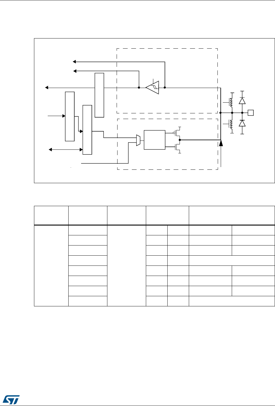
RM0430 Rev 8 185/1324
RM0430 General-purpose I/Os (GPIO)
203
Figure 17 show the basic structure of a 5 V tolerant I/O port bit. Table 25 gives the possible
port bit configurations.
Figure 17. Basic structure of a five-volt tolerant I/O port bit
1. VDD_FT is a potential specific to five-volt tolerant I/Os and different from VDD.
Table 25. Port bit configuration table(1)
MODER(i)
[1:0] OTYPER(i) OSPEEDR(i)
[B:A]
PUPDR(i)
[1:0] I/O configuration
01
0
SPEED
[B:A]
0 0 GP output PP
0 0 1 GP output PP + PU
0 1 0 GP output PP + PD
0 1 1 Reserved
1 0 0 GP output OD
1 0 1 GP output OD + PU
1 1 0 GP output OD + PD
1 1 1 Reserved (GP output OD)
!LTERNATEFUNCTIONOUTPUT
!LTERNATEFUNCTIONINPUT
0USHPULL
OPENDRAINOR
DISABLED
/UTPUTDATAREGISTER
2EADWRITE
&ROMONCHIP
PERIPHERAL
4OONCHIP
PERIPHERAL
/UTPUT
CONTROL
!NALOG
ONOFF 0ULL
0ULL
ONOFF
)/PIN
6$$
6$$
633
633
44,3CHMITT
TRIGGER
633
6$$?&4
0ROTECTION
DIODE
0ROTECTION
DIODE
ONOFF
)NPUTDRIVER
/UTPUTDRIVER
DOWN
UP
0-/3
.-/3
2EAD
"ITSETRESETREGISTERS
7RITE
!NALOG
)NPUTDATAREGISTER
AIB
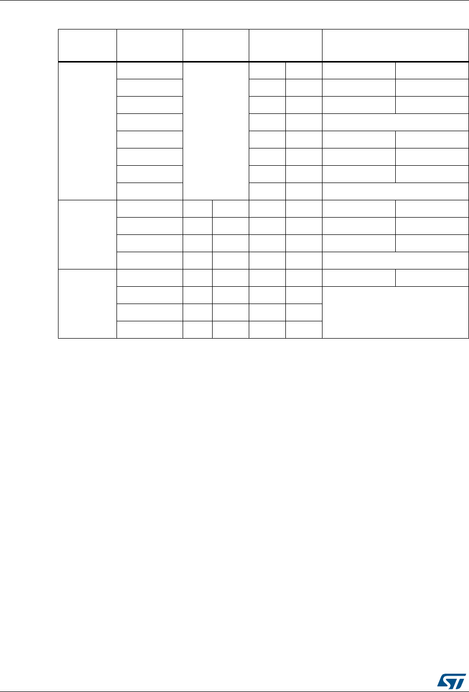
General-purpose I/Os (GPIO) RM0430
186/1324 RM0430 Rev 8
7.3.1 General-purpose I/O (GPIO)
During and just after reset, the alternate functions are not active and the I/O ports are
configured in input floating mode.
The debug pins are in AF pull-up/pull-down after reset:
•PA15: JTDI in pull-up
•PA14: JTCK/SWCLK in pull-down
•PA13: JTMS/SWDAT in pull-up
•PB4: NJTRST in pull-up
•PB3: JTDO in floating state
When the pin is configured as output, the value written to the output data register
(GPIOx_ODR) is output on the I/O pin. It is possible to use the output driver in push-pull
mode or open-drain mode (only the N-MOS is activated when 0 is output).
The input data register (GPIOx_IDR) captures the data present on the I/O pin at every AHB1
clock cycle.
All GPIO pins have weak internal pull-up and pull-down resistors, which can be activated or
not depending on the value in the GPIOx_PUPDR register.
10
0
SPEED
[B:A]
0 0 AF PP
0 0 1 AF PP + PU
0 1 0 AF PP + PD
0 1 1 Reserved
100AFOD
101AFOD + PU
110AFOD + PD
1 1 1 Reserved
00
x x x 0 0 Input Floating
x x x 0 1 Input PU
x x x 1 0 Input PD
x x x 1 1 Reserved (input floating)
11
x x x 0 0 Input/output Analog
xxx01
Reservedxxx10
xxx11
1. GP = general-purpose, PP = push-pull, PU = pull-up, PD = pull-down, OD = open-drain, AF = alternate
function.
Table 25. Port bit configuration table(1) (continued)
MODER(i)
[1:0] OTYPER(i) OSPEEDR(i)
[B:A]
PUPDR(i)
[1:0] I/O configuration

RM0430 Rev 8 187/1324
RM0430 General-purpose I/Os (GPIO)
203
7.3.2 I/O pin multiplexer and mapping
The microcontroller I/O pins are connected to onboard peripherals/modules through a
multiplexer that allows only one peripheral’s alternate function (AF) connected to an I/O pin
at a time. In this way, there can be no conflict between peripherals sharing the same I/O pin.
Each I/O pin has a multiplexer with sixteen alternate function inputs (AF0 to AF15) that can
be configured through the GPIOx_AFRL (for pin 0 to 7) and GPIOx_AFRH (for pin 8 to 15)
registers:
•After reset all I/Os are connected to the system’s alternate function 0 (AF0)
•The peripherals’ alternate functions are mapped from AF1 to AF13
•Cortex®-M4 with FPU EVENTOUT is mapped on AF15
This structure is shown in Figure 18: Selecting an alternate function on STM32F413/423
below.
In addition to this flexible I/O multiplexing architecture, each peripheral has alternate
functions mapped onto different I/O pins to optimize the number of peripherals available in
smaller packages.
To use an I/O in a given configuration, proceed as follows:
•System function
Connect the I/O to AF0 and configure it depending on the function used:
– JTAG/SWD, after each device reset these pins are assigned as dedicated pins
immediately usable by the debugger host (not controlled by the GPIO controller)
– RTC_REFIN: this pin should be configured in Input floating mode
– MCO1 and MCO2: these pins have to be configured in alternate function mode.
Note: You can disable some or all of the JTAG/SWD pins and so release the associated pins for
GPIO usage.
For more details please refer to Section 6.2.10: Clock-out capability.

General-purpose I/Os (GPIO) RM0430
188/1324 RM0430 Rev 8
•GPIO
Configure the desired I/O as output or input in the GPIOx_MODER register.
•Peripheral alternate function
For the ADC, configure the desired I/O as analog in the GPIOx_MODER register.
For other peripherals:
– Configure the desired I/O as an alternate function in the GPIOx_MODER register
– Select the type, pull-up/pull-down and output speed via the GPIOx_OTYPER,
GPIOx_PUPDR and GPIOx_OSPEEDR registers, respectively
– Connect the I/O to the desired AFx in the GPIOx_AFRL or GPIOx_AFRH register
•EVENTOUT
Configure the I/O pin used to output the Cortex®-M4 with FPU EVENTOUT signal by
connecting it to AF15
Note: Please refer to the “Alternate function mapping” table in the datasheets for the detailed
mapping of the system and peripherals’ alternate function I/O pins.
Table 26. Flexible SWJ-DP pin assignment
Available debug ports
SWJ I/O pin assigned
PA13 /
JTMS/
SWDIO
PA14 /
JTCK/
SWCLK
PA15 /
JTDI
PB3 /
JTDO
PB4/
NJTRST
Full SWJ (JTAG-DP + SW-DP) - Reset state X X X X X
Full SWJ (JTAG-DP + SW-DP) but without
NJTRST XXXX
JTAG-DP Disabled and SW-DP Enabled X X
JTAG-DP Disabled and SW-DP Disabled Released
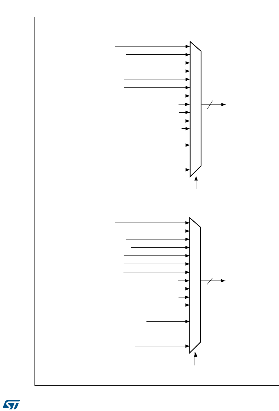
RM0430 Rev 8 189/1324
RM0430 General-purpose I/Os (GPIO)
203
Figure 18. Selecting an alternate function on STM32F413/423
06Y9
)RUSLQVWRWKH*3,2[B$)5/>@UHJLVWHUVHOHFWVWKHGHGLFDWHGDOWHUQDWHIXQFWLRQ
$)V\VWHP
$)7,07,0
$)7,0
$)7,0
$),&,&)03
$)63,
$)63,')6'0
$)63,86$57
$)')6'086$57&$1
$),&,&)03&$17,048$'63,
$)')6'0)60&48$'63,27*B)6
$)
$))0&6',2
$)
$)
$)(9(17287
3LQ[[
$)5/>@
)RUSLQVWRWKH*3,2[B$)5+>@UHJLVWHUVHOHFWVWKHGHGLFDWHGDOWHUQDWHIXQFWLRQ
3LQ[[
$)5+>@
$)V\VWHP
$)7,07,0
$)7,0
$)7,0
$),&,&)03
$)63,
$)63,')6'0
$)63,86$57
$)')6'086$57&$1
$),&,&)03&$17,048$'63,
$)')6'0)60&48$'63,27*B)6
$)
$))0&6',2
$)
$)
$)(9(17287

General-purpose I/Os (GPIO) RM0430
190/1324 RM0430 Rev 8
7.3.3 I/O port control registers
Each of the GPIOs has four 32-bit memory-mapped control registers (GPIOx_MODER,
GPIOx_OTYPER, GPIOx_OSPEEDR, GPIOx_PUPDR) to configure up to 16 I/Os.
The GPIOx_MODER register is used to select the I/O direction (input, output, AF, analog).
The GPIOx_OTYPER and GPIOx_OSPEEDR registers are used to select the output type
(push-pull or open-drain) and speed (the I/O speed pins are directly connected to the
corresponding GPIOx_OSPEEDR register bits whatever the I/O direction). The
GPIOx_PUPDR register is used to select the pull-up/pull-down whatever the I/O direction.
7.3.4 I/O port data registers
Each GPIO has two 16-bit memory-mapped data registers: input and output data registers
(GPIOx_IDR and GPIOx_ODR). GPIOx_ODR stores the data to be output, it is read/write
accessible. The data input through the I/O are stored into the input data register
(GPIOx_IDR), a read-only register.
See Section 7.4.5: GPIO port input data register (GPIOx_IDR) (x = A...H) and Section 7.4.6:
GPIO port output data register (GPIOx_ODR) (x = A...H) for the register descriptions.
7.3.5 I/O data bitwise handling
The bit set reset register (GPIOx_BSRR) is a 32-bit register which allows the application to
set and reset each individual bit in the output data register (GPIOx_ODR). The bit set reset
register has twice the size of GPIOx_ODR.
To each bit in GPIOx_ODR, correspond two control bits in GPIOx_BSRR: BSRR(i) and
BSRR(i+SIZE). When written to 1, bit BSRR(i) sets the corresponding ODR(i) bit. When
written to 1, bit BSRR(i+SIZE) resets the ODR(i) corresponding bit.
Writing any bit to 0 in GPIOx_BSRR does not have any effect on the corresponding bit in
GPIOx_ODR. If there is an attempt to both set and reset a bit in GPIOx_BSRR, the set
action takes priority.
Using the GPIOx_BSRR register to change the values of individual bits in GPIOx_ODR is a
“one-shot” effect that does not lock the GPIOx_ODR bits. The GPIOx_ODR bits can always
be accessed directly. The GPIOx_BSRR register provides a way of performing atomic
bitwise handling.
There is no need for the software to disable interrupts when programming the GPIOx_ODR
at bit level: it is possible to modify one or more bits in a single atomic AHB1 write access.
7.3.6 GPIO locking mechanism
It is possible to freeze the GPIO control registers by applying a specific write sequence to
the GPIOx_LCKR register. The frozen registers are GPIOx_MODER, GPIOx_OTYPER,
GPIOx_OSPEEDR, GPIOx_PUPDR, GPIOx_AFRL and GPIOx_AFRH.
To write the GPIOx_LCKR register, a specific write / read sequence has to be applied. When
the right LOCK sequence is applied to bit 16 in this register, the value of LCKR[15:0] is used
to lock the configuration of the I/Os (during the write sequence the LCKR[15:0] value must
be the same). When the LOCK sequence has been applied to a port bit, the value of the port
bit can no longer be modified until the next MCU or peripheral reset. Each GPIOx_LCKR bit
freezes the corresponding bit in the control registers (GPIOx_MODER, GPIOx_OTYPER,
GPIOx_OSPEEDR, GPIOx_PUPDR, GPIOx_AFRL and GPIOx_AFRH).

RM0430 Rev 8 191/1324
RM0430 General-purpose I/Os (GPIO)
203
The LOCK sequence (refer to Section 7.4.8: GPIO port configuration lock register
(GPIOx_LCKR) (x = A...H)) can only be performed using a word (32-bit long) access to the
GPIOx_LCKR register due to the fact that GPIOx_LCKR bit 16 has to be set at the same
time as the [15:0] bits.
For more details please refer to LCKR register description in Section 7.4.8: GPIO port
configuration lock register (GPIOx_LCKR) (x = A...H).
7.3.7 I/O alternate function input/output
Two registers are provided to select one out of the sixteen alternate function inputs/outputs
available for each I/O. With these registers, you can connect an alternate function to some
other pin as required by your application.
This means that a number of possible peripheral functions are multiplexed on each GPIO
using the GPIOx_AFRL and GPIOx_AFRH alternate function registers. The application can
thus select any one of the possible functions for each I/O. The AF selection signal being
common to the alternate function input and alternate function output, a single channel is
selected for the alternate function input/output of one I/O.
To know which functions are multiplexed on each GPIO pin, refer to the datasheets.
Note: The application is allowed to select one of the possible peripheral functions for each I/O at a
time.
7.3.8 External interrupt/wakeup lines
All ports have external interrupt capability. To use external interrupt lines, the port must be
configured in input mode, refer to Section 10.2: External interrupt/event controller (EXTI)
and Section 10.2.3: Wakeup event management.
7.3.9 Input configuration
When the I/O port is programmed as Input:
•the output buffer is disabled
•the Schmitt trigger input is activated
•the pull-up and pull-down resistors are activated depending on the value in the
GPIOx_PUPDR register
•The data present on the I/O pin are sampled into the input data register every AHB1
clock cycle
•A read access to the input data register provides the I/O State
Figure 19 shows the input configuration of the I/O port bit.
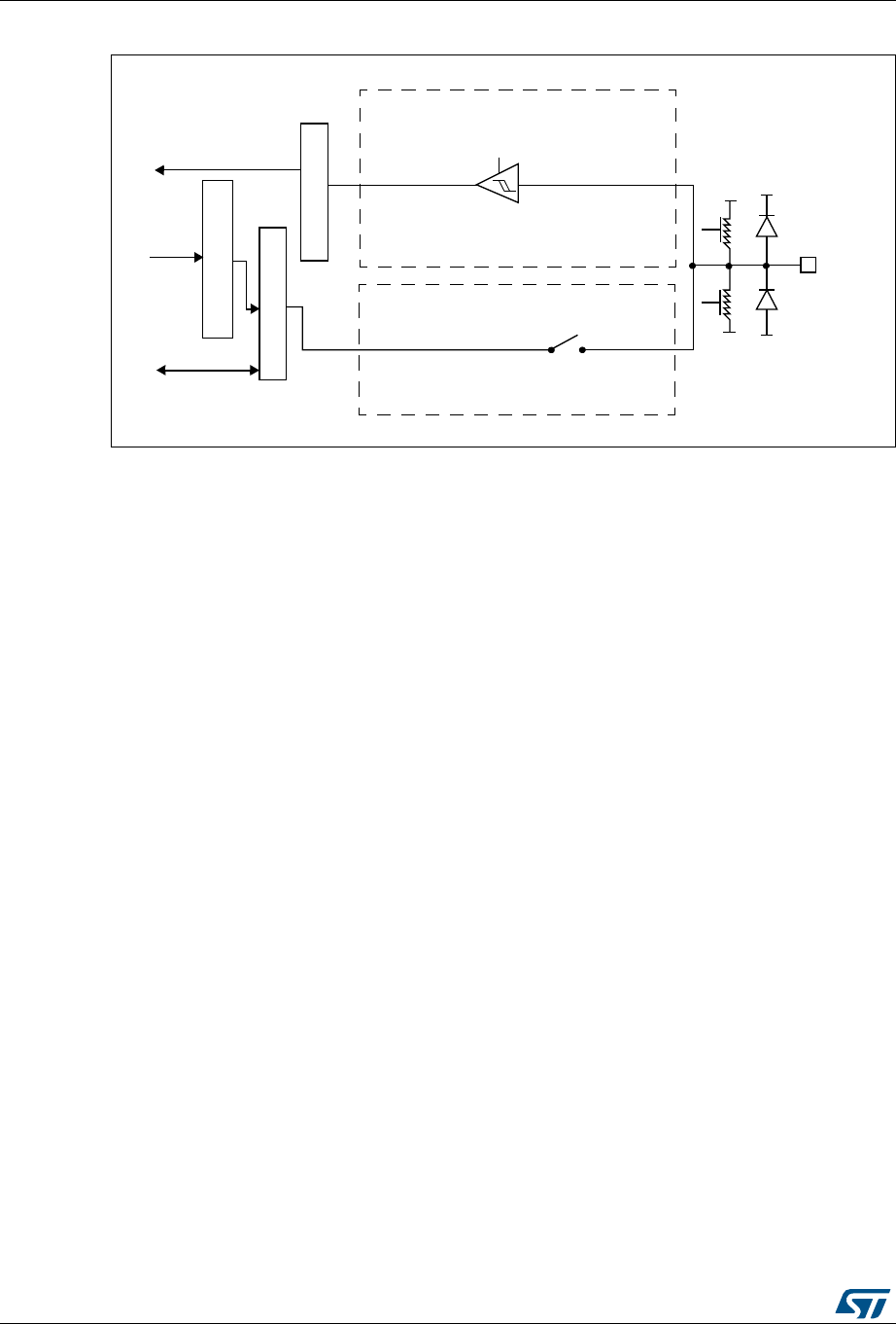
General-purpose I/Os (GPIO) RM0430
192/1324 RM0430 Rev 8
Figure 19. Input floating/pull up/pull down configurations
7.3.10 Output configuration
When the I/O port is programmed as output:
•The output buffer is enabled:
– Open drain mode: A “0” in the Output register activates the N-MOS whereas a “1”
in the Output register leaves the port in Hi-Z (the P-MOS is never activated)
– Push-pull mode: A “0” in the Output register activates the N-MOS whereas a “1” in
the Output register activates the P-MOS
•The Schmitt trigger input is activated
•The weak pull-up and pull-down resistors are activated or not depending on the value
in the GPIOx_PUPDR register
•The data present on the I/O pin are sampled into the input data register every AHB1
clock cycle
•A read access to the input data register gets the I/O state
•A read access to the output data register gets the last written value
Figure 20 shows the output configuration of the I/O port bit.
ONOFF
PULL
PULL
ONOFF
)/PIN
6$$
633
44,3CHMITT
TRIGGER
633
6$$
PROTECTION
DIODE
PROTECTION
DIODE
ON
INPUTDRIVER
OUTPUTDRIVER
DOWN
UP
)NPUTDATAREGISTER
/UTPUTDATAREGISTER
2EADWRITE
2EAD
"ITSETRESETREGISTERS
7RITE
AIB
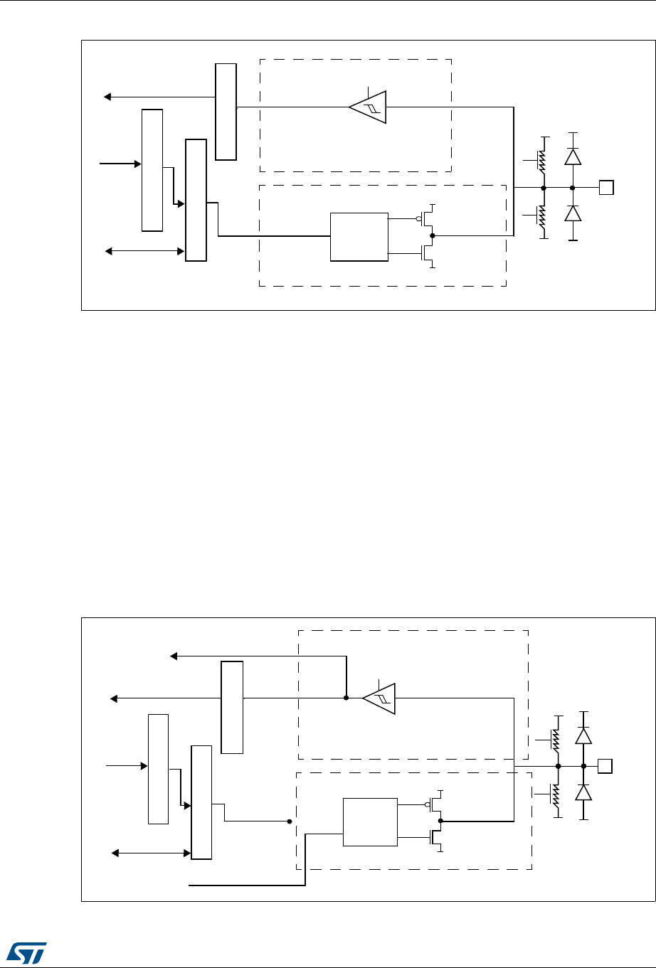
RM0430 Rev 8 193/1324
RM0430 General-purpose I/Os (GPIO)
203
Figure 20. Output configuration
7.3.11 Alternate function configuration
When the I/O port is programmed as alternate function:
•The output buffer can be configured as open-drain or push-pull
•The output buffer is driven by the signal coming from the peripheral (transmitter enable
and data)
•The Schmitt trigger input is activated
•The weak pull-up and pull-down resistors are activated or not depending on the value
in the GPIOx_PUPDR register
•The data present on the I/O pin are sampled into the input data register every AHB1
clock cycle
•A read access to the input data register gets the I/O state
Figure 21 shows the Alternate function configuration of the I/O port bit.
Figure 21. Alternate function configuration
0USHPULLOR
/PENDRAIN
/UTPUT
CONTROL
6
$$
6
33
44,3CHMITT
TRIGGER
ON
)NPUTDRIVER
/UTPUTDRIVER
0-/3
.-/3
)NPUTDATAREGISTER
/UTPUTDATAREGISTER
2EADWRITE
2EAD
"ITSETRESETREGISTERS
7RITE
ONOFF
PULL
PULL
ONOFF
6
$$
6
33
6
33
6
$$
PROTECTION
DIODE
PROTECTION
DIODE
DOWN
UP
)/PIN
AIB
!LTERNATEFUNCTIONOUTPUT
!LTERNATEFUNCTIONINPUT
PUSHPULLOR
OPENDRAIN
&ROMONCHIP
PERIPHERAL
4OONCHIP
PERIPHERAL
/UTPUT
CONTROL
6$$
633
44,3CHMITT
TRIGGER
ON
)NPUTDRIVER
/UTPUTDRIVER
0-/3
.-/3
)NPUTDATAREGISTER
/UTPUTDATAREGISTER
2EADWRITE
2EAD
"ITSETRESETREGISTERS
7RITE
ONOFF
ONOFF
6$$
633 633
6$$
PROTECTION
DIODE
PROTECTION
DIODE
0ULL
0ULL
)/PIN
DOWN
UP
AIB
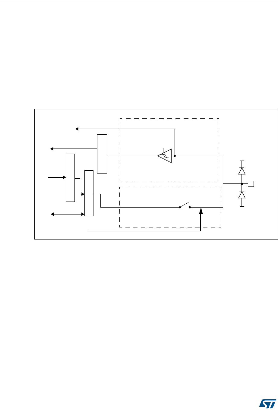
General-purpose I/Os (GPIO) RM0430
194/1324 RM0430 Rev 8
7.3.12 Analog configuration
When the I/O port is programmed as analog configuration:
•The output buffer is disabled
•The Schmitt trigger input is deactivated, providing zero consumption for every analog
value of the I/O pin. The output of the Schmitt trigger is forced to a constant value (0).
•The weak pull-up and pull-down resistors are disabled
•Read access to the input data register gets the value “0”
Note: In the analog configuration, the I/O pins cannot be 5 Volt tolerant.
Figure 22 shows the high-impedance, analog-input configuration of the I/O port bit.
Figure 22. High impedance-analog configuration
7.3.13 Using the OSC32_IN/OSC32_OUT pins as GPIO PC14/PC15
port pins
The LSE oscillator pins OSC32_IN and OSC32_OUT can be used as general-purpose
PC14 and PC15 I/Os, respectively, when the LSE oscillator is off. The PC14 and PC15 I/Os
are only configured as LSE oscillator pins OSC32_IN and OSC32_OUT when the LSE
oscillator is ON. This is done by setting the LSEON bit in the RCC_BDCR register. The LSE
has priority over the GPIO function.
Note: The PC14/PC15 GPIO functionality is lost when the 1.2 V domain is powered off (by the
device entering the standby mode) or when the backup domain is supplied by VBAT (VDD no
more supplied). In this case the I/Os are set in analog input mode.
7.3.14 Using the OSC_IN/OSC_OUT pins as GPIO PH0/PH1 port pins
The HSE oscillator pins OSC_IN/OSC_OUT can be used as general-purpose PH0/PH1
I/Os, respectively, when the HSE oscillator is OFF. (after reset, the HSE oscillator is off). The
PH0/PH1 I/Os are only configured as OSC_IN/OSC_OUT HSE oscillator pins when the
HSE oscillator is ON. This is done by setting the HSEON bit in the RCC_CR register. The
HSE has priority over the GPIO function.
&ROMONCHIP
PERIPHERAL
4OONCHIP
PERIPHERAL
!NALOG
TRIGGER
OFF
)NPUTDRIVER
)NPUTDATAREGISTER
/UTPUTDATAREGISTER
2EADWRITE
2EAD
"ITSETRESETREGISTERS
7RITE
!NALOG
6
33
6
$$
PROTECTION
DIODE
PROTECTION
DIODE
)/PIN
AI
44,3CHMITT

RM0430 Rev 8 195/1324
RM0430 General-purpose I/Os (GPIO)
203
7.3.15 Selection of RTC additional functions
The STM32F4xx feature one GPIO pin RTC_AF1 that can be used for the detection of a
tamper or time stamp event, or RTC_ALARM, or RTC_CALIB RTC outputs.
•The RTC_AF1 (PC13) can be used for the following purposes:
RTC_ALARM output: this output can be RTC Alarm A, RTC Alarm B or RTC Wakeup
depending on the OSEL[1:0] bits in the RTC_CR register
•RTC_CALIB output: this feature is enabled by setting the COE[23] in the RTC_CR
register
•RTC_TAMP1: tamper event detection
•RTC_TS: time stamp event detection
The selection of the corresponding pin is performed through the RTC_TAFCR register as
follows:
•TAMP1INSEL is used to select which pin is used as the RTC_TAMP1 tamper input
•TSINSEL is used to select which pin is used as the RTC_TS time stamp input
•ALARMOUTTYPE is used to select whether the RTC_ALARM is output in push-pull or
open-drain mode
The output mechanism follows the priority order listed in Table 27.
Table 27. RTC additional functions(1)
Pin
configuration
and function
enabled enabled Tamper
enabled
Time
stamp
enabled
TAMP1INSEL
TAMPER1
pin selection
TSINSEL
TIMESTAMP
pin
selection
ALARMOUTTYP
configuration
Alarm out
output OD 1Don’t care
Don’t
care
Don’t
care Don’t care Don’t care 0
Alarm out
output PP 1Don’t care
Don’t
care
Don’t
care Don’t care Don’t care 1
Calibration
out output PP 01
Don’t
care
Don’t
care Don’t care Don’t care Don’t care
TAMPER1
input floating 0 0 1 0 0 Don’t care Don’t care
TIMESTAMP
and
TAMPER1
input floating
0 0 1 1 0 0 Don’t care
TIMESTAMP
input floating 0 0 0 1 Don’t care 0 Don’t care
Standard
GPIO 0 0 0 0 Don’t care Don’t care Don’t care
1. OD: open drain; PP: push-pull.
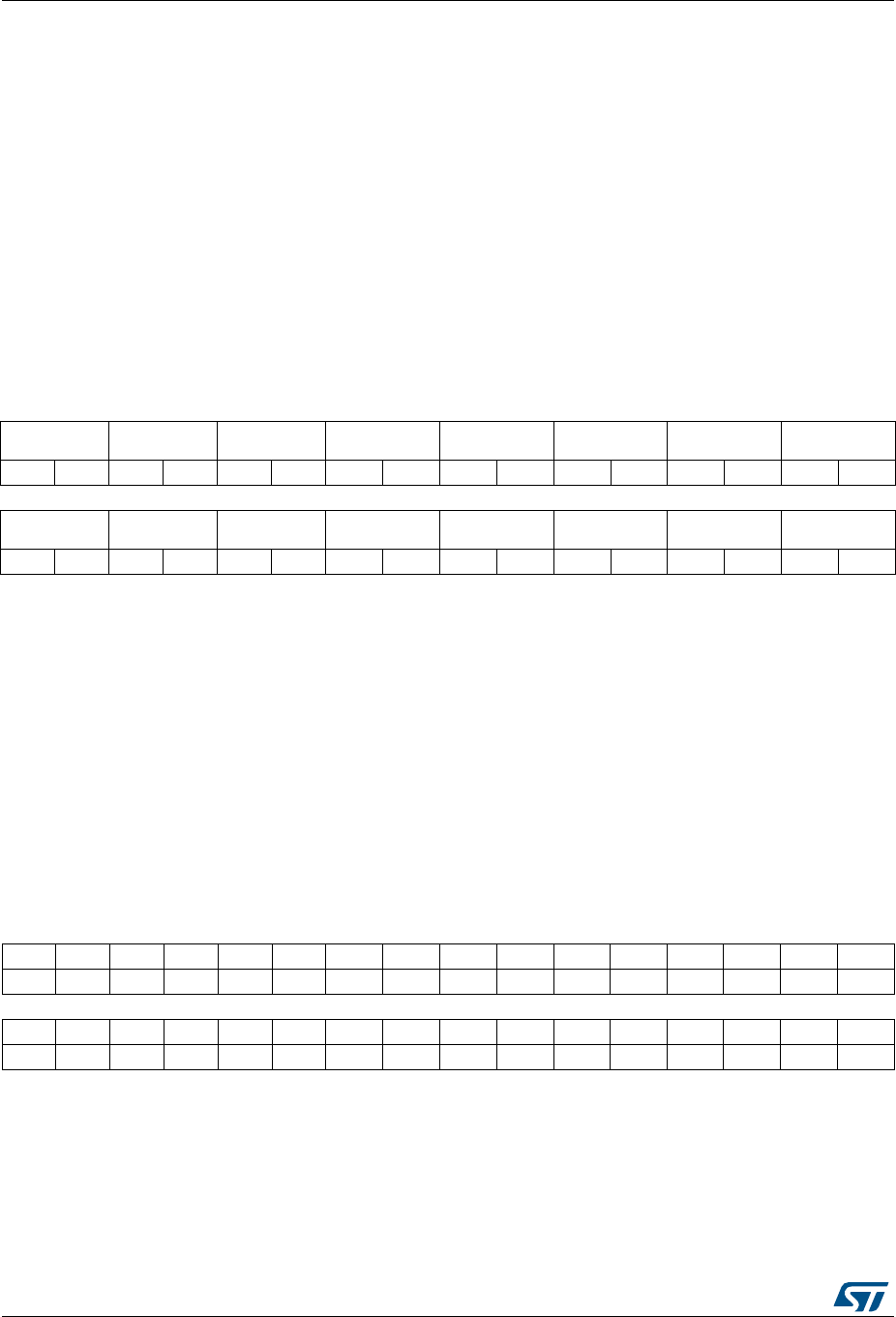
General-purpose I/Os (GPIO) RM0430
196/1324 RM0430 Rev 8
7.4 GPIO registers
This section gives a detailed description of the GPIO registers.
For a summary of register bits, register address offsets and reset values, refer to Table 28 .
The GPIO registers can be accessed by byte (8 bits), half-words (16 bits) or words (32 bits).
7.4.1 GPIO port mode register (GPIOx_MODER) (x = A...H)
Address offset: 0x00
Reset values:
•0x0A800 0000 for port A
•0x0000 0280 for port B
•0x0000 0000 for other ports
7.4.2 GPIO port output type register (GPIOx_OTYPER)
(x = A...H)
Address offset: 0x04
Reset value: 0x0000 0000
31 30 29 28 27 26 25 24 23 22 21 20 19 18 17 16
MODER15[1:0] MODER14[1:0] MODER13[1:0] MODER12[1:0] MODER11[1:0] MODER10[1:0] MODER9[1:0] MODER8[1:0]
rw rw rw rw rw rw rw rw rw rw rw rw rw rw rw rw
1514131211109876543210
MODER7[1:0] MODER6[1:0] MODER5[1:0] MODER4[1:0] MODER3[1:0] MODER2[1:0] MODER1[1:0] MODER0[1:0]
rw rw rw rw rw rw rw rw rw rw rw rw rw rw rw rw
Bits 2y:2y+1 MODERy[1:0]: Port x configuration bits (y = 0..15)
These bits are written by software to configure the I/O direction mode.
00: Input (reset state)
01: General purpose output mode
10: Alternate function mode
11: Analog mode
31 30 29 28 27 26 25 24 23 22 21 20 19 18 17 16
Res. Res. Res. Res. Res. Res. Res. Res. Res. Res. Res. Res. Res. Res. Res. Res.
1514131211109876543210
OT15 OT14 OT13 OT12 OT11 OT10 OT9 OT8 OT7 OT6 OT5 OT4 OT3 OT2 OT1 OT0
rw rw rw rw rw rw rw rw rw rw rw rw rw rw rw rw
Bits 31:16 Reserved, must be kept at reset value.
Bits 15:0 OTy: Port x configuration bits (y = 0..15)
These bits are written by software to configure the output type of the I/O port.
0: Output push-pull (reset state)
1: Output open-drain

RM0430 Rev 8 197/1324
RM0430 General-purpose I/Os (GPIO)
203
7.4.3 GPIO port output speed register (GPIOx_OSPEEDR)
(x = A...H)
Address offset: 0x08
Reset values:
•0x0C00 0000 for port A
•0x0000 00C0 for port B
•0x0000 0000 for other ports
7.4.4 GPIO port pull-up/pull-down register (GPIOx_PUPDR)
(x = A...H)
Address offset: 0x0C
Reset values:
•0x6400 0000 for port A
•0x0000 0100 for port B
•0x0000 0000 for other ports
31 30 29 28 27 26 25 24 23 22 21 20 19 18 17 16
OSPEEDR15
[1:0]
OSPEEDR14
[1:0]
OSPEEDR13
[1:0]
OSPEEDR12
[1:0]
OSPEEDR11
[1:0]
OSPEEDR10
[1:0]
OSPEEDR9
[1:0]
OSPEEDR8
[1:0]
rw rw rw rw rw rw rw rw rw rw rw rw rw rw rw rw
15 14 13 12 11 10 9 8 7 6 5 4 3 2 1 0
OSPEEDR7[1:0] OSPEEDR6[1:0] OSPEEDR5[1:0] OSPEEDR4[1:0] OSPEEDR3[1:0] OSPEEDR2[1:0] OSPEEDR1
[1:0]
OSPEEDR0
1:0]
rw rw rw rw rw rw rw rw rw rw rw rw rw rw rw rw
Bits 2y:2y+1 OSPEEDRy[1:0]: Port x configuration bits (y = 0..15)
These bits are written by software to configure the I/O output speed.
00: Low speed
01: Medium speed
10: Fast speed
11: High speed
Note: Refer to the product datasheets for the values of OSPEEDRy bits versus VDD
range and external load.
31 30 29 28 27 26 25 24 23 22 21 20 19 18 17 16
PUPDR15[1:0] PUPDR14[1:0] PUPDR13[1:0] PUPDR12[1:0] PUPDR11[1:0] PUPDR10[1:0] PUPDR9[1:0] PUPDR8[1:0]
rw rw rw rw rw rw rw rw rw rw rw rw rw rw rw rw
1514131211109876543210
PUPDR7[1:0] PUPDR6[1:0] PUPDR5[1:0] PUPDR4[1:0] PUPDR3[1:0] PUPDR2[1:0] PUPDR1[1:0] PUPDR0[1:0]
rw rw rw rw rw rw rw rw rw rw rw rw rw rw rw rw
Bits 2y:2y+1 PUPDRy[1:0]: Port x configuration bits (y = 0..15)
These bits are written by software to configure the I/O pull-up or pull-down
00: No pull-up, pull-down
01: Pull-up
10: Pull-down
11: Reserved
General-purpose I/Os (GPIO) RM0430
198/1324 RM0430 Rev 8
7.4.5 GPIO port input data register (GPIOx_IDR) (x = A...H)
Address offset: 0x10
Reset value: 0x0000 XXXX (where X means undefined)
7.4.6 GPIO port output data register (GPIOx_ODR) (x = A...H)
Address offset: 0x14
Reset value: 0x0000 0000
7.4.7 GPIO port bit set/reset register (GPIOx_BSRR) (x = A...H)
Address offset: 0x18
Reset value: 0x0000 0000
31 30 29 28 27 26 25 24 23 22 21 20 19 18 17 16
Res. Res. Res. Res. Res. Res. Res. Res. Res. Res. Res. Res. Res. Res. Res. Res.
1514131211109876543210
IDR15 IDR14 IDR13 IDR12 IDR11 IDR10 IDR9 IDR8 IDR7 IDR6 IDR5 IDR4 IDR3 IDR2 IDR1 IDR0
rrrrrr r r r r rrrrrr
Bits 31:16 Reserved, must be kept at reset value.
Bits 15:0 IDRy: Port input data (y = 0..15)
These bits are read-only and can be accessed in word mode only. They contain the input
value of the corresponding I/O port.
31 30 29 28 27 26 25 24 23 22 21 20 19 18 17 16
Res. Res. Res. Res. Res. Res. Res. Res. Res. Res. Res. Res. Res. Res. Res. Res.
1514131211109876543210
ODR15 ODR14 ODR13 ODR12 ODR11 ODR10 ODR9 ODR8 ODR7 ODR6 ODR5 ODR4 ODR3 ODR2 ODR1 ODR0
rw rw rw rw rw rw rw rw rw rw rw rw rw rw rw rw
Bits 31:16 Reserved, must be kept at reset value.
Bits 15:0 ODRy: Port output data (y = 0..15)
These bits can be read and written by software.
Note: For atomic bit set/reset, the ODR bits can be individually set and reset by writing to the
GPIOx_BSRR register (x = A...H).
31 30 29 28 27 26 25 24 23 22 21 20 19 18 17 16
BR15 BR14 BR13 BR12 BR11 BR10 BR9 BR8 BR7 BR6 BR5 BR4 BR3 BR2 BR1 BR0
wwwwwwwwwwwwwwww
1514131211109876543210
BS15 BS14 BS13 BS12 BS11 BS10 BS9 BS8 BS7 BS6 BS5 BS4 BS3 BS2 BS1 BS0
wwwwwwwwwwwwwwww

RM0430 Rev 8 199/1324
RM0430 General-purpose I/Os (GPIO)
203
7.4.8 GPIO port configuration lock register (GPIOx_LCKR)
(x = A...H)
This register is used to lock the configuration of the port bits when a correct write sequence
is applied to bit 16 (LCKK). The value of bits [15:0] is used to lock the configuration of the
GPIO. During the write sequence, the value of LCKR[15:0] must not change. When the
LOCK sequence has been applied on a port bit, the value of this port bit can no longer be
modified until the next MCU or peripheral reset.
Note: A specific write sequence is used to write to the GPIOx_LCKR register. Only word access
(32-bit long) is allowed during this write sequence.
Each lock bit freezes a specific configuration register (control and alternate function
registers).
Address offset: 0x1C
Reset value: 0x0000 0000
Access: 32-bit word only, read/write register
Bits 31:16 BRy: Port x reset bit y (y = 0..15)
These bits are write-only and can be accessed in word, half-word or byte mode. A read to
these bits returns the value 0x0000.
0: No action on the corresponding ODRx bit
1: Resets the corresponding ODRx bit
Note: If both BSx and BRx are set, BSx has priority.
Bits 15:0 BSy: Port x set bit y (y= 0..15)
These bits are write-only and can be accessed in word, half-word or byte mode. A read to
these bits returns the value 0x0000.
0: No action on the corresponding ODRx bit
1: Sets the corresponding ODRx bit
31 30 29 28 27 26 25 24 23 22 21 20 19 18 17 16
Res. Res. Res. Res. Res. Res. Res. Res. Res. Res. Res. Res. Res. Res. Res. LCKK
rw
15 14 13 12 11 10 9 8 7 6 5 4 3 2 1 0
LCK15 LCK14 LCK13 LCK12 LCK11 LCK10 LCK9 LCK8 LCK7 LCK6 LCK5 LCK4 LCK3 LCK2 LCK1 LCK0
rw rw rw rw rw rw rw rw rw rw rw rw rw rw rw rw
General-purpose I/Os (GPIO) RM0430
200/1324 RM0430 Rev 8
7.4.9 GPIO alternate function low register (GPIOx_AFRL) (x = A...H)
Address offset: 0x20
Reset value: 0x0000 0000
Bits 31:17 Reserved, must be kept at reset value.
Bit 16 LCKK[16]: Lock key
This bit can be read any time. It can only be modified using the lock key write sequence.
0: Port configuration lock key not active
1: Port configuration lock key active. The GPIOx_LCKR register is locked until an MCU reset
or a peripheral reset occurs.
LOCK key write sequence:
WR LCKR[16] = ‘1’ + LCKR[15:0]
WR LCKR[16] = ‘0’ + LCKR[15:0]
WR LCKR[16] = ‘1’ + LCKR[15:0]
RD LCKR
RD LCKR[16] = ‘1’ (this read operation is optional but it confirms that the lock is active)
Note: During the LOCK key write sequence, the value of LCK[15:0] must not change.
Any error in the lock sequence aborts the lock.
After the first lock sequence on any bit of the port, any read access on the LCKK bit will
return ‘1’ until the next CPU reset.
Bits 15:0 LCKy: Port x lock bit y (y= 0..15)
These bits are read/write but can only be written when the LCKK bit is ‘0.
0: Port configuration not locked
1: Port configuration locked
31 30 29 28 27 26 25 24 23 22 21 20 19 18 17 16
AFRL7[3:0] AFRL6[3:0] AFRL5[3:0] AFRL4[3:0]
rw rw rw rw rw rw rw rw rw rw rw rw rw rw rw rw
1514131211109876543210
AFRL3[3:0] AFRL2[3:0] AFRL1[3:0] AFRL0[3:0]
rw rw rw rw rw rw rw rw rw rw rw rw rw rw rw rw
Bits 31:0 AFRLy: Alternate function selection for port x bit y (y = 0..7)
These bits are written by software to configure alternate function I/Os
AFRLy selection:
0000: AF0
0001: AF1
0010: AF2
0011: AF3
0100: AF4
0101: AF5
0110: AF6
0111: AF7
1000: AF8
1001: AF9
1010: AF10
1011: AF11
1100: AF12
1101: AF13
1110: AF14
1111: AF15
RM0430 Rev 8 201/1324
RM0430 General-purpose I/Os (GPIO)
203
7.4.10 GPIO alternate function high register (GPIOx_AFRH)
(x = A...H)
Address offset: 0x24
Reset value: 0x0000 0000
7.4.11 GPIO register map
The following table gives the GPIO register map and the reset values.
31 30 29 28 27 26 25 24 23 22 21 20 19 18 17 16
AFRH15[3:0] AFRH14[3:0] AFRH13[3:0] AFRH12[3:0]
rw rw rw rw rw rw rw rw rw rw rw rw rw rw rw rw
1514131211109876543210
AFRH11[3:0] AFRH10[3:0] AFRH9[3:0] AFRH8[3:0]
rw rw rw rw rw rw rw rw rw rw rw rw rw rw rw rw
Bits 31:0 AFRHy: Alternate function selection for port x bit y (y = 8..15)
These bits are written by software to configure alternate function I/Os
AFRHy selection:
0000: AF0
0001: AF1
0010: AF2
0011: AF3
0100: AF4
0101: AF5
0110: AF6
0111: AF7
1000: AF8
1001: AF9
1010: AF10
1011: AF11
1100: AF12
1101: AF13
1110: AF14
1111: AF15
Table 28. GPIO register map and reset values
Offset Register
31
30
29
28
27
26
25
24
23
22
21
20
19
18
17
16
15
14
13
12
11
10
9
8
7
6
5
4
3
2
1
0
0x00
GPIOA_
MODER
MODER15[1:0]
MODER14[1:0]
MODER13[1:0]
MODER12[1:0]
MODER11[1:0]
MODER10[1:0]
MODER9[1:0]
MODER8[1:0]
MODER7[1:0]
MODER6[1:0]
MODER5[1:0]
MODER4[1:0]
MODER3[1:0]
MODER2[1:0]
MODER1[1:0]
MODER0[1:0]
Reset value 00001100000000000000000000000000
0x00
GPIOB_
MODER
MODER15[1:0]
MODER14[1:0]
MODER13[1:0]
MODER12[1:0]
MODER11[1:0]
MODER10[1:0]
MODER9[1:0]
MODER8[1:0]
MODER7[1:0]
MODER6[1:0]
MODER5[1:0]
MODER4[1:0]
MODER3[1:0]
MODER2[1:0]
MODER1[1:0]
MODER0[1:0]
Reset value 00000000000000000000001010000000
0x00
GPIOx_MODER
(where x =
C...H)
MODER15[1:0]
MODER14[1:0]
MODER13[1:0]
MODER12[1:0]
MODER11[1:0]
MODER10[1:0]
MODER9[1:0]
MODER8[1:0]
MODER7[1:0]
MODER6[1:0]
MODER5[1:0]
MODER4[1:0]
MODER3[1:0]
MODER2[1:0]
MODER1[1:0]
MODER0[1:0]
Reset value 00000000000000000000000000000000

General-purpose I/Os (GPIO) RM0430
202/1324 RM0430 Rev 8
0x04
GPIOx_
OTYPER
(where x = A...H)
Res.
Res.
Res.
Res.
Res.
Res.
Res.
Res.
Res.
Res.
Res.
Res.
Res.
Res.
Res.
Res.
OT15
OT14
OT13
OT12
OT11
OT10
OT9
OT8
OT7
OT6
OT5
OT4
OT3
OT2
OT1
OT0
Reset value 0000000000000000
0x08
GPIOx_
OSPEEDR
(where x =
C...H)
OSPEEDR15[1:0]
OSPEEDR14[1:0]
OSPEEDR13[1:0]
OSPEEDR12[1:0]
OSPEEDR11[1:0]
OSPEEDR10[1:0]
OSPEEDR9[1:0]
OSPEEDR8[1:0]
OSPEEDR7[1:0]
OSPEEDR6[1:0]
OSPEEDR5[1:0]
OSPEEDR4[1:0]
OSPEEDR3[1:0]
OSPEEDR2[1:0]
OSPEEDR1[1:0]
OSPEEDR0[1:0]
Reset value 00000000000000000000000000000000
0x08
GPIOA_
OSPEEDER
OSPEEDR15[1:0]
OSPEEDR14[1:0]
OSPEEDR13[1:0]
OSPEEDR12[1:0]
OSPEEDR11[1:0]
OSPEEDR10[1:0]
OSPEEDR9[1:0]
OSPEEDR8[1:0]
OSPEEDR7[1:0]
OSPEEDR6[1:0]
OSPEEDR5[1:0]
OSPEEDR4[1:0]
OSPEEDR3[1:0]
OSPEEDR2[1:0]
OSPEEDR1[1:0]
OSPEEDR0[1:0]
Reset value 00001100000000000000000000000000
0x08
GPIOB_
OSPEEDR
OSPEEDR15[1:0]
OSPEEDR14[1:0]
OSPEEDR13[1:0]
OSPEEDR12[1:0]
OSPEEDR11[1:0]
OSPEEDR10[1:0]
OSPEEDR9[1:0]
OSPEEDR8[1:0]
OSPEEDR7[1:0]
OSPEEDR6[1:0]
OSPEEDR5[1:0]
OSPEEDR4[1:0]
OSPEEDR3[1:0]
OSPEEDR2[1:0]
OSPEEDR1[1:0]
OSPEEDR0[1:0]
Reset value 00000000000000000000000011000000
0x0C GPIOA_PUPDR
PUPDR15[1:0]
PUPDR14[1:0]
PUPDR13[1:0]
PUPDR12[1:0]
PUPDR11[1:0]
PUPDR10[1:0]
PUPDR9[1:0]
PUPDR8[1:0]
PUPDR7[1:0]
PUPDR6[1:0]
PUPDR5[1:0]
PUPDR4[1:0]
PUPDR3[1:0]
PUPDR2[1:0]
PUPDR1[1:0]
PUPDR0[1:0]
Reset value 01100100000000000000000000000000
0x0C GPIOB_PUPDR
PUPDR15[1:0]
PUPDR14[1:0]
PUPDR13[1:0]
PUPDR12[1:0]
PUPDR11[1:0]
PUPDR10[1:0]
PUPDR9[1:0]
PUPDR8[1:0]
PUPDR7[1:0]
PUPDR6[1:0]
PUPDR5[1:0]
PUPDR4[1:0]
PUPDR3[1:0]
PUPDR2[1:0]
PUPDR1[1:0]
PUPDR0[1:0]
Reset value 00000000000000000000000100000000
0x0C
GPIOx_PUPDR
(where x =
C...H)
PUPDR15[1:0]
PUPDR14[1:0]
PUPDR13[1:0]
PUPDR12[1:0]
PUPDR11[1:0]
PUPDR10[1:0]
PUPDR9[1:0]
PUPDR8[1:0]
PUPDR7[1:0]
PUPDR6[1:0]
PUPDR5[1:0]
PUPDR4[1:0]
PUPDR3[1:0]
PUPDR2[1:0]
PUPDR1[1:0]
PUPDR0[1:0]
Reset value 00000000000000000000000000000000
0x10
GPIOx_IDR
(where x = A...H)
Res.
Res.
Res.
Res.
Res.
Res.
Res.
Res.
Res.
Res.
Res.
Res.
Res.
Res.
Res.
Res.
IDR15
IDR14
IDR13
IDR12
IDR11
IDR10
IDR9
IDR8
IDR7
IDR6
IDR5
IDR4
IDR3
IDR2
IDR1
IDR0
Reset value xxxxxxxxxxxxxxxx
0x14
GPIOx_ODR
(where x = A...H)
Res.
Res.
Res.
Res.
Res.
Res.
Res.
Res.
Res.
Res.
Res.
Res.
Res.
Res.
Res.
Res.
ODR15
ODR14
ODR13
ODR12
ODR11
ODR10
ODR9
ODR8
ODR7
ODR6
ODR5
ODR4
ODR3
ODR2
ODR1
ODR0
Reset value 0000000000000000
0x18
GPIOx_BSRR
(where x = A...H)
BR15
BR14
BR13
BR12
BR11
BR10
BR9
BR8
BR7
BR6
BR5
BR4
BR3
BR2
BR1
BR0
BS15
BS14
BS13
BS12
BS11
BS10
BS9
BS8
BS7
BS6
BS5
BS4
BS3
BS2
BS1
BS0
Reset value 00000000000000000000000000000000
Table 28. GPIO register map and reset values (continued)
Offset Register
31
30
29
28
27
26
25
24
23
22
21
20
19
18
17
16
15
14
13
12
11
10
9
8
7
6
5
4
3
2
1
0

RM0430 Rev 8 203/1324
RM0430 General-purpose I/Os (GPIO)
203
Refer to Section: Memory map for the register boundary addresses.
0x1C
GPIOx_LCKR
(where x = A...H)
Res.
Res.
Res.
Res.
Res.
Res.
Res.
Res.
Res.
Res.
Res.
Res.
Res.
Res.
Res.
LCKK
LCK15
LCK14
LCK13
LCK12
LCK11
LCK10
LCK9
LCK8
LCK7
LCK6
LCK5
LCK4
LCK3
LCK2
LCK1
LCK0
Reset value 00000000000000000
0x20
GPIOx_AFRL
(where x = A...H) AFRL7[3:0] AFRL6[3:0] AFRL5[3:0] AFRL4[3:0] AFRL3[3:0] AFRL2[3:0] AFRL1[3:0] AFRL0[3:0]
Reset value 00000000000000000000000000000000
0x24
GPIOx_AFRH
(where x = A...H) AFRH15[3:0] AFRH14[3:0] AFRH13[3:0] AFRH12[3:0] AFRH11[3:0] AFRH10[3:0] AFRH9[3:0] AFRH8[3:0]
Reset value 00000000000000000000000000000000
Table 28. GPIO register map and reset values (continued)
Offset Register
31
30
29
28
27
26
25
24
23
22
21
20
19
18
17
16
15
14
13
12
11
10
9
8
7
6
5
4
3
2
1
0

System configuration controller (SYSCFG) RM0430
204/1324 RM0430 Rev 8
8 System configuration controller (SYSCFG)
The system configuration controller is mainly used to remap the memory accessible in the
code area and manage the external interrupt line connection to the GPIOs.
8.1 I/O compensation cell
By default the I/O compensation cell is not used. However when the I/O output buffer speed
is configured in 50 MHz or 100 MHz mode, it is recommended to use the compensation cell
for slew rate control on I/O tf(IO)out)/tr(IO)out commutation to reduce the I/O noise on power
supply.
When the compensation cell is enabled, a READY flag is set to indicate that the
compensation cell is ready and can be used. The I/O compensation cell can be used only
when the supply voltage ranges from 2.4 to 3.6 V.
8.2 SYSCFG registers
8.2.1 SYSCFG memory remap register (SYSCFG_MEMRMP)
This register is used for specific configurations on memory remap:
•Two bits are used to configure the type of memory accessible at address 0x0000 0000.
These bits are used to select the physical remap by software and so, bypass the BOOT
pins.
•After reset these bits take the value selected by the BOOT pins. When booting from
main Flash memory with BOOT0 pin set to 0, this register takes the value 0x00.
In remap mode, the CPU can access the external memory via ICode bus instead of System
bus which boosts up the performance.
Address offset: 0x00
Reset value: 0x0000 000X (X is the memory mode selected by the BOOT pins)
)
31 30 29 28 27 26 25 24 23 22 21 20 19 18 17 16
Res. Res. Res. Res. Res. Res. Res. Res. Res. Res. Res. Res. Res. Res. Res. Res.
1514131211109876543210
Res. Res. Res. Res. Res. Res. Res. Res. Res. Res. Res. Res. Res. Res. MEM_MODE
rw rw

RM0430 Rev 8 205/1324
RM0430 System configuration controller (SYSCFG)
213
8.2.2 SYSCFG peripheral mode configuration register (SYSCFG_PMC)
Address offset: 0x04
Reset value: 0x0000 0000
Bits 31:2 Reserved, must be kept at reset value.
Bits 1:0 MEM_MODE: Memory mapping selection
Set and cleared by software. This bit controls the memory internal mapping at
address 0x0000 0000. After reset these bits take the value selected by the Boot
pins.
00: Main Flash memory mapped at 0x0000 0000
01: System Flash memory mapped at 0x0000 0000
10: reserved
11: Embedded SRAM mapped at 0x0000 0000
Note: Refer to Figure 2: Memory map for details about the memory mapping at
address 0x0000 0000.
31 30 29 28 27 26 25 24 23 22 21 20 19 18 17 16
Res. Res. Res. Res. Res. Res. Res. Res. Res. Res. Res. Res. Res. Res. Res. ADC1D
C2
rw
15 14 13 12 11 10 9 8 7 6 5 4 3 2 1 0
Res. Res. Res. Res. Res. Res. Res. Res. Res. Res. Res. Res. Res. Res. Res. Res.
Bits 31:17 Reserved, must be kept at reset value.
Bit 16 ADC1DC2:
0: No effect.
1: Refer to AN4073 on how to use this bit
Note: These bits can be set only if the following conditions are met:
- ADC clock higher or equal to 30 MHz.
- Only one ADC1DC2 bit must be selected if ADC conversions do not start
at the same time and the sampling times differ.
- These bits must not be set when the ADCDC1 bit is set in PWR_CR
register.
Bits 15:0 Reserved, must be kept at reset value.

System configuration controller (SYSCFG) RM0430
206/1324 RM0430 Rev 8
8.2.3 SYSCFG external interrupt configuration register 1
(SYSCFG_EXTICR1)
Address offset: 0x08
Reset value: 0x0000 0000
8.2.4 SYSCFG external interrupt configuration register 2
(SYSCFG_EXTICR2)
Address offset: 0x0C
Reset value: 0x0000 0000
31 30 29 28 27 26 25 24 23 22 21 20 19 18 17 16
Res. Res. Res. Res. Res. Res. Res. Res. Res. Res. Res. Res. Res. Res. Res. Res.
1514131211109876543210
EXTI3[3:0] EXTI2[3:0] EXTI1[3:0] EXTI0[3:0]
rw rw rw rw rw rw rw rw rw rw rw rw rw rw rw rw
Bits 31:16 Reserved, must be kept at reset value.
Bits 15:0 EXTIx[3:0]: EXTI x configuration (x = 0 to 3)
These bits are written by software to select the source input for the EXTIx
external interrupt.
0000: PA[x] pin
0001: PB[x] pin
0010: PC[x] pin
0011: PD[x] pin
0100: PE[x] pin
0101: PF[x] pin
0110: PG[x] pin
0111: PH[x] pin (Reserved for EXTI3 and EXTI2 configurations)
Other configurations: reserved
31 30 29 28 27 26 25 24 23 22 21 20 19 18 17 16
Res. Res. Res. Res. Res. Res. Res. Res. Res. Res. Res. Res. Res. Res. Res. Res.
1514131211109876543210
EXTI7[3:0] EXTI6[3:0] EXTI5[3:0] EXTI4[3:0]
rw rw rw rw rw rw rw rw rw rw rw rw rw rw rw rw
RM0430 Rev 8 207/1324
RM0430 System configuration controller (SYSCFG)
213
8.2.5 SYSCFG external interrupt configuration register 3
(SYSCFG_EXTICR3)
Address offset: 0x10
Reset value: 0x0000 0000
Bits 31:16 Reserved, must be kept at reset value.
Bits 15:0 EXTIx[3:0]: EXTI x configuration (x = 4 to 7)
These bits are written by software to select the source input for the EXTIx
external interrupt.
0000: PA[x] pin
0001: PB[x] pin
0010: PC[x] pin
0011: PD[x] pin
0100: PE[x] pin
0101: PF[x] pin
0110: PG[x] pin
Other configurations: reserved
31 30 29 28 27 26 25 24 23 22 21 20 19 18 17 16
Res. Res. Res. Res. Res. Res. Res. Res. Res. Res. Res. Res. Res. Res. Res. Res.
1514131211109876543210
EXTI11[3:0] EXTI10[3:0] EXTI9[3:0] EXTI8[3:0]
rw rw rw rw rw rw rw rw rw rw rw rw rw rw rw rw
Bits 31:16 Reserved, must be kept at reset value.
Bits 15:0 EXTIx[3:0]: EXTI x configuration (x = 8 to 11)
These bits are written by software to select the source input for the EXTIx external
interrupt.
0000: PA[x] pin
0001: PB[x] pin
0010: PC[x] pin
0011: PD[x] pin
0100: PE[x] pin
0101: PF[x] pin
0110: PG[x] pin
Other configurations: reserved

System configuration controller (SYSCFG) RM0430
208/1324 RM0430 Rev 8
8.2.6 SYSCFG external interrupt configuration register 4
(SYSCFG_EXTICR4)
Address offset: 0x14
Reset value: 0x0000 0000
8.2.7 SYSCFG configuration register 2 (SYSCFG_CFGR2)
Address offset: 0x1C
Reset value: 0x0000 0000
31 30 29 28 27 26 25 24 23 22 21 20 19 18 17 16
Res. Res. Res. Res. Res. Res. Res. Res. Res. Res. Res. Res. Res. Res. Res. Res.
1514131211109876543210
EXTI15[3:0] EXTI14[3:0] EXTI13[3:0] EXTI12[3:0]
rw rw rw rw rw rw rw rw rw rw rw rw rw rw rw rw
Bits 31:16 Reserved, must be kept at reset value.
Bits 15:0 EXTIx[3:0]: EXTI x configuration (x = 12 to 15)
These bits are written by software to select the source input for the EXTIx external
interrupt.
0000: PA[x] pin
0001: PB[x] pin
0010: PC[x] pin
0011: PD[x] pin
0100: PE[x] pin
0101: PF[x] pin
0110: PG[x] pin
31 30 29 28 27 26 25 24 23 22 21 20 19 18 17 16
Res. Res. Res. Res. Res. Res. Res. Res. Res. Res. Res. Res. Res. Res. Res. Res.
1514131211109876543210
Res. Res. Res. Res. Res. Res. Res. Res. Res. Res. Res. Res. Res. PVDL Res. CLL
rw rw
Bits 31:3 Reserved, must be kept at reset value.

RM0430 Rev 8 209/1324
RM0430 System configuration controller (SYSCFG)
213
8.2.8 Compensation cell control register (SYSCFG_CMPCR)
Address offset: 0x20
Reset value: 0x0000 0000
Bit 2 PVDL: PVD lock
This bit is set by software. It can be cleared only by a system reset. It enables and
locks the PVD connection to TIM1/8 Break input. It also locks (write protection) the
PVDE and PVDS[2:0] bits of PWR_CR register.
0: PVD interrupt not connected to TIM1/8 Break input. PVDE and PVDS[2:0] can be
read and modified
1: PVD interrupt connected to TIM1/8 Break input. PVDE and PVDS[2:0] are read-
only
Bit 1 Reserved, must be kept at reset value.
Bit 0 CLL: core lockup lock
This bit is set and cleared by software. It enables and locks the LOCKUP (Hardfault)
output of the Cortex®-M4 with FPU core with TIM1/8 Break input.
0: Cortex®-M4 with FPU LOCKUP output not connected to TIM1/8 Break input
1: Cortex®-M4 with FPU LOCKUP output connected to TIM1/8 Break input
31 30 29 28 27 26 25 24 23 22 21 20 19 18 17 16
Res. Res. Res. Res. Res. Res. Res. Res. Res. Res. Res. Res. Res. Res. Res. Res.
1514131211109 8 7 654321 0
Res. Res. Res. Res. Res. Res. Res. READY Res. Res. Res. Res. Res. Res. Res. CMP_PD
rrw
Bits 31:9 Reserved, must be kept at reset value.
Bit 8 READY: Compensation cell ready flag
0: I/O compensation cell not ready
1: O compensation cell ready
Bits 7:2 Reserved, must be kept at reset value.
Bit 0 CMP_PD: Compensation cell power-down
0: I/O compensation cell power-down mode
1: I/O compensation cell enabled

System configuration controller (SYSCFG) RM0430
210/1324 RM0430 Rev 8
8.2.9 SYSCFG configuration register (SYSCFG_CFGR)
Address offset: 0x2C
Reset value: 0x0000 0000
8.2.10 DFSDM Multi-channel delay control register (SYSCFG_MCHDLYCR)
Address offset: 0x30
Reset value: 0x0000 0000
31 30 29 28 27 26 25 24 23 22 21 20 19 18 17 16
Res. Res Res. Res. Res. Res. Res. Res. Res. Res. Res. Res. Res. Res. Res. Res.
15141312111098765432 1 0
Res. Res. Res. Res. Res. Res. Res. Res. Res. Res. Res. Res. Res. Res. I2CFMP1_SDA I2CFMP1_SCL
rw rw
Bits 31:2 Reserved, must be kept at reset value.
Bit 1 I2CFMP1_SDA
Set and cleared by software. When this bit is set, it forces FM+ drive capability on
I2CFMP1_SDA pin selected through GPIO port mode register and GPIO alternate
function selection bits.
Bit 0 I2CFMP1_SCL
Set and cleared by software. When this bit is set, it forces FM+ drive capability on
I2CFMP1_SCL pin selected through GPIO port mode register and GPIO alternate
function selection bits.
31 30 29 28 27 26 25 24 23 22 21 20 19 18 17 16
Res. Res. Res. Res. Res. Res. Res. Res. Res. Res. Res. Res. Res.
DFSDM2
_CKO
SEL
DFSDM2
_CFG
DFSDM
2_CK37
SEL
rrrrrrrrrrrrrrwrwrw
15 14 13 12 11 10 9 8 7 6 5 4 3 2 1 0
DFSDM2
_CK26
SEL
DFSDM2
_CK15
SEL
DFSDM2
_CK04
SEL
DFSDM2
_D6
SEL
DFSDM2
_D4
SEL
DFSDM
2_D2
SEL
DFSDM
2_D0
SEL
MCHDL
YEN2
DFSDM1
_CKO
SEL
DFSDM1
_CFG
DFSDM1
_CK13
SEL
DFSDM
1_CK02
SEL
DFSDM1
_D2
SEL
DFSDM1
_D0
SEL
MCHDL
YEN1
BSCK
SEL
rw rw rw rw rw rw rw rw rw rw rw rw rw rw rw rw
Bits 31:19 Reserved, must be kept at reset value.
Bit 18 DFSDM2_CKOSEL: Source selection for DFSDM2_CKOUT (M2 multiplexer on
Figure 81: Multi-channel delay block for pulse skipping
0: The source for DFSDM2_CKOUT is the CkOut generated by the DFSDM2
1: The source for DFSDM2_CKOUT is the output of M27
Bit 17 DFSDM2_CFG: CkIn source selection for DFSDM2 (M9, M10, M11, M12, M13, M14,
M15, M16 and M2 multiplexers on Figure 81: Multi-channel delay block for pulse
skipping
0: The source for CkIn[7:0] signals are the pins DFSDM2_CKINy (M[16:9] = 0)
1: The source for CkIn[7:0] signals are provided by the outputs of DM[6:3]
(M16:9] = 1)

RM0430 Rev 8 211/1324
RM0430 System configuration controller (SYSCFG)
213
Bit 16 DFSDM2_CK37SEL: Distribution of the DFSDM2 bitstream clock gated by TIM3 OC1
(DM3 demultiplexer on Figure 81: Multi-channel delay block for pulse skipping)
0: The gated clock is distributed to CkIn3 (DM3 = 0)
1: The gated clock is distributed to CkIn7 (DM3 = 1)
Bit 15 DFSDM2_CK26SEL: Distribution of the DFSDM2 bitstream clock gated by TIM3 OC2
(DM4 demultiplexer on Figure 81: Multi-channel delay block for pulse skipping)
0: The gated clock is distributed to CkIn2 (DM4 = 0)
1: The gated clock is distributed to CkIn6 (DM4 = 1)
Bit14 DFSDM2_CK15SEL: Distribution of the DFSDM2 bitstream clock gated by TIM3 OC3
(DM5 demultiplexer on Figure 81: Multi-channel delay block for pulse skipping)
0: The gated clock is distributed to CkIn1 (DM5 = 0)
1: The gated clock is distributed to CkIn5 (DM5 = 1)
Bit 13 DFSDM2_CK04SEL: Distribution of the DFSDM2 bitstream clock gated by TIM3 OC4
(DM6 demultiplexer on Figure 81: Multi-channel delay block for pulse skipping)
0: The gated clock is distributed to CkIn0 (DM6 = 0)
1: The gated clock is distributed to CkIn4 (DM6 = 1)
Bit 12 DFSDM2_D6SEL: Source selection for DatIn6 of DFSDM2 (M20 multiplexer on
Figure 81: Multi-channel delay block for pulse skipping)
0: The source for DatIn6 is from the DFSDM2_DATIN6 pin (M20 = 0)
1: DatIn6 is sharing the same data than DatIn7 (M20 = 1)
Bit 11 DFSDM2_D4SEL: Source selection for DatIn4 of DFSDM2 (M19 multiplexer on
Figure 81: Multi-channel delay block for pulse skipping)
0: The source for DatIn4 is from the DFSDM2_DATIN4 pin (M19 = 0)
1: DatIn4 is sharing the same data than DatIn5 (M19 = 1)
Bit 10 DFSDM2_D2SEL: Source selection for DatIn2 of DFSDM2 (M18 multiplexer on
Figure 81: Multi-channel delay block for pulse skipping)
0: The source for DatIn2 is from the DFSDM2_DATIN2 pin (M18 = 0)
1: DatIn2 is sharing the same data than DatIn3 (M18 = 1)
Bit 9 DFSDM2_D0SEL: Source selection for DatIn0 of DFSDM2 (M17 multiplexer on
Figure 81: Multi-channel delay block for pulse skipping)
0: The source for DatIn0 is from the DFSDM2_DATIN0 pin (M17 = 0)
1: DatIn0 is sharing the same data than DatIn1 (M17 = 1)
Bit 8 MCHDLYEN2: MCHDLY clock enable for DFSDM2 (G3,G4,G5,G6 gating signal on
Figure 81: Multi-channel delay block for pulse skipping)
0: Delay clock for DFSDM2 is disabled (G[6:3] = 0)
1: Delay clock for DFSDM2 is enabled (G[6:3] = 1)
Bit 7 DFSDM1_CKOSEL: Source selection for DFSDM1_CKOUT (M1 multiplexer on
Figure 81: Multi-channel delay block for pulse skipping)
0: The source for DFSDM1_CKOUT is the CkOut generated by the DFSDM1 (M1=0)
1: The source for DFSDM1_CKOUT is the output of M27 (M1=1)
Bit 6 DFSDM1_CFG: CkIn source selection for DFSDM1 (M3,M4,M5,M6 multiplexer on
Figure 1)
0: The source for CkIn[3:0] signals are the pins DFSDM1_CKINy (M[6:3] = 0)
1: The source for CkIn[3:0] signals are provided by the outputs of DM[2:1] (M[6:3] = 1)
Bit 5 DFSDM1_CK13SEL: Distribution of the DFSDM1 bitstream clock gated by TIM4 OC1
(DM1 demultiplexer on Figure 81: Multi-channel delay block for pulse skipping)
0: The gated clock is distributed to CkIn1 (DM1 = 0)
1: The gated clock is distributed to CkIn3 (DM1 = 1)

System configuration controller (SYSCFG) RM0430
212/1324 RM0430 Rev 8
Bit 4 DFSDM1_CK02SEL: Distribution of the DFSDM1 bitstream clock gated by TIM4 OC2
(DM2 demultiplexer on Figure 81: Multi-channel delay block for pulse skipping)
0: The gated clock is distributed to CkIn0 (DM2 = 0)
1: The gated clock is distributed to CkIn2 (DM2 = 1)
Bit 3 DFSDM1_D2SEL: Source selection for DatIn2 of DFSDM1 (M8 multiplexer on
Figure 81: Multi-channel delay block for pulse skipping)
0: The source for DatIn2 is from the DFSDM1_DATIN2 pin (M8 = 0)
1: DatIn2 is sharing the same data than DatIn3 (M8 = 1)
Bit 2 DFSDM1_D0SEL: Source selection for DatIn0 of DFSDM1 (M7 multiplexer on
Figure 81: Multi-channel delay block for pulse skipping)
0: The source for DatIn0 is from the DFSDM1_DATIN0 pin (M7 = 0)
1: DatIn0 is sharing the same data than DatIn1 (M7 = 1)
Bit 1 MCHDLYEN1: MCHDLY clock enable for DFSDM1 (G1,G2 gating signal on
Figure 81: Multi-channel delay block for pulse skipping)
0: Delay clock for DFSDM1 is disabled (G[2:1] = 0)
1: Delay clock for DFSDM1 is enabled (G[2:1] = 1)
Bit 0 BSCKSEL: Bitstream clock source selection (M27, M28, M29 multiplexers on
Figure 81: Multi-channel delay block for pulse skipping)
0: The clock source is stopped for the bitstream clock (M[29:27] = 0)
1: The DFSDM2 is selected as clock source for the bitstream clock (M[29:27] = 1)

RM0430 Rev 8 213/1324
RM0430 System configuration controller (SYSCFG)
213
8.2.11 SYSCFG register map
The following table gives the SYSCFG register map and the reset values.
Refer to Section 2.2.2 on page 58 for the register boundary addresses.
Table 29. SYSCFG register map and reset values
Offset Register
31
30
29
28
27
26
25
24
23
22
21
20
19
18
17
16
15
14
13
12
11
10
9
8
7
6
5
4
3
2
1
0
0x00
SYSCFG_
MEMRMP
Res.
Res.
Res.
Res.
Res.
Res.
Res.
Res.
Res.
Res.
Res.
Res.
Res.
Res.
Res.
Res.
Res.
Res.
Res.
Res.
Res.
Res.
Res.
Res.
Res.
Res.
Res.
Res.
Res.
Res.
MEM_MODE
Reset value xx
0x04 SYSCFG_PMC
Res.
Res.
Res.
Res.
Res.
Res.
Res.
Res.
Res.
Res.
Res.
Res.
Res.
Res.
Res.
ADC1DC2
Res.
Res.
Res.
Res.
Res.
Res.
Res.
Res.
Res.
Res.
Res.
Res.
Res.
Res.
Res.
Res.
Reset value 0
0x08 SYSCFG_EXTICR1
Res.
Res.
Res.
Res.
Res.
Res.
Res.
Res.
Res.
Res.
Res.
Res.
Res.
Res.
Res.
Res.
EXTI3[3:0] EXTI2[3:0] EXTI1[3:0] EXTI0[3:0]
Reset value 0000000000000000
0x0C SYSCFG_EXTICR2
Res.
Res.
Res.
Res.
Res.
Res.
Res.
Res.
Res.
Res.
Res.
Res.
Res.
Res.
Res.
Res.
EXTI7[3:0] EXTI6[3:0] EXTI5[3:0] EXTI4[3:0]
Reset value 0000000000000000
0x10 SYSCFG_EXTICR3
Res.
Res.
Res.
Res.
Res.
Res.
Res.
Res.
Res.
Res.
Res.
Res.
Res.
Res.
Res.
Res.
EXTI11[3:0] EXTI10[3:0] EXTI9[3:0] EXTI8[3:0]
Reset value 0000000000000000
0x14 SYSCFG_EXTICR4
Res.
Res.
Res.
Res.
Res.
Res.
Res.
Res.
Res.
Res.
Res.
Res.
Res.
Res.
Res.
Res.
EXTI15[3:0] EXTI14[3:0] EXTI13[3:0] EXTI12[3:0]
Reset value 0000000000000000
0x1C SYSCFG_CFGR2
Res.
Res.
Res.
Res.
Res.
Res.
Res.
Res.
Res.
Res.
Res.
Res.
Res.
Res.
Res.
Res.
Res.
Res.
Res.
Res.
Res.
Res.
Res.
Res.
Res.
Res.
Res.
Res.
Res.
PVDL
Res.
CLL
Reset value 00
0x20 SYSCFG_CMPCR
Res.
Res.
Res.
Res.
Res.
Res.
Res.
Res.
Res.
Res.
Res.
Res.
Res.
Res.
Res.
Res.
Res.
Res.
Res.
Res.
Res.
Res.
Res.
Res.
READY
Res.
Res.
Res.
Res.
Res.
Res.
CMP_PD
Reset value 00
0x2C SYSCFG_CFGR
Res.
Res.
Res.
Res.
Res.
Res.
Res.
Res.
Res.
Res.
Res.
Res.
Res.
Res.
Res.
Res.
Res.
Res.
Res.
Res.
Res.
Res.
Res.
Res.
READY
Res.
Res.
Res.
Res.
Res.
I2CFMP1_SDA
I2CFMP1_SCL
Reset value 000
0x30 SYSCFG_MCHDLYCR
Res.
Res.
Res.
Res.
Res.
Res.
Res.
Res.
Res.
Res.
Res.
Res.
Res.
DFSDM2_CKOSEL
DFSDM2_CFG
DFSDM2_CK37SEL
DFSDM2_CK26SEL
DFSDM2_CK15SEL
DFSDM2_CK04SEL
DFSDM2_D6SEL
DFSDM2_D4SEL
DFSDM2_D2SEL
DFSDM2_D0SEL
MCHDLYEN2
DFSDM1_CKOSEL
DFSDM1_CFG
DFSDM1_CK13SEL
DFSDM1_CK02SEL
DFSDM1_D2SEL
DFSDM1_D0SEL
MCHDLYEN1
BSCKSEL
Reset value 0000000000000000000

Direct memory access controller (DMA) RM0430
214/1324 RM0430 Rev 8
9 Direct memory access controller (DMA)
9.1 DMA introduction
Direct memory access (DMA) is used in order to provide high-speed data transfer between
peripherals and memory and between memory and memory. Data can be quickly moved by
DMA without any CPU action. This keeps CPU resources free for other operations.
The DMA controller combines a powerful dual AHB master bus architecture with
independent FIFO to optimize the bandwidth of the system, based on a complex bus matrix
architecture.
The two DMA controllers (DMA1 and DMA2) have 16 streams in total (8 for each controller),
each dedicated to managing memory access requests from one or more peripherals.
Each stream can have up to 16 channels (requests) in total.
Each DMA controller has an arbiter for handling the priority between DMA requests.
9.2 DMA main features
The main DMA features are:
•Dual AHB master bus architecture, one dedicated to memory accesses and one
dedicated to peripheral accesses
•AHB slave programming interface supporting only 32-bit accesses
•8 streams for each DMA controller, up to 16 channels (requests) per stream
•Four-word depth 32 first-in, first-out memory buffers (FIFOs) per stream, that can be
used in FIFO mode or direct mode:
– FIFO mode: with threshold level software selectable between 1/4, 1/2 or 3/4 of the
FIFO size
– Direct mode: each DMA request immediately initiates a transfer from/to the
memory. When it is configured in direct mode (FIFO disabled), to transfer data in
memory-to-peripheral mode, the DMA preloads only one data from the memory to
the internal FIFO to ensure an immediate data transfer as soon as a DMA request
is triggered by a peripheral.
•Each stream can be configured to be:
– a regular channel that supports peripheral-to-memory, memory-to-peripheral and
memory-to-memory transfers
– a double buffer channel that also supports double buffering on the memory side
•Priorities between DMA stream requests are software-programmable (4 levels
consisting of very high, high, medium, low) or hardware in case of equality (for
example, request 0 has priority over request 1)
•Each stream also supports software trigger for memory-to-memory transfers (only
available for the DMA2 controller)
•Each stream request can be selected among up to 16 possible channel requests. This
selection is software-configurable and allows several peripherals to initiate DMA
requests
•The number of data items to be transferred can be managed either by the DMA
controller or by the peripheral:

RM0430 Rev 8 215/1324
RM0430 Direct memory access controller (DMA)
248
– DMA flow controller: the number of data items to be transferred is software-
programmable from 1 to 65535
– Peripheral flow controller: the number of data items to be transferred is unknown
and controlled by the source or the destination peripheral that signals the end of
the transfer by hardware
•Independent source and destination transfer width (byte, half-word, word): when the
data widths of the source and destination are not equal, the DMA automatically
packs/unpacks the necessary transfers to optimize the bandwidth. This feature is only
available in FIFO mode
•Incrementing or non-incrementing addressing for source and destination
•Supports incremental burst transfers of 4, 8 or 16 beats. The size of the burst is
software-configurable, usually equal to half the FIFO size of the peripheral
•Each stream supports circular buffer management
•5 event flags (DMA half transfer, DMA transfer complete, DMA transfer error, DMA
FIFO error, direct mode error) logically ORed together in a single interrupt request for
each stream
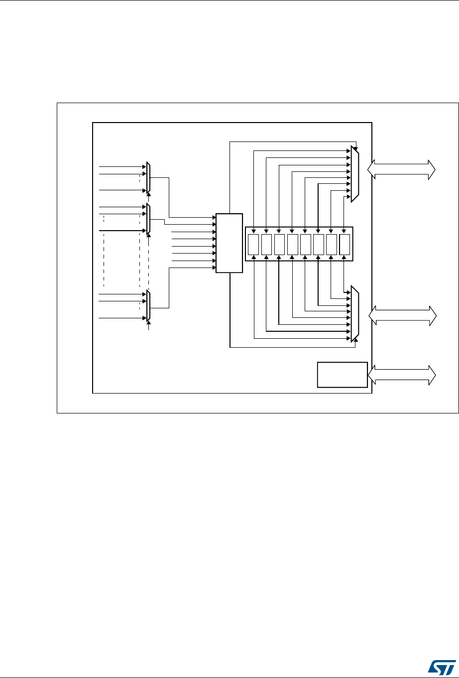
Direct memory access controller (DMA) RM0430
216/1324 RM0430 Rev 8
9.3 DMA functional description
9.3.1 DMA block diagram
Figure 23 shows the block diagram of a DMA.
Figure 23. DMA block diagram
9.3.2 DMA overview
The DMA controller performs direct memory transfer: as an AHB master, it can take the
control of the AHB bus matrix to initiate AHB transactions.
It carries out the following transactions:
•peripheral-to-memory
•memory-to-peripheral
•memory-to-memory
The DMA controller provides two AHB master ports: the AHB memory port, intended to be
connected to memories and the AHB peripheral port, intended to be connected to
peripherals. However, to allow memory-to-memory transfers, the AHB peripheral port must
also have access to the memories.
The AHB slave port is used to program the DMA controller (it supports only 32-bit
accesses).
$+%PDVWHU
0HPRU\SRUW
),)2
$+%PDVWHU
3HULSKHUDOSRUW
675($0
),)2 675($0
675($0
675($0
),)2 675($0675($0
),)2
675($0
675($0
5(4B675($0
5(4B675B&+
5(4B675B&+
'0$FRQWUROOHU
),)2 675($0675($0
),)2 675($0675($0
),)2 675($0675($0
),)2 675($0675($0
$UELWHU
5(4B675($0
5(4B675($0
5(4B675($0
5(4B675($0
5(4B675($0
5(4B675($0
5(4B675($0
5(4B675B&+
5(4B675B&+
5(4B675B&+
5(4B675B&+
5(4B675B&+
5(4B675B&+
5(4B675B&+
$+%VODYH
SURJUDPPLQJ
LQWHUIDFH
3URJUDPPLQJSRUW
&KDQQHO
VHOHFWLRQ
06Y9
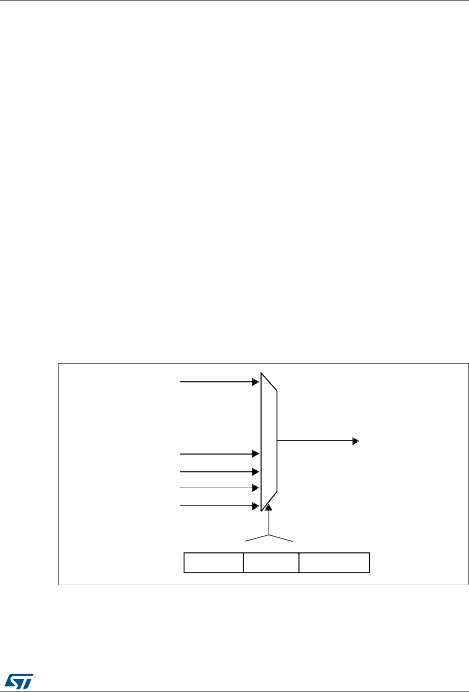
RM0430 Rev 8 217/1324
RM0430 Direct memory access controller (DMA)
248
9.3.3 DMA transactions
A DMA transaction consists of a sequence of a given number of data transfers. The number
of data items to be transferred and their width (8-bit, 16-bit or 32-bit) are software-
programmable.
Each DMA transfer consists of three operations:
•a loading from the peripheral data register or a location in memory, addressed through
the DMA_SxPAR or DMA_SxM0AR register
•a storage of the data loaded to the peripheral data register or a location in memory
addressed through the DMA_SxPAR or DMA_SxM0AR register
•a post-decrement of the DMA_SxNDTR register, containing the number of transactions
that still have to be performed
After an event, the peripheral sends a request signal to the DMA controller. The DMA
controller serves the request depending on the channel priorities. As soon as the DMA
controller accesses the peripheral, an Acknowledge signal is sent to the peripheral by the
DMA controller. The peripheral releases its request as soon as it gets the Acknowledge
signal from the DMA controller. Once the request has been deasserted by the peripheral,
the DMA controller releases the Acknowledge signal. If there are more requests, the
peripheral can initiate the next transaction.
9.3.4 Channel selection
Each stream is associated with a DMA request that can be selected out of 16 possible
channel requests. The selection is controlled by the CHSEL[3:0] bits in the DMA_SxCR
register.
Figure 24. Channel selection
The 16 requests from the peripherals (such as TIM, ADC, SPI, I2C) are independently
connected to each channel and their connection depends on the product implementation.
Table 30 and Table 31 give examples of DMA request mappings.
5(4B675($0[
5(4B675[B&+
5(4B675[B&+
5(4B675[B&+
5(4B675[B&+
5(4B675[B&+
&+6(/>@
'0$B6[&5
D^ǀϯϵϲϮϵsϭ

Direct memory access controller (DMA) RM0430
218/1324 RM0430 Rev 8
Table 30. DMA1 request mapping
Peripheral
requests Stream 0 Stream 1 Stream 2 Stream 3 Stream 4 Stream 5 Stream 6 Stream 7
Channel 0 SPI3_RX I2C1_TX SPI3_RX SPI2_RX SPI2_TX SPI3_TX - SPI3_TX
Channel 1 I2C1_RX I2C3_RX TIM7_UP I2CFMP1_RX TIM7_UP I2C1_RX I2C1_TX I2C1_TX
Channel 2 TIM4_CH1 I2CFMP1_TX I2S3_EXT_RX TIM4_CH2 I2S2_EXT_TX I2S3_EXT_TX TIM4_UP TIM4_CH3
Channel 3 I2S3_EXT_RX TIM2_UP
TIM2_CH3 I2C3_RX I2S2_EXT_RX I2C3_TX TIM2_CH1 TIM2_CH2
TIM2_CH4
TIM2_UP
TIM2_CH4
Channel 4 UART5_RX USART3_RX UART4_RX USART3_TX UART4_TX USART2_RX USART2_TX I2CFMP1_TX
Channel 5 UART8_RX UART7_TX TIM3_UP
TIM3_CH4 UART7_RX TIM3_CH1
TIM3_TRIG TIM3_CH2 UART8_RX TIM3_CH3
Channel 6 TIM5_CH3
TIM5_UP
TIM5_CH4
TIM5_TRIG TIM5_CH1 TIM5_CH4
‘TIM5_TRIG TIM5_CH2 I2C3_TX TIM5_UP USART2_RX
Channel 7 I2CFMP1_RX TIM6_UP I2C2_RX I2C2_RX USART3_TX DAC1 DAC2 I2C2_TX
Channel 8 - - - - - - - UART5_TX
Table 31. DMA2 request mapping
Peripheral
requests Stream 0 Stream 1 Stream 2 Stream 3 Stream 4 Stream 5 Stream 6 Stream 7
Channel 0 ADC1 SAI1_A
TIM8_CH1
TIM8_CH2
TIM8_CH3
SAI1_A ADC1 SAI1_B
TIM1_CH1
TIM1_CH2
TIM1_CH3
UART9_RX
Channel 1 UART9_TX - - - SAI1B - - -
Channel 2 - - SPI1_TX SPI5_RX SPI5_TX AES_OUT(1) AES_IN(1) -
Channel 3 SPI1_RX DFSDM1_
FLT1 SPI1_RX SPI1_TX DFSDM1_
FLT1 SPI1_TX DFSDM1_
FLT0 QUADSPI
Channel 4 SPI4_RX SPI4_TX USART1_RX SDIO SPI4_RX USART1_RX SDIO USART1_TX
Channel 5 UART10_RX USART6_RX USART6_RX SPI4_RX SPI4_TX SPI5_TX USART6_TX USART6_TX
Channel 6 TIM1_TRIG TIM1_CH1 TIM1_CH2 TIM1_CH1
TIM1_CH4
TIM1_TRIG
TIM1_COM
TIM1_UP TIM1_CH3 UART10_TX
Channel 7 DFSDM1_
FLT0 TIM8_UP TIM8_CH1 TIM8_CH2 TIM8_CH3 SPI5_RX SPI5_TX
TIM8_CH4
TIM8_TRIG
TIM8_COM
Channel 8 DFSDM2_
FLT0
DFSDM2_
FLT1
DFSDM2_
FLT2
DFSDM2_
FLT3
DFSDM2_
FLT0
DFSDM2_
FLT1
DFSDM2_
FLT2
DFSDM2_
FLT3
Channel 9 - - - UART10_RX - UART10_TX - -
1. Only available for STM32F423xx.

RM0430 Rev 8 219/1324
RM0430 Direct memory access controller (DMA)
248
9.3.5 Arbiter
An arbiter manages the 8 DMA stream requests based on their priority for each of the two
AHB master ports (memory and peripheral ports) and launches the peripheral/memory
access sequences.
Priorities are managed in two stages:
•Software: each stream priority can be configured in the DMA_SxCR register. There are
four levels:
– Very high priority
– High priority
– Medium priority
– Low priority
•Hardware: If two requests have the same software priority level, the stream with the
lower number takes priority over the stream with the higher number. For example,
stream 2 takes priority over stream 4.
9.3.6 DMA streams
Each of the 8 DMA controller streams provides a unidirectional transfer link between a
source and a destination.
Each stream can be configured to perform:
•Regular type transactions: memory-to-peripherals, peripherals-to-memory or memory-
to-memory transfers
•Double-buffer type transactions: double buffer transfers using two memory pointers for
the memory (while the DMA is reading/writing from/to a buffer, the application can
write/read to/from the other buffer).
The amount of data to be transferred (up to 65535) is programmable and related to the
source width of the peripheral that requests the DMA transfer connected to the peripheral
AHB port. The register that contains the amount of data items to be transferred is
decremented after each transaction.
9.3.7 Source, destination and transfer modes
Both source and destination transfers can address peripherals and memories in the entire
4 Gbytes area, at addresses comprised between 0x0000 0000 and 0xFFFF FFFF.
The direction is configured using the DIR[1:0] bits in the DMA_SxCR register and offers
three possibilities: memory-to-peripheral, peripheral-to-memory or memory-to-memory
transfers. Table 32 describes the corresponding source and destination addresses.
Table 32. Source and destination address
Bits DIR[1:0] of the
DMA_SxCR register Direction Source address Destination address
00 Peripheral-to-memory DMA_SxPAR DMA_SxM0AR
01 Memory-to-peripheral DMA_SxM0AR DMA_SxPAR
10 Memory-to-memory DMA_SxPAR DMA_SxM0AR
11 Reserved - -
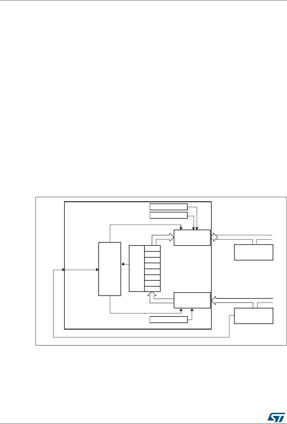
Direct memory access controller (DMA) RM0430
220/1324 RM0430 Rev 8
When the data width (programmed in the PSIZE or MSIZE bits in the DMA_SxCR register)
is a half-word or a word, respectively, the peripheral or memory address written into the
DMA_SxPAR or DMA_SxM0AR/M1AR registers has to be aligned on a word or half-word
address boundary, respectively.
Peripheral-to-memory mode
Figure 25 describes this mode.
When this mode is enabled (by setting the bit EN in the DMA_SxCR register), each time a
peripheral request occurs, the stream initiates a transfer from the source to fill the FIFO.
When the threshold level of the FIFO is reached, the contents of the FIFO are drained and
stored into the destination.
The transfer stops once the DMA_SxNDTR register reaches zero, when the peripheral
requests the end of transfers (in case of a peripheral flow controller) or when the EN bit in
the DMA_SxCR register is cleared by software.
In direct mode (when the DMDIS value in the DMA_SxFCR register is ‘0’), the threshold
level of the FIFO is not used: after each single data transfer from the peripheral to the FIFO,
the corresponding data are immediately drained and stored into the destination.
The stream has access to the AHB source or destination port only if the arbitration of the
corresponding stream is won. This arbitration is performed using the priority defined for
each stream using the PL[1:0] bits in the DMA_SxCR register.
Figure 25. Peripheral-to-memory mode
1. For double-buffer mode.
Memory-to-peripheral mode
Figure 26 describes this mode.
When this mode is enabled (by setting the EN bit in the DMA_SxCR register), the stream
immediately initiates transfers from the source to entirely fill the FIFO.
-EMORYBUS
0ERIPHERALBUS
2%1?342%!-X !RBITER
$-!?3X-!2
&)&/
!("MEMORY
PORT
!("PERIPHERAL
PORT
$-!?3X0!2
&)&/
LEVEL
$-!CONTROLLER $-!?3X-!2
DESTINATION
SOURCE
PERIPHERAL
-EMORY
0ERIPHERAL$-!REQUEST
AI
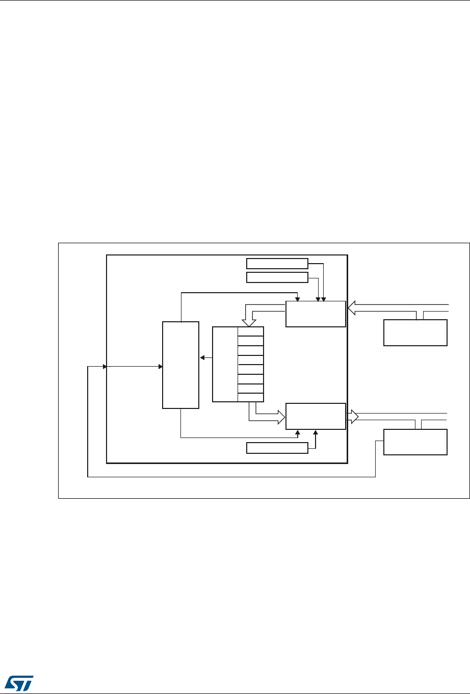
RM0430 Rev 8 221/1324
RM0430 Direct memory access controller (DMA)
248
Each time a peripheral request occurs, the contents of the FIFO are drained and stored into
the destination. When the level of the FIFO is lower than or equal to the predefined
threshold level, the FIFO is fully reloaded with data from the memory.
The transfer stops once the DMA_SxNDTR register reaches zero, when the peripheral
requests the end of transfers (in case of a peripheral flow controller) or when the EN bit in
the DMA_SxCR register is cleared by software.
In direct mode (when the DMDIS value in the DMA_SxFCR register is '0'), the threshold
level of the FIFO is not used. Once the stream is enabled, the DMA preloads the first data to
transfer into an internal FIFO. As soon as the peripheral requests a data transfer, the DMA
transfers the preloaded value into the configured destination. It then reloads again the
empty internal FIFO with the next data to be transfer. The preloaded data size corresponds
to the value of the PSIZE bitfield in the DMA_SxCR register.
The stream has access to the AHB source or destination port only if the arbitration of the
corresponding stream is won. This arbitration is performed using the priority defined for
each stream using the PL[1:0] bits in the DMA_SxCR register.
Figure 26. Memory-to-peripheral mode
1. For double-buffer mode.
Memory-to-memory mode
The DMA channels can also work without being triggered by a request from a peripheral.
This is the memory-to-memory mode, described in Figure 27.
When the stream is enabled by setting the Enable bit (EN) in the DMA_SxCR register, the
stream immediately starts to fill the FIFO up to the threshold level. When the threshold level
is reached, the FIFO contents are drained and stored into the destination.
The transfer stops once the DMA_SxNDTR register reaches zero or when the EN bit in the
DMA_SxCR register is cleared by software.
0ERIPHERALBUS
-EMORYBUS
2%1?342%!-X !RBITER
$-!?3X-!2
&)&/
!("MEMORY
PORT
!("PERIPHERAL
PORT
$-!?3X0!2
&)&/
LEVEL
$-!CONTROLLER $-!?3X-!2
SOURCE
DESTINATION
0ERIPHERAL
-EMORY
0ERIPHERAL$-!REQUEST
AI
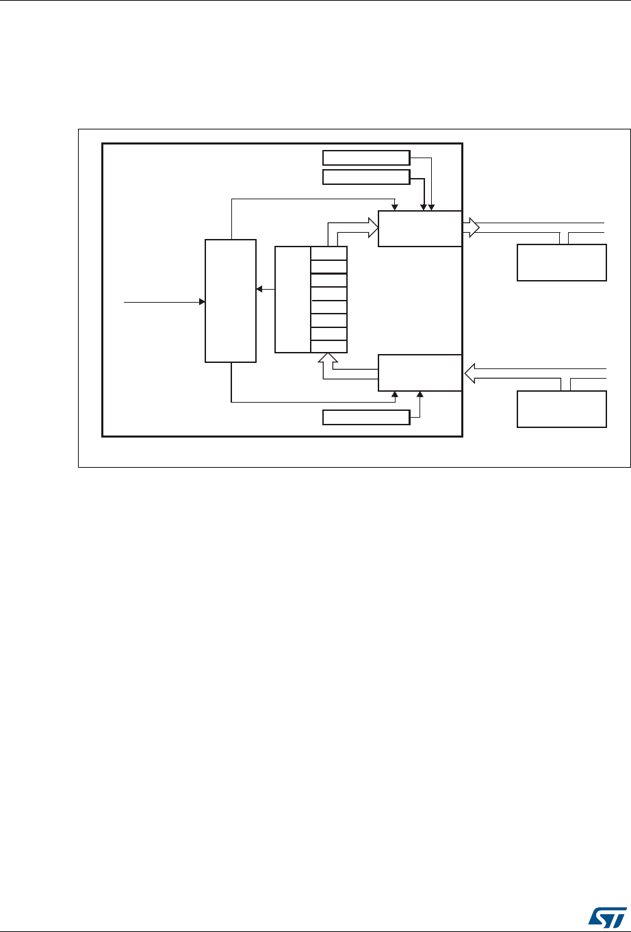
Direct memory access controller (DMA) RM0430
222/1324 RM0430 Rev 8
The stream has access to the AHB source or destination port only if the arbitration of the
corresponding stream is won. This arbitration is performed using the priority defined for
each stream using the PL[1:0] bits in the DMA_SxCR register.
Note: When memory-to-memory mode is used, the circular and direct modes are not allowed.
Figure 27. Memory-to-memory mode
1. For double-buffer mode.
9.3.8 Pointer incrementation
Peripheral and memory pointers can optionally be automatically post-incremented or kept
constant after each transfer depending on the PINC and MINC bits in the DMA_SxCR
register.
Disabling the increment mode is useful when the peripheral source or destination data is
accessed through a single register.
If the increment mode is enabled, the address of the next transfer is the address of the
previous one incremented by 1 (for bytes), 2 (for half-words) or 4 (for words) depending on
the data width programmed in the PSIZE or MSIZE bits in the DMA_SxCR register.
In order to optimize the packing operation, it is possible to fix the increment offset size for
the peripheral address whatever the size of the data transferred on the AHB peripheral port.
The PINCOS bit in the DMA_SxCR register is used to align the increment offset size with
the data size on the peripheral AHB port, or on a 32-bit address (the address is then
incremented by 4). The PINCOS bit has an impact on the AHB peripheral port only.
If the PINCOS bit is set, the address of the following transfer is the address of the previous
one incremented by 4 (automatically aligned on a 32-bit address), whatever the PSIZE
value. The AHB memory port, however, is not impacted by this operation.
-EMORYBUS
0ERIPHERALBUS
3TREAMENABLE
!RBITER
$-!?3X-!2
&)&/
!("MEMORY
PORT
!("PERIPHERAL
PORT
$-!?3X0!2
&)&/
LEVEL
$-!CONTROLLER $-!?3X-!2
DESTINATION
SOURCE
-EMORY
-EMORY
&)&/
AI

RM0430 Rev 8 223/1324
RM0430 Direct memory access controller (DMA)
248
9.3.9 Circular mode
The circular mode is available to handle circular buffers and continuous data flows (e.g.
ADC scan mode). This feature can be enabled using the CIRC bit in the DMA_SxCR
register.
When the circular mode is activated, the number of data items to be transferred is
automatically reloaded with the initial value programmed during the stream configuration
phase, and the DMA requests continue to be served.
Note: In the circular mode, it is mandatory to respect the following rule in case of a burst mode
configured for memory:
DMA_SxNDTR = Multiple of ((Mburst beat) × (Msize)/(Psize)), where:
– (Mburst beat) = 4, 8 or 16 (depending on the MBURST bits in the DMA_SxCR
register)
– ((Msize)/(Psize)) = 1, 2, 4, 1/2 or 1/4 (Msize and Psize represent the MSIZE and
PSIZE bits in the DMA_SxCR register. They are byte dependent)
– DMA_SxNDTR = Number of data items to transfer on the AHB peripheral port
For example: Mburst beat = 8 (INCR8), MSIZE = ‘00’ (byte) and PSIZE = ‘01’ (half-word), in
this case: DMA_SxNDTR must be a multiple of (8 × 1/2 = 4).
If this formula is not respected, the DMA behavior and data integrity are not guaranteed.
NDTR must also be a multiple of the Peripheral burst size multiplied by the peripheral data
size, otherwise this could result in a bad DMA behavior.
9.3.10 Double-buffer mode
This mode is available for all the DMA1 and DMA2 streams.
The double-buffer mode is enabled by setting the DBM bit in the DMA_SxCR register.
A double-buffer stream works as a regular (single buffer) stream with the difference that it
has two memory pointers. When the double-buffer mode is enabled, the circular mode is
automatically enabled (CIRC bit in DMA_SxCR is not relevant) and at each end of
transaction, the memory pointers are swapped.
In this mode, the DMA controller swaps from one memory target to another at each end of
transaction. This allows the software to process one memory area while the second memory
area is being filled/used by the DMA transfer. The double-buffer stream can work in both
directions (the memory can be either the source or the destination) as described in
Table 33: Source and destination address registers in double-buffer mode (DBM = 1).
Note: In double-buffer mode, it is possible to update the base address for the AHB memory port
on-the-fly (DMA_SxM0AR or DMA_SxM1AR) when the stream is enabled, by respecting the
following conditions:
•
When the CT bit is ‘0’ in the DMA_SxCR register, the DMA_SxM1AR register can be
written. Attempting to write to this register while CT = '1' sets an error flag (TEIF) and
the stream is automatically disabled.
•
When the CT bit is ‘1’ in the DMA_SxCR register, the DMA_SxM0AR register can be
written. Attempting to write to this register while CT = '0', sets an error flag (TEIF) and
the stream is automatically disabled.
To avoid any error condition, it is advised to change the base address as soon as the TCIF
flag is asserted because, at this point, the targeted memory must have changed from

Direct memory access controller (DMA) RM0430
224/1324 RM0430 Rev 8
memory 0 to 1 (or from 1 to 0) depending on the value of CT in the DMA_SxCR register in
accordance with one of the two above conditions.
For all the other modes (except the double-buffer mode), the memory address registers are
write-protected as soon as the stream is enabled.
9.3.11 Programmable data width, packing/unpacking, endianness
The number of data items to be transferred has to be programmed into DMA_SxNDTR
(number of data items to transfer bit, NDT) before enabling the stream (except when the
flow controller is the peripheral, PFCTRL bit in DMA_SxCR is set).
When using the internal FIFO, the data widths of the source and destination data are
programmable through the PSIZE and MSIZE bits in the DMA_SxCR register (can be 8-,
16- or 32-bit).
When PSIZE and MSIZE are not equal:
•The data width of the number of data items to transfer, configured in the DMA_SxNDTR
register is equal to the width of the peripheral bus (configured by the PSIZE bits in the
DMA_SxCR register). For instance, in case of peripheral-to-memory, memory-to-
peripheral or memory-to-memory transfers and if the PSIZE[1:0] bits are configured for
half-word, the number of bytes to be transferred is equal to 2 × NDT.
•The DMA controller only copes with little-endian addressing for both source and
destination. This is described in Table 34: Packing/unpacking and endian behavior (bit
PINC = MINC = 1).
This packing/unpacking procedure may present a risk of data corruption when the operation
is interrupted before the data are completely packed/unpacked. So, to ensure data
coherence, the stream may be configured to generate burst transfers: in this case, each
group of transfers belonging to a burst are indivisible (refer to Section 9.3.12: Single and
burst transfers).
In direct mode (DMDIS = 0 in the DMA_SxFCR register), the packing/unpacking of data is
not possible. In this case, it is not allowed to have different source and destination transfer
data widths: both are equal and defined by the PSIZE bits in the DMA_SxCR register.
MSIZE bits are not relevant.
Table 33. Source and destination address registers in double-buffer mode (DBM = 1)
Bits DIR[1:0] of the
DMA_SxCR register Direction Source address Destination address
00 Peripheral-to-memory DMA_SxPAR DMA_SxM0AR / DMA_SxM1AR
01 Memory-to-peripheral DMA_SxM0AR / DMA_SxM1AR DMA_SxPAR
10 Not allowed(1)
11 Reserved - -
1. When the double-buffer mode is enabled, the circular mode is automatically enabled. Since the memory-to-memory mode
is not compatible with the circular mode, when the double-buffer mode is enabled, it is not allowed to configure the
memory-to-memory mode.

RM0430 Rev 8 225/1324
RM0430 Direct memory access controller (DMA)
248
Note: Peripheral port may be the source or the destination (it could also be the memory source in
the case of memory-to-memory transfer).
PSIZE, MSIZE and NDT[15:0] have to be configured so as to ensure that the last transfer
will not be incomplete. This can occur when the data width of the peripheral port (PSIZE
bits) is lower than the data width of the memory port (MSIZE bits). This constraint is
summarized in Table 35.
Table 34. Packing/unpacking and endian behavior (bit PINC = MINC = 1)
AHB
memory
port
width
AHB
peripheral
port
width
Number
of data
items to
transfer
(NDT)
-
Memory
transfer
number
Memory port
address / byte
lane
Peripheral
transfer
number
Peripheral port address / byte lane
-PINCOS = 1 PINCOS = 0
884
-
1
2
3
4
0x0 / B0[7:0]
0x1 / B1[7:0]
0x2 / B2[7:0]
0x3 / B3[7:0]
1
2
3
4
0x0 / B0[7:0]
0x4 / B1[7:0]
0x8 / B2[7:0]
0xC / B3[7:0]
0x0 / B0[7:0]
0x1 / B1[7:0]
0x2 / B2[7:0]
0x3 / B3[7:0]
8162
-
1
2
3
4
0x0 / B0[7:0]
0x1 / B1[7:0]
0x2 / B2[7:0]
0x3 / B3[7:0]
1
2
0x0 / B1|B0[15:0]
0x4 / B3|B2[15:0]
0x0 / B1|B0[15:0]
0x2 / B3|B2[15:0]
8321
-
1
2
3
4
0x0 / B0[7:0]
0x1 / B1[7:0]
0x2 / B2[7:0]
0x3 / B3[7:0]
10x0 /
B3|B2|B1|B0[31:0]
0x0 /
B3|B2|B1|B0[31:0]
16 8 4 -
1
2
0x0 / B1|B0[15:0]
0x2 / B3|B2[15:0]
1
2
3
4
0x0 / B0[7:0]
0x4 / B1[7:0]
0x8 / B2[7:0]
0xC / B3[7:0]
0x0 / B0[7:0]
0x1 / B1[7:0]
0x2 / B2[7:0]
0x3 / B3[7:0]
16 16 2 -
1
2
0x0 / B1|B0[15:0]
0x2 / B1|B0[15:0]
1
2
0x0 / B1|B0[15:0]
0x4 / B3|B2[15:0]
0x0 / B1|B0[15:0]
0x2 / B3|B2[15:0]
16 32 1 -1
2
0x0 / B1|B0[15:0]
0x2 / B3|B2[15:0]
10x0 /
B3|B2|B1|B0[31:0]
0x0 /
B3|B2|B1|B0[31:0]
32 8 4 -
10x0 / B3|B2|B1|B0[31:0] 1
2
3
4
0x0 / B0[7:0]
0x4 / B1[7:0]
0x8 / B2[7:0]
0xC / B3[7:0]
0x0 / B0[7:0]
0x1 / B1[7:0]
0x2 / B2[7:0]
0x3 / B3[7:0]
32 16 2 -10x0 /B3|B2|B1|B0[31:0] 1
2
0x0 / B1|B0[15:0]
0x4 / B3|B2[15:0]
0x0 / B1|B0[15:0]
0x2 / B3|B2[15:0]
32 32 1 -1 0x0 /B3|B2|B1|B0 [31:0] 1 0x0 /B3|B2|B1|B0
[31:0]
0x0 /
B3|B2|B1|B0[31:0]
Table 35. Restriction on NDT versus PSIZE and MSIZE
PSIZE[1:0] of DMA_SxCR MSIZE[1:0] of DMA_SxCR NDT[15:0] of DMA_SxNDTR
00 (8-bit) 01 (16-bit) must be a multiple of 2
00 (8-bit) 10 (32-bit) must be a multiple of 4
01 (16-bit) 10 (32-bit) must be a multiple of 2

Direct memory access controller (DMA) RM0430
226/1324 RM0430 Rev 8
9.3.12 Single and burst transfers
The DMA controller can generate single transfers or incremental burst transfers of 4, 8 or 16
beats.
The size of the burst is configured by software independently for the two AHB ports by using
the MBURST[1:0] and PBURST[1:0] bits in the DMA_SxCR register.
The burst size indicates the number of beats in the burst, not the number of bytes
transferred.
To ensure data coherence, each group of transfers that form a burst are indivisible: AHB
transfers are locked and the arbiter of the AHB bus matrix does not degrant the DMA master
during the sequence of the burst transfer.
Depending on the single or burst configuration, each DMA request initiates a different
number of transfers on the AHB peripheral port:
•When the AHB peripheral port is configured for single transfers, each DMA request
generates a data transfer of a byte, half-word or word depending on the PSIZE[1:0] bits
in the DMA_SxCR register
•When the AHB peripheral port is configured for burst transfers, each DMA request
generates 4,8 or 16 beats of byte, half word or word transfers depending on the
PBURST[1:0] and PSIZE[1:0] bits in the DMA_SxCR register.
The same as above has to be considered for the AHB memory port considering the
MBURST and MSIZE bits.
In direct mode, the stream can only generate single transfers and the MBURST[1:0] and
PBURST[1:0] bits are forced by hardware.
The address pointers (DMA_SxPAR or DMA_SxM0AR registers) must be chosen so as to
ensure that all transfers within a burst block are aligned on the address boundary equal to
the size of the transfer.
The burst configuration has to be selected in order to respect the AHB protocol, where
bursts must not cross the 1 Kbyte address boundary because the minimum address space
that can be allocated to a single slave is 1 Kbyte. This means that the 1 Kbyte address
boundary must not be crossed by a burst block transfer, otherwise an AHB error is
generated, that is not reported by the DMA registers.
9.3.13 FIFO
FIFO structure
The FIFO is used to temporarily store data coming from the source before transmitting them
to the destination.
Each stream has an independent 4-word FIFO and the threshold level is software-
configurable between 1/4, 1/2, 3/4 or full.
To enable the use of the FIFO threshold level, the direct mode must be disabled by setting
the DMDIS bit in the DMA_SxFCR register.
The structure of the FIFO differs depending on the source and destination data widths, and
is described in Figure 28: FIFO structure.
RM0430 Rev 8 227/1324
RM0430 Direct memory access controller (DMA)
248
Figure 28. FIFO structure
FIFO threshold and burst configuration
Caution is required when choosing the FIFO threshold (bits FTH[1:0] of the DMA_SxFCR
register) and the size of the memory burst (MBURST[1:0] of the DMA_SxCR register): The
content pointed by the FIFO threshold must exactly match an integer number of memory
burst transfers. If this is not in the case, a FIFO error (flag FEIFx of the DMA_HISR or
DMA_LISR register) is generated when the stream is enabled, then the stream is
automatically disabled. The allowed and forbidden configurations are described in Table 36.
The forbidden configurations are highlighted in gray in the table.
3OURCEBYTE
WORDS
BYTELANE
BYTELANE
BYTELANE
BYTELANE
&ULL%MPTY
"
"
"
"
"
"
"
"
"
"
"
"
"
"
"
"
$ESTINATIONWORD
3OURCEBYTE $ESTINATIONHALFWORD
WORDS
BYTELANE
BYTELANE
BYTELANE
BYTELANE
&ULL%MPTY
"
"
"
"
"
"
"
"
"
"
"
"
"
"
"
"
7777
(
(
(
(
(
(
(
(
3OURCEHALFWORD $ESTINATIONWORD
WORDS
BYTELANE
BYTELANE
BYTELANE
BYTELANE
&ULL%MPTY
(
7777
(
(
(
(
(
(
(
""""""""""""""""
""""""""""""""""
((((((((
((((((((
7777
7777
3OURCEHALFWORD
WORDS
BYTELANE
BYTELANE
BYTELANE
BYTELANE
&ULL%MPTY
$ESTINATIONBYTE
((((((((
"
"
"
"
"
"
"
"
"
"
"
"
"
"
"
"
(
(
(
(
(
(
(
(
""""""""
""""""""
AI
Table 36. FIFO threshold configurations
MSIZE FIFO level MBURST = INCR4 MBURST = INCR8 MBURST = INCR16
Byte
1/4 1 burst of 4 beats Forbidden
Forbidden1/2 2 bursts of 4 beats 1 burst of 8 beats
3/4 3 bursts of 4 beats Forbidden
Full 4 bursts of 4 beats 2 bursts of 8 beats 1 burst of 16 beats

Direct memory access controller (DMA) RM0430
228/1324 RM0430 Rev 8
In all cases, the burst size multiplied by the data size must not exceed the FIFO size (data
size can be: 1 (byte), 2 (half-word) or 4 (word)).
Incomplete burst transfer at the end of a DMA transfer may happen if one of the following
conditions occurs:
•For the AHB peripheral port configuration: the total number of data items (set in the
DMA_SxNDTR register) is not a multiple of the burst size multiplied by the data size.
•For the AHB memory port configuration: the number of remaining data items in the
FIFO to be transferred to the memory is not a multiple of the burst size multiplied by the
data size.
In such cases, the remaining data to be transferred is managed in single mode by the DMA,
even if a burst transaction is requested during the DMA stream configuration.
Note: When burst transfers are requested on the peripheral AHB port and the FIFO is used
(DMDIS = 1 in the DMA_SxCR register), it is mandatory to respect the following rule to
avoid permanent underrun or overrun conditions, depending on the DMA stream direction:
If (PBURST × PSIZE) = FIFO_SIZE (4 words), FIFO_Threshold = 3/4 is forbidden with
PSIZE = 1, 2 or 4 and PBURST = 4, 8 or 16.
This rule ensures that enough FIFO space at a time is free to serve the request from the
peripheral.
FIFO flush
The FIFO can be flushed when the stream is disabled by resetting the EN bit in the
DMA_SxCR register and when the stream is configured to manage peripheral-to-memory or
memory-to-memory transfers. If some data are still present in the FIFO when the stream is
disabled, the DMA controller continues transferring the remaining data to the destination
(even though stream is effectively disabled). When this flush is completed, the transfer
complete status bit (TCIFx) in the DMA_LISR or DMA_HISR register is set.
The remaining data counter DMA_SxNDTR keeps the value in this case to indicate how
many data items are currently available in the destination memory.
Note that during the FIFO flush operation, if the number of remaining data items in the FIFO
to be transferred to memory (in bytes) is less than the memory data width (for example 2
bytes in FIFO while MSIZE is configured to word), data is sent with the data width set in the
MSIZE bit in the DMA_SxCR register. This means that memory is written with an undesired
Half-word
1/4 Forbidden
Forbidden
Forbidden
1/2 1 burst of 4 beats
3/4 Forbidden
Full 2 bursts of 4 beats 1 burst of 8 beats
Word
1/4
Forbidden
Forbidden
1/2
3/4
Full 1 burst of 4 beats
Table 36. FIFO threshold configurations (continued)
MSIZE FIFO level MBURST = INCR4 MBURST = INCR8 MBURST = INCR16

RM0430 Rev 8 229/1324
RM0430 Direct memory access controller (DMA)
248
value. The software may read the DMA_SxNDTR register to determine the memory area
that contains the good data (start address and last address).
If the number of remaining data items in the FIFO is lower than a burst size (if the MBURST
bits in DMA_SxCR register are set to configure the stream to manage burst on the AHB
memory port), single transactions are generated to complete the FIFO flush.
Direct mode
By default, the FIFO operates in direct mode (DMDIS bit in the DMA_SxFCR is reset) and
the FIFO threshold level is not used. This mode is useful when the system requires an
immediate and single transfer to or from the memory after each DMA request.
When the DMA is configured in direct mode (FIFO disabled), to transfer data in memory-to-
peripheral mode, the DMA preloads one data from the memory to the internal FIFO to
ensure an immediate data transfer as soon as a DMA request is triggered by a peripheral.
To avoid saturating the FIFO, it is recommended to configure the corresponding stream with
a high priority.
This mode is restricted to transfers where:
•the source and destination transfer widths are equal and both defined by the
PSIZE[1:0] bits in DMA_SxCR (MSIZE[1:0] bits are not relevant)
•burst transfers are not possible (PBURST[1:0] and MBURST[1:0] bits in DMA_SxCR
are don’t care)
Direct mode must not be used when implementing memory-to-memory transfers.
9.3.14 DMA transfer completion
Different events can generate an end of transfer by setting the TCIFx bit in the DMA_LISR
or DMA_HISR status register:
•In DMA flow controller mode:
– The DMA_SxNDTR counter has reached zero in the memory-to-peripheral mode.
– The stream is disabled before the end of transfer (by clearing the EN bit in the
DMA_SxCR register) and (when transfers are peripheral-to-memory or memory-
to-memory) all the remaining data have been flushed from the FIFO into the
memory.
•In Peripheral flow controller mode:
– The last external burst or single request has been generated from the peripheral
and (when the DMA is operating in peripheral-to-memory mode) the remaining
data have been transferred from the FIFO into the memory
– The stream is disabled by software, and (when the DMA is operating in peripheral-
to-memory mode) the remaining data have been transferred from the FIFO into
the memory
Note: The transfer completion is dependent on the remaining data in FIFO to be transferred into
memory only in the case of peripheral-to-memory mode. This condition is not applicable in
memory-to-peripheral mode.
If the stream is configured in noncircular mode, after the end of the transfer (that is when the
number of data to be transferred reaches zero), the DMA is stopped (EN bit in DMA_SxCR
register is cleared by Hardware) and no DMA request is served unless the software
reprograms the stream and re-enables it (by setting the EN bit in the DMA_SxCR register).

Direct memory access controller (DMA) RM0430
230/1324 RM0430 Rev 8
9.3.15 DMA transfer suspension
At any time, a DMA transfer can be suspended to be restarted later on or to be definitively
disabled before the end of the DMA transfer.
There are two cases:
•The stream disables the transfer with no later-on restart from the point where it was
stopped. There is no particular action to do, except to clear the EN bit in the
DMA_SxCR register to disable the stream. The stream may take time to be disabled
(ongoing transfer is completed first). The transfer complete interrupt flag (TCIF in the
DMA_LISR or DMA_HISR register) is set in order to indicate the end of transfer. The
value of the EN bit in DMA_SxCR is now ‘0’ to confirm the stream interruption. The
DMA_SxNDTR register contains the number of remaining data items at the moment
when the stream was stopped so that the software can determine how many data items
have been transferred before the stream was interrupted.
•The stream suspends the transfer before the number of remaining data items to be
transferred in the DMA_SxNDTR register reaches 0. The aim is to restart the transfer
later by re-enabling the stream. In order to restart from the point where the transfer was
stopped, the software has to read the DMA_SxNDTR register after disabling the stream
by writing the EN bit in DMA_SxCR register (and then checking that it is at ‘0’) to know
the number of data items already collected. Then:
– The peripheral and/or memory addresses have to be updated in order to adjust
the address pointers
– The SxNDTR register has to be updated with the remaining number of data items
to be transferred (the value read when the stream was disabled)
– The stream may then be re-enabled to restart the transfer from the point it was
stopped
Note: A transfer complete interrupt flag (TCIF in DMA_LISR or DMA_HISR) is set to indicate the
end of transfer due to the stream interruption.
9.3.16 Flow controller
The entity that controls the number of data to be transferred is known as the flow controller.
This flow controller is configured independently for each stream using the PFCTRL bit in the
DMA_SxCR register.
The flow controller can be:
•The DMA controller: in this case, the number of data items to be transferred is
programmed by software into the DMA_SxNDTR register before the DMA stream is
enabled.
•The peripheral source or destination: this is the case when the number of data items to
be transferred is unknown. The peripheral indicates by hardware to the DMA controller
when the last data are being transferred. This feature is only supported for peripherals
that are able to signal the end of the transfer.
When the peripheral flow controller is used for a given stream, the value written into the
DMA_SxNDTR has no effect on the DMA transfer. Actually, whatever the value written, it will
be forced by hardware to 0xFFFF as soon as the stream is enabled, to respect the following
schemes:
•Anticipated stream interruption: EN bit in DMA_SxCR register is reset to 0 by the
software to stop the stream before the last data hardware signal (single or burst) is sent
by the peripheral. In such a case, the stream is switched off and the FIFO flush is

RM0430 Rev 8 231/1324
RM0430 Direct memory access controller (DMA)
248
triggered in the case of a peripheral-to-memory DMA transfer. The TCIFx flag of the
corresponding stream is set in the status register to indicate the DMA completion. To
know the number of data items transferred during the DMA transfer, read the
DMA_SxNDTR register and apply the following formula:
– Number_of_data_transferred = 0xFFFF – DMA_SxNDTR
•Normal stream interruption due to the reception of a last data hardware signal: the
stream is automatically interrupted when the peripheral requests the last transfer
(single or burst) and when this transfer is complete. the TCIFx flag of the corresponding
stream is set in the status register to indicate the DMA transfer completion. To know the
number of data items transferred, read the DMA_SxNDTR register and apply the same
formula as above.
•The DMA_SxNDTR register reaches 0: the TCIFx flag of the corresponding stream is
set in the status register to indicate the forced DMA transfer completion. The stream is
automatically switched off even though the last data hardware signal (single or burst)
has not been yet asserted. The already transferred data is not lost. This means that a
maximum of 65535 data items can be managed by the DMA in a single transaction,
even in peripheral flow control mode.
Note: When configured in memory-to-memory mode, the DMA is always the flow controller and
the PFCTRL bit is forced to 0 by hardware.
The circular mode is forbidden in the peripheral flow controller mode.
9.3.17 Summary of the possible DMA configurations
Table 37 summarizes the different possible DMA configurations. The forbidden
configurations are highlighted in gray in the table.
Table 37. Possible DMA configurations
DMA transfer
mode Source Destination Flow
controller
Circular
mode
Transfer
type
Direct
mode
Double-
buffer mode
Peripheral-to-
memory
AHB
peripheral port
AHB
memory port
DMA Possible
single Possible
Possible
burst Forbidden
Peripheral Forbidden
single Possible
Forbidden
burst Forbidden
Memory-to-
peripheral
AHB
memory port
AHB
peripheral port
DMA Possible
single Possible
Possible
burst Forbidden
Peripheral Forbidden
single Possible
Forbidden
burst Forbidden
Memory-to-
memory
AHB
peripheral port
AHB
memory port DMA only Forbidden
single
Forbidden Forbidden
burst

Direct memory access controller (DMA) RM0430
232/1324 RM0430 Rev 8
9.3.18 Stream configuration procedure
The following sequence must be followed to configure a DMA stream x (where x is the
stream number):
1. If the stream is enabled, disable it by resetting the EN bit in the DMA_SxCR register,
then read this bit in order to confirm that there is no ongoing stream operation. Writing
this bit to 0 is not immediately effective since it is actually written to 0 once all the
current transfers are finished. When the EN bit is read as 0, this means that the stream
is ready to be configured. It is therefore necessary to wait for the EN bit to be cleared
before starting any stream configuration. All the stream dedicated bits set in the status
register (DMA_LISR and DMA_HISR) from the previous data block DMA transfer must
be cleared before the stream can be re-enabled.
2. Set the peripheral port register address in the DMA_SxPAR register. The data is moved
from/ to this address to/ from the peripheral port after the peripheral event.
3. Set the memory address in the DMA_SxMA0R register (and in the DMA_SxMA1R
register in the case of a double-buffer mode). The data is written to or read from this
memory after the peripheral event.
4. Configure the total number of data items to be transferred in the DMA_SxNDTR
register. After each peripheral event or each beat of the burst, this value is
decremented.
5. Select the DMA channel (request) using CHSEL[3:0] in the DMA_SxCR register.
6. If the peripheral is intended to be the flow controller and if it supports this feature, set
the PFCTRL bit in the DMA_SxCR register.
7. Configure the stream priority using the PL[1:0] bits in the DMA_SxCR register.
8. Configure the FIFO usage (enable or disable, threshold in transmission and reception)
9. Configure the data transfer direction, peripheral and memory incremented/fixed mode,
single or burst transactions, peripheral and memory data widths, circular mode,
double-buffer mode and interrupts after half and/or full transfer, and/or errors in the
DMA_SxCR register.
10. Activate the stream by setting the EN bit in the DMA_SxCR register.
As soon as the stream is enabled, it can serve any DMA request from the peripheral
connected to the stream.
Once half the data have been transferred on the AHB destination port, the half-transfer flag
(HTIF) is set and an interrupt is generated if the half-transfer interrupt enable bit (HTIE) is
set. At the end of the transfer, the transfer complete flag (TCIF) is set and an interrupt is
generated if the transfer complete interrupt enable bit (TCIE) is set.
Warning: To switch off a peripheral connected to a DMA stream
request, it is mandatory to, first, switch off the DMA stream to
which the peripheral is connected, then to wait for EN bit = 0.
Only then can the peripheral be safely disabled.

RM0430 Rev 8 233/1324
RM0430 Direct memory access controller (DMA)
248
9.3.19 Error management
The DMA controller can detect the following errors:
•Transfer error: the transfer error interrupt flag (TEIFx) is set when:
– a bus error occurs during a DMA read or a write access
– a write access is requested by software on a memory address register in
double-buffer mode whereas the stream is enabled and the current target memory
is the one impacted by the write into the memory address register (refer to
Section 9.3.10: Double-buffer mode)
•FIFO error: the FIFO error interrupt flag (FEIFx) is set if:
– a FIFO underrun condition is detected
– a FIFO overrun condition is detected (no detection in memory-to-memory mode
because requests and transfers are internally managed by the DMA)
– the stream is enabled while the FIFO threshold level is not compatible with the
size of the memory burst (refer to Table 36: FIFO threshold configurations)
•Direct mode error: the direct mode error interrupt flag (DMEIFx) can only be set in the
peripheral-to-memory mode while operating in direct mode and when the MINC bit in
the DMA_SxCR register is cleared. This flag is set when a DMA request occurs while
the previous data have not yet been fully transferred into the memory (because the
memory bus was not granted). In this case, the flag indicates that 2 data items were be
transferred successively to the same destination address, which could be an issue if
the destination is not able to manage this situation
In direct mode, the FIFO error flag can also be set under the following conditions:
•In the peripheral-to-memory mode, the FIFO can be saturated (overrun) if the memory
bus is not granted for several peripheral requests.
•In the memory-to-peripheral mode, an underrun condition may occur if the memory bus
has not been granted before a peripheral request occurs.
If the TEIFx or the FEIFx flag is set due to incompatibility between burst size and FIFO
threshold level, the faulty stream is automatically disabled through a hardware clear of its
EN bit in the corresponding stream configuration register (DMA_SxCR).
If the DMEIFx or the FEIFx flag is set due to an overrun or underrun condition, the faulty
stream is not automatically disabled and it is up to the software to disable or not the stream
by resetting the EN bit in the DMA_SxCR register. This is because there is no data loss
when this kind of errors occur.
When the stream's error interrupt flag (TEIF, FEIF, DMEIF) in the DMA_LISR or DMA_HISR
register is set, an interrupt is generated if the corresponding interrupt enable bit (TEIE,
FEIE, DMIE) in the DMA_SxCR or DMA_SxFCR register is set.
Note: When a FIFO overrun or underrun condition occurs, the data is not lost because the
peripheral request is not acknowledged by the stream until the overrun or underrun
condition is cleared. If this acknowledge takes too much time, the peripheral itself may
detect an overrun or underrun condition of its internal buffer and data might be lost.
Direct memory access controller (DMA) RM0430
234/1324 RM0430 Rev 8
9.4 DMA interrupts
For each DMA stream, an interrupt can be produced on the following events:
•Half-transfer reached
•Transfer complete
•Transfer error
•FIFO error (overrun, underrun or FIFO level error)
•Direct mode error
Separate interrupt enable control bits are available for flexibility as shown in Table 38.
Note: Before setting an enable control bit EN = 1, the corresponding event flag must be cleared,
otherwise an interrupt is immediately generated.
Table 38. DMA interrupt requests
Interrupt event Event flag Enable control bit
Half-transfer HTIF HTIE
Transfer complete TCIF TCIE
Transfer error TEIF TEIE
FIFO overrun/underrun FEIF FEIE
Direct mode error DMEIF DMEIE

RM0430 Rev 8 235/1324
RM0430 Direct memory access controller (DMA)
248
9.5 DMA registers
The DMA registers have to be accessed by words (32 bits).
9.5.1 DMA low interrupt status register (DMA_LISR)
Address offset: 0x00
Reset value: 0x0000 0000
31 30 29 28 27 26 25 24 23 22 21 20 19 18 17 16
Res. Res. Res. Res. TCIF3 HTIF3 TEIF3 DMEIF3 Res. FEIF3 TCIF2 HTIF2 TEIF2 DMEIF2 Res. FEIF2
rr r r r r r r r r
15 14 13 12 11 10 9 8 7 6 5 4 3 2 1 0
Res. Res. Res. Res. TCIF1 HTIF1 TEIF1 DMEIF1 Res. FEIF1 TCIF0 HTIF0 TEIF0 DMEIF0 Res. FEIF0
rr r r r r r r r r
Bits 31:28, 15:12 Reserved, must be kept at reset value.
Bits 27, 21, 11, 5 TCIF[3:0]: stream x transfer complete interrupt flag (x = 3..0)
This bit is set by hardware. It is cleared by software writing 1 to the corresponding bit in the
DMA_LIFCR register.
0: no transfer complete event on stream x
1: a transfer complete event occurred on stream x
Bits 26, 20, 10, 4 HTIF[3:0]: stream x half transfer interrupt flag (x = 3..0)
This bit is set by hardware. It is cleared by software writing 1 to the corresponding bit in the
DMA_LIFCR register.
0: no half transfer event on stream x
1: a half transfer event occurred on stream x
Bits 25, 19, 9, 3 TEIF[3:0]: stream x transfer error interrupt flag (x = 3..0)
This bit is set by hardware. It is cleared by software writing 1 to the corresponding bit in the
DMA_LIFCR register.
0: no transfer error on stream x
1: a transfer error occurred on stream x
Bits 24, 18, 8, 2 DMEIF[3:0]: stream x direct mode error interrupt flag (x = 3..0)
This bit is set by hardware. It is cleared by software writing 1 to the corresponding bit in the
DMA_LIFCR register.
0: No direct mode error on stream x
1: a direct mode error occurred on stream x
Bits 23, 17, 7, 1 Reserved, must be kept at reset value.
Bits 22, 16, 6, 0 FEIF[3:0]: stream x FIFO error interrupt flag (x = 3..0)
This bit is set by hardware. It is cleared by software writing 1 to the corresponding bit in the
DMA_LIFCR register.
0: no FIFO error event on stream x
1: a FIFO error event occurred on stream x

Direct memory access controller (DMA) RM0430
236/1324 RM0430 Rev 8
9.5.2 DMA high interrupt status register (DMA_HISR)
Address offset: 0x04
Reset value: 0x0000 0000
31 30 29 28 27 26 25 24 23 22 21 20 19 18 17 16
Res. Res. Res. Res. TCIF7 HTIF7 TEIF7 DMEIF7 Res. FEIF7 TCIF6 HTIF6 TEIF6 DMEIF6 Res. FEIF6
rr r r r r r r r r
15 14 13 12 11 10 9 8 7 6 5 4 3 2 1 0
Res. Res. Res. Res. TCIF5 HTIF5 TEIF5 DMEIF5 Res. FEIF5 TCIF4 HTIF4 TEIF4 DMEIF4 Res. FEIF4
rr r r r r r r r r
Bits 31:28, 15:12 Reserved, must be kept at reset value.
Bits 27, 21, 11, 5 TCIF[7:4]: stream x transfer complete interrupt flag (x = 7..4)
This bit is set by hardware. It is cleared by software writing 1 to the corresponding bit in the
DMA_HIFCR register.
0: no transfer complete event on stream x
1: atransfer complete event occurred on stream x
Bits 26, 20, 10, 4 HTIF[7:4]: stream x half transfer interrupt flag (x = 7..4)
This bit is set by hardware. It is cleared by software writing 1 to the corresponding bit in the
DMA_HIFCR register.
0: no half transfer event on stream x
1: a half transfer event occurred on stream x
Bits 25, 19, 9, 3 TEIF[7:4]: stream x transfer error interrupt flag (x = 7..4)
This bit is set by hardware. It is cleared by software writing 1 to the corresponding bit in the
DMA_HIFCR register.
0: no transfer error on stream x
1: a transfer error occurred on stream x
Bits 24, 18, 8, 2 DMEIF[7:4]: stream x direct mode error interrupt flag (x = 7..4)
This bit is set by hardware. It is cleared by software writing 1 to the corresponding bit in the
DMA_HIFCR register.
0: no direct mode error on stream x
1: a direct mode error occurred on stream x
Bits 23, 17, 7, 1 Reserved, must be kept at reset value.
Bits 22, 16, 6, 0 FEIF[7:4]: stream x FIFO error interrupt flag (x = 7..4)
This bit is set by hardware. It is cleared by software writing 1 to the corresponding bit in the
DMA_HIFCR register.
0: no FIFO error event on stream x
1: a FIFO error event occurred on stream x

RM0430 Rev 8 237/1324
RM0430 Direct memory access controller (DMA)
248
9.5.3 DMA low interrupt flag clear register (DMA_LIFCR)
Address offset: 0x08
Reset value: 0x0000 0000
9.5.4 DMA high interrupt flag clear register (DMA_HIFCR)
Address offset: 0x0C
Reset value: 0x0000 0000
31 30 29 28 27 26 25 24 23 22 21 20 19 18 17 16
Res. Res. Res. Res. CTCIF3 CHTIF3 CTEIF3 CDMEIF3 Res. CFEIF3 CTCIF2 CHTIF2 CTEIF2 CDMEIF2 Res. CFEIF2
www w ww ww w w
15 14 13 12 11 10 9 8 7 6 5 4 3 2 1 0
Res. Res. Res. Res. CTCIF1 CHTIF1 CTEIF1 CDMEIF1 Res. CFEIF1 CTCIF0 CHTIF0 CTEIF0 CDMEIF0 Res. CFEIF0
www w ww ww w w
Bits 31:28, 15:12 Reserved, must be kept at reset value.
Bits 27, 21, 11, 5 CTCIF[3:0]: stream x clear transfer complete interrupt flag (x = 3..0)
Writing 1 to this bit clears the corresponding TCIFx flag in the DMA_LISR register.
Bits 26, 20, 10, 4 CHTIF[3:0]: stream x clear half transfer interrupt flag (x = 3..0)
Writing 1 to this bit clears the corresponding HTIFx flag in the DMA_LISR register
Bits 25, 19, 9, 3 CTEIF[3:0]: Stream x clear transfer error interrupt flag (x = 3..0)
Writing 1 to this bit clears the corresponding TEIFx flag in the DMA_LISR register.
Bits 24, 18, 8, 2 CDMEIF[3:0]: stream x clear direct mode error interrupt flag (x = 3..0)
Writing 1 to this bit clears the corresponding DMEIFx flag in the DMA_LISR register.
Bits 23, 17, 7, 1 Reserved, must be kept at reset value.
Bits 22, 16, 6, 0 CFEIF[3:0]: stream x clear FIFO error interrupt flag (x = 3..0)
Writing 1 to this bit clears the corresponding CFEIFx flag in the DMA_LISR register.
31 30 29 28 27 26 25 24 23 22 21 20 19 18 17 16
Res. Res. Res. Res. CTCIF7 CHTIF7 CTEIF7 CDMEIF7 Res. CFEIF7 CTCIF6 CHTIF6 CTEIF6 CDMEIF6 Res. CFEIF6
www w w w w w w w
15 14 13 12 11 10 9 8 7 6 5 4 3 2 1 0
Res. Res. Res. Res. CTCIF5 CHTIF5 CTEIF5 CDMEIF5 Res. CFEIF5 CTCIF4 CHTIF4 CTEIF4 CDMEIF4 Res. CFEIF4
www w w w w w w w
Bits 31:28, 15:12 Reserved, must be kept at reset value.
Bits 27, 21, 11, 5 CTCIF[7:4]: stream x clear transfer complete interrupt flag (x = 7..4)
Writing 1 to this bit clears the corresponding TCIFx flag in the DMA_HISR register.
Bits 26, 20, 10, 4 CHTIF[7:4]: stream x clear half transfer interrupt flag (x = 7..4)
Writing 1 to this bit clears the corresponding HTIFx flag in the DMA_HISR register.
Bits 25, 19, 9, 3 CTEIF[7:4]: stream x clear transfer error interrupt flag (x = 7..4)
Writing 1 to this bit clears the corresponding TEIFx flag in the DMA_HISR register.

Direct memory access controller (DMA) RM0430
238/1324 RM0430 Rev 8
9.5.5 DMA stream x configuration register (DMA_SxCR)
This register is used to configure the concerned stream.
Address offset: 0x10 + 0x18 * x, (x = 0 to 7)
Reset value: 0x0000 0000
Bits 24, 18, 8, 2 CDMEIF[7:4]: stream x clear direct mode error interrupt flag (x = 7..4)
Writing 1 to this bit clears the corresponding DMEIFx flag in the DMA_HISR register.
Bits 23, 17, 7, 1 Reserved, must be kept at reset value.
Bits 22, 16, 6, 0 CFEIF[7:4]: stream x clear FIFO error interrupt flag (x = 7..4)
Writing 1 to this bit clears the corresponding CFEIFx flag in the DMA_HISR register.
31 30 29 28 27 26 25 24 23 22 21 20 19 18 17 16
Res. Res. Res. CHSEL[3:0] MBURST[1:0] PBURST[1:0] Res. CT DBM PL[1:0]
rw rw rw rw rw rw rw rw rw rw rw rw
15 14 13 12 11 10 9 8 7 6 5 4 3 2 1 0
PINCOS MSIZE[1:0] PSIZE[1:0] MINC PINC CIRC DIR[1:0] PFCTRL TCIE HTIE TEIE DMEIE EN
rw rw rw rw rw rw rw rw rw rw rw rw rw rw rw rw
Bits 31:29 Reserved, must be kept at reset value.
Bits 28:25 CHSEL[3:0]: channel selection
These bits are set and cleared by software.
0000: channel 0 selected
0001: channel 1 selected
0010: channel 2 selected
0011: channel 3 selected
0100: channel 4 selected
0101: channel 5 selected
0110: channel 6 selected
0111: channel 7 selected
1000: channel 8 selected
1001: channel 9 selected
1010: channel 10 selected
1011: channel 11 selected
1100: channel 12 selected
1101: channel 13 selected
1110: channel 14 selected
1111: channel 15 selected
These bits are protected and can be written only if EN is ‘0’.
Bits 24:23 MBURST[1:0]: memory burst transfer configuration
These bits are set and cleared by software.
00: single transfer
01: INCR4 (incremental burst of 4 beats)
10: INCR8 (incremental burst of 8 beats)
11: INCR16 (incremental burst of 16 beats)
These bits are protected and can be written only if EN is ‘0’.
In direct mode, these bits are forced to 0x0 by hardware as soon as bit EN= '1'.

RM0430 Rev 8 239/1324
RM0430 Direct memory access controller (DMA)
248
Bits 22:21 PBURST[1:0]: peripheral burst transfer configuration
These bits are set and cleared by software.
00: single transfer
01: INCR4 (incremental burst of 4 beats)
10: INCR8 (incremental burst of 8 beats)
11: INCR16 (incremental burst of 16 beats)
These bits are protected and can be written only if EN is ‘0’.
In direct mode, these bits are forced to 0x0 by hardware.
Bit 20 Reserved, must be kept at reset value.
Bit 19 CT: current target (only in double-buffer mode)
This bit is set and cleared by hardware. It can also be written by software.
0: current target memory is Memory 0 (addressed by the DMA_SxM0AR pointer)
1: current target memory is Memory 1 (addressed by the DMA_SxM1AR pointer)
This bit can be written only if EN is ‘0’ to indicate the target memory area of the first transfer.
Once the stream is enabled, this bit operates as a status flag indicating which memory area
is the current target.
Bit 18 DBM: double-buffer mode
This bit is set and cleared by software.
0: no buffer switching at the end of transfer
1: memory target switched at the end of the DMA transfer
This bit is protected and can be written only if EN is ‘0’.
Bits 17:16 PL[1:0]: priority level
These bits are set and cleared by software.
00: low
01: medium
10: high
11: very high
These bits are protected and can be written only if EN is ‘0’.
Bit 15 PINCOS: peripheral increment offset size
This bit is set and cleared by software
0: The offset size for the peripheral address calculation is linked to the PSIZE
1: The offset size for the peripheral address calculation is fixed to 4 (32-bit alignment).
This bit has no meaning if bit PINC = '0'.
This bit is protected and can be written only if EN = '0'.
This bit is forced low by hardware when the stream is enabled (bit EN = '1') if the direct mode
is selected or if PBURST are different from “00”.
Bits 14:13 MSIZE[1:0]: memory data size
These bits are set and cleared by software.
00: byte (8-bit)
01: half-word (16-bit)
10: word (32-bit)
11: reserved
These bits are protected and can be written only if EN is ‘0’.
In direct mode, MSIZE is forced by hardware to the same value as PSIZE as soon as
bit EN = '1'.

Direct memory access controller (DMA) RM0430
240/1324 RM0430 Rev 8
Bits 12:11 PSIZE[1:0]: peripheral data size
These bits are set and cleared by software.
00: byte (8-bit)
01: half-word (16-bit)
10: word (32-bit)
11: reserved
These bits are protected and can be written only if EN is ‘0’.
Bit 10 MINC: memory increment mode
This bit is set and cleared by software.
0: memory address pointer is fixed
1: memory address pointer is incremented after each data transfer (increment is done
according to MSIZE)
This bit is protected and can be written only if EN is ‘0’.
Bit 9 PINC: peripheral increment mode
This bit is set and cleared by software.
0: peripheral address pointer is fixed
1: peripheral address pointer is incremented after each data transfer (increment is done
according to PSIZE)
This bit is protected and can be written only if EN is ‘0’.
Bit 8 CIRC: circular mode
This bit is set and cleared by software and can be cleared by hardware.
0: circular mode disabled
1: circular mode enabled
When the peripheral is the flow controller (bit PFCTRL = 1) and the stream is enabled (bit
EN = 1), then this bit is automatically forced by hardware to 0.
It is automatically forced by hardware to 1 if the DBM bit is set, as soon as the stream is
enabled (bit EN ='1').
Bits 7:6 DIR[1:0]: data transfer direction
These bits are set and cleared by software.
00: peripheral-to-memory
01: memory-to-peripheral
10: memory-to-memory
11: reserved
These bits are protected and can be written only if EN is ‘0’.
Bit 5 PFCTRL: peripheral flow controller
This bit is set and cleared by software.
0: DMA is the flow controller
1: The peripheral is the flow controller
This bit is protected and can be written only if EN is ‘0’.
When the memory-to-memory mode is selected (bits DIR[1:0]=10), then this bit is
automatically forced to 0 by hardware.
Bit 4 TCIE: transfer complete interrupt enable
This bit is set and cleared by software.
0: TC interrupt disabled
1: TC interrupt enabled
Bit 3 HTIE: half transfer interrupt enable
This bit is set and cleared by software.
0: HT interrupt disabled
1: HT interrupt enabled

RM0430 Rev 8 241/1324
RM0430 Direct memory access controller (DMA)
248
9.5.6 DMA stream x number of data register (DMA_SxNDTR)
Address offset: 0x14 + 0x18 * x, (x = 0 to 7)
Reset value: 0x0000 0000
Bit 2 TEIE: transfer error interrupt enable
This bit is set and cleared by software.
0: TE interrupt disabled
1: TE interrupt enabled
Bit 1 DMEIE: direct mode error interrupt enable
This bit is set and cleared by software.
0: DME interrupt disabled
1: DME interrupt enabled
Bit 0 EN: stream enable / flag stream ready when read low
This bit is set and cleared by software.
0: stream disabled
1: stream enabled
This bit may be cleared by hardware:
– on a DMA end of transfer (stream ready to be configured)
– if a transfer error occurs on the AHB master buses
– when the FIFO threshold on memory AHB port is not compatible with the size of the
burst
When this bit is read as 0, the software is allowed to program the configuration and FIFO bits
registers. It is forbidden to write these registers when the EN bit is read as 1.
Note: Before setting EN bit to '1' to start a new transfer, the event flags corresponding to the
stream in DMA_LISR or DMA_HISR register must be cleared.
31 30 29 28 27 26 25 24 23 22 21 20 19 18 17 16
Res. Res. Res. Res. Res. Res. Res. Res. Res. Res. Res. Res. Res. Res. Res. Res.
1514131211109876543210
NDT[15:0]
rw rw rw rw rw rw rw rw rw rw rw rw rw rw rw rw
Bits 31:16 Reserved, must be kept at reset value.
Bits 15:0 NDT[15:0]: number of data items to transfer (0 up to 65535)
This register can be written only when the stream is disabled. When the stream is enabled,
this register is read-only, indicating the remaining data items to be transmitted. This register
decrements after each DMA transfer.
Once the transfer is completed, this register can either stay at zero (when the stream is in
normal mode) or be reloaded automatically with the previously programmed value in the
following cases:
– when the stream is configured in circular mode.
– when the stream is enabled again by setting EN bit to '1'.
If the value of this register is zero, no transaction can be served even if the stream is
enabled.
Direct memory access controller (DMA) RM0430
242/1324 RM0430 Rev 8
9.5.7 DMA stream x peripheral address register (DMA_SxPAR)
Address offset: 0x18 + 0x18 * x, (x = 0 to 7)
Reset value: 0x0000 0000
9.5.8 DMA stream x memory 0 address register (DMA_SxM0AR)
Address offset: 0x1C + 0x18 * x, (x = 0 to 7)
Reset value: 0x0000 0000
9.5.9 DMA stream x memory 1 address register (DMA_SxM1AR)
Address offset: 0x20 + 0x18 * x, (x = 0 to 7)
Reset value: 0x0000 0000
31 30 29 28 27 26 25 24 23 22 21 20 19 18 17 16
PAR[31:16]
rw rw rw rw rw rw rw rw rw rw rw rw rw rw rw rw
1514131211109876543210
PAR[15:0]
rw rw rw rw rw rw rw rw rw rw rw rw rw rw rw rw
Bits 31:0 PAR[31:0]: peripheral address
Base address of the peripheral data register from/to which the data is read/written.
These bits are write-protected and can be written only when bit EN = '0' in the DMA_SxCR
register.
31 30 29 28 27 26 25 24 23 22 21 20 19 18 17 16
M0A[31:16]
rw rw rw rw rw rw rw rw rw rw rw rw rw rw rw rw
1514131211109876543210
M0A[15:0]
rw rw rw rw rw rw rw rw rw rw rw rw rw rw rw rw
Bits 31:0 M0A[31:0]: memory 0 address
Base address of memory area 0 from/to which the data is read/written.
These bits are write-protected. They can be written only if:
– the stream is disabled (bit EN= '0' in the DMA_SxCR register) or
– the stream is enabled (EN=’1’ in DMA_SxCR register) and bit CT = '1' in the
DMA_SxCR register (in double-buffer mode).
31 30 29 28 27 26 25 24 23 22 21 20 19 18 17 16
M1A[31:16]
rw rw rw rw rw rw rw rw rw rw rw rw rw rw rw rw
1514131211109876543210
M1A[15:0]
rw rw rw rw rw rw rw rw rw rw rw rw rw rw rw rw

RM0430 Rev 8 243/1324
RM0430 Direct memory access controller (DMA)
248
9.5.10 DMA stream x FIFO control register (DMA_SxFCR)
Address offset: 0x24 + 0x24 * x, (x = 0 to 7)
Reset value: 0x0000 0021
Bits 31:0 M1A[31:0]: memory 1 address (used in case of double-buffer mode)
Base address of memory area 1 from/to which the data is read/written.
This register is used only for the double-buffer mode.
These bits are write-protected. They can be written only if:
– the stream is disabled (bit EN= '0' in the DMA_SxCR register) or
– the stream is enabled (EN=’1’ in DMA_SxCR register) and bit CT = '0' in the
DMA_SxCR register.
31 30 29 28 27 26 25 24 23 22 21 20 19 18 17 16
Res. Res. Res. Res. Res. Res. Res. Res. Res. Res. Res. Res. Res. Res. Res. Res.
15 14 13 12 11 10 9 8 7 6 5 4 3 2 1 0
Res. Res. Res. Res. Res. Res. Res. Res. FEIE Res. FS[2:0] DMDIS FTH[1:0]
rw r r r rw rw rw
Bits 31:8 Reserved, must be kept at reset value.
Bit 7 FEIE: FIFO error interrupt enable
This bit is set and cleared by software.
0: FE interrupt disabled
1: FE interrupt enabled
Bit 6 Reserved, must be kept at reset value.
Bits 5:3 FS[2:0]: FIFO status
These bits are read-only.
000: 0 < fifo_level < 1/4
001: 1/4 ≤ fifo_level < 1/2
010: 1/2 ≤ fifo_level < 3/4
011: 3/4 ≤ fifo_level < full
100: FIFO is empty
101: FIFO is full
others: no meaning
These bits are not relevant in the direct mode (DMDIS bit is zero).
Bit 2 DMDIS: direct mode disable
This bit is set and cleared by software. It can be set by hardware.
0: direct mode enabled
1: direct mode disabled
This bit is protected and can be written only if EN is ‘0’.
This bit is set by hardware if the memory-to-memory mode is selected (DIR bit in
DMA_SxCR are “10”) and the EN bit in the DMA_SxCR register is ‘1’ because the direct
mode is not allowed in the memory-to-memory configuration.

Direct memory access controller (DMA) RM0430
244/1324 RM0430 Rev 8
Bits 1:0 FTH[1:0]: FIFO threshold selection
These bits are set and cleared by software.
00: 1/4 full FIFO
01: 1/2 full FIFO
10: 3/4 full FIFO
11: full FIFO
These bits are not used in the direct mode when the DMIS value is zero.
These bits are protected and can be written only if EN is ‘0’.

RM0430 Rev 8 245/1324
RM0430 Direct memory access controller (DMA)
248
9.5.11 DMA register map
Table 39 summarizes the DMA registers.
Table 39. DMA register map and reset values
Offset Register name
31
30
29
28
27
26
25
24
23
22
21
20
19
18
17
16
15
14
13
12
11
10
9
8
7
6
5
4
3
2
1
0
0x0000 DMA_LISR
Res.
Res.
Res.
Res.
TCIF3
HTIF3
TEIF3
DMEIF3
Res.
FEIF3
TCIF2
HTIF2
TEIF2
DMEIF2
Res.
FEIF2
Res.
Res.
Res.
Res.
TCIF1
HTIF1
TEIF1
DMEIF1
Res.
FEIF1
TCIF0
HTIF0
TEIF0
DMEIF0
Res.
FEIF0
Reset value 0000 00000 0 0000 00000 0
0x0004 DMA_HISR
Res
Res
Res
Res
TCIF7
HTIF7
TEIF7
DMEIF7
Res
FEIF7
TCIF6
HTIF6
TEIF6
DMEIF6
Res
FEIF6
Res
Res
Res
Res
TCIF5
HTIF5
TEIF5
DMEIF5
Res
FEIF5
TCIF4
HTIF4
TEIF4
DMEIF4
Res
FEIF4
Reset value 0000 00000 0 0000 00000 0
0x0008 DMA_LIFCR
Res
Res
Res
Res
CTCIF3
CHTIF3
TEIF3
CDMEIF3
Res
CFEIF3
CTCIF2
CHTIF2
CTEIF2
CDMEIF2
Res
CFEIF2
Res
Res
Res
Res
CTCIF1
CHTIF1
CTEIF1
CDMEIF1
Res
CFEIF1
CTCIF0
CHTIF0
CTEIF0
CDMEIF0
Res
CFEIF0
Reset value 0000 00000 0 0000 00000 0
0x000C DMA_HIFCR
Res
Res
Res
Res
CTCIF7
CHTIF7
CTEIF7
CDMEIF7
Res
CFEIF7
CTCIF6
CHTIF6
CTEIF6
CDMEIF6
Res
CFEIF6
Res
Res
Res
Res
CTCIF5
CHTIF5
CTEIF5
CDMEIF5
Res
CFEIF5
CTCIF4
CHTIF4
CTEIF4
CDMEIF4
Res
CFEIF4
Reset value 0000 00000 0 0000 00000 0
0x0010 DMA_S0CR
Res
Res
Res
CHSEL[3:0]
MBURST[1:0]
PBURST[1:0]
Res
CT
DBM
PL[1:0]
PINCOS
MSIZE[1:0]
PSIZE[1:0]
MINC
PINC
CIRC
DIR[1:0]
PFCTRL
TCIE
HTIE
TEIE
DMEIE
EN
Reset value 00000000 00000000000000000000
0x0014 DMA_S0NDTR
Res
Res
Res
Res
Res
Res
Res
Res
Res
Res
Res
Res
Res
Res
Res
Res
NDT[15:0]
Reset value 0000000000000000
0x0018 DMA_S0PAR PA[31:0]
Reset value 00000000000000000000000000000000
0x001C DMA_S0M0AR M0A[31:0]
Reset value 00000000000000000000000000000000
0x0020 DMA_S0M1AR M1A[31:0]
Reset value 00000000000000000000000000000000
0x0024 DMA_S0FCR
Res
Res
Res
Res
Res
Res
Res
Res
Res
Res
Res
Res
Res
Res
Res
Res
Res
Res
Res
Res
Res
Res
Res
Res
FEIE
Res
FS[2:0]
DMDIS
FTH[1:0]
Reset value 0 100001
0x0028 DMA_S1CR
Res
Res
Res
CHSEL[3:0]
MBURST[1:0]
PBURST[1:0]
Res
CT
DBM
PL[1:0]
PINCOS
MSIZE[1:0]
PSIZE[1:0]
MINC
PINC
CIRC
DIR[1:0]
PFCTRL
TCIE
HTIE
TEIE
DMEIE
EN
Reset value 00000000 00000000000000000000
0x002C DMA_S1NDTR
Res
Res
Res
Res
Res
Res
Res
Res
Res
Res
Res
Res
Res
Res
Res
Res
NDT[15:0]
Reset value 0000000000000000
0x0030 DMA_S1PAR PA[31:0]
Reset value 00000000000000000000000000000000
Direct memory access controller (DMA) RM0430
246/1324 RM0430 Rev 8
0x0034 DMA_S1M0AR M0A[31:0]
Reset value 00000000000000000000000000000000
0x0038 DMA_S1M1AR M1A[31:0]
Reset value 00000000000000000000000000000000
0x003C DMA_S1FCR
Res
Res
Res
Res
Res
Res
Res
Res
Res
Res
Res
Res
Res
Res
Res
Res
Res
Res
Res
Res
Res
Res
Res
Res
FEIE
Res
FS[2:0]
DMDIS
FTH[1:0]
Reset value 0 100001
0x0040 DMA_S2CR
Res
Res
Res
CHSEL[3:0]
MBURST[1:0]
PBURST[1:0]
Res
CT
DBM
PL[1:0]
PINCOS
MSIZE[1:0]
PSIZE[1:0]
MINC
PINC
CIRC
DIR
[1:0]
PFCTRL
TCIE
HTIE
TEIE
DMEIE
EN
Reset value 00000000 00000000000000000000
0x0044 DMA_S2NDTR
Res
Res
Res
Res
Res
Res
Res
Res
Res
Res
Res
Res
Res
Res
Res
Res
NDT[15:0]
Reset value 0000000000000000
0x0048 DMA_S2PAR PA[31:0]
Reset value 00000000000000000000000000000000
0x004C DMA_S2M0AR M0A[31:0]
Reset value 00000000000000000000000000000000
0x0050 DMA_S2M1AR M1A[31:0]
Reset value 00000000000000000000000000000000
0x0054 DMA_S2FCR
Res
Res
Res
Res
Res
Res
Res
Res
Res
Res
Res
Res
Res
Res
Res
Res
Res
Res
Res
Res
Res
Res
Res
Res
FEIE
Res
FS[2:0]
DMDIS
FTH[1:0]
Reset value 0 100001
0x0058 DMA_S3CR
Res
Res
Res
CHSEL[3:0]
MBURST[1:0]
PBURST[1:0]
Res
CT
DBM
PL[1:0]
PINCOS
MSIZE[1:0]
PSIZE[1:0]
MINC
PINC
CIRC
DIR[1:0]
PFCTRL
TCIE
HTIE
TEIE
DMEIE
EN
Reset value 00000000 00000000000000000000
0x005C DMA_S3NDTR
Res
Res
Res
Res
Res
Res
Res
Res
Res
Res
Res
Res
Res
Res
Res
Res
NDT[15:0]
Reset value 0000000000000000
0x0060 DMA_S3PAR PA[31:0]
Reset value 00000000000000000000000000000000
0x0064 DMA_S3M0AR M0A[31:0]
Reset value 00000000000000000000000000000000
0x0068 DMA_S3M1AR M1A[31:0]
Reset value 00000000000000000000000000000000
Table 39. DMA register map and reset values (continued)
Offset Register name
31
30
29
28
27
26
25
24
23
22
21
20
19
18
17
16
15
14
13
12
11
10
9
8
7
6
5
4
3
2
1
0

RM0430 Rev 8 247/1324
RM0430 Direct memory access controller (DMA)
248
0x006C DMA_S3FCR
Res
Res
Res
Res
Res
Res
Res
Res
Res
Res
Res
Res
Res
Res
Res
Res
Res
Res
Res
Res
Res
Res
Res
Res
FEIE
Res
FS[2:0]
DMDIS
FTH[1:0]
Reset value 0 100001
0x0070 DMA_S4CR
Res
Res
Res
CHSEL[3:0]
MBURST[1:0]
PBURST[1:0]
Res
CT
DBM
PL[1:0]
PINCOS
MSIZE[1:0]
PSIZE[1:0]
MINC
PINC
CIRC
DIR
[1:0]
PFCTRL
TCIE
HTIE
TEIE
DMEIE
EN
Reset value 00000000 00000000000000000000
0x0074 DMA_S4NDTR
Res
Res
Res
Res
Res
Res
Res
Res
Res
Res
Res
Res
Res
Res
Res
Res
NDT[15:0]
Reset value 0000000000000000
0x0078 DMA_S4PAR PA[31:0]
Reset value 00000000000000000000000000000000
0x007C DMA_S4M0AR M0A[31:0]
Reset value 00000000000000000000000000000000
0x0080 DMA_S4M1AR M1A[31:0]
Reset value 00000000000000000000000000000000
0x0084 DMA_S4FCR
Res
Res
Res
Res
Res
Res
Res
Res
Res
Res
Res
Res
Res
Res
Res
Res
Res
Res
Res
Res
Res
Res
Res
Res
FEIE
Res
FS[2:0]
DMDIS
FTH[1:0]
Reset value 0 100001
0x0088 DMA_S5CR
Res
Res
Res
CHSEL[3:0]
MBURST[1:0]
PBURST[1:0]
Res
CT
DBM
PL[1:0]
PINCOS
MSIZE[1:0]
PSIZE[1:0]
MINC
PINC
CIRC
DIR[1:0]
PFCTRL
TCIE
HTIE
TEIE
DMEIE
EN
Reset value 00000000 00000000000000000000
0x008C DMA_S5NDTR
Res
Res
Res
Res
Res
Res
Res
Res
Res
Res
Res
Res
Res
Res
Res
Res
NDT[15:0]
Reset value 0000000000000000
0x0090 DMA_S5PAR PA[31:0]
Reset value 00000000000000000000000000000000
0x0094 DMA_S5M0AR M0A[31:0]
Reset value 00000000000000000000000000000000
0x0098 DMA_S5M1AR M1A[31:0]
Reset value 00000000000000000000000000000000
0x009C DMA_S5FCR
Res
Res
Res
Res
Res
Res
Res
Res
Res
Res
Res
Res
Res
Res
Res
Res
Res
Res
Res
Res
Res
Res
Res
Res
FEIE
Res
FS[2:0]
DMDIS
FTH[1:0]
Reset value 0 100001
0x00A0 DMA_S6CR
Res.
Res.
Res.
CHSEL[3:0]
MBURST[1:0]
PBURST[1:0]
Res.
CT
DBM
PL[1:0]
PINCOS
MSIZE[1:0]
PSIZE[1:0]
MINC
PINC
CIRC
DIR[1:0]
PFCTRL
TCIE
HTIE
TEIE
DMEIE
EN
Reset value 00000000 00000000000000000000
Table 39. DMA register map and reset values (continued)
Offset Register name
31
30
29
28
27
26
25
24
23
22
21
20
19
18
17
16
15
14
13
12
11
10
9
8
7
6
5
4
3
2
1
0
Direct memory access controller (DMA) RM0430
248/1324 RM0430 Rev 8
Refer to Section 2.2.2 on page 58 for the register boundary addresses.
0x00A4 DMA_S6NDTR
Res
Res
Res
Res
Res
Res
Res
Res
Res
Res
Res
Res
Res
Res
Res
Res
NDT[15:0]
Reset value 0000000000000000
0x00A8 DMA_S6PAR PA[31:0]
Reset value 00000000000000000000000000000000
0x00AC DMA_S6M0AR M0A[31:0]
Reset value 00000000000000000000000000000000
0x00B0 DMA_S6M1AR M1A[31:0]
Reset value 00000000000000000000000000000000
0x00B4 DMA_S6FCR
Res
Res
Res
Res
Res
Res
Res
Res
Res
Res
Res
Res
Res
Res
Res
Res
Res
Res
Res
Res
Res
Res
Res
Res
FEIE
Res
FS[2:0]
DMDIS
FTH[1:0]
Reset value 0 100001
0x00B8 DMA_S7CR
Res
Res
Res
CHSEL[3:0]
MBURST[1:0]
PBURST[1:0]
Res
CT
DBM
PL[1:0]
PINCOS
MSIZE[1:0]
PSIZE[1:0]
MINC
PINC
CIRC
DIR[1:0]
PFCTRL
TCIE
HTIE
TEIE
DMEIE
EN
Reset value 00000000 0000 000000000000000
0x00BC DMA_S7NDTR
Res
Res
Res
Res
Res
Res
Res
Res
Res
Res
Res
Res
Res
Res
Res
Res
NDT[15:0]
Reset value 0000000000000000
0x00C0 DMA_S7PAR PA[31:0]
Reset value 00000000000000000000000000000000
0x00C4 DMA_S7M0AR M0A[31:0]
Reset value 00000000000000000000000000000000
0x00C8 DMA_S7M1AR M1A[31:0]
Reset value 00000000000000000000000000000000
0x00CC DMA_S7FCR
Res
Res
Res
Res
Res
Res
Res
Res
Res
Res
Res
Res
Res
Res
Res
Res
Res
Res
Res
Res
Res
Res
Res
Res
FEIE
Res
FS[2:0]
DMDIS
FTH[1:0]
Reset value 0 100001
Table 39. DMA register map and reset values (continued)
Offset Register name
31
30
29
28
27
26
25
24
23
22
21
20
19
18
17
16
15
14
13
12
11
10
9
8
7
6
5
4
3
2
1
0

RM0430 Rev 8 249/1324
RM0430 Interrupts and events
263
10 Interrupts and events
10.1 Nested vectored interrupt controller (NVIC)
10.1.1 NVIC features
The nested vector interrupt controller NVIC includes the following features:
•52 maskable interrupt channels (not including the 16 interrupt lines of Cortex®-M4 with
FPU)
•16 programmable priority levels (4 bits of interrupt priority are used)
•low-latency exception and interrupt handling
•power management control
•implementation of system control registers
The NVIC and the processor core interface are closely coupled, which enables low latency
interrupt processing and efficient processing of late arriving interrupts.
All interrupts including the core exceptions are managed by the NVIC. For more information
on exceptions and NVIC programming, refer to programming manual PM0214.
10.1.2 SysTick calibration value register
The SysTick calibration value is fixed to 10500, which gives a reference time base of 1 ms
with the SysTick clock set to 10.5 MHz (HCLK/8, with HCLK set to 84 MHz).
10.1.3 Interrupt and exception vectors
See Table 40, for the vector table for the STM32F413/423 devices.
10.2 External interrupt/event controller (EXTI)
The external interrupt/event controller consists of up to 23 edge detectors for generating
event/interrupt requests. Each input line can be independently configured to select the type
(interrupt or event) and the corresponding trigger event (rising or falling or both). Each line
can also masked independently. A pending register maintains the status line of the interrupt
requests.

Interrupts and events RM0430
250/1324 RM0430 Rev 8
Table 40. Vector table for STM32F413/423
Position
Priority
Type of
priority Acronym Description Address
- - - - Reserved 0x0000 0000
- -3 fixed Reset Reset 0x0000 0004
- -2 fixed NMI Non maskable interrupt, Clock Security
System 0x0000 0008
- -1 fixed HardFault All class of fault 0x0000 000C
- 0 settable MemManage Memory management 0x0000 0010
- 1 settable BusFault Pre-fetch fault, memory access fault 0x0000 0014
- 2 settable UsageFault Undefined instruction or illegal state 0x0000 0018
-- - - Reserved 0x0000 001C -
0x0000 002B
- 3 settable SVCall System Service call via SWI instruction 0x0000 002C
- 4 settable Debug Monitor Debug Monitor 0x0000 0030
- - - Reserved 0x0000 0034
- 5 settable PendSV Pendable request for system service 0x0000 0038
- 6 settable Systick System tick timer 0x0000 003C
0 7 settable WWDG Window Watchdog interrupt 0x0000 0040
1 8 settable PVD PVD through EXTI line detection interrupt 0x0000 0044
2 9 settable TAMP_STAMP Tamper and TimeStamp interrupts
through the EXTI line 0x0000 0048
3 10 settable RTC_WKUP RTC Wakeup interrupt through the EXTI line 0x0000 004C
4 11 settable FLASH Flash global interrupt 0x0000 0050
5 12 settable RCC RCC global interrupt 0x0000 0054
6 13 settable EXTI0 EXTI Line0 interrupt 0x0000 0058
7 14 settable EXTI1 EXTI Line1 interrupt 0x0000 005C
8 15 settable EXTI2 EXTI Line2 interrupt 0x0000 0060
9 16 settable EXTI3 EXTI Line3 interrupt 0x0000 0064
10 17 settable EXTI4 EXTI Line4 interrupt 0x0000 0068
11 18 settable DMA1_Stream0 DMA1 Stream0 global interrupt 0x0000 006C
12 19 settable DMA1_Stream1 DMA1 Stream1 global interrupt 0x0000 0070
13 20 settable DMA1_Stream2 DMA1 Stream2 global interrupt 0x0000 0074
14 21 settable DMA1_Stream3 DMA1 Stream3 global interrupt 0x0000 0078

RM0430 Rev 8 251/1324
RM0430 Interrupts and events
263
15 22 settable DMA1_Stream4 DMA1 Stream4 global interrupt 0x0000 007C
16 23 settable DMA1_Stream5 DMA1 Stream5 global interrupt 0x0000 0080
17 24 settable DMA1_Stream6 DMA1 Stream6 global interrupt 0x0000 0084
18 25 settable ADC ADC1 global interrupt 0x0000 0088
19 26 settable CAN1_TX CAN1 TX interrupt 0x0000 008C
20 27 settable CAN1_RX0 CAN1 RX0 interrupt 0x0000 0090
21 28 settable CAN1_RX1 CAN1 RX1 interrupt 0x0000 0094
22 29 settable CAN1_SCE CAN1 SCE interrupt 0x0000 0098
23 30 settable EXTI9_5 EXTI Line[9:5] interrupts 0x0000 009C
24 31 settable TIM1_BRK_TIM9 TIM1 Break interrupt
and TIM9 global interrupt 0x0000 00A0
25 32 settable TIM1_UP_TIM10 TIM1 update interrupt
and TIM10 global interrupt 0x0000 00A4
26 33 settable TIM_TRG_COM_TIM11 TIM1 Trigger & Commutation interrupts
and TIM11 global interrupt 0x0000 00A8
27 34 settable TIM1_CC TIM1 Capture Compare interrupt 0x0000 00AC
28 35 settable TIM2 TIM2 global interrupt 0x0000 00B0
29 36 settable TIM3 TIM3 global interrupt 0x0000 00B4
30 37 settable TIM4 TIM4 global interrupt 0x0000 00B8
31 38 settable I2C1_EVT I2C1 global event interrupt 0x0000 00BC
32 39 settable I2C1_ERR I2C1 global error interrupt 0x0000 00C0
33 40 settable I2C2_EVT I2C2 global event interrupt 0x0000 00C4
34 41 settable I2C2_ERR I2C2 global error interrupt 0x0000 00C8
35 42 settable SPI1 SPI1 global interrupt 0x0000 00CC
36 43 settable SPI2 SPI2 global interrupt 0x0000 00D0
37 44 settable USART1 USART1 global interrupt 0x0000 00D4
38 45 settable USART2 USART2 global interrupt 0x0000 00D8
39 46 settable USART 3 USART3 global interrupt 0x0000 00DC
40 47 settable EXTI15_10 EXTI Line[15:10] interrupts 0x0000 00E0
Table 40. Vector table for STM32F413/423 (continued)
Position
Priority
Type of
priority Acronym Description Address

Interrupts and events RM0430
252/1324 RM0430 Rev 8
41 48 settable EXTI17 /
RTC Alarm
EXTI Line 17 interrupt /
RTC Alarms (A and B) through EXTI line
interrupt
0x0000 00E4
42 49 settable EXTI18 / OTG_FS_WKUP EXTI Line 18 interrupt / USB On-The-Go FS
Wakeup through EXTI line interrupt 0x0000 00E8
43 50 settable TIM8_BRK_TIM12 TIM8 Break interrupt
TIM12 global interrupt 0x0000 00EC
44 51 settable TIM8_UP_TIM13 TIM8 Update interrupt
TIM13 global interrupt 0x0000 00F0
45 52 settable TIM8_TRG_COM_TIM14 TIM8 Trigger & Commutation interrupt
TIM14 global interrupt 0x0000 00F4
46 53 settable TIM8_CC TIM8 Cap/Com interrupt 0x0000 00F8
47 54 settable DMA1_Stream7 DMA1 global interrupt Channel 7 0x0000 00FC
48 55 settable FSMC FSMC global interrupt 0x0000 0100
49 56 settable SDIO SDIO global interrupt 0x0000 0104
50 57 settable TIM5 TIM5 global interrupt 0x0000 0108
51 58 settable SPI3 SPI3 global interrupt 0x0000 010C
52 59 settable UART4 UART4 global interrupt 0x0000 0110
53 60 settable UART5 UART5 global interrupt 0x0000 0114
54 61 settable TIM6_GLB_IT/DAC1/DAC2 TIMER6, DAC1 and DAC2 global interrupt 0x0000 0118
55 62 settable TIM7 TIM7 global interrupt 0x0000 011C
56 63 settable DMA2_Stream0 DMA2 Stream0 global interrupt 0x0000 0120
57 64 settable DMA2_Stream1 DMA2 Stream1 global interrupt 0x0000 0124
58 65 settable DMA2_Stream2 DMA2 Stream2 global interrupt 0x0000 0128
59 66 settable DMA2_Stream3 DMA2 Stream3 global interrupt 0x0000 012C
60 67 settable DMA2_Stream4 DMA2 Stream4 global interrupt 0x0000 0130
61 68 settable DFSDM1_FLT0 SD filter0 global interrupt 0x0000 0134
62 69 settable DFSDM1_FLT1 SD filter1 global interrupt 0x0000 0138
63 70 settable CAN2_TX CAN2 TX interrupt 0x0000 013C
64 71 settable CAN2_RX0 BXCAN2 RX0 interrupt 0x0000 0140
65 72 settable CAN2_RX1 BXCAN2 RX1 interrupt 0x0000 0144
66 73 settable CAN2_SCE CAN2 SCE interrupt 0x0000 0148
Table 40. Vector table for STM32F413/423 (continued)
Position
Priority
Type of
priority Acronym Description Address

RM0430 Rev 8 253/1324
RM0430 Interrupts and events
263
67 74 settable OTG_FS USB On The Go FS global interrupt 0x0000 014C
68 75 settable DMA2_Stream5 DMA2 Stream5 global interrupt 0x0000 0150
69 76 settable DMA2_Stream6 DMA2 Stream6 global interrupt 0x0000 0154
70 77 settable DMA2_Stream7 DMA2 Stream7 global interrupt 0x0000 0158
71 78 settable USART6 USART6 global interrupt 0x0000 015C
72 79 settable I2C3_EV I2C3 event interrupt 0x0000 0160
73 80 settable I2C3_ER I2C3 error interrupt 0x0000 0164
74 81 settable CAN3_TX CAN 3 TX interrupt 0x0000 0168
75 82 settable CAN3_RX0 BxCAN 3 RX0 interrupt 0x0000 016C
76 83 settable CAN3_RX1 BxCAN 3 RX1 interrupt 0x0000 0170
77 84 settable CAN3_SCE CAN 3 SCE interrupt 0x0000 0174
79 86 settable CRYPTO(1) AES global interrupt 0x0000 017C
80 87 settable RNG RNG global interrupt 0x0000 0180
81 88 settable FPU FPU global interrupt 0x0000 0184
82 89 settable UART7 UART7 global interrupt 0x0000 0188
83 90 settable UART8 UART8 global interrupt 0x0000 018C
84 91 settable SPI4 SPI4 global interrupt 0x0000 0190
85 92 settable SPI5 SPI5 global interrupt 0x0000 0194
87 94 settable SAI1 SAI1 global interrupt 0x0000 019C
88 95 settable UART9 UART9 global interrupt 0x0000 01A0
89 96 settable UART10 UART10 global interrupt 0x0000 01A4
92 99 settable Quad-SPI Quad-SPI global interrupt 0x0000 01B0
95 102 settable I2CFMP1 event I2CFMP1 event interrupt 0x0000 01BC
96 103 settable I2CFMP1 error I2CFMP1 error interrupt 0x0000 01C0
97 104 settable EXTI23 / LPTIM1 LP Timer global interrupt or
EXTI interrupt line 23 0x0000 01C4
98 105 settable DFSDM2_FLT0 DFSDM2 SD filter 0 global interrupt 0x0000 01C8
99 106 settable DFSDM2_FLT1 DFSDM2 SD filter 1 global interrupt 0x0000 01CC
100 107 settable DFSDM2_FLT2 DFSDM2 SD filter 2 global interrupt 0x0000 01D0
101 108 settable DFSDM2_FLT3 DFSDM2 SD filter 3 global interrupt 0x0000 01D4
1. Only available for STM32F423xx.
Table 40. Vector table for STM32F413/423 (continued)
Position
Priority
Type of
priority Acronym Description Address
Interrupts and events RM0430
254/1324 RM0430 Rev 8
10.2.1 EXTI main features
The main features of the EXTI controller are the following:
•independent trigger and mask on each interrupt/event line
•dedicated status bit for each interrupt line
•generation of up to 23 software event/interrupt requests
•detection of external signals with a pulse width lower than the APB2 clock period. Refer
to the electrical characteristics section of the STM32F4xx datasheets for details on this
parameter.
10.2.2 EXTI block diagram
Figure 29 shows the block diagram.
Figure 29. External interrupt/event controller block diagram
10.2.3 Wakeup event management
The STM32F4xx are able to handle external or internal events in order to wake up the core
(WFE). The wakeup event can be generated either by:
•enabling an interrupt in the peripheral control register but not in the NVIC, and enabling
the SEVONPEND bit in the Cortex®-M4 with FPU System Control register. When the
MCU resumes from WFE, the peripheral interrupt pending bit and the peripheral NVIC
3HULSKHUDOLQWHUIDFH
(GJHGHWHFW
FLUFXLW
$0%$$3%EXV
3&/.
7R19,&LQWHUUXSW
FRQWUROOHU
6RIWZDUH
LQWHUUXSW
HYHQW
UHJLVWHU
5LVLQJ
WULJJHU
VHOHFWLRQ
UHJLVWHU
(YHQW
PDVN
UHJLVWHU
3XOVH
JHQHUDWRU
,QSXW
OLQH
3HQGLQJ
UHTXHVW
UHJLVWHU
069
,QWHUUXSW
PDVN
UHJLVWHU
)DOOLQJ
WULJJHU
VHOHFWLRQ
UHJLVWHU

RM0430 Rev 8 255/1324
RM0430 Interrupts and events
263
IRQ channel pending bit (in the NVIC interrupt clear pending register) have to be
cleared.
•or configuring an external or internal EXTI line in event mode. When the CPU resumes
from WFE, it is not necessary to clear the peripheral interrupt pending bit or the NVIC
IRQ channel pending bit as the pending bit corresponding to the event line is not set.
To use an external line as a wakeup event, refer to Section 10.2.4: Functional description.

Interrupts and events RM0430
256/1324 RM0430 Rev 8
10.2.4 Functional description
To generate the interrupt, the interrupt line should be configured and enabled. This is done
by programming the two trigger registers with the desired edge detection and by enabling
the interrupt request by writing a ‘1’ to the corresponding bit in the interrupt mask register.
When the selected edge occurs on the external interrupt line, an interrupt request is
generated. The pending bit corresponding to the interrupt line is also set. This request is
reset by writing a ‘1’ in the pending register.
To generate the event, the event line should be configured and enabled. This is done by
programming the two trigger registers with the desired edge detection and by enabling the
event request by writing a ‘1’ to the corresponding bit in the event mask register. When the
selected edge occurs on the event line, an event pulse is generated. The pending bit
corresponding to the event line is not set.
An interrupt/event request can also be generated by software by writing a ‘1’ in the software
interrupt/event register.
Hardware interrupt selection
To configure the 23 lines as interrupt sources, use the following procedure:
•Configure the mask bits of the 23 interrupt lines (EXTI_IMR)
•Configure the Trigger selection bits of the interrupt lines (EXTI_RTSR and EXTI_FTSR)
•Configure the enable and mask bits that control the NVIC IRQ channel mapped to the
external interrupt controller (EXTI) so that an interrupt coming from one of the 23 lines
can be correctly acknowledged.
Hardware event selection
To configure the 23 lines as event sources, use the following procedure:
•Configure the mask bits of the 23 event lines (EXTI_EMR)
•Configure the Trigger selection bits of the event lines (EXTI_RTSR and EXTI_FTSR)
Software interrupt/event selection
The 23 lines can be configured as software interrupt/event lines. The following is the
procedure to generate a software interrupt.
•Configure the mask bits of the 23 interrupt/event lines (EXTI_IMR, EXTI_EMR)
•Set the required bit in the software interrupt register (EXTI_SWIER)
RM0430 Rev 8 257/1324
RM0430 Interrupts and events
263
10.2.5 External interrupt/event line mapping
Up to STM32F413/423 are connected to the 16 external interrupt/event lines in the following
manner:
Figure 30. External interrupt/event GPIO mapping
The five other EXTI lines are connected as follows:
•EXTI line 16 is connected to the PVD output
•EXTI line 17 is connected to the RTC Alarm event
•EXTI line 18 is connected to the USB OTG FS Wakeup event
•EXTI line 21 is connected to the RTC Tamper and TimeStamp events
•EXTI line 22 is connected to the RTC Wakeup event
•EXTI line 23 is connected to the LPTIM1 asynchronous event
3$
3%
3&
3'
3(
3)
3*
3+
3$
3%
3&
3'
3(
3)
3*
3+
3$
3%
3&
3'
3(
3)
3*
(;7,
(;7,>@ELWVLQWKH6<6&)*B(;7,&5UHJLVWHU
(;7,>@ELWVLQWKH6<6&)*B(;7,&5UHJLVWHU
(;7,>@ELWVLQWKH6<6&)*B(;7,&5UHJLVWHU
06Y9
(;7,
(;7,

Interrupts and events RM0430
258/1324 RM0430 Rev 8
10.3 EXTI registers
Refer to Section 1.2: List of abbreviations for registers for a list of abbreviations used in
register descriptions.
10.3.1 Interrupt mask register (EXTI_IMR)
Address offset: 0x00
Reset value: 0x0000 0000
10.3.2 Event mask register (EXTI_EMR)
Address offset: 0x04
Reset value: 0x0000 0000
31 30 29 28 27 26 25 24 23 22 21 20 19 18 17 16
Res. Res. Res. Res. Res. Res. Res. Res. MR23 MR22 MR21 Res. Res. MR18 MR17 MR16
rw rw rw rw rw rw
15 14 13 12 11 10 9 8 7 6 5 4 3 2 1 0
MR15 MR14 MR13 MR12 MR11 MR10 MR9 MR8 MR7 MR6 MR5 MR4 MR3 MR2 MR1 MR0
rw rw rw rw rw rw rw rw rw rw rw rw rw rw rw rw
Bits 31:24 Reserved, must be kept at reset value.
Bits 23:21 MR[23:21]: Interrupt mask on line x
0: Interrupt request from line x is masked
1: Interrupt request from line x is not masked
Bits 20:19 Reserved, must be kept at reset value.
Bits 18:0 MR[18:0]: Interrupt mask on line x
0: Interrupt request from line x is masked
1: Interrupt request from line x is not masked

RM0430 Rev 8 259/1324
RM0430 Interrupts and events
263
10.3.3 Rising trigger selection register (EXTI_RTSR)
Address offset: 0x08
Reset value: 0x0000 0000
Note: The external wakeup lines are edge triggered, no glitch must be generated on these lines.
If a rising edge occurs on the external interrupt line while writing to the EXTI_RTSR register,
the pending bit is be set.
Rising and falling edge triggers can be set for the same interrupt line. In this configuration,
both generate a trigger condition.
31 30 29 28 27 26 25 24 23 22 21 20 19 18 17 16
Res. Res. Res. Res. Res. Res. Res. Res. TR23 TR22 TR21 Res. Res. TR18 TR17 TR16
rw rw rw rw rw rw
1514131211109 8 765432 1 0
TR15 TR14 TR13 TR12 TR11 TR10 TR9 TR8 TR7 TR6 TR5 TR4 TR3 TR2 TR1 TR0
rw rw rw rw rw rw rw rw rw rw rw rw rw rw rw rw
Bits 31:24 Reserved, must be kept at reset value.
Bits 23:21 TR[23:21]: Rising trigger event configuration bit of line x
0: Rising trigger disabled (for Event and Interrupt) for input line
1: Rising trigger enabled (for Event and Interrupt) for input line
Bits 20:19 Reserved, must be kept at reset value.
Bits 18:0 TR[18:0]: Rising trigger event configuration bit of line x
0: Rising trigger disabled (for Event and Interrupt) for input line
1: Rising trigger enabled (for Event and Interrupt) for input line

Interrupts and events RM0430
260/1324 RM0430 Rev 8
10.3.4 Falling trigger selection register (EXTI_FTSR)
Address offset: 0x0C
Reset value: 0x0000 0000
Note: The external wakeup lines are edge triggered, no glitch must be generated on these lines.
If a falling edge occurs on the external interrupt line while writing to the EXTI_FTSR register,
the pending bit is not set.
Rising and falling edge triggers can be set for the same interrupt line. In this configuration,
both generate a trigger condition.
31 30 29 28 27 26 25 24 23 22 21 20 19 18 17 16
Res. Res. Res. Res. Res. Res. Res. Res. TR23 TR22 TR21 Res. Res. TR18 TR17 TR16
rw rw rw rw rw rw
1514131211109 8 765432 1 0
TR15 TR14 TR13 TR12 TR11 TR10 TR9 TR8 TR7 TR6 TR5 TR4 TR3 TR2 TR1 TR0
rw rw rw rw rw rw rw rw rw rw rw rw rw rw rw rw
Bits 31:24 Reserved, must be kept at reset value.
Bits 23:21 TR[23:21]: Falling trigger event configuration bit of line x
0: Falling trigger disabled (for Event and Interrupt) for input line
1: Falling trigger enabled (for Event and Interrupt) for input line.
Bits 20:19 Reserved, must be kept at reset value.
Bits 18:0 TR[18:0]: Falling trigger event configuration bit of line x
0: Falling trigger disabled (for Event and Interrupt) for input line
1: Falling trigger enabled (for Event and Interrupt) for input line.

RM0430 Rev 8 261/1324
RM0430 Interrupts and events
263
10.3.5 Software interrupt event register (EXTI_SWIER)
Address offset: 0x10
Reset value: 0x0000 0000
31 30 29 28 27 26 25 24 23 22 21 20 19 18 17 16
Res. Res. Res. Res. Res. Res. Res. Res. SWIER
23
SWIER
22
SWIER
21 Res. Res. SWIER
18
SWIER
17
SWIER
16
rw rw rw rw rw rw
1514131211109 8 765432 1 0
SWIER
15
SWIER
14
SWIER
13
SWIER
12
SWIER
11
SWIER
10
SWIER
9
SWIER
8
SWIER
7
SWIER
6
SWIER
5
SWIER
4
SWIER
3
SWIER
2
SWIER
1
SWIER
0
rw rw rw rw rw rw rw rw rw rw rw rw rw rw rw rw
Bits 31:24 Reserved, must be kept at reset value.
Bits 23:21 SWIER[23:21]: Software Interrupt on line x
If interrupt are enabled on line x in the EXTI_IMR register, writing '1' to SWIERx bit when it is
set at '0' sets the corresponding pending bit in the EXTI_PR register, thus resulting in an
interrupt request generation.
This bit is cleared by clearing the corresponding bit in EXTI_PR (by writing a 1 to the bit).
Bits 20:19 Reserved, must be kept at reset value.
Bits 18:0 SWIER[18:0]: Software Interrupt on line x
If interrupt are enabled on line x in the EXTI_IMR register, writing '1' to SWIERx bit when it is
set at '0' sets the corresponding pending bit in the EXTI_PR register, thus resulting in an
interrupt request generation.
This bit is cleared by clearing the corresponding bit in EXTI_PR (by writing a 1 to the bit).

Interrupts and events RM0430
262/1324 RM0430 Rev 8
10.3.6 Pending register (EXTI_PR)
Address offset: 0x14
Reset value: undefined
31 30 29 28 27 26 25 24 23 22 21 20 19 18 17 16
Res. Res. Res. Res. Res. Res. Res. Res. PR23 PR22 PR21 Res. Res. PR18 PR17 PR16
rc_w1 rc_w1 rc_w1 rc_w1 rc_w1 rc_w1
1514131211109 8 765432 1 0
PR15 PR14 PR13 PR12 PR11 PR10 PR9 PR8 PR7 PR6 PR5 PR4 PR3 PR2 PR1 PR0
rc_w1 rc_w1 rc_w1 rc_w1 rc_w1 rc_w1 rc_w1 rc_w1 rc_w1 rc_w1 rc_w1 rc_w1 rc_w1 rc_w1 rc_w1 rc_w1
Bits 31:24 Reserved, must be kept at reset value.
Bits 23:21 PR[22:21]: Pending bit
0: No trigger request occurred
1: selected trigger request occurred
This bit is set when the selected edge event arrives on the external interrupt line.
This bit is cleared by programming it to ‘1’.
Bits 20:19 Reserved, must be kept at reset value.
Bits 18:0 PR[18:0]: Pending bit
0: No trigger request occurred
1: selected trigger request occurred
This bit is set when the selected edge event arrives on the external interrupt line.
This bit is cleared by programming it to ‘1’.
RM0430 Rev 8 263/1324
RM0430 Interrupts and events
263
10.3.7 EXTI register map
Table 41 gives the EXTI register map and the reset values.
Refer to Section 2.2.2: Memory map and register boundary addresses for the register
boundary addresses.
Table 41. External interrupt/event controller register map and reset values
Offset Register
31
30
29
28
27
26
25
24
23
22
21
20
19
18
17
16
15
14
13
12
11
10
9
8
7
6
5
4
3
2
1
0
0x00 EXTI_IMR
Res.
Res.
Res.
Res.
Res.
Res.
Res.
Res.
MR
[23:21]
Res.
Res.
MR[18:0]
Reset value 00 0 0000000000000000000
0x04 EXTI_EMR
Res.
Res.
Res.
Res.
Res.
Res.
Res.
Res.
MR
[23:21]
Res.
Res.
MR[18:0]
Reset value 00 0 0000000000000000000
0x08 EXTI_RTSR
Res.
Res.
Res.
Res.
Res.
Res.
Res.
Res.
TR
[23:21]
Res.
Res.
TR[18:0]
Reset value 00 0 0000000000000000000
0x0C
EXTI_FTSR
Res.
Res.
Res.
Res.
Res.
Res.
Res.
Res.
TR
[23:21]
Res.
Res.
TR[18:0]
Reset value 00 0 0000000000000000000
0x10
EXTI_SWIER
Res.
Res.
Res.
Res.
Res.
Res.
Res.
Res.
SWIER
[23:21]
Res.
Res.
SWIER[18:0]
Reset value 00 0 0000000000000000000
0x14
EXTI_PR
Res.
Res.
Res.
Res.
Res.
Res.
Res.
Res.
PR
[23:21]
Res.
Res.
PR[18:0]
Reset value 00 0 0000000000000000000

Flexible static memory controller (FSMC) RM0430
264/1324 RM0430 Rev 8
11 Flexible static memory controller (FSMC)
The Flexible static memory controller (FSMC) includes one memory controller:
•The NOR/PSRAM memory controller
11.1 FSMC main features
The FSMC functional block makes the interface with: synchronous and asynchronous static
memories. Its main purposes are:
•to translate AHB transactions into the appropriate external device protocol
•to meet the access time requirements of the external memory devices
All external memories share the addresses, data and control signals with the controller.
Each external device is accessed by means of a unique chip select. The FSMC performs
only one access at a time to an external device.
The main features of the FSMC controller are the following:
•Interface with static-memory mapped devices including:
– Static random access memory (SRAM)
– NOR Flash memory
– PSRAM (4 memory banks)
•Interface with parallel LCD modules, supporting Intel 8080 and Motorola 6800 modes.
•Burst mode support for faster access to synchronous devices such as NOR Flash
memory, PSRAM)
•Programmable continuous clock output for asynchronous and synchronous accesses
•8-,16-bit wide data bus
•Independent chip select control for each memory bank
•Independent configuration for each memory bank
•Write enable and byte lane select outputs for use with PSRAM, SRAM devices
•External asynchronous wait control
•Write FIFO with 16 x32-bit depth
The Write FIFO is common to all memory controllers and consists of:
•a Write Data FIFO which stores the AHB data to be written to the memory (up to 32
bits) plus one bit for the AHB transfer (burst or not sequential mode)
•a Write Address FIFO which stores the AHB address (up to 28 bits) plus the AHB data
size (up to 2 bits). When operating in burst mode, only the start address is stored
except when crossing a page boundary (for PSRAM). In this case, the AHB burst is
broken into two FIFO entries.
The Write FIFO can be disabled by setting the WFDIS bit in the FSMC_BCR1 register.
At startup the FSMC pins must be configured by the user application. The FSMC I/O pins
which are not used by the application can be used for other purposes.
The FSMC registers that define the external device type and associated characteristics are
usually set at boot time and do not change until the next reset or power-up. However, the
settings can be changed at any time.
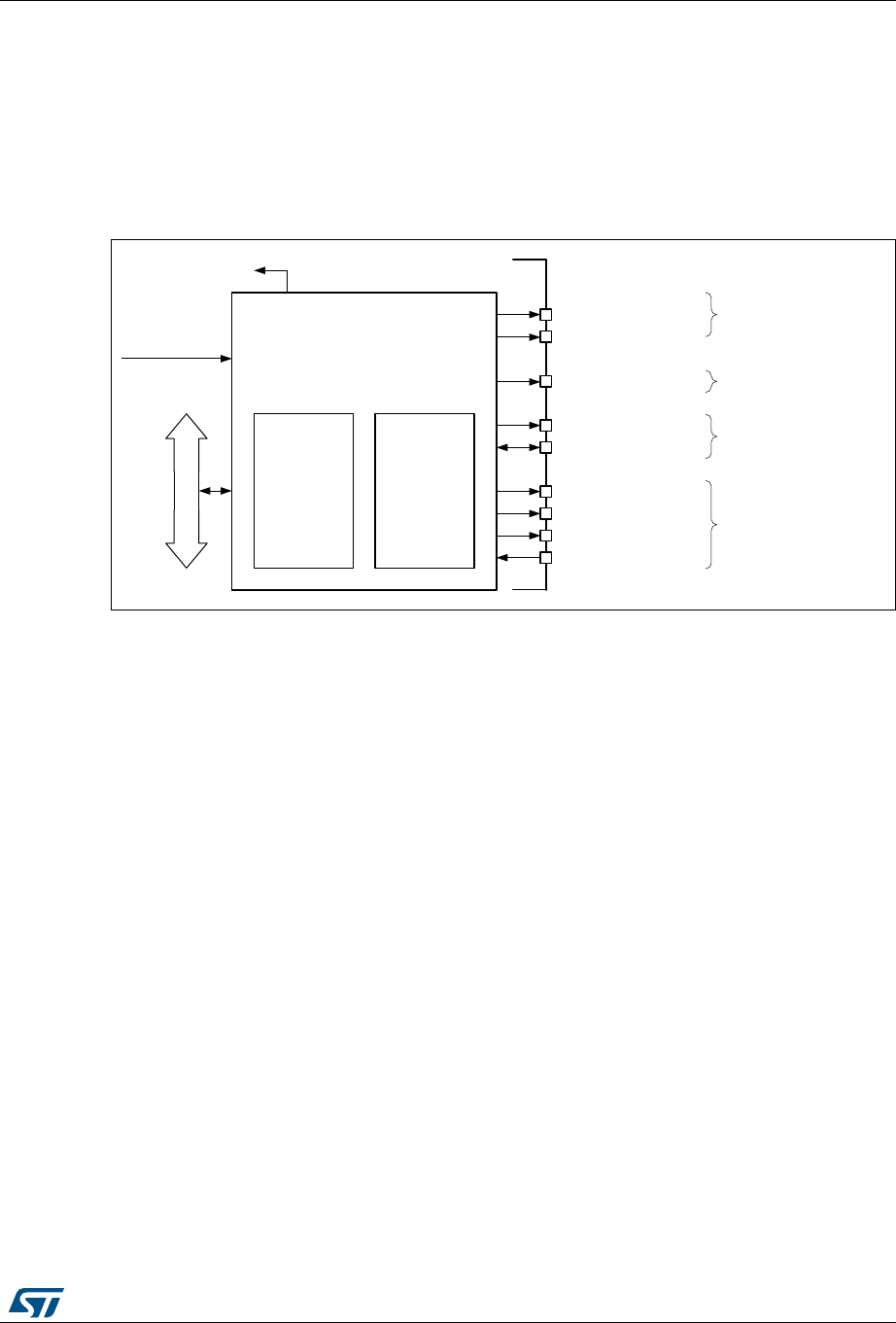
RM0430 Rev 8 265/1324
RM0430 Flexible static memory controller (FSMC)
306
11.2 FMC block diagram
The FSMC consists of the following main blocks:
•The AHB interface (including the FSMC configuration registers)
•The NOR Flash/PSRAM/SRAM controller
The block diagram is shown in the figure below.
Figure 31. FSMC block diagram
06Y9
125365$0
VLJQDOV
)60&B1(>@
)60&B1/RU1$'9
)60&B'>@
)60&B12(
)60&B1:(
)60&B1%/>@
)60&B&/.
)60&B$>@
)60&LQWHUUXSWVWR19,&
)URPFORFN
FRQWUROOHU
125365$0
PHPRU\
FRQWUROOHU
&RQILJXUDWLRQ
UHJLVWHUV
+&/.
)60&B1:$,7
125365$065$0
VKDUHGVLJQDOV
6KDUHGVLJQDOV
125365$065$0
VKDUHGVLJQDOV

Flexible static memory controller (FSMC) RM0430
266/1324 RM0430 Rev 8
11.3 AHB interface
The AHB slave interface allows internal CPUs and other bus master peripherals to access
the external memories.
AHB transactions are translated into the external device protocol. In particular, if the
selected external memory is 16- or 8-bit wide, 32-bit wide transactions on the AHB are split
into consecutive 16- or 8-bit accesses. The FSMC chip select (FSMC_NEx) does not toggle
between the consecutive accesses except in case of Access mode D when the Extended
mode is enabled.
The FSMC generates an AHB error in the following conditions:
•When reading or writing to an FSMC bank (Bank 1 to 4) which is not enabled.
•When reading or writing to the NOR Flash bank while the FACCEN bit is reset in the
FSMC_BCRx register.
The effect of an AHB error depends on the AHB master which has attempted the R/W
access:
•If the access has been attempted by the Cortex®-M4 with FPU CPU, a hard fault
interrupt is generated.
•If the access has been performed by a DMA controller, a DMA transfer error is
generated and the corresponding DMA channel is automatically disabled.
The AHB clock (HCLK) is the reference clock for the FSMC.
11.3.1 Supported memories and transactions
General transaction rules
The requested AHB transaction data size can be 8-, 16- or 32-bit wide whereas the
accessed external device has a fixed data width. This may lead to inconsistent transfers.
Therefore, some simple transaction rules must be followed:
•AHB transaction size and memory data size are equal
There is no issue in this case.
•AHB transaction size is greater than the memory size:
In this case, the FSMC splits the AHB transaction into smaller consecutive memory
accesses to meet the external data width. The FSMC chip select (FSMC_NEx) does
not toggle between the consecutive accesses.
•AHB transaction size is smaller than the memory size:
The transfer may or not be consistent depending on the type of external device:
– Accesses to devices that have the byte select feature (SRAM, ROM, PSRAM)
In this case, the FSMC allows read/write transactions and accesses the right data
through its byte lanes NBL[1:0].
Bytes to be written are addressed by NBL[1:0].
All memory bytes are read (NBL[1:0] are driven low during read transaction) and
the useless ones are discarded.
– Accesses to devices that do not have the byte select feature (NOR)
This situation occurs when a byte access is requested to a 16-bit wide Flash
memory. Since the device cannot be accessed in Byte mode (only 16-bit words
can be read/written from/to the Flash memory), Write transactions and Read
RM0430 Rev 8 267/1324
RM0430 Flexible static memory controller (FSMC)
306
transactions are allowed (the controller reads the entire 16-bit memory word and
uses only the required byte).
Wrap support for NOR Flash/PSRAM
Wrap burst mode for synchronous memories is not supported. The memories must be
configured in Linear burst mode of undefined length.
Configuration registers
The FSMC can be configured through a set of registers. Refer to Section 11.5.6, for a
detailed description of the NOR Flash/PSRAM controller registers.
11.4 External device address mapping
From the FSMC point of view, the external memory is divided into fixed-size banks of
256 Mbytes each (see Figure 32):
•Bank 1 used to address up to 4 NOR Flash memory or PSRAM devices. This bank is
split into 4 NOR/PSRAM subbanks with 4 dedicated chip selects, as follows:
– Bank 1 - NOR/PSRAM 1
– Bank 1 - NOR/PSRAM 2
– Bank 1 - NOR/PSRAM 3
– Bank 1 - NOR/PSRAM 4
For each bank the type of memory to be used can be configured by the user application
through the Configuration register.
Figure 32. FSMC memory banks
11.4.1 NOR/PSRAM address mapping
HADDR[27:26] bits are used to select one of the four memory banks as shown in Table 42.
069
6XSSRUWHGPHPRU\W\SH
%DQN
[0%
125365$065$0
%DQN
[
$GGUHVV
[)))))))
Table 42. NOR/PSRAM bank selection
HADDR[27:26](1)
1. HADDR are internal AHB address lines that are translated to external memory.
Selected bank
00 Bank 1 - NOR/PSRAM 1
01 Bank 1 - NOR/PSRAM 2
10 Bank 1 - NOR/PSRAM 3
11 Bank 1 - NOR/PSRAM 4

Flexible static memory controller (FSMC) RM0430
268/1324 RM0430 Rev 8
The HADDR[25:0] bits contain the external memory address. Since HADDR is a byte
address whereas the memory is addressed at word level, the address actually issued to the
memory varies according to the memory data width, as shown in the following table.
11.5 NOR Flash/PSRAM controller
The FSMC generates the appropriate signal timings to drive the following types of
memories:
•Asynchronous SRAM and ROM
–8 bits
– 16 bits
•PSRAM (CellularRAM™)
– Asynchronous mode
– Burst mode for synchronous accesses
– Multiplexed or non-multiplexed
•NOR Flash memory
– Asynchronous mode
– Burst mode for synchronous accesses
– Multiplexed or non-multiplexed
The FSMC outputs a unique chip select signal, NE[4:1], per bank. All the other signals
(addresses, data and control) are shared.
The FSMC supports a wide range of devices through a programmable timings among
which:
•Programmable wait states (up to 15)
•Programmable bus turnaround cycles (up to 15)
•Programmable output enable and write enable delays (up to 15)
•Independent read and write timings and protocol to support the widest variety of
memories and timings
•Programmable continuous clock (FSMC_CLK) output.
The FSMC Clock (FSMC_CLK) is a submultiple of the HCLK clock. It can be delivered to the
selected external device either during synchronous accesses only or during asynchronous
Table 43. NOR/PSRAM External memory address
Memory width(1)
1. In case of a 16-bit external memory width, the FSMC will internally use HADDR[25:1] to generate the
address for external memory FSMC_A[24:0].
Whatever the external memory width, FSMC_A[0] should be connected to external memory address A[0].
Data address issued to the memory Maximum memory capacity (bits)
8-bit HADDR[25:0] 64 Mbytes x 8 = 512 Mbit
16-bit HADDR[25:1] >> 1 64 Mbytes/2 x 16 = 512 Mbit

RM0430 Rev 8 269/1324
RM0430 Flexible static memory controller (FSMC)
306
and synchronous accesses depending on the CCKEN bit configuration in the FSMC_BCR1
register:
•If the CCLKEN bit is reset, the FSMC generates the clock (CLK) only during
synchronous accesses (Read/write transactions).
•If the CCLKEN bit is set, the FSMC generates a continuous clock during asynchronous
and synchronous accesses. To generate the FSMC_CLK continuous clock, Bank 1
must be configured in Synchronous mode (see Section 11.5.6: NOR/PSRAM controller
registers). Since the same clock is used for all synchronous memories, when a
continuous output clock is generated and synchronous accesses are performed, the
AHB data size has to be the same as the memory data width (MWID) otherwise the
FSMC_CLK frequency will be changed depending on AHB data transaction (refer to
Section 11.5.5: Synchronous transactions for FSMC_CLK divider ratio formula).
The size of each bank is fixed and equal to 64 Mbytes. Each bank is configured through
dedicated registers (see Section 11.5.6: NOR/PSRAM controller registers).
The programmable memory parameters include access times (see Table 44 ) and support
for wait management (for PSRAM and NOR Flash accessed in Burst mode).
11.5.1 External memory interface signals
Table 45 , Table 46 and Table 47 list the signals that are typically used to interface with NOR
Flash memory, SRAM and PSRAM.
Note: The prefix “N” identifies the signals that are active low.
Table 44. Programmable NOR/PSRAM access parameters
Parameter Function Access mode Unit Min. Max.
Address
setup
Duration of the address
setup phase Asynchronous AHB clock cycle
(HCLK) 015
Address hold Duration of the address hold
phase
Asynchronous,
muxed I/Os
AHB clock cycle
(HCLK) 115
Data setup Duration of the data setup
phase Asynchronous AHB clock cycle
(HCLK) 1256
Bust turn Duration of the bus
turnaround phase
Asynchronous and
synchronous read
/ write
AHB clock cycle
(HCLK) 015
Clock divide
ratio
Number of AHB clock cycles
(HCLK) to build one memory
clock cycle (CLK)
Synchronous AHB clock cycle
(HCLK) 2 16
Data latency
Number of clock cycles to
issue to the memory before
the first data of the burst
Synchronous Memory clock
cycle (CLK) 2 17
Flexible static memory controller (FSMC) RM0430
270/1324 RM0430 Rev 8
NOR Flash memory, non-multiplexed I/Os
The maximum capacity is 512 Mbits (26 address lines).
NOR Flash memory, 16-bit multiplexed I/Os
The maximum capacity is 512 Mbits.
PSRAM/SRAM, non-multiplexed I/Os
Table 45. Non-multiplexed I/O NOR Flash memory
FSMC signal name I/O Function
CLK O Clock (for synchronous access)
A[25:0] O Address bus
D[15:0] I/O Bidirectional data bus
NE[x] O Chip select, x = 1..4
NOE O Output enable
NWE O Write enable
NL(=NADV) O Latch enable (this signal is called address
valid, NADV, by some NOR Flash devices)
NWAIT I NOR Flash wait input signal to the FSMC
Table 46. 16-bit multiplexed I/O NOR Flash memory
FSMC signal name I/O Function
CLK O Clock (for synchronous access)
A[25:16] O Address bus
AD[15:0] I/O
16-bit multiplexed, bidirectional address/data bus (the 16-bit address
A[15:0] and data D[15:0] are multiplexed on the databus)
NE[x] O Chip select, x = 1..4
NOE O Output enable
NWE O Write enable
NL(=NADV) O Latch enable (this signal is called address valid, NADV, by some NOR
Flash devices)
NWAIT I NOR Flash wait input signal to the FSMC
Table 47. Non-multiplexed I/Os PSRAM/SRAM
FSMC signal
name I/O Function
CLK O Clock (only for PSRAM synchronous access)
A[25:0] O Address bus
D[15:0] I/O Data bidirectional bus

RM0430 Rev 8 271/1324
RM0430 Flexible static memory controller (FSMC)
306
The maximum capacity is 512 Mbits.
PSRAM, 16-bit multiplexed I/Os
The maximum capacity is 512 Mbits (26 address lines).
11.5.2 Supported memories and transactions
Table 49 below shows an example of the supported devices, access modes and
transactions when the memory data bus is 16-bit wide for NOR Flash memory, PSRAM and
SRAM. The transactions not allowed (or not supported) by the FSMC are shown in gray in
this example.
NE[x] O Chip select, x = 1..4 (called NCE by PSRAM (CellularRAM™ i.e. CRAM))
NOE O Output enable
NWE O Write enable
NL(= NADV) O Address valid only for PSRAM input (memory signal name: NADV)
NWAIT I PSRAM wait input signal to the FSMC
NBL[1:0] O Byte lane output. Byte 0 and Byte 1 control (upper and lower byte enable)
Table 48. 16-Bit multiplexed I/O PSRAM
FSMC signal
name I/O Function
CLK O Clock (for synchronous access)
A[25:16] O Address bus
AD[15:0] I/O 16-bit multiplexed, bidirectional address/data bus (the 16-bit address
A[15:0] and data D[15:0] are multiplexed on the databus)
NE[x] O Chip select, x = 1..4 (called NCE by PSRAM (CellularRAM™ i.e. CRAM))
NOE O Output enable
NWE O Write enable
NL(= NADV) O Address valid PSRAM input (memory signal name: NADV)
NWAIT I PSRAM wait input signal to the FSMC
NBL[1:0] O Byte lane output. Byte 0 and Byte 1 control (upper and lower byte enable)
Table 47. Non-multiplexed I/Os PSRAM/SRAM (continued)
FSMC signal
name I/O Function

Flexible static memory controller (FSMC) RM0430
272/1324 RM0430 Rev 8
Table 49. NOR Flash/PSRAM: example of supported memories and transactions
Device Mode R/W
AHB
data
size
Memory
data size
Allowed/
not
allowed
Comments
NOR Flash
(muxed I/Os
and nonmuxed
I/Os)
Asynchronous R 8 16 Y -
Asynchronous W 8 16 N -
Asynchronous R 16 16 Y -
Asynchronous W 16 16 Y -
Asynchronous R 32 16 Y Split into 2 FSMC accesses
Asynchronous W 32 16 Y Split into 2 FSMC accesses
Asynchronous
page R -16 N Mode is not supported
Synchronous R 8 16 N -
Synchronous R 16 16 Y -
Synchronous R 32 16 Y -
PSRAM
(multiplexed
I/Os and non-
multiplexed
I/Os)
Asynchronous R 8 16 Y -
Asynchronous W 8 16 Y Use of byte lanes NBL[1:0]
Asynchronous R 16 16 Y -
Asynchronous W 16 16 Y -
Asynchronous R 32 16 Y Split into 2 FSMC accesses
Asynchronous W 32 16 Y Split into 2 FSMC accesses
Asynchronous
page R -16 N Mode is not supported
Synchronous R 8 16 N -
Synchronous R 16 16 Y -
Synchronous R 32 16 Y -
Synchronous W 8 16 Y Use of byte lanes NBL[1:0]
Synchronous W 16/32 16 Y -
SRAM and
ROM
Asynchronous R 8 / 16 16 Y -
Asynchronous W 8 / 16 16 Y Use of byte lanes NBL[1:0]
Asynchronous R 32 16 Y Split into 2 FSMC accesses
Asynchronous W 32 16 Y Split into 2 FSMC accesses
Use of byte lanes NBL[1:0]

RM0430 Rev 8 273/1324
RM0430 Flexible static memory controller (FSMC)
306
11.5.3 General timing rules
Signals synchronization
•All controller output signals change on the rising edge of the internal clock (HCLK)
•In Synchronous mode (read or write), all output signals change on the rising edge of
HCLK. Whatever the CLKDIV value, all outputs change as follows:
– NOEL/NWEL/ NEL/NADVL/ NADVH /NBLL/ Address valid outputs change on the
falling edge of FSMC_CLK clock.
– NOEH/ NWEH / NEH/ NOEH/NBLH/ Address invalid outputs change on the rising
edge of FSMC_CLK clock.
11.5.4 NOR Flash/PSRAM controller asynchronous transactions
Asynchronous static memories (NOR Flash, PSRAM, SRAM)
•Signals are synchronized by the internal clock HCLK. This clock is not issued to the
memory
•The FSMC always samples the data before de-asserting the NOE signal. This
guarantees that the memory data hold timing constraint is met (minimum Chip Enable
high to data transition is usually 0 ns)
•If the Extended mode is enabled (EXTMOD bit is set in the FSMC_BCRx register), up
to four extended modes (A, B, C and D) are available. It is possible to mix A, B, C and
D modes for read and write operations. For example, read operation can be performed
in mode A and write in mode B.
•If the Extended mode is disabled (EXTMOD bit is reset in the FSMC_BCRx register),
the FSMC can operate in Mode1 or Mode2 as follows:
– Mode 1 is the default mode when SRAM/PSRAM memory type is selected (MTYP
= 0x0 or 0x01 in the FSMC_BCRx register)
– Mode 2 is the default mode when NOR memory type is selected (MTYP = 0x10 in
the FSMC_BCRx register).
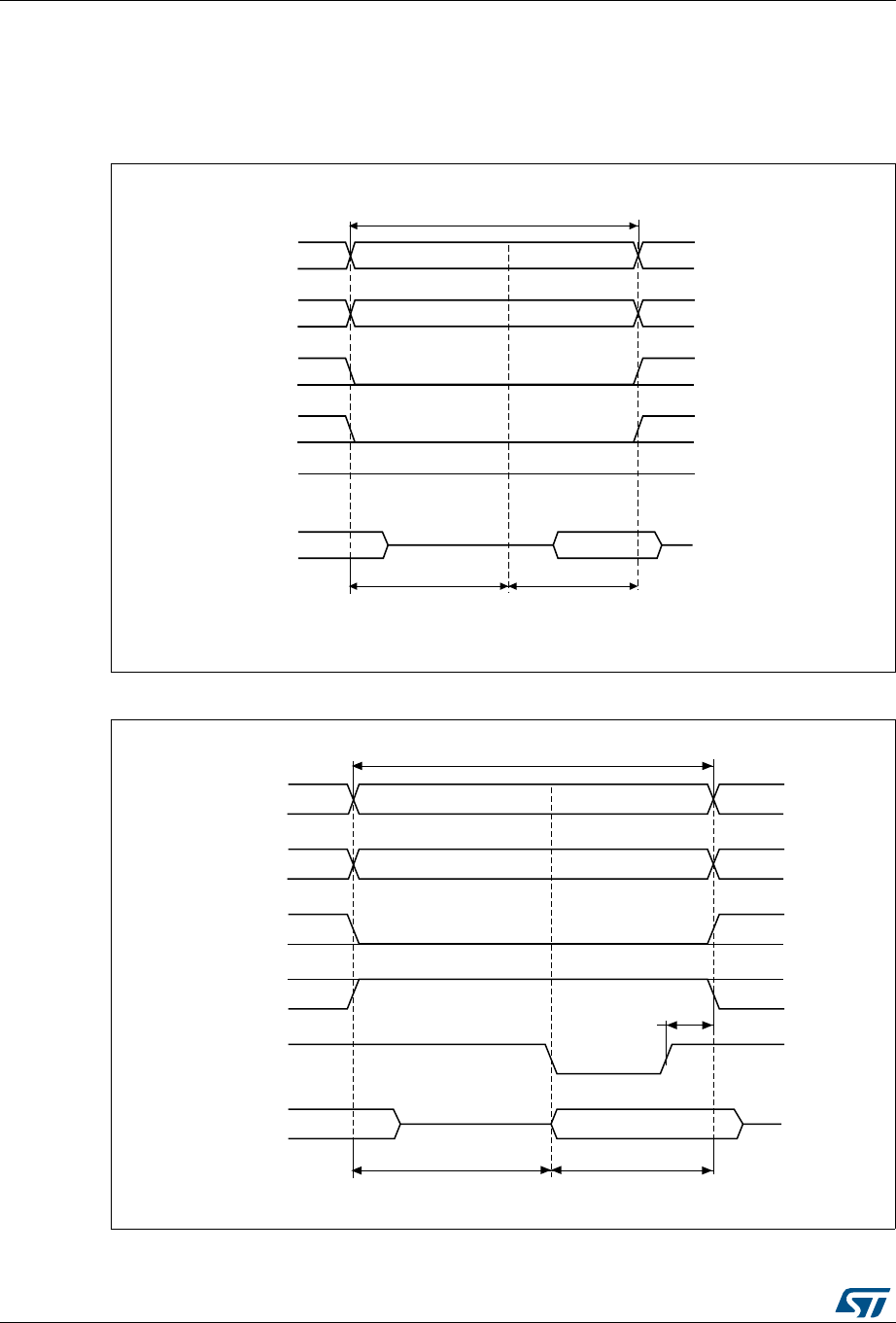
Flexible static memory controller (FSMC) RM0430
274/1324 RM0430 Rev 8
Mode 1 - SRAM/PSRAM (CRAM)
The next figures show the read and write transactions for the supported modes followed by
the required configuration of FSMC_BCRx, and FSMC_BTRx/FSMC_BWTRx registers.
Figure 33. Mode1 read access waveforms
Figure 34. Mode1 write access waveforms
$>@
12(
$''6(7 '$7$67
0HPRU\WUDQVDFWLRQ
1([
'>@
+&/.F\FOHV +&/.F\FOHV
1:(
1%/>@
GDWDGULYHQ
E\PHPRU\
069
+LJK
06Y9
$>@
12(
$''6(7 '$7$67
0HPRU\WUDQVDFWLRQ
1([
'>@
+&/.F\FOHV +&/.F\FOHV
1:(
1%/>@
GDWDGULYHQE\)60&
+&/.

RM0430 Rev 8 275/1324
RM0430 Flexible static memory controller (FSMC)
306
The one HCLK cycle at the end of the write transaction helps guarantee the address and
data hold time after the NWE rising edge. Due to the presence of this HCLK cycle, the
DATAST value must be greater than zero (DATAST > 0).
Table 50. FSMC_BCRx bit fields
Bit number Bit name Value to set
31:22 Reserved 0x000
21 WFDIS As needed
20 CCLKEN As needed
19 CBURSTRW 0x0 (no effect in Asynchronous mode)
18:16 CPSIZE 0x0 (no effect in Asynchronous mode)
15 ASYNCWAIT Set to 1 if the memory supports this feature. Otherwise keep at 0.
14 EXTMOD 0x0
13 WAITEN 0x0 (no effect in Asynchronous mode)
12 WREN As needed
11 Reserved 0x0
10 Reserved 0x0
9 WAITPOL Meaningful only if bit 15 is 1
8 BURSTEN 0x0
7 Reserved 0x1
6 FACCEN Don’t care
5:4 MWID As needed
3:2 MTYP As needed, exclude 0x2 (NOR Flash memory)
1 MUXE 0x0
0 MBKEN 0x1
Table 51. FSMC_BTRx bit fields
Bit number Bit name Value to set
31:30 Reserved 0x0
29:28 ACCMOD Don’t care
27:24 DATLAT Don’t care
23:20 CLKDIV Don’t care
19:16 BUSTURN Time between NEx high to NEx low (BUSTURN HCLK).
15:8 DATAST Duration of the second access phase (DATAST+1 HCLK cycles for
write accesses, DATAST HCLK cycles for read accesses).
7:4 ADDHLD Don’t care
3:0 ADDSET Duration of the first access phase (ADDSET HCLK cycles).
Minimum value for ADDSET is 0.
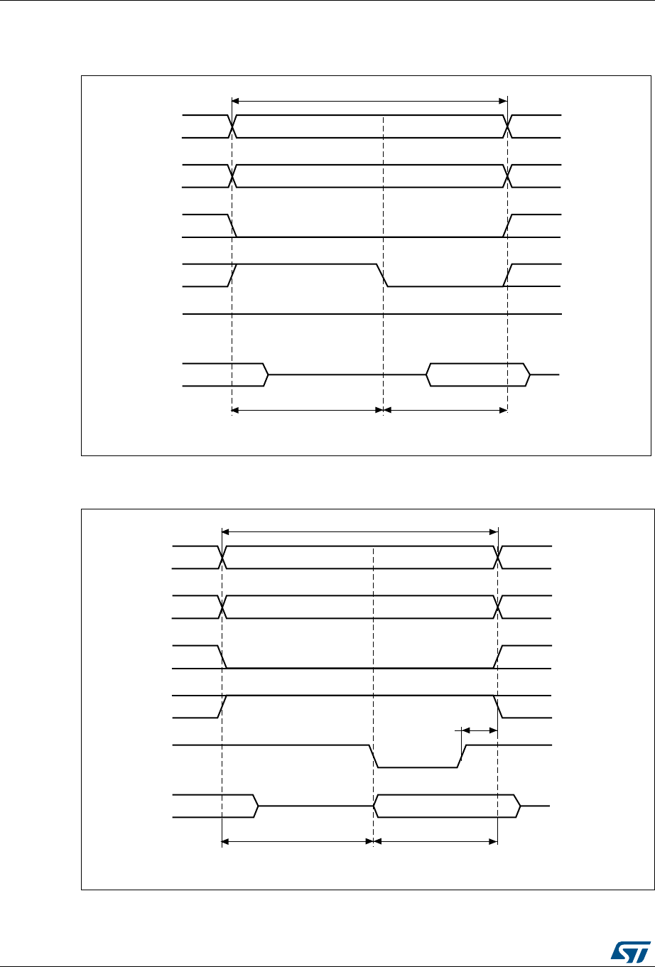
Flexible static memory controller (FSMC) RM0430
276/1324 RM0430 Rev 8
Mode A - SRAM/PSRAM (CRAM) OE toggling
Figure 35. ModeA read access waveforms
1. NBL[1:0] are driven low during the read access
Figure 36. ModeA write access waveforms
!;=
./%
!$$3%4 $!4!34
-EMORYTRANSACTION
.%X
$;=
(#,+CYCLES (#,+CYCLES
.7%
.",;=
DATADRIVEN
BYMEMORY
-36
(IGH
Ϯϱ͗Ϭ
EK
^d ;d^dнϭͿ
DĞŵŽƌLJƚƌĂŶƐĂĐƚŝŽŶ
Edž
ϭϱ͗Ϭ
,><ĐLJĐůĞƐ ,><ĐLJĐůĞƐ
Et
E>ϭ͗Ϭ
ĚĂƚĂĚƌŝǀĞŶďLJ&^D
D^ϯϰϰϴϬsϭ
ϭ,><

RM0430 Rev 8 277/1324
RM0430 Flexible static memory controller (FSMC)
306
The differences compared with Mode1 are the toggling of NOE and the independent read
and write timings.
Table 52. FSMC_BCRx bit fields
Bit number Bit name Value to set
31:22 Reserved 0x000
21 WFDIS As needed
20 CCLKEN As needed
19 CBURSTRW 0x0 (no effect in Asynchronous mode)
18:16 CPSIZE 0x0 (no effect in Asynchronous mode)
15 ASYNCWAIT Set to 1 if the memory supports this feature. Otherwise keep at 0.
14 EXTMOD 0x1
13 WAITEN 0x0 (no effect in Asynchronous mode)
12 WREN As needed
11 WAITCFG Don’t care
10 Reserved 0x0
9 WAITPOL Meaningful only if bit 15 is 1
8 BURSTEN 0x0
7 Reserved 0x1
6 FACCEN Don’t care
5:4 MWID As needed
3:2 MTYP As needed, exclude 0x2 (NOR Flash memory)
1 MUXEN 0x0
0 MBKEN 0x1
Table 53. FSMC_BTRx bit fields
Bit number Bit name Value to set
31:30 Reserved 0x0
29:28 ACCMOD 0x0
27:24 DATLAT Don’t care
23:20 CLKDIV Don’t care
19:16 BUSTURN Time between NEx high to NEx low (BUSTURN HCLK).
15:8 DATAST Duration of the second access phase (DATAST HCLK cycles) for read
accesses.
7:4 ADDHLD Don’t care
3:0 ADDSET
Duration of the first access phase (ADDSET HCLK cycles) for read
accesses.
Minimum value for ADDSET is 0.
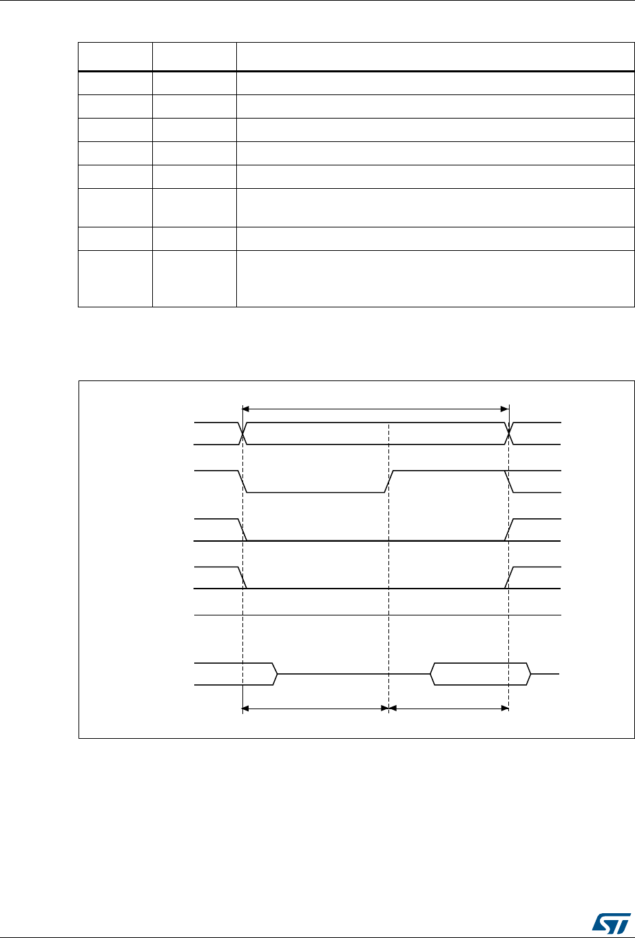
Flexible static memory controller (FSMC) RM0430
278/1324 RM0430 Rev 8
Mode 2/B - NOR Flash
Figure 37. Mode2 and mode B read access waveforms
Table 54. FSMC_BWTRx bit fields
Bit number Bit name Value to set
31:30 Reserved 0x0
29:28 ACCMOD 0x0
27:24 DATLAT Don’t care
23:20 CLKDIV Don’t care
19:16 BUSTURN Time between NEx high to NEx low (BUSTURN HCLK).
15:8 DATAST Duration of the second access phase (DATAST HCLK cycles) for write
accesses.
7:4 ADDHLD Don’t care
3:0 ADDSET
Duration of the first access phase (ADDSET HCLK cycles) for write
accesses.
Minimum value for ADDSET is 0.
069
$>@
12(
$''6(7 '$7$67
0HPRU\WUDQVDFWLRQ
1([
'>@
+&/.F\FOHV +&/.F\FOHV
1:(
1$'9
GDWDGULYHQ
E\PHPRU\
+LJK
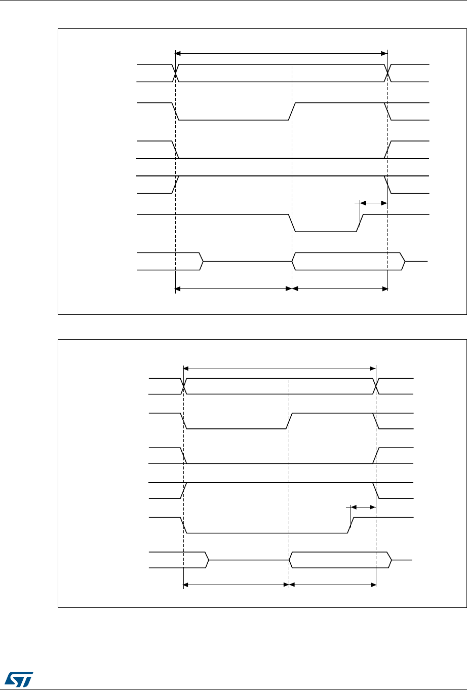
RM0430 Rev 8 279/1324
RM0430 Flexible static memory controller (FSMC)
306
Figure 38. Mode2 write access waveforms
Figure 39. ModeB write access waveforms
The differences with Mode1 are the toggling of NWE and the independent read and write
timings when extended mode is set (Mode B).
069
$>@
12(
$''6(7 '$7$67
0HPRU\WUDQVDFWLRQ
1([
'>@
+&/.F\FOHV +&/.F\FOHV
1:(
1$'9
+&/.
GDWDGULYHQE\)0&
06Y9
$>@
12(
$''6(7 '$7$67
0HPRU\WUDQVDFWLRQ
1([
'>@
+&/.F\FOHV +&/.F\FOHV
1:(
1$'9
GDWDGULYHQE\)60&
+&/.

Flexible static memory controller (FSMC) RM0430
280/1324 RM0430 Rev 8
Table 55. FSMC_BCRx bit fields
Bit number Bit name Value to set
31:22 Reserved 0x000
21 WFDIS As needed
20 CCLKEN As needed
19 CBURSTRW 0x0 (no effect in Asynchronous mode)
18:16 CPSIZE 0x0 (no effect in Asynchronous mode)
15 ASYNCWAIT Set to 1 if the memory supports this feature. Otherwise keep at 0.
14 EXTMOD 0x1 for mode B, 0x0 for mode 2
13 WAITEN 0x0 (no effect in Asynchronous mode)
12 WREN As needed
11 WAITCFG Don’t care
10 Reserved 0x0
9 WAITPOL Meaningful only if bit 15 is 1
8 BURSTEN 0x0
7 Reserved 0x1
6 FACCEN 0x1
5:4 MWID As needed
3:2 MTYP 0x2 (NOR Flash memory)
1 MUXEN 0x0
0 MBKEN 0x1
Table 56. FSMC_BTRx bit fields
Bit number Bit name Value to set
31:30 Reserved 0x0
29:28 ACCMOD 0x1 if Extended mode is set
27:24 DATLAT Don’t care
23:20 CLKDIV Don’t care
19:16 BUSTURN Time between NEx high to NEx low (BUSTURN HCLK).
15:8 DATAST Duration of the access second phase (DATAST HCLK cycles) for
read accesses.
7:4 ADDHLD Don’t care
3:0 ADDSET Duration of the access first phase (ADDSET HCLK cycles) for read
accesses. Minimum value for ADDSET is 0.
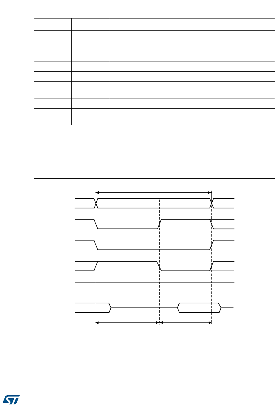
RM0430 Rev 8 281/1324
RM0430 Flexible static memory controller (FSMC)
306
Note: The FSMC_BWTRx register is valid only if the Extended mode is set (mode B), otherwise its
content is don’t care.
Mode C - NOR Flash - OE toggling
Figure 40. ModeC read access waveforms
Table 57. FSMC_BWTRx bit fields
Bit number Bit name Value to set
31:30 Reserved 0x0
29:28 ACCMOD 0x1 if Extended mode is set
27:24 DATLAT Don’t care
23:20 CLKDIV Don’t care
19:16 BUSTURN Time between NEx high to NEx low (BUSTURN HCLK).
15:8 DATAST Duration of the access second phase (DATAST HCLK cycles) for
write accesses.
7:4 ADDHLD Don’t care
3:0 ADDSET Duration of the access first phase (ADDSET HCLK cycles) for write
accesses. Minimum value for ADDSET is 0.
!;=
./%
!$$3%4 $!4!34
-EMORYTRANSACTION
.%X
$;=
(#,+CYCLES (#,+CYCLES
.7%
.!$6
DATADRIVEN
BYMEMORY
-36
(IGH
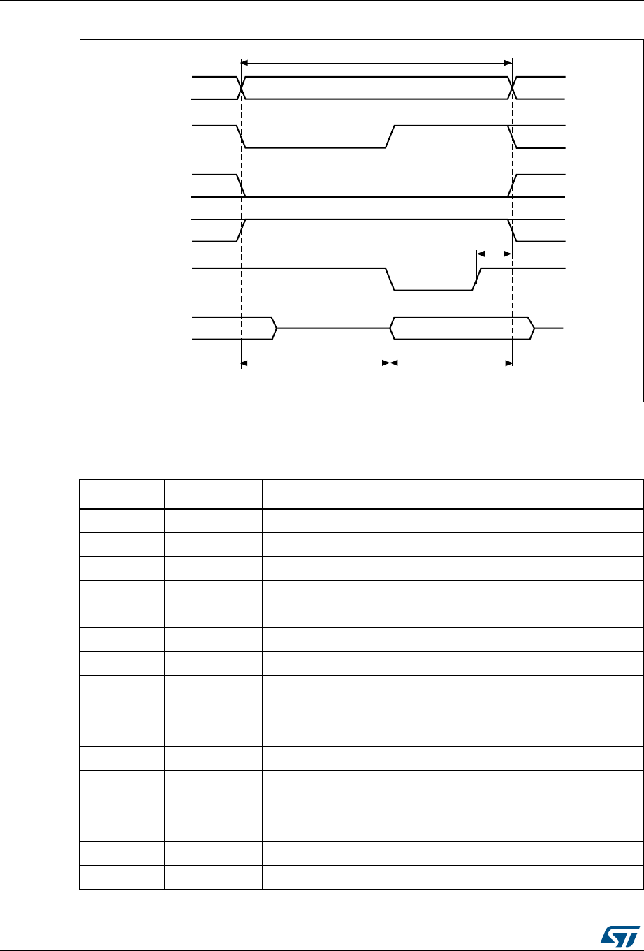
Flexible static memory controller (FSMC) RM0430
282/1324 RM0430 Rev 8
Figure 41. ModeC write access waveforms
The differences compared with Mode1 are the toggling of NOE and the independent read
and write timings.
Table 58. FSMC_BCRx bit fields
Bit number Bit name Value to set
31:22 Reserved 0x000
21 WFDIS As needed
20 CCLKEN As needed
19 CBURSTRW 0x0 (no effect in Asynchronous mode)
18:16 CPSIZE 0x0 (no effect in Asynchronous mode)
15 ASYNCWAIT Set to 1 if the memory supports this feature. Otherwise keep at 0.
14 EXTMOD 0x1
13 WAITEN 0x0 (no effect in Asynchronous mode)
12 WREN As needed
11 WAITCFG Don’t care
10 Reserved 0x0
9 WAITPOL Meaningful only if bit 15 is 1
8 BURSTEN 0x0
7 Reserved 0x1
6 FACCEN 0x1
5:4 MWID As needed
!;=
./%
!$$3%4 $!4!34
-EMORYTRANSACTION
.%X
$;=
(#,+CYCLES (#,+CYCLES
.7%
.!$6
DATADRIVENBY&3-#
-36
(#,+

RM0430 Rev 8 283/1324
RM0430 Flexible static memory controller (FSMC)
306
3:2 MTYP 0x02 (NOR Flash memory)
1 MUXEN 0x0
0 MBKEN 0x1
Table 58. FSMC_BCRx bit fields (continued)
Bit number Bit name Value to set
Table 59. FSMC_BTRx bit fields
Bit number Bit name Value to set
31:30 Reserved 0x0
29:28 ACCMOD 0x2
27:24 DATLAT 0x0
23:20 CLKDIV 0x0
19:16 BUSTURN Time between NEx high to NEx low (BUSTURN HCLK).
15:8 DATAST Duration of the second access phase (DATAST HCLK cycles) for
read accesses.
7:4 ADDHLD Don’t care
3:0 ADDSET Duration of the first access phase (ADDSET HCLK cycles) for read
accesses. Minimum value for ADDSET is 0.
Table 60. FSMC_BWTRx bit fields
Bit number Bit name Value to set
31:30 Reserved 0x0
29:28 ACCMOD 0x2
27:24 DATLAT Don’t care
23:20 CLKDIV Don’t care
19:16 BUSTURN Time between NEx high to NEx low (BUSTURN HCLK).
15:8 DATAST Duration of the second access phase (DATAST HCLK cycles) for
write accesses.
7:4 ADDHLD Don’t care
3:0 ADDSET Duration of the first access phase (ADDSET HCLK cycles) for write
accesses. Minimum value for ADDSET is 0.
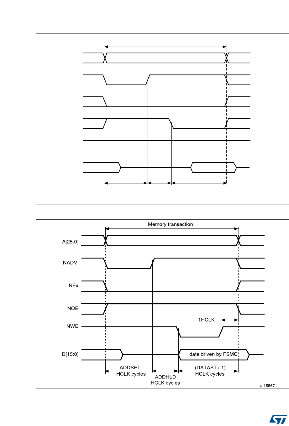
Flexible static memory controller (FSMC) RM0430
284/1324 RM0430 Rev 8
Mode D - asynchronous access with extended address
Figure 42. ModeD read access waveforms
Figure 43. ModeD write access waveforms
!;=
./%
!$$3%4 $!4!34
-EMORYTRANSACTION
.%X
$;=
(#,+CYCLES (#,+CYCLES
.7%
.!$6
DATADRIVEN
BYMEMORY
-36
(IGH
!$$(,$
(#,+CYCLES

RM0430 Rev 8 285/1324
RM0430 Flexible static memory controller (FSMC)
306
The differences with Mode1 are the toggling of NOE that goes on toggling after NADV
changes and the independent read and write timings.
Table 61. FSMC_BCRx bit fields
Bit number Bit name Value to set
31:22 Reserved 0x000
21 WFDIS As needed
20 CCLKEN As needed
19 CBURSTRW 0x0 (no effect in Asynchronous mode)
18:16 CPSIZE 0x0 (no effect in Asynchronous mode)
15 ASYNCWAIT Set to 1 if the memory supports this feature. Otherwise keep at 0.
14 EXTMOD 0x1
13 WAITEN 0x0 (no effect in Asynchronous mode)
12 WREN As needed
11 WAITCFG Don’t care
10 Reserved 0x0
9 WAITPOL Meaningful only if bit 15 is 1
8 BURSTEN 0x0
7 Reserved 0x1
6 FACCEN Set according to memory support
5:4 MWID As needed
3:2 MTYP As needed
1 MUXEN 0x0
0 MBKEN 0x1
Table 62. FSMC_BTRx bit fields
Bit number Bit name Value to set
31:30 Reserved 0x0
29:28 ACCMOD 0x3
27:24 DATLAT Don’t care
23:20 CLKDIV Don’t care
19:16 BUSTURN Time between NEx high to NEx low (BUSTURN HCLK).
15:8 DATAST Duration of the second access phase (DATAST HCLK cycles) for read
accesses.
7:4 ADDHLD Duration of the middle phase of the read access (ADDHLD HCLK
cycles)
3:0 ADDSET Duration of the first access phase (ADDSET HCLK cycles) for read
accesses. Minimum value for ADDSET is 1.
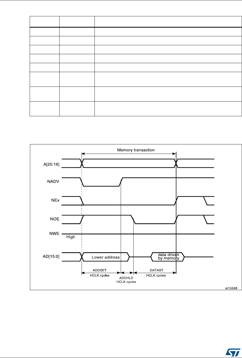
Flexible static memory controller (FSMC) RM0430
286/1324 RM0430 Rev 8
Muxed mode - multiplexed asynchronous access to NOR Flash memory
Figure 44. Muxed read access waveforms
Table 63. FSMC_BWTRx bit fields
Bit number Bit name Value to set
31:30 Reserved 0x0
29:28 ACCMOD 0x3
27:24 DATLAT Don’t care
23:20 CLKDIV Don’t care
19:16 BUSTURN Time between NEx high to NEx low (BUSTURN HCLK).
15:8 DATAST Duration of the second access phase (DATAST + 1 HCLK cycles) for
write accesses.
7:4 ADDHLD Duration of the middle phase of the write access (ADDHLD HCLK
cycles)
3:0 ADDSET Duration of the first access phase (ADDSET HCLK cycles) for write
accesses. Minimum value for ADDSET is 1.
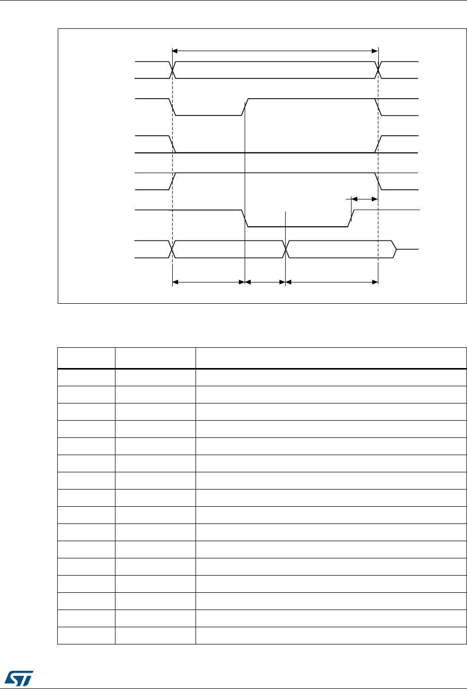
RM0430 Rev 8 287/1324
RM0430 Flexible static memory controller (FSMC)
306
Figure 45. Muxed write access waveforms
The difference with ModeD is the drive of the lower address byte(s) on the data bus.
Table 64. FSMC_BCRx bit fields
Bit number Bit name Value to set
31:22 Reserved 0x000
21 WFDIS As needed
20 CCLKEN As needed
19 CBURSTRW 0x0 (no effect in Asynchronous mode)
18:16 CPSIZE 0x0 (no effect in Asynchronous mode)
15 ASYNCWAIT Set to 1 if the memory supports this feature. Otherwise keep at 0.
14 EXTMOD 0x0
13 WAITEN 0x0 (no effect in Asynchronous mode)
12 WREN As needed
11 WAITCFG Don’t care
10 Reserved 0x0
9 WAITPOL Meaningful only if bit 15 is 1
8 BURSTEN 0x0
7 Reserved 0x1
6 FACCEN 0x1
5:4 MWID As needed
06Y9
$>@
12(
0HPRU\WUDQVDFWLRQ
1([
1:(
1$'9
+&/.
$''6(7
+&/.F\FOHV
'$7$67
+&/.F\FOHV
$''+/'
+&/.F\FOHV
$'>@ GDWDGULYHQE\)60&
/RZHUDGGUHVV

Flexible static memory controller (FSMC) RM0430
288/1324 RM0430 Rev 8
WAIT management in asynchronous accesses
If the asynchronous memory asserts the WAIT signal to indicate that it is not yet ready to
accept or to provide data, the ASYNCWAIT bit has to be set in FSMC_BCRx register.
If the WAIT signal is active (high or low depending on the WAITPOL bit), the second access
phase (Data setup phase), programmed by the DATAST bits, is extended until WAIT
becomes inactive. Unlike the data setup phase, the first access phases (Address setup and
Address hold phases), programmed by the ADDSET and ADDHLD bits, are not WAIT
sensitive and so they are not prolonged.
The data setup phase must be programmed so that WAIT can be detected 4 HCLK cycles
before the end of the memory transaction. The following cases must be considered:
3:2 MTYP 0x2 (NOR Flash memory) or 0x1(PSRAM)
1 MUXEN 0x1
0 MBKEN 0x1
Table 65. FSMC_BTRx bit fields
Bit number Bit name Value to set
31:30 Reserved 0x0
29:28 ACCMOD 0x0
27:24 DATLAT Don’t care
23:20 CLKDIV Don’t care
19:16 BUSTURN Time between NEx high to NEx low (BUSTURN HCLK).
15:8 DATAST Duration of the second access phase (DATAST HCLK cycles for read
accesses and DATAST+1 HCLK cycles for write accesses).
7:4 ADDHLD Duration of the middle phase of the access (ADDHLD HCLK cycles).
3:0 ADDSET Duration of the first access phase (ADDSET HCLK cycles). Minimum
value for ADDSET is 1.
Table 64. FSMC_BCRx bit fields (continued)
Bit number Bit name Value to set
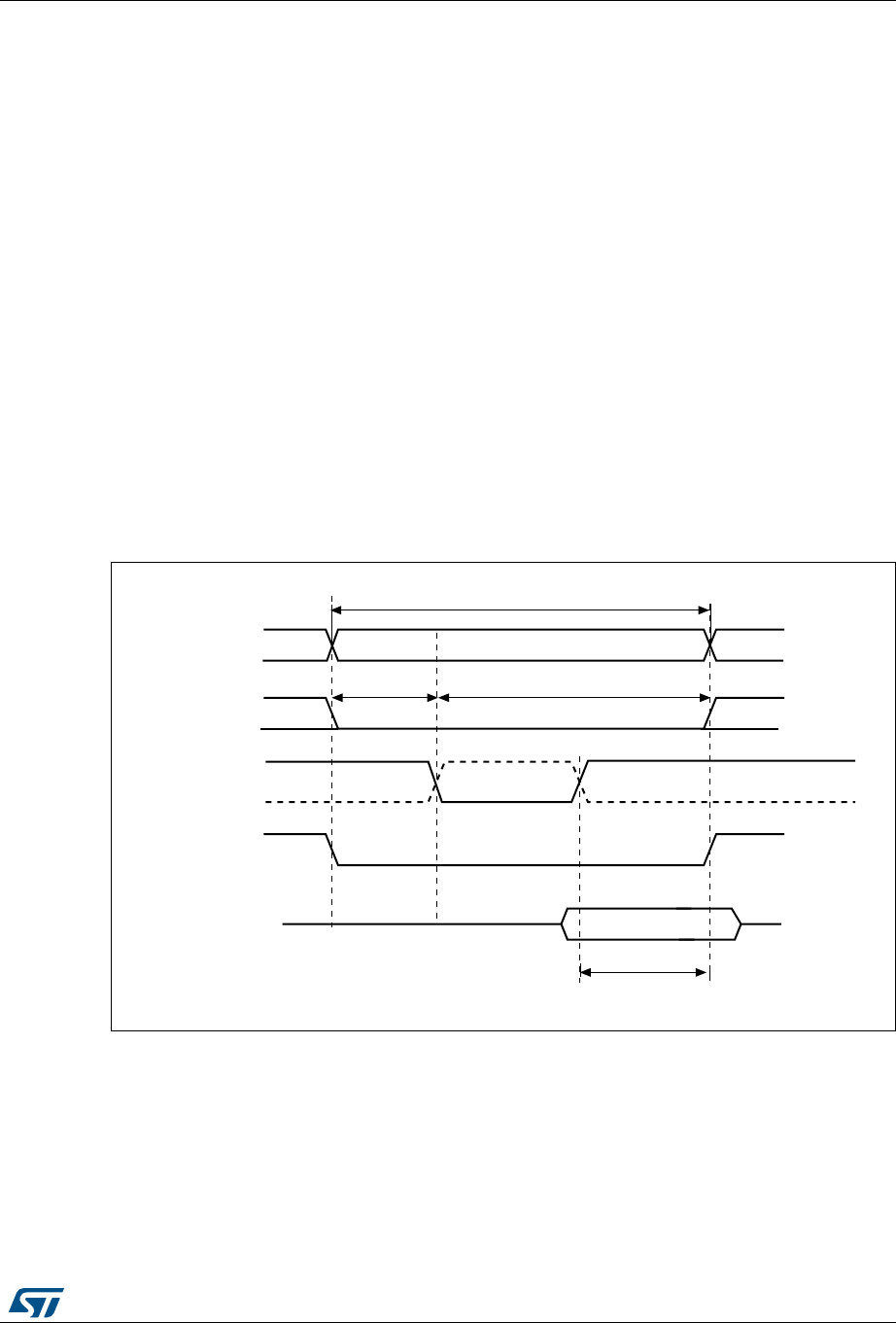
RM0430 Rev 8 289/1324
RM0430 Flexible static memory controller (FSMC)
306
1. The memory asserts the WAIT signal aligned to NOE/NWE which toggles:
2. The memory asserts the WAIT signal aligned to NEx (or NOE/NWE not toggling):
if
then:
otherwise
where max_wait_assertion_time is the maximum time taken by the memory to assert
the WAIT signal once NEx/NOE/NWE is low.
Figure 46 and Figure 47 show the number of HCLK clock cycles that are added to the
memory access phase after WAIT is released by the asynchronous memory (independently
of the above cases).
Figure 46. Asynchronous wait during a read access waveforms
1. NWAIT polarity depends on WAITPOL bit setting in FSMC_BCRx register.
DATAST 4 HCLK×()max_wait_assertion_time+≥
max_wait_assertion_time address_phase hold_phase+>
DATAST 4 HCLK×()max_wait_assertion_time address_phase–hold_phase–()+≥
DATAST 4 HCLK×≥
$>@
12(
+&/.
0HPRU\WUDQVDFWLRQ
'>@
1([
GDWDGULYHQE\PHPRU\
069
DGGUHVVSKDVH GDWDVHWXSSKDVH
.7!)4 DONTCARE DONTCARE
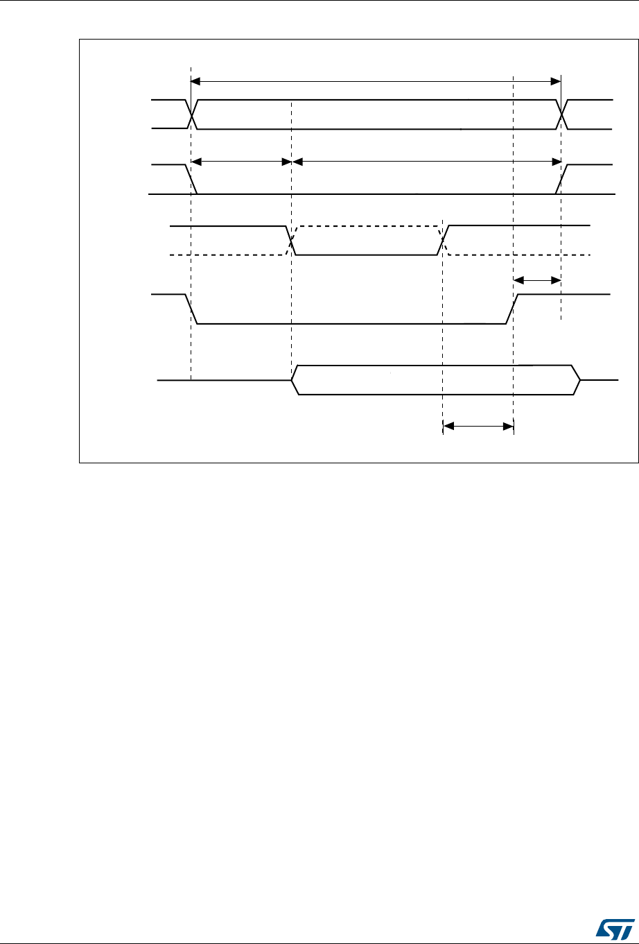
Flexible static memory controller (FSMC) RM0430
290/1324 RM0430 Rev 8
Figure 47. Asynchronous wait during a write access waveforms
1. NWAIT polarity depends on WAITPOL bit setting in FSMC_BCRx register.
11.5.5 Synchronous transactions
The memory clock, FSMC_CLK, is a submultiple of HCLK. It depends on the value of
CLKDIV and the MWID/ AHB data size, following the formula given below:
Whatever MWID size: 16 or 8-bit, the FSMC_CLK divider ratio is always defined by the
programmed CLKDIV value.
Example:
•If CLKDIV=1, MWID = 16 bits, AHB data size=8 bits, FSMC_CLK=HCLK/2.
NOR Flash memories specify a minimum time from NADV assertion to CLK high. To meet
this constraint, the FSMC does not issue the clock to the memory during the first internal
clock cycle of the synchronous access (before NADV assertion). This guarantees that the
rising edge of the memory clock occurs in the middle of the NADV low pulse.
Data latency versus NOR memory latency
The data latency is the number of cycles to wait before sampling the data. The DATLAT
value must be consistent with the latency value specified in the NOR Flash configuration
register. The FSMC does not include the clock cycle when NADV is low in the data latency
count.
$>@
1:(
0HPRU\WUDQVDFWLRQ
'>@
1([
GDWDGULYHQE\)60&
069
+&/.
DGGUHVVSKDVH GDWDVHWXSSKDVH
+&/.
.7!)4 DONTCARE DONTCARE
FSMC_CLK divider ratio max CLKDIV 1+MWID AHB data size()(, )=

RM0430 Rev 8 291/1324
RM0430 Flexible static memory controller (FSMC)
306
Caution: Some NOR Flash memories include the NADV Low cycle in the data latency count, so that
the exact relation between the NOR Flash latency and the FSMC DATLAT parameter can be
either:
•NOR Flash latency = (DATLAT + 2) CLK clock cycles
•or NOR Flash latency = (DATLAT + 3) CLK clock cycles
Some recent memories assert NWAIT during the latency phase. In such cases DATLAT can
be set to its minimum value. As a result, the FSMC samples the data and waits long enough
to evaluate if the data are valid. Thus the FSMC detects when the memory exits latency and
real data are processed.
Other memories do not assert NWAIT during latency. In this case the latency must be set
correctly for both the FSMC and the memory, otherwise invalid data are mistaken for good
data, or valid data are lost in the initial phase of the memory access.
Single-burst transfer
When the selected bank is configured in Burst mode for synchronous accesses, if for
example an AHB single-burst transaction is requested on 16-bit memories, the FSMC
performs a burst transaction of length 1 (if the AHB transfer is 16 bits), or length 2 (if the
AHB transfer is 32 bits) and de-assert the chip select signal when the last data is strobed.
Such transfers are not the most efficient in terms of cycles compared to asynchronous read
operations. Nevertheless, a random asynchronous access would first require to re-program
the memory access mode, which would altogether last longer.
Cross boundary page for CellularRAM™ 1.5
CellularRAM™ 1.5 does not allow burst access to cross the page boundary. The FSMC
controller allows to split automatically the burst access when the memory page size is
reached by configuring the CPSIZE bits in the FSMC_BCR1 register following the memory
page size.
Wait management
For synchronous NOR Flash memories, NWAIT is evaluated after the programmed latency
period, which corresponds to (DATLAT+2) CLK clock cycles.
If NWAIT is active (low level when WAITPOL = 0, high level when WAITPOL = 1), wait
states are inserted until NWAIT is inactive (high level when WAITPOL = 0, low level when
WAITPOL = 1).
When NWAIT is inactive, the data is considered valid either immediately (bit WAITCFG = 1)
or on the next clock edge (bit WAITCFG = 0).
During wait-state insertion via the NWAIT signal, the controller continues to send clock
pulses to the memory, keeping the chip select and output enable signals valid. It does not
consider the data as valid.
In Burst mode, there are two timing configurations for the NOR Flash NWAIT signal:
•The Flash memory asserts the NWAIT signal one data cycle before the wait state
(default after reset).
•The Flash memory asserts the NWAIT signal during the wait state
The FSMC supports both NOR Flash wait state configurations, for each chip select, thanks
to the WAITCFG bit in the FSMC_BCRx registers (x = 0..3).
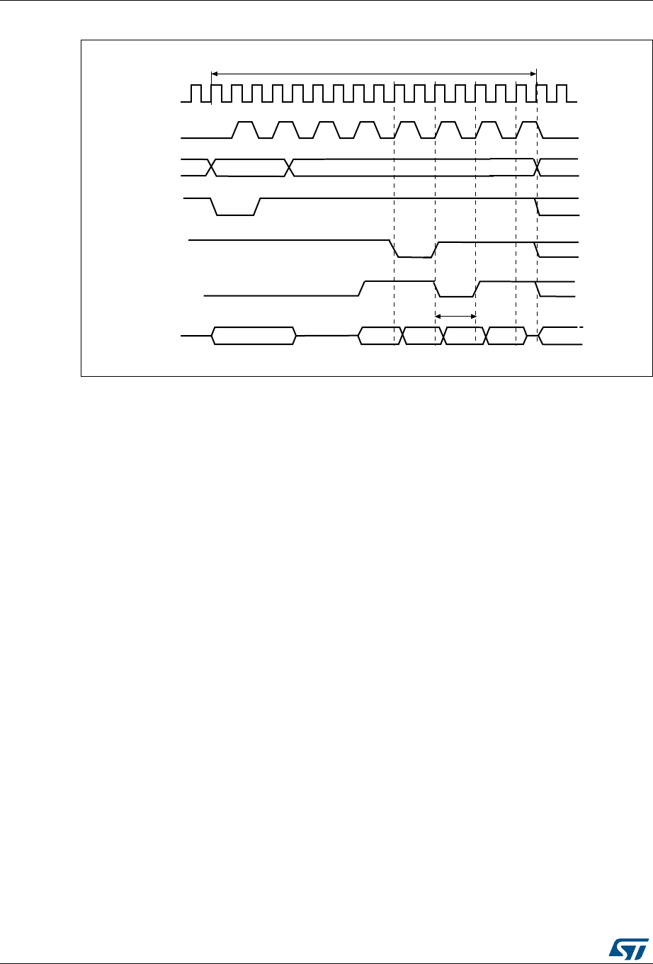
Flexible static memory controller (FSMC) RM0430
292/1324 RM0430 Rev 8
Figure 48. Wait configuration waveforms
DGGU>@ GDWD GDWD
DGGU>@
0HPRU\WUDQVDFWLRQ EXUVWRIKDOIZRUGV
+&/.
&/.
$>@
1$'9
1:$,7
:$,7&)*
$'>@
LQVHUWHGZDLWVWDWH
GDWD
1:$,7
:$,7&)*
DLF
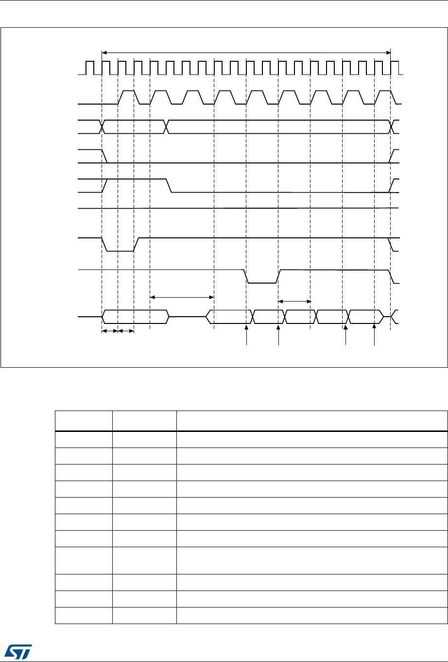
RM0430 Rev 8 293/1324
RM0430 Flexible static memory controller (FSMC)
306
Figure 49. Synchronous multiplexed read mode waveforms - NOR, PSRAM (CRAM)
1. Byte lane outputs (NBL are not shown; for NOR access, they are held high, and, for PSRAM (CRAM)
access, they are held low.
$GGU>@ GDWD GDWD
DGGU>@
0HPRU\WUDQVDFWLRQ EXUVWRIKDOIZRUGV
+&/.
&/.
$>@
1([
12(
1:( +LJK
1$'9
1:$,7
:$,7&)*
$'>@
FORFN
F\FOH
FORFN
F\FOH
'$7/$7 LQVHUWHGZDLWVWDWH
'DWDVWUREHV DLI
&/.F\FOHV
GDWD GDWD
'DWDVWUREHV
Table 66. FSMC_BCRx bit fields
Bit number Bit name Value to set
31:22 Reserved 0x000
21 WFDIS As needed
20 CCLKEN As needed
19 CBURSTRW No effect on synchronous read
18:16 CPSIZE 0x0 (no effect in Asynchronous mode)
15 ASYNCWAIT 0x0
14 EXTMOD 0x0
13 WAITEN To be set to 1 if the memory supports this feature, to be kept at 0
otherwise
12 WREN No effect on synchronous read
11 WAITCFG To be set according to memory
10 Reserved 0x0

Flexible static memory controller (FSMC) RM0430
294/1324 RM0430 Rev 8
9 WAITPOL To be set according to memory
8 BURSTEN 0x1
7 Reserved 0x1
6 FACCEN Set according to memory support (NOR Flash memory)
5-4 MWID As needed
3-2 MTYP 0x1 or 0x2
1 MUXEN As needed
0 MBKEN 0x1
Table 67. FSMC_BTRx bit fields
Bit number Bit name Value to set
31:30 Reserved 0x0
29:28 ACCMOD 0x0
27-24 DATLAT Data latency
27-24 DATLAT Data latency
23-20 CLKDIV
0x0 to get CLK = HCLK
0x1 to get CLK = 2 × HCLK
..
19-16 BUSTURN Time between NEx high to NEx low (BUSTURN HCLK).
15-8 DATAST Don’t care
7-4 ADDHLD Don’t care
3-0 ADDSET Don’t care
Table 66. FSMC_BCRx bit fields (continued)
Bit number Bit name Value to set
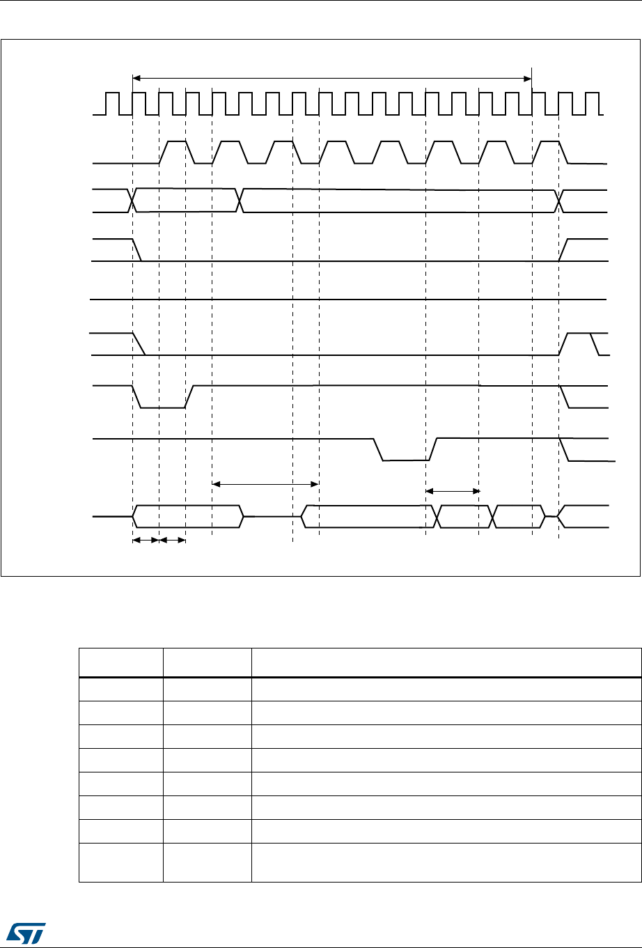
RM0430 Rev 8 295/1324
RM0430 Flexible static memory controller (FSMC)
306
Figure 50. Synchronous multiplexed write mode waveforms - PSRAM (CRAM)
1. The memory must issue NWAIT signal one cycle in advance, accordingly WAITCFG must be programmed to 0.
2. Byte Lane (NBL) outputs are not shown, they are held low while NEx is active.
!DDR;= DATA
ADDR;=
-EMORYTRANSACTIONBURSTOFHALFWORDS
(#,+
#,+
!;=
.%X
./%
.7%
(I:
.!$6
.7!)4
7!)4#&'
!$;=
CLOCK CLOCK
$!4,!4 INSERTEDWAITSTATE
AIF
#,+CYCLES
DATA
Table 68. FSMC_BCRx bit fields
Bit number Bit name Value to set
31:22 Reserved 0x000
21 WFDIS As needed
20 CCLKEN As needed
19 CBURSTRW 0x1
18:16 CPSIZE As needed (0x1 for CRAM 1.5)
15 ASYNCWAIT 0x0
14 EXTMOD 0x0
13 WAITEN To be set to 1 if the memory supports this feature, to be kept at 0
otherwise.

Flexible static memory controller (FSMC) RM0430
296/1324 RM0430 Rev 8
12 WREN 0x1
11 WAITCFG 0x0
10 Reserved 0x0
9 WAITPOL to be set according to memory
8 BURSTEN no effect on synchronous write
7 Reserved 0x1
6 FACCEN Set according to memory support
5-4 MWID As needed
3-2 MTYP 0x1
1 MUXEN As needed
0 MBKEN 0x1
Table 69. FSMC_BTRx bit fields
Bit number Bit name Value to set
31-30 Reserved 0x0
29:28 ACCMOD 0x0
27-24 DATLAT Data latency
23-20 CLKDIV 0x0 to get CLK = HCLK
0x1 to get CLK = 2 × HCLK
19-16 BUSTURN Time between NEx high to NEx low (BUSTURN HCLK).
15-8 DATAST Don’t care
7-4 ADDHLD Don’t care
3-0 ADDSET Don’t care
Table 68. FSMC_BCRx bit fields (continued)
Bit number Bit name Value to set

RM0430 Rev 8 297/1324
RM0430 Flexible static memory controller (FSMC)
306
11.5.6 NOR/PSRAM controller registers
SRAM/NOR-Flash chip-select control register for bank x (FSMC_BCRx) (x = 1
to 4)
Address offset: 8 * (x – 1), (x = 1 to 4)
Reset value: Bank 1: 0x0000 30DB
Reset value: Bank 2: 0x0000 30D2
Reset value: Bank 3: 0x0000 30D2
Reset value: Bank 4: 0x0000 30D2
This register contains the control information of each memory bank, used for SRAMs,
PSRAM and NOR Flash memories.
31 30 29 28 27 26 25 24 23 22 21 20 19 18 17 16
Res. Res. Res. Res. Res. Res. Res. Res. Res. Res. WFDIS CCLK
EN
CBURST
RW CPSIZE[2:0]
rw rw rw rw rw rw
151413121110987654 3 210
ASYNC
WAIT
EXT
MOD
WAIT
EN WREN WAIT
CFG Res. WAIT
POL
BURST
EN Res. FACC
EN MWID[1:0] MTYP[1:0] MUX
EN
MBK
EN
rw rw rw rw rw rw rw rw rw rw rw rw rw rw
Bits 31:22 Reserved, must be kept at reset value.
Bit 21 WFDIS: Write FIFO Disable
This bit disables the Write FIFO used by the FSMC controller.
0: Write FIFO enabled (Default after reset)
1: Write FIFO disabled
Note: The WFDIS bit of the FSMC_BCR2..4 registers is don’t care. It is only enabled through the
FSMC_BCR1 register.
Bit 20 CCLKEN: Continuous Clock Enable.
This bit enables the FSMC_CLK clock output to external memory devices.
0: The FSMC_CLK is only generated during the synchronous memory access (read/write
transaction). The FSMC_CLK clock ratio is specified by the programmed CLKDIV value in the
FSMC_BCRx register (default after reset).
1: The FSMC_CLK is generated continuously during asynchronous and synchronous access. The
FSMC_CLK clock is activated when the CCLKEN is set.
Note: The CCLKEN bit of the FSMC_BCR2..4 registers is don’t care. It is only enabled through the
FSMC_BCR1 register. Bank 1 must be configured in Synchronous mode to generate the
FSMC_CLK continuous clock.
Note: If CCLKEN bit is set, the FSMC_CLK clock ratio is specified by CLKDIV value in the
FSMC_BTR1 register. CLKDIV in FSMC_BWTR1 is don’t care.
Note: If the Synchronous mode is used and CCLKEN bit is set, the synchronous memories
connected to other banks than Bank 1 are clocked by the same clock (the CLKDIV value in
the FSMC_BTR2..4 and FSMC_BWTR2..4 registers for other banks has no effect.)

Flexible static memory controller (FSMC) RM0430
298/1324 RM0430 Rev 8
Bit 19 CBURSTRW: Write burst enable.
For PSRAM (CRAM) operating in Burst mode, the bit enables synchronous accesses during write
operations. The enable bit for synchronous read accesses is the BURSTEN bit in the
FSMC_BCRx register.
0: Write operations are always performed in Asynchronous mode
1: Write operations are performed in Synchronous mode.
Bits 18:16 CPSIZE[2:0]: CRAM page size.
These are used for CellularRAM™ 1.5 which does not allow burst access to cross the address
boundaries between pages. When these bits are configured, the FSMC controller splits
automatically the burst access when the memory page size is reached (refer to memory datasheet
for page size).
000: No burst split when crossing page boundary (default after reset)
001: 128 bytes
010: 256 bytes
011: 512 bytes
100: 1024 bytes
Others: reserved
Bit 15 ASYNCWAIT: Wait signal during asynchronous transfers
This bit enables/disables the FSMC to use the wait signal even during an asynchronous protocol.
0: NWAIT signal is not taken in to account when running an asynchronous protocol (default after
reset)
1: NWAIT signal is taken in to account when running an asynchronous protocol
Bit 14 EXTMOD: Extended mode enable.
This bit enables the FSMC to program the write timings for non multiplexed asynchronous
accesses inside the FSMC_BWTR register, thus resulting in different timings for read and write
operations.
0: values inside FSMC_BWTR register are not taken into account (default after reset)
1: values inside FSMC_BWTR register are taken into account
Note: When the Extended mode is disabled, the FSMC can operate in Mode1 or Mode2 as follows:
– Mode 1 is the default mode when the SRAM/PSRAM memory type is selected (MTYP
=0x0 or 0x01)
– Mode 2 is the default mode when the NOR memory type is selected (MTYP = 0x10).
Bit 13 WAITEN: Wait enable bit.
This bit enables/disables wait-state insertion via the NWAIT signal when accessing the memory in
Synchronous mode.
0: NWAIT signal is disabled (its level not taken into account, no wait state inserted after the
programmed Flash latency period)
1: NWAIT signal is enabled (its level is taken into account after the programmed latency period to
insert wait states if asserted) (default after reset)
Bit 12 WREN: Write enable bit.
This bit indicates whether write operations are enabled/disabled in the bank by the FSMC:
0: Write operations are disabled in the bank by the FSMC, an AHB error is reported,
1: Write operations are enabled for the bank by the FSMC (default after reset).
Bit 11 WAITCFG: Wait timing configuration.
The NWAIT signal indicates whether the data from the memory are valid or if a wait state must be
inserted when accessing the memory in Synchronous mode. This configuration bit determines if
NWAIT is asserted by the memory one clock cycle before the wait state or during the wait state:
0: NWAIT signal is active one data cycle before wait state (default after reset),
1: NWAIT signal is active during wait state (not used for PSRAM).

RM0430 Rev 8 299/1324
RM0430 Flexible static memory controller (FSMC)
306
SRAM/NOR-Flash chip-select timing register for bank x (FSMC_BTRx)
Address offset: 0x04 + 8 * (x – 1), (x = 1 to 4)
Reset value: 0x0FFF FFFF
This register contains the control information of each memory bank, used for SRAMs,
PSRAM and NOR Flash memories.If the EXTMOD bit is set in the FSMC_BCRx register,
then this register is partitioned for write and read access, that is, 2 registers are available:
one to configure read accesses (this register) and one to configure write accesses
(FSMC_BWTRx registers).
Bit 10 Reserved, must be kept at reset value.
Bit 9 WAITPOL: Wait signal polarity bit.
Defines the polarity of the wait signal from memory used for either in Synchronous or
Asynchronous mode:
0: NWAIT active low (default after reset),
1: NWAIT active high.
Bit 8 BURSTEN: Burst enable bit.
This bit enables/disables synchronous accesses during read operations. It is valid only for
synchronous memories operating in Burst mode:
0: Burst mode disabled (default after reset). Read accesses are performed in Asynchronous mode.
1: Burst mode enable. Read accesses are performed in Synchronous mode.
Bit 7 Reserved, must be kept at reset value.
Bit 6 FACCEN: Flash access enable
Enables NOR Flash memory access operations.
0: Corresponding NOR Flash memory access is disabled
1: Corresponding NOR Flash memory access is enabled (default after reset)
Bits 5:4 MWID[1:0]: Memory data bus width.
Defines the external memory device width, valid for all type of memories.
00: 8 bits
01: 16 bits (default after reset)
10: reserved
11: reserved
Bits 3:2 MTYP[1:0]: Memory type.
Defines the type of external memory attached to the corresponding memory bank:
00: SRAM (default after reset for Bank 2...4)
01: PSRAM (CRAM)
10: NOR Flash (default after reset for Bank 1)
11: reserved
Bit 1 MUXEN: Address/data multiplexing enable bit.
When this bit is set, the address and data values are multiplexed on the data bus, valid only with
NOR and PSRAM memories:
0: Address/Data non multiplexed
1: Address/Data multiplexed on databus (default after reset)
Bit 0 MBKEN: Memory bank enable bit.
Enables the memory bank. After reset Bank1 is enabled, all others are disabled. Accessing a
disabled bank causes an ERROR on AHB bus.
0: Corresponding memory bank is disabled
1: Corresponding memory bank is enabled

Flexible static memory controller (FSMC) RM0430
300/1324 RM0430 Rev 8
31 30 29 28 27 26 25 24 23 22 21 20 19 18 17 16
Res. Res. ACCMOD[1:0] DATLAT[3:0] CLKDIV[3:0] BUSTURN[3:0]
rw rw rw rw rw rw rw rw rw rw rw rw rw rw
1514131211109876543210
DATAST[7:0] ADDHLD[3:0] ADDSET[3:0]
rw rw rw rw rw rw rw rw rw rw rw rw rw rw rw rw
Bits 31:30 Reserved, must be kept at reset value.
Bits 29:28 ACCMOD[1:0]: Access mode
Specifies the asynchronous access modes as shown in the timing diagrams. These bits are
taken into account only when the EXTMOD bit in the FSMC_BCRx register is 1.
00: Access mode A
01: Access mode B
10: Access mode C
11: Access mode D
Bits 27:24 DATLAT[3:0]: (see note below bit descriptions): Data latency for synchronous memory
For synchronous access with read/write Burst mode enabled (BURSTEN / CBURSTRW bits
set), defines the number of memory clock cycles (+2) to issue to the memory before
reading/writing the first data:
This timing parameter is not expressed in HCLK periods, but in FSMC_CLK periods.
For asynchronous access, this value is don't care.
0000: Data latency of 2 CLK clock cycles for first burst access
1111: Data latency of 17 CLK clock cycles for first burst access (default value after reset)
Bits 23:20 CLKDIV[3:0]: Clock divide ratio (for FSMC_CLK signal)
Defines the period of FSMC_CLK clock output signal, expressed in number of HCLK cycles:
0000: FSMC_CLK period= 1x HCLK period
0001: FSMC_CLK period = 2 × HCLK periods
0010: FSMC_CLK period = 3 × HCLK periods
1111: FSMC_CLK period = 16 × HCLK periods (default value after reset)
In asynchronous NOR Flash, SRAM or PSRAM accesses, this value is don’t care.
Note: Refer to Section 11.5.5: Synchronous transactions for FSMC_CLK divider ratio formula)

RM0430 Rev 8 301/1324
RM0430 Flexible static memory controller (FSMC)
306
Bits 19:16 BUSTURN[3:0]: Bus turnaround phase duration
These bits are written by software to add a delay at the end of a write-to-read (and read-to-
write) transaction. This delay allows to match the minimum time between consecutive
transactions (tEHEL from NEx high to NEx low) and the maximum time needed by the
memory to free the data bus after a read access (tEHQZ). The programmed bus turnaround
delay is inserted between an asynchronous read (muxed or mode D) or write transaction and
any other asynchronous /synchronous read or write to or from a static bank. The bank can be
the same or different in case of read, in case of write the bank can be different except for
muxed or mode D.
In some cases, whatever the programmed BUSTURN values, the bus turnaround delay is
fixed
as follows:
• The bus turnaround delay is not inserted between two consecutive asynchronous write
transfers to the same static memory bank except for muxed and D modes.
• There is a bus turnaround delay of 1 HCLK clock cycle between:
–Two consecutive asynchronous read transfers to the same static memory bank except for
muxed and D modes.
–An asynchronous read to an asynchronous or synchronous write to any static bank or
dynamic bank except for muxed and D modes.
–An asynchronous (modes 1, 2, A, B or C) read and a read from another static bank.
• There is a bus turnaround delay of 2 HCLK clock cycle between:
–Two consecutive synchronous writes (burst or single) to the same bank.
–A synchronous write (burst or single) access and an asynchronous write or read transfer
to or from static memory bank (the bank can be the same or different for the case of
read.
–Two consecutive synchronous reads (burst or single) followed by any
synchronous/asynchronous read or write from/to another static memory bank.
• There is a bus turnaround delay of 3 HCLK clock cycle between:
–Two consecutive synchronous writes (burst or single) to different static bank.
–A synchronous write (burst or single) access and a synchronous read from the same or a
different bank.
0000: BUSTURN phase duration = 0 HCLK clock cycle added
...
1111: BUSTURN phase duration = 15 x HCLK clock cycles added (default value after reset)
Bits 15:8 DATAST[7:0]: Data-phase duration
These bits are written by software to define the duration of the data phase (refer to Figure 33
to Figure 45), used in asynchronous accesses:
0000 0000: Reserved
0000 0001: DATAST phase duration = 1 × HCLK clock cycles
0000 0010: DATAST phase duration = 2 × HCLK clock cycles
...
1111 1111: DATAST phase duration = 255 × HCLK clock cycles (default value after reset)
For each memory type and access mode data-phase duration, refer to the respective figure
(Figure 33 to Figure 45).
Example: Mode1, write access, DATAST=1: Data-phase duration= DATAST+1 = 2 HCLK
clock cycles.
Note: In synchronous accesses, this value is don’t care.

Flexible static memory controller (FSMC) RM0430
302/1324 RM0430 Rev 8
Note: PSRAMs (CRAMs) have a variable latency due to internal refresh. Therefore these
memories issue the NWAIT signal during the whole latency phase to prolong the latency as
needed.
With PSRAMs (CRAMs) the filled DATLAT must be set to 0, so that the FSMC exits its
latency phase soon and starts sampling NWAIT from memory, then starts to read or write
when the memory is ready.
This method can be used also with the latest generation of synchronous Flash memories
that issue the NWAIT signal, unlike older Flash memories (check the datasheet of the
specific Flash memory being used).
SRAM/NOR-Flash write timing registers 1..4 (FSMC_BWTR1..4)
Address offset: 0x104 + 8 * (x – 1), x = 1...4
Reset value: 0x0FFF FFFF
This register contains the control information of each memory bank. It is used for SRAMs,
PSRAMs and NOR Flash memories. When the EXTMOD bit is set in the FSMC_BCRx
register, then this register is active for write access.
Bits 7:4 ADDHLD[3:0]: Address-hold phase duration
These bits are written by software to define the duration of the address hold phase (refer to
Figure 33 to Figure 45), used in mode D or multiplexed accesses:
0000: Reserved
0001: ADDHLD phase duration =1 × HCLK clock cycle
0010: ADDHLD phase duration = 2 × HCLK clock cycle
...
1111: ADDHLD phase duration = 15 × HCLK clock cycles (default value after reset)
For each access mode address-hold phase duration, refer to the respective figure (Figure 33
to Figure 45).
Note: In synchronous accesses, this value is not used, the address hold phase is always 1
memory clock period duration.
Bits 3:0 ADDSET[3:0]: Address setup phase duration
These bits are written by software to define the duration of the address setup phase (refer to
Figure 33 to Figure 45), used in SRAMs, ROMs, asynchronous NOR Flash and PSRAM:
0000: ADDSET phase duration = 0 × HCLK clock cycle
...
1111: ADDSET phase duration = 15 × HCLK clock cycles (default value after reset)
For each access mode address setup phase duration, refer to the respective figure
(Figure 33 to Figure 45).
Note: In synchronous accesses, this value is don’t care.
In Muxed mode or Mode D, the minimum value for ADDSET is 1.
In mode 1 and PSRAM memory, the minimum value for ADDSET is 1.
31 30 29 28 27 26 25 24 23 22 21 20 19 18 17 16
Res. Res. ACCMOD[1:0] Res. Res. Res. Res. Res. Res. Res. Res. BUSTURN[3:0]
rw rw rw rw rw rw
1514131211109876543210
DATAST[7:0] ADDHLD[3:0] ADDSET[3:0]
rw rw rw rw rw rw rw rw rw rw rw rw rw rw rw rw
Bits 31:30 Reserved, must be kept at reset value.

RM0430 Rev 8 303/1324
RM0430 Flexible static memory controller (FSMC)
306
Bits 29:28 ACCMOD[1:0]: Access mode.
Specifies the asynchronous access modes as shown in the next timing diagrams.These bits are
taken into account only when the EXTMOD bit in the FSMC_BCRx register is 1.
00: Access mode A
01: Access mode B
10: Access mode C
11: Access mode D
Bits 27:20 Reserved, must be kept at reset value.
Bits 19:16 BUSTURN[3:0]: Bus turnaround phase duration
The programmed bus turnaround delay is inserted between an asynchronous write transfer and
any other asynchronous /synchronous read or write transfer to or from a static bank. The bank can
be the same or different in case of read, in case of write the bank can be different expect for muxed
or mode D.
In some cases, whatever the programmed BUSTURN values, the bus turnaround delay is fixed as
follows:
• The bus turnaround delay is not inserted between two consecutive asynchronous write transfers
to the same static memory bank except for muxed and D modes.
• There is a bus turnaround delay of 2 HCLK clock cycle between:
–Two consecutive synchronous writes (burst or single) to the same bank.
–A synchronous write (burst or single) transfer and an asynchronous write or read transfer to or
from static memory bank.
• There is a bus turnaround delay of 3 HCLK clock cycle between:
–Two consecutive synchronous writes (burst or single) to different static bank.
–A synchronous write (burst or single) transfer and a synchronous read from the same or a
different bank.
0000: BUSTURN phase duration = 0 HCLK clock cycle added
...
1111: BUSTURN phase duration = 15 HCLK clock cycles added (default value after reset)
Bits 15:8 DATAST[7:0]: Data-phase duration.
These bits are written by software to define the duration of the data phase (refer to Figure 33 to
Figure 45), used in asynchronous SRAM, PSRAM and NOR Flash memory accesses:
0000 0000: Reserved
0000 0001: DATAST phase duration = 1 × HCLK clock cycles
0000 0010: DATAST phase duration = 2 × HCLK clock cycles
...
1111 1111: DATAST phase duration = 255 × HCLK clock cycles (default value after reset)
Bits 7:4 ADDHLD[3:0]: Address-hold phase duration.
These bits are written by software to define the duration of the address hold phase (refer to
Figure 42 to Figure 45), used in asynchronous multiplexed accesses:
0000: Reserved
0001: ADDHLD phase duration = 1 × HCLK clock cycle
0010: ADDHLD phase duration = 2 × HCLK clock cycle
...
1111: ADDHLD phase duration = 15 × HCLK clock cycles (default value after reset)
Note: In synchronous NOR Flash accesses, this value is not used, the address hold phase is always
1 Flash clock period duration.

Flexible static memory controller (FSMC) RM0430
304/1324 RM0430 Rev 8
Bits 3:0 ADDSET[3:0]: Address setup phase duration.
These bits are written by software to define the duration of the address setup phase in HCLK
cycles (refer to Figure 33 to Figure 45), used in asynchronous accesses:
0000: ADDSET phase duration = 0 × HCLK clock cycle
...
1111: ADDSET phase duration = 15 × HCLK clock cycles (default value after reset)
Note: In synchronous accesses, this value is not used, the address setup phase is always 1 Flash
clock period duration. In muxed mode, the minimum ADDSET value is 1.

RM0430 Rev 8 305/1324
RM0430 Flexible static memory controller (FSMC)
306
11.6 FSMC register map
Table 70. FSMC register map
Offset Register
31
30
29
28
27
26
25
24
23
22
21
20
19
18
17
16
15
14
13
12
11
10
9
8
7
6
5
4
3
2
1
0
0x00 FSMC_BCR1
Res.
Res.
Res.
Res.
Res.
Res.
Res.
Res.
Res.
Res.
WFDIS
CCLKEN
CBURSTRW
CPSIZE
[2:0]
ASYNCWAIT
EXTMOD
WAITEN
WREN
WAITCFG
Res.
WAITPOL
BURSTEN
Res.
FACCEN
MWID
[1:0]
MTYP
[1:0]
MUXEN
MBKEN
Reset value 00000000110 00 1011011
0x08 FSMC_BCR2
Res.
Res.
Res.
Res.
Res.
Res.
Res.
Res.
Res.
Res.
Res.
Res.
CBURSTRW
CPSIZE
[2:0]
ASYNCWAIT
EXTMOD
WAITEN
WREN
WAITCFG
Res.
WAITPOL
BURSTEN
Res.
FACCEN
MWID
[1:0]
MTYP
[1:0]
MUXEN
MBKEN
Reset value 000000110 00 1010010
0x10 FSMC_BCR3
Res.
Res.
Res.
Res.
Res.
Res.
Res.
Res.
Res.
Res.
Res.
Res.
CBURSTRW
CPSIZE
[2:0]
ASYNCWAIT
EXTMOD
WAITEN
WREN
WAITCFG
Res.
WAITPOL
BURSTEN
Res.
FACCEN
MWID
[1:0]
MTYP
[1:0]
MUXEN
MBKEN
Reset value 000000110 00 1010010
0x18 FSMC_BCR4
Res.
Res.
Res.
Res.
Res.
Res.
Res.
Res.
Res.
Res.
Res.
Res.
CBURSTRW
CPSIZE
[2:0]
ASYNCWAIT
EXTMOD
WAITEN
WREN
WAITCFG
Res.
WAITPOL
BURSTEN
Res.
FACCEN
MWID
[1:0]
MTYP
[1:0]
MUXEN
MBKEN
Reset value 000000110 00 1010010
0x04 FSMC_BTR1
Res.
Res.
ACCMOD[1:0]
DATLAT[3:0] CLKDIV[3:0] BUSTURN[3:0] DATAST[7:0] ADDHLD[3:0] ADDSET[3:0]
Reset value 001111111 111111111111111111111
0x0C FSMC_BTR2
Res.
Res.
ACCMOD[1:0]
DATLAT[3:0] CLKDIV[3:0] BUSTURN[3:0] DATAST[7:0] ADDHLD[3:0] ADDSET[3:0]
Reset value 001111111 111111111111111111111
0x14 FSMC_BTR3
Res.
Res.
ACCMOD[1:0]
DATLAT[3:0] CLKDIV[3:0] BUSTURN[3:0] DATAST[7:0] ADDHLD[3:0] ADDSET[3:0]
Reset value 001111111 111111111111111111111
0x1C FSMC_BTR4
Res.
Res.
ACCMOD[1:0]
DATLAT[3:0] CLKDIV[3:0] BUSTURN[3:0] DATAST[7:0] ADDHLD[3:0] ADDSET[3:0]
Reset value 001111111 111111111111111111111
0x104 FSMC_BWTR1
Res.
Res.
ACCMOD[1:0]
Res.
Res.
Res.
Res.
Res.
Res.
Res.
Res.
BUSTURN[3:0] DATAST[7:0] ADDHLD[3:0] ADDSET[3:0]
Reset value 00 11111111111111111111
0x10C FSMC_BWTR2
Res.
Res.
ACCMOD[1:0]
Res.
Res.
Res.
Res.
Res.
Res.
Res.
Res.
BUSTURN[3:0] DATAST[7:0] ADDHLD[3:0] ADDSET[3:0]
Reset value 00 11111111111111111111

Flexible static memory controller (FSMC) RM0430
306/1324 RM0430 Rev 8
Refer to Section 2.2.2 on page 58 for the register boundary addresses.
0x114 FSMC_BWTR3
Res.
Res.
ACCMOD[1:0]
Res.
Res.
Res.
Res.
Res.
Res.
Res.
Res.
BUSTURN[3:0] DATAST[7:0] ADDHLD[3:0] ADDSET[3:0]
Reset value 00 11111111111111111111
0x11C FSMC_BWTR4
Res.
Res.
ACCMOD[1:0]
Res.
Res.
Res.
Res.
Res.
Res.
Res.
Res.
BUSTURN[3:0] DATAST[7:0] ADDHLD[3:0] ADDSET[3:0]
Reset value 00 11111111111111111111
Table 70. FSMC register map (continued)
Offset Register
31
30
29
28
27
26
25
24
23
22
21
20
19
18
17
16
15
14
13
12
11
10
9
8
7
6
5
4
3
2
1
0
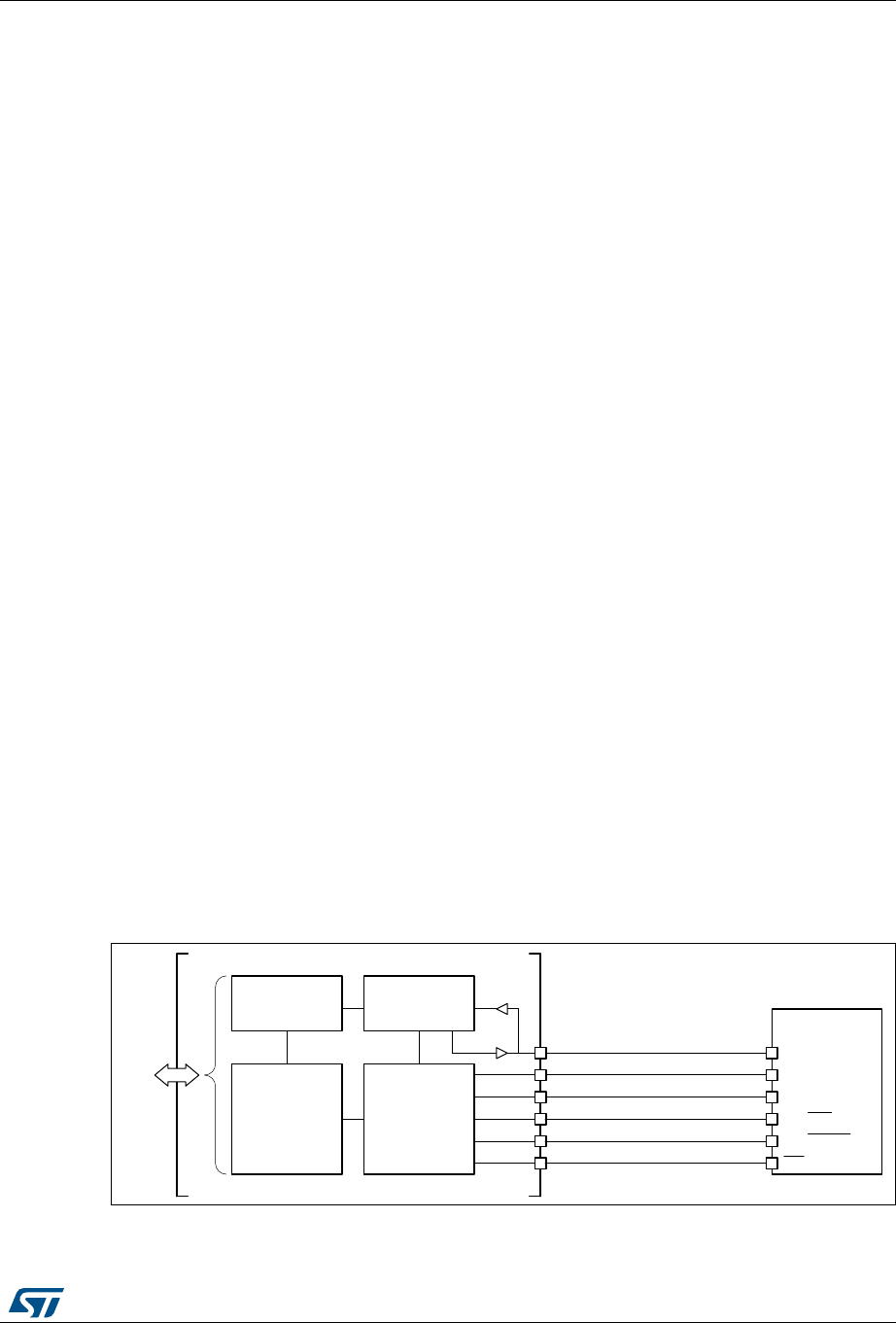
RM0430 Rev 8 307/1324
RM0430 Quad-SPI interface (QUADSPI)
335
12 Quad-SPI interface (QUADSPI)
12.1 Introduction
The QUADSPI is a specialized communication interface targeting single, dual or quad SPI
Flash memories. It can operate in any of the three following modes:
•indirect mode: all the operations are performed using the QUADSPI registers
•status polling mode: the external Flash memory status register is periodically read and
an interrupt can be generated in case of flag setting
•memory-mapped mode: the external Flash memory is mapped to the microcontroller
address space and is seen by the system as if it was an internal memory
Both throughput and capacity can be increased two-fold using dual-flash mode, where two
Quad-SPI Flash memories are accessed simultaneously.
12.2 QUADSPI main features
•Three functional modes: indirect, status-polling, and memory-mapped
•Dual-flash mode, where 8 bits can be sent/received simultaneously by accessing two
Flash memories in parallel.
•SDR and DDR support
•Fully programmable opcode for both indirect and memory mapped mode
•Fully programmable frame format for both indirect and memory mapped mode
•Integrated FIFO for reception and transmission
•8, 16, and 32-bit data accesses are allowed
•DMA channel for indirect mode operations
•Interrupt generation on FIFO threshold, timeout, operation complete, and access error
12.3 QUADSPI functional description
12.3.1 QUADSPI block diagram
Figure 51. QUADSPI block diagram when dual-flash mode is disabled
63,)/$6+
069
&/.
%.B,262
%.B,26,
%.B,2
%.B,2
&/.
46,
462
4:3
4+2/'
%.BQ&6 &6
$+%
5HJLVWHUV
FRQWURO
&ORFN
PDQDJHPHQW
),)2 6KLIWUHJLVWHU
48$'63,
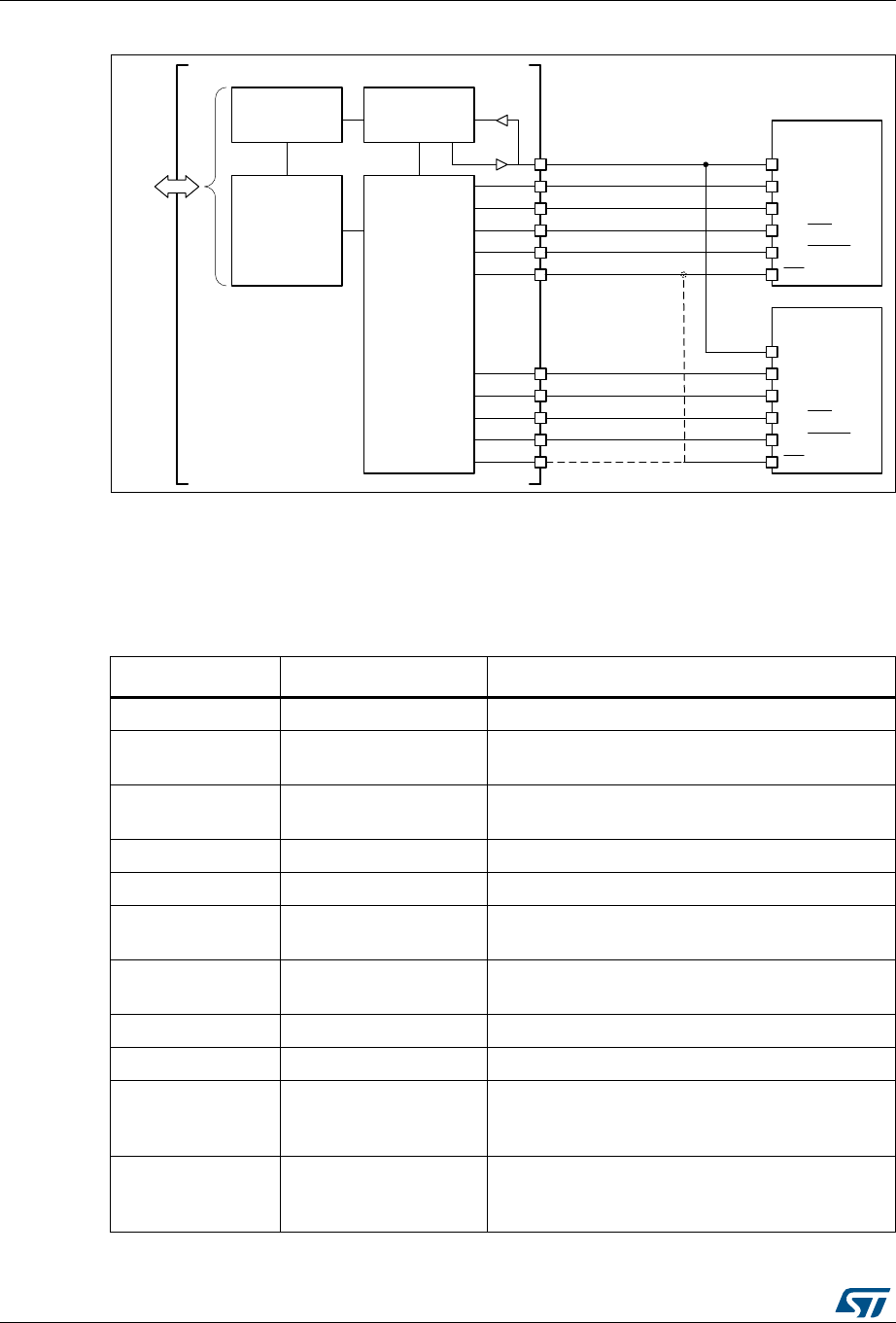
Quad-SPI interface (QUADSPI) RM0430
308/1324 RM0430 Rev 8
Figure 52. QUADSPI block diagram when dual-flash mode is enabled
12.3.2 QUADSPI pins
Table 71 lists the QUADSPI pins, six for interfacing with a single Flash memory, or 10 to 11
for interfacing with two Flash memories (FLASH 1 and FLASH 2) in dual-flash mode.
069
63,)/$6+
&/.
%.B,262
%.B,26,
%.B,2
%.B,2
&/.
46,
462
4:3
4+2/'
%.BQ&6 &6
$+%
5HJLVWHUV
FRQWURO
&ORFN
PDQDJHPHQW
),)2
6KLIWUHJLVWHU
48$'63,
%.B,262
%.B,26,
%.B,2
%.B,2
%.BQ&6
63,)/$6+
&/.
46,
462
4:3
4+2/'
&6
Table 71. QUADSPI pins
Signal name Signal type Description
CLK Digital output Clock to FLASH 1 and FLASH 2
BK1_IO0/SO Digital input/output Bidirectional IO in dual/quad modes or serial output
in single mode, for FLASH 1
BK1_IO1/SI Digital input/output Bidirectional IO in dual/quad modes or serial input
in single mode, for FLASH 1
BK1_IO2 Digital input/output Bidirectional IO in quad mode, for FLASH 1
BK1_IO3 Digital input/output Bidirectional IO in quad mode, for FLASH 1
BK2_IO0/SO Digital input/output Bidirectional IO in dual/quad modes or serial output
in single mode, for FLASH 2
BK2_IO1/SI Digital input/output Bidirectional IO in dual/quad modes or serial input
in single mode, for FLASH 2
BK2_IO2 Digital input/output Bidirectional IO in quad mode, for FLASH 2
BK2_IO3 Digital input/output Bidirectional IO in quad mode, for FLASH 2
BK1_nCS Digital output
Chip select (active low) for FLASH 1. Can also be
used for FLASH 2 if QUADSPI is always used in
dual-flash mode.
BK2_nCS Digital output
Chip select (active low) for FLASH 2. Can also be
used for FLASH 1 if QUADSPI is always used in
dual-flash mode.
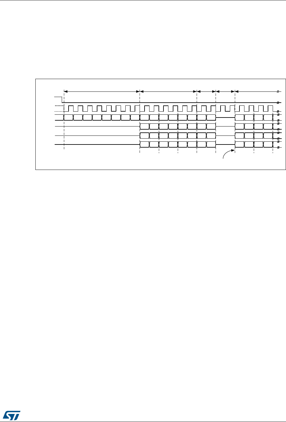
RM0430 Rev 8 309/1324
RM0430 Quad-SPI interface (QUADSPI)
335
12.3.3 QUADSPI command sequence
The QUADSPI communicates with the Flash memory using commands. Each command
can include 5 phases: instruction, address, alternate byte, dummy, data. Any of these
phases can be configured to be skipped, but at least one of the instruction, address,
alternate byte, or data phase must be present.
nCS falls before the start of each command and rises again after each command finishes.
Figure 53. An example of a read command in quad mode
Instruction phase
During this phase, an 8-bit instruction, configured in INSTRUCTION field of
QUADSPI_CCR[7:0] register, is sent to the Flash memory, specifying the type of operation
to be performed.
Though most Flash memories can receive instructions only one bit at a time from the
IO0/SO signal (single SPI mode), the instruction phase can optionally send 2 bits at a time
(over IO0/IO1 in dual SPI mode) or 4 bits at a time (over IO0/IO1/IO2/IO3 in quad SPI
mode). This can be configured using the IMODE[1:0] field of QUADSPI_CCR[9:8] register.
When IMODE = 00, the instruction phase is skipped, and the command sequence starts
with the address phase, if present.
Address phase
In the address phase, 1-4 bytes are sent to the Flash memory to indicate the address of the
operation. The number of address bytes to be sent is configured in the ADSIZE[1:0] field of
QUADSPI_CCR[13:12] register. In indirect and automatic-polling modes, the address bytes
to be sent are specified in the ADDRESS[31:0] field of QUADSPI_AR register, while in
memory-mapped mode the address is given directly via the AHB (from the Cortex® or from
a DMA).
The address phase can send 1 bit at a time (over SO in single SPI mode), 2 bits at a time
(over IO0/IO1 in dual SPI mode), or 4 bits at a time (over IO0/IO1/IO2/IO3 in quad SPI
mode). This can be configured using the ADMODE[1:0] field of QUADSPI_CCR[11:10]
register.
When ADMODE = 00, the address phase is skipped, and the command sequence proceeds
directly to the next phase, if any.
069
Q&6
6&/.
,2
,2
,2
,2
$ $ $ 0 %\WH %\WH
,QVWUXFWLRQ $GGUHVV $OW 'XPP\ 'DWD
,2VZLWFKIURP
RXWSXWWRLQSXW

Quad-SPI interface (QUADSPI) RM0430
310/1324 RM0430 Rev 8
Alternate-bytes phase
In the alternate-bytes phase, 1-4 bytes are sent to the Flash memory, generally to control
the mode of operation. The number of alternate bytes to be sent is configured in the
ABSIZE[1:0] field of QUADSPI_CCR[17:16] register. The bytes to be sent are specified in
the QUADSPI_ABR register.
The alternate-bytes phase can send 1 bit at a time (over SO in single SPI mode), 2 bits at a
time (over IO0/IO1 in dual SPI mode), or 4 bits at a time (over IO0/IO1/IO2/IO3 in quad SPI
mode). This can be configured using the ABMODE[1:0] field of QUADSPI_CCR[15:14]
register.
When ABMODE = 00, the alternate-bytes phase is skipped, and the command sequence
proceeds directly to the next phase, if any.
There may be times when only a single nibble needs to be sent during the alternate-byte
phase rather than a full byte, such as when dual-mode is used and only two cycles are used
for the alternate bytes. In this case, firmware can use quad-mode (ABMODE = 11) and send
a byte with bits 7 and 3 of ALTERNATE set to ‘1’ (keeping the IO3 line high), and bits 6 and
2 set to ‘0’ (keeping the IO2 line low). In this case the upper two bits of the nibble to be sent
are placed in bits 4:3 of ALTERNATE while the lower two bits are placed in bits 1 and 0. For
example, if the nibble 2 (0010) is to be sent over IO0/IO1, then ALTERNATE should be set
to 0x8A (1000_1010).
Dummy-cycles phase
In the dummy-cycles phase, 1-31 cycles are given without any data being sent or received,
in order to allow the Flash memory the time to prepare for the data phase when higher clock
frequencies are used. The number of cycles given during this phase is specified in the
DCYC[4:0] field of QUADSPI_CCR[22:18] register. In both SDR and DDR modes, the
duration is specified as a number of full CLK cycles.
When DCYC is zero, the dummy-cycles phase is skipped, and the command sequence
proceeds directly to the data phase, if present.
The operating mode of the dummy-cycles phase is determined by DMODE.
In order to assure enough “turn-around” time for changing the data signals from output
mode to input mode, there must be at least one dummy cycle when using dual or quad
mode to receive data from the Flash memory.
Data phase
During the data phase, any number of bytes can be sent to, or received from the Flash
memory.
In indirect and automatic-polling modes, the number of bytes to be sent/received is specified
in the QUADSPI_DLR register.
In indirect write mode the data to be sent to the Flash memory must be written to the
QUADSPI_DR register, while in indirect read mode the data received from the Flash
memory is obtained by reading from the QUADSPI_DR register.
In memory-mapped mode, the data which is read is sent back directly over the AHB to the
Cortex or to a DMA.
The data phase can send/receive 1 bit at a time (over SO/SI in single SPI mode), 2 bits at a
time (over IO0/IO1 in dual SPI mode), or 4 bits at a time (over IO0/IO1/IO2/IO3 in quad SPI

RM0430 Rev 8 311/1324
RM0430 Quad-SPI interface (QUADSPI)
335
mode). This can be configured using the ABMODE[1:0] field of QUADSPI_CCR[15:14]
register.
When DMODE = 00, the data phase is skipped, and the command sequence finishes
immediately by raising nCS. This configuration must only be used in only indirect write
mode.
12.3.4 QUADSPI signal interface protocol modes
Single SPI mode
Legacy SPI mode allows just a single bit to be sent/received serially. In this mode, data is
sent to the Flash memory over the SO signal (whose I/O shared with IO0). Data received
from the Flash memory arrives via SI (whose I/O shared with IO1).
The different phases can each be configured separately to use this single bit mode by
setting the IMODE/ADMODE/ABMODE/DMODE fields (in QUADSPI_CCR) to 01.
In each phase which is configured in single mode:
•IO0 (SO) is in output mode
•IO1 (SI) is in input mode (high impedance)
•IO2 is in output mode and forced to ‘0’ (to deactivate the “write protect” function)
•IO3 is in output mode and forced to ‘1’ (to deactivate the “hold” function)
This is the case even for the dummy phase if DMODE = 01.
Dual SPI mode
In dual SPI mode, two bits are sent/received simultaneously over the IO0/IO1 signals.
The different phases can each be configured separately to use dual SPI mode by setting the
IMODE/ADMODE/ABMODE/DMODE fields of QUADSPI_CCR register to 10.
In each phase which is configured in dual mode:
•IO0/IO1 are at high-impedance (input) during the data phase for read operations, and
outputs in all other cases
•IO2 is in output mode and forced to ‘0’
•IO3 is in output mode and forced to ‘1’
In the dummy phase when DMODE = 01, IO0/IO1 are always high-impedance.
Quad SPI mode
In quad SPI mode, four bits are sent/received simultaneously over the IO0/IO1/IO2/IO3
signals.
The different phases can each be configured separately to use quad SPI mode by setting
the IMODE/ADMODE/ABMODE/DMODE fields of QUADSPI_CCR register to 11.
In each phase which is configured in quad mode, IO0/IO1/IO2/IO3 are all are at high-
impedance (input) during the data phase for read operations, and outputs in all other cases.
In the dummy phase when DMODE = 11, IO0/IO1/IO2/IO3 are all high-impedance.
IO2 and IO3 are used only in Quad SPI mode. If none of the phases are configured to use
Quad SPI mode, then the pins corresponding to IO2 and IO3 can be used for other functions
even while QUADSPI is active.
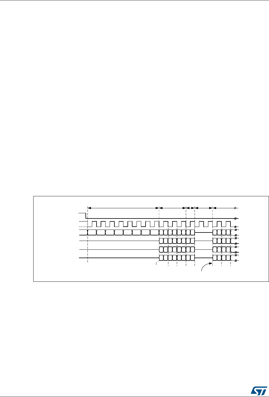
Quad-SPI interface (QUADSPI) RM0430
312/1324 RM0430 Rev 8
SDR mode
By default, the DDRM bit (QUADSPI_CCR[31]) is 0 and the QUADSPI operates in single
data rate (SDR) mode.
In SDR mode, when the QUADSPI is driving the IO0/SO, IO1, IO2, IO3 signals, these
signals transition only with the falling edge of CLK.
When receiving data in SDR mode, the QUADSPI assumes that the Flash memories also
send the data using CLK’s falling edge. By default (when SSHIFT = 0), the signals are
sampled using the following (rising) edge of CLK.
DDR mode
When the DDRM bit (QUADSPI_CCR[31]) is set to 1, the QUADSPI operates in double data
rate (DDR) mode.
In DDR mode, when the QUADSPI is driving the IO0/SO, IO1, IO2, IO3 signals in the
address/alternate-byte/data phases, a bit is sent on each of the falling and rising edges of
CLK.
The instruction phase is not affected by DDRM. The instruction is always sent using CLK’s
falling edge.
When receiving data in DDR mode, the QUADSPI assumes that the Flash memories also
send the data using both rising and falling CLK edges. When DDRM = 1, firmware must
clear SSHIFT bit (bit 4 of QUADSPI_CR). Thus, the signals are sampled one half of a CLK
cycle later (on the following, opposite edge).
Figure 54. An example of a DDR command in quad mode
Dual-flash mode
When the DFM bit (bit 6 of QUADSPI_CR) is 1, the QUADSPI is in dual-flash mode, where
two external quad SPI Flash memories (FLASH 1 and FLASH 2) are used in order to
send/receive 8 bits (or 16 bits in DDR mode) every cycle, effectively doubling the throughput
as well as the capacity.
Each of the Flash memories use the same CLK and optionally the same nCS signals, but
each have separate IO0, IO1, IO2, and IO3 signals.
Dual-flash mode can be used in conjunction with single-bit, dual-bit, and quad-bit modes, as
well as with either SDR or DDR mode.
069
Q&6
6&/.
,2
,2
,2
,2
$$ 0 %\WH
,QVWUXFWLRQ $GGUHVV $OW 'XPP\ 'DWD
,2VZLWFKIURP
RXWSXWWRLQSXW
$
%\WH

RM0430 Rev 8 313/1324
RM0430 Quad-SPI interface (QUADSPI)
335
The Flash memory size, as specified in FSIZE[4:0] (QUADSPI_DCR[20:16]), should reflect
the total Flash memory capacity, which is double the size of one individual component.
If address X is even, then the byte which the QUADSPI gives for address X is the byte at the
address X/2 of FLASH 1, and the byte which the QUADSPI gives for address X+1 is the
byte at the address X/2 of FLASH 2. In other words, bytes at even addresses are all stored
in FLASH 1 and bytes at odd addresses are all stored in FLASH 2.
When reading the Flash memories status registers in dual-flash mode, twice as many bytes
should be read compared to doing the same read in single-flash mode. This means that if
each Flash memory gives 8 valid bits after the instruction for fetching the status register,
then the QUADSPI must be configured with a data length of 2 bytes (16 bits), and the
QUADSPI will receive one byte from each Flash memory. If each Flash memory gives a
status of 16 bits, then the QUADSPI must be configured to read 4 bytes to get all the status
bits of both Flash memories in dual-flash mode. The least-significant byte of the result (in
the data register) is the least-significant byte of FLASH 1 status register, while the next byte
is the least-significant byte of FLASH 2 status register. Then, the third byte of the data
register is FLASH 1 second byte, while the forth byte is FLASH 2 second byte (in the case
that the Flash memories have 16-bit status registers).
An even number of bytes must always be accessed in dual-flash mode. For this reason, bit
0 of the data length field (QUADSPI_DLR[0]) is stuck at 1 when DRM = 1.
In dual-flash mode, the behavior of FLASH 1 interface signals are basically the same as in
normal mode. FLASH 2 interface signals have exactly the same waveforms as FLASH 1
during the instruction, address, alternate-byte, and dummy-cycles phases. In other words,
each Flash memory always receives the same instruction and the same address. Then,
during the data phase, the BK1_IOx and BK2_IOx buses are both transferring data in
parallel, but the data that are sent to (or received from) FLASH 1 are distinct from those of
FLASH 2.
12.3.5 QUADSPI indirect mode
When in indirect mode, commands are started by writing to QUADSPI registers and data is
transferred by writing or reading the data register, in the same way as for other
communication peripherals.
When FMODE = 00 (QUADSPI_CCR[27:26]), the QUADSPI is in indirect write mode,
where bytes are sent to the Flash memory during the data phase. Data are provided by
writing to the data register (QUADSPI_DR).
When FMODE = 01, the QUADSPI is in indirect read mode, where bytes are received from
the Flash memory during the data phase. Data are recovered by reading QUADSPI_DR.
The number of bytes to be read/written is specified in the data length register
(QUADSPI_DLR). If QUADSPI_DLR = 0xFFFF_FFFF (all 1’s), then the data length is
considered undefined and the QUADSPI simply continues to transfer data until the end of
Flash memory (as defined by FSIZE) is reached. If no bytes are to be transferred, DMODE
(QUADSPI_CCR[25:24]) should be set to 00.
If QUADSPI_DLR = 0xFFFF_FFFF and FSIZE = 0x1F (max value indicating a 4GB Flash
memory), then in this special case the transfers continue indefinitely, stopping only after an
abort request or after the QUADSPI is disabled. After the last memory address is read (at
address 0xFFFF_FFFF), reading continues with address = 0x0000_0000.
When the programmed number of bytes to be transmitted or received is reached, TCF is set
and an interrupt is generated if TCIE = 1. In the case of undefined number of data, the TCF

Quad-SPI interface (QUADSPI) RM0430
314/1324 RM0430 Rev 8
is set when the limit of the external SPI memory is reached according to the Flash memory
size defined in the QUADSPI_CR.
Triggering the start of a command
Essentially, a command starts as soon as firmware gives the last information that is
necessary for this command. Depending on the QUADSPI configuration, there are three
different ways to trigger the start of a command in indirect mode. The commands starts
immediately after:
1. a write is performed to INSTRUCTION[7:0] (QUADSPI_CCR), if no address is
necessary (when ADMODE = 00) and if no data needs to be provided by the firmware
(when FMODE = 01 or DMODE = 00)
2. a write is performed to ADDRESS[31:0] (QUADSPI_AR), if an address is necessary
(when ADMODE != 00) and if no data needs to be provided by the firmware (when
FMODE = 01 or DMODE = 00)
3. a write is performed to DATA[31:0] (QUADSPI_DR), if an address is necessary (when
ADMODE != 00) and if data needs to be provided by the firmware (when FMODE = 00
and DMODE != 00)
Writes to the alternate byte register (QUADSPI_ABR) never trigger the communication start.
If alternate bytes are required, they must be programmed before.
As soon as a command is started, the BUSY bit (bit 5 of QUADSPI_SR) is automatically set.
FIFO and data management
In indirect mode, data go through a 32-byte FIFO which is internal to the QUADSPI.
FLEVEL[5:0] (QUADSPI_SR[13:8]) indicates how many bytes are currently being held in
the FIFO.
In indirect write mode (FMODE = 00), firmware adds data to the FIFO when it writes
QUADSPI_DR. Word writes add 4 bytes to the FIFO, halfword writes add 2 bytes, and byte
writes add only 1 byte. If firmware adds too many bytes to the FIFO (more than is indicated
by DL[31:0]), the extra bytes are flushed from the FIFO at the end of the write operation
(when TCF is set).
Byte/halfword accesses to QUADSPI_DR must be done only to the least significant
byte/halfword of the 32-bit register.
FTHRES[3:0] is used to define a FIFO threshold. When the threshold is reached, the FTF
(FIFO threshold flag) is set. In indirect read mode, FTF is set when the number of valid
bytes to be read from the FIFO is above the threshold. FTF is also set if there are data in the
FIFO after the last byte is read from the Flash memory, regardless of the FTHRES setting.
In indirect write mode, FTF is set when the number of empty bytes in the FIFO is above the
threshold.
If FTIE = 1, there is an interrupt when FTF is set. If DMAEN = 1, a DMA transfer is initiated
when FTF is set. FTF is cleared by HW as soon as the threshold condition is no longer true
(after enough data has been transferred by the CPU or DMA).
In indirect read mode when the FIFO becomes full, the QUADSPI temporarily stops reading
bytes from the Flash memory to avoid an overrun. Note that the reading of the Flash
memory does not restart until 4 bytes become vacant in the FIFO (when FLEVEL ≤11).
Thus, when FTHRES ≥13, the application must take care to read enough bytes to assure
that the QUADSPI starts retrieving data from the Flash memory again. Otherwise, the FTF
flag stays at '0' as long as 11 < FLEVEL < FTHRES.

RM0430 Rev 8 315/1324
RM0430 Quad-SPI interface (QUADSPI)
335
12.3.6 QUADSPI status flag polling mode
In automatic-polling mode, the QUADSPI periodically starts a command to read a defined
number of status bytes (up to 4). The received bytes can be masked to isolate some status
bits and an interrupt can be generated when the selected bits have a defined value.
The accesses to the Flash memory begin in the same way as in indirect read mode: if no
address is required (AMODE = 00), accesses begin as soon as the QUADSPI_CCR is
written. Otherwise, if an address is required, the first access begins when QUADSPI_AR is
written. BUSY goes high at this point and stays high even between the periodic accesses.
The contents of MASK[31:0] (QUADSPI_PSMAR) are used to mask the data from the Flash
memory in automatic-polling mode. If the MASK[n] = 0, then bit n of the result is masked
and not considered. If MASK[n] = 1, and the content of bit[n] is the same as MATCH[n]
(QUADSPI_PSMAR), then there is a match for bit n.
If the polling match mode bit (PMM, bit 23 of QUADSPI_CR) is 0, then “AND” match mode is
activated. This means status match flag (SMF) is set only when there is a match on all of the
unmasked bits.
If PMM = 1, then “OR” match mode is activated. This means SMF is set if there is a match
on any of the unmasked bits.
An interrupt is called when SMF is set if SMIE = 1.
If the automatic-polling-mode-stop (APMS) bit is set, operation stops and BUSY goes to 0
as soon as a match is detected. Otherwise, BUSY stays at ‘1’ and the periodic accesses
continue until there is an abort or the QUADSPI is disabled (EN = 0).
The data register (QUADSPI_DR) contains the latest received status bytes (the FIFO is
deactivated). The content of the data register is not affected by the masking used in the
matching logic. The FTF status bit is set as soon as a new reading of the status is complete,
and FTF is cleared as soon as the data is read.
12.3.7 QUADSPI memory-mapped mode
When configured in memory-mapped mode, the external SPI device is seen as an internal
memory.
It is forbidden to access QUADSPI Flash bank area before having properly configured and
enabled the QUADSPI peripheral.
No more than 256MB can addressed even if the Flash memory capacity is larger.
If an access is made to an address outside of the range defined by FSIZE but still within the
256MB range, then a bus error is given. The effect of this error depends on the bus master
that attempted the access:
•If it is the Cortex® CPU, bus fault exception is generated when enabled (or a hard fault
exception when bus fault is disabled)
•If it is a DMA, a DMA transfer error is generated and the corresponding DMA channel is
automatically disabled.
Byte, halfword, and word access types are all supported.
Support for execute in place (XIP) operation is implemented, where the QUADSPI
anticipates the next microcontroller access and load in advance the byte at the following
address. If the subsequent access is indeed made at a continuous address, the access will
be completed faster since the value is already prefetched.

Quad-SPI interface (QUADSPI) RM0430
316/1324 RM0430 Rev 8
By default, the QUADSPI never stops its prefetch operation, keeping the previous read
operation active with nCS maintained low, even if no access to the Flash memory occurs for
a long time. Since Flash memories tend to consume more when nCS is held low, the
application might want to activate the timeout counter (TCEN = 1, bit 3 of QUADSPI_CR) so
that nCS is released after a period of TIMEOUT[15:0] (QUADSPI_LPTR) cycles have
elapsed without any access since when the FIFO becomes full with prefetch data.
BUSY goes high as soon as the first memory-mapped access occurs. Because of the
prefetch operations, BUSY does not fall until there is a timeout, there is an abort, or the
peripheral is disabled.
12.3.8 QUADSPI Flash memory configuration
The device configuration register (QUADSPI_DCR) can be used to specify the
characteristics of the external SPI Flash memory.
The FSIZE[4:0] field defines the size of external memory using the following formula:
Number of bytes in Flash memory = 2[FSIZE+1]
FSIZE+1 is effectively the number of address bits required to address the Flash memory.
The Flash memory capacity can be up to 4GB (addressed using 32 bits) in indirect mode,
but the addressable space in memory-mapped mode is limited to 256MB.
If DFM = 1, FSIZE indicates the total capacity of the two Flash memories together.
When the QUADSPI executes two commands, one immediately after the other, it raises the
chip select signal (nCS) high between the two commands for only one CLK cycle by default.
If the Flash memory requires more time between commands, the chip select high time
(CSHT) field can be used to specify the minimum number of CLK cycles (up to 8) that nCS
must remain high.
The clock mode (CKMODE) bit indicates the CLK signal logic level in between commands
(when nCS = 1).
12.3.9 QUADSPI delayed data sampling
By default, the QUADSPI samples the data driven by the Flash memory one half of a CLK
cycle after the Flash memory drives the signal.
In case of external signal delays, it may be beneficial to sample the data later. Using the
SSHIFT bit (bit 4 of QUADSPI_CR), the sampling of the data can be shifted by half of a CLK
cycle.
Clock shifting is not supported in DDR mode: the SSHIFT bit must be clear when DDRM bit
is set.
12.3.10 QUADSPI configuration
The QUADSPI configuration is done in two phases:
•QUADSPI IP configuration
•QUADSPI Flash memory configuration
Once configured and enabled, the QUADSPI can be used in one of its three operating
modes: indirect mode, status-polling mode, or memory-mapped mode.
QUADSPI IP configuration

RM0430 Rev 8 317/1324
RM0430 Quad-SPI interface (QUADSPI)
335
The QUADSPI IP is configured using the QUADSPI_CR. The user shall configure the clock
prescaler division factor and the sample shifting settings for the incoming data.
DDR mode can be set through the DDRM bit. Once enabled, the address and the alternate
bytes are sent on both clock edges and the data are sent/received on both clock edges.
Regardless of the DDRM bit setting, instructions are always sent in SDR mode.
The DMA requests are enabled setting the DMAEN bit. In case of interrupt usage, their
respective enable bit can be also set during this phase.
FIFO level for either DMA request generation or interrupt generation is programmed in the
FTHRES bits.
If timeout counter is needed, the TCEN bit can be set and the timeout value programmed in
the QUADSPI_LPTR register.
Dual-flash mode can be activated by setting DFM to 1.
QUADSPI Flash memory configuration
The parameters related to the targeted external Flash memory are configured through the
QUADSPI_DCR register.The user shall program the Flash memory size in the FSIZE bits,
the Chip Select minimum high time in the CSHT bits, and the functional mode (Mode 0 or
Mode 3) in the MODE bit.
12.3.11 QUADSPI usage
The operating mode is selected using FMODE[1:0] (QUADSPI_CCR[27:26]).
Indirect mode procedure
When FMODE is programmed to 00, indirect write mode is selected and data can be sent to
the Flash memory. With FMODE = 01, indirect read mode is selected where data can be
read from the Flash memory.
When the QUADSPI is used in indirect mode, the frames are constructed in the following
way:
1. Specify a number of data bytes to read or write in the QUADSPI_DLR.
2. Specify the frame format, mode and instruction code in the QUADSPI_CCR.
3. Specify optional alternate byte to be sent right after the address phase in the
QUADSPI_ABR.
4. Specify the operating mode in the QUADSPI_CR. If FMODE = 00 (indirect write mode)
and DMAEN = 1, then QUADSPI_AR should be specified before QUADSPI_CR,
because otherwise QUADSPI_DR might be written by the DMA before QUADSPI_AR
is updated (if the DMA controller has already been enabled)
5. Specify the targeted address in the QUADSPI_AR.
6. Read/Write the data from/to the FIFO through the QUADSPI_DR.

Quad-SPI interface (QUADSPI) RM0430
318/1324 RM0430 Rev 8
When writing the control register (QUADSPI_CR) the user specifies the following settings:
•The enable bit (EN) set to ‘1’
•The DMA enable bit (DMAEN) for transferring data to/from RAM
•Timeout counter enable bit (TCEN)
•Sample shift setting (SSHIFT)
•FIFO threshold level (FTRHES) to indicate when the FTF flag should be set
•Interrupt enables
•Automatic polling mode parameters: match mode and stop mode (valid when
FMODE = 11)
•Clock prescaler
When writing the communication configuration register (QUADSPI_CCR) the user specifies
the following parameters:
•The instruction byte through the INSTRUCTION bits
•The way the instruction has to be sent through the IMODE bits (1/2/4 lines)
•The way the address has to be sent through the ADMODE bits (None/1/2/4 lines)
•The address size (8/16/24/32-bit) through the ADSIZE bits
•The way the alternate bytes have to be sent through the ABMODE (None/1/2/4 lines)
•The alternate bytes number (1/2/3/4) through the ABSIZE bits
•The presence or not of dummy bytes through the DBMODE bit
•The number of dummy bytes through the DCYC bits
•The way the data have to be sent/received (None/1/2/4 lines) through the DMODE bits
If neither the address register (QUADSPI_AR) nor the data register (QUADSPI_DR) need to
be updated for a particular command, then the command sequence starts as soon as
QUADSPI_CCR is written. This is the case when both ADMODE and DMODE are 00, or if
just ADMODE = 00 when in indirect read mode (FMODE = 01).
When an address is required (ADMODE is not 00) and the data register does not need to be
written (when FMODE = 01 or DMODE = 00), the command sequence starts as soon as the
address is updated with a write to QUADSPI_AR.
In case of data transmission (FMODE = 00 and DMODE! = 00), the communication start is
triggered by a write in the FIFO through QUADSPI_DR.
Status flag polling mode
The status flag polling mode is enabled setting the FMODE field (QUADSPI_CCR[27:26]) to
10. In this mode, the programmed frame will be sent and the data retrieved periodically.
The maximum amount of data read in each frame is 4 bytes. If more data is requested in
QUADSPI_DLR, it will be ignored and only 4 bytes will be read.
The periodicity is specified in the QUADSPI_PISR register.
Once the status data has been retrieved, it can internally be processed i order to:
•set the status match flag and generate an interrupt if enabled
•stop automatically the periodic retrieving of the status bytes
The received value can be masked with the value stored in the QUADSPI_PSMKR and
ORed or ANDed with the value stored in the QUADSPI_PSMAR.

RM0430 Rev 8 319/1324
RM0430 Quad-SPI interface (QUADSPI)
335
In case of match, the status match flag is set and an interrupt is generated if enabled, and
the QUADSPI can be automatically stopped if the AMPS bit is set.
In any case, the latest retrieved value is available in the QUADSPI_DR.
Memory-mapped mode
In memory-mapped mode, the external Flash memory is seen as internal memory but with
some latency during accesses. Only read operations are allowed to the external Flash
memory in this mode.
Memory-mapped mode is entered by setting the FMODE to 11 in the QUADSPI_CCR
register.
The programmed instruction and frame is sent when a master is accessing the memory
mapped space.
The FIFO is used as a prefetch buffer to anticipate linear reads. Any access to
QUADSPI_DR in this mode returns zero.
The data length register (QUADSPI_DLR) has no meaning in memory-mapped mode.
12.3.12 Sending the instruction only once
Some Flash memories (e.g. Winbound) might provide a mode where an instruction must be
sent only with the first command sequence, while subsequent commands start directly with
the address. One can take advantage of such a feature using the SIOO bit
(QUADSPI_CCR[28]).
SIOO is valid for all functional modes (indirect, automatic polling, and memory-mapped). If
the SIOO bit is set, the instruction is sent only for the first command following a write to
QUADSPI_CCR. Subsequent command sequences skip the instruction phase, until there is
a write to QUADSPI_CCR.
SIOO has no effect when IMODE = 00 (no instruction).
12.3.13 QUADSPI error management
An error can be generated in the following case:
•In indirect mode or status flag polling mode when a wrong address has been
programmed in the QUADSPI_AR (according to the Flash memory size defined by
FSIZE[4:0] in the QUADSPI_DCR): this will set the TEF and an interrupt is generated if
enabled.
•Also in indirect mode, if the address plus the data length exceeds the Flash memory
size, TEF will be set as soon as the access is triggered.
•In memory-mapped mode, when an out of range access is done by a master or when
the QUADSPI is disabled: this will generate a bus error as a response to the faulty bus
master request.
•When a master is accessing the memory mapped space while the memory mapped
mode is disabled: this will generate a bus error as a response to the faulty bus master
request.
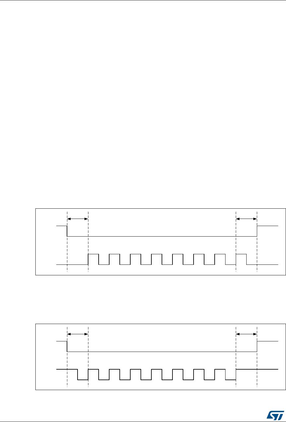
Quad-SPI interface (QUADSPI) RM0430
320/1324 RM0430 Rev 8
12.3.14 QUADSPI busy bit and abort functionality
Once the QUADSPI starts an operation with the Flash memory, the BUSY bit is
automatically set in the QUADSPI_SR.
In indirect mode, the BUSY bit is reset once the QUADSPI has completed the requested
command sequence and the FIFO is empty.
In automatic-polling mode, BUSY goes low only after the last periodic access is complete,
due to a match when APMS = 1, or due to an abort.
After the first access in memory-mapped mode, BUSY goes low only on a timeout event or
on an abort.
Any operation can be aborted by setting the ABORT bit in the QUADSPI_CR. Once the
abort is completed, the BUSY bit and the ABORT bit are automatically reset, and the FIFO
is flushed.
Note: Some Flash memories might misbehave if a write operation to a status registers is aborted.
12.3.15 nCS behavior
By default, nCS is high, deselecting the external Flash memory. nCS falls before an
operation begins and rises as soon as it finishes.
When CKMODE = 0 (“mode0”, where CLK stays low when no operation is in progress) nCS
falls one CLK cycle before an operation first rising CLK edge, and nCS rises one CLK cycle
after the operation final rising CLK edge, as shown in Figure 55.
Figure 55. nCS when CKMODE = 0 (T = CLK period)
When CKMODE=1 (“mode3”, where CLK goes high when no operation is in progress) and
DDRM=0 (SDR mode), nCS still falls one CLK cycle before an operation first rising CLK
edge, and nCS rises one CLK cycle after the operation final rising CLK edge, as shown in
Figure 56.
Figure 56. nCS when CKMODE = 1 in SDR mode (T = CLK period)
069
Q&6
6&/.
77
069
Q&6
6&/.
77
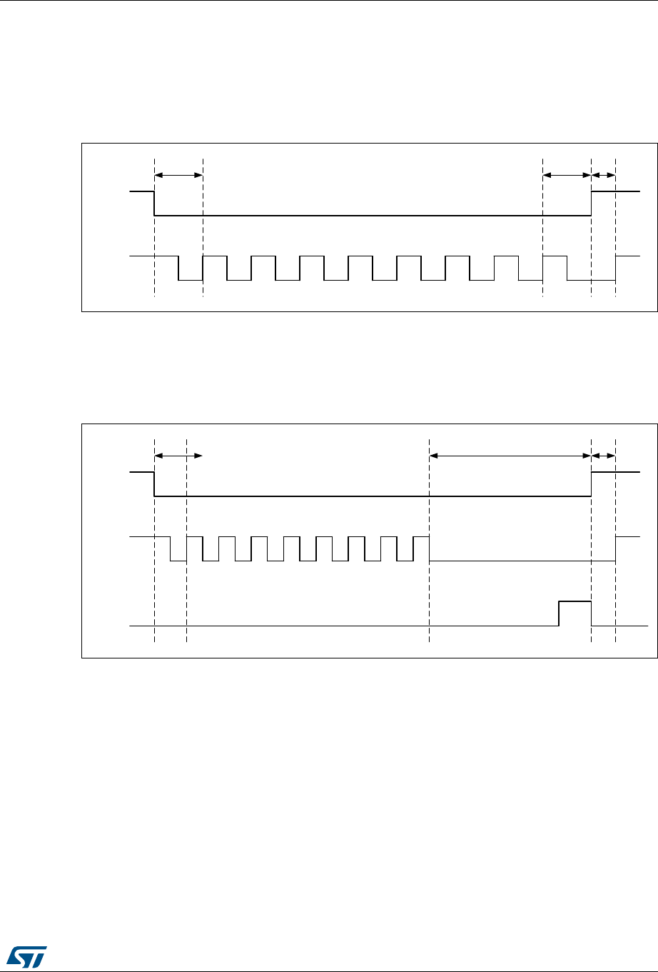
RM0430 Rev 8 321/1324
RM0430 Quad-SPI interface (QUADSPI)
335
When CKMODE = 1 (“mode3”) and DDRM = 1 (DDR mode), nCS falls one CLK cycle
before an operation first rising CLK edge, and nCS rises one CLK cycle after the operation
final active rising CLK edge, as shown in Figure 57. Because DDR operations must finish
with a falling edge, CLK is low when nCS rises, and CLK rises back up one half of a CLK
cycle afterwards.
Figure 57. nCS when CKMODE = 1 in DDR mode (T = CLK period)
When the FIFO stays full in a read operation or if the FIFO stays empty in a write operation,
the operation stalls and CLK stays low until firmware services the FIFO. If an abort occurs
when an operation is stalled, nCS rises just after the abort is requested and then CLK rises
one half of a CLK cycle later, as shown in Figure 58.
Figure 58. nCS when CKMODE = 1 with an abort (T = CLK period)
When not in dual-flash mode (DFM = 0), only FLASH 1 is accessed and thus the BK2_nCS
stays high. In dual-flash mode, BK2_nCS behaves exactly the same as BK1_nCS. Thus, if
there is a FLASH 2 and if the application always stays in dual-flash mode, then FLASH 2
may use BK1_nCS and the pin outputting BK2_nCS can be used for other functions.
069
Q&6
6&/.
77 7
069
Q&6
6&/.
&ORFNVWDOOHG7 7
$ERUW

Quad-SPI interface (QUADSPI) RM0430
322/1324 RM0430 Rev 8
12.4 QUADSPI interrupts
An interrupt can be produced on the following events:
•Timeout
•Status match
•FIFO threshold
•Transfer complete
•Transfer error
Separate interrupt enable bits are available for flexibility.
Table 72. QUADSPI interrupt requests
Interrupt event Event flag Enable control bit
Timeout TOF TOIE
Status match SMF SMIE
FIFO threshold FTF FTIE
Transfer complete TCF TCIE
Transfer error TEF TEIE

RM0430 Rev 8 323/1324
RM0430 Quad-SPI interface (QUADSPI)
335
12.5 QUADSPI registers
12.5.1 QUADSPI control register (QUADSPI_CR)
Address offset: 0x0000
Reset value: 0x0000 0000
31 30 29 28 27 26 25 24 23 22 21 20 19 18 17 16
PRESCALER[7:0] PMM APMS Res. TOIE SMIE FTIE TCIE TEIE
rw rw rw rw rw rw rw rw rw rw rw rw rw rw rw
15 14 13 12 11 10 9 8 7 6 5 4 3 2 1 0
Res. Res. Res. FTHRES[4:0] FSEL DFM Res. SSHIFT TCEN DMAEN ABORT EN
rw rw rw rw rw rw rw rw rw rw rw rw
Bits 31:24 PRESCALER[7:0]: Clock prescaler
This field defines the scaler factor for generating CLK based on the AHB clock
(value+1).
0: FCLK = FAHB, AHB clock used directly as QUADSPI CLK (prescaler bypassed)
1: FCLK = FAHB/2
2: FCLK = FAHB/3
...
255: FCLK = FAHB/256
For odd clock division factors, CLK’s duty cycle is not 50%. The clock signal remains
low one cycle longer than it stays high.
This field can be modified only when BUSY = 0.
Bit 23 PMM: Polling match mode
This bit indicates which method should be used for determining a “match” during
automatic polling mode.
0: AND match mode. SMF is set if all the unmasked bits received from the Flash
memory match the corresponding bits in the match register.
1: OR match mode. SMF is set if any one of the unmasked bits received from the Flash
memory matches its corresponding bit in the match register.
This bit can be modified only when BUSY = 0.
Bit 22 APMS: Automatic poll mode stop
This bit determines if automatic polling is stopped after a match.
0: Automatic polling mode is stopped only by abort or by disabling the QUADSPI.
1: Automatic polling mode stops as soon as there is a match.
This bit can be modified only when BUSY = 0.
Bit 21 Reserved, must be kept at reset value.
Bit 20 TOIE: TimeOut interrupt enable
This bit enables the TimeOut interrupt.
0: Interrupt disable
1: Interrupt enabled
Bit 19 SMIE: Status match interrupt enable
This bit enables the status match interrupt.
0: Interrupt disable
1: Interrupt enabled

Quad-SPI interface (QUADSPI) RM0430
324/1324 RM0430 Rev 8
Bit 18 FTIE: FIFO threshold interrupt enable
This bit enables the FIFO threshold interrupt.
0: Interrupt disabled
1: Interrupt enabled
Bit 17 TCIE: Transfer complete interrupt enable
This bit enables the transfer complete interrupt.
0: Interrupt disabled
1: Interrupt enabled
Bit 16 TEIE: Transfer error interrupt enable
This bit enables the transfer error interrupt.
0: Interrupt disable
1: Interrupt enabled
Bits 15:13 Reserved, must be kept at reset value.
Bits 12:8 FTHRES[4:0] FIFO threshold level
Defines, in indirect mode, the threshold number of bytes in the FIFO that will cause the
FIFO threshold flag (FTF, QUADSPI_SR[2]) to be set.
In indirect write mode (FMODE = 00):
0: FTF is set if there are 1 or more free bytes available to be written to in the FIFO
1: FTF is set if there are 2 or more free bytes available to be written to in the FIFO
...
31: FTF is set if there are 32 free bytes available to be written to in the FIFO
In indirect read mode (FMODE = 01):
0: FTF is set if there are 1 or more valid bytes that can be read from the FIFO
1: FTF is set if there are 2 or more valid bytes that can be read from the FIFO
...
31: FTF is set if there are 32 valid bytes that can be read from the FIFO
If DMAEN = 1, then the DMA controller for the corresponding channel must be disabled
before changing the FTHRES value.
Bit 7 FSEL: Flash memory selection
This bit selects the Flash memory to be addressed in single flash mode (when DFM =
0).
0: FLASH 1 selected
1: FLASH 2 selected
This bit can be modified only when BUSY = 0.
This bit is ignored when DFM = 1.
Bit 6 DFM: Dual-flash mode
This bit activates dual-flash mode, where two external Flash memories are used
simultaneously to double throughput and capacity.
0: Dual-flash mode disabled
1: Dual-flash mode enabled
This bit can be modified only when BUSY = 0.
Bit 5 Reserved, must be kept at reset value.

RM0430 Rev 8 325/1324
RM0430 Quad-SPI interface (QUADSPI)
335
Bit 4 SSHIFT: Sample shift
By default, the QUADSPI samples data 1/2 of a CLK cycle after the data is driven by the
Flash memory. This bit allows the data is to be sampled later in order to account for
external signal delays.
0: No shift
1: 1/2 cycle shift
Firmware must assure that SSHIFT = 0 when in DDR mode (when DDRM = 1).
This field can be modified only when BUSY = 0.
Bit 3 TCEN: Timeout counter enable
This bit is valid only when memory-mapped mode (FMODE = 11) is selected. Activating
this bit causes the chip select (nCS) to be released (and thus reduces consumption) if
there has not been an access after a certain amount of time, where this time is defined
by TIMEOUT[15:0] (QUADSPI_LPTR).
Enable the timeout counter.
By default, the QUADSPI never stops its prefetch operation, keeping the previous read
operation active with nCS maintained low, even if no access to the Flash memory
occurs for a long time. Since Flash memories tend to consume more when nCS is held
low, the application might want to activate the timeout counter (TCEN = 1, bit 3 of
QUADSPI_CR) so that nCS is released after a period of TIMEOUT[15:0]
(QUADSPI_LPTR) cycles have elapsed without an access since when the FIFO
becomes full with prefetch data.
0: Timeout counter is disabled, and thus the chip select (nCS) remains active
indefinitely after an access in memory-mapped mode.
1: Timeout counter is enabled, and thus the chip select is released in memory-mapped
mode after TIMEOUT[15:0] cycles of Flash memory inactivity.
This bit can be modified only when BUSY = 0.
Bit 2 DMAEN: DMA enable
In indirect mode, DMA can be used to input or output data via the QUADSPI_DR
register. DMA transfers are initiated when the FIFO threshold flag, FTF, is set.
0: DMA is disabled for indirect mode
1: DMA is enabled for indirect mode
Bit 1 ABORT: Abort request
This bit aborts the on-going command sequence. It is automatically reset once the abort
is complete.
This bit stops the current transfer.
In polling mode or memory-mapped mode, this bit also reset the APM bit or the DM bit.
0: No abort requested
1: Abort requested
Bit 0 EN: Enable
Enable the QUADSPI.
0: QUADSPI is disabled
1: QUADSPI is enabled

Quad-SPI interface (QUADSPI) RM0430
326/1324 RM0430 Rev 8
12.5.2 QUADSPI device configuration register (QUADSPI_DCR)
Address offset: 0x0004
Reset value: 0x0000 0000
31 30 29 28 27 26 25 24 23 22 21 20 19 18 17 16
Res. Res. Res. Res. Res. Res. Res. Res. Res. Res. Res. FSIZE[4:0]
rw rw rw rw rw
15 14 13 12 11 10 9 8 7 6 5 4 3 2 1 0
Res. Res. Res. Res. Res. CSHT[2:0] Res. Res. Res. Res. Res. Res. Res. CK
MODE
rw rw rw rw
Bits 31:21 Reserved, must be kept at reset value.
Bits 20:16 FSIZE[4:0]: Flash memory size
This field defines the size of external memory using the following formula:
Number of bytes in Flash memory = 2[FSIZE+1]
FSIZE+1 is effectively the number of address bits required to address the Flash
memory. The Flash memory capacity can be up to 4GB (addressed using 32 bits) in
indirect mode, but the addressable space in memory-mapped mode is limited to
256MB.
If DFM = 1, FSIZE indicates the total capacity of the two Flash memories together.
This field can be modified only when BUSY = 0.
Bits 15:11 Reserved, must be kept at reset value.
Bits 10:8 CSHT[2:0]: Chip select high time
CSHT+1 defines the minimum number of CLK cycles which the chip select (nCS) must
remain high between commands issued to the Flash memory.
0: nCS stays high for at least 1 cycle between Flash memory commands
1: nCS stays high for at least 2 cycles between Flash memory commands
...
7: nCS stays high for at least 8 cycles between Flash memory commands
This field can be modified only when BUSY = 0.
Bits 7:1 Reserved, must be kept at reset value.
Bit 0 CKMODE: Mode 0 / mode 3
This bit indicates the level that CLK takes between commands (when nCS = 1).
0: CLK must stay low while nCS is high (chip select released). This is referred to as
mode 0.
1: CLK must stay high while nCS is high (chip select released). This is referred to as
mode 3.
This field can be modified only when BUSY = 0.

RM0430 Rev 8 327/1324
RM0430 Quad-SPI interface (QUADSPI)
335
12.5.3 QUADSPI status register (QUADSPI_SR)
Address offset: 0x0008
Reset value: 0x0000 0000
31 30 29 28 27 26 25 24 23 22 21 20 19 18 17 16
Res. Res. Res. Res. Res. Res. Res. Res. Res. Res. Res. Res. Res. Res. Res. Res.
15 14 13 12 11 10 9 8 7 6 5 4 3 2 1 0
Res. Res. FLEVEL[5:0] Res. Res. BUSY TOF SMF FTF TCF TEF
rrr r r r r r r r r r
Bits 31:14 Reserved, must be kept at reset value.
Bits 13:8 FLEVEL[5:0]: FIFO level
This field gives the number of valid bytes which are being held in the FIFO. FLEVEL = 0
when the FIFO is empty, and 32 when it is full. In memory-mapped mode and in
automatic status polling mode, FLEVEL is zero.
Bits 7:6 Reserved, must be kept at reset value.
Bit 5 BUSY: Busy
This bit is set when an operation is on going. This bit clears automatically when the
operation with the Flash memory is finished and the FIFO is empty.
Bit 4 TOF: Timeout flag
This bit is set when timeout occurs. It is cleared by writing 1 to CTOF.
Bit 3 SMF: Status match flag
This bit is set in automatic polling mode when the unmasked received data matches the
corresponding bits in the match register (QUADSPI_PSMAR). It is cleared by writing 1
to CSMF.
Bit 2 FTF: FIFO threshold flag
In indirect mode, this bit is set when the FIFO threshold has been reached, or if there is
any data left in the FIFO after reads from the Flash memory are complete. It is cleared
automatically as soon as threshold condition is no longer true.
In automatic polling mode this bit is set every time the status register is read, and the bit
is cleared when the data register is read.
Bit 1 TCF: Transfer complete flag
This bit is set in indirect mode when the programmed number of data has been
transferred or in any mode when the transfer has been aborted.It is cleared by writing 1
to CTCF.
Bit 0 TEF: Transfer error flag
This bit is set in indirect mode when an invalid address is being accessed in indirect
mode. It is cleared by writing 1 to CTEF.

Quad-SPI interface (QUADSPI) RM0430
328/1324 RM0430 Rev 8
12.5.4 QUADSPI flag clear register (QUADSPI_FCR)
Address offset: 0x000C
Reset value: 0x0000 0000
12.5.5 QUADSPI data length register (QUADSPI_DLR)
Address offset: 0x0010
Reset value: 0x0000 0000
31 30 29 28 27 26 25 24 23 22 21 20 19 18 17 16
Res. Res. Res. Res. Res. Res. Res. Res. Res. Res. Res. Res. Res. Res. Res. Res.
15 14 13 12 11 10 9 8 7 6 5 4 3 2 1 0
Res. Res. Res. Res. Res. Res. Res. Res. Res. Res. Res. CTOF CSMF Res. CTCF CTEF
ww ww
Bits 31:5 Reserved, must be kept at reset value.
Bit 4 CTOF: Clear timeout flag
Writing 1 clears the TOF flag in the QUADSPI_SR register
Bit 3 CSMF: Clear status match flag
Writing 1 clears the SMF flag in the QUADSPI_SR register
Bit 2 Reserved, must be kept at reset value.
Bit 1 CTCF: Clear transfer complete flag
Writing 1 clears the TCF flag in the QUADSPI_SR register
Bit 0 CTEF: Clear transfer error flag
Writing 1 clears the TEF flag in the QUADSPI_SR register
31 30 29 28 27 26 25 24 23 22 21 20 19 18 17 16
DL[31:16]
rw rw rw rw rw rw rw rw rw rw rw rw rw rw rw rw
15 14 13 12 11 10 9 8 7 6 5 4 3 2 1 0
DL[15:0]
rw rw rw rw rw rw rw rw rw rw rw rw rw rw rw rw
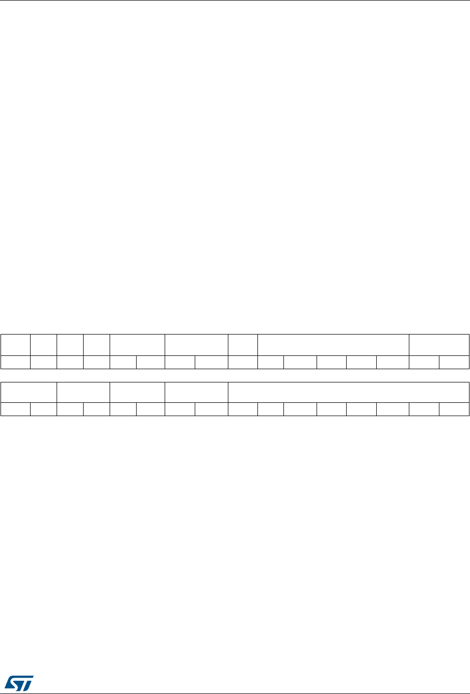
RM0430 Rev 8 329/1324
RM0430 Quad-SPI interface (QUADSPI)
335
12.5.6 QUADSPI communication configuration register (QUADSPI_CCR)
Address offset: 0x0014
Reset value: 0x0000 0000
Bits 31:0 DL[31:0]: Data length
Number of data to be retrieved (value+1) in indirect and status-polling modes. A value
no greater than 3 (indicating 4 bytes) should be used for status-polling mode.
All 1s in indirect mode means undefined length, where QUADSPI will continue until the
end of memory, as defined by FSIZE.
0x0000_0000: 1 byte is to be transferred
0x0000_0001: 2 bytes are to be transferred
0x0000_0002: 3 bytes are to be transferred
0x0000_0003: 4 bytes are to be transferred
...
0xFFFF_FFFD: 4,294,967,294 (4G-2) bytes are to be transferred
0xFFFF_FFFE: 4,294,967,295 (4G-1) bytes are to be transferred
0xFFFF_FFFF: undefined length -- all bytes until the end of Flash memory (as defined
by FSIZE) are to be transferred. Continue reading indefinitely if FSIZE = 0x1F.
DL[0] is stuck at ‘1’ in dual-flash mode (DFM = 1) even when ‘0’ is written to this bit, thus
assuring that each access transfers an even number of bytes.
This field has no effect when in memory-mapped mode (FMODE = 10).
This field can be written only when BUSY = 0.
31 30 29 28 27 26 25 24 23 22 21 20 19 18 17 16
DDRM DHHC Res. SIOO FMODE[1:0] DMODE[1:0] Res. DCYC[4:0] ABSIZE[1:0]
rw rw rw rw rw rw rw rw rw rw rw rw rw rw
15 14 13 12 11 10 9 8 7 6 5 4 3 2 1 0
ABMODE[1:0] ADSIZE[1:0] ADMODE[1:0] IMODE[1:0] INSTRUCTION[7:0]
rw rw rw rw rw rw rw rw rw rw rw rw rw rw rw rw
Bit 31 DDRM: Double data rate mode
This bit sets the DDR mode for the address, alternate byte and data phase:
0: DDR Mode disabled
1: DDR Mode enabled
This field can be written only when BUSY = 0.
Bit 30 DHHC: DDR hold
Delay the data output by 1/4 of the QUADSPI output clock cycle in DDR mode:
0: Delay the data output using analog delay
1: Delay the data output by 1/4 of a QUADSPI output clock cycle.
This feature is only active in DDR mode.
This field can be written only when BUSY = 0.
Bit 29 Reserved, must be kept at reset value.

Quad-SPI interface (QUADSPI) RM0430
330/1324 RM0430 Rev 8
Bit 28 SIOO: Send instruction only once mode
See Section 12.3.12: Sending the instruction only once on page 319. This bit has no
effect when IMODE = 00.
0: Send instruction on every transaction
1: Send instruction only for the first command
This field can be written only when BUSY = 0.
Bits 27:26 FMODE[1:0]: Functional mode
This field defines the QUADSPI functional mode of operation.
00: Indirect write mode
01: Indirect read mode
10: Automatic polling mode
11: Memory-mapped mode
If DMAEN = 1 already, then the DMA controller for the corresponding channel must be
disabled before changing the FMODE value.
This field can be written only when BUSY = 0.
Bits 25:24 DMODE[1:0]: Data mode
This field defines the data phase’s mode of operation:
00: No data
01: Data on a single line
10: Data on two lines
11: Data on four lines
This field also determines the dummy phase mode of operation.
This field can be written only when BUSY = 0.
Bit 23 Reserved, must be kept at reset value.
Bits 22:18 DCYC[4:0]: Number of dummy cycles
This field defines the duration of the dummy phase. In both SDR and DDR modes, it
specifies a number of CLK cycles (0-31).
This field can be written only when BUSY = 0.
Bits 17:16 ABSIZE[1:0]: Alternate bytes size
This bit defines alternate bytes size:
00: 8-bit alternate byte
01: 16-bit alternate bytes
10: 24-bit alternate bytes
11: 32-bit alternate bytes
This field can be written only when BUSY = 0.
Bits 15:14 ABMODE[1:0]: Alternate bytes mode
This field defines the alternate-bytes phase mode of operation:
00: No alternate bytes
01: Alternate bytes on a single line
10: Alternate bytes on two lines
11: Alternate bytes on four lines
This field can be written only when BUSY = 0.

RM0430 Rev 8 331/1324
RM0430 Quad-SPI interface (QUADSPI)
335
12.5.7 QUADSPI address register (QUADSPI_AR)
Address offset: 0x0018
Reset value: 0x0000 0000
Bits 13:12 ADSIZE[1:0]: Address size
This bit defines address size:
00: 8-bit address
01: 16-bit address
10: 24-bit address
11: 32-bit address
This field can be written only when BUSY = 0.
Bits 11:10 ADMODE[1:0]: Address mode
This field defines the address phase mode of operation:
00: No address
01: Address on a single line
10: Address on two lines
11: Address on four lines
This field can be written only when BUSY = 0.
Bits 9:8 IMODE[1:0]: Instruction mode
This field defines the instruction phase mode of operation:
00: No instruction
01: Instruction on a single line
10: Instruction on two lines
11: Instruction on four lines
This field can be written only when BUSY = 0.
Bits 7:0 INSTRUCTION[7:0]: Instruction
Instruction to be send to the external SPI device.
This field can be written only when BUSY = 0.
31 30 29 28 27 26 25 24 23 22 21 20 19 18 17 16
ADDRESS[31:16]
rw rw rw rw rw rw rw rw rw rw rw rw rw rw rw rw
15 14 13 12 11 10 9 8 7 6 5 4 3 2 1 0
ADDRESS[15:0]
rw rw rw rw rw rw rw rw rw rw rw rw rw rw rw rw
Bits 31:0 ADDRESS[31:0]: Address
Address to be send to the external Flash memory
Writes to this field are ignored when BUSY = 0 or when FMODE = 11 (memory-mapped
mode).
In dual flash mode, ADDRESS[0] is automatically stuck to ‘0’ as the address should
always be even

Quad-SPI interface (QUADSPI) RM0430
332/1324 RM0430 Rev 8
12.5.8 QUADSPI alternate bytes registers (QUADSPI_ABR)
Address offset: 0x001C
Reset value: 0x0000 0000
12.5.9 QUADSPI data register (QUADSPI_DR)
Address offset: 0x0020
Reset value: 0x0000 0000
31 30 29 28 27 26 25 24 23 22 21 20 19 18 17 16
ALTERNATE[31:16]
rw rw rw rw rw rw rw rw rw rw rw rw rw rw rw rw
15 14 13 12 11 10 9 8 7 6 5 4 3 2 1 0
ALTERNATE[15:0]
rw rw rw rw rw rw rw rw rw rw rw rw rw rw rw rw
Bits 31:0 ALTERNATE[31:0]: Alternate Bytes
Optional data to be send to the external SPI device right after the address.
This field can be written only when BUSY = 0.
31 30 29 28 27 26 25 24 23 22 21 20 19 18 17 16
DATA[31:16]
rw rw rw rw rw rw rw rw rw rw rw rw rw rw rw rw
15 14 13 12 11 10 9 8 7 6 5 4 3 2 1 0
DATA[15:0]
rw rw rw rw rw rw rw rw rw rw rw rw rw rw rw rw
Bits 31:0 DATA[31:0]: Data
Data to be sent/received to/from the external SPI device.
In indirect write mode, data written to this register is stored on the FIFO before it is sent
to the Flash memory during the data phase. If the FIFO is too full, a write operation is
stalled until the FIFO has enough space to accept the amount of data being written.
In indirect read mode, reading this register gives (via the FIFO) the data which was
received from the Flash memory. If the FIFO does not have as many bytes as requested
by the read operation and if BUSY=1, the read operation is stalled until enough data is
present or until the transfer is complete, whichever happens first.
In automatic polling mode, this register contains the last data read from the Flash
memory (without masking).
Word, halfword, and byte accesses to this register are supported. In indirect write mode,
a byte write adds 1 byte to the FIFO, a halfword write 2, and a word write 4. Similarly, in
indirect read mode, a byte read removes 1 byte from the FIFO, a halfword read 2, and a
word read 4. Accesses in indirect mode must be aligned to the bottom of this register: a
byte read must read DATA[7:0] and a halfword read must read DATA[15:0].

RM0430 Rev 8 333/1324
RM0430 Quad-SPI interface (QUADSPI)
335
12.5.10 QUADSPI polling status mask register (QUADSPI _PSMKR)
Address offset: 0x0024
Reset value: 0x0000 0000
12.5.11 QUADSPI polling status match register (QUADSPI _PSMAR)
Address offset: 0x0028
Reset value: 0x0000 0000
31 30 29 28 27 26 25 24 23 22 21 20 19 18 17 16
MASK[31:16]
rw rw rw rw rw rw rw rw rw rw rw rw rw rw rw rw
15 14 13 12 11 10 9 8 7 6 5 4 3 2 1 0
MASK[15:0]
rw rw rw rw rw rw rw rw rw rw rw rw rw rw rw rw
Bits 31:0 MASK[31:0]: Status mask
Mask to be applied to the status bytes received in polling mode.
For bit n:
0: Bit n of the data received in automatic polling mode is masked and its value is not
considered in the matching logic
1: Bit n of the data received in automatic polling mode is unmasked and its value is
considered in the matching logic
This field can be written only when BUSY = 0.
31 30 29 28 27 26 25 24 23 22 21 20 19 18 17 16
MATCH[31:16]
rw rw rw rw rw rw rw rw rw rw rw rw rw rw rw rw
15 14 13 12 11 10 9 8 7 6 5 4 3 2 1 0
MATCH[15:0]
rw rw rw rw rw rw rw rw rw rw rw rw rw rw rw rw
Bits 31:0 MATCH[31:0]: Status match
Value to be compared with the masked status register to get a match.
This field can be written only when BUSY = 0.
Quad-SPI interface (QUADSPI) RM0430
334/1324 RM0430 Rev 8
12.5.12 QUADSPI polling interval register (QUADSPI _PIR)
Address offset: 0x002C
Reset value: 0x0000 0000
12.5.13 QUADSPI low-power timeout register (QUADSPI_LPTR)
Address offset: 0x0030
Reset value: 0x0000 0000
31 30 29 28 27 26 25 24 23 22 21 20 19 18 17 16
Res. Res. Res. Res. Res. Res. Res. Res. Res. Res. Res. Res. Res. Res. Res. Res.
15 14 13 12 11 10 9 8 7 6 5 4 3 2 1 0
INTERVAL[15:0]
rw rw rw rw rw rw rw rw rw rw rw rw rw rw rw rw
Bits 31:16 Reserved, must be kept at reset value.
Bits 15:0 INTERVAL[15:0]: Polling interval
Number of CLK cycles between to read during automatic polling phases.
This field can be written only when BUSY = 0.
31 30 29 28 27 26 25 24 23 22 21 20 19 18 17 16
Res. Res. Res. Res. Res. Res. Res. Res. Res. Res. Res. Res. Res. Res. Res. Res.
15 14 13 12 11 10 9 8 7 6 5 4 3 2 1 0
TIMEOUT[15:0]
rw rw rw rw rw rw rw rw rw rw rw rw rw rw rw rw
Bits 31:16 Reserved, must be kept at reset value.
Bits 15:0 TIMEOUT[15:0]: Timeout period
After each access in memory-mapped mode, the QUADSPI prefetches the subsequent
bytes and holds these bytes in the FIFO. This field indicates how many CLK cycles the
QUADSPI waits after the FIFO becomes full until it raises nCS, putting the Flash
memory in a lower-consumption state.
This field can be written only when BUSY = 0.
RM0430 Rev 8 335/1324
RM0430 Quad-SPI interface (QUADSPI)
335
12.5.14 QUADSPI register map
Refer to Section 2.2.2 on page 58 for the register boundary addresses.
Table 73. QUADSPI register map and reset values
Offset Register
name
31
30
29
28
27
26
25
24
23
22
21
20
19
18
17
16
15
14
13
12
11
10
9
8
7
6
5
4
3
2
1
0
0x0000
QUADSPI_CR PRESCALER[7:0]
PMM
APMS
Res.
TOIE
SMIE
FTIE
TCIE
TEIE
Res.
Res.
Res.
FTHRES
[4:0]
FSEL
DFM
Res.
SSHIFT
TCEN
DMAEN
ABORT
EN
Reset value 0000000000 00000 0000000 00000
0x0004
QUADSPI_DCR
Res.
Res.
Res.
Res.
Res.
Res.
Res.
Res.
Res.
Res.
Res.
FSIZE[4:0]
Res.
Res.
Res.
Res.
Res.
CSHT
Res.
Res.
Res.
Res.
Res.
Res.
Res.
CKMODE
Reset value 0 0 0 0 0 0 0 0 0
0x0008
QUADSPI_SR
Res.
Res.
Res.
Res.
Res.
Res.
Res.
Res.
Res.
Res.
Res.
Res.
Res.
Res.
Res.
Res.
Res.
FLEVEL[6:0]
Res.
Res.
BUSY
TOF
SMF
FTF
TCF
TEF
Reset value 0000000 000000
0x000C
QUADSPI_FCR
Res.
Res.
Res.
Res.
Res.
Res.
Res.
Res.
Res.
Res.
Res.
Res.
Res.
Res.
Res.
Res.
Res.
Res.
Res.
Res.
Res.
Res.
Res.
Res.
Res.
Res.
Res.
CTOF
CSMF
Res.
CTCF
CTEF
Reset value 00 00
0x0010 QUADSPI_DLR DL[31:0]
Reset value 00000000000000000000000000000000
0x0014
QUADSPI_CCR
DDRM
DHHC
Res.
SIOO
FMODE[1:0]
DMODE[1:0]
Res.
DCYC[4:0]
ABSIZE[1:0]
ABMODE[1:0]
ADSIZE[1:0]
ADMODE[1:0]
IMODE[1:0]
INSTRUCTION[7:0]
Reset value 00 00000 00000000000000000000000
0x0018
QUADSPI_AR ADDRESS[31:0]
Reset value 00000000000000000000000000000000
0x001C QUADSPI_ABR ALTERNATE[31:0]
Reset value 00000000000000000000000000000000
0x0020
QUADSPI_DR DATA[31:0]
Reset value 00000000000000000000000000000000
0x0024
QUADSPI_
PSMKR MASK[31:0]
Reset value 00000000000000000000000000000000
0x0028
QUADSPI_
PSMAR MATCH[31:0]
Reset value 00000000000000000000000000000000
0x002C
QUADSPI_PIR
Res.
Res.
Res.
Res.
Res.
Res.
Res.
Res.
Res.
Res.
Res.
Res.
Res.
Res.
Res.
Res.
INTERVAL[15:0]
Reset value 0000000000000000
0x0030
QUADSPI_
LPTR
Res.
Res.
Res.
Res.
Res.
Res.
Res.
Res.
Res.
Res.
Res.
Res.
Res.
Res.
Res.
Res.
TIMEOUT[15:0]
Reset value 0000000000000000

Analog-to-digital converter (ADC) RM0430
336/1324 RM0430 Rev 8
13 Analog-to-digital converter (ADC)
13.1 ADC introduction
The 12-bit ADC is a successive approximation analog-to-digital converter. It has up to 19
multiplexed channels allowing it to measure signals from 16 external sources, two internal
sources, and the VBAT channel. The A/D conversion of the channels can be performed in
single, continuous, scan or discontinuous mode. The result of the ADC is stored into a left-
or right-aligned 16-bit data register.
The analog watchdog feature allows the application to detect if the input voltage goes
beyond the user-defined, higher or lower thresholds.
13.2 ADC main features
•12-bit, 10-bit, 8-bit or 6-bit configurable resolution
•Interrupt generation at the end of conversion, end of injected conversion, and in case of
analog watchdog or overrun events
•Single and continuous conversion modes
•Scan mode for automatic conversion of channel 0 to channel ‘n’
•Data alignment with in-built data coherency
•Channel-wise programmable sampling time
•External trigger option with configurable polarity for both regular and injected
conversions
•Discontinuous mode
•Configurable delay between conversions in Dual/Triple interleaved mode
•ADC supply requirements: 2.4 V to 3.6 V at full speed and down to 1.8 V at slower
speed
•ADC input range: VREF– ≤ VIN ≤ VREF+
•DMA request generation during regular channel conversion
Figure 59 shows the block diagram of the ADC.
Note: VREF–, if available (depending on package), must be tied to VSSA.
13.3 ADC functional description
Figure 59 shows a single ADC block diagram and Table 74 gives the ADC pin description.
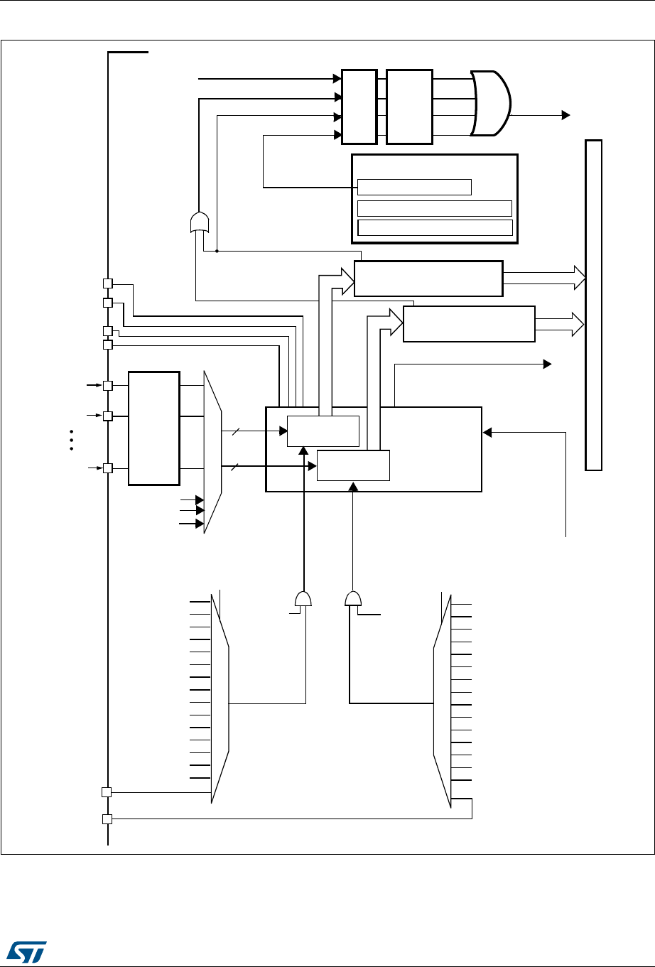
RM0430 Rev 8 337/1324
RM0430 Analog-to-digital converter (ADC)
365
Figure 59. Single ADC block diagram
$'&[B,1
$'&[B,1
$QDORJ WR GLJLWDO
FRQYHUWHU
$'&[B,1
$QDORJ
PX[
$'&&/.
$'&,QWHUUXSWWR19,&
*3,2
SRUWV
$QDORJZDWFKGRJ
$GGUHVVGDWDEXV
/RZHUWKUHVKROGELWV
&RPSDUHUHVXOW
+LJKHUWKUHVKROGELWV
)ODJV HQDEOHELWV
(2&
$:'
$QDORJZDWFKGRJHYHQW
9''$
966$
95()
95()
,QWHUUXSW
(;7,B
7,0B&+
)URP$'&SUHVFDOHU
ELWV
(QGRIFRQYHUVLRQ
FKDQQHOV
,QMHFWHG
FKDQQHOV
(QGRILQMHFWHGFRQYHUVLRQ -(2&
(2&,(
$:',(
-(2&,(
XSWR
XSWR
5HJXODUGDWDUHJLVWHU
[ELWV
,QMHFWHGGDWDUHJLVWHUV
5HJXODU
6WDUWWULJJHU
UHJXODUJURXS
(;76(/>@ELWV
(;7(1
7,0B&+
(;7,B
7,0B75*2
7,0B&+
7,0B75*2
6WDUWWULJJHU
LQMHFWHGJURXS
-(;76(/>@ELWV
7,0B&+
-(;7(1 >@ELWV
>@ELWV
'0$UHTXHVW
7HPSVHQVRU
95(),17
295295,(
'0$RYHUUXQ
9%$7
7,0B&+
7,0B75*2
7,0B&+
7,0B&+
7,0B75*2
7,0B&+
7,0B&+
7,0B&+
7,0B&+
7,0B&+
7,0B&+
7,0B&+
7,0B&+
7,0B&+
7,0B&+
7,0B&+
7,0B&+
7,0B&+
7,0B75*2
7,0B&+
7,0B75*2
7,0B&+
7,0B75*2
7,0B&+
DL

Analog-to-digital converter (ADC) RM0430
338/1324 RM0430 Rev 8
13.3.1 ADC on-off control
The ADC is powered on by setting the ADON bit in the ADC_CR2 register. When the ADON
bit is set for the first time, it wakes up the ADC from the Power-down mode.
The conversion starts when either the SWSTART or the JSWSTART bit is set.
The user can stop conversion and put the ADC in power down mode by clearing the ADON
bit. In this mode the ADC consumes almost no power (only a few µA).
13.3.2 ADC clock
The ADC features two clock schemes:
•Clock for the analog circuitry: ADCCLK
This clock is generated from the APB2 clock divided by a programmable prescaler that
allows the ADC to work at fPCLK2/2, /4, /6 or /8. Refer to the datasheets for the
maximum value of ADCCLK.
•Clock for the digital interface (used for registers read/write access)
This clock is equal to the APB2 clock. The digital interface clock can be
enabled/disabled individually for each ADC through the RCC APB2 peripheral clock
enable register (RCC_APB2ENR).
13.3.3 Channel selection
There are 16 multiplexed channels. It is possible to organize the conversions in two groups:
regular and injected. A group consists of a sequence of conversions that can be done on
any channel and in any order. For instance, it is possible to implement the conversion
sequence in the following order: ADC_IN3, ADC_IN8, ADC_IN2, ADC_IN2, ADC_IN0,
ADC_IN2, ADC_IN2, ADC_IN15.
•A regular group is composed of up to 16 conversions. The regular channels and their
order in the conversion sequence must be selected in the ADC_SQRx registers. The
total number of conversions in the regular group must be written in the L[3:0] bits in the
ADC_SQR1 register.
•An injected group is composed of up to 4 conversions. The injected channels and
their order in the conversion sequence must be selected in the ADC_JSQR register.
Table 74. ADC pins
Name Signal type Remarks
VREF+
Input, analog reference
positive
The higher/positive reference voltage for the ADC,
1.8 V ≤ VREF+ ≤ VDDA
VDDA Input, analog supply
Analog power supply equal to VDD and
2.4 V ≤VDDA ≤VDD (3.6 V) for full speed
1.8 V ≤VDDA ≤VDD (3.6 V) for reduced speed
VREF–
Input, analog reference
negative
The lower/negative reference voltage for the ADC,
VREF– = VSSA
VSSA
Input, analog supply
ground Ground for analog power supply equal to VSS
ADCx_IN[15:0] Analog input signals 16 analog input channels

RM0430 Rev 8 339/1324
RM0430 Analog-to-digital converter (ADC)
365
The total number of conversions in the injected group must be written in the L[1:0] bits
in the ADC_JSQR register.
If the ADC_SQRx or ADC_JSQR registers are modified during a conversion, the current
conversion is reset and a new start pulse is sent to the ADC to convert the newly chosen
group.
Temperature sensor, VREFINT and VBAT internal channels
•The temperature sensor is internally connected to ADC1_IN18 channel which is shared
with VBAT. Only one conversion, temperature sensor or VBAT, must be selected at a
time. When the temperature sensor and VBAT conversion are set simultaneously, only
the VBAT conversion is performed.
The internal reference voltage VREFINT is connected to ADC1_IN17.
The VBAT channel is connected to ADC1_IN18 channel. It can also be converted as an
injected or regular channel.
13.3.4 Single conversion mode
In Single conversion mode the ADC does one conversion. This mode is started with the
CONT bit at 0 by either:
•setting the SWSTART bit in the ADC_CR2 register (for a regular channel only)
•setting the JSWSTART bit (for an injected channel)
•external trigger (for a regular or injected channel)
Once the conversion of the selected channel is complete:
•If a regular channel was converted:
– The converted data are stored into the 16-bit ADC_DR register
– The EOC (end of conversion) flag is set
– An interrupt is generated if the EOCIE bit is set
•If an injected channel was converted:
– The converted data are stored into the 16-bit ADC_JDR1 register
– The JEOC (end of conversion injected) flag is set
– An interrupt is generated if the JEOCIE bit is set
Then the ADC stops.
13.3.5 Continuous conversion mode
In continuous conversion mode, the ADC starts a new conversion as soon as it finishes one.
This mode is started with the CONT bit at 1 either by external trigger or by setting the
SWSTRT bit in the ADC_CR2 register (for regular channels only).
After each conversion:
•If a regular group of channels was converted:
– The last converted data are stored into the 16-bit ADC_DR register
– The EOC (end of conversion) flag is set
– An interrupt is generated if the EOCIE bit is set
Note: Injected channels cannot be converted continuously. The only exception is when an injected
channel is configured to be converted automatically after regular channels in continuous
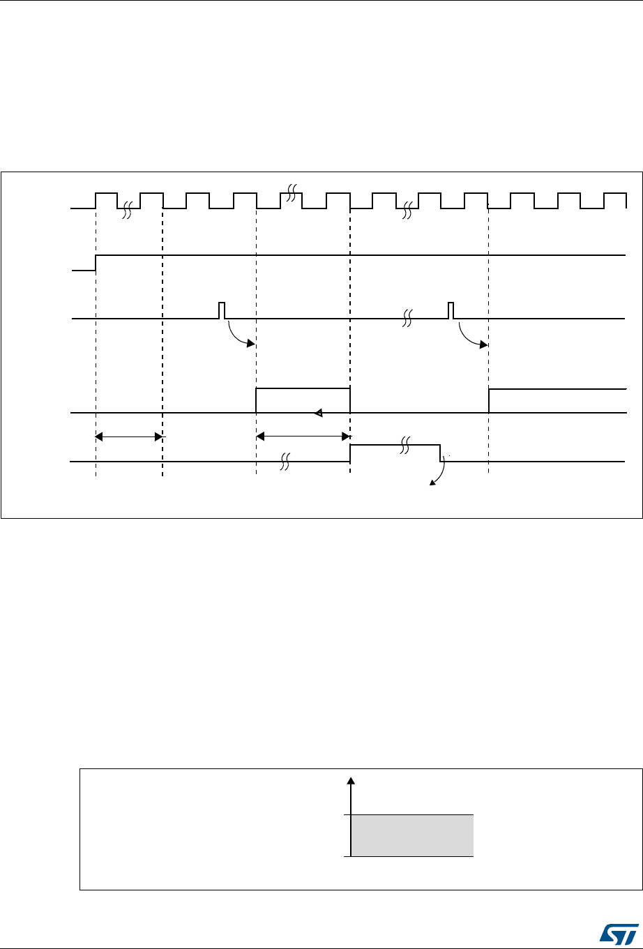
Analog-to-digital converter (ADC) RM0430
340/1324 RM0430 Rev 8
mode (using JAUTO bit), refer to Auto-injection section).
13.3.6 Timing diagram
As shown in Figure 60, the ADC needs a stabilization time of tSTAB before it starts
converting accurately. After the start of the ADC conversion and after 15 clock cycles, the
EOC flag is set and the 16-bit ADC data register contains the result of the conversion.
Figure 60. Timing diagram
13.3.7 Analog watchdog
The AWD analog watchdog status bit is set if the analog voltage converted by the ADC is
below a lower threshold or above a higher threshold. These thresholds are programmed in
the 12 least significant bits of the ADC_HTR and ADC_LTR 16-bit registers. An interrupt can
be enabled by using the AWDIE bit in the ADC_CR1 register.
The threshold value is independent of the alignment selected by the ALIGN bit in the
ADC_CR2 register. The analog voltage is compared to the lower and higher thresholds
before alignment.
Table 75 shows how the ADC_CR1 register should be configured to enable the analog
watchdog on one or more channels.
Figure 61. Analog watchdog’s guarded area
!$#?#,+
%/#
.EXT!$#CONVERSION
!$#CONVERSION
#ONVERSIONTIME
T34!"
!$#
3OFTWARECLEARSTHE%/#BIT
TOTALCONVTIME
3TARTSTCONVERSION 3TARTNEXTCONVERSION
AIB
!$/.
3734!24
*3734!24
DL
$QDORJYROWDJH
+LJKHUWKUHVKROG
/RZHUWKUHVKROG
*XDUGHGDUHD
+75
/75

RM0430 Rev 8 341/1324
RM0430 Analog-to-digital converter (ADC)
365
13.3.8 Scan mode
This mode is used to scan a group of analog channels.
The Scan mode is selected by setting the SCAN bit in the ADC_CR1 register. Once this bit
has been set, the ADC scans all the channels selected in the ADC_SQRx registers (for
regular channels) or in the ADC_JSQR register (for injected channels). A single conversion
is performed for each channel of the group. After each end of conversion, the next channel
in the group is converted automatically. If the CONT bit is set, regular channel conversion
does not stop at the last selected channel in the group but continues again from the first
selected channel.
If the DMA bit is set, the direct memory access (DMA) controller is used to transfer the data
converted from the regular group of channels (stored in the ADC_DR register) to SRAM
after each regular channel conversion.
The EOC bit is set in the ADC_SR register:
•At the end of each regular group sequence if the EOCS bit is cleared to 0
•At the end of each regular channel conversion if the EOCS bit is set to 1
The data converted from an injected channel are always stored into the ADC_JDRx
registers.
13.3.9 Injected channel management
Triggered injection
To use triggered injection, the JAUTO bit must be cleared in the ADC_CR1 register.
1. Start the conversion of a group of regular channels either by external trigger or by
setting the SWSTART bit in the ADC_CR2 register.
2. If an external injected trigger occurs or if the JSWSTART bit is set during the
conversion of a regular group of channels, the current conversion is reset and the
injected channel sequence switches to Scan-once mode.
3. Then, the regular conversion of the regular group of channels is resumed from the last
interrupted regular conversion.
If a regular event occurs during an injected conversion, the injected conversion is not
Table 75. Analog watchdog channel selection
Channels guarded by the analog
watchdog
ADC_CR1 register control bits (x = don’t care)
AWDSGL bit AWDEN bit JAWDEN bit
None x 0 0
All injected channels 0 0 1
All regular channels 0 1 0
All regular and injected channels 0 1 1
Single(1) injected channel
1. Selected by the AWDCH[4:0] bits
101
Single(1) regular channel 1 1 0
Single (1) regular or injected channel 1 1 1
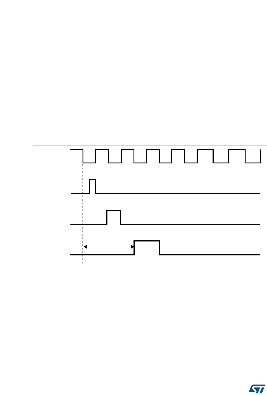
Analog-to-digital converter (ADC) RM0430
342/1324 RM0430 Rev 8
interrupted but the regular sequence is executed at the end of the injected sequence.
Figure 62 shows the corresponding timing diagram.
Note: When using triggered injection, one must ensure that the interval between trigger events is
longer than the injection sequence. For instance, if the sequence length is 30 ADC clock
cycles (that is two conversions with a sampling time of 3 clock periods), the minimum
interval between triggers must be 31 ADC clock cycles.
Auto-injection
If the JAUTO bit is set, then the channels in the injected group are automatically converted
after the regular group of channels. This can be used to convert a sequence of up to 20
conversions programmed in the ADC_SQRx and ADC_JSQR registers.
In this mode, external trigger on injected channels must be disabled.
If the CONT bit is also set in addition to the JAUTO bit, regular channels followed by injected
channels are continuously converted.
Note: It is not possible to use both the auto-injected and discontinuous modes simultaneously.
Figure 62. Injected conversion latency
1. The maximum latency value can be found in the electrical characteristics of the STM32F413/423
datasheets.
13.3.10 Discontinuous mode
Regular group
This mode is enabled by setting the DISCEN bit in the ADC_CR1 register. It can be used to
convert a short sequence of n conversions (n ≤ 8) that is part of the sequence of
conversions selected in the ADC_SQRx registers. The value of n is specified by writing to
the DISCNUM[2:0] bits in the ADC_CR1 register.
When an external trigger occurs, it starts the next n conversions selected in the ADC_SQRx
registers until all the conversions in the sequence are done. The total sequence length is
defined by the L[3:0] bits in the ADC_SQR1 register.
!$##,+
)NJECTIONEVENT
2ESET!$#
3/# MAXLATENCY
AI

RM0430 Rev 8 343/1324
RM0430 Analog-to-digital converter (ADC)
365
Example:
•n = 3, channels to be converted = 0, 1, 2, 3, 6, 7, 9, 10
•1st trigger: sequence converted 0, 1, 2. An EOC event is generated at each
conversion.
•2nd trigger: sequence converted 3, 6, 7. An EOC event is generated at each
conversion
•3rd trigger: sequence converted 9, 10.An EOC event is generated at each conversion
•4th trigger: sequence converted 0, 1, 2. An EOC event is generated at each conversion
Note: When a regular group is converted in discontinuous mode, no rollover occurs.
When all subgroups are converted, the next trigger starts the conversion of the first
subgroup. In the example above, the 4th trigger reconverts the channels 0, 1 and 2 in the
1st subgroup.
Injected group
This mode is enabled by setting the JDISCEN bit in the ADC_CR1 register. It can be used to
convert the sequence selected in the ADC_JSQR register, channel by channel, after an
external trigger event.
When an external trigger occurs, it starts the next channel conversions selected in the
ADC_JSQR registers until all the conversions in the sequence are done. The total sequence
length is defined by the JL[1:0] bits in the ADC_JSQR register.
Example:
n = 1, channels to be converted = 1, 2, 3
1st trigger: channel 1 converted
2nd trigger: channel 2 converted
3rd trigger: channel 3 converted and JEOC event generated
4th trigger: channel 1
Note: When all injected channels are converted, the next trigger starts the conversion of the first
injected channel. In the example above, the 4th trigger reconverts the 1st injected channel
1.
It is not possible to use both the auto-injected and discontinuous modes simultaneously.
Discontinuous mode must not be set for regular and injected groups at the same time.
Discontinuous mode must be enabled only for the conversion of one group.
13.4 Data alignment
The ALIGN bit in the ADC_CR2 register selects the alignment of the data stored after
conversion. Data can be right- or left-aligned as shown in Figure 63 and Figure 64.
The converted data value from the injected group of channels is decreased by the user-
defined offset written in the ADC_JOFRx registers so the result can be a negative value.
The SEXT bit represents the extended sign value.
For channels in a regular group, no offset is subtracted so only twelve bits are significant.
Analog-to-digital converter (ADC) RM0430
344/1324 RM0430 Rev 8
Figure 63. Right alignment of 12-bit data
Figure 64. Left alignment of 12-bit data
Special case: when left-aligned, the data are aligned on a half-word basis except when the
resolution is set to 6-bit. in that case, the data are aligned on a byte basis as shown in
Figure 65.
Figure 65. Left alignment of 6-bit data
13.5 Channel-wise programmable sampling time
The ADC samples the input voltage for a number of ADCCLK cycles that can be modified
using the SMP[2:0] bits in the ADC_SMPR1 and ADC_SMPR2 registers. Each channel can
be sampled with a different sampling time.
The total conversion time is calculated as follows:
Tconv = Sampling time + 12 cycles
Example:
With ADCCLK = 30 MHz and sampling time = 3 cycles:
Tconv = 3 + 12 = 15 cycles = 0.5 µs with APB2 at 60 MHz
$$$ $ $ $ $ $ $ $$$3%843%843%843%84
$$
$$
)NJECTEDGROUP
2EGULARGROUP
$ $ $ $ $ $ $ $
AI
$$
$ $ $ $ $ $$$$$3%84
)NJECTEDGROUP
2EGULARGROUP
AI
$ $ $ $ $ $ $ $ $ $ $ $
$$
3%843%843%843%843%843%84
)NJECTEDGROUP
2EGULARGROUP
AI
$ $ $ $ $ $
3%843%84 $ $ $ $ 3%84
RM0430 Rev 8 345/1324
RM0430 Analog-to-digital converter (ADC)
365
13.6 Conversion on external trigger and trigger polarity
Conversion can be triggered by an external event (e.g. timer capture, EXTI line). If the
EXTEN[1:0] control bits (for a regular conversion) or JEXTEN[1:0] bits (for an injected
conversion) are different from “0b00”, then external events are able to trigger a conversion
with the selected polarity. Table 76 provides the correspondence between the EXTEN[1:0]
and JEXTEN[1:0] values and the trigger polarity.
Note: The polarity of the external trigger can be changed on the fly.
The EXTSEL[3:0] and JEXTSEL[3:0] control bits are used to select which out of 16 possible
events can trigger conversion for the regular and injected groups.
Table 77 gives the possible external trigger for regular conversion.
Table 76. Configuring the trigger polarity
Source EXTEN[1:0] / JEXTEN[1:0]
Trigger detection disabled 00
Detection on the rising edge 01
Detection on the falling edge 10
Detection on both the rising and falling edges 11
Table 77. External trigger for regular channels
Source Type EXTSEL[3:0]
TIM1_CH1 event
Internal signal from on-chip timers
0000
TIM1_CH2 event 0001
TIM1_CH3 event 0010
TIM2_CH2 event 0011
TIM2_CH3 event 0100
TIM2_CH4 event 0101
TIM2_TRGO event 0110
TIM3_CH1 event 0111
TIM3_TRGO event 1000
TIM4_CH4 event 1001
TIM5_CH1 event 1010
TIM5_CH2 event 1011
TIM5_CH3 event 1100
TIM8_CH1 event 1101
TIM8_TRGO event 1110
EXTI line11 External pin 1111

Analog-to-digital converter (ADC) RM0430
346/1324 RM0430 Rev 8
Table 78 gives the possible external trigger for injected conversion.
Software source trigger events can be generated by setting SWSTART (for regular
conversion) or JSWSTART (for injected conversion) in ADC_CR2.
A regular group conversion can be interrupted by an injected trigger.
Note: The trigger selection can be changed on the fly. However, when the selection changes,
there is a time frame of 1 APB clock cycle during which the trigger detection is disabled.
This is to avoid spurious detection during transitions.
13.7 Fast conversion mode
It is possible to perform faster conversion by reducing the ADC resolution. The RES bits are
used to select the number of bits available in the data register. The minimum conversion
time for each resolution is then as follows:
•12 bits: 3 + 12 = 15 ADCCLK cycles
•10 bits: 3 + 10 = 13 ADCCLK cycles
•8 bits: 3 + 8 = 11 ADCCLK cycles
•6 bits: 3 + 6 = 9 ADCCLK cycles
Table 78. External trigger for injected channels
Source Connection type JEXTSEL[3:0]
TIM1_CH4 event
Internal signal from on-chip timers
0000
TIM1_TRGO event 0001
TIM2_CH1 event 0010
TIM2_TRGO event 0011
TIM3_CH2 event 0100
TIM3_CH4 event 0101
TIM4_CH1 event 0110
TIM4_CH2 event 0111
TIM4_CH3 event 1000
TIM4_TRGO event 1001
TIM5_CH4 event 1010
TIM5_TRGO event 1011
TIM8_CH2 event 1100
TIM8_CH3 event 1101
TIM8_CH4 event 1110
EXTI line15 External pin 1111

RM0430 Rev 8 347/1324
RM0430 Analog-to-digital converter (ADC)
365
13.8 Data management
13.8.1 Using the DMA
Since converted regular channel values are stored into a unique data register, it is useful to
use DMA for conversion of more than one regular channel. This avoids the loss of the data
already stored in the ADC_DR register.
When the DMA mode is enabled (DMA bit set to 1 in the ADC_CR2 register), after each
conversion of a regular channel, a DMA request is generated. This allows the transfer of the
converted data from the ADC_DR register to the destination location selected by the
software.
Despite this, if data are lost (overrun), the OVR bit in the ADC_SR register is set and an
interrupt is generated (if the OVRIE enable bit is set). DMA transfers are then disabled and
DMA requests are no longer accepted. In this case, if a DMA request is made, the regular
conversion in progress is aborted and further regular triggers are ignored. It is then
necessary to clear the OVR flag and the DMAEN bit in the used DMA stream, and to re-
initialize both the DMA and the ADC to have the wanted converted channel data transferred
to the right memory location. Only then can the conversion be resumed and the data
transfer, enabled again. Injected channel conversions are not impacted by overrun errors.
When OVR = 1 in DMA mode, the DMA requests are blocked after the last valid data have
been transferred, which means that all the data transferred to the RAM can be considered
as valid.
At the end of the last DMA transfer (number of transfers configured in the DMA controller’s
DMA_SxNTR register):
•No new DMA request is issued to the DMA controller if the DDS bit is cleared to 0 in the
ADC_CR2 register (this avoids generating an overrun error). However the DMA bit is
not cleared by hardware. It must be written to 0, then to 1 to start a new transfer.
•Requests can continue to be generated if the DDS bit is set to 1. This allows
configuring the DMA in double-buffer circular mode.
To recover the ADC from OVR state when the DMA is used, follow the steps below:
1. Reinitialize the DMA (adjust destination address and NDTR counter)
2. Clear the ADC OVR bit in ADC_SR register
3. Trigger the ADC to start the conversion.
13.8.2 Managing a sequence of conversions without using the DMA
If the conversions are slow enough, the conversion sequence can be handled by the
software. In this case the EOCS bit must be set in the ADC_CR2 register for the EOC status
bit to be set at the end of each conversion, and not only at the end of the sequence. When
EOCS = 1, overrun detection is automatically enabled. Thus, each time a conversion is
complete, EOC is set and the ADC_DR register can be read. The overrun management is
the same as when the DMA is used.
To recover the ADC from OVR state when the EOCS is set, follow the steps below:
1. Clear the ADC OVR bit in ADC_SR register
2. Trigger the ADC to start the conversion.
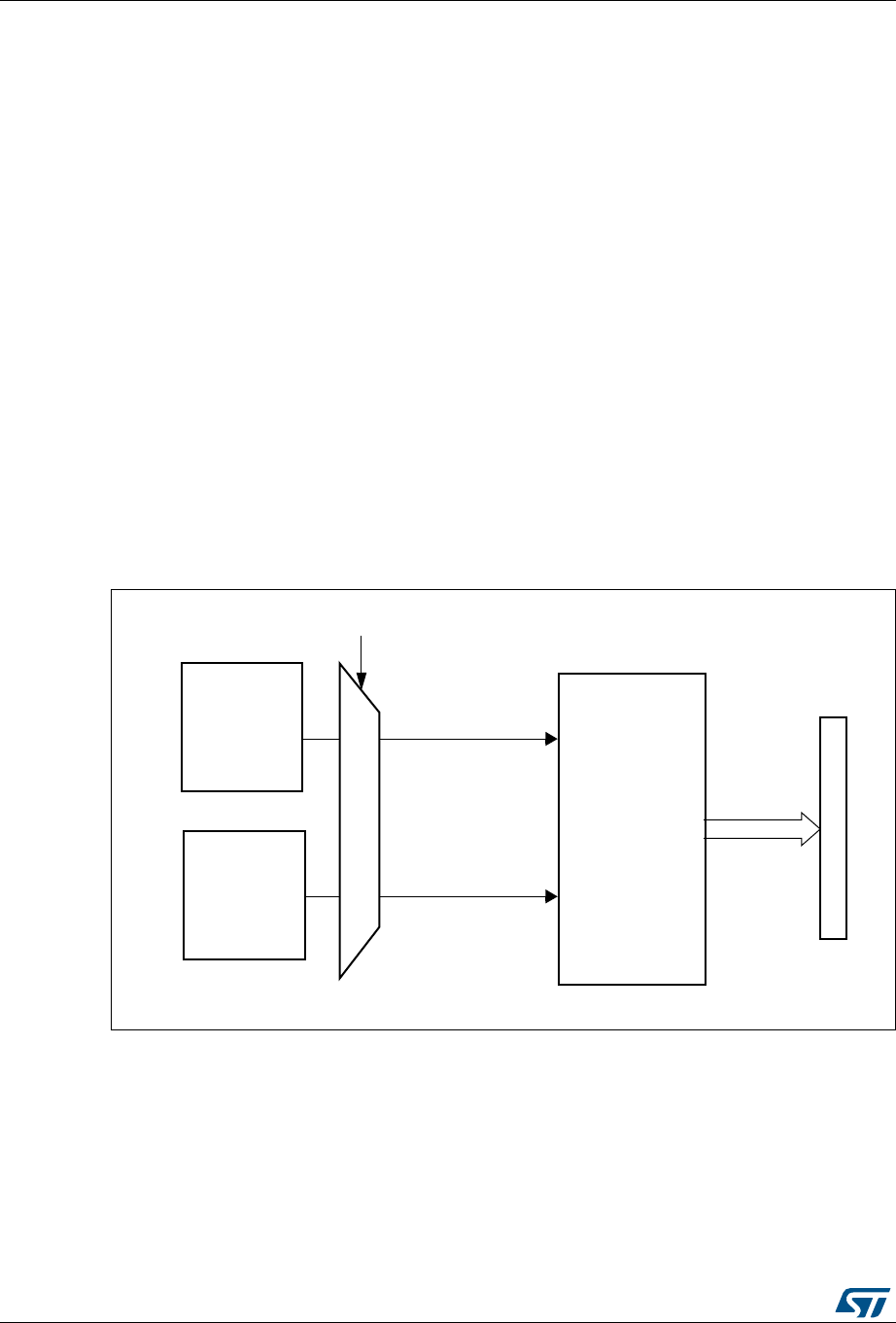
Analog-to-digital converter (ADC) RM0430
348/1324 RM0430 Rev 8
13.8.3 Conversions without DMA and without overrun detection
It may be useful to let the ADC convert one or more channels without reading the data each
time (if there is an analog watchdog for instance). For that, the DMA must be disabled
(DMA = 0) and the EOC bit must be set at the end of a sequence only (EOCS = 0). In this
configuration, overrun detection is disabled.
13.9 Temperature sensor
The temperature sensor can be used to measure the ambient temperature (TA) of the
device.
Figure 66 shows the block diagram of the temperature sensor.
When not in use, the sensor can be put in power down mode.
Note: The TSVREFE bit must be set to enable the conversion of both internal channels: the
ADC1_IN18 (temperature sensor) and the ADC1_IN17 (VREFINT).
Main features
•Supported temperature range: –40 to 125 °C
•Precision: ±1.5 °C
Figure 66. Temperature sensor and VREFINT channel block diagram
1. VSENSE is input to ADC1_IN18.
069
7HPSHUDWXUH
VHQVRU
96(16(
7695()(FRQWUROELW
$'&
$GGUHVVGDWDEXV
95(),17
$'&B,1
,QWHUQDO
SRZHUEORFN $'&B,1
FRQYHUWHGGDWD

RM0430 Rev 8 349/1324
RM0430 Analog-to-digital converter (ADC)
365
Reading the temperature
To use the sensor:
3. Select ADC1_IN18 input channel.
4. Select a sampling time greater than the minimum sampling time specified in the
datasheet.
5. Set the TSVREFE bit in the ADC_CCR register to wake up the temperature sensor
from power down mode
6. Start the ADC conversion by setting the SWSTART bit (or by external trigger)
7. Read the resulting VSENSE data in the ADC data register
8. Calculate the temperature using the following formula:
Temperature (in °C) = {(VSENSE – V25) / Avg_Slope} + 25
Where:
–V
25 = VSENSE value for 25° C
– Avg_Slope = average slope of the temperature vs. VSENSE curve (given in mV/°C
or µV/°C)
Refer to the datasheet electrical characteristics section for the actual values of V25 and
Avg_Slope.
Note: The sensor has a startup time after waking from power down mode before it can output
VSENSE at the correct level. The ADC also has a startup time after power-on, so to minimize
the delay, the ADON and TSVREFE bits should be set at the same time.
The temperature sensor output voltage changes linearly with temperature. The offset of this
linear function depends on each chip due to process variation (up to 45 °C from one chip to
another).
The internal temperature sensor is more suited for applications that detect temperature
variations instead of absolute temperatures. If accurate temperature reading is required, an
external temperature sensor should be used.
13.10 Battery charge monitoring
The VBATE bit in the ADC_CCR register is used to switch to the battery voltage. As the
VBAT voltage could be higher than VDDA, to ensure the correct operation of the ADC, the
VBAT pin is internally connected to a bridge divider.
When the VBATE is set, the bridge is automatically enabled to connect:
•VBAT/4 to the ADC1_IN18 input channel
Note: The VBAT and temperature sensor are connected to the same ADC internal channel
(ADC1_IN18). Only one conversion, either temperature sensor or VBAT, must be selected
at a time. When both conversion are enabled simultaneously, only the VBAT conversion is
performed.
Analog-to-digital converter (ADC) RM0430
350/1324 RM0430 Rev 8
13.11 ADC interrupts
An interrupt can be produced on the end of conversion for regular and injected groups,
when the analog watchdog status bit is set and when the overrun status bit is set. Separate
interrupt enable bits are available for flexibility.
Two other flags are present in the ADC_SR register, but there is no interrupt associated with
them:
•JSTRT (Start of conversion for channels of an injected group)
•STRT (Start of conversion for channels of a regular group)
Table 79. ADC interrupts
Interrupt event Event flag Enable control bit
End of conversion of a regular group EOC EOCIE
End of conversion of an injected group JEOC JEOCIE
Analog watchdog status bit is set AWD AWDIE
Overrun OVR OVRIE

RM0430 Rev 8 351/1324
RM0430 Analog-to-digital converter (ADC)
365
13.12 ADC registers
Refer to Section 1.2 on page 52 for a list of abbreviations used in register descriptions.
The peripheral registers must be written at word level (32 bits). Read accesses can be done
by bytes (8 bits), half-words (16 bits) or words (32 bits).
13.12.1 ADC status register (ADC_SR)
Address offset: 0x00
Reset value: 0x0000 0000
31 30 29 28 27 26 25 24 23 22 21 20 19 18 17 16
Res. Res. Res. Res. Res. Res. Res. Res. Res. Res. Res. Res. Res. Res. Res. Res.
15 14 13 12 11 10 9 8 7 6 5 4 3 2 1 0
Res. Res. Res. Res. Res. Res. Res. Res. Res. Res. OVR STRT JSTRT JEOC EOC AWD
rc_w0 rc_w0 rc_w0 rc_w0 rc_w0 rc_w0
Bits 31:6 Reserved, must be kept at reset value.
Bit 5 OVR: Overrun
This bit is set by hardware when data are lost (either in single mode or in dual/triple mode). It
is cleared by software. Overrun detection is enabled only when DMA = 1 or EOCS = 1.
0: No overrun occurred
1: Overrun has occurred
Bit 4 STRT: Regular channel start flag
This bit is set by hardware when regular channel conversion starts. It is cleared by software.
0: No regular channel conversion started
1: Regular channel conversion has started
Bit 3 JSTRT: Injected channel start flag
This bit is set by hardware when injected group conversion starts. It is cleared by software.
0: No injected group conversion started
1: Injected group conversion has started
Bit 2 JEOC: Injected channel end of conversion
This bit is set by hardware at the end of the conversion of all injected channels in the group.
It is cleared by software.
0: Conversion is not complete
1: Conversion complete
Bit 1 EOC: Regular channel end of conversion
This bit is set by hardware at the end of the conversion of a regular group of channels. It is
cleared by software or by reading the ADC_DR register.
0: Conversion not complete (EOCS=0), or sequence of conversions not complete (EOCS=1)
1: Conversion complete (EOCS=0), or sequence of conversions complete (EOCS=1)
Bit 0 AWD: Analog watchdog flag
This bit is set by hardware when the converted voltage crosses the values programmed in
the ADC_LTR and ADC_HTR registers. It is cleared by software.
0: No analog watchdog event occurred
1: Analog watchdog event occurred

Analog-to-digital converter (ADC) RM0430
352/1324 RM0430 Rev 8
13.12.2 ADC control register 1 (ADC_CR1)
Address offset: 0x04
Reset value: 0x0000 0000
31 30 29 28 27 26 25 24 23 22 21 20 19 18 17 16
Res. Res. Res. Res. Res. OVRIE RES AWDEN JAWDEN Res. Res. Res. Res. Res. Res.
rw rw rw rw rw
15 14 13 12 11 10 9 8 7 6 5 4 3 2 1 0
DISCNUM[2:0] JDISCEN DISCEN JAUTO AWDSGL SCAN JEOCIE AWDIE EOCIE AWDCH[4:0]
rw rw rw rw rw rw rw rw rw rw rw rw rw rw rw rw
Bits 31:27 Reserved, must be kept at reset value.
Bit 26 OVRIE: Overrun interrupt enable
This bit is set and cleared by software to enable/disable the Overrun interrupt.
0: Overrun interrupt disabled
1: Overrun interrupt enabled. An interrupt is generated when the OVR bit is set.
Bits 25:24 RES[1:0]: Resolution
These bits are written by software to select the resolution of the conversion.
00: 12-bit (minimum 15 ADCCLK cycles)
01: 10-bit (minimum 13 ADCCLK cycles)
10: 8-bit (minimum 11 ADCCLK cycles)
11: 6-bit (minimum 9 ADCCLK cycles)
Bit 23 AWDEN: Analog watchdog enable on regular channels
This bit is set and cleared by software.
0: Analog watchdog disabled on regular channels
1: Analog watchdog enabled on regular channels
Bit 22 JAWDEN: Analog watchdog enable on injected channels
This bit is set and cleared by software.
0: Analog watchdog disabled on injected channels
1: Analog watchdog enabled on injected channels
Bits 21:16 Reserved, must be kept at reset value.
Bits 15:13 DISCNUM[2:0]: Discontinuous mode channel count
These bits are written by software to define the number of regular channels to be converted
in discontinuous mode, after receiving an external trigger.
000: 1 channel
001: 2 channels
...
111: 8 channels
Bit 12 JDISCEN: Discontinuous mode on injected channels
This bit is set and cleared by software to enable/disable discontinuous mode on the injected
channels of a group.
0: Discontinuous mode on injected channels disabled
1: Discontinuous mode on injected channels enabled

RM0430 Rev 8 353/1324
RM0430 Analog-to-digital converter (ADC)
365
Bit 11 DISCEN: Discontinuous mode on regular channels
This bit is set and cleared by software to enable/disable Discontinuous mode on regular
channels.
0: Discontinuous mode on regular channels disabled
1: Discontinuous mode on regular channels enabled
Bit 10 JAUTO: Automatic injected group conversion
This bit is set and cleared by software to enable/disable automatic injected group conversion
after regular group conversion.
0: Automatic injected group conversion disabled
1: Automatic injected group conversion enabled
Bit 9 AWDSGL: Enable the watchdog on a single channel in scan mode
This bit is set and cleared by software to enable/disable the analog watchdog on the channel
identified by the AWDCH[4:0] bits.
0: Analog watchdog enabled on all channels
1: Analog watchdog enabled on a single channel
Bit 8 SCAN: Scan mode
This bit is set and cleared by software to enable/disable the Scan mode. In Scan mode, the
inputs selected through the ADC_SQRx or ADC_JSQRx registers are converted.
0: Scan mode disabled
1: Scan mode enabled
Note: An EOC interrupt is generated if the EOCIE bit is set:
– At the end of each regular group sequence if the EOCS bit is cleared to 0
– At the end of each regular channel conversion if the EOCS bit is set to 1
Note: A JEOC interrupt is generated only on the end of conversion of the last channel if the
JEOCIE bit is set.
Bit 7 JEOCIE: Interrupt enable for injected channels
This bit is set and cleared by software to enable/disable the end of conversion interrupt for
injected channels.
0: JEOC interrupt disabled
1: JEOC interrupt enabled. An interrupt is generated when the JEOC bit is set.
Bit 6 AWDIE: Analog watchdog interrupt enable
This bit is set and cleared by software to enable/disable the analog watchdog interrupt.
0: Analog watchdog interrupt disabled
1: Analog watchdog interrupt enabled
Bit 5 EOCIE: Interrupt enable for EOC
This bit is set and cleared by software to enable/disable the end of conversion interrupt.
0: EOC interrupt disabled
1: EOC interrupt enabled. An interrupt is generated when the EOC bit is set.
Bits 4:0 AWDCH[4:0]: Analog watchdog channel select bits
These bits are set and cleared by software. They select the input channel to be guarded by
the analog watchdog.
Note: 00000: ADC analog input Channel0
00001: ADC analog input Channel1
...
01111: ADC analog input Channel15
10000: ADC analog input Channel16
10001: ADC analog input Channel17
10010: ADC analog input Channel18
Other values reserved

Analog-to-digital converter (ADC) RM0430
354/1324 RM0430 Rev 8
13.12.3 ADC control register 2 (ADC_CR2)
Address offset: 0x08
Reset value: 0x0000 0000
31 30 29 28 27 26 25 24 23 22 21 20 19 18 17 16
Res. SWSTART EXTEN EXTSEL[3:0] Res. JSWSTART JEXTEN JEXTSEL[3:0]
rw rw rw rw rw rw rw rw rw rw rw rw rw rw
15 14 13121110987 6 543210
Res. Res. Res. Res. ALIGN EOCS DDS DMA Res. Res. Res. Res. Res. Res. CONT ADON
rw rw rw rw rw rw
Bit 31 Reserved, must be kept at reset value.
Bit 30 SWSTART: Start conversion of regular channels
This bit is set by software to start conversion and cleared by hardware as soon as the
conversion starts.
0: Reset state
1: Starts conversion of regular channels
Note: This bit can be set only when ADON = 1 otherwise no conversion is launched.
Bits 29:28 EXTEN: External trigger enable for regular channels
These bits are set and cleared by software to select the external trigger polarity and enable
the trigger of a regular group.
00: Trigger detection disabled
01: Trigger detection on the rising edge
10: Trigger detection on the falling edge
11: Trigger detection on both the rising and falling edges
Bits 27:24 EXTSEL[3:0]: External event select for regular group
These bits select the external event used to trigger the start of conversion of a regular group:
0000: Timer 1 CC1 event
0001: Timer 1 CC2 event
0010: Timer 1 CC3 event
0011: Timer 2 CC2 event
0100: Timer 2 CC3 event
0101: Timer 2 CC4 event
0110: Timer 2 TRGO event
0111: Timer 3 CC1 event
1000: Timer 3 TRGO event
1001: Timer 4 CC4 event
1010: Timer 5 CC1 event
1011: Timer 5 CC2 event
1100: Timer 5 CC3 event
1101: Timer 8 CC1 event
1110: Timer 8 TRGO event
1111: EXTI line 11
Bit 23 Reserved, must be kept at reset value.

RM0430 Rev 8 355/1324
RM0430 Analog-to-digital converter (ADC)
365
Bit 22 JSWSTART: Start conversion of injected channels
This bit is set by software and cleared by hardware as soon as the conversion starts.
0: Reset state
1: Starts conversion of injected channels
This bit can be set only when ADON = 1 otherwise no conversion is launched.
Bits 21:20 JEXTEN: External trigger enable for injected channels
These bits are set and cleared by software to select the external trigger polarity and enable
the trigger of an injected group.
00: Trigger detection disabled
01: Trigger detection on the rising edge
10: Trigger detection on the falling edge
11: Trigger detection on both the rising and falling edges
Bits 19:16 JEXTSEL[3:0]: External event select for injected group
These bits select the external event used to trigger the start of conversion of an injected group.
0000: Timer 1 CC4 event
0001: Timer 1 TRGO event
0010: Timer 2 CC1 event
0011: Timer 2 TRGO event
0100: Timer 3 CC2 event
0101: Timer 3 CC4 event
0110: Timer 4 CC1 event
0111: Timer 4 CC2 event
1000: Timer 4 CC3 event
1001: Timer 4 TRGO event
1010: Timer 5 CC4 event
1011: Timer 5 TRGO event
1100: Timer 8 CC2 event
1101: Timer 8 CC3 event
1110: Timer 8 CC4 event
1111: EXTI line15
Bits 15:12 Reserved, must be kept at reset value.
Bit 11 ALIGN: Data alignment
This bit is set and cleared by software. Refer to Figure 63 and Figure 64.
0: Right alignment
1: Left alignment
Bit 10 EOCS: End of conversion selection
This bit is set and cleared by software.
0:The EOC bit is set at the end of each sequence of regular conversions. Overrun detection
is enabled only if DMA=1.
1: The EOC bit is set at the end of each regular conversion. Overrun detection is enabled.
Bit 9 DDS: DMA disable selection (for single ADC mode)
This bit is set and cleared by software.
0: No new DMA request is issued after the last transfer (as configured in the DMA controller)
1: DMA requests are issued as long as data are converted and DMA=1
Analog-to-digital converter (ADC) RM0430
356/1324 RM0430 Rev 8
13.12.4 ADC sample time register 1 (ADC_SMPR1)
Address offset: 0x0C
Reset value: 0x0000 0000
Bit 8 DMA: Direct memory access mode (for single ADC mode)
This bit is set and cleared by software. Refer to the DMA controller chapter for more details.
0: DMA mode disabled
1: DMA mode enabled
Bits 7:2 Reserved, must be kept at reset value.
Bit 1 CONT: Continuous conversion
This bit is set and cleared by software. If it is set, conversion takes place continuously until it
is cleared.
0: Single conversion mode
1: Continuous conversion mode
Bit 0 ADON: A/D Converter ON / OFF
This bit is set and cleared by software.
0: Disable ADC conversion and go to power down mode
1: Enable ADC
31 30 29 28 27 26 25 24 23 22 21 20 19 18 17 16
Res. Res. Res. Res. Res. SMP18[2:0] SMP17[2:0] SMP16[2:0] SMP15[2:1]
rw rw rw rw rw rw rw rw rw rw rw
15 14 13 12 11 10 9 8 7 6 5 4 3 2 1 0
SMP15_0 SMP14[2:0] SMP13[2:0] SMP12[2:0] SMP11[2:0] SMP10[2:0]
rw rw rw rw rw rw rw rw rw rw rw rw rw rw rw rw
Bits 31: 27 Reserved, must be kept at reset value.
Bits 26:0 SMPx[2:0]: Channel x sampling time selection
These bits are written by software to select the sampling time individually for each channel.
During sampling cycles, the channel selection bits must remain unchanged.
Note: 000: 3 cycles
001: 15 cycles
010: 28 cycles
011: 56 cycles
100: 84 cycles
101: 112 cycles
110: 144 cycles
111: 480 cycles

RM0430 Rev 8 357/1324
RM0430 Analog-to-digital converter (ADC)
365
13.12.5 ADC sample time register 2 (ADC_SMPR2)
Address offset: 0x10
Reset value: 0x0000 0000
13.12.6 ADC injected channel data offset register x (ADC_JOFRx) (x=1..4)
Address offset: 0x14-0x20
Reset value: 0x0000 0000
13.12.7 ADC watchdog higher threshold register (ADC_HTR)
Address offset: 0x24
Reset value: 0x0000 0FFF
31 30 29 28 27 26 25 24 23 22 21 20 19 18 17 16
Res. Res. SMP9[2:0] SMP8[2:0] SMP7[2:0] SMP6[2:0] SMP5[2:1]
rw rw rw rw rw rw rw rw rw rw rw rw rw rw
1514131211109876543210
SMP5_0 SMP4[2:0] SMP3[2:0] SMP2[2:0] SMP1[2:0] SMP0[2:0]
rw rw rw rw rw rw rw rw rw rw rw rw rw rw rw rw
Bits 31:30 Reserved, must be kept at reset value.
Bits 29:0 SMPx[2:0]: Channel x sampling time selection
These bits are written by software to select the sampling time individually for each channel.
During sample cycles, the channel selection bits must remain unchanged.
Note: 000: 3 cycles
001: 15 cycles
010: 28 cycles
011: 56 cycles
100: 84 cycles
101: 112 cycles
110: 144 cycles
111: 480 cycles
31 30 29 28 27 26 25 24 23 22 21 20 19 18 17 16
Res. Res. Res. Res. Res. Res. Res. Res. Res. Res. Res. Res. Res. Res. Res. Res.
15 14 13 12 11 10 9 8 7 6 5 4 3 2 1 0
Res. Res. Res. Res. JOFFSETx[11:0]
rw rw rw rw rw rw rw rw rw rw rw rw
Bits 31:12 Reserved, must be kept at reset value.
Bits 11:0 JOFFSETx[11:0]: Data offset for injected channel x
These bits are written by software to define the offset to be subtracted from the raw
converted data when converting injected channels. The conversion result can be read from
in the ADC_JDRx registers.
Analog-to-digital converter (ADC) RM0430
358/1324 RM0430 Rev 8
Note: The software can write to these registers when an ADC conversion is ongoing. The
programmed value will be effective when the next conversion is complete. Writing to this
register is performed with a write delay that can create uncertainty on the effective time at
which the new value is programmed.
13.12.8 ADC watchdog lower threshold register (ADC_LTR)
Address offset: 0x28
Reset value: 0x0000 0000
Note: The software can write to these registers when an ADC conversion is ongoing. The
programmed value will be effective when the next conversion is complete. Writing to this
register is performed with a write delay that can create uncertainty on the effective time at
which the new value is programmed.
13.12.9 ADC regular sequence register 1 (ADC_SQR1)
Address offset: 0x2C
Reset value: 0x0000 0000
31 30 29 28 27 26 25 24 23 22 21 20 19 18 17 16
Res. Res. Res. Res. Res. Res. Res. Res. Res. Res. Res. Res. Res. Res. Res. Res.
15 14 13 12 11 10 9 8 7 6 5 4 3 2 1 0
Res. Res. Res. Res. HT[11:0]
rw rw rw rw rw rw rw rw rw rw rw rw
Bits 31:12 Reserved, must be kept at reset value.
Bits 11:0 HT[11:0]: Analog watchdog higher threshold
These bits are written by software to define the higher threshold for the analog watchdog.
31 30 29 28 27 26 25 24 23 22 21 20 19 18 17 16
Res. Res. Res. Res. Res. Res. Res. Res. Res. Res. Res. Res. Res. Res. Res. Res.
15 14 13 12 11 10 9 8 7 6 5 4 3 2 1 0
Res. Res. Res. Res. LT[11:0]
rw rw rw rw rw rw rw rw rw rw rw rw
Bits 31:12 Reserved, must be kept at reset value.
Bits 11:0 LT[11:0]: Analog watchdog lower threshold
These bits are written by software to define the lower threshold for the analog watchdog.
31 30 29 28 27 26 25 24 23 22 21 20 19 18 17 16
Res. Res. Res. Res. Res. Res. Res. Res. L[3:0] SQ16[4:1]
rw rw rw rw rw rw rw rw
15 14 13 12 11 10 9 8 7 6 5 4 3 2 1 0
SQ16_0 SQ15[4:0] SQ14[4:0] SQ13[4:0]
rw rw rw rw rw rw rw rw rw rw rw rw rw rw rw rw
RM0430 Rev 8 359/1324
RM0430 Analog-to-digital converter (ADC)
365
13.12.10 ADC regular sequence register 2 (ADC_SQR2)
Address offset: 0x30
Reset value: 0x0000 0000
Bits 31:24 Reserved, must be kept at reset value.
Bits 23:20 L[3:0]: Regular channel sequence length
These bits are written by software to define the total number of conversions in the regular
channel conversion sequence.
0000: 1 conversion
0001: 2 conversions
...
1111: 16 conversions
Bits 19:15 SQ16[4:0]: 16th conversion in regular sequence
These bits are written by software with the channel number (0..18) assigned as the 16th in
the conversion sequence.
Bits 14:10 SQ15[4:0]: 15th conversion in regular sequence
Bits 9:5 SQ14[4:0]: 14th conversion in regular sequence
Bits 4:0 SQ13[4:0]: 13th conversion in regular sequence
31 30 29 28 27 26 25 24 23 22 21 20 19 18 17 16
Res. Res. SQ12[4:0] SQ11[4:0] SQ10[4:1]
rw rw rw rw rw rw rw rw rw rw rw rw rw rw
1514131211109876543210
SQ10_0 SQ9[4:0] SQ8[4:0] SQ7[4:0]
rw rw rw rw rw rw rw rw rw rw rw rw rw rw rw rw
Bits 31:30 Reserved, must be kept at reset value.
Bits 29:26 SQ12[4:0]: 12th conversion in regular sequence
These bits are written by software with the channel number (0..18) assigned as the 12th in
the sequence to be converted.
Bits 24:20 SQ11[4:0]: 11th conversion in regular sequence
Bits 19:15 SQ10[4:0]: 10th conversion in regular sequence
Bits 14:10 SQ9[4:0]: 9th conversion in regular sequence
Bits 9:5 SQ8[4:0]: 8th conversion in regular sequence
Bits 4:0 SQ7[4:0]: 7th conversion in regular sequence

Analog-to-digital converter (ADC) RM0430
360/1324 RM0430 Rev 8
13.12.11 ADC regular sequence register 3 (ADC_SQR3)
Address offset: 0x34
Reset value: 0x0000 0000
31 30 29 28 27 26 25 24 23 22 21 20 19 18 17 16
Res. Res. SQ6[4:0] SQ5[4:0] SQ4[4:1]
rw rw rw rw rw rw rw rw rw rw rw rw rw rw
15 14 13 12 11 10 9 8 7 6 5 4 3 2 1 0
SQ4_0 SQ3[4:0] SQ2[4:0] SQ1[4:0]
rw rw rw rw rw rw rw rw rw rw rw rw rw rw rw rw
Bits 31:30 Reserved, must be kept at reset value.
Bits 29:25 SQ6[4:0]: 6th conversion in regular sequence
These bits are written by software with the channel number (0..18) assigned as the 6th in the
sequence to be converted.
Bits 24:20 SQ5[4:0]: 5th conversion in regular sequence
Bits 19:15 SQ4[4:0]: 4th conversion in regular sequence
Bits 14:10 SQ3[4:0]: 3rd conversion in regular sequence
Bits 9:5 SQ2[4:0]: 2nd conversion in regular sequence
Bits 4:0 SQ1[4:0]: 1st conversion in regular sequence

RM0430 Rev 8 361/1324
RM0430 Analog-to-digital converter (ADC)
365
13.12.12 ADC injected sequence register (ADC_JSQR)
Address offset: 0x38
Reset value: 0x0000 0000
Note: When JL[1:0]=3 (4 injected conversions in the sequencer), the ADC converts the channels
in the following order: JSQ1[4:0], JSQ2[4:0], JSQ3[4:0], and JSQ4[4:0].
When JL=2 (3 injected conversions in the sequencer), the ADC converts the channels in the
following order: JSQ2[4:0], JSQ3[4:0], and JSQ4[4:0].
When JL=1 (2 injected conversions in the sequencer), the ADC converts the channels in
starting from JSQ3[4:0], and then JSQ4[4:0].
When JL=0 (1 injected conversion in the sequencer), the ADC converts only JSQ4[4:0]
channel.
13.12.13 ADC injected data register x (ADC_JDRx) (x= 1..4)
Address offset: 0x3C - 0x48
Reset value: 0x0000 0000
31 30 29 28 27 26 25 24 23 22 21 20 19 18 17 16
Res. Res. Res. Res. Res. Res. Res. Res. Res. Res. JL[1:0] JSQ4[4:1]
rw rw rw rw rw rw
15 14 13 12 11 10 9 8 7 6 5 4 3 2 1 0
JSQ4[0] JSQ3[4:0] JSQ2[4:0] JSQ1[4:0]
rw rw rw rw rw rw rw rw rw rw rw rw rw rw rw rw
Bits 31:22 Reserved, must be kept at reset value.
Bits 21:20 JL[1:0]: Injected sequence length
These bits are written by software to define the total number of conversions in the injected
channel conversion sequence.
00: 1 conversion
01: 2 conversions
10: 3 conversions
11: 4 conversions
Bits 19:15 JSQ4[4:0]: 4th conversion in injected sequence (when JL[1:0]=3, see note below)
These bits are written by software with the channel number (0..18) assigned as the 4th in the
sequence to be converted.
Bits 14:10 JSQ3[4:0]: 3rd conversion in injected sequence (when JL[1:0]=3, see note below)
Bits 9:5 JSQ2[4:0]: 2nd conversion in injected sequence (when JL[1:0]=3, see note below)
Bits 4:0 JSQ1[4:0]: 1st conversion in injected sequence (when JL[1:0]=3, see note below)
31 30 29 28 27 26 25 24 23 22 21 20 19 18 17 16
Res. Res. Res. Res. Res. Res. Res. Res. Res. Res. Res. Res. Res. Res. Res. Res.
15 14 13 12 11 10 9 8 7 6 5 4 3 2 1 0
JDATA[15:0]
rrrrrrrrrrrrrrrr
Analog-to-digital converter (ADC) RM0430
362/1324 RM0430 Rev 8
13.12.14 ADC regular data register (ADC_DR)
Address offset: 0x4C
Reset value: 0x0000 0000
13.12.15 ADC Common status register (ADC_CSR)
Address offset: 0x00 (this offset address is relative to ADC1 base address + 0x300)
Reset value: 0x0000 0000
This register provides an image of the status bits of ADC1. Nevertheless it is read-only and
does not allow to clear the different status bits. Instead each status bit must be cleared by
writing it to 0 in the corresponding ADC_SR register.
Bits 31:16 Reserved, must be kept at reset value.
Bits 15:0 JDATA[15:0]: Injected data
These bits are read-only. They contain the conversion result from injected channel x. The
data are left -or right-aligned as shown in Figure 63 and Figure 64.
31 30 29 28 27 26 25 24 23 22 21 20 19 18 17 16
Res. Res. Res. Res. Res. Res. Res. Res. Res. Res. Res. Res. Res. Res. Res. Res.
15 14 13 12 11 10 9 8 7 6 5 4 3 2 1 0
DATA[15:0]
rrrrrrrrrrrrrrrr
Bits 31:16 Reserved, must be kept at reset value.
Bits 15:0 DATA[15:0]: Regular data
These bits are read-only. They contain the conversion result from the regular
channels. The data are left- or right-aligned as shown in Figure 63 and
Figure 64.
31 30 29 28 27 26 25 24 23 22 21 20 19 18 17 16
Res. Res. Res. Res. Res. Res. Res. Res. Res. Res. Res. Res. Res. Res. Res. Res.
15 14 13 12 11 10 9 8 7 6 5 4 3 2 1 0
Res. Res. Res. Res. Res. Res. Res. Res. Res. Res. OVR1 STRT1 JSTRT1 JEOC 1 EOC1 AWD1
rrrrrr
Bits 31:6 Reserved, must be kept at reset value.
Bit 5 OVR1: Overrun flag of ADC1
This bit is a copy of the OVR bit in the ADC1_SR register.
Bit 4 STRT1: Regular channel Start flag of ADC1
This bit is a copy of the STRT bit in the ADC1_SR register.
Bit 3 JSTRT1: Injected channel Start flag of ADC1
This bit is a copy of the JSTRT bit in the ADC1_SR register.

RM0430 Rev 8 363/1324
RM0430 Analog-to-digital converter (ADC)
365
13.12.16 ADC common control register (ADC_CCR)
Address offset: 0x04 (this offset address is relative to ADC1 base address + 0x300)
Reset value: 0x0000 0000
Bit 2 JEOC1: Injected channel end of conversion of ADC1
This bit is a copy of the JEOC bit in the ADC1_SR register.
Bit 1 EOC1: End of conversion of ADC1
This bit is a copy of the EOC bit in the ADC1_SR register.
Bit 0 AWD1: Analog watchdog flag of ADC1
This bit is a copy of the AWD bit in the ADC1_SR register.
31 30 29 28 27 26 25 24 23 22 21 20 19 18 17 16
Res. Res. Res. Res. Res. Res. Res. Res. TSVREFE VBATE Res. Res. Res. Res. ADCPRE
rw rw rw rw
15 14 13 12 11 10 9 8 7 6 5 4 3 2 1 0
Res. Res. Res. Res. Res. Res. Res. Res. Res. Res. Res. Res. Res. Res. Res. Res.
Bits 31:24 Reserved, must be kept at reset value.
Bit 23 TSVREFE: Temperature sensor and VREFINT enable
This bit is set and cleared by software to enable/disable the temperature sensor and the
VREFINT channel.
0: Temperature sensor and VREFINT channel disabled
1: Temperature sensor and VREFINT channel enabled
Note: VBATE must be disabled when TSVREFE is set. If both bits are set, only the VBAT
conversion is performed.
Bit 22 VBATE: VBAT enable
This bit is set and cleared by software to enable/disable the VBAT channel.
0: VBAT channel disabled
1: VBAT channel enabled
Bits 21:18 Reserved, must be kept at reset value.
Bits 17:16 ADCPRE: ADC prescaler
Set and cleared by software to select the frequency of the clock to the ADC. The clock is
common for all the ADCs.
Note: 00: PCLK2 divided by 2
01: PCLK2 divided by 4
10: PCLK2 divided by 6
11: PCLK2 divided by 8
Bits 15:0 Reserved, must be kept at reset value.
Analog-to-digital converter (ADC) RM0430
364/1324 RM0430 Rev 8
13.12.17 ADC register map
The following table summarizes the ADC registers.
Table 80. ADC global register map
Offset Register
0x000 - 0x04C ADC1
0x050 - 0x2FC Reserved
0x300 - 0x308 Common registers
Table 81. ADC register map and reset values
Offset Register
31
30
29
28
27
26
25
24
23
22
21
20
19
18
17
16
15
14
13
12
11
10
9
8
7
6
5
4
3
2
1
0
0x00 ADC_SR
Res.
Res.
Res.
Res.
Res.
Res.
Res.
Res.
Res.
Res.
Res.
Res.
Res.
Res.
Res.
Res.
Res.
Res.
Res.
Res.
Res.
Res.
Res.
Res.
Res.
Res.
OVR
STRT
JSTRT
JEOC
EOC
AWD
Reset value 000000
0x04 ADC_CR1
Res.
Res.
Res.
Res.
Res.
OVRIE
RES[1:0]
AWDEN
JAWDEN
Res.
Res.
Res.
Res.
Res.
Res.
DISC
NUM [2:0]
JDISCEN
DISCEN
JAUTO
AWD SGL
SCAN
JEOCIE
AWDIE
EOCIE
AWDCH[4:0]
Reset value 00000 0000000000000000
0x08 ADC_CR2
Res.
SWSTART
EXTEN[1:0]
EXTSEL [3:0]
Res.
JSWSTART
JEXTEN[1:0]
JEXTSEL
[3:0]
Res.
Res.
Res.
Res.
ALIGN
EOCS
DDS
DMA
Res.
Res.
Res.
Res.
Res.
Res.
CONT
ADON
Reset value 0000000 0000000 00 0 00
0x0C ADC_SMPR1 Sample time bits SMPx_x
Reset value 00000000000000000000000000000000
0x10 ADC_SMPR2 Sample time bits SMPx_x
Reset value 00000000000000000000000000000000
0x14 ADC_JOFR1
Res.
Res.
Res.
Res.
Res.
Res.
Res.
Res.
Res.
Res.
Res.
Res.
Res.
Res.
Res.
Res.
Res.
Res.
Res.
Res.
JOFFSET1[11:0]
Reset value 000000000000
0x18
ADC_JOFR2
Res.
Res.
Res.
Res.
Res.
Res.
Res.
Res.
Res.
Res.
Res.
Res.
Res.
Res.
Res.
Res.
Res.
Res.
Res.
Res.
JOFFSET2[11:0]
Reset value 000000000000
0x1C
ADC_JOFR3
Res.
Res.
Res.
Res.
Res.
Res.
Res.
Res.
Res.
Res.
Res.
Res.
Res.
Res.
Res.
Res.
Res.
Res.
Res.
Res.
JOFFSET3[11:0]
Reset value 000000000000
0x20
ADC_JOFR4
Res.
Res.
Res.
Res.
Res.
Res.
Res.
Res.
Res.
Res.
Res.
Res.
Res.
Res.
Res.
Res.
Res.
Res.
Res.
Res.
JOFFSET4[11:0]
Reset value 000000000000
0x24
ADC_HTR
Res.
Res.
Res.
Res.
Res.
Res.
Res.
Res.
Res.
Res.
Res.
Res.
Res.
Res.
Res.
Res.
Res.
Res.
Res.
Res.
HT[11:0]
Reset value 111111111111
0x28
ADC_LTR
Res.
Res.
Res.
Res.
Res.
Res.
Res.
Res.
Res.
Res.
Res.
Res.
Res.
Res.
Res.
Res.
Res.
Res.
Res.
Res.
LT[11:0]
Reset value 000000000000
0x2C
ADC_SQR1
Res.
Res.
Res.
Res.
Res.
Res.
Res.
Res.
L[3:0] Regular channel sequence SQx_x bits
Reset value 000000000000000000000000
0x30
ADC_SQR2
Res.
Res.
Regular channel sequence SQx_x bits
Reset value 000000000000000000000000000000
RM0430 Rev 8 365/1324
RM0430 Analog-to-digital converter (ADC)
365
Refer to Section 2.2.2 on page 58 for the register boundary addresses.
0x34 ADC_SQR3
Res.
Res.
Regular channel sequence SQx_x bits
Reset value 000000000000000000000000000000
0x38 ADC_JSQR
Res.
Res.
Res.
Res.
Res.
Res.
Res.
Res.
Res.
Res.
JL[1:0] Injected channel sequence JSQx_x bits
Reset value 0000000000000000000000
0x3C ADC_JDR1
Res.
Res.
Res.
Res.
Res.
Res.
Res.
Res.
Res.
Res.
Res.
Res.
Res.
Res.
Res.
Res.
JDATA[15:0]
Reset value 0000000000000000
0x40 ADC_JDR2
Res.
Res.
Res.
Res.
Res.
Res.
Res.
Res.
Res.
Res.
Res.
Res.
Res.
Res.
Res.
Res.
JDATA[15:0]
Reset value 0000000000000000
0x44 ADC_JDR3
Res.
Res.
Res.
Res.
Res.
Res.
Res.
Res.
Res.
Res.
Res.
Res.
Res.
Res.
Res.
Res.
JDATA[15:0]
Reset value 0000000000000000
0x48 ADC_JDR4
Res.
Res.
Res.
Res.
Res.
Res.
Res.
Res.
Res.
Res.
Res.
Res.
Res.
Res.
Res.
Res.
JDATA[15:0]
Reset value 0000000000000000
0x4C ADC_DR
Res.
Res.
Res.
Res.
Res.
Res.
Res.
Res.
Res.
Res.
Res.
Res.
Res.
Res.
Res.
Res.
Regular DATA[15:0]
Reset value 0000000000000000
Table 81. ADC register map and reset values (continued)
Offset Register
31
30
29
28
27
26
25
24
23
22
21
20
19
18
17
16
15
14
13
12
11
10
9
8
7
6
5
4
3
2
1
0
Table 82. ADC register map and reset values (common ADC registers)
Offset Register
31
30
29
28
27
26
25
24
23
22
21
20
19
18
17
16
15
14
13
12
11
10
9
8
7
6
5
4
3
2
1
0
0x00 ADC_CSR
Res.
Res.
Res.
Res.
Res.
Res.
Res.
Res.
Res.
Res.
Res.
Res.
Res.
Res.
Res.
Res.
Res.
Res.
Res.
Res.
Res.
Res.
Res.
Res.
Res.
Res.
OVR
STRT
JSTRT
JEOC
EOC
AWD
Reset value 000000
0x04
ADC_CCR
Res.
Res.
Res.
Res.
Res.
Res.
Res.
Res.
TSVREFE.
VBATE
Res.
Res.
Res.
Res.
ADCPRE[1:0]
Res.
Res.
Res.
Res.
Res.
Res.
Res.
Res.
Res.
Res.
Res.
Res.
Res.
Res.
Res.
Res.
Reset value 0 0

Digital-to-analog converter (DAC) RM0430
366/1324 RM0430 Rev 8
14 Digital-to-analog converter (DAC)
14.1 DAC introduction
The DAC module is a 12-bit, voltage output digital-to-analog converter. The DAC can be
configured in 8- or 12-bit mode and may be used in conjunction with the DMA controller. In
12-bit mode, the data could be left- or right-aligned. The DAC has two output channels, each
with its own converter. In dual DAC channel mode, conversions could be done
independently or simultaneously when both channels are grouped together for synchronous
update operations. An input reference pin, VREF+ (shared with ADC) is available for better
resolution.
14.2 DAC main features
•Two DAC converters: one output channel each
•Left or right data alignment in 12-bit mode
•Synchronized update capability
•Noise-wave generation
•Triangular-wave generation
•Dual DAC channel for independent or simultaneous conversions
•DMA capability for each channel
•DMA underrun error detection
•External triggers for conversion
•Input voltage reference, VREF+
Figure 67 shows the block diagram of a DAC channel and Table 83 gives the pin
description.
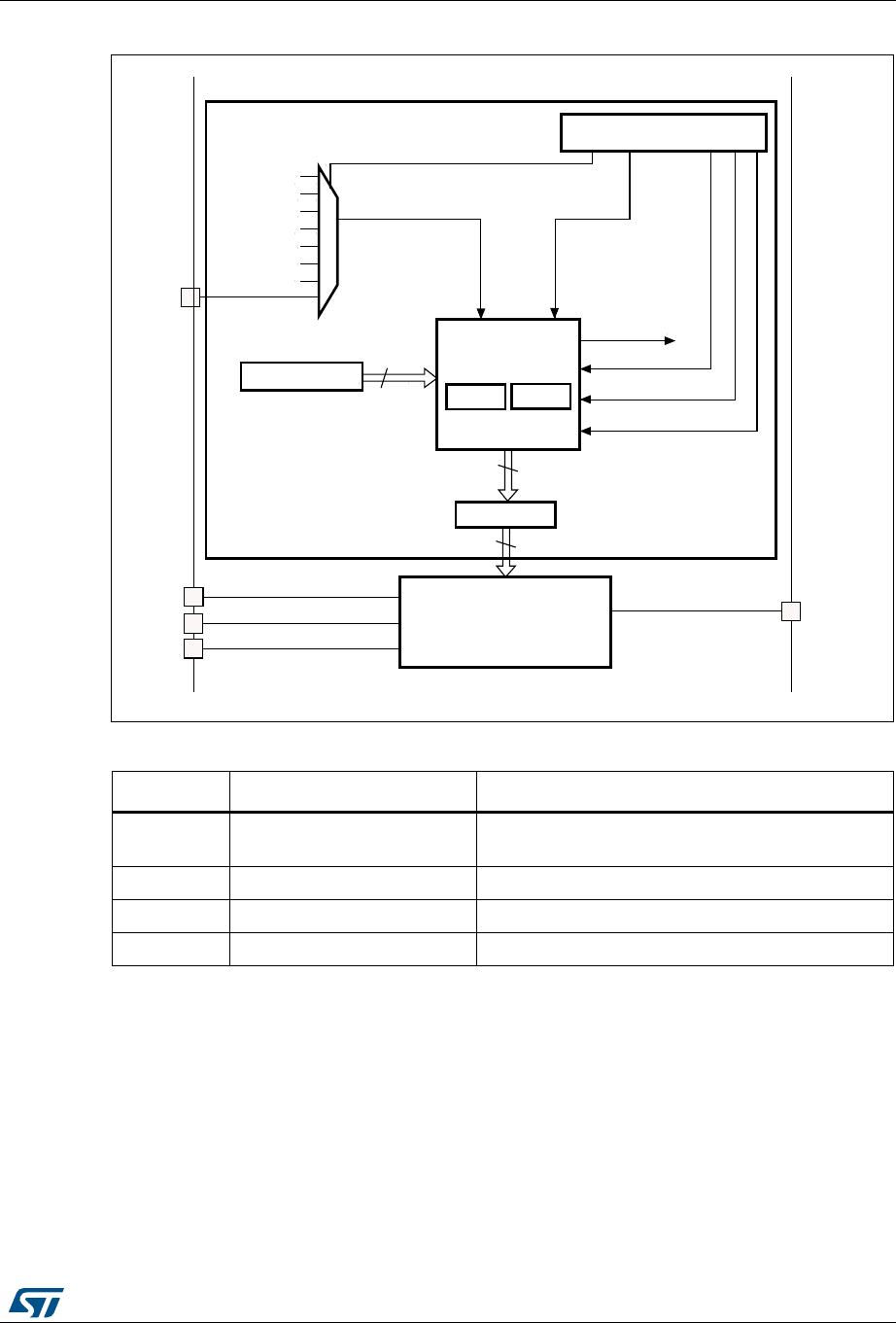
RM0430 Rev 8 367/1324
RM0430 Digital-to-analog converter (DAC)
387
Figure 67. DAC channel block diagram
Note: Once the DAC channelx is enabled, the corresponding GPIO pin (PA4 or PA5) is
automatically connected to the analog converter output (DAC_OUTx). In order to avoid
parasitic consumption, the PA4 or PA5 pin should first be configured to analog (AIN).
Table 83. DAC pins
Name Signal type Remarks
VREF+
Input, analog reference
positive
The higher/positive reference voltage for the DAC,
V ≤ V
REF+ ≤ V
DDA
VDDA Input, analog supply Analog power supply
VSSA Input, analog supply ground Ground for analog power supply
DAC_OUTx Analog output signal DAC channelx analog output
V
DDA
V
SSA
V
REF+
DAC_OUTx
Control logicx
DHRx
12-bit
12-bit
LFSRx trianglex
DM A requestx
TSELx[2:0] bits
TIM4_T RGO
TIM5_T RGO
TIM6_T RGO
TIM7_T RGO
TIM2_T RGO
TIM8_T RGO
EXTI_9
DMAENx
TENx
MAMPx[3:0] bits
WAVENx[1:0] bits
SWTRIGx
DORx
Digital-to-analog
converterx
12-bit
DAC control register
ai14708b
Trigger selectorx

Digital-to-analog converter (DAC) RM0430
368/1324 RM0430 Rev 8
14.3 DAC functional description
14.3.1 DAC channel enable
Each DAC channel can be powered on by setting its corresponding ENx bit in the DAC_CR
register. The DAC channel is then enabled after a startup time tWAKEUP
.
Note: The ENx bit enables the analog DAC Channelx macrocell only. The DAC Channelx digital
interface is enabled even if the ENx bit is reset.
14.3.2 DAC output buffer enable
The DAC integrates two output buffers that can be used to reduce the output impedance,
and to drive external loads directly without having to add an external operational amplifier.
Each DAC channel output buffer can be enabled and disabled using the corresponding
BOFFx bit in the DAC_CR register.
14.3.3 DAC data format
Depending on the selected configuration mode, the data have to be written into the specified
register as described below:
•Single DAC channelx, there are three possibilities:
– 8-bit right alignment: the software has to load data into the DAC_DHR8Rx [7:0]
bits (stored into the DHRx[11:4] bits)
– 12-bit left alignment: the software has to load data into the DAC_DHR12Lx [15:4]
bits (stored into the DHRx[11:0] bits)
– 12-bit right alignment: the software has to load data into the DAC_DHR12Rx [11:0]
bits (stored into the DHRx[11:0] bits)
Depending on the loaded DAC_DHRyyyx register, the data written by the user is shifted and
stored into the corresponding DHRx (data holding registerx, which are internal non-memory-
mapped registers). The DHRx register is then loaded into the DORx register either
automatically, by software trigger or by an external event trigger.
RM0430 Rev 8 369/1324
RM0430 Digital-to-analog converter (DAC)
387
Figure 68. Data registers in single DAC channel mode
•Dual DAC channels, there are three possibilities:
– 8-bit right alignment: data for DAC channel1 to be loaded into the DAC_DHR8RD
[7:0] bits (stored into the DHR1[11:4] bits) and data for DAC channel2 to be loaded
into the DAC_DHR8RD [15:8] bits (stored into the DHR2[11:4] bits)
– 12-bit left alignment: data for DAC channel1 to be loaded into the DAC_DHR12LD
[15:4] bits (stored into the DHR1[11:0] bits) and data for DAC channel2 to be
loaded into the DAC_DHR12LD [31:20] bits (stored into the DHR2[11:0] bits)
– 12-bit right alignment: data for DAC channel1 to be loaded into the
DAC_DHR12RD [11:0] bits (stored into the DHR1[11:0] bits) and data for DAC
channel2 to be loaded into the DAC_DHR12LD [27:16] bits (stored into the
DHR2[11:0] bits)
Depending on the loaded DAC_DHRyyyD register, the data written by the user is shifted
and stored into DHR1 and DHR2 (data holding registers, which are internal non-memory-
mapped registers). The DHR1 and DHR2 registers are then loaded into the DOR1 and
DOR2 registers, respectively, either automatically, by software trigger or by an external
event trigger.
Figure 69. Data registers in dual DAC channel mode
14.3.4 DAC conversion
The DAC_DORx cannot be written directly and any data transfer to the DAC channelx must
be performed by loading the DAC_DHRx register (write to DAC_DHR8Rx, DAC_DHR12Lx,
DAC_DHR12Rx, DAC_DHR8RD, DAC_DHR12LD or DAC_DHR12LD).
Data stored in the DAC_DHRx register are automatically transferred to the DAC_DORx
register after one APB1 clock cycle, if no hardware trigger is selected (TENx bit in DAC_CR
register is reset). However, when a hardware trigger is selected (TENx bit in DAC_CR
register is set) and a trigger occurs, the transfer is performed three APB1 clock cycles later.
ELWULJKWDOLJQHG
ELWOHIWDOLJQHG
ELWULJKWDOLJQHG
DLE
31 24 15 7 0
8-bit right aligned
12-bit left aligned
12-bit right aligned
ai14709
ELWULJKWDOLJQHG
ELWOHIWDOLJQHG
ELWULJKWDOLJQHG
DLE
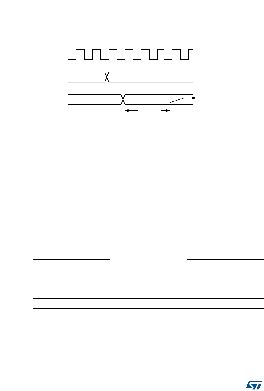
Digital-to-analog converter (DAC) RM0430
370/1324 RM0430 Rev 8
When DAC_DORx is loaded with the DAC_DHRx contents, the analog output voltage
becomes available after a time tSETTLING that depends on the power supply voltage and the
analog output load.
Figure 70. Timing diagram for conversion with trigger disabled TEN = 0
14.3.5 DAC output voltage
Digital inputs are converted to output voltages on a linear conversion between 0 and VREF+.
The analog output voltages on each DAC channel pin are determined by the following
equation:
14.3.6 DAC trigger selection
If the TENx control bit is set, conversion can then be triggered by an external event (timer
counter, external interrupt line). The TSELx[2:0] control bits determine which out of 8
possible events will trigger conversion as shown in Table 84.
Each time a DAC interface detects a rising edge on the selected timer TRGO output, or on
the selected external interrupt line 9, the last data stored into the DAC_DHRx register are
transferred into the DAC_DORx register. The DAC_DORx register is updated three APB1
cycles after the trigger occurs.
!0"?#,+
X!#
X!#
T3%44,).'
$(2
$/2
/UTPUTVOLTAGE
AVAILABLEON$!#?/54PIN
AIC
DACoutput VREF
DOR
4096
--------------
×=
Table 84. External triggers
Source Type TSEL[2:0]
Timer 6 TRGO event
Internal signal from on-chip
timers
000
Timer 8 TRGO event 001
Timer 7 TRGO event 010
Timer 5 TRGO event 011
Timer 2 TRGO event 100
Timer 4 TRGO event 101
EXTI line9 External pin 110
SWTRIG Software control bit 111

RM0430 Rev 8 371/1324
RM0430 Digital-to-analog converter (DAC)
387
If the software trigger is selected, the conversion starts once the SWTRIG bit is set.
SWTRIG is reset by hardware once the DAC_DORx register has been loaded with the
DAC_DHRx register contents.
Note: TSELx[2:0] bit cannot be changed when the ENx bit is set.
When software trigger is selected, the transfer from the DAC_DHRx register to the
DAC_DORx register takes only one APB1 clock cycle.
14.3.7 DMA request
Each DAC channel has a DMA capability. Two DMA channels are used to service DAC
channel DMA requests.
A DAC DMA request is generated when an external trigger (but not a software trigger)
occurs while the DMAENx bit is set. The value of the DAC_DHRx register is then transferred
into the DAC_DORx register.
In dual mode, if both DMAENx bits are set, two DMA requests are generated. If only one
DMA request is needed, the user should set only the corresponding DMAENx bit. In this
way, the application can manage both DAC channels in dual mode by using one DMA
request and a unique DMA channel.
DMA underrun
The DAC DMA request is not queued so that if a second external trigger arrives before the
acknowledgement for the first external trigger is received (first request), then no new
request is issued and the DMA channelx underrun flag DMAUDRx in the DAC_SR register
is set, reporting the error condition. DMA data transfers are then disabled and no further
DMA request is treated. The DAC channelx continues to convert old data.
The software should clear the DMAUDRx flag by writing “1”, clear the DMAEN bit of the
used DMA stream and re-initialize both DMA and DAC channelx to restart the transfer
correctly. The software should modify the DAC trigger conversion frequency or lighten the
DMA workload to avoid a new DMA underrun. Finally, the DAC conversion could be
resumed by enabling both DMA data transfer and conversion trigger.
For each DAC channelx, an interrupt is also generated if its corresponding DMAUDRIEx bit
in the DAC_CR register is enabled.
14.3.8 Noise generation
In order to generate a variable-amplitude pseudonoise, an LFSR (linear feedback shift
register) is available. DAC noise generation is selected by setting WAVEx[1:0] to “01”. The
preloaded value in LFSR is 0xAAA. This register is updated three APB1 clock cycles after
each trigger event, following a specific calculation algorithm.
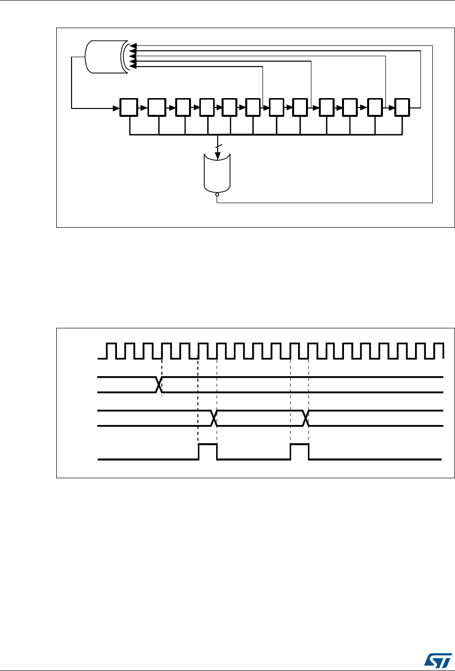
Digital-to-analog converter (DAC) RM0430
372/1324 RM0430 Rev 8
Figure 71. DAC LFSR register calculation algorithm
The LFSR value, that may be masked partially or totally by means of the MAMPx[3:0] bits in
the DAC_CR register, is added up to the DAC_DHRx contents without overflow and this
value is then stored into the DAC_DORx register.
If LFSR is 0x0000, a ‘1 is injected into it (antilock-up mechanism).
It is possible to reset LFSR wave generation by resetting the WAVEx[1:0] bits.
Figure 72. DAC conversion (SW trigger enabled) with LFSR wave generation
Note: The DAC trigger must be enabled for noise generation by setting the TENx bit in the
DAC_CR register.
14.3.9 Triangle-wave generation
It is possible to add a small-amplitude triangular waveform on a DC or slowly varying signal.
DAC triangle-wave generation is selected by setting WAVEx[1:0] to “10”. The amplitude is
configured through the MAMPx[3:0] bits in the DAC_CR register. An internal triangle counter
is incremented three APB1 clock cycles after each trigger event. The value of this counter is
then added to the DAC_DHRx register without overflow and the sum is stored into the
DAC_DORx register. The triangle counter is incremented as long as it is less than the
maximum amplitude defined by the MAMPx[3:0] bits. Once the configured amplitude is
reached, the counter is decremented down to 0, then incremented again and so on.
125
;
;
;
;
;
;25
DLF
$3%B&/.
[
[$$$
'+5
'25
DLE
['
6:75,*
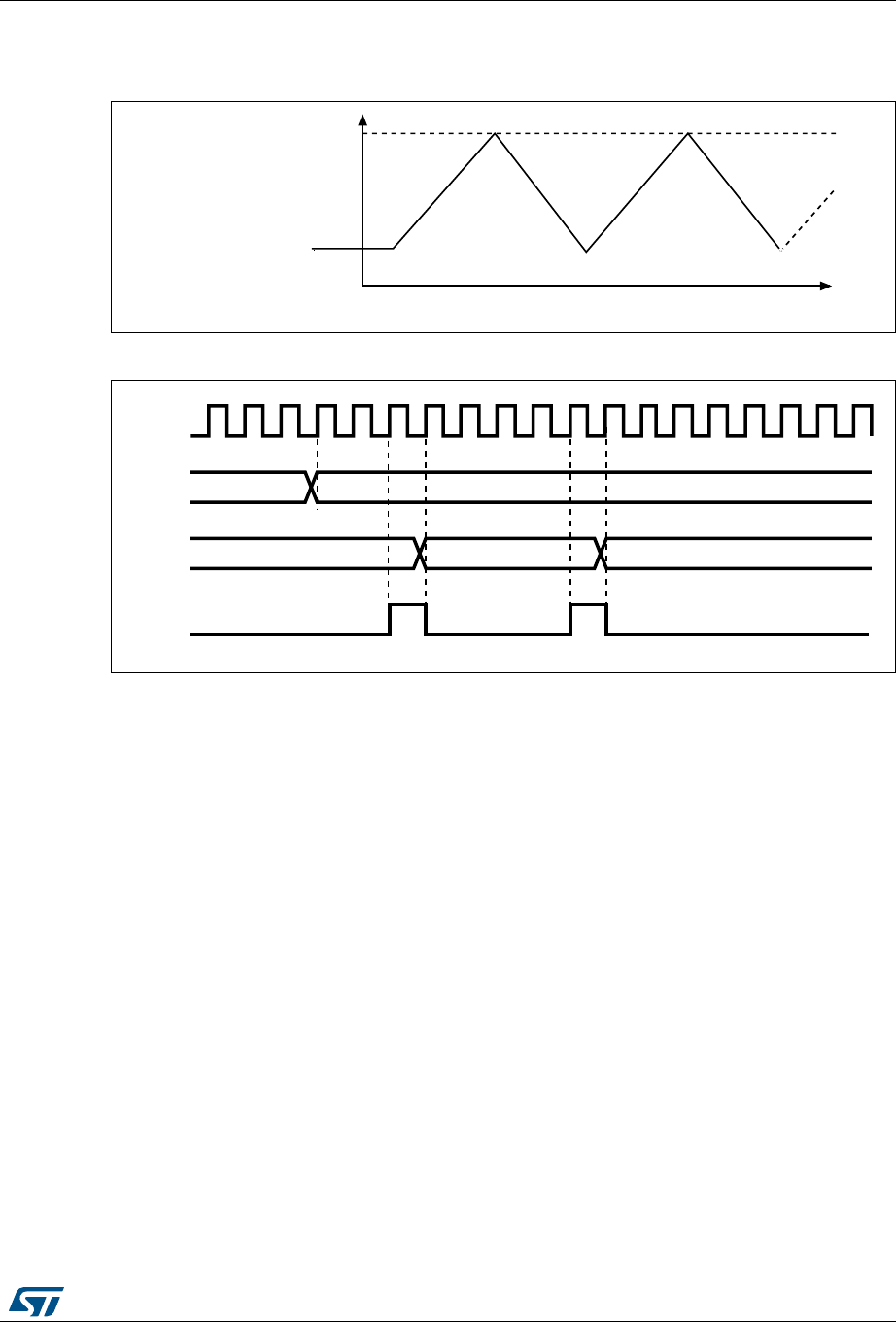
RM0430 Rev 8 373/1324
RM0430 Digital-to-analog converter (DAC)
387
It is possible to reset triangle wave generation by resetting the WAVEx[1:0] bits.
Figure 73. DAC triangle wave generation
Figure 74. DAC conversion (SW trigger enabled) with triangle wave generation
Note: The DAC trigger must be enabled for noise generation by setting the TENx bit in the
DAC_CR register.
The MAMPx[3:0] bits must be configured before enabling the DAC, otherwise they cannot
be changed.
14.4 Dual DAC channel conversion
To efficiently use the bus bandwidth in applications that require the two DAC channels at the
same time, three dual registers are implemented: DHR8RD, DHR12RD and DHR12LD. A
unique register access is then required to drive both DAC channels at the same time.
Eleven possible conversion modes are possible using the two DAC channels and these dual
registers. All the conversion modes can nevertheless be obtained using separate DHRx
registers if needed.
All modes are described in the paragraphs below.
-!-0X;=MAXAMPLITUDE
$!#?$(2XBASEVALUE
$!#?$(2XBASEVALUE
)NCREMENTATION
AIC
$ECREMENTATION
$3%B&/.
[
[$$$
'+5
'25
DLE
['
6:75,*

Digital-to-analog converter (DAC) RM0430
374/1324 RM0430 Rev 8
14.4.1 Independent trigger without wave generation
To configure the DAC in this conversion mode, the following sequence is required:
•Set the two DAC channel trigger enable bits TEN1 and TEN2
•Configure different trigger sources by setting different values in the TSEL1[2:0] and
TSEL2[2:0] bits
•Load the dual DAC channel data into the desired DHR register (DAC_DHR12RD,
DAC_DHR12LD or DAC_DHR8RD)
When a DAC channel1 trigger arrives, the DHR1 register is transferred into DAC_DOR1
(three APB1 clock cycles later).
When a DAC channel2 trigger arrives, the DHR2 register is transferred into DAC_DOR2
(three APB1 clock cycles later).
14.4.2 Independent trigger with single LFSR generation
To configure the DAC in this conversion mode, the following sequence is required:
•Set the two DAC channel trigger enable bits TEN1 and TEN2
•Configure different trigger sources by setting different values in the TSEL1[2:0] and
TSEL2[2:0] bits
•Configure the two DAC channel WAVEx[1:0] bits as “01” and the same LFSR mask
value in the MAMPx[3:0] bits
•Load the dual DAC channel data into the desired DHR register (DHR12RD, DHR12LD
or DHR8RD)
When a DAC channel1 trigger arrives, the LFSR1 counter, with the same mask, is added to
the DHR1 register and the sum is transferred into DAC_DOR1 (three APB1 clock cycles
later). Then the LFSR1 counter is updated.
When a DAC channel2 trigger arrives, the LFSR2 counter, with the same mask, is added to
the DHR2 register and the sum is transferred into DAC_DOR2 (three APB1 clock cycles
later). Then the LFSR2 counter is updated.
14.4.3 Independent trigger with different LFSR generation
To configure the DAC in this conversion mode, the following sequence is required:
•Set the two DAC channel trigger enable bits TEN1 and TEN2
•Configure different trigger sources by setting different values in the TSEL1[2:0] and
TSEL2[2:0] bits
•Configure the two DAC channel WAVEx[1:0] bits as “01” and set different LFSR masks
values in the MAMP1[3:0] and MAMP2[3:0] bits
•Load the dual DAC channel data into the desired DHR register (DAC_DHR12RD,
DAC_DHR12LD or DAC_DHR8RD)
When a DAC channel1 trigger arrives, the LFSR1 counter, with the mask configured by
MAMP1[3:0], is added to the DHR1 register and the sum is transferred into DAC_DOR1
(three APB1 clock cycles later). Then the LFSR1 counter is updated.
When a DAC channel2 trigger arrives, the LFSR2 counter, with the mask configured by
MAMP2[3:0], is added to the DHR2 register and the sum is transferred into DAC_DOR2
(three APB1 clock cycles later). Then the LFSR2 counter is updated.

RM0430 Rev 8 375/1324
RM0430 Digital-to-analog converter (DAC)
387
14.4.4 Independent trigger with single triangle generation
To configure the DAC in this conversion mode, the following sequence is required:
•Set the two DAC channel trigger enable bits TEN1 and TEN2
•Configure different trigger sources by setting different values in the TSEL1[2:0] and
TSEL2[2:0] bits
•Configure the two DAC channel WAVEx[1:0] bits as “1x” and the same maximum
amplitude value in the MAMPx[3:0] bits
•Load the dual DAC channel data into the desired DHR register (DAC_DHR12RD,
DAC_DHR12LD or DAC_DHR8RD)
When a DAC channel1 trigger arrives, the DAC channel1 triangle counter, with the same
triangle amplitude, is added to the DHR1 register and the sum is transferred into
DAC_DOR1 (three APB1 clock cycles later). The DAC channel1 triangle counter is then
updated.
When a DAC channel2 trigger arrives, the DAC channel2 triangle counter, with the same
triangle amplitude, is added to the DHR2 register and the sum is transferred into
DAC_DOR2 (three APB1 clock cycles later). The DAC channel2 triangle counter is then
updated.
14.4.5 Independent trigger with different triangle generation
To configure the DAC in this conversion mode, the following sequence is required:
•Set the two DAC channel trigger enable bits TEN1 and TEN2
•Configure different trigger sources by setting different values in the TSEL1[2:0] and
TSEL2[2:0] bits
•Configure the two DAC channel WAVEx[1:0] bits as “1x” and set different maximum
amplitude values in the MAMP1[3:0] and MAMP2[3:0] bits
•Load the dual DAC channel data into the desired DHR register (DAC_DHR12RD,
DAC_DHR12LD or DAC_DHR8RD)
When a DAC channel1 trigger arrives, the DAC channel1 triangle counter, with a triangle
amplitude configured by MAMP1[3:0], is added to the DHR1 register and the sum is
transferred into DAC_DOR1 (three APB1 clock cycles later). The DAC channel1 triangle
counter is then updated.
When a DAC channel2 trigger arrives, the DAC channel2 triangle counter, with a triangle
amplitude configured by MAMP2[3:0], is added to the DHR2 register and the sum is
transferred into DAC_DOR2 (three APB1 clock cycles later). The DAC channel2 triangle
counter is then updated.
14.4.6 Simultaneous software start
To configure the DAC in this conversion mode, the following sequence is required:
•Load the dual DAC channel data to the desired DHR register (DAC_DHR12RD,
DAC_DHR12LD or DAC_DHR8RD)
In this configuration, one APB1 clock cycle later, the DHR1 and DHR2 registers are
transferred into DAC_DOR1 and DAC_DOR2, respectively.

Digital-to-analog converter (DAC) RM0430
376/1324 RM0430 Rev 8
14.4.7 Simultaneous trigger without wave generation
To configure the DAC in this conversion mode, the following sequence is required:
•Set the two DAC channel trigger enable bits TEN1 and TEN2
•Configure the same trigger source for both DAC channels by setting the same value in
the TSEL1[2:0] and TSEL2[2:0] bits
•Load the dual DAC channel data to the desired DHR register (DAC_DHR12RD,
DAC_DHR12LD or DAC_DHR8RD)
When a trigger arrives, the DHR1 and DHR2 registers are transferred into DAC_DOR1 and
DAC_DOR2, respectively (after three APB1 clock cycles).
14.4.8 Simultaneous trigger with single LFSR generation
To configure the DAC in this conversion mode, the following sequence is required:
•Set the two DAC channel trigger enable bits TEN1 and TEN2
•Configure the same trigger source for both DAC channels by setting the same value in
the TSEL1[2:0] and TSEL2[2:0] bits
•Configure the two DAC channel WAVEx[1:0] bits as “01” and the same LFSR mask
value in the MAMPx[3:0] bits
•Load the dual DAC channel data to the desired DHR register (DHR12RD, DHR12LD or
DHR8RD)
When a trigger arrives, the LFSR1 counter, with the same mask, is added to the DHR1
register and the sum is transferred into DAC_DOR1 (three APB1 clock cycles later). The
LFSR1 counter is then updated. At the same time, the LFSR2 counter, with the same mask,
is added to the DHR2 register and the sum is transferred into DAC_DOR2 (three APB1
clock cycles later). The LFSR2 counter is then updated.
14.4.9 Simultaneous trigger with different LFSR generation
To configure the DAC in this conversion mode, the following sequence is required:
•Set the two DAC channel trigger enable bits TEN1 and TEN2
•Configure the same trigger source for both DAC channels by setting the same value in
the TSEL1[2:0] and TSEL2[2:0] bits
•Configure the two DAC channel WAVEx[1:0] bits as “01” and set different LFSR mask
values using the MAMP1[3:0] and MAMP2[3:0] bits
•Load the dual DAC channel data into the desired DHR register (DAC_DHR12RD,
DAC_DHR12LD or DAC_DHR8RD)
When a trigger arrives, the LFSR1 counter, with the mask configured by MAMP1[3:0], is
added to the DHR1 register and the sum is transferred into DAC_DOR1 (three APB1 clock
cycles later). The LFSR1 counter is then updated.
At the same time, the LFSR2 counter, with the mask configured by MAMP2[3:0], is added to
the DHR2 register and the sum is transferred into DAC_DOR2 (three APB1 clock cycles
later). The LFSR2 counter is then updated.

RM0430 Rev 8 377/1324
RM0430 Digital-to-analog converter (DAC)
387
14.4.10 Simultaneous trigger with single triangle generation
To configure the DAC in this conversion mode, the following sequence is required:
•Set the two DAC channel trigger enable bits TEN1 and TEN2
•Configure the same trigger source for both DAC channels by setting the same value in
the TSEL1[2:0] and TSEL2[2:0] bits
•Configure the two DAC channel WAVEx[1:0] bits as “1x” and the same maximum
amplitude value using the MAMPx[3:0] bits
•Load the dual DAC channel data into the desired DHR register (DAC_DHR12RD,
DAC_DHR12LD or DAC_DHR8RD)
When a trigger arrives, the DAC channel1 triangle counter, with the same triangle
amplitude, is added to the DHR1 register and the sum is transferred into DAC_DOR1 (three
APB1 clock cycles later). The DAC channel1 triangle counter is then updated.
At the same time, the DAC channel2 triangle counter, with the same triangle amplitude, is
added to the DHR2 register and the sum is transferred into DAC_DOR2 (three APB1 clock
cycles later). The DAC channel2 triangle counter is then updated.
14.4.11 Simultaneous trigger with different triangle generation
To configure the DAC in this conversion mode, the following sequence is required:
•Set the two DAC channel trigger enable bits TEN1 and TEN2
•Configure the same trigger source for both DAC channels by setting the same value in
the TSEL1[2:0] and TSEL2[2:0] bits
•Configure the two DAC channel WAVEx[1:0] bits as “1x” and set different maximum
amplitude values in the MAMP1[3:0] and MAMP2[3:0] bits
•Load the dual DAC channel data into the desired DHR register (DAC_DHR12RD,
DAC_DHR12LD or DAC_DHR8RD)
When a trigger arrives, the DAC channel1 triangle counter, with a triangle amplitude
configured by MAMP1[3:0], is added to the DHR1 register and the sum is transferred into
DAC_DOR1 (three APB1 clock cycles later). Then the DAC channel1 triangle counter is
updated.
At the same time, the DAC channel2 triangle counter, with a triangle amplitude configured
by MAMP2[3:0], is added to the DHR2 register and the sum is transferred into DAC_DOR2
(three APB1 clock cycles later). Then the DAC channel2 triangle counter is updated.

Digital-to-analog converter (DAC) RM0430
378/1324 RM0430 Rev 8
14.5 DAC registers
Refer to Section 1.2: List of abbreviations for registers for a list of abbreviations used in
register descriptions.
The peripheral registers have to be accessed by words (32 bits).
14.5.1 DAC control register (DAC_CR)
Address offset: 0x00
Reset value: 0x0000 0000
31 30 29 28 27 26 25 24 23 22 21 20 19 18 17 16
Reserved
DMAU
DRIE2
DMA
EN2 MAMP2[3:0] WAVE2[1:0] TSEL2[2:0] TEN2 BOFF2 EN2
rw rw rw rw rw rw rw rw rw rw rw rw rw rw
1514131211109876543210
Reserved
DMAU
DRIE1
DMA
EN1 MAMP1[3:0] WAVE1[1:0] TSEL1[2:0] TEN1 BOFF1 EN1
rw rw rw rw rw rw rw rw rw rw rw rw rw rw
Bits 31:30 Reserved, must be kept at reset value.
Bits 29 DMAUDRIE2: DAC channel2 DMA underrun interrupt enable
This bit is set and cleared by software.
0: DAC channel2 DMA underrun interrupt disabled
1: DAC channel2 DMA underrun interrupt enabled
Bit 28 DMAEN2: DAC channel2 DMA enable
This bit is set and cleared by software.
0: DAC channel2 DMA mode disabled
1: DAC channel2 DMA mode enabled
Bits 27:24 MAMP2[3:0]: DAC channel2 mask/amplitude selector
These bits are written by software to select mask in wave generation mode or amplitude in
triangle generation mode.
0000: Unmask bit0 of LFSR/ triangle amplitude equal to 1
0001: Unmask bits[1:0] of LFSR/ triangle amplitude equal to 3
0010: Unmask bits[2:0] of LFSR/ triangle amplitude equal to 7
0011: Unmask bits[3:0] of LFSR/ triangle amplitude equal to 15
0100: Unmask bits[4:0] of LFSR/ triangle amplitude equal to 31
0101: Unmask bits[5:0] of LFSR/ triangle amplitude equal to 63
0110: Unmask bits[6:0] of LFSR/ triangle amplitude equal to 127
0111: Unmask bits[7:0] of LFSR/ triangle amplitude equal to 255
1000: Unmask bits[8:0] of LFSR/ triangle amplitude equal to 511
1001: Unmask bits[9:0] of LFSR/ triangle amplitude equal to 1023
1010: Unmask bits[10:0] of LFSR/ triangle amplitude equal to 2047
≥ 1011: Unmask bits[11:0] of LFSR/ triangle amplitude equal to 4095
Bits 23:22 WAVE2[1:0]: DAC channel2 noise/triangle wave generation enable
These bits are set/reset by software.
00: wave generation disabled
01: Noise wave generation enabled
1x: Triangle wave generation enabled
Note: Only used if bit TEN2 = 1 (DAC channel2 trigger enabled)

RM0430 Rev 8 379/1324
RM0430 Digital-to-analog converter (DAC)
387
Bits 21:19 TSEL2[2:0]: DAC channel2 trigger selection
These bits select the external event used to trigger DAC channel2
000: Timer 6 TRGO event
001: Timer 8 TRGO event
010: Timer 7 TRGO event
011: 5 TRGO event
100: Timer 2 TRGO event
101: Timer 4 TRGO event
110: External line9
111: Software trigger
Note: Only used if bit TEN2 = 1 (DAC channel2 trigger enabled).
Bit 18 TEN2: DAC channel2 trigger enable
This bit is set and cleared by software to enable/disable DAC channel2 trigger
0: DAC channel2 trigger disabled and data written into the DAC_DHRx register are
transferred one APB1 clock cycle later to the DAC_DOR2 register
1: DAC channel2 trigger enabled and data from the DAC_DHRx register are transferred
three APB1 clock cycles later to the DAC_DOR2 register
Note: When software trigger is selected, the transfer from the DAC_DHRx register to the
DAC_DOR2 register takes only one APB1 clock cycle.
Bit 17 BOFF2: DAC channel2 output buffer disable
This bit is set and cleared by software to enable/disable DAC channel2 output buffer.
0: DAC channel2 output buffer enabled
1: DAC channel2 output buffer disabled
Bit 16 EN2: DAC channel2 enable
This bit is set and cleared by software to enable/disable DAC channel2.
0: DAC channel2 disabled
1: DAC channel2 enabled
Bits 15:14 Reserved, must be kept at reset value.
Bit 13 DMAUDRIE1: DAC channel1 DMA Underrun Interrupt enable
This bit is set and cleared by software.
0: DAC channel1 DMA Underrun Interrupt disabled
1: DAC channel1 DMA Underrun Interrupt enabled
Bit 12 DMAEN1: DAC channel1 DMA enable
This bit is set and cleared by software.
0: DAC channel1 DMA mode disabled
1: DAC channel1 DMA mode enabled

Digital-to-analog converter (DAC) RM0430
380/1324 RM0430 Rev 8
Bits 11:8 MAMP1[3:0]: DAC channel1 mask/amplitude selector
These bits are written by software to select mask in wave generation mode or amplitude in
triangle generation mode.
0000: Unmask bit0 of LFSR/ triangle amplitude equal to 1
0001: Unmask bits[1:0] of LFSR/ triangle amplitude equal to 3
0010: Unmask bits[2:0] of LFSR/ triangle amplitude equal to 7
0011: Unmask bits[3:0] of LFSR/ triangle amplitude equal to 15
0100: Unmask bits[4:0] of LFSR/ triangle amplitude equal to 31
0101: Unmask bits[5:0] of LFSR/ triangle amplitude equal to 63
0110: Unmask bits[6:0] of LFSR/ triangle amplitude equal to 127
0111: Unmask bits[7:0] of LFSR/ triangle amplitude equal to 255
1000: Unmask bits[8:0] of LFSR/ triangle amplitude equal to 511
1001: Unmask bits[9:0] of LFSR/ triangle amplitude equal to 1023
1010: Unmask bits[10:0] of LFSR/ triangle amplitude equal to 2047
≥ 1011: Unmask bits[11:0] of LFSR/ triangle amplitude equal to 4095
Bits 7:6 WAVE1[1:0]: DAC channel1 noise/triangle wave generation enable
These bits are set and cleared by software.
00: wave generation disabled
01: Noise wave generation enabled
1x: Triangle wave generation enabled
Note: Only used if bit TEN1 = 1 (DAC channel1 trigger enabled).
Bits 5:3 TSEL1[2:0]: DAC channel1 trigger selection
These bits select the external event used to trigger DAC channel1.
000: Timer 6 TRGO event
001: Timer 8 TRGO event
010: Timer 7 TRGO event
011: Timer TRGO event
100: Timer 2 TRGO event
101: Timer 4 TRGO event
110: External line9
111: Software trigger
Note: Only used if bit TEN1 = 1 (DAC channel1 trigger enabled).
Bit 2 TEN1: DAC channel1 trigger enable
This bit is set and cleared by software to enable/disable DAC channel1 trigger.
0: DAC channel1 trigger disabled and data written into the DAC_DHRx register are
transferred one APB1 clock cycle later to the DAC_DOR1 register
1: DAC channel1 trigger enabled and data from the DAC_DHRx register are transferred
three APB1 clock cycles later to the DAC_DOR1 register
Note: When software trigger is selected, the transfer from the DAC_DHRx register to the
DAC_DOR1 register takes only one APB1 clock cycle.
Bit 1 BOFF1: DAC channel1 output buffer disable
This bit is set and cleared by software to enable/disable DAC channel1 output buffer.
0: DAC channel1 output buffer enabled
1: DAC channel1 output buffer disabled
Bit 0 EN1: DAC channel1 enable
This bit is set and cleared by software to enable/disable DAC channel1.
0: DAC channel1 disabled
1: DAC channel1 enabled

RM0430 Rev 8 381/1324
RM0430 Digital-to-analog converter (DAC)
387
14.5.2 DAC software trigger register (DAC_SWTRIGR)
Address offset: 0x04
Reset value: 0x0000 0000
14.5.3 DAC channel1 12-bit right-aligned data holding register
(DAC_DHR12R1)
Address offset: 0x08
Reset value: 0x0000 0000
31 30 29 28 27 26 25 24 23 22 21 20 19 18 17 16
Reserved
15 14 13 12 11 10 9 8 7 6 5 4 3 2 1 0
Reserved
SWTRIG2 SWTRIG1
ww
Bits 31:2 Reserved, must be kept at reset value.
Bit 1 SWTRIG2: DAC channel2 software trigger
This bit is set and cleared by software to enable/disable the software trigger.
0: Software trigger disabled
1: Software trigger enabled
Note: This bit is cleared by hardware (one APB1 clock cycle later) once the DAC_DHR2
register value has been loaded into the DAC_DOR2 register.
Bit 0 SWTRIG1: DAC channel1 software trigger
This bit is set and cleared by software to enable/disable the software trigger.
0: Software trigger disabled
1: Software trigger enabled
Note: This bit is cleared by hardware (one APB1 clock cycle later) once the DAC_DHR1
register value has been loaded into the DAC_DOR1 register.
31 30 29 28 27 26 25 24 23 22 21 20 19 18 17 16
Reserved
1514131211109876543210
Reserved
DACC1DHR[11:0]
rw rw rw rw rw rw rw rw rw rw rw rw
Bits 31:12 Reserved, must be kept at reset value.
Bits 11:0 DACC1DHR[11:0]: DAC channel1 12-bit right-aligned data
These bits are written by software which specifies 12-bit data for DAC channel1.
Digital-to-analog converter (DAC) RM0430
382/1324 RM0430 Rev 8
14.5.4 DAC channel1 12-bit left aligned data holding register
(DAC_DHR12L1)
Address offset: 0x0C
Reset value: 0x0000 0000
14.5.5 DAC channel1 8-bit right aligned data holding register
(DAC_DHR8R1)
Address offset: 0x10
Reset value: 0x0000 0000
31 30 29 28 27 26 25 24 23 22 21 20 19 18 17 16
Reserved
1514131211109876543210
DACC1DHR[11:0] Reserved
rw rw rw rw rw rw rw rw rw rw rw rw
Bits 31:16 Reserved, must be kept at reset value.
Bits 15:4 DACC1DHR[11:0]: DAC channel1 12-bit left-aligned data
These bits are written by software which specifies 12-bit data for DAC channel1.
Bits 3:0 Reserved, must be kept at reset value.
31 30 29 28 27 26 25 24 23 22 21 20 19 18 17 16
Reserved
1514131211109876543210
Reserved
DACC1DHR[7:0]
rw rw rw rw rw rw rw rw
Bits 31:8 Reserved, must be kept at reset value.
Bits 7:0 DACC1DHR[7:0]: DAC channel1 8-bit right-aligned data
These bits are written by software which specifies 8-bit data for DAC channel1.
RM0430 Rev 8 383/1324
RM0430 Digital-to-analog converter (DAC)
387
14.5.6 DAC channel2 12-bit right aligned data holding register
(DAC_DHR12R2)
Address offset: 0x14
Reset value: 0x0000 0000
14.5.7 DAC channel2 12-bit left aligned data holding register
(DAC_DHR12L2)
Address offset: 0x18
Reset value: 0x0000 0000
14.5.8 DAC channel2 8-bit right-aligned data holding register
(DAC_DHR8R2)
Address offset: 0x1C
Reset value: 0x0000 0000
31 30 29 28 27 26 25 24 23 22 21 20 19 18 17 16
Reserved
1514131211109876543210
Reserved DACC2DHR[11:0]
rw rw rw rw rw rw rw rw rw rw rw rw
Bits 31:12 Reserved, must be kept at reset value.
Bits 11:0 DACC2DHR[11:0]: DAC channel2 12-bit right-aligned data
These bits are written by software which specifies 12-bit data for DAC channel2.
31 30 29 28 27 26 25 24 23 22 21 20 19 18 17 16
Reserved
1514131211109876543210
DACC2DHR[11:0] Reserved
rw rw rw rw rw rw rw rw rw rw rw rw
Bits 31:16 Reserved, must be kept at reset value.
Bits 15:4 DACC2DHR[11:0]: DAC channel2 12-bit left-aligned data
These bits are written by software which specify 12-bit data for DAC channel2.
Bits 3:0 Reserved, must be kept at reset value.
31 30 29 28 27 26 25 24 23 22 21 20 19 18 17 16
Reserved
1514131211109876543210
Reserved
DACC2DHR[7:0]
rw rw rw rw rw rw rw rw
Bits 31:8 Reserved, must be kept at reset value.
Bits 7:0 DACC2DHR[7:0]: DAC channel2 8-bit right-aligned data
These bits are written by software which specifies 8-bit data for DAC channel2.
Digital-to-analog converter (DAC) RM0430
384/1324 RM0430 Rev 8
14.5.9 Dual DAC 12-bit right-aligned data holding register
(DAC_DHR12RD)
Address offset: 0x20
Reset value: 0x0000 0000
14.5.10 DUAL DAC 12-bit left aligned data holding register
(DAC_DHR12LD)
Address offset: 0x24
Reset value: 0x0000 0000
31 30 29 28 27 26 25 24 23 22 21 20 19 18 17 16
Reserved
DACC2DHR[11:0]
rw rw rw rw rw rw rw rw rw rw rw rw
1514131211109876543210
Reserved
DACC1DHR[11:0]
rw rw rw rw rw rw rw rw rw rw rw rw
Bits 31:28 Reserved, must be kept at reset value.
Bits 27:16 DACC2DHR[11:0]: DAC channel2 12-bit right-aligned data
These bits are written by software which specifies 12-bit data for DAC channel2.
Bits 15:12 Reserved, must be kept at reset value.
Bits 11:0 DACC1DHR[11:0]: DAC channel1 12-bit right-aligned data
These bits are written by software which specifies 12-bit data for DAC channel1.
31 30 29 28 27 26 25 24 23 22 21 20 19 18 17 16
DACC2DHR[11:0]
Reserved
rw rw rw rw rw rw rw rw rw rw rw rw
1514131211109876543210
DACC1DHR[11:0]
Reserved
rw rw rw rw rw rw rw rw rw rw rw rw
Bits 31:20 DACC2DHR[11:0]: DAC channel2 12-bit left-aligned data
These bits are written by software which specifies 12-bit data for DAC channel2.
Bits 19:16 Reserved, must be kept at reset value.
Bits 15:4 DACC1DHR[11:0]: DAC channel1 12-bit left-aligned data
These bits are written by software which specifies 12-bit data for DAC channel1.
Bits 3:0 Reserved, must be kept at reset value.
RM0430 Rev 8 385/1324
RM0430 Digital-to-analog converter (DAC)
387
14.5.11 DUAL DAC 8-bit right aligned data holding register
(DAC_DHR8RD)
Address offset: 0x28
Reset value: 0x0000 0000
14.5.12 DAC channel1 data output register (DAC_DOR1)
Address offset: 0x2C
Reset value: 0x0000 0000
14.5.13 DAC channel2 data output register (DAC_DOR2)
Address offset: 0x30
Reset value: 0x0000 0000
31 30 29 28 27 26 25 24 23 22 21 20 19 18 17 16
Reserved
1514131211109876543210
DACC2DHR[7:0] DACC1DHR[7:0]
rw rw rw rw rw rw rw rw rw rw rw rw rw rw rw rw
Bits 31:16 Reserved, must be kept at reset value.
Bits 15:8 DACC2DHR[7:0]: DAC channel2 8-bit right-aligned data
These bits are written by software which specifies 8-bit data for DAC channel2.
Bits 7:0 DACC1DHR[7:0]: DAC channel1 8-bit right-aligned data
These bits are written by software which specifies 8-bit data for DAC channel1.
31 30 29 28 27 26 25 24 23 22 21 20 19 18 17 16
Reserved
1514131211109876543210
Reserved DACC1DOR[11:0]
rrrrrrrrrrrr
Bits 31:12 Reserved, must be kept at reset value.
Bit 11:0 DACC1DOR[11:0]: DAC channel1 data output
These bits are read-only, they contain data output for DAC channel1.
31 30 29 28 27 26 25 24 23 22 21 20 19 18 17 16
Reserved
1514131211109876543210
Reserved DACC2DOR[11:0]
rrrrrrrrrrrr
Bits 31:12 Reserved, must be kept at reset value.
Bits 11:0 DACC2DOR[11:0]: DAC channel2 data output
These bits are read-only, they contain data output for DAC channel2.
Digital-to-analog converter (DAC) RM0430
386/1324 RM0430 Rev 8
14.5.14 DAC status register (DAC_SR)
Address offset: 0x34
Reset value: 0x0000 0000
14.5.15 DAC register map
Table 85 summarizes the DAC registers.
31 30 29 28 27 26 25 24 23 22 21 20 19 18 17 16
Reserved DMAUDR2 Reserved
rc_w1
1514 13 1211109876543210
Reserved DMAUDR1 Reserved
rc_w1
Bits 31:30 Reserved, must be kept at reset value.
Bit 29 DMAUDR2: DAC channel2 DMA underrun flag
This bit is set by hardware and cleared by software (by writing it to 1).
0: No DMA underrun error condition occurred for DAC channel2
1: DMA underrun error condition occurred for DAC channel2 (the currently selected trigger is
driving DAC channel2 conversion at a frequency higher than the DMA service capability rate)
Bits 28:14 Reserved, must be kept at reset value.
Bit 13 DMAUDR1: DAC channel1 DMA underrun flag
This bit is set by hardware and cleared by software (by writing it to 1).
0: No DMA underrun error condition occurred for DAC channel1
1: DMA underrun error condition occurred for DAC channel1 (the currently selected trigger is
driving DAC channel1 conversion at a frequency higher than the DMA service capability rate)
Bits 12:0 Reserved, must be kept at reset value.
Table 85. DAC register map
Offset Register
31
30
29
28
27
26
25
24
23
22
21
20
19
18
17
16
15
14
13
12
11
10
9
8
7
6
5
4
3
2
1
0
0x00 DAC_CR
Reserved
DMAUDRIE2
DMAEN2
MAMP2[3:0] WAVE
2[2:0] TSEL2[2:0]
TEN2
BOFF2
EN2
Reserved
DMAUDRIE1
DMAEN1
MAMP1[3:0] WAVE
1[2:0]
TSEL1[2
:0]
TEN1
BOFF1
EN1
0x04 DAC_
SWTRIGR Reserved
SWTRIG2
SWTRIG1
0x08 DAC_
DHR12R1 Reserved DACC1DHR[11:0]
0x0C DAC_
DHR12L1 Reserved DACC1DHR[11:0] Reserved
0x10 DAC_
DHR8R1 Reserved DACC1DHR[7:0]
0x14 DAC_
DHR12R2 Reserved DACC2DHR[11:0]
RM0430 Rev 8 387/1324
RM0430 Digital-to-analog converter (DAC)
387
Refer to Section 2.2.2: Memory map and register boundary addresses.
0x18 DAC_
DHR12L2 Reserved DACC2DHR[11:0] Reserved
0x1C DAC_
DHR8R2 Reserved DACC2DHR[7:0]
0x20 DAC_
DHR12RD Reserved DACC2DHR[11:0] Reserved DACC1DHR[11:0]
0x24 DAC_
DHR12LD DACC2DHR[11:0] Reserved DACC1DHR[11:0] Reserved
0x28 DAC_
DHR8RD Reserved DACC2DHR[7:0] DACC1DHR[7:0]
0x2C DAC_
DOR1 Reserved DACC1DOR[11:0]
0x30 DAC_
DOR2 Reserved DACC2DOR[11:0]
0x34 DAC_SR
Reserved
DMAUDR2
Reserved
DMAUDR1
Reserved
Table 85. DAC register map (continued)
Offset Register
31
30
29
28
27
26
25
24
23
22
21
20
19
18
17
16
15
14
13
12
11
10
9
8
7
6
5
4
3
2
1
0

Digital filter for sigma delta modulators (DFSDM) RM0430
388/1324 RM0430 Rev 8
15 Digital filter for sigma delta modulators (DFSDM)
15.1 Introduction
Digital filter for sigma delta modulators (DFSDM) is a high-performance module dedicated to
interface external Σ∆ modulators to a microcontroller. It is featuring up to 8 external digital
serial interfaces (channels) and up to 4 digital filters with flexible Sigma Delta stream digital
processing options to offer up to 24-bit final ADC resolution. DFSDM also features optional
parallel data stream input from microcontroller memory.
An external Σ∆ modulator provides digital data stream of converted analog values from the
external Σ∆ modulator analog input. This digital data stream is sent into a DFSDM input
channel through a serial interface. DFSDM supports several standards to connect various
Σ∆ modulator outputs: SPI interface and Manchester coded 1-wire interface (both with
adjustable parameters). DFSDM module supports the connection of up to 8 multiplexed
input digital serial channels which are shared with up to 4 DFSDM modules. DFSDM
module also supports alternative parallel data inputs from up to 8 internal 16-bit data
channels (from microcontrollers memory).
DFSDM is converting an input data stream into a final digital data word which represents an
analog input value on a Σ∆ modulator analog input. The conversion is based on a
configurable digital process: the digital filtering and decimation of the input serial data
stream.
The conversion speed and resolution are adjustable according to configurable parameters
for digital processing: filter type, filter order, length of filter, integrator length. The maximum
output data resolution is up to 24 bits. There are two conversion modes: single conversion
mode and continuous mode. The data can be automatically stored in a system RAM buffer
through DMA, thus reducing the software overhead.
A flexible timer triggering system can be used to control the start of conversion of DFSDM.
This timing control is capable of triggering simultaneous conversions or inserting a
programmable delay between conversions.
DFSDM features an analog watchdog function. Analog watchdog can be assigned to any of
the input channel data stream or to final output data. Analog watchdog has its own digital
filtering of input data stream to reach the required speed and resolution of watched data.
To detect short-circuit in control applications, there is a short-circuit detector. This block
watches each input channel data stream for occurrence of stable data for a defined time
duration (several 0’s or 1’s in an input data stream).
An extremes detector block watches final output data and stores maximum and minimum
values from the output data values. The extremes values stored can be restarted by
software.
Two power modes are supported: normal mode and stop mode.

RM0430 Rev 8 389/1324
RM0430 Digital filter for sigma delta modulators (DFSDM)
449
15.2 DFSDM main features
•Up to 8 multiplexed input digital serial channels:
– configurable SPI interface to connect various Σ∆ modulators
– configurable Manchester coded 1 wire interface support
– clock output for Σ∆ modulator(s)
•Alternative inputs from up to 8 internal digital parallel channels:
– inputs with up to 16 bit resolution
– internal sources: memory (CPU/DMA write) data streams
•Adjustable digital signal processing:
–Sinc
x filter: filter order/type (1..5), oversampling ratio (up to 1..1024)
– integrator: oversampling ratio (1..256)
•Up to 24-bit output data resolution:
– right bit-shifter on final data (0..31 bits)
•Signed output data format
•Automatic data offset correction (offset stored in register by user)
•Continuous or single conversion
•Start-of-conversion synchronization with:
– software trigger
– internal timers
– external events
– start-of-conversion synchronously with first DFSDM filter (DFSDM_FLT0)
•Analog watchdog feature:
– low value and high value data threshold registers
– own configurable Sincx digital filter (order = 1..3, oversampling ratio = 1..32)
– input from output data register or from one or more input digital serial channels
– continuous monitoring independently from standard conversion
•Short-circuit detector to detect saturated analog input values (bottom and top ranges):
– up to 8-bit counter to detect 1..256 consecutive 0’s or 1’s on input data stream
– monitoring continuously each channel (8 serial channel transceiver outputs)
•Break generation on analog watchdog event or short-circuit detector event
•Extremes detector:
– store minimum and maximum values of output data values
– refreshed by software
•DMA may be used to read the conversion data
•Interrupts: end of conversion, overrun, analog watchdog, short-circuit, channel clock
absence
•“regular” or “injected” conversions:
– “regular” conversions can be requested at any time or even in continuous mode
without having any impact on the timing of “injected” conversions

Digital filter for sigma delta modulators (DFSDM) RM0430
390/1324 RM0430 Rev 8
15.3 DFSDM implementation
This section describes the configuration implemented in DFSDMx.
Table 86. DFSDMx implementation
DFSDM features DFSDM1 DFSDM2
Number of channels 4 8
Number of filters 2 4
Input from internal ADC - -
Supported trigger sources 10 10
Pulses skipper X(1)
1. Specific pulses skipper implemented (see Section : Pulses skipper).
X(1)
ID registers support - -
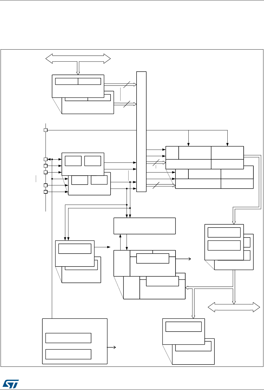
RM0430 Rev 8 391/1324
RM0430 Digital filter for sigma delta modulators (DFSDM)
449
15.4 DFSDM functional description
15.4.1 DFSDM block diagram
Figure 75. Single DFSDM block diagram
069
&RQWUROXQLW
,QWHUUXSW
EUHDN
,QWHUUXSWVDQGHYHQWV
HQGRIFRQYHUVLRQ
DQDORJZDWFKGRJ
VKRUWFLUFXLWGHWHFWLRQ
RYHUUXQ
'DWDRXWSXW
&RQILJXUDWLRQ
UHJLVWHUV
'0$LQWHUUXSWEUHDN
FRQWUROFORFNFRQWURO
)LOWHU
FRQILJ $QDORJZDWFKGRJ
+LJKWKUHVKROG
/RZWKUHVKROG
)LOWHU
FRQILJ $QDORJZDWFKGRJ
+LJKWKUHVKROG
/RZWKUHVKROG
([WUHPHV
GHWHFWRU
0D[LPXPYDOXH
0LQLPXPYDOXH
([WUHPHV
GHWHFWRU
0D[LPXPYDOXH
0LQLPXPYDOXH
')6'0GDWD
5LJKWELWVKLIW
FRXQW
&DOLEUDWLRQGDWD
FRUUHFWLRQXQLW
ZDWFKGRJILOWHUV
ZDWFKGRJFRPSDUDWRUV
&RQILJ
6WDWXV
6KRUWFLUFXLW
GHWHFWRU
VVFRXQWHU
WKUHVKROG
6KRUWFLUFXLW
GHWHFWRU
VVFRXQWHU
WKUHVKROG
6HULDOWUDQVFHLYHU
&ORFN
FRQWURO
0RGH
FRQWURO
6HULDOWUDQVFHLYHU
&ORFN
FRQWURO
0RGH
FRQWURO
&ORFNLQ
'DWDLQ
,QWHUUXSW
EUHDN
&.,1
'$7,1
&.287
&.,1
'$7,1 6LQF[ILOWHU
)LOWHU
RUGHU
2YHUVDPSOLQJ
UDWLR
,QWHJUDWRUXQLW
2YHUVDPSOLQJ
UDWLR
6LQF[ILOWHU
)LOWHU
RUGHU
2YHUVDPSOLQJ
UDWLR
,QWHJUDWRUXQLW
2YHUVDPSOLQJ
UDWLR
&ORFN
'DWD
&ORFN
'DWD
(;75*>@
')6'0GDWD
5LJKWELWVKLIW
FRXQW
&DOLEUDWLRQGDWD
FRUUHFWLRQXQLW
3DUDOOHOLQSXWGDWD
UHJLVWHU
6DPSOH 6DPSOH
3DUDOOHOLQSXWGDWD
UHJLVWHU
6DPSOH 6DPSOH
$3%EXV
$3%EXV
&KDQQHOPXOWLSOH[HU

Digital filter for sigma delta modulators (DFSDM) RM0430
392/1324 RM0430 Rev 8
1. This example shows 4 DFSDM filters and 8 input channels (max. configuration).
15.4.2 DFSDM pins and internal signals
Table 87. DFSDM external pins
Name Signal Type Remarks
VDD Power supply Digital power supply.
VSS Power supply Digital ground power supply.
CKIN[7:0] Clock input Clock signal provided from external Σ∆ modulator. FT input.
DATIN[7:0] Data input Data signal provided from external Σ∆ modulator. FT input.
CKOUT Clock output Clock output to provide clock signal into external Σ∆
modulator.
EXTRG[1:0] External trigger
signal
Input trigger from two EXTI signals to start analog
conversion (from GPIOs: EXTI11, EXTI15).
Table 88. DFSDM internal signals
Name Signal Type Remarks
dfsdm_jtrg[10:0]
Internal/
external trigger
signal
Input trigger from internal/external trigger sources to start
analog conversion, see Table 89 and Table 90 for details.
dfsdm_break[3:0] break signal
output
Break signals event generation from Analog watchdog or
short-circuit detector
dfsdm_dma[3:0] DMA request
signal
DMA request signal from each DFSDM_FLTx (x=0..3):
end of injected conversion event.
dfsdm_it[3:0] Interrupt
request signal Interrupt signal for each DFSDM_FLTx (x=0..3)
Table 89. DFSDM1 triggers connection
Trigger name Trigger source
dfsdm_jtrg0 TIM1_TRGO2
dfsdm_jtrg1 TIM3_TRGO2
dfsdm_jtrg2 TIM8_TRGO2
dfsdm_jtrg3 TIM10_OC1
dfsdm_jtrg4 N/A
dfsdm_jtrg5 TIM4_TRGO2
dfsdm_jtrg6 N/A
dfsdm_jtrg7 TIM6_TRGO1
dfsdm_jtrg8 N/A
dfsdm_jtrg9 EXTI11
dfsdm_jtrg10 EXTI15

RM0430 Rev 8 393/1324
RM0430 Digital filter for sigma delta modulators (DFSDM)
449
15.4.3 DFSDM reset and clocks
DFSDM on-off control
The DFSDM interface is globally enabled by setting DFSDMEN=1 in the
DFSDM_CH0CFGR1 register. Once DFSDM is globally enabled, all input channels (y=0..7)
and digital filters DFSDM_FLTx (x=0..3) start to work if their enable bits are set (channel
enable bit CHEN in DFSDM_CHyCFGR1 and DFSDM_FLTx enable bit DFEN in
DFSDM_FLTxCR1).
Digital filter x DFSDM_FLTx (x=0..3) is enabled by setting DFEN=1 in the
DFSDM_FLTxCR1 register. Once DFSDM_FLTx is enabled (DFEN=1), both Sincx digital
filter unit and integrator unit are reinitialized.
By clearing DFEN, any conversion which may be in progress is immediately stopped and
DFSDM_FLTx is put into stop mode. All register settings remain unchanged except
DFSDM_FLTxAWSR and DFSDM_FLTxISR (which are reset).
Channel y (y=0..7) is enabled by setting CHEN=1 in the DFSDM_CHyCFGR1 register.
Once the channel is enabled, it receives serial data from the external Σ∆ modulator or
parallel internal data sources (CPU/DMA wire from memory).
DFSDM must be globally disabled (by DFSDMEN=0 in DFSDM_CH0CFGR1) before
stopping the system clock to enter in the STOP mode of the device.
Table 90. DFSDM2 triggers connection
Trigger name Trigger source
dfsdm_jtrg0 TIM1_TRGO3
dfsdm_jtrg1 TIM3_TRGO3
dfsdm_jtrg2 TIM8_TRGO4
dfsdm_jtrg3 TIM10_OC1
dfsdm_jtrg4 TIM2_TRGO2
dfsdm_jtrg5 TIM4_TRGO4
dfsdm_jtrg6 TIM11_OC1
dfsdm_jtrg7 TIM6_TRGO2
dfsdm_jtrg8 TIM7_TRGO2
dfsdm_jtrg9 EXTI11
dfsdm_jtrg10 EXTI15
Table 91. DFSDM break connection
Break name Break destination
dfsdm_break[0] TIM1 break
dfsdm_break[1] -
dfsdm_break[2] TIM8 break
dfsdm_break[3] -

Digital filter for sigma delta modulators (DFSDM) RM0430
394/1324 RM0430 Rev 8
DFSDM clocks
The internal DFSDM clock fDFSDMCLK, which is used to drive the channel transceivers,
digital processing blocks (digital filter, integrator) and next additional blocks (analog
watchdog, short-circuit detector, extremes detector, control block) is generated by the RCC
block and is derived from the system clock SYSCLK or peripheral clock PCLK2 (see
DFSDMSEL bit description in ). The DFSDM clock is automatically stopped in stop mode (if
DFEN = 0 for all DFSDM_FLTx, x=0..3).
The DFSDM serial channel transceivers can receive an external serial clock to sample an
external serial data stream. The internal DFSDM clock must be at least 4 times faster than
the external serial clock if standard SPI coding is used, and 6 times faster than the external
serial clock if Manchester coding is used.
DFSDM can provide one external output clock signal to drive external Σ∆ modulator(s) clock
input(s). It is provided on CKOUT pin. This output clock signal must be in the range
specified in given device datasheet and is derived from DFSDM clock or from audio clock
(see CKOUTSRC bit in DFSDM_CH0CFGR1 register) by programmable divider in the
range 2 - 256 (CKOUTDIV in DFSDM_CH0CFGR1 register). Audio clock source is SAI1
clock selected by SAI1SEL[1:0] field in RCC configuration (see ).
15.4.4 Serial channel transceivers
There are 8 multiplexed serial data channels which can be selected for conversion by each
filter or Analog watchdog or Short-circuit detector. Those serial transceivers receive data
stream from external Σ∆ modulator. Data stream can be sent in SPI format or Manchester
coded format (see SITP[1:0] bits in DFSDM_CHyCFGR1 register).
The channel is enabled for operation by setting CHEN=1 in DFSDM_CHyCFGR1 register.
Channel inputs selection
Serial inputs (data and clock signals) from DATINy and CKINy pins can be redirected from
the following channel pins. This serial input channel redirection is set by CHINSEL bit in
DFSDM_CHyCFGR1 register.
Channel redirection can be used to collect audio data from PDM (pulse density modulation)
stereo microphone type. PDM stereo microphone has one data and one clock signal. Data
signal provides information for both left and right audio channel (rising clock edge samples
for left channel and falling clock edge samples for right channel).
Configuration of serial channels for PDM microphone input:
•PDM microphone signals (data, clock) will be connected to DFSDM input serial channel
y (DATINy, CKOUT) pins.
•Channel y will be configured: CHINSEL = 0 (input from given channel pins: DATINy,
CKINy).
•Channel (y-1) (modulo 8) will be configured: CHINSEL = 1 (input from the following
channel ((y-1)+1) pins: DATINy, CKINy).
•Channel y: SITP[1:0] = 0 (rising edge to strobe data) => left audio channel on channel
y.
•Channel (y-1): SITP[1:0] = 1 (falling edge to strobe data) => right audio channel on
channel y-1.
•Two DFSDM filters will be assigned to channel y and channel (y-1) (to filter left and
right channels from PDM microphone).
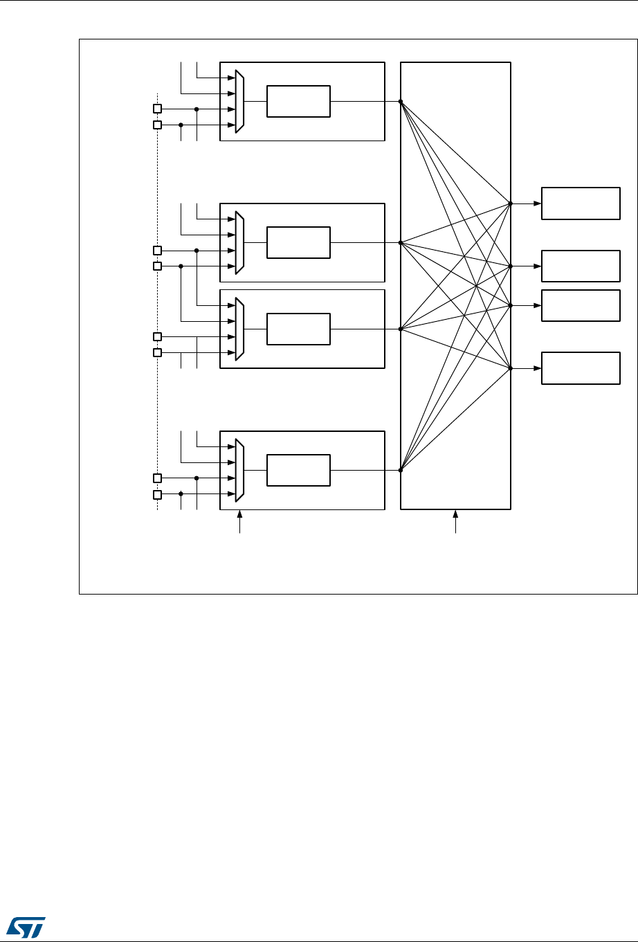
RM0430 Rev 8 395/1324
RM0430 Digital filter for sigma delta modulators (DFSDM)
449
Figure 76. Input channel pins redirection
Output clock generation
A clock signal can be provided on CKOUT pin to drive external Σ∆ modulator clock inputs.
The frequency of this CKOUT signal is derived from DFSDM clock or from audio clock (see
CKOUTSRC bit in DFSDM_CH0CFGR1 register) divided by a predivider (see CKOUTDIV
bits in DFSDM_CH0CFGR1 register). If the output clock is stopped, then CKOUT signal is
set to low state (output clock can be stopped by CKOUTDIV=0 in DFSDM_CHyCFGR1
register or by DFSDMEN=0 in DFSDM_CH0CFGR1 register). The output clock stopping is
performed:
•4 system clocks after DFSDMEN is cleared (if CKOUTSRC=0)
•1 system clock and 3 audio clocks after DFSDMEN is cleared (if CKOUTSRC=1)
Before changing CKOUTSRC the software has to wait for CKOUT being stopped to avoid
glitch on CKOUT pin. The output clock signal frequency must be in the range 0 - 20 MHz.
06Y9
)/7[
)/7[
'$7$,1
'$7,1\
'$7,1\
'$7,1\PD[
&+,16(/
5&+
)/7
)/7[PD[
&.,1\PD[
&.,1\
&.,1\
&.,1
&+\PD[
'HFRGH
&+\
'HFRGH
&+\
'HFRGH
&+
'HFRGH

Digital filter for sigma delta modulators (DFSDM) RM0430
396/1324 RM0430 Rev 8
SPI data input format operation
In SPI format, the data stream is sent in serial format through data and clock signals. Data
signal is always provided from DATINy pin. A clock signal can be provided externally from
CKINy pin or internally from a signal derived from the CKOUT signal source.
In case of external clock source selection (SPICKSEL[1:0]=0) data signal (on DATINy pin) is
sampled on rising or falling clock edge (of CKINy pin) according SITP[1:0] bits setting (in
DFSDM_CHyCFGR1 register).
Internal clock sources - see SPICKSEL[1:0] in DFSDM_CHyCFGR1 register:
•CKOUT signal:
– For connection to external Σ∆ modulator which uses directly its clock input (from
CKOUT) to generate its output serial communication clock.
– Sampling point: on rising/falling edge according SITP[1:0] setting.
•CKOUT/2 signal (generated on CKOUT rising edge):
– For connection to external Σ∆ modulator which divides its clock input (from
CKOUT) by 2 to generate its output serial communication clock (and this output
clock change is active on each clock input rising edge).
– Sampling point: on each second CKOUT falling edge.
•CKOUT/2 signal (generated on CKOUT falling edge):
– For connection to external Σ∆ modulator which divides its clock input (from
CKOUT) by 2 to generate its output serial communication clock (and this output
clock change is active on each clock input falling edge).
– Sampling point: on each second CKOUT rising edge.
Note: An internal clock source can only be used when the external Σ∆ modulator uses CKOUT
signal as a clock input (to have synchronous clock and data operation).
Internal clock source usage can save CKINy pin connection (CKINy pins can be used for
other purpose).
The clock source signal frequency must be in the range 0 - 20 MHz for SPI coding and less
than fDFSDMCLK/4.
Manchester coded data input format operation
In Manchester coded format, the data stream is sent in serial format through DATINy pin
only. Decoded data and clock signal are recovered from serial stream after Manchester
decoding. There are two possible settings of Manchester codings (see SITP[1:0] bits in
DFSDM_CHyCFGR1 register):
•signal rising edge = log 0; signal falling edge = log 1
•signal rising edge = log 1; signal falling edge = log 0
The recovered clock signal frequency for Manchester coding must be in the range
0 - 10 MHz and less than fDFSDMCLK/6.
To correctly receive Manchester coded data, the CKOUTDIV divider (in
DFSDM_CH0CFGR1 register) must be set with respect to expected Manchester data rate
according formula:
CKOUTDIV 1+()TSYSCLK
×()TManchester clock 2 CKOUTDIV×TSYSCLK
×()<<
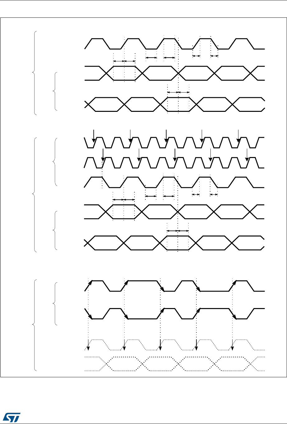
RM0430 Rev 8 397/1324
RM0430 Digital filter for sigma delta modulators (DFSDM)
449
Figure 77. Channel transceiver timing diagrams
069
6,73
&.287
'$7,1\
6,73
WVX WK
WVX WK
WIWU
WZO WZK
63,WLPLQJ63,&.6(/
UHFRYHUHGFORFN
6,73
'$7,1\
6,73
0DQFKHVWHUWLPLQJ
UHFRYHUHGGDWD
6,73
&.,1\'$7,1\
6,73
WVX WK
WVX WK
WIWU
WZO WZK
63,WLPLQJ63,&.6(/
63,&.6(/
63,&.6(/
63,&.6(/
63,&.6(/
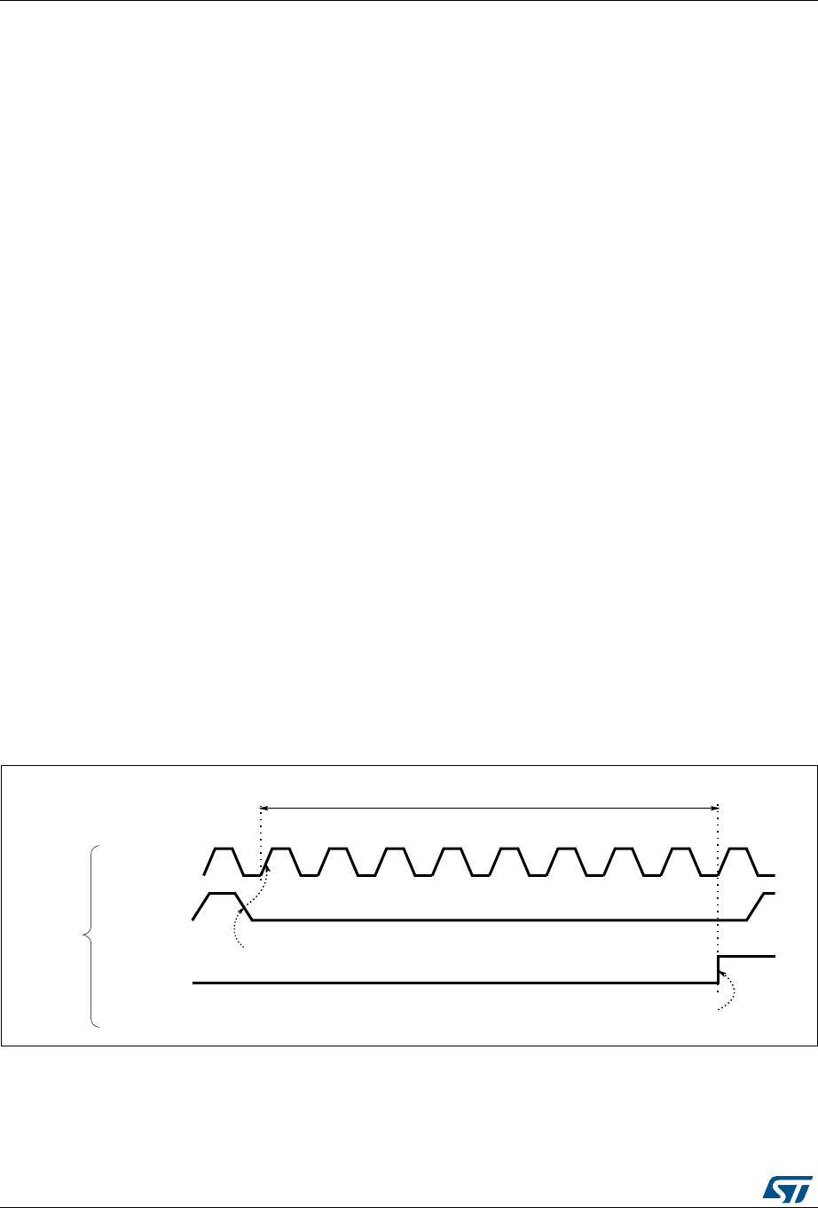
Digital filter for sigma delta modulators (DFSDM) RM0430
398/1324 RM0430 Rev 8
Clock absence detection
Channels serial clock inputs can be checked for clock absence/presence to ensure the
correct operation of conversion and error reporting. Clock absence detection can be
enabled or disabled on each input channel y by bit CKABEN in DFSDM_CHyCFGR1
register. If enabled, then this clock absence detection is performed continuously on a given
channel. A clock absence flag is set (CKABF[y] = 1) and an interrupt can be invoked (if
CKABIE=1) in case of an input clock error (see CKABF[7:0] in DFSDM_FLT0ISR register
and CKABEN in DFSDM_CHyCFGR1). After a clock absence flag clearing (by CLRCKABF
in DFSDM_FLT0ICR register), the clock absence flag is refreshed. Clock absence status bit
CKABF[y] is set also by hardware when corresponding channel y is disabled (if CHEN[y] = 0
then CKABF[y] is held in set state).
When a clock absence event has occurred, the data conversion (and/or analog watchdog
and short-circuit detector) provides incorrect data. The user should manage this event and
discard given data while a clock absence is reported.
The clock absence feature is available only when the system clock is used for the CKOUT
signal (CKOUTSRC=0 in DFSDM_CH0CFGR1 register).
When the transceiver is not yet synchronized, the clock absence flag is set and cannot be
cleared by CLRCKABF[y] bit (in DFSDM_FLT0ICR register). The software sequence
concerning clock absence detection feature should be:
•Enable given channel by CHEN = 1
•Try to clear the clock absence flag (by CLRCKABF = 1) until the clock absence flag is
really cleared (CKABF = 0). At this time, the transceiver is synchronized (signal clock is
valid) and is able to receive data.
•Enable the clock absence feature CKABEN = 1 and the associated interrupt CKABIE =
1 to detect if the SPI clock is lost or Manchester data edges are missing.
If SPI data format is used, then the clock absence detection is based on the comparison of
an external input clock with an output clock generation (CKOUT signal). The external input
clock signal into the input channel must be changed at least once per 8 signal periods of
CKOUT signal (which is controlled by CKOUTDIV field in DFSDM_CH0CFGR1 register).
Figure 78. Clock absence timing diagram for SPI
If Manchester data format is used, then the clock absence means that the clock recovery is
unable to perform from Manchester coded signal. For a correct clock recovery, it is first
necessary to receive data with 1 to 0 or 0 to 1 transition (see Figure 80 for Manchester
synchronization).
069
&.287
63,FORFNSUHVHQFH
WLPLQJ
PD[SHULRGV
&.,1\
ODVWFORFNFKDQJH
&.$%)>\@
HUURUUHSRUWHG
UHVWDUWFRXQWLQJ
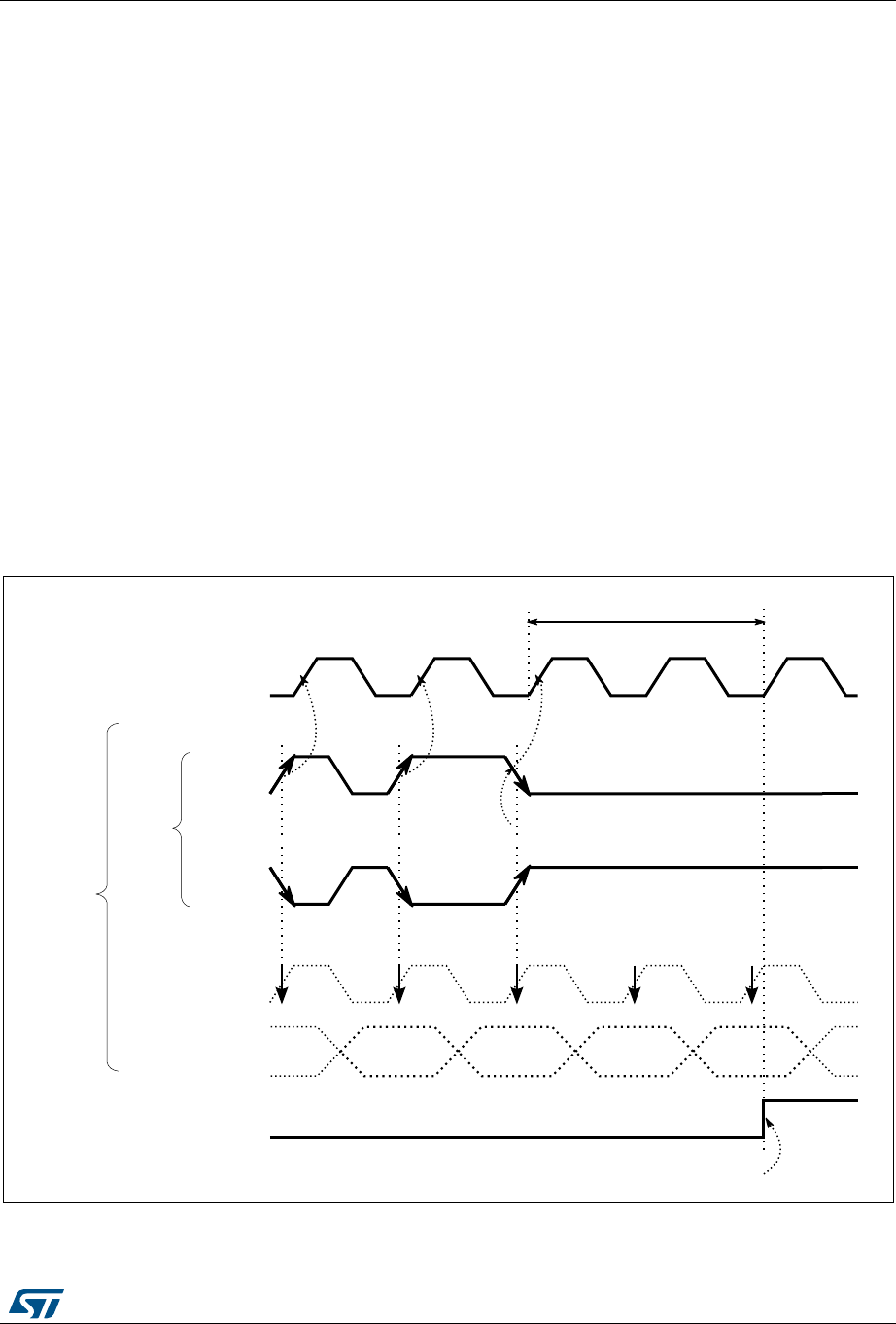
RM0430 Rev 8 399/1324
RM0430 Digital filter for sigma delta modulators (DFSDM)
449
The detection of a clock absence in Manchester coding (after a first successful
synchronization) is based on changes comparison of coded serial data input signal with
output clock generation (CKOUT signal). There must be a voltage level change on DATINy
pin during 2 periods of CKOUT signal (which is controlled by CKOUTDIV bits in
DFSDM_CH0CFGR1 register). This condition also defines the minimum data rate to be able
to correctly recover the Manchester coded data and clock signals.
The maximum data rate of Manchester coded data must be less than the CKOUT signal.
So to correctly receive Manchester coded data, the CKOUTDIV divider must be set
according the formula:
A clock absence flag is set (CKABF[y] = 1) and an interrupt can be invoked (if CKABIE=1) in
case of an input clock recovery error (see CKABF[7:0] in DFSDM_FLT0ISR register and
CKABEN in DFSDM_CHyCFGR1). After a clock absence flag clearing (by CLRCKABF in
DFSDM_FLT0ICR register), the clock absence flag is refreshed.
Figure 79. Clock absence timing diagram for Manchester coding
CKOUTDIV 1+()TSYSCLK
×()TManchester clock 2 CKOUTDIV×TSYSCLK
×()<<
069
&.287
UHFRYHUHGFORFN
6,73
'$7,1\
6,73
0DQFKHVWHUFORFNSUHVHQFH
WLPLQJ
UHFRYHUHGGDWD ""
ODVWGDWDFKDQJH
&.$%)>\@
HUURUUHSRUWHG
UHVWDUWFRXQWLQJ
PD[SHULRGV

Digital filter for sigma delta modulators (DFSDM) RM0430
400/1324 RM0430 Rev 8
Manchester/SPI code synchronization
The Manchester coded stream must be synchronized the first time after enabling the
channel (CHEN=1 in DFSDM_CHyCFGR1 register). The synchronization ends when a data
transition from 0 to 1 or from 1 to 0 (to be able to detect valid data edge) is received. The
end of the synchronization can be checked by polling CKABF[y]=0 for a given channel after
it has been cleared by CLRCKABF[y] in DFSDM_FLT0ICR, following the software sequence
detailed hereafter:
CKABF[y] flag is cleared by setting CLRCKABF[y] bit. If channel y is not yet synchronized
the hardware immediately set the CKABF[y] flag. Software is then reading back the
CKABF[y] flag and if it is set then perform again clearing of this flag by setting
CLRCKABF[y] bit. This software sequence (polling of CKABF[y] flag) continues until
CKABF[y] flag is set (signalizing that Manchester stream is synchronized). To be able to
synchronize/receive Manchester coded data the CKOUTDIV divider (in
DFSDM_CH0CFGR1 register) must be set with respect to expected Manchester data rate
according the formula below.
SPI coded stream is synchronized after first detection of clock input signal (valid
rising/falling edge).
Note: When the transceiver is not yet synchronized, the clock absence flag is set and cannot be
cleared by CLRCKABF[y] bit (in DFSDM_FLT0ICR register).
CKOUTDIV 1+()TSYSCLK
×()TManchester clock 2 CKOUTDIV×TSYSCLK
×()<<
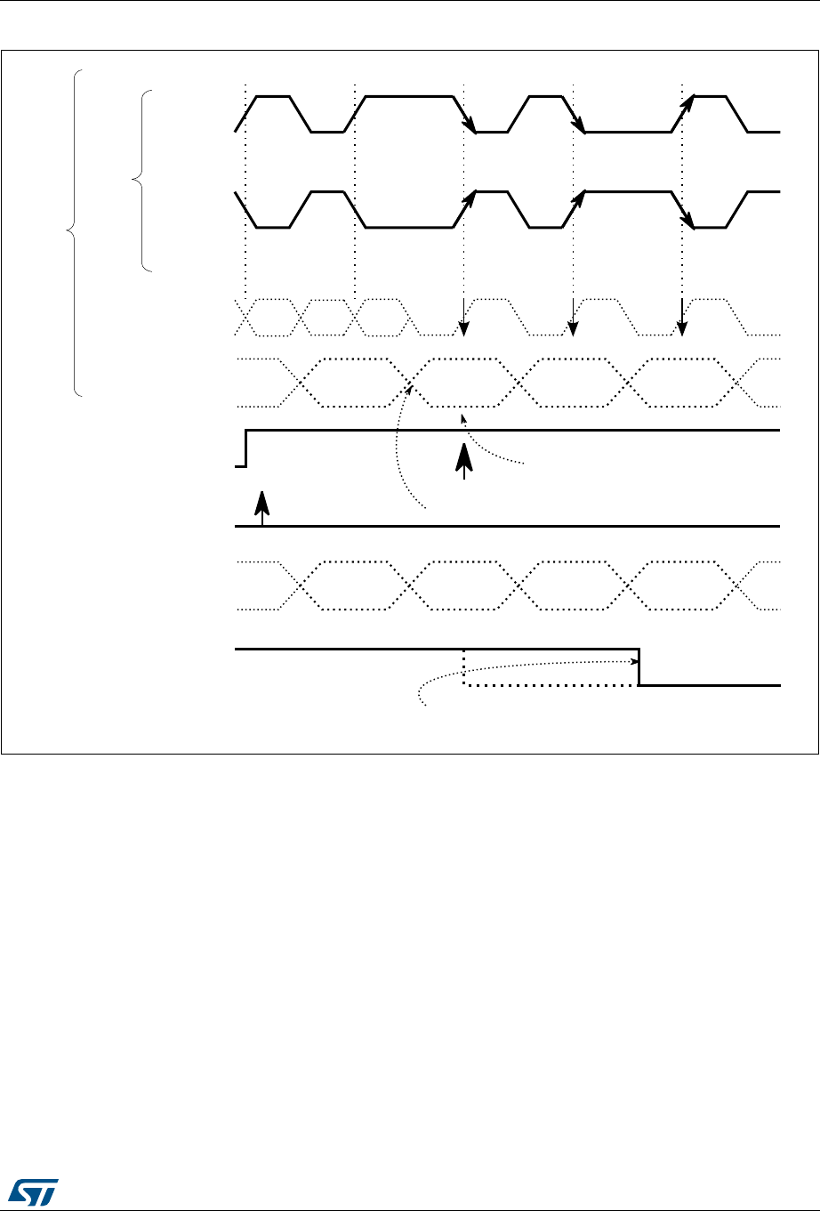
RM0430 Rev 8 401/1324
RM0430 Digital filter for sigma delta modulators (DFSDM)
449
Figure 80. First conversion for Manchester coding (Manchester synchronization)
External serial clock frequency measurement
The measuring of a channel serial clock input frequency provides a real data rate from an
external Σ∆ modulator, which is important for application purposes.
An external serial clock input frequency can be measured by a timer counting DFSDM
clocks (fDFSDMCLK) during one conversion duration. The counting starts at the first input data
clock after a conversion trigger (regular or injected) and finishes by last input data clock
before conversion ends (end of conversion flag is set). Each conversion duration (time
between first serial sample and last serial sample) is updated in counter CNVCNT[27:0] in
register DFSDM_FLTxCNVTIMR when the conversion finishes (JEOCF=1 or REOCF=1).
The user can then compute the data rate according to the digital filter settings (FORD,
FOSR, IOSR, FAST). The external serial frequency measurement is stopped only if the filter
is bypassed (FOSR=0, only integrator is active, CNVCNT[27:0]=0 in
DFSDM_FLTxCNVTIMR register).
In case of parallel data input (Section 15.4.6: Parallel data inputs) the measured frequency
is the average input data rate during one conversion.
069
UHFRYHUHGFORFN
6,73
'$7,1\
6,73
0DQFKHVWHUWLPLQJ
GDWDIURP
PRGXODWRU
&+(1
ILUVWGDWDELWWRJJOHHQGRI0DQFKHVWHUV\QFKURQL]DWLRQ
ILUVWFRQYHUVLRQ
VWDUWWULJJHU
UHFRYHUHGGDWD ""
UHDOVWDUWRIILUVWFRQYHUVLRQ
&.$%)>\@
FOHDULQJRI&.$%)>\@IODJE\VRIWZDUHSROOLQJ

Digital filter for sigma delta modulators (DFSDM) RM0430
402/1324 RM0430 Rev 8
Note: When conversion is interrupted (e.g. by disabling/enabling the selected channel) the
interruption time is also counted in CNVCNT[27:0]. Therefore it is recommended to not
interrupt the conversion for correct conversion duration result.
Conversion times:
injected conversion or regular conversion with FAST = 0 (or first conversion if
FAST=1):
for Sincx filters (x=1..5):
t = CNVCNT/fDFSDMCLK = [FOSR * (IOSR-1 + FORD) + FORD] / fCKIN
for FastSinc filter:
t = CNVCNT/fDFSDMCLK = [FOSR * (IOSR-1 + 4) + 2] / fCKIN
regular conversion with FAST = 1 (except first conversion):
for Sincx and FastSinc filters:
t = CNVCNT/fDFSDMCLK = [FOSR * IOSR] / fCKIN
in case if FOSR = FOSR[9:0]+1 = 1 (filter bypassed, active only integrator):
t = IOSR / fCKIN (... but CNVCNT=0)
where:
•fCKIN is the channel input clock frequency (on given channel CKINy pin) or input data
rate (in case of parallel data input)
•FOSR is the filter oversampling ratio: FOSR = FOSR[9:0]+1 (see DFSDM_FLTxFCR
register)
•IOSR is the integrator oversampling ratio: IOSR = IOSR[7:0]+1 (see DFSDM_FLTxFCR
register)
•FORD is the filter order: FORD = FORD[2:0] (see DFSDM_FLTxFCR register)
Channel offset setting
Each channel has its own offset setting (in register) which is finally subtracted from each
conversion result (injected or regular) from a given channel. Offset correction is performed
after the data right bit shift. The offset is stored as a 24-bit signed value in OFFSET[23:0]
field in DFSDM_CHyCFGR2 register.
Data right bit shift
To have the result aligned to a 24-bit value, each channel defines a number of right bit shifts
which will be applied on each conversion result (injected or regular) from a given channel.
The data bit shift number is stored in DTRBS[4:0] bits in DFSDM_CHyCFGR2 register.
The right bit-shift is rounding the result to nearest integer value. The sign of shifted result is
maintained, in order to have valid 24-bit signed format of result data.
Pulses skipper
Purpose of the pulses skipper is to implement delay line like behavior for given input
channel(s). Given number of samples from input serial data stream (serial stream only) can
be discarded before they enter into the filter. This data discarding is performed by skipping
given number of sampling input clock pulses (given serial data samples are then not
sampled by filter). The sampling clock is gated by pulses skipper function for given number
of clock pulses. When given clock pulses are skipped then the filtering continues for
following input data. With comparison to non skipped data stream this operation causes that

RM0430 Rev 8 403/1324
RM0430 Digital filter for sigma delta modulators (DFSDM)
449
the final output sample (and next samples) from filter will be calculated from later input data.
This final sample then looks a bit in forward - because it is calculated from newer input
samples than the “non-skipped” sample. The final “skipped sample” is converted later
because the skipped input data samples must be replaced by followed input data samples.
The final data buffers behavior (skipped and non-skipped output data buffers comparison)
looks like the non-skipped data stream is a bit delayed - both data buffers will be phase
shifted.
The implementation of clock skipping is based on a block named MCHDLY (multi-channel
delay block) added on the top level of DFSDMs (see Figure 81). This MCHDLY block is
controlled via a MCHDLYCR register (see the Section 8.2.10: DFSDM Multi-channel delay
control register (SYSCFG_MCHDLYCR)) where are all MCHDLY control bits.
By using MCHDLY block, the DFSDMs can be used for beamforming with up to 6 digital
microphones. In beamforming mode the clock to digital microphones (or sigma-delta
modulators) is provided by DFSDM2 clock output (dfsdm2_ckout signal on Figure 81). This
clock output signal is then distributed to (see Figure 81):
•OR gates (to implement pulse skipping by clock masking/gating)
•Trigger inputs (ETR) of two timers: TIM4 and TIM3 (to define how many pulses will be
skipped)
•DFSDM1_CKOUT and DFSDM2_CKOUT pins outputs through M1 and M2
multiplexers (to generate output clock signal on DFSDMx pins)
The OR gates are used to skip the input serial clock pulses provided to the DFSDMs in
order to generate a delay on the corresponding input channel.
This clock gating is controlled by two timers (TIM4 and TIM3). Timers are programmed in
one shot mode to generate masking pulse with defined length to gate required number of
clock pulses.
In the Figure 81, MIC1 receives its serial clock via another clock output pin
(DFSDM1_CKOUT pin) which can provide either clock output from DFSDM2 or DFSDM1
CKOUT signal. This configuration allows to use for low-power use-cases only one
microphone (MIC1) - while DFSDM2_CKOUT is disabled and DFSDM1_CKOUT enabled
(for example voice detection), and reusing MIC1 for beamforming use cases (when
DFSDM2_CKOUT is enabled).
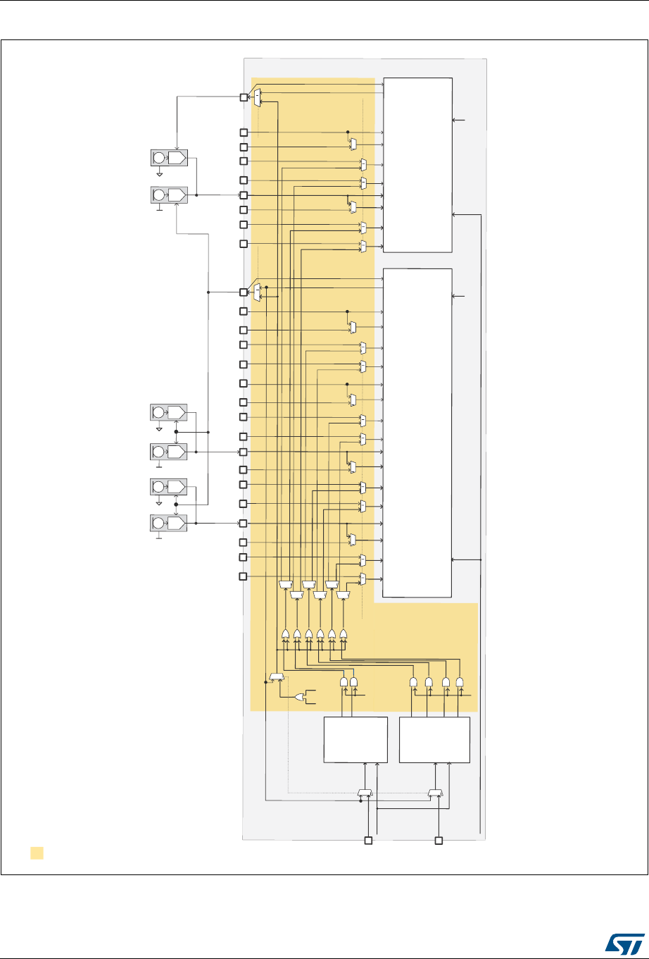
Digital filter for sigma delta modulators (DFSDM) RM0430
404/1324 RM0430 Rev 8
Figure 81. Multi-channel delay block for pulse skipping
06YY
')6'01%7 1%)
&N,Q
&N,Q
&N,Q
&N,Q
&N,Q
'DW,Q
'DW,Q
'DW,Q
'DW,Q
'DW,Q
')6'01%7 1%)
&N,Q
&N,Q
'DW,Q
'DW,Q
&N2XW
&N2XW%
&N2XW
&N2XW%
7,0
7,0
/5
/5
*1'
9&& B'$7,1
/5
/5
*1'
9&&
/5
/5
*1'
9&&
B'$7,1
0,&0,&
0,&
0,&
0,&0,&
3&/.
0
0
0
670
0&+'/<
2&
2&
2&
2&
2&
,75
&ONBJDWHG
&ONBJDWHG
&ONBJDWHG
&ONBJDWHG
&ONBJDWHG
&ONBJDWHG
B&.287
B'$7,1
B&.287
&N,Q
&N,Q
'DW,Q
'DW,Q
&N,Q
&N,Q
'DW,Q
'DW,Q
3&/.
3&/.
0
0000
0
00
3&/.
3&/. 3&/.
&N,Q
'DW,Q
B'$7,1
B'$7,1
00
0
00
0
0
0
0
B'$7,1
B'$7,1
B'$7,1
'0
'0
'0
'0
'0
'0
$FON
)URP3//,6
$FON
)URP3//,6
0
0
0
(75
(75
(75
,75
(75
GIVGPBFNRXW
2&
B'$7,1
B'$7,1
*
*
*
*
*
*
0&+'/<(1
0&+'/<(1
0&+'/<(1
0&+'/<(1
%6&.6(/
')6'0&)* ')6'0&)*
')6'0&.26(/ ')6'0&.26(/
B&.,1
B&.,1
B&.,1
B&.,1
B&.,1
B'$7,1
B&.,1
B'$7,1
B&.,1
B&.,1
B&.,1
B&.,1
B&.,1
B&.,1
0&+'/<
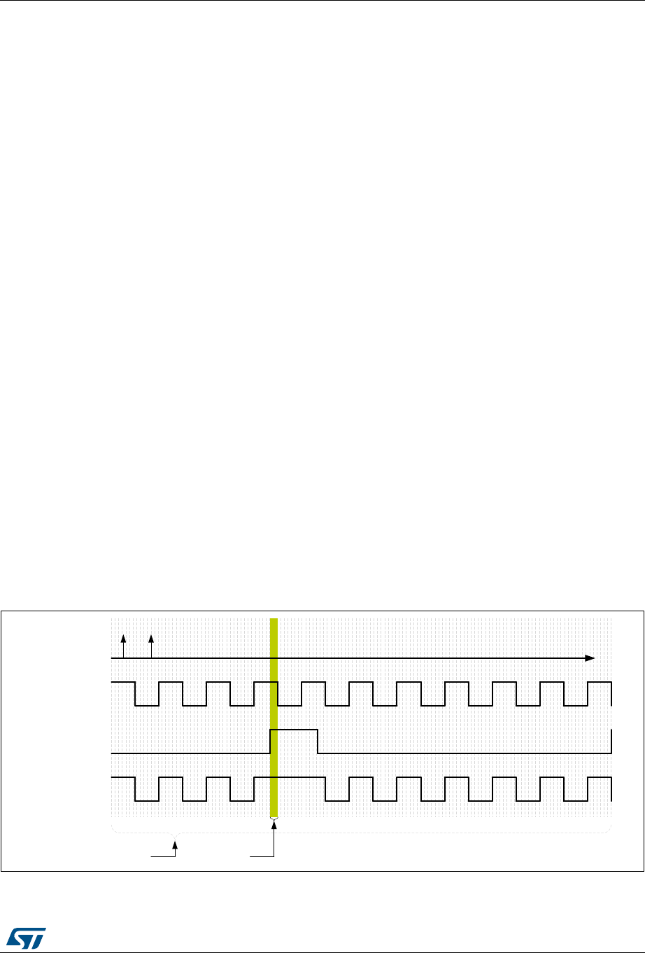
RM0430 Rev 8 405/1324
RM0430 Digital filter for sigma delta modulators (DFSDM)
449
The DFSDM shall be configured as follow:
•CHINSEL must be set to 0 for all channels (channel data are taken from pins of the
same channel)
•SPICKSEL must be set to 0 for all channels (in order to select external CKINy as input
clock)
The TIM3 and TIM4 shall be configured as follow:
•TIM4 outputs (OC[2:1]) and TIM3 outputs (OC[4:1]) must be low in inactive mode
when no gating is required. When the application needs to provide delays to
microphones, then the timers shall be programmed in One Pulse Mode (OPM). In this
mode, the timer allows the counter to be started in response to a rising edge on ETRx
(or ITRx) input and to generate a pulse with a programmable length.
•The ETRx input must be used when the bitstream clock is generated by the DFSDM2.
•The clock reference used by the timers can be its APB clock or its APB clock multiplied
by 2 or 4. The higher this frequency is, the better it is.
While TIM3 and TIM4 are working with DFSDM2 using ETRx input, the timers
reference clock frequency must be at least 12 times the frequency of the input
bitstream clock, taking the assumption that the bitstream clock duty cycle is 50%. This
is due to the fact that ETRx input have a bigger propagation delay: up to 5 periods of
the timers reference clock.
•Using these rules will prevent timing violation.
In case it is required to synchronize DFSDM1 and DFSDM2 filter conversions (for example
for beamforming applications), the following sequence should take place (refer to
Figure 81):
•Enable audio clocks used by DFSDM
•Program DFSDM to use the CkIn
•Use the DFSDM2 CkOut to inject the DFSDM2 audio clock to the CkIn
•Block the DFSDM2 CkOut signals: bit BSCKSEL=0
•Start all filters conversions (all used DFSDM1 and DFSDM2 filters)
•Release the DFSDM2 CkOut: bit BSCKSEL=1
Figure 82. Pulses skipper operation
06Y9
6RIWZDUHDFFHVV
GIVGPBFNRXW
7,0B2&
FONBJDWHG
7LPHUVFORFNUHIHUHQFH 0DUJLQ

Digital filter for sigma delta modulators (DFSDM) RM0430
406/1324 RM0430 Rev 8
Table 92. Demultiplexers (DM[6:1]) operation
Control Output 0 Output 1
0 input L
1 L input
Table 93. Use-cases examples for beamforming applications
Use cases
TIM4
TIM3
DFSDM2
DFSDM1
DFSDM2_CKOSEL
DFSDM2_CFG
DFSDM2_CK37SEL
DFSDM2_CK26SEL
DFSDM2_CK15SEL
DFSDM2_CK04SEL
DFSDM2_D6SEL
DFSDM2_D4SEL
DFSDM2_D2SEL
DFSDM2_D0SEL
MCHDLYEN2
DFSDM1_CKOSEL
DFSDM1_CFG
DFSDM1_CK13SEL
DFSDM1_CK02SEL
DFSDM1_D2SEL
DFSDM1_D0SEL
MCHDLYEN1
BSCKSEL
Multiplexer/
gate on schematic ----
M2
M[16:9]
DM3
DM4
DM5
DM6
M20
M19
M18
M17
G[6:3]
M1
M[6:3]
DM1
DM2
M8
M7
G[2:1]
M[29:27]
Speech recognition_1 OFFOFFOFFONxxxxxxxxxx00xxxxx00
Beamforming4_
DFSDM_1_3 OFFON ONOFF110000xx1110xxxxx01
Beamforming4_
DFSDM_3_5 OFFON ONOFF110011x11x10xxxxx01
Beamforming4_
DFSDM_5_7 OFFON ONOFF11111111xx10xxxxx01
Beamforming4_
DFSDM_1_7 OFFON ONOFF1111001xx110xxxxx01
Beamforming6_
DFSDM_1_3_1 ON ON ON ON 110000xx1111100x111
Beamforming6_
DFSDM_1_3_3 ON ON ON ON 110000xx11111111x11

RM0430 Rev 8 407/1324
RM0430 Digital filter for sigma delta modulators (DFSDM)
449
15.4.5 Configuring the input serial interface
The following parameters must be configured for the input serial interface:
•Output clock predivider. There is a programmable predivider to generate the output
clock from DFSDM clock (2 - 256). It is defined by CKOUTDIV[7:0] bits in
DFSDM_CH0CFGR1 register.
•Serial interface type and input clock phase. Selection of SPI or Manchester coding
and sampling edge of input clock. It is defined by SITP [1:0] bits in
DFSDM_CHyCFGR1 register.
•Input clock source. External source from CKINy pin or internal from CKOUT pin. It is
defined by SPICKSEL[1:0] field in DFSDM_CHyCFGR1 register.
•Final data right bit-shift. Defines the final data right bit shift to have the result aligned
to a 24-bit value. It is defined by DTRBS[4:0] in DFSDM_CHyCFGR2 register.
•Channel offset per channel. Defines the analog offset of a given serial channel (offset
of connected external Σ∆ modulator). It is defined by OFFSET[23:0] bits in
DFSDM_CHyCFGR2 register.
•short-circuit detector and clock absence per channel enable. To enable or disable
the short-circuit detector (by SCDEN bit) and the clock absence monitoring (by
CKABEN bit) on a given serial channel in register DFSDM_CHyCFGR1.
•Analog watchdog filter and short-circuit detector threshold settings. To configure
channel analog watchdog filter parameters and channel short-circuit detector
parameters. Configurations are defined in DFSDM_CHyAWSCDR register.
15.4.6 Parallel data inputs
Each input channel provides a register for 16-bit parallel data input (besides serial data
input). Each 16-bit parallel input can be sourced from internal data sources only:
•direct CPU/DMA writing.
The selection for using serial or parallel data input for a given channel is done by field
DATMPX[1:0] of DFSDM_CHyCFGR1 register. In DATMPX[1:0] is also defined the parallel
data source: direct write by CPU/DMA.
Each channel contains a 32-bit data input register DFSDM_CHyDATINR in which it can be
written a 16-bit data. Data are in 16-bit signed format. Those data can be used as input to
the digital filter which is accepting 16-bit parallel data.
If serial data input is selected (DATMPX[1:0] = 0), the DFSDM_CHyDATINR register is write
protected.
Input from memory (direct CPU/DMA write)
The direct data write into DFSDM_CHyDATINR register by CPU or DMA (DATMPX[1:0]=2)
can be used as data input in order to process digital data streams from memory or
peripherals.
Data can be written by CPU or DMA into DFSDM_CHyDATINR register:
1. CPU data write:
Input data are written directly by CPU into DFSDM_CHyDATINR register.
2. DMA data write:
The DMA should be configured in memory-to-memory transfer mode to transfer data
from memory buffer into DFSDM_CHyDATINR register. The destination memory

Digital filter for sigma delta modulators (DFSDM) RM0430
408/1324 RM0430 Rev 8
address is the address of DFSDM_CHyDATINR register. Data are transferred at DMA
transfer speed from memory to DFSDM parallel input.
This DMA transfer is different from DMA used to read DFSDM conversion results. Both
DMA can be used at the same time - first DMA (configured as memory-to-memory
transfer) for input data writings and second DMA (configured as peripheral-to-memory
transfer) for data results reading.
The accesses to DFSDM_CHyDATINR can be either 16-bit or 32-bit wide, allowing to load
respectively one or two samples in one write operation. 32-bit input data register
(DFSDM_CHyDATINR) can be filled with one or two 16-bit data samples, depending on the
data packing operation mode defined in field DATPACK[1:0] of DFSDM_CHyCFGR1
register:
1. Standard mode (DATPACK[1:0]=0):
Only one sample is stored in field INDAT0[15:0] of DFSDM_CHyDATINR register which
is used as input data for channel y. The upper 16 bits (INDAT1[15:0]) are ignored and
write protected. The digital filter must perform one input sampling (from INDAT0[15:0])
to empty data register after it has been filled by CPU/DMA. This mode is used together
with 16-bit CPU/DMA access to DFSDM_CHyDATINR register to load one sample per
write operation.
2. Interleaved mode (DATPACK[1:0]=1):
DFSDM_CHyDATINR register is used as a two sample buffer. The first sample is
stored in INDAT0[15:0] and the second sample is stored in INDAT1[15:0]. The digital
filter must perform two input samplings from channel y to empty DFSDM_CHyDATINR
register. This mode is used together with 32-bit CPU/DMA access to
DFSDM_CHyDATINR register to load two samples per write operation.
3. Dual mode (DATPACK[1:0]=2):
Two samples are written into DFSDM_CHyDATINR register. The data INDAT0[15:0] is
for channel y, the data in INDAT1[15:0] is for channel y+1. The data in INDAT1[15:0] is
automatically copied INDAT0[15:0] of the following (y+1) channel data register
DFSDM_CH[y+1]DATINR). The digital filters must perform two samplings - one from
channel y and one from channel (y+1) - in order to empty DFSDM_CHyDATINR
registers.
Dual mode setting (DATPACK[1:0]=2) is available only on even channel numbers (y =
0, 2, 4, 6). If odd channel (y = 1, 3, 5, 7) is set to Dual mode then both INDAT0[15:0]
and INDAT1[15:0] parts are write protected for this channel. If even channel is set to
Dual mode then the following odd channel must be set into Standard mode
(DATPACK[1:0]=0) for correct cooperation with even channels.
See Figure 83 for DFSDM_CHyDATINR registers data modes and assignments of data
samples to channels.

RM0430 Rev 8 409/1324
RM0430 Digital filter for sigma delta modulators (DFSDM)
449
Figure 83. DFSDM_CHyDATINR registers operation modes and assignment
The write into DFSDM_CHyDATINR register to load one or two samples must be performed
after the selected input channel (channel y) is enabled for data collection (starting
conversion for channel y). Otherwise written data are lost for next processing.
For example: for single conversion and interleaved mode, do not start writing pair of data
samples into DFSDM_CHyDATINR before the single conversion is started (any data
present in the DFSDM_CHyDATINR before starting a conversion is discarded).
15.4.7 Channel selection
There are 8 multiplexed channels which can be selected for conversion using the injected
channel group and/or using the regular channel.
The injected channel group is a selection of any or all of the 8 channels. JCHG[7:0] in the
DFSDM_FLTxJCHGR register selects the channels of the injected group, where JCHG[y]=1
means that channel y is selected.
Injected conversions can operate in scan mode (JSCAN=1) or single mode (JSCAN=0). In
scan mode, each of the selected channels is converted, one after another. The lowest
channel (channel 0, if selected) is converted first, followed immediately by the next higher
channel until all the channels selected by JCHG[7:0] have been converted. In single mode
(JSCAN=0), only one channel from the selected channels is converted, and the channel
selection is moved to the next channel. Writing to JCHG[7:0] if JSCAN=0 resets the channel
selection to the lowest selected channel.
Injected conversions can be launched by software or by a trigger. They are never
interrupted by regular conversions.
The regular channel is a selection of just one of the 8 channels. RCH[2:0] in the
DFSDM_FLTxCR1 register indicates the selected channel.
Regular conversions can be launched only by software (not by a trigger). A sequence of
continuous regular conversions is temporarily interrupted when an injected conversion is
requested.
Performing a conversion on a disabled channel (CHEN=0 in DFSDM_CHyCFGR1 register)
causes that the conversion will never end - because no input data is provided (with no clock
signal). In this case, it is necessary to enable a given channel (CHEN=1 in
DFSDM_CHyCFGR1 register) or to stop the conversion by DFEN=0 in DFSDM_FLTxCR1
register.
069
&KVDPSOH &KVDPSOH
8QXVHG &KVDPSOH
&KVDPSOH &KVDPSOH
8QXVHG &KVDPSOH
&KVDPSOH &KVDPSOH
8QXVHG &KVDPSOH
&KVDPSOH &KVDPSOH
8QXVHG &KVDPSOH
\
\
\
\
\
\
\
\
&KVDPSOH &KVDPSOH
&KVDPSOH &KVDPSOH
&KVDPSOH &KVDPSOH
&KVDPSOH &KVDPSOH
&KVDPSOH &KVDPSOH
&KVDPSOH &KVDPSOH
&KVDPSOH &KVDPSOH
&KVDPSOH &KVDPSOH
8QXVHG &KVDPSOH
8QXVHG &KVDPSOH
8QXVHG &KVDPSOH
8QXVHG &KVDPSOH
8QXVHG &KVDPSOH
8QXVHG &KVDPSOH
8QXVHG &KVDPSOH
8QXVHG &KVDPSOH
6WDQGDUGPRGH ,QWHUOHDYHGPRGH 'XDOPRGH
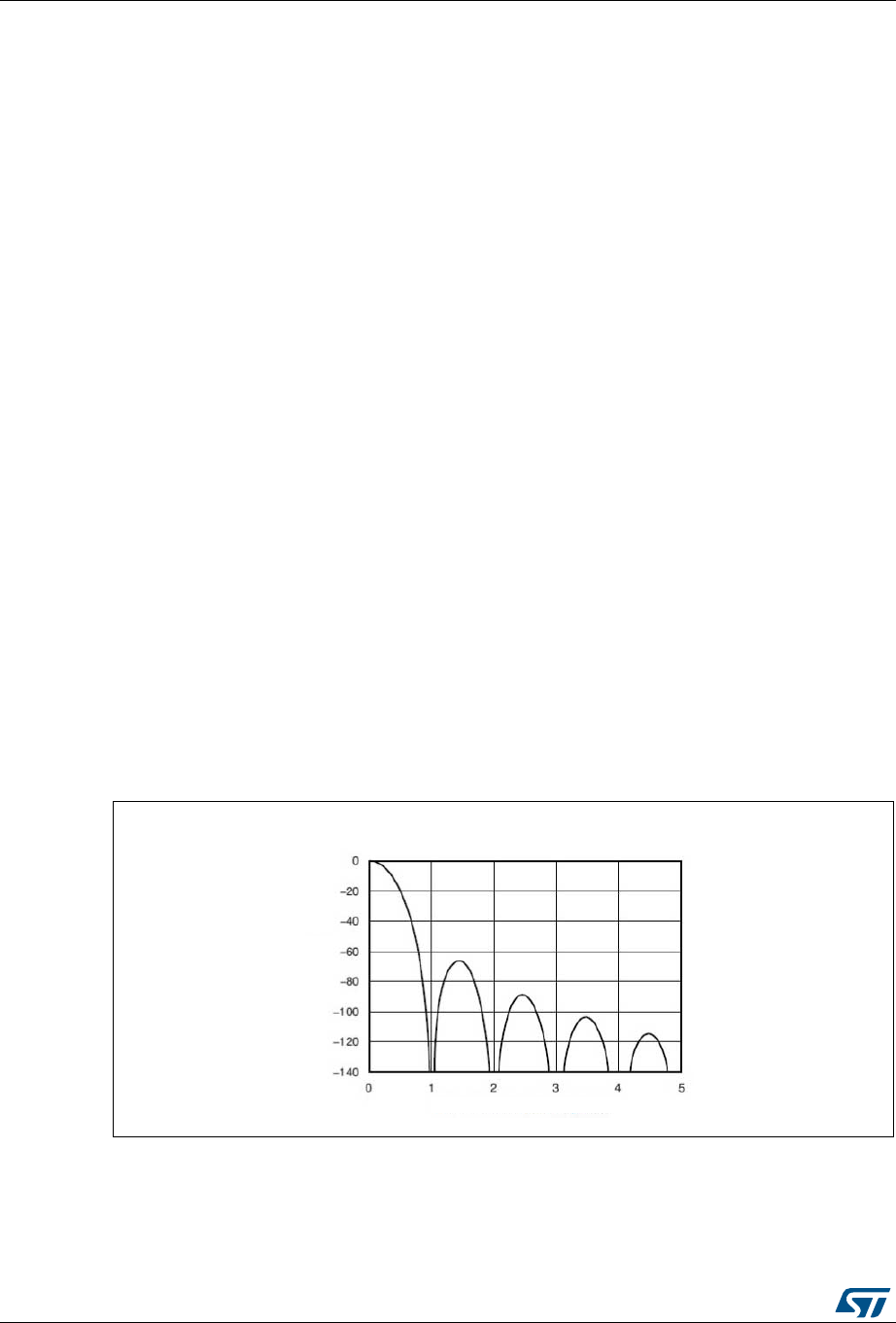
Digital filter for sigma delta modulators (DFSDM) RM0430
410/1324 RM0430 Rev 8
15.4.8 Digital filter configuration
DFSDM contains a Sincx type digital filter implementation. This Sincx filter performs an input
digital data stream filtering, which results in decreasing the output data rate (decimation)
and increasing the output data resolution. The Sincx digital filter is configurable in order to
reach the required output data rates and required output data resolution. The configurable
parameters are:
•Filter order/type: (see FORD[2:0] bits in DFSDM_FLTxFCR register):
–FastSinc
–Sinc
1
–Sinc
2
–Sinc
3
–Sinc
4
–Sinc
5
•Filter oversampling/decimation ratio (see FOSR[9:0] bits in DFSDM_FLTxFCR
register):
– FOSR = 1-1024 - for FastSinc filter and Sincx filter x = FORD = 1..3
– FOSR = 1-215 - for Sincx filter x = FORD = 4
– FOSR = 1-73 - for Sincx filter x = FORD = 5
The filter has the following transfer function (impulse response in H domain):
•Sincx filter type:
•FastSinc filter type:
Figure 84. Example: Sinc3 filter response
Hz() 1z
FOSR–
–
1z
1–
–
-----------------------------
⎝⎠
⎜⎟
⎛⎞
x
=
Hz() 1z
FOSR–
–
1z
1–
–
-----------------------------
⎝⎠
⎜⎟
⎛⎞
2
1z
2FOSR⋅()–
+()⋅=
1RUPDOL]HGIUHTXHQF\I,1I'$7$
*DLQG%
069
RM0430 Rev 8 411/1324
RM0430 Digital filter for sigma delta modulators (DFSDM)
449
For more information about Sinc filter type properties and usage, it is recommended to study
the theory about digital filters (more resources can be downloaded from internet).
15.4.9 Integrator unit
The integrator performs additional decimation and a resolution increase of data coming from
the digital filter. The integrator simply performs the sum of data from a digital filter for a given
number of data samples from a filter.
The integrator oversampling ratio parameter defines how many data counts will be summed
to one data output from the integrator. IOSR can be set in the range 1-256 (see IOSR[7:0]
bits description in DFSDM_FLTxFCR register).
15.4.10 Analog watchdog
The analog watchdog purpose is to trigger an external signal (break or interrupt) when an
analog signal reaches or crosses given maximum and minimum threshold values. An
interrupt/event/break generation can then be invoked.
Each analog watchdog will supervise serial data receiver outputs (after the analog watchdog
filter on each channel) or data output register (current injected or regular conversion result)
according to AWFSEL bit setting (in DFSDM_FLTxCR1 register). The input channels to be
monitored or not by the analog watchdog x will be selected by AWDCH[7:0] in
DFSDM_FLTxCR2 register.
Table 94. Filter maximum output resolution (peak data values from filter output)
for some FOSR values
FOSR Sinc1Sinc2FastSinc Sinc3Sinc4Sinc5
x +/- x +/- x2 +/- 2x2 +/- x3+/- x4 +/- x5
4 +/- 4 +/- 16 +/- 32 +/- 64 +/- 256 +/- 1024
8 +/- 8 +/- 64 +/- 128 +/- 512 +/- 4096 -
32 +/- 32 +/- 1024 +/- 2048 +/- 32768 +/- 1048576 +/- 33554432
64 +/- 64 +/- 4096 +/- 8192 +/- 262144 +/- 16777216 +/- 1073741824
128 +/- 128 +/- 16384 +/- 32768 +/- 2097152 +/- 268435456
256 +/- 256 +/- 65536 +/- 131072 +/- 16777216 Result can overflow on full scale
input (> 32-bit signed integer)
1024 +/- 1024 +/- 1048576 +/- 2097152 +/- 1073741824
Table 95. Integrator maximum output resolution (peak data values from integrator
output) for some IOSR values and FOSR = 256 and Sinc3 filter type (largest data)
IOSR Sinc1Sinc2FastSinc Sinc3Sinc4Sinc5
x +/- FOSR. x +/- FOSR2. x +/- 2.FOSR2. x +/- FOSR3. x +/- FOSR4. x +/- FOSR5. x
4 - - - +/- 67 108 864 - -
32 - - - +/- 536 870 912 - -
128 - - - +/- 2 147 483
648 --
256 - - - +/- 232 --

Digital filter for sigma delta modulators (DFSDM) RM0430
412/1324 RM0430 Rev 8
Analog watchdog conversions on input channels are independent from standard
conversions. In this case, the analog watchdog uses its own filters and signal processing on
each input channel independently from the main injected or regular conversions. Analog
watchdog conversions are performed in a continuous mode on the selected input channels
in order to watch channels also when main injected or regular conversions are paused
(RCIP = 0, JCIP = 0).
There are high and low threshold registers which are compared with given data values (set
by AWHT[23:0] bits in DFSDM_FLTxAWHTR register and by AWLT[23:0] bits in
DFSDM_FLTxAWLTR register).
There are 2 options for comparing the threshold registers with the data values
•Option1: in this case, the input data are taken from final output data register
(AWFSEL=0). This option is characterized by:
– high input data resolution (up to 24-bits)
– slow response time - inappropriate for fast response applications like overcurrent
detection
– for the comparison the final data are taken after bit shifting and offset data
correction
– final data are available only after main regular or injected conversions are
performed
– can be used in case of parallel input data source (DATMPX[1:0] ≠ 0 in
DFSDM_CHyCFGR1 register)
•Option2: in this case, the input data are taken from any serial data receivers output
(AWFSEL=1). This option is characterized by:
– input serial data are processed by dedicated analog watchdog Sincx channel
filters with configurable oversampling ratio (1..32) and filter order (1..3) (see
AWFOSR[4:0] and AWFORD[1:0] bits setting in DFSDM_CHyAWSCDR register)
– lower resolution (up to 16-bit)
– fast response time - appropriate for applications which require a fast response like
overcurrent/overvoltage detection)
– data are available in continuous mode independently from main regular or injected
conversions activity
In case of input channels monitoring (AWFSEL=1), the data for comparison to threshold is
taken from channels selected by AWDCH[7:0] field (DFSDM_FLTxCR2 register). Each of
the selected channels filter result is compared to one threshold value pair (AWHT[23:0] /
AWLT[23:0]). In this case, only higher 16 bits (AWHT[23:8] / AWLT[23:8]) define the 16-bit
threshold compared with the analog watchdog filter output because data coming from the
analog watchdog filter is up to a 16-bit resolution. Bits AWHT[7:0] / AWLT[7:0] are not taken
into comparison in this case (AWFSEL=1).
Parameters of the analog watchdog filter configuration for each input channel are set in
DFSDM_CHyAWSCDR register (filter order AWFORD[1:0] and filter oversampling ratio
AWFOSR[4:0]).
Each input channel has its own comparator which compares the analog watchdog data
(from analog watchdog filter) with analog watchdog threshold values (AWHT/AWLT). When
several channels are selected (field AWDCH[7:0] field of DFSDM_FLTxCR2 register),
several comparison requests may be received simultaneously. In this case, the channel
request with the lowest number is managed first and then continuing to higher selected
channels. For each channel, the result can be recorded in a separate flag (fields

RM0430 Rev 8 413/1324
RM0430 Digital filter for sigma delta modulators (DFSDM)
449
AWHTF[7:0], AWLTF[7:0] of DFSDM_FLTxAWSR register). Each channel request is
executed in 8 DFSDM clock cycles. So, the bandwidth from each channel is limited to 8
DFSDM clock cycles (if AWDCH[7:0] = 0xFF). Because the maximum input channel
sampling clock frequency is the DFSDM clock frequency divided by 4, the configuration
AWFOSR = 0 (analog watchdog filter is bypassed) cannot be used for analog watchdog
feature at this input clock speed. Therefore user must properly configure the number of
watched channels and analog watchdog filter parameters with respect to input sampling
clock speed and DFSDM frequency.
Analog watchdog filter data for given channel y is available for reading by firmware on field
WDATA[15:0] in DFSDM_CHyWDATR register. That analog watchdog filter data is
converted continuously (if CHEN=1 in DFSDM_CHyCFGR1 register) with the data rate
given by the analog watchdog filter setting and the channel input clock frequency.
The analog watchdog filter conversion works like a regular Fast Continuous Conversion
without the intergator. The number of serial samples needed for one result from analog
watchdog filter output (at channel input clock frequency fCKIN):
first conversion:
for Sincx filters (x=1..5): number of samples = [FOSR * FORD + FORD + 1]
for FastSinc filter: number of samples = [FOSR * 4 + 2 + 1]
next conversions:
for Sincx and FastSinc filters: number of samples = [FOSR * IOSR]
where:
FOSR ....... filter oversampling ratio: FOSR = AWFOSR[4:0]+1 (see DFSDM_CHyAWSCDR
register)
FORD ....... the filter order: FORD = AWFORD[1:0] (see DFSDM_CHyAWSCDR register)
In case of output data register monitoring (AWFSEL=0), the comparison is done after a right
bit shift and an offset correction of final data (see OFFSET[23:0] and DTRBS[4:0] fields in
DFSDM_CHyCFGR2 register). A comparison is performed after each injected or regular
end of conversion for the channels selected by AWDCH[7:0] field (in DFSDM_FLTxCR2
register).
The status of an analog watchdog event is signalized in DFSDM_FLTxAWSR register where
a given event is latched. AWHTF[y]=1 flag signalizes crossing AWHT[23:0] value on
channel y. AWLTF[y]=1 flag signalizes crossing AWLT[23:0] value on channel y. Latched
events in DFSDM_FLTxAWSR register are cleared by writing ‘1’ into the corresponding
clearing bit CLRAWHTF[y] or CLRAWLTF[y] in DFSDM_FLTxAWCFR register.
The global status of an analog watchdog is signalized by the AWDF flag bit in
DFSDM_FLTxISR register (it is used for the fast detection of an interrupt source). AWDF=1
signalizes that at least one watchdog occurred (AWHTF[y]=1 or AWLTF[y]=1 for at least one
channel). AWDF bit is cleared when all AWHTF[7:0] and AWLTF[7:0] are cleared.
An analog watchdog event can be assigned to break output signal. There are four break
outputs to be assigned to a high or low threshold crossing event (dfsdm_break[3:0]). The
break signal assignment to a given analog watchdog event is done by BKAWH[3:0] and
BKAWL[3:0] fields in DFSDM_FLTxAWHTR and DFSDM_FLTxAWLTR register.

Digital filter for sigma delta modulators (DFSDM) RM0430
414/1324 RM0430 Rev 8
15.4.11 Short-circuit detector
The purpose of a short-circuit detector is to signalize with a very fast response time if an
analog signal reached saturated values (out of full scale ranges) and remained on this value
given time. This behavior can detect short-circuit or open circuit errors (e.g. overcurrent or
overvoltage). An interrupt/event/break generation can be invoked.
Input data into a short-circuit detector is taken from channel transceiver outputs.
There is an upcounting counter on each input channel which is counting consecutive 0’s or
1’s on serial data receiver outputs. A counter is restarted if there is a change in the data
stream received - 1 to 0 or 0 to 1 change of data signal. If this counter reaches a short-circuit
threshold register value (SCDT[7:0] bits in DFSDM_CHyAWSCDR register), then a short-
circuit event is invoked. Each input channel has its short-circuit detector. Any channel can
be selected to be continuously monitored by setting the SCDEN bit (in DFSDM_CHyCFGR1
register) and it has its own short-circuit detector settings (threshold value in SCDT[7:0] bits,
status bit SCDF[7:0], status clearing bits CLRSCDF[7:0]). Status flag SCDF[y] is cleared
also by hardware when corresponding channel y is disabled (CHEN[y] = 0).
On each channel, a short-circuit detector event can be assigned to break output signal
dfsdm_break[3:0]. There are four break outputs to be assigned to a short-circuit detector
event. The break signal assignment to a given channel short-circuit detector event is done
by BKSCD[3:0] field in DFSDM_CHyAWSCDR register.
Short circuit detector cannot be used in case of parallel input data channel selection
(DATMPX[1:0] ≠ 0 in DFSDM_CHyCFGR1 register).
Four break outputs are totally available (shared with the analog watchdog function).
15.4.12 Extreme detector
The purpose of an extremes detector is to collect the minimum and maximum values of final
output data words (peak to peak values).
If the output data word is higher than the value stored in the extremes detector maximum
register (EXMAX[23:0] bits in DFSDM_FLTxEXMAX register), then this register is updated
with the current output data word value and the channel from which the data is stored is in
EXMAXCH[2:0] bits (in DFSDM_FLTxEXMAX register) .
If the output data word is lower than the value stored in the extremes detector minimum
register (EXMIN[23:0] bits in DFSDM_FLTxEXMIN register), then this register is updated
with the current output data word value and the channel from which the data is stored is in
EXMINCH[2:0] bits (in DFSDM_FLTxEXMIN register).
The minimum and maximum register values can be refreshed by software (by reading given
DFSDM_FLTxEXMAX or DFSDM_FLTxEXMIN register). After refresh, the extremes
detector minimum data register DFSDM_FLTxEXMIN is filled with 0x7FFFFF (maximum
positive value) and the extremes detector maximum register DFSDM_FLTxEXMAX is filled
with 0x800000 (minimum negative value).
The extremes detector performs a comparison after a right bit shift and an offset data
correction. For each extremes detector, the input channels to be considered into computing
the extremes value are selected in EXCH[7:0] bits (in DFSDM_FLTxCR2 register).

RM0430 Rev 8 415/1324
RM0430 Digital filter for sigma delta modulators (DFSDM)
449
15.4.13 Data unit block
The data unit block is the last block of the whole processing path: External Σ∆ modulators -
Serial transceivers - Sinc filter - Integrator - Data unit block.
The output data rate depends on the serial data stream rate, and filter and integrator
settings. The maximum output data rate is:
or
Maximum output data rate in case of parallel data input:
or
or
The right bit-shift of final data is performed in this module because the final data width is 24-
bit and data coming from the processing path can be up to 32 bits. This right bit-shift is
configurable in the range 0-31 bits for each selected input channel (see DTRBS[4:0] bits in
DFSDM_CHyCFGR2 register). The right bit-shift is rounding the result to nearest integer
value. The sign of shifted result is maintained - to have valid 24-bit signed format of result
data.
In the next step, an offset correction of the result is performed. The offset correction value
(OFFSET[23:0] stored in register DFSDM_CHyCFGR2) is subtracted from the output data
for a given channel. Data in the OFFSET[23:0] field is set by software by the appropriate
calibration routine.
Due to the fact that all operations in digital processing are performed on 32-bit signed
registers, the following conditions must be fulfilled not to overflow the result:
FOSR FORD . IOSR <= 231 ... for Sincx filters, x = 1..5)
2 . FOSR 2 . IOSR <= 231 ... for FastSinc filter)
Datarate samples s⁄fCKIN
FOSR IOSR 1–FORD
+()FORD 1+()+⋅
----------------------------------------------------------------------------------------------------------
=...FAST = 0, Sincx filter
Datarate samples s⁄fCKIN
FOSR IOSR 1–4+()21+()+⋅
-----------------------------------------------------------------------------------
=...FAST = 0, FastSinc filter
Datarate samples s⁄fCKIN
FOSR IOSR
⋅
----------------------------------
=...FAST = 1
Datarate samples s⁄fDATAIN_RATE
FOSR IOSR 1–FORD
+()FORD 1+()+⋅
----------------------------------------------------------------------------------------------------------
=...FAST = 0, Sincx filter
Datarate samples s⁄fDATAIN_RATE
FOSR IOSR 1–4+()21+()+⋅
-----------------------------------------------------------------------------------
=...FAST = 0, FastSinc filter
Datarate samples s⁄fDATAIN_RATE
FOSR IOSR
⋅
------------------------------------
=...FAST=1 or any filter bypass case FOSR 1=()
where: fDATAIN_RATE...input data rate from CPU/DMA

Digital filter for sigma delta modulators (DFSDM) RM0430
416/1324 RM0430 Rev 8
Note: In case of filter and integrator bypass (IOSR[7:0]=0, FOSR[9:0]=0), the input data rate
(fDATAIN_RATE) must be limited to be able to read all output data:
fDATAIN_RATE ≤ fAPB
where fAPB is the bus frequency to which the DFSDM peripheral is connected.
15.4.14 Signed data format
Each DFSDM input serial channel can be connected to one external Σ∆ modulator. An
external Σ∆ modulator can have 2 differential inputs (positive and negative) which can be
used for a differential or single-ended signal measurement.
A Σ∆ modulator output is always assumed in a signed format (a data stream of zeros and
ones from a Σ∆ modulator represents values -1 and +1).
Signed data format in registers: Data is in a signed format in registers for final output data,
analog watchdog, extremes detector, offset correction. The msb of output data word
represents the sign of value (two’s complement format).
15.4.15 Launching conversions
Injected conversions can be launched using the following methods:
•Software: writing ‘1’ to JSWSTART in the DFSDM_FLTxCR1 register.
•Trigger: JEXTSEL[2:0] selects the trigger signal while JEXTEN activates the trigger
and selects the active edge at the same time (see the DFSDM_FLTxCR1 register).
•Synchronous with DFSDM_FLT0 if JSYNC=1: for DFSDM_FLTx (x>0), an injected
conversion is automatically launched when in DFSDM_FLT0; the injected conversion is
started by software (JSWSTART=1 in DFSDM_FLT0CR2 register). Each injected
conversion in DFSDM_FLTx (x>0) is always executed according to its local
configuration settings (JSCAN, JCHG, etc.).
If the scan conversion is enabled (bit JSCAN=1) then, each time an injected conversion is
triggered, all of the selected channels in the injected group (JCHG[7:0] bits in
DFSDM_FLTxJCHGR register) are converted sequentially, starting with the lowest channel
(channel 0, if selected).
If the scan conversion is disabled (bit JSCAN=0) then, each time an injected conversion is
triggered, only one of the selected channels in the injected group (JCHG[7:0] bits in
DFSDM_FLTxJCHGR register) is converted and the channel selection is then moved to the
next selected channel. Writing to the JCHG[7:0] bits when JSCAN=0 sets the channel
selection to the lowest selected injected channel.
Only one injected conversion can be ongoing at a given time. Thus, any request to launch
an injected conversion is ignored if another request for an injected conversion has already
been issued but not yet completed.
Regular conversions can be launched using the following methods:
•Software: by writing ‘1’ to RSWSTART in the DFSDM_FLTxCR1 register.
•Synchronous with DFSDM_FLT0 if RSYNC=1: for DFSDM_FLTx (x>0), a regular
conversion is automatically launched when in DFSDM_FLT0; a regular conversion is
started by software (RSWSTART=1 in DFSDM_FLT0CR2 register). Each regular
conversion in DFSDM_FLTx (x>0) is always executed according to its local
configuration settings (RCONT, RCH, etc.).
Only one regular conversion can be pending or ongoing at a given time. Thus, any request
to launch a regular conversion is ignored if another request for a regular conversion has

RM0430 Rev 8 417/1324
RM0430 Digital filter for sigma delta modulators (DFSDM)
449
already been issued but not yet completed. A regular conversion can be pending if it was
interrupted by an injected conversion or if it was started while an injected conversion was in
progress. This pending regular conversion is then delayed and is performed when all
injected conversion are finished. Any delayed regular conversion is signalized by RPEND bit
in DFSDM_FLTxRDATAR register.
15.4.16 Continuous and fast continuous modes
Setting RCONT in the DFSDM_FLTxCR1 register causes regular conversions to execute in
continuous mode. RCONT=1 means that the channel selected by RCH[2:0] is converted
repeatedly after ‘1’ is written to RSWSTART.
The regular conversions executing in continuous mode can be stopped by writing ‘0’ to
RCONT. After clearing RCONT, the on-going conversion is stopped immediately.
In continuous mode, the data rate can be increased by setting the FAST bit in the
DFSDM_FLTxCR1 register. In this case, the filter does not need to be refilled by new fresh
data if converting continuously from one channel because data inside the filter is valid from
previously sampled continuous data. The speed increase depends on the chosen filter
order. The first conversion in fast mode (FAST=1) after starting a continuous conversion by
RSWSTART=1 takes still full time (as when FAST=0), then each subsequent conversion is
finished in shorter intervals.
Conversion time in continuous mode:
if FAST = 0 (or first conversion if FAST=1):
for Sincx filters:
t = CNVCNT/fDFSDMCLK = [FOSR * (IOSR-1 + FORD) + FORD] / fCKIN
for FastSinc filter:
t = CNVCNT/fDFSDMCLK = [FOSR * (IOSR-1 + 4) + 2] / fCKIN
if FAST = 1 (except first conversion):
for Sincx and FastSinc filters:
t = CNVCNT/fDFSDMCLK = [FOSR * IOSR] / fCKIN
in case FOSR = FOSR[9:0]+1 = 1 (filter bypassed, only integrator active):
t = IOSR / fCKIN (... but CNVCNT=0)
Continuous mode is not available for injected conversions. Injected conversions can be
started by timer trigger to emulate the continuous mode with precise timing.
If a regular continuous conversion is in progress (RCONT=1) and if a write access to
DFSDM_FLTxCR1 register requesting regular continuous conversion (RCONT=1) is
performed, then regular continuous conversion is restarted from the next conversion cycle
(like new regular continuous conversion is applied for new channel selection - even if there
is no change in DFSDM_FLTxCR1 register).
15.4.17 Request precedence
An injected conversion has a higher precedence than a regular conversion. A regular
conversion which is already in progress is immediately interrupted by the request of an
injected conversion; this regular conversion is restarted after the injected conversion
finishes.

Digital filter for sigma delta modulators (DFSDM) RM0430
418/1324 RM0430 Rev 8
An injected conversion cannot be launched if another injected conversion is pending or
already in progress: any request to launch an injected conversion (either by JSWSTART or
by a trigger) is ignored as long as bit JCIP is ‘1’ (in the DFSDM_FLTxISR register).
Similarly, a regular conversion cannot be launched if another regular conversion is pending
or already in progress: any request to launch a regular conversion (using RSWSTART) is
ignored as long as bit RCIP is ‘1’ (in the DFSDM_FLTxISR register).
However, if an injected conversion is requested while a regular conversion is already in
progress, the regular conversion is immediately stopped and an injected conversion is
launched. The regular conversion is then restarted and this delayed restart is signalized in
bit RPEND.
Injected conversions have precedence over regular conversions in that a injected
conversion can temporarily interrupt a sequence of continuous regular conversions. When
the sequence of injected conversions finishes, the continuous regular conversions start
again if RCONT is still set (and RPEND bit will signalize the delayed start on the first regular
conversion result).
Precedence also matters when actions are initiated by the same write to DFSDM, or if
multiple actions are pending at the end of another action. For example, suppose that, while
an injected conversion is in process (JCIP=1), a single write operation to DFSDM_FLTxCR1
writes ‘1’ to RSWSTART, requesting a regular conversion. When the injected sequence
finishes, the precedence dictates that the regular conversion is performed next and its
delayed start is signalized in RPEND bit.
15.4.18 Power optimization in run mode
In order to reduce the consumption, the DFSDM filter and integrator are automatically put
into idle when not used by conversions (RCIP=0, JCIP=0).
15.5 DFSDM interrupts
In order to increase the CPU performance, a set of interrupts related to the CPU event
occurrence has been implemented:
•End of injected conversion interrupt:
– enabled by JEOCIE bit in DFSDM_FLTxCR2 register
– indicated in JEOCF bit in DFSDM_FLTxISR register
– cleared by reading DFSDM_FLTxJDATAR register (injected data)
– indication of which channel end of conversion occurred, reported in JDATACH[2:0]
bits in DFSDM_FLTxJDATAR register
•End of regular conversion interrupt:
– enabled by REOCIE bit in DFSDM_FLTxCR2 register
– indicated in REOCF bit in DFSDM_FLTxISR register
– cleared by reading DFSDM_FLTxRDATAR register (regular data)
– indication of which channel end of conversion occurred, reported in
RDATACH[2:0] bits in DFSDM_FLTxRDATAR register
•Data overrun interrupt for injected conversions:
– occurred when injected converted data were not read from DFSDM_FLTxJDATAR
register (by CPU or DMA) and were overwritten by a new injected conversion

RM0430 Rev 8 419/1324
RM0430 Digital filter for sigma delta modulators (DFSDM)
449
– enabled by JOVRIE bit in DFSDM_FLTxCR2 register
– indicated in JOVRF bit in DFSDM_FLTxISR register
– cleared by writing ‘1’ into CLRJOVRF bit in DFSDM_FLTxICR register
•Data overrun interrupt for regular conversions:
– occurred when regular converted data were not read from DFSDM_FLTxRDATAR
register (by CPU or DMA) and were overwritten by a new regular conversion
– enabled by ROVRIE bit in DFSDM_FLTxCR2 register
– indicated in ROVRF bit in DFSDM_FLTxISR register
– cleared by writing ‘1’ into CLRROVRF bit in DFSDM_FLTxICR register
•Analog watchdog interrupt:
– occurred when converted data (output data or data from analog watchdog filter -
according to AWFSEL bit setting in DFSDM_FLTxCR1 register) crosses
over/under high/low thresholds in DFSDM_FLTxAWHTR / DFSDM_FLTxAWLTR
registers
– enabled by AWDIE bit in DFSDM_FLTxCR2 register (on selected channels
AWDCH[7:0])
– indicated in AWDF bit in DFSDM_FLTxISR register
– separate indication of high or low analog watchdog threshold error by AWHTF[7:0]
and AWLTF[7:0] fields in DFSDM_FLTxAWSR register
– cleared by writing ‘1’ into corresponding CLRAWHTF[7:0] or CLRAWLTF[7:0] bits
in DFSDM_FLTxAWCFR register
•Short-circuit detector interrupt:
– occurred when the number of stable data crosses over thresholds in
DFSDM_CHyAWSCDR register
– enabled by SCDIE bit in DFSDM_FLTxCR2 register (on channel selected by
SCDEN bi tin DFSDM_CHyCFGR1 register)
– indicated in SCDF[7:0] bits in DFSDM_FLTxISR register (which also reports the
channel on which the short-circuit detector event occurred)
– cleared by writing ‘1’ into the corresponding CLRSCDF[7:0] bit in
DFSDM_FLTxICR register
•Channel clock absence interrupt:
– occurred when there is clock absence on CKINy pin (see Clock absence detection
in Section 15.4.4: Serial channel transceivers)
– enabled by CKABIE bit in DFSDM_FLTxCR2 register (on channels selected by
CKABEN bit in DFSDM_CHyCFGR1 register)
– indicated in CKABF[y] bit in DFSDM_FLTxISR register
– cleared by writing ‘1’ into CLRCKABF[y] bit in DFSDM_FLTxICR register
Table 96. DFSDM interrupt requests
Interrupt event Event flag Event/Interrupt clearing
method
Interrupt enable
control bit
End of injected conversion JEOCF reading DFSDM_FLTxJDATAR JEOCIE
End of regular conversion REOCF reading DFSDM_FLTxRDATAR REOCIE
Injected data overrun JOVRF writing CLRJOVRF = 1 JOVRIE

Digital filter for sigma delta modulators (DFSDM) RM0430
420/1324 RM0430 Rev 8
15.6 DFSDM DMA transfer
To decrease the CPU intervention, conversions can be transferred into memory using a
DMA transfer. A DMA transfer for injected conversions is enabled by setting bit JDMAEN=1
in DFSDM_FLTxCR1 register. A DMA transfer for regular conversions is enabled by setting
bit RDMAEN=1 in DFSDM_FLTxCR1 register.
Note: With a DMA transfer, the interrupt flag is automatically cleared at the end of the injected or
regular conversion (JEOCF or REOCF bit in DFSDM_FLTxISR register) because DMA is
reading DFSDM_FLTxJDATAR or DFSDM_FLTxRDATAR register.
15.7 DFSDM channel y registers (y=0..7)
15.7.1 DFSDM channel y configuration register (DFSDM_CHyCFGR1)
This register specifies the parameters used by channel y.
Address offset: 0x00 + 0x20 * y, (y = 0 to 7)
Reset value: 0x0000 0000
Regular data overrun ROVRF writing CLRROVRF = 1 ROVRIE
Analog watchdog
AWDF,
AWHTF[7:0],
AWLTF[7:0]
writing CLRAWHTF[7:0] = 1
writing CLRAWLTF[7:0] = 1
AWDIE,
(AWDCH[7:0])
short-circuit detector SCDF[7:0] writing CLRSCDF[7:0] = 1 SCDIE,
(SCDEN)
Channel clock absence CKABF[7:0] writing CLRCKABF[7:0] = 1 CKABIE,
(CKABEN)
Table 96. DFSDM interrupt requests (continued)
Interrupt event Event flag Event/Interrupt clearing
method
Interrupt enable
control bit
31 30 29 28 27 26 25 24 23 22 21 20 19 18 17 16
DFSDM
EN
CKOUT
SRC Res. Res. Res. Res. Res. Res. CKOUTDIV[7:0]
rw rw rw rw rw rw rw rw rw rw
1514131211109876543210
DATPACK[1:0] DATMPX[1:0] Res. Res. Res. CHIN
SEL CHEN CKAB
EN SCDEN Res. SPICKSEL[1:0] SITP[1:0]
rw rw rw rw rw rw rw rw rw rw rw rw

RM0430 Rev 8 421/1324
RM0430 Digital filter for sigma delta modulators (DFSDM)
449
Bit 31 DFSDMEN: Global enable for DFSDM interface
0: DFSDM interface disabled
1: DFSDM interface enabled
If DFSDM interface is enabled, then it is started to operate according to enabled y channels and
enabled x filters settings (CHEN bit in DFSDM_CHyCFGR1 and DFEN bit in DFSDM_FLTxCR1).
Data cleared by setting DFSDMEN=0:
–all registers DFSDM_FLTxISR are set to reset state (x = 0..3)
–all registers DFSDM_FLTxAWSR are set to reset state (x = 0..3)
Note: DFSDMEN is present only in DFSDM_CH0CFGR1 register (channel y=0)
Bit 30 CKOUTSRC: Output serial clock source selection
0: Source for output clock is from system clock
1: Source for output clock is from audio clock
This value can be modified only when DFSDMEN=0 (in DFSDM_CH0CFGR1 register).
Note: CKOUTSRC is present only in DFSDM_CH0CFGR1 register (channel y=0)
Bits 29:24 Reserved, must be kept at reset value.
Bits 23:16 CKOUTDIV[7:0]: Output serial clock divider
0: Output clock generation is disabled (CKOUT signal is set to low state)
1- 255: Defines the division of system clock for the serial clock output for CKOUT signal in range 2 -
256 (Divider = CKOUTDIV+1).
CKOUTDIV also defines the threshold for a clock absence detection.
This value can only be modified when DFSDMEN=0 (in DFSDM_CH0CFGR1 register).
If DFSDMEN=0 (in DFSDM_CH0CFGR1 register) then CKOUT signal is set to low state (setting is
performed one DFSDM clock cycle after DFSDMEN=0).
Note: CKOUTDIV is present only in DFSDM_CH0CFGR1 register (channel y=0)
Bits 15:14 DATPACK[1:0]: Data packing mode in DFSDM_CHyDATINR register.
0:Standard: input data in DFSDM_CHyDATINR register are stored only in INDAT0[15:0]. To empty
DFSDM_CHyDATINR register one sample must be read by the DFSDM filter from channel y.
1: Interleaved: input data in DFSDM_CHyDATINR register are stored as two samples:
–first sample in INDAT0[15:0] (assigned to channel y)
–second sample INDAT1[15:0] (assigned to channel y)
To empty DFSDM_CHyDATINR register, two samples must be read by the digital filter from
channel y (INDAT0[15:0] part is read as first sample and then INDAT1[15:0] part is read as next
sample).
2: Dual: input data in DFSDM_CHyDATINR register are stored as two samples:
–first sample INDAT0[15:0] (assigned to channel y)
–second sample INDAT1[15:0] (assigned to channel y+1)
To empty DFSDM_CHyDATINR register first sample must be read by the digital filter from channel
y and second sample must be read by another digital filter from channel y+1. Dual mode is
available only on even channel numbers (y = 0, 2, 4, 6), for odd channel numbers (y = 1, 3, 5, 7)
DFSDM_CHyDATINR is write protected. If an even channel is set to dual mode then the following
odd channel must be set into standard mode (DATPACK[1:0]=0) for correct cooperation with even
channel.
3: Reserved
This value can be modified only when CHEN=0 (in DFSDM_CHyCFGR1 register).

Digital filter for sigma delta modulators (DFSDM) RM0430
422/1324 RM0430 Rev 8
Bits 13:12 DATMPX[1:0]: Input data multiplexer for channel y
0:Data to channel y are taken from external serial inputs as 1-bit values. DFSDM_CHyDATINR
register is write protected.
1: Reserved
2:Data to channel y are taken from internal DFSDM_CHyDATINR register by direct CPU/DMA write.
There can be written one or two 16-bit data samples according DATPACK[1:0] bit field setting.
3:Reserved
Note: This value can be modified only when CHEN=0 (in DFSDM_CHyCFGR1 register).
Bits 11:9 Reserved, must be kept at reset value.
Bit 8 CHINSEL: Channel inputs selection
0: Channel inputs are taken from pins of the same channel y.
1: Channel inputs are taken from pins of the following channel (channel (y+1) modulo 8).
This value can be modified only when CHEN=0 (in DFSDM_CHyCFGR1 register).
Bit 7 CHEN: Channel y enable
0: Channel y disabled
1: Channel y enabled
If channel y is enabled, then serial data receiving is started according to the given channel setting.
Bit 6 CKABEN: Clock absence detector enable on channel y
0: Clock absence detector disabled on channel y
1: Clock absence detector enabled on channel y
Bit 5 SCDEN: Short-circuit detector enable on channel y
0: Input channel y will not be guarded by the short-circuit detector
1: Input channel y will be continuously guarded by the short-circuit detector
Bit 4 Reserved, must be kept at reset value.
Bits 3:2 SPICKSEL[1:0]: SPI clock select for channel y
0:clock coming from external CKINy input - sampling point according SITP[1:0]
1:clock coming from internal CKOUT output - sampling point according SITP[1:0]
2:clock coming from internal CKOUT - sampling point on each second CKOUT falling edge.
For connection to external Σ∆ modulator which divides its clock input (from CKOUT) by 2 to
generate its output serial communication clock (and this output clock change is active on each
clock input rising edge).
3:clock coming from internal CKOUT output - sampling point on each second CKOUT rising edge.
For connection to external Σ∆ modulator which divides its clock input (from CKOUT) by 2 to
generate its output serial communication clock (and this output clock change is active on each
clock input falling edge).
This value can be modified only when CHEN=0 (in DFSDM_CHyCFGR1 register).
Bits 1:0 SITP[1:0]: Serial interface type for channel y
00: SPI with rising edge to strobe data
01: SPI with falling edge to strobe data
10: Manchester coded input on DATINy pin: rising edge = logic 0, falling edge = logic 1
11: Manchester coded input on DATINy pin: rising edge = logic 1, falling edge = logic 0
This value can only be modified when CHEN=0 (in DFSDM_CHyCFGR1 register).
RM0430 Rev 8 423/1324
RM0430 Digital filter for sigma delta modulators (DFSDM)
449
15.7.2 DFSDM channel y configuration register (DFSDM_CHyCFGR2)
This register specifies the parameters used by channel y.
Address offset: 0x04 + 0x20 * y, (y = 0 to 7)
Reset value: 0x0000 0000
15.7.3 DFSDM channel y analog watchdog and short-circuit detector register
(DFSDM_CHyAWSCDR)
Short-circuit detector and analog watchdog settings for channel y.
Address offset: 0x08 + 0x20 * y, (y = 0 to 7)
Reset value: 0x0000 0000
31 30 29 28 27 26 25 24 23 22 21 20 19 18 17 16
OFFSET[23:8]
rw rw rw rw rw rw rw rw rw rw rw rw rw rw rw rw
15 14 13 12 11 10 9 8 7 6 5 4 3 2 1 0
OFFSET[7:0] DTRBS[4:0] Res. Res. Res.
rw rw rw rw rw rw rw rw rw rw rw rw rw
Bits 31:8 OFFSET[23:0]: 24-bit calibration offset for channel y
For channel y, OFFSET is applied to the results of each conversion from this channel.
This value is set by software.
Bits 7:3 DTRBS[4:0]: Data right bit-shift for channel y
0-31: Defines the shift of the data result coming from the integrator - how many bit shifts to the right
will be performed to have final results. Bit-shift is performed before offset correction. The data shift is
rounding the result to nearest integer value. The sign of shifted result is maintained (to have valid
24-bit signed format of result data).
This value can be modified only when CHEN=0 (in DFSDM_CHyCFGR1 register).
Bits 2:0 Reserved, must be kept at reset value.
31 30 29 28 27 26 25 24 23 22 21 20 19 18 17 16
Res. Res. Res. Res. Res. Res. Res. Res. AWFORD[1:0] Res. AWFOSR[4:0]
rw rw rw rw rw rw rw
15 14 13 12 11 10 9 8 7 6 5 4 3 2 1 0
BKSCD[3:0] Res. Res. Res. Res. SCDT[7:0]
rw rw rw rw rw rw rw rw rw rw rw rw

Digital filter for sigma delta modulators (DFSDM) RM0430
424/1324 RM0430 Rev 8
15.7.4 DFSDM channel y watchdog filter data register
(DFSDM_CHyWDATR)
This register contains the data resulting from the analog watchdog filter associated to the
input channel y.
Address offset: 0x0C + 0x20 * y, (y = 0 to 7)
Reset value: 0x0000 0000
Bits 31:24 Reserved, must be kept at reset value.
Bits 23:22 AWFORD[1:0]: Analog watchdog Sinc filter order on channel y
0: FastSinc filter type
1: Sinc1 filter type
2: Sinc2 filter type
3: Sinc3 filter type
Sincx filter type transfer function:
FastSinc filter type transfer function:
This bit can be modified only when CHEN=0 (in DFSDM_CHyCFGR1 register).
Bit 21 Reserved, must be kept at reset value.
Bits 20:16 AWFOSR[4:0]: Analog watchdog filter oversampling ratio (decimation rate) on channel y
0 - 31: Defines the length of the Sinc type filter in the range 1 - 32 (AWFOSR + 1). This number is
also the decimation ratio of the analog data rate.
This bit can be modified only when CHEN=0 (in DFSDM_CHyCFGR1 register).
Note: If AWFOSR = 0 then the filter has no effect (filter bypass).
Bits 15:12 BKSCD[3:0]: Break signal assignment for short-circuit detector on channel y
BKSCD[i] = 0: Break i signal not assigned to short-circuit detector on channel y
BKSCD[i] = 1: Break i signal assigned to short-circuit detector on channel y
Bits 11:8 Reserved, must be kept at reset value.
Bits 7:0 SCDT[7:0]: short-circuit detector threshold for channel y
These bits are written by software to define the threshold counter for the short-circuit detector. If this
value is reached, then a short-circuit detector event occurs on a given channel.
Hz() 1z
FOSR–
–
1z
1–
–
-----------------------------
⎝⎠
⎜⎟
⎛⎞
x
=
Hz() 1z
FOSR–
–
1z
1–
–
-----------------------------
⎝⎠
⎜⎟
⎛⎞
2
1z
2FOSR⋅()–
+()⋅=
31 30 29 28 27 26 25 24 23 22 21 20 19 18 17 16
Res. Res. Res. Res. Res. Res. Res. Res. Res. Res. Res. Res. Res. Res. Res. Res.
15 14 13 12 11 10 9 8 7 6 5 4 3 2 1 0
WDATA[15:0]
rrrrrrrrrrrrrrrr

RM0430 Rev 8 425/1324
RM0430 Digital filter for sigma delta modulators (DFSDM)
449
15.7.5 DFSDM channel y data input register (DFSDM_CHyDATINR)
This register contains 16-bit input data to be processed by DFSDM filter module.
Address offset: 0x10 + 0x20 * y, (y = 0 to 7)
Reset value: 0x0000 0000
Bits 31:16 Reserved, must be kept at reset value.
Bits 15:0 WDATA[15:0]: Input channel y watchdog data
Data converted by the analog watchdog filter for input channel y. This data is continuously converted
(no trigger) for this channel, with a limited resolution (OSR=1..32/sinc order = 1..3).
31 30 29 28 27 26 25 24 23 22 21 20 19 18 17 16
INDAT1[15:0]
rw rw rw rw rw rw rw rw rw rw rw rw rw rw rw rw
15 14 13 12 11 10 9 8 7 6 5 4 3 2 1 0
INDAT0[15:0]
rw rw rw rw rw rw rw rw rw rw rw rw rw rw rw rw
Bits 31:16 INDAT1[15:0]: Input data for channel y or channel y+1
Input parallel channel data to be processed by the digital filter if DATMPX[1:0]=1 or DATMPX[1:0]=2.
Data can be written by CPU/DMA (if DATMPX[1:0]=2).
If DATPACK[1:0]=0 (standard mode)
INDAT0[15:0] is write protected (not used for input sample).
If DATPACK[1:0]=1 (interleaved mode)
Second channel y data sample is stored into INDAT1[15:0]. First channel y data sample is stored
into INDAT0[15:0]. Both samples are read sequentially by DFSDM_FLTx filter as two channel y
data samples.
If DATPACK[1:0]=2 (dual mode).
For even y channels: sample in INDAT1[15:0] is automatically copied into INDAT0[15:0] of
channel (y+1).
For odd y channels: INDAT1[15:0] is write protected.
See Section 15.4.6: Parallel data inputs for more details.
INDAT0[15:1] is in the16-bit signed format.
Bits 15:0 INDAT0[15:0]: Input data for channel y
Input parallel channel data to be processed by the digital filter if DATMPX[1:0]=1 or DATMPX[1:0]=2.
Data can be written by CPU/DMA (if DATMPX[1:0]=2).
If DATPACK[1:0]=0 (standard mode)
Channel y data sample is stored into INDAT0[15:0].
If DATPACK[1:0]=1 (interleaved mode)
First channel y data sample is stored into INDAT0[15:0]. Second channel y data sample is stored
into INDAT1[15:0]. Both samples are read sequentially by DFSDM_FLTx filter as two channel y
data samples.
If DATPACK[1:0]=2 (dual mode).
For even y channels: Channel y data sample is stored into INDAT0[15:0].
For odd y channels: INDAT0[15:0] is write protected.
See Section 15.4.6: Parallel data inputs for more details.
INDAT0[15:0] is in the16-bit signed format.

Digital filter for sigma delta modulators (DFSDM) RM0430
426/1324 RM0430 Rev 8
15.8 DFSDM filter x module registers (x=0..3)
15.8.1 DFSDM filter x control register 1 (DFSDM_FLTxCR1)
Address offset: 0x100 + 0x80 * x, (x = 0 to 3)
Reset value: 0x0000 0000
31 30 29 28 27 26 25 24 23 22 21 20 19 18 17 16
Res. AWF
SEL FAST Res. Res. RCH[2:0] Res. Res. RDMA
EN Res. RSYNC RCON
T
RSW
START Res.
rw rw rw rw rw rw rw rw rt_w1
1514131211109876543210
Res. JEXTEN[1:0] Res. Res. JEXTSEL[2:0] Res. Res. JDMA
EN JSCAN JSYNC Res. JSW
START DFEN
rw rw rw rw rw rw rw rw rt_w1 rw
Bit 31 Reserved, must be kept at reset value.
Bit 30 AWFSEL: Analog watchdog fast mode select
0: Analog watchdog on data output value (after the digital filter). The comparison is done after offset
correction and shift
1: Analog watchdog on channel transceivers value (after watchdog filter)
Bit 29 FAST: Fast conversion mode selection for regular conversions
0: Fast conversion mode disabled
1: Fast conversion mode enabled
When converting a regular conversion in continuous mode, having enabled the fast mode causes
each conversion (except the first) to execute faster than in standard mode. This bit has no effect on
conversions which are not continuous.
This bit can be modified only when DFEN=0 (DFSDM_FLTxCR1).
if FAST=0 (or first conversion in continuous mode if FAST=1):
t = [FOSR * (IOSR-1 + FORD) + FORD] / fCKIN..... for Sincx filters
t = [FOSR * (IOSR-1 + 4) + 2] / fCKIN..... for FastSinc filter
if FAST=1 in continuous mode (except first conversion):
t = [FOSR * IOSR] / fCKIN
in case if FOSR = FOSR[9:0]+1 = 1 (filter bypassed, active only integrator):
t = IOSR / fCKIN (... but CNVCNT=0)
where: fCKIN is the channel input clock frequency (on given channel CKINy pin) or input data rate in
case of parallel data input.
Bits 28:27 Reserved, must be kept at reset value.
Bits 26:24 RCH[2:0]: Regular channel selection
0: Channel 0 is selected as the regular channel
1: Channel 1 is selected as the regular channel
...
7: Channel 7 is selected as the regular channel
Writing these bits when RCIP=1 takes effect when the next regular conversion begins. This is
especially useful in continuous mode (when RCONT=1). It also affects regular conversions which
are pending (due to ongoing injected conversion).
Bits 23:22 Reserved, must be kept at reset value.

RM0430 Rev 8 427/1324
RM0430 Digital filter for sigma delta modulators (DFSDM)
449
Bit 21 RDMAEN: DMA channel enabled to read data for the regular conversion
0: The DMA channel is not enabled to read regular data
1: The DMA channel is enabled to read regular data
This bit can be modified only when DFEN=0 (DFSDM_FLTxCR1).
Bit 20 Reserved, must be kept at reset value.
Bit 19 RSYNC: Launch regular conversion synchronously with DFSDM_FLT0
0: Do not launch a regular conversion synchronously with DFSDM_FLT0
1: Launch a regular conversion in this DFSDM_FLTx at the very moment when a regular conversion
is launched in DFSDM_FLT0
This bit can be modified only when DFEN=0 (DFSDM_FLTxCR1).
Bit 18 RCONT: Continuous mode selection for regular conversions
0: The regular channel is converted just once for each conversion request
1: The regular channel is converted repeatedly after each conversion request
Writing ‘0’ to this bit while a continuous regular conversion is already in progress stops the
continuous mode immediately.
Bit 17 RSWSTART: Software start of a conversion on the regular channel
0: Writing ‘0’ has no effect
1: Writing ‘1’ makes a request to start a conversion on the regular channel and causes RCIP to
become ‘1’. If RCIP=1 already, writing to RSWSTART has no effect. Writing ‘1’ has no effect if
RSYNC=1.
This bit is always read as ‘0’.
Bits 16:15 Reserved, must be kept at reset value.
Bits 14:13 JEXTEN[1:0]: Trigger enable and trigger edge selection for injected conversions
00: Trigger detection is disabled
01: Each rising edge on the selected trigger makes a request to launch an injected conversion
10: Each falling edge on the selected trigger makes a request to launch an injected conversion
11: Both rising edges and falling edges on the selected trigger make requests to launch injected
conversions
This bit can be modified only when DFEN=0 (DFSDM_FLTxCR1).
Bits 12:11 Reserved, must be kept at reset value.
Bits 10:8 JEXTSEL[2:0]: Trigger signal selection for launching injected conversions
0x0-0x7: Trigger inputs selected by the following table.
This bit can be modified only when DFEN=0 (DFSDM_FLTxCR1).
DFSDM1_FLT0 DFSDM1_FLT1
0x00 dfsdm_jtrg0 dfsdm_jtrg0
0x01 dfsdm_jtrg1 dfsdm_jtrg1
0x02 dfsdm_jtrg2 dfsdm_jtrg2
0x03 dfsdm_jtrg3 dfsdm_jtrg3
0x04 dfsdm_jtrg5 dfsdm_jtrg5
0x05 dfsdm_jtrg7 dfsdm_jtrg7
0x06 dfsdm_jtrg9 dfsdm_jtrg9
0x07 dfsdm_jtrg10 dfsdm_jtrg10
Refer to Table 89: DFSDM1 triggers connection.

Digital filter for sigma delta modulators (DFSDM) RM0430
428/1324 RM0430 Rev 8
DFSDM2_FLT0 DFSDM2_FLT1 DFSDM2_FLT2 DFSDM2_FLT3
0x00 dfsdm_jtrg0 dfsdm_jtrg0 dfsdm_jtrg0 dfsdm_jtrg0
0x01 dfsdm_jtrg1 dfsdm_jtrg1 dfsdm_jtrg1 dfsdm_jtrg1
0x02 dfsdm_jtrg2 dfsdm_jtrg2 dfsdm_jtrg2 dfsdm_jtrg2
0x03 dfsdm_jtrg3 dfsdm_jtrg3 dfsdm_jtrg3 dfsdm_jtrg4
0x04 dfsdm_jtrg5 dfsdm_jtrg5 dfsdm_jtrg5 dfsdm_jtrg6
0x05 dfsdm_jtrg7 dfsdm_jtrg7 dfsdm_jtrg8 dfsdm_jtrg8
0x06 dfsdm_jtrg9 dfsdm_jtrg9 dfsdm_jtrg9 dfsdm_jtrg9
0x07 dfsdm_jtrg10 dfsdm_jtrg10 dfsdm_jtrg10 dfsdm_jtrg10
Refer to Table 90: DFSDM2 triggers connection.
Bits 7:6 Reserved, must be kept at reset value.
Bit 5 JDMAEN: DMA channel enabled to read data for the injected channel group
0: The DMA channel is not enabled to read injected data
1: The DMA channel is enabled to read injected data
This bit can be modified only when DFEN=0 (DFSDM_FLTxCR1).
Bit 4 JSCAN: Scanning conversion mode for injected conversions
0: One channel conversion is performed from the injected channel group and next the selected
channel from this group is selected.
1: The series of conversions for the injected group channels is executed, starting over with the
lowest selected channel.
This bit can be modified only when DFEN=0 (DFSDM_FLTxCR1).
Writing JCHG if JSCAN=0 resets the channel selection to the lowest selected channel.
Bit 3 JSYNC: Launch an injected conversion synchronously with the DFSDM_FLT0 JSWSTART trigger
0: Do not launch an injected conversion synchronously with DFSDM_FLT0
1: Launch an injected conversion in this DFSDM_FLTx at the very moment when an injected
conversion is launched in DFSDM_FLT0 by its JSWSTART trigger
This bit can be modified only when DFEN=0 (DFSDM_FLTxCR1).
Bit 2 Reserved, must be kept at reset value.
Bit 1 JSWSTART: Start a conversion of the injected group of channels
0: Writing ‘0’ has no effect.
1: Writing ‘1’ makes a request to convert the channels in the injected conversion group, causing
JCIP to become ‘1’ at the same time. If JCIP=1 already, then writing to JSWSTART has no effect.
Writing ‘1’ has no effect if JSYNC=1.
This bit is always read as ‘0’.
Bit 0 DFEN: DFSDM_FLTx enable
0: DFSDM_FLTx is disabled. All conversions of given DFSDM_FLTx are stopped immediately and
all DFSDM_FLTx functions are stopped.
1: DFSDM_FLTx is enabled. If DFSDM_FLTx is enabled, then DFSDM_FLTx starts operating
according to its setting.
Data which are cleared by setting DFEN=0:
–register DFSDM_FLTxISR is set to the reset state
–register DFSDM_FLTxAWSR is set to the reset state

RM0430 Rev 8 429/1324
RM0430 Digital filter for sigma delta modulators (DFSDM)
449
15.8.2 DFSDM filter x control register 2 (DFSDM_FLTxCR2)
Address offset: 0x104 + 0x80 * x, (x = 0 to 3)
Reset value: 0x0000 0000
31 30 29 28 27 26 25 24 23 22 21 20 19 18 17 16
Res. Res. Res. Res. Res. Res. Res. Res. AWDCH[7:0]
rw rw rw rw rw rw rw rw
1514131211109876543210
EXCH[7:0] Res. CKAB
IE SCDIE AWDIE ROVR
IE
JOVRI
E
REOC
IE
JEOCI
E
rw rw rw rw rw rw rw rw rw rw rw rw rw rw rw
Bits 31:24 Reserved, must be kept at reset value.
Bits 23:16 AWDCH[7:0]: Analog watchdog channel selection
These bits select the input channel to be guarded continuously by the analog watchdog.
AWDCH[y] = 0: Analog watchdog is disabled on channel y
AWDCH[y] = 1: Analog watchdog is enabled on channel y
Bits 15:8 EXCH[7:0]: Extremes detector channel selection
These bits select the input channels to be taken by the Extremes detector.
EXCH[y] = 0: Extremes detector does not accept data from channel y
EXCH[y] = 1: Extremes detector accepts data from channel y
Bit 7 Reserved, must be kept at reset value.
Bit 6 CKABIE: Clock absence interrupt enable
0: Detection of channel input clock absence interrupt is disabled
1: Detection of channel input clock absence interrupt is enabled
Please see the explanation of CKABF[7:0] in DFSDM_FLTxISR.
Note: CKABIE is present only in DFSDM_FLT0CR2 register (filter x=0)
Bit 5 SCDIE: Short-circuit detector interrupt enable
0: short-circuit detector interrupt is disabled
1: short-circuit detector interrupt is enabled
Please see the explanation of SCDF[7:0] in DFSDM_FLTxISR.
Note: SCDIE is present only in DFSDM_FLT0CR2 register (filter x=0)
Bit 4 AWDIE: Analog watchdog interrupt enable
0: Analog watchdog interrupt is disabled
1: Analog watchdog interrupt is enabled
Please see the explanation of AWDF in DFSDM_FLTxISR.
Bit 3 ROVRIE: Regular data overrun interrupt enable
0: Regular data overrun interrupt is disabled
1: Regular data overrun interrupt is enabled
Please see the explanation of ROVRF in DFSDM_FLTxISR.
Digital filter for sigma delta modulators (DFSDM) RM0430
430/1324 RM0430 Rev 8
15.8.3 DFSDM filter x interrupt and status register (DFSDM_FLTxISR)
Address offset: 0x108 + 0x80 * x, (x = 0 to 3)
Reset value: 0x00FF 0000
Bit 2 JOVRIE: Injected data overrun interrupt enable
0: Injected data overrun interrupt is disabled
1: Injected data overrun interrupt is enabled
Please see the explanation of JOVRF in DFSDM_FLTxISR.
Bit 1 REOCIE: Regular end of conversion interrupt enable
0: Regular end of conversion interrupt is disabled
1: Regular end of conversion interrupt is enabled
Please see the explanation of REOCF in DFSDM_FLTxISR.
Bit 0 JEOCIE: Injected end of conversion interrupt enable
0: Injected end of conversion interrupt is disabled
1: Injected end of conversion interrupt is enabled
Please see the explanation of JEOCF in DFSDM_FLTxISR.
31 30 29 28 27 26 25 24 23 22 21 20 19 18 17 16
SCDF[7:0] CKABF[7:0]
rrrrrrrrrrrrrrrr
1514131211109876543210
Res. RCIP JCIP Res. Res. Res. Res. Res. Res. Res. Res. AWDF ROVRF JOVRF REOCF JEOCF
rr rrrrr
Bits 31:24 SCDF[7:0]: short-circuit detector flag
SDCF[y]=0: No short-circuit detector event occurred on channel y
SDCF[y]=1: The short-circuit detector counter reaches, on channel y, the value programmed in the
DFSDM_CHyAWSCDR registers
This bit is set by hardware. It can be cleared by software using the corresponding CLRSCDF[y] bit in
the DFSDM_FLTxICR register. SCDF[y] is cleared also by hardware when CHEN[y] = 0 (given
channel is disabled).
Note: SCDF[7:0] is present only in DFSDM_FLT0ISR register (filter x=0)
Bits 23:16 CKABF[7:0]: Clock absence flag
CKABF[y]=0: Clock signal on channel y is present.
CKABF[y]=1: Clock signal on channel y is not present.
Given y bit is set by hardware when clock absence is detected on channel y. It is held at
CKABF[y]=1 state by hardware when CHEN=0 (see DFSDM_CHyCFGR1 register). It is held at
CKABF[y]=1 state by hardware when the transceiver is not yet synchronized.It can be cleared by
software using the corresponding CLRCKABF[y] bit in the DFSDM_FLTxICR register.
Note: CKABF[7:0] is present only in DFSDM_FLT0ISR register (filter x=0)
Bit 15 Reserved, must be kept at reset value.
Bit 14 RCIP: Regular conversion in progress status
0: No request to convert the regular channel has been issued
1: The conversion of the regular channel is in progress or a request for a regular conversion is
pending
A request to start a regular conversion is ignored when RCIP=1.

RM0430 Rev 8 431/1324
RM0430 Digital filter for sigma delta modulators (DFSDM)
449
Note: For each of the flag bits, an interrupt can be enabled by setting the corresponding bit in
DFSDM_FLTxCR2. If an interrupt is called, the flag must be cleared before exiting the
interrupt service routine.
All the bits of DFSDM_FLTxISR are automatically reset when DFEN=0.
Bit 13 JCIP: Injected conversion in progress status
0: No request to convert the injected channel group (neither by software nor by trigger) has been
issued
1: The conversion of the injected channel group is in progress or a request for a injected conversion
is pending, due either to ‘1’ being written to JSWSTART or to a trigger detection
A request to start an injected conversion is ignored when JCIP=1.
Bits 12:5 Reserved, must be kept at reset value.
Bit 4 AWDF: Analog watchdog
0: No Analog watchdog event occurred
1: The analog watchdog block detected voltage which crosses the value programmed in the
DFSDM_FLTxAWLTR or DFSDM_FLTxAWHTR registers.
This bit is set by hardware. It is cleared by software by clearing all source flag bits AWHTF[7:0] and
AWLTF[7:0] in DFSDM_FLTxAWSR register (by writing ‘1’ into the clear bits in
DFSDM_FLTxAWCFR register).
Bit 3 ROVRF: Regular conversion overrun flag
0: No regular conversion overrun has occurred
1: A regular conversion overrun has occurred, which means that a regular conversion finished while
REOCF was already ‘1’. RDATAR is not affected by overruns
This bit is set by hardware. It can be cleared by software using the CLRROVRF bit in the
DFSDM_FLTxICR register.
Bit 2 JOVRF: Injected conversion overrun flag
0: No injected conversion overrun has occurred
1: An injected conversion overrun has occurred, which means that an injected conversion finished
while JEOCF was already ‘1’. JDATAR is not affected by overruns
This bit is set by hardware. It can be cleared by software using the CLRJOVRF bit in the
DFSDM_FLTxICR register.
Bit 1 REOCF: End of regular conversion flag
0: No regular conversion has completed
1: A regular conversion has completed and its data may be read
This bit is set by hardware. It is cleared when the software or DMA reads DFSDM_FLTxRDATAR.
Bit 0 JEOCF: End of injected conversion flag
0: No injected conversion has completed
1: An injected conversion has completed and its data may be read
This bit is set by hardware. It is cleared when the software or DMA reads DFSDM_FLTxJDATAR.

Digital filter for sigma delta modulators (DFSDM) RM0430
432/1324 RM0430 Rev 8
15.8.4 DFSDM filter x interrupt flag clear register (DFSDM_FLTxICR)
Address offset: 0x10C + 0x80 * x, (x = 0 to 3)
Reset value: 0x0000 0000
Note: The bits of DFSDM_FLTxICR are always read as ‘0’.
31 30 29 28 27 26 25 24 23 22 21 20 19 18 17 16
CLRSCDF[7:0] CLRCKABF[7:0]
rc_w1 rc_w1 rc_w1 rc_w1 rc_w1 rc_w1 rc_w1 rc_w1 rc_w1 rc_w1 rc_w1 rc_w1 rc_w1 rc_w1 rc_w1 rc_w1
1514131211109876543210
Res. Res. Res. Res. Res. Res. Res. Res. Res. Res. Res. Res. CLRR
OVRF
CLRJ
OVRF Res. Res.
rc_w1 rc_w1
Bits 31:24 CLRSCDF[7:0]: Clear the short-circuit detector flag
CLRSCDF[y]=0: Writing ‘0’ has no effect
CLRSCDF[y]=1: Writing ‘1’ to position y clears the corresponding SCDF[y] bit in the
DFSDM_FLTxISR register
Note: CLRSCDF[7:0] is present only in DFSDM_FLT0ICR register (filter x=0)
Bits 23:16 CLRCKABF[7:0]: Clear the clock absence flag
CLRCKABF[y]=0: Writing ‘0’ has no effect
CLRCKABF[y]=1: Writing ‘1’ to position y clears the corresponding CKABF[y] bit in the
DFSDM_FLTxISR register. When the transceiver is not yet synchronized, the clock absence flag is
set and cannot be cleared by CLRCKABF[y].
Note: CLRCKABF[7:0] is present only in DFSDM_FLT0ICR register (filter x=0)
Bits 15:4 Reserved, must be kept at reset value.
Bit 3 CLRROVRF: Clear the regular conversion overrun flag
0: Writing ‘0’ has no effect
1: Writing ‘1’ clears the ROVRF bit in the DFSDM_FLTxISR register
Bit 2 CLRJOVRF: Clear the injected conversion overrun flag
0: Writing ‘0’ has no effect
1: Writing ‘1’ clears the JOVRF bit in the DFSDM_FLTxISR register
Bits 1:0 Reserved, must be kept at reset value.

RM0430 Rev 8 433/1324
RM0430 Digital filter for sigma delta modulators (DFSDM)
449
15.8.5 DFSDM filter x injected channel group selection register
(DFSDM_FLTxJCHGR)
Address offset: 0x110 + 0x80 * x, (x = 0 to 3)
Reset value: 0x0000 0001
15.8.6 DFSDM filter x control register (DFSDM_FLTxFCR)
Address offset: 0x114 + 0x80 * x, (x = 0 to 3)
Reset value: 0x0000 0000
31 30 29 28 27 26 25 24 23 22 21 20 19 18 17 16
Res. Res. Res. Res. Res. Res. Res. Res. Res. Res. Res. Res. Res. Res. Res. Res.
1514131211109876543210
Res. Res. Res. Res. Res. Res. Res. Res. JCHG[7:0]
rw rw rw rw rw rw rw rw
Bits 31:8 Reserved, must be kept at reset value.
Bits 7:0 JCHG[7:0]: Injected channel group selection
JCHG[y]=0: channel y is not part of the injected group
JCHG[y]=1: channel y is part of the injected group
If JSCAN=1, each of the selected channels is converted, one after another. The lowest channel
(channel 0, if selected) is converted first and the sequence ends at the highest selected channel.
If JSCAN=0, then only one channel is converted from the selected channels, and the channel
selection is moved to the next channel. Writing JCHG, if JSCAN=0, resets the channel selection to
the lowest selected channel.
At least one channel must always be selected for the injected group. Writes causing all JCHG bits to
be zero are ignored.
31 30 29 28 27 26 25 24 23 22 21 20 19 18 17 16
FORD[2:0] Res. Res. Res. FOSR[9:0]
rw rw rw rw rw rw rw rw rw rw rw rw rw
1514131211109876543210
Res. Res. Res. Res. Res. Res. Res. Res. IOSR[7:0]
rw rw rw rw rw rw rw rw

Digital filter for sigma delta modulators (DFSDM) RM0430
434/1324 RM0430 Rev 8
15.8.7 DFSDM filter x data register for injected group
(DFSDM_FLTxJDATAR)
Address offset: 0x118 + 0x80 * x, (x = 0 to 3)
Reset value: 0x0000 0000
Bits 31:29 FORD[2:0]: Sinc filter order
0: FastSinc filter type
1: Sinc1 filter type
2: Sinc2 filter type
3: Sinc3 filter type
4: Sinc4 filter type
5: Sinc5 filter type
6-7: Reserved
Sincx filter type transfer function:
FastSinc filter type transfer function:
This bit can only be modified when DFEN=0 (DFSDM_FLTxCR1).
Bits 28:26 Reserved, must be kept at reset value.
Bits 25:16 FOSR[9:0]: Sinc filter oversampling ratio (decimation rate)
0 - 1023: Defines the length of the Sinc type filter in the range 1 - 1024 (FOSR = FOSR[9:0] +1). This
number is also the decimation ratio of the output data rate from filter.
This bit can only be modified when DFEN=0 (DFSDM_FLTxCR1)
Note: If FOSR = 0, then the filter has no effect (filter bypass).
Bits 15:8 Reserved, must be kept at reset value.
Bits 7:0 IOSR[7:0]: Integrator oversampling ratio (averaging length)
0- 255: The length of the Integrator in the range 1 - 256 (IOSR + 1). Defines how many samples
from Sinc filter will be summed into one output data sample from the integrator. The output data rate
from the integrator will be decreased by this number (additional data decimation ratio).
This bit can only be modified when DFEN=0 (DFSDM_FLTxCR1)
Note: If IOSR = 0, then the Integrator has no effect (Integrator bypass).
Hz() 1z
FOSR–
–
1z
1–
–
-----------------------------
⎝⎠
⎜⎟
⎛⎞
x
=
Hz() 1z
FOSR–
–
1z
1–
–
-----------------------------
⎝⎠
⎜⎟
⎛⎞
2
1z
2FOSR⋅()–
+()⋅=
31 30 29 28 27 26 25 24 23 22 21 20 19 18 17 16
JDATA[23:8]
rrrrrrrrrrrrrrrr
1514131211109876543210
JDATA[7:0] Res. Res. Res. Res. Res. JDATACH[2:0]
rrrrrrrr rrr
RM0430 Rev 8 435/1324
RM0430 Digital filter for sigma delta modulators (DFSDM)
449
Note: DMA may be used to read the data from this register. Half-word accesses may be used to
read only the MSBs of conversion data.
Reading this register also clears JEOCF in DFSDM_FLTxISR. Thus, the firmware must not
read this register if DMA is activated to read data from this register.
15.8.8 DFSDM filter x data register for the regular channel
(DFSDM_FLTxRDATAR)
Address offset: 0x11C + 0x80 * x, (x = 0 to 3)
Reset value: 0x0000 0000
Note: Half-word accesses may be used to read only the MSBs of conversion data.
Reading this register also clears REOCF in DFSDM_FLTxISR.
Bits 31:8 JDATA[23:0]: Injected group conversion data
When each conversion of a channel in the injected group finishes, its resulting data is stored in this
field. The data is valid when JEOCF=1. Reading this register clears the corresponding JEOCF.
Bits 7:3 Reserved, must be kept at reset value.
Bits 2:0 JDATACH[2:0]: Injected channel most recently converted
When each conversion of a channel in the injected group finishes, JDATACH[2:0] is updated to
indicate which channel was converted. Thus, JDATA[23:0] holds the data that corresponds to the
channel indicated by JDATACH[2:0].
31 30 29 28 27 26 25 24 23 22 21 20 19 18 17 16
RDATA[23:8]
rrrrrrrrrrrrrrrr
1514131211109876543210
RDATA[7:0] Res. Res. Res. RPEND Res. RDATACH[2:0]
rrrrrrrr r rrr
Bits 31:8 RDATA[23:0]: Regular channel conversion data
When each regular conversion finishes, its data is stored in this register. The data is valid when
REOCF=1. Reading this register clears the corresponding REOCF.
Bits 7:5 Reserved, must be kept at reset value.
Bit 4 RPEND: Regular channel pending data
Regular data in RDATA[23:0] was delayed due to an injected channel trigger during the conversion
Bit 3 Reserved, must be kept at reset value.
Bits 2:0 RDATACH[2:0]: Regular channel most recently converted
When each regular conversion finishes, RDATACH[2:0] is updated to indicate which channel was
converted (because regular channel selection RCH[2:0] in DFSDM_FLTxCR1 register can be
updated during regular conversion). Thus RDATA[23:0] holds the data that corresponds to the
channel indicated by RDATACH[2:0].

Digital filter for sigma delta modulators (DFSDM) RM0430
436/1324 RM0430 Rev 8
15.8.9 DFSDM filter x analog watchdog high threshold register
(DFSDM_FLTxAWHTR)
Address offset: 0x120 + 0x80 * x, (x = 0 to 3)
Reset value: 0x0000 0000
15.8.10 DFSDM filter x analog watchdog low threshold register
(DFSDM_FLTxAWLTR)
Address offset: 0x124 + 0x80 * x, (x = 0 to 3)
Reset value: 0x0000 0000
31 30 29 28 27 26 25 24 23 22 21 20 19 18 17 16
AWHT[23:8]
rw rw rw rw rw rw rw rw rw rw rw rw rw rw rw rw
1514131211109876543210
AWHT[7:0] Res. Res. Res. Res. BKAWH[3:0]
rw rw rw rw rw rw rw rw rw rw rw rw
Bits 31:8 AWHT[23:0]: Analog watchdog high threshold
These bits are written by software to define the high threshold for the analog watchdog.
Note: In case channel transceivers monitor (AWFSEL=1), the higher 16 bits (AWHT[23:8]) define the
16-bit threshold as compared with the analog watchdog filter output (because data coming from
the analog watchdog filter are up to a 16-bit resolution). Bits AWHT[7:0] are not taken into
comparison in this case.
Bits 7:4 Reserved, must be kept at reset value.
Bits 3:0 BKAWH[3:0]: Break signal assignment to analog watchdog high threshold event
BKAWH[i] = 0: Break i signal is not assigned to an analog watchdog high threshold event
BKAWH[i] = 1: Break i signal is assigned to an analog watchdog high threshold event
31 30 29 28 27 26 25 24 23 22 21 20 19 18 17 16
AWLT[23:8]
rw rw rw rw rw rw rw rw rw rw rw rw rw rw rw rw
1514131211109876543210
AWLT[7:0] Res. Res. Res. Res. BKAWL[3:0]
rw rw rw rw rw rw rw rw rw rw rw rw

RM0430 Rev 8 437/1324
RM0430 Digital filter for sigma delta modulators (DFSDM)
449
15.8.11 DFSDM filter x analog watchdog status register
(DFSDM_FLTxAWSR)
Address offset: 0x128 + 0x80 * x, (x = 0 to 3)
Reset value: 0x0000 0000
Note: All the bits of DFSDM_FLTxAWSR are automatically reset when DFEN=0.
Bits 31:8 AWLT[23:0]: Analog watchdog low threshold
These bits are written by software to define the low threshold for the analog watchdog.
Note: In case channel transceivers monitor (AWFSEL=1), only the higher 16 bits (AWLT[23:8]) define
the 16-bit threshold as compared with the analog watchdog filter output (because data coming
from the analog watchdog filter are up to a 16-bit resolution). Bits AWLT[7:0] are not taken into
comparison in this case.
Bits 7:4 Reserved, must be kept at reset value.
Bits 3:0 BKAWL[3:0]: Break signal assignment to analog watchdog low threshold event
BKAWL[i] = 0: Break i signal is not assigned to an analog watchdog low threshold event
BKAWL[i] = 1: Break i signal is assigned to an analog watchdog low threshold event
31 30 29 28 27 26 25 24 23 22 21 20 19 18 17 16
Res. Res. Res. Res. Res. Res. Res. Res. Res. Res. Res. Res. Res. Res. Res. Res.
1514131211109876543210
AWHTF[7:0] AWLTF[7:0]
rrrrrrrrrrrrrrrr
Bits 31:16 Reserved, must be kept at reset value.
Bits 15:8 AWHTF[7:0]: Analog watchdog high threshold flag
AWHTF[y]=1 indicates a high threshold error on channel y. It is set by hardware. It can be cleared by
software using the corresponding CLRAWHTF[y] bit in the DFSDM_FLTxAWCFR register.
Bits 7:0 AWLTF[7:0]: Analog watchdog low threshold flag
AWLTF[y]=1 indicates a low threshold error on channel y. It is set by hardware. It can be cleared by
software using the corresponding CLRAWLTF[y] bit in the DFSDM_FLTxAWCFR register.

Digital filter for sigma delta modulators (DFSDM) RM0430
438/1324 RM0430 Rev 8
15.8.12 DFSDM filter x analog watchdog clear flag register
(DFSDM_FLTxAWCFR)
Address offset: 0x12C + 0x80 * x, (x = 0 to 3)
Reset value: 0x0000 0000
15.8.13 DFSDM filter x extremes detector maximum register
(DFSDM_FLTxEXMAX)
Address offset: 0x130 + 0x80 * x, (x = 0 to 3)
Reset value: 0x8000 0000
31 30 29 28 27 26 25 24 23 22 21 20 19 18 17 16
Res. Res. Res. Res. Res. Res. Res. Res. Res. Res. Res. Res. Res. Res. Res. Res.
1514131211109876543210
CLRAWHTF[7:0] CLRAWLTF[7:0]
rc_w1 rc_w1 rc_w1 rc_w1 rc_w1 rc_w1 rc_w1 rc_w1 rc_w1 rc_w1 rc_w1 rc_w1 rc_w1 rc_w1 rc_w1 rc_w1
Bits 31:16 Reserved, must be kept at reset value.
Bits 15:8 CLRAWHTF[7:0]: Clear the analog watchdog high threshold flag
CLRAWHTF[y]=0: Writing ‘0’ has no effect
CLRAWHTF[y]=1: Writing ‘1’ to position y clears the corresponding AWHTF[y] bit in the
DFSDM_FLTxAWSR register
Bits 7:0 CLRAWLTF[7:0]: Clear the analog watchdog low threshold flag
CLRAWLTF[y]=0: Writing ‘0’ has no effect
CLRAWLTF[y]=1: Writing ‘1’ to position y clears the corresponding AWLTF[y] bit in the
DFSDM_FLTxAWSR register
31 30 29 28 27 26 25 24 23 22 21 20 19 18 17 16
EXMAX[23:8]
rs_r rc_r rc_r rc_r rc_r rc_r rc_r rc_r rc_r rc_r rc_r rc_r rc_r rc_r rc_r rc_r
1514131211109876543210
EXMAX[7:0] Res. Res. Res. Res. Res. EXMAXCH[2:0]
rc_r rc_r rc_r rc_r rc_r rc_r rc_r rc_r r r r
Bits 31:8 EXMAX[23:0]: Extremes detector maximum value
These bits are set by hardware and indicate the highest value converted by DFSDM_FLTx.
EXMAX[23:0] bits are reset to value (0x800000) by reading of this register.
Bits 7:3 Reserved, must be kept at reset value.
Bits 2:0 EXMAXCH[2:0]: Extremes detector maximum data channel.
These bits contains information about the channel on which the data is stored into EXMAX[23:0].
Bits are cleared by reading of this register.
RM0430 Rev 8 439/1324
RM0430 Digital filter for sigma delta modulators (DFSDM)
449
15.8.14 DFSDM filter x extremes detector minimum register
(DFSDM_FLTxEXMIN)
Address offset: 0x134 + 0x80 * x, (x = 0 to 3)
Reset value: 0x7FFF FF00
15.8.15 DFSDM filter x conversion timer register (DFSDM_FLTxCNVTIMR)
Address offset: 0x138 + 0x80 * x, (x = 0 to 3)
Reset value: 0x0000 0000
31 30 29 28 27 26 25 24 23 22 21 20 19 18 17 16
EXMIN[23:8]
rc_r rs_r rs_r rs_r rs_r rs_r rs_r rs_r rs_r rs_r rs_r rs_r rs_r rs_r rs_r rs_r
1514131211109876543210
EXMIN[7:0] Res. Res. Res. Res. Res. EXMINCH[2:0]
rs_r rs_r rs_r rs_r rs_r rs_r rs_r rs_r r r r
Bits 31:8 EXMIN[23:0]: Extremes detector minimum value
These bits are set by hardware and indicate the lowest value converted by DFSDM_FLTx.
EXMIN[23:0] bits are reset to value (0x7FFFFF) by reading of this register.
Bits 7:3 Reserved, must be kept at reset value.
Bits 2:0 EXMINCH[2:0]: Extremes detector minimum data channel
These bits contain information about the channel on which the data is stored into EXMIN[23:0]. Bits
are cleared by reading of this register.
31 30 29 28 27 26 25 24 23 22 21 20 19 18 17 16
CNVCNT[27:12]
rrrrrrrrrrrrrrrr
1514131211109876543210
CNVCNT[11:0] Res. Res. Res. Res.
rrrrrrrrrrrr
Digital filter for sigma delta modulators (DFSDM) RM0430
440/1324 RM0430 Rev 8
15.8.16 DFSDM register map
The following table summarizes the DFSDM registers.
Bits 31:4 CNVCNT[27:0]: 28-bit timer counting conversion time t = CNVCNT[27:0] / fDFSDMCLK
The timer has an input clock from DFSDM clock (system clock fDFSDMCLK). Conversion time
measurement is started on each conversion start and stopped when conversion finishes (interval
between first and last serial sample). Only in case of filter bypass (FOSR[9:0] = 0) is the conversion
time measurement stopped and CNVCNT[27:0] = 0. The counted time is:
if FAST=0 (or first conversion in continuous mode if FAST=1):
t = [FOSR * (IOSR-1 + FORD) + FORD] / fCKIN..... for Sincx filters
t = [FOSR * (IOSR-1 + 4) + 2] / fCKIN..... for FastSinc filter
if FAST=1 in continuous mode (except first conversion):
t = [FOSR * IOSR] / fCKIN
in case if FOSR = FOSR[9:0]+1 = 1 (filter bypassed, active only integrator):
CNVCNT = 0 (counting is stopped, conversion time: t = IOSR / fCKIN)
where: fCKIN is the channel input clock frequency (on given channel CKINy pin) or input data rate in
case of parallel data input (from CPU/DMA write)
Note: When conversion is interrupted (e.g. by disable/enable selected channel) the timer counts also
this interruption time.
Bits 3:0 Reserved, must be kept at reset value.
Table 97. DFSDM register map and reset values
Offset Register
name
31
30
29
28
27
26
25
24
23
22
21
20
19
18
17
16
15
14
13
12
11
10
9
8
7
6
5
4
3
2
1
0
0x00
DFSDM_
CH0CFGR1
DFSDMEN
CKOUTSRC
Res.
Res.
Res.
Res.
Res.
Res.
CKOUTDIV[7:0]
DATPACK[1:0]
DATMPX[1:0]
Res.
Res.
Res.
CHINSEL
CHEN
CKABEN
SCDEN
Res.
SPICKSEL
[1:0]
SITP[1:0]
reset value 00 000000000000 0000 0000
0x04
DFSDM_
CH0CFGR2 OFFSET[23:0] DTRBS[4:0]
Res.
Res.
Res.
reset value 0 0
0x08
DFSDM_
CH0AWSCDR
Res.
Res.
Res.
Res.
Res.
Res.
Res.
Res.
AWFORD
[1:0]
Res.
AWFOSR[4:0] BKSCD[3:0]
Res.
Res.
Res.
Res.
SCDT[7:0]
reset value 00 000000000 00000000
0x0C
DFSDM_
CH0WDATR
Res.
Res.
Res.
Res.
Res.
Res.
Res.
Res.
Res.
Res.
Res.
Res.
Res.
Res.
Res.
Res.
WDATA[15:0]
reset value 0000000000000000
0x10
DFSDM_
CH0DATINR INDAT1[15:0] INDAT0[15:0]
reset value 00000000000000000000000000000000
0x14 -
0x1C Reserved
Res.
Res.
Res.
Res.
Res.
Res.
Res.
Res.
Res.
Res.
Res.
Res.
Res.
Res.
Res.
Res.
Res.
Res.
Res.
Res.
Res.
Res.
Res.
Res.
Res.
Res.
Res.
Res.
Res.
Res.
Res.
Res.
0x20
DFSDM_
CH1CFGR1
Res.
Res.
Res.
Res.
Res.
Res.
Res.
Res.
Res.
Res.
Res.
Res.
Res.
Res.
Res.
Res.
DATPACK[1:0]
DATMPX[1:0]
Res.
Res.
Res.
CHINSEL
CHEN
CKABEN
SCDEN
Res.
SPICKSEL
[1:0]
SITP[1:0]
reset value 0000 0000 0000

RM0430 Rev 8 441/1324
RM0430 Digital filter for sigma delta modulators (DFSDM)
449
0x24
DFSDM_
CH1CFGR2 OFFSET[23:0] DTRBS[4:0]
Res.
Res.
Res.
reset value 00000000000000000000000000000
0x28
DFSDM_
CH1AWSCDR
Res.
Res.
Res.
Res.
Res.
Res.
Res.
Res.
AWFORD[1:0]
Res.
AWFOSR[4:0] BKSCD[3:0]
Res.
Res.
Res.
Res.
SCDT[7:0]
reset value 00 000000000 00000000
0x2C
DFSDM_
CH1WDATR
Res.
Res.
Res.
Res.
Res.
Res.
Res.
Res.
Res.
Res.
Res.
Res.
Res.
Res.
Res.
Res.
WDATA[15:0]
reset value 00000000000000000
0x30
DFSDM_
CH1DATINR INDAT1[15:0] INDAT0[15:0]
reset value 00000000000000000000000000000000
0x34 -
0x3C Reserved
Res.
Res.
Res.
Res.
Res.
Res.
Res.
Res.
Res.
Res.
Res.
Res.
Res.
Res.
Res.
Res.
Res.
Res.
Res.
Res.
Res.
Res.
Res.
Res.
Res.
Res.
Res.
Res.
Res.
Res.
Res.
Res.
0x40
DFSDM_
CH2CFGR1
Res.
Res.
Res.
Res.
Res.
Res.
Res.
Res.
Res.
Res.
Res.
Res.
Res.
Res.
Res.
Res.
DATPACK[1:0]
DATMPX[1:0]
Res.
Res.
Res.
CHINSEL
CHEN
CKABEN
SCDEN
Res.
SPICKSEL[1:0]
SITP[1:0]
reset value 0000 0000 0000
0x44
DFSDM_
CH2CFGR2 OFFSET[23:0] DTRBS[4:0]
Res.
Res.
Res.
reset value 00000000000000000000000000000
0x48
DFSDM_
CH2AWSCDR
Res.
Res.
Res.
Res.
Res.
Res.
Res.
Res.
AWFORD[1:0]
Res.
AWFOSR[4:0] BKSCD[3:0]
Res.
Res.
Res.
Res.
SCDT[7:0]
reset value 00 000000000 00000000
0x4C
DFSDM_
CH2WDATR
Res.
Res.
Res.
Res.
Res.
Res.
Res.
Res.
Res.
Res.
Res.
Res.
Res.
Res.
Res.
Res.
WDATA[15:0]
reset value 0000000000000000
0x50
DFSDM_
CH2DATINR INDAT1[15:0] INDAT0[15:0]
reset value 00000000000000000000000000000000
0x54 -
0x5C Reserved
Res.
Res.
Res.
Res.
Res.
Res.
Res.
Res.
Res.
Res.
Res.
Res.
Res.
Res.
Res.
Res.
Res.
Res.
Res.
Res.
Res.
Res.
Res.
Res.
Res.
Res.
Res.
Res.
Res.
Res.
Res.
Res.
0x60
DFSDM_
CH3CFGR1
Res.
Res.
Res.
Res.
Res.
Res.
Res.
Res.
Res.
Res.
Res.
Res.
Res.
Res.
Res.
Res.
DATPACK[1:0]
DATMPX[1:0]
Res.
Res.
Res.
CHINSEL
CHEN
CKABEN
SCDEN
Res.
SPICKSEL[1:0]
SITP[1:0]
reset value 0000 0000 0000
0x64
DFSDM_
CH3CFGR2 OFFSET[23:0] DTRBS[4:0]
Res.
Res.
Res.
reset value 00000000000000000000000000000
Table 97. DFSDM register map and reset values (continued)
Offset Register
name
31
30
29
28
27
26
25
24
23
22
21
20
19
18
17
16
15
14
13
12
11
10
9
8
7
6
5
4
3
2
1
0

Digital filter for sigma delta modulators (DFSDM) RM0430
442/1324 RM0430 Rev 8
0x68
DFSDM_
CH3AWSCDR
Res.
Res.
Res.
Res.
Res.
Res.
Res.
Res.
AWFORD[1:0]
Res.
AWFOSR[4:0] BKSCD[3:0]
Res.
Res.
Res.
Res.
SCDT[7:0]
reset value 00 000000000 00000000
0x6C
DFSDM_
CH3WDATR
Res.
Res.
Res.
Res.
Res.
Res.
Res.
Res.
Res.
Res.
Res.
Res.
Res.
Res.
Res.
Res.
WDATA[15:0]
reset value 0000000000000000
0x70
DFSDM_
CH3DATINR INDAT1[15:0] INDAT0[15:0]
reset value 00000000000000000000000000000000
0x74 -
0x7C Reserved
Res.
Res.
Res.
Res.
Res.
Res.
Res.
Res.
Res.
Res.
Res.
Res.
Res.
Res.
Res.
Res.
Res.
Res.
Res.
Res.
Res.
Res.
Res.
Res.
Res.
Res.
Res.
Res.
Res.
Res.
Res.
Res.
0x80
DFSDM_
CH4CFGR1
Res.
Res.
Res.
Res.
Res.
Res.
Res.
Res.
Res.
Res.
Res.
Res.
Res.
Res.
Res.
Res.
DATPACK[1:0]
DATMPX[1:0]
Res.
Res.
Res.
CHINSEL
CHEN
CKABEN
SCDEN
Res.
SPICKSEL[1:0]
SITP[1:0]
reset value 0000 0000 0000
0x84
DFSDM_
CH4CFGR2 OFFSET[23:0] DTRBS[4:0]
Res.
Res.
Res.
reset value 00000000000000000000000000000
0x88
DFSDM_
CH4AWSCDR
Res.
Res.
Res.
Res.
Res.
Res.
Res.
Res.
AWFORD[1:0]
Res.
AWFOSR[4:0] BKSCD[3:0]
Res.
Res.
Res.
Res.
SCDT[7:0]
reset value 00 000000000 00000000
0x8C
DFSDM_
CH4WDATR
Res.
Res.
Res.
Res.
Res.
Res.
Res.
Res.
Res.
Res.
Res.
Res.
Res.
Res.
Res.
Res.
WDATA[15:0]
reset value 0000000000000000
0x90
DFSDM_
CH4DATINR INDAT1[15:0] INDAT0[15:0]
reset value 00000000000000000000000000000000
0x94 -
0x9C Reserved
Res.
Res.
Res.
Res.
Res.
Res.
Res.
Res.
Res.
Res.
Res.
Res.
Res.
Res.
Res.
Res.
Res.
Res.
Res.
Res.
Res.
Res.
Res.
Res.
Res.
Res.
Res.
Res.
Res.
Res.
Res.
Res.
0xA0
DFSDM_
CH5CFGR1
Res.
Res.
Res.
Res.
Res.
Res.
Res.
Res.
Res.
Res.
Res.
Res.
Res.
Res.
Res.
Res.
DATPACK[1:0]
DATMPX[1:0]
Res.
Res.
Res.
CHINSEL
CHEN
CKABEN
SCDEN
Res.
SPICKSEL[1:0]
SITP[1:0]
reset value 0000 0000 0000
0xA4
DFSDM_
CH5CFGR2 OFFSET[23:0] DTRBS[4:0]
Res.
Res.
Res.
reset value 00000000000000000000000000000
0xA8
DFSDM_
CH5AWSCDR
Res.
Res.
Res.
Res.
Res.
Res.
Res.
Res.
AWFORD[1:0]
Res.
AWFOSR[4:0] BKSCD[3:0]
Res.
Res.
Res.
Res.
SCDT[7:0]
reset value 00 000000000 00000000
Table 97. DFSDM register map and reset values (continued)
Offset Register
name
31
30
29
28
27
26
25
24
23
22
21
20
19
18
17
16
15
14
13
12
11
10
9
8
7
6
5
4
3
2
1
0

RM0430 Rev 8 443/1324
RM0430 Digital filter for sigma delta modulators (DFSDM)
449
0xAC
DFSDM_
CH5WDATR
Res.
Res.
Res.
Res.
Res.
Res.
Res.
Res.
Res.
Res.
Res.
Res.
Res.
Res.
Res.
WDATA[15:0]
reset value 0000000000000000
0xB0
DFSDM_
CH5DATINR INDAT1[15:0] INDAT0[15:0]
reset value 00000000000000000000000000000000
0xB4 -
0xBC Reserved
Res.
Res.
Res.
Res.
Res.
Res.
Res.
Res.
Res.
Res.
Res.
Res.
Res.
Res.
Res.
Res.
Res.
Res.
Res.
Res.
Res.
Res.
Res.
Res.
Res.
Res.
Res.
Res.
Res.
Res.
Res.
Res.
0xC0
DFSDM_
CH6CFGR1
Res.
Res.
Res.
Res.
Res.
Res.
Res.
Res.
Res.
Res.
Res.
Res.
Res.
Res.
Res.
Res.
DATPACK[1:0]
DATMPX[1:0]
Res.
Res.
Res.
CHINSEL
CHEN
CKABEN
SCDEN
Res.
SPICKSEL[1:0]
SITP[1:0]
reset value 0000 0000 0000
0xC4
DFSDM_
CH6CFGR2 OFFSET[23:0] DTRBS[4:0]
Res.
Res.
Res.
reset value 00000000000000000000000000000
0xC8
DFSDM_
CH6AWSCDR
Res.
Res.
Res.
Res.
Res.
Res.
Res.
Res.
AWFORD[1:0]
Res.
AWFOSR[4:0] BKSCD[3:0]
Res.
Res.
Res.
Res.
SCDT[7:0]
reset value 00 000000000 00000000
0xCC
DFSDM_
CH6WDATR
Res.
Res.
Res.
Res.
Res.
Res.
Res.
Res.
Res.
Res.
Res.
Res.
Res.
Res.
Res.
Res.
WDATA[15:0]
reset value 0000000000000000
0xD0
DFSDM_
CH6DATINR INDAT1[15:0] INDAT0[15:0]
reset value 00000000000000000000000000000000
0xD4 -
0xDC Reserved
Res.
Res.
Res.
Res.
Res.
Res.
Res.
Res.
Res.
Res.
Res.
Res.
Res.
Res.
Res.
Res.
Res.
Res.
Res.
Res.
Res.
Res.
Res.
Res.
Res.
Res.
Res.
Res.
Res.
Res.
Res.
Res.
0xE0
DFSDM_
CH7CFGR1
Res.
Res.
Res.
Res.
Res.
Res.
Res.
Res.
Res.
Res.
Res.
Res.
Res.
Res.
Res.
Res.
DATPACK[1:0]
DATMPX[1:0]
Res.
Res.
Res.
CHINSEL
CHEN
CKABEN
SCDEN
Res.
SPICKSEL[1:0]
SITP[1:0]
reset value 0000 0000 0000
0xE4
DFSDM_
CH7CFGR2 OFFSET[23:0] DTRBS[4:0]
Res.
Res.
Res.
reset value 00000000000000000000000000000
0xE8
DFSDM_
CH7AWSCDR
Res.
Res.
Res.
Res.
Res.
Res.
Res.
Res.
AWFORD[1:0]
Res.
AWFOSR[4:0] BKSCD[3:0]
Res.
Res.
Res.
Res.
SCDT[7:0]
reset value 00 000000000 00000000
0xEC
DFSDM_
CH7WDATR
Res.
Res.
Res.
Res.
Res.
Res.
Res.
Res.
Res.
Res.
Res.
Res.
Res.
Res.
Res.
Res.
WDATA[15:0]
reset value 0000000000000000
0xF0
DFSDM_
CH7DATINR INDAT1[15:0] INDAT0[15:0]
reset value 00000000000000000000000000000000
Table 97. DFSDM register map and reset values (continued)
Offset Register
name
31
30
29
28
27
26
25
24
23
22
21
20
19
18
17
16
15
14
13
12
11
10
9
8
7
6
5
4
3
2
1
0

Digital filter for sigma delta modulators (DFSDM) RM0430
444/1324 RM0430 Rev 8
0xF4 -
0xFC Reserved
Res.
Res.
Res.
Res.
Res.
Res.
Res.
Res.
Res.
Res.
Res.
Res.
Res.
Res.
Res.
Res.
Res.
Res.
Res.
Res.
Res.
Res.
Res.
Res.
Res.
Res.
Res.
Res.
Res.
Res.
Res.
Res.
0x100
DFSDM_
FLT0CR1
Res.
AWFSEL
FAST
Res.
Res.
RCH[2:0]
Res.
Res.
RDMAEN
Res.
RSYNC
RCONT
RSW START
Res.
Res.
JEXTEN[1:0]
Res.
Res.
JEXTSEL[2:0]
Res.
Res.
JDMAEN
JSCAN
JSYNC
Res.
JSW START
DFEN
reset value 00 000 0 000 00 000 000 00
0x104
DFSDM_
FLT0CR2
Res.
Res.
Res.
Res.
Res.
Res.
Res.
Res.
AWDCH[7:0] EXCH[7:0]
Res.
CKABIE
SCDIE
AWDIE
ROVRIE
JOVRIE
REOCIE
JEOCIE
reset value 0000000000000000 0000000
0x108
DFSDM_
FLT0ISR SCDF[7:0] CKABF[7:0]
Res.
RCIP
JCIP
Res.
Res.
Res.
Res.
Res.
Res.
Res.
Res.
AWDF
ROVRF
JOVRF
REOCF
JEOCF
reset value 0000000011111111 00 00000
0x10C
DFSDM_
FLT0ICR CLRSCDF[7:0] CLRCKABF[7:0]
Res.
Res.
Res.
Res.
Res.
Res.
Res.
Res.
Res.
Res.
Res.
Res.
CLR ROVRF
CLR JOVRF
Res.
Res.
reset value 0000000000000000 00
0x110
DFSDM_
FLT0JCHGR
Res.
Res.
Res.
Res.
Res.
Res.
Res.
Res.
Res.
Res.
Res.
Res.
Res.
Res.
Res.
Res.
Res.
Res.
Res.
Res.
Res.
Res.
Res.
Res.
JCHG[7:0]
reset value 00000001
0x114
DFSDM_
FLT0FCR
FORD[2:0]
Res.
Res.
Res.
FOSR[9:0]
Res.
Res.
Res.
Res.
Res.
Res.
Res.
Res.
IOSR[7:0]
reset value 000 0000000000 00000000
0x118
DFSDM_
FLT0JDATAR JDATA[23:0]
Res.
Res.
Res.
Res.
Res.
JDATACH [2:0]
reset value 000000000000000000000000 000
0x11C
DFSDM_
FLT0RDATAR RDATA[23:0]
Res.
Res.
Res.
RPEND
Res.
RDATA
CH[2:0]
reset value 000000000000000000000000 0 000
0x120
DFSDM_
FLT0AWHTR AWHT[23:0]
Res.
Res.
Res.
Res.
BKAWH[3:0]
reset value 000000000000000000000000 0000
0x124
DFSDM_
FLT0AWLTR AWLT[23:0]
Res.
Res.
Res.
Res.
BKAWL[3:0]
reset value 000000000000000000000000 0000
0x128
DFSDM_
FLT0AWSR
Res.
Res.
Res.
Res.
Res.
Res.
Res.
Res.
Res.
Res.
Res.
Res.
Res.
Res.
Res.
Res.
AWHTF[7:0] AWLTF[7:0]
reset value 0000000000000000
0x12C
DFSDM_
FLT0AWCFR
Res.
Res.
Res.
Res.
Res.
Res.
Res.
Res.
Res.
Res.
Res.
Res.
Res.
Res.
Res.
Res.
CLRAWHTF[7:0] CLRAWLTF[7:0]
reset value 0000000000000000
Table 97. DFSDM register map and reset values (continued)
Offset Register
name
31
30
29
28
27
26
25
24
23
22
21
20
19
18
17
16
15
14
13
12
11
10
9
8
7
6
5
4
3
2
1
0

RM0430 Rev 8 445/1324
RM0430 Digital filter for sigma delta modulators (DFSDM)
449
0x130
DFSDM_
FLT0EXMAX EXMAX[23:0]
Res.
Res.
Res.
Res.
Res.
EXMAXCH[2:0]
reset value 100000000000000000000000 000
0x134
DFSDM_
FLT0EXMIN EXMIN[23:0]
Res.
Res.
Res.
Res.
Res.
EXMINCH[2:0]
reset value 011111111111111111111111 000
0x138
DFSDM_
FLT0CNVTIMR CNVCNT[27:0]
Res.
Res.
Res.
Res.
reset value 0000000000000000000000000000
0x13C -
0x17C Reserved
Res.
Res.
Res.
Res.
Res.
Res.
Res.
Res.
Res.
Res.
Res.
Res.
Res.
Res.
Res.
Res.
Res.
Res.
Res.
Res.
Res.
Res.
Res.
Res.
Res.
Res.
Res.
Res.
Res.
Res.
Res.
Res.
0x180
DFSDM_
FLT1CR1
Res.
AWFSEL
FAST
Res.
Res.
RCH[2:0]
Res.
Res.
RDMAEN
Res.
RSYNC
RCONT
RSW START
Res.
Res.
JEXTEN[1:0]
Res.
Res.
JEXTSEL[2:0]
Res.
Res.
JDMAEN
JSCAN
JSYNC
Res.
JSW START
DFEN
reset value 00 000 0 000 00 000 000 00
0x184
DFSDM_
FLT1CR2
Res.
Res.
Res.
Res.
Res.
Res.
Res.
Res.
AWDCH[7:0] EXCH[7:0]
Res.
Res.
Res.
AWDIE
ROVRIE
JOVRIE
REOCIE
JEOCIE
reset value 0000000000000000 00000
0x188
DFSDM_
FLT1ISR
Res.
Res.
Res.
Res.
Res.
Res.
Res.
Res.
Res.
Res.
Res.
Res.
Res.
Res.
Res.
Res.
Res.
RCIP
JCIP
Res.
Res.
Res.
Res.
Res.
Res.
Res.
Res.
AWDF
ROVRF
JOVRF
REOCF
JEOCF
reset value 00 00000
0x18C
DFSDM_
FLT1ICR
Res.
Res.
Res.
Res.
Res.
Res.
Res.
Res.
Res.
Res.
Res.
Res.
Res.
Res.
Res.
Res.
Res.
Res.
Res.
Res.
Res.
Res.
Res.
Res.
Res.
Res.
Res.
Res.
CLR ROVRF
CLR JOVRF
Res.
Res.
reset value 00
0x190
DFSDM_
FLT1JCHGR
Res.
Res.
Res.
Res.
Res.
Res.
Res.
Res.
Res.
Res.
Res.
Res.
Res.
Res.
Res.
Res.
Res.
Res.
Res.
Res.
Res.
Res.
Res.
Res.
JCHG[7:0]
reset value 00000001
0x194
DFSDM_
FLT1FCR
FORD[2:0]
Res.
Res.
Res.
FOSR[9:0]
Res.
Res.
Res.
Res.
Res.
Res.
Res.
Res.
IOSR[7:0]
reset value 000 0000000000 00000000
0x198
DFSDM_
FLT1JDATAR JDATA[23:0]
Res.
Res.
Res.
Res.
Res.
JDATACH[2:0]
reset value 000000000000000000000000 000
Table 97. DFSDM register map and reset values (continued)
Offset Register
name
31
30
29
28
27
26
25
24
23
22
21
20
19
18
17
16
15
14
13
12
11
10
9
8
7
6
5
4
3
2
1
0

Digital filter for sigma delta modulators (DFSDM) RM0430
446/1324 RM0430 Rev 8
0x19C
DFSDM_
FLT1RDATAR RDATA[23:0]
Res.
Res.
Res.
RPEND
Res.
RDATA
CH[2:0]
reset value 000000000000000000000000 0 000
0x1A0
DFSDM_
FLT1AWHTR AWHT[23:0]
Res.
Res.
Res.
Res.
BKAWH[3:0]
reset value 000000000000000000000000 0000
0x1A4
DFSDM_
FLT1AWLTR AWLT[23:0]
Res.
Res.
Res.
Res.
BKAWL[3:0]
reset value 000000000000000000000000 0000
0x1A8
DFSDM_
FLT1AWSR
Res.
Res.
Res.
Res.
Res.
Res.
Res.
Res.
Res.
Res.
Res.
Res.
Res.
Res.
Res.
Res.
AWHTF[7:0] AWLTF[7:0]
reset value 0000000000000000
0x1AC
DFSDM_
FLT1AWCFR
Res.
Res.
Res.
Res.
Res.
Res.
Res.
Res.
Res.
Res.
Res.
Res.
Res.
Res.
Res.
Res.
CLRAWHTF[7:0] CLRAWLTF[7:0]
reset value 0000000000000000
0x1B0
DFSDM_
FLT1EXMAX EXMAX[23:0]
Res.
Res.
Res.
Res.
Res.
EXMAXCH[2:0]
reset value 100000000000000000000000 000
0x1B4
DFSDM_
FLT1EXMIN EXMIN[23:0]
Res.
Res.
Res.
Res.
Res.
EXMINCH[2:0]
reset value 011111111111111111111111 000
0x1B8
DFSDM_
FLT1CNVTIMR CNVCNT[27:0]
Res.
Res.
Res.
Res.
reset value 0000000000000000000000000000
0x1BC -
0x1FC Reserved
Res.
Res.
Res.
Res.
Res.
Res.
Res.
Res.
Res.
Res.
Res.
Res.
Res.
Res.
Res.
Res.
Res.
Res.
Res.
Res.
Res.
Res.
Res.
Res.
Res.
Res.
Res.
Res.
Res.
Res.
Res.
Res.
0x200
DFSDM_
FLT2CR1
Res.
AWFSEL
FAST
Res.
Res.
RCH[2:0]
Res.
Res.
RDMAEN
Res.
RSYNC
RCONT
RSW START
Res.
Res.
JEXTEN[1:0]
Res.
Res.
JEXTSEL[2:0]
Res.
Res.
JDMAEN
JSCAN
JSYNC
Res.
JSW START
DFEN
reset value 00 000 0 000 00 000 000 00
0x204
DFSDM_
FLT2CR2
Res.
Res.
Res.
Res.
Res.
Res.
Res.
Res.
AWDCH[7:0] EXCH[7:0]
Res.
Res.
Res.
AWDIE
ROVRIE
JOVRIE
REOCIE
JEOCIE
reset value 0000000000000000 00000
0x208
DFSDM_
FLT2ISR
Res.
Res.
Res.
Res.
Res.
Res.
Res.
Res.
Res.
Res.
Res.
Res.
Res.
Res.
Res.
Res.
Res.
RCIP
JCIP
Res.
Res.
Res.
Res.
Res.
Res.
Res.
Res.
AWDF
ROVRF
JOVRF
REOCF
JEOCF
reset value 00 00000
0x20C
DFSDM_
FLT2ICR
Res.
Res.
Res.
Res.
Res.
Res.
Res.
Res.
Res.
Res.
Res.
Res.
Res.
Res.
Res.
Res.
Res.
Res.
Res.
Res.
Res.
Res.
Res.
Res.
Res.
Res.
Res.
Res.
CLR ROVRF
CLR JOVRF
Res.
Res.
reset value 00
Table 97. DFSDM register map and reset values (continued)
Offset Register
name
31
30
29
28
27
26
25
24
23
22
21
20
19
18
17
16
15
14
13
12
11
10
9
8
7
6
5
4
3
2
1
0

RM0430 Rev 8 447/1324
RM0430 Digital filter for sigma delta modulators (DFSDM)
449
0x210
DFSDM_
FLT2JCHGR
Res.
Res.
Res.
Res.
Res.
Res.
Res.
Res.
Res.
Res.
Res.
Res.
Res.
Res.
Res.
Res.
Res.
Res.
Res.
Res.
Res.
Res.
Res.
Res.
JCHG[7:0]
reset value 00000001
0x214
DFSDM_
FLT2FCR
FORD[2:0]
Res.
Res.
Res.
FOSR[9:0]
Res.
Res.
Res.
Res.
Res.
Res.
Res.
Res.
IOSR[7:0]
reset value 000 0000000000 00000000
0x218
DFSDM_
FLT2JDATAR JDATA[23:0]
Res.
Res.
Res.
Res.
Res.
JDATACH[2:0]
reset value 000000000000000000000000 000
0x21C
DFSDM_
FLT2RDATAR RDATA[23:0]
Res.
Res.
Res.
RPEND
Res.
RDATA
CH[2:0]
reset value 000000000000000000000000 0 000
0x220
DFSDM_
FLT2AWHTR AWHT[23:0]
Res.
Res.
Res.
Res.
BKAWH[3:0]
reset value 000000000000000000000000 0000
0x224
DFSDM_
FLT2AWLTR AWLT[23:0]
Res.
Res.
Res.
Res.
BKAWL[3:0]
reset value 000000000000000000000000 0000
0x228
DFSDM_
FLT2AWSR
Res.
Res.
Res.
Res.
Res.
Res.
Res.
Res.
Res.
Res.
Res.
Res.
Res.
Res.
Res.
Res.
AWHTF[7:0] AWLTF[7:0]
reset value 0000000000000000
0x22C
DFSDM_
FLT2AWCFR
Res.
Res.
Res.
Res.
Res.
Res.
Res.
Res.
Res.
Res.
Res.
Res.
Res.
Res.
Res.
Res.
CLRAWHTF[7:0] CLRAWLTF[7:0]
reset value 0000000000000000
0x230
DFSDM_
FLT2EXMAX EXMAX[23:0]
Res.
Res.
Res.
Res.
Res.
EXMAXCH[2:0]
reset value 100000000000000000000000 000
0x234
DFSDM_
FLT2EXMIN EXMIN[23:0]
Res.
Res.
Res.
Res.
Res.
EXMINCH[2:0]
reset value 011111111111111111111111 000
0x238
DFSDM_
FLT2CNVTIMR CNVCNT[27:0]
Res.
Res.
Res.
Res.
reset value 0000000000000000000000000000
0x23C -
0x27C Reserved
Res.
Res.
Res.
Res.
Res.
Res.
Res.
Res.
Res.
Res.
Res.
Res.
Res.
Res.
Res.
Res.
Res.
Res.
Res.
Res.
Res.
Res.
Res.
Res.
Res.
Res.
Res.
Res.
Res.
Res.
Res.
Res.
0x280
DFSDM_
FLT3CR1
Res.
AWFSEL
FAST
Res.
Res.
RCH[2:0]
Res.
Res.
RDMAEN
Res.
RSYNC
RCONT
RSW START
Res.
Res.
JEXTEN[1:0]
Res.
Res.
JEXTSEL[2:0]
Res.
Res.
JDMAEN
JSCAN
JSYNC
Res.
JSW START
DFEN
reset value 00 000 0 000 00 000 000 00
Table 97. DFSDM register map and reset values (continued)
Offset Register
name
31
30
29
28
27
26
25
24
23
22
21
20
19
18
17
16
15
14
13
12
11
10
9
8
7
6
5
4
3
2
1
0
Digital filter for sigma delta modulators (DFSDM) RM0430
448/1324 RM0430 Rev 8
0x284
DFSDM_
FLT3CR2
Res.
Res.
Res.
Res.
Res.
Res.
Res.
Res.
AWDCH[7:0] EXCH[7:0]
Res.
Res.
Res.
AWDIE
ROVRIE
JOVRIE
REOCIE
JEOCIE
reset value 0000000000000000 00000
0x288
DFSDM_
FLT3ISR
Res.
Res.
Res.
Res.
Res.
Res.
Res.
Res.
Res.
Res.
Res.
Res.
Res.
Res.
Res.
Res.
Res.
RCIP
JCIP
Res.
Res.
Res.
Res.
Res.
Res.
Res.
Res.
AWDF
ROVRF
JOVRF
REOCF
JEOCF
reset value 00 00000
0x28C
DFSDM_
FLT3ICR
Res.
Res.
Res.
Res.
Res.
Res.
Res.
Res.
Res.
Res.
Res.
Res.
Res.
Res.
Res.
Res.
Res.
Res.
Res.
Res.
Res.
Res.
Res.
Res.
Res.
Res.
Res.
Res.
CLR ROVRF
CLR JOVRF
Res.
Res.
reset value 00
0x290
DFSDM_
FLT3JCHGR
Res.
Res.
Res.
Res.
Res.
Res.
Res.
Res.
Res.
Res.
Res.
Res.
Res.
Res.
Res.
Res.
Res.
Res.
Res.
Res.
Res.
Res.
Res.
Res.
JCHG[7:0]
reset value 00000001
0x294
DFSDM_
FLT3FCR
FORD[2:0]
Res.
Res.
Res.
FOSR[9:0]
Res.
Res.
Res.
Res.
Res.
Res.
Res.
Res.
IOSR[7:0]
reset value 000 0000000000 00000000
0x298
DFSDM_
FLT3JDATAR JDATA[23:0]
Res.
Res.
Res.
Res.
Res.
JDATACH[2:0]
reset value 000000000000000000000000 000
0x29C
DFSDM_
FLT3RDATAR RDATA[23:0]
Res.
Res.
Res.
RPEND
Res.
RDATA
CH[2:0]
reset value 000000000000000000000000 0 000
0x2A0
DFSDM_
FLT3AWHTR AWHT[23:0]
Res.
Res.
Res.
Res.
BKAWH[3:0]
reset value 000000000000000000000000 0000
0x2A4
DFSDM_
FLT3AWLTR AWLT[23:0]
Res.
Res.
Res.
Res.
BKAWL[3:0]
reset value 000000000000000000000000 0000
0x2A8
DFSDM_
FLT3AWSR
Res.
Res.
Res.
Res.
Res.
Res.
Res.
Res.
Res.
Res.
Res.
Res.
Res.
Res.
Res.
Res.
AWHTF[7:0] AWLTF[7:0]
reset value 0000000000000000
0x2AC
DFSDM_
FLT3AWCFR
Res.
Res.
Res.
Res.
Res.
Res.
Res.
Res.
Res.
Res.
Res.
Res.
Res.
Res.
Res.
Res.
CLRAWHTF[7:0] CLRAWLTF[7:0]
reset value 0000000000000000
0x2B0
DFSDM_
FLT3EXMAX EXMAX[23:0]
Res.
Res.
Res.
Res.
Res.
EXMAXCH[2:0]
reset value 100000000000000000000000 000
Table 97. DFSDM register map and reset values (continued)
Offset Register
name
31
30
29
28
27
26
25
24
23
22
21
20
19
18
17
16
15
14
13
12
11
10
9
8
7
6
5
4
3
2
1
0

RM0430 Rev 8 449/1324
RM0430 Digital filter for sigma delta modulators (DFSDM)
449
Refer to Section 2.2.2 on page 58 for the register boundary addresses.
0x2B4
DFSDM_
FLT3EXMIN EXMIN[23:0]
Res.
Res.
Res.
Res.
Res.
EXMINCH[2:0]
reset value 011111111111111111111111 000
0x2B8
DFSDM_
FLT3CNVTIMR CNVCNT[27:0]
Res.
Res.
Res.
Res.
reset value 0000000000000000000000000000
0x2BC -
0x3FC Reserved
Res.
Res.
Res.
Res.
Res.
Res.
Res.
Res.
Res.
Res.
Res.
Res.
Res.
Res.
Res.
Res.
Res.
Res.
Res.
Res.
Res.
Res.
Res.
Res.
Res.
Res.
Res.
Res.
Res.
Res.
Res.
Res.
Table 97. DFSDM register map and reset values (continued)
Offset Register
name
31
30
29
28
27
26
25
24
23
22
21
20
19
18
17
16
15
14
13
12
11
10
9
8
7
6
5
4
3
2
1
0

True random number generator (RNG) RM0430
450/1324 RM0430 Rev 8
16 True random number generator (RNG)
16.1 Introduction
The RNG is a true random number generator that continuously provides 32-bit entropy
samples, based on an analog noise source. It can be used by the application as a live
entropy source to build a NIST compliant Deterministic Random Bit Generator (DRBG).
The RNG true random number generator has been validated according to the German
AIS-31 standard.
16.2 RNG main features
•The RNG delivers 32-bit true random numbers, produced by an analog entropy source
post-processed with linear-feedback shift registers (LFSR).
•It is validated according to the AIS-31 pre-defined class PTG.2 evaluation methodology,
which is part of the German Common Criteria (CC) scheme.
•It produces one 32-bit random samples every 42 RNG clock cycles (dedicated clock).
•It allows embedded continuous basic health tests with associated error management
– Includes too low sampling clock detection and repetition count tests.
•It can be disabled to reduce power consumption.
•It has an AMBA AHB slave peripheral, accessible through 32-bit word single accesses
only (else an AHB bus error is generated). Warning! any write not equal to 32 bits might
corrupt the register content.
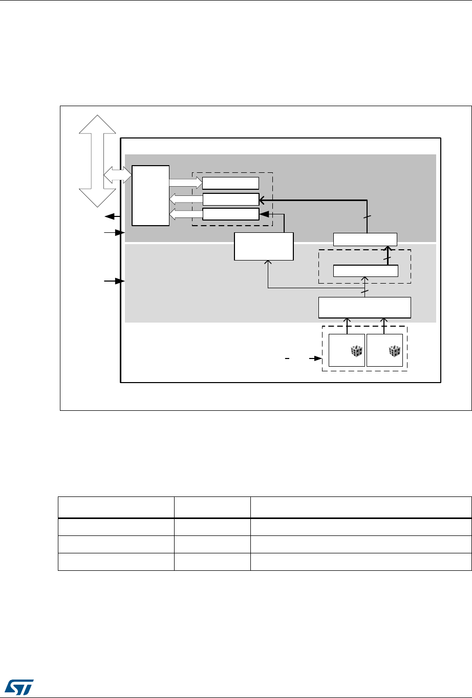
RM0430 Rev 8 451/1324
RM0430 True random number generator (RNG)
461
16.3 RNG functional description
16.3.1 RNG block diagram
Figure 85 shows the RNG block diagram.
Figure 85. RNG block diagram
16.3.2 RNG internal signals
Table 98 describes a list of useful-to-know internal signals available at the RNG level, not at
the STM32 product level (on pads).
06Y9
751*Y
51*B65
$+%
LQWHUIDFH
VWDWXV
51*B&5
$QDORJ
QRLVH
VRXUFH
%DQNHG5HJLVWHUV
6DPSOLQJ
1RUPDOL]DWLRQ[
$QDORJQRLVHVRXUFH
ELW
$QDORJ
QRLVH
VRXUFH
HQBRVF
ELW$+%%XV
UQJBLW
UQJBKFON
UQJBFON
$+%FORFNGRPDLQ
51*FORFNGRPDLQ
'DWDVKLIWUHJ
ELW
ELW/)65[
3RVWSURFHVVLQJORJLF ELW
)DXOWGHWHFWLRQ
&ORFNFKHFNHU
$ODUPV
51*B'5
GDWD
FRQWURO
Table 98. RNG internal input/output signals
Signal name Signal type Description
rng_it Digital output RNG global interrupt request
rng_hclk Digital input AHB clock
rng_clk Digital input RNG dedicated clock, asynchronous to rng_hclk
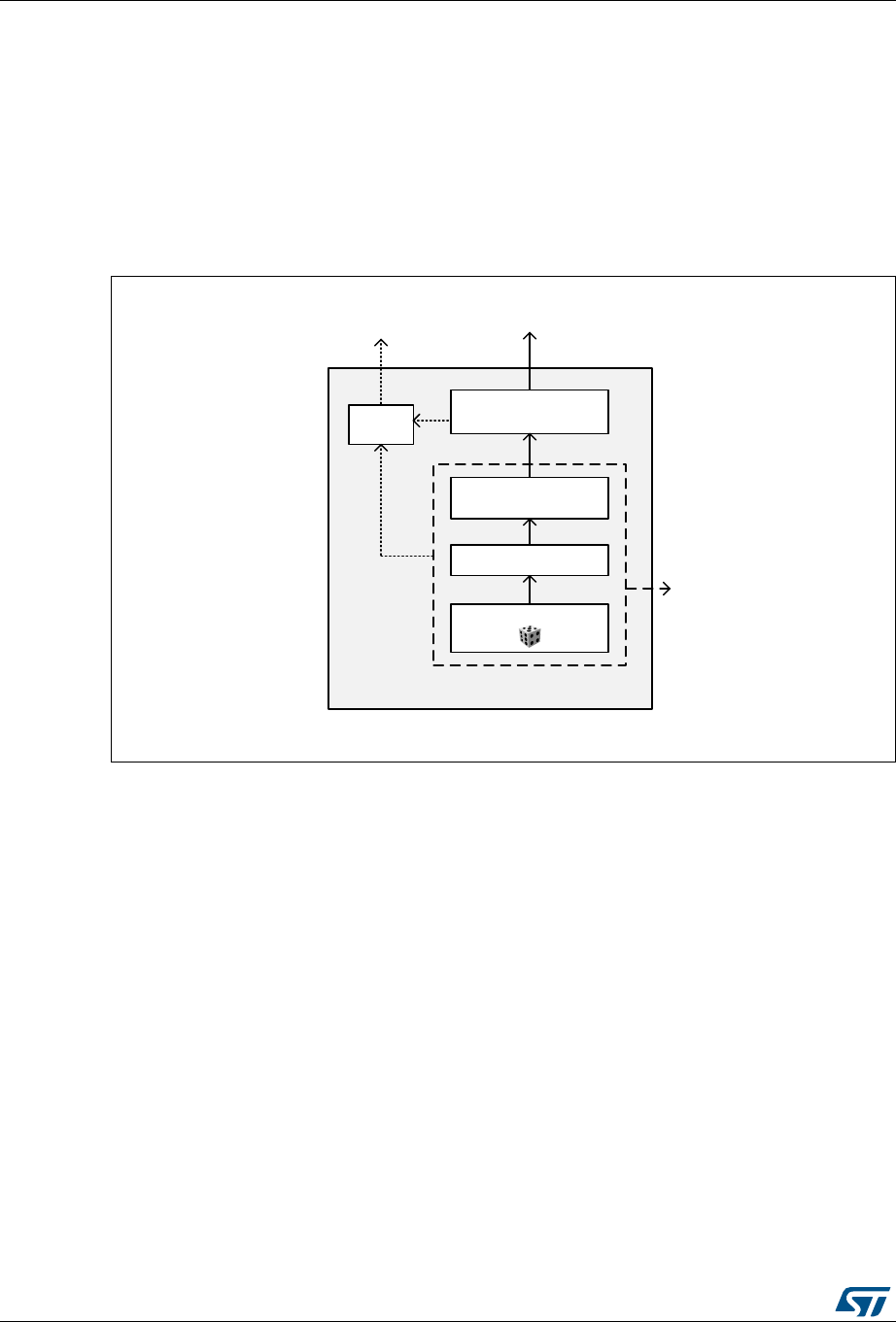
True random number generator (RNG) RM0430
452/1324 RM0430 Rev 8
16.3.3 Random number generation
The true random number generator (RNG) delivers truly random data through its AHB
interface at deterministic intervals. The RNG implements the entropy source model pictured
on Figure 86, and provides three main functions to the application:
•Collects the bitstring output of the entropy source box
•Obtains samples of the noise source for validation purpose
•Collects error messages from continuous health tests
Figure 86. Entropy source model
The main components of the RNG are:
•A source of physical randomness (analog noise source)
•A digitization stage for this analog noise source
•A stage delivering post-processed noise source (raw data)
•An output buffer for the raw data. If further cryptographic conditioning is required by the
application it will need to be performed by software.
•An optional output for the digitized noise source (unbuffered, on digital pads)
•Basic health tests on the digitized noise source
All those components are detailed below.
Noise source
The noise source is the component that contains the non-deterministic, entropy-providing
activity that is ultimately responsible for the uncertainty associated with the bitstring output
by the entropy source. It is composed of:
•Two analog noise sources, each based on three XORed free-running ring oscillator
outputs. It is possible to disable those analog oscillators to save power, as described in
06Y9
(QWURS\VRXUFH
1RLVH6RXUFH
'LJLWL]DWLRQ
3RVWSURFHVVLQJ
RSWLRQDO
5DZGDWD
&RQGLWLRQLQJ
RSWLRQDO
+HDWK
WHVWV
2XWSXW
(UURU
PHVVDJH
2XWSXW
UDZGDWDRU
GLJLWL]HGQRLVH
VRXUFH

RM0430 Rev 8 453/1324
RM0430 True random number generator (RNG)
461
Section 16.4: RNG low-power usage.
•A sampling stage of these outputs clocked by a dedicated clock input (rng_clk),
delivering a 2-bit raw data output.
This noise source sampling is independent to the AHB interface clock frequency
(rng_hclk).
Note: In Section 16.7: Entropy source validation recommended RNG clock frequencies are given.
Post processing
The sample values obtained from a true random noise source consist of 2-bit bitstrings.
Because this noise source output is biased, the RNG implements a post-processing
component that reduces that bias to a tolerable level.
The RNG post-processing consists of two stages, applied to each noise source bits:
•The RNG takes half of the bits from the sampled noise source, and half of the bits from
inverted sampled noise source. Thus, if the source generates more ‘1’ than ‘0’ (or the
opposite), it is filtered
•A linear feedback shift register (LFSR) performs a whitening process, producing 8-bit
strings.
This component is clocked by the RNG clock.
The times required between two random number generations, and between the RNG
initialization and availability of first sample are described in Section 16.6: RNG processing
time.
Output buffer
The RNG_DR data output register can store up to two 16-bit words which have been output
from the post-processing component (LFSR). In order to read back 32-bit random samples it
is required to wait 42 RNG clock cycles.
Whenever a random number is available through the RNG_DR register the DRDY flag
transitions from “0” to “1”. This flag remains high until output buffer becomes empty after
reading one word from the RNG_DR register.
Note: When interrupts are enabled an interrupt is generated when this data ready flag transitions
from “0” to “1”. Interrupt is then cleared automatically by the RNG as explained above.

True random number generator (RNG) RM0430
454/1324 RM0430 Rev 8
Health checks
This component ensures that the entire entropy source (with its noise source) starts then
operates as expected, obtaining assurance that failures are caught quickly and with a high
probability and reliability.
The RNG implements the following health check features:
1. Behavior tests, applied to the entropy source at run-time
– Repetition count test, flagging an error when:
a) One of the noise source has provided more than 64 consecutive bits at a constant
value (“0” or “1”)
b) One of the noise sources has delivered more than 32 consecutive occurrence of
two bits patterns (“01” or “10”)
2. Vendor specific continuous test
– Real-time “too slow” sampling clock detector, flagging an error when one RNG
clock cycle is smaller than AHB clock cycle divided by 16.
The CECS and SECS status bits in the RNG_SR register indicate when an error condition is
detected, as detailed in Section 16.3.7: Error management.
Note: An interrupt can be generated when an error is detected.
16.3.4 RNG initialization
When a hardware reset occurs the following chain of events occurs:
1. The analog noise source is enabled, and logic starts sampling the analog output after
four RNG clock cycles, filling LFSR shift register and associated 16-bit post-processing
shift register.
2. The output buffer is refilled automatically according to the RNG usage.
The associated initialization time can be found in Section 16.6: RNG processing time.
16.3.5 RNG operation
Normal operations
To run the RNG using interrupts the following steps are recommended:
1. Enable the interrupts by setting the IE bit in the RNG_CR register. At the same time
enable the RNG by setting the bit RNGEN=1.
2. An interrupt is now generated when a random number is ready or when an error
occurs. Therefore at each interrupt, check that:
– No error occurred. The SEIS and CEIS bits should be set to ‘0’ in the RNG_SR
register.
– A random number is ready. The DRDY bit must be set to ‘1’ in the RNG_SR
register.
– If above two conditions are true the content of the RNG_DR register can be read.

RM0430 Rev 8 455/1324
RM0430 True random number generator (RNG)
461
To run the RNG in polling mode following steps are recommended:
1. Enable the random number generation by setting the RNGEN bit to “1” in the RNG_CR
register.
2. Read the RNG_SR register and check that:
– No error occurred (the SEIS and CEIS bits should be set to ‘0’)
– A random number is ready (the DRDY bit should be set to ‘1’)
3. If above conditions are true read the content of the RNG_DR register.
Note: When data is not ready (DRDY=”0”) RNG_DR returns zero.
Low-power operations
If the power consumption is a concern to the application, low-power strategies can be used,
as described in Section 16.4: RNG low-power usage on page 456.
Software post-processing
If a NIST approved DRBG with 128 bits of security strength is required an approved random
generator software must be built around the RNG true random number generator.
16.3.6 RNG clocking
The RNG runs on two different clocks: the AHB bus clock and a dedicated RNG clock.
The AHB clock is used to clock the AHB banked registers and the post-processing
component. The RNG clock is used for noise source sampling. Recommended clock
configurations are detailed in Section 16.7: Entropy source validation.
Caution: When the CED bit in the RNG_CR register is set to “0”, the RNG clock frequency must be
higher than AHB clock frequency divided by 16, otherwise the clock checker will flag a clock
error (CECS or CEIS in the RNG_SR register) and the RNG will stop producing random
numbers.
See Section 16.3.1: RNG block diagram for details (AHB and RNG clock domains).
16.3.7 Error management
In parallel to random number generation an health check block verifies the correct noise
source behavior and the frequency of the RNG source clock as detailed in this section.
Associated error state is also described.
Clock error detection
When the clock error detection is enabled (CED = 0) and if the RNG clock frequency is too
low, the RNG stops generating random numbers and sets to “1” both the CEIS and CECS
bits to indicate that a clock error occurred. In this case, the application should check that the
RNG clock is configured correctly (see Section 16.3.6: RNG clocking) and then it must clear
the CEIS bit interrupt flag. As soon as the RNG clock operates correctly, the CECS bit will
be automatically cleared.
The RNG operates only when the CECS flag is set to “0”. However note that the clock error
has no impact on the previously generated random numbers, and the RNG_DR register
contents can still be used.

True random number generator (RNG) RM0430
456/1324 RM0430 Rev 8
Noise source error detection
When a noise source (or seed) error occurs, the RNG stops generating random numbers
and sets to “1” both SEIS and SECS bits to indicate that a seed error occurred. If a value is
available in the RNG_DR register, it must not be used as it may not have enough entropy.
In order to fully recover from a seed error application must clear the SEIS bit by writing it to
“0”, then clear and set the RNGEN bit to reinitialize and restart the RNG.
16.4 RNG low-power usage
If power consumption is a concern, the RNG can be disabled as soon as the DRDY bit is set
to “1” by setting the RNGEN bit to “0” in the RNG_CR register. The 32-bit random value
stored in the RNG_DR register will be still be available. If a new random is needed the
application will need to re-enable the RNG and wait for 42+4 RNG clock cycles.
When disabling the RNG the user deactivates all the analog seed generators, whose power
consumption is given in the datasheet electrical characteristics section.
16.5 RNG interrupts
In the RNG an interrupt can be produced on the following events:
•Data ready flag
•Seed error, see Section 16.3.7: Error management
•Clock error, see Section 16.3.7: Error management
Dedicated interrupt enable control bits are available as shown in Table 99
The user can enable or disable the above interrupt sources individually by changing the
mask bits or the general interrupt control bit IE in the RNG_CR register. The status of the
individual interrupt sources can be read from the RNG_SR register.
Note: Interrupts are generated only when RNG is enabled.
16.6 RNG processing time
The RNG can produce one 32-bit random numbers every 42 RNG clock cycles.
After enabling or re-enabling the RNG using the RNGEN bit it takes 46 RNG clock cycles
before random data are available.
Table 99. RNG interrupt requests
Interrupt event Event flag Enable control bit
Data ready flag DRDY IE
Seed error flag SEIS IE
Clock error flag CEIS IE

RM0430 Rev 8 457/1324
RM0430 True random number generator (RNG)
461
16.7 Entropy source validation
16.7.1 Introduction
In order to assess the amount of entropy available from the RNG, STMicroelectronics has
tested the peripheral against AIS-31 PTG.2 set of tests. The results can be provided on
demand or the customer can reproduce the measurements using the AIS reference
software. The customer could also test the RNG against an older NIST SP800-22 set of
tests.
16.7.2 Validation conditions
STMicroelectronics has validated the RNG true random number generator in the following
conditions:
•RNG clock rng_clk= 48 MHz (CED bit = ‘0’ in RNG_CR register) and rng_clk= 400kHz
(CED bit=”1” in RNG_CR)
•AHB clock rng_hclk= 60 MHz
16.7.3 Data collection
If raw data needs to be read instead of pre-processed data the developer is invited to
contact STMicroelectronics to receive the correct procedure to follow.

True random number generator (RNG) RM0430
458/1324 RM0430 Rev 8
16.8 RNG registers
The RNG is associated with a control register, a data register and a status register.
16.8.1 RNG control register (RNG_CR)
Address offset: 0x000
Reset value: 0x0000 0000
31 30 29 28 27 26 25 24 23 22 21 20 19 18 17 16
Res. Res. Res. Res. Res. Res. Res. Res. Res. Res. Res. Res. Res. Res. Res. Res.
15 14 13 12 11 10 9 8 7 6 5 4 3 2 1 0
Res. Res. Res. Res. Res. Res. Res. Res. Res. Res. CED Res. IE RNGEN Res. Res.
rw rw rw
Bits 31:6 Reserved, must be kept at reset value
Bit 5 CED: Clock error detection
0: Clock error detection is enable
1: Clock error detection is disable
The clock error detection cannot be enabled nor disabled on-the-fly when the RNG is
enabled, i.e. to enable or disable CED the RNG must be disabled.
Bit 4 Reserved, must be kept at reset value.
Bit 3 IE: Interrupt Enable
0: RNG Interrupt is disabled
1: RNG Interrupt is enabled. An interrupt is pending as soon as DRDY=’1’, SEIS=’1’ or
CEIS=’1’ in the RNG_SR register.
Bit 2 RNGEN: True random number generator enable
0: True random number generator is disabled. Analog noise sources are powered off and
logic clocked by the RNG clock is gated.
1: True random number generator is enabled.
Bits 1:0 Reserved, must be kept at reset value.

RM0430 Rev 8 459/1324
RM0430 True random number generator (RNG)
461
16.8.2 RNG status register (RNG_SR)
Address offset: 0x004
Reset value: 0x0000 0000
31 30 29 28 27 26 25 24 23 22 21 20 19 18 17 16
Res. Res. Res. Res. Res. Res. Res. Res. Res. Res. Res. Res. Res. Res. Res. Res.
1514131211109876543210
Res. Res. Res. Res. Res. Res. Res. Res. Res. SEIS CEIS Res. Res. SECS CECS DRDY
rc_w0 rc_w0 r r r
Bits 31:7 Reserved, must be kept at reset value.
Bit 6 SEIS: Seed error interrupt status
This bit is set at the same time as SECS. It is cleared by writing it to ‘0’.
0: No faulty sequence detected
1: At least one faulty sequence has been detected. See SECS bit description for details.
An interrupt is pending if IE = ‘1’ in the RNG_CR register.
Bit 5 CEIS: Clock error interrupt status
This bit is set at the same time as CECS. It is cleared by writing it to ‘0’.
0: The RNG clock is correct (fRNGCLK > fHCLK/16)
1: The RNG has been detected too slow (fRNGCLK < fHCLK/16)
An interrupt is pending if IE = ‘1’ in the RNG_CR register.
Bits 4:3 Reserved, must be kept at reset value.
Bit 2 SECS: Seed error current status
0: No faulty sequence has currently been detected. If the SEIS bit is set, this means that a
faulty sequence was detected and the situation has been recovered.
1: One of the noise source has provided more than 64 consecutive bits at a constant value
(“0” or “1”), or more than 32 consecutive occurrence of two bits patterns (“01” or “10”)
Bit 1 CECS: Clock error current status
0: The RNG clock is correct (fRNGCLK> fHCLK/16). If the CEIS bit is set, this means that a
slow clock was detected and the situation has been recovered.
1: The RNG clock is too slow (fRNGCLK< fHCLK/16).
Note: CECS bit is valid only if the CED bit in the RNG_CR register is set to “0”.
Bit 0 DRDY: Data Ready
0: The RNG_DR register is not yet valid, no random data is available.
1: The RNG_DR register contains valid random data.
Once the RNG_DR register has been read, this bit returns to ‘0’ until a new random value is
generated.
If IE=’1’ in the RNG_CR register, an interrupt is generated when DRDY=’1’.

True random number generator (RNG) RM0430
460/1324 RM0430 Rev 8
16.8.3 RNG data register (RNG_DR)
Address offset: 0x008
Reset value: 0x0000 0000
The RNG_DR register is a read-only register that delivers a 32-bit random value when read.
After being read this register delivers a new random value after 42 periods of RNG clock if
the output FIFO is empty.
The content of this register is valid when DRDY=’1’, even if RNGEN=’0’.
31 30 29 28 27 26 25 24 23 22 21 20 19 18 17 16
RNDATA[31:16]
rrrrrrrrrrrrrrrr
1514131211109876543210
RNDATA[15:0]
rrrrrrrrrrrrrrrr
Bits 31:0 RNDATA[31:0]: Random data
32-bit random data which are valid when DRDY=’1’. When DRDY=’0’ RNDATA value is zero.
RM0430 Rev 8 461/1324
RM0430 True random number generator (RNG)
461
16.8.4 RNG register map
Table 100 gives the RNG register map and reset values.
Table 100. RNG register map and reset map
Offset Register name
31
30
29
28
27
26
25
24
23
22
21
20
19
18
17
16
15
14
13
12
11
10
9
8
7
6
5
4
3
2
1
0
0x000 RNG_CR
Res.
Res.
Res.
Res.
Res.
Res.
Res.
Res.
Res.
Res.
Res.
Res.
Res.
Res.
Res.
Res.
Res.
Res.
Res.
Res.
Res.
Res.
Res.
Res.
Res.
Res.
CED
Res.
IE
RNGEN
Res.
Res.
Reset value 000
0x004 RNG_SR
Res.
Res.
Res.
Res.
Res.
Res.
Res.
Res.
Res.
Res.
Res.
Res.
Res.
Res.
Res.
Res.
Res.
Res.
Res.
Res.
Res.
Res.
Res.
Res.
Res.
SEIS
CEIS
Res.
Res.
SECS
CECS
DRDY
Reset value 00 000
0x008 RNG_DR RNDATA[31:0]
Reset value 00000000000000000000000000000000

Advanced-control timers (TIM1&TIM8) RM0430
462/1324 RM0430 Rev 8
17 Advanced-control timers (TIM1&TIM8)
17.1 TIM1&TIM8 introduction
The advanced-control timer (TIM1&TIM8) consist of a 16-bit auto-reload counter driven by a
programmable prescaler.
It may be used for a variety of purposes, including measuring the pulse length of input
signals (input capture) or generating output waveforms (output compare, PWM,
complementary PWM with dead-time insertion).
Pulse lengths and waveform periods can be modulated from a few microseconds to several
milliseconds using the timer prescaler and the RCC clock controller prescalers.
The advanced-control (TIM1) and general-purpose (TIMx) timers are completely
independent, and do not share any resources. They can be synchronized together as
described in Section 17.3.20.
17.2 TIM1&TIM8 main features
TIM1&TIM8 timer features include:
•16-bit up, down, up/down auto-reload counter.
•16-bit programmable prescaler allowing dividing (also “on the fly”) the counter clock
frequency either by any factor between 1 and 65536.
•Up to 4 independent channels for:
– Input Capture
– Output Compare
– PWM generation (Edge and Center-aligned Mode)
– One-pulse mode output
•Complementary outputs with programmable dead-time
•Synchronization circuit to control the timer with external signals and to interconnect
several timers together.
•Repetition counter to update the timer registers only after a given number of cycles of
the counter.
•Break input to put the timer’s output signals in reset state or in a known state.
•Interrupt/DMA generation on the following events:
– Update: counter overflow/underflow, counter initialization (by software or
internal/external trigger)
– Trigger event (counter start, stop, initialization or count by internal/external trigger)
– Input capture
– Output compare
– Break input
•Supports incremental (quadrature) encoder and Hall-sensor circuitry for positioning
purposes
•Trigger input for external clock or cycle-by-cycle current management
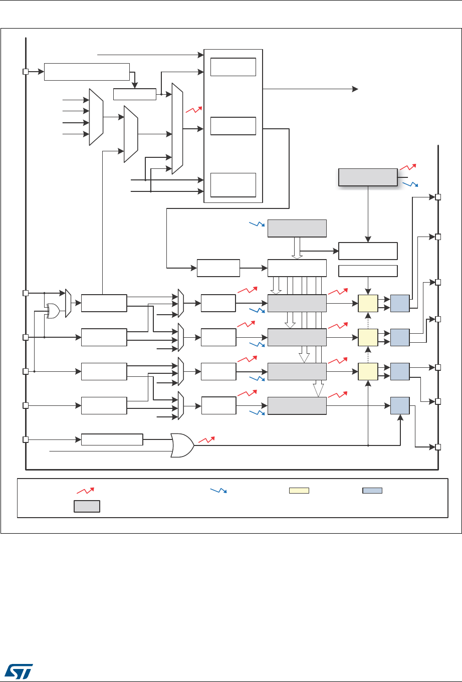
RM0430 Rev 8 463/1324
RM0430 Advanced-control timers (TIM1&TIM8)
533
Figure 87. Advanced-control timer block diagram
069
,QWHUUXSW'0$RXWSXW (YHQW
5HJ 3UHORDGUHJLVWHUVWUDQVIHUUHGWRDFWLYHUHJLVWHUVRQ8HYHQWDFFRUGLQJWRFRQWUROELW
/HJHQG
3RODULW\VHOHFWLRQ
,QSXWILOWHU
(GJHGHWHFWRU
,QSXWILOWHU
(GJHGHWHFWRU
,QSXWILOWHU
(GJHGHWHFWRU
,QSXWILOWHU
(GJHGHWHFWRU
75&
75&
75&
75&
7,)3
7,)3
7,)3
7,)3
3UHVFDOHU
,&
,&
,&
,&
3UHVFDOHU
3UHVFDOHU
3UHVFDOHU
7,)3
7,)3
7,)3
7,)3
7,
7,
7,
7,
%5.
&ORFNIDLOXUHHYHQWIURPFORFNFRQWUROOHU
&66&ORFN6HFXULW\6\VWHP
,&36
,&36
,&36
,&36
%,
&DSWXUH&RPSDUH
5HJLVWHU
8
&DSWXUH&RPSDUH
5HJLVWHU
8
8
&DSWXUH&RPSDUH
5HJLVWHU
&DSWXUH&RPSDUH
5HJLVWHU
8
&&,
&&,
&&,
&&,
&&,
&&,
&&,
&&,
2&5()
2&5()
2&5()
2&5()
2&
2&1
2&
2&1
2&
2&1 2&
'7*>@UHJLVWHUV
&17
FRXQWHU
36&
SUHVFDOHU
&.B&17&.B36&
5HSHWLWLRQFRXQWHU
5(35HJLVWHU
8,
3RODULW\VHOHFWLRQ
(GJHGHWHFWRUDQG3UHVFDOHU
,QSXWILOWHU
7ULJJHU
FRQWUROOHU
6ODYHPRGH
FRQWUROOHU
(QFRGHU
LQWHUIDFH
5HVHW
(QDEOH
8S'RZQ
&RXQW
7RRWKHUWLPHUV
7R'$&DQG$'&
75*2
75*,
7*,
,QWHUQDOFORFN&.B,17
(75)
(753
(75
&.B7,0IURP5&&
7,)3
7,)3
7,0[B(757,0[B&+7,0[B&+7,0[B&+7,0[B&+7,0[B%.,1
7,0[B&+7,0[B&+17,0[B&+7,0[B&+1 7,0[B&+7,0[B&+ 7,0[B&+1
8
8
'7* 2XWSXWFRQWURO
$XWR5HORDG
5HJLVWHU
8
,75
,75
,75
,75
7,)B('

Advanced-control timers (TIM1&TIM8) RM0430
464/1324 RM0430 Rev 8
17.3 TIM1&TIM8 functional description
17.3.1 Time-base unit
The main block of the programmable advanced-control timer is a 16-bit counter with its
related auto-reload register. The counter can count up, down or both up and down. The
counter clock can be divided by a prescaler.
The counter, the auto-reload register and the prescaler register can be written or read by
software. This is true even when the counter is running.
The time-base unit includes:
•Counter register (TIMx_CNT)
•Prescaler register (TIMx_PSC)
•Auto-reload register (TIMx_ARR)
•Repetition counter register (TIMx_RCR)
The auto-reload register is preloaded. Writing to or reading from the auto-reload register
accesses the preload register. The content of the preload register are transferred into the
shadow register permanently or at each update event (UEV), depending on the auto-reload
preload enable bit (ARPE) in TIMx_CR1 register. The update event is sent when the counter
reaches the overflow (or underflow when downcounting) and if the UDIS bit equals 0 in the
TIMx_CR1 register. It can also be generated by software. The generation of the update
event is described in detailed for each configuration.
The counter is clocked by the prescaler output CK_CNT, which is enabled only when the
counter enable bit (CEN) in TIMx_CR1 register is set (refer also to the slave mode controller
description to get more details on counter enabling).
Note that the counter starts counting 1 clock cycle after setting the CEN bit in the TIMx_CR1
register.
Prescaler description
The prescaler can divide the counter clock frequency by any factor between 1 and 65536. It
is based on a 16-bit counter controlled through a 16-bit register (in the TIMx_PSC register).
It can be changed on the fly as this control register is buffered. The new prescaler ratio is
taken into account at the next update event.
Figure 88 and Figure 89 give some examples of the counter behavior when the prescaler
ratio is changed on the fly:
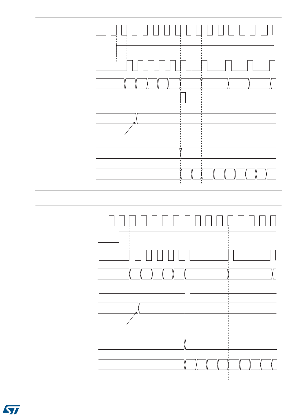
RM0430 Rev 8 465/1324
RM0430 Advanced-control timers (TIM1&TIM8)
533
Figure 88. Counter timing diagram with prescaler division change from 1 to 2
Figure 89. Counter timing diagram with prescaler division change from 1 to 4
&.B36&
&(1
7LPHUFORFN &.B&17
&RXQWHUUHJLVWHU
8SGDWHHYHQW8(9
3UHVFDOHUFRQWUROUHJLVWHU
:ULWHDQHZYDOXHLQ7,0[B36&
3UHVFDOHUEXIIHU
3UHVFDOHUFRXQWHU
)$ )%) ) ) )&
069
069
&.B36&
&(1
7LPHUFORFN &.B&17
&RXQWHUUHJLVWHU
8SGDWHHYHQW8(9
3UHVFDOHUFRQWUROUHJLVWHU
:ULWHDQHZYDOXHLQ7,0[B36&
3UHVFDOHUEXIIHU
3UHVFDOHUFRXQWHU
)$ )%
) ) ) )&
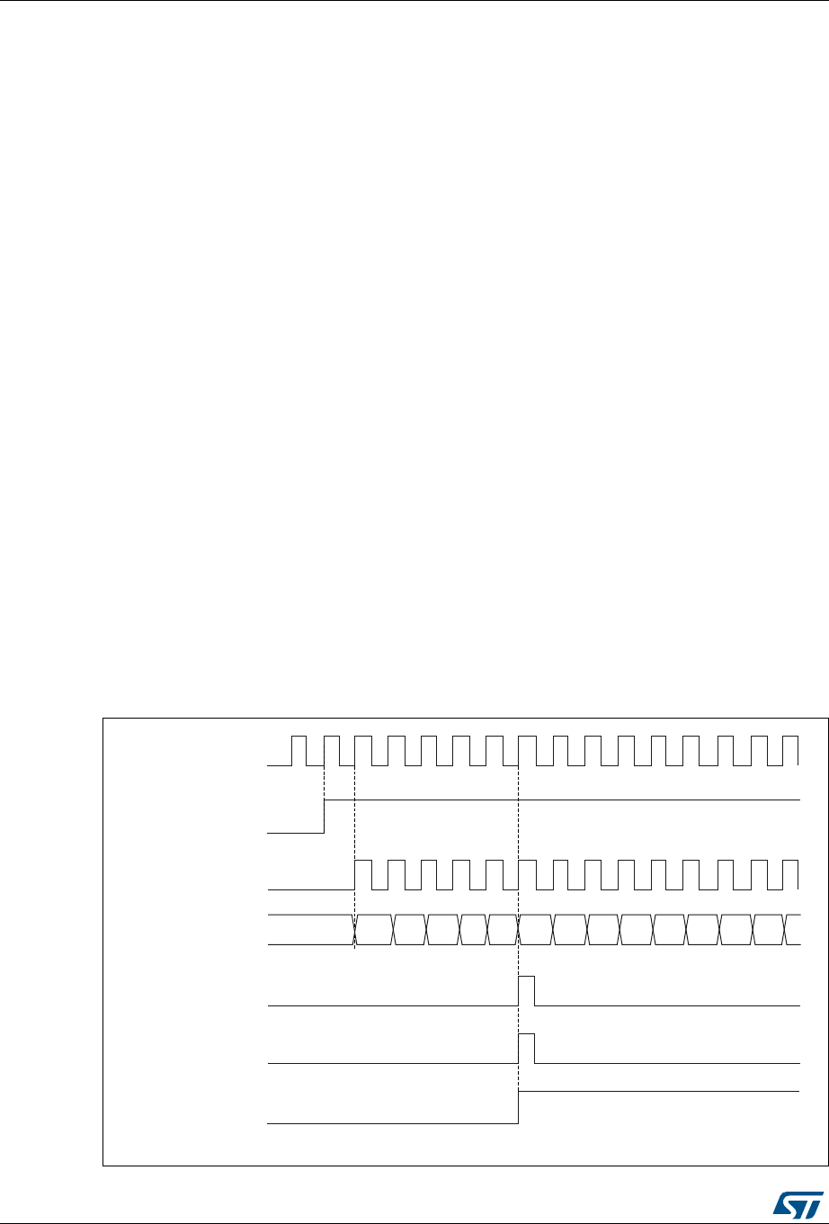
Advanced-control timers (TIM1&TIM8) RM0430
466/1324 RM0430 Rev 8
17.3.2 Counter modes
Upcounting mode
In upcounting mode, the counter counts from 0 to the auto-reload value (content of the
TIMx_ARR register), then restarts from 0 and generates a counter overflow event.
If the repetition counter is used, the update event (UEV) is generated after upcounting is
repeated for the number of times programmed in the repetition counter register plus one
(TIMx_RCR+1). Else the update event is generated at each counter overflow.
Setting the UG bit in the TIMx_EGR register (by software or by using the slave mode
controller) also generates an update event.
The UEV event can be disabled by software by setting the UDIS bit in the TIMx_CR1
register. This is to avoid updating the shadow registers while writing new values in the
preload registers. Then no update event occurs until the UDIS bit has been written to 0.
However, the counter restarts from 0, as well as the counter of the prescaler (but the
prescale rate does not change). In addition, if the URS bit (update request selection) in
TIMx_CR1 register is set, setting the UG bit generates an update event UEV but without
setting the UIF flag (thus no interrupt or DMA request is sent). This is to avoid generating
both update and capture interrupts when clearing the counter on the capture event.
When an update event occurs, all the registers are updated and the update flag (UIF bit in
TIMx_SR register) is set (depending on the URS bit):
•The repetition counter is reloaded with the content of TIMx_RCR register,
•The auto-reload shadow register is updated with the preload value (TIMx_ARR),
•The buffer of the prescaler is reloaded with the preload value (content of the TIMx_PSC
register).
The following figures show some examples of the counter behavior for different clock
frequencies when TIMx_ARR=0x36.
Figure 90. Counter timing diagram, internal clock divided by 1
ϬϬ ϬϮ Ϭϯ Ϭϰ Ϭϱ Ϭϲ Ϭϳϯϯ ϯϰ ϯϱ ϯϲϯϭ
069
<ͺW^
EdͺE
dŝŵĞƌĐůŽĐŬс<ͺEd
ŽƵŶƚĞƌƌĞŐŝƐƚĞƌ
hƉĚĂƚĞĞǀĞŶƚ;hsͿ
ŽƵŶƚĞƌŽǀĞƌĨůŽǁ
hƉĚĂƚĞŝŶƚĞƌƌƵƉƚĨůĂŐ;h/&Ϳ
ϬϭϯϮ
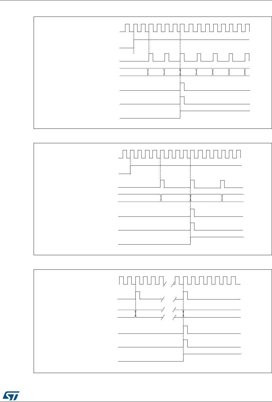
RM0430 Rev 8 467/1324
RM0430 Advanced-control timers (TIM1&TIM8)
533
Figure 91. Counter timing diagram, internal clock divided by 2
Figure 92. Counter timing diagram, internal clock divided by 4
Figure 93. Counter timing diagram, internal clock divided by N
069
&.B36&
&17B(1
7LPHUFORFN &.B&17
&RXQWHUUHJLVWHU
8SGDWHHYHQW8(9
&RXQWHURYHUIORZ
8SGDWHLQWHUUXSWIODJ8,)
069
&.B36&
&17B(1
7LPHUFORFN &.B&17
&RXQWHUUHJLVWHU
8SGDWHHYHQW8(9
&RXQWHURYHUIORZ
8SGDWHLQWHUUXSWIODJ8,)
069
&.B36&
7LPHUFORFN &.B&17
&RXQWHUUHJLVWHU
8SGDWHHYHQW8(9
&RXQWHURYHUIORZ
8SGDWHLQWHUUXSWIODJ8,)
)
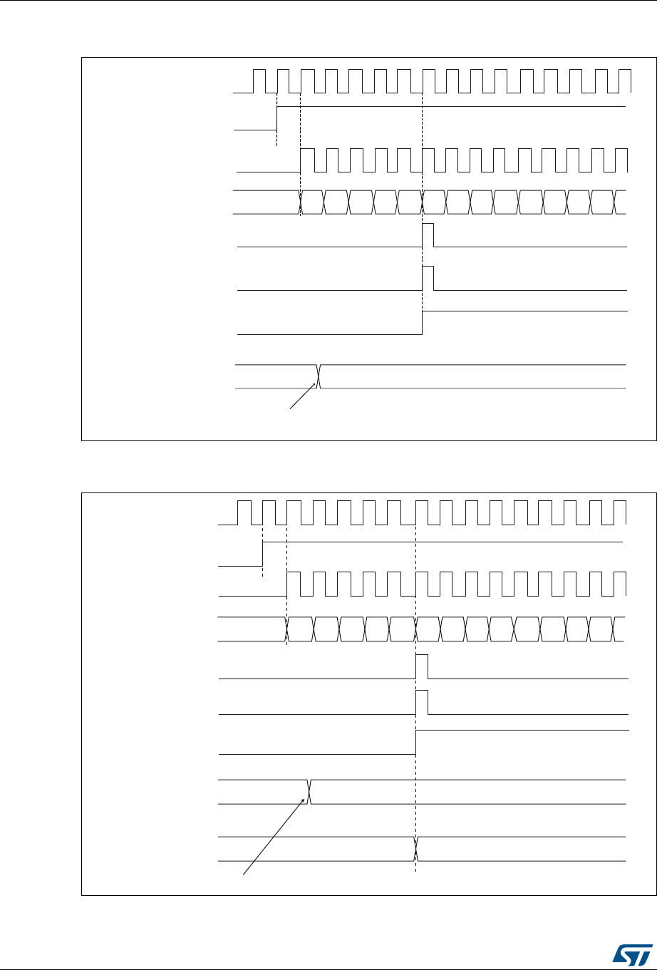
Advanced-control timers (TIM1&TIM8) RM0430
468/1324 RM0430 Rev 8
Figure 94. Counter timing diagram, update event when ARPE=0
(TIMx_ARR not preloaded)
Figure 95. Counter timing diagram, update event when ARPE=1
(TIMx_ARR preloaded)
&& ϯϲ
069
<ͺW^
dŝŵĞƌĐůŽĐŬс<ͺEd
ŽƵŶƚĞƌƌĞŐŝƐƚĞƌ
hƉĚĂƚĞĞǀĞŶƚ;hsͿ
ŽƵŶƚĞƌŽǀĞƌĨůŽǁ
hƉĚĂƚĞŝŶƚĞƌƌƵƉƚĨůĂŐ;h/&Ϳ
ϬϬ ϬϮ Ϭϯ Ϭϰ Ϭϱ Ϭϲ ϬϳϯϮ ϯϯ ϯϰ ϯϱ ϯϲϯϭ Ϭϭ
E
ƵƚŽͲƌĞůŽĂĚƉƌĞůŽĂĚƌĞŐŝƐƚĞƌ
tƌŝƚĞĂŶĞǁǀĂůƵĞŝŶd/DdžͺZZ
069
)
&.B36&
7LPHUFORFN &.B&17
&RXQWHUUHJLVWHU
8SGDWHHYHQW8(9
&RXQWHURYHUIORZ
8SGDWHLQWHUUXSWIODJ
8,)
) ) ) ) ))
&(1
$XWRUHORDGSUHORDG
UHJLVWHU
:ULWHDQHZYDOXHLQ7,0[B$55
$XWRUHORDGVKDGRZ
UHJLVWHU )

RM0430 Rev 8 469/1324
RM0430 Advanced-control timers (TIM1&TIM8)
533
Downcounting mode
In downcounting mode, the counter counts from the auto-reload value (content of the
TIMx_ARR register) down to 0, then restarts from the auto-reload value and generates a
counter underflow event.
If the repetition counter is used, the update event (UEV) is generated after downcounting is
repeated for the number of times programmed in the repetition counter register plus one
(TIMx_RCR+1). Else the update event is generated at each counter underflow.
Setting the UG bit in the TIMx_EGR register (by software or by using the slave mode
controller) also generates an update event.
The UEV update event can be disabled by software by setting the UDIS bit in TIMx_CR1
register. This is to avoid updating the shadow registers while writing new values in the
preload registers. Then no update event occurs until UDIS bit has been written to 0.
However, the counter restarts from the current auto-reload value, whereas the counter of the
prescaler restarts from 0 (but the prescale rate doesn’t change).
In addition, if the URS bit (update request selection) in TIMx_CR1 register is set, setting the
UG bit generates an update event UEV but without setting the UIF flag (thus no interrupt or
DMA request is sent). This is to avoid generating both update and capture interrupts when
clearing the counter on the capture event.
When an update event occurs, all the registers are updated and the update flag (UIF bit in
TIMx_SR register) is set (depending on the URS bit):
•The repetition counter is reloaded with the content of TIMx_RCR register
•The buffer of the prescaler is reloaded with the preload value (content of the TIMx_PSC
register)
•The auto-reload active register is updated with the preload value (content of the
TIMx_ARR register). Note that the auto-reload is updated before the counter is
reloaded, so that the next period is the expected one
The following figures show some examples of the counter behavior for different clock
frequencies when TIMx_ARR=0x36.
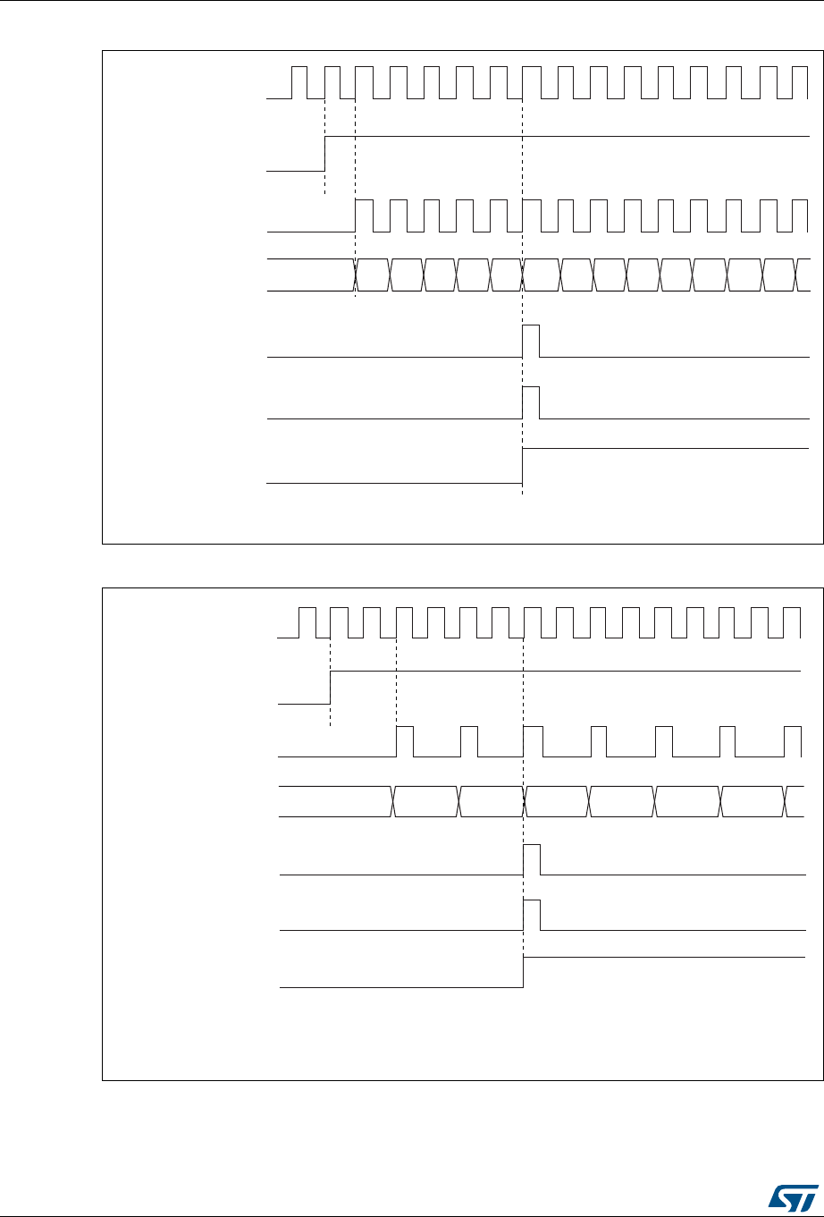
Advanced-control timers (TIM1&TIM8) RM0430
470/1324 RM0430 Rev 8
Figure 96. Counter timing diagram, internal clock divided by 1
Figure 97. Counter timing diagram, internal clock divided by 2
)
069
&.B36&
&17B(1
7LPHUFORFN &.B&17
&RXQWHUUHJLVWHU
8SGDWHHYHQW8(9
&RXQWHUXQGHUIORZ
FQWBXGI
8SGDWHLQWHUUXSWIODJ
8,)
069
&.B36&
&17B(1
7LPHUFORFN &.B&17
&RXQWHUUHJLVWHU
8SGDWHHYHQW8(9
&RXQWHUXQGHUIORZ
8SGDWHLQWHUUXSWIODJ
8,)
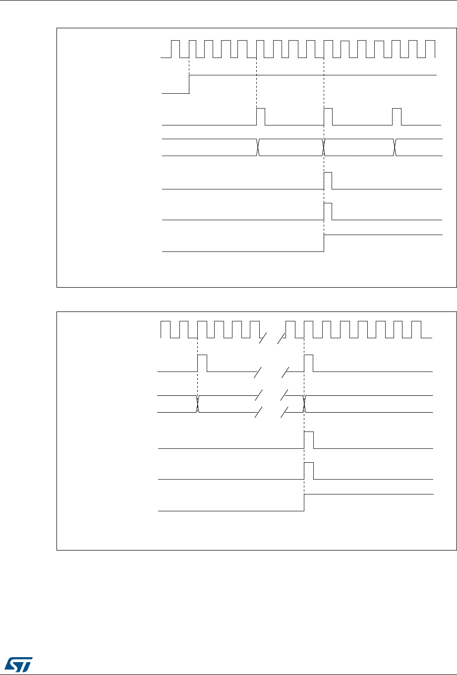
RM0430 Rev 8 471/1324
RM0430 Advanced-control timers (TIM1&TIM8)
533
Figure 98. Counter timing diagram, internal clock divided by 4
Figure 99. Counter timing diagram, internal clock divided by N
069
&.B36&
7LPHUFORFN &.B&17
&RXQWHUUHJLVWHU
8SGDWHHYHQW8(9
&RXQWHUXQGHUIORZ
8SGDWHLQWHUUXSWIODJ
8,)
&17B(1
)
069
&.B36&
7LPHUFORFN &.B&17
&RXQWHUUHJLVWHU
8SGDWHHYHQW8(9
&RXQWHUXQGHUIORZ
8SGDWHLQWHUUXSWIODJ
8,)
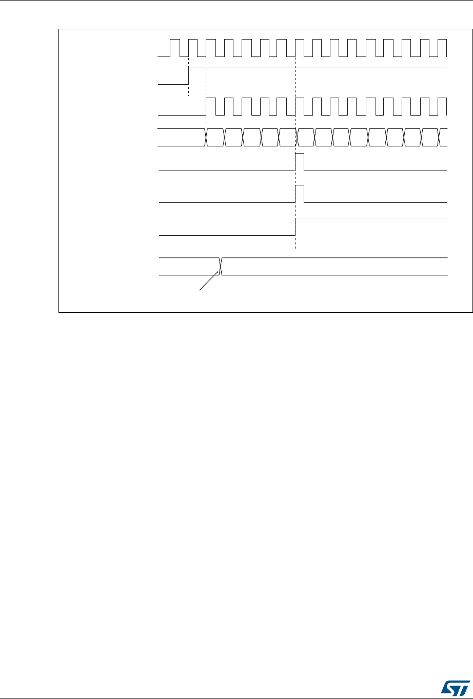
Advanced-control timers (TIM1&TIM8) RM0430
472/1324 RM0430 Rev 8
Figure 100. Counter timing diagram, update event when repetition counter is not used
Center-aligned mode (up/down counting)
In center-aligned mode, the counter counts from 0 to the auto-reload value (content of the
TIMx_ARR register) – 1, generates a counter overflow event, then counts from the auto-
reload value down to 1 and generates a counter underflow event. Then it restarts counting
from 0.
Center-aligned mode is active when the CMS bits in TIMx_CR1 register are not equal to
'00'. The Output compare interrupt flag of channels configured in output is set when: the
counter counts down (Center aligned mode 1, CMS = "01"), the counter counts up (Center
aligned mode 2, CMS = "10") the counter counts up and down (Center aligned mode 3,
CMS = "11").
In this mode, the DIR direction bit in the TIMx_CR1 register cannot be written. It is updated
by hardware and gives the current direction of the counter.
The update event can be generated at each counter overflow and at each counter underflow
or by setting the UG bit in the TIMx_EGR register (by software or by using the slave mode
controller) also generates an update event. In this case, the counter restarts counting from
0, as well as the counter of the prescaler.
The UEV update event can be disabled by software by setting the UDIS bit in the TIMx_CR1
register. This is to avoid updating the shadow registers while writing new values in the
preload registers. Then no update event occurs until UDIS bit has been written to 0.
However, the counter continues counting up and down, based on the current auto-reload
value.
In addition, if the URS bit (update request selection) in TIMx_CR1 register is set, setting the
UG bit generates an UEV update event but without setting the UIF flag (thus no interrupt or
))
069
&.B36&
7LPHUFORFN &.B&17
&RXQWHUUHJLVWHU
8SGDWHHYHQW8(9
&RXQWHUXQGHUIORZ
8SGDWHLQWHUUXSWIODJ
8,)
)
&(1
$XWRUHORDGSUHORDG
UHJLVWHU
:ULWHDQHZYDOXHLQ7,0[B$55
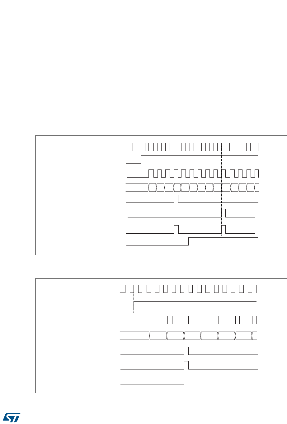
RM0430 Rev 8 473/1324
RM0430 Advanced-control timers (TIM1&TIM8)
533
DMA request is sent). This is to avoid generating both update and capture interrupts when
clearing the counter on the capture event.
When an update event occurs, all the registers are updated and the update flag (UIF bit in
TIMx_SR register) is set (depending on the URS bit):
•The repetition counter is reloaded with the content of TIMx_RCR register
•The buffer of the prescaler is reloaded with the preload value (content of the TIMx_PSC
register)
•The auto-reload active register is updated with the preload value (content of the
TIMx_ARR register). Note that if the update source is a counter overflow, the auto-
reload is updated before the counter is reloaded, so that the next period is the expected
one (the counter is loaded with the new value).
The following figures show some examples of the counter behavior for different clock
frequencies.
Figure 101. Counter timing diagram, internal clock divided by 1, TIMx_ARR = 0x6
1. Here, center-aligned mode 1 is used (for more details refer to Section 17.4: TIM1&TIM8 registers).
Figure 102. Counter timing diagram, internal clock divided by 2
069
&.B36&
7LPHUFORFN &.B&17
&RXQWHUUHJLVWHU
8SGDWHHYHQW8(9
&RXQWHURYHUIORZ
8SGDWHLQWHUUXSWIODJ8,)
&(1
&RXQWHUXQGHUIORZ
069
&.B36&
7LPHUFORFN &.B&17
&RXQWHUUHJLVWHU
8SGDWHHYHQW8(9
8SGDWHLQWHUUXSWIODJ8,)
&17B(1
&RXQWHUXQGHUIORZ
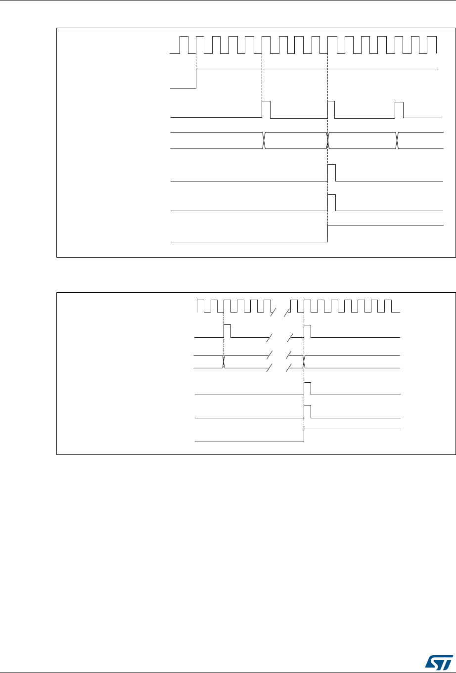
Advanced-control timers (TIM1&TIM8) RM0430
474/1324 RM0430 Rev 8
Figure 103. Counter timing diagram, internal clock divided by 4, TIMx_ARR=0x36
1. Center-aligned mode 2 or 3 is used with an UIF on overflow.
Figure 104. Counter timing diagram, internal clock divided by N
069
&.B36&
7LPHUFORFN &.B&17
&RXQWHUUHJLVWHU
8SGDWHHYHQW8(9
&RXQWHURYHUIORZ
8SGDWHLQWHUUXSWIODJ8,)
&17B(1
069
&.B36&
7LPHUFORFN &.B&17
&RXQWHUUHJLVWHU
8SGDWHHYHQW8(9
8SGDWHLQWHUUXSWIODJ8,)
&RXQWHUXQGHUIORZ
)
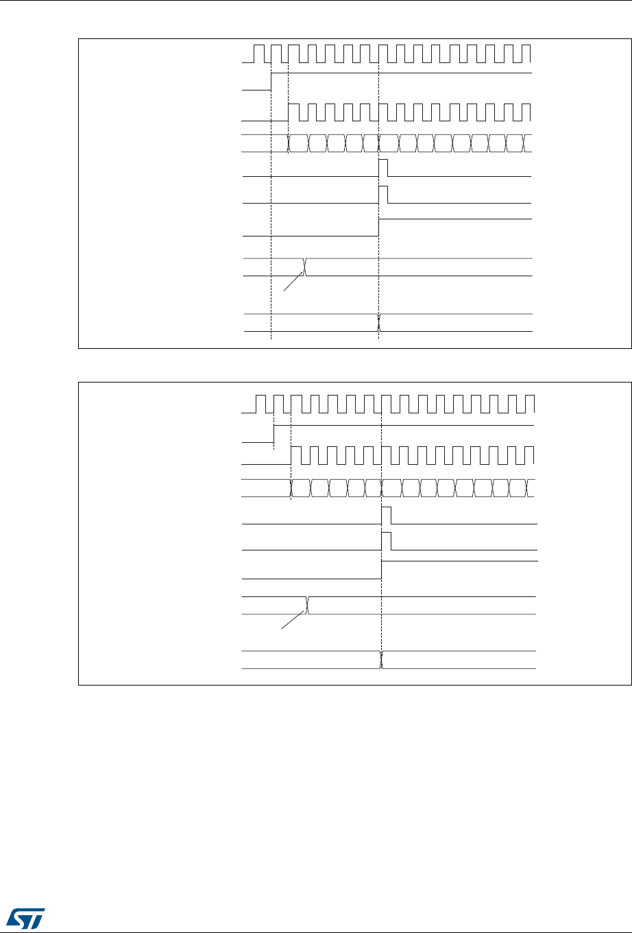
RM0430 Rev 8 475/1324
RM0430 Advanced-control timers (TIM1&TIM8)
533
Figure 105. Counter timing diagram, update event with ARPE=1 (counter underflow)
Figure 106. Counter timing diagram, update event with ARPE=1 (counter overflow)
17.3.3 Repetition counter
Section 17.3.1: Time-base unit describes how the update event (UEV) is generated with
respect to the counter overflows/underflows. It is actually generated only when the repetition
counter has reached zero. This can be useful when generating PWM signals.
This means that data are transferred from the preload registers to the shadow registers
(TIMx_ARR auto-reload register, TIMx_PSC prescaler register, but also TIMx_CCRx
capture/compare registers in compare mode) every N+1 counter overflows or underflows,
where N is the value in the TIMx_RCR repetition counter register.
069
&.B36&
7LPHUFORFN &.B&17
&RXQWHUUHJLVWHU
8SGDWHHYHQW8(9
&RXQWHURYHUIORZ
8SGDWHLQWHUUXSWIODJ8,)
&(1
$XWRUHORDGSUHORDGUHJLVWHU
:ULWHDQHZYDOXHLQ7,0[B$55
$XWRUHORDGDFWLYHUHJLVWHU
)'
)'
069
)'
&.B36&
7LPHUFORFN &.B&17
&RXQWHUUHJLVWHU
8SGDWHHYHQW8(9
&RXQWHURYHUIORZ
8SGDWHLQWHUUXSWIODJ8,)
)) ) )$ )% )&)
&(1
$XWRUHORDGSUHORDGUHJLVWHU
:ULWHDQHZYDOXHLQ7,0[B$55
$XWRUHORDGDFWLYHUHJLVWHU )'

Advanced-control timers (TIM1&TIM8) RM0430
476/1324 RM0430 Rev 8
The repetition counter is decremented:
•At each counter overflow in upcounting mode,
•At each counter underflow in downcounting mode,
•At each counter overflow and at each counter underflow in center-aligned mode.
Although this limits the maximum number of repetition to 128 PWM cycles, it makes it
possible to update the duty cycle twice per PWM period. When refreshing compare
registers only once per PWM period in center-aligned mode, maximum resolution is
2xTck, due to the symmetry of the pattern.
The repetition counter is an auto-reload type; the repetition rate is maintained as defined by
the TIMx_RCR register value (refer to Figure 107). When the update event is generated by
software (by setting the UG bit in TIMx_EGR register) or by hardware through the slave
mode controller, it occurs immediately whatever the value of the repetition counter is and the
repetition counter is reloaded with the content of the TIMx_RCR register.
In center-aligned mode, for odd values of RCR, the update event occurs either on the
overflow or on the underflow depending on when the RCR register was written and when
the counter was started. If the RCR was written before starting the counter, the UEV occurs
on the overflow. If the RCR was written after starting the counter, the UEV occurs on the
underflow. For example for RCR = 3, the UEV is generated on each 4th overflow or
underflow event depending on when RCR was written.
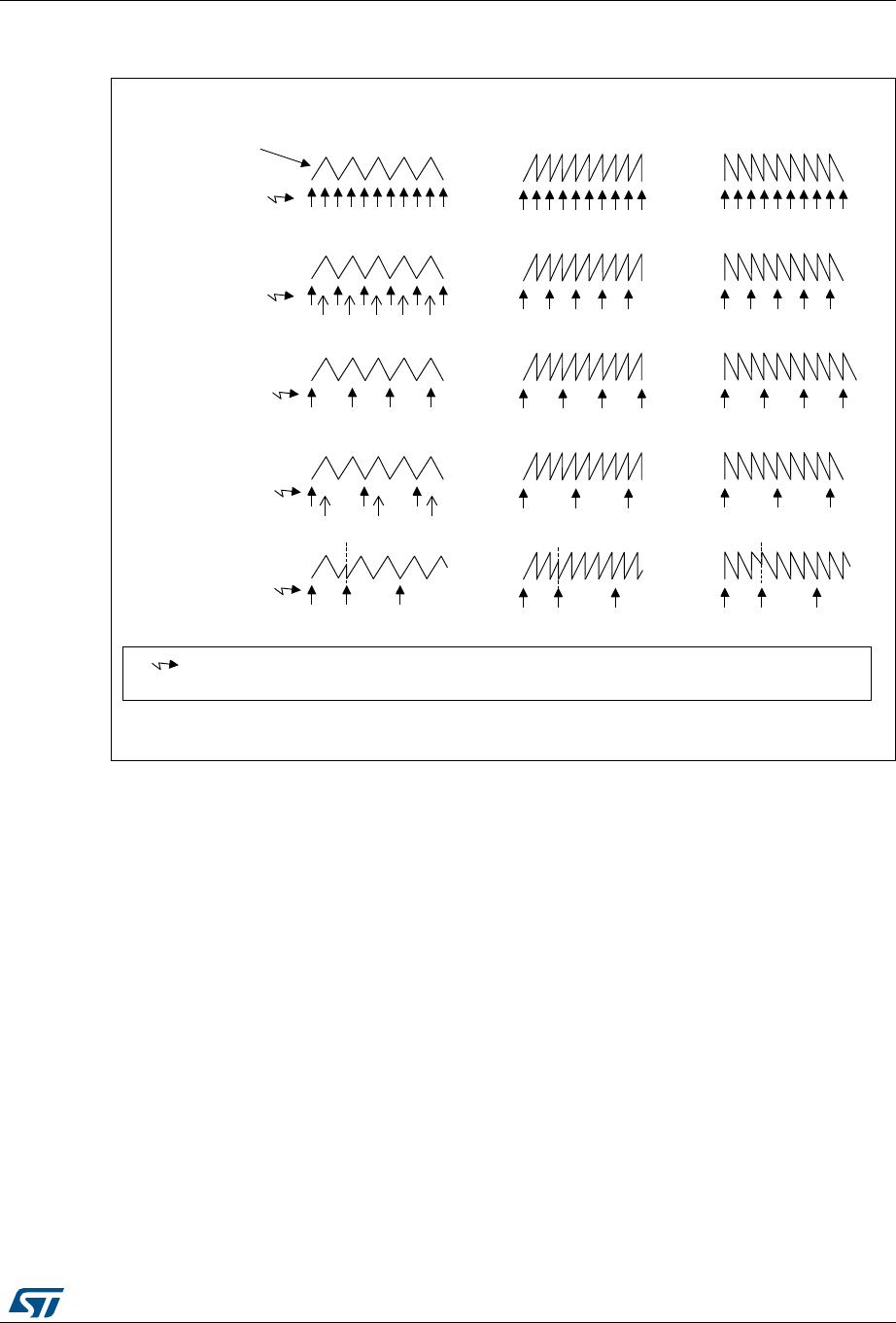
RM0430 Rev 8 477/1324
RM0430 Advanced-control timers (TIM1&TIM8)
533
Figure 107. Update rate examples depending on mode and TIMx_RCR register
settings
06Y9
8(9
8(9
8(9
8(9
8(9
&RXQWHUDOLJQHGPRGH (GJHDOLJQHGPRGH
8SFRXQWLQJ 'RZQFRXQWLQJ
E\6:E\6:E\6:
7,0[B5&5
DQG
UHV\QFKURQL]DWLRQ
7,0[B5&5
7,0[B5&5
7,0[B5&5
7,0[B5&5
&RXQWHU
7,0[B&17
8(9 8SGDWHHYHQW3UHORDGUHJLVWHUVWUDQVIHUUHGWRDFWLYHUHJLVWHUVDQGXSGDWHLQWHUUXSWJHQHUDWHG
8SGDWH(YHQWLIWKHUHSHWLWLRQFRXQWHUXQGHUIORZRFFXUVZKHQWKHFRXQWHULVHTXDOWRWKHDXWRUHORDGYDOXH
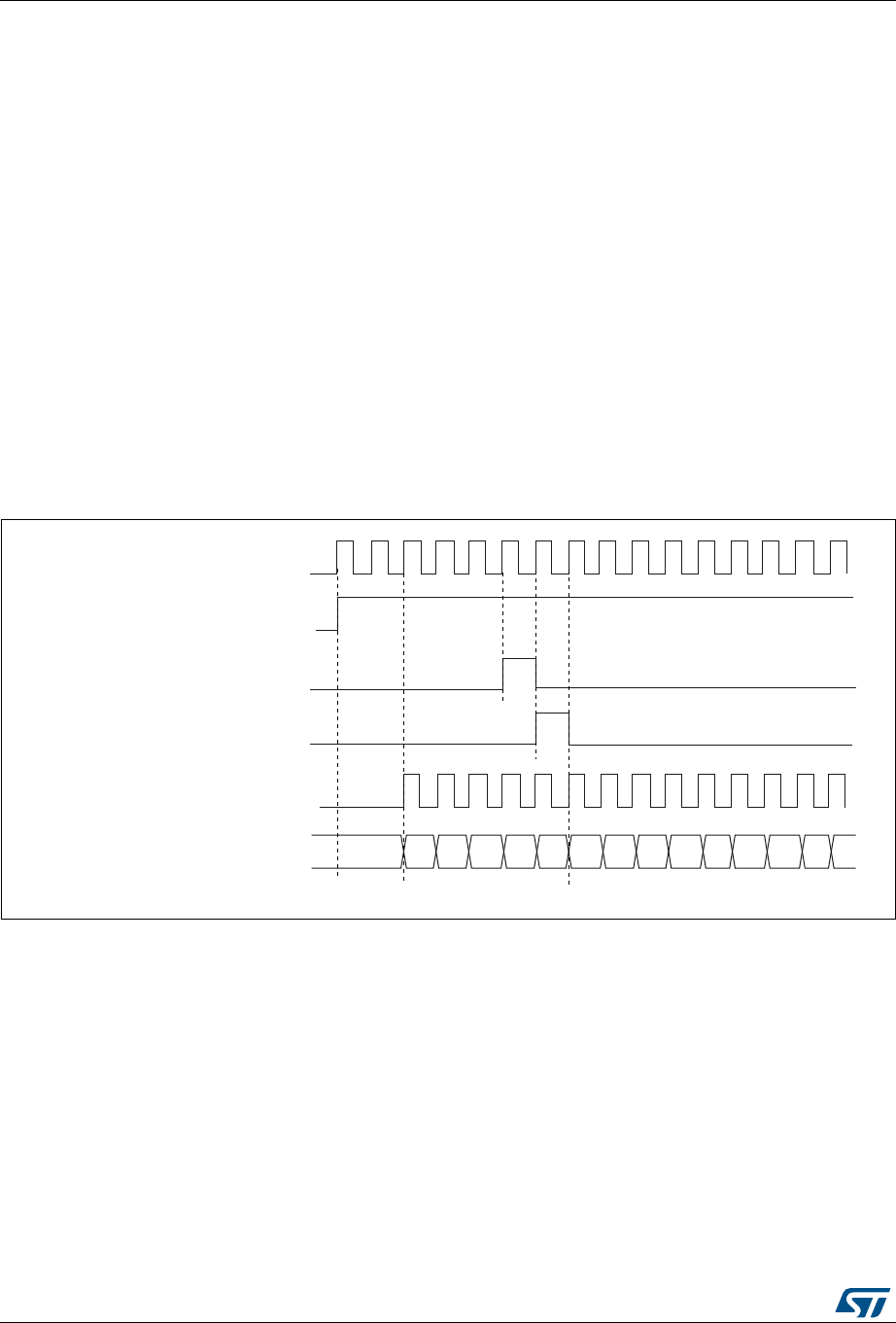
Advanced-control timers (TIM1&TIM8) RM0430
478/1324 RM0430 Rev 8
17.3.4 Clock selection
The counter clock can be provided by the following clock sources:
•Internal clock (CK_INT)
•External clock mode1: external input pin
•External clock mode2: external trigger input ETR
•Internal trigger inputs (ITRx): using one timer as prescaler for another timer, for
example, you can configure Timer 1 to act as a prescaler for Timer 2. Refer to Using
one timer as prescaler for another timer for more details.
Internal clock source (CK_INT)
If the slave mode controller is disabled (SMS=000), then the CEN, DIR (in the TIMx_CR1
register) and UG bits (in the TIMx_EGR register) are actual control bits and can be changed
only by software (except UG which remains cleared automatically). As soon as the CEN bit
is written to 1, the prescaler is clocked by the internal clock CK_INT.
Figure 108 shows the behavior of the control circuit and the upcounter in normal mode,
without prescaler.
Figure 108. Control circuit in normal mode, internal clock divided by 1
External clock source mode 1
This mode is selected when SMS=111 in the TIMx_SMCR register. The counter can count at
each rising or falling edge on a selected input.
,QWHUQDOFORFN
&RXQWHUFORFN &.B&17 &.B36&
&RXQWHUUHJLVWHU
&(1 &17B(1
8*
&17B,1,7
069
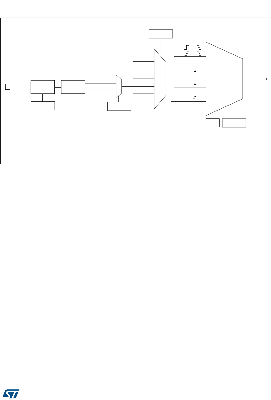
RM0430 Rev 8 479/1324
RM0430 Advanced-control timers (TIM1&TIM8)
533
Figure 109. TI2 external clock connection example
For example, to configure the upcounter to count in response to a rising edge on the TI2
input, use the following procedure:
1. Configure channel 2 to detect rising edges on the TI2 input by writing CC2S = ‘01’ in
the TIMx_CCMR1 register.
2. Configure the input filter duration by writing the IC2F[3:0] bits in the TIMx_CCMR1
register (if no filter is needed, keep IC2F=0000).
3. Select rising edge polarity by writing CC2P=0 and CC2NP=0 in the TIMx_CCER
register.
4. Configure the timer in external clock mode 1 by writing SMS=111 in the TIMx_SMCR
register.
5. Select TI2 as the trigger input source by writing TS=110 in the TIMx_SMCR register.
6. Enable the counter by writing CEN=1 in the TIMx_CR1 register.
Note: The capture prescaler is not used for triggering, so you don’t need to configure it.
When a rising edge occurs on TI2, the counter counts once and the TIF flag is set.
The delay between the rising edge on TI2 and the actual clock of the counter is due to the
resynchronization circuit on TI2 input.
([WHUQDOFORFN
PRGH
,QWHUQDOFORFN
PRGH
75*,
&.B,17
&.B36&
7,0[B60&5
606>@
,75[
7,B('
7,)3
7,)3
7,0[B60&5
76>@
7,
7,0[B&&(5
&&3
)LOWHU
,&)>@
7,0[B&&05
(GJH
GHWHFWRU
7,)B5LVLQJ
7,)B)DOOLQJ
[[
069
LQWHUQDOFORFN
7,) RU
7,) RU
RU
(QFRGHU
PRGH
(75)
([WHUQDOFORFN
PRGH
(75)
(&(
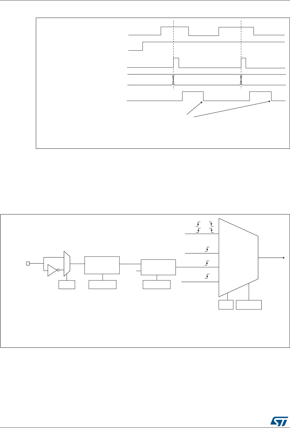
Advanced-control timers (TIM1&TIM8) RM0430
480/1324 RM0430 Rev 8
Figure 110. Control circuit in external clock mode 1
External clock source mode 2
This mode is selected by writing ECE=1 in the TIMx_SMCR register.
The counter can count at each rising or falling edge on the external trigger input ETR.
Figure 111 gives an overview of the external trigger input block.
Figure 111. External trigger input block
For example, to configure the upcounter to count each 2 rising edges on ETR, use the
following procedure:
&RXQWHUFORFN &.B&17 &.B36&
&RXQWHUUHJLVWHU
7,
&17B(1
7,)
:ULWH7,)
069
([WHUQDOFORFN
PRGH
,QWHUQDOFORFN
PRGH
75*,
&.B,17
&.B36&
7,0[B60&5
606>@
069
LQWHUQDOFORFN
7,) RU
7,) RU
RU
(QFRGHU
PRGH
([WHUQDOFORFN
PRGH
(75)
(&(
7,0[B60&5
(73
(75SLQ
(75
'LYLGHU
)LOWHU
GRZQFRXQWHU
I
(753
7,0[B60&5
(736>@
7,0[B60&5
(7)>@
'76
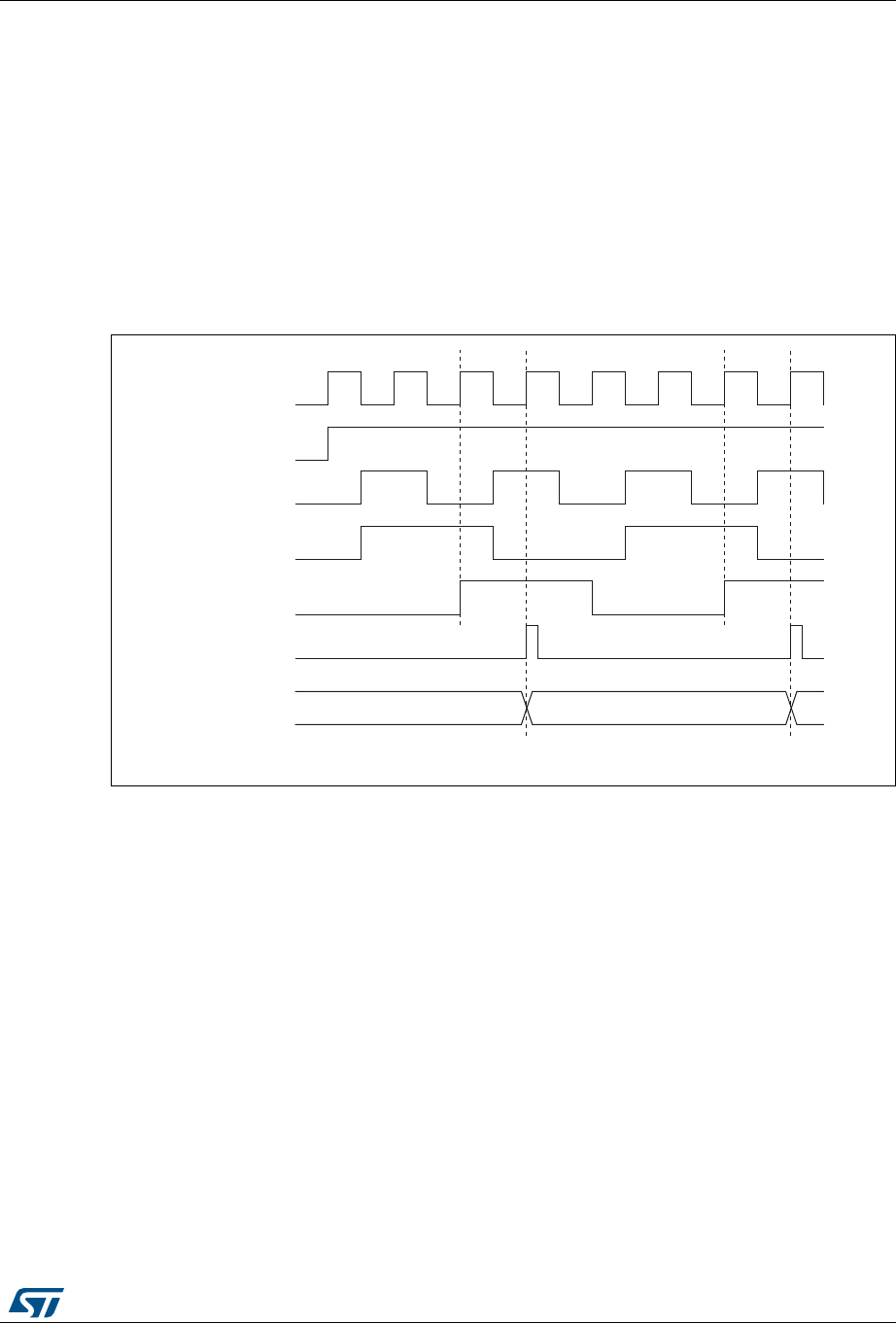
RM0430 Rev 8 481/1324
RM0430 Advanced-control timers (TIM1&TIM8)
533
1. As no filter is needed in this example, write ETF[3:0]=0000 in the TIMx_SMCR register.
2. Set the prescaler by writing ETPS[1:0]=01 in the TIMx_SMCR register
3. Select rising edge detection on the ETR pin by writing ETP=0 in the TIMx_SMCR
register
4. Enable external clock mode 2 by writing ECE=1 in the TIMx_SMCR register.
5. Enable the counter by writing CEN=1 in the TIMx_CR1 register.
The counter counts once each 2 ETR rising edges.
The delay between the rising edge on ETR and the actual clock of the counter is due to the
resynchronization circuit on the ETRP signal.
Figure 112. Control circuit in external clock mode 2
17.3.5 Capture/compare channels
Each Capture/Compare channel is built around a capture/compare register (including a
shadow register), a input stage for capture (with digital filter, multiplexing and prescaler) and
an output stage (with comparator and output control).
Figure 113 to Figure 116 give an overview of one Capture/Compare channel.
The input stage samples the corresponding TIx input to generate a filtered signal TIxF.
Then, an edge detector with polarity selection generates a signal (TIxFPx) which can be
used as trigger input by the slave mode controller or as the capture command. It is
prescaled before the capture register (ICxPS).
069
I&.B,17
&17B(1
(75
(753
(75)
&RXQWHUFORFN
&.B,17 &.B36&
&RXQWHUUHJLVWHU

Advanced-control timers (TIM1&TIM8) RM0430
482/1324 RM0430 Rev 8
Figure 113. Capture/compare channel (example: channel 1 input stage)
The output stage generates an intermediate waveform which is then used for reference:
OCxRef (active high). The polarity acts at the end of the chain.
Figure 114. Capture/compare channel 1 main circuit
'LYLGHU
,&36>@
7,)B('
7RWKHVODYHPRGHFRQWUROOHU
7,)3
&&6>@
,&
7,)3
75&
IURPVODYHPRGH
FRQWUROOHU
,&36
069
7,
7,0[B&&(5
&&3&&13
)LOWHU
GRZQFRXQWHU
,&)>@
7,0[B&&05
(GJH
GHWHFWRU
7,)B5LVLQJ
7,)B)DOOLQJ
7,0[B&&05
7,0[B&&(5
7,)B5LVLQJ
IURPFKDQQHO
7,)B)DOOLQJ
IURPFKDQQHO
7,)
I
&&(
'76
&&(
&DSWXUHFRPSDUHVKDGRZUHJLVWHU
&RPSDUDWRU
&DSWXUHFRPSDUHSUHORDGUHJLVWHU
&RXQWHU
,&36
&&6>@
&&6>@
&DSWXUH
,QSXW
PRGH
6
5
5HDG&&5+
5HDG&&5/
UHDGBLQBSURJUHVV
FDSWXUHBWUDQVIHU &&6>@
&&6>@
6
5
ZULWH&&5+
ZULWH&&5/
ZULWHBLQBSURJUHVV
2XWSXW
PRGH
8(9
2&3(
IURPWLPH
EDVHXQLW
FRPSDUHBWUDQVIHU
$3%%XV
KLJK
ORZ
LIELW
0&8SHULSKHUDOLQWHUIDFH
7,0B&&05
2&3(
&17!&&5
&17 &&5
7,0B(*5
&&*
069
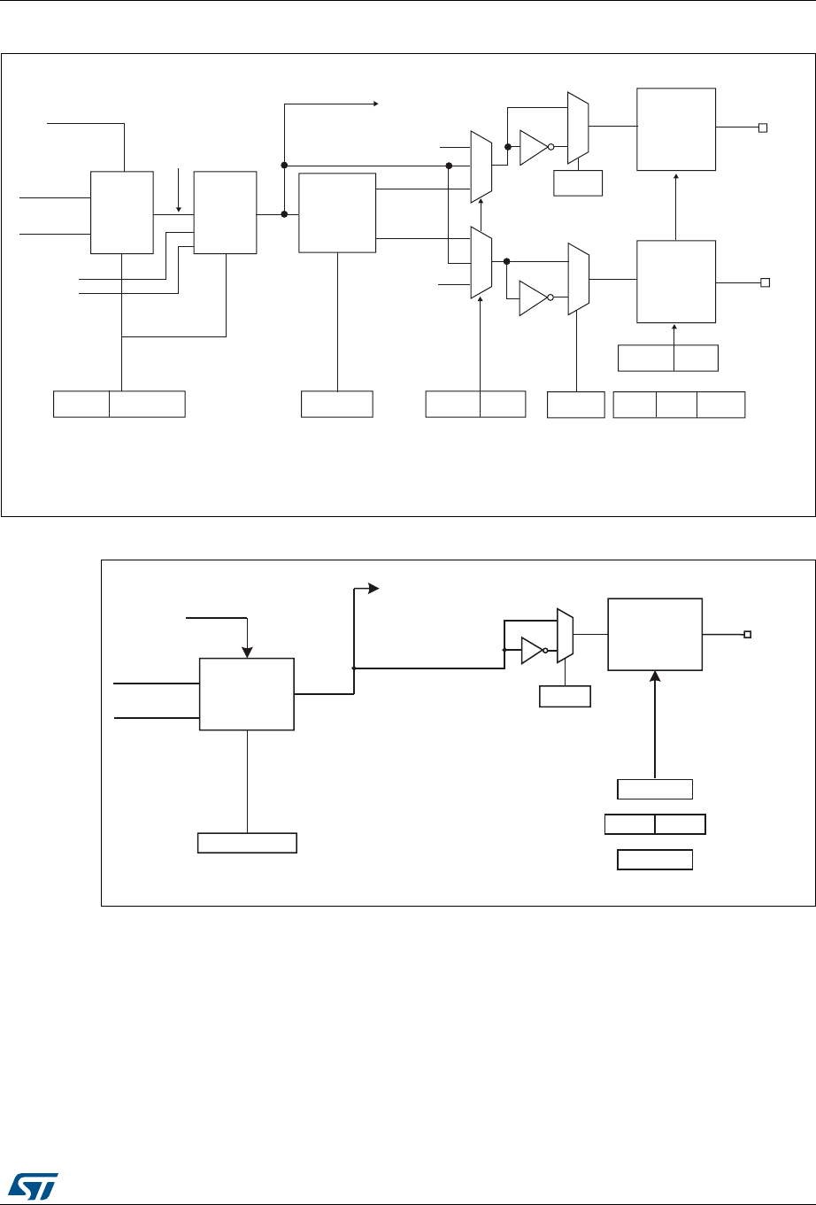
RM0430 Rev 8 483/1324
RM0430 Advanced-control timers (TIM1&TIM8)
533
Figure 115. Output stage of capture/compare channel (channels 1 to 3)
Figure 116. Output stage of capture/compare channel (channel 4)
The capture/compare block is made of one preload register and one shadow register. Write
and read always access the preload register.
In capture mode, captures are actually done in the shadow register, which is copied into the
preload register.
In compare mode, the content of the preload register is copied into the shadow register
which is compared to the counter.
069
2XWSXW
PRGH
FRQWUROOHU
&17!&&5
&17 &&5
7,0B&&05
2&0>@
2&5()
2&&(
'HDGWLPH
JHQHUDWRU
2&B'7
2&1B'7
'7*>@
7,0B%'75
µ
µ
&&(
7,0B&&(5
&&1(
&&3
7,0B&&(5
&&13
7,0B&&(5
2&
2XWSXW
HQDEOH
FLUFXLW
2&1
&&( 7,0B&&(5
&&1(
266,
7,0B%'75
02( 2665
[
[
2XWSXW
VHOHFWRU
2&[5()
2&5()&
7RWKHPDVWHUPRGH
FRQWUROOHU
2XWSXW
HQDEOH
FLUFXLW
2&5()
(75)
069
2XWSXW
PRGH
FRQWUROOHU
7,0B&&05
2&0>@
2&5()
&&3
7,0B&&(5
2&
7RWKHPDVWHU
PRGHFRQWUROOHU 2XWSXW
HQDEOH
FLUFXLW
(75
&17!&&5
&17!&&5
7,0B&&(5
7,0B%'75
7,0B&5
266,02(
&&(
2,6

Advanced-control timers (TIM1&TIM8) RM0430
484/1324 RM0430 Rev 8
17.3.6 Input capture mode
In Input capture mode, the Capture/Compare Registers (TIMx_CCRx) are used to latch the
value of the counter after a transition detected by the corresponding ICx signal. When a
capture occurs, the corresponding CCXIF flag (TIMx_SR register) is set and an interrupt or
a DMA request can be sent if they are enabled. If a capture occurs while the CCxIF flag was
already high, then the over-capture flag CCxOF (TIMx_SR register) is set. CCxIF can be
cleared by software by writing it to ‘0’ or by reading the captured data stored in the
TIMx_CCRx register. CCxOF is cleared when you write it to ‘0’.
The following example shows how to capture the counter value in TIMx_CCR1 when TI1
input rises. To do this, use the following procedure:
•Select the active input: TIMx_CCR1 must be linked to the TI1 input, so write the CC1S
bits to 01 in the TIMx_CCMR1 register. As soon as CC1S becomes different from 00,
the channel is configured in input and the TIMx_CCR1 register becomes read-only.
•Program the input filter duration you need with respect to the signal you connect to the
timer (by programming ICxF bits in the TIMx_CCMRx register if the input is a TIx input).
Let’s imagine that, when toggling, the input signal is not stable during at must 5 internal
clock cycles. We must program a filter duration longer than these 5 clock cycles. We
can validate a transition on TI1 when 8 consecutive samples with the new level have
been detected (sampled at fDTS frequency). Then write IC1F bits to 0011 in the
TIMx_CCMR1 register.
•Select the edge of the active transition on the TI1 channel by writing CC1P and CC1NP
bits to 0 in the TIMx_CCER register (rising edge in this case).
•Program the input prescaler. In our example, we wish the capture to be performed at
each valid transition, so the prescaler is disabled (write IC1PS bits to ‘00’ in the
TIMx_CCMR1 register).
•Enable capture from the counter into the capture register by setting the CC1E bit in the
TIMx_CCER register.
•If needed, enable the related interrupt request by setting the CC1IE bit in the
TIMx_DIER register, and/or the DMA request by setting the CC1DE bit in the
TIMx_DIER register.
When an input capture occurs:
•The TIMx_CCR1 register gets the value of the counter on the active transition.
•CC1IF flag is set (interrupt flag). CC1OF is also set if at least two consecutive captures
occurred whereas the flag was not cleared.
•An interrupt is generated depending on the CC1IE bit.
•A DMA request is generated depending on the CC1DE bit.
In order to handle the overcapture, it is recommended to read the data before the
overcapture flag. This is to avoid missing an overcapture which could happen after reading
the flag and before reading the data.
Note: IC interrupt and/or DMA requests can be generated by software by setting the
corresponding CCxG bit in the TIMx_EGR register.
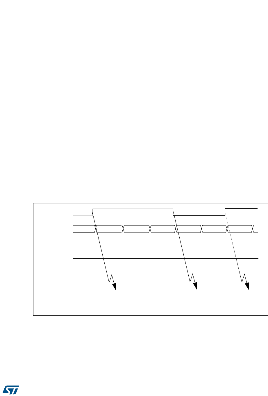
RM0430 Rev 8 485/1324
RM0430 Advanced-control timers (TIM1&TIM8)
533
17.3.7 PWM input mode
This mode is a particular case of input capture mode. The procedure is the same except:
•Two ICx signals are mapped on the same TIx input.
•These 2 ICx signals are active on edges with opposite polarity.
•One of the two TIxFP signals is selected as trigger input and the slave mode controller
is configured in reset mode.
For example, you can measure the period (in TIMx_CCR1 register) and the duty cycle (in
TIMx_CCR2 register) of the PWM applied on TI1 using the following procedure (depending
on CK_INT frequency and prescaler value):
•Select the active input for TIMx_CCR1: write the CC1S bits to 01 in the TIMx_CCMR1
register (TI1 selected).
•Select the active polarity for TI1FP1 (used both for capture in TIMx_CCR1 and counter
clear): write the CC1P and CC1NP bits to ‘0’ (active on rising edge).
•Select the active input for TIMx_CCR2: write the CC2S bits to 10 in the TIMx_CCMR1
register (TI1 selected).
•Select the active polarity for TI1FP2 (used for capture in TIMx_CCR2): write the CC2P
and CC2NP bits to ‘1’ (active on falling edge).
•Select the valid trigger input: write the TS bits to 101 in the TIMx_SMCR register
(TI1FP1 selected).
•Configure the slave mode controller in reset mode: write the SMS bits to 100 in the
TIMx_SMCR register.
•Enable the captures: write the CC1E and CC2E bits to ‘1’ in the TIMx_CCER register.
Figure 117. PWM input mode timing
17.3.8 Forced output mode
In output mode (CCxS bits = 00 in the TIMx_CCMRx register), each output compare signal
(OCxREF and then OCx/OCxN) can be forced to active or inactive level directly by software,
independently of any comparison between the output compare register and the counter.
TI1
TIMx_CNT 0000 0001 0002 0003 0004 00000004
TIMx_CCR1
TIMx_CCR2
0004
0002
IC1 capture
IC2 capture
reset counter
IC2 capture
pulse width
IC1 capture
period
measurementmeasurement
ai15413

Advanced-control timers (TIM1&TIM8) RM0430
486/1324 RM0430 Rev 8
To force an output compare signal (OCXREF/OCx) to its active level, you just need to write
101 in the OCxM bits in the corresponding TIMx_CCMRx register. Thus OCXREF is forced
high (OCxREF is always active high) and OCx get opposite value to CCxP polarity bit.
For example: CCxP=0 (OCx active high) => OCx is forced to high level.
The OCxREF signal can be forced low by writing the OCxM bits to 100 in the TIMx_CCMRx
register.
Anyway, the comparison between the TIMx_CCRx shadow register and the counter is still
performed and allows the flag to be set. Interrupt and DMA requests can be sent
accordingly. This is described in the output compare mode section below.
17.3.9 Output compare mode
This function is used to control an output waveform or indicating when a period of time has
elapsed.
When a match is found between the capture/compare register and the counter, the output
compare function:
•Assigns the corresponding output pin to a programmable value defined by the output
compare mode (OCxM bits in the TIMx_CCMRx register) and the output polarity (CCxP
bit in the TIMx_CCER register). The output pin can keep its level (OCXM=000), be set
active (OCxM=001), be set inactive (OCxM=010) or can toggle (OCxM=011) on match.
•Sets a flag in the interrupt status register (CCxIF bit in the TIMx_SR register).
•Generates an interrupt if the corresponding interrupt mask is set (CCXIE bit in the
TIMx_DIER register).
•Sends a DMA request if the corresponding enable bit is set (CCxDE bit in the
TIMx_DIER register, CCDS bit in the TIMx_CR2 register for the DMA request
selection).
The TIMx_CCRx registers can be programmed with or without preload registers using the
OCxPE bit in the TIMx_CCMRx register.
In output compare mode, the update event UEV has no effect on OCxREF and OCx output.
The timing resolution is one count of the counter. Output compare mode can also be used to
output a single pulse (in One Pulse mode).
Procedure:
1. Select the counter clock (internal, external, prescaler).
2. Write the desired data in the TIMx_ARR and TIMx_CCRx registers.
3. Set the CCxIE bit if an interrupt request is to be generated.
4. Select the output mode. For example:
– Write OCxM = 011 to toggle OCx output pin when CNT matches CCRx
– Write OCxPE = 0 to disable preload register
– Write CCxP = 0 to select active high polarity
– Write CCxE = 1 to enable the output
5. Enable the counter by setting the CEN bit in the TIMx_CR1 register.
The TIMx_CCRx register can be updated at any time by software to control the output
waveform, provided that the preload register is not enabled (OCxPE=’0’, else TIMx_CCRx
shadow register is updated only at the next update event UEV). An example is given in
Figure 118.

RM0430 Rev 8 487/1324
RM0430 Advanced-control timers (TIM1&TIM8)
533
Figure 118. Output compare mode, toggle on OC1.
17.3.10 PWM mode
Pulse Width Modulation mode allows you to generate a signal with a frequency determined
by the value of the TIMx_ARR register and a duty cycle determined by the value of the
TIMx_CCRx register.
The PWM mode can be selected independently on each channel (one PWM per OCx
output) by writing ‘110’ (PWM mode 1) or ‘111’ (PWM mode 2) in the OCxM bits in the
TIMx_CCMRx register. You must enable the corresponding preload register by setting the
OCxPE bit in the TIMx_CCMRx register, and eventually the auto-reload preload register (in
upcounting or center-aligned modes) by setting the ARPE bit in the TIMx_CR1 register.
As the preload registers are transferred to the shadow registers only when an update event
occurs, before starting the counter, you have to initialize all the registers by setting the UG
bit in the TIMx_EGR register.
OCx polarity is software programmable using the CCxP bit in the TIMx_CCER register. It
can be programmed as active high or active low. OCx output is enabled by a combination of
the CCxE, CCxNE, MOE, OSSI and OSSR bits (TIMx_CCER and TIMx_BDTR registers).
Refer to the TIMx_CCER register description for more details.
In PWM mode (1 or 2), TIMx_CNT and TIMx_CCRx are always compared to determine
whether TIMx_CCRx ≤ TIMx_CNT or TIMx_CNT ≤ TIMx_CCRx (depending on the direction
of the counter).
The timer is able to generate PWM in edge-aligned mode or center-aligned mode
depending on the CMS bits in the TIMx_CR1 register.
069
2&5() 2&
7,0B&17 % %
7,0B&&5 $
:ULWH%KLQWKH&&5UHJLVWHU
0DWFKGHWHFWHGRQ&&5
,QWHUUXSWJHQHUDWHGLIHQDEOHG
%
%
$
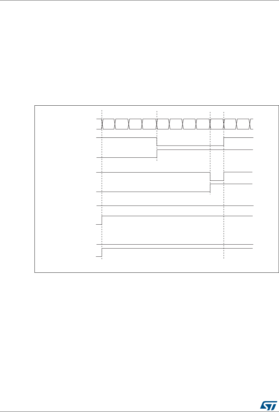
Advanced-control timers (TIM1&TIM8) RM0430
488/1324 RM0430 Rev 8
PWM edge-aligned mode
•Upcounting configuration
Upcounting is active when the DIR bit in the TIMx_CR1 register is low. Refer to
Upcounting mode.
In the following example, we consider PWM mode 1. The reference PWM signal
OCxREF is high as long as TIMx_CNT < TIMx_CCRx else it becomes low. If the
compare value in TIMx_CCRx is greater than the auto-reload value (in TIMx_ARR)
then OCxREF is held at ‘1’. If the compare value is 0 then OCxRef is held at ‘0’.
Figure 119 shows some edge-aligned PWM waveforms in an example where
TIMx_ARR=8.
Figure 119. Edge-aligned PWM waveforms (ARR=8)
•Downcounting configuration
Downcounting is active when DIR bit in TIMx_CR1 register is high. Refer to
Downcounting mode.
In PWM mode 1, the reference signal OCxRef is low as long as
TIMx_CNT > TIMx_CCRx else it becomes high. If the compare value in TIMx_CCRx is
greater than the auto-reload value in TIMx_ARR, then OCxREF is held at ‘1’. 0% PWM
is not possible in this mode.
PWM center-aligned mode
Center-aligned mode is active when the CMS bits in TIMx_CR1 register are different from
‘00’ (all the remaining configurations having the same effect on the OCxRef/OCx signals).
The compare flag is set when the counter counts up, when it counts down or both when it
counts up and down depending on the CMS bits configuration. The direction bit (DIR) in the
TIMx_CR1 register is updated by hardware and must not be changed by software. Refer to
Center-aligned mode (up/down counting).
069
&RXQWHUUHJLVWHU
µ
2&;5()
&&[,)
2&;5()
&&[,)
2&;5()
&&[,)
2&;5()
&&[,)
&&5[
&&5[
&&5[!
&&5[
µ

RM0430 Rev 8 489/1324
RM0430 Advanced-control timers (TIM1&TIM8)
533
Figure 120 shows some center-aligned PWM waveforms in an example where:
•TIMx_ARR=8,
•PWM mode is the PWM mode 1,
•The flag is set when the counter counts down corresponding to the center-aligned
mode 1 selected for CMS=01 in TIMx_CR1 register.
Figure 120. Center-aligned PWM waveforms (ARR=8)
&&[,)
&RXQWHUUHJLVWHU
&&5[
2&[5()
&06
&06
&06
&&[,)
&&5[
2&[5()
&06 RU
&&[,)
&&5[
2&[5()
&06
&06
&06
µ
&&[,)
&&5[!
2&[5()
&06
&06
&06
µ
&&[,)
&&5[
2&[5()
&06
&06
&06
µ
$,E

Advanced-control timers (TIM1&TIM8) RM0430
490/1324 RM0430 Rev 8
Hints on using center-aligned mode:
•When starting in center-aligned mode, the current up-down configuration is used. It
means that the counter counts up or down depending on the value written in the DIR bit
in the TIMx_CR1 register. Moreover, the DIR and CMS bits must not be changed at the
same time by the software.
•Writing to the counter while running in center-aligned mode is not recommended as it
can lead to unexpected results. In particular:
– The direction is not updated if you write a value in the counter that is greater than
the auto-reload value (TIMx_CNT>TIMx_ARR). For example, if the counter was
counting up, it continues to count up.
– The direction is updated if you write 0 or write the TIMx_ARR value in the counter
but no Update Event UEV is generated.
•The safest way to use center-aligned mode is to generate an update by software
(setting the UG bit in the TIMx_EGR register) just before starting the counter and not to
write the counter while it is running.
17.3.11 Complementary outputs and dead-time insertion
The advanced-control timers (TIM1&TIM8) can output two complementary signals and
manage the switching-off and the switching-on instants of the outputs.
This time is generally known as dead-time and you have to adjust it depending on the
devices you have connected to the outputs and their characteristics (intrinsic delays of level-
shifters, delays due to power switches...)
You can select the polarity of the outputs (main output OCx or complementary OCxN)
independently for each output. This is done by writing to the CCxP and CCxNP bits in the
TIMx_CCER register.
The complementary signals OCx and OCxN are activated by a combination of several
control bits: the CCxE and CCxNE bits in the TIMx_CCER register and the MOE, OISx,
OISxN, OSSI and OSSR bits in the TIMx_BDTR and TIMx_CR2 registers. Refer to
Table 103 for more details. In particular, the dead-time is activated when switching to the
IDLE state (MOE falling down to 0).
Dead-time insertion is enabled by setting both CCxE and CCxNE bits, and the MOE bit if the
break circuit is present. DTG[7:0] bits of the TIMx_BDTR register are used to control the
dead-time generation for all channels. From a reference waveform OCxREF, it generates 2
outputs OCx and OCxN. If OCx and OCxN are active high:
•The OCx output signal is the same as the reference signal except for the rising edge,
which is delayed relative to the reference rising edge.
•The OCxN output signal is the opposite of the reference signal except for the rising
edge, which is delayed relative to the reference falling edge.
If the delay is greater than the width of the active output (OCx or OCxN) then the
corresponding pulse is not generated.
The following figures show the relationships between the output signals of the dead-time
generator and the reference signal OCxREF. (we suppose CCxP=0, CCxNP=0, MOE=1,
CCxE=1 and CCxNE=1 in these examples).
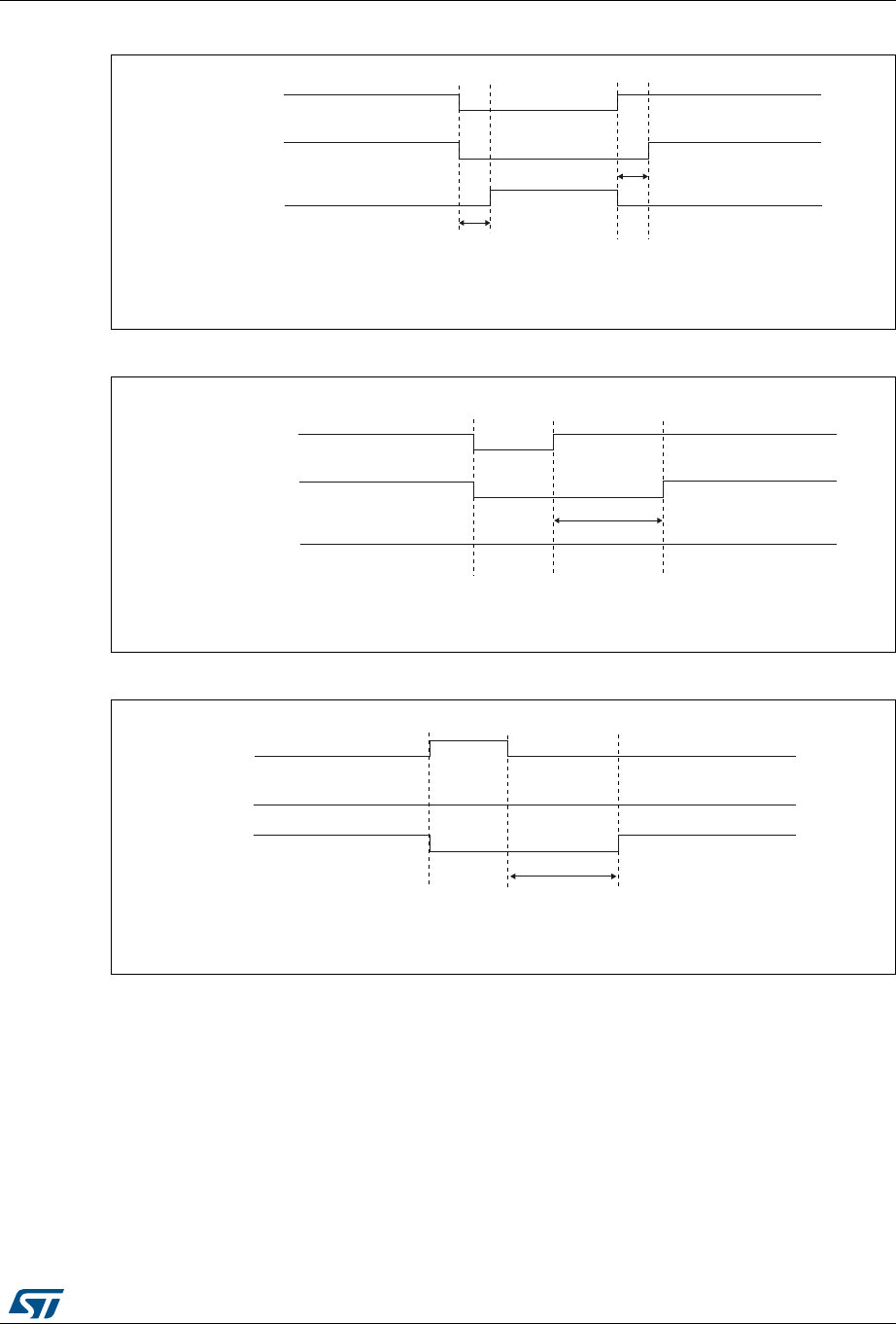
RM0430 Rev 8 491/1324
RM0430 Advanced-control timers (TIM1&TIM8)
533
Figure 121. Complementary output with dead-time insertion.
Figure 122. Dead-time waveforms with delay greater than the negative pulse.
Figure 123. Dead-time waveforms with delay greater than the positive pulse.
The dead-time delay is the same for each of the channels and is programmable with the
DTG bits in the TIMx_BDTR register. Refer to Section 17.4.18: TIM1&TIM8 break and dead-
time register (TIMx_BDTR) for delay calculation.
Re-directing OCxREF to OCx or OCxN
In output mode (forced, output compare or PWM), OCxREF can be re-directed to the OCx
output or to OCxN output by configuring the CCxE and CCxNE bits in the TIMx_CCER
register.
This allows you to send a specific waveform (such as PWM or static active level) on one
output while the complementary remains at its inactive level. Other alternative possibilities
GHOD\
GHOD\
2&[5()
2&[
2&[1
069
069
GHOD\
2&[5()
2&[
2&[1
069
GHOD\
2&[5()
2&[
2&[1

Advanced-control timers (TIM1&TIM8) RM0430
492/1324 RM0430 Rev 8
are to have both outputs at inactive level or both outputs active and complementary with
dead-time.
Note: When only OCxN is enabled (CCxE=0, CCxNE=1), it is not complemented and becomes
active as soon as OCxREF is high. For example, if CCxNP=0 then OCxN=OCxRef. On the
other hand, when both OCx and OCxN are enabled (CCxE=CCxNE=1) OCx becomes
active when OCxREF is high whereas OCxN is complemented and becomes active when
OCxREF is low.
17.3.12 Using the break function
When using the break function, the output enable signals and inactive levels are modified
according to additional control bits (MOE, OSSI and OSSR bits in the TIMx_BDTR register,
OISx and OISxN bits in the TIMx_CR2 register). In any case, the OCx and OCxN outputs
cannot be set both to active level at a given time. Refer to Table 103 for more details.
The break source can be either the break input pin or a clock failure event, generated by the
Clock Security System (CSS), from the Reset Clock Controller. For further information on
the Clock Security System, refer to Section 6.2.7: Clock security system (CSS).
When exiting from reset, the break circuit is disabled and the MOE bit is low. You can enable
the break function by setting the BKE bit in the TIMx_BDTR register. The break input
polarity can be selected by configuring the BKP bit in the same register. BKE and BKP can
be modified at the same time. When the BKE and BKP bits are written, a delay of 1 APB
clock cycle is applied before the writing is effective. Consequently, it is necessary to wait 1
APB clock period to correctly read back the bit after the write operation.
Because MOE falling edge can be asynchronous, a resynchronization circuit has been
inserted between the actual signal (acting on the outputs) and the synchronous control bit
(accessed in the TIMx_BDTR register). It results in some delays between the asynchronous
and the synchronous signals. In particular, when writing MOE to 1 whereas it was low, user
must insert a delay (dummy instruction) before reading it correctly. This is because user
writes the asynchronous signal and reads the synchronous signal.
When a break occurs (selected level on the break input):
•The MOE bit is cleared asynchronously, putting the outputs in inactive state, idle state
or in reset state (selected by the OSSI bit). This feature functions even if the MCU
oscillator is off.
•Each output channel is driven with the level programmed in the OISx bit in the
TIMx_CR2 register as soon as MOE=0. If OSSI=0 then the timer releases the enable
output else the enable output remains high.
•When complementary outputs are used:
– The outputs are first put in reset state inactive state (depending on the polarity).
This is done asynchronously so that it works even if no clock is provided to the
timer.
– If the timer clock is still present, then the dead-time generator is reactivated in
order to drive the outputs with the level programmed in the OISx and OISxN bits
after a dead-time. Even in this case, OCx and OCxN cannot be driven to their

RM0430 Rev 8 493/1324
RM0430 Advanced-control timers (TIM1&TIM8)
533
active level together. Note that because of the resynchronization on MOE, the
dead-time duration is a bit longer than usual (around 2 ck_tim clock cycles).
– If OSSI=0 then the timer releases the enable outputs else the enable outputs
remain or become high as soon as one of the CCxE or CCxNE bits is high.
•The break status flag (BIF bit in the TIMx_SR register) is set. An interrupt can be
generated if the BIE bit in the TIMx_DIER register is set. A DMA request can be sent if
the BDE bit in the TIMx_DIER register is set.
•If the AOE bit in the TIMx_BDTR register is set, the MOE bit is automatically set again
at the next update event UEV. This can be used to perform a regulation, for instance.
Else, MOE remains low until you write it to ‘1’ again. In this case, it can be used for
security and you can connect the break input to an alarm from power drivers, thermal
sensors or any security components.
Note: The break inputs is acting on level. Thus, the MOE cannot be set while the break input is
active (neither automatically nor by software). In the meantime, the status flag BIF cannot
be cleared.
The break can be generated by the BRK input which has a programmable polarity and an
enable bit BKE in the TIMx_BDTR Register.
There are two solutions to generate a break:
•By using the BRK input which has a programmable polarity and an enable bit BKE in
the TIMx_BDTR register
•By software through the BG bit of the TIMx_EGR register.
In addition to the break input and the output management, a write protection has been
implemented inside the break circuit to safeguard the application. It allows you to freeze the
configuration of several parameters (dead-time duration, OCx/OCxN polarities and state
when disabled, OCxM configurations, break enable and polarity). You can choose from 3
levels of protection selected by the LOCK bits in the TIMx_BDTR register. Refer to
Section 17.4.18: TIM1&TIM8 break and dead-time register (TIMx_BDTR). The LOCK bits
can be written only once after an MCU reset.
Figure 124 shows an example of behavior of the outputs in response to a break.
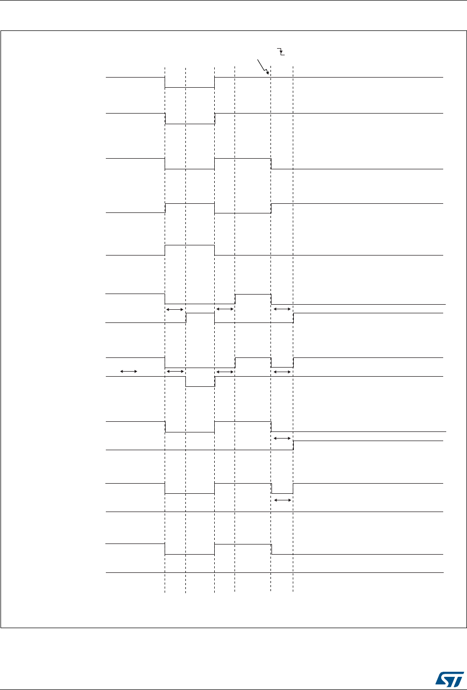
Advanced-control timers (TIM1&TIM8) RM0430
494/1324 RM0430 Rev 8
Figure 124. Output behavior in response to a break.
GHOD\ GHOD\ GHOD\
GHOD\ GHOD\ GHOD\
GHOD\
GHOD\
2&[5()
2&[
2&[1QRWLPSOHPHQWHG&&[3 2,6[
2&[
2&[1QRWLPSOHPHQWHG&&[3 2,6[
2&[
2&[1QRWLPSOHPHQWHG&&[3 2,6[
2&[
2&[1QRWLPSOHPHQWHG&&[3 2,6[
2&[
2&[1
&&[( &&[3 2,6[ &&[1( &&[13 2,6[1
2&[
2&[1
&&[( &&[3 2,6[ &&[1( &&[13 2,6[1
2&[
2&[1
&&[( &&[3 2,6[ &&[1( &&[13 2,6[1
2&[
2&[1
&&[( &&[3 2,6[ &&[1( &&[13 2,6[1
2&[
2&[1
&&[( &&[3 &&[1( &&[13 2,6[ 2,6[1 RU2,6[ 2,6[1
069
%5($.02(
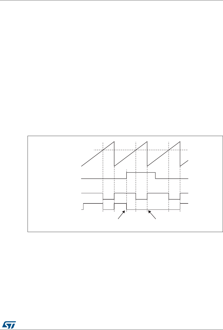
RM0430 Rev 8 495/1324
RM0430 Advanced-control timers (TIM1&TIM8)
533
17.3.13 Clearing the OCxREF signal on an external event
The OCxREF signal for a given channel can be driven Low by applying a High level to the
ETRF input (OCxCE enable bit of the corresponding TIMx_CCMRx register set to ‘1’). The
OCxREF signal remains Low until the next update event, UEV, occurs.
This function can only be used in output compare and PWM modes, and does not work in
forced mode.
For example, the ETR signal can be connected to the output of a comparator to be used for
current handling. In this case, the ETR must be configured as follow:
1. The External Trigger Prescaler should be kept off: bits ETPS[1:0] of the TIMx_SMCR
register set to ‘00’.
2. The external clock mode 2 must be disabled: bit ECE of the TIMx_SMCR register set to
‘0’.
3. The External Trigger Polarity (ETP) and the External Trigger Filter (ETF) can be
configured according to the user needs.
Figure 125 shows the behavior of the OCxREF signal when the ETRF Input becomes High,
for both values of the enable bit OCxCE. In this example, the timer TIMx is programmed in
PWM mode.
Figure 125. Clearing TIMx OCxREF
Note: In case of a PWM with a 100% duty cycle (if CCRx>ARR), then OCxREF is enabled again at
the next counter overflow.
06Y9
&&5[
&RXQWHU&17
(75)
2&[5()2&[&( µ
2&[5()2&[&( µ
(75)EHFRPHVKLJK (75)VWLOOKLJK
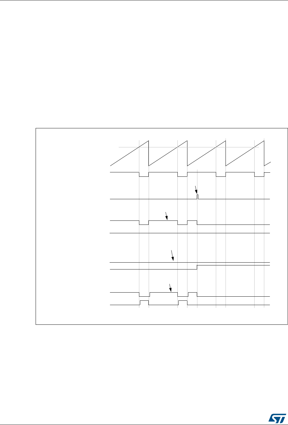
Advanced-control timers (TIM1&TIM8) RM0430
496/1324 RM0430 Rev 8
17.3.14 6-step PWM generation
When complementary outputs are used on a channel, preload bits are available on the
OCxM, CCxE and CCxNE bits. The preload bits are transferred to the shadow bits at the
COM commutation event. Thus you can program in advance the configuration for the next
step and change the configuration of all the channels at the same time. COM can be
generated by software by setting the COM bit in the TIMx_EGR register or by hardware (on
TRGI rising edge).
A flag is set when the COM event occurs (COMIF bit in the TIMx_SR register), which can
generate an interrupt (if the COMIE bit is set in the TIMx_DIER register) or a DMA request
(if the COMDE bit is set in the TIMx_DIER register).
Figure 126 describes the behavior of the OCx and OCxN outputs when a COM event
occurs, in 3 different examples of programmed configurations.
Figure 126. 6-step generation, COM example (OSSR=1)
(CCRx)
OCx
OCxN
Write COM to 1
counter (CNT)
OCxREF
COM event
CCxE=1
CCxNE=0
OCxM=100
OCx
OCxN
CCxE=0
CCxNE=1
OCxM=101
OCx
OCxN
CCxE=1
CCxNE=0
OCxM=100
Example 1
Example 2
Example 3
write OCxM to 100
CCxE=1
CCxNE=0
OCxM=100 (forced inactive)
CCxE=1
CCxNE=0
OCxM=100 (forced inactive)
Write CCxNE to 1
and OCxM to 101
write CCxNE to 0
and OCxM to 100
CCxE=1
CCxNE=0
OCxM=100 (forced inactive)
ai14910
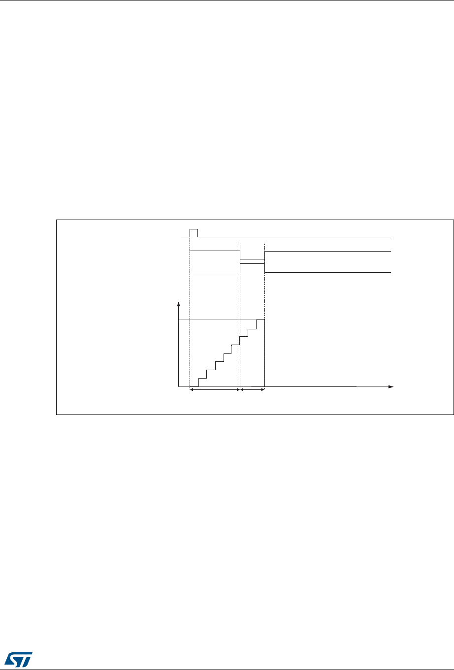
RM0430 Rev 8 497/1324
RM0430 Advanced-control timers (TIM1&TIM8)
533
17.3.15 One-pulse mode
One-pulse mode (OPM) is a particular case of the previous modes. It allows the counter to
be started in response to a stimulus and to generate a pulse with a programmable length
after a programmable delay.
Starting the counter can be controlled through the slave mode controller. Generating the
waveform can be done in output compare mode or PWM mode. You select One-pulse mode
by setting the OPM bit in the TIMx_CR1 register. This makes the counter stop automatically
at the next update event UEV.
A pulse can be correctly generated only if the compare value is different from the counter
initial value. Before starting (when the timer is waiting for the trigger), the configuration must
be:
•In upcounting: CNT < CCRx ≤ ARR (in particular, 0 < CCRx)
•In downcounting: CNT > CCRx
Figure 127. Example of one pulse mode.
For example you may want to generate a positive pulse on OC1 with a length of tPULSE and
after a delay of tDELAY as soon as a positive edge is detected on the TI2 input pin.
Let’s use TI2FP2 as trigger 1:
•Map TI2FP2 to TI2 by writing CC2S=’01’ in the TIMx_CCMR1 register.
•TI2FP2 must detect a rising edge, write CC2P=’0’ and CC2NP=’0’ in the TIMx_CCER
register.
•Configure TI2FP2 as trigger for the slave mode controller (TRGI) by writing TS=’110’ in
the TIMx_SMCR register.
•TI2FP2 is used to start the counter by writing SMS to ‘110’ in the TIMx_SMCR register
(trigger mode).
069
7,
2&5()
&RXQWHU
ƚ
7,0B$55
7,0B&&5
2&
ƚ>z ƚWh>^

Advanced-control timers (TIM1&TIM8) RM0430
498/1324 RM0430 Rev 8
The OPM waveform is defined by writing the compare registers (taking into account the
clock frequency and the counter prescaler).
•The tDELAY is defined by the value written in the TIMx_CCR1 register.
•The tPULSE is defined by the difference between the auto-reload value and the compare
value (TIMx_ARR - TIMx_CCR1).
•Let’s say you want to build a waveform with a transition from ‘0’ to ‘1’ when a compare
match occurs and a transition from ‘1’ to ‘0’ when the counter reaches the auto-reload
value. To do this you enable PWM mode 2 by writing OC1M=111 in the TIMx_CCMR1
register. You can optionally enable the preload registers by writing OC1PE=’1’ in the
TIMx_CCMR1 register and ARPE in the TIMx_CR1 register. In this case you have to
write the compare value in the TIMx_CCR1 register, the auto-reload value in the
TIMx_ARR register, generate an update by setting the UG bit and wait for external
trigger event on TI2. CC1P is written to ‘0’ in this example.
In our example, the DIR and CMS bits in the TIMx_CR1 register should be low.
You only want 1 pulse (Single mode), so you write '1 in the OPM bit in the TIMx_CR1
register to stop the counter at the next update event (when the counter rolls over from the
auto-reload value back to 0). When OPM bit in the TIMx_CR1 register is set to '0', so the
Repetitive Mode is selected.
Particular case: OCx fast enable:
In One-pulse mode, the edge detection on TIx input set the CEN bit which enables the
counter. Then the comparison between the counter and the compare value makes the
output toggle. But several clock cycles are needed for these operations and it limits the
minimum delay tDELAY min we can get.
If you want to output a waveform with the minimum delay, you can set the OCxFE bit in the
TIMx_CCMRx register. Then OCxRef (and OCx) are forced in response to the stimulus,
without taking in account the comparison. Its new level is the same as if a compare match
had occurred. OCxFE acts only if the channel is configured in PWM1 or PWM2 mode.
17.3.16 Encoder interface mode
To select Encoder Interface mode write SMS=‘001’ in the TIMx_SMCR register if the
counter is counting on TI2 edges only, SMS=’010’ if it is counting on TI1 edges only and
SMS=’011’ if it is counting on both TI1 and TI2 edges.
Select the TI1 and TI2 polarity by programming the CC1P and CC2P bits in the TIMx_CCER
register. When needed, you can program the input filter as well. CC1NP and CC2NP must
be kept low.
The two inputs TI1 and TI2 are used to interface to an incremental encoder. Refer to
Table 101. The counter is clocked by each valid transition on TI1FP1 or TI2FP2 (TI1 and TI2
after input filter and polarity selection, TI1FP1=TI1 if not filtered and not inverted,
TI2FP2=TI2 if not filtered and not inverted) assuming that it is enabled (CEN bit in
TIMx_CR1 register written to ‘1’). The sequence of transitions of the two inputs is evaluated
and generates count pulses as well as the direction signal. Depending on the sequence the
counter counts up or down, the DIR bit in the TIMx_CR1 register is modified by hardware
accordingly. The DIR bit is calculated at each transition on any input (TI1 or TI2), whatever
the counter is counting on TI1 only, TI2 only or both TI1 and TI2.
Encoder interface mode acts simply as an external clock with direction selection. This
means that the counter just counts continuously between 0 and the auto-reload value in the
TIMx_ARR register (0 to ARR or ARR down to 0 depending on the direction). So you must

RM0430 Rev 8 499/1324
RM0430 Advanced-control timers (TIM1&TIM8)
533
configure TIMx_ARR before starting. in the same way, the capture, compare, prescaler,
repetition counter, trigger output features continue to work as normal. Encoder mode and
External clock mode 2 are not compatible and must not be selected together.
In this mode, the counter is modified automatically following the speed and the direction of
the incremental encoder and its content, therefore, always represents the encoder’s
position. The count direction correspond to the rotation direction of the connected sensor.
Table 101 summarizes the possible combinations, assuming TI1 and TI2 don’t switch at the
same time.
An external incremental encoder can be connected directly to the MCU without external
interface logic. However, comparators are normally be used to convert the encoder’s
differential outputs to digital signals. This greatly increases noise immunity. The third
encoder output which indicate the mechanical zero position, may be connected to an
external interrupt input and trigger a counter reset.
Figure 128 gives an example of counter operation, showing count signal generation and
direction control. It also shows how input jitter is compensated where both edges are
selected. This might occur if the sensor is positioned near to one of the switching points. For
this example we assume that the configuration is the following:
•CC1S=’01’ (TIMx_CCMR1 register, TI1FP1 mapped on TI1).
•CC2S=’01’ (TIMx_CCMR2 register, TI1FP2 mapped on TI2).
•CC1P=’0’, CC1NP=’0’, and IC1F = ‘0000’ (TIMx_CCER register, TI1FP1 non-inverted,
TI1FP1=TI1).
•CC2P=’0’, CC2NP=’0’, and IC2F = ‘0000’ (TIMx_CCER register, TI1FP2 non-inverted,
TI1FP2= TI2).
•SMS=’011’ (TIMx_SMCR register, both inputs are active on both rising and falling
edges).
•CEN=’1’ (TIMx_CR1 register, Counter enabled).
Table 101. Counting direction versus encoder signals
Active edge
Level on opposite signal
(TI1FP1 for TI2,
TI2FP2 for TI1)
TI1FP1 signal TI2FP2 signal
Rising Falling Rising Falling
Counting on
TI1 only
High Down Up No Count No Count
Low Up Down No Count No Count
Counting on
TI2 only
High No Count No Count Up Down
Low No Count No Count Down Up
Counting on
TI1 and TI2
High Down Up Up Down
Low Up Down Down Up
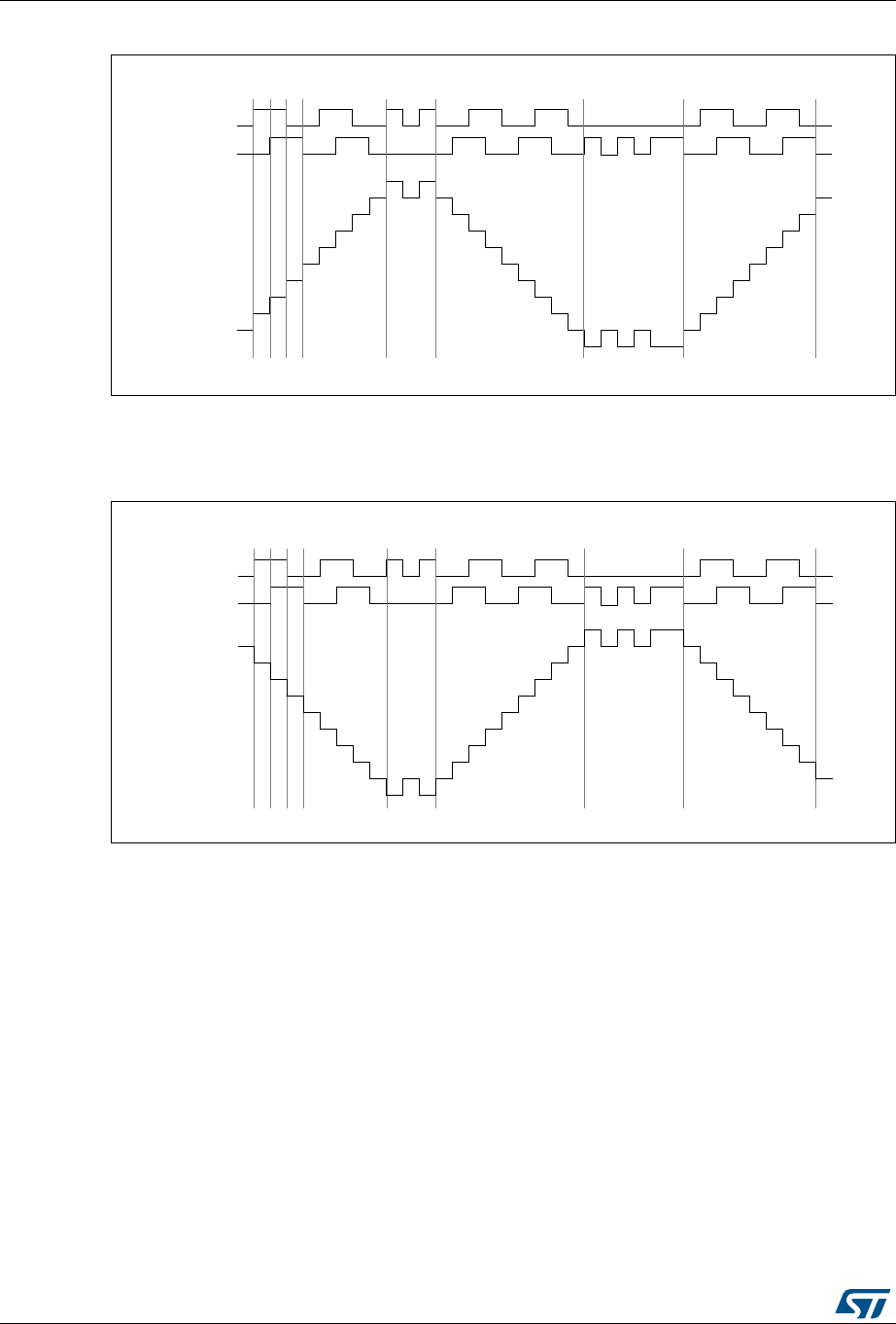
Advanced-control timers (TIM1&TIM8) RM0430
500/1324 RM0430 Rev 8
Figure 128. Example of counter operation in encoder interface mode.
Figure 129 gives an example of counter behavior when TI1FP1 polarity is inverted (same
configuration as above except CC1P=’1’).
Figure 129. Example of encoder interface mode with TI1FP1 polarity inverted.
The timer, when configured in Encoder Interface mode provides information on the sensor’s
current position. You can obtain dynamic information (speed, acceleration, deceleration) by
measuring the period between two encoder events using a second timer configured in
capture mode. The output of the encoder which indicates the mechanical zero can be used
for this purpose. Depending on the time between two events, the counter can also be read
at regular times. You can do this by latching the counter value into a third input capture
register if available (then the capture signal must be periodic and can be generated by
another timer). when available, it is also possible to read its value through a DMA request
generated by a real-time clock.
7,
EDFNZDUGMLWWHU MLWWHU
XS GRZQ XS
7,
&RXQWHU
IRUZDUG IRUZDUG
069
7,
EDFNZDUGMLWWHU MLWWHU
XSGRZQ
7,
&RXQWHU
IRUZDUG IRUZDUG
069
GRZQ

RM0430 Rev 8 501/1324
RM0430 Advanced-control timers (TIM1&TIM8)
533
17.3.17 Timer input XOR function
The TI1S bit in the TIMx_CR2 register allows the input filter of channel 1 to be connected to
the output of a XOR gate, combining the three input pins TIMx_CH1, TIMx_CH2 and
TIMx_CH3.
The XOR output can be used with all the timer input functions such as trigger or input
capture. An example of this feature used to interface Hall sensors is given in
Section 17.3.18 below.
17.3.18 Interfacing with Hall sensors
This is done using the advanced-control timers (TIM1 or TIM8) to generate PWM signals to
drive the motor and another timer TIMx (TIM2, TIM3, TIM4 orTIM5) referred to as
“interfacing timer” in Figure 130. The “interfacing timer” captures the 3 timer input pins
(TIMx_CH1, TIMx_CH2, and TIMx_CH3) connected through a XOR to the TI1 input channel
(selected by setting the TI1S bit in the TIMx_CR2 register).
The slave mode controller is configured in reset mode; the slave input is TI1F_ED. Thus,
each time one of the 3 inputs toggles, the counter restarts counting from 0. This creates a
time base triggered by any change on the Hall inputs.
On the “interfacing timer”, capture/compare channel 1 is configured in capture mode,
capture signal is TRC (see Figure 113). The captured value, which corresponds to the time
elapsed between 2 changes on the inputs, gives information about motor speed.
The “interfacing timer” can be used in output mode to generate a pulse which changes the
configuration of the channels of the advanced-control timer (TIM1 or TIM8) (by triggering a
COM event). The TIM1 timer is used to generate PWM signals to drive the motor. To do this,
the interfacing timer channel must be programmed so that a positive pulse is generated
after a programmed delay (in output compare or PWM mode). This pulse is sent to the
advanced-control timer (TIM1or TIM8) through the TRGO output.
Example: you want to change the PWM configuration of your advanced-control timer TIM1
after a programmed delay each time a change occurs on the Hall inputs connected to one of
the TIMx timers.
•Configure 3 timer inputs ORed to the TI1 input channel by writing the TI1S bit in the
TIMx_CR2 register to ‘1’,
•Program the time base: write the TIMx_ARR to the max value (the counter must be
cleared by the TI1 change. Set the prescaler to get a maximum counter period longer
than the time between 2 changes on the sensors,
•Program channel 1 in capture mode (TRC selected): write the CC1S bits in the
TIMx_CCMR1 register to ‘11’. You can also program the digital filter if needed,
•Program channel 2 in PWM 2 mode with the desired delay: write the OC2M bits to ‘111’
and the CC2S bits to ‘00’ in the TIMx_CCMR1 register,
•Select OC2REF as trigger output on TRGO: write the MMS bits in the TIMx_CR2
register to ‘101’,
In the advanced-control timer TIM1, the right ITR input must be selected as trigger input, the
timer is programmed to generate PWM signals, the capture/compare control signals are
preloaded (CCPC=1 in the TIMx_CR2 register) and the COM event is controlled by the
trigger input (CCUS=1 in the TIMx_CR2 register). The PWM control bits (CCxE, OCxM) are
written after a COM event for the next step (this can be done in an interrupt subroutine
generated by the rising edge of OC2REF).
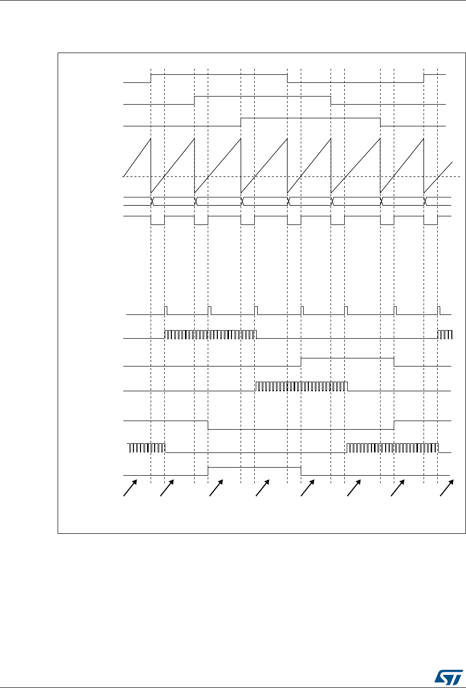
Advanced-control timers (TIM1&TIM8) RM0430
502/1324 RM0430 Rev 8
Figure 130 describes this example.
Figure 130. Example of Hall sensor interface
DLE
&RXQWHU&17
75*2 2&5()
&&5
2&
2&1
&20
:ULWH&&[(&&[1(
7,+
7,+
7,+
&&5
2&
2&1
2&
2&1
&
DQG2&[0IRUQH[WVWHS
,QWHUIDFLQJWLPHU$GYDQFHGFRQWUROWLPHUV
&$ &$ & &$ &$%
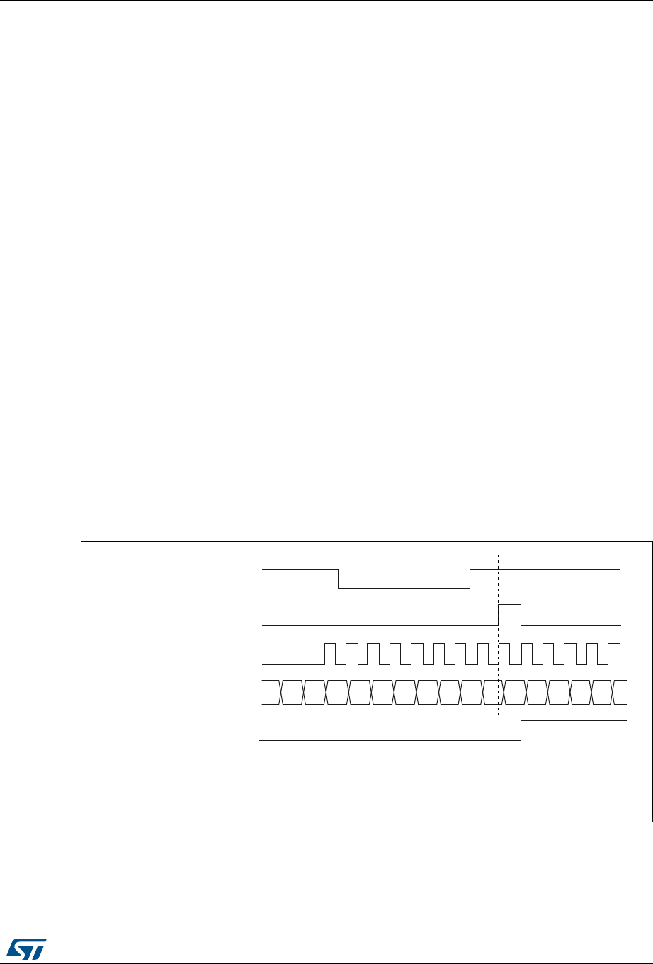
RM0430 Rev 8 503/1324
RM0430 Advanced-control timers (TIM1&TIM8)
533
17.3.19 TIMx and external trigger synchronization
The TIMx timer can be synchronized with an external trigger in several modes: Reset mode,
Gated mode and Trigger mode.
Slave mode: Reset mode
The counter and its prescaler can be reinitialized in response to an event on a trigger input.
Moreover, if the URS bit from the TIMx_CR1 register is low, an update event UEV is
generated. Then all the preloaded registers (TIMx_ARR, TIMx_CCRx) are updated.
In the following example, the upcounter is cleared in response to a rising edge on TI1 input:
•Configure the channel 1 to detect rising edges on TI1. Configure the input filter duration
(in this example, we don’t need any filter, so we keep IC1F=0000). The capture
prescaler is not used for triggering, so you don’t need to configure it. The CC1S bits
select the input capture source only, CC1S = 01 in the TIMx_CCMR1 register. Write
CC1P=0 and CC1NP=’0’ in TIMx_CCER register to validate the polarity (and detect
rising edges only).
•Configure the timer in reset mode by writing SMS=100 in TIMx_SMCR register. Select
TI1 as the input source by writing TS=101 in TIMx_SMCR register.
•Start the counter by writing CEN=1 in the TIMx_CR1 register.
The counter starts counting on the internal clock, then behaves normally until TI1 rising
edge. When TI1 rises, the counter is cleared and restarts from 0. In the meantime, the
trigger flag is set (TIF bit in the TIMx_SR register) and an interrupt request, or a DMA
request can be sent if enabled (depending on the TIE and TDE bits in TIMx_DIER register).
The following figure shows this behavior when the auto-reload register TIMx_ARR=0x36.
The delay between the rising edge on TI1 and the actual reset of the counter is due to the
resynchronization circuit on TI1 input.
Figure 131. Control circuit in reset mode
069
&RXQWHUFORFN FNBFQW FNBSVF
&RXQWHUUHJLVWHU
8*
7,
7,)
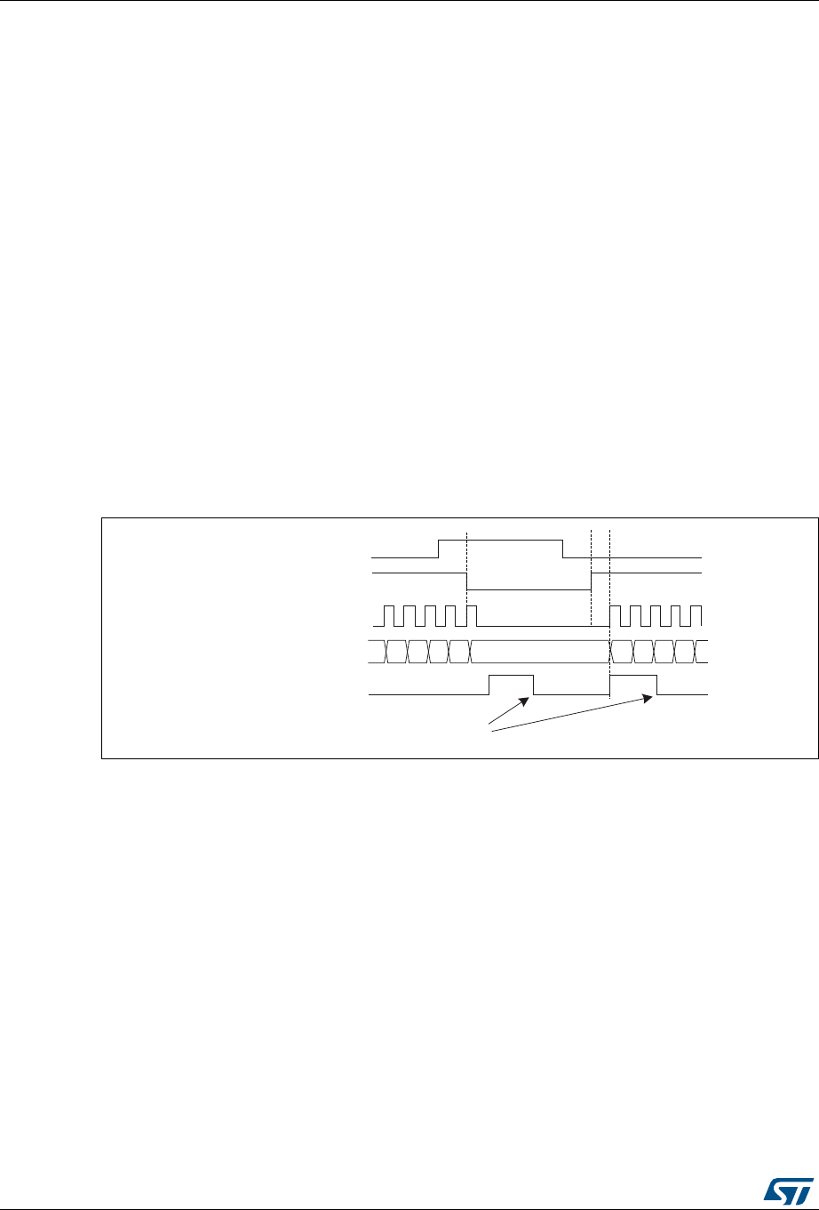
Advanced-control timers (TIM1&TIM8) RM0430
504/1324 RM0430 Rev 8
Slave mode: Gated mode
The counter can be enabled depending on the level of a selected input.
In the following example, the upcounter counts only when TI1 input is low:
•Configure the channel 1 to detect low levels on TI1. Configure the input filter duration
(in this example, we don’t need any filter, so we keep IC1F=0000). The capture
prescaler is not used for triggering, so you don’t need to configure it. The CC1S bits
select the input capture source only, CC1S=01 in TIMx_CCMR1 register. Write
CC1P=1 and CC1NP=’0’ in TIMx_CCER register to validate the polarity (and detect
low level only).
•Configure the timer in gated mode by writing SMS=101 in TIMx_SMCR register. Select
TI1 as the input source by writing TS=101 in TIMx_SMCR register.
•Enable the counter by writing CEN=1 in the TIMx_CR1 register (in gated mode, the
counter doesn’t start if CEN=0, whatever is the trigger input level).
The counter starts counting on the internal clock as long as TI1 is low and stops as soon as
TI1 becomes high. The TIF flag in the TIMx_SR register is set both when the counter starts
or stops.
The delay between the rising edge on TI1 and the actual stop of the counter is due to the
resynchronization circuit on TI1 input.
Figure 132. Control circuit in gated mode
069
7,
&17B(1
:ULWH7,)
&RXQWHUFORFN FNBFQW FNBSVF
&RXQWHUUHJLVWHU
7,)
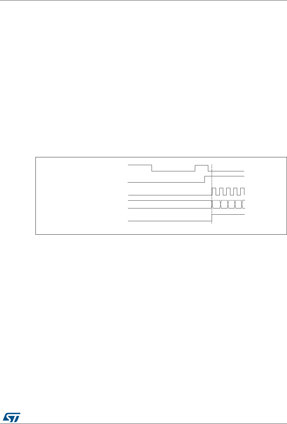
RM0430 Rev 8 505/1324
RM0430 Advanced-control timers (TIM1&TIM8)
533
Slave mode: Trigger mode
The counter can start in response to an event on a selected input.
In the following example, the upcounter starts in response to a rising edge on TI2 input:
•Configure the channel 2 to detect rising edges on TI2. Configure the input filter duration
(in this example, we don’t need any filter, so we keep IC2F=0000). The capture
prescaler is not used for triggering, so you don’t need to configure it. The CC2S bits are
configured to select the input capture source only, CC2S=01 in TIMx_CCMR1 register.
Write CC2P=1 and CC2NP=0 in TIMx_CCER register to validate the polarity (and
detect low level only).
•Configure the timer in trigger mode by writing SMS=110 in TIMx_SMCR register. Select
TI2 as the input source by writing TS=110 in TIMx_SMCR register.
When a rising edge occurs on TI2, the counter starts counting on the internal clock and the
TIF flag is set.
The delay between the rising edge on TI2 and the actual start of the counter is due to the
resynchronization circuit on TI2 input.
Figure 133. Control circuit in trigger mode
Slave mode: external clock mode 2 + trigger mode
The external clock mode 2 can be used in addition to another slave mode (except external
clock mode 1 and encoder mode). In this case, the ETR signal is used as external clock
input, and another input can be selected as trigger input (in reset mode, gated mode or
trigger mode). It is recommended not to select ETR as TRGI through the TS bits of
TIMx_SMCR register.
In the following example, the upcounter is incremented at each rising edge of the ETR
signal as soon as a rising edge of TI1 occurs:
1. Configure the external trigger input circuit by programming the TIMx_SMCR register as
follows:
– ETF = 0000: no filter
– ETPS = 00: prescaler disabled
– ETP = 0: detection of rising edges on ETR and ECE=1 to enable the external clock
mode 2.
069
7,
&17B(1
&RXQWHUFORFN FNBFQW FNBSVF
&RXQWHUUHJLVWHU
7,)
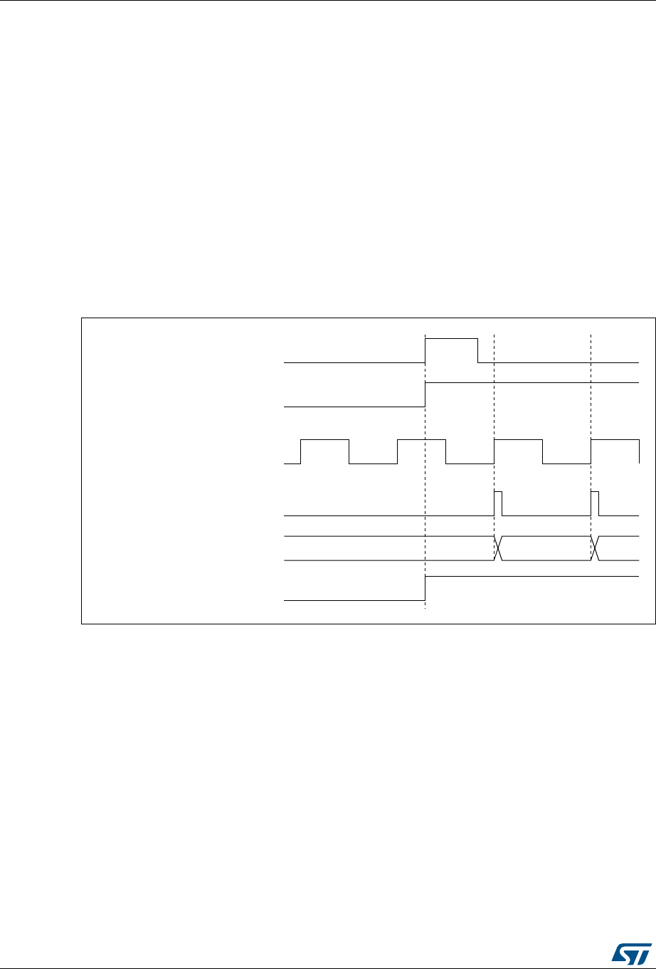
Advanced-control timers (TIM1&TIM8) RM0430
506/1324 RM0430 Rev 8
2. Configure the channel 1 as follows, to detect rising edges on TI:
– IC1F=0000: no filter.
– The capture prescaler is not used for triggering and does not need to be
configured.
– CC1S=01 in TIMx_CCMR1 register to select only the input capture source
– CC1P=0 and CC1NP=’0’ in TIMx_CCER register to validate the polarity (and
detect rising edge only).
3. Configure the timer in trigger mode by writing SMS=110 in TIMx_SMCR register. Select
TI1 as the input source by writing TS=101 in TIMx_SMCR register.
A rising edge on TI1 enables the counter and sets the TIF flag. The counter then counts on
ETR rising edges.
The delay between the rising edge of the ETR signal and the actual reset of the counter is
due to the resynchronization circuit on ETRP input.
Figure 134. Control circuit in external clock mode 2 + trigger mode
17.3.20 Timer synchronization
The TIM timers are linked together internally for timer synchronization or chaining. Refer to
Section 18.3.15: Timer synchronization on page 566 for details.
17.3.21 Debug mode
When the microcontroller enters debug mode (Cortex®-M4 with FPU core halted), the TIMx
counter either continues to work normally or stops, depending on DBG_TIMx_STOP
configuration bit in DBG module. For more details, refer to Section 37.16.2: Debug support
for timers, watchdog, bxCAN and I2C.
069
7,)
&RXQWHUUHJLVWHU
&RXQWHUFORFN &.B&17 &.B36&
(75
&(1&17B(1
7,

RM0430 Rev 8 507/1324
RM0430 Advanced-control timers (TIM1&TIM8)
533
17.4 TIM1&TIM8 registers
Refer to Section 1.2: List of abbreviations for registers for a list of abbreviations used in
register descriptions.
The peripheral registers must be written by half-words (16 bits) or words (32 bits). Read
accesses can be done by bytes (8 bits), half-word (16 bits) or words (32 bits).
17.4.1 TIM1&TIM8 control register 1 (TIMx_CR1)
Address offset: 0x00
Reset value: 0x0000
1514131211109876543210
Res. Res. Res. Res. Res. Res. CKD[1:0] ARPE CMS[1:0] DIR OPM URS UDIS CEN
rw rw rw rw rw rw rw rw rw rw
Bits 15:10 Reserved, must be kept at reset value.
Bits 9:8 CKD[1:0]: Clock division
This bit-field indicates the division ratio between the timer clock (CK_INT) frequency and the
dead-time and sampling clock (tDTS)used by the dead-time generators and the digital filters
(ETR, TIx),
00: tDTS=tCK_INT
01: tDTS=2*tCK_INT
10: tDTS=4*tCK_INT
11: Reserved, do not program this value
Bit 7 ARPE: Auto-reload preload enable
0: TIMx_ARR register is not buffered
1: TIMx_ARR register is buffered
Bits 6:5 CMS[1:0]: Center-aligned mode selection
00: Edge-aligned mode. The counter counts up or down depending on the direction bit
(DIR).
01: Center-aligned mode 1. The counter counts up and down alternatively. Output compare
interrupt flags of channels configured in output (CCxS=00 in TIMx_CCMRx register) are set
only when the counter is counting down.
10: Center-aligned mode 2. The counter counts up and down alternatively. Output compare
interrupt flags of channels configured in output (CCxS=00 in TIMx_CCMRx register) are set
only when the counter is counting up.
11: Center-aligned mode 3. The counter counts up and down alternatively. Output compare
interrupt flags of channels configured in output (CCxS=00 in TIMx_CCMRx register) are set
both when the counter is counting up or down.
Note: It is not allowed to switch from edge-aligned mode to center-aligned mode as long as
the counter is enabled (CEN=1)
Bit 4 DIR: Direction
0: Counter used as upcounter
1: Counter used as downcounter
Note: This bit is read only when the timer is configured in Center-aligned mode or Encoder
mode.

Advanced-control timers (TIM1&TIM8) RM0430
508/1324 RM0430 Rev 8
17.4.2 TIM1&TIM8 control register 2 (TIMx_CR2)
Address offset: 0x04
Reset value: 0x0000
Bit 3 OPM: One pulse mode
0: Counter is not stopped at update event
1: Counter stops counting at the next update event (clearing the bit CEN)
Bit 2 URS: Update request source
This bit is set and cleared by software to select the UEV event sources.
0: Any of the following events generate an update interrupt or DMA request if enabled.
These events can be:
– Counter overflow/underflow
– Setting the UG bit
– Update generation through the slave mode controller
1: Only counter overflow/underflow generates an update interrupt or DMA request if
enabled.
Bit 1 UDIS: Update disable
This bit is set and cleared by software to enable/disable UEV event generation.
0: UEV enabled. The Update (UEV) event is generated by one of the following events:
– Counter overflow/underflow
– Setting the UG bit
– Update generation through the slave mode controller
Buffered registers are then loaded with their preload values.
1: UEV disabled. The Update event is not generated, shadow registers keep their value
(ARR, PSC, CCRx). However the counter and the prescaler are reinitialized if the UG bit is
set or if a hardware reset is received from the slave mode controller.
Bit 0 CEN: Counter enable
0: Counter disabled
1: Counter enabled
Note: External clock, gated mode and encoder mode can work only if the CEN bit has been
previously set by software. However trigger mode can set the CEN bit automatically by
hardware.
1514131211109876543210
Res. OIS4 OIS3N OIS3 OIS2N OIS2 OIS1N OIS1 TI1S MMS[2:0] CCDS CCUS Res. CCPC
rw rw rw rw rw rw rw rw rw rw rw rw rw rw
Bit 15 Reserved, must be kept at reset value.
Bit 14 OIS4: Output Idle state 4 (OC4 output)
refer to OIS1 bit
Bit 13 OIS3N: Output Idle state 3 (OC3N output)
refer to OIS1N bit
Bit 12 OIS3: Output Idle state 3 (OC3 output)
refer to OIS1 bit

RM0430 Rev 8 509/1324
RM0430 Advanced-control timers (TIM1&TIM8)
533
Bit 11 OIS2N: Output Idle state 2 (OC2N output)
refer to OIS1N bit
Bit 10 OIS2: Output Idle state 2 (OC2 output)
refer to OIS1 bit
Bit 9 OIS1N: Output Idle state 1 (OC1N output)
0: OC1N=0 after a dead-time when MOE=0
1: OC1N=1 after a dead-time when MOE=0
Note: This bit can not be modified as long as LOCK level 1, 2 or 3 has been programmed
(LOCK bits in TIMx_BDTR register).
Bit 8 OIS1: Output Idle state 1 (OC1 output)
0: OC1=0 (after a dead-time if OC1N is implemented) when MOE=0
1: OC1=1 (after a dead-time if OC1N is implemented) when MOE=0
Note: This bit can not be modified as long as LOCK level 1, 2 or 3 has been programmed
(LOCK bits in TIMx_BDTR register).
Bit 7 TI1S: TI1 selection
0: The TIMx_CH1 pin is connected to TI1 input
1: The TIMx_CH1, CH2 and CH3 pins are connected to the TI1 input (XOR combination)
Bits 6:4 MMS[2:0]: Master mode selection
These bits allow to select the information to be sent in master mode to slave timers for
synchronization (TRGO). The combination is as follows:
000: Reset - the UG bit from the TIMx_EGR register is used as trigger output (TRGO). If the
reset is generated by the trigger input (slave mode controller configured in reset mode) then
the signal on TRGO is delayed compared to the actual reset.
001: Enable - the Counter Enable signal CNT_EN is used as trigger output (TRGO). It is
useful to start several timers at the same time or to control a window in which a slave timer is
enable. The Counter Enable signal is generated by a logic OR between CEN control bit and
the trigger input when configured in gated mode. When the Counter Enable signal is
controlled by the trigger input, there is a delay on TRGO, except if the master/slave mode is
selected (see the MSM bit description in TIMx_SMCR register).
010: Update - The update event is selected as trigger output (TRGO). For instance a master
timer can then be used as a prescaler for a slave timer.
011: Compare Pulse - The trigger output send a positive pulse when the CC1IF flag is to be
set (even if it was already high), as soon as a capture or a compare match occurred.
(TRGO).
100: Compare - OC1REF signal is used as trigger output (TRGO)
101: Compare - OC2REF signal is used as trigger output (TRGO)
110: Compare - OC3REF signal is used as trigger output (TRGO)
111: Compare - OC4REF signal is used as trigger output (TRGO)
Bit 3 CCDS: Capture/compare DMA selection
0: CCx DMA request sent when CCx event occurs
1: CCx DMA requests sent when update event occurs
Bit 2 CCUS: Capture/compare control update selection
0: When capture/compare control bits are preloaded (CCPC=1), they are updated by setting
the COMG bit only
1: When capture/compare control bits are preloaded (CCPC=1), they are updated by setting
the COMG bit or when an rising edge occurs on TRGI
Note: This bit acts only on channels that have a complementary output.

Advanced-control timers (TIM1&TIM8) RM0430
510/1324 RM0430 Rev 8
17.4.3 TIM1&TIM8 slave mode control register (TIMx_SMCR)
Address offset: 0x08
Reset value: 0x0000
Bit 1 Reserved, must be kept at reset value.
Bit 0 CCPC: Capture/compare preloaded control
0: CCxE, CCxNE and OCxM bits are not preloaded
1: CCxE, CCxNE and OCxM bits are preloaded, after having been written, they are updated
only when a commutation event (COM) occurs (COMG bit set or rising edge detected on
TRGI, depending on the CCUS bit).
Note: This bit acts only on channels that have a complementary output.
1514131211109876543210
ETP ECE ETPS[1:0] ETF[3:0] MSM TS[2:0] Res. SMS[2:0]
rw rw rw rw rw rw rw rw rw rw rw rw rw rw rw
Bit 15 ETP: External trigger polarity
This bit selects whether ETR or ETR is used for trigger operations
0: ETR is non-inverted, active at high level or rising edge.
1: ETR is inverted, active at low level or falling edge.
Bit 14 ECE: External clock enable
This bit enables External clock mode 2.
0: External clock mode 2 disabled
1: External clock mode 2 enabled. The counter is clocked by any active edge on the ETRF
signal.
Note: 1: Setting the ECE bit has the same effect as selecting external clock mode 1 with
TRGI connected to ETRF (SMS=111 and TS=111).
2: It is possible to simultaneously use external clock mode 2 with the following slave
modes: reset mode, gated mode and trigger mode. Nevertheless, TRGI must not be
connected to ETRF in this case (TS bits must not be 111).
3: If external clock mode 1 and external clock mode 2 are enabled at the same time,
the external clock input is ETRF.
Bits 13:12 ETPS[1:0]: External trigger prescaler
External trigger signal ETRP frequency must be at most 1/4 of TIMxCLK frequency. A
prescaler can be enabled to reduce ETRP frequency. It is useful when inputting fast external
clocks.
00: Prescaler OFF
01: ETRP frequency divided by 2
10: ETRP frequency divided by 4
11: ETRP frequency divided by 8

RM0430 Rev 8 511/1324
RM0430 Advanced-control timers (TIM1&TIM8)
533
Bits 11:8 ETF[3:0]: External trigger filter
This bit-field then defines the frequency used to sample ETRP signal and the length of the
digital filter applied to ETRP. The digital filter is made of an event counter in which N
consecutive events are needed to validate a transition on the output:
0000: No filter, sampling is done at fDTS
0001: fSAMPLING=fCK_INT
, N=2
0010: fSAMPLING=fCK_INT
, N=4
0011: fSAMPLING=fCK_INT
, N=8
0100: fSAMPLING=fDTS/2, N=6
0101: fSAMPLING=fDTS/2, N=8
0110: fSAMPLING=fDTS/4, N=6
0111: fSAMPLING=fDTS/4, N=8
1000: fSAMPLING=fDTS/8, N=6
1001: fSAMPLING=fDTS/8, N=8
1010: fSAMPLING=fDTS/16, N=5
1011: fSAMPLING=fDTS/16, N=6
1100: fSAMPLING=fDTS/16, N=8
1101: fSAMPLING=fDTS/32, N=5
1110: fSAMPLING=fDTS/32, N=6
1111: fSAMPLING=fDTS/32, N=8
Bit 7 MSM: Master/slave mode
0: No action
1: The effect of an event on the trigger input (TRGI) is delayed to allow a perfect
synchronization between the current timer and its slaves (through TRGO). It is useful if we
want to synchronize several timers on a single external event.
Bits 6:4 TS[2:0]: Trigger selection
This bit-field selects the trigger input to be used to synchronize the counter.
000: Internal Trigger 0 (ITR0)
001: Internal Trigger 1 (ITR1)
010: Internal Trigger 2 (ITR2)
011: Internal Trigger 3 (ITR3)
100: TI1 Edge Detector (TI1F_ED)
101: Filtered Timer Input 1 (TI1FP1)
110: Filtered Timer Input 2 (TI2FP2)
111: External Trigger input (ETRF)
See Table 102: TIMx Internal trigger connection for more details on ITRx meaning for each
Timer.
Note: These bits must be changed only when they are not used (e.g. when SMS=000) to
avoid wrong edge detections at the transition.
Bit 3 Reserved, must be kept at reset value.
Advanced-control timers (TIM1&TIM8) RM0430
512/1324 RM0430 Rev 8
17.4.4 TIM1&TIM8 DMA/interrupt enable register (TIMx_DIER)
Address offset: 0x0C
Reset value: 0x0000
Bits 2:0 SMS: Slave mode selection
When external signals are selected the active edge of the trigger signal (TRGI) is linked to
the polarity selected on the external input (see Input Control register and Control Register
description.
000: Slave mode disabled - if CEN = ‘1’ then the prescaler is clocked directly by the internal
clock.
001: Encoder mode 1 - Counter counts up/down on TI2FP2 edge depending on TI1FP1
level.
010: Encoder mode 2 - Counter counts up/down on TI1FP1 edge depending on TI2FP2
level.
011: Encoder mode 3 - Counter counts up/down on both TI1FP1 and TI2FP2 edges
depending on the level of the other input.
100: Reset Mode - Rising edge of the selected trigger input (TRGI) reinitializes the counter
and generates an update of the registers.
101: Gated Mode - The counter clock is enabled when the trigger input (TRGI) is high. The
counter stops (but is not reset) as soon as the trigger becomes low. Both start and stop of
the counter are controlled.
110: Trigger Mode - The counter starts at a rising edge of the trigger TRGI (but it is not
reset). Only the start of the counter is controlled.
111: External Clock Mode 1 - Rising edges of the selected trigger (TRGI) clock the counter.
Note: The gated mode must not be used if TI1F_ED is selected as the trigger input
(TS=’100’). Indeed, TI1F_ED outputs 1 pulse for each transition on TI1F, whereas the
gated mode checks the level of the trigger signal.
Table 102. TIMx Internal trigger connection
Slave TIM ITR0 (TS = 000) ITR1 (TS = 001) ITR2 (TS = 010) ITR3 (TS = 011)
TIM1 TIM5 TIM2 TIM3 or LPTIM1(1)
1. The selection of TIM3 or LPTIM1 is done via LPTIM1_OR register bit 2. TIM3 is selected by default.
TIM4
TIM8 TIM1 TIM2 TIM4 TIM5
1514131211109876543210
Res. TDE COMDE CC4DE CC3DE CC2DE CC1DE UDE BIE TIE COMIE CC4IE CC3IE CC2IE CC1IE UIE
rw rw rw rw rw rw rw rw rw rw rw rw rw rw rw
Bit 15 Reserved, must be kept at reset value.
Bit 14 TDE: Trigger DMA request enable
0: Trigger DMA request disabled
1: Trigger DMA request enabled
Bit 13 COMDE: COM DMA request enable
0: COM DMA request disabled
1: COM DMA request enabled

RM0430 Rev 8 513/1324
RM0430 Advanced-control timers (TIM1&TIM8)
533
Bit 12 CC4DE: Capture/Compare 4 DMA request enable
0: CC4 DMA request disabled
1: CC4 DMA request enabled
Bit 11 CC3DE: Capture/Compare 3 DMA request enable
0: CC3 DMA request disabled
1: CC3 DMA request enabled
Bit 10 CC2DE: Capture/Compare 2 DMA request enable
0: CC2 DMA request disabled
1: CC2 DMA request enabled
Bit 9 CC1DE: Capture/Compare 1 DMA request enable
0: CC1 DMA request disabled
1: CC1 DMA request enabled
Bit 8 UDE: Update DMA request enable
0: Update DMA request disabled
1: Update DMA request enabled
Bit 7 BIE: Break interrupt enable
0: Break interrupt disabled
1: Break interrupt enabled
Bit 6 TIE: Trigger interrupt enable
0: Trigger interrupt disabled
1: Trigger interrupt enabled
Bit 5 COMIE: COM interrupt enable
0: COM interrupt disabled
1: COM interrupt enabled
Bit 4 CC4IE: Capture/Compare 4 interrupt enable
0: CC4 interrupt disabled
1: CC4 interrupt enabled
Bit 3 CC3IE: Capture/Compare 3 interrupt enable
0: CC3 interrupt disabled
1: CC3 interrupt enabled
Bit 2 CC2IE: Capture/Compare 2 interrupt enable
0: CC2 interrupt disabled
1: CC2 interrupt enabled
Bit 1 CC1IE: Capture/Compare 1 interrupt enable
0: CC1 interrupt disabled
1: CC1 interrupt enabled
Bit 0 UIE: Update interrupt enable
0: Update interrupt disabled
1: Update interrupt enabled

Advanced-control timers (TIM1&TIM8) RM0430
514/1324 RM0430 Rev 8
17.4.5 TIM1&TIM8 status register (TIMx_SR)
Address offset: 0x10
Reset value: 0x0000
151413121110 9876543210
Res. Res. Res. CC4OF CC3OF CC2OF CC1OF Res. BIF TIF COMIF CC4IF CC3IF CC2IF CC1IF UIF
rc_w0 rc_w0 rc_w0 rc_w0 rc_w0 rc_w0 rc_w0 rc_w0 rc_w0 rc_w0 rc_w0 rc_w0
Bits 15:13 Reserved, must be kept at reset value.
Bit 12 CC4OF: Capture/Compare 4 overcapture flag
refer to CC1OF description
Bit 11 CC3OF: Capture/Compare 3 overcapture flag
refer to CC1OF description
Bit 10 CC2OF: Capture/Compare 2 overcapture flag
refer to CC1OF description
Bit 9 CC1OF: Capture/Compare 1 overcapture flag
This flag is set by hardware only when the corresponding channel is configured in input
capture mode. It is cleared by software by writing it to ‘0’.
0: No overcapture has been detected.
1: The counter value has been captured in TIMx_CCR1 register while CC1IF flag was
already set
Bit 8 Reserved, must be kept at reset value.
Bit 7 BIF: Break interrupt flag
This flag is set by hardware as soon as the break input goes active. It can be cleared by
software if the break input is not active.
0: No break event occurred.
1: An active level has been detected on the break input.
Bit 6 TIF: Trigger interrupt flag
This flag is set by hardware on trigger event (active edge detected on TRGI input when the
slave mode controller is enabled in all modes but gated mode. It is set when the counter
starts or stops when gated mode is selected. It is cleared by software.
0: No trigger event occurred.
1: Trigger interrupt pending.
Bit 5 COMIF: COM interrupt flag
This flag is set by hardware on COM event (when Capture/compare Control bits - CCxE,
CCxNE, OCxM - have been updated). It is cleared by software.
0: No COM event occurred.
1: COM interrupt pending.
Bit 4 CC4IF: Capture/Compare 4 interrupt flag
refer to CC1IF description
Bit 3 CC3IF: Capture/Compare 3 interrupt flag
refer to CC1IF description

RM0430 Rev 8 515/1324
RM0430 Advanced-control timers (TIM1&TIM8)
533
17.4.6 TIM1&TIM8 event generation register (TIMx_EGR)
Address offset: 0x14
Reset value: 0x0000
Bit 2 CC2IF: Capture/Compare 2 interrupt flag
refer to CC1IF description
Bit 1 CC1IF: Capture/Compare 1 interrupt flag
If channel CC1 is configured as output:
This flag is set by hardware when the counter matches the compare value, with some
exception in center-aligned mode (refer to the CMS bits in the TIMx_CR1 register
description). It is cleared by software.
0: No match.
1: The content of the counter TIMx_CNT matches the content of the TIMx_CCR1 register.
When the contents of TIMx_CCR1 are greater than the contents of TIMx_ARR, the CC1IF
bit goes high on the counter overflow (in upcounting and up/down-counting modes) or
underflow (in downcounting mode)
If channel CC1 is configured as input:
This bit is set by hardware on a capture. It is cleared by software or by reading the
TIMx_CCR1 register.
0: No input capture occurred
1: The counter value has been captured in TIMx_CCR1 register (An edge has been
detected on IC1 which matches the selected polarity)
Bit 0 UIF: Update interrupt flag
This bit is set by hardware on an update event. It is cleared by software.
0: No update occurred.
1: Update interrupt pending. This bit is set by hardware when the registers are updated:
–At overflow or underflow regarding the repetition counter value (update if repetition
counter = 0) and if the UDIS=0 in the TIMx_CR1 register.
–When CNT is reinitialized by software using the UG bit in TIMx_EGR register, if URS=0
and UDIS=0 in the TIMx_CR1 register.
–When CNT is reinitialized by a trigger event (refer to Section 17.4.3: TIM1&TIM8 slave
mode control register (TIMx_SMCR)), if URS=0 and UDIS=0 in the TIMx_CR1 register.
1514131211109876543210
Res. Res. Res. Res. Res. Res. Res. Res. BG TG COMG CC4G CC3G CC2G CC1G UG
wwwwwwww
Bits 15:8 Reserved, must be kept at reset value.
Bit 7 BG: Break generation
This bit is set by software in order to generate an event, it is automatically cleared by
hardware.
0: No action
1: A break event is generated. MOE bit is cleared and BIF flag is set. Related interrupt or
DMA transfer can occur if enabled.
Bit 6 TG: Trigger generation
This bit is set by software in order to generate an event, it is automatically cleared by
hardware.
0: No action
1: The TIF flag is set in TIMx_SR register. Related interrupt or DMA transfer can occur if
enabled.

Advanced-control timers (TIM1&TIM8) RM0430
516/1324 RM0430 Rev 8
Bit 5 COMG: Capture/Compare control update generation
This bit can be set by software, it is automatically cleared by hardware
0: No action
1: When CCPC bit is set, it allows to update CCxE, CCxNE and OCxM bits
Note: This bit acts only on channels having a complementary output.
Bit 4 CC4G: Capture/Compare 4 generation
refer to CC1G description
Bit 3 CC3G: Capture/Compare 3 generation
refer to CC1G description
Bit 2 CC2G: Capture/Compare 2 generation
refer to CC1G description
Bit 1 CC1G: Capture/Compare 1 generation
This bit is set by software in order to generate an event, it is automatically cleared by
hardware.
0: No action
1: A capture/compare event is generated on channel 1:
If channel CC1 is configured as output:
CC1IF flag is set, Corresponding interrupt or DMA request is sent if enabled.
If channel CC1 is configured as input:
The current value of the counter is captured in TIMx_CCR1 register. The CC1IF flag is set,
the corresponding interrupt or DMA request is sent if enabled. The CC1OF flag is set if the
CC1IF flag was already high.
Bit 0 UG: Update generation
This bit can be set by software, it is automatically cleared by hardware.
0: No action
1: Reinitialize the counter and generates an update of the registers. Note that the prescaler
counter is cleared too (anyway the prescaler ratio is not affected). The counter is cleared if
the center-aligned mode is selected or if DIR=0 (upcounting), else it takes the auto-reload
value (TIMx_ARR) if DIR=1 (downcounting).

RM0430 Rev 8 517/1324
RM0430 Advanced-control timers (TIM1&TIM8)
533
17.4.7 TIM1&TIM8 capture/compare mode register 1 (TIMx_CCMR1)
Address offset: 0x18
Reset value: 0x0000
The channels can be used in input (capture mode) or in output (compare mode). The
direction of a channel is defined by configuring the corresponding CCxS bits. All the other
bits of this register have a different function in input and in output mode. For a given bit,
OCxx describes its function when the channel is configured in output, ICxx describes its
function when the channel is configured in input. So you must take care that the same bit
can have a different meaning for the input stage and for the output stage.
Output compare mode:
1514131211109876543210
OC2
CE OC2M[2:0] OC2
PE
OC2
FE CC2S[1:0]
OC1
CE OC1M[2:0] OC1
PE
OC1
FE CC1S[1:0]
IC2F[3:0] IC2PSC[1:0] IC1F[3:0] IC1PSC[1:0]
rw rw rw rw rw rw rw rw rw rw rw rw rw rw rw rw
Bit 15 OC2CE: Output Compare 2 clear enable
Bits 14:12 OC2M[2:0]: Output Compare 2 mode
Bit 11 OC2PE: Output Compare 2 preload enable
Bit 10 OC2FE: Output Compare 2 fast enable
Bits 9:8 CC2S[1:0]: Capture/Compare 2 selection
This bit-field defines the direction of the channel (input/output) as well as the used input.
00: CC2 channel is configured as output
01: CC2 channel is configured as input, IC2 is mapped on TI2
10: CC2 channel is configured as input, IC2 is mapped on TI1
11: CC2 channel is configured as input, IC2 is mapped on TRC. This mode is working only if
an internal trigger input is selected through the TS bit (TIMx_SMCR register)
Note: CC2S bits are writable only when the channel is OFF (CC2E = ‘0’ in TIMx_CCER).
Bit 7 OC1CE: Output Compare 1 clear enable
OC1CE: Output Compare 1 Clear Enable
0: OC1Ref is not affected by the ETRF Input
1: OC1Ref is cleared as soon as a High level is detected on ETRF input

Advanced-control timers (TIM1&TIM8) RM0430
518/1324 RM0430 Rev 8
Bits 6:4 OC1M: Output Compare 1 mode
These bits define the behavior of the output reference signal OC1REF from which OC1 and
OC1N are derived. OC1REF is active high whereas OC1 and OC1N active level depends on
CC1P and CC1NP bits.
000: Frozen - The comparison between the output compare register TIMx_CCR1 and the
counter TIMx_CNT has no effect on the outputs.(this mode is used to generate a timing
base).
001: Set channel 1 to active level on match. OC1REF signal is forced high when the counter
TIMx_CNT matches the capture/compare register 1 (TIMx_CCR1).
010: Set channel 1 to inactive level on match. OC1REF signal is forced low when the counter
TIMx_CNT matches the capture/compare register 1 (TIMx_CCR1).
011: Toggle - OC1REF toggles when TIMx_CNT=TIMx_CCR1.
100: Force inactive level - OC1REF is forced low.
101: Force active level - OC1REF is forced high.
110: PWM mode 1 - In upcounting, channel 1 is active as long as TIMx_CNT<TIMx_CCR1
else inactive. In downcounting, channel 1 is inactive (OC1REF=‘0’) as long as
TIMx_CNT>TIMx_CCR1 else active (OC1REF=’1’).
111: PWM mode 2 - In upcounting, channel 1 is inactive as long as TIMx_CNT<TIMx_CCR1
else active. In downcounting, channel 1 is active as long as TIMx_CNT>TIMx_CCR1 else
inactive.
Note: 1: These bits can not be modified as long as LOCK level 3 has been programmed
(LOCK bits in TIMx_BDTR register) and CC1S=’00’ (the channel is configured in
output).
2: In PWM mode 1 or 2, the OCREF level changes only when the result of the
comparison changes or when the output compare mode switches from “frozen” mode to
“PWM” mode.
3: On channels having a complementary output, this bit field is preloaded. If the CCPC
bit is set in the TIMx_CR2 register then the OC1M active bits take the new value from
the preloaded bits only when a COM event is generated.
Bit 3 OC1PE: Output Compare 1 preload enable
0: Preload register on TIMx_CCR1 disabled. TIMx_CCR1 can be written at anytime, the new
value is taken in account immediately.
1: Preload register on TIMx_CCR1 enabled. Read/Write operations access the preload
register. TIMx_CCR1 preload value is loaded in the active register at each update event.
Note: 1: These bits can not be modified as long as LOCK level 3 has been programmed
(LOCK bits in TIMx_BDTR register) and CC1S=’00’ (the channel is configured in
output).
2: The PWM mode can be used without validating the preload register only in one pulse
mode (OPM bit set in TIMx_CR1 register). Else the behavior is not guaranteed.
Bit 2 OC1FE: Output Compare 1 fast enable
This bit is used to accelerate the effect of an event on the trigger in input on the CC output.
0: CC1 behaves normally depending on counter and CCR1 values even when the trigger is
ON. The minimum delay to activate CC1 output when an edge occurs on the trigger input is 5
clock cycles.
1: An active edge on the trigger input acts like a compare match on CC1 output. Then, OC is
set to the compare level independently from the result of the comparison. Delay to sample
the trigger input and to activate CC1 output is reduced to 3 clock cycles. OCFE acts only if
the channel is configured in PWM1 or PWM2 mode.

RM0430 Rev 8 519/1324
RM0430 Advanced-control timers (TIM1&TIM8)
533
Input capture mode
Bits 1:0 CC1S: Capture/Compare 1 selection
This bit-field defines the direction of the channel (input/output) as well as the used input.
00: CC1 channel is configured as output
01: CC1 channel is configured as input, IC1 is mapped on TI1
10: CC1 channel is configured as input, IC1 is mapped on TI2
11: CC1 channel is configured as input, IC1 is mapped on TRC. This mode is working only if
an internal trigger input is selected through TS bit (TIMx_SMCR register)
Note: CC1S bits are writable only when the channel is OFF (CC1E = ‘0’ in TIMx_CCER).
Bits 15:12 IC2F: Input capture 2 filter
Bits 11:10 IC2PSC[1:0]: Input capture 2 prescaler
Bits 9:8 CC2S: Capture/Compare 2 selection
This bit-field defines the direction of the channel (input/output) as well as the used input.
00: CC2 channel is configured as output
01: CC2 channel is configured as input, IC2 is mapped on TI2
10: CC2 channel is configured as input, IC2 is mapped on TI1
11: CC2 channel is configured as input, IC2 is mapped on TRC. This mode is working only if an
internal trigger input is selected through TS bit (TIMx_SMCR register)
Note: CC2S bits are writable only when the channel is OFF (CC2E = ‘0’ in TIMx_CCER).
Bits 7:4 IC1F[3:0]: Input capture 1 filter
This bit-field defines the frequency used to sample TI1 input and the length of the digital filter applied
to TI1. The digital filter is made of an event counter in which N consecutive events are needed to
validate a transition on the output:
0000: No filter, sampling is done at fDTS
0001: fSAMPLING=fCK_INT
, N=2
0010: fSAMPLING=fCK_INT
, N=4
0011: fSAMPLING=fCK_INT
, N=8
0100: fSAMPLING=fDTS/2, N=6
0101: fSAMPLING=fDTS/2, N=8
0110: fSAMPLING=fDTS/4, N=6
0111: fSAMPLING=fDTS/4, N=8
1000: fSAMPLING=fDTS/8, N=6
1001: fSAMPLING=fDTS/8, N=8
1010: fSAMPLING=fDTS/16, N=5
1011: fSAMPLING=fDTS/16, N=6
1100: fSAMPLING=fDTS/16, N=8
1101: fSAMPLING=fDTS/32, N=5
1110: fSAMPLING=fDTS/32, N=6
1111: fSAMPLING=fDTS/32, N=8

Advanced-control timers (TIM1&TIM8) RM0430
520/1324 RM0430 Rev 8
17.4.8 TIM1&TIM8 capture/compare mode register 2 (TIMx_CCMR2)
Address offset: 0x1C
Reset value: 0x0000
Refer to the above CCMR1 register description.
Output compare mode
Bits 3:2 IC1PSC: Input capture 1 prescaler
This bit-field defines the ratio of the prescaler acting on CC1 input (IC1).
The prescaler is reset as soon as CC1E=’0’ (TIMx_CCER register).
00: no prescaler, capture is done each time an edge is detected on the capture input
01: capture is done once every 2 events
10: capture is done once every 4 events
11: capture is done once every 8 events
Bits 1:0 CC1S: Capture/Compare 1 Selection
This bit-field defines the direction of the channel (input/output) as well as the used input.
00: CC1 channel is configured as output
01: CC1 channel is configured as input, IC1 is mapped on TI1
10: CC1 channel is configured as input, IC1 is mapped on TI2
11: CC1 channel is configured as input, IC1 is mapped on TRC. This mode is working only if an
internal trigger input is selected through TS bit (TIMx_SMCR register)
Note: CC1S bits are writable only when the channel is OFF (CC1E = ‘0’ in TIMx_CCER).
1514131211109876543210
OC4
CE OC4M[2:0] OC4
PE
OC4
FE CC4S[1:0]
OC3
CE. OC3M[2:0] OC3
PE
OC3
FE CC3S[1:0]
IC4F[3:0] IC4PSC[1:0] IC3F[3:0] IC3PSC[1:0]
rw rw rw rw rw rw rw rw rw rw rw rw rw rw rw rw
Bit 15 OC4CE: Output compare 4 clear enable
Bits 14:12 OC4M: Output compare 4 mode
Bit 11 OC4PE: Output compare 4 preload enable
Bit 10 OC4FE: Output compare 4 fast enable
Bits 9:8 CC4S: Capture/Compare 4 selection
This bit-field defines the direction of the channel (input/output) as well as the used input.
00: CC4 channel is configured as output
01: CC4 channel is configured as input, IC4 is mapped on TI4
10: CC4 channel is configured as input, IC4 is mapped on TI3
11: CC4 channel is configured as input, IC4 is mapped on TRC. This mode is working only if
an internal trigger input is selected through TS bit (TIMx_SMCR register)
Note: CC4S bits are writable only when the channel is OFF (CC4E = ‘0’ in TIMx_CCER).
Bit 7 OC3CE: Output compare 3 clear enable
Bits 6:4 OC3M: Output compare 3 mode

RM0430 Rev 8 521/1324
RM0430 Advanced-control timers (TIM1&TIM8)
533
Input capture mode
17.4.9 TIM1&TIM8 capture/compare enable register (TIMx_CCER)
Address offset: 0x20
Reset value: 0x0000
Bit 3 OC3PE: Output compare 3 preload enable
Bit 2 OC3FE: Output compare 3 fast enable
Bits 1:0 CC3S: Capture/Compare 3 selection
This bit-field defines the direction of the channel (input/output) as well as the used input.
00: CC3 channel is configured as output
01: CC3 channel is configured as input, IC3 is mapped on TI3
10: CC3 channel is configured as input, IC3 is mapped on TI4
11: CC3 channel is configured as input, IC3 is mapped on TRC. This mode is working only if
an internal trigger input is selected through TS bit (TIMx_SMCR register)
Note: CC3S bits are writable only when the channel is OFF (CC3E = ‘0’ in TIMx_CCER).
Bits 15:12 IC4F: Input capture 4 filter
Bits 11:10 IC4PSC: Input capture 4 prescaler
Bits 9:8 CC4S: Capture/Compare 4 selection
This bit-field defines the direction of the channel (input/output) as well as the used input.
00: CC4 channel is configured as output
01: CC4 channel is configured as input, IC4 is mapped on TI4
10: CC4 channel is configured as input, IC4 is mapped on TI3
11: CC4 channel is configured as input, IC4 is mapped on TRC. This mode is working only if
an internal trigger input is selected through TS bit (TIMx_SMCR register)
Note: CC4S bits are writable only when the channel is OFF (CC4E = ‘0’ in TIMx_CCER).
Bits 7:4 IC3F: Input capture 3 filter
Bits 3:2 IC3PSC: Input capture 3 prescaler
Bits 1:0 CC3S: Capture/compare 3 selection
This bit-field defines the direction of the channel (input/output) as well as the used input.
00: CC3 channel is configured as output
01: CC3 channel is configured as input, IC3 is mapped on TI3
10: CC3 channel is configured as input, IC3 is mapped on TI4
11: CC3 channel is configured as input, IC3 is mapped on TRC. This mode is working only if
an internal trigger input is selected through TS bit (TIMx_SMCR register)
Note: CC3S bits are writable only when the channel is OFF (CC3E = ‘0’ in TIMx_CCER).
1514131211109876543210
Res. Res. CC4P CC4E CC3NP CC3NE CC3P CC3E CC2NP CC2NE CC2P CC2E CC1NP CC1NE CC1P CC1E
rw rw rw rw rw rw rw rw rw rw rw rw rw rw
Bits 15:14 Reserved, must be kept at reset value.
Bit 13 CC4P: Capture/Compare 4 output polarity
refer to CC1P description

Advanced-control timers (TIM1&TIM8) RM0430
522/1324 RM0430 Rev 8
Bit 12 CC4E: Capture/Compare 4 output enable
refer to CC1E description
Bit 11 CC3NP: Capture/Compare 3 complementary output polarity
refer to CC1NP description
Bit 10 CC3NE: Capture/Compare 3 complementary output enable
refer to CC1NE description
Bit 9 CC3P: Capture/Compare 3 output polarity
refer to CC1P description
Bit 8 CC3E: Capture/Compare 3 output enable
refer to CC1E description
Bit 7 CC2NP: Capture/Compare 2 complementary output polarity
refer to CC1NP description
Bit 6 CC2NE: Capture/Compare 2 complementary output enable
refer to CC1NE description
Bit 5 CC2P: Capture/Compare 2 output polarity
refer to CC1P description
Bit 4 CC2E: Capture/Compare 2 output enable
refer to CC1E description
Bit 3 CC1NP: Capture/Compare 1 complementary output polarity
CC1 channel configured as output:
0: OC1N active high.
1: OC1N active low.
CC1 channel configured as input:
This bit is used in conjunction with CC1P to define the polarity of TI1FP1 and TI2FP1. Refer
to CC1P description.
Note: On channels having a complementary output, this bit is preloaded. If the CCPC bit is
set in the TIMx_CR2 register then the CC1NP active bit takes the new value from the
preloaded bit only when a Commutation event is generated.
Note: This bit is not writable as soon as LOCK level 2 or 3 has been programmed (LOCK bits
in TIMx_BDTR register) and CC1S=”00” (the channel is configured in output).
Bit 2 CC1NE: Capture/Compare 1 complementary output enable
0: Off - OC1N is not active. OC1N level is then function of MOE, OSSI, OSSR, OIS1, OIS1N
and CC1E bits.
1: On - OC1N signal is output on the corresponding output pin depending on MOE, OSSI,
OSSR, OIS1, OIS1N and CC1E bits.
Note: On channels having a complementary output, this bit is preloaded. If the CCPC bit is
set in the TIMx_CR2 register then the CC1NE active bit takes the new value from the
preloaded bit only when a Commutation event is generated.

RM0430 Rev 8 523/1324
RM0430 Advanced-control timers (TIM1&TIM8)
533
Bit 1 CC1P: Capture/Compare 1 output polarity
CC1 channel configured as output:
0: OC1 active high
1: OC1 active low
CC1 channel configured as input:
CC1NP/CC1P bits select the active polarity of TI1FP1 and TI2FP1 for trigger or capture
operations.
00: non-inverted/rising edge
The circuit is sensitive to TIxFP1 rising edge (capture or trigger operations in reset, external
clock or trigger mode), TIxFP1 is not inverted (trigger operation in gated mode or encoder
mode).
01: inverted/falling edge
The circuit is sensitive to TIxFP1 falling edge (capture or trigger operations in reset, external
clock or trigger mode), TIxFP1 is inverted (trigger operation in gated mode or encoder
mode).
10: reserved, do not use this configuration.
11: non-inverted/both edges
The circuit is sensitive to both TIxFP1 rising and falling edges (capture or trigger operations
in reset, external clock or trigger mode), TIxFP1 is not inverted (trigger operation in gated
mode). This configuration must not be used in encoder mode.
Note: On channels having a complementary output, this bit is preloaded. If the CCPC bit is
set in the TIMx_CR2 register then the CC1P active bit takes the new value from the
preloaded bit only when a Commutation event is generated.
Note: This bit is not writable as soon as LOCK level 2 or 3 has been programmed (LOCK bits
in TIMx_BDTR register).
Bit 0 CC1E: Capture/Compare 1 output enable
CC1 channel configured as output:
0: Off - OC1 is not active. OC1 level is then function of MOE, OSSI, OSSR, OIS1, OIS1N
and CC1NE bits.
1: On - OC1 signal is output on the corresponding output pin depending on MOE, OSSI,
OSSR, OIS1, OIS1N and CC1NE bits.
CC1 channel configured as input:
This bit determines if a capture of the counter value can actually be done into the input
capture/compare register 1 (TIMx_CCR1) or not.
0: Capture disabled.
1: Capture enabled.
Note: On channels having a complementary output, this bit is preloaded. If the CCPC bit is
set in the TIMx_CR2 register then the CC1E active bit takes the new value from the
preloaded bit only when a Commutation event is generated.

Advanced-control timers (TIM1&TIM8) RM0430
524/1324 RM0430 Rev 8
Table 103. Output control bits for complementary OCx and OCxN channels
with break feature
Control bits Output states(1)
MOE
bit
OSSI
bit
OSSR
bit
CCxE
bit
CCxNE
bit OCx output state OCxN output state
1X
0
0
0
Output Disabled (not driven by
the timer)
OCx=0, OCx_EN=0
Output Disabled (not driven by the timer)
OCxN=0, OCxN_EN=0
1
Output Disabled (not driven by
the timer)
OCx=0, OCx_EN=0
OCxREF + Polarity OCxN=OCxREF xor
CCxNP, OCxN_EN=1
1
0
OCxREF + Polarity
OCx=OCxREF xor CCxP,
OCx_EN=1
Output Disabled (not driven by the timer)
OCxN=0, OCxN_EN=0
1OCREF + Polarity + dead-time
OCx_EN=1
Complementary to OCREF (not
OCREF)
+ Polarity + dead-time
OCxN_EN=1
1
0
0
Output Disabled (not driven by
the timer)
OCx=CCxP, OCx_EN=0
Output Disabled (not driven by the timer)
OCxN=CCxNP, OCxN_EN=0
1
Off-State (output enabled with
inactive state)
OCx=CCxP, OCx_EN=1
OCxREF + Polarity
OCxN=OCxREF xor CCxNP,
OCxN_EN=1
1
0
OCxREF + Polarity
OCx=OCxREF xor CCxP,
OCx_EN=1
Off-State (output enabled with inactive
state)
OCxN=CCxNP, OCxN_EN=1
1OCREF + Polarity + dead-time
OCx_EN=1
Complementary to OCREF (not
OCREF) + Polarity + dead-time
OCxN_EN=1
0
0
X
00
Output Disabled (not driven by
the timer)
OCx=CCxP, OCx_EN=0
Output Disabled (not driven by the timer)
OCxN=CCxNP, OCxN_EN=0
1 Output Disabled (not driven by the timer)
Asynchronously: OCx=CCxP, OCx_EN=0, OCxN=CCxNP, OCxN_EN=0
Then if the clock is present: OCx=OISx and OCxN=OISxN after a dead-
time, assuming that OISx and OISxN do not correspond to OCX and
OCxN both in active state.
1
0
1
1
00
Output Disabled (not driven by
the timer)
OCx=CCxP, OCx_EN=0
Output Disabled (not driven by the timer)
OCxN=CCxNP, OCxN_EN=0
1 Off-State (output enabled with inactive state)
Asynchronously: OCx=CCxP, OCx_EN=1, OCxN=CCxNP, OCxN_EN=1
Then if the clock is present: OCx=OISx and OCxN=OISxN after a dead-
time, assuming that OISx and OISxN do not correspond to OCX and
OCxN both in active state
1
0
1
1. When both outputs of a channel are not used (CCxE = CCxNE = 0), the OISx, OISxN, CCxP and CCxNP bits must be kept
cleared.

RM0430 Rev 8 525/1324
RM0430 Advanced-control timers (TIM1&TIM8)
533
Note: The state of the external I/O pins connected to the complementary OCx and OCxN channels
depends on the OCx and OCxN channel state and the GPIO registers.
17.4.10 TIM1&TIM8 counter (TIMx_CNT)
Address offset: 0x24
Reset value: 0x0000
17.4.11 TIM1&TIM8 prescaler (TIMx_PSC)
Address offset: 0x28
Reset value: 0x0000
17.4.12 TIM1 auto-reload register (TIMx_ARR)
Address offset: 0x2C
Reset value: 0x0000
1514131211109876543210
CNT[15:0]
rw rw rw rw rw rw rw rw rw rw rw rw rw rw rw rw
Bits 15:0 CNT[15:0]: Counter value
1514131211109876543210
PSC[15:0]
rw rw rw rw rw rw rw rw rw rw rw rw rw rw rw rw
Bits 15:0 PSC[15:0]: Prescaler value
The counter clock frequency (CK_CNT) is equal to fCK_PSC / (PSC[15:0] + 1).
PSC contains the value to be loaded in the active prescaler register at each update event
(including when the counter is cleared through UG bit of TIMx_EGR register or through
trigger controller when configured in “reset mode”).
1514131211109876543210
ARR[15:0]
rw rw rw rw rw rw rw rw rw rw rw rw rw rw rw rw
Bits 15:0 ARR[15:0]: Auto-reload value
ARR is the value to be loaded in the actual auto-reload register.
Refer to Section 17.3.1: Time-base unit for more details about ARR update and behavior.
The counter is blocked while the auto-reload value is null.

Advanced-control timers (TIM1&TIM8) RM0430
526/1324 RM0430 Rev 8
17.4.13 TIM1&TIM8 repetition counter register (TIMx_RCR)
Address offset: 0x30
Reset value: 0x0000
17.4.14 TIM1&TIM8 capture/compare register 1 (TIMx_CCR1)
Address offset: 0x34
Reset value: 0x0000
1514131211109876543210
Res. Res. Res. Res. Res. Res. Res. Res. REP[7:0]
rw rw rw rw rw rw rw rw
Bits 15:8 Reserved, must be kept at reset value.
Bits 7:0 REP[7:0]: Repetition counter value
These bits allow the user to set-up the update rate of the compare registers (i.e. periodic
transfers from preload to active registers) when preload registers are enable, as well as the
update interrupt generation rate, if this interrupt is enable.
Each time the REP_CNT related downcounter reaches zero, an update event is generated
and it restarts counting from REP value. As REP_CNT is reloaded with REP value only at
the repetition update event U_RC, any write to the TIMx_RCR register is not taken in
account until the next repetition update event.
It means in PWM mode (REP+1) corresponds to:
– the number of PWM periods in edge-aligned mode
– the number of half PWM period in center-aligned mode.
1514131211109876543210
CCR1[15:0]
rw rw rw rw rw rw rw rw rw rw rw rw rw rw rw rw
Bits 15:0 CCR1[15:0]: Capture/Compare 1 value
If channel CC1 is configured as output:
CCR1 is the value to be loaded in the actual capture/compare 1 register (preload value).
It is loaded permanently if the preload feature is not selected in the TIMx_CCMR1 register
(bit OC1PE). Else the preload value is copied in the active capture/compare 1 register when
an update event occurs.
The active capture/compare register contains the value to be compared to the counter
TIMx_CNT and signaled on OC1 output.
If channel CC1 is configured as input:
CCR1 is the counter value transferred by the last input capture 1 event (IC1).

RM0430 Rev 8 527/1324
RM0430 Advanced-control timers (TIM1&TIM8)
533
17.4.15 TIM1 capture/compare register 2 (TIMx_CCR2)
Address offset: 0x38
Reset value: 0x0000
17.4.16 TIM1&TIM8 capture/compare register 3 (TIMx_CCR3)
Address offset: 0x3C
Reset value: 0x0000
1514131211109876543210
CCR2[15:0]
rw rw rw rw rw rw rw rw rw rw rw rw rw rw rw rw
Bits 15:0 CCR2[15:0]: Capture/Compare 2 value
If channel CC2 is configured as output:
CCR2 is the value to be loaded in the actual capture/compare 2 register (preload value).
It is loaded permanently if the preload feature is not selected in the TIMx_CCMR2 register
(bit OC2PE). Else the preload value is copied in the active capture/compare 2 register when
an update event occurs.
The active capture/compare register contains the value to be compared to the counter
TIMx_CNT and signalled on OC2 output.
If channel CC2 is configured as input:
CCR2 is the counter value transferred by the last input capture 2 event (IC2).
1514131211109876543210
CCR3[15:0]
rw rw rw rw rw rw rw rw rw rw rw rw rw rw rw rw
Bits 15:0 CCR3[15:0]: Capture/Compare value
If channel CC3 is configured as output:
CCR3 is the value to be loaded in the actual capture/compare 3 register (preload value).
It is loaded permanently if the preload feature is not selected in the TIMx_CCMR3 register
(bit OC3PE). Else the preload value is copied in the active capture/compare 3 register when
an update event occurs.
The active capture/compare register contains the value to be compared to the counter
TIMx_CNT and signalled on OC3 output.
If channel CC3 is configured as input:
CCR3 is the counter value transferred by the last input capture 3 event (IC3).

Advanced-control timers (TIM1&TIM8) RM0430
528/1324 RM0430 Rev 8
17.4.17 TIM1&TIM8 capture/compare register 4 (TIMx_CCR4)
Address offset: 0x40
Reset value: 0x0000
17.4.18 TIM1&TIM8 break and dead-time register (TIMx_BDTR)
Address offset: 0x44
Reset value: 0x0000
Note: As the bits AOE, BKP, BKE, OSSI, OSSR and DTG[7:0] can be write-locked depending on
the LOCK configuration, it can be necessary to configure all of them during the first write
access to the TIMx_BDTR register.
1514131211109876543210
CCR4[15:0]
rw rw rw rw rw rw rw rw rw rw rw rw rw rw rw rw
Bits 15:0 CCR4[15:0]: Capture/Compare value
If channel CC4 is configured as output:
CCR4 is the value to be loaded in the actual capture/compare 4 register (preload value).
It is loaded permanently if the preload feature is not selected in the TIMx_CCMR4 register
(bit OC4PE). Else the preload value is copied in the active capture/compare 4 register when
an update event occurs.
The active capture/compare register contains the value to be compared to the counter
TIMx_CNT and signalled on OC4 output.
If channel CC4 is configured as input:
CCR4 is the counter value transferred by the last input capture 4 event (IC4).
1514131211109876543210
MOE AOE BKP BKE OSSR OSSI LOCK[1:0] DTG[7:0]
rw rw rw rw rw rw rw rw rw rw rw rw rw rw rw rw
Bit 15 MOE: Main output enable
This bit is cleared asynchronously by hardware as soon as the break input is active. It is set
by software or automatically depending on the AOE bit. It is acting only on the channels
which are configured in output.
0: OC and OCN outputs are disabled or forced to idle state.
1: OC and OCN outputs are enabled if their respective enable bits are set (CCxE, CCxNE in
TIMx_CCER register).
See OC/OCN enable description for more details (Section 17.4.9: TIM1&TIM8
capture/compare enable register (TIMx_CCER) on page 521).
Bit 14 AOE: Automatic output enable
0: MOE can be set only by software
1: MOE can be set by software or automatically at the next update event (if the break input is
not be active)
Note: This bit can not be modified as long as LOCK level 1 has been programmed (LOCK bits
in TIMx_BDTR register).

RM0430 Rev 8 529/1324
RM0430 Advanced-control timers (TIM1&TIM8)
533
Bit 13 BKP: Break polarity
0: Break input BRK is active low
1: Break input BRK is active high
Note: This bit can not be modified as long as LOCK level 1 has been programmed (LOCK bits
in TIMx_BDTR register).
Note: Any write operation to this bit takes a delay of 1 APB clock cycle to become effective.
Bit 12 BKE: Break enable
0: Break inputs (BRK and CSS clock failure event) disabled
1; Break inputs (BRK and CSS clock failure event) enabled
Note: This bit cannot be modified when LOCK level 1 has been programmed (LOCK bits in
TIMx_BDTR register).
Note: Any write operation to this bit takes a delay of 1 APB clock cycle to become effective.
Bit 11 OSSR: Off-state selection for Run mode
This bit is used when MOE=1 on channels having a complementary output which are
configured as outputs. OSSR is not implemented if no complementary output is implemented
in the timer.
See OC/OCN enable description for more details (Section 17.4.9: TIM1&TIM8
capture/compare enable register (TIMx_CCER) on page 521).
0: When inactive, OC/OCN outputs are disabled (OC/OCN enable output signal=0).
1: When inactive, OC/OCN outputs are enabled with their inactive level as soon as CCxE=1
or CCxNE=1. Then, OC/OCN enable output signal=1
Note: This bit can not be modified as soon as the LOCK level 2 has been programmed (LOCK
bits in TIMx_BDTR register).
Bit 10 OSSI: Off-state selection for Idle mode
This bit is used when MOE=0 on channels configured as outputs.
See OC/OCN enable description for more details (Section 17.4.9: TIM1&TIM8
capture/compare enable register (TIMx_CCER) on page 521).
0: When inactive, OC/OCN outputs are disabled (OC/OCN enable output signal=0).
1: When inactive, OC/OCN outputs are forced first with their idle level as soon as CCxE=1 or
CCxNE=1. OC/OCN enable output signal=1)
Note: This bit can not be modified as soon as the LOCK level 2 has been programmed (LOCK
bits in TIMx_BDTR register).
Bits 9:8 LOCK[1:0]: Lock configuration
These bits offer a write protection against software errors.
00: LOCK OFF - No bit is write protected.
01: LOCK Level 1 = DTG bits in TIMx_BDTR register, OISx and OISxN bits in TIMx_CR2
register and BKE/BKP/AOE bits in TIMx_BDTR register can no longer be written.
10: LOCK Level 2 = LOCK Level 1 + CC Polarity bits (CCxP/CCxNP bits in TIMx_CCER
register, as long as the related channel is configured in output through the CCxS bits) as well
as OSSR and OSSI bits can no longer be written.
11: LOCK Level 3 = LOCK Level 2 + CC Control bits (OCxM and OCxPE bits in
TIMx_CCMRx registers, as long as the related channel is configured in output through the
CCxS bits) can no longer be written.
Note: The LOCK bits can be written only once after the reset. Once the TIMx_BDTR register
has been written, their content is frozen until the next reset.

Advanced-control timers (TIM1&TIM8) RM0430
530/1324 RM0430 Rev 8
17.4.19 TIM1&TIM8 DMA control register (TIMx_DCR)
Address offset: 0x48
Reset value: 0x0000
Bits 7:0 DTG[7:0]: Dead-time generator setup
This bit-field defines the duration of the dead-time inserted between the complementary
outputs. DT correspond to this duration.
DTG[7:5]=0xx => DT=DTG[7:0]x tdtg with tdtg=tDTS.
DTG[7:5]=10x => DT=(64+DTG[5:0])xtdtg with Tdtg=2xtDTS.
DTG[7:5]=110 => DT=(32+DTG[4:0])xtdtg with Tdtg=8xtDTS.
DTG[7:5]=111 => DT=(32+DTG[4:0])xtdtg with Tdtg=16xtDTS.
Example if TDTS=125ns (8MHz), dead-time possible values are:
0 to 15875 ns by 125 ns steps,
16 us to 31750 ns by 250 ns steps,
32 us to 63us by 1 us steps,
64 us to 126 us by 2 us steps
Note: This bit-field can not be modified as long as LOCK level 1, 2 or 3 has been programmed
(LOCK bits in TIMx_BDTR register).
1514131211109876543210
Res. Res. Res. DBL[4:0] Res. Res. Res. DBA[4:0]
rw rw rw rw rw rw rw rw rw rw
Bits 15:13 Reserved, must be kept at reset value.
Bits 12:8 DBL[4:0]: DMA burst length
This 5-bit vector defines the number of DMA transfers (the timer detects a burst transfer
when a read or a write access to the TIMx_DMAR register address is performed).
the TIMx_DMAR address)
00000: 1 transfer
00001: 2 transfers
00010: 3 transfers
...
10001: 18 transfers
Bits 7:5 Reserved, must be kept at reset value.
Bits 4:0 DBA[4:0]: DMA base address
This 5-bits vector defines the base-address for DMA transfers (when read/write access are
done through the TIMx_DMAR address). DBA is defined as an offset starting from the
address of the TIMx_CR1 register.
Example:
00000: TIMx_CR1,
00001: TIMx_CR2,
00010: TIMx_SMCR,
...
Example: Let us consider the following transfer: DBL = 7 transfers and DBA = TIMx_CR1. In
this case the transfer is done to/from 7 registers starting from the TIMx_CR1 address.

RM0430 Rev 8 531/1324
RM0430 Advanced-control timers (TIM1&TIM8)
533
17.4.20 TIM1&TIM8 DMA address for full transfer (TIMx_DMAR)
Address offset: 0x4C
Reset value: 0x0000
Example of how to use the DMA burst feature
In this example the timer DMA burst feature is used to update the contents of the CCRx
registers (x = 2, 3, 4) with the DMA transferring half words into the CCRx registers.
This is done in the following steps:
1. Configure the corresponding DMA channel as follows:
– DMA channel peripheral address is the DMAR register address
– DMA channel memory address is the address of the buffer in the RAM containing
the data to be transferred by DMA into CCRx registers.
– Number of data to transfer = 3 (See note below).
– Circular mode disabled.
2. Configure the DCR register by configuring the DBA and DBL bit fields as follows:
DBL = 3 transfers, DBA = 0xE.
3. Enable the TIMx update DMA request (set the UDE bit in the DIER register).
4. Enable TIMx
5. Enable the DMA channel
Note: This example is for the case where every CCRx register to be updated once. If every CCRx
register is to be updated twice for example, the number of data to transfer should be 6. Let's
take the example of a buffer in the RAM containing data1, data2, data3, data4, data5 and
data6. The data is transferred to the CCRx registers as follows: on the first update DMA
request, data1 is transferred to CCR2, data2 is transferred to CCR3, data3 is transferred to
CCR4 and on the second update DMA request, data4 is transferred to CCR2, data5 is
transferred to CCR3 and data6 is transferred to CCR4.
1514131211109876543210
DMAB[15:0]
rw rw rw rw rw rw rw rw rw rw rw rw rw rw rw rw
Bits 15:0 DMAB[15:0]: DMA register for burst accesses
A read or write operation to the DMAR register accesses the register located at the address
(TIMx_CR1 address) + (DBA + DMA index) x 4
where TIMx_CR1 address is the address of the control register 1, DBA is the DMA base
address configured in TIMx_DCR register, DMA index is automatically controlled by the
DMA transfer, and ranges from 0 to DBL (DBL configured in TIMx_DCR).

Advanced-control timers (TIM1&TIM8) RM0430
532/1324 RM0430 Rev 8
17.4.21 TIM1&TIM8 register map
TIM1&TIM8 registers are mapped as 16-bit addressable registers as described in the table
below:
Table 104. TIM1&TIM8 register map and reset values
Offset Register
31
30
29
28
27
26
25
24
23
22
21
20
19
18
17
16
15
14
13
12
11
10
9
8
7
6
5
4
3
2
1
0
0x00 TIMx_CR1
Res.
Res.
Res.
Res.
Res.
Res.
Res.
Res.
Res.
Res.
Res.
Res.
Res.
Res.
Res.
Res.
Res.
Res.
Res.
Res.
Res.
CKD
[1:0]
ARPE
CMS
[1:0]
DIR
OPM
URS
UDIS
CEN
Reset value 0000000000
0x04 TIMx_CR2
Res.
Res.
Res.
Res.
Res.
Res.
Res.
Res.
Res.
Res.
Res.
Res.
Res.
Res.
Res.
Res.
Res.
OIS4
OIS3N
OIS3
OIS2N
OIS2
OIS1N
OIS1
TI1S
MMS[2:0]
CCDS
CCUS
Res.
CCPC
Reset value 0000000000000 0
0x08 TIMx_SMCR
Res.
Res.
Res.
Res.
Res.
Res.
Res.
Res.
Res.
Res.
Res.
Res.
Res.
Res.
Res.
Res.
ETP
ECE
ETPS
[1:0] ETF[3:0]
MSM
TS[2:0]
Res.
SMS[2:0]
Reset value 000000000000 000
0x0C TIMx_DIER
Res.
Res.
Res.
Res.
Res.
Res.
Res.
Res.
Res.
Res.
Res.
Res.
Res.
Res.
Res.
Res.
Res.
TDE
COMDE
CC4DE
CC3DE
CC2DE
CC1DE
UDE
BIE
TIE
COMIE
CC4IE
CC3IE
CC2IE
CC1IE
UIE
Reset value 000000000000000
0x10 TIMx_SR
Res.
Res.
Res.
Res.
Res.
Res.
Res.
Res.
Res.
Res.
Res.
Res.
Res.
Res.
Res.
Res.
Res.
Res.
Res.
CC4OF
CC3OF
CC2OF
CC1OF
Res.
BIF
TIF
COMIF
CC4IF
CC3IF
CC2IF
CC1IF
UIF
Reset value 0000 00000000
0x14 TIMx_EGR
Res.
Res.
Res.
Res.
Res.
Res.
Res.
Res.
Res.
Res.
Res.
Res.
Res.
Res.
Res.
Res.
Res.
Res.
Res.
Res.
Res.
Res.
Res.
Res.
BG
TG
COMG
CC4G
CC3G
CC2G
CC1G
UG
Reset value 00000000
0x18
TIMx_CCMR1
Output Compare
mode
Res.
Res.
Res.
Res.
Res.
Res.
Res.
Res.
Res.
Res.
Res.
Res.
Res.
Res.
Res.
Res.
OC2CE
OC2M
[2:0]
OC2PE
OC2FE
CC2S
[1:0]
OC1CE
OC1M
[2:0]
OC1PE
OC1FE
CC1S
[1:0]
Reset value 0000000000000000
TIMx_CCMR1
Input Capture
mode
Res.
Res.
Res.
Res.
Res.
Res.
Res.
Res.
Res.
Res.
Res.
Res.
Res.
Res.
Res.
Res.
IC2F[3:0]
IC2
PSC
[1:0]
CC2S
[1:0] IC1F[3:0]
IC1
PSC
[1:0]
CC1S
[1:0]
Reset value 0000000000000000
0x1C
TIMx_CCMR2
Output Compare
mode
Res.
Res.
Res.
Res.
Res.
Res.
Res.
Res.
Res.
Res.
Res.
Res.
Res.
Res.
Res.
Res.
O24CE
OC4M
[2:0]
OC4PE
OC4FE
CC4S
[1:0]
OC3CE
OC3M
[2:0]
OC3PE
OC3FE
CC3S
[1:0]
Reset value 0000000000000000
TIMx_CCMR2
Input Capture
mode
Res.
Res.
Res.
Res.
Res.
Res.
Res.
Res.
Res.
Res.
Res.
Res.
Res.
Res.
Res.
Res.
IC4F[3:0]
IC4
PSC
[1:0]
CC4S
[1:0] IC3F[3:0]
IC3
PSC
[1:0]
CC3S
[1:0]
Reset value 0000000000000000
0x20 TIMx_CCER
Res.
Res.
Res.
Res.
Res.
Res.
Res.
Res.
Res.
Res.
Res.
Res.
Res.
Res.
Res.
Res.
Res.
Res.
CC4P
CC4E
CC3NP
CC3NE
CC3P
CC3E
CC2NP
CC2NE
CC2P
CC2E
CC1NP
CC1NE
CC1P
CC1E
Reset value 00000000000000
0x24 TIMx_CNT
Res.
Res.
Res.
Res.
Res.
Res.
Res.
Res.
Res.
Res.
Res.
Res.
Res.
Res.
Res.
Res.
CNT[15:0]
Reset value 0000000000000000
0x28 TIMx_PSC
Res.
Res.
Res.
Res.
Res.
Res.
Res.
Res.
Res.
Res.
Res.
Res.
Res.
Res.
Res.
Res.
PSC[15:0]
Reset value 0000000000000000
0x2C TIMx_ARR
Res.
Res.
Res.
Res.
Res.
Res.
Res.
Res.
Res.
Res.
Res.
Res.
Res.
Res.
Res.
Res.
ARR[15:0]
Reset value 0000000000000000
0x30 TIMx_RCR
Res.
Res.
Res.
Res.
Res.
Res.
Res.
Res.
Res.
Res.
Res.
Res.
Res.
Res.
Res.
Res.
Res.
Res.
Res.
Res.
Res.
Res.
Res.
Res.
REP[7:0]
Reset value 00000000
RM0430 Rev 8 533/1324
RM0430 Advanced-control timers (TIM1&TIM8)
533
Refer to Section 2.2.2 on page 58 for the register boundary addresses.
0x34 TIMx_CCR1 CCR1[15:0]
Reset value 0000000000000000
0x38 TIMx_CCR2
Res.
Res.
Res.
Res.
Res.
Res.
Res.
Res.
Res.
Res.
Res.
Res.
Res.
Res.
Res.
Res.
CCR2[15:0]
Reset value 0000000000000000
0x3C TIMx_CCR3
Res.
Res.
Res.
Res.
Res.
Res.
Res.
Res.
Res.
Res.
Res.
Res.
Res.
Res.
Res.
Res.
CCR3[15:0]
Reset value 0000000000000000
0x40 TIMx_CCR4
Res.
Res.
Res.
Res.
Res.
Res.
Res.
Res.
Res.
Res.
Res.
Res.
Res.
Res.
Res.
Res.
CCR4[15:0]
Reset value 0000000000000000
0x44 TIMx_BDTR
Res.
Res.
Res.
Res.
Res.
Res.
Res.
Res.
Res.
Res.
Res.
Res.
Res.
Res.
Res.
Res.
MOE
AOE
BKP
BKE
OSSR
OSSI
LOCK
[1:0] DT[7:0]
Reset value 0000000000000000
0x48 TIMx_DCR
Res.
Res.
Res.
Res.
Res.
Res.
Res.
Res.
Res.
Res.
Res.
Res.
Res.
Res.
Res.
Res.
Res.
Res.
Res.
DBL[4:0]
Res.
Res.
Res.
DBA[4:0]
Reset value 00000 00000
0x4C TIMx_DMAR
Res.
Res.
Res.
Res.
Res.
Res.
Res.
Res.
Res.
Res.
Res.
Res.
Res.
Res.
Res.
Res.
DMAB[15:0]
Reset value 0000000000000000
Table 104. TIM1&TIM8 register map and reset values (continued)
Offset Register
31
30
29
28
27
26
25
24
23
22
21
20
19
18
17
16
15
14
13
12
11
10
9
8
7
6
5
4
3
2
1
0

General-purpose timers (TIM2 to TIM5) RM0430
534/1324 RM0430 Rev 8
18 General-purpose timers (TIM2 to TIM5)
18.1 TIM2 to TIM5 introduction
The general-purpose timers consist of a 16-bit or 32-bit auto-reload counter driven by a
programmable prescaler.
They may be used for a variety of purposes, including measuring the pulse lengths of input
signals (input capture) or generating output waveforms (output compare and PWM).
Pulse lengths and waveform periods can be modulated from a few microseconds to several
milliseconds using the timer prescaler and the RCC clock controller prescalers.
The timers are completely independent, and do not share any resources. They can be
synchronized together as described in Section 18.3.15.
18.2 TIM2 to TIM5 main features
General-purpose TIMx timer features include:
•16-bit (TIM3 and TIM4) or 32-bit (TIM2 and TIM5) up, down, up/down auto-reload
counter.
•16-bit programmable prescaler used to divide (also “on the fly”) the counter clock
frequency by any factor between 1 and 65536.
•Up to 4 independent channels for:
– Input capture
– Output compare
– PWM generation (Edge- and Center-aligned modes)
– One-pulse mode output
•Synchronization circuit to control the timer with external signals and to interconnect
several timers.
•Interrupt/DMA generation on the following events:
– Update: counter overflow/underflow, counter initialization (by software or
internal/external trigger)
– Trigger event (counter start, stop, initialization or count by internal/external trigger)
– Input capture
– Output compare
•Supports incremental (quadrature) encoder and hall-sensor circuitry for positioning
purposes
•Trigger input for external clock or cycle-by-cycle current management
RM0430 Rev 8 535/1324
RM0430 General-purpose timers (TIM2 to TIM5)
594
Figure 135. General-purpose timer block diagram
18.3 TIM2 to TIM5 functional description
18.3.1 Time-base unit
The main block of the programmable timer is a 16-bit/32-bit counter with its related auto-
reload register. The counter can count up. The counter clock can be divided by a prescaler.
The counter, the auto-reload register and the prescaler register can be written or read by
software. This is true even when the counter is running.
8
8
8
&&,
&&,
7ULJJHU
FRQWUROOHU
6WRSFOHDURUXSGRZQ
7,)3
7,)3
,75
,75
,75 75*,
2XWSXW
FRQWURO
75*2
2&5()
2&5()
8
8,
5HVHWHQDEOHXSFRXQW
&.B36&
,&
,& ,&36
,&36
7,)3
7*,
75&
75&
,75
75&
7,)B('
&&,
&&,
7,)3
7,)3
7,)3
7,
7,
7,0[B&+
7,0[B&+
2&
2& 7,0[B&+
7,0[B&+
WRRWKHUWLPHUV
WR'$&$'&
6ODYH
FRQWUROOHU
PRGH
36&
SUHVFDOHU &17FRXQWHU
,QWHUQDOFORFN&.B,17
&.B&17
7,0[&/.IURP5&&
,75
069
;25
,QSXWILOWHU
HGJHGHWHFWRU
&DSWXUH&RPSDUHUHJLVWHU
1RWHV
5HJ 3UHORDGUHJLVWHUVWUDQVIHUUHG
WRDFWLYHUHJLVWHUVRQ8HYHQW
DFFRUGLQJWRFRQWUROELW
(YHQW
,QWHUUXSW'0$RXWSXW
$XWRUHORDGUHJLVWHU
&DSWXUH&RPSDUHUHJLVWHU
3UHVFDOHU
3UHVFDOHU
,QSXWILOWHU
HGJHGHWHFWRU
2XWSXW
FRQWURO
8
8
&&,
&&,
2XWSXW
FRQWURO
2&5()
2&5()
,&
,& ,&36
,&36
7,)3
7,)3
7,0[B&+
7,0[B&+
2&
2& 7,0[B&+
7,0[B&+
,QSXWILOWHU
HGJHGHWHFWRU
&DSWXUH&RPSDUHUHJLVWHU
&DSWXUH&RPSDUHUHJLVWHU
3UHVFDOHU
3UHVFDOHU
,QSXWILOWHU
HGJHGHWHFWRU
2XWSXW
FRQWURO
75&
7,)3
7,)3
75&
&&,
&&,
7,
7,
(QFRGHU
LQWHUIDFH
7,0[B(75 ,QSXWILOWHU
3RODULW\VHOHFWLRQHGJH
GHWHFWRUSUHVFDOHU
(75 (753
(75)
(75)
General-purpose timers (TIM2 to TIM5) RM0430
536/1324 RM0430 Rev 8
The time-base unit includes:
•Counter Register (TIMx_CNT)
•Prescaler Register (TIMx_PSC):
•Auto-Reload Register (TIMx_ARR)
The auto-reload register is preloaded. Writing to or reading from the auto-reload register
accesses the preload register. The content of the preload register are transferred into the
shadow register permanently or at each update event (UEV), depending on the auto-reload
preload enable bit (ARPE) in TIMx_CR1 register. The update event is sent when the counter
reaches the overflow (or underflow when downcounting) and if the UDIS bit equals 0 in the
TIMx_CR1 register. It can also be generated by software. The generation of the update
event is described in detail for each configuration.
The counter is clocked by the prescaler output CK_CNT, which is enabled only when the
counter enable bit (CEN) in TIMx_CR1 register is set (refer also to the slave mode controller
description to get more details on counter enabling).
Note that the actual counter enable signal CNT_EN is set 1 clock cycle after CEN.
Prescaler description
The prescaler can divide the counter clock frequency by any factor between 1 and 65536. It
is based on a 16-bit counter controlled through a 16-bit/32-bit register (in the TIMx_PSC
register). It can be changed on the fly as this control register is buffered. The new prescaler
ratio is taken into account at the next update event.
Figure 136 and Figure 137 give some examples of the counter behavior when the prescaler
ratio is changed on the fly:
Figure 136. Counter timing diagram with prescaler division change from 1 to 2
069
&.B36&
&17B(1
7LPHUFORFN &.B&17
&RXQWHUUHJLVWHU
8SGDWHHYHQW8(9
3UHVFDOHUFRQWUROUHJLVWHU
:ULWHDQHZYDOXHLQ7,0[B36&
3UHVFDOHUEXIIHU
3UHVFDOHUFRXQWHU
)$ )%) ) ) )&
RM0430 Rev 8 537/1324
RM0430 General-purpose timers (TIM2 to TIM5)
594
Figure 137. Counter timing diagram with prescaler division change from 1 to 4
18.3.2 Counter modes
Upcounting mode
In upcounting mode, the counter counts from 0 to the auto-reload value (content of the
TIMx_ARR register), then restarts from 0 and generates a counter overflow event.
An Update event can be generated at each counter overflow or by setting the UG bit in the
TIMx_EGR register (by software or by using the slave mode controller).
The UEV event can be disabled by software by setting the UDIS bit in TIMx_CR1 register.
This is to avoid updating the shadow registers while writing new values in the preload
registers. Then no update event occurs until the UDIS bit has been written to 0. However,
the counter restarts from 0, as well as the counter of the prescaler (but the prescale rate
does not change). In addition, if the URS bit (update request selection) in TIMx_CR1
register is set, setting the UG bit generates an update event UEV but without setting the UIF
flag (thus no interrupt or DMA request is sent). This is to avoid generating both update and
capture interrupts when clearing the counter on the capture event.
When an update event occurs, all the registers are updated and the update flag (UIF bit in
TIMx_SR register) is set (depending on the URS bit):
•The buffer of the prescaler is reloaded with the preload value (content of the TIMx_PSC
register)
•The auto-reload shadow register is updated with the preload value (TIMx_ARR)
The following figures show some examples of the counter behavior for different clock
frequencies when TIMx_ARR=0x36.
069
&.B36&
&17B(1
7LPHUFORFN &.B&17
&RXQWHUUHJLVWHU
8SGDWHHYHQW8(9
3UHVFDOHUFRQWUROUHJLVWHU
:ULWHDQHZYDOXHLQ7,0[B36&
3UHVFDOHUEXIIHU
3UHVFDOHUFRXQWHU
)$ )%) ) ) )&
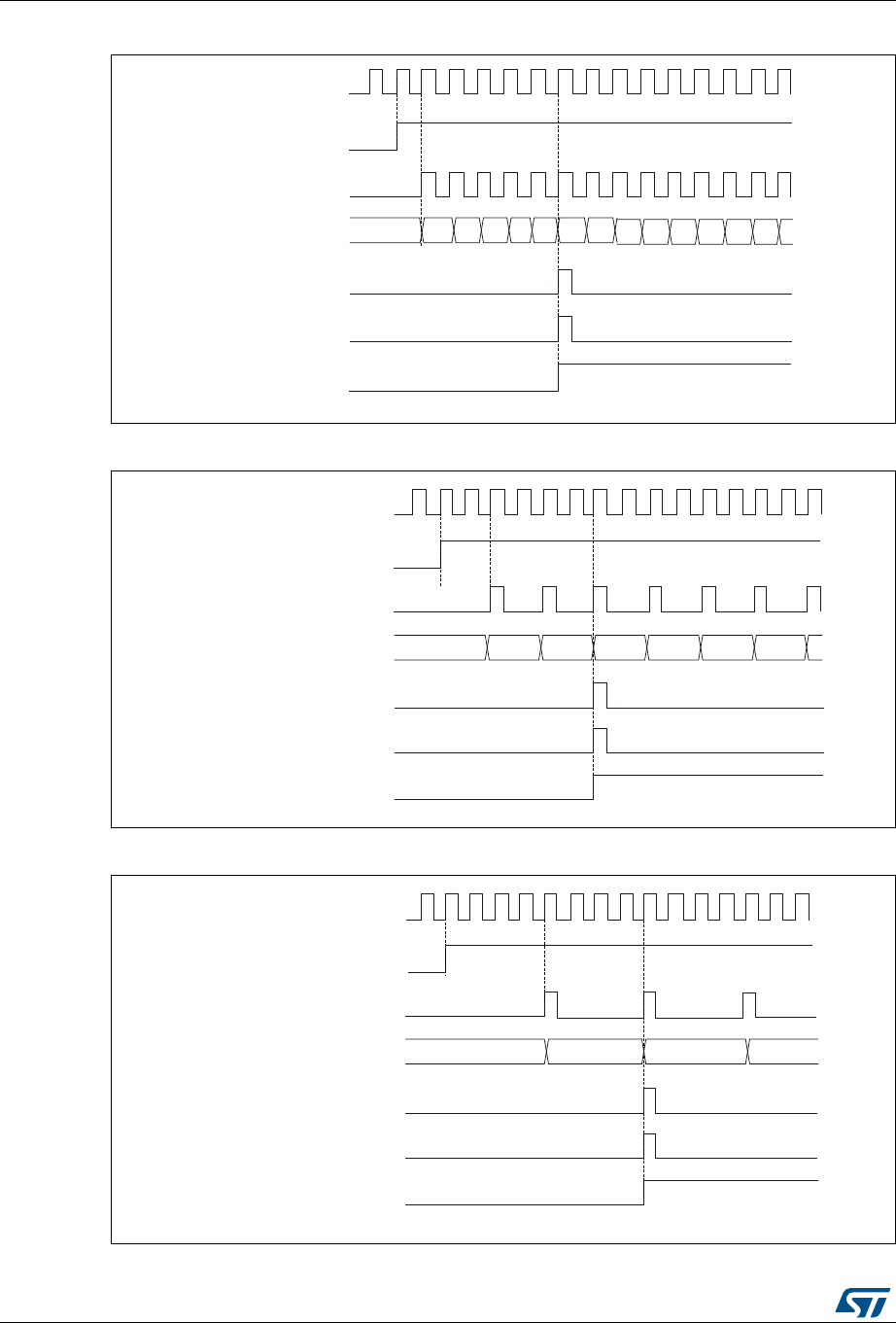
General-purpose timers (TIM2 to TIM5) RM0430
538/1324 RM0430 Rev 8
Figure 138. Counter timing diagram, internal clock divided by 1
Figure 139. Counter timing diagram, internal clock divided by 2
Figure 140. Counter timing diagram, internal clock divided by 4
069
&.B,17
&17B(1
7LPHUFORFN &.B&17
&RXQWHUUHJLVWHU
8SGDWHHYHQW8(9
&RXQWHURYHUIORZ
8SGDWHLQWHUUXSWIODJ8,)
069
&.B,17
&17B(1
7LPHUFORFN &.B&17
&RXQWHUUHJLVWHU
8SGDWHHYHQW8(9
&RXQWHURYHUIORZ
8SGDWHLQWHUUXSWIODJ8,)
06Y9
&.B,17
7LPHUFORFN &.B&17
&RXQWHUUHJLVWHU
8SGDWHHYHQW8(9
&RXQWHURYHUIORZ
8SGDWHLQWHUUXSWIODJ8,)
&17B(1
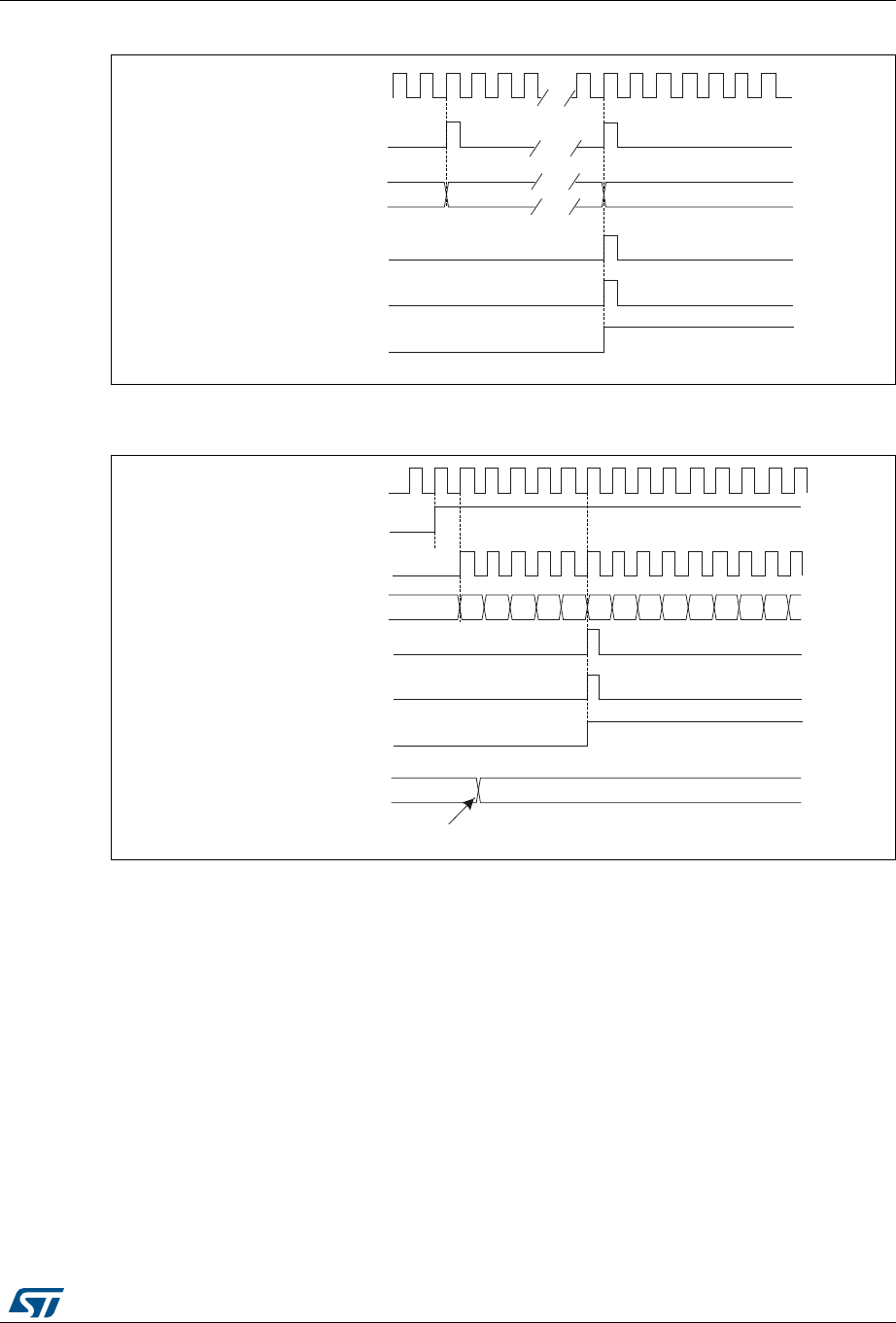
RM0430 Rev 8 539/1324
RM0430 General-purpose timers (TIM2 to TIM5)
594
Figure 141. Counter timing diagram, internal clock divided by N
Figure 142. Counter timing diagram, Update event when ARPE=0 (TIMx_ARR not
preloaded)
06Y9
&.B,17
7LPHUFORFN &.B&17
&RXQWHUUHJLVWHU
8SGDWHHYHQW8(9
&RXQWHURYHUIORZ
8SGDWHLQWHUUXSWIODJ8,)
)
))
06Y9
&.B,17
7LPHUFORFN &.B&17
&RXQWHUUHJLVWHU
8SGDWHHYHQW8(9
&RXQWHURYHUIORZ
8SGDWHLQWHUUXSWIODJ8,)
&17B(1
$XWRUHORDGUHJLVWHU
:ULWHDQHZYDOXHLQ7,0[B$55
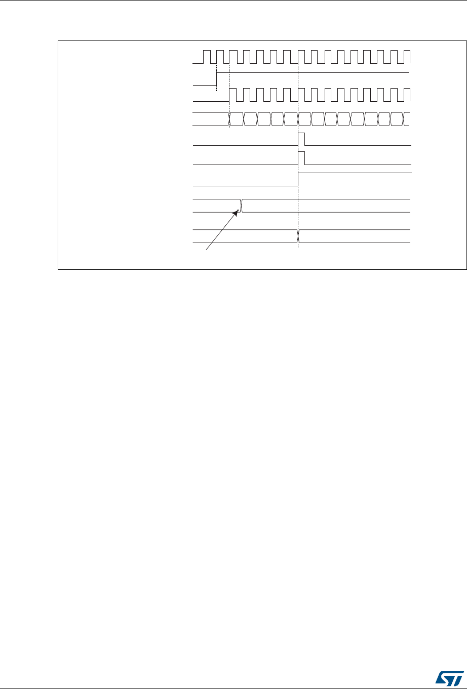
General-purpose timers (TIM2 to TIM5) RM0430
540/1324 RM0430 Rev 8
Figure 143. Counter timing diagram, Update event when ARPE=1 (TIMx_ARR
preloaded)
Downcounting mode
In downcounting mode, the counter counts from the auto-reload value (content of the
TIMx_ARR register) down to 0, then restarts from the auto-reload value and generates a
counter underflow event.
An Update event can be generate at each counter underflow or by setting the UG bit in the
TIMx_EGR register (by software or by using the slave mode controller)
The UEV update event can be disabled by software by setting the UDIS bit in TIMx_CR1
register. This is to avoid updating the shadow registers while writing new values in the
preload registers. Then no update event occurs until UDIS bit has been written to 0.
However, the counter restarts from the current auto-reload value, whereas the counter of the
prescaler restarts from 0 (but the prescale rate doesn’t change).
In addition, if the URS bit (update request selection) in TIMx_CR1 register is set, setting the
UG bit generates an update event UEV but without setting the UIF flag (thus no interrupt or
DMA request is sent). This is to avoid generating both update and capture interrupts when
clearing the counter on the capture event.
When an update event occurs, all the registers are updated and the update flag (UIF bit in
TIMx_SR register) is set (depending on the URS bit):
•The buffer of the prescaler is reloaded with the preload value (content of the TIMx_PSC
register).
•The auto-reload active register is updated with the preload value (content of the
TIMx_ARR register). Note that the auto-reload is updated before the counter is
reloaded, so that the next period is the expected one.
The following figures show some examples of the counter behavior for different clock
frequencies when TIMx_ARR=0x36.
06Y9
)
&.B36&
7LPHUFORFN &.B&17
&RXQWHUUHJLVWHU
8SGDWHHYHQW8(9
&RXQWHURYHUIORZ
8SGDWHLQWHUUXSWIODJ8,)
) ) ) ) ))
&17B(1
$XWRUHORDGSUHORDGUHJLVWHU
:ULWHDQHZYDOXHLQ7,0[B$55
$XWRUHORDGVKDGRZUHJLVWHU )
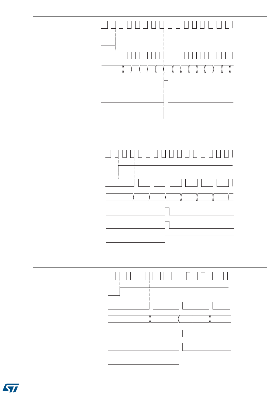
RM0430 Rev 8 541/1324
RM0430 General-purpose timers (TIM2 to TIM5)
594
Figure 144. Counter timing diagram, internal clock divided by 1
Figure 145. Counter timing diagram, internal clock divided by 2
Figure 146. Counter timing diagram, internal clock divided by 4
)
06Y9
&.B,17
&17B(1
7LPHUFORFN &.B&17
&RXQWHUUHJLVWHU
8SGDWHHYHQW8(9
&RXQWHUXQGHUIORZFQWBXGI
8SGDWHLQWHUUXSWIODJ8,)
06Y9
&.B,17
&17B(1
7LPHUFORFN &.B&17
&RXQWHUUHJLVWHU
8SGDWHHYHQW8(9
&RXQWHUXQGHUIORZ
8SGDWHLQWHUUXSWIODJ8,)
06Y9
&.B,17
7LPHUFORFN &.B&17
&RXQWHUUHJLVWHU
8SGDWHHYHQW8(9
&RXQWHUXQGHUIORZ
8SGDWHLQWHUUXSWIODJ8,)
&17B(1
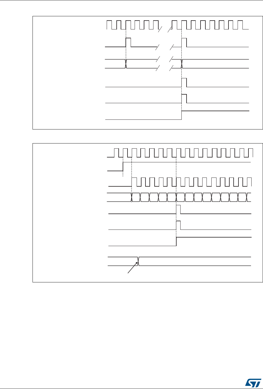
General-purpose timers (TIM2 to TIM5) RM0430
542/1324 RM0430 Rev 8
Figure 147. Counter timing diagram, internal clock divided by N
Figure 148. Counter timing diagram, Update event
Center-aligned mode (up/down counting)
In center-aligned mode, the counter counts from 0 to the auto-reload value (content of the
TIMx_ARR register) – 1, generates a counter overflow event, then counts from the auto-
reload value down to 1 and generates a counter underflow event. Then it restarts counting
from 0.
Center-aligned mode is active when the CMS bits in TIMx_CR1 register are not equal to
'00'. The Output compare interrupt flag of channels configured in output is set when: the
counter counts down (Center aligned mode 1, CMS = "01"), the counter counts up (Center
aligned mode 2, CMS = "10") the counter counts up and down (Center aligned mode 3,
CMS = "11").
069
)
&.B,17
7LPHUFORFN &.B&17
&RXQWHUUHJLVWHU
8SGDWHHYHQW8(9
&RXQWHURYHUIORZ
8SGDWHLQWHUUXSWIODJ8,)
069
))
&.B,17
7LPHUFORFN &.B&17
&RXQWHUUHJLVWHU
8SGDWHHYHQW8(9
&RXQWHURYHUIORZ
8SGDWHLQWHUUXSWIODJ8,)
&17B(1
$XWRUHORDGSUHORDGUHJLVWHU
:ULWHDQHZYDOXHLQ7,0[B$55
)
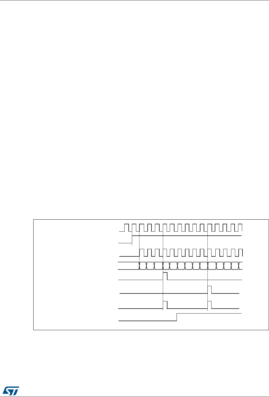
RM0430 Rev 8 543/1324
RM0430 General-purpose timers (TIM2 to TIM5)
594
In this mode, the direction bit (DIR from TIMx_CR1 register) cannot be written. It is updated
by hardware and gives the current direction of the counter.
The update event can be generated at each counter overflow and at each counter underflow
or by setting the UG bit in the TIMx_EGR register (by software or by using the slave mode
controller) also generates an update event. In this case, the counter restarts counting from
0, as well as the counter of the prescaler.
The UEV update event can be disabled by software by setting the UDIS bit in TIMx_CR1
register. This is to avoid updating the shadow registers while writing new values in the
preload registers. Then no update event occurs until the UDIS bit has been written to 0.
However, the counter continues counting up and down, based on the current auto-reload
value.
In addition, if the URS bit (update request selection) in TIMx_CR1 register is set, setting the
UG bit generates an update event UEV but without setting the UIF flag (thus no interrupt or
DMA request is sent). This is to avoid generating both update and capture interrupt when
clearing the counter on the capture event.
When an update event occurs, all the registers are updated and the update flag (UIF bit in
TIMx_SR register) is set (depending on the URS bit):
•The buffer of the prescaler is reloaded with the preload value (content of the TIMx_PSC
register).
•The auto-reload active register is updated with the preload value (content of the
TIMx_ARR register). Note that if the update source is a counter overflow, the auto-
reload is updated before the counter is reloaded, so that the next period is the expected
one (the counter is loaded with the new value).
The following figures show some examples of the counter behavior for different clock
frequencies.
Figure 149. Counter timing diagram, internal clock divided by 1, TIMx_ARR=0x6
1. Here, center-aligned mode 1 is used (for more details refer to Section 18.4.1: TIMx control register 1 (TIMx_CR1)
on page 572).
069
&.B,17
7LPHUFORFN &.B&17
&RXQWHUUHJLVWHU
8SGDWHHYHQW8(9
&RXQWHURYHUIORZ
8SGDWHLQWHUUXSWIODJ8,)
&17B(1
&RXQWHUXQGHUIORZ
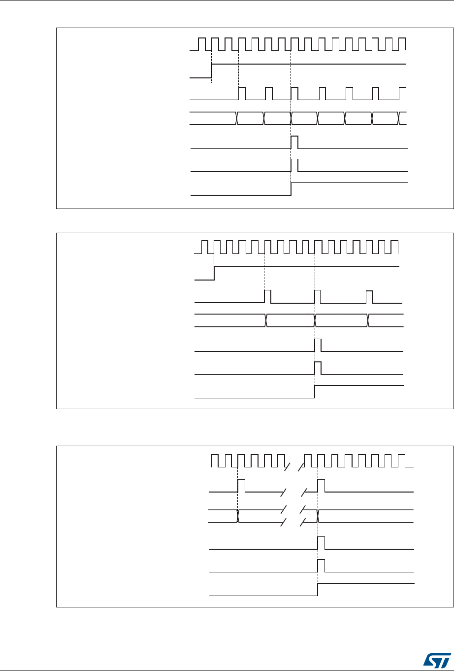
General-purpose timers (TIM2 to TIM5) RM0430
544/1324 RM0430 Rev 8
Figure 150. Counter timing diagram, internal clock divided by 2
Figure 151. Counter timing diagram, internal clock divided by 4, TIMx_ARR=0x36
1. Center-aligned mode 2 or 3 is used with an UIF on overflow.
Figure 152. Counter timing diagram, internal clock divided by N
069
&.B,17
7LPHUFORFN &.B&17
&RXQWHUUHJLVWHU
8SGDWHHYHQW8(9
8SGDWHLQWHUUXSWIODJ8,)
&17B(1
&RXQWHUXQGHUIORZ
069
&.B,17
7LPHUFORFN &.B&17
&RXQWHUUHJLVWHU
8SGDWHHYHQW8(9
&RXQWHURYHUIORZFQWBRYI
8SGDWHLQWHUUXSWIODJ8,)
&17B(1
069
&.B,17
7LPHUFORFN &.B&17
&RXQWHUUHJLVWHU
8SGDWHHYHQW8(9
8SGDWHLQWHUUXSWIODJ8,)
&RXQWHUXQGHUIORZ
)
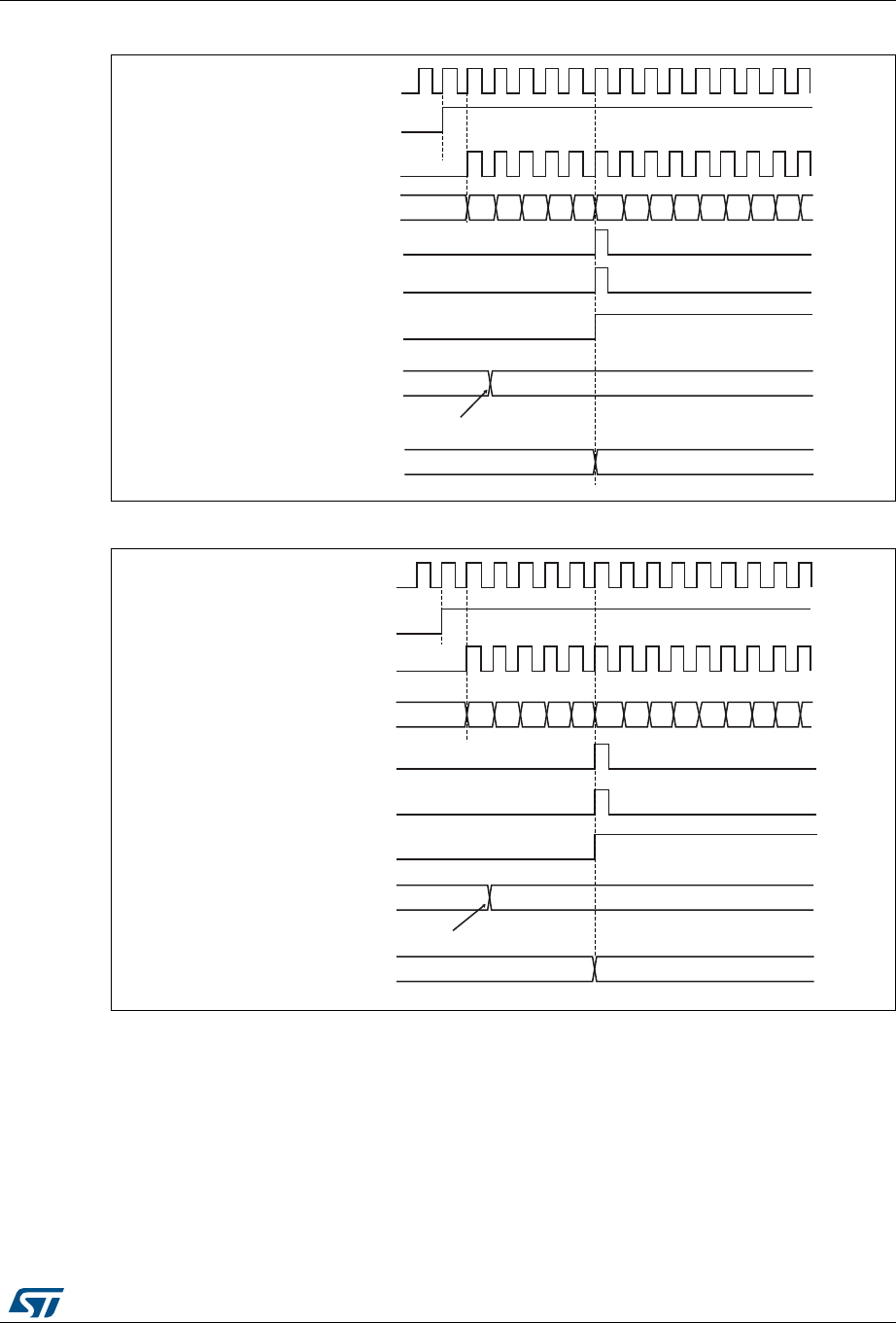
RM0430 Rev 8 545/1324
RM0430 General-purpose timers (TIM2 to TIM5)
594
Figure 153. Counter timing diagram, Update event with ARPE=1 (counter underflow)
Figure 154. Counter timing diagram, Update event with ARPE=1 (counter overflow)
069
)'
&.B,17
7LPHUFORFN &.B&17
&RXQWHUUHJLVWHU
8SGDWHHYHQW8(9
&RXQWHUXQGHUIORZ
8SGDWHLQWHUUXSWIODJ8,)
&17B(1
$XWRUHORDGSUHORDGUHJLVWHU
:ULWHDQHZYDOXHLQ7,0[B$55
)'
$XWRUHORDGDFWLYHUHJLVWHU
069
)'
&.B,17
7LPHUFORFN &.B&17
&RXQWHUUHJLVWHU
8SGDWHHYHQW8(9
&RXQWHURYHUIORZ
8SGDWHLQWHUUXSWIODJ8,)
)) ) )$ )% )&)
&17B(1
$XWRUHORDGSUHORDGUHJLVWHU
:ULWHDQHZYDOXHLQ7,0[B$55
$XWRUHORDGDFWLYHUHJLVWHU )'
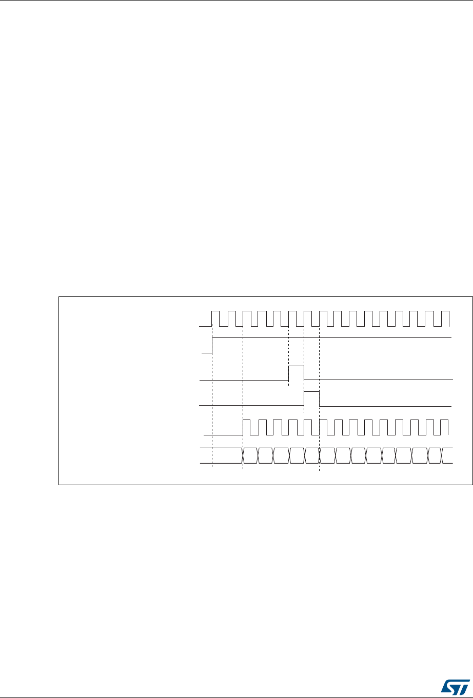
General-purpose timers (TIM2 to TIM5) RM0430
546/1324 RM0430 Rev 8
18.3.3 Clock selection
The counter clock can be provided by the following clock sources:
•Internal clock (CK_INT)
•External clock mode1: external input pin (TIx)
•External clock mode2: external trigger input (ETR) available on TIM2, TIM3 and TIM4
only.
•Internal trigger inputs (ITRx): using one timer as prescaler for another timer, for
example, you can configure Timer to act as a prescaler for Timer 2. Refer to Using one
timer as prescaler for another for more details.
Internal clock source (CK_INT)
If the slave mode controller is disabled (SMS=000 in the TIMx_SMCR register), then the
CEN, DIR (in the TIMx_CR1 register) and UG bits (in the TIMx_EGR register) are actual
control bits and can be changed only by software (except UG which remains cleared
automatically). As soon as the CEN bit is written to 1, the prescaler is clocked by the internal
clock CK_INT.
Figure 155 shows the behavior of the control circuit and the upcounter in normal mode,
without prescaler.
Figure 155. Control circuit in normal mode, internal clock divided by 1
External clock source mode 1
This mode is selected when SMS=111 in the TIMx_SMCR register. The counter can count at
each rising or falling edge on a selected input.
,QWHUQDOFORFN
&RXQWHUFORFN &.B&17 &.B36&
&RXQWHUUHJLVWHU
&(1 &17B(1
8*
&17B,1,7
069
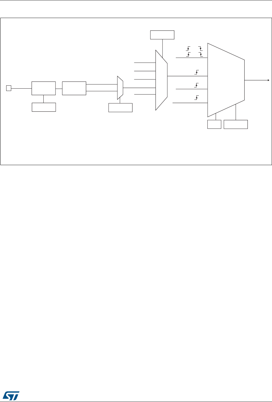
RM0430 Rev 8 547/1324
RM0430 General-purpose timers (TIM2 to TIM5)
594
Figure 156. TI2 external clock connection example
For example, to configure the upcounter to count in response to a rising edge on the TI2
input, use the following procedure:
1. Configure channel 2 to detect rising edges on the TI2 input by writing CC2S= ‘01 in the
TIMx_CCMR1 register.
2. Configure the input filter duration by writing the IC2F[3:0] bits in the TIMx_CCMR1
register (if no filter is needed, keep IC2F=0000).
Note: The capture prescaler is not used for triggering, so you don’t need to configure it.
3. Select rising edge polarity by writing CC2P=0 and CC2NP=0 in the TIMx_CCER
register.
4. Configure the timer in external clock mode 1 by writing SMS=111 in the TIMx_SMCR
register.
5. Select TI2 as the input source by writing TS=110 in the TIMx_SMCR register.
6. Enable the counter by writing CEN=1 in the TIMx_CR1 register.
When a rising edge occurs on TI2, the counter counts once and the TIF flag is set.
The delay between the rising edge on TI2 and the actual clock of the counter is due to the
resynchronization circuit on TI2 input.
([WHUQDOFORFN
PRGH
,QWHUQDOFORFN
PRGH
75*,
&.B,17
&.B36&
7,0[B60&5
606>@
,75[
7,B('
7,)3
7,)3
7,0[B60&5
76>@
7,
7,0[B&&(5
&&3
)LOWHU
,&)>@
7,0[B&&05
(GJH
GHWHFWRU
7,)B5LVLQJ
7,)B)DOOLQJ
[[
069
LQWHUQDOFORFN
7,) RU
7,) RU
RU
(QFRGHU
PRGH
(75)
([WHUQDOFORFN
PRGH
(75)
(&(
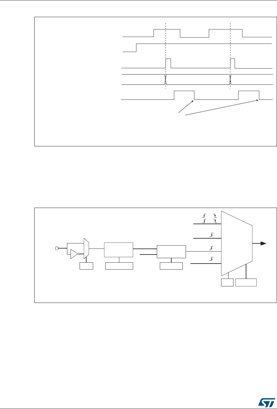
General-purpose timers (TIM2 to TIM5) RM0430
548/1324 RM0430 Rev 8
Figure 157. Control circuit in external clock mode 1
External clock source mode 2
This mode is selected by writing ECE=1 in the TIMx_SMCR register.
The counter can count at each rising or falling edge on the external trigger input ETR.
Figure 158 gives an overview of the external trigger input block.
Figure 158. External trigger input block
For example, to configure the upcounter to count each 2 rising edges on ETR, use the
following procedure:
1. As no filter is needed in this example, write ETF[3:0]=0000 in the TIMx_SMCR register.
2. Set the prescaler by writing ETPS[1:0]=01 in the TIMx_SMCR register
3. Select rising edge detection on the ETR pin by writing ETP=0 in the TIMx_SMCR
register
4. Enable external clock mode 2 by writing ECE=1 in the TIMx_SMCR register.
5. Enable the counter by writing CEN=1 in the TIMx_CR1 register.
The counter counts once each 2 ETR rising edges.
&RXQWHUFORFN &.B&17 &.B36&
&RXQWHUUHJLVWHU
7,
&17B(1
7,)
:ULWH7,)
069
069
75*,
&.B,17
7,0[B60&5
606>@
LQWHUQDOFORFN
7,) RU
7,) RU
RU (QFRGHU
PRGH
(75)
(&(
7,0[B60&5
(73
(75SLQ
(75
'LYLGHU
)LOWHU
GRZQFRXQWHU
&.B,17
(753
7,0[B60&5
(736>@
7,0[B60&5
(7)>@
([WHUQDOFORFN
PRGH
([WHUQDOFORFN
PRGH
,QWHUQDOFORFN
PRGH
&.B36&
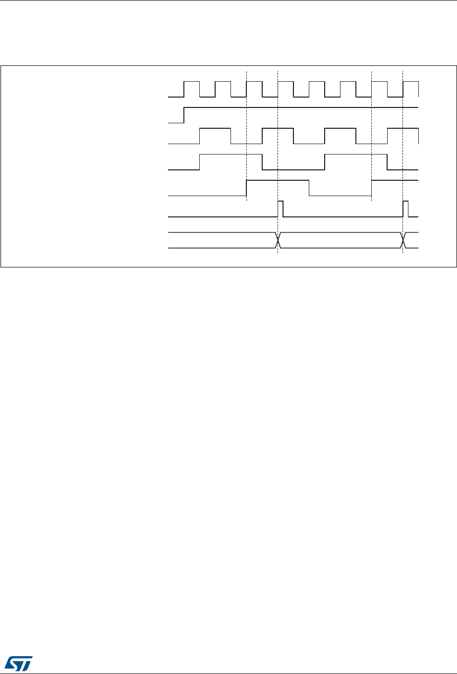
RM0430 Rev 8 549/1324
RM0430 General-purpose timers (TIM2 to TIM5)
594
The delay between the rising edge on ETR and the actual clock of the counter is due to the
resynchronization circuit on the ETRP signal.
Figure 159. Control circuit in external clock mode 2
18.3.4 Capture/compare channels
Each Capture/Compare channel is built around a capture/compare register (including a
shadow register), a input stage for capture (with digital filter, multiplexing and prescaler) and
an output stage (with comparator and output control).
The following figure gives an overview of one Capture/Compare channel.
The input stage samples the corresponding TIx input to generate a filtered signal TIxF.
Then, an edge detector with polarity selection generates a signal (TIxFPx) which can be
used as trigger input by the slave mode controller or as the capture command. It is
prescaled before the capture register (ICxPS).
069
&17B(1
(75
(753
(75)
&RXQWHUFORFN &.B,17 &.B36&
&RXQWHUUHJLVWHU
&.B,17
General-purpose timers (TIM2 to TIM5) RM0430
550/1324 RM0430 Rev 8
Figure 160. Capture/compare channel (example: channel 1 input stage)
The output stage generates an intermediate waveform which is then used for reference:
OCxRef (active high). The polarity acts at the end of the chain.
Figure 161. Capture/compare channel 1 main circuit
'LYLGHU
,&36>@
7,)B('
7RWKHVODYHPRGHFRQWUROOHU
7,)3
&&6>@
,&
7,)3
75&
IURPVODYHPRGH
FRQWUROOHU
,&36
069
7,
7,0[B&&(5
&&3&&13
)LOWHU
GRZQFRXQWHU
,&)>@
7,0[B&&05
(GJH
GHWHFWRU
7,)B5LVLQJ
7,)B)DOOLQJ
7,0[B&&05
7,0[B&&(5
7,)B5LVLQJ
IURPFKDQQHO
7,)B)DOOLQJ
IURPFKDQQHO
7,)
I
&&(
'76
&&(
&DSWXUHFRPSDUHVKDGRZUHJLVWHU
&RPSDUDWRU
&DSWXUHFRPSDUHSUHORDGUHJLVWHU
&RXQWHU
,&36
&&6>@
&&6>@
&DSWXUH
,QSXW
PRGH
6
5
5HDG&&5+
5HDG&&5/
UHDGBLQBSURJUHVV
FDSWXUHBWUDQVIHU &&6>@
&&6>@
6
5
ZULWH&&5+
ZULWH&&5/
ZULWHBLQBSURJUHVV
2XWSXW
PRGH
8(9
2&3(
IURPWLPH
EDVHXQLW
FRPSDUHBWUDQVIHU
$3%%XV
KLJK
ORZ
LIELW
0&8SHULSKHUDOLQWHUIDFH
7,0[B&&05
2&3(
&17!&&5
&17 &&5
7,0[B(*5
&&*
069
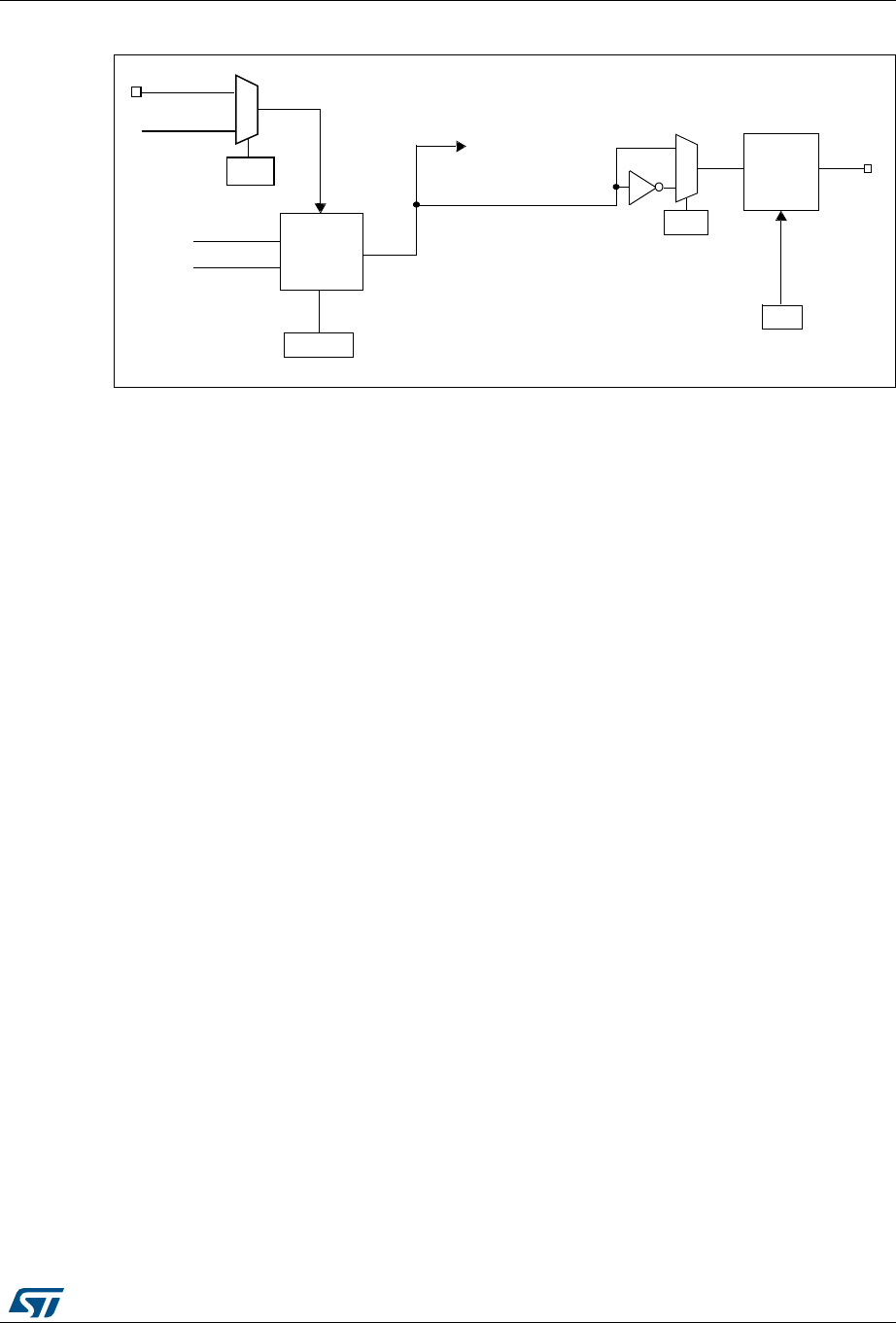
RM0430 Rev 8 551/1324
RM0430 General-purpose timers (TIM2 to TIM5)
594
Figure 162. Output stage of capture/compare channel (channel 1)
The capture/compare block is made of one preload register and one shadow register. Write
and read always access the preload register.
In capture mode, captures are actually done in the shadow register, which is copied into the
preload register.
In compare mode, the content of the preload register is copied into the shadow register
which is compared to the counter.
18.3.5 Input capture mode
In Input capture mode, the Capture/Compare Registers (TIMx_CCRx) are used to latch the
value of the counter after a transition detected by the corresponding ICx signal. When a
capture occurs, the corresponding CCXIF flag (TIMx_SR register) is set and an interrupt or
a DMA request can be sent if they are enabled. If a capture occurs while the CCxIF flag was
already high, then the over-capture flag CCxOF (TIMx_SR register) is set. CCxIF can be
cleared by software by writing it to 0 or by reading the captured data stored in the
TIMx_CCRx register. CCxOF is cleared when you write it to 0.
The following example shows how to capture the counter value in TIMx_CCR1 when TI1
input rises. To do this, use the following procedure:
•Select the active input: TIMx_CCR1 must be linked to the TI1 input, so write the CC1S
bits to 01 in the TIMx_CCMR1 register. As soon as CC1S becomes different from 00,
the channel is configured in input and the TIMx_CCR1 register becomes read-only.
•Program the input filter duration you need with respect to the signal you connect to the
timer (by programming the ICxF bits in the TIMx_CCMRx register if the input is one of
the TIx inputs). Let’s imagine that, when toggling, the input signal is not stable during at
must 5 internal clock cycles. We must program a filter duration longer than these 5
clock cycles. We can validate a transition on TI1 when 8 consecutive samples with the
KƵƚƉƵƚŵŽĚĞ
EdхZϭ
EdсZϭ ĐŽŶƚƌŽůůĞƌ
d/DdžͺDZϭ
KϭDϮ͗Ϭ
ŽĐϭƌĞĨ
Ϭ
ϭ
ϭW
d/DdžͺZ
KƵƚƉƵƚ
ŶĂďůĞ
ŝƌĐƵŝƚ
Kϭ
ϭ
d/DdžͺZ
dŽƚŚĞŵĂƐƚĞƌŵŽĚĞ
ĐŽŶƚƌŽůůĞƌ
dZ&
Ϭ
ϭ
KZ&ͺ>Z
KZ&ͺ>Zͺ/Ed
K^
d/Ddžͺ^DZ
Ăŝϭϳϭϴϳ

General-purpose timers (TIM2 to TIM5) RM0430
552/1324 RM0430 Rev 8
new level have been detected (sampled at fDTS frequency). Then write IC1F bits to
0011 in the TIMx_CCMR1 register.
•Select the edge of the active transition on the TI1 channel by writing the CC1P and
CC1NP bits to 00 in the TIMx_CCER register (rising edge in this case).
•Program the input prescaler. In our example, we wish the capture to be performed at
each valid transition, so the prescaler is disabled (write IC1PS bits to 00 in the
TIMx_CCMR1 register).
•Enable capture from the counter into the capture register by setting the CC1E bit in the
TIMx_CCER register.
•If needed, enable the related interrupt request by setting the CC1IE bit in the
TIMx_DIER register, and/or the DMA request by setting the CC1DE bit in the
TIMx_DIER register.
When an input capture occurs:
•The TIMx_CCR1 register gets the value of the counter on the active transition.
•CC1IF flag is set (interrupt flag). CC1OF is also set if at least two consecutive captures
occurred whereas the flag was not cleared.
•An interrupt is generated depending on the CC1IE bit.
•A DMA request is generated depending on the CC1DE bit.
In order to handle the overcapture, it is recommended to read the data before the
overcapture flag. This is to avoid missing an overcapture which could happen after reading
the flag and before reading the data.
Note: IC interrupt and/or DMA requests can be generated by software by setting the
corresponding CCxG bit in the TIMx_EGR register.
18.3.6 PWM input mode
This mode is a particular case of input capture mode. The procedure is the same except:
•Two ICx signals are mapped on the same TIx input.
•These 2 ICx signals are active on edges with opposite polarity.
•One of the two TIxFP signals is selected as trigger input and the slave mode controller
is configured in reset mode.
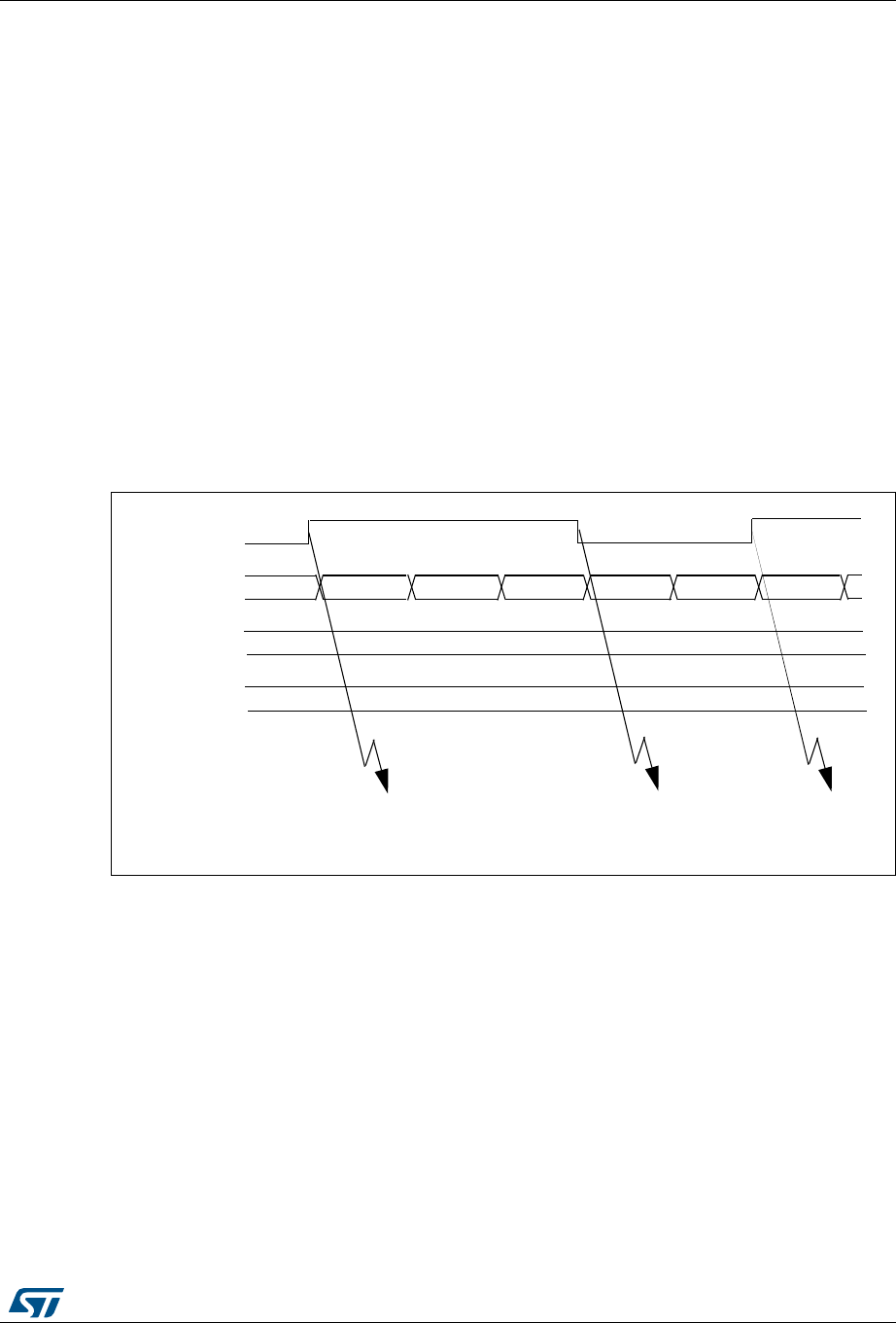
RM0430 Rev 8 553/1324
RM0430 General-purpose timers (TIM2 to TIM5)
594
For example, you can measure the period (in TIMx_CCR1 register) and the duty cycle (in
TIMx_CCR2 register) of the PWM applied on TI1 using the following procedure (depending
on CK_INT frequency and prescaler value):
•Select the active input for TIMx_CCR1: write the CC1S bits to 01 in the TIMx_CCMR1
register (TI1 selected).
•Select the active polarity for TI1FP1 (used both for capture in TIMx_CCR1 and counter
clear): write the CC1P to ‘0’ and the CC1NP bit to ‘0’ (active on rising edge).
•Select the active input for TIMx_CCR2: write the CC2S bits to 10 in the TIMx_CCMR1
register (TI1 selected).
•Select the active polarity for TI1FP2 (used for capture in TIMx_CCR2): write the CC2P
bit to ‘1’ and the CC2NP bit to ’0’(active on falling edge).
•Select the valid trigger input: write the TS bits to 101 in the TIMx_SMCR register
(TI1FP1 selected).
•Configure the slave mode controller in reset mode: write the SMS bits to 100 in the
TIMx_SMCR register.
•Enable the captures: write the CC1E and CC2E bits to ‘1 in the TIMx_CCER register.
Figure 163. PWM input mode timing
18.3.7 Forced output mode
In output mode (CCxS bits = 00 in the TIMx_CCMRx register), each output compare signal
(OCxREF and then OCx) can be forced to active or inactive level directly by software,
independently of any comparison between the output compare register and the counter.
To force an output compare signal (ocxref/OCx) to its active level, you just need to write 101
in the OCxM bits in the corresponding TIMx_CCMRx register. Thus ocxref is forced high
(OCxREF is always active high) and OCx get opposite value to CCxP polarity bit.
e.g.: CCxP=0 (OCx active high) => OCx is forced to high level.
ocxref signal can be forced low by writing the OCxM bits to 100 in the TIMx_CCMRx
register.
TI1
TIMx_CNT 0000 0001 0002 0003 0004 00000004
TIMx_CCR1
TIMx_CCR2
0004
0002
IC1 capture
IC2 capture
reset counter
IC2 capture
pulse width
IC1 capture
period
measurementmeasurement
ai15413

General-purpose timers (TIM2 to TIM5) RM0430
554/1324 RM0430 Rev 8
Anyway, the comparison between the TIMx_CCRx shadow register and the counter is still
performed and allows the flag to be set. Interrupt and DMA requests can be sent
accordingly. This is described in the Output Compare Mode section.
18.3.8 Output compare mode
This function is used to control an output waveform or indicating when a period of time has
elapsed.
When a match is found between the capture/compare register and the counter, the output
compare function:
•Assigns the corresponding output pin to a programmable value defined by the output
compare mode (OCxM bits in the TIMx_CCMRx register) and the output polarity (CCxP
bit in the TIMx_CCER register). The output pin can keep its level (OCXM=000), be set
active (OCxM=001), be set inactive (OCxM=010) or can toggle (OCxM=011) on match.
•Sets a flag in the interrupt status register (CCxIF bit in the TIMx_SR register).
•Generates an interrupt if the corresponding interrupt mask is set (CCXIE bit in the
TIMx_DIER register).
•Sends a DMA request if the corresponding enable bit is set (CCxDE bit in the
TIMx_DIER register, CCDS bit in the TIMx_CR2 register for the DMA request
selection).
The TIMx_CCRx registers can be programmed with or without preload registers using the
OCxPE bit in the TIMx_CCMRx register.
In output compare mode, the update event UEV has no effect on ocxref and OCx output.
The timing resolution is one count of the counter. Output compare mode can also be used to
output a single pulse (in One-pulse mode).
Procedure:
1. Select the counter clock (internal, external, prescaler).
2. Write the desired data in the TIMx_ARR and TIMx_CCRx registers.
3. Set the CCxIE and/or CCxDE bits if an interrupt and/or a DMA request is to be
generated.
4. Select the output mode. For example, you must write OCxM=011, OCxPE=0, CCxP=0
and CCxE=1 to toggle OCx output pin when CNT matches CCRx, CCRx preload is not
used, OCx is enabled and active high.
5. Enable the counter by setting the CEN bit in the TIMx_CR1 register.
The TIMx_CCRx register can be updated at any time by software to control the output
waveform, provided that the preload register is not enabled (OCxPE=0, else TIMx_CCRx
shadow register is updated only at the next update event UEV). An example is given in
Figure 164.

RM0430 Rev 8 555/1324
RM0430 General-purpose timers (TIM2 to TIM5)
594
Figure 164. Output compare mode, toggle on OC1
18.3.9 PWM mode
Pulse width modulation mode allows you to generate a signal with a frequency determined
by the value of the TIMx_ARR register and a duty cycle determined by the value of the
TIMx_CCRx register.
The PWM mode can be selected independently on each channel (one PWM per OCx
output) by writing 110 (PWM mode 1) or ‘111 (PWM mode 2) in the OCxM bits in the
TIMx_CCMRx register. You must enable the corresponding preload register by setting the
OCxPE bit in the TIMx_CCMRx register, and eventually the auto-reload preload register by
setting the ARPE bit in the TIMx_CR1 register.
As the preload registers are transferred to the shadow registers only when an update event
occurs, before starting the counter, you have to initialize all the registers by setting the UG
bit in the TIMx_EGR register.
OCx polarity is software programmable using the CCxP bit in the TIMx_CCER register. It
can be programmed as active high or active low. OCx output is enabled by the CCxE bit in
the TIMx_CCER register. Refer to the TIMx_CCERx register description for more details.
In PWM mode (1 or 2), TIMx_CNT and TIMx_CCRx are always compared to determine
whether TIMx_CCRx ≤ TIMx_CNT or TIMx_CNT ≤ TIMx_CCRx (depending on the direction
of the counter). However, to comply with the ETRF (OCREF can be cleared by an external
event through the ETR signal until the next PWM period), the OCREF signal is asserted
only:
•When the result of the comparison changes, or
•When the output compare mode (OCxM bits in TIMx_CCMRx register) switches from
the “frozen” configuration (no comparison, OCxM=‘000) to one of the PWM modes
(OCxM=‘110 or ‘111).
This forces the PWM by software while the timer is running.
The timer is able to generate PWM in edge-aligned mode or center-aligned mode
depending on the CMS bits in the TIMx_CR1 register.
069
2&5() 2&
7,0[B&17 % %
7,0[B&&5 $
:ULWH%KLQWKH&&5UHJLVWHU
0DWFKGHWHFWHGRQ&&5
,QWHUUXSWJHQHUDWHGLIHQDEOHG
%
%
$
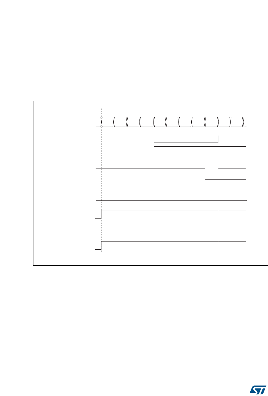
General-purpose timers (TIM2 to TIM5) RM0430
556/1324 RM0430 Rev 8
PWM edge-aligned mode
Upcounting configuration
Upcounting is active when the DIR bit in the TIMx_CR1 register is low. Refer to Upcounting
mode on page 537.
In the following example, we consider PWM mode 1. The reference PWM signal OCxREF is
high as long as TIMx_CNT <TIMx_CCRx else it becomes low. If the compare value in
TIMx_CCRx is greater than the auto-reload value (in TIMx_ARR) then OCxREF is held at ‘1.
If the compare value is 0 then OCxREF is held at ‘0. Figure 165 shows some edge-aligned
PWM waveforms in an example where TIMx_ARR=8.
Figure 165. Edge-aligned PWM waveforms (ARR=8)
Downcounting configuration
Downcounting is active when DIR bit in TIMx_CR1 register is high. Refer to Downcounting
mode on page 540.
In PWM mode 1, the reference signal ocxref is low as long as TIMx_CNT>TIMx_CCRx else
it becomes high. If the compare value in TIMx_CCRx is greater than the auto-reload value in
TIMx_ARR, then ocxref is held at ‘1. 0% PWM is not possible in this mode.
PWM center-aligned mode
Center-aligned mode is active when the CMS bits in TIMx_CR1 register are different from
‘00 (all the remaining configurations having the same effect on the ocxref/OCx signals). The
compare flag is set when the counter counts up, when it counts down or both when it counts
up and down depending on the CMS bits configuration. The direction bit (DIR) in the
TIMx_CR1 register is updated by hardware and must not be changed by software. Refer to
069
&RXQWHUUHJLVWHU
µ
2&;5()
&&[,)
2&;5()
&&[,)
2&;5()
&&[,)
2&;5()
&&[,)
&&5[
&&5[
&&5[!
&&5[
µ
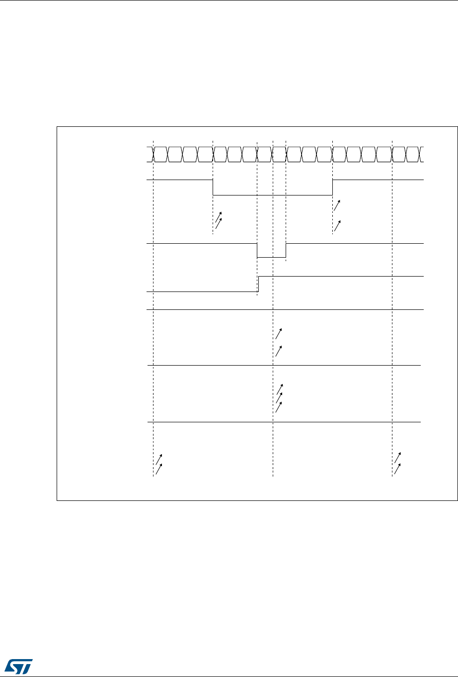
RM0430 Rev 8 557/1324
RM0430 General-purpose timers (TIM2 to TIM5)
594
Center-aligned mode (up/down counting) on page 542.
Figure 166 shows some center-aligned PWM waveforms in an example where:
•TIMx_ARR=8,
•PWM mode is the PWM mode 1,
•The flag is set when the counter counts down corresponding to the center-aligned
mode 1 selected for CMS=01 in TIMx_CR1 register.
Figure 166. Center-aligned PWM waveforms (ARR=8)
Hints on using center-aligned mode:
•When starting in center-aligned mode, the current up-down configuration is used. It
means that the counter counts up or down depending on the value written in the DIR bit
&&[,)
&RXQWHUUHJLVWHU
&&5[
2&[5()
&06
&06
&06
&&[,)
&&5[
2&[5()
&06 RU
&&[,)
&&5[
2&[5()
&06
&06
&06
µ
&&[,)
&&5[!
2&[5()
&06
&06
&06
µ
&&[,)
&&5[
2&[5()
&06
&06
&06
µ
$,E
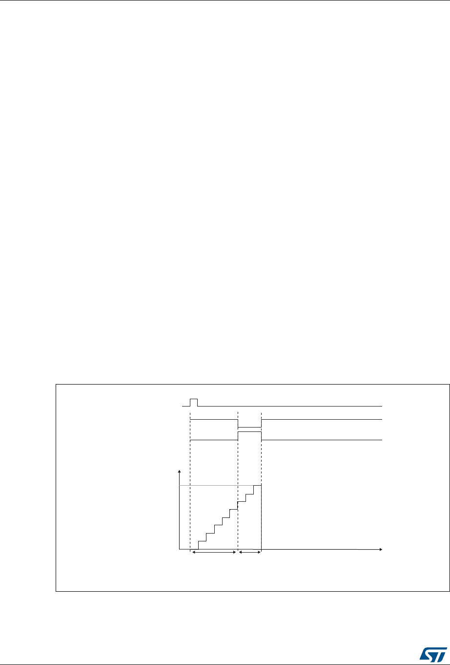
General-purpose timers (TIM2 to TIM5) RM0430
558/1324 RM0430 Rev 8
in the TIMx_CR1 register. Moreover, the DIR and CMS bits must not be changed at the
same time by the software.
•Writing to the counter while running in center-aligned mode is not recommended as it
can lead to unexpected results. In particular:
– The direction is not updated if you write a value in the counter that is greater than
the auto-reload value (TIMx_CNT>TIMx_ARR). For example, if the counter was
counting up, it continues to count up.
– The direction is updated if you write 0 or write the TIMx_ARR value in the counter
but no Update Event UEV is generated.
•The safest way to use center-aligned mode is to generate an update by software
(setting the UG bit in the TIMx_EGR register) just before starting the counter and not to
write the counter while it is running.
18.3.10 One-pulse mode
One-pulse mode (OPM) is a particular case of the previous modes. It allows the counter to
be started in response to a stimulus and to generate a pulse with a programmable length
after a programmable delay.
Starting the counter can be controlled through the slave mode controller. Generating the
waveform can be done in output compare mode or PWM mode. You select One-pulse mode
by setting the OPM bit in the TIMx_CR1 register. This makes the counter stop automatically
at the next update event UEV.
A pulse can be correctly generated only if the compare value is different from the counter
initial value. Before starting (when the timer is waiting for the trigger), the configuration must
be:
•In upcounting: CNT<CCRx ≤ ARR (in particular, 0<CCRx),
•In downcounting: CNT>CCRx.
Figure 167. Example of one-pulse mode
For example you may want to generate a positive pulse on OC1 with a length of tPULSE and
after a delay of tDELAY as soon as a positive edge is detected on the TI2 input pin.
069
7,
2&5()
&RXQWHU
W
7,0B$55
7,0B&&5
2&
W'(/$< W38/6(

RM0430 Rev 8 559/1324
RM0430 General-purpose timers (TIM2 to TIM5)
594
Let’s use TI2FP2 as trigger 1:
•Map TI2FP2 on TI2 by writing CC2S=01 in the TIMx_CCMR1 register.
•TI2FP2 must detect a rising edge, write CC2P=0 and CC2NP=’0’ in the TIMx_CCER
register.
•Configure TI2FP2 as trigger for the slave mode controller (TRGI) by writing TS=110 in
the TIMx_SMCR register.
•TI2FP2 is used to start the counter by writing SMS to ‘110 in the TIMx_SMCR register
(trigger mode).
The OPM waveform is defined by writing the compare registers (taking into account the
clock frequency and the counter prescaler).
•The tDELAY is defined by the value written in the TIMx_CCR1 register.
•The tPULSE is defined by the difference between the auto-reload value and the compare
value (TIMx_ARR - TIMx_CCR + 1).
•Let’s say you want to build a waveform with a transition from ‘0 to ‘1 when a compare
match occurs and a transition from ‘1 to ‘0 when the counter reaches the auto-reload
value. To do this you enable PWM mode 2 by writing OC1M=111 in the TIMx_CCMR1
register. You can optionally enable the preload registers by writing OC1PE=1 in the
TIMx_CCMR1 register and ARPE in the TIMx_CR1 register. In this case you have to
write the compare value in the TIMx_CCR1 register, the auto-reload value in the
TIMx_ARR register, generate an update by setting the UG bit and wait for external
trigger event on TI2. CC1P is written to ‘0 in this example.
In our example, the DIR and CMS bits in the TIMx_CR1 register should be low.
You only want 1 pulse (Single mode), so you write '1 in the OPM bit in the TIMx_CR1
register to stop the counter at the next update event (when the counter rolls over from the
auto-reload value back to 0). When OPM bit in the TIMx_CR1 register is set to '0', so the
Repetitive Mode is selected.
Particular case: OCx fast enable:
In One-pulse mode, the edge detection on TIx input set the CEN bit which enables the
counter. Then the comparison between the counter and the compare value makes the
output toggle. But several clock cycles are needed for these operations and it limits the
minimum delay tDELAY min we can get.
If you want to output a waveform with the minimum delay, you can set the OCxFE bit in the
TIMx_CCMRx register. Then OCxRef (and OCx) is forced in response to the stimulus,
without taking in account the comparison. Its new level is the same as if a compare match
had occurred. OCxFE acts only if the channel is configured in PWM1 or PWM2 mode.
18.3.11 Clearing the OCxREF signal on an external event
The OCxREF signal for a given channel can be driven Low by applying a High level to the
ETRF input (OCxCE enable bit of the corresponding TIMx_CCMRx register set to '1'). The
OCxREF signal remains Low until the next update event, UEV, occurs.
This function can only be used in output compare and PWM modes, and does not work in
forced mode.
For example, the ETR signal can be connected to the output of a comparator to be used for
current handling. In this case, ETR must be configured as follows:
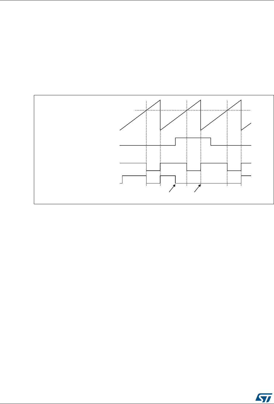
General-purpose timers (TIM2 to TIM5) RM0430
560/1324 RM0430 Rev 8
1. The external trigger prescaler should be kept off: bits ETPS[1:0] in the TIMx_SMCR
register are cleared to 00.
2. The external clock mode 2 must be disabled: bit ECE in the TIM1_SMCR register is
cleared to 0.
3. The external trigger polarity (ETP) and the external trigger filter (ETF) can be
configured according to the application’s needs.
Figure 168 shows the behavior of the OCxREF signal when the ETRF input becomes high,
for both values of the OCxCE enable bit. In this example, the timer TIMx is programmed in
PWM mode.
Figure 168. Clearing TIMx OCxREF
1. In case of a PWM with a 100% duty cycle (if CCRx>ARR), OCxREF is enabled again at the next counter
overflow.
18.3.12 Encoder interface mode
To select Encoder Interface mode write SMS=‘001 in the TIMx_SMCR register if the counter
is counting on TI2 edges only, SMS=010 if it is counting on TI1 edges only and SMS=011 if
it is counting on both TI1 and TI2 edges.
Select the TI1 and TI2 polarity by programming the CC1P and CC2P bits in the TIMx_CCER
register. When needed, you can program the input filter as well.
The two inputs TI1 and TI2 are used to interface to an incremental encoder. Refer to
Table 105. The counter is clocked by each valid transition on TI1FP1 or TI2FP2 (TI1 and TI2
after input filter and polarity selection, TI1FP1=TI1 if not filtered and not inverted,
TI2FP2=TI2 if not filtered and not inverted) assuming that it is enabled (CEN bit in
TIMx_CR1 register written to ‘1). The sequence of transitions of the two inputs is evaluated
and generates count pulses as well as the direction signal. Depending on the sequence the
counter counts up or down, the DIR bit in the TIMx_CR1 register is modified by hardware
accordingly. The DIR bit is calculated at each transition on any input (TI1 or TI2), whatever
the counter is counting on TI1 only, TI2 only or both TI1 and TI2.
Encoder interface mode acts simply as an external clock with direction selection. This
means that the counter just counts continuously between 0 and the auto-reload value in the
TIMx_ARR register (0 to ARR or ARR down to 0 depending on the direction). So you must
configure TIMx_ARR before starting. In the same way, the capture, compare, prescaler,
trigger output features continue to work as normal.
069
&&5[
&RXQWHU&17
(75)
2&[5()2&[&( µ
2&[5()2&[&( µ
(75)EHFRPHVKLJK (75)VWLOOKLJK

RM0430 Rev 8 561/1324
RM0430 General-purpose timers (TIM2 to TIM5)
594
In this mode, the counter is modified automatically following the speed and the direction of
the incremental encoder and its content, therefore, always represents the encoder’s
position. The count direction correspond to the rotation direction of the connected sensor.
The table summarizes the possible combinations, assuming TI1 and TI2 don’t switch at the
same time.
An external incremental encoder can be connected directly to the MCU without external
interface logic. However, comparators are normally be used to convert the encoder’s
differential outputs to digital signals. This greatly increases noise immunity. The third
encoder output which indicate the mechanical zero position, may be connected to an
external interrupt input and trigger a counter reset.
Figure 169 gives an example of counter operation, showing count signal generation and
direction control. It also shows how input jitter is compensated where both edges are
selected. This might occur if the sensor is positioned near to one of the switching points. For
this example we assume that the configuration is the following:
•CC1S= ‘01’ (TIMx_CCMR1 register, TI1FP1 mapped on TI1)
•CC2S= ‘01’ (TIMx_CCMR2 register, TI2FP2 mapped on TI2)
•CC1P= ‘0’, CC1NP = ‘0’, IC1F =’0000’ (TIMx_CCER register, TI1FP1 noninverted,
TI1FP1=TI1)
•CC2P= ‘0’, CC2NP = ‘0’, IC2F =’0000’ (TIMx_CCER register, TI2FP2 noninverted,
TI2FP2=TI2)
•SMS= ‘011’ (TIMx_SMCR register, both inputs are active on both rising and falling
edges)
•CEN = 1 (TIMx_CR1 register, Counter is enabled)
Table 105. Counting direction versus encoder signals
Active edge
Level on opposite
signal (TI1FP1 for
TI2, TI2FP2 for TI1)
TI1FP1 signal TI2FP2 signal
Rising Falling Rising Falling
Counting on
TI1 only
High Down Up No Count No Count
Low Up Down No Count No Count
Counting on
TI2 only
High No Count No Count Up Down
Low No Count No Count Down Up
Counting on
TI1 and TI2
High Down Up Up Down
Low Up Down Down Up
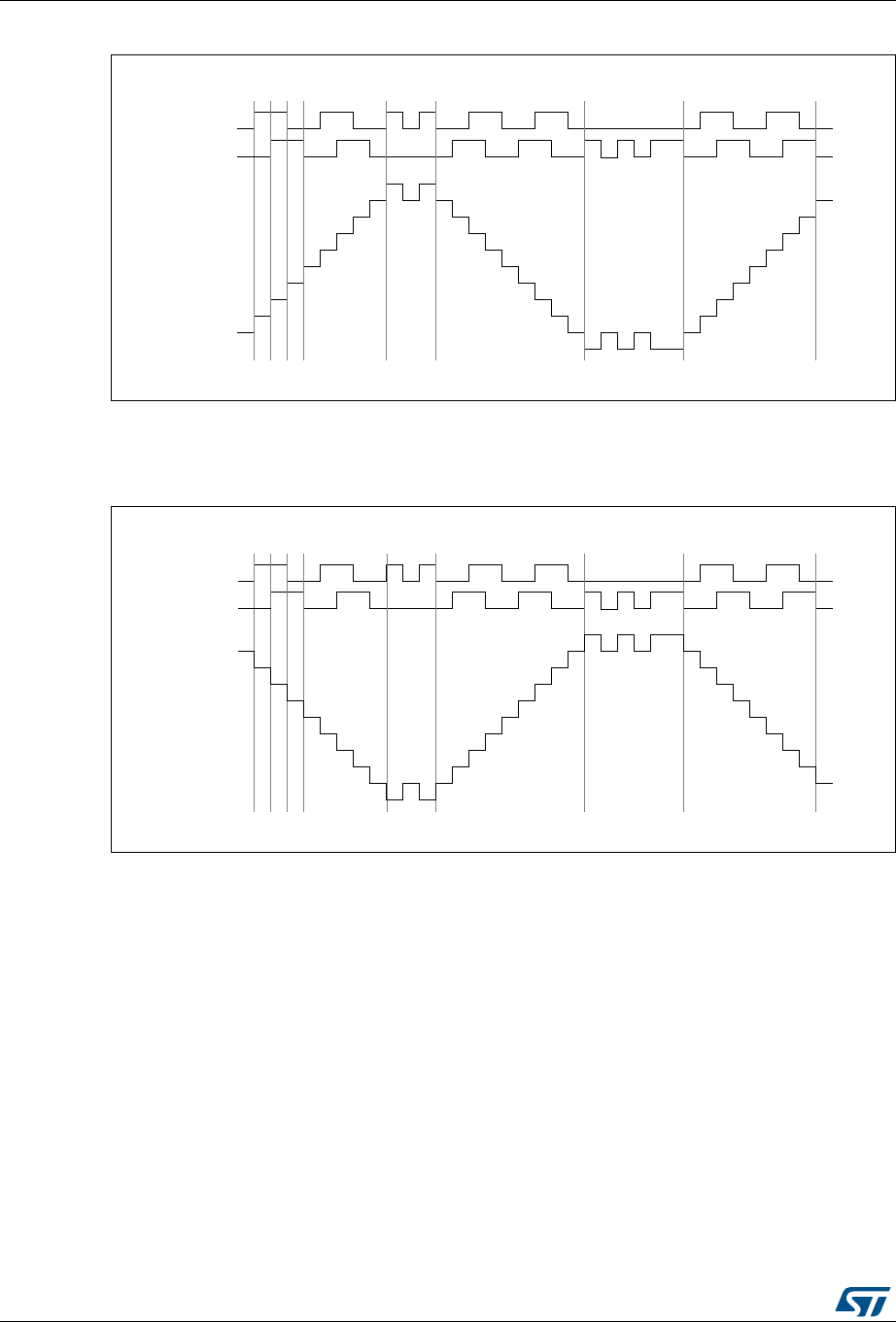
General-purpose timers (TIM2 to TIM5) RM0430
562/1324 RM0430 Rev 8
Figure 169. Example of counter operation in encoder interface mode
Figure 170 gives an example of counter behavior when TI1FP1 polarity is inverted (same
configuration as above except CC1P=1).
Figure 170. Example of encoder interface mode with TI1FP1 polarity inverted
The timer, when configured in Encoder Interface mode provides information on the sensor’s
current position. You can obtain dynamic information (speed, acceleration, deceleration) by
measuring the period between two encoder events using a second timer configured in
capture mode. The output of the encoder which indicates the mechanical zero can be used
for this purpose. Depending on the time between two events, the counter can also be read
at regular times. You can do this by latching the counter value into a third input capture
register if available (then the capture signal must be periodic and can be generated by
another timer). when available, it is also possible to read its value through a DMA request
generated by a Real-Time clock.
7,
EDFNZDUGMLWWHU MLWWHU
XS GRZQ XS
7,
&RXQWHU
IRUZDUG IRUZDUG
069
7,
EDFNZDUGMLWWHU MLWWHU
XSGRZQ
7,
&RXQWHU
IRUZDUG IRUZDUG
069
GRZQ
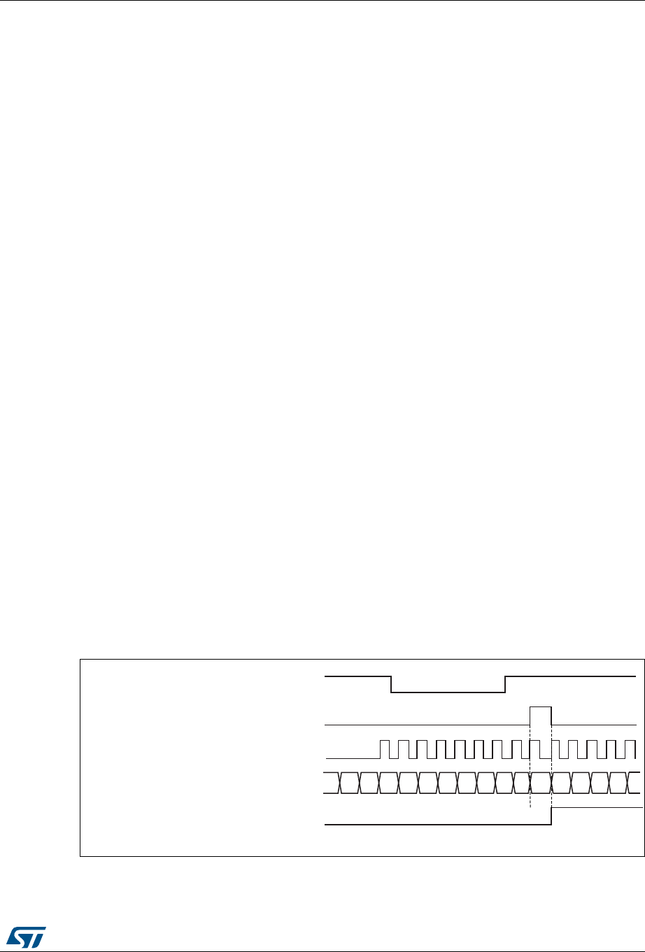
RM0430 Rev 8 563/1324
RM0430 General-purpose timers (TIM2 to TIM5)
594
18.3.13 Timer input XOR function
The TI1S bit in the TIM_CR2 register, allows the input filter of channel 1 to be connected to
the output of a XOR gate, combining the three input pins TIMx_CH1 to TIMx_CH3.
The XOR output can be used with all the timer input functions such as trigger or input
capture.
18.3.14 Timers and external trigger synchronization
The TIMx Timers can be synchronized with an external trigger in several modes: Reset
mode, Gated mode and Trigger mode.
Slave mode: Reset mode
The counter and its prescaler can be reinitialized in response to an event on a trigger input.
Moreover, if the URS bit from the TIMx_CR1 register is low, an update event UEV is
generated. Then all the preloaded registers (TIMx_ARR, TIMx_CCRx) are updated.
In the following example, the upcounter is cleared in response to a rising edge on TI1 input:
•Configure the channel 1 to detect rising edges on TI1. Configure the input filter duration
(in this example, we don’t need any filter, so we keep IC1F=0000). The capture
prescaler is not used for triggering, so you don’t need to configure it. The CC1S bits
select the input capture source only, CC1S = 01 in the TIMx_CCMR1 register. Write
CC1P=0 and CC1NP=0 in TIMx_CCER register to validate the polarity (and detect
rising edges only).
•Configure the timer in reset mode by writing SMS=100 in TIMx_SMCR register. Select
TI1 as the input source by writing TS=101 in TIMx_SMCR register.
•Start the counter by writing CEN=1 in the TIMx_CR1 register.
The counter starts counting on the internal clock, then behaves normally until TI1 rising
edge. When TI1 rises, the counter is cleared and restarts from 0. In the meantime, the
trigger flag is set (TIF bit in the TIMx_SR register) and an interrupt request, or a DMA
request can be sent if enabled (depending on the TIE and TDE bits in TIMx_DIER register).
The following figure shows this behavior when the auto-reload register TIMx_ARR=0x36.
The delay between the rising edge on TI1 and the actual reset of the counter is due to the
resynchronization circuit on TI1 input.
Figure 171. Control circuit in reset mode
069
&RXQWHUFORFN &.B&17 &.B36&
&RXQWHUUHJLVWHU
8*
7,
7,)
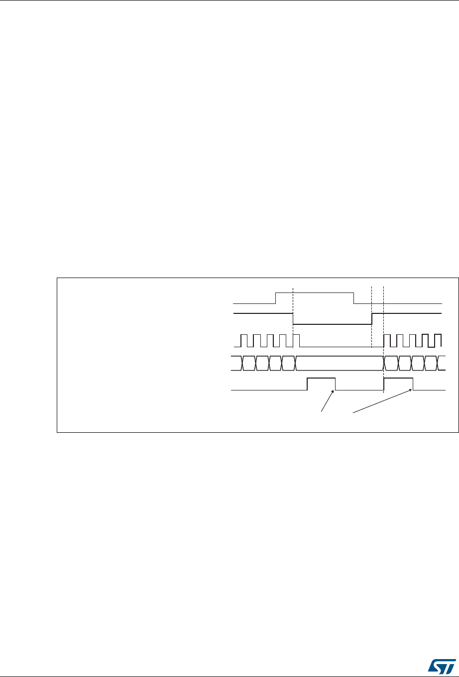
General-purpose timers (TIM2 to TIM5) RM0430
564/1324 RM0430 Rev 8
Slave mode: Gated mode
The counter can be enabled depending on the level of a selected input.
In the following example, the upcounter counts only when TI1 input is low:
•Configure the channel 1 to detect low levels on TI1. Configure the input filter duration
(in this example, we don’t need any filter, so we keep IC1F=0000). The capture
prescaler is not used for triggering, so you don’t need to configure it. The CC1S bits
select the input capture source only, CC1S=01 in TIMx_CCMR1 register. Write
CC1P=1 in TIMx_CCER register to validate the polarity (and detect low level only).
•Configure the timer in gated mode by writing SMS=101 in TIMx_SMCR register. Select
TI1 as the input source by writing TS=101 in TIMx_SMCR register.
•Enable the counter by writing CEN=1 in the TIMx_CR1 register (in gated mode, the
counter doesn’t start if CEN=0, whatever is the trigger input level).
The counter starts counting on the internal clock as long as TI1 is low and stops as soon as
TI1 becomes high. The TIF flag in the TIMx_SR register is set both when the counter starts
or stops.
The delay between the rising edge on TI1 and the actual stop of the counter is due to the
resynchronization circuit on TI1 input.
Figure 172. Control circuit in gated mode
1. The configuration “CCxP=CCxNP=1” (detection of both rising and falling edges) does not have any effect
in gated mode because gated mode acts on a level and not on an edge.
Slave mode: Trigger mode
The counter can start in response to an event on a selected input.
In the following example, the upcounter starts in response to a rising edge on TI2 input:
•Configure the channel 2 to detect rising edges on TI2. Configure the input filter duration
(in this example, we don’t need any filter, so we keep IC2F=0000). The capture
prescaler is not used for triggering, so you don’t need to configure it. CC2S bits are
selecting the input capture source only, CC2S=01 in TIMx_CCMR1 register. Write
CC2P=1 in TIMx_CCER register to validate the polarity (and detect low level only).
•Configure the timer in trigger mode by writing SMS=110 in TIMx_SMCR register. Select
TI2 as the input source by writing TS=110 in TIMx_SMCR register.
When a rising edge occurs on TI2, the counter starts counting on the internal clock and the
TIF flag is set.
069
&RXQWHUFORFN &.B&17 &.B36&
7,
&17B(1
:ULWH7,)
&RXQWHUUHJLVWHU
7,)

RM0430 Rev 8 565/1324
RM0430 General-purpose timers (TIM2 to TIM5)
594
The delay between the rising edge on TI2 and the actual start of the counter is due to the
resynchronization circuit on TI2 input.
Figure 173. Control circuit in trigger mode
Slave mode: External Clock mode 2 + trigger mode
The external clock mode 2 can be used in addition to another slave mode (except external
clock mode 1 and encoder mode). In this case, the ETR signal is used as external clock
input, and another input can be selected as trigger input when operating in reset mode,
gated mode or trigger mode. It is recommended not to select ETR as TRGI through the TS
bits of TIMx_SMCR register.
In the following example, the upcounter is incremented at each rising edge of the ETR
signal as soon as a rising edge of TI1 occurs:
1. Configure the external trigger input circuit by programming the TIMx_SMCR register as
follows:
– ETF = 0000: no filter
– ETPS = 00: prescaler disabled
– ETP = 0: detection of rising edges on ETR and ECE=1 to enable the external clock
mode 2.
2. Configure the channel 1 as follows, to detect rising edges on TI:
– IC1F = 0000: no filter.
– The capture prescaler is not used for triggering and does not need to be
configured.
– CC1S = 01 in TIMx_CCMR1 register to select only the input capture source
– CC1P = 0 in TIMx_CCER register to validate the polarity (and detect rising edge
only).
3. Configure the timer in trigger mode by writing SMS=110 in TIMx_SMCR register. Select
TI1 as the input source by writing TS=101 in TIMx_SMCR register.
A rising edge on TI1 enables the counter and sets the TIF flag. The counter then counts on
ETR rising edges.
The delay between the rising edge of the ETR signal and the actual reset of the counter is
due to the resynchronization circuit on ETRP input.
069
7,
&17B(1
&RXQWHUUHJLVWHU
7,)
&RXQWHUFORFN &.B&17 &.B36&
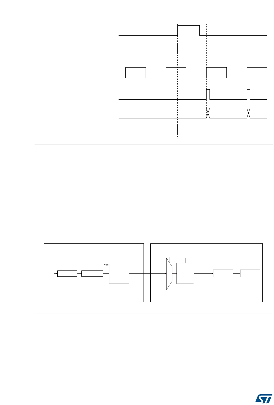
General-purpose timers (TIM2 to TIM5) RM0430
566/1324 RM0430 Rev 8
Figure 174. Control circuit in external clock mode 2 + trigger mode
18.3.15 Timer synchronization
The TIMx timers are linked together internally for timer synchronization or chaining. When
one Timer is configured in Master Mode, it can reset, start, stop or clock the counter of
another Timer configured in Slave Mode.
Figure 175 presents an overview of the trigger selection and the master mode selection
blocks.
Using one timer as prescaler for another
Figure 175. Master/Slave timer example
069
7,)
&RXQWHUUHJLVWHU
&RXQWHUFORFN &.B&17 &.B36&
(75
&(1&17B(1
7,
069
&RXQWHU
0DVWHU
PRGH
FRQWURO
8(9
3UHVFDOHU
&ORFN
&RXQWHU3UHVFDOHU
&.B36&75*2
006 606
76
,QSXWWULJJHU
VHOHFWLRQ
7,0 7,0
6ODYH
PRGH
FRQWURO
,75

RM0430 Rev 8 567/1324
RM0430 General-purpose timers (TIM2 to TIM5)
594
For example, you can configure Timer 1 to act as a prescaler for Timer 2. Refer to
Figure 175. To do this:
•Configure Timer 1 in master mode so that it outputs a periodic trigger signal on each
update event UEV. If you write MMS=010 in the TIM1_CR2 register, a rising edge is
output on TRGO1 each time an update event is generated.
•To connect the TRGO1 output of Timer 1 to Timer 2, Timer 2 must be configured in
slave mode using ITR0 as internal trigger. You select this through the TS bits in the
TIM2_SMCR register (writing TS=000).
•Then you put the slave mode controller in external clock mode 1 (write SMS=111 in the
TIM2_SMCR register). This causes Timer 2 to be clocked by the rising edge of the
periodic Timer 1 trigger signal (which correspond to the timer 1 counter overflow).
•Finally both timers must be enabled by setting their respective CEN bits (TIMx_CR1
register).
Note: If OCx is selected on Timer 1 as trigger output (MMS=1xx), its rising edge is used to clock
the counter of timer 2.
Using one timer to enable another timer
In this example, we control the enable of Timer 2 with the output compare 1 of Timer 1.
Refer to Figure 175 for connections. Timer 2 counts on the divided internal clock only when
OC1REF of Timer 1 is high. Both counter clock frequencies are divided by 3 by the
prescaler compared to CK_INT (fCK_CNT = fCK_INT/3).
•Configure Timer 1 master mode to send its Output Compare 1 Reference (OC1REF)
signal as trigger output (MMS=100 in the TIM1_CR2 register).
•Configure the Timer 1 OC1REF waveform (TIM1_CCMR1 register).
•Configure Timer 2 to get the input trigger from Timer 1 (TS=000 in the TIM2_SMCR
register).
•Configure Timer 2 in gated mode (SMS=101 in TIM2_SMCR register).
•Enable Timer 2 by writing ‘1 in the CEN bit (TIM2_CR1 register).
•Start Timer 1 by writing ‘1 in the CEN bit (TIM1_CR1 register).
Note: The counter 2 clock is not synchronized with counter 1, this mode only affects the Timer 2
counter enable signal.
Figure 176. Gating timer 2 with OC1REF of timer 1
In the example in Figure 176, the Timer 2 counter and prescaler are not initialized before
being started. So they start counting from their current value. It is possible to start from a
given value by resetting both timers before starting Timer 1. You can then write any value
069
&.B,17
)& )' )( ))
7,0(52&5()
7,0(5&17
7,0(5&17
7,0(57,)
:ULWH7,)
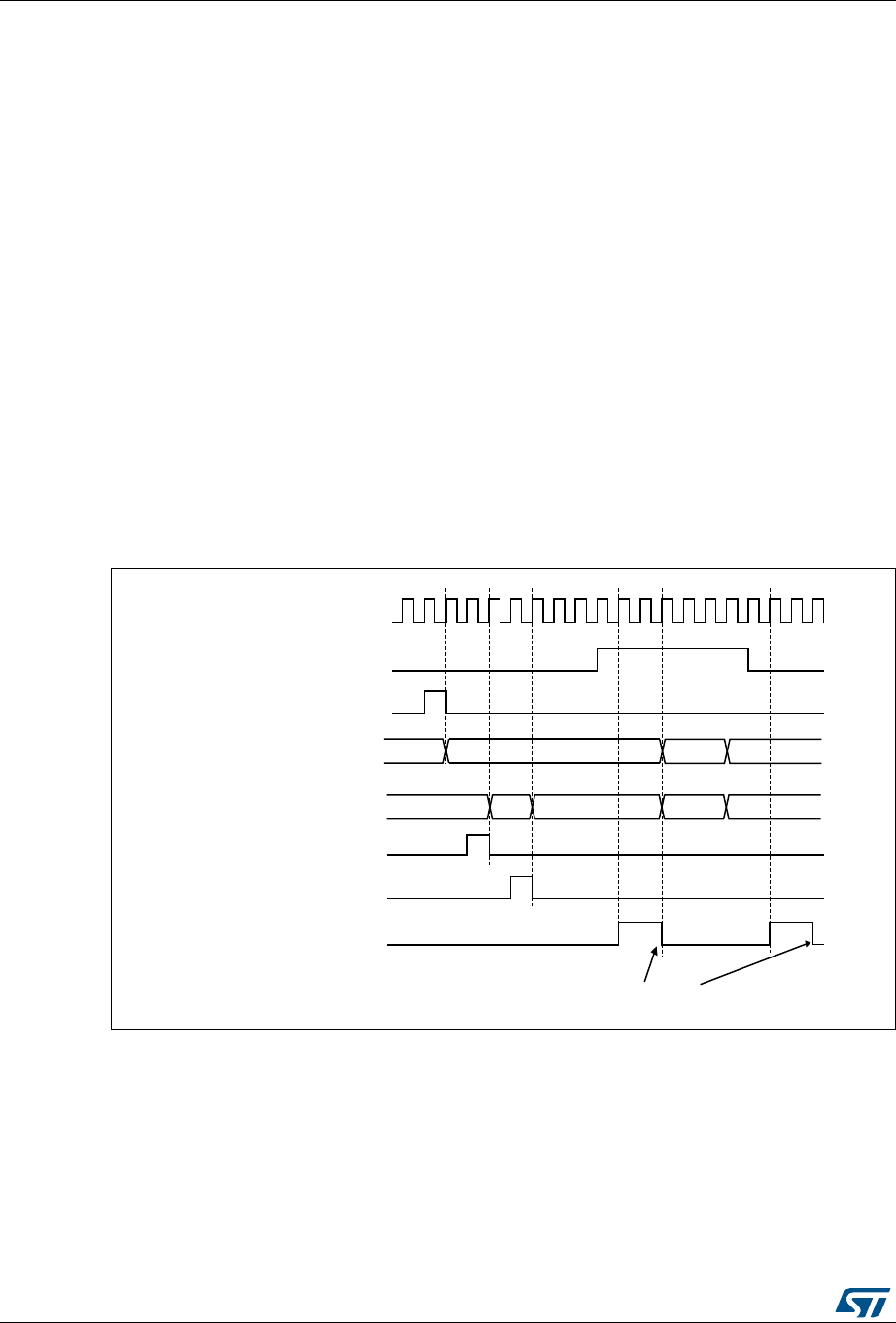
General-purpose timers (TIM2 to TIM5) RM0430
568/1324 RM0430 Rev 8
you want in the timer counters. The timers can easily be reset by software using the UG bit
in the TIMx_EGR registers.
In the next example, we synchronize Timer 1 and Timer 2. Timer 1 is the master and starts
from 0. Timer 2 is the slave and starts from 0xE7. The prescaler ratio is the same for both
timers. Timer 2 stops when Timer 1 is disabled by writing ‘0 to the CEN bit in the TIM1_CR1
register:
•Configure Timer 1 master mode to send its Output Compare 1 Reference (OC1REF)
signal as trigger output (MMS=100 in the TIM1_CR2 register).
•Configure the Timer 1 OC1REF waveform (TIM1_CCMR1 register).
•Configure Timer 2 to get the input trigger from Timer 1 (TS=000 in the TIM2_SMCR
register).
•Configure Timer 2 in gated mode (SMS=101 in TIM2_SMCR register).
•Reset Timer 1 by writing ‘1 in UG bit (TIM1_EGR register).
•Reset Timer 2 by writing ‘1 in UG bit (TIM2_EGR register).
•Initialize Timer 2 to 0xE7 by writing ‘0xE7’ in the timer 2 counter (TIM2_CNTL).
•Enable Timer 2 by writing ‘1 in the CEN bit (TIM2_CR1 register).
•Start Timer 1 by writing ‘1 in the CEN bit (TIM1_CR1 register).
•Stop Timer 1 by writing ‘0 in the CEN bit (TIM1_CR1 register).
Figure 177. Gating timer 2 with Enable of timer 1
Using one timer to start another timer
In this example, we set the enable of Timer 2 with the update event of Timer 1. Refer to
Figure 175 for connections. Timer 2 starts counting from its current value (which can be
nonzero) on the divided internal clock as soon as the update event is generated by Timer 1.
When Timer 2 receives the trigger signal its CEN bit is automatically set and the counter
069
&.B,17
(
7,0(5&17B,1,7
7,0(5&17
$%
7,0(5&17
7,0(5&17B,1,7
:ULWH7,)
((
7,0(5&(1 &17B(1
7,0(5ZULWH&17
7,0(57,)
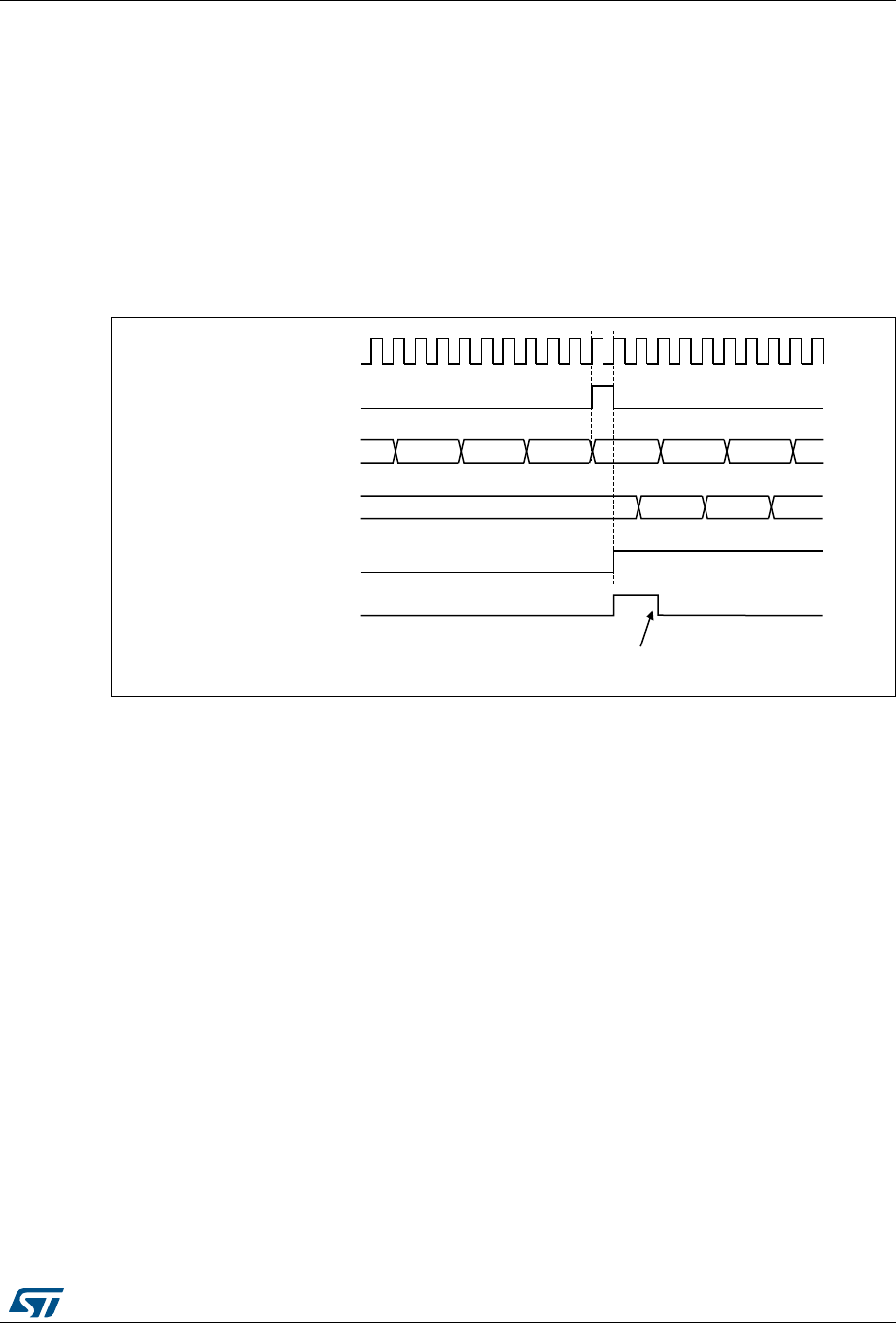
RM0430 Rev 8 569/1324
RM0430 General-purpose timers (TIM2 to TIM5)
594
counts until we write ‘0 to the CEN bit in the TIM2_CR1 register. Both counter clock
frequencies are divided by 3 by the prescaler compared to CK_INT (fCK_CNT = fCK_INT/3).
•Configure Timer 1 master mode to send its Update Event (UEV) as trigger output
(MMS=010 in the TIM1_CR2 register).
•Configure the Timer 1 period (TIM1_ARR registers).
•Configure Timer 2 to get the input trigger from Timer 1 (TS=000 in the TIM2_SMCR
register).
•Configure Timer 2 in trigger mode (SMS=110 in TIM2_SMCR register).
•Start Timer 1 by writing ‘1 in the CEN bit (TIM1_CR1 register).
Figure 178. Triggering timer 2 with update of timer 1
As in the previous example, you can initialize both counters before starting counting.
Figure 179 shows the behavior with the same configuration as in Figure 176, but in trigger
mode instead of gated mode (SMS=110 in the TIM2_SMCR register).
069
:ULWH7,)
&.B,17
7,0(5&17
)'
7,0(5&17
7,0(5&(1 &17B(1
7,0(57,)
)( ))
7,0(58(9
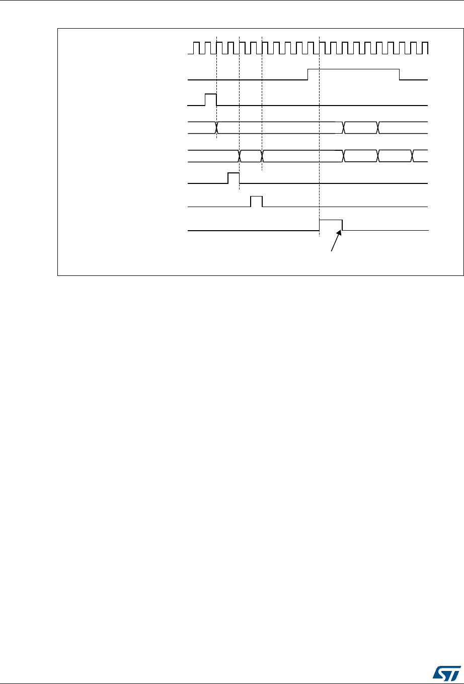
General-purpose timers (TIM2 to TIM5) RM0430
570/1324 RM0430 Rev 8
Figure 179. Triggering timer 2 with Enable of timer 1
Using one timer as prescaler for another timer
For example, you can configure Timer 1 to act as a prescaler for Timer 2. Refer to
Figure 175 for connections. To do this:
•Configure Timer 1 master mode to send its Update Event (UEV) as trigger output
(MMS=010 in the TIM1_CR2 register). then it outputs a periodic signal on each counter
overflow.
•Configure the Timer 1 period (TIM1_ARR registers).
•Configure Timer 2 to get the input trigger from Timer 1 (TS=000 in the TIM2_SMCR
register).
•Configure Timer 2 in external clock mode 1 (SMS=111 in TIM2_SMCR register).
•Start Timer 2 by writing ‘1 in the CEN bit (TIM2_CR1 register).
•Start Timer 1 by writing ‘1 in the CEN bit (TIM1_CR1 register).
Starting 2 timers synchronously in response to an external trigger
In this example, we set the enable of timer 1 when its TI1 input rises, and the enable of
Timer 2 with the enable of Timer 1. Refer to Figure 175 for connections. To ensure the
069
:ULWH7,)
&.B,17
7,0(5&17
7,0(5&17B,1,7
7,0(5&(1 &17B(1
7,0(57,)
(
(
&' ( ($
7,0(5&17
7,0(5&17B,1,7
7,0(5ZULWH&17
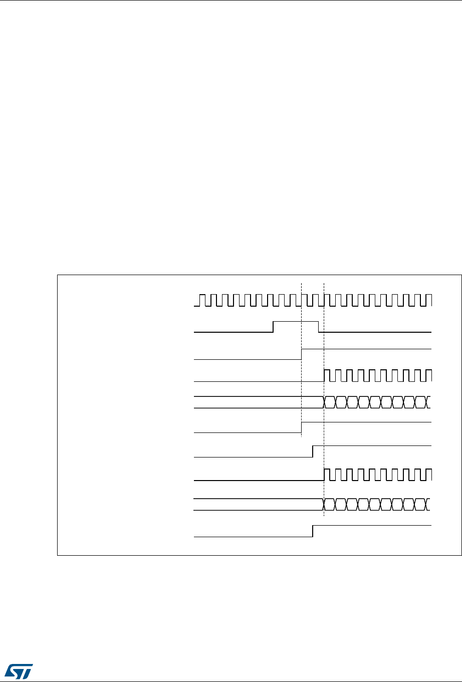
RM0430 Rev 8 571/1324
RM0430 General-purpose timers (TIM2 to TIM5)
594
counters are aligned, Timer 1 must be configured in Master/Slave mode (slave with respect
to TI1, master with respect to Timer 2):
•Configure Timer 1 master mode to send its Enable as trigger output (MMS=001 in the
TIM1_CR2 register).
•Configure Timer 1 slave mode to get the input trigger from TI1 (TS=100 in the
TIM1_SMCR register).
•Configure Timer 1 in trigger mode (SMS=110 in the TIM1_SMCR register).
•Configure the Timer 1 in Master/Slave mode by writing MSM=1 (TIM1_SMCR register).
•Configure Timer 2 to get the input trigger from Timer 1 (TS=000 in the TIM2_SMCR
register).
•Configure Timer 2 in trigger mode (SMS=110 in the TIM2_SMCR register).
When a rising edge occurs on TI1 (Timer 1), both counters starts counting synchronously on
the internal clock and both TIF flags are set.
Note: In this example both timers are initialized before starting (by setting their respective UG
bits). Both counters starts from 0, but you can easily insert an offset between them by
writing any of the counter registers (TIMx_CNT). You can see that the master/slave mode
insert a delay between CNT_EN and CK_PSC on timer 1.
Figure 180. Triggering timer 1 and 2 with timer 1 TI1 input
18.3.16 Debug mode
When the microcontroller enters debug mode (Cortex®-M4 with FPU core - halted), the
TIMx counter either continues to work normally or stops, depending on DBG_TIMx_STOP
configuration bit in DBGMCU module. For more details, refer to Section 37.16.2: Debug
support for timers, watchdog, bxCAN and I2C.
069
&.B,17
7,0(5&17
7,0(5&(1 &17B(1
7,0(57,)
7,0(5&17
7,0(5&(1 &17B(1
7,0(57,)
7,0(5&.B36&
7,0(57,
7,0(5&.B36&

General-purpose timers (TIM2 to TIM5) RM0430
572/1324 RM0430 Rev 8
18.4 TIM2 to TIM5 registers
Refer to Section 1.2 on page 52 for a list of abbreviations used in register descriptions.
The 32-bit peripheral registers have to be written by words (32 bits). All other peripheral
registers have to be written by half-words (16 bits) or words (32 bits). Read accesses can be
done by bytes (8 bits), half-words (16 bits) or words (32 bits).
18.4.1 TIMx control register 1 (TIMx_CR1)
Address offset: 0x00
Reset value: 0x0000
1514131211109876543210
Res. Res. Res. Res. Res. Res. CKD[1:0] ARPE CMS DIR OPM URS UDIS CEN
rw rw rw rw rw rw rw rw rw rw
Bits 15:10 Reserved, must be kept at reset value.
Bits 9:8 CKD: Clock division
This bit-field indicates the division ratio between the timer clock (CK_INT) frequency and
sampling clock used by the digital filters (ETR, TIx),
00: tDTS = tCK_INT
01: tDTS = 2 × tCK_INT
10: tDTS = 4 × tCK_INT
11: Reserved
Bit 7 ARPE: Auto-reload preload enable
0: TIMx_ARR register is not buffered
1: TIMx_ARR register is buffered
Bits 6:5 CMS: Center-aligned mode selection
00: Edge-aligned mode. The counter counts up or down depending on the direction bit
(DIR).
01: Center-aligned mode 1. The counter counts up and down alternatively. Output compare
interrupt flags of channels configured in output (CCxS=00 in TIMx_CCMRx register) are set
only when the counter is counting down.
10: Center-aligned mode 2. The counter counts up and down alternatively. Output compare
interrupt flags of channels configured in output (CCxS=00 in TIMx_CCMRx register) are set
only when the counter is counting up.
11: Center-aligned mode 3. The counter counts up and down alternatively. Output compare
interrupt flags of channels configured in output (CCxS=00 in TIMx_CCMRx register) are set
both when the counter is counting up or down.
Note: It is not allowed to switch from edge-aligned mode to center-aligned mode as long as
the counter is enabled (CEN=1)
Bit 4 DIR: Direction
0: Counter used as upcounter
1: Counter used as downcounter
Note: This bit is read only when the timer is configured in Center-aligned mode or Encoder
mode.
Bit 3 OPM: One-pulse mode
0: Counter is not stopped at update event
1: Counter stops counting at the next update event (clearing the bit CEN)

RM0430 Rev 8 573/1324
RM0430 General-purpose timers (TIM2 to TIM5)
594
Bit 2 URS: Update request source
This bit is set and cleared by software to select the UEV event sources.
0: Any of the following events generate an update interrupt or DMA request if enabled.
These events can be:
– Counter overflow/underflow
– Setting the UG bit
– Update generation through the slave mode controller
1: Only counter overflow/underflow generates an update interrupt or DMA request if
enabled.
Bit 1 UDIS: Update disable
This bit is set and cleared by software to enable/disable UEV event generation.
0: UEV enabled. The Update (UEV) event is generated by one of the following events:
– Counter overflow/underflow
– Setting the UG bit
– Update generation through the slave mode controller
Buffered registers are then loaded with their preload values.
1: UEV disabled. The Update event is not generated, shadow registers keep their value
(ARR, PSC, CCRx). However the counter and the prescaler are reinitialized if the UG bit is
set or if a hardware reset is received from the slave mode controller.
Bit 0 CEN: Counter enable
0: Counter disabled
1: Counter enabled
Note: External clock, gated mode and encoder mode can work only if the CEN bit has been
previously set by software. However trigger mode can set the CEN bit automatically by
hardware.
CEN is cleared automatically in one-pulse mode, when an update event occurs.

General-purpose timers (TIM2 to TIM5) RM0430
574/1324 RM0430 Rev 8
18.4.2 TIMx control register 2 (TIMx_CR2)
Address offset: 0x04
Reset value: 0x0000
1514131211109876543210
Res. Res. Res. Res. Res. Res. Res. Res. TI1S MMS[2:0] CCDS Res. Res. Res.
rw rw rw rw rw
Bits 15:8 Reserved, must be kept at reset value.
Bit 7 TI1S: TI1 selection
0: The TIMx_CH1 pin is connected to TI1 input
1: The TIMx_CH1, CH2 and CH3 pins are connected to the TI1 input (XOR combination)
Bits 6:4 MMS[2:0]: Master mode selection
These bits allow to select the information to be sent in master mode to slave timers for
synchronization (TRGO). The combination is as follows:
000: Reset - the UG bit from the TIMx_EGR register is used as trigger output (TRGO). If the
reset is generated by the trigger input (slave mode controller configured in reset mode) then
the signal on TRGO is delayed compared to the actual reset.
001: Enable - the Counter enable signal, CNT_EN, is used as trigger output (TRGO). It is
useful to start several timers at the same time or to control a window in which a slave timer is
enabled. The Counter Enable signal is generated by a logic OR between CEN control bit
and the trigger input when configured in gated mode.
When the Counter Enable signal is controlled by the trigger input, there is a delay on TRGO,
except if the master/slave mode is selected (see the MSM bit description in TIMx_SMCR
register).
010: Update - The update event is selected as trigger output (TRGO). For instance a master
timer can then be used as a prescaler for a slave timer.
011: Compare Pulse - The trigger output send a positive pulse when the CC1IF flag is to be
set (even if it was already high), as soon as a capture or a compare match occurred.
(TRGO)
100: Compare - OC1REF signal is used as trigger output (TRGO)
101: Compare - OC2REF signal is used as trigger output (TRGO)
110: Compare - OC3REF signal is used as trigger output (TRGO)
111: Compare - OC4REF signal is used as trigger output (TRGO)
Bit 3 CCDS: Capture/compare DMA selection
0: CCx DMA request sent when CCx event occurs
1: CCx DMA requests sent when update event occurs
Bits 2:0 Reserved, must be kept at reset value.

RM0430 Rev 8 575/1324
RM0430 General-purpose timers (TIM2 to TIM5)
594
18.4.3 TIMx slave mode control register (TIMx_SMCR)
Address offset: 0x08
Reset value: 0x0000
1514131211109876543210
ETP ECE ETPS[1:0] ETF[3:0] MSM TS[2:0] Res. SMS[2:0]
rw rw rw rw rw rw rw rw rw rw rw rw rw rw rw
Bit 15 ETP: External trigger polarity
This bit selects whether ETR or ETR is used for trigger operations
0: ETR is noninverted, active at high level or rising edge
1: ETR is inverted, active at low level or falling edge
Bit 14 ECE: External clock enable
This bit enables External clock mode 2.
0: External clock mode 2 disabled
1: External clock mode 2 enabled. The counter is clocked by any active edge on the ETRF
signal.
1: Setting the ECE bit has the same effect as selecting external clock mode 1 with TRGI
connected to ETRF (SMS=111 and TS=111).
2: It is possible to simultaneously use external clock mode 2 with the following slave modes:
reset mode, gated mode and trigger mode. Nevertheless, TRGI must not be connected to
ETRF in this case (TS bits must not be 111).
3: If external clock mode 1 and external clock mode 2 are enabled at the same time, the
external clock input is ETRF.
Bits 13:12 ETPS: External trigger prescaler
External trigger signal ETRP frequency must be at most 1/4 of CK_INT frequency. A
prescaler can be enabled to reduce ETRP frequency. It is useful when inputting fast external
clocks.
00: Prescaler OFF
01: ETRP frequency divided by 2
10: ETRP frequency divided by 4
11: ETRP frequency divided by 8
Bits 11:8 ETF[3:0]: External trigger filter
This bit-field then defines the frequency used to sample ETRP signal and the length of the
digital filter applied to ETRP. The digital filter is made of an event counter in which N
consecutive events are needed to validate a transition on the output:
0000: No filter, sampling is done at fDTS
0001: fSAMPLING=fCK_INT
, N=2
0010: fSAMPLING=fCK_INT
, N=4
0011: fSAMPLING=fCK_INT
, N=8
0100: fSAMPLING=fDTS/2, N=6
0101: fSAMPLING=fDTS/2, N=8
0110: fSAMPLING=fDTS/4, N=6
0111: fSAMPLING=fDTS/4, N=8
1000: fSAMPLING=fDTS/8, N=6
1001: fSAMPLING=fDTS/8, N=8
1010: fSAMPLING=fDTS/16, N=5
1011: fSAMPLING=fDTS/16, N=6
1100: fSAMPLING=fDTS/16, N=8
1101: fSAMPLING=fDTS/32, N=5
1110: fSAMPLING=fDTS/32, N=6
1111: fSAMPLING=fDTS/32, N=8

General-purpose timers (TIM2 to TIM5) RM0430
576/1324 RM0430 Rev 8
Bit 7 MSM: Master/Slave mode
0: No action
1: The effect of an event on the trigger input (TRGI) is delayed to allow a perfect
synchronization between the current timer and its slaves (through TRGO). It is useful if we
want to synchronize several timers on a single external event.
Bits 6:4 TS: Trigger selection
This bit-field selects the trigger input to be used to synchronize the counter.
000: Internal Trigger 0 (ITR0)
001: Internal Trigger 1 (ITR1).
010: Internal Trigger 2 (ITR2).
011: Internal Trigger 3 (ITR3).
100: TI1 Edge Detector (TI1F_ED)
101: Filtered Timer Input 1 (TI1FP1)
110: Filtered Timer Input 2 (TI2FP2)
111: External Trigger input (ETRF)
See Table 106 for more details on ITRx meaning for each Timer.
Note: These bits must be changed only when they are not used (e.g. when SMS=000) to
avoid wrong edge detections at the transition.
Bit 3 Reserved, must be kept at reset value.
Bits 2:0 SMS: Slave mode selection
When external signals are selected the active edge of the trigger signal (TRGI) is linked to
the polarity selected on the external input (see Input Control register and Control Register
description.
000: Slave mode disabled - if CEN = ‘1 then the prescaler is clocked directly by the internal
clock.
001: Encoder mode 1 - Counter counts up/down on TI2FP2 edge depending on TI1FP1
level.
010: Encoder mode 2 - Counter counts up/down on TI1FP1 edge depending on TI2FP2
level.
011: Encoder mode 3 - Counter counts up/down on both TI1FP1 and TI2FP2 edges
depending on the level of the other input.
100: Reset Mode - Rising edge of the selected trigger input (TRGI) reinitializes the counter
and generates an update of the registers.
101: Gated Mode - The counter clock is enabled when the trigger input (TRGI) is high. The
counter stops (but is not reset) as soon as the trigger becomes low. Both start and stop of
the counter are controlled.
110: Trigger Mode - The counter starts at a rising edge of the trigger TRGI (but it is not
reset). Only the start of the counter is controlled.
111: External Clock Mode 1 - Rising edges of the selected trigger (TRGI) clock the counter.
Note: The gated mode must not be used if TI1F_ED is selected as the trigger input (TS=100).
Indeed, TI1F_ED outputs 1 pulse for each transition on TI1F, whereas the gated mode
checks the level of the trigger signal.
Table 106. TIMx internal trigger connections
Slave TIM ITR0 (TS = 000) ITR1 (TS = 001) ITR2 (TS = 010) ITR3 (TS = 011)
TIM2 TIM1 TIM8 TIM3 TIM4
TIM3 TIM1 TIM2 TIM5 TIM4
TIM4 TIM1 TIM2 TIM3 TIM8
TIM5 TIM2 TIM3 or LPTIM1(1)
1. The selection of TIM3 or LPTIM1 is done via LPTIM1_OR register bit 3. TIM3 is selected by default.
TIM4 TIM8

RM0430 Rev 8 577/1324
RM0430 General-purpose timers (TIM2 to TIM5)
594
18.4.4 TIMx DMA/Interrupt enable register (TIMx_DIER)
Address offset: 0x0C
Reset value: 0x0000
1514131211109876543210
Res. TDE Res. CC4DE CC3DE CC2DE CC1DE UDE Res. TIE Res. CC4IE CC3IE CC2IE CC1IE UIE
rw rw rw rw rw rw rw rw rw rw rw rw
Bit 15 Reserved, must be kept at reset value.
Bit 14 TDE: Trigger DMA request enable
0: Trigger DMA request disabled.
1: Trigger DMA request enabled.
Bit 13 Reserved, always read as 0
Bit 12 CC4DE: Capture/Compare 4 DMA request enable
0: CC4 DMA request disabled.
1: CC4 DMA request enabled.
Bit 11 CC3DE: Capture/Compare 3 DMA request enable
0: CC3 DMA request disabled.
1: CC3 DMA request enabled.
Bit 10 CC2DE: Capture/Compare 2 DMA request enable
0: CC2 DMA request disabled.
1: CC2 DMA request enabled.
Bit 9 CC1DE: Capture/Compare 1 DMA request enable
0: CC1 DMA request disabled.
1: CC1 DMA request enabled.
Bit 8 UDE: Update DMA request enable
0: Update DMA request disabled.
1: Update DMA request enabled.
Bit 7 Reserved, must be kept at reset value.
Bit 6 TIE: Trigger interrupt enable
0: Trigger interrupt disabled.
1: Trigger interrupt enabled.
Bit 5 Reserved, must be kept at reset value.
Bit 4 CC4IE: Capture/Compare 4 interrupt enable
0: CC4 interrupt disabled.
1: CC4 interrupt enabled.
Bit 3 CC3IE: Capture/Compare 3 interrupt enable
0: CC3 interrupt disabled
1: CC3 interrupt enabled

General-purpose timers (TIM2 to TIM5) RM0430
578/1324 RM0430 Rev 8
18.4.5 TIMx status register (TIMx_SR)
Address offset: 0x10
Reset value: 0x0000
Bit 2 CC2IE: Capture/Compare 2 interrupt enable
0: CC2 interrupt disabled
1: CC2 interrupt enabled
Bit 1 CC1IE: Capture/Compare 1 interrupt enable
0: CC1 interrupt disabled
1: CC1 interrupt enabled
Bit 0 UIE: Update interrupt enable
0: Update interrupt disabled
1: Update interrupt enabled
1514131211109876543210
Res. Res. Res. CC4OF CC3OF CC2OF CC1OF Res. Res. TIF Res. CC4IF CC3IF CC2IF CC1IF UIF
rc_w0 rc_w0 rc_w0 rc_w0 rc_w0 rc_w0 rc_w0 rc_w0 rc_w0 rc_w0
Bits 15:13 Reserved, must be kept at reset value.
Bit 12 CC4OF: Capture/Compare 4 overcapture flag
refer to CC1OF description
Bit 11 CC3OF: Capture/Compare 3 overcapture flag
refer to CC1OF description
Bit 10 CC2OF: Capture/compare 2 overcapture flag
refer to CC1OF description
Bit 9 CC1OF: Capture/Compare 1 overcapture flag
This flag is set by hardware only when the corresponding channel is configured in input
capture mode. It is cleared by software by writing it to ‘0.
0: No overcapture has been detected
1: The counter value has been captured in TIMx_CCR1 register while CC1IF flag was
already set
Bits 8:7 Reserved, must be kept at reset value.
Bit 6 TIF: Trigger interrupt flag
This flag is set by hardware on trigger event (active edge detected on TRGI input when the
slave mode controller is enabled in all modes but gated mode. It is set when the counter
starts or stops when gated mode is selected. It is cleared by software.
0: No trigger event occurred
1: Trigger interrupt pending
Bit 5 Reserved, must be kept at reset value.
Bit 4 CC4IF: Capture/Compare 4 interrupt flag
refer to CC1IF description
Bit 3 CC3IF: Capture/Compare 3 interrupt flag
refer to CC1IF description

RM0430 Rev 8 579/1324
RM0430 General-purpose timers (TIM2 to TIM5)
594
Bit 2 CC2IF: Capture/Compare 2 interrupt flag
refer to CC1IF description
Bit 1 CC1IF: Capture/compare 1 interrupt flag
If channel CC1 is configured as output:
This flag is set by hardware when the counter matches the compare value, with some
exception in center-aligned mode (refer to the CMS bits in the TIMx_CR1 register
description). It is cleared by software.
0: No match
1: The content of the counter TIMx_CNT matches the content of the TIMx_CCR1 register.
When the contents of TIMx_CCR1 are greater than the contents of TIMx_ARR, the CC1IF bit
goes high on the counter overflow (in upcounting and up/down-counting modes) or underflow
(in downcounting mode)
If channel CC1 is configured as input:
This bit is set by hardware on a capture. It is cleared by software or by reading the
TIMx_CCR1 register.
0: No input capture occurred
1: The counter value has been captured in TIMx_CCR1 register (An edge has been detected
on IC1 which matches the selected polarity)
Bit 0 UIF: Update interrupt flag
″This bit is set by hardware on an update event. It is cleared by software.
0: No update occurred.
1: Update interrupt pending. This bit is set by hardware when the registers are updated:
″At overflow or underflow (for TIM2 to TIM5) and if UDIS=0 in the TIMx_CR1 register.
″When CNT is reinitialized by software using the UG bit in TIMx_EGR register, if URS=0
and UDIS=0 in the TIMx_CR1 register.
When CNT is reinitialized by a trigger event (refer to the synchro control register description),
if URS=0 and UDIS=0 in the TIMx_CR1 register.

General-purpose timers (TIM2 to TIM5) RM0430
580/1324 RM0430 Rev 8
18.4.6 TIMx event generation register (TIMx_EGR)
Address offset: 0x14
Reset value: 0x0000
1514131211109876543210
Res. Res. Res. Res. Res. Res. Res. Res. Res. TG Res. CC4G CC3G CC2G CC1G UG
w wwwww
Bits 15:7 Reserved, must be kept at reset value.
Bit 6 TG: Trigger generation
This bit is set by software in order to generate an event, it is automatically cleared by
hardware.
0: No action
1: The TIF flag is set in TIMx_SR register. Related interrupt or DMA transfer can occur if
enabled.
Bit 5 Reserved, must be kept at reset value.
Bit 4 CC4G: Capture/compare 4 generation
refer to CC1G description
Bit 3 CC3G: Capture/compare 3 generation
refer to CC1G description
Bit 2 CC2G: Capture/compare 2 generation
refer to CC1G description
Bit 1 CC1G: Capture/compare 1 generation
This bit is set by software in order to generate an event, it is automatically cleared by
hardware.
0: No action
1: A capture/compare event is generated on channel 1:
If channel CC1 is configured as output:
CC1IF flag is set, Corresponding interrupt or DMA request is sent if enabled.
If channel CC1 is configured as input:
The current value of the counter is captured in TIMx_CCR1 register. The CC1IF flag is set,
the corresponding interrupt or DMA request is sent if enabled. The CC1OF flag is set if the
CC1IF flag was already high.
Bit 0 UG: Update generation
This bit can be set by software, it is automatically cleared by hardware.
0: No action
1: Re-initialize the counter and generates an update of the registers. Note that the prescaler
counter is cleared too (anyway the prescaler ratio is not affected). The counter is cleared if
the center-aligned mode is selected or if DIR=0 (upcounting), else it takes the auto-reload
value (TIMx_ARR) if DIR=1 (downcounting).

RM0430 Rev 8 581/1324
RM0430 General-purpose timers (TIM2 to TIM5)
594
18.4.7 TIMx capture/compare mode register 1 (TIMx_CCMR1)
Address offset: 0x18
Reset value: 0x0000
The channels can be used in input (capture mode) or in output (compare mode). The
direction of a channel is defined by configuring the corresponding CCxS bits. All the other
bits of this register have a different function in input and in output mode. For a given bit,
OCxx describes its function when the channel is configured in output, ICxx describes its
function when the channel is configured in input. So you must take care that the same bit
can have a different meaning for the input stage and for the output stage.
Output compare mode
1514131211109876543210
OC2CE OC2M[2:0] OC2PE OC2FE CC2S[1:0] OC1CE OC1M[2:0] OC1PE OC1FE CC1S[1:0]
IC2F[3:0] IC2PSC[1:0] IC1F[3:0] IC1PSC[1:0]
rw rw rw rw rw rw rw rw rw rw rw rw rw rw rw rw
Bit 15 OC2CE: Output compare 2 clear enable
Bits 14:12 OC2M[2:0]: Output compare 2 mode
Bit 11 OC2PE: Output compare 2 preload enable
Bit 10 OC2FE: Output compare 2 fast enable
Bits 9:8 CC2S[1:0]: Capture/Compare 2 selection
This bit-field defines the direction of the channel (input/output) as well as the used input.
00: CC2 channel is configured as output
01: CC2 channel is configured as input, IC2 is mapped on TI2
10: CC2 channel is configured as input, IC2 is mapped on TI1
11: CC2 channel is configured as input, IC2 is mapped on TRC. This mode is working only if
an internal trigger input is selected through the TS bit (TIMx_SMCR register)
Note: CC2S bits are writable only when the channel is OFF (CC2E = 0 in TIMx_CCER).
Bit 7 OC1CE: Output compare 1 clear enable
OC1CE: Output Compare 1 Clear Enable
0: OC1Ref is not affected by the ETRF input
1: OC1Ref is cleared as soon as a High level is detected on ETRF input

General-purpose timers (TIM2 to TIM5) RM0430
582/1324 RM0430 Rev 8
Bits 6:4 OC1M: Output compare 1 mode
These bits define the behavior of the output reference signal OC1REF from which OC1 and
OC1N are derived. OC1REF is active high whereas OC1 and OC1N active level depends
on CC1P and CC1NP bits.
000: Frozen - The comparison between the output compare register TIMx_CCR1 and the
counter TIMx_CNT has no effect on the outputs.(this mode is used to generate a timing
base).
001: Set channel 1 to active level on match. OC1REF signal is forced high when the counter
TIMx_CNT matches the capture/compare register 1 (TIMx_CCR1).
010: Set channel 1 to inactive level on match. OC1REF signal is forced low when the
counter TIMx_CNT matches the capture/compare register 1 (TIMx_CCR1).
011: Toggle - OC1REF toggles when TIMx_CNT=TIMx_CCR1.
100: Force inactive level - OC1REF is forced low.
101: Force active level - OC1REF is forced high.
110: PWM mode 1 - In upcounting, channel 1 is active as long as TIMx_CNT<TIMx_CCR1
else inactive. In downcounting, channel 1 is inactive (OC1REF=‘0) as long as
TIMx_CNT>TIMx_CCR1 else active (OC1REF=1).
111: PWM mode 2 - In upcounting, channel 1 is inactive as long as TIMx_CNT<TIMx_CCR1
else active. In downcounting, channel 1 is active as long as TIMx_CNT>TIMx_CCR1 else
inactive.
Note: In PWM mode 1 or 2, the OCREF level changes only when the result of the
comparison changes or when the output compare mode switches from “frozen” mode
to “PWM” mode.
Bit 3 OC1PE: Output compare 1 preload enable
0: Preload register on TIMx_CCR1 disabled. TIMx_CCR1 can be written at anytime, the
new value is taken in account immediately.
1: Preload register on TIMx_CCR1 enabled. Read/Write operations access the preload
register. TIMx_CCR1 preload value is loaded in the active register at each update event.
Note: 1: These bits can not be modified as long as LOCK level 3 has been programmed
(LOCK bits in TIMx_BDTR register) and CC1S=00 (the channel is configured in
output).
2: The PWM mode can be used without validating the preload register only in one-
pulse mode (OPM bit set in TIMx_CR1 register). Else the behavior is not guaranteed.
Bit 2 OC1FE: Output compare 1 fast enable
This bit is used to accelerate the effect of an event on the trigger in input on the CC output.
0: CC1 behaves normally depending on counter and CCR1 values even when the trigger is
ON. The minimum delay to activate CC1 output when an edge occurs on the trigger input is
5 clock cycles.
1: An active edge on the trigger input acts like a compare match on CC1 output. Then, OC
is set to the compare level independently from the result of the comparison. Delay to sample
the trigger input and to activate CC1 output is reduced to 3 clock cycles. OCFE acts only if
the channel is configured in PWM1 or PWM2 mode.
Bits 1:0 CC1S: Capture/Compare 1 selection
This bit-field defines the direction of the channel (input/output) as well as the used input.
00: CC1 channel is configured as output.
01: CC1 channel is configured as input, IC1 is mapped on TI1.
10: CC1 channel is configured as input, IC1 is mapped on TI2.
11: CC1 channel is configured as input, IC1 is mapped on TRC. This mode is working only if
an internal trigger input is selected through TS bit (TIMx_SMCR register)
Note: CC1S bits are writable only when the channel is OFF (CC1E = 0 in TIMx_CCER).

RM0430 Rev 8 583/1324
RM0430 General-purpose timers (TIM2 to TIM5)
594
Input capture mode
Bits 15:12 IC2F: Input capture 2 filter
Bits 11:10 IC2PSC[1:0]: Input capture 2 prescaler
Bits 9:8 CC2S: Capture/compare 2 selection
This bit-field defines the direction of the channel (input/output) as well as the used input.
00: CC2 channel is configured as output.
01: CC2 channel is configured as input, IC2 is mapped on TI2.
10: CC2 channel is configured as input, IC2 is mapped on TI1.
11: CC2 channel is configured as input, IC2 is mapped on TRC. This mode is working only if
an internal trigger input is selected through TS bit (TIMx_SMCR register)
Note: CC2S bits are writable only when the channel is OFF (CC2E = 0 in TIMx_CCER).
Bits 7:4 IC1F: Input capture 1 filter
This bit-field defines the frequency used to sample TI1 input and the length of the digital filter
applied to TI1. The digital filter is made of an event counter in which N consecutive events
are needed to validate a transition on the output:
0000: No filter, sampling is done at fDTS
0001: fSAMPLING=fCK_INT
, N=2
0010: fSAMPLING=fCK_INT
, N=4
0011: fSAMPLING=fCK_INT
, N=8
0100: fSAMPLING=fDTS/2, N=6
0101: fSAMPLING=fDTS/2, N=8
0110: fSAMPLING=fDTS/4, N=6
0111: fSAMPLING=fDTS/4, N=8
1000: fSAMPLING=fDTS/8, N=6
1001: fSAMPLING=fDTS/8, N=8
1010: fSAMPLING=fDTS/16, N=5
1011: fSAMPLING=fDTS/16, N=6
1100: fSAMPLING=fDTS/16, N=8
1101: fSAMPLING=fDTS/32, N=5
1110: fSAMPLING=fDTS/32, N=6
1111: fSAMPLING=fDTS/32, N=8
Bits 3:2 IC1PSC: Input capture 1 prescaler
This bit-field defines the ratio of the prescaler acting on CC1 input (IC1).
The prescaler is reset as soon as CC1E=0 (TIMx_CCER register).
00: no prescaler, capture is done each time an edge is detected on the capture input
01: capture is done once every 2 events
10: capture is done once every 4 events
11: capture is done once every 8 events
Bits 1:0 CC1S: Capture/Compare 1 selection
This bit-field defines the direction of the channel (input/output) as well as the used input.
00: CC1 channel is configured as output
01: CC1 channel is configured as input, IC1 is mapped on TI1
10: CC1 channel is configured as input, IC1 is mapped on TI2
11: CC1 channel is configured as input, IC1 is mapped on TRC. This mode is working only if
an internal trigger input is selected through TS bit (TIMx_SMCR register)
Note: CC1S bits are writable only when the channel is OFF (CC1E = 0 in TIMx_CCER).

General-purpose timers (TIM2 to TIM5) RM0430
584/1324 RM0430 Rev 8
18.4.8 TIMx capture/compare mode register 2 (TIMx_CCMR2)
Address offset: 0x1C
Reset value: 0x0000
Refer to the above CCMR1 register description.
Output compare mode
1514131211109876543210
OC4CE OC4M[2:0] OC4PE OC4FE CC4S[1:0] OC3CE OC3M[2:0] OC3PE OC3FE CC3S[1:0]
IC4F[3:0] IC4PSC[1:0] IC3F[3:0] IC3PSC[1:0]
rw rw rw rw rw rw rw rw rw rw rw rw rw rw rw rw
Bit 15 OC4CE: Output compare 4 clear enable
Bits 14:12 OC4M: Output compare 4 mode
Bit 11 OC4PE: Output compare 4 preload enable
Bit 10 OC4FE: Output compare 4 fast enable
Bits 9:8 CC4S: Capture/Compare 4 selection
This bit-field defines the direction of the channel (input/output) as well as the used input.
00: CC4 channel is configured as output
01: CC4 channel is configured as input, IC4 is mapped on TI4
10: CC4 channel is configured as input, IC4 is mapped on TI3
11: CC4 channel is configured as input, IC4 is mapped on TRC. This mode is working only if
an internal trigger input is selected through TS bit (TIMx_SMCR register)
Note: CC4S bits are writable only when the channel is OFF (CC4E = 0 in TIMx_CCER).
Bit 7 OC3CE: Output compare 3 clear enable
Bits 6:4 OC3M: Output compare 3 mode
Bit 3 OC3PE: Output compare 3 preload enable
Bit 2 OC3FE: Output compare 3 fast enable
Bits 1:0 CC3S: Capture/Compare 3 selection
This bit-field defines the direction of the channel (input/output) as well as the used input.
00: CC3 channel is configured as output
01: CC3 channel is configured as input, IC3 is mapped on TI3
10: CC3 channel is configured as input, IC3 is mapped on TI4
11: CC3 channel is configured as input, IC3 is mapped on TRC. This mode is working only if
an internal trigger input is selected through TS bit (TIMx_SMCR register)
Note: CC3S bits are writable only when the channel is OFF (CC3E = 0 in TIMx_CCER).

RM0430 Rev 8 585/1324
RM0430 General-purpose timers (TIM2 to TIM5)
594
Input capture mode
18.4.9 TIMx capture/compare enable register (TIMx_CCER)
Address offset: 0x20
Reset value: 0x0000
Bits 15:12 IC4F: Input capture 4 filter
Bits 11:10 IC4PSC: Input capture 4 prescaler
Bits 9:8 CC4S: Capture/Compare 4 selection
This bit-field defines the direction of the channel (input/output) as well as the used input.
00: CC4 channel is configured as output
01: CC4 channel is configured as input, IC4 is mapped on TI4
10: CC4 channel is configured as input, IC4 is mapped on TI3
11: CC4 channel is configured as input, IC4 is mapped on TRC. This mode is working only if
an internal trigger input is selected through TS bit (TIMx_SMCR register)
Note: CC4S bits are writable only when the channel is OFF (CC4E = 0 in TIMx_CCER).
Bits 7:4 IC3F: Input capture 3 filter
Bits 3:2 IC3PSC: Input capture 3 prescaler
Bits 1:0 CC3S: Capture/Compare 3 selection
This bit-field defines the direction of the channel (input/output) as well as the used input.
00: CC3 channel is configured as output
01: CC3 channel is configured as input, IC3 is mapped on TI3
10: CC3 channel is configured as input, IC3 is mapped on TI4
11: CC3 channel is configured as input, IC3 is mapped on TRC. This mode is working only if
an internal trigger input is selected through TS bit (TIMx_SMCR register)
Note: CC3S bits are writable only when the channel is OFF (CC3E = 0 in TIMx_CCER).
1514131211109876543210
CC4NP Res. CC4P CC4E CC3NP Res. CC3P CC3E CC2NP Res. CC2P CC2E CC1NP Res. CC1P CC1E
rw rw rw rw rw rw rw rw rw rw rw rw
Bit 15 CC4NP: Capture/Compare 4 output Polarity.
Refer to CC1NP description
Bit 14 Reserved, must be kept at reset value.
Bit 13 CC4P: Capture/Compare 4 output Polarity.
refer to CC1P description
Bit 12 CC4E: Capture/Compare 4 output enable.
refer to CC1E description
Bit 11 CC3NP: Capture/Compare 3 output Polarity.
refer to CC1NP description
Bit 10 Reserved, must be kept at reset value.
Bit 9 CC3P: Capture/Compare 3 output Polarity.
refer to CC1P description
Bit 8 CC3E: Capture/Compare 3 output enable.
refer to CC1E description

General-purpose timers (TIM2 to TIM5) RM0430
586/1324 RM0430 Rev 8
Note: The state of the external IO pins connected to the standard OCx channels depends on the
OCx channel state and the GPIO registers.
Bit 7 CC2NP: Capture/Compare 2 output Polarity.
refer to CC1NP description
Bit 6 Reserved, must be kept at reset value.
Bit 5 CC2P: Capture/Compare 2 output Polarity.
refer to CC1P description
Bit 4 CC2E: Capture/Compare 2 output enable.
refer to CC1E description
Bit 3 CC1NP: Capture/Compare 1 output Polarity.
CC1 channel configured as output:
CC1NP must be kept cleared in this case.
CC1 channel configured as input:
This bit is used in conjunction with CC1P to define TI1FP1/TI2FP1 polarity. refer to CC1P
description.
Bit 2 Reserved, must be kept at reset value.
Bit 1 CC1P: Capture/Compare 1 output Polarity.
CC1 channel configured as output:
0: OC1 active high
1: OC1 active low
CC1 channel configured as input:
CC1NP/CC1P bits select TI1FP1 and TI2FP1 polarity for trigger or capture operations.
00: noninverted/rising edge
Circuit is sensitive to TIxFP1 rising edge (capture, trigger in reset, external clock or trigger
mode), TIxFP1 is not inverted (trigger in gated mode, encoder mode).
01: inverted/falling edge
Circuit is sensitive to TIxFP1 falling edge (capture, trigger in reset, external clock or trigger
mode), TIxFP1 is inverted (trigger in gated mode, encoder mode).
10: reserved, do not use this configuration.
11: noninverted/both edges
Circuit is sensitive to both TIxFP1 rising and falling edges (capture, trigger in reset, external
clock or trigger mode), TIxFP1 is not inverted (trigger in gated mode). This configuration
must not be used for encoder mode.
Bit 0 CC1E: Capture/Compare 1 output enable.
CC1 channel configured as output:
0: Off - OC1 is not active
1: On - OC1 signal is output on the corresponding output pin
CC1 channel configured as input:
This bit determines if a capture of the counter value can actually be done into the input
capture/compare register 1 (TIMx_CCR1) or not.
0: Capture disabled
1: Capture enabled
Table 107. Output control bit for standard OCx channels
CCxE bit OCx output state
0 Output Disabled (OCx=0, OCx_EN=0)
1 OCx=OCxREF + Polarity, OCx_EN=1

RM0430 Rev 8 587/1324
RM0430 General-purpose timers (TIM2 to TIM5)
594
18.4.10 TIMx counter (TIMx_CNT)
Address offset: 0x24
Reset value: 0x0000
18.4.11 TIMx prescaler (TIMx_PSC)
Address offset: 0x28
Reset value: 0x0000
18.4.12 TIMx auto-reload register (TIMx_ARR)
Address offset: 0x2C
Reset value: 0x0000
1514131211109876543210
CNT[15:0]
rw rw rw rw rw rw rw rw rw rw rw rw rw rw rw rw
Bits 15:0 CNT[15:0]: Counter value
1514131211109876543210
PSC[15:0]
rw rw rw rw rw rw rw rw rw rw rw rw rw rw rw rw
Bits 15:0 PSC[15:0]: Prescaler value
The counter clock frequency CK_CNT is equal to fCK_PSC / (PSC[15:0] + 1).
PSC contains the value to be loaded in the active prescaler register at each update event.
1514131211109876543210
ARR[15:0]
rw rw rw rw rw rw rw rw rw rw rw rw rw rw rw rw
Bits 15:0 ARR[15:0]: Auto-reload value
ARR is the value to be loaded in the actual auto-reload register.
Refer to the Section 18.3.1: Time-base unit on page 535 for more details about ARR update
and behavior.
The counter is blocked while the auto-reload value is null.

General-purpose timers (TIM2 to TIM5) RM0430
588/1324 RM0430 Rev 8
18.4.13 TIMx capture/compare register 1 (TIMx_CCR1)
Address offset: 0x34
Reset value: 0x0000 0000
18.4.14 TIMx capture/compare register 2 (TIMx_CCR2)
Address offset: 0x38
Reset value: 0x0000 0000
31 30 29 28 27 26 25 24 23 22 21 20 19 18 17 16
CCR1[31:16] (depending on timers)
rw rw rw rw rw rw rw rw rw rw rw rw rw rw rw rw
1514131211109876543210
CCR1[15:0]
rw rw rw rw rw rw rw rw rw rw rw rw rw rw rw rw
Bits 31:16 CCR1[31:16]: High Capture/Compare 1 value (on TIM2 and TIM5).
Bits 15:0 CCR1[15:0]: Low Capture/Compare 1 value
If channel CC1 is configured as output:
CCR1 is the value to be loaded in the actual capture/compare 1 register (preload value).
It is loaded permanently if the preload feature is not selected in the TIMx_CCMR1 register
(bit OC1PE). Else the preload value is copied in the active capture/compare 1 register when
an update event occurs.
The active capture/compare register contains the value to be compared to the counter
TIMx_CNT and signaled on OC1 output.
If channel CC1is configured as input:
CCR1 is the counter value transferred by the last input capture 1 event (IC1).
31 30 29 28 27 26 25 24 23 22 21 20 19 18 17 16
CCR2[31:16] (depending on timers)
rw rw rw rw rw rw rw rw rw rw rw rw rw rw rw rw
1514131211109876543210
CCR2[15:0]
rw rw rw rw rw rw rw rw rw rw rw rw rw rw rw rw
Bits 31:16 CCR2[31:16]: High Capture/Compare 2 value (on TIM2 and TIM5).
Bits 15:0 CCR2[15:0]: Low Capture/Compare 2 value
If channel CC2 is configured as output:
CCR2 is the value to be loaded in the actual capture/compare 2 register (preload value).
It is loaded permanently if the preload feature is not selected in the TIMx_CCMR register (bit
OC2PE). Else the preload value is copied in the active capture/compare 2 register when an
update event occurs.
The active capture/compare register contains the value to be compared to the counter
TIMx_CNT and signalled on OC2 output.
If channel CC2 is configured as input:
CCR2 is the counter value transferred by the last input capture 2 event (IC2).

RM0430 Rev 8 589/1324
RM0430 General-purpose timers (TIM2 to TIM5)
594
18.4.15 TIMx capture/compare register 3 (TIMx_CCR3)
Address offset: 0x3C
Reset value: 0x0000 0000
18.4.16 TIMx capture/compare register 4 (TIMx_CCR4)
Address offset: 0x40
Reset value: 0x0000 0000
31 30 29 28 27 26 25 24 23 22 21 20 19 18 17 16
CCR3[31:16] (depending on timers)
rw rw rw rw rw rw rw rw rw rw rw rw rw rw rw rw
1514131211109876543210
CCR3[15:0]
rw rw rw rw rw rw rw rw rw rw rw rw rw rw rw rw
Bits 31:16 CCR3[31:16]: High Capture/Compare 3 value (on TIM2 and TIM5).
Bits 15:0 CCR3[15:0]: Low Capture/Compare value
If channel CC3 is configured as output:
CCR3 is the value to be loaded in the actual capture/compare 3 register (preload value).
It is loaded permanently if the preload feature is not selected in the TIMx_CCMR register (bit
OC3PE). Else the preload value is copied in the active capture/compare 3 register when an
update event occurs.
The active capture/compare register contains the value to be compared to the counter
TIMx_CNT and signaled on OC3 output.
If channel CC3 is configured as input:
CCR3 is the counter value transferred by the last input capture 3 event (IC3).
31 30 29 28 27 26 25 24 23 22 21 20 19 18 17 16
CCR4[31:16] (depending on timers)
rw rw rw rw rw rw rw rw rw rw rw rw rw rw rw rw
1514131211109876543210
CCR4[15:0]
rw rw rw rw rw rw rw rw rw rw rw rw rw rw rw rw
Bits 31:16 CCR4[31:16]: High Capture/Compare 4 value (onTIM2 and TIM5).
Bits 15:0 CCR4[15:0]: Low Capture/Compare value
1. if CC4 channel is configured as output (CC4S bits):
CCR4 is the value to be loaded in the actual capture/compare 4 register (preload value).
It is loaded permanently if the preload feature is not selected in the TIMx_CCMR register
(bit OC4PE). Else the preload value is copied in the active capture/compare 4 register
when an update event occurs.
The active capture/compare register contains the value to be compared to the counter
TIMx_CNT and signalled on OC4 output.
2. if CC4 channel is configured as input (CC4S bits in TIMx_CCMR4 register):
CCR4 is the counter value transferred by the last input capture 4 event (IC4).

General-purpose timers (TIM2 to TIM5) RM0430
590/1324 RM0430 Rev 8
18.4.17 TIMx DMA control register (TIMx_DCR)
Address offset: 0x48
Reset value: 0x0000
18.4.18 TIMx DMA address for full transfer (TIMx_DMAR)
Address offset: 0x4C
Reset value: 0x0000
Example of how to use the DMA burst feature
In this example the timer DMA burst feature is used to update the contents of the CCRx
registers (x = 2, 3, 4) with the DMA transferring half words into the CCRx registers.
This is done in the following steps:
1514131211109876543210
Res. Res. Res. DBL[4:0] Res. Res. Res. DBA[4:0]
rw rw rw rw rw rw rw rw rw rw
Bits 15:13 Reserved, must be kept at reset value.
Bits 12:8 DBL[4:0]: DMA burst length
This 5-bit vector defines the number of DMA transfers (the timer recognizes a burst transfer
when a read or a write access is done to the TIMx_DMAR address).
00000: 1 transfer,
00001: 2 transfers,
00010: 3 transfers,
...
10001: 18 transfers.
Bits 7:5 Reserved, must be kept at reset value.
Bits 4:0 DBA[4:0]: DMA base address
This 5-bit vector defines the base-address for DMA transfers (when read/write access are
done through the TIMx_DMAR address). DBA is defined as an offset starting from the
address of the TIMx_CR1 register.
Example:
00000: TIMx_CR1,
00001: TIMx_CR2,
00010: TIMx_SMCR,
...
Example: Let us consider the following transfer: DBL = 7 transfers & DBA = TIMx_CR1. In this
case the transfer is done to/from 7 registers starting from the TIMx_CR1 address.
1514131211109876543210
DMAB[15:0]
rw rw rw rw rw rw rw rw rw rw rw rw rw rw rw rw
Bits 15:0 DMAB[15:0]: DMA register for burst accesses
A read or write operation to the DMAR register accesses the register located at the address
(TIMx_CR1 address) + (DBA + DMA index) x 4
where TIMx_CR1 address is the address of the control register 1, DBA is the DMA base
address configured in TIMx_DCR register, DMA index is automatically controlled by the
DMA transfer, and ranges from 0 to DBL (DBL configured in TIMx_DCR).

RM0430 Rev 8 591/1324
RM0430 General-purpose timers (TIM2 to TIM5)
594
1. Configure the corresponding DMA channel as follows:
– DMA channel peripheral address is the DMAR register address
– DMA channel memory address is the address of the buffer in the RAM containing
the data to be transferred by DMA into CCRx registers.
– Number of data to transfer = 3 (See note below).
– Circular mode disabled.
2. Configure the DCR register by configuring the DBA and DBL bit fields as follows:
DBL = 3 transfers, DBA = 0xE.
3. Enable the TIMx update DMA request (set the UDE bit in the DIER register).
4. Enable TIMx
5. Enable the DMA channel
Note: This example is for the case where every CCRx register to be updated once. If every CCRx
register is to be updated twice for example, the number of data to transfer should be 6. Let's
take the example of a buffer in the RAM containing data1, data2, data3, data4, data5 and
data6. The data is transferred to the CCRx registers as follows: on the first update DMA
request, data1 is transferred to CCR2, data2 is transferred to CCR3, data3 is transferred to
CCR4 and on the second update DMA request, data4 is transferred to CCR2, data5 is
transferred to CCR3 and data6 is transferred to CCR4.
18.4.19 TIM2 option register (TIM2_OR)
Address offset: 0x50
Reset value: 0x0000
15 14 13 12 11 10 9 8 7 6 5 4 3 2 1 0
Res. Res. Res. Res. ITR1_RMP Res. Res. Res. Res. Res. Res. Res. Res. Res. Res.
rw rw
Bits 15:12 Reserved, must be kept at reset value.
Bits 11:10 ITR1_RMP: Internal trigger 1 remap
Set and cleared by software.
00: TIM8_TRGOUT
01: Reserved
10: OTG FS SOF is connected to the TIM2_ITR1 input
11: OTG HS SOF is connected to the TIM2_ITR1 input
Bits 9:0 Reserved, must be kept at reset value.

General-purpose timers (TIM2 to TIM5) RM0430
592/1324 RM0430 Rev 8
18.4.20 TIM5 option register (TIM5_OR)
Address offset: 0x50
Reset value: 0x0000
1514131211109876543210
Res. Res. Res. Res. Res. Res. Res. Res. TI4_RMP Res. Res. Res. Res. Res. Res.
rw rw
Bits 15:8 Reserved, must be kept at reset value.
Bits 7:6 TI4_RMP: Timer Input 4 remap
Set and cleared by software.
00: TIM5 Channel4 is connected to the GPIO: Refer to the Alternate function mapping table
in the datasheets.
01: the LSI internal clock is connected to the TIM5_CH4 input for calibration purposes
10: the LSE internal clock is connected to the TIM5_CH4 input for calibration purposes
11: the RTC wakeup interrupt is connected to TIM5_CH4 input for calibration purposes.
Wakeup interrupt should be enabled.
Bits 5:0 Reserved, must be kept at reset value.

RM0430 Rev 8 593/1324
RM0430 General-purpose timers (TIM2 to TIM5)
594
18.4.21 TIMx register map
TIMx registers are mapped as described in the table below:
Table 108. TIM2 to TIM5 register map and reset values
Offset Register
31
30
29
28
27
26
25
24
23
22
21
20
19
18
17
16
15
14
13
12
11
10
9
8
7
6
5
4
3
2
1
0
0x00
TIMx_CR1
Res.
Res.
Res.
Res.
Res.
Res.
Res.
Res.
Res.
Res.
Res.
Res.
Res.
Res.
Res.
Res.
Res.
Res.
Res.
Res.
Res.
Res.
CKD
[1:0]
ARPE
CMS
[1:0]
DIR
OPM
URS
UDIS
CEN
Reset value 0000000000
0x04
TIMx_CR2
Res.
Res.
Res.
Res.
Res.
Res.
Res.
Res.
Res.
Res.
Res.
Res.
Res.
Res.
Res.
Res.
Res.
Res.
Res.
Res.
Res.
Res.
Res.
Res.
TI1S
MMS[2:0]
CCDS
Res.
Res.
Res.
Reset value 00000
0x08
TIMx_SMCR
Res.
Res.
Res.
Res.
Res.
Res.
Res.
Res.
Res.
Res.
Res.
Res.
Res.
Res.
Res.
Res.
ETP
ECE
ETPS
[1:0] ETF[3:0]
MSM
TS[2:0]
Res.
SMS[2:0]
Reset value 000000000000 000
0x0C
TIMx_DIER
Res.
Res.
Res.
Res.
Res.
Res.
Res.
Res.
Res.
Res.
Res.
Res.
Res.
Res.
Res.
Res.
Res.
TDE
COMDE
CC4DE
CC3DE
CC2DE
CC1DE
UDE
Res.
TIE
Res.
CC4IE
CC3IE
CC2IE
CC1IE
UIE
Reset value 0000000 0 00000
0x10
TIMx_SR
Res.
Res.
Res.
Res.
Res.
Res.
Res.
Res.
Res.
Res.
Res.
Res.
Res.
Res.
Res.
Res.
Res.
Res.
Res.
CC4OF
CC3OF
CC2OF
CC1OF
Res.
Res.
TIF
Res.
CC4IF
CC3IF
CC2IF
CC1IF
UIF
Reset value 0000 0 00000
0x14
TIMx_EGR
Res.
Res.
Res.
Res.
Res.
Res.
Res.
Res.
Res.
Res.
Res.
Res.
Res.
Res.
Res.
Res.
Res.
Res.
Res.
Res.
Res.
Res.
Res.
Res.
Res.
TG
Res.
CC4G
CC3G
CC2G
CC1G
UG
Reset value 0 00000
0x18
TIMx_CCMR1
Output Compare
mode
Res.
Res.
Res.
Res.
Res.
Res.
Res.
Res.
Res.
Res.
Res.
Res.
Res.
Res.
Res.
Res.
OC2CE
OC2M
[2:0]
OC2PE
OC2FE
CC2S
[1:0]
OC1CE
OC1M
[2:0]
OC1PE
OC1FE
CC1S
[1:0]
Reset value 0000000000000000
TIMx_CCMR1
Input Capture
mode
Res.
Res.
Res.
Res.
Res.
Res.
Res.
Res.
Res.
Res.
Res.
Res.
Res.
Res.
Res.
Res.
IC2F[3:0]
IC2
PSC
[1:0]
CC2S
[1:0] IC1F[3:0]
IC1
PSC
[1:0]
CC1S
[1:0]
Reset value 0000000000000000
0x1C
TIMx_CCMR2
Output Compare
mode
Res.
Res.
Res.
Res.
Res.
Res.
Res.
Res.
Res.
Res.
Res.
Res.
Res.
Res.
Res.
Res.
O24CE
OC4M
[2:0]
OC4PE
OC4FE
CC4S
[1:0]
OC3CE
OC3M
[2:0]
OC3PE
OC3FE
CC3S
[1:0]
Reset value 0000000000000000
TIMx_CCMR2
Input Capture
mode
Res.
Res.
Res.
Res.
Res.
Res.
Res.
Res.
Res.
Res.
Res.
Res.
Res.
Res.
Res.
Res.
IC4F[3:0]
IC4
PSC
[1:0]
CC4S
[1:0] IC3F[3:0]
IC3
PSC
[1:0]
CC3S
[1:0]
Reset value 0000000000000000
0x20
TIMx_CCER
Res.
Res.
Res.
Res.
Res.
Res.
Res.
Res.
Res.
Res.
Res.
Res.
Res.
Res.
Res.
Res.
CC4NP
Res.
CC4P
CC4E
CC3NP
Res.
CC3P
CC3E
CC2NP
Res.
CC2P
CC2E
CC1NP
Res.
CC1P
CC1E
Reset value 0 000 000 000 00
0x24
TIMx_CNT CNT[31:16]
(TIM2 and TIM5 only, reserved on the other timers) CNT[15:0]
Reset value 00000000000000000 0 0 0 000000000000

General-purpose timers (TIM2 to TIM5) RM0430
594/1324 RM0430 Rev 8
Refer to Section 2.2.2: Memory map and register boundary addresses for the register
boundary addresses.
0x28
TIMx_PSC
Res.
Res.
Res.
Res.
Res.
Res.
Res.
Res.
Res.
Res.
Res.
Res.
Res.
Res.
Res.
Res.
PSC[15:0]
Reset value 0000000000000000
0x2C
TIMx_ARR ARR[31:16]
(TIM2 and TIM5 only, reserved on the other timers) ARR[15:0]
Reset value 00000000000000000 0 0 0 000000000000
0x30 Reserved
Res.
Res.
Res.
Res.
Res.
Res.
Res.
Res.
Res.
Res.
Res.
Res.
Res.
Res.
Res.
Res.
Res.
Res.
Res.
Res.
Res.
Res.
Res.
Res.
Res.
Res.
Res.
Res.
Res.
Res.
Res.
Res.
0x34
TIMx_CCR1 CCR1[31:16]
(TIM2 and TIM5 only, reserved on the other timers) CCR1[15:0]
Reset value 00000000000000000 0 0 0 000000000000
0x38
TIMx_CCR2 CCR2[31:16]
(TIM2 and TIM5 only, reserved on the other timers) CCR2[15:0]
Reset value 00000000000000000 0 0 0 000000000000
0x3C
TIMx_CCR3 CCR3[31:16]
(TIM2 and TIM5 only, reserved on the other timers) CCR3[15:0]
Reset value 00000000000000000 0 0 0 000000000000
0x40
TIMx_CCR4 CCR4[31:16]
(TIM2 and TIM5 only, reserved on the other timers) CCR4[15:0]
Reset value 00000000000000000 0 0 0 000000000000
0x44 Reserved
Res.
Res.
Res.
Res.
Res.
Res.
Res.
Res.
Res.
Res.
Res.
Res.
Res.
Res.
Res.
Res.
Res.
Res.
Res.
Res.
Res.
Res.
Res.
Res.
Res.
Res.
Res.
Res.
Res.
Res.
Res.
Res.
0x48
TIMx_DCR
Res.
Res.
Res.
Res.
Res.
Res.
Res.
Res.
Res.
Res.
Res.
Res.
Res.
Res.
Res.
Res.
Res.
Res.
Res.
DBL[4:0]
Res.
Res.
Res.
DBA[4:0]
Reset value 00000 00000
0x4C
TIMx_DMAR
Res.
Res.
Res.
Res.
Res.
Res.
Res.
Res.
Res.
Res.
Res.
Res.
Res.
Res.
Res.
Res.
DMAB[15:0]
Reset value 0000000000000000
0x50
TIM2_OR
Res.
Res.
Res.
Res.
Res.
Res.
Res.
Res.
Res.
Res.
Res.
Res.
Res.
Res.
Res.
Res.
Res.
Res.
Res.
Res.
ITR1_
RMP
Res.
Res.
Res.
Res.
Res.
Res.
Res.
Res.
Res.
Res.
Reset value 00
0x50
TIM5_OR
Res.
Res.
Res.
Res.
Res.
Res.
Res.
Res.
Res.
Res.
Res.
Res.
Res.
Res.
Res.
Res.
Res.
Res.
Res.
Res.
Res.
Res.
Res.
Res.
IT4_
RMP
Res.
Res.
Res.
Res.
Res.
Res.
Reset value 00
Table 108. TIM2 to TIM5 register map and reset values (continued)
Offset Register
31
30
29
28
27
26
25
24
23
22
21
20
19
18
17
16
15
14
13
12
11
10
9
8
7
6
5
4
3
2
1
0

RM0430 Rev 8 595/1324
RM0430 General-purpose timers (TIM9 to TIM14)
641
19 General-purpose timers (TIM9 to TIM14)
19.1 TIM9 to TIM14 introduction
The TIM9 to TIM14 general-purpose timers consist of a 16-bit auto-reload counter driven by
a programmable prescaler.
They may be used for a variety of purposes, including measuring the pulse lengths of input
signals (input capture) or generating output waveforms (output compare, PWM).
Pulse lengths and waveform periods can be modulated from a few microseconds to several
milliseconds using the timer prescaler and the RCC clock controller prescalers.
The TIM9 to TIM14 timers are completely independent, and do not share any resources.
They can be synchronized together as described in Section 19.3.12.
19.2 TIM9 to TIM14 main features
19.2.1 TIM9/TIM12 main features
The features of the TIM9 to TIM14 general-purpose timers include:
•16-bit auto-reload upcounter
•16-bit programmable prescaler used to divide the counter clock frequency by any factor
between 1 and 65536 (can be changed “on the fly”)
•Up to 2 independent channels for:
– Input capture
– Output compare
– PWM generation (edge-aligned mode)
– One-pulse mode output
•Synchronization circuit to control the timer with external signals and to interconnect
several timers together
•Interrupt generation on the following events:
– Update: counter overflow, counter initialization (by software or internal trigger)
– Trigger event (counter start, stop, initialization or count by internal trigger)
– Input capture
– Output compare
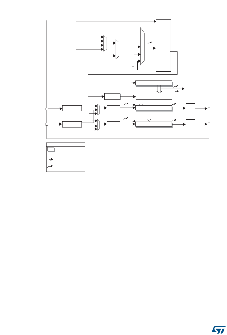
General-purpose timers (TIM9 to TIM14) RM0430
596/1324 RM0430 Rev 8
Figure 181. General-purpose timer block diagram (TIM9 and TIM12)
19.2.2 TIM10/TIM11 and TIM13/TIM14 main features
The features of general-purpose timers TIM10/TIM11 and TIM13/TIM14 include:
•16-bit auto-reload upcounter
•16-bit programmable prescaler used to divide the counter clock frequency by any factor
between 1 and 65536 (can be changed “on the fly”)
•independent channel for:
– Input capture
– Output compare
– PWM generation (edge-aligned mode)
– One-pulse mode output
•Interrupt generation on the following events:
– Update: counter overflow, counter initialization (by software)
– Input capture
– Output compare
Auto-reload register
Capture/Compare 1 register
Capture/Compare 2 register
U
U
U
CC1I
CC2I
Tr i g g e r
controller
Stop, Clear
TI1FP1
TI2FP2
ITR0
ITR1
ITR2
ITR3
TRGI
output
control
OC1
OC1REF
OC2REF
U
UI
Reset, Enable, Count
IC1
IC2
Prescaler
Prescaler
Input filter &
Edge detector
IC2PS
IC1PS
TI1FP1
output
control
OC2
Reg
event
Notes:
Preload registers transferred
to active registers on
U
event
according to control bit
interrupt
TGI
TRC
TRC
ITR
TRC
TI1F_ED
Input filter &
Edge detector
CC1I
CC2I
TI1FP2
TI2FP1
TI2FP2
TI1
TI2
TIMx_CH1
TIMx_CH2
TIMx_CH1
TIMx_CH2
Prescaler
COUNTER
+/-
CK_PSC
PSC CNT
CK_CNT
controller
mode
Slave
Internal clock (CK_INT)
ai17190
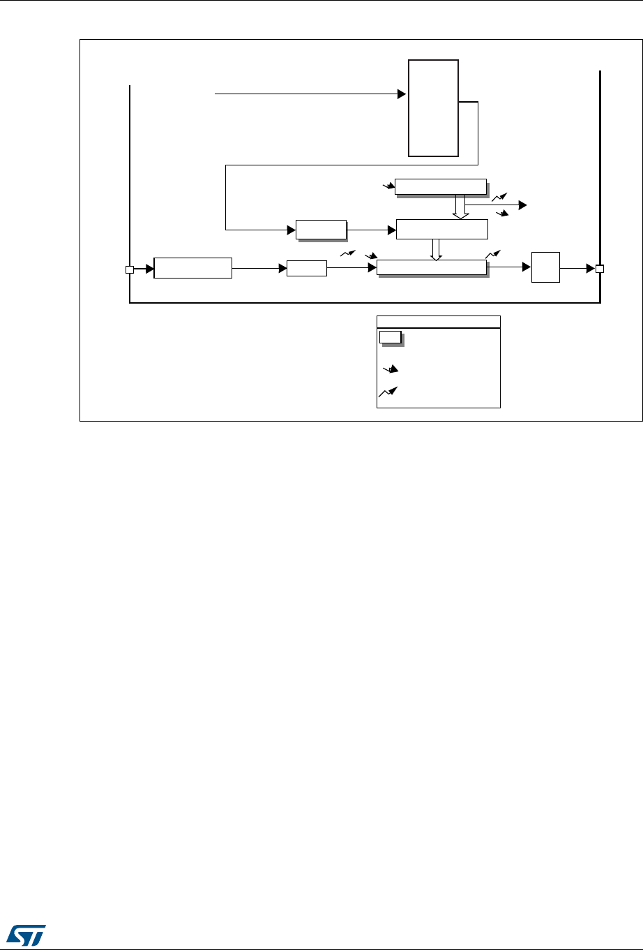
RM0430 Rev 8 597/1324
RM0430 General-purpose timers (TIM9 to TIM14)
641
Figure 182. General-purpose timer block diagram (TIM10/11/13/14)
!UTORELOADREGISTER
#APTURE#OMPAREREGISTER
5
5
##)
3TOP#LEAR
OUTPUT
CONTROL
/#
/#2%&
5
5)
)#
0RESCALER
)NPUTFILTER
EDGEDETECTOR
)#03
4)&0
2EG
EVENT
.OTES
0RELOADREGISTERSTRANSFERRED
TOACTIVEREGISTERSON5EVENT
ACCORDINGTOCONTROLBIT
INTERRUPT$-!OUTPUT
##)
4)
4)-X?#(
PRESCALER COUNTER
#+?03# 03# #.4
#+?#.4
)NTERNALCLOCK#+?).4
AIC
4RIGGER
#ONTROLLER
%NABLE
COUNTER
4)-X?#(

General-purpose timers (TIM9 to TIM14) RM0430
598/1324 RM0430 Rev 8
19.3 TIM9 to TIM14 functional description
19.3.1 Time-base unit
The main block of the timer is a 16-bit counter with its related auto-reload register. The
counters counts up.
The counter clock can be divided by a prescaler.
The counter, the auto-reload register and the prescaler register can be written or read by
software. This is true even when the counter is running.
The time-base unit includes:
•Counter register (TIMx_CNT)
•Prescaler register (TIMx_PSC)
•Auto-reload register (TIMx_ARR)
The auto-reload register is preloaded. Writing to or reading from the auto-reload register
accesses the preload register. The content of the preload register are transferred into the
shadow register permanently or at each update event (UEV), depending on the auto-reload
preload enable bit (ARPE) in TIMx_CR1 register. The update event is sent when the counter
reaches the overflow and if the UDIS bit equals 0 in the TIMx_CR1 register. It can also be
generated by software. The generation of the update event is described in details for each
configuration.
The counter is clocked by the prescaler output CK_CNT, which is enabled only when the
counter enable bit (CEN) in TIMx_CR1 register is set (refer also to the slave mode controller
description to get more details on counter enabling).
Note that the counter starts counting 1 clock cycle after setting the CEN bit in the TIMx_CR1
register.
Prescaler description
The prescaler can divide the counter clock frequency by any factor between 1 and 65536. It
is based on a 16-bit counter controlled through a 16-bit register (in the TIMx_PSC register).
It can be changed on the fly as this control register is buffered. The new prescaler ratio is
taken into account at the next update event.
Figure 183 and Figure 184 give some examples of the counter behavior when the prescaler
ratio is changed on the fly.
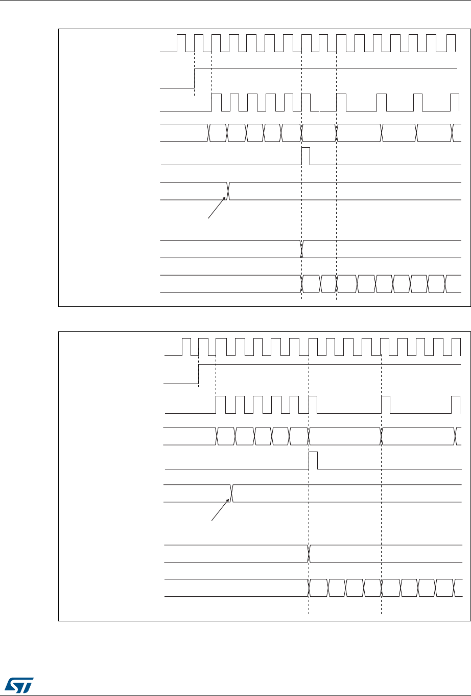
RM0430 Rev 8 599/1324
RM0430 General-purpose timers (TIM9 to TIM14)
641
Figure 183. Counter timing diagram with prescaler division change from 1 to 2
Figure 184. Counter timing diagram with prescaler division change from 1 to 4
&.B36&
&(1
7LPHUFORFN &.B&17
&RXQWHUUHJLVWHU
8SGDWHHYHQW8(9
3UHVFDOHUFRQWUROUHJLVWHU
:ULWHDQHZYDOXHLQ7,0[B36&
3UHVFDOHUEXIIHU
3UHVFDOHUFRXQWHU
)$ )%) ) ) )&
069
069
&.B36&
&(1
7LPHUFORFN &.B&17
&RXQWHUUHJLVWHU
8SGDWHHYHQW8(9
3UHVFDOHUFRQWUROUHJLVWHU
:ULWHDQHZYDOXHLQ7,0[B36&
3UHVFDOHUEXIIHU
3UHVFDOHUFRXQWHU
)$ )%
) ) ) )&
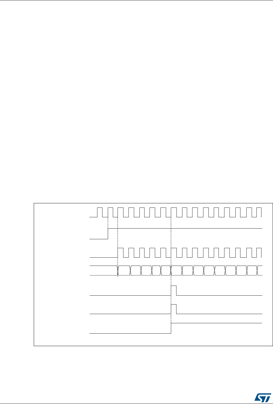
General-purpose timers (TIM9 to TIM14) RM0430
600/1324 RM0430 Rev 8
19.3.2 Counter modes
Upcounting mode
In upcounting mode, the counter counts from 0 to the auto-reload value (content of the
TIMx_ARR register), then restarts from 0 and generates a counter overflow event.
Setting the UG bit in the TIMx_EGR register (by software or by using the slave mode
controller on TIM9 and TIM12) also generates an update event.
The UEV event can be disabled by software by setting the UDIS bit in the TIMx_CR1
register. This is to avoid updating the shadow registers while writing new values in the
preload registers. Then no update event occurs until the UDIS bit has been written to 0.
However, the counter restarts from 0, as well as the counter of the prescaler (but the
prescale rate does not change). In addition, if the URS bit (update request selection) in
TIMx_CR1 register is set, setting the UG bit generates an update event UEV but without
setting the UIF flag (thus no interrupt is sent). This is to avoid generating both update and
capture interrupts when clearing the counter on the capture event.
When an update event occurs, all the registers are updated and the update flag (UIF bit in
TIMx_SR register) is set (depending on the URS bit):
•The auto-reload shadow register is updated with the preload value (TIMx_ARR),
•The buffer of the prescaler is reloaded with the preload value (content of the TIMx_PSC
register).
The following figures show some examples of the counter behavior for different clock
frequencies when TIMx_ARR=0x36.
Figure 185. Counter timing diagram, internal clock divided by 1
ϬϬ ϬϮ Ϭϯ Ϭϰ Ϭϱ Ϭϲ Ϭϳϯϯ ϯϰ ϯϱ ϯϲϯϭ
069
<ͺW^
EdͺE
dŝŵĞƌĐůŽĐŬс<ͺEd
ŽƵŶƚĞƌƌĞŐŝƐƚĞƌ
hƉĚĂƚĞĞǀĞŶƚ;hsͿ
ŽƵŶƚĞƌŽǀĞƌĨůŽǁ
hƉĚĂƚĞŝŶƚĞƌƌƵƉƚĨůĂŐ;h/&Ϳ
ϬϭϯϮ
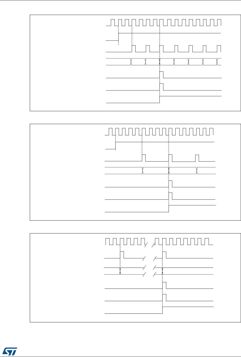
RM0430 Rev 8 601/1324
RM0430 General-purpose timers (TIM9 to TIM14)
641
Figure 186. Counter timing diagram, internal clock divided by 2
Figure 187. Counter timing diagram, internal clock divided by 4
Figure 188. Counter timing diagram, internal clock divided by N
069
&.B36&
&17B(1
7LPHUFORFN &.B&17
&RXQWHUUHJLVWHU
8SGDWHHYHQW8(9
&RXQWHURYHUIORZ
8SGDWHLQWHUUXSWIODJ8,)
069
&.B36&
&17B(1
7LPHUFORFN &.B&17
&RXQWHUUHJLVWHU
8SGDWHHYHQW8(9
&RXQWHURYHUIORZ
8SGDWHLQWHUUXSWIODJ8,)
069
&.B36&
7LPHUFORFN &.B&17
&RXQWHUUHJLVWHU
8SGDWHHYHQW8(9
&RXQWHURYHUIORZ
8SGDWHLQWHUUXSWIODJ8,)
)
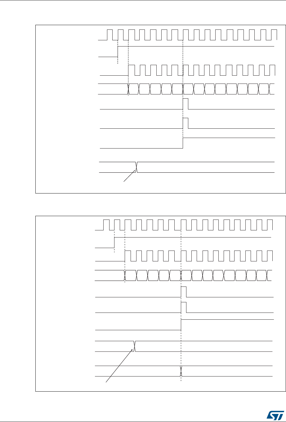
General-purpose timers (TIM9 to TIM14) RM0430
602/1324 RM0430 Rev 8
Figure 189. Counter timing diagram, update event when ARPE=0
(TIMx_ARR not preloaded)
Figure 190. Counter timing diagram, update event when ARPE=1
(TIMx_ARR preloaded)
&& ϯϲ
069
<ͺW^
dŝŵĞƌĐůŽĐŬс<ͺEd
ŽƵŶƚĞƌƌĞŐŝƐƚĞƌ
hƉĚĂƚĞĞǀĞŶƚ;hsͿ
ŽƵŶƚĞƌŽǀĞƌĨůŽǁ
hƉĚĂƚĞŝŶƚĞƌƌƵƉƚĨůĂŐ;h/&Ϳ
ϬϬ ϬϮ Ϭϯ Ϭϰ Ϭϱ Ϭϲ ϬϳϯϮ ϯϯ ϯϰ ϯϱ ϯϲϯϭ Ϭϭ
E
ƵƚŽͲƌĞůŽĂĚƉƌĞůŽĂĚƌĞŐŝƐƚĞƌ
tƌŝƚĞĂŶĞǁǀĂůƵĞŝŶd/DdžͺZZ
069
)
&.B36&
7LPHUFORFN &.B&17
&RXQWHUUHJLVWHU
8SGDWHHYHQW8(9
&RXQWHURYHUIORZ
8SGDWHLQWHUUXSWIODJ
8,)
) ) ) ) ))
&(1
$XWRUHORDGSUHORDG
UHJLVWHU
:ULWHDQHZYDOXHLQ7,0[B$55
$XWRUHORDGVKDGRZ
UHJLVWHU )
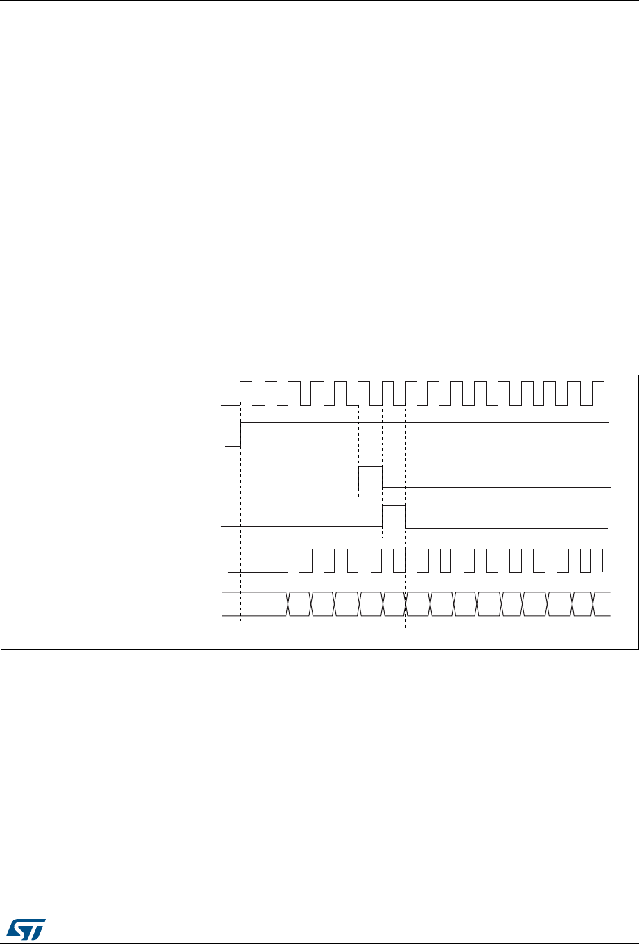
RM0430 Rev 8 603/1324
RM0430 General-purpose timers (TIM9 to TIM14)
641
19.3.3 Clock selection
The counter clock can be provided by the following clock sources:
•Internal clock (CK_INT)
•External clock mode1 (for TIM9 and TIM12): external input pin (TIx)
•Internal trigger inputs (ITRx) (for TIM9 and TIM12): connecting the trigger output from
another timer. Refer to Using one timer as prescaler for another for more details.
Internal clock source (CK_INT)
The internal clock source is the default clock source for TIM10/TIM11 and TIM13/TIM14.
For TIM9 and TIM12, the internal clock source is selected when the slave mode controller is
disabled (SMS=’000’). The CEN bit in the TIMx_CR1 register and the UG bit in the
TIMx_EGR register are then used as control bits and can be changed only by software
(except for UG which remains cleared). As soon as the CEN bit is programmed to 1, the
prescaler is clocked by the internal clock CK_INT.
Figure 191 shows the behavior of the control circuit and the upcounter in normal mode,
without prescaler.
Figure 191. Control circuit in normal mode, internal clock divided by 1
External clock source mode 1(TIM9 and TIM12)
This mode is selected when SMS=’111’ in the TIMx_SMCR register. The counter can count
at each rising or falling edge on a selected input.
,QWHUQDOFORFN
&RXQWHUFORFN &.B&17 &.B36&
&RXQWHUUHJLVWHU
&(1 &17B(1
8*
&17B,1,7
069

General-purpose timers (TIM9 to TIM14) RM0430
604/1324 RM0430 Rev 8
Figure 192. TI2 external clock connection example
For example, to configure the upcounter to count in response to a rising edge on the TI2
input, use the following procedure:
1. Configure channel 2 to detect rising edges on the TI2 input by writing CC2S = ‘01’ in
the TIMx_CCMR1 register.
2. Configure the input filter duration by writing the IC2F[3:0] bits in the TIMx_CCMR1
register (if no filter is needed, keep IC2F=’0000’).
3. Select the rising edge polarity by writing CC2P=’0’ and CC2NP=’0’ in the TIMx_CCER
register.
4. Configure the timer in external clock mode 1 by writing SMS=’111’ in the TIMx_SMCR
register.
5. Select TI2 as the trigger input source by writing TS=’110’ in the TIMx_SMCR register.
6. Enable the counter by writing CEN=’1’ in the TIMx_CR1 register.
Note: The capture prescaler is not used for triggering, so you don’t need to configure it.
When a rising edge occurs on TI2, the counter counts once and the TIF flag is set.
The delay between the rising edge on TI2 and the actual clock of the counter is due to the
resynchronization circuit on TI2 input.
Figure 193. Control circuit in external clock mode 1
([WHUQDOFORFN
PRGH
,QWHUQDOFORFN
PRGH
75*,
&.B,17
&.B36&
7,0[B60&5
606>@
,75[
7,B('
7,)3
7,)3
7,0[B60&5
76>@
7,
7,0[B&&(5
&&3
)LOWHU
,&)>@
7,0[B&&05
(GJH
GHWHFWRU
7,)B5LVLQJ
7,)B)DOOLQJ
[[
069
LQWHUQDOFORFN
7,) RU
7,) RU
RU
&RXQWHUFORFN &.B&17 &.B36&
&RXQWHUUHJLVWHU
7,
&17B(1
7,)
:ULWH7,) 069
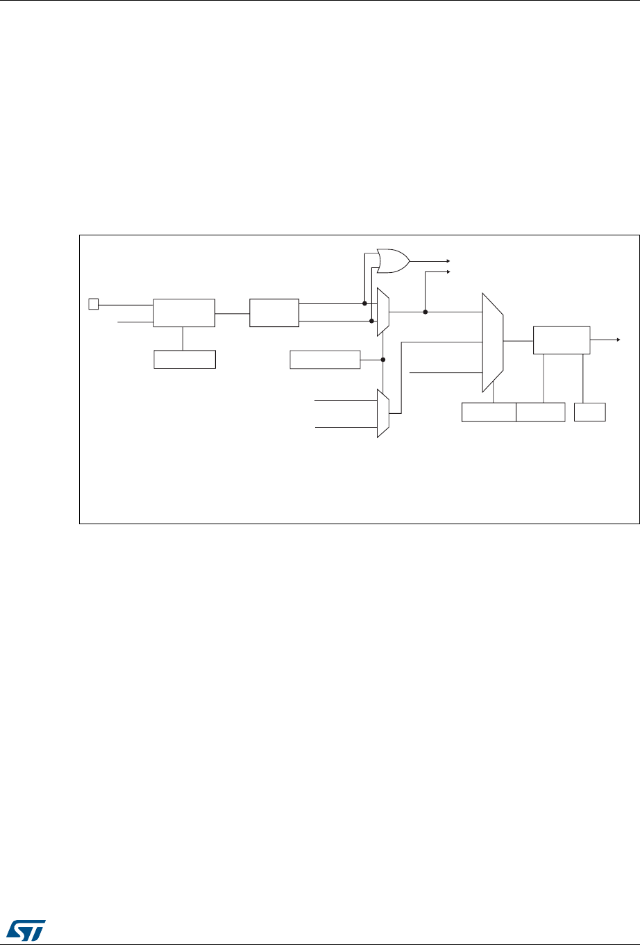
RM0430 Rev 8 605/1324
RM0430 General-purpose timers (TIM9 to TIM14)
641
19.3.4 Capture/compare channels
Each Capture/Compare channel is built around a capture/compare register (including a
shadow register), a input stage for capture (with digital filter, multiplexing and prescaler) and
an output stage (with comparator and output control).
Figure 194 to Figure 196 give an overview of one capture/compare channel.
The input stage samples the corresponding TIx input to generate a filtered signal TIxF.
Then, an edge detector with polarity selection generates a signal (TIxFPx) which can be
used as trigger input by the slave mode controller or as the capture command. It is
prescaled before the capture register (ICxPS).
Figure 194. Capture/compare channel (example: channel 1 input stage)
The output stage generates an intermediate waveform which is then used for reference:
OCxRef (active high). The polarity acts at the end of the chain.
'LYLGHU
,&36>@
7,)B('
7RWKHVODYHPRGHFRQWUROOHU
7,)3
&&6>@
,&
7,)3
75&
IURPVODYHPRGH
FRQWUROOHU
,&36
069
7,
7,0[B&&(5
&&3&&13
)LOWHU
GRZQFRXQWHU
,&)>@
7,0[B&&05
(GJH
GHWHFWRU
7,)B5LVLQJ
7,)B)DOOLQJ
7,0[B&&05
7,0[B&&(5
7,)B5LVLQJ
IURPFKDQQHO
7,)B)DOOLQJ
IURPFKDQQHO
7,)
I
&&(
'76
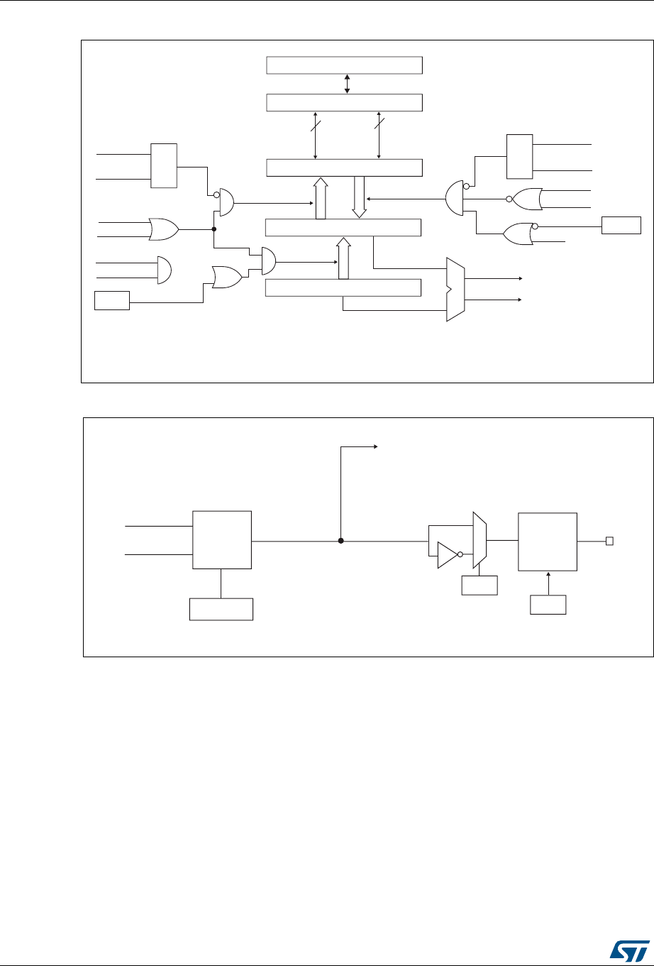
General-purpose timers (TIM9 to TIM14) RM0430
606/1324 RM0430 Rev 8
Figure 195. Capture/compare channel 1 main circuit
Figure 196. Output stage of capture/compare channel (channel 1)
The capture/compare block is made of one preload register and one shadow register. Write
and read always access the preload register.
In capture mode, captures are actually done in the shadow register, which is copied into the
preload register.
In compare mode, the content of the preload register is copied into the shadow register
which is compared to the counter.
19.3.5 Input capture mode
In Input capture mode, the Capture/Compare Registers (TIMx_CCRx) are used to latch the
value of the counter after a transition detected by the corresponding ICx signal. When a
capture occurs, the corresponding CCXIF flag (TIMx_SR register) is set and an interrupt or
a DMA request can be sent if they are enabled. If a capture occurs while the CCxIF flag was
already high, then the over-capture flag CCxOF (TIMx_SR register) is set. CCxIF can be
&&(
&DSWXUHFRPSDUHVKDGRZUHJLVWHU
&RPSDUDWRU
&DSWXUHFRPSDUHSUHORDGUHJLVWHU
&RXQWHU
,&36
&&6>@
&&6>@
&DSWXUH
,QSXW
PRGH
6
5
5HDG&&5+
5HDG&&5/
UHDGBLQBSURJUHVV
FDSWXUHBWUDQVIHU &&6>@
&&6>@
6
5
ZULWH&&5+
ZULWH&&5/
ZULWHBLQBSURJUHVV
2XWSXW
PRGH
8(9
2&3(
IURPWLPH
EDVHXQLW
FRPSDUHBWUDQVIHU
$3%%XV
KLJK
ORZ
LIELW
0&8SHULSKHUDOLQWHUIDFH
7,0B&&05
2&3(
&17!&&5
&17 &&5
7,0B(*5
&&*
069
DL
2XWSXW
PRGH
FRQWUROOHU
&17!&&5
&17 &&5
7,0[B&&05
2&0>@
&&3
7,0[B&&(5
2XWSXW
HQDEOH
FLUFXLW
2&
&&( 7,0[B&&(5
7RWKHPDVWHU
PRGHFRQWUROOHU
2&B5()

RM0430 Rev 8 607/1324
RM0430 General-purpose timers (TIM9 to TIM14)
641
cleared by software by writing it to ‘0’ or by reading the captured data stored in the
TIMx_CCRx register. CCxOF is cleared when you write it to ‘0’.
The following example shows how to capture the counter value in TIMx_CCR1 when TI1
input rises. To do this, use the following procedure:
1. Select the active input: TIMx_CCR1 must be linked to the TI1 input, so write the CC1S
bits to ‘01’ in the TIMx_CCMR1 register. As soon as CC1S becomes different from ‘00’,
the channel is configured in input mode and the TIMx_CCR1 register becomes read-
only.
2. Program the input filter duration you need with respect to the signal you connect to the
timer (by programming the ICxF bits in the TIMx_CCMRx register if the input is one of
the TIx inputs). Let’s imagine that, when toggling, the input signal is not stable during at
must 5 internal clock cycles. We must program a filter duration longer than these 5
clock cycles. We can validate a transition on TI1 when 8 consecutive samples with the
new level have been detected (sampled at fDTS frequency). Then write IC1F bits to
‘0011’ in the TIMx_CCMR1 register.
3. Select the edge of the active transition on the TI1 channel by programming CC1P and
CC1NP bits to ‘00’ in the TIMx_CCER register (rising edge in this case).
4. Program the input prescaler. In our example, we wish the capture to be performed at
each valid transition, so the prescaler is disabled (write IC1PS bits to ‘00’ in the
TIMx_CCMR1 register).
5. Enable capture from the counter into the capture register by setting the CC1E bit in the
TIMx_CCER register.
6. If needed, enable the related interrupt request by setting the CC1IE bit in the
TIMx_DIER register.
When an input capture occurs:
•The TIMx_CCR1 register gets the value of the counter on the active transition.
•CC1IF flag is set (interrupt flag). CC1OF is also set if at least two consecutive captures
occurred whereas the flag was not cleared.
•An interrupt is generated depending on the CC1IE bit.
In order to handle the overcapture, it is recommended to read the data before the
overcapture flag. This is to avoid missing an overcapture which could happen after reading
the flag and before reading the data.
Note: IC interrupt requests can be generated by software by setting the corresponding CCxG bit in
the TIMx_EGR register.
19.3.6 PWM input mode (only for TIM9/12)
This mode is a particular case of input capture mode. The procedure is the same except:
•Two ICx signals are mapped on the same TIx input.
•These 2 ICx signals are active on edges with opposite polarity.
•One of the two TIxFP signals is selected as trigger input and the slave mode controller
is configured in reset mode.
For example, you can measure the period (in TIMx_CCR1 register) and the duty cycle (in
TIMx_CCR2 register) of the PWM applied on TI1 using the following procedure (depending
on CK_INT frequency and prescaler value):
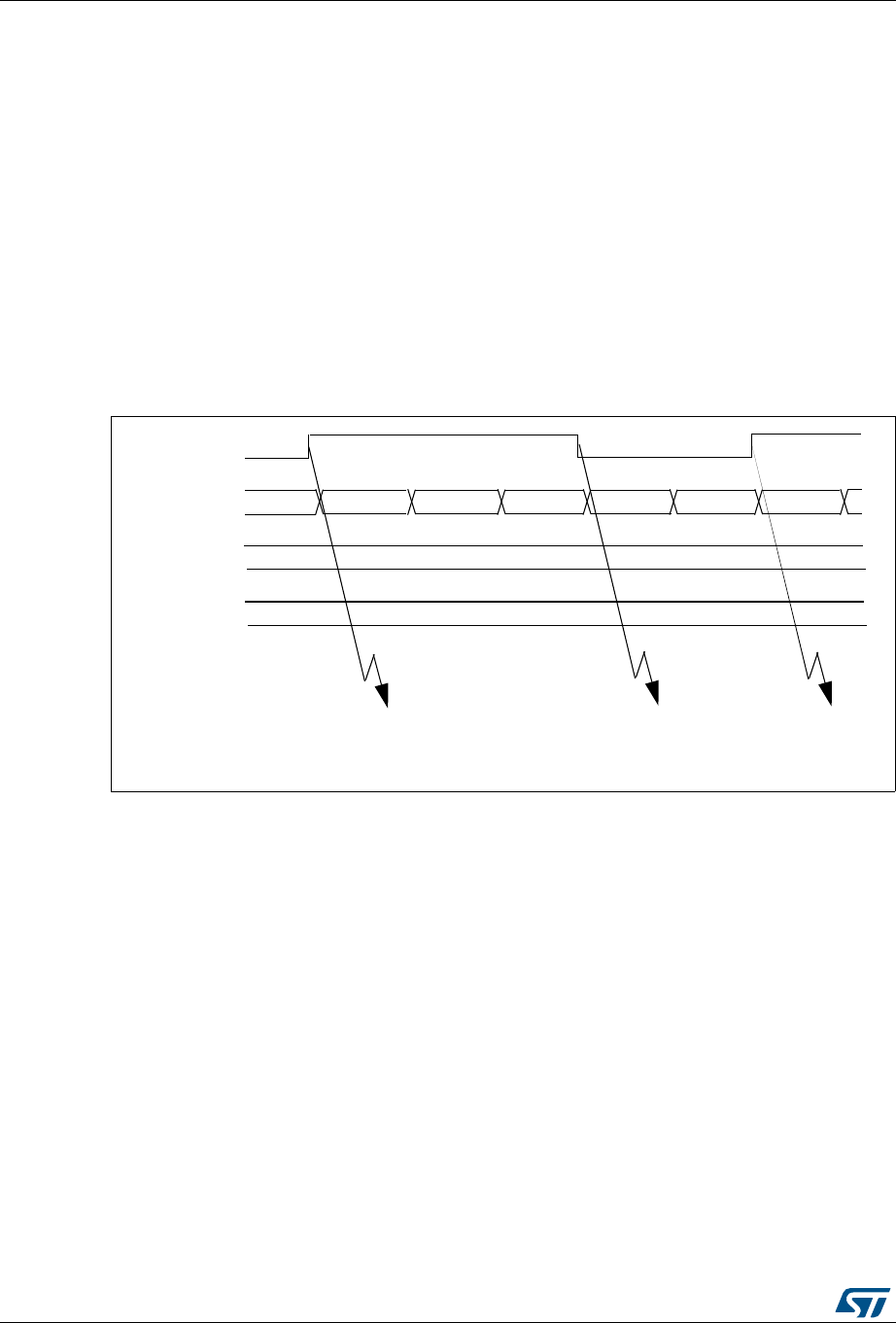
General-purpose timers (TIM9 to TIM14) RM0430
608/1324 RM0430 Rev 8
1. Select the active input for TIMx_CCR1: write the CC1S bits to ‘01’ in the TIMx_CCMR1
register (TI1 selected).
2. Select the active polarity for TI1FP1 (used both for capture in TIMx_CCR1 and counter
clear): program the CC1P and CC1NP bits to ‘00’ (active on rising edge).
3. Select the active input for TIMx_CCR2: write the CC2S bits to ‘10’ in the TIMx_CCMR1
register (TI1 selected).
4. Select the active polarity for TI1FP2 (used for capture in TIMx_CCR2): program the
CC2P and CC2NP bits to ‘11’ (active on falling edge).
5. Select the valid trigger input: write the TS bits to ‘101’ in the TIMx_SMCR register
(TI1FP1 selected).
6. Configure the slave mode controller in reset mode: write the SMS bits to ‘100’ in the
TIMx_SMCR register.
7. Enable the captures: write the CC1E and CC2E bits to ‘1’ in the TIMx_CCER register.
Figure 197. PWM input mode timing
1. The PWM input mode can be used only with the TIMx_CH1/TIMx_CH2 signals due to the fact that only
TI1FP1 and TI2FP2 are connected to the slave mode controller.
19.3.7 Forced output mode
In output mode (CCxS bits = ‘00’ in the TIMx_CCMRx register), each output compare signal
(OCxREF and then OCx) can be forced to active or inactive level directly by software,
independently of any comparison between the output compare register and the counter.
To force an output compare signal (OCXREF/OCx) to its active level, you just need to write
‘101’ in the OCxM bits in the corresponding TIMx_CCMRx register. Thus OCXREF is forced
high (OCxREF is always active high) and OCx get opposite value to CCxP polarity bit.
For example: CCxP=’0’ (OCx active high) => OCx is forced to high level.
The OCxREF signal can be forced low by writing the OCxM bits to ‘100’ in the
TIMx_CCMRx register.
Anyway, the comparison between the TIMx_CCRx shadow register and the counter is still
performed and allows the flag to be set. Interrupt requests can be sent accordingly. This is
described in the output compare mode section below.
TI1
TIMx_CNT 0000 0001 0002 0003 0004 00000004
TIMx_CCR1
TIMx_CCR2
0004
0002
IC1 capture
IC2 capture
reset counter
IC2 capture
pulse width
IC1 capture
period
measurementmeasurement
ai15413

RM0430 Rev 8 609/1324
RM0430 General-purpose timers (TIM9 to TIM14)
641
19.3.8 Output compare mode
This function is used to control an output waveform or indicating when a period of time has
elapsed.
When a match is found between the capture/compare register and the counter, the output
compare function:
1. Assigns the corresponding output pin to a programmable value defined by the output
compare mode (OCxM bits in the TIMx_CCMRx register) and the output polarity (CCxP
bit in the TIMx_CCER register). The output pin can keep its level (OCXM=’000’), be set
active (OCxM=’001’), be set inactive (OCxM=’010’) or can toggle (OCxM=’011’) on
match.
2. Sets a flag in the interrupt status register (CCxIF bit in the TIMx_SR register).
3. Generates an interrupt if the corresponding interrupt mask is set (CCXIE bit in the
TIMx_DIER register).
The TIMx_CCRx registers can be programmed with or without preload registers using the
OCxPE bit in the TIMx_CCMRx register.
In output compare mode, the update event UEV has no effect on OCxREF and OCx output.
The timing resolution is one count of the counter. Output compare mode can also be used to
output a single pulse (in One-pulse mode).
Procedure:
1. Select the counter clock (internal, external, prescaler).
2. Write the desired data in the TIMx_ARR and TIMx_CCRx registers.
3. Set the CCxIE bit if an interrupt request is to be generated.
4. Select the output mode. For example:
– Write OCxM = ‘011’ to toggle OCx output pin when CNT matches CCRx
– Write OCxPE = ‘0’ to disable preload register
– Write CCxP = ‘0’ to select active high polarity
– Write CCxE = ‘1’ to enable the output
5. Enable the counter by setting the CEN bit in the TIMx_CR1 register.
The TIMx_CCRx register can be updated at any time by software to control the output
waveform, provided that the preload register is not enabled (OCxPE=’0’, else TIMx_CCRx
shadow register is updated only at the next update event UEV). An example is given in
Figure 198.
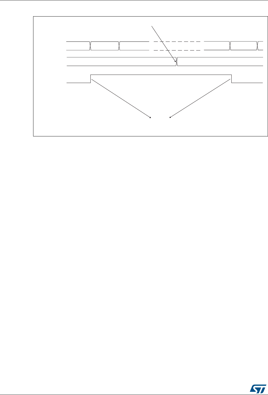
General-purpose timers (TIM9 to TIM14) RM0430
610/1324 RM0430 Rev 8
Figure 198. Output compare mode, toggle on OC1.
19.3.9 PWM mode
Pulse Width Modulation mode allows you to generate a signal with a frequency determined
by the value of the TIMx_ARR register and a duty cycle determined by the value of the
TIMx_CCRx register.
The PWM mode can be selected independently on each channel (one PWM per OCx
output) by writing ‘110’ (PWM mode 1) or ‘111’ (PWM mode 2) in the OCxM bits in the
TIMx_CCMRx register. You must enable the corresponding preload register by setting the
OCxPE bit in the TIMx_CCMRx register, and eventually the auto-reload preload register (in
upcounting or center-aligned modes) by setting the ARPE bit in the TIMx_CR1 register.
As the preload registers are transferred to the shadow registers only when an update event
occurs, before starting the counter, you have to initialize all the registers by setting the UG
bit in the TIMx_EGR register.
The OCx polarity is software programmable using the CCxP bit in the TIMx_CCER register.
It can be programmed as active high or active low. The OCx output is enabled by the CCxE
bit in the TIMx_CCER register. Refer to the TIMx_CCERx register description for more
details.
In PWM mode (1 or 2), TIMx_CNT and TIMx_CCRx are always compared to determine
whether TIMx_CNT ≤ TIMx_CCRx.
The timer is able to generate PWM in edge-aligned mode only since the counter is
upcounting.
PWM edge-aligned mode
In the following example, we consider PWM mode 1. The reference PWM signal OCxREF is
high as long as TIMx_CNT < TIMx_CCRx else it becomes low. If the compare value in
TIMx_CCRx is greater than the auto-reload value (in TIMx_ARR) then OCxREF is held at
‘1’. If the compare value is 0 then OCxRef is held at ‘0’. Figure 199 shows some edge-
aligned PWM waveforms in an example where TIMx_ARR=8.
069
2&5() 2&
7,0B&17 % %
7,0B&&5 $
:ULWH%KLQWKH&&5UHJLVWHU
0DWFKGHWHFWHGRQ&&5
,QWHUUXSWJHQHUDWHGLIHQDEOHG
%
%
$
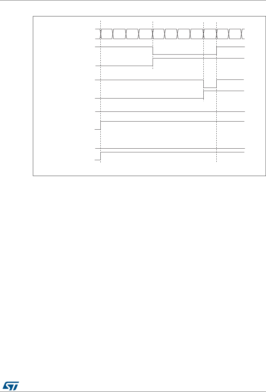
RM0430 Rev 8 611/1324
RM0430 General-purpose timers (TIM9 to TIM14)
641
Figure 199. Edge-aligned PWM waveforms (ARR=8)
19.3.10 One-pulse mode
One-pulse mode (OPM) is a particular case of the previous modes. It allows the counter to
be started in response to a stimulus and to generate a pulse with a programmable length
after a programmable delay.
Starting the counter can be controlled through the slave mode controller. Generating the
waveform can be done in output compare mode or PWM mode. You select One-pulse mode
by setting the OPM bit in the TIMx_CR1 register. This makes the counter stop automatically
at the next update event UEV.
A pulse can be correctly generated only if the compare value is different from the counter
initial value. Before starting (when the timer is waiting for the trigger), the configuration must
be as follows:
CNT < CCRx ≤ ARR (in particular, 0 < CCRx)
069
&RXQWHUUHJLVWHU
µ
2&;5()
&&[,)
2&;5()
&&[,)
2&;5()
&&[,)
2&;5()
&&[,)
&&5[
&&5[
&&5[!
&&5[
µ
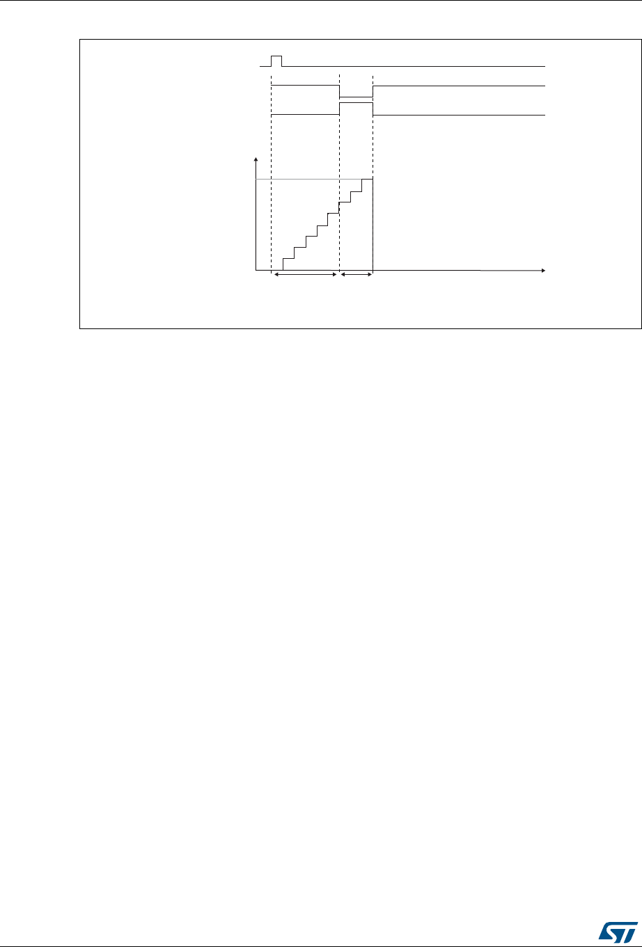
General-purpose timers (TIM9 to TIM14) RM0430
612/1324 RM0430 Rev 8
Figure 200. Example of one pulse mode.
For example you may want to generate a positive pulse on OC1 with a length of tPULSE and
after a delay of tDELAY as soon as a positive edge is detected on the TI2 input pin.
Use TI2FP2 as trigger 1:
1. Map TI2FP2 to TI2 by writing CC2S=’01’ in the TIMx_CCMR1 register.
2. TI2FP2 must detect a rising edge, write CC2P=’0’ and CC2NP = ‘0’ in the TIMx_CCER
register.
3. Configure TI2FP2 as trigger for the slave mode controller (TRGI) by writing TS=’110’ in
the TIMx_SMCR register.
4. TI2FP2 is used to start the counter by writing SMS to ‘110’ in the TIMx_SMCR register
(trigger mode).
The OPM waveform is defined by writing the compare registers (taking into account the
clock frequency and the counter prescaler).
•The tDELAY is defined by the value written in the TIMx_CCR1 register.
•The tPULSE is defined by the difference between the auto-reload value and the compare
value (TIMx_ARR - TIMx_CCR1).
•Let’s say you want to build a waveform with a transition from ‘0’ to ‘1’ when a compare
match occurs and a transition from ‘1’ to ‘0’ when the counter reaches the auto-reload
value. To do this you enable PWM mode 2 by writing OC1M=’111’ in the TIMx_CCMR1
register. You can optionally enable the preload registers by writing OC1PE=’1’ in the
TIMx_CCMR1 register and ARPE in the TIMx_CR1 register. In this case you have to
write the compare value in the TIMx_CCR1 register, the auto-reload value in the
TIMx_ARR register, generate an update by setting the UG bit and wait for external
trigger event on TI2. CC1P is written to ‘0’ in this example.
You only want 1 pulse (Single mode), so you write '1 in the OPM bit in the TIMx_CR1
register to stop the counter at the next update event (when the counter rolls over from the
auto-reload value back to 0). When OPM bit in the TIMx_CR1 register is set to '0', so the
Repetitive Mode is selected.
069
7,
2&5()
&RXQWHU
W
7,0B$55
7,0B&&5
2&
W'(/$< W38/6(

RM0430 Rev 8 613/1324
RM0430 General-purpose timers (TIM9 to TIM14)
641
Particular case: OCx fast enable
In One-pulse mode, the edge detection on TIx input set the CEN bit which enables the
counter. Then the comparison between the counter and the compare value makes the
output toggle. But several clock cycles are needed for these operations and it limits the
minimum delay tDELAY min we can get.
If you want to output a waveform with the minimum delay, you can set the OCxFE bit in the
TIMx_CCMRx register. Then OCxRef (and OCx) are forced in response to the stimulus,
without taking in account the comparison. Its new level is the same as if a compare match
had occurred. OCxFE acts only if the channel is configured in PWM1 or PWM2 mode.
19.3.11 TIM9/12 external trigger synchronization
The TIM9/12 timers can be synchronized with an external trigger in several modes: Reset
mode, Gated mode and Trigger mode.
Slave mode: Reset mode
The counter and its prescaler can be reinitialized in response to an event on a trigger input.
Moreover, if the URS bit from the TIMx_CR1 register is low, an update event UEV is
generated. Then all the preloaded registers (TIMx_ARR, TIMx_CCRx) are updated.
In the following example, the upcounter is cleared in response to a rising edge on TI1 input:
1. Configure the channel 1 to detect rising edges on TI1. Configure the input filter duration
(in this example, we don’t need any filter, so we keep IC1F=’0000’). The capture
prescaler is not used for triggering, so you don’t need to configure it. The CC1S bits
select the input capture source only, CC1S = ‘01’ in the TIMx_CCMR1 register.
Program CC1P and CC1NP to ‘00’ in TIMx_CCER register to validate the polarity (and
detect rising edges only).
2. Configure the timer in reset mode by writing SMS=’100’ in TIMx_SMCR register. Select
TI1 as the input source by writing TS=’101’ in TIMx_SMCR register.
3. Start the counter by writing CEN=’1’ in the TIMx_CR1 register.
The counter starts counting on the internal clock, then behaves normally until TI1 rising
edge. When TI1 rises, the counter is cleared and restarts from 0. In the meantime, the
trigger flag is set (TIF bit in the TIMx_SR register) and an interrupt request can be sent if
enabled (depending on the TIE bit in TIMx_DIER register).
The following figure shows this behavior when the auto-reload register TIMx_ARR=0x36.
The delay between the rising edge on TI1 and the actual reset of the counter is due to the
resynchronization circuit on TI1 input.

General-purpose timers (TIM9 to TIM14) RM0430
614/1324 RM0430 Rev 8
Figure 201. Control circuit in reset mode
Slave mode: Gated mode
The counter can be enabled depending on the level of a selected input.
In the following example, the upcounter counts only when TI1 input is low:
1. Configure the channel 1 to detect low levels on TI1. Configure the input filter duration
(in this example, we don’t need any filter, so we keep IC1F=’0000’). The capture
prescaler is not used for triggering, so you don’t need to configure it. The CC1S bits
select the input capture source only, CC1S=’01’ in TIMx_CCMR1 register. Program
CC1P=’1’ and CC1NP= ‘0’ in TIMx_CCER register to validate the polarity (and detect
low level only).
2. Configure the timer in gated mode by writing SMS=’101’ in TIMx_SMCR register.
Select TI1 as the input source by writing TS=’101’ in TIMx_SMCR register.
3. Enable the counter by writing CEN=’1’ in the TIMx_CR1 register (in gated mode, the
counter doesn’t start if CEN=’0’, whatever is the trigger input level).
The counter starts counting on the internal clock as long as TI1 is low and stops as soon as
TI1 becomes high. The TIF flag in the TIMx_SR register is set both when the counter starts
or stops.
The delay between the rising edge on TI1 and the actual stop of the counter is due to the
resynchronization circuit on TI1 input.
069
&RXQWHUFORFN FNBFQW FNBSVF
&RXQWHUUHJLVWHU
8*
7,
7,)
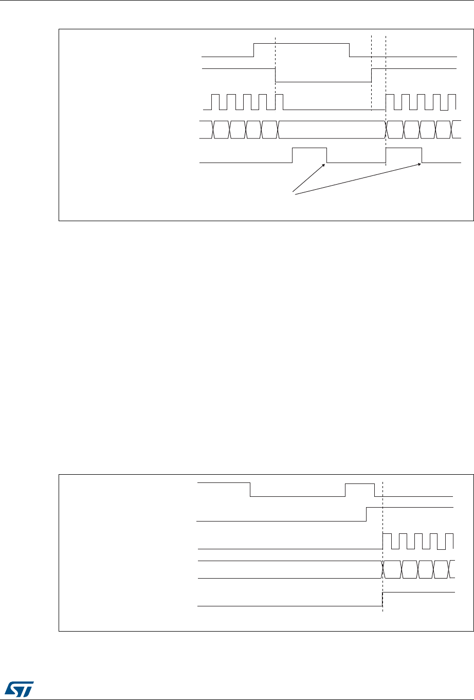
RM0430 Rev 8 615/1324
RM0430 General-purpose timers (TIM9 to TIM14)
641
Figure 202. Control circuit in gated mode
Slave mode: Trigger mode
The counter can start in response to an event on a selected input.
In the following example, the upcounter starts in response to a rising edge on TI2 input:
1. Configure the channel 2 to detect rising edges on TI2. Configure the input filter duration
(in this example, we don’t need any filter, so we keep IC2F=’0000’). The capture
prescaler is not used for triggering, so you don’t need to configure it. The CC2S bits are
configured to select the input capture source only, CC2S=’01’ in TIMx_CCMR1 register.
Program CC2P=’1’ and CC2NP=’0’ in TIMx_CCER register to validate the polarity (and
detect low level only).
2. Configure the timer in trigger mode by writing SMS=’110’ in TIMx_SMCR register.
Select TI2 as the input source by writing TS=’110’ in TIMx_SMCR register.
When a rising edge occurs on TI2, the counter starts counting on the internal clock and the
TIF flag is set.
The delay between the rising edge on TI2 and the actual start of the counter is due to the
resynchronization circuit on TI2 input.
Figure 203. Control circuit in trigger mode
069
7,
FQWBHQ
:ULWH7,)
&RXQWHUFORFN FNBFQW FNBSVF
&RXQWHUUHJLVWHU
7,)
069
7,
FQWBHQ
&RXQWHUFORFN FNBFQW FNBSVF
&RXQWHUUHJLVWHU
7,)

General-purpose timers (TIM9 to TIM14) RM0430
616/1324 RM0430 Rev 8
19.3.12 Timer synchronization (TIM9/12)
The TIM timers are linked together internally for timer synchronization or chaining. Refer to
Section 18.3.15: Timer synchronization for details.
19.3.13 Debug mode
When the microcontroller enters debug mode (Cortex®-M4 with FPU core halted), the TIMx
counter either continues to work normally or stops, depending on DBG_TIMx_STOP
configuration bit in DBG module. For more details, refer to Section 37.16.2: Debug support
for timers, watchdog, bxCAN and I2C.
19.4 TIM9 and TIM12 registers
Refer to Section 1.2 on page 52 for a list of abbreviations used in register descriptions.
The peripheral registers have to be written by half-words (16 bits) or words (32 bits). Read
accesses can be done by bytes (8 bits), half-words (16 bits) or words (32 bits).
19.4.1 TIM9/12 control register 1 (TIMx_CR1)
Address offset: 0x00
Reset value: 0x0000
1514131211109876543210
Res. Res. Res. Res. Res. Res. CKD[1:0] ARPE Res. Res. Res. OPM URS UDIS CEN
rw rw rw rw rw rw rw
Bits 15:10 Reserved, must be kept at reset value.
Bits 9:8 CKD: Clock division
This bit-field indicates the division ratio between the timer clock (CK_INT) frequency and
sampling clock used by the digital filters (TIx),
00: tDTS = tCK_INT
01: tDTS = 2 × tCK_INT
10: tDTS = 4 × tCK_INT
11: Reserved
Bit 7 ARPE: Auto-reload preload enable
0: TIMx_ARR register is not buffered.
1: TIMx_ARR register is buffered.
Bits 6:4 Reserved, must be kept at reset value.
Bit 3 OPM: One-pulse mode
0: Counter is not stopped on the update event
1: Counter stops counting on the next update event (clearing the CEN bit).

RM0430 Rev 8 617/1324
RM0430 General-purpose timers (TIM9 to TIM14)
641
Bit 2 URS: Update request source
This bit is set and cleared by software to select the UEV event sources.
0: Any of the following events generates an update interrupt if enabled:
– Counter overflow
– Setting the UG bit
1: Only counter overflow generates an update interrupt if enabled.
Bit 1 UDIS: Update disable
This bit is set and cleared by software to enable/disable update event (UEV) generation.
0: UEV enabled. An UEV is generated by one of the following events:
– Counter overflow
– Setting the UG bit
Buffered registers are then loaded with their preload values.
1: UEV disabled. No UEV is generated, shadow registers keep their value (ARR, PSC,
CCRx). The counter and the prescaler are reinitialized if the UG bit is set.
Bit 0 CEN: Counter enable
0: Counter disabled
1: Counter enabled
CEN is cleared automatically in one-pulse mode, when an update event occurs.

General-purpose timers (TIM9 to TIM14) RM0430
618/1324 RM0430 Rev 8
19.4.2 TIM9/12 slave mode control register (TIMx_SMCR)
Address offset: 0x08
Reset value: 0x0000
1514131211109876543210
Res. Res. Res. Res. Res. Res. Res. Res. MSM TS[2:0] Res. SMS[2:0]
rw rw rw rw rw rw rw
Bits 15:8 Reserved, must be kept at reset value.
Bit 7 MSM: Master/Slave mode
0: No action
1: The effect of an event on the trigger input (TRGI) is delayed to allow a perfect
synchronization between the current timer and its slaves (through TRGO). It is useful in
order to synchronize several timers on a single external event.
Bits 6:4 TS: Trigger selection
This bitfield selects the trigger input to be used to synchronize the counter.
000: Internal Trigger 0 (ITR0)
001: Internal Trigger 1 (ITR1)
010: Internal Trigger 2 (ITR2)
011: Internal Trigger 3 (ITR3)
100: TI1 Edge Detector (TI1F_ED)
101: Filtered Timer Input 1 (TI1FP1)
110: Filtered Timer Input 2 (TI2FP2)
111: Reserved.
See Table 109 for more details on the meaning of ITRx for each timer.
Note: These bits must be changed only when they are not used (e.g. when SMS=’000’) to
avoid wrong edge detections at the transition.
Bit 3 Reserved, must be kept at reset value.
Bits 2:0 SMS: Slave mode selection
When external signals are selected, the active edge of the trigger signal (TRGI) is linked to
the polarity selected on the external input (see Input control register and Control register
descriptions.
000: Slave mode disabled - if CEN = 1 then the prescaler is clocked directly by the internal
clock
001: Reserved
010: Reserved
011: Reserved
100: Reset mode - Rising edge of the selected trigger input (TRGI) reinitializes the counter
and generates an update of the registers
101: Gated mode - The counter clock is enabled when the trigger input (TRGI) is high. The
counter stops (but is not reset) as soon as the trigger becomes low. Counter starts and stops
are both controlled
110: Trigger mode - The counter starts on a rising edge of the trigger TRGI (but it is not
reset). Only the start of the counter is controlled
111: External clock mode 1 - Rising edges of the selected trigger (TRGI) clock the counter
Note: The Gated mode must not be used if TI1F_ED is selected as the trigger input
(TS=’100’). Indeed, TI1F_ED outputs 1 pulse for each transition on TI1F, whereas the
Gated mode checks the level of the trigger signal.

RM0430 Rev 8 619/1324
RM0430 General-purpose timers (TIM9 to TIM14)
641
19.4.3 TIM9/12 Interrupt enable register (TIMx_DIER)
Address offset: 0x0C
Reset value: 0x0000
Table 109. TIMx internal trigger connections
Slave TIM ITR0 (TS = ‘000’) ITR1 (TS = ‘001’) ITR2 (TS = ‘010’) ITR3 (TS = ‘011’)
TIM9 TIM2 TIM3 or LPTIM1(1)
1. The selection of TIM3 or LPTIM1 is done via LPTIM1_OR register bit 4. TIM3 is selected by default.
TIM10_OC TIM11_OC
TIM12 TIM4 TIM5 TIM13_OC TIM14_OC
1514131211109876543210
Res. Res. Res. Res. Res. Res. Res. Res. Res. TIE Res. Res. Res. CC2IE CC1IE UIE
rw rw rw rw
Bits 15:7 Reserved, must be kept at reset value.
Bit 6 TIE: Trigger interrupt enable
0: Trigger interrupt disabled.
1: Trigger interrupt enabled.
Bits 5:3 Reserved, must be kept at reset value.
Bit 2 CC2IE: Capture/Compare 2 interrupt enable
0: CC2 interrupt disabled.
1: CC2 interrupt enabled.
Bit 1 CC1IE: Capture/Compare 1 interrupt enable
0: CC1 interrupt disabled.
1: CC1 interrupt enabled.
Bit 0 UIE: Update interrupt enable
0: Update interrupt disabled.
1: Update interrupt enabled.

General-purpose timers (TIM9 to TIM14) RM0430
620/1324 RM0430 Rev 8
19.4.4 TIM9/12 status register (TIMx_SR)
Address offset: 0x10
Reset value: 0x0000
1514131211109876543210
Res. Res. Res. Res. Res. CC2OF CC1OF Res. Res. TIF Res. Res. Res. CC2IF CC1IF UIF
rc_w0 rc_w0 rc_w0 rc_w0 rc_w0 rc_w0
Bits 15:11 Reserved, must be kept at reset value.
Bit 10 CC2OF: Capture/compare 2 overcapture flag
refer to CC1OF description
Bit 9 CC1OF: Capture/Compare 1 overcapture flag
This flag is set by hardware only when the corresponding channel is configured in input
capture mode. It is cleared by software by writing it to ‘0’.
0: No overcapture has been detected.
1: The counter value has been captured in TIMx_CCR1 register while CC1IF flag was
already set
Bits 8:7 Reserved, must be kept at reset value.
Bit 6 TIF: Trigger interrupt flag
This flag is set by hardware on trigger event (active edge detected on TRGI input when the
slave mode controller is enabled in all modes but gated mode. It is set when the counter
starts or stops when gated mode is selected. It is cleared by software.
0: No trigger event occurred.
1: Trigger interrupt pending.
Bits 5:3 Reserved, must be kept at reset value.
Bit 2 CC2IF: Capture/Compare 2 interrupt flag
refer to CC1IF description

RM0430 Rev 8 621/1324
RM0430 General-purpose timers (TIM9 to TIM14)
641
Bit 1 CC1IF: Capture/compare 1 interrupt flag
If channel CC1 is configured as output:
This flag is set by hardware when the counter matches the compare value. It is cleared by
software.
0: No match.
1: The content of the counter TIMx_CNT matches the content of the TIMx_CCR1 register.
When the contents of TIMx_CCR1 are greater than the contents of TIMx_ARR, the CC1IF
bit goes high on the counter overflow.
If channel CC1 is configured as input:
This bit is set by hardware on a capture. It is cleared by software or by reading the
TIMx_CCR1 register.
0: No input capture occurred.
1: The counter value has been captured in TIMx_CCR1 register (an edge has been detected
on IC1 which matches the selected polarity).
Bit 0 UIF: Update interrupt flag
This bit is set by hardware on an update event. It is cleared by software.
0: No update occurred.
1: Update interrupt pending. This bit is set by hardware when the registers are updated:
– At overflow and if UDIS=’0’ in the TIMx_CR1 register.
– When CNT is reinitialized by software using the UG bit in TIMx_EGR register, if URS=’0’ and
UDIS=’0’ in the TIMx_CR1 register.
– When CNT is reinitialized by a trigger event (refer to the synchro control register
description), if URS=’0’ and UDIS=’0’ in the TIMx_CR1 register.

General-purpose timers (TIM9 to TIM14) RM0430
622/1324 RM0430 Rev 8
19.4.5 TIM9/12 event generation register (TIMx_EGR)
Address offset: 0x14
Reset value: 0x0000
19.4.6 TIM9/12 capture/compare mode register 1 (TIMx_CCMR1)
Address offset: 0x18
Reset value: 0x0000
The channels can be used in input (capture mode) or in output (compare mode). The
direction of a channel is defined by configuring the corresponding CCxS bits. All the other
bits in this register have different functions in input and output modes. For a given bit, OCxx
describes its function when the channel is configured in output mode, ICxx describes its
function when the channel is configured in input mode. So you must take care that the same
bit can have different meanings for the input stage and the output stage.
1514131211109876543210
Res. Res. Res. Res. Res. Res. Res. Res. Res. TG Res. Res. Res. CC2G CC1G UG
w www
Bits 15:7 Reserved, must be kept at reset value.
Bit 6 TG: Trigger generation
This bit is set by software in order to generate an event, it is automatically cleared by
hardware.
0: No action
1: The TIF flag is set in the TIMx_SR register. Related interrupt can occur if enabled
Bits 5:3 Reserved, must be kept at reset value.
Bit 2 CC2G: Capture/compare 2 generation
refer to CC1G description
Bit 1 CC1G: Capture/compare 1 generation
This bit is set by software to generate an event, it is automatically cleared by hardware.
0: No action
1: A capture/compare event is generated on channel 1:
If channel CC1 is configured as output:
the CC1IF flag is set, the corresponding interrupt is sent if enabled.
If channel CC1 is configured as input:
The current counter value is captured in the TIMx_CCR1 register. The CC1IF flag is set, the
corresponding interrupt is sent if enabled. The CC1OF flag is set if the CC1IF flag was
already high.
Bit 0 UG: Update generation
This bit can be set by software, it is automatically cleared by hardware.
0: No action
1: Re-initializes the counter and generates an update of the registers. The prescaler counter
is also cleared and the prescaler ratio is not affected. The counter is cleared.
1514131211109876543210
Res. OC2M[2:0] OC2PE OC2FE CC2S[1:0] Res. OC1M[2:0] OC1PE OC1FE CC1S[1:0]
IC2F[3:0] IC2PSC[1:0] IC1F[3:0] IC1PSC[1:0]
rw rw rw rw rw rw rw rw rw rw rw rw rw rw rw rw

RM0430 Rev 8 623/1324
RM0430 General-purpose timers (TIM9 to TIM14)
641
Output compare mode
Bit 15 Reserved, must be kept at reset value.
Bits 14:12 OC2M[2:0]: Output compare 2 mode
Bit 11 OC2PE: Output compare 2 preload enable
Bit 10 OC2FE: Output compare 2 fast enable
Bits 9:8 CC2S[1:0]: Capture/Compare 2 selection
This bitfield defines the direction of the channel (input/output) as well as the used input.
00: CC2 channel is configured as output
01: CC2 channel is configured as input, IC2 is mapped on TI2
10: CC2 channel is configured as input, IC2 is mapped on TI1
11: CC2 channel is configured as input, IC2 is mapped on TRC. This mode works only if an
internal trigger input is selected through the TS bit (TIMx_SMCR register
Note: The CC2S bits are writable only when the channel is OFF (CC2E = 0 in TIMx_CCER).
Bit 7 Reserved, must be kept at reset value.
Bits 6:4 OC1M: Output compare 1 mode
These bits define the behavior of the output reference signal OC1REF from which OC1 and
OC1N are derived. OC1REF is active high whereas the active levels of OC1 and OC1N
depend on the CC1P and CC1NP bits, respectively.
000: Frozen - The comparison between the output compare register TIMx_CCR1 and the
counter TIMx_CNT has no effect on the outputs.(this mode is used to generate a timing
base).
001: Set channel 1 to active level on match. The OC1REF signal is forced high when the
TIMx_CNT counter matches the capture/compare register 1 (TIMx_CCR1).
010: Set channel 1 to inactive level on match. The OC1REF signal is forced low when the
TIMx_CNT counter matches the capture/compare register 1 (TIMx_CCR1).
011: Toggle - OC1REF toggles when TIMx_CNT=TIMx_CCR1
100: Force inactive level - OC1REF is forced low
101: Force active level - OC1REF is forced high
110: PWM mode 1 - In upcounting, channel 1 is active as long as TIMx_CNT<TIMx_CCR1
else it is inactive. In downcounting, channel 1 is inactive (OC1REF=‘0) as long as
TIMx_CNT>TIMx_CCR1, else it is active (OC1REF=’1’)
111: PWM mode 2 - In upcounting, channel 1 is inactive as long as TIMx_CNT<TIMx_CCR1
else it is active. In downcounting, channel 1 is active as long as TIMx_CNT>TIMx_CCR1
else it is inactive.
Note: In PWM mode 1 or 2, the OCREF level changes only when the result of the
comparison changes or when the output compare mode switches from “frozen” mode
to “PWM” mode.

General-purpose timers (TIM9 to TIM14) RM0430
624/1324 RM0430 Rev 8
Bit 3 OC1PE: Output compare 1 preload enable
0: Preload register on TIMx_CCR1 disabled. TIMx_CCR1 can be written at anytime, the
new value is taken into account immediately
1: Preload register on TIMx_CCR1 enabled. Read/Write operations access the preload
register. TIMx_CCR1 preload value is loaded into the active register at each update event
Note: The PWM mode can be used without validating the preload register only in one-pulse
mode (OPM bit set in the TIMx_CR1 register). Else the behavior is not guaranteed.
Bit 2 OC1FE: Output compare 1 fast enable
This bit is used to accelerate the effect of an event on the trigger in input on the CC output.
0: CC1 behaves normally depending on the counter and CCR1 values even when the
trigger is ON. The minimum delay to activate the CC1 output when an edge occurs on the
trigger input is 5 clock cycles
1: An active edge on the trigger input acts like a compare match on the CC1 output. Then,
OC is set to the compare level independently of the result of the comparison. Delay to
sample the trigger input and to activate CC1 output is reduced to 3 clock cycles. OC1FE
acts only if the channel is configured in PWM1 or PWM2 mode.
Bits 1:0 CC1S: Capture/Compare 1 selection
This bitfield defines the direction of the channel (input/output) as well as the used input.
00: CC1 channel is configured as output
01: CC1 channel is configured as input, IC1 is mapped on TI1
10: CC1 channel is configured as input, IC1 is mapped on TI2
11: CC1 channel is configured as input, IC1 is mapped on TRC. This mode works only if an
internal trigger input is selected through the TS bit (TIMx_SMCR register)
Note: The CC1S bits are writable only when the channel is OFF (CC1E = 0 in TIMx_CCER).

RM0430 Rev 8 625/1324
RM0430 General-purpose timers (TIM9 to TIM14)
641
Input capture mode
Bits 15:12 IC2F: Input capture 2 filter
Bits 11:10 IC2PSC[1:0]: Input capture 2 prescaler
Bits 9:8 CC2S: Capture/compare 2 selection
This bitfield defines the direction of the channel (input/output) as well as the used input.
00: CC2 channel is configured as output
01: CC2 channel is configured as input, IC2 is mapped on TI2
10: CC2 channel is configured as input, IC2 is mapped on TI1
11: CC2 channel is configured as input, IC2 is mapped on TRC. This mode works only if an
internal trigger input is selected through the TS bit (TIMx_SMCR register)
Note: The CC2S bits are writable only when the channel is OFF (CC2E = 0 in TIMx_CCER).
Bits 7:4 IC1F: Input capture 1 filter
This bitfield defines the frequency used to sample the TI1 input and the length of the digital
filter applied to TI1. The digital filter is made of an event counter in which N consecutive
events are needed to validate a transition on the output:
0000: No filter, sampling is done at fDTS1000: fSAMPLING=fDTS/8, N=6
0001: fSAMPLING=fCK_INT
, N=21001: fSAMPLING=fDTS/8, N=8
0010: fSAMPLING=fCK_INT
, N=41010: fSAMPLING=fDTS/16, N=5
0011: fSAMPLING=fCK_INT
, N=8 1011: fSAMPLING=fDTS/16, N=6
0100: fSAMPLING=fDTS/2, N=61100: fSAMPLING=fDTS/16, N=8
0101: fSAMPLING=fDTS/2, N=81101: fSAMPLING=fDTS/32, N=5
0110: fSAMPLING=fDTS/4, N=61110: fSAMPLING=fDTS/32, N=6
0111: fSAMPLING=fDTS/4, N=81111: fSAMPLING=fDTS/32, N=8
Bits 3:2 IC1PSC: Input capture 1 prescaler
This bitfield defines the ratio of the prescaler acting on the CC1 input (IC1).
The prescaler is reset as soon as CC1E=’0’ (TIMx_CCER register).
00: no prescaler, capture is done each time an edge is detected on the capture input
01: capture is done once every 2 events
10: capture is done once every 4 events
11: capture is done once every 8 events
Bits 1:0 CC1S: Capture/Compare 1 selection
This bitfield defines the direction of the channel (input/output) as well as the used input.
00: CC1 channel is configured as output
01: CC1 channel is configured as input, IC1 is mapped on TI1
10: CC1 channel is configured as input, IC1 is mapped on TI2
11: CC1 channel is configured as input, IC1 is mapped on TRC. This mode is working only if
an internal trigger input is selected through TS bit (TIMx_SMCR register)
Note: The CC1S bits are writable only when the channel is OFF (CC1E = 0 in TIMx_CCER).

General-purpose timers (TIM9 to TIM14) RM0430
626/1324 RM0430 Rev 8
19.4.7 TIM9/12 capture/compare enable register (TIMx_CCER)
Address offset: 0x20
Reset value: 0x0000
1514131211109876543210
Res. Res. Res. Res. Res. Res. Res. Res. CC2NP Res. CC2P CC2E CC1NP Res. CC1P CC1E
rw rw rw rw rw rw
Bits 15:8 Reserved, must be kept at reset value.
Bit 7 CC2NP: Capture/Compare 2 output Polarity
refer to CC1NP description
Bit 6 Reserved, must be kept at reset value.
Bit 5 CC2P: Capture/Compare 2 output Polarity
refer to CC1P description
Bit 4 CC2E: Capture/Compare 2 output enable
refer to CC1E description
Bit 3 CC1NP: Capture/Compare 1 complementary output Polarity
CC1 channel configured as output: CC1NP must be kept cleared
CC1 channel configured as input: CC1NP is used in conjunction with CC1P to define
TI1FP1/TI2FP1 polarity (refer to CC1P description).
Bit 2 Reserved, must be kept at reset value.
Bit 1 CC1P: Capture/Compare 1 output Polarity.
CC1 channel configured as output:
0: OC1 active high.
1: OC1 active low.
CC1 channel configured as input:
CC1NP/CC1P bits select TI1FP1 and TI2FP1 polarity for trigger or capture operations.
00: noninverted/rising edge
Circuit is sensitive to TIxFP1 rising edge (capture, trigger in reset, external clock or trigger
mode), TIxFP1 is not inverted (trigger in gated mode, encoder mode).
01: inverted/falling edge
Circuit is sensitive to TIxFP1 falling edge (capture, trigger in reset, external clock or trigger
mode), TIxFP1 is inverted (trigger in gated mode, encoder mode).
10: reserved, do not use this configuration.
Note: 11: noninverted/both edges
Circuit is sensitive to both TIxFP1 rising and falling edges (capture, trigger in reset,
external clock or trigger mode), TIxFP1 is not inverted (trigger in gated mode). This
configuration must not be used for encoder mode.
Bit 0 CC1E: Capture/Compare 1 output enable.
CC1 channel configured as output:
0: Off - OC1 is not active.
1: On - OC1 signal is output on the corresponding output pin.
CC1 channel configured as input:
This bit determines if a capture of the counter value can actually be done into the input
capture/compare register 1 (TIMx_CCR1) or not.
0: Capture disabled.
1: Capture enabled.
RM0430 Rev 8 627/1324
RM0430 General-purpose timers (TIM9 to TIM14)
641
Note: The states of the external I/O pins connected to the standard OCx channels depend on the
state of the OCx channel and on the GPIO registers.
19.4.8 TIM9/12 counter (TIMx_CNT)
Address offset: 0x24
Reset value: 0x0000 0000
19.4.9 TIM9/12 prescaler (TIMx_PSC)
Address offset: 0x28
Reset value: 0x0000
19.4.10 TIM9/12 auto-reload register (TIMx_ARR)
Address offset: 0x2C
Reset value: 0x0000
Table 110. Output control bit for standard OCx channels
CCxE bit OCx output state
0 Output disabled (OCx=’0’, OCx_EN=’0’)
1 OCx=OCxREF + Polarity, OCx_EN=’1’
1514131211109876543210
CNT[15:0]
rw rw rw rw rw rw rw rw rw rw rw rw rw rw rw rw
Bits 15:0 CNT[15:0]: Counter value
1514131211109876543210
PSC[15:0]
rw rw rw rw rw rw rw rw rw rw rw rw rw rw rw rw
Bits 15:0 PSC[15:0]: Prescaler value
The counter clock frequency CK_CNT is equal to fCK_PSC / (PSC[15:0] + 1).
PSC contains the value to be loaded into the active prescaler register at each update event.
1514131211109876543210
ARR[15:0]
rw rw rw rw rw rw rw rw rw rw rw rw rw rw rw rw
Bits 15:0 ARR[15:0]: Auto-reload value
ARR is the value to be loaded into the actual auto-reload register.
Refer to Section 19.3.1: Time-base unit for more details about ARR update and behavior.
The counter is blocked while the auto-reload value is null.

General-purpose timers (TIM9 to TIM14) RM0430
628/1324 RM0430 Rev 8
19.4.11 TIM9/12 capture/compare register 1 (TIMx_CCR1)
Address offset: 0x34
Reset value: 0x0000
19.4.12 TIM9/12 capture/compare register 2 (TIMx_CCR2)
Address offset: 0x38
Reset value: 0x0000
1514131211109876543210
CCR1[15:0]
rw rw rw rw rw rw rw rw rw rw rw rw rw rw rw rw
Bits 15:0 CCR1[15:0]: Capture/Compare 1 value
If channel CC1 is configured as output:
CCR1 is the value to be loaded into the actual capture/compare 1 register (preload value).
It is loaded permanently if the preload feature is not selected in the TIMx_CCMR1 register
(OC1PE bit). Else the preload value is copied into the active capture/compare 1 register
when an update event occurs.
The active capture/compare register contains the value to be compared to the TIMx_CNT
counter and signaled on the OC1 output.
If channel CC1is configured as input:
CCR1 is the counter value transferred by the last input capture 1 event (IC1).
1514131211109876543210
CCR2[15:0]
rw rw rw rw rw rw rw rw rw rw rw rw rw rw rw rw
Bits 15:0 CCR2[15:0]: Capture/Compare 2 value
If channel CC2 is configured as output:
CCR2 is the value to be loaded into the actual capture/compare 2 register (preload value).
It is loaded permanently if the preload feature is not selected in the TIMx_CCMR2 register
(OC2PE bit). Else the preload value is copied into the active capture/compare 2 register
when an update event occurs.
The active capture/compare register contains the value to be compared to the TIMx_CNT
counter and signalled on the OC2 output.
If channel CC2 is configured as input:
CCR2 is the counter value transferred by the last input capture 2 event (IC2).

RM0430 Rev 8 629/1324
RM0430 General-purpose timers (TIM9 to TIM14)
641
19.4.13 TIM9/12 register map
TIM9/12 registers are mapped as 16-bit addressable registers as described below:
Table 111. TIM9/12 register map and reset values
Offset Register
31
30
29
28
27
26
25
24
23
22
21
20
19
18
17
16
15
14
13
12
11
10
9
8
7
6
5
4
3
2
1
0
0x00
TIMx_CR1
Res.
Res.
Res.
Res.
Res.
Res.
Res.
Res.
Res.
Res.
Res.
Res.
Res.
Res.
Res.
Res.
Res.
Res.
Res.
Res.
Res.
Res.
CKD
[1:0]
ARPE
Res.
Res.
Res.
OPM
URS
UDIS
CEN
Reset value 000 0000
0x08
TIMx_SMCR
Res.
Res.
Res.
Res.
Res.
Res.
Res.
Res.
Res.
Res.
Res.
Res.
Res.
Res.
Res.
Res.
Res.
Res.
Res.
Res.
Res.
Res.
Res.
Res.
MSM
TS[2:0]
Res.
SMS[2:0]
Reset value 0000
0x0C
TIMx_DIER
Res.
Res.
Res.
Res.
Res.
Res.
Res.
Res.
Res.
Res.
Res.
Res.
Res.
Res.
Res.
Res.
Res.
Res.
Res.
Res.
Res.
Res.
Res.
Res.
Res.
TIE
Res.
Res.
Res.
CC2IE
CC1IE
UIE
Reset value 0000
0x10
TIMx_SR
Res.
Res.
Res.
Res.
Res.
Res.
Res.
Res.
Res.
Res.
Res.
Res.
Res.
Res.
Res.
Res.
Res.
Res.
Res.
Res.
Res.
CC2OF
CC1OF
Res.
Res.
TIF
Res.
Res.
Res.
CC2IF
CC1IF
UIF
Reset value 00 0 000
0x14
TIMx_EGR
Res.
Res.
Res.
Res.
Res.
Res.
Res.
Res.
Res.
Res.
Res.
Res.
Res.
Res.
Res.
Res.
Res.
Res.
Res.
Res.
Res.
Res.
Res.
Res.
Res.
TG
Res.
Res.
Res.
CC2G
CC1G
UG
Reset value 0000
0x18
TIMx_CCMR1
Output Compare
mode
Res.
Res.
Res.
Res.
Res.
Res.
Res.
Res.
Res.
Res.
Res.
Res.
Res.
Res.
Res.
Res.
Res.
OC2M
[2:0]
OC2PE
OC2FE
CC2S
[1:0]
Res.
OC1M
[2:0]
OC1PE
OC1FE
CC1
S
[1:0]
Reset value 0 0 0 0 0 0 0 0 0 0 0 0 0 0 0
TIMx_CCMR1
Input Capture
mode
Res.
Res.
Res.
Res.
Res.
Res.
Res.
Res.
Res.
Res.
Res.
Res.
Res.
Res.
Res.
Res.
IC2F[3:0]
IC2
PSC
[1:0]
CC2S
[1:0] IC1F[3:0]
IC1
PSC
[1:0]
CC1
S
[1:0]
Reset value 0 0 0 0 0 0 0 0 0 0 0 0 0 0 0 0
0x1C Reserved
Res.
Res.
Res.
Res.
Res.
Res.
Res.
Res.
Res.
Res.
Res.
Res.
Res.
Res.
Res.
Res.
Res.
Res.
Res.
Res.
Res.
Res.
Res.
Res.
Res.
Res.
Res.
Res.
Res.
Res.
Res.
Res.
0x20
TIMx_CCER
Res.
Res.
Res.
Res.
Res.
Res.
Res.
Res.
Res.
Res.
Res.
Res.
Res.
Res.
Res.
Res.
Res.
Res.
Res.
Res.
Res.
Res.
Res.
Res.
CC2NP
Res.
CC2P
CC2E
CC1NP
Res.
CC1P
CC1E
Reset value 000000
0x24
TIMx_CNT
Res.
Res.
Res.
Res.
Res.
Res.
Res.
Res.
Res.
Res.
Res.
Res.
Res.
Res.
Res.
Res.
CNT[15:0]
Reset value 0 0 0 0 0 0 0 0 0 0 0 0 0 0 0 0
0x28
TIMx_PSC
Res.
Res.
Res.
Res.
Res.
Res.
Res.
Res.
Res.
Res.
Res.
Res.
Res.
Res.
Res.
Res.
PSC[15:0]
Reset value 0 0 0 0 0 0 0 0 0 0 0 0 0 0 0 0
0x2C
TIMx_ARR
Res.
Res.
Res.
Res.
Res.
Res.
Res.
Res.
Res.
Res.
Res.
Res.
Res.
Res.
Res.
Res.
ARR[15:0]
Reset value 0 0 0 0 0 0 0 0 0 0 0 0 0 0 0 0
0x30 Reserved
Res.
Res.
Res.
Res.
Res.
Res.
Res.
Res.
Res.
Res.
Res.
Res.
Res.
Res.
Res.
Res.
Res.
Res.
Res.
Res.
Res.
Res.
Res.
Res.
Res.
Res.
Res.
Res.
Res.
Res.
Res.
Res.

General-purpose timers (TIM9 to TIM14) RM0430
630/1324 RM0430 Rev 8
Refer to Section 2.2.2 on page 58 for the register boundary addresses.
0x34
TIMx_CCR1
Res.
Res.
Res.
Res.
Res.
Res.
Res.
Res.
Res.
Res.
Res.
Res.
Res.
Res.
Res.
Res.
CCR1[15:0]
Reset value 0 0 0 0 0 0 0 0 0 0 0 0 0 0 0 0
0x38
TIMx_CCR2
Res.
Res.
Res.
Res.
Res.
Res.
Res.
Res.
Res.
Res.
Res.
Res.
Res.
Res.
Res.
Res.
CCR2[15:0]
Reset value 0 0 0 0 0 0 0 0 0 0 0 0 0 0 0 0
0x3C to
0x4C Reserved
Res.
Res.
Res.
Res.
Res.
Res.
Res.
Res.
Res.
Res.
Res.
Res.
Res.
Res.
Res.
Res.
Res.
Res.
Res.
Res.
Res.
Res.
Res.
Res.
Res.
Res.
Res.
Res.
Res.
Res.
Res.
Res.
Table 111. TIM9/12 register map and reset values (continued)
Offset Register
31
30
29
28
27
26
25
24
23
22
21
20
19
18
17
16
15
14
13
12
11
10
9
8
7
6
5
4
3
2
1
0

RM0430 Rev 8 631/1324
RM0430 General-purpose timers (TIM9 to TIM14)
641
19.5 TIM10/11/13/14 registers
The peripheral registers have to be written by half-words (16 bits) or words (32 bits). Read
accesses can be done by bytes (8 bits), half-words (16 bits) or words (32 bits).
19.5.1 TIM10/11/13/14 control register 1 (TIMx_CR1)
Address offset: 0x00
Reset value: 0x0000
1514131211109876543210
Res. Res. Res. Res. Res. Res. CKD[1:0] ARPE Res. Res. Res. Res. URS UDIS CEN
rw rw rw rw rw rw
Bits 15:10 Reserved, must be kept at reset value.
Bits 9:8 CKD: Clock division
This bit-field indicates the division ratio between the timer clock (CK_INT) frequency and
sampling clock used by the digital filters (TIx),
00: tDTS = tCK_INT
01: tDTS = 2 × tCK_INT
10: tDTS = 4 × tCK_INT
11: Reserved
Bit 7 ARPE: Auto-reload preload enable
0: TIMx_ARR register is not buffered
1: TIMx_ARR register is buffered
Bits 6:3 Reserved, must be kept at reset value.
Bit 2 URS: Update request source
This bit is set and cleared by software to select the update interrupt (UEV) sources.
0: Any of the following events generate an UEV if enabled:
– Counter overflow
– Setting the UG bit
1: Only counter overflow generates an UEV if enabled.
Bit 1 UDIS: Update disable
This bit is set and cleared by software to enable/disable update interrupt (UEV) event
generation.
0: UEV enabled. An UEV is generated by one of the following events:
– Counter overflow
– Setting the UG bit.
Buffered registers are then loaded with their preload values.
1: UEV disabled. No UEV is generated, shadow registers keep their value (ARR, PSC,
CCRx). The counter and the prescaler are reinitialized if the UG bit is set.
Bit 0 CEN: Counter enable
0: Counter disabled
1: Counter enabled

General-purpose timers (TIM9 to TIM14) RM0430
632/1324 RM0430 Rev 8
19.5.2 TIM10/11/13/14 Interrupt enable register (TIMx_DIER)
Address offset: 0x0C
Reset value: 0x0000
19.5.3 TIM10/11/13/14 status register (TIMx_SR)
Address offset: 0x10
Reset value: 0x0000
1514131211109876543210
Res. Res. Res. Res. Res. Res. Res. Res. Res. Res. Res. Res. Res. Res. CC1IE UIE
rw rw
Bits 15:2 Reserved, must be kept at reset value.
Bit 1 CC1IE: Capture/Compare 1 interrupt enable
0: CC1 interrupt disabled
1: CC1 interrupt enabled
Bit 0 UIE: Update interrupt enable
0: Update interrupt disabled
1: Update interrupt enabled
1514131211109876543210
Res. Res. Res. Res. Res. Res. CC1OF Res. Res. Res. Res. Res. Res. Res. CC1IF UIF
rc_w0 rc_w0 rc_w0
Bits 15:10 Reserved, must be kept at reset value.
Bit 9 CC1OF: Capture/Compare 1 overcapture flag
This flag is set by hardware only when the corresponding channel is configured in input
capture mode. It is cleared by software by writing it to ‘0’.
0: No overcapture has been detected.
1: The counter value has been captured in TIMx_CCR1 register while CC1IF flag was
already set
Bits 8:2 Reserved, must be kept at reset value.

RM0430 Rev 8 633/1324
RM0430 General-purpose timers (TIM9 to TIM14)
641
19.5.4 TIM10/11/13/14 event generation register (TIMx_EGR)
Address offset: 0x14
Reset value: 0x0000
Bit 1 CC1IF: Capture/compare 1 interrupt flag
If channel CC1 is configured as output:
This flag is set by hardware when the counter matches the compare value. It is cleared by
software.
0: No match.
1: The content of the counter TIMx_CNT matches the content of the TIMx_CCR1 register.
When the contents of TIMx_CCR1 are greater than the contents of TIMx_ARR, the CC1IF bit
goes high on the counter overflow.
If channel CC1 is configured as input:
This bit is set by hardware on a capture. It is cleared by software or by reading the
TIMx_CCR1 register.
0: No input capture occurred.
1: The counter value has been captured in TIMx_CCR1 register (an edge has been detected
on IC1 which matches the selected polarity).
Bit 0 UIF: Update interrupt flag
This bit is set by hardware on an update event. It is cleared by software.
0: No update occurred.
1: Update interrupt pending. This bit is set by hardware when the registers are updated:
– At overflow and if UDIS=’0’ in the TIMx_CR1 register.
– When CNT is reinitialized by software using the UG bit in TIMx_EGR register, if
URS=’0’ and UDIS=’0’ in the TIMx_CR1 register.
1514131211109876543210
Res. Res. Res. Res. Res. Res. Res. Res. Res. Res. Res. Res. Res. Res. CC1G UG
ww
Bits 15:2 Reserved, must be kept at reset value.
Bit 1 CC1G: Capture/compare 1 generation
This bit is set by software in order to generate an event, it is automatically cleared by
hardware.
0: No action
1: A capture/compare event is generated on channel 1:
If channel CC1 is configured as output:
CC1IF flag is set, Corresponding interrupt or is sent if enabled.
If channel CC1 is configured as input:
The current value of the counter is captured in TIMx_CCR1 register. The CC1IF flag is set,
the corresponding interrupt is sent if enabled. The CC1OF flag is set if the CC1IF flag was
already high.
Bit 0 UG: Update generation
This bit can be set by software, it is automatically cleared by hardware.
0: No action
1: Re-initialize the counter and generates an update of the registers. Note that the prescaler
counter is cleared too (anyway the prescaler ratio is not affected). The counter is cleared.

General-purpose timers (TIM9 to TIM14) RM0430
634/1324 RM0430 Rev 8
19.5.5 TIM10/11/13/14 capture/compare mode register 1
(TIMx_CCMR1)
Address offset: 0x18
Reset value: 0x0000
The channels can be used in input (capture mode) or in output (compare mode). The
direction of a channel is defined by configuring the corresponding CCxS bits. All the other
bits of this register have a different function in input and in output mode. For a given bit,
OCxx describes its function when the channel is configured in output, ICxx describes its
function when the channel is configured in input. So you must take care that the same bit
can have a different meaning for the input stage and for the output stage.
1514131211109876543210
Res. Res. Res. Res. Res. Res. Res. Res. Res. OC1M[2:0] OC1PE OC1FE
CC1S[1:0]
Res. Res. Res. Res. Res. Res. Res. Res. IC1F[3:0] IC1PSC[1:0]
rw rw rw rw rw rw rw rw

RM0430 Rev 8 635/1324
RM0430 General-purpose timers (TIM9 to TIM14)
641
Output compare mode
Bits 15:7 Reserved, must be kept at reset value.
Bits 6:4 OC1M: Output compare 1 mode
These bits define the behavior of the output reference signal OC1REF from which OC1 is
derived. OC1REF is active high whereas OC1 active level depends on CC1P bit.
000: Frozen. The comparison between the output compare register TIMx_CCR1 and the
counter TIMx_CNT has no effect on the outputs.
001: Set channel 1 to active level on match. OC1REF signal is forced high when the counter
TIMx_CNT matches the capture/compare register 1 (TIMx_CCR1).
010: Set channel 1 to inactive level on match. OC1REF signal is forced low when the
counter TIMx_CNT matches the capture/compare register 1 (TIMx_CCR1).
011: Toggle - OC1REF toggles when TIMx_CNT = TIMx_CCR1.
100: Force inactive level - OC1REF is forced low.
101: Force active level - OC1REF is forced high.
110: PWM mode 1 - Channel 1 is active as long as TIMx_CNT < TIMx_CCR1 else inactive.
111: PWM mode 2 - Channel 1 is inactive as long as TIMx_CNT < TIMx_CCR1 else active.
Note: In PWM mode 1 or 2, the OCREF level changes when the result of the comparison
changes or when the output compare mode switches from frozen to PWM mode.
Bit 3 OC1PE: Output compare 1 preload enable
0: Preload register on TIMx_CCR1 disabled. TIMx_CCR1 can be written at anytime, the
new value is taken in account immediately.
1: Preload register on TIMx_CCR1 enabled. Read/Write operations access the preload
register. TIMx_CCR1 preload value is loaded in the active register at each update event.
Note: The PWM mode can be used without validating the preload register only in one pulse
mode (OPM bit set in TIMx_CR1 register). Else the behavior is not guaranteed.
Bit 2 OC1FE: Output compare 1 fast enable
This bit is used to accelerate the effect of an event on the trigger in input on the CC output.
0: CC1 behaves normally depending on counter and CCR1 values even when the trigger is
ON. The minimum delay to activate CC1 output when an edge occurs on the trigger input is
5 clock cycles.
1: An active edge on the trigger input acts like a compare match on CC1 output. OC is then
set to the compare level independently of the result of the comparison. Delay to sample the
trigger input and to activate CC1 output is reduced to 3 clock cycles. OC1FE acts only if the
channel is configured in PWM1 or PWM2 mode.
Bits 1:0 CC1S: Capture/Compare 1 selection
This bit-field defines the direction of the channel (input/output) as well as the used input.
00: CC1 channel is configured as output.
01: CC1 channel is configured as input, IC1 is mapped on TI1.
10:
11:
Note: CC1S bits are writable only when the channel is OFF (CC1E = 0 in TIMx_CCER).

General-purpose timers (TIM9 to TIM14) RM0430
636/1324 RM0430 Rev 8
Input capture mode
Bits 15:8 Reserved, must be kept at reset value.
Bits 7:4 IC1F: Input capture 1 filter
This bit-field defines the frequency used to sample TI1 input and the length of the digital filter
applied to TI1. The digital filter is made of an event counter in which N consecutive events
are needed to validate a transition on the output:
0000: No filter, sampling is done at fDTS1000: fSAMPLING=fDTS/8, N=6
0001: fSAMPLING=fCK_INT
, N=21001: fSAMPLING=fDTS/8, N=8
0010: fSAMPLING=fCK_INT
, N=41010: fSAMPLING=fDTS/16, N=5
0011: fSAMPLING=fCK_INT
, N=81011: fSAMPLING=fDTS/16, N=6
0100: fSAMPLING=fDTS/2, N=61100: fSAMPLING=fDTS/16, N=8
0101: fSAMPLING=fDTS/2, N=81101: fSAMPLING=fDTS/32, N=5
0110: fSAMPLING=fDTS/4, N=61110: fSAMPLING=fDTS/32, N=6
0111: fSAMPLING=fDTS/4, N=81111: fSAMPLING=fDTS/32, N=8
Bits 3:2 IC1PSC: Input capture 1 prescaler
This bit-field defines the ratio of the prescaler acting on CC1 input (IC1).
The prescaler is reset as soon as CC1E=’0’ (TIMx_CCER register).
00: no prescaler, capture is done each time an edge is detected on the capture input
01: capture is done once every 2 events
10: capture is done once every 4 events
11: capture is done once every 8 events
Bits 1:0 CC1S: Capture/Compare 1 selection
This bit-field defines the direction of the channel (input/output) as well as the used input.
00: CC1 channel is configured as output
01: CC1 channel is configured as input, IC1 is mapped on TI1
10: Reserved
11: Reserved
Note: CC1S bits are writable only when the channel is OFF (CC1E = 0 in TIMx_CCER).

RM0430 Rev 8 637/1324
RM0430 General-purpose timers (TIM9 to TIM14)
641
19.5.6 TIM10/11/13/14 capture/compare enable register
(TIMx_CCER)
Address offset: 0x20
Reset value: 0x0000
Note: The state of the external I/O pins connected to the standard OCx channels depends on the
OCx channel state and the GPIO registers.
1514131211109876543210
Res. Res. Res. Res. Res. Res. Res. Res. Res. Res. Res. Res. CC1NP Res. CC1P CC1E
rw rw rw
Bits 15:4 Reserved, must be kept at reset value.
Bit 3 CC1NP: Capture/Compare 1 complementary output Polarity.
CC1 channel configured as output: CC1NP must be kept cleared.
CC1 channel configured as input: CC1NP bit is used in conjunction with CC1P to define
TI1FP1 polarity (refer to CC1P description).
Bit 2 Reserved, must be kept at reset value.
Bit 1 CC1P: Capture/Compare 1 output Polarity.
CC1 channel configured as output:
0: OC1 active high
1: OC1 active low
CC1 channel configured as input:
The CC1P bit selects TI1FP1 and TI2FP1 polarity for trigger or capture operations.
00: noninverted/rising edge
Circuit is sensitive to TI1FP1 rising edge (capture mode), TI1FP1 is not inverted.
01: inverted/falling edge
Circuit is sensitive to TI1FP1 falling edge (capture mode), TI1FP1 is inverted.
10: reserved, do not use this configuration.
11: noninverted/both edges
Circuit is sensitive to both TI1FP1 rising and falling edges (capture mode), TI1FP1 is not
inverted.
Bit 0 CC1E: Capture/Compare 1 output enable.
CC1 channel configured as output:
0: Off - OC1 is not active
1: On - OC1 signal is output on the corresponding output pin
CC1 channel configured as input:
This bit determines if a capture of the counter value can actually be done into the input
capture/compare register 1 (TIMx_CCR1) or not.
0: Capture disabled
1: Capture enabled
Table 112. Output control bit for standard OCx channels
CCxE bit OCx output state
0 Output Disabled (OCx=’0’, OCx_EN=’0’)
1 OCx=OCxREF + Polarity, OCx_EN=’1’

General-purpose timers (TIM9 to TIM14) RM0430
638/1324 RM0430 Rev 8
19.5.7 TIM10/11/13/14 counter (TIMx_CNT)
Address offset: 0x24
Reset value: 0x0000
19.5.8 TIM10/11/13/14 prescaler (TIMx_PSC)
Address offset: 0x28
Reset value: 0x0000
19.5.9 TIM10/11/13/14 auto-reload register (TIMx_ARR)
Address offset: 0x2C
Reset value: 0x0000
1514131211109876543210
CNT[15:0]
rw rw rw rw rw rw rw rw rw rw rw rw rw rw rw rw
Bits 15:0 CNT[15:0]: Counter value
1514131211109876543210
PSC[15:0]
rw rw rw rw rw rw rw rw rw rw rw rw rw rw rw rw
Bits 15:0 PSC[15:0]: Prescaler value
The counter clock frequency CK_CNT is equal to fCK_PSC / (PSC[15:0] + 1).
PSC contains the value to be loaded in the active prescaler register at each update event.
1514131211109876543210
ARR[15:0]
rw rw rw rw rw rw rw rw rw rw rw rw rw rw rw rw
Bits 15:0 ARR[15:0]: Auto-reload value
ARR is the value to be loaded in the actual auto-reload register.
Refer to Section 19.3.1: Time-base unit for more details about ARR update and behavior.
The counter is blocked while the auto-reload value is null.

RM0430 Rev 8 639/1324
RM0430 General-purpose timers (TIM9 to TIM14)
641
19.5.10 TIM10/11/13/14 capture/compare register 1 (TIMx_CCR1)
Address offset: 0x34
Reset value: 0x0000
19.5.11 TIM11 option register 1 (TIM11_OR)
Address offset: 0x50
Reset value: 0x0000
1514131211109876543210
CCR1[15:0]
rw rw rw rw rw rw rw rw rw rw rw rw rw rw rw rw
Bits 15:0 CCR1[15:0]: Capture/Compare 1 value
If channel CC1 is configured as output:
CCR1 is the value to be loaded in the actual capture/compare 1 register (preload value).
It is loaded permanently if the preload feature is not selected in the TIMx_CCMR1 register (bit
OC1PE). Else the preload value is copied in the active capture/compare 1 register when an
update event occurs.
The active capture/compare register contains the value to be compared to the counter
TIMx_CNT and signaled on OC1 output.
If channel CC1is configured as input:
CCR1 is the counter value transferred by the last input capture 1 event (IC1).
1514131211109876543210
Res. Res. Res. Res. Res. Res. Res. Res. Res. Res. Res. Res. Res. Res. TI1_RMP[1:0]
rw
Bits 15:2 Reserved, must be kept at reset value.
Bits 1:0 TI1_RMP[1:0]: TIM11 Input 1 remapping capability
Set and cleared by software.
00,01,11: TIM11 Channel1 is connected to the GPIO (refer to the Alternate function mapping
table in the datasheets).
10: HSE_RTC clock (HSE divided by programmable prescaler) is connected to the
TIM11_CH1 input for measurement purposes.

General-purpose timers (TIM9 to TIM14) RM0430
640/1324 RM0430 Rev 8
19.5.12 TIM10/11/13/14 register map
TIMx registers are mapped as 16-bit addressable registers as described in the table below:
Table 113. TIM10/11/13/14 register map and reset values
Offset Register
31
30
29
28
27
26
25
24
23
22
21
20
19
18
17
16
15
14
13
12
11
10
9
8
7
6
5
4
3
2
1
0
0x00
TIMx_CR1
Res.
Res.
Res.
Res.
Res.
Res.
Res.
Res.
Res.
Res.
Res.
Res.
Res.
Res.
Res.
Res.
Res.
Res.
Res.
Res.
Res.
Res.
CKD
[1:0]
ARPE
Res.
Res.
Res.
Res.
URS
UDIS
CEN
Reset value 000 0 0 0
0x08
TIMx_SMCR
Res.
Res.
Res.
Res.
Res.
Res.
Res.
Res.
Res.
Res.
Res.
Res.
Res.
Res.
Res.
Res.
Res.
Res.
Res.
Res.
Res.
Res.
Res.
Res.
Res.
Res.
Res.
Res.
Res.
Res.
Res.
Res.
Reset value
0x0C
TIMx_DIER
Res.
Res.
Res.
Res.
Res.
Res.
Res.
Res.
Res.
Res.
Res.
Res.
Res.
Res.
Res.
Res.
Res.
Res.
Res.
Res.
Res.
Res.
Res.
Res.
Res.
Res.
Res.
Res.
Res.
Res.
CC1IE
UIE
Reset value 00
0x10
TIMx_SR
Res.
Res.
Res.
Res.
Res.
Res.
Res.
Res.
Res.
Res.
Res.
Res.
Res.
Res.
Res.
Res.
Res.
Res.
Res.
Res.
Res.
Res.
CC1OF
Res.
Res.
Res.
Res.
Res.
Res.
Res.
CC1IF
UIF
Reset value 000
0x14
TIMx_EGR
Res.
Res.
Res.
Res.
Res.
Res.
Res.
Res.
Res.
Res.
Res.
Res.
Res.
Res.
Res.
Res.
Res.
Res.
Res.
Res.
Res.
Res.
Res.
Res.
Res.
Res.
Res.
Res.
Res.
Res.
CC1G
UG
Reset value 00
0x18
TIMx_CCMR1
Output compare
mode
Res.
Res.
Res.
Res.
Res.
Res.
Res.
Res.
Res.
Res.
Res.
Res.
Res.
Res.
Res.
Res.
Res.
Res.
Res.
Res.
Res.
Res.
Res.
Res.
Res.
OC1M
[2:0]
OC1PE
OC1FE
CC1S
[1:0]
Reset value 00000 0 0
TIMx_CCMR1
Input capture
mode
Res.
Res.
Res.
Res.
Res.
Res.
Res.
Res.
Res.
Res.
Res.
Res.
Res.
Res.
Res.
Res.
Res.
Res.
Res.
Res.
Res.
Res.
Res.
Res.
IC1F[3:0]
IC1
PSC
[1:0]
CC1S
[1:0]
Reset value 000000 0 0
0x1C Reserved
Res.
Res.
Res.
Res.
Res.
Res.
Res.
Res.
Res.
Res.
Res.
Res.
Res.
Res.
Res.
Res.
Res.
Res.
Res.
Res.
Res.
Res.
Res.
Res.
Res.
Res.
Res.
Res.
Res.
Res.
Res.
Res.
0x20
TIMx_CCER
Res.
Res.
Res.
Res.
Res.
Res.
Res.
Res.
Res.
Res.
Res.
Res.
Res.
Res.
Res.
Res.
Res.
Res.
Res.
Res.
Res.
Res.
Res.
Res.
Res.
Res.
Res.
Res.
CC1NP
Res.
CC1P
CC1E
Reset value 000
0x24
TIMx_CNT
Res.
Res.
Res.
Res.
Res.
Res.
Res.
Res.
Res.
Res.
Res.
Res.
Res.
Res.
Res.
Res.
CNT[15:0]
Reset value 00000000000000 0 0
0x28
TIMx_PSC
Res.
Res.
Res.
Res.
Res.
Res.
Res.
Res.
Res.
Res.
Res.
Res.
Res.
Res.
Res.
Res.
PSC[15:0]
Reset value 00000000000000 0 0
0x2C
TIMx_ARR
Res.
Res.
Res.
Res.
Res.
Res.
Res.
Res.
Res.
Res.
Res.
Res.
Res.
Res.
Res.
Res.
ARR[15:0]
Reset value 00000000000000 0 0
0x30 Reserved
Res.
Res.
Res.
Res.
Res.
Res.
Res.
Res.
Res.
Res.
Res.
Res.
Res.
Res.
Res.
Res.
Res.
Res.
Res.
Res.
Res.
Res.
Res.
Res.
Res.
Res.
Res.
Res.
Res.
Res.
Res.
Res.

RM0430 Rev 8 641/1324
RM0430 General-purpose timers (TIM9 to TIM14)
641
Refer to Section 2.2.2 on page 58 for the register boundary addresses.
0x34
TIMx_CCR1
Res.
Res.
Res.
Res.
Res.
Res.
Res.
Res.
Res.
Res.
Res.
Res.
Res.
Res.
Res.
Res.
CCR1[15:0]
Reset value 00000000000000 0 0
0x38 to
0x4C Reserved
Res.
Res.
Res.
Res.
Res.
Res.
Res.
Res.
Res.
Res.
Res.
Res.
Res.
Res.
Res.
Res.
Res.
Res.
Res.
Res.
Res.
Res.
Res.
Res.
Res.
Res.
Res.
Res.
Res.
Res.
Res.
Res.
0x50
TIMx_OR
Res.
Res.
Res.
Res.
Res.
Res.
Res.
Res.
Res.
Res.
Res.
Res.
Res.
Res.
Res.
Res.
Res.
Res.
Res.
Res.
Res.
Res.
Res.
Res.
Res.
Res.
Res.
Res.
Res.
Res.
TI1_RMP
Reset value 00
Table 113. TIM10/11/13/14 register map and reset values (continued)
Offset Register
31
30
29
28
27
26
25
24
23
22
21
20
19
18
17
16
15
14
13
12
11
10
9
8
7
6
5
4
3
2
1
0
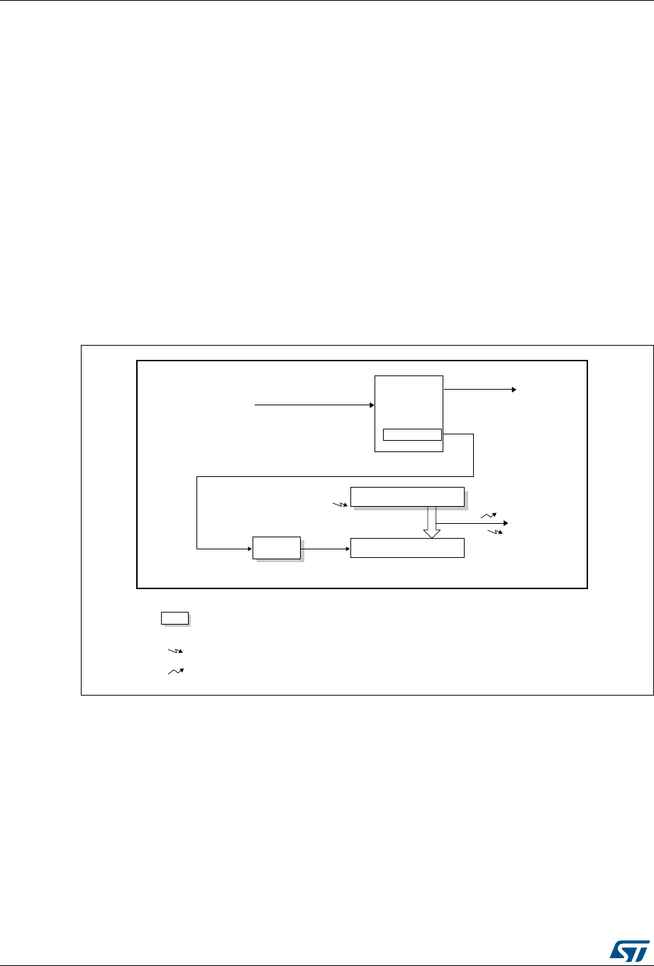
Basic timers (TIM6/7) RM0430
642/1324 RM0430 Rev 8
20 Basic timers (TIM6/7)
20.1 Introduction
The basic timers TIM6, TIM7 consist of a 16-bit auto-reload counter driven by a
programmable prescaler.
20.2 TIM6/7 main features
Basic timer (TIM6/TIM7) features include:
•16-bit auto-reload upcounter
•16-bit programmable prescaler used to divide (also “on the fly”) the counter clock
frequency by any factor between 1 and 65536
•Interrupt/DMA generation on the update event: counter overflow
Figure 204. Basic timer block diagram
06Y9
$XWRUHORDGUHJLVWHU
&17FRXQWHU
,QWHUQDOFORFN&.B,17
&.B36& &.B&17
6WRSFOHDURUXS
8,
8
8
1RWHV
5HJ 3UHORDGUHJLVWHUVWUDQVIHUUHG
WRDFWLYHUHJLVWHUVRQ8HYHQW
DFFRUGLQJWRFRQWUROELW
(YHQW
,QWHUUXSW'0$RXWSXW
36&
SUHVFDOHU
7ULJJHU
&RQWUROOHU
5HVHWHQDEOH&RXQW
7,0[&/.IURP5&&
75*2
&RQWURO

RM0430 Rev 8 643/1324
RM0430 Basic timers (TIM6/7)
654
20.3 TIM6/7 functional description
20.3.1 Time-base unit
The main block of the programmable timer is a 16-bit upcounter with its related auto-reload
register. The counter clock can be divided by a prescaler.
The counter, the auto-reload register and the prescaler register can be written or read by
software. This is true even when the counter is running.
The time-base unit includes:
•Counter Register (TIMx_CNT)
•Prescaler Register (TIMx_PSC)
•Auto-Reload Register (TIMx_ARR)
The auto-reload register is preloaded. The preload register is accessed each time an
attempt is made to write or read the auto-reload register. The contents of the preload
register are transferred into the shadow register permanently or at each update event UEV,
depending on the auto-reload preload enable bit (ARPE) in the TIMx_CR1 register. The
update event is sent when the counter reaches the overflow value and if the UDIS bit equals
0 in the TIMx_CR1 register. It can also be generated by software. The generation of the
update event is described in detail for each configuration.
The counter is clocked by the prescaler output CK_CNT, which is enabled only when the
counter enable bit (CEN) in the TIMx_CR1 register is set.
Note that the actual counter enable signal CNT_EN is set 1 clock cycle after CEN.
Prescaler description
The prescaler can divide the counter clock frequency by any factor between 1 and 65536. It
is based on a 16-bit counter controlled through a 16-bit register (in the TIMx_PSC register).
It can be changed on the fly as the TIMx_PSC control register is buffered. The new
prescaler ratio is taken into account at the next update event.
Figure 205 and Figure 206 give some examples of the counter behavior when the prescaler
ratio is changed on the fly.
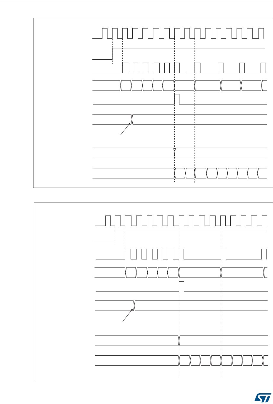
Basic timers (TIM6/7) RM0430
644/1324 RM0430 Rev 8
Figure 205. Counter timing diagram with prescaler division change from 1 to 2
Figure 206. Counter timing diagram with prescaler division change from 1 to 4
&.B36&
&(1
7LPHUFORFN &.B&17
&RXQWHUUHJLVWHU
8SGDWHHYHQW8(9
3UHVFDOHUFRQWUROUHJLVWHU
:ULWHDQHZYDOXHLQ7,0[B36&
3UHVFDOHUEXIIHU
3UHVFDOHUFRXQWHU
)$ )%) ) ) )&
069
069
&.B36&
&(1
7LPHUFORFN &.B&17
&RXQWHUUHJLVWHU
8SGDWHHYHQW8(9
3UHVFDOHUFRQWUROUHJLVWHU
:ULWHDQHZYDOXHLQ7,0[B36&
3UHVFDOHUEXIIHU
3UHVFDOHUFRXQWHU
)$ )%
) ) ) )&
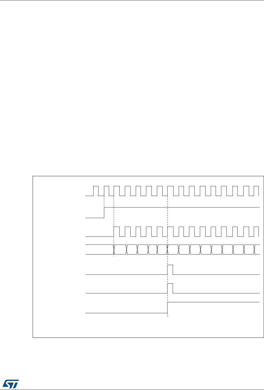
RM0430 Rev 8 645/1324
RM0430 Basic timers (TIM6/7)
654
20.3.2 Counting mode
The counter counts from 0 to the auto-reload value (contents of the TIMx_ARR register),
then restarts from 0 and generates a counter overflow event.
An update event can be generate at each counter overflow or by setting the UG bit in the
TIMx_EGR register (by software or by using the slave mode controller).
The UEV event can be disabled by software by setting the UDIS bit in the TIMx_CR1
register. This avoids updating the shadow registers while writing new values into the preload
registers. In this way, no update event occurs until the UDIS bit has been written to 0,
however, the counter and the prescaler counter both restart from 0 (but the prescale rate
does not change). In addition, if the URS (update request selection) bit in the TIMx_CR1
register is set, setting the UG bit generates an update event UEV, but the UIF flag is not set
(so no interrupt or DMA request is sent).
When an update event occurs, all the registers are updated and the update flag (UIF bit in
the TIMx_SR register) is set (depending on the URS bit):
•The buffer of the prescaler is reloaded with the preload value (contents of the
TIMx_PSC register)
•The auto-reload shadow register is updated with the preload value (TIMx_ARR)
The following figures show some examples of the counter behavior for different clock
frequencies when TIMx_ARR = 0x36.
Figure 207. Counter timing diagram, internal clock divided by 1
069
&.B36&
&17B(1
7LPHUFORFN &.B&17
&RXQWHUUHJLVWHU
8SGDWHHYHQW8(9
&RXQWHURYHUIORZ
8SGDWHLQWHUUXSWIODJ
8,)
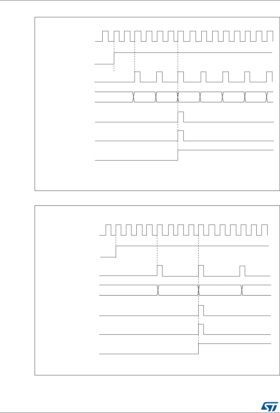
Basic timers (TIM6/7) RM0430
646/1324 RM0430 Rev 8
Figure 208. Counter timing diagram, internal clock divided by 2
Figure 209. Counter timing diagram, internal clock divided by 4
069
&.B36&
&17B(1
7LPHUFORFN &.B&17
&RXQWHUUHJLVWHU
8SGDWHHYHQW8(9
&RXQWHURYHUIORZ
8SGDWHLQWHUUXSWIODJ
8,)
069
&.B36&
7LPHUFORFN &.B&17
&RXQWHUUHJLVWHU
8SGDWHHYHQW8(9
&RXQWHURYHUIORZ
8SGDWHLQWHUUXSWIODJ
8,)
&17B(1
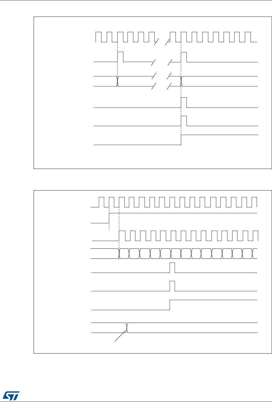
RM0430 Rev 8 647/1324
RM0430 Basic timers (TIM6/7)
654
Figure 210. Counter timing diagram, internal clock divided by N
Figure 211. Counter timing diagram, update event when ARPE = 0 (TIMx_ARR not
preloaded)
)
069
&.B36&
7LPHUFORFN &.B&17
&RXQWHUUHJLVWHU
8SGDWHHYHQW8(9
&RXQWHURYHUIORZ
8SGDWHLQWHUUXSWIODJ
8,)
))
069
&.B36&
7LPHUFORFN &.B&17
&RXQWHUUHJLVWHU
8SGDWHHYHQW8(9
&RXQWHURYHUIORZ
8SGDWHLQWHUUXSWIODJ
8,)
&(1
$XWRUHORDGSUHORDG
UHJLVWHU
:ULWHDQHZYDOXHLQ7,0[B$55
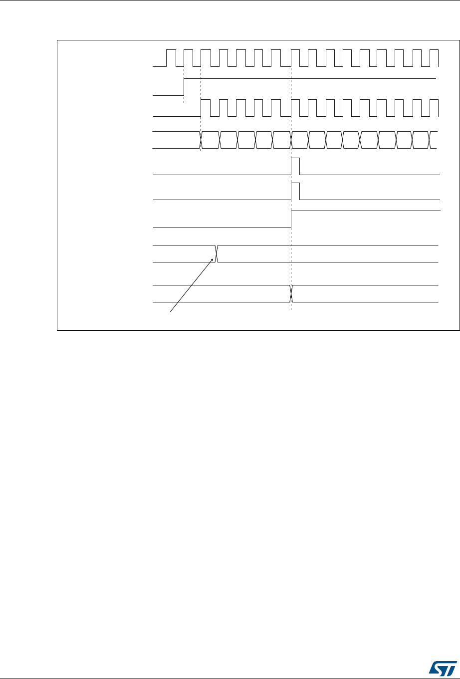
Basic timers (TIM6/7) RM0430
648/1324 RM0430 Rev 8
Figure 212. Counter timing diagram, update event when ARPE=1 (TIMx_ARR
preloaded)
20.3.3 Clock source
The counter clock is provided by the Internal clock (CK_INT) source.
The CEN (in the TIMx_CR1 register) and UG bits (in the TIMx_EGR register) are actual
control bits and can be changed only by software (except for UG that remains cleared
automatically). As soon as the CEN bit is written to 1, the prescaler is clocked by the internal
clock CK_INT.
Figure 213 shows the behavior of the control circuit and the upcounter in normal mode,
without prescaler.
069
)
&.B36&
7LPHUFORFN &.B&17
&RXQWHUUHJLVWHU
8SGDWHHYHQW8(9
&RXQWHURYHUIORZ
8SGDWHLQWHUUXSWIODJ
8,)
) ) ) ) ))
&(1
$XWRUHORDGSUHORDG
UHJLVWHU
:ULWHDQHZYDOXHLQ7,0[B$55
$XWRUHORDGVKDGRZ
UHJLVWHU )
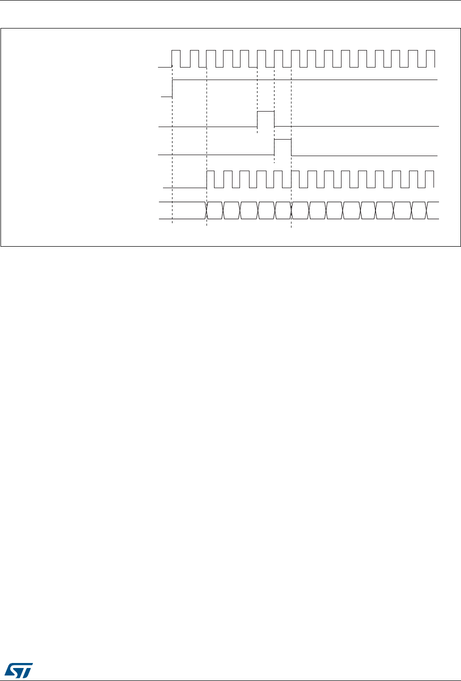
RM0430 Rev 8 649/1324
RM0430 Basic timers (TIM6/7)
654
Figure 213. Control circuit in normal mode, internal clock divided by 1
20.3.4 Debug mode
When the microcontroller enters the debug mode (Cortex®-M4 with FPU core - halted), the
TIMx counter either continues to work normally or stops, depending on the
DBG_TIMx_STOP configuration bit in the DBG module. For more details, refer to
Section 34.16.2: Debug support for timers, watchdog, bxCAN and I2C.
,QWHUQDOFORFN
&RXQWHUFORFN &.B&17 &.B36&
&RXQWHUUHJLVWHU
&(1 &17B(1
8*
&17B,1,7
069

Basic timers (TIM6/7) RM0430
650/1324 RM0430 Rev 8
20.4 TIM6/7 registers
Refer to Section 1.2: List of abbreviations for registers for a list of abbreviations used in
register descriptions.
The peripheral registers have to be written by half-words (16 bits) or words (32 bits). Read
accesses can be done by bytes (8 bits), half-words (16 bits) or words (32 bits).
20.4.1 TIM6/7 control register 1 (TIMx_CR1)
Address offset: 0x00
Reset value: 0x0000
1514131211109876543210
Res. Res. Res. Res. Res. Res. Res. Res. ARPE Res. Res. Res. OPM URS UDIS CEN
rw rw rw rw rw
Bits 15:8 Reserved, must be kept at reset value.
Bit 7 ARPE: Auto-reload preload enable
0: TIMx_ARR register is not buffered.
1: TIMx_ARR register is buffered.
Bits 6:4 Reserved, must be kept at reset value.
Bit 3 OPM: One-pulse mode
0: Counter is not stopped at update event
1: Counter stops counting at the next update event (clearing the CEN bit).
Bit 2 URS: Update request source
This bit is set and cleared by software to select the UEV event sources.
0: Any of the following events generates an update interrupt or DMA request if enabled.
These events can be:
– Counter overflow/underflow
– Setting the UG bit
– Update generation through the slave mode controller
1: Only counter overflow/underflow generates an update interrupt or DMA request if
enabled.
Bit 1 UDIS: Update disable
This bit is set and cleared by software to enable/disable UEV event generation.
0: UEV enabled. The Update (UEV) event is generated by one of the following events:
– Counter overflow/underflow
– Setting the UG bit
– Update generation through the slave mode controller
Buffered registers are then loaded with their preload values.
1: UEV disabled. The Update event is not generated, shadow registers keep their value
(ARR, PSC). However the counter and the prescaler are reinitialized if the UG bit is set or if
a hardware reset is received from the slave mode controller.
Bit 0 CEN: Counter enable
0: Counter disabled
1: Counter enabled
Note: Gated mode can work only if the CEN bit has been previously set by software.
However trigger mode can set the CEN bit automatically by hardware.
CEN is cleared automatically in one-pulse mode, when an update event occurs.

RM0430 Rev 8 651/1324
RM0430 Basic timers (TIM6/7)
654
20.4.2 TIM6/7 control register 2 (TIMx_CR2)
Address offset: 0x04
Reset value: 0x0000
20.4.3 TIM6/7 DMA/Interrupt enable register (TIMx_DIER)
Address offset: 0x0C
Reset value: 0x0000
1514131211109876543210
Res. Res. Res. Res. Res. Res. Res. Res. Res. MMS[2:0] Res. Res. Res. Res.
rw rw rw
Bits 15:7 Reserved, must be kept at reset value.
Bits 6:4 MMS: Master mode selection
These bits are used to select the information to be sent in master mode to slave timers for
synchronization (TRGO). The combination is as follows:
000: Reset - the UG bit from the TIMx_EGR register is used as a trigger output (TRGO). If
reset is generated by the trigger input (slave mode controller configured in reset mode) then
the signal on TRGO is delayed compared to the actual reset.
001: Enable - the Counter enable signal, CNT_EN, is used as a trigger output (TRGO). It is
useful to start several timers at the same time or to control a window in which a slave timer
is enabled. The Counter Enable signal is generated by a logic OR between CEN control bit
and the trigger input when configured in gated mode.
When the Counter Enable signal is controlled by the trigger input, there is a delay on TRGO,
except if the master/slave mode is selected (see the MSM bit description in the TIMx_SMCR
register).
010: Update - The update event is selected as a trigger output (TRGO). For instance a
master timer can then be used as a prescaler for a slave timer.
Bits 3:0 Reserved, must be kept at reset value.
1514131211109876543210
Res. Res. Res. Res. Res. Res. Res. UDE Res. Res. Res. Res. Res. Res. Res. UIE
rw rw
Bits 15:9 Reserved, must be kept at reset value.
Bit 8 UDE: Update DMA request enable
0: Update DMA request disabled.
1: Update DMA request enabled.
Bits 7:1 Reserved, must be kept at reset value.
Bit 0 UIE: Update interrupt enable
0: Update interrupt disabled.
1: Update interrupt enabled.
Basic timers (TIM6/7) RM0430
652/1324 RM0430 Rev 8
20.4.4 TIM6/7 status register (TIMx_SR)
Address offset: 0x10
Reset value: 0x0000
20.4.5 TIM6/7 event generation register (TIMx_EGR)
Address offset: 0x14
Reset value: 0x0000
20.4.6 TIM6/7 counter (TIMx_CNT)
Address offset: 0x24
Reset value: 0x0000
1514131211109876543210
Res. Res. Res. Res. Res. Res. Res. Res. Res. Res. Res. Res. Res. Res. Res. UIF
rc_w0
Bits 15:1 Reserved, must be kept at reset value.
Bit 0 UIF: Update interrupt flag
This bit is set by hardware on an update event. It is cleared by software.
0: No update occurred.
1: Update interrupt pending. This bit is set by hardware when the registers are updated:
– At overflow or underflow regarding the repetition counter value and if UDIS = 0 in the
TIMx_CR1 register.
– When CNT is reinitialized by software using the UG bit in the TIMx_EGR register, if URS = 0
and UDIS = 0 in the TIMx_CR1 register.
1514131211109876543210
Res. Res. Res. Res. Res. Res. Res. Res. Res. Res. Res. Res. Res. Res. Res. UG
w
Bits 15:1 Reserved, must be kept at reset value.
Bit 0 UG: Update generation
This bit can be set by software, it is automatically cleared by hardware.
0: No action.
1: Re-initializes the timer counter and generates an update of the registers. Note that the
prescaler counter is cleared too (but the prescaler ratio is not affected).
1514131211109876543210
CNT[15:0]
rw rw rw rw rw rw rw rw rw rw rw rw rw rw rw rw
Bits 15:0 CNT[15:0]: Counter value

RM0430 Rev 8 653/1324
RM0430 Basic timers (TIM6/7)
654
20.4.7 TIM6/7 prescaler (TIMx_PSC)
Address offset: 0x28
Reset value: 0x0000
20.4.8 TIM6/7 auto-reload register (TIMx_ARR)
Address offset: 0x2C
Reset value: 0xFFFF
1514131211109876543210
PSC[15:0]
rw rw rw rw rw rw rw rw rw rw rw rw rw rw rw rw
Bits 15:0 PSC[15:0]: Prescaler value
The counter clock frequency (CK_CNT) is equal to fCK_PSC / (PSC[15:0] + 1).
PSC contains the value to be loaded in the active prescaler register at each update event
(including when the counter is cleared through UG bit of TIMx_EGR register or through
trigger controller when configured in “reset mode”).
1514131211109876543210
ARR[15:0]
rw rw rw rw rw rw rw rw rw rw rw rw rw rw rw rw
Bits 15:0 ARR[15:0]: Auto-reload value
ARR is the value to be loaded into the actual auto-reload register.
Refer to Section 20.3.1: Time-base unit on page 643 for more details about ARR update and
behavior.
The counter is blocked while the auto-reload value is null.

Basic timers (TIM6/7) RM0430
654/1324 RM0430 Rev 8
20.4.9 TIM6/7 register map
TIMx registers are mapped as 16-bit addressable registers as described in the table below:
Refer to Section 2.2.2 on page 58 for the register boundary addresses.
Table 114. TIM6 register map and reset values
Offset Register
15
14
13
12
11
10
9
8
7
6
5
4
3
2
1
0
0x00
TIMx_CR1
Res.
Res.
Res.
Res.
Res.
Res.
Res.
Res.
ARPE
Res.
Res.
Res.
OPM
URS
UDIS
CEN
Reset value 0 0000
0x04
TIMx_CR2
Res.
Res.
Res.
Res.
Res.
Res.
Res.
Res.
Res.
MMS[2:0]
Res.
Res.
Res.
Res.
Reset value 0 0 0
0x08 Res.
0x0C
TIMx_DIER
Res.
Res.
Res.
Res.
Res.
Res.
Res.
UDE
Res.
Res.
Res.
Res.
Res.
Res.
Res.
UIE
Reset value 0 0
0x10
TIMx_SR
Res.
Res.
Res.
Res.
Res.
Res.
Res.
Res.
Res.
Res.
Res.
Res.
Res.
Res.
Res.
UIF
Reset value 0
0x14
TIMx_EGR
Res.
Res.
Res.
Res.
Res.
Res.
Res.
Res.
Res.
Res.
Res.
Res.
Res.
Res.
Res.
UG
Reset value 0
0x18 Res.
0x1C Res.
0x20 Res.
0x24
TIMx_CNT CNT[15:0]
Reset value 0000000000 0 00000
0x28
TIMx_PSC PSC[15:0]
Reset value 0000000000 0 00000
0x2C
TIMx_ARR ARR[15:0]
Reset value 1111111111 1 11111

RM0430 Rev 8 655/1324
RM0430 Low-power timer (LPTIM)
677
21 Low-power timer (LPTIM)
21.1 Introduction
The LPTIM is a 16-bit timer that benefits from the ultimate developments in power
consumption reduction. Thanks to its diversity of clock sources, the LPTIM is able to keep
running in all power modes except for Standby mode. Given its capability to run even with
no internal clock source, the LPTIM can be used as a “Pulse Counter” which can be useful
in some applications. Also, the LPTIM capability to wake up the system from low-power
modes, makes it suitable to realize “Timeout functions” with extremely low power
consumption.
The LPTIM introduces a flexible clock scheme that provides the needed functionalities and
performance, while minimizing the power consumption.
21.2 LPTIM main features
•16 bit upcounter
•3-bit prescaler with 8 possible dividing factors (1,2,4,8,16,32,64,128)
•Selectable clock
– Internal clock sources: LSE, LSI, HSI or APB clock
– External clock source over LPTIM input (working with no LP oscillator running,
used by Pulse Counter application)
•16 bit ARR autoreload register
•16 bit compare register
•Continuous/One-shot mode
•Selectable software/hardware input trigger
•Programmable Digital Glitch filter
•Configurable output: Pulse, PWM
•Configurable I/O polarity
•Encoder mode
21.3 LPTIM implementation
Table 115 describes LPTIM implementation on STM32F413/423 devices.
Table 115. STM32F413/423 LPTIM features
LPTIM modes/features(1)
1. X = supported.
LPTIM1
Encoder mode X
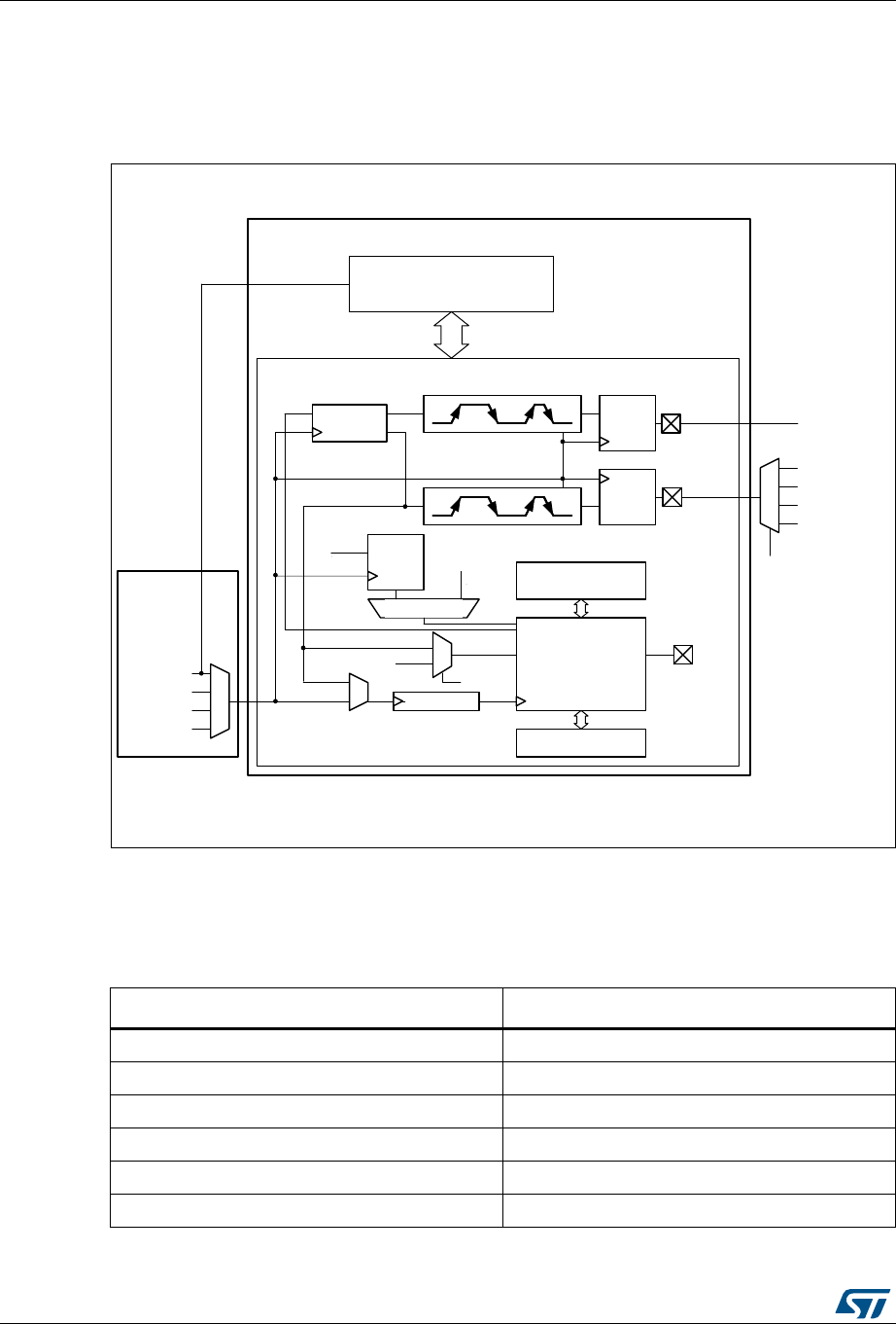
Low-power timer (LPTIM) RM0430
656/1324 RM0430 Rev 8
21.4 LPTIM functional description
21.4.1 LPTIM block diagram
Figure 214. Low-power timer block diagram
21.4.2 LPTIM trigger mapping
The LPTIM external trigger connections are detailed hereafter:
06Y9
5&&
/37,0
$3%B,7)
.HUQHO
VZ
WULJJHU
XSWRH[W
WULJJHU
&/.08;
+6,
/6,
/6(
$3%FORFN
ELWFRPSDUH
ELWFRXQWHU
ELW$55
2XW
3UHVFDOHU
0X[WULJJHU
*OLWFK
ILOWHU
*OLWFK
ILOWHU
,QSXW
(QFRGHU *OLWFK
ILOWHU
,QSXW
8SGRZQ
&2817
02'(
$)SDGLQSXW
3$SDG
3%SDG
7,0'$&WULJJHU
/37,0B25
$)SDGLQSXW
Table 116. LPTIM1 external trigger connection
TRIGSEL External trigger
lptim_ext_trig0 PB6 or PC3 input on AF1
lptim_ext_trig1 RTC alarm A output signal
lptim_ext_trig2 RTC alarm B output signal
lptim_ext_trig3 RTC tamper output signal
lptim_ext_trig4 TIM1 trigger output (4) output signal
lptim_ext_trig5 TIM5 trigger output (3) output signal

RM0430 Rev 8 657/1324
RM0430 Low-power timer (LPTIM)
677
21.4.3 LPTIM input1 multiplexing
Various inputs can be selected for LPTIM1 input 1 through the LPTMI option register
(LPTIM1_OR).
This input can either be connected to the pads selected by the LPTIM alternate function
(AF1) or directly connected internally to PA4, PB9 pad or to TIM6/DAC trigger.
In case of internal connection to PA4 or PB9, the selected alternate function for this pad
defines the peripheral to which the timer is connected.
PA4 and PB9 can also be configured as GPIO.
21.4.4 LPTIM reset and clocks
The LPTIM can be clocked using several clock sources. It can be clocked using an internal
clock signal which can be chosen among APB, LSI, LSE or HSI sources through the Reset
and Clock controller (RCC). Also, the LPTIM can be clocked using an external clock signal
injected on its external Input1. When clocked with an external clock source, the LPTIM may
run in one of these two possible configurations:
•The first configuration is when the LPTIM is clocked by an external signal but in the
same time an internal clock signal is provided to the LPTIM either from APB or any
other embedded oscillator including LSE, LSI and HSI.
•The second configuration is when the LPTIM is solely clocked by an external clock
source through its external Input1. This configuration is the one used to realize Timeout
function or Pulse counter function when all the embedded oscillators are turned off
after entering a low-power mode.
Programming the CKSEL and COUNTMODE bits allows controlling whether the LPTIM will
use an external clock source or an internal one.
When configured to use an external clock source, the CKPOL bits are used to select the
external clock signal active edge. If both edges are configured to be active ones, an internal
clock signal should also be provided (first configuration). In this case, the internal clock
signal frequency should be at least four times higher than the external clock signal
frequency.
21.4.5 Glitch filter
The LPTIM inputs, either external (mapped to microcontroller GPIOs) or internal (mapped
on the chip-level to other embedded peripherals, such as embedded comparators), are
protected with digital filters that prevent any glitches and noise perturbations to propagate
inside the LPTIM. This is in order to prevent spurious counts or triggers.
Before activating the digital filters, an internal clock source should first be provided to the
LPTIM. This is necessary to guarantee the proper operation of the filters.
lptim_ext_trig6 Reserved
lptim_ext_trig7 Reserved
Table 116. LPTIM1 external trigger connection (continued)
TRIGSEL External trigger
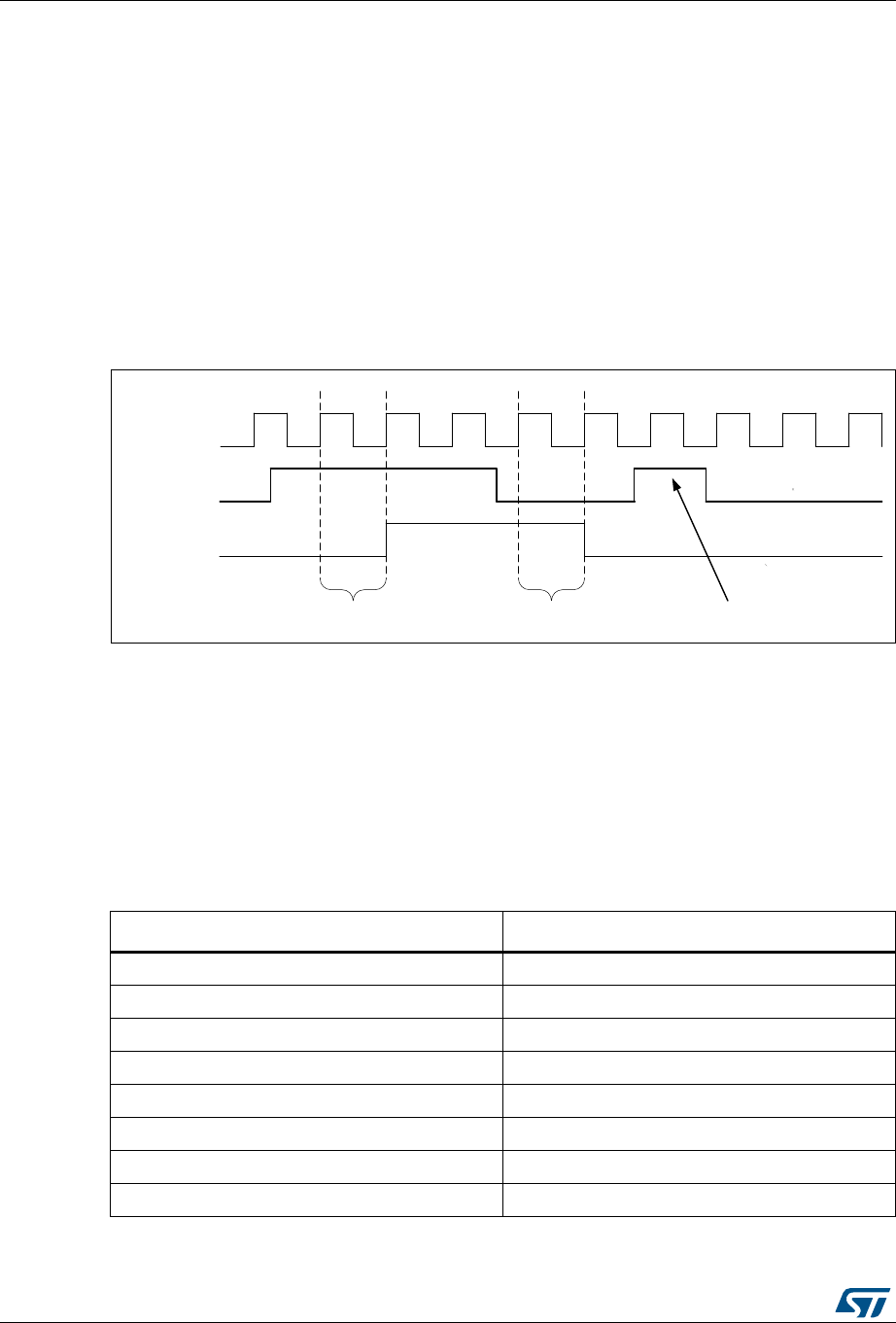
Low-power timer (LPTIM) RM0430
658/1324 RM0430 Rev 8
The digital filters are divided into two groups:
•The first group of digital filters protects the LPTIM external inputs. The digital filters
sensitivity is controlled by the CKFLT bits
•The second group of digital filters protects the LPTIM internal trigger inputs. The digital
filters sensitivity is controlled by the TRGFLT bits.
Note: The digital filters sensitivity is controlled by groups. It is not possible to configure each digital
filter sensitivity separately inside the same group.
The filter sensitivity acts on the number of consecutive equal samples that should be
detected on one of the LPTIM inputs to consider a signal level change as a valid transition.
Figure 215 shows an example of glitch filter behavior in case of a 2 consecutive samples
programmed.
Figure 215. Glitch filter timing diagram
Note: In case no internal clock signal is provided, the digital filter must be deactivated by setting
the CKFLT and TRGFLT bits to ‘0’. In that case, an external analog filter may be used to
protect the LPTIM external inputs against glitches.
21.4.6 Prescaler
The LPTIM 16-bit counter is preceded by a configurable power-of-2 prescaler. The prescaler
division ratio is controlled by the PRESC[2:0] 3-bit field. The table below lists all the possible
division ratios:
069
&/.08;
,QSXW
)LOWHURXW
FRQVHFXWLYHVDPSOHV FRQVHFXWLYHVDPSOHV )LOWHUHG
Table 117. Prescaler division ratios
programming dividing factor
000 /1
001 /2
010 /4
011 /8
100 /16
101 /32
110 /64
111 /128

RM0430 Rev 8 659/1324
RM0430 Low-power timer (LPTIM)
677
21.4.7 Trigger multiplexer
The LPTIM counter may be started either by software or after the detection of an active
edge on one of the 8 trigger inputs.
TRIGEN[1:0] is used to determine the LPTIM trigger source:
•When TRIGEN[1:0] equals ‘00’, The LPTIM counter is started as soon as one of the
CNTSTRT or the SNGSTRT bits is set by software. The three remaining possible
values for the TRIGEN[1:0] are used to configure the active edge used by the trigger
inputs. The LPTIM counter starts as soon as an active edge is detected.
•When TRIGEN[1:0] is different than ‘00’, TRIGSEL[2:0] is used to select which of the 8
trigger inputs is used to start the counter.
The external triggers are considered asynchronous signals for the LPTIM. So after a trigger
detection, a two-counter-clock period latency is needed before the timer starts running due
to the synchronization.
If a new trigger event occurs when the timer is already started it will be ignored (unless
timeout function is enabled).
Note: The timer must be enabled before setting the SNGSTRT/CNTSTRT bits. Any write on these
bits when the timer is disabled will be discarded by hardware.
21.4.8 Operating mode
The LPTIM features two operating modes:
•The Continuous mode: the timer is free running, the timer is started from a trigger event
and never stops until the timer is disabled
•One-shot mode: the timer is started from a trigger event and stops when reaching the
ARR value.
One-shot mode
To enable the one-shot counting, the SNGSTRT bit must be set.
A new trigger event will re-start the timer. Any trigger event occurring after the counter starts
and before the counter reaches ARR will be discarded.
In case an external trigger is selected, each external trigger event arriving after the
SNGSTRT bit is set, and after the counter register has stopped (contains zero value), will
start the counter for a new one-shot counting cycle as shown in Figure 216.
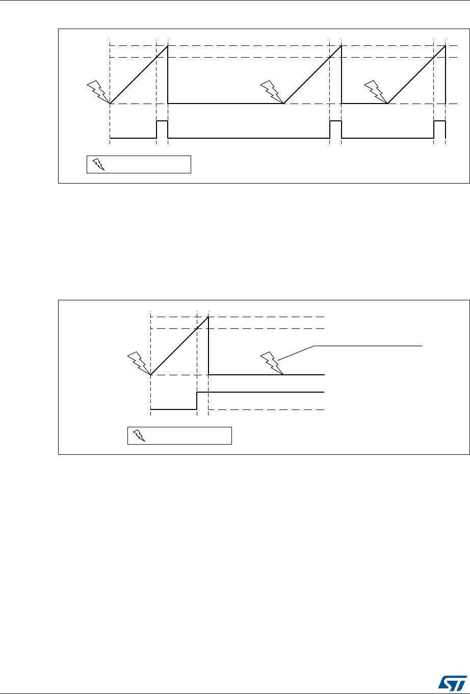
Low-power timer (LPTIM) RM0430
660/1324 RM0430 Rev 8
Figure 216. LPTIM output waveform, single counting mode configuration
- Set-once mode activated:
It should be noted that when the WAVE bit-field in the LPTIM_CFGR register is set, the Set-
once mode is activated. In this case, the counter is only started once following the first
trigger, and any subsequent trigger event is discarded as shown in Figure 217.
Figure 217. LPTIM output waveform, Single counting mode configuration
and Set-once mode activated (WAVE bit is set)
In case of software start (TRIGEN[1:0] = ‘00’), the SNGSTRT setting will start the counter for
one-shot counting.
Continous mode
To enable the continuous counting, the CNTSTRT bit must be set.
In case an external trigger is selected, an external trigger event arriving after CNTSTRT is
set will start the counter for continuous counting. Any subsequent external trigger event will
be discarded as shown in Figure 218.
In case of software start (TRIGEN[1:0] = ‘00’), setting CNTSTRT will start the counter for
continuous counting.
06Y9
3:0
&RPSDUH
/37,0B$55
([WHUQDOWULJJHUHYHQW
06Y9
3:0
&RPSDUH
/37,0B$55
'LVFDUGHGWULJJHU
([WHUQDOWULJJHUHYHQW

RM0430 Rev 8 661/1324
RM0430 Low-power timer (LPTIM)
677
Figure 218. LPTIM output waveform, Continuous counting mode configuration
SNGSTRT and CNTSTRT bits can only be set when the timer is enabled (The ENABLE bit
is set to ‘1’). It is possible to change “on the fly” from One-shot mode to Continuous mode.
If the Continuous mode was previously selected, setting SNGSTRT will switch the LPTIM to
the One-shot mode. The counter (if active) will stop as soon as it reaches ARR.
If the One-shot mode was previously selected, setting CNTSTRT will switch the LPTIM to
the Continuous mode. The counter (if active) will restart as soon as it reaches ARR.
21.4.9 Timeout function
The detection of an active edge on one selected trigger input can be used to reset the
LPTIM counter. This feature is controlled through the TIMOUT bit.
The first trigger event will start the timer, any successive trigger event will reset the counter
and the timer will restart.
A low-power timeout function can be realized. The timeout value corresponds to the
compare value; if no trigger occurs within the expected time frame, the MCU is waked-up by
the compare match event.
21.4.10 Waveform generation
Two 16-bit registers, the LPTIM_ARR (autoreload register) and LPTIM_CMP (compare
register), are used to generate several different waveforms on LPTIM output
The timer can generate the following waveforms:
•The PWM mode: the LPTIM output is set as soon as a match occurs between the
LPTIM_CMP and the LPTIM_CNT registers. The LPTIM output is reset as soon as a
match occurs between the LPTIM_ARR and the LPTIM_CNT registers
•The One-pulse mode: the output waveform is similar to the one of the PWM mode for
the first pulse, then the output is permanently reset
•The Set-once mode: the output waveform is similar to the One-pulse mode except that
the output is kept to the last signal level (depends on the output configured polarity).
The above described modes require that the LPTIM_ARR register value be strictly greater
than the LPTIM_CMP register value.
06Y9
3:0
&RPSDUH
/37,0B$55
'LVFDUGHGWULJJHUV
([WHUQDOWULJJHUHYHQW
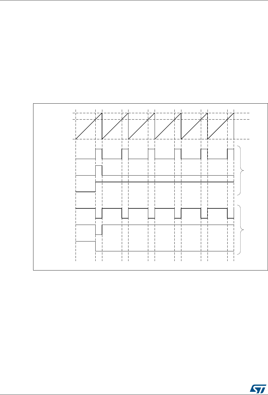
Low-power timer (LPTIM) RM0430
662/1324 RM0430 Rev 8
The LPTIM output waveform can be configured through the WAVE bit as follow:
•Resetting the WAVE bit to ‘0’ forces the LPTIM to generate either a PWM waveform or
a One pulse waveform depending on which bit is set: CNTSTRT or SNGSTRT.
•Setting the WAVE bit to ‘1’ forces the LPTIM to generate a Set-once mode waveform.
The WAVPOL bit controls the LPTIM output polarity. The change takes effect immediately,
so the output default value will change immediately after the polarity is re-configured, even
before the timer is enabled.
Signals with frequencies up to the LPTIM clock frequency divided by 2 can be generated.
Figure 219 below shows the three possible waveforms that can be generated on the LPTIM
output. Also, it shows the effect of the polarity change using the WAVPOL bit.
Figure 219. Waveform generation
21.4.11 Register update
The LPTIM_ARR register and LPTIM_CMP register are updated immediately after the APB
bus write operation, or at the end of the current period if the timer is already started.
The PRELOAD bit controls how the LPTIM_ARR and the LPTIM_CMP registers are
updated:
•When the PRELOAD bit is reset to ‘0’, the LPTIM_ARR and the LPTIM_CMP registers
are immediately updated after any write access.
•When the PRELOAD bit is set to ‘1’, the LPTIM_ARR and the LPTIM_CMP registers
are updated at the end of the current period, if the timer has been already started.
The LPTIM APB interface and the LPTIM kernel logic use different clocks, so there is some
latency between the APB write and the moment when these values are available to the
069
/37,0B$55
&RPSDUH
3:0
2QHVKRW
6HWRQFH
3:0
2QHVKRW
6HWRQFH
3RO
3RO

RM0430 Rev 8 663/1324
RM0430 Low-power timer (LPTIM)
677
counter comparator. Within this latency period, any additional write into these registers must
be avoided.
The ARROK flag and the CMPOK flag in the LPTIM_ISR register indicate when the write
operation is completed to respectively the LPTIM_ARR register and the LPTIM_CMP
register.
After a write to the LPTIM_ARR register or the LPTIM_CMP register, a new write operation
to the same register can only be performed when the previous write operation is completed.
Any successive write before respectively the ARROK flag or the CMPOK flag be set, will
lead to unpredictable results.
21.4.12 Counter mode
The LPTIM counter can be used to count external events on the LPTIM Input1 or it can be
used to count internal clock cycles. The CKSEL and COUNTMODE bits control which
source will be used for updating the counter.
In case the LPTIM is configured to count external events on Input1, the counter can be
updated following a rising edge, falling edge or both edges depending on the value written
to the CKPOL[1:0] bits.
The count modes below can be selected, depending on CKSEL and COUNTMODE values:
•CKSEL = 0: the LPTIM is clocked by an internal clock source
– COUNTMODE = 0
The LPTIM is configured to be clocked by an internal clock source and the LPTIM
counter is configured to be updated following each internal clock pulse.
– COUNTMODE = 1
The LPTIM external Input1 is sampled with the internal clock provided to the
LPTIM.
Consequently, in order not to miss any event, the frequency of the changes on the
external Input1 signal should never exceed the frequency of the internal clock
provided to the LPTIM. Also, the internal clock provided to the LPTIM must not be
prescaled (PRESC[2:0] = 000).
•CKSEL = 1: the LPTIM is clocked by an external clock source
COUNTMODE value is don’t care.
In this configuration, the LPTIM has no need for an internal clock source (except if the
glitch filters are enabled). The signal injected on the LPTIM external Input1 is used as
system clock for the LPTIM. This configuration is suitable for operation modes where
no embedded oscillator is enabled.
For this configuration, the LPTIM counter can be updated either on rising edges or
falling edges of the input1 clock signal but not on both rising and falling edges.
Since the signal injected on the LPTIM external Input1 is also used to clock the LPTIM
kernel logic, there is some initial latency (after the LPTIM is enabled) before the counter
is incremented. More precisely, the first five active edges on the LPTIM external Input1
(after LPTIM is enable) are lost.
21.4.13 Timer enable
The ENABLE bit located in the LPTIM_CR register is used to enable/disable the LPTIM
kernel logic. After setting the ENABLE bit, a delay of two counter clock is needed before the
LPTIM is actually enabled.

Low-power timer (LPTIM) RM0430
664/1324 RM0430 Rev 8
The LPTIM_CFGR and LPTIM_IER registers must be modified only when the LPTIM is
disabled.
21.4.14 Encoder mode
This mode allows handling signals from quadrature encoders used to detect angular
position of rotary elements. Encoder interface mode acts simply as an external clock with
direction selection. This means that the counter just counts continuously between 0 and the
auto-reload value programmed into the LPTIM_ARR register (0 up to ARR or ARR down to
0 depending on the direction). Therefore you must configure LPTIM_ARR before starting.
From the two external input signals, Input1 and Input2, a clock signal is generated to clock
the LPTIM counter. The phase between those two signals determines the counting direction.
The Encoder mode is only available when the LPTIM is clocked by an internal clock source.
The signals frequency on both Input1 and Input2 inputs must not exceed the LPTIM internal
clock frequency divided by 4. This is mandatory in order to guarantee a proper operation of
the LPTIM.
Direction change is signalized by the two Down and Up flags in the LPTIM_ISR register.
Also, an interrupt can be generated for both direction change events if enabled through the
DOWNIE bit.
To activate the Encoder mode the ENC bit has to be set to ‘1’. The LPTIM must first be
configured in Continuous mode.
When Encoder mode is active, the LPTIM counter is modified automatically following the
speed and the direction of the incremental encoder. Therefore, its content always
represents the encoder’s position. The count direction, signaled by the Up and Down flags,
correspond to the rotation direction of the encoder rotor.
According to the edge sensitivity configured using the CKPOL[1:0] bits, different counting
scenarios are possible. The following table summarizes the possible combinations,
assuming that Input1 and Input2 do not switch at the same time.
The following figure shows a counting sequence for Encoder mode where both-edge
sensitivity is configured.
Caution: In this mode the LPTIM must be clocked by an internal clock source, so the CKSEL bit must
be maintained to its reset value which is equal to ‘0’. Also, the prescaler division ratio must
be equal to its reset value which is 1 (PRESC[2:0] bits must be ‘000’).
Table 118. Encoder counting scenarios
Active edge
Level on opposite
signal (Input1 for
Input2, Input2 for
Input1)
Input1 signal Input2 signal
Rising Falling Rising Falling
Rising Edge
High Down No count Up No count
Low Up No count Down No count
Falling Edge
High No count Up No count Down
Low No count Down No count Up
Both Edges
High Down Up Up Down
Low Up Down Down Up
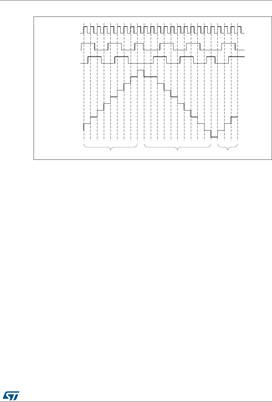
RM0430 Rev 8 665/1324
RM0430 Low-power timer (LPTIM)
677
Figure 220. Encoder mode counting sequence
21.4.15 Debug mode
When the microcontroller enters debug mode (core halted), the LPTIM counter either
continues to work normally or stops, depending on the DBG_LPTIM_STOP configuration bit
in the DBG module.
21.5 LPTIM interrupts
The following events generate an interrupt/wake-up event, if they are enabled through the
LPTIM_IER register:
•Compare match
•Auto-reload match (whatever the direction if encoder mode)
•External trigger event
•Autoreload register write completed
•Compare register write completed
•Direction change (encoder mode), programmable (up / down / both).
Note: If any bit in the LPTIM_IER register (Interrupt Enable Register) is set after that its
corresponding flag in the LPTIM_ISR register (Status Register) is set, the interrupt is not
asserted.
069
7
&RXQWHU
XS XSGRZQ
7

Low-power timer (LPTIM) RM0430
666/1324 RM0430 Rev 8
21.6 LPTIM registers
21.6.1 LPTIM interrupt and status register (LPTIM_ISR)
Address offset: 0x000
Reset value: 0x0000 0000
Table 119. Interrupt events
Interrupt event Description
Compare match Interrupt flag is raised when the content of the Counter register
(LPTIM_CNT) matches the content of the compare register (LPTIM_CMP).
Auto-reload match
Interrupt flag is raised when the content of the Counter register
(LPTIM_CNT) matches the content of the Auto-reload register
(LPTIM_ARR).
External trigger event Interrupt flag is raised when an external trigger event is detected
Auto-reload register
update OK
Interrupt flag is raised when the write operation to the LPTIM_ARR register
is complete.
Compare register
update OK
Interrupt flag is raised when the write operation to the LPTIM_CMP register
is complete.
Direction change
Used in Encoder mode. Two interrupt flags are embedded to signal
direction change:
– UP flag signals up-counting direction change
– DOWN flag signals down-counting direction change.
31 30 29 28 27 26 25 24 23 22 21 20 19 18 17 16
Res. Res. Res. Res. Res. Res. Res. Res. Res. Res. Res. Res. Res. Res. Res. Res.
1514131211109876543210
Res. Res. Res. Res. Res. Res. Res. Res. Res. DOWN UP ARRO
K
CMP
OK
EXTTR
IG ARRM CMPM
rrrrrrr
Bits 31:22 Reserved, must be kept at reset value.
Bit 21 Reserved, must be kept at reset value.
Bit 20 Reserved, must be kept at reset value.
Bit 19 Reserved, must be kept at reset value.
Bits 18:16 Reserved, must be kept at reset value.
Bit 15 Reserved, must be kept at reset value.
Bit 14 Reserved, must be kept at reset value.
Bit 13 Reserved, must be kept at reset value.
Bit 12 Reserved, must be kept at reset value.
Bit 11 Reserved, must be kept at reset value.

RM0430 Rev 8 667/1324
RM0430 Low-power timer (LPTIM)
677
21.6.2 LPTIM interrupt clear register (LPTIM_ICR)
Address offset: 0x004
Reset value: 0x0000 0000
Bit 10 Reserved, must be kept at reset value.
Bit 9 Reserved, must be kept at reset value.
Bits 8:7 Reserved, must be kept at reset value.
Bit 6 DOWN: Counter direction change up to down
In Encoder mode, DOWN bit is set by hardware to inform application that the counter direction has
changed from up to down.
Bit 5 UP: Counter direction change down to up
In Encoder mode, UP bit is set by hardware to inform application that the counter direction has
changed from down to up.
Bit 4 ARROK: Autoreload register update OK
ARROK is set by hardware to inform application that the APB bus write operation to the LPTIM_ARR
register has been successfully completed.
Bit 3 CMPOK: Compare register update OK
CMPOK is set by hardware to inform application that the APB bus write operation to the
LPTIM_CMP register has been successfully completed.
Bit 2 EXTTRIG: External trigger edge event
EXTTRIG is set by hardware to inform application that a valid edge on the selected external trigger
input has occurred. If the trigger is ignored because the timer has already started, then this flag is
not set.
Bit 1 ARRM: Autoreload match
ARRM is set by hardware to inform application that LPTIM_CNT register’s value reached the
LPTIM_ARR register’s value.
Bit 0 CMPM: Compare match
The CMPM bit is set by hardware to inform application that LPTIM_CNT register value reached the
LPTIM_CMP register’s value.
31 30 29 28 27 26 25 24 23 22 21 20 19 18 17 16
Res. Res. Res. Res. Res. Res. Res. Res. Res. Res. Res. Res. Res. Res. Res. Res.
1514131211109876543210
Res. Res. Res. Res. Res. Res. Res. Res. Res. DOWN
CF UPCF ARRO
KCF
CMPO
KCF
EXTTR
IGCF
ARRM
CF
CMPM
CF
wwwwwww
Bits 31:22 Reserved, must be kept at reset value.
Bit 21 Reserved, must be kept at reset value.
Bit 20 Reserved, must be kept at reset value.
Bit 19 Reserved, must be kept at reset value.

Low-power timer (LPTIM) RM0430
668/1324 RM0430 Rev 8
21.6.3 LPTIM interrupt enable register (LPTIM_IER)
Address offset: 0x008
Reset value: 0x0000 0000
Bits 18:16 Reserved, must be kept at reset value.
Bit 15 Reserved, must be kept at reset value.
Bit 14 Reserved, must be kept at reset value.
Bit 13 Reserved, must be kept at reset value.
Bit 12 Reserved, must be kept at reset value.
Bit 11 Reserved, must be kept at reset value.
Bit 10 Reserved, must be kept at reset value.
Bit 9 Reserved, must be kept at reset value.
Bits 8:7 Reserved, must be kept at reset value.
Bit 6 DOWNCF: Direction change to down clear flag
Writing 1 to this bit clear the DOWN flag in the LPTIM_ISR register.
Bit 5 UPCF: Direction change to UP clear flag
Writing 1 to this bit clear the UP flag in the LPTIM_ISR register.
Bit 4 ARROKCF: Autoreload register update OK clear flag
Writing 1 to this bit clears the ARROK flag in the LPTIM_ISR register
Bit 3 CMPOKCF: Compare register update OK clear flag
Writing 1 to this bit clears the CMPOK flag in the LPTIM_ISR register
Bit 2 EXTTRIGCF: External trigger valid edge clear flag
Writing 1 to this bit clears the EXTTRIG flag in the LPTIM_ISR register
Bit 1 ARRMCF: Autoreload match clear flag
Writing 1 to this bit clears the ARRM flag in the LPTIM_ISR register
Bit 0 CMPMCF: Compare match clear flag
Writing 1 to this bit clears the CMP flag in the LPTIM_ISR register
31 30 29 28 27 26 25 24 23 22 21 20 19 18 17 16
Res. Res. Res. Res. Res. Res. Res. Res. Res. Res. Res. Res. Res. Res. Res. Res.
1514131211109876543210
Res. Res. Res. Res. Res. Res. Res. Res. Res. DOWNI
EUPIE ARRO
KIE
CMPO
KIE
EXT
TRIGIE
ARRM
IE
CMPM
IE
rw rw rw rw rw rw rw
Bits 31:28 Reserved, must be kept at reset value.
Bit 27 Reserved, must be kept at reset value.
Bit 26 Reserved, must be kept at reset value.
Bit 25 Reserved, must be kept at reset value.

RM0430 Rev 8 669/1324
RM0430 Low-power timer (LPTIM)
677
Caution: The LPTIM_IER register must only be modified when the LPTIM is disabled (ENABLE bit reset to ‘0’)
Bit 24 Reserved, must be kept at reset value.
Bit 23 Reserved, must be kept at reset value.
Bit 22 Reserved, must be kept at reset value.
Bit 21 Reserved, must be kept at reset value.
Bit 20 Reserved, must be kept at reset value.
Bit 19 Reserved, must be kept at reset value.
Bits 18:17 Reserved, must be kept at reset value.
Bit 16 Reserved, must be kept at reset value.
Bit 15 Reserved, must be kept at reset value.
Bit 14 Reserved, must be kept at reset value.
Bit 13 Reserved, must be kept at reset value.
Bit 12 Reserved, must be kept at reset value.
Bit 11 Reserved, must be kept at reset value.
Bit 10 Reserved, must be kept at reset value.
Bit 9 Reserved, must be kept at reset value.
Bits 8:7 Reserved, must be kept at reset value.
Bit 6 DOWNIE: Direction change to down Interrupt Enable
0: DOWN interrupt disabled
1: DOWN interrupt enabled
Bit 5 UPIE: Direction change to UP Interrupt Enable
0: UP interrupt disabled
1: UP interrupt enabled
Bit 4 ARROKIE: Autoreload register update OK Interrupt Enable
0: ARROK interrupt disabled
1: ARROK interrupt enabled
Bit 3 CMPOKIE: Compare register update OK Interrupt Enable
0: CMPOK interrupt disabled
1: CMPOK interrupt enabled
Bit 2 EXTTRIGIE: External trigger valid edge Interrupt Enable
0: EXTTRIG interrupt disabled
1: EXTTRIG interrupt enabled
Bit 1 ARRMIE: Autoreload match Interrupt Enable
0: ARRM interrupt disabled
1: ARRM interrupt enabled
Bit 0 CMPMIE: Compare match Interrupt Enable
0: CMPM interrupt disabled
1: CMPM interrupt enabled

Low-power timer (LPTIM) RM0430
670/1324 RM0430 Rev 8
21.6.4 LPTIM configuration register (LPTIM_CFGR)
Address offset: 0x00C
Reset value: 0x0000 0000
31 30 29 28 27 26 25 24 23 22 21 20 19 18 17 16
Res. Res. Res. Res. Res. Res. Res. ENC COUNT
MODE PRELOAD WAVPOL WAVE TIMOUT TRIGEN[1:0] Res.
rw rw rw rw rw rw rw rw
15 14 13 12 11 10 9 8 7 6 5 4 3 2 1 0
TRIGSEL[2:0] Res. PRESC[2:0] Res. TRGFLT[1:0] Res. CKFLT[1:0] CKPOL[1:0] CKSEL
rw rw rw rw rw rw rw rw rw rw rw rw rw
Bits 31:30 Reserved, must be kept at reset value.
Bit 29 Reserved, must be kept at reset value.
Bits 28:25 Reserved, must be kept at reset value.
Bit 24 ENC: Encoder mode enable
The ENC bit controls the Encoder mode
0: Encoder mode disabled
1: Encoder mode enabled
Bit 23 COUNTMODE: counter mode enabled
The COUNTMODE bit selects which clock source is used by the LPTIM to clock the counter:
0: the counter is incremented following each internal clock pulse
1: the counter is incremented following each valid clock pulse on the LPTIM external Input1
Bit 22 PRELOAD: Registers update mode
The PRELOAD bit controls the LPTIM_ARR and the LPTIM_CMP registers update modality
0: Registers are updated after each APB bus write access
1: Registers are updated at the end of the current LPTIM period
Bit 21 WAVPOL: Waveform shape polarity
The WAVEPOL bit controls the output polarity
0: The LPTIM output reflects the compare results between LPTIM_ARR and LPTIM_CMP
registers
1: The LPTIM output reflects the inverse of the compare results between LPTIM_ARR and
LPTIM_CMP registers
Bit 20 WAVE: Waveform shape
The WAVE bit controls the output shape
0: Deactivate Set-once mode, PWM / One Pulse waveform (depending on OPMODE bit)
1: Activate the Set-once mode
Bit 19 TIMOUT: Timeout enable
The TIMOUT bit controls the Timeout feature
0: a trigger event arriving when the timer is already started will be ignored
1: A trigger event arriving when the timer is already started will reset and restart the counter

RM0430 Rev 8 671/1324
RM0430 Low-power timer (LPTIM)
677
Bits 18:17 TRIGEN[1:0]: Trigger enable and polarity
The TRIGEN bits controls whether the LPTIM counter is started by an external trigger or not. If the
external trigger option is selected, three configurations are possible for the trigger active edge:
00: software trigger (counting start is initiated by software)
01: rising edge is the active edge
10: falling edge is the active edge
11: both edges are active edges
Bit 16 Reserved, must be kept at reset value.
Bits 15:13 TRIGSEL[2:0]: Trigger selector
The TRIGSEL bits select the trigger source that will serve as a trigger event for the LPTIM among
the below 8 available sources:
000: lptim_ext_trig0
001: lptim_ext_trig1
010: lptim_ext_trig2
011: lptim_ext_trig3
100: lptim_ext_trig4
101: lptim_ext_trig5
110: lptim_ext_trig6
111: lptim_ext_trig7
See Section 21.4.2: LPTIM trigger mapping for details.
Bit 12 Reserved, must be kept at reset value.
Bits 11:9 PRESC[2:0]: Clock prescaler
The PRESC bits configure the prescaler division factor. It can be one among the following division
factors:
000: /1
001: /2
010: /4
011: /8
100: /16
101: /32
110: /64
111: /128
Bit 8 Reserved, must be kept at reset value.
Bits 7:6 TRGFLT[1:0]: Configurable digital filter for trigger
The TRGFLT value sets the number of consecutive equal samples that should be detected when a
level change occurs on an internal trigger before it is considered as a valid level transition. An
internal clock source must be present to use this feature
00: any trigger active level change is considered as a valid trigger
01: trigger active level change must be stable for at least 2 clock periods before it is considered as
valid trigger.
10: trigger active level change must be stable for at least 4 clock periods before it is considered as
valid trigger.
11: trigger active level change must be stable for at least 8 clock periods before it is considered as
valid trigger.
Bit 5 Reserved, must be kept at reset value.

Low-power timer (LPTIM) RM0430
672/1324 RM0430 Rev 8
Caution: The LPTIM_CFGR register must only be modified when the LPTIM is disabled (ENABLE bit
reset to ‘0’).
21.6.5 LPTIM control register (LPTIM_CR)
Address offset: 0x010
Reset value: 0x0000 0000
Bits 4:3 CKFLT[1:0]: Configurable digital filter for external clock
The CKFLT value sets the number of consecutive equal samples that should be detected when a
level change occurs on an external clock signal before it is considered as a valid level transition. An
internal clock source must be present to use this feature
00: any external clock signal level change is considered as a valid transition
01: external clock signal level change must be stable for at least 2 clock periods before it is
considered as valid transition.
10: external clock signal level change must be stable for at least 4 clock periods before it is
considered as valid transition.
11: external clock signal level change must be stable for at least 8 clock periods before it is
considered as valid transition.
Bits 2:1 CKPOL[1:0]: Clock Polarity
If LPTIM is clocked by an external clock source:
When the LPTIM is clocked by an external clock source, CKPOL bits is used to configure the active
edge or edges used by the counter:
00: the rising edge is the active edge used for counting
01: the falling edge is the active edge used for counting
10: both edges are active edges. When both external clock signal edges are considered active
ones, the LPTIM must also be clocked by an internal clock source with a frequency equal to at
least four time the external clock frequency.
11: not allowed
If the LPTIM is configured in Encoder mode (ENC bit is set):
00: the encoder sub-mode 1 is active
01: the encoder sub-mode 2 is active
10: the encoder sub-mode 3 is active
Refer to Section 21.4.14: Encoder mode for more details about Encoder mode sub-modes.
Bit 0 CKSEL: Clock selector
The CKSEL bit selects which clock source the LPTIM will use:
0: LPTIM is clocked by internal clock source (APB clock or any of the embedded oscillators)
1: LPTIM is clocked by an external clock source through the LPTIM external Input1
31 30 29 28 27 26 25 24 23 22 21 20 19 18 17 16
Res. Res. Res. Res. Res. Res. Res. Res. Res. Res. Res. Res. Res. Res. Res. Res.
1514131211109876543210
Res. Res. Res. Res. Res. Res. Res. Res. Res. Res. Res. Res. Res. CNT
STRT
SNG
STRT
ENA
BLE
rw rw rw

RM0430 Rev 8 673/1324
RM0430 Low-power timer (LPTIM)
677
21.6.6 LPTIM compare register (LPTIM_CMP)
Address offset: 0x014
Reset value: 0x0000 0000
Caution: The LPTIM_CMP register must only be modified when the LPTIM is enabled (ENABLE bit
set to ‘1’).
Bits 31:3 Reserved, must be kept at reset value.
Bit 2 CNTSTRT: Timer start in Continuous mode
This bit is set by software and cleared by hardware.
In case of software start (TRIGEN[1:0] = ‘00’), setting this bit starts the LPTIM in Continuous mode.
If the software start is disabled (TRIGEN[1:0] different than ‘00’), setting this bit starts the timer in
Continuous mode as soon as an external trigger is detected.
If this bit is set when a single pulse mode counting is ongoing, then the timer will not stop at the next
match between the LPTIM_ARR and LPTIM_CNT registers and the LPTIM counter keeps counting
in Continuous mode.
This bit can be set only when the LPTIM is enabled. It will be automatically reset by hardware.
Bit 1 SNGSTRT: LPTIM start in Single mode
This bit is set by software and cleared by hardware.
In case of software start (TRIGEN[1:0] = ‘00’), setting this bit starts the LPTIM in single pulse mode.
If the software start is disabled (TRIGEN[1:0] different than ‘00’), setting this bit starts the LPTIM in
single pulse mode as soon as an external trigger is detected.
If this bit is set when the LPTIM is in continuous counting mode, then the LPTIM will stop at the
following match between LPTIM_ARR and LPTIM_CNT registers.
This bit can only be set when the LPTIM is enabled. It will be automatically reset by hardware.
Bit 0 ENABLE: LPTIM enable
The ENABLE bit is set and cleared by software.
0:LPTIM is disabled
1:LPTIM is enabled
31 30 29 28 27 26 25 24 23 22 21 20 19 18 17 16
Res. Res. Res. Res. Res. Res. Res. Res. Res. Res. Res. Res. Res. Res. Res. Res.
15 14 13 12 11 10 9 8 7 6 5 4 3 2 1 0
CMP[15:0]
rw rw rw rw rw rw rw rw rw rw rw rw rw rw rw rw
Bits 31:16 Reserved, must be kept at reset value.
Bits 15:0 CMP[15:0]: Compare value
CMP is the compare value used by the LPTIM.

Low-power timer (LPTIM) RM0430
674/1324 RM0430 Rev 8
21.6.7 LPTIM autoreload register (LPTIM_ARR)
Address offset: 0x018
Reset value: 0x0000 0001
Caution: The LPTIM_ARR register must only be modified when the LPTIM is enabled (ENABLE bit
set to ‘1’).
21.6.8 LPTIM counter register (LPTIM_CNT)
Address offset: 0x01C
Reset value: 0x0000 0000
31 30 29 28 27 26 25 24 23 22 21 20 19 18 17 16
Res. Res. Res. Res. Res. Res. Res. Res. Res. Res. Res. Res. Res. Res. Res. Res.
15 14 13 12 11 10 9 8 7 6 5 4 3 2 1 0
ARR[15:0]
rw rw rw rw rw rw rw rw rw rw rw rw rw rw rw rw
Bits 31:16 Reserved, must be kept at reset value.
Bits 15:0 ARR[15:0]: Auto reload value
ARR is the autoreload value for the LPTIM.
This value must be strictly greater than the CMP[15:0] value.
31 30 29 28 27 26 25 24 23 22 21 20 19 18 17 16
Res. Res. Res. Res. Res. Res. Res. Res. Res. Res. Res. Res. Res. Res. Res. Res.
1514131211109876543210
CNT[15:0]
rrrrrrrrrrrrrrrr
Bits 31:16 Reserved, must be kept at reset value.
Bits 15:0 CNT[15:0]: Counter value
When the LPTIM is running with an asynchronous clock, reading the LPTIM_CNT register may
return unreliable values. So in this case it is necessary to perform two consecutive read accesses
and verify that the two returned values are identical.
It should be noted that for a reliable LPTIM_CNT register read access, two consecutive read
accesses must be performed and compared. A read access can be considered reliable when the
values of the two consecutive read accesses are equal.

RM0430 Rev 8 675/1324
RM0430 Low-power timer (LPTIM)
677
21.6.9 LPTIM1 option register (LPTIM1_OPTR)
Address offset: 0x020
Reset value: 0x0000 0000
31 30 29 28 27 26 25 24 23 22 21 20 19 18 17 16
Res. Res. Res. Res. Res. Res. Res. Res. Res. Res. Res. Res. Res. Res. Res. Res.
15 14 13 12 11 10 9 8 7 6 5 4 3 2 1 0
Res. Res. Res. Res. Res. Res. Res. Res. Res. Res. Res. TIM9_ITR1
_RMP
TIM5_ITR1
_RMP
TIM1_ITR2
_RMP
LPT_IN1
_RMP
rw rw rw rw
Bits 31:5 Reserved, must be kept at reset value.
Bit 4 TIM9_ITR1_RMP: TIMER9 input Trigger 1 remap
Set and cleared by software.
0: TIM3 output trigger
1: Output channel of LPTIMERS
Bit 3 TIM5_ITR1_RMP: TIMER5 input Trigger 1 remap
Set and cleared by software.
0: TIM3 output trigger
1: Output channel of LPTIMERS
Bit 2 TIM1_ITR2_RMP: TIMER1 input Trigger 2 remap
Set and cleared by software.
0: TIM3 output trigger
1: Output channel of LPTIMERS
Bits 1:0 LPT_IN1_RMP: LPTimer input Trigger 2 remap
Set and cleared by software.
00: Port B5 or Port C0 selected by alternate function with AF1
01: Port A4 direct IO input (signal input not depending to any alternate function selection)
10: Port B9 direct IO input (signal input not depending to any alternate function selection)
11: Output channel of LPTIMER

Low-power timer (LPTIM) RM0430
676/1324 RM0430 Rev 8
21.6.10 LPTIM register map
The following table summarizes the LPTIM registers.
Table 120. LPTIM register map and reset values
Offset Register name
31
30
29
28
27
26
25
24
23
22
21
20
19
18
17
16
15
14
13
12
11
10
9
8
7
6
5
4
3
2
1
0
0x000
LPTIM_ISR
Res.
Res.
Res.
Res.
Res.
Res.
Res.
Res.
Res.
Res.
Res.
Res.
Res.
Res.
Res.
Res.
Res.
Res.
Res.
Res.
Res.
Res.
Res.
Res.
Res.
DOWN
UP
ARROK
CMPOK
EXTTRIG
ARRM
CMPM
Reset value 0000000
0x004
LPTIM_ICR
Res.
Res.
Res.
Res.
Res.
Res.
Res.
Res.
Res.
Res.
Res.
Res.
Res.
Res.
Res.
Res.
Res.
Res.
Res.
Res.
Res.
Res.
Res.
Res.
Res.
DOWNCF
UPCF
ARROKCF
CMPOKCF
EXTTRIGCF
ARRMCF
CMPMCF
Reset value 0000000
0x008
LPTIM_IER
Res.
Res.
Res.
Res.
Res.
Res.
Res.
Res.
Res.
Res.
Res.
Res.
Res.
Res.
Res.
Res.
Res.
Res.
Res.
Res.
Res.
Res.
Res.
Res.
Res.
DOWNIE
UPIE
ARROKIE
CMPOKIE
EXTTRIGIE
ARRMIE
CMPMIE
Reset value 0000000
0x00C
LPTIM_CFGR
Res.
Res.
Res.
Res.
Res.
Res.
Res.
ENC
COUNTMODE
PRELOAD
WAVPOL
WAVE
TIMOUT
TRIGEN
Res.
TRIGSEL[2:0]
Res.
PRESC
Res.
TRGFLT
Res.
CKFLT
CKPOL
CKSEL
Reset value 00000000 000 000 00 00000
0x010
LPTIM_CR
Res.
Res.
Res.
Res.
Res.
Res.
Res.
Res.
Res.
Res.
Res.
Res.
Res.
Res.
Res.
Res.
Res.
Res.
Res.
Res.
Res.
Res.
Res.
Res.
Res.
Res.
Res.
RSTARE
Res.
CNTSTRT
SNGSTRT
ENABLE
Reset value 0000
0x014
LPTIM_CMP
Res.
Res.
Res.
Res.
Res.
Res.
Res.
Res.
Res.
Res.
Res.
Res.
Res.
Res.
Res.
Res.
CMP[15:0]
Reset value 0000000000000000
0x018
LPTIM_ARR
Res.
Res.
Res.
Res.
Res.
Res.
Res.
Res.
Res.
Res.
Res.
Res.
Res.
Res.
Res.
Res.
ARR[15:0]
Reset value 0000000000000001
0x01C
LPTIM_CNT
Res.
Res.
Res.
Res.
Res.
Res.
Res.
Res.
Res.
Res.
Res.
Res.
Res.
Res.
Res.
Res.
CNT[15:0]
Reset value 0000000000000000
0x020
LPTIM_OR
Res.
Res.
Res.
Res.
Res.
Res.
Res.
Res.
Res.
Res.
Res.
Res.
Res.
Res.
Res.
Res.
Res.
Res.
Res.
Res.
Res.
Res.
Res.
Res.
Res.
Res.
Res.
TIM9_ITR1_RMP
TIM5_ITR1_RMP
TIM1_ITR2_RMP
LPT_IN1_RMP
Reset value 000 0


Independent watchdog (IWDG) RM0430
678/1324 RM0430 Rev 8
22 Independent watchdog (IWDG)
22.1 IWDG introduction
The devices feature two embedded watchdog peripherals that offer a combination of high
safety level, timing accuracy and flexibility of use. Both watchdog peripherals (Independent
and Window) serve to detect and resolve malfunctions due to software failure, and to trigger
system reset or an interrupt (window watchdog only) when the counter reaches a given
timeout value.
The independent watchdog (IWDG) is clocked by its own dedicated low-speed clock (LSI)
and thus stays active even if the main clock fails. The window watchdog (WWDG) clock is
prescaled from the APB1 clock and has a configurable time-window that can be
programmed to detect abnormally late or early application behavior.
The IWDG is best suited for applications that require the watchdog to run as a totally
independent process outside the main application, but have lower timing accuracy
constraints. The WWDG is best suited for applications that require the watchdog to react
within an accurate timing window. For further information on the window watchdog, refer to
Section 23: Window watchdog (WWDG).
22.2 IWDG main features
•Free-running downcounter
•Clocked from an independent RC oscillator (can operate in Standby and Stop modes)
•Reset (if watchdog activated) when the downcounter value of 0x000 is reached
22.3 IWDG functional description
Figure 221 shows the functional blocks of the independent watchdog module.
When the independent watchdog is started by writing the value 0xCCCC in the Key register
(IWDG_KR), the counter starts counting down from the reset value of 0xFFF. When it
reaches the end of count value (0x000) a reset signal is generated (IWDG reset).
Whenever the key value 0xAAAA is written in the IWDG_KR register, the IWDG_RLR value
is reloaded in the counter and the watchdog reset is prevented.
22.3.1 Hardware watchdog
If the “Hardware watchdog” feature is enabled through the device option bits, the watchdog
is automatically enabled at power-on, and will generate a reset unless the Key register is
written by the software before the counter reaches end of count.
22.3.2 Register access protection
Write access to the IWDG_PR and IWDG_RLR registers is protected. To modify them, you
must first write the code 0x5555 in the IWDG_KR register. A write access to this register
with a different value will break the sequence and register access will be protected again.
This implies that it is the case of the reload operation (writing 0xAAAA).
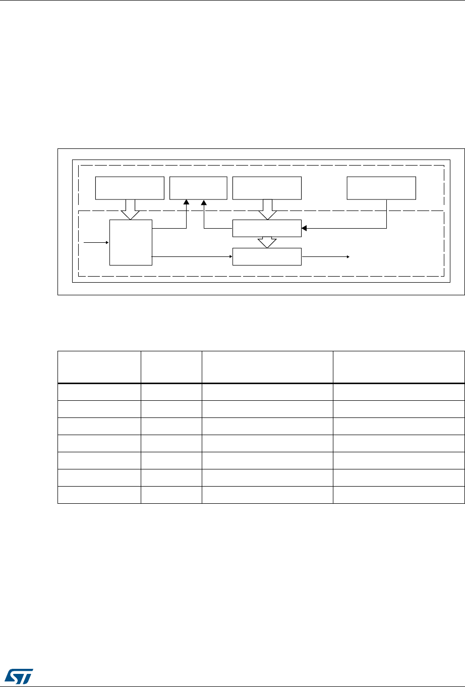
RM0430 Rev 8 679/1324
RM0430 Independent watchdog (IWDG)
683
A status register is available to indicate that an update of the prescaler or the down-counter
reload value is on going.
22.3.3 Debug mode
When the microcontroller enters debug mode (Cortex®-M4 with FPU core halted), the IWDG
counter either continues to work normally or stops, depending on DBG_IWDG_STOP
configuration bit in DBG module. For more details, refer to Section 37.16.4: Debug MCU
APB1 freeze register (DBGMCU_APB1_FZ).
Figure 221. Independent watchdog block diagram
Note: The watchdog function is implemented in the VDD voltage domain that is still functional in
Stop and Standby modes.
)7$'RESET
PRESCALER
)7$'?02
0RESCALERREGISTER
)7$'?2,2
2ELOADREGISTER
BIT
,3)
K(Z
)7$'?+2
+EYREGISTER
#/2%
6$$VOLTAGEDOMAIN
)7$'?32
3TATUSREGISTER
-36
BITRELOADVALUE
BITDOWNCOUNTER
Table 121. Min/max IWDG timeout period at 32 kHz (LSI)(1)
1. These timings are given for a 32 kHz clock but the microcontroller internal RC frequency can vary. Refers
to LSI oscillator characteristics table in device datasheet for from max and min values.
Prescaler divider PR[2:0] bits Min timeout (ms) RL[11:0]=
0x000
Max timeout (ms) RL[11:0]=
0xFFF
/4 0 0.125 512
/8 1 0.25 1024
/16 2 0.5 2048
/32 3 1 4096
/64 4 2 8192
/128 5 4 16384
/256 6 8 32768

Independent watchdog (IWDG) RM0430
680/1324 RM0430 Rev 8
22.4 IWDG registers
Refer to Section 1.2 on page 52 for a list of abbreviations used in register descriptions.
The peripheral registers have to be accessed by half-words (16 bits) or words (32 bits).
22.4.1 Key register (IWDG_KR)
Address offset: 0x00
Reset value: 0x0000 0000 (reset by Standby mode)
31 30 29 28 27 26 25 24 23 22 21 20 19 18 17 16
Res. Res. Res. Res. Res. Res. Res. Res. Res. Res. Res. Res. Res. Res. Res. Res.
15 14 13 12 11 10 9 8 7 6 5 4 3 2 1 0
KEY[15:0]
wwwwwww w w w w w w w w w
Bits 31:16 Reserved, must be kept at reset value.
Bits 15:0 KEY[15:0]: Key value (write only, read 0000h)
These bits must be written by software at regular intervals with the key value AAAAh,
otherwise the watchdog generates a reset when the counter reaches 0.
Writing the key value 5555h to enable access to the IWDG_PR and IWDG_RLR registers
(see Section 22.3.2)
Writing the key value CCCCh starts the watchdog (except if the hardware watchdog option is
selected)

RM0430 Rev 8 681/1324
RM0430 Independent watchdog (IWDG)
683
22.4.2 Prescaler register (IWDG_PR)
Address offset: 0x04
Reset value: 0x0000 0000
31 30 29 28 27 26 25 24 23 22 21 20 19 18 17 16
Res. Res. Res. Res. Res. Res. Res. Res. Res. Res. Res. Res. Res. Res. Res. Res.
15 14 13 12 11 10 9 8 7 6 5 4 3 2 1 0
Res. Res. Res. Res. Res. Res. Res. Res. Res. Res. Res. Res. Res. PR[2:0]
rw rw rw
Bits 31:3 Reserved, must be kept at reset value.
Bits 2:0 PR[2:0]: Prescaler divider
These bits are write access protected seeSection 22.3.2. They are written by software to
select the prescaler divider feeding the counter clock. PVU bit of IWDG_SR must be reset in
order to be able to change the prescaler divider.
000: divider /4
001: divider /8
010: divider /16
011: divider /32
100: divider /64
101: divider /128
110: divider /256
111: divider /256
Note: Reading this register returns the prescaler value from the VDD voltage domain. This
value may not be up to date/valid if a write operation to this register is ongoing. For this
reason the value read from this register is valid only when the PVU bit in the IWDG_SR
register is reset.

Independent watchdog (IWDG) RM0430
682/1324 RM0430 Rev 8
22.4.3 Reload register (IWDG_RLR)
Address offset: 0x08
Reset value: 0x0000 0FFF (reset by Standby mode)
22.4.4 Status register (IWDG_SR)
Address offset: 0x0C
Reset value: 0x0000 0000 (not reset by Standby mode)
31 30 29 28 27 26 25 24 23 22 21 20 19 18 17 16
Res. Res. Res. Res. Res. Res. Res. Res. Res. Res. Res. Res. Res. Res. Res. Res.
15 14 13 12 11 10 9 8 7 6 5 4 3 2 1 0
Res. Res. Res. Res. RL[11:0]
rw rw rw rw rw rw rw rw rw rw rw rw
Bits 31:12 Reserved, must be kept at reset value.
Bits11:0 RL[11:0]: Watchdog counter reload value
These bits are write access protected see Section 22.3.2. They are written by software to
define the value to be loaded in the watchdog counter each time the value AAAAh is written
in the IWDG_KR register. The watchdog counter counts down from this value. The timeout
period is a function of this value and the clock prescaler. Refer to Table 121.
The RVU bit in the IWDG_SR register must be reset in order to be able to change the reload
value.
Note: Reading this register returns the reload value from the VDD voltage domain. This value
may not be up to date/valid if a write operation to this register is ongoing on this
register. For this reason the value read from this register is valid only when the RVU bit
in the IWDG_SR register is reset.
31 30 29 28 27 26 25 24 23 22 21 20 19 18 17 16
Res. Res. Res. Res. Res. Res. Res. Res. Res. Res. Res. Res. Res. Res. Res. Res.
15 14 13 12 11 10 9 8 7 6 5 4 3 2 1 0
Res. Res. Res. Res. Res. Res. Res. Res. Res. Res. Res. Res. Res. Res. RVU PVU
rr
Bits 31:2 Reserved, must be kept at reset value.
Bit 1 RVU: Watchdog counter reload value update
This bit is set by hardware to indicate that an update of the reload value is ongoing. It is reset
by hardware when the reload value update operation is completed in the VDD voltage domain
(takes up to 5 RC 40 kHz cycles).
Reload value can be updated only when RVU bit is reset.
Bit 0 PVU: Watchdog prescaler value update
This bit is set by hardware to indicate that an update of the prescaler value is ongoing. It is
reset by hardware when the prescaler update operation is completed in the VDD voltage
domain (takes up to 5 RC 40 kHz cycles).
Prescaler value can be updated only when PVU bit is reset.

RM0430 Rev 8 683/1324
RM0430 Independent watchdog (IWDG)
683
Note: If several reload values or prescaler values are used by application, it is mandatory to wait
until RVU bit is reset before changing the reload value and to wait until PVU bit is reset
before changing the prescaler value. However, after updating the prescaler and/or the
reload value it is not necessary to wait until RVU or PVU is reset before continuing code
execution (even in case of low-power mode entry, the write operation is taken into account
and will complete)
22.4.5 IWDG register map
The following table gives the IWDG register map and reset values.
Refer to Section 2.2.2 on page 58 for the register boundary addresses.
Table 122. IWDG register map and reset values
Offset Register
31
30
29
28
27
26
25
24
23
22
21
20
19
18
17
16
15
14
13
12
11
10
9
8
7
6
5
4
3
2
1
0
0x00
IWDG_KR
Res.
Res.
Res.
Res.
Res.
Res.
Res.
Res.
Res.
Res.
Res.
Res.
Res.
Res.
Res.
Res.
KEY[15:0]
Reset value 0000000000000000
0x04
IWDG_PR
Res.
Res.
Res.
Res.
Res.
Res.
Res.
Res.
Res.
Res.
Res.
Res.
Res.
Res.
Res.
Res.
Res.
Res.
Res.
Res.
Res.
Res.
Res.
Res.
Res.
Res.
Res.
Res.
Res.
PR[2:0]
Reset value 000
0x08
IWDG_RLR
Res.
Res.
Res.
Res.
Res.
Res.
Res.
Res.
Res.
Res.
Res.
Res.
Res.
Res.
Res.
Res.
Res.
Res.
Res.
Res.
RL[11:0]
Reset value 111111111111
0x0C
IWDG_SR
Res.
Res.
Res.
Res.
Res.
Res.
Res.
Res.
Res.
Res.
Res.
Res.
Res.
Res.
Res.
Res.
Res.
Res.
Res.
Res.
Res.
Res.
Res.
Res.
Res.
Res.
Res.
Res.
Res.
Res.
RVU
PVU
Reset value 00

Window watchdog (WWDG) RM0430
684/1324 RM0430 Rev 8
23 Window watchdog (WWDG)
23.1 WWDG introduction
The window watchdog is used to detect the occurrence of a software fault, usually
generated by external interference or by unforeseen logical conditions, which causes the
application program to abandon its normal sequence. The watchdog circuit generates an
MCU reset on expiry of a programmed time period, unless the program refreshes the
contents of the downcounter before the T6 bit becomes cleared. An MCU reset is also
generated if the 7-bit downcounter value (in the control register) is refreshed before the
downcounter has reached the window register value. This implies that the counter must be
refreshed in a limited window.
23.2 WWDG main features
•Programmable free-running downcounter
•Conditional reset
– Reset (if watchdog activated) when the downcounter value becomes less than
0x40
– Reset (if watchdog activated) if the downcounter is reloaded outside the window
(see Figure 223)
•Early wakeup interrupt (EWI): triggered (if enabled and the watchdog activated) when
the downcounter is equal to 0x40.
23.3 WWDG functional description
If the watchdog is activated (the WDGA bit is set in the WWDG_CR register) and when the
7-bit downcounter (T[6:0] bits) rolls over from 0x40 to 0x3F (T6 becomes cleared), it initiates
a reset. If the software reloads the counter while the counter is greater than the value stored
in the window register, then a reset is generated.
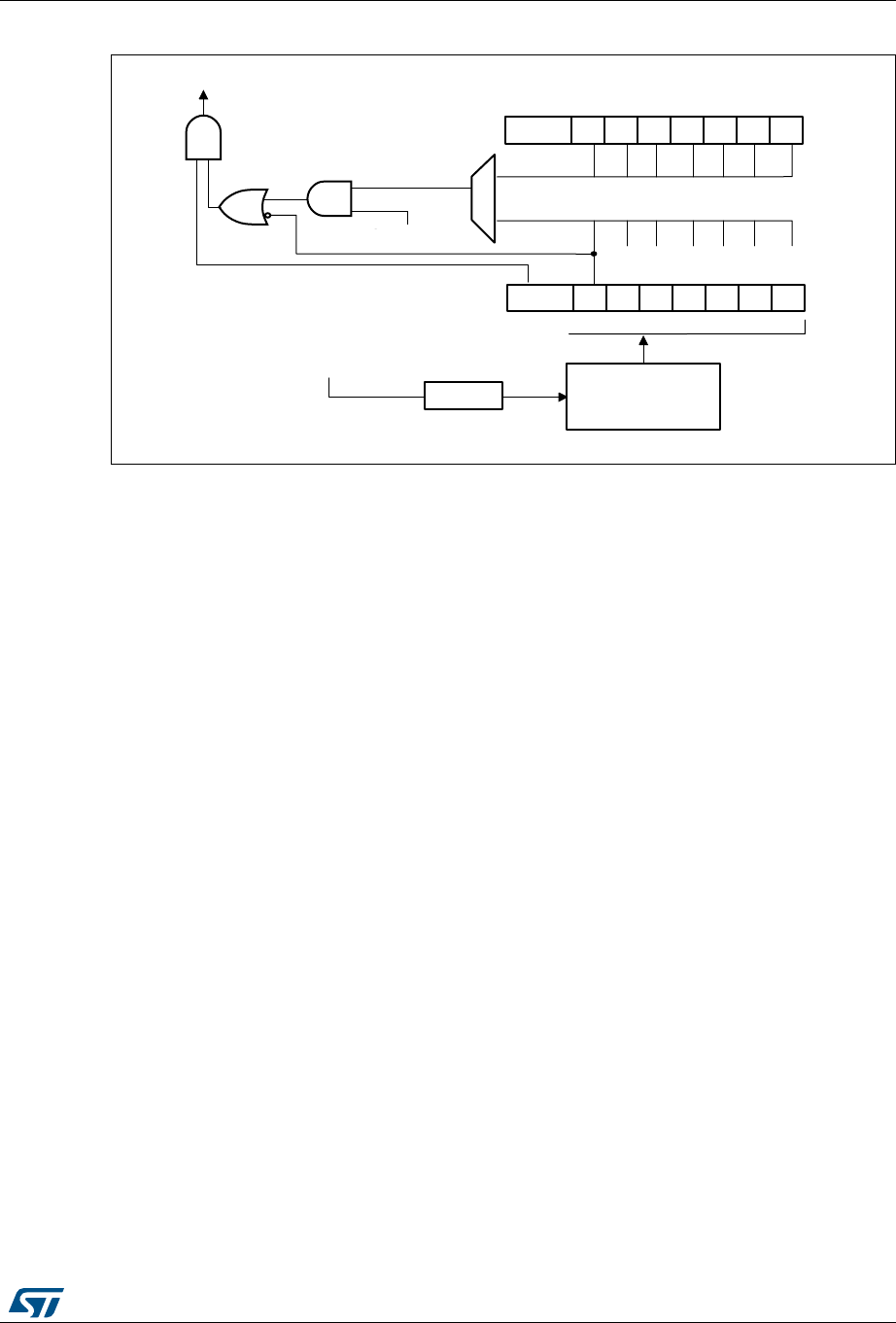
RM0430 Rev 8 685/1324
RM0430 Window watchdog (WWDG)
690
Figure 222. Watchdog block diagram
The application program must write in the WWDG_CR register at regular intervals during
normal operation to prevent an MCU reset. This operation must occur only when the counter
value is lower than the window register value. The value to be stored in the WWDG_CR
register must be between 0xFF and 0xC0.
Enabling the watchdog
The watchdog is always disabled after a reset. It is enabled by setting the WDGA bit in the
WWDG_CR register, then it cannot be disabled again except by a reset.
Controlling the downcounter
This downcounter is free-running, counting down even if the watchdog is disabled. When
the watchdog is enabled, the T6 bit must be set to prevent generating an immediate reset.
The T[5:0] bits contain the number of increments which represents the time delay before the
watchdog produces a reset. The timing varies between a minimum and a maximum value
due to the unknown status of the prescaler when writing to the WWDG_CR register (see
Figure 223). The Configuration register (WWDG_CFR) contains the high limit of the window:
To prevent a reset, the downcounter must be reloaded when its value is lower than the
window register value and greater than 0x3F. Figure 223 describes the window watchdog
process.
Note: The T6 bit can be used to generate a software reset (the WDGA bit is set and the T6 bit is
cleared).
Advanced watchdog interrupt feature
The Early Wakeup Interrupt (EWI) can be used if specific safety operations or data logging
must be performed before the actual reset is generated. The EWI interrupt is enabled by
setting the EWI bit in the WWDG_CFR register. When the downcounter reaches the value
0x40, an EWI interrupt is generated and the corresponding interrupt service routine (ISR)
can be used to trigger specific actions (such as communications or data logging), before
resetting the device.
06Y9
5(6(7
ELWGRZQFRXQWHU&17
:DWFKGRJFRQILJXUDWLRQUHJLVWHU::'*B&)5
FRPSDUDWRU
7!:
ZKHQ
:ULWH::'*B&5
3&/.
IURP5&&FORFNFRQWUROOHU
:'*SUHVFDOHU
:'*7%
: ::::: :
:'*$ 7
:DWFKGRJFRQWUROUHJLVWHU::'*B&5
77777 7
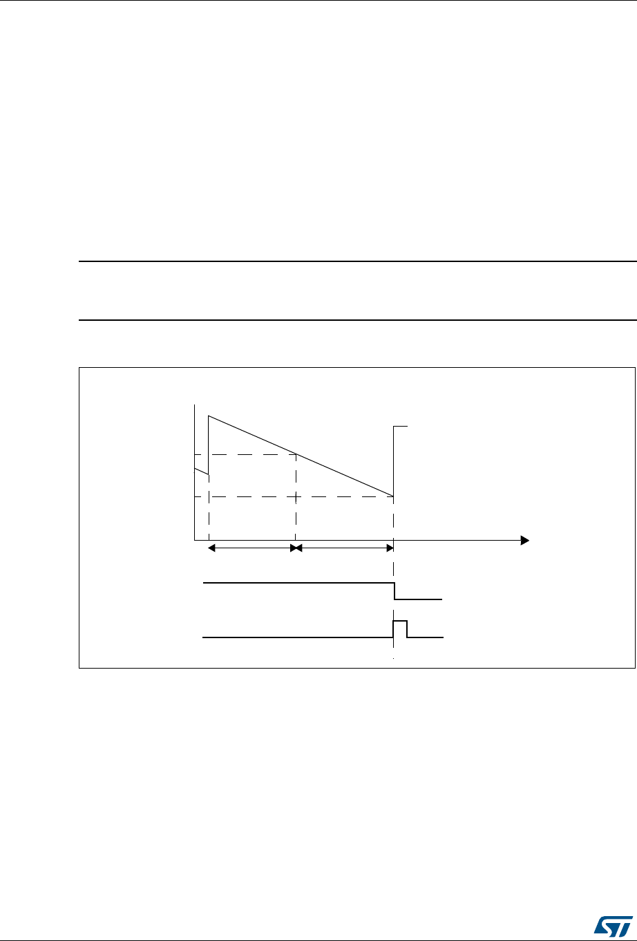
Window watchdog (WWDG) RM0430
686/1324 RM0430 Rev 8
In some applications, the EWI interrupt can be used to manage a software system check
and/or system recovery/graceful degradation, without generating a WWDG reset. In this
case, the corresponding interrupt service routine (ISR) should reload the WWDG counter to
avoid the WWDG reset, then trigger the required actions.
The EWI interrupt is cleared by writing '0' to the EWIF bit in the WWDG_SR register.
Note: When the EWI interrupt cannot be served, e.g. due to a system lock in a higher priority task,
the WWDG reset will eventually be generated.
23.4 How to program the watchdog timeout
The formula in Figure 223 must be used to calculate the WWDG timeout.
Warning: When writing to the WWDG_CR register, always write 1 in the
T6 bit to avoid generating an immediate reset.
Figure 223. Window watchdog timing diagram
The formula to calculate the timeout value is given by:
where:
tWWDG: WWDG timeout
tPCLK1: APB1 clock period measured in ms
4096: value corresponding to internal divider.
AIC
7;=
4;=#.4DOWNCOUNTER
2EFRESHNOTALLOWED
X&
2EFRESHALLOWED 4IME
4BIT
2%3%4
tWWDG tPCLK1 4096×2WDGTB[1:0]
×T5:0] 1+()×=ms()

RM0430 Rev 8 687/1324
RM0430 Window watchdog (WWDG)
690
As an example, let us assume APB1 frequency is equal to 24 MHz, WDGTB[1:0] is set to 3
and T[5:0] is set to 63:
Refer to the datasheets for the minimum and maximum values of the tWWDG.
23.5 Debug mode
When the microcontroller enters debug mode (Cortex®-M4 with FPU core halted), the
WWDG counter either continues to work normally or stops, depending on
DBG_WWDG_STOP configuration bit in DBG module. For more details, refer to
Section 37.16.2: Debug support for timers, watchdog, bxCAN and I2C.
tWWDG 1 24000⁄4096×23
×63 1+()×21.85 ms==

Window watchdog (WWDG) RM0430
688/1324 RM0430 Rev 8
23.6 WWDG registers
Refer to Section 1.2 on page 52 for a list of abbreviations used in register descriptions.
The peripheral registers have to be accessed by half-words (16 bits) or words (32 bits).
23.6.1 Control register (WWDG_CR)
Address offset: 0x00
Reset value: 0x0000 007F
31 30 29 28 27 26 25 24 23 22 21 20 19 18 17 16
Res. Res. Res. Res. Res. Res. Res. Res. Res. Res. Res. Res. Res. Res. Res. Res.
1514131211109876543210
Res. Res. Res. Res. Res. Res. Res. Res. WDGA T[6:0]
rs rw
Bits 31:8 Reserved, must be kept at reset value.
Bit 7 WDGA: Activation bit
This bit is set by software and only cleared by hardware after a reset. When WDGA = 1, the
watchdog can generate a reset.
0: Watchdog disabled
1: Watchdog enabled
Bits 6:0 T[6:0]: 7-bit counter (MSB to LSB)
These bits contain the value of the watchdog counter. It is decremented every (4096 x
2WDGTB[1:0]) PCLK1 cycles. A reset is produced when it rolls over from 0x40 to 0x3F (T6
becomes cleared).

RM0430 Rev 8 689/1324
RM0430 Window watchdog (WWDG)
690
23.6.2 Configuration register (WWDG_CFR)
Address offset: 0x04
Reset value: 0x0000 007F
23.6.3 Status register (WWDG_SR)
Address offset: 0x08
Reset value: 0x0000 0000
31 30 29 28 27 26 25 24 23 22 21 20 19 18 17 16
Res. Res. Res. Res. Res. Res. Res. Res. Res. Res. Res. Res. Res. Res. Res. Res.
1514131211109876543210
Res. Res. Res. Res. Res. Res. EWI WDGTB[1:0] W[6:0]
rs rw rw
Bits 31:10 Reserved, must be kept at reset value.
Bit 9 EWI: Early wakeup interrupt
When set, an interrupt occurs whenever the counter reaches the value 0x40. This interrupt is
only cleared by hardware after a reset.
Bits 8:7 WDGTB[1:0]: Timer base
The time base of the prescaler can be modified as follows:
00: CK Counter Clock (PCLK1 div 4096) div 1
01: CK Counter Clock (PCLK1 div 4096) div 2
10: CK Counter Clock (PCLK1 div 4096) div 4
11: CK Counter Clock (PCLK1 div 4096) div 8
Bits 6:0 W[6:0]: 7-bit window value
These bits contain the window value to be compared to the downcounter.
31 30 29 28 27 26 25 24 23 22 21 20 19 18 17 16
Res. Res. Res. Res. Res. Res. Res. Res. Res. Res. Res. Res. Res. Res. Res. Res.
1514131211109876543210
Res. Res. Res. Res. Res. Res. Res. Res. Res. Res. Res. Res. Res. Res. Res. EWIF
rc_w0
Bits 31:1 Reserved, must be kept at reset value.
Bit 0 EWIF: Early wakeup interrupt flag
This bit is set by hardware when the counter has reached the value 0x40. It must be cleared
by software by writing ‘0’. A write of ‘1’ has no effect. This bit is also set if the interrupt is not
enabled.

Window watchdog (WWDG) RM0430
690/1324 RM0430 Rev 8
23.6.4 WWDG register map
The following table gives the WWDG register map and reset values.
Refer to Section 2.2.2 on page 58 for the register boundary addresses.
Table 123. WWDG register map and reset values
Offset Register
31
30
29
28
27
26
25
24
23
22
21
20
19
18
17
16
15
14
13
12
11
10
9
8
7
6
5
4
3
2
1
0
0x00
WWDG_CR
Res.
Res.
Res.
Res.
Res.
Res.
Res.
Res.
Res.
Res.
Res.
Res.
Res.
Res.
Res.
Res.
Res.
Res.
Res.
Res.
Res.
Res.
Res.
Res.
WDGA
T[6:0]
Reset value 01111111
0x04
WWDG_CFR
Res.
Res.
Res.
Res.
Res.
Res.
Res.
Res.
Res.
Res.
Res.
Res.
Res.
Res.
Res.
Res.
Res.
Res.
Res.
Res.
Res.
Res.
EWI
WDGTB1
WDGTB0
W[6:0]
Reset value 0001111111
0x08
WWDG_SR
Res.
Res.
Res.
Res.
Res.
Res.
Res.
Res.
Res.
Res.
Res.
Res.
Res.
Res.
Res.
Res.
Res.
Res.
Res.
Res.
Res.
Res.
Res.
Res.
Res.
Res.
Res.
Res.
Res.
Res.
Res.
EWIF
Reset value 0

RM0430 Rev 8 691/1324
RM0430 AES hardware accelerator (AES)
743
24 AES hardware accelerator (AES)
24.1 Introduction
The AES hardware accelerator (AES) encrypts or decrypts data, using an algorithm and
implementation fully compliant with the advanced encryption standard (AES) defined in
Federal information processing standards (FIPS) publication 197.
Multiple chaining modes are supported (ECB, CBC, CTR, GCM, GMAC, CCM), for key
sizes of 128 or 256 bits.
The AES accelerator is a 32-bit AHB peripheral. It supports DMA single transfers for
incoming and outgoing data (two DMA channels required).
The AES peripheral provides hardware acceleration to AES cryptographic algorithms
packaged in STM32 cryptographic library.
AES is an AMBA AHB slave peripheral, accessible through 32-bit word single accesses only
(otherwise an AHB bus error is generated and write accesses are ignored).
24.2 AES main features
•Compliance with NIST “Advanced encryption standard (AES), FIPS publication 197”
from November 2001
•128-bit data block processing
•Support for cipher key lengths of 128-bit and 256-bit
•Encryption and decryption with multiple chaining modes:
– Electronic codebook (ECB) mode
– Cipher block chaining (CBC) mode
– Counter (CTR) mode
– Galois counter mode (GCM)
– Galois message authentication code (GMAC) mode
– Counter with CBC-MAC (CCM) mode
•51 or 75 clock cycle latency in ECB mode for processing one 128-bit block of data with,
respectively, 128-bit or 256-bit key
•Integrated key scheduler with its key derivation stage (ECB or CBC decryption only)
•AMBA AHB slave peripheral, accessible through 32-bit word single accesses only
•256-bit register for storing the cryptographic key (eight 32-bit registers)
•128-bit register for storing initialization vector (four 32-bit registers)
•32-bit buffer for data input and output
•Automatic data flow control with support of single-transfer direct memory access (DMA)
using two channels (one for incoming data, one for processed data)
•Data-swapping logic to support 1-, 8-, 16- or 32-bit data
•Possibility for software to suspend a message if AES needs to process another
message with a higher priority, then resume the original message
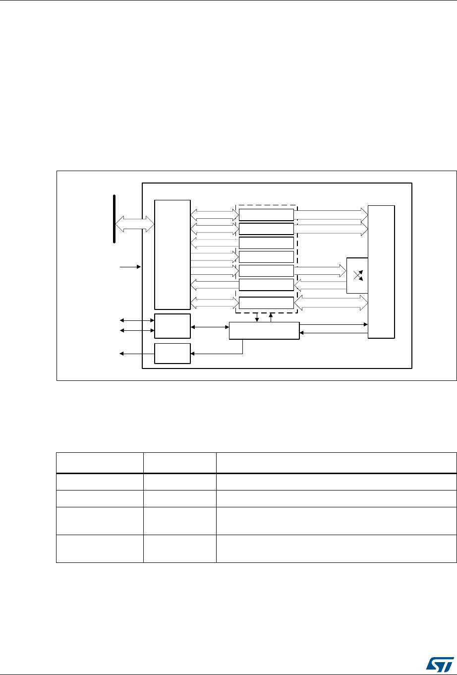
AES hardware accelerator (AES) RM0430
692/1324 RM0430 Rev 8
24.3 AES implementation
The device has a single instance of AES peripheral.
24.4 AES functional description
24.4.1 AES block diagram
Figure 224 shows the block diagram of AES.
Figure 224. AES block diagram
24.4.2 AES internal signals
Table 124 describes the user relevant internal signals interfacing the AES peripheral.
06Y9
DHVBKFON
%DQNHGUHJLVWHUV
'287
.(<
,9,
',1
$(6
NH\
FRQWURO
VWDWXV
,9FRXQWHU
GDWDLQ
GDWDRXW
DHVBLW
ELW
$+%EXV
DHVBLQBGPD
$(6B&5
$(6B.(<5[
$(6B65
$(6B,95[
$(6B',15
$(6B'2875
$(6
&RUH
$($
VZDS
$+%
LQWHUIDFH
,54
LQWHUIDFH
&RQWURO/RJLF
'0$
LQWHUIDFH
DHVBRXWBGPD
ELW
DFFHVV
6DYH5HVWRUH
$(6B68635[
Table 124. AES internal input/output signals
Signal name Signal type Description
aes_hclk digital input AHB bus clock
aes_it digital output AES interrupt request
aes_in_dma digital
input/output Input DMA single request/acknowledge
aes_out_dma digital
input/output Output DMA single request/acknowledge

RM0430 Rev 8 693/1324
RM0430 AES hardware accelerator (AES)
743
24.4.3 AES cryptographic core
Overview
The AES cryptographic core consists of the following components:
•AES algorithm (AEA)
•multiplier over a binary Galois field (GF2mul)
•key input
•initialization vector (IV) input
•chaining algorithm logic (XOR, feedback/counter, mask)
The AES core works on 128-bit data blocks (four words) with 128-bit or 256-bit key length.
Depending on the chaining mode, the AES requires zero or one 96-bit initialization vector IV
(and a 32-bit counter field).
The AES features the following modes of operation:
•Mode 1:
Plaintext encryption using a key stored in the AES_KEYRx registers
•Mode 2:
ECB or CBC decryption key preparation. It must be used prior to selecting Mode 3 with
ECB or CBC chaining modes. The key prepared for decryption is stored automatically
in the AES_KEYRx registers. Now the AES peripheral is ready to switch to Mode 3 for
executing data decryption.
•Mode 3:
Ciphertext decryption using a key stored in the AES_KEYRx registers. When ECB and
CBC chaining modes are selected, the key must be prepared beforehand, through
Mode 2.
•Mode 4:
ECB or CBC ciphertext single decryption using the key stored in the AES_KEYRx
registers (the initial key is derived automatically).
Note: Mode 2 and mode 4 are only used when performing ECB and CBC decryption.
When Mode 4 is selected only one decryption can be done, therefore usage of Mode 2 and
Mode 3 is recommended instead.
The operating mode is selected by programming the MODE[1:0] bitfield of the AES_CR
register. It may be done only when the AES peripheral is disabled.
Typical data processing
Typical usage of the AES is described in Section 24.4.4: AES procedure to perform a cipher
operation on page 698.
Note: The outputs of the intermediate AEA stages are never revealed outside the cryptographic
boundary, with the exclusion of the IVI bitfield.
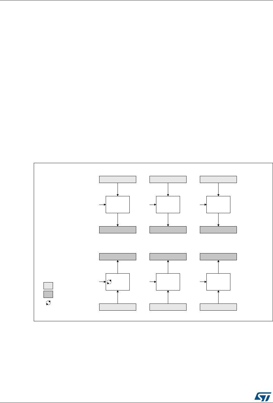
AES hardware accelerator (AES) RM0430
694/1324 RM0430 Rev 8
Chaining modes
The following chaining modes are supported by AES, selected through the CHMOD[2:0]
bitfield of the AES_CR register:
•Electronic code book (ECB)
•Cipher block chaining (CBC)
•Counter (CTR)
•Galois counter mode (GCM)
•Galois message authentication code (GMAC)
•Counter with CBC-MAC (CCM)
Note: The chaining mode may be changed only when AES is disabled (bit EN of the AES_CR
register set).
Principle of each AES chaining mode is provided in the following subsections.
Detailed information is in dedicated sections, starting from Section 24.4.8: AES basic
chaining modes (ECB, CBC).
Electronic codebook (ECB) mode
Figure 225. ECB encryption and decryption principle
ECB is the simplest mode of operation. There are no chaining operations, and no special
initialization stage. The message is divided into blocks and each block is encrypted or
decrypted separately.
Note: For decryption, a special key scheduling is required before processing the first block.
06Y9
(QFU\SWLRQ
3ODLQWH[WEORFN 3ODLQWH[WEORFN 3ODLQWH[WEORFN
&LSKHUWH[WEORFN &LSKHUWH[WEORFN &LSKHUWH[WEORFN
(QFU\SW (QFU\SW (QFU\SW
'HFU\SWLRQ
NH\ NH\ NH\
3ODLQWH[WEORFN 3ODLQWH[WEORFN 3ODLQWH[WEORFN
&LSKHUWH[WEORFN &LSKHUWH[WEORFN &LSKHUWH[WEORFN
'HFU\SW 'HFU\SW 'HFU\SW
NH\ NH\ NH\
LQSXW
RXWSXW
NH\
VFKHGXOLQJ
/HJHQG
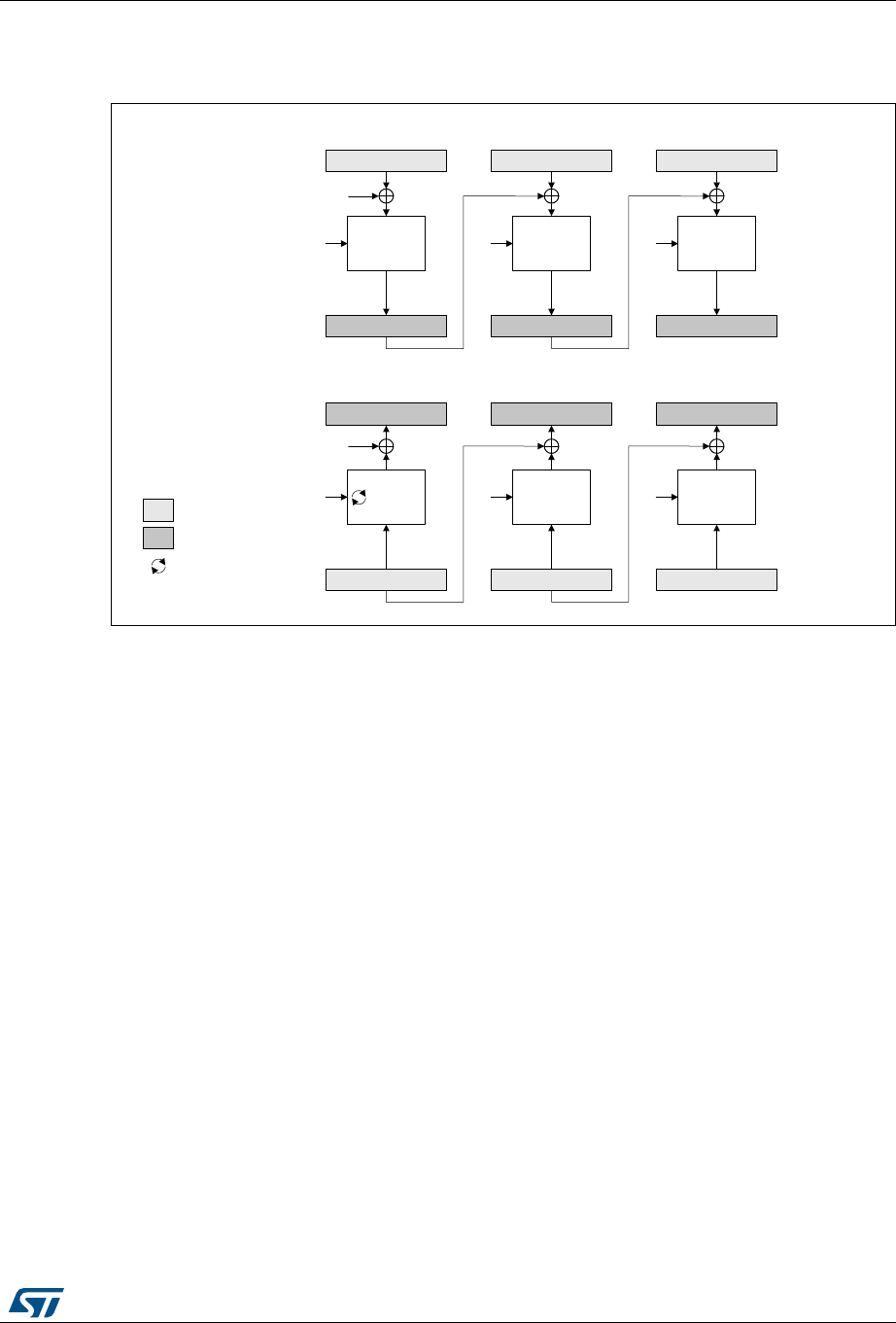
RM0430 Rev 8 695/1324
RM0430 AES hardware accelerator (AES)
743
Cipher block chaining (CBC) mode
Figure 226. CBC encryption and decryption principle
In CBC mode the output of each block chains with the input of the following block. To make
each message unique, an initialization vector is used during the first block processing.
Note: For decryption, a special key scheduling is required before processing the first block.
06Y9
(QFU\SWLRQ
3ODLQWH[WEORFN 3ODLQWH[WEORFN 3ODLQWH[WEORFN
&LSKHUWH[WEORFN &LSKHUWH[WEORFN &LSKHUWH[WEORFN
(QFU\SW (QFU\SW (QFU\SW
'HFU\SWLRQ
NH\ NH\ NH\
3ODLQWH[WEORFN 3ODLQWH[WEORFN 3ODLQWH[WEORFN
&LSKHUWH[WEORFN &LSKHUWH[WEORFN &LSKHUWH[WEORFN
'HFU\SW 'HFU\SW 'HFU\SW
NH\ NH\ NH\
LQSXW
RXWSXW
NH\
VFKHGXOLQJ
/HJHQG
LQLWLDOL]DWLRQ
YHFWRU
LQLWLDOL]DWLRQ
YHFWRU
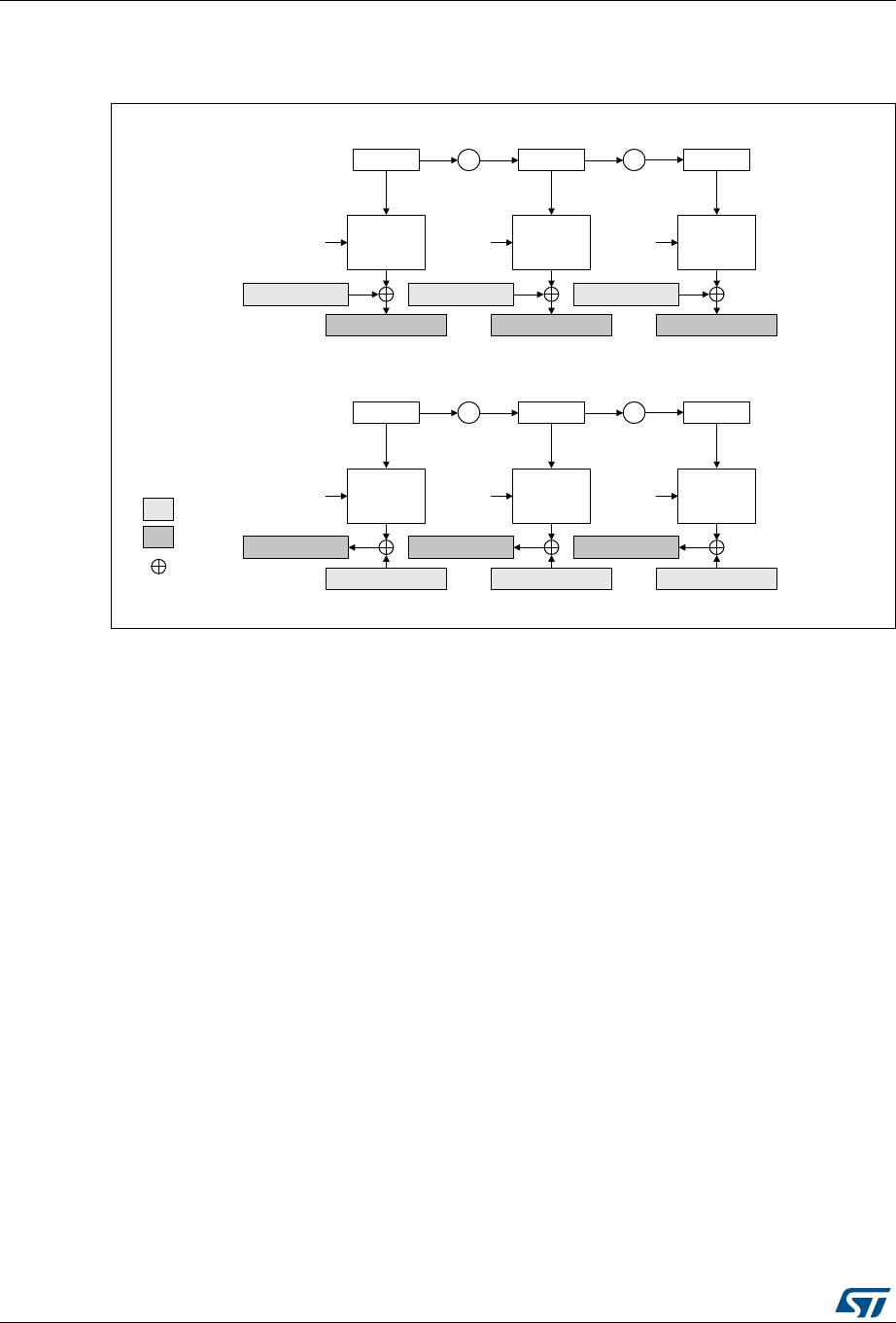
AES hardware accelerator (AES) RM0430
696/1324 RM0430 Rev 8
Counter (CTR) mode
Figure 227. CTR encryption and decryption principle
The CTR mode uses the AES core to generate a key stream. The keys are then XORed
with the plaintext to obtain the ciphertext as specified in NIST Special Publication 800-38A,
Recommendation for Block Cipher Modes of Operation.
Note: Unlike with ECB and CBC modes, no key scheduling is required for the CTR decryption,
since in this chaining scheme the AES core is always used in encryption mode for producing
the key stream, or counter blocks.
06Y9
(QFU\SWLRQ
3ODLQWH[WEORFN
&LSKHUWH[WEORFN &LSKHUWH[WEORFN &LSKHUWH[WEORFN
(QFU\SW (QFU\SW (QFU\SW
'HFU\SWLRQ
&LSKHUWH[WEORFN &LSKHUWH[WEORFN &LSKHUWH[WEORFN
'HFU\SW 'HFU\SW 'HFU\SW
LQSXW
RXWSXW
/HJHQG
NH\ NH\ NH\
NH\ NH\ NH\
3ODLQWH[WEORFN 3ODLQWH[WEORFN
&RXQWHU &RXQWHU &RXQWHU
3ODLQWH[WEORFN 3ODLQWH[WEORFN 3ODLQWH[WEORFN
&RXQWHU &RXQWHU &RXQWHU
;25
YDOXH YDOXH YDOXH
YDOXH YDOXH YDOXH
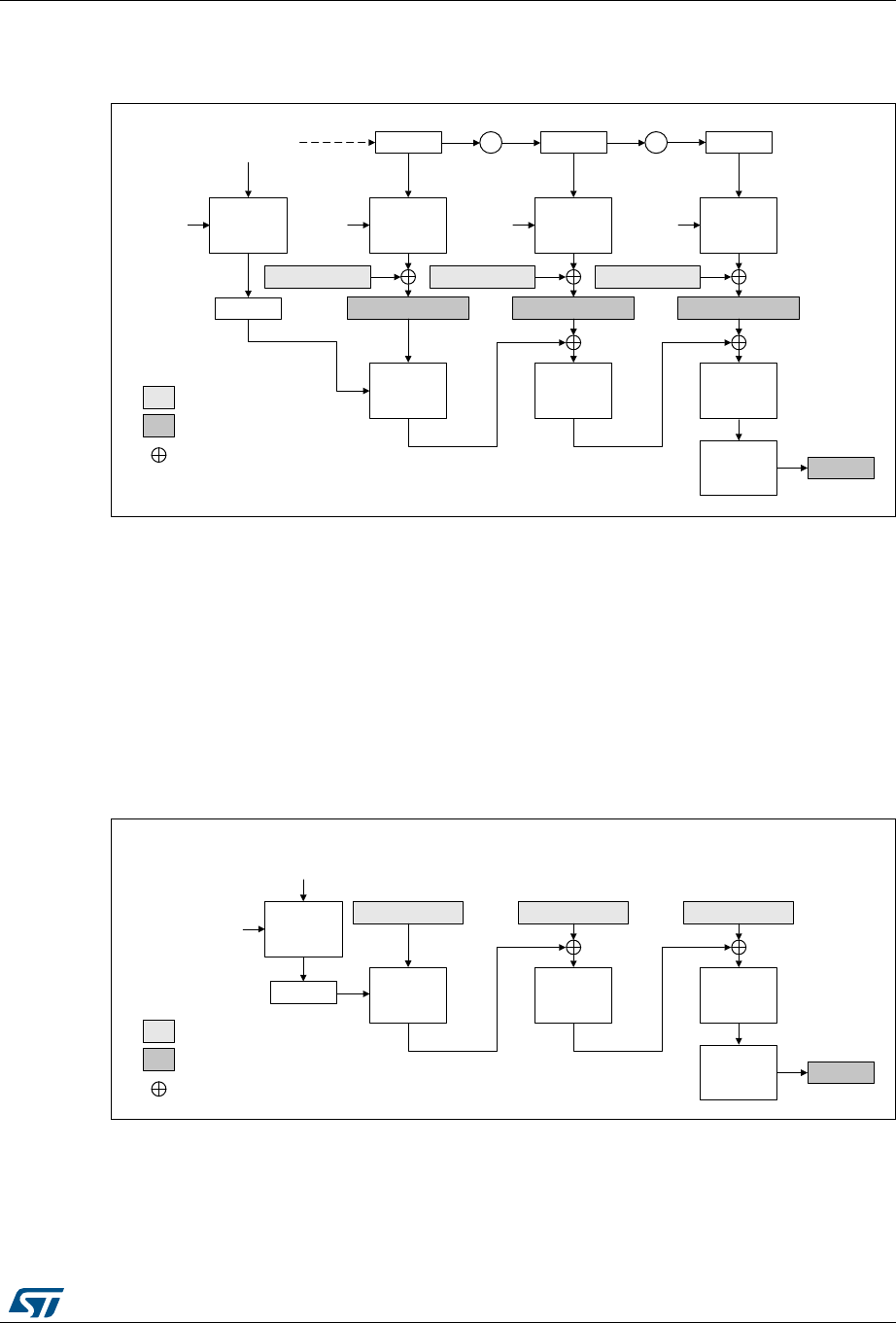
RM0430 Rev 8 697/1324
RM0430 AES hardware accelerator (AES)
743
Galois/counter mode (GCM)
Figure 228. GCM encryption and authentication principle
In Galois/counter mode (GCM), the plaintext message is encrypted while a message
authentication code (MAC) is computed in parallel, thus generating the corresponding
ciphertext and its MAC (also known as authentication tag). It is defined in NIST Special
Publication 800-38D, Recommendation for Block Cipher Modes of Operation -
Galois/Counter Mode (GCM) and GMAC.
GCM mode is based on AES in counter mode for confidentiality. It uses a multiplier over a
fixed finite field for computing the message authentication code. It requires an initial value
and a particular 128-bit block at the end of the message.
Galois message authentication code (GMAC) principle
Figure 229. GMAC authentication principle
Galois message authentication code (GMAC) allows authenticating a message and
generating the corresponding message authentication code (MAC). It is defined in NIST
Special Publication 800-38D, Recommendation for Block Cipher Modes of Operation -
Galois/Counter Mode (GCM) and GMAC.
06Y9
3ODLQWH[WEORFN
&LSKHUWH[WEORFN &LSKHUWH[WEORFN &LSKHUWH[WEORFN
(QFU\SW (QFU\SW (QFU\SW
NH\ NH\ NH\
3ODLQWH[WEORFN 3ODLQWH[WEORFN
&RXQWHU &RXQWHU &RXQWHU
*)PXO *)PXO *)PXO
)LQDO 7$*
,QLW
(QFU\SW
NH\
,QLWLDOL]DWLRQ
YHFWRU
+
LQSXW
RXWSXW
/HJHQG
;25
YDOXH YDOXH YDOXH
06Y9
3ODLQWH[WEORFN 3ODLQWH[WEORFN 3ODLQWH[WEORFN
*)PXO *)PXO *)PXO
)LQDO 7$*
,QLW
(QFU\SW
NH\
,QLWLDOL]DWLRQ
YHFWRU
+
LQSXW
RXWSXW
/HJHQG
;25
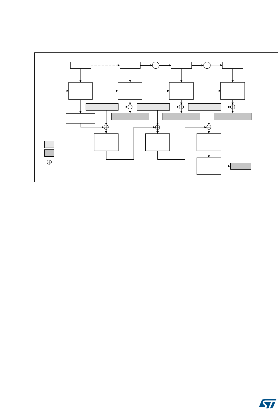
AES hardware accelerator (AES) RM0430
698/1324 RM0430 Rev 8
GMAC is similar to GCM, except that it is applied on a message composed only by plaintext
authenticated data (that is, only header, no payload).
Counter with CBC-MAC (CCM) principle
Figure 230. CCM encryption and authentication principle
In Counter with cipher block chaining-message authentication code (CCM) mode, the
plaintext message is encrypted while a message authentication code (MAC) is computed in
parallel, thus generating the corresponding ciphertext and the corresponding MAC (also
known as tag). It is described by NIST in Special Publication 800-38C, Recommendation for
Block Cipher Modes of Operation - The CCM Mode for Authentication and Confidentiality.
CCM mode is based on AES in counter mode for confidentiality and it uses CBC for
computing the message authentication code. It requires an initial value.
Like GCM, the CCM chaining mode can be applied on a message composed only by
plaintext authenticated data (that is, only header, no payload). Note that this way of using
CCM is not called CMAC (it is not similar to GCM/GMAC), and its usage is not
recommended by NIST.
24.4.4 AES procedure to perform a cipher operation
Introduction
A typical cipher operation is explained below. Detailed information is provided in sections
starting from Section 24.4.8: AES basic chaining modes (ECB, CBC).
The flowcharts shown in Figure 231 and Figure 232 describe the way STM32 cryptographic
library implements the AES algorithm. AES accelerates the execution of the AES-128 and
AES-256 cryptographic algorithms in ECB, CBC, CTR, CCM, and GCM operating modes.
Note: For more details on the cryptographic library, refer to the UM1924 user manual “STM32
crypto library” available from www.st.com.
06Y9
3ODLQWH[WEORFN
&LSKHUWH[WEORFN &LSKHUWH[WEORFN &LSKHUWH[WEORFN
(QFU\SW (QFU\SW (QFU\SW
NH\ NH\ NH\
3ODLQWH[WEORFN 3ODLQWH[WEORFN
&RXQW &RXQW &RXQW
(QFU\SW (QFU\SW (QFU\SW
)LQDO 7$*
,QLW
(QFU\SW
NH\
,QLWLDOL]DWLRQ
YHFWRU
LQSXW
RXWSXW
/HJHQG
;25
%
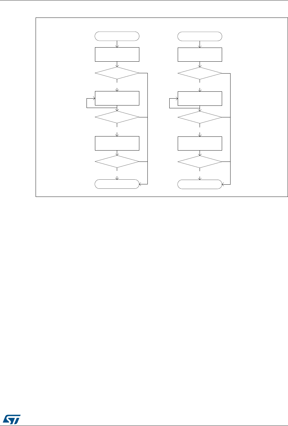
RM0430 Rev 8 699/1324
RM0430 AES hardware accelerator (AES)
743
Figure 231. STM32 cryptolib AES flowchart examples
06Y9
(UURUVWDWXV
%HJLQ
$(6B[HQFU\SWLQLW
$(6B[HQFU\SW
DSSHQG
(UURUVWDWXV
$(6B[HQFU\SWILQLVK
ILQDO
(UURUVWDWXV
(QG
VXFFHVV
VXFFHVV
VXFFHVV
(QFU\SWLRQ
(UURUVWDWXV
%HJLQ
$(6B[GHFU\SWLQLW
$(6B[GHFU\SW
DSSHQG
(UURUVWDWXV
$(6B[GHFU\SWILQLVK
ILQDO
(UURUVWDWXV
(QG
VXFFHVV
VXFFHVV
VXFFHVV
'HFU\SWLRQ
'DWDWRDSSHQG 'DWDWRDSSHQG
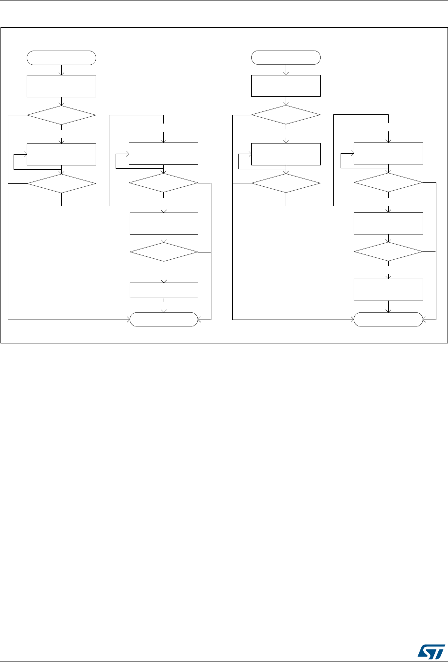
AES hardware accelerator (AES) RM0430
700/1324 RM0430 Rev 8
Figure 232. STM32 cryptolib AES flowchart examples (continued)
Initialization of AES
To initialize AES, first disable it by clearing the EN bit of the AES_CR register. Then perform
the following steps in any order:
•Configure the AES mode, by programming the MODE[1:0] bitfield of the AES_CR
register.
– For encryption, Mode 1 must be selected (MODE[1:0] = 00).
– For decryption, Mode 3 must be selected (MODE[1:0] = 10), unless ECB or CBC
chaining modes are used. In this latter case, an initial key derivation of the
encryption key must be performed, as described in Section 24.4.5: AES
decryption key preparation.
•Select the chaining mode, by programming the CHMOD[2:0] bitfield of the AES_CR
register
•Configure the key size (128-bit or 256-bit), with the KEYSIZE bitfield of the AES_CR
register.
•Write a symmetric key into the AES_KEYRx registers (4 or 8 registers depending on
the key size).
•Configure the data type (1-, 8-, 16- or 32-bit), with the DATATYPE[1:0] bitfield in the
AES_CR register.
•When it is required (for example in CBC or CTR chaining modes), write the initialization
vectors into the AES_IVRx register.
06Y9
(UURUVWDWXV
%HJLQ
$(6B[HQFU\SWLQLW
$(6B[KHDGHU
DSSHQG
(UURUVWDWXV
VXFFHVV VXFFHVV
$XWKHQWLFDWHG(QFU\SWLRQ
$(6B[HQFU\SW
DSSHQG
(UURUVWDWXV
$(6B[HQFU\SW
ILQLVKILQDO
(UURUVWDWXV
(QG
VXFFHVV
VXFFHVV
(UURUVWDWXV
%HJLQ
$(6B[GHFU\SWLQLW
$(6B[KHDGHU
DSSHQG
(UURUVWDWXV
VXFFHVV VXFFHVV
$XWKHQWLFDWHG'HFU\SWLRQ
$(6B[GHFU\SW
DSSHQG
(UURUVWDWXV
$(6B[GHFU\SW
ILQLVKILQDO
(UURUVWDWXV
(QG
VXFFHVV
VXFFHVV
0$&7DJ
FRPSDULVRQ
'DWDWRDSSHQG 'DWDWRDSSHQG 'DWDWRDSSHQG 'DWDWRDSSHQG
5HWUHLYH7DJ

RM0430 Rev 8 701/1324
RM0430 AES hardware accelerator (AES)
743
Data append
This section describes different ways of appending data for processing, where the size of
data to process is not a multiple of 128 bits.
For ECB, CBC and GCM encryption mode, refer to Section 24.4.6: AES ciphertext stealing
and data padding. The second-last and the last block management in these cases is more
complex than in the sequence described in this section.
Data append through polling
This method uses flag polling to control the data append.
For all other cases, the data is appended through the following sequence:
1. Enable the AES peripheral by setting the EN bit of the AES_CR register.
2. Repeat the following sub-sequence until the payload is entirely processed:
a) Write four input data words into the AES_DINR register.
b) Wait until the status flag CCF is set in the AES_SR, then read the four data words
from the AES_DOUTR register.
c) Clear the CCF flag, by setting the CCFC bit of the AES_CR register.
d) If the data block just processed is the second-last block of the message and the
significant data in the last block to process is inferior to 128 bits, pad the
remainder of the last block with zeros
3. Discard the data that is not part of the payload, then disable the AES peripheral by
clearing the EN bit of the AES_CR register.
Note: Up to three wait cycles are automatically inserted between two consecutive writes to the
AES_DINR register, to allow sending the key to the AES processor.
Data append using interrupt
The method uses interrupt from the AES peripheral to control the data append, through the
following sequence:
1. Enable interrupts from AES by setting the CCFIE bit of the AES_CR register.
2. Enable the AES peripheral by setting the EN bit of the AES_CR register.
3. Write first four input data words into the AES_DINR register.
4. Handle the data in the AES interrupt service routine, upon interrupt:
a) Read four output data words from the AES_DOUTR register.
b) Clear the CCF flag and thus the pending interrupt, by setting the CCFC bit of the
AES_CR register
c) If the data block just processed is the second-last block of an message and the
significant data in the last block to process is inferior to 128 bits, pad the
remainder of the last block with zeros. Then proceed with point 4e).
d) If the data block just processed is the last block of the message, discard the data
that is not part of the payload, then disable the AES peripheral by clearing the EN
bit of the AES_CR register and quit the interrupt service routine.
e) Write next four input data words into the AES_DINR register and quit the interrupt
service routine.
Note: AES is tolerant of delays between consecutive read or write operations, which allows, for
example, an interrupt from another peripheral to be served between two AES computations.

AES hardware accelerator (AES) RM0430
702/1324 RM0430 Rev 8
Data append using DMA
With this method, all the transfers and processing are managed by DMA and AES. To use
the method, proceed as follows:
1. Prepare the last four-word data block (if the data to process does not fill it completely),
by padding the remainder of the block with zeros.
2. Configure the DMA controller so as to transfer the data to process from the memory to
the AES peripheral input and the processed data from the AES peripheral output to the
memory, as described in Section 24.4.16: AES DMA interface. Configure the DMA
controller so as to generate an interrupt on transfer completion.
3. Enable the AES peripheral by setting the EN bit of the AES_CR register
4. Enable DMA requests by setting the DMAINEN and DMAOUTEN bits of the AES_CR
register.
5. Upon DMA interrupt indicating the transfer completion, get the AES-processed data
from the memory.
Note: The CCF flag has no use with this method, because the reading of the AES_DOUTR
register is managed by DMA automatically, without any software action, at the end of the
computation phase.
24.4.5 AES decryption key preparation
For an ECB or CBC decryption, a key for the first round of decryption must be derived from
the key of the last round of encryption. This is why a complete key schedule of encryption is
required before performing the decryption. This key preparation is not required for AES
decryption in modes other than ECB or CBC.
Recommended method is to select the Mode 2 by setting to 01 the MODE[1:0] bitfield of the
AES_CR (key process only), then proceed with the decryption by setting MODE[1:0] to 10
(Mode 3, decryption only). Mode 2 usage is described below:
1. Disable the AES peripheral by clearing the EN bit of the AES_CR register.
2. Select Mode 2 by setting to 01 the MODE[1:0] bitfield of the AES_CR. The
CHMOD[2:0] bitfield is not significant in this case because this key derivation mode is
independent of the chaining algorithm selected.
3. Set key length to 128 or 256 bits, via KEYSIZE bit of AES_CR register.
4. Write the AES_KEYRx registers (128 or 256 bits) with encryption key, as shown in
Figure 233. Writes to the AES_IVRx registers have no effect.
5. Enable the AES peripheral, by setting the EN bit of the AES_CR register.
6. Wait until the CCF flag is set in the AES_SR register.
7. Derived key is available in AES core, ready to use for decryption. Application can also
read the AES_KEYRx register to obtain the derived key if needed, as shown in
Figure 233 (the processed key is loaded automatically into the AES_KEYRx registers).
Note: The AES is disabled by hardware when the derivation key is available.
To restart a derivation key computation, repeat steps 4, 5, 6 and 7.
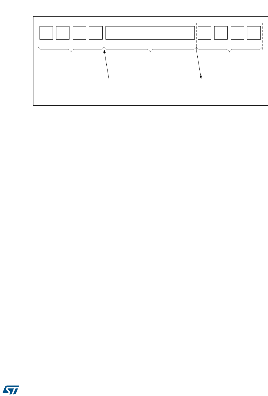
RM0430 Rev 8 703/1324
RM0430 AES hardware accelerator (AES)
743
Figure 233. Encryption key derivation for ECB/CBC decryption (Mode 2)
If the software stores the initial key prepared for decryption, it is enough to do the key
schedule operation only once for all the data to be decrypted with a given cipher key.
Note: The operation of the key preparation lasts 80 or 109 clock cycles, depending on the key size
(128- or 256-bit).
Note: Alternative key preparation is to select Mode 4 by setting to 11 the MODE[1:0] bitfield of the
AES_CR register. In this case Mode 3 cannot be used.
24.4.6 AES ciphertext stealing and data padding
When using AES in ECB or CBC modes to manage messages the size of which is not a
multiple of the block size (128 bits), ciphertext stealing techniques are used, such as those
described in NIST Special Publication 800-38A, Recommendation for Block Cipher Modes
of Operation: Three Variants of Ciphertext Stealing for CBC Mode. Since the AES peripheral
on the device does not support such techniques, the last two blocks of input data must be
handled in a special way by the application.
Note: Ciphertext stealing techniques are not documented in this reference manual.
Similarly, when AES is used in other modes than ECB or CBC, an incomplete input data
block (that is, block with input data shorter than 128 bits) must be padded with zeros prior to
encryption (that is, extra bits must be appended to the trailing end of the data string). After
decryption, the extra bits must be discarded. As AES does not implement automatic data
padding operation to the last block, the application must follow the recommendation given
in Section 24.4.4: AES procedure to perform a cipher operation on page 698 to manage
messages the size of which is not a multiple of 128 bits.
Note: Padding data are swapped in a similar way as normal data, according to the
DATATYPE[1:0] field of the AES_CR register (see Section 24.4.13: .AES data registers and
data swapping on page 724 for details).
A workaround is required in order to properly compute authentication tags for GCM
encryption, when the input data in the last block is inferior to 128 bits. During GCM
encryption payload phase and before inserting a last plaintext block smaller than 128 bits,
then application must apply the following steps:
069
:5
(.
:5
(.
:5
(.
:5
(. :DLWXQWLOIODJ&&) 5'
'.
5'
'.
5'
'.
5'
'.
,QSXWSKDVH
ZULWHRSHUDWLRQVLQWR
$(6B.(<5[>@
&RPSXWDWLRQSKDVH
2XWSXWSKDVHRSWLRQDO
UHDGRSHUDWLRQVRI
$(6B.(<5[>@
(. HQFU\SWLRQNH\ ZRUGV(.«(.
'. GHFU\SWLRQNH\ ZRUGV'.«'.
06% /6% 06% /6%
(1 LQWR$(6B&5 ELWGHULYDWLRQNH\
VWRUHGLQWR$(6B.(<5[
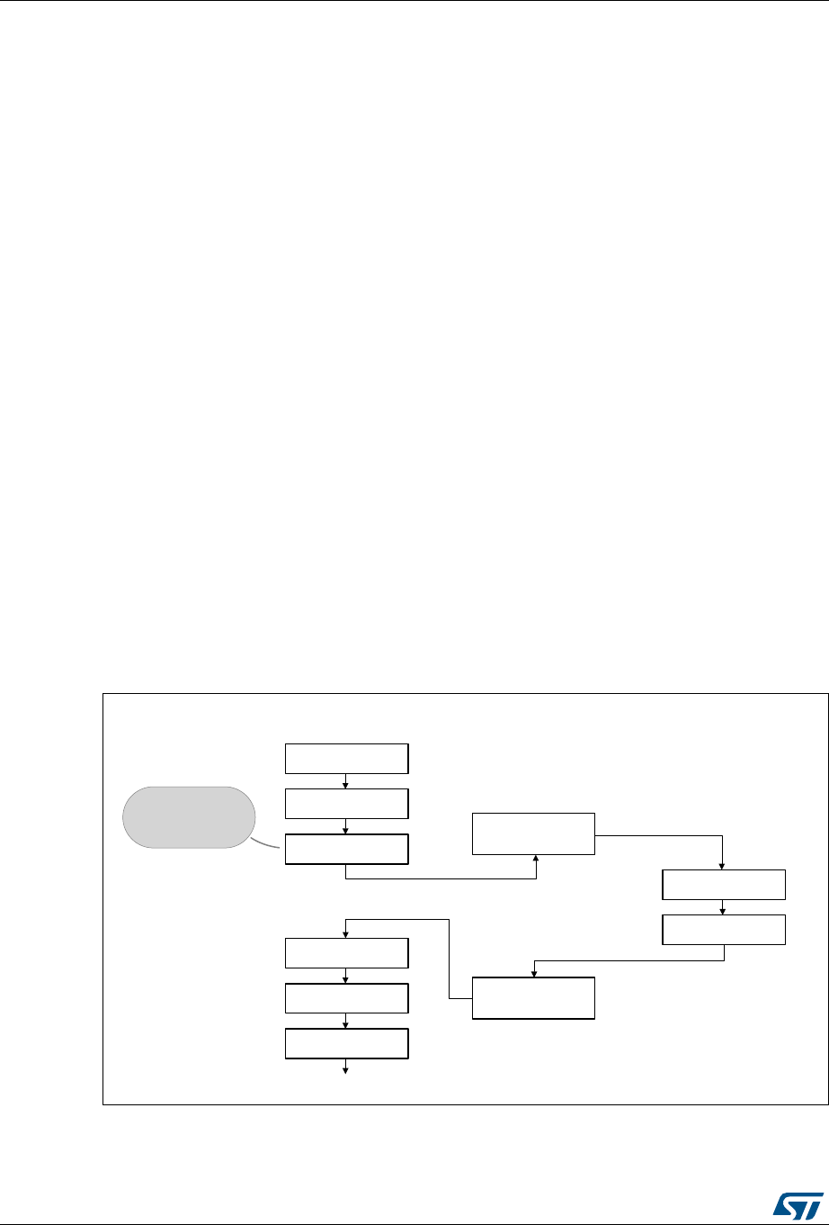
AES hardware accelerator (AES) RM0430
704/1324 RM0430 Rev 8
1. Disable the AES peripheral by clearing the EN bit of the AES_CR register
2. Change the mode to CTR by writing 010 to the CHMOD[2:0] bitfield of the AES_CR
register.
3. Pad the last block (smaller than 128 bits) with zeros to have a complete block of 128
bits, then write it into AES_DINR register.
4. Upon encryption completion, read the 128-bit ciphertext from the AES_DOUTR register
and store it as intermediate data.
5. Change again the mode to GCM by writing 011 to the CHMOD[2:0] bitfield of the
AES_CR register.
6. Select Final phase by writing 11 to the GCMPH[1:0] bitfield of the AES_CR register.
7. In the intermediate data, set to zero the bits corresponding to the padded bits of the last
block of payload, then insert the resulting data into AES_DINR register.
8. Wait for operation completion, and read data on AES_DOUTR. This data is to be
discarded.
9. Apply the normal Final phase as described in Section 24.4.10: AES Galois/counter
mode (GCM) on page 712
24.4.7 AES task suspend and resume
A message can be suspended if another message with a higher priority must be processed.
When this highest priority message is sent, the suspended message can resume in both
encryption or decryption mode.
Suspend/resume operations do not break the chaining operation and the message
processing can resume as soon as AES is enabled again to receive the next data block.
Figure 234 gives an example of suspend/resume operation: Message 1 is suspended in
order to send a shorter and higher-priority Message 2.
Figure 234. Example of suspend mode management
A detailed description of suspend/resume operations is in the sections dedicated to each
AES mode.
06Y9
ELWEORFN
0HVVDJH
ELWEORFN
ELWEORFN
ELWEORFN
ELWEORFN
$(6VXVSHQG
VHTXHQFH
$(6UHVXPH
VHTXHQFH
ELWEORFN
ELWEORFN
0HVVDJH
ELWEORFN
1HZKLJKHUSULRULW\
PHVVDJHWREH
SURFHVVHG
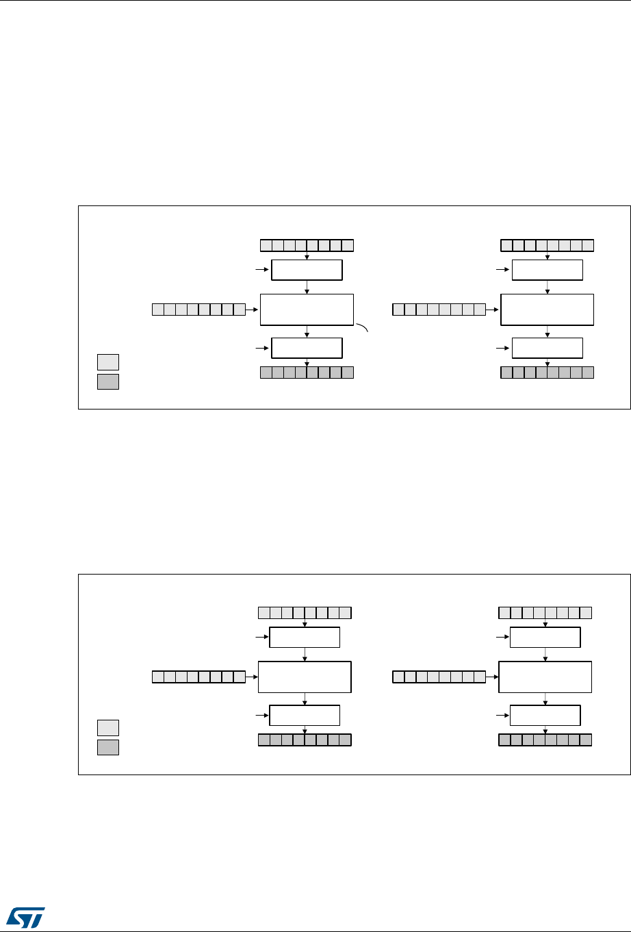
RM0430 Rev 8 705/1324
RM0430 AES hardware accelerator (AES)
743
24.4.8 AES basic chaining modes (ECB, CBC)
Overview
This section gives a brief explanation of the four basic operation modes provided by the
AES computing core: ECB encryption, ECB decryption, CBC encryption and CBC
decryption. For detailed information, refer to the FIPS publication 197 from November 26,
2001.
Figure 235 illustrates the electronic codebook (ECB) encryption.
Figure 235. ECB encryption
In ECB encrypt mode, the 128-bit plaintext input data block Px in the AES_DINR register
first goes through bit/byte/half-word swapping. The swap result Ix is processed with the AES
core set in encrypt mode, using a 128- or 256-bit key. The encryption result Ox goes through
bit/byte/half-word swapping, then is stored in the AES_DOUTR register as 128-bit ciphertext
output data block Cx. The ECB encryption continues in this way until the last complete
plaintext block is encrypted.
Figure 236 illustrates the electronic codebook (ECB) decryption.
Figure 236. ECB decryption
To perform an AES decryption in the ECB mode, the secret key has to be prepared by
collecting the last-round encryption key (which requires to first execute the complete key
schedule for encryption), and using it as the first-round key for the decryption of the
ciphertext. This preparation is supported by the AES core.
06Y9
(QFU\SW
$(6B.(<5[.(<
$(6B',15SODLQWH[W3
$(6B'2875FLSKHUWH[W&
6ZDS
PDQDJHPHQW
'$7$7<3(>@
'$7$7<3(>@ 6ZDS
PDQDJHPHQW
(QFU\SW
$(6B.(<5[.(<
$(6B',15SODLQWH[W3
$(6B'2875FLSKHUWH[W&
6ZDS
PDQDJHPHQW
'$7$7<3(>@
'$7$7<3(>@ 6ZDS
PDQDJHPHQW
LQSXW
RXWSXW
/HJHQG
, ,
2 2
%ORFN %ORFN
$(6FRUH
06Y9
'HFU\SW
$(6B.(<5[.(<
$(6B',15FLSKHUWH[W&
$(6B'2875SODLQWH[W3
6ZDS
PDQDJHPHQW
'$7$7<3(>@
'$7$7<3(>@ 6ZDS
PDQDJHPHQW
'HFU\SW
$(6B.(<5[.(<
$(6B',15FLSKHUWH[W&
$(6B'2875SODLQWH[W3
6ZDS
PDQDJHPHQW
'$7$7<3(>@
'$7$7<3(>@ 6ZDS
PDQDJHPHQW
LQSXW
RXWSXW
/HJHQG
, ,
2 2
%ORFN %ORFN
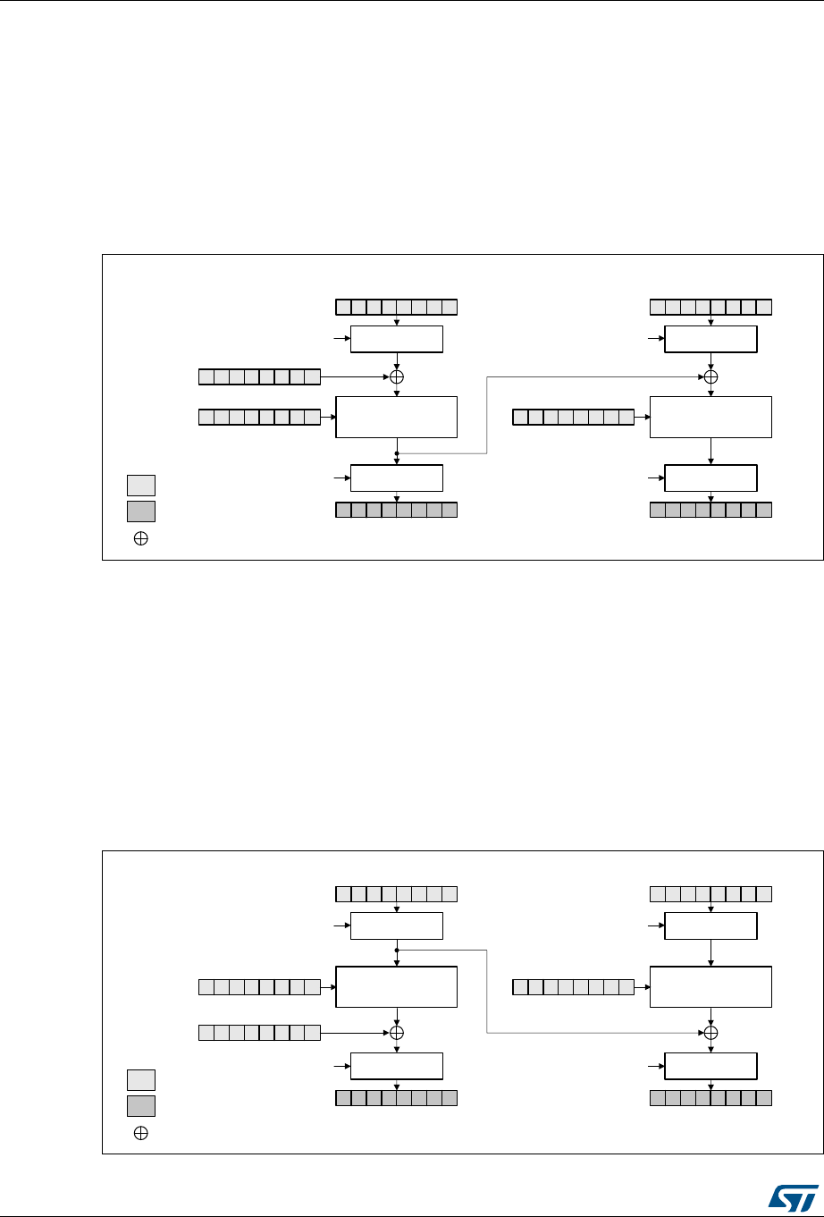
AES hardware accelerator (AES) RM0430
706/1324 RM0430 Rev 8
In ECB decrypt mode, the 128-bit ciphertext input data block C1 in the AES_DINR register
first goes through bit/byte/half-word swapping. The keying sequence is reversed compared
to that of the ECB encryption. The swap result I1 is processed with the AES core set in
decrypt mode, using the formerly prepared decryption key. The decryption result goes
through bit/byte/half-word swapping, then is stored in the AES_DOUTR register as 128-bit
plaintext output data block P1. The ECB decryption continues in this way until the last
complete ciphertext block is decrypted.
Figure 237 illustrates the cipher block chaining (CBC) encryption mode.
Figure 237. CBC encryption
In CBC encrypt mode, the first plaintext input block, after bit/byte/half-word swapping (P1’),
is XOR-ed with a 128-bit IVI bitfield (initialization vector and counter), producing the I1 input
data for encrypt with the AES core, using a 128- or 256-bit key. The resulting 128-bit output
block O1, after swapping operation, is used as ciphertext C1. The O1 data is then XOR-ed
with the second-block plaintext data P2’ to produce the I2 input data for the AES core to
produce the second block of ciphertext data. The chaining of data blocks continues in this
way until the last plaintext block in the message is encrypted.
If the message size is not a multiple of 128 bits, the final partial data block is encrypted in
the way explained in Section 24.4.6: AES ciphertext stealing and data padding.
Figure 238 illustrates the cipher block chaining (CBC) decryption mode.
Figure 238. CBC decryption
06Y9
%ORFNFLSKHU
HQFU\SWLRQ
$(6B.(<5[.(<
$(6B',15SODLQWH[W3
$(6B'2875FLSKHUWH[W&
6ZDS
PDQDJHPHQW
'$7$7<3(>@
'$7$7<3(>@ 6ZDS
PDQDJHPHQW
%ORFNFLSKHU
HQFU\SWLRQ
$(6B.(<5[.(<
$(6B',15SODLQWH[W3
$(6B'2875FLSKHUWH[W&
6ZDS
PDQDJHPHQW
'$7$7<3(>@
'$7$7<3(>@ 6ZDS
PDQDJHPHQW
$(6B,95[LQLWYHFWRU
LQSXW
RXWSXW
/HJHQG
;25
, ,
2 2
%ORFN %ORFN
,9, 3 3
06Y9
'HFU\SW
$(6B.(<5[.(<
$(6B',15FLSKHUWH[W&
$(6B'2875SODLQWH[W3
6ZDS
PDQDJHPHQW
'$7$7<3(>@
'$7$7<3(>@ 6ZDS
PDQDJHPHQW
'HFU\SW
$(6B.(<5[.(<
$(6B',15FLSKHUWH[W&
$(6B'2875SODLQWH[W3
6ZDS
PDQDJHPHQW
'$7$7<3(>@
'$7$7<3(>@ 6ZDS
PDQDJHPHQW
$(6B,95[,9
LQSXW
RXWSXW
/HJHQG
;25
, ,
2 2
%ORFN %ORFN
,9,
3 3

RM0430 Rev 8 707/1324
RM0430 AES hardware accelerator (AES)
743
In CBC decrypt mode, like in ECB decrypt mode, the secret key must be prepared to
perform an AES decryption.
After the key preparation process, the decryption goes as follows: the first 128-bit ciphertext
block (after the swap operation) is used directly as the AES core input block I1 for decrypt
operation, using the 128-bit or 256-bit key. Its output O1 is XOR-ed with the 128-bit IVI field
(that must be identical to that used during encryption) to produce the first plaintext block P1.
The second ciphertext block is processed in the same way as the first block, except that the
I1 data from the first block is used in place of the initialization vector.
The decryption continues in this way until the last complete ciphertext block is decrypted.
If the message size is not a multiple of 128 bits, the final partial data block is decrypted in
the way explained in Section 24.4.6: AES ciphertext stealing and data padding.
For more information on data swapping, refer to Section 24.4.13: .AES data registers and
data swapping.
ECB/CBC encryption sequence
The sequence of events to perform an ECB/CBC encryption (more detail in Section 24.4.4):
1. Disable the AES peripheral by clearing the EN bit of the AES_CR register.
2. Select the Mode 1 by to 00 the MODE[1:0] bitfield of the AES_CR register and select
ECB or CBC chaining mode by setting the CHMOD[2:0] bitfield of the AES_CR register
to 000 or 001, respectively. Data type can also be defined, using DATATYPE[1:0]
bitfield.
3. Select 128- or 256-bit key length through the KEYSIZE bit of the AES_CR register.
4. Write the AES_KEYRx registers (128 or 256 bits) with encryption key. Fill the
AES_IVRx registers with the initialization vector data if CBC mode has been selected.
5. Enable the AES peripheral by setting the EN bit of the AES_CR register.
6. Write the AES_DINR register four times to input the plaintext (MSB first), as shown in
Figure 239.
7. Wait until the CCF flag is set in the AES_SR register.
8. Read the AES_DOUTR register four times to get the ciphertext (MSB first) as shown in
Figure 239. Then clear the CCF flag by setting the CCFC bit of the AES_CR register.
9. Repeat steps 6,7,8 to process all the blocks with the same encryption key.
Figure 239. ECB/CBC encryption (Mode 1)
069
:5
37
:5
37
:5
37
:5
37 :DLWXQWLOIODJ&&) 5'
&7
5'
&7
5'
&7
5'
&7
,QSXWSKDVH
ZULWHRSHUDWLRQVLQWR
$(6B',15>@
&RPSXWDWLRQSKDVH 2XWSXWSKDVH
UHDGRSHUDWLRQVRI
$(6B'2875>@
37 SODLQWH[W ZRUGV37«37
&7 FLSKHUWH[W ZRUGV&7«&7
06% /6% 06% /6%
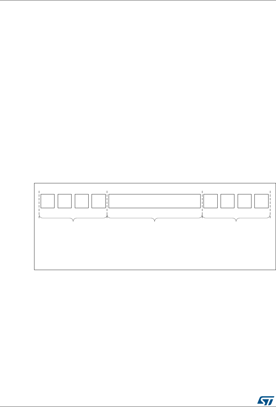
AES hardware accelerator (AES) RM0430
708/1324 RM0430 Rev 8
ECB/CBC decryption sequence
The sequence of events to perform an AES ECB/CBC decryption is as follows (more detail
in Section 24.4.4):
1. Follow the steps described in Section 24.4.5: AES decryption key preparation on
page 702, in order to prepare the decryption key in AES core.
2. Disable the AES peripheral by clearing the EN bit of the AES_CR register.
3. Select the Mode 3 by setting to 10 the MODE[1:0] bitfield of the AES_CR register and
select ECB or CBC chaining mode by setting the CHMOD[2:0] bitfield of the AES_CR
register to 000 or 001, respectively. Data type can also be defined, using
DATATYPE[1:0] bitfield.
4. Select key length of 128 or 256 bits via KEYSIZE bitfield of the AES_CR register.
5. Write the AES_IVRx registers with the initialization vector (required in CBC mode only).
6. Enable AES by setting the EN bit of the AES_CR register.
7. Write the AES_DINR register four times to input the cipher text (MSB first), as shown in
Figure 240.
8. Wait until the CCF flag is set in the AES_SR register.
9. Read the AES_DOUTR register four times to get the plain text (MSB first), as shown in
Figure 240. Then clear the CCF flag by setting the CCFC bit of the AES_CR register.
10. Repeat steps 7,8,9 to process all the blocks encrypted with the same key.
Figure 240. ECB/CBC decryption (Mode 3)
Suspend/resume operations in ECB/CBC modes
To suspend the processing of a message, proceed as follows:
1. If DMA is used, stop the AES DMA transfers to the IN FIFO by clearing the DMAINEN
bit of the AES_CR register.
2. If DMA is not used, read four times the AES_DOUTR register to save the last
processed block. If DMA is used, wait until the CCF flag is set in the AES_SR register
069
:5
&7
:5
&7
:5
&7
:5
&7 :DLWXQWLOIODJ&&) 5'
37
5'
37
5'
37
5'
37
,QSXWSKDVH
ZULWHRSHUDWLRQVLQWR
$(6B',15>@
&RPSXWDWLRQSKDVH 2XWSXWSKDVH
UHDGRSHUDWLRQVIURP
$(6B'2875>@
37 SODLQWH[W ZRUGV37«37
&7 FLSKHUWH[W ZRUGV&7«&7
06% /6% 06% /6%

RM0430 Rev 8 709/1324
RM0430 AES hardware accelerator (AES)
743
then stop the DMA transfers from the OUT FIFO by clearing the DMAOUTEN bit of the
AES_CR register.
3. If DMA is not used, poll the CCF flag of the AES_SR register until it becomes 1
(computation completed).
4. Clear the CCF flag by setting the CCFC bit of the AES_CR register.
5. Save initialization vector registers (only required in CBC mode as AES_IVRx registers
are altered during the data processing).
6. Disable the AES peripheral by clearing the bit EN of the AES_CR register.
7. Save the current AES configuration in the memory (except AES initialization vector
values).
8. If DMA is used, save the DMA controller status (pointers for IN and OUT data transfers,
number of remaining bytes, and so on).
Note: In point 7, the derived key information stored in AES_KEYRx registers can optionally be
saved in memory if the interrupted process is a decryption. Otherwise those registers do not
need to be saved as the original key value is known by the application
To resume the processing of a message, proceed as follows:
1. If DMA is used, configure the DMA controller so as to complete the rest of the FIFO IN
and FIFO OUT transfers.
2. Ensure that AES is disabled (the EN bit of the AES_CR must be 0).
3. Restore the AES_CR and AES_KEYRx register setting, using the values of the saved
configuration. In case of decryption, derived key information can be written in
AES_KEYRx register instead of the original key value.
4. Prepare the decryption key as described in Section 24.4.5: AES decryption key
preparation (only required for ECB or CBC decryption). This step is not necessary if
derived key information has been loaded in AES_KEYRx registers.
5. Restore AES_IVRx registers using the saved configuration (only required in CBC
mode).
6. Enable the AES peripheral by setting the EN bit of the AES_CR register.
7. If DMA is used, enable AES DMA transfers by setting the DMAINEN and DMAOUTEN
bits of the AES_CR register.
Alternative single ECB/CBC decryption using Mode 4
The sequence of events to perform a single round of ECB/CBC decryption using Mode 4 is:
1. Disable the AES peripheral by clearing the EN bit of the AES_CR register.
2. Select the Mode 4 by setting to 11 the MODE[1:0] bitfield of the AES_CR register and
select ECB or CBC chaining mode by setting the CHMOD[2:0] bitfield of the AES_CR
register to 000 or 001, respectively.
3. Select key length of 128 or 256 bits via KEYSIZE bitfield of the AES_CR register.
4. Write the AES_KEYRx registers with the encryption key. Write the AES_IVRx registers
if the CBC mode is selected.
5. Enable the AES peripheral by setting the EN bit of the AES_CR register.
6. Write the AES_DINR register four times to input the cipher text (MSB first).
7. Wait until the CCF flag is set in the AES_SR register.
8. Read the AES_DOUTR register four times to get the plain text (MSB first). Then clear
the CCF flag by setting the CCFC bit of the AES_CR register.
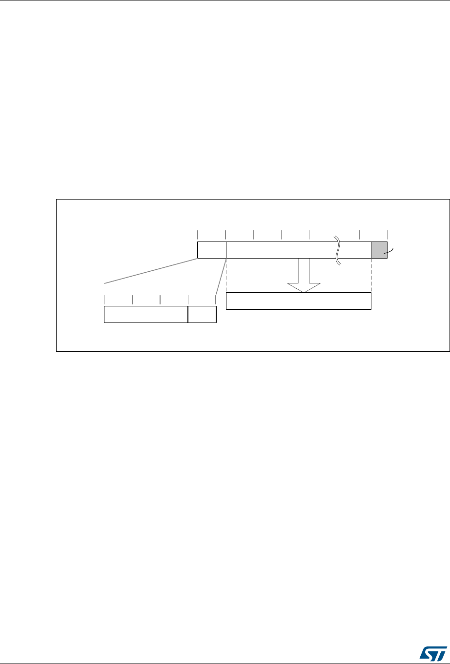
AES hardware accelerator (AES) RM0430
710/1324 RM0430 Rev 8
Note: When mode 4 is selected mode 3 cannot be used.
In mode 4, the AES_KEYRx registers contain the encryption key during all phases of the
processing. No derivation key is stored in these registers. It is stored internally in AES.
24.4.9 AES counter (CTR) mode
Overview
The counter mode (CTR) uses AES as a key-stream generator. The generated keys are
then XOR-ed with the plaintext to obtain the ciphertext.
CTR chaining is defined in NIST Special Publication 800-38A, Recommendation for Block
Cipher Modes of Operation. A typical message construction in CTR mode is given in
Figure 241.
Figure 241. Message construction in CTR mode
The structure of this message is:
•A 16-byte initial counter block (ICB), composed of two distinct fields:
–Initialization vector (IV): a 96-bit value that must be unique for each encryption
cycle with a given key.
–Counter: a 32-bit big-endian integer that is incremented each time a block
processing is completed. The initial value of the counter should be set to 1.
•The plaintext P is encrypted as ciphertext C, with a known length. This length can be
non-multiple of 16 bytes, in which case a plaintext padding is required.
CTR encryption and decryption
Figure 242 and Figure 243 describe the CTR encryption and decryption process,
respectively, as implemented in the AES peripheral. The CTR mode is selected by writing
010 to the CHMOD[2:0] bitfield of AES_CR register.
06Y9
E\WHERXQGDULHV
,&% &LSKHUWH[W&
E\WHERXQGDULHV
&RXQWHU,QLWLDOL]DWLRQYHFWRU,9
GHFU\SW
3ODLQWH[W3
=HUR
SDGGLQJ
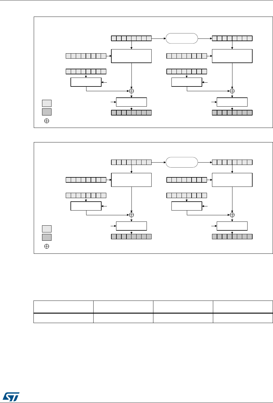
RM0430 Rev 8 711/1324
RM0430 AES hardware accelerator (AES)
743
Figure 242. CTR encryption
Figure 243. CTR decryption
In CTR mode, the cryptographic core output (also called keystream) Ox is XOR-ed with
relevant input block (Px' for encryption, Cx' for decryption), to produce the correct output
block (Cx' for encryption, Px' for decryption). Initialization vectors in AES must be initialized
as shown in Table 125.
Unlike in CBC mode that uses the AES_IVRx registers only once when processing the first
data block, in CTR mode AES_IVRx registers are used for processing each data block, and
the AES peripheral increments the counter bits of the initialization vector (leaving the nonce
bits unchanged).
CTR decryption does not differ from CTR encryption, since the core always encrypts the
current counter block to produce the key stream that is then XOR-ed with the plaintext (CTR
Table 125. CTR mode initialization vector definition
AES_IVR3[31:0] AES_IVR2[31:0] AES_IVR1[31:0] AES_IVR0[31:0]
Nonce[31:0] Nonce[63:32] Nonce[95:64] 32-bit counter = 0x0001
06Y9
(QFU\SW
$(6B.(<5[.(<
$(6B',15SODLQWH[W3
$(6B'2875FLSKHUWH[W&
'$7$7<3(>@ 6ZDS
PDQDJHPHQW
$(6B,95[
,9ELWFRXQWHU
LQSXW
RXWSXW
/HJHQG
;25
6ZDS
PDQDJHPHQW
'$7$7<3(>@
(QFU\SW
$(6B.(<5[.(<
$(6B'2875FLSKHUWH[W&
'$7$7<3(>@ 6ZDS
PDQDJHPHQW
$(6B,95[
6ZDS
PDQDJHPHQW
'$7$7<3(>@
&RXQWHU
LQFUHPHQW
$(6B',15SODLQWH[W3
, ,
2 2
%ORFN %ORFN
3 3
& &
06Y9
(QFU\SW
$(6B.(<5[.(<
$(6B',15FLSKHUWH[W&
$(6B'2875SODLQWH[W3
'$7$7<3(>@ 6ZDS
PDQDJHPHQW
$(6B,95[
1RQFHELWFRXQWHU
LQSXW
RXWSXW
/HJHQG
;25
6ZDS
PDQDJHPHQW
'$7$7<3(>@
(QFU\SW
$(6B.(<5[.(<
$(6B'2875SODLQWH[W3
'$7$7<3(>@ 6ZDS
PDQDJHPHQW
$(6B,95[
1RQFHELWFRXQWHU
6ZDS
PDQDJHPHQW
'$7$7<3(>@
&RXQWHU
LQFUHPHQW
$(6B',15FLSKHUWH[W&
, ,
2 2
%ORFN %ORFN
& &
3 3

AES hardware accelerator (AES) RM0430
712/1324 RM0430 Rev 8
encryption) or ciphertext (CTR decryption) input. In CTR mode, the MODE[1:0] bitfield
settings 11, 10 or 00 default all to encryption mode, and the setting 01 (key derivation) is
forbidden.
The sequence of events to perform an encryption or a decryption in CTR chaining mode:
1. Ensure that AES is disabled (the EN bit of the AES_CR must be 0).
2. Select CTR chaining mode by setting to 010 the CHMOD[2:0] bitfield of the AES_CR
register. Set MODE[1:0] bitfield to any value other than 01.
3. Initialize the AES_KEYRx registers, and load the AES_IVRx registers as described in
Table 125.
4. Set the EN bit of the AES_CR register, to start encrypting the current counter (EN is
automatically reset when the calculation finishes).
5. If it is the last block, pad the data with zeros to have a complete block, if needed.
6. Append data in AES, and read the result. The three possible scenarios are described in
Section 24.4.4: AES procedure to perform a cipher operation.
7. Repeat the previous step till the second-last block is processed. For the last block,
apply the two previous steps and discard the bits that are not part of the payload (if the
size of the significant data in the last input block is less than 16 bytes).
Suspend/resume operations in CTR mode
Like for the CBC mode, it is possible to interrupt a message to send a higher priority
message, and resume the message that was interrupted. Detailed CBC suspend/resume
sequence is described in Section 24.4.8: AES basic chaining modes (ECB, CBC).
Note: Like for CBC mode, the AES_IVRx registers must be reloaded during the resume operation.
24.4.10 AES Galois/counter mode (GCM)
Overview
The AES Galois/counter mode (GCM) allows encrypting and authenticating a plaintext
message into the corresponding ciphertext and tag (also known as message authentication
code). To ensure confidentiality, GCM algorithm is based on AES counter mode. It uses a
multiplier over a fixed finite field to generate the tag.
GCM chaining is defined in NIST Special Publication 800-38D, Recommendation for Block
Cipher Modes of Operation - Galois/Counter Mode (GCM) and GMAC. A typical message
construction in GCM mode is given in Figure 244.
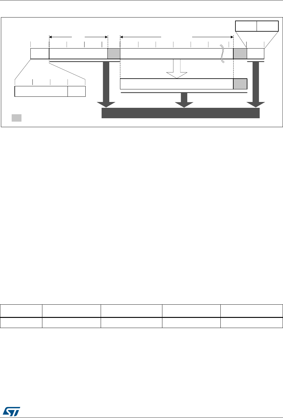
RM0430 Rev 8 713/1324
RM0430 AES hardware accelerator (AES)
743
Figure 244. Message construction in GCM
The message has the following structure:
•16-byte initial counter block (ICB), composed of two distinct fields:
–Initialization vector (IV): a 96-bit value that must be unique for each encryption
cycle with a given key. Note that the GCM standard supports IVs with less than 96
bits, but in this case strict rules apply.
–Counter: a 32-bit big-endian integer that is incremented each time a block
processing is completed. According to NIST specification, the counter value is 0x2
when processing the first block of payload.
•Authenticated header AAD (also knows as additional authentication data) has a
known length Len(A) that may be a non-multiple of 16 bytes, and must not exceed
264 – 1 bits. This part of the message is only authenticated, not encrypted.
•Plaintext message P is both authenticated and encrypted as ciphertext C, with a
known length Len(P) that may be non-multiple of 16 bytes, and cannot exceed 232 -2
128-bit blocks.
•Last block contains the AAD header length (bits [32:63]) and the payload length (bits
[96:127]) information, as shown in Table 126.
The GCM standard specifies that ciphertext C has the same bit length as the plaintext P.
When a part of the message (AAD or P) has a length that is a non-multiple of 16-bytes a
special padding scheme is required.
06Y9
3ODLQWH[W3
E\WH
ERXQGDULHV
$GGLWLRQDODXWKHQWLFDWHGGDWD
$$'
$XWKHQWLFDWHGHQFU\SWHGFLSKHUWH[W&
/HQ$ /HQ3 /HQ&
>/HQ$@
/DVW
EORFN
>/HQ&@
$XWKHQWLFDWLRQWDJ7
,&%
E\WHERXQGDULHV
&RXQWHU,QLWLDOL]DWLRQYHFWRU,9
DXWKHQWLFDWH
HQFU\SW
=HURSDGGLQJ]HURHGELWV
DXWKHQWLFDWH
DXWK
Table 126. GCM last block definition
Endianness Bit[0] ---------- Bit[31] Bit[32]---------- Bit[63] Bit[64] -------- Bit[95] Bit[96] --------- Bit[127]
Input data 0x0 AAD length[31:0] 0x0 Payload length[31:0]
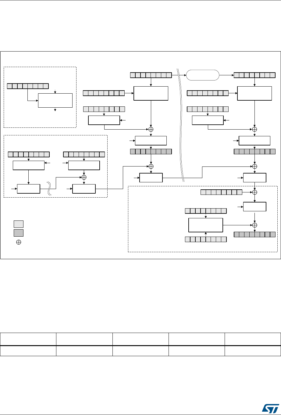
AES hardware accelerator (AES) RM0430
714/1324 RM0430 Rev 8
GCM processing
Figure 245 describes the GCM implementation in the AES peripheral. The GCM is selected
by writing 011 to the CHMOD[2:0] bitfield of the AES_CR register.
Figure 245. GCM authenticated encryption
The mechanism for the confidentiality of the plaintext in GCM mode is similar to that in the
Counter mode, with a particular increment function (denoted 32-bit increment) that
generates the sequence of input counter blocks.
AES_IVRx registers keeping the counter block of data are used for processing each data
block. The AES peripheral automatically increments the Counter[31:0] bitfield. The first
counter block (CB1) is derived from the initial counter block ICB by the application software
(see Table 127).
Note: In GCM mode, the settings 01 and 11 of the MODE[1:0] bitfield are forbidden.
06Y9
)LQDO
,QLW
+HDGHU
$(6B.(<5[.(<
$(6B',15SODLQWH[W3
$(6B'2875
FLSKHUWH[W&
'$7$7<3(
>@ 6ZDS
PDQDJHPHQW
$(6B,95[
,&%ELWFRXQWHU [
LQSXW
RXWSXW
/HJHQG
;25
6ZDS
PDQDJHPHQW
'$7$7<3(
>@
$(6B.(<5[.(<
'$7$7<3(>@ 6ZDS
PDQDJHPHQW
$(6B,95[
6ZDS
PDQDJHPHQW
'$7$7<3(
>@
&RXQWHU
LQFUHPHQW
$(6B',15SODLQWH[W3Q
+
$(6B'2875
FLSKHUWH[W&Q
+
(QFU\SW
>@
+
$(6B',15$$'
6ZDS
PDQDJHPHQW 6ZDS
PDQDJHPHQW
$(6B',15$$'L
*)PXO
'$7$7<3(
>@
*)PXO
++
$(6B.(<5[.(<
*)PXO *)PXO
*)PXO
+
$(6B',15
/HQ$__/HQ&
(QFU\SW
$(6B.(<5[NH\
$(6B,95[
,9ELWFRXQWHU [
$(6B'2875
$XWKHQWLFDWLRQ7$*7
6
(QFU\SW (QFU\SW
%ORFN %ORFNQ
&%Q
&% &%Q
3D\ORDG
Table 127. GCM mode IVI bitfield initialization
Register AES_IVR3[31:0] AES_IVR2[31:0] AES_IVR1[31:0] AES_IVR0[31:0]
Input data ICB[31:0] ICB[63:32] ICB[95:64] Counter[31:0] = 0x2

RM0430 Rev 8 715/1324
RM0430 AES hardware accelerator (AES)
743
The authentication mechanism in GCM mode is based on a hash function called GF2mul
that performs multiplication by a fixed parameter, called hash subkey (H), within a binary
Galois field.
A GCM message is processed through the following phases, further described in next
subsections:
•Init phase: AES prepares the GCM hash subkey (H).
•Header phase: AES processes the additional authenticated data (AAD), with hash
computation only.
•Payload phase: AES processes the plaintext (P) with hash computation, counter block
encryption and data XOR-ing. It operates in a similar way for ciphertext (C).
•Final phase: AES generates the authenticated tag (T) using the last block of the
message.
GCM init phase
During this first step, the GCM hash subkey (H) is calculated and saved internally, to be
used for processing all the blocks. The recommended sequence is:
1. Ensure that AES is disabled (the EN bit of the AES_CR must be 0).
2. Select GCM chaining mode, by setting to 011 the CHMOD[2:0] bitfield of the AES_CR
register, and set to 00 (no data swapping) the DATATYPE[1:0] bitfield.
3. Indicate the Init phase, by setting to 00 the GCMPH[1:0] bitfield of the AES_CR
register.
4. Set the MODE[1:0] bitfield of the AES_CR register to 00 or 10.
5. Initialize the AES_KEYRx registers with a key, and initialize AES_IVRx registers with
the information as defined in Table 127.
6. Start the calculation of the hash key, by setting to 1 the EN bit of the AES_CR register
(EN is automatically reset when the calculation finishes).
7. Wait until the end of computation, indicated by the CCF flag of the AES_SR transiting
to 1. Alternatively, use the corresponding interrupt.
8. Clear the CCF flag of the AES_SR register, by setting to 1 the CCFC bit of the AES_CR
register, and optionally set the data type (1-, 8- or 16-bit) using the DATATYPE[1:0]
bitfield.
GCM header phase
This phase coming after the GCM Init phase must be completed before the payload phase.
The sequence to execute, identical for encryption and decryption, is:
1. Indicate the header phase, by setting to 01 the GCMPH[1:0] bitfield of the AES_CR
register. Do not modify the MODE[1:0] bitfield as set in the Init phase.
2. Enable the AES peripheral by setting the EN bit of the AES_CR register.
3. If it is the last block and the AAD size in the block is inferior to 128 bits, pad the
remainder of the block with zeros. Then append the data block into AES in one of ways
described in Section 24.4.4: AES procedure to perform a cipher operation on
page 698.
4. Repeat the step 3 until the last additional authenticated data block is processed.
Note: The header phase can be skipped if there is no AAD, that is, Len(A) = 0.

AES hardware accelerator (AES) RM0430
716/1324 RM0430 Rev 8
GCM payload phase
This phase, identical for encryption and decryption, is executed after the GCM header
phase. During this phase, the encrypted/decrypted payload is stored in the AES_DOUTR
register. The sequence to execute is:
1. If the header phase was skipped, enable the AES peripheral by setting the EN bit of the
AES_CR register.
2. Indicate the payload phase, by setting to 10 the GCMPH[1:0] bitfield of the AES_CR
register. Do not modify the MODE[1:0] bitfield as set in the Init phase.
3. If it is the last block and the plaintext (encryption) or ciphertext (decryption) size in the
block is inferior to 128 bits, pad the remainder of the block with zeros.
4. Append the data block into AES in one of ways described in Section 24.4.4: AES
procedure to perform a cipher operation on page 698, and read the result.
5. Repeat the previous step till the second-last plaintext block is encrypted or till the last
block of ciphertext is decrypted. For the last block of plaintext (encryption only),
execute the two previous steps. For the last block, discard the bits that are not part of
the payload when the last block size is less than 16 bytes.
Note: The payload phase can be skipped if there is no payload data, that is, Len(C) = 0 (see
GMAC mode).
GCM final phase
In this last phase, the AES peripheral generates the GCM authentication tag and stores it in
the AES_DOUTR register. The sequence to execute is:
1. Indicate the final phase, by setting to 11 the GCMPH[1:0] bitfield of the AES_CR
register. Select encrypt mode by setting to 00 the MODE[1:0] bitfield of the AES_CR
register.
2. Compose the data of the block, by concatenating the AAD bit length and the payload
bit length, as shown in Table 126. Write the block into the AES_DINR register.
3. Wait until the end of computation, indicated by the CCF flag of the AES_SR transiting
to 1.
4. Get the GCM authentication tag, by reading the AES_DOUTR register four times.
5. Clear the CCF flag in the AES_SR register, by setting to 1 the CCFC bit of the AES_CR
register.
6. Disable the AES peripheral, by clearing the bit EN of the AES_CR register. If it is an
authenticated decryption, compare the generated tag with the expected tag passed
with the message.
Note: In the final phase, data must be swapped according to the data type set in the
DATATYPE[1:0] bitfield of the AES_CR register.
When transiting from the header or the payload phase to the final phase, the AES peripheral
must not be disabled, otherwise the result is wrong.

RM0430 Rev 8 717/1324
RM0430 AES hardware accelerator (AES)
743
Suspend/resume operations in GCM mode
To suspend the processing of a message, proceed as follows:
1. If DMA is used, stop the AES DMA transfers to the IN FIFO by clearing the DMAINEN
bit of the AES_CR register. If DMA is not used, make sure that the current computation
is completed, which is indicated by the CCF flag of the AES_SR register set to 1.
2. In the payload phase, if DMA is not used, read four times the AES_DOUTR register to
save the last-processed block. If DMA is used, wait until the CCF flag is set in the
AES_SR register then stop the DMA transfers from the OUT FIFO by clearing the
DMAOUTEN bit of the AES_CR register.
3. Clear the CCF flag of the AES_SR register, by setting to 1 the CCFC bit of the AES_CR
register.
4. Save the AES_SUSPxR registers in the memory, where x is from 0 to 7.
5. In the payload phase, save the AES_IVRx registers as, during the data processing,
they changed from their initial values. In the header phase, this step is not required.
6. Disable the AES peripheral, by clearing the EN bit of the AES_CR register.
7. Save the current AES configuration in the memory, excluding the initialization vector
registers AES_IVRx. Key registers do not need to be saved as the original key value is
known by the application.
8. If DMA is used, save the DMA controller status (pointers for IN data transfers, number
of remaining bytes, and so on). In the payload phase, pointers for OUT data transfers
must also be saved.
To resume the processing of a message, proceed as follows:
1. If DMA is used, configure the DMA controller in order to complete the rest of the FIFO
IN transfers. In the payload phase, the rest of the FIFO OUT transfers must also be
configured in the DMA controller.
2. Ensure that the AES peripheral is disabled (the EN bit of the AES_CR register must be
0).
3. Write the suspend register values, previously saved in the memory, back into their
corresponding AES_SUSPxR registers, where x is from 0 to 7.
4. In the payload phase, write the initialization vector register values, previously saved in
the memory, back into their corresponding AES_IVRx registers. In the header phase,
write initial setting values back into the AES_IVRx registers.
5. Restore the initial setting values in the AES_CR and AES_KEYRx registers.
6. Enable the AES peripheral by setting the EN bit of the AES_CR register.
7. If DMA is used, enable AES DMA requests by setting the DMAINEN bit (and
DMAOUTEN bit if in payload phase) of the AES_CR register.
24.4.11 AES Galois message authentication code (GMAC)
Overview
The Galois message authentication code (GMAC) allows the authentication of a plaintext,
generating the corresponding tag information (also known as message authentication
code). It is based on GCM algorithm, as defined in NIST Special Publication 800-38D,
Recommendation for Block Cipher Modes of Operation - Galois/Counter Mode (GCM) and
GMAC.
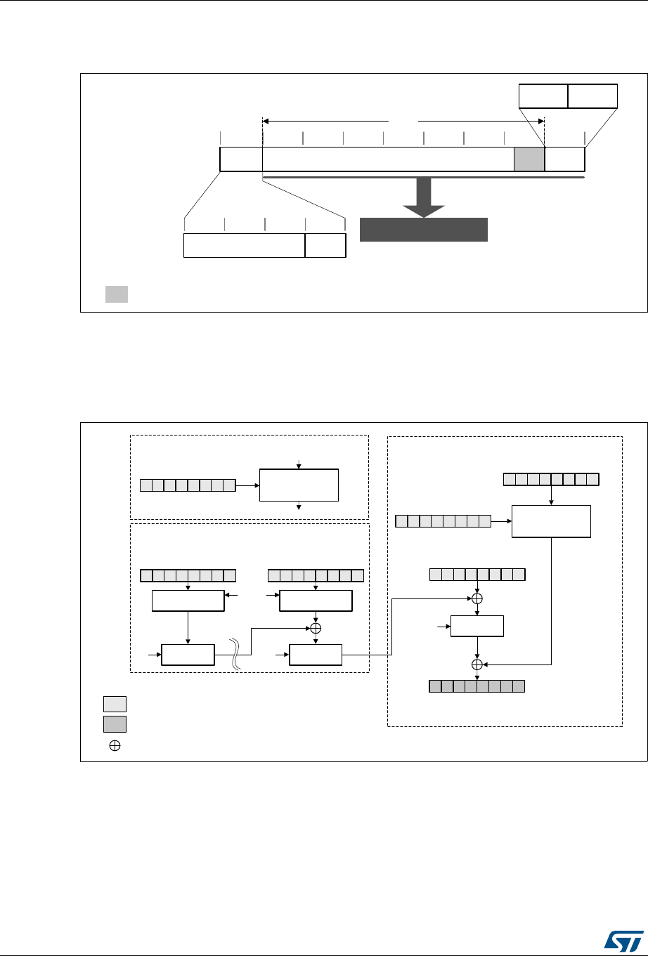
AES hardware accelerator (AES) RM0430
718/1324 RM0430 Rev 8
A typical message construction for GMAC is given in Figure 246.
Figure 246. Message construction in GMAC mode
AES GMAC processing
Figure 247 describes the GMAC mode implementation in the AES peripheral. This mode is
selected by writing 011 to the CHMOD[2:0] bitfield of the AES_CR register.
Figure 247. GMAC authentication mode
The GMAC algorithm corresponds to the GCM algorithm applied on a message only
containing a header. As a consequence, all steps and settings are the same as with the
GCM, except that the payload phase is omitted.
Suspend/resume operations in GMAC
In GMAC mode, the sequence described for the GCM applies except that only the header
phase can be interrupted.
06Y9
$XWKHQWLFDWHGGDWD
E\WH
ERXQGDULHV
/HQ$
>/HQ$@
/DVW
EORFN
>@
$XWKHQWLFDWLRQWDJ7
,&%
E\WHERXQGDULHV
&RXQWHU,QLWLDOL]DWLRQYHFWRU,9
=HURSDGGLQJ
DXWK
06Y9
)LQDO
,QLW
+HDGHU
$(6B.(<5[.(<
LQSXW
RXWSXW
/HJHQG
;25
$(6B.(<5[.(<
$(6B,95[
,9ELWFRXQWHU [
(QFU\SW
>@
+
$(6B',15
PHVVDJHEORFN
6ZDS
PDQDJHPHQW 6ZDS
PDQDJHPHQW
$(6B',15
PHVVDJHEORFNQ
*)PXO
'$7$7<3(
>@
*)PXO
++
*)PXO
+
$(6B',15
OHQ$__OHQ&
$(6B'2875
DXWKHQWLFDWLRQWDJ7
6
(QFU\SW
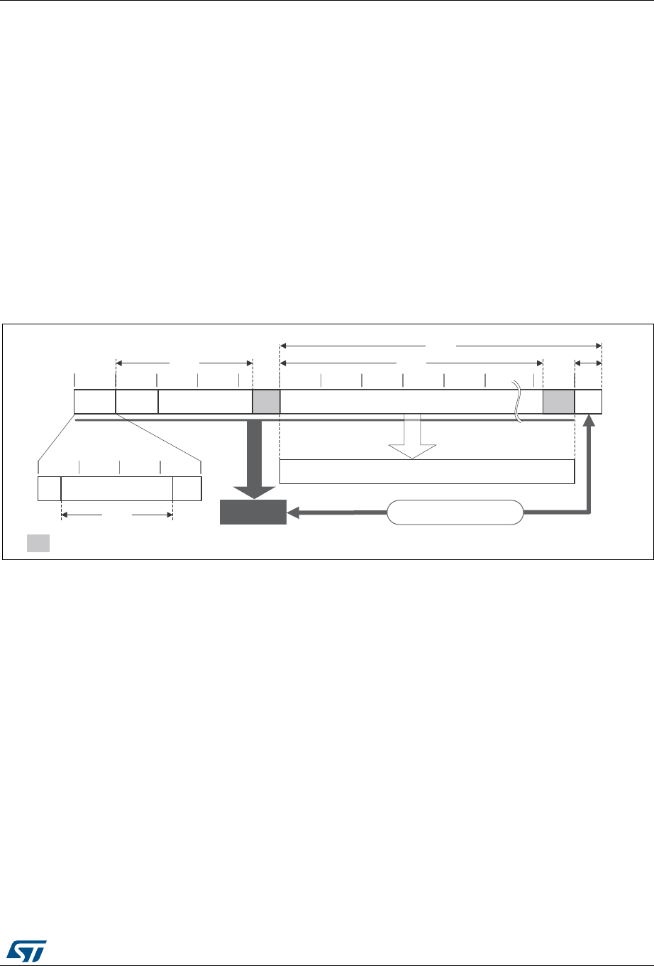
RM0430 Rev 8 719/1324
RM0430 AES hardware accelerator (AES)
743
24.4.12 AES counter with CBC-MAC (CCM)
Overview
The AES counter with cipher block chaining-message authentication code (CCM)
algorithm allows encryption and authentication of plaintext, generating the corresponding
ciphertext and tag (also known as message authentication code). To ensure confidentiality,
the CCM algorithm is based on AES in counter mode. It uses cipher block chaining
technique to generate the message authentication code. This is commonly called CBC-
MAC.
Note: NIST does not approve this CBC-MAC as an authentication mode outside the context of the
CCM specification.
CCM chaining is specified in NIST Special Publication 800-38C, Recommendation for Block
Cipher Modes of Operation - The CCM Mode for Authentication and Confidentiality. A typical
message construction for CCM is given in Figure 248.
Figure 248. Message construction in CCM mode
The structure of the message is:
•16-byte first authentication block (B0), composed of three distinct fields:
–Q: a bit string representation of the octet length of P (Len(P))
–Nonce (N): a single-use value (that is, a new nonce should be assigned to each
new communication) of Len(N) size. The sum Len(N) + Len(P) must be equal to
15 bytes.
–Flags: most significant octet containing four flags for control information, as
specified by the standard. It contains two 3-bit strings to encode the values t (MAC
length expressed in bytes) and Q (plaintext length such that Len(P) < 28q bytes).
The counter blocks range associated to Q is equal to 28Q-4, that is, if the maximum
value of Q is 8, the counter blocks used in cipher shall be on 60 bits.
•16-byte blocks (B) associated to the Associated Data (A).
This part of the message is only authenticated, not encrypted. This section has a
known length Len(A) that can be a non-multiple of 16 bytes (see Figure 248). The
06Y9
3ODLQWH[W3
E\WH
ERXQGDULHV
$VVRFLDWHGGDWD$
$XWKHQWLFDWHGHQFU\SWHGFLSKHUWH[W&
/HQ$ /HQ3
(QF
7
0$&7
%
E\WHERXQGDULHV
41RQFH1
DXWKHQWLFDWH
HQFU\SW
=HURSDGGLQJ
/HQ&
>D@
>D@
/HQ7
IODJV
/HQ1 'HFU\SWDQGFRPSDUH

AES hardware accelerator (AES) RM0430
720/1324 RM0430 Rev 8
standard also states that, on MSB bits of the first message block (B1), the associated
data length expressed in bytes (a) must be encoded as follows:
– If 0 < a < 216 -2
8, then it is encoded as [a]16, that is, on two bytes.
–If 2
16 -2
8 < a < 232, then it is encoded as 0xff || 0xfe || [a]32, that is, on six bytes.
–If 2
32 < a < 264, then it is encoded as 0xff || 0xff || [a]64, that is, on ten bytes.
•16-byte blocks (B) associated to the plaintext message P, which is both authenticated
and encrypted as ciphertext C, with a known length Len(P). This length can be a non-
multiple of 16 bytes (see Figure 248).
•Encrypted MAC (T) of length Len(T) appended to the ciphertext C of overall length
Len(C).
When a part of the message (A or P) has a length that is a non-multiple of 16-bytes, a
special padding scheme is required.
Note: CCM chaining mode can also be used with associated data only (that is, no payload).
As an example, the C.1 section in NIST Special Publication 800-38C gives the following
values (hexadecimal numbers):
N: 10111213 141516 (Len(N)= 56 bits or 7 bytes)
A: 00010203 04050607 (Len(A)= 64 bits or 8 bytes)
P: 20212223 (Len(P)= 32 bits or 4 bytes)
T: 6084341B (Len(T)= 32 bits or t = 4)
B0: 4F101112 13141516 00000000 00000004
B1: 00080001 02030405 06070000 00000000
B2: 20212223 00000000 00000000 00000000
CTR0: 0710111213 141516 00000000 00000000
CTR1: 0710111213 141516 00000000 00000001
Generation of formatted input data blocks Bx (especially B0 and B1) must be managed by
the application.
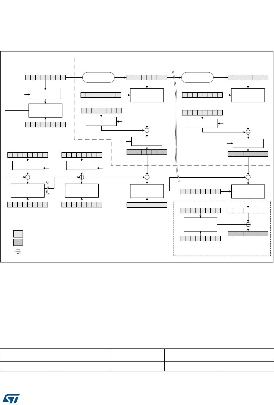
RM0430 Rev 8 721/1324
RM0430 AES hardware accelerator (AES)
743
CCM processing
Figure 249 describes the CCM implementation within the AES peripheral (decryption
example).
Figure 249. CCM mode authenticated decryption
The data input to the generation-encryption process are a valid nonce, a valid payload
string, and a valid associated data string, all properly formatted. The CBC chaining
mechanism is applied to the formatted plaintext data to generate a MAC, with a known
length. Counter mode encryption that requires a sufficiently long sequence of counter blocks
as input, is applied to the payload string and separately to the MAC. The resulting ciphertext
C is the output of the generation-encryption process on plaintext P.
AES_IVRx registers are used for processing each data block, AES automatically
incrementing the CTR counter with a bit length defined by the first block B0. Table 128
shows how the application must load the B0 data.
06Y9
$(6&&0ILQDO
$(6B'2875FLSKHUWH[W&
$(6B',15
SODLQWH[W3
'$7$7<3(
>@ 6ZDS
PDQDJHPHQW
$(6B,95[&75
LQSXW
RXWSXW
/HJHQG
;25
6ZDS
PDQDJHPHQW
'$7$7<3(
>@
$(6B.(<5[.(<
'$7$7<3(>@
6ZDS
PDQDJHPHQW
$(6B,95[&75P
6ZDS
PDQDJHPHQW
'$7$7<3(
>@
ELW
LQFUHPHQW
$(6B'2875FLSKHUWH[W
PLQXVWDJODVWEORFN&P
$(6B',15
SODLQWH[WODVWEORFN3P
(QFU\SW
$(6B',15
ILUVWEORFN%
$(6B',15DVVRFLDWHG
GDWDEORFN%
6ZDS
PDQDJHPHQW 6ZDS
PDQDJHPHQW
$(6B',15DVVRFLDWHG
GDWDODVWEORFN%X
$(6B.(<5[.(<
$(6B',15&75
%ORFNFLSKHU
HQFU\SWLRQ
$(6B.(<5[.(<
$(6B'2875
DXWKHQWLFDWLRQWDJ7
0$&7
(QFU\SW (QFU\SW
6
%U
%X
(QFU\SW
$(6B.(<5[.(<
(QFU\SW
$(6B.(<5[.(<
(QFU\SW
$(6B.(<5[.(<
(QFU\SW
$(6B.(<5[.(<
$(6B.(<5[NH\
'$7$7<3(>@ 6ZDS
PDQDJHPHQW
&&0DXWKHQWLFDWLRQRQO\ &75
'$7$7<3(>@
'$7$7<3(>@
6P
6
%ORFN %ORFNP
6:SURFHVVLQJ
3D\ORDG
Table 128. Initialization of AES_IVRx registers in CCM mode
Register AES_IVR3[31:0] AES_IVR2[31:0] AES_IVR1[31:0] AES_IVR0[31:0]
Input data B0[31:0] B0[63:32] B0[95:64] B0[127:96]

AES hardware accelerator (AES) RM0430
722/1324 RM0430 Rev 8
A CCM message is processed through two distinct processes - first, payload encryption or
decryption, in which the AES peripheral is configured in CTR mode, then associated data
and payload authentication, in which the AES peripheral first executes the CCM header
phase, then the CCM final phase.
Payload encryption/decryption
This step is performed independently of the tag computation. It uses standard CTR chaining
mode. Refer to Section 24.4.9: AES counter (CTR) mode for details. The construction of the
CTR1 initialization vector (see Figure 249) to load into AES_IVRx registers is defined in
NIST Special Publication 800-38C.
Note: This phase can be skipped if there is no payload data, that is, when Len(P) = 0 or
Len(C) = Len(T).
Remove LSBLen(T)(C) encrypted tag information when decrypting ciphertext C.
Associated data and payload authentication
In order to compute the CCM authentication tag associated with the plaintext message, it is
recommended to execute the following header phase sequence:
1. Ensure that the AES peripheral is disabled (the EN bit of the AES_CR must be 0).
2. Select CCM chaining mode, by setting to 100 the CHMOD[2:0] bitfield of the AES_CR
register, and optionally, set the DATATYPE[1:0] bitfield.
3. Indicate the header phase, by setting to 01 the GCMPH[1:0] bitfield of the AES_CR
register. Select encrypt mode by setting to 00 the MODE[1:0] bitfield of the AES_CR
register.
4. Initialize the AES_KEYRx registers with a key, and initialize AES_IVRx registers with
zero values.
5. Enable the AES peripheral by setting the EN bit of the AES_CR register.
6. Write the AES_DINR register with B0, as shown in Table 128. B0 data must be
swapped according to the DATATYPE[1:0] bitfield of the AES_CR register.
7. Wait until the end-of-computation flag CCF of the AES_SR register is set to 1.
8. Clear the CCF flag of the AES_SR register by setting the CCFC bit of the AES_CR
register.
9. Process data block. If it is the last block of associated data or plaintext and data size in
the block is inferior to 128 bits, pad the remainder of the block with zeros. Then append
the data block into AES in one of ways described in Section 24.4.4: AES procedure to
perform a cipher operation on page 698.
10. Repeat the previous step to process all data blocks, starting from the first block of
associated data and ending with the last block of plaintext payload data.

RM0430 Rev 8 723/1324
RM0430 AES hardware accelerator (AES)
743
In final phase, the AES peripheral generates the CCM authentication tag and stores it in the
AES_DOUTR register:
11. Indicate the final phase, by setting to 11 the GCMPH[1:0] bitfield of the AES_CR
register. Keep as-is the encryption mode in the MODE[1:0] bitfield.
12. Write four times the last data input into the AES_DIN register. This input must be the
128-bit value CTR0, formatted from the original B0 packet (that is, 5 flag bits set to 0,
and Q length bits set to 0).
13. Wait until the end-of-computation flag CCF of the AES_SR register is set.
14. Read four times the AES_DOUTR register: the output corresponds to the encrypted
CCM authentication tag.
15. Clear the CCF flag of the AES_SR register by setting the CCFC bit of the AES_CR
register.
16. Disable the AES peripheral, by clearing the EN bit of the AES_CR register.
17. For authenticated decryption, compare the generated encrypted tag with the encrypted
tag padded in the ciphertext.
Note: In this final phase, data must be swapped according to the DATATYPE[1:0] bitfield of the
AES_CR register.
When transiting from the header phase to the final phase, the AES peripheral must not be
disabled, otherwise the result is wrong.
Application must mask the authentication tag output with tag length to obtain a valid tag.
Suspend/resume operations in CCM mode
To suspend the authentication of the associated data and payload (GCMPH[1:0]= 01),
proceed as follows. Suspending the message during the encryption/decryption phase is
described in Section 24.4.9: AES counter (CTR) mode on page 710.
1. If DMA is used, stop the AES DMA transfers to the IN FIFO by clearing the DMAINEN
bit of the AES_CR register. If DMA is not used, make sure that the current computation
is completed, which is indicated by the CCF flag of the AES_SR register set to 1.
2. Clear the CCF flag of the AES_SR register, by setting to 1 the CCFC bit of the AES_CR
register.
3. Save the AES_SUSPxR registers (where x is from 0 to 7) in the memory.
4. Save the AES_IVRx registers, as during the data processing they changed from their
initial values.
5. Disable the AES peripheral, by clearing the bit EN of the AES_CR register.
6. Save the current AES configuration in the memory, excluding the initialization vector
registers AES_IVRx. Key registers do not need to be saved as the original key value is
known by the application.
7. If DMA is used, save the DMA controller status (pointers for IN data transfers, number
of remaining bytes, and so on).

AES hardware accelerator (AES) RM0430
724/1324 RM0430 Rev 8
To resume the authentication of the associated data and payload (GCMPH[1:0]= 01 or
11), proceed as follows:
1. If DMA is used, configure the DMA controller in order to complete the rest of the FIFO
IN transfers.
2. Ensure that AES processor is disabled (the EN bit of the AES_CR register must be 0).
3. Write the suspend register values, previously saved in the memory, back into their
corresponding AES_SUSPxR registers (where x is from 0 to 7).
4. Write the initialization vector register values, previously saved in the memory, back into
their corresponding AES_IVRx registers.
5. Restore the initial setting values in the AES_CR and AES_KEYRx registers.
6. Enable the AES peripheral by setting the EN bit of the AES_CR register.
7. If DMA is used, enable AES DMA requests by setting the DMAINEN bit of the AES_CR
register.
Note: In CCM mode the MODE[1:0] bitfield settings 01 and 11 (key derivation) are forbidden.
24.4.13 .AES data registers and data swapping
Data input and output
A 128-bit data block is entered into the AES peripheral with four successive 32-bit word
writes into the AES_DINR register (bitfield DIN[127:0]), the most significant word (bits
[127:96]) first, the least significant word (bits [31:0]) last.
A 128-bit data block is retrieved from the AES peripheral with four successive 32-bit word
reads from the AES_DOUTR register (bitfield DOUT[127:0]), the most significant word (bits
[127:96]) first, the least significant word (bits [31:0]) last.
The 32-bit data word for AES_DINR register or from AES_DOUTR register is organized in
big endian order, that is:
•the most significant byte of a word to write into AES_DINR must be put on the lowest
address out of the four adjacent memory locations keeping the word to write, or
•the most significant byte of a word read from AES_DOUTR goes to the lowest address
out of the four adjacent memory locations receiving the word
For using DMA for input data block write into AES, the four words of the input block must be
stored in the memory consecutively and in big-endian order, that is, the most significant
word on the lowest address. See Section 24.4.16: AES DMA interface.
Data swapping
The AES peripheral can be configured to perform a bit-, a byte-, a half-word-, or no
swapping on the input data word in the AES_DINR register, before loading it to the AES
processing core, and on the data output from the AES processing core, before sending it to
the AES_DOUTR register. The choice depends on the type of data. For example, a byte
swapping is used for an ASCII text stream.
The data swap type is selected through the DATATYPE[1:0] bitfield of the AES_CR register.
The selection applies both to the input and the output of the AES core.
For different data swap types, Figure 250 shows the construction of AES processing core
input buffer data P127..0, from the input data entered through the AES_DINR register, or the
construction of the output data available through the AES_DOUTR register, from the AES
processing core output buffer data P127..0.
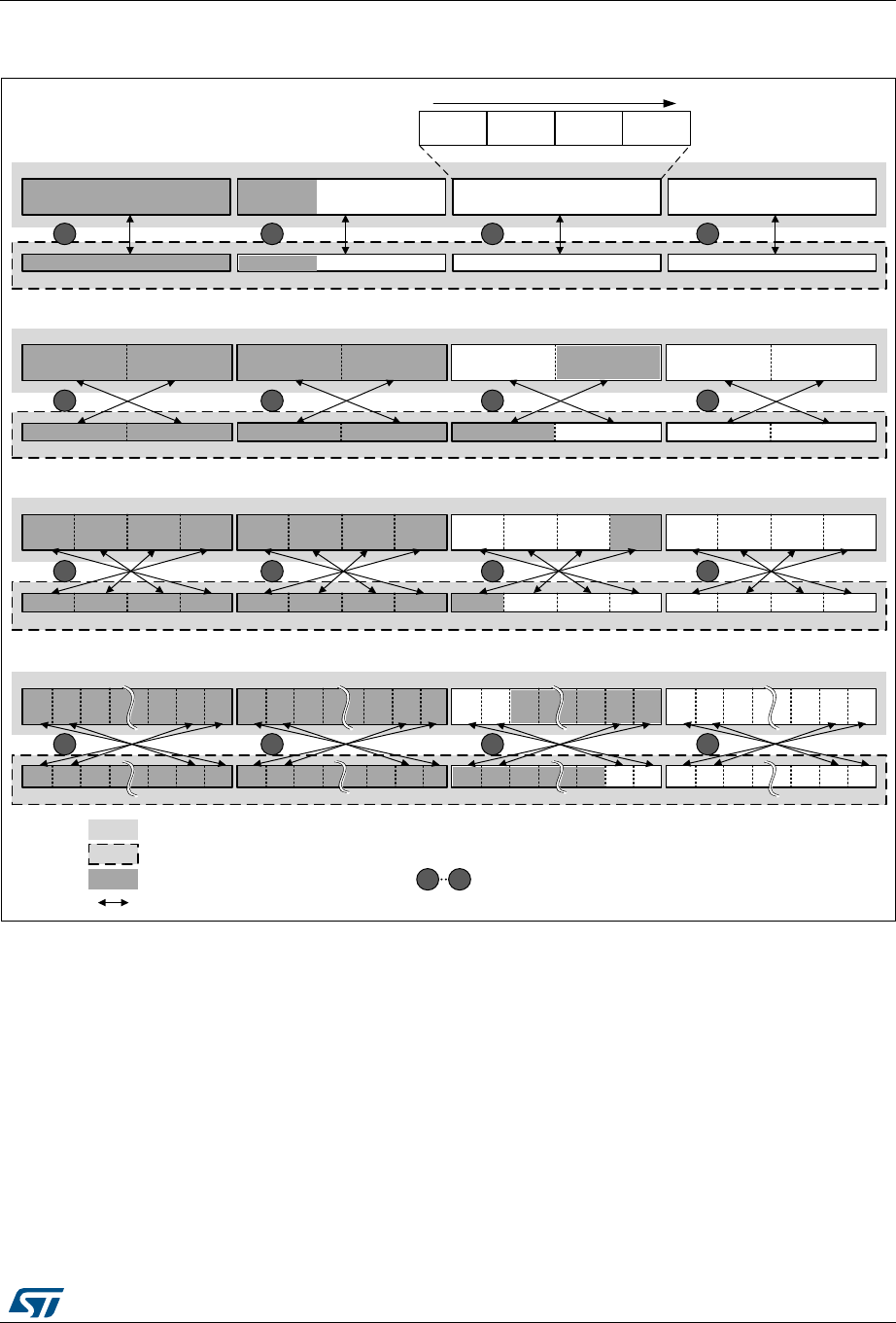
RM0430 Rev 8 725/1324
RM0430 AES hardware accelerator (AES)
743
Figure 250. 128-bit block construction with respect to data swap
Note: The data in AES key registers (AES_KEYRx) and initialization registers (AES_IVRx) are not
sensitive to the swap mode selection.
Data padding
Figure 250 also gives an example of memory data block padding with zeros such that the
zeroed bits after the data swap form a contiguous zone at the MSB end of the AES core
input buffer. The example shows the padding of an input data block containing:
•48 message bits, with DATATYPE[1:0] = 01
•56 message bits, with DATATYPE[1:0] = 10
•34 message bits, with DATATYPE[1:0] = 11
06Y9
'$7$7<3(>@ QRVZDSSLQJ
:RUG:RUG
' ' 3
/6%06%
'$7$7<3(>@ ELWKDOIZRUGVZDSSLQJ
:RUG
'$7$7<3(>@ ELWE\WHVZDSSLQJ
:RUG:RUG
'$7$7<3(>@ ELWVZDSSLQJ
:RUG
/6%
06%
/6%
06%
/6%06%
/6%06%
06%
06%
06% /6%
/6%
:RUG:RUG
/6%
:RUG
:RUG:RUG
' ' ' '
'
:RUG
=HURSDGGLQJH[DPSOH
/HJHQG
'DWDVZDS
:RUG
'
:RUG
:RUG:RUG
$(6LQSXWRXWSXWGDWDEORFNLQPHPRU\
$(6FRUHLQSXWRXWSXWEXIIHUGDWD
2UGHURIZULWHWR$(6B',15UHDGIURP$(6B'2875
06%
/6%
LQFUHDVLQJPHPRU\DGGUHVV
' ' ' ' ' '
''
' ' '' ' ' ' ''''' '' ' '
' '' ' '' ' ' ' ' ' ' ' ' ' '
' ' ' ' ' ' ' ' ' ' ' ' '''' ' ' ' ' ' ' ' '
E\WH E\WH E\WH E\WH
' ' ' '' ' ' '
PRVWVLJQLILFDQWELWRIPHPRU\GDWDEORFN$(&FRUHEXIIHU
OHDVWVLJQLILFDQWELWRIPHPRU\GDWDEORFN$(&FRUHEXIIHU
'[ LQSXWRXWSXWGDWDELWµ[
'' ' ' '' ' ' '' ' ' '' ' '
' ' ' ' ' ' ' ' ' ' ' ' ' ' ' '
' '' '' ' '' '' '' '' '' '' '' '' ''

AES hardware accelerator (AES) RM0430
726/1324 RM0430 Rev 8
24.4.14 AES key registers
The AES_KEYRx registers store the encryption or decryption key bitfield KEY[127:0] or
KEY[255:0]. The data to write to or to read from each register is organized in the memory in
little-endian order, that is, with most significant byte on the highest address.
The key is spread over the eight registers as shown in Table 129.
The key for encryption or decryption may be written into these registers when the AES
peripheral is disabled.
The key registers are not affected by the data swapping controlled by DATATYPE[1:0]
bitfield of the AES_CR register.
24.4.15 AES initialization vector registers
The four AES_IVRx registers keep the initialization vector input bitfield IVI[127:0]. The data
to write to or to read from each register is organized in the memory in little-endian order, that
is, with most significant byte on the highest address. The registers are also ordered from
lowest address (AES_IVR0) to highest address (AES_IVR3).
The signification of data in the bitfield depends on the chaining mode selected. When used,
the bitfield is updated upon each computation cycle of the AES core.
Write operations to the AES_IVRx registers when the AES peripheral is enabled have no
effect to the register contents. For modifying the contents of the AES_IVRx registers, the EN
bit of the AES_CR register must first be cleared.
Reading the AES_IVRx registers returns the latest counter value (useful for managing
suspend mode).
The AES_IVRx registers are not affected by the data swapping feature controlled by the
DATATYPE[1:0] bitfield of the CRYP_CR register.
24.4.16 AES DMA interface
The AES peripheral provides an interface to connect to the DMA (direct memory access)
controller. The DMA operation is controlled through the AES_CR register.
Data input using DMA
Setting the DMAINEN bit of the AES_CR register enables DMA writing into AES. The AES
peripheral then initiates a DMA request during the input phase each time it requires a word
to be written to the AES_DINR register. It asserts four DMA requests to transfer one 128-bit
(four-word) input data block from memory, as shown in Figure 251.
See Table 130 for recommended DMA configuration.
Table 129. Key endianness in AES_KEYRx registers (128- or 256-bit key length)
AES_KEYR7
[31:0]
AES_KEYR6
[31:0]
AES_KEYR5
[31:0]
AES_KEYR4
[31:0]
AES_KEYR3
[31:0]
AES_KEYR2
[31:0]
AES_KEYR1
[31:0]
AES_KEYR0
[31:0]
- - - - KEY[127:96] KEY[95:64] KEY[63:32] KEY[31:0]
KEY[255:224] KEY[223:192] KEY[191:160] KEY[159:128] KEY[127:96] KEY[95:64] KEY[63:32] KEY[31:0]
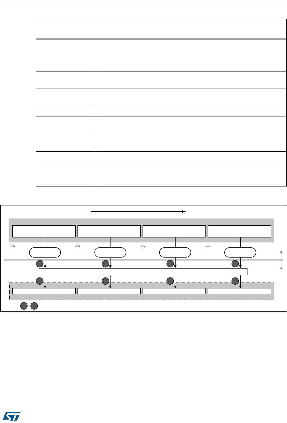
RM0430 Rev 8 727/1324
RM0430 AES hardware accelerator (AES)
743
Figure 251. DMA transfer of a 128-bit data block during input phase
Data output using DMA
Setting the DMAOUTEN bit of the AES_CR register enables DMA reading from AES. The
AES peripheral then initiates a DMA request during the Output phase each time it requires a
word to be read from the AES_DOUTR register. It asserts four DMA requests to transfer one
128-bit (four-word) output data block to memory, as shown in Figure 252.
See Table 131 for recommended DMA configuration.
Table 130. DMA channel configuration for memory-to-AES data transfer
DMA channel control
register field Recommended configuration
Transfer size
Message length: a multiple of 128 bits.
According to the algorithm and the mode selected, special padding/
ciphertext stealing might be required. Refer to Section 24.4.6: AES
ciphertext stealing and data padding on page 703 for details.
Source burst size
(memory) Single
Destination burst size
(peripheral) Single
DMA FIFO size AES FIFO_size = 4 bytes.
Source transfer width
(memory) 32-bit words
Destination transfer
width (peripheral) 32-bit words
Source address
increment (memory) Yes, after each 32-bit transfer
Destination address
increment (peripheral)
Fixed address of AES_DINR (no increment)
06Y9
$(6FRUHLQSXWEXIIHU
$(6B',15
/6%
06%
1RVZDSSLQJ
0HPRU\DFFHVVHGWKURXJK'0$
:RUG:RUG :RUG:RUG
'0$
VLQJOHZULWH
'0$UHT1 '0$UHT1 '0$UHT1 '0$UHT1
, , , , , ,
,,
' ' ' ' ' '
''
',1>@ ',1>@ ',1>@ ',1>@
'0$
VLQJOHZULWH '0$
VLQJOHZULWH '0$
VLQJOHZULWH
&KURQRORJLFDORUGHU
,QFUHDVLQJDGGUHVV
/6%06%
$(6
SHULSKHUDO 6\VWHP
2UGHURIZULWHWR$(6B',15
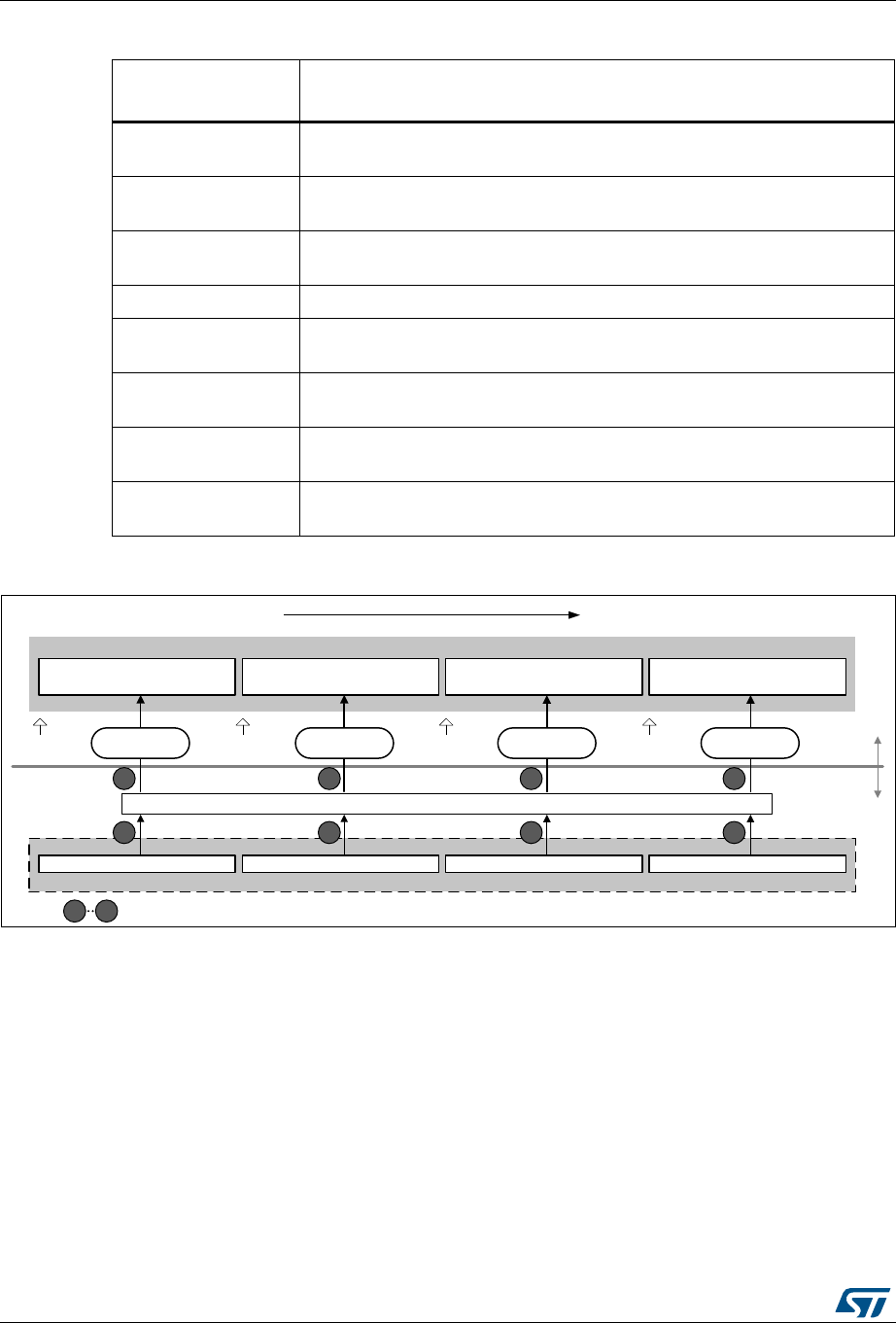
AES hardware accelerator (AES) RM0430
728/1324 RM0430 Rev 8
Figure 252. DMA transfer of a 128-bit data block during output phase
DMA operation in different operating modes
DMA operations are usable when Mode 1 (encryption) or Mode 3 (decryption) are selected
via the MODE[1:0] bitfield of the register AES_CR. As in Mode 2 (key derivation) the
AES_KEYRx registers must be written by software, enabling the DMA transfer through the
DMAINEN and DMAOUTEN bits of the AES_CR register have no effect in that mode.
DMA single requests are generated by AES until it is disabled. So, after the data output
phase at the end of processing of a 128-bit data block, AES switches automatically to a new
data input phase for the next data block, if any.
When the data transferring between AES and memory is managed by DMA, the CCF flag is
not relevant and can be ignored (left set) by software. It must only be cleared when
transiting back to data transferring managed by software. See Suspend/resume operations
Table 131. DMA channel configuration for AES-to-memory data transfer
DMA channel control
register field Recommended configuration
Transfer size It is the message length multiple of AES block size (4 words). According to
the case extra bytes will have to be discarded.
Source burst size
(peripheral) Single
Destination burst size
(memory) Single
DMA FIFIO size AES FIFO_size = 4 bytes
Source transfer width
(peripheral) 32-bit words
Destination transfer
width (memory) 32-bit words
Source address
increment (peripheral) Fixed address of AES_DINR (no increment)
Destination address
increment (memory)
Yes, after each 32-bit transfer
06Y9
$(6FRUHRXWSXWEXIIHU
/6%
06%
1RVZDSSLQJ
0HPRU\DFFHVVHGWKURXJK'0$
:RUG:RUG :RUG:RUG
'0$
VLQJOHUHDG
'0$UHT1 '0$UHT1 '0$UHT1 '0$UHT1
2 2 2 2 2 2
22
' ' ' ' ' '
''
'287>@ '287>@ '287>@ '287>@
'0$
VLQJOHUHDG '0$
VLQJOHUHDG '0$
VLQJOHUHDG
&KURQRORJLFDORUGHU
,QFUHDVLQJDGGUHVV
/6%06%
6\VWHP
$(6
SHULSKHUDO
2UGHURIUHDGIURP$(6B'2875
$(6B'2875
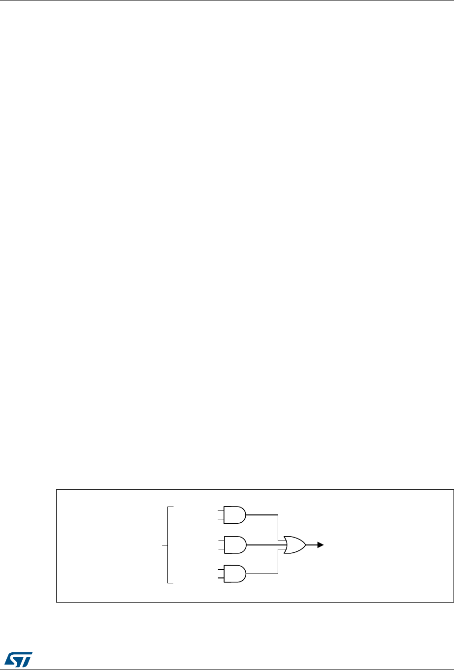
RM0430 Rev 8 729/1324
RM0430 AES hardware accelerator (AES)
743
in ECB/CBC modes in Section 24.4.8: AES basic chaining modes (ECB, CBC) as example.
24.4.17 AES error management
The read error flag (RDERR) and write error flag (WRERR) of the AES_SR register are set
when an unexpected read or write operation, respectively, is detected. An interrupt can be
generated if the error interrupt enable (ERRIE) bit of the AES_CR register is set. For more
details, refer to Section 24.5: AES interrupts.
Note: AES is not disabled after an error detection and continues processing.
AES can be re-initialized at any moment by clearing then setting the EN bit of the AES_CR
register.
Read error flag (RDERR)
When an unexpected read operation is detected during the computation phase or during the
input phase, the AES read error flag (RDERR) is set in the AES_SR register. An interrupt is
generated if the ERRIE bit of the AES_CR register is set.
The RDERR flag is cleared by setting the corresponding ERRC bit of the AES_CR register.
Write error flag (WDERR)
When an unexpected write operation is detected during the computation phase or during the
output phase, the AES write error flag (WRERR) is set in the AES_SR register. An interrupt
is generated if the ERRIE bit of the AES_CR register is set.
The WDERR flag is cleared by setting the corresponding ERRC bit of the AES_CR register.
24.5 AES interrupts
There are three individual maskable interrupt sources generated by the AES peripheral, to
signal the following events:
•computation completed
•read error, see Section 24.4.17
•write error, see Section 24.4.17
These three sources are combined into a common interrupt signal aes_it that connects to
NVIC (nested vectored interrupt controller).
Figure 253. AES interrupt signal generation
Each AES interrupt source can individually be enabled/disabled, by setting/clearing the
corresponding enable bit of the AES_CR register. See Figure 253.
06Y9
:5(55
(55,( DHVBLW
JRHVWR19,&
5'(55
(55,(
&&)
&&),(
)ODJVLQ$(6B65UHJLVWHU
%LWVRI$(6B&5UHJLVWHU
AES hardware accelerator (AES) RM0430
730/1324 RM0430 Rev 8
The status of the individual maskable interrupt sources can be read from the AES_SR
register.
Table 132 gives a summary of the interrupt sources, their event flags and enable bits.
24.6 AES processing latency
The tables below summarize the latency to process a 128-bit block for each mode of
operation.
Table 132. AES interrupt requests
AES interrupt event Event flag Enable bit
computation completed flag CCF CCFIE
read error flag RDERR ERRIE
write error flag WRERR ERRIE
Table 133. Processing latency (in clock cycle) for ECB, CBC and CTR
Key size Mode of operation Algorithm Input
phase
Computation
phase
Output
phase Total
128-bit
Mode 1: Encryption ECB, CBC, CTR 8 202 4 214
Mode 2: Key derivation - - 80 - 80
Mode 3: Decryption ECB, CBC, CTR 8 202 4 214
Mode 4: Key derivation then
decryption ECB, CBC 8 276 4 288
256-bit
Mode 1: Encryption ECB, CBC, CTR 8 286 4 298
Mode 2: Key derivation - - 109 - 109
Mode 3: Decryption ECB, CBC, CTR 8 286 4 298
Mode 4: Key derivation then
decryption ECB, CBC 8 380 4 392
Table 134. Processing latency for GCM and CCM (in clock cycle)
Key size Mode of operation Algorithm Init Phase Header
phase
Payload
phase Tag phase
128-bit
Mode 1: Encryption/
Mode 3: Decryption GCM 215 67 202 202
-CCM
authentication -206-202
256-bit
Mode 1: Encryption/
Mode 3: Decryption GCM 299 67 286 286
-CCM
authentication -290-286

RM0430 Rev 8 731/1324
RM0430 AES hardware accelerator (AES)
743
Note: Data insertion can include wait states forced by AES on the AHB bus (maximum 3 cycles,
typical 1 cycle). This applies to all header/payload/tag phases.
24.7 AES registers
24.7.1 AES control register (AES_CR)
Address offset: 0x00
Reset value: 0x0000 0000
31 30 29 28 27 26 25 24 23 22 21 20 19 18 17 16
Res. Res. Res. Res. Res. Res. Res. Res. Res. Res. Res. Res. Res. KEYSI
ZE Res. CHMO
D[2]
rw rw
1514131211109876543210
Res. GCMPH[1:0] DMAO
UTEN
DMAIN
EN ERRIE CCFIE ERRC CCFC CHMOD[1:0] MODE[1:0] DATATYPE[1:0] EN
rw rw rw rw rw rw rw rw rw rw rw rw rw rw rw
Bits 31:19 Reserved, must be kept at zero
Bit 18 KEYSIZE: Key size selection
This bitfield defines the length of the key used in the AES cryptographic core, in bits:
0: 128
1: 256
The bit value change is allowed only when AES is disabled, so as to avoid an unpredictable
behavior.
Bit 17 Reserved, must be kept at zero
Bit 16 CHMOD[2]: Chaining mode selection, bit [2]
Refer to the bits [5:6] of the register for the description of the CHMOD[2:0] bitfield
Bit 15 Reserved, must be kept at zero
Bits 14:13 GCMPH[1:0]: GCM or CCM phase selection
This bitfield selects the phase of GCM, GMAC or CCM algorithm:
00: Init phase
01: Header phase
10: Payload phase
11: Final phase
The bitfield has no effect if other than GCM, GMAC or CCM algorithms are selected (through the
ALGOMODE bitfield).

AES hardware accelerator (AES) RM0430
732/1324 RM0430 Rev 8
Bit 12 DMAOUTEN: DMA output enable
This bit enables/disables data transferring with DMA, in the output phase:
0: Disable
1: Enable
When the bit is set, DMA requests are automatically generated by AES during the output data
phase. This feature is only effective when Mode 1 or Mode 3 is selected through the MODE[1:0]
bitfield. It is not effective for Mode 2 (key derivation).
Usage of DMA with Mode 4 (single decryption) is not recommended.
Bit 11 DMAINEN: DMA input enable
This bit enables/disables data transferring with DMA, in the input phase:
0: Disable
1: Enable
When the bit is set, DMA requests are automatically generated by AES during the input data phase.
This feature is only effective when Mode 1 or Mode 3 is selected through the MODE[1:0] bitfield. It is
not effective for Mode 2 (key derivation).
Usage of DMA with Mode 4 (single decryption) is not recommended.
Bit 10 ERRIE: Error interrupt enable
This bit enables or disables (masks) the AES interrupt generation when RDERR and/or WRERR is
set:
0: Disable (mask)
1: Enable
Bit 9 CCFIE: CCF interrupt enable
This bit enables or disables (masks) the AES interrupt generation when CCF (computation complete
flag) is set:
0: Disable (mask)
1: Enable
Bit 8 ERRC: Error flag clear
Upon written to 1, this bit clears the RDERR and WRERR error flags in the AES_SR register:
0: No effect
1: Clear RDERR and WRERR flags
Reading the flag always returns zero.
Bit 7 CCFC: Computation complete flag clear
Upon written to 1, this bit clears the computation complete flag (CCF) in the AES_SR register:
0: No effect
1: Clear CCF
Reading the flag always returns zero.

RM0430 Rev 8 733/1324
RM0430 AES hardware accelerator (AES)
743
Bits 6:5 CHMOD[1:0]: Chaining mode selection, bits [1:0]
These bits, together with the bit CHMOD[2] (see bit 16 of this register), form CHMOD[2:0] bitfield that
selects the AES chaining mode:
000: Electronic codebook (ECB)
001: Cipher-Block Chaining (CBC)
010: Counter Mode (CTR)
011: Galois Counter Mode (GCM) and Galois Message Authentication Code (GMAC)
100: Counter with CBC-MAC (CCM)
>100: Reserved
The bitfield value change is allowed only when AES is disabled, so as to avoid an unpredictable
behavior.
Bits 4:3 MODE[1:0]: AES operating mode
This bitfield selects the AES operating mode:
00: Mode 1: encryption
01: Mode 2: key derivation (or key preparation for ECB/CBC decryption)
10: Mode 3: decryption
11: Mode 4: key derivation then single decryption
The bitfield value change is allowed only when AES is disabled, so as to avoid an unpredictable
behavior. Any attempt to selecting Mode 4 while either ECB or CBC chaining mode is not selected,
defaults to effective selection of Mode 3. It is not possible to select a Mode 3 following a Mode 4.
Bits 2:1 DATATYPE[1:0]: Data type selection
This bitfield defines the format of data written in the AES_DINR register or read from the
AES_DOUTR register, through selecting the mode of data swapping:
00: None
01: Half-word (16-bit)
10: Byte (8-bit)
11: Bit
For more details, refer to Section 24.4.13: .AES data registers and data swapping.
The bitfield value change is allowed only when AES is disabled, so as to avoid an unpredictable
behavior.
Bit 0 EN: AES enable
This bit enables/disables the AES peripheral:
0: Disable
1: Enable
At any moment, clearing then setting the bit re-initializes the AES peripheral.
This bit is automatically cleared by hardware when the key preparation process ends (Mode 2).

AES hardware accelerator (AES) RM0430
734/1324 RM0430 Rev 8
24.7.2 AES status register (AES_SR)
Address offset: 0x04
Reset value: 0x0000 0000
31 30 29 28 27 26 25 24 23 22 21 20 19 18 17 16
Res. Res. Res. Res. Res. Res. Res. Res. Res. Res. Res. Res. Res. Res. Res. Res.
r rrrrr r r r r r r r r r r
15 14 13 12 11 10 9 8 7 6 5 4 3 2 1 0
Res. Res. Res. Res. Res. Res. Res. Res. Res. Res. Res. Res. BUSY WRERR RDERR CCF
r rrrrr r r r r r r r r r r
Bits 31:4 Reserved, must be kept at zero
Bit 3 BUSY: Busy
This flag indicates whether AES is idle or busy during GCM payload encryption phase:
0: Idle
1: Busy
The flag is controlled by hardware. When the flag indicates “idle”, the current message processing
may be suspended to process a higher-priority message.
This flag is effective only in GCM payload encryption phase. in other chaining modes, or in GCM
phases other than payload encryption, the flag must be ignored.

RM0430 Rev 8 735/1324
RM0430 AES hardware accelerator (AES)
743
24.7.3 AES data input register (AES_DINR)
Address offset: 0x08
Reset value: 0x0000 0000
Only 32-bit access type is supported.
Bit 2 WRERR: Write error
This flag indicates the detection of an unexpected write operation to the AES_DINR register (during
computation or data output phase):
0: Not detected
1: Detected
The flag is set by hardware. It is cleared by software upon setting the ERRC bit of the AES_CR
register.
Upon the flag setting, an interrupt is generated if enabled through the ERRIE bit of the AES_CR
register.
The flag setting has no impact on the AES operation.
The flag is not effective when key derivation mode, or GCM/CCM Init phase is selected.
Bit 1 RDERR: Read error flag
This flag indicates the detection of an unexpected read operation from the AES_DOUTR register
(during computation or data input phase):
0: Not detected
1: Detected
The flag is set by hardware. It is cleared by software upon setting the ERRC bit of the AES_CR
register.
Upon the flag setting, an interrupt is generated if enabled through the ERRIE bit of the AES_CR
register.
The flag setting has no impact on the AES operation.
The flag is not effective when key derivation mode, nor GCM/CCM init/header phase is selected.
Bit 0 CCF: Computation completed flag
This flag indicates whether the computation is completed:
0: Not completed
1: Completed
The flag is set by hardware upon the completion of the computation. It is cleared by software, upon
setting the CCFC bit of the AES_CR register.
Upon the flag setting, an interrupt is generated if enabled through the CCFIE bit of the AES_CR
register.
The flag is significant only when the DMAOUTEN bit is 0. It may stay high when DMA_EN is 1.
31 30 29 28 27 26 25 24 23 22 21 20 19 18 17 16
DIN[x+31:x+16]
rw rw rw rw rw rw rw rw rw rw rw rw rw rw rw rw
15 14 13 12 11 10 9 8 7 6 5 4 3 2 1 0
DIN[x+15:x]
rw rw rw rw rw rw rw rw rw rw rw rw rw rw rw rw

AES hardware accelerator (AES) RM0430
736/1324 RM0430 Rev 8
24.7.4 AES data output register (AES_DOUTR)
Address offset: 0x0C
Reset value: 0x0000 0000
Only 32-bit access type is supported.
24.7.5 AES key register 0 (AES_KEYR0)
Address offset: 0x10
Reset value: 0x0000 0000
Bits 31:0 DIN[x+31:x]: One of four 32-bit words of a 128-bit input data block being written into the peripheral
This bitfield feeds a 32-bit input buffer. A 4-fold sequential write to this bitfield during the input phase
virtually writes a complete 128-bit block of input data to the AES peripheral. Upon each write, the
data from the input buffer are handled by the data swap block according to the DATATYPE[1:0]
bitfield, then written into the AES core 128-bit input buffer.
The substitution for “x”, from the first to the fourth write operation, is: 96, 64, 32, and 0. In other
words, data from the first to the fourth write operation are: DIN[127:96], DIN[95:64], DIN[63:32], and
DIN[31:0].
The data signification of the input data block depends on the AES operating mode:
- Mode 1 (encryption): plaintext
- Mode 2 (key derivation): the bitfield is not used (AES_KEYRx registers used for input)
- Mode 3 (decryption) and Mode 4 (key derivation then single decryption): ciphertext
The data swap operation is described in Section 24.4.13: .AES data registers and data swapping on
page 724.
31 30 29 28 27 26 25 24 23 22 21 20 19 18 17 16
DOUT[x+31:x+16]
rrrrrrrrrrrrrrrr
1514131211109876543210
DOUT[x+15:0]
rrrrrrrrrrrrrrrr
Bits 31:0 DOUT[x+31:x]: One of four 32-bit words of a 128-bit output data block being read from the peripheral
This bitfield fetches a 32-bit output buffer. A 4-fold sequential read of this bitfield, upon the
computation completion (CCF set), virtually reads a complete 128-bit block of output data from the
AES peripheral. Before reaching the output buffer, the data produced by the AES core are handled
by the data swap block according to the DATATYPE[1:0] bitfield.
The substitution for DOUT[x+31:x], from the first to the fourth read operation, is: 96, 64, 32, and 0. In
other words, data from the first to the fourth read operation are: DOUT[127:96], DOUT[95:64],
DOUT[63:32], and DOUT[31:0].
The data signification of the output data block depends on the AES operating mode:
- Mode 1 (encryption): ciphertext
- Mode 2 (key derivation): the bitfield is not used (AES_KEYRx registers used for output).
- Mode 3 (decryption) and Mode 4 (key derivation then single decryption): plaintext
The data swap operation is described in Section 24.4.13: .AES data registers and data swapping on
page 724.

RM0430 Rev 8 737/1324
RM0430 AES hardware accelerator (AES)
743
24.7.6 AES key register 1 (AES_KEYR1)
Address offset: 0x14
Reset value: 0x0000 0000
24.7.7 AES key register 2 (AES_KEYR2)
Address offset: 0x18
Reset value: 0x0000 0000
31 30 29 28 27 26 25 24 23 22 21 20 19 18 17 16
KEY[31:16]
rw rw rw rw rw rw rw rw rw rw rw rw rw rw rw rw
1514131211109876543210
KEY[15:0]
rw rw rw rw rw rw rw rw rw rw rw rw rw rw rw rw
Bits 31:0 KEY[31:0]: Cryptographic key, bits [31:0]
This bitfield contains the bits [31:0] of the AES encryption or decryption key, depending on the
operating mode:
- In Mode 1 (encryption), Mode 2 (key derivation) and Mode 4 (key derivation then single
decryption): the value to write into the bitfield is the encryption key.
- In Mode 3 (decryption): the value to write into the bitfield is the encryption key to be derived before
being used for decryption. After writing the encryption key into the bitfield, its reading before
enabling AES returns the same value. Its reading after enabling AES and after the CCF flag is set
returns the decryption key derived from the encryption key.
Note: In mode 4 (key derivation then decryption) the bitfield always contains the encryption key.
The AES_KEYRx registers may be written only when the AES peripheral is disabled.
Refer to Section 24.4.14: AES key registers on page 726 for more details.
31 30 29 28 27 26 25 24 23 22 21 20 19 18 17 16
KEY[63:48]
rw rw rw rw rw rw rw rw rw rw rw rw rw rw rw rw
1514131211109876543210
KEY[47:32]
rw rw rw rw rw rw rw rw rw rw rw rw rw rw rw rw
Bits 31:0 KEY[63:32]: Cryptographic key, bits [63:32]
Refer to the AES_KEYR0 register for description of the KEY[255:0] bitfield.
31 30 29 28 27 26 25 24 23 22 21 20 19 18 17 16
KEY[95:80]
rw rw rw rw rw rw rw rw rw rw rw rw rw rw rw rw
1514131211109876543210
KEY[79:64]
rw rw rw rw rw rw rw rw rw rw rw rw rw rw rw rw
AES hardware accelerator (AES) RM0430
738/1324 RM0430 Rev 8
24.7.8 AES key register 3 (AES_KEYR3)
Address offset: 0x1C
Reset value: 0x0000 0000
24.7.9 AES initialization vector register 0 (AES_IVR0)
Address offset: 0x20
Reset value: 0x0000 0000
24.7.10 AES initialization vector register 1 (AES_IVR1)
Address offset: 0x24
Reset value: 0x0000 0000
Bits 31:0 KEY[95:64]: Cryptographic key, bits [95:64]
Refer to the AES_KEYR0 register for description of the KEY[255:0] bitfield.
31 30 29 28 27 26 25 24 23 22 21 20 19 18 17 16
KEY[127:112]
rw rw rw rw rw rw rw rw rw rw rw rw rw rw rw rw
15 14 13 12 11 10 9 8 7 6 5 4 3 2 1 0
KEY[111:96]
rw rw rw rw rw rw rw rw rw rw rw rw rw rw rw rw
Bits 31:0 KEY[127:96]: Cryptographic key, bits [127:96]
Refer to the AES_KEYR0 register for description of the KEY[255:0] bitfield.
31 30 29 28 27 26 25 24 23 22 21 20 19 18 17 16
IVI[31:16]
rw rw rw rw rw rw rw rw rw rw rw rw rw rw rw rw
1514131211109876543210
IVI[15:0]
rw rw rw rw rw rw rw rw rw rw rw rw rw rw rw rw
Bits 31:0 IVI[31:0]: Initialization vector input, bits [31:0]
Refer to Section 24.4.15: AES initialization vector registers on page 726 for description of the
IVI[127:0] bitfield.
The initialization vector is only used in chaining modes other than ECB.
The initialization vector may be written only when the AES peripheral is disabled.
RM0430 Rev 8 739/1324
RM0430 AES hardware accelerator (AES)
743
24.7.11 AES initialization vector register 2 (AES_IVR2)
Address offset: 0x28
Reset value: 0x0000 0000
24.7.12 AES initialization vector register 3 (AES_IVR3)
Address offset: 0x2C
Reset value: 0x0000 0000
31 30 29 28 27 26 25 24 23 22 21 20 19 18 17 16
IVI[63:48]
rw rw rw rw rw rw rw rw rw rw rw rw rw rw rw rw
1514131211109876543210
IVI[47:32]
rw rw rw rw rw rw rw rw rw rw rw rw rw rw rw rw
Bits 31:0 IVI[63:32]: Initialization vector input, bits [63:32]
Refer to Section 24.4.15: AES initialization vector registers on page 726 for description of the
IVI[127:0] bitfield.
The initialization vector is only used in chaining modes other than ECB.
The initialization vector may be written only when the AES peripheral is disabled.
31 30 29 28 27 26 25 24 23 22 21 20 19 18 17 16
IVI[95:80]
rw rw rw rw rw rw rw rw rw rw rw rw rw rw rw rw
1514131211109876543210
IVI[79:64]
rw rw rw rw rw rw rw rw rw rw rw rw rw rw rw rw
Bits 31:0 IVI[95:64]: Initialization vector input, bits [95:64]
Refer to Section 24.4.15: AES initialization vector registers on page 726 for description of the
IVI[127:0] bitfield.
The initialization vector is only used in chaining modes other than ECB.
The initialization vector may be written only when the AES peripheral is disabled.
31 30 29 28 27 26 25 24 23 22 21 20 19 18 17 16
IVI[127:112]
rw rw rw rw rw rw rw rw rw rw rw rw rw rw rw rw
1514131211109876543210
IVI[111:96]
rw rw rw rw rw rw rw rw rw rw rw rw rw rw rw rw
AES hardware accelerator (AES) RM0430
740/1324 RM0430 Rev 8
24.7.13 AES key register 4 (AES_KEYR4)
Address offset: 0x30
Reset value: 0x0000 0000
24.7.14 AES key register 5 (AES_KEYR5)
Address offset: 0x34
Reset value: 0x0000 0000
24.7.15 AES key register 6 (AES_KEYR6)
Address offset: 0x38
Reset value: 0x0000 0000
Bits 31:0 IVI[127:96]: Initialization vector input, bits [127:96]
Refer to Section 24.4.15: AES initialization vector registers on page 726 for description of the
IVI[127:0] bitfield.
The initialization vector is only used in chaining modes other than ECB.
The initialization vector may be written only when the AES peripheral is disabled.
31 30 29 28 27 26 25 24 23 22 21 20 19 18 17 16
KEY[159:144]
rw rw rw rw rw rw rw rw rw rw rw rw rw rw rw rw
1514131211109876543210
KEY[143:128]
rw rw rw rw rw rw rw rw rw rw rw rw rw rw rw rw
Bits 31:0 KEY[159:128]: Cryptographic key, bits [159:128]
Refer to the AES_KEYR0 register for description of the KEY[255:0] bitfield.
31 30 29 28 27 26 25 24 23 22 21 20 19 18 17 16
KEY[191:176]
rw rw rw rw rw rw rw rw rw rw rw rw rw rw rw rw
1514131211109876543210
KEY[175:160]
rw rw rw rw rw rw rw rw rw rw rw rw rw rw rw rw
Bits 31:0 KEY[191:160]: Cryptographic key, bits [191:160]
Refer to the AES_KEYR0 register for description of the KEY[255:0] bitfield.
31 30 29 28 27 26 25 24 23 22 21 20 19 18 17 16
KEY[223:208]
rw rw rw rw rw rw rw rw rw rw rw rw rw rw rw rw
1514131211109876543210
KEY[207:192]
rw rw rw rw rw rw rw rw rw rw rw rw rw rw rw rw
RM0430 Rev 8 741/1324
RM0430 AES hardware accelerator (AES)
743
24.7.16 AES key register 7 (AES_KEYR7)
Address offset: 0x3C
Reset value: 0x0000 0000
Note: The key registers from 4 to 7 are used only when the key length of 256 bits is selected. They
have no effect when the key length of 128 bits is selected (only key registers 0 to 3 are used
in that case).
24.7.17 AES suspend registers (AES_SUSPxR)
Address offset: 0x040 + x * 0x4, (x = 0 to 7)
Reset value: 0x0000 0000
These registers contain the complete internal register states of the AES processor when the
AES processing of the current task is suspended to process a higher-priority task.
Upon suspend, the software reads and saves the AES_SUSPxR register contents (where x
is from 0 to 7) into memory, before using the AES processor for the higher-priority task.
Upon completion, the software restores the saved contents back into the corresponding
suspend registers, before resuming the original task.
Note: These registers are used only when GCM, GMAC, or CCM chaining mode is selected.
These registers can be read only when AES is enabled. Reading these registers while AES
is disabled returns 0x0000 0000.
Bits 31:0 KEY[223:192]: Cryptographic key, bits [223:192]
Refer to the AES_KEYR0 register for description of the KEY[255:0] bitfield.
31 30 29 28 27 26 25 24 23 22 21 20 19 18 17 16
KEY[255:240]
rw rw rw rw rw rw rw rw rw rw rw rw rw rw rw rw
1514131211109876543210
KEY[239:224]
rw rw rw rw rw rw rw rw rw rw rw rw rw rw rw rw
Bits 31:0 KEY[255:224]: Cryptographic key, bits [255:224]
Refer to the AES_KEYR0 register for description of the KEY[255:0] bitfield.
31 30 29 28 27 26 25 24 23 22 21 20 19 18 17 16
SUSPx
rw rw rw rw rw rw rw rw rw rw rw rw rw rw rw rw
1514131211109876543210
SUSPx
rw rw rw rw rw rw rw rw rw rw rw rw rw rw rw rw
Bits 31:0 SUSPx: AES suspend
Upon suspend operation, this bitfield of every AES_SUSPxR register takes the value of one of
internal AES registers.

AES hardware accelerator (AES) RM0430
742/1324 RM0430 Rev 8
24.7.18 AES register map
Table 135. AES register map and reset values
Offset Register
31
30
29
28
27
26
25
24
23
22
21
20
19
18
17
16
15
14
13
12
11
10
9
8
7
6
5
4
3
2
1
0
0x0000
AES_CR
Res.
Res.
Res.
Res.
Res.
Res.
Res.
Res.
Res.
Res.
Res.
Res.
Res.
KEYSIZE
Res.
CHMOD[2]
Res.
GCMPH[1:0]
DMAOUTEN
DMAINEN
ERRIE
CCFIE
ERRC
CCFC
CHMOD[1:0]
MODE[1:0]
DATATYPE[1:0]
EN
Reset value 0 0 000000000000000
0x0004
AES_SR
Res.
Res.
Res.
Res.
Res.
Res.
Res.
Res.
Res.
Res.
Res.
Res.
Res.
Res.
Res.
Res.
Res.
Res.
Res.
Res.
Res.
Res.
Res.
Res.
Res.
Res.
Res.
Res.
BUSY
WRERR
RDERR
CCF
Reset value 0000
0x0008
AES_DINR
x=96,64,32,0 DIN[x+31:x]
Reset value 00000000000000000000000000000000
0x000
C
AES_DOUTR
x=96,64,32,0 DOUT[x+31:x]
Reset value 00000000000000000000000000000000
0x0010
AES_KEYR0 KEY[31:0]
Reset value 00000000000000000000000000000000
0x0014
AES_KEYR1 KEY[63:32]
Reset value 00000000000000000000000000000000
0x0018
AES_KEYR2 KEY[95:64]
Reset value 00000000000000000000000000000000
0x001
C
AES_KEYR3 KEY[127:96]
Reset value 00000000000000000000000000000000
0x0020
AES_IVR0 IVI[31:0]
Reset value 00000000000000000000000000000000
0x0024
AES_IVR1 IVI[63:32]
Reset value 00000000000000000000000000000000
0x0028
AES_IVR2 IVI[95:64]
Reset value 00000000000000000000000000000000
0x002
C
AES_IVR3 IVI[127:96]
Reset value 00000000000000000000000000000000
0x0030
AES_KEYR4 KEY[159:128]
Reset value 00000000000000000000000000000000
0x0034
AES_KEYR5 KEY[191:160]
Reset value 00000000000000000000000000000000
0x0038
AES_KEYR6 KEY[223:192]
Reset value 00000000000000000000000000000000
RM0430 Rev 8 743/1324
RM0430 AES hardware accelerator (AES)
743
0x003
C
AES_KEYR7 KEY[255:224]
Reset value 00000000000000000000000000000000
0x0040
AES_SUSP0R SUSP0[31:0]
Reset value 00000000000000000000000000000000
0x0044
AES_SUSP1R SUSP1[31:0]
Reset value 00000000000000000000000000000000
0x0048
AES_SUSP2R SUSP2[31:0]
Reset value 00000000000000000000000000000000
0x004
C
AES_SUSP3R SUSP3[31:0]
Reset value 00000000000000000000000000000000
0x0050
AES_SUSP4R SUSP4[31:0]
Reset value 00000000000000000000000000000000
0x0054
AES_SUSP5R SUSP5[31:0]
Reset value 00000000000000000000000000000000
0x0058
AES_SUSP6R SUSP6[31:0]
Reset value 00000000000000000000000000000000
0x005
C
AES_SUSP7R SUSP7[31:0]
Reset value 00000000000000000000000000000000
Table 135. AES register map and reset values (continued)
Offset Register
31
30
29
28
27
26
25
24
23
22
21
20
19
18
17
16
15
14
13
12
11
10
9
8
7
6
5
4
3
2
1
0

Real-time clock (RTC) RM0430
744/1324 RM0430 Rev 8
25 Real-time clock (RTC)
25.1 Introduction
The real-time clock (RTC) is an independent BCD timer/counter. The RTC provides a
time-of-day clock/calendar, two programmable alarm interrupts, and a periodic
programmable wakeup flag with interrupt capability. The RTC also includes an automatic
wakeup unit to manage low power modes.
Two 32-bit registers contain the seconds, minutes, hours (12- or 24-hour format), day (day
of week), date (day of month), month, and year, expressed in binary coded decimal format
(BCD). The sub-seconds value is also available in binary format.
Compensations for 28-, 29- (leap year), 30-, and 31-day months are performed
automatically. Daylight saving time compensation can also be performed.
Additional 32-bit registers contain the programmable alarm subseconds, seconds, minutes,
hours, day, and date.
A digital calibration feature is available to compensate for any deviation in crystal oscillator
accuracy.
After backup domain reset, all RTC registers are protected against possible parasitic write
accesses.
As long as the supply voltage remains in the operating range, the RTC never stops,
regardless of the device status (Run mode, low power mode or under reset).
25.2 RTC main features
The RTC unit main features are the following (see Figure 254):
•Calendar with subseconds, seconds, minutes, hours (12 or 24 format), day (day of
week), date (day of month), month, and year.
•Daylight saving compensation programmable by software.
•Two programmable alarms with interrupt function. The alarms can be triggered by any
combination of the calendar fields.
•Automatic wakeup unit generating a periodic flag that triggers an automatic wakeup
interrupt.
•Reference clock detection: a more precise second source clock (50 or 60 Hz) can be
used to enhance the calendar precision.
•Accurate synchronization with an external clock using the subsecond shift feature.
•Maskable interrupts/events:
–Alarm A
–Alarm B
– Wakeup interrupt
–Timestamp
– Tamper detection
•Digital calibration circuit (periodic counter correction)
– 5 ppm accuracy
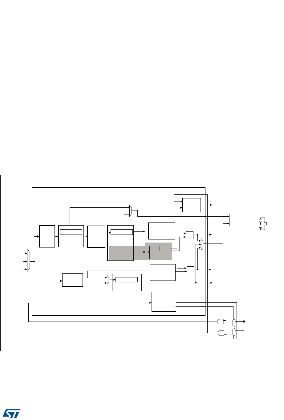
RM0430 Rev 8 745/1324
RM0430 Real-time clock (RTC)
781
– 0.95 ppm accuracy, obtained in a calibration window of several seconds
•Timestamp function for event saving (1 event)
•Tamper detection:
– 2 tamper events with configurable filter and internal pull-up.
•20 backup registers (80 bytes). The backup registers are reset when a tamper
detection event occurs.
•Alternate function output (RTC_OUT) which selects one of the following two outputs:
– RTC_CALIB: 512 Hz or 1 Hz clock output (with an LSE frequency of 32.768 kHz).
This output is enabled by setting the COE bit in the RTC_CR register. It is routed
to the device RTC_AF1 function.
– RTC_ALARM (Alarm A, Alarm B or wakeup).
This output is selected by configuring the OSEL[1:0] bits in the RTC_CR register.
It is routed to the device RTC_AF1 function.
•RTC alternate function inputs:
– RTC_TS: timestamp event detection. It is routed to the device RTC_AF1.
– RTC_TAMP1: TAMPER1 event detection. It is routed to the device RTC_AF1.
– RTC_REFIN: reference clock input (usually the mains, 50 or 60 Hz).
Figure 254. RTC block diagram
06Y9
&NBDSUH
GHIDXOW+]
57&B&$/,%
+]
57&B:875
57&&/.
:87)
+6(B57&
0+]PD[
/6(
+]
/6,
6\QFKURQRXV
ELWSUHVFDOHU
GHIDXOW &DOHQGDU
3UHVFDOHU
ELWZDNHXS
DXWRUHORDGWLPHU
$ODUP$
57&B$/50$5
57&B$/50$665
UHJLVWHUV
$/5$)
57&B$/$50
57&B35 ( 5 57&B35(5
&RDUVH
FDOLEUDWLRQ
57&B&$/
,%5
$/5%)
7LPH
VWDPS
UHJLVWHUV
76)
2XWSXW
FRQWURO 57&B$)
57&B287
6PRRWK
&DOLEUDWLRQ
57&B&$/
5
+]
$ODUP%
57&B$/50%5
57&B$/50%665
UHJLVWHUV
:8&.6(/>@
%DFNXSDQG
57&WDPSHU
FRQWURO
UHJLVWHUV
57&B7$03
57&B76
7$03(
76(
6KDGRZ
5HJLVWHUV
57&B665
6KDGRZ
5HJLVWHUV
57&B75'5
FNBVSUH
GHIDXOW
+]
$V\QFKURQRXV
ELWSUHVFDOHU
GHIDXOW

Real-time clock (RTC) RM0430
746/1324 RM0430 Rev 8
25.3 RTC functional description
25.3.1 Clock and prescalers
The RTC clock source (RTCCLK) is selected through the clock controller among the LSE
clock, the LSI oscillator clock, and the HSE clock. For more information on the RTC clock
source configuration, refer to Section 6: Reset and clock control (RCC) for STM32F413/423.
A programmable prescaler stage generates a 1 Hz clock which is used to update the
calendar. To minimize power consumption, the prescaler is split into 2 programmable
prescalers (see Figure 254: RTC block diagram):
•A 7-bit asynchronous prescaler configured through the PREDIV_A bits of the
RTC_PRER register.
• A 15-bit synchronous prescaler configured through the PREDIV_S bits of the
RTC_PRER register.
Note: When both prescalers are used, it is recommended to configure the asynchronous prescaler
to a high value to minimize consumption.
The asynchronous prescaler division factor is set to 128, and the synchronous division
factor to 256, to obtain an internal clock frequency of 1 Hz (ck_spre) with an LSE frequency
of 32.768 kHz.
The minimum division factor is 1 and the maximum division factor is 222.
This corresponds to a maximum input frequency of around 4 MHz.
fck_apre is given by the following formula:
The ck_apre clock is used to clock the binary RTC_SSR subseconds downcounter. When it
reaches 0, RTC_SSR is reloaded with the content of PREDIV_S.
fck_spre is given by the following formula:
The ck_spre clock can be used either to update the calendar or as timebase for the 16-bit
wakeup auto-reload timer. To obtain short timeout periods, the 16-bit wakeup auto-reload
timer can also run with the RTCCLK divided by the programmable 4-bit asynchronous
prescaler (see Section 25.3.4 for details).
25.3.2 Real-time clock and calendar
The RTC calendar time and date registers are accessed through shadow registers which
are synchronized with PCLK1 (APB1 clock). They can also be accessed directly in order to
avoid waiting for the synchronization duration.
•RTC_SSR for the subseconds
•RTC_TR for the time
•RTC_DR for the date
fCK_APRE
fRTCCLK
PREDIV_A 1+
---------------------------------------
=
fCK_SPRE
fRTCCLK
PREDIV_S 1+()PREDIV_A 1+()×
-----------------------------------------------------------------------------------------------
=

RM0430 Rev 8 747/1324
RM0430 Real-time clock (RTC)
781
Every two RTCCLK periods, the current calendar value is copied into the shadow registers,
and the RSF bit of RTC_ISR register is set (see Section 25.6.4). The copy is not performed
in Stop and Standby mode. When exiting these modes, the shadow registers are updated
after up to two RTCCLK periods.
When the application reads the calendar registers, it accesses the content of the shadow
registers.It is possible to make a direct access to the calendar registers by setting the
BYPSHAD control bit in the RTC_CR register. By default, this bit is cleared, and the user
accesses the shadow registers.
When reading the RTC_SSR, RTC_TR or RTC_DR registers in BYPSHAD=0 mode, the
frequency of the APB clock (fAPB) must be at least 7 times the frequency of the RTC clock
(fRTCCLK).
The shadow registers are reset by system reset.
25.3.3 Programmable alarms
The RTC unit provides two programmable alarms, Alarm A and Alarm B.
The programmable alarm functions are enabled through the ALRAIE and ALRBIE bits in the
RTC_CR register. The ALRAF and ALRBF flags are set to 1 if the calendar subseconds,
seconds, minutes, hours, date or day match the values programmed in the alarm registers
RTC_ALRMASSR/RTC_ALRMAR and RTC_ALRMBSSR/RTC_ALRMBR, respectively.
Each calendar field can be independently selected through the MSKx bits of the
RTC_ALRMAR and RTC_ALRMBR registers, and through the MASKSSx bits of the
RTC_ALRMASSR and RTC_ALRMBSSR registers. The alarm interrupts are enabled
through the ALRAIE and ALRBIE bits in the RTC_CR register.
Alarm A and Alarm B (if enabled by bits OSEL[1:0] in RTC_CR register) can be routed to the
RTC_ALARM output. RTC_ALARM polarity can be configured through bit POL in the
RTC_CR register.
Caution: If the seconds field is selected (MSK0 bit reset in RTC_ALRMAR or RTC_ALRMBR), the
synchronous prescaler division factor set in the RTC_PRER register must be at least 3 to
ensure correct behavior.
25.3.4 Periodic auto-wakeup
The periodic wakeup flag is generated by a 16-bit programmable auto-reload down-counter.
The wakeup timer range can be extended to 17 bits.
The wakeup function is enabled through the WUTE bit in the RTC_CR register.
The wakeup timer clock input can be:
•RTC clock (RTCCLK) divided by 2, 4, 8, or 16.
When RTCCLK is LSE(32.768 kHz), this allows to configure the wakeup interrupt
period from 122 µs to 32 s, with a resolution down to 61µs.
•ck_spre (usually 1 Hz internal clock)
When ck_spre frequency is 1Hz, this allows to achieve a wakeup time from 1 s to
around 36 hours with one-second resolution. This large programmable time range is
divided in 2 parts:
– from 1s to 18 hours when WUCKSEL [2:1] = 10
– and from around 18h to 36h when WUCKSEL[2:1] = 11. In this last case 216 is
added to the 16-bit counter current value.When the initialization sequence is

Real-time clock (RTC) RM0430
748/1324 RM0430 Rev 8
complete (see Programming the wakeup timer), the timer starts counting
down.When the wakeup function is enabled, the down-counting remains active in
low power modes. In addition, when it reaches 0, the WUTF flag is set in the
RTC_ISR register, and the wakeup counter is automatically reloaded with its
reload value (RTC_WUTR register value).
The WUTF flag must then be cleared by software.
When the periodic wakeup interrupt is enabled by setting the WUTIE bit in the RTC_CR2
register, it can exit the device from low power modes.
The periodic wakeup flag can be routed to the RTC_ALARM output provided it has been
enabled through bits OSEL[1:0] of RTC_CR register. RTC_ALARM polarity can be
configured through the POL bit in the RTC_CR register.
System reset, as well as low power modes (Sleep, Stop and Standby) have no influence on
the wakeup timer.
25.3.5 RTC initialization and configuration
RTC register access
The RTC registers are 32-bit registers. The APB interface introduces 2 wait-states in RTC
register accesses except on read accesses to calendar shadow registers when
BYPSHAD=0.
RTC register write protection
After system reset, the RTC registers are protected against parasitic write access with the
DBP bit of the PWR power control register (PWR_CR). The DBP bit must be set to enable
RTC registers write access.
After backup domain reset, all the RTC registers are write-protected. Writing to the RTC
registers is enabled by writing a key into the Write Protection register, RTC_WPR.
The following steps are required to unlock the write protection on all the RTC registers
except for RTC_ISR[13:8], RTC_TAFCR, and RTC_BKPxR.
1. Write ‘0xCA’ into the RTC_WPR register.
2. Write ‘0x53’ into the RTC_WPR register.
Writing a wrong key reactivates the write protection.
The protection mechanism is not affected by system reset.
Calendar initialization and configuration
To program the initial time and date calendar values, including the time format and the
prescaler configuration, the following sequence is required:
1. Set INIT bit to 1 in the RTC_ISR register to enter initialization mode. In this mode, the
calendar counter is stopped and its value can be updated.
2. Poll INITF bit of in the RTC_ISR register. The initialization phase mode is entered when
INITF is set to 1. It takes from 1 to 2 RTCCLK clock cycles (due to clock
synchronization).
3. To generate a 1 Hz clock for the calendar counter, program first the synchronous
prescaler factor in RTC_PRER register, and then program the asynchronous prescaler

RM0430 Rev 8 749/1324
RM0430 Real-time clock (RTC)
781
factor. Even if only one of the two fields needs to be changed, 2 separate write
accesses must be performed to the RTC_PRER register.
4. Load the initial time and date values in the shadow registers (RTC_TR and RTC_DR),
and configure the time format (12 or 24 hours) through the FMT bit in the RTC_CR
register.
5. Exit the initialization mode by clearing the INIT bit. The actual calendar counter value is
then automatically loaded and the counting restarts after 4 RTCCLK clock cycles.
When the initialization sequence is complete, the calendar starts counting.
Note: After a system reset, the application can read the INITS flag in the RTC_ISR register to
check if the calendar has been initialized or not. If this flag equals 0, the calendar has not
been initialized since the year field is set at its backup domain reset default value (0x00).
To read the calendar after initialization, the software must first check that the RSF flag is set
in the RTC_ISR register.
Daylight saving time
The daylight saving time management is performed through bits SUB1H, ADD1H, and BKP
of the RTC_CR register.
Using SUB1H or ADD1H, the software can subtract or add one hour to the calendar in one
single operation without going through the initialization procedure.
In addition, the software can use the BKP bit to memorize this operation.
Programming the alarm
A similar procedure must be followed to program or update the programmable alarm (Alarm
A or Alarm B):
1. Clear ALRAE or ALRBIE in RTC_CR to disable Alarm A or Alarm B.
2. Poll ALRAWF or ALRBWF in RTC_ISR until it is set to make sure the access to alarm
registers is allowed. This takes 1 to 2 RTCCLK clock cycles (due to clock
synchronization).
3. Program the Alarm A or Alarm B registers (RTC_ALRMASSR/RTC_ALRMAR or
RTC_ALRMBSSR/RTC_ALRMBR).
4. Set ALRAE or ALRBIE in the RTC_CR register to enable Alarm A or Alarm B again.
Note: Each change of the RTC_CR register is taken into account after 1 to 2 RTCCLK clock cycles
due to clock synchronization.
Programming the wakeup timer
The following sequence is required to configure or change the wakeup timer auto-reload
value (WUT[15:0] in RTC_WUTR):
1. Clear WUTE in RTC_CR to disable the wakeup timer.
2. Poll WUTWF until it is set in RTC_ISR to make sure the access to wakeup auto-reload
counter and to WUCKSEL[2:0] bits is allowed. It takes 1 to 2 RTCCLK clock cycles
(due to clock synchronization).
3. Program the wakeup auto-reload value WUT[15:0] and the wakeup clock selection
(WUCKSEL[2:0] bits in RTC_CR).Set WUTE in RTC_CR to enable the timer again.
The wakeup timer restarts down-counting. Due to clock synchronization, the WUTWF
bit is cleared up to 2 RTCCLK clocks cycles after WUTE is cleared.

Real-time clock (RTC) RM0430
750/1324 RM0430 Rev 8
25.3.6 Reading the calendar
When BYPSHAD control bit is cleared in the RTC_CR register
To read the RTC calendar registers (RTC_SSR, RTC_TR and RTC_DR) properly, the APB1
clock frequency (fPCLK1) must be equal to or greater than seven times the fRTCCLK RTC
clock frequency. This ensures a secure behavior of the synchronization mechanism.
If the APB1 clock frequency is less than seven times the RTC clock frequency, the software
must read the calendar time and date registers twice. If the second read of the RTC_TR
gives the same result as the first read, this ensures that the data is correct. Otherwise a third
read access must be done. In any case the APB1 clock frequency must never be lower than
the RTC clock frequency.
The RSF bit is set in RTC_ISR register each time the calendar registers are copied into the
RTC_SSR, RTC_TR and RTC_DR shadow registers. The copy is performed every two
RTCCLK cycles. To ensure consistency between the 3 values, reading either RTC_SSR or
RTC_TR locks the values in the higher-order calendar shadow registers until RTC_DR is
read. In case the software makes read accesses to the calendar in a time interval smaller
than 2 RTCCLK periods: RSF must be cleared by software after the first calendar read, and
then the software must wait until RSF is set before reading again the RTC_SSR, RTC_TR
and RTC_DR registers.
After waking up from low power mode (Stop or Standby), RSF must be cleared by software.
The software must then wait until it is set again before reading the RTC_SSR, RTC_TR and
RTC_DR registers.
The RSF bit must be cleared after wakeup and not before entering low power mode.
Note: After a system reset, the software must wait until RSF is set before reading the RTC_SSR,
RTC_TR and RTC_DR registers. Indeed, a system reset resets the shadow registers to
their default values.
After an initialization (refer to Calendar initialization and configuration): the software must
wait until RSF is set before reading the RTC_SSR, RTC_TR and RTC_DR registers.
After synchronization (refer to Section 25.3.8): the software must wait until RSF is set before
reading the RTC_SSR, RTC_TR and RTC_DR registers.
When the BYPSHAD control bit is set in the RTC_CR register (bypass shadow
registers)
Reading the calendar registers gives the values from the calendar counters directly, thus
eliminating the need to wait for the RSF bit to be set. This is especially useful after exiting
from low power modes (STOP or Standby), since the shadow registers are not updated
during these modes.
When the BYPSHAD bit is set to 1, the results of the different registers might not be
coherent with each other if an RTCCLK edge occurs between two read accesses to the
registers. Additionally, the value of one of the registers may be incorrect if an RTCCLK edge
occurs during the read operation. The software must read all the registers twice, and then
compare the results to confirm that the data is coherent and correct. Alternatively, the
software can just compare the two results of the least-significant calendar register.
Note: While BYPSHAD=1, instructions which read the calendar registers require one extra APB
cycle to complete.

RM0430 Rev 8 751/1324
RM0430 Real-time clock (RTC)
781
25.3.7 Resetting the RTC
The calendar shadow registers (RTC_SSR, RTC_TR and RTC_DR) and some bits of the
RTC status register (RTC_ISR) are reset to their default values by all available system reset
sources.
On the contrary, the following registers are resetted to their default values by a backup
domain reset and are not affected by a system reset: the RTC current calendar registers,
the RTC control register (RTC_CR), the prescaler register (RTC_PRER), the RTC
calibration registers (RTC_CALIBR or RTC_CALR), the RTC shift register (RTC_SHIFTR),
the RTC timestamp registers (RTC_TSSSR, RTC_TSTR and RTC_TSDR), the RTC tamper
and alternate function configuration register (RTC_TAFCR), the RTC backup registers
(RTC_BKPxR), the wakeup timer register (RTC_WUTR), the Alarm A and Alarm B registers
(RTC_ALRMASSR/RTC_ALRMAR and RTC_ALRMBSSR/RTC_ALRMBR).
In addition, when clocked by LSE, the RTC keeps on running under system reset if the reset
source is different from the Backup domain reset one (refer to RCC for details about the list
of RTC clock sources not affected by system reset). When a backup domain reset occurs,
the RTC is stopped and all the RTC registers are set to their reset values.
25.3.8 RTC synchronization
The RTC can be synchronized to a remote clock with a high degree of precision. After
reading the sub-second field (RTC_SSR or RTC_TSSSR), a calculation can be made of the
precise offset between the times being maintained by the remote clock and the RTC. The
RTC can then be adjusted to eliminate this offset by “shifting” its clock by a fraction of a
second using RTC_SHIFTR.
RTC_SSR contains the value of the synchronous prescaler’s counter. This allows one to
calculate the exact time being maintained by the RTC down to a resolution of
1 / (PREDIV_S + 1) seconds. As a consequence, the resolution can be improved by
increasing the synchronous prescaler value (PREDIV_S[14:0]. The maximum resolution
allowed (30.52 μs with a 32768 Hz clock) is obtained with PREDIV_S set to 0x7FFF.
However, increasing PREDIV_S means that PREDIV_A must be decreased in order to
maintain the synchronous prescaler’s output at 1 Hz. In this way, the frequency of the
asynchronous prescaler’s output increases, which may increase the RTC dynamic
consumption.
The RTC can be finely adjusted using the RTC shift control register (RTC_SHIFTR). Writing
to RTC_SHIFTR can shift (either delay or advance) the clock by up to a second with a
resolution of 1 / (PREDIV_S + 1) seconds. The shift operation consists of adding the
SUBFS[14:0] value to the synchronous prescaler counter SS[15:0]: this will delay the clock.
If at the same time the ADD1S bit is set, this results in adding one second and at the same
time subtracting a fraction of second, so this will advance the clock.
Caution: Before initiating a shift operation, the user must check that SS[15] = 0 in order to ensure that
no overflow will occur.
As soon as a shift operation is initiated by a write to the RTC_SHIFTR register, the SHPF
flag is set by hardware to indicate that a shift operation is pending. This bit is cleared by
hardware as soon as the shift operation has completed.
Caution: This synchronization feature is not compatible with the reference clock detection feature:
firmware must not write to RTC_SHIFTR when REFCKON=1.

Real-time clock (RTC) RM0430
752/1324 RM0430 Rev 8
25.3.9 RTC reference clock detection
The RTC calendar update can be synchronized to a reference clock RTC_REFIN, usually
the mains (50 or 60 Hz). The RTC_REFIN reference clock should have a higher precision
than the 32.768 kHz LSE clock. When the RTC_REFIN detection is enabled (REFCKON bit
of RTC_CR set to 1), the calendar is still clocked by the LSE, and RTC_REFIN is used to
compensate for the imprecision of the calendar update frequency (1 Hz).
Each 1 Hz clock edge is compared to the nearest reference clock edge (if one is found
within a given time window). In most cases, the two clock edges are properly aligned. When
the 1 Hz clock becomes misaligned due to the imprecision of the LSE clock, the RTC shifts
the 1 Hz clock a bit so that future 1 Hz clock edges are aligned. Thanks to this mechanism,
the calendar becomes as precise as the reference clock.
The RTC detects if the reference clock source is present by using the 256 Hz clock
(ck_apre) generated from the 32.768 kHz quartz. The detection is performed during a time
window around each of the calendar updates (every 1 s). The window equals 7 ck_apre
periods when detecting the first reference clock edge. A smaller window of 3 ck_apre
periods is used for subsequent calendar updates.
Each time the reference clock is detected in the window, the asynchronous prescaler which
outputs the ck_apre clock is forced to reload. This has no effect when the reference clock
and the 1 Hz clock are aligned because the prescaler is being reloaded at the same
moment. When the clocks are not aligned, the reload shifts future 1 Hz clock edges a little
for them to be aligned with the reference clock.
If the reference clock halts (no reference clock edge occurred during the 3 ck_apre window),
the calendar is updated continuously based solely on the LSE clock. The RTC then waits for
the reference clock using a large 7 ck_apre period detection window centered on the
ck_spre edge.
When the reference clock detection is enabled, PREDIV_A and PREDIV_S must be set to
their default values:
•PREDIV_A = 0x007F
•PREDIV_S = 0x00FF
Note: The reference clock detection is not available in Standby mode.
Caution: The reference clock detection feature cannot be used in conjunction with the coarse digital
calibration: RTC_CALIBR must be kept at 0x0000 0000 when REFCKON=1.
25.3.10 RTC coarse digital calibration
Two digital calibration methods are available: coarse and smooth calibration. To perform
coarse calibration refer to Section 25.6.7: RTC calibration register (RTC_CALIBR).
The two calibration methods are not intended to be used together, the application must
select one of the two methods. Coarse calibration is provided for compatibly reasons. To
perform smooth calibration refer to Section 25.3.11: RTC smooth digital calibration and to
Section 25.6.16: RTC calibration register (RTC_CALR)
The coarse digital calibration can be used to compensate crystal inaccuracy by adding
(positive calibration) or masking (negative calibration) clock cycles at the output of the
asynchronous prescaler (ck_apre).
Positive and negative calibration are selected by setting the DCS bit in RTC_CALIBR
register to ‘0’ and ‘1’, respectively.

RM0430 Rev 8 753/1324
RM0430 Real-time clock (RTC)
781
When positive calibration is enabled (DCS = ‘0’), 2 ck_apre cycles are added every minute
(around 15360 ck_apre cycles) for 2xDC minutes. This causes the calendar to be updated
sooner, thereby adjusting the effective RTC frequency to be a bit higher.
When negative calibration is enabled (DCS = ‘1’), 1 ck_apre cycle is removed every minute
(around 15360 ck_apre cycles) for 2xDC minutes. This causes the calendar to be updated
later, thereby adjusting the effective RTC frequency to be a bit lower.
DC is configured through bits DC[4:0] of RTC_CALIBR register. This number ranges from 0
to 31 corresponding to a time interval (2xDC) ranging from 0 to 62.
The coarse digital calibration can be configured only in initialization mode, and starts when
the INIT bit is cleared. The full calibration cycle lasts 64 minutes. The first 2xDC minutes of
the 64 -minute cycle are modified as just described.
Negative calibration can be performed with a resolution of about 2 ppm while positive
calibration can be performed with a resolution of about 4 ppm. The maximum calibration
ranges from -63 ppm to 126 ppm.
The calibration can be performed either on the LSE or on the HSE clock.
Caution: Digital calibration may not work correctly if PREDIV_A < 6.
Case of RTCCLK=32.768 kHz and PREDIV_A+1=128
The following description assumes that ck_apre frequency is 256 Hz obtained with an LSE
clock nominal frequency of 32.768 kHz, and PREDIV_A set to 127 (default value).
The ck_spre clock frequency is only modified during the first 2xDC minutes of the 64-minute
cycle. For example, when DC equals 1, only the first 2 minutes are modified. This means
that the first 2xDC minutes of each 64-minute cycle have, once per minute, one second
either shortened by 256 or lengthened by 128 RTCCLK cycles, given that each ck_apre
cycle represents 128 RTCCLK cycles (with PREDIV_A+1=128).
Therefore each calibration step has the effect of adding 512 or subtracting 256 oscillator
cycles for every 125829120 RTCCLK cycles (64min x 60 s/min x 32768 cycles/s). This is
equivalent to +4.069 ppm or-2.035 ppm per calibration step. As a result, the calibration
resolution is +10.5 or -5.27 seconds per month, and the total calibration ranges from +5.45
to -2.72 minutes per month.
In order to measure the clock deviation, a 512 Hz clock is output for calibration.Refer to
Section 25.3.14: Calibration clock output.
25.3.11 RTC smooth digital calibration
RTC frequency can be digitally calibrated with a resolution of about 0.954 ppm with a range
from -487.1 ppm to +488.5 ppm. The correction of the frequency is performed using series
of small adjustments (adding and/or subtracting individual RTCCLK pulses). These
adjustments are fairly well distributed so that the RTC is well calibrated even when observed
over short durations of time.
The smooth digital calibration is performed during a cycle of about 220 RTCCLK pulses, or
32 seconds when the input frequency is 32768 Hz. This cycle is maintained by a 20-bit
counter, cal_cnt[19:0], clocked by RTCCLK.

Real-time clock (RTC) RM0430
754/1324 RM0430 Rev 8
The smooth calibration register (RTC_CALR) specifies the number of RTCCLK clock cycles
to be masked during the 32-second cycle:
•Setting the bit CALM[0] to 1 causes exactly one pulse to be masked during the 32-
second cycle.
•Setting CALM[1] to 1 causes two additional cycles to be masked
•Setting CALM[2] to 1 causes four additional cycles to be masked
•and so on up to CALM[8] set to 1 which causes 256 clocks to be masked.
Note: CALM[8:0] (RTC_CALRx) specifies the number of RTCCLK pulses to be masked during the
32-second cycle. Setting the bit CALM[0] to ‘1’ causes exactly one pulse to be masked
during the 32-second cycle at the moment when cal_cnt[19:0] is 0x80000; CALM[1]=1
causes two other cycles to be masked (when cal_cnt is 0x40000 and 0xC0000); CALM[2]=1
causes four other cycles to be masked (cal_cnt = 0x20000/0x60000/0xA0000/ 0xE0000);
and so on up to CALM[8]=1 which causes 256 clocks to be masked (cal_cnt = 0xXX800).
While CALM allows the RTC frequency to be reduced by up to 487.1 ppm with fine
resolution, the bit CALP can be used to increase the frequency by 488.5 ppm. Setting CALP
to ‘1’ effectively inserts an extra RTCCLK pulse every 211 RTCCLK cycles, which means
that 512 clocks are added during every 32-second cycle.
Using CALM together with CALP, an offset ranging from -511 to +512 RTCCLK cycles can
be added during the 32-second cycle, which translates to a calibration range of -487.1 ppm
to +488.5 ppm with a resolution of about 0.954 ppm.
The formula to calculate the effective calibrated frequency (FCAL) given the input frequency
(FRTCCLK) is as follows:
FCAL = FRTCCLK x [1 + (CALP x 512 - CALM) / (220 + CALM - CALP x 512)]
Calibration when PREDIV_A<3
The CALP bit can not be set to 1 when the asynchronous prescaler value (PREDIV_A bits in
RTC_PRER register) is less than 3. If CALP was already set to 1 and PREDIV_A bits are
set to a value less than 3, CALP is ignored and the calibration operates as if CALP was
equal to 0.
To perform a calibration with PREDIV_A less than 3, the synchronous prescaler value
(PREDIV_S) should be reduced so that each second is accelerated by 8 RTCCLK clock
cycles, which is equivalent to adding 256 clock cycles every 32 seconds. As a result,
between 255 and 256 clock pulses (corresponding to a calibration range from 243.3 to
244.1 ppm) can effectively be added during each 32-second cycle using only the CALM bits.
With a nominal RTCCLK frequency of 32768 Hz, when PREDIV_A equals 1 (division factor
of 2), PREDIV_S should be set to 16379 rather than 16383 (4 less). The only other
interesting case is when PREDIV_A equals 0, PREDIV_S should be set to 32759 rather
than 32767 (8 less).
If PREDIV_S is reduced in this way, the formula given the effective frequency of the
calibrated input clock is as follows:
FCAL = FRTCCLK x [1 + (256 - CALM) / (220 + CALM - 256)]
In this case, CALM[7:0] equals 0x100 (the midpoint of the CALM range) is the correct
setting if RTCCLK is exactly 32768.00 Hz.

RM0430 Rev 8 755/1324
RM0430 Real-time clock (RTC)
781
Verifying the RTC calibration
RTC precision is performed by measuring the precise frequency of RTCCLK and calculating
the correct CALM value and CALP values. An optional 1 Hz output is provided to allow
applications to measure and verify the RTC precision.
Measuring the precise frequency of the RTC over a limited interval can result in a
measurement error of up to 2 RTCCLK clock cycles over the measurement period,
depending on how the digital calibration cycle is aligned with the measurement period.
However, this measurement error can be eliminated if the measurement period is the same
length as the calibration cycle period. In this case, the only error observed is the error due to
the resolution of the digital calibration.
•By default, the calibration cycle period is 32 seconds.
Using this mode and measuring the accuracy of the 1 Hz output over exactly 32
seconds guarantees that the measure is within 0.477 ppm (0.5 RTCCLK cycles over 32
seconds, due to the limitation of the calibration resolution).
•CALW16 bit of the RTC_CALR register can be set to 1 to force a 16- second calibration
cycle period.
In this case, the RTC precision can be measured during 16 seconds with a maximum
error of 0.954 ppm (0.5 RTCCLK cycles over 16 seconds). However, since the
calibration resolution is reduced, the long term RTC precision is also reduced to 0.954
ppm: CALM[0] bit is stuck at 0 when CALW16 is set to 1.
•CALW8 bit of the RTC_CALR register can be set to 1 to force a 8- second calibration
cycle period.
In this case, the RTC precision can be measured during 8 seconds with a maximum
error of 1.907 ppm (0.5 RTCCLK cycles over 8s). The long term RTC precision is also
reduced to 1.907 ppm: CALM[1:0] bits are stuck at 00 when CALW8 is set to 1.
Re-calibration on-the-fly
The calibration register (RTC_CALR) can be updated on-the-fly while RTC_ISR/INITF=0, by
using the follow process:
1. Poll the RTC_ISR/RECALPF (re-calibration pending flag).
2. If it is set to 0, write a new value to RTC_CALR, if necessary. RECALPF is then
automatically set to 1
3. Within three ck_apre cycles after the write operation to RTC_CALR, the new calibration
settings take effect.
25.3.12 Timestamp function
Timestamp is enabled by setting the TSE bit of RTC_CR register to 1.
The calendar is saved in the timestamp registers (RTC_TSSSR, RTC_TSTR, RTC_TSDR)
when a timestamp event is detected on the pin to which the TIMESTAMP alternate function
is mapped. When a timestamp event occurs, the timestamp flag bit (TSF) in RTC_ISR
register is set.
By setting the TSIE bit in the RTC_CR register, an interrupt is generated when a timestamp
event occurs.

Real-time clock (RTC) RM0430
756/1324 RM0430 Rev 8
If a new timestamp event is detected while the timestamp flag (TSF) is already set, the
timestamp overflow flag (TSOVF) flag is set and the timestamp registers (RTC_TSTR and
RTC_TSDR) maintain the results of the previous event.
Note: TSF is set 2 ck_apre cycles after the timestamp event occurs due to synchronization
process.
There is no delay in the setting of TSOVF. This means that if two timestamp events are
close together, TSOVF can be seen as '1' while TSF is still '0'. As a consequence, it is
recommended to poll TSOVF only after TSF has been set.
Caution: If a timestamp event occurs immediately after the TSF bit is supposed to be cleared, then
both TSF and TSOVF bits are set. To avoid masking a timestamp event occurring at the
same moment, the application must not write ‘0’ into TSF bit unless it has already read it to
‘1’.
Optionally, a tamper event can cause a timestamp to be recorded. See the description of the
TAMPTS control bit in Section 25.6.17: RTC tamper and alternate function configuration
register (RTC_TAFCR). If the timestamp event is on the same pin as a tamper event
configured in filtered mode (TAMPFLT set to a non-zero value), the timestamp on tamper
detection event mode must be selected by setting TAMPTS='1' in RTC_TAFCR register.
TIMESTAMP alternate function
The TIMESTAMP additional function is mapped to RTC_AF1.
25.3.13 Tamper detection
Two tamper detection inputs are available. They can be configured either for edge detection,
or for level detection with filtering.
RTC backup registers
The backup registers (RTC_BKPxR) are twenty 32-bit registers for storing 80 bytes of user
application data. They are implemented in the backup domain that remains powered-on by
VBAT when the VDD power is switched off. They are not reset by system reset or when the
device wakes up from Standby mode. They are reset by a backup domain reset
The backup registers are reset when a tamper detection event occurs (see Section 25.6.20:
RTC backup registers (RTC_BKPxR) and Tamper detection initialization on page 756.
Tamper detection initialization
Each tamper detection input is associated with the TAMP1F/TAMP2F flags in the RTC_ISR2
register. Each input can be enabled by setting the corresponding TAMP1E/TAMP2E bits to 1
in the RTC_TAFCR register.
A tamper detection event resets all backup registers (RTC_BKPxR).
By setting the TAMPIE bit in the RTC_TAFCR register, an interrupt is generated when a
tamper detection event occurs.
Timestamp on tamper event
With TAMPTS set to ‘1 , any tamper event causes a timestamp to occur. In this case, either
the TSF bit or the TSOVF bit are set in RTC_ISR, in the same manner as if a normal
timestamp event occurs. The affected tamper flag register (TAMP1F, TAMP2F) is set at the
same time that TSF or TSOVF is set.

RM0430 Rev 8 757/1324
RM0430 Real-time clock (RTC)
781
Edge detection on tamper inputs
If the TAMPFLT bits are “00”, the TAMPER pins generate tamper detection events
(RTC_TAMP[2:1]) when either a rising edge is observed or an falling edge is observed
depending on the corresponding TAMPxTRG bit. The internal pull-up resistors on the
TAMPER inputs are deactivated when edge detection is selected.
Caution: To avoid losing tamper detection events, the signal used for edge detection is logically
ANDed with TAMPxE in order to detect a tamper detection event in case it occurs before the
TAMPERx pin is enabled.
•When TAMPxTRG = 0: if the TAMPERx alternate function is already high before
tamper detection is enabled (TAMPxE bit set to 1), a tamper event is detected as soon
as TAMPERx is enabled, even if there was no rising edge on TAMPERx after TAMPxE
was set.
•When TAMPxTRG = 1: if the TAMPERx alternate function is already low before tamper
detection is enabled, a tamper event is detected as soon as TAMPERx is enabled
(even if there was no falling edge on TAMPERx after TAMPxE was set.
After a tamper event has been detected and cleared, the TAMPERx alternate function
should be disabled and then re-enabled (TAMPxE set to 1) before re-programming the
backup registers (RTC_BKPxR). This prevents the application from writing to the backup
registers while the TAMPERx value still indicates a tamper detection. This is equivalent to a
level detection on the TAMPERx alternate function.
Note: Tamper detection is still active when VDD power is switched off. To avoid unwanted resetting
of the backup registers, the pin to which the TAMPER alternate function is mapped should
be externally tied to the correct level.
Level detection with filtering on tamper inputs
Level detection with filtering is performed by setting TAMPFLT to a non-zero value. A tamper
detection event is generated when either 2, 4, or 8 (depending on TAMPFLT) consecutive
samples are observed at the level designated by the TAMPxTRG bits
(TAMP1TRG/TAMP2TRG).
The TAMPER inputs are pre-charged through the I/O internal pull-up resistance before its
state is sampled, unless disabled by setting TAMPPUDIS to 1,The duration of the precharge
is determined by the TAMPPRCH bits, allowing for larger capacitances on the tamper
inputs.
The trade-off between tamper detection latency and power consumption through the pull-up
can be optimized by using TAMPFREQ to determine the frequency of the sampling for level
detection.
Note: Refer to the datasheets for the electrical characteristics of the pull-up resistors.
TAMPER alternate function detection
The TAMPER1 additional function is mapped to RTC_AF1 pin.
25.3.14 Calibration clock output
When the COE bit is set to 1 in the RTC_CR register, a reference clock is provided on the
RTC_CALIB device output. If the COSEL bit in the RTC_CR register is reset and
PREDIV_A = 0x7F, the RTC_CALIB frequency is fRTCCLK/64. This corresponds to a
calibration output at 512 Hz for an RTCCLK frequency at 32.768 kHz.

Real-time clock (RTC) RM0430
758/1324 RM0430 Rev 8
The RTC_CALIB output is not impacted by the calibration value programmed in
RTC_CALIBR register. The RTC_CALIB duty cycle is irregular: there is a light jitter on falling
edges. It is therefore recommended to use rising edges.
If COSEL is set and “PREDIV_S+1” is a non-zero multiple of 256 (i.e: PREDIV_S[7:0] =
0xFF), the RTC_CALIB frequency is fRTCCLK/(256 * (PREDIV_A+1)). This corresponds to a
calibration output at 1 Hz for prescaler default values (PREDIV_A = Ox7F, PREDIV_S =
0xFF), with an RTCCLK frequency at 32.768 kHz.
Calibration alternate function output
When the COE bit in the RTC_CR register is set to 1, the calibration alternate function
(RTC_CALIB) is enabled on RTC_AF1.
Note: When RTC_CALIB or RTC_ALARM is selected, RTC_AF1 is automatically configured in
output alternate function.
25.3.15 Alarm output
Three functions can be selected on Alarm output: ALRAF, ALRBF and WUTF. These
functions reflect the contents of the corresponding flags in the RTC_ISR register.
The OSEL[1:0] control bits in the RTC_CR register are used to activate the alarm alternate
function output (RTC_ALARM) in RTC_AF1, and to select the function which is output on
RTC_ALARM.
The polarity of the output is determined by the POL control bit in RTC_CR so that the
opposite of the selected flag bit is output when POL is set to 1.
Alarm alternate function output
RTC_ALARM can be configured in output open drain or output push-pull using the control
bit ALARMOUTTYPE in the RTC_TAFCR register.
Note: Once RTC_ALARM is enabled, it has priority over RTC_CALIB (COE bit is don't care on
RTC_AF1).
When RTC_CALIB or RTC_ALARM is selected, RTC_AF1 is automatically configured in
output alternate function.
25.4 RTC and low power modes
Table 136. Effect of low power modes on RTC
Mode Description
Sleep No effect
RTC interrupts cause the device to exit the Sleep mode.
Stop
The RTC remains active when the RTC clock source is LSE or LSI. RTC alarm, RTC
tamper event, RTC time stamp event, and RTC Wakeup cause the device to exit the Stop
mode.
Standby
The RTC remains active when the RTC clock source is LSE or LSI. RTC alarm, RTC
tamper event, RTC time stamp event, and RTC Wakeup cause the device to exit the
Standby mode.

RM0430 Rev 8 759/1324
RM0430 Real-time clock (RTC)
781
25.5 RTC interrupts
All RTC interrupts are connected to the EXTI controller.
To enable the RTC Alarm interrupt, the following sequence is required:
1. Configure and enable the EXTI Line 17 in interrupt mode and select the rising edge
sensitivity.
2. Configure and enable the RTC_Alarm IRQ channel in the NVIC.
3. Configure the RTC to generate RTC alarms (Alarm A or Alarm B).
To enable the RTC Wakeup interrupt, the following sequence is required:
1. Configure and enable the EXTI Line 22 in interrupt mode and select the rising edge
sensitivity.
2. Configure and enable the RTC_WKUP IRQ channel in the NVIC.
3. Configure the RTC to generate the RTC wakeup timer event.
To enable the RTC Tamper interrupt, the following sequence is required:
1. Configure and enable the EXTI Line 21 in interrupt mode and select the rising edge
sensitivity.
2. Configure and Enable the TAMP_STAMP IRQ channel in the NVIC.
3. Configure the RTC to detect the RTC tamper event.
To enable the RTC TimeStamp interrupt, the following sequence is required:
1. Configure and enable the EXTI Line 21 in interrupt mode and select the rising edge
sensitivity.
2. Configure and Enable the TAMP_STAMP IRQ channel in the NVIC.
3. Configure the RTC to detect the RTC timestamp event.
Table 137. Interrupt control bits
Interrupt event Event flag
Enable
control
bit
Exit the
Sleep
mode
Exit the
Stop
mode
Exit the
Standby
mode
Alarm A ALRAF ALRAIE yes yes(1)
1. Wakeup from STOP and Standby modes is possible only when the RTC clock source is LSE or LSI.
yes(1)
Alarm B ALRBF ALRBIE yes yes(1) yes(1)
Wakeup WUTF WUTIE yes yes(1) yes(1)
TimeStamp TSF TSIE yes yes(1) yes(1)
Tamper1 detection TAMP1F TAMPIE yes yes(1) yes(1)

Real-time clock (RTC) RM0430
760/1324 RM0430 Rev 8
25.6 RTC registers
Refer to Section 1.2 on page 52 of this reference manual for a list of abbreviations used in
register descriptions.
The peripheral registers have to be accessed by words (32 bits).
25.6.1 RTC time register (RTC_TR)
The RTC_TR is the calendar time shadow register. This register must be written in
initialization mode only. Refer to Calendar initialization and configuration and Reading the
calendar.
Address offset: 0x00
Backup domain reset value: 0x0000 0000
System reset: 0x0000 0000 when BYPSHAD = 0. Not affected when BYPSHAD = 1.
Note: This register is write protected. The write access procedure is described in RTC register
write protection.
31 30 29 28 27 26 25 24 23 22 21 20 19 18 17 16
Res. Res. Res. Res. Res. Res. Res. Res. Res. PM HT[1:0] HU[3:0]
rw rw rw rw rw rw rw
1514131211109876543210
Res. MNT[2:0] MNU[3:0] Res. ST[2:0] SU[3:0]
rw rw rw rw rw rw rw rw rw rw rw rw rw rw
Bits 31-24 Reserved, must be kept at reset value
Bit 23 Reserved, must be kept at reset value.
Bit 22 PM: AM/PM notation
0: AM or 24-hour format
1: PM
Bits 21:20 HT[1:0]: Hour tens in BCD format
Bits 19:16 HU[3:0]: Hour units in BCD format
Bit 15 Reserved, must be kept at reset value.
Bits 14:12 MNT[2:0]: Minute tens in BCD format
Bits 11:8 MNU[3:0]: Minute units in BCD format
Bit 7 Reserved, must be kept at reset value.
Bits 6:4 ST[2:0]: Second tens in BCD format
Bits 3:0 SU[3:0]: Second units in BCD format

RM0430 Rev 8 761/1324
RM0430 Real-time clock (RTC)
781
25.6.2 RTC date register (RTC_DR)
The RTC_DR is the calendar date shadow register. This register must be written in
initialization mode only. Refer to Calendar initialization and configuration and Reading the
calendar.
Address offset: 0x04
Backup domain reset value: 0x0000_2101
System reset: 0x0000 2101 when BYPSHAD = 0. Not affected when BYPSHAD = 1.
Note: This register is write protected. The write access procedure is described in RTC register
write protection.
31 30 29 28 27 26 25 24 23 22 21 20 19 18 17 16
Res. Res. Res. Res. Res. Res. Res. Res. YT[3:0] YU[3:0]
rw rw rw rw rw rw rw rw
1514131211109876543210
WDU[2:0] MT MU[3:0] Res. Res. DT[1:0] DU[3:0]
rw rw rw rw rw rw rw rw rw rw rw rw rw rw
Bits 31-24 Reserved, must be kept at reset value
Bits 23:20 YT[3:0]: Year tens in BCD format
Bits 19:16 YU[3:0]: Year units in BCD format
Bits 15:13 WDU[2:0]: Week day units
000: forbidden
001: Monday
...
111: Sunday
Bit 12 MT: Month tens in BCD format
Bits 11:8 MU: Month units in BCD format
Bits 7:6 Reserved, must be kept at reset value.
Bits 5:4 DT[1:0]: Date tens in BCD format
Bits 3:0 DU[3:0]: Date units in BCD format

Real-time clock (RTC) RM0430
762/1324 RM0430 Rev 8
25.6.3 RTC control register (RTC_CR)
Address offset: 0x08
Backup domain reset value: 0x0000 0000
System reset: not affected
31 30 29 28 27 26 25 24 23 22 21 20 19 18 17 16
Res. Res. Res. Res. Res. Res. Res. Res. COE OSEL[1:0] POL COSEL BKP SUB1H ADD1H
rw rw rw rw rw rw w w
15 14 13 12 11 10 9 8 7 6 5 4 3 2 1 0
TSIE WUTIE ALRBIE ALRAIE TSE WUTE ALRBE ALRAE DCE FMT BYPSHAD REFCKON TSEDGE WUCKSEL[2:0]
rw rw rw rw rw rw rw rw rw rw rw rw rw rw rw rw
Bits 31:24 Reserved, must be kept at reset value.
Bit 23 COE: Calibration output enable
This bit enables the RTC_CALIB output
0: Calibration output disabled
1: Calibration output enabled
Bits 22:21 OSEL[1:0]: Output selection
These bits are used to select the flag to be routed to RTC_ALARM output
00: Output disabled
01: Alarm A output enabled
10:Alarm B output enabled
11: Wakeup output enabled
Bit 20 POL: Output polarity
This bit is used to configure the polarity of RTC_ALARM output
0: The pin is high when ALRAF/ALRBF/WUTF is asserted (depending on OSEL[1:0])
1: The pin is low when ALRAF/ALRBF/WUTF is asserted (depending on OSEL[1:0]).
Bit 19 COSEL: Calibration output selection
When COE=1, this bit selects which signal is output on RTC_CALIB.
0: Calibration output is 512 Hz
1: Calibration output is 1 Hz
These frequencies are valid for RTCCLK at 32.768 kHz and prescalers at their default
values (PREDIV_A=127 and PREDIV_S=255). Refer to Section 25.3.14: Calibration clock
output
Bit 18 BKP: Backup
This bit can be written by the user to memorize whether the daylight saving time change has
been performed or not.
Bit 17 SUB1H: Subtract 1 hour (winter time change)
When this bit is set outside initialization mode, 1 hour is subtracted to the calendar time if the
current hour is not 0. This bit is always read as 0.
Setting this bit has no effect when current hour is 0.
0: No effect
1: Subtracts 1 hour to the current time. This can be used for winter time change.

RM0430 Rev 8 763/1324
RM0430 Real-time clock (RTC)
781
Bit 16 ADD1H: Add 1 hour (summer time change)
When this bit is set outside initialization mode, 1 hour is added to the calendar time. This bit
is always read as 0.
0: No effect
1: Adds 1 hour to the current time. This can be used for summer time change
Bit 15 TSIE: Timestamp interrupt enable
0: Timestamp Interrupt disable
1: Timestamp Interrupt enable
Bit 14 WUTIE: Wakeup timer interrupt enable
0: Wakeup timer interrupt disabled
1: Wakeup timer interrupt enabled
Bit 13 ALRBIE: Alarm B interrupt enable
0: Alarm B Interrupt disable
1: Alarm B Interrupt enable
Bit 12 ALRAIE: Alarm A interrupt enable
0: Alarm A interrupt disabled
1: Alarm A interrupt enabled
Bit 11 TSE: Time stamp enable
0: Time stamp disable
1: Time stamp enable
Bit 10 WUTE: Wakeup timer enable
0: Wakeup timer disabled
1: Wakeup timer enabled
Bit 9 ALRBE: Alarm B enable
0: Alarm B disabled
1: Alarm B enabled
Bit 8 ALRAE: Alarm A enable
0: Alarm A disabled
1: Alarm A enabled
Bit 7 DCE: Coarse digital calibration enable
0: Digital calibration disabled
1: Digital calibration enabled
PREDIV_A must be 6 or greater
Bit 6 FMT: Hour format
0: 24 hour/day format
1: AM/PM hour format
Bit 5 BYPSHAD: Bypass the shadow registers
0: Calendar values (when reading from RTC_SSR, RTC_TR, and RTC_DR) are taken from
the shadow registers, which are updated once every two RTCCLK cycles.
1: Calendar values (when reading from RTC_SSR, RTC_TR, and RTC_DR) are taken
directly from the calendar counters.
Note: If the frequency of the APB1 clock is less than seven times the frequency of RTCCLK,
BYPSHAD must be set to ‘1’.

Real-time clock (RTC) RM0430
764/1324 RM0430 Rev 8
Note: WUT = Wakeup unit counter value. WUT = (0x0000 to 0xFFFF) + 0x10000 added when
WUCKSEL[2:1 = 11].
Bits 7, 6 and 4 of this register can be written in initialization mode only (RTC_ISR/INITF = 1).
Bits 2 to 0 of this register can be written only when RTC_CR WUTE bit = 0 and RTC_ISR
WUTWF bit = 1.
It is recommended not to change the hour during the calendar hour increment as it could
mask the incrementation of the calendar hour.
ADD1H and SUB1H changes are effective in the next second.
This register is write protected. The write access procedure is described in RTC register
write protection.
25.6.4 RTC initialization and status register (RTC_ISR)
Address offset: 0x0C
Backup domain reset value: 0x0000 0007
System reset value: Not affected except INIT, INITF and RSF which are cleared to 0.
Bit 4 REFCKON: Reference clock detection enable (50 or 60 Hz)
0: Reference clock detection disabled
1: Reference clock detection enabled
Note: PREDIV_S must be 0x00FF.
Bit 3 TSEDGE: Timestamp event active edge
0: TIMESTAMP rising edge generates a timestamp event
1: TIMESTAMP falling edge generates a timestamp event
TSE must be reset when TSEDGE is changed to avoid unwanted TSF setting
Bits 2:0 WUCKSEL[2:0]: Wakeup clock selection
000: RTC/16 clock is selected
001: RTC/8 clock is selected
010: RTC/4 clock is selected
011: RTC/2 clock is selected
10x: ck_spre (usually 1 Hz) clock is selected
11x: ck_spre (usually 1 Hz) clock is selected and 216 is added to the WUT counter value
(see note below)
31 30 29 28 27 26 25 24 23 22 21 20 19 18 17 16
Res. Res. Res. Res. Res. Res. Res. Res. Res. Res. Res. Res. Res. Res. Res. RECALPF
r
1514 13 121110 9 8 76543 2 1 0
Res. Res TAMP1F TSOVF TSF WUTF ALRBF ALRAF INIT INITF RSF INITS SHPF WUT WF ALRB WF ALRA WF
rc_w0 rc_w0 rc_w0 rc_w0 rc_w0 rc_w0 rw r rc_w0 r r r r r
Bits 31:17 Reserved, must be kept at reset value
Bit 16 RECALPF: Recalibration pending Flag
The RECALPF status flag is automatically set to ‘1’ when software writes to the RTC_CALR
register, indicating that the RTC_CALR register is blocked. When the new calibration
settings are taken into account, this bit returns to ‘0’. Refer to Re-calibration on-the-fly.
Bits 15:14 Reserved, must be kept at reset value.

RM0430 Rev 8 765/1324
RM0430 Real-time clock (RTC)
781
Bit 13 TAMP1F: Tamper detection flag
This flag is set by hardware when a tamper detection event is detected.
It is cleared by software writing 0.
Bit 12 TSOVF: Timestamp overflow flag
This flag is set by hardware when a timestamp event occurs while TSF is already set.
This flag is cleared by software by writing 0. It is recommended to check and then clear
TSOVF only after clearing the TSF bit. Otherwise, an overflow might not be noticed if a
timestamp event occurs immediately before the TSF bit is cleared.
Bit 11 TSF: Timestamp flag
This flag is set by hardware when a timestamp event occurs.
This flag is cleared by software by writing 0.
Bit 10 WUTF: Wakeup timer flag
This flag is set by hardware when the wakeup auto-reload counter reaches 0.
This flag is cleared by software by writing 0.
This flag must be cleared by software at least 1.5 RTCCLK periods before WUTF is set to 1
again.
Bit 9 ALRBF: Alarm B flag
This flag is set by hardware when the time/date registers (RTC_TR and RTC_DR) match the
Alarm B register (RTC_ALRMBR).
This flag is cleared by software by writing 0.
Bit 8 ALRAF: Alarm A flag
This flag is set by hardware when the time/date registers (RTC_TR and RTC_DR) match the
Alarm A register (RTC_ALRMAR).
This flag is cleared by software by writing 0.
Bit 7 INIT: Initialization mode
0: Free running mode
1: Initialization mode used to program time and date register (RTC_TR and RTC_DR), and
prescaler register (RTC_PRER). Counters are stopped and start counting from the new
value when INIT is reset.
Bit 6 INITF: Initialization flag
When this bit is set to 1, the RTC is in initialization state, and the time, date and prescaler
registers can be updated.
0: Calendar registers update is not allowed
1: Calendar registers update is allowed.
Bit 5 RSF: Registers synchronization flag
This bit is set by hardware each time the calendar registers are copied into the shadow
registers (RTC_SSRx, RTC_TRx and RTC_DRx). This bit is cleared by hardware in
initialization mode, while a shift operation is pending (SHPF=1), or when in bypass shadow
register mode (BYPSHAD=1). This bit can also be cleared by software.
0: Calendar shadow registers not yet synchronized
1: Calendar shadow registers synchronized
Bit 4 INITS: Initialization status flag
This bit is set by hardware when the calendar year field is different from 0 (backup domain
reset value state).
0: Calendar has not been initialized
1: Calendar has been initialized

Real-time clock (RTC) RM0430
766/1324 RM0430 Rev 8
Note: The ALRAF, ALRBF, WUTF and TSF bits are cleared 2 APB clock cycles after programming
them to 0.
This register is write protected (except for RTC_ISR[13:8] bits). The write access procedure
is described in RTC register write protection.
25.6.5 RTC prescaler register (RTC_PRER)
Address offset: 0x10
Backup domain reset value: 0x007F 00FF
System reset: not affected
Bit 3 SHPF: Shift operation pending
0: No shift operation is pending
1: A shift operation is pending
This flag is set by hardware as soon as a shift operation is initiated by a write to the
RTC_SHIFTR. It is cleared by hardware when the corresponding shift operation has been
executed. Writing to SHPF has no effect.
Bit 2 WUTWF: Wakeup timer write flag
This bit is set by hardware up to 2 RTCCLK cycles after the WUTE bit has been set to 0 in
RTC_CR. It is cleared up to 2 RTCCLK cycles after the WUTE bit has been set to 1. The
wakeup timer values can be changed when WUTE bit is cleared and WUTWF is set.
0: Wakeup timer configuration update not allowed
1: Wakeup timer configuration update allowed
Bit 1 ALRBWF: Alarm B write flag
This bit is set by hardware when Alarm B values can be changed, after the ALRBIE bit has
been set to 0 in RTC_CR.
It is cleared by hardware in initialization mode.
0: Alarm B update not allowed
1: Alarm B update allowed.
Bit 0 ALRAWF: Alarm A write flag
This bit is set by hardware when Alarm A values can be changed, after the ALRAE bit has
been set to 0 in RTC_CR.
It is cleared by hardware in initialization mode.
0: Alarm A update not allowed
1: Alarm A update allowed
31 30 29 28 27 26 25 24 23 22 21 20 19 18 17 16
Res. Res. Res. Res. Res. Res. Res. Res. Res. PREDIV_A[6:0]
rw rw rw rw rw rw rw
1514131211109876543210
Res. PREDIV_S[14:0]
rw rw rw rw rw rw rw rw rw rw rw rw rw rw rw

RM0430 Rev 8 767/1324
RM0430 Real-time clock (RTC)
781
Note: This register must be written in initialization mode only. The initialization must be performed
in two separate write accesses. Refer to Calendar initialization and configuration
This register is write protected. The write access procedure is described in RTC register
write protection.
25.6.6 RTC wakeup timer register (RTC_WUTR)
Address offset: 0x14
Backup domain reset value: 0x0000 FFFF
System reset: not affected
Note: This register can be written only when WUTWF is set to 1 in RTC_ISR.
This register is write protected. The write access procedure is described in RTC register
write protection.
25.6.7 RTC calibration register (RTC_CALIBR)
Address offset: 0x18
Backup domain reset value: 0x0000 0000
System reset: not affected
Bits 31:23 Reserved, must be kept at reset value
Bits 22:16 PREDIV_A[6:0]: Asynchronous prescaler factor
This is the asynchronous division factor:
ck_apre frequency = RTCCLK frequency/(PREDIV_A+1)
Bit 15 Reserved, must be kept at reset value.
Bits 14:0 PREDIV_S[14:0]: Synchronous prescaler factor
This is the synchronous division factor:
ck_spre frequency = ck_apre frequency/(PREDIV_S+1)
31 30 29 28 27 26 25 24 23 22 21 20 19 18 17 16
Res. Res. Res. Res. Res. Res. Res. Res. Res. Res. Res. Res. Res. Res. Res. Res.
1514131211109876543210
WUT[15:0]
rw rw rw rw rw rw rw rw rw rw rw rw rw rw rw rw
Bits 31:16 Reserved, must be kept at reset value
Bits 15:0 WUT[15:0]: Wakeup auto-reload value bits
When the wakeup timer is enabled (WUTE set to 1), the WUTF flag is set every (WUT[15:0]
+ 1) ck_wut cycles. The ck_wut period is selected through WUCKSEL[2:0] bits of the
RTC_CR register
When WUCKSEL[2] = 1, the wakeup timer becomes 17-bits and WUCKSEL[1] effectively
becomes WUT[16] the most-significant bit to be reloaded into the timer.
Note: The first assertion of WUTF occurs (WUT+1) ck_wut cycles after WUTE is set. Setting
WUT[15:0] to 0x0000 with WUCKSEL[2:0] =011 (RTCCLK/2) is forbidden.

Real-time clock (RTC) RM0430
768/1324 RM0430 Rev 8
Note: This register can be written in initialization mode only (RTC_ISR/INITF = ‘1’).
This register is write protected. The write access procedure is described in RTC register
write protection.
31 30 29 28 27 26 25 24 23 22 21 20 19 18 17 16
Res. Res. Res. Res. Res. Res. Res. Res. Res. Res. Res. Res. Res. Res. Res. Res.
15141312111098765432 1 0
Res. Res. Res. Res. Res. Res. Res. Res. DCS Res. Res. DC[4:0]
rw rw rw rw rw rw
Bits 31:8 Reserved, must be kept at reset value
Bit 7 DCS: Digital calibration sign
0: Positive calibration: calendar update frequency is increased
1: Negative calibration: calendar update frequency is decreased
Bits 6:5 Reserved, must be kept at reset value.
Bits 4:0 DC[4:0]: Digital calibration
DCS = 0 (positive calibration)
00000: +0 ppm
00001: +4 ppm (rounded value)
00010: +8 ppm (rounded value)
..
11111: +126 ppm (rounded value)
DCS = 1 (negative calibration)
00000: -0 ppm
00001: -2 ppm (rounded value)
00010: -4 ppm (rounded value)
..
11111: - 63 ppm (rounded value)
Refer to Case of RTCCLK=32.768 kHz and PREDIV_A+1=128 for the exact step value.

RM0430 Rev 8 769/1324
RM0430 Real-time clock (RTC)
781
25.6.8 RTC alarm A register (RTC_ALRMAR)
Address offset: 0x1C
Backup domain reset value: 0x0000 0000
System reset: not affected
Note: This register can be written only when ALRAWF is set to 1 in RTC_ISR, or in initialization
mode.
This register is write protected. The write access procedure is described in RTC register
write protection.
31 30 29 28 27 26 25 24 23 22 21 20 19 18 17 16
MSK4 WDSEL DT[1:0] DU[3:0] MSK3 PM HT[1:0] HU[3:0]
rw rw rw rw rw rw rw rw rw rw rw rw rw rw rw rw
1514131211109876543210
MSK2 MNT[2:0] MNU[3:0] MSK1 ST[2:0] SU[3:0]
rw rw rw rw rw rw rw rw rw rw rw rw rw rw rw rw
Bit 31 MSK4: Alarm A date mask
0: Alarm A set if the date/day match
1: Date/day don’t care in Alarm A comparison
Bit 30 WDSEL: Week day selection
0: DU[3:0] represents the date units
1: DU[3:0] represents the week day. DT[1:0] is don’t care.
Bits 29:28 DT[1:0]: Date tens in BCD format.
Bits 27:24 DU[3:0]: Date units or day in BCD format.
Bit 23 MSK3: Alarm A hours mask
0: Alarm A set if the hours match
1: Hours don’t care in Alarm A comparison
Bit 22 PM: AM/PM notation
0: AM or 24-hour format
1: PM
Bits 21:20 HT[1:0]: Hour tens in BCD format.
Bits 19:16 HU[3:0]: Hour units in BCD format.
Bit 15 MSK2: Alarm A minutes mask
0: Alarm A set if the minutes match
1: Minutes don’t care in Alarm A comparison
Bits 14:12 MNT[2:0]: Minute tens in BCD format.
Bits 11:8 MNU[3:0]: Minute units in BCD format.
Bit 7 MSK1: Alarm A seconds mask
0: Alarm A set if the seconds match
1: Seconds don’t care in Alarm A comparison
Bits 6:4 ST[2:0]: Second tens in BCD format.
Bits 3:0 SU[3:0]: Second units in BCD format.

Real-time clock (RTC) RM0430
770/1324 RM0430 Rev 8
25.6.9 RTC alarm B register (RTC_ALRMBR)
Address offset: 0x20
Backup domain reset value: 0x0000 0000
System reset: not affected
Note: This register can be written only when ALRBWF is set to 1 in RTC_ISR, or in initialization
mode.
This register is write protected. The write access procedure is described in RTC register
write protection.
31 30 29 28 27 26 25 24 23 22 21 20 19 18 17 16
MSK4 WDSEL DT[1:0] DU[3:0] MSK3 PM HT[1:0] HU[3:0]
rw rw rw rw rw rw rw rw rw rw rw rw rw rw rw rw
1514131211109876543210
MSK2 MNT[2:0] MNU[3:0] MSK1 ST[2:0] SU[3:0]
rw rw rw rw rw rw rw rw rw rw rw rw rw rw rw rw
Bit 31 MSK4: Alarm B date mask
0: Alarm B set if the date and day match
1: Date and day don’t care in Alarm B comparison
Bit 30 WDSEL: Week day selection
0: DU[3:0] represents the date units
1: DU[3:0] represents the week day. DT[1:0] is don’t care.
Bits 29:28 DT[1:0]: Date tens in BCD format
Bits 27:24 DU[3:0]: Date units or day in BCD format
Bit 23 MSK3: Alarm B hours mask
0: Alarm B set if the hours match
1: Hours don’t care in Alarm B comparison
Bit 22 PM: AM/PM notation
0: AM or 24-hour format
1: PM
Bits 21:20 HT[1:0]: Hour tens in BCD format
Bits 19:16 HU[3:0]: Hour units in BCD format
Bit 15 MSK2: Alarm B minutes mask
0: Alarm B set if the minutes match
1: Minutes don’t care in Alarm B comparison
Bits 14:12 MNT[2:0]: Minute tens in BCD format
Bits 11:8 MNU[3:0]: Minute units in BCD format
Bit 7 MSK1: Alarm B seconds mask
0: Alarm B set if the seconds match
1: Seconds don’t care in Alarm B comparison
Bits 6:4 ST[2:0]: Second tens in BCD format
Bits 3:0 SU[3:0]: Second units in BCD format
RM0430 Rev 8 771/1324
RM0430 Real-time clock (RTC)
781
25.6.10 RTC write protection register (RTC_WPR)
Address offset: 0x24
Backup domain reset value: 0x0000 0000
25.6.11 RTC sub second register (RTC_SSR)
Address offset: 0x28
Backup domain reset value: 0x0000 0000
System reset: 0x0000 0000 when BYPSHAD = 0. Not affected when BYPSHAD = 1
.
31 30 29 28 27 26 25 24 23 22 21 20 19 18 17 16
Res. Res. Res. Res. Res. Res. Res. Res. Res. Res. Res. Res. Res. Res. Res. Res.
1514131211109876543210
Res. Res. Res. Res. Res. Res. Res. Res. KEY
wwwwwwww
Bits 31:8 Reserved, must be kept at reset value.
Bits 7:0 KEY: Write protection key
This byte is written by software.
Reading this byte always returns 0x00.
Refer to RTC register write protection for a description of how to unlock RTC register write
protection.
31 30 29 28 27 26 25 24 23 22 21 20 19 18 17 16
Res. Res. Res. Res. Res. Res. Res. Res. Res. Res. Res. Res. Res. Res. Res. Res.
rrrr rrrrrrrrrr r r
15 14 13 12 11 10 9 8 7 6 5 4 3 2 1 0
SS[15:0]
rrrr rrrrrrrrrr r r
Bits 31:16 Reserved, must be kept at reset value
Bits 15:0 SS: Sub second value
SS[15:0] is the value in the synchronous prescaler’s counter. The fraction of a second is
given by the formula below:
Second fraction = ( PREDIV_S - SS ) / ( PREDIV_S + 1 )
Note: SS can be larger than PREDIV_S only after a shift operation. In that case, the correct
time/date is one second less than as indicated by RTC_TR/RTC_DR.

Real-time clock (RTC) RM0430
772/1324 RM0430 Rev 8
25.6.12 RTC shift control register (RTC_SHIFTR)
Address offset: 0x2C
Backup domain reset value: 0x0000 0000
System reset: not affected
Note: This register is write protected. The write access procedure is described in RTC register
write protection
31 30 29 28 27 26 25 24 23 22 21 20 19 18 17 16
ADD1S Res. Res. Res. Res. Res. Res. Res. Res. Res. Res. Res. Res. Res. Res. Res.
w
1514131211109876543210
Res. SUBFS[14:0]
wwwwwwwwwwwwwww
Bit 31 ADD1S: Add one second
0: No effect
1: Add one second to the clock/calendar
This bit is write only and is always read as zero. Writing to this bit has no effect when a shift
operation is pending (when SHPF=1, in RTC_ISR).
This function is intended to be used with SUBFS (see description below) in order to
effectively add a fraction of a second to the clock in an atomic operation.
Bits 30:15 Reserved, must be kept at reset value
Bits 14:0 SUBFS: Subtract a fraction of a second
These bits are write only and is always read as zero. Writing to this bit has no effect when a
shift operation is pending (when SHPF=1, in RTC_ISR).
The value which is written to SUBFS is added to the synchronous prescaler’s counter. Since
this counter counts down, this operation effectively subtracts from (delays) the clock by:
Delay (seconds) = SUBFS / ( PREDIV_S + 1 )
A fraction of a second can effectively be added to the clock (advancing the clock) when the
ADD1S function is used in conjunction with SUBFS, effectively advancing the clock by:
Advance (seconds) = ( 1 - ( SUBFS / ( PREDIV_S + 1 ) ) ) .
Note: Writing to SUBFS causes RSF to be cleared. Software can then wait until RSF=1 to be
sure that the shadow registers have been updated with the shifted time.
Refer to Section 25.3.8: RTC synchronization.
RM0430 Rev 8 773/1324
RM0430 Real-time clock (RTC)
781
25.6.13 RTC time stamp time register (RTC_TSTR)
Address offset: 0x30
Backup domain reset value: 0x0000 0000
System reset: not affected
Note: The content of this register is valid only when TSF is set to 1 in RTC_ISR. It is cleared when
TSF bit is reset.
25.6.14 RTC time stamp date register (RTC_TSDR)
Address offset: 0x34
Backup domain reset value: 0x0000 0000
System reset: not affected
31 30 29 28 27 26 25 24 23 22 21 20 19 18 17 16
Res. Res. Res. Res. Res. Res. Res. Res. Res. PM HT[1:0] HU[3:0]
rrrrr r r
15 14 13 12 11 10 9 8 7 6 5 4 3 2 1 0
Res. MNT[2:0] MNU[3:0] Res. ST[2:0] SU[3:0]
rrr rrrr rrrrr r r
Bits 31:23 Reserved, must be kept at reset value.
Bit 22 PM: AM/PM notation
0: AM or 24-hour format
1: PM
Bits 21:20 HT[1:0]: Hour tens in BCD format.
Bits 19:16 HU[3:0]: Hour units in BCD format.
Bit 15 Reserved, must be kept at reset value.
Bits 14:12 MNT[2:0]: Minute tens in BCD format.
Bits 11:8 MNU[3:0]: Minute units in BCD format.
Bit 7 Reserved, must be kept at reset value.
Bits 6:4 ST[2:0]: Second tens in BCD format.
Bits 3:0 SU[3:0]: Second units in BCD format.
31 30 29 28 27 26 25 24 23 22 21 20 19 18 17 16
Res. Res. Res. Res. Res. Res. Res. Res. Res. Res. Res. Res. Res. Res. Res. Res.
1514131211109876543210
WDU[1:0] MT MU[3:0] Res. Res. DT[1:0] DU[3:0]
rrrrrrrr rrrrrr

Real-time clock (RTC) RM0430
774/1324 RM0430 Rev 8
Note: The content of this register is valid only when TSF is set to 1 in RTC_ISR. It is cleared when
TSF bit is reset.
25.6.15 RTC timestamp sub second register (RTC_TSSSR)
Address offset: 0x38
Backup domain reset value: 0x0000 0000
System reset: not affected
Note: The content of this register is valid only when RTC_ISR/TSF is set. It is cleared when the
RTC_ISR/TSF bit is reset.
25.6.16 RTC calibration register (RTC_CALR)
Address offset: 0x3C
Backup domain reset value: 0x0000 0000
System reset: not affected
Bits 31:16 Reserved, must be kept at reset value.
Bits 15:13 WDU[1:0]: Week day units
Bit 12 MT: Month tens in BCD format
Bits 11:8 MU[3:0]: Month units in BCD format
Bits 7:6 Reserved, must be kept at reset value.
Bits 5:4 DT[1:0]: Date tens in BCD format
Bits 3:0 DU[3:0]: Date units in BCD format
31 30 29 28 27 26 25 24 23 22 21 20 19 18 17 16
Res. Res. Res. Res. Res. Res. Res. Res. Res. Res. Res. Res. Res. Res. Res. Res.
rrrrrrrrrrrrrrrr
1514131211109876543210
SS[15:0]
rrrrrrrrrrrrrrrr
Bits 31:16 Reserved
Bits 15:0 SS: Sub second value
SS[15:0] is the value of the synchronous prescaler’s counter when the timestamp event
occurred.
31 30 29 28 27 26 25 24 23 22 21 20 19 18 17 16
Res. Res. Res. Res. Res. Res. Res. Res. Res. Res. Res. Res. Res. Res. Res. Res.
rr r rrrrrrrrrrrrr
1514131211109876543210
CALP CALW8 CALW16 Res. Res. Res. Res. CALM[8:0]
rwrwrwrrrrrwrwrwrwrwrwrwrwrw

RM0430 Rev 8 775/1324
RM0430 Real-time clock (RTC)
781
Note: This register is write protected. The write access procedure is described in RTC register
write protection.
25.6.17 RTC tamper and alternate function configuration register
(RTC_TAFCR)
Address offset: 0x40
Backup domain reset value: 0x0000 0000
System reset: not affected
Bits 31:16 Reserved, must be kept at reset value
Bit 15 CALP: Increase frequency of RTC by 488.5 ppm
0: No RTCCLK pulses are added.
1: One RTCCLK pulse is effectively inserted every 211 pulses (frequency increased by
488.5 ppm).
This feature is intended to be used in conjunction with CALM, which lowers the frequency of
the calendar with a fine resolution. if the input frequency is 32768 Hz, the number of
RTCCLK pulses added during a 32-second window is calculated as follows: (512 * CALP) -
CALM.
Refer to Section 25.3.11: RTC smooth digital calibration.
Bit 14 CALW8: Use an 8-second calibration cycle period
When CALW8 is set to ‘1’, the 8-second calibration cycle period is selected.
CALM[1:0] are stuck at “00” when CALW8=’1’.
Refer to Section 25.3.11: RTC smooth digital calibration.
Bit 13 CALW16: Use a 16-second calibration cycle period
When CALW16 is set to ‘1’, the 16-second calibration cycle period is selected. This bit must
not be set to ‘1’ if CALW8=1.
Note: CALM[0] is stuck at ‘0’ when CALW16=’1’.
Refer to Section 25.3.11: RTC smooth digital calibration.
Bits 12:9 Reserved, must be kept at reset value
Bits 8:0 CALM[8:0]: Calibration minus
The frequency of the calendar is reduced by masking CALM out of 220 RTCCLK pulses (32
seconds if the input frequency is 32768 Hz). This decreases the frequency of the calendar
with a resolution of 0.9537 ppm.
To increase the frequency of the calendar, this feature should be used in conjunction with
CALP.
See Section 25.3.11: RTC smooth digital calibration on page 753.
31 30 29 28 27 26 25 24 23 22 21 20 19 18 17 16
Res. Res. Res. Res. Res. Res. Res. Res. Res. Res. Res. Res. Res. ALARMOUT
TYPE
TSIN
SEL
TAMP1I
NSEL
rw rw rw
15 14 13 12 11 10 9 8 7 6 5 4 3 2 1 0
TAMP
PUDIS
TAMP
PRCH[1:0]
TAMP
FLT[1:0]
TAMP
FREQ[2:0] TAMPTS Res. Res. Res. Res. TAMPIE TAMP1TRG TAMP1E
rw rw rw rw rw rw rw rw rw rw rw rw

Real-time clock (RTC) RM0430
776/1324 RM0430 Rev 8
Bits 31:19 Reserved, must be kept at reset value. Always read as 0.
Bit 18 ALARMOUTTYPE: RTC_ALARM output type
0: RTC_ALARM is an open-drain output
1: RTC_ALARM is a push-pull output
Bit 17 TSINSEL: TIMESTAMP mapping
0: RTC_AF1 used as TIMESTAMP
1: Reserved
Bit 16 TAMP1INSEL: TAMPER1 mapping
0: RTC_AF1 used as TAMPER1
1: Reserved
Note: TAMP1E must be reset when TAMP1INSEL is changed to avoid unwanted setting of
TAMP1F.
Bit 15 TAMPPUDIS: TAMPER pull-up disable
This bit determines if each of the tamper pins are pre-charged before each sample.
0: Precharge tamper pins before sampling (enable internal pull-up)
1: Disable precharge of tamper pins
Note:
Bits 14:13 TAMPPRCH[1:0]: Tamper precharge duration
These bit determines the duration of time during which the pull-up/is activated before each
sample. TAMPPRCH is valid for each of the tamper inputs.
0x0: 1 RTCCLK cycle
0x1: 2 RTCCLK cycles
0x2: 4 RTCCLK cycles
0x3: 8 RTCCLK cycles
Bits 12:11 TAMPFLT[1:0]: Tamper filter count
These bits determines the number of consecutive samples at the specified level
(TAMP*TRG) necessary to activate a Tamper event. TAMPFLT is valid for each of the tamper
inputs.
0x0: Tamper is activated on edge of tamper input transitions to the active level (no internal
pull-up on tamper input).
0x1: Tamper is activated after 2 consecutive samples at the active level.
0x2: Tamper is activated after 4 consecutive samples at the active level.
0x3: Tamper is activated after 8 consecutive samples at the active level.
Bits 10:8 TAMPFREQ[2:0]: Tamper sampling frequency
Determines the frequency at which each of the tamper inputs are sampled.
0x0: RTCCLK / 32768 (1 Hz when RTCCLK = 32768 Hz)
0x1: RTCCLK / 16384 (2 Hz when RTCCLK = 32768 Hz)
0x2: RTCCLK / 8192 (4 Hz when RTCCLK = 32768 Hz)
0x3: RTCCLK / 4096 (8 Hz when RTCCLK = 32768 Hz)
0x4: RTCCLK / 2048 (16 Hz when RTCCLK = 32768 Hz)
0x5: RTCCLK / 1024 (32 Hz when RTCCLK = 32768 Hz)
0x6: RTCCLK / 512 (64 Hz when RTCCLK = 32768 Hz)
0x7: RTCCLK / 256 (128 Hz when RTCCLK = 32768 Hz)
Bit 7 TAMPTS: Activate timestamp on tamper detection event
0: Tamper detection event does not cause a timestamp to be saved
1: Save timestamp on tamper detection event
TAMPTS is valid even if TSE=0 in the RTC_CR register.
RM0430 Rev 8 777/1324
RM0430 Real-time clock (RTC)
781
25.6.18 RTC alarm A sub second register (RTC_ALRMASSR)
Address offset: 0x44
Backup domain reset value: 0x0000 0000
System reset: not affected
Bits 6:3 Reserved. Always read as 0.
Bit 2 TAMPIE: Tamper interrupt enable
0: Tamper interrupt disabled
1: Tamper interrupt enabled
Bit 1 TAMP1TRG: Active level for tamper 1
if TAMPFLT != 00:
0: TAMPER1 staying low triggers a tamper detection event.
1: TAMPER1 staying high triggers a tamper detection event.
if TAMPFLT = 00:
0: TAMPER1 rising edge triggers a tamper detection event.
1: TAMPER1 falling edge triggers a tamper detection event.
Caution: When TAMPFLT = 0, TAMP1E must be reset when TAMP1TRG is changed to avoid
spuriously setting TAMP1F.
Bit 0 TAMP1E: Tamper 1 detection enable
0: Tamper 1 detection disabled
1: Tamper 1 detection enabled
31 30 29 28 27 26 25 24 23 22 21 20 19 18 17 16
Res. Res. Res. Res. MASKSS[3:0] Res. Res. Res. Res. Res. Res. Res. Res.
rw rw rw rw
1514131211109876543210
Res. SS[14:0]
rw rw rw rw rw rw rw rw rw rw rw rw w rw rw
Bits 31:28 Reserved, must be kept at reset value
Bits 27:24 MASKSS[3:0]: Mask the most-significant bits starting at this bit
0: No comparison on sub seconds for Alarm A. The alarm is set when the seconds unit is
incremented (assuming that the rest of the fields match).
1: SS[14:1] are don’t care in Alarm A comparison. Only SS[0] is compared.
2: SS[14:2] are don’t care in Alarm A comparison. Only SS[1:0] are compared.
3: SS[14:3] are don’t care in Alarm A comparison. Only SS[2:0] are compared.
...
12: SS[14:12] are don’t care in Alarm A comparison. SS[11:0] are compared.
13: SS[14:13] are don’t care in Alarm A comparison. SS[12:0] are compared.
14: SS[14] is don’t care in Alarm A comparison. SS[13:0] are compared.
15: All 15 SS bits are compared and must match to activate alarm.
The overflow bits of the synchronous counter (bits 15) is never compared. This bit can be
different from 0 only after a shift operation.

Real-time clock (RTC) RM0430
778/1324 RM0430 Rev 8
Note: This register can be written only when ALRAE is reset in RTC_CR register, or in initialization
mode.
This register is write protected. The write access procedure is described in RTC register
write protection on page 748
25.6.19 RTC alarm B sub second register (RTC_ALRMBSSR)
Address offset: 0x48
Backup domain reset value: 0x0000 0000
System reset: not affected
Note: This register can be written only when ALRBIE is reset in RTC_CR register, or in
initialization mode.
This register is write protected.The write access procedure is described in RTC register
write protection
Bits 23:15 Reserved, must be kept at reset value
Bits 14:0 SS[14:0]: Sub seconds value
This value is compared with the contents of the synchronous prescaler’s counter to
determine if Alarm A is to be activated. Only bits 0 up MASKSS-1 are compared.
31 30 29 28 27 26 25 24 23 22 21 20 19 18 17 16
Res. Res. Res. Res. MASKSS[3:0] Res. Res. Res. Res. Res. Res. Res. Res.
rrrrrwrwrwrwrrrrrrrr
1514131211109876543210
Res. SS[14:0]
r rwrwrwrwrwrwrwrwrwrwrwrw w rwrw
Bits 31:28 Reserved, must be kept at reset value
Bits 27:24 MASKSS[3:0]: Mask the most-significant bits starting at this bit
0x0: No comparison on sub seconds for Alarm B. The alarm is set when the seconds unit is
incremented (assuming that the rest of the fields match).
0x1: SS[14:1] are don’t care in Alarm B comparison. Only SS[0] is compared.
0x2: SS[14:2] are don’t care in Alarm B comparison. Only SS[1:0] are compared.
0x3: SS[14:3] are don’t care in Alarm B comparison. Only SS[2:0] are compared.
...
0xC: SS[14:12] are don’t care in Alarm B comparison. SS[11:0] are compared.
0xD: SS[14:13] are don’t care in Alarm B comparison. SS[12:0] are compared.
0xE: SS[14] is don’t care in Alarm B comparison. SS[13:0] are compared.
0xF: All 15 SS bits are compared and must match to activate alarm.
The overflow bits of the synchronous counter (bits 15) is never compared. This bit can be
different from 0 only after a shift operation.
Bits 23:15 Reserved, must be kept at reset value
Bits 14:0 SS[14:0]: Sub seconds value
This value is compared with the contents of the synchronous prescaler’s counter to
determine if Alarm B is to be activated. Only bits 0 up to MASKSS-1 are compared.
RM0430 Rev 8 779/1324
RM0430 Real-time clock (RTC)
781
25.6.20 RTC backup registers (RTC_BKPxR)
Address offset: 0x50 to 0x9C
Backup domain reset value: 0x0000 0000
System reset: not affected
25.6.21 RTC register map
31 30 29 28 27 26 25 24 23 22 21 20 19 18 17 16
BKP[31:16]
rw rw rw rw rw rw rw rw rw rw rw rw rw rw rw rw
1514131211109876543210
BKP[15:0]
rw rw rw rw rw rw rw rw rw rw rw rw rw w rw rw
Bits 31:0 BKP[31:0]
The application can write or read data to and from these registers.
They are powered-on by VBAT when VDD is switched off, so that they are not reset by
System reset, and their contents remain valid when the device operates in low-power mode.
This register is reset on a tamper detection event, as long as TAMPxF=1.
Table 138. RTC register map and reset values
Offset Register
31
30
29
28
27
26
25
24
23
22
21
20
19
18
17
16
15
14
13
12
11
10
9
8
7
6
5
4
3
2
1
0
0x00
RTC_TR
Res.
Res.
Res.
Res.
Res.
Res.
Res.
Res.
Res.
PM
HT
[1:0] HU[3:0]
Res.
MNT[2:0] MNU[3:0]
Res.
ST[2:0] SU[3:0]
Reset value 0 0 0 0 0 0 0 0 0 0 0 0 0 0 0 0 0 0 0 0 0
0x04
RTC_DR
Res.
Res.
Res.
Res.
Res.
Res.
Res.
Res.
YT[3:0] YU[3:0] WDU[2:0]
MT
MU[3:0]
Res.
Res.
DT
[1:0] DU[3:0]
Reset value 0 0 1 00001 000001
0x08
RTC_CR
Res.
Res.
Res.
Res.
Res.
Res.
Res.
Res.
COE
OSEL
[1:0]
POL
COSEL
BKP
SUB1H
ADD1H
TSIE
WUTIE
ALRBIE
ALRAIE
TSE
WUTE
ALRBE
ALRAE
DCE
FMT
BYPSHAD
REFCKON
TSEDGE
WCKSEL
[2:0]
Reset value 00 000000 0 0 0 00000000000 0 0
0x0C
RTC_ISR
Res.
Res.
Res.
Res.
Res.
Res.
Res.
Res.
Res.
Res.
Res.
Res.
Res.
Res.
Res.
Res.
Res.
Res.
TAMP1F
TSOVF
TSF
WUTF
ALRBF
ALRAF
INIT
INITF
RSF
INITS
SHPF
WUTWF
ALRBWF
ALRAWF
Reset value 0 00000000001 0 1
0x10
RTC_PRER
Res.
Res.
Res.
Res.
Res.
Res.
Res.
Res.
Res.
PREDIV_A[6:0]
Res.
PREDIV_S[14:0]
Reset value 1 111111 0 0 00000111111 1 1
0x14
RTC_WUTR
Res.
Res.
Res.
Res.
Res.
Res.
Res.
Res.
Res.
Res.
Res.
Res.
Res.
Res.
Res.
Res.
WUT[15:0]
Reset value 1 1 1 11111111111 1 1
0x18
RTC_CALIBR
Res.
Res.
Res.
Res.
Res.
Res.
Res.
Res.
Res.
Res.
Res.
Res.
Res.
Res.
Res.
Res.
Res.
Res.
Res.
Res.
Res.
Res.
Res.
Res.
DCS
Res.
Res.
DC[4:0]
Reset value 000000
Real-time clock (RTC) RM0430
780/1324 RM0430 Rev 8
0x1C
RTC_ALRMAR
MSK4
WDSEL
DT
[1:0] DU[3:0]
MSK3
PM
HT
[1:0] HU[3:0]
MSK2
MNT[2:0] MNU[3:0]
MSK1
ST[2:0] SU[3:0]
Reset value 00000 0 0 000 0 000000 0 0 00000000000 0 0
0x20
RTC_ALRMBR
MSK4
WDSEL
DT
[1:0] DU[3:0]
MSK3
PM
HT
[1:0] HU[3:0]
MSK2
MNT[2:0] MNU[3:0]
MSK2
ST[2:0] SU[3:0]
Reset value 00000 0 0 000 0 000000 0 0 00000000000 0 0
0x24
RTC_WPR
Res.
Res.
Res.
Res.
Res.
Res.
Res.
Res.
Res.
Res.
Res.
Res.
Res.
Res.
Res.
Res.
Res.
Res.
Res.
Res.
Res.
Res.
Res.
Res.
KEY[7:0]
Reset value 000000 0 0
0x28
RTC_SSR
Res.
Res.
Res.
Res.
Res.
Res.
Res.
Res.
Res.
Res.
Res.
Res.
Res.
Res.
Res.
Res.
SS[15:0]
Reset value 0 0 0 00000000000 0 0
0x2C
RTC_SHIFTR
ADD1S
Res.
Res.
Res.
Res.
Res.
Res.
Res.
Res.
Res.
Res.
Res.
Res.
Res.
Res.
Res.
Res.
SUBFS[14:0]
Reset value 00 0 00000000000 0 0
0x30
RTC_TSTR
Res.
Res.
Res.
Res.
Res.
Res.
Res.
Res.
Res.
PM
HT[1:0]
HU[3:0]
Res.
MNT[2:0]
MNU[3:0]
Res.
ST[2:0] SU[3:0]
Reset value 0 0 0 0 0 0 0 0 0 0 0 0 0 0 0 0 0 0 0 0 0
0x38
RTC_TSSSR
Res.
Res.
Res.
Res.
Res.
Res.
Res.
Res.
Res.
Res.
Res.
Res.
Res.
Res.
Res.
Res.
SS[15:0]
Reset value 0 0 0 00000000000 0 0
0x3C
RTC_ CALR
Res.
Res.
Res.
Res.
Res.
Res.
Res.
Res.
Res.
Res.
Res.
Res.
Res.
Res.
Res.
Res.
CALP
CALW8
CALW16
Res.
Res.
Res.
Res.
CALM[8:0]
Reset value 0 0 0 0000000 0 0
0x40
RTC_TAFCR
Res.
Res.
Res.
Res.
Res.
Res.
Res.
Res.
Res.
Res.
Res.
Res.
Res.
ALARMOUTTYPE
TSINSEL
TAMP1INSEL
TAMPPUDIS
TAMPPRCH[1:0]
TAMPFLT[1:0]
TAMPFREQ[2:0]
TAMPTS
Res.
Res.
Res.
Res.
TAMPIE
TAMP1ETRG
TAMP1E
Reset value 0000 0 0 000000 00000
0x44
RTC_
ALRMASSR
Res.
Res.
Res.
Res.
MASKSS[3:0]
Res.
Res.
Res.
Res.
Res.
Res.
Res.
Res.
Res.
SS[14:0]
Reset value 0 0 0 0 0 0 00000000000 0 0
0x48
RTC_
ALRMBSSR
Res.
Res.
Res.
Res.
MASKSS[3:0]
Res.
Res.
Res.
Res.
Res.
Res.
Res.
Res.
Res.
SS[14:0]
Reset value 0 0 0 0 0 0 00000000000 0 0
Table 138. RTC register map and reset values (continued)
Offset Register
31
30
29
28
27
26
25
24
23
22
21
20
19
18
17
16
15
14
13
12
11
10
9
8
7
6
5
4
3
2
1
0

RM0430 Rev 8 781/1324
RM0430 Real-time clock (RTC)
781
Refer to Section 2.2.2 on page 58 for the register boundary addresses.
Caution: In Table 138, the reset value is the value after a backup domain reset. The majority of the
registers are not affected by a system reset. For more information, refer to Section 25.3.7:
Resetting the RTC.
0x50
to 0x9C
RTC_BKP0R BKP[31:0]
Reset value 00000 0 0 000 0 000000 0 0 00000000000 0 0
to
RTC_BKP19R BKP[31:0]
Reset value 00000 0 0 000 0 000000 0 0 00000000000 0 0
Table 138. RTC register map and reset values (continued)
Offset Register
31
30
29
28
27
26
25
24
23
22
21
20
19
18
17
16
15
14
13
12
11
10
9
8
7
6
5
4
3
2
1
0

Fast-mode Plus Inter-integrated circuit (FMPI2C) interface RM0430
782/1324 RM0430 Rev 8
26 Fast-mode Plus Inter-integrated circuit (FMPI2C)
interface
26.1 Introduction
The I2C (inter-integrated circuit) bus interface handles communications between the
microcontroller and the serial I2C bus. It provides multimaster capability, and controls all I2C
bus-specific sequencing, protocol, arbitration and timing. It supports Standard-mode (Sm),
Fast-mode (Fm) and Fast-mode Plus (Fm+).
It is also SMBus (system management bus) and PMBus (power management bus)
compatible.
DMA can be used to reduce CPU overload.
26.2 FMPI2C main features
•I2C bus specification rev03 compatibility:
– Slave and master modes
– Multimaster capability
– Standard-mode (up to 100 kHz)
– Fast-mode (up to 400 kHz)
– Fast-mode Plus (up to 1 MHz)
– 7-bit and 10-bit addressing mode
– Multiple 7-bit slave addresses (2 addresses, 1 with configurable mask)
– All 7-bit addresses acknowledge mode
– General call
– Programmable setup and hold times
– Easy to use event management
– Optional clock stretching
– Software reset
•1-byte buffer with DMA capability
•Programmable analog and digital noise filters
RM0430 Rev 8 783/1324
RM0430 Fast-mode Plus Inter-integrated circuit (FMPI2C) interface
847
The following additional features are also available depending on the product
implementation (see Section 26.3: FMPI2C implementation):
•SMBus specification rev 3.0 compatibility:
– Hardware PEC (Packet Error Checking) generation and verification with ACK
control
– Command and data acknowledge control
– Address resolution protocol (ARP) support
– Host and Device support
– SMBus alert
– Timeouts and idle condition detection
•PMBus rev 1.3 standard compatibility
•Independent clock: a choice of independent clock sources allowing the FMPI2C
communication speed to be independent from the PCLK reprogramming
26.3 FMPI2C implementation
This manual describes the full set of features implemented in FMPI2C1.
26.4 FMPI2C functional description
In addition to receiving and transmitting data, this interface converts it from serial to parallel
format and vice versa. The interrupts are enabled or disabled by software. The interface is
connected to the I2C bus by a data pin (SDA) and by a clock pin (SCL). It can be connected
with a standard (up to 100 kHz), Fast-mode (up to 400 kHz) or Fast-mode Plus (up to
1MHz) I
2C bus.
This interface can also be connected to a SMBus with the data pin (SDA) and clock pin
(SCL).
If SMBus feature is supported: the additional optional SMBus Alert pin (SMBA) is also
available.
Table 139. STM32F413/423 FMPI2C implementation
I2C features(1)
1. X = supported.
I2CFMP1
7-bit addressing mode X
10-bit addressing mode X
Standard-mode (up to 100 kbit/s) X
Fast-mode (up to 400 kbit/s) X
Fast-mode Plus (2)(up to 1 Mbit/s)
2. 20 mA output drive for Fm+ mode is not supported.
X
Independent clock X
Wakeup from Stop mode -
SMBus/PMBus X
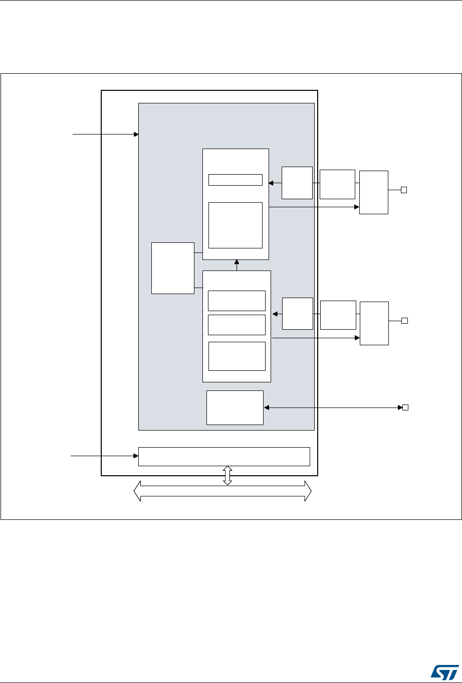
Fast-mode Plus Inter-integrated circuit (FMPI2C) interface RM0430
784/1324 RM0430 Rev 8
26.4.1 FMPI2C block diagram
The block diagram of the FMPI2C interface is shown in Figure 255.
Figure 255. FMPI2C block diagram
The FMPI2C is clocked by an independent clock source which allows to the FMPI2C to
operate independently from the PCLK frequency.
This independent clock source can be selected from the following clock sources:
•PCLK1: APB1 clock (default value)
•HSI: high speed internal oscillator
•SYSCLK: system clock
Refer to Section 6: Reset and clock control (RCC) for STM32F413/423 for more details.
06Y9
,&&/.
:DNHXS
RQ
DGGUHVV
PDWFK
60%86
3(&
JHQHUDWLRQ
FKHFN
6KLIWUHJLVWHU
'DWDFRQWURO
60%XV
7LPHRXW
FKHFN
&ORFNFRQWURO
0DVWHUFORFN
JHQHUDWLRQ
6ODYHFORFN
VWUHWFKLQJ
60%XV$OHUW
FRQWURO
VWDWXV
'LJLWDO
QRLVH
ILOWHU ,&B6&/
,&B60%$
5HJLVWHUV
$3%EXV
*3,2
ORJLF
$QDORJ
QRLVH
ILOWHU
'LJLWDO
QRLVH
ILOWHU ,&B6'$
*3,2
ORJLF
$QDORJ
QRLVH
ILOWHU
,FBSFON
,FBNHUBFN
3&/.

RM0430 Rev 8 785/1324
RM0430 Fast-mode Plus Inter-integrated circuit (FMPI2C) interface
847
26.4.2 FMPI2C clock requirements
The FMPI2C kernel is clocked by FMPI2CCLK.
The FMPI2CCLK period tI2CCLK must respect the following conditions:
tI2CCLK < (tLOW - tfilters) / 4 and tI2CCLK < tHIGH
with:
tLOW: SCL low time and tHIGH: SCL high time
tfilters: when enabled, sum of the delays brought by the analog filter and by the digital filter.
Analog filter delay is maximum 260 ns. Digital filter delay is DNF x tI2CCLK.
The PCLK clock period tPCLK must respect the following condition:
tPCLK < 4/3 tSCL
with tSCL: SCL period
Caution: When the FMPI2C kernel is clocked by PCLK, this clock must respect the conditions for
tI2CCLK.
26.4.3 Mode selection
The interface can operate in one of the four following modes:
•Slave transmitter
•Slave receiver
•Master transmitter
•Master receiver
By default, it operates in slave mode. The interface automatically switches from slave to
master when it generates a START condition, and from master to slave if an arbitration loss
or a STOP generation occurs, allowing multimaster capability.
Communication flow
In Master mode, the FMPI2C interface initiates a data transfer and generates the clock
signal. A serial data transfer always begins with a START condition and ends with a STOP
condition. Both START and STOP conditions are generated in master mode by software.
In Slave mode, the interface is capable of recognizing its own addresses (7 or 10-bit), and
the General Call address. The General Call address detection can be enabled or disabled
by software. The reserved SMBus addresses can also be enabled by software.
Data and addresses are transferred as 8-bit bytes, MSB first. The first byte(s) following the
START condition contain the address (one in 7-bit mode, two in 10-bit mode). The address
is always transmitted in Master mode.
A 9th clock pulse follows the 8 clock cycles of a byte transfer, during which the receiver must
send an acknowledge bit to the transmitter. Refer to the following figure.
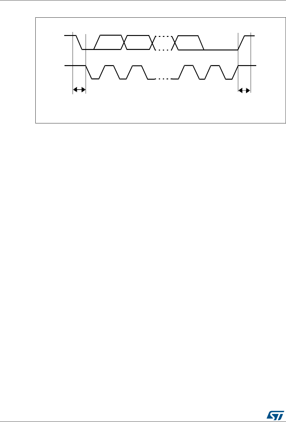
Fast-mode Plus Inter-integrated circuit (FMPI2C) interface RM0430
786/1324 RM0430 Rev 8
Figure 256. I2C bus protocol
Acknowledge can be enabled or disabled by software. The FMPI2C interface addresses can
be selected by software.
26.4.4 FMPI2C initialization
Enabling and disabling the peripheral
The FMPI2C peripheral clock must be configured and enabled in the clock controller (refer
to Section 6: Reset and clock control (RCC) for STM32F413/423).
Then the FMPI2C can be enabled by setting the PE bit in the FMPI2C_CR1 register.
When the FMPI2C is disabled (PE=0), the I2C performs a software reset. Refer to
Section 26.4.5: Software reset for more details.
Noise filters
Before enabling the FMPI2C peripheral by setting the PE bit in FMPI2C_CR1 register, the
user must configure the noise filters, if needed. By default, an analog noise filter is present
on the SDA and SCL inputs. This analog filter is compliant with the I2C specification which
requires the suppression of spikes with a pulse width up to 50 ns in Fast-mode and Fast-
mode Plus. The user can disable this analog filter by setting the ANFOFF bit, and/or select a
digital filter by configuring the DNF[3:0] bit in the FMPI2C_CR1 register.
When the digital filter is enabled, the level of the SCL or the SDA line is internally changed
only if it remains stable for more than DNF x FMPI2CCLK periods. This allows to suppress
spikes with a programmable length of 1 to 15 FMPI2CCLK periods.
Caution: Changing the filter configuration is not allowed when the FMPI2C is enabled.
069
6'$
6&/
6WDUW
FRQGLWLRQ
6WRS
FRQGLWLRQ
06% $&.
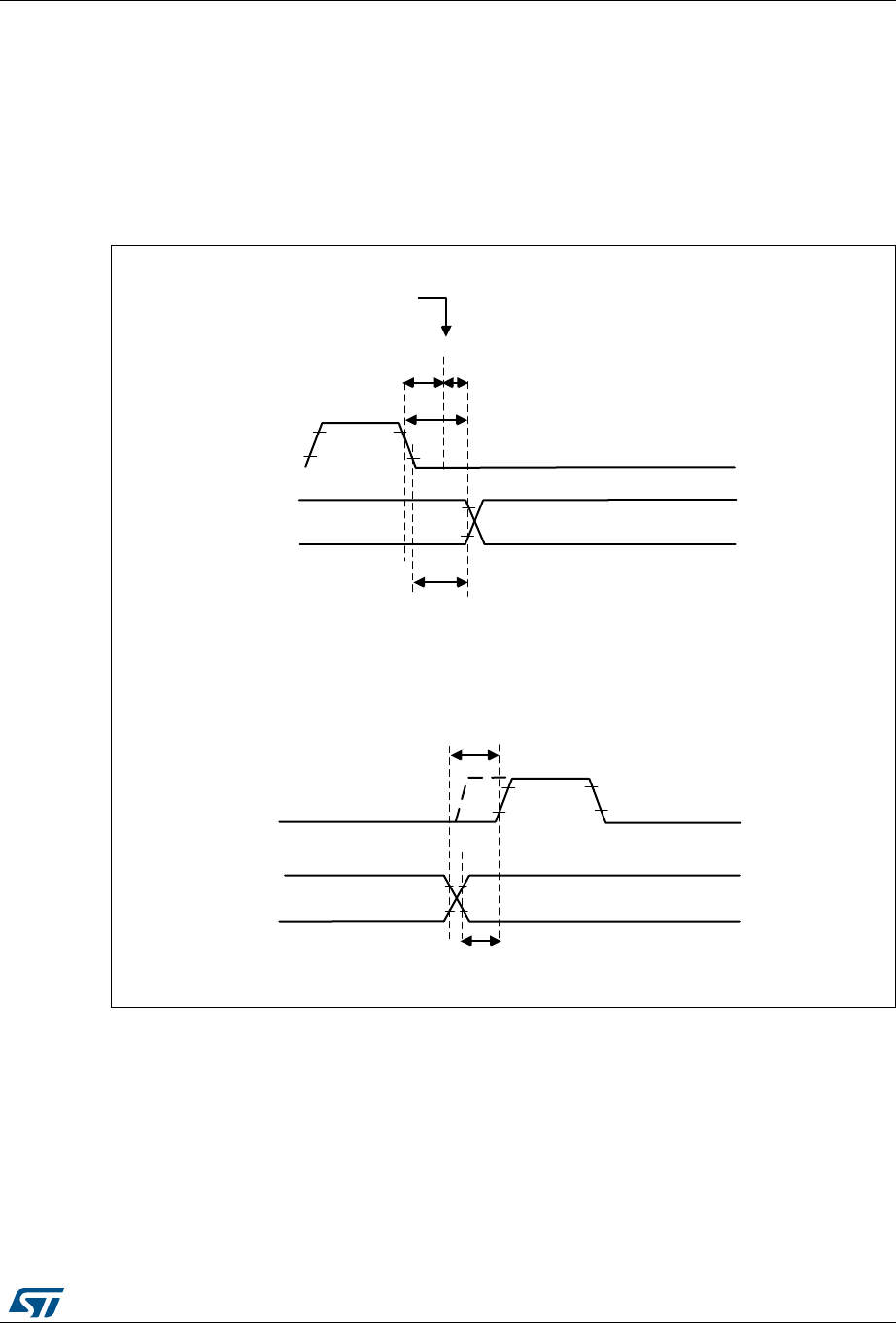
RM0430 Rev 8 787/1324
RM0430 Fast-mode Plus Inter-integrated circuit (FMPI2C) interface
847
FMPI2C timings
The timings must be configured in order to guarantee a correct data hold and setup time,
used in master and slave modes. This is done by programming the PRESC[3:0],
SCLDEL[3:0] and SDADEL[3:0] bits in the FMPI2C_TIMINGR register.
The STM32CubeMX tool calculates and provides the I2C_TIMINGR content in the I2C
configuration window
Figure 257. Setup and hold timings
06Y9
W6<1&
6&/IDOOLQJHGJHLQWHUQDO
GHWHFWLRQ
6'$'(/6&/VWUHWFKHGORZE\WKH,&
6'$RXWSXWGHOD\
6&/
6'$
d,K>d/D
W+''$7
6&/'(/
6&/VWUHWFKHGORZE\WKH,&
6&/
6'$
d^dhWd/D
W6867$
'DWDKROGWLPHLQFDVHRIWUDQVPLVVLRQWKHGDWDLVVHQWRQ6'$RXWSXWDIWHU
WKH6'$'(/GHOD\LILWLVDOUHDG\DYDLODEOHLQ,&B7;'5
'DWDVHWXSWLPHLQFDVHRIWUDQVPLVVLRQWKH6&/'(/FRXQWHUVWDUWV
ZKHQWKHGDWDLVVHQWRQ6'$RXWSXW
069
W6<1&
6&/IDOOLQJHGJHLQWHUQDO
GHWHFWLRQ
6'$'(/6&/VWUHWFKHGORZE\WKH,&
6'$RXWSXWGHOD\
6&/
6'$
d,K>d/D
W+''$7
6&/'(/
6&/VWUHWFKHGORZE\WKH,&
6&/
6'$
d^dhWd/D
W68'$7
'DWDKROGWLPHLQFDVHRIWUDQVPLVVLRQWKHGDWDLVVHQWRQ6'$RXWSXWDIWHU
WKH6'$'(/GHOD\LILWLVDOUHDG\DYDLODEOHLQ,&B7;'5
'DWDVHWXSWLPHLQFDVHRIWUDQVPLVVLRQWKH6&/'(/FRXQWHUVWDUWV
ZKHQWKHGDWDLVVHQWRQ6'$RXWSXW

Fast-mode Plus Inter-integrated circuit (FMPI2C) interface RM0430
788/1324 RM0430 Rev 8
•When the SCL falling edge is internally detected, a delay is inserted before sending
SDA output. This delay is tSDADEL = SDADEL x tPRESC + tI2CCLK where tPRESC = (PRESC+1)
x tI2CCLK.
TSDADEL impacts the hold time tHD;DAT.
The total SDA output delay is:
tSYNC1 + {[SDADEL x (PRESC+1) + 1] x tI2CCLK }
tSYNC1 duration depends on these parameters:
– SCL falling slope
– When enabled, input delay brought by the analog filter: tAF(min) < tAF < tAF(max) ns.
– When enabled, input delay brought by the digital filter: tDNF = DNF x tI2CCLK
– Delay due to SCL synchronization to FMPI2CCLK clock (2 to 3 FMPI2CCLK
periods)
In order to bridge the undefined region of the SCL falling edge, the user must program
SDADEL in such a way that:
{tf (max) +tHD;DAT (min) -tAF(min) - [(DNF +3) x tI2CCLK]} / {(PRESC +1) x tI2CCLK } ≤ SDADEL
SDADEL ≤ {tHD;DAT (max) -tAF(max) - [(DNF+4) x tI2CCLK]} / {(PRESC +1) x tI2CCLK }
Note: tAF(min) / tAF(max) are part of the equation only when the analog filter is enabled. Refer to
device datasheet for tAF values.
The maximum tHD;DAT could be 3.45 µs, 0.9 µs and 0.45 µs for Standard-mode, Fast-mode
and Fast-mode Plus, but must be less than the maximum of tVD;DAT by a transition time.
This maximum must only be met if the device does not stretch the LOW period (tLOW) of the
SCL signal. If the clock stretches the SCL, the data must be valid by the set-up time before
it releases the clock.
The SDA rising edge is usually the worst case, so in this case the previous equation
becomes:
SDADEL ≤ {tVD;DAT (max) -tr (max) -260 ns - [(DNF+4) x tI2CCLK]} / {(PRESC +1) x tI2CCLK }.
Note: This condition can be violated when NOSTRETCH=0, because the device stretches SCL
low to guarantee the set-up time, according to the SCLDEL value.
Refer to Table 140: I2C-SMBUS specification data setup and hold times for tf, tr, tHD;DAT and
tVD;DAT standard values.
•After tSDADEL delay, or after sending SDA output in case the slave had to stretch the
clock because the data was not yet written in I2C_TXDR register, SCL line is kept at
low level during the setup time. This setup time is tSCLDEL = (SCLDEL+1) x tPRESC where
tPRESC = (PRESC+1) x tI2CCLK.
tSCLDEL impacts the setup time tSU;DAT .
In order to bridge the undefined region of the SDA transition (rising edge usually worst
case), the user must program SCLDEL in such a way that:
{[tr (max) + tSU;DAT (min)] / [(PRESC+1)] x tI2CCLK]} - 1 <= SCLDEL
Refer to Table 140: I2C-SMBUS specification data setup and hold times for tr and tSU;DAT
standard values.

RM0430 Rev 8 789/1324
RM0430 Fast-mode Plus Inter-integrated circuit (FMPI2C) interface
847
The SDA and SCL transition time values to be used are the ones in the application. Using
the maximum values from the standard increases the constraints for the SDADEL and
SCLDEL calculation, but ensures the feature whatever the application.
Note: At every clock pulse, after SCL falling edge detection, the I2C master or slave stretches SCL
low during at least [(SDADEL+SCLDEL+1) x (PRESC+1) + 1] x tI2CCLK, in both transmission
and reception modes. In transmission mode, in case the data is not yet written in I2C_TXDR
when SDADEL counter is finished, the I2C keeps on stretching SCL low until the next data
is written. Then new data MSB is sent on SDA output, and SCLDEL counter starts,
continuing stretching SCL low to guarantee the data setup time.
If NOSTRETCH=1 in slave mode, the SCL is not stretched. Consequently the SDADEL
must be programmed in such a way to guarantee also a sufficient setup time.
Additionally, in master mode, the SCL clock high and low levels must be configured by
programming the PRESC[3:0], SCLH[7:0] and SCLL[7:0] bits in the FMPI2C_TIMINGR
register.
•When the SCL falling edge is internally detected, a delay is inserted before releasing
the SCL output. This delay is tSCLL = (SCLL+1) x tPRESC where tPRESC = (PRESC+1) x
tI2CCLK.
tSCLL impacts the SCL low time tLOW .
•When the SCL rising edge is internally detected, a delay is inserted before forcing the
SCL output to low level. This delay is tSCLH = (SCLH+1) x tPRESC where tPRESC =
(PRESC+1) x tI2CCLK. tSCLH impacts the SCL high time tHIGH .
Refer to FMPI2C master initialization for more details.
Caution: Changing the timing configuration is not allowed when the FMPI2C is enabled.
The FMPI2C slave NOSTRETCH mode must also be configured before enabling the
peripheral. Refer to FMPI2C slave initialization for more details.
Caution: Changing the NOSTRETCH configuration is not allowed when the FMPI2C is enabled.
Table 140. I2C-SMBUS specification data setup and hold times
Symbol Parameter
Standard-mode
(Sm)
Fast-mode
(Fm)
Fast-mode Plus
(Fm+) SMBUS
Unit
Min. Max Min. Max Min. Max Min. Max
tHD;DAT Data hold time 0-0-0 -0.3-
µs
tVD;DAT Data valid time - 3.45 - 0.9 - 0.45 - -
tSU;DAT Data setup time 250 - 100 - 50 - 250 -
ns
tr
Rise time of both SDA
and SCL signals - 1000 - 300 - 120 - 1000
tf
Fall time of both SDA
and SCL signals - 300 - 300 - 120 - 300
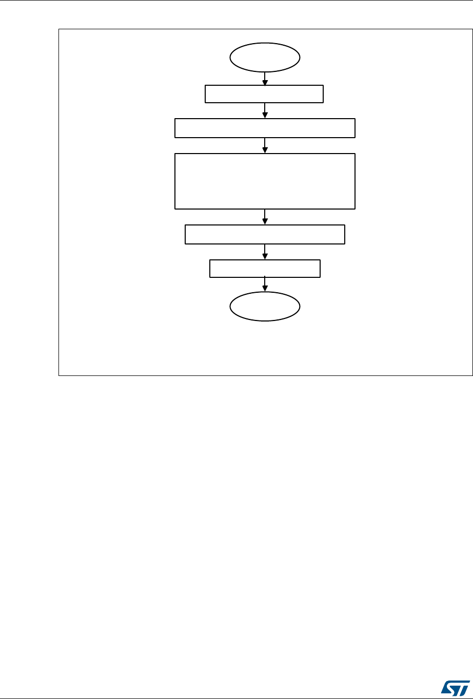
Fast-mode Plus Inter-integrated circuit (FMPI2C) interface RM0430
790/1324 RM0430 Rev 8
Figure 258. FMPI2C initialization flowchart
26.4.5 Software reset
A software reset can be performed by clearing the PE bit in the FMPI2C_CR1 register. In
that case FMPI2C lines SCL and SDA are released. Internal states machines are reset and
communication control bits, as well as status bits come back to their reset value. The
configuration registers are not impacted.
Here is the list of impacted register bits:
1. FMPI2C_CR2 register: START, STOP, NACK
2. FMPI2C_ISR register: BUSY, TXE, TXIS, RXNE, ADDR, NACKF, TCR, TC, STOPF,
BERR, ARLO, OVR
and in addition when the SMBus feature is supported:
1. FMPI2C_CR2 register: PECBYTE
2. FMPI2C_ISR register: PECERR, TIMEOUT, ALERT
PE must be kept low during at least 3 APB clock cycles in order to perform the software
reset. This is ensured by writing the following software sequence: - Write PE=0 - Check
PE=0 - Write PE=1.
D^ǀϯϱϵϲϮsϭ
&OHDU3(ELWLQ)03,&B&5
,QLWLDOVHWWLQJV
&RQILJXUH$1)2))DQG'1)>@LQ
)03,&B&5
&RQILJXUH35(6&>@
6'$'(/>@6&/'(/>@6&/+>@
6&//>@LQ)03,&B7,0,1*5
&RQILJXUH12675(7&+LQ)03,&B&5
6HW3(ELWLQ)03,&B&5
(QG
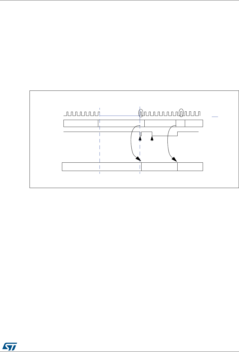
RM0430 Rev 8 791/1324
RM0430 Fast-mode Plus Inter-integrated circuit (FMPI2C) interface
847
26.4.6 Data transfer
The data transfer is managed through transmit and receive data registers and a shift
register.
Reception
The SDA input fills the shift register. After the 8th SCL pulse (when the complete data byte is
received), the shift register is copied into FMPI2C_RXDR register if it is empty (RXNE=0). If
RXNE=1, meaning that the previous received data byte has not yet been read, the SCL line
is stretched low until FMPI2C_RXDR is read. The stretch is inserted between the 8th and
9th SCL pulse (before the Acknowledge pulse).
Figure 259. Data reception
dždž
^ŚŝĨƚƌĞŐŝƐƚĞƌ ĚĂƚĂϭ
ĚĂƚĂϭ
dždž ĚĂƚĂϮ
ZyE
<ƉƵůƐĞ
ĚĂƚĂϬ ĚĂƚĂϮ
<ƉƵůƐĞ
dždž
&DW/ϮͺZyZ
ƌĚĚĂƚĂϭƌĚĚĂƚĂϬ
^>
ůĞŐĞŶĚ͗
^>
ƐƚƌĞƚĐŚ
D^ǀϯϱϵϳϲsϭ
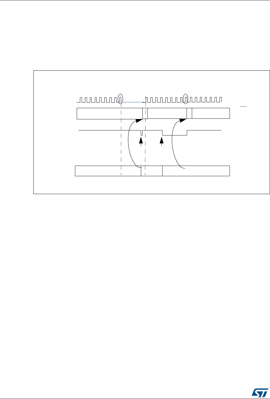
Fast-mode Plus Inter-integrated circuit (FMPI2C) interface RM0430
792/1324 RM0430 Rev 8
Transmission
If the FMPI2C_TXDR register is not empty (TXE=0), its content is copied into the shift
register after the 9th SCL pulse (the Acknowledge pulse). Then the shift register content is
shifted out on SDA line. If TXE=1, meaning that no data is written yet in FMPI2C_TXDR,
SCL line is stretched low until FMPI2C_TXDR is written. The stretch is done after the 9th
SCL pulse.
Figure 260. Data transmission
Hardware transfer management
The FMPI2C has a byte counter embedded in hardware in order to manage byte transfer
and to close the communication in various modes such as:
– NACK, STOP and ReSTART generation in master mode
– ACK control in slave receiver mode
– PEC generation/checking when SMBus feature is supported
The byte counter is always used in master mode. By default it is disabled in slave mode, but
it can be enabled by software by setting the SBC (Slave Byte Control) bit in the
FMPI2C_CR2 register.
The number of bytes to be transferred is programmed in the NBYTES[7:0] bit field in the
FMPI2C_CR2 register. If the number of bytes to be transferred (NBYTES) is greater than
255, or if a receiver wants to control the acknowledge value of a received data byte, the
reload mode must be selected by setting the RELOAD bit in the FMPI2C_CR2 register. In
this mode, TCR flag is set when the number of bytes programmed in NBYTES has been
transferred, and an interrupt is generated if TCIE is set. SCL is stretched as long as TCR
flag is set. TCR is cleared by software when NBYTES is written to a non-zero value.
When the NBYTES counter is reloaded with the last number of bytes, RELOAD bit must be
cleared.
D^ǀϯϱϵϳϳsϭ
dždž
^ŚŝĨƚƌĞŐŝƐƚĞƌ
ĚĂƚĂϭ
ĚĂƚĂϭ
dždž
ĚĂƚĂϮ
dy
<ƉƵůƐĞ
ĚĂƚĂϬ ĚĂƚĂϮ
<ƉƵůƐĞ
dždž
&DW/ϮͺdyZ
ǁƌĚĂƚĂϭ ǁƌĚĂƚĂϮ
^> ůĞŐĞŶĚ͗
^>
ƐƚƌĞƚĐŚ

RM0430 Rev 8 793/1324
RM0430 Fast-mode Plus Inter-integrated circuit (FMPI2C) interface
847
When RELOAD=0 in master mode, the counter can be used in 2 modes:
•Automatic end mode (AUTOEND = ‘1’ in the FMPI2C_CR2 register). In this mode, the
master automatically sends a STOP condition once the number of bytes programmed
in the NBYTES[7:0] bit field has been transferred.
•Software end mode (AUTOEND = ‘0’ in the FMPI2C_CR2 register). In this mode,
software action is expected once the number of bytes programmed in the NBYTES[7:0]
bit field has been transferred; the TC flag is set and an interrupt is generated if the
TCIE bit is set. The SCL signal is stretched as long as the TC flag is set. The TC flag is
cleared by software when the START or STOP bit is set in the FMPI2C_CR2 register.
This mode must be used when the master wants to send a RESTART condition.
Caution: The AUTOEND bit has no effect when the RELOAD bit is set.
26.4.7 FMPI2C slave mode
FMPI2C slave initialization
In order to work in slave mode, the user must enable at least one slave address. Two
registers FMPI2C_OAR1 and FMPI2C_OAR2 are available in order to program the slave
own addresses OA1 and OA2.
•OA1 can be configured either in 7-bit mode (by default) or in 10-bit addressing mode by
setting the OA1MODE bit in the FMPI2C_OAR1 register.
OA1 is enabled by setting the OA1EN bit in the FMPI2C_OAR1 register.
•If additional slave addresses are required, the 2nd slave address OA2 can be
configured. Up to 7 OA2 LSB can be masked by configuring the OA2MSK[2:0] bits in
the FMPI2C_OAR2 register. Therefore for OA2MSK configured from 1 to 6, only
OA2[7:2], OA2[7:3], OA2[7:4], OA2[7:5], OA2[7:6] or OA2[7] are compared with the
received address. As soon as OA2MSK is not equal to 0, the address comparator for
OA2 excludes the FMPI2C reserved addresses (0000 XXX and 1111 XXX), which are
not acknowledged. If OA2MSK=7, all received 7-bit addresses are acknowledged
(except reserved addresses). OA2 is always a 7-bit address.
These reserved addresses can be acknowledged if they are enabled by the specific
enable bit, if they are programmed in the FMPI2C_OAR1 or FMPI2C_OAR2 register
with OA2MSK=0.
OA2 is enabled by setting the OA2EN bit in the FMPI2C_OAR2 register.
•The General Call address is enabled by setting the GCEN bit in the FMPI2C_CR1
register.
When the FMPI2C is selected by one of its enabled addresses, the ADDR interrupt status
flag is set, and an interrupt is generated if the ADDRIE bit is set.
Table 141. FMPI2C configuration
Function SBC bit RELOAD bit AUTOEND bit
Master Tx/Rx NBYTES + STOP x 0 1
Master Tx/Rx + NBYTES + RESTART x 0 0
Slave Tx/Rx
all received bytes ACKed 0xx
Slave Rx with ACK control 1 1 x

Fast-mode Plus Inter-integrated circuit (FMPI2C) interface RM0430
794/1324 RM0430 Rev 8
By default, the slave uses its clock stretching capability, which means that it stretches the
SCL signal at low level when needed, in order to perform software actions. If the master
does not support clock stretching, the FMPI2C must be configured with NOSTRETCH=1 in
the FMPI2C_CR1 register.
After receiving an ADDR interrupt, if several addresses are enabled the user must read the
ADDCODE[6:0] bits in the FMPI2C_ISR register in order to check which address matched.
DIR flag must also be checked in order to know the transfer direction.
Slave clock stretching (NOSTRETCH = 0)
In default mode, the FMPI2C slave stretches the SCL clock in the following situations:
•When the ADDR flag is set: the received address matches with one of the enabled
slave addresses. This stretch is released when the ADDR flag is cleared by software
setting the ADDRCF bit.
•In transmission, if the previous data transmission is completed and no new data is
written in FMPI2C_TXDR register, or if the first data byte is not written when the ADDR
flag is cleared (TXE=1). This stretch is released when the data is written to the
FMPI2C_TXDR register.
•In reception when the FMPI2C_RXDR register is not read yet and a new data reception
is completed. This stretch is released when FMPI2C_RXDR is read.
•When TCR = 1 in Slave Byte Control mode, reload mode (SBC=1 and RELOAD=1),
meaning that the last data byte has been transferred. This stretch is released when
then TCR is cleared by writing a non-zero value in the NBYTES[7:0] field.
•After SCL falling edge detection, the FMPI2C stretches SCL low during
[(SDADEL+SCLDEL+1) x (PRESC+1) + 1] x tI2CCLK.
Slave without clock stretching (NOSTRETCH = 1)
When NOSTRETCH = 1 in the FMPI2C_CR1 register, the FMPI2C slave does not stretch
the SCL signal.
•The SCL clock is not stretched while the ADDR flag is set.
•In transmission, the data must be written in the FMPI2C_TXDR register before the first
SCL pulse corresponding to its transfer occurs. If not, an underrun occurs, the OVR
flag is set in the FMPI2C_ISR register and an interrupt is generated if the ERRIE bit is
set in the FMPI2C_CR1 register. The OVR flag is also set when the first data
transmission starts and the STOPF bit is still set (has not been cleared). Therefore, if
the user clears the STOPF flag of the previous transfer only after writing the first data to
be transmitted in the next transfer, he ensures that the OVR status is provided, even for
the first data to be transmitted.
•In reception, the data must be read from the FMPI2C_RXDR register before the 9th
SCL pulse (ACK pulse) of the next data byte occurs. If not an overrun occurs, the OVR
flag is set in the FMPI2C_ISR register and an interrupt is generated if the ERRIE bit is
set in the FMPI2C_CR1 register.
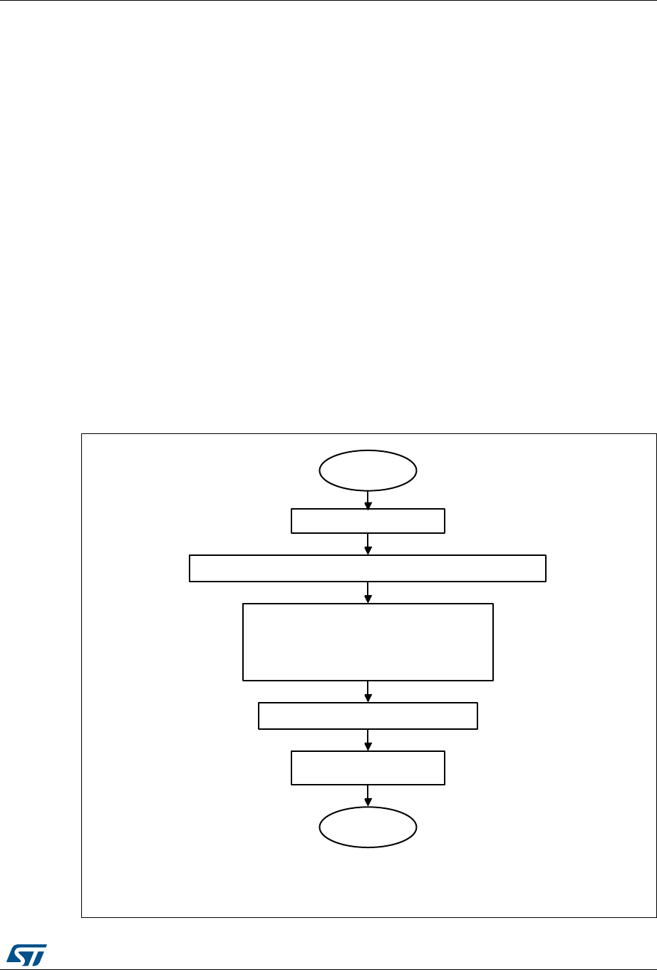
RM0430 Rev 8 795/1324
RM0430 Fast-mode Plus Inter-integrated circuit (FMPI2C) interface
847
Slave Byte Control mode
In order to allow byte ACK control in slave reception mode, Slave Byte Control mode must
be enabled by setting the SBC bit in the FMPI2C_CR1 register. This is required to be
compliant with SMBus standards.
Reload mode must be selected in order to allow byte ACK control in slave reception mode
(RELOAD=1). To get control of each byte, NBYTES must be initialized to 0x1 in the ADDR
interrupt subroutine, and reloaded to 0x1 after each received byte. When the byte is
received, the TCR bit is set, stretching the SCL signal low between the 8th and 9th SCL
pulses. The user can read the data from the FMPI2C_RXDR register, and then decide to
acknowledge it or not by configuring the ACK bit in the FMPI2C_CR2 register. The SCL
stretch is released by programming NBYTES to a non-zero value: the acknowledge or not-
acknowledge is sent and next byte can be received.
NBYTES can be loaded with a value greater than 0x1, and in this case, the reception flow is
continuous during NBYTES data reception.
Note: The SBC bit must be configured when the FMPI2C is disabled, or when the slave is not
addressed, or when ADDR=1.
The RELOAD bit value can be changed when ADDR=1, or when TCR=1.
Caution: Slave Byte Control mode is not compatible with NOSTRETCH mode. Setting SBC when
NOSTRETCH=1 is not allowed.
Figure 261. Slave initialization flowchart
D^ǀϯϱϵϲϯsϭ
,QLWLDOVHWWLQJV
6ODYH
LQLWLDOL]DWLRQ
&OHDU^2$(12$(1`LQ)03,&B2$5DQG)03,&B2$5
&RQILJXUH^2$>@2$02'(2$(1
2$>@2$06.>@2$(1*&(1`
&RQILJXUH6%&LQ)03,&B&5
(QDEOHLQWHUUXSWVDQGRU
'0$LQ)03,&B&5
(QG
6%&PXVWEHVHWWRVXSSRUW60%XVIHDWXUHV

Fast-mode Plus Inter-integrated circuit (FMPI2C) interface RM0430
796/1324 RM0430 Rev 8
Slave transmitter
A transmit interrupt status (TXIS) is generated when the FMPI2C_TXDR register becomes
empty. An interrupt is generated if the TXIE bit is set in the FMPI2C_CR1 register.
The TXIS bit is cleared when the FMPI2C_TXDR register is written with the next data byte
to be transmitted.
When a NACK is received, the NACKF bit is set in the FMPI2C_ISR register and an
interrupt is generated if the NACKIE bit is set in the FMPI2C_CR1 register. The slave
automatically releases the SCL and SDA lines in order to let the master perform a STOP or
a RESTART condition. The TXIS bit is not set when a NACK is received.
When a STOP is received and the STOPIE bit is set in the FMPI2C_CR1 register, the
STOPF flag is set in the FMPI2C_ISR register and an interrupt is generated. In most
applications, the SBC bit is usually programmed to ‘0’. In this case, If TXE = 0 when the
slave address is received (ADDR=1), the user can choose either to send the content of the
FMPI2C_TXDR register as the first data byte, or to flush the FMPI2C_TXDR register by
setting the TXE bit in order to program a new data byte.
In Slave Byte Control mode (SBC=1), the number of bytes to be transmitted must be
programmed in NBYTES in the address match interrupt subroutine (ADDR=1). In this case,
the number of TXIS events during the transfer corresponds to the value programmed in
NBYTES.
Caution: When NOSTRETCH=1, the SCL clock is not stretched while the ADDR flag is set, so the
user cannot flush the FMPI2C_TXDR register content in the ADDR subroutine, in order to
program the first data byte. The first data byte to be sent must be previously programmed in
the FMPI2C_TXDR register:
•This data can be the data written in the last TXIS event of the previous transmission
message.
•If this data byte is not the one to be sent, the FMPI2C_TXDR register can be flushed by
setting the TXE bit in order to program a new data byte. The STOPF bit must be
cleared only after these actions, in order to guarantee that they are executed before the
first data transmission starts, following the address acknowledge.
If STOPF is still set when the first data transmission starts, an underrun error will be
generated (the OVR flag is set).
If a TXIS event is needed, (Transmit Interrupt or Transmit DMA request), the user must
set the TXIS bit in addition to the TXE bit, in order to generate a TXIS event.
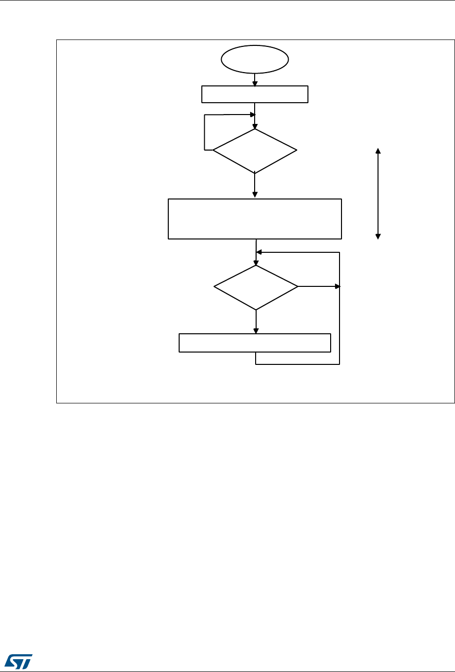
RM0430 Rev 8 797/1324
RM0430 Fast-mode Plus Inter-integrated circuit (FMPI2C) interface
847
Figure 262. Transfer sequence flowchart for FMPI2C slave transmitter,
NOSTRETCH=0
D^ǀϯϱϵϲϰsϭ
6ODYHLQLWLDOL]DWLRQ
6ODYH
WUDQVPLVVLRQ
5HDG$''&2'(DQG',5LQ)03,&B,65
2SWLRQDO6HW)03,&B,657;(
6HW)03,&B,&5$''5&)
:ULWH)03,&B7;'57;'$7$
)03,&B,65$''5
"
1R
<HV
)03,&B,657;,6
"
<HV
1R
6&/
VWUHWFKHG
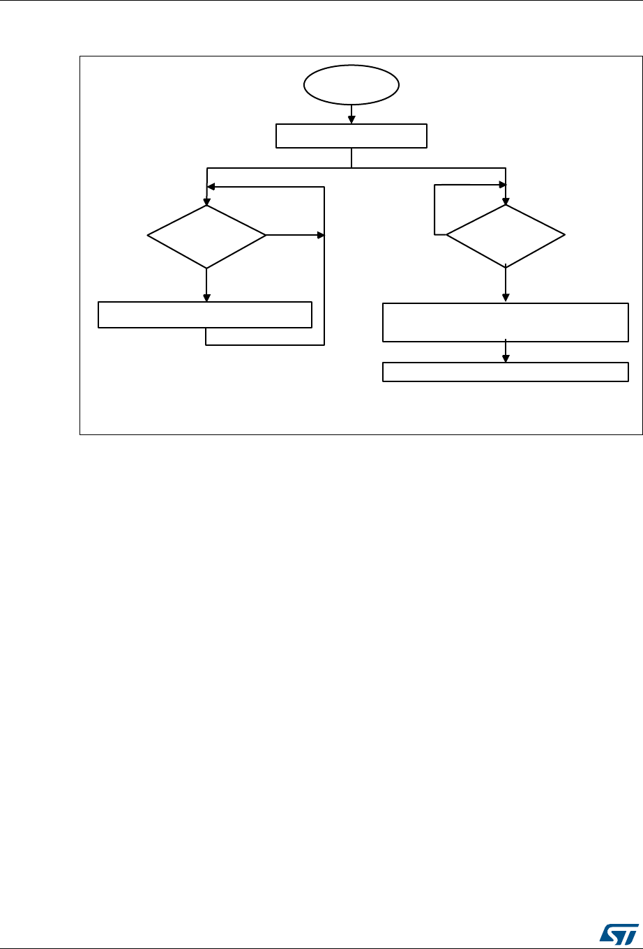
Fast-mode Plus Inter-integrated circuit (FMPI2C) interface RM0430
798/1324 RM0430 Rev 8
Figure 263. Transfer sequence flowchart for FMPI2C slave transmitter,
NOSTRETCH=1
D^ǀϯϱϵϲϱsϭ
6ODYHLQLWLDOL]DWLRQ
6ODYH
WUDQVPLVVLRQ
2SWLRQDO6HW)03,&B,657;(
DQG)03,&B,657;,6
:ULWH)03,&B7;'57;'$7$
)03,&B,656723)
"
1R
<HV
)03,&B,657;,6
"
<HV
1R
6HW)03,&B,&56723&)
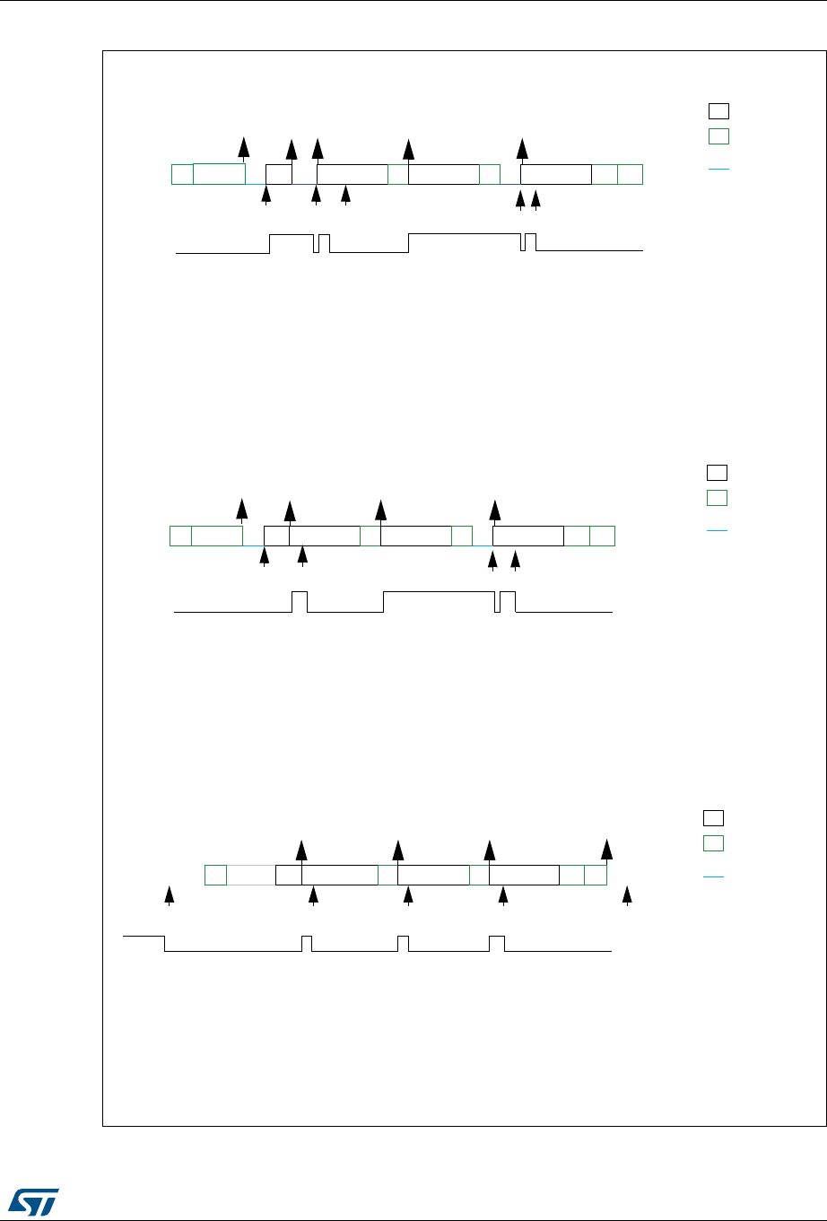
RM0430 Rev 8 799/1324
RM0430 Fast-mode Plus Inter-integrated circuit (FMPI2C) interface
847
Figure 264. Transfer bus diagrams for FMPI2C slave transmitter
069
([DPSOH)03,&VODYHWUDQVPLWWHUE\WHVZLWKVWGDWDIOXVKHG
12675(7&+
(9$''5,65FKHFN$''&2'(DQG',5VHW7;(VHW$''5&)
(97;,6,65ZUGDWD
(97;,6,65ZUGDWD
(97;,6,65ZUGDWD
(97;,6,65ZUGDWDQRWVHQW
$''5
$
7;,6
$
7;,6
1$
7;,6
7;(
3
OHJHQG
WUDQVPLVVLRQ
UHFHSWLRQ
6&/VWUHWFK
(9 (9 (9 (9
([DPSOH)03,&VODYHWUDQVPLWWHUE\WHV12675(7&+
(9ZUGDWD
(97;,6,65ZUGDWD
(97;,6,65ZUGDWD
(97;,6,65ZUGDWDQRWVHQW
(96723),65RSWLRQDOVHW7;(DQG7;,6VHW6723&)
$
7;,6 7;,6
7;(
OHJHQG
WUDQVPLVVLRQ
UHFHSWLRQ
6&/VWUHWFK
(9 (9 (9
7;,6
(9
6723)
(9
([DPSOH)03,&VODYHWUDQVPLWWHUE\WHVZLWKRXWVWGDWDIOXVK
12675(7&+
(9$''5,65FKHFN$''&2'(DQG',5VHW$''5&)
(97;,6,65ZUGDWD
(97;,6,65ZUGDWD
(97;,6,65ZUGDWDQRWVHQW
$''5 7;,6 7;,6 7;,6
7;(
OHJHQG
WUDQVPLVVLRQ
UHFHSWLRQ
6&/VWUHWFK
(9 (9 (9 (9
7;,6
(9
6 $GGUHVV GDWD $ GDWD GDWD$1$3
6 $GGUHVV $ GDWD $ GDWD $ GDWD 1$ 3
6$GGUHVV $ GDWD
GDWD
GDWD
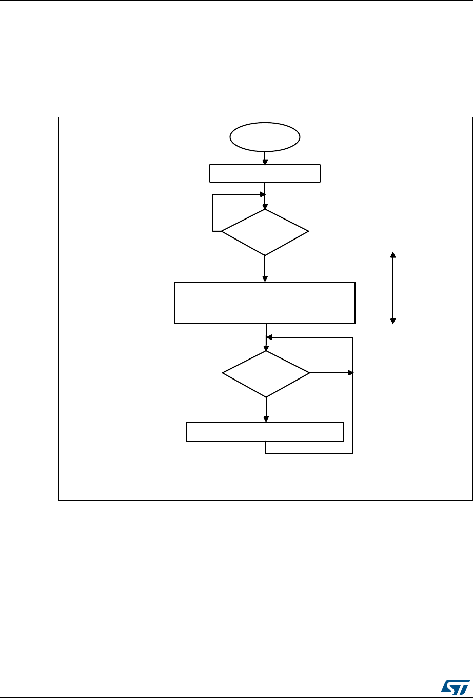
Fast-mode Plus Inter-integrated circuit (FMPI2C) interface RM0430
800/1324 RM0430 Rev 8
Slave receiver
RXNE is set in FMPI2C_ISR when the FMPI2C_RXDR is full, and generates an interrupt if
RXIE is set in FMPI2C_CR1. RXNE is cleared when FMPI2C_RXDR is read.
When a STOP is received and STOPIE is set in FMPI2C_CR1, STOPF is set in
FMPI2C_ISR and an interrupt is generated.
Figure 265. Transfer sequence flowchart for slave receiver with NOSTRETCH=0
D^ǀϯϱϵϲϲsϭ
6ODYHLQLWLDOL]DWLRQ
6ODYHUHFHSWLRQ
5HDG$''&2'(DQG',5LQ)03,&B,65
6HW)03,&B,&5$''5&)
:ULWH)03,&B5;'55;'$7$
)03,&B,65$''5
"
1R
<HV
)03,&B,655;1(
"
<HV
1R
6&/
VWUHWFKHG
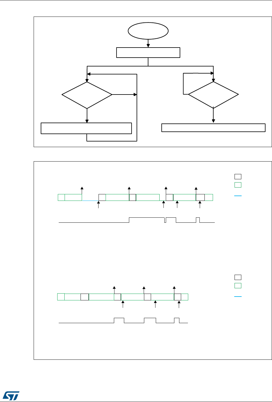
RM0430 Rev 8 801/1324
RM0430 Fast-mode Plus Inter-integrated circuit (FMPI2C) interface
847
Figure 266. Transfer sequence flowchart for slave receiver with NOSTRETCH=1
Figure 267. Transfer bus diagrams for FMPI2C slave receiver
D^ǀϯϱϵϲϳsϭ
6ODYHLQLWLDOL]DWLRQ
6ODYHUHFHSWLRQ
5HDG)03,&B5;'55;'$7$
)03,&B,656723)
"
1R
<HV
)03,&B,655;1(
"
<HV
1R
6HW)03,&B,&56723&)
069
(9$''5,65FKHFN$''&2'(DQG',5VHW$''5&)
(95;1(,65UGGDWD
(95;1(,65UGGDWD
(95;1(,65UGGDWD
$
$''5
$$
5;1(
$
5;1(
5;1(
OHJHQG
WUDQVPLVVLRQ
UHFHSWLRQ
6&/VWUHWFK
(9 (9 (9
(95;1(,65UGGDWD
(95;1(,65UGGDWD
(95;1(,65UGGDWD
(96723),65VHW6723&)
$
$$ $
5;1(
OHJHQG
WUDQVPLVVLRQ
UHFHSWLRQ
6&/VWUHWFK
5;1(
(9
([DPSOH)03,&VODYHUHFHLYHUE\WHV12675(7&+
4$GGUHVV GDWD GDWD GDWD 1
([DPSOH)03,&VODYHUHFHLYHUE\WHV12675(7&+
4$GGUHVV GDWD GDWD GDWD
(9
(9
(9
5;1( 5;1( 5;1(

Fast-mode Plus Inter-integrated circuit (FMPI2C) interface RM0430
802/1324 RM0430 Rev 8
26.4.8 FMPI2C master mode
FMPI2C master initialization
Before enabling the peripheral, the FMPI2C master clock must be configured by setting the
SCLH and SCLL bits in the FMPI2C_TIMINGR register.
The STM32CubeMX tool calculates and provides the I2C_TIMINGR content in the I2C
Configuration window.
A clock synchronization mechanism is implemented in order to support multi-master
environment and slave clock stretching.
In order to allow clock synchronization:
•The low level of the clock is counted using the SCLL counter, starting from the SCL low
level internal detection.
•The high level of the clock is counted using the SCLH counter, starting from the SCL
high level internal detection.
The FMPI2C detects its own SCL low level after a tSYNC1 delay depending on the SCL falling
edge, SCL input noise filters (analog + digital) and SCL synchronization to the I2CxCLK
clock. The FMPI2C releases SCL to high level once the SCLL counter reaches the value
programmed in the SCLL[7:0] bits in the FMPI2C_TIMINGR register.
The FMPI2C detects its own SCL high level after a tSYNC2 delay depending on the SCL rising
edge, SCL input noise filters (analog + digital) and SCL synchronization to I2CxCLK clock.
The FMPI2C ties SCL to low level once the SCLH counter is reached reaches the value
programmed in the SCLH[7:0] bits in the FMPI2C_TIMINGR register.
Consequently the master clock period is:
tSCL = tSYNC1 + tSYNC2 + {[(SCLH+1) + (SCLL+1)] x (PRESC+1) x tI2CCLK}
The duration of tSYNC1 depends on these parameters:
– SCL falling slope
– When enabled, input delay induced by the analog filter.
– When enabled, input delay induced by the digital filter: DNF x tI2CCLK
– Delay due to SCL synchronization with FMPI2CCLK clock (2 to 3 FMPI2CCLK
periods)
The duration of tSYNC2 depends on these parameters:
– SCL rising slope
– When enabled, input delay induced by the analog filter.
– When enabled, input delay induced by the digital filter: DNF x tI2CCLK
– Delay due to SCL synchronization with FMPI2CCLK clock (2 to 3 FMPI2CCLK
periods)
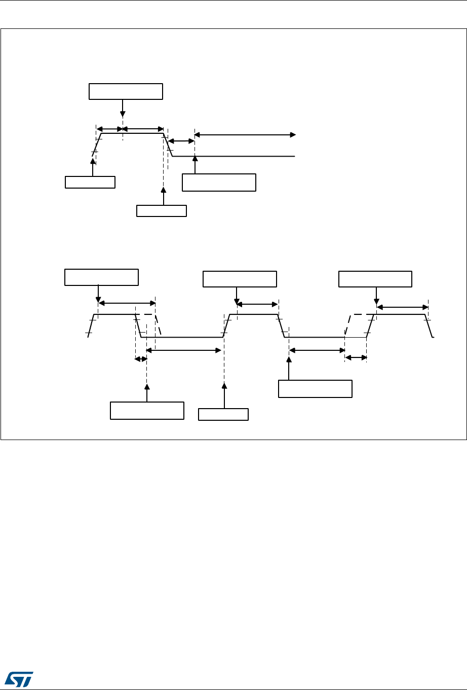
RM0430 Rev 8 803/1324
RM0430 Fast-mode Plus Inter-integrated circuit (FMPI2C) interface
847
Figure 268. Master clock generation
Caution: In order to be I2C or SMBus compliant, the master clock must respect the timings given
below:
069
W6<1&
6&/KLJKOHYHOGHWHFWHG
6&/+FRXQWHUVWDUWV
6&/+
6&/
6&/PDVWHUFORFNJHQHUDWLRQ
6&/UHOHDVHG 6&/ORZOHYHOGHWHFWHG
6&//FRXQWHUVWDUWV
6&/GULYHQORZ
6&//
W6<1&
6&/PDVWHUFORFNV\QFKURQL]DWLRQ
6&//
6&/GULYHQORZE\
DQRWKHUGHYLFH
6&/ORZOHYHOGHWHFWHG
6&//FRXQWHUVWDUWV 6&/UHOHDVHG
6&/+
6&/+
6&/KLJKOHYHOGHWHFWHG
6&/+FRXQWHUVWDUWV 6&/KLJKOHYHOGHWHFWHG
6&/+FRXQWHUVWDUWV
6&/ORZOHYHOGHWHFWHG
6&//FRXQWHUVWDUWV
6&//
6&/GULYHQORZE\
DQRWKHUGHYLFH
6&/+
6&/KLJKOHYHOGHWHFWHG
6&/+FRXQWHUVWDUWV
Fast-mode Plus Inter-integrated circuit (FMPI2C) interface RM0430
804/1324 RM0430 Rev 8
Note: SCLL is also used to generate the tBUF and tSU:STA timings.
SCLH is also used to generate the tHD:STA and tSU:STO timings.
Refer to Section 26.4.9: FMPI2C_TIMINGR register configuration examples for examples of
FMPI2C_TIMINGR settings vs. FMPI2CCLK frequency.
Master communication initialization (address phase)
In order to initiate the communication, the user must program the following parameters for
the addressed slave in the FMPI2C_CR2 register:
•Addressing mode (7-bit or 10-bit): ADD10
•Slave address to be sent: SADD[9:0]
•Transfer direction: RD_WRN
•In case of 10-bit address read: HEAD10R bit. HEAD10R must be configure to indicate
if the complete address sequence must be sent, or only the header in case of a
direction change.
•The number of bytes to be transferred: NBYTES[7:0]. If the number of bytes is equal to
or greater than 255 bytes, NBYTES[7:0] must initially be filled with 0xFF.
The user must then set the START bit in FMPI2C_CR2 register. Changing all the above bits
is not allowed when START bit is set.
Then the master automatically sends the START condition followed by the slave address as
soon as it detects that the bus is free (BUSY = 0) and after a delay of tBUF
.
In case of an arbitration loss, the master automatically switches back to slave mode and can
acknowledge its own address if it is addressed as a slave.
Note: The START bit is reset by hardware when the slave address has been sent on the bus,
whatever the received acknowledge value. The START bit is also reset by hardware if an
arbitration loss occurs.
In 10-bit addressing mode, when the Slave Address first 7 bits is NACKed by the slave, the
Table 142. I2C-SMBUS specification clock timings
Symbol Parameter
Standard-
mode (Sm)
Fast-mode
(Fm)
Fast-mode
Plus (Fm+) SMBUS
Unit
Min Max Min Max Min Max Min Max
fSCL SCL clock frequency - 100 - 400 - 1000 - 100 kHz
tHD:STA Hold time (repeated) START condition 4.0 - 0.6 - 0.26 - 4.0 - µs
tSU:STA
Set-up time for a repeated START
condition 4.7 - 0.6 - 0.26 - 4.7 - µs
tSU:STO Set-up time for STOP condition 4.0 - 0.6 - 0.26 - 4.0 - µs
tBUF
Bus free time between a STOP and
START condition 4.7 - 1.3 - 0.5 - 4.7 - µs
tLOW Low period of the SCL clock 4.7 - 1.3 - 0.5 - 4.7 - µs
tHIGH Period of the SCL clock 4.0 - 0.6 - 0.26 - 4.0 50 µs
tr Rise time of both SDA and SCL signals - 1000 - 300 - 120 - 1000 ns
tf Fall time of both SDA and SCL signals - 300 - 300 - 120 - 300 ns
RM0430 Rev 8 805/1324
RM0430 Fast-mode Plus Inter-integrated circuit (FMPI2C) interface
847
master will re-launch automatically the slave address transmission until ACK is received. In
this case ADDRCF must be set if a NACK is received from the slave, in order to stop
sending the slave address.
If the FMPI2C is addressed as a slave (ADDR=1) while the START bit is set, the FMPI2C
switches to slave mode and the START bit is cleared when the ADDRCF bit is set.
Note: The same procedure is applied for a Repeated Start condition. In this case BUSY=1.
Figure 269. Master initialization flowchart
Initialization of a master receiver addressing a 10-bit address slave
•If the slave address is in 10-bit format, the user can choose to send the complete read
sequence by clearing the HEAD10R bit in the FMPI2C_CR2 register. In this case the
master automatically sends the following complete sequence after the START bit is set:
(Re)Start + Slave address 10-bit header Write + Slave address 2nd byte + REStart +
Slave address 10-bit header Read
Figure 270. 10-bit address read access with HEAD10R=0
D^ǀϯϱϵϲϴsϭ
,QLWLDOVHWWLQJV
0DVWHU
LQLWLDOL]DWLRQ
(QDEOHLQWHUUXSWVDQGRU'0$LQ)03,&B&5
(QG
D^ǀϰϭϬϲϲsϭ
'$7$ $ 3$'$7$
6ODYHDGGUHVV
QGE\WH
6ODYHDGGUHVV
VWELWV
6U$$ 5:5:
6ODYHDGGUHVV
VWELWV
6 $
;;
;;
:ULWH 5HDG
Fast-mode Plus Inter-integrated circuit (FMPI2C) interface RM0430
806/1324 RM0430 Rev 8
•If the master addresses a 10-bit address slave, transmits data to this slave and then
reads data from the same slave, a master transmission flow must be done first. Then a
repeated start is set with the 10 bit slave address configured with HEAD10R=1. In this
case the master sends this sequence: ReStart + Slave address 10-bit header Read.
Figure 271. 10-bit address read access with HEAD10R=1
Master transmitter
In the case of a write transfer, the TXIS flag is set after each byte transmission, after the 9th
SCL pulse when an ACK is received.
A TXIS event generates an interrupt if the TXIE bit is set in the FMPI2C_CR1 register. The
flag is cleared when the FMPI2C_TXDR register is written with the next data byte to be
transmitted.
The number of TXIS events during the transfer corresponds to the value programmed in
NBYTES[7:0]. If the total number of data bytes to be sent is greater than 255, reload mode
must be selected by setting the RELOAD bit in the FMPI2C_CR2 register. In this case,
when NBYTES data have been transferred, the TCR flag is set and the SCL line is stretched
low until NBYTES[7:0] is written to a non-zero value.
The TXIS flag is not set when a NACK is received.
•When RELOAD=0 and NBYTES data have been transferred:
– In automatic end mode (AUTOEND=1), a STOP is automatically sent.
– In software end mode (AUTOEND=0), the TC flag is set and the SCL line is
stretched low in order to perform software actions:
A RESTART condition can be requested by setting the START bit in the
FMPI2C_CR2 register with the proper slave address configuration, and number of
bytes to be transferred. Setting the START bit clears the TC flag and the START
condition is sent on the bus.
A STOP condition can be requested by setting the STOP bit in the FMPI2C_CR2
register. Setting the STOP bit clears the TC flag and the STOP condition is sent on
the bus.
•If a NACK is received: the TXIS flag is not set, and a STOP condition is automatically
sent after the NACK reception. the NACKF flag is set in the FMPI2C_ISR register, and
an interrupt is generated if the NACKIE bit is set.
D^ϭϵϴϮϯsϭ
'$7$'$7$
6ODYHDGGUHVV
QGE\WH
6ODYHDGGUHVV
VWELWV
6U
$$
5:
6ODYHDGGUHVV
VWELWV
6 $
;;
;;
:ULWH
5HDG
'$7$ $ 3$'$7$$
$$5:
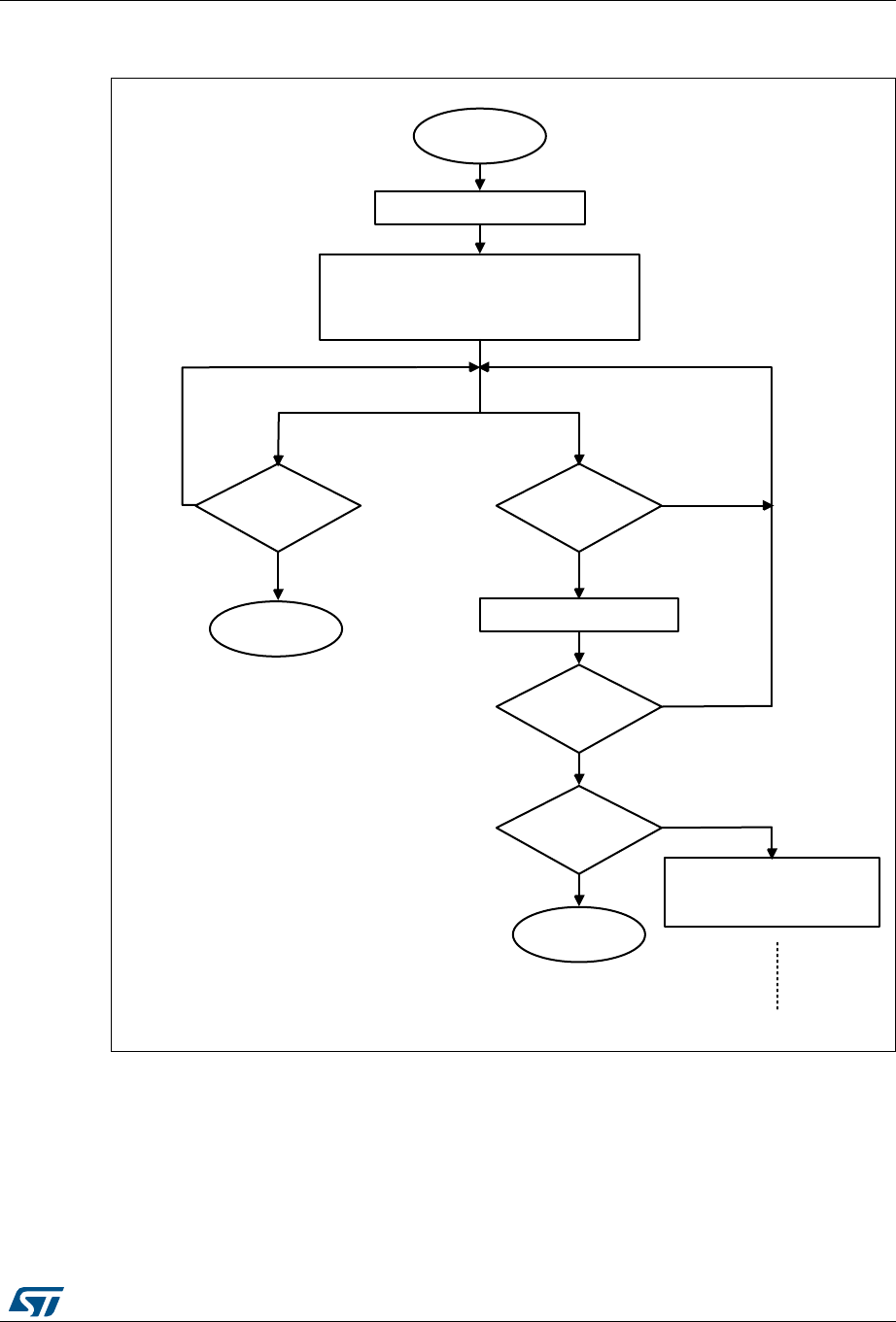
RM0430 Rev 8 807/1324
RM0430 Fast-mode Plus Inter-integrated circuit (FMPI2C) interface
847
Figure 272. Transfer sequence flowchart for FMPI2C master transmitter for N≤255
bytes
D^ǀϯϱϵϲϵsϭ
0DVWHULQLWLDOL]DWLRQ
0DVWHU
WUDQVPLVVLRQ
:ULWH)03,&B7;'5
)03,&B,657;,6
"
1R
<HV
)03,&B,651$&.)
"
<HV
1R
1%<7(6 1
$872(1' IRU5(67$57IRU6723
&RQILJXUHVODYHDGGUHVV
6HW)03,&B&567$57
(QG
1%<7(6
WUDQVPLWWHG"
)03,&B,657&
"
<HV
(QG
1R
<HV
1R 6HW)03,&B&567$57
ZLWKVODYHDGGHVV1%<7(6
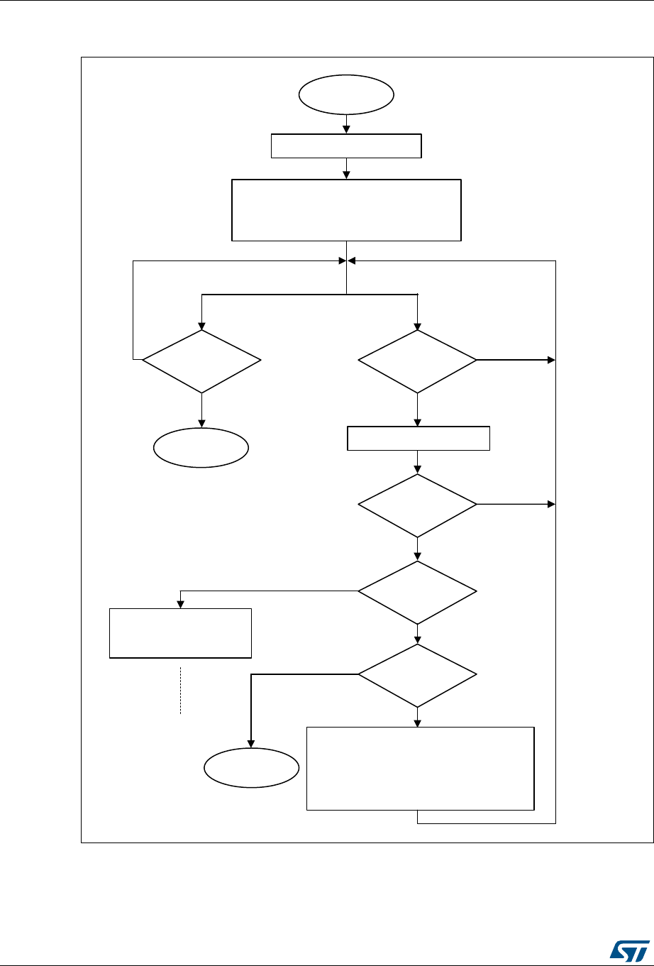
Fast-mode Plus Inter-integrated circuit (FMPI2C) interface RM0430
808/1324 RM0430 Rev 8
Figure 273. Transfer sequence flowchart for FMPI2C master transmitter for N>255
bytes
06Y9
0DVWHULQLWLDOL]DWLRQ
0DVWHU
WUDQVPLVVLRQ
:ULWH)03,&B7;'5
)03,&B,657;,6
"
1R
<HV
)03,&B,651$&.)
"
<HV
1R
1%<7(6 [))1 1
5(/2$'
&RQILJXUHVODYHDGGUHVV
6HW)03,&B&567$57
(QG
1%<7(6
WUDQVPLWWHG "
)03,&B,657&
"
<HV
(QG
1R
<HV
1R
6HW)03,&B&567$57
ZLWKVODYHDGGHVV
1%<7(6
)03,&B,657&5
"
<HV
,)1
1%<7(6 11 5(/2$'
$872(1' IRU5(67$57IRU6723
(/6(
1%<7(6 [))1 1
5(/2$'
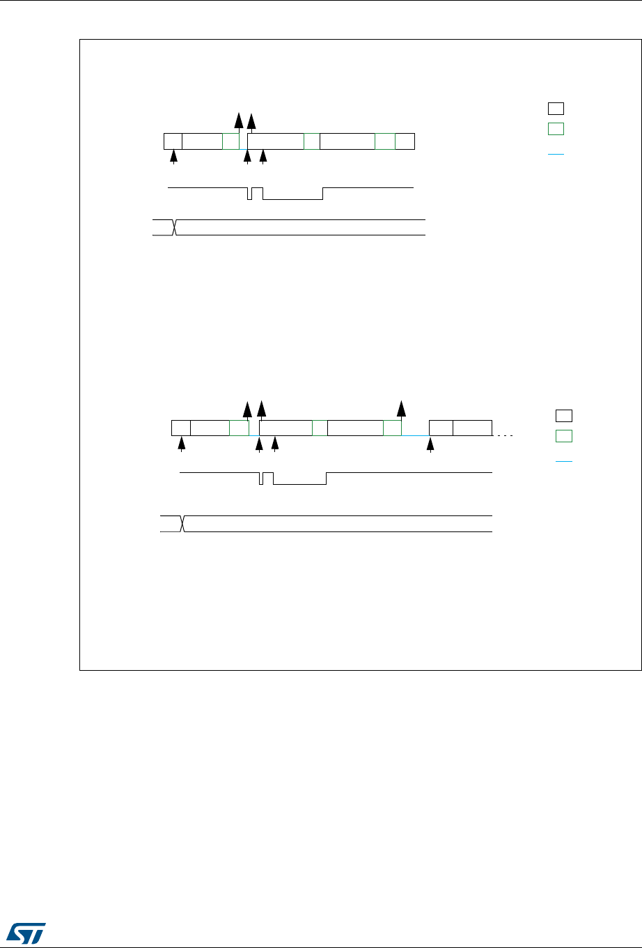
RM0430 Rev 8 809/1324
RM0430 Fast-mode Plus Inter-integrated circuit (FMPI2C) interface
847
Figure 274. Transfer bus diagrams for FMPI2C master transmitter
069
([DPSOH)03,&PDVWHUWUDQVPLWWHUE\WHVDXWRPDWLFHQGPRGH6723
,1,7SURJUDP6ODYHDGGUHVVSURJUDP1%<7(6 $872(1' VHW67$57
(97;,6,65ZUGDWD
(97;,6,65ZUGDWD
7;,67;,6
OHJHQG
WUDQVPLVVLRQ
UHFHSWLRQ
6&/VWUHWFK
(9 (9
[[
,1,7
([DPSOH)03,&PDVWHUWUDQVPLWWHUE\WHVVRIWZDUHHQGPRGH5(67$57
,1,7SURJUDP6ODYHDGGUHVVSURJUDP1%<7(6 $872(1' VHW67$57
(97;,6,65ZUGDWD
(97;,6,65ZUGDWD
(97&,65SURJUDP6ODYHDGGUHVVSURJUDP1%<7(6 1VHW67$57
7;,6 7;,6 OHJHQG
WUDQVPLVV
LRQ
UHFHSWLRQ
6&/VWUHW
FK
(9 (9
,1,7
7&
7;(
7;(
(9
1%<7(6
1%<7(6
[[
6 $GGUHVV $ GDWD $ GDWD 5H6 $GGUHVV$
6 $GGUHVV $ GDWD $GDWD $3

Fast-mode Plus Inter-integrated circuit (FMPI2C) interface RM0430
810/1324 RM0430 Rev 8
Master receiver
In the case of a read transfer, the RXNE flag is set after each byte reception, after the 8th
SCL pulse. An RXNE event generates an interrupt if the RXIE bit is set in the FMPI2C_CR1
register. The flag is cleared when FMPI2C_RXDR is read.
If the total number of data bytes to be received is greater than 255, reload mode must be
selected by setting the RELOAD bit in the FMPI2C_CR2 register. In this case, when
NBYTES[7:0] data have been transferred, the TCR flag is set and the SCL line is stretched
low until NBYTES[7:0] is written to a non-zero value.
•When RELOAD=0 and NBYTES[7:0] data have been transferred:
– In automatic end mode (AUTOEND=1), a NACK and a STOP are automatically
sent after the last received byte.
– In software end mode (AUTOEND=0), a NACK is automatically sent after the last
received byte, the TC flag is set and the SCL line is stretched low in order to allow
software actions:
A RESTART condition can be requested by setting the START bit in the
FMPI2C_CR2 register with the proper slave address configuration, and number of
bytes to be transferred. Setting the START bit clears the TC flag and the START
condition, followed by slave address, are sent on the bus.
A STOP condition can be requested by setting the STOP bit in the FMPI2C_CR2
register. Setting the STOP bit clears the TC flag and the STOP condition is sent on
the bus.
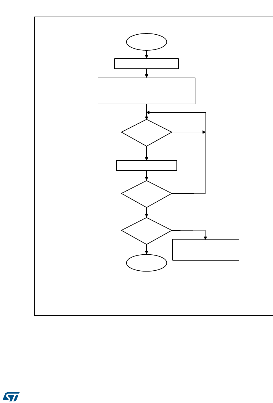
RM0430 Rev 8 811/1324
RM0430 Fast-mode Plus Inter-integrated circuit (FMPI2C) interface
847
Figure 275. Transfer sequence flowchart for FMPI2C master receiver for N≤255 bytes
D^ǀϯϱϵϳϭsϭ
0DVWHULQLWLDOL]DWLRQ
0DVWHUUHFHSWLRQ
5HDG)03,&B5;'5
)03,&B,655;1(
"
1R
<HV
1%<7(6 1
$872(1' IRU5(67$57IRU6723
&RQILJXUHVODYHDGGUHVV
6HW)03,&B&567$57
1%<7(6
UHFHLYHG"
)03,&B,657&
"
<HV
(QG
1R
<HV
1R 6HW)03,&B&567$57
ZLWKVODYHDGGHVV1%<7(6
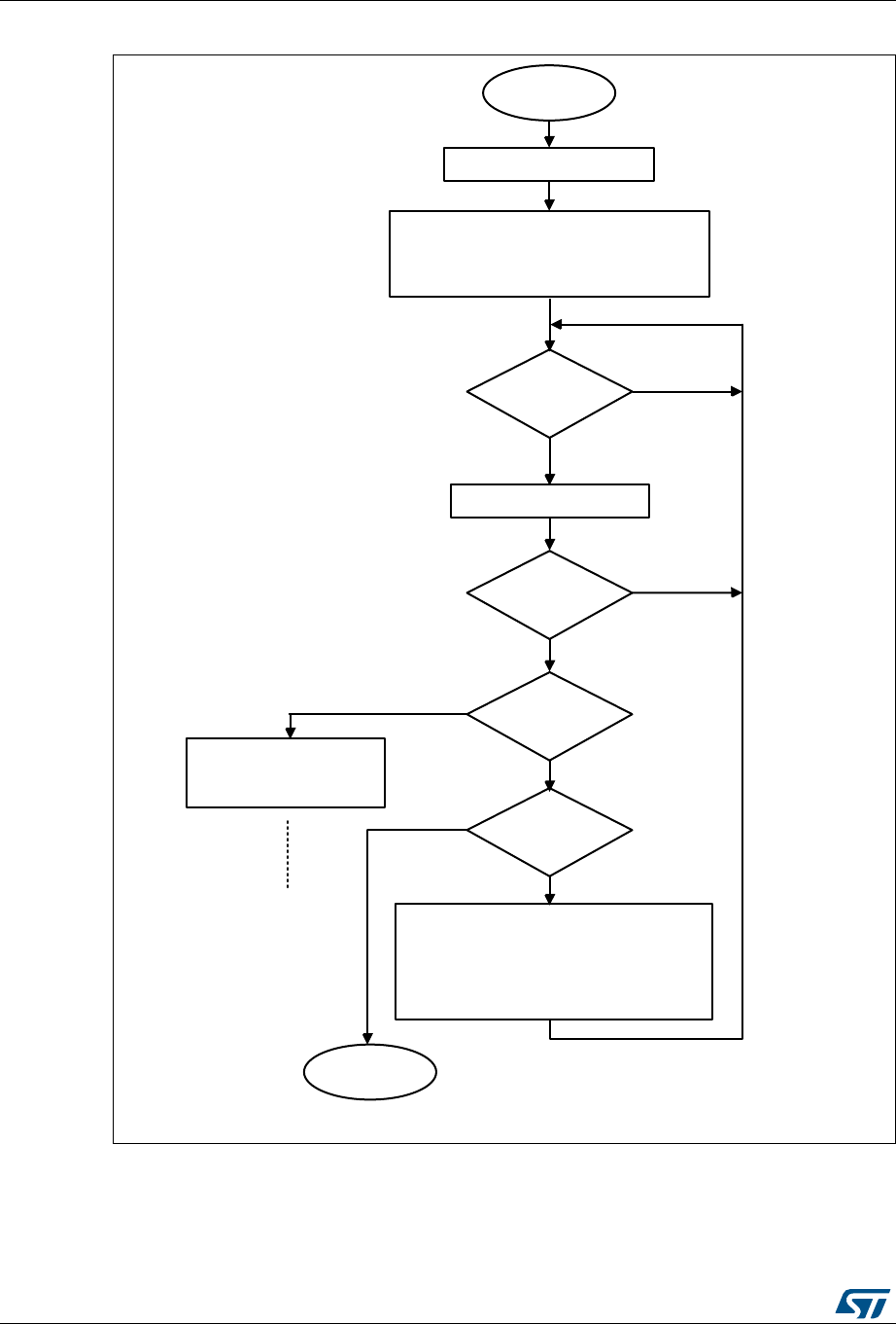
Fast-mode Plus Inter-integrated circuit (FMPI2C) interface RM0430
812/1324 RM0430 Rev 8
Figure 276. Transfer sequence flowchart for FMPI2C master receiver for N >255 bytes
D^ǀϯϱϵϳϮsϭ
0DVWHULQLWLDOL]DWLRQ
0DVWHUUHFHSWLRQ
5HDG)03,&B5;'5
)03,&B,655;1(
"
1R
<HV
1%<7(6 [))1 1
5(/2$'
&RQILJXUHVODYHDGGUHVV
6HW)03,&B&567$57
1%<7(6
UHFHLYHG"
)03,&B,657&
"
<HV
(QG
1R
<HV
1R
6HW)03,&B&567$57
ZLWKVODYHDGGHVV
1%<7(6
)03,&B,657&5
"
<HV
,)1
1%<7(6 11 5(/2$'
$872(1' IRU5(67$57IRU6723
(/6(
1%<7(6 [))1 1
5(/2$'
1R
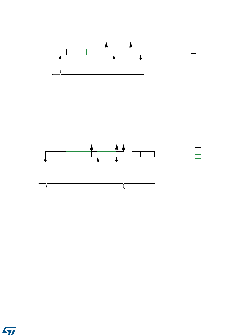
RM0430 Rev 8 813/1324
RM0430 Fast-mode Plus Inter-integrated circuit (FMPI2C) interface
847
Figure 277. Transfer bus diagrams for FMPI2C master receiver
069
([DPSOH)03,&PDVWHUUHFHLYHUE\WHVDXWRPDWLFHQGPRGH6723
,1,7SURJUDP6ODYHDGGUHVVSURJUDP1%<7(6 $872(1' VHW67$57
(95;1(,65UGGDWD
(95;1(,65UGGDWD
$
5;1( 5;1(
1%<7(6
OHJHQG
WUDQVPLVVLRQ
UHFHSWLRQ
6&/VWUHWFK
(9
[[
,1,7
([DPSOH)03,&PDVWHUUHFHLYHUE\WHVVRIWZDUHHQGPRGH5(67$57
,1,7SURJUDP6ODYHDGGUHVVSURJUDP1%<7(6 $872(1' VHW67$57
(95;1(,65UGGDWD
(95;1(,65UHDGGDWD
(97&,65SURJUDP6ODYHDGGUHVVSURJUDP1%<7(6 1VHW67$57
$
5;1( 5;1(
1%<7(6
OHJHQG
WUDQVPLVVLRQ
UHFHSWLRQ
6&/VWUHWFK
(9 (9
[[
,1,7
1
(9
7&
$GGUHVV6 $ GDWD GDWD 1$ 5H6 $GGUHVV
6 $GGUHVV $GDWD GDWD 1$ 3
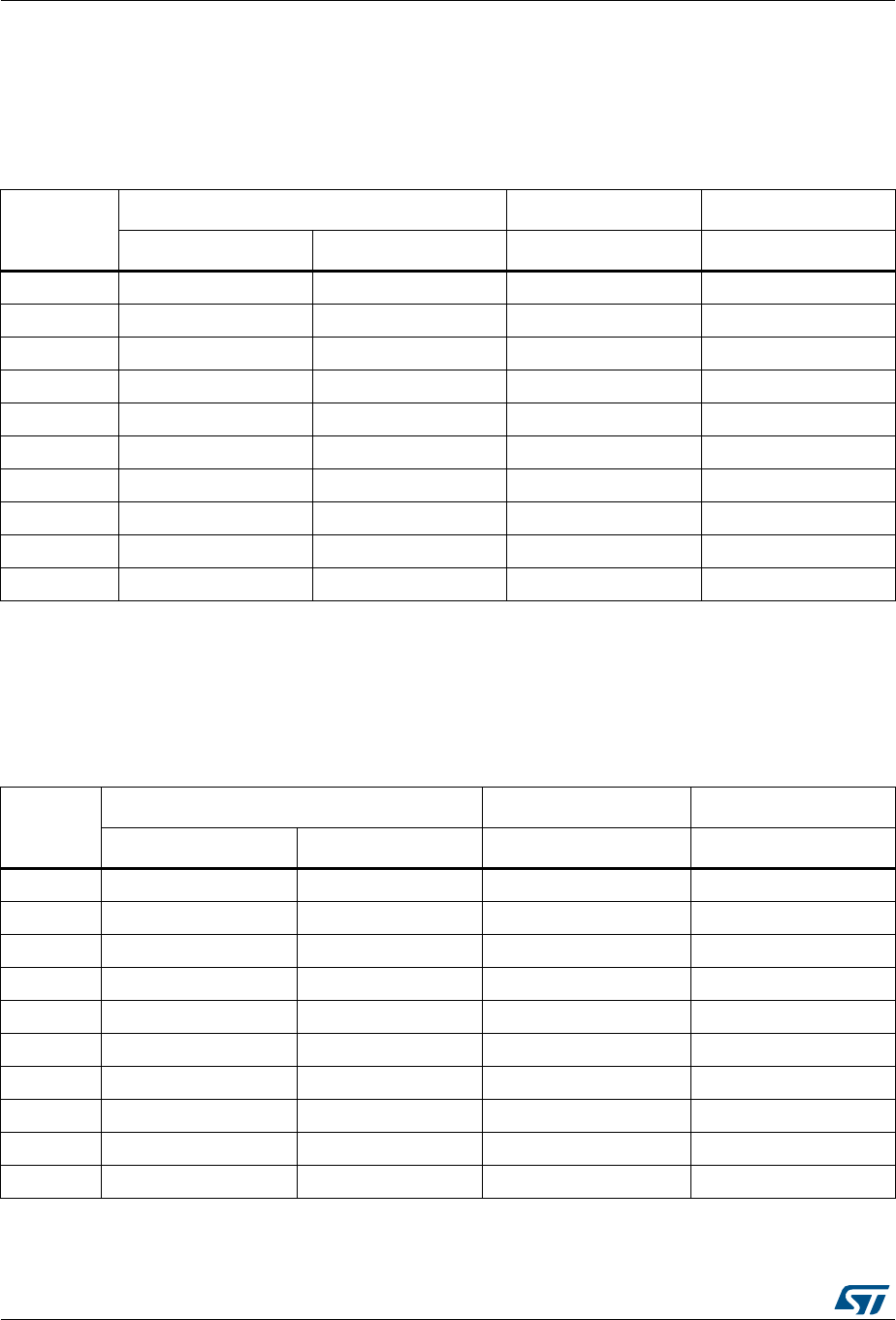
Fast-mode Plus Inter-integrated circuit (FMPI2C) interface RM0430
814/1324 RM0430 Rev 8
26.4.9 FMPI2C_TIMINGR register configuration examples
The tables below provide examples of how to program the FMPI2C_TIMINGR to obtain
timings compliant with the I2C specification. In order to get more accurate configuration
values, the STM32CubeMX tool (I2C Configuration window) should be used.
Table 143. Examples of timing settings for fI2CCLK = 8 MHz
Parameter
Standard-mode (Sm) Fast-mode (Fm) Fast-mode Plus (Fm+)
10 kHz 100 kHz 400 kHz 500 kHz
PRESC 1 1 0 0
SCLL 0xC7 0x13 0x9 0x6
tSCLL 200x250 ns = 50 µs 20x250 ns = 5.0 µs 10x125 ns = 1250 ns 7x125 ns = 875 ns
SCLH 0xC3 0xF 0x3 0x3
tSCLH 196x250 ns = 49 µs 16x250 ns = 4.0µs 4x125ns = 500ns 4x125 ns = 500 ns
tSCL(1) ~100 µs(2) ~10 µs(2) ~2500 ns(3) ~2000 ns(4)
SDADEL 0x2 0x2 0x1 0x0
tSDADEL 2x250 ns = 500 ns 2x250 ns = 500 ns 1x125 ns = 125 ns 0 ns
SCLDEL 0x4 0x4 0x3 0x1
tSCLDEL 5x250 ns = 1250 ns 5x250 ns = 1250 ns 4x125 ns = 500 ns 2x125 ns = 250 ns
1. SCL period tSCL is greater than tSCLL + tSCLH due to SCL internal detection delay. Values provided for tSCL are examples
only.
2. tSYNC1 + tSYNC2 minimum value is 4 x tI2CCLK = 500 ns. Example with tSYNC1 + tSYNC2 = 1000 ns
3. tSYNC1 + tSYNC2 minimum value is 4 x tI2CCLK = 500 ns. Example with tSYNC1 + tSYNC2 = 750 ns
4. tSYNC1 + tSYNC2 minimum value is 4 x tI2CCLK = 500 ns. Example with tSYNC1 + tSYNC2 = 655 ns
Table 144. Examples of timings settings for fI2CCLK = 16 MHz
Parameter
Standard-mode (Sm) Fast-mode (Fm) Fast-mode Plus (Fm+)
10 kHz 100 kHz 400 kHz 1000 kHz
PRESC 3 3 1 0
SCLL 0xC7 0x13 0x9 0x4
tSCLL 200 x 250 ns = 50 µs 20 x 250 ns = 5.0 µs 10 x 125 ns = 1250 ns 5 x 62.5 ns = 312.5 ns
SCLH 0xC3 0xF 0x3 0x2
tSCLH 196 x 250 ns = 49 µs 16 x 250 ns = 4.0 µs 4 x 125ns = 500 ns 3 x 62.5 ns = 187.5 ns
tSCL(1) ~100 µs(2) ~10 µs(2) ~2500 ns(3) ~1000 ns(4)
SDADEL 0x2 0x2 0x2 0x0
tSDADEL 2 x 250 ns = 500 ns 2 x 250 ns = 500 ns 2 x 125 ns = 250 ns 0 ns
SCLDEL 0x4 0x4 0x3 0x2
tSCLDEL 5 x 250 ns = 1250 ns 5 x 250 ns = 1250 ns 4 x 125 ns = 500 ns 3 x 62.5 ns = 187.5 ns
1. SCL period tSCL is greater than tSCLL + tSCLH due to SCL internal detection delay. Values provided for tSCL are examples
only.

RM0430 Rev 8 815/1324
RM0430 Fast-mode Plus Inter-integrated circuit (FMPI2C) interface
847
26.4.10 SMBus specific features
This section is relevant only when SMBus feature is supported. Refer to Section 26.3:
FMPI2C implementation.
Introduction
The System Management Bus (SMBus) is a two-wire interface through which various
devices can communicate with each other and with the rest of the system. It is based on I2C
principles of operation. SMBus provides a control bus for system and power management
related tasks.
This peripheral is compatible with the SMBUS specification (http://smbus.org).
The System Management Bus Specification refers to three types of devices.
•A slave is a device that receives or responds to a command.
•A master is a device that issues commands, generates the clocks and terminates the
transfer.
•A host is a specialized master that provides the main interface to the system’s CPU. A
host must be a master-slave and must support the SMBus host notify protocol. Only
one host is allowed in a system.
This peripheral can be configured as master or slave device, and also as a host.
Bus protocols
There are eleven possible command protocols for any given device. A device may use any
or all of the eleven protocols to communicate. The protocols are Quick Command, Send
Byte, Receive Byte, Write Byte, Write Word, Read Byte, Read Word, Process Call, Block
Read, Block Write and Block Write-Block Read Process Call. These protocols should be
implemented by the user software.
For more details of these protocols, refer to SMBus specification (http://smbus.org).
Address resolution protocol (ARP)
SMBus slave address conflicts can be resolved by dynamically assigning a new unique
address to each slave device. In order to provide a mechanism to isolate each device for the
purpose of address assignment each device must implement a unique device identifier
(UDID). This 128-bit number is implemented by software.
This peripheral supports the Address Resolution Protocol (ARP). The SMBus Device
Default Address (0b1100 001) is enabled by setting SMBDEN bit in FMPI2C_CR1 register.
The ARP commands should be implemented by the user software.
Arbitration is also performed in slave mode for ARP support.
For more details of the SMBus Address Resolution Protocol, refer to SMBus specification
(http://smbus.org).
2. tSYNC1 + tSYNC2 minimum value is 4 x tI2CCLK = 250 ns. Example with tSYNC1 + tSYNC2 = 1000 ns
3. tSYNC1 + tSYNC2 minimum value is 4 x tI2CCLK = 250 ns. Example with tSYNC1 + tSYNC2 = 750 ns
4. tSYNC1 + tSYNC2 minimum value is 4 x tI2CCLK = 250 ns. Example with tSYNC1 + tSYNC2 = 500 ns

Fast-mode Plus Inter-integrated circuit (FMPI2C) interface RM0430
816/1324 RM0430 Rev 8
Received Command and Data acknowledge control
A SMBus receiver must be able to NACK each received command or data. In order to allow
the ACK control in slave mode, the Slave Byte Control mode must be enabled by setting
SBC bit in FMPI2C_CR1 register. Refer to Slave Byte Control mode on page 795 for more
details.
Host Notify protocol
This peripheral supports the Host Notify protocol by setting the SMBHEN bit in the
FMPI2C_CR1 register. In this case the host will acknowledge the SMBus Host address
(0b0001 000).
When this protocol is used, the device acts as a master and the host as a slave.
SMBus alert
The SMBus ALERT optional signal is supported. A slave-only device can signal the host
through the SMBALERT# pin that it wants to talk. The host processes the interrupt and
simultaneously accesses all SMBALERT# devices through the Alert Response Address
(0b0001 100). Only the device(s) which pulled SMBALERT# low will acknowledge the Alert
Response Address.
When configured as a slave device(SMBHEN=0), the SMBA pin is pulled low by setting the
ALERTEN bit in the FMPI2C_CR1 register. The Alert Response Address is enabled at the
same time.
When configured as a host (SMBHEN=1), the ALERT flag is set in the FMPI2C_ISR register
when a falling edge is detected on the SMBA pin and ALERTEN=1. An interrupt is
generated if the ERRIE bit is set in the FMPI2C_CR1 register. When ALERTEN=0, the
ALERT line is considered high even if the external SMBA pin is low.
If the SMBus ALERT pin is not needed, the SMBA pin can be used as a standard GPIO if
ALERTEN=0.
Packet error checking
A packet error checking mechanism has been introduced in the SMBus specification to
improve reliability and communication robustness. Packet Error Checking is implemented
by appending a Packet Error Code (PEC) at the end of each message transfer. The PEC is
calculated by using the C(x) = x8 + x2 + x + 1 CRC-8 polynomial on all the message bytes
(including addresses and read/write bits).
The peripheral embeds a hardware PEC calculator and allows to send a Not Acknowledge
automatically when the received byte does not match with the hardware calculated PEC.
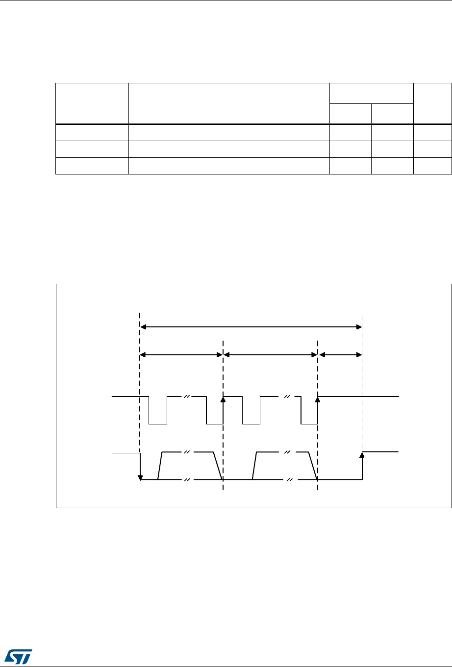
RM0430 Rev 8 817/1324
RM0430 Fast-mode Plus Inter-integrated circuit (FMPI2C) interface
847
Timeouts
This peripheral embeds hardware timers in order to be compliant with the 3 timeouts defined
in SMBus specification.
Figure 278. Timeout intervals for tLOW:SEXT
, tLOW:MEXT
.
Table 145. SMBus timeout specifications
Symbol Parameter
Limits
Unit
Min Max
tTIMEOUT Detect clock low timeout 25 35 ms
tLOW:SEXT(1)
1. tLOW:SEXT is the cumulative time a given slave device is allowed to extend the clock cycles in one message
from the initial START to the STOP. It is possible that, another slave device or the master will also extend
the clock causing the combined clock low extend time to be greater than tLOW:SEXT
. Therefore, this
parameter is measured with the slave device as the sole target of a full-speed master.
Cumulative clock low extend time (slave device) - 25 ms
tLOW:MEXT(2)
2. tLOW:MEXT is the cumulative time a master device is allowed to extend its clock cycles within each byte of a
message as defined from START-to-ACK, ACK-to-ACK, or ACK-to-STOP. It is possible that a slave device
or another master will also extend the clock causing the combined clock low time to be greater than
tLOW:MEXT on a given byte. Therefore, this parameter is measured with a full speed slave device as the sole
target of the master.
Cumulative clock low extend time (master device) - 10 ms
069
6WDUW 6WRS
W/2:6(;7
W/2:0(;7 W/2:0(;7 W/2:0(;7
&ON$FN &ON$FN
60%&/.
60%'$7

Fast-mode Plus Inter-integrated circuit (FMPI2C) interface RM0430
818/1324 RM0430 Rev 8
Bus idle detection
A master can assume that the bus is free if it detects that the clock and data signals have
been high for tIDLE greater than tHIGH,MAX. (refer to Table 140: I2C-SMBUS specification data
setup and hold times)
This timing parameter covers the condition where a master has been dynamically added to
the bus and may not have detected a state transition on the SMBCLK or SMBDAT lines. In
this case, the master must wait long enough to ensure that a transfer is not currently in
progress. The peripheral supports a hardware bus idle detection.
26.4.11 SMBus initialization
This section is relevant only when SMBus feature is supported. Refer to Section 26.3:
FMPI2C implementation.
In addition to FMPI2C initialization, some other specific initialization must be done in order
to perform SMBus communication:
Received Command and Data Acknowledge control (Slave mode)
A SMBus receiver must be able to NACK each received command or data. In order to allow
ACK control in slave mode, the Slave Byte Control mode must be enabled by setting the
SBC bit in the FMPI2C_CR1 register. Refer to Slave Byte Control mode on page 795 for
more details.
Specific address (Slave mode)
The specific SMBus addresses should be enabled if needed. Refer to Bus idle detection on
page 818 for more details.
•The SMBus Device Default address (0b1100 001) is enabled by setting the SMBDEN
bit in the FMPI2C_CR1 register.
•The SMBus Host address (0b0001 000) is enabled by setting the SMBHEN bit in the
FMPI2C_CR1 register.
•The Alert Response Address (0b0001100) is enabled by setting the ALERTEN bit in the
FMPI2C_CR1 register.
Packet error checking
PEC calculation is enabled by setting the PECEN bit in the FMPI2C_CR1 register. Then the
PEC transfer is managed with the help of a hardware byte counter: NBYTES[7:0] in the
FMPI2C_CR2 register. The PECEN bit must be configured before enabling the FMPI2C.
The PEC transfer is managed with the hardware byte counter, so the SBC bit must be set
when interfacing the SMBus in slave mode. The PEC is transferred after NBYTES-1 data
have been transferred when the PECBYTE bit is set and the RELOAD bit is cleared. If
RELOAD is set, PECBYTE has no effect.
Caution: Changing the PECEN configuration is not allowed when the FMPI2C is enabled.

RM0430 Rev 8 819/1324
RM0430 Fast-mode Plus Inter-integrated circuit (FMPI2C) interface
847
Timeout detection
The timeout detection is enabled by setting the TIMOUTEN and TEXTEN bits in the
FMPI2C_TIMEOUTR register. The timers must be programmed in such a way that they
detect a timeout before the maximum time given in the SMBus specification.
•tTIMEOUT check
In order to enable the tTIMEOUT check, the 12-bit TIMEOUTA[11:0] bits must be
programmed with the timer reload value in order to check the tTIMEOUT parameter. The
TIDLE bit must be configured to ‘0’ in order to detect the SCL low level timeout.
Then the timer is enabled by setting the TIMOUTEN in the FMPI2C_TIMEOUTR
register.
If SCL is tied low for a time greater than (TIMEOUTA+1) x 2048 x tI2CCLK, the TIMEOUT
flag is set in the FMPI2C_ISR register.
Refer to Table 147: Examples of TIMEOUTA settings for various FMPI2CCLK
frequencies (max tTIMEOUT = 25 ms).
Caution: Changing the TIMEOUTA[11:0] bits and TIDLE bit configuration is not allowed when the
TIMEOUTEN bit is set.
•tLOW:SEXT and tLOW:MEXT check
Depending on if the peripheral is configured as a master or as a slave, The 12-bit
TIMEOUTB timer must be configured in order to check tLOW:SEXT for a slave and
tLOW:MEXT for a master. As the standard specifies only a maximum, the user can choose
the same value for the both.
Then the timer is enabled by setting the TEXTEN bit in the FMPI2C_TIMEOUTR
register.
If the SMBus peripheral performs a cumulative SCL stretch for a time greater than
(TIMEOUTB+1) x 2048 x tI2CCLK, and in the timeout interval described in Bus idle
detection on page 818 section, the TIMEOUT flag is set in the FMPI2C_ISR register.
Refer to Table 148: Examples of TIMEOUTB settings for various FMPI2CCLK
frequencies
Caution: Changing the TIMEOUTB configuration is not allowed when the TEXTEN bit is set.
Bus Idle detection
In order to enable the tIDLE check, the 12-bit TIMEOUTA[11:0] field must be programmed
with the timer reload value in order to obtain the tIDLE parameter. The TIDLE bit must be
configured to ‘1 in order to detect both SCL and SDA high level timeout.
Then the timer is enabled by setting the TIMOUTEN bit in the FMPI2C_TIMEOUTR register.
If both the SCL and SDA lines remain high for a time greater than (TIMEOUTA+1) x 4 x
tI2CCLK, the TIMEOUT flag is set in the FMPI2C_ISR register.
Table 146. SMBUS with PEC configuration
Mode SBC bit RELOAD bit AUTOEND bit PECBYTE bit
Master Tx/Rx NBYTES + PEC+ STOP x 0 1 1
Master Tx/Rx NBYTES + PEC + ReSTART x 0 0 1
Slave Tx/Rx with PEC 1 0 x 1

Fast-mode Plus Inter-integrated circuit (FMPI2C) interface RM0430
820/1324 RM0430 Rev 8
Refer to Table 149: Examples of TIMEOUTA settings for various FMPI2CCLK frequencies
(max tIDLE = 50 µs)
Caution: Changing the TIMEOUTA and TIDLE configuration is not allowed when the TIMEOUTEN is
set.
26.4.12 SMBus: FMPI2C_TIMEOUTR register configuration examples
This section is relevant only when SMBus feature is supported. Refer to Section 26.3:
FMPI2C implementation.
•Configuring the maximum duration of tTIMEOUT to 25 ms:
•Configuring the maximum duration of tLOW:SEXT and tLOW:MEXT to 8 ms:
•Configuring the maximum duration of tIDLE to 50 µs
26.4.13 SMBus slave mode
This section is relevant only when SMBus feature is supported. Refer to Section 26.3:
FMPI2C implementation.
In addition to FMPI2C slave transfer management (refer to Section 26.4.7: FMPI2C slave
mode) some additional software flowcharts are provided to support SMBus.
SMBus Slave transmitter
When the IP is used in SMBus, SBC must be programmed to ‘1’ in order to allow the PEC
transmission at the end of the programmed number of data bytes. When the PECBYTE bit
is set, the number of bytes programmed in NBYTES[7:0] includes the PEC transmission. In
that case the total number of TXIS interrupts will be NBYTES-1 and the content of the
Table 147. Examples of TIMEOUTA settings for various FMPI2CCLK frequencies
(max tTIMEOUT = 25 ms)
fI2CCLK TIMEOUTA[11:0] bits TIDLE bit TIMEOUTEN bit tTIMEOUT
8 MHz 0x61 0 1 98 x 2048 x 125 ns = 25 ms
16 MHz 0xC3 0 1 196 x 2048 x 62.5 ns = 25 ms
Table 148. Examples of TIMEOUTB settings for various FMPI2CCLK frequencies
fI2CCLK TIMEOUTB[11:0] bits TEXTEN bit tLOW:EXT
8 MHz 0x1F 1 32 x 2048 x 125 ns = 8 ms
16 MHz 0x3F 1 64 x 2048 x 62.5 ns = 8 ms
Table 149. Examples of TIMEOUTA settings for various FMPI2CCLK frequencies
(max tIDLE = 50 µs)
fI2CCLK TIMEOUTA[11:0] bits TIDLE bit TIMEOUTEN bit tTIDLE
8 MHz 0x63 1 1 100 x 4 x 125 ns = 50 µs
16 MHz 0xC7 1 1 200 x 4 x 62.5 ns = 50 µs
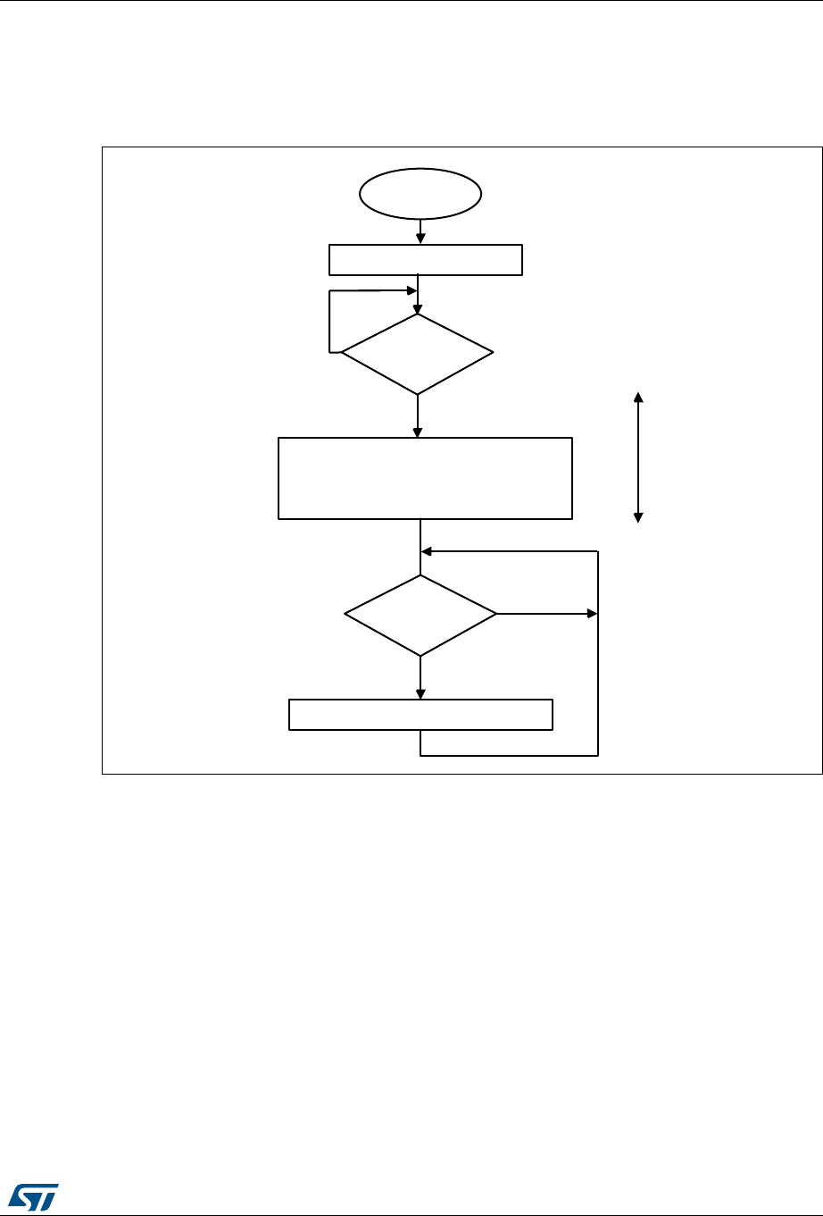
RM0430 Rev 8 821/1324
RM0430 Fast-mode Plus Inter-integrated circuit (FMPI2C) interface
847
FMPI2C_PECR register is automatically transmitted if the master requests an extra byte
after the NBYTES-1 data transfer.
Caution: The PECBYTE bit has no effect when the RELOAD bit is set.
Figure 279. Transfer sequence flowchart for SMBus slave transmitter N bytes + PEC
D^ǀϯϱϵϳϯsϭ
6ODYHLQLWLDOL]DWLRQ
60%XVVODYH
WUDQVPLVVLRQ
:ULWH)03,&B7;'57;'$7$
)03,&B,657;,6
"
1R
<HV
)03,&B,65$''5
"
<HV
1R
5HDG$''&2'(DQG',5LQ)03,&B,65
)03,&B&51%<7(6 1
3(&%<7(
6HW)03,&B,&5$''5&)
6&/
VWUHWFKHG
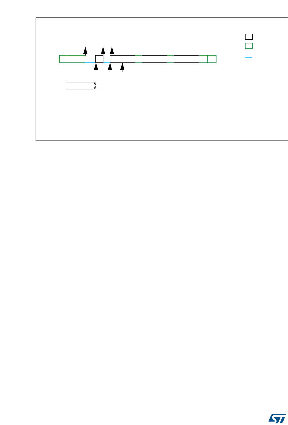
Fast-mode Plus Inter-integrated circuit (FMPI2C) interface RM0430
822/1324 RM0430 Rev 8
Figure 280. Transfer bus diagrams for SMBus slave transmitter (SBC=1)
SMBus Slave receiver
When the FMPI2C is used in SMBus mode, SBC must be programmed to ‘1’ in order to
allow the PEC checking at the end of the programmed number of data bytes. In order to
allow the ACK control of each byte, the reload mode must be selected (RELOAD=1). Refer
to Slave Byte Control mode on page 795 for more details.
In order to check the PEC byte, the RELOAD bit must be cleared and the PECBYTE bit
must be set. In this case, after NBYTES-1 data have been received, the next received byte
is compared with the internal FMPI2C_PECR register content. A NACK is automatically
generated if the comparison does not match, and an ACK is automatically generated if the
comparison matches, whatever the ACK bit value. Once the PEC byte is received, it is
copied into the FMPI2C_RXDR register like any other data, and the RXNE flag is set.
In the case of a PEC mismatch, the PECERR flag is set and an interrupt is generated if the
ERRIE bit is set in the FMPI2C_CR1 register.
If no ACK software control is needed, the user can program PECBYTE=1 and, in the same
write operation, program NBYTES with the number of bytes to be received in a continuous
flow. After NBYTES-1 are received, the next received byte is checked as being the PEC.
Caution: The PECBYTE bit has no effect when the RELOAD bit is set.
069
([DPSOH60%XVVODYHWUDQVPLWWHUE\WHV3(&
(9$''5,65FKHFN$''&2'(SURJUDP1%<7(6 VHW3(&%<7(VHW$''5&)
(97;,6,65ZUGDWD
(97;,6,65ZUGDWD
$''5
OHJHQG
WUDQVPLVVLRQ
UHFHSWLRQ
6&/VWUHWFK
(9 (9
7;,6 7;,6
(9
1%<7(6
6 $GGUHVV $ $GDWD GDWD 3(&
$1$ 3
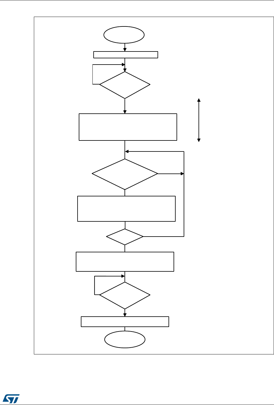
RM0430 Rev 8 823/1324
RM0430 Fast-mode Plus Inter-integrated circuit (FMPI2C) interface
847
Figure 281. Transfer sequence flowchart for SMBus slave receiver N Bytes + PEC
D^ǀϯϱϵϳϰsϭ
6ODYHLQLWLDOL]DWLRQ
60%XVVODYH
UHFHSWLRQ
5HDG)03,&B5;'55;'$7$
)03,&B,655;1( "
)03,&B,657&5 "
1R
<HV
)03,&B,65$''5
"
<HV
1R
5HDG$''&2'(DQG',5LQ)03,&B,65
)03,&B&51%<7(6 5(/2$'
3(&%<7(
6HW)03,&B,&5$''5&)
6&/
VWUHWFKHG
5HDG)03,&B5;'55;'$7$
3URJUDP)03,&B&51$&.
)03,&B&51%<7(6
1 1
1 "
5HDG)03,&B5;'55;'$7$
3URJUDP5(/2$'
1$&. DQG1%<7(6
)03,&B,655;1(
"
1R
(QG
1R
<HV
<HV
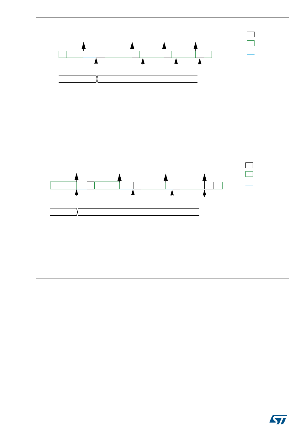
Fast-mode Plus Inter-integrated circuit (FMPI2C) interface RM0430
824/1324 RM0430 Rev 8
Figure 282. Bus transfer diagrams for SMBus slave receiver (SBC=1)
This section is relevant only when SMBus feature is supported. Refer to Section 26.3:
FMPI2C implementation.
In addition to FMPI2C master transfer management (refer to Section 26.4.8: FMPI2C
master mode) some additional software flowcharts are provided to support SMBus.
SMBus Master transmitter
When the SMBus master wants to transmit the PEC, the PECBYTE bit must be set and the
number of bytes must be programmed in the NBYTES[7:0] field, before setting the START
bit. In this case the total number of TXIS interrupts will be NBYTES-1. So if the PECBYTE
bit is set when NBYTES=0x1, the content of the FMPI2C_PECR register is automatically
transmitted.
If the SMBus master wants to send a STOP condition after the PEC, automatic end mode
should be selected (AUTOEND=1). In this case, the STOP condition automatically follows
the PEC transmission.
069
([DPSOH60%XVVODYHUHFHLYHUE\WHV3(&
$GGUHVV
6
(9$''5,65FKHFN$''&2'(DQG',5SURJUDP1%<7(6 3(&%<7( 5(/2$' VHW$''5&)
(95;1(,65UGGDWD
(95;1(,65UGGDWD
(95;1(,65UG3(&
$
GDWD
$
GDWD
$
5;1(
3(&
$
5;1(
3
OHJHQG
WUDQVPLVVLRQ
UHFHSWLRQ
6&/VWUHWFK
(9 (9 (9 (9
$''5
5;1(
1%<7(6
([DPSOH60%XVVODYHUHFHLYHUE\WHV3(&ZLWK$&.FRQWURO
5(/2$'
$GGUHVV
6
(9$''5,65FKHFN$''&2'(DQG',5SURJUDP1%<7(6 3(&%<7( 5(/2$' VHW$''5&)
(95;1(7&5,65UGGDWDSURJUDP1$&. DQG1%<7(6
(95;1(7&5,65UGGDWDSURJUDP1$&. 1%<7(6 DQG5(/2$'
(95;1(7&5,65UG3(&
$
$''5
GDWD
$
GDWD
$
5;1(7&5
3(&
$
5;1(7&5
3
OHJHQG
WUDQVPLVVLRQ
UHFHSWLRQ
6&/VWUHWFK
9(9(9(
5;1(
(9
1%<7(6
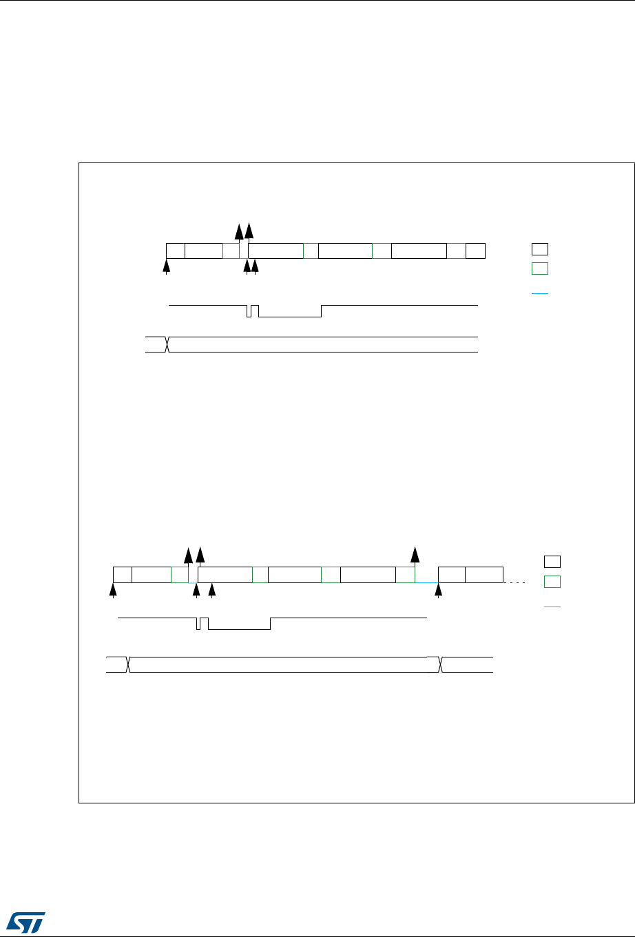
RM0430 Rev 8 825/1324
RM0430 Fast-mode Plus Inter-integrated circuit (FMPI2C) interface
847
When the SMBus master wants to send a RESTART condition after the PEC, software
mode must be selected (AUTOEND=0). In this case, once NBYTES-1 have been
transmitted, the FMPI2C_PECR register content is transmitted and the TC flag is set after
the PEC transmission, stretching the SCL line low. The RESTART condition must be
programmed in the TC interrupt subroutine.
Caution: The PECBYTE bit has no effect when the RELOAD bit is set.
Figure 283. Bus transfer diagrams for SMBus master transmitter
069
([DPSOH60%XVPDVWHUWUDQVPLWWHUE\WHV3(&DXWRPDWLFHQGPRGH6723
$GGUHVV
6
,1,7SURJUDP6ODYHDGGUHVVSURJUDP1%<7(6 $872(1' VHW3(&%<7(VHW67$57
(97;,6,65ZUGDWD
(97;,6,65ZUGDWD
$
GDWD
$
7;,6 7;,6
GDWD
$
1%<7(6
$
OHJHQG
WUDQVPLVVLRQ
UHFHSWLRQ
6&/VWUHWFK
(9
[[
,1,7
([DPSOH60%XVPDVWHUWUDQVPLWWHUE\WHV3(&VRIWZDUHHQGPRGH5(67$57
,1,7SURJUDP6ODYHDGGUHVVSURJUDP1%<7(6 $872(1' VHW3(&%<7(VHW67$57
(97;,6,65ZUGDWD
(97;,6,65ZUGDWD
(97&,65SURJUDP6ODYHDGGUHVVSURJUDP1%<7(6 1VHW67$57
1%<7(6
5VWDUW
OHJHQG
WUDQVPLVVLRQ
UHFHSWLRQ
6&/VWUHWFK
[[
$GGUHVV
1
3(&
3
(9
$
7;(
$GGUHVV
6
$
GDWD
$
7;,6 7;,6
GDWD
$
(9
,1,7
3(&
(9
7&
(9

Fast-mode Plus Inter-integrated circuit (FMPI2C) interface RM0430
826/1324 RM0430 Rev 8
SMBus Master receiver
When the SMBus master wants to receive the PEC followed by a STOP at the end of the
transfer, automatic end mode can be selected (AUTOEND=1). The PECBYTE bit must be
set and the slave address must be programmed, before setting the START bit. In this case,
after NBYTES-1 data have been received, the next received byte is automatically checked
versus the FMPI2C_PECR register content. A NACK response is given to the PEC byte,
followed by a STOP condition.
When the SMBus master receiver wants to receive the PEC byte followed by a RESTART
condition at the end of the transfer, software mode must be selected (AUTOEND=0). The
PECBYTE bit must be set and the slave address must be programmed, before setting the
START bit. In this case, after NBYTES-1 data have been received, the next received byte is
automatically checked versus the FMPI2C_PECR register content. The TC flag is set after
the PEC byte reception, stretching the SCL line low. The RESTART condition can be
programmed in the TC interrupt subroutine.
Caution: The PECBYTE bit has no effect when the RELOAD bit is set.
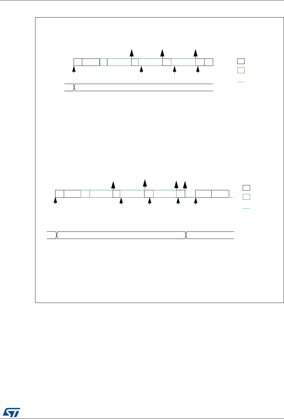
RM0430 Rev 8 827/1324
RM0430 Fast-mode Plus Inter-integrated circuit (FMPI2C) interface
847
Figure 284. Bus transfer diagrams for SMBus master receiver
26.4.14 Error conditions
The following are the error conditions which may cause communication to fail.
Bus error (BERR)
A bus error is detected when a START or a STOP condition is detected and is not located
after a multiple of 9 SCL clock pulses. A START or a STOP condition is detected when a
SDA edge occurs while SCL is high.
The bus error flag is set only if the FMPI2C is involved in the transfer as master or
addressed slave (i.e not during the address phase in slave mode).
069
([DPSOH60%XVPDVWHUUHFHLYHUE\WHV3(&DXWRPDWLFHQGPRGH6723
$GGUHVV
6
,1,7SURJUDP6ODYHDGGUHVVSURJUDP1%<7(6 $872(1' VHW3(&%<7(VHW67$57
(95;1(,65UGGDWD
(95;1(,65UGGDWD
(95;1(,65UG3(&
$
GDWD
$
5;1( 5;1(
GDWD
$
1%<7(6
1$
OHJHQG
WUDQVPLVVLRQ
UHFHSWLRQ
6&/VWUHWFK
9(9(
[[
,1,7
([DPSOH60%XVPDVWHUUHFHLYHUE\WHV3(&VRIWZDUHHQGPRGH5(67$57
$GGUHVV
6
,1,7SURJUDP6ODYHDGGUHVVSURJUDP1%<7(6 $872(1' VHW3(&%<7(VHW67$57
(95;1(,65UGGDWD
(95;1(,65UGGDWD
(95;1(,65UHDG3(&
(97&,65SURJUDP6ODYHDGGUHVVSURJUDP1%<7(6 1VHW67$57
$
GDWD
$
5;1( 5;1(
GDWD
$
1%<7(6
5HVWDUW
OHJHQG
WUDQVPLVVLRQ
UHFHSWLRQ
6&/VWUHWFK
(9 (9
[[
,1,7
$GGUHVV
1
3(&
3
5;1(
(9
1$
3(&
5;1(
(9
7&
(9

Fast-mode Plus Inter-integrated circuit (FMPI2C) interface RM0430
828/1324 RM0430 Rev 8
In case of a misplaced START or RESTART detection in slave mode, the FMPI2C enters
address recognition state like for a correct START condition.
When a bus error is detected, the BERR flag is set in the FMPI2C_ISR register, and an
interrupt is generated if the ERRIE bit is set in the FMPI2C_CR1 register.
Arbitration lost (ARLO)
An arbitration loss is detected when a high level is sent on the SDA line, but a low level is
sampled on the SCL rising edge.
•In master mode, arbitration loss is detected during the address phase, data phase and
data acknowledge phase. In this case, the SDA and SCL lines are released, the
START control bit is cleared by hardware and the master switches automatically to
slave mode.
•In slave mode, arbitration loss is detected during data phase and data acknowledge
phase. In this case, the transfer is stopped, and the SCL and SDA lines are released.
When an arbitration loss is detected, the ARLO flag is set in the FMPI2C_ISR register, and
an interrupt is generated if the ERRIE bit is set in the FMPI2C_CR1 register.
Overrun/underrun error (OVR)
An overrun or underrun error is detected in slave mode when NOSTRETCH=1 and:
•In reception when a new byte is received and the RXDR register has not been read yet.
The new received byte is lost, and a NACK is automatically sent as a response to the
new byte.
•In transmission:
– When STOPF=1 and the first data byte should be sent. The content of the
FMPI2C_TXDR register is sent if TXE=0, 0xFF if not.
– When a new byte should be sent and the FMPI2C_TXDR register has not been
written yet, 0xFF is sent.
When an overrun or underrun error is detected, the OVR flag is set in the FMPI2C_ISR
register, and an interrupt is generated if the ERRIE bit is set in the FMPI2C_CR1 register.
Packet Error Checking Error (PECERR)
This section is relevant only when the SMBus feature is supported. Refer to Section 26.3:
FMPI2C implementation.
A PEC error is detected when the received PEC byte does not match with the
FMPI2C_PECR register content. A NACK is automatically sent after the wrong PEC
reception.
When a PEC error is detected, the PECERR flag is set in the FMPI2C_ISR register, and an
interrupt is generated if the ERRIE bit is set in the FMPI2C_CR1 register.

RM0430 Rev 8 829/1324
RM0430 Fast-mode Plus Inter-integrated circuit (FMPI2C) interface
847
Timeout Error (TIMEOUT)
This section is relevant only when the SMBus feature is supported. Refer to Section 26.3:
FMPI2C implementation.
A timeout error occurs for any of these conditions:
•TIDLE=0 and SCL remained low for the time defined in the TIMEOUTA[11:0] bits: this is
used to detect a SMBus timeout.
•TIDLE=1 and both SDA and SCL remained high for the time defined in the TIMEOUTA
[11:0] bits: this is used to detect a bus idle condition.
•Master cumulative clock low extend time reached the time defined in the
TIMEOUTB[11:0] bits (SMBus tLOW:MEXT parameter)
•Slave cumulative clock low extend time reached the time defined in TIMEOUTB[11:0]
bits (SMBus tLOW:SEXT parameter)
When a timeout violation is detected in master mode, a STOP condition is automatically
sent.
When a timeout violation is detected in slave mode, SDA and SCL lines are automatically
released.
When a timeout error is detected, the TIMEOUT flag is set in the FMPI2C_ISR register, and
an interrupt is generated if the ERRIE bit is set in the FMPI2C_CR1 register.
Alert (ALERT)
This section is relevant only when the SMBus feature is supported. Refer to Section 26.3:
FMPI2C implementation.
The ALERT flag is set when the FMPI2C interface is configured as a Host (SMBHEN=1),
the alert pin detection is enabled (ALERTEN=1) and a falling edge is detected on the SMBA
pin. An interrupt is generated if the ERRIE bit is set in the FMPI2C_CR1 register.
26.4.15 DMA requests
Transmission using DMA
DMA (Direct Memory Access) can be enabled for transmission by setting the TXDMAEN bit
in the FMPI2C_CR1 register. Data is loaded from an SRAM area configured using the DMA
peripheral (see ) to the FMPI2C_TXDR register whenever the TXIS bit is set.
Only the data are transferred with DMA.
•In master mode: the initialization, the slave address, direction, number of bytes and
START bit are programmed by software (the transmitted slave address cannot be
transferred with DMA). When all data are transferred using DMA, the DMA must be
initialized before setting the START bit. The end of transfer is managed with the

Fast-mode Plus Inter-integrated circuit (FMPI2C) interface RM0430
830/1324 RM0430 Rev 8
NBYTES counter. Refer to Master transmitter on page 806.
•In slave mode:
– With NOSTRETCH=0, when all data are transferred using DMA, the DMA must be
initialized before the address match event, or in ADDR interrupt subroutine, before
clearing ADDR.
– With NOSTRETCH=1, the DMA must be initialized before the address match
event.
•For instances supporting SMBus: the PEC transfer is managed with NBYTES counter.
Refer to SMBus Slave transmitter on page 820 and SMBus Master transmitter on
page 824.
Note: If DMA is used for transmission, the TXIE bit does not need to be enabled.
Reception using DMA
DMA (Direct Memory Access) can be enabled for reception by setting the RXDMAEN bit in
the FMPI2C_CR1 register. Data is loaded from the FMPI2C_RXDR register to an SRAM
area configured using the DMA peripheral (refer to ) whenever the RXNE bit is set. Only the
data (including PEC) are transferred with DMA.
•In master mode, the initialization, the slave address, direction, number of bytes and
START bit are programmed by software. When all data are transferred using DMA, the
DMA must be initialized before setting the START bit. The end of transfer is managed
with the NBYTES counter.
•In slave mode with NOSTRETCH=0, when all data are transferred using DMA, the
DMA must be initialized before the address match event, or in the ADDR interrupt
subroutine, before clearing the ADDR flag.
•If SMBus is supported (see Section 26.3: FMPI2C implementation): the PEC transfer is
managed with the NBYTES counter. Refer to SMBus Slave receiver on page 822 and
SMBus Master receiver on page 826.
Note: If DMA is used for reception, the RXIE bit does not need to be enabled.
26.4.16 Debug mode
When the microcontroller enters debug mode (core halted), the SMBus timeout either
continues to work normally or stops, depending on the DBG_I2Cx_ configuration bits in the
DBG module.
26.5 FMPI2C low-power modes
Table 150. Low-power modes
Mode Description
Sleep No effect
FMPI2C interrupts cause the device to exit the Sleep mode.
Stop The contents of FMPI2C registers are kept.
Standby The FMPI2C peripheral is powered down and must be reinitialized after exiting Standby.

RM0430 Rev 8 831/1324
RM0430 Fast-mode Plus Inter-integrated circuit (FMPI2C) interface
847
26.6 FMPI2C interrupts
The table below gives the list of FMPI2C interrupt requests.
Depending on the product implementation, all these interrupts events can either share the
same interrupt vector (FMPI2C global interrupt), or be grouped into 2 interrupt vectors
(FMPI2C event interrupt and FMPI2C error interrupt). Refer to Table 40: Vector table for
STM32F413/423 for details.
26.7 FMPI2C registers
Refer to Section 1.2 on page 52 for a list of abbreviations used in register descriptions.
The peripheral registers are accessed by words (32-bit).
26.7.1 Control register 1 (FMPI2C_CR1)
Address offset: 0x00
Reset value: 0x0000 0000
Table 151. FMPI2C Interrupt requests
Interrupt
acronym Interrupt event Event flag Enable
control bit
Interrupt clear
method
Exit the
Sleep mode
Exit the
Stop mode
I2C_EV
Receive buffer not
empty RXNE RXIE
Read
FMPI2C_RXDR
register
Yes
No
Transmit buffer
interrupt status TXIS TXIE
Write
FMPI2C_TXDR
register
Stop detection
interrupt flag STOPF STOPIE Write STOPCF=1
Transfer Complete
Reload TCR
TCIE
Write
FMPI2C_CR2 with
NBYTES[7:0] ≠ 0
Transfer complete TC Write START=1 or
STOP=1
Address matched ADDR ADDRIE Write ADDRCF=1
NACK reception NACKF NACKIE Write NACKCF=1
I2C_ER
Bus error BERR
ERRIE
Write BERRCF=1
Yes No
Arbitration loss ARLO Write ARLOCF=1
Overrun/Underrun OVR Write OVRCF=1
PEC error PECERR Write
PECERRCF=1
Timeout/tLOW error TIMEOUT Write
TIMEOUTCF=1
SMBus Alert ALERT Write ALERTCF=1

Fast-mode Plus Inter-integrated circuit (FMPI2C) interface RM0430
832/1324 RM0430 Rev 8
Access: No wait states, except if a write access occurs while a write access to this register is
ongoing. In this case, wait states are inserted in the second write access until the previous
one is completed. The latency of the second write access can be up to 2 x PCLK1 + 6 x
FMPI2CCLK.
31 30 29 28 27 26 25 24 23 22 21 20 19 18 17 16
Res. Res. Res. Res. Res. Res. Res. Res. PECEN ALERT
EN
SMBD
EN
SMBH
EN GCEN Res. NOSTR
ETCH SBC
rw rw rw rw rw rw rw
15141312111098 7 6543210
RXDMA
EN
TXDMA
EN Res. ANF
OFF DNF ERRIE TCIE STOP
IE
NACK
IE
ADDR
IE RXIE TXIE PE
rw rw rw rw rw rw rw rw rw rw rw rw rw rw rw
Bits 31:24 Reserved, must be kept at reset value.
Bit 23 PECEN: PEC enable
0: PEC calculation disabled
1: PEC calculation enabled
Note: If the SMBus feature is not supported, this bit is reserved and forced by hardware to ‘0’.
Refer to Section 26.3: FMPI2C implementation.
Bit 22 ALERTEN: SMBus alert enable
Device mode (SMBHEN=0):
0: Releases SMBA pin high and Alert Response Address Header disabled: 0001100x
followed by NACK.
1: Drives SMBA pin low and Alert Response Address Header enables: 0001100x followed
by ACK.
Host mode (SMBHEN=1):
0: SMBus Alert pin (SMBA) not supported.
1: SMBus Alert pin (SMBA) supported.
Note: When ALERTEN=0, the SMBA pin can be used as a standard GPIO.
If the SMBus feature is not supported, this bit is reserved and forced by hardware to ‘0’.
Refer to Section 26.3: FMPI2C implementation.
Bit 21 SMBDEN: SMBus Device Default address enable
0: Device default address disabled. Address 0b1100001x is NACKed.
1: Device default address enabled. Address 0b1100001x is ACKed.
Note: If the SMBus feature is not supported, this bit is reserved and forced by hardware to ‘0’.
Refer to Section 26.3: FMPI2C implementation.
Bit 20 SMBHEN: SMBus Host address enable
0: Host address disabled. Address 0b0001000x is NACKed.
1: Host address enabled. Address 0b0001000x is ACKed.
Note: If the SMBus feature is not supported, this bit is reserved and forced by hardware to ‘0’.
Refer to Section 26.3: FMPI2C implementation.
Bit 19 GCEN: General call enable
0: General call disabled. Address 0b00000000 is NACKed.
1: General call enabled. Address 0b00000000 is ACKed.
Bit 18 Reserved, must be kept at reset value.

RM0430 Rev 8 833/1324
RM0430 Fast-mode Plus Inter-integrated circuit (FMPI2C) interface
847
Bit 17 NOSTRETCH: Clock stretching disable
This bit is used to disable clock stretching in slave mode. It must be kept cleared in master
mode.
0: Clock stretching enabled
1: Clock stretching disabled
Note: This bit can only be programmed when the I2C is disabled (PE = 0).
Bit 16 SBC: Slave byte control
This bit is used to enable hardware byte control in slave mode.
0: Slave byte control disabled
1: Slave byte control enabled
Bit 15 RXDMAEN: DMA reception requests enable
0: DMA mode disabled for reception
1: DMA mode enabled for reception
Bit 14 TXDMAEN: DMA transmission requests enable
0: DMA mode disabled for transmission
1: DMA mode enabled for transmission
Bit 13 Reserved, must be kept at reset value.
Bit 12 ANFOFF: Analog noise filter OFF
0: Analog noise filter enabled
1: Analog noise filter disabled
Note: This bit can only be programmed when the FMPI2C is disabled (PE = 0).
Bits 11:8 DNF[3:0]: Digital noise filter
These bits are used to configure the digital noise filter on SDA and SCL input. The digital filter
will filter spikes with a length of up to DNF[3:0] * tI2CCLK
0000: Digital filter disabled
0001: Digital filter enabled and filtering capability up to 1 tI2CCLK
...
1111: digital filter enabled and filtering capability up to15 tI2CCLK
Note: If the analog filter is also enabled, the digital filter is added to the analog filter.
This filter can only be programmed when the FMPI2C is disabled (PE = 0).
Bit 7 ERRIE: Error interrupts enable
0: Error detection interrupts disabled
1: Error detection interrupts enabled
Note: Any of these errors generate an interrupt:
Arbitration Loss (ARLO)
Bus Error detection (BERR)
Overrun/Underrun (OVR)
Timeout detection (TIMEOUT)
PEC error detection (PECERR)
Alert pin event detection (ALERT)
Bit 6 TCIE: Transfer Complete interrupt enable
0: Transfer Complete interrupt disabled
1: Transfer Complete interrupt enabled
Note: Any of these events will generate an interrupt:
Transfer Complete (TC)
Transfer Complete Reload (TCR)

Fast-mode Plus Inter-integrated circuit (FMPI2C) interface RM0430
834/1324 RM0430 Rev 8
26.7.2 Control register 2 (FMPI2C_CR2)
Address offset: 0x04
Reset value: 0x0000 0000
Access: No wait states, except if a write access occurs while a write access to this register is
ongoing. In this case, wait states are inserted in the second write access until the previous
one is completed. The latency of the second write access can be up to 2 x PCLK1 + 6 x
FMPI2CCLK.
Bit 5 STOPIE: Stop detection Interrupt enable
0: Stop detection (STOPF) interrupt disabled
1: Stop detection (STOPF) interrupt enabled
Bit 4 NACKIE: Not acknowledge received Interrupt enable
0: Not acknowledge (NACKF) received interrupts disabled
1: Not acknowledge (NACKF) received interrupts enabled
Bit 3 ADDRIE: Address match Interrupt enable (slave only)
0: Address match (ADDR) interrupts disabled
1: Address match (ADDR) interrupts enabled
Bit 2 RXIE: RX Interrupt enable
0: Receive (RXNE) interrupt disabled
1: Receive (RXNE) interrupt enabled
Bit 1 TXIE: TX Interrupt enable
0: Transmit (TXIS) interrupt disabled
1: Transmit (TXIS) interrupt enabled
Bit 0 PE: Peripheral enable
0: Peripheral disable
1: Peripheral enable
Note: When PE=0, the FMPI2C SCL and SDA lines are released. Internal state machines
and status bits are put back to their reset value. When cleared, PE must be kept low for
at least 3 APB clock cycles.
31 30 29 28 27 26 25 24 23 22 21 20 19 18 17 16
Res. Res. Res. Res. Res. PEC
BYTE
AUTO
END
RE
LOAD NBYTES[7:0]
rs rw rw rw rw rw rw rw rw rw rw
1514131211109876543210
NACK STOP START HEAD
10R ADD10 RD_
WRN SADD[9:0]
rs rs rs rw rw rw rw rw rw rw rw rw rw rw rw rw

RM0430 Rev 8 835/1324
RM0430 Fast-mode Plus Inter-integrated circuit (FMPI2C) interface
847
Bits 31:27 Reserved, must be kept at reset value.
Bit 26 PECBYTE: Packet error checking byte
This bit is set by software, and cleared by hardware when the PEC is transferred, or when a
STOP condition or an Address matched is received, also when PE=0.
0: No PEC transfer.
1: PEC transmission/reception is requested
Note: Writing ‘0’ to this bit has no effect.
This bit has no effect when RELOAD is set.
This bit has no effect is slave mode when SBC=0.
If the SMBus feature is not supported, this bit is reserved and forced by hardware to ‘0’.
Refer to Section 26.3: FMPI2C implementation.
Bit 25 AUTOEND: Automatic end mode (master mode)
This bit is set and cleared by software.
0: software end mode: TC flag is set when NBYTES data are transferred, stretching SCL low.
1: Automatic end mode: a STOP condition is automatically sent when NBYTES data are
transferred.
Note: This bit has no effect in slave mode or when the RELOAD bit is set.
Bit 24 RELOAD: NBYTES reload mode
This bit is set and cleared by software.
0: The transfer is completed after the NBYTES data transfer (STOP or RESTART will follow).
1: The transfer is not completed after the NBYTES data transfer (NBYTES will be reloaded).
TCR flag is set when NBYTES data are transferred, stretching SCL low.
Bits 23:16 NBYTES[7:0]: Number of bytes
The number of bytes to be transmitted/received is programmed there. This field is don’t care in
slave mode with SBC=0.
Note: Changing these bits when the START bit is set is not allowed.
Bit 15 NACK: NACK generation (slave mode)
The bit is set by software, cleared by hardware when the NACK is sent, or when a STOP
condition or an Address matched is received, or when PE=0.
0: an ACK is sent after current received byte.
1: a NACK is sent after current received byte.
Note: Writing ‘0’ to this bit has no effect.
This bit is used in slave mode only: in master receiver mode, NACK is automatically
generated after last byte preceding STOP or RESTART condition, whatever the NACK
bit value.
When an overrun occurs in slave receiver NOSTRETCH mode, a NACK is
automatically generated whatever the NACK bit value.
When hardware PEC checking is enabled (PECBYTE=1), the PEC acknowledge value
does not depend on the NACK value.
Bit 14 STOP: Stop generation (master mode)
The bit is set by software, cleared by hardware when a STOP condition is detected, or when
PE = 0.
In Master Mode:
0: No Stop generation.
1: Stop generation after current byte transfer.
Note: Writing ‘0’ to this bit has no effect.

Fast-mode Plus Inter-integrated circuit (FMPI2C) interface RM0430
836/1324 RM0430 Rev 8
Bit 13 START: Start generation
This bit is set by software, and cleared by hardware after the Start followed by the address
sequence is sent, by an arbitration loss, by a timeout error detection, or when PE = 0. It can
also be cleared by software by writing ‘1’ to the ADDRCF bit in the FMPI2C_ICR register.
0: No Start generation.
1: Restart/Start generation:
– If the FMPI2C is already in master mode with AUTOEND = 0, setting this bit generates a
Repeated Start condition when RELOAD=0, after the end of the NBYTES transfer.
– Otherwise setting this bit will generate a START condition once the bus is free.
Note: Writing ‘0’ to this bit has no effect.
The START bit can be set even if the bus is BUSY or FMPI2C is in slave mode.
This bit has no effect when RELOAD is set. In 10-bit addressing mode, if a NACK is
received on the first part of the address, the START bit is not cleared by hardware and
the master will resend the address sequence, unless the START bit is cleared by
software
Bit 12 HEAD10R: 10-bit address header only read direction (master receiver mode)
0: The master sends the complete 10 bit slave address read sequence: Start + 2 bytes 10bit
address in write direction + Restart + 1st 7 bits of the 10 bit address in read direction.
1: The master only sends the 1st 7 bits of the 10 bit address, followed by Read direction.
Note: Changing this bit when the START bit is set is not allowed.
Bit 11 ADD10: 10-bit addressing mode (master mode)
0: The master operates in 7-bit addressing mode,
1: The master operates in 10-bit addressing mode
Note: Changing this bit when the START bit is set is not allowed.
Bit 10 RD_WRN: Transfer direction (master mode)
0: Master requests a write transfer.
1: Master requests a read transfer.
Note: Changing this bit when the START bit is set is not allowed.
Bits 9:8 SADD[9:8]: Slave address bit 9:8 (master mode)
In 7-bit addressing mode (ADD10 = 0):
These bits are don’t care
In 10-bit addressing mode (ADD10 = 1):
These bits should be written with bits 9:8 of the slave address to be sent
Note: Changing these bits when the START bit is set is not allowed.
Bits 7:1 SADD[7:1]: Slave address bit 7:1 (master mode)
In 7-bit addressing mode (ADD10 = 0):
These bits should be written with the 7-bit slave address to be sent
In 10-bit addressing mode (ADD10 = 1):
These bits should be written with bits 7:1 of the slave address to be sent.
Note: Changing these bits when the START bit is set is not allowed.
Bit 0 SADD0: Slave address bit 0 (master mode)
In 7-bit addressing mode (ADD10 = 0):
This bit is don’t care
In 10-bit addressing mode (ADD10 = 1):
This bit should be written with bit 0 of the slave address to be sent
Note: Changing these bits when the START bit is set is not allowed.

RM0430 Rev 8 837/1324
RM0430 Fast-mode Plus Inter-integrated circuit (FMPI2C) interface
847
26.7.3 Own address 1 register (FMPI2C_OAR1)
Address offset: 0x08
Reset value: 0x0000 0000
Access: No wait states, except if a write access occurs while a write access to this register is
ongoing. In this case, wait states are inserted in the second write access until the previous
one is completed. The latency of the second write access can be up to 2 x PCLK1 + 6 x
FMPI2CCLK.
31 30 29 28 27 26 25 24 23 22 21 20 19 18 17 16
Res. Res. Res. Res. Res. Res. Res. Res. Res. Res. Res. Res. Res. Res. Res. Res.
1514131211109876543210
OA1EN Res. Res. Res. Res. OA1
MODE OA1[9:8] OA1[7:1] OA1[0]
rw rw rw rw rw rw rw rw rw rw rw rw
Bits 31:16 Reserved, must be kept at reset value.
Bit 15 OA1EN: Own Address 1 enable
0: Own address 1 disabled. The received slave address OA1 is NACKed.
1: Own address 1 enabled. The received slave address OA1 is ACKed.
Bits 14:11 Reserved, must be kept at reset value.
Bit 10 OA1MODE: Own Address 1 10-bit mode
0: Own address 1 is a 7-bit address.
1: Own address 1 is a 10-bit address.
Note: This bit can be written only when OA1EN=0.
Bits 9:8 OA1[9:8]: Interface address
7-bit addressing mode: do not care
10-bit addressing mode: bits 9:8 of address
Note: These bits can be written only when OA1EN=0.
Bits 7:1 OA1[7:1]: Interface address
7-bit addressing mode: 7-bit address
10-bit addressing mode: bits 7:1 of 10-bit address
Note: These bits can be written only when OA1EN=0.
Bit 0 OA1[0]: Interface address
7-bit addressing mode: do not care
10-bit addressing mode: bit 0 of address
Note: This bit can be written only when OA1EN=0.

Fast-mode Plus Inter-integrated circuit (FMPI2C) interface RM0430
838/1324 RM0430 Rev 8
26.7.4 Own address 2 register (FMPI2C_OAR2)
Address offset: 0x0C
Reset value: 0x0000 0000
Access: No wait states, except if a write access occurs while a write access to this register is
ongoing. In this case, wait states are inserted in the second write access until the previous
one is completed. The latency of the second write access can be up to 2 x PCLK1 + 6 x
FMPI2CCLK.
31 30 29 28 27 26 25 24 23 22 21 20 19 18 17 16
Res. Res. Res. Res. Res. Res. Res. Res. Res. Res. Res. Res. Res. Res. Res. Res.
15 14 13 12 11 10 9 8 7 6 5 4 3 2 1 0
OA2EN Res. Res. Res. Res. OA2MSK[2:0] OA2[7:1] Res.
rw rw rw rw rw rw rw rw rw rw rw
Bits 31:16 Reserved, must be kept at reset value.
Bit 15 OA2EN: Own Address 2 enable
0: Own address 2 disabled. The received slave address OA2 is NACKed.
1: Own address 2 enabled. The received slave address OA2 is ACKed.
Bits 14:11 Reserved, must be kept at reset value.
Bits 10:8 OA2MSK[2:0]: Own Address 2 masks
000: No mask
001: OA2[1] is masked and don’t care. Only OA2[7:2] are compared.
010: OA2[2:1] are masked and don’t care. Only OA2[7:3] are compared.
011: OA2[3:1] are masked and don’t care. Only OA2[7:4] are compared.
100: OA2[4:1] are masked and don’t care. Only OA2[7:5] are compared.
101: OA2[5:1] are masked and don’t care. Only OA2[7:6] are compared.
110: OA2[6:1] are masked and don’t care. Only OA2[7] is compared.
111: OA2[7:1] are masked and don’t care. No comparison is done, and all (except reserved)
7-bit received addresses are acknowledged.
Note: These bits can be written only when OA2EN=0.
As soon as OA2MSK is not equal to 0, the reserved FMPI2C addresses (0b0000xxx
and 0b1111xxx) are not acknowledged even if the comparison matches.
Bits 7:1 OA2[7:1]: Interface address
7-bit addressing mode: 7-bit address
Note: These bits can be written only when OA2EN=0.
Bit 0 Reserved, must be kept at reset value.

RM0430 Rev 8 839/1324
RM0430 Fast-mode Plus Inter-integrated circuit (FMPI2C) interface
847
26.7.5 Timing register (FMPI2C_TIMINGR)
Address offset: 0x10
Reset value: 0x0000 0000
Access: No wait states
Note: This register must be configured when the FMPI2C is disabled (PE = 0).
Note: The STM32CubeMX tool calculates and provides the I2C_TIMINGR content in the I2C
Configuration window.
31 30 29 28 27 26 25 24 23 22 21 20 19 18 17 16
PRESC[3:0] Res. Res. Res. Res. SCLDEL[3:0] SDADEL[3:0]
rw rw rw rw rw rw rw rw rw rw rw rw
15141312111098 7 654321 0
SCLH[7:0] SCLL[7:0]
rw rw rw rw rw rw rw rw rw rw rw rw rw rw rw rw
Bits 31:28 PRESC[3:0]: Timing prescaler
This field is used to prescale FMPI2CCLK in order to generate the clock period tPRESC used for
data setup and hold counters (refer to FMPI2C timings on page 787) and for SCL high and low
level counters (refer to FMPI2C master initialization on page 802).
tPRESC = (PRESC+1) x tI2CCLK
Bits 27:24 Reserved, must be kept at reset value.
Bits 23:20 SCLDEL[3:0]: Data setup time
This field is used to generate a delay tSCLDEL between SDA edge and SCL rising edge. In
master mode and in slave mode with NOSTRETCH = 0, the SCL line is stretched low during
tSCLDEL.
tSCLDEL = (SCLDEL+1) x tPRESC
Note: tSCLDEL is used to generate tSU:DAT timing.
Bits 19:16 SDADEL[3:0]: Data hold time
This field is used to generate the delay tSDADEL between SCL falling edge and SDA edge. In
master mode and in slave mode with NOSTRETCH = 0, the SCL line is stretched low during
tSDADEL.
tSDADEL= SDADEL x tPRESC
Note: SDADEL is used to generate tHD:DAT timing.
Bits 15:8 SCLH[7:0]: SCL high period (master mode)
This field is used to generate the SCL high period in master mode.
tSCLH = (SCLH+1) x tPRESC
Note: SCLH is also used to generate tSU:STO and tHD:STA timing.
Bits 7:0 SCLL[7:0]: SCL low period (master mode)
This field is used to generate the SCL low period in master mode.
tSCLL = (SCLL+1) x tPRESC
Note: SCLL is also used to generate tBUF and tSU:STA timings.

Fast-mode Plus Inter-integrated circuit (FMPI2C) interface RM0430
840/1324 RM0430 Rev 8
26.7.6 Timeout register (FMPI2C_TIMEOUTR)
Address offset: 0x14
Reset value: 0x0000 0000
Access: No wait states, except if a write access occurs while a write access to this register is
ongoing. In this case, wait states are inserted in the second write access until the previous
one is completed. The latency of the second write access can be up to 2 x PCLK1 + 6 x
FMPI2CCLK.
Note: If the SMBus feature is not supported, this register is reserved and forced by hardware to
“0x00000000”. Refer to Section 26.3: FMPI2C implementation.
31 30 29 28 27 26 25 24 23 22 21 20 19 18 17 16
TEXTEN Res. Res. Res. TIMEOUTB[11:0]
rw rw rw rw rw rw rw rw rw rw rw rw rw
15 14 13 12 11109876543210
TIMOUTEN Res. Res. TIDLE TIMEOUTA[11:0]
rw rw rw rw rw rw rw rw rw rw rw rw rw rw
Bit 31 TEXTEN: Extended clock timeout enable
0: Extended clock timeout detection is disabled
1: Extended clock timeout detection is enabled. When a cumulative SCL stretch for more
than tLOW:EXT is done by the FMPI2C interface, a timeout error is detected (TIMEOUT=1).
Bits 30:28 Reserved, must be kept at reset value.
Bits 27:16 TIMEOUTB[11:0]: Bus timeout B
This field is used to configure the cumulative clock extension timeout:
In master mode, the master cumulative clock low extend time (tLOW:MEXT) is detected
In slave mode, the slave cumulative clock low extend time (tLOW:SEXT) is detected
tLOW:EXT= (TIMEOUTB+1) x 2048 x tI2CCLK
Note: These bits can be written only when TEXTEN=0.
Bit 15 TIMOUTEN: Clock timeout enable
0: SCL timeout detection is disabled
1: SCL timeout detection is enabled: when SCL is low for more than tTIMEOUT (TIDLE=0) or
high for more than tIDLE (TIDLE=1), a timeout error is detected (TIMEOUT=1).
Bits 14:13 Reserved, must be kept at reset value.
Bit 12 TIDLE: Idle clock timeout detection
0: TIMEOUTA is used to detect SCL low timeout
1: TIMEOUTA is used to detect both SCL and SDA high timeout (bus idle condition)
Note: This bit can be written only when TIMOUTEN=0.
Bits 11:0 TIMEOUTA[11:0]: Bus Timeout A
This field is used to configure:
– The SCL low timeout condition tTIMEOUT when TIDLE=0
tTIMEOUT= (TIMEOUTA+1) x 2048 x tI2CCLK
– The bus idle condition (both SCL and SDA high) when TIDLE=1
tIDLE= (TIMEOUTA+1) x 4 x tI2CCLK
Note: These bits can be written only when TIMOUTEN=0.

RM0430 Rev 8 841/1324
RM0430 Fast-mode Plus Inter-integrated circuit (FMPI2C) interface
847
26.7.7 Interrupt and status register (FMPI2C_ISR)
Address offset: 0x18
Reset value: 0x0000 0001
Access: No wait states
31 30 29 28 27 26 25 24 23 22 21 20 19 18 17 16
Res. Res. Res. Res. Res. Res. Res. Res. ADDCODE[6:0] DIR
rrrrrrrr
1514131211109876543210
BUSY Res. ALERT TIME
OUT
PEC
ERR OVR ARLO BERR TCR TC STOPF NACKF ADDR RXNE TXIS TXE
r rrrrrrrrrrrrrsrs
Bits 31:24 Reserved, must be kept at reset value.
Bits 23:17 ADDCODE[6:0]: Address match code (Slave mode)
These bits are updated with the received address when an address match event occurs
(ADDR = 1).
In the case of a 10-bit address, ADDCODE provides the 10-bit header followed by the 2 MSBs
of the address.
Bit 16 DIR: Transfer direction (Slave mode)
This flag is updated when an address match event occurs (ADDR=1).
0: Write transfer, slave enters receiver mode.
1: Read transfer, slave enters transmitter mode.
Bit 15 BUSY: Bus busy
This flag indicates that a communication is in progress on the bus. It is set by hardware when a
START condition is detected. It is cleared by hardware when a STOP condition is detected, or
when PE=0.
Bit 14 Reserved, must be kept at reset value.
Bit 13 ALERT: SMBus alert
This flag is set by hardware when SMBHEN=1 (SMBus host configuration), ALERTEN=1 and
a SMBALERT event (falling edge) is detected on SMBA pin. It is cleared by software by setting
the ALERTCF bit.
Note: This bit is cleared by hardware when PE=0.
If the SMBus feature is not supported, this bit is reserved and forced by hardware to ‘0’.
Refer to Section 26.3: FMPI2C implementation.
Bit 12 TIMEOUT: Timeout or tLOW detection flag
This flag is set by hardware when a timeout or extended clock timeout occurred. It is cleared
by software by setting the TIMEOUTCF bit.
Note: This bit is cleared by hardware when PE=0.
If the SMBus feature is not supported, this bit is reserved and forced by hardware to ‘0’.
Refer to Section 26.3: FMPI2C implementation.

Fast-mode Plus Inter-integrated circuit (FMPI2C) interface RM0430
842/1324 RM0430 Rev 8
Bit 11 PECERR: PEC Error in reception
This flag is set by hardware when the received PEC does not match with the PEC register
content. A NACK is automatically sent after the wrong PEC reception. It is cleared by software
by setting the PECCF bit.
Note: This bit is cleared by hardware when PE=0.
If the SMBus feature is not supported, this bit is reserved and forced by hardware to ‘0’.
Refer to Section 26.3: FMPI2C implementation.
Bit 10 OVR: Overrun/Underrun (slave mode)
This flag is set by hardware in slave mode with NOSTRETCH=1, when an overrun/underrun
error occurs. It is cleared by software by setting the OVRCF bit.
Note: This bit is cleared by hardware when PE=0.
Bit 9 ARLO: Arbitration lost
This flag is set by hardware in case of arbitration loss. It is cleared by software by setting the
ARLOCF bit.
Note: This bit is cleared by hardware when PE=0.
Bit 8 BERR: Bus error
This flag is set by hardware when a misplaced Start or STOP condition is detected whereas
the peripheral is involved in the transfer. The flag is not set during the address phase in slave
mode. It is cleared by software by setting BERRCF bit.
Note: This bit is cleared by hardware when PE=0.
Bit 7 TCR: Transfer Complete Reload
This flag is set by hardware when RELOAD=1 and NBYTES data have been transferred. It is
cleared by software when NBYTES is written to a non-zero value.
Note: This bit is cleared by hardware when PE=0.
This flag is only for master mode, or for slave mode when the SBC bit is set.
Bit 6 TC: Transfer Complete (master mode)
This flag is set by hardware when RELOAD=0, AUTOEND=0 and NBYTES data have been
transferred. It is cleared by software when START bit or STOP bit is set.
Note: This bit is cleared by hardware when PE=0.
Bit 5 STOPF: Stop detection flag
This flag is set by hardware when a STOP condition is detected on the bus and the peripheral
is involved in this transfer:
– either as a master, provided that the STOP condition is generated by the peripheral.
– or as a slave, provided that the peripheral has been addressed previously during this
transfer.
It is cleared by software by setting the STOPCF bit.
Note: This bit is cleared by hardware when PE=0.
Bit 4 NACKF: Not Acknowledge received flag
This flag is set by hardware when a NACK is received after a byte transmission. It is cleared by
software by setting the NACKCF bit.
Note: This bit is cleared by hardware when PE=0.
Bit 3 ADDR: Address matched (slave mode)
This bit is set by hardware as soon as the received slave address matched with one of the
enabled slave addresses. It is cleared by software by setting ADDRCF bit.
Note: This bit is cleared by hardware when PE=0.

RM0430 Rev 8 843/1324
RM0430 Fast-mode Plus Inter-integrated circuit (FMPI2C) interface
847
26.7.8 Interrupt clear register (FMPI2C_ICR)
Address offset: 0x1C
Reset value: 0x0000 0000
Access: No wait states
Bit 2 RXNE: Receive data register not empty (receivers)
This bit is set by hardware when the received data is copied into the FMPI2C_RXDR register,
and is ready to be read. It is cleared when FMPI2C_RXDR is read.
Note: This bit is cleared by hardware when PE=0.
Bit 1 TXIS: Transmit interrupt status (transmitters)
This bit is set by hardware when the FMPI2C_TXDR register is empty and the data to be
transmitted must be written in the FMPI2C_TXDR register. It is cleared when the next data to
be sent is written in the FMPI2C_TXDR register.
This bit can be written to ‘1’ by software when NOSTRETCH=1 only, in order to generate a
TXIS event (interrupt if TXIE=1 or DMA request if TXDMAEN=1).
Note: This bit is cleared by hardware when PE=0.
Bit 0 TXE: Transmit data register empty (transmitters)
This bit is set by hardware when the FMPI2C_TXDR register is empty. It is cleared when the
next data to be sent is written in the FMPI2C_TXDR register.
This bit can be written to ‘1’ by software in order to flush the transmit data register
FMPI2C_TXDR.
Note: This bit is set by hardware when PE=0.
31 30 29 28 27 26 25 24 23 22 21 20 19 18 17 16
Res. Res. Res. Res. Res. Res. Res. Res. Res. Res. Res. Res. Res. Res. Res. Res.
1514131211109876543210
Res. Res. ALERT
CF
TIM
OUTCF PECCF OVRCF ARLO
CF
BERR
CF Res. Res. STOP
CF
NACK
CF
ADDR
CF Res. Res. Res.
wwwwww www
Bits 31:14 Reserved, must be kept at reset value.
Bit 13 ALERTCF: Alert flag clear
Writing 1 to this bit clears the ALERT flag in the FMPI2C_ISR register.
Note: If the SMBus feature is not supported, this bit is reserved and forced by hardware to ‘0’.
Refer to Section 26.3: FMPI2C implementation.
Bit 12 TIMOUTCF: Timeout detection flag clear
Writing 1 to this bit clears the TIMEOUT flag in the FMPI2C_ISR register.
Note: If the SMBus feature is not supported, this bit is reserved and forced by hardware to ‘0’.
Refer to Section 26.3: FMPI2C implementation.
Bit 11 PECCF: PEC Error flag clear
Writing 1 to this bit clears the PECERR flag in the FMPI2C_ISR register.
Note: If the SMBus feature is not supported, this bit is reserved and forced by hardware to ‘0’.
Refer to Section 26.3: FMPI2C implementation.

Fast-mode Plus Inter-integrated circuit (FMPI2C) interface RM0430
844/1324 RM0430 Rev 8
26.7.9 PEC register (FMPI2C_PECR)
Address offset: 0x20
Reset value: 0x0000 0000
Access: No wait states
Note: If the SMBus feature is not supported, this register is reserved and forced by hardware to
“0x00000000”. Refer to Section 26.3: FMPI2C implementation.
Bit 10 OVRCF: Overrun/Underrun flag clear
Writing 1 to this bit clears the OVR flag in the FMPI2C_ISR register.
Bit 9 ARLOCF: Arbitration Lost flag clear
Writing 1 to this bit clears the ARLO flag in the FMPI2C_ISR register.
Bit 8 BERRCF: Bus error flag clear
Writing 1 to this bit clears the BERRF flag in the FMPI2C_ISR register.
Bits 7:6 Reserved, must be kept at reset value.
Bit 5 STOPCF: STOP detection flag clear
Writing 1 to this bit clears the STOPF flag in the FMPI2C_ISR register.
Bit 4 NACKCF: Not Acknowledge flag clear
Writing 1 to this bit clears the NACKF flag in FMPI2C_ISR register.
Bit 3 ADDRCF: Address matched flag clear
Writing 1 to this bit clears the ADDR flag in the FMPI2C_ISR register. Writing 1 to this bit also
clears the START bit in the FMPI2C_CR2 register.
Bits 2:0 Reserved, must be kept at reset value.
31 30 29 28 27 26 25 24 23 22 21 20 19 18 17 16
Res. Res. Res. Res. Res. Res. Res. Res. Res. Res. Res. Res. Res. Res. Res. Res.
1514131211109876543210
Res. Res. Res. Res. Res. Res. Res. Res. PEC[7:0]
rrrrrrrr
Bits 31:8 Reserved, must be kept at reset value.
Bits 7:0 PEC[7:0] Packet error checking register
This field contains the internal PEC when PECEN=1.
The PEC is cleared by hardware when PE=0.
RM0430 Rev 8 845/1324
RM0430 Fast-mode Plus Inter-integrated circuit (FMPI2C) interface
847
26.7.10 Receive data register (FMPI2C_RXDR)
Address offset: 0x24
Reset value: 0x0000 0000
Access: No wait states
26.7.11 Transmit data register (FMPI2C_TXDR)
Address offset: 0x28
Reset value: 0x0000 0000
Access: No wait states
31 30 29 28 27 26 25 24 23 22 21 20 19 18 17 16
Res. Res. Res. Res. Res. Res. Res. Res. Res. Res. Res. Res. Res. Res. Res. Res.
1514131211109876543210
Res. Res. Res. Res. Res. Res. Res. Res. RXDATA[7:0]
rrrrrrrr
Bits 31:8 Reserved, must be kept at reset value.
Bits 7:0 RXDATA[7:0] 8-bit receive data
Data byte received from the I2C bus.
31 30 29 28 27 26 25 24 23 22 21 20 19 18 17 16
Res. Res. Res. Res. Res. Res. Res. Res. Res. Res. Res. Res. Res. Res. Res. Res.
1514131211109876543210
Res. Res. Res. Res. Res. Res. Res. Res. TXDATA[7:0]
rw rw rw rw rw rw rw rw
Bits 31:8 Reserved, must be kept at reset value.
Bits 7:0 TXDATA[7:0] 8-bit transmit data
Data byte to be transmitted to the I2C bus.
Note: These bits can be written only when TXE=1.

Fast-mode Plus Inter-integrated circuit (FMPI2C) interface RM0430
846/1324 RM0430 Rev 8
26.7.12 FMPI2C register map
The table below provides the FMPI2C register map and reset values.
Table 152. FMPI2C register map and reset values
Offset Register
name
31
30
29
28
27
26
25
24
23
22
21
20
19
18
17
16
15
14
13
12
11
10
9
8
7
6
5
4
3
2
1
0
0x0
FMPI2C_CR1
Res.
Res.
Res.
Res.
Res.
Res.
Res.
Res.
PECEN
ALERTEN
SMBDEN
SMBHEN
GCEN
Res
NOSTRETCH
SBC
RXDMAEN
TXDMAEN
Res.
ANFOFF
DNF[3:0]
ERRIE
TCIE
STOPIE
NACKIE
ADDRIE
RXIE
TXIE
PE
Reset value 00000 0000 0000000000000
0x4
FMPI2C_CR2
Res.
Res.
Res.
Res.
Res.
PECBYTE
AUTOEND
RELOAD
NBYTES[7:0]
NACK
STOP
START
HEAD10R
ADD10
RD_WRN
SADD[9:0]
Reset value 000000000000000000000000000
0x8
FMPI2C_OAR1
Res.
Res.
Res.
Res.
Res.
Res.
Res.
Res.
Res.
Res.
Res.
Res.
Res.
Res.
Res.
Res.
OA1EN
Res.
Res.
Res.
Res.
OA1MODE
OA1[9:0]
Reset value 0 00000000000
0xC
FMPI2C_OAR2
Res.
Res.
Res.
Res.
Res.
Res.
Res.
Res.
Res.
Res.
Res.
Res.
Res.
Res.
Res.
Res.
OA2EN
Res.
Res.
Res.
Res.
OA2MS
K [2:0] OA2[7:1]
Res.
Reset value 0 0000000000
0x10
FMPI2C_TIMING
RPRESC[3:0]
Res.
Res.
Res.
Res.
SCLDEL[3:0
]
SDADEL[3:
0] SCLH[7:0] SCLL[7:0]
Reset value 0000 000000000000000000000000
0x14
FMPI2C_
TIMEOUTR
TEXTEN
Res.
Res.
Res.
TIMEOUTB[11:0]
TIMOUTEN
Res.
TIDLE
TIMEOUTA[11:0]
Reset value 0 0000000000000 0000000000000
0x18
FMPI2C_ISR
Res.
Res.
Res.
Res.
Res.
Res.
Res.
Res.
ADDCODE[6:0]
DIR
BUSY
Res.
ALERT
TIMEOUT
PECERR
OVR
ARLO
BERR
TCR
TC
STOPF
NACKF
ADDR
RXNE
TXIS
TXE
Reset value 000000000 00000000000001
0x1C
FMPI2C_ICR
Res.
Res.
Res.
Res.
Res.
Res.
Res.
Res.
Res.
Res.
Res.
Res.
Res.
Res.
Res.
Res.
Res.
Res.
ALERTCF
TIMOUTCF
PECCF
OVRCF
ARLOCF
BERRCF
Res.
Res.
STOPCF
NACKCF
ADDRCF
Res.
Res.
Res.
Reset value 000000 000
0x20
FMPI2C_PECR
Res.
Res.
Res.
Res.
Res.
Res.
Res.
Res.
Res.
Res.
Res.
Res.
Res.
Res.
Res.
Res.
Res.
Res.
Res.
Res.
Res.
Res.
Res.
Res.
PEC[7:0]
Reset value 00000000
0x24
FMPI2C_RXDR
Res.
Res.
Res.
Res.
Res.
Res.
Res.
Res.
Res.
Res.
Res.
Res.
Res.
Res.
Res.
Res.
Res.
Res.
Res.
Res.
Res.
Res.
Res.
Res.
RXDATA[7:0]
Reset value 00000000

RM0430 Rev 8 847/1324
RM0430 Fast-mode Plus Inter-integrated circuit (FMPI2C) interface
847
Refer to Section 2.2.2 on page 58 for the register boundary addresses.
0x28
FMPI2C_TXDR
Res.
Res.
Res.
Res.
Res.
Res.
Res.
Res.
Res.
Res.
Res.
Res.
Res.
Res.
Res.
Res.
Res.
Res.
Res.
Res.
Res.
Res.
Res.
Res.
TXDATA[7:0]
Reset value 00000000
Table 152. FMPI2C register map and reset values (continued)
Offset Register
name
31
30
29
28
27
26
25
24
23
22
21
20
19
18
17
16
15
14
13
12
11
10
9
8
7
6
5
4
3
2
1
0

Inter-integrated circuit (I2C) interface RM0430
848/1324 RM0430 Rev 8
27 Inter-integrated circuit (I2C) interface
27.1 I2C introduction
I2C (inter-integrated circuit) bus Interface serves as an interface between the microcontroller
and the serial I2C bus. It provides multimaster capability, and controls all I2C bus-specific
sequencing, protocol, arbitration and timing. It supports the standard mode (Sm, up to 100
kHz) and Fm mode (Fm, up to 400 kHz).
It may be used for a variety of purposes, including CRC generation and verification, SMBus
(system management bus) and PMBus (power management bus).
Depending on specific device implementation DMA capability can be available for reduced
CPU overload.

RM0430 Rev 8 849/1324
RM0430 Inter-integrated circuit (I2C) interface
882
27.2 I2C main features
•Parallel-bus/I2C protocol converter
•Multimaster capability: the same interface can act as Master or Slave
•I2C Master features:
– Clock generation
– Start and Stop generation
•I2C Slave features:
– Programmable I2C Address detection
– Dual Addressing Capability to acknowledge 2 slave addresses
– Stop bit detection
•Generation and detection of 7-bit/10-bit addressing and General Call
•Supports different communication speeds:
– Standard Speed (up to 100 kHz)
– Fast Speed (up to 400 kHz)
•Analog noise filter
•Programmable digital noise filter
•Status flags:
– Transmitter/Receiver mode flag
– End-of-Byte transmission flag
–I
2C busy flag
•Error flags:
– Arbitration lost condition for master mode
– Acknowledgment failure after address/ data transmission
– Detection of misplaced start or stop condition
– Overrun/Underrun if clock stretching is disabled
•2 Interrupt vectors:
– 1 Interrupt for successful address/ data communication
– 1 Interrupt for error condition
•Optional clock stretching
•1-byte buffer with DMA capability
•Configurable PEC (packet error checking) generation or verification:
– PEC value can be transmitted as last byte in Tx mode
– PEC error checking for last received byte
•SMBus 2.0 Compatibility:
– 25 ms clock low timeout delay
– 10 ms master cumulative clock low extend time
– 25 ms slave cumulative clock low extend time
– Hardware PEC generation/verification with ACK control
– Address Resolution Protocol (ARP) supported
•PMBus Compatibility
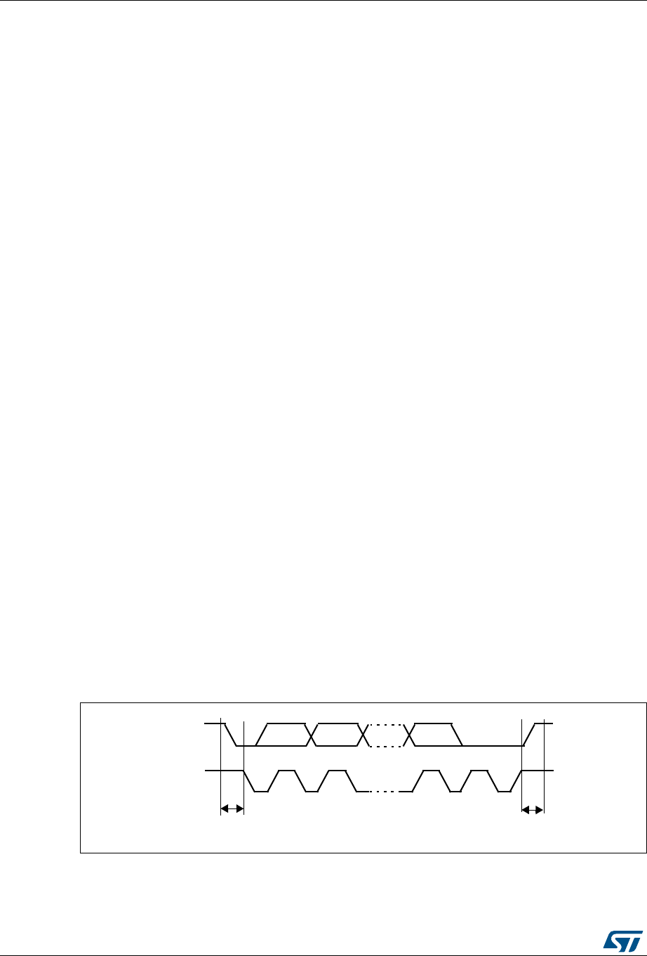
Inter-integrated circuit (I2C) interface RM0430
850/1324 RM0430 Rev 8
Note: Some of the above features may not be available in certain products. The user should refer
to the product data sheet, to identify the specific features supported by the I2C interface
implementation.
27.3 I2C functional description
In addition to receiving and transmitting data, this interface converts it from serial to parallel
format and vice versa. The interrupts are enabled or disabled by software. The interface is
connected to the I2C bus by a data pin (SDA) and by a clock pin (SCL). It can be connected
with a standard (up to 100 kHz) or fast (up to 400 kHz) I2C bus.
27.3.1 Mode selection
The interface can operate in one of the four following modes:
•Slave transmitter
•Slave receiver
•Master transmitter
•Master receiver
By default, it operates in slave mode. The interface automatically switches from slave to
master, after it generates a START condition and from master to slave, if an arbitration loss
or a Stop generation occurs, allowing multimaster capability.
Communication flow
In Master mode, the I2C interface initiates a data transfer and generates the clock signal. A
serial data transfer always begins with a start condition and ends with a stop condition. Both
start and stop conditions are generated in master mode by software.
In Slave mode, the interface is capable of recognizing its own addresses (7 or 10-bit), and
the General Call address. The General Call address detection may be enabled or disabled
by software.
Data and addresses are transferred as 8-bit bytes, MSB first. The first byte(s) following the
start condition contain the address (one in 7-bit mode, two in 10-bit mode). The address is
always transmitted in Master mode.
A 9th clock pulse follows the 8 clock cycles of a byte transfer, during which the receiver must
send an acknowledge bit to the transmitter. Refer to Figure 285.
Figure 285. I2C bus protocol
Acknowledge may be enabled or disabled by software. The I2C interface addresses (dual
addressing 7-bit/ 10-bit and/or general call address) can be selected by software.
SCL
SDA
12 8 9
MSB ACK
Stop
Start
condition
condition
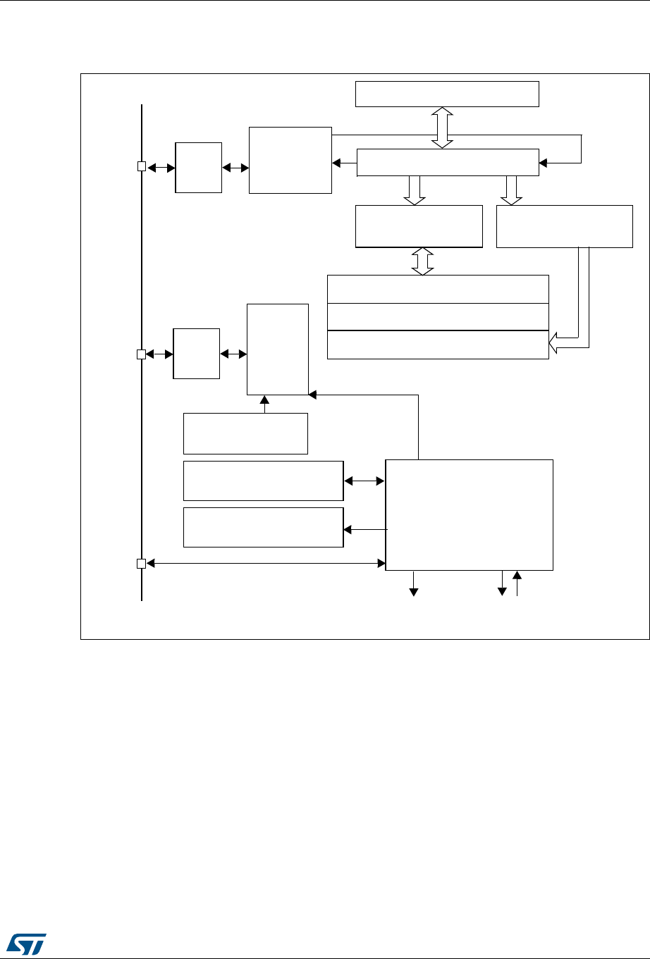
RM0430 Rev 8 851/1324
RM0430 Inter-integrated circuit (I2C) interface
882
The block diagram of the I2C interface is shown in Figure 286.
Figure 286. I2C block diagram
1. SMBA is an optional signal in SMBus mode. This signal is not applicable if SMBus is disabled.
27.3.2 I2C slave mode
By default the I2C interface operates in Slave mode. To switch from default Slave mode to
Master mode a Start condition generation is needed.
The peripheral input clock must be programmed in the I2C_CR2 register in order to
generate correct timings. The peripheral input clock frequency must be at least:
•2 MHz in Sm mode
•4 MHz in Fm mode
As soon as a start condition is detected, the address is received from the SDA line and sent
to the shift register. Then it is compared with the address of the interface (OAR1) and with
OAR2 (if ENDUAL=1) or the General Call address (if ENGC = 1).
$ATASHIFTREGISTER
#OMPARATOR
/WNADDRESSREGISTER
#LOCKCONTROL
3TATUSREGISTERS
#ONTROLREGISTERS
#ONTROL
#LOCK
CONTROL
$ATA
CONTROL
3#,
LOGIC
$UALADDRESSREGISTER
$ATAREGISTER
0%#REGISTER
)NTERRUPTS
0%#CALCULATION
3-"!
3$!
2EGISTER##2
3232
#2#2
$-!REQUESTS!#+
-36
.OISE
FILTER
.OISE
FILTER

Inter-integrated circuit (I2C) interface RM0430
852/1324 RM0430 Rev 8
Note: In 10-bit addressing mode, the comparison includes the header sequence (11110xx0),
where xx denotes the two most significant bits of the address.
Header or address not matched: the interface ignores it and waits for another Start
condition.
Header matched (10-bit mode only): the interface generates an acknowledge pulse if the
ACK bit is set and waits for the 8-bit slave address.
Address matched: the interface generates in sequence:
•An acknowledge pulse if the ACK bit is set
•The ADDR bit is set by hardware and an interrupt is generated if the ITEVFEN bit is
set.
•If ENDUAL=1, the software has to read the DUALF bit to check which slave address
has been acknowledged.
In 10-bit mode, after receiving the address sequence the slave is always in Receiver mode.
It will enter Transmitter mode on receiving a repeated Start condition followed by the header
sequence with matching address bits and the least significant bit set (11110xx1).
The TRA bit indicates whether the slave is in Receiver or Transmitter mode.
Slave transmitter
Following the address reception and after clearing ADDR, the slave sends bytes from the
DR register to the SDA line via the internal shift register.
The slave stretches SCL low until ADDR is cleared and DR filled with the data to be sent
(see Figure 287 Transfer sequencing EV1 EV3).
When the acknowledge pulse is received:
•The TxE bit is set by hardware with an interrupt if the ITEVFEN and the ITBUFEN bits
are set.
If TxE is set and some data were not written in the I2C_DR register before the end of the
next data transmission, the BTF bit is set and the interface waits until BTF is cleared by a
read to I2C_SR1 followed by a write to the I2C_DR register, stretching SCL low.
RM0430 Rev 8 853/1324
RM0430 Inter-integrated circuit (I2C) interface
882
Figure 287. Transfer sequence diagram for slave transmitter
1. The EV1 and EV3_1 events stretch SCL low until the end of the corresponding software sequence.
2. The EV3 event stretches SCL low if the software sequence is not completed before the end of the next byte
transmission
Slave receiver
Following the address reception and after clearing ADDR, the slave receives bytes from the
SDA line into the DR register via the internal shift register. After each byte the interface
generates in sequence:
•An acknowledge pulse if the ACK bit is set
•The RxNE bit is set by hardware and an interrupt is generated if the ITEVFEN and
ITBUFEN bit is set.
If RxNE is set and the data in the DR register is not read before the end of the next data
reception, the BTF bit is set and the interface waits until BTF is cleared by a read from the
I2C_DR register, stretching SCL low (see Figure 288 Transfer sequencing).
ELWVODYHWUDQVPLWWHU
ELWVODYHWUDQVPLWWHU
6 $ GGUHVV $ 'DWD
(9 (9 (9
6U'DWD $
(9 (9B (9 (9 (9
DL9
'DWD$$
'DWD1 1$ 3
(9
(9 (9
6 +HDGHU $ $GGUHVV $
(9
+HDGHU $ 'DWD1 1$ 3
/HJHQG 6 6WDUW6U 5HSHDWHG6WDUW3 6WRS$ $FNQRZOHGJH1$ 1RQDFNQRZOHGJH
(9[ (YHQWZLWKLQWHUUXSWLI,7(9)(1
(97[( VKLIWUHJLVWHUHPSW\GDWDUHJLVWHUHPSW\ZULWH'DWDLQ'5
(97[( VKLIWUHJLVWHUQRWHPSW\GDWDUHJLVWHUHPSW\FOHDUHGE\ZULWLQJ'5
(9$) $)LVFOHDUHGE\ZULWLQJµ¶LQ$)ELWRI65UHJLVWHU
$9$''5 FOHDUHGE\UHDGLQJ65IROORZHGE\UHDGLQJ65

Inter-integrated circuit (I2C) interface RM0430
854/1324 RM0430 Rev 8
Figure 288. Transfer sequence diagram for slave receiver
1. The EV1 event stretches SCL low until the end of the corresponding software sequence.
2. The EV2 event stretches SCL low if the software sequence is not completed before the end of the next byte
reception.
3. After checking the SR1 register content, the user should perform the complete clearing sequence for each
flag found set.
Thus, for ADDR and STOPF flags, the following sequence is required inside the I2C interrupt routine:
READ SR1
if (ADDR == 1) {READ SR1; READ SR2}
if (STOPF == 1) {READ SR1; WRITE CR1}
The purpose is to make sure that both ADDR and STOPF flags are cleared if both are found set.
Closing slave communication
After the last data byte is transferred a Stop Condition is generated by the master. The
interface detects this condition and sets:
•The STOPF bit and generates an interrupt if the ITEVFEN bit is set.
The STOPF bit is cleared by a read of the SR1 register followed by a write to the CR1
register (see Figure 288: Transfer sequence diagram for slave receiver EV4).
27.3.3 I2C master mode
In Master mode, the I2C interface initiates a data transfer and generates the clock signal. A
serial data transfer always begins with a Start condition and ends with a Stop condition.
Master mode is selected as soon as the Start condition is generated on the bus with a
START bit.
The following is the required sequence in master mode.
•Program the peripheral input clock in I2C_CR2 Register in order to generate correct
timings
•Configure the clock control registers
•Configure the rise time register
•Program the I2C_CR1 register to enable the peripheral
•Set the START bit in the I2C_CR1 register to generate a Start condition
The peripheral input clock frequency must be at least:
•2 MHz in Sm mode
•4 MHz in Fm mode
ELWVODYHUHFHLYHU
ELWVODY HUHFHLYHU
/HJHQG 6 6WDUW6U 5HSHDWHG6WDUW3 6WRS$ $FNQRZOHGJH
(9[ (YHQWZLWKLQWHUUXSWLI,7(9)(1
(9$''5 FOHDUHGE\UHDGLQJ65IROORZHGE\UHDGLQJ65
(95[1( FOHDUHGE\UHDGLQJ'5UHJLVWHU
(96723) FOHDUHGE\UHDGLQJ65UHJLVWHUIROORZHGE\ZULWLQJWRWKH&5UHJLVWHU
$'DWD $ 'DWD1 $ 3
$$
'DWD1
DL9
6 $GGUHVV 'DWD $
(9 (9 (9 (9 (9
(9 (9
$3
(9
'DWD$GGUHVV
$
6+HDGHU

RM0430 Rev 8 855/1324
RM0430 Inter-integrated circuit (I2C) interface
882
SCL master clock generation
The CCR bits are used to generate the high and low level of the SCL clock, starting from the
generation of the rising and falling edge (respectively). As a slave may stretch the SCL line,
the peripheral checks the SCL input from the bus at the end of the time programmed in
TRISE bits after rising edge generation.
•If the SCL line is low, it means that a slave is stretching the bus, and the high level
counter stops until the SCL line is detected high. This allows to guarantee the minimum
HIGH period of the SCL clock parameter.
•If the SCL line is high, the high level counter keeps on counting.
Indeed, the feedback loop from the SCL rising edge generation by the peripheral to the SCL
rising edge detection by the peripheral takes time even if no slave stretches the clock. This
loopback duration is linked to the SCL rising time (impacting SCL VIH input detection), plus
delay due to the noise filter present on the SCL input path, plus delay due to internal SCL
input synchronization with APB clock. The maximum time used by the feedback loop is
programmed in the TRISE bits, so that the SCL frequency remains stable whatever the SCL
rising time.
Start condition
Setting the START bit causes the interface to generate a Start condition and to switch to
Master mode (MSL bit set) when the BUSY bit is cleared.
Note: In master mode, setting the START bit causes the interface to generate a ReStart condition
at the end of the current byte transfer.
Once the Start condition is sent:
•The SB bit is set by hardware and an interrupt is generated if the ITEVFEN bit is set.
Then the master waits for a read of the SR1 register followed by a write in the DR register
with the Slave address (see Figure 289 and Figure 290 Transfer sequencing EV5).
Slave address transmission
Then the slave address is sent to the SDA line via the internal shift register.
•In 10-bit addressing mode, sending the header sequence causes the following event:
– The ADD10 bit is set by hardware and an interrupt is generated if the ITEVFEN bit
is set.
Then the master waits for a read of the SR1 register followed by a write in the DR
register with the second address byte (see Figure 289 and Figure 290 Transfer
sequencing).
– The ADDR bit is set by hardware and an interrupt is generated if the ITEVFEN bit
is set.
Then the master waits for a read of the SR1 register followed by a read of the SR2
register (see Figure 289 and Figure 290 Transfer sequencing).
•In 7-bit addressing mode, one address byte is sent.
As soon as the address byte is sent,
– The ADDR bit is set by hardware and an interrupt is generated if the ITEVFEN bit
is set.
Then the master waits for a read of the SR1 register followed by a read of the SR2
register (see Figure 289 and Figure 290 Transfer sequencing).

Inter-integrated circuit (I2C) interface RM0430
856/1324 RM0430 Rev 8
The master can decide to enter Transmitter or Receiver mode depending on the LSB of the
slave address sent.
•In 7-bit addressing mode,
– To enter Transmitter mode, a master sends the slave address with LSB reset.
– To enter Receiver mode, a master sends the slave address with LSB set.
•In 10-bit addressing mode,
– To enter Transmitter mode, a master sends the header (11110xx0) and then the
slave address, (where xx denotes the two most significant bits of the address).
– To enter Receiver mode, a master sends the header (11110xx0) and then the
slave address. Then it should send a repeated Start condition followed by the
header (11110xx1), (where xx denotes the two most significant bits of the
address).
The TRA bit indicates whether the master is in Receiver or Transmitter mode.
Master transmitter
Following the address transmission and after clearing ADDR, the master sends bytes from
the DR register to the SDA line via the internal shift register.
The master waits until the first data byte is written into I2C_DR (see Figure 289 Transfer
sequencing EV8_1).
When the acknowledge pulse is received, the TxE bit is set by hardware and an interrupt is
generated if the ITEVFEN and ITBUFEN bits are set.
If TxE is set and a data byte was not written in the DR register before the end of the last data
transmission, BTF is set and the interface waits until BTF is cleared by a write to I2C_DR,
stretching SCL low.
Closing the communication
After the last byte is written to the DR register, the STOP bit is set by software to generate a
Stop condition (see Figure 289 Transfer sequencing EV8_2). The interface automatically
goes back to slave mode (MSL bit cleared).
Note: Stop condition should be programmed during EV8_2 event, when either TxE or BTF is set.

RM0430 Rev 8 857/1324
RM0430 Inter-integrated circuit (I2C) interface
882
Figure 289. Transfer sequence diagram for master transmitter
1. The EV5, EV6, EV9, EV8_1 and EV8_2 events stretch SCL low until the end of the corresponding software sequence.
2. The EV8 event stretches SCL low if the software sequence is not complete before the end of the next byte transmission.
ELWPDVWHUWUDQVPLWWHU
$
DL9
6 $GGUHVV $'DWD 'DWD$ 'DWD1 $3
(9 (9 (9B (9 (9 (9 (9B
'DWD1 $3
(9B
'DWD $
(9 (9(9B(9
6
(9
+HDGHU $ $GGUHVV $
(9
ELWPDVWHUWUDQVPLWWHU
/HJHQG6 6WDUW65 5HSHDWHGVWDUW3 VWRS$ $FNQRZOHGJH
(9[ (YHQWZLWKLQWHUUXSWLI,7(9)(1
(96% FOHDUHGE\UHDGLQJ65UHJLVWHUIROORZHGE\ZULWLQJ'5UHJLVWHUZLWKDGGUHVV
(9$''5 FOHDUHGE\UHDGLQJ65UHJLVWHUIROORZHGE\UHDGLQJ65
(9B7[( VKLIWUHJLVWHUHPSW\GDWDUHJLVWHUHPSW\ZULWH'DWDLQ'5
(97[( VKLIWUHJLVWHUQRWHPSW\GDWDUHJLVWHUHPSW\FOHDUHGE\ZULWLQJ'5UHJLVWHU
(9B7[( %7) 3URJUDPVWRSUHTXHVW7[(DQG%7)DUHFOHDUHGE\KDUGZDUHE\WKHVWRSFRQGLWLRQ
(9$'' FOHDUHGE\UHDGLQJ65UHJLVWHUIROORZHGE\ZULWLQJ'5UHJLVWHU

Inter-integrated circuit (I2C) interface RM0430
858/1324 RM0430 Rev 8
Master receiver
Following the address transmission and after clearing ADDR, the I2C interface enters
Master Receiver mode. In this mode the interface receives bytes from the SDA line into the
DR register via the internal shift register. After each byte the interface generates in
sequence:
1. An acknowledge pulse if the ACK bit is set
2. The RxNE bit is set and an interrupt is generated if the ITEVFEN and ITBUFEN bits are
set (see Figure 290 Transfer sequencing EV7).
If the RxNE bit is set and the data in the DR register is not read before the end of the last
data reception, the BTF bit is set by hardware and the interface waits until BTF is cleared by
a read in the DR register, stretching SCL low.
Closing the communication
The master sends a NACK for the last byte received from the slave. After receiving this
NACK, the slave releases the control of the SCL and SDA lines. Then the master can send
a Stop/Restart condition.
1. To generate the nonacknowledge pulse after the last received data byte, the ACK bit
must be cleared just after reading the second last data byte (after second last RxNE
event).
2. In order to generate the Stop/Restart condition, software must set the STOP/START bit
after reading the second last data byte (after the second last RxNE event).
3. In case a single byte has to be received, the Acknowledge disable is made during EV6
(before ADDR flag is cleared) and the STOP condition generation is made after EV6.
After the Stop condition generation, the interface goes automatically back to slave mode
(MSL bit cleared).

RM0430 Rev 8 859/1324
RM0430 Inter-integrated circuit (I2C) interface
882
Figure 290. Transfer sequence diagram for master receiver
1. If a single byte is received, it is NA.
2. The EV5, EV6 and EV9 events stretch SCL low until the end of the corresponding software sequence.
3. The EV7 event stretches SCL low if the software sequence is not completed before the end of the next byte reception.
4. The EV7_1 software sequence must be completed before the ACK pulse of the current byte transfer.
The procedures described below are recommended if the EV7-1 software sequence is not
completed before the ACK pulse of the current byte transfer.
These procedures must be followed to make sure:
•The ACK bit is set low on time before the end of the last data reception
•The STOP bit is set high after the last data reception without reception of
supplementary data.
For 2-byte reception:
•Wait until ADDR = 1 (SCL stretched low until the ADDR flag is cleared)
•Set ACK low, set POS high
•Clear ADDR flag
•Wait until BTF = 1 (Data 1 in DR, Data2 in shift register, SCL stretched low until a data
1 is read)
•Set STOP high
•Read data 1 and 2
BITMASTERRECEIVER
BITMASTERRECEIVER
,EGEND33TART3R2EPEATED3TART03TOP!!CKNOWLEDGE.!.ONACKNOWLEDGE
%6X%VENTWITHINTERRUPTIF)4%6&%.
%63"CLEAREDBYREADING32REGISTERFOLLOWEDBYWRITING$2REGISTER
%6!$$2CLEAREDBYREADING32REGISTERFOLLOWEDBYREADING32)NBITMASTERRECEIVERMODETHISSE
QUENCESHOULDBEFOLLOWEDBYWRITING#2WITH34!24
%62X.%CLEAREDBYREADING$2REGISTER
%6?2X.%CLEAREDBYREADING$2REGISTERPROGRAM!# +AND34/0REQUEST
%6!$$CLEAREDBYREADING32REGISTERFOLLOWEDBYWRITING$2REGISTER
3 !DDRESS ! $ATA ! $ATA ! $ATA. .! 0
%6 %6 %6 %6 %6? %6
3 (EADER ! !DDRESS !
%6 %6 %6
3R(EADER ! $ATA !
%6 %6 %6
$ATA !
%6
$ATA. .! 0
%6? %6
AID
)NCASEOFTHERECEPTIONOFBYTETHE!CKNOWLEDGEDISABLEMUSTBEPERFORMEDDURING%6EVENTIEBEFORECLEARING!$$2FLAG

Inter-integrated circuit (I2C) interface RM0430
860/1324 RM0430 Rev 8
For N >2 -byte reception, from N-2 data reception
•Wait until BTF = 1 (data N-2 in DR, data N-1 in shift register, SCL stretched low until
data N-2 is read)
•Set ACK low
•Read data N-2
•Wait until BTF = 1 (data N-1 in DR, data N in shift register, SCL stretched low until a
data N-1 is read)
•Set STOP high
•Read data N-1 and N
27.3.4 Error conditions
The following are the error conditions which may cause communication to fail.
Bus error (BERR)
This error occurs when the I2C interface detects an external Stop or Start condition during
an address or a data transfer. In this case:
•the BERR bit is set and an interrupt is generated if the ITERREN bit is set
•in Slave mode: data are discarded and the lines are released by hardware:
– in case of a misplaced Start, the slave considers it is a restart and waits for an
address, or a Stop condition
– in case of a misplaced Stop, the slave behaves like for a Stop condition and the
lines are released by hardware
•In Master mode: the lines are not released and the state of the current transmission is
not affected. It is up to the software to abort or not the current transmission
Acknowledge failure (AF)
This error occurs when the interface detects a nonacknowledge bit. In this case:
•the AF bit is set and an interrupt is generated if the ITERREN bit is set
•a transmitter which receives a NACK must reset the communication:
– If Slave: lines are released by hardware
– If Master: a Stop or repeated Start condition must be generated by software
Arbitration lost (ARLO)
This error occurs when the I2C interface detects an arbitration lost condition. In this case,
•the ARLO bit is set by hardware (and an interrupt is generated if the ITERREN bit is
set)
•the I2C Interface goes automatically back to slave mode (the MSL bit is cleared). When
the I2C loses the arbitration, it is not able to acknowledge its slave address in the same
transfer, but it can acknowledge it after a repeated Start from the winning master.
•lines are released by hardware

RM0430 Rev 8 861/1324
RM0430 Inter-integrated circuit (I2C) interface
882
Overrun/underrun error (OVR)
An overrun error can occur in slave mode when clock stretching is disabled and the I2C
interface is receiving data. The interface has received a byte (RxNE=1) and the data in DR
has not been read, before the next byte is received by the interface. In this case,
•The last received byte is lost.
•In case of Overrun error, software should clear the RxNE bit and the transmitter should
re-transmit the last received byte.
Underrun error can occur in slave mode when clock stretching is disabled and the I2C
interface is transmitting data. The interface has not updated the DR with the next byte
(TxE=1), before the clock comes for the next byte. In this case,
•The same byte in the DR register will be sent again
•The user should make sure that data received on the receiver side during an underrun
error are discarded and that the next bytes are written within the clock low time
specified in the I2C bus standard.
For the first byte to be transmitted, the DR must be written after ADDR is cleared and before
the first SCL rising edge. If not possible, the receiver must discard the first data.
27.3.5 Programmable noise filter
In Fm mode, the I2C standard requires that spikes are suppressed to a length of 50 ns on
SDA and SCL lines.
An analog noise filter is implemented in the SDA and SCL I/Os. This filter is enabled by
default and can be disabled by setting the ANOFF bit in the I2C_FLTR register.
A digital noise filter can be enabled by configuring the DNF[3:0] bits to a non-zero value.
This suppresses the spikes on SDA and SCL inputs with a length of up to DNF[3:0] *
TPCLK1.
Enabling the digital noise filter increases the SDA hold time by (DNF[3:0] +1)* TPCLK.
To be compliant with the maximum hold time of the I2C-bus specification version 2.1
(Thd:dat), the DNF bits must be programmed using the constraints shown in Table 153, and
assuming that the analog filter is disabled.
Note: DNF[3:0] must only be configured when the I2C is disabled (PE = 0). If the analog filter is
also enabled, the digital filter is added to the analog filter.
Table 153. Maximum DNF[3:0] value to be compliant with Thd:dat(max)
PCLK1 frequency
Maximum DNF value
Sm mode Fm mode
2 <= FPCLK1 <= 5 2 0
5 < FPCLK1 <= 10 12 0
10 < FPCLK1 <= 20 15 1
20 < FPCLK1 <= 30 15 7
30 < FPCLK1 <= 40 15 13
40 < FPCLK1 <= 50 15 15

Inter-integrated circuit (I2C) interface RM0430
862/1324 RM0430 Rev 8
Note: For each frequency range, the constraint is given based on the worst case which is the
minimum frequency of the range. Greater DNF values can be used if the system can
support maximum hold time violation.
27.3.6 SDA/SCL line control
•If clock stretching is enabled:
– Transmitter mode: If TxE=1 and BTF=1: the interface holds the clock line low
before transmission to wait for the microcontroller to write the byte in the Data
Register (both buffer and shift register are empty).
– Receiver mode: If RxNE=1 and BTF=1: the interface holds the clock line low after
reception to wait for the microcontroller to read the byte in the Data Register (both
buffer and shift register are full).
•If clock stretching is disabled in Slave mode:
– Overrun Error in case of RxNE=1 and no read of DR has been done before the
next byte is received. The last received byte is lost.
– Underrun Error in case TxE=1 and no write into DR has been done before the next
byte must be transmitted. The same byte will be sent again.
– Write Collision not managed.
27.3.7 SMBus
Introduction
The System Management Bus (SMBus) is a two-wire interface through which various
devices can communicate with each other and with the rest of the system. It is based on I2C
principles of operation. SMBus provides a control bus for system and power management
related tasks. A system may use SMBus to pass messages to and from devices instead of
toggling individual control lines.
The System Management Bus Specification refers to three types of devices. A slave is a
device that is receiving or responding to a command. A master is a device that issues
commands, generates the clocks, and terminates the transfer. A host is a specialized
master that provides the main interface to the system's CPU. A host must be a master-slave
and must support the SMBus host notify protocol. Only one host is allowed in a system.
Similarities between SMBus and I2C
•2 wire bus protocol (1 Clk, 1 Data) + SMBus Alert line optional
•Master-slave communication, Master provides clock
•Multi master capability
•SMBus data format similar to I2C 7-bit addressing format (Figure 285).
Differences between SMBus and I2C
The following table describes the differences between SMBus and I2C.

RM0430 Rev 8 863/1324
RM0430 Inter-integrated circuit (I2C) interface
882
SMBus application usage
With System Management Bus, a device can provide manufacturer information, tell the
system what its model/part number is, save its state for a suspend event, report different
types of errors, accept control parameters, and return its status. SMBus provides a control
bus for system and power management related tasks.
Device identification
Any device that exists on the System Management Bus as a slave has a unique address
called the Slave Address. For the list of reserved slave addresses, refer to the SMBus
specification version. 2.0 (http://smbus.org/).
Bus protocols
The SMBus specification supports up to 9 bus protocols. For more details of these protocols
and SMBus address types, refer to SMBus specification version. 2.0. These protocols
should be implemented by the user software.
Address resolution protocol (ARP)
SMBus slave address conflicts can be resolved by dynamically assigning a new unique
address to each slave device. The Address Resolution Protocol (ARP) has the following
attributes:
•Address assignment uses the standard SMBus physical layer arbitration mechanism
•Assigned addresses remain constant while device power is applied; address retention
through device power loss is also allowed
•No additional SMBus packet overhead is incurred after address assignment. (i.e.
subsequent accesses to assigned slave addresses have the same overhead as
accesses to fixed address devices.)
•Any SMBus master can enumerate the bus
Unique device identifier (UDID)
In order to provide a mechanism to isolate each device for the purpose of address
assignment, each device must implement a unique device identifier (UDID).
For the details on 128 bit UDID and more information on ARP, refer to SMBus specification
version 2.0.
Table 154. SMBus vs. I2C
SMBus I2C
Max. speed 100 kHz Max. speed 400 kHz
Min. clock speed 10 kHz No minimum clock speed
35 ms clock low timeout No timeout
Logic levels are fixed Logic levels are VDD dependent
Different address types (reserved, dynamic etc.) 7-bit, 10-bit and general call slave address types
Different bus protocols (quick command, process
call etc.) No bus protocols

Inter-integrated circuit (I2C) interface RM0430
864/1324 RM0430 Rev 8
SMBus alert mode
SMBus Alert is an optional signal with an interrupt line for devices that want to trade their
ability to master for a pin. SMBA is a wired-AND signal just as the SCL and SDA signals are.
SMBA is used in conjunction with the SMBus General Call Address. Messages invoked with
the SMBus are 2 bytes long.
A slave-only device can signal the host through SMBA that it wants to talk by setting ALERT
bit in I2C_CR1 register. The host processes the interrupt and simultaneously accesses all
SMBA devices through the Alert Response Address (known as ARA having a value 0001
100X). Only the device(s) which pulled SMBA low will acknowledge the Alert Response
Address. This status is identified using SMBALERT Status flag in I2C_SR1 register. The
host performs a modified Receive Byte operation. The 7 bit device address provided by the
slave transmit device is placed in the 7 most significant bits of the byte. The eighth bit can
be a zero or one.
If more than one device pulls SMBA low, the highest priority (lowest address) device will win
communication rights via standard arbitration during the slave address transfer. After
acknowledging the slave address the device must disengage its SMBA pull-down. If the
host still sees SMBA low when the message transfer is complete, it knows to read the ARA
again.
A host which does not implement the SMBA signal may periodically access the ARA.
For more details on SMBus Alert mode, refer to SMBus specification version 2.0
(http://smbus.org/).
Timeout error
There are differences in the timing specifications between I2C and SMBus.
SMBus defines a clock low timeout, TIMEOUT of 35 ms. Also SMBus specifies TLOW:
SEXT as the cumulative clock low extend time for a slave device. SMBus specifies TLOW:
MEXT as the cumulative clock low extend time for a master device. For more details on
these timeouts, refer to SMBus specification version 2.0.
The status flag Timeout or Tlow Error in I2C_SR1 shows the status of this feature.
How to use the interface in SMBus mode
To switch from I2C mode to SMBus mode, the following sequence should be performed.
•Set the SMBus bit in the I2C_CR1 register
•Configure the SMBTYPE and ENARP bits in the I2C_CR1 register as required for the
application
If you want to configure the device as a master, follow the Start condition generation
procedure in Section 27.3.3: I2C master mode. Otherwise, follow the sequence in
Section 27.3.2: I2C slave mode.
The application has to control the various SMBus protocols by software.
•SMB Device Default Address acknowledged if ENARP=1 and SMBTYPE=0
•SMB Host Header acknowledged if ENARP=1 and SMBTYPE=1
•SMB Alert Response Address acknowledged if SMBALERT=1

RM0430 Rev 8 865/1324
RM0430 Inter-integrated circuit (I2C) interface
882
27.3.8 DMA requests
DMA requests (when enabled) are generated only for data transfer. DMA requests are
generated by Data Register becoming empty in transmission and Data Register becoming
full in reception. The DMA must be initialized and enabled before the I2C data transfer. The
DMAEN bit must be set in the I2C_CR2 register before the ADDR event. In master mode or
in slave mode when clock stretching is enabled, the DMAEN bit can also be set during the
ADDR event, before clearing the ADDR flag. The DMA request must be served before the
end of the current byte transfer. When the number of data transfers which has been
programmed for the corresponding DMA stream is reached, the DMA controller sends an
End of Transfer EOT signal to the I2C interface and generates a Transfer Complete interrupt
if enabled:
•Master transmitter: In the interrupt routine after the EOT interrupt, disable DMA
requests then wait for a BTF event before programming the Stop condition.
•Master receiver
– When the number of bytes to be received is equal to or greater than two, the DMA
controller sends a hardware signal, EOT_1, corresponding to the last but one data
byte (number_of_bytes – 1). If, in the I2C_CR2 register, the LAST bit is set, I2C
automatically sends a NACK after the next byte following EOT_1. The user can
generate a Stop condition in the DMA Transfer Complete interrupt routine if
enabled.
– When a single byte must be received: the NACK must be programmed during EV6
event, i.e. program ACK=0 when ADDR=1, before clearing ADDR flag. Then the
user can program the STOP condition either after clearing ADDR flag, or in the
DMA Transfer Complete interrupt routine.
Transmission using DMA
DMA mode can be enabled for transmission by setting the DMAEN bit in the I2C_CR2
register. Data will be loaded from a Memory area configured using the DMA peripheral (refer
to the DMA specification) to the I2C_DR register whenever the TxE bit is set. To map a DMA
stream x for I2C transmission (where x is the stream number), perform the following
sequence:
1. Set the I2C_DR register address in the DMA_SxPAR register. The data will be moved
to this address from the memory after each TxE event.
2. Set the memory address in the DMA_SxMA0R register (and in DMA_SxMA1R register
in the case of a bouble buffer mode). The data will be loaded into I2C_DR from this
memory after each TxE event.
3. Configure the total number of bytes to be transferred in the DMA_SxNDTR register.
After each TxE event, this value will be decremented.
4. Configure the DMA stream priority using the PL[0:1] bits in the DMA_SxCR register
5. Set the DIR bit in the DMA_SxCR register and configure interrupts after half transfer or
full transfer depending on application requirements.
6. Activate the stream by setting the EN bit in the DMA_SxCR register.
When the number of data transfers which has been programmed in the DMA Controller
registers is reached, the DMA controller sends an End of Transfer EOT/ EOT_1 signal to the
I2C interface and the DMA generates an interrupt, if enabled, on the DMA stream interrupt
vector.
Note: Do not enable the ITBUFEN bit in the I2C_CR2 register if DMA is used for transmission.

Inter-integrated circuit (I2C) interface RM0430
866/1324 RM0430 Rev 8
Reception using DMA
DMA mode can be enabled for reception by setting the DMAEN bit in the I2C_CR2 register.
Data will be loaded from the I2C_DR register to a Memory area configured using the DMA
peripheral (refer to the DMA specification) whenever a data byte is received. To map a DMA
stream x for I2C reception (where x is the stream number), perform the following sequence:
1. Set the I2C_DR register address in DMA_SxPAR register. The data will be moved from
this address to the memory after each RxNE event.
2. Set the memory address in the DMA_SxMA0R register (and in DMA_SxMA1R register
in the case of a bouble buffer mode). The data will be loaded from the I2C_DR register
to this memory area after each RxNE event.
3. Configure the total number of bytes to be transferred in the DMA_SxNDTR register.
After each RxNE event, this value will be decremented.
4. Configure the stream priority using the PL[0:1] bits in the DMA_SxCR register
5. Reset the DIR bit and configure interrupts in the DMA_SxCR register after half transfer
or full transfer depending on application requirements.
6. Activate the stream by setting the EN bit in the DMA_SxCR register.
When the number of data transfers which has been programmed in the DMA Controller
registers is reached, the DMA controller sends an End of Transfer EOT/ EOT_1 signal to the
I2C interface and DMA generates an interrupt, if enabled, on the DMA stream interrupt
vector.
Note: Do not enable the ITBUFEN bit in the I2C_CR2 register if DMA is used for reception.
27.3.9 Packet error checking
A PEC calculator has been implemented to improve the reliability of communication. The
PEC is calculated by using the C(x) = x8 + x2 + x + 1 CRC-8 polynomial serially on each bit.
•PEC calculation is enabled by setting the ENPEC bit in the I2C_CR1 register. PEC is a
CRC-8 calculated on all message bytes including addresses and R/W bits.
– In transmission: set the PEC transfer bit in the I2C_CR1 register after the TxE
event corresponding to the last byte. The PEC will be transferred after the last
transmitted byte.
– In reception: set the PEC bit in the I2C_CR1 register after the RxNE event
corresponding to the last byte so that the receiver sends a NACK if the next
received byte is not equal to the internally calculated PEC. In case of Master-
Receiver, a NACK must follow the PEC whatever the check result. The PEC must

RM0430 Rev 8 867/1324
RM0430 Inter-integrated circuit (I2C) interface
882
be set before the ACK of the CRC reception in slave mode. It must be set when
the ACK is set low in master mode.
•A PECERR error flag/interrupt is also available in the I2C_SR1 register.
•If DMA and PEC calculation are both enabled:-
– In transmission: when the I2C interface receives an EOT signal from the DMA
controller, it automatically sends a PEC after the last byte.
– In reception: when the I2C interface receives an EOT_1 signal from the DMA
controller, it will automatically consider the next byte as a PEC and will check it. A
DMA request is generated after PEC reception.
•To allow intermediate PEC transfers, a control bit is available in the I2C_CR2 register
(LAST bit) to determine if it is really the last DMA transfer or not. If it is the last DMA
request for a master receiver, a NACK is automatically sent after the last received byte.
•PEC calculation is corrupted by an arbitration loss.
27.4 I2C interrupts
The table below gives the list of I2C interrupt requests.
Note: SB, ADDR, ADD10, STOPF, BTF, RxNE and TxE are logically ORed on the same interrupt
channel.
BERR, ARLO, AF, OVR, PECERR, TIMEOUT and SMBALERT are logically ORed on the
same interrupt channel.
Table 155. I2C Interrupt requests
Interrupt event Event flag Enable control bit
Start bit sent (Master) SB
ITEVFEN
Address sent (Master) or Address matched (Slave) ADDR
10-bit header sent (Master) ADD10
Stop received (Slave) STOPF
Data byte transfer finished BTF
Receive buffer not empty RxNE
ITEVFEN and ITBUFEN
Transmit buffer empty TxE
Bus error BERR
ITERREN
Arbitration loss (Master) ARLO
Acknowledge failure AF
Overrun/Underrun OVR
PEC error PECERR
Timeout/Tlow error TIMEOUT
SMBus Alert SMBALERT
Inter-integrated circuit (I2C) interface RM0430
868/1324 RM0430 Rev 8
Figure 291. I2C interrupt mapping diagram
ADDR
SB
ADD10
RxNE
TxE
BTF
it_event
ARLO
BERR
AF
OVR
PECERR
TIMEOUT
SMBALERT
ITERREN
it_error
ITEVFEN
ITBUFEN
STOPF

RM0430 Rev 8 869/1324
RM0430 Inter-integrated circuit (I2C) interface
882
27.5 I2C debug mode
When the microcontroller enters the debug mode (Cortex®-M4 with FPU core halted), the
SMBUS timeout either continues to work normally or stops, depending on the
DBG_I2Cx_SMBUS_TIMEOUT configuration bits in the DBG module. For more details,
refer to Section 34.16.2: Debug support for timers, watchdog, bxCAN and I2C.
27.6 I2C registers
Refer to Section 1.2 on page 52 for a list of abbreviations used in register descriptions.
The peripheral registers have to be accessed by half-words (16 bits) or words (32 bits).
27.6.1 I2C Control register 1 (I2C_CR1)
Address offset: 0x00
Reset value: 0x0000
1514131211109876543210
SW
RST Res. ALERT PEC POS ACK STOP START
NO
STRET
CH
ENGC ENPEC ENARP SMB
TYPE Res. SM
BUS PE
rw rw rw rw rw rw rw rw rw rw rw rw rw rw
Bit 15 SWRST: Software reset
When set, the I2C is under reset state. Before resetting this bit, make sure the I2C lines are
released and the bus is free.
0: I2C Peripheral not under reset
1: I2C Peripheral under reset state
Note: This bit can be used to reinitialize the peripheral after an error or a locked state. As an
example, if the BUSY bit is set and remains locked due to a glitch on the bus, the
SWRST bit can be used to exit from this state.
Bit 14 Reserved, must be kept at reset value
Bit 13 ALERT: SMBus alert
This bit is set and cleared by software, and cleared by hardware when PE=0.
0: Releases SMBA pin high. Alert Response Address Header followed by NACK.
1: Drives SMBA pin low. Alert Response Address Header followed by ACK.
Bit 12 PEC: Packet error checking
This bit is set and cleared by software, and cleared by hardware when PEC is transferred or
by a START or Stop condition or when PE=0.
0: No PEC transfer
1: PEC transfer (in Tx or Rx mode)
Note: PEC calculation is corrupted by an arbitration loss.

Inter-integrated circuit (I2C) interface RM0430
870/1324 RM0430 Rev 8
Bit 11 POS: Acknowledge/PEC Position (for data reception)
This bit is set and cleared by software and cleared by hardware when PE=0.
0: ACK bit controls the (N)ACK of the current byte being received in the shift register. The
PEC bit indicates that current byte in shift register is a PEC.
1: ACK bit controls the (N)ACK of the next byte which will be received in the shift register.
The PEC bit indicates that the next byte in the shift register is a PEC
Note: The POS bit must be used only in 2-byte reception configuration in master mode. It
must be configured before data reception starts, as described in the 2-byte reception
procedure recommended in Master receiver.
Bit 10 ACK: Acknowledge enable
This bit is set and cleared by software and cleared by hardware when PE=0.
0: No acknowledge returned
1: Acknowledge returned after a byte is received (matched address or data)
Bit 9 STOP: Stop generation
The bit is set and cleared by software, cleared by hardware when a Stop condition is
detected, set by hardware when a timeout error is detected.
In Master Mode:
0: No Stop generation.
1: Stop generation after the current byte transfer or after the current Start condition is sent.
In Slave mode:
0: No Stop generation.
1: Release the SCL and SDA lines after the current byte transfer.
Bit 8 START: Start generation
This bit is set and cleared by software and cleared by hardware when start is sent or PE=0.
In Master Mode:
0: No Start generation
1: Repeated start generation
In Slave mode:
0: No Start generation
1: Start generation when the bus is free
Bit 7 NOSTRETCH: Clock stretching disable (Slave mode)
This bit is used to disable clock stretching in slave mode when ADDR or BTF flag is set, until
it is reset by software.
0: Clock stretching enabled
1: Clock stretching disabled
Bit 6 ENGC: General call enable
0: General call disabled. Address 00h is NACKed.
1: General call enabled. Address 00h is ACKed.
Bit 5 ENPEC: PEC enable
0: PEC calculation disabled
1: PEC calculation enabled
Bit 4 ENARP: ARP enable
0: ARP disable
1: ARP enable
SMBus Device default address recognized if SMBTYPE=0
SMBus Host address recognized if SMBTYPE=1
Bit 3 SMBTYPE: SMBus type
0: SMBus Device
1: SMBus Host

RM0430 Rev 8 871/1324
RM0430 Inter-integrated circuit (I2C) interface
882
Note: When the STOP, START or PEC bit is set, the software must not perform any write access
to I2C_CR1 before this bit is cleared by hardware. Otherwise there is a risk of setting a
second STOP, START or PEC request.
27.6.2 I2C Control register 2 (I2C_CR2)
Address offset: 0x04
Reset value: 0x0000
Bit 2 Reserved, must be kept at reset value
Bit 1 SMBUS: SMBus mode
0: I2C mode
1: SMBus mode
Bit 0 PE: Peripheral enable
0: Peripheral disable
1: Peripheral enable
Note: If this bit is reset while a communication is on going, the peripheral is disabled at the
end of the current communication, when back to IDLE state.
All bit resets due to PE=0 occur at the end of the communication.
In master mode, this bit must not be reset before the end of the communication.
1514131211109876543210
Res. Res. Res. LAST DMA
EN
ITBUF
EN
ITEVT
EN
ITERR
EN Res. Res. FREQ[5:0]
rw rw rw rw rw rw rw rw rw rw rw
Bits 15:13 Reserved, must be kept at reset value
Bit 12 LAST: DMA last transfer
0: Next DMA EOT is not the last transfer
1: Next DMA EOT is the last transfer
Note: This bit is used in master receiver mode to permit the generation of a NACK on the last
received data.
Bit 11 DMAEN: DMA requests enable
0: DMA requests disabled
1: DMA request enabled when TxE=1 or RxNE =1
Bit 10 ITBUFEN: Buffer interrupt enable
0: TxE = 1 or RxNE = 1 does not generate any interrupt.
1: TxE = 1 or RxNE = 1 generates Event Interrupt (whatever the state of DMAEN)
Bit 9 ITEVTEN: Event interrupt enable
0: Event interrupt disabled
1: Event interrupt enabled
This interrupt is generated when:
– SB = 1 (Master)
– ADDR = 1 (Master/Slave)
– ADD10= 1 (Master)
– STOPF = 1 (Slave)
– BTF = 1 with no TxE or RxNE event
– TxE event to 1 if ITBUFEN = 1
– RxNE event to 1if ITBUFEN = 1

Inter-integrated circuit (I2C) interface RM0430
872/1324 RM0430 Rev 8
ITERREN: Error interrupt enable
0: Error interrupt disabled
1: Error interrupt enabled
This interrupt is generated when:
–BERR = 1
–ARLO = 1
–AF = 1
–OVR = 1
– PECERR = 1
–TIMEOUT = 1
– SMBALERT = 1
Bits 7:6 Reserved, must be kept at reset value
Bits 5:0 FREQ[5:0]: Peripheral clock frequency
The FREQ bits must be configured with the APB clock frequency value (I2C peripheral
connected to APB). The FREQ field is used by the peripheral to generate data setup and
hold times compliant with the I2C specifications. The minimum allowed frequency is 2 MHz,
the maximum frequency is limited by the maximum APB frequency and cannot exceed
50 MHz (peripheral intrinsic maximum limit).
0b000000: Not allowed
0b000001: Not allowed
0b000010: 2 MHz
...
0b110010: 50 MHz
Higher than 0b101010: Not allowed

RM0430 Rev 8 873/1324
RM0430 Inter-integrated circuit (I2C) interface
882
27.6.3 I2C Own address register 1 (I2C_OAR1)
Address offset: 0x08
Reset value: 0x0000
27.6.4 I2C Own address register 2 (I2C_OAR2)
Address offset: 0x0C
Reset value: 0x0000
1514131211109876543210
ADD
MODE Res. Res. Res. Res. Res. ADD[9:8] ADD[7:1] ADD0
rw rw rw rw rw rw rw rw rw rw rw
Bit 15 ADDMODE Addressing mode (slave mode)
0: 7-bit slave address (10-bit address not acknowledged)
1: 10-bit slave address (7-bit address not acknowledged)
Bit 14 Should always be kept at 1 by software.
Bits 13:10 Reserved, must be kept at reset value
Bits 9:8 ADD[9:8]: Interface address
7-bit addressing mode: don’t care
10-bit addressing mode: bits9:8 of address
Bits 7:1 ADD[7:1]: Interface address
bits 7:1 of address
Bit 0 ADD0: Interface address
7-bit addressing mode: don’t care
10-bit addressing mode: bit 0 of address
1514131211109876543210
Res. Res. Res. Res. Res. Res. Res. Res. ADD2[7:1] EN
DUAL
rw rw rw rw rw rw rw rw
Bits 15:8 Reserved, must be kept at reset value
Bits 7:1 ADD2[7:1]: Interface address
bits 7:1 of address in dual addressing mode
Bit 0 ENDUAL: Dual addressing mode enable
0: Only OAR1 is recognized in 7-bit addressing mode
1: Both OAR1 and OAR2 are recognized in 7-bit addressing mode

Inter-integrated circuit (I2C) interface RM0430
874/1324 RM0430 Rev 8
27.6.5 I2C Data register (I2C_DR)
Address offset: 0x10
Reset value: 0x0000
27.6.6 I2C Status register 1 (I2C_SR1)
Address offset: 0x14
Reset value: 0x0000
1514131211109876543210
Res. Res. Res. Res. Res. Res. Res. Res. DR[7:0]
rw rw rw rw rw rw rw rw
Bits 15:8 Reserved, must be kept at reset value
Bits 7:0 DR[7:0] 8-bit data register
Byte received or to be transmitted to the bus.
– Transmitter mode: Byte transmission starts automatically when a byte is written in the DR
register. A continuous transmit stream can be maintained if the next data to be transmitted is
put in DR once the transmission is started (TxE=1)
– Receiver mode: Received byte is copied into DR (RxNE=1). A continuous transmit stream
can be maintained if DR is read before the next data byte is received (RxNE=1).
Note: In slave mode, the address is not copied into DR.
Write collision is not managed (DR can be written if TxE=0).
If an ARLO event occurs on ACK pulse, the received byte is not copied into DR
and so cannot be read.
1514131211109876543210
SMB
ALERT
TIMEO
UT Res. PEC
ERR OVR AF ARLO BERR TxE RxNE Res. STOPF ADD10 BTF ADDR SB
rc_w0rc_w0 rc_w0rc_w0rc_w0rc_w0rc_w0rr rrrrr

RM0430 Rev 8 875/1324
RM0430 Inter-integrated circuit (I2C) interface
882
Bit 15 SMBALERT: SMBus alert
In SMBus host mode:
0: no SMBALERT
1: SMBALERT event occurred on pin
In SMBus slave mode:
0: no SMBALERT response address header
1: SMBALERT response address header to SMBALERT LOW received
– Cleared by software writing 0, or by hardware when PE=0.
Bit 14 TIMEOUT: Timeout or Tlow error
0: No timeout error
1: SCL remained LOW for 25 ms (Timeout)
or
Master cumulative clock low extend time more than 10 ms (Tlow:mext)
or
Slave cumulative clock low extend time more than 25 ms (Tlow:sext)
– When set in slave mode: slave resets the communication and lines are released by
hardware
– When set in master mode: Stop condition sent by hardware
– Cleared by software writing 0, or by hardware when PE=0.
Note: This functionality is available only in SMBus mode.
Bit 13 Reserved, must be kept at reset value
Bit 12 PECERR: PEC Error in reception
0: no PEC error: receiver returns ACK after PEC reception (if ACK=1)
1: PEC error: receiver returns NACK after PEC reception (whatever ACK)
– Cleared by software writing 0, or by hardware when PE=0.
– Note: When the received CRC is wrong, PECERR is not set in slave mode if the PEC control
bit is not set before the end of the CRC reception. Nevertheless, reading the PEC value
determines whether the received CRC is right or wrong.
Bit 11 OVR: Overrun/Underrun
0: No overrun/underrun
1: Overrun or underrun
– Set by hardware in slave mode when NOSTRETCH=1 and:
– In reception when a new byte is received (including ACK pulse) and the DR register has not
been read yet. New received byte is lost.
– In transmission when a new byte should be sent and the DR register has not been written
yet. The same byte is sent twice.
– Cleared by software writing 0, or by hardware when PE=0.
Note: If the DR write occurs very close to SCL rising edge, the sent data is unspecified and a
hold timing error occurs
Bit 10 AF: Acknowledge failure
0: No acknowledge failure
1: Acknowledge failure
– Set by hardware when no acknowledge is returned.
– Cleared by software writing 0, or by hardware when PE=0.

Inter-integrated circuit (I2C) interface RM0430
876/1324 RM0430 Rev 8
Bit 9 ARLO: Arbitration lost (master mode)
0: No Arbitration Lost detected
1: Arbitration Lost detected
Set by hardware when the interface loses the arbitration of the bus to another master
– Cleared by software writing 0, or by hardware when PE=0.
After an ARLO event the interface switches back automatically to Slave mode (MSL=0).
Note: In SMBUS, the arbitration on the data in slave mode occurs only during the data phase,
or the acknowledge transmission (not on the address acknowledge).
Bit 8 BERR: Bus error
0: No misplaced Start or Stop condition
1: Misplaced Start or Stop condition
– Set by hardware when the interface detects an SDA rising or falling edge while SCL is high,
occurring in a non-valid position during a byte transfer.
– Cleared by software writing 0, or by hardware when PE=0.
Bit 7 TxE: Data register empty (transmitters)
0: Data register not empty
1: Data register empty
– Set when DR is empty in transmission. TxE is not set during address phase.
– Cleared by software writing to the DR register or by hardware after a start or a stop condition
or when PE=0.
TxE is not set if either a NACK is received, or if next byte to be transmitted is PEC (PEC=1)
Note: TxE is not cleared by writing the first data being transmitted, or by writing data when
BTF is set, as in both cases the data register is still empty.
Bit 6 RxNE: Data register not empty (receivers)
0: Data register empty
1: Data register not empty
– Set when data register is not empty in receiver mode. RxNE is not set during address phase.
– Cleared by software reading or writing the DR register or by hardware when PE=0.
RxNE is not set in case of ARLO event.
Note: RxNE is not cleared by reading data when BTF is set, as the data register is still full.
Bit 5 Reserved, must be kept at reset value
Bit 4 STOPF: Stop detection (slave mode)
0: No Stop condition detected
1: Stop condition detected
– Set by hardware when a Stop condition is detected on the bus by the slave after an
acknowledge (if ACK=1).
– Cleared by software reading the SR1 register followed by a write in the CR1 register, or by
hardware when PE=0
Note: The STOPF bit is not set after a NACK reception.
It is recommended to perform the complete clearing sequence (READ SR1 then
WRITE CR1) after the STOPF is set. Refer to Figure 288: Transfer sequence diagram
for slave receiver on page 854.

RM0430 Rev 8 877/1324
RM0430 Inter-integrated circuit (I2C) interface
882
Bit 3 ADD10: 10-bit header sent (Master mode)
0: No ADD10 event occurred.
1: Master has sent first address byte (header).
– Set by hardware when the master has sent the first byte in 10-bit address mode.
– Cleared by software reading the SR1 register followed by a write in the DR register of the
second address byte, or by hardware when PE=0.
Note: ADD10 bit is not set after a NACK reception
Bit 2 BTF: Byte transfer finished
0: Data byte transfer not done
1: Data byte transfer succeeded
– Set by hardware when NOSTRETCH=0 and:
– In reception when a new byte is received (including ACK pulse) and DR has not been read
yet (RxNE=1).
– In transmission when a new byte should be sent and DR has not been written yet (TxE=1).
– Cleared by software by either a read or write in the DR register or by hardware after a start or
a stop condition in transmission or when PE=0.
Note: The BTF bit is not set after a NACK reception
The BTF bit is not set if next byte to be transmitted is the PEC (TRA=1 in I2C_SR2
register and PEC=1 in I2C_CR1 register)
Bit 1 ADDR: Address sent (master mode)/matched (slave mode)
This bit is cleared by software reading SR1 register followed reading SR2, or by hardware
when PE=0.
Address matched (Slave)
0: Address mismatched or not received.
1: Received address matched.
– Set by hardware as soon as the received slave address matched with the OAR registers
content or a general call or a SMBus Device Default Address or SMBus Host or SMBus Alert
is recognized. (when enabled depending on configuration).
Note: In slave mode, it is recommended to perform the complete clearing sequence (READ
SR1 then READ SR2) after ADDR is set. Refer to Figure 288: Transfer sequence
diagram for slave receiver on page 854.
Address sent (Master)
0: No end of address transmission
1: End of address transmission
– For 10-bit addressing, the bit is set after the ACK of the 2nd byte.
– For 7-bit addressing, the bit is set after the ACK of the byte.
Note: ADDR is not set after a NACK reception
Bit 0 SB: Start bit (Master mode)
0: No Start condition
1: Start condition generated.
– Set when a Start condition generated.
– Cleared by software by reading the SR1 register followed by writing the DR register, or by
hardware when PE=0

Inter-integrated circuit (I2C) interface RM0430
878/1324 RM0430 Rev 8
27.6.7 I2C Status register 2 (I2C_SR2)
Address offset: 0x18
Reset value: 0x0000
Note: Reading I2C_SR2 after reading I2C_SR1 clears the ADDR flag, even if the ADDR flag was
set after reading I2C_SR1. Consequently, I2C_SR2 must be read only when ADDR is found
set in I2C_SR1 or when the STOPF bit is cleared.
1514131211109876543210
PEC[7:0] DUALF SMB
HOST
SMB
DEFAU
LT
GEN
CALL Res. TRA BUSY MSL
rrrrrrrrrrrr rrr
Bits 15:8 PEC[7:0] Packet error checking register
This register contains the internal PEC when ENPEC=1.
Bit 7 DUALF: Dual flag (Slave mode)
0: Received address matched with OAR1
1: Received address matched with OAR2
– Cleared by hardware after a Stop condition or repeated Start condition, or when PE=0.
Bit 6 SMBHOST: SMBus host header (Slave mode)
0: No SMBus Host address
1: SMBus Host address received when SMBTYPE=1 and ENARP=1.
– Cleared by hardware after a Stop condition or repeated Start condition, or when PE=0.
Bit 5 SMBDEFAULT: SMBus device default address (Slave mode)
0: No SMBus Device Default address
1: SMBus Device Default address received when ENARP=1
– Cleared by hardware after a Stop condition or repeated Start condition, or when PE=0.
Bit 4 GENCALL: General call address (Slave mode)
0: No General Call
1: General Call Address received when ENGC=1
– Cleared by hardware after a Stop condition or repeated Start condition, or when PE=0.
Bit 3 Reserved, must be kept at reset value

RM0430 Rev 8 879/1324
RM0430 Inter-integrated circuit (I2C) interface
882
Note: Reading I2C_SR2 after reading I2C_SR1 clears the ADDR flag, even if the ADDR flag was
set after reading I2C_SR1. Consequently, I2C_SR2 must be read only when ADDR is found
set in I2C_SR1 or when the STOPF bit is cleared.
27.6.8 I2C Clock control register (I2C_CCR)
Address offset: 0x1C
Reset value: 0x0000
Note: fPCLK1 must be at least 2 MHz to achieve Sm mode I²C frequencies. It must be at least 4
MHz to achieve Fm mode I²C frequencies. It must be a multiple of 10MHz to reach the
400 kHz maximum I²C Fm mode clock.
The CCR register must be configured only when the I2C is disabled (PE = 0).
Bit 2 TRA: Transmitter/receiver
0: Data bytes received
1: Data bytes transmitted
This bit is set depending on the R/W bit of the address byte, at the end of total address
phase.
It is also cleared by hardware after detection of Stop condition (STOPF=1), repeated Start
condition, loss of bus arbitration (ARLO=1), or when PE=0.
Bit 1 BUSY: Bus busy
0: No communication on the bus
1: Communication ongoing on the bus
– Set by hardware on detection of SDA or SCL low
– cleared by hardware on detection of a Stop condition.
It indicates a communication in progress on the bus. This information is still updated when
the interface is disabled (PE=0).
Bit 0 MSL: Master/slave
0: Slave Mode
1: Master Mode
– Set by hardware as soon as the interface is in Master mode (SB=1).
– Cleared by hardware after detecting a Stop condition on the bus or a loss of arbitration
(ARLO=1), or by hardware when PE=0.
1514131211109876543210
F/S DUTY Res. Res. CCR[11:0]
rw rw rw rw rw rw rw rw rw rw rw rw rw rw
Bit 15 F/S: I2C master mode selection
0: Sm mode I2C
1: Fm mode I2C

Inter-integrated circuit (I2C) interface RM0430
880/1324 RM0430 Rev 8
27.6.9 I2C TRISE register (I2C_TRISE)
Address offset: 0x20
Reset value: 0x0002
Bit 14 DUTY: Fm mode duty cycle
0: Fm mode tlow/thigh = 2
1: Fm mode tlow/thigh = 16/9 (see CCR)
Bits 13:12 Reserved, must be kept at reset value
Bits 11:0 CCR[11:0]: Clock control register in Fm/Sm mode (Master mode)
Controls the SCL clock in master mode.
Sm mode or SMBus:
Thigh = CCR * TPCLK1
Tlow = CCR * TPCLK1
Fm mode:
If DUTY = 0:
Thigh = CCR * TPCLK1
Tlow = 2 * CCR * TPCLK1
If DUTY = 1: (to reach 400 kHz)
Thigh = 9 * CCR * TPCLK1
Tlow = 16 * CCR * TPCLK1
For instance: in Sm mode, to generate a 100 kHz SCL frequency:
If FREQR = 08, TPCLK1 = 125 ns so CCR must be programmed with 0x28
(0x28 <=> 40d x 125 ns = 5000 ns.)
Note: The minimum allowed value is 0x04, except in FAST DUTY mode where the minimum
allowed value is 0x01
thigh = tr(SCL) + tw(SCLH). See device datasheet for the definitions of parameters.
tlow = tf(SCL) + tw(SCLL). See device datasheet for the definitions of parameters.
I2C communication speed, fSCL ~ 1/(thigh + tlow). The real frequency may differ due to
the analog noise filter input delay.
The CCR register must be configured only when the I2C is disabled (PE = 0).
1514131211109876543210
Res. Res. Res. Res. Res. Res. Res. Res. Res. Res. TRISE[5:0]
rw rw rw rw rw rw
Bits 15:6 Reserved, must be kept at reset value
Bits 5:0 TRISE[5:0]: Maximum rise time in Fm/Sm mode (Master mode)
These bits should provide the maximum duration of the SCL feedback loop in master mode.
The purpose is to keep a stable SCL frequency whatever the SCL rising edge duration.
These bits must be programmed with the maximum SCL rise time given in the I2C bus
specification, incremented by 1.
For instance: in Sm mode, the maximum allowed SCL rise time is 1000 ns.
If, in the I2C_CR2 register, the value of FREQ[5:0] bits is equal to 0x08 and TPCLK1 = 125 ns
therefore the TRISE[5:0] bits must be programmed with 09h.
(1000 ns / 125 ns = 8 + 1)
The filter value can also be added to TRISE[5:0].
If the result is not an integer, TRISE[5:0] must be programmed with the integer part, in order
to respect the tHIGH parameter.
Note: TRISE[5:0] must be configured only when the I2C is disabled (PE = 0).

RM0430 Rev 8 881/1324
RM0430 Inter-integrated circuit (I2C) interface
882
27.6.10 I2C FLTR register (I2C_FLTR)
Address offset: 0x24
Reset value: 0x0000
1514131211109876543210
Res. Res. Res. Res. Res. Res. Res. Res. Res. Res. Res. ANOFF DNF[3:0]
rw rw rw rw rw
Bits 15:5 Reserved, must be kept at reset value
Bit 4 ANOFF: Analog noise filter OFF
0: Analog noise filter enable
1: Analog noise filter disable
Note: ANOFF must be configured only when the I2C is disabled (PE = 0).
Bits 3:0 DNF[3:0]: Digital noise filter
These bits are used to configure the digital noise filter on SDA and SCL inputs. The digital filter
will suppress the spikes with a length of up to DNF[3:0] * TPCLK1.
0000: Digital noise filter disable
0001: Digital noise filter enabled and filtering capability up to 1* TPCLK1.
...
1111: Digital noise filter enabled and filtering capability up to 15* TPCLK1.
Note: DNF[3:0] must be configured only when the I2C is disabled (PE = 0). If the analog filter
is also enabled, the digital filter is added to the analog filter.

Inter-integrated circuit (I2C) interface RM0430
882/1324 RM0430 Rev 8
27.6.11 I2C register map
The table below provides the I2C register map and reset values.
Refer to Section 2.2.2 for the register boundary addresses.
Table 156. I2C register map and reset values
Offset Register
31
30
29
28
27
26
25
24
23
22
21
20
19
18
17
16
15
14
13
12
11
10
9
8
7
6
5
4
3
2
1
0
0x00
I2C_CR1
Res.
Res.
Res.
Res.
Res.
Res.
Res.
Res.
Res.
Res.
Res.
Res.
Res.
Res.
Res.
Res.
SWRST
Res.
ALERT
PEC
POS
ACK
STOP
START
NOSTRETCH
ENGC
ENPEC
ENARP
SMBTYPE
Res.
SMBUS
PE
Reset value 0 00000000000 00
0x04
I2C_CR2
Res.
Res.
Res.
Res.
Res.
Res.
Res.
Res.
Res.
Res.
Res.
Res.
Res.
Res.
Res.
Res.
Res.
Res.
Res.
LAST
DMAEN
ITBUFEN
ITEVTEN
ITERREN
Res.
Res.
FREQ[5:0]
Reset value 00000 000000
0x08
I2C_OAR1
Res.
Res.
Res.
Res.
Res.
Res.
Res.
Res.
Res.
Res.
Res.
Res.
Res.
Res.
Res.
Res.
ADDMODE
Res.
Res.
Res.
Res.
Res.
ADD[
9:8] ADD[7:1]
ADD0
Reset value 0 0000000000
0x0C
I2C_OAR2
Res.
Res.
Res.
Res.
Res.
Res.
Res.
Res.
Res.
Res.
Res.
Res.
Res.
Res.
Res.
Res.
Res.
Res.
Res.
Res.
Res.
Res.
Res.
Res.
ADD2[7:1]
ENDUAL
Reset value 00000000
0x10
I2C_DR
Res.
Res.
Res.
Res.
Res.
Res.
Res.
Res.
Res.
Res.
Res.
Res.
Res.
Res.
Res.
Res.
Res.
Res.
Res.
Res.
Res.
Res.
Res.
Res.
DR[7:0]
Reset value 00000000
0x14
I2C_SR1
Res.
Res.
Res.
Res.
Res.
Res.
Res.
Res.
Res.
Res.
Res.
Res.
Res.
Res.
Res.
Res.
SMBALERT
TIMEOUT
Res.
PECERR
OVR
AF
ARLO
BERR
TxE
RxNE
Res.
STOPF
ADD10
BTF
ADDR
SB
Reset value 00 0000000 00000
0x18
I2C_SR2
Res.
Res.
Res.
Res.
Res.
Res.
Res.
Res.
Res.
Res.
Res.
Res.
Res.
Res.
Res.
Res.
PEC[7:0]
DUALF
SMBHOST
SMBDEFAULT
GENCALL
Res.
TRA
BUSY
MSL
Reset value 000000000000 000
0x1C
I2C_CCR
Res.
Res.
Res.
Res.
Res.
Res.
Res.
Res.
Res.
Res.
Res.
Res.
Res.
Res.
Res.
Res.
F/S
DUTY
Res.
Res.
CCR[11:0]
Reset value 00 000000000000
0x20
I2C_TRISE
Res.
Res.
Res.
Res.
Res.
Res.
Res.
Res.
Res.
Res.
Res.
Res.
Res.
Res.
Res.
Res.
Res.
Res.
Res.
Res.
Res.
Res.
Res.
Res.
Res.
Res.
TRISE[5:0]
Reset value 000010
0x24
I2C_FLTR
Res.
Res.
Res.
Res.
Res.
Res.
Res.
Res.
Res.
Res.
Res.
Res.
Res.
Res.
Res.
Res.
Res.
Res.
Res.
Res.
Res.
Res.
Res.
Res.
Res.
Res.
Res.
ANOFF
DNF[3:0]
Reset value 00000

RM0430 Rev 8 883/1324
RM0430 Universal synchronous receiver transmitter (USART) /universal asynchronous receiver
934
28 Universal synchronous receiver transmitter (USART)
/universal asynchronous receiver transmitter (UART)
28.1 USART introduction
The universal synchronous asynchronous receiver transmitter (USART) offers a flexible
means of full-duplex data exchange with external equipment requiring an industry standard
NRZ asynchronous serial data format. The USART offers a very wide range of baud rates
using a fractional baud rate generator.
It supports synchronous one-way communication and half-duplex single wire
communication. It also supports the LIN (local interconnection network), Smartcard Protocol
and IrDA (infrared data association) SIR ENDEC specifications, and modem operations
(CTS/RTS). It allows multiprocessor communication.
High speed data communication is possible by using the DMA for multibuffer configuration.

Universal synchronous receiver transmitter (USART) /universal asynchronous receiver transmit-
884/1324 RM0430 Rev 8
28.2 USART main features
•Full duplex, asynchronous communications
•NRZ standard format (Mark/Space)
•Configurable oversampling method by 16 or by 8 to give flexibility between speed and
clock tolerance
•Fractional baud rate generator systems
– Common programmable transmit and receive baud rate (refer to the datasheets
for the value of the baud rate at the maximum APB frequency.
•Programmable data word length (8 or 9 bits)
•Configurable stop bits - support for 1 or 2 stop bits
•LIN Master Synchronous Break send capability and LIN slave break detection
capability
– 13-bit break generation and 10/11 bit break detection when USART is hardware
configured for LIN
•Transmitter clock output for synchronous transmission
•IrDA SIR encoder decoder
– Support for 3/16 bit duration for normal mode
•Smartcard emulation capability
– The Smartcard interface supports the asynchronous protocol Smartcards as
defined in the ISO 7816-3 standards
– 0.5, 1.5 stop bits for Smartcard operation
•Single-wire half-duplex communication
•Configurable multibuffer communication using DMA (direct memory access)
– Buffering of received/transmitted bytes in reserved SRAM using centralized DMA
•Separate enable bits for transmitter and receiver
•Transfer detection flags:
– Receive buffer full
– Transmit buffer empty
– End of transmission flags
•Parity control:
– Transmits parity bit
– Checks parity of received data byte
•Four error detection flags:
– Overrun error
– Noise detection
– Frame error
– Parity error
•Ten interrupt sources with flags:
– CTS changes
– LIN break detection
– Transmit data register empty
– Transmission complete

RM0430 Rev 8 885/1324
RM0430 Universal synchronous receiver transmitter (USART) /universal asynchronous receiver
934
– Receive data register full
– Idle line received
– Overrun error
– Framing error
– Noise error
– Parity error
•Multiprocessor communication - enter into mute mode if address match does not occur
•Wake up from mute mode (by idle line detection or address mark detection)
•Two receiver wakeup modes: Address bit (MSB, 9th bit), Idle line
28.3 USART implementation
This section describes the full set of features implemented in USART1. Refer to Table 157:
USART features for the differences between USART instances.
28.4 USART functional description
The interface is externally connected to another device by three pins (see Figure 292). Any
USART bidirectional communication requires a minimum of two pins: Receive Data In (RX)
and Transmit Data Out (TX):
Table 157. USART features
USART
modes/features(1)
USART
1
USART
2
USART
3
UART
4
UART
5
USART
6
UART
7
UART
8
UART
9
UART
10
Asynchronous
mode XX X XXXXXXX
Hardware flow
control X X X NA NA X NA NA NA NA
Multibuffer
communication
(DMA)
XX X XXXXXXX
Multiprocessor
communication XX X XXXXXXX
Synchronous
mode X X X NA NA X NA NA NA NA
Smartcard mode X X X NA NA X NA NA NA NA
Half-duplex
(single-wire mode) XX X XXXXXXX
IrDA SIR ENDEC
block XX X XXXXXXX
IrDA mode X X X X X X X X X X
LIN mode X X X X X X X X X X
1. X = supported.

Universal synchronous receiver transmitter (USART) /universal asynchronous receiver transmit-
886/1324 RM0430 Rev 8
RX: Receive Data Input is the serial data input. Oversampling techniques are used for data
recovery by discriminating between valid incoming data and noise.
TX: Transmit Data Output. When the transmitter is disabled, the output pin returns to its I/O
port configuration. When the transmitter is enabled and nothing is to be transmitted, the TX
pin is at high level. In single-wire and smartcard modes, this I/O is used to transmit and
receive the data (at USART level, data are then received on SW_RX).
Through these pins, serial data is transmitted and received in normal USART mode as
frames comprising:
•An Idle Line prior to transmission or reception
•A start bit
•A data word (8 or 9 bits) least significant bit first
•0.5,1, 1.5, 2 Stop bits indicating that the frame is complete
•This interface uses a fractional baud rate generator - with a 12-bit mantissa and 4-bit
fraction
•A status register (USART_SR)
•Data Register (USART_DR)
•A baud rate register (USART_BRR) - 12-bit mantissa and 4-bit fraction.
•A Guardtime Register (USART_GTPR) in case of Smartcard mode.
Refer to Section 28.6: USART registers for the definition of each bit.
The following pin is required to interface in synchronous mode:
•SCLK: Transmitter clock output. This pin outputs the transmitter data clock for
synchronous transmission corresponding to SPI master mode (no clock pulses on start
bit and stop bit, and a software option to send a clock pulse on the last data bit). In
parallel data can be received synchronously on RX. This can be used to control
peripherals that have shift registers (e.g. LCD drivers). The clock phase and polarity
are software programmable. In smartcard mode, SCLK can provide the clock to the
smartcard.
The following pins are required in Hardware flow control mode:
•nCTS: Clear To Send blocks the data transmission at the end of the current transfer
when high
•nRTS: Request to send indicates that the USART is ready to receive a data (when
low).
RM0430 Rev 8 887/1324
RM0430 Universal synchronous receiver transmitter (USART) /universal asynchronous receiver
934
Figure 292. USART block diagram
Wakeup
unit
Receiver
control
SR
Transmit
control
TXETC RXNEIDLEORE NF FE
USART
control
interrupt
CR1
MWAKE
Receive data register (RDR)
Receive Shift Register
Read
Transmit data register (TDR)
Transmit Shift Register
Write
SW_RX
TX
(Data register) DR
Transmitter
clock
Receiver
clock
Receiver rate
Transmitter rate
f
PCLKx(x=1,2)
control
control
/
[8 x (2 - OVER8)]
Conventional baud rate generator
SBKRWURETE
IDLERXNE
TCIETXEIE
CR1
UE PCE PS
PEIE
PE
PWDATA
IRLP
SCEN IREN
DMAR
DMAT
USART Address
CR2
CR3
IrDA
SIR
ENDEC
block
LINE CKEN CPOL CPHA LBCL
SCLK control SCLK
CR2
GT
STOP[1:0]
NACK
DIV_Mantissa
15 0
RE
USART_BRR
/USARTDIV
TE
HD
(CPU or DMA)
(CPU or DMA)
PRDATA
Hardware
flow
controller
CTSLBD
RX
IRDA_OUT
IRDA_IN
nRTS
nCTS
GTPR
PSC
IE IE
DIV_Fraction
4
USARTDIV = DIV_Mantissa + (DIV_Fraction / 8 × (2 – OVER8))
SAMPLING
CR1
OVER8
DIVIDER
ai16099
Universal synchronous receiver transmitter (USART) /universal asynchronous receiver transmit-
888/1324 RM0430 Rev 8
28.4.1 USART character description
Word length may be selected as being either 8 or 9 bits by programming the M bit in the
USART_CR1 register (see Figure 293).
The TX pin is in low state during the start bit. It is in high state during the stop bit.
An Idle character is interpreted as an entire frame of “1”s followed by the start bit of the
next frame that contains data (The number of “1” ‘s will include the number of stop bits).
A Break character is interpreted on receiving “0”s for a frame period. At the end of the
break frame the transmitter inserts either 1 or 2 stop bits (logic “1” bit) to acknowledge the
start bit.
Transmission and reception are driven by a common baud rate generator, the clock for each
is generated when the enable bit is set respectively for the transmitter and receiver.
The details of each block is given below.
Figure 293. Word length programming
069
%LW %LW %LW %LW %LW %LW %LW %LW %LW
6WDUW
ELW
6WRS
ELW
1H[W
6WDUW
ELW
,GOHIUDPH
J S
%UHDNIUDPH
&ORFN
%LW %LW %LW %LW %LW %LW %LW %LW
&ORFN
ELWZRUGOHQJWK0ELWLVUHVHW6WRSELW
6WDUW
ELW
6WRS
ELW
6WDUW
ELW
6WDUW
ELW
3RVVLEOH
SDULW\ELW
1H[WGDWDIUDPH'DWDIUDPH
3RVVLEOH
SDULW\ELW
1H[WGDWDIUDPH'DWDIUDPH
6WRS
ELW
6WDUW
ELW
6WRS
ELW
6WDUW
ELW
/%&/ELWFRQWUROVODVWGDWDFORFNSXOVH
,GOHIUDPH
%UHDNIUDPH
1H[W
6WDUW
ELW

RM0430 Rev 8 889/1324
RM0430 Universal synchronous receiver transmitter (USART) /universal asynchronous receiver
934
28.4.2 Transmitter
The transmitter can send data words of either 8 or 9 bits depending on the M bit status.
When the transmit enable bit (TE) is set, the data in the transmit shift register is output on
the TX pin and the corresponding clock pulses are output on the SCLK pin.
Character transmission
During an USART transmission, data shifts out least significant bit first on the TX pin. In this
mode, the USART_DR register consists of a buffer (TDR) between the internal bus and the
transmit shift register (see Figure 292).
Every character is preceded by a start bit that is a logic level low for one bit period. The
character is terminated by a configurable number of stop bits.
The following stop bits are supported by USART: 0.5, 1, 1.5 and 2 stop bits.
Note: The TE bit should not be reset during transmission of data. Resetting the TE bit during the
transmission will corrupt the data on the TX pin as the baud rate counters will get frozen.
The current data being transmitted will be lost.
An idle frame will be sent after the TE bit is enabled.
Configurable stop bits
The number of stop bits to be transmitted with every character can be programmed in
Control register 2, bits 13,12.
•1 stop bit: This is the default value of number of stop bits.
•2 Stop bits: This will be supported by normal USART, single-wire and modem modes.
•0.5 stop bit: To be used when receiving data in Smartcard mode.
•1.5 stop bits: To be used when transmitting and receiving data in Smartcard mode.
An idle frame transmission will include the stop bits.
A break transmission will be 10 low bits followed by the configured number of stop bits
(when m = 0) and 11 low bits followed by the configured number of stop bits (when m = 1). It
is not possible to transmit long breaks (break of length greater than 10/11 low bits).
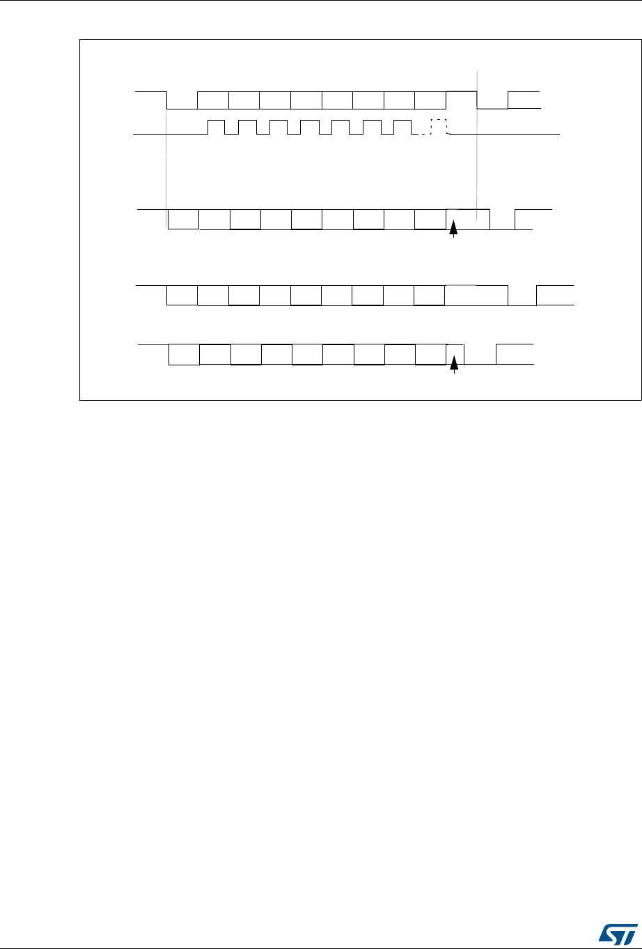
Universal synchronous receiver transmitter (USART) /universal asynchronous receiver transmit-
890/1324 RM0430 Rev 8
Figure 294. Configurable stop bits
Procedure:
1. Enable the USART by writing the UE bit in USART_CR1 register to 1.
2. Program the M bit in USART_CR1 to define the word length.
3. Program the number of stop bits in USART_CR2.
4. Select DMA enable (DMAT) in USART_CR3 if Multi buffer Communication is to take
place. Configure the DMA register as explained in multibuffer communication.
5. Select the desired baud rate using the USART_BRR register.
6. Set the TE bit in USART_CR1 to send an idle frame as first transmission.
7. Write the data to send in the USART_DR register (this clears the TXE bit). Repeat this
for each data to be transmitted in case of single buffer.
8. After writing the last data into the USART_DR register, wait until TC=1. This indicates
that the transmission of the last frame is complete. This is required for instance when
the USART is disabled or enters the Halt mode to avoid corrupting the last
transmission.
Single byte communication
Clearing the TXE bit is always performed by a write to the data register.
The TXE bit is set by hardware and it indicates:
•The data has been moved from TDR to the shift register and the data transmission has
started.
•The TDR register is empty.
•The next data can be written in the USART_DR register without overwriting the
previous data.
This flag generates an interrupt if the TXEIE bit is set.
Bit0 Bit1 Bit2 Bit3 Bit4 Bit5 Bit6 Bit7
Start
Bit Stop
bit
Next
start
bit
8-bit Word length (M bit is reset)
Possible
parity
bit
Data frame
Next data frame
****
** LBCL bit controls last data clock pulse
CLOCK **
Bit0 Bit1 Bit2 Bit3 Bit4 Bit5 Bit6 Bit7
Start
Bit
2 Stop
Bits
Next
Start
Bit
Possible
parity
bit
Data frame
Next data frame
Bit0 Bit1 Bit2 Bit3 Bit4 Bit5 Bit6 Bit7
Start
Bit
Next
start
bit
Possible
Parity
Bit
Data frame
Next data frame
1/2 stop bit
Bit0 Bit1 Bit2 Bit3 Bit4 Bit5 Bit6 Bit7
Start
Bit
Next
start
bit
Possible
Parity
Bit
Data frame
Next data frame
1 1/2 stop bits
a) 1 Stop Bit
b) 1 1/2 stop Bits
c) 2 Stop Bits
d) 1/2 Stop Bit
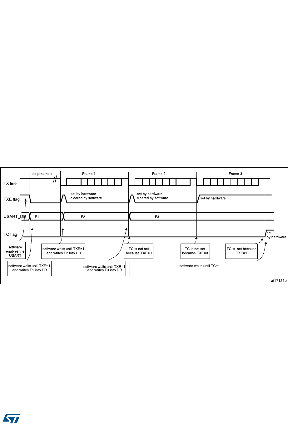
RM0430 Rev 8 891/1324
RM0430 Universal synchronous receiver transmitter (USART) /universal asynchronous receiver
934
When a transmission is taking place, a write instruction to the USART_DR register stores
the data in the TDR register and which is copied in the shift register at the end of the current
transmission.
When no transmission is taking place, a write instruction to the USART_DR register places
the data directly in the shift register, the data transmission starts, and the TXE bit is
immediately set.
If a frame is transmitted (after the stop bit) and the TXE bit is set, the TC bit goes high. An
interrupt is generated if the TCIE bit is set in the USART_CR1 register.
After writing the last data into the USART_DR register, it is mandatory to wait for TC=1
before disabling the USART or causing the microcontroller to enter the low power mode
(see Figure 295: TC/TXE behavior when transmitting).
The TC bit is cleared by the following software sequence:
1. A read from the USART_SR register
2. A write to the USART_DR register
Note: The TC bit can also be cleared by writing a ‘0 to it. This clearing sequence is recommended
only for Multibuffer communication.
Figure 295. TC/TXE behavior when transmitting
Break characters
Setting the SBK bit transmits a break character. The break frame length depends on the M
bit (see Figure 293).
If the SBK bit is set to ‘1 a break character is sent on the TX line after completing the current
character transmission. This bit is reset by hardware when the break character is completed
(during the stop bit of the break character). The USART inserts a logic 1 bit at the end of the
last break frame to guarantee the recognition of the start bit of the next frame.
Note: If the software resets the SBK bit before the commencement of break transmission, the
break character will not be transmitted. For two consecutive breaks, the SBK bit should be
set after the stop bit of the previous break.
Idle characters
Setting the TE bit drives the USART to send an idle frame before the first data frame.
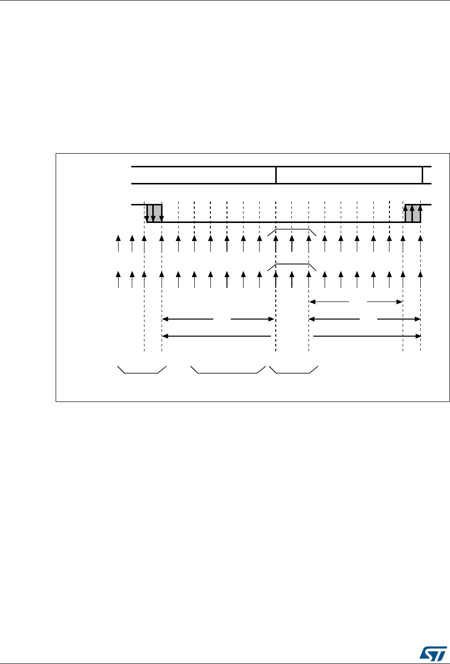
Universal synchronous receiver transmitter (USART) /universal asynchronous receiver transmit-
892/1324 RM0430 Rev 8
28.4.3 Receiver
The USART can receive data words of either 8 or 9 bits depending on the M bit in the
USART_CR1 register.
Start bit detection
The start bit detection sequence is the same when oversampling by 16 or by 8.
In the USART, the start bit is detected when a specific sequence of samples is recognized.
This sequence is: 1 1 1 0 X 0 X 0 X 0 0 0 0.
Figure 296. Start bit detection when oversampling by 16 or 8
Note: If the sequence is not complete, the start bit detection aborts and the receiver returns to the
idle state (no flag is set) where it waits for a falling edge.
The start bit is confirmed (RXNE flag set, interrupt generated if RXNEIE=1) if the 3 sampled
bits are at 0 (first sampling on the 3rd, 5th and 7th bits finds the 3 bits at 0 and second
sampling on the 8th, 9th and 10th bits also finds the 3 bits at 0).
The start bit is validated (RXNE flag set, interrupt generated if RXNEIE=1) but the NE noise
flag is set if, for both samplings, at least 2 out of the 3 sampled bits are at 0 (sampling on the
3rd, 5th and 7th bits and sampling on the 8th, 9th and 10th bits). If this condition is not met,
the start detection aborts and the receiver returns to the idle state (no flag is set).
If, for one of the samplings (sampling on the 3rd, 5th and 7th bits or sampling on the 8th, 9th
and 10th bits), 2 out of the 3 bits are found at 0, the start bit is validated but the NE noise
flag bit is set.
Character reception
During an USART reception, data shifts in least significant bit first through the RX pin. In this
mode, the USART_DR register consists of a buffer (RDR) between the internal bus and the
received shift register.
; ; ; ;;;;;
)DOOLQJHGJH
GHWHFWLRQ
; ; ; ; ; ; ; ;
;
$WOHDVWELWV
RXWRIDW
$WOHDVWELWV
RXWRIDW
2QHELWWLPH
&RQGLWLRQV
WRYDOLGDWH
WKHVWDUWELW
5HDO
VDPSOH
FORFN
,GHDO
VDPSOH
FORFN
5;OLQH
5;VWDWH ,GOH 6WDUWELW
6DPSOHGYDOXHV
DLE

RM0430 Rev 8 893/1324
RM0430 Universal synchronous receiver transmitter (USART) /universal asynchronous receiver
934
Procedure:
1. Enable the USART by writing the UE bit in USART_CR1 register to 1.
2. Program the M bit in USART_CR1 to define the word length.
3. Program the number of stop bits in USART_CR2.
4. Select DMA enable (DMAR) in USART_CR3 if multibuffer communication is to take
place. Configure the DMA register as explained in multibuffer communication. STEP 3
5. Select the desired baud rate using the baud rate register USART_BRR
6. Set the RE bit USART_CR1. This enables the receiver that begins searching for a start
bit.
When a character is received
•The RXNE bit is set. It indicates that the content of the shift register is transferred to the
RDR. In other words, data has been received and can be read (as well as its
associated error flags).
•An interrupt is generated if the RXNEIE bit is set.
•The error flags can be set if a frame error, noise or an overrun error has been detected
during reception.
•In multibuffer, RXNE is set after every byte received and is cleared by the DMA read to
the Data Register.
•In single buffer mode, clearing the RXNE bit is performed by a software read to the
USART_DR register. The RXNE flag can also be cleared by writing a zero to it. The
RXNE bit must be cleared before the end of the reception of the next character to avoid
an overrun error.
Note: The RE bit should not be reset while receiving data. If the RE bit is disabled during
reception, the reception of the current byte will be aborted.
Break character
When a break character is received, the USART handles it as a framing error.
Idle character
When an idle frame is detected, there is the same procedure as a data received character
plus an interrupt if the IDLEIE bit is set.
Overrun error
An overrun error occurs when a character is received when RXNE has not been reset. Data
can not be transferred from the shift register to the RDR register until the RXNE bit is
cleared.

Universal synchronous receiver transmitter (USART) /universal asynchronous receiver transmit-
894/1324 RM0430 Rev 8
The RXNE flag is set after every byte received. An overrun error occurs if RXNE flag is set
when the next data is received or the previous DMA request has not been serviced. When
an overrun error occurs:
•The ORE bit is set.
•The RDR content will not be lost. The previous data is available when a read to
USART_DR is performed.
•The shift register will be overwritten. After that point, any data received during overrun
is lost.
•An interrupt is generated if either the RXNEIE bit is set or both the EIE and DMAR bits
are set.
•The ORE bit is reset by a read to the USART_SR register followed by a USART_DR
register read operation.
Note: The ORE bit, when set, indicates that at least 1 data has been lost. There are two
possibilities:
•if RXNE=1, then the last valid data is stored in the receive register RDR and can be
read,
•if RXNE=0, then it means that the last valid data has already been read and thus there
is nothing to be read in the RDR. This case can occur when the last valid data is read in
the RDR at the same time as the new (and lost) data is received. It may also occur
when the new data is received during the reading sequence (between the USART_SR
register read access and the USART_DR read access).
Selecting the proper oversampling method
The receiver implements different user-configurable oversampling techniques (except in
synchronous mode) for data recovery by discriminating between valid incoming data and
noise.
The oversampling method can be selected by programming the OVER8 bit in the
USART_CR1 register and can be either 16 or 8 times the baud rate clock (Figure 297 and
Figure 298).
Depending on the application:
•select oversampling by 8 (OVER8=1) to achieve higher speed (up to fPCLK/8). In this
case the maximum receiver tolerance to clock deviation is reduced (refer to
Section 28.4.5: USART receiver tolerance to clock deviation)
•select oversampling by 16 (OVER8=0) to increase the tolerance of the receiver to clock
deviations. In this case, the maximum speed is limited to maximum fPCLK/16
Programming the ONEBIT bit in the USART_CR3 register selects the method used to
evaluate the logic level. There are two options:
•the majority vote of the three samples in the center of the received bit. In this case,
when the 3 samples used for the majority vote are not equal, the NF bit is set
•a single sample in the center of the received bit
Depending on the application:
– select the three samples’ majority vote method (ONEBIT=0) when operating in a
noisy environment and reject the data when a noise is detected (refer to
Figure 158) because this indicates that a glitch occurred during the sampling.
– select the single sample method (ONEBIT=1) when the line is noise-free to
increase the receiver tolerance to clock deviations (see Section 28.4.5: USART
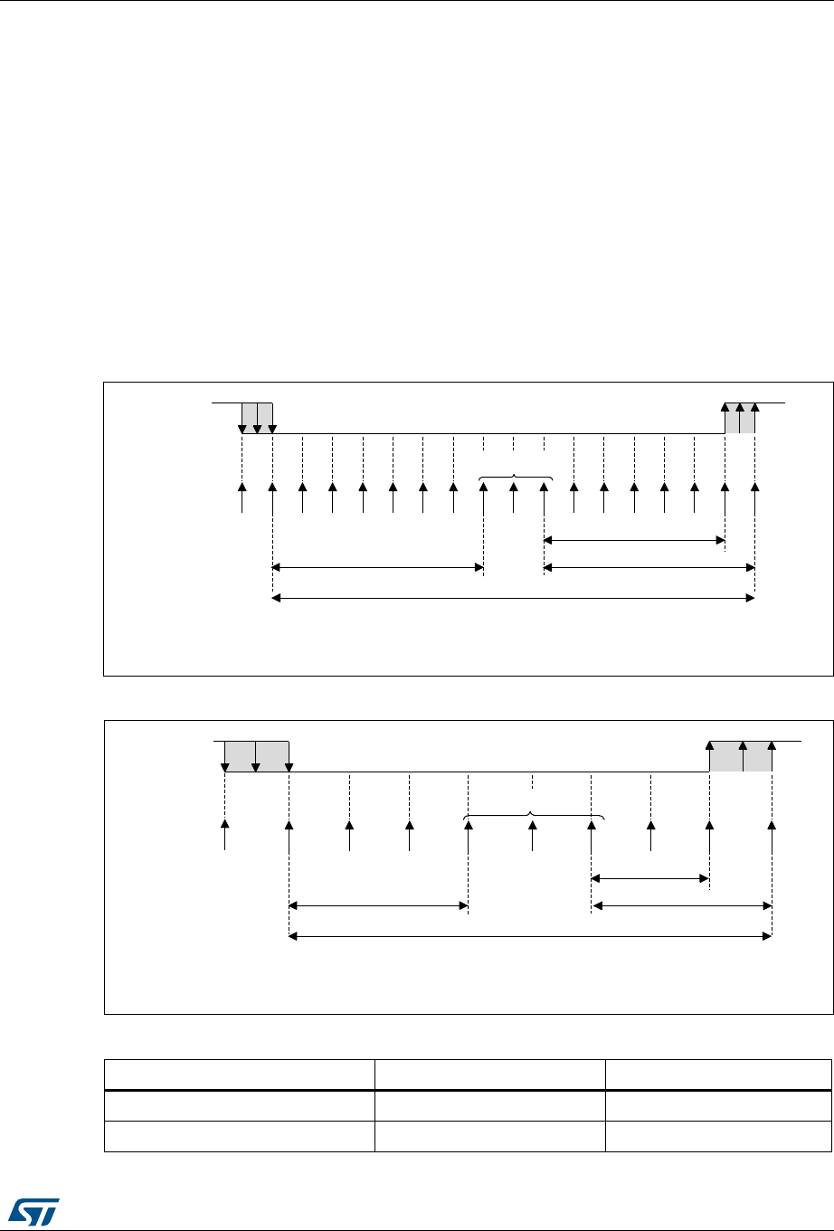
RM0430 Rev 8 895/1324
RM0430 Universal synchronous receiver transmitter (USART) /universal asynchronous receiver
934
receiver tolerance to clock deviation). In this case the NF bit will never be set.
When noise is detected in a frame:
•The NF bit is set at the rising edge of the RXNE bit.
•The invalid data is transferred from the Shift register to the USART_DR register.
•No interrupt is generated in case of single byte communication. However this bit rises
at the same time as the RXNE bit that itself generates an interrupt. In case of
multibuffer communication an interrupt will be issued if the EIE bit is set in the
USART_CR3 register.
The NF bit is reset by a USART_SR register read operation followed by a USART_DR
register read operation.
Note: Oversampling by 8 is not available in the Smartcard, IrDA and LIN modes. In those modes,
the OVER8 bit is forced to ‘0 by hardware.
Figure 297. Data sampling when oversampling by 16
Figure 298. Data sampling when oversampling by 8
Table 158. Noise detection from sampled data
Sampled value NE status Received bit value
000 0 0
001 1 0
06Y9
VDPSOHGYDOXHV
2QHELWWLPH
6DPSOHFORFN
5;OLQH
06Y9
VDPSOHGYDOXHV
2QHELWWLPH
6DPSOH
FORFN[
5;OLQH

Universal synchronous receiver transmitter (USART) /universal asynchronous receiver transmit-
896/1324 RM0430 Rev 8
Framing error
A framing error is detected when:
The stop bit is not recognized on reception at the expected time, following either a de-
synchronization or excessive noise.
When the framing error is detected:
•The FE bit is set by hardware
•The invalid data is transferred from the Shift register to the USART_DR register.
•No interrupt is generated in case of single byte communication. However this bit rises
at the same time as the RXNE bit that itself generates an interrupt. In case of
multibuffer communication an interrupt will be issued if the EIE bit is set in the
USART_CR3 register.
The FE bit is reset by a USART_SR register read operation followed by a USART_DR
register read operation.
Configurable stop bits during reception
The number of stop bits to be received can be configured through the control bits of Control
Register 2 - it can be either 1 or 2 in normal mode and 0.5 or 1.5 in Smartcard mode.
1. 0.5 stop bit (reception in Smartcard mode): No sampling is done for 0.5 stop bit. As
a consequence, no framing error and no break frame can be detected when 0.5 stop bit
is selected.
2. 1 stop bit: Sampling for 1 stop Bit is done on the 8th, 9th and 10th samples.
3. 1.5 stop bits (Smartcard mode): When transmitting in smartcard mode, the device
must check that the data is correctly sent. Thus the receiver block must be enabled (RE
=1 in the USART_CR1 register) and the stop bit is checked to test if the smartcard has
detected a parity error. In the event of a parity error, the smartcard forces the data
signal low during the sampling - NACK signal-, which is flagged as a framing error.
Then, the FE flag is set with the RXNE at the end of the 1.5 stop bit. Sampling for 1.5
stop bits is done on the 16th, 17th and 18th samples (1 baud clock period after the
beginning of the stop bit). The 1.5 stop bit can be decomposed into two parts: one 0.5
baud clock period during which nothing happens, followed by 1 normal stop bit period
during which sampling occurs halfway through. Refer to Section 28.4.11 for more
details.
4. 2 stop bits: Sampling for 2 stop bits is done on the 8th, 9th and 10th samples of the first
stop bit. If a framing error is detected during the first stop bit the framing error flag will
010 1 0
011 1 1
100 1 0
101 1 1
110 1 1
111 0 1
Table 158. Noise detection from sampled data (continued)
Sampled value NE status Received bit value

RM0430 Rev 8 897/1324
RM0430 Universal synchronous receiver transmitter (USART) /universal asynchronous receiver
934
be set. The second stop bit is not checked for framing error. The RXNE flag will be set
at the end of the first stop bit.
28.4.4 Fractional baud rate generation
The baud rate for the receiver and transmitter (Rx and Tx) are both set to the same value as
programmed in the Mantissa and Fraction values of USARTDIV.
Equation 1: Baud rate for standard USART (SPI mode included)
Equation 2: Baud rate in Smartcard, LIN and IrDA modes
USARTDIV is an unsigned fixed point number that is coded on the USART_BRR register.
•When OVER8=0, the fractional part is coded on 4 bits and programmed by the
DIV_fraction[3:0] bits in the USART_BRR register
•When OVER8=1, the fractional part is coded on 3 bits and programmed by the
DIV_fraction[2:0] bits in the USART_BRR register, and bit DIV_fraction[3] must be kept
cleared.
Note: The baud counters are updated to the new value in the baud registers after a write operation
to USART_BRR. Hence the baud rate register value should not be changed during
communication.
How to derive USARTDIV from USART_BRR register values when OVER8=0
Example 1:
If DIV_Mantissa = 0d27 and DIV_Fraction = 0d12 (USART_BRR = 0x1BC), then
Mantissa (USARTDIV) = 0d27
Fraction (USARTDIV) = 12/16 = 0d0.75
Therefore USARTDIV = 0d27.75
Example 2:
To program USARTDIV = 0d25.62
This leads to:
DIV_Fraction = 16*0d0.62 = 0d9.92
The nearest real number is 0d10 = 0xA
DIV_Mantissa = mantissa (0d25.620) = 0d25 = 0x19
Then, USART_BRR = 0x19A hence USARTDIV = 0d25.625
Example 3:
To program USARTDIV = 0d50.99
Tx/Rx baud fCK
8 2 OVER8–()USARTDIV××
-------------------------------------------------------------------------------------
=
Tx/Rx baud fCK
16 USARTDIV×
----------------------------------------------
=

Universal synchronous receiver transmitter (USART) /universal asynchronous receiver transmit-
898/1324 RM0430 Rev 8
This leads to:
DIV_Fraction = 16*0d0.99 = 0d15.84
The nearest real number is 0d16 = 0x10 => overflow of DIV_frac[3:0] => carry must be
added up to the mantissa
DIV_Mantissa = mantissa (0d50.990 + carry) = 0d51 = 0x33
Then, USART_BRR = 0x330 hence USARTDIV = 0d51.000
How to derive USARTDIV from USART_BRR register values when OVER8=1
Example 1:
If DIV_Mantissa = 0x27 and DIV_Fraction[2:0]= 0d6 (USART_BRR = 0x1B6), then
Mantissa (USARTDIV) = 0d27
Fraction (USARTDIV) = 6/8 = 0d0.75
Therefore USARTDIV = 0d27.75
Example 2:
To program USARTDIV = 0d25.62
This leads to:
DIV_Fraction = 8*0d0.62 = 0d4.96
The nearest real number is 0d5 = 0x5
DIV_Mantissa = mantissa (0d25.620) = 0d25 = 0x19
Then, USART_BRR = 0x195 => USARTDIV = 0d25.625
Example 3:
To program USARTDIV = 0d50.99
This leads to:
DIV_Fraction = 8*0d0.99 = 0d7.92
The nearest real number is 0d8 = 0x8 => overflow of the DIV_frac[2:0] => carry must be
added up to the mantissa
DIV_Mantissa = mantissa (0d50.990 + carry) = 0d51 = 0x33
Then, USART_BRR = 0x0330 => USARTDIV = 0d51.000
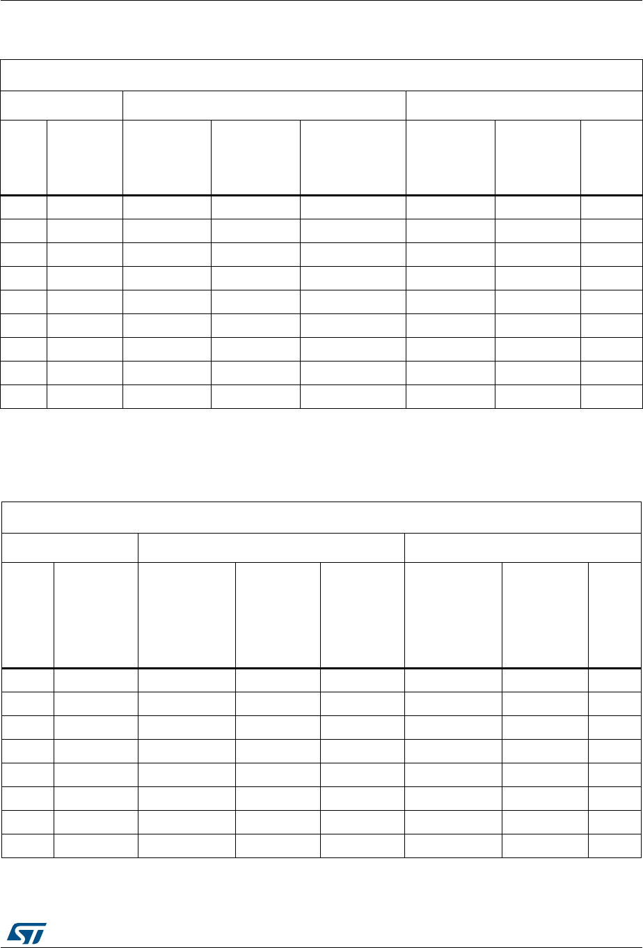
RM0430 Rev 8 899/1324
RM0430 Universal synchronous receiver transmitter (USART) /universal asynchronous receiver
934
Table 159. Error calculation for programmed baud rates at fPCLK = 8 MHz or fPCLK = 12 MHz,
oversampling by 16(1)
Oversampling by 16 (OVER8=0)
Baud rate fPCLK = 8 MHz fPCLK = 12 MHz
S.No Desired Actual
Value
programmed
in the baud
rate register
% Error =
(Calculated -
Desired) B.rate /
Desired B.rate
Actual
Value
programmed
in the baud
rate register
% Error
1 1.2 KBps 1.2 KBps 416.6875 0 1.2 KBps 625 0
2 2.4 KBps 2.4 KBps 208.3125 0.01 2.4 KBps 312.5 0
3 9.6 KBps 9.604 KBps 52.0625 0.04 9.6 KBps 78.125 0
4 19.2 KBps 19.185 KBps 26.0625 0.08 19.2 KBps 39.0625 0
5 38.4 KBps 38.462 KBps 13 0.16 38.339 KBps 19.5625 0.16
6 57.6 KBps 57.554 KBps 8.6875 0.08 57.692 KBps 13 0.16
7 115.2 KBps 115.942 KBps 4.3125 0.64 115.385 KBps 6.5 0.16
8 230.4 KBps 228.571 KBps 2.1875 0.79 230.769 KBps 3.25 0.16
9 460.8 KBps 470.588 KBps 1.0625 2.12 461.538 KBps 1.625 0.16
1. The lower the CPU clock the lower the accuracy for a particular baud rate. The upper limit of the achievable baud rate can
be fixed with these data.
Table 160. Error calculation for programmed baud rates at fPCLK = 8 MHz or fPCLK = 12 MHz,
oversampling by 8(1)
Oversampling by 8 (OVER8 = 1)
Baud rate fPCLK = 8 MHz fPCLK = 12 MHz
S.No Desired Actual
Value
programmed
in the baud
rate register
% Error =
(Calculated -
Desired)
B.rate /
Desired
B.rate
Actual
Value
programmed
in the baud
rate register
% Error
1 1.2 KBps 1.2 KBps 833.375 0 1.2 KBps 1250 0
2 2.4 KBps 2.4 KBps 416.625 0.01 2.4 KBps 625 0
3 9.6 KBps 9.604 KBps 104.125 0.04 9.6 KBps 156.25 0
4 19.2 KBps 19.185 KBps 52.125 0.08 19.2 KBps 78.125 0
5 38.4 KBps 38.462 KBps 26 0.16 38.339 KBps 39.125 0.16
6 57.6 KBps 57.554 KBps 17.375 0.08 57.692 KBps 26 0.16
7 115.2 KBps 115.942 KBps 8.625 0.64 115.385 KBps 13 0.16
8 230.4 KBps 228.571 KBps 4.375 0.79 230.769 KBps 6.5 0.16
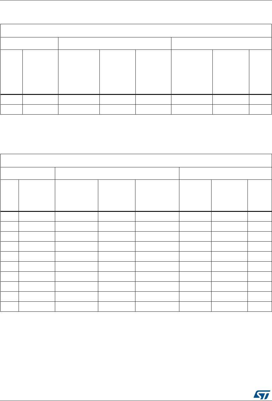
Universal synchronous receiver transmitter (USART) /universal asynchronous receiver transmit-
900/1324 RM0430 Rev 8
9 460.8 KBps 470.588 KBps 2.125 2.12 461.538 KBps 3.25 0.16
10 921.6 KBps 888.889 KBps 1.125 3.55 923.077 KBps 1.625 0.16
1. The lower the CPU clock the lower the accuracy for a particular baud rate. The upper limit of the achievable baud rate can
be fixed with these data.
Table 160. Error calculation for programmed baud rates at fPCLK = 8 MHz or fPCLK = 12 MHz,
oversampling by 8(1) (continued)
Oversampling by 8 (OVER8 = 1)
Baud rate fPCLK = 8 MHz fPCLK = 12 MHz
S.No Desired Actual
Value
programmed
in the baud
rate register
% Error =
(Calculated -
Desired)
B.rate /
Desired
B.rate
Actual
Value
programmed
in the baud
rate register
% Error
Table 161. Error calculation for programmed baud rates at fPCLK = 16 MHz or fPCLK = 24 MHz,
oversampling by 16(1)
Oversampling by 16 (OVER8 = 0)
Baud rate fPCLK = 16 MHz fPCLK = 24 MHz
S.No Desired Actual
Value
programmed
in the baud
rate register
% Error =
(Calculated -
Desired) B.rate /
Desired B.rate
Actual
Value
programmed
in the baud
rate register
% Error
1 1.2 KBps 1.2 KBps 833.3125 0 1.2 1250 0
2 2.4 KBps 2.4 KBps 416.6875 0 2.4 625 0
3 9.6 KBps 9.598 KBps 104.1875 0.02 9.6 156.25 0
4 19.2 KBps 19.208 KBps 52.0625 0.04 19.2 78.125 0
5 38.4 KBps 38.369 KBps 26.0625 0.08 38.4 39.0625 0
6 57.6 KBps 57.554 KBps 17.375 0.08 57.554 26.0625 0.08
7 115.2 KBps 115.108 KBps 8.6875 0.08 115.385 13 0.16
8 230.4 KBps 231.884 KBps 4.3125 0.64 230.769 6.5 0.16
9 460.8 KBps 457.143 KBps 2.1875 0.79 461.538 3.25 0.16
10 921.6 KBps 941.176 KBps 1.0625 2.12 923.077 1.625 0.16
1. The lower the CPU clock the lower the accuracy for a particular baud rate. The upper limit of the achievable baud rate can
be fixed with these data.
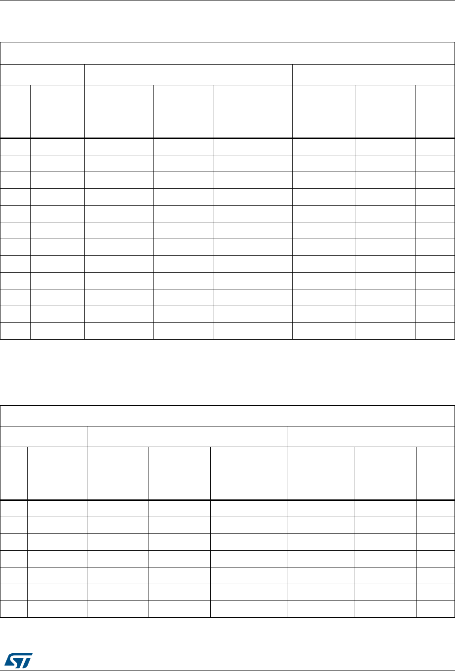
RM0430 Rev 8 901/1324
RM0430 Universal synchronous receiver transmitter (USART) /universal asynchronous receiver
934
Table 162. Error calculation for programmed baud rates at fPCLK = 16 MHz or fPCLK = 24 MHz,
oversampling by 8(1)
Oversampling by 8 (OVER8=1)
Baud rate fPCLK = 16 MHz fPCLK = 24 MHz
S.No Desired Actual
Value
programmed
in the baud
rate register
% Error =
(Calculated -
Desired) B.rate /
Desired B.rate
Actual
Value
programmed
in the baud
rate register
% Error
1 1.2 KBps 1.2 KBps 1666.625 0 1.2 KBps 2500 0
2 2.4 KBps 2.4 KBps 833.375 0 2.4 KBps 1250 0
3 9.6 KBps 9.598 KBps 208.375 0.02 9.6 KBps 312.5 0
4 19.2 KBps 19.208 KBps 104.125 0.04 19.2 KBps 156.25 0
5 38.4 KBps 38.369 KBps 52.125 0.08 38.4 KBps 78.125 0
6 57.6 KBps 57.554 KBps 34.75 0.08 57.554 KBps 52.125 0.08
7 115.2 KBps 115.108 KBps 17.375 0.08 115.385 KBps 26 0.16
8 230.4 KBps 231.884 KBps 8.625 0.64 230.769 KBps 13 0.16
9 460.8 KBps 457.143 KBps 4.375 0.79 461.538 KBps 6.5 0.16
10 921.6 KBps 941.176 KBps 2.125 2.12 923.077 KBps 3.25 0.16
11 2 MBps 2000 KBps 1 0 2000 KBps 1.5 0
12 3 MBps NA NA NA 3000 KBps 1 0
1. The lower the CPU clock the lower the accuracy for a particular baud rate. The upper limit of the achievable baud rate can
be fixed with these data.
Table 163. Error calculation for programmed baud rates at fPCLK = 8 MHz or fPCLK = 16 MHz,
oversampling by 16(1)
Oversampling by 16 (OVER8=0)
Baud rate fPCLK = 8 MHz fPCLK = 16 MHz
S.No Desired Actual
Value
programmed
in the baud
rate register
% Error =
(Calculated -
Desired)B.Rate
/Desired B.Rate
Actual
Value
programmed
in the baud
rate register
% Error
1 2.4 KBps 2.400 KBps 208.3125 0.00% 2.400 KBps 416.6875 0.00%
2 9.6 KBps 9.604 KBps 52.0625 0.04% 9.598 KBps 104.1875 0.02%
3 19.2 KBps 19.185 KBps 26.0625 0.08% 19.208 KBps 52.0625 0.04%
4 57.6 KBps 57.554 KBps 8.6875 0.08% 57.554 KBps 17.3750 0.08%
5 115.2 KBps 115.942 KBps 4.3125 0.64% 115.108 KBps 8.6875 0.08%
6 230.4 KBps 228.571 KBps 2.1875 0.79% 231.884 KBps 4.3125 0.64%
7 460.8 KBps 470.588 KBps 1.0625 2.12% 457.143 KBps 2.1875 0.79%
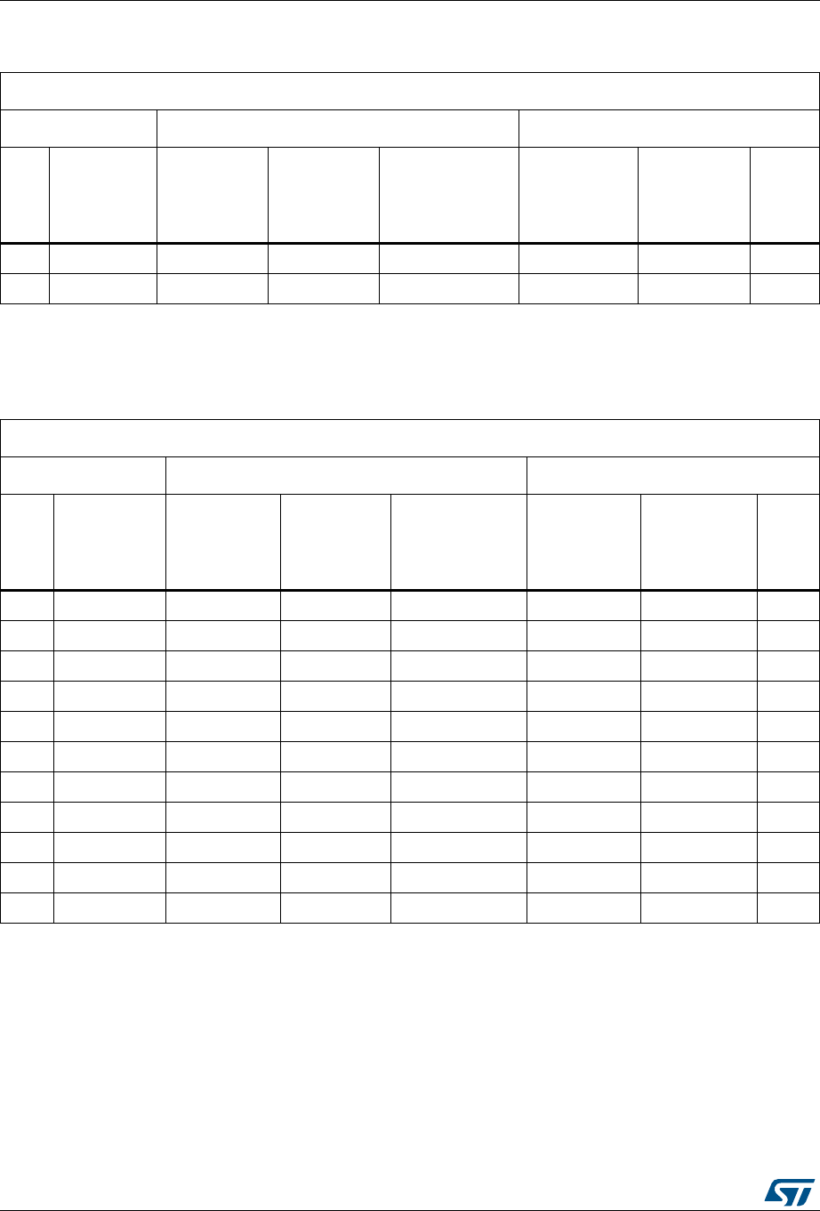
Universal synchronous receiver transmitter (USART) /universal asynchronous receiver transmit-
902/1324 RM0430 Rev 8
8 896 KBps NA NA NA 888.889 KBps 1.1250 0.79%
9 921.6 KBps NA NA NA 941.176 KBps 1.0625 2.12%
1. The lower the CPU clock the lower the accuracy for a particular baud rate. The upper limit of the achievable baud rate can
be fixed with these data.
Table 164. Error calculation for programmed baud rates at fPCLK = 8 MHz or fPCLK = 16 MHz,
oversampling by 8(1)
Oversampling by 8 (OVER8=1)
Baud rate fPCLK = 8 MHz fPCLK = 16 MHz
S.No Desired Actual
Value
programmed
in the baud
rate register
% Error =
(Calculated -
Desired)B.Rate
/Desired B.Rate
Actual
Value
programmed
in the baud
rate register
%
Error
1 2.4 KBps 2.400 KBps 416.625 0.01% 2.400 KBps 833.375 0.00%
2 9.6 KBps 9.604 KBps 104.125 0.04% 9.598 KBps 208.375 0.02%
3 19.2 KBps 19.185 KBps 52.125 0.08% 19.208 KBps 104.125 0.04%
4 57.6 KBps 57.557 KBps 17.375 0.08% 57.554 KBps 34.750 0.08%
5 115.2 KBps 115.942 KBps 8.625 0.64% 115.108 KBps 17.375 0.08%
6 230.4 KBps 228.571 KBps 4.375 0.79% 231.884 KBps 8.625 0.64%
7 460.8 KBps 470.588 KBps 2.125 2.12% 457.143 KBps 4.375 0.79%
8 896 KBps 888.889 KBps 1.125 0.79% 888.889 KBps 2.250 0.79%
9 921.6 KBps 888.889 KBps 1.125 3.55% 941.176 KBps 2.125 2.12%
10 1.792 MBps NA NA NA 1.7777 MBps 1.125 0.79%
11 1.8432 MBps NA NA NA 1.7777 MBps 1.125 3.55%
1. The lower the CPU clock the lower the accuracy for a particular baud rate. The upper limit of the achievable baud rate can
be fixed with these data.
Table 163. Error calculation for programmed baud rates at fPCLK = 8 MHz or fPCLK = 16 MHz,
oversampling by 16(1) (continued)
Oversampling by 16 (OVER8=0)
Baud rate fPCLK = 8 MHz fPCLK = 16 MHz
S.No Desired Actual
Value
programmed
in the baud
rate register
% Error =
(Calculated -
Desired)B.Rate
/Desired B.Rate
Actual
Value
programmed
in the baud
rate register
% Error

RM0430 Rev 8 903/1324
RM0430 Universal synchronous receiver transmitter (USART) /universal asynchronous receiver
934
Table 165. Error calculation for programmed baud rates at fPCLK = 30 MHz or fPCLK = 60 MHz,
oversampling by 16(1)(2)
Oversampling by 16 (OVER8=0)
Baud rate fPCLK = 30 MHz fPCLK = 60 MHz
S.No Desired Actual
Value
programmed
in the baud
rate register
% Error =
(Calculated -
Desired)B.Rate
/Desired B.Rate
Actual
Value
programmed
in the baud
rate register
%
Error
1 2.4 KBps 2.400 KBps 781.2500 0.00% 2.400 KBps 1562.5000 0.00%
2 9.6 KBps 9.600 KBps 195.3125 0.00% 9.600 KBps 390.6250 0.00%
3 19.2 KBps 19.194 KBps 97.6875 0.03% 19.200 KBps 195.3125 0.00%
4 57.6 KBps 57.582KBps 32.5625 0.03% 57.582 KBps 65.1250 0.03%
5 115.2 KBps 115.385 KBps 16.2500 0.16% 115.163 KBps 32.5625 0.03%
6 230.4 KBps 230.769 KBps 8.1250 0.16% 230.769 KBps 16.2500 0.16%
7 460.8 KBps 461.538 KBps 4.0625 0.16% 461.538 KBps 8.1250 0.16%
8 896 KBps 909.091 KBps 2.0625 1.46% 895.522 KBps 4.1875 0.05%
9 921.6 KBps 909.091 KBps 2.0625 1.36% 923.077 KBps 4.0625 0.16%
10 1.792 MBps 1.1764 MBps 1.0625 1.52% 1.8182 MBps 2.0625 1.36%
11 1.8432 MBps 1.8750 MBps 1.0000 1.73% 1.8182 MBps 2.0625 1.52%
12 3.584 MBps NA NA NA 3.2594 MBps 1.0625 1.52%
13 3.6864 MBps NA NA NA 3.7500 MBps 1.0000 1.73%
1. The lower the CPU clock the lower the accuracy for a particular baud rate. The upper limit of the achievable baud rate can
be fixed with these data.
2. Only USART1 and USART6 are clocked with PCLK2. Other USARTs are clocked with PCLK1. Refer to the device
datasheets for the maximum values for PCLK1 and PCLK2.
Table 166. Error calculation for programmed baud rates at fPCLK = 30 MHz or fPCLK = 60 MHz,
oversampling by 8(1) (2)
Oversampling by 8 (OVER8=1)
Baud rate fPCLK = 30 MHz fPCLK =60 MHz
S.No Desired Actual
Value
programmed
in the baud
rate register
% Error =
(Calculated -
Desired)B.Rate
/Desired B.Rate
Actual
Value
programmed
in the baud
rate register
%
Error
1 2.4 KBps 2.400 KBps 1562.5000 0.00% 2.400 KBps 3125.0000 0.00%
2 9.6 KBps 9.600 KBps 390.6250 0.00% 9.600 KBps 781.2500 0.00%
3 19.2 KBps 19.194 KBps 195.3750 0.03% 19.200 KBps 390.6250 0.00%
4 57.6 KBps 57.582 KBps 65.1250 0.16% 57.582 KBps 130.2500 0.03%
5 115.2 KBps 115.385 KBps 32.5000 0.16% 115.163 KBps 65.1250 0.03%
6 230.4 KBps 230.769 KBps 16.2500 0.16% 230.769 KBps 32.5000 0.16%
Universal synchronous receiver transmitter (USART) /universal asynchronous receiver transmit-
904/1324 RM0430 Rev 8
7 460.8 KBps 461.538 KBps 8.1250 0.16% 461.538 KBps 16.2500 0.16%
8 896 KBps 909.091 KBps 4.1250 1.46% 895.522 KBps 8.3750 0.05%
9 921.6 KBps 909.091 KBps 4.1250 1.36% 923.077 KBps 8.1250 0.16%
10 1.792 MBps 1.7647 MBps 2.1250 1.52% 1.8182 MBps 4.1250 1.46%
11 1.8432 MBps 1.8750 MBps 2.0000 1.73% 1.8182 MBps 4.1250 1.36%
12 3.584 MBps 3.7500 MBps 1.0000 4.63% 3.5294 MBps 2.1250 1.52%
13 3.6864 MBps 3.7500 MBps 1.0000 1.73% 3.7500 MBps 2.0000 1.73%
14 7.168 MBps NA NA NA 7.5000 MBps 1.0000 4.63%
15 7.3728 MBps NA NA NA 7.5000 MBps 1.0000 1.73%
1. The lower the CPU clock the lower the accuracy for a particular baud rate. The upper limit of the achievable baud rate can
be fixed with these data.
2. Only USART1 and USART6 are clocked with PCLK2. Other USARTs are clocked with PCLK1. Refer to the device
datasheets for the maximum values for PCLK1 and PCLK2.
Table 166. Error calculation for programmed baud rates at fPCLK = 30 MHz or fPCLK = 60 MHz,
oversampling by 8(1) (2) (continued)
Oversampling by 8 (OVER8=1)
Baud rate fPCLK = 30 MHz fPCLK =60 MHz
S.No Desired Actual
Value
programmed
in the baud
rate register
% Error =
(Calculated -
Desired)B.Rate
/Desired B.Rate
Actual
Value
programmed
in the baud
rate register
%
Error
Table 167. Error calculation for programmed baud rates at fPCLK = 42 MHz or fPCLK = 84 Hz,
oversampling by 16(1)(2)
Oversampling by 16 (OVER8=0)
Baud rate fPCLK = 42 MHz fPCLK = 84 MHz
S.No Desired Actual
Value
programmed
in the baud
rate register
% Error =
(Calculated -
Desired)B.Rate
/Desired B.Rate
Actual
Value
programmed
in the baud
rate register
%
Error
1 1.2 KBps 1.2 KBps 2187.5 0 1.2 KBps 4375 0
2 2.4 KBps 2.4 KBps 1093.75 0 2.4 KBps 2187.5 0
3 9.6 KBps 9.6 KBps 273.4375 0 9.6 KBps 546.875 0
4 19.2 KBps 19.195 KBps 136.75 0.02 19.2 KBps 273.4375 0
5 38.4 KBps 38.391 KBps 68.375 0.02 38.391 KBps 136.75 0.02
6 57.6 KBps 57.613 KBps 45.5625 0.02 57.613 KBps 91.125 0.02
7 115.2 KBps 115.068 KBps 22.8125 0.11 115.226 KBps 45.5625 0.02
8 230.4 KBps 230.769 KBps 11.375 0.16 230.137 KBps 22.8125 0.11
9 460.8 KBps 461.538 KBps 5.6875 0.16 461.538 KBps 11.375 0.16

RM0430 Rev 8 905/1324
RM0430 Universal synchronous receiver transmitter (USART) /universal asynchronous receiver
934
10 921.6 KBps 913.043 KBps 2.875 0.93 923.076 KBps 5.6875 0.93
11 1.792 MBps 1.826 MBps 1.4375 1.9 1.787 MBps 2.9375 0.27
12 1.8432 MBps 1.826 MBps 1.4375 0.93 1.826 MBps 2.875 0.93
13 3.584 MBps NA NA NA 3.652 MBps 1.4375 1.9
14 3.6864 MBps NA NA NA 3.652 MBps 1.4375 0.93
1. The lower the CPU clock the lower the accuracy for a particular baud rate. The upper limit of the achievable baud rate can
be fixed with these data.
2. Only USART1 and USART6 are clocked with PCLK2. Other USARTs are clocked with PCLK1. Refer to the device
datasheets for the maximum values for PCLK1 and PCLK2.
Table 167. Error calculation for programmed baud rates at fPCLK = 42 MHz or fPCLK = 84 Hz,
oversampling by 16(1)(2) (continued)
Oversampling by 16 (OVER8=0)
Baud rate fPCLK = 42 MHz fPCLK = 84 MHz
S.No Desired Actual
Value
programmed
in the baud
rate register
% Error =
(Calculated -
Desired)B.Rate
/Desired B.Rate
Actual
Value
programmed
in the baud
rate register
%
Error
Table 168. Error calculation for programmed baud rates at fPCLK = 42 MHz or fPCLK = 84 MHz,
oversampling by 8(1)(2)
Oversampling by 8 (OVER8=1)
Baud rate fPCLK = 42 MHz fPCLK = 84 MHz
S.No Desired Actual
Value
programmed
in the baud
rate register
% Error =
(Calculated -
Desired)B.Rate
/Desired B.Rate
Actual
Value
programmed
in the baud
rate register
%
Error
1 1.2 KBps 1.2 KBps 4375 0 1.2 KBps 8750 0
2 2.4 KBps 2.4 KBps 2187.5 0 2.4 KBps 4375 0
3 9.6 KBps 9.6 KBps 546.875 0 9.6 KBps 1093.75 0
4 19.2 KBps 19.195 KBps 273.5 0.02 19.2 KBps 546.875 0
5 38.4 KBps 38.391 KBps 136.75 0.02 38.391 KBps 273.5 0.02
6 57.6 KBps 57.613 KBps 91.125 0.02 57.613 KBps 182.25 0.02
7 115.2 KBps 115.068 KBps 45.625 0.11 115.226 KBps 91.125 0.02
8 230.4 KBps 230.769 KBps 22.75 0.11 230.137 KBps 45.625 0.11
9 460.8 KBps 461.538 KBps 11.375 0.16 461.538 KBps 22.75 0.16
10 921.6 KBps 913.043 KBps 5.75 0.93 923.076 KBps 11.375 0.93
11 1.792 MBps 1.826 MBps 2.875 1.9 1.787Mbps 5.875 0.27
12 1.8432 MBps 1.826 MBps 2.875 0.93 1.826 MBps 5.75 0.93
13 3.584 MBps 3.5 MBps 1.5 2.34 3.652 MBps 2.875 1.9
14 3.6864 MBps 3.82 MBps 1.375 3.57 3.652 MBps 2.875 0.93
Universal synchronous receiver transmitter (USART) /universal asynchronous receiver transmit-
906/1324 RM0430 Rev 8
28.4.5 USART receiver tolerance to clock deviation
The USART asynchronous receiver works correctly only if the total clock system deviation is
smaller than the USART receiver tolerance. The causes that contribute to the total deviation
are:
•DTRA: Deviation due to the transmitter error (also includes the deviation of the
transmitter local oscillator)
•DQUANT: Error due to the baud rate quantization of the receiver
•DREC: Deviation of the receiver local oscillator
•DTCL: Deviation due to the transmission line (generally due to the transceivers that
can introduce an asymmetry between the low-to-high transition timing and the
high-to-low transition timing)
DTRA + DQUANT + DREC + DTCL < USART receiver tolerance
The USART receiver tolerance to properly receive data is equal to the maximum tolerated
deviation and depends on the following choices:
•10- or 11-bit character length defined by the M bit in the USART_CR1 register
•oversampling by 8 or 16 defined by the OVER8 bit in the USART_CR1 register
•use of fractional baud rate or not
•use of 1 bit or 3 bits to sample the data, depending on the value of the ONEBIT bit in
the USART_CR3 register
15 7.168 MBps NA NA NA 7 MBps 1.5 2.34
16 7.3728 MBps NA NA NA 7.636 MBps 1.375 3.57
18 9 MBps NA NA NA 9.333 MBps 1.125 3.7
20 10.5 MBps NA NA NA 10.5 MBps 1 0
1. The lower the CPU clock the lower the accuracy for a particular baud rate. The upper limit of the achievable baud rate can
be fixed with these data.
2. Only USART1 and USART6 are clocked with PCLK2. Other USARTs are clocked with PCLK1. Refer to the device
datasheets for the maximum values for PCLK1 and PCLK2.
Table 168. Error calculation for programmed baud rates at fPCLK = 42 MHz or fPCLK = 84 MHz,
oversampling by 8(1)(2) (continued)
Oversampling by 8 (OVER8=1)
Baud rate fPCLK = 42 MHz fPCLK = 84 MHz
S.No Desired Actual
Value
programmed
in the baud
rate register
% Error =
(Calculated -
Desired)B.Rate
/Desired B.Rate
Actual
Value
programmed
in the baud
rate register
%
Error
Table 169. USART receiver tolerance when DIV fraction is 0
M bit
OVER8 bit = 0 OVER8 bit = 1
ONEBIT=0 ONEBIT=1 ONEBIT=0 ONEBIT=1
0 3.75% 4.375% 2.50% 3.75%
1 3.41% 3.97% 2.27% 3.41%

RM0430 Rev 8 907/1324
RM0430 Universal synchronous receiver transmitter (USART) /universal asynchronous receiver
934
Note: The figures specified in Table 169 and Table 170 may slightly differ in the special case when
the received frames contain some Idle frames of exactly 10-bit times when M=0 (11-bit times
when M=1).
28.4.6 Multiprocessor communication
There is a possibility of performing multiprocessor communication with the USART (several
USARTs connected in a network). For instance one of the USARTs can be the master, its TX
output is connected to the RX input of the other USART. The others are slaves, their
respective TX outputs are logically ANDed together and connected to the RX input of the
master.
In multiprocessor configurations it is often desirable that only the intended message
recipient should actively receive the full message contents, thus reducing redundant USART
service overhead for all non addressed receivers.
The non addressed devices may be placed in mute mode by means of the muting function.
In mute mode:
•None of the reception status bits can be set.
•All the receive interrupts are inhibited.
•The RWU bit in USART_CR1 register is set to 1. RWU can be controlled automatically
by hardware or written by the software under certain conditions.
The USART can enter or exit from mute mode using one of two methods, depending on the
WAKE bit in the USART_CR1 register:
•Idle Line detection if the WAKE bit is reset,
•Address Mark detection if the WAKE bit is set.
Idle line detection (WAKE=0)
The USART enters mute mode when the RWU bit is written to 1.
It wakes up when an Idle frame is detected. Then the RWU bit is cleared by hardware but
the IDLE bit is not set in the USART_SR register. RWU can also be written to 0 by software.
An example of mute mode behavior using Idle line detection is given in Figure 299.
Table 170. USART receiver tolerance when DIV_Fraction is different from 0
M bit
OVER8 bit = 0 OVER8 bit = 1
ONEBIT=0 ONEBIT=1 ONEBIT=0 ONEBIT=1
0 3.33% 3.88% 2% 3%
1 3.03% 3.53% 1.82% 2.73%
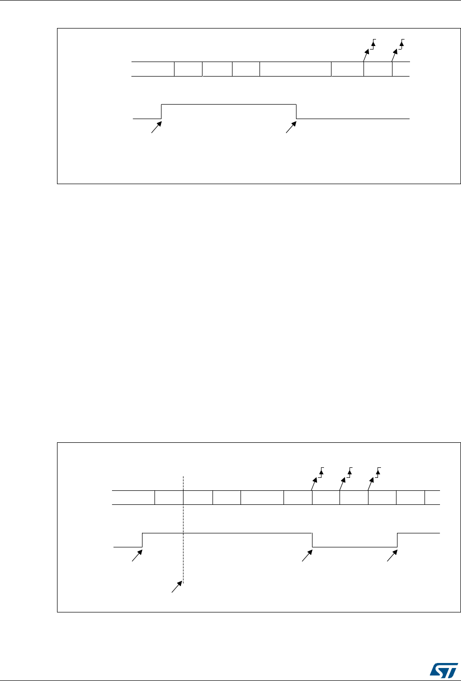
Universal synchronous receiver transmitter (USART) /universal asynchronous receiver transmit-
908/1324 RM0430 Rev 8
Figure 299. Mute mode using Idle line detection
Address mark detection (WAKE=1)
In this mode, bytes are recognized as addresses if their MSB is a ‘1 else they are
considered as data. In an address byte, the address of the targeted receiver is put on the 4
LSB. This 4-bit word is compared by the receiver with its own address that is programmed in
the ADD bits in the USART_CR2 register.
The USART enters mute mode when an address character is received that does not match
its programmed address. In this case, the RWU bit is set by hardware. The RXNE flag is not
set for this address byte and no interrupt nor DMA request is issued as the USART would
have entered mute mode.
It exits from mute mode when an address character is received that matches the
programmed address. Then the RWU bit is cleared and subsequent bytes are received
normally. The RXNE bit is set for the address character since the RWU bit has been
cleared.
The RWU bit can be written to as 0 or 1 when the receiver buffer contains no data (RXNE=0
in the USART_SR register). Otherwise the write attempt is ignored.
An example of mute mode behavior using address mark detection is given in Figure 300.
Figure 300. Mute mode using address mark detection
06Y9
'DWD 'DWD ,'/('DWD 'DWD 'DWD
,GOHIUDPHGHWHFWHG0054ZULWWHQWR
5:8
5;
0XWHPRGH 1RUPDOPRGH
5;1( 5;1(
'DWD
06Y9
,'/( $GGU 'DWD 'DWD ,'/( $GGU 'DWD 'DWD $GGU 'DWD
,QWKLVH[DPSOHWKHFXUUHQWDGGUHVVRIWKHUHFHLYHULV
SURJUDPPHGLQWKH86$57B&5UHJLVWHU
5;1(
1RQPDWFKLQJDGGUHVV0DWFKLQJDGGUHVV
1RQPDWFKLQJDGGUHVV
0054ZULWWHQWR
5;1(ZDVFOHDUHG
5:8
5;
0XWHPRGH 0XWHPRGH1RUPDOPRGH
5;1( 5;1(

RM0430 Rev 8 909/1324
RM0430 Universal synchronous receiver transmitter (USART) /universal asynchronous receiver
934
28.4.7 Parity control
Parity control (generation of parity bit in transmission and parity checking in reception) can
be enabled by setting the PCE bit in the USART_CR1 register. Depending on the frame
length defined by the M bit, the possible USART frame formats are as listed in Table 171.
Even parity
The parity bit is calculated to obtain an even number of “1s” inside the frame made of the 7
or 8 LSB bits (depending on whether M is equal to 0 or 1) and the parity bit.
E.g.: data=00110101; 4 bits set => parity bit will be 0 if even parity is selected (PS bit in
USART_CR1 = 0).
Odd parity
The parity bit is calculated to obtain an odd number of “1s” inside the frame made of the 7 or
8 LSB bits (depending on whether M is equal to 0 or 1) and the parity bit.
E.g.: data=00110101; 4 bits set => parity bit will be 1 if odd parity is selected (PS bit in
USART_CR1 = 1).
Parity checking in reception
If the parity check fails, the PE flag is set in the USART_SR register and an interrupt is
generated if PEIE is set in the USART_CR1 register. The PE flag is cleared by a software
sequence (a read from the status register followed by a read or write access to the
USART_DR data register).
Note: In case of wakeup by an address mark: the MSB bit of the data is taken into account to
identify an address but not the parity bit. And the receiver does not check the parity of the
address data (PE is not set in case of a parity error).
Parity generation in transmission
If the PCE bit is set in USART_CR1, then the MSB bit of the data written in the data register
is transmitted but is changed by the parity bit (even number of “1s” if even parity is selected
(PS=0) or an odd number of “1s” if odd parity is selected (PS=1)).
Note: The software routine that manages the transmission can activate the software sequence
that clears the PE flag (a read from the status register followed by a read or write access to
the data register). When operating in half-duplex mode, depending on the software, this can
cause the PE flag to be unexpectedly cleared.
Table 171. Frame formats
M bit PCE bit USART frame(1)
1. Legends: SB: start bit, STB: stop bit, PB: parity bit.
0 0 | SB | 8 bit data | STB |
0 1 | SB | 7-bit data | PB | STB |
1 0 | SB | 9-bit data | STB |
1 1 | SB | 8-bit data PB | STB |

Universal synchronous receiver transmitter (USART) /universal asynchronous receiver transmit-
910/1324 RM0430 Rev 8
28.4.8 LIN (local interconnection network) mode
The LIN mode is selected by setting the LINEN bit in the USART_CR2 register. In LIN
mode, the following bits must be kept cleared:
•STOP[1:0] and CLKEN in the USART_CR2 register
•SCEN, HDSEL and IREN in the USART_CR3 register.
LIN transmission
The same procedure explained in Section 28.4.2 has to be applied for LIN Master
transmission than for normal USART transmission with the following differences:
•Clear the M bit to configure 8-bit word length.
•Set the LINEN bit to enter LIN mode. In this case, setting the SBK bit sends 13 ‘0 bits
as a break character. Then a bit of value ‘1 is sent to allow the next start detection.
LIN reception
A break detection circuit is implemented on the USART interface. The detection is totally
independent from the normal USART receiver. A break can be detected whenever it occurs,
during Idle state or during a frame.
When the receiver is enabled (RE=1 in USART_CR1), the circuit looks at the RX input for a
start signal. The method for detecting start bits is the same when searching break
characters or data. After a start bit has been detected, the circuit samples the next bits
exactly like for the data (on the 8th, 9th and 10th samples). If 10 (when the LBDL = 0 in
USART_CR2) or 11 (when LBDL=1 in USART_CR2) consecutive bits are detected as ‘0,
and are followed by a delimiter character, the LBD flag is set in USART_SR. If the LBDIE
bit=1, an interrupt is generated. Before validating the break, the delimiter is checked for as it
signifies that the RX line has returned to a high level.
If a ‘1 is sampled before the 10 or 11 have occurred, the break detection circuit cancels the
current detection and searches for a start bit again.
If the LIN mode is disabled (LINEN=0), the receiver continues working as normal USART,
without taking into account the break detection.
If the LIN mode is enabled (LINEN=1), as soon as a framing error occurs (i.e. stop bit
detected at ‘0, which will be the case for any break frame), the receiver stops until the break
detection circuit receives either a ‘1, if the break word was not complete, or a delimiter
character if a break has been detected.
The behavior of the break detector state machine and the break flag is shown in Figure 301.
Examples of break frames are given on Figure 302, where we suppose that LBDL=1 (11-bit
break length), and M=0 (8-bit data).
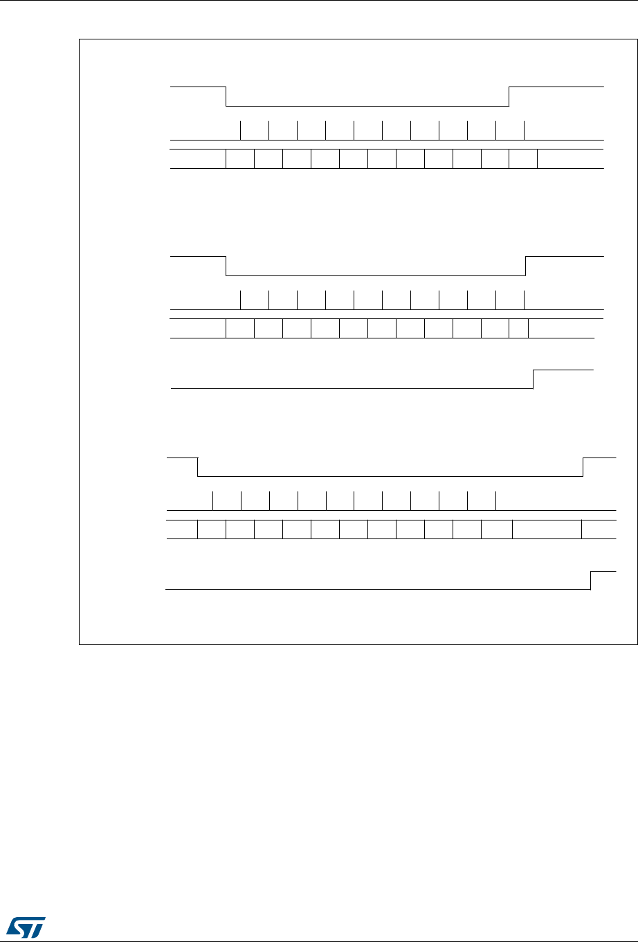
RM0430 Rev 8 911/1324
RM0430 Universal synchronous receiver transmitter (USART) /universal asynchronous receiver
934
Figure 301. Break detection in LIN mode (11-bit break length - LBDL bit is set)
06Y9
,GOH %LW %LW %LW %LW %LW %LW %LW %LW %LW %LW %LW ,GOH
&DVHEUHDNVLJQDOQRWORQJHQRXJK !EUHDNGLVFDUGHG/%')LVQRWVHW
5;OLQH
&DSWXUHVWUREH
%UHDNVWDWH
PDFKLQH
5HDGVDPSOHV
,GOH %LW %LW %LW %LW %LW %LW %LW %LW %LW %LW % ,GOH
&DVHEUHDNVLJQDOMXVWORQJHQRXJK !EUHDNGHWHFWHG/%')LVVHW
5;OLQH
&DSWXUHVWUREH
%UHDNVWDWH
PDFKLQH
5HDGVDPSOHV
%UHDNIUDPH
%UHDNIUDPH
'HOLPLWHULVLPPHGLDWH
/%')
,GOH %LW %LW %LW %LW %LW %LW %LW %LW %LW %LW %LW ,GOH
&DVHEUHDNVLJQDOORQJHQRXJK !EUHDNGHWHFWHG/%')LVVHW
5;OLQH
&DSWXUHVWUREH
%UHDNVWDWH
PDFKLQH
5HDGVDPSOHV
%UHDNIUDPH
/%')
ZDLWGHOLPLWHU
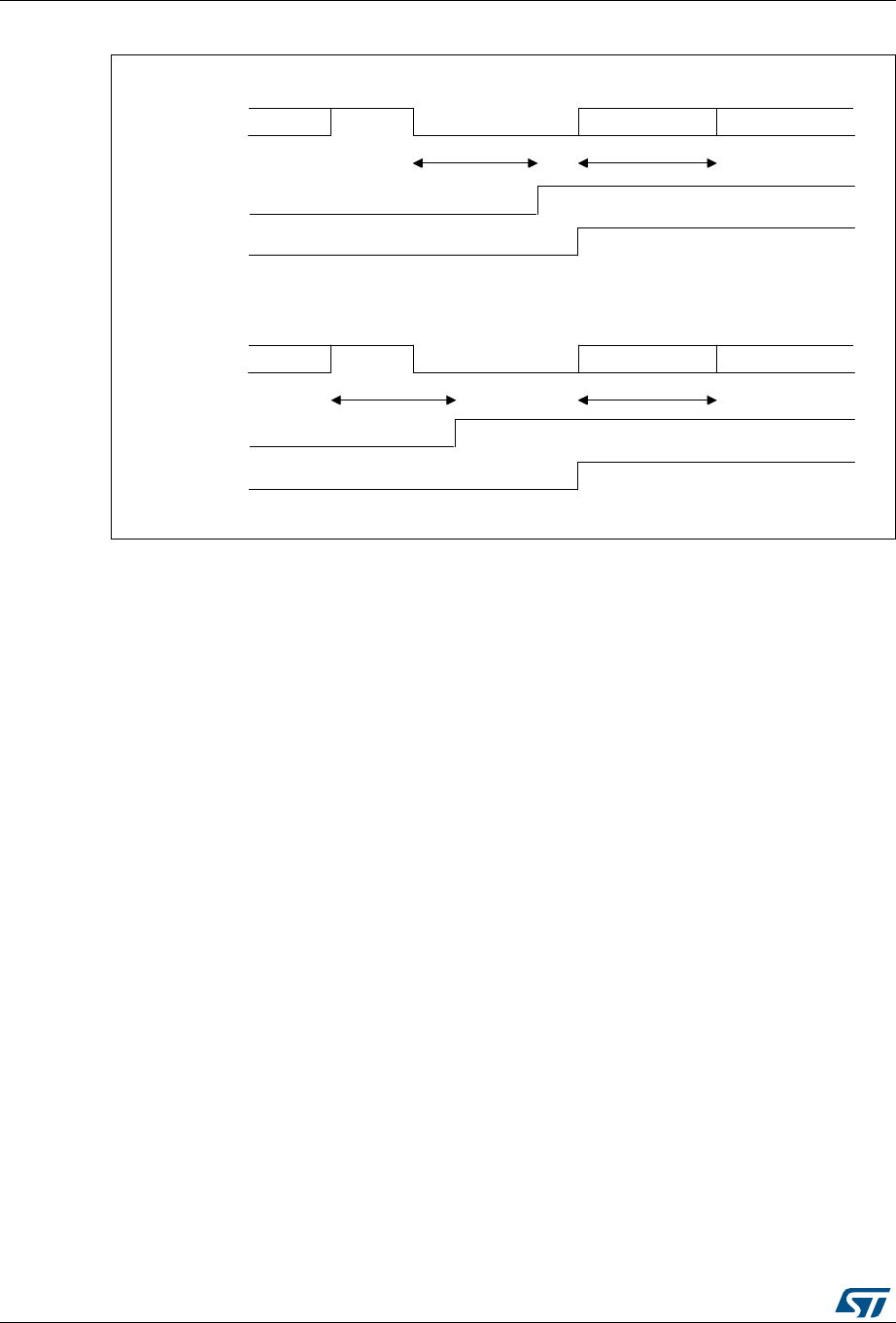
Universal synchronous receiver transmitter (USART) /universal asynchronous receiver transmit-
912/1324 RM0430 Rev 8
Figure 302. Break detection in LIN mode vs. Framing error detection
28.4.9 USART synchronous mode
The synchronous mode is selected by writing the CLKEN bit in the USART_CR2 register to
1. In synchronous mode, the following bits must be kept cleared:
•LINEN bit in the USART_CR2 register,
•SCEN, HDSEL and IREN bits in the USART_CR3 register.
The USART allows the user to control a bidirectional synchronous serial communications in
master mode. The SCLK pin is the output of the USART transmitter clock. No clock pulses
are sent to the SCLK pin during start bit and stop bit. Depending on the state of the LBCL bit
in the USART_CR2 register clock pulses will or will not be generated during the last valid
data bit (address mark). The CPOL bit in the USART_CR2 register allows the user to select
the clock polarity, and the CPHA bit in the USART_CR2 register allows the user to select the
phase of the external clock (see Figure 303, Figure 304 and Figure 305).
During the Idle state, preamble and send break, the external SCLK clock is not activated.
In synchronous mode the USART transmitter works exactly like in asynchronous mode. But
as SCLK is synchronized with TX (according to CPOL and CPHA), the data on TX is
synchronous.
In this mode the USART receiver works in a different manner compared to the
asynchronous mode. If RE=1, the data is sampled on SCLK (rising or falling edge,
depending on CPOL and CPHA), without any oversampling. A setup and a hold time (that
depends on the baud rate: 1/16 bit time) must be respected.
Note: The SCLK pin works in conjunction with the TX pin. Thus, the clock is provided only if the
transmitter is enabled (TE=1) and a data is being transmitted (the data register USART_DR
06Y9
GDWD ,'/( %5($. GDWD[ GDWDKHDGHU
GDWDWLPH GDWDWLPH
5;OLQH
5;1()(
/%')
&DVHEUHDNRFFXUULQJDIWHUDQ,GOH
GDWD GDWD %5($. GDWD[ GDWDKHDGHU
GDWDWLPH GDWDWLPH
5;OLQH
5;1()(
/%')
&DVHEUHDNRFFXUULQJZKLOHGDWDLVEHLQJUHFHLYHG
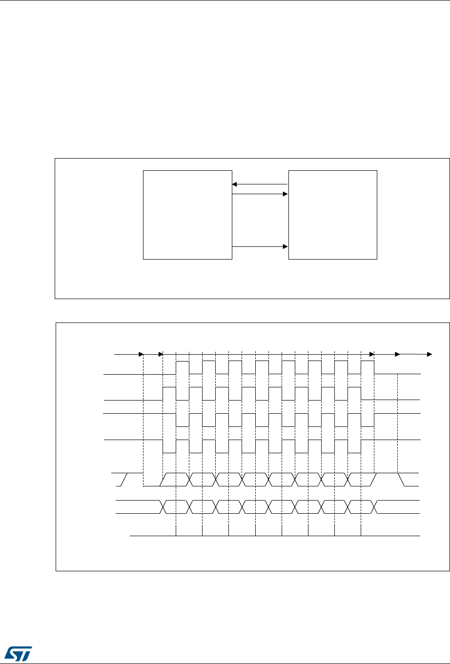
RM0430 Rev 8 913/1324
RM0430 Universal synchronous receiver transmitter (USART) /universal asynchronous receiver
934
has been written). This means that it is not possible to receive a synchronous data without
transmitting data.
The LBCL, CPOL and CPHA bits have to be selected when both the transmitter and the
receiver are disabled (TE=RE=0) to ensure that the clock pulses function correctly. These
bits should not be changed while the transmitter or the receiver is enabled.
It is advised that TE and RE are set in the same instruction in order to minimize the setup
and the hold time of the receiver.
The USART supports master mode only: it cannot receive or send data related to an input
clock (SCLK is always an output).
Figure 303. USART example of synchronous transmission
Figure 304. USART data clock timing diagram (M=0)
06Y9
86$57 6\QFKURQRXVGHYLFH
HJVODYH63,
5;
7;
'DWDRXW
'DWDLQ
&ORFN
6&/.
06Y9
06%
06%
/6%
/6%
6WDUW
6WDUW 6WRS
,GOHRUSUHFHGLQJ
WUDQVPLVVLRQ
,GOHRUQH[W
WUDQVPLVVLRQ
/%&/ELWFRQWUROVODVWGDWDSXOVH
&DSWXUHVWUREH
'DWDRQ5;
IURPVODYH
'DWDRQ7;
IURPPDVWHU
&ORFN&32/ &3+$
&ORFN&32/ &3+$
&ORFN&32/ &3+$
&ORFN&32/ &3+$
6WRS
0ELWV GDWDELWV
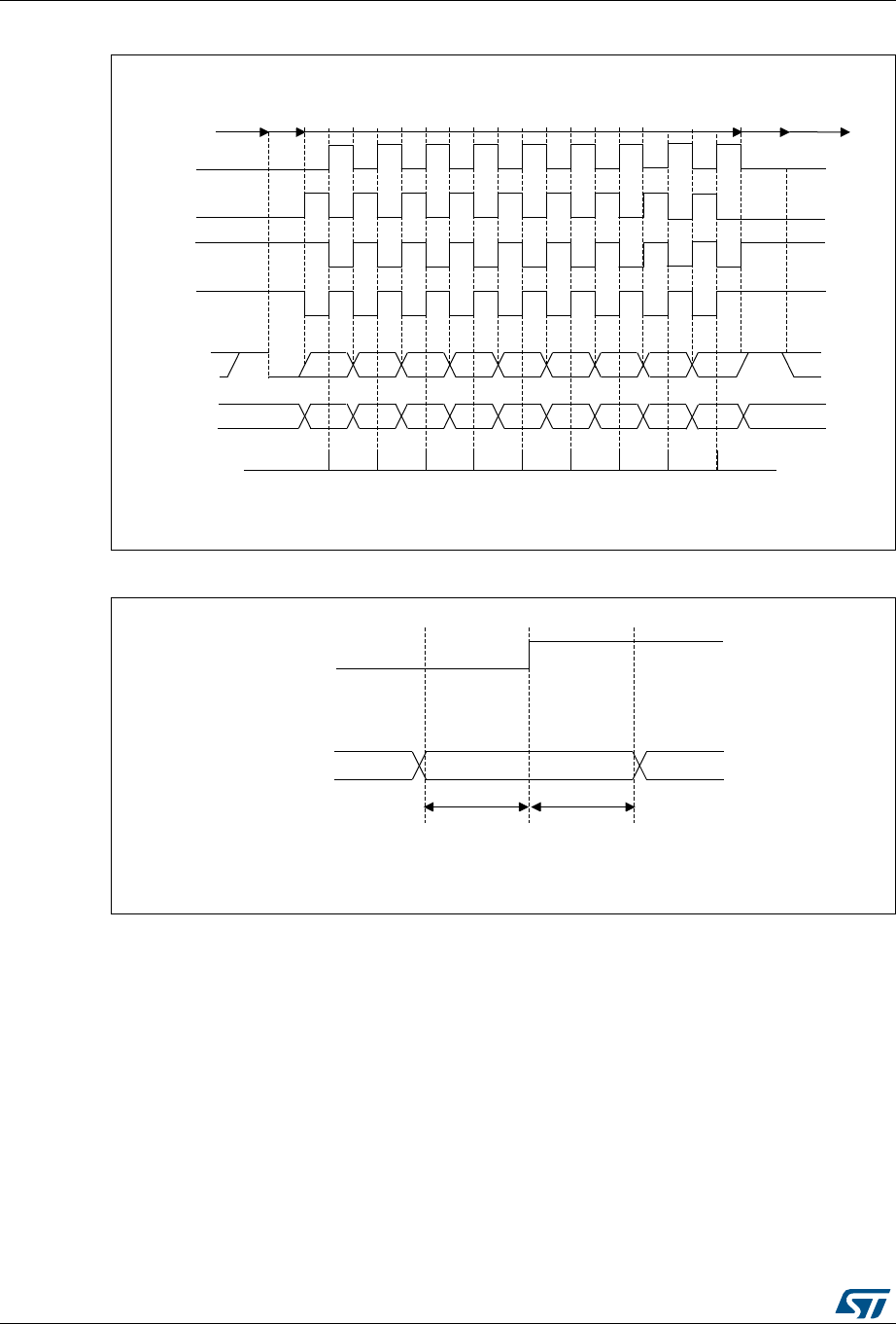
Universal synchronous receiver transmitter (USART) /universal asynchronous receiver transmit-
914/1324 RM0430 Rev 8
Figure 305. USART data clock timing diagram (M=1)
Figure 306. RX data setup/hold time
Note: The function of SCLK is different in Smartcard mode. Refer to the Smartcard mode chapter
for more details.
28.4.10 Single-wire half-duplex communication
The single-wire half-duplex mode is selected by setting the HDSEL bit in the USART_CR3
register. In this mode, the following bits must be kept cleared:
•LINEN and CLKEN bits in the USART_CR2 register,
•SCEN and IREN bits in the USART_CR3 register.
The USART can be configured to follow a single-wire half-duplex protocol where the TX and
RX lines are internally connected. The selection between half- and full-duplex
communication is made with a control bit ‘HALF DUPLEX SEL’ (HDSEL in USART_CR3).
06Y9
06%
06%
/6%
/6%6WDUW
6WDUW 6WRS
,GOHRU
SUHFHGLQJ
WUDQVPLVVLRQ
,GOHRUQH[W
WUDQVPLVVLRQ
/%&/ELWFRQWUROVODVWGDWDSXOVH
&DSWXUH
VWUREH
'DWDRQ5;
IURPVODYH
'DWDRQ7;
IURPPDVWHU
&ORFN&32/
&3+$
&ORFN&32/
&3+$
&ORFN&32/
&3+$
&ORFN&32/
&3+$
6WRS
0ELWV GDWDELWV
06Y9
'DWDRQ5;IURPVODYH
6&/.
FDSWXUHVWUREHRQ6&/.
ULVLQJHGJHLQWKLVH[DPSOH
9DOLG'$7$ELW
W6(783 W+2/'
W6(783 W+2/'ELWWLPH
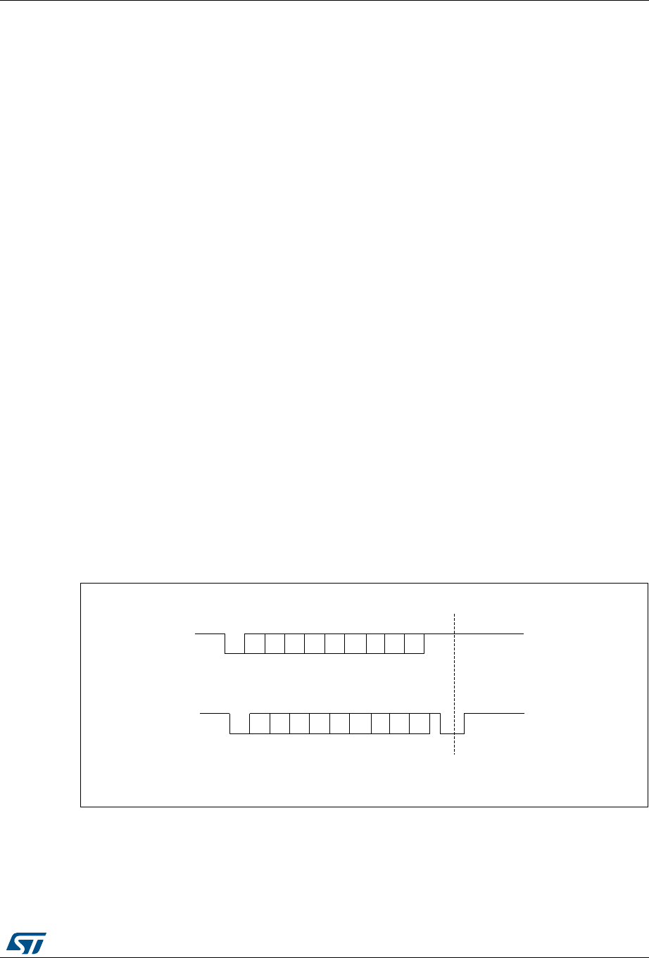
RM0430 Rev 8 915/1324
RM0430 Universal synchronous receiver transmitter (USART) /universal asynchronous receiver
934
As soon as HDSEL is written to 1:
•the TX and RX lines are internally connected
•the RX pin is no longer used
•the TX pin is always released when no data is transmitted. Thus, it acts as a standard
I/O in idle or in reception. It means that the I/O must be configured so that TX is
configured as floating input (or output high open-drain) when not driven by the USART.
Apart from this, the communications are similar to what is done in normal USART mode.
The conflicts on the line must be managed by the software (by the use of a centralized
arbiter, for instance). In particular, the transmission is never blocked by hardware and
continue to occur as soon as a data is written in the data register while the TE bit is set.
28.4.11 Smartcard
The Smartcard mode is selected by setting the SCEN bit in the USART_CR3 register. In
smartcard mode, the following bits must be kept cleared:
•LINEN bit in the USART_CR2 register,
•HDSEL and IREN bits in the USART_CR3 register.
Moreover, the CLKEN bit may be set in order to provide a clock to the smartcard.
The Smartcard interface is designed to support asynchronous protocol Smartcards as
defined in the ISO 7816-3 standard. The USART should be configured as:
•8 bits plus parity: where M=1 and PCE=1 in the USART_CR1 register
•1.5 stop bits when transmitting and receiving: where STOP=11 in the USART_CR2
register.
Note: It is also possible to choose 0.5 stop bit for receiving but it is recommended to use 1.5 stop
bits for both transmitting and receiving to avoid switching between the two configurations.
Figure 307 shows examples of what can be seen on the data line with and without parity
error.
Figure 307. ISO 7816-3 asynchronous protocol
When connected to a Smartcard, the TX output of the USART drives a bidirectional line that
is also driven by the Smartcard. The TX pin must be configured as open-drain.
Smartcard is a single wire half duplex communication protocol.
•Transmission of data from the transmit shift register is guaranteed to be delayed by a
minimum of 1/2 baud clock. In normal operation a full transmit shift register will start
06Y9
:LWKRXW3DULW\HUURU
S
6
*XDUGWLPH
:LWK3DULW\HUURU
S
6
*XDUGWLPH
6WDUWELW
6WDUWELW /LQHSXOOHGORZE\UHFHLYHU
GXULQJVWRSLQFDVHRISDULW\HUURU
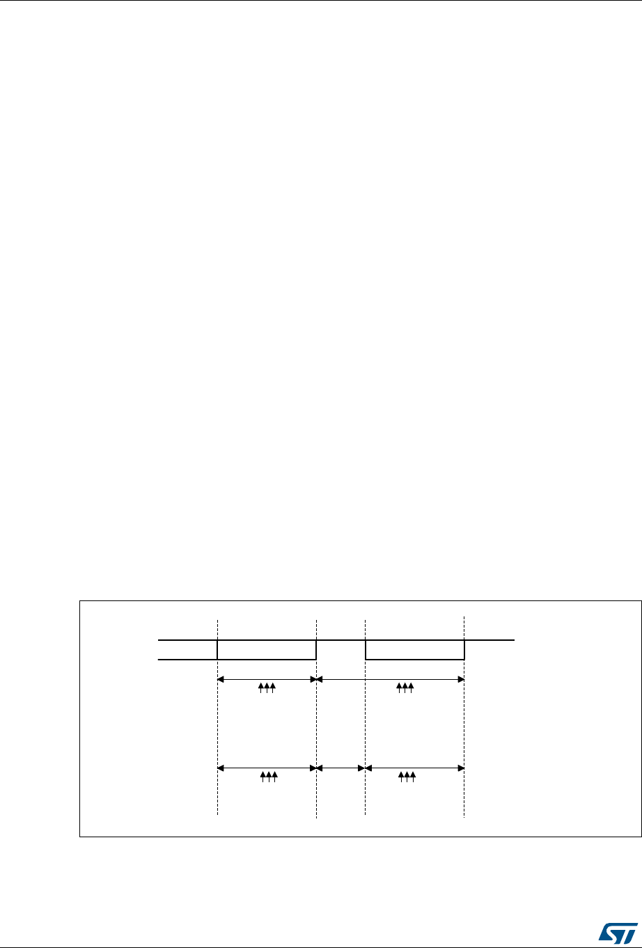
Universal synchronous receiver transmitter (USART) /universal asynchronous receiver transmit-
916/1324 RM0430 Rev 8
shifting on the next baud clock edge. In Smartcard mode this transmission is further
delayed by a guaranteed 1/2 baud clock.
•If a parity error is detected during reception of a frame programmed with a 0.5 or 1.5
stop bit period, the transmit line is pulled low for a baud clock period after the
completion of the receive frame. This is to indicate to the Smartcard that the data
transmitted to USART has not been correctly received. This NACK signal (pulling
transmit line low for 1 baud clock) will cause a framing error on the transmitter side
(configured with 1.5 stop bits). The application can handle re-sending of data according
to the protocol. A parity error is ‘NACK’ed by the receiver if the NACK control bit is set,
otherwise a NACK is not transmitted.
•The assertion of the TC flag can be delayed by programming the Guard Time register.
In normal operation, TC is asserted when the transmit shift register is empty and no
further transmit requests are outstanding. In Smartcard mode an empty transmit shift
register triggers the guard time counter to count up to the programmed value in the
Guard Time register. TC is forced low during this time. When the guard time counter
reaches the programmed value TC is asserted high.
•The de-assertion of TC flag is unaffected by Smartcard mode.
•If a framing error is detected on the transmitter end (due to a NACK from the receiver),
the NACK will not be detected as a start bit by the receive block of the transmitter.
According to the ISO protocol, the duration of the received NACK can be 1 or 2 baud
clock periods.
•On the receiver side, if a parity error is detected and a NACK is transmitted the receiver
will not detect the NACK as a start bit.
Note: A break character is not significant in Smartcard mode. A 0x00 data with a framing error will
be treated as data and not as a break.
No Idle frame is transmitted when toggling the TE bit. The Idle frame (as defined for the
other configurations) is not defined by the ISO protocol.
Figure 308 details how the NACK signal is sampled by the USART. In this example the
USART is transmitting a data and is configured with 1.5 stop bits. The receiver part of the
USART is enabled in order to check the integrity of the data and the NACK signal.
Figure 308. Parity error detection using the 1.5 stop bits
The USART can provide a clock to the smartcard through the SCLK output. In smartcard
mode, SCLK is not associated to the communication but is simply derived from the internal
peripheral input clock through a 5-bit prescaler. The division ratio is configured in the
069
%LW 3DULW\ELW 6WRSELW
ELWWLPH ELWWLPH
ELW
WLPH
6DPSOLQJDW
WKWKWK
6DPSOLQJDW
WKWKWK
6DPSOLQJDW
WKWKWK
6DPSOLQJDW
WKWKWK

RM0430 Rev 8 917/1324
RM0430 Universal synchronous receiver transmitter (USART) /universal asynchronous receiver
934
prescaler register USART_GTPR. SCLK frequency can be programmed from fCK/2 to
fCK/62, where fCK is the peripheral input clock.
28.4.12 IrDA SIR ENDEC block
The IrDA mode is selected by setting the IREN bit in the USART_CR3 register. In IrDA
mode, the following bits must be kept cleared:
•LINEN, STOP and CLKEN bits in the USART_CR2 register,
•SCEN and HDSEL bits in the USART_CR3 register.
The IrDA SIR physical layer specifies use of a Return to Zero, Inverted (RZI) modulation
scheme that represents logic 0 as an infrared light pulse (see Figure 309).
The SIR Transmit encoder modulates the Non Return to Zero (NRZ) transmit bit stream
output from USART. The output pulse stream is transmitted to an external output driver and
infrared LED. USART supports only bit rates up to 115.2Kbps for the SIR ENDEC. In normal
mode the transmitted pulse width is specified as 3/16 of a bit period.
The SIR receive decoder demodulates the return-to-zero bit stream from the infrared
detector and outputs the received NRZ serial bit stream to USART. The decoder input is
normally HIGH (marking state) in the Idle state. The transmit encoder output has the
opposite polarity to the decoder input. A start bit is detected when the decoder input is low.
•IrDA is a half duplex communication protocol. If the Transmitter is busy (i.e. the USART
is sending data to the IrDA encoder), any data on the IrDA receive line will be ignored
by the IrDA decoder and if the Receiver is busy (USART is receiving decoded data
from the USART), data on the TX from the USART to IrDA will not be encoded by IrDA.
While receiving data, transmission should be avoided as the data to be transmitted
could be corrupted.
•A ‘0 is transmitted as a high pulse and a ‘1 is transmitted as a ‘0. The width of the pulse
is specified as 3/16th of the selected bit period in normal mode (see Figure 310).
•The SIR decoder converts the IrDA compliant receive signal into a bit stream for
USART.
•The SIR receive logic interprets a high state as a logic one and low pulses as logic
zeros.
•The transmit encoder output has the opposite polarity to the decoder input. The SIR
output is in low state when Idle.
•The IrDA specification requires the acceptance of pulses greater than 1.41 us. The
acceptable pulse width is programmable. Glitch detection logic on the receiver end
filters out pulses of width less than 2 PSC periods (PSC is the prescaler value
programmed in the IrDA low-power Baud Register, USART_GTPR). Pulses of width
less than 1 PSC period are always rejected, but those of width greater than one and
less than two periods may be accepted or rejected, those greater than 2 periods will be
accepted as a pulse. The IrDA encoder/decoder doesn’t work when PSC=0.
•The receiver can communicate with a low-power transmitter.
•In IrDA mode, the STOP bits in the USART_CR2 register must be configured to “1 stop
bit”.
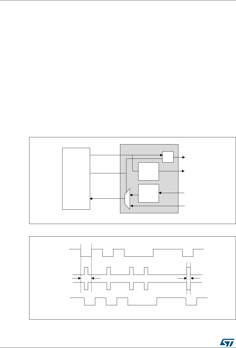
Universal synchronous receiver transmitter (USART) /universal asynchronous receiver transmit-
918/1324 RM0430 Rev 8
IrDA low-power mode
Transmitter:
In low-power mode the pulse width is not maintained at 3/16 of the bit period. Instead, the
width of the pulse is 3 times the low-power baud rate that can be a minimum of 1.42 MHz.
Generally this value is 1.8432 MHz (1.42 MHz < PSC< 2.12 MHz). A low-power mode
programmable divisor divides the system clock to achieve this value.
Receiver:
Receiving in low-power mode is similar to receiving in normal mode. For glitch detection the
USART should discard pulses of duration shorter than 1/PSC. A valid low is accepted only if
its duration is greater than 2 periods of the IrDA low-power Baud clock (PSC value in
USART_GTPR).
Note: A pulse of width less than two and greater than one PSC period(s) may or may not be
rejected.
The receiver set up time should be managed by software. The IrDA physical layer
specification specifies a minimum of 10 ms delay between transmission and reception (IrDA
is a half duplex protocol).
Figure 309. IrDA SIR ENDEC- block diagram
Figure 310. IrDA data modulation (3/16) -Normal mode
6,5(1
06Y9
86$57
25
6,5
7UDQVPLW
(QFRGHU
6,5
5HFHLYH
'(FRGHU
7;
5;
86$57B5;
,U'$B,1
,U'$B287
86$57B7;
06Y9
7;
6WDUW
ELW
6WRS
ELW
%LWSHULRG
,U'$B287
,U'$B,1
5;

RM0430 Rev 8 919/1324
RM0430 Universal synchronous receiver transmitter (USART) /universal asynchronous receiver
934
28.4.13 Continuous communication using DMA
The USART is capable of continuous communication using the DMA. The DMA requests for
Rx buffer and Tx buffer are generated independently.
Transmission using DMA
DMA mode can be enabled for transmission by setting DMAT bit in the USART_CR3
register. Data is loaded from a SRAM area configured using the DMA peripheral (refer to the
DMA specification) to the USART_DR register whenever the TXE bit is set. To map a DMA
channel for USART transmission, use the following procedure (x denotes the channel
number):
1. Write the USART_DR register address in the DMA control register to configure it as the
destination of the transfer. The data will be moved to this address from memory after
each TXE event.
2. Write the memory address in the DMA control register to configure it as the source of
the transfer. The data will be loaded into the USART_DR register from this memory
area after each TXE event.
3. Configure the total number of bytes to be transferred to the DMA control register.
4. Configure the channel priority in the DMA register
5. Configure DMA interrupt generation after half/ full transfer as required by the
application.
6. Clear the TC bit in the SR register by writing 0 to it.
7. Activate the channel in the DMA register.
When the number of data transfers programmed in the DMA Controller is reached, the DMA
controller generates an interrupt on the DMA channel interrupt vector.
In transmission mode, once the DMA has written all the data to be transmitted (the TCIF flag
is set in the DMA_ISR register), the TC flag can be monitored to make sure that the USART
communication is complete. This is required to avoid corrupting the last transmission before
disabling the USART or entering the Stop mode. The software must wait until TC=1. The TC
flag remains cleared during all data transfers and it is set by hardware at the last frame end
of transmission.
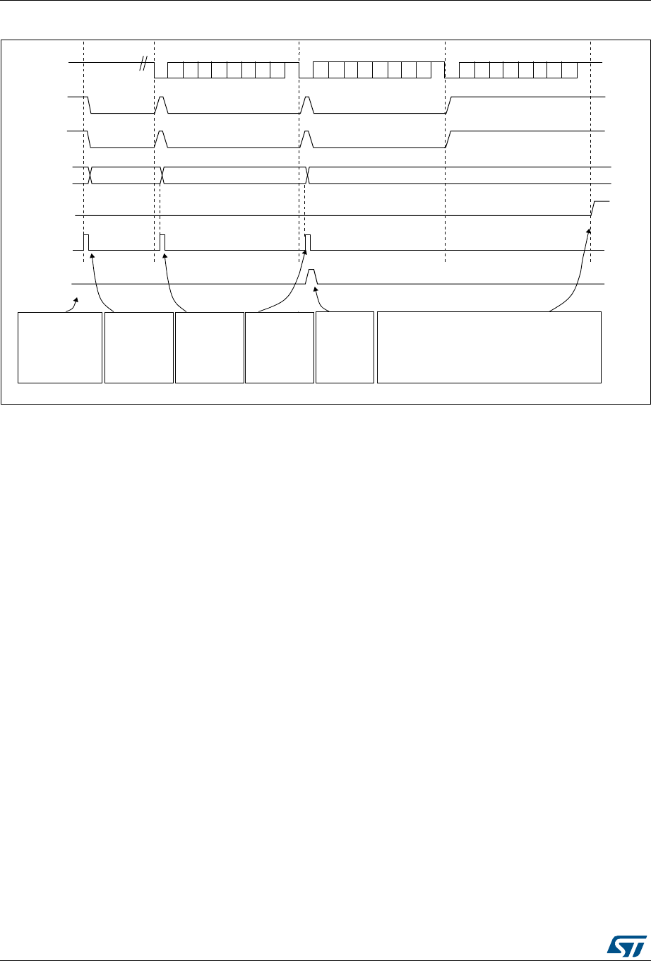
Universal synchronous receiver transmitter (USART) /universal asynchronous receiver transmit-
920/1324 RM0430 Rev 8
Figure 311. Transmission using DMA
Reception using DMA
DMA mode can be enabled for reception by setting the DMAR bit in USART_CR3 register.
Data is loaded from the USART_DR register to a SRAM area configured using the DMA
peripheral (refer to the DMA specification) whenever a data byte is received. To map a DMA
channel for USART reception, use the following procedure:
1. Write the USART_DR register address in the DMA control register to configure it as the
source of the transfer. The data will be moved from this address to the memory after
each RXNE event.
2. Write the memory address in the DMA control register to configure it as the destination
of the transfer. The data will be loaded from USART_DR to this memory area after each
RXNE event.
3. Configure the total number of bytes to be transferred in the DMA control register.
4. Configure the channel priority in the DMA control register
5. Configure interrupt generation after half/ full transfer as required by the application.
6. Activate the channel in the DMA control register.
When the number of data transfers programmed in the DMA Controller is reached, the DMA
controller generates an interrupt on the DMA channel interrupt vector. The DMAR bit should
be cleared by software in the USART_CR3 register during the interrupt subroutine.
) ))
AIB
6RIWZDUH
FRQILJXUHV'0$
WRVHQGGDWD
EORFNVDQG
HQDEOHV86$57
7KH'0$
WUDQVIHULV
FRPSOHWH
7&,) LQ
'0$B,65
'0$ZULWHV
)LQWR
86$57B7'5
'0$ZULWHV
)LQWR
86$57B7'5
'0$ZULWHV
)LQWR
86$57B7'5
6RIWZDUHZDLWVXQWLO7&
6HWE\KDUGZDUH
&OHDUHG
E\
VRIWZDUH
6HWE\
KDUGZDUH
7;OLQH
7;(IODJ
86$57B7'5
'0$UHTXHVW
'0$ZULWHV
86$57B7'5
'0$7&,)IODJ
WUDQVIHU
FRPSOHWH
7&IODJ
)UDPH )UDPH )UDPH
,GOHSUHDPEOH
6HWE\KDUGZDUH
FOHDUHGE\'0$UHDG
6HWE\KDUGZDUH
FOHDUHGE\'0$UHDG 6HWE\KDUGZDUH
,JQRUHGE\WKH'0$EHFDXVH
WKHWUDQVIHULVFRPSOHWH
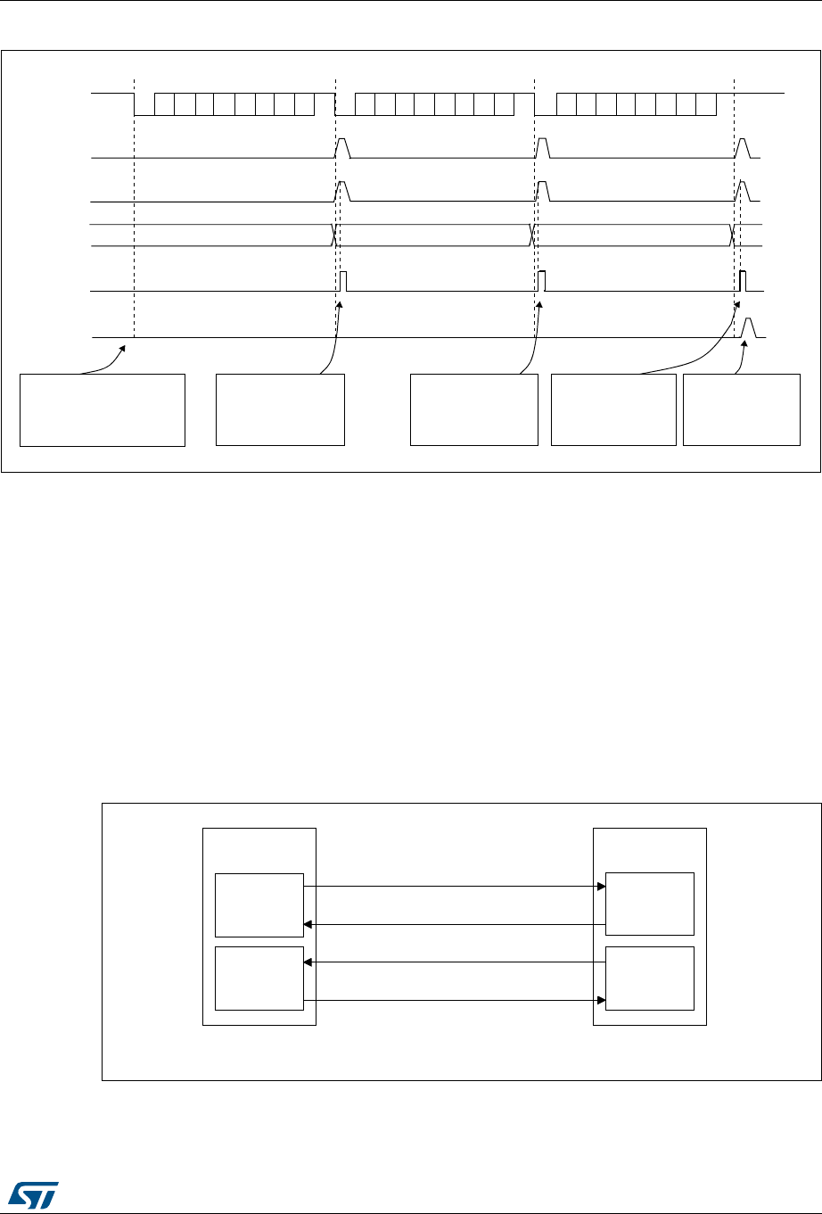
RM0430 Rev 8 921/1324
RM0430 Universal synchronous receiver transmitter (USART) /universal asynchronous receiver
934
Figure 312. Reception using DMA
Error flagging and interrupt generation in multibuffer communication
In case of multibuffer communication if any error occurs during the transaction the error flag
will be asserted after the current byte. An interrupt will be generated if the interrupt enable
flag is set. For framing error, overrun error and noise flag that are asserted with RXNE in
case of single byte reception, there will be separate error flag interrupt enable bit (EIE bit in
the USART_CR3 register), which if set will issue an interrupt after the current byte with
either of these errors.
28.4.14 Hardware flow control
It is possible to control the serial data flow between 2 devices by using the nCTS input and
the nRTS output. The Figure 313 shows how to connect 2 devices in this mode:
Figure 313. Hardware flow control between 2 USARTs
RTS and CTS flow control can be enabled independently by writing respectively RTSE and
CTSE bits to 1 (in the USART_CR3 register).
7;OLQH
)UDPH
) )
6HWE\KDUGZDUH
FOHDUHGE\'0$UHDG
)
DLE
)UDPH )UDPH
5;1(IODJ
86$57B7'5
'0$UHTXHVW
'0$UHDGV
86$57B7'5
'0$7&,)IODJ
WUDQVIHUFRPSOHWH
6RIWZDUHFRQILJXUHVWKH
'0$WRUHFHLYHGDWD
EORFNVDQGHQDEOHV
WKH86$57
'0$UHDGV)
IURP86$57B7'5
7KH'0$WUDQVIHU
LVFRPSOHWH
7&,) LQ
'0$B,65
6HWE\KDUGZDUH
&OHDUHG
E\
VRIWZDUH
'0$UHDGV)
IURP86$57B7'5
'0$UHDGV)
IURP86$57B7'5
06Y9
7;FLUFXLW
86$57
7;
5;FLUFXLW
5;FLUFXLW
86$57
7;FLUFXLW
7;
Q&76
Q&76
Q576
5;
Q576
5;
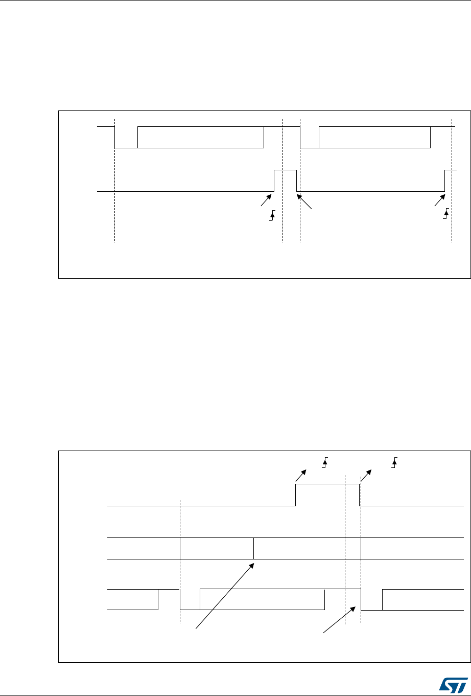
Universal synchronous receiver transmitter (USART) /universal asynchronous receiver transmit-
922/1324 RM0430 Rev 8
RTS flow control
If the RTS flow control is enabled (RTSE=1), then nRTS is asserted (tied low) as long as the
USART receiver is ready to receive a new data. When the receive register is full, nRTS is
deasserted, indicating that the transmission is expected to stop at the end of the current
frame. Figure 314 shows an example of communication with RTS flow control enabled.
Figure 314. RTS flow control
CTS flow control
If the CTS flow control is enabled (CTSE=1), then the transmitter checks the nCTS input
before transmitting the next frame. If nCTS is asserted (tied low), then the next data is
transmitted (assuming that a data is to be transmitted, in other words, if TXE=0), else the
transmission does not occur. When nCTS is deasserted during a transmission, the current
transmission is completed before the transmitter stops.
When CTSE=1, the CTSIF status bit is automatically set by hardware as soon as the nCTS
input toggles. It indicates when the receiver becomes ready or not ready for communication.
An interrupt is generated if the CTSIE bit in the USART_CR3 register is set. The figure
below shows an example of communication with CTS flow control enabled.
Figure 315. CTS flow control
06Y9
6WDUW
ELW
6WDUW
ELW
6WRS
ELW ,GOH 6WRS
ELW
5;
Q576
'DWDUHDG
'DWDFDQQRZEHWUDQVPLWWHG
5;1( 5;1(
'DWD 'DWD
06Y9
6WDUW
ELW
6WRS
ELW
7;
7'5
&76
'DWD
'DWD
6WRS
ELW ,GOH 6WDUW
ELW
'DWD 'DWD
'DWD
HPSW\ HPSW\
&76
Q&76
7UDQVPLWGDWDUHJLVWHU
:ULWLQJGDWDLQ7'5 7UDQVPLVVLRQRI'DWDLV
GHOD\HGXQWLOQ&76

RM0430 Rev 8 923/1324
RM0430 Universal synchronous receiver transmitter (USART) /universal asynchronous receiver
934
Note: Special behavior of break frames: when the CTS flow is enabled, the transmitter does not
check the nCTS input state to send a break.
28.5 USART interrupts
The USART interrupt events are connected to the same interrupt vector (see Figure 316).
•During transmission: Transmission Complete, Clear to Send or Transmit Data Register
empty interrupt.
•While receiving: Idle Line detection, Overrun error, Receive Data register not empty,
Parity error, LIN break detection, Noise Flag (only in multi buffer communication) and
Framing Error (only in multi buffer communication).
These events generate an interrupt if the corresponding Enable Control Bit is set.
Table 172. USART interrupt requests
Interrupt event Event flag Enable control bit
Transmit Data Register Empty TXE TXEIE
CTS flag CTS CTSIE
Transmission Complete TC TCIE
Received Data Ready to be Read RXNE
RXNEIE
Overrun Error Detected ORE
Idle Line Detected IDLE IDLEIE
Parity Error PE PEIE
Break Flag LBD LBDIE
Noise Flag, Overrun error and Framing Error
in multibuffer communication NF or ORE or FE EIE
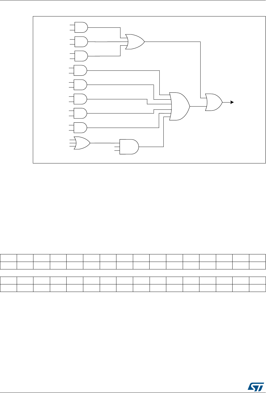
Universal synchronous receiver transmitter (USART) /universal asynchronous receiver transmit-
924/1324 RM0430 Rev 8
Figure 316. USART interrupt mapping diagram
28.6 USART registers
Refer to Section 1.2 on page 52 for a list of abbreviations used in register descriptions.
The peripheral registers have to be accessed by half-words (16 bits) or words (32 bits).
28.6.1 Status register (USART_SR)
Address offset: 0x00
Reset value: 0x00C0 0000
069
7;(
7;(,(
5;1(,(
25(
86$57
LQWHUUXSW
,'/(
,'/(,(
7&
7&,(
&76
&76,(
3(
3(,(
5;1(,(
5;1(
/%'
/%',(
)(
1(
25( (,(
'0$5
31 30 29 28 27 26 25 24 23 22 21 20 19 18 17 16
Res. Res. Res. Res. Res. Res. Res. Res. Res. Res. Res. Res. Res. Res. Res. Res.
1514131211109876543210
Res. Res. Res. Res. Res. Res. CTS LBD TXE TC RXNE IDLE ORE NF FE PE
rc_w0rc_w0rrc_w0rc_w0rrrrr

RM0430 Rev 8 925/1324
RM0430 Universal synchronous receiver transmitter (USART) /universal asynchronous receiver
934
Bits 31:10 Reserved, must be kept at reset value
Bit 9 CTS: CTS flag
This bit is set by hardware when the nCTS input toggles, if the CTSE bit is set. It is cleared
by software (by writing it to 0). An interrupt is generated if CTSIE=1 in the USART_CR3
register.
0: No change occurred on the nCTS status line
1: A change occurred on the nCTS status line
Note: This bit is not available for UART4 & UART5.
Bit 8 LBD: LIN break detection flag
This bit is set by hardware when the LIN break is detected. It is cleared by software (by
writing it to 0). An interrupt is generated if LBDIE = 1 in the USART_CR2 register.
0: LIN Break not detected
1: LIN break detected
Note: An interrupt is generated when LBD=1 if LBDIE=1
Bit 7 TXE: Transmit data register empty
This bit is set by hardware when the content of the TDR register has been transferred into
the shift register. An interrupt is generated if the TXEIE bit =1 in the USART_CR1 register. It
is cleared by a write to the USART_DR register.
0: Data is not transferred to the shift register
1: Data is transferred to the shift register)
Note: This bit is used during single buffer transmission.
Bit 6 TC: Transmission complete
This bit is set by hardware if the transmission of a frame containing data is complete and if
TXE is set. An interrupt is generated if TCIE=1 in the USART_CR1 register. It is cleared by
a software sequence (a read from the USART_SR register followed by a write to the
USART_DR register). The TC bit can also be cleared by writing a '0' to it. This clearing
sequence is recommended only for multibuffer communication.
0: Transmission is not complete
1: Transmission is complete
Bit 5 RXNE: Read data register not empty
This bit is set by hardware when the content of the RDR shift register has been transferred
to the USART_DR register. An interrupt is generated if RXNEIE=1 in the USART_CR1
register. It is cleared by a read to the USART_DR register. The RXNE flag can also be
cleared by writing a zero to it. This clearing sequence is recommended only for multibuffer
communication.
0: Data is not received
1: Received data is ready to be read.
Bit 4 IDLE: IDLE line detected
This bit is set by hardware when an Idle Line is detected. An interrupt is generated if the
IDLEIE=1 in the USART_CR1 register. It is cleared by a software sequence (an read to the
USART_SR register followed by a read to the USART_DR register).
0: No Idle Line is detected
1: Idle Line is detected
Note: The IDLE bit will not be set again until the RXNE bit has been set itself (i.e. a new idle
line occurs).

Universal synchronous receiver transmitter (USART) /universal asynchronous receiver transmit-
926/1324 RM0430 Rev 8
Bit 3 ORE: Overrun error
This bit is set by hardware when the word currently being received in the shift register is
ready to be transferred into the RDR register while RXNE=1. An interrupt is generated if
RXNEIE=1 in the USART_CR1 register. It is cleared by a software sequence (an read to the
USART_SR register followed by a read to the USART_DR register).
0: No Overrun error
1: Overrun error is detected
Note: When this bit is set, the RDR register content will not be lost but the shift register will be
overwritten. An interrupt is generated on ORE flag in case of Multi Buffer
communication if the EIE bit is set.
Bit 2 NF: Noise detected flag
This bit is set by hardware when noise is detected on a received frame. It is cleared by a
software sequence (an read to the USART_SR register followed by a read to the
USART_DR register).
0: No noise is detected
1: Noise is detected
Note: This bit does not generate interrupt as it appears at the same time as the RXNE bit that
itself generates an interrupting interrupt is generated on NF flag in case of Multi Buffer
communication if the EIE bit is set.
Note: When the line is noise-free, the NF flag can be disabled by programming the ONEBIT
bit to 1 to increase the USART tolerance to deviations (Refer to Section 28.4.5: USART
receiver tolerance to clock deviation on page 906).
Bit 1 FE: Framing error
This bit is set by hardware when a de-synchronization, excessive noise or a break character
is detected. It is cleared by a software sequence (an read to the USART_SR register
followed by a read to the USART_DR register).
0: No Framing error is detected
1: Framing error or break character is detected
Note: This bit does not generate interrupt as it appears at the same time as the RXNE bit that
itself generates an interrupt. If the word currently being transferred causes both frame
error and overrun error, it will be transferred and only the ORE bit will be set.
An interrupt is generated on FE flag in case of Multi Buffer communication if the EIE bit
is set.
Bit 0 PE: Parity error
This bit is set by hardware when a parity error occurs in receiver mode. It is cleared by a
software sequence (a read from the status register followed by a read or write access to the
USART_DR data register). The software must wait for the RXNE flag to be set before
clearing the PE bit.
An interrupt is generated if PEIE = 1 in the USART_CR1 register.
0: No parity error
1: Parity error

RM0430 Rev 8 927/1324
RM0430 Universal synchronous receiver transmitter (USART) /universal asynchronous receiver
934
28.6.2 Data register (USART_DR)
Address offset: 0x04
Reset value: 0x0000 0000
28.6.3 Baud rate register (USART_BRR)
Note: The baud counters stop counting if the TE or RE bits are disabled respectively.
Address offset: 0x08
Reset value: 0x0000 0000
31 30 29 28 27 26 25 24 23 22 21 20 19 18 17 16
Res. Res. Res. Res. Res. Res. Res. Res. Res. Res. Res. Res. Res. Res. Res. Res.
15 14 13 12 11 10 9 8 7 6 5 4 3 2 1 0
Res. Res. Res. Res. Res. Res. Res. DR[8:0]
rw rw rw rw rw rw rw rw rw
Bits 31:9 Reserved, must be kept at reset value
Bits 8:0 DR[8:0]: Data value
Contains the Received or Transmitted data character, depending on whether it is read from
or written to.
The Data register performs a double function (read and write) since it is composed of two
registers, one for transmission (TDR) and one for reception (RDR)
The TDR register provides the parallel interface between the internal bus and the output shift
register (see Figure 1).
The RDR register provides the parallel interface between the input shift register and the
internal bus.
When transmitting with the parity enabled (PCE bit set to 1 in the USART_CR1 register), the
value written in the MSB (bit 7 or bit 8 depending on the data length) has no effect because
it is replaced by the parity.
When receiving with the parity enabled, the value read in the MSB bit is the received parity
bit.
31 30 29 28 27 26 25 24 23 22 21 20 19 18 17 16
Res. Res. Res. Res. Res. Res. Res. Res. Res. Res. Res. Res. Res. Res. Res. Res.
1514131211109876543210
DIV_Mantissa[11:0] DIV_Fraction[3:0]
rw rw rw rw rw rw rw rw rw rw rw rw rw rw rw rw
Bits 31:16 Reserved, must be kept at reset value
Bits 15:4 DIV_Mantissa[11:0]: mantissa of USARTDIV
These 12 bits define the mantissa of the USART Divider (USARTDIV)
Bits 3:0 DIV_Fraction[3:0]: fraction of USARTDIV
These 4 bits define the fraction of the USART Divider (USARTDIV). When OVER8=1, the
DIV_Fraction3 bit is not considered and must be kept cleared.

Universal synchronous receiver transmitter (USART) /universal asynchronous receiver transmit-
928/1324 RM0430 Rev 8
28.6.4 Control register 1 (USART_CR1)
Address offset: 0x0C
Reset value: 0x0000 0000
31 30 29 28 27 26 25 24 23 22 21 20 19 18 17 16
Res. Res. Res. Res. Res. Res. Res. Res. Res. Res. Res. Res. Res. Res. Res. Res.
15 14 13 12 11 10 9 8 7 6 5 4 3 2 1 0
OVER8 Res. UE M WAKE PCE PS PEIE TXEIE TCIE RXNEIE IDLEIE TE RE RWU SBK
rw rw rw rw rw rw rw rw rw rw rw rw rw rw rw
Bits 31:16 Reserved, must be kept at reset value
Bit 15 OVER8: Oversampling mode
0: oversampling by 16
1: oversampling by 8
Note: Oversampling by 8 is not available in the Smartcard, IrDA and LIN modes: when
SCEN=1,IREN=1 or LINEN=1 then OVER8 is forced to ‘0 by hardware.
Bit 14 Reserved, must be kept at reset value
Bit 13 UE: USART enable
When this bit is cleared the USART prescalers and outputs are stopped and the end of the
current
byte transfer in order to reduce power consumption. This bit is set and cleared by software.
0: USART prescaler and outputs disabled
1: USART enabled
Bit 12 M: Word length
This bit determines the word length. It is set or cleared by software.
0: 1 Start bit, 8 Data bits, n Stop bit
1: 1 Start bit, 9 Data bits, n Stop bit
Note: The M bit must not be modified during a data transfer (both transmission and reception)
Bit 11 WAKE: Wakeup method
This bit determines the USART wakeup method, it is set or cleared by software.
0: Idle Line
1: Address Mark
Bit 10 PCE: Parity control enable
This bit selects the hardware parity control (generation and detection). When the parity
control is enabled, the computed parity is inserted at the MSB position (9th bit if M=1; 8th bit
if M=0) and parity is checked on the received data. This bit is set and cleared by software.
Once it is set, PCE is active after the current byte (in reception and in transmission).
0: Parity control disabled
1: Parity control enabled
Bit 9 PS: Parity selection
This bit selects the odd or even parity when the parity generation/detection is enabled (PCE
bit set). It is set and cleared by software. The parity will be selected after the current byte.
0: Even parity
1: Odd parity

RM0430 Rev 8 929/1324
RM0430 Universal synchronous receiver transmitter (USART) /universal asynchronous receiver
934
Bit 8 PEIE: PE interrupt enable
This bit is set and cleared by software.
0: Interrupt is inhibited
1: An USART interrupt is generated whenever PE=1 in the USART_SR register
Bit 7 TXEIE: TXE interrupt enable
This bit is set and cleared by software.
0: Interrupt is inhibited
1: An USART interrupt is generated whenever TXE=1 in the USART_SR register
Bit 6 TCIE: Transmission complete interrupt enable
This bit is set and cleared by software.
0: Interrupt is inhibited
1: An USART interrupt is generated whenever TC=1 in the USART_SR register
Bit 5 RXNEIE: RXNE interrupt enable
This bit is set and cleared by software.
0: Interrupt is inhibited
1: An USART interrupt is generated whenever ORE=1 or RXNE=1 in the USART_SR
register
Bit 4 IDLEIE: IDLE interrupt enable
This bit is set and cleared by software.
0: Interrupt is inhibited
1: An USART interrupt is generated whenever IDLE=1 in the USART_SR register
Bit 3 TE: Transmitter enable
This bit enables the transmitter. It is set and cleared by software.
0: Transmitter is disabled
1: Transmitter is enabled
Note: 1: During transmission, a “0” pulse on the TE bit (“0” followed by “1”) sends a preamble
(idle line) after the current word, except in smartcard mode.
2: When TE is set there is a 1 bit-time delay before the transmission starts.
Bit 2 RE: Receiver enable
This bit enables the receiver. It is set and cleared by software.
0: Receiver is disabled
1: Receiver is enabled and begins searching for a start bit
Bit 1 RWU: Receiver wakeup
This bit determines if the USART is in mute mode or not. It is set and cleared by software
and can be cleared by hardware when a wakeup sequence is recognized.
0: Receiver in active mode
1: Receiver in mute mode
Note: 1: Before selecting Mute mode (by setting the RWU bit) the USART must first receive a
data byte, otherwise it cannot function in Mute mode with wakeup by Idle line detection.
2: In Address Mark Detection wakeup configuration (WAKE bit=1) the RWU bit cannot
be modified by software while the RXNE bit is set.
Bit 0 SBK: Send break
This bit set is used to send break characters. It can be set and cleared by software. It should
be set by software, and will be reset by hardware during the stop bit of break.
0: No break character is transmitted
1: Break character will be transmitted

Universal synchronous receiver transmitter (USART) /universal asynchronous receiver transmit-
930/1324 RM0430 Rev 8
28.6.5 Control register 2 (USART_CR2)
Address offset: 0x10
Reset value: 0x0000 0000
31 30 29 28 27 26 25 24 23 22 21 20 19 18 17 16
Res. Res. Res. Res. Res. Res. Res. Res. Res. Res. Res. Res. Res. Res. Res. Res.
1514131211109876543210
Res. LINEN STOP[1:0] CLKEN CPOL CPHA LBCL Res. LBDIE LBDL Res. ADD[3:0]
rw rw rw rw rw rw rw rw rw rw rw rw rw
Bits 31:15 Reserved, must be kept at reset value
Bit 14 LINEN: LIN mode enable
This bit is set and cleared by software.
0: LIN mode disabled
1: LIN mode enabled
The LIN mode enables the capability to send LIN Synch Breaks (13 low bits) using the SBK bit in
the USART_CR1 register, and to detect LIN Sync breaks.
Bits 13:12 STOP: STOP bits
These bits are used for programming the stop bits.
00: 1 Stop bit
01: 0.5 Stop bit
10: 2 Stop bits
11: 1.5 Stop bit
Note: The 0.5 Stop bit and 1.5 Stop bit are not available for UART4 & UART5.
Bit 11 CLKEN: Clock enable
This bit allows the user to enable the SCLK pin.
0: SCLK pin disabled
1: SCLK pin enabled
This bit is not available for UART4 & UART5.
Bit 10 CPOL: Clock polarity
This bit allows the user to select the polarity of the clock output on the SCLK pin in synchronous
mode. It works in conjunction with the CPHA bit to produce the desired clock/data relationship
0: Steady low value on SCLK pin outside transmission window.
1: Steady high value on SCLK pin outside transmission window.
This bit is not available for UART4 & UART5.
Bit 9 CPHA: Clock phase
This bit allows the user to select the phase of the clock output on the SCLK pin in synchronous
mode. It works in conjunction with the CPOL bit to produce the desired clock/data relationship (see
figures 304 to 305)
0: The first clock transition is the first data capture edge
1: The second clock transition is the first data capture edge
Note: This bit is not available for UART4 & UART5.

RM0430 Rev 8 931/1324
RM0430 Universal synchronous receiver transmitter (USART) /universal asynchronous receiver
934
Note: These 3 bits (CPOL, CPHA, LBCL) should not be written while the transmitter is enabled.
28.6.6 Control register 3 (USART_CR3)
Address offset: 0x14
Reset value: 0x0000 0000
Bit 8 LBCL: Last bit clock pulse
This bit allows the user to select whether the clock pulse associated with the last data bit
transmitted (MSB) has to be output on the SCLK pin in synchronous mode.
0: The clock pulse of the last data bit is not output to the SCLK pin
1: The clock pulse of the last data bit is output to the SCLK pin
Note: 1: The last bit is the 8th or 9th data bit transmitted depending on the 8 or 9 bit format selected
by the M bit in the USART_CR1 register.
2: This bit is not available for UART4 & UART5.
Bit 7 Reserved, must be kept at reset value
Bit 6 LBDIE: LIN break detection interrupt enable
Break interrupt mask (break detection using break delimiter).
0: Interrupt is inhibited
1: An interrupt is generated whenever LBD=1 in the USART_SR register
Bit 5 LBDL: lin break detection length
This bit is for selection between 11 bit or 10 bit break detection.
0: 10-bit break detection
1: 11-bit break detection
Bit 4 Reserved, must be kept at reset value
Bits 3:0 ADD[3:0]: Address of the USART node
This bit-field gives the address of the USART node.
This is used in multiprocessor communication during mute mode, for wake up with address mark
detection.
31 30 29 28 27 26 25 24 23 22 21 20 19 18 17 16
Res. Res. Res. Res. Res. Res. Res. Res. Res. Res. Res. Res. Res. Res. Res. Res.
15 14 13 12 11 10 9 8 7 6 5 4 3 2 1 0
Res. Res. Res. Res. ONEBIT CTSIE CTSE RTSE DMAT DMAR SCEN NACK HDSEL IRLP IREN EIE
rw rw rw rw rw rw rw rw rw rw rw rw
Bits 31:12 Reserved, must be kept at reset value
Bit 11 ONEBIT: One sample bit method enable
This bit allows the user to select the sample method. When the one sample bit method is
selected the noise detection flag (NF) is disabled.
0: Three sample bit method
1: One sample bit method
Bit 10 CTSIE: CTS interrupt enable
0: Interrupt is inhibited
1: An interrupt is generated whenever CTS=1 in the USART_SR register
Note: This bit is not available for UART4 & UART5.

Universal synchronous receiver transmitter (USART) /universal asynchronous receiver transmit-
932/1324 RM0430 Rev 8
Bit 9 CTSE: CTS enable
0: CTS hardware flow control disabled
1: CTS mode enabled, data is only transmitted when the nCTS input is asserted (tied to 0).
If the nCTS input is deasserted while a data is being transmitted, then the transmission is
completed before stopping. If a data is written into the data register while nCTS is
deasserted, the transmission is postponed until nCTS is asserted.
Note: This bit is not available for UART4 & UART5.
Bit 8 RTSE: RTS enable
0: RTS hardware flow control disabled
1: RTS interrupt enabled, data is only requested when there is space in the receive buffer.
The transmission of data is expected to cease after the current character has been
transmitted. The nRTS output is asserted (tied to 0) when a data can be received.
Note: This bit is not available for UART4 & UART5.
Bit 7 DMAT: DMA enable transmitter
This bit is set/reset by software
1: DMA mode is enabled for transmission.
0: DMA mode is disabled for transmission.
Bit 6 DMAR: DMA enable receiver
This bit is set/reset by software
1: DMA mode is enabled for reception
0: DMA mode is disabled for reception
Bit 5 SCEN: Smartcard mode enable
This bit is used for enabling Smartcard mode.
0: Smartcard Mode disabled
1: Smartcard Mode enabled
Note: This bit is not available for UART4 & UART5.
Bit 4 NACK: Smartcard NACK enable
0: NACK transmission in case of parity error is disabled
1: NACK transmission during parity error is enabled
Note: This bit is not available for UART4 & UART5.
Bit 3 HDSEL: Half-duplex selection
Selection of Single-wire Half-duplex mode
0: Half duplex mode is not selected
1: Half duplex mode is selected
Bit 2 IRLP: IrDA low-power
This bit is used for selecting between normal and low-power IrDA modes
0: Normal mode
1: Low-power mode
Bit 1 IREN: IrDA mode enable
This bit is set and cleared by software.
0: IrDA disabled
1: IrDA enabled

RM0430 Rev 8 933/1324
RM0430 Universal synchronous receiver transmitter (USART) /universal asynchronous receiver
934
28.6.7 Guard time and prescaler register (USART_GTPR)
Address offset: 0x18
Reset value: 0x0000 0000
Bit 0 EIE: Error interrupt enable
Error Interrupt Enable Bit is required to enable interrupt generation in case of a framing
error, overrun error or noise flag (FE=1 or ORE=1 or NF=1 in the USART_SR register) in
case of Multi Buffer Communication (DMAR=1 in the USART_CR3 register).
0: Interrupt is inhibited
1: An interrupt is generated whenever DMAR=1 in the USART_CR3 register and FE=1 or
ORE=1 or NF=1 in the USART_SR register.
31 30 29 28 27 26 25 24 23 22 21 20 19 18 17 16
Res. Res. Res. Res. Res. Res. Res. Res. Res. Res. Res. Res. Res. Res. Res. Res.
1514131211109876543210
GT[7:0] PSC[7:0]
rw rw rw rw rw rw rw rw rw rw rw rw rw rw rw rw
Bits 31:16 Reserved, must be kept at reset value
Bits 15:8 GT[7:0]: Guard time value
This bit-field gives the Guard time value in terms of number of baud clocks.
This is used in Smartcard mode. The Transmission Complete flag is set after this guard time
value.
Note: This bit is not available for UART4 & UART5.
Bits 7:0 PSC[7:0]: Prescaler value
–In IrDA Low-power mode:
PSC[7:0] = IrDA Low-Power Baud Rate
Used for programming the prescaler for dividing the system clock to achieve the low-power
frequency:
The source clock is divided by the value given in the register (8 significant bits):
00000000: Reserved - do not program this value
00000001: divides the source clock by 1
00000010: divides the source clock by 2
...
–In normal IrDA mode: PSC must be set to 00000001.
– In smartcard mode:
PSC[4:0]: Prescaler value
Used for programming the prescaler for dividing the system clock to provide the smartcard
clock.
The value given in the register (5 significant bits) is multiplied by 2 to give the division factor
of the source clock frequency:
00000: Reserved - do not program this value
00001: divides the source clock by 2
00010: divides the source clock by 4
00011: divides the source clock by 6
...
Note: 1: Bits [7:5] have no effect if Smartcard mode is used.
2: This bit is not available for UART4 & UART5.

Universal synchronous receiver transmitter (USART) /universal asynchronous receiver transmit-
934/1324 RM0430 Rev 8
28.6.8 USART register map
The table below gives the USART register map and reset values.
Refer to Section 2.2.2 on page 58 for the register boundary addresses.
Table 173. USART register map and reset values
Offset Register
31
30
29
28
27
26
25
24
23
22
21
20
19
18
17
16
15
14
13
12
11
10
9
8
7
6
5
4
3
2
1
0
0x00
USART_SR
Res.
Res.
Res.
Res.
Res.
Res.
Res.
Res.
Res.
Res.
Res.
Res.
Res.
Res.
Res.
Res.
Res.
Res.
Res.
Res.
Res.
Res.
CTS
LBD
TXE
TC
RXNE
IDLE
ORE
NF
FE
PE
Reset value 0011000000
0x04
USART_DR
Res.
Res.
Res.
Res.
Res.
Res.
Res.
Res.
Res.
Res.
Res.
Res.
Res.
Res.
Res.
Res.
Res.
Res.
Res.
Res.
Res.
Res.
Res.
DR[8:0]
Reset value 000000000
0x08
USART_BRR
Res.
Res.
Res.
Res.
Res.
Res.
Res.
Res.
Res.
Res.
Res.
Res.
Res.
Res.
Res.
Res.
DIV_Mantissa[15:4] DIV_Fraction
[3:0]
Reset value 0000000000000000
0x0C
USART_CR1
Res.
Res.
Res.
Res.
Res.
Res.
Res.
Res.
Res.
Res.
Res.
Res.
Res.
Res.
Res.
Res.
OVER8
Res.
UE
M
WAKE
PCE
PS
PEIE
TXEIE
TCIE
RXNEIE
IDLEIE
TE
RE
RWU
SBK
Reset value 0 00000000000000
0x10
USART_CR2
Res.
Res.
Res.
Res.
Res.
Res.
Res.
Res.
Res.
Res.
Res.
Res.
Res.
Res.
Res.
Res.
Res.
LINEN
STOP
[1:0]
CLKEN
CPOL
CPHA
LBCL
Res.
LBDIE
LBDL
Res.
ADD[3:0]
Reset value 0000000 00 0000
0x14
USART_CR3
Res.
Res.
Res.
Res.
Res.
Res.
Res.
Res.
Res.
Res.
Res.
Res.
Res.
Res.
Res.
Res.
Res.
Res.
Res.
Res.
ONEBIT
CTSIE
CTSE
RTSE
DMAT
DMAR
SCEN
NACK
HDSEL
IRLP
IREN
EIE
Reset value 000000000000
0x18
USART_GTPR
Res.
Res.
Res.
Res.
Res.
Res.
Res.
Res.
Res.
Res.
Res.
Res.
Res.
Res.
Res.
Res.
GT[7:0] PSC[7:0]
Reset value 0000000000000000

RM0430 Rev 8 935/1324
RM0430 Serial peripheral interface/ inter-IC sound (SPI/I2S)
986
29 Serial peripheral interface/ inter-IC sound (SPI/I2S)
29.1 Introduction
The SPI/I²S interface can be used to communicate with external devices using the SPI
protocol or the I2S audio protocol. SPI or I2S mode is selectable by software. SPI mode is
selected by default after a device reset.
The serial peripheral interface (SPI) protocol supports half-duplex, full-duplex and simplex
synchronous, serial communication with external devices. The interface can be configured
as master and in this case it provides the communication clock (SCK) to the external slave
device. The interface is also capable of operating in multimaster configuration.
The Inter-IC sound (I2S) protocol is also a synchronous serial communication interface. It
can operate in slave or master mode with full-duplex and half-duplex communication.
It can address four different audio standards including the Philips I2S standard, the MSB-
and LSB-justified standards and the PCM standard.
Warning: Since some SPI1 pins may be mapped onto some pins used
by the JTAG interface, you can either map SPI/I2S onto other
pins, disable the JTAG and use the SWD interface prior to
configuring the pins listed as SPI I/Os (when debugging the
application) or disable both JTAG/SWD interfaces (for
standalone applications). For more information on the
configuration of the JTAG/SWD interface pins, please refer to
Section 7.3.2: I/O pin multiplexer and mapping.

Serial peripheral interface/ inter-IC sound (SPI/I2S) RM0430
936/1324 RM0430 Rev 8
29.1.1 SPI main features
•Master or slave operation
•Full-duplex synchronous transfers on three lines
•Half-duplex synchronous transfer on two lines (with bidirectional data line)
•Simplex synchronous transfers on two lines (with unidirectional data line)
•8-bit to 16-bit transfer frame format selection
•Multimaster mode capability
•8 master mode baud rate prescalers up to fPCLK/2.
•Slave mode frequency up to fPCLK/2.
•NSS management by hardware or software for both master and slave: dynamic change
of master/slave operations
•Programmable clock polarity and phase
•Programmable data order with MSB-first or LSB-first shifting
•Dedicated transmission and reception flags with interrupt capability
•SPI bus busy status flag
•SPI Motorola support
•Hardware CRC feature for reliable communication:
– CRC value can be transmitted as last byte in Tx mode
– Automatic CRC error checking for last received byte
•Master mode fault, overrun flags with interrupt capability
•CRC Error flag
•1-byte/word transmission and reception buffer with DMA capability: Tx and Rx requests

RM0430 Rev 8 937/1324
RM0430 Serial peripheral interface/ inter-IC sound (SPI/I2S)
986
29.1.2 SPI extended features
•SPI TI mode support
29.1.3 I2S features
•Full-duplex communication
•Half-duplex communication (only transmitter or receiver)
•Master or slave operations
•8-bit programmable linear prescaler to reach accurate audio sample frequencies (from
8 kHz to 192 kHz)
•Data format may be 16-bit, 24-bit or 32-bit
•Packet frame is fixed to 16-bit (16-bit data frame) or 32-bit (16-bit, 24-bit, 32-bit data
frame) by audio channel
•Programmable clock polarity (steady state)
•Underrun flag in slave transmission mode, overrun flag in reception mode (master and
slave) and Frame Error Flag in reception and transmitter mode (slave only)
•16-bit register for transmission and reception with one data register for both channel
sides
•Supported I2S protocols:
–I
2S Philips standard
– MSB-Justified standard (Left-Justified)
– LSB-Justified standard (Right-Justified)
– PCM standard (with short and long frame synchronization on 16-bit channel frame
or 16-bit data frame extended to 32-bit channel frame)
•Data direction is always MSB first
•DMA capability for transmission and reception (16-bit wide)
•Master clock can be output to drive an external audio component. Ratio is fixed at
256 × FS (where FS is the audio sampling frequency)
•I2S (I2S1, I2S2, I2S3, I2S4 and I2S5) clock can be derived from an external clock
mapped on the I2S_CKIN pin.
29.2 SPI/I2S implementation
This manual describes the full set of features implemented in SPI1, SPI2, SPI3, SPI4 and
SPI5.
Table 174. STM32F413/423 SPI implementation
SPI Features(1)
1. X = supported.
SPI1 SPI2 SPI3 SPI4 SPI5
Hardware CRC calculation X X X X X
I2S mode XXXXX
TI mode XXXXX
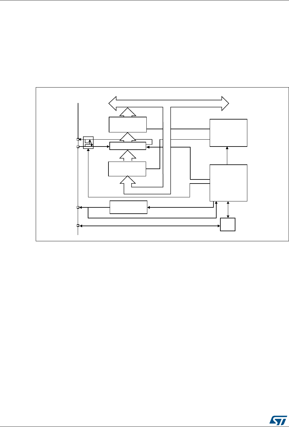
Serial peripheral interface/ inter-IC sound (SPI/I2S) RM0430
938/1324 RM0430 Rev 8
29.3 SPI functional description
29.3.1 General description
The SPI allows synchronous, serial communication between the MCU and external devices.
Application software can manage the communication by polling the status flag or using
dedicated SPI interrupt. The main elements of SPI and their interactions are shown in the
following block diagram Figure 317.
Figure 317. SPI block diagram
Four I/O pins are dedicated to SPI communication with external devices.
•MISO: Master In / Slave Out data. In the general case, this pin is used to transmit data
in slave mode and receive data in master mode.
•MOSI: Master Out / Slave In data. In the general case, this pin is used to transmit data
in master mode and receive data in slave mode.
•SCK: Serial Clock output pin for SPI masters and input pin for SPI slaves.
•NSS: Slave select pin. Depending on the SPI and NSS settings, this pin can be used to
either:
– select an individual slave device for communication
– synchronize the data frame or
– detect a conflict between multiple masters
See Section 29.3.5: Slave select (NSS) pin management for details.
The SPI bus allows the communication between one master device and one or more slave
devices. The bus consists of at least two wires - one for the clock signal and the other for
synchronous data transfer. Other signals can be added depending on the data exchange
between SPI nodes and their slave select signal management.
06Y9
6KLIWUHJLVWHU
:ULWH
5HDG
&RPPXQLFDWLRQ
FRQWUROOHU
$GGUHVVDQGGDWDEXV
&5&FRQWUROOHU
,QWHUQDO166
&5&(1
&5&1(;7
/6%),567
&32/
&3+$
'))
026,
0,62
6&.
166
5[
EXIIHU
7;
EXIIHU
%5>@
%,',2(
%,',02'(
5;2/1<
166
ORJLF
%DXGUDWH
JHQHUDWRU
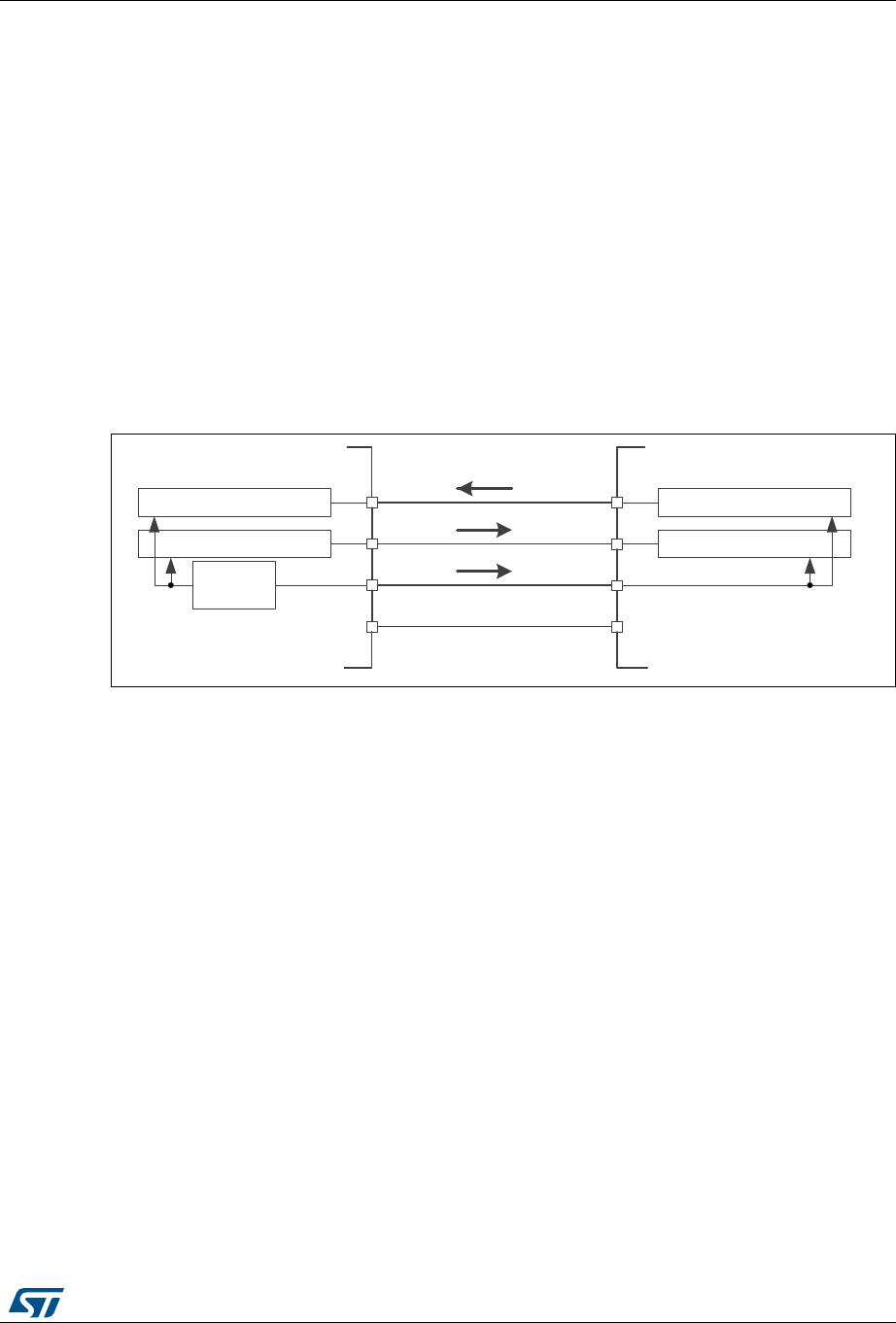
RM0430 Rev 8 939/1324
RM0430 Serial peripheral interface/ inter-IC sound (SPI/I2S)
986
29.3.2 Communications between one master and one slave
The SPI allows the MCU to communicate using different configurations, depending on the
device targeted and the application requirements. These configurations use 2 or 3 wires
(with software NSS management) or 3 or 4 wires (with hardware NSS management).
Communication is always initiated by the master.
Full-duplex communication
By default, the SPI is configured for full-duplex communication. In this configuration, the
shift registers of the master and slave are linked using two unidirectional lines between the
MOSI and the MISO pins. During SPI communication, data is shifted synchronously on the
SCK clock edges provided by the master. The master transmits the data to be sent to the
slave via the MOSI line and receives data from the slave via the MISO line. When the data
frame transfer is complete (all the bits are shifted) the information between the master and
slave is exchanged.
Figure 318. Full-duplex single master/ single slave application
1. The NSS pins can be used to provide a hardware control flow between master and slave. Optionally, the
pins can be left unused by the peripheral. Then the flow has to be handled internally for both master and
slave. For more details see Section 29.3.5: Slave select (NSS) pin management.
Half-duplex communication
The SPI can communicate in half-duplex mode by setting the BIDIMODE bit in the
SPIx_CR1 register. In this configuration, one single cross connection line is used to link the
shift registers of the master and slave together. During this communication, the data is
synchronously shifted between the shift registers on the SCK clock edge in the transfer
direction selected reciprocally by both master and slave with the BDIOE bit in their
SPIx_CR1 registers. In this configuration, the master’s MISO pin and the slave’s MOSI pin
are free for other application uses and act as GPIOs.
5[VKLIWUHJLVWHU
7[VKLIWUHJLVWHU 5[VKLIWUHJLVWHU
7[VKLIWUHJLVWHU
63,FORFN
JHQHUDWRU
0DVWHU 6ODYH
0,62
026,
6&.
166
0,62
026,
6&.
166
06Y9
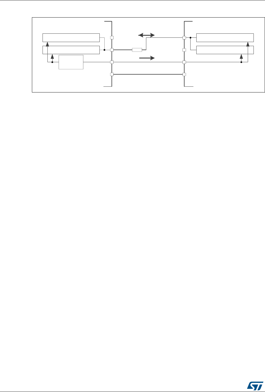
Serial peripheral interface/ inter-IC sound (SPI/I2S) RM0430
940/1324 RM0430 Rev 8
Figure 319. Half-duplex single master/ single slave application
1. The NSS pins can be used to provide a hardware control flow between master and slave. Optionally, the
pins can be left unused by the peripheral. Then the flow has to be handled internally for both master and
slave. For more details see Section 29.3.5: Slave select (NSS) pin management.
2. In this configuration, the master’s MISO pin and the slave’s MOSI pin can be used as GPIOs.
3. A critical situation can happen when communication direction is changed not synchronously between two
nodes working at bidirectionnal mode and new transmitter accesses the common data line while former
transmitter still keeps an opposite value on the line (the value depends on SPI configuration and
communication data). Both nodes then fight while providing opposite output levels on the common line
temporary till next node changes its direction settings correspondingly, too. It is suggested to insert a serial
resistance between MISO and MOSI pins at this mode to protect the outputs and limit the current blowing
between them at this situation.
Simplex communications
The SPI can communicate in simplex mode by setting the SPI in transmit-only or in receive-
only using the RXONLY bit in the SPIx_CR2 register. In this configuration, only one line is
used for the transfer between the shift registers of the master and slave. The remaining
MISO and MOSI pins pair is not used for communication and can be used as standard
GPIOs.
•Transmit-only mode (RXONLY=0): The configuration settings are the same as for full-
duplex. The application has to ignore the information captured on the unused input pin.
This pin can be used as a standard GPIO.
•Receive-only mode (RXONLY=1): The application can disable the SPI output function
by setting the RXONLY bit. In slave configuration, the MISO output is disabled and the
pin can be used as a GPIO. The slave continues to receive data from the MOSI pin
while its slave select signal is active (see 29.3.5: Slave select (NSS) pin management).
Received data events appear depending on the data buffer configuration. In the master
configuration, the MOSI output is disabled and the pin can be used as a GPIO. The
clock signal is generated continuously as long as the SPI is enabled. The only way to
stop the clock is to clear the RXONLY bit or the SPE bit and wait until the incoming
pattern from the MISO pin is finished and fills the data buffer structure, depending on its
configuration.
5[VKLIWUHJLVWHU
7[VKLIWUHJLVWHU 5[VKLIWUHJLVWHU
7[VKLIWUHJLVWHU
63,FORFN
JHQHUDWRU
0DVWHU 6ODYH
0,62
026,
6&.
166
0,62
026,
6&.
166
Nȍ
06Y9
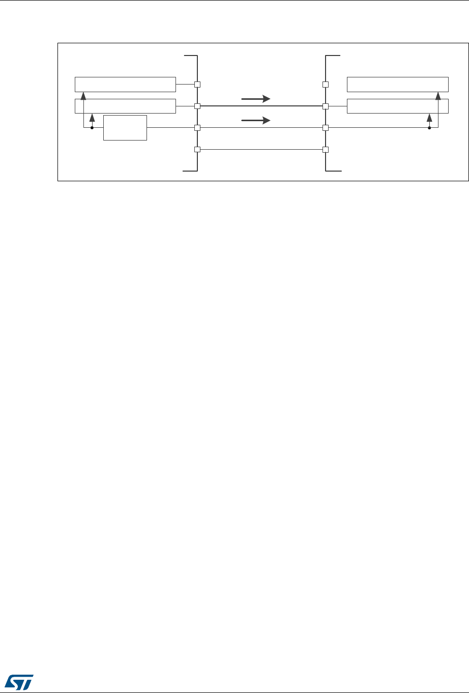
RM0430 Rev 8 941/1324
RM0430 Serial peripheral interface/ inter-IC sound (SPI/I2S)
986
Figure 320. Simplex single master/single slave application (master in transmit-only/
slave in receive-only mode)
1. The NSS pins can be used to provide a hardware control flow between master and slave. Optionally, the
pins can be left unused by the peripheral. Then the flow has to be handled internally for both master and
slave. For more details see Section 29.3.5: Slave select (NSS) pin management.
2. An accidental input information is captured at the input of transmitter Rx shift register. All the events
associated with the transmitter receive flow must be ignored in standard transmit only mode (e.g. OVF
flag).
3. In this configuration, both the MISO pins can be used as GPIOs.
Note: Any simplex communication can be alternatively replaced by a variant of the half-duplex
communication with a constant setting of the transaction direction (bidirectional mode is
enabled while BDIO bit is not changed).
5[VKLIWUHJLVWHU
7[VKLIWUHJLVWHU 5[VKLIWUHJLVWHU
7[VKLIWUHJLVWHU
63,FORFN
JHQHUDWRU
0DVWHU ^ůĂǀĞ
0,62
026,
6&.
166
0,62
026,
6&.
166
06Y9
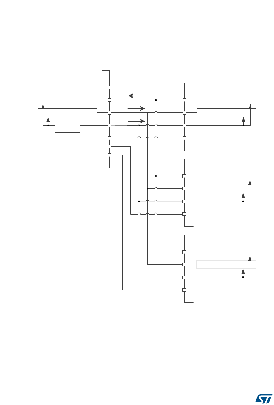
Serial peripheral interface/ inter-IC sound (SPI/I2S) RM0430
942/1324 RM0430 Rev 8
29.3.3 Standard multi-slave communication
In a configuration with two or more independent slaves, the master uses GPIO pins to
manage the chip select lines for each slave (see Figure 321.). The master must select one
of the slaves individually by pulling low the GPIO connected to the slave NSS input. When
this is done, a standard master and dedicated slave communication is established.
Figure 321. Master and three independent slaves
1. NSS pin is not used on master side at this configuration. It has to be managed internally (SSM=1, SSI=1) to
prevent any MODF error.
2. As MISO pins of the slaves are connected together, all slaves must have the GPIO configuration of their
MISO pin set as alternate function open-drain (see Section 7.3.7: I/O alternate function input/output on
page 191).
5[VKLIWUHJLVWHU
7[VKLIWUHJLVWHU 5[VKLIWUHJLVWHU
7[VKLIWUHJLVWHU
63,FORFN
JHQHUDWRU
0DVWHU 6ODYH
0,62
026,
6&.
166
0,62
026,
6&.
166
5[VKLIWUHJLVWHU
7[VKLIWUHJLVWHU
6ODYH
5[VKLIWUHJLVWHU
7[VKLIWUHJLVWHU
6ODYH
,2
,2
,2
0,62
026,
6&.
166
0,62
026,
6&.
166
06Y9
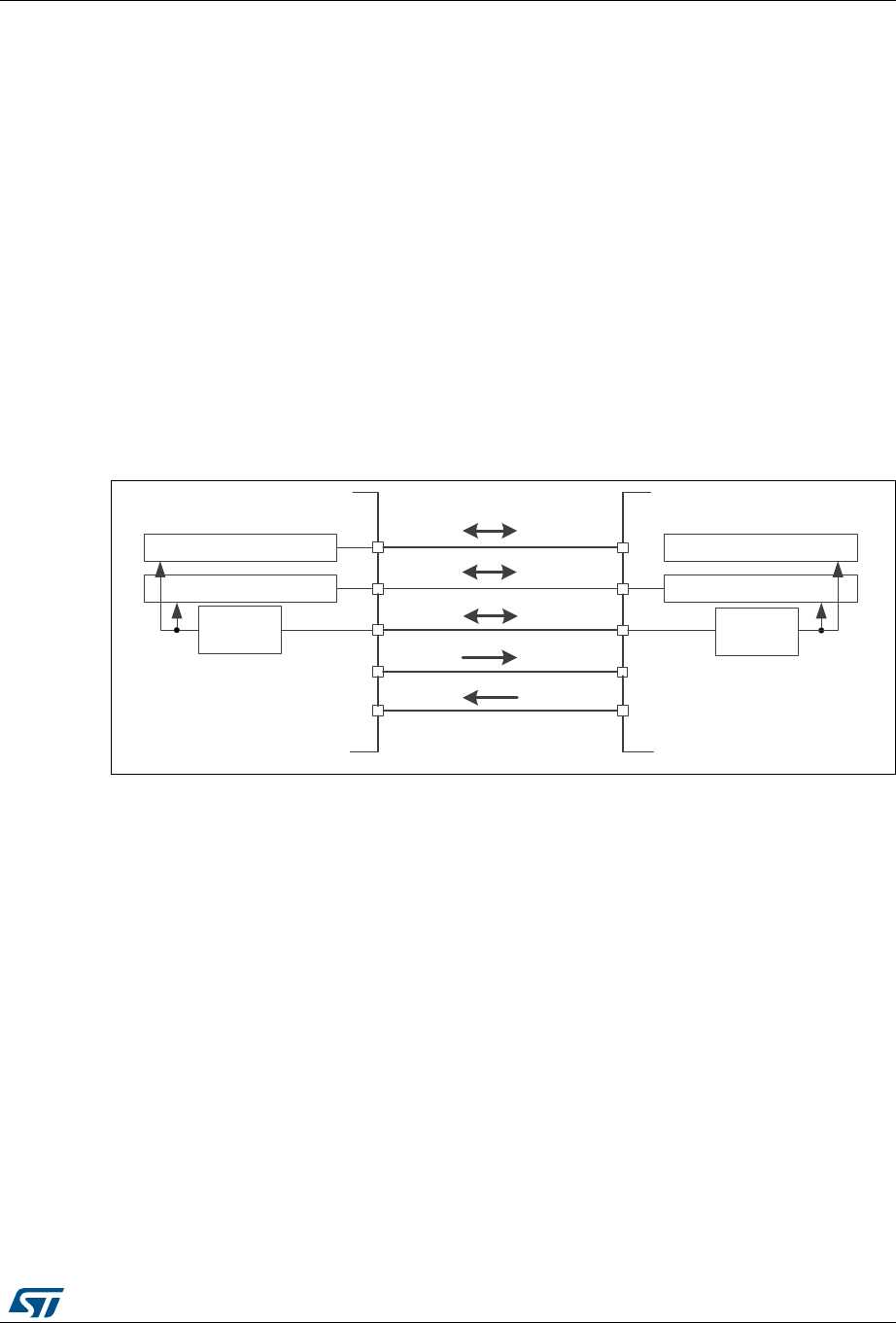
RM0430 Rev 8 943/1324
RM0430 Serial peripheral interface/ inter-IC sound (SPI/I2S)
986
29.3.4 Multi-master communication
Unless SPI bus is not designed for a multi-master capability primarily, the user can use build
in feature which detects a potential conflict between two nodes trying to master the bus at
the same time. For this detection, NSS pin is used configured at hardware input mode.
The connection of more than two SPI nodes working at this mode is impossible as only one
node can apply its output on a common data line at time.
When nodes are non active, both stay at slave mode by default. Once one node wants to
overtake control on the bus, it switches itself into master mode and applies active level on
the slave select input of the other node via dedicated GPIO pin. After the session is
completed, the active slave select signal is released and the node mastering the bus
temporary returns back to passive slave mode waiting for next session start.
If potentially both nodes raised their mastering request at the same time a bus conflict event
appears (see mode fault MODF event). Then the user can apply some simple arbitration
process (e.g. to postpone next attempt by predefined different time-outs applied at both
nodes).
Figure 322. Multi-master application
1. The NSS pin is configured at hardware input mode at both nodes. Its active level enables the MISO line
output control as the passive node is configured as a slave.
29.3.5 Slave select (NSS) pin management
In slave mode, the NSS works as a standard “chip select” input and lets the slave
communicate with the master. In master mode, NSS can be used either as output or input.
As an input it can prevent multimaster bus collision, and as an output it can drive a slave
select signal of a single slave.
Hardware or software slave select management can be set using the SSM bit in the
SPIx_CR1 register:
•Software NSS management (SSM = 1): in this configuration, slave select information
is driven internally by the SSI bit value in register SPIx_CR1. The external NSS pin is
free for other application uses.
•Hardware NSS management (SSM = 0): in this case, there are two possible
configurations. The configuration used depends on the NSS output configuration
(SSOE bit in register SPIx_CR1).
5[7[VKLIWUHJLVWHU
7[5[VKLIWUHJLVWHU 7[5[VKLIWUHJLVWHU
5[7[VKLIWUHJLVWHU
63,FORFN
JHQHUDWRU
0DVWHU
6ODYH
DĂƐƚĞƌ
;^ůĂǀĞͿ
0,62
026,
6&.
166
0,62
026,
6&.
166
06Y9
63,FORFN
JHQHUDWRU
*3,2
*3,2
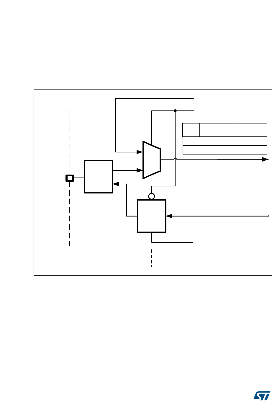
Serial peripheral interface/ inter-IC sound (SPI/I2S) RM0430
944/1324 RM0430 Rev 8
–NSS output enable (SSM=0,SSOE = 1): this configuration is only used when the
MCU is set as master. The NSS pin is managed by the hardware. The NSS signal
is driven low as soon as the SPI is enabled in master mode (SPE=1), and is kept
low until the SPI is disabled (SPE =0).
–NSS output disable (SSM=0, SSOE = 0): if the microcontroller is acting as the
master on the bus, this configuration allows multimaster capability. If the NSS pin
is pulled low in this mode, the SPI enters master mode fault state and the device is
automatically reconfigured in slave mode. In slave mode, the NSS pin works as a
standard “chip select” input and the slave is selected while NSS line is at low level.
Figure 323. Hardware/software slave select management
166,QSXW
660FRQWUROELW
66,FRQWUROELW
662(FRQWUROELW
1662XWSXW
166
SLQ
XVHGLQ0DVWHUPRGH166
+:PDQDJHPHQWRQO\
166
2XWSXW
&RQWURO
0DVWHU
PRGH 6ODYHPRGH
1RQDFWLYH2.9GG
166
,QS
$FWLYH&RQIOLFW9VV
166H[WHUQDOORJLF 166LQWHUQDOORJLF
*3,2
ORJLF
DLYH

RM0430 Rev 8 945/1324
RM0430 Serial peripheral interface/ inter-IC sound (SPI/I2S)
986
29.3.6 Communication formats
During SPI communication, receive and transmit operations are performed simultaneously.
The serial clock (SCK) synchronizes the shifting and sampling of the information on the data
lines. The communication format depends on the clock phase, the clock polarity and the
data frame format. To be able to communicate together, the master and slaves devices must
follow the same communication format.
Clock phase and polarity controls
Four possible timing relationships may be chosen by software, using the CPOL and CPHA
bits in the SPIx_CR1 register. The CPOL (clock polarity) bit controls the idle state value of
the clock when no data is being transferred. This bit affects both master and slave modes. If
CPOL is reset, the SCK pin has a low-level idle state. If CPOL is set, the SCK pin has a
high-level idle state.
If the CPHA bit is set, the second edge on the SCK pin captures the first data bit transacted
(falling edge if the CPOL bit is reset, rising edge if the CPOL bit is set). Data are latched on
each occurrence of this clock transition type. If the CPHA bit is reset, the first edge on the
SCK pin captures the first data bit transacted (falling edge if the CPOL bit is set, rising edge
if the CPOL bit is reset). Data are latched on each occurrence of this clock transition type.
The combination of CPOL (clock polarity) and CPHA (clock phase) bits selects the data
capture clock edge.
Figure 324, shows an SPI full-duplex transfer with the four combinations of the CPHA and
CPOL bits.
Note: Prior to changing the CPOL/CPHA bits the SPI must be disabled by resetting the SPE bit.
The idle state of SCK must correspond to the polarity selected in the SPIx_CR1 register (by
pulling up SCK if CPOL=1 or pulling down SCK if CPOL=0).
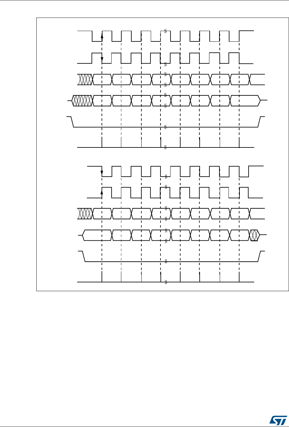
Serial peripheral interface/ inter-IC sound (SPI/I2S) RM0430
946/1324 RM0430 Rev 8
Figure 324. Data clock timing diagram
Note: The order of data bits depends on LSBFIRST bit setting.
Data frame format
The SPI shift register can be set up to shift out MSB-first or LSB-first, depending on the
value of the LSBFIRST bit. Each data frame is 8 or 16 bit long depending on the size of the
data programmed using the DFF bit in the SPI_CR1 register. The selected data frame
format is applicable both for transmission and reception.
&32/
&32/
06%LW /6%LW
06%LW /6%LW
0,62
026,
166
WRVODYH
&DSWXUHVWUREH
&3+$
&32/
&32/
06%LW /6%LW
06%LW /6%LW
0,62
026,
166
WRVODYH
&DSWXUHVWUREH
&3+$
DLG

RM0430 Rev 8 947/1324
RM0430 Serial peripheral interface/ inter-IC sound (SPI/I2S)
986
29.3.7 SPI configuration
The configuration procedure is almost the same for master and slave. For specific mode
setups, follow the dedicated chapters. When a standard communication is to be initialized,
perform these steps:
1. Write proper GPIO registers: Configure GPIO for MOSI, MISO and SCK pins.
2. Write to the SPI_CR1 register:
a) Configure the serial clock baud rate using the BR[2:0] bits (Note: 3).
b) Configure the CPOL and CPHA bits combination to define one of the four
relationships between the data transfer and the serial clock. (Note: 2 - except the
case when CRC is enabled at TI mode).
c) Select simplex or half-duplex mode by configuring RXONLY or BIDIMODE and
BIDIOE (RXONLY and BIDIMODE can't be set at the same time).
d) Configure the LSBFIRST bit to define the frame format (Note: 2).
e) Configure the CRCEN and CRCEN bits if CRC is needed (while SCK clock signal
is at idle state).
f) Configure SSM and SSI (Note: 2).
g) Configure the MSTR bit (in multimaster NSS configuration, avoid conflict state on
NSS if master is configured to prevent MODF error).
h) Set the DFF bit to configure the data frame format (8 or 16 bits).
3. Write to SPI_CR2 register:
a) Configure SSOE (Note: 1 & 2).
b) Set the FRF bit if the TI protocol is required.
4. Write to SPI_CRCPR register: Configure the CRC polynomial if needed.
5. Write proper DMA registers: Configure DMA streams dedicated for SPI Tx and Rx in
DMA registers if the DMA streams are used.
Note: (1) Step is not required in slave mode.
(2) Step is not required in TI mode.
(3) The step is not required in slave mode except slave working at TI mode.
29.3.8 Procedure for enabling SPI
It is recommended to enable the SPI slave before the master sends the clock. Otherwise,
undesired data transmission might occur. The slave data register must already contain data
to be sent before starting communication with the master (either on the first edge of the
communication clock, or before the end of the ongoing communication if the clock signal is
continuous). The SCK signal must be settled at an idle state level corresponding to the
selected polarity before the SPI slave is enabled.
At full-duplex (or in any transmit-only mode), the master starts communicating when the SPI
is enabled and data to be sent is written in the Tx Buffer.
In any master receive-only mode (RXONLY=1 or BIDIMODE=1 & BIDIOE=0), the master
starts communicating and the clock starts running immediately after the SPI is enabled.
The slave starts communicating when it receives a correct clock signal from the master. The
slave software must write the data to be sent before the SPI master initiates the transfer.
Refer to Section 29.3.11: Communication using DMA (direct memory addressing) for details
on how to handle DMA.

Serial peripheral interface/ inter-IC sound (SPI/I2S) RM0430
948/1324 RM0430 Rev 8
29.3.9 Data transmission and reception procedures
Rx and Tx buffers
In reception, data are received and then stored into an internal Rx buffer while in
transmission, data are first stored into an internal Tx buffer before being transmitted. A read
access to the SPI_DR register returns the Rx buffered value whereas a write access to the
SPI_DR stores the written data into the Tx buffer.
Tx buffer handling
The data frame is loaded from the Tx buffer into the shift register during the first bit
transmission. Bits are then shifted out serially from the shift register to a dedicated output
pin depending on LSBFIRST bit setting.The TXE flag (Tx buffer empty) is set when the data
are transferred from the Tx buffer to the shift register. It indicates that the internal Tx buffer is
ready to be loaded with the next data. An interrupt can be generated if the TXEIE bit of the
SPI_CR2 register is set. Clearing the TXE bit is performed by writing to the SPI_DR register.
A continuous transmit stream can be achieved if the next data to be transmitted are stored
in the Tx buffer while previous frame transmission is still ongoing. When the software writes
to Tx buffer while the TXE flag is not set, the data waiting for transaction is overwritten.
Rx buffer handling
The RXNE flag (Rx buffer not empty) is set on the last sampling clock edge, when the data
are transferred from the shift register to the Rx buffer. It indicates that data are ready to be
read from the SPI_DR register. An interrupt can be generated if the RXNEIE bit in the
SPI_CR2 register is set. Clearing the RXNE bit is performed by reading the SPI_DR
register.
If a device has not cleared the RXNE bit resulting from the previous data byte transmitted,
an overrun condition occurs when the next value is buffered. The OVR bit is set and an
interrupt is generated if the ERRIE bit is set.
Another way to manage the data exchange is to use DMA (see Section 9.2: DMA main
features).
Sequence handling
The BSY bit is set when a current data frame transaction is ongoing. When the clock signal
runs continuously, the BSY flag remains set between data frames on the master side.
However, on the slave side, it becomes low for a minimum duration of one SPI clock cycle
between each data frame transfer.
For some configurations, the BSY flag can be used during the last data transfer to wait until
the completion of the transfer.
When a receive-only mode is configured on the master side, either in half-duplex
(BIDIMODE=1, BIDIOE=0) or simplex configuration (BIDIMODE=0, RXONLY=1), the
master starts the receive sequence as soon as the SPI is enabled. Then the clock signal is
provided by the master and it does not stop until either the SPI or the receive-only mode is
disabled by the master. The master receives data frames continuously up to this moment.
While the master can provide all the transactions in continuous mode (SCK signal is
continuous), it has to respect slave capability to handle data flow and its content at anytime.
When necessary, the master must slow down the communication and provide either a
slower clock or separate frames or data sessions with sufficient delays. Be aware there is no
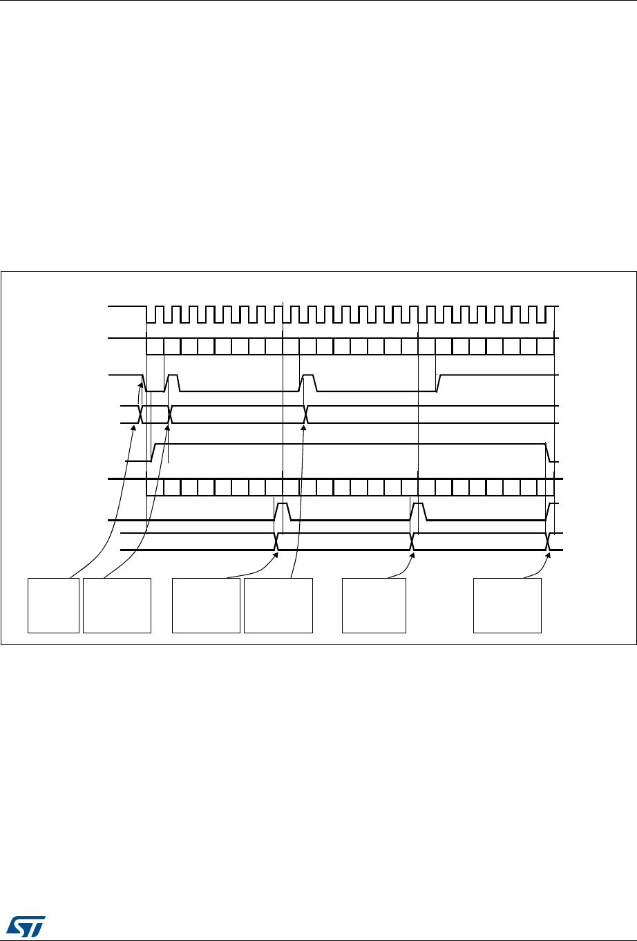
RM0430 Rev 8 949/1324
RM0430 Serial peripheral interface/ inter-IC sound (SPI/I2S)
986
underflow error signal for slave operating in SPI mode, and that data from the slave are
always transacted and processed by the master even if the slave cannot not prepare them
correctly in time. It is preferable for the slave to use DMA, especially when data frames are
shorter and bus rate is high.
Each sequence must be encased by the NSS pulse in parallel with the multislave system to
select just one of the slaves for communication. In single slave systems, using NSS to
control the slave is not necessary. However, the NSS pulse can be used to synchronize the
slave with the beginning of each data transfer sequence. NSS can be managed either by
software or by hardware (see Section 29.3.4: Multi-master communication).
Refer to Figure 325 and Figure 326 for a description of continuous transfers in master / full-
duplex and slave full-duplex mode.
Figure 325. TXE/RXNE/BSY behavior in master / full-duplex mode (BIDIMODE=0,
RXONLY=0) in the case of continuous transfers
0,62026,LQ
7[EXIIHU
'$7$ [$
7;(IODJ
[)
%6<IODJ
[)
VRIWZDUH
ZULWHV[)
LQWR63,B'5
VRIWZDUHZDLWV
XQWLO7;( DQG
ZULWHV[)LQWR
63,B'5
VRIWZDUHZDLWV
XQWLO5;1(
DQGUHDGV[$
IURP63,B'5
VHWE\KDUGZDUH
FOHDUHGE\VRIWZDUH
VHWE\KDUGZDUH
FOHDUHGE\VRIWZDUH VHWE\KDUGZDUH
VHWE\KDUGZDUH
6&.
'$7$ [$ '$7$ [$
UHVHWE\KDUGZDUH
([DPSOHLQ0DVWHUPRGHZLWK&32/ &3+$
[)
5;1(IODJ
ZULWH63,B'5
5[EXIIHU
VHWE\KDUGZDUH
0,62026,RXW
'$7$ [) '$7$ [) '$7$ [)
UHDG63,B'5
[$ [$ [$
VRIWZDUHZDLWV
XQWLO7;( DQG
ZULWHV[)LQWR
63,B'5
VRIWZDUHZDLWV
XQWLO5;1(
DQGUHDGV[$
IURP63,B'5
VRIWZDUHZDLWV
XQWLO5;1(
DQGUHDGV[$
IURP63,B'5
E E E E E E E E E E E E E E E E E E E E E E E E
E E E E E E E E E E E E E E E E E E E E E E E E
FOHDUHGE\VRIWZDUH
DL
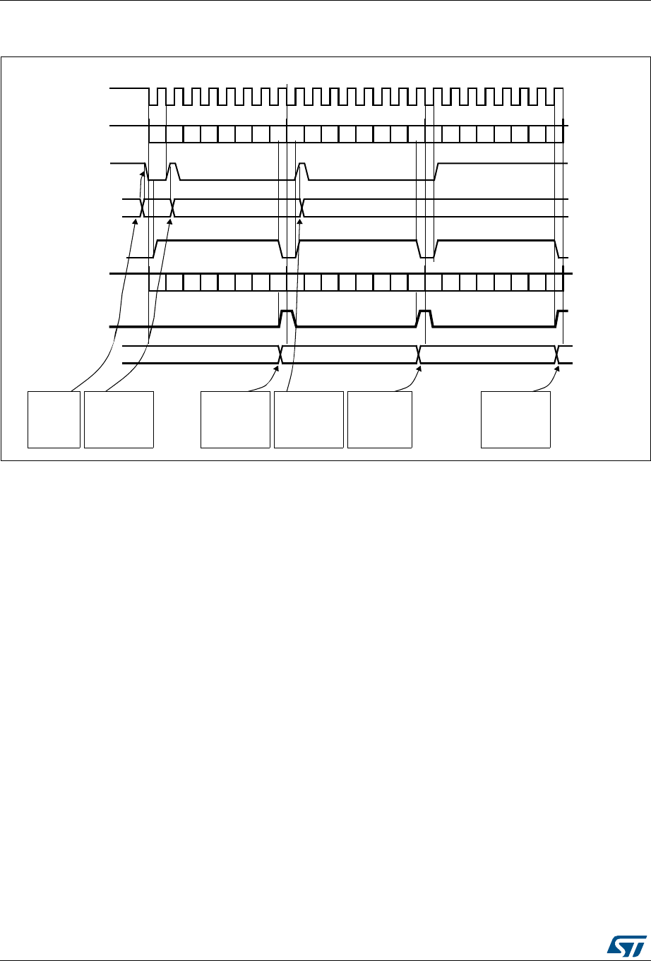
Serial peripheral interface/ inter-IC sound (SPI/I2S) RM0430
950/1324 RM0430 Rev 8
Figure 326. TXE/RXNE/BSY behavior in slave / full-duplex mode (BIDIMODE=0,
RXONLY=0) in the case of continuous transfers
29.3.10 Procedure for disabling the SPI
When SPI is disabled, it is mandatory to follow the disable procedures described in this
paragraph. It is important to do this before the system enters a low-power mode when the
peripheral clock is stopped. Ongoing transactions can be corrupted in this case. In some
modes the disable procedure is the only way to stop continuous communication running.
Master in full-duplex or transmit only mode can finish any transaction when it stops
providing data for transmission. In this case, the clock stops after the last data transaction.
Standard disable procedure is based on pulling BSY status together with TXE flag to check
if a transmission session is fully completed. This check can be done in specific cases, too,
when it is necessary to identify the end of ongoing transactions, for example:
•When NSS signal is managed by an arbitrary GPIO toggle and the master has to
provide proper end of NSS pulse for slave, or
•When transactions’ streams from DMA are completed while the last data frame or CRC
frame transaction is still ongoing in the peripheral bus.
The correct disable procedure is (except when receive-only mode is used):
1. Wait until RXNE=1 to receive the last data.
2. Wait until TXE=1 and then wait until BSY=0 before disabling the SPI.
3. Read received data.
[)
VHWE\FOHDUHGE\VRIWZDUH
0,62026,LQ
7[EXIIHU
'$7$ [$
7;(IODJ
[)
%6<IODJ
[)
VRIWZDUH
ZULWHV[)
LQWR63,B'5
VRIWZDUHZDLWV
XQWLO7;( DQG
ZULWHV[)LQWR
63,B'5
VRIWZDUHZDLWV
XQWLO5;1(
DQGUHDGV[$
IURP63,B'5
VHWE\KDUGZDUH
FOHDUHGE\VRIWZDUH
VHWE\KDUGZDUH
FOHDUHGE\VRIWZDUH VHWE\KDUGZDUH
6&.
'$7$ [$ '$7$ [$
UHVHWE\KDUGZDUH
([DPSOHLQ6ODYHPRGHZLWK&32/ &3+$
5;1(IODJ
ZULWHWR63,B'5
5[EXIIHU
VHWE\KDUGZDUH
0,62026,RXW
'$7$ [) '$7$ [) '$7$ [)
UHDGIURP63,B'5
[$ [$ [$
VRIWZDUHZDLWV
XQWLO7;( DQG
ZULWHV[)LQWR
63,B'5
VRIWZDUHZDLWV
XQWLO5;1(
DQGUHDGV[$
IURP63,B'5
VRIWZDUHZDLWV
XQWLO5;1(
DQGUHDGV[$
IURP63,B'5
E E E E E E E E E E E E E E E E E E E E E E E E
E E E E E E E E E E E E E E E E E E E E E E E E
FOHDUHGE\VRIWZDUH
DL

RM0430 Rev 8 951/1324
RM0430 Serial peripheral interface/ inter-IC sound (SPI/I2S)
986
Note: During discontinuous communications, there is a 2 APB clock period delay between the
write operation to the SPI_DR register and BSY bit setting. As a consequence it is
mandatory to wait first until TXE is set and then until BSY is cleared after writing the last
data.
The correct disable procedure for certain receive-only modes is:
1. Interrupt the receive flow by disabling SPI (SPE=0) in the specific time window while
the last data frame is ongoing.
2. Wait until BSY=0 (the last data frame is processed).
3. Read received data.
Note: To stop a continuous receive sequence, a specific time window must be respected during
the reception of the last data frame. It starts when the first bit is sampled and ends before
the last bit transfer starts.
29.3.11 Communication using DMA (direct memory addressing)
To operate at its maximum speed and to facilitate the data register read/write process
required to avoid overrun, the SPI features a DMA capability, which implements a simple
request/acknowledge protocol.
A DMA access is requested when the TXE or RXNE enable bit in the SPIx_CR2 register is
set. Separate requests must be issued to the Tx and Rx buffers.
•In transmission, a DMA request is issued each time TXE is set to 1. The DMA then
writes to the SPIx_DR register.
•In reception, a DMA request is issued each time RXNE is set to 1. The DMA then reads
the SPIx_DR register.
Refer to Figure 327 and Figure 328 for a description of the DMA transmission and reception
waveforms.
When the SPI is used only to transmit data, it is possible to enable only the SPI Tx DMA
channel. In this case, the OVR flag is set because the data received is not read. When the
SPI is used only to receive data, it is possible to enable only the SPI Rx DMA channel.
In transmission mode, when the DMA has written all the data to be transmitted (the TCIF
flag is set in the DMA_ISR register), the BSY flag can be monitored to ensure that the SPI
communication is complete. This is required to avoid corrupting the last transmission before
disabling the SPI or entering the Stop mode. The software must first wait until TXE = 1 and
then until BSY = 0.
When starting communication using DMA, to prevent DMA channel management raising
error events, these steps must be followed in order:
1. Enable DMA Rx buffer in the RXDMAEN bit in the SPI_CR2 register, if DMA Rx is
used.
2. Enable DMA streams for Tx and Rx in DMA registers, if the streams are used.
3. Enable DMA Tx buffer in the TXDMAEN bit in the SPI_CR2 register, if DMA Tx is used.
4. Enable the SPI by setting the SPE bit.
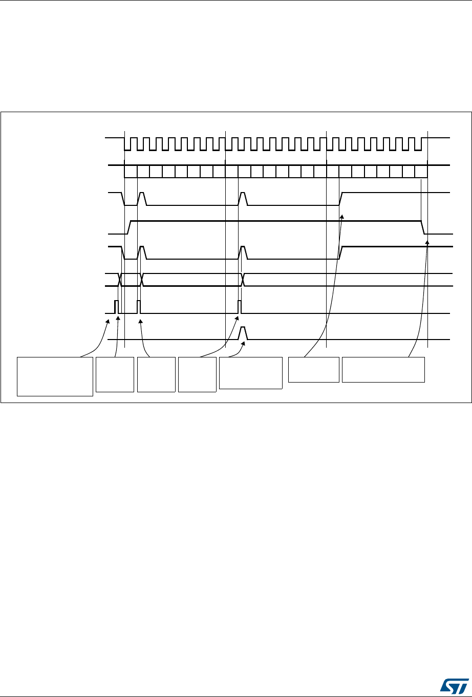
Serial peripheral interface/ inter-IC sound (SPI/I2S) RM0430
952/1324 RM0430 Rev 8
To close communication it is mandatory to follow these steps in order:
1. Disable DMA streams for Tx and Rx in the DMA registers, if the streams are used.
2. Disable the SPI by following the SPI disable procedure.
3. Disable DMA Tx and Rx buffers by clearing the TXDMAEN and RXDMAEN bits in the
SPI_CR2 register, if DMA Tx and/or DMA Rx are used.
Figure 327. Transmission using DMA
[)
7[EXIIHU
7;(IODJ
[)
%6<IODJ
[)
VHWE\KDUGZDUH
FOHDUE\'0$ZULWH
VHWE\KDUGZDUH
FOHDUHGE\'0$ZULWH VHWE\KDUGZDUH
VHWE\KDUGZDUH
6&.
UHVHW
([DPSOHZLWK&32/ &3+$
ZULWHWR63,B'5
0,62026,RXW
'$7$ [) '$7$ [) '$7$ [)
VRIWZDUHFRQILJXUHVWKH
'0$63,7[FKDQQHO
WRVHQGGDWDLWHPV
DQGHQDEOHVWKH63,
'0$ZULWHVWR63,B'5
'0$UHTXHVW LJQRUHGE\WKH'0$EHFDXVH
'0$7&,)IODJ VHWE\KDUGZDUH FOHDUE\VRIWZDUH
'0$ZULWHV
'$7$LQWR
63,B'5
E\KDUGZDUH
'0$ZULWHV
'$7$LQWR
63,B'5
'0$ZULWHV
'$7$LQWR
63,B'5
VRIWZDUHZDLWVXQWLO%6<
'0$WUDQVIHUFRPSOHWH
'0$WUDQVIHULV
FRPSOHWH7&,) LQ
'0$B,65
VRIWZDUHZDLWV
XQWLO7;(
'0$WUDQVIHULVFRPSOHWH
E E E E E E E E E E E E E E E E E E E E E E E E
DL
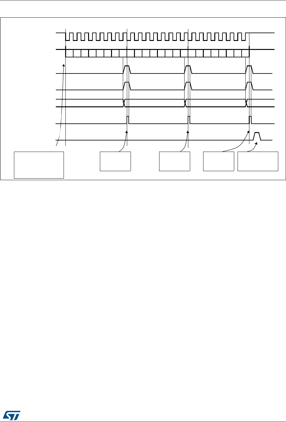
RM0430 Rev 8 953/1324
RM0430 Serial peripheral interface/ inter-IC sound (SPI/I2S)
986
Figure 328. Reception using DMA
29.3.12 SPI status flags
Three status flags are provided for the application to completely monitor the state of the SPI
bus.
Tx buffer empty flag (TXE)
When it is set, the TXE flag indicates that the Tx buffer is empty and that the next data to be
transmitted can be loaded into the buffer. The TXE flag is cleared by writing to the SPI_DR
register.
Rx buffer not empty (RXNE)
When set, the RXNE flag indicates that there are valid received data in the Rx buffer. It is
cleared by reading from the SPI_DR register.
Busy flag (BSY)
The BSY flag is set and cleared by hardware (writing to this flag has no effect).
When BSY is set, it indicates that a data transfer is in progress on the SPI (the SPI bus is
busy). There is one exception in master bidirectional receive mode (MSTR=1 and BDM=1
and BDOE=0) where the BSY flag is kept low during reception.
The BSY flag can be used in certain modes to detect the end of a transfer, thus preventing
corruption of the last transfer when the SPI peripheral clock is disabled before entering a
low-power mode or an NSS pulse end is handled by software.
The BSY flag is also useful for preventing write collisions in a multimaster system.
0,62026,LQ
'$7$ [$
VRIWZDUHFRQILJXUHVWKH
'0$63,5[FKDQQHO
WRUHFHLYHGDWDLWHPV
DQGHQDEOHVWKH63,
6&.
'$7$ [$ '$7$ [$
([DPSOHZLWK&32/ &3+$
5;1(IODJ
5[EXIIHU
VHWE\KDUGZDUH
UHDGIURP63,B'5 [$ [$ [$
'0$UHTXHVW
'0$UHDGV
'$7$IURP
63,B'5
IODJ'0$7&,)
VHWE\KDUGZDUH FOHDU
E\VRIWZDUH
'0$UHDGIURP63,B'5
7KH'0$WUDQVIHULV
FRPSOHWH7&,) LQ
'0$B,65
'0$UHDGV
'$7$IURP
63,B'5
'0$UHDGV
'$7$IURP
63,B'5
'0$WUDQVIHUFRPSOHWH
E E E E E E E E E E E E E E E E E E E E E E E E
FOHDUE\'0$UHDG
DL

Serial peripheral interface/ inter-IC sound (SPI/I2S) RM0430
954/1324 RM0430 Rev 8
The BSY flag is cleared under any one of the following conditions:
•When the SPI is correctly disabled
•When a fault is detected in Master mode (MODF bit set to 1)
•In Master mode, when it finishes a data transmission and no new data is ready to be
sent
•In Slave mode, when the BSY flag is set to '0' for at least one SPI clock cycle between
each data transfer.
Note: It is recommended to use always the TXE and RXNE flags (instead of the BSY flags) to
handle data transmission or reception operations.
29.3.13 SPI error flags
An SPI interrupt is generated if one of the following error flags is set and interrupt is enabled
by setting the ERRIE bit.
Overrun flag (OVR)
An overrun condition occurs when the master or the slave completes the reception of the
next data frame while the read operation of the previous frame from the Rx buffer has not
completed (case RXNE flag is set).
In this case, the content of the Rx buffer is not updated with the new data received. A read
operation from the SPI_DR register returns the frame previously received. All other
subsequently transmitted data are lost.
Clearing the OVR bit is done by a read access to the SPI_DR register followed by a read
access to the SPI_SR register.
Mode fault (MODF)
Mode fault occurs when the master device has its internal NSS signal (NSS pin in NSS
hardware mode, or SSI bit in NSS software mode) pulled low. This automatically sets the
MODF bit. Master mode fault affects the SPI interface in the following ways:
•The MODF bit is set and an SPI interrupt is generated if the ERRIE bit is set.
•The SPE bit is cleared. This blocks all output from the device and disables the SPI
interface.
•The MSTR bit is cleared, thus forcing the device into slave mode.
Use the following software sequence to clear the MODF bit:
1. Make a read or write access to the SPIx_SR register while the MODF bit is set.
2. Then write to the SPIx_CR1 register.
To avoid any multiple slave conflicts in a system comprising several MCUs, the NSS pin
must be pulled high during the MODF bit clearing sequence. The SPE and MSTR bits can
be restored to their original state after this clearing sequence. As a security, hardware does
not allow the SPE and MSTR bits to be set while the MODF bit is set. In a slave device the
MODF bit cannot be set except as the result of a previous multimaster conflict.

RM0430 Rev 8 955/1324
RM0430 Serial peripheral interface/ inter-IC sound (SPI/I2S)
986
CRC error (CRCERR)
This flag is used to verify the validity of the value received when the CRCEN bit in the
SPIx_CR1 register is set. The CRCERR flag in the SPIx_SR register is set if the value
received in the shift register does not match the receiver SPIx_RXCRC value. The flag is
cleared by the software.
TI mode frame format error (FRE)
A TI mode frame format error is detected when an NSS pulse occurs during an ongoing
communication when the SPI is operating in slave mode and configured to conform to the TI
mode protocol. When this error occurs, the FRE flag is set in the SPIx_SR register. The SPI
is not disabled when an error occurs, the NSS pulse is ignored, and the SPI waits for the
next NSS pulse before starting a new transfer. The data may be corrupted since the error
detection may result in the loss of two data bytes.
The FRE flag is cleared when SPIx_SR register is read. If the ERRIE bit is set, an interrupt
is generated on the NSS error detection. In this case, the SPI should be disabled because
data consistency is no longer guaranteed and communications should be re-initiated by the
master when the slave SPI is enabled again.
29.4 SPI special features
29.4.1 TI mode
TI protocol in master mode
The SPI interface is compatible with the TI protocol. The FRF bit of the SPIx_CR2 register
can be used to configure the SPI to be compliant with this protocol.
The clock polarity and phase are forced to conform to the TI protocol requirements whatever
the values set in the SPIx_CR1 register. NSS management is also specific to the TI protocol
which makes the configuration of NSS management through the SPIx_CR1 and SPIx_CR2
registers (SSM, SSI, SSOE) impossible in this case.
In slave mode, the SPI baud rate prescaler is used to control the moment when the MISO
pin state changes to HiZ when the current transaction finishes (see Figure 329). Any baud
rate can be used, making it possible to determine this moment with optimal flexibility.
However, the baud rate is generally set to the external master clock baud rate. The delay for
the MISO signal to become HiZ (trelease) depends on internal resynchronization and on the
baud rate value set in through the BR[2:0] bits in the SPIx_CR1 register. It is given by the
formula:
If the slave detects a misplaced NSS pulse during a data frame transaction the TIFRE flag is
set.
This feature is not available for Motorola SPI communications (FRF bit set to 0).
tbaud_rate
2
----------------------4t
pclk
×+trelease
tbaud_rate
2
----------------------6t
pclk
×+<<
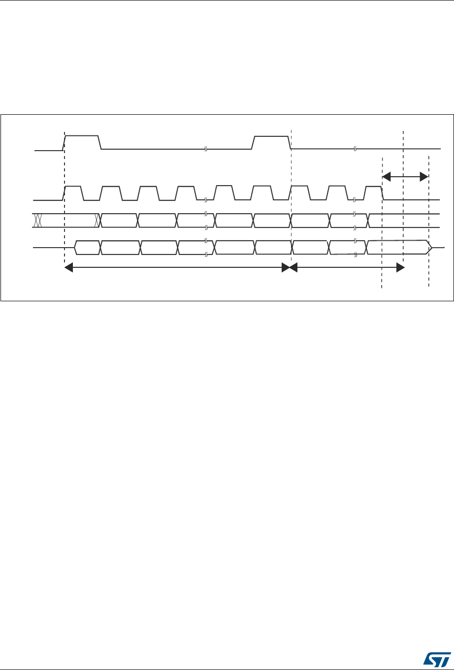
Serial peripheral interface/ inter-IC sound (SPI/I2S) RM0430
956/1324 RM0430 Rev 8
Note: To detect TI frame errors in slave transmitter only mode by using the Error interrupt
(ERRIE=1), the SPI must be configured in 2-line unidirectional mode by setting BIDIMODE
and BIDIOE to 1 in the SPI_CR1 register. When BIDIMODE is set to 0, OVR is set to 1
because the data register is never read and error interrupts are always generated, while
when BIDIMODE is set to 1, data are not received and OVR is never set.
Figure 329 shows the SPI communication waveforms when TI mode is selected.
Figure 329. TI mode transfer
29.4.2 CRC calculation
Two separate CRC calculators (on transmission and reception data flows) are implemented
in order to check the reliability of transmitted and received data. The SPI offers CRC8 or
CRC16 calculation depending on the data format selected through the DFF bit. The CRC is
calculated serially using the polynomial programmed in the SPI_CRCPR register.
CRC principle
CRC calculation is enabled by setting the CRCEN bit in the SPIx_CR1 register before the
SPI is enabled (SPE = 1). The CRC value is calculated using an odd programmable
polynomial on each bit. The calculation is processed on the sampling clock edge defined by
the CPHA and CPOL bits in the SPIx_CR1 register. The calculated CRC value is checked
automatically at the end of the data block as well as for transfer managed by CPU or by the
DMA. When a mismatch is detected between the CRC calculated internally on the received
data and the CRC sent by the transmitter, a CRCERR flag is set to indicate a data corruption
error. The right procedure for handling the CRC calculation depends on the SPI
configuration and the chosen transfer management.
Note: The polynomial value should only be odd. No even values are supported.
CRC transfer managed by CPU
Communication starts and continues normally until the last data frame has to be sent or
received in the SPIx_DR register. Then CRCNEXT bit has to be set in the SPIx_CR1
register to indicate that the CRC frame transaction will follow after the transaction of the
currently processed data frame. The CRCNEXT bit must be set before the end of the last
data frame transaction. CRC calculation is frozen during CRC transaction.
069
06%
0,62
166
6&.
WULJJHU
VDPSOLQJ
WULJJHU
VDPSOLQJ
WULJJHU
VDPSOLQJ
'RQRWFDUH /6%
026,
RU 06% /6%
06% /6%
06% /6%
)5$0( )5$0(
W
5(/($6(

RM0430 Rev 8 957/1324
RM0430 Serial peripheral interface/ inter-IC sound (SPI/I2S)
986
The received CRC is stored in the Rx buffer like any other data frame.
A CRC-format transaction takes one more data frame to communicate at the end of data
sequence.
When the last CRC data is received, an automatic check is performed comparing the
received value and the value in the SPIx_RXCRC register. Software has to check the
CRCERR flag in the SPIx_SR register to determine if the data transfers were corrupted or
not. Software clears the CRCERR flag by writing '0' to it.
After the CRC reception, the CRC value is stored in the Rx buffer and must be read in the
SPIx_DR register in order to clear the RXNE flag.
CRC transfer managed by DMA
When SPI communication is enabled with CRC communication and DMA mode, the
transmission and reception of the CRC at the end of communication is automatic (with the
exception of reading CRC data in receive-only mode). The CRCNEXT bit does not have to
be handled by the software. The counter for the SPI transmission DMA channel has to be
set to the number of data frames to transmit excluding the CRC frame. On the receiver side,
the received CRC value is handled automatically by DMA at the end of the transaction but
user must take care to flush out the CRC frame received from SPI_DR as it is always loaded
into it.
At the end of the data and CRC transfers, the CRCERR flag in the SPIx_SR register is set if
corruption occurred during the transfer.
Resetting the SPIx_TXCRC and SPIx_RXCRC values
The SPIx_TXCRC and SPIx_RXCRC values are cleared automatically when CRC
calculation is enabled.
When the SPI is configured in slave mode with the CRC feature enabled, a CRC calculation
is performed even if a high level is applied on the NSS pin. This may happen for example in
case of a multislave environment where the communication master addresses slaves
alternately.
Between a slave disabling (high level on NSS) and a new slave enabling (low level on NSS),
the CRC value should be cleared on both master and slave sides to resynchronize the
master and slave respective CRC calculation.
To clear the CRC, follow the below sequence:
1. Disable the SPI
2. Clear the CRCEN bit
3. Enable the CRCEN bit
4. Enable the SPI
Note: When the SPI interface is configured as a slave, the NSS internal signal needs to be kept
low during transaction of the CRC phase once the CRCNEXT signal is released, (see more
details at the product errata sheet).
At TI mode, despite the fact that the clock phase and clock polarity setting is fixed and
independent on the SPIx_CR1 register, the corresponding setting CPOL=0 CPHA=1 has to
be kept at the SPIx_CR1 register anyway if CRC is applied. In addition, the CRC calculation
has to be reset between sessions by the SPI disable sequence by re-enabling the CRCEN
bit described above at both master and slave sides, else the CRC calculation can be
corrupted at this specific mode.
Serial peripheral interface/ inter-IC sound (SPI/I2S) RM0430
958/1324 RM0430 Rev 8
29.5 SPI interrupts
During SPI communication an interrupts can be generated by the following events:
•Transmit Tx buffer ready to be loaded
•Data received in Rx buffer
•Master mode fault
•Overrun error
•TI frame format error
Interrupts can be enabled and disabled separately.
Table 175. SPI interrupt requests
Interrupt event Event flag Enable Control bit
Transmit Tx buffer ready to be loaded TXE TXEIE
Data received in Rx buffer RXNE RXNEIE
Master Mode fault event MODF
ERRIE
Overrun error OVR
CRC error CRCERR
TI frame format error FRE
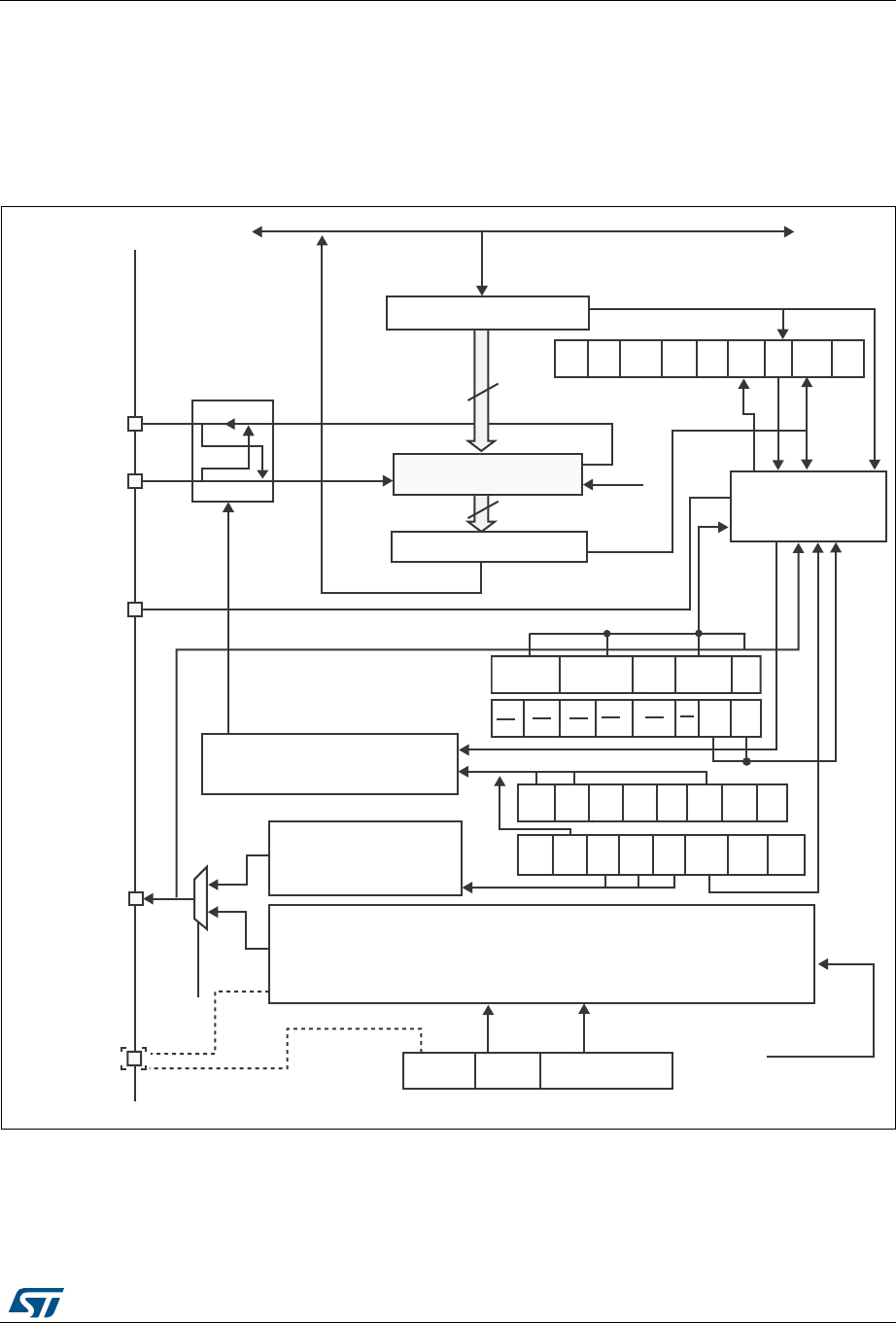
RM0430 Rev 8 959/1324
RM0430 Serial peripheral interface/ inter-IC sound (SPI/I2S)
986
29.6 I2S functional description
29.6.1 I2S general description
The block diagram of the I2S is shown in Figure 330.
Figure 330. I2S block diagram
1. I2S2ext_SD and I2S3ext_SD are the extended SD pins that control the I2S full-duplex mode.
2. MCK is mapped on the MISO pin.
7[EXIIHU
6KLIWUHJLVWHU
ELW
&RPPXQLFDWLRQ
5[EXIIHU
ELW
026,6'
0DVWHUFRQWUROORJLF
63,
EDXGUDWHJHQHUDWRU
,602'
/6%ILUVW
/6%
)LUVW 63( %5 %5 %5 0675 &32/ &3+$
%LGL
PRGH
%LGL
2(
&5&
(1
&5&
1H[W ')) 5[
RQO\ 660 66,
$GGUHVVDQGGDWDEXV
FRQWURO
166:6
%6< 295 02') &5&
(55
&+
6,'( 7[( 5[1(
,6FORFNJHQHUDWRU
0&.
,6B
&.
,6
02' ,6(
&+
'$7/(1 /(1
&.
32/
,6&)* ,667'
0&.2( 2'' ,6',9>@
>@ >@ >@
8'5
,6[&/.
069
)5(
&.
-)3/
)3EXT?3$
)3EXT?3$
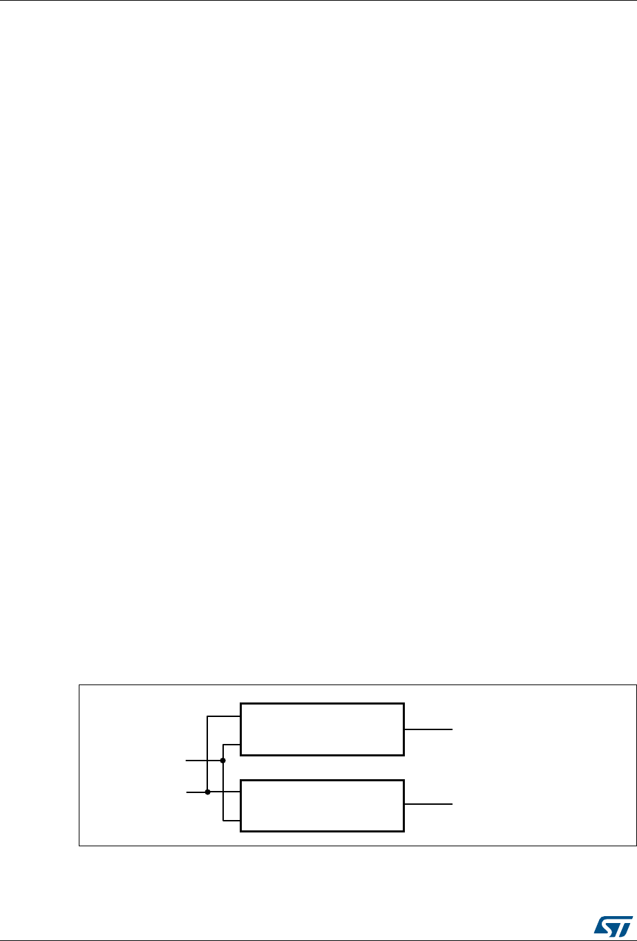
Serial peripheral interface/ inter-IC sound (SPI/I2S) RM0430
960/1324 RM0430 Rev 8
The SPI can function as an audio I2S interface when the I2S capability is enabled (by setting
the I2SMOD bit in the SPIx_I2SCFGR register). This interface mainly uses the same pins,
flags and interrupts as the SPI.
The I2S shares three common pins with the SPI:
•SD: Serial Data (mapped on the MOSI pin) to transmit or receive the two time-
multiplexed data channels (in half-duplex mode only).
•WS: Word Select (mapped on the NSS pin) is the data control signal output in master
mode and input in slave mode.
•CK: Serial Clock (mapped on the SCK pin) is the serial clock output in master mode
and serial clock input in slave mode.
An additional pin can be used when a master clock output is needed for some external
audio devices:
•MCK: Master Clock (mapped separately) is used, when the I2S is configured in master
mode (and when the MCKOE bit in the SPIx_I2SPR register is set), to output this
additional clock generated at a preconfigured frequency rate equal to 256 × fS, where
fS is the audio sampling frequency.
The I2S uses its own clock generator to produce the communication clock when it is set in
master mode. This clock generator is also the source of the master clock output. Two
additional registers are available in I2S mode. One is linked to the clock generator
configuration SPIx_I2SPR and the other one is a generic I2S configuration register
SPIx_I2SCFGR (audio standard, slave/master mode, data format, packet frame, clock
polarity, etc.).
The SPIx_CR1 register and all CRC registers are not used in the I2S mode. Likewise, the
SSOE bit in the SPIx_CR2 register and the MODF and CRCERR bits in the SPIx_SR are
not used.
The I2S uses the same SPI register for data transfer (SPIx_DR) in 16-bit wide mode.
29.6.2 I2S full-duplex
To support I2S full-duplex mode, two extra I2S instances called extended I2Ss (I2S2_ext,
I2S3_ext) are available in addition to I2S2 and I2S3 (see Figure 331). The first I2S full-
duplex interface is consequently based on I2S2 and I2S2_ext, and the second one on I2S3
and I2S3_ext.
Note: I2S2_ext an I2S3_ext are used only in full-duplex mode.
Figure 331. I2S full-duplex block diagram
1. Where x can be 2 or 3.
069
63,,6[
,6[BH[W
63,[B026,,6[B6'LQRXW
,6B:6
,6[B6&.
,6[BH[W6'LQRXW

RM0430 Rev 8 961/1324
RM0430 Serial peripheral interface/ inter-IC sound (SPI/I2S)
986
I2Sx can operate in master mode. As a result:
• Only I2Sx can output SCK and WS in half-duplex mode
• Only I2Sx can deliver SCK and WS to I2S2_ext and I2S3_ext in full-duplex mode.
The extended I2Ss (I2Sx_ext) can be used only in full-duplex mode. The I2Sx_ext operate
always in slave mode.
Both I2Sx and I2Sx_ext can be configured as transmitters or receivers.
29.6.3 Supported audio protocols
The three-line bus has to handle only audio data generally time-multiplexed on two
channels: the right channel and the left channel. However there is only one 16-bit register
for transmission or reception. So, it is up to the software to write into the data register the
appropriate value corresponding to each channel side, or to read the data from the data
register and to identify the corresponding channel by checking the CHSIDE bit in the
SPIx_SR register. Channel left is always sent first followed by the channel right (CHSIDE
has no meaning for the PCM protocol).
Four data and packet frames are available. Data may be sent with a format of:
•16-bit data packed in a 16-bit frame
•16-bit data packed in a 32-bit frame
•24-bit data packed in a 32-bit frame
•32-bit data packed in a 32-bit frame
When using 16-bit data extended on 32-bit packet, the first 16 bits (MSB) are the significant
bits, the 16-bit LSB is forced to 0 without any need for software action or DMA request (only
one read/write operation).
The 24-bit and 32-bit data frames need two CPU read or write operations to/from the
SPIx_DR register or two DMA operations if the DMA is preferred for the application. For 24-
bit data frame specifically, the 8 non significant bits are extended to 32 bits with 0-bits (by
hardware).
For all data formats and communication standards, the most significant bit is always sent
first (MSB first).
The I2S interface supports four audio standards, configurable using the I2SSTD[1:0] and
PCMSYNC bits in the SPIx_I2SCFGR register.
I2S Philips standard
For this standard, the WS signal is used to indicate which channel is being transmitted. It is
activated one CK clock cycle before the first bit (MSB) is available.
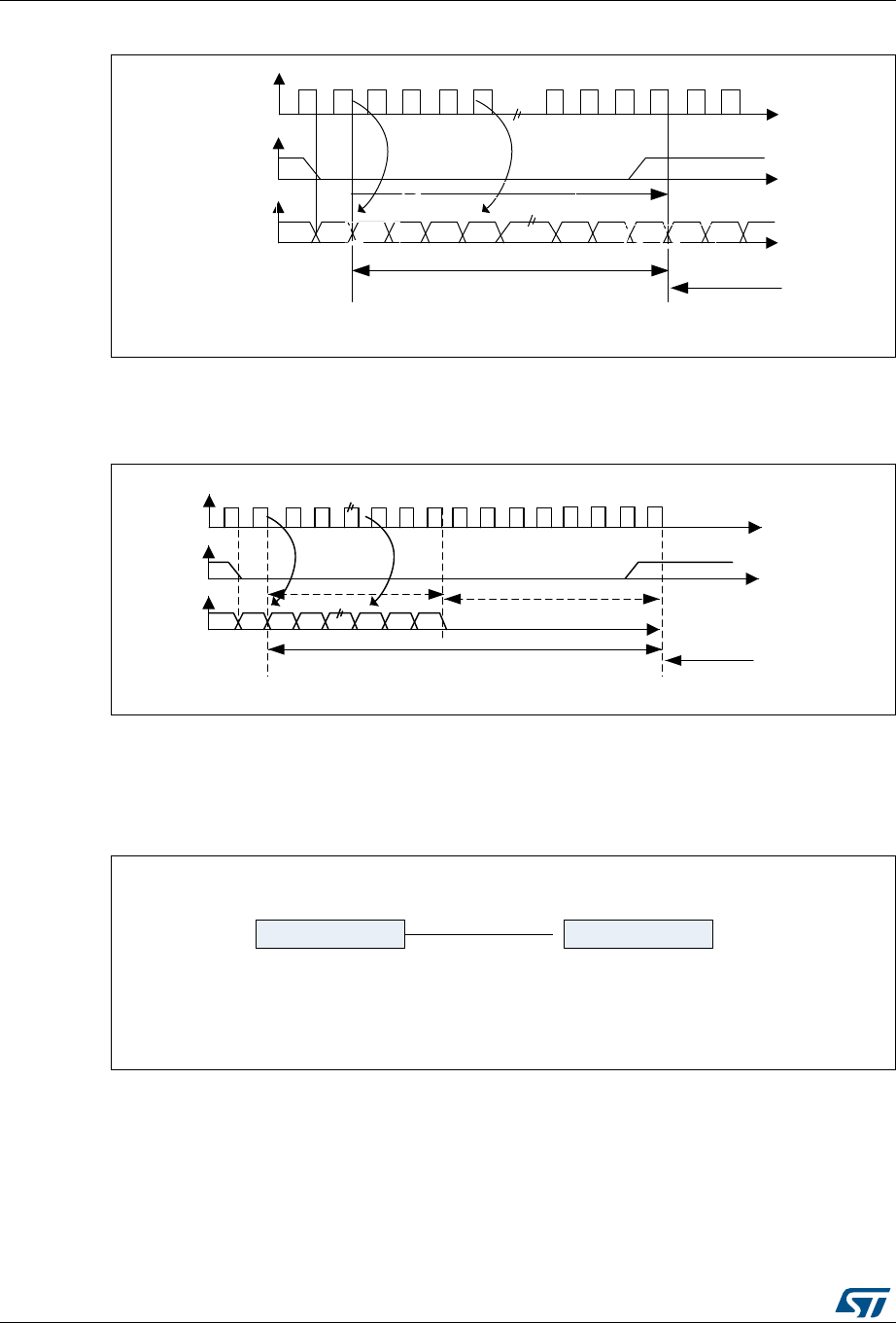
Serial peripheral interface/ inter-IC sound (SPI/I2S) RM0430
962/1324 RM0430 Rev 8
Figure 332. I2S Philips protocol waveforms (16/32-bit full accuracy, CPOL = 0)
Data are latched on the falling edge of CK (for the transmitter) and are read on the rising
edge (for the receiver). The WS signal is also latched on the falling edge of CK.
Figure 333. I2S Philips standard waveforms (24-bit frame with CPOL = 0)
This mode needs two write or read operations to/from the SPIx_DR register.
•In transmission mode:
If 0x8EAA33 has to be sent (24-bit):
Figure 334. Transmitting 0x8EAA33
•In reception mode:
If data 0x8EAA33 is received:
069
&.
:6
6'
&DQEHELWRUELW
06% 06%/6%
&KDQQHOOHIW
&KDQQHO
ULJKW
WUDQVPLVVLRQ UHFHSWLRQ
069
&.
:6
6'
7UDQVPLVVLRQ 5HFHSWLRQ
ELWGDWD
06% /6%
&KDQQHOOHIWELW
&KDQQHOULJKW
ELWUHPDLQLQJIRUFHG
069
[($$ [;;
)LUVWZULWHWR'DWDUHJLVWHU 6HFRQGZULWHWR'DWDUHJLVWHU
2QO\WKH06%DUHVHQW
WRFRPSDUHWKHELWV
/6%VKDYHQRPHDQLQJ
DQGFDQEHDQ\WKLQJ
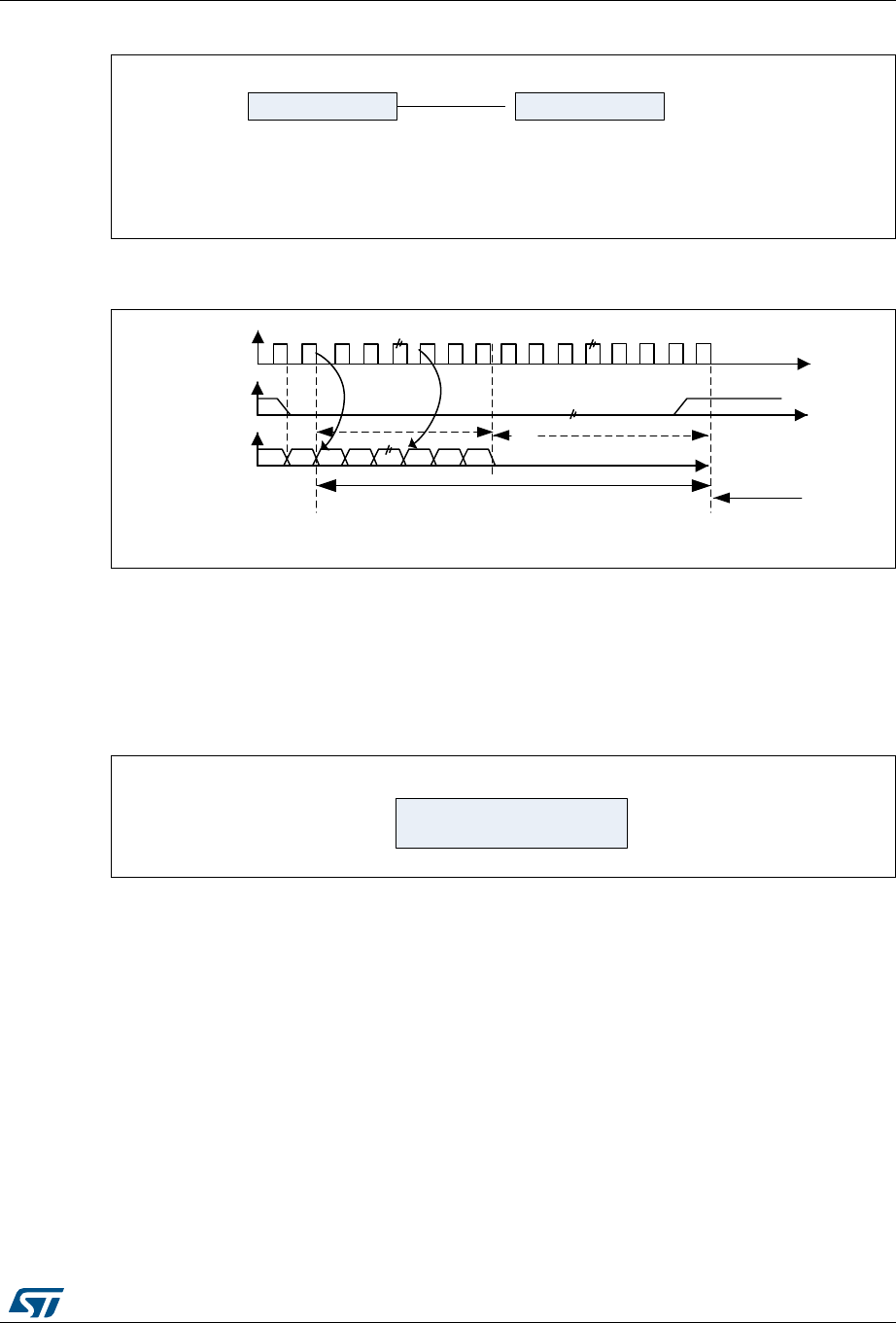
RM0430 Rev 8 963/1324
RM0430 Serial peripheral interface/ inter-IC sound (SPI/I2S)
986
Figure 335. Receiving 0x8EAA33
Figure 336. I2S Philips standard (16-bit extended to 32-bit packet frame with
CPOL = 0)
When 16-bit data frame extended to 32-bit channel frame is selected during the I2S
configuration phase, only one access to the SPIx_DR register is required. The 16 remaining
bits are forced by hardware to 0x0000 to extend the data to 32-bit format.
If the data to transmit or the received data are 0x76A3 (0x76A30000 extended to 32-bit), the
operation shown in Figure 337 is required.
Figure 337. Example of 16-bit data frame extended to 32-bit channel frame
For transmission, each time an MSB is written to SPIx_DR, the TXE flag is set and its
interrupt, if allowed, is generated to load the SPIx_DR register with the new value to send.
This takes place even if 0x0000 have not yet been sent because it is done by hardware.
For reception, the RXNE flag is set and its interrupt, if allowed, is generated when the first
16 MSB half-word is received.
In this way, more time is provided between two write or read operations, which prevents
underrun or overrun conditions (depending on the direction of the data transfer).
MSB justified standard
For this standard, the WS signal is generated at the same time as the first data bit, which is
the MSBit.
069
[($$ [;;
)LUVWUHDGWR'DWDUHJLVWHU 6HFRQGUHDGWR'DWDUHJLVWHU
2QO\WKH06%DUHVHQW
WRFRPSDUHWKHELWV
/6%VKDYHQRPHDQLQJ
DQGFDQEHDQ\WKLQJ
069
&.
:6
6'
7UDQVPLVVLRQ 5HFHSWLRQ
ELWGDWD
06% /6%
&KDQQHOOHIWELW &KDQQHOULJKW
ELWUHPDLQLQJIRUFHG
069
[$
2QO\RQHDFFHVVWR63,[B'5
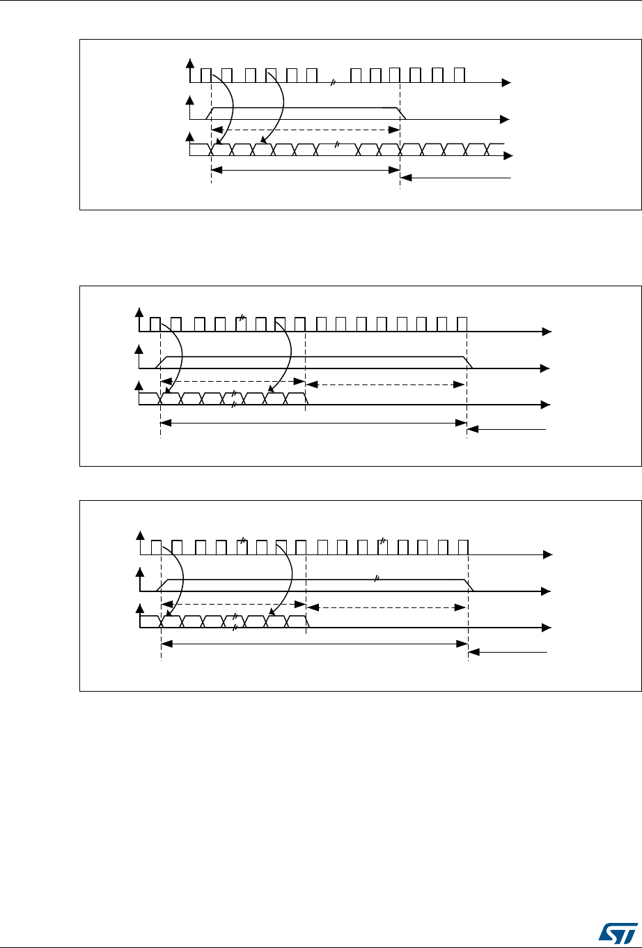
Serial peripheral interface/ inter-IC sound (SPI/I2S) RM0430
964/1324 RM0430 Rev 8
Figure 338. MSB Justified 16-bit or 32-bit full-accuracy length with CPOL = 0
Data are latched on the falling edge of CK (for transmitter) and are read on the rising edge
(for the receiver).
Figure 339. MSB justified 24-bit frame length with CPOL = 0
Figure 340. MSB justified 16-bit extended to 32-bit packet frame with CPOL = 0
LSB justified standard
This standard is similar to the MSB justified standard (no difference for the 16-bit and 32-bit
full-accuracy frame formats).
069
&.
:6
6'
7UDQVPLVVLRQ 5HFHSWLRQ
RUELWGDWD
06% /6%
&KDQQHOOHIW
&KDQQHOULJKW
06%
069
&.
:6
6'
7UDQVPLVVLRQ 5HFHSWLRQ
ELWGDWD
06% /6%
&KDQQHOOHIWELW
&KDQQHOULJKW
ELWUHPDLQLQJ
IRUFHG
069
&.
:6
6'
7UDQVPLVVLRQ 5HFHSWLRQ
ELWGDWD
06% /6%
&KDQQHOOHIWELW
&KDQQHOULJKW
ELWUHPDLQLQJ
IRUFHG
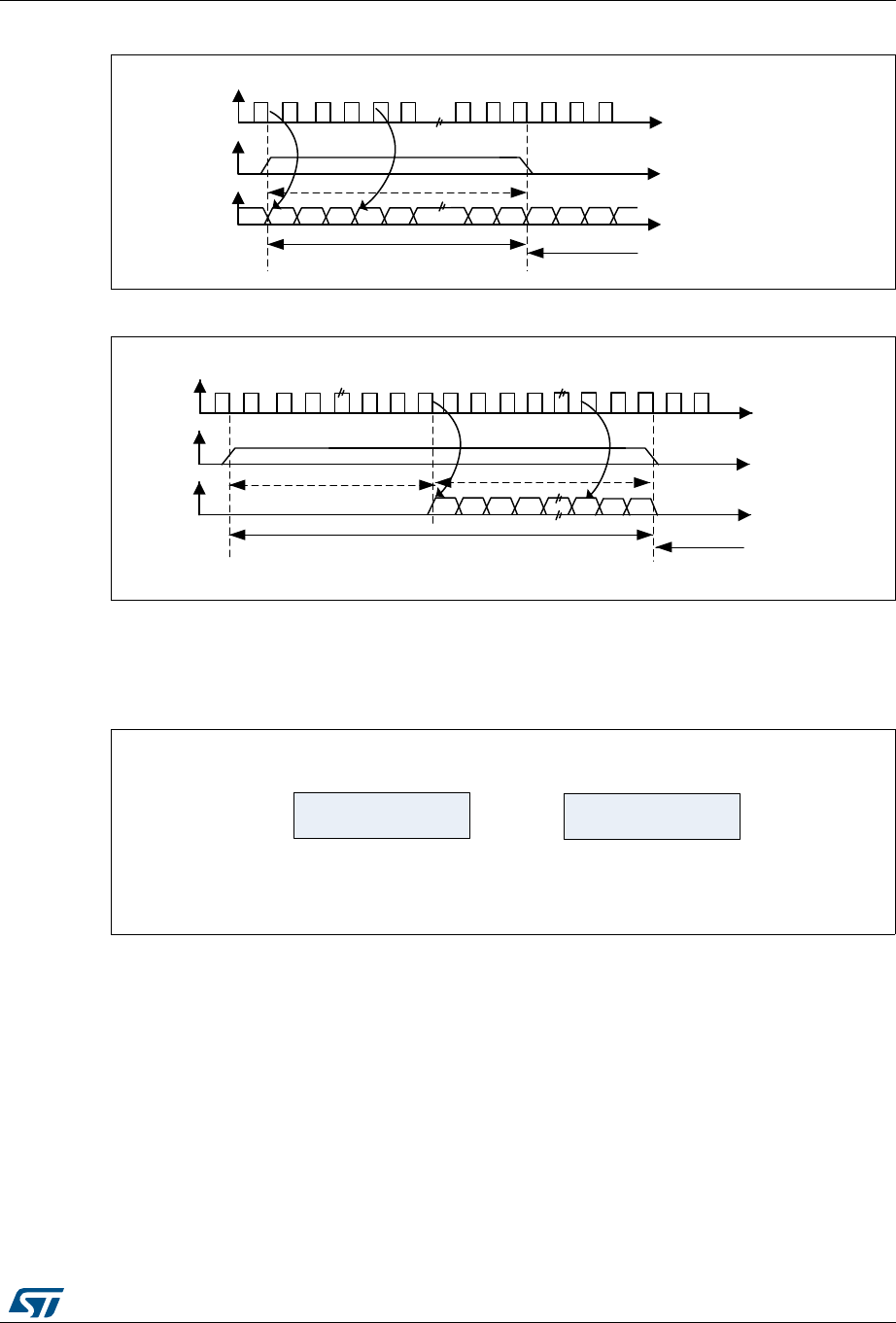
RM0430 Rev 8 965/1324
RM0430 Serial peripheral interface/ inter-IC sound (SPI/I2S)
986
Figure 341. LSB justified 16-bit or 32-bit full-accuracy with CPOL = 0
Figure 342. LSB justified 24-bit frame length with CPOL = 0
•In transmission mode:
If data 0x3478AE have to be transmitted, two write operations to the SPIx_DR register
are required by software or by DMA. The operations are shown below.
Figure 343. Operations required to transmit 0x3478AE
•In reception mode:
If data 0x3478AE are received, two successive read operations from the SPIx_DR
register are required on each RXNE event.
069
&.
:6
6'
7UDQVPLVVLRQ 5HFHSWLRQ
RUELWGDWD
06% /6%
&KDQQHOOHIW
&KDQQHOULJKW
06%
069
&.
:6
6'
7UDQVPLVVLRQ
5HFHSWLRQ
ELWGDWD
IRUFHG
06% /6%
&KDQQHOOHIWELW
&KDQQHOULJKW
ELWUHPDLQLQJ
[;; [$(
)LUVWZULWHWR'DWDUHJLVWHU
FRQGLWLRQHGE\7;(
6HFRQGZULWHWR'DWDUHJLVWHU
FRQGLWLRQHGE\7;(
2QO\WKH/6%RIWKH
KDOIZRUGDUHVLJQLILFDQW
$ILHOGRI[LVIRUFHG
LQVWHDGRIWKH06%V
069
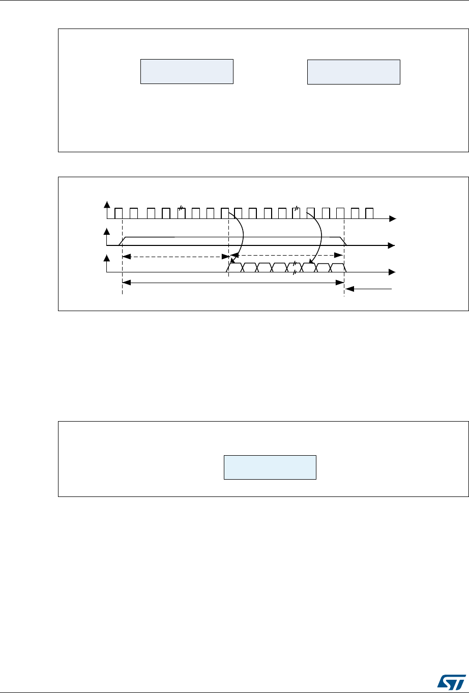
Serial peripheral interface/ inter-IC sound (SPI/I2S) RM0430
966/1324 RM0430 Rev 8
Figure 344. Operations required to receive 0x3478AE
Figure 345. LSB justified 16-bit extended to 32-bit packet frame with CPOL = 0
When 16-bit data frame extended to 32-bit channel frame is selected during the I2S
configuration phase, Only one access to the SPIx_DR register is required. The 16 remaining
bits are forced by hardware to 0x0000 to extend the data to 32-bit format. In this case it
corresponds to the half-word MSB.
If the data to transmit or the received data are 0x76A3 (0x0000 76A3 extended to 32-bit),
the operation shown in Figure 346 is required.
Figure 346. Example of 16-bit data frame extended to 32-bit channel frame
In transmission mode, when a TXE event occurs, the application has to write the data to be
transmitted (in this case 0x76A3). The 0x000 field is transmitted first (extension on 32-bit).
The TXE flag is set again as soon as the effective data (0x76A3) is sent on SD.
In reception mode, RXNE is asserted as soon as the significant half-word is received (and
not the 0x0000 field).
In this way, more time is provided between two write or read operations to prevent underrun
or overrun conditions.
[;; [$(
)LUVWUHDGIURP'DWDUHJLVWHU
FRQGLWLRQHGE\5;1(
6HFRQGUHDGIURP'DWDUHJLVWHU
FRQGLWLRQHGE\5;1(
2QO\WKH/6%RIWKH
KDOIZRUGDUHVLJQLILFDQW
$ILHOGRI[LVIRUFHG
LQVWHDGRIWKH06%V
069
069
&.
:6
6'
7UDQVPLVVLRQ
5HFHSWLRQ
ELWGDWD
IRUFHG
06% /6%
&KDQQHOOHIWELW
&KDQQHOULJKW
ELWUHPDLQLQJ
[$
2QO\RQHDFFHVVWRWKH63,['5UHJLVWHU
069
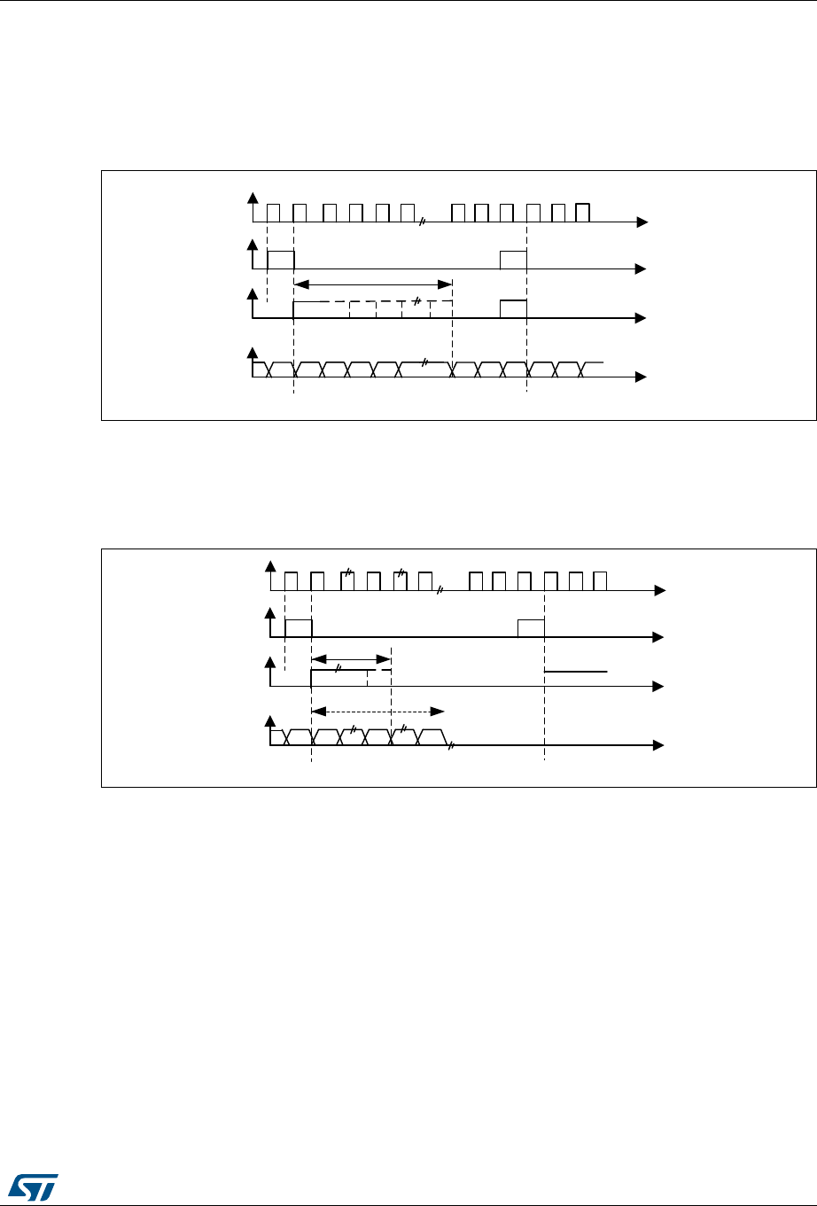
RM0430 Rev 8 967/1324
RM0430 Serial peripheral interface/ inter-IC sound (SPI/I2S)
986
PCM standard
For the PCM standard, there is no need to use channel-side information. The two PCM
modes (short and long frame) are available and configurable using the PCMSYNC bit in
SPIx_I2SCFGR register.
Figure 347. PCM standard waveforms (16-bit)
For long frame synchronization, the WS signal assertion time is fixed to 13 bits in master
mode.
For short frame synchronization, the WS synchronization signal is only one cycle long.
Figure 348. PCM standard waveforms (16-bit extended to 32-bit packet frame)
Note: For both modes (master and slave) and for both synchronizations (short and long), the
number of bits between two consecutive pieces of data (and so two synchronization signals)
needs to be specified (DATLEN and CHLEN bits in the SPIx_I2SCFGR register) even in
slave mode.
29.6.4 Clock generator
The I2S bitrate determines the data flow on the I2S data line and the I2S clock signal
frequency.
I2S bitrate = number of bits per channel × number of channels × sampling audio frequency
For a 16-bit audio, left and right channel, the I2S bitrate is calculated as follows:
I2S bitrate = 16 × 2 × fS
It will be: I2S bitrate = 32 x 2 x fS if the packet length is 32-bit wide.
069
&.
:6
VKRUWIUDPH
6'
:6
ORQJIUDPH
ELWV
06% /6% 06%
069
&.
:6
VKRUWIUDPH
6'
:6
ORQJIUDPH
8SWRELWV
06% /6%
ELWV
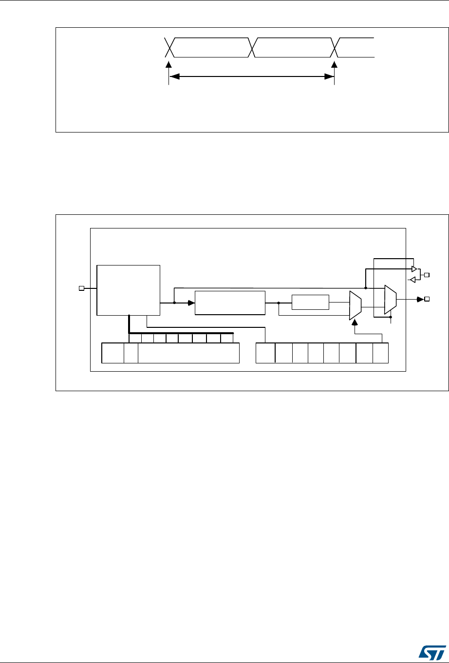
Serial peripheral interface/ inter-IC sound (SPI/I2S) RM0430
968/1324 RM0430 Rev 8
Figure 349. Audio sampling frequency definition
When the master mode is configured, a specific action needs to be taken to properly
program the linear divider in order to communicate with the desired audio frequency.
Figure 350 presents the communication clock architecture. The I2Sx clock is always the
system clock.
Figure 350. I2S clock generator architecture
1. Where x = 2.
The audio sampling frequency may be 192 KHz, 96 kHz, 48 kHz, 44.1 kHz, 32 kHz,
22.05 kHz, 16 kHz, 11.025 kHz or 8 kHz (or any other value within this range). In order to
reach the desired frequency, the linear divider needs to be programmed according to the
formulas below:
When the master clock is generated (MCKOE in the SPIx_I2SPR register is set):
fS = I2SxCLK / [(16*2)*((2*I2SDIV)+ODD)*8)] when the channel frame is 16-bit wide
fS = I2SxCLK / [(32*2)*((2*I2SDIV)+ODD)*4)] when the channel frame is 32-bit wide
When the master clock is disabled (MCKOE bit cleared):
fS = I2SxCLK / [(16*2)*((2*I2SDIV)+ODD))] when the channel frame is 16-bit wide
fS = I2SxCLK / [(32*2)*((2*I2SDIV)+ODD))] when the channel frame is 32-bit wide
Table 176 provides example precision values for different clock configurations.
Note: Other configurations are possible that allow optimum clock precision.
069
RUELWOHIW
FKDQQHO
RUELW
ULJKWFKDQQHO
RUELWV
VDPSOLQJSRLQW VDPSOLQJSRLQW
)6
)6DXGLRVDPSOLQJIUHTXHQF\
069
0&.2( 2''
ELWOLQHDUGLYLGHU
UHVKDSLQJVWDJH
'LYLGHUE\ 'LY
,ð6',9>@
,ð602'
&+/(1
0&.2(
&.
0&.
,ð6[&/.

RM0430 Rev 8 969/1324
RM0430 Serial peripheral interface/ inter-IC sound (SPI/I2S)
986
Table 176. Audio-frequency precision using standard 8 MHz HSE(1)
1. This table gives only example values for different clock configurations. Other configurations allowing
optimum clock precision are possible.
SYSCLK
(MHz)
Data
length I2SDIV I2SODD MCLK Target fS
(Hz) Real fS (KHz) Error
48 16 8 0 No 96000 93750 2.3438%
48 32 4 0 No 96000 93750 2.3438%
48 16 15 1 No 48000 48387.0968 0.8065%
48 32 8 0 No 48000 46875 2.3438%
48 16 17 0 No 44100 44117.647 0.0400%
48 32 8 1 No 44100 44117.647 0.0400%
48 16 23 1 No 32000 31914.8936 0.2660%
48 32 11 1 No 32000 32608.696 1.9022%
48 16 34 0 No 22050 22058.8235 0.0400%
48 32 17 0 No 22050 22058.8235 0.0400%
48 16 47 0 No 16000 15957.4468 0.2660%
48 32 23 1 No 16000 15957.447 0.2660%
48 16 68 0 No 11025 11029.4118 0.0400%
48 32 34 0 No 11025 11029.412 0.0400%
48 16 94 0 No 8000 7978.7234 0.2660%
48 32 47 0 No 8000 7978.7234 0.2660%
48 16 2 0 Yes 48000 46875 2.3430%
48 32 2 0 Yes 48000 46875 2.3430%
48 16 2 0 Yes 44100 46875 6.2925%
48 32 2 0 Yes 44100 46875 6.2925%
48 16 3 0 Yes 32000 31250 2.3438%
48 32 3 0 Yes 32000 31250 2.3438%
48 16 4 1 Yes 22050 20833.333 5.5178%
48 32 4 1 Yes 22050 20833.333 5.5178%
48 16 6 0 Yes 16000 15625 2.3438%
48 32 6 0 Yes 16000 15625 2.3438%
48 16 8 1 Yes 11025 11029.4118 0.0400%
48 32 8 1 Yes 11025 11029.4118 0.0400%
48 16 11 1 Yes 8000 8152.17391 1.9022%
48 32 11 1 Yes 8000 8152.17391 1.9022%

Serial peripheral interface/ inter-IC sound (SPI/I2S) RM0430
970/1324 RM0430 Rev 8
29.6.5 I2S master mode
The I2S can be configured as follows:
•In master mode for transmission or reception (half-duplex mode using I2Sx)
•In master mode transmission and reception (full-duplex mode using I2Sx and
I2Sx_ext).
This means that the serial clock is generated on the CK pin as well as the Word Select
signal WS. Master clock (MCK) may be output or not, controlled by the MCKOE bit in the
SPIx_I2SPR register.
Procedure
1. Select the I2SDIV[7:0] bits in the SPIx_I2SPR register to define the serial clock baud
rate to reach the proper audio sample frequency. The ODD bit in the SPIx_I2SPR
register also has to be defined.
2. Select the CKPOL bit to define the steady level for the communication clock. Set the
MCKOE bit in the SPIx_I2SPR register if the master clock MCK needs to be provided
to the external ADC audio component (the I2SDIV and ODD values should be
computed depending on the state of the MCK output, for more details refer to
Section 29.6.4: Clock generator).
3. Set the I2SMOD bit in the SPIx_I2SCFGR register to activate the I2S functions and
choose the I2S standard through the I2SSTD[1:0] and PCMSYNC bits, the data length
through the DATLEN[1:0] bits and the number of bits per channel by configuring the
CHLEN bit. Select also the I2S master mode and direction (Transmitter or Receiver)
through the I2SCFG[1:0] bits in the SPIx_I2SCFGR register.
4. If needed, select all the potential interrupt sources and the DMA capabilities by writing
the SPIx_CR2 register.
5. The I2SE bit in SPIx_I2SCFGR register must be set.
WS and CK are configured in output mode. MCK is also an output, if the MCKOE bit in
SPIx_I2SPR is set.
Transmission sequence
The transmission sequence begins when a half-word is written into the Tx buffer.
Lets assume the first data written into the Tx buffer corresponds to the left channel data.
When data are transferred from the Tx buffer to the shift register, TXE is set and data
corresponding to the right channel have to be written into the Tx buffer. The CHSIDE flag
indicates which channel is to be transmitted. It has a meaning when the TXE flag is set
because the CHSIDE flag is updated when TXE goes high.
A full frame has to be considered as a left channel data transmission followed by a right
channel data transmission. It is not possible to have a partial frame where only the left
channel is sent.
The data half-word is parallel loaded into the 16-bit shift register during the first bit
transmission, and then shifted out, serially, to the MOSI/SD pin, MSB first. The TXE flag is
set after each transfer from the Tx buffer to the shift register and an interrupt is generated if
the TXEIE bit in the SPIx_CR2 register is set.
For more details about the write operations depending on the I2S Standard-mode selected,
refer to Section 29.6.3: Supported audio protocols).

RM0430 Rev 8 971/1324
RM0430 Serial peripheral interface/ inter-IC sound (SPI/I2S)
986
To ensure a continuous audio data transmission, it is mandatory to write the SPIx_DR
register with the next data to transmit before the end of the current transmission.
To switch off the I2S, by clearing I2SE, it is mandatory to wait for TXE = 1 and BSY = 0.
Reception sequence
The operating mode is the same as for transmission mode except for the point 3 (refer to the
procedure described in Section 29.6.5: I2S master mode), where the configuration should
set the master reception mode through the I2SCFG[1:0] bits.
Whatever the data or channel length, the audio data are received by 16-bit packets. This
means that each time the Rx buffer is full, the RXNE flag is set and an interrupt is generated
if the RXNEIE bit is set in SPIx_CR2 register. Depending on the data and channel length
configuration, the audio value received for a right or left channel may result from one or two
receptions into the Rx buffer.
Clearing the RXNE bit is performed by reading the SPIx_DR register.
CHSIDE is updated after each reception. It is sensitive to the WS signal generated by the
I2S cell.
For more details about the read operations depending on the I2S Standard-mode selected,
refer to Section 29.6.3: Supported audio protocols.
If data are received while the previously received data have not been read yet, an overrun is
generated and the OVR flag is set. If the ERRIE bit is set in the SPIx_CR2 register, an
interrupt is generated to indicate the error.
To switch off the I2S, specific actions are required to ensure that the I2S completes the
transfer cycle properly without initiating a new data transfer. The sequence depends on the
configuration of the data and channel lengths, and on the audio protocol mode selected. In
the case of:
•16-bit data length extended on 32-bit channel length (DATLEN = 00 and CHLEN = 1)
using the LSB justified mode (I2SSTD = 10)
a) Wait for the second to last RXNE = 1 (n – 1)
b) Then wait 17 I2S clock cycles (using a software loop)
c) Disable the I2S (I2SE = 0)
•16-bit data length extended on 32-bit channel length (DATLEN = 00 and CHLEN = 1) in
MSB justified, I2S or PCM modes (I2SSTD = 00, I2SSTD = 01 or I2SSTD = 11,
respectively)
a) Wait for the last RXNE
b) Then wait 1 I2S clock cycle (using a software loop)
c) Disable the I2S (I2SE = 0)
•For all other combinations of DATLEN and CHLEN, whatever the audio mode selected
through the I2SSTD bits, carry out the following sequence to switch off the I2S:
a) Wait for the second to last RXNE = 1 (n – 1)
b) Then wait one I2S clock cycle (using a software loop)
c) Disable the I2S (I2SE = 0)
Note: The BSY flag is kept low during transfers.

Serial peripheral interface/ inter-IC sound (SPI/I2S) RM0430
972/1324 RM0430 Rev 8
29.6.6 I2S slave mode
The I2S can be configured as follows:
•In slave mode for transmission or reception (half-duplex mode using I2Sx)
•In slave mode transmission and reception (full-duplex mode using I2Sx and I2Sx_ext).
The operating mode is following mainly the same rules as described for the I2S master
configuration. In slave mode, there is no clock to be generated by the I2S interface. The
clock and WS signals are input from the external master connected to the I2S interface.
There is then no need, for the user, to configure the clock.
The configuration steps to follow are listed below:
1. Set the I2SMOD bit in the SPIx_I2SCFGR register to select I2S mode and choose the
I2S standard through the I2SSTD[1:0] bits, the data length through the DATLEN[1:0]
bits and the number of bits per channel for the frame configuring the CHLEN bit. Select
also the mode (transmission or reception) for the slave through the I2SCFG[1:0] bits in
SPIx_I2SCFGR register.
2. If needed, select all the potential interrupt sources and the DMA capabilities by writing
the SPIx_CR2 register.
3. The I2SE bit in SPIx_I2SCFGR register must be set.
Transmission sequence
The transmission sequence begins when the external master device sends the clock and
when the NSS_WS signal requests the transfer of data. The slave has to be enabled before
the external master starts the communication. The I2S data register has to be loaded before
the master initiates the communication.
For the I2S, MSB justified and LSB justified modes, the first data item to be written into the
data register corresponds to the data for the left channel. When the communication starts,
the data are transferred from the Tx buffer to the shift register. The TXE flag is then set in
order to request the right channel data to be written into the I2S data register.
The CHSIDE flag indicates which channel is to be transmitted. Compared to the master
transmission mode, in slave mode, CHSIDE is sensitive to the WS signal coming from the
external master. This means that the slave needs to be ready to transmit the first data
before the clock is generated by the master. WS assertion corresponds to left channel
transmitted first.
Note: The I2SE has to be written at least two PCLK cycles before the first clock of the master
comes on the CK line.
The data half-word is parallel-loaded into the 16-bit shift register (from the internal bus)
during the first bit transmission, and then shifted out serially to the MOSI/SD pin MSB first.
The TXE flag is set after each transfer from the Tx buffer to the shift register and an interrupt
is generated if the TXEIE bit in the SPIx_CR2 register is set.
Note that the TXE flag should be checked to be at 1 before attempting to write the Tx buffer.
For more details about the write operations depending on the I2S Standard-mode selected,
refer to Section 29.6.3: Supported audio protocols.

RM0430 Rev 8 973/1324
RM0430 Serial peripheral interface/ inter-IC sound (SPI/I2S)
986
To secure a continuous audio data transmission, it is mandatory to write the SPIx_DR
register with the next data to transmit before the end of the current transmission. An
underrun flag is set and an interrupt may be generated if the data are not written into the
SPIx_DR register before the first clock edge of the next data communication. This indicates
to the software that the transferred data are wrong. If the ERRIE bit is set into the SPIx_CR2
register, an interrupt is generated when the UDR flag in the SPIx_SR register goes high. In
this case, it is mandatory to switch off the I2S and to restart a data transfer starting from the
left channel.
To switch off the I2S, by clearing the I2SE bit, it is mandatory to wait for TXE = 1 and
BSY = 0.
Reception sequence
The operating mode is the same as for the transmission mode except for the point 1 (refer to
the procedure described in Section 29.6.6: I2S slave mode), where the configuration should
set the master reception mode using the I2SCFG[1:0] bits in the SPIx_I2SCFGR register.
Whatever the data length or the channel length, the audio data are received by 16-bit
packets. This means that each time the RX buffer is full, the RXNE flag in the SPIx_SR
register is set and an interrupt is generated if the RXNEIE bit is set in the SPIx_CR2
register. Depending on the data length and channel length configuration, the audio value
received for a right or left channel may result from one or two receptions into the RX buffer.
The CHSIDE flag is updated each time data are received to be read from the SPIx_DR
register. It is sensitive to the external WS line managed by the external master component.
Clearing the RXNE bit is performed by reading the SPIx_DR register.
For more details about the read operations depending the I2S Standard-mode selected,
refer to Section 29.6.3: Supported audio protocols.
If data are received while the preceding received data have not yet been read, an overrun is
generated and the OVR flag is set. If the bit ERRIE is set in the SPIx_CR2 register, an
interrupt is generated to indicate the error.
To switch off the I2S in reception mode, I2SE has to be cleared immediately after receiving
the last RXNE = 1.
Note: The external master components should have the capability of sending/receiving data in 16-
bit or 32-bit packets via an audio channel.
29.6.7 I2S status flags
Three status flags are provided for the application to fully monitor the state of the I2S bus.
Busy flag (BSY)
The BSY flag is set and cleared by hardware (writing to this flag has no effect). It indicates
the state of the communication layer of the I2S.
When BSY is set, it indicates that the I2S is busy communicating. There is one exception in
master receive mode (I2SCFG = 11) where the BSY flag is kept low during reception.
The BSY flag is useful to detect the end of a transfer if the software needs to disable the I2S.
This avoids corrupting the last transfer. For this, the procedure described below must be
strictly respected.
The BSY flag is set when a transfer starts, except when the I2S is in master receiver mode.

Serial peripheral interface/ inter-IC sound (SPI/I2S) RM0430
974/1324 RM0430 Rev 8
The BSY flag is cleared:
•When a transfer completes (except in master transmit mode, in which the
communication is supposed to be continuous)
•When the I2S is disabled
When communication is continuous:
•In master transmit mode, the BSY flag is kept high during all the transfers
•In slave mode, the BSY flag goes low for one I2S clock cycle between each transfer
Note: Do not use the BSY flag to handle each data transmission or reception. It is better to use the
TXE and RXNE flags instead.
Tx buffer empty flag (TXE)
When set, this flag indicates that the Tx buffer is empty and the next data to be transmitted
can then be loaded into it. The TXE flag is reset when the Tx buffer already contains data to
be transmitted. It is also reset when the I2S is disabled (I2SE bit is reset).
RX buffer not empty (RXNE)
When set, this flag indicates that there are valid received data in the RX Buffer. It is reset
when SPIx_DR register is read.
Channel Side flag (CHSIDE)
In transmission mode, this flag is refreshed when TXE goes high. It indicates the channel
side to which the data to transfer on SD has to belong. In case of an underrun error event in
slave transmission mode, this flag is not reliable and I2S needs to be switched off and
switched on before resuming the communication.
In reception mode, this flag is refreshed when data are received into SPIx_DR. It indicates
from which channel side data have been received. Note that in case of error (like OVR) this
flag becomes meaningless and the I2S should be reset by disabling and then enabling it
(with configuration if it needs changing).
This flag has no meaning in the PCM standard (for both Short and Long frame modes).
When the OVR or UDR flag in the SPIx_SR is set and the ERRIE bit in SPIx_CR2 is also
set, an interrupt is generated. This interrupt can be cleared by reading the SPIx_SR status
register (once the interrupt source has been cleared).
29.6.8 I2S error flags
There are three error flags for the I2S cell.
Underrun flag (UDR)
In slave transmission mode this flag is set when the first clock for data transmission appears
while the software has not yet loaded any value into SPIx_DR. It is available when the
I2SMOD bit in the SPIx_I2SCFGR register is set. An interrupt may be generated if the
ERRIE bit in the SPIx_CR2 register is set.
The UDR bit is cleared by a read operation on the SPIx_SR register.

RM0430 Rev 8 975/1324
RM0430 Serial peripheral interface/ inter-IC sound (SPI/I2S)
986
Overrun flag (OVR)
This flag is set when data are received and the previous data have not yet been read from
the SPIx_DR register. As a result, the incoming data are lost. An interrupt may be generated
if the ERRIE bit is set in the SPIx_CR2 register.
In this case, the receive buffer contents are not updated with the newly received data from
the transmitter device. A read operation to the SPIx_DR register returns the previous
correctly received data. All other subsequently transmitted half-words are lost.
Clearing the OVR bit is done by a read operation on the SPIx_DR register followed by a
read access to the SPIx_SR register.
Frame error flag (FRE)
This flag can be set by hardware only if the I2S is configured in Slave mode. It is set if the
external master is changing the WS line while the slave is not expecting this change. If the
synchronization is lost, the following steps are required to recover from this state and
resynchronize the external master device with the I2S slave device:
1. Disable the I2S.
2. Enable it again when the correct level is detected on the WS line (WS line is high in I2S
mode or low for MSB- or LSB-justified or PCM modes.
Desynchronization between master and slave devices may be due to noisy environment on
the SCK communication clock or on the WS frame synchronization line. An error interrupt
can be generated if the ERRIE bit is set. The desynchronization flag (FRE) is cleared by
software when the status register is read.
29.6.9 I2S interrupts
Table 177 provides the list of I2S interrupts.
29.6.10 DMA features
In I2S mode, the DMA works in exactly the same way as it does in SPI mode. There is no
difference except that the CRC feature is not available in I2S mode since there is no data
transfer protection system.
Table 177. I2S interrupt requests
Interrupt event Event flag Enable control bit
Transmit buffer empty flag TXE TXEIE
Receive buffer not empty flag RXNE RXNEIE
Overrun error OVR
ERRIEUnderrun error UDR
Frame error flag FRE

Serial peripheral interface/ inter-IC sound (SPI/I2S) RM0430
976/1324 RM0430 Rev 8
29.7 SPI and I2S registers
The peripheral registers can be accessed by half-words (16-bit) or words (32-bit). SPI_DR
in addition by can be accessed by 8-bit access.
Refer to Section 1.2 for a list of abbreviations used in register descriptions.
The peripheral registers can be accessed by half-words (16 bits) or words (32 bits).
29.7.1 SPI control register 1 (SPI_CR1) (not used in I2S mode)
Address offset: 0x00
Reset value: 0x0000
1514131211109876543210
BIDI
MODE
BIDI
OE
CRC
EN
CRC
NEXT DFF RX
ONLY SSM SSI LSB
FIRST SPE BR [2:0] MSTR CPOL CPHA
rw rw rw rw rw rw rw rw rw rw rw rw rw rw rw rw
Bit 15 BIDIMODE: Bidirectional data mode enable
This bit enables half-duplex communication using common single bidirectional data line.
Keep RXONLY bit clear when bidirectional mode is active.
0: 2-line unidirectional data mode selected
1: 1-line bidirectional data mode selected
Note: This bit is not used in I2S mode
Bit 14 BIDIOE: Output enable in bidirectional mode
This bit combined with the BIDIMODE bit selects the direction of transfer in bidirectional
mode
0: Output disabled (receive-only mode)
1: Output enabled (transmit-only mode)
Note: In master mode, the MOSI pin is used while the MISO pin is used in slave mode.
This bit is not used in I2S mode.
Bit 13 CRCEN: Hardware CRC calculation enable
0: CRC calculation disabled
1: CRC calculation enabled
Note: This bit should be written only when SPI is disabled (SPE = ‘0’) for correct operation.
It is not used in I2S mode.
Bit 12 CRCNEXT: CRC transfer next
0: Data phase (no CRC phase)
1: Next transfer is CRC (CRC phase)
Note: When the SPI is configured in full-duplex or transmitter only modes, CRCNEXT must be
written as soon as the last data is written to the SPI_DR register.
When the SPI is configured in receiver only mode, CRCNEXT must be set after the
second last data reception.
This bit should be kept cleared when the transfers are managed by DMA.
It is not used in I2S mode.

RM0430 Rev 8 977/1324
RM0430 Serial peripheral interface/ inter-IC sound (SPI/I2S)
986
Bit 11 DFF: Data frame format
0: 8-bit data frame format is selected for transmission/reception
1: 16-bit data frame format is selected for transmission/reception
Note: This bit should be written only when SPI is disabled (SPE = ‘0’) for correct operation.
It is not used in I2S mode.
Bit 10 RXONLY: Receive only mode enable
This bit enables simplex communication using a single unidirectional line to receive data
exclusively. Keep BIDIMODE bit clear when receive only mode is active.
This bit is also useful in a multislave system in which this particular slave is not accessed, the
output from the accessed slave is not corrupted.
0: full-duplex (Transmit and receive)
1: Output disabled (Receive-only mode)
Note: This bit is not used in I2S mode
Bit 9 SSM: Software slave management
When the SSM bit is set, the NSS pin input is replaced with the value from the SSI bit.
0: Software slave management disabled
1: Software slave management enabled
Note: This bit is not used in I2S mode and SPI TI mode
Bit 8 SSI: Internal slave select
This bit has an effect only when the SSM bit is set. The value of this bit is forced onto the
NSS pin and the IO value of the NSS pin is ignored.
Note: This bit is not used in I2S mode and SPI TI mode
Bit 7 LSBFIRST: Frame format
0: MSB transmitted first
1: LSB transmitted first
Note: This bit should not be changed when communication is ongoing.
It is not used in I2S mode and SPI TI mode
Bit 6 SPE: SPI enable
0: Peripheral disabled
1: Peripheral enabled
Note: When disabling the SPI, follow the procedure described in Section 29.3.10: Procedure
for disabling the SPI.
This bit is not used in I2S mode.
Bits 5:3 BR[2:0]: Baud rate control
000: fPCLK/2
001: fPCLK/4
010: fPCLK/8
011: fPCLK/16
100: fPCLK/32
101: fPCLK/64
110: fPCLK/128
111: fPCLK/256
Note: These bits should not be changed when communication is ongoing.
They are not used in I2S mode.

Serial peripheral interface/ inter-IC sound (SPI/I2S) RM0430
978/1324 RM0430 Rev 8
29.7.2 SPI control register 2 (SPI_CR2)
Address offset: 0x04
Reset value: 0x0000
Bit 2 MSTR: Master selection
0: Slave configuration
1: Master configuration
Note: This bit should not be changed when communication is ongoing.
It is not used in I2S mode.
Bit1 CPOL: Clock polarity
0: CK to 0 when idle
1: CK to 1 when idle
Note: This bit should not be changed when communication is ongoing.
It is not used in I2S mode and SPI TI mode except the case when CRC is applied
at TI mode.
Bit 0 CPHA: Clock phase
0: The first clock transition is the first data capture edge
1: The second clock transition is the first data capture edge
Note: This bit should not be changed when communication is ongoing.
It is not used in I2S mode and SPI TI mode except the case when CRC is applied
at TI mode.
15 14 13 12 11 10 9 8 7 6 5 4 3 2 1 0
Res. Res. Res. Res. Res. Res. Res. Res. TXEIE RXNEIE ERRIE FRF Res. SSOE TXDMAEN RXDMAEN
rw rw rw rw rw rw rw
Bits 15:8 Reserved, must be kept at reset value.
Bit 7 TXEIE: Tx buffer empty interrupt enable
0: TXE interrupt masked
1: TXE interrupt not masked. Used to generate an interrupt request when the TXE flag is set.
Bit 6 RXNEIE: RX buffer not empty interrupt enable
0: RXNE interrupt masked
1: RXNE interrupt not masked. Used to generate an interrupt request when the RXNE flag is
set.
Bit 5 ERRIE: Error interrupt enable
This bit controls the generation of an interrupt when an error condition occurs (OVR,
CRCERR, MODF, FRE in SPI mode, and UDR, OVR, FRE in I2S mode).
0: Error interrupt is masked
1: Error interrupt is enabled
Bit 4 FRF: Frame format
0: SPI Motorola mode
1 SPI TI mode
Note: This bit is not used in I2S mode.
Bit 3 Reserved. Forced to 0 by hardware.

RM0430 Rev 8 979/1324
RM0430 Serial peripheral interface/ inter-IC sound (SPI/I2S)
986
29.7.3 SPI status register (SPI_SR)
Address offset: 0x08
Reset value: 0x0002
Bit 2 SSOE: SS output enable
0: SS output is disabled in master mode and the cell can work in multimaster configuration
1: SS output is enabled in master mode and when the cell is enabled. The cell cannot work
in a multimaster environment.
Note: This bit is not used in I2S mode and SPI TI mode.
Bit 1 TXDMAEN: Tx buffer DMA enable
When this bit is set, the DMA request is made whenever the TXE flag is set.
0: Tx buffer DMA disabled
1: Tx buffer DMA enabled
Bit 0 RXDMAEN: Rx buffer DMA enable
When this bit is set, the DMA request is made whenever the RXNE flag is set.
0: Rx buffer DMA disabled
1: Rx buffer DMA enabled
1514131211109876543 2 10
Res. Res. Res. Res. Res. Res. Res. FRE BSY OVR MODF CRC
ERR UDR CHSIDE TXE RXNE
rrrrrc_w0r r rr
Bits 15:9 Reserved. Forced to 0 by hardware.
Bit 8 FRE: Frame Error
0: No frame error
1: Frame error occurred.
This bit is set by hardware and cleared by software when the SPI_SR register is read.
This bit is used in SPI TI mode or in I2S mode whatever the audio protocol selected. It
detects a change on NSS or WS line which takes place in slave mode at a non expected
time, informing about a desynchronization between the external master device and the
slave.
Bit 7 BSY: Busy flag
0: SPI (or I2S) not busy
1: SPI (or I2S) is busy in communication or Tx buffer is not empty
This flag is set and cleared by hardware.
Note: BSY flag must be used with caution: refer to Section 29.3.12: SPI status flags and
Section 29.3.10: Procedure for disabling the SPI.
Bit 6 OVR: Overrun flag
0: No overrun occurred
1: Overrun occurred
This flag is set by hardware and reset by a software sequence. Refer to Section 29.3.13: SPI
error flags for the software sequence.

Serial peripheral interface/ inter-IC sound (SPI/I2S) RM0430
980/1324 RM0430 Rev 8
Bit 5 MODF: Mode fault
0: No mode fault occurred
1: Mode fault occurred
This flag is set by hardware and reset by a software sequence. Refer to Section 29.4 on
page 955 for the software sequence.
Note: This bit is not used in I2S mode
Bit 4 CRCERR: CRC error flag
0: CRC value received matches the SPI_RXCRCR value
1: CRC value received does not match the SPI_RXCRCR value
This flag is set by hardware and cleared by software writing 0.
Note: This bit is not used in I2S mode.
Bit 3 UDR: Underrun flag
0: No underrun occurred
1: Underrun occurred
This flag is set by hardware and reset by a software sequence. Refer to Section 29.6.8: I2S
error flags for the software sequence.
Note: This bit is not used in SPI mode.
Bit 2 CHSIDE: Channel side
0: Channel Left has to be transmitted or has been received
1: Channel Right has to be transmitted or has been received
Note: This bit is not used for SPI mode and is meaningless in PCM mode.
Bit 1 TXE: Transmit buffer empty
0: Tx buffer not empty
1: Tx buffer empty
Bit 0 RXNE: Receive buffer not empty
0: Rx buffer empty
1: Rx buffer not empty

RM0430 Rev 8 981/1324
RM0430 Serial peripheral interface/ inter-IC sound (SPI/I2S)
986
29.7.4 SPI data register (SPI_DR)
Address offset: 0x0C
Reset value: 0x0000
29.7.5 SPI CRC polynomial register (SPI_CRCPR) (not used in I2S
mode)
Address offset: 0x10
Reset value: 0x0007
1514131211109876543210
DR[15:0]
rw rw rw rw rw rw rw rw rw rw rw rw rw rw rw rw
Bits 15:0 DR[15:0]: Data register
Data received or to be transmitted.
The data register is split into 2 buffers - one for writing (Transmit Buffer) and another one for
reading (Receive buffer). A write to the data register will write into the Tx buffer and a read
from the data register will return the value held in the Rx buffer.
Note: These notes apply to SPI mode:
Depending on the data frame format selection bit (DFF in SPI_CR1 register), the data
sent or received is either 8-bit or 16-bit. This selection has to be made before enabling
the SPI to ensure correct operation.
For an 8-bit data frame, the buffers are 8-bit and only the LSB of the register
(SPI_DR[7:0]) is used for transmission/reception. When in reception mode, the MSB of
the register (SPI_DR[15:8]) is forced to 0.
For a 16-bit data frame, the buffers are 16-bit and the entire register, SPI_DR[15:0] is
used for transmission/reception.
1514131211109876543210
CRCPOLY[15:0]
rw rw rw rw rw rw rw rw rw rw rw rw rw rw rw rw
Bits 15:0 CRCPOLY[15:0]: CRC polynomial register
This register contains the polynomial for the CRC calculation.
The CRC polynomial (0007h) is the reset value of this register. Another polynomial can be
configured as required.
Note: These bits are not used for the I2S mode.

Serial peripheral interface/ inter-IC sound (SPI/I2S) RM0430
982/1324 RM0430 Rev 8
29.7.6 SPI RX CRC register (SPI_RXCRCR) (not used in I2S mode)
Address offset: 0x14
Reset value: 0x0000
29.7.7 SPI TX CRC register (SPI_TXCRCR) (not used in I2S mode)
Address offset: 0x18
Reset value: 0x0000
1514131211109876543210
RXCRC[15:0]
rrrrrrrrrrrrrrrr
Bits 15:0 RXCRC[15:0]: Rx CRC register
When CRC calculation is enabled, the RxCRC[15:0] bits contain the computed CRC value of
the subsequently received bytes. This register is reset when the CRCEN bit in SPI_CR1
register is written to 1. The CRC is calculated serially using the polynomial programmed in
the SPI_CRCPR register.
Only the 8 LSB bits are considered when the data frame format is set to be 8-bit data (DFF
bit of SPI_CR1 is cleared). CRC calculation is done based on any CRC8 standard.
The entire 16-bits of this register are considered when a 16-bit data frame format is selected
(DFF bit of the SPI_CR1 register is set). CRC calculation is done based on any CRC16
standard.
Note: A read to this register when the BSY Flag is set could return an incorrect value.These
bits are not used for I2S mode.
1514131211109876543210
TXCRC[15:0]
rrrrrrrrrrrrrrrr
Bits 15:0 TXCRC[15:0]: Tx CRC register
When CRC calculation is enabled, the TxCRC[7:0] bits contain the computed CRC value of
the subsequently transmitted bytes. This register is reset when the CRCEN bit of SPI_CR1
is written to 1. The CRC is calculated serially using the polynomial programmed in the
SPI_CRCPR register.
Only the 8 LSB bits are considered when the data frame format is set to be 8-bit data (DFF
bit of SPI_CR1 is cleared). CRC calculation is done based on any CRC8 standard.
The entire 16-bits of this register are considered when a 16-bit data frame format is selected
(DFF bit of the SPI_CR1 register is set). CRC calculation is done based on any CRC16
standard.
Note: A read to this register when the BSY flag is set could return an incorrect value. These
bits are not used for I2S mode.

RM0430 Rev 8 983/1324
RM0430 Serial peripheral interface/ inter-IC sound (SPI/I2S)
986
29.7.8 SPI_I2S configuration register (SPI_I2SCFGR)
Address offset: 0x1C
Reset value: 0x0000
15 14 13 12 11 10 9 8 7 6 5 4 3 2 1 0
Res. Res. Res. ASTRE
NI2SMOD I2SE I2SCFG PCMSY
NC Res. I2SSTD CKPOL DATLEN CHLEN
rw rw rw rw rw rw rw rw rw rw rw rw
Bits 15:13 Reserved, must be kept at reset value.
Bit 12 ASTREN: Asynchronous start enable.
0: The Asynchronous start is disabled. When the I2S is enabled in slave mode, the I2S slave starts
the transfer when the I2S clock is received and an appropriate transition (depending on the protocol
selected) is detected on the WS signal.
1: The Asynchronous start is enabled. When the I2S is enabled in slave mode, the I2S slave starts
immediately the transfer when the I2S clock is received from the master without checking the
expected transition of WS signal.
Note: Note: The appropriate transition is a falling edge on WS signal when I2S Philips Standard is
used, or a rising edge for other standards.
Bit 11 I2SMOD: I2S mode selection
0: SPI mode is selected
1: I2S mode is selected
Note: This bit should be configured when the SPI or I2S is disabled
Bit 10 I2SE: I2S Enable
0: I2S peripheral is disabled
1: I2S peripheral is enabled
Note: This bit is not used in SPI mode.
Bits 9:8 I2SCFG: I2S configuration mode
00: Slave - transmit
01: Slave - receive
10: Master - transmit
11: Master - receive
Note: This bit should be configured when the I2S is disabled.
It is not used in SPI mode.
Bit 7 PCMSYNC: PCM frame synchronization
0: Short frame synchronization
1: Long frame synchronization
Note: This bit has a meaning only if I2SSTD = 11 (PCM standard is used)
It is not used in SPI mode.
Bit 6 Reserved: forced at 0 by hardware
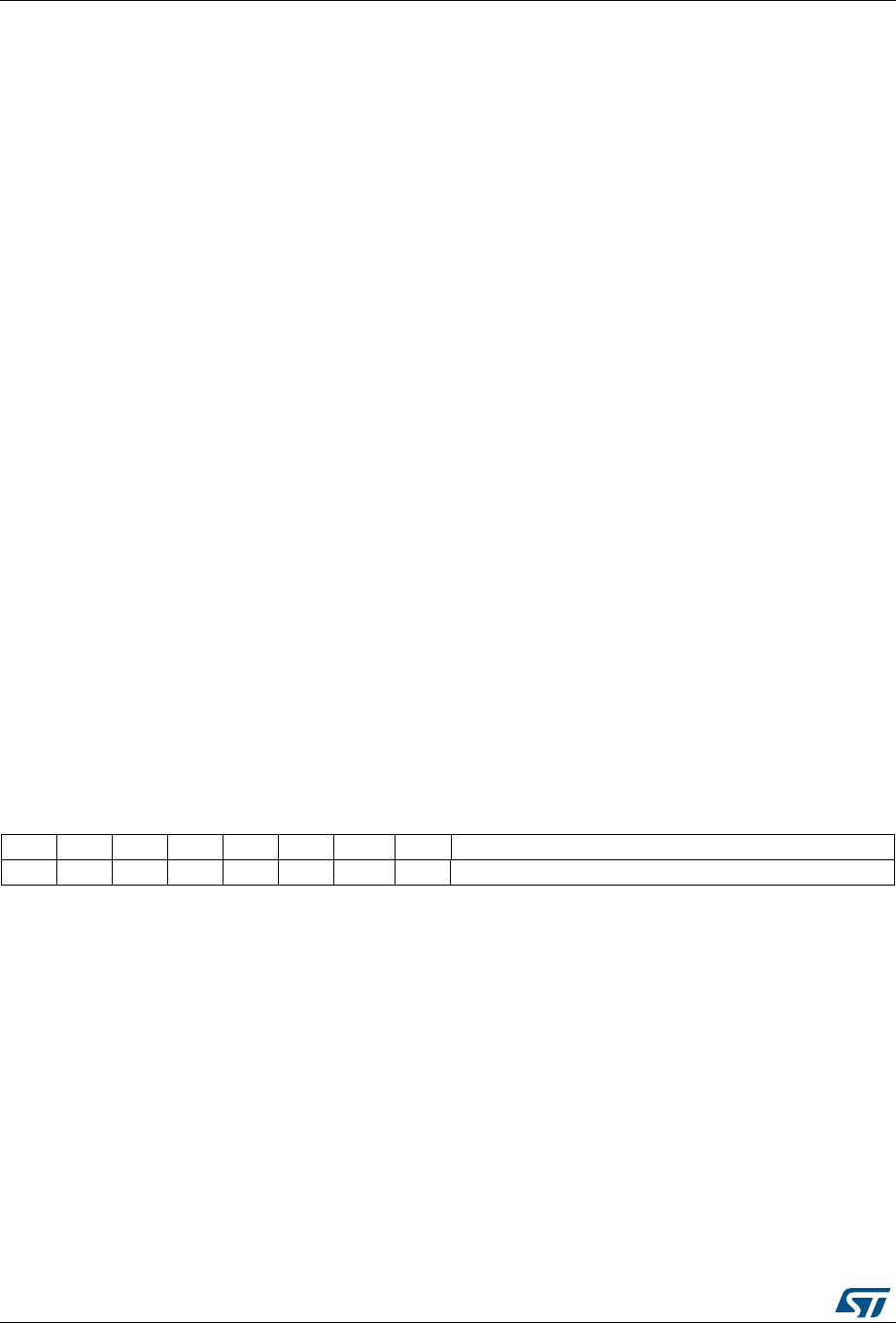
Serial peripheral interface/ inter-IC sound (SPI/I2S) RM0430
984/1324 RM0430 Rev 8
29.7.9 SPI_I2S prescaler register (SPI_I2SPR)
Address offset: 0x20
Reset value: 0000 0010 (0x0002)
Bits 5:4 I2SSTD: I2S standard selection
00: I2S Philips standard.
01: MSB justified standard (left justified)
10: LSB justified standard (right justified)
11: PCM standard
For more details on I2S standards, refer to Section 29.6.3 on page 961. Not used in SPI mode.
Note: For correct operation, these bits should be configured when the I2S is disabled.
Bit 3 CKPOL: Steady state clock polarity
0: I2S clock steady state is low level
1: I2S clock steady state is high level
Note: For correct operation, this bit should be configured when the I2S is disabled.
This bit is not used in SPI mode
Bits 2:1 DATLEN: Data length to be transferred
00: 16-bit data length
01: 24-bit data length
10: 32-bit data length
11: Not allowed
Note: For correct operation, these bits should be configured when the I2S is disabled.
This bit is not used in SPI mode.
Bit 0 CHLEN: Channel length (number of bits per audio channel)
0: 16-bit wide
1: 32-bit wide
The bit write operation has a meaning only if DATLEN = 00 otherwise the channel length is fixed to
32-bit by hardware whatever the value filled in. Not used in SPI mode.
Note: For correct operation, this bit should be configured when the I2S is disabled.
1514131211109 876543210
Res. Res. Res. Res. Res. Res. MCKOE ODD I2SDIV
rw rw rw
Bits 15:10 Reserved, must be kept at reset value.

RM0430 Rev 8 985/1324
RM0430 Serial peripheral interface/ inter-IC sound (SPI/I2S)
986
Bit 9 MCKOE: Master clock output enable
0: Master clock output is disabled
1: Master clock output is enabled
Note: This bit should be configured when the I2S is disabled. It is used only when the I2S is in master
mode.
This bit is not used in SPI mode.
Bit 8 ODD: Odd factor for the prescaler
0: real divider value is = I2SDIV *2
1: real divider value is = (I2SDIV * 2)+1
Refer to Section 29.6.4 on page 967. Not used in SPI mode.
Note: This bit should be configured when the I2S is disabled. It is used only when the I2S is in master
mode.
Bits 7:0 I2SDIV: I2S Linear prescaler
I2SDIV [7:0] = 0 or I2SDIV [7:0] = 1 are forbidden values.
Refer to Section 29.6.4 on page 967. Not used in SPI mode.
Note: These bits should be configured when the I2S is disabled. It is used only when the I2S is in
master mode.

Serial peripheral interface/ inter-IC sound (SPI/I2S) RM0430
986/1324 RM0430 Rev 8
29.7.10 SPI register map
The table provides shows the SPI register map and reset values.
Refer to Section 2.2.2 on page 58 for the register boundary addresses.
Table 178. SPI register map and reset values
Offset Register
31
30
29
28
27
26
25
24
23
22
21
20
19
18
17
16
15
14
13
12
11
10
9
8
7
6
5
4
3
2
1
0
0x00 SPI_CR1
Res.
Res.
Res.
Res.
Res.
Res.
Res.
Res.
Res.
Res.
Res.
Res.
Res.
Res.
Res.
Res.
BIDIMODE
BIDIOE
CRCEN
CRCNEXT
DFF
RXONLY
SSM
SSI
LSBFIRST
SPE
BR
[2:0]
MSTR
CPOL
CPHA
Reset value 0000000000000000
0x04 SPI_CR2
Res.
Res.
Res.
Res.
Res.
Res.
Res.
Res.
Res.
Res.
Res.
Res.
Res.
Res.
Res.
Res.
Res.
Res.
Res.
Res.
Res.
Res.
Res.
Res.
TXEIE
RXNEIE
ERRIE
FRF
Res.
SSOE
TXDMAEN
RXDMAEN
Reset value 0 0 0 0 0 0 0
0x08 SPI_SR
Res.
Res.
Res.
Res.
Res.
Res.
Res.
Res.
Res.
Res.
Res.
Res.
Res.
Res.
Res.
Res.
Res.
Res.
Res.
Res.
Res.
Res.
Res.
FRE
BSY
OVR
MODF
CRCERR
UDR
CHSIDE
TXE
RXNE
Reset value 000000010
0x0C SPI_DR
Res.
Res.
Res.
Res.
Res.
Res.
Res.
Res.
Res.
Res.
Res.
Res.
Res.
Res.
Res.
Res.
DR[15:0]
Reset value 0000000000000000
0x10 SPI_CRCPR
Res.
Res.
Res.
Res.
Res.
Res.
Res.
Res.
Res.
Res.
Res.
Res.
Res.
Res.
Res.
Res.
CRCPOLY[15:0]
Reset value 0000000000000111
0x14 SPI_RXCRCR
Res.
Res.
Res.
Res.
Res.
Res.
Res.
Res.
Res.
Res.
Res.
Res.
Res.
Res.
Res.
Res.
RxCRC[15:0]
Reset value 0000000000000000
0x18 SPI_TXCRCR
Res.
Res.
Res.
Res.
Res.
Res.
Res.
Res.
Res.
Res.
Res.
Res.
Res.
Res.
Res.
Res.
TxCRC[15:0]
Reset value 0000000000000000
0x1C SPI_I2SCFGR
Res.
Res.
Res.
Res.
Res.
Res.
Res.
Res.
Res.
Res.
Res.
Res.
Res.
Res.
Res.
Res.
Res.
Res.
Res.
ASTREN
I2SMOD
I2SE
I2SCFG
PCMSYNC
Res.
I2SSTD
CKPOL
DATLEN
CHLEN
Reset value 000000 000000
0x20 SPI_I2SPR
Res.
Res.
Res.
Res.
Res.
Res.
Res.
Res.
Res.
Res.
Res.
Res.
Res.
Res.
Res.
Res.
Res.
Res.
Res.
Res.
Res.
Res.
MCKOE
ODD
I2SDIV
Reset value 0000000010

RM0430 Rev 8 987/1324
RM0430 Serial audio interface (SAI)
1025
30 Serial audio interface (SAI)
30.1 Introduction
The SAI interface (serial audio interface) offers a wide set of audio protocols due to its
flexibility and wide range of configurations. Many stereo or mono audio applications may be
targeted. I2S standards, LSB or MSB-justified, PCM/DSP, TDM, and AC’97 protocols may
be addressed for example.
To bring this level of flexibility and configurability, the SAI contains two audio sub-blocks that
are fully independent of each other. Each audio sub-block is connected to up to 4 pins (SD,
SCK, FS, MCLK). Some of these pins can be shared if the two sub-blocks are declared as
synchronous to leave some free to be used as general purpose I/Os. The MCLK pin can be
output, or not, depending on the application, the decoder requirement and whether the
audio block is configured as the master.
The SAI can work in master or slave configuration. The audio sub-blocks can be either
receiver or transmitter and can work synchronously or not (with respect to the other one).

Serial audio interface (SAI) RM0430
988/1324 RM0430 Rev 8
30.2 Main features
•Two independent audio sub-blocks which can be transmitters or receivers with their
respective FIFO.
•8-word integrated FIFOs for each audio sub-block.
•Synchronous or asynchronous mode between the audio sub-blocks.
•Master or slave configuration independent for both audio sub-blocks.
•Clock generator for each audio block to target independent audio frequency sampling
when both audio sub-blocks are configured in master mode.
•Data size configurable: 8-, 10-, 16-, 20-, 24-, 32-bit.
•Peripheral with large configurability and flexibility allowing to target as example the
following audio protocol: I2S, LSB or MSB-justified, PCM/DSP, TDM, AC’97
•Up to 16 slots available with configurable size and with the possibility to select which
ones are active in the audio frame.
•Number of bits by frame may be configurable.
•Frame synchronization active level configurable (offset, bit length, level).
•First active bit position in the slot is configurable.
•LSB first or MSB first for data transfer.
•Mute mode.
•Stereo/Mono audio frame capability.
•Communication clock strobing edge configurable (SCK).
•Error flags with associated interrupts if enabled respectively.
– Overrun and underrun detection,
– Anticipated frame synchronization signal detection in slave mode,
– Late frame synchronization signal detection in slave mode,
– Codec not ready for the AC’97 mode in reception.
•Interruption sources when enabled:
–Errors,
– FIFO requests.
•DMA interface with 2 dedicated channels to handle access to the dedicated integrated
FIFO of each SAI audio sub-block.
30.3 Functional block diagram
The block diagram of the SAI is shown in Figure 351.
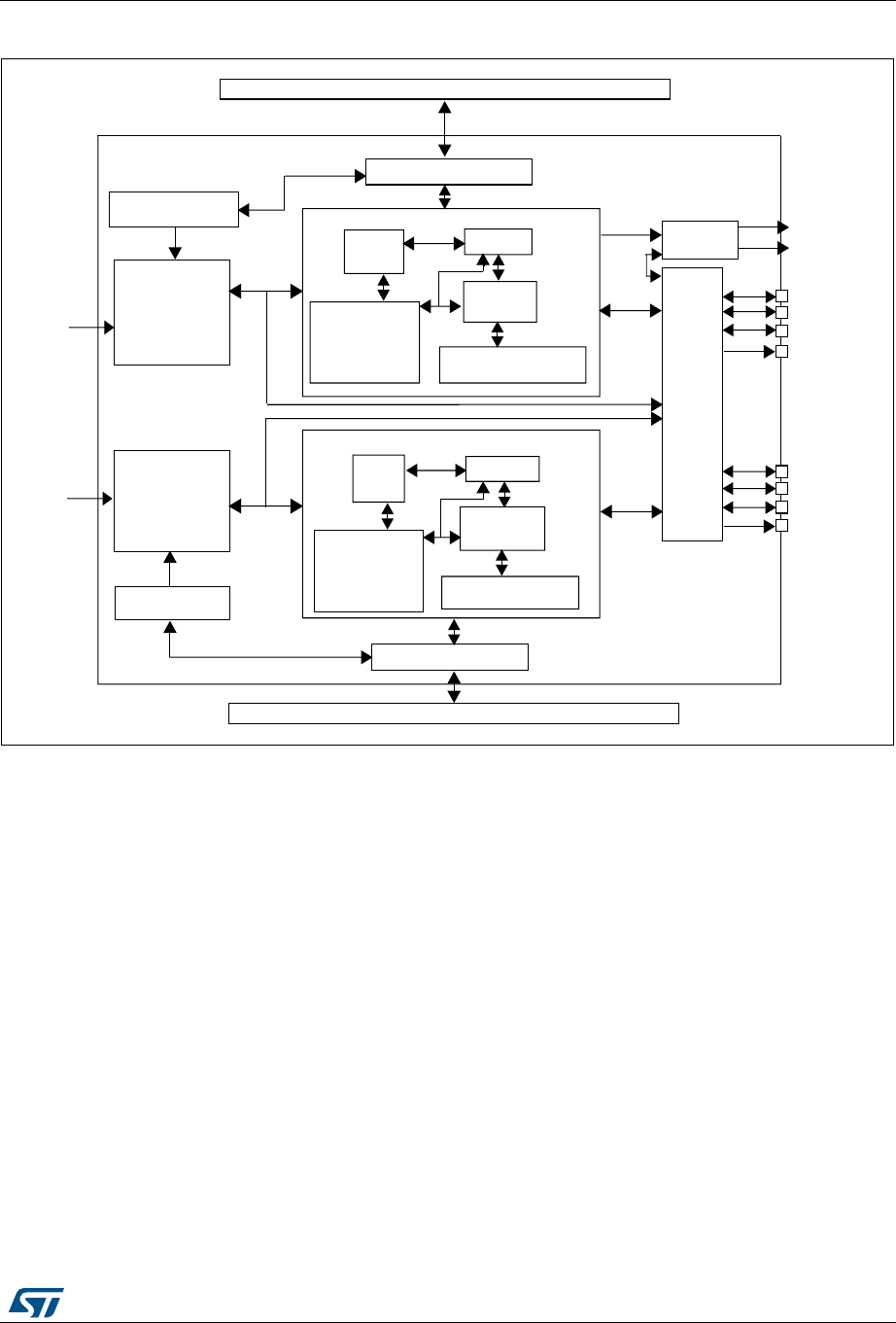
RM0430 Rev 8 989/1324
RM0430 Serial audio interface (SAI)
1025
Figure 351. Functional block diagram
The SAI is mainly composed of two audio sub-blocks with their own clock generator. Each
audio block integrates a 32-bit shift register controlled by their own functional state machine.
Data are stored or read from the dedicated FIFO. FIFO may be accessed by the CPU, or by
DMA in order to leave the CPU free during the communication. Each audio block is
independent. They can be synchronous with each other.
An I/O line controller manages each dedicated pins for a given audio block in the SAI. If the
two blocks are synchronized, this controller reduces the number of I/Os used, freeing up an
FS pin, an SCK pin and eventually an MCLK pin, making them general purpose I/Os.
The functional state machine can be configured to address a wide range of audio protocols.
Some registers are present to set-up the desired protocols (audio frame waveform
generator).
The audio block can be a transmitter or receiver, in master or slave mode. The master mode
means the bit clock SCK and the frame synchronization signal are generated from the SAI,
whereas in slave mode, they come from another external or internal master. There is a
particular case for which the FS signal direction is not directly linked to the master or slave
mode definition. In AC’97 protocol, it will be an SAI output even if the SAI (link controller) is
set-up to consume the SCK clock (and so to be in Slave mode).
069
),)2
),)2
$XGLREORFN$
ELWVKLIWUHJLVWHU
$3%LQWHUIDFH
$3%LQWHUIDFH
6HULDO$XGLR,QWHUIDFH
),)2FWUO
)60
&RQILJXUDWLRQ
UHJLVWHUVDQG
6WDWXVUHJLVWHU
$3%
$3%
6$,B&.B$
V\QFKUR
FWUORXW
LQWBVFN
LQWB)6
)6B$
6&.B$
6'B$
0&/.B$
6$,B;&5
&ORFNJHQHUDWRU
$XGLREORFN$
)60
6$,
$XGLREORFN%
),)2FWUO
&RQILJXUDWLRQ
UHJLVWHUVDQG
6WDWXVUHJLVWHU
&ORFNJHQHUDWRU
$XGLREORFN%
6$,B;&5
6$,B&.B%
,2OLQH0DQDJHPHQW
)6B%
6&.B%
6'B%
0&/.B%
ELWVKLIWUHJLVWHU

Serial audio interface (SAI) RM0430
990/1324 RM0430 Rev 8
30.4 Main SAI modes
Each audio sub-block of the SAI can be configured to be master or slave via bit MODE[0] in
the SAI_xCR1 register of the selected audio block.
In master mode:
•The bit clock is generated by the SAI using the clock generator on pin SCK_A or
SCK_B (depending which audio block is declared as a master in the SAI).
•The dedicated pin SCK_x is considered as an output.
In slave mode:
•The slave must be enabled before the master is enabled.
•The slave audio block’s SCK clock I/O pin is considered input if it is configured in
asynchronous mode.
•If the audio block is declared synchronous with the second audio block in the SAI, its
SCK I/O pin is released to leave it free to be used as a general purpose I/O and is
connected internally to the SCK pin of the device with which it will be synchronized.
Each audio sub-block can be independently defined as a transmitter or receiver by bit
MODE[1] in the SAI_xCR1 register of the relevant audio block. The I/O pin SD will be
defined respectively as an output or an input.
It is possible to declare two master audio blocks in the same SAI with two different MCLK
and SCK clock frequencies (they have to be declared asynchronous).
Each of the audio blocks in the SAI are enabled by bit SAIxEN in the SAI_xCR1 register. As
soon as this bit is active, the transmitter or the receiver is sensitive to the activity on the
clock line, data line and synchronization line in slave mode.
In master TX mode, enabling the audio block immediately generates the bit clock for the
external slaves even if there is no data in the FIFO, However FS signal generation is
conditioned by the presence of data in the FIFO. After the FIFO receives the first data to
transmit, this data is output to external slaves. If there is no data to transmit in the FIFO, 0
values are then sent in the audio frame with an underrun flag generation.
In slave mode, the audio frame starts when the audio block is enabled and when a start of
frame is detected.
In Slave TX mode, no underrun event is possible on the first frame after the audio block is
enabled, because the mandatory operating sequence in this case is:
1. Write into the SAI_xDR (by software or by DMA).
2. Wait until the FIFO threshold (FLH) flag is different from 000b (FIFO empty).
3. Enable the audio block in slave transmitter mode.
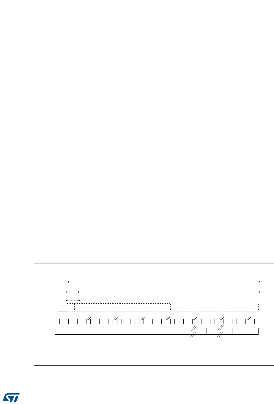
RM0430 Rev 8 991/1324
RM0430 Serial audio interface (SAI)
1025
30.5 SAI synchronization mode
Internal synchronization
An audio block can be declared synchronous with the second audio block. In this case, the
bit clock and the frame synchronization signals are shared to reduce the number of external
pins used for the communication. The audio block declared as synchronous with the other
one will see its own SCK_x, FS_x, and MCLK_x pins released to bring them back as GPIOs.
The one declared asynchronous is the one for which the I/O pins FS_x and SCK_x ad
MCLK_x (if the audio block is considered as master) are considered.
Typically, the audio block synchronous mode may be used to configure the SAI in full duplex
mode. One of the two audio blocks can be configured as master and the other as slave, or
both can be slaves; with one block declared as asynchronous (respective bit SYNCEN[1:0]
= 00 in SAI_xCR1) and the other one declared as synchronous with the other audio block
(respective bit SYNCEN[1:0] = 01 in the SAI_xCR1).
Note: APB frequency PCLK must be greater or equal to twice the bit rate clock frequency (due to
internal resynchronization stages).
30.6 Audio data size
The audio frame can target different data sizes by configuring bit DS[2:0] in the SAI_xCR1
register. The data sizes may be 8-, 10-, 16-, 20-, 24- or 32-bit. During the transfer, either the
MSB or the LSB of the data are sent first, depending on the configuration of bit LSBFIRST in
the SAI_xCR1 register.
30.7 Frame synchronization
The FS signal acts as the Frame synchronization signal in the audio frame (start of frame).
The shape of this signal is completely configurable in order to target the different audio
protocols with their own specificities concerning this Frame synchronization behavior. This
configurability is done using register SAI_xFRCR. Figure 352 gives a view of this flexibility.
Figure 352. Audio frame
3LOT
&S
SCK
SD
&SOFFSET
&SLENGTHBITS
&SACTIVELENGTHBITS
-36
3LOT 3LOT 3LOT 3LOTN
xx

Serial audio interface (SAI) RM0430
992/1324 RM0430 Rev 8
In AC’97 mode (bit PRTCFG[1:0] = 10 in the SAI_xCR1 register), the frame synchronization
shape is forced to be configured to target these protocols. The SAI_xFRCR register value is
ignored.
Each audio block is independent and so each requires a specific configuration.
30.7.1 Frame length
•Master mode: The audio frame length can be configured up to 256 bit clock, setting bit
FRL[7:0] in the SAI_xFRCR register. If the frame length is greater than the number of
declared slots for the frame, the remaining bits to transmit will be extended to 0 or the
SD line will be released to HI-z depending the state of bit TRIS in the SAI_xCR2
register (refer to Section 30.12.4). In reception mode, the remaining bit is ignored.
•Slave mode: The audio frame length is mainly used in order to specify to the slave the
number of bit clocks per audio frame sent by the external master. It is used mainly to
detect from the master, any anticipated or late occurrence of the Frame
synchronization signal during an on-going audio frame. An error will be generated in
such case. For more details please refer to the Section 30.13.
The number of bits in the frame is equal to FRL[7:0] + 1.
The minimum number of bits to transfer in an audio frame is 8. This is the case when the
data size is 8-bit and only one slot is defined in NBSLOT[3:0] in the SAI_xSLOTR register
(NBSLOT[3:0] = 0000 for slot 0).
In master mode:
•If bit NODIV in the SAI_xCR1 register is cleared, the frame length should be aligned to
a number equal to a power of 2, from 8 to 256. This is to ensure that an audio frame
contains an integer number of MCLK pulses per bit clock, which ensures correct
operation of the external DAC/ADC inside the decoders. If the value set in FRL[7:0]
does not respect this rule, flag WCKCFG is set when the audio block is enabled and an
interrupt is generated if bit WCKCFGIE is set in the SAI_xIM register. The SAI is
automatically disabled.
•If bit NODIV in the SAI_xCR1 register is set, the FRL[7:0] bit can take any of the values
without constraint since the input clock of the audio block should be equal to the bit
clock. There is no MCLK_x clock which can be output. MCLK_x output pad is
automatically disabled.
In slave mode, there are no constraints for the FRL[7:0] bit configuration in the SAI_xFRCR
register.
30.7.2 Frame synchronization polarity
Bit FSPOL in the SAI_xFRCR register sets the active polarity of the FS pin from which a
frame is started. The start of frame is edge sensitive.
In slave mode, the audio block waits for a valid frame to start to transmit or to receive. Start
of frame is synchronized to this signal. It is effective only if the start of frame is not detected
during an on-going communication and assimilated to an anticipated start of frame (refer to
Section 30.13).
In master mode, the frame synchronization is sent continuously each time an audio frame is
complete until the SAIxEN bit in the SAI_xCR1 register is cleared. If no data is present in the
FIFO at the end of the previous audio frame, an underrun condition will be managed as
described in Section 30.13), but there will be no interruption in the audio communication
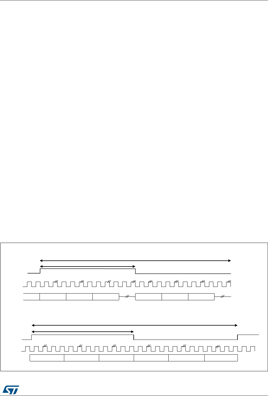
RM0430 Rev 8 993/1324
RM0430 Serial audio interface (SAI)
1025
flow.
30.7.3 Frame synchronization active level length
Bit FSALL[6:0] in the SAI_xFRCR register configures the length of the active level of the
Frame synchronization signal. The length can be set from 1 to 128 bit clock SCK.
The active length may be half of the frame length in I2S, LSB or MSB-justified modes for
instance, or one-bit wide for PCM/DSP or TDM mode, or even 16-bit length in AC’97.
30.7.4 Frame synchronization offset
Depending on the audio protocol targeted in the application, the Frame synchronization
signal can be asserted when transmitting the last bit or the first bit of the audio frame (as for
instance, respectively, in I2S standard protocol and in MSB-justified protocol). Bit FSOFF in
the SAI_xFRCR register makes the choice.
30.7.5 FS signal role
The FS signal may have a different meaning depending on the FS function. Bit FSDEF in
the SAI_xFRCR register selects which meaning it will have. It may be either:
•0: a start of frame, like for instance the PCM/DSP, TDM, AC’97, audio protocols,
•1: a start of frame and a channel side identification within the audio frame like for the
I2S, the MSB or LSB-justified protocols.
When the FS signal is considered as a start of frame and channel side identification within
the frame, the number of declared slots must be considered to be half of the number for the
left channel and half of the number for the right channel. If the number of bit clock on half
audio frame is greater than the number of slots dedicated to a channel side, if TRIS = 0, 0 is
sent for transmission for the remaining bit clock in the SAI_xCR2 register, otherwise if TRIS
= 1, the SD line is released to HI-Z. In reception, the remaining bit clock are not considered
until the channel side changes.
Figure 353. FS role is start of frame + channel side identification (FSDEF = TRIS = 1)
VFN
VORW
$XGLRIUDPH
)6
+DOIRIIUDPH
$XGLRIUDPH
)6
+DOIRIIUDPH
1XPEHURIVORWVQRWDOLJQHGZLWKWKHDXGLRIUDPH
1XPEHURIVORWVDOLJQHGZLWKWKHDXGLRIUDPH
-36
3LOT
VFN
VORW 3LOT 3LOT 3LOT 3LOT
3LOT
3LOT/. 3LOT/&& 3LOT/. 3LOT/. 3LOT/&& 3LOT/.
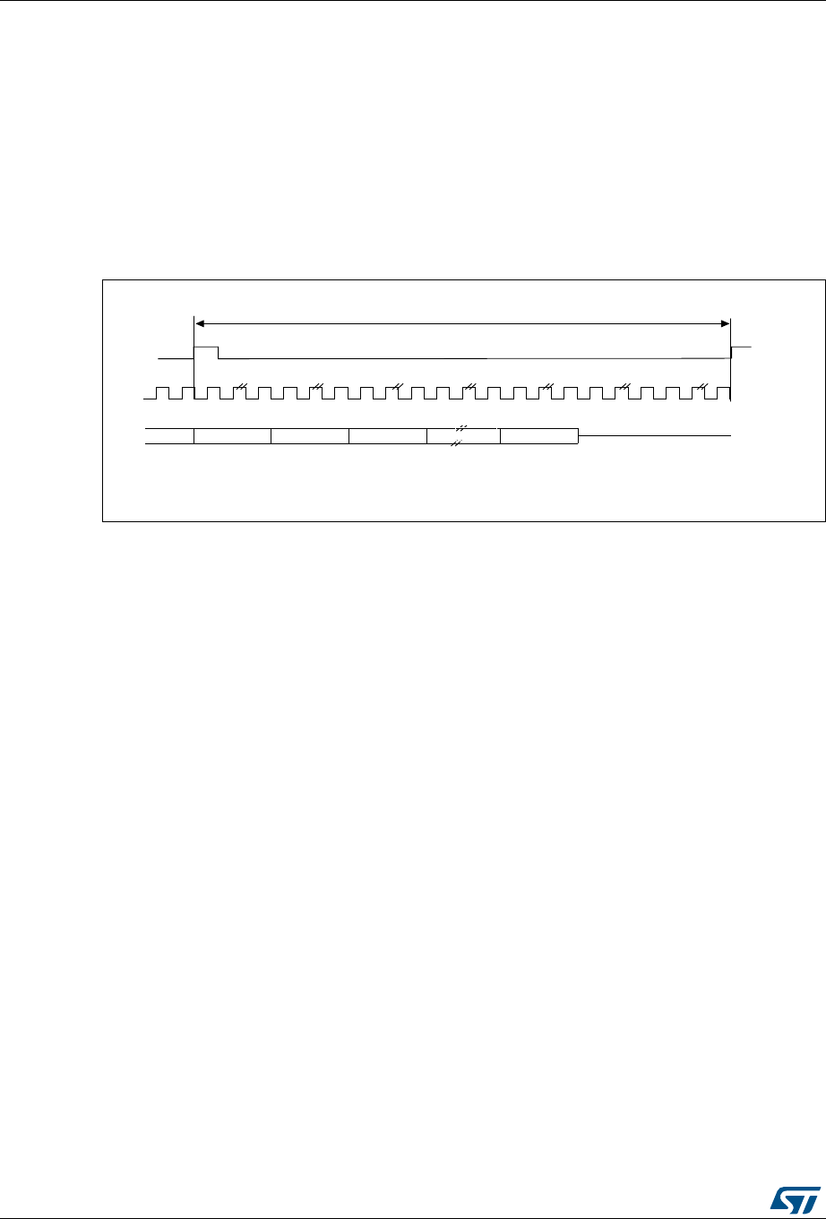
Serial audio interface (SAI) RM0430
994/1324 RM0430 Rev 8
1. The frame length should be even.
If bit FSDEF in SAI_xFRCR is kept clear, so FS signal is equivalent to a start of frame, and
if the number of slots defined in bit NBSLOT[3:0] in SAI_xSLOTR multiplied by
the number of bits by slot configured in bit SLOTSZ[1:0] in SAI_xSLOTR is less than the
frame size (bit FRL[7:0] in the SAI_xFRCR register), then,
•if TRIS = 0 in the SAI_xCR2 register, the remaining bit after the last slot will be forced to
0 until the end of frame in case of transmission,
•if TRIS = 1, the line will be released to HI-Z during the transfer of these remaining bits.
In reception mode, these bits are discarded.
Figure 354. FS role is start of frame (FSDEF = 0)
30.8 Slot configuration
The slot is the basic element in the audio frame. The number of slots in the audio frame is
equal to the configured setting of bit NBSLOT[3:0] in the SAI_xSLOTR register +1.
The maximum number of slots per audio frame is fixed at 16.
For AC’97 protocol (when bit PRTCFG[1:0] = 10), the number of slots is automatically set to
target the protocol specification, and the value of NBSLOT[3:0] is ignored.
Each slot can be defined as a valid slot, or not, by setting bit SLOTEN[15:0] in the
SAI_xSLOTR register. In an audio frame, during the transfer of a non-valid slot, 0 value will
be forced on the data line or the SD data line will be released to HI-z (refer to
Section 30.12.4) if the audio block is transmitter, or the received value from the end of this
slot will be ignored. Consequently, there will be no FIFO access and so no request to read
or write the FIFO linked to this inactive slot status.
The slot size is also configurable as shown in the Figure 355. The size of the slots is
selected by setting bit SLOTSZ[1:0] in the SAI_xSLOTR register. The size is applied
identically for each slot in an audio frame.
$XGLRIUDPH
'DWD DIWHUVORWQLI75,6
6'RXWSXWUHOHDVHG+,=DIWHUVORWQLI75,6
069
VFN
VORW 6ORW 6ORW 6ORW 6ORWQ
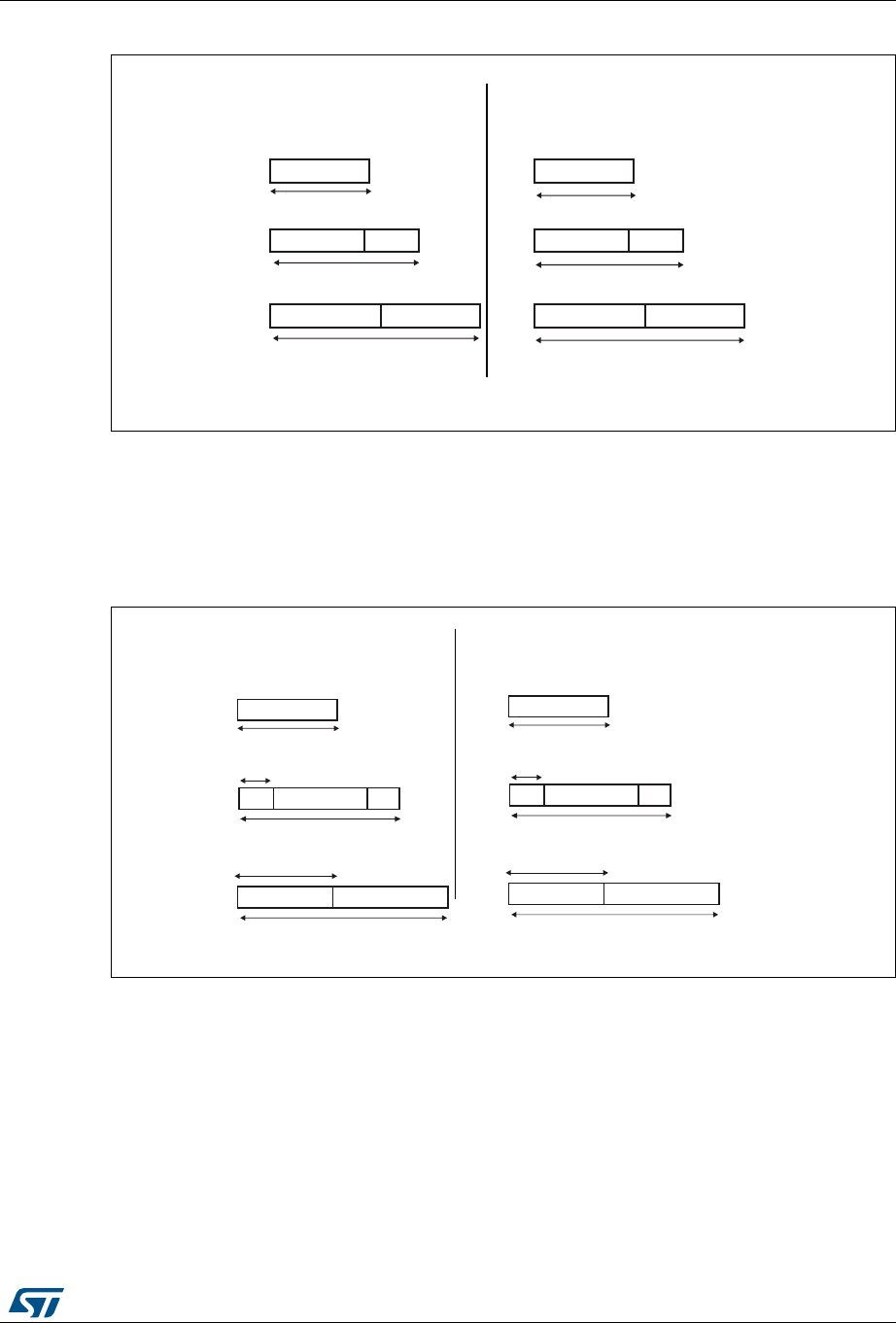
RM0430 Rev 8 995/1324
RM0430 Serial audio interface (SAI)
1025
Figure 355. Slot size configuration with FBOFF = 0 in SAI_xSLOTR
It is possible to choose the position of the first data bit to transfer within the slots, this offset
is configured by bit FBOFF[5:0] in the SAI_xSLOTR register. 0 values will be injected in
transmitter mode from the beginning of the slot until this offset position is reached. In
reception, the bit in the offset phase is ignored. This feature targets the LSB justified
protocol (if the offset is equal to the slot size minus the data size).
Figure 356. First bit offset
It is mandatory to respect the following conditions in order to avoid bad SAI behavior:
FBOFF ≤ (SLOTSZ - DS),
DS ≤ SLOTSZ,
NBSLOT x SLOTSZ ≤ FRL (frame length),
The number of slots should be even when bit FSDEF in the SAI_xFRCR register is set.
In AC’97 (bit PRTCFG[1:0] = 10), the slot size is automatically set as defined in
Section 30.11.
069
;;
;;;;
;GRQ¶WFDUH
$XGLREORFNLVWUDQVPLWWHU
6ORWVL]H GDWDVL]H
GDWDVL]H
GDWDVL]H
GDWDVL]H
GDWDVL]H
VORW[
VORW[
VORW[
ELW
ELW
$XGLREORFNLVUHFHLYHU
6ORWVL]H GDWDVL]H
GDWDVL]H
GDWDVL]H
GDWDVL]H
VORW[
VORW[
VORW[
ELW
ELW
GDWDVL]H
069
;;;;
;GRQ¶WFDUH
$XGLREORFNLVWUDQVPLWWHU
6ORWVL]H GDWDVL]H
GDWDVL]H
GDWDVL]H
GDWDVL]H
GDWDVL]H
VORW[
VORW[
VORW[
ELW
ELW
$XGLREORFNLVUHFHLYHU
)%2))
)%2)) 6/276='6
;;
6ORWVL]H GDWDVL]H
GDWDVL]H
GDWDVL]H
GDWDVL]H
GDWDVL]H
VORW[
VORW[
VORW[
ELW
ELW
;;
)%2))
)%2)) 6/276='6
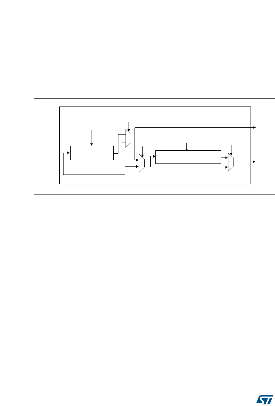
Serial audio interface (SAI) RM0430
996/1324 RM0430 Rev 8
30.9 SAI clock generator
Each audio block has its own clock generator to make these two blocks completely
independent. There is no difference in terms of functionality between these two clock
generators. They are exactly the same.
When the audio block is defined as Master, the clock generator generates the
communication clock (the bit clock) and the master clock for external decoders.
When the audio block is defined as slave, the clock generator is OFF.
Figure 357 illustrates the architecture of the audio block clock generator.
Figure 357. Audio block clock generator overview
Note: If NoDiv is set to 1, the MCLK_x signal will be set at 0 level if this pin is configured as the
SAI pin in GPIO peripherals.
The clock source for the clock generator comes from the product clock controller. The
SAI_CK_x clock is equivalent to the master clock which may be divided for the external
decoders using bit MCKDIV[3:0]:
MCLK_x = SAI_CK_x / (MCKDIV[3:0] * 2), if MCKDIV[3:0] is not equal to 0000.
MCLK_x = SAI_CK_x, if MCKDIV[3:0] is equal to 0000.
MCLK_x signal is used only in TDM.
The division must be even in order to keep 50% on the Duty cycle on the MCLK output and
on the SCK_x clock. If bit MCKDIV[3:0] = 0000, division by one is applied to have MCLK_x
= SAI_CK_x.
In the SAI, the single ratio MCLK/FS = 256 is considered. Mostly, three frequency ranges
will be encountered as illustrated in the Table 179.
0DVWHUFORFN
GLYLGHU %LWFORFNGLYLGHU
0&.',9>@
6&.B[
0&/.B[
12',9
12',9
12',9
6$,B&.B[
069
)5/>@

RM0430 Rev 8 997/1324
RM0430 Serial audio interface (SAI)
1025
The master clock may be generated externally on an I/O pad for external decoders if the
corresponding audio block is declared as master with bit NODIV = 0 in the SAI_xCR1
register. In slave, the value set in this last bit is ignored since the clock generator is OFF,
and the MCLK_x I/O pin is released for use as a general purpose I/O.
The bit clock is derived from the master clock. The bit clock divider sets the divider factor
between the bit clock SCK_x and the master clock MCLK_x following the formula:
SCK_x = MCLK x (FRL[7:0] +1) / 256
where:
256 is the fixed ratio between MCLK and the audio frequency sampling.
FRL[7:0] is the number of bit clock - 1 in the audio frame, configured in the SAI_xFRCR
register.
It is mandatory in master mode that (FRL[7:0] +1) should be equal to a number with a power
of 2 (refer to Section 30.7) in order to have an even integer number of MCLK_x pulses by bit
clock. The 50% duty cycle is guaranteed on the bit clock SCK_x.
The SAI_CK_x clock can be also equal to the bit clock frequency. In this case, bit NODIV in
the SAI_xCR1 register should be set and the value inside the MCKDIV divider and the bit
clock divider will be ignored. In this case, the number of bits per frame is fully configurable
without the need to be equal to a power of two.
The bit clock strobing edge on SCK can be configured by bit CKSTR in the SAI_xCR1
register.
30.10 Internal FIFOs
Each audio block in the SAI has its own FIFO. Depending if the block is defined to be a
transmitter or a receiver, the FIFO will be written or read, respectively. There is therefore
only one FIFO request linked to FREQ bit in the SAI_xSR register.
Table 179. Example of possible audio frequency sampling range
Input SAI_CK_x clock
frequency
Most usual audio frequency
sampling achievable MCKDIV[3:0]
192 kHz x 256
192 kHz MCKDIV[3:0] = 0000
96 kHz MCKDIV[3:0] = 0001
48 kHz MCKDIV[3:0] = 0010
16 kHz MCKDIV[3:0] = 0100
8 kHz MCKDIV[3:0] = 1000
44.1 kHz x 256
44.1 kHz MCKDIV[3:0] = 0000
22.05 kHz MCKDIV[3:0] = 0001
11.025 kHz MCKDIV[3:0] = 0010
SAI_CK_x = MCLK(1)
1. This may happen when the product clock controller selects an external clock source, instead of PLL clock.
MCLK MCKDIV[3:0] = 0000

Serial audio interface (SAI) RM0430
998/1324 RM0430 Rev 8
An interrupt is generated if FREQIE bit is enabled in the SAI_xIM register. This depends on:
•FIFO threshold setting (FLTH bits in SAI_CR2)
•Communication direction transmitter or receiver (see Section : Interrupt generation in
transmitter mode and Section : Interrupt generation in reception mode)
Interrupt generation in transmitter mode
The interrupt generation depends on the FIFO configuration in transmitter mode:
•When the FIFO threshold bits in SAI_XCR2 register are configured as FIFO empty
(FTH[2:0] set to 000b), an interrupt is generated (FREQ bit set by hardware to 1 in
SAI_XSR register) if no data are available in SAI_xDR register (FLTH[2:0] bits in SAI_xSR
is less than 001b). This Interrupt (FREQ bit in SAI_XSR register) is cleared by hardware
when the FIFO became not empty (FLTH[2:0] bits in SAI_xSR are different from 000b) i.e
one or more data are stored in the FIFO.
•When the FIFO threshold bits in SAI_XCR2 register are configured as FIFO quarter full
(FTH[2:0] set to 001b), an interrupt is generated (FREQ bit set by hardware to 1 in
SAI_XSR register) if less than a quarter of the FIFO contains data (FLTH[2:0] bits in
SAI_xSR are less than 010b). This Interrupt (FREQ bit in SAI_XSR register) is cleared by
hardware when at least a quarter of the FIFO contains data (FLTH[2:0] bits in SAI_xSR
are higher or equal to 010b).
•When the FIFO threshold bits in SAI_XCR2 register are configured as FIFO half full
(FTH[2:0] set to 010b), an interrupt is generated (FREQ bit set by hardware to 1 in
SAI_XSR register) if less than half of the FIFO contains data (FLTH[2:0] bits in SAI_xSR
are less than 011b). This Interrupt (FREQ bit in SAI_XSR register) is cleared by hardware
when at least half of the FIFO contains data (FLTH[2:0] bits in SAI_xSR are higher or
equal to 011b).
•When the FIFO threshold bits in SAI_XCR2 register are configured as FIFO three quarter
(FTH[2:0] set to 011b), an interrupt is generated (FREQ bit is set by hardware to 1 in
SAI_XSR register) if less than three quarters of the FIFO contain data (FLTH[2:0] bits in
SAI_xSR are less than 100b). This Interrupt (FREQ bit in SAI_XSR register) is cleared by
hardware when at least three quarters of the FIFO contain data (FLTH[2:0] bits in
SAI_xSR are higher or equal to 100b).
•When the FIFO threshold bits in SAI_XCR2 register are configured as FIFO full (FTH[2:0]
set to 100b), an interrupt is generated (FREQ bit is set by hardware to 1 in SAI_XSR
register) if the FIFO is not full (FLTH[2:0] bits in SAI_xSR is less than 101b). This Interrupt
(FREQ bit in SAI_XSR register) is cleared by hardware when the FIFO is full (FLTH[2:0]
bits in SAI_xSR is equal to 101b value).
Interrupt generation in reception mode
The interrupt generation depends on the FIFO configuration in reception mode:
•When the FIFO threshold bits in SAI_XCR2 register are configured as FIFO empty
(FTH[2:0] set to 000b), an interrupt is generated (FREQ bit is set by hardware to 1 in
SAI_XSR register) if at least one data is available in SAI_xDR register(FLTH[2:0] bits in
SAI_xSR is higher or equal to 001b). This Interrupt (FREQ bit in SAI_XSR register) is
cleared by hardware when the FIFO became empty (FLTH[2:0] bits in SAI_xSR is equal
to 000b) i.e no data is stored in FIFO.
•When the FIFO threshold bits in SAI_XCR2 register are configured as FIFO quarter fully
(FTH[2:0] set to 001b), an interrupt is generated (FREQ bit is set by hardware to 1 in
SAI_XSR register) if at less one quarter of the FIFO data locations are available

RM0430 Rev 8 999/1324
RM0430 Serial audio interface (SAI)
1025
(FLTH[2:0] bits in SAI_xSR is higher or equal to 010b). This Interrupt (FREQ bit in
SAI_XSR register) is cleared by hardware when less than a quarter of the FIFO data
locations become available (FLTH[2:0] bits in SAI_xSR is less than 010b).
•When the FIFO threshold bits in SAI_XCR2 register are configured as FIFO half fully
(FTH[2:0] set to 010b value), an interrupt is generated (FREQ bit is set by hardware to 1
in SAI_XSR register) if at least half of the FIFO data locations are available (FLTH[2:0]
bits in SAI_xSR is higher or equal to 011b). This Interrupt (FREQ bit in SAI_XSR register)
is cleared by hardware when less than half of the FIFO data locations become available
(FLTH[2:0] bits in SAI_xSR is less than 011b).
•When the FIFO threshold bits in SAI_XCR2 register are configured as FIFO three quarter
full(FTH[2:0] set to 011b value), an interrupt is generated (FREQ bit is set by hardware to
1 in SAI_XSR register) if at least three quarters of the FIFO data locations are available
(FLTH[2:0] bits in SAI_xSR is higher or equal to 100b). This Interrupt (FREQ bit in
SAI_XSR register) is cleared by hardware when the FIFO has less than three quarters of
the FIFO data locations avalable(FLTH[2:0] bits in SAI_xSR is less than 100b).
•When the FIFO threshold bits in SAI_XCR2 register are configured as FIFO full(FTH[2:0]
set to 100b), an interrupt is generated (FREQ bit is set by hardware to 1 in SAI_XSR
register) if the FIFO is full (FLTH[2:0] bits in SAI_xSR is equal to 101b). This Interrupt
(FREQ bit in SAI_XSR register) is cleared by hardware when the FIFO is not full
(FLTH[2:0] bits in SAI_xSR is less than 101b).
Like interrupt generation, the SAI can use the DMA if DMAEN bit in the SAI_xCR1 register is
set. The FREQ bit assertion mechanism is the same as the interruption generation
mechanism described above for FREQIE.
Each FIFO is an 8-word FIFO. Each read or write operation from/to the FIFO targets one
word FIFO allocation whatever the access size. Each FIFO word contains one audio frame.
FIFO pointers are incremented by one word after each access to the SAI_xDR register.
Data should be right aligned when it is written in the SAI_xDR.
Data received will be right aligned in the SAI_xDR.
The FIFO pointers can be reinitialized when the SAI is disabled by setting bit FFLUSH in the
SAI_xCR2 register. If FFLUSH is set when the SAI is enabled the data present in the FIFO
will be lost automatically.
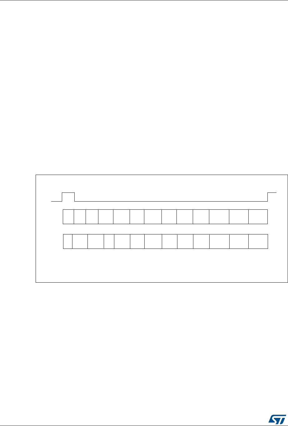
Serial audio interface (SAI) RM0430
1000/1324 RM0430 Rev 8
30.11 AC’97 link controller
The SAI is able to work as an AC’97 link controller. In this protocol:
•The slot number and the slot size are fixed.
•The frame synchronization signal is perfectly defined and has a fixed shape.
To select this protocol, set bit PRTCFG[1:0] in the SAI_xCR1 register to 10. When AC’97
mode is selected the data sizes that can be used are 16-bit or 20-bit only, else SAI behavior
is not guaranteed.
•Bits NBSLOT[3:0] and SLOTSZ[1:0] are consequently ignored.
•The number of slots is fixed at 13 slots. The first one is 16 bits wide and all the others
are 20 bits wide (data slots).
•Bit FBOFF[5:0] in the SAI_xSLOTR register is ignored
•The SAI_xFRCR register is ignored.
The FS signal from the block defined as asynchronous is configured automatically as an
output, since the AC’97 controller link drives the FS signal whatever the master or slave
configuration.
Figure 358 presents an AC’97 audio frame structure.
Figure 358. AC’97 audio frame
Note: In AC’97 protocol, bit 2 of the tag is reserved (always 0), so whatever the value written in the
SAI FIFO, bit 2 of the TAG is forced to 0 level.
For more details about TAG representation, please refer to the AC’97 protocol standard.
One SAI can be used to target an AC’97 point-to-point communication.
In receiver mode, the SAI acting as an AC’97 link controller will require no FIFO request and
so no data storage in the FIFO when the codec ready bit in the slot 0 is decoded low. If bit
CNRDYIE is enabled in the SAI_xIM register, flag CNRDY will be set in the SAI_xSR
register and an interrupt is generated. This flag is dedicated to the AC’97 protocol.
30.12 Specific features
The SAI has some specific functions which can be useful depending on the audio protocol
selected. These functions are accessible through specific bits in the SAI_xCR2 register.
069
)6
6',
6'2
7DJ &0'
$''5
&0'
'$7$
/,1(
'$&
3&0
/)5217
3&0
5)5217
3&0
&(17(5
3&0
/6855
3&0
56855
3&0
/)(
/,1(
'$&
+6(7
'$&
,2
&75/
7DJ 67$786
$''5
67$786
'$7$
/,1(
$'&
3&0
/()7
3&0
5,*+7
3&0
0,&
565
9'
565
/9'
/,1(
$'& +6(7 ,2
67$786
565
9'

RM0430 Rev 8 1001/1324
RM0430 Serial audio interface (SAI)
1025
30.12.1 Mute mode
Mute mode may be used when the audio block is a transmitter or receiver.
Transmitter
In transmitter mode, Mute mode can be selected at anytime. Mute mode is active for entire
audio frames. The bit MUTE in the SAI_xCR2 register requests Mute mode when it is set
during an on-going frame.
The mute mode bit is strobed only at the end of the frame. If set at this time, the mute mode
is active at the beginning of the new audio frame, for a complete frame, until the next end of
frame, it then strobes the bit to determine if the next frame will still be a mute frame.
If the number of slots set in bit NBSLOT[3:0] in the SAI_xSLOTR register is lower than or
equal to two, it is possible to specify if the value sent during the Mute mode is 0 or if it is the
last value of each slot. The selection is done via bit MUTEVAL in the SAI_xCR2 register.
If the number of slots set in bit NBSLOT[3:0] in the SAI_xSLOTR register is greater than
two, MUTEVAL bit in the SAI_xCR2 has no meaning as 0 values are sent on each bit on
each slot.
During Mute mode, the FIFO pointers are still incremented, meaning that data which was
present in the FIFO and for which the Mute mode is requested is discarded.
Receiver
In receiver mode, it is possible to detect a Mute mode sent from the external transmitter
when all the declared and valid slots of the audio frame receive 0 for a given consecutive
number of audio frames (bit MUTECNT[5:0] in the SAI_xCR2 register).
When the number of MUTE frames is detected, flag MUTEDET in the SAI_xSR register is
set and an interrupt can be generated if bit MUTEDETIE is set in the SAI_xCR2.
The mute frame counter is cleared when the audio block is disabled or when a valid slot
receives at least one data in an audio frame. The interrupt is generated just once, when the
counter reaches the specified value in bit MUTECNT[5:0]. Then the interrupt event is re-
armed when the counter is cleared.
30.12.2 MONO/STEREO function
In transmission mode, it is possible to address the Mono mode without any data pre-
processing in memory when the number of slot is equal to 2 (NBSLOT[3:0] = 0001 in the
SAI_xSLOTR). In such a case, the access to and from the FIFO will be reduced by two
since in transmission, the data for slot 0 is duplicated into data slot 1.
To select the Mono feature, set bit MONO in the SAI_xCR1 register.
In reception mode, bit MONO can be set and has a meaning only if the number of slots is
equal to 2 like for the transmission mode. When it is set, only the data of slot 0 will be stored
in the FIFO. The data belonging to slot 1 will be discarded since in this case, it is supposed
to be the same as the previous slot. If the data flux in reception is a real stereo audio flow
with a distinct and different left and right data, bit MONO has no meaning. The conversion
from the output stereo file to the equivalent mono file is done by software.
Note: To enable Mono mode, NBSLOT and SLOTEN must equal two and MONO bit set to 1.
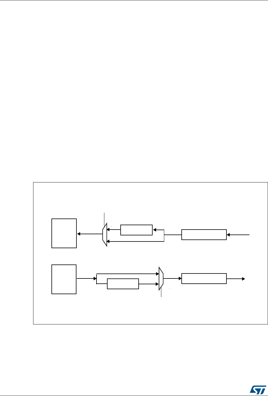
Serial audio interface (SAI) RM0430
1002/1324 RM0430 Rev 8
30.12.3 Companding mode
Telecommunication applications may require to process the data to transmit or to receive
with a data companding algorithm.
Depending on the COMP[1:0] bit in the SAI_xCR2 register (used only when TDM mode is
selected), the software may choose to process or not the data before sending it on SD serial
output line (compression) or to expand the data after the reception on SD serial input line
(expansion) as illustrated in Figure 359,.The two companding modes supported are the µ-
Law and the A-Law log which are a part of the CCITT G.711 recommendation.
The companding standard employed in the United States and Japan is the µ-Law and allows
14 bits of dynamic range (COMP[1:0] = 10 in the SAI_xCR2 register).
The European companding standard is A-Law and allows 13 bits of dynamic range
(COMP[1:0] = 11 in the SAI_xCR2 register).
Companding standard (µ-Law or A-Law) can be computed based on 1’s complement or 2’s
complement representation depending on the CPL bit setting in the SAI_xCR2 register.
The µ-Law and A-Law formats encode data into 8-bit code elements with MSB alignment.
Companded data is always 8 bits wide. For this reason, bit DS[2:0] in the SAI_xCR1 register
will be forced to 010 when the SAI audio block is enabled (bit SAIxEN = 1 in the SAI_xCR1
register) and when the COMP[1:0] bit selects one of these two companding modes.
If no companding processing is required, COMP[1:0] bit in the SAI_xCR2 register should be
kept cleared.
Figure 359. Data companding hardware in an audio block in the SAI
Note: Not applicable when AC’97 selected.
Expansion or compression mode is automatically selected by the SAI configuration.
•If the SAI audio block is configured to be a transmitter, and if the COMP[1] bit is set in
the SAI_xCR2 register, the compression mode will be applied.
•If the SAI audio block is declared as a receiver, the expansion algorithm will be applied.
H[SDQG
),)2
&203>@
&203>@
ELWVKLIWUHJLVWHU
6'
5HFHLYHUPRGHELW02'(>@ LQ6$,B[&5
7UDQVPLWWHUPRGHELW02'(>@ LQ6$,B[&5
069
ELWVKLIWUHJLVWHU
6'
FRPSUHVV
),)2

RM0430 Rev 8 1003/1324
RM0430 Serial audio interface (SAI)
1025
30.12.4 Output data line management on an inactive slot
In transmitter mode, it is possible to choose the behavior of the SD line in output when an
inactive slot is sent on the data line (via bit TRIS in the SAI_xCR2 register when the SAI is
disabled).
•Either the SAI forces 0 on the SD output line when an inactive slot is transmitted, or
•The line is released in HI-z state at the end of the last bit of data transferred, to release
the line for other transmitters connected to this node.
It is important to note that the two transmitters do not attempt to drive the same SD output
pin simultaneously, which could result in a short circuit. In order to ensure a gap between
transmissions, if the data is lower than 32-bit, the data can be extended to 32-bit by setting
bit SLOTSZ[1:0] = 10 in the SAI_xSLOTR register. Then, the SD output pin will be tristated
at the end of the LSB of the active slot (during the padding to 0 phase to extend the data to
32-bit) if the following slot is declared inactive.
In addition, if the number of slots multiplied by the slot size is lower than the frame length,
the SD output line will be tristated when the padding to 0 is done to complete the audio
frame.
Figure 360 illustrates these behaviors.
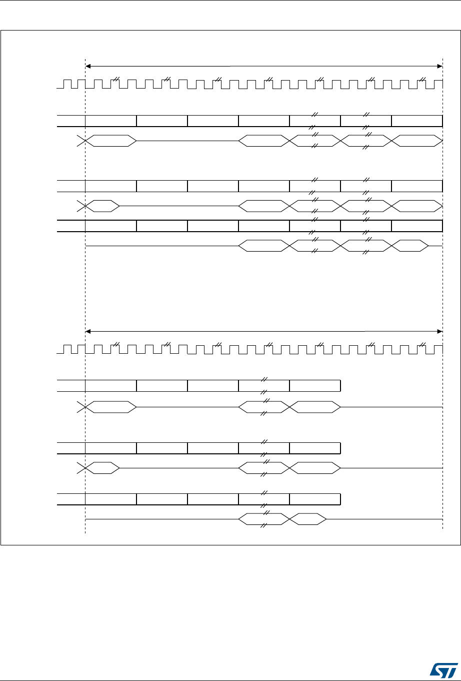
Serial audio interface (SAI) RM0430
1004/1324 RM0430 Rev 8
Figure 360. Tristate strategy on SD output line on an inactive slot
When the selected audio protocol uses the FS signal as a start of frame and a channel side
identification (bit FSDEF = 1 in the SAI_xFRCR register), the tristate mode is managed
according to Figure 361 (where bit TRIS in the SAI_xCR1 register = 1, and FSDEF=1, and
half frame length > number of slots/2, and NBSLOT=6).
VORW
$XGLRIUDPH
%LW75,6 LQWKH6$,B[&5DQGIUDPHOHQJWK QXPEHURIVORWV
069
6ORWVL]H GDWDVL]H
6ORWVL]H!GDWDVL]H
%LW75,6 LQWKH6$,B[&5DQGIUDPHOHQJWK!QXPEHURIVORWV
6'RXWSXW
SCK
3LOT/. 3LOT/&& 3LOT/&& 3LOT/. /. /. 3LOTN/.
$ATA $ATA $ATAM
3LOT/. 3LOT/&& 3LOT/&& 3LOT/. /. /. 3LOTN/.
$ATA $ATA $ATAM
3LOT/. 3LOT/&& 3LOT/&& 3LOT/. /. /. 3LOTN/.
$ATA $ATAM
VORW
6'RXWSXW
VORW
6'RXWSXW
VORW
$XGLRIUDPH
6ORWVL]H GDWDVL]H
6'RXWSXW
SCK
3LOT/. 3LOT/&& 3LOT/&& /. 3LOTN/.
$ATA $ATAM
VORW
6ORWVL]H!GDWDVL]H
6'RXWSXW
3LOT/. 3LOT/&& 3LOT/&& /. 3LOTN/.
$ATAM
$ATA
VORW
6'RXWSXW
3LOT/. 3LOT/&& 3LOT/&& /.
$ATAM
/.
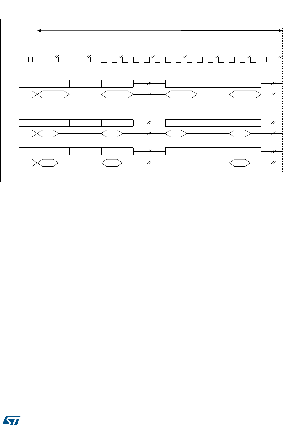
RM0430 Rev 8 1005/1324
RM0430 Serial audio interface (SAI)
1025
Figure 361. Tristate on output data line in a protocol like I2S
If the TRIS bit in the SAI_xCR2 register is cleared, all the High impedance states on the SD
output line on Figure 360 and Figure 361 are replaced by a drive with a value of 0.
30.13 Error flags
The SAI embeds some error flags:
– FIFO overrun/underrun,
– Anticipated frame synchronization detection,
– Late frame synchronization detection,
– Codec not ready (AC’97 exclusively),
– Wrong clock configuration in master mode.
30.13.1 FIFO overrun/underrun (OVRUDR)
The FIFO Overrun/Underrun bit is called OVRUDR in the SAI_xSR register.
The overrun or underrun errors occupy the same bit since an audio block can be either
receiver or transmitter and each audio block in an SAI has its own SAI_xSR register.
Overrun
When the audio block is configured as receiver, an overrun condition may appear if data is
received in an audio frame when the FIFO is full and is not able to store the received data.
In this case, the received data is lost, the flag OVRUDR in the SAI_xSR register is set and
an interrupt is generated if bit OVRUDRIE is set in the SAI_xIM register. The slot number
from which the overrun occurs, is stored internally. No more data will be stored into the FIFO
until it becomes free to store new data. When the FIFO has at least one data free, the SAI
audio block receiver will store new data (from new audio frame) from the slot number which
VORW
069
6ORWVL]H GDWDVL]H
6ORWVL]H!GDWDVL]H
6'RXWSXW
SCK
3LOT/. 3LOT/&& 3LOT/. 3LOT/. 3LOT/&& 3LOT/.
$ATA $ATA
3LOT/. 3LOT/&& 3LOT/.
$ATA
VORW
6'RXWSXW
$ATA $ATA
3LOT/. 3LOT/&& 3LOT/.
$ATA $ATA $ATA
3LOT/. 3LOT/&& 3LOT/.
$ATA
VORW
6'RXWSXW
3LOT/. 3LOT/&& 3LOT/.
$ATA $ATAM
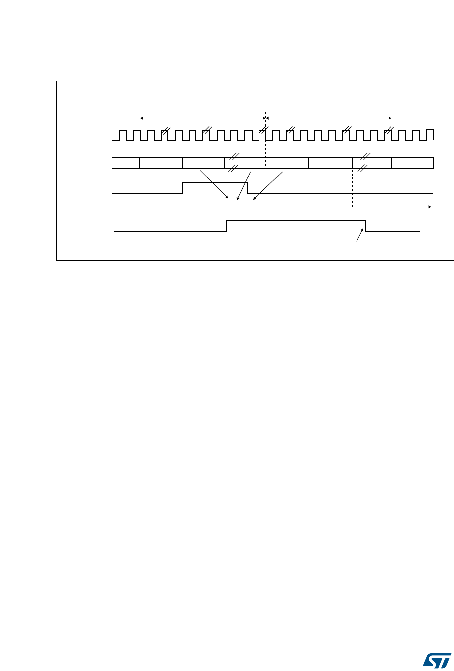
Serial audio interface (SAI) RM0430
1006/1324 RM0430 Rev 8
was stored internally when the overrun condition was detected, and this, to avoid data slot
de-alignment in the destination memory (refer to Figure 362).
The OVRUDR flag is cleared when bit COVRUDR is set in the SAI_xCLRFR register.
Figure 362. Overrun detection error
Underrun
An underrun may occur when the audio block in the SAI is a transmitter and the FIFO is
empty when data needs to be transmitted (the audio block configuration (Master or Slave) is
not relevant). If an underrun is detected, the software must resynchronize data and slot.
Proceed as follows:
1. Disable the SAI peripheral by resetting the SAIEN bit of the SAI_xCR1 register. Check
that the SAI has been disabled by reading back the SAIEN bit (SAIEN should be equal
to 0).
2. Flush the Tx FIFO through the FFLUS bit of the SAI_xCR2 register.
3. Re-assigned to the correct data to be transferred on the first active slot of the new
frame.
4. Re-enabling the SAI peripheral (SAIEN bit set to 1).
The underrun event sets the OVRUDR flag in the SAI_xSR register and an interrupt is
generated if the OVRUDRIE bit is set in the SAI_xIM register. To clear this flag, set the
COVRUDR bit in the SAI_xCLRFR register.
069
VFN
GDWD 6ORW21
([DPSOH),)2RYHUUXQRQ6ORW
$XGLRIUDPH $XGLRIUDPH
6ORWQ21
21
),)2IXOO
2958'5
6ORW21 3LOT/. 6ORW21 6ORW21
5HFHLYHGGDWDGLVFDUGHG 'DWDVWRUHGDJDLQLQ),)2
&2958'5

RM0430 Rev 8 1007/1324
RM0430 Serial audio interface (SAI)
1025
Figure 363. FIFO underrun event
30.13.2 Anticipated frame synchronisation detection (AFSDET)
This flag AFSDET is used only in Slave mode. In master mode, it is never asserted. It
informs about the detection of a frame synchronisation (FS) earlier than expected since the
frame length, the frame polarity, the frame offset are defined and known.
Early detection sets flag AFSDET in the SAI_xSR register.
This detection has no effect on the current audio frame which is not sensitive to the
anticipated FS. This means that “parasitic” events on signal FS are flagged without any
perturbation of the current audio frame.
If bit AFSDETIE is set in the SAI_xIM register, an interrupt is generated. To clear the flag
AFSDET, bit CAFSDET in the SAI_xCLRFR register has to be set.
To resynchronize with the master after Anticipated frame detection error, four steps should
be respected:
1. SAI block should be disabled by resetting SAIEN bit in SAI_xCR1 register, to be sure
that the SAI is disabled SAIEN bit is should be equal to 0 (reading back this bit).
2. FIFO should be flushed via FFLUS bit in SAI_xCR2 register.
3. Re-enabling the SAI peripheral (SAIEN bit set to 1) then the SAI.
4. SAI block will wait for the assertion on FS to restart the synchronization with master.
Note: This flag is not asserted in AC’97 since the SAI audio block acts as a link controller and
generates the FS signal even when declared as slave.
30.13.3 Late frame synchronization detection
Flag LFSDET in the SAI_xSR register can be set only when the SAI audio block is defined
as slave. The frame length, the frame polarity and the frame offset configuration are known
in register SAI_xFRCR.
If the external master does not send the FS signal at the expecting time (generating the
signal too late), the flag LFSDET in the SAI_xSR register will be set and an interrupt is
generated if bit LFSDETIE in the SAI_xIM register is set.
The flag is cleared when bit CLFSDET is set in the SAI_xCLRFR register.
-36
VFN
GDWD 6ORW21 087(
3LOTSIZEDATASIZE
6'RXWSXW
([DPSOH),)2XQGHUUXQRQ6ORW
$XGLRIUDPH $XGLRIUDPH
087( 6ORW21 21 6ORW21
29581'
087(
),)2HPSW\
29581'

Serial audio interface (SAI) RM0430
1008/1324 RM0430 Rev 8
The late frame synchronisation detection flag is set when the error is detected, SAI needs to
be resynchronized with the master (the four steps described above should be respected).
This detection and flag assertion can detect glitches on the SCK clock in a noisy
environment, detected by the state machine of the audio block. It could incorrectly shift the
SAI audio block state machine from one state in the current audio frame, thus corrupting the
frame.
There is no corruption if the external master is not managing the audio data frame transfer in
a continuous mode, which should not be the case for most application purposes. In this
case, flag LFSDET will be set.
Note: This flag is not asserted in AC’97 mode since the SAI audio block acts as a link controller
and generates the FS signal even when declared as slave.
30.13.4 Codec not ready (CNRDY AC’97)
The flag CNRDY in the SAI_xSR register is relevant only if the SAI audio block is configured
to work in AC’97 mode (bit PRTCFG[1:0] = 10 in the SAI_xCR1 register). If bit CNRDYIE is
set in the SAI_xIM register, an interrupt will be generated when the flag CNRDY is set.
It is asserted when the codec is not ready to communicate during the reception of the TAG 0
(slot0) of the AC’97 audio frame. In this case, there will be no data automatically stored into
the FIFO since the codec is not ready, until the TAG 0 indicates that the codec is ready. All
the active slots defined in the SAI_xSLOTR register will be captured when the codec is
ready.
To clear the flag, bit CCNRDY in the SAI_xCLRFR register has to be set.
30.13.5 Wrong clock configuration in master mode (with NODIV = 0)
When the audio block is master (MODE[1] = 0 in the SAI_xCR1 register) and if bit NODIV in
the SAI_xCR1 is clear, the flag WCKCFG will be set if bit FRL[7:0] in the SAI_xFRCR is not
set with a proper value when the SAIxEN bit in the SAI_xCR1 register is set, in order to
respect this following rule:
where n is in the range from 3 to 8.
If bit WCKCFGIE is set, an interrupt is generated when flag WCKCFG is set in the SAI_xSR
register. To clear the flag, set bit CWCKCFG bit in the SAI_xCLRFR register.
When bit WCKCFG is set, the audio block is automatically disabled, clearing bit SAIxEN in
the SAI_xCR1 register via hardware.
The above formula is intended to guarantee that the number of MCLK pulses by bit clock is
an even integer in the audio frame with a 50% duty cycle bit clock generation to guarantee
the good quality of the audio sounds or acquisitions.
30.14 Interrupt sources
The SAI has 7 possible interrupt sources as illustrated by Table 180.
FRL[7,0]()1+2n
=

RM0430 Rev 8 1009/1324
RM0430 Serial audio interface (SAI)
1025
Below are the SAI configuration steps to follow when an interrupt occurs:
1. Disable SAI interrupt.
2. Configure SAI.
3. Configure SAI interrupt source.
4. Enable SAI.
30.15 Disabling the SAI
The audio block in the SAI can be disabled at any moment by clearing bit SAIxEN in the
SAI_xCR1 register. All the frames that have already started will be automatically completed
before the total extinction of the SAI. Bit SAIxEN in the SAI_xCR1 register will stay high until
the SAI is completely switched-off at the end of the current audio frame transfer.
If there is an audio block in the SAI synchronous with the other one, the one which is the
master must be disabled first.
Table 180. Interrupt sources
Interrupt
source
Interru
pt
group
Audio block mode Interrupt enable Interrupt clear
FREQ FREQ Master or Slave
Receiver or transmitter
FREQIE in
SAI_xIM register
Depend on:
- FIFO threshold setting
(FLTH bits in SAI_CR2)
- Communication direction
transmitter or receiver
for more details please refer
to Internal FIFOs section
OVRUDR ERROR Master or Slave
Receiver or transmitter
OVRUDRIE in
SAI_xIM register
COVRUDR = 1 in
SAI_xCLRFR register
AFSDET ERROR
Slave
(Not used in AC’97
mode)
AFSDETIE in
SAI_xIM register
CAFSDET = 1 in
SAI_xCLRFR register
LFSDET ERROR
Slave
(Not used in AC’97
mode)
LFSDETIE in
SAI_xIM register
CLFSDET = 1 in
SAI_xCLRFR register
CNRDY ERROR Slave
(Only in AC’97 mode)
CNRDYIE in
SAI_xIM register
CCNRDY = 1 in
SAI_xCLRFR register
MUTEDE
TMUTE Master or slave
Receiver mode only
MUTEDETIE in
SAI_xIM register
CMUTEDET = 1 in
SAI_xCLRFR register
WCKCFG ERROR
Master with NODIV = 0
in the SAI_xCR1
register
WCKCFGIE in
SAI_xIM register
CWCKCFG = 1 in
SAI_xCLRFR register

Serial audio interface (SAI) RM0430
1010/1324 RM0430 Rev 8
30.16 SAI DMA interface
In order to free the CPU and to optimize the bus bandwidth, each SAI audio block has an
independent DMA interface in order to read or to write into the SAI_xDR register (to hit the
internal FIFO). There is one DMA channel per audio block following basic DMA
request/acknowledge protocol.
To configure the audio block to transfer through the DMA interface, set bit DMAEN in the
SAI_xCR1 register. The DMA request is managed directly by the FIFO controller depend of
FIFO threshold level (for more details please refer to Internal FIFOs section). DMA direction
is linked to the SAI audio block configuration:
•If the audio block is a transmitter, the audio block’s FIFO controller outputs a DMA
request to load the FIFO with data written in the SAI_xDR register.
•If the audio block is a receiver, the DMA request will concern read operations from the
SAI_xDR register.
Below are the SAI configuration steps followed when DMA is used:
1. Configure SAI and FIFO Threshold level (in order to specify when the DMA request to
be launched)
2. Configure SAI DMA channel
3. Enable DMA
4. Enable SAI
Note: Before configuring the SAI block, the SAI DMA channel must be disabled.

RM0430 Rev 8 1011/1324
RM0430 Serial audio interface (SAI)
1025
30.17 SAI registers
30.17.1 SAI xConfiguration register 1 (SAI_xCR1) where x is A or B
Address offset: Block A: 0x004
Address offset: Block B: 0x024
Reset value: 0x0000 0040
31 30 29 28 27 26 25 24 23 22 21 20 19 18 17 16
Reserved MCKDIV[3:0] NODIV Res. DMAEN SAIxEN
rw rw rw rw rw rw rw
15 14 13 12 11 10 9 8 7 6 5 4 3 2 1 0
Reserved
OutDri
vMONO SYNCEN[1:0] CKSTR LSBFIR
ST DS[2:0] Res. PRTCFG[1:0] MODE[1:0]
rw rw rw rw rw rw rw rw rw rw rw rw rw
Bits 31:24 Reserved, always read as 0.
Bit 23:20 MCKDIV[3:0]: Master clock divider. These bits are set and cleared by software.
0000: Divides by 1 the master clock input.
Otherwise, The Master clock frequency is calculated accordingly to the following formula:
MCLK_x = SAI_CK_x / (MCKDIV[3:0] * 2)
These bits have no meaning when the audio block is slave.
They have to be configured when the audio block is disabled.
Bit 19 NODIV: No divider. This bit is set and cleared by software.
0: Master Clock divider is enabled
1: No divider used in the clock generator (in this case Master Clock Divider bit has no effect)
Bit 18 Reserved, always read as 0.
Bit 17 DMAEN: DMA enable. This bit is set and cleared by software.
0: DMA is disabled
1: DMA is enabled
Note: In receiver mode, the bits MODE must be configured before setting bit DMAEN to avoid a DMA
request since the audio block is transmitter after reset (default setting)
Bit 16 SAIxEN: Audio block enable where x is A or B. This bit is set by software. It is cleared by hardware,
after disabling it by software (writing the bit low), the audio is completely disabled (waiting for the end
of the current frame).
0: Audio block is disabled
1: Audio block is enabled: this bit can be set only if it is at 0 during the write operation (means the
SAI is completely disabled before being re-enabled).
This bit allows to control the state of the audio block. If it is disabled somewhere in an audio frame,
the on-going transfer will be completed and the cell will be totally disabled at the end of this audio
frame transfer.
Note: When SAIx block is configured as master mode, clock must be present on the input of the SAI
before setting SAIxEN bit.
Bits 15:14 Reserved, always read as 0.
Bit 13 OUTDRIV: Output drive. This bit is set and cleared by software.
0: Audio block output driven when SAIEN is set
1: Audio block output driven immediately after the setting of this bit.
Note: This bit has to be set before enabling the audio block but after the audio block configuration.

Serial audio interface (SAI) RM0430
1012/1324 RM0430 Rev 8
Bit 12 MONO: Mono mode. This bit is set and cleared by software.
0: Stereo mode
1: Mono mode.
This bit has a meaning only when the number of slots is equal to 2.
When the Mono mode is selected, the data of the slot 0 data is duplicated on the slot 1 when the
audio block is a transmitter. In reception mode, the slot1 is discarded and only the data received
from the slot 0 will be stored.
Refer to Section 30.12.2 for more details.
Bits 11:10 SYNCEN[1:0]: Synchronization enable. This bit is set and cleared by software.
00: audio block is asynchronous.
01: audio block is synchronous with the other internal audio block. In this case audio block should be
configured in Slave mode
10: Reserved.
11: Not used
These bits have to be configured when the audio block is disabled.
Bit 9 CKSTR: Clock strobing edge. This bit is set and cleared by software.
0: data strobing edge is falling edge of SCK
1: data strobing edge is rising edge of SCK
This bit has to be configured when the audio block is disabled.
Bit 8 LSBFIRST: Least significant bit first. This bit is set and cleared by software.
0: data is transferred with the MSB of the data first
1: data is transferred with the LSB of the data first
This bit has to be configured when the audio block is disabled.
This bit has no meaning in AC’97 audio protocol since in AC’97 data is transferred with the MSB of
the data first.
Bits 7:5 DS[2:0]: Data size. These bits are set and cleared by software.
000: Not used
001: Not used
010: 8-bit
011: 10-bit
100: 16-bit
101: 20-bit
110: 24-bit
111: 32-bit
When the companding mode is selected (bit COMP[1:0]), these DS[1:0] are ignored since the data
size is fixed to 8-bit mode by the algorithm itself.
These bits must be configured when the audio block is disabled.
Note: When AC’97 mode is selected the data sizes that can be used are: 16-bit or 20-bit only, else
SAI behavior is not guaranteed.

RM0430 Rev 8 1013/1324
RM0430 Serial audio interface (SAI)
1025
Bit 4 Reserved, always read as 0.
Bits 3:2 PRTCFG[1:0]: Protocol configuration. These bits are set and cleared by software.
00: Free protocol
01: Not used
10: AC’97 protocol
11: Not used
Free protocol selection allows to use the powerful configuration of the audio block to address a
specific audio protocol (like I2S, LSB/MSB justified, TDM, PCM/DSP...) setting most of the
configuration register bits as well as frame configuration register.
These bits have to be configured when the audio block is disabled.
Bits 1:0 MODE[1:0]: Audio block mode. These bits are set and cleared by software.
00: Master transmitter
01: Master receiver
10: Slave transmitter
11: Slave receiver
These bits have to be configured when the audio block is disabled.
Note: In Master transmitter mode the audio block will start to generate the FS and clocks

Serial audio interface (SAI) RM0430
1014/1324 RM0430 Rev 8
30.17.2 SAI xConfiguration register 2 (SAI_xCR2) where x is A or B
Address offset: Block A: 0x008
Address offset: Block B: 0x028
Reset value: 0x0000 0000
31 30 29 28 27 26 25 24 23 22 21 20 19 18 17 16
Reserved
15 14 13 12 11 10 9 8 7 6 5 4 3 2 1 0
COMP[1:0] CPL MUTECNT[5:0] MUTE
VAL Mute TRIS FFLUS FTH
rw rw rw rw rw rw rw rw rw rw rw rw rw rw rw rw
Bits 31:16 Reserved, always read as 0
Bits 15:14 COMP[1:0]: Companding mode. These bits are set and cleared by software.
00: No companding algorithm
01: Reserved.
10: µ-Law algorithm
11: A-Law algorithm
The µ-Law and the A-Law log are a part of the CCITT G.711 recommendation, the type of
complement that will be used depends on ComPLement bit.
The data expansion or data compression are determined by the state of bit MODE[0].
The data compression is applied if the audio block is configured as a transmitter.
The data expansion is automatically applied when the audio block is configured as a receiver.
Refer to Section 30.12.3 for more details.
Note: Companding mode is applicable only when TDM is selected.
Bit 13 CPL: Complement bit. This bit is set and cleared by software.
It defines the type of complement to be used for companding mode
0: 1’s complement representation.
1: 2’s complement representation.
Note: This bit has effect only when the companding mode is µ-Law algorithm or A-Law algorithm.
Bits 12:7 MUTECNT[5:0]: Mute counter. These bits are set and cleared by software.
These bits are used only in reception mode.
The value set in these bits is compared to the number of consecutive mute frames detected in
reception. When the number of mute frames is equal to this value, the flag MUTEDET will be set and
an interrupt will be generated if bit MUTEDETIE is set.
Refer to Section 30.12.1 for more details.

RM0430 Rev 8 1015/1324
RM0430 Serial audio interface (SAI)
1025
Bit 6 MUTEVAL: Mute value. This bit is set and cleared by software.This bit has to be written before
enabling the audio block: SAIxEN.
0: Bit value 0 is sent during the MUTE mode.
1: Last values are sent during the MUTE mode.
This bit has a meaning only when the audio block is a transmitter and when the number of slots is
lower or equal to 2 and if the MUTE bit is set.
If more slots are declared, the bit value sent during the transmission in mute mode will be equal to 0,
whatever the value of this MUTEVAL bit.
if the number of slot is lower or equal to 2 and MUTEVAL = 1, the mute value transmitted for each
slot will be the ones sent during the previous frame.
Refer to Section 30.12.1 for more details.
Bit 5 MUTE: Mute. This bit is set and cleared by software.
0: No Mute mode.
1: Mute mode enabled.
This bit has a meaning only when the audio block is a transmitter. The MUTE value is linked to the
MUTEVAL value if the number of slots is lower or equal to 2, or equal to 0 if it is greater than 2.
Refer to Section 30.12.1 for more details.
Bit 4 TRIS: Tristate management on data line. This bit is set and cleared by software.
0: SD output line is still driven by the SAI when a slot is inactive.
1: SD output line is released (HI-Z) at the end of the last data bit of the last active slot if the next one
is inactive.
This bit has a meaning only if the audio block is configured to be a transmitter.
This bit should be configured when SAI is disabled.
Refer to Section 30.12.4 for more details.
Bit 3 FFLUSH: FIFO flush. This bit is set by software. It is always read low.
0: No FIFO flush.
1: FIFO flush.
Writing 1 to the bit triggers the FIFO Flush. All the internal FIFO pointers (read and write) are
cleared.
Data still present in the FIFO will be lost in such case (no more transmission or received data lost).
This bit should be configured when SAI is disabled.
Before flushing SAI, DMA stream/interruption must be disabled
Bits 2:0 FTH: FIFO threshold. This bit is set and cleared by software.
000: FIFO empty
001: ¼ FIFO
010: ½ FIFO
011: ¾ FIFO
100: FIFO full
101: Reserved
110: Reserved
111: Reserved

Serial audio interface (SAI) RM0430
1016/1324 RM0430 Rev 8
30.17.3 SAI xFrame configuration register (SAI_XFRCR) where x is A or B
Address offset: Block A: 0x00C
Address offset: Block B: 0x02C
Reset value: 0x0000 0007
Note: This register has no meaning in AC’97 audio protocol
31 30 29 28 27 26 25 24 23 22 21 20 19 18 17 16
Reserved FSOFF FSPOL FSDEF
rw rw r
15 14 13 12 11 10 9 8 7 6 5 4 3 2 1 0
Res. FSALL[6:0] FRL[7:0]
rw rw rw rw rw rw rw rw rw rw rw rw rw rw rw
Bits 31:19 Reserved, always read as 0.
Bit 18 FSOFF: Frame synchronization offset. This bit is set and cleared by software.
0: FS is asserted on the first bit of the slot 0.
1: FS is asserted one bit before the first bit of the slot 0.
This bit has no meaning and is not used in AC’97 audio block configuration.
This bit must be configured when the audio block is disabled.
Bit 17 FSPOL: Frame synchronization polarity. This bit is set and cleared by software
0: FS is active low (falling edge)
1: FS is active high (rising edge)
This bit is used to configure the level of the start of frame on the FS signal.
This bit has no meaning and is not used in AC’97 audio block configuration.
This bit must be configured when the audio block is disabled.
Bit 16 FSDEF: Frame synchronization definition. This bit is set and cleared by software.
0: FS signal is a start frame signal
1: FS signal is a start of frame signal + channel side identification
When the bit is set, the number of slots defined in the SAI_ASLOTR register has to be even. It
means that there will be half of this number of slots dedicated for the left channel and the other slots
for the right channel (e.g: this bit has to be set for I2S or MSB/LSB-justified protocols...)
This bit has no meaning and is not used in AC’97 audio block configuration.
This bit must be configured when the audio block is disabled.

RM0430 Rev 8 1017/1324
RM0430 Serial audio interface (SAI)
1025
Bit 15 Reserved, always read as 0.
Bits 14:8 FSALL[6:0]: Frame synchronization active level length. These bits are set and cleared by software
The value set in these bits specifies the length in number of bit clock (SCK) + 1 (FSALL[6:0] + 1) of
the active level of the FS signal in the audio frame
These bits have no meaning and are not used in AC’97 audio block configuration.
These bits must be configured when the audio block is disabled.
Bits 7:0 FRL[7:0]: Frame length. These bits are set and cleared by software.
They define the length of the audio frame. More precisely, these bits define the number of SCK
clocks for each audio frame.
The number of bits in the frame is equal to FRL[7:0] + 1.
The minimum number of bits to transfer in an audio frame has to be equal to 8 or else the audio
block will have unexpected behavior. This is the case when the data size is 8-bit and only one slot 0
is defined in NBSLOT[4:0] in the SAI_ASLOTR register (NBSLOT[3:0] = 0000).
In master mode, if the master clock MCLK_x pin is declared as an output, the frame length should
be aligned to a number equal to a power of 2, from 8 to 256 in order to keep in an audio frame, an
integer number of MCLK pulses by bit clock for correct operation for external DAC/ADC inside the
decoders.
The Frame length should be even.
These bits have no meaning and are not used in AC’97 audio block configuration.

Serial audio interface (SAI) RM0430
1018/1324 RM0430 Rev 8
30.17.4 SAI xSlot register (SAI_xSLOTR) where x is A or B
Address offset: Block A: 0x010
Address offset: Block B: 0x030
Reset value: 0x0000 0000
Note: This register has no meaning in AC’97 audio protocol
31 30 29 28 27 26 25 24 23 22 21 20 19 18 17 16
SLOTEN[15:0]
rw rw rw rw rw rw rw rw rw rw rw rw rw rw rw rw
15 14 13 12 11 10 9 8 7 6 5 4 3 2 1 0
Reserved NBSLOT[3:0] SLOTSZ[1:0] Res FBOFF[4:0]
rw rw rw rw rw rw rw rw rw rw rw
Bits 31:16 SLOTEN[15:0]: Slot enable. These bits are set and cleared by software.
Each bit of the SLOTEN bits identify a slot position from 0 to 15 (maximum 16 slots)
0: Inactive slot.
1: Active slot.
These bits must be set when the audio block is disabled.
They are ignored in AC’97 mode.
Bits 15:12 Reserved, always read as 0.
Bits 11:8 NBSLOT[3:0]: Number of slots in an audio frame. These bits are set and cleared by software.
The value set in these bits register represents the number of slots + 1 in the audio frame (including
the number of inactive slots). The maximum number of slots is 16.
The number of slots should be even if bit FSDEF in the SAI_AFRCR register is set.
If the size is greater than the data size, the remaining bits will be forced to 0 if bit TRIS in the
SAI_xCR1 register is clear, otherwise they will be forced to 0 if the next slot is active or the SD line
will be forced to HI-Z if the next slot is inactive and bit TRIS = 1.
These bits must be set when the audio block is disabled.
They are ignored in AC’97 omode.
Bits 7:6 SLOTSZ[1:0]: Slot size
This bits is set and cleared by software.
00: The slot size is equivalent to the data size (specified in DS[3:0] in the SAI_ACR1 register).
01: 16-bit
10: 32-bit
11: Reserved
The slot size must be greater or equal to the data size. If this condition is not respected, the behavior
of the SAI will be undetermined.
These bits must be set when the audio block is disabled.
They are ignored in AC’97 mode.
Bit 1 Reserved, always read as 0.
Bits 4:0 FBOFF[4:0]: First bit offset
These bits are set and cleared by software.
The value set in these bits represents the position of the first data transfer bit in the slot. It represents
an offset value. During this offset phase 0 value are sent on the data line for transmission mode. For
reception mode, the received bit are discarded during the offset phase.
These bits must be set when the audio block is disabled.
They are ignored in AC’97 mode.

RM0430 Rev 8 1019/1324
RM0430 Serial audio interface (SAI)
1025
30.17.5 SAI xInterrupt mask register2(SAI_xIM) where x is A or B
Address offset: blockA: 0x014
Address offset: block B: 0x034
Reset value: 0x0000 0000
31 30 29 28 27 26 25 24 23 22 21 20 19 18 17 16
Reserved
15 14 13 12 11 10 9 8 7 6 5 4 3 2 1 0
Reserved
LFSDETI
E
AFSDET
IE
CNRDY
IE
FREQI
E
WCKC
FGIE
MUT
EDET
IE
OVRU
DRIE
rw rw rw rw rw rw rw
Bits 31:7 Reserved, always read as 0.
Bit 6 LFSDETIE: Late frame synchronization detection interrupt enable. This bit is set and cleared by
software.
0: Interrupt is disabled
1: Interrupt is enabled
When this bit is set, an interrupt will be generated if the LFSDET bit is set in the SAI_ASR register.
This bit has no meaning in AC’97 mode. It has no meaning also if the audio block is master.
Bit 5 AFSDETIE: Anticipated frame synchronization detection interrupt enable. This bit is set and cleared by
software.
0: Interrupt is disabled
1: Interrupt is enabled
When this bit is set, an interrupt will be generated if the AFSDET bit in the SAI_ASR register is set.
This bit has no meaning in AC’97 mode. It has no meaning also if the audio block is master.
Bit 4 CNRDYIE: Codec not ready interrupt enable (ac’97). This bit is set and cleared by software.
0: Interrupt is disabled
1: Interrupt is enabled
When the interrupt is enabled, the audio block will detect in the slot 0 (tag0) of the AC’97 frame if the
codec connected on this line is ready or not. If not, the flag CNRDY in the SAI_ASR register will be
set and an interruption will be generated.
This bit has a meaning only if the AC97 mode is selected (bit PRTCFG[1:0]) and the audio block is a
receiver.
Bit 3 FREQIE: FIFO request interrupt enable. This bit is set and cleared by software.
0: Interrupt is disabled
1: Interrupt is enabled
When this bit is set, an interrupt will be generated if the FREQ bit in the SAI_ASR register is set.
In receiver mode, the bit MODE must be configured before setting bit FREQIE to avoid a parasitic
interruption since the audio block is a transmitter (default setting).

Serial audio interface (SAI) RM0430
1020/1324 RM0430 Rev 8
Bit 2 WCKCFGIE: Wrong clock configuration interrupt enable. This bit is set and cleared by software.
0: Interrupt is disabled
1: Interrupt is enabled
This bit is considered only if the audio block is configured as master (MODE[1] = 0 in the SAI_ACR1
register) and bit NODIV = 0 in the SAI_xCR1 register.
It generates an interrupt if the flag WCKCFG in the SAI_ASR register is set.
Note: This bit is used only in TDM mode and has no meaning for other modes.
Bit 1 MUTEDETIE: Mute detection interrupt enable. This bit is set and cleared by software.
0: Interrupt is disabled
1: Interrupt is enabled
When this bit is set, an interrupt will be generated if the MUTEDET bit in the SAI_ASR register is set.
This bit has a meaning only if the audio block is configured in receiver mode.
Bit 0 OVRUDRIE: Overrun/underrun interrupt enable. This bit is set and cleared by software.
0: Interrupt is disabled
1: Interrupt is enabled
When this bit is set, an interrupt will be generated if the OVRUDR bit in the SAI_ASR register is set.

RM0430 Rev 8 1021/1324
RM0430 Serial audio interface (SAI)
1025
30.17.6 SAI xStatus register (SAI_xSR) where x is A or B
Address offset: block A: 0x018
Address offset: block B: 0x038
Reset value: 0x0000 0008
31 30 29 28 27 26 25 24 23 22 21 20 19 18 17 16
Reserved FLTH
rrr
15 14 13 12 11 10 9 8 7 6 5 4 3 2 1 0
Reserved LFSDET AFSDET CNRDY FREQ WCKCFG MUTED
ET OVRUDR
rr r r r r r
Bits 31:19 Reserved, always read as 0.
Bits 18:16 FLTH: FIFO level threshold. This bit is read only. The FIFO level threshold flag is managed only by
hardware and its setting depends on SAI block configuration (transmitter or receiver mode).
If SAI block is configured as transmitter:
000: FIFO_empty
001: FIFO <= ¼ but not empty
010: ¼ < FIFO <= ½
011: ½ < FIFO <= ¾
100: ¾ < FIFO but not full
101: FIFO full
If SAI block is configured as receiver:
000: FIFO_empty
001: FIFO < ¼ but not empty
010: ¼ <= FIFO < ½
011: ½ =< FIFO < ¾
100: ¾ =< FIFO but not full
101: FIFO full
Bits 15:7 Reserved, always read as 0.
Bit 6 LFSDET: Late frame synchronization detection. This bit is read only.
0: No error.
1: Frame synchronization signal is not present at the right time.
This flag can be set only if the audio block is configured in Slave mode.
It is not used in AC’97 mode.
It may generate an interrupt if bit LFSDETIE in the SAI_xIM register is set.
This flag is cleared when the software sets bit CLFSDET in the SAI_xCLRFR register
Bit 5 AFSDET: Anticipated frame synchronization detection. This bit is read only.
0: No error.
1: Frame synchronization signal is detected earlier than expected.
This flag can be set only if the audio block is configured in Slave mode.
It is not used in AC’97.
It may generate an interrupt if bit AFSDETIE in the SAI_xIM register is set.
This flag is cleared when the software sets bit CAFSDET in the SAI_xCLRFR register

Serial audio interface (SAI) RM0430
1022/1324 RM0430 Rev 8
Bit 4 CNRDY: Codec not ready. This bit is read only.
0: The external AC’97 codec is ready
1: The external AC’97 codec is not ready
This bit is used only when the AC’97 audio protocol is selected in the SAI_xCR1 register and is
configured in receiver mode.
It may generate an interrupt if bit CNRDYIE in the SAI_xIM register is set.
This flag is cleared when the software sets bit CCNRDY in the SAI_xCLRFR register
Bit 3 FREQ: FIFO request. This bit is read only.
0: No FIFO request.
1: FIFO request to read or to write the SAI_xDR.
The request depends on the audio block configuration.
If configured in transmission, the FIFO request concerns a write request operation in the SAI_xDR.
If configured in reception, the FIFO request concerns a read request operation from the SAI_xDR.
This flag can generate an interrupt if bit FREQIE in the SAI_xIM register is set.
Bit 2 WCKCFG: Wrong clock configuration flag. This bit is read only.
0: The clock configuration is correct
1: The clock configuration does not respect the rule concerning the frame length specification
defined in Section 30.7 (configuration of FRL[7:0] bit in the SAI_x FRCR register)
This bit is used only when the audio block is master (MODE[1] = 0 in the SAI_xCR1 register) and
when NODIV = 0 in the SAI_xCR1 register.
It may generate an interrupt if bit WCKCFGIE in the SAI_xIM register is set.
This flag is cleared when the software sets bit CWCKCFG in the SAI_xCLRFR register
Bit 1 MUTEDET: Mute detection. This bit is read only.
0: No MUTE detection on the SD input line
1: MUTE value detected on the SD input line (0 value) for a specified number of consecutive audio
frame
This flag is set if consecutive 0 values are received in each slot of an audio frame and for a
consecutive number of audio frames (set in the MUTECNT bit in the SAI_xCR2 register).
It may generate an interrupt if bit MUTEDETIE in the SAI_xIM register is set.
This flag is cleared when the software sets bit CMUTEDET in the SAI_xCLRFR register.
Bit 0 OVRUDR: Overrun / underrun. This bit is read only.
0: No overrun/underrun error.
1: Overrun/underrun error detection.
The overrun condition can occur only when the audio block is configured in reception.
The underrun condition can occur only when the audio block is configured in transmission.
It may generate an interrupt if bit OVRUDRIE in the SAI_xIM register is set.
This flag is cleared when the software set bit COVRUDR bit in the SAI_xCLRFR register.

RM0430 Rev 8 1023/1324
RM0430 Serial audio interface (SAI)
1025
30.17.7 SAI xClear flag register (SAI_xCLRFR) where X is A or B
Address offset: block A: 0x01C
Address offset: block B: 0x03C
Reset value: 0x0000 0000
31 30 29 28 27 26 25 24 23 22 21 20 19 18 17 16
Reserved
15 14 13 12 11 10 9 8 7 6 5 4 3 2 1 0
Reserved CLFSDET CAFSDE
TCCNRDY Reserved CWCKCFG CMUTE
DET
COVRUD
R
rw rw rw rw rw rw
Bits 31:7 Reserved, always read as 0.
Bit 6 CLFSDET: Clear late frame synchronization detection flag. This bit is write only.
Writing 1 in this bit clears the flag LFSDET in the SAI_xSR register.
It is not used in AC’97.
Reading this bit always returns the value 0.
Bit 5 .CAFSDET: Clear anticipated frame synchronization detection flag. This bit is write only.
Writing 1 in this bit clears the flag AFSDET in the SAI_xSR register.
It is not used in AC’97.
Reading this bit always returns the value 0.
Bit 4 CCNRDY: Clear codec not ready flag. This bit is write only.
Writing 1 in this bit clears the flag CNRDY in the SAI_xSR register.
This bit is used only when the AC’97 audio protocol is selected in the SAI_xCR1 register.
Reading this bit always returns the value 0.
Bit 3 Reserved, always read as 0.
Bit 2 CWCKCFG: Clear wrong clock configuration flag. This bit is write only.
Writing 1 in this bit clears the flag WCKCFG in the SAI_xSR register.
This bit is used only when the audio block is set as master (MODE[1] = 0 in the SAI_ACR1 register)
and bit NODIV = 0 in the SAI_xCR1 register.
Reading this bit always returns the value 0.
Bit 1 CMUTEDET: Mute detection flag. This bit is write only.
Writing 1 in this bit clears the flag MUTEDET in the SAI_xSR register.
Reading this bit always returns the value 0.
Bit 0 COVRUDR: Clear overrun / underrun. This bit is write only.
Writing 1 in this bit clears the flag OVRUDR in the SAI_xSR register.
Reading this bit always returns the value 0.
Serial audio interface (SAI) RM0430
1024/1324 RM0430 Rev 8
30.17.8 SAI xData register (SAI_xDR) where x is A or B
Address offset: block A: 0x020
Address offset: block B: 0x040
Reset value: 0x0000 0000
30.17.9 SAI register map
The following table summarizes the SAI registers.
31 30 29 28 27 26 25 24 23 22 21 20 19 18 17 16
DATA[31:16]
rw rw rw rw rw rw rw rw rw rw rw rw rw rw rw rw
15 14 13 12 11 10 9 8 7 6 5 4 3 2 1 0
DATA[15:0]
rw rw rw rw rw rw rw rw rw rw rw rw rw rw rw rw
Bits 31:0 DATA[31:0]: Data
A write into this register has the effect of loading the FIFO if the FIFO is not full.
A read from this register has to effect of draining-up the FIFO if the FIFO is not empty.
Table 181. SAI register map and reset values
Offset
Register
and reset
value
31
30
29
28
27
26
25
24
23
22
21
20
19
18
17
16
15
14
13
12
11
10
9
8
7
6
5
4
3
2
1
0
0x0004
or
0x002
4
SAI_xCR1
Reserved
MCKDIV[3:0]
NODIV
Res.
DMAEN
SAIxEN
Reserved.
OutDri
MONO
SYN
CEN[
1:0]
CKSTR
LSBFIRST
DS[2:0]
Res.
PRT
CFG[
1:0]
MOD
E[1:0
]
Reset value 00000 00 000000010 0000
0x0008
or
0x002
8
SAI_xCR2
Reserved
COM
P[1:0
]
CPL
MUTECN[5:0]
MUTE VAL
MUTE
TRIS
FFLUS
FTH
Reset
value 0000000000000000
0x000C
or
0x002
C
SAI_xFRCR
Reserved
FSOFF
FSPOL
FSDEF
Reserved
FSALL[6:0] FRL[7:0]
Reset value 000 000000000000111
0x0010
or
0x003
0
SAI_xSLOT
RSLOTEN[15:0]
Reserved
NBSLOT[3:0]
SLO
TSZ[
1:0}
Reserved
FBOFF[4:0]
Reset
value 0000000000000000 000000 00000
RM0430 Rev 8 1025/1324
RM0430 Serial audio interface (SAI)
1025
Refer to Section: Memory map for the register boundary addresses.
0x0014
or
0x003
4
SAI_xIM
Reserved
LFSDET
AFSDETIE
CNRDYIE
FREQIE
WCKCFG
MUTEDET
OVRUDRIE
Reset value 0000000
0x0018
or
0x003
8
SAI_xSR
Reserved
FLVL[2:0]
Reserved
LFSDET
AFSDET
CNRDY
FREQ
WCKCFG
MUTEDET
OVRUDR
Reset value 000 0000100
0x001
C
or
0x003
C
SAI_xCLRF
R
Reserved
LFSDET
CAFSDET
CNRDY
Res.
WCKCFG
MUTEDET
OVRUDR
Reset value 000 000
0x0020
or
0x004
0
SAI_xDR DATA[31:0]
Reset value 00000000000000000000000000000000
Table 181. SAI register map and reset values (continued)
Offset
Register
and reset
value
31
30
29
28
27
26
25
24
23
22
21
20
19
18
17
16
15
14
13
12
11
10
9
8
7
6
5
4
3
2
1
0

Secure digital input/output interface (SDIO) RM0430
1026/1324 RM0430 Rev 8
31 Secure digital input/output interface (SDIO)
31.1 SDIO main features
The SD/SDIO MMC card host interface (SDIO) provides an interface between the APB2
peripheral bus and MultiMediaCards (MMCs), SD memory cards and SDIO cards.
The MultiMediaCard system specifications are available through the MultiMediaCard
Association website, published by the MMCA technical committee.
SD memory card and SD I/O card system specifications are available through the SD card
Association website.
The SDIO features include the following:
•Full compliance with MultiMediaCard System Specification Version 4.2. Card support
for three different databus modes: 1-bit (default), 4-bit and 8-bit
•Full compatibility with previous versions of MultiMediaCards (forward compatibility)
•Full compliance with SD Memory Card Specifications Version 2.0
•Full compliance with SD I/O Card Specification Version 2.0: card support for two
different databus modes: 1-bit (default) and 4-bit
•Data transfer up to 50 MHz for the 8 bit mode
•Data and command output enable signals to control external bidirectional drivers.
Note: 1 The SDIO does not have an SPI-compatible communication mode.
2 The SD memory card protocol is a superset of the MultiMediaCard protocol as defined in the
MultiMediaCard system specification V2.11. Several commands required for SD memory
devices are not supported by either SD I/O-only cards or the I/O portion of combo cards.
Some of these commands have no use in SD I/O devices, such as erase commands, and
thus are not supported in the SDIO protocol. In addition, several commands are different
between SD memory cards and SD I/O cards and thus are not supported in the SDIO
protocol. For details refer to SD I/O card Specification Version 1.0.
The MultiMediaCard/SD bus connects cards to the controller.
The current version of the SDIO supports only one SD/SDIO/MMC4.2 card at any one time
and a stack of MMC4.1 or previous.
31.2 SDIO bus topology
Communication over the bus is based on command and data transfers.
The basic transaction on the MultiMediaCard/SD/SD I/O bus is the command/response
transaction. These types of bus transaction transfer their information directly within the
command or response structure. In addition, some operations have a data token.
Data transfers to/from SD/SDIO memory cards are done in data blocks. Data transfers
to/from MMC are done data blocks or streams.
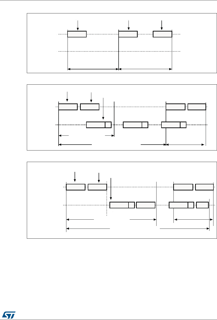
RM0430 Rev 8 1027/1324
RM0430 Secure digital input/output interface (SDIO)
1084
Figure 364. “No response” and “no data” operations
Figure 365. (Multiple) block read operation
Figure 366. (Multiple) block write operation
Note: The SDIO will not send any data as long as the Busy signal is asserted (SDIO_D0 pulled
low).
06Y9
2SHUDWLRQQRUHVSRQVH 2SHUDWLRQQRGDWD
6',2B&0'
6',2B'
)URPKRVWWRFDUGV )URPKRVWWRFDUG )URPFDUGWRKRVW
5HVSRQVH&RPPDQG &RPPDQG
06Y9
&RPPDQG 5HVSRQVH
'DWDEORFN FUF 'DWDEORFN FUF 'DWDEORFN FUF
%ORFNUHDGRSHUDWLRQ
0XOWLSOHEORFNUHDGRSHUDWLRQ 'DWDVWRSRSHUDWLRQ
)URPKRVWWRFDUG )URPFDUGWRKRVW
GDWDIURPFDUGWRKRVW 6WRSFRPPDQG
VWRSVGDWDWUDQVIHU
&RPPDQG 5HVSRQVH
6',2B&0'
6',2B'
06Y9
&RPPDQG 5HVSRQVH
'DWDEORFN FUF 'DWDEORFN FUF
'DWDVWRSRSHUDWLRQ
)URPKRVWWRFDUG )URPFDUGWRKRVW
GDWDIURPKRVWWRFDUG 6WRSFRPPDQG
VWRSVGDWDWUDQVIHU
&RPPDQG 5HVSRQVH
6',2B&0'
6',2B' %XV\
%ORFNZULWHRSHUDWLRQ
%XV\
0XOWLSOHEORFNZULWHRSHUDWLRQ
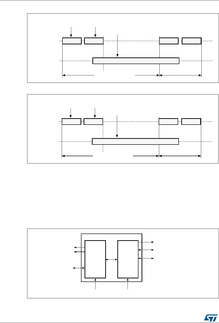
Secure digital input/output interface (SDIO) RM0430
1028/1324 RM0430 Rev 8
Figure 367. Sequential read operation
Figure 368. Sequential write operation
31.3 SDIO functional description
The SDIO consists of two parts:
•The SDIO adapter block provides all functions specific to the MMC/SD/SD I/O card
such as the clock generation unit, command and data transfer.
•The APB2 interface accesses the SDIO adapter registers, and generates interrupt and
DMA request signals.
Figure 369. SDIO block diagram
06Y9
'DWDVWRSRSHUDWLRQ
)URPFDUGWRKRVW 6WRSFRPPDQG
VWRSVGDWDWUDQVIHU
&RPPDQG 5HVSRQVH &RPPDQG 5HVSRQVH
'DWDVWUHDP
'DWDWUDQVIHURSHUDWLRQ
)URPKRVWWR
FDUGV
'DWDIURPFDUGWRKRVW
6',2B&0'
6',2B'
06Y9
'DWDVWRSRSHUDWLRQ
)URPFDUGWRKRVW 6WRSFRPPDQG
VWRSVGDWDWUDQVIHU
5HVSRQVH&RPPDQG 5HVSRQVH&RPPDQG
'DWDVWUHDP
'DWDWUDQVIHURSHUDWLRQ
)URPKRVWWR
FDUGV
'DWDIURPKRVWWRFDUG
6',2B&0'
6',2B'
06Y9
$3%EXV
$3%
,QWHUUXSWVDQG
3&/.
6',2B&.
LQWHUIDFH
'0$UHTXHVW
6',2&/.
6',2B'>@
6',2B&0'
6',2
6',2
DGDSWHU

RM0430 Rev 8 1029/1324
RM0430 Secure digital input/output interface (SDIO)
1084
By default SDIO_D0 is used for data transfer. After initialization, the host can change the
databus width.
If a MultiMediaCard is connected to the bus, SDIO_D0, SDIO_D[3:0] or SDIO_D[7:0] can be
used for data transfer. MMC V3.31 or previous, supports only 1 bit of data so only SDIO_D0
can be used.
If an SD or SD I/O card is connected to the bus, data transfer can be configured by the host
to use SDIO_D0 or SDIO_D[3:0]. All data lines are operating in push-pull mode.
SDIO_CMD has two operational modes:
•Open-drain for initialization (only for MMCV3.31 or previous)
•Push-pull for command transfer (SD/SD I/O card MMC4.2 use push-pull drivers also for
initialization)
SDIO_CK is the clock to the card: one bit is transferred on both command and data lines
with each clock cycle.
The SDIO uses two clock signals:
•SDIO adapter clock SDIOCLK = 50 MHz)
•APB2 bus clock (PCLK2)
PCLK2 and SDIO_CK clock frequencies must respect the following condition:
The signals shown in Table 182 are used on the MultiMediaCard/SD/SD I/O card bus.
Table 182. SDIO I/O definitions
Pin Direction Description
SDIO_CK Output MultiMediaCard/SD/SDIO card clock. This pin is the clock from
host to card.
SDIO_CMD Bidirectional MultiMediaCard/SD/SDIO card command. This pin is the
bidirectional command/response signal.
SDIO_D[7:0] Bidirectional MultiMediaCard/SD/SDIO card data. These pins are the
bidirectional databus.
Frequenc PCLK2()3xWidth()32⁄()Frequency SDIO_CK()×>
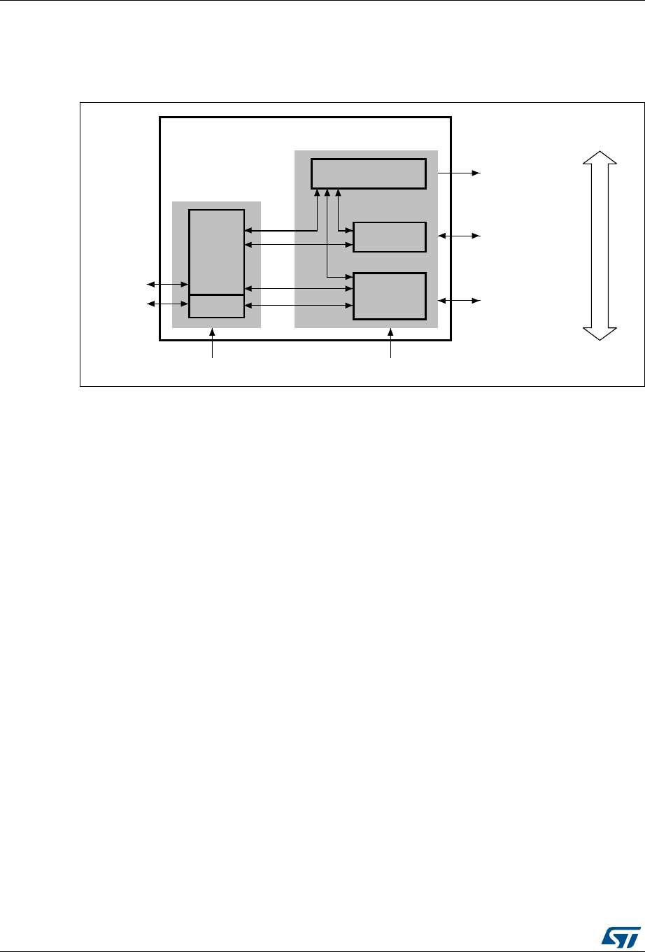
Secure digital input/output interface (SDIO) RM0430
1030/1324 RM0430 Rev 8
31.3.1 SDIO adapter
Figure 370 shows a simplified block diagram of an SDIO adapter.
Figure 370. SDIO adapter
The SDIO adapter is a multimedia/secure digital memory card bus master that provides an
interface to a multimedia card stack or to a secure digital memory card. It consists of five
subunits:
•Adapter register block
•Control unit
•Command path
•Data path
•Data FIFO
Note: The adapter registers and FIFO use the APB2 bus clock domain (PCLK2). The control unit,
command path and data path use the SDIO adapter clock domain (SDIOCLK).
Adapter register block
The adapter register block contains all system registers. This block also generates the
signals that clear the static flags in the multimedia card. The clear signals are generated
when 1 is written into the corresponding bit location in the SDIO Clear register.
Control unit
The control unit contains the power management functions and the clock divider for the
memory card clock.
There are three power phases:
•power-off
•power-up
•power-on
06Y9
7R$3%
LQWHUIDFH
&RQWUROXQLW
&RPPDQG
SDWK
'DWDSDWK
$GDSWHU
UHJLVWHUV
6',2B&.
6',2B&0'
6',2B'>@
6',2DGDSWHU
3&/. 6',2&/.
),)2
&DUGEXV
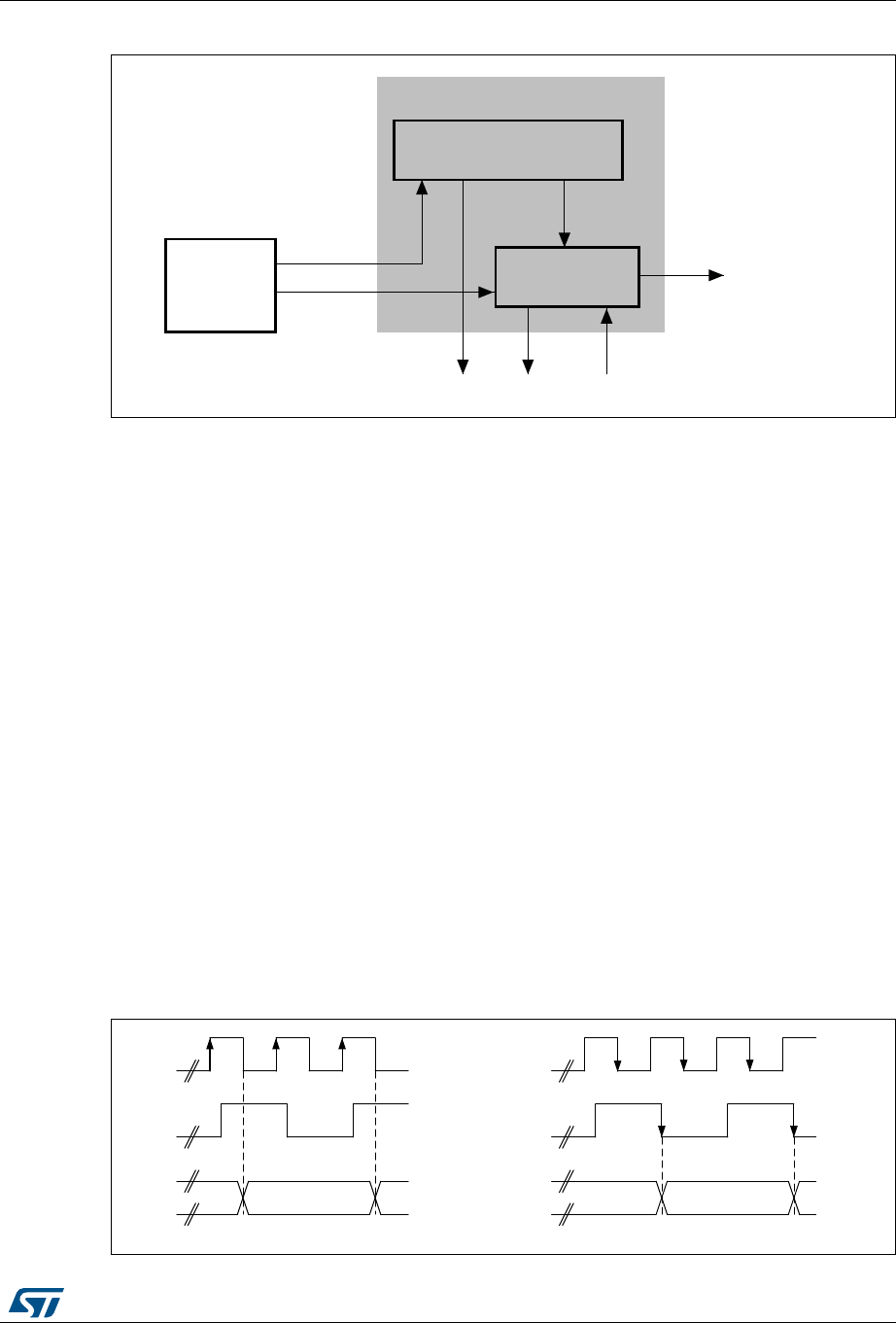
RM0430 Rev 8 1031/1324
RM0430 Secure digital input/output interface (SDIO)
1084
Figure 371. Control unit
The control unit is illustrated in Figure 371. It consists of a power management subunit and
a clock management subunit.
The power management subunit disables the card bus output signals during the power-off
and power-up phases.
The clock management subunit generates and controls the SDIO_CK signal. The SDIO_CK
output can use either the clock divide or the clock bypass mode. The clock output is
inactive:
•after reset
•during the power-off or power-up phases
•if the power saving mode is enabled and the card bus is in the Idle state (eight clock
periods after both the command and data path subunits enter the Idle phase)
The clock management subunit controls SDIO_CK dephasing. When not in bypass mode
the SDIO command and data output are generated on the SDIOCLK falling edge
succeeding the rising edge of SDIO_CK. (SDIO_CK rising edge occurs on SDIOCLK rising
edge) when SDIO_CLKCR[13] bit is reset (NEGEDGE = 0). When SDIO_CLKCR[13] bit is
set (NEGEDGE = 1) SDIO command and data changed on the SDIO_CK falling edge.
When SDIO_CLKCR[10] is set (BYPASS = 1), SDIO_CK rising edge occurs on SDIOCLK
rising edge. The data and the command change on SDIOCLK falling edge whatever
NEGEDGE value.
The data and command responses are latched using SDIO_CK rising edge.
Figure 372. SDIO_CK clock dephasing (BYPASS = 0)
06Y9
&RQWUROXQLW
3RZHUPDQDJHPHQW
&ORFNPDQDJHPHQW
$GDSWHU
UHJLVWHUV
6',2B&.
7RFRPPDQGDQGGDWDSDWK
06Y9
6',2&/.
6',2B&.
1(*('*( 1(*('*(
&0''DWD
RXWSXW
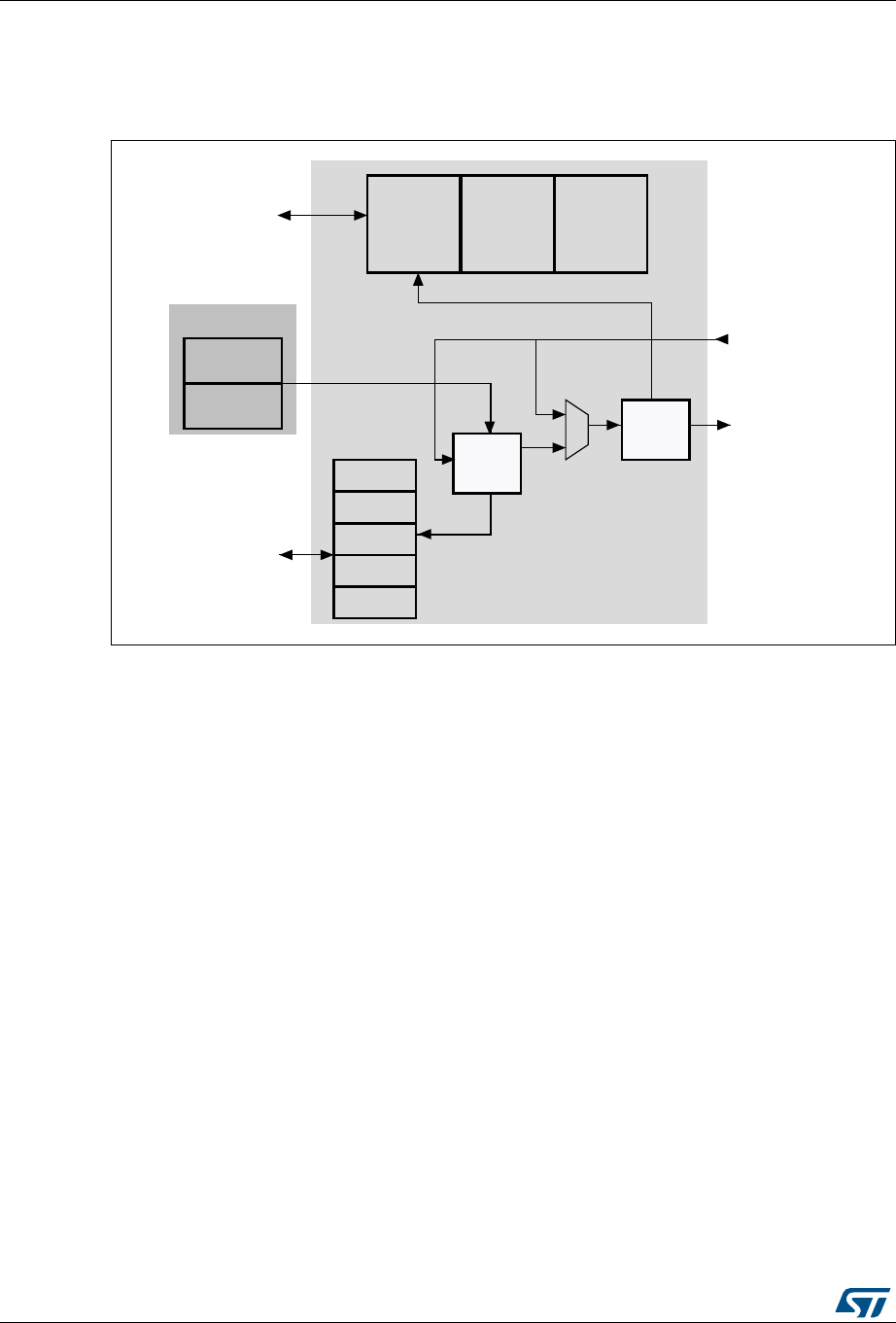
Secure digital input/output interface (SDIO) RM0430
1032/1324 RM0430 Rev 8
Command path
The command path unit sends commands to and receives responses from the cards.
Figure 373. SDIO adapter command path
•Command path state machine (CPSM)
– When the command register is written to and the enable bit is set, command
transfer starts. When the command has been sent, the command path state
machine (CPSM) sets the status flags and enters the Idle state if a response is not
required. If a response is required, it waits for the response (see Figure 374 on
page 1033). When the response is received, the received CRC code and the
internally generated code are compared, and the appropriate status flags are set.
06Y9
$GDSWHUUHJLVWHUV
&0'
6WDWXV
IODJ
&5&
6KLIW
UHJLVWHU
&0'
7RFRQWUROXQLW
6',2B&0'LQ
6',2B&0'RXW
7R$3%LQWHUIDFH
&RQWURO
ORJLF
&RPPDQG
WLPHU
$UJXPHQW
5HVSRQVH
UHJLVWHUV
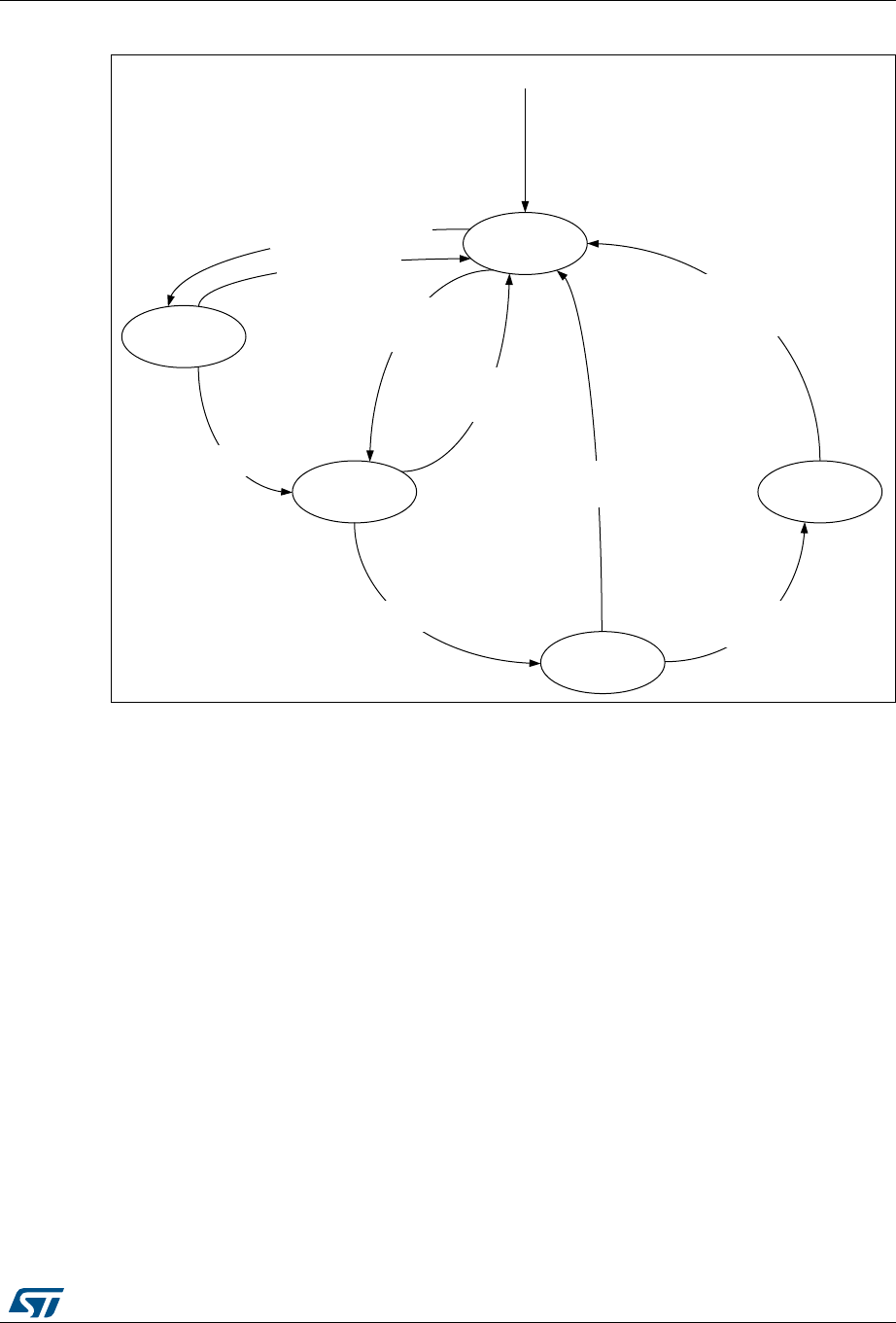
RM0430 Rev 8 1033/1324
RM0430 Secure digital input/output interface (SDIO)
1084
Figure 374. Command path state machine (SDIO)
When the Wait state is entered, the command timer starts running. If the timeout is reached
before the CPSM moves to the Receive state, the timeout flag is set and the Idle state is
entered.
Note: The command timeout has a fixed value of 64 SDIO_CK clock periods.
If the interrupt bit is set in the command register, the timer is disabled and the CPSM waits
for an interrupt request from one of the cards. If a pending bit is set in the command register,
the CPSM enters the Pend state, and waits for a CmdPend signal from the data path
subunit. When CmdPend is detected, the CPSM moves to the Send state. This enables the
data counter to trigger the stop command transmission.
Note: The CPSM remains in the Idle state for at least eight SDIO_CK periods to meet the NCC and
NRC timing constraints. NCC is the minimum delay between two host commands, and NRC is
the minimum delay between the host command and the card response.
069
,GOH
5HFHLYH
3HQG
6HQG
:DLW
5HVSRQVHUHFHLYHGRU
GLVDEOHGRUFRPPDQG
&5&IDLOHG
5HVSRQVH
VWDUWHG
&360GLVDEOHG
RUQRUHVSRQVH
(QDEOHGDQG
FRPPDQGVWDUW
&360HQDEOHGDQG
SHQGLQJFRPPDQG
/DVWGDWD
2QUHVHW
:DLWIRUUHVSRQVH
&360GLVDEOHGRU
FRPPDQGWLPHRXW
&360GLVDEOHG
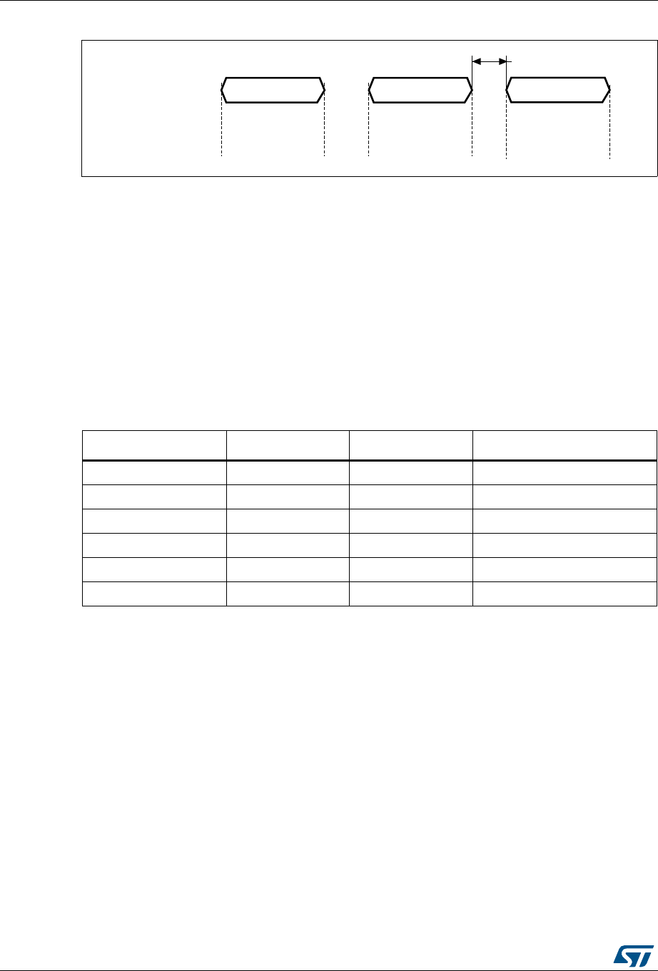
Secure digital input/output interface (SDIO) RM0430
1034/1324 RM0430 Rev 8
Figure 375. SDIO command transfer
•Command format
– Command: a command is a token that starts an operation. Command are sent
from the host either to a single card (addressed command) or to all connected
cards (broadcast command are available for MMC V3.31 or previous). Commands
are transferred serially on the CMD line. All commands have a fixed length of 48
bits. The general format for a command token for MultiMediaCards, SD-Memory
cards and SDIO-Cards is shown in Table 183.
The command path operates in a half-duplex mode, so that commands and
responses can either be sent or received. If the CPSM is not in the Send state, the
SDIO_CMD output is in the Hi-Z state, as shown in Figure 375 on page 1034.
Data on SDIO_CMD are synchronous with the rising edge of SDIO_CK. Table 183
shows the command format.
– Response: a response is a token that is sent from an addressed card (or
synchronously from all connected cards for MMC V3.31 or previous), to the host
as an answer to a previously received command. Responses are transferred
serially on the CMD line.
The SDIO supports two response types. Both use CRC error checking:
•48 bit short response
•136 bit long response
Note: If the response does not contain a CRC (CMD1 response), the device driver must ignore the
CRC failed status.
Table 183. Command format
Bit position Width Value Description
47 1 0 Start bit
46 1 1 Transmission bit
[45:40] 6 - Command index
[39:8] 32 - Argument
[7:1] 7 - CRC7
011End bit
06Y9
6',2B&.
6',2B&0'
&RPPDQG 5HVSRQVH &RPPDQG
6WDWH ,GOH 6HQG :DLW 5HFHLYH ,GOH 6HQG
+L= &RQWUROOHUGULYHV +L= &DUGGULYHV +L= &RQWUROOHUGULYHV
DWOHDVW6',2B&.F\FOHV
RM0430 Rev 8 1035/1324
RM0430 Secure digital input/output interface (SDIO)
1084
The command register contains the command index (six bits sent to a card) and the
command type. These determine whether the command requires a response, and whether
the response is 48 or 136 bits long (see Section 31.8.4 on page 1070). The command path
implements the status flags shown in Table 186:
The CRC generator calculates the CRC checksum for all bits before the CRC code. This
includes the start bit, transmitter bit, command index, and command argument (or card
status). The CRC checksum is calculated for the first 120 bits of CID or CSD for the long
response format. Note that the start bit, transmitter bit and the six reserved bits are not used
in the CRC calculation.
The CRC checksum is a 7-bit value:
CRC[6:0] = Remainder [(M(x) * x7) / G(x)]
G(x) = x7 + x3 + 1
M(x) = (start bit) * x39 + ... + (last bit before CRC) * x0, or
M(x) = (start bit) * x119 + ... + (last bit before CRC) * x0
Table 184. Short response format
Bit position Width Value Description
47 1 0 Start bit
46 1 0 Transmission bit
[45:40] 6 - Command index
[39:8] 32 - Argument
[7:1] 7 - CRC7(or 1111111)
011End bit
Table 185. Long response format
Bit position Width Value Description
135 1 0 Start bit
134 1 0 Transmission bit
[133:128] 6 111111 Reserved
[127:1] 127 - CID or CSD (including internal CRC7)
0 1 1 End bit
Table 186. Command path status flags
Flag Description
CMDREND Set if response CRC is OK.
CCRCFAIL Set if response CRC fails.
CMDSENT Set when command (that does not require response) is sent
CTIMEOUT Response timeout.
CMDACT Command transfer in progress.
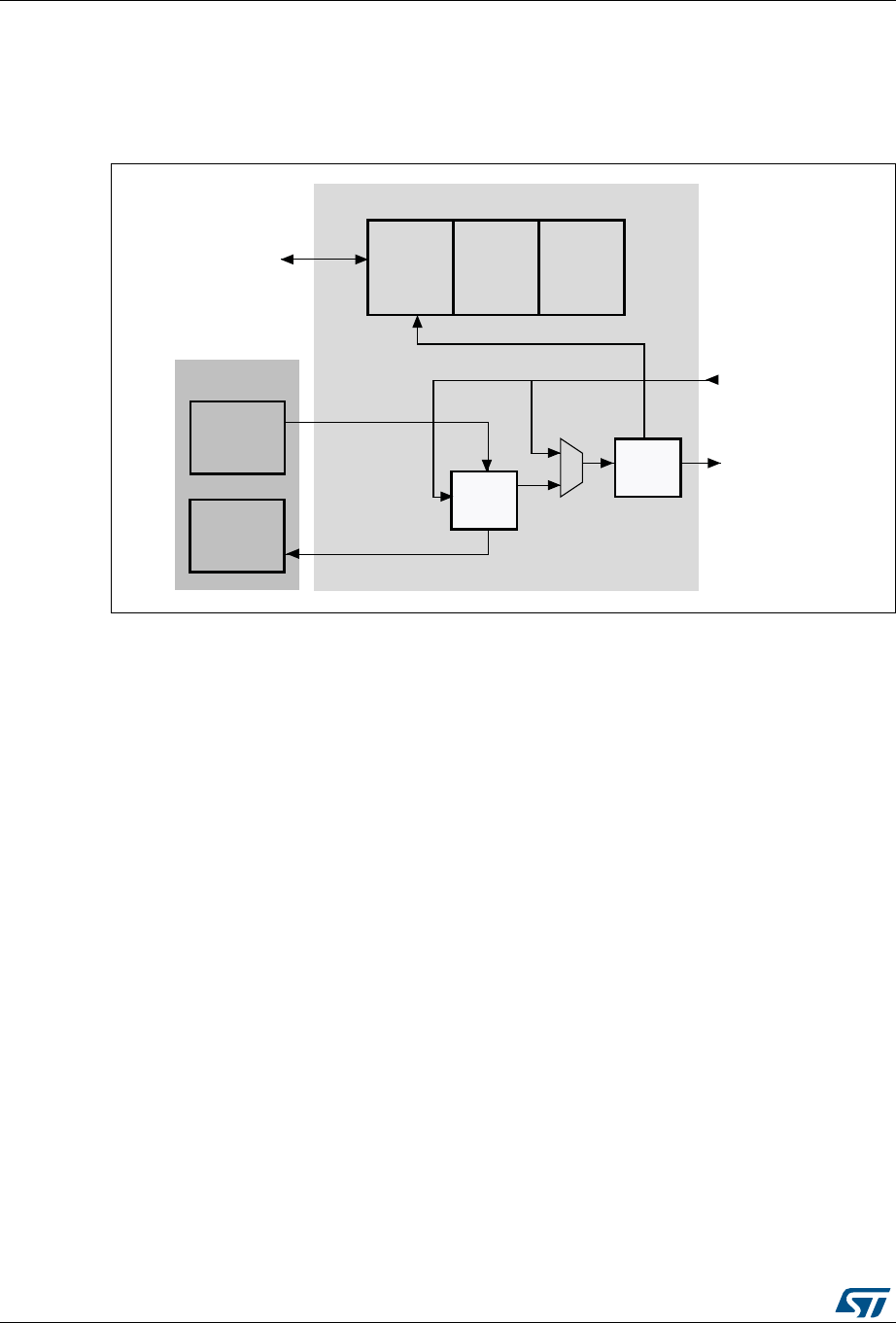
Secure digital input/output interface (SDIO) RM0430
1036/1324 RM0430 Rev 8
Data path
The data path subunit transfers data to and from cards. Figure 376 shows a block diagram
of the data path.
Figure 376. Data path
The card databus width can be programmed using the clock control register. If the 4-bit wide
bus mode is enabled, data is transferred at four bits per clock cycle over all four data signals
(SDIO_D[3:0]). If the 8-bit wide bus mode is enabled, data is transferred at eight bits per
clock cycle over all eight data signals (SDIO_D[7:0]). If the wide bus mode is not enabled,
only one bit per clock cycle is transferred over SDIO_D0.
Depending on the transfer direction (send or receive), the data path state machine (DPSM)
moves to the Wait_S or Wait_R state when it is enabled:
•Send: the DPSM moves to the Wait_S state. If there is data in the transmit FIFO, the
DPSM moves to the Send state, and the data path subunit starts sending data to a
card.
•Receive: the DPSM moves to the Wait_R state and waits for a start bit. When it
receives a start bit, the DPSM moves to the Receive state, and the data path subunit
starts receiving data from a card.
Data path state machine (DPSM)
The DPSM operates at SDIO_CK frequency. Data on the card bus signals is synchronous to
the rising edge of SDIO_CK. The DPSM has six states, as shown in Figure 377: Data path
state machine (DPSM).
06Y9
'DWDSDWK
'DWD),)2
7UDQVPLW
6WDWXV
IODJ
&5&
6KLIW
UHJLVWHU
7RFRQWUROXQLW
6',2B'LQ>@
6',2B'RXW>@
5HFHLYH
&RQWURO
ORJLF
'DWD
WLPHU
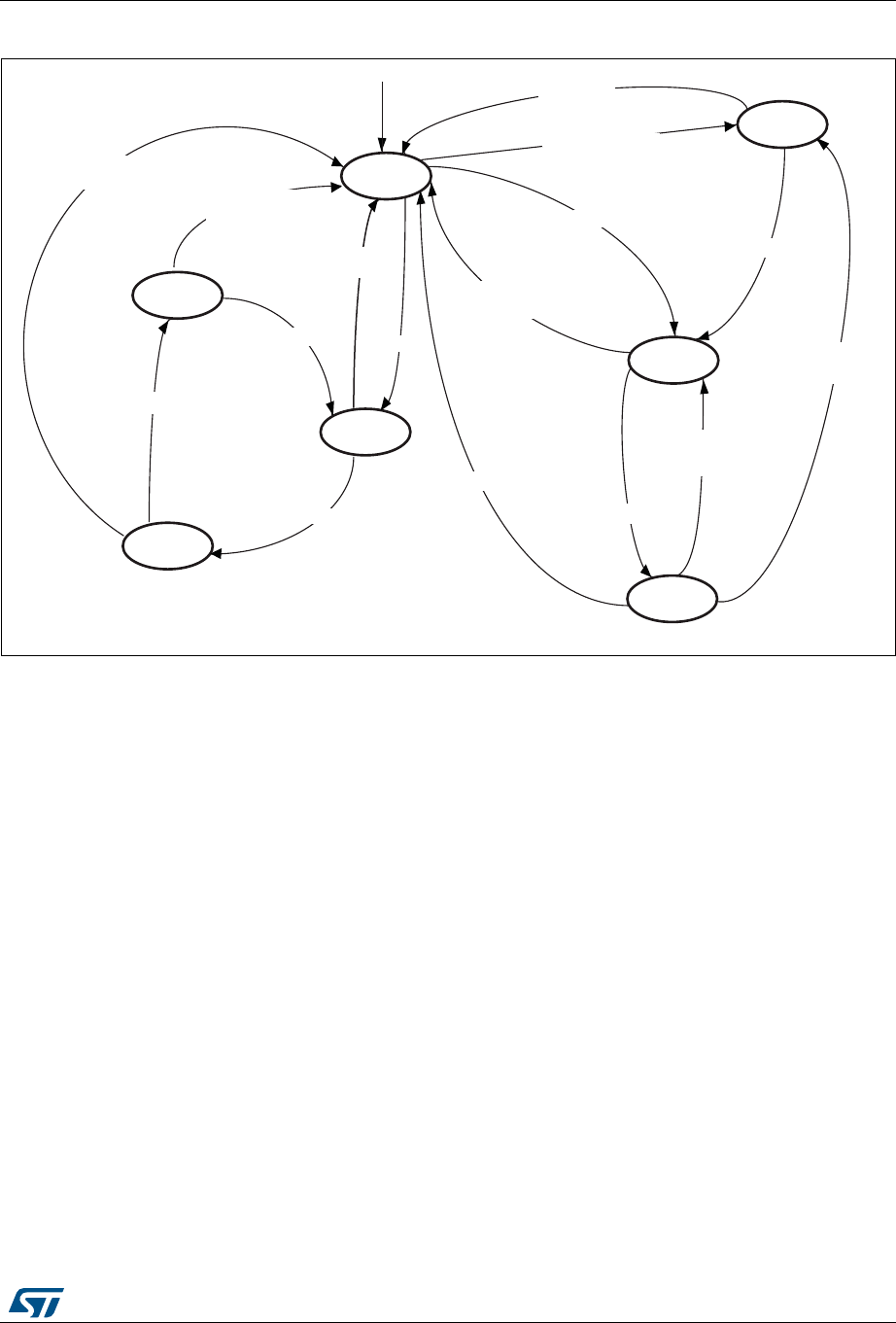
RM0430 Rev 8 1037/1324
RM0430 Secure digital input/output interface (SDIO)
1084
Figure 377. Data path state machine (DPSM)
•Idle: the data path is inactive, and the SDIO_D[7:0] outputs are in Hi-Z. When the data
control register is written and the enable bit is set, the DPSM loads the data counter
with a new value and, depending on the data direction bit, moves to either the Wait_S
or the Wait_R state.
•Wait_R: if the data counter equals zero, the DPSM moves to the Idle state when the
receive FIFO is empty. If the data counter is not zero, the DPSM waits for a start bit on
SDIO_D. The DPSM moves to the Receive state if it receives a start bit before a
timeout, and loads the data block counter. If it reaches a timeout before it detects a
start bit, it moves to the Idle state and sets the timeout status flag.
•Receive: serial data received from a card is packed in bytes and written to the data
FIFO. Depending on the transfer mode bit in the data control register, the data transfer
mode can be either block or stream:
– In block mode, when the data block counter reaches zero, the DPSM waits until it
receives the CRC code. If the received code matches the internally generated
CRC code, the DPSM moves to the Wait_R state. If not, the CRC fail status flag is
set and the DPSM moves to the Idle state.
– In stream mode, the DPSM receives data while the data counter is not zero. When
the counter is zero, the remaining data in the shift register is written to the data
FIFO, and the DPSM moves to the Wait_R state.
If a FIFO overrun error occurs, the DPSM sets the FIFO error flag and moves to the
Idle state:
•Wait_S: the DPSM moves to the Idle state if the data counter is zero. If not, it waits until
the data FIFO empty flag is deasserted, and moves to the Send state.
)DLE
"USY
3END
7AIT?2
2ECEIVE
%NDOFPACKET
$ISABLEDOR#2#FAIL
ORTIMEOUT
.OTBUSY
$ISABLEDOR
ENDOFDATA
$ATAREADY
%NDOFPACKETOR
ENDOFDATAOR
&)&/OVERRUN
%NABLEANDNOTSEND
$ISABLEDOR
2X&)&/EMPTYORTIMEOUTOR
STARTBITERROR
$ISABLEDOR&)&/UNDERRUNOR
ENDOFDATAOR#2#FAIL
AIB
7AIT?3
3TARTBIT
/NRESET
$ISABLEDOR#2#FAIL
%NABLEANDSEND
$03-DISABLED
2EAD7AIT
$03-ENABLEDAND
2EAD7AIT3TARTED
AND3$)/MODEENABLED
2EAD7AIT3TOP
$ATARECEIVEDAND
2EAD7AIT3TARTEDAND
3$)/MODEENABLED

Secure digital input/output interface (SDIO) RM0430
1038/1324 RM0430 Rev 8
Note: The DPSM remains in the Wait_S state for at least two clock periods to meet the NWR timing
requirements, where NWR is the number of clock cycles between the reception of the card
response and the start of the data transfer from the host.
•Send: the DPSM starts sending data to a card. Depending on the transfer mode bit in
the data control register, the data transfer mode can be either block or stream:
– In block mode, when the data block counter reaches zero, the DPSM sends an
internally generated CRC code and end bit, and moves to the Busy state.
– In stream mode, the DPSM sends data to a card while the enable bit is high and
the data counter is not zero. It then moves to the Idle state.
If a FIFO underrun error occurs, the DPSM sets the FIFO error flag and moves to the
Idle state.
•Busy: the DPSM waits for the CRC status flag:
– If it does not receive a positive CRC status, it moves to the Idle state and sets the
CRC fail status flag.
– If it receives a positive CRC status, it moves to the Wait_S state if SDIO_D0 is not
low (the card is not busy).
If a timeout occurs while the DPSM is in the Busy state, it sets the data timeout flag and
moves to the Idle state.
The data timer is enabled when the DPSM is in the Wait_R or Busy state, and
generates the data timeout error:
– When transmitting data, the timeout occurs if the DPSM stays in the Busy state for
longer than the programmed timeout period
– When receiving data, the timeout occurs if the end of the data is not true, and if the
DPSM stays in the Wait_R state for longer than the programmed timeout period.
•Data: data can be transferred from the card to the host or vice versa. Data is
transferred via the data lines. They are stored in a FIFO of 32 words, each word is 32
bits wide.
Table 187. Data token format
Description Start bit Data CRC16 End bit
Block Data 0 - yes 1
Stream Data 0 - no 1

RM0430 Rev 8 1039/1324
RM0430 Secure digital input/output interface (SDIO)
1084
DPSM Flags
The status of the data path subunit transfer is reported by several status flags
Table 188. DPSM flags
Data FIFO
The data FIFO (first-in-first-out) subunit is a data buffer with a transmit and receive unit.
The FIFO contains a 32-bit wide, 32-word deep data buffer, and transmit and receive logic.
Because the data FIFO operates in the APB2 clock domain (PCLK2), all signals from the
subunits in the SDIO clock domain (SDIOCLK) are resynchronized.
Depending on the TXACT and RXACT flags, the FIFO can be disabled, transmit enabled, or
receive enabled. TXACT and RXACT are driven by the data path subunit and are mutually
exclusive:
– The transmit FIFO refers to the transmit logic and data buffer when TXACT is
asserted
– The receive FIFO refers to the receive logic and data buffer when RXACT is
asserted
•Transmit FIFO:
Data can be written to the transmit FIFO through the APB2 interface when the SDIO is
enabled for transmission.
The transmit FIFO is accessible via 32 sequential addresses. The transmit FIFO
contains a data output register that holds the data word pointed to by the read pointer.
When the data path subunit has loaded its shift register, it increments the read pointer
and drives new data out.
If the transmit FIFO is disabled, all status flags are deasserted. The data path subunit
asserts TXACT when it transmits data.
Flag Description
DBCKEND
Set to high when data block send/receive CRC check is passed.
In SDIO multibyte transfer mode this flag is set at the end of the transfer (a
multibyte transfer is considered as a single block transfer by the host).
DATAEND Set to high when SDIO_DCOUNT register decrements and reaches 0.
DATAEND indicates the end of a transfer on SDIO data line.
DTIMEOUT
Set to high when data timeout period is reached.
When data timer reaches zero while DPSM is in Wait_R or Busy state, timeout is
set. DTIMEOUT can be set after DATAEND if DPSM remains in busy state for
longer than the programmed period.
DCRCFAIL Set to high when data block send/receive CRC check fails.

Secure digital input/output interface (SDIO) RM0430
1040/1324 RM0430 Rev 8
•Receive FIFO
When the data path subunit receives a word of data, it drives the data on the write
databus. The write pointer is incremented after the write operation completes. On the
read side, the contents of the FIFO word pointed to by the current value of the read
pointer is driven onto the read databus. If the receive FIFO is disabled, all status flags
are deasserted, and the read and write pointers are reset. The data path subunit
asserts RXACT when it receives data. Table 190 lists the receive FIFO status flags.
The receive FIFO is accessible via 32 sequential addresses.
Table 189. Transmit FIFO status flags
Flag Description
TXFIFOF Set to high when all 32 transmit FIFO words contain valid data.
TXFIFOE Set to high when the transmit FIFO does not contain valid data.
TXFIFOHE Set to high when 8 or more transmit FIFO words are empty. This flag can be used
as a DMA request.
TXDAVL Set to high when the transmit FIFO contains valid data. This flag is the inverse of
the TXFIFOE flag.
TXUNDERR
Set to high when an underrun error occurs. This flag is cleared by writing to the
SDIO Clear register.
Note: In case of TXUNDERR, and DMA is used to fill SDIO FIFO, user software
should disable DMA stream, and then write DMAEN bit in SDIO_DCTRL
with ‘0’ (to disable DMA request generation).
Table 190. Receive FIFO status flags
Flag Description
RXFIFOF Set to high when all 32 receive FIFO words contain valid data
RXFIFOE Set to high when the receive FIFO does not contain valid data.
RXFIFOHF Set to high when 8 or more receive FIFO words contain valid data. This flag can be
used as a DMA request.
RXDAVL Set to high when the receive FIFO is not empty. This flag is the inverse of the
RXFIFOE flag.
RXOVERR
Set to high when an overrun error occurs. This flag is cleared by writing to the SDIO
Clear register.
Note: In case of RXOVERR, and DMA is used to read SDIO FIFO, user software
should disable DMA stream, and then write DMAEN bit in SDIO_DCTRL
with ‘0’ (to disable DMA request generation).

RM0430 Rev 8 1041/1324
RM0430 Secure digital input/output interface (SDIO)
1084
31.3.2 SDIO APB2 interface
The APB2 interface generates the interrupt and DMA requests, and accesses the SDIO
adapter registers and the data FIFO. It consists of a data path, register decoder, and
interrupt/DMA logic.
SDIO interrupts
The interrupt logic generates an interrupt request signal that is asserted when at least one
of the selected status flags is high. A mask register is provided to allow selection of the
conditions that will generate an interrupt. A status flag generates the interrupt request if a
corresponding mask flag is set.
SDIO/DMA interface
SDIO APB interface controls all subunit to perform transfers between the host and card
Example of read procedure using DMA
Send CMD17 (READ_BLOCK) as follows:
a) Program the SDIO data length register (SDIO data timer register should be
already programmed before the card identification process)
b) Program DMA channel (refer to DMA configuration for SDIO controller)
c) Program the SDIO data control register: DTEN with ‘1’ (SDIO card host enabled to
send data); DTDIR with ‘1’ (from card to controller); DTMODE with ‘0’ (block data
transfer); DMAEN with ‘1’ (DMA enabled); DBLOCKSIZE with 0x9 (512 bytes).
Other fields are don’t care.
d) Program the SDIO argument register with the address location of the card from
where data is to be transferred
e) Program the SDIO command register: CmdIndex with 17(READ_BLOCK);
WaitResp with ‘1’ (SDIO card host waits for a response); CPSMEN with ‘1’ (SDIO
card host enabled to send a command). Other fields are at their reset value.
f) Wait for SDIO_STA[6] = CMDREND interrupt, (CMDREND is set if there is no
error on command path).
g) Wait for SDIO_STA[10] = DBCKEND, (DBCKEND is set in case of no errors until
the CRC check is passed)
h) Wait until the FIFO is empty, when FIFO is empty the SDIO_STA[5] = RXOVERR
value has to be check to guarantee that read succeeded
Note: When FIFO overrun error occurs with last 1-4 bytes, it may happens that RXOVERR flag is
set 2 APB clock cycles after DATAEND flag is set. To guarantee success of read operation
RXOVERR must be cheked after FIFO is empty.

Secure digital input/output interface (SDIO) RM0430
1042/1324 RM0430 Rev 8
Example of write procedure using DMA
Send CMD24 (WRITE_BLOCK) as follows:
a) Program the SDIO data length register (SDIO data timer register should be
already programmed before the card identification process)
b) Program DMA channel (refer to DMA configuration for SDIO controller)
c) Program the SDIO argument register with the address location of the card from
where data is to be transferred
d) Program the SDIO command register: CmdIndex with 24(WRITE_BLOCK);
WaitResp with ‘1’ (SDIO card host waits for a response); CPSMEN with ‘1’ (SDIO
card host enabled to send a command). Other fields are at their reset value.
e) Wait for SDIO_STA[6] = CMDREND interrupt, then Program the SDIO data control
register: DTEN with ‘1’ (SDIO card host enabled to send data); DTDIR with ‘0’
(from controller to card); DTMODE with ‘0’ (block data transfer); DMAEN with ‘1’
(DMA enabled); DBLOCKSIZE with 0x9 (512 bytes). Other fields are don’t care.
f) Wait for SDIO_STA[10] = DBCKEND, (DBCKEND is set in case of no errors)
DMA configuration for SDIO controller
a) Enable DMA2 controller and clear any pending interrupts.
b) Program the DMA2_Stream3 (or DMA2_Stream6) Channel4 source address
register with the memory location base address and DMA2_Stream3 (or
DMA2_Stream6) Channel4 destination address register with the SDIO_FIFO
register address.
c) Program DMA2_Stream3 (or DMA2_Stream6) Channel4 control register (memory
increment, not peripheral increment, peripheral and source width is word size).
d) Program DMA2_Stream3 (or DMA2_Stream6) Channel4 to select the peripheral
as flow controller (set PFCTRL bit in DMA_S3CR (or DMA_S6CR) configuration
register).
e) Configure the incremental burst transfer to 4 beats (at least from peripheral side)
in DMA2_Stream3 (or DMA2_Stream6) Channel4.
f) Enable DMA2_Stream3 (or DMA2_Stream6) Channel4
Note: SDIO host allows only to use the DMA in peripheral flow controller mode. DMA stream used
to serve SDIO must be configured in peripheral flow controller mode
SDIO generates only DMA burst requests to DMA controller. DMA must be configured in
incremental burst mode on peripheral side.
31.4 Card functional description
31.4.1 Card identification mode
While in card identification mode the host resets all cards, validates the operation voltage
range, identifies cards and sets a relative card address (RCA) for each card on the bus. All
data communications in the card identification mode use the command line (CMD) only.

RM0430 Rev 8 1043/1324
RM0430 Secure digital input/output interface (SDIO)
1084
31.4.2 Card reset
The GO_IDLE_STATE command (CMD0) is the software reset command and it puts the
MultiMediaCard and SD memory in the Idle state. The IO_RW_DIRECT command (CMD52)
resets the SD I/O card. After power-up or CMD0, all cards output bus drivers are in the high-
impedance state and the cards are initialized with a default relative card address
(RCA=0x0001) and with a default driver stage register setting (lowest speed, highest driving
current capability).
31.4.3 Operating voltage range validation
All cards can communicate with the SDIO card host using any operating voltage within the
specification range. The supported minimum and maximum VDD values are defined in the
operation conditions register (OCR) on the card.
Cards that store the card identification number (CID) and card specific data (CSD) in the
payload memory are able to communicate this information only under data-transfer VDD
conditions. When the SDIO card host module and the card have incompatible VDD ranges,
the card is not able to complete the identification cycle and cannot send CSD data. For this
purpose, the special commands, SEND_OP_COND (CMD1), SD_APP_OP_COND
(ACMD41 for SD Memory), and IO_SEND_OP_COND (CMD5 for SD I/O), are designed to
provide a mechanism to identify and reject cards that do not match the VDD range desired
by the SDIO card host. The SDIO card host sends the required VDD voltage window as the
operand of these commands. Cards that cannot perform data transfer in the specified range
disconnect from the bus and go to the inactive state.
By using these commands without including the voltage range as the operand, the SDIO
card host can query each card and determine the common voltage range before placing out-
of-range cards in the inactive state. This query is used when the SDIO card host is able to
select a common voltage range or when the user requires notification that cards are not
usable.
31.4.4 Card identification process
The card identification process differs for MultiMediaCards and SD cards. For
MultiMediaCard cards, the identification process starts at clock rate Fod. The SDIO_CMD
line output drivers are open-drain and allow parallel card operation during this process. The
registration process is accomplished as follows:
1. The bus is activated.
2. The SDIO card host broadcasts SEND_OP_COND (CMD1) to receive operation
conditions.
3. The response is the wired AND operation of the operation condition registers from all
cards.
4. Incompatible cards are placed in the inactive state.
5. The SDIO card host broadcasts ALL_SEND_CID (CMD2) to all active cards.
6. The active cards simultaneously send their CID numbers serially. Cards with outgoing
CID bits that do not match the bits on the command line stop transmitting and must wait
for the next identification cycle. One card successfully transmits a full CID to the SDIO
card host and enters the Identification state.
7. The SDIO card host issues SET_RELATIVE_ADDR (CMD3) to that card. This new
address is called the relative card address (RCA); it is shorter than the CID and

Secure digital input/output interface (SDIO) RM0430
1044/1324 RM0430 Rev 8
addresses the card. The assigned card changes to the Standby state, it does not react
to further identification cycles, and its output switches from open-drain to push-pull.
8. The SDIO card host repeats steps 5 through 7 until it receives a timeout condition.
For the SD card, the identification process starts at clock rate Fod, and the SDIO_CMD line
output drives are push-pull drivers instead of open-drain. The registration process is
accomplished as follows:
1. The bus is activated.
2. The SDIO card host broadcasts SD_APP_OP_COND (ACMD41).
3. The cards respond with the contents of their operation condition registers.
4. The incompatible cards are placed in the inactive state.
5. The SDIO card host broadcasts ALL_SEND_CID (CMD2) to all active cards.
6. The cards send back their unique card identification numbers (CIDs) and enter the
Identification state.
7. The SDIO card host issues SET_RELATIVE_ADDR (CMD3) to an active card with an
address. This new address is called the relative card address (RCA); it is shorter than
the CID and addresses the card. The assigned card changes to the Standby state. The
SDIO card host can reissue this command to change the RCA. The RCA of the card is
the last assigned value.
8. The SDIO card host repeats steps 5 through 7 with all active cards.
For the SD I/O card, the registration process is accomplished as follows:
1. The bus is activated.
2. The SDIO card host sends IO_SEND_OP_COND (CMD5).
3. The cards respond with the contents of their operation condition registers.
4. The incompatible cards are set to the inactive state.
5. The SDIO card host issues SET_RELATIVE_ADDR (CMD3) to an active card with an
address. This new address is called the relative card address (RCA); it is shorter than
the CID and addresses the card. The assigned card changes to the Standby state. The
SDIO card host can reissue this command to change the RCA. The RCA of the card is
the last assigned value.
31.4.5 Block write
During block write (CMD24 - 27) one or more blocks of data are transferred from the host to
the card with a CRC appended to the end of each block by the host. A card supporting block
write is always able to accept a block of data defined by WRITE_BL_LEN. If the CRC fails,
the card indicates the failure on the SDIO_D line and the transferred data are discarded and
not written, and all further transmitted blocks (in multiple block write mode) are ignored.
If the host uses partial blocks whose accumulated length is not block aligned and, block
misalignment is not allowed (CSD parameter WRITE_BLK_MISALIGN is not set), the card
will detect the block misalignment error before the beginning of the first misaligned block.
(ADDRESS_ERROR error bit is set in the status register). The write operation will also be
aborted if the host tries to write over a write-protected area. In this case, however, the card
will set the WP_VIOLATION bit.
Programming of the CID and CSD registers does not require a previous block length setting.
The transferred data is also CRC protected. If a part of the CSD or CID register is stored in
ROM, then this unchangeable part must match the corresponding part of the receive buffer.
If this match fails, then the card reports an error and does not change any register contents.

RM0430 Rev 8 1045/1324
RM0430 Secure digital input/output interface (SDIO)
1084
Some cards may require long and unpredictable times to write a block of data. After
receiving a block of data and completing the CRC check, the card begins writing and holds
the SDIO_D line low if its write buffer is full and unable to accept new data from a new
WRITE_BLOCK command. The host may poll the status of the card with a SEND_STATUS
command (CMD13) at any time, and the card will respond with its status. The
READY_FOR_DATA status bit indicates whether the card can accept new data or whether
the write process is still in progress. The host may deselect the card by issuing CMD7 (to
select a different card), which will place the card in the Disconnect state and release the
SDIO_D line(s) without interrupting the write operation. When reselecting the card, it will
reactivate busy indication by pulling SDIO_D to low if programming is still in progress and
the write buffer is unavailable.
31.4.6 Block read
In Block read mode the basic unit of data transfer is a block whose maximum size is defined
in the CSD (READ_BL_LEN). If READ_BL_PARTIAL is set, smaller blocks whose start and
end addresses are entirely contained within one physical block (as defined by
READ_BL_LEN) may also be transmitted. A CRC is appended to the end of each block,
ensuring data transfer integrity. CMD17 (READ_SINGLE_BLOCK) initiates a block read and
after completing the transfer, the card returns to the Transfer state.
CMD18 (READ_MULTIPLE_BLOCK) starts a transfer of several consecutive blocks.
The host can abort reading at any time, within a multiple block operation, regardless of its
type. Transaction abort is done by sending the stop transmission command.
If the card detects an error (for example, out of range, address misalignment or internal
error) during a multiple block read operation (both types) it stops the data transmission and
remains in the data state. The host must than abort the operation by sending the stop
transmission command. The read error is reported in the response to the stop transmission
command.
If the host sends a stop transmission command after the card transmits the last block of a
multiple block operation with a predefined number of blocks, it is responded to as an illegal
command, since the card is no longer in the data state. If the host uses partial blocks whose
accumulated length is not block-aligned and block misalignment is not allowed, the card
detects a block misalignment error condition at the beginning of the first misaligned block
(ADDRESS_ERROR error bit is set in the status register).
31.4.7 Stream access, stream write and stream read
(MultiMediaCard only)
In stream mode, data is transferred in bytes and no CRC is appended at the end of each
block.
Stream write (MultiMediaCard only)
WRITE_DAT_UNTIL_STOP (CMD20) starts the data transfer from the SDIO card host to
the card, beginning at the specified address and continuing until the SDIO card host issues
a stop command. When partial blocks are allowed (CSD parameter WRITE_BL_PARTIAL is
set), the data stream can start and stop at any address within the card address space,
otherwise it can only start and stop at block boundaries. Because the amount of data to be
transferred is not determined in advance, a CRC cannot be used. When the end of the
memory range is reached while sending data and no stop command is sent by the SDIO
card host, any additional transferred data are discarded.

Secure digital input/output interface (SDIO) RM0430
1046/1324 RM0430 Rev 8
The maximum clock frequency for a stream write operation is given by the following
equation fields of the card-specific data register:
•Maximumspeed = maximum write frequency
•TRANSPEED = maximum data transfer rate
•writebllen = maximum write data block length
•NSAC = data read access time 2 in CLK cycles
•TAAC = data read access time 1
•R2WFACTOR = write speed factor
If the host attempts to use a higher frequency, the card may not be able to process the data
and stop programming, set the OVERRUN error bit in the status register, and while ignoring
all further data transfer, wait (in the receive data state) for a stop command. The write
operation is also aborted if the host tries to write over a write-protected area. In this case,
however, the card sets the WP_VIOLATION bit.
Stream read (MultiMediaCard only)
READ_DAT_UNTIL_STOP (CMD11) controls a stream-oriented data transfer.
This command instructs the card to send its data, starting at a specified address, until the
SDIO card host sends STOP_TRANSMISSION (CMD12). The stop command has an
execution delay due to the serial command transmission and the data transfer stops after
the end bit of the stop command. When the end of the memory range is reached while
sending data and no stop command is sent by the SDIO card host, any subsequent data
sent are considered undefined.
The maximum clock frequency for a stream read operation is given by the following
equation and uses fields of the card specific data register.
•Maximumspeed = maximum read frequency
•TRANSPEED = maximum data transfer rate
•readbllen = maximum read data block length
•writebllen = maximum write data block length
•NSAC = data read access time 2 in CLK cycles
•TAAC = data read access time 1
•R2WFACTOR = write speed factor
If the host attempts to use a higher frequency, the card is not able to sustain data transfer. If
this happens, the card sets the UNDERRUN error bit in the status register, aborts the
transmission and waits in the data state for a stop command.
Maximumspeed MIN TRANSPEED 82
writebllen
×()NSAC–()
TAAC R2WFACTOR×
-------------------------------------------------------------------------(, )=
Maximumspeed MIN TRANSPEED 82
readbllen
×()NSAC–()
TAAC R2WFACTOR×
------------------------------------------------------------------------(, )=

RM0430 Rev 8 1047/1324
RM0430 Secure digital input/output interface (SDIO)
1084
31.4.8 Erase: group erase and sector erase
The erasable unit of the MultiMediaCard is the erase group. The erase group is measured in
write blocks, which are the basic writable units of the card. The size of the erase group is a
card-specific parameter and defined in the CSD.
The host can erase a contiguous range of Erase Groups. Starting the erase process is a
three-step sequence.
First the host defines the start address of the range using the ERASE_GROUP_START
(CMD35) command, next it defines the last address of the range using the
ERASE_GROUP_END (CMD36) command and, finally, it starts the erase process by
issuing the ERASE (CMD38) command. The address field in the erase commands is an
Erase Group address in byte units. The card ignores all LSBs below the Erase Group size,
effectively rounding the address down to the Erase Group boundary.
If an erase command is received out of sequence, the card sets the ERASE_SEQ_ERROR
bit in the status register and resets the whole sequence.
If an out-of-sequence (neither of the erase commands, except SEND_STATUS) command
received, the card sets the ERASE_RESET status bit in the status register, resets the erase
sequence and executes the last command.
If the erase range includes write protected blocks, they are left intact and only nonprotected
blocks are erased. The WP_ERASE_SKIP status bit in the status register is set.
The card indicates that an erase is in progress by holding SDIO_D low. The actual erase
time may be quite long, and the host may issue CMD7 to deselect the card.
31.4.9 Wide bus selection or deselection
Wide bus (4-bit bus width) operation mode is selected or deselected using
SET_BUS_WIDTH (ACMD6). The default bus width after power-up or GO_IDLE_STATE
(CMD0) is 1 bit. SET_BUS_WIDTH (ACMD6) is only valid in a transfer state, which means
that the bus width can be changed only after a card is selected by
SELECT/DESELECT_CARD (CMD7).
31.4.10 Protection management
Three write protection methods for the cards are supported in the SDIO card host module:
1. internal card write protection (card responsibility)
2. mechanical write protection switch (SDIO card host module responsibility only)
3. password-protected card lock operation
Internal card write protection
Card data can be protected against write and erase. By setting the permanent or temporary
write-protect bits in the CSD, the entire card can be permanently write-protected by the
manufacturer or content provider. For cards that support write protection of groups of
sectors by setting the WP_GRP_ENABLE bit in the CSD, portions of the data can be
protected, and the write protection can be changed by the application. The write protection
is in units of WP_GRP_SIZE sectors as specified in the CSD. The SET_WRITE_PROT and
CLR_WRITE_PROT commands control the protection of the addressed group. The
SEND_WRITE_PROT command is similar to a single block read command. The card sends
a data block containing 32 write protection bits (representing 32 write protect groups starting

Secure digital input/output interface (SDIO) RM0430
1048/1324 RM0430 Rev 8
at the specified address) followed by 16 CRC bits. The address field in the write protect
commands is a group address in byte units.
The card ignores all LSBs below the group size.
Mechanical write protect switch
A mechanical sliding tab on the side of the card allows the user to set or clear the write
protection on a card. When the sliding tab is positioned with the window open, the card is
write-protected, and when the window is closed, the card contents can be changed. A
matched switch on the socket side indicates to the SDIO card host module that the card is
write-protected. The SDIO card host module is responsible for protecting the card. The
position of the write protect switch is unknown to the internal circuitry of the card.
Password protect
The password protection feature enables the SDIO card host module to lock and unlock a
card with a password. The password is stored in the 128-bit PWD register and its size is set
in the 8-bit PWD_LEN register. These registers are nonvolatile so that a power cycle does
not erase them. Locked cards respond to and execute certain commands. This means that
the SDIO card host module is allowed to reset, initialize, select, and query for status,
however it is not allowed to access data on the card. When the password is set (as indicated
by a nonzero value of PWD_LEN), the card is locked automatically after power-up. As with
the CSD and CID register write commands, the lock/unlock commands are available in the
transfer state only. In this state, the command does not include an address argument and
the card must be selected before using it. The card lock/unlock commands have the
structure and bus transaction types of a regular single-block write command. The
transferred data block includes all of the required information for the command (the
password setting mode, the PWD itself, and card lock/unlock). The command data block
size is defined by the SDIO card host module before it sends the card lock/unlock
command, and has the structure shown in Table 204.
The bit settings are as follows:
•ERASE: setting it forces an erase operation. All other bits must be zero, and only the
command byte is sent
•LOCK_UNLOCK: setting it locks the card. LOCK_UNLOCK can be set simultaneously
with SET_PWD, however not with CLR_PWD
•CLR_PWD: setting it clears the password data
•SET_PWD: setting it saves the password data to memory
•PWD_LEN: it defines the length of the password in bytes
•PWD: the password (new or currently used, depending on the command)
The following sections list the command sequences to set/reset a password, lock/unlock the
card, and force an erase.
Setting the password
1. Select a card (SELECT/DESELECT_CARD, CMD7), if none is already selected.
2. Define the block length (SET_BLOCKLEN, CMD16) to send, given by the 8-bit card
lock/unlock mode, the 8-bit PWD_LEN, and the number of bytes of the new password.

RM0430 Rev 8 1049/1324
RM0430 Secure digital input/output interface (SDIO)
1084
When a password replacement is done, the block size must take into account that both
the old and the new passwords are sent with the command.
3. Send LOCK/UNLOCK (CMD42) with the appropriate data block size on the data line
including the 16-bit CRC. The data block indicates the mode (SET_PWD = 1), the
length (PWD_LEN), and the password (PWD) itself. When a password replacement is
done, the length value (PWD_LEN) includes the length of both passwords, the old and
the new one, and the PWD field includes the old password (currently used) followed by
the new password.
4. When the password is matched, the new password and its size are saved into the PWD
and PWD_LEN fields, respectively. When the old password sent does not correspond
(in size and/or content) to the expected password, the LOCK_UNLOCK_FAILED error
bit is set in the card status register, and the password is not changed.
The password length field (PWD_LEN) indicates whether a password is currently set. When
this field is nonzero, there is a password set and the card locks itself after power-up. It is
possible to lock the card immediately in the current power session by setting the
LOCK_UNLOCK bit (while setting the password) or sending an additional command for card
locking.
Resetting the password
1. Select a card (SELECT/DESELECT_CARD, CMD7), if none is already selected.
2. Define the block length (SET_BLOCKLEN, CMD16) to send, given by the 8-bit card
lock/unlock mode, the 8-bit PWD_LEN, and the number of bytes in the currently used
password.
3. Send LOCK/UNLOCK (CMD42) with the appropriate data block size on the data line
including the 16-bit CRC. The data block indicates the mode (CLR_PWD = 1), the
length (PWD_LEN) and the password (PWD) itself. The LOCK_UNLOCK bit is ignored.
4. When the password is matched, the PWD field is cleared and PWD_LEN is set to 0.
When the password sent does not correspond (in size and/or content) to the expected
password, the LOCK_UNLOCK_FAILED error bit is set in the card status register, and
the password is not changed.
Locking a card
1. Select a card (SELECT/DESELECT_CARD, CMD7), if none is already selected.
2. Define the block length (SET_BLOCKLEN, CMD16) to send, given by the 8-bit card
lock/unlock mode (byte 0 in Table 204), the 8-bit PWD_LEN, and the number of bytes
of the current password.
3. Send LOCK/UNLOCK (CMD42) with the appropriate data block size on the data line
including the 16-bit CRC. The data block indicates the mode (LOCK_UNLOCK = 1), the
length (PWD_LEN), and the password (PWD) itself.
4. When the password is matched, the card is locked and the CARD_IS_LOCKED status
bit is set in the card status register. When the password sent does not correspond (in
size and/or content) to the expected password, the LOCK_UNLOCK_FAILED error bit
is set in the card status register, and the lock fails.
It is possible to set the password and to lock the card in the same sequence. In this case,
the SDIO card host module performs all the required steps for setting the password (see
Setting the password on page 1048), however it is necessary to set the LOCK_UNLOCK bit
in Step 3 when the new password command is sent.

Secure digital input/output interface (SDIO) RM0430
1050/1324 RM0430 Rev 8
When the password is previously set (PWD_LEN is not 0), the card is locked automatically
after power on reset. An attempt to lock a locked card or to lock a card that does not have a
password fails and the LOCK_UNLOCK_FAILED error bit is set in the card status register.
Unlocking the card
1. Select a card (SELECT/DESELECT_CARD, CMD7), if none is already selected.
2. Define the block length (SET_BLOCKLEN, CMD16) to send, given by the 8-bit
cardlock/unlock mode (byte 0 in Table 204), the 8-bit PWD_LEN, and the number of
bytes of the current password.
3. Send LOCK/UNLOCK (CMD42) with the appropriate data block size on the data line
including the 16-bit CRC. The data block indicates the mode (LOCK_UNLOCK = 0), the
length (PWD_LEN), and the password (PWD) itself.
4. When the password is matched, the card is unlocked and the CARD_IS_LOCKED
status bit is cleared in the card status register. When the password sent is not correct in
size and/or content and does not correspond to the expected password, the
LOCK_UNLOCK_FAILED error bit is set in the card status register, and the card
remains locked.
The unlocking function is only valid for the current power session. When the PWD field is not
clear, the card is locked automatically on the next power-up.
An attempt to unlock an unlocked card fails and the LOCK_UNLOCK_FAILED error bit is set
in the card status register.
Forcing erase
If the user has forgotten the password (PWD content), it is possible to access the card after
clearing all the data on the card. This forced erase operation erases all card data and all
password data.
1. Select a card (SELECT/DESELECT_CARD, CMD7), if none is already selected.
2. Set the block length (SET_BLOCKLEN, CMD16) to 1 byte. Only the 8-bit card
lock/unlock byte (byte 0 in Table 204) is sent.
3. Send LOCK/UNLOCK (CMD42) with the appropriate data byte on the data line
including the 16-bit CRC. The data block indicates the mode (ERASE = 1). All other bits
must be zero.
4. When the ERASE bit is the only bit set in the data field, all card contents are erased,
including the PWD and PWD_LEN fields, and the card is no longer locked. When any
other bits are set, the LOCK_UNLOCK_FAILED error bit is set in the card status
register and the card retains all of its data, and remains locked.
An attempt to use a force erase on an unlocked card fails and the LOCK_UNLOCK_FAILED
error bit is set in the card status register.

RM0430 Rev 8 1051/1324
RM0430 Secure digital input/output interface (SDIO)
1084
31.4.11 Card status register
The response format R1 contains a 32-bit field named card status. This field is intended to
transmit the card status information (which may be stored in a local status register) to the
host. If not specified otherwise, the status entries are always related to the previously issued
command.
Table 191 defines the different entries of the status. The type and clear condition fields in
the table are abbreviated as follows:
Type:
•E: error bit
•S: status bit
•R: detected and set for the actual command response
•X: detected and set during command execution. The SDIO card host must poll the card
by issuing the status command to read these bits.
Clear condition:
•A: according to the card current state
•B: always related to the previous command. Reception of a valid command clears it
(with a delay of one command)
•C: clear by read
Table 191. Card status
Bits Identifier Type Value Description Clear
condition
31 ADDRESS_
OUT_OF_RANGE E R X ’0’= no error
’1’= error
The command address argument was out
of the allowed range for this card.
A multiple block or stream read/write
operation is (although started in a valid
address) attempting to read or write
beyond the card capacity.
C
30 ADDRESS_MISALIGN - ’0’= no error
’1’= error
The commands address argument (in
accordance with the currently set block
length) positions the first data block
misaligned to the card physical blocks.
A multiple block read/write operation
(although started with a valid
address/block-length combination) is
attempting to read or write a data block
which is not aligned with the physical
blocks of the card.
C
29 BLOCK_LEN_ERROR - ’0’= no error
’1’= error
Either the argument of a
SET_BLOCKLEN command exceeds the
maximum value allowed for the card, or
the previously defined block length is
illegal for the current command (e.g. the
host issues a write command, the current
block length is smaller than the maximum
allowed value for the card and it is not
allowed to write partial blocks)
C

Secure digital input/output interface (SDIO) RM0430
1052/1324 RM0430 Rev 8
28 ERASE_SEQ_ERROR - ’0’= no error
’1’= error
An error in the sequence of erase
commands occurred. C
27 ERASE_PARAM E X ’0’= no error
’1’= error
An invalid selection of erase groups for
erase occurred. C
26 WP_VIOLATION E X ’0’= no error
’1’= error
Attempt to program a write-protected
block. C
25 CARD_IS_LOCKED S R
‘0’ = card
unlocked
‘1’ = card locked
When set, signals that the card is locked
by the host A
24 LOCK_UNLOCK_
FAILED E X ’0’= no error
’1’= error
Set when a sequence or password error
has been detected in lock/unlock card
command
C
23 COM_CRC_ERROR E R ’0’= no error
’1’= error
The CRC check of the previous command
failed. B
22 ILLEGAL_COMMAND E R ’0’= no error
’1’= error Command not legal for the card state B
21 CARD_ECC_FAILED E X ’0’= success
’1’= failure
Card internal ECC was applied but failed
to correct the data. C
20 CC_ERROR E R ’0’= no error
’1’= error
(Undefined by the standard) A card error
occurred, which is not related to the host
command.
C
19 ERROR E X ’0’= no error
’1’= error
(Undefined by the standard) A generic
card error related to the (and detected
during) execution of the last host
command (e.g. read or write failures).
C
18 Reserved
17 Reserved
16 CID/CSD_OVERWRITE E X ’0’= no error ‘1’=
error
Can be either of the following errors:
– The CID register has already been
written and cannot be overwritten
– The read-only section of the CSD does
not match the card contents
– An attempt to reverse the copy (set as
original) or permanent WP
(unprotected) bits was made
C
15 WP_ERASE_SKIP E X ’0’= not protected
’1’= protected
Set when only partial address space
was erased due to existing write C
14 CARD_ECC_DISABLED S X ’0’= enabled
’1’= disabled
The command has been executed without
using the internal ECC. A
Table 191. Card status (continued)
Bits Identifier Type Value Description Clear
condition

RM0430 Rev 8 1053/1324
RM0430 Secure digital input/output interface (SDIO)
1084
13 ERASE_RESET - ’0’= cleared
’1’= set
An erase sequence was cleared before
executing because an out of erase
sequence command was received
(commands other than CMD35, CMD36,
CMD38 or CMD13)
C
12:9 CURRENT_STATE S R
0 = Idle
1 = Ready
2 = Ident
3 = Stby
4 = Tran
5 = Data
6 = Rcv
7 = Prg
8 = Dis
9 = Btst
10-15 = reserved
The state of the card when receiving the
command. If the command execution
causes a state change, it will be visible to
the host in the response on the next
command. The four bits are interpreted as
a binary number between 0 and 15.
B
8 READY_FOR_DATA S R ’0’= not ready
‘1’ = ready
Corresponds to buffer empty signalling on
the bus -
7 SWITCH_ERROR E X ’0’= no error
’1’= switch error
If set, the card did not switch to the
expected mode as requested by the
SWITCH command
B
6 Reserved
5 APP_CMD S R ‘0’ = Disabled
‘1’ = Enabled
The card will expect ACMD, or an
indication that the command has been
interpreted as ACMD
C
4 Reserved for SD I/O Card
3 AKE_SEQ_ERROR E R ’0’= no error
’1’= error
Error in the sequence of the
authentication process C
2 Reserved for application specific commands
1
Reserved for manufacturer test mode
0
Table 191. Card status (continued)
Bits Identifier Type Value Description Clear
condition

Secure digital input/output interface (SDIO) RM0430
1054/1324 RM0430 Rev 8
31.4.12 SD status register
The SD status contains status bits that are related to the SD memory card proprietary
features and may be used for future application-specific usage. The size of the SD Status is
one data block of 512 bits. The contents of this register are transmitted to the SDIO card
host if ACMD13 is sent (CMD55 followed with CMD13). ACMD13 can be sent to a card in
transfer state only (card is selected).
Table 192 defines the different entries of the SD status register. The type and clear condition
fields in the table are abbreviated as follows:
Type:
•E: error bit
•S: status bit
•R: detected and set for the actual command response
•X: detected and set during command execution. The SDIO card Host must poll the card
by issuing the status command to read these bits
Clear condition:
•A: according to the card current state
•B: always related to the previous command. Reception of a valid command clears it
(with a delay of one command)
•C: clear by read
Table 192. SD status
Bits Identifier Type Value Description Clear
condition
511: 510 DAT_BUS_WIDTH S R
’00’= 1 (default)
‘01’= reserved
‘10’= 4 bit width
‘11’= reserved
Shows the currently defined
databus width that was
defined by
SET_BUS_WIDTH
command
A
509 SECURED_MODE S R ’0’= Not in the mode
’1’= In Secured Mode
Card is in Secured Mode of
operation (refer to the “SD
Security Specification”).
A
508: 496 Reserved
495: 480 SD_CARD_TYPE S R
’00xxh’= SD Memory Cards as
defined in Physical Spec Ver1.01-
2.00 (’x’= don’t care). The
following cards are currently
defined:
’0000’= Regular SD RD/WR Card.
’0001’= SD ROM Card
In the future, the 8 LSBs will
be used to define different
variations of an SD memory
card (each bit will define
different SD types). The 8
MSBs will be used to define
SD Cards that do not comply
with current SD physical
layer specification.
A
479: 448 SIZE_OF_PROTE
CT ED_AREA S R Size of protected area (See
below) (See below) A
447: 440 SPEED_CLASS S R Speed Class of the card (See
below) (See below) A

RM0430 Rev 8 1055/1324
RM0430 Secure digital input/output interface (SDIO)
1084
SIZE_OF_PROTECTED_AREA
Setting this field differs between standard- and high-capacity cards. In the case of a
standard-capacity card, the capacity of protected area is calculated as follows:
Protected area = SIZE_OF_PROTECTED_AREA_* MULT * BLOCK_LEN.
SIZE_OF_PROTECTED_AREA is specified by the unit in MULT*BLOCK_LEN.
In the case of a high-capacity card, the capacity of protected area is specified in this field:
Protected area = SIZE_OF_PROTECTED_AREA
SIZE_OF_PROTECTED_AREA is specified by the unit in bytes.
SPEED_CLASS
This 8-bit field indicates the speed class and the value can be calculated by PW/2 (where
PW is the write performance).
439: 432 PERFORMANCE_
MOVE S R
Performance of move indicated by
1 [MB/s] step.
(See below)
(See below) A
431:428 AU_SIZE S R Size of AU
(See below) (See below) A
427:424 Reserved
423:408 ERASE_SIZE S R Number of AUs to be erased at a
time (See below) A
407:402 ERASE_TIMEOUT S R
Timeout value for erasing areas
specified by
UNIT_OF_ERASE_AU
(See below) A
401:400 ERASE_OFFSET S R Fixed offset value added to erase
time. (See below) A
399:312 Reserved
311:0 Reserved for Manufacturer
Table 192. SD status (continued)
Bits Identifier Type Value Description Clear
condition
Table 193. Speed class code field
SPEED_CLASS Value definition
00h Class 0
01h Class 2
02h Class 4
03h Class 6
04h – FFh Reserved

Secure digital input/output interface (SDIO) RM0430
1056/1324 RM0430 Rev 8
PERFORMANCE_MOVE
This 8-bit field indicates Pm (performance move) and the value can be set by 1 [MB/sec]
steps. If the card does not move used RUs (recording units), Pm should be considered as
infinity. Setting the field to FFh means infinity.
AU_SIZE
This 4-bit field indicates the AU size and the value can be selected in the power of 2 base
from 16 KB.
The maximum AU size, which depends on the card capacity, is defined in Table 196. The
card can be set to any AU size between RU size and maximum AU size.
Table 194. Performance move field
PERFORMANCE_MOVE Value definition
00h Not defined
01h 1 [MB/sec]
02h 02h 2 [MB/sec]
--------- ---------
FEh 254 [MB/sec]
FFh Infinity
Table 195. AU_SIZE field
AU_SIZE Value definition
00h Not defined
01h 16 KB
02h 32 KB
03h 64 KB
04h 128 KB
05h 256 KB
06h 512 KB
07h 1 MB
08h 2 MB
09h 4 MB
Ah – Fh Reserved
Table 196. Maximum AU size
Capacity 16 MB-64 MB 128 MB-256 MB 512 MB 1 GB-32 GB
Maximum AU Size 512 KB 1 MB 2 MB 4 MB

RM0430 Rev 8 1057/1324
RM0430 Secure digital input/output interface (SDIO)
1084
ERASE_SIZE
This 16-bit field indicates NERASE. When NERASE numbers of AUs are erased, the timeout
value is specified by ERASE_TIMEOUT (Refer to ERASE_TIMEOUT). The host should
determine the proper number of AUs to be erased in one operation so that the host can
show the progress of the erase operation. If this field is set to 0, the erase timeout
calculation is not supported.
ERASE_TIMEOUT
This 6-bit field indicates TERASE and the value indicates the erase timeout from offset when
multiple AUs are being erased as specified by ERASE_SIZE. The range of
ERASE_TIMEOUT can be defined as up to 63 seconds and the card manufacturer can
choose any combination of ERASE_SIZE and ERASE_TIMEOUT depending on the
implementation. Determining ERASE_TIMEOUT determines the ERASE_SIZE.
ERASE_OFFSET
This 2-bit field indicates TOFFSET and one of four values can be selected. This field is
meaningless if the ERASE_SIZE and ERASE_TIMEOUT fields are set to 0.
Table 197. Erase size field
ERASE_SIZE Value definition
0000h Erase timeout calculation is not supported.
0001h 1 AU
0002h 2 AU
0003h 3 AU
--------- ---------
FFFFh 65535 AU
Table 198. Erase timeout field
ERASE_TIMEOUT Value definition
00 Erase timeout calculation is not supported.
01 1 [sec]
02 2 [sec]
03 3 [sec]
--------- ---------
63 63 [sec]
Table 199. Erase offset field
ERASE_OFFSET Value definition
0h 0 [sec]
1h 1 [sec]

Secure digital input/output interface (SDIO) RM0430
1058/1324 RM0430 Rev 8
31.4.13 SD I/O mode
SD I/O interrupts
To allow the SD I/O card to interrupt the MultiMediaCard/SD module, an interrupt function is
available on a pin on the SD interface. Pin 8, used as SDIO_D1 when operating in the 4-bit
SD mode, signals the cards interrupt to the MultiMediaCard/SD module. The use of the
interrupt is optional for each card or function within a card. The SD I/O interrupt is level-
sensitive, which means that the interrupt line must be held active (low) until it is either
recognized and acted upon by the MultiMediaCard/SD module or deasserted due to the end
of the interrupt period. After the MultiMediaCard/SD module has serviced the interrupt, the
interrupt status bit is cleared via an I/O write to the appropriate bit in the SD I/O card’s
internal registers. The interrupt output of all SD I/O cards is active low and the application
must provide pull-up resistors externally on all data lines (SDIO_D[3:0]). The
MultiMediaCard/SD module samples the level of pin 8 (SDIO_D/IRQ) into the interrupt
detector only during the interrupt period. At all other times, the MultiMediaCard/SD module
ignores this value.
The interrupt period is applicable for both memory and I/O operations. The definition of the
interrupt period for operations with single blocks is different from the definition for multiple-
block data transfers.
SD I/O suspend and resume
Within a multifunction SD I/O or a card with both I/O and memory functions, there are
multiple devices (I/O and memory) that share access to the MMC/SD bus. To share access
to the MMC/SD module among multiple devices, SD I/O and combo cards optionally
implement the concept of suspend/resume. When a card supports suspend/resume, the
MMC/SD module can temporarily halt a data transfer operation to one function or memory
(suspend) to free the bus for a higher-priority transfer to a different function or memory. After
this higher-priority transfer is complete, the original transfer is resumed (restarted) where it
left off. Support of suspend/resume is optional on a per-card basis. To perform the
suspend/resume operation on the MMC/SD bus, the MMC/SD module performs the
following steps:
1. Determines the function currently using the SDIO_D [3:0] line(s)
2. Requests the lower-priority or slower transaction to suspend
3. Waits for the transaction suspension to complete
4. Begins the higher-priority transaction
5. Waits for the completion of the higher priority transaction
6. Restores the suspended transaction
SD I/O ReadWait
The optional ReadWait (RW) operation is defined only for the SD 1-bit and 4-bit modes. The
ReadWait operation allows the MMC/SD module to signal a card that it is reading multiple
2h 2 [sec]
3h 3 [sec]
Table 199. Erase offset field (continued)
ERASE_OFFSET Value definition

RM0430 Rev 8 1059/1324
RM0430 Secure digital input/output interface (SDIO)
1084
registers (IO_RW_EXTENDED, CMD53) to temporarily stall the data transfer while allowing
the MMC/SD module to send commands to any function within the SD I/O device. To
determine when a card supports the ReadWait protocol, the MMC/SD module must test
capability bits in the internal card registers. The timing for ReadWait is based on the
interrupt period.
31.4.14 Commands and responses
Application-specific and general commands
The SDIO card host module system is designed to provide a standard interface for a variety
of applications types. In this environment, there is a need for specific customer/application
features. To implement these features, two types of generic commands are defined in the
standard: application-specific commands (ACMD) and general commands (GEN_CMD).
When the card receives the APP_CMD (CMD55) command, the card expects the next
command to be an application-specific command. ACMDs have the same structure as
regular MultiMediaCard commands and can have the same CMD number. The card
recognizes it as ACMD because it appears after APP_CMD (CMD55). When the command
immediately following the APP_CMD (CMD55) is not a defined application-specific
command, the standard command is used. For example, when the card has a definition for
SD_STATUS (ACMD13), and receives CMD13 immediately following APP_CMD (CMD55),
this is interpreted as SD_STATUS (ACMD13). However, when the card receives CMD7
immediately following APP_CMD (CMD55) and the card does not have a definition for
ACMD7, this is interpreted as the standard (SELECT/DESELECT_CARD) CMD7.
To use one of the manufacturer-specific ACMDs the SD card Host must perform the
following steps:
1. Send APP_CMD (CMD55)
The card responds to the MultiMediaCard/SD module, indicating that the APP_CMD bit
is set and an ACMD is now expected.
2. Send the required ACMD
The card responds to the MultiMediaCard/SD module, indicating that the APP_CMD bit
is set and that the accepted command is interpreted as an ACMD. When a nonACMD
is sent, it is handled by the card as a normal MultiMediaCard command and the
APP_CMD bit in the card status register stays clear.
When an invalid command is sent (neither ACMD nor CMD) it is handled as a standard
MultiMediaCard illegal command error.
The bus transaction for a GEN_CMD is the same as the single-block read or write
commands (WRITE_BLOCK, CMD24 or READ_SINGLE_BLOCK,CMD17). In this case, the
argument denotes the direction of the data transfer rather than the address, and the data
block has vendor-specific format and meaning.
The card must be selected (in transfer state) before sending GEN_CMD (CMD56). The data
block size is defined by SET_BLOCKLEN (CMD16). The response to GEN_CMD (CMD56)
is in R1b format.

Secure digital input/output interface (SDIO) RM0430
1060/1324 RM0430 Rev 8
Command types
Both application-specific and general commands are divided into the four following types:
•broadcast command (BC): sent to all cards; no responses returned.
•broadcast command with response (BCR): sent to all cards; responses received
from all cards simultaneously.
•addressed (point-to-point) command (AC): sent to the card that is selected; does
not include a data transfer on the SDIO_D line(s).
•addressed (point-to-point) data transfer command (ADTC): sent to the card that is
selected; includes a data transfer on the SDIO_D line(s).
Command formats
See Table 183 on page 1034 for command formats.
Commands for the MultiMediaCard/SD module
Table 200. Block-oriented write commands
CMD
index Type Argument Response
format Abbreviation Description
CMD23 ac
[31:16] set to 0
[15:0] number
of blocks
R1 SET_BLOCK_COUNT
Defines the number of blocks which
are going to be transferred in the
multiple-block read or write command
that follows.
CMD24 adtc [31:0] data
address R1 WRITE_BLOCK Writes a block of the size selected by
the SET_BLOCKLEN command.
CMD25 adtc [31:0] data
address R1 WRITE_MULTIPLE_BLOCK
Continuously writes blocks of data
until a STOP_TRANSMISSION
follows or the requested number of
blocks has been received.
CMD26 adtc [31:0] stuff bits R1 PROGRAM_CID
Programming of the card identification
register. This command must be
issued only once per card. The card
contains hardware to prevent this
operation after the first programming.
Normally this command is reserved
for manufacturer.
CMD27 adtc [31:0] stuff bits R1 PROGRAM_CSD Programming of the programmable
bits of the CSD.

RM0430 Rev 8 1061/1324
RM0430 Secure digital input/output interface (SDIO)
1084
Table 201. Block-oriented write protection commands
CMD
index Type Argument Response
format Abbreviation Description
CMD28 ac [31:0] data
address R1b SET_WRITE_PROT
If the card has write protection features,
this command sets the write protection bit
of the addressed group. The properties of
write protection are coded in the card-
specific data (WP_GRP_SIZE).
CMD29 ac [31:0] data
address R1b CLR_WRITE_PROT
If the card provides write protection
features, this command clears the write
protection bit of the addressed group.
CMD30 adtc
[31:0] write
protect data
address
R1 SEND_WRITE_PROT
If the card provides write protection
features, this command asks the card to
send the status of the write protection
bits.
CMD31 Reserved
Table 202. Erase commands
CMD
index Type Argument Response
format Abbreviation Description
CMD32
...
CMD34
Reserved. These command indexes cannot be used in order to maintain backward compatibility with older
versions of the MultiMediaCard.
CMD35 ac [31:0] data address R1 ERASE_GROUP_START
Sets the address of the first erase
group within a range to be selected
for erase.
CMD36 ac [31:0] data address R1 ERASE_GROUP_END
Sets the address of the last erase
group within a continuous range to be
selected for erase.
CMD37 Reserved. This command index cannot be used in order to maintain backward compatibility with older
versions of the MultiMediaCards
CMD38 ac [31:0] stuff bits R1 ERASE Erases all previously selected write
blocks.
Table 203. I/O mode commands
CMD
index Type Argument Response
format Abbreviation Description
CMD39 ac
[31:16] RCA
[15:15] register
write flag
[14:8] register
address
[7:0] register data
R4 FAST_IO
Used to write and read 8-bit (register) data
fields. The command addresses a card and a
register and provides the data for writing if
the write flag is set. The R4 response
contains data read from the addressed
register. This command accesses
application-dependent registers that are not
defined in the MultiMediaCard standard.

Secure digital input/output interface (SDIO) RM0430
1062/1324 RM0430 Rev 8
31.5 Response formats
All responses are sent via the SDIO command line SDIO_CMD. The response transmission
always starts with the left bit of the bit string corresponding to the response code word. The
code length depends on the response type.
A response always starts with a start bit (always 0), followed by the bit indicating the
direction of transmission (card = 0). A value denoted by x in the tables below indicates a
variable entry. All responses, except for the R3 response type, are protected by a CRC.
Every command code word is terminated by the end bit (always 1).
There are five types of responses. Their formats are defined as follows:
CMD40 bcr [31:0] stuff bits R5 GO_IRQ_STATE Places the system in the interrupt mode.
CMD41 Reserved
Table 203. I/O mode commands (continued)
CMD
index Type Argument Response
format Abbreviation Description
Table 204. Lock card
CMD
index Type Argument Response
format Abbreviation Description
CMD42 adtc [31:0] stuff bits R1b LOCK_UNLOCK
Sets/resets the password or locks/unlocks
the card. The size of the data block is set
by the SET_BLOCK_LEN command.
CMD43
...
CMD54
Reserved
Table 205. Application-specific commands
CMD
index Type Argument Response
format Abbreviation Description
CMD55 ac [31:16] RCA
[15:0] stuff bits R1 APP_CMD
Indicates to the card that the next command
bits is an application specific command rather
than a standard command
CMD56 adtc [31:1] stuff bits
[0]: RD/WR --
Used either to transfer a data block to the card
or to get a data block from the card for general
purpose/application-specific commands. The
size of the data block shall be set by the
SET_BLOCK_LEN command.
CMD57
...
CMD59
Reserved.
CMD60
...
CMD63
Reserved for manufacturer.
RM0430 Rev 8 1063/1324
RM0430 Secure digital input/output interface (SDIO)
1084
31.5.1 R1 (normal response command)
Code length = 48 bits. The 45:40 bits indicate the index of the command to be responded to,
this value being interpreted as a binary-coded number (between 0 and 63). The status of the
card is coded in 32 bits.
31.5.2 R1b
It is identical to R1 with an optional busy signal transmitted on the data line. The card may
become busy after receiving these commands based on its state prior to the command
reception.
31.5.3 R2 (CID, CSD register)
Code length = 136 bits. The contents of the CID register are sent as a response to the
CMD2 and CMD10 commands. The contents of the CSD register are sent as a response to
CMD9. Only the bits [127...1] of the CID and CSD are transferred, the reserved bit [0] of
these registers is replaced by the end bit of the response. The card indicates that an erase
is in progress by holding SDIO_D0 low. The actual erase time may be quite long, and the
host may issue CMD7 to deselect the card.
Table 206. R1 response
Bit position Width (bits Value Description
47 1 0 Start bit
46 1 0 Transmission bit
[45:40] 6 X Command index
[39:8] 32 X Card status
[7:1] 7 X CRC7
011 End bit
Table 207. R2 response
Bit position Width (bits Value Description
135 1 0 Start bit
134 1 0 Transmission bit
[133:128] 6 ‘111111’ Command index
[127:1] 127 X Card status
011 End bit
Secure digital input/output interface (SDIO) RM0430
1064/1324 RM0430 Rev 8
31.5.4 R3 (OCR register)
Code length: 48 bits. The contents of the OCR register are sent as a response to CMD1.
The level coding is as follows: restricted voltage windows = low, card busy = low.
31.5.5 R4 (Fast I/O)
Code length: 48 bits. The argument field contains the RCA of the addressed card, the
register address to be read out or written to, and its content.
31.5.6 R4b
For SD I/O only: an SDIO card receiving the CMD5 will respond with a unique SDIO
response R4. The format is:
Table 208. R3 response
Bit position Width (bits Value Description
47 1 0 Start bit
46 1 0 Transmission bit
[45:40] 6 ‘111111’ Reserved
[39:8] 32 X OCR register
[7:1] 7 ‘1111111’ Reserved
011 End bit
Table 209. R4 response
Bit position Width (bits Value Description
47 1 0 Start bit
46 1 0 Transmission bit
[45:40] 6 ‘100111’ CMD39
[39:8] Argument field
[31:16] 16 X RCA
[15:8] 8 X register address
[7:0] 8 X read register contents
[7:1] 7 X CRC7
0 1 1 End bit
Table 210. R4b response
Bit position Width (bits Value Description
47 1 0 Start bit
46 1 0 Transmission bit
[45:40] 6 X Reserved
RM0430 Rev 8 1065/1324
RM0430 Secure digital input/output interface (SDIO)
1084
Once an SD I/O card has received a CMD5, the I/O portion of that card is enabled to
respond normally to all further commands. This I/O enable of the function within the I/O card
will remain set until a reset, power cycle or CMD52 with write to I/O reset is received by the
card. Note that an SD memory-only card may respond to a CMD5. The proper response for
a memory-only card would be Present memory = 1 and Number of I/O functions = 0. A
memory-only card built to meet the SD Memory Card specification version 1.0 would detect
the CMD5 as an illegal command and not respond. The I/O aware host will send CMD5. If
the card responds with response R4, the host determines the card’s configuration based on
the data contained within the R4 response.
31.5.7 R5 (interrupt request)
Only for MultiMediaCard. Code length: 48 bits. If the response is generated by the host, the
RCA field in the argument will be 0x0.
31.5.8 R6
Only for SD I/O. The normal response to CMD3 by a memory device. It is shown in
Table 212.
[39:8] Argument field
39 16 X Card is ready
[38:36] 3 X Number of I/O functions
35 1 X Present memory
[34:32] 3 X Stuff bits
[31:8] 24 X I/O ORC
[7:1] 7 X Reserved
0 1 1 End bit
Table 210. R4b response (continued)
Bit position Width (bits Value Description
Table 211. R5 response
Bit position Width (bits Value Description
47 1 0 Start bit
46 1 0 Transmission bit
[45:40] 6 ‘101000’ CMD40
[39:8] Argument field
[31:16] 16 X RCA [31:16] of winning
card or of the host
[15:0] 16 X Not defined. May be used
for IRQ data
[7:1] 7 X CRC7
0 1 1 End bit

Secure digital input/output interface (SDIO) RM0430
1066/1324 RM0430 Rev 8
The card [23:8] status bits are changed when CMD3 is sent to an I/O-only card. In this case,
the 16 bits of response are the SD I/O-only values:
•Bit [15] COM_CRC_ERROR
•Bit [14] ILLEGAL_COMMAND
•Bit [13] ERROR
•Bits [12:0] Reserved
31.6 SDIO I/O card-specific operations
The following features are SD I/O-specific operations:
•SDIO read wait operation by SDIO_D2 signalling
•SDIO read wait operation by stopping the clock
•SDIO suspend/resume operation (write and read suspend)
•SDIO interrupts
The SDIO supports these operations only if the SDIO_DCTRL[11] bit is set, except for read
suspend that does not need specific hardware implementation.
31.6.1 SDIO I/O read wait operation by SDIO_D2 signalling
It is possible to start the readwait interval before the first block is received: when the data
path is enabled (SDIO_DCTRL[0] bit set), the SDIO-specific operation is enabled
(SDIO_DCTRL[11] bit set), read wait starts (SDIO_DCTRL[10] =0 and SDIO_DCTRL[8] =1)
and data direction is from card to SDIO (SDIO_DCTRL[1] = 1), the DPSM directly moves
from Idle to Readwait. In Readwait the DPSM drives SDIO_D2 to 0 after 2 SDIO_CK clock
cycles. In this state, when you set the RWSTOP bit (SDIO_DCTRL[9]), the DPSM remains
in Wait for two more SDIO_CK clock cycles to drive SDIO_D2 to 1 for one clock cycle (in
accordance with SDIO specification). The DPSM then starts waiting again until it receives
data from the card. The DPSM will not start a readwait interval while receiving a block even
if read wait start is set: the readwait interval will start after the CRC is received. The
RWSTOP bit has to be cleared to start a new read wait operation. During the readwait
interval, the SDIO can detect SDIO interrupts on SDIO_D1.
Table 212. R6 response
Bit position Width (bits) Value Description
47 1 0 Start bit
46 1 0 Transmission bit
[45:40] 6 ‘101000’ CMD40
[39:8] Argument
field
[31:16] 16 X RCA [31:16] of winning card or of the host
[15:0] 16 X Not defined. May be used for IRQ data
[7:1] 7 X CRC7
0 1 1 End bit

RM0430 Rev 8 1067/1324
RM0430 Secure digital input/output interface (SDIO)
1084
31.6.2 SDIO read wait operation by stopping SDIO_CK
If the SDIO card does not support the previous read wait method, the SDIO can perform a
read wait by stopping SDIO_CK (SDIO_DCTRL is set just like in the method presented in
Section 31.6.1, but SDIO_DCTRL[10] =1): DSPM stops the clock two SDIO_CK cycles after
the end bit of the current received block and starts the clock again after the read wait start bit
is set.
As SDIO_CK is stopped, any command can be issued to the card. During a read/wait
interval, the SDIO can detect SDIO interrupts on SDIO_D1.
31.6.3 SDIO suspend/resume operation
While sending data to the card, the SDIO can suspend the write operation. the
SDIO_CMD[11] bit is set and indicates to the CPSM that the current command is a suspend
command. The CPSM analyzes the response and when the ACK is received from the card
(suspend accepted), it acknowledges the DPSM that goes Idle after receiving the CRC
token of the current block.
The hardware does not save the number of the remaining block to be sent to complete the
suspended operation (resume).
The write operation can be suspended by software, just by disabling the DPSM
(SDIO_DCTRL[0] =0) when the ACK of the suspend command is received from the card.
The DPSM enters then the Idle state.
To suspend a read: the DPSM waits in the Wait_r state as the function to be suspended
sends a complete packet just before stopping the data transaction. The application
continues reading RxFIFO until the FIF0 is empty, and the DPSM goes Idle automatically.
31.6.4 SDIO interrupts
SDIO interrupts are detected on the SDIO_D1 line once the SDIO_DCTRL[11] bit is set.
When SDIO interrupt is detected, SDIO_STA[22] (SDIOIT) bit is set. This static bit can be
cleared with clear bit SDIO_ICR[22] (SDIOITC). An interrupt can be generated when
SDIOIT status bit is set. Separated interrupt enable SDIO_MASK[22] bit (SDIOITE) is
available to enable and disable interrupt request.
When SD card interrupt occurs (SDIO_STA[22] bit set), host software follows below steps to
handle it.
1. Disable SDIOIT interrupt signaling by clearing SDIOITE bit (SDIO_MASK[22] = ‘0’),
2. Serve card interrupt request, and clear the source of interrupt on the SD card,
3. Clear SDIOIT bit by writing ‘1’ to SDIOITC bit (SDIO_ICR[22] = ‘1’),
4. Enable SDIOIT interrupt signaling by writing ‘1’ to SDIOITE bit (SDIO_MASK[22] = ‘1’).
Steps 2 to 4 can be executed out of the SDIO interrupt service routine.
31.7 HW flow control
The HW flow control functionality is used to avoid FIFO underrun (TX mode) and overrun
(RX mode) errors.
The behavior is to stop SDIO_CK and freeze SDIO state machines. The data transfer is
stalled while the FIFO is unable to transmit or receive data. Only state machines clocked by

Secure digital input/output interface (SDIO) RM0430
1068/1324 RM0430 Rev 8
SDIOCLK are frozen, the APB2 interface is still alive. The FIFO can thus be filled or emptied
even if flow control is activated.
To enable HW flow control, the SDIO_CLKCR[14] register bit must be set to 1. After reset
Flow Control is disabled.
31.8 SDIO registers
The device communicates to the system via 32-bit-wide control registers accessible via
APB2.
31.8.1 SDIO power control register (SDIO_POWER)
Address offset: 0x00
Reset value: 0x0000 0000
Note: At least seven PCLK2 clock periods are needed between two write accesses to this register.
Note: After a data write, data cannot be written to this register for three SDIOCLK clock periods
plus two PCLK2 clock periods.
31.8.2 SDIO clock control register (SDIO_CLKCR)
Address offset: 0x04
Reset value: 0x0000 0000
The SDIO_CLKCR register controls the SDIO_CK output clock.
31 30 29 28 27 26 25 24 23 22 21 20 19 18 17 16
Res. Res. Res. Res. Res. Res. Res. Res. Res. Res. Res. Res. Res. Res. Res. Res.
1514131211109876543210
Res. Res. Res. Res. Res. Res. Res. Res. Res. Res. Res. Res. Res. Res. PWRCTRL
rw rw
Bits 31:2 Reserved, must be kept at reset value.
[1:0] PWRCTRL: Power supply control bits.
These bits are used to define the current functional state of the card clock:
00: Power-off: the clock to card is stopped.
01: Reserved
10: Reserved power-up
11: Power-on: the card is clocked.
31 30 29 28 27 26 25 24 23 22 21 20 19 18 17 16
Res. Res. Res. Res. Res. Res. Res. Res. Res. Res. Res. Res. Res. Res. Res. Res.
1514131211109876543210
Res. HWFC
_EN
NEGE
DGE
WID
BUS
BYPAS
S
PWRS
AV CLKEN CLKDIV
rw rw rw rw rw rw rw rw rw rw rw rw rw rw rw

RM0430 Rev 8 1069/1324
RM0430 Secure digital input/output interface (SDIO)
1084
Note: 1 While the SD/SDIO card or MultiMediaCard is in identification mode, the SDIO_CK
frequency must be less than 400 kHz.
2 The clock frequency can be changed to the maximum card bus frequency when relative
card addresses are assigned to all cards.
3 After a data write, data cannot be written to this register for three SDIOCLK clock periods
plus two PCLK2 clock periods. SDIO_CK can also be stopped during the read wait interval
for SD I/O cards: in this case the SDIO_CLKCR register does not control SDIO_CK.
Bits 31:15 Reserved, must be kept at reset value.
Bit 14 HWFC_EN: HW Flow Control enable
0b: HW Flow Control is disabled
1b: HW Flow Control is enabled
When HW Flow Control is enabled, the meaning of the TXFIFOE and RXFIFOF interrupt
signals, see SDIO Status register definition in Section 31.8.11.
Bit 13 NEGEDGE: SDIO_CK dephasing selection bit
0b: Command and Data changed on the SDIOCLK falling edge succeeding the rising edge
of SDIO_CK. (SDIO_CK rising edge occurs on SDIOCLK rising edge).
1b: Command and Data changed on the SDIO_CK falling edge.
When BYPASS is active, the data and the command change on SDIOCLK falling edge
whatever NEGEDGE value.
Bits 12:11 WIDBUS: Wide bus mode enable bit
00: Default bus mode: SDIO_D0 used
01: 4-wide bus mode: SDIO_D[3:0] used
10: 8-wide bus mode: SDIO_D[7:0] used
Bit 10 BYPASS: Clock divider bypass enable bit
0: Disable bypass: SDIOCLK is divided according to the CLKDIV value before driving the
SDIO_CK output signal.
1: Enable bypass: SDIOCLK directly drives the SDIO_CK output signal.
Bit 9 PWRSAV: Power saving configuration bit
For power saving, the SDIO_CK clock output can be disabled when the bus is idle by setting
PWRSAV:
0: SDIO_CK clock is always enabled
1: SDIO_CK is only enabled when the bus is active
Bit 8 CLKEN: Clock enable bit
0: SDIO_CK is disabled
1: SDIO_CK is enabled
Bits 7:0 CLKDIV: Clock divide factor
This field defines the divide factor between the input clock (SDIOCLK) and the output clock
(SDIO_CK): SDIO_CK frequency = SDIOCLK / [CLKDIV + 2].

Secure digital input/output interface (SDIO) RM0430
1070/1324 RM0430 Rev 8
31.8.3 SDIO argument register (SDIO_ARG)
Address offset: 0x08
Reset value: 0x0000 0000
The SDIO_ARG register contains a 32-bit command argument, which is sent to a card as
part of a command message.
31.8.4 SDIO command register (SDIO_CMD)
Address offset: 0x0C
Reset value: 0x0000 0000
The SDIO_CMD register contains the command index and command type bits. The
command index is sent to a card as part of a command message. The command type bits
control the command path state machine (CPSM).
31 30 29 28 27 26 25 24 23 22 21 20 19 18 17 16
CMDARG[31:16]
rw rw rw rw rw rw rw rw rw rw rw rw rw rw rw rw
1514131211109876543210
CMDARG[15:0]
rw rw rw rw rw rw rw rw rw rw rw rw rw rw rw rw
Bits 31:0 CMDARG: Command argument
Command argument sent to a card as part of a command message. If a command contains
an argument, it must be loaded into this register before writing a command to the command
register.
31 30 29 28 27 26 25 24 23 22 21 20 19 18 17 16
Res. Res. Res. Res. Res. Res. Res. Res. Res. Res. Res. Res. Res. Res. Res. Res.
1514131211109876543210
Res. Res. Res. Res. SDIO
Suspend
CPSM
EN
WAIT
PEND
WAIT
INT WAITRESP CMDINDEX
rw rw rw rw rw rw rw rw rw rw rw rw
Bits 31:12 Reserved, must be kept at reset value.
Bit 11 SDIOSuspend: SD I/O suspend command
If this bit is set, the command to be sent is a suspend command (to be used only with SDIO
card).
Bit 10 CPSMEN: Command path state machine (CPSM) Enable bit
If this bit is set, the CPSM is enabled.
Bit 9 WAITPEND: CPSM Waits for ends of data transfer (CmdPend internal signal).
If this bit is set, the CPSM waits for the end of data transfer before it starts sending a
command. This feature is available only with Stream data transfer mode
SDIO_DCTRL[2] = 1.

RM0430 Rev 8 1071/1324
RM0430 Secure digital input/output interface (SDIO)
1084
Note: 1 After a data write, data cannot be written to this register for three SDIOCLK clock periods
plus two PCLK2 clock periods.
2 MultiMediaCards can send two kinds of response: short responses, 48 bits long, or long
responses,136 bits long. SD card and SD I/O card can send only short responses, the
argument can vary according to the type of response: the software will distinguish the type
of response according to the sent command.
31.8.5 SDIO command response register (SDIO_RESPCMD)
Address offset: 0x10
Reset value: 0x0000 0000
The SDIO_RESPCMD register contains the command index field of the last command
response received. If the command response transmission does not contain the command
index field (long or OCR response), the RESPCMD field is unknown, although it must
contain 111111b (the value of the reserved field from the response).
31.8.6 SDIO response 1..4 register (SDIO_RESPx)
Address offset: (0x10 + (4 × x)); x = 1..4
Reset value: 0x0000 0000
The SDIO_RESP1/2/3/4 registers contain the status of a card, which is part of the received
response.
Bit 8 WAITINT: CPSM waits for interrupt request
If this bit is set, the CPSM disables command timeout and waits for an interrupt request.
Bits 7:6 WAITRESP: Wait for response bits
They are used to configure whether the CPSM is to wait for a response, and if yes, which
kind of response.
00: No response, expect CMDSENT flag
01: Short response, expect CMDREND or CCRCFAIL flag
10: No response, expect CMDSENT flag
11: Long response, expect CMDREND or CCRCFAIL flag
Bits 5:0 CMDINDEX: Command index
The command index is sent to the card as part of a command message.
31 30 29 28 27 26 25 24 23 22 21 20 19 18 17 16
Res. Res. Res. Res. Res. Res. Res. Res. Res. Res. Res. Res. Res. Res. Res. Res.
1514131211109876543210
Res. Res. Res. Res. Res. Res. Res. Res. Res. Res. RESPCMD
rrrrrr
Bits 31:6 Reserved, must be kept at reset value.
Bits 5:0 RESPCMD: Response command index
Read-only bit field. Contains the command index of the last command response received.
Secure digital input/output interface (SDIO) RM0430
1072/1324 RM0430 Rev 8
The Card Status size is 32 or 127 bits, depending on the response type.
The most significant bit of the card status is received first. The SDIO_RESP4 register LSB is
always 0b.
31.8.7 SDIO data timer register (SDIO_DTIMER)
Address offset: 0x24
Reset value: 0x0000 0000
The SDIO_DTIMER register contains the data timeout period, in card bus clock periods.
A counter loads the value from the SDIO_DTIMER register, and starts decrementing when
the data path state machine (DPSM) enters the Wait_R or Busy state. If the timer reaches 0
while the DPSM is in either of these states, the timeout status flag is set.
Note: A data transfer must be written to the data timer register and the data length register before
being written to the data control register.
31 30 29 28 27 26 25 24 23 22 21 20 19 18 17 16
CARDSTATUSx[31:16]
rrrrrrrrrrrrrrrr
1514131211109876543210
CARDSTATUSx[15:0]
rrrrrrrrrrrrrrrr
Bits 31:0 CARDSTATUSx: see Table 213.
Table 213. Response type and SDIO_RESPx registers
Register Short response Long response
SDIO_RESP1 Card Status[31:0] Card Status [127:96]
SDIO_RESP2 Unused Card Status [95:64]
SDIO_RESP3 Unused Card Status [63:32]
SDIO_RESP4 Unused Card Status [31:1]0b
31 30 29 28 27 26 25 24 23 22 21 20 19 18 17 16
DATATIME[31:16]
rw rw rw rw rw rw rw rw rw rw rw rw rw rw rw rw
1514131211109876543210
DATATIME[15:0]
rw rw rw rw rw rw rw rw rw rw rw rw rw rw rw rw
Bits 31:0 DATATIME: Data timeout period
Data timeout period expressed in card bus clock periods.
RM0430 Rev 8 1073/1324
RM0430 Secure digital input/output interface (SDIO)
1084
31.8.8 SDIO data length register (SDIO_DLEN)
Address offset: 0x28
Reset value: 0x0000 0000
The SDIO_DLEN register contains the number of data bytes to be transferred. The value is
loaded into the data counter when data transfer starts.
Note: For a block data transfer, the value in the data length register must be a multiple of the block
size (see SDMMC_DCTRL). Before being written to the data control register a timeout must
be written to the data timer register and the data length register.
In case of IO_RW_EXTENDED (CMD53):
- If the Stream or SDIO multibyte data transfer is selected the value in the data length
register must be between 1 and 512.
- If the Block data transfer is selected the value in the data length register must be between
1*Data block size and 512*Data block size.
31.8.9 SDIO data control register (SDIO_DCTRL)
Address offset: 0x2C
Reset value: 0x0000 0000
The SDIO_DCTRL register control the data path state machine (DPSM).
31 30 29 28 27 26 25 24 23 22 21 20 19 18 17 16
Res. Res. Res. Res. Res. Res. Res. DATALENGTH[24:16]
rw rw rw rw rw rw rw rw rw
1514131211109876543210
DATALENGTH[15:0]
rw rw rw rw rw rw rw rw rw rw rw rw rw rw rw rw
Bits 31:25 Reserved, must be kept at reset value.
Bits 24:0 DATALENGTH: Data length value
Number of data bytes to be transferred.
31 30 29 28 27 26 25 24 23 22 21 20 19 18 17 16
Res. Res. Res. Res. Res. Res. Res. Res. Res. Res. Res. Res. Res. Res. Res. Res.
1514131211109876543210
Res. Res. Res. Res. SDIO
EN
RW
MOD
RW
STOP
RW
START DBLOCKSIZE DMA
EN
DT
MODE DTDIR DTEN
rw rw rw rw rw rw rw rw rw rw rw rw

Secure digital input/output interface (SDIO) RM0430
1074/1324 RM0430 Rev 8
Bits 31:12 Reserved, must be kept at reset value.
Bit 11 SDIOEN: SD I/O enable functions
If this bit is set, the DPSM performs an SD I/O-card-specific operation.
Bit 10 RWMOD: Read wait mode
0: Read Wait control stopping SDIO_D2
1: Read Wait control using SDIO_CK
Bit 9 RWSTOP: Read wait stop
0: Read wait in progress if RWSTART bit is set
1: Enable for read wait stop if RWSTART bit is set
Bit 8 RWSTART: Read wait start
If this bit is set, read wait operation starts.
Bits 7:4 DBLOCKSIZE: Data block size
Define the data block length when the block data transfer mode is selected:
0000: (0 decimal) lock length = 20 = 1 byte
0001: (1 decimal) lock length = 21 = 2 bytes
0010: (2 decimal) lock length = 22 = 4 bytes
0011: (3 decimal) lock length = 23 = 8 bytes
0100: (4 decimal) lock length = 24 = 16 bytes
0101: (5 decimal) lock length = 25 = 32 bytes
0110: (6 decimal) lock length = 26 = 64 bytes
0111: (7 decimal) lock length = 27 = 128 bytes
1000: (8 decimal) lock length = 28 = 256 bytes
1001: (9 decimal) lock length = 29 = 512 bytes
1010: (10 decimal) lock length = 210 = 1024 bytes
1011: (11 decimal) lock length = 211 = 2048 bytes
1100: (12 decimal) lock length = 212 = 4096 bytes
1101: (13 decimal) lock length = 213 = 8192 bytes
1110: (14 decimal) lock length = 214 = 16384 bytes
1111: (15 decimal) reserved
Bit 3 DMAEN: DMA enable bit
0: DMA disabled.
1: DMA enabled.
Bit 2 DTMODE: Data transfer mode selection 1: Stream or SDIO multibyte data transfer.
0: Block data transfer
1: Stream or SDIO multibyte data transfer
Bit 1 DTDIR: Data transfer direction selection
0: From controller to card.
1: From card to controller.
[0] DTEN: Data transfer enabled bit
Data transfer starts if 1b is written to the DTEN bit. Depending on the direction bit, DTDIR,
the DPSM moves to the Wait_S, Wait_R state or Readwait if RW Start is set immediately at
the beginning of the transfer. It is not necessary to clear the enable bit after the end of a data
transfer but the SDIO_DCTRL must be updated to enable a new data transfer

RM0430 Rev 8 1075/1324
RM0430 Secure digital input/output interface (SDIO)
1084
Note: After a data write, data cannot be written to this register for three SDIOCLK clock periods
plus two PCLK2 clock periods.
The meaning of the DTMODE bit changes according to the value of the SDIOEN bit. When
SDIOEN=0 and DTMODE=1, the MultiMediaCard stream mode is enabled, and when
SDIOEN=1 and DTMODE=1, the peripheral enables an SDIO multibyte transfer.

Secure digital input/output interface (SDIO) RM0430
1076/1324 RM0430 Rev 8
31.8.10 SDIO data counter register (SDIO_DCOUNT)
Address offset: 0x30
Reset value: 0x0000 0000
The SDIO_DCOUNT register loads the value from the data length register (see
SDIO_DLEN) when the DPSM moves from the Idle state to the Wait_R or Wait_S state. As
data is transferred, the counter decrements the value until it reaches 0. The DPSM then
moves to the Idle state and the data status end flag, DATAEND, is set.
Note: This register should be read only when the data transfer is complete.
31.8.11 SDIO status register (SDIO_STA)
Address offset: 0x34
Reset value: 0x0000 0000
The SDIO_STA register is a read-only register. It contains two types of flag:
•Static flags (bits [23:22,10:0]): these bits remain asserted until they are cleared by
writing to the SDIO Interrupt Clear register (see SDIO_ICR)
•Dynamic flags (bits [21:11]): these bits change state depending on the state of the
underlying logic (for example, FIFO full and empty flags are asserted and deasserted
as data while written to the FIFO)
31 30 29 28 27 26 25 24 23 22 21 20 19 18 17 16
Res. Res. Res. Res. Res. Res. Res. DATACOUNT[24:16]
rrrrrrrrr
1514131211109876543210
DATACOUNT[15:0]
rrrrrrrrrrrrrrrr
Bits 31:25 Reserved, must be kept at reset value.
Bits 24:0 DATACOUNT: Data count value
When this bit is read, the number of remaining data bytes to be transferred is returned. Write
has no effect.
31 30 29 28 27 26 25 24 23 22 21 20 19 18 17 16
Res. Res. Res. Res. Res. Res. Res. Res. Res. SDIOIT RXD
AVL
TXD
AVL
RX
FIFOE
TX
FIFOE
RX
FIFOF
TX
FIFOF
r r rrrrr
1514131211109876 5 43210
RX
FIFO
HF
TX
FIFO
HE
RXACT TXACT CMD
ACT
DBCK
END Res. DATA
END
CMDS
ENT
CMDR
END
RX
OVERR
TXUND
ERR
DTIME
OUT
CTIME
OUT
DCRC
FAIL
CCRC
FAIL
rrrrrr rrr r rrrrr
Bits 31:23 Reserved, must be kept at reset value.
Bit 22 SDIOIT: SDIO interrupt received
Bit 21 RXDAVL: Data available in receive FIFO

RM0430 Rev 8 1077/1324
RM0430 Secure digital input/output interface (SDIO)
1084
31.8.12 SDIO interrupt clear register (SDIO_ICR)
Address offset: 0x38
Reset value: 0x0000 0000
The SDIO_ICR register is a write-only register. Writing a bit with 1b clears the corresponding
bit in the SDIO_STA Status register.
Bit 20 TXDAVL: Data available in transmit FIFO
Bit 19 RXFIFOE: Receive FIFO empty
Bit 18 TXFIFOE: Transmit FIFO empty
When HW Flow Control is enabled, TXFIFOE signals becomes activated when the FIFO
contains 2 words.
Bit 17 RXFIFOF: Receive FIFO full
When HW Flow Control is enabled, RXFIFOF signals becomes activated 2 words before the
FIFO is full.
Bit 16 TXFIFOF: Transmit FIFO full
Bit 15 RXFIFOHF: Receive FIFO half full: there are at least 8 words in the FIFO
Bit 14 TXFIFOHE: Transmit FIFO half empty: at least 8 words can be written into the FIFO
Bit 13 RXACT: Data receive in progress
Bit 12 TXACT: Data transmit in progress
Bit 11 CMDACT: Command transfer in progress
Bit 10 DBCKEND: Data block sent/received (CRC check passed)
Bit 9 Reserved, must be kept at reset value.
Bit 8 DATAEND: Data end (data counter, SDIDCOUNT, is zero)
Bit 7 CMDSENT: Command sent (no response required)
Bit 6 CMDREND: Command response received (CRC check passed)
Bit 5 RXOVERR: Received FIFO overrun error
Note: If DMA is used to read SDIO FIFO (DMAEN bit is set in SDIO_DCTRL register), user
software should disable DMA stream, and then write with ‘0’ (to disable DMA request
generation).
Bit 4 TXUNDERR: Transmit FIFO underrun error
Note: If DMA is used to fill SDIO FIFO (DMAEN bit is set in SDIO_DCTRL register), user
software should disable DMA stream, and then write DMAEN with ‘0’ (to disable DMA
request generation).
Bit 3 DTIMEOUT: Data timeout
Bit 2 CTIMEOUT: Command response timeout
The Command TimeOut period has a fixed value of 64 SDIO_CK clock periods.
Bit 1 DCRCFAIL: Data block sent/received (CRC check failed)
Bit 0 CCRCFAIL: Command response received (CRC check failed)

Secure digital input/output interface (SDIO) RM0430
1078/1324 RM0430 Rev 8
31 30 29 28 27 26 25 24 23 22 21 20 19 18 17 16
Res. Res. Res. Res. Res. Res. Res. Res. Res. SDIO
ITC Res. Res. Res. Res. Res. Res.
rw
1514131211109876 5 4 3210
Res. Res. Res. Res. Res. DBCK
ENDC Res. DATA
ENDC
CMD
SENTC
CMD
REND
C
RX
OVERR
C
TX
UNDERR
C
DTIME
OUTC
CTIME
OUTC
DCRC
FAILC
CCRC
FAILC
rw rw rw rw rw rw rw rw rw rw
Bits 31:23 Reserved, must be kept at reset value.
Bit 22 SDIOITC: SDIOIT flag clear bit
Set by software to clear the SDIOIT flag.
0: SDIOIT not cleared
1: SDIOIT cleared
Bits 21:11 Reserved, must be kept at reset value.
Bit 10 DBCKENDC: DBCKEND flag clear bit
Set by software to clear the DBCKEND flag.
0: DBCKEND not cleared
1: DBCKEND cleared
Bit 9 Reserved, must be kept at reset value.
Bit 8 DATAENDC: DATAEND flag clear bit
Set by software to clear the DATAEND flag.
0: DATAEND not cleared
1: DATAEND cleared
Bit 7 CMDSENTC: CMDSENT flag clear bit
Set by software to clear the CMDSENT flag.
0: CMDSENT not cleared
1: CMDSENT cleared
Bit 6 CMDRENDC: CMDREND flag clear bit
Set by software to clear the CMDREND flag.
0: CMDREND not cleared
1: CMDREND cleared
Bit 5 RXOVERRC: RXOVERR flag clear bit
Set by software to clear the RXOVERR flag.
0: RXOVERR not cleared
1: RXOVERR cleared
Bit 4 TXUNDERRC: TXUNDERR flag clear bit
Set by software to clear TXUNDERR flag.
0: TXUNDERR not cleared
1: TXUNDERR cleared
Bit 3 DTIMEOUTC: DTIMEOUT flag clear bit
Set by software to clear the DTIMEOUT flag.
0: DTIMEOUT not cleared
1: DTIMEOUT cleared

RM0430 Rev 8 1079/1324
RM0430 Secure digital input/output interface (SDIO)
1084
31.8.13 SDIO mask register (SDIO_MASK)
Address offset: 0x3C
Reset value: 0x0000 0000
The interrupt mask register determines which status flags generate an interrupt request by
setting the corresponding bit to 1b.
Bit 2 CTIMEOUTC: CTIMEOUT flag clear bit
Set by software to clear the CTIMEOUT flag.
0: CTIMEOUT not cleared
1: CTIMEOUT cleared
Bit 1 DCRCFAILC: DCRCFAIL flag clear bit
Set by software to clear the DCRCFAIL flag.
0: DCRCFAIL not cleared
1: DCRCFAIL cleared
Bit 0 CCRCFAILC: CCRCFAIL flag clear bit
Set by software to clear the CCRCFAIL flag.
0: CCRCFAIL not cleared
1: CCRCFAIL cleared
31 30 29 28 27 26 25 24 23 22 21 20 19 18 17 16
Res. Res. Res. Res. Res. Res. Res. Res. Res. SDIO
ITIE
RXD
AVLIE
TXD
AVLIE
RX
FIFO
EIE
TX
FIFO
EIE
RX
FIFO
FIE
TX
FIFO
FIE
rw rw rw rw rw rw rw
1514131211109876 5 4 3210
RX
FIFO
HFIE
TX
FIFO
HEIE
RX
ACTIE
TX
ACTIE
CMD
ACTIE
DBCK
ENDIE Res. DATA
ENDIE
CMD
SENT
IE
CMD
REND
IE
RX
OVERR
IE
TX
UNDERR
IE
DTIME
OUTIE
CTIME
OUTIE
DCRC
FAILIE
CCRC
FAILIE
rw rw rw rw rw rw rw rw rw rw rw rw rw rw rw
Bits 31:23 Reserved, must be kept at reset value.
Bit 22 SDIOITIE: SDIO mode interrupt received interrupt enable
Set and cleared by software to enable/disable the interrupt generated when receiving the
SDIO mode interrupt.
0: SDIO Mode Interrupt Received interrupt disabled
1: SDIO Mode Interrupt Received interrupt enabled
Bit 21 RXDAVLIE: Data available in Rx FIFO interrupt enable
Set and cleared by software to enable/disable the interrupt generated by the presence of
data available in Rx FIFO.
0: Data available in Rx FIFO interrupt disabled
1: Data available in Rx FIFO interrupt enabled
Bit 20 TXDAVLIE: Data available in Tx FIFO interrupt enable
Set and cleared by software to enable/disable the interrupt generated by the presence of
data available in Tx FIFO.
0: Data available in Tx FIFO interrupt disabled
1: Data available in Tx FIFO interrupt enabled

Secure digital input/output interface (SDIO) RM0430
1080/1324 RM0430 Rev 8
Bit 19 RXFIFOEIE: Rx FIFO empty interrupt enable
Set and cleared by software to enable/disable interrupt caused by Rx FIFO empty.
0: Rx FIFO empty interrupt disabled
1: Rx FIFO empty interrupt enabled
Bit 18 TXFIFOEIE: Tx FIFO empty interrupt enable
Set and cleared by software to enable/disable interrupt caused by Tx FIFO empty.
0: Tx FIFO empty interrupt disabled
1: Tx FIFO empty interrupt enabled
Bit 17 RXFIFOFIE: Rx FIFO full interrupt enable
Set and cleared by software to enable/disable interrupt caused by Rx FIFO full.
0: Rx FIFO full interrupt disabled
1: Rx FIFO full interrupt enabled
Bit 16 TXFIFOFIE: Tx FIFO full interrupt enable
Set and cleared by software to enable/disable interrupt caused by Tx FIFO full.
0: Tx FIFO full interrupt disabled
1: Tx FIFO full interrupt enabled
Bit 15 RXFIFOHFIE: Rx FIFO half full interrupt enable
Set and cleared by software to enable/disable interrupt caused by Rx FIFO half full.
0: Rx FIFO half full interrupt disabled
1: Rx FIFO half full interrupt enabled
Bit 14 TXFIFOHEIE: Tx FIFO half empty interrupt enable
Set and cleared by software to enable/disable interrupt caused by Tx FIFO half empty.
0: Tx FIFO half empty interrupt disabled
1: Tx FIFO half empty interrupt enabled
Bit 13 RXACTIE: Data receive acting interrupt enable
Set and cleared by software to enable/disable interrupt caused by data being received (data
receive acting).
0: Data receive acting interrupt disabled
1: Data receive acting interrupt enabled
Bit 12 TXACTIE: Data transmit acting interrupt enable
Set and cleared by software to enable/disable interrupt caused by data being transferred
(data transmit acting).
0: Data transmit acting interrupt disabled
1: Data transmit acting interrupt enabled
Bit 11 CMDACTIE: Command acting interrupt enable
Set and cleared by software to enable/disable interrupt caused by a command being
transferred (command acting).
0: Command acting interrupt disabled
1: Command acting interrupt enabled
Bit 10 DBCKENDIE: Data block end interrupt enable
Set and cleared by software to enable/disable interrupt caused by data block end.
0: Data block end interrupt disabled
1: Data block end interrupt enabled
Bit 9 Reserved, must be kept at reset value.

RM0430 Rev 8 1081/1324
RM0430 Secure digital input/output interface (SDIO)
1084
31.8.14 SDIO FIFO counter register (SDIO_FIFOCNT)
Address offset: 0x48
Reset value: 0x0000 0000
The SDIO_FIFOCNT register contains the remaining number of words to be written to or
read from the FIFO. The FIFO counter loads the value from the data length register (see
SDIO_DLEN) when the data transfer enable bit, DTEN, is set in the data control register
(SDIO_DCTRL register) and the DPSM is at the Idle state. If the data length is not word-
aligned (multiple of 4), the remaining 1 to 3 bytes are regarded as a word.
Bit 8 DATAENDIE: Data end interrupt enable
Set and cleared by software to enable/disable interrupt caused by data end.
0: Data end interrupt disabled
1: Data end interrupt enabled
Bit 7 CMDSENTIE: Command sent interrupt enable
Set and cleared by software to enable/disable interrupt caused by sending command.
0: Command sent interrupt disabled
1: Command sent interrupt enabled
Bit 6 CMDRENDIE: Command response received interrupt enable
Set and cleared by software to enable/disable interrupt caused by receiving command
response.
0: Command response received interrupt disabled
1: command Response Received interrupt enabled
Bit 5 RXOVERRIE: Rx FIFO overrun error interrupt enable
Set and cleared by software to enable/disable interrupt caused by Rx FIFO overrun error.
0: Rx FIFO overrun error interrupt disabled
1: Rx FIFO overrun error interrupt enabled
Bit 4 TXUNDERRIE: Tx FIFO underrun error interrupt enable
Set and cleared by software to enable/disable interrupt caused by Tx FIFO underrun error.
0: Tx FIFO underrun error interrupt disabled
1: Tx FIFO underrun error interrupt enabled
Bit 3 DTIMEOUTIE: Data timeout interrupt enable
Set and cleared by software to enable/disable interrupt caused by data timeout.
0: Data timeout interrupt disabled
1: Data timeout interrupt enabled
Bit 2 CTIMEOUTIE: Command timeout interrupt enable
Set and cleared by software to enable/disable interrupt caused by command timeout.
0: Command timeout interrupt disabled
1: Command timeout interrupt enabled
Bit 1 DCRCFAILIE: Data CRC fail interrupt enable
Set and cleared by software to enable/disable interrupt caused by data CRC failure.
0: Data CRC fail interrupt disabled
1: Data CRC fail interrupt enabled
Bit 0 CCRCFAILIE: Command CRC fail interrupt enable
Set and cleared by software to enable/disable interrupt caused by command CRC failure.
0: Command CRC fail interrupt disabled
1: Command CRC fail interrupt enabled
Secure digital input/output interface (SDIO) RM0430
1082/1324 RM0430 Rev 8
31.8.15 SDIO data FIFO register (SDIO_FIFO)
Address offset: 0x80
Reset value: 0x0000 0000
The receive and transmit FIFOs can be read or written as 32-bit wide registers. The FIFOs
contain 32 entries on 32 sequential addresses. This allows the CPU to use its load and store
multiple operands to read from/write to the FIFO.
31 30 29 28 27 26 25 24 23 22 21 20 19 18 17 16
Res. Res. Res. Res. Res. Res. Res. Res. FIFOCOUNT[23:16]
rrrrrrrr
1514131211109876543210
FIFOCOUNT[15:0]
rrrrrrrrrrrrrrrr
Bits 31:24 Reserved, must be kept at reset value.
Bits 23:0 FIFOCOUNT: Remaining number of words to be written to or read from the FIFO.
31 30 29 28 27 26 25 24 23 22 21 20 19 18 17 16
FIF0Data[31:16]
rw rw rw rw rw rw rw rw rw rw rw rw rw rw rw rw
1514131211109876543210
FIF0Data[15:0]
rw rw rw rw rw rw rw rw rw rw rw rw rw rw rw rw
bits 31:0 FIFOData: Receive and transmit FIFO data
The FIFO data occupies 32 entries of 32-bit words, from address:
SDIO base + 0x080 to SDIO base + 0xFC.

RM0430 Rev 8 1083/1324
RM0430 Secure digital input/output interface (SDIO)
1084
31.8.16 SDIO register map
The following table summarizes the SDIO registers.
Table 214. SDIO register map
Offset Register
31
30
29
28
27
26
25
24
23
22
21
20
19
18
17
16
15
14
13
12
11
10
9
8
7
6
5
4
3
2
1
0
0x00
SDIO_
POWER
Res.
Res.
Res.
Res.
Res.
Res.
Res.
Res.
Res.
Res.
Res.
Res.
Res.
Res.
Res.
Res.
Res.
Res.
Res.
Res.
Res.
Res.
Res.
Res.
Res.
Res.
Res.
Res.
Res.
Res.
PWRCTRL
Reset value 00
0x04
SDIO_
CLKCR
Res.
Res.
Res.
Res.
Res.
Res.
Res.
Res.
Res.
Res.
Res.
Res.
Res.
Res.
Res.
Res.
Res.
HWFC_EN
NEGEDGE
WIDBUS
BYPASS
PWRSAV
CLKEN
CLKDIV
Reset value 000000000000000
0x08 SDIO_ARG CMDARG
Reset value 0000000000 0 0 00000000000000000000
0x0C
SDIO_CMD
Res.
Res.
Res.
Res.
Res.
Res.
Res.
Res.
Res.
Res.
Res.
Res.
Res.
Res.
Res.
Res.
Res.
Res.
Res.
Res.
SDIOSuspend
CPSMEN
WAITPEND
WAITINT
WAITRESP
CMDINDEX
Reset value 000000000000
0x10
SDIO_
RESPCMD
Res.
Res.
Res.
Res.
Res.
Res.
Res.
Res.
Res.
Res.
Res.
Res.
Res.
Res.
Res.
Res.
Res.
Res.
Res.
Res.
Res.
Res.
Res.
Res.
Res.
Res.
RESPCMD
Reset value 000000
0x14
SDIO_
RESP1 CARDSTATUS1
Reset value 0000000000 0 0 00000000000000000000
0x18
SDIO_
RESP2 CARDSTATUS2
Reset value 0000000000 0 0 00000000000000000000
0x1C
SDIO_
RESP3 CARDSTATUS3
Reset value 0000000000 0 0 00000000000000000000
0x20
SDIO_
RESP4 CARDSTATUS4
Reset value 0000000000 0 0 00000000000000000000
0x24
SDIO_
DTIMER DATATIME
Reset value 0000000000 0 0 00000000000000000000
0x28
SDIO_
DLEN
Res.
Res.
Res.
Res.
Res.
Res.
Res.
DATALENGTH
Reset value 0000000000000000000000000
0x2C
SDIO_
DCTRL
Res.
Res.
Res.
Res.
Res.
Res.
Res.
Res.
Res.
Res.
Res.
Res.
Res.
Res.
Res.
Res.
Res.
Res.
Res.
Res.
SDIOEN
RWMOD
RWSTOP
RWSTART
DBLOCKSIZE
DMAEN
DTMODE
DTDIR
DTEN
Reset value 000000000000
Secure digital input/output interface (SDIO) RM0430
1084/1324 RM0430 Rev 8
Refer to Section 2.2.2: Memory map and register boundary addresses for the register
boundary addresses.
0x30
SDIO_
DCOUNT
Res.
Res.
Res.
Res.
Res.
Res.
Res.
DATACOUNT
Reset value 0000000000000000000000000
0x34
SDIO_STA
Res.
Res.
Res.
Res.
Res.
Res.
Res.
Res.
Res.
SDIOIT
RXDAVL
TXDAVL
RXFIFOE
TXFIFOE
RXFIFOF
TXFIFOF
RXFIFOHF
TXFIFOHE
RXACT
TXACT
CMDACT
DBCKEND
Res.
DATAEND
CMDSENT
CMDREND
RXOVERR
TXUNDERR
DTIMEOUT
CTIMEOUT
DCRCFAIL
CCRCFAIL
Reset value 00 00000000000 000000000
0x38
SDIO_ICR
Res.
Res.
Res.
Res.
Res.
Res.
Res.
Res.
Res.
SDIOITC
Res.
Res.
Res.
Res.
Res.
Res.
Res.
Res.
Res.
Res.
Res.
DBCKENDC
Res.
DATAENDC
CMDSENTC
CMDRENDC
RXOVERRC
TXUNDERRC
DTIMEOUTC
CTIMEOUTC
DCRCFAILC
CCRCFAILC
Reset value 0 0 000000000
0x3C
SDIO_
MASK
Res.
Res.
Res.
Res.
Res.
Res.
Res.
Res.
Res.
SDIOITIE
RXDAVLIE
TXDAVLIE
RXFIFOEIE
TXFIFOEIE
RXFIFOFIE
TXFIFOFIE
RXFIFOHFIE
TXFIFOHEIE
RXACTIE
TXACTIE
CMDACTIE
DBCKENDIE
Res.
DATAENDIE
CMDSENTIE
CMDRENDIE
RXOVERRIE
TXUNDERRIE
DTIMEOUTIE
CTIMEOUTIE
DCRCFAILIE
CCRCFAILIE
Reset value 00 00000000000 000000000
0x48
SDIO_
FIFOCNT
Res.
Res.
Res.
Res.
Res.
Res.
Res.
Res.
FIFOCOUNT
Reset value 000000000000000000000000
0x80 SDIO_FIFO FIF0Data
Reset value 0000000000 0 0 00000000000000000000
Table 214. SDIO register map (continued)
Offset Register
31
30
29
28
27
26
25
24
23
22
21
20
19
18
17
16
15
14
13
12
11
10
9
8
7
6
5
4
3
2
1
0

RM0430 Rev 8 1085/1324
RM0430 Controller area network (bxCAN)
1130
32 Controller area network (bxCAN)
32.1 Introduction
The Basic Extended CAN peripheral, named bxCAN, interfaces the CAN network. It
supports the CAN protocols version 2.0A and B. It has been designed to manage a high
number of incoming messages efficiently with a minimum CPU load. It also meets the
priority requirements for transmit messages.
For safety-critical applications, the CAN controller provides all hardware functions for
supporting the CAN Time Triggered Communication option.
32.2 bxCAN main features
•Supports CAN protocol version 2.0 A, B Active
•Bit rates up to 1 Mbit/s
•Supports the Time Triggered Communication option
Transmission
•Three transmit mailboxes
•Configurable transmit priority
•Time Stamp on SOF transmission
Reception
•Two receive FIFOs with three stages
•Scalable filter banks:
– 28 filter banks shared between CAN1 and CAN2 for dual CAN
– 14 filter banks for single CAN
•Identifier list feature
•Configurable FIFO overrun
•Time Stamp on SOF reception
Time-triggered communication option
•Disable automatic retransmission mode
•16-bit free running timer
•Time Stamp sent in last two data bytes
Management
•Maskable interrupts
•Software-efficient mailbox mapping at a unique address space
Dual CAN peripheral configuration
•CAN1: Master bxCAN for managing the communication between a Slave bxCAN and
the 512-byte SRAM memory
•CAN2: Slave bxCAN, with no direct access to the SRAM memory.
•The two bxCAN cells share the 512-byte SRAM memory (see Figure 379: Dual-CAN
block diagram)
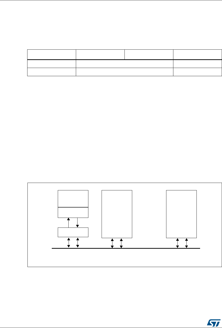
Controller area network (bxCAN) RM0430
1086/1324 RM0430 Rev 8
Single CAN peripheral configuration:
•CAN3: Master bxCAN with dedicated Memory Access Controller unit and 512-byte
SRAM memory
See Table 215.
32.3 bxCAN general description
In today CAN applications, the number of nodes in a network is increasing and often several
networks are linked together via gateways. Typically the number of messages in the system
(to be handled by each node) has significantly increased. In addition to the application
messages, Network Management and Diagnostic messages have been introduced.
•An enhanced filtering mechanism is required to handle each type of message.
Furthermore, application tasks require more CPU time, therefore real-time constraints
caused by message reception have to be reduced.
•A receive FIFO scheme allows the CPU to be dedicated to application tasks for a long
time period without losing messages.
The standard HLP (Higher Layer Protocol) based on standard CAN drivers requires an
efficient interface to the CAN controller.
Figure 378. CAN network topology
32.3.1 CAN 2.0B active core
The bxCAN module handles the transmission and the reception of CAN messages fully
autonomously. Standard identifiers (11-bit) and extended identifiers (29-bit) are fully
supported by hardware.
Table 215. CAN implementation
CAN features CAN1 CAN2 CAN3
SRAM size 512-byte shared between the two bxCAN 512-byte
Filter banks 26 filter banks shared between CAN1 and CAN2 14 fiter banks
&$1QRGH
&$1QRGH
&$1QRGHQ
&$1
&$1
+LJK /RZ
&$1
&$1
5[ 7[
&$1
7UDQVFHLYHU
&$1
&RQWUROOHU
0&8
&$1%XV
$SSOLFDWLRQ
069

RM0430 Rev 8 1087/1324
RM0430 Controller area network (bxCAN)
1130
32.3.2 Control, status and configuration registers
The application uses these registers to:
•Configure CAN parameters, e.g. baud rate
•Request transmissions
•Handle receptions
•Manage interrupts
•Get diagnostic information
32.3.3 Tx mailboxes
Three transmit mailboxes are provided to the software for setting up messages. The
transmission Scheduler decides which mailbox has to be transmitted first.
32.3.4 Acceptance filters
The bxCAN provides up to 28 scalable/configurable identifier filter banks in dual CAN
configuration or up to 14 scalable/configurable identifier filter banks in single CAN
configuration, for selecting the incoming messages, that the software needs and discarding
the others.
Receive FIFO
Two receive FIFOs are used by hardware to store the incoming messages. Three complete
messages can be stored in each FIFO. The FIFOs are managed completely by hardware.
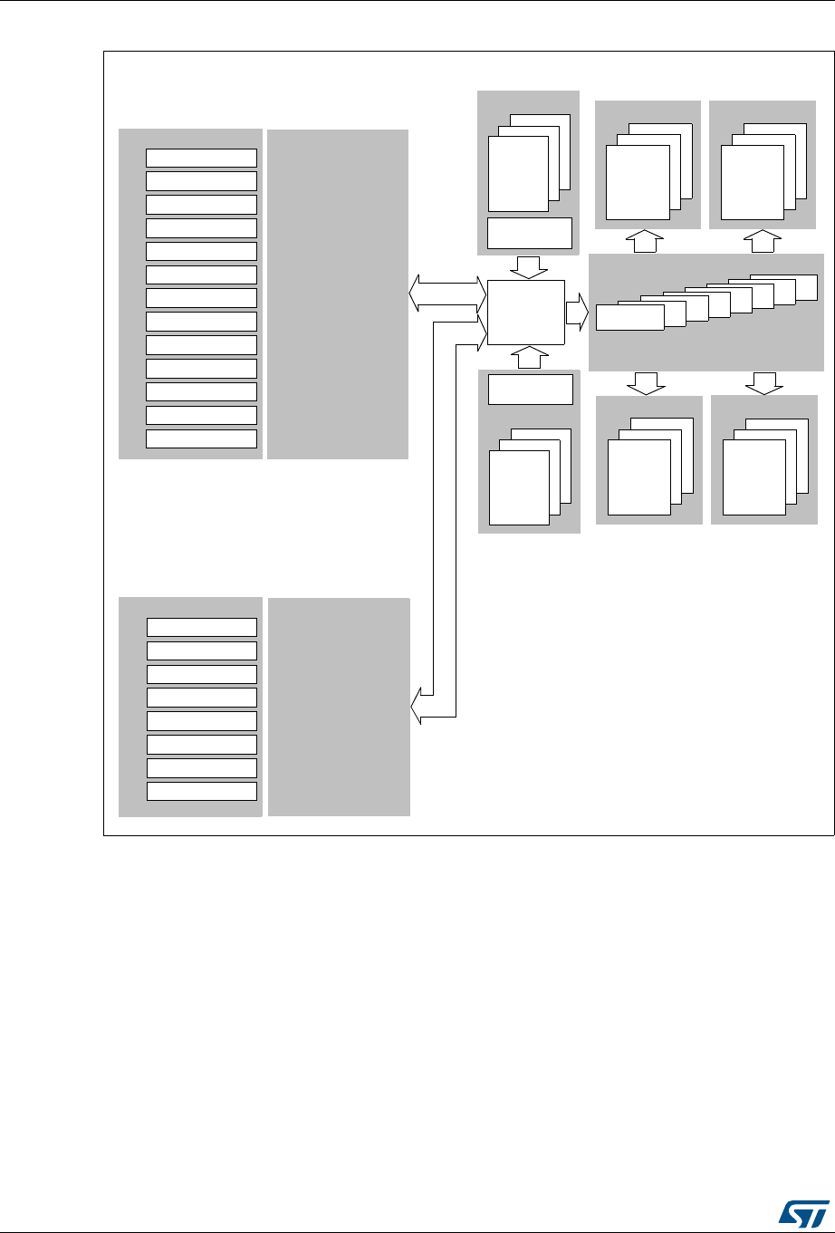
Controller area network (bxCAN) RM0430
1088/1324 RM0430 Rev 8
Figure 379. Dual-CAN block diagram
$FFHS W DQFH)LOW HU V
)L O W H U
7U DQ VP L VV L R Q
6FKHGXOHU
0DLOER[
5H FH L Y H ), )2
0DLOER[
5HFHLYH),)2
0DLOER[
7[0DLOER[HV
7U DQ VP L VV L R Q
6FKHGXOHU
0DLOER[
5HFHLYH),)2
0DLOER[
5H F H L Y H ) ,) 2
0DLOER[
7[0DLOER[HV
0HPRU\
$FFHVV
&R Q W U R O O H U
0DVW HU&RQ WU RO
0DVW HU6W DW XV
5[ ), )2 6W DW X V
5[ ), )2 6W DW X V
(UURU6WDWXV
%L W 7L P L QJ
,QWHUUXSW(QDEOH
&RQWURO6WDWXV&RQILJXUDWLRQ
7[6W DW XV
0DVWHU&RQWURO
0DVWHU6WDWXV
5[ ), )2 6W D W X V
5[ ), )2 6W D W X V
(UURU6WDWXV
%L W 7L P L Q J
)LOWHU0RGH
)LOWHU6FDOH
,QWHUUXSW(QDEOH
&RQWURO6WDWXV&RQILJXUDWLRQ
7[6W DW XV
)L O W H U ), ) 2 $V VL J Q
)LOWHU0DVWHU
)LOWHU$FWLYDWLRQ
&$1%$FWLYH&RUH
&$16ODYH
&$1%$FWLYH&RUH
&$10DVWHUZLWKE\WHV65$0
0DVWHU UHWVD0UHWVD0
0DVWHU)LOWHUV
6O D Y H
6O D Y H 6O D Y H
6ODYH)LOWHUV
WR
WR
DLE
1RWH&$1VWDUWILOWHUEDQNQXPEHUQLVFRQILJXUDEOHE\ZULWLQJ
&$16%>@ELWVLQWKH&$1B)05UHJLVWHU
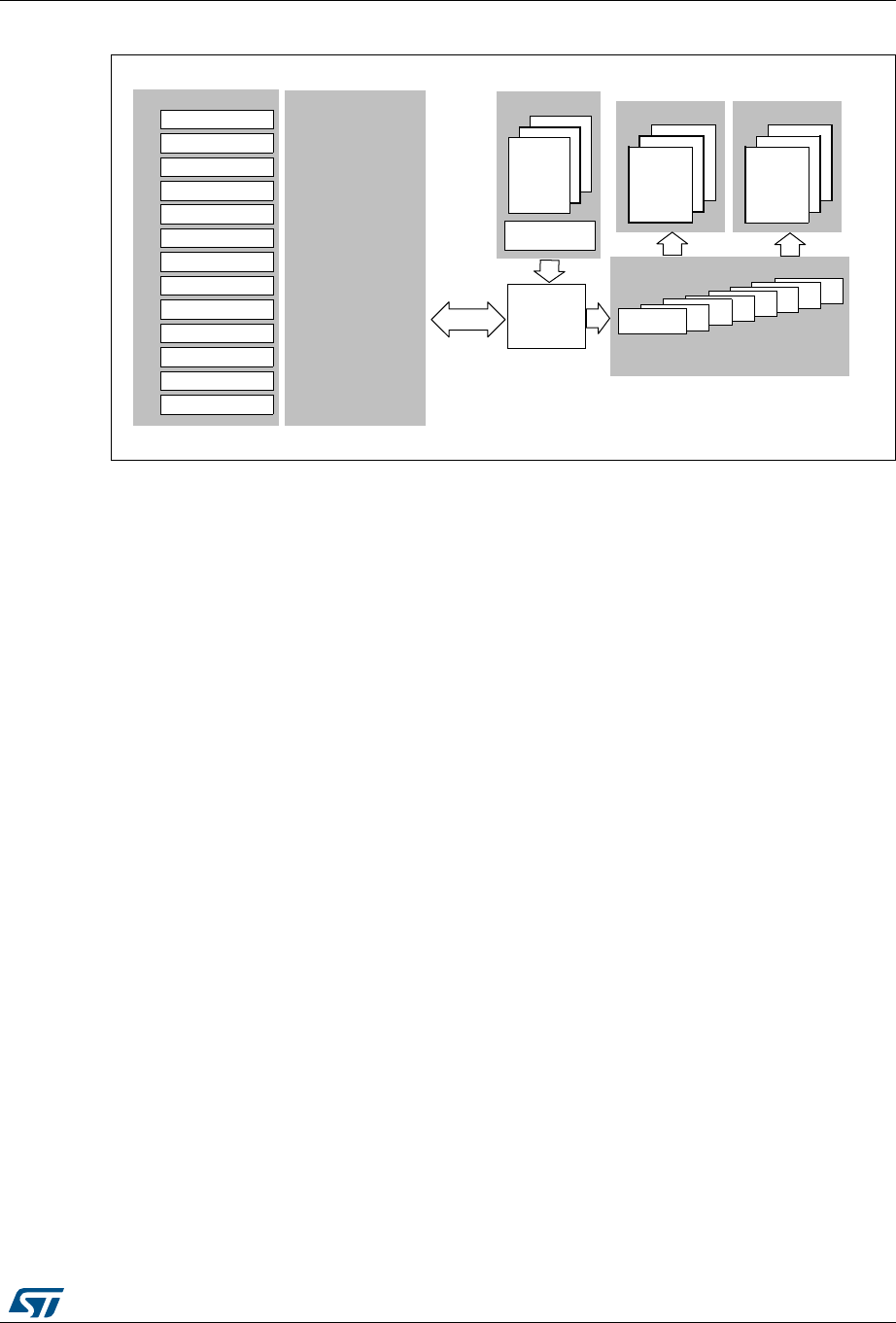
RM0430 Rev 8 1089/1324
RM0430 Controller area network (bxCAN)
1130
Figure 380. Single-CAN block diagram
32.4 bxCAN operating modes
bxCAN has three main operating modes: initialization, normal and Sleep. After a
hardware reset, bxCAN is in Sleep mode to reduce power consumption and an internal pull-
up is active on CANTX. The software requests bxCAN to enter initialization or Sleep mode
by setting the INRQ or SLEEP bits in the CAN_MCR register. Once the mode has been
entered, bxCAN confirms it by setting the INAK or SLAK bits in the CAN_MSR register and
the internal pull-up is disabled. When neither INAK nor SLAK are set, bxCAN is in normal
mode. Before entering normal mode bxCAN always has to synchronize on the CAN bus.
To synchronize, bxCAN waits until the CAN bus is idle, this means 11 consecutive recessive
bits have been monitored on CANRX.
32.4.1 Initialization mode
The software initialization can be done while the hardware is in Initialization mode. To enter
this mode the software sets the INRQ bit in the CAN_MCR register and waits until the
hardware has confirmed the request by setting the INAK bit in the CAN_MSR register.
To leave Initialization mode, the software clears the INQR bit. bxCAN has left Initialization
mode once the INAK bit has been cleared by hardware.
While in Initialization Mode, all message transfers to and from the CAN bus are stopped and
the status of the CAN bus output CANTX is recessive (high).
Entering Initialization Mode does not change any of the configuration registers.
To initialize the CAN Controller, software has to set up the Bit Timing (CAN_BTR) and CAN
options (CAN_MCR) registers.
To initialize the registers associated with the CAN filter banks (mode, scale, FIFO
assignment, activation and filter values), software has to set the FINIT bit (CAN_FMR). Filter
initialization also can be done outside the initialization mode.
06Y9
ϭϮ
͘͘
ĐĐĞƉƚĂŶĐĞ &ŝůƚĞƌƐ
͘͘
ϯ
Ϯ
ϭ
&ŝůƚĞƌ Ϭ
ϭϯ
DĂŝůďŽdž Ϭ
ϭ
Ϯ
ZĞĐĞŝǀĞ &/&K ϭ
DĂŝůďŽ dž Ϭ
ϭ
Ϯ
ZĞ Đ Ğŝ ǀĞ & /& K Ϭ
DĂŝůďŽ dž Ϭ
ϭ
Ϯ
ddž DĂŝůďŽ dž ĞƐ
DĞŵ ŽƌLJ
ĐĐĞƐƐ
ŽŶƚƌŽůůĞƌ
ŽŶƚƌŽů
^ƚĂƚƵƐ
Zdž &/&K Ϭ ^ƚĂƚƵƐ
Zdž &/&K ϭ ^ƚĂƚƵƐ
ƌƌŽƌ ^ƚĂƚƵƐ
ŝƚ dŝŵŝŶŐ
&ŝůƚĞƌ DŽĚ Ğ
&ŝ ůƚĞƌ ^Đ ĂůĞ
/ŶƚĞƌƌƵƉ ƚ ŶĂďů Ğ
ŽŶ ƚƌŽů ͬ^ ƚĂ ƚƵƐ ͬ ŽŶ ĨŝŐƵƌĂ ƚŝŽ Ŷ
ddž ^ƚĂƚƵƐ
&ŝůƚĞƌ &/&K ƐƐŝŐŶ
&ŝůƚĞƌ DĂ ƐƚĞƌ
&ŝ ůƚĞƌ Đ ƚŝ ǀĂ ƚŝŽ Ŷ
E Ϯ͘Ϭ ĐƚŝǀĞ Žƌ Ğ
EϱϭϮďLJƚĞƐ^ZD
DĂƐƚĞƌ
ƌĞƚƐĂDƌĞƚƐĂD
D ĂƐ ƚĞ ƌ &ŝů ƚ Ğƌ Ɛ ^ ůĂ ǀ Ğ & ŝůƚĞƌƐ
;Ϭ ƚŽ Ϯϳ Ϳ
;Ϭ ƚŽ ϮϳͿ
dƌĂŶƐŵŝƐƐŝŽŶ
ƐĐŚĞĚƵůĞƌ

Controller area network (bxCAN) RM0430
1090/1324 RM0430 Rev 8
Note: When FINIT=1, CAN reception is deactivated.
The filter values also can be modified by deactivating the associated filter activation bits (in
the CAN_FA1R register).
If a filter bank is not used, it is recommended to leave it non active (leave the corresponding
FACT bit cleared).
32.4.2 Normal mode
Once the initialization is complete, the software must request the hardware to enter Normal
mode to be able to synchronize on the CAN bus and start reception and transmission.
The request to enter Normal mode is issued by clearing the INRQ bit in the CAN_MCR
register. The bxCAN enters Normal mode and is ready to take part in bus activities when it
has synchronized with the data transfer on the CAN bus. This is done by waiting for the
occurrence of a sequence of 11 consecutive recessive bits (Bus Idle state). The switch to
Normal mode is confirmed by the hardware by clearing the INAK bit in the CAN_MSR
register.
The initialization of the filter values is independent from Initialization Mode but must be done
while the filter is not active (corresponding FACTx bit cleared). The filter scale and mode
configuration must be configured before entering Normal Mode.
32.4.3 Sleep mode (low-power)
To reduce power consumption, bxCAN has a low-power mode called Sleep mode. This
mode is entered on software request by setting the SLEEP bit in the CAN_MCR register. In
this mode, the bxCAN clock is stopped, however software can still access the bxCAN
mailboxes.
If software requests entry to initialization mode by setting the INRQ bit while bxCAN is in
Sleep mode, it must also clear the SLEEP bit.
bxCAN can be woken up (exit Sleep mode) either by software clearing the SLEEP bit or on
detection of CAN bus activity.
On CAN bus activity detection, hardware automatically performs the wakeup sequence by
clearing the SLEEP bit if the AWUM bit in the CAN_MCR register is set. If the AWUM bit is
cleared, software has to clear the SLEEP bit when a wakeup interrupt occurs, in order to exit
from Sleep mode.
Note: If the wakeup interrupt is enabled (WKUIE bit set in CAN_IER register) a wakeup interrupt
will be generated on detection of CAN bus activity, even if the bxCAN automatically
performs the wakeup sequence.
After the SLEEP bit has been cleared, Sleep mode is exited once bxCAN has synchronized
with the CAN bus, refer to Figure 381: bxCAN operating modes. The Sleep mode is exited
once the SLAK bit has been cleared by hardware.
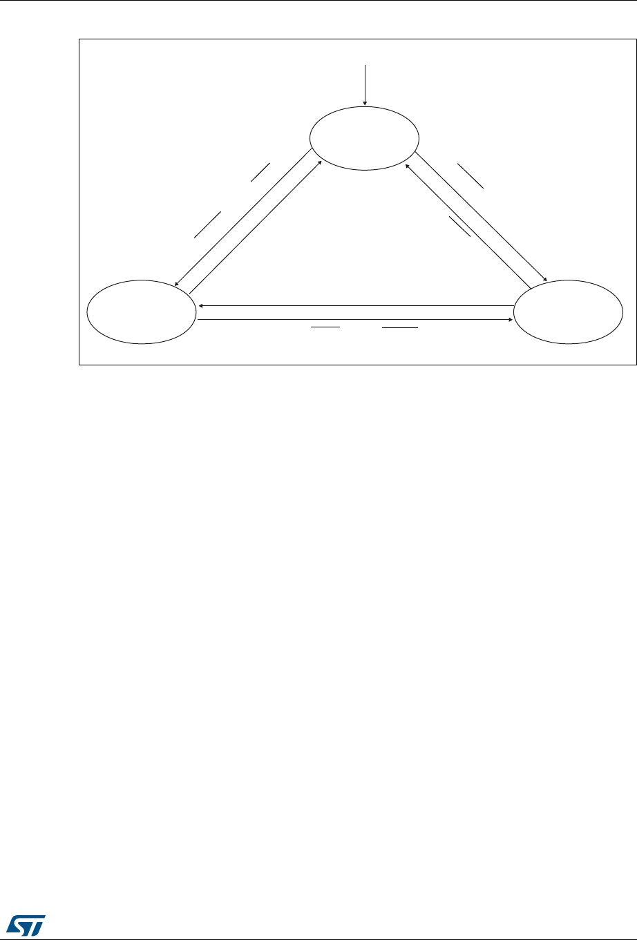
RM0430 Rev 8 1091/1324
RM0430 Controller area network (bxCAN)
1130
Figure 381. bxCAN operating modes
1. ACK = The wait state during which hardware confirms a request by setting the INAK or SLAK bits in the
CAN_MSR register
2. SYNC = The state during which bxCAN waits until the CAN bus is idle, meaning 11 consecutive recessive
bits have been monitored on CANRX
32.5 Test mode
Test mode can be selected by the SILM and LBKM bits in the CAN_BTR register. These bits
must be configured while bxCAN is in Initialization mode. Once test mode has been
selected, the INRQ bit in the CAN_MCR register must be reset to enter Normal mode.
32.5.1 Silent mode
The bxCAN can be put in Silent mode by setting the SILM bit in the CAN_BTR register.
In Silent mode, the bxCAN is able to receive valid data frames and valid remote frames, but
it sends only recessive bits on the CAN bus and it cannot start a transmission. If the bxCAN
has to send a dominant bit (ACK bit, overload flag, active error flag), the bit is rerouted
internally so that the CAN Core monitors this dominant bit, although the CAN bus may
remain in recessive state. Silent mode can be used to analyze the traffic on a CAN bus
without affecting it by the transmission of dominant bits (Acknowledge Bits, Error Frames).
6OHHS
1RUPDO
5HVHW
,1546<1&6/((3
DL
6/$.
,1$.
6/$.
,1$.
6/$.
,1$.
,154$&.
6/((3,154$&.
6/((3,154$&.
6/((3$&.
6/((36<1&,154
,QLWLDOL]DWLRQ
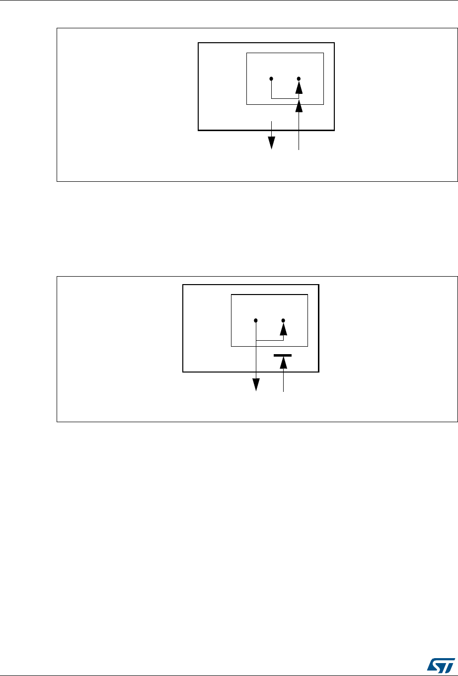
Controller area network (bxCAN) RM0430
1092/1324 RM0430 Rev 8
Figure 382. bxCAN in silent mode
32.5.2 Loop back mode
The bxCAN can be set in Loop Back Mode by setting the LBKM bit in the CAN_BTR
register. In Loop Back Mode, the bxCAN treats its own transmitted messages as received
messages and stores them (if they pass acceptance filtering) in a Receive mailbox.
Figure 383. bxCAN in loop back mode
This mode is provided for self-test functions. To be independent of external events, the CAN
Core ignores acknowledge errors (no dominant bit sampled in the acknowledge slot of a
data / remote frame) in Loop Back Mode. In this mode, the bxCAN performs an internal
feedback from its Tx output to its Rx input. The actual value of the CANRX input pin is
disregarded by the bxCAN. The transmitted messages can be monitored on the CANTX pin.
32.5.3 Loop back combined with silent mode
It is also possible to combine Loop Back mode and Silent mode by setting the LBKM and
SILM bits in the CAN_BTR register. This mode can be used for a “Hot Selftest”, meaning the
bxCAN can be tested like in Loop Back mode but without affecting a running CAN system
connected to the CANTX and CANRX pins. In this mode, the CANRX pin is disconnected
from the bxCAN and the CANTX pin is held recessive.
E[&$1
&$17; &$15;
7[ 5[
069
E[&$1
&$17; &$15;
7[ 5[
069
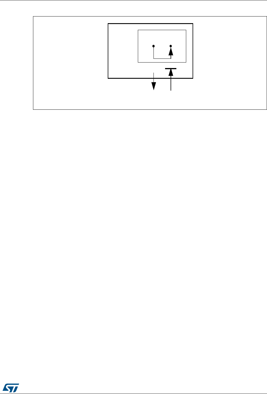
RM0430 Rev 8 1093/1324
RM0430 Controller area network (bxCAN)
1130
Figure 384. bxCAN in combined mode
32.6 Behavior in debug mode
When the microcontroller enters the debug mode (Cortex®-M4 with FPU core halted), the
bxCAN continues to work normally or stops, depending on:
•DBG_CAN1_STOP bit for CAN1, DBG_CAN2_STOP bit for CAN2 or
DBG_CAN3_STOP bit for CAN3 in the DBGMCU_APB1_FZ register
•the DBF bit in CAN_MCR. For more details, refer to Section 32.9.2: CAN control and
status registers.
32.7 bxCAN functional description
32.7.1 Transmission handling
In order to transmit a message, the application must select one empty transmit mailbox, set
up the identifier, the data length code (DLC) and the data before requesting the transmission
by setting the corresponding TXRQ bit in the CAN_TIxR register. Once the mailbox has left
empty state, the software no longer has write access to the mailbox registers. Immediately
after the TXRQ bit has been set, the mailbox enters pending state and waits to become the
highest priority mailbox, see Transmit Priority. As soon as the mailbox has the highest
priority it will be scheduled for transmission. The transmission of the message of the
scheduled mailbox will start (enter transmit state) when the CAN bus becomes idle. Once
the mailbox has been successfully transmitted, it will become empty again. The hardware
indicates a successful transmission by setting the RQCP and TXOK bits in the CAN_TSR
register.
If the transmission fails, the cause is indicated by the ALST bit in the CAN_TSR register in
case of an Arbitration Lost, and/or the TERR bit, in case of transmission error detection.
Transmit priority
By identifier
When more than one transmit mailbox is pending, the transmission order is given by the
identifier of the message stored in the mailbox. The message with the lowest identifier value
has the highest priority according to the arbitration of the CAN protocol. If the identifier
values are equal, the lower mailbox number will be scheduled first.
E[&$1
&$17; &$15;
7[ 5[
069
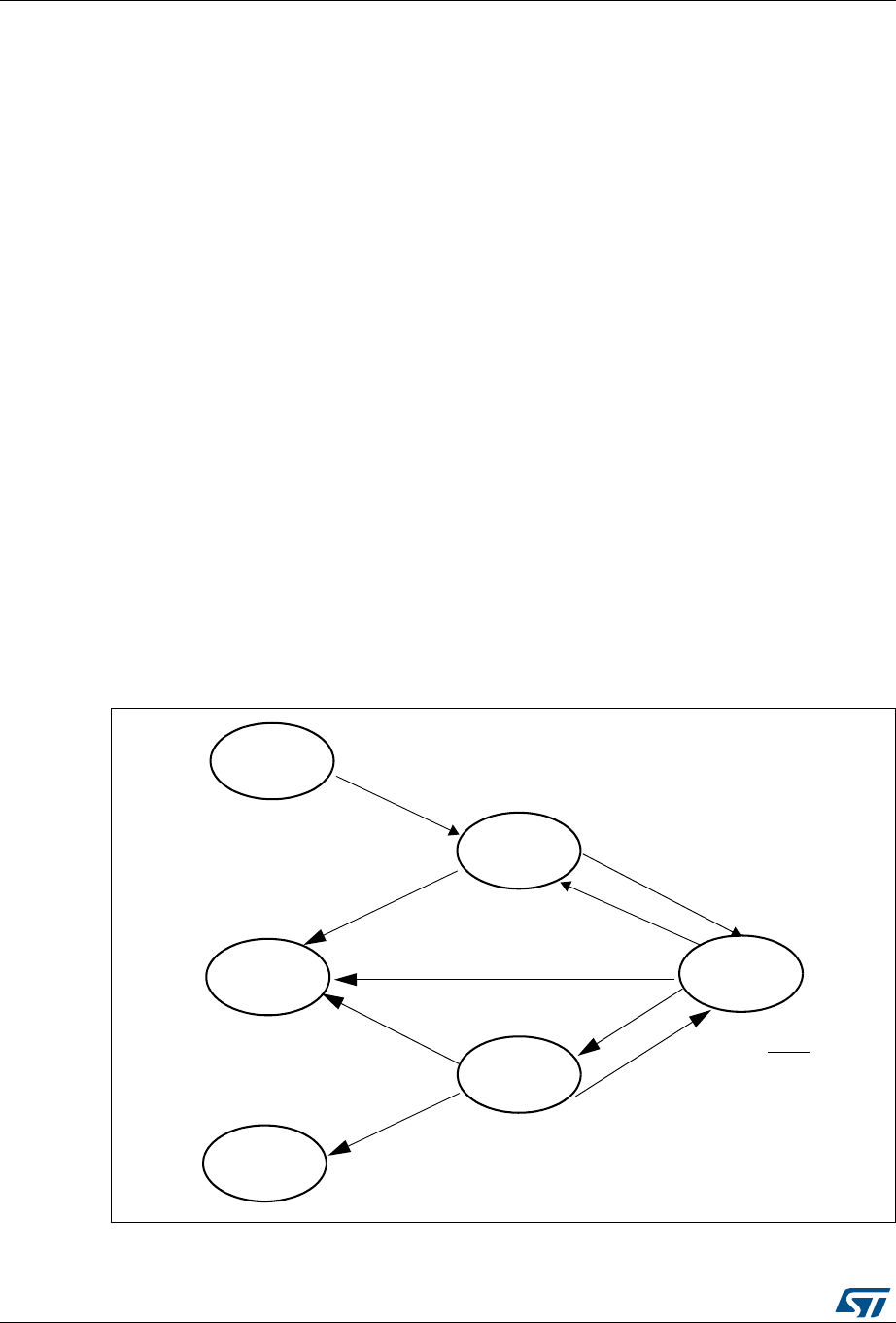
Controller area network (bxCAN) RM0430
1094/1324 RM0430 Rev 8
By transmit request order
The transmit mailboxes can be configured as a transmit FIFO by setting the TXFP bit in the
CAN_MCR register. In this mode the priority order is given by the transmit request order.
This mode is very useful for segmented transmission.
Abort
A transmission request can be aborted by the user setting the ABRQ bit in the CAN_TSR
register. In pending or scheduled state, the mailbox is aborted immediately. An abort
request while the mailbox is in transmit state can have two results. If the mailbox is
transmitted successfully the mailbox becomes empty with the TXOK bit set in the
CAN_TSR register. If the transmission fails, the mailbox becomes scheduled, the
transmission is aborted and becomes empty with TXOK cleared. In all cases the mailbox
will become empty again at least at the end of the current transmission.
Non automatic retransmission mode
This mode has been implemented in order to fulfill the requirement of the Time Triggered
Communication option of the CAN standard. To configure the hardware in this mode the
NART bit in the CAN_MCR register must be set.
In this mode, each transmission is started only once. If the first attempt fails, due to an
arbitration loss or an error, the hardware will not automatically restart the message
transmission.
At the end of the first transmission attempt, the hardware considers the request as
completed and sets the RQCP bit in the CAN_TSR register. The result of the transmission is
indicated in the CAN_TSR register by the TXOK, ALST and TERR bits.
Figure 385. Transmit mailbox states
(037<
7;54
54&3 ;
7;2. ;
3(1',1*
54&3
7;2.
6&+('8/('
54&3
7;2.
0DLOER[KDV
75$160,7
54&3
7;2.
&$1%XV ,'/(
7UDQVPLWIDLOHG1$57
7UDQVPLWVXFFHHGHG
0DLOER[GRHVQRW
(037<
54&3
7;2.
KLJKHVWSULRULW\
KDYHKLJKHVWSULRULW\
(037<
54&3
7;2.
$%54
$%54
7UDQVPLWIDLOHG1$57
70(
70(
70(
70(
70(
70(
069
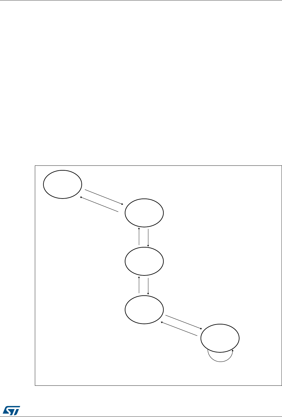
RM0430 Rev 8 1095/1324
RM0430 Controller area network (bxCAN)
1130
32.7.2 Time triggered communication mode
In this mode, the internal counter of the CAN hardware is activated and used to generate the
Time Stamp value stored in the CAN_RDTxR/CAN_TDTxR registers, respectively (for Rx
and Tx mailboxes). The internal counter is incremented each CAN bit time (refer to
Section 32.7.7: Bit timing). The internal counter is captured on the sample point of the Start
Of Frame bit in both reception and transmission.
32.7.3 Reception handling
For the reception of CAN messages, three mailboxes organized as a FIFO are provided. In
order to save CPU load, simplify the software and guarantee data consistency, the FIFO is
managed completely by hardware. The application accesses the messages stored in the
FIFO through the FIFO output mailbox.
Valid message
A received message is considered as valid when it has been received correctly according to
the CAN protocol (no error until the last but one bit of the EOF field) and It passed through
the identifier filtering successfully, see Section 32.7.4: Identifier filtering.
Figure 386. Receive FIFO states
%-049
6ALID-ESSAGE
&-0X
&/62
0%.$).'?
&-0X
&/62
2ECEIVED
0%.$).'?
&-0X
&/62
0%.$).'?
&-0X
&/62
6ALID-ESSAGE
2ECEIVED
2ELEASE
/6%225.
&-0X
&/62
-AILBOX
2ELEASE
-AILBOX
6ALID-ESSAGE
2ECEIVED
6ALID-ESSAGE
2ECEIVED
2ELEASE
-AILBOX
2ELEASE
-AILBOX
6ALID-ESSAGE
2ECEIVED
2&/-
2&/-
2&/-
-36

Controller area network (bxCAN) RM0430
1096/1324 RM0430 Rev 8
FIFO management
Starting from the empty state, the first valid message received is stored in the FIFO which
becomes pending_1. The hardware signals the event setting the FMP[1:0] bits in the
CAN_RFR register to the value 01b. The message is available in the FIFO output mailbox.
The software reads out the mailbox content and releases it by setting the RFOM bit in the
CAN_RFR register. The FIFO becomes empty again. If a new valid message has been
received in the meantime, the FIFO stays in pending_1 state and the new message is
available in the output mailbox.
If the application does not release the mailbox, the next valid message will be stored in the
FIFO which enters pending_2 state (FMP[1:0] = 10b). The storage process is repeated for
the next valid message putting the FIFO into pending_3 state (FMP[1:0] = 11b). At this
point, the software must release the output mailbox by setting the RFOM bit, so that a
mailbox is free to store the next valid message. Otherwise the next valid message received
will cause a loss of message.
Refer also to Section 32.7.5: Message storage
Overrun
Once the FIFO is in pending_3 state (i.e. the three mailboxes are full) the next valid
message reception will lead to an overrun and a message will be lost. The hardware
signals the overrun condition by setting the FOVR bit in the CAN_RFR register. Which
message is lost depends on the configuration of the FIFO:
•If the FIFO lock function is disabled (RFLM bit in the CAN_MCR register cleared) the
last message stored in the FIFO will be overwritten by the new incoming message. In
this case the latest messages will be always available to the application.
•If the FIFO lock function is enabled (RFLM bit in the CAN_MCR register set) the most
recent message will be discarded and the software will have the three oldest messages
in the FIFO available.
Reception related interrupts
Once a message has been stored in the FIFO, the FMP[1:0] bits are updated and an
interrupt request is generated if the FMPIE bit in the CAN_IER register is set.
When the FIFO becomes full (i.e. a third message is stored) the FULL bit in the CAN_RFR
register is set and an interrupt is generated if the FFIE bit in the CAN_IER register is set.
On overrun condition, the FOVR bit is set and an interrupt is generated if the FOVIE bit in
the CAN_IER register is set.
32.7.4 Identifier filtering
In the CAN protocol the identifier of a message is not associated with the address of a node
but related to the content of the message. Consequently a transmitter broadcasts its
message to all receivers. On message reception a receiver node decides - depending on
the identifier value - whether the software needs the message or not. If the message is
needed, it is copied into the SRAM. If not, the message must be discarded without
intervention by the software.
To fulfill this requirement in dual CAN configuration, bxCAN Controller provides 28
configurable and scalable filter banks (27-0) to the application. In single CAN configuration
bxCAN Controller provides 14 configurable and scalable filter banks (13-0) to the application
in order to receive only the messages the software needs.

RM0430 Rev 8 1097/1324
RM0430 Controller area network (bxCAN)
1130
This hardware filtering saves CPU resources which would be otherwise needed to perform
filtering by software. Each filter bank x consists of two 32-bit registers, CAN_FxR0 and
CAN_FxR1.
Scalable width
To optimize and adapt the filters to the application needs, each filter bank can be scaled
independently. Depending on the filter scale a filter bank provides:
•One 32-bit filter for the STDID[10:0], EXTID[17:0], IDE and RTR bits.
•Two 16-bit filters for the STDID[10:0], RTR, IDE and EXTID[17:15] bits.
Refer to Figure 387.
Furthermore, the filters can be configured in mask mode or in identifier list mode.
Mask mode
In mask mode the identifier registers are associated with mask registers specifying which
bits of the identifier are handled as “must match” or as “don’t care”.
Identifier list mode
In identifier list mode, the mask registers are used as identifier registers. Thus instead of
defining an identifier and a mask, two identifiers are specified, doubling the number of single
identifiers. All bits of the incoming identifier must match the bits specified in the filter
registers.
Filter bank scale and mode configuration
The filter banks are configured by means of the corresponding CAN_FMR register. To
configure a filter bank it must be deactivated by clearing the FACT bit in the CAN_FAR
register. The filter scale is configured by means of the corresponding FSCx bit in the
CAN_FS1R register, refer to Figure 387. The identifier list or identifier mask mode for the
corresponding Mask/Identifier registers is configured by means of the FBMx bits in the
CAN_FMR register.
To filter a group of identifiers, configure the Mask/Identifier registers in mask mode.
To select single identifiers, configure the Mask/Identifier registers in identifier list mode.
Filters not used by the application should be left deactivated.
Each filter within a filter bank is numbered (called the Filter Number) from 0 to a maximum
dependent on the mode and the scale of each of the filter banks.
Concerning the filter configuration, refer to Figure 387.
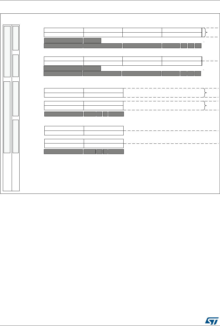
Controller area network (bxCAN) RM0430
1098/1324 RM0430 Rev 8
Figure 387. Filter bank scale configuration - register organization
Filter match index
Once a message has been received in the FIFO it is available to the application. Typically,
application data is copied into SRAM locations. To copy the data to the right location the
application has to identify the data by means of the identifier. To avoid this, and to ease the
access to the SRAM locations, the CAN controller provides a Filter Match Index.
This index is stored in the mailbox together with the message according to the filter priority
rules. Thus each received message has its associated filter match index.
The Filter Match index can be used in two ways:
•Compare the Filter Match index with a list of expected values.
•Use the Filter Match Index as an index on an array to access the data destination
location.
For non masked filters, the software no longer has to compare the identifier.
If the filter is masked the software reduces the comparison to the masked bits only.
The index value of the filter number does not take into account the activation state of the
filter banks. In addition, two independent numbering schemes are used, one for each FIFO.
06Y9
2QH%LW)LOWHU,GHQWLILHU0DVN
[ ILOWHUEDQNQXPEHU
)6&[ )6&[
7KHVHELWVDUHORFDWHGLQWKH&$1B)65UHJLVWHU
)LOWHU%DQN6FDOH
,'
0DVN
,'
67,'>@
0DSSLQJ67','
,'
,'
,'
,'
,'
,'
,'
Q
Q
Q
Q
&RQILJ%LWV
,' ,GHQWLILHU
)%0[ )%0[
)%0[
)%0[
)LOWHU%DQN0RGH
7ZR%LW)LOWHUV,GHQWLILHU/LVW
7ZR%LW)LOWHUV,GHQWLILHU0DVN
)RXU%LW)LOWHUV,GHQWLILHU/LVW
0DSSLQJ
0DSSLQJ
&$1B)[5>@
&$1B)[5>@ &$1B)[5>@
&$1B)[5>@ &$1B)[5>@
&$1B)[5>@
&$1B)[5>@
&$1B)[5>@
&$1B)[5>@
&$1B)[5>@ &$1B)[5>@
&$1B)[5>@ &$1B)[5>@
&$1B)[5>@
&$1B)[5>@
&$1B)[5>@
&$1B)[5>@
&$1B)[5>@
&$1B)[5>@
&$1B)[5>@
&$1B)[5>@
&$1B)[5>@
&$1B)[5>@
&$1B)[5>@
&$1B)[5>@
&$1B)[5>@
&$1B)[5>@
&$1B)[5>@
&$1B)[5>@
&$1B)[5>@
&$1B)[5>@
&$1B)[5>@
7KHVHELWVDUHORFDWHGLQWKH&$1B)05UHJLVWHU
Q
Q
Q
Q
Q
)LOWHU
1XP
0DVN
0DVN
67,'>@
(;,'>@,'(57567,'>@67,'>@
(;,'>@
,'(
575
67,'>@
67,'>@
(;7,'>@
0DSSLQJ([W,'
(;,'>@ (;,'>@ (;,'>@ ,'( 575
67,'>@
0DSSLQJ67',' 67,'>@
(;7,'>@
0DSSLQJ([W,'
(;,'>@ (;,'>@ (;,'>@ ,'( 575
RM0430 Rev 8 1099/1324
RM0430 Controller area network (bxCAN)
1130
Refer to Figure 388 for an example.
Figure 388. Example of filter numbering
Filter priority rules
Depending on the filter combination it may occur that an identifier passes successfully
through several filters. In this case the filter match value stored in the receive mailbox is
chosen according to the following priority rules:
•A 32-bit filter takes priority over a 16-bit filter.
•For filters of equal scale, priority is given to the Identifier List mode over the Identifier
Mask mode
•For filters of equal scale and mode, priority is given by the filter number (the lower the
number, the higher the priority).
,'/LVWELW
,'0DVNELW
,'/LVWELW
,'/LVWELW
'HDFWLYDWHG
,'0DVNELW
,'/LVWELW
)LOWHU
,'0DVNELW
),)2 )LOWHU
,'0DVNELW
,'/LVWELW
,'0DVNELW
,'/LVWELW
'HDFWLYDWHG
,'0DVNELW
,'/LVWELW
)LOWHU
,'0DVNELW
),)2 )LOWHU
'HDFWLYDWHG
1XP 1XP%DQN%DQN
069
,' ,GHQWLILHU

Controller area network (bxCAN) RM0430
1100/1324 RM0430 Rev 8
Figure 389. Filtering mechanism - example
The example above shows the filtering principle of the bxCAN. On reception of a message,
the identifier is compared first with the filters configured in identifier list mode. If there is a
match, the message is stored in the associated FIFO and the index of the matching filter is
stored in the Filter Match Index. As shown in the example, the identifier matches with
Identifier #2 thus the message content and FMI 2 is stored in the FIFO.
If there is no match, the incoming identifier is then compared with the filters configured in
mask mode.
If the identifier does not match any of the identifiers configured in the filters, the message is
discarded by hardware without disturbing the software.
32.7.5 Message storage
The interface between the software and the hardware for the CAN messages is
implemented by means of mailboxes. A mailbox contains all information related to a
message; identifier, data, control, status and time stamp information.
Transmit mailbox
The software sets up the message to be transmitted in an empty transmit mailbox. The
status of the transmission is indicated by hardware in the CAN_TSR register.
,GHQWLILHU/LVW
0HVVDJH'LVFDUGHG
,GHQWLILHU0DVN
,GHQWLILHU
,GHQWLILHU
,GHQWLILHU
,GHQWLILHU
,GHQWLILHU
0DVN
,GHQWLILHU
0DVN
,GHQWLILHU
0HVVDJH5HFHLYHG
&WUO 'DWD
,GHQWLILHU0DWFK
0HVVDJH
6WRUHG
5HFHLYH),)2
1R0DWFK
)RXQG
)LOWHUQXPEHUVWRUHGLQWKH
)LOWHU0DWFK,QGH[ILHOG
ZLWKLQWKH&$1B5'7[5
UHJLVWHU
)0,
)LOWHUEDQN
([DPSOHRIILOWHUEDQNVLQELWXQLGHQWLILHGPRGHDQG
1XP
WKHUHPDLQLQJLQELWLGHQWLILHUPDVNPRGH
069
RM0430 Rev 8 1101/1324
RM0430 Controller area network (bxCAN)
1130
Receive mailbox
When a message has been received, it is available to the software in the FIFO output
mailbox. Once the software has handled the message (e.g. read it) the software must
release the FIFO output mailbox by means of the RFOM bit in the CAN_RFR register to
make the next incoming message available. The filter match index is stored in the MFMI
field of the CAN_RDTxR register. The 16-bit time stamp value is stored in the TIME[15:0]
field of CAN_RDTxR.
Figure 390. CAN error state diagram
Table 216. Transmit mailbox mapping
Offset to transmit mailbox base address Register name
0CAN_TIxR
4 CAN_TDTxR
8CAN_TDLxR
12 CAN_TDHxR
Table 217. Receive mailbox mapping
Offset to receive mailbox base
address (bytes) Register name
0CAN_RIxR
4 CAN_RDTxR
8 CAN_RDLxR
12 CAN_RDHxR
(5525$&7,9(
DL
(55253$66,9(
%862))
:KHQ7(&DQG5(&
:KHQ7(&RU5(&!
:KHQ7(&!:KHQUHFHVVLYHELWVRFFXU

Controller area network (bxCAN) RM0430
1102/1324 RM0430 Rev 8
32.7.6 Error management
The error management as described in the CAN protocol is handled entirely by hardware
using a Transmit Error Counter (TEC value, in CAN_ESR register) and a Receive Error
Counter (REC value, in the CAN_ESR register), which get incremented or decremented
according to the error condition. For detailed information about TEC and REC management,
refer to the CAN standard.
Both of them may be read by software to determine the stability of the network.
Furthermore, the CAN hardware provides detailed information on the current error status in
CAN_ESR register. By means of the CAN_IER register (ERRIE bit, etc.), the software can
configure the interrupt generation on error detection in a very flexible way.
Bus-Off recovery
The Bus-Off state is reached when TEC is greater than 255, this state is indicated by BOFF
bit in CAN_ESR register. In Bus-Off state, the bxCAN is no longer able to transmit and
receive messages.
Depending on the ABOM bit in the CAN_MCR register bxCAN will recover from Bus-Off
(become error active again) either automatically or on software request. But in both cases
the bxCAN has to wait at least for the recovery sequence specified in the CAN standard
(128 occurrences of 11 consecutive recessive bits monitored on CANRX).
If ABOM is set, the bxCAN will start the recovering sequence automatically after it has
entered Bus-Off state.
If ABOM is cleared, the software must initiate the recovering sequence by requesting
bxCAN to enter and to leave initialization mode.
Note: In initialization mode, bxCAN does not monitor the CANRX signal, therefore it cannot
complete the recovery sequence. To recover, bxCAN must be in normal mode.
32.7.7 Bit timing
The bit timing logic monitors the serial bus-line and performs sampling and adjustment of
the sample point by synchronizing on the start-bit edge and resynchronizing on the following
edges.
Its operation may be explained simply by splitting nominal bit time into three segments as
follows:
•Synchronization segment (SYNC_SEG): a bit change is expected to occur within this
time segment. It has a fixed length of one time quantum (1 x tq).
•Bit segment 1 (BS1): defines the location of the sample point. It includes the
PROP_SEG and PHASE_SEG1 of the CAN standard. Its duration is programmable
between 1 and 16 time quanta but may be automatically lengthened to compensate for
positive phase drifts due to differences in the frequency of the various nodes of the
network.
•Bit segment 2 (BS2): defines the location of the transmit point. It represents the
PHASE_SEG2 of the CAN standard. Its duration is programmable between 1 and 8
time quanta but may also be automatically shortened to compensate for negative
phase drifts.
The resynchronization Jump Width (SJW) defines an upper bound to the amount of
lengthening or shortening of the bit segments. It is programmable between 1 and 4 time
quanta.
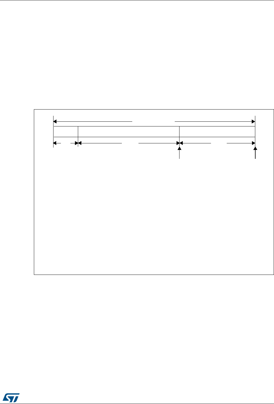
RM0430 Rev 8 1103/1324
RM0430 Controller area network (bxCAN)
1130
A valid edge is defined as the first transition in a bit time from dominant to recessive bus
level provided the controller itself does not send a recessive bit.
If a valid edge is detected in BS1 instead of SYNC_SEG, BS1 is extended by up to SJW so
that the sample point is delayed.
Conversely, if a valid edge is detected in BS2 instead of SYNC_SEG, BS2 is shortened by
up to SJW so that the transmit point is moved earlier.
As a safeguard against programming errors, the configuration of the Bit Timing Register
(CAN_BTR) is only possible while the device is in Standby mode.
Note: For a detailed description of the CAN bit timing and resynchronization mechanism, refer to
the ISO 11898 standard.
Figure 391. Bit timing
6<1&B6(* %,76(*0(17%6 %,76(*0(17%6
120,1$/%,77,0(
[WTW%6 W%6
6$03/(32,17 75$160,732,17
1RPLQDO%LW7LPH ;WTW%6 W%6
ZLWK
W%6 WT[76>@
W%6 WT[76>@
WT %53>@[W3&/.
W3&/. WLPHSHULRGRIWKH$3%FORFN
%53>@76>@DQG76>@DUHGHILQHGLQWKH&$1B%755HJLVWHU
%DXG 5DWH
1RPLQDO%LW7LPH
ZKHUHWTUHIHUVWRWKH7LPHTXDQWXP
069
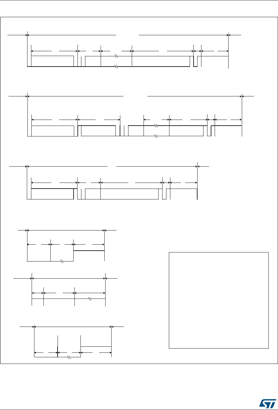
Controller area network (bxCAN) RM0430
1104/1324 RM0430 Rev 8
Figure 392. CAN frames
DLE
,QWHU)UDPH6SDFH
6XVSHQG
7UDQVPLVVLRQ %XV,GOH
$Q\)UDPH
,QWHUPLVVLRQ
'DWD)UDPHRU
5HPRWH)UDPH
'DWD)UDPHRU
5HPRWH)UDPH (UURU)UDPH ,QWHU)UDPH6SDFH
RU2YHUORDG)UDPH
(UURU
'HOLPLWHU
)ODJ(FKR
(UURU
)ODJ
,QWHU)UDPH6SDFH
$&.
U
U
575
'/& &5& (2)
,'(
655
1
62)
,'
&5&)LHOG $&.)LHOG&WUO)LHOG$UELWUDWLRQ)LHOG$UELWUDWLRQ)LHOG 'DWD)LHOG
'DWD)UDPH([WHQGHG,GHQWLILHU
1
,QWHU)UDPH6SDFH
RU2YHUORDG)UDPH
,QWHU)UDPH6SDFH
1
$UELWUDWLRQ)LHOG &WUO)LHOG 'DWD)LHOG &5&)LHOG $&.)LHOG
,QWHU)UDPH6SDFH
RU2YHUORDG)UDPH
'DWD)UDPH6WDQGDUG,GHQWLILHU
1
'/& &5& (2)
$&.
,'
62)
575
,'(
U
,QWHU)UDPH6SDFH
62)
575
,'(
U
$&.
(2),' '/& &5&
$UELWUDWLRQ)LHOG &WUO)LHOG &5&)LHOG $&.)LHOG
,QWHU)UDPH6SDFH
RU2YHUORDG)UDPH
5HPRWH)UDPH
,QWHU)UDPH6SDFH
RU(UURU)UDPH
2YHUORDG)UDPH
(QGRI)UDPHRU
(UURU'HOLPLWHURU
2YHUORDG'HOLPLWHU
2YHUORDG
)ODJ
2YHUORDG
(FKR
2YHUORDG
'HOLPLWHU
1RWHV
1
62) 6WDUW2I)UDPH
,' ,GHQWLILHU
575 5HPRWH7UDQVPLVVLRQ5HTXHVW
,'( ,GHQWLILHU([WHQVLRQ%LW
U 5HVHUYHG%LW
'/& 'DWD/HQJWK&RGH
&5& &\FOLF5HGXQGDQF\&RGH
(UURUIODJGRPLQDQWELWVLIQRGHLVHUURU
DFWLYHHOVHUHFHVVLYHELWV
6XVSHQGWUDQVPLVVLRQDSSOLHVWRHUURU
SDVVLYHQRGHVRQO\
(2) (QGRI)UDPH
$&. $FNQRZOHGJHELW
&WUO &RQWURO
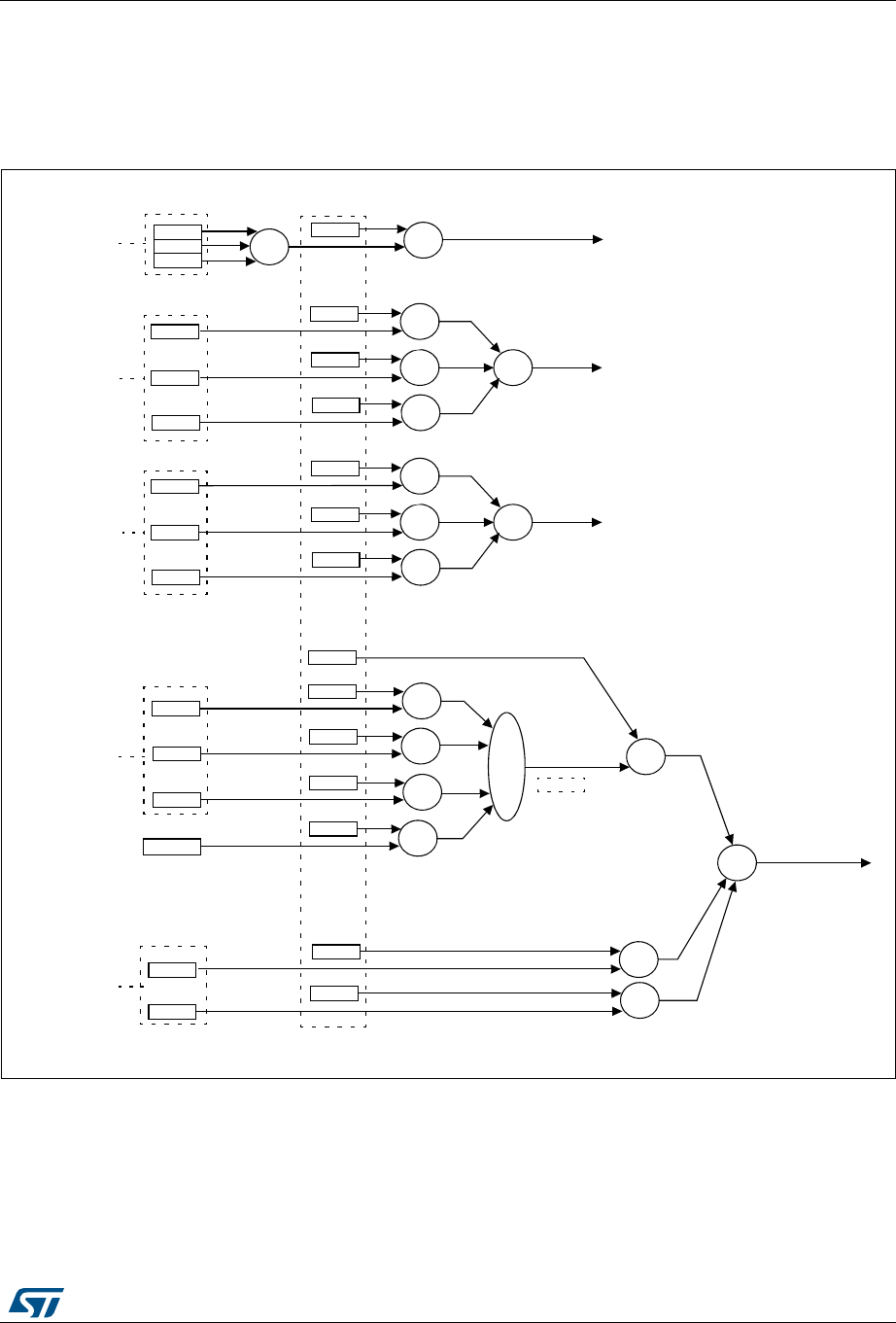
RM0430 Rev 8 1105/1324
RM0430 Controller area network (bxCAN)
1130
32.8 bxCAN interrupts
Four interrupt vectors are dedicated to bxCAN. Each interrupt source can be independently
enabled or disabled by means of the CAN Interrupt Enable Register (CAN_IER).
Figure 393. Event flags and interrupt generation
54&3
54&3
)03
&$1B765 70(,(
&$1B,(5
75$160,7
)03,(
)8//
)),(
)295
)29,(
&$1B5)5
),)2
(:*)
(:*,(
(39)
(39,(
%2))
%2),(
/(&
/(&,(
&$1B(65
(55,(
,17(55837
,17(55837
)03
)03,(
)8//
)),(
)295
)29,(
&$1B5)5
),)2
,17(55837
54&3
:.8,
:.8,(
&$1B065
,17(55837
(5525
67$786 &+$1*(
(55,
6/$.,
6/.,(
&$1B065
069

Controller area network (bxCAN) RM0430
1106/1324 RM0430 Rev 8
•The transmit interrupt can be generated by the following events:
– Transmit mailbox 0 becomes empty, RQCP0 bit in the CAN_TSR register set.
– Transmit mailbox 1 becomes empty, RQCP1 bit in the CAN_TSR register set.
– Transmit mailbox 2 becomes empty, RQCP2 bit in the CAN_TSR register set.
•The FIFO 0 interrupt can be generated by the following events:
– Reception of a new message, FMP0 bits in the CAN_RF0R register are not ‘00’.
– FIFO0 full condition, FULL0 bit in the CAN_RF0R register set.
– FIFO0 overrun condition, FOVR0 bit in the CAN_RF0R register set.
•The FIFO 1 interrupt can be generated by the following events:
– Reception of a new message, FMP1 bits in the CAN_RF1R register are not ‘00’.
– FIFO1 full condition, FULL1 bit in the CAN_RF1R register set.
– FIFO1 overrun condition, FOVR1 bit in the CAN_RF1R register set.
•The error and status change interrupt can be generated by the following events:
– Error condition, for more details on error conditions refer to the CAN Error Status
register (CAN_ESR).
– Wakeup condition, SOF monitored on the CAN Rx signal.
– Entry into Sleep mode.
32.9 CAN registers
The peripheral registers have to be accessed by words (32 bits).
32.9.1 Register access protection
Erroneous access to certain configuration registers can cause the hardware to temporarily
disturb the whole CAN network. Therefore the CAN_BTR register can be modified by
software only while the CAN hardware is in initialization mode.
Although the transmission of incorrect data will not cause problems at the CAN network
level, it can severely disturb the application. A transmit mailbox can be only modified by
software while it is in empty state, refer to Figure 385: Transmit mailbox states.
The filter values can be modified either deactivating the associated filter banks or by setting
the FINIT bit. Moreover, the modification of the filter configuration (scale, mode and FIFO
assignment) in CAN_FMxR, CAN_FSxR and CAN_FFAR registers can only be done when
the filter initialization mode is set (FINIT=1) in the CAN_FMR register.
32.9.2 CAN control and status registers
Refer to Section 1.2 for a list of abbreviations used in register descriptions.
CAN master control register (CAN_MCR)
Address offset: 0x00
Reset value: 0x0001 0002

RM0430 Rev 8 1107/1324
RM0430 Controller area network (bxCAN)
1130
31 30 29 28 27 26 25 24 23 22 21 20 19 18 17 16
Res. Res. Res. Res. Res. Res. Res. Res. Res. Res. Res. Res. Res. Res. Res. DBF
rw
1514131211109876543210
RESET Res. Res. Res. Res. Res. Res. Res. TTCM ABOM AWUM NART RFLM TXFP SLEEP INRQ
rs rw rw rw rw rw rw rw rw
Bits 31:17 Reserved, must be kept at reset value.
Bit 16 DBF: Debug freeze
0: CAN working during debug
1: CAN reception/transmission frozen during debug. Reception FIFOs can still be
accessed/controlled normally.
Bit 15 RESET: bxCAN software master reset
0: Normal operation.
1: Force a master reset of the bxCAN -> Sleep mode activated after reset (FMP bits and
CAN_MCR register are initialized to the reset values). This bit is automatically reset to 0.
Bits 14:8 Reserved, must be kept at reset value.
Bit 7 TTCM: Time triggered communication mode
0: Time Triggered Communication mode disabled.
1: Time Triggered Communication mode enabled
Note: For more information on Time Triggered Communication mode, refer to Section 32.7.2:
Time triggered communication mode.
Bit 6 ABOM: Automatic bus-off management
This bit controls the behavior of the CAN hardware on leaving the Bus-Off state.
0: The Bus-Off state is left on software request, once 128 occurrences of 11 recessive bits
have been monitored and the software has first set and cleared the INRQ bit of the
CAN_MCR register.
1: The Bus-Off state is left automatically by hardware once 128 occurrences of 11 recessive
bits have been monitored.
For detailed information on the Bus-Off state refer to Section 32.7.6: Error management.
Bit 5 AWUM: Automatic wakeup mode
This bit controls the behavior of the CAN hardware on message reception during Sleep
mode.
0: The Sleep mode is left on software request by clearing the SLEEP bit of the CAN_MCR
register.
1: The Sleep mode is left automatically by hardware on CAN message detection.
The SLEEP bit of the CAN_MCR register and the SLAK bit of the CAN_MSR register are
cleared by hardware.
Bit 4 NART
: No automatic retransmission
0: The CAN hardware will automatically retransmit the message until it has been
successfully transmitted according to the CAN standard.
1: A message will be transmitted only once, independently of the transmission result
(successful, error or arbitration lost).

Controller area network (bxCAN) RM0430
1108/1324 RM0430 Rev 8
CAN master status register (CAN_MSR)
Address offset: 0x04
Reset value: 0x0000 0C02
Bit 3 RFLM: Receive FIFO locked mode
0: Receive FIFO not locked on overrun. Once a receive FIFO is full the next incoming
message will overwrite the previous one.
1: Receive FIFO locked against overrun. Once a receive FIFO is full the next incoming
message will be discarded.
Bit 2 TXFP: Transmit FIFO priority
This bit controls the transmission order when several mailboxes are pending at the same
time.
0: Priority driven by the identifier of the message
1: Priority driven by the request order (chronologically)
Bit 1 SLEEP: Sleep mode request
This bit is set by software to request the CAN hardware to enter the Sleep mode. Sleep
mode will be entered as soon as the current CAN activity (transmission or reception of a
CAN frame) has been completed.
This bit is cleared by software to exit Sleep mode.
This bit is cleared by hardware when the AWUM bit is set and a SOF bit is detected on the
CAN Rx signal.
This bit is set after reset - CAN starts in Sleep mode.
Bit 0 INRQ: Initialization request
The software clears this bit to switch the hardware into normal mode. Once 11 consecutive
recessive bits have been monitored on the Rx signal the CAN hardware is synchronized and
ready for transmission and reception. Hardware signals this event by clearing the INAK bit in
the CAN_MSR register.
Software sets this bit to request the CAN hardware to enter initialization mode. Once
software has set the INRQ bit, the CAN hardware waits until the current CAN activity
(transmission or reception) is completed before entering the initialization mode. Hardware
signals this event by setting the INAK bit in the CAN_MSR register.
31 30 29 28 27 26 25 24 23 22 21 20 19 18 17 16
Res. Res. Res. Res. Res. Res. Res. Res. Res. Res. Res. Res. Res. Res. Res. Res.
1514131211109876543210
Res. Res. Res. Res. RX SAMP RXM TXM Res. Res. Res. SLAKI WKUI ERRI SLAK INAK
rrrr rc_w1rc_w1rc_w1rr
Bits 31:12 Reserved, must be kept at reset value.
Bit 11 RX: CAN Rx signal
Monitors the actual value of the CAN_RX Pin.
Bit 10 SAMP: Last sample point
The value of RX on the last sample point (current received bit value).
Bit 9 RXM: Receive mode
The CAN hardware is currently receiver.

RM0430 Rev 8 1109/1324
RM0430 Controller area network (bxCAN)
1130
CAN transmit status register (CAN_TSR)
Address offset: 0x08
Reset value: 0x1C00 0000
Bit 8 TXM: Transmit mode
The CAN hardware is currently transmitter.
Bits 7:5 Reserved, must be kept at reset value.
Bit 4 SLAKI: Sleep acknowledge interrupt
When SLKIE=1, this bit is set by hardware to signal that the bxCAN has entered Sleep
Mode. When set, this bit generates a status change interrupt if the SLKIE bit in the
CAN_IER register is set.
This bit is cleared by software or by hardware, when SLAK is cleared.
Note: When SLKIE=0, no polling on SLAKI is possible. In this case the SLAK bit can be
polled.
Bit 3 WKUI: Wakeup interrupt
This bit is set by hardware to signal that a SOF bit has been detected while the CAN
hardware was in Sleep mode. Setting this bit generates a status change interrupt if the
WKUIE bit in the CAN_IER register is set.
This bit is cleared by software.
Bit 2 ERRI: Error interrupt
This bit is set by hardware when a bit of the CAN_ESR has been set on error detection and
the corresponding interrupt in the CAN_IER is enabled. Setting this bit generates a status
change interrupt if the ERRIE bit in the CAN_IER register is set.
This bit is cleared by software.
Bit 1 SLAK: Sleep acknowledge
This bit is set by hardware and indicates to the software that the CAN hardware is now in
Sleep mode. This bit acknowledges the Sleep mode request from the software (set SLEEP
bit in CAN_MCR register).
This bit is cleared by hardware when the CAN hardware has left Sleep mode (to be
synchronized on the CAN bus). To be synchronized the hardware has to monitor a
sequence of 11 consecutive recessive bits on the CAN RX signal.
Note: The process of leaving Sleep mode is triggered when the SLEEP bit in the CAN_MCR
register is cleared. Refer to the AWUM bit of the CAN_MCR register description for
detailed information for clearing SLEEP bit
Bit 0 INAK: Initialization acknowledge
This bit is set by hardware and indicates to the software that the CAN hardware is now in
initialization mode. This bit acknowledges the initialization request from the software (set
INRQ bit in CAN_MCR register).
This bit is cleared by hardware when the CAN hardware has left the initialization mode (to
be synchronized on the CAN bus). To be synchronized the hardware has to monitor a
sequence of 11 consecutive recessive bits on the CAN RX signal.
31 30 29 28 27 26 25 24 23 22 21 20 19 18 17 16
LOW2 LOW1 LOW0 TME2 TME1 TME0 CODE[1:0] ABRQ2 Res. Res. Res. TERR2 ALST2 TXOK2 RQCP2
r r r r r r r r rs rc_w1 rc_w1 rc_w1 rc_w1
15 14 13 12 11 10 9 8 7 6 5 4 3 2 1 0
ABRQ1 Res. Res. Res. TERR1 ALST1 TXOK1 RQCP1 ABRQ0 Res. Res. Res. TERR0 ALST0 TXOK0 RQCP0
rs rc_w1 rc_w1 rc_w1 rc_w1 rs rc_w1 rc_w1 rc_w1 rc_w1

Controller area network (bxCAN) RM0430
1110/1324 RM0430 Rev 8
Bit 31 LOW2: Lowest priority flag for mailbox 2
This bit is set by hardware when more than one mailbox are pending for transmission and
mailbox 2 has the lowest priority.
Bit 30 LOW1: Lowest priority flag for mailbox 1
This bit is set by hardware when more than one mailbox are pending for transmission and
mailbox 1 has the lowest priority.
Bit 29 LOW0: Lowest priority flag for mailbox 0
This bit is set by hardware when more than one mailbox are pending for transmission and
mailbox 0 has the lowest priority.
Note: The LOW[2:0] bits are set to zero when only one mailbox is pending.
Bit 28 TME2: Transmit mailbox 2 empty
This bit is set by hardware when no transmit request is pending for mailbox 2.
Bit 27 TME1: Transmit mailbox 1 empty
This bit is set by hardware when no transmit request is pending for mailbox 1.
Bit 26 TME0: Transmit mailbox 0 empty
This bit is set by hardware when no transmit request is pending for mailbox 0.
Bits 25:24 CODE[1:0]: Mailbox code
In case at least one transmit mailbox is free, the code value is equal to the number of the
next transmit mailbox free.
In case all transmit mailboxes are pending, the code value is equal to the number of the
transmit mailbox with the lowest priority.
Bit 23 ABRQ2: Abort request for mailbox 2
Set by software to abort the transmission request for the corresponding mailbox.
Cleared by hardware when the mailbox becomes empty.
Setting this bit has no effect when the mailbox is not pending for transmission.
Bits 22:20 Reserved, must be kept at reset value.
Bit 19 TERR2: Transmission error of mailbox 2
This bit is set when the previous TX failed due to an error.
Bit 18 ALST2: Arbitration lost for mailbox 2
This bit is set when the previous TX failed due to an arbitration lost.
Bit 17 TXOK2: Transmission OK of mailbox 2
The hardware updates this bit after each transmission attempt.
0: The previous transmission failed
1: The previous transmission was successful
This bit is set by hardware when the transmission request on mailbox 2 has been completed
successfully. Refer to Figure 385.
Bit 16 RQCP2: Request completed mailbox2
Set by hardware when the last request (transmit or abort) has been performed.
Cleared by software writing a “1” or by hardware on transmission request (TXRQ2 set in
CAN_TMID2R register).
Clearing this bit clears all the status bits (TXOK2, ALST2 and TERR2) for Mailbox 2.
Bit 15 ABRQ1: Abort request for mailbox 1
Set by software to abort the transmission request for the corresponding mailbox.
Cleared by hardware when the mailbox becomes empty.
Setting this bit has no effect when the mailbox is not pending for transmission.
Bits 14:12 Reserved, must be kept at reset value.

RM0430 Rev 8 1111/1324
RM0430 Controller area network (bxCAN)
1130
CAN receive FIFO 0 register (CAN_RF0R)
Address offset: 0x0C
Reset value: 0x0000 0000
Bit 11 TERR1: Transmission error of mailbox1
This bit is set when the previous TX failed due to an error.
Bit 10 ALST1: Arbitration lost for mailbox1
This bit is set when the previous TX failed due to an arbitration lost.
Bit 9 TXOK1: Transmission OK of mailbox1
The hardware updates this bit after each transmission attempt.
0: The previous transmission failed
1: The previous transmission was successful
This bit is set by hardware when the transmission request on mailbox 1 has been completed
successfully. Refer to Figure 385
Bit 8 RQCP1: Request completed mailbox1
Set by hardware when the last request (transmit or abort) has been performed.
Cleared by software writing a “1” or by hardware on transmission request (TXRQ1 set in
CAN_TI1R register).
Clearing this bit clears all the status bits (TXOK1, ALST1 and TERR1) for Mailbox 1.
Bit 7 ABRQ0: Abort request for mailbox0
Set by software to abort the transmission request for the corresponding mailbox.
Cleared by hardware when the mailbox becomes empty.
Setting this bit has no effect when the mailbox is not pending for transmission.
Bits 6:4 Reserved, must be kept at reset value.
Bit 3 TERR0: Transmission error of mailbox0
This bit is set when the previous TX failed due to an error.
Bit 2 ALST0: Arbitration lost for mailbox0
This bit is set when the previous TX failed due to an arbitration lost.
Bit 1 TXOK0: Transmission OK of mailbox0
The hardware updates this bit after each transmission attempt.
0: The previous transmission failed
1: The previous transmission was successful
This bit is set by hardware when the transmission request on mailbox 1 has been completed
successfully. Refer to Figure 385
Bit 0 RQCP0: Request completed mailbox0
Set by hardware when the last request (transmit or abort) has been performed.
Cleared by software writing a “1” or by hardware on transmission request (TXRQ0 set in
CAN_TI0R register).
Clearing this bit clears all the status bits (TXOK0, ALST0 and TERR0) for Mailbox 0.
31 30 29 28 27 26 25 24 23 22 21 20 19 18 17 16
Res. Res. Res. Res. Res. Res. Res. Res. Res. Res. Res. Res. Res. Res. Res. Res.
1514131211109876 5 43210
Res. Res. Res. Res. Res. Res. Res. Res. Res. Res. RFOM0 FOVR0 FULL0 Res. FMP0[1:0]
rs rc_w1 rc_w1 r r

Controller area network (bxCAN) RM0430
1112/1324 RM0430 Rev 8
CAN receive FIFO 1 register (CAN_RF1R)
Address offset: 0x10
Reset value: 0x0000 0000
Bits 31:6 Reserved, must be kept at reset value.
Bit 5 RFOM0: Release FIFO 0 output mailbox
Set by software to release the output mailbox of the FIFO. The output mailbox can only be
released when at least one message is pending in the FIFO. Setting this bit when the FIFO
is empty has no effect. If at least two messages are pending in the FIFO, the software has to
release the output mailbox to access the next message.
Cleared by hardware when the output mailbox has been released.
Bit 4 FOVR0: FIFO 0 overrun
This bit is set by hardware when a new message has been received and passed the filter
while the FIFO was full.
This bit is cleared by software.
Bit 3 FULL0: FIFO 0 full
Set by hardware when three messages are stored in the FIFO.
This bit is cleared by software.
Bit 2 Reserved, must be kept at reset value.
Bits 1:0 FMP0[1:0]: FIFO 0 message pending
These bits indicate how many messages are pending in the receive FIFO.
FMP is increased each time the hardware stores a new message in to the FIFO. FMP is
decreased each time the software releases the output mailbox by setting the RFOM0 bit.
31 30 29 28 27 26 25 24 23 22 21 20 19 18 17 16
Res. Res. Res. Res. Res. Res. Res. Res. Res. Res. Res. Res. Res. Res. Res. Res.
1514131211109876 5 43210
Res. Res. Res. Res. Res. Res. Res. Res. Res. Res. RFOM1 FOVR1 FULL1 Res. FMP1[1:0]
rs rc_w1 rc_w1 r r
Bits 31:6 Reserved, must be kept at reset value.
Bit 5 RFOM1: Release FIFO 1 output mailbox
Set by software to release the output mailbox of the FIFO. The output mailbox can only be
released when at least one message is pending in the FIFO. Setting this bit when the FIFO
is empty has no effect. If at least two messages are pending in the FIFO, the software has to
release the output mailbox to access the next message.
Cleared by hardware when the output mailbox has been released.
Bit 4 FOVR1: FIFO 1 overrun
This bit is set by hardware when a new message has been received and passed the filter
while the FIFO was full.
This bit is cleared by software.

RM0430 Rev 8 1113/1324
RM0430 Controller area network (bxCAN)
1130
CAN interrupt enable register (CAN_IER)
Address offset: 0x14
Reset value: 0x0000 0000
Bit 3 FULL1: FIFO 1 full
Set by hardware when three messages are stored in the FIFO.
This bit is cleared by software.
Bit 2 Reserved, must be kept at reset value.
Bits 1:0 FMP1[1:0]: FIFO 1 message pending
These bits indicate how many messages are pending in the receive FIFO1.
FMP1 is increased each time the hardware stores a new message in to the FIFO1. FMP is
decreased each time the software releases the output mailbox by setting the RFOM1 bit.
31 30 29 28 27 26 25 24 23 22 21 20 19 18 17 16
Res. Res. Res. Res. Res. Res. Res. Res. Res. Res. Res. Res. Res. Res. SLKIE WKUIE
rw rw
151413121110987654321 0
ERRIE Res. Res. Res. LEC
IE
BOF
IE
EPV
IE
EWG
IE Res. FOV
IE1
FF
IE1
FMP
IE1
FOV
IE0
FF
IE0
FMP
IE0
TME
IE
rw rw rw rw rw rw rw rw rw rw rw rw
Bits 31:18 Reserved, must be kept at reset value.
Bit 17 SLKIE: Sleep interrupt enable
0: No interrupt when SLAKI bit is set.
1: Interrupt generated when SLAKI bit is set.
Bit 16 WKUIE: Wakeup interrupt enable
0: No interrupt when WKUI is set.
1: Interrupt generated when WKUI bit is set.
Bit 15 ERRIE: Error interrupt enable
0: No interrupt will be generated when an error condition is pending in the CAN_ESR.
1: An interrupt will be generation when an error condition is pending in the CAN_ESR.
Bits 14:12 Reserved, must be kept at reset value.
Bit 11 LECIE: Last error code interrupt enable
0: ERRI bit will not be set when the error code in LEC[2:0] is set by hardware on error
detection.
1: ERRI bit will be set when the error code in LEC[2:0] is set by hardware on error detection.
Bit 10 BOFIE: Bus-off interrupt enable
0: ERRI bit will not be set when BOFF is set.
1: ERRI bit will be set when BOFF is set.
Bit 9 EPVIE: Error passive interrupt enable
0: ERRI bit will not be set when EPVF is set.
1: ERRI bit will be set when EPVF is set.

Controller area network (bxCAN) RM0430
1114/1324 RM0430 Rev 8
CAN error status register (CAN_ESR)
Address offset: 0x18
Reset value: 0x0000 0000
Bit 8 EWGIE: Error warning interrupt enable
0: ERRI bit will not be set when EWGF is set.
1: ERRI bit will be set when EWGF is set.
Bit 7 Reserved, must be kept at reset value.
Bit 6 FOVIE1: FIFO overrun interrupt enable
0: No interrupt when FOVR is set.
1: Interrupt generation when FOVR is set.
Bit 5 FFIE1: FIFO full interrupt enable
0: No interrupt when FULL bit is set.
1: Interrupt generated when FULL bit is set.
Bit 4 FMPIE1: FIFO message pending interrupt enable
0: No interrupt generated when state of FMP[1:0] bits are not 00b.
1: Interrupt generated when state of FMP[1:0] bits are not 00b.
Bit 3 FOVIE0: FIFO overrun interrupt enable
0: No interrupt when FOVR bit is set.
1: Interrupt generated when FOVR bit is set.
Bit 2 FFIE0: FIFO full interrupt enable
0: No interrupt when FULL bit is set.
1: Interrupt generated when FULL bit is set.
Bit 1 FMPIE0: FIFO message pending interrupt enable
0: No interrupt generated when state of FMP[1:0] bits are not 00b.
1: Interrupt generated when state of FMP[1:0] bits are not 00b.
Bit 0 TMEIE: Transmit mailbox empty interrupt enable
0: No interrupt when RQCPx bit is set.
1: Interrupt generated when RQCPx bit is set.
Note: Refer to Section 32.8: bxCAN interrupts.
31 30 29 28 27 26 25 24 23 22 21 20 19 18 17 16
REC[7:0] TEC[7:0]
rrrrrrrrrrrrrrrr
1514131211109876543210
Res. Res. Res. Res. Res. Res. Res. Res. Res. LEC[2:0] Res. BOFF EPVF EWGF
rw rw rw r r r

RM0430 Rev 8 1115/1324
RM0430 Controller area network (bxCAN)
1130
CAN bit timing register (CAN_BTR)
Address offset: 0x1C
Reset value: 0x0123 0000
This register can only be accessed by the software when the CAN hardware is in
initialization mode.
Bits 31:24 REC[7:0]: Receive error counter
The implementing part of the fault confinement mechanism of the CAN protocol. In case of
an error during reception, this counter is incremented by 1 or by 8 depending on the error
condition as defined by the CAN standard. After every successful reception the counter is
decremented by 1 or reset to 120 if its value was higher than 128. When the counter value
exceeds 127, the CAN controller enters the error passive state.
Bits 23:16 TEC[7:0]: Least significant byte of the 9-bit transmit error counter
The implementing part of the fault confinement mechanism of the CAN protocol.
Bits 15:7 Reserved, must be kept at reset value.
Bits 6:4 LEC[2:0]: Last error code
This field is set by hardware and holds a code which indicates the error condition of the last
error detected on the CAN bus. If a message has been transferred (reception or
transmission) without error, this field will be cleared to ‘0’.
The LEC[2:0] bits can be set to value 0b111 by software. They are updated by hardware to
indicate the current communication status.
000: No Error
001: Stuff Error
010: Form Error
011: Acknowledgment Error
100: Bit recessive Error
101: Bit dominant Error
110: CRC Error
111: Set by software
Bit 3 Reserved, must be kept at reset value.
Bit 2 BOFF: Bus-off flag
This bit is set by hardware when it enters the bus-off state. The bus-off state is entered on
TEC overflow, greater than 255, refer to Section 32.7.6 on page 1102.
Bit 1 EPVF: Error passive flag
This bit is set by hardware when the Error Passive limit has been reached (Receive Error
Counter or Transmit Error Counter>127).
Bit 0 EWGF: Error warning flag
This bit is set by hardware when the warning limit has been reached
(Receive Error Counter or Transmit Error Counter≥96).
31 30 29 28 27 26 25 24 23 22 21 20 19 18 17 16
SILM LBKM Res. Res. Res. Res. SJW[1:0] Res. TS2[2:0] TS1[3:0]
rw rw rw rw rw rw rw rw rw rw rw
1514131211109876543210
Res. Res. Res. Res. Res. Res. BRP[9:0]
rw rw rw rw rw rw rw rw rw rw

Controller area network (bxCAN) RM0430
1116/1324 RM0430 Rev 8
32.9.3 CAN mailbox registers
This chapter describes the registers of the transmit and receive mailboxes. Refer to
Section 32.7.5: Message storage on page 1100 for detailed register mapping.
Transmit and receive mailboxes have the same registers except:
•The FMI field in the CAN_RDTxR register.
•A receive mailbox is always write protected.
•A transmit mailbox is write-enabled only while empty, corresponding TME bit in the
CAN_TSR register set.
There are 3 TX Mailboxes and 2 RX Mailboxes. Each RX Mailbox allows access to a 3 level
depth FIFO, the access being offered only to the oldest received message in the FIFO.
Each mailbox consist of 4 registers.
Bit 31 SILM: Silent mode (debug)
0: Normal operation
1: Silent Mode
Bit 30 LBKM: Loop back mode (debug)
0: Loop Back Mode disabled
1: Loop Back Mode enabled
Bits 29:26 Reserved, must be kept at reset value.
Bits 25:24 SJW[1:0]: Resynchronization jump width
These bits define the maximum number of time quanta the CAN hardware is allowed to
lengthen or shorten a bit to perform the resynchronization.
tRJW = tq x (SJW[1:0] + 1)
Bit 23 Reserved, must be kept at reset value.
Bits 22:20 TS2[2:0]: Time segment 2
These bits define the number of time quanta in Time Segment 2.
tBS2 = tq x (TS2[2:0] + 1)
Bits 19:16 TS1[3:0]: Time segment 1
These bits define the number of time quanta in Time Segment 1
tBS1 = tq x (TS1[3:0] + 1)
For more information on bit timing, refer to Section 32.7.7: Bit timing on page 1102.
Bits 15:10 Reserved, must be kept at reset value.
Bits 9:0 BRP[9:0]: Baud rate prescaler
These bits define the length of a time quanta.
tq = (BRP[9:0]+1) x tPCLK
RM0430 Rev 8 1117/1324
RM0430 Controller area network (bxCAN)
1130
Figure 394. CAN mailbox registers
CAN TX mailbox identifier register (CAN_TIxR) (x = 0..2)
Address offsets: 0x180, 0x190, 0x1A0
Reset value: 0xXXXX XXXX (except bit 0, TXRQ = 0)
All TX registers are write protected when the mailbox is pending transmission (TMEx reset).
This register also implements the TX request control (bit 0) - reset value 0.
&$1B5,5
&$1B5'75
&$1B5/5
&$1B5+5
&$1B7,5
&$1B7'75
&$1B7'/5
&$1B7'+5
),)2 7KUHH7[0DLOER[HV
&$1B5,5
&$1B5'75
&$1B5/5
&$1B5+5
),)2
&$1B7,5
&$1B7'75
&$1B7'/5
&$1B7'+5
&$1B7,5
&$1B7'75
&$1B7'/5
&$1B7'+5
069
31 30 29 28 27 26 25 24 23 22 21 20 19 18 17 16
STID[10:0]/EXID[28:18] EXID[17:13]
rw rw rw rw rw rw rw rw rw rw rw rw rw rw rw rw
1514131211109876543210
EXID[12:0] IDE RTR TXRQ
rw rw rw rw rw rw rw rw rw rw rw rw rw rw rw rw
Bits 31:21 STID[10:0]/EXID[28:18]: Standard identifier or extended identifier
The standard identifier or the MSBs of the extended identifier (depending on the IDE bit
value).
Bit 20:3 EXID[17:0]: Extended identifier
The LSBs of the extended identifier.
Bit 2 IDE: Identifier extension
This bit defines the identifier type of message in the mailbox.
0: Standard identifier.
1: Extended identifier.
Bit 1 RTR: Remote transmission request
0: Data frame
1: Remote frame
Bit 0 TXRQ: Transmit mailbox request
Set by software to request the transmission for the corresponding mailbox.
Cleared by hardware when the mailbox becomes empty.

Controller area network (bxCAN) RM0430
1118/1324 RM0430 Rev 8
CAN mailbox data length control and time stamp register
(CAN_TDTxR) (x = 0..2)
All bits of this register are write protected when the mailbox is not in empty state.
Address offsets: 0x184, 0x194, 0x1A4
Reset value: 0xXXXX XXXX
31 30 29 28 27 26 25 24 23 22 21 20 19 18 17 16
TIME[15:0]
rw rw rw rw rw rw rw rw rw rw rw rw rw rw rw rw
1514131211109876543210
Res. Res. Res. Res. Res. Res. Res. Res. Res. Res. Res. Res. DLC[3:0]
rw rw rw rw
Bits 31:16 TIME[15:0]: Message time stamp
This field contains the 16-bit timer value captured at the SOF transmission.
Bits 15:9 Reserved, must be kept at reset value.
Bit 8 TGT
: Transmit global time
This bit is active only when the hardware is in the Time Trigger Communication mode,
TTCM bit of the CAN_MCR register is set.
0: Time stamp TIME[15:0] is not sent.
1: Time stamp TIME[15:0] value is sent in the last two data bytes of the 8-byte message:
TIME[7:0] in data byte 7 and TIME[15:8] in data byte 6, replacing the data written in
CAN_TDHxR[31:16] register (DATA6[7:0] and DATA7[7:0]). DLC must be programmed as 8
in order these two bytes to be sent over the CAN bus.
Bits 7:4 Reserved, must be kept at reset value.
Bits 3:0 DLC[3:0]: Data length code
This field defines the number of data bytes a data frame contains or a remote frame request.
A message can contain from 0 to 8 data bytes, depending on the value in the DLC field.

RM0430 Rev 8 1119/1324
RM0430 Controller area network (bxCAN)
1130
CAN mailbox data low register (CAN_TDLxR) (x = 0..2)
All bits of this register are write protected when the mailbox is not in empty state.
Address offsets: 0x188, 0x198, 0x1A8
Reset value: 0xXXXX XXXX
CAN mailbox data high register (CAN_TDHxR) (x = 0..2)
All bits of this register are write protected when the mailbox is not in empty state.
Address offsets: 0x18C, 0x19C, 0x1AC
Reset value: 0xXXXX XXXX
31 30 29 28 27 26 25 24 23 22 21 20 19 18 17 16
DATA3[7:0] DATA2[7:0]
rw rw rw rw rw rw rw rw rw rw rw rw rw rw rw rw
1514131211109876543210
DATA1[7:0] DATA0[7:0]
rw rw rw rw rw rw rw rw rw rw rw rw rw rw rw rw
Bits 31:24 DATA3[7:0]: Data byte 3
Data byte 3 of the message.
Bits 23:16 DATA2[7:0]: Data byte 2
Data byte 2 of the message.
Bits 15:8 DATA1[7:0]: Data byte 1
Data byte 1 of the message.
Bits 7:0 DATA0[7:0]: Data byte 0
Data byte 0 of the message.
A message can contain from 0 to 8 data bytes and starts with byte 0.
31 30 29 28 27 26 25 24 23 22 21 20 19 18 17 16
DATA7[7:0] DATA6[7:0]
rw rw rw rw rw rw rw rw rw rw rw rw rw rw rw rw
1514131211109876543210
DATA5[7:0] DATA4[7:0]
rw rw rw rw rw rw rw rw rw rw rw rw rw rw rw rw
Controller area network (bxCAN) RM0430
1120/1324 RM0430 Rev 8
CAN receive FIFO mailbox identifier register (CAN_RIxR) (x = 0..1)
Address offsets: 0x1B0, 0x1C0
Reset value: 0xXXXX XXXX
All RX registers are write protected.
Bits 31:24 DATA7[7:0]: Data byte 7
Data byte 7 of the message.
Note: If TGT of this message and TTCM are active, DATA7 and DATA6 will be replaced by
the TIME stamp value.
Bits 23:16 DATA6[7:0]: Data byte 6
Data byte 6 of the message.
Bits 15:8 DATA5[7:0]: Data byte 5
Data byte 5 of the message.
Bits 7:0 DATA4[7:0]: Data byte 4
Data byte 4 of the message.
31 30 29 28 27 26 25 24 23 22 21 20 19 18 17 16
STID[10:0]/EXID[28:18] EXID[17:13]
rrrrrrrrrrrrrrrr
1514131211109876543210
EXID[12:0] IDE RTR Res
rrrrrrrrrrrrrrr
Bits 31:21 STID[10:0]/EXID[28:18]: Standard identifier or extended identifier
The standard identifier or the MSBs of the extended identifier (depending on the IDE bit
value).
Bits 20:3 EXID[17:0]: Extended identifier
The LSBs of the extended identifier.
Bit 2 IDE: Identifier extension
This bit defines the identifier type of message in the mailbox.
0: Standard identifier.
1: Extended identifier.
Bit 1 RTR: Remote transmission request
0: Data frame
1: Remote frame
Bit 0 Reserved, must be kept at reset value.

RM0430 Rev 8 1121/1324
RM0430 Controller area network (bxCAN)
1130
CAN receive FIFO mailbox data length control and time stamp register
(CAN_RDTxR) (x = 0..1)
Address offsets: 0x1B4, 0x1C4
Reset value: 0xXXXX XXXX
All RX registers are write protected.
31 30 29 28 27 26 25 24 23 22 21 20 19 18 17 16
TIME[15:0]
rrrrrrrrrrrrrrrr
1514131211109876543210
FMI[7:0] Res. Res. Res. Res. DLC[3:0]
rrrrrrrr rrrr
Bits 31:16 TIME[15:0]: Message time stamp
This field contains the 16-bit timer value captured at the SOF detection.
Bits 15:8 FMI[7:0]: Filter match index
This register contains the index of the filter the message stored in the mailbox passed
through. For more details on identifier filtering refer to Section 32.7.4: Identifier filtering on
page 1096 - Filter Match Index paragraph.
Bits 7:4 Reserved, must be kept at reset value.
Bits 3:0 DLC[3:0]: Data length code
This field defines the number of data bytes a data frame contains (0 to 8). It is 0 in the case
of a remote frame request.

Controller area network (bxCAN) RM0430
1122/1324 RM0430 Rev 8
CAN receive FIFO mailbox data low register (CAN_RDLxR) (x = 0..1)
All bits of this register are write protected when the mailbox is not in empty state.
Address offsets: 0x1B8, 0x1C8
Reset value: 0xXXXX XXXX
All RX registers are write protected.
CAN receive FIFO mailbox data high register (CAN_RDHxR) (x = 0..1)
Address offsets: 0x1BC, 0x1CC
Reset value: 0xXXXX XXXX
All RX registers are write protected.
31 30 29 28 27 26 25 24 23 22 21 20 19 18 17 16
DATA3[7:0] DATA2[7:0]
rrrrrrrrrrrrrrrr
1514131211109876543210
DATA1[7:0] DATA0[7:0]
rrrrrrrrrrrrrrrr
Bits 31:24 DATA3[7:0]: Data Byte 3
Data byte 3 of the message.
Bits 23:16 DATA2[7:0]: Data Byte 2
Data byte 2 of the message.
Bits 15:8 DATA1[7:0]: Data Byte 1
Data byte 1 of the message.
Bits 7:0 DATA0[7:0]: Data Byte 0
Data byte 0 of the message.
A message can contain from 0 to 8 data bytes and starts with byte 0.
31 30 29 28 27 26 25 24 23 22 21 20 19 18 17 16
DATA7[7:0] DATA6[7:0]
rrrrrrrrrrrrrrrr
1514131211109876543210
DATA5[7:0] DATA4[7:0]
rrrrrrrrrrrrrrrr
Bits 31:24 DATA7[7:0]: Data Byte 7
Data byte 3 of the message.

RM0430 Rev 8 1123/1324
RM0430 Controller area network (bxCAN)
1130
32.9.4 CAN filter registers
CAN filter master register (CAN_FMR)
Address offset: 0x200
Reset value: 0x2A1C 0E01
All bits of this register are set and cleared by software.
CAN filter mode register (CAN_FM1R)
Address offset: 0x204
Reset value: 0x0000 0000
This register can be written only when the filter initialization mode is set (FINIT=1) in the
CAN_FMR register.
Bits 23:16 DATA6[7:0]: Data Byte 6
Data byte 2 of the message.
Bits 15:8 DATA5[7:0]: Data Byte 5
Data byte 1 of the message.
Bits 7:0 DATA4[7:0]: Data Byte 4
Data byte 0 of the message.
31 30 29 28 27 26 25 24 23 22 21 20 19 18 17 16
Res. Res. Res. Res. Res. Res. Res. Res. Res. Res. Res. Res. Res. Res. Res. Res.
1514131211109876543210
Res. Res. CANSB[5:0] Res. Res. Res. Res. Res. Res. Res. FINIT
rw rw rw rw rw rw rw
Bits 31:14 Reserved, must be kept at reset value.
Bits 13:8 CANSB[5:0]: CAN start bank
These bits are set and cleared by software. When both CAN are used, they define the start
bank of each CAN interface:
000001 = 1 filter assigned to CAN1 and 27 assigned to CAN2
011011 = 27 filters assigned to CAN1 and 1 filter assigned to CAN2
– to assign all filters to one CAN set CANSB value to zero and deactivate the non
used CAN
– to use CAN1 only: stop the clock on CAN2 and/or set the CAN_MCR.INRQ on
CAN2
– to use CAN2 only: set the CAN_MCR.INRQ on CAN1 or deactivate the interupt
register CAN_IER on CAN1
Note: Bits [13:8] are available only for dual CAN peripheral configuration and are reserved
for single CAN peripheral configuration.
Bits 7:1 Reserved, must be kept at reset value.
Bit 0 FINIT
: Filter initialization mode
Initialization mode for filter banks
0: Active filters mode.
1: Initialization mode for the filters.
Controller area network (bxCAN) RM0430
1124/1324 RM0430 Rev 8
Note: Refer to Figure 387: Filter bank scale configuration - register organization on page 1098.
CAN filter scale register (CAN_FS1R)
Address offset: 0x20C
Reset value: 0x0000 0000
This register can be written only when the filter initialization mode is set (FINIT=1) in the
CAN_FMR register.
Note: Refer to Figure 387: Filter bank scale configuration - register organization on page 1098.
CAN filter FIFO assignment register (CAN_FFA1R)
Address offset: 0x214
Reset value: 0x0000 0000
This register can be written only when the filter initialization mode is set (FINIT=1) in the
CAN_FMR register.
31 30 29 28 27 26 25 24 23 22 21 20 19 18 17 16
Res. Res. Res. Res. FBM27 FBM26 FBM25 FBM24 FBM23 FBM22 FBM21 FBM20 FBM19 FBM18 FBM17 FBM16
rw rw rw rw rw rw rw rw rw rw rw rw
1514131211109876543210
FBM15 FBM14 FBM13 FBM12 FBM11 FBM10 FBM9 FBM8 FBM7 FBM6 FBM5 FBM4 FBM3 FBM2 FBM1 FBM0
rw rw rw rw rw rw rw rw rw rw rw rw rw rw rw rw
Bits 31:28 Reserved, must be kept at reset value.
Bits 27:0 FBMx: Filter mode
Mode of the registers of Filter x.
0: Two 32-bit registers of filter bank x are in Identifier Mask mode.
1: Two 32-bit registers of filter bank x are in Identifier List mode.
Note: Bits 27:14 are available for dual CAN configuration and are reserved for single CAN
configuration.
31 30 29 28 27 26 25 24 23 22 21 20 19 18 17 16
Res. Res. Res. Res. FSC27 FSC26 FSC25 FSC24 FSC23 FSC22 FSC21 FSC20 FSC19 FSC18 FSC17 FSC16
rw rw rw rw rw rw rw rw rw rw rw rw
1514131211109876543210
FSC15 FSC14 FSC13 FSC12 FSC11 FSC10 FSC9 FSC8 FSC7 FSC6 FSC5 FSC4 FSC3 FSC2 FSC1 FSC0
rw rw rw rw rw rw rw rw rw rw rw rw rw rw rw rw
Bits 31:28 Reserved, must be kept at reset value.
Bits 27:0 FSCx: Filter scale configuration
These bits define the scale configuration of Filters 27-0.
0: Dual 16-bit scale configuration
1: Single 32-bit scale configuration
Note: Bits 27:14 are available for dual CAN configuration and are reserved for single CAN
configuration.

RM0430 Rev 8 1125/1324
RM0430 Controller area network (bxCAN)
1130
CAN filter activation register (CAN_FA1R)
Address offset: 0x21C
Reset value: 0x0000 0000
31 30 29 28 27 26 25 24 23 22 21 20 19 18 17 16
Res. Res. Res. Res. FFA27 FFA26 FFA25 FFA24 FFA23 FFA22 FFA21 FFA20 FFA19 FFA18 FFA17 FFA16
rw rw rw rw rw rw rw rw rw rw rw rw
1514131211109876543210
FFA15 FFA14 FFA13 FFA12 FFA11 FFA10 FFA9 FFA8 FFA7 FFA6 FFA5 FFA4 FFA3 FFA2 FFA1 FFA0
rw rw rw rw rw rw rw rw rw rw rw rw rw rw rw rw
Bits 31:28 Reserved, must be kept at reset value.
Bits 27:0 FFAx: Filter FIFO assignment for filter x
The message passing through this filter will be stored in the specified FIFO.
0: Filter assigned to FIFO 0
1: Filter assigned to FIFO 1
Note: Bits 27:14 are available for dual CAN configuration and are reserved for single CAN
configuration.
31 30 29 28 27 26 25 24 23 22 21 20 19 18 17 16
Res. Res. Res. Res. FACT
27
FACT
26
FACT
25
FACT
24
FACT
23
FACT
22
FACT
21
FACT
20
FACT
19
FACT
18
FACT
17
FACT
16
rw rw rw rw rw rw rw rw rw rw rw rw
1514131211109876543210
FACT
15
FACT
14
FACT
13
FACT
12
FACT
11
FACT
10 FACT9 FACT8 FACT7 FACT6 FACT5 FACT4 FACT3 FACT2 FACT1 FACT0
rw rw rw rw rw rw rw rw rw rw rw rw rw rw rw rw
Bits 31:28 Reserved, must be kept at reset value.
Bits 27:0 FACTx: Filter active
The software sets this bit to activate Filter x. To modify the Filter x registers (CAN_FxR[0:7]),
the FACTx bit must be cleared or the FINIT bit of the CAN_FMR register must be set.
0: Filter x is not active
1: Filter x is active
Note: Bits 27:14 are available for dual CAN configuration and are reserved for single CAN
configuration.

Controller area network (bxCAN) RM0430
1126/1324 RM0430 Rev 8
Filter bank i register x (CAN_FiRx) (i = 0..27, x = 1, 2)
Address offsets: 0x240 to 0x31C
Reset value: 0xXXXX XXXX
Depending on CAN peripheral configuration there are 28 filter banks, in dual CAN or 14 filter
banks in single CAN configuration. Each filter bank i (i= 0 to 27 in dual CAN configuration
and i= 0 to 13 in single CAN configuration) is composed of two 32-bit registers,
CAN_FiR[2:1].
This register can only be modified when the FACTx bit of the CAN_FAxR register is cleared
or when the FINIT bit of the CAN_FMR register is set.
In all configurations:
Note: Depending on the scale and mode configuration of the filter the function of each register can
differ. For the filter mapping, functions description and mask registers association, refer to
Section 32.7.4: Identifier filtering on page 1096.
A Mask/Identifier register in mask mode has the same bit mapping as in identifier list
mode.
For the register mapping/addresses of the filter banks refer to Table 218 on page 1127.
31 30 29 28 27 26 25 24 23 22 21 20 19 18 17 16
FB31 FB30 FB29 FB28 FB27 FB26 FB25 FB24 FB23 FB22 FB21 FB20 FB19 FB18 FB17 FB16
rw rw rw rw rw rw rw rw rw rw rw rw rw rw rw rw
1514131211109876543210
FB15 FB14 FB13 FB12 FB11 FB10 FB9 FB8 FB7 FB6 FB5 FB4 FB3 FB2 FB1 FB0
rw rw rw rw rw rw rw rw rw rw rw rw rw rw rw rw
Bits 31:0 FB[31:0]: Filter bits
Identifier
Each bit of the register specifies the level of the corresponding bit of the expected identifier.
0: Dominant bit is expected
1: Recessive bit is expected
Mask
Each bit of the register specifies whether the bit of the associated identifier register must
match with the corresponding bit of the expected identifier or not.
0: Do not care, the bit is not used for the comparison
1: Must match, the bit of the incoming identifier must have the same level has specified in
the corresponding identifier register of the filter.
RM0430 Rev 8 1127/1324
RM0430 Controller area network (bxCAN)
1130
32.9.5 bxCAN register map
Refer to Section 2.2.2 on page 58 for the register boundary addresses. The registers from
offset 0x200 to 0x31C are present only in CAN1 and CAN3.
Table 218. bxCAN register map and reset values
Offset Register
31
30
29
28
27
26
25
24
23
22
21
20
19
18
17
16
15
14
13
12
11
10
9
8
7
6
5
4
3
2
1
0
0x000
CAN_MCR
Res.
Res.
Res.
Res.
Res.
Res.
Res.
Res.
Res.
Res.
Res.
Res.
Res.
Res.
Res.
DBF
RESET
Res.
Res.
Res.
Res.
Res.
Res.
Res.
TTCM
ABOM
AWUM
NART
RFLM
TXFP
SLEEP
INRQ
Reset value 10 00000010
0x004
CAN_MSR
Res.
Res.
Res.
Res.
Res.
Res.
Res.
Res.
Res.
Res.
Res.
Res.
Res.
Res.
Res.
Res.
Res.
Res.
Res.
Res.
RX
SAMP
RXM
TXM
Res.
Res.
Res.
SLAKI
WKUI
ERRI
SLAK
INAK
Reset value 1100 00010
0x008
CAN_TSR
LOW[2:0]
TME[2:0]
CODE[1:0]
ABRQ2
Res.
Res.
Res.
TERR2
ALST2
TXOK2
RQCP2
ABRQ1
Res.
Res.
Res.
TERR1
ALST1
TXOK1
RQCP1
ABRQ0
Res.
Res.
Res.
TERR0
ALST0
TXOK0
RQCP0
Reset value 000111000 00000 00000 0000
0x00C
CAN_RF0R
Res.
Res.
Res.
Res.
Res.
Res.
Res.
Res.
Res.
Res.
Res.
Res.
Res.
Res.
Res.
Res.
Res.
Res.
Res.
Res.
Res.
Res.
Res.
Res.
Res.
Res.
RFOM0
FOVR0
FULL0
Res.
FMP0[1:0]
Reset value 000 00
0x010
CAN_RF1R
Res.
Res.
Res.
Res.
Res.
Res.
Res.
Res.
Res.
Res.
Res.
Res.
Res.
Res.
Res.
Res.
Res.
Res.
Res.
Res.
Res.
Res.
Res.
Res.
Res.
Res.
RFOM1
FOVR1
FULL1
Res.
FMP1[1:0]
Reset value 000 00
0x014
CAN_IER
Res.
Res.
Res.
Res.
Res.
Res.
Res.
Res.
Res.
Res.
Res.
Res.
Res.
Res.
SLKIE
WKUIE
ERRIE
Res.
Res.
Res.
LECIE
BOFIE
EPVIE
EWGIE
Res.
FOVIE1
FFIE1
FMPIE1
FOVIE0
FFIE0
FMPIE0
TMEIE
Reset value 000 0000 0000000
0x018
CAN_ESR REC[7:0] TEC[7:0]
Res.
Res.
Res.
Res.
Res.
Res.
Res.
Res.
Res.
LEC[2:0]
Res.
BOFF
EPVF
EWGF
Reset value 0000000000000000 000 000
0x01C
CAN_BTR
SILM
LBKM
Res.
Res.
Res.
Res.
SJW[1:0]
Res.
TS2[2:0] TS1[3:0]
Res.
Res.
Res.
Res.
Res.
Res.
BRP[9:0]
Reset value 00 00 0100011 0000000000
0x020-
0x17F -
Res.
Res.
Res.
Res.
Res.
Res.
Res.
Res.
Res.
Res.
Res.
Res.
Res.
Res.
Res.
Res.
Res.
Res.
Res.
Res.
Res.
Res.
Res.
Res.
Res.
Res.
Res.
Res.
Res.
Res.
Res.
Res.
0x180
CAN_TI0R STID[10:0]/EXID[28:18] EXID[17:0]
IDE
RTR
TXRQ
Reset value xxxxxxxxxxxxxxxxxxxxxxxxxxxxxxx0
Controller area network (bxCAN) RM0430
1128/1324 RM0430 Rev 8
0x184
CAN_TDT0R TIME[15:0]
Res.
Res.
Res.
Res.
Res.
Res.
Res.
TGT
Res.
Res.
Res.
Res.
DLC[3:0]
Reset value xxxxxxxxxxxxxxxx-------x----xxxx
0x188
CAN_TDL0R DATA3[7:0] DATA2[7:0] DATA1[7:0] DATA0[7:0]
Reset value xxxxxxxxxxxxxxxxxxxxxxxxxxxxxxxx
0x18C
CAN_TDH0R DATA7[7:0] DATA6[7:0] DATA5[7:0] DATA4[7:0]
Reset value xxxxxxxxxxxxxxxxxxxxxxxxxxxxxxxx
0x190
CAN_TI1R STID[10:0]/EXID[28:18] EXID[17:0]
IDE
RTR
TXRQ
Reset value xxxxxxxxxxxxxxxxxxxxxxxxxxxxxxx0
0x194
CAN_TDT1R TIME[15:0]
Res.
Res.
Res.
Res.
Res.
Res.
Res.
TGT
Res.
Res.
Res.
Res.
DLC[3:0]
Reset value xxxxxxxxxxxxxxxx-------x----xxxx
0x198
CAN_TDL1R DATA3[7:0] DATA2[7:0] DATA1[7:0] DATA0[7:0]
Reset value xxxxxxxxxxxxxxxxxxxxxxxxxxxxxxxx
0x19C
CAN_TDH1R DATA7[7:0] DATA6[7:0] DATA5[7:0] DATA4[7:0]
Reset value xxxxxxxxxxxxxxxxxxxxxxxxxxxxxxxx
0x1A0
CAN_TI2R STID[10:0]/EXID[28:18] EXID[17:0]
IDE
RTR
TXRQ
Reset value xxxxxxxxxxxxxxxxxxxxxxxxxxxxxxx0
0x1A4
CAN_TDT2R TIME[15:0]
Res.
Res.
Res.
Res.
Res.
Res.
Res.
TGT
Res.
Res.
Res.
Res.
DLC[3:0]
Reset value xxxxxxxxxxxxxxxx-------x----xxxx
0x1A8
CAN_TDL2R DATA3[7:0] DATA2[7:0] DATA1[7:0] DATA0[7:0]
Reset value xxxxxxxxxxxxxxxxxxxxxxxxxxxxxxxx
0x1AC
CAN_TDH2R DATA7[7:0] DATA6[7:0] DATA5[7:0] DATA4[7:0]
Reset value xxxxxxxxxxxxxxxxxxxxxxxxxxxxxxxx
0x1B0
CAN_RI0R STID[10:0]/EXID[28:18] EXID[17:0]
IDE
RTR
Res.
Reset value xxxxxxxxxxxxxxxxxxxxxxxxxxxxxxx-
Table 218. bxCAN register map and reset values (continued)
Offset Register
31
30
29
28
27
26
25
24
23
22
21
20
19
18
17
16
15
14
13
12
11
10
9
8
7
6
5
4
3
2
1
0
RM0430 Rev 8 1129/1324
RM0430 Controller area network (bxCAN)
1130
0x1B4
CAN_RDT0R TIME[15:0] FMI[7:0]
Res.
Res.
Res.
Res.
DLC[3:0]
Reset value xxxxxxxxxxxxxxxxxxxxxxxx----xxxx
0x1B8
CAN_RDL0R DATA3[7:0] DATA2[7:0] DATA1[7:0] DATA0[7:0]
Reset value xxxxxxxxxxxxxxxxxxxxxxxxxxxxxxxx
0x1BC
CAN_RDH0R DATA7[7:0] DATA6[7:0] DATA5[7:0] DATA4[7:0]
Reset value xxxxxxxxxxxxxxxxxxxxxxxxxxxxxxxx
0x1C0
CAN_RI1R STID[10:0]/EXID[28:18] EXID[17:0]
IDE
RTR
Res.
Reset value xxxxxxxxxxxxxxxxxxxxxxxxxxxxxxx-
0x1C4
CAN_RDT1R TIME[15:0] FMI[7:0]
Res.
Res.
Res.
Res.
DLC[3:0]
Reset value xxxxxxxxxxxxxxxxxxxxxxxx----xxxx
0x1C8
CAN_RDL1R DATA3[7:0] DATA2[7:0] DATA1[7:0] DATA0[7:0]
Reset value xxxxxxxxxxxxxxxxxxxxxxxxxxxxxxxx
0x1CC
CAN_RDH1R DATA7[7:0] DATA6[7:0] DATA5[7:0] DATA4[7:0]
Reset value xxxxxxxxxxxxxxxxxxxxxxxxxxxxxxxx
0x1D0-
0x1FF -
Res.
Res.
Res.
Res.
Res.
Res.
Res.
Res.
Res.
Res.
Res.
Res.
Res.
Res.
Res.
Res.
Res.
Res.
Res.
Res.
Res.
Res.
Res.
Res.
Res.
Res.
Res.
Res.
Res.
Res.
Res.
Res.
0x200
CAN_FMR
Res.
Res.
Res.
Res.
Res.
Res.
Res.
Res.
Res.
Res.
Res.
Res.
Res.
Res.
Res.
Res.
Res.
Res.
CANSB[5:0]
Res.
Res.
Res.
Res.
Res.
Res.
Res.
FINIT
Reset value 001110 1
0x204
CAN_FM1R
Res.
Res.
Res.
Res.
FBM[27:0]
Reset value 0000000000000000000000000000
0x208
-
Res.
Res.
Res.
Res.
Res.
Res.
Res.
Res.
Res.
Res.
Res.
Res.
Res.
Res.
Res.
Res.
Res.
Res.
Res.
Res.
Res.
Res.
Res.
Res.
Res.
Res.
Res.
Res.
Res.
Res.
Res.
Res.
-
0x20C
CAN_FS1R
Res.
Res.
Res.
Res.
FSC[27:0]
Reset value 0000000000000000000000000000
0x210 -
Res.
Res.
Res.
Res.
Res.
Res.
Res.
Res.
Res.
Res.
Res.
Res.
Res.
Res.
Res.
Res.
Res.
Res.
Res.
Res.
Res.
Res.
Res.
Res.
Res.
Res.
Res.
Res.
Res.
Res.
Res.
Res.
Table 218. bxCAN register map and reset values (continued)
Offset Register
31
30
29
28
27
26
25
24
23
22
21
20
19
18
17
16
15
14
13
12
11
10
9
8
7
6
5
4
3
2
1
0
Controller area network (bxCAN) RM0430
1130/1324 RM0430 Rev 8
0x214
CAN_FFA1R
Res.
Res.
Res.
Res.
FFA[27:0]
Reset value 0000000000000000000000000000
0x218 -
Res.
Res.
Res.
Res.
Res.
Res.
Res.
Res.
Res.
Res.
Res.
Res.
Res.
Res.
Res.
Res.
Res.
Res.
Res.
Res.
Res.
Res.
Res.
Res.
Res.
Res.
Res.
Res.
Res.
Res.
Res.
Res.
0x21C
CAN_FA1R
Res.
Res.
Res.
Res.
FACT[27:0]
Reset value 0000000000000000000000000000
0x220 -
Res.
Res.
Res.
Res.
Res.
Res.
Res.
Res.
Res.
Res.
Res.
Res.
Res.
Res.
Res.
Res.
Res.
Res.
Res.
Res.
Res.
Res.
Res.
Res.
Res.
Res.
Res.
Res.
Res.
Res.
Res.
Res.
0x224-
0x23F -
Res.
Res.
Res.
Res.
Res.
Res.
Res.
Res.
Res.
Res.
Res.
Res.
Res.
Res.
Res.
Res.
Res.
Res.
Res.
Res.
Res.
Res.
Res.
Res.
Res.
Res.
Res.
Res.
Res.
Res.
Res.
Res.
0x240
CAN_F0R1 FB[31:0]
Reset value xxxxxxxxxxxxxxxxxxxxxxxxxxxxxxxx
0x244
CAN_F0R2 FB[31:0]
Reset value xxxxxxxxxxxxxxxxxxxxxxxxxxxxxxxx
0x248
CAN_F1R1 FB[31:0]
Reset value xxxxxxxxxxxxxxxxxxxxxxxxxxxxxxxx
0x24C
CAN_F1R2 FB[31:0]
Reset value xxxxxxxxxxxxxxxxxxxxxxxxxxxxxxxx
.
.
.
.
.
.
.
.
.
.
.
.
0x318
CAN_F27R1 FB[31:0]
Reset value xxxxxxxxxxxxxxxxxxxxxxxxxxxxxxxx
0x31C
CAN_F27R2 FB[31:0]
Reset value xxxxxxxxxxxxxxxxxxxxxxxxxxxxxxxx
Table 218. bxCAN register map and reset values (continued)
Offset Register
31
30
29
28
27
26
25
24
23
22
21
20
19
18
17
16
15
14
13
12
11
10
9
8
7
6
5
4
3
2
1
0

RM0430 Rev 8 1131/1324
RM0430 USB on-the-go full-speed (OTG_FS)
1283
33 USB on-the-go full-speed (OTG_FS)
33.1 Introduction
Portions Copyright (c) Synopsys, Inc. All rights reserved. Used with permission.
This section presents the architecture and the programming model of the OTG_FS
controller.
The following acronyms are used throughout the section:
References are made to the following documents:
•USB On-The-Go Supplement, Revision 2.0
•Universal Serial Bus Revision 2.0 Specification
•USB 2.0 Link Power Management Addendum Engineering Change Notice to the USB
2.0 specification, July 16, 2007
•Errata for USB 2.0 ECN: Link Power Management (LPM) - 7/2007
•Battery Charging Specification, Revision 1.2
The USB OTG is a dual-role device (DRD) controller that supports both device and host
functions and is fully compliant with the On-The-Go Supplement to the USB 2.0
Specification. It can also be configured as a host-only or device-only controller, fully
compliant with the USB 2.0 Specification. OTG_FS supports the speeds defined in the
Table 219: OTG_FS speeds supported below. The USB OTG supports both HNP and SRP.
The only external device required is a charge pump for VBUS in OTG mode.
FS Full-speed
LS Low-speed
MAC Media access controller
OTG On-the-go
PFC Packet FIFO controller
PHY Physical layer
USB Universal serial bus
UTMI USB 2.0 Transceiver Macrocell interface (UTMI)
LPM Link power management
BCD Battery charging detector
HNP Host negotiation protocol
SRP Session request protocol
Table 219. OTG_FS speeds supported
- HS (480 Mb/s) FS (12 Mb/s) LS (1.5 Mb/s)
Host mode - X X
Device mode - X -

USB on-the-go full-speed (OTG_FS) RM0430
1132/1324 RM0430 Rev 8
33.2 OTG main features
The main features can be divided into three categories: general, host-mode and device-
mode features.
33.2.1 General features
The OTG_FS interface general features are the following:
•It is USB-IF certified to the Universal Serial Bus Specification Rev 2.0
•It includes full support (PHY) for the optional On-The-Go (OTG) protocol detailed in the
On-The-Go Supplement Rev 2.0 specification
– Integrated support for A-B device identification (ID line)
– Integrated support for host Negotiation protocol (HNP) and session request
protocol (SRP)
– It allows host to turn VBUS off to conserve battery power in OTG applications
– It supports OTG monitoring of VBUS levels with internal comparators
– It supports dynamic host-peripheral switch of role
•It is software-configurable to operate as:
– SRP capable USB FS Peripheral (B-device)
– SRP capable USB FS/LS host (A-device)
– USB On-The-Go Full-Speed Dual Role device
•It supports FS SOF and LS Keep-alives with
– SOF pulse PAD connectivity
– SOF pulse internal connection to timer (TIMx)
– Configurable framing period
– Configurable end of frame interrupt
•It includes power saving features such as system stop during USB suspend, switch-off
of clock domains internal to the digital core, PHY and DFIFO power management.
•It features a dedicated RAM of 1.25 Kbytes with advanced FIFO control:
– Configurable partitioning of RAM space into different FIFOs for flexible and
efficient use of RAM
– Each FIFO can hold multiple packets
– Dynamic memory allocation
– Configurable FIFO sizes that are not powers of 2 to allow the use of contiguous
memory locations
•It guarantees max USB bandwidth for up to one frame (1 ms) without system
intervention.
•It supports charging port detection as described in Battery Charging Specification
Revision 1.2 on the FS PHY transceiver only.

RM0430 Rev 8 1133/1324
RM0430 USB on-the-go full-speed (OTG_FS)
1283
33.2.2 Host-mode features
The OTG_FS interface main features and requirements in host-mode are the following:
•External charge pump for VBUS voltage generation.
•Up to 12 host channels (pipes): each channel is dynamically reconfigurable to allocate
any type of USB transfer.
•Built-in hardware scheduler holding:
– Up to 12 interrupt plus isochronous transfer requests in the periodic hardware
queue
– Up to 12 control plus bulk transfer requests in the non-periodic hardware queue
•Management of a shared Rx FIFO, a periodic Tx FIFO and a nonperiodic Tx FIFO for
efficient usage of the USB data RAM.
33.2.3 Peripheral-mode features
The OTG_FS interface main features in peripheral-mode are the following:
•1 bidirectional control endpoint0
•5 IN endpoints (EPs) configurable to support bulk, interrupt or isochronous transfers
•5 OUT endpoints configurable to support bulk, interrupt or isochronous transfers
•Management of a shared Rx FIFO and a Tx-OUT FIFO for efficient usage of the USB
data RAM
•Management of up to 6 dedicated Tx-IN FIFOs (one for each active IN EP) to put less
load on the application
•Support for the soft disconnect feature.
33.2.4 Split rail for USB
In some package options it is possible to work with a split rail VDDUSB which has a more
restrictive voltage specification than the VDD which can work at a lower range.
When this is the case, and assuming that VDD is indeed below the minimum functional level
for VDDUSB, please take the following precautions.
For host only applications:
•No special precautions are necessary.
For VBUS powered USB2.0 peripheral device:
•No special precautions are necessary. VBUS detection is not needed, as VBUS state is
reflected directly in the presence of power supplies on the MCU.
All other cases (VBUS detection is required):
•Refer to the datasheet (Electrical Characteristics, and Appendix for application block
diagrams). A different range of the VDD supply will apply this case.

USB on-the-go full-speed (OTG_FS) RM0430
1134/1324 RM0430 Rev 8
33.3 OTG implementation
Table 220. OTG implementation(1)
1. “X” = supported
“-” = non supported
USB features OTG_FS
Device bidirectional endpoints (including EP0) 6
Host mode channels 12
Size of dedicated SRAM 1.2 KBytes
USB 2.0 link power management (LPM) support X
OTG revision supported 2.0
Attach detection protocol (ADP) support -
Battery charging detection (BCD) support X
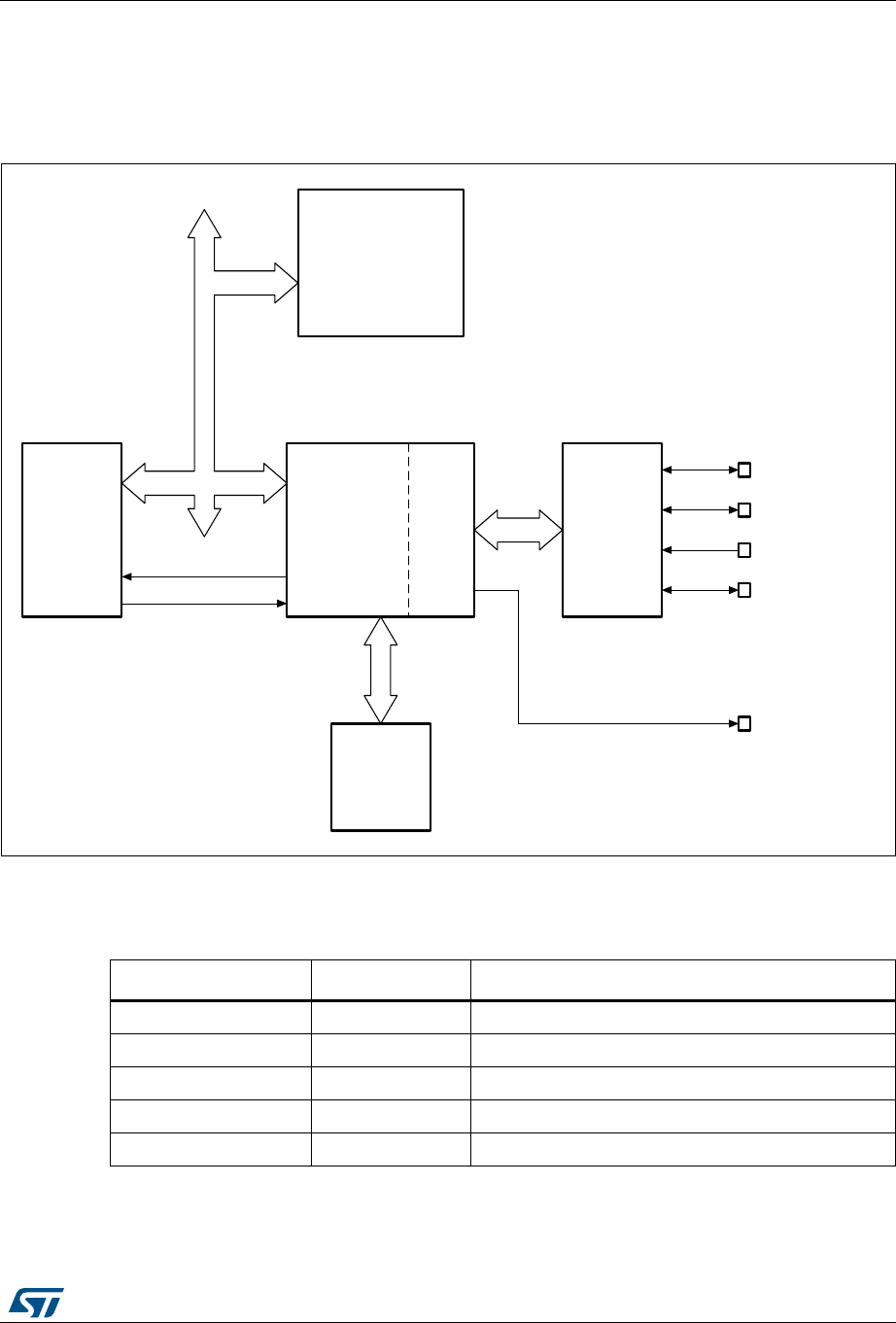
RM0430 Rev 8 1135/1324
RM0430 USB on-the-go full-speed (OTG_FS)
1283
33.4 OTG functional description
33.4.1 OTG block diagram
Figure 395. OTG full-speed block diagram
33.4.2 USB OTG pin and internal signals
069
86%
27*)6
FRUH
6\VWHPFORFNGRPDLQ 86%FORFN
GRPDLQ
27*
)6
3+<
27*B)6B'3
27*B)6B'0
27*B)6B,'
27*B)6B9%86
8QLYHUVDOVHULDOEXV
3RZHU
DQG
FORFN
FRQWUROOHU
&RUWH[
FRUH
870,)6
5$0EXV
.E\WH
86%GDWD
),)2V
86%FORFNDW0+]
86%VXVSHQG
27*B)6B62)
Table 221. OTG_FS input/output pins
Signal name Signal type Description
OTG_FS_DP Digital input/output USB OTG D+ line
OTG_FS_DM Digital input/output USB OTG D- line
OTG_FS_ID Digital input USB OTG ID
OTG_FS_VBUS Analog input USB OTG VBUS
OTG_FS_SOF Digital output USB OTG Start Of Frame (visibility)

USB on-the-go full-speed (OTG_FS) RM0430
1136/1324 RM0430 Rev 8
33.4.3 OTG core
The USB OTG receives the 48 MHz clock from the reset and clock controller (RCC). The
USB clock is used for driving the 48 MHz domain at full-speed (12 Mbit/s) and must be
enabled prior to configuring the OTG core.
The CPU reads and writes from/to the OTG core registers through the AHB peripheral bus.
It is informed of USB events through the single USB OTG interrupt line described in
Section 33.13: OTG_FS interrupts.
The CPU submits data over the USB by writing 32-bit words to dedicated OTG locations
(push registers). The data are then automatically stored into Tx-data FIFOs configured
within the USB data RAM. There is one Tx FIFO push register for each in-endpoint
(peripheral mode) or out-channel (host mode).
The CPU receives the data from the USB by reading 32-bit words from dedicated OTG
addresses (pop registers). The data are then automatically retrieved from a shared Rx FIFO
configured within the 1.25-Kbyte USB data RAM. There is one Rx FIFO pop register for
each out-endpoint or in-channel.
The USB protocol layer is driven by the serial interface engine (SIE) and serialized over the
USB by the transceiver module within the on-chip physical layer (PHY).
33.4.4 Full-speed OTG PHY
The embedded full-speed OTG PHY is controlled by the OTG FS core and conveys USB
control & data signals through the full-speed subset of the UTMI+ Bus (UTMIFS). It provides
the physical support to USB connectivity.
The full-speed OTG PHY includes the following components:
•FS/LS transceiver module used by both host and device. It directly drives transmission
and reception on the single-ended USB lines.
•Integrated ID pull-up resistor used to sample the ID line for A/B device identification.
•DP/DM integrated pull-up and pull-down resistors controlled by the OTG_FS core
depending on the current role of the device. As a peripheral, it enables the DP pull-up
resistor to signal full-speed peripheral connections as soon as VBUS is sensed to be at
a valid level (B-session valid). In host mode, pull-down resistors are enabled on both
DP/DM. Pull-up and pull-down resistors are dynamically switched when the role of the
device is changed via the host negotiation protocol (HNP).
•Pull-up/pull-down resistor ECN circuit. The DP pull-up consists of two resistors
controlled separately from the OTG_FS as per the resistor Engineering Change Notice
applied to USB Rev2.0. The dynamic trimming of the DP pull-up strength allows for
better noise rejection and Tx/Rx signal quality.
•VBUS sensing comparators with hysteresis used to detect VBUS valid, A-B session valid
and session-end voltage thresholds. They are used to drive the session request
Table 222. OTG_FS input/output signals
Signal name Signal type Description
usb_sof Digital output USB OTG start-of-frame event for on chip peripherals
usb_wkup Digital output USB OTG wakeup event output
usb_gbl_it Digital output USB OTG global interrupt
RM0430 Rev 8 1137/1324
RM0430 USB on-the-go full-speed (OTG_FS)
1283
protocol (SRP), detect valid startup and end-of-session conditions, and constantly
monitor the VBUS supply during USB operations.
•VBUS pulsing method circuit used to charge/discharge VBUS through resistors during
the SRP (weak drive).
Caution: To guarantee a correct operation for the USB OTG FS peripheral, the AHB frequency should
be higher than 14.2 MHz.
33.5 OTG dual role device (DRD)
Figure 396. OTG_FS A-B device connection
1. External voltage regulator only needed when building a VBUS powered device.
2. STMPS2141STR needed only if the application has to support a VBUS powered device. A basic power
switch can be used if 5 V are available on the application board.
33.5.1 ID line detection
The host or peripheral (the default) role is assumed depending on the ID input pin. The ID
line status is determined on plugging in the USB cable, depending on whether a MicroA or
MicroB plug is connected to the micro-AB receptacle.
•If the B-side of the USB cable is connected with a floating ID wire, the integrated pull-
up resistor detects a high ID level and the default peripheral role is confirmed. In this
configuration the OTG_FS complies with the standard FSM described in section 4.2.4:
ID pin of the On-the-Go specification Rev2.0, supplement to the USB2.0.
•If the A-side of the USB cable is connected with a grounded ID, the OTG_FS issues an
ID line status change interrupt (CIDSCHG bit in OTG_GINTSTS) for host software
initialization, and automatically switches to the host role. In this configuration the
OTG_FS complies with the standard FSM described by section 4.2.4: ID pin of the On-
the-Go specification Rev2.0, supplement to the USB2.0.
06Y9
26&B,1
26&B287
*3,2
*3,2,54
9''
(1
2YHUFXUUHQW
9WR9''
9ROWDJH
UHJXODWRU
9''
93ZU
9%86
'0
'3
,'
966
67036675
&XUUHQWOLPLWHG
SRZHUGLVWULEXWLRQ
VZLWFK
86%PLFUR$%FRQQHFWRU

USB on-the-go full-speed (OTG_FS) RM0430
1138/1324 RM0430 Rev 8
33.5.2 HNP dual role device
The HNP capable bit in the Global USB configuration register (HNPCAP bit in OTG_
GUSBCFG) enables the OTG_FS core to dynamically change its role from A-host to A-
peripheral and vice-versa, or from B-Peripheral to B-host and vice-versa according to the
host negotiation protocol (HNP). The current device status can be read by the combined
values of the connector ID status bit in the Global OTG control and status register (CIDSTS
bit in OTG_GOTGCTL) and the current mode of operation bit in the global interrupt and
status register (CMOD bit in OTG_GINTSTS).
The HNP program model is described in detail in Section 33.16: OTG_FS programming
model.
33.5.3 SRP dual role device
The SRP capable bit in the global USB configuration register (SRPCAP bit in
OTG_GUSBCFG) enables the OTG_FS core to switch off the generation of VBUS for the A-
device to save power. Note that the A-device is always in charge of driving VBUS regardless
of the host or peripheral role of the OTG_FS.
The SRP A/B-device program model is described in detail in Section 33.16: OTG_FS
programming model.
33.6 USB peripheral
This section gives the functional description of the OTG_FS in the USB peripheral mode.
The OTG_FS works as an USB peripheral in the following circumstances:
•OTG B-Peripheral
– OTG B-device default state if B-side of USB cable is plugged in
•OTG A-Peripheral
– OTG A-device state after the HNP switches the OTG_FS to its peripheral role
•B-device
– If the ID line is present, functional and connected to the B-side of the USB cable,
and the HNP-capable bit in the Global USB Configuration register (HNPCAP bit in
OTG_GUSBCFG) is cleared.
•Peripheral only (see Figure 397: USB_FS peripheral-only connection)
– The force device mode bit (FDMOD) in the Section 33.15.4: OTG USB
configuration register (OTG_GUSBCFG) is set to 1, forcing the OTG_FS core to
work as an USB peripheral-only. In this case, the ID line is ignored even if it is
present on the USB connector.
Note: To build a bus-powered device implementation in case of the B-device or peripheral-only
configuration, an external regulator has to be added, that generates the necessary power-
supply from VBUS.
RM0430 Rev 8 1139/1324
RM0430 USB on-the-go full-speed (OTG_FS)
1283
Figure 397. USB_FS peripheral-only connection
1. Use a regulator to build a bus-powered device.
33.6.1 SRP-capable peripheral
The SRP capable bit in the Global USB configuration register (SRPCAP bit in
OTG_GUSBCFG) enables the OTG_FS to support the session request protocol (SRP). In
this way, it allows the remote A-device to save power by switching off VBUS while the USB
session is suspended.
The SRP peripheral mode program model is described in detail in the B-device session
request protocol section.
33.6.2 Peripheral states
Powered state
The VBUS input detects the B-session valid voltage by which the USB peripheral is allowed
to enter the powered state (see USB2.0 section 9.1). The OTG_FS then automatically
connects the DP pull-up resistor to signal full-speed device connection to the host and
generates the session request interrupt (SRQINT bit in OTG_GINTSTS) to notify the
powered state.
The VBUS input also ensures that valid VBUS levels are supplied by the host during USB
operations. If a drop in VBUS below B-session valid happens to be detected (for instance
because of a power disturbance or if the host port has been switched off), the OTG_FS
automatically disconnects and the session end detected (SEDET bit in OTG_GOTGINT)
interrupt is generated to notify that the OTG_FS has exited the powered state.
In the powered state, the OTG_FS expects to receive some reset signaling from the host.
No other USB operation is possible. When a reset signaling is received the reset detected
interrupt (USBRST in OTG_GINTSTS) is generated. When the reset signaling is complete,
the enumeration done interrupt (ENUMDNE bit in OTG_GINTSTS) is generated and the
OTG_FS enters the Default state.
06Y9
K^ͺ/E
K^ͺKhd
'W/K
'W/Kн/ZY
9''
(1
2YHUFXUUHQW
9WR9''
9ROWDJH
UHJXODWRU
9''
93ZU
9%86
'0
'3
966
67036675
&XUUHQWOLPLWHG
SRZHUGLVWULEXWLRQ
VZLWFK
h^ŵŝĐƌŽĐŽŶŶĞĐƚŽƌ

USB on-the-go full-speed (OTG_FS) RM0430
1140/1324 RM0430 Rev 8
Soft disconnect
The powered state can be exited by software with the soft disconnect feature. The DP pull-
up resistor is removed by setting the soft disconnect bit in the device control register (SDIS
bit in OTG_DCTL), causing a device disconnect detection interrupt on the host side even
though the USB cable was not really removed from the host port.
Default state
In the Default state the OTG_FS expects to receive a SET_ADDRESS command from the
host. No other USB operation is possible. When a valid SET_ADDRESS command is
decoded on the USB, the application writes the corresponding number into the device
address field in the device configuration register (DAD bit in OTG_DCFG). The OTG_FS
then enters the address state and is ready to answer host transactions at the configured
USB address.
Suspended state
The OTG_FS peripheral constantly monitors the USB activity. After counting 3 ms of USB
idleness, the early suspend interrupt (ESUSP bit in OTG_GINTSTS) is issued, and
confirmed 3 ms later, if appropriate, by the suspend interrupt (USBSUSP bit in
OTG_GINTSTS). The device suspend bit is then automatically set in the device status
register (SUSPSTS bit in OTG_DSTS) and the OTG_FS enters the suspended state.
The suspended state may optionally be exited by the device itself. In this case the
application sets the remote wakeup signaling bit in the device control register (RWUSIG bit
in OTG_DCTL) and clears it after 1 to 15 ms.
When a resume signaling is detected from the host, the resume interrupt (WKUPINT bit in
OTG_GINTSTS) is generated and the device suspend bit is automatically cleared.
33.6.3 Peripheral endpoints
The OTG_FS core instantiates the following USB endpoints:
•Control endpoint 0:
– Bidirectional and handles control messages only
– Separate set of registers to handle in and out transactions
– Proper control (OTG_DIEPCTL0/OTG_DOEPCTL0), transfer configuration
(OTG_DIEPTSIZ0/OTG_DOEPTSIZ0), and status-interrupt
(OTG_DIEPINT0/)OTG_DOEPINT0) registers. The available set of bits inside the
control and transfer size registers slightly differs from that of other endpoints
•5 IN endpoints
– Each of them can be configured to support the isochronous, bulk or interrupt
transfer type
– Each of them has proper control (OTG_DIEPCTLx), transfer configuration
(OTG_DIEPTSIZx), and status-interrupt (OTG_DIEPINTx) registers
– The device IN endpoints common interrupt mask register (OTG_DIEPMSK) is
available to enable/disable a single kind of endpoint interrupt source on all of the
IN endpoints (EP0 included)
– Support for incomplete isochronous IN transfer interrupt (IISOIXFR bit in
OTG_GINTSTS), asserted when there is at least one isochronous IN endpoint on

RM0430 Rev 8 1141/1324
RM0430 USB on-the-go full-speed (OTG_FS)
1283
which the transfer is not completed in the current frame. This interrupt is asserted
along with the end of periodic frame interrupt (OTG_GINTSTS/EOPF).
•5 OUT endpoints
– Each of them can be configured to support the isochronous, bulk or interrupt
transfer type
– Each of them has a proper control (OTG_DOEPCTLx), transfer configuration
(OTG_DOEPTSIZx) and status-interrupt (OTG_DOEPINTx) register
– Device OUT endpoints common interrupt mask register (OTG_DOEPMSK) is
available to enable/disable a single kind of endpoint interrupt source on all of the
OUT endpoints (EP0 included)
– Support for incomplete isochronous OUT transfer interrupt (INCOMPISOOUT bit
in OTG_GINTSTS), asserted when there is at least one isochronous OUT
endpoint on which the transfer is not completed in the current frame. This interrupt
is asserted along with the end of periodic frame interrupt (OTG_GINTSTS/EOPF).
Endpoint control
•The following endpoint controls are available to the application through the device
endpoint-x IN/OUT control register (OTG_DIEPCTLx/OTG_DOEPCTLx):
– Endpoint enable/disable
– Endpoint activate in current configuration
– Program USB transfer type (isochronous, bulk, interrupt)
– Program supported packet size
– Program Tx FIFO number associated with the IN endpoint
– Program the expected or transmitted data0/data1 PID (bulk/interrupt only)
– Program the even/odd frame during which the transaction is received or
transmitted (isochronous only)
– Optionally program the NAK bit to always negative-acknowledge the host
regardless of the FIFO status
– Optionally program the STALL bit to always stall host tokens to that endpoint
– Optionally program the SNOOP mode for OUT endpoint not to check the CRC
field of received data
Endpoint transfer
The device endpoint-x transfer size registers (OTG_DIEPTSIZx/OTG_DOEPTSIZx) allow
the application to program the transfer size parameters and read the transfer status.
Programming must be done before setting the endpoint enable bit in the endpoint control
register. Once the endpoint is enabled, these fields are read-only as the OTG_FS core
updates them with the current transfer status.
The following transfer parameters can be programmed:
•Transfer size in bytes
•Number of packets that constitute the overall transfer size
Endpoint status/interrupt
The device endpoint-x interrupt registers (OTG_DIEPINTx/OTG_DOPEPINTx) indicate the
status of an endpoint with respect to USB- and AHB-related events. The application must
read these registers when the OUT endpoint interrupt bit or the IN endpoint interrupt bit in

USB on-the-go full-speed (OTG_FS) RM0430
1142/1324 RM0430 Rev 8
the core interrupt register (OEPINT bit in OTG_GINTSTS or IEPINT bit in OTG_GINTSTS,
respectively) is set. Before the application can read these registers, it must first read the
device all endpoints interrupt (OTG_DAINT) register to get the exact endpoint number for
the device endpoint-x interrupt register. The application must clear the appropriate bit in this
register to clear the corresponding bits in the OTG_DAINT and OTG_GINTSTS registers
The peripheral core provides the following status checks and interrupt generation:
•Transfer completed interrupt, indicating that data transfer was completed on both the
application (AHB) and USB sides
•Setup stage has been done (control-out only)
•Associated transmit FIFO is half or completely empty (in endpoints)
•NAK acknowledge has been transmitted to the host (isochronous-in only)
•IN token received when Tx FIFO was empty (bulk-in/interrupt-in only)
•Out token received when endpoint was not yet enabled
•Babble error condition has been detected
•Endpoint disable by application is effective
•Endpoint NAK by application is effective (isochronous-in only)
•More than 3 back-to-back setup packets were received (control-out only)
•Timeout condition detected (control-in only)
•Isochronous out packet has been dropped, without generating an interrupt
33.7 USB host
This section gives the functional description of the OTG_FS in the USB host mode. The
OTG_FS works as a USB host in the following circumstances:
•OTG A-host
– OTG A-device default state when the A-side of the USB cable is plugged in
•OTG B-host
– OTG B-device after HNP switching to the host role
•A-device
– If the ID line is present, functional and connected to the A-side of the USB cable,
and the HNP-capable bit is cleared in the Global USB Configuration register
(HNPCAP bit in OTG_GUSBCFG). Integrated pull-down resistors are
automatically set on the DP/DM lines.
•Host only
– The force host mode bit (FHMOD) in the OTG USB configuration register
(OTG_GUSBCFG) forces the OTG_FS core to work as a USB host-only. In this
case, the ID line is ignored even if present on the USB connector. Integrated pull-
down resistors are automatically set on the DP/DM lines.
Note: On-chip 5 V VBUS generation is not supported. For this reason, a charge pump or, if 5 V are
available on the application board, a basic power switch must be added externally to drive
the 5 V VBUS line. The external charge pump can be driven by any GPIO output. This is
required for the OTG A-host, A-device and host-only configurations.
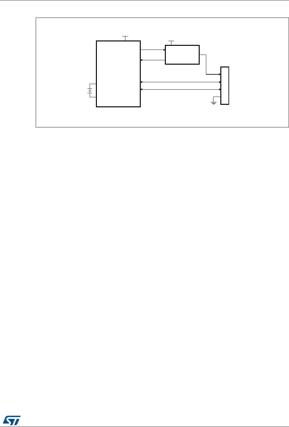
RM0430 Rev 8 1143/1324
RM0430 USB on-the-go full-speed (OTG_FS)
1283
Figure 398. USB_FS host-only connection
1. VDD range is between 2 V and 3.6 V.
33.7.1 SRP-capable host
SRP support is available through the SRP capable bit in the global USB configuration
register (SRPCAP bit in OTG_GUSBCFG). With the SRP feature enabled, the host can
save power by switching off the VBUS power while the USB session is suspended.
The SRP host mode program model is described in detail in the A-device session request
protocol) section.
33.7.2 USB host states
Host port power
On-chip 5 V VBUS generation is not supported. For this reason, a charge pump or, if 5 V are
available on the application board, a basic power switch, must be added externally to drive
the 5 V VBUS line. The external charge pump can be driven by any GPIO output or via an
I2C interface connected to an external PMIC (power management IC). When the application
decides to power on VBUS, it must also set the port power bit in the host port control and
status register (PPWR bit in OTG_HPRT).
VBUS valid
When HNP or SRP is enabled the VBUS sensing pin should be connected to VBUS. The
VBUS input ensures that valid VBUS levels are supplied by the charge pump during USB
operations. Any unforeseen VBUS voltage drop below the VBUS valid threshold (4.4 V) leads
to an OTG interrupt triggered by the session end detected bit (SEDET bit in
OTG_GOTGINT). The application is then required to remove the VBUS power and clear the
port power bit.
When HNP and SRP are both disabled, the VBUS sensing pin does not need to be
connected to VBUS.
The charge pump overcurrent flag can also be used to prevent electrical damage. Connect
the overcurrent flag output from the charge pump to any GPIO input and configure it to
generate a port interrupt on the active level. The overcurrent ISR must promptly disable the
VBUS generation and clear the port power bit.
06Y9
67036675
&XUUHQWOLPLWHG
SRZHUGLVWULEXWLRQ
VZLWFK
26&B,1
26&B287
*3,2
*3,2,54
(1
2YHUFXUUHQW
9
93ZU
9%86
'0
'3
966
86%6WG$FRQQHFWRU
9''

USB on-the-go full-speed (OTG_FS) RM0430
1144/1324 RM0430 Rev 8
Host detection of a peripheral connection
If SRP or HNP are enabled, even if USB peripherals or B-devices can be attached at any
time, the OTG_FS will not detect any bus connection until VBUS is no longer sensed at a
valid level (5 V). When VBUS is at a valid level and a remote B-device is attached, the
OTG_FS core issues a host port interrupt triggered by the device connected bit in the host
port control and status register (PCDET bit in OTG_HPRT).
When HNP and SRP are both disabled, USB peripherals or B-device are detected as soon
as they are connected. The OTG_FS core issues a host port interrupt triggered by the
device connected bit in the host port control and status (PCDET bit in OTG_HPRT).
Host detection of peripheral a disconnection
The peripheral disconnection event triggers the disconnect detected interrupt (DISCINT bit
in OTG_GINTSTS).
Host enumeration
After detecting a peripheral connection the host must start the enumeration process by
sending USB reset and configuration commands to the new peripheral.
Before starting to drive a USB reset, the application waits for the OTG interrupt triggered by
the debounce done bit (DBCDNE bit in OTG_GOTGINT), which indicates that the bus is
stable again after the electrical debounce caused by the attachment of a pull-up resistor on
DP (FS) or DM (LS).
The application drives a USB reset signaling (single-ended zero) over the USB by keeping
the port reset bit set in the host port control and status register (PRST bit in OTG_HPRT) for
a minimum of 10 ms and a maximum of 20 ms. The application takes care of the timing
count and then of clearing the port reset bit.
Once the USB reset sequence has completed, the host port interrupt is triggered by the port
enable/disable change bit (PENCHNG bit in OTG_HPRT). This informs the application that
the speed of the enumerated peripheral can be read from the port speed field in the host
port control and status register (PSPD bit in OTG_HPRT) and that the host is starting to
drive SOFs (FS) or Keep alives (LS). The host is now ready to complete the peripheral
enumeration by sending peripheral configuration commands.
Host suspend
The application decides to suspend the USB activity by setting the port suspend bit in the
host port control and status register (PSUSP bit in OTG_HPRT). The OTG_FS core stops
sending SOFs and enters the suspended state.
The suspended state can be optionally exited on the remote device’s initiative (remote
wakeup). In this case the remote wakeup interrupt (WKUPINT bit in OTG_GINTSTS) is
generated upon detection of a remote wakeup signaling, the port resume bit in the host port
control and status register (PRES bit in OTG_HPRT) self-sets, and resume signaling is
automatically driven over the USB. The application must time the resume window and then
clear the port resume bit to exit the suspended state and restart the SOF.
If the suspended state is exited on the host initiative, the application must set the port
resume bit to start resume signaling on the host port, time the resume window and finally
clear the port resume bit.

RM0430 Rev 8 1145/1324
RM0430 USB on-the-go full-speed (OTG_FS)
1283
33.7.3 Host channels
The OTG_FS core instantiates 12 host channels. Each host channel supports an USB host
transfer (USB pipe). The host is not able to support more than 12 transfer requests at the
same time. If more than 12 transfer requests are pending from the application, the host
controller driver (HCD) must re-allocate channels when they become available from
previous duty, that is, after receiving the transfer completed and channel halted interrupts.
Each host channel can be configured to support in/out and any type of periodic/nonperiodic
transaction. Each host channel makes us of proper control (OTG_HCCHARx), transfer
configuration (OTG_HCTSIZx) and status/interrupt (OTG_HCINTx) registers with
associated mask (OTG_HCINTMSKx) registers.
Host channel control
•The following host channel controls are available to the application through the host
channel-x characteristics register (OTG_HCCHARx):
– Channel enable/disable
– Program the FS/LS speed of target USB peripheral
– Program the address of target USB peripheral
– Program the endpoint number of target USB peripheral
– Program the transfer IN/OUT direction
– Program the USB transfer type (control, bulk, interrupt, isochronous)
– Program the maximum packet size (MPS)
– Program the periodic transfer to be executed during odd/even frames
Host channel transfer
The host channel transfer size registers (OTG_HCTSIZx) allow the application to program
the transfer size parameters, and read the transfer status. Programming must be done
before setting the channel enable bit in the host channel characteristics register. Once the
endpoint is enabled the packet count field is read-only as the OTG_FS core updates it
according to the current transfer status.
•The following transfer parameters can be programmed:
– transfer size in bytes
– number of packets making up the overall transfer size
– initial data PID
Host channel status/interrupt
The host channel-x interrupt register (OTG_HCINTx) indicates the status of an endpoint
with respect to USB- and AHB-related events. The application must read these register
when the host channels interrupt bit in the core interrupt register (HCINT bit in
OTG_GINTSTS) is set. Before the application can read these registers, it must first read the
host all channels interrupt (OTG_HAINT) register to get the exact channel number for the
host channel-x interrupt register. The application must clear the appropriate bit in this
register to clear the corresponding bits in the OTG_HAINT and OTG_GINTSTS registers.

USB on-the-go full-speed (OTG_FS) RM0430
1146/1324 RM0430 Rev 8
The mask bits for each interrupt source of each channel are also available in the
OTG_HCINTMSKx register.
•The host core provides the following status checks and interrupt generation:
– Transfer completed interrupt, indicating that the data transfer is complete on both
the application (AHB) and USB sides
– Channel has stopped due to transfer completed, USB transaction error or disable
command from the application
– Associated transmit FIFO is half or completely empty (IN endpoints)
– ACK response received
– NAK response received
– STALL response received
– USB transaction error due to CRC failure, timeout, bit stuff error, false EOP
– Babble error
– frame overrun
– data toggle error
33.7.4 Host scheduler
The host core features a built-in hardware scheduler which is able to autonomously re-order
and manage the USB transaction requests posted by the application. At the beginning of
each frame the host executes the periodic (isochronous and interrupt) transactions first,
followed by the nonperiodic (control and bulk) transactions to achieve the higher level of
priority granted to the isochronous and interrupt transfer types by the USB specification.
The host processes the USB transactions through request queues (one for periodic and one
for nonperiodic). Each request queue can hold up to 8 entries. Each entry represents a
pending transaction request from the application, and holds the IN or OUT channel number
along with other information to perform a transaction on the USB. The order in which the
requests are written to the queue determines the sequence of the transactions on the USB
interface.
At the beginning of each frame, the host processes the periodic request queue first, followed
by the nonperiodic request queue. The host issues an incomplete periodic transfer interrupt
(IPXFR bit in OTG_GINTSTS) if an isochronous or interrupt transaction scheduled for the
current frame is still pending at the end of the current frame. The OTG_FS core is fully
responsible for the management of the periodic and nonperiodic request queues.The
periodic transmit FIFO and queue status register (OTG_HPTXSTS) and nonperiodic
transmit FIFO and queue status register (OTG_HNPTXSTS) are read-only registers which
can be used by the application to read the status of each request queue. They contain:
•The number of free entries currently available in the periodic (nonperiodic) request
queue (8 max)
•Free space currently available in the periodic (nonperiodic) Tx FIFO (out-transactions)
•IN/OUT token, host channel number and other status information.
As request queues can hold a maximum of 8 entries each, the application can push to
schedule host transactions in advance with respect to the moment they physically reach the
SB for a maximum of 8 pending periodic transactions plus 8 pending non-periodic
transactions.
To post a transaction request to the host scheduler (queue) the application must check that
there is at least 1 entry available in the periodic (nonperiodic) request queue by reading the
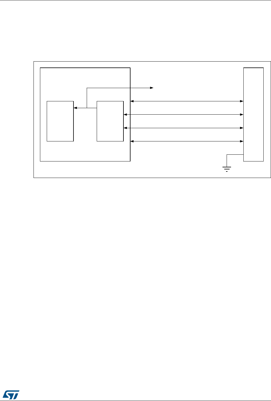
RM0430 Rev 8 1147/1324
RM0430 USB on-the-go full-speed (OTG_FS)
1283
PTXQSAV bits in the OTG_HNPTXSTS register or NPTQXSAV bits in the
OTG_HNPTXSTS register.
33.8 SOF trigger
Figure 399. SOF connectivity (SOF trigger output to TIM and ITR1 connection)
The OTG_FS core provides means to monitor, track and configure SOF framing in the host
and peripheral, as well as an SOF pulse output connectivity feature.
Such utilities are especially useful for adaptive audio clock generation techniques, where
the audio peripheral needs to synchronize to the isochronous stream provided by the PC, or
the host needs to trim its framing rate according to the requirements of the audio peripheral.
33.8.1 Host SOFs
In host mode the number of PHY clocks occurring between the generation of two
consecutive SOF (FS) or Keep-alive (LS) tokens is programmable in the host frame interval
register (HFIR), thus providing application control over the SOF framing period. An interrupt
is generated at any start of frame (SOF bit in OTG_GINTSTS). The current frame number
and the time remaining until the next SOF are tracked in the host frame number register
(HFNUM).
A SOF pulse signal, is generated at any SOF starting token and with a width of 20 HCLK
cycles. The SOF pulse is also internally connected to the input trigger of the timer, so that
the input capture feature, the output compare feature and the timer can be triggered by the
SOF pulse.
33.8.2 Peripheral SOFs
In device mode, the start of frame interrupt is generated each time an SOF token is received
on the USB (SOF bit in OTG_GINTSTS). The corresponding frame number can be read
from the device status register (FNSOF bit in OTG_DSTS). A SOF pulse signal with a width
of 20 HCLK cycles is also generated.The SOF pulse signal is also internally connected to
the TIM input trigger, so that the input capture feature, the output compare feature and the
timer can be triggered by the SOF pulse.
670
7,0 62)JHQ
62)SXOVH
86%PLFUR$%FRQQHFWRU
,75
62)SXOVHRXWSXWWR
H[WHUQDODXGLRFRQWURO
9%86
966
'
'
,'
06Y9

USB on-the-go full-speed (OTG_FS) RM0430
1148/1324 RM0430 Rev 8
The end of periodic frame interrupt (OTG_GINTSTS/EOPF) is used to notify the application
when 80%, 85%, 90% or 95% of the time frame interval elapsed depending on the periodic
frame interval field in the device configuration register (PFIVL bit in OTG_DCFG). This
feature can be used to determine if all of the isochronous traffic for that frame is complete.
33.9 OTG low-power modes
Table 223 below defines the STM32 low power modes and their compatibility with the OTG.
The following bits and procedures reduce power consumption.
The power consumption of the OTG PHY is controlled by two or three bits in the general
core configuration register, depending on OTG revision supported.
•PHY power down (OTG_GCCFG/PWRDWN)
It switches on/off the full-speed transceiver module of the PHY. It must be preliminarily
set to allow any USB operation
•VBUS detection enable (OTG_GCCFG/VBDEN)
It switches on/off the VBUS sensing comparators associated with OTG operations
Power reduction techniques are available while in the USB suspended state, when the USB
session is not yet valid or the device is disconnected.
•Stop PHY clock (STPPCLK bit in OTG_PCGCCTL)
When setting the stop PHY clock bit in the clock gating control register, most of the
48 MHz clock domain internal to the OTG full-speed core is switched off by clock
gating. The dynamic power consumption due to the USB clock switching activity is cut
even if the 48 MHz clock input is kept running by the application
Most of the transceiver is also disabled, and only the part in charge of detecting the
asynchronous resume or remote wakeup event is kept alive.
•Gate HCLK (GATEHCLK bit in OTG_PCGCCTL)
When setting the Gate HCLK bit in the clock gating control register, most of the system
clock domain internal to the OTG_FS core is switched off by clock gating. Only the
register read and write interface is kept alive. The dynamic power consumption due to
Table 223. Compatibility of STM32 low power modes with the OTG
Mode Description USB compatibility
Run MCU fully active Required when USB not in
suspend state.
Sleep USB suspend exit causes the device to exit Sleep mode. Peripheral
registers content is kept.
Available while USB is in
suspend state.
Stop USB suspend exit causes the device to exit Stop mode. Peripheral
registers content is kept(1).
Available while USB is in
suspend state.
Standby Powered-down. The peripheral must be reinitialized after exiting
Standby mode.
Not compatible with USB
applications.
1. Within Stop mode there are different possible settings. Some restrictions may also exist, please refer to Section 5: Power
controller (PWR) to understand which (if any) restrictions apply when using OTG.
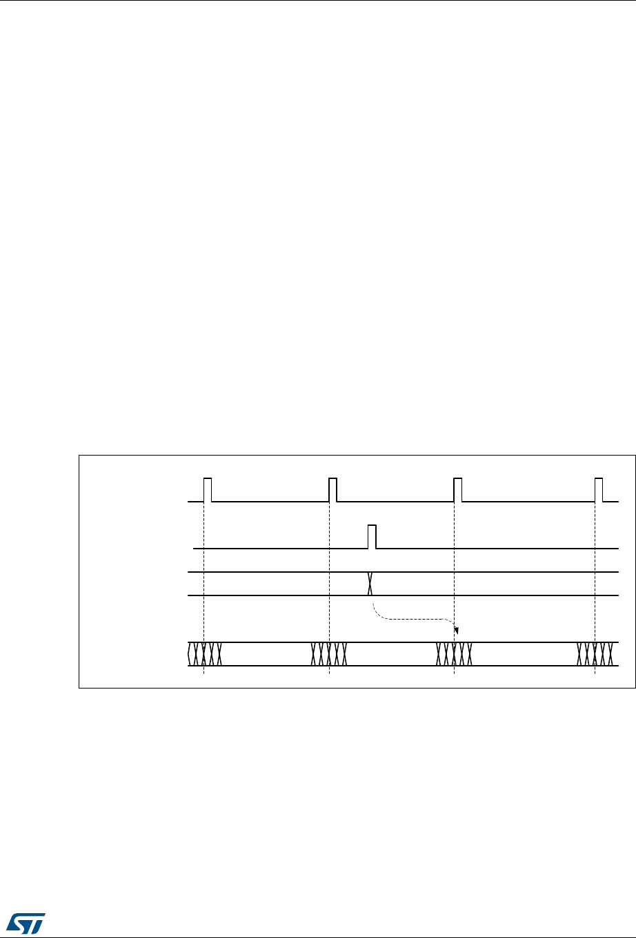
RM0430 Rev 8 1149/1324
RM0430 USB on-the-go full-speed (OTG_FS)
1283
the USB clock switching activity is cut even if the system clock is kept running by the
application for other purposes.
•USB system stop
When the OTG_FS is in the USB suspended state, the application may decide to
drastically reduce the overall power consumption by a complete shut down of all the
clock sources in the system. USB System Stop is activated by first setting the Stop
PHY clock bit and then configuring the system deep sleep mode in the power control
system module (PWR).
The OTG_FS core automatically reactivates both system and USB clocks by
asynchronous detection of remote wakeup (as an host) or resume (as a device)
signaling on the USB.
To save dynamic power, the USB data FIFO is clocked only when accessed by the OTG_FS
core.
33.10 Dynamic update of the OTG_HFIR register
The USB core embeds a dynamic trimming capability of SOF framing period in host mode
allowing to synchronize an external device with the SOF frames.
When the OTG_HFIR register is changed within a current SOF frame, the SOF period
correction is applied in the next frame as described in Figure 400.
For a dynamic update, it is required to set RLDCTRL=0.
Figure 400. Updating OTG_HFIR dynamically (RLDCTRL = 0)
33.11 USB data FIFOs
The USB system features 1.25 Kbytes of dedicated RAM with a sophisticated FIFO control
mechanism. The packet FIFO controller module in the OTG_FS core organizes RAM space
into Tx FIFOs into which the application pushes the data to be temporarily stored before the
USB transmission, and into a single Rx FIFO where the data received from the USB are
temporarily stored before retrieval (popped) by the application. The number of instructed
FIFOs and how these are organized inside the RAM depends on the device’s role. In
peripheral mode an additional Tx FIFO is instructed for each active IN endpoint. Any FIFO
size is software configured to better meet the application requirements.
DLE
62)UHORDG
27*B+),5ZULWH
27*B+),5YDOXH
)UDPHWLPHU
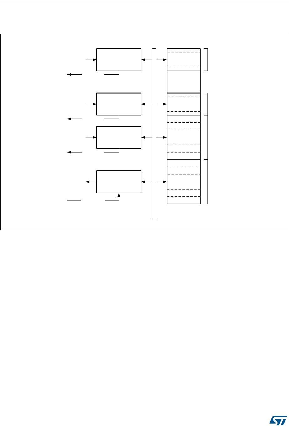
USB on-the-go full-speed (OTG_FS) RM0430
1150/1324 RM0430 Rev 8
33.11.1 Peripheral FIFO architecture
Figure 401. Device-mode FIFO address mapping and AHB FIFO access mapping
Peripheral Rx FIFO
The OTG peripheral uses a single receive FIFO that receives the data directed to all OUT
endpoints. Received packets are stacked back-to-back until free space is available in the Rx
FIFO. The status of the received packet (which contains the OUT endpoint destination
number, the byte count, the data PID and the validity of the received data) is also stored by
the core on top of the data payload. When no more space is available, host transactions are
NACKed and an interrupt is received on the addressed endpoint. The size of the receive
FIFO is configured in the receive FIFO size register (OTG_GRXFSIZ).
The single receive FIFO architecture makes it more efficient for the USB peripheral to fill in
the receive RAM buffer:
•All OUT endpoints share the same RAM buffer (shared FIFO)
•The OTG_FS core can fill in the receive FIFO up to the limit for any host sequence of
OUT tokens
The application keeps receiving the Rx FIFO non-empty interrupt (RXFLVL bit in
OTG_GINTSTS) as long as there is at least one packet available for download. It reads the
packet information from the receive status read and pop register (OTG_GRXSTSP) and
finally pops data off the receive FIFO by reading from the endpoint-related pop address.
06Y9
'HGLFDWHG7[
),)2[FRQWURO
RSWLRQDO
,1HQGSRLQW7[),)2[
'),)2SXVKDFFHVV
IURP$+%
0$&SRS
7[),)2[
SDFNHW
27*B',(37;)[>@
27*B',(37;)[>@
'HGLFDWHG7[
),)2FRQWURO
RSWLRQDO
,1HQGSRLQW7[),)2
'),)2SXVKDFFHVV
IURP$+%
7[),)2
SDFNHW
27*B',(37;)>@
27*B',(37;)>@
0$&SRS
'HGLFDWHG7[
),)2FRQWURO
RSWLRQDO
,1HQGSRLQW7[),)2
'),)2SXVKDFFHVV
IURP$+%
7[),)2
SDFNHW
27*B',(37;)>@
27*B',(37;)>@
0$&SRS
'HGLFDWHG7[
),)2FRQWURO
RSWLRQDO
$Q\287HQGSRLQW
'),)2SRSDFFHVV
IURP$+%
5[SDFNHWV 27*B*5;)6,=>@
0$&SXVK $ 5[VWDUWDGGUHVVIL[HG
WR
6LQJOHGDWD
),)2
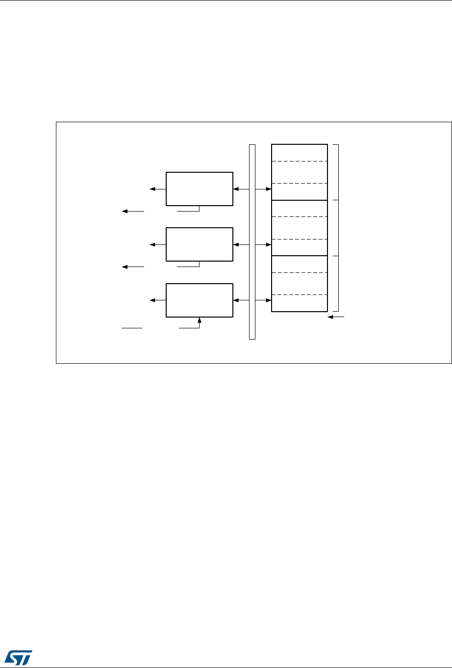
RM0430 Rev 8 1151/1324
RM0430 USB on-the-go full-speed (OTG_FS)
1283
Peripheral Tx FIFOs
The core has a dedicated FIFO for each IN endpoint. The application configures FIFO sizes
by writing the endpoint 0 transmit FIFO size register (OTG_DIEPTXF0) for IN endpoint0 and
the device IN endpoint transmit FIFOx registers (OTG_DIEPTXFx) for IN endpoint-x.
33.11.2 Host FIFO architecture
Figure 402. Host-mode FIFO address mapping and AHB FIFO access mapping
Host Rx FIFO
The host uses one receiver FIFO for all periodic and nonperiodic transactions. The FIFO is
used as a receive buffer to hold the received data (payload of the received packet) from the
USB until it is transferred to the system memory. Packets received from any remote IN
endpoint are stacked back-to-back until free space is available. The status of each received
packet with the host channel destination, byte count, data PID and validity of the received
data are also stored into the FIFO. The size of the receive FIFO is configured in the receive
FIFO size register (OTG_GRXFSIZ).
The single receive FIFO architecture makes it highly efficient for the USB host to fill in the
receive data buffer:
•All IN configured host channels share the same RAM buffer (shared FIFO)
•The OTG_FS core can fill in the receive FIFO up to the limit for any sequence of IN
tokens driven by the host software
The application receives the Rx FIFO not-empty interrupt as long as there is at least one
packet available for download. It reads the packet information from the receive status read
and pop register and finally pops the data off the receive FIFO.
06Y9
27*B+137;)6,=>@
5[),)2FRQWURO
$Q\FKDQQHO'),)2SRS
DFFHVVIURP$+%
5[SDFNHWV 27*B*5;)6,=>@
0$&SXVK
5[VWDUWDGGUHVVIL[HGWR
$
6LQJOHGDWD
),)2
27*B+137;)6,=>@
1RQSHULRGLF7[
),)2FRQWURO
$Q\QRQSHULRGLF
FKDQQHO'),)2SXVK
DFFHVVIURP$+%
1RQSHULRGLF
7[SDFNHWV
0$&SRS
27*B+37;)6,=>@
27*B+37;)6,=>@
3HULRGLF7[),)2
FRQWURORSWLRQDO
$Q\SHULRGLFFKDQQHO
'),)2SXVKDFFHVV
IURP$+%
3HULRGLF7[
SDFNHWV
0$&SRS

USB on-the-go full-speed (OTG_FS) RM0430
1152/1324 RM0430 Rev 8
Host Tx FIFOs
The host uses one transmit FIFO for all non-periodic (control and bulk) OUT transactions
and one transmit FIFO for all periodic (isochronous and interrupt) OUT transactions. FIFOs
are used as transmit buffers to hold the data (payload of the transmit packet) to be
transmitted over the USB. The size of the periodic (nonperiodic) Tx FIFO is configured in the
host periodic (nonperiodic) transmit FIFO size OTG_HPTXFSIZ / OTG_HNPTXFSIZ)
register.
The two Tx FIFO implementation derives from the higher priority granted to the periodic type
of traffic over the USB frame. At the beginning of each frame, the built-in host scheduler
processes the periodic request queue first, followed by the nonperiodic request queue.
The two transmit FIFO architecture provides the USB host with separate optimization for
periodic and nonperiodic transmit data buffer management:
•All host channels configured to support periodic (nonperiodic) transactions in the OUT
direction share the same RAM buffer (shared FIFOs)
•The OTG_FS core can fill in the periodic (nonperiodic) transmit FIFO up to the limit for
any sequence of OUT tokens driven by the host software
The OTG_FS core issues the periodic Tx FIFO empty interrupt (PTXFE bit in
OTG_GINTSTS) as long as the periodic Tx FIFO is half or completely empty, depending on
the value of the periodic Tx FIFO empty level bit in the AHB configuration register
(PTXFELVL bit in OTG_GAHBCFG). The application can push the transmission data in
advance as long as free space is available in both the periodic Tx FIFO and the periodic
request queue. The host periodic transmit FIFO and queue status register
(OTG_HPTXSTS) can be read to know how much space is available in both.
OTG_FS core issues the non periodic Tx FIFO empty interrupt (NPTXFE bit in
OTG_GINTSTS) as long as the nonperiodic Tx FIFO is half or completely empty depending
on the non periodic Tx FIFO empty level bit in the AHB configuration register (TXFELVL bit
in OTG_GAHBCFG). The application can push the transmission data as long as free space
is available in both the nonperiodic Tx FIFO and nonperiodic request queue. The host
nonperiodic transmit FIFO and queue status register (OTG_HNPTXSTS) can be read to
know how much space is available in both.
33.11.3 FIFO RAM allocation
Device mode
Receive FIFO RAM allocation: the application should allocate RAM for SETUP packets:
•10 locations must be reserved in the receive FIFO to receive SETUP packets on
control endpoint. The core does not use these locations, which are reserved for SETUP
packets, to write any other data.
•One location is to be allocated for Global OUT NAK.
•Status information is written to the FIFO along with each received packet. Therefore, a
minimum space of (largest packet size / 4) + 1 must be allocated to receive packets. If
multiple isochronous endpoints are enabled, then at least two (largest packet size / 4) +
1 spaces must be allocated to receive back-to-back packets. Typically, two (largest
packet size / 4) + 1 spaces are recommended so that when the previous packet is
being transferred to the CPU, the USB can receive the subsequent packet.
•Along with the last packet for each endpoint, transfer complete status information is
also pushed to the FIFO. One location for each OUT endpoint is recommended.

RM0430 Rev 8 1153/1324
RM0430 USB on-the-go full-speed (OTG_FS)
1283
Device RxFIFO =
(5 * number of control endpoints + 8) + ((largest USB packet used / 4) + 1 for status
information) + (2 * number of OUT endpoints) + 1 for Global NAK
Example: The MPS is 1,024 bytes for a periodic USB packet and 512 bytes for a non-
periodic USB packet. There are three OUT endpoints, three IN endpoints, one control
endpoint, and three host channels.
Device RxFIFO = (5 * 1 + 8) + ((1,024 / 4) +1) + (2 * 4) + 1 = 279
Transmit FIFO RAM allocation: the minimum RAM space required for each IN endpoint
Transmit FIFO is the maximum packet size for that particular IN endpoint.
Note: More space allocated in the transmit IN endpoint FIFO results in better performance on the
USB.
Host mode
Receive FIFO RAM allocation:
Status information is written to the FIFO along with each received packet. Therefore, a
minimum space of (largest packet size / 4) + 1 must be allocated to receive packets. If
multiple isochronous channels are enabled, then at least two (largest packet size / 4) + 1
spaces must be allocated to receive back-to-back packets. Typically, two (largest packet
size / 4) + 1 spaces are recommended so that when the previous packet is being transferred
to the CPU, the USB can receive the subsequent packet.
Along with the last packet in the host channel, transfer complete status information is also
pushed to the FIFO. So one location must be allocated for this.
Host RxFIFO = (largest USB packet used / 4) + 1 for status information + 1 transfer
complete
Example: Host RxFIFO = ((1,024 / 4) + 1) + 1 = 258
Transmit FIFO RAM allocation:
The minimum amount of RAM required for the host Non-periodic Transmit FIFO is the
largest maximum packet size among all supported non-periodic OUT channels.
Typically, two largest packet sizes worth of space is recommended, so that when the current
packet is under transfer to the USB, the CPU can get the next packet.
Non-Periodic TxFIFO = largest non-periodic USB packet used / 4
Example: Non-Periodic TxFIFO = (512 / 4) = 128
The minimum amount of RAM required for host periodic Transmit FIFO is the largest
maximum packet size out of all the supported periodic OUT channels. If there is at least one
isochronous OUT endpoint, then the space must be at least two times the maximum packet
size of that channel.
Host Periodic TxFIFO = largest periodic USB packet used / 4
Example: Host Periodic TxFIFO = (1,024 / 4) = 256
Note: More space allocated in the Transmit Non-periodic FIFO results in better performance on
the USB.

USB on-the-go full-speed (OTG_FS) RM0430
1154/1324 RM0430 Rev 8
33.12 OTG_FS system performance
Best USB and system performance is achieved owing to the large RAM buffers, the highly
configurable FIFO sizes, the quick 32-bit FIFO access through AHB push/pop registers and,
especially, the advanced FIFO control mechanism. Indeed, this mechanism allows the
OTG_FS to fill in the available RAM space at best regardless of the current USB sequence.
With these features:
•The application gains good margins to calibrate its intervention in order to optimize the
CPU bandwidth usage:
– It can accumulate large amounts of transmission data in advance compared to
when they are effectively sent over the USB
– It benefits of a large time margin to download data from the single receive FIFO
•The USB core is able to maintain its full operating rate, that is to provide maximum full-
speed bandwidth with a great margin of autonomy versus application intervention:
– It has a large reserve of transmission data at its disposal to autonomously manage
the sending of data over the USB
– It has a lot of empty space available in the receive buffer to autonomously fill it in
with the data coming from the USB
As the OTG_FS core is able to fill in the 1.25-Kbyte RAM buffer very efficiently, and as
1.25-Kbyte of transmit/receive data is more than enough to cover a full speed frame, the
USB system is able to withstand the maximum full-speed data rate for up to one USB frame
(1 ms) without any CPU intervention.
33.13 OTG_FS interrupts
When the OTG_FS controller is operating in one mode, either device or host, the application
must not access registers from the other mode. If an illegal access occurs, a mode
mismatch interrupt is generated and reflected in the core interrupt register (MMIS bit in the
OTG_GINTSTS register). When the core switches from one mode to the other, the registers
in the new mode of operation must be reprogrammed as they would be after a power-on
reset.
Figure 403 shows the interrupt hierarchy.
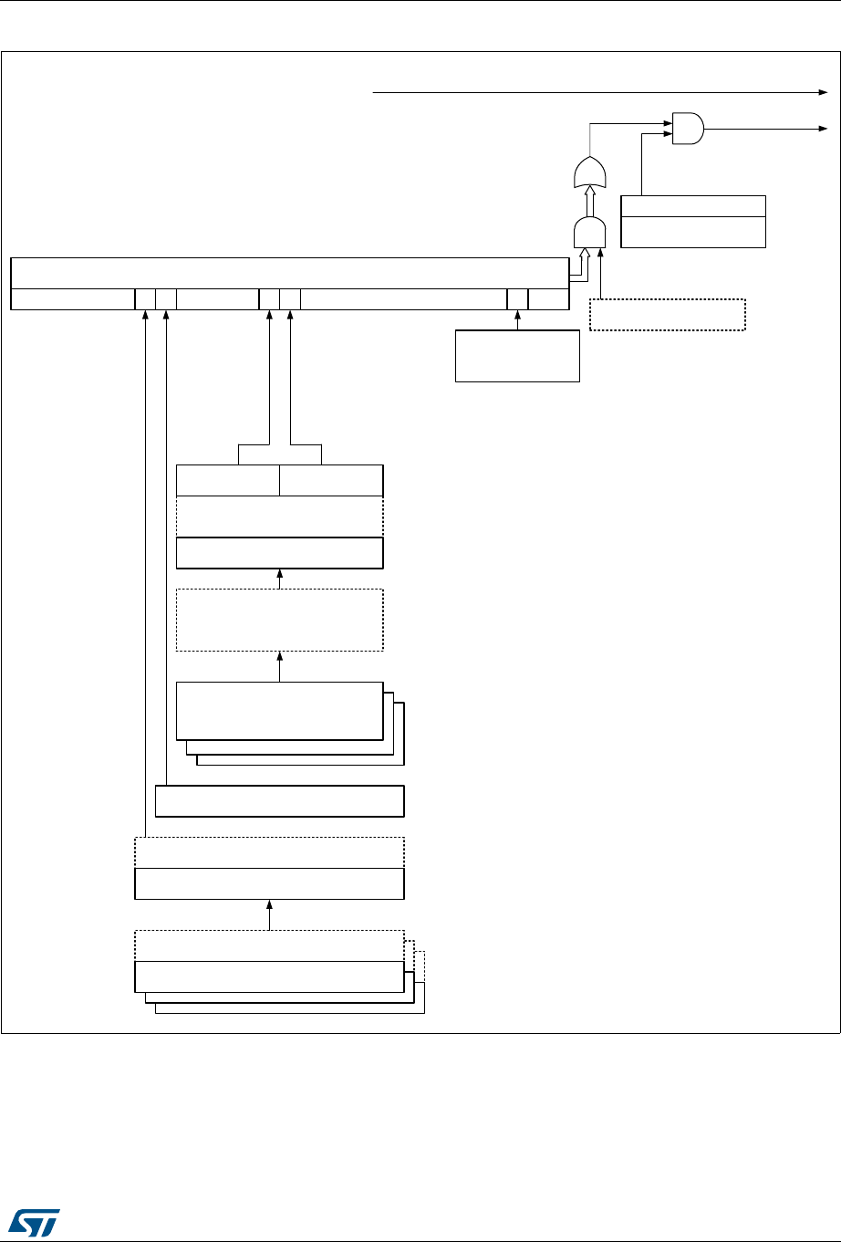
RM0430 Rev 8 1155/1324
RM0430 USB on-the-go full-speed (OTG_FS)
1283
Figure 403. Interrupt hierarchy
1. OTG_FS_WKUP becomes active (high state) when resume condition occurs during L1 SLEEP or L2 SUSPEND states.
06Y9
27*B'$,1706.
'HYLFHDOOHQGSRLQWVLQWHUUXSWPDVN
UHJLVWHU
27*B',(306.
27*B'2(306.
'HYLFH,1287HQGSRLQWVFRPPRQ
LQWHUUXSWPDVNUHJLVWHU
27*B+&7,1706.[
+RVWFKDQQHOVLQWHUUXSWPDVNUHJLVWHUV
27*B+$,1706.
+RVWDOOFKDQQHOVLQWHUUXSWPDVNUHJLVWHU
27*B+&7,17[
+RVWFKDQQHOVLQWHUUXSWUHJLVWHUV
27*B+$,17
+RVWDOOFKDQQHOVLQWHUUXSWUHJLVWHU
27*B+357
+RVWSRUWFRQWURODQGVWDWXVUHJLVWHU
27*B'$,17
'HYLFHDOOHQGSRLQWVLQWHUUXSWUHJLVWHU
(3
287HQGSRLQWV
(3
,1HQGSRLQWV
27*B*27*,17
27*LQWHUUXSWUHJLVWHU
27*B',(3,17[
27*B'2(3,17[
'HYLFH,1287HQGSRLQWLQWHUUXSW
UHJLVWHUV
27*B*,17676
&RUHUHJLVWHULQWHUUXSW
27*B*,1706.
&RUHLQWHUUXSWPDVNUHJLVWHU
27*B$+%&)*
$+%FRQILJXUDWLRQUHJLVWHU
*OREDOLQWHUUXSWPDVNELW
25
$1'
*OREDOLQWHUUXSW
27*B)6
:DNHXSLQWHUUXSW
27*B)6B:.83
$1'
[
[ +&
[
[ +&
+&,17
+357,17
2(3,13
,(3,17
27*,17

USB on-the-go full-speed (OTG_FS) RM0430
1156/1324 RM0430 Rev 8
33.14 OTG_FS control and status registers
By reading from and writing to the control and status registers (CSRs) through the AHB
slave interface, the application controls the OTG_FS controller. These registers are 32 bits
wide, and the addresses are 32-bit block aligned. The OTG_FS registers must be accessed
by words (32 bits).
CSRs are classified as follows:
•Core global registers
•Host-mode registers
•Host global registers
•Host port CSRs
•Host channel-specific registers
•Device-mode registers
•Device global registers
•Device endpoint-specific registers
•Power and clock-gating registers
•Data FIFO (DFIFO) access registers
Only the core global, power and clock-gating, data FIFO access, and host port control and
status registers can be accessed in both host and device modes. When the OTG_FS
controller is operating in one mode, either device or host, the application must not access
registers from the other mode. If an illegal access occurs, a mode mismatch interrupt is
generated and reflected in the core interrupt register (MMIS bit in the OTG_GINTSTS
register). When the core switches from one mode to the other, the registers in the new mode
of operation must be reprogrammed as they would be after a power-on reset.
33.14.1 CSR memory map
The host and device mode registers occupy different addresses. All registers are
implemented in the AHB clock domain.
Global CSR map
These registers are available in both host and device modes.
Table 224. Core global control and status registers (CSRs)
Acronym Address
offset Register name
OTG_GOTGCTL 0x000 Section 33.15.1: OTG control and status register (OTG_GOTGCTL)
OTG_GOTGINT 0x004 Section 33.15.2: OTG interrupt register (OTG_GOTGINT)
OTG_GAHBCFG 0x008 Section 33.15.3: OTG AHB configuration register (OTG_GAHBCFG)
OTG_GUSBCFG 0x00C Section 33.15.4: OTG USB configuration register (OTG_GUSBCFG)
OTG_GRSTCTL 0x010 Section 33.15.5: OTG reset register (OTG_GRSTCTL)
OTG_GINTSTS 0x014 Section 33.15.6: OTG core interrupt register (OTG_GINTSTS)
OTG_GINTMSK 0x018 Section 33.15.7: OTG interrupt mask register (OTG_GINTMSK)

RM0430 Rev 8 1157/1324
RM0430 USB on-the-go full-speed (OTG_FS)
1283
Host-mode CSR map
These registers must be programmed every time the core changes to host mode.
OTG_GRXSTSR 0x01C Section 33.15.8: OTG receive status debug read/OTG status read and pop
registers (OTG_GRXSTSR/OTG_GRXSTSP)
OTG_GRXSTSP 0x020
OTG_GRXFSIZ 0x024 Section 33.15.9: OTG receive FIFO size register (OTG_GRXFSIZ)
OTG_HNPTXFSIZ/
OTG_DIEPTXF0(1) 0x028 Section 33.15.10: OTG host non-periodic transmit FIFO size register
(OTG_HNPTXFSIZ)/Endpoint 0 Transmit FIFO size (OTG_DIEPTXF0)
OTG_HNPTXSTS 0x02C Section 33.15.11: OTG non-periodic transmit FIFO/queue status register
(OTG_HNPTXSTS)
OTG_GCCFG 0x038 Section 33.15.12: OTG general core configuration register (OTG_GCCFG)
OTG_CID 0x03C Section 33.15.13: OTG core ID register (OTG_CID)
OTG_GLPMCFG 0x54 Section 33.15.14: OTG core LPM configuration register (OTG_GLPMCFG)
OTG_HPTXFSIZ 0x100 Section 33.15.15: OTG host periodic transmit FIFO size register
(OTG_HPTXFSIZ)
OTG_DIEPTXFx
0x104
0x108
...
0x114
Section 33.15.16: OTG device IN endpoint transmit FIFO size register
(OTG_DIEPTXFx) (x = 1..5, where x is the FIFO number)
1. The general rule is to use OTG_HNPTXFSIZ for host mode and OTG_DIEPTXF0 for device mode.
Table 224. Core global control and status registers (CSRs) (continued)
Acronym Address
offset Register name
Table 225. Host-mode control and status registers (CSRs)
Acronym Offset
address Register name
OTG_HCFG 0x400 Section 33.15.18: OTG host configuration register (OTG_HCFG)
OTG_HFIR 0x404 Section 33.15.19: OTG host frame interval register (OTG_HFIR)
OTG_HFNUM 0x408 Section 33.15.20: OTG host frame number/frame time remaining register
(OTG_HFNUM)
OTG_HPTXSTS 0x410 Section 33.15.21: OTG_Host periodic transmit FIFO/queue status register
(OTG_HPTXSTS)
OTG_HAINT 0x414 Section 33.15.22: OTG host all channels interrupt register (OTG_HAINT)
OTG_HAINTMSK 0x418 Section 33.15.23: OTG host all channels interrupt mask register
(OTG_HAINTMSK)
OTG_HPRT 0x440 Section 33.15.24: OTG host port control and status register (OTG_HPRT)

USB on-the-go full-speed (OTG_FS) RM0430
1158/1324 RM0430 Rev 8
Device-mode CSR map
These registers must be programmed every time the core changes to device mode.
OTG_HCCHARx
0x500
0x520
...
0x660
Section 33.15.25: OTG host channel x characteristics register
(OTG_HCCHARx) (x = 0..11, where x = Channel number)
OTG_HCINTx
0x508
0x528
....
0x668
Section 33.15.26: OTG host channel x interrupt register (OTG_HCINTx)
(x = 0..11, where x = Channel number)
OTG_HCINTMSKx
0x50C
0x52C
....
0x66C
Section 33.15.27: OTG host channel x interrupt mask register
(OTG_HCINTMSKx) (x = 0..11, where x = Channel number)
OTG_HCTSIZx
0x510
0x530
....
0x670
Section 33.15.28: OTG host channel x transfer size register
(OTG_HCTSIZx) (x = 0..11, where x = Channel number)
Table 225. Host-mode control and status registers (CSRs) (continued)
Acronym Offset
address Register name
Table 226. Device-mode control and status registers
Acronym Offset
address Register name
OTG_DCFG 0x800 Section 33.15.30: OTG device configuration register (OTG_DCFG)
OTG_DCTL 0x804 Section 33.15.31: OTG device control register (OTG_DCTL)
OTG_DSTS 0x808 Section 33.15.32: OTG device status register (OTG_DSTS)
OTG_DIEPMSK 0x810 Section 33.15.33: OTG device IN endpoint common interrupt mask
register (OTG_DIEPMSK)
OTG_DOEPMSK 0x814 Section 33.15.34: OTG device OUT endpoint common interrupt mask
register (OTG_DOEPMSK)
OTG_DAINT 0x818 Section 33.15.35: OTG device all endpoints interrupt register
(OTG_DAINT)
OTG_DAINTMSK 0x81C Section 33.15.36: OTG all endpoints interrupt mask register
(OTG_DAINTMSK)
OTG_DVBUSDIS 0x828 Section 33.15.37: OTG device VBUS discharge time register
(OTG_DVBUSDIS)
OTG_DVBUSPULSE 0x82C Section 33.15.38: OTG device VBUS pulsing time register
(OTG_DVBUSPULSE)

RM0430 Rev 8 1159/1324
RM0430 USB on-the-go full-speed (OTG_FS)
1283
OTG_DIEPEMPMSK 0x834 Section 33.15.39: OTG device IN endpoint FIFO empty interrupt mask
register (OTG_DIEPEMPMSK)
OTG_DIEPCTL0 0x900 Section 33.15.40: OTG device control IN endpoint 0 control register
(OTG_DIEPCTL0)
OTG_DIEPCTLx
0x920
0x940
...
0x9A0
Section 33.15.41: OTG device IN endpoint x control register
(OTG_DIEPCTLx) (x = 1..5 , where x = endpoint number)
OTG_DIEPINTx
0x908
0x928
....
0x988
Section 33.15.42: OTG device IN endpoint x interrupt register
(OTG_DIEPINTx) (x = 0..5, where x = Endpoint number)
OTG_DIEPTSIZ0 0x910 Section 33.15.43: OTG device IN endpoint 0 transfer size register
(OTG_DIEPTSIZ0)
OTG_DTXFSTSx
0x918
0x938
....
0x998
Section 33.15.44: OTG device IN endpoint transmit FIFO status register
(OTG_DTXFSTSx) (x = 0..5, where x = endpoint number)
OTG_DIEPTSIZx
0x930
0x950
...
0x9B0
Section 33.15.45: OTG device IN endpoint x transfer size register
(OTG_DIEPTSIZx) (x = 1..5, where x = endpoint number)
OTG_DOEPCTL0 0xB00 Section 33.15.46: OTG device control OUT endpoint 0 control register
(OTG_DOEPCTL0)
OTG_DOEPINTx
0xB08
0xB28
...
0xBA8
Section 33.15.47: OTG device OUT endpoint x interrupt register
(OTG_DOEPINTx) (x = 0..5, where x = Endpoint number)
OTG_DOEPTSIZ0 0xB10 Section 33.15.48: OTG device OUT endpoint 0 transfer size register
(OTG_DOEPTSIZ0)
OTG_DOEPCTLx
0xB20
0xB40
...
0xBA0
Section 33.15.49: OTG device OUT endpoint x control register
(OTG_DOEPCTLx) (x = 1..5, where x = endpoint number)
OTG_DOEPTSIZx
0xB30
0xB50
...
0xBB0
Section 33.15.50: OTG device OUT endpoint x transfer size register
(OTG_DOEPTSIZx) (x = 1..5, where x = Endpoint number)
Table 226. Device-mode control and status registers (continued)
Acronym Offset
address Register name

USB on-the-go full-speed (OTG_FS) RM0430
1160/1324 RM0430 Rev 8
Data FIFO (DFIFO) access register map
These registers, available in both host and device modes, are used to read or write the FIFO
space for a specific endpoint or a channel, in a given direction. If a host channel is of type
IN, the FIFO can only be read on the channel. Similarly, if a host channel is of type OUT, the
FIFO can only be written on the channel.
Power and clock gating CSR map
There is a single register for power and clock gating. It is available in both host and device
modes.
33.15 OTG_FS registers
These registers are available in both host and device modes, and do not need to be
reprogrammed when switching between these modes.
Bit values in the register descriptions are expressed in binary unless otherwise specified.
Table 227. Data FIFO (DFIFO) access register map
FIFO access register section Offset address Access
Device IN endpoint 0/Host OUT Channel 0: DFIFO write access
Device OUT endpoint 0/Host IN Channel 0: DFIFO read access 0x1000–0x1FFC w
r
Device IN endpoint 1/Host OUT Channel 1: DFIFO write access
Device OUT endpoint 1/Host IN Channel 1: DFIFO read access 0x2000–0x2FFC w
r
... ... ...
Device IN endpoint x(1)/Host OUT Channel x(1): DFIFO write access
Device OUT endpoint x(1)/Host IN Channel x(1): DFIFO read access
1. Where x is 5 in device mode and 11 in host mode.
0xX000–0xXFFC w
r
Table 228. Power and clock gating control and status registers
Acronym Offset address Register name
OTG_PCGCCTL 0xE00–0xE04 Section 33.15.51: OTG power and clock gating control
register (OTG_PCGCCTL)

RM0430 Rev 8 1161/1324
RM0430 USB on-the-go full-speed (OTG_FS)
1283
33.15.1 OTG control and status register (OTG_GOTGCTL)
Address offset: 0x000
Reset value: 0x0001 0000
The OTG_GOTGCTL register controls the behavior and reflects the status of the OTG
function of the core.
31 30 29 28 27 26 25 24 23 22 21 20 19 18 17 16
Res. Res. Res. Res. Res. Res. Res. Res. Res. Res. CUR
MOD
OTG
VER BSVLD ASVLD DBCT CID
STS
rrwrrrr
1514131211109876543210
Res. Res. Res. EHEN DHNP
EN
HSHNP
EN
HNP
RQ
HNG
SCS
BVALO
VAL
BVALO
EN
AVALO
VAL
AVALO
EN
VBVAL
OVAL
VBVAL
OEN SRQ SRQ
SCS
rwrwrwrw r rwrwrwrwrwrwrw r
Bits 31:22 Reserved, must be kept at reset value.
Bit 21 CURMOD: Current mode of operation
Indicates the current mode (host or device).
0: Device mode
1: Host mode
Bit 20 OTGVER: OTG version
Selects the OTG revision.
0:OTG Version 1.3. OTG1.3 is obsolete for new product development.
1:OTG Version 2.0. In this version the core supports only data line pulsing for SRP.
Bit 19 BSVLD: B-session valid
Indicates the device mode transceiver status.
0: B-session is not valid.
1: B-session is valid.
In OTG mode, the user can use this bit to determine if the device is connected or
disconnected.
Note: Only accessible in device mode.
Bit 18 ASVLD: A-session valid
Indicates the host mode transceiver status.
0: A-session is not valid
1: A-session is valid
Note: Only accessible in host mode.
Bit 17 DBCT: Long/short debounce time
Indicates the debounce time of a detected connection.
0: Long debounce time, used for physical connections (100 ms + 2.5 µs)
1: Short debounce time, used for soft connections (2.5 µs)
Note: Only accessible in host mode.
Bit 16 CIDSTS: Connector ID status
Indicates the connector ID status on a connect event.
0: The OTG_FS controller is in A-device mode
1: The OTG_FS controller is in B-device mode
Note: Accessible in both device and host modes.

USB on-the-go full-speed (OTG_FS) RM0430
1162/1324 RM0430 Rev 8
Bits 15:13 Reserved, must be kept at reset value.
Bit 12 EHEN: Embedded host enable
It is used to select between OTG A device state machine and embedded host state machine.
0: OTG A device state machine is selected
1: Embedded host state machine is selected
Bit 11 DHNPEN: Device HNP enabled
The application sets this bit when it successfully receives a SetFeature.SetHNPEnable
command from the connected USB host.
0: HNP is not enabled in the application
1: HNP is enabled in the application
Note: Only accessible in device mode.
Bit 10 HSHNPEN: host set HNP enable
The application sets this bit when it has successfully enabled HNP (using the
SetFeature.SetHNPEnable command) on the connected device.
0: Host Set HNP is not enabled
1: Host Set HNP is enabled
Note: Only accessible in host mode.
Bit 9 HNPRQ: HNP request
The application sets this bit to initiate an HNP request to the connected USB host. The
application can clear this bit by writing a 0 when the host negotiation success status change
bit in the OTG_GOTGINT register (HNSSCHG bit in OTG_GOTGINT) is set. The core clears
this bit when the HNSSCHG bit is cleared.
0: No HNP request
1: HNP request
Note: Only accessible in device mode.
Bit 8 HNGSCS: Host negotiation success
The core sets this bit when host negotiation is successful. The core clears this bit when the
HNP request (HNPRQ) bit in this register is set.
0: Host negotiation failure
1: Host negotiation success
Note: Only accessible in device mode.
Bit 7 BVALOVAL: B-peripheral session valid override value.
This bit is used to set override value for Bvalid signal when BVALOEN bit is set.
0: Bvalid value is '0' when BVALOEN = 1
1: Bvalid value is '1' when BVALOEN = 1
Note: Only accessible in device mode.
Bit 6 BVALOEN: B-peripheral session valid override enable.
This bit is used to enable/disable the software to override the Bvalid signal using the
BVALOVAL bit.
0:Override is disabled and Bvalid signal from the respective PHY selected is used internally
by the core
1:Internally Bvalid received from the PHY is overridden with BVALOVAL bit value
Note: Only accessible in device mode.
Bit 5 AVALOVAL: A-peripheral session valid override value.
This bit is used to set override value for Avalid signal when AVALOEN bit is set.
0: Avalid value is '0' when AVALOEN = 1
1: Avalid value is '1' when AVALOEN = 1
Note: Only accessible in host mode.

RM0430 Rev 8 1163/1324
RM0430 USB on-the-go full-speed (OTG_FS)
1283
Bit 4 AVALOEN: A-peripheral session valid override enable.
This bit is used to enable/disable the software to override the Avalid signal using the
AVALOVAL bit.
0:Override is disabled and Avalid signal from the respective PHY selected is used internally
by the core
1:Internally Avalid received from the PHY is overridden with AVALOVAL bit value
Note: Only accessible in host mode.
Bit 3 VBVALOVAL: VBUS valid override value.
This bit is used to set override value for vbusvalid signal when VBVALOEN bit is set.
0: vbusvalid value is '0' when VBVALOEN = 1
1: vbusvalid value is '1' when VBVALOEN = 1
Note: Only accessible in host mode.
Bit 2 VBVALOEN: VBUS valid override enable.
This bit is used to enable/disable the software to override the vbusvalid signal using the
VBVALOVAL bit.
0: Override is disabled and vbusvalid signal from the respective PHY selected is used
internally by the core
1: Internally vbusvalid received from the PHY is overridden with VBVALOVAL bit value
Note: Only accessible in host mode.
Bit 1 SRQ: Session request
The application sets this bit to initiate a session request on the USB. The application can
clear this bit by writing a 0 when the host negotiation success status change bit in the
OTG_GOTGINT register (HNSSCHG bit in OTG_GOTGINT) is set. The core clears this bit
when the HNSSCHG bit is cleared.
If the user uses the USB 1.1 full-speed serial transceiver interface to initiate the session
request, the application must wait until VBUS discharges to 0.2 V, after the B-session valid bit
in this register (BSVLD bit in OTG_GOTGCTL) is cleared.
0: No session request
1: Session request
Note: Only accessible in device mode.
Bit 0 SRQSCS: Session request success
The core sets this bit when a session request initiation is successful.
0: Session request failure
1: Session request success
Note: Only accessible in device mode.

USB on-the-go full-speed (OTG_FS) RM0430
1164/1324 RM0430 Rev 8
33.15.2 OTG interrupt register (OTG_GOTGINT)
Address offset: 0x04
Reset value: 0x0000 0000
The application reads this register whenever there is an OTG interrupt and clears the bits in
this register to clear the OTG interrupt.
31 30 29 28 27 26 25 24 23 22 21 20 19 18 17 16
Res. Res. Res. Res. Res. Res. Res. Res. Res. Res. Res. ID
CHNG
DBC
DNE
ADTO
CHG
HNG
DET Res.
rc_w1rc_w1rc_w1rc_w1
1514131211109876543210
Res. Res. Res. Res. Res. Res. HNSS
CHG
SRSS
CHG Res. Res. Res. Res. Res. SEDET Res. Res.
rc_w1 rc_w1 rc_w1
Bits 31:21 Reserved, must be kept at reset value.
Bit 20 IDCHNG:
This bit when set indicates that there is a change in the value of the ID input pin.
Bit 19 DBCDNE: Debounce done
The core sets this bit when the debounce is completed after the device connect. The
application can start driving USB reset after seeing this interrupt. This bit is only valid when
the HNP Capable or SRP Capable bit is set in the OTG_GUSBCFG register (HNPCAP bit or
SRPCAP bit in OTG_GUSBCFG, respectively).
Note: Only accessible in host mode.
Bit 18 ADTOCHG: A-device timeout change
The core sets this bit to indicate that the A-device has timed out while waiting for the B-device
to connect.
Note: Accessible in both device and host modes.
Bit 17 HNGDET: Host negotiation detected
The core sets this bit when it detects a host negotiation request on the USB.
Note: Accessible in both device and host modes.
Bits 16:10 Reserved, must be kept at reset value.
Bit 9 HNSSCHG: Host negotiation success status change
The core sets this bit on the success or failure of a USB host negotiation request. The
application must read the host negotiation success bit of the OTG_GOTGCTL register
(HNGSCS bit in OTG_GOTGCTL) to check for success or failure.
Note: Accessible in both device and host modes.
Bits 7:3 Reserved, must be kept at reset value.

RM0430 Rev 8 1165/1324
RM0430 USB on-the-go full-speed (OTG_FS)
1283
33.15.3 OTG AHB configuration register (OTG_GAHBCFG)
Address offset: 0x008
Reset value: 0x0000 0000
This register can be used to configure the core after power-on or a change in mode. This
register mainly contains AHB system-related configuration parameters. Do not change this
register after the initial programming. The application must program this register before
starting any transactions on either the AHB or the USB.
Bit 8 SRSSCHG: Session request success status change
The core sets this bit on the success or failure of a session request. The application must
read the session request success bit in the OTG_GOTGCTL register (SRQSCS bit in
OTG_GOTGCTL) to check for success or failure.
Note: Accessible in both device and host modes.
Bit 2 SEDET: Session end detected
The core sets this bit to indicate that the level of the voltage on VBUS is no longer valid for a
B-Peripheral session when VBUS < 0.8 V.
Note: Accessible in both device and host modes.
Bits 1:0 Reserved, must be kept at reset value.
31 30 29 28 27 26 25 24 23 22 21 20 19 18 17 16
Res. Res. Res. Res. Res. Res. Res. Res. Res. Res. Res. Res. Res. Res. Res. Res.
1514131211109876543210
Res. Res. Res. Res. Res. Res. Res. PTXFE
LVL
TXFE
LVL Res. Res. Res. Res. Res. Res. GINT
MSK
rw rw rw

USB on-the-go full-speed (OTG_FS) RM0430
1166/1324 RM0430 Rev 8
33.15.4 OTG USB configuration register (OTG_GUSBCFG)
Address offset: 0x00C
Reset value: 0x0000 1440
This register can be used to configure the core after power-on or a changing to host mode
or device mode. It contains USB and USB-PHY related configuration parameters. The
application must program this register before starting any transactions on either the AHB or
the USB. Do not make changes to this register after the initial programming.
Bits 31:9 Reserved, must be kept at reset value.
Bit 8 PTXFELVL: Periodic Tx FIFO empty level
Indicates when the periodic Tx FIFO empty interrupt bit in the OTG_GINTSTS register
(PTXFE bit in OTG_GINTSTS) is triggered.
0: PTXFE (in OTG_GINTSTS) interrupt indicates that the Periodic Tx FIFO is half empty
1: PTXFE (in OTG_GINTSTS) interrupt indicates that the Periodic Tx FIFO is completely
empty
Note: Only accessible in host mode.
Bit 7 TXFELVL: Tx FIFO empty level
In device mode, this bit indicates when IN endpoint Transmit FIFO empty interrupt (TXFE in
OTG_DIEPINTx) is triggered:
0:The TXFE (in OTG_DIEPINTx) interrupt indicates that the IN endpoint Tx FIFO is half
empty
1:The TXFE (in OTG_DIEPINTx) interrupt indicates that the IN endpoint Tx FIFO is
completely empty
In host mode, this bit indicates when the nonperiodic Tx FIFO empty interrupt (NPTXFE bit in
OTG_GINTSTS) is triggered:
0:The NPTXFE (in OTG_GINTSTS) interrupt indicates that the nonperiodic Tx FIFO is half
empty
1:The NPTXFE (in OTG_GINTSTS) interrupt indicates that the nonperiodic Tx FIFO is
completely empty
Bits 6:1 Reserved, must be kept at reset value.
Bit 0 GINTMSK: Global interrupt mask
The application uses this bit to mask or unmask the interrupt line assertion to itself.
Irrespective of this bit’s setting, the interrupt status registers are updated by the core.
0: Mask the interrupt assertion to the application.
1: Unmask the interrupt assertion to the application.
Note: Accessible in both device and host modes.
31 30 29 28 27 26 25 24 23 22 21 20 19 18 17 16
Res. FD
MOD
FH
MOD Res. Res. Res. Res. Res. Res. Res. Res. Res. Res. Res. Res. Res.
rw rw
1514131211109876543210
Res. Res. TRDT HNP
CAP
SRP
CAP Res. PHY
SEL Res. Res. Res. TOCAL
rw rw rw r rw

RM0430 Rev 8 1167/1324
RM0430 USB on-the-go full-speed (OTG_FS)
1283
Bit 31 Reserved, must be kept at reset value.
Bit 30 FDMOD: Force device mode
Writing a 1 to this bit, forces the core to device mode irrespective of the OTG_ID input pin.
0: Normal mode
1: Force device mode
After setting the force bit, the application must wait at least 25 ms before the change takes
effect.
Note: Accessible in both device and host modes.
Bit 29 FHMOD: Force host mode
Writing a 1 to this bit, forces the core to host mode irrespective of the OTG_ID input pin.
0: Normal mode
1: Force host mode
After setting the force bit, the application must wait at least 25 ms before the change takes
effect.
Note: Accessible in both device and host modes.
Bits 28:26 Reserved, must be kept at reset value.
Bit 22 Reserved, must be kept at reset value.
Bit 15 Reserved, must be kept at reset value.
Bit 14 Reserved, must be kept at reset value.
Bits 13:10 TRDT[3:0]: USB turnaround time
These bits allows to set the turnaround time in PHY clocks. They must be configured
according to Table 229: TRDT values (FS), depending on the application AHB frequency.
Higher TRDT values allow stretching the USB response time to IN tokens in order to
compensate for longer AHB read access latency to the data FIFO.
Note: Only accessible in device mode.
Bit 9 HNPCAP: HNP-capable
The application uses this bit to control the OTG_FS controller’s HNP capabilities.
0: HNP capability is not enabled.
1: HNP capability is enabled.
Note: Accessible in both device and host modes.
Bit 8 SRPCAP: SRP-capable
The application uses this bit to control the OTG_FS controller’s SRP capabilities. If the core
operates as a non-SRP-capable
B-device, it cannot request the connected A-device (host) to activate VBUS and start a
session.
0: SRP capability is not enabled.
1: SRP capability is enabled.
Note: Accessible in both device and host modes.
Bit 7 Reserved, must be kept at reset value.
Bit 6 PHYSEL: Full Speed serial transceiver select
This bit is always 1 with read-only access.
Bit 5 Reserved, must be kept at reset value.
USB on-the-go full-speed (OTG_FS) RM0430
1168/1324 RM0430 Rev 8
33.15.5 OTG reset register (OTG_GRSTCTL)
Address offset: 0x10
Reset value: 0x8000 0000
The application uses this register to reset various hardware features inside the core.
Bit 4 Reserved, must be kept at reset value.
Bit 3 Reserved, must be kept at reset value.
Bits 2:0 TOCAL[2:0]: FS timeout calibration
The number of PHY clocks that the application programs in this field is added to the full-
speed interpacket timeout duration in the core to account for any additional delays
introduced by the PHY. This can be required, because the delay introduced by the PHY in
generating the line state condition can vary from one PHY to another.
The USB standard timeout value for full-speed operation is 16 to 18 (inclusive) bit times. The
application must program this field based on the speed of enumeration. The number of bit
times added per PHY clock is 0.25 bit times.
Table 229. TRDT values (FS)
AHB frequency range (MHz)
TRDT minimum value
Min Max
14.2 15 0xF
15 16 0xE
16 17.2 0xD
17.2 18.5 0xC
18.5 20 0xB
20 21.8 0xA
21.8 24 0x9
24 27.5 0x8
27.5 32 0x7
32 - 0x6
31 30 29 28 27 26 25 24 23 22 21 20 19 18 17 16
AHB
IDL Res. Res. Res. Res. Res. Res. Res. Res. Res. Res. Res. Res. Res. Res. Res.
r r
1514131211109876543210
Res. Res. Res. Res. Res. TXFNUM TXF
FLSH
RXF
FLSH Res. FCRST PSRST CSRST
rw rs rs rs rs r

RM0430 Rev 8 1169/1324
RM0430 USB on-the-go full-speed (OTG_FS)
1283
Bit 31 AHBIDL: AHB master idle
Indicates that the AHB master state machine is in the Idle condition.
Note: Accessible in both device and host modes.
Bits 30:11 Reserved, must be kept at reset value.
Bits 10:6 TXFNUM[4:0]: Tx FIFO number
This is the FIFO number that must be flushed using the Tx FIFO Flush bit. This field must not
be changed until the core clears the Tx FIFO Flush bit.
00000:
– Non-periodic Tx FIFO flush in host mode
– Tx FIFO 0 flush in device mode
00001:
– Periodic Tx FIFO flush in host mode
– Tx FIFO 1 flush in device mode
00010: Tx FIFO 2 flush in device mode
...
01111: Tx FIFO 15 flush in device mode
10000: Flush all the transmit FIFOs in device or host mode.
Note: Accessible in both device and host modes.
Bit 5 TXFFLSH: Tx FIFO flush
This bit selectively flushes a single or all transmit FIFOs, but cannot do so if the core is in the
midst of a transaction.
The application must write this bit only after checking that the core is neither writing to the Tx
FIFO nor reading from the Tx FIFO. Verify using these registers:
Read—NAK Effective interrupt ensures the core is not reading from the FIFO
Write—AHBIDL bit in OTG_GRSTCTL ensures the core is not writing anything to the FIFO.
Flushing is normally recommended when FIFOs are reconfigured. FIFO flushing is also
recommended during device endpoint disable. The application must wait until the core clears
this bit before performing any operations. This bit takes eight clocks to clear, using the slower
clock of phy_clk or hclk.
Note: Accessible in both device and host modes.
Bit 4 RXFFLSH: Rx FIFO flush
The application can flush the entire Rx FIFO using this bit, but must first ensure that the core
is not in the middle of a transaction.
The application must only write to this bit after checking that the core is neither reading from
the Rx FIFO nor writing to the Rx FIFO.
The application must wait until the bit is cleared before performing any other operations. This
bit requires 8 clocks (slowest of PHY or AHB clock) to clear.
Note: Accessible in both device and host modes.
Bit 3 Reserved, must be kept at reset value.

USB on-the-go full-speed (OTG_FS) RM0430
1170/1324 RM0430 Rev 8
Bit 2 FCRST: Host frame counter reset
The application writes this bit to reset the frame number counter inside the core. When the
frame counter is reset, the subsequent SOF sent out by the core has a frame number of 0.
When application writes '1' to the bit, it might not be able to read back the value as it will get
cleared by the core in a few clock cycles.
Note: Only accessible in host mode.
Bit 1 PSRST: Partial soft reset
Resets the internal state machines but keeps the enumeration info. Could be used to recover
some specific PHY errors.
Note: Accessible in both device and host modes.
Bit 0 CSRST: Core soft reset
Resets the HCLK and PHY clock domains as follows:
Clears the interrupts and all the CSR register bits except for the following bits:
– GATEHCLK bit in OTG_PCGCCTL
– STPPCLK bit in OTG_PCGCCTL
– FSLSPCS bits in OTG_HCFG
– DSPD bit in OTG_DCFG
– SDIS bit in OTG_DCTL
– OTG_GCCFG register
All module state machines (except for the AHB slave unit) are reset to the Idle state, and all
the transmit FIFOs and the receive FIFO are flushed.
Any transactions on the AHB Master are terminated as soon as possible, after completing the
last data phase of an AHB transfer. Any transactions on the USB are terminated immediately.
The application can write to this bit any time it wants to reset the core. This is a self-clearing
bit and the core clears this bit after all the necessary logic is reset in the core, which can take
several clocks, depending on the current state of the core. Once this bit has been cleared,
the software must wait at least 3 PHY clocks before accessing the PHY domain
(synchronization delay). The software must also check that bit 31 in this register is set to 1
(AHB Master is Idle) before starting any operation.
Typically, the software reset is used during software development and also when the user
dynamically changes the PHY selection bits in the above listed USB configuration registers.
When you change the PHY, the corresponding clock for the PHY is selected and used in the
PHY domain. Once a new clock is selected, the PHY domain has to be reset for proper
operation.
Note: Accessible in both device and host modes.

RM0430 Rev 8 1171/1324
RM0430 USB on-the-go full-speed (OTG_FS)
1283
33.15.6 OTG core interrupt register (OTG_GINTSTS)
Address offset: 0x014
Reset value: 0x1400 0020
This register interrupts the application for system-level events in the current mode (device
mode or host mode).
Some of the bits in this register are valid only in host mode, while others are valid in device
mode only. This register also indicates the current mode. To clear the interrupt status bits of
the rc_w1 type, the application must write 1 into the bit.
The FIFO status interrupts are read-only; once software reads from or writes to the FIFO
while servicing these interrupts, FIFO interrupt conditions are cleared automatically.
The application must clear the OTG_GINTSTS register at initialization before unmasking
the interrupt bit to avoid any interrupts generated prior to initialization.
31 30 29 28 27 26 25 24 23 22 21 20 19 18 17 16
WKUP
INT
SRQ
INT
DISC
INT
CIDS
CHG
LPM
INT PTXFE HCINT HPRT
INT
RST
DET Res.
IPXFR/
IN
COMP
ISO
OUT
IISOI
XFR
OEP
INT IEPINT Res. Res.
rc_w1 rc_w1 rc_w1 rc_w1 rc_w1 r r r rc_w1 rc_w1 rc_w1 r r
1514131211109876543210
EOPF ISOO
DRP
ENUM
DNE
USB
RST
USB
SUSP ESUSP Res. Res.
GO
NAK
EFF
GI
NAK
EFF
NPTXF
E
RXF
LVL SOF OTG
INT MMIS CMOD
rc_w1 rc_w1 rc_w1 rc_w1 rc_w1 rc_w1 r r r r rc_w1 r rc_w1 r
Bit 31 WKUPINT: Resume/remote wakeup detected interrupt
Wakeup interrupt during suspend(L2) or LPM(L1) state.
– During suspend(L2):
In device mode, this interrupt is asserted when a resume is detected on the USB. In host
mode, this interrupt is asserted when a remote wakeup is detected on the USB.
– During LPM(L1):
This interrupt is asserted for either host initiated resume or device initiated remote wakeup
on USB.
Note: Accessible in both device and host modes.
Bit 30 SRQINT: Session request/new session detected interrupt
In host mode, this interrupt is asserted when a session request is detected from the device.
In device mode, this interrupt is asserted when VBUS is in the valid range for a B-peripheral
device. Accessible in both device and host modes.
Bit 29 DISCINT: Disconnect detected interrupt
Asserted when a device disconnect is detected.
Note: Only accessible in host mode.
Bit 28 CIDSCHG: Connector ID status change
The core sets this bit when there is a change in connector ID status.
Note: Accessible in both device and host modes.

USB on-the-go full-speed (OTG_FS) RM0430
1172/1324 RM0430 Rev 8
Bit 27 LPMINT: LPM interrupt
In device mode, this interrupt is asserted when the device receives an LPM transaction and
responds with a non-ERRORed response.
In host mode, this interrupt is asserted when the device responds to an LPM transaction with
a non-ERRORed response or when the host core has completed LPM transactions for the
programmed number of times (RETRYCNT bit in OTG_GLPMCFG).
This field is valid only if the LPMEN bit in OTG_GLPMCFG is set to 1.
Bit 26 PTXFE: Periodic Tx FIFO empty
Asserted when the periodic transmit FIFO is either half or completely empty and there is
space for at least one entry to be written in the periodic request queue. The half or
completely empty status is determined by the periodic Tx FIFO empty level bit in the
OTG_GAHBCFG register (PTXFELVL bit in OTG_GAHBCFG).
Note: Only accessible in host mode.
Bit 25 HCINT: Host channels interrupt
The core sets this bit to indicate that an interrupt is pending on one of the channels of the
core (in host mode). The application must read the OTG_HAINT register to determine the
exact number of the channel on which the interrupt occurred, and then read the
corresponding OTG_HCINTx register to determine the exact cause of the interrupt. The
application must clear the appropriate status bit in the OTG_HCINTx register to clear this bit.
Note: Only accessible in host mode.
Bit 24 HPRTINT: Host port interrupt
The core sets this bit to indicate a change in port status of one of the OTG_FS controller
ports in host mode. The application must read the OTG_HPRT register to determine the
exact event that caused this interrupt. The application must clear the appropriate status bit in
the OTG_HPRT register to clear this bit.
Note: Only accessible in host mode.
Bit 23 RSTDET: Reset detected interrupt
In device mode, this interrupt is asserted when a reset is detected on the USB in partial
power-down mode when the device is in suspend.
Note: Only accessible in device mode.
Bit 22 Reserved, must be kept at reset value .
Bit 21 IPXFR: Incomplete periodic transfer
In host mode, the core sets this interrupt bit when there are incomplete periodic transactions
still pending, which are scheduled for the current frame.
INCOMPISOOUT: Incomplete isochronous OUT transfer
In device mode, the core sets this interrupt to indicate that there is at least one isochronous
OUT endpoint on which the transfer is not completed in the current frame. This interrupt is
asserted along with the End of periodic frame interrupt (EOPF) bit in this register.
Bit 20 IISOIXFR: Incomplete isochronous IN transfer
The core sets this interrupt to indicate that there is at least one isochronous IN endpoint on
which the transfer is not completed in the current frame. This interrupt is asserted along with
the End of periodic frame interrupt (EOPF) bit in this register.
Note: Only accessible in device mode.

RM0430 Rev 8 1173/1324
RM0430 USB on-the-go full-speed (OTG_FS)
1283
Bit 19 OEPINT: OUT endpoint interrupt
The core sets this bit to indicate that an interrupt is pending on one of the OUT endpoints of
the core (in device mode). The application must read the OTG_DAINT register to determine
the exact number of the OUT endpoint on which the interrupt occurred, and then read the
corresponding OTG_DOEPINTx register to determine the exact cause of the interrupt. The
application must clear the appropriate status bit in the corresponding OTG_DOEPINTx
register to clear this bit.
Note: Only accessible in device mode.
Bit 18 IEPINT: IN endpoint interrupt
The core sets this bit to indicate that an interrupt is pending on one of the IN endpoints of the
core (in device mode). The application must read the OTG_DAINT register to determine the
exact number of the IN endpoint on which the interrupt occurred, and then read the
corresponding OTG_DIEPINTx register to determine the exact cause of the interrupt. The
application must clear the appropriate status bit in the corresponding OTG_DIEPINTx
register to clear this bit.
Note: Only accessible in device mode.
Bits 17:16 Reserved, must be kept at reset value.
Bit 15 EOPF: End of periodic frame interrupt
Indicates that the period specified in the periodic frame interval field of the OTG_DCFG
register (PFIVL bit in OTG_DCFG) has been reached in the current frame.
Note: Only accessible in device mode.
Bit 14 ISOODRP: Isochronous OUT packet dropped interrupt
The core sets this bit when it fails to write an isochronous OUT packet into the Rx FIFO
because the Rx FIFO does not have enough space to accommodate a maximum size
packet for the isochronous OUT endpoint.
Note: Only accessible in device mode.
Bit 13 ENUMDNE: Enumeration done
The core sets this bit to indicate that speed enumeration is complete. The application must
read the OTG_DSTS register to obtain the enumerated speed.
Note: Only accessible in device mode.
Bit 12 USBRST: USB reset
The core sets this bit to indicate that a reset is detected on the USB.
Note: Only accessible in device mode.
Bit 11 USBSUSP: USB suspend
The core sets this bit to indicate that a suspend was detected on the USB. The core enters
the suspended state when there is no activity on the data lines for an extended period of
time.
Note: Only accessible in device mode.
Bit 10 ESUSP: Early suspend
The core sets this bit to indicate that an Idle state has been detected on the USB for 3 ms.
Note: Only accessible in device mode.
Bits 9:8 Reserved, must be kept at reset value.
Bit 7 GONAKEFF: Global OUT NAK effective
Indicates that the Set global OUT NAK bit in the OTG_DCTL register (SGONAK bit in
OTG_DCTL), set by the application, has taken effect in the core. This bit can be cleared by
writing the Clear global OUT NAK bit in the OTG_DCTL register (CGONAK bit in
OTG_DCTL).
Note: Only accessible in device mode.

USB on-the-go full-speed (OTG_FS) RM0430
1174/1324 RM0430 Rev 8
Bit 6 GINAKEFF: Global IN non-periodic NAK effective
Indicates that the Set global non-periodic IN NAK bit in the OTG_DCTL register (SGINAK bit
in OTG_DCTL), set by the application, has taken effect in the core. That is, the core has
sampled the Global IN NAK bit set by the application. This bit can be cleared by clearing the
Clear global non-periodic IN NAK bit in the OTG_DCTL register (CGINAK bit in
OTG_DCTL).
This interrupt does not necessarily mean that a NAK handshake is sent out on the USB. The
STALL bit takes precedence over the NAK bit.
Note: Only accessible in device mode.
Bit 5 NPTXFE: Non-periodic Tx FIFO empty
This interrupt is asserted when the non-periodic Tx FIFO is either half or completely empty,
and there is space for at least one entry to be written to the non-periodic transmit request
queue. The half or completely empty status is determined by the non-periodic Tx FIFO
empty level bit in the OTG_GAHBCFG register (TXFELVL bit in OTG_GAHBCFG).
Note: Accessible in host mode only.
Bit 4 RXFLVL: Rx FIFO non-empty
Indicates that there is at least one packet pending to be read from the Rx FIFO.
Note: Accessible in both host and device modes.
Bit 3 SOF: Start of frame
In host mode, the core sets this bit to indicate that an SOF (FS), or Keep-Alive (LS) is
transmitted on the USB. The application must write a 1 to this bit to clear the interrupt.
In device mode, in the core sets this bit to indicate that an SOF token has been received on
the USB. The application can read the OTG_DSTS register to get the current frame number.
This interrupt is seen only when the core is operating in FS.
Note: This register may return '1' if read immediately after power on reset. If the register bit
reads '1' immediately after power on reset it does not indicate that an SOF has been
sent (in case of host mode) or SOF has been received (in case of device mode). The
read value of this interrupt is valid only after a valid connection between host and
device is established. If the bit is set after power on reset the application can clear the
bit.
Note: Accessible in both host and device modes.
Bit 2 OTGINT: OTG interrupt
The core sets this bit to indicate an OTG protocol event. The application must read the OTG
interrupt status (OTG_GOTGINT) register to determine the exact event that caused this
interrupt. The application must clear the appropriate status bit in the OTG_GOTGINT
register to clear this bit.
Note: Accessible in both host and device modes.
Bit 1 MMIS: Mode mismatch interrupt
The core sets this bit when the application is trying to access:
– A host mode register, when the core is operating in device mode
– A device mode register, when the core is operating in host mode
The register access is completed on the AHB with an OKAY response, but is ignored by the
core internally and does not affect the operation of the core.
Note: Accessible in both host and device modes.
Bit 0 CMOD: Current mode of operation
Indicates the current mode.
0: Device mode
1: Host mode
Note: Accessible in both host and device modes.

RM0430 Rev 8 1175/1324
RM0430 USB on-the-go full-speed (OTG_FS)
1283
33.15.7 OTG interrupt mask register (OTG_GINTMSK)
Address offset: 0x018
Reset value: 0x0000 0000
This register works with the core interrupt register to interrupt the application. When an
interrupt bit is masked, the interrupt associated with that bit is not generated. However, the
core interrupt (OTG_GINTSTS) register bit corresponding to that interrupt is still set.
31 30 29 28 27 26 25 24 23 22 21 20 19 18 17 16
WUIM SRQIM DISCIN
T
CIDSC
HGM
LPMIN
TM
PTXFE
MHCIM PRTIM RSTDE
TM Res.
IPXFR
M/IISO
OXFR
M
IISOIX
FRM
OEPIN
TIEPINT Res. Res.
rw rw rw rw rw rw rw rw rw rw rw rw rw
1514131211109876543210
EOPF
M
ISOOD
RPM
ENUM
DNEM
USBRS
T
USBSU
SPM
ESUSP
MRes. Res. GONA
KEFFM
GINAK
EFFM
NPTXF
EM
RXFLV
LM SOFM OTGIN
TMMISM Res.
rw rw rw rw rw rw rw rw rw rw rw rw rw
Bit 31 WUIM: Resume/remote wakeup detected interrupt mask
0: Masked interrupt
1: Unmasked interrupt
Note: Accessible in both host and device modes.
Bit 30 SRQIM: Session request/new session detected interrupt mask
0: Masked interrupt
1: Unmasked interrupt
Note: Accessible in both host and device modes.
Bit 29 DISCINT: Disconnect detected interrupt mask
0: Masked interrupt
1: Unmasked interrupt
Note: Only accessible in host mode.
Bit 28 CIDSCHGM: Connector ID status change mask
0: Masked interrupt
1: Unmasked interrupt
Note: Accessible in both host and device modes.
Bit 27 LPMINTM: LPM interrupt mask
0: Masked interrupt
1: Unmasked interrupt
Note: Accessible in both host and device modes.
Bit 26 PTXFEM: Periodic Tx FIFO empty mask
0: Masked interrupt
1: Unmasked interrupt
Note: Only accessible in host mode.
Bit 25 HCIM: Host channels interrupt mask
0: Masked interrupt
1: Unmasked interrupt
Note: Only accessible in host mode.

USB on-the-go full-speed (OTG_FS) RM0430
1176/1324 RM0430 Rev 8
Bit 24 PRTIM: Host port interrupt mask
0: Masked interrupt
1: Unmasked interrupt
Note: Only accessible in host mode.
Bit 23 RSTDETM: Reset detected interrupt mask
0: Masked interrupt
1: Unmasked interrupt
Note: Only accessible in device mode.
Bit 22 Reserved, must be kept at reset value .
Bit 21 IPXFRM: Incomplete periodic transfer mask
0: Masked interrupt
1: Unmasked interrupt
Note: Only accessible in host mode.
IISOOXFRM: Incomplete isochronous OUT transfer mask
0: Masked interrupt
1: Unmasked interrupt
Note: Only accessible in device mode.
Bit 20 IISOIXFRM: Incomplete isochronous IN transfer mask
0: Masked interrupt
1: Unmasked interrupt
Note: Only accessible in device mode.
Bit 19 OEPINT: OUT endpoints interrupt mask
0: Masked interrupt
1: Unmasked interrupt
Note: Only accessible in device mode.
Bit 18 IEPINT: IN endpoints interrupt mask
0: Masked interrupt
1: Unmasked interrupt
Note: Only accessible in device mode.
Bits 17:16 Reserved, must be kept at reset value.
Bit 15 EOPFM: End of periodic frame interrupt mask
0: Masked interrupt
1: Unmasked interrupt
Note: Only accessible in device mode.
Bit 14 ISOODRPM: Isochronous OUT packet dropped interrupt mask
0: Masked interrupt
1: Unmasked interrupt
Note: Only accessible in device mode.
Bit 13 ENUMDNEM: Enumeration done mask
0: Masked interrupt
1: Unmasked interrupt
Note: Only accessible in device mode.

RM0430 Rev 8 1177/1324
RM0430 USB on-the-go full-speed (OTG_FS)
1283
Bit 12 USBRST: USB reset mask
0: Masked interrupt
1: Unmasked interrupt
Note: Only accessible in device mode.
Bit 11 USBSUSPM: USB suspend mask
0: Masked interrupt
1: Unmasked interrupt
Note: Only accessible in device mode.
Bit 10 ESUSPM: Early suspend mask
0: Masked interrupt
1: Unmasked interrupt
Note: Only accessible in device mode.
Bits 9:8 Reserved, must be kept at reset value.
Bit 7 GONAKEFFM: Global OUT NAK effective mask
0: Masked interrupt
1: Unmasked interrupt
Note: Only accessible in device mode.
Bit 6 GINAKEFFM: Global non-periodic IN NAK effective mask
0: Masked interrupt
1: Unmasked interrupt
Note: Only accessible in device mode.
Bit 5 NPTXFEM: Non-periodic Tx FIFO empty mask
0: Masked interrupt
1: Unmasked interrupt
Note: Only accessible in host mode.
Bit 4 RXFLVLM: Receive FIFO non-empty mask
0: Masked interrupt
1: Unmasked interrupt
Note: Accessible in both device and host modes.
Bit 3 SOFM: Start of frame mask
0: Masked interrupt
1: Unmasked interrupt
Note: Accessible in both device and host modes.
Bit 2 OTGINT: OTG interrupt mask
0: Masked interrupt
1: Unmasked interrupt
Note: Accessible in both device and host modes.
Bit 1 MMISM: Mode mismatch interrupt mask
0: Masked interrupt
1: Unmasked interrupt
Note: Accessible in both device and host modes.
Bit 0 Reserved, must be kept at reset value.

USB on-the-go full-speed (OTG_FS) RM0430
1178/1324 RM0430 Rev 8
33.15.8 OTG receive status debug read/OTG status read and
pop registers (OTG_GRXSTSR/OTG_GRXSTSP)
Address offset for read: 0x01C
Address offset for pop: 0x020
Reset value: 0x0000 0000
A read to the receive status debug read register returns the contents of the top of the
receive FIFO. A read to the receive status read and pop register additionally pops the top
data entry out of the Rx FIFO.
The receive status contents must be interpreted differently in host and device modes. The
core ignores the receive status pop/read when the receive FIFO is empty and returns a
value of 0x0000 0000. The application must only pop the receive status FIFO when the
receive FIFO non-empty bit of the core interrupt register (RXFLVL bit in OTG_GINTSTS) is
asserted.
Host mode:
31 30 29 28 27 26 25 24 23 22 21 20 19 18 17 16
Res. Res. Res. Res. Res. Res. Res. Res. Res. Res. Res. PKTSTS[3:0] DPID
rrrrr
1514131211109876543210
DPID BCNT[10:0] CHNUM[3:0]
rrrrrrrrrrrrrrrr
Bits 31:21 Reserved, must be kept at reset value.
Bits 20:17 PKTSTS[3:0]: Packet status
Indicates the status of the received packet
0010: IN data packet received
0011: IN transfer completed (triggers an interrupt)
0101: Data toggle error (triggers an interrupt)
0111: Channel halted (triggers an interrupt)
Others: Reserved
Bits 16:15 DPID: Data PID
Indicates the data PID of the received packet
00: DATA0
10: DATA1
Bits 14:4 BCNT[10:0]: Byte count
Indicates the byte count of the received IN data packet.
Bits 3:0 CHNUM[3:0]: Channel number
Indicates the channel number to which the current received packet belongs.

RM0430 Rev 8 1179/1324
RM0430 USB on-the-go full-speed (OTG_FS)
1283
Device mode:
31 30 29 28 27 26 25 24 23 22 21 20 19 18 17 16
Res. Res. Res. Res. STSPH
ST Res. Res. FRMNUM[3:0] PKTSTS[3:0] DPID[1]
r rrrrrrrrr
1514131211109876543210
DPID[0] BCNT[10:0] EPNUM[3:0]
rrrrrrrrrrrrrrrr
Bits 31:28 Reserved, must be kept at reset value.
Bit 27 STSPHST: Status phase start
Indicates the start of the status phase for a control write transfer. This bit is set along with
the OUT transfer completed PKTSTS pattern.
Bits 26:25 Reserved, must be kept at reset value.
Bits 24:21 FRMNUM[3:0]: Frame number
This is the least significant 4 bits of the frame number in which the packet is received on the
USB. This field is supported only when isochronous OUT endpoints are supported.
Bits 20:17 PKTSTS[3:0]: Packet status
Indicates the status of the received packet
0001: Global OUT NAK (triggers an interrupt)
0010: OUT data packet received
0011: OUT transfer completed (triggers an interrupt)
0100: SETUP transaction completed (triggers an interrupt)
0110: SETUP data packet received
Others: Reserved
Bits 16:15 DPID[1:0]: Data PID
Indicates the data PID of the received OUT data packet
00: DATA0
10: DATA1
Bits 14:4 BCNT[10:0]: Byte count
Indicates the byte count of the received data packet.
Bits 3:0 EPNUM[3:0]: Endpoint number
Indicates the endpoint number to which the current received packet belongs.
USB on-the-go full-speed (OTG_FS) RM0430
1180/1324 RM0430 Rev 8
33.15.9 OTG receive FIFO size register (OTG_GRXFSIZ)
Address offset: 0x024
Reset value: 0x0000 0200
The application can program the RAM size that must be allocated to the Rx FIFO.
33.15.10 OTG host non-periodic transmit FIFO size register
(OTG_HNPTXFSIZ)/Endpoint 0 Transmit FIFO size
(OTG_DIEPTXF0)
Address offset: 0x028
Reset value: 0x0200 0200
Host mode
31 30 29 28 27 26 25 24 23 22 21 20 19 18 17 16
Res. Res. Res. Res. Res. Res. Res. Res. Res. Res. Res. Res. Res. Res. Res. Res.
1514131211109876543210
RXFD[15:0]
rw rw rw rw rw rw rw rw rw rw rw rw rw rw rw rw
Bits 31:16 Reserved, must be kept at reset value.
Bits 15:0 RXFD[15:0]: Rx FIFO depth
This value is in terms of 32-bit words.
Minimum value is 16
Programmed values must respect the available FIFO memory allocation and must not
exceed the power-on value.
31 30 29 28 27 26 25 24 23 22 21 20 19 18 17 16
NPTXFD/TX0FD[15:0]
rw rw rw rw rw rw rw rw rw rw rw rw rw rw rw rw
1514131211109876543210
NPTXFSA/TX0FSA[15:0]
rw rw rw rw rw rw rw rw rw rw rw rw rw rw rw rw
Bits 31:16 NPTXFD[15:0]: Non-periodic Tx FIFO depth
This value is in terms of 32-bit words.
Minimum value is 16
Programmed values must respect the available FIFO memory allocation and must not
exceed the power-on value.
Bits 15:0 NPTXFSA[15:0]: Non-periodic transmit RAM start address
This field configures the memory start address for non-periodic transmit FIFO RAM.
RM0430 Rev 8 1181/1324
RM0430 USB on-the-go full-speed (OTG_FS)
1283
Device mode
33.15.11 OTG non-periodic transmit FIFO/queue status register
(OTG_HNPTXSTS)
Address offset: 0x02C
Reset value: 0x0008 0200
Note: In device mode, this register is not valid.
This read-only register contains the free space information for the non-periodic Tx FIFO and
the non-periodic transmit request queue.
Bits 31:16 TX0FD: Endpoint 0 Tx FIFO depth
This value is in terms of 32-bit words.
Minimum value is 16
Programmed values must respect the available FIFO memory allocation and must not
exceed the power-on value.
Bits 15:0 TX0FSA: Endpoint 0 transmit RAM start address
This field configures the memory start address for the endpoint 0 transmit FIFO RAM.
31 30 29 28 27 26 25 24 23 22 21 20 19 18 17 16
Res. NPTXQTOP[6:0] NPTQXSAV[7:0]
rrrrrrrrrrrrrrr
1514131211109876543210
NPTXFSAV[15:0]
rrrrrrrrrrrrrrrr

USB on-the-go full-speed (OTG_FS) RM0430
1182/1324 RM0430 Rev 8
33.15.12 OTG general core configuration register (OTG_GCCFG)
Address offset: 0x038
Reset value: 0x0000 XXXX
Bit 31 Reserved, must be kept at reset value.
Bits 30:24 NPTXQTOP[6:0]: Top of the non-periodic transmit request queue
Entry in the non-periodic Tx request queue that is currently being processed by the MAC.
Bits 30:27: Channel/endpoint number
Bits 26:25:
00: IN/OUT token
01: Zero-length transmit packet (device IN/host OUT)
11: Channel halt command
Bit 24: Terminate (last entry for selected channel/endpoint)
Bits 23:16 NPTQXSAV[7:0]: Non-periodic transmit request queue space available
Indicates the amount of free space available in the non-periodic transmit request queue.
This queue holds both IN and OUT requests.
0: Non-periodic transmit request queue is full
1: 1 location available
2: locations available
n: n locations available (0 ≤ n ≤ 8)
Others: Reserved
Bits 15:0 NPTXFSAV[15:0]: Non-periodic Tx FIFO space available
Indicates the amount of free space available in the non-periodic Tx FIFO.
Values are in terms of 32-bit words.
0: Non-periodic Tx FIFO is full
1: 1 word available
2: 2 words available
n: n words available (where 0 ≤ n ≤ 512)
Others: Reserved
31 30 29 28 27 26 25 24 23 22 21 20 19 18 17 16
Res. Res. Res. Res. Res. Res. Res. Res. Res. Res. VBDEN SDEN PDEN DCD
EN BCDEN PWR
DWN
rw rw rw rw rw rw
1514131211109876543210
Res. Res. Res. Res. Res. Res. Res. Res. Res. Res. Res. Res. PS2
DET SDET PDET DCDET
rrrr

RM0430 Rev 8 1183/1324
RM0430 USB on-the-go full-speed (OTG_FS)
1283
Bits 31:22 Reserved, must be kept at reset value.
Bit 21 VBDEN: USB VBUS detection enable
Enables VBUS sensing comparators to detect VBUS valid levels on the VBUS PAD for USB
host and device operation. If HNP and/or SRP support is enabled, VBUS comparators are
automatically enabled independently of VBDEN value.
0 = VBUS detection disabled
1 = VBUS detection enabled
Bit 20 SDEN: Secondary detection (SD) mode enable
This bit is set by the software to put the BCD into SD mode. Only one detection mode (DCD,
PD, SD or OFF) should be selected to work correctly
Bit 19 PDEN: Primary detection (PD) mode enable
This bit is set by the software to put the BCD into PD mode. Only one detection mode (DCD,
PD, SD or OFF) should be selected to work correctly.
Bit 18 DCDEN: Data contact detection (DCD) mode enable
This bit is set by the software to put the BCD into DCD mode. Only one detection mode
(DCD, PD, SD or OFF) should be selected to work correctly.
Bit 17 BCDEN: Battery charging detector (BCD) enable
This bit is set by the software to enable the BCD support within the USB device. When
enabled, the USB PHY is fully controlled by BCD and cannot be used for normal
communication. Once the BCD discovery is finished, the BCD should be placed in OFF
mode by clearing this bit to ‘0’ in order to allow the normal USB operation.
Bit 16 PWRDWN: Power down control
Used to activate the transceiver in transmission/reception. When reset, the transceiver is
kept in power-down. When set, the BCD function must be off (BCDEN=0).
0 = USB FS transceiver disabled
1 = USB FS transceiver enabled
Bits 15:4 Reserved, must be kept at reset value.
Bit 3 PS2DET: DM pull-up detection status
This bit is active only during PD and gives the result of comparison between DM voltage
level and VLGC threshold. In normal situation, the DM level should be below this threshold.
If it is above, it means that the DM is externally pulled high. This can be caused by
connection to a PS2 port (which pulls-up both DP and DM lines) or to some proprietary
charger not following the BCD specification.
0: Normal port detected (connected to SDP, CDP or DCP)
1: PS2 port or proprietary charger detected
Bit 2 SDET: Secondary detection (SD) status
This bit gives the result of SD.
0: CDP detected
1: DCP detected
Bit 1 PDET: Primary detection (PD) status
This bit gives the result of PD.
0: no BCD support detected (connected to SDP or proprietary device).
1: BCD support detected (connected to CDP or DCP).
Bit 0 DCDET: Data contact detection (DCD) status
This bit gives the result of DCD.
0: data lines contact not detected
1: data lines contact detected
USB on-the-go full-speed (OTG_FS) RM0430
1184/1324 RM0430 Rev 8
33.15.13 OTG core ID register (OTG_CID)
Address offset: 0x03C
Reset value: 0x0000 2000
This is a register containing the Product ID as reset value.
33.15.14 OTG core LPM configuration register (OTG_GLPMCFG)
Address offset: 0x54
Reset value: 0x0000 0000
31 30 29 28 27 26 25 24 23 22 21 20 19 18 17 16
PRODUCT_ID[31:16]
rw rw rw rw rw rw rw rw rw rw rw rw rw rw rw rw
1514131211109876543210
PRODUCT_ID[15:0]
rw rw rw rw rw rw rw rw rw rw rw rw rw rw rw rw
Bits 31:0 PRODUCT_ID[31:0]: Product ID field
Application-programmable ID field.
31 30 29 28 27 26 25 24 23 22 21 20 19 18 17 16
Res. Res. Res. EN
BESL LPMRCNTSTS[2:0] SND
LPM LPMRCNT[2:0] LPMCHIDX[3:0] L1RSM
OK
rw r r r rs rw rw rw rw rw rw rw r
1514131211109876543210
SLP
STS LPMRSP[1:0] L1DS
EN BESLTHRS[3:0] L1SS
EN
REM
WAKE BESL[3:0] LPM
ACK
LPM
EN
r r r rw rw rw rw rw rw rw/r rw/r rw/r rw/r rw/r rw rw
Bits 31:29 Reserved, must be kept at reset value.
Bit 28 ENBESL: Enable best effort service latency
This bit enables the BESL feature as defined in the LPM errata:
0:The core works as described in the following document:
USB 2.0 Link Power Management Addendum Engineering Change Notice to the USB 2.0
specification, July 16, 2007
1:The core works as described in the LPM Errata:
Errata for USB 2.0 ECN: Link Power Management (LPM) - 7/2007
Note: Only the updated behavior (described in LPM Errata) is considered in this document
and so the ENBESL bit should be set to '1' by application SW.
Bits 27:25 LPMRCNTSTS[2:0]: LPM retry count status
Number of LPM host retries still remaining to be transmitted for the current LPM sequence.
Note: Accessible only in host mode.

RM0430 Rev 8 1185/1324
RM0430 USB on-the-go full-speed (OTG_FS)
1283
Bit 24 SNDLPM: Send LPM transaction
When the application software sets this bit, an LPM transaction containing two tokens, EXT
and LPM is sent. The hardware clears this bit once a valid response (STALL, NYET, or
ACK) is received from the device or the core has finished transmitting the programmed
number of LPM retries.
Note: This bit must be set only when the host is connected to a local port.
Note: Accessible only in host mode.
Bits 23:21 LPMRCNT:[2:0] LPM retry count
When the device gives an ERROR response, this is the number of additional LPM retries
that the host performs until a valid device response (STALL, NYET, or ACK) is received.
Note: Accessible only in host mode.
Bits 20:17 LPMCHIDX[3:0]: LPM Channel Index
The channel number on which the LPM transaction has to be applied while sending an LPM
transaction to the local device. Based on the LPM channel index, the core automatically
inserts the device address and endpoint number programmed in the corresponding channel
into the LPM transaction.
Note: Accessible only in host mode.
Bit 16 L1RSMOK: Sleep state resume OK
Indicates that the device or host can start resume from Sleep state. This bit is valid in LPM
sleep (L1) state. It is set in sleep mode after a delay of 50 μs (TL1Residency).
This bit is reset when SLPSTS is 0.
1: The application or host can start resume from Sleep state
0: The application or host cannot start resume from Sleep state
Bit 15 SLPSTS: Port sleep status
Device mode:
This bit is set as long as a Sleep condition is present on the USB bus. The core enters the
Sleep state when an ACK response is sent to an LPM transaction and the TL1TokenRetry
timer has expired. To stop the PHY clock, the application must set the STPPCLK bit in
OTG_PCGCCTL, which asserts the PHY suspend input signal.
The application must rely on SLPSTS and not ACK in LPMRSP to confirm transition into
sleep.
The core comes out of sleep:
– When there is any activity on the USB linestate
– When the application writes to the RWUSIG bit in OTG_DCTL or when the application
resets or soft-disconnects the device.
Host mode:
The host transitions to Sleep (L1) state as a side-effect of a successful LPM transaction by
the core to the local port with ACK response from the device. The read value of this bit
reflects the current Sleep status of the port.
The core clears this bit after:
– The core detects a remote L1 wakeup signal,
– The application sets the PRST bit or the PRES bit in the OTG_HPRT register, or
– The application sets the L1Resume/ remote wakeup detected interrupt bit or disconnect
detected interrupt bit in the core interrupt register (WKUPINT or DISCINT bit in
OTG_GINTSTS, respectively).
0: Core not in L1
1: Core in L1

USB on-the-go full-speed (OTG_FS) RM0430
1186/1324 RM0430 Rev 8
Bits 14:13 LPMRST[1:0]: LPM response
Device mode:
The response of the core to LPM transaction received is reflected in these two bits.
Host mode:
Handshake response received from local device for LPM transaction
11: ACK
10: NYET
01: STALL
00: ERROR (No handshake response)
Bit 12 L1DSEN: L1 deep sleep enable
Enables suspending the PHY in L1 Sleep mode. For maximum power saving during L1
Sleep mode, this bit should be set to '1' by application SW in all the cases.
Bits11:8 BESLTHRS[3:0]: BESL threshold
Device mode:
The core puts the PHY into deep low power mode in L1 when BESL value is greater than or
equal to the value defined in this field BESL_Thres[3:0].
Host mode:
The core puts the PHY into deep low power mode in L1. BESLTHRS[3:0] specifies the time
for which resume signaling is to be reflected by host (TL1HubDrvResume2) on the USB bus
when it detects device initiated resume.
BESLTHRS must not be programmed with a value greater than 1100b in host mode,
because this exceeds maximum TL1HubDrvResume2.
Thres[3:0] host mode resume signaling time (μs):
0000: 75
0001: 100
0010: 150
0011: 250
0100: 350
0101: 450
0110: 950
All other values: reserved
Bit 7 L1SSEN: L1 Shallow Sleep enable
Enables suspending the PHY in L1 Sleep mode. For maximum power saving during L1
Sleep mode, this bit should be set to '1' by application SW in all the cases.
Bit 6 REMWAKE: bRemoteWake value
Host mode:
The value of remote wake up to be sent in the wIndex field of LPM transaction.
Device mode (read-only):
This field is updated with the received LPM token bRemoteWake bmAttribute when an ACK,
NYET, or STALL response is sent to an LPM transaction.

RM0430 Rev 8 1187/1324
RM0430 USB on-the-go full-speed (OTG_FS)
1283
Bits 5:2 BESL[3:0]: Best effort service latency
Host mode:
The value of BESL to be sent in an LPM transaction. This value is also used to initiate
resume for a duration TL1HubDrvResume1 for host initiated resume.
Device mode (read-only):
This field is updated with the received LPM token BESL bmAttribute when an ACK, NYET,
or STALL response is sent to an LPM transaction.
BESL[3:0]TBESL (μs)
0000: 125
0001: 150
0010: 200
0011: 300
0100: 400
0101: 500
0110: 1000
0111: 2000
1000: 3000
1001: 4000
1010: 5000
1011: 6000
1100: 7000
1101: 8000
1110: 9000
1111: 10000
Bit 1 LPMACK: LPM token acknowledge enable
Handshake response to LPM token preprogrammed by device application software.
1: ACK
Even though ACK is preprogrammed, the core device responds with ACK only on
successful LPM transaction. The LPM transaction is successful if:
– No PID/CRC5 errors in either EXT token or LPM token (else ERROR)
– Valid bLinkState = 0001B (L1) received in LPM transaction (else STALL)
– No data pending in transmit queue (else NYET).
0: NYET
The preprogrammed software bit is over-ridden for response to LPM token when:
– The received bLinkState is not L1 (STALL response), or
– An error is detected in either of the LPM token packets because of corruption (ERROR
response).
Note: Accessible only in device mode.
Bit 0 LPMEN: LPM support enable
The application uses this bit to control the OTG_FS core LPM capabilities.
If the core operates as a non-LPM-capable host, it cannot request the connected device or
hub to activate LPM mode.
If the core operates as a non-LPM-capable device, it cannot respond to any LPM
transactions.
0: LPM capability is not enabled
1: LPM capability is enabled

USB on-the-go full-speed (OTG_FS) RM0430
1188/1324 RM0430 Rev 8
33.15.15 OTG host periodic transmit FIFO size register
(OTG_HPTXFSIZ)
Address offset: 0x100
Reset value: 0x0200 0400
33.15.16 OTG device IN endpoint transmit FIFO size register
(OTG_DIEPTXFx) (x = 1..5, where x is the
FIFO number)
Address offset: 0x104 + (x – 1) * 0x04
Reset value: 0x0200 0200 + (x * 0x200)
31 30 29 28 27 26 25 24 23 22 21 20 19 18 17 16
PTXFSIZ[15:0]
rw rw rw rw rw rw rw rw rw rw rw rw rw rw rw rw
1514131211109876543210
PTXSA[15:0]
rw rw rw rw rw rw rw rw rw rw rw rw rw rw rw rw
Bits 31:16 PTXFSIZ[15:0]: Host periodic Tx FIFO depth
This value is in terms of 32-bit words.
Minimum value is 16
Bits 15:0 PTXSA[15:0]: Host periodic Tx FIFO start address
This field configures the memory start address for periodic transmit FIFO RAM.
31 30 29 28 27 26 25 24 23 22 21 20 19 18 17 16
INEPTXFD[15:0]
rw rw rw rw rw rw rw rw rw rw rw rw rw rw rw rw
1514131211109876543210
INEPTXSA[15:0]
rw rw rw rw rw rw rw rw rw rw rw rw rw rw rw rw
Bits 31:16 INEPTXFD[15:0]: IN endpoint Tx FIFO depth
This value is in terms of 32-bit words.
Minimum value is 16
Bits 15:0 INEPTXSA[15:0]: IN endpoint FIFOx transmit RAM start address
This field contains the memory start address for IN endpoint transmit FIFOx. The address
must be aligned with a 32-bit memory location.

RM0430 Rev 8 1189/1324
RM0430 USB on-the-go full-speed (OTG_FS)
1283
33.15.17 Host-mode registers
Bit values in the register descriptions are expressed in binary unless otherwise specified.
Host-mode registers affect the operation of the core in the host mode. Host mode registers
must not be accessed in device mode, as the results are undefined. Host mode registers
can be categorized as follows:
33.15.18 OTG host configuration register (OTG_HCFG)
Address offset: 0x400
Reset value: 0x0000 0000
This register configures the core after power-on. Do not make changes to this register after
initializing the host.
31 30 29 28 27 26 25 24 23 22 21 20 19 18 17 16
Res. Res. Res. Res. Res. Res. Res. Res. Res. Res. Res. Res. Res. Res. Res.
1514131211109876543210
Res. Res. Res. Res. Res. Res. Res. Res. Res. Res. Res. Res. Res. FSLSS FSLSPCS[1:0]
rrwrw
Bits 31:3 Reserved, must be kept at reset value.
Bit 2 FSLSS: FS- and LS-only support
The application uses this bit to control the core’s enumeration speed. Using this bit, the
application can make the core enumerate as an FS host, even if the connected device
supports HS traffic. Do not make changes to this field after initial programming.
1: FS/LS-only, even if the connected device can support HS (read-only).
Bits 1:0 FSLSPCS[1:0]: FS/LS PHY clock select
When the core is in FS host mode
01: PHY clock is running at 48 MHz
Others: Reserved
When the core is in LS host mode
00: Reserved
01: Select 48 MHz PHY clock frequency
10: Select 6 MHz PHY clock frequency
11: Reserved
Note: The FSLSPCS must be set on a connection event according to the speed of the
connected device (after changing this bit, a software reset must be performed).

USB on-the-go full-speed (OTG_FS) RM0430
1190/1324 RM0430 Rev 8
33.15.19 OTG host frame interval register (OTG_HFIR)
Address offset: 0x404
Reset value: 0x0000 EA60
This register stores the frame interval information for the current speed to which the
OTG_FS controller has enumerated.
31 30 29 28 27 26 25 24 23 22 21 20 19 18 17 16
Res. Res. Res. Res. Res. Res. Res. Res. Res. Res. Res. Res. Res. Res. Res. RLD
CTRL
rw
1514131211109876543210
FRIVL[15:0]
rw rw rw rw rw rw rw rw rw rw rw rw rw rw rw rw
Bits 31:17 Reserved, must be kept at reset value.
Bit 16 RLDCTRL: Reload control
This bit allows dynamic reloading of the HFIR register during run time.
0: The HFIR can be dynamically reloaded during run time.
1: The HFIR cannot be reloaded dynamically
This bit needs to be programmed during initial configuration and its value must not be
changed during run time.
Caution: RLDCTRL = 1 is not recommended.
Bits 15:0 FRIVL[15:0]: Frame interval
The value that the application programs to this field, specifies the interval between two
consecutive SOFs (FS) or Keep-Alive tokens (LS). This field contains the number of PHY
clocks that constitute the required frame interval. The application can write a value to this
register only after the port enable bit of the host port control and status register (PENA bit in
OTG_HPRT) has been set. If no value is programmed, the core calculates the value based
on the PHY clock specified in the FS/LS PHY clock select field of the host configuration
register (FSLSPCS in OTG_HCFG). Do not change the value of this field after the initial
configuration, unless the RLDCTRL bit is set. In such case, the FRIVL is reloaded with each
SOF event.
– Frame interval = 1 ms × (FRIVL - 1)
RM0430 Rev 8 1191/1324
RM0430 USB on-the-go full-speed (OTG_FS)
1283
33.15.20 OTG host frame number/frame time remaining register
(OTG_HFNUM)
Address offset: 0x408
Reset value: 0x0000 3FFF
This register indicates the current frame number. It also indicates the time remaining (in
terms of the number of PHY clocks) in the current frame.
33.15.21 OTG_Host periodic transmit FIFO/queue status register
(OTG_HPTXSTS)
Address offset: 0x410
Reset value: 0x0008 0100
This read-only register contains the free space information for the periodic Tx FIFO and the
periodic transmit request queue.
31 30 29 28 27 26 25 24 23 22 21 20 19 18 17 16
FTREM[15:0]
rrrrrrrrrrrrrrrr
1514131211109876543210
FRNUM[15:0]
rrrrrrrrrrrrrrrr
Bits 31:16 FTREM[15:0]: Frame time remaining
Indicates the amount of time remaining in the current frame, in terms of PHY clocks. This
field decrements on each PHY clock. When it reaches zero, this field is reloaded with the
value in the Frame interval register and a new SOF is transmitted on the USB.
Bits 15:0 FRNUM[15:0]: Frame number
This field increments when a new SOF is transmitted on the USB, and is cleared to 0 when
it reaches 0x3FFF.
31 30 29 28 27 26 25 24 23 22 21 20 19 18 17 16
PTXQTOP[7:0] PTXQSAV[7:0]
rrrrrrrrrrrrrrrr
1514131211109876543210
PTXFSAVL[15:0]
rrrrrrrrrrrrrrrr

USB on-the-go full-speed (OTG_FS) RM0430
1192/1324 RM0430 Rev 8
33.15.22 OTG host all channels interrupt register (OTG_HAINT)
Address offset: 0x414
Reset value: 0x0000 0000
When a significant event occurs on a channel, the host all channels interrupt register
interrupts the application using the host channels interrupt bit of the core interrupt register
(HCINT bit in OTG_GINTSTS). This is shown in Figure 403. There is one interrupt bit per
channel, up to a maximum of 16 bits. Bits in this register are set and cleared when the
application sets and clears bits in the corresponding host channel-x interrupt register.
Bits 31:24 PTXQTOP[7:0]: Top of the periodic transmit request queue
This indicates the entry in the periodic Tx request queue that is currently being processed by
the MAC.
This register is used for debugging.
Bit 31: Odd/Even frame
0: send in even frame
1: send in odd frame
Bits 30:27: Channel/endpoint number
Bits 26:25: Type
00: IN/OUT
01: Zero-length packet
11: Disable channel command
Bit 24: Terminate (last entry for the selected channel/endpoint)
Bits 23:16 PTXQSAV[7:0]: Periodic transmit request queue space available
Indicates the number of free locations available to be written in the periodic transmit request
queue. This queue holds both IN and OUT requests.
00: Periodic transmit request queue is full
01: 1 location available
10: 2 locations available
bxn: n locations available (0 ≤ n ≤ 8)
Others: Reserved
Bits 15:0 PTXFSAVL[15:0]: Periodic transmit data FIFO space available
Indicates the number of free locations available to be written to in the periodic Tx FIFO.
Values are in terms of 32-bit words
0000: Periodic Tx FIFO is full
0001: 1 word available
0010: 2 words available
bxn: n words available (where 0 ≤ n ≤ PTXFD)
Others: Reserved
31 30 29 28 27 26 25 24 23 22 21 20 19 18 17 16
Res. Res. Res. Res. Res. Res. Res. Res. Res. Res. Res. Res. Res. Res. Res. Res.
1514131211109876543210
HAINT[15:0]
rrrrrrrrrrrrrrrr

RM0430 Rev 8 1193/1324
RM0430 USB on-the-go full-speed (OTG_FS)
1283
33.15.23 OTG host all channels interrupt mask register
(OTG_HAINTMSK)
Address offset: 0x418
Reset value: 0x0000 0000
The host all channel interrupt mask register works with the host all channel interrupt register
to interrupt the application when an event occurs on a channel. There is one interrupt mask
bit per channel, up to a maximum of 16 bits.
Bits 31:16 Reserved, must be kept at reset value.
Bits 15:0 HAINT[15:0]: Channel interrupts
One bit per channel: Bit 0 for Channel 0, bit 15 for Channel 15
31 30 29 28 27 26 25 24 23 22 21 20 19 18 17 16
Res. Res. Res. Res. Res. Res. Res. Res. Res. Res. Res. Res. Res. Res. Res. Res.
1514131211109876543210
HAINTM[15:0]
rw rw rw rw rw rw rw rw rw rw rw rw rw rw rw rw
Bits 31:16 Reserved, must be kept at reset value.
Bits 15:0 HAINTM[15:0]: Channel interrupt mask
0: Masked interrupt
1: Unmasked interrupt
One bit per channel: Bit 0 for channel 0, bit 15 for channel 15

USB on-the-go full-speed (OTG_FS) RM0430
1194/1324 RM0430 Rev 8
33.15.24 OTG host port control and status register (OTG_HPRT)
Address offset: 0x440
Reset value: 0x0000 0000
This register is available only in host mode. Currently, the OTG host supports only one port.
A single register holds USB port-related information such as USB reset, enable, suspend,
resume, connect status, and test mode for each port. It is shown in Figure 403. The rc_w1
bits in this register can trigger an interrupt to the application through the host port interrupt
bit of the core interrupt register (HPRTINT bit in OTG_GINTSTS). On a port interrupt, the
application must read this register and clear the bit that caused the interrupt. For the rc_w1
bits, the application must write a 1 to the bit to clear the interrupt.
31 30 29 28 27 26 25 24 23 22 21 20 19 18 17 16
Res. Res. Res. Res. Res. Res. Res. Res. Res. Res. Res. Res. Res. PSPD[1:0] PTCTL
[3]
rrrw
1514131211109876543210
PTCTL[2:0] PPWR PLSTS[1:0] Res. PRST PSUSP PRES POC
CHNG POCA PEN
CHNG PENA PCDET PCSTS
rw rw rw rw r r rw rs rw rc_w1 r rc_w1 rc_w1 rc_w1 r
Bits 31:19 Reserved, must be kept at reset value.
Bits 18:17 PSPD[1:0]: Port speed
Indicates the speed of the device attached to this port.
01: Full speed
10: Low speed
11: Reserved
Bits 16:13 PTCTL[3:0]: Port test control
The application writes a nonzero value to this field to put the port into a Test mode, and the
corresponding pattern is signaled on the port.
0000: Test mode disabled
0001: Test_J mode
0010: Test_K mode
0011: Test_SE0_NAK mode
0100: Test_Packet mode
0101: Test_Force_Enable
Others: Reserved
Bit 12 PPWR: Port power
The application uses this field to control power to this port, and the core clears this bit on an
overcurrent condition.
0: Power off
1: Power on
Bits 11:10 PLSTS[1:0]: Port line status
Indicates the current logic level USB data lines
Bit 10: Logic level of OTG_DP
Bit 11: Logic level of OTG_DM
Bit 9 Reserved, must be kept at reset value.

RM0430 Rev 8 1195/1324
RM0430 USB on-the-go full-speed (OTG_FS)
1283
Bit 8 PRST: Port reset
When the application sets this bit, a reset sequence is started on this port. The application
must time the reset period and clear this bit after the reset sequence is complete.
0: Port not in reset
1: Port in reset
The application must leave this bit set for a minimum duration of at least 10 ms to start a
reset on the port. The application can leave it set for another 10 ms in addition to the
required minimum duration, before clearing the bit, even though there is no maximum limit
set by the USB standard.
High speed: 50 ms
Full speed/Low speed: 10 ms
Bit 7 PSUSP: Port suspend
The application sets this bit to put this port in suspend mode. The core only stops sending
SOFs when this is set. To stop the PHY clock, the application must set the port clock stop
bit, which asserts the suspend input pin of the PHY.
The read value of this bit reflects the current suspend status of the port. This bit is cleared
by the core after a remote wakeup signal is detected or the application sets the port reset bit
or port resume bit in this register or the resume/remote wakeup detected interrupt bit or
disconnect detected interrupt bit in the core interrupt register (WKUPINT or DISCINT in
OTG_GINTSTS, respectively).
0: Port not in suspend mode
1: Port in suspend mode
Bit 6 PRES: Port resume
The application sets this bit to drive resume signaling on the port. The core continues to
drive the resume signal until the application clears this bit.
If the core detects a USB remote wakeup sequence, as indicated by the port resume/remote
wakeup detected interrupt bit of the core interrupt register (WKUPINT bit in
OTG_GINTSTS), the core starts driving resume signaling without application intervention
and clears this bit when it detects a disconnect condition. The read value of this bit indicates
whether the core is currently driving resume signaling.
0: No resume driven
1: Resume driven
When LPM is enabled and the core is in L1 state, the behavior of this bit is as follow:
1. The application sets this bit to drive resume signaling on the port.
2. The core continues to drive the resume signal until a predetermined time specified in
BESLTHRS[3:0] field of OTG_GLPMCFG register.
3. If the core detects a USB remote wakeup sequence, as indicated by the port
L1Resume/Remote L1Wakeup detected interrupt bit of the core interrupt register
(WKUPINT in OTG_GINTSTS), the core starts driving resume signaling without application
intervention and clears this bit at the end of resume.This bit can be set or cleared by both
the core and the application. This bit is cleared by the core even if there is no device
connected to the host.
Bit 5 POCCHNG: Port overcurrent change
The core sets this bit when the status of the port overcurrent active bit (bit 4) in this register
changes.
Bit 4 POCA: Port overcurrent active
Indicates the overcurrent condition of the port.
0: No overcurrent condition
1: Overcurrent condition
Bit 3 PENCHNG: Port enable/disable change
The core sets this bit when the status of the port enable bit 2 in this register changes.

USB on-the-go full-speed (OTG_FS) RM0430
1196/1324 RM0430 Rev 8
33.15.25 OTG host channel x characteristics register (OTG_HCCHARx)
(x = 0..11, where x = Channel number)
Address offset: 0x500 + (x * 0x20)
Reset value: 0x0000 0000
Bit 2 PENA: Port enable
A port is enabled only by the core after a reset sequence, and is disabled by an overcurrent
condition, a disconnect condition, or by the application clearing this bit. The application
cannot set this bit by a register write. It can only clear it to disable the port. This bit does not
trigger any interrupt to the application.
0: Port disabled
1: Port enabled
Bit 1 PCDET: Port connect detected
The core sets this bit when a device connection is detected to trigger an interrupt to the
application using the host port interrupt bit in the core interrupt register (HPRTINT bit in
OTG_GINTSTS). The application must write a 1 to this bit to clear the interrupt.
Bit 0 PCSTS: Port connect status
0: No device is attached to the port
1: A device is attached to the port
31 30 29 28 27 26 25 24 23 22 21 20 19 18 17 16
CHENA CHDIS ODD
FRM DAD[6:0] MCNT[1:0] EPTYP[1:0] LSDEV Res.
rs rs rw rw rw rw rw rw rw rw rw rw rw rw rw
1514131211109876543210
EPDIR EPNUM[3:0] MPSIZ[10:0]
rw rw rw rw rw rw rw rw rw rw rw rw rw rw rw rw
Bit 31 CHENA: Channel enable
This field is set by the application and cleared by the OTG host.
0: Channel disabled
1: Channel enabled
Bit 30 CHDIS: Channel disable
The application sets this bit to stop transmitting/receiving data on a channel, even before
the transfer for that channel is complete. The application must wait for the Channel disabled
interrupt before treating the channel as disabled.
Bit 29 ODDFRM: Odd frame
This field is set (reset) by the application to indicate that the OTG host must perform a
transfer in an odd frame. This field is applicable for only periodic (isochronous and interrupt)
transactions.
0: Even frame
1: Odd frame
Bits 28:22 DAD[6:0]: Device address
This field selects the specific device serving as the data source or sink.

RM0430 Rev 8 1197/1324
RM0430 USB on-the-go full-speed (OTG_FS)
1283
33.15.26 OTG host channel x interrupt register (OTG_HCINTx)
(x = 0..11, where x = Channel number)
Address offset: 0x508 + (x * 0x20)
Reset value: 0x0000 0000
This register indicates the status of a channel with respect to USB- and AHB-related events.
It is shown in Figure 403. The application must read this register when the host channels
interrupt bit in the core interrupt register (HCINT bit in OTG_GINTSTS) is set. Before the
application can read this register, it must first read the host all channels interrupt
(OTG_HAINT) register to get the exact channel number for the host channel-x interrupt
register. The application must clear the appropriate bit in this register to clear the
corresponding bits in the OTG_HAINT and OTG_GINTSTS registers.
Bits 21:20 MCNT[1:0]: Multicount
This field indicates to the host the number of transactions that must be executed per frame
for this periodic endpoint. For non-periodic transfers, this field is not used
00: Reserved. This field yields undefined results
01: 1 transaction
10: 2 transactions per frame to be issued for this endpoint
11: 3 transactions per frame to be issued for this endpoint
Note: This field must be set to at least 01.
Bits 19:18 EPTYP[1:0]: Endpoint type
Indicates the transfer type selected.
00: Control
01: Isochronous
10: Bulk
11: Interrupt
Bit 17 LSDEV: Low-speed device
This field is set by the application to indicate that this channel is communicating to a low-
speed device.
Bit 16 Reserved, must be kept at reset value.
Bit 15 EPDIR: Endpoint direction
Indicates whether the transaction is IN or OUT.
0: OUT
1: IN
Bits 14:11 EPNUM[3:0]: Endpoint number
Indicates the endpoint number on the device serving as the data source or sink.
Bits 10:0 MPSIZ[10:0]: Maximum packet size
Indicates the maximum packet size of the associated endpoint.
31 30 29 28 27 26 25 24 23 22 21 20 19 18 17 16
Res. Res. Res. Res. Res. Res. Res. Res. Res. Res. Res. Res. Res. Res. Res. Res.
1514131211109876543210
Res. Res. Res. Res. Res. DTERR FRM
OR BBERR TXERR Res. ACK NAK STALL Res. CHH XFRC
rc_w1rc_w1rc_w1rc_w1 rc_w1rc_w1rc_w1 rc_w1rc_w1

USB on-the-go full-speed (OTG_FS) RM0430
1198/1324 RM0430 Rev 8
33.15.27 OTG host channel x interrupt mask register (OTG_HCINTMSKx)
(x = 0..11, where x = Channel number)
Address offset: 0x50C + (x * 0x20)
Reset value: 0x0000 0000
This register reflects the mask for each channel status described in the previous section.
Bits 31:11 Reserved, must be kept at reset value.
Bit 10 DTERR: Data toggle error.
Bit 9 FRMOR: Frame overrun.
Bit 8 BBERR: Babble error.
Bit 7 TXERR: Transaction error.
Indicates one of the following errors occurred on the USB.
CRC check failure
Timeout
Bit stuff error
False EOP
Bit 6 Reserved, must be kept at reset value.
Bit 5 ACK: ACK response received/transmitted interrupt.
Bit 4 NAK: NAK response received interrupt.
Bit 3 STALL: STALL response received interrupt.
Bit 2 Reserved, must be kept at reset value.
Bit 1 CHH: Channel halted.
Indicates the transfer completed abnormally either because of any USB transaction error or
in response to disable request by the application.
Bit 0 XFRC: Transfer completed.
Transfer completed normally without any errors.
31 30 29 28 27 26 25 24 23 22 21 20 19 18 17 16
Res. Res. Res. Res. Res. Res. Res. Res. Res. Res. Res. Res. Res. Res. Res. Res.
1514131211109876543210
Res. Res. Res. Res. Res. DTERR
M
FRM
ORM
BBERR
M
TXERR
MRes. ACKM NAKM STALL
MRes. CHHM XFRC
M
rw rw rw rw rw rw rw rw rw

RM0430 Rev 8 1199/1324
RM0430 USB on-the-go full-speed (OTG_FS)
1283
33.15.28 OTG host channel x transfer size register (OTG_HCTSIZx)
(x = 0..11, where x = Channel number)
Address offset: 0x510 + (x * 0x20)
Reset value: 0x0000 0000
Bits 31:11 Reserved, must be kept at reset value.
Bit 10 DTERRM: Data toggle error mask.
0: Masked interrupt
1: Unmasked interrupt
Bit 9 FRMORM: Frame overrun mask.
0: Masked interrupt
1: Unmasked interrupt
Bit 8 BBERRM: Babble error mask.
0: Masked interrupt
1: Unmasked interrupt
Bit 7 TXERRM: Transaction error mask.
0: Masked interrupt
1: Unmasked interrupt
Bit 6 Reserved, must be kept at reset value.
Bit 5 ACKM: ACK response received/transmitted interrupt mask.
0: Masked interrupt
1: Unmasked interrupt
Bit 4 NAKM: NAK response received interrupt mask.
0: Masked interrupt
1: Unmasked interrupt
Bit 3 STALLM: STALL response received interrupt mask.
0: Masked interrupt
1: Unmasked interrupt
Bit 2 Reserved, must be kept at reset value.
Bit 1 CHHM: Channel halted mask
0: Masked interrupt
1: Unmasked interrupt
Bit 0 XFRCM: Transfer completed mask
0: Masked interrupt
1: Unmasked interrupt
31 30 29 28 27 26 25 24 23 22 21 20 19 18 17 16
Res. DPID[1:0] PKTCNT[9:0] XFRSIZ[18:16]
rw rw rw rw rw rw rw rw rw rw rw rw rw rw rw
1514131211109876543210
XFRSIZ[15:0]
rw rw rw rw rw rw rw rw rw rw rw rw rw rw rw rw

USB on-the-go full-speed (OTG_FS) RM0430
1200/1324 RM0430 Rev 8
33.15.29 Device-mode registers
These registers must be programmed every time the core changes to device mode
33.15.30 OTG device configuration register (OTG_DCFG)
Address offset: 0x800
Reset value: 0x0220 0000
This register configures the core in device mode after power-on or after certain control
commands or enumeration. Do not make changes to this register after initial programming.
Bit 31 Reserved, must be kept at reset value.
Bits 30:29 DPID[1:0]: Data PID
The application programs this field with the type of PID to use for the initial transaction. The
host maintains this field for the rest of the transfer.
00: DATA0
10: DATA1
11: SETUP (control) / reserved (non-control)
Bits 28:19 PKTCNT[9:0]: Packet count
This field is programmed by the application with the expected number of packets to be
transmitted (OUT) or received (IN).
The host decrements this count on every successful transmission or reception of an OUT/IN
packet. Once this count reaches zero, the application is interrupted to indicate normal
completion.
Bits 18:0 XFRSIZ[18:0]: Transfer size
For an OUT, this field is the number of data bytes the host sends during the transfer.
For an IN, this field is the buffer size that the application has reserved for the transfer. The
application is expected to program this field as an integer multiple of the maximum packet
size for IN transactions (periodic and non-periodic).
31 30 29 28 27 26 25 24 23 22 21 20 19 18 17 16
Res. Res. Res. Res. Res. Res. Res. Res. Res. Res. Res. Res. Res. Res. Res. Res.
1514131211109876543210
ERRAT
IM Res. Res. PFIVL[1:0] DAD[6:0] Res. NZLSO
HSK DSPD[1:0]
rw rw rw rw rw rw rw rw rw rw rw rw rw
Bits 31:16 Reserved, must be kept at reset value.
Bit 15 ERRATIM: Erratic error interrupt mask
1: Mask early suspend interrupt on erratic error
0: Early suspend interrupt is generated on erratic error
Bit 13 Reserved, must be kept at reset value.

RM0430 Rev 8 1201/1324
RM0430 USB on-the-go full-speed (OTG_FS)
1283
33.15.31 OTG device control register (OTG_DCTL)
Address offset: 0x804
Reset value: 0x0000 0002
Bits 12:11 PFIVL[1:0]: Periodic frame interval
Indicates the time within a frame at which the application must be notified using the end of
periodic frame interrupt. This can be used to determine if all the isochronous traffic for that
frame is complete.
00: 80% of the frame interval
01: 85% of the frame interval
10: 90% of the frame interval
11: 95% of the frame interval
Bits 10:4 DAD[6:0]: Device address
The application must program this field after every SetAddress control command.
Bit 3 Reserved, must be kept at reset value.
Bit 2 NZLSOHSK: Non-zero-length status OUT handshake
The application can use this field to select the handshake the core sends on receiving a
nonzero-length data packet during the OUT transaction of a control transfer’s status stage.
1:Send a STALL handshake on a nonzero-length status OUT transaction and do not send
the received OUT packet to the application.
0:Send the received OUT packet to the application (zero-length or nonzero-length) and send
a handshake based on the NAK and STALL bits for the endpoint in the device endpoint
control register.
Bits 1:0 DSPD[1:0]: Device speed
Indicates the speed at which the application requires the core to enumerate, or the
maximum speed the application can support. However, the actual bus speed is determined
only after the chirp sequence is completed, and is based on the speed of the USB host to
which the core is connected.
00: Reserved
01: Reserved
10: Reserved
11: Full speed (USB 1.1 transceiver clock is 48 MHz)
31 30 29 28 27 26 25 24 23 22 21 20 19 18 17 16
Res. Res. Res. Res. Res. Res. Res. Res. Res. Res. Res. Res. Res.
DS
BESL
RJCT
Res. Res.
rw
1514131211109876543210
Res. Res. Res. Res.
PO
PRG
DNE
CGO
NAK
SGO
NAK
CGI
NAK
SGI
NAK TCTL[2:0] GON
STS
GIN
STS SDIS RWU
SIG
rwwwwwrwrwrwr rrwrw

USB on-the-go full-speed (OTG_FS) RM0430
1202/1324 RM0430 Rev 8
Bits 31:19 Reserved, must be kept at reset value.
Bit 18 DSBESLRJCT: Deep sleep BESL reject
Core rejects LPM request with BESL value greater than BESL threshold programmed.
NYET response is sent for LPM tokens with BESL value greater than BESL threshold. By
default, the deep sleep BESL reject feature is disabled.
Bits 17:12 Reserved, must be kept at reset value.
Bit 11 POPRGDNE: Power-on programming done
The application uses this bit to indicate that register programming is completed after a
wakeup from power down mode.
Bit 10 CGONAK: Clear global OUT NAK
Writing 1 to this field clears the Global OUT NAK.
Bit 9 SGONAK: Set global OUT NAK
Writing 1 to this field sets the Global OUT NAK.
The application uses this bit to send a NAK handshake on all OUT endpoints.
The application must set the this bit only after making sure that the Global OUT NAK
effective bit in the core interrupt register (GONAKEFF bit in OTG_GINTSTS) is cleared.
Bit 8 CGINAK: Clear global IN NAK
Writing 1 to this field clears the Global IN NAK.
Bit 7 SGINAK: Set global IN NAK
Writing 1 to this field sets the Global non-periodic IN NAK.The application uses this bit to
send a NAK handshake on all non-periodic IN endpoints.
The application must set this bit only after making sure that the Global IN NAK effective bit
in the core interrupt register (GINAKEFF bit in OTG_GINTSTS) is cleared.
Bits 6:4 TCTL[2:0]: Test control
000: Test mode disabled
001: Test_J mode
010: Test_K mode
011: Test_SE0_NAK mode
100: Test_Packet mode
101: Test_Force_Enable
Others: Reserved
Bit 3 GONSTS: Global OUT NAK status
0:A handshake is sent based on the FIFO status and the NAK and STALL bit settings.
1:No data is written to the Rx FIFO, irrespective of space availability. Sends a NAK
handshake on all packets, except on SETUP transactions. All isochronous OUT packets are
dropped.

RM0430 Rev 8 1203/1324
RM0430 USB on-the-go full-speed (OTG_FS)
1283
Table 230 contains the minimum duration (according to device state) for which the Soft
disconnect (SDIS) bit must be set for the USB host to detect a device disconnect. To
accommodate clock jitter, it is recommended that the application add some extra delay to
the specified minimum duration.
Bit 2 GINSTS: Global IN NAK status
0:A handshake is sent out based on the data availability in the transmit FIFO.
1:A NAK handshake is sent out on all non-periodic IN endpoints, irrespective of the data
availability in the transmit FIFO.
Bit 1 SDIS: Soft disconnect
The application uses this bit to signal the USB OTG core to perform a soft disconnect. As
long as this bit is set, the host does not see that the device is connected, and the device
does not receive signals on the USB. The core stays in the disconnected state until the
application clears this bit.
0:Normal operation. When this bit is cleared after a soft disconnect, the core generates a
device connect event to the USB host. When the device is reconnected, the USB host
restarts device enumeration.
1:The core generates a device disconnect event to the USB host.
Bit 0 RWUSIG: Remote wakeup signaling
When the application sets this bit, the core initiates remote signaling to wake up the USB
host. The application must set this bit to instruct the core to exit the suspend state. As
specified in the USB 2.0 specification, the application must clear this bit 1 ms to 15 ms after
setting it.
If LPM is enabled and the core is in the L1 (sleep) state, when the application sets this bit,
the core initiates L1 remote signaling to wake up the USB host. The application must set
this bit to instruct the core to exit the sleep state. As specified in the LPM specification, the
hardware automatically clears this bit 50 µs (TL1DevDrvResume) after being set by the
application. The application must not set this bit when bRemoteWake from the previous
LPM transaction is zero (refer to REMWAKE bit in GLPMCFG register).
Table 230. Minimum duration for soft disconnect
Operating speed Device state Minimum duration
Full speed Suspended 1 ms + 2.5 µs
Full speed Idle 2.5 µs
Full speed Not Idle or suspended (Performing transactions) 2.5 µs

USB on-the-go full-speed (OTG_FS) RM0430
1204/1324 RM0430 Rev 8
33.15.32 OTG device status register (OTG_DSTS)
Address offset: 0x808
Reset value: 0x0000 0010
This register indicates the status of the core with respect to USB-related events. It must be
read on interrupts from the device all interrupts (OTG_DAINT) register.
31 30 29 28 27 26 25 24 23 22 21 20 19 18 17 16
Res. Res. Res. Res. Res. Res. Res. Res. DEVLNSTS[1:0] FNSOF[13:8]
rrrrrrrr
1514131211109876543210
FNSOF[7:0] Res. Res. Res. Res. EERR ENUMSPD[1:0] SUSP
STS
rrrrrrrr rrrr
Bits 31:24 Reserved, must be kept at reset value.
Bits 23:22 DEVLNSTS[1:0]: Device line status
Indicates the current logic level USB data lines.
Bit [23]: Logic level of D+
Bit [22]: Logic level of D-
Bits 21:8 FNSOF[13:0]: Frame number of the received SOF
Bits 7:4 Reserved, must be kept at reset value.
Bit 3 EERR: Erratic error
The core sets this bit to report any erratic errors.
Due to erratic errors, the OTG_FS controller goes into suspended state and an interrupt is
generated to the application with Early suspend bit of the OTG_GINTSTS register (ESUSP
bit in OTG_GINTSTS). If the early suspend is asserted due to an erratic error, the application
can only perform a soft disconnect recover.
Bits 2:1 ENUMSPD[1:0]: Enumerated speed
Indicates the speed at which the OTG_FS controller has come up after speed detection
through a chirp sequence.
01: Reserved
10: Reserved
11: Full speed (PHY clock is running at 48 MHz)
Others: reserved
Bit 0 SUSPSTS: Suspend status
In device mode, this bit is set as long as a suspend condition is detected on the USB. The
core enters the suspended state when there is no activity on the USB data lines for a period
of 3 ms. The core comes out of the suspend:
– When there is an activity on the USB data lines
– When the application writes to the remote wakeup signaling bit in the OTG_DCTL register
(RWUSIG bit in OTG_DCTL).

RM0430 Rev 8 1205/1324
RM0430 USB on-the-go full-speed (OTG_FS)
1283
33.15.33 OTG device IN endpoint common interrupt mask register
(OTG_DIEPMSK)
Address offset: 0x810
Reset value: 0x0000 0000
This register works with each of the OTG_DIEPINTx registers for all endpoints to generate
an interrupt per IN endpoint. The IN endpoint interrupt for a specific status in the
OTG_DIEPINTx register can be masked by writing to the corresponding bit in this register.
Status bits are masked by default.
31 30 29 28 27 26 25 24 23 22 21 20 19 18 17 16
Res. Res. Res. Res. Res. Res. Res. Res. Res. Res. Res. Res. Res. Res. Res. Res.
1514131211109876543210
Res. Res. NAKM Res. Res. Res. Res. TXFU
RM Res. INEPN
EM
INEPN
MM
ITTXFE
MSK TOM Res. EPDM XFRC
M
rw rw rw rw rw rw rw rw
Bits 31:14 Reserved, must be kept at reset value.
Bit 13 NAKM: NAK interrupt mask
0: Masked interrupt
1: Unmasked interrupt
Bits 12:10 Reserved, must be kept at reset value.
Bit 9 Reserved, must be kept at reset value.
Bit 8 TXFURM: FIFO underrun mask
0: Masked interrupt
1: Unmasked interrupt
Bit 7 Reserved, must be kept at reset value.
Bit 6 INEPNEM: IN endpoint NAK effective mask
0: Masked interrupt
1: Unmasked interrupt
Bit 5 INEPNMM: IN token received with EP mismatch mask
0: Masked interrupt
1: Unmasked interrupt
Bit 4 ITTXFEMSK: IN token received when Tx FIFO empty mask
0: Masked interrupt
1: Unmasked interrupt
Bit 3 TOM: Timeout condition mask (Non-isochronous endpoints)
0: Masked interrupt
1: Unmasked interrupt

USB on-the-go full-speed (OTG_FS) RM0430
1206/1324 RM0430 Rev 8
33.15.34 OTG device OUT endpoint common interrupt mask register
(OTG_DOEPMSK)
Address offset: 0x814
Reset value: 0x0000 0000
This register works with each of the OTG_DOEPINTx registers for all endpoints to generate
an interrupt per OUT endpoint. The OUT endpoint interrupt for a specific status in the
OTG_DOEPINTx register can be masked by writing into the corresponding bit in this
register. Status bits are masked by default.
Bit 2 Reserved, must be kept at reset value.
Bit 1 EPDM: Endpoint disabled interrupt mask
0: Masked interrupt
1: Unmasked interrupt
Bit 0 XFRCM: Transfer completed interrupt mask
0: Masked interrupt
1: Unmasked interrupt
31 30 29 28 27 26 25 24 23 22 21 20 19 18 17 16
Res. Res. Res. Res. Res. Res. Res. Res. Res. Res. Res. Res. Res. Res. Res. Res.
1514131211109876543210
Res. NYET
MSK
NAK
MSK
BERR
MRes. Res. Res.
OUT
PKT
ERRM
Res. Res.
STS
PHSR
XM
OTEPD
M
STUPM Res. EPDM XFRC
M
rw rw rw rw rw rw rw rw rw
Bits 31:15 Reserved, must be kept at reset value.
Bit 14 NYETMSK: NYET interrupt mask
0: Masked interrupt
1: Unmasked interrupt
Bit 13 NAKMSK: NAK interrupt mask
0: Masked interrupt
1: Unmasked interrupt
Bit 12 BERRM: Babble error interrupt mask
0: Masked interrupt
1: Unmasked interrupt
Bits 11:10 Reserved, must be kept at reset value.
Bit 9 Reserved, must be kept at reset value.
Bit 8 OUTPKTERRM: Out packet error mask
0: Masked interrupt
1: Unmasked interrupt
Bit 7 Reserved, must be kept at reset value.
Bit 6 Reserved, must be kept at reset value.

RM0430 Rev 8 1207/1324
RM0430 USB on-the-go full-speed (OTG_FS)
1283
33.15.35 OTG device all endpoints interrupt register (OTG_DAINT)
Address offset: 0x818
Reset value: 0x0000 0000
When a significant event occurs on an endpoint, a OTG_DAINT register interrupts the
application using the device OUT endpoints interrupt bit or device IN endpoints interrupt bit
of the OTG_GINTSTS register (OEPINT or IEPINT in OTG_GINTSTS, respectively). There
is one interrupt bit per endpoint, up to a maximum of 16 bits for OUT endpoints and 16 bits
for IN endpoints. For a bidirectional endpoint, the corresponding IN and OUT interrupt bits
are used. Bits in this register are set and cleared when the application sets and clears bits in
the corresponding device endpoint-x interrupt register (OTG_DIEPINTx/OTG_DOEPINTx).
Bit 5 STSPHSRXM: Status phase received for control write mask
0: Masked interrupt
1: Unmasked interrupt
Bit 4 OTEPDM: OUT token received when endpoint disabled mask. Applies to control OUT
endpoints only.
0: Masked interrupt
1: Unmasked interrupt
Bit 3 STUPM: STUPM: SETUP phase done mask. Applies to control endpoints only.
0: Masked interrupt
1: Unmasked interrupt
Bit 2 Reserved, must be kept at reset value.
Bit 1 EPDM: Endpoint disabled interrupt mask
0: Masked interrupt
1: Unmasked interrupt
Bit 0 XFRCM: Transfer completed interrupt mask
0: Masked interrupt
1: Unmasked interrupt
31 30 29 28 27 26 25 24 23 22 21 20 19 18 17 16
OEPINT[15:0]
rrrrrrrrrrrrrrrr
1514131211109876543210
IEPINT[15:0]
rrrrrrrrrrrrrrrr
Bits 31:16 OEPINT[15:0]: OUT endpoint interrupt bits
One bit per OUT endpoint:
Bit 16 for OUT endpoint 0, bit 19 for OUT endpoint 3.
Bits 15:0 IEPINT[15:0]: IN endpoint interrupt bits
One bit per IN endpoint:
Bit 0 for IN endpoint 0, bit 3 for endpoint 3.

USB on-the-go full-speed (OTG_FS) RM0430
1208/1324 RM0430 Rev 8
33.15.36 OTG all endpoints interrupt mask register
(OTG_DAINTMSK)
Address offset: 0x81C
Reset value: 0x0000 0000
The OTG_DAINTMSK register works with the device endpoint interrupt register to interrupt
the application when an event occurs on a device endpoint. However, the OTG_DAINT
register bit corresponding to that interrupt is still set.
33.15.37 OTG device VBUS discharge time register
(OTG_DVBUSDIS)
Address offset: 0x0828
Reset value: 0x0000 17D7
This register specifies the VBUS discharge time after VBUS pulsing during SRP.
31 30 29 28 27 26 25 24 23 22 21 20 19 18 17 16
OEPM[15:0]
rw rw rw rw rw rw rw rw rw rw rw rw rw rw rw rw
1514131211109876543210
IEPM[15:0]
rw rw rw rw rw rw rw rw rw rw rw rw rw rw rw rw
Bits 31:16 OEPM[15:0]: OUT EP interrupt mask bits
One per OUT endpoint:
Bit 16 for OUT EP 0, bit 19 for OUT EP 3
0: Masked interrupt
1: Unmasked interrupt
Bits 15:0 IEPM[15:0]: IN EP interrupt mask bits
One bit per IN endpoint:
Bit 0 for IN EP 0, bit 3 for IN EP 3
0: Masked interrupt
1: Unmasked interrupt
31 30 29 28 27 26 25 24 23 22 21 20 19 18 17 16
Res. Res. Res. Res. Res. Res. Res. Res. Res. Res. Res. Res. Res. Res. Res. Res.
1514131211109876543210
VBUSDT[15:0]
rw rw rw rw rw rw rw rw rw rw rw rw rw rw rw rw

RM0430 Rev 8 1209/1324
RM0430 USB on-the-go full-speed (OTG_FS)
1283
33.15.38 OTG device VBUS pulsing time register
(OTG_DVBUSPULSE)
Address offset: 0x082C
Reset value: 0x0000 05B8
This register specifies the VBUS pulsing time during SRP.
33.15.39 OTG device IN endpoint FIFO empty interrupt mask register
(OTG_DIEPEMPMSK)
Address offset: 0x834
Reset value: 0x0000 0000
This register is used to control the IN endpoint FIFO empty interrupt generation
(TXFE_OTG_DIEPINTx).
Bits 31:16 Reserved, must be kept at reset value.
Bits 15:0 VBUSDT[15:0]: Device VBUS discharge time
Specifies the VBUS discharge time after VBUS pulsing during SRP. This value equals:
VBUS discharge time in PHY clocks / 1 024
Depending on your VBUS load, this value may need adjusting.
31 30 29 28 27 26 25 24 23 22 21 20 19 18 17 16
Res. Res. Res. Res. Res. Res. Res. Res. Res. Res. Res. Res. Res. Res. Res. Res.
1514131211109876543210
DVBUSP[15:0]
rw rw rw rw rw rw rw rw rw rw rw rw rw rw rw rw
Bits 31:16 Reserved, must be kept at reset value.
Bits 15:0 DVBUSP[15:0]: Device VBUS pulsing time. This feature is only relevant to OTG1.3.
Specifies the VBUS pulsing time during SRP. This value equals:
VBUS pulsing time in PHY clocks / 1 024
31 30 29 28 27 26 25 24 23 22 21 20 19 18 17 16
Res. Res. Res. Res. Res. Res. Res. Res. Res. Res. Res. Res. Res. Res. Res. Res.
1514131211109876543210
INEPTXFEM[15:0]
rw rw rw rw rw rw rw rw rw rw rw rw rw rw rw rw

USB on-the-go full-speed (OTG_FS) RM0430
1210/1324 RM0430 Rev 8
33.15.40 OTG device control IN endpoint 0 control register
(OTG_DIEPCTL0)
Address offset: 0x900
Reset value: 0x0000 0000
This section describes the OTG_DIEPCTL0 register for USB_OTG FS. Nonzero control
endpoints use registers for endpoints 1–3.
Bits 31:16 Reserved, must be kept at reset value.
Bits 15:0 INEPTXFEM[15:0]: IN EP Tx FIFO empty interrupt mask bits
These bits act as mask bits for OTG_DIEPINTx.
TXFE interrupt one bit per IN endpoint:
Bit 0 for IN endpoint 0, bit 3 for IN endpoint 3
0: Masked interrupt
1: Unmasked interrupt
31 30 29 28 27 26 25 24 23 22 21 20 19 18 17 16
EPENA EPDIS Res. Res. SNAK CNAK TXFNUM[3:0] STALL Res. EPTYP NAK
STS Res.
rs rs w w rw rw rw rw rs r r r
1514131211109876543210
USBA
EP Res. Res. Res. Res. Res. Res. Res. Res. Res. Res. Res. Res. Res. MPSIZ[1:0]
rrw rw
Bit 31 EPENA: Endpoint enable
The application sets this bit to start transmitting data on the endpoint 0.
The core clears this bit before setting any of the following interrupts on this endpoint:
– Endpoint disabled
– Transfer completed
Bit 30 EPDIS: Endpoint disable
The application sets this bit to stop transmitting data on an endpoint, even before the
transfer for that endpoint is complete. The application must wait for the endpoint disabled
interrupt before treating the endpoint as disabled. The core clears this bit before setting the
endpoint disabled interrupt. The application must set this bit only if endpoint enable is
already set for this endpoint.
Bits 29:28 Reserved, must be kept at reset value.
Bit 27 SNAK: Set NAK
A write to this bit sets the NAK bit for the endpoint.
Using this bit, the application can control the transmission of NAK handshakes on an
endpoint. The core can also set this bit for an endpoint after a SETUP packet is received on
that endpoint.
Bit 26 CNAK: Clear NAK
A write to this bit clears the NAK bit for the endpoint.
Bits 25:22 TXFNUM[3:0]: Tx FIFO number
This value is set to the FIFO number that is assigned to IN endpoint 0.

RM0430 Rev 8 1211/1324
RM0430 USB on-the-go full-speed (OTG_FS)
1283
33.15.41 OTG device IN endpoint x control register (OTG_DIEPCTLx)
(x = 1..5 , where x = endpoint number)
Address offset: 0x900 + (x * 0x20)
Reset value: 0x0000 0000
The application uses this register to control the behavior of each logical endpoint other than
endpoint 0.
Bit 21 STALL: STALL handshake
The application can only set this bit, and the core clears it when a SETUP token is received
for this endpoint. If a NAK bit, a Global IN NAK or Global OUT NAK is set along with this bit,
the STALL bit takes priority.
Bit 20 Reserved, must be kept at reset value.
Bits 19:18 EPTYP: Endpoint type
Hardcoded to ‘00’ for control.
Bit 17 NAKSTS: NAK status
Indicates the following:
0: The core is transmitting non-NAK handshakes based on the FIFO status
1: The core is transmitting NAK handshakes on this endpoint.
When this bit is set, either by the application or core, the core stops transmitting data, even
if there are data available in the Tx FIFO. Irrespective of this bit’s setting, the core always
responds to SETUP data packets with an ACK handshake.
Bit 16 Reserved, must be kept at reset value.
Bit 15 USBAEP: USB active endpoint
This bit is always set to 1, indicating that control endpoint 0 is always active in all
configurations and interfaces.
Bits 14:2 Reserved, must be kept at reset value.
Bits 1:0 MPSIZ[1:0]: Maximum packet size
The application must program this field with the maximum packet size for the current logical
endpoint.
00: 64 bytes
01: 32 bytes
10: 16 bytes
11: 8 bytes
31 30 29 28 27 26 25 24 23 22 21 20 19 18 17 16
EPENA EPDIS SODD
FRM
SD0
PID/
SEVN
FRM
SNAK CNAK TXFNUM[3:0] STALL Res. EPTYP[1:0] NAK
STS
EO
NUM/
DPID
rs rs w w w w rw rw rw rw rw/rs rw rw r r
1514131211109876543210
USBA
EP Res. Res. Res. Res. MPSIZ[10:0]
rw rw rw rw rw rw rw rw rw rw rw rw

USB on-the-go full-speed (OTG_FS) RM0430
1212/1324 RM0430 Rev 8
Bit 31 EPENA: Endpoint enable
The application sets this bit to start transmitting data on an endpoint.
The core clears this bit before setting any of the following interrupts on this endpoint:
– SETUP phase done
– Endpoint disabled
– Transfer completed
Bit 30 EPDIS: Endpoint disable
The application sets this bit to stop transmitting/receiving data on an endpoint, even before
the transfer for that endpoint is complete. The application must wait for the endpoint
disabled interrupt before treating the endpoint as disabled. The core clears this bit before
setting the endpoint disabled interrupt. The application must set this bit only if endpoint
enable is already set for this endpoint.
Bit 29 SODDFRM: Set odd frame
Applies to isochronous IN and OUT endpoints only.
Writing to this field sets the Even/Odd frame (EONUM) field to odd frame.
Bit 28 SD0PID: Set DATA0 PID
Applies to interrupt/bulk IN endpoints only.
Writing to this field sets the endpoint data PID (DPID) field in this register to DATA0.
SEVNFRM: Set even frame
Applies to isochronous IN endpoints only.
Writing to this field sets the Even/Odd frame (EONUM) field to even frame.
Bit 27 SNAK: Set NAK
A write to this bit sets the NAK bit for the endpoint.
Using this bit, the application can control the transmission of NAK handshakes on an
endpoint. The core can also set this bit for OUT endpoints on a transfer completed interrupt,
or after a SETUP is received on the endpoint.
Bit 26 CNAK: Clear NAK
A write to this bit clears the NAK bit for the endpoint.
Bits 25:22 TXFNUM: Tx FIFO number
These bits specify the FIFO number associated with this endpoint. Each active IN endpoint
must be programmed to a separate FIFO number.
This field is valid only for IN endpoints.
Bit 21 STALL: STALL handshake
Applies to non-control, non-isochronous IN endpoints only (access type is rw).
The application sets this bit to stall all tokens from the USB host to this endpoint. If a NAK
bit, Global IN NAK, or Global OUT NAK is set along with this bit, the STALL bit takes priority.
Only the application can clear this bit, never the core.
Applies to control endpoints only (access type is rs).
The application can only set this bit, and the core clears it, when a SETUP token is received
for this endpoint. If a NAK bit, Global IN NAK, or Global OUT NAK is set along with this bit,
the STALL bit takes priority. Irrespective of this bit’s setting, the core always responds to
SETUP data packets with an ACK handshake.
Bit 20 Reserved, must be kept at reset value.

RM0430 Rev 8 1213/1324
RM0430 USB on-the-go full-speed (OTG_FS)
1283
Bits 19:18 EPTYP[1:0]: Endpoint type
This is the transfer type supported by this logical endpoint.
00: Control
01: Isochronous
10: Bulk
11: Interrupt
Bit 17 NAKSTS: NAK status
It indicates the following:
0: The core is transmitting non-NAK handshakes based on the FIFO status.
1: The core is transmitting NAK handshakes on this endpoint.
When either the application or the core sets this bit:
For non-isochronous IN endpoints: The core stops transmitting any data on an IN endpoint,
even if there are data available in the Tx FIFO.
For isochronous IN endpoints: The core sends out a zero-length data packet, even if there
are data available in the Tx FIFO.
Irrespective of this bit’s setting, the core always responds to SETUP data packets with an
ACK handshake.
Bit 16 EONUM: Even/odd frame
Applies to isochronous IN endpoints only.
Indicates the frame number in which the core transmits/receives isochronous data for this
endpoint. The application must program the even/odd frame number in which it intends to
transmit/receive isochronous data for this endpoint using the SEVNFRM and SODDFRM
fields in this register.
0: Even frame
1: Odd frame
DPID: Endpoint data PID
Applies to interrupt/bulk IN endpoints only.
Contains the PID of the packet to be received or transmitted on this endpoint. The
application must program the PID of the first packet to be received or transmitted on this
endpoint, after the endpoint is activated. The application uses the SD0PID register field to
program either DATA0 or DATA1 PID.
0: DATA0
1: DATA1
Bit 15 USBAEP: USB active endpoint
Indicates whether this endpoint is active in the current configuration and interface. The core
clears this bit for all endpoints (other than EP 0) after detecting a USB reset. After receiving
the SetConfiguration and SetInterface commands, the application must program endpoint
registers accordingly and set this bit.
Bits 14:11 Reserved, must be kept at reset value.
Bits 10:0 MPSIZ[10:0]: Maximum packet size
The application must program this field with the maximum packet size for the current logical
endpoint. This value is in bytes.

USB on-the-go full-speed (OTG_FS) RM0430
1214/1324 RM0430 Rev 8
33.15.42 OTG device IN endpoint x interrupt register (OTG_DIEPINTx)
(x = 0..5, where x = Endpoint number)
Address offset: 0x908 + (x * 0x20)
Reset value: 0x0000 0080
This register indicates the status of an endpoint with respect to USB- and AHB-related
events. It is shown in Figure 403. The application must read this register when the IN
endpoints interrupt bit of the core interrupt register (IEPINT in OTG_GINTSTS) is set.
Before the application can read this register, it must first read the device all endpoints
interrupt (OTG_DAINT) register to get the exact endpoint number for the device endpoint-x
interrupt register. The application must clear the appropriate bit in this register to clear the
corresponding bits in the OTG_DAINT and OTG_GINTSTS registers.
31 30 29 28 27 26 25 24 23 22 21 20 19 18 17 16
Res. Res. Res. Res. Res. Res. Res. Res. Res. Res. Res. Res. Res. Res. Res. Res.
1514131211109876543210
Res. Res. NAK Res. PKTD
RPSTS Res. Res.
TXFIF
OUD
RN
TXFE IN
EPNE
IN
EPNM ITTXFE TOC Res. EP
DISD XFRC
rc_w1 rc_w1 rc_w1 r r rc_w1 rc_w1 rc_w1 rc_w1 rc_w1
Bits 31:14 Reserved, must be kept at reset value.
Bit 13 NAK: NAK input
The core generates this interrupt when a NAK is transmitted or received by the device. In
case of isochronous IN endpoints the interrupt gets generated when a zero length packet is
transmitted due to unavailability of data in the Tx FIFO.
Bit 12 Reserved, must be kept at reset value.
Bit 11 PKTDRPSTS: Packet dropped status
This bit indicates to the application that an ISOC OUT packet has been dropped. This bit
does not have an associated mask bit and does not generate an interrupt.
Bit 10 Reserved, must be kept at reset value.
Bit 9 Reserved, must be kept at reset value.
Bit 8 TXFIFOUDRN: Transmit Fifo Underrun (TxfifoUndrn)
The core generates this interrupt when it detects a transmit FIFO underrun condition for this
endpoint. Dependency: This interrupt is valid only when Thresholding is enabled
Bit 7 TXFE: Transmit FIFO empty
This interrupt is asserted when the Tx FIFO for this endpoint is either half or completely
empty. The half or completely empty status is determined by the Tx FIFO Empty Level bit in
the OTG_GAHBCFG register (TXFELVL bit in OTG_GAHBCFG).

RM0430 Rev 8 1215/1324
RM0430 USB on-the-go full-speed (OTG_FS)
1283
33.15.43 OTG device IN endpoint 0 transfer size register
(OTG_DIEPTSIZ0)
Address offset: 0x910
Reset value: 0x0000 0000
The application must modify this register before enabling endpoint 0. Once endpoint 0 is
enabled using the endpoint enable bit in the device control endpoint 0 control registers
(EPENA in OTG_DIEPCTL0), the core modifies this register. The application can only read
this register once the core has cleared the endpoint enable bit.
Nonzero endpoints use the registers for endpoints 1–3.
Bit 6 INEPNE: IN endpoint NAK effective
This bit can be cleared when the application clears the IN endpoint NAK by writing to the
CNAK bit in OTG_DIEPCTLx.
This interrupt indicates that the core has sampled the NAK bit set (either by the application
or by the core). The interrupt indicates that the IN endpoint NAK bit set by the application
has taken effect in the core.
This interrupt does not guarantee that a NAK handshake is sent on the USB. A STALL bit
takes priority over a NAK bit.
Bit 5 INEPNM: IN token received with EP mismatch
Indicates that the data in the top of the non-periodic TxFIFO belongs to an endpoint other
than the one for which the IN token was received. This interrupt is asserted on the endpoint
for which the IN token was received.
Bit 4 ITTXFE: IN token received when Tx FIFO is empty
Indicates that an IN token was received when the associated Tx FIFO (periodic/non-
periodic) was empty. This interrupt is asserted on the endpoint for which the IN token was
received.
Bit 3 TOC: Timeout condition
Indicates that the core has detected a timeout condition on the USB for the last IN token on
this endpoint.
Bit 2 Reserved, must be kept at reset value
Bit 1 EPDISD: Endpoint disabled interrupt
This bit indicates that the endpoint is disabled per the application’s request.
Bit 0 XFRC: Transfer completed interrupt
This field indicates that the programmed transfer is complete on the AHB as well as on the
USB, for this endpoint.
31 30 29 28 27 26 25 24 23 22 21 20 19 18 17 16
Res. Res. Res. Res. Res. Res. Res. Res. Res. Res. Res. PKTCNT[1:0] Res. Res. Res.
rw rw
1514131211109876543210
Res. Res. Res. Res. Res. Res. Res. Res. Res. XFRSIZ[6:0]
rw rw rw rw rw rw rw

USB on-the-go full-speed (OTG_FS) RM0430
1216/1324 RM0430 Rev 8
33.15.44 OTG device IN endpoint transmit FIFO status register
(OTG_DTXFSTSx) (x = 0..5, where
x = endpoint number)
Address offset for IN endpoints: 0x918 + (x * 0x20) This read-only register contains the free
space information for the device IN endpoint Tx FIFO.
Bits 31:21 Reserved, must be kept at reset value.
Bits 20:19 PKTCNT[1:0]: Packet count
Indicates the total number of USB packets that constitute the transfer size amount of data for
endpoint 0.
This field is decremented every time a packet (maximum size or short packet) is read from
the Tx FIFO.
Bits 18:7 Reserved, must be kept at reset value.
Bits 6:0 XFRSIZ[6:0]: Transfer size
Indicates the transfer size in bytes for endpoint 0. The core interrupts the application only
after it has exhausted the transfer size amount of data. The transfer size can be set to the
maximum packet size of the endpoint, to be interrupted at the end of each packet.
The core decrements this field every time a packet from the external memory is written to
the Tx FIFO.
31 30 29 28 27 26 25 24 23 22 21 20 19 18 17 16
Res. Res. Res. Res. Res. Res. Res. Res. Res. Res. Res. Res. Res. Res. Res. Res.
1514131211109876543210
INEPTFSAV[15:0]
rrrrrrrrrrrrrrrr
Bits 31:16 Reserved, must be kept at reset value.
Bits 15:0 INEPTFSAV[15:0]: IN endpoint Tx FIFO space available
Indicates the amount of free space available in the endpoint Tx FIFO.
Values are in terms of 32-bit words:
0x0: Endpoint Tx FIFO is full
0x1: 1 word available
0x2: 2 words available
0xn: n words available
Others: Reserved

RM0430 Rev 8 1217/1324
RM0430 USB on-the-go full-speed (OTG_FS)
1283
33.15.45 OTG device IN endpoint x transfer size register (OTG_DIEPTSIZx)
(x = 1..5, where x = endpoint number)
Address offset: 0x910 + (x * 0x20)
Reset value: 0x0000 0000
The application must modify this register before enabling the endpoint. Once the endpoint is
enabled using the endpoint enable bit in the OTG_DIEPCTLx registers (EPENA bit in
OTG_DIEPCTLx), the core modifies this register. The application can only read this register
once the core has cleared the endpoint enable bit.
31 30 29 28 27 26 25 24 23 22 21 20 19 18 17 16
Res. MCNT[1:0] PKTCNT[9:0] XFRSIZ[18:16]
rw rw rw rw rw rw rw rw rw rw rw rw rw rw rw
1514131211109876543210
XFRSIZ[15:0]
rw rw rw rw rw rw rw rw rw rw rw rw rw rw rw rw
Bit 31 Reserved, must be kept at reset value.
Bits 30:29 MCNT[1:0]: Multi count
For periodic IN endpoints, this field indicates the number of packets that must be transmitted
per frame on the USB. The core uses this field to calculate the data PID for isochronous IN
endpoints.
01: 1 packet
10: 2 packets
11: 3 packets
Bits 28:19 PKTCNT[9:0]: Packet count
Indicates the total number of USB packets that constitute the transfer size amount of data for
this endpoint.
This field is decremented every time a packet (maximum size or short packet) is read from
the Tx FIFO.
Bits 18:0 XFRSIZ[18:0]: Transfer size
This field contains the transfer size in bytes for the current endpoint. The core only interrupts
the application after it has exhausted the transfer size amount of data. The transfer size can
be set to the maximum packet size of the endpoint, to be interrupted at the end of each
packet.
The core decrements this field every time a packet from the external memory is written to the
Tx FIFO.

USB on-the-go full-speed (OTG_FS) RM0430
1218/1324 RM0430 Rev 8
33.15.46 OTG device control OUT endpoint 0 control register
(OTG_DOEPCTL0)
Address offset: 0xB00
Reset value: 0x0000 8000
This section describes the OTG_DOEPCTL0 register. Nonzero control endpoints use
registers for endpoints 1–3.
31 30 29 28 27 26 25 24 23 22 21 20 19 18 17 16
EPENA EPDIS Res. Res. SNAK CNAK Res. Res. Res. Res. STALL SNPM EPTYP[1:0] NAK
STS Res.
w r w w rs rw r r r
1514131211109876543210
USBA
EP Res. Res. Res. Res. Res. Res. Res. Res. Res. Res. Res. Res. Res. MPSIZ[1:0]
rrr
Bit 31 EPENA: Endpoint enable
The application sets this bit to start transmitting data on endpoint 0.
The core clears this bit before setting any of the following interrupts on this endpoint:
– SETUP phase done
– Endpoint disabled
– Transfer completed
Bit 30 EPDIS: Endpoint disable
The application cannot disable control OUT endpoint 0.
Bits 29:28 Reserved, must be kept at reset value.
Bit 27 SNAK: Set NAK
A write to this bit sets the NAK bit for the endpoint.
Using this bit, the application can control the transmission of NAK handshakes on an
endpoint. The core can also set this bit on a transfer completed interrupt, or after a SETUP
is received on the endpoint.
Bit 26 CNAK: Clear NAK
A write to this bit clears the NAK bit for the endpoint.
Bits 25:22 Reserved, must be kept at reset value.
Bit 21 STALL: STALL handshake
The application can only set this bit, and the core clears it, when a SETUP token is received
for this endpoint. If a NAK bit or Global OUT NAK is set along with this bit, the STALL bit
takes priority. Irrespective of this bit’s setting, the core always responds to SETUP data
packets with an ACK handshake.
Bit 20 SNPM: Snoop mode
This bit configures the endpoint to Snoop mode. In Snoop mode, the core does not check
the correctness of OUT packets before transferring them to application memory.
Bits 19:18 EPTYP[1:0]: Endpoint type
Hardcoded to 2’b00 for control.

RM0430 Rev 8 1219/1324
RM0430 USB on-the-go full-speed (OTG_FS)
1283
33.15.47 OTG device OUT endpoint x interrupt register (OTG_DOEPINTx)
(x = 0..5, where x = Endpoint number)
Address offset: 0xB08 + (x * 0x20)
Reset value: 0x0000 0080
This register indicates the status of an endpoint with respect to USB- and AHB-related
events. It is shown in Figure 403. The application must read this register when the OUT
endpoints interrupt bit of the OTG_GINTSTS register (OEPINT bit in OTG_GINTSTS) is set.
Before the application can read this register, it must first read the OTG_DAINT register to
get the exact endpoint number for the OTG_DOEPINTx register. The application must clear
the appropriate bit in this register to clear the corresponding bits in the OTG_DAINT and
OTG_GINTSTS registers.
Bit 17 NAKSTS: NAK status
Indicates the following:
0: The core is transmitting non-NAK handshakes based on the FIFO status.
1: The core is transmitting NAK handshakes on this endpoint.
When either the application or the core sets this bit, the core stops receiving data, even if
there is space in the Rx FIFO to accommodate the incoming packet. Irrespective of this bit’s
setting, the core always responds to SETUP data packets with an ACK handshake.
Bit 16 Reserved, must be kept at reset value.
Bit 15 USBAEP: USB active endpoint
This bit is always set to 1, indicating that a control endpoint 0 is always active in all
configurations and interfaces.
Bits 14:2 Reserved, must be kept at reset value.
Bits 1:0 MPSIZ[1:0]: Maximum packet size
The maximum packet size for control OUT endpoint 0 is the same as what is programmed in
control IN endpoint 0.
00: 64 bytes
01: 32 bytes
10: 16 bytes
11: 8 bytes
31 30 29 28 27 26 25 24 23 22 21 20 19 18 17 16
Res. Res. Res. Res. Res. Res. Res. Res. Res. Res. Res. Res. Res. Res. Res. Res.
1514131211109876543210
Res. NYET NAK BERR Res. Res. Res.
OUT
PKT
ERR
Res. Res. STSPH
SRX
OTEP
DIS STUP Res. EP
DISD XFRC
rc_w1 rc_w1 rc_w1 rc_w1 rc_w1 rc_w1 rc_w1 rc_w1 rc_w1
Bits 31:16 Reserved, must be kept at reset value.
Bit 15 Reserved, must be kept at reset value.
Bit 14 NYET: NYET interrupt
This interrupt is generated when a NYET response is transmitted for a non isochronous
OUT endpoint.

USB on-the-go full-speed (OTG_FS) RM0430
1220/1324 RM0430 Rev 8
Bit 13 NAK: NAK input
The core generates this interrupt when a NAK is transmitted or received by the device. In
case of isochronous IN endpoints the interrupt gets generated when a zero length packet is
transmitted due to unavailability of data in the Tx FIFO.
Bit 12 BERR: Babble error interrupt
The core generates this interrupt when babble is received for the endpoint.
Bits 11:10 Reserved, must be kept at reset value.
Bit 9 Reserved, must be kept at reset value.
Bit 8 OUTPKTERR: OUT packet error
This interrupt is asserted when the core detects an overflow or a CRC error for an OUT
packet. This interrupt is valid only when thresholding is enabled.
Bit 7 Reserved, must be kept at reset value.
Bit 6 Reserved, must be kept at reset value.
Bit 5 STSPHSRX: Status phase received for control write
This interrupt is valid only for control OUT endpoints. This interrupt is generated only after
OTG_FS has transferred all the data that the host has sent during the data phase of a
control write transfer, to the system memory buffer. The interrupt indicates to the application
that the host has switched from data phase to the status phase of a control write transfer.
The application can use this interrupt to ACK or STALL the status phase, after it has
decoded the data phase.
Bit 4 OTEPDIS: OUT token received when endpoint disabled
Applies only to control OUT endpoints.
Indicates that an OUT token was received when the endpoint was not yet enabled. This
interrupt is asserted on the endpoint for which the OUT token was received.
Bit 3 STUP: SETUP phase done
Applies to control OUT endpoint only.
Indicates that the SETUP phase for the control endpoint is complete and no more back-to-
back SETUP packets were received for the current control transfer. On this interrupt, the
application can decode the received SETUP data packet.
Bit 2 Reserved, must be kept at reset value.
Bit 1 EPDISD: Endpoint disabled interrupt
This bit indicates that the endpoint is disabled per the application’s request.
Bit 0 XFRC: Transfer completed interrupt
This field indicates that the programmed transfer is complete on the AHB as well as on the
USB, for this endpoint.

RM0430 Rev 8 1221/1324
RM0430 USB on-the-go full-speed (OTG_FS)
1283
33.15.48 OTG device OUT endpoint 0 transfer size register
(OTG_DOEPTSIZ0)
Address offset: 0xB10
Reset value: 0x0000 0000
The application must modify this register before enabling endpoint 0. Once endpoint 0 is
enabled using the endpoint enable bit in the OTG_DOEPCTL0 registers (EPENA bit in
OTG_DOEPCTL0), the core modifies this register. The application can only read this
register once the core has cleared the endpoint enable bit.
Nonzero endpoints use the registers for endpoints 1–5.
31 30 29 28 27 26 25 24 23 22 21 20 19 18 17 16
Res. STUPCNT[1:0] Res. Res. Res. Res. Res. Res. Res. Res. Res.
PKTCNT
Res. Res. Res.
rw rw rw
1514131211109876543210
Res. Res. Res. Res. Res. Res. Res. Res. Res. XFRSIZ[6:0]
rw rw rw rw rw rw rw
Bit 31 Reserved, must be kept at reset value.
Bits 30:29 STUPCNT[1:0]: SETUP packet count
This field specifies the number of back-to-back SETUP data packets the endpoint can
receive.
01: 1 packet
10: 2 packets
11: 3 packets
Bits 28:20 Reserved, must be kept at reset value.
Bit 19 PKTCNT: Packet count
This field is decremented to zero after a packet is written into the Rx FIFO.
Bits 18:7 Reserved, must be kept at reset value.
Bits 6:0 XFRSIZ[6:0]: Transfer size
Indicates the transfer size in bytes for endpoint 0. The core interrupts the application only
after it has exhausted the transfer size amount of data. The transfer size can be set to the
maximum packet size of the endpoint, to be interrupted at the end of each packet.
The core decrements this field every time a packet is read from the Rx FIFO and written to
the external memory.

USB on-the-go full-speed (OTG_FS) RM0430
1222/1324 RM0430 Rev 8
33.15.49 OTG device OUT endpoint x control register (OTG_DOEPCTLx)
(x = 1..5, where x = endpoint number)
Address offset for OUT endpoints: 0xB00 + (x * 0x20)
Reset value: 0x0000 0000
The application uses this register to control the behavior of each logical endpoint other than
endpoint 0.
31 30 29 28 27 26 25 24 23 22 21 20 19 18 17 16
EPENA EPDIS
SD1
PID/
SODD
FRM
SD0
PID/
SEVN
FRM
SNAK CNAK Res. Res. Res. Res. STALL SNPM EPTYP[1:0] NAK
STS
EO
NUM/
DPID
rs rs w w w w rw/rs rw rw rw r r
1514131211109876543210
USBA
EP Res. Res. Res. Res. MPSIZ[10:0]
rw rw rw rw rw rw rw rw rw rw rw rw
Bit 31 EPENA: Endpoint enable
Applies to IN and OUT endpoints.
The application sets this bit to start transmitting data on an endpoint.
The core clears this bit before setting any of the following interrupts on this endpoint:
– SETUP phase done
– Endpoint disabled
– Transfer completed
Bit 30 EPDIS: Endpoint disable
The application sets this bit to stop transmitting/receiving data on an endpoint, even before
the transfer for that endpoint is complete. The application must wait for the endpoint
disabled interrupt before treating the endpoint as disabled. The core clears this bit before
setting the endpoint disabled interrupt. The application must set this bit only if endpoint
enable is already set for this endpoint.
Bit 29 SD1PID: Set DATA1 PID
Applies to interrupt/bulk IN and OUT endpoints only. Writing to this field sets the endpoint
data PID (DPID) field in this register to DATA1.
SODDFRM: Set odd frame
Applies to isochronous IN and OUT endpoints only. Writing to this field sets the Even/Odd
frame (EONUM) field to odd frame.
Bit 28 SD0PID: Set DATA0 PID
Applies to interrupt/bulk OUT endpoints only.
Writing to this field sets the endpoint data PID (DPID) field in this register to DATA0.
SEVNFRM: Set even frame
Applies to isochronous OUT endpoints only.
Writing to this field sets the Even/Odd frame (EONUM) field to even frame.
Bit 27 SNAK: Set NAK
A write to this bit sets the NAK bit for the endpoint.
Using this bit, the application can control the transmission of NAK handshakes on an
endpoint. The core can also set this bit for OUT endpoints on a transfer completed interrupt,
or after a SETUP is received on the endpoint.

RM0430 Rev 8 1223/1324
RM0430 USB on-the-go full-speed (OTG_FS)
1283
Bit 26 CNAK: Clear NAK
A write to this bit clears the NAK bit for the endpoint.
Bits 25:22 Reserved, must be kept at reset value.
Bit 21 STALL: STALL handshake
Applies to non-control, non-isochronous OUT endpoints only (access type is rw).
The application sets this bit to stall all tokens from the USB host to this endpoint. If a NAK
bit, Global IN NAK, or Global OUT NAK is set along with this bit, the STALL bit takes
priority. Only the application can clear this bit, never the core.
Applies to control endpoints only (access type is rs).
The application can only set this bit, and the core clears it, when a SETUP token is received
for this endpoint. If a NAK bit, Global IN NAK, or Global OUT NAK is set along with this bit,
the STALL bit takes priority. Irrespective of this bit’s setting, the core always responds to
SETUP data packets with an ACK handshake.
Bit 20 SNPM: Snoop mode
This bit configures the endpoint to Snoop mode. In Snoop mode, the core does not check
the correctness of OUT packets before transferring them to application memory.
Bits 19:18 EPTYP[1:0]: Endpoint type
This is the transfer type supported by this logical endpoint.
00: Control
01: Isochronous
10: Bulk
11: Interrupt
Bit 17 NAKSTS: NAK status
Indicates the following:
0: The core is transmitting non-NAK handshakes based on the FIFO status.
1: The core is transmitting NAK handshakes on this endpoint.
When either the application or the core sets this bit:
The core stops receiving any data on an OUT endpoint, even if there is space in the Rx
FIFO to accommodate the incoming packet.
Irrespective of this bit’s setting, the core always responds to SETUP data packets with an
ACK handshake.
Bit 16 EONUM: Even/odd frame
Applies to isochronous IN and OUT endpoints only.
Indicates the frame number in which the core transmits/receives isochronous data for this
endpoint. The application must program the even/odd frame number in which it intends to
transmit/receive isochronous data for this endpoint using the SEVNFRM and SODDFRM
fields in this register.
0: Even frame
1: Odd frame
DPID: Endpoint data PID
Applies to interrupt/bulk OUT endpoints only.
Contains the PID of the packet to be received or transmitted on this endpoint. The
application must program the PID of the first packet to be received or transmitted on this
endpoint, after the endpoint is activated. The application uses the SD0PID register field to
program either DATA0 or DATA1 PID.
0: DATA0
1: DATA1
USB on-the-go full-speed (OTG_FS) RM0430
1224/1324 RM0430 Rev 8
33.15.50 OTG device OUT endpoint x transfer size register
(OTG_DOEPTSIZx) (x = 1..5,
where x = Endpoint number)
Address offset: 0xB10 + (x * 0x20)
Reset value: 0x0000 0000
The application must modify this register before enabling the endpoint. Once the endpoint is
enabled using endpoint enable bit of the OTG_DOEPCTLx registers (EPENA bit in
OTG_DOEPCTLx), the core modifies this register. The application can only read this
register once the core has cleared the endpoint enable bit.
Bit 15 USBAEP: USB active endpoint
Indicates whether this endpoint is active in the current configuration and interface. The core
clears this bit for all endpoints (other than EP 0) after detecting a USB reset. After receiving
the SetConfiguration and SetInterface commands, the application must program endpoint
registers accordingly and set this bit.
Bits 14:11 Reserved, must be kept at reset value.
Bits 10:0 MPSIZ[10:0]: Maximum packet size
The application must program this field with the maximum packet size for the current logical
endpoint. This value is in bytes.
31 30 29 28 27 26 25 24 23 22 21 20 19 18 17 16
Res. RXDPID/
STUPCNT[1:0] PKTCNT[9:0] XFRSIZ
r/rw r/rw rw rw rw rw rw rw rw rw rw rw rw rw rw
1514131211109876543210
XFRSIZ
rw rw rw rw rw rw rw rw rw rw rw rw rw rw rw rw
Bit 31 Reserved, must be kept at reset value.
Bits 30:29 RXDPID[1:0]: Received data PID
Applies to isochronous OUT endpoints only.
This is the data PID received in the last packet for this endpoint.
00: DATA0
10: DATA1

RM0430 Rev 8 1225/1324
RM0430 USB on-the-go full-speed (OTG_FS)
1283
33.15.51 OTG power and clock gating control register (OTG_PCGCCTL)
Address offset: 0xE00
Reset value: 0x200B 8000
This register is available in host and device modes.
STUPCNT[1:0]: SETUP packet count
Applies to control OUT endpoints only.
This field specifies the number of back-to-back SETUP data packets the endpoint can
receive.
01: 1 packet
10: 2 packets
11: 3 packets
Bits 28:19 PKTCNT[9:0]: Packet count
Indicates the total number of USB packets that constitute the transfer size amount of data for
this endpoint.
This field is decremented every time a packet (maximum size or short packet) is written to
the Rx FIFO.
Bits 18:0 XFRSIZ: Transfer size
This field contains the transfer size in bytes for the current endpoint. The core only interrupts
the application after it has exhausted the transfer size amount of data. The transfer size can
be set to the maximum packet size of the endpoint, to be interrupted at the end of each
packet.
The core decrements this field every time a packet is read from the Rx FIFO and written to
the external memory.
31 30 29 28 27 26 25 24 23 22 21 20 19 18 17 16
Res. Res. Res. Res. Res. Res. Res. Res. Res. Res. Res. Res. Res. Res. Res. Res.
1514131211109876543210
Res. Res. Res. Res. Res. Res. Res. Res. SUSP PHY
SLEEP
ENL1
GTG
PHY
SUSP Res. Res. GATE
HCLK
STPP
CLK
rrrw
rrw rw
Bits 31:8 Reserved, must be kept at reset value.
Bit 7 SUSP: Deep Sleep
This bit indicates that the PHY is in Deep Sleep when in L1 state.
Bit 6 PHYSLEEP: PHY in Sleep
This bit indicates that the PHY is in the Sleep state.
Bit 5 ENL1GTG: Enable sleep clock gating
When this bit is set, core internal clock gating is enabled in Sleep state if the core cannot
assert utmi_l1_suspend_n. When this bit is not set, the PHY clock is not gated in Sleep
state.
Bit 4 PHYSUSP: PHY suspended
Indicates that the PHY has been suspended. This bit is updated once the PHY is suspended
after the application has set the STPPCLK bit.

USB on-the-go full-speed (OTG_FS) RM0430
1226/1324 RM0430 Rev 8
33.15.52 OTG_FS register map
The table below gives the USB OTG register map and reset values.
Bits 3:2 Reserved, must be kept at reset value.
Bit 1 GATEHCLK: Gate HCLK
The application sets this bit to gate HCLK to modules other than the AHB Slave and Master
and wakeup logic when the USB is suspended or the session is not valid. The application
clears this bit when the USB is resumed or a new session starts.
Bit 0 STPPCLK: Stop PHY clock
The application sets this bit to stop the PHY clock when the USB is suspended, the session
is not valid, or the device is disconnected. The application clears this bit when the USB is
resumed or a new session starts.
Table 231. OTG_FS register map and reset values
Offset Register
name
31
30
29
28
27
26
25
24
23
22
21
20
19
18
17
16
15
14
13
12
11
10
9
8
7
6
5
4
3
2
1
0
0x000
OTG_
GOTGCTL
Res.
Res.
Res.
Res.
Res.
Res.
Res.
Res.
Res.
Res.
CURMOD
OTGVER
BSVLD
ASVLD
DBCT
CIDSTS
Res.
Res.
Res.
EHEN
DHNPEN
HSHNPEN
HNPRQ
HNGSCS
BVALOVAL
BVALOEN
AVALOVAL
AVALOEN
VBVALOVAL
VBVALOEN
SRQ
SRQSCS
Reset value 000001 0000000000000
0x004
OTG_
GOTGINT
Res.
Res.
Res.
Res.
Res.
Res.
Res.
Res.
Res.
Res.
Res.
IDCHNG
DBCDNE
ADTOCHG
HNGDET
Res.
Res.
Res.
Res.
Res.
Res.
Res.
HNSSCHG
SRSSCHG
Res.
Res.
Res.
Res.
Res.
SEDET
Res.
Res.
Reset value 0 0 0 0 - 0 0 0
0x008
OTG_
GAHBCFG
Res.
Res.
Res.
Res.
Res.
Res.
Res.
Res.
Res.
Res.
Res.
Res.
Res.
Res.
Res.
Res.
Res.
Res.
Res.
Res.
Res.
Res.
Res.
PTXFELVL
TXFELVL
Res.
Res.
Res.
Res.
Res.
Res.
GINTMSK
Reset value 00 0
0x00C
OTG_
GUSBCFG
Res.
FDMOD
FHMOD
Res.
Res.
Res.
Res.
Res.
Res.
Res.
Res.
Res.
Res.
Res.
Res.
Res.
Res.
Res.
TRDT
HNPCAP
SRPCAP
Res.
PHYSEL
Res.
Res.
Res.
TOCAL
Reset value 0 0 0 1 0 1 0 0 1 0 0 0
0x010
OTG_
GRSTCTL
AHBIDL
Res.
Res.
Res.
Res.
Res.
Res.
Res.
Res.
Res.
Res.
Res.
Res.
Res.
Res.
Res.
Res.
Res.
Res.
Res.
Res.
TXFNUM
TXFFLSH
RXFFLSH
Res.
FCRST
PSRST
CSRST
Reset value 1 0000000 000
0x014
OTG_
GINTSTS
WKUPINT
SRQINT
DISCINT
CIDSCHG
LPMINT
PTXFE
HCINT
HPRTINT
RSTDET
Res.
IPXFR/INCOMPISOOUT
IISOIXFR
OEPINT
IEPINT
Res.
Res.
EOPF
ISOODRP
ENUMDNE
USBRST
USBSUSP
ESUSP
Res.
Res.
GONAKEFF
GINAKEFF
NPTXFE
RXFLVL
SOF
OTGINT
MMIS
CMOD
Reset value 000101000 0000 000000 00100000
RM0430 Rev 8 1227/1324
RM0430 USB on-the-go full-speed (OTG_FS)
1283
0x018
OTG_
GINTMSK
WUIM
SRQIM
DISCINT
CIDSCHGM
LPMINTM
PTXFEM
HCIM
PRTIM
RSTDETM
Res.
IPXFRM/IISOOXFRM
IISOIXFRM
OEPINT
IEPINT
Res.
Res.
EOPFM
ISOODRPM
ENUMDNEM
USBRST
USBSUSPM
ESUSPM
Res.
Res.
GONAKEFFM
GINAKEFFM
NPTXFEM
RXFLVLM
SOFM
OTGINT
MMISM
Res.
Reset value 000000000 0000 000000 0000000
0x01C
OTG_
GRXSTSR
(host mode)
Res.
Res.
Res.
Res.
Res.
Res.
Res.
Res.
Res.
Res.
Res.
PKTSTS DPID BCNT CHNUM
Reset value 000000000000000000000
OTG_
GRXSTSR
(Device mode)
Res.
Res.
Res.
Res.
STSPHST
Res.
Res.
FRMNUM PKTSTS DPID BCNT EPNUM
Reset value 0 0000000000000000000000000
0x020
OTG_
GRXSTSP
(host mode)
Res.
Res.
Res.
Res.
Res.
Res.
Res.
Res.
Res.
Res.
Res.
PKTSTS DPID BCNT CHNUM
Reset value 000000000000000000000
OTG_
GRXSTSP
(Device mode)
Res.
Res.
Res.
Res.
STSPHST
Res.
Res.
FRMNUM PKTSTS DPID BCNT EPNUM
Reset value 0 0000000000000000000000000
0x024
OTG_
GRXFSIZ
Res.
Res.
Res.
Res.
Res.
Res.
Res.
Res.
Res.
Res.
Res.
Res.
Res.
Res.
Res.
Res.
RXFD
Reset value 0000001000000000
0x028
OTG_
HNPTXFSIZ/
OTG_
DIEPTXF0
NPTXFD/TX0FD NPTXFSA/TX0FSA
Reset value 00000010000000000000001000000000
0x02C
OTG_
HNPTXSTS
Res.
NPTXQTOP NPTQXSAV NPTXFSAV
Reset value 0000000000010000000001000000000
0x038
OTG_
GCCFG
Res.
Res.
Res.
Res.
Res.
Res.
Res.
Res.
Res.
Res.
VBDEN
SDEN
PDEN
DCDEN
BCDEN
PWRDWN
Res.
Res.
Res.
Res.
Res.
Res.
Res.
Res.
Res.
Res.
Res.
Res.
PS2DET
SDET
PDET
DCDET
Reset value 0 0 0 0 0 0 X X X X
0x03C OTG_CID PRODUCT_ID
Reset value 00000000000000000010000000000000
0x054
OTG_
GLPMCFG
Res.
Res.
Res.
ENBESL
LPMR
CNTSTS
SNDLPM
LPM
RCNT LPMCHIDX
L1RSMOK
SLPSTS
LPM
RSP
L1DSEN
BESLTHRS
L1SSEN
REMWAKE
BESL
LPMACK
LPMEN
Reset value 00000000000000000000000000000
Table 231. OTG_FS register map and reset values (continued)
Offset Register
name
31
30
29
28
27
26
25
24
23
22
21
20
19
18
17
16
15
14
13
12
11
10
9
8
7
6
5
4
3
2
1
0
USB on-the-go full-speed (OTG_FS) RM0430
1228/1324 RM0430 Rev 8
0x100
OTG_
HPTXFSIZ PTXFSIZ PTXSA
Reset value 00000010000000000000010000000000
0x104
OTG_
DIEPTXF1 INEPTXFD INEPTXSA
Reset value 00000010000000000000010000000000
0x108
OTG_
DIEPTXF2 INEPTXFD INEPTXSA
Reset value 00000010000000000000011000000000
.
.
.
.
.
.
.
.
.
.
.
.
0x114
OTG_
DIEPTXF5 INEPTXFD INEPTXSA
Reset value 00000010000000000000110000000000
0x400
OTG_
HCFG
Res.
Res.
Res.
Res.
Res.
Res.
Res.
Res.
Res.
Res.
Res.
Res.
Res.
Res.
Res.
Res.
Res.
Res.
Res.
Res.
Res.
Res.
Res.
Res.
Res.
Res.
Res.
Res.
Res.
FSLSS
FSL
S
PCS
Reset value 000
0x404
OTG_
HFIR
Res.
Res.
Res.
Res.
Res.
Res.
Res.
Res.
Res.
Res.
Res.
Res.
Res.
Res.
Res.
RLDCTRL
FRIVL
Reset value 01110101001100000
0x408
OTG_
HFNUM FTREM FRNUM
Reset value 00000000000000000011111111111111
0x410
OTG_
HPTXSTS PTXQTOP PTXQSAV PTXFSAVL
Reset value 00000000000010000000010000000000
0x414
OTG_
HAINT
Res.
Res.
Res.
Res.
Res.
Res.
Res.
Res.
Res.
Res.
Res.
Res.
Res.
Res.
Res.
Res.
HAINT
Reset value 0000000000000000
0x418
OTG_
HAINTMSK
Res.
Res.
Res.
Res.
Res.
Res.
Res.
Res.
Res.
Res.
Res.
Res.
Res.
Res.
Res.
Res.
HAINTM
Reset value 0000000000000000
0x440
OTG_
HPRT
Res.
Res.
Res.
Res.
Res.
Res.
Res.
Res.
Res.
Res.
Res.
Res.
Res.
PSP
DPTCTL
PPWR
PLSTS
Res.
PRST
PSUSP
PRES
POCCHNG
POCA
PENCHNG
PENA
PCDET
PCSTS
Reset value 000000000 000000000
0x500
OTG_
HCCHAR0
CHENA
CHDIS
ODDFRM
DAD
MCNT
EPTYP
LSDEV
Res.
EPDIR
EPNUM MPSIZ
Reset value 000000000000000 0000000000000000
0x508
OTG_
HCINT0
Res.
Res.
Res.
Res.
Res.
Res.
Res.
Res.
Res.
Res.
Res.
Res.
Res.
Res.
Res.
Res.
Res.
Res.
Res.
Res.
Res.
DTERR
FRMOR
BBERR
TXERR
Res.
ACK
NAK
STALL
Res.
CHH
XFRC
Reset value 0000 000 00
Table 231. OTG_FS register map and reset values (continued)
Offset Register
name
31
30
29
28
27
26
25
24
23
22
21
20
19
18
17
16
15
14
13
12
11
10
9
8
7
6
5
4
3
2
1
0
RM0430 Rev 8 1229/1324
RM0430 USB on-the-go full-speed (OTG_FS)
1283
0x50C
OTG_
HCINTMSK0
Res.
Res.
Res.
Res.
Res.
Res.
Res.
Res.
Res.
Res.
Res.
Res.
Res.
Res.
Res.
Res.
Res.
Res.
Res.
Res.
Res.
DTERRM
FRMORM
BBERRM
TXERRM
ACKM
NAKM
STALLM
Res.
CHHM
XFRCM
Reset value 0000 000 00
0x510
OTG_
HCTSIZ0
Res.
DPID PKTCNT XFRSIZ
Reset value 0000000000000000000000000000000
0x520
OTG_
HCCHAR1
CHENA
CHDIS
ODDFRM
DAD
MCNT
EPTYP
LSDEV
Res.
EPDIR
EPNUM MPSIZ
Reset value 000000000000000 0000000000000000
0x528
OTG_
HCINT1
Res.
Res.
Res.
Res.
Res.
Res.
Res.
Res.
Res.
Res.
Res.
Res.
Res.
Res.
Res.
Res.
Res.
Res.
Res.
Res.
Res.
DTERR
FRMOR
BBERR
TXERR
Res.
ACK
NAK
STALL
Res.
CHH
XFRC
Reset value 0000 000 00
0x52C
OTG_
HCINTMSK1
Res.
Res.
Res.
Res.
Res.
Res.
Res.
Res.
Res.
Res.
Res.
Res.
Res.
Res.
Res.
Res.
Res.
Res.
Res.
Res.
Res.
DTERRM
FRMORM
BBERRM
TXERRM
ACKM
NAKM
STALLM
Res.
CHHM
XFRCM
Reset value 0000 000 00
0x530
OTG_
HCTSIZ1
Res.
DPID PKTCNT XFRSIZ
Reset value 0000000000000000000000000000000
.
.
.
.
.
.
.
.
.
.
.
.
0x660
OTG_
HCCHAR11
CHENA
CHDIS
ODDFRM
DAD
MCNT
EPTYP
LSDEV
Res.
EPDIR
EPNUM MPSIZ
Reset value 000000000000000 0000000000000000
0x668
OTG_
HCINT11
Res.
Res.
Res.
Res.
Res.
Res.
Res.
Res.
Res.
Res.
Res.
Res.
Res.
Res.
Res.
Res.
Res.
Res.
Res.
Res.
Res.
DTERR
FRMOR
BBERR
TXERR
Res.
ACK
NAK
STALL
Res.
CHH
XFRC
Reset value 0000 000 00
0x66C
OTG_
HCINTMSK11
Res.
Res.
Res.
Res.
Res.
Res.
Res.
Res.
Res.
Res.
Res.
Res.
Res.
Res.
Res.
Res.
Res.
Res.
Res.
Res.
Res.
DTERRM
FRMORM
BBERRM
TXERRM
ACKM
NAKM
STALLM
Res.
CHHM
XFRCM
Reset value 0000 000 00
0x670
OTG_
HCTSIZ11
Res.
DPID PKTCNT XFRSIZ
Reset value 0000000000000000000000000000000
0x800
OTG_
DCFG
Res.
Res.
Res.
Res.
Res.
Res.
Res.
Res.
Res.
Res.
Res.
Res.
Res.
Res.
Res.
Res.
ERRATIM
XCVRDLY
Res.
PFIVL
DAD
Res.
NZLSOHSK
DSPD
Reset value 00 000000000 000
Table 231. OTG_FS register map and reset values (continued)
Offset Register
name
31
30
29
28
27
26
25
24
23
22
21
20
19
18
17
16
15
14
13
12
11
10
9
8
7
6
5
4
3
2
1
0

USB on-the-go full-speed (OTG_FS) RM0430
1230/1324 RM0430 Rev 8
0x804
OTG_
DCTL
Res.
Res.
Res.
Res.
Res.
Res.
Res.
Res.
Res.
Res.
Res.
Res.
Res.
DSBESLRJCT
Res.
Res.
Res.
Res.
Res.
Res.
POPRGDNE
CGONAK
SGONAK
CGINAK
SGINAK
TCTL
GONSTS
GINSTS
SDIS
RWUSIG
Reset value 0 000000000010
0x808
OTG_
DSTS
Res.
Res.
Res.
Res.
Res.
Res.
Res.
Res.
DEV
LN
STS
FNSOF
Res.
Res.
Res.
Res.
EERR
ENUMSPD
SUSPSTS
Reset value 0000000000000000 0000
0x810
OTG_
DIEPMSK
Res.
Res.
Res.
Res.
Res.
Res.
Res.
Res.
Res.
Res.
Res.
Res.
Res.
Res.
Res.
Res.
Res.
Res.
NAKM
Res.
Res.
Res.
Res.
TXFURM
Res.
INEPNEM
INEPNMM
ITTXFEMSK
TOM
Res.
EPDM
XFRCM
Reset value 0 0 0 0 0 0 0 0
0x814
OTG_
DOEPMSK
Res.
Res.
Res.
Res.
Res.
Res.
Res.
Res.
Res.
Res.
Res.
Res.
Res.
Res.
Res.
Res.
Res.
NYETMSK
NAKMSK
BERRM
Res.
Res.
Res.
OUTPKTERRM
Res.
Res.
Res.
OTEPDM
STUPM
Res.
EPDM
XFRCM
Reset value 0 0 0 0 0 0 0 0
0x818
OTG_
DAINT OEPINT IEPINT
Reset value 00000000000000000000000000000000
0x81C
OTG_
DAINTMSK OEPM IEPM
Reset value 00000000000000000000000000000000
0x828
OTG_
DVBUSDIS
Res.
Res.
Res.
Res.
Res.
Res.
Res.
Res.
Res.
Res.
Res.
Res.
Res.
Res.
Res.
Res.
VBUSDT
Reset value 0001011111010111
0x82C
OTG_DVB
USPULSE
Res.
Res.
Res.
Res.
Res.
Res.
Res.
Res.
Res.
Res.
Res.
Res.
Res.
Res.
Res.
Res.
DVBUSP
Reset value 0000010110111000
0x834
OTG_DIE
PEMPMSK
Res.
Res.
Res.
Res.
Res.
Res.
Res.
Res.
Res.
Res.
Res.
Res.
Res.
Res.
Res.
Res.
INEPTXFEM
Reset value 0000000000000000
0x900
OTG_
DIEPCTL0
EPENA
EPDIS
Res.
Res.
SNAK
CNAK
TXFNUM
STALL
Res.
EPTYP
NAKSTS
Res.
USBAEP
Res.
Res.
Res.
Res.
Res.
Res.
Res.
Res.
Res.
Res.
Res.
Res.
Res.
MPSIZ
Reset value 00 0000000 000 1 00
0x908
OTG_
DIEPINT0
Res.
Res.
Res.
Res.
Res.
Res.
Res.
Res.
Res.
Res.
Res.
Res.
Res.
Res.
Res.
Res.
Res.
Res.
NAK
Res.
PKTDRPSTS
Res.
Res.
TXFIFOUDRN
TXFE
INEPNE
INEPNM
ITTXFE
TOC
Res.
EPDISD
XFRC
Reset value 0 0 0 1 0 0 0 0 0 0
Table 231. OTG_FS register map and reset values (continued)
Offset Register
name
31
30
29
28
27
26
25
24
23
22
21
20
19
18
17
16
15
14
13
12
11
10
9
8
7
6
5
4
3
2
1
0
RM0430 Rev 8 1231/1324
RM0430 USB on-the-go full-speed (OTG_FS)
1283
0x910
OTG_
DIEPTSIZ0
Res.
Res.
Res.
Res.
Res.
Res.
Res.
Res.
Res.
Res.
Res.
PKT
CNT
Res.
Res.
Res.
Res.
Res.
Res.
Res.
Res.
Res.
Res.
Res.
Res.
XFRSIZ
Reset value 00 0000000
0x918
OTG_
DTXFSTS0
Res.
Res.
Res.
Res.
Res.
Res.
Res.
Res.
Res.
Res.
Res.
Res.
Res.
Res.
Res.
Res.
INEPTFSAV
Reset value 0000001000000000
0x920
OTG_
DIEPCTL1
EPENA
EPDIS
SODDFRM/SD1PID
SD0PID/SEVNFRM
SNAK
CNAK
TXFNUM
STALL
Res.
EPTYP
NAKSTS
EONUM/DPID
USBAEP
Res.
Res.
Res.
Res.
MPSIZ
Reset value 00000000000 00000 00000000000
0x928
OTG_
DIEPINT1
Res.
Res.
Res.
Res.
Res.
Res.
Res.
Res.
Res.
Res.
Res.
Res.
Res.
Res.
Res.
Res.
Res.
Res.
NAK
Res.
PKTDRPSTS
Res.
Res.
TXFIFOUDRN
TXFE
INEPNE
INEPNM
ITTXFE
TOC
Res.
EPDISD
XFRC
Reset value 0 0 0 1 0 0 0 0 0 0
0x930
OTG_
DIEPTSIZ1
Res.
MCN
TPKTCNT XFRSIZ
Reset value 0000000000000000000000000000000
0x938
OTG_
DTXFSTS1
Res.
Res.
Res.
Res.
Res.
Res.
Res.
Res.
Res.
Res.
Res.
Res.
Res.
Res.
Res.
Res.
INEPTFSAV
Reset value 0000001000000000
0x940
OTG_
DIEPCTL2
EPENA
EPDIS
SODDFRM
SD0PID/SEVNFRM
SNAK
CNAK
TXFNUM
STALL
Res.
EPTYP
NAKSTS
EONUM/DPID
USBAEP
Res.
Res.
Res.
Res.
MPSIZ
Reset value 00000000000 00000 00000000000
.
.
.
.
.
.
.
.
.
.
.
.
0x9A0
OTG_
DIEPCTL5
EPENA
EPDIS
SODDFRM
SD0PID/SEVNFRM
SNAK
CNAK
TXFNUM
STALL
Res.
EPTYP
NAKSTS
EONUM/DPID
USBAEP
Res.
Res.
Res.
Res.
MPSIZ
Reset value 00000000000 00000 00000000000
.
.
.
.
.
.
.
.
.
.
.
.
Table 231. OTG_FS register map and reset values (continued)
Offset Register
name
31
30
29
28
27
26
25
24
23
22
21
20
19
18
17
16
15
14
13
12
11
10
9
8
7
6
5
4
3
2
1
0
USB on-the-go full-speed (OTG_FS) RM0430
1232/1324 RM0430 Rev 8
0x9A8
OTG_
DIEPINT5
Res.
Res.
Res.
Res.
Res.
Res.
Res.
Res.
Res.
Res.
Res.
Res.
Res.
Res.
Res.
Res.
Res.
Res.
NAK
Res.
PKTDRPSTS
Res.
Res.
TXFIFOUDRN
TXFE
INEPNE
INEPNM
ITTXFE
TOC
Res.
EPDISD
XFRC
Reset value 0 0 0 1 0 0 0 0 0 0
.
.
.
.
.
.
.
.
.
.
.
.
0x9B8
OTG_
DTXFSTS5
Res.
Res.
Res.
Res.
Res.
Res.
Res.
Res.
Res.
Res.
Res.
Res.
Res.
Res.
Res.
Res.
INEPTFSAV
Reset value 0000001000000000
.
.
.
.
.
.
.
.
.
.
.
.
0x9B0
OTG_
DIEPTSIZ5
Res.
MCNT
PKTCNT XFRSIZ
Reset value 0000000000000000000000000000000
0xB00
OTG_
DOEPCTL0
EPENA
EPDIS
Res.
Res.
SNAK
CNAK
Res.
Res.
Res.
Res.
STALL
SNPM
EPTYP
NAKSTS
Res.
USBAEP
Res.
Res.
Res.
Res.
Res.
Res.
Res.
Res.
Res.
Res.
Res.
Res.
Res.
MPSIZ
Reset value 0 0 0 0 0 0 0 0 0 1 0 0
0xB08
OTG_
DOEPINT0
Res.
Res.
Res.
Res.
Res.
Res.
Res.
Res.
Res.
Res.
Res.
Res.
Res.
Res.
Res.
Res.
Res.
NYET
NAK
BERR
Res.
Res.
Res.
OUTPKTERR
Res.
Res.
STSPHSRX
OTEPDIS
STUP
Res.
EPDISD
XFRC
Reset value 000 0 000 00
0xB10
OTG_
DOEPTSIZ0
Res.
STU
P
CNT
Res.
Res.
Res.
Res.
Res.
Res.
Res.
Res.
Res.
PKTCNT
Res.
Res.
Res.
Res.
Res.
Res.
Res.
Res.
Res.
Res.
Res.
Res.
XFRSIZ
Reset value 00 0 0000000
0xB20
OTG_
DOEPCTL1
EPENA
EPDIS
SODDFRM
SD0PID/SEVNFRM
SNAK
CNAK
Res.
Res.
Res.
Res.
STALL
SNPM
EP
TYP
NAKSTS
EONUM/DPID
USBAEP
Res.
Res.
Res.
Res.
MPSIZ
Reset value 000000 0000000 00000000000
0xB28
OTG_
DOEPINT1
Res.
Res.
Res.
Res.
Res.
Res.
Res.
Res.
Res.
Res.
Res.
Res.
Res.
Res.
Res.
Res.
Res.
NYET
NAK
BERR
Res.
Res.
Res.
OUTPKTERR
Res.
Res.
STSPHSRX
OTEPDIS
STUP
Res.
EPDISD
XFRC
Reset value 000 0 000 00
Table 231. OTG_FS register map and reset values (continued)
Offset Register
name
31
30
29
28
27
26
25
24
23
22
21
20
19
18
17
16
15
14
13
12
11
10
9
8
7
6
5
4
3
2
1
0
RM0430 Rev 8 1233/1324
RM0430 USB on-the-go full-speed (OTG_FS)
1283
Refer to Section 2.2.2 on page 58 for the register boundary addresses.
0xB30
OTG_
DOEPTSIZ1
Res.
RXDPID/
STUPCNT
PKTCNT XFRSIZ
Reset value 0000000000000000000000000000000
.
.
.
.
.
.
.
.
.
.
.
.
0xBA0
OTG_
DOEPCTL5
EPENA
EPDIS
SODDFRM
SD0PID/SEVNFRM
SNAK
CNAK
Res.
Res.
Res.
Res.
STALL
SNPM
EPTYP
NAKSTS
EONUM/DPID
USBAEP
Res.
Res.
Res.
Res.
MPSIZ
Reset value 000000 0000000 00000000000
0xBA8
OTG_
DOEPINT5
Res.
Res.
Res.
Res.
Res.
Res.
Res.
Res.
Res.
Res.
Res.
Res.
Res.
Res.
Res.
Res.
Res.
NYET
NAK
BERR
Res.
Res.
Res.
OUTPKTERR
Res.
Res.
STSPHSRX
OTEPDIS
STUP
Res.
EPDISD
XFRC
Reset value 000 0 - 000 00
0xBB0
OTG_
DOEPTSIZ5
Res.
RXDPID/
STUPCNT
PKTCNT XFRSIZ
Reset value 0000000000000000000000000000000
0xE00
OTG_
PCGCCTL
Res.
Res.
Res.
Res.
Res.
Res.
Res.
Res.
Res.
Res.
Res.
Res.
Res.
Res.
Res.
Res.
Res.
Res.
Res.
Res.
Res.
Res.
Res.
Res.
SUSP
PHYSLEEP
ENL1GTG
PHYSUSP
Res.
Res.
GATEHCLK
STPPCLK
Reset value 0000 00
Table 231. OTG_FS register map and reset values (continued)
Offset Register
name
31
30
29
28
27
26
25
24
23
22
21
20
19
18
17
16
15
14
13
12
11
10
9
8
7
6
5
4
3
2
1
0

USB on-the-go full-speed (OTG_FS) RM0430
1234/1324 RM0430 Rev 8
33.16 OTG_FS programming model
33.16.1 Core initialization
The application must perform the core initialization sequence. If the cable is connected
during power-up, the current mode of operation bit in the OTG_GINTSTS (CMOD bit in
OTG_GINTSTS) reflects the mode. The OTG_FS controller enters host mode when an “A”
plug is connected or device mode when a “B” plug is connected.
This section explains the initialization of the OTG_FS controller after power-on. The
application must follow the initialization sequence irrespective of host or device mode
operation. All core global registers are initialized according to the core’s configuration:
1. Program the following fields in the OTG_GAHBCFG register:
– Global interrupt mask bit GINTMSK = 1
– Rx FIFO non-empty (RXFLVL bit in OTG_GINTSTS)
– Periodic Tx FIFO empty level
2. Program the following fields in the OTG_GUSBCFG register:
– HNP capable bit
– SRP capable bit
– OTG_FS timeout calibration field
– USB turnaround time field
3. The software must unmask the following bits in the OTG_GINTMSK register:
OTG interrupt mask
Mode mismatch interrupt mask
4. The software can read the CMOD bit in OTG_GINTSTS to determine whether the
OTG_FS controller is operating in host or device mode.
33.16.2 Host initialization
To initialize the core as host, the application must perform the following steps:

RM0430 Rev 8 1235/1324
RM0430 USB on-the-go full-speed (OTG_FS)
1283
1. Program the HPRTINT in the OTG_GINTMSK register to unmask
2. Program the OTG_HCFG register to select full-speed host
3. Program the PPWR bit in OTG_HPRT to 1. This drives VBUS on the USB.
4. Wait for the PCDET interrupt in OTG_HPRT0. This indicates that a device is
connecting to the port.
5. Program the PRST bit in OTG_HPRT to 1. This starts the reset process.
6. Wait at least 10 ms for the reset process to complete.
7. Program the PRST bit in OTG_HPRT to 0.
8. Wait for the PENCHNG interrupt in OTG_HPRT.
9. Read the PSPD bit in OTG_HPRT to get the enumerated speed.
10. Program the HFIR register with a value corresponding to the selected PHY clock 1
11. Program the FSLSPCS field in the OTG_HCFG register following the speed of the
device detected in step 9. If FSLSPCS has been changed a port reset must be
performed.
12. Program the OTG_GRXFSIZ register to select the size of the receive FIFO.
13. Program the OTG_HNPTXFSIZ register to select the size and the start address of the
Non-periodic transmit FIFO for non-periodic transactions.
14. Program the OTG_HPTXFSIZ register to select the size and start address of the
periodic transmit FIFO for periodic transactions.
To communicate with devices, the system software must initialize and enable at least one
channel.
33.16.3 Device initialization
The application must perform the following steps to initialize the core as a device on power-
up or after a mode change from host to device.
1. Program the following fields in the OTG_DCFG register:
– Device speed
– Non-zero-length status OUT handshake
2. Program the OTG_GINTMSK register to unmask the following interrupts:
– USB reset
– Enumeration done
– Early suspend
– USB suspend
–SOF
3. Wait for the USBRST interrupt in OTG_GINTSTS. It indicates that a reset has been
detected on the USB that lasts for about 10 ms on receiving this interrupt.
Wait for the ENUMDNE interrupt in OTG_GINTSTS. This interrupt indicates the end of reset
on the USB. On receiving this interrupt, the application must read the OTG_DSTS register
to determine the enumeration speed and perform the steps listed in Endpoint initialization on
enumeration completion on page 1258.
At this point, the device is ready to accept SOF packets and perform control transfers on
control endpoint 0.

USB on-the-go full-speed (OTG_FS) RM0430
1236/1324 RM0430 Rev 8
33.16.4 Host programming model
Channel initialization
The application must initialize one or more channels before it can communicate with
connected devices. To initialize and enable a channel, the application must perform the
following steps:
1. Program the OTG_GINTMSK register to unmask the following:
2. Channel interrupt
– Non-periodic transmit FIFO empty for OUT transactions (applicable when
operating in pipelined transaction-level with the packet count field programmed
with more than one).
– Non-periodic transmit FIFO half-empty for OUT transactions (applicable when
operating in pipelined transaction-level with the packet count field programmed
with more than one).
3. Program the OTG_HAINTMSK register to unmask the selected channels’ interrupts.
4. Program the OTG_HCINTMSK register to unmask the transaction-related interrupts of
interest given in the host channel interrupt register.
5. Program the selected channel’s OTG_HCTSIZx register with the total transfer size, in
bytes, and the expected number of packets, including short packets. The application
must program the PID field with the initial data PID (to be used on the first OUT
transaction or to be expected from the first IN transaction).
6. Program the OTG_HCCHARx register of the selected channel with the device’s
endpoint characteristics, such as type, speed, direction, and so forth. (The channel can
be enabled by setting the channel enable bit to 1 only when the application is ready to
transmit or receive any packet).
Halting a channel
The application can disable any channel by programming the OTG_HCCHARx register with
the CHDIS and CHENA bits set to 1. This enables the OTG_FS host to flush the posted
requests (if any) and generates a channel halted interrupt. The application must wait for the
CHH interrupt in OTG_HCINTx before reallocating the channel for other transactions. The
OTG_FS host does not interrupt the transaction that has already been started on the USB.
Before disabling a channel, the application must ensure that there is at least one free space
available in the non-periodic request queue (when disabling a non-periodic channel) or the
periodic request queue (when disabling a periodic channel). The application can simply
flush the posted requests when the request queue is full (before disabling the channel), by
programming the OTG_HCCHARx register with the CHDIS bit set to 1, and the CHENA bit
cleared to 0.
The application is expected to disable a channel on any of the following conditions:
1. When an STALL, TXERR, BBERR or DTERR interrupt in OTG_HCINTx is received for
an IN or OUT channel. The application must be able to receive other interrupts
(DTERR, Nak, data, TXERR) for the same channel before receiving the halt.
2. When a DISCINT (disconnect device) interrupt in OTG_GINTSTS is received. (The
application is expected to disable all enabled channels).
3. When the application aborts a transfer before normal completion.
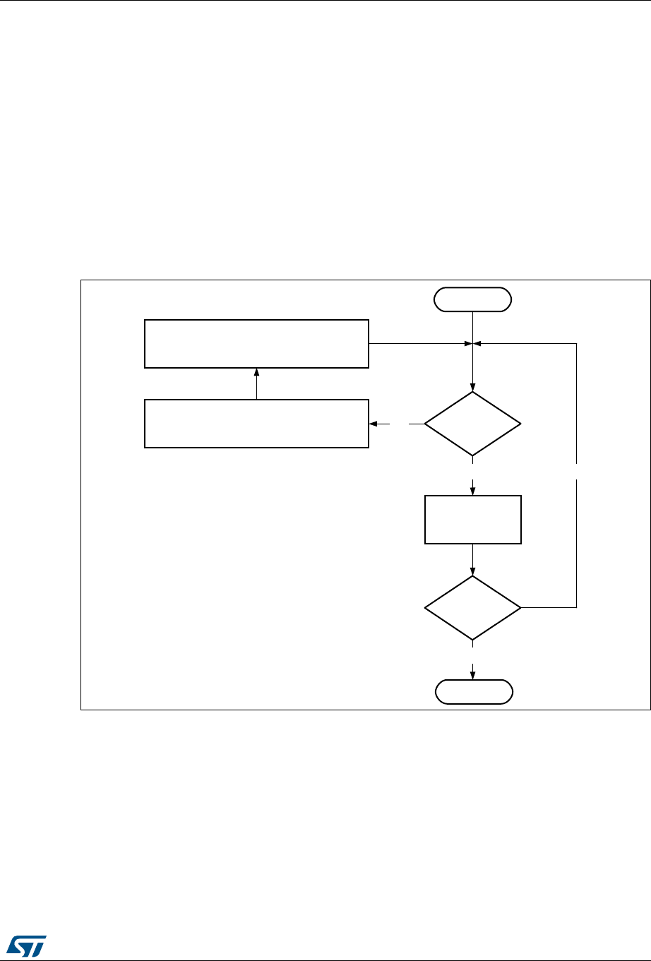
RM0430 Rev 8 1237/1324
RM0430 USB on-the-go full-speed (OTG_FS)
1283
Operational model
The application must initialize a channel before communicating to the connected device.
This section explains the sequence of operation to be performed for different types of USB
transactions.
•Writing the transmit FIFO
The OTG_FS host automatically writes an entry (OUT request) to the periodic/non-
periodic request queue, along with the last 32-bit word write of a packet. The
application must ensure that at least one free space is available in the periodic/non-
periodic request queue before starting to write to the transmit FIFO. The application
must always write to the transmit FIFO in 32-bit words. If the packet size is non-32-bit
word aligned, the application must use padding. The OTG_FS host determines the
actual packet size based on the programmed maximum packet size and transfer size.
Figure 404. Transmit FIFO write task
•Reading the receive FIFO
The application must ignore all packet statuses other than IN data packet (bx0010).
ĂŝϭϱϲϳϯĐ
ϭDW^
Žƌ>W^&/&KƐƉĂĐĞ
ĂǀĂŝůĂďůĞ͍
:DLWIRU137;)(37;)(LQWHUUXSWLQ
27*B*,17676
5HDG27*B+37;67627*B+137;676
UHJLVWHUVIRUDYDLODEOH),)2DQGTXHXH
VSDFHV
:ULWHSDFNHW
GDWDWRWUDQVPLW
),)2
<HV
1R
DŽƌĞ
ƉĂĐŬĞƚƐƚŽ
ƐĞŶĚ͍
ŽŶĞ
0360D[LPXPSDFNHWVL]H
/36/DVWSDFNHWVL]H
^ƚĂƌƚ
<HV
1R
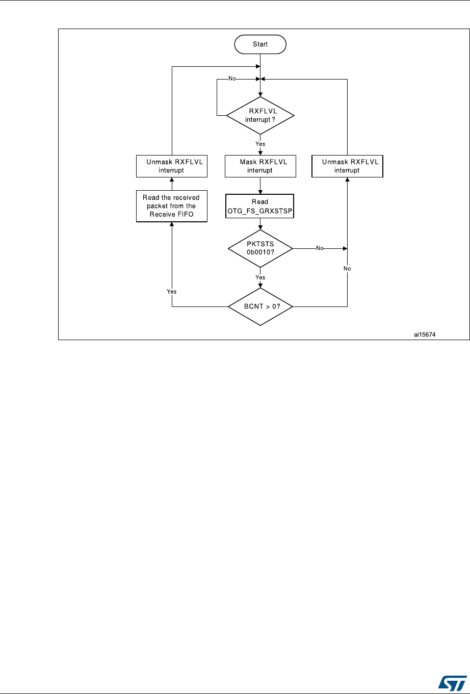
USB on-the-go full-speed (OTG_FS) RM0430
1238/1324 RM0430 Rev 8
Figure 405. Receive FIFO read task
•Bulk and control OUT/SETUP transactions
A typical bulk or control OUT/SETUP pipelined transaction-level operation is shown in
Figure 406. See channel 1 (ch_1). Two bulk OUT packets are transmitted. A control
SETUP transaction operates in the same way but has only one packet. The
assumptions are:
– The application is attempting to send two maximum-packet-size packets (transfer
size = 1, 024 bytes).
– The non-periodic transmit FIFO can hold two packets (128 bytes for FS).
– The non-periodic request queue depth = 4.
•Normal bulk and control OUT/SETUP operations
The sequence of operations in (channel 1) is as follows:
1. Initialize channel 1
2. Write the first packet for channel 1
3. Along with the last word write, the core writes an entry to the non-periodic request
queue
4. As soon as the non-periodic queue becomes non-empty, the core attempts to send an
OUT token in the current frame
5. Write the second (last) packet for channel 1
6. The core generates the XFRC interrupt as soon as the last transaction is completed
successfully
7. In response to the XFRC interrupt, de-allocate the channel for other transfers
8. Handling non-ACK responses
RM0430 Rev 8 1239/1324
RM0430 USB on-the-go full-speed (OTG_FS)
1283
Figure 406. Normal bulk/control OUT/SETUP
1. The grayed elements are not relevant in the context of this figure.
06Y9
$&.
+RVW$SSOLFDWLRQ $+%
287
'$7$
036
036
ZULWHBW[BILIR
FKB
LQLWBUHJFKB
VHW
B
F
KB
HQ
FKB
LQLWBUHJFKB
ZULWHBW[BILIR
FKB
VHWBF
K
BHQ
FKB
F
KB
FKB
FKB
FKB
'HDOORFDWH
FKB
F
KB
F
KB
F
KB
FKB
$&.
287
W
W
5[)/YOLQWHUUXSW
;IHU&RPSOLQWHUUXSW
VHWBF
K
BHQ
FKB
1RQ3HULRGLF5HTXHVW
4XHXH
$VVXPHWKDWWKLVTXHXH
FDQKROGHQWULHV
B
'
$
7
$
,1
UHD
G
BU[BVW
V
UHDGBU[B
I
L
IR
VHWBF
K
BHQ
FKB
W
W
5[)/YOLQWHUUXSW
0
3
6
UHD
G
BU[BVWVUH
DGBU[B
I
L
IR
W
W
5[)/YOLQWHUUXSW
UHD
G
BU[BVW
V
W
W
;IHU&RPSOLQWHUUXSW
'LVDEOH
FKB
'H
DOORFD
W
H
FKB
&K+OWGLQWHUUXSW
W
&K+OWGLQWHUUXSW
F
KB
UHD
G
BU[BVW
V
W
W
5[)/YOLQWHUUXSW
'$7$
036
'
$
7
$
'HYLFH86%
$
$
$&.
,1
$
$
$&.
036
0
3
6

USB on-the-go full-speed (OTG_FS) RM0430
1240/1324 RM0430 Rev 8
The channel-specific interrupt service routine for bulk and control OUT/SETUP
transactions is shown in the following code samples.
•Interrupt service routine for bulk/control OUT/SETUP and bulk/control IN
transactions
a) Bulk/control OUT/SETUP
Unmask (NAK/TXERR/STALL/XFRC)
if (XFRC)
{
Reset Error Count
Mask ACK
De-allocate Channel
}
else if (STALL)
{
Transfer Done = 1
Unmask CHH
Disable Channel
}
else if (NAK or TXERR )
{
Rewind Buffer Pointers
Unmask CHH
Disable Channel
if (TXERR)
{
Increment Error Count
Unmask ACK
}
else
{
Reset Error Count
}
}
else if (CHH)
{
Mask CHH
if (Transfer Done or (Error_count == 3))
{
De-allocate Channel
}
else
{
Re-initialize Channel
}
}

RM0430 Rev 8 1241/1324
RM0430 USB on-the-go full-speed (OTG_FS)
1283
else if (ACK)
{
Reset Error Count
Mask ACK
}
The application is expected to write the data packets into the transmit FIFO when the
space is available in the transmit FIFO and the request queue. The application can
make use of the NPTXFE interrupt in OTG_GINTSTS to find the transmit FIFO space.
b) Bulk/control IN
Unmask (TXERR/XFRC/BBERR/STALL/DTERR)
if (XFRC)
{
Reset Error Count
Unmask CHH
Disable Channel
Reset Error Count
Mask ACK
}
else if (TXERR or BBERR or STALL)
{
Unmask CHH
Disable Channel
if (TXERR)
{
Increment Error Count
Unmask ACK
}
}
else if (CHH)
{
Mask CHH
if (Transfer Done or (Error_count == 3))
{
De-allocate Channel
}
else
{
Re-initialize Channel
}
}
else if (ACK)
{
Reset Error Count
Mask ACK
}

USB on-the-go full-speed (OTG_FS) RM0430
1242/1324 RM0430 Rev 8
else if (DTERR)
{
Reset Error Count
}
The application is expected to write the requests as and when the request queue space is
available and until the XFRC interrupt is received.
•Bulk and control IN transactions
A typical bulk or control IN pipelined transaction-level operation is shown in Figure 407.
See channel 2 (ch_2). The assumptions are:
– The application is attempting to receive two maximum-packet-size packets
(transfer size = 1 024 bytes).
– The receive FIFO can contain at least one maximum-packet-size packet and two
status words per packet (72 bytes for FS).
– The non-periodic request queue depth = 4.
RM0430 Rev 8 1243/1324
RM0430 USB on-the-go full-speed (OTG_FS)
1283
Figure 407. Bulk/control IN transactions
1. The grayed elements are not relevant in the context of this figure.
DLE
$
&
.
.
.
+RVW$SSOLFDWLRQ $+%
2
8
7
7
7
'
$
7
$
0
3
6
0
36
0
3
6
ZULWH
B
W[
B
ILIR
FKB
LQLWBUHJFKB
VHWBFKBHQ
FKB
LQLWBUHJFKB
ZULWHBW[B
I
L
I
R
FKB
VHWBFKBHQ
FKB
FKB
FKB
F
KB
FKB
'
HD
OO
RFDW
H
FKB
FKB
FKB
FKB
F
KB
$
&
.
.
.
2
8
7
7
7
5[)/YOLQWHUUXSW
;
;
;
I
H
U
&
UU
R
P
S
O
L
Q
W
H
U
U
X
U
U
S
W
VHWBFKBHQ
FKB
1RQ3HULRGLF5HTXHVW
4XHXH
$VVXPHWKDWWKLVTXHXH
FDQKROGHQWULHV
FK
F
'$7$
UHDGBU[BVWV
UHDGBU[BILIR
036
VHWBFKBHQ
FKB
5[)/YOLQWHUUXSW
036
UHDGBU[BVWVUH
DGBU[BILIR
5[)/YOLQWHUUXSW
UHDGBU[BVWV
;IHU&RPSOLQWHUUXSW
'LVDEOH
FKB
'HDOORFDWH
FKB
&K+OWGLQWHUUXSW
FKB
UHDGBU[BVWV
5[)/YOLQWHUUXSW
'
$
7
$
0
3
6
'$7$
'HYLFH86%
$&.
,1
$&.
,1

USB on-the-go full-speed (OTG_FS) RM0430
1244/1324 RM0430 Rev 8
The sequence of operations is as follows:
1. Initialize channel 2.
2. Set the CHENA bit in OTG_HCCHAR2 to write an IN request to the non-periodic
request queue.
3. The core attempts to send an IN token after completing the current OUT transaction.
4. The core generates an RXFLVL interrupt as soon as the received packet is written to
the receive FIFO.
5. In response to the RXFLVL interrupt, mask the RXFLVL interrupt and read the received
packet status to determine the number of bytes received, then read the receive FIFO
accordingly. Following this, unmask the RXFLVL interrupt.
6. The core generates the RXFLVL interrupt for the transfer completion status entry in the
receive FIFO.
7. The application must read and ignore the receive packet status when the receive
packet status is not an IN data packet (PKTSTS in OTG_GRXSTSR ≠ 0b0010).
8. The core generates the XFRC interrupt as soon as the receive packet status is read.
9. In response to the XFRC interrupt, disable the channel and stop writing the
OTG_HCCHAR2 register for further requests. The core writes a channel disable
request to the non-periodic request queue as soon as the OTG_HCCHAR2 register is
written.
10. The core generates the RXFLVL interrupt as soon as the halt status is written to the
receive FIFO.
11. Read and ignore the receive packet status.
12. The core generates a CHH interrupt as soon as the halt status is popped from the
receive FIFO.
13. In response to the CHH interrupt, de-allocate the channel for other transfers.
14. Handling non-ACK responses
•Control transactions
Setup, data, and status stages of a control transfer must be performed as three
separate transfers. setup-, data- or status-stage OUT transactions are performed
similarly to the bulk OUT transactions explained previously. Data- or status-stage IN
transactions are performed similarly to the bulk IN transactions explained previously.
For all three stages, the application is expected to set the EPTYP field in
OTG_HCCHAR1 to control. During the setup stage, the application is expected to set
the PID field in OTG_HCTSIZ1 to SETUP.
•Interrupt OUT transactions
A typical interrupt OUT operation is shown in Figure 408. The assumptions are:
– The application is attempting to send one packet in every frame (up to 1 maximum
packet size), starting with the odd frame (transfer size = 1 024 bytes)
– The periodic transmit FIFO can hold one packet (1 KB)
– Periodic request queue depth = 4
The sequence of operations is as follows:

RM0430 Rev 8 1245/1324
RM0430 USB on-the-go full-speed (OTG_FS)
1283
1. Initialize and enable channel 1. The application must set the ODDFRM bit in
OTG_HCCHAR1.
2. Write the first packet for channel 1.
3. Along with the last word write of each packet, the OTG_FS host writes an entry to the
periodic request queue.
4. The OTG_FS host attempts to send an OUT token in the next (odd) frame.
5. The OTG_FS host generates an XFRC interrupt as soon as the last packet is
transmitted successfully.
6. In response to the XFRC interrupt, reinitialize the channel for the next transfer.
USB on-the-go full-speed (OTG_FS) RM0430
1246/1324 RM0430 Rev 8
Figure 408. Normal interrupt OUT
1. The grayed elements are not relevant in the context of this figure.
•Interrupt service routine for interrupt OUT/IN transactions
a) Interrupt OUT
Unmask (NAK/TXERR/STALL/XFRC/FRMOR)
06Y9
+RVW
$SSOLFDWLRQ 'HYLFH$+%
287
'$7$
036
036
036
ZULWHBW[BILIR
FKB
LQLWBUHJFKB
VHW
B
F
KB
H
Q
FKB
LQLWBUH
J
FKB
ZULWHBW[BILIR
FKB
287
'$7$
036
;IHU&RPSOLQWHUUXSW
3HULRGLF5HTXHVW4XHXH
$VVXPHWKDWWKLVTXHXH
FDQKROGHQWULHV
'
$
7
$
5
[)/YOLQWHUUX
S
W
0
3
6
UHD
GB
U[
B
VW
V
UHDG
B
U[
BI
L
I
R
5[)/YOLQWHUUXSW
UHD
GB
U[
B
VW
V
;I
HU
&
RP
S
OLQWHUUX
S
W
2GG
PLFUR
IUDPH
(YHQ
PLFUR
IUDPH
LQLWBUHJFKB
VHW
B
F
KB
H
Q
FKB
LQLWBUH
J
FKB
ZULWHBW[BILIR
FKB
LQLWBUHJFKB
;IHU&RPSOLQWHUUXSW
036
'
$
7
$
$&.
$&.
FKB
F
K
B
FKB
FK
FKB
86%
,1
$
$
$&.
,1
B
5[)/YO LQWHUUXSW

RM0430 Rev 8 1247/1324
RM0430 USB on-the-go full-speed (OTG_FS)
1283
if (XFRC)
{
Reset Error Count
Mask ACK
De-allocate Channel
}
else
if (STALL or FRMOR)
{
Mask ACK
Unmask CHH
Disable Channel
if (STALL)
{
Transfer Done = 1
}
}
else
if (NAK or TXERR)
{
Rewind Buffer Pointers
Reset Error Count
Mask ACK
Unmask CHH
Disable Channel
}
else
if (CHH)
{
Mask CHH
if (Transfer Done or (Error_count == 3))
{
De-allocate Channel
}
else
{
Re-initialize Channel (in next b_interval - 1 Frame)
}
}
else
if (ACK)
{
Reset Error Count
Mask ACK
}

USB on-the-go full-speed (OTG_FS) RM0430
1248/1324 RM0430 Rev 8
The application uses the NPTXFE interrupt in OTG_GINTSTS to find the
transmit FIFO space.
Interrupt IN
Unmask (NAK/TXERR/XFRC/BBERR/STALL/FRMOR/DTERR)
if (XFRC)
{
Reset Error Count
Mask ACK
if (OTG_HCTSIZx.PKTCNT == 0)
{
De-allocate Channel
}
else
{
Transfer Done = 1
Unmask CHH
Disable Channel
}
}
else
if (STALL or FRMOR or NAK or DTERR or BBERR)
{
Mask ACK
Unmask CHH
Disable Channel
if (STALL or BBERR)
{
Reset Error Count
Transfer Done = 1
}
else
if (!FRMOR)
{
Reset Error Count
}
}
else
if (TXERR)
{
Increment Error Count
Unmask ACK
Unmask CHH
Disable Channel
}
else

RM0430 Rev 8 1249/1324
RM0430 USB on-the-go full-speed (OTG_FS)
1283
if (CHH)
{
Mask CHH
if (Transfer Done or (Error_count == 3))
{
De-allocate Channel
}
else
Re-initialize Channel (in next b_interval - 1 /Frame)
}
}
else
if (ACK)
{
Reset Error Count
Mask ACK
}
•Interrupt IN transactions
The assumptions are:
– The application is attempting to receive one packet (up to 1 maximum packet size)
in every frame, starting with odd (transfer size = 1 024 bytes).
– The receive FIFO can hold at least one maximum-packet-size packet and two
status words per packet (1 031 bytes).
– Periodic request queue depth = 4.
•Normal interrupt IN operation
The sequence of operations is as follows:
1. Initialize channel 2. The application must set the ODDFRM bit in OTG_HCCHAR2.
2. Set the CHENA bit in OTG_HCCHAR2 to write an IN request to the periodic request
queue.
3. The OTG_FS host writes an IN request to the periodic request queue for each
OTG_HCCHAR2 register write with the CHENA bit set.
4. The OTG_FS host attempts to send an IN token in the next (odd) frame.
5. As soon as the IN packet is received and written to the receive FIFO, the OTG_FS host
generates an RXFLVL interrupt.
6. In response to the RXFLVL interrupt, read the received packet status to determine the
number of bytes received, then read the receive FIFO accordingly. The application
must mask the RXFLVL interrupt before reading the receive FIFO, and unmask after
reading the entire packet.
7. The core generates the RXFLVL interrupt for the transfer completion status entry in the
receive FIFO. The application must read and ignore the receive packet status when the
receive packet status is not an IN data packet (PKTSTS in GRXSTSR ≠ 0b0010).
8. The core generates an XFRC interrupt as soon as the receive packet status is read.
9. In response to the XFRC interrupt, read the PKTCNT field in OTG_HCTSIZ2. If the
PKTCNT bit in OTG_HCTSIZ2 is not equal to 0, disable the channel before re-

USB on-the-go full-speed (OTG_FS) RM0430
1250/1324 RM0430 Rev 8
initializing the channel for the next transfer, if any). If PKTCNT bit in OTG_HCTSIZ2 =
0, reinitialize the channel for the next transfer. This time, the application must reset the
ODDFRM bit in OTG_HCCHAR2.
RM0430 Rev 8 1251/1324
RM0430 USB on-the-go full-speed (OTG_FS)
1283
Figure 409. Normal interrupt IN
1. The grayed elements are not relevant in the context of this figure.
•Isochronous OUT transactions
A typical isochronous OUT operation is shown in Figure 409. The assumptions are:
– The application is attempting to send one packet every frame (up to 1 maximum
DLE
+RVW
$SSOLFDWLRQ 'HYLFH$+%
2
8
7
7
7
'
$
7
$
0
3
6
0
36
0
3
6
ZULWH
B
W[
B
ILIR
FKB
L
QLWBUH
J
FKB
VHWBFKBHQ
FKB
LQLWBUHJFKB
ZULWH
B
W[
BI
L
I
R
FKB
2
8
7
'
$
$
7
$
$
0
3
6
;
;
I
I
H
H
U
U
&
&
R
R
P
P
S
S
O
O
L
L
Q
Q
W
W
H
H
U
U
U
U
X
X
S
S
W
W
W
W
3HULRGLF5HTXHVW4XHXH
$VVXPHWKDWWKLVTXHXH
FDQKROGHQWULHV
'$7$
5[)/YOLQWHUUXSW
036
UHDGBU[BVWV
UHDGBU[BILIR
5[)/YOLQWHUUXSW
UHDGBU[BVWV
;IHU&RPSOLQWHUUXSW
2GG
PLFUR
IUDPH
(YHQ
PLFUR
IUDPH
L
QLWBUH
J
FKB
VHWBFKBHQ
FKB
LQLWBUHJFKB
ZULWH
B
W[
B
ILIR
FKB
L
QLWBUH
J
FKB
;
I
I
I
H
U
U
U
&
R
P
S
O
L
Q
W
H
U
U
U
U
X
S
W
0
3
6
'$7$
$
&
.
.
.
$
$
$
$
$
&
.
FKB
FK
FKB
FKB
FKB
FK
86%
,1
$&.
,1

USB on-the-go full-speed (OTG_FS) RM0430
1252/1324 RM0430 Rev 8
packet size), starting with an odd frame. (transfer size = 1 024 bytes).
– The periodic transmit FIFO can hold one packet (1 KB).
– Periodic request queue depth = 4.
The sequence of operations is as follows:
1. Initialize and enable channel 1. The application must set the ODDFRM bit in
OTG_HCCHAR1.
2. Write the first packet for channel 1.
3. Along with the last word write of each packet, the OTG_FS host writes an entry to the
periodic request queue.
4. The OTG_FS host attempts to send the OUT token in the next frame (odd).
5. The OTG_FS host generates the XFRC interrupt as soon as the last packet is
transmitted successfully.
6. In response to the XFRC interrupt, reinitialize the channel for the next transfer.
7. Handling non-ACK responses
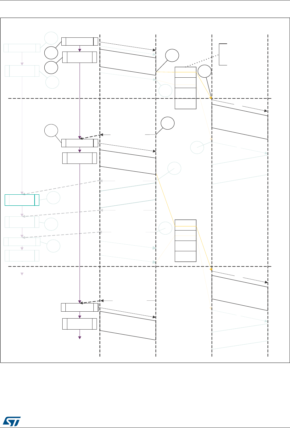
RM0430 Rev 8 1253/1324
RM0430 USB on-the-go full-speed (OTG_FS)
1283
Figure 410. Isochronous OUT transactions
1. The grayed elements are not relevant in the context of this figure.
•Interrupt service routine for isochronous OUT/IN transactions
Code sample: isochronous OUT
Unmask (FRMOR/XFRC)
if (XFRC)
06Y9
+RVW$SSOLFDWLRQ $+%
ZULWHBW[BILIR
FKB
LQLWBUHJFKB
ZULWHBW[BILIR
FKB
F
KB
;IHU&RPSOLQWHUUXSW
3HULRGLF5HTXHVW
4XHXH
$VVXPHWKDWWKLVTXHXH
FDQKROGHQWULHV
LQLWBUHJFKB
ZULWHBW[BILIR
FKB
LQLWBUHJFKB
036
'
$
7
$
(YHQ
PLFUR
IUDPH
2GG
PLFUR
IUDPH
'HYLFH86%
VHW
B
F
KB
H
Q
FKB
LQLWBUH
J
FKB
UHD
G
BU[BVW
V
UHDGBU[B
I
L
IR
UHD
G
BU[BVW
V
VHWBF
K
BH
Q
FKB
LQLWBUHJ
FKB
5[)/YOLQWHUUXSW
5[)/YOLQWHUUXSW
;IHU&RPSOLQWHUUXSW
;IHU&RPSOLQWHUUXSW
287
,1
,1
287
'$7$
036
'
$
7
$
'$7$
036
FKB
FK
FKB
FKB
036
036
0
3
6

USB on-the-go full-speed (OTG_FS) RM0430
1254/1324 RM0430 Rev 8
{
De-allocate Channel
}
else
if (FRMOR)
{
Unmask CHH
Disable Channel
}
else
if (CHH)
{
Mask CHH
De-allocate Channel
}
Code sample: Isochronous IN
Unmask (TXERR/XFRC/FRMOR/BBERR)
if (XFRC or FRMOR)
{
if (XFRC and (OTG_HCTSIZx.PKTCNT == 0))
{
Reset Error Count
De-allocate Channel
}
else
{
Unmask CHH
Disable Channel
}
}
else
if (TXERR or BBERR)
{
Increment Error Count
Unmask CHH
Disable Channel
}
else
if (CHH)
{
Mask CHH
if (Transfer Done or (Error_count == 3))
{
De-allocate Channel
}

RM0430 Rev 8 1255/1324
RM0430 USB on-the-go full-speed (OTG_FS)
1283
else
{
Re-initialize Channel
}
}
•Isochronous IN transactions
The assumptions are:
– The application is attempting to receive one packet (up to 1 maximum packet size)
in every frame starting with the next odd frame (transfer size = 1 024 bytes).
– The receive FIFO can hold at least one maximum-packet-size packet and two
status word per packet (1 031 bytes).
– Periodic request queue depth = 4.
The sequence of operations is as follows:
1. Initialize channel 2. The application must set the ODDFRM bit in OTG_HCCHAR2.
2. Set the CHENA bit in OTG_HCCHAR2 to write an IN request to the periodic request
queue.
3. The OTG_FS host writes an IN request to the periodic request queue for each
OTG_HCCHAR2 register write with the CHENA bit set.
4. The OTG_FS host attempts to send an IN token in the next odd frame.
5. As soon as the IN packet is received and written to the receive FIFO, the OTG_FS host
generates an RXFLVL interrupt.
6. In response to the RXFLVL interrupt, read the received packet status to determine the
number of bytes received, then read the receive FIFO accordingly. The application
must mask the RXFLVL interrupt before reading the receive FIFO, and unmask it after
reading the entire packet.
7. The core generates an RXFLVL interrupt for the transfer completion status entry in the
receive FIFO. This time, the application must read and ignore the receive packet status
when the receive packet status is not an IN data packet (PKTSTS bit in
OTG_GRXSTSR ≠ 0b0010).
8. The core generates an XFRC interrupt as soon as the receive packet status is read.
9. In response to the XFRC interrupt, read the PKTCNT field in OTG_HCTSIZ2. If
PKTCNT ≠ 0 in OTG_HCTSIZ2, disable the channel before re-initializing the channel
for the next transfer, if any. If PKTCNT = 0 in OTG_HCTSIZ2, reinitialize the channel
for the next transfer. This time, the application must reset the ODDFRM bit in
OTG_HCCHAR2.
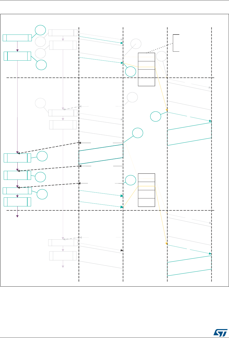
USB on-the-go full-speed (OTG_FS) RM0430
1256/1324 RM0430 Rev 8
Figure 411. Isochronous IN transactions
1. The grayed elements are not relevant in the context of this figure.
•Selecting the queue depth
Choose the periodic and non-periodic request queue depths carefully to match the
number of periodic/non-periodic endpoints accessed.
The non-periodic request queue depth affects the performance of non-periodic
06Y9
+RVW$SSOLFDWLRQ $+%
ZULWH
B
W[
B
ILIR
FKB
LQLWBUH
J
FKB
ZULWHBW[B
I
L
I
R
FKB
FKB
3HULRGLF5HTXHVW
4XHXH
$VVXPHWKDWWKLVTXHXH
FDQKROGHQWULHV
036
LQLWBUHJ
FKB
ZULWHBW[B
I
L
I
R
FKB
LQLWBUHJ
FKB
(YHQ
PLFUR
IUDPH
2GG
PLFUR
IUDPH
'HYLFH86%
VHWBFKBHQ
FKB
LQLWBUHJFKB
UHDGBU[BVWV
UHDGBU[BILIR
UHDGBU[BVWV
VHWBFKBHQ
FKB
LQLWBUHJFKB
5[)/YOLQWHUUXSW
5[)/YOLQWHUUXSW
;IHU&RPSOLQWHUUXSW
;IHU&RPSOLQWHUUXSW
287
,1
,1
287
FKB
FKB
FK
FKB
FK
0
3
6
0
3
6
0
3
6
;IHU&RPSOLQWHUUXSW
'$7$
036
'$7$
036
'$7$
'$7$

RM0430 Rev 8 1257/1324
RM0430 USB on-the-go full-speed (OTG_FS)
1283
transfers. The deeper the queue (along with sufficient FIFO size), the more often the
core is able to pipeline non-periodic transfers. If the queue size is small, the core is
able to put in new requests only when the queue space is freed up.
The core’s periodic request queue depth is critical to perform periodic transfers as
scheduled. Select the periodic queue depth, based on the number of periodic transfers
scheduled in a microframe. If the periodic request queue depth is smaller than the
periodic transfers scheduled in a microframe, a frame overrun condition occurs.
•Handling babble conditions
OTG_FS controller handles two cases of babble: packet babble and port babble.
Packet babble occurs if the device sends more data than the maximum packet size for
the channel. Port babble occurs if the core continues to receive data from the device at
EOF2 (the end of frame 2, which is very close to SOF).
When OTG_FS controller detects a packet babble, it stops writing data into the Rx
buffer and waits for the end of packet (EOP). When it detects an EOP, it flushes already
written data in the Rx buffer and generates a Babble interrupt to the application.
When OTG_FS controller detects a port babble, it flushes the Rx FIFO and disables the
port. The core then generates a port disabled interrupt (HPRTINT in OTG_GINTSTS,
PENCHNG in OTG_HPRT). On receiving this interrupt, the application must determine
that this is not due to an overcurrent condition (another cause of the port disabled
interrupt) by checking POCA in OTG_HPRT, then perform a soft reset. The core does
not send any more tokens after it has detected a port babble condition.
33.16.5 Device programming model
Endpoint initialization on USB reset
1. Set the NAK bit for all OUT endpoints
– SNAK = 1 in OTG_DOEPCTLx (for all OUT endpoints)
2. Unmask the following interrupt bits
– INEP0 = 1 in OTG_DAINTMSK (control 0 IN endpoint)
– OUTEP0 = 1 in OTG_DAINTMSK (control 0 OUT endpoint)
– STUPM = 1 in OTG_DOEPMSK
– XFRCM = 1 in OTG_DOEPMSK
– XFRCM = 1 in OTG_DIEPMSK
– TOM = 1 in OTG_DIEPMSK
3. Set up the data FIFO RAM for each of the FIFOs
– Program the OTG_GRXFSIZ register, to be able to receive control OUT data and
setup data. If thresholding is not enabled, at a minimum, this must be equal to 1
max packet size of control endpoint 0 + 2 words (for the status of the control OUT
data packet) + 10 words (for setup packets).
– Program the OTG_DIEPTXF0 register (depending on the FIFO number chosen) to
be able to transmit control IN data. At a minimum, this must be equal to 1 max
packet size of control endpoint 0.
4. Program the following fields in the endpoint-specific registers for control OUT endpoint
0 to receive a SETUP packet
– STUPCNT = 3 in OTG_DOEPTSIZ0 (to receive up to 3 back-to-back SETUP
packets)

USB on-the-go full-speed (OTG_FS) RM0430
1258/1324 RM0430 Rev 8
At this point, all initialization required to receive SETUP packets is done.
Endpoint initialization on enumeration completion
1. On the Enumeration Done interrupt (ENUMDNE in OTG_GINTSTS), read the
OTG_DSTS register to determine the enumeration speed.
2. Program the MPSIZ field in OTG_DIEPCTL0 to set the maximum packet size. This
step configures control endpoint 0. The maximum packet size for a control endpoint
depends on the enumeration speed.
At this point, the device is ready to receive SOF packets and is configured to perform control
transfers on control endpoint 0.
Endpoint initialization on SetAddress command
This section describes what the application must do when it receives a SetAddress
command in a SETUP packet.
1. Program the OTG_DCFG register with the device address received in the SetAddress
command
2. Program the core to send out a status IN packet
Endpoint initialization on SetConfiguration/SetInterface command
This section describes what the application must do when it receives a SetConfiguration or
SetInterface command in a SETUP packet.
1. When a SetConfiguration command is received, the application must program the
endpoint registers to configure them with the characteristics of the valid endpoints in
the new configuration.
2. When a SetInterface command is received, the application must program the endpoint
registers of the endpoints affected by this command.
3. Some endpoints that were active in the prior configuration or alternate setting are not
valid in the new configuration or alternate setting. These invalid endpoints must be
deactivated.
4. Unmask the interrupt for each active endpoint and mask the interrupts for all inactive
endpoints in the OTG_DAINTMSK register.
5. Set up the data FIFO RAM for each FIFO.
6. After all required endpoints are configured; the application must program the core to
send a status IN packet.
At this point, the device core is configured to receive and transmit any type of data packet.
Endpoint activation
This section describes the steps required to activate a device endpoint or to configure an
existing device endpoint to a new type.

RM0430 Rev 8 1259/1324
RM0430 USB on-the-go full-speed (OTG_FS)
1283
1. Program the characteristics of the required endpoint into the following fields of the
OTG_DIEPCTLx register (for IN or bidirectional endpoints) or the OTG_DOEPCTLx
register (for OUT or bidirectional endpoints).
– Maximum packet size
– USB active endpoint = 1
– Endpoint start data toggle (for interrupt and bulk endpoints)
– Endpoint type
– Tx FIFO number
2. Once the endpoint is activated, the core starts decoding the tokens addressed to that
endpoint and sends out a valid handshake for each valid token received for the
endpoint.
Endpoint deactivation
This section describes the steps required to deactivate an existing endpoint.
1. In the endpoint to be deactivated, clear the USB active endpoint bit in the
OTG_DIEPCTLx register (for IN or bidirectional endpoints) or the OTG_DOEPCTLx
register (for OUT or bidirectional endpoints).
2. Once the endpoint is deactivated, the core ignores tokens addressed to that endpoint,
which results in a timeout on the USB.
Note: The application must meet the following conditions to set up the device core to handle
traffic:
NPTXFEM and RXFLVLM in the OTG_GINTMSK register must be cleared.
Operational model
SETUP and OUT data transfers:
This section describes the internal data flow and application-level operations during data
OUT transfers and SETUP transactions.
•Packet read
This section describes how to read packets (OUT data and SETUP packets) from the
receive FIFO.
1. On catching an RXFLVL interrupt (OTG_GINTSTS register), the application must read
the receive status pop register (OTG_GRXSTSP).
2. The application can mask the RXFLVL interrupt (in OTG_GINTSTS) by writing to
RXFLVLM = 0 (in OTG_GINTMSK), until it has read the packet from the receive FIFO.
3. If the received packet’s byte count is not 0, the byte count amount of data is popped
from the receive data FIFO and stored in memory. If the received packet byte count is
0, no data is popped from the receive data FIFO.
4. The receive status readout of the packet of FIFO indicates one of the following:
a) Global OUT NAK pattern:
PKTSTS = Global OUT NAK, BCNT = 0x000, EPNUM = (0x0),
DPID = (0b00).
These data indicate that the global OUT NAK bit has taken effect.
b) SETUP packet pattern:
PKTSTS = SETUP, BCNT = 0x008, EPNUM = Control EP Num,
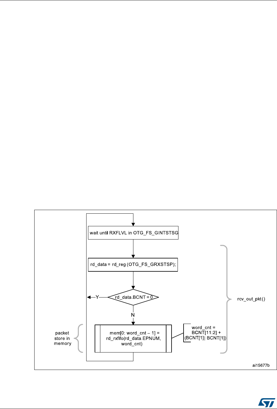
USB on-the-go full-speed (OTG_FS) RM0430
1260/1324 RM0430 Rev 8
DPID = DATA0. These data indicate that a SETUP packet for the specified
endpoint is now available for reading from the receive FIFO.
c) Setup stage done pattern:
PKTSTS = Setup Stage Done, BCNT = 0x0, EPNUM = Control EP Num,
DPID = (0b00).
These data indicate that the setup stage for the specified endpoint has completed
and the data stage has started. After this entry is popped from the receive FIFO,
the core asserts a setup interrupt on the specified control OUT endpoint.
d) Data OUT packet pattern:
PKTSTS = DataOUT, BCNT = size of the received data OUT packet (0 ≤ BCNT
≤ 1 024), EPNUM = EPNUM on which the packet was received, DPID = Actual
Data PID.
e) Data transfer completed pattern:
PKTSTS = Data OUT transfer done, BCNT = 0x0, EPNUM = OUT EP Num on
which the data transfer is complete, DPID = (0b00).
These data indicate that an OUT data transfer for the specified OUT endpoint has
completed. After this entry is popped from the receive FIFO, the core asserts a
transfer completed interrupt on the specified OUT endpoint.
5. After the data payload is popped from the receive FIFO, the RXFLVL interrupt
(OTG_GINTSTS) must be unmasked.
6. Steps 1–5 are repeated every time the application detects assertion of the interrupt line
due to RXFLVL in OTG_GINTSTS. Reading an empty receive FIFO can result in
undefined core behavior.
Figure 412 provides a flowchart of the above procedure.
Figure 412. Receive FIFO packet read
SETUP transactions

RM0430 Rev 8 1261/1324
RM0430 USB on-the-go full-speed (OTG_FS)
1283
This section describes how the core handles SETUP packets and the application’s
sequence for handling SETUP transactions.
•Application requirements
1. To receive a SETUP packet, the STUPCNT field (OTG_DOEPTSIZx) in a control OUT
endpoint must be programmed to a non-zero value. When the application programs the
STUPCNT field to a non-zero value, the core receives SETUP packets and writes them
to the receive FIFO, irrespective of the NAK status and EPENA bit setting in
OTG_DOEPCTLx. The STUPCNT field is decremented every time the control endpoint
receives a SETUP packet. If the STUPCNT field is not programmed to a proper value
before receiving a SETUP packet, the core still receives the SETUP packet and
decrements the STUPCNT field, but the application may not be able to determine the
correct number of SETUP packets received in the setup stage of a control transfer.
– STUPCNT = 3 in OTG_DOEPTSIZx
2. The application must always allocate some extra space in the receive data FIFO, to be
able to receive up to three SETUP packets on a control endpoint.
– The space to be reserved is 10 words. Three words are required for the first
SETUP packet, 1 word is required for the setup stage done word and 6 words are
required to store two extra SETUP packets among all control endpoints.
– 3 words per SETUP packet are required to store 8 bytes of SETUP data and 4
bytes of SETUP status (setup packet pattern). The core reserves this space in the
receive data FIFO to write SETUP data only, and never uses this space for data
packets.
3. The application must read the 2 words of the SETUP packet from the receive FIFO.
4. The application must read and discard the setup stage done word from the receive
FIFO.
•Internal data flow
1. When a SETUP packet is received, the core writes the received data to the receive
FIFO, without checking for available space in the receive FIFO and irrespective of the
endpoint’s NAK and STALL bit settings.
– The core internally sets the IN NAK and OUT NAK bits for the control IN/OUT
endpoints on which the SETUP packet was received.
2. For every SETUP packet received on the USB, 3 words of data are written to the
receive FIFO, and the STUPCNT field is decremented by 1.
– The first word contains control information used internally by the core
– The second word contains the first 4 bytes of the SETUP command
– The third word contains the last 4 bytes of the SETUP command
3. When the setup stage changes to a data IN/OUT stage, the core writes an entry (setup
stage done word) to the receive FIFO, indicating the completion of the setup stage.
4. On the AHB side, SETUP packets are emptied by the application.
5. When the application pops the setup stage done word from the receive FIFO, the core
interrupts the application with an STUP interrupt (OTG_DOEPINTx), indicating it can
process the received SETUP packet.
6. The core clears the endpoint enable bit for control OUT endpoints.
•Application programming sequence
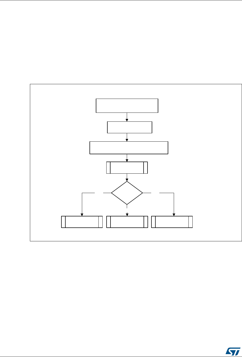
USB on-the-go full-speed (OTG_FS) RM0430
1262/1324 RM0430 Rev 8
1. Program the OTG_DOEPTSIZx register.
– STUPCNT = 3
2. Wait for the RXFLVL interrupt (OTG_GINTSTS) and empty the data packets from the
receive FIFO.
3. Assertion of the STUP interrupt (OTG_DOEPINTx) marks a successful completion of
the SETUP data transfer.
– On this interrupt, the application must read the OTG_DOEPTSIZx register to
determine the number of SETUP packets received and process the last received
SETUP packet.
Figure 413. Processing a SETUP packet
•Handling more than three back-to-back SETUP packets
Per the USB 2.0 specification, normally, during a SETUP packet error, a host does not send
more than three back-to-back SETUP packets to the same endpoint. However, the USB 2.0
specification does not limit the number of back-to-back SETUP packets a host can send to
the same endpoint. When this condition occurs, the OTG_FS controller generates an
interrupt (B2BSTUP in OTG_DOEPINTx).
•Setting the global OUT NAK
Internal data flow:
1. When the application sets the Global OUT NAK (SGONAK bit in OTG_DCTL), the core
stops writing data, except SETUP packets, to the receive FIFO. Irrespective of the
06Y9
:DLWIRU673LQ27*B'2(3,17[
UHPBVXSFQW
UGBUHJ27*B'2(376,=[
VHWXSBFPG> PHP>±UHPBVXSFQW@
VHWXSBFPG>@ PHP>±UHPBVXSFQW@
FWUOBUGZUVWDJH
)LQGVHWXSFPGW\SH
VWDJH
5HDG
VHWXSBQSBLQBSNW
6WDWXV,1SKDVH
UFYBRXWBSNW
'DWD287SKDVH
VHWXSBQSBLQBSNW
'DWD,1SKDVH
:ULWH

RM0430 Rev 8 1263/1324
RM0430 USB on-the-go full-speed (OTG_FS)
1283
space availability in the receive FIFO, non-isochronous OUT tokens receive a NAK
handshake response, and the core ignores isochronous OUT data packets
2. The core writes the Global OUT NAK pattern to the receive FIFO. The application must
reserve enough receive FIFO space to write this data pattern.
3. When the application pops the Global OUT NAK pattern word from the receive FIFO,
the core sets the GONAKEFF interrupt (OTG_GINTSTS).
4. Once the application detects this interrupt, it can assume that the core is in Global OUT
NAK mode. The application can clear this interrupt by clearing the SGONAK bit in
OTG_DCTL.
Application programming sequence:
1. To stop receiving any kind of data in the receive FIFO, the application must set the
Global OUT NAK bit by programming the following field:
– SGONAK = 1 in OTG_DCTL
2. Wait for the assertion of the GONAKEFF interrupt in OTG_GINTSTS. When asserted,
this interrupt indicates that the core has stopped receiving any type of data except
SETUP packets.
3. The application can receive valid OUT packets after it has set SGONAK in OTG_DCTL
and before the core asserts the GONAKEFF interrupt (OTG_GINTSTS).
4. The application can temporarily mask this interrupt by writing to the GONAKEFFM bit in
the OTG_GINTMSK register.
– GONAKEFFM = 0 in the OTG_GINTMSK register
5. Whenever the application is ready to exit the Global OUT NAK mode, it must clear the
SGONAK bit in OTG_DCTL. This also clears the GONAKEFF interrupt
(OTG_GINTSTS).
– CGONAK = 1 in OTG_DCTL
6. If the application has masked this interrupt earlier, it must be unmasked as follows:
– GONAKEFFM = 1 in OTG_GINTMSK
•Disabling an OUT endpoint
The application must use this sequence to disable an OUT endpoint that it has enabled.
Application programming sequence:

USB on-the-go full-speed (OTG_FS) RM0430
1264/1324 RM0430 Rev 8
1. Before disabling any OUT endpoint, the application must enable Global OUT NAK
mode in the core.
– SGONAK = 1 in OTG_DCTL
2. Wait for the GONAKEFF interrupt (OTG_GINTSTS)
3. Disable the required OUT endpoint by programming the following fields:
– EPDIS = 1 in OTG_DOEPCTLx
– SNAK = 1 in OTG_DOEPCTLx
4. Wait for the EPDISD interrupt (OTG_DOEPINTx), which indicates that the OUT
endpoint is completely disabled. When the EPDISD interrupt is asserted, the core also
clears the following bits:
– EPDIS = 0 in OTG_DOEPCTLx
– EPENA = 0 in OTG_DOEPCTLx
5. The application must clear the Global OUT NAK bit to start receiving data from other
non-disabled OUT endpoints.
– SGONAK = 0 in OTG_DCTL
•Generic non-isochronous OUT data transfers
This section describes a regular non-isochronous OUT data transfer (control, bulk, or
interrupt).
Application requirements:
1. Before setting up an OUT transfer, the application must allocate a buffer in the memory
to accommodate all data to be received as part of the OUT transfer.
2. For OUT transfers, the transfer size field in the endpoint’s transfer size register must be
a multiple of the maximum packet size of the endpoint, adjusted to the word boundary.
– transfer size[EPNUM] = n × (MPSIZ[EPNUM] + 4 – (MPSIZ[EPNUM] mod 4))
– packet count[EPNUM] = n
–n > 0
3. On any OUT endpoint interrupt, the application must read the endpoint’s transfer size
register to calculate the size of the payload in the memory. The received payload size
can be less than the programmed transfer size.
– Payload size in memory = application programmed initial transfer size – core
updated final transfer size
– Number of USB packets in which this payload was received = application
programmed initial packet count – core updated final packet count
Internal data flow:
1. The application must set the transfer size and packet count fields in the endpoint-
specific registers, clear the NAK bit, and enable the endpoint to receive the data.
2. Once the NAK bit is cleared, the core starts receiving data and writes it to the receive
FIFO, as long as there is space in the receive FIFO. For every data packet received on
the USB, the data packet and its status are written to the receive FIFO. Every packet

RM0430 Rev 8 1265/1324
RM0430 USB on-the-go full-speed (OTG_FS)
1283
(maximum packet size or short packet) written to the receive FIFO decrements the
packet count field for that endpoint by 1.
– OUT data packets received with bad data CRC are flushed from the receive FIFO
automatically.
– After sending an ACK for the packet on the USB, the core discards non-
isochronous OUT data packets that the host, which cannot detect the ACK, re-
sends. The application does not detect multiple back-to-back data OUT packets
on the same endpoint with the same data PID. In this case the packet count is not
decremented.
– If there is no space in the receive FIFO, isochronous or non-isochronous data
packets are ignored and not written to the receive FIFO. Additionally, non-
isochronous OUT tokens receive a NAK handshake reply.
– In all the above three cases, the packet count is not decremented because no data
are written to the receive FIFO.
3. When the packet count becomes 0 or when a short packet is received on the endpoint,
the NAK bit for that endpoint is set. Once the NAK bit is set, the isochronous or non-
isochronous data packets are ignored and not written to the receive FIFO, and non-
isochronous OUT tokens receive a NAK handshake reply.
4. After the data are written to the receive FIFO, the application reads the data from the
receive FIFO and writes it to external memory, one packet at a time per endpoint.
5. At the end of every packet write on the AHB to external memory, the transfer size for
the endpoint is decremented by the size of the written packet.
6. The OUT data transfer completed pattern for an OUT endpoint is written to the receive
FIFO on one of the following conditions:
– The transfer size is 0 and the packet count is 0
– The last OUT data packet written to the receive FIFO is a short packet
(0 ≤ packet size < maximum packet size)
7. When either the application pops this entry (OUT data transfer completed), a transfer
completed interrupt is generated for the endpoint and the endpoint enable is cleared.
Application programming sequence:
1. Program the OTG_DOEPTSIZx register for the transfer size and the corresponding
packet count.
2. Program the OTG_DOEPCTLx register with the endpoint characteristics, and set the
EPENA and CNAK bits.
– EPENA = 1 in OTG_DOEPCTLx
– CNAK = 1 in OTG_DOEPCTLx
3. Wait for the RXFLVL interrupt (in OTG_GINTSTS) and empty the data packets from the
receive FIFO.
– This step can be repeated many times, depending on the transfer size.
4. Asserting the XFRC interrupt (OTG_DOEPINTx) marks a successful completion of the
non-isochronous OUT data transfer.
5. Read the OTG_DOEPTSIZx register to determine the size of the received data
payload.
•Generic isochronous OUT data transfer
This section describes a regular isochronous OUT data transfer.

USB on-the-go full-speed (OTG_FS) RM0430
1266/1324 RM0430 Rev 8
Application requirements:
1. All the application requirements for non-isochronous OUT data transfers also apply to
isochronous OUT data transfers.
2. For isochronous OUT data transfers, the transfer size and packet count fields must
always be set to the number of maximum-packet-size packets that can be received in a
single frame and no more. Isochronous OUT data transfers cannot span more than 1
frame.
3. The application must read all isochronous OUT data packets from the receive FIFO
(data and status) before the end of the periodic frame (EOPF interrupt in
OTG_GINTSTS).
4. To receive data in the following frame, an isochronous OUT endpoint must be enabled
after the EOPF (OTG_GINTSTS) and before the SOF (OTG_GINTSTS).
Internal data flow:
1. The internal data flow for isochronous OUT endpoints is the same as that for non-
isochronous OUT endpoints, but for a few differences.
2. When an isochronous OUT endpoint is enabled by setting the endpoint enable and
clearing the NAK bits, the Even/Odd frame bit must also be set appropriately. The core
receives data on an isochronous OUT endpoint in a particular frame only if the
following condition is met:
– EONUM (in OTG_DOEPCTLx) = FNSOF[0] (in OTG_DSTS)
3. When the application completely reads an isochronous OUT data packet (data and
status) from the receive FIFO, the core updates the RXDPID field in OTG_DOEPTSIZx
with the data PID of the last isochronous OUT data packet read from the receive FIFO.
Application programming sequence:

RM0430 Rev 8 1267/1324
RM0430 USB on-the-go full-speed (OTG_FS)
1283
1. Program the OTG_DOEPTSIZx register for the transfer size and the corresponding
packet count
2. Program the OTG_DOEPCTLx register with the endpoint characteristics and set the
endpoint enable, ClearNAK, and Even/Odd frame bits.
– EPENA = 1
–CNAK=1
– EONUM = (0: Even/1: Odd)
3. Wait for the RXFLVL interrupt (in OTG_GINTSTS) and empty the data packets from the
receive FIFO
– This step can be repeated many times, depending on the transfer size.
4. The assertion of the XFRC interrupt (in OTG_DOEPINTx) marks the completion of the
isochronous OUT data transfer. This interrupt does not necessarily mean that the data
in memory are good.
5. This interrupt cannot always be detected for isochronous OUT transfers. Instead, the
application can detect the INCOMPISOOUT interrupt in OTG_GINTSTS.
6. Read the OTG_DOEPTSIZx register to determine the size of the received transfer and
to determine the validity of the data received in the frame. The application must treat
the data received in memory as valid only if one of the following conditions is met:
– RXDPID = DATA0 (in OTG_DOEPTSIZx) and the number of USB packets in
which this payload was received = 1
– RXDPID = DATA1 (in OTG_DOEPTSIZx) and the number of USB packets in
which this payload was received = 2
The number of USB packets in which this payload was received =
Application programmed initial packet count – core updated final packet count
The application can discard invalid data packets.
•Incomplete isochronous OUT data transfers
This section describes the application programming sequence when isochronous OUT data
packets are dropped inside the core.
Internal data flow:
1. For isochronous OUT endpoints, the XFRC interrupt (in OTG_DOEPINTx) may not
always be asserted. If the core drops isochronous OUT data packets, the application
could fail to detect the XFRC interrupt (OTG_DOEPINTx) under the following
circumstances:
– When the receive FIFO cannot accommodate the complete ISO OUT data packet,
the core drops the received ISO OUT data
– When the isochronous OUT data packet is received with CRC errors
– When the isochronous OUT token received by the core is corrupted
– When the application is very slow in reading the data from the receive FIFO
2. When the core detects an end of periodic frame before transfer completion to all
isochronous OUT endpoints, it asserts the incomplete isochronous OUT data interrupt
(INCOMPISOOUT in OTG_GINTSTS), indicating that an XFRC interrupt (in
OTG_DOEPINTx) is not asserted on at least one of the isochronous OUT endpoints. At
this point, the endpoint with the incomplete transfer remains enabled, but no active
transfers remain in progress on this endpoint on the USB.

USB on-the-go full-speed (OTG_FS) RM0430
1268/1324 RM0430 Rev 8
Application programming sequence:
1. Asserting the INCOMPISOOUT interrupt (OTG_GINTSTS) indicates that in the current
frame, at least one isochronous OUT endpoint has an incomplete transfer.
2. If this occurs because isochronous OUT data is not completely emptied from the
endpoint, the application must ensure that the application empties all isochronous OUT
data (data and status) from the receive FIFO before proceeding.
– When all data are emptied from the receive FIFO, the application can detect the
XFRC interrupt (OTG_DOEPINTx). In this case, the application must re-enable
the endpoint to receive isochronous OUT data in the next frame.
3. When it receives an INCOMPISOOUT interrupt (in OTG_GINTSTS), the application
must read the control registers of all isochronous OUT endpoints (OTG_DOEPCTLx) to
determine which endpoints had an incomplete transfer in the current microframe. An
endpoint transfer is incomplete if both the following conditions are met:
– EONUM bit (in OTG_DOEPCTLx) = FNSOF[0] (in OTG_DSTS)
– EPENA = 1 (in OTG_DOEPCTLx)
4. The previous step must be performed before the SOF interrupt (in OTG_GINTSTS) is
detected, to ensure that the current frame number is not changed.
5. For isochronous OUT endpoints with incomplete transfers, the application must discard
the data in the memory and disable the endpoint by setting the EPDIS bit in
OTG_DOEPCTLx.
6. Wait for the EPDISD interrupt (in OTG_DOEPINTx) and enable the endpoint to receive
new data in the next frame.
– Because the core can take some time to disable the endpoint, the application may
not be able to receive the data in the next frame after receiving bad isochronous
data.
•Stalling a non-isochronous OUT endpoint
This section describes how the application can stall a non-isochronous endpoint.
1. Put the core in the Global OUT NAK mode.
2. Disable the required endpoint
– When disabling the endpoint, instead of setting the SNAK bit in OTG_DOEPCTL,
set STALL = 1 (in OTG_DOEPCTL).
The STALL bit always takes precedence over the NAK bit.
3. When the application is ready to end the STALL handshake for the endpoint, the
STALL bit (in OTG_DOEPCTLx) must be cleared.
4. If the application is setting or clearing a STALL for an endpoint due to a
SetFeature.Endpoint Halt or ClearFeature.Endpoint Halt command, the STALL bit must
be set or cleared before the application sets up the status stage transfer on the control
endpoint.
Examples
This section describes and depicts some fundamental transfer types and scenarios.
•Bulk OUT transaction
Figure 414 depicts the reception of a single Bulk OUT data packet from the USB to the AHB
and describes the events involved in the process.
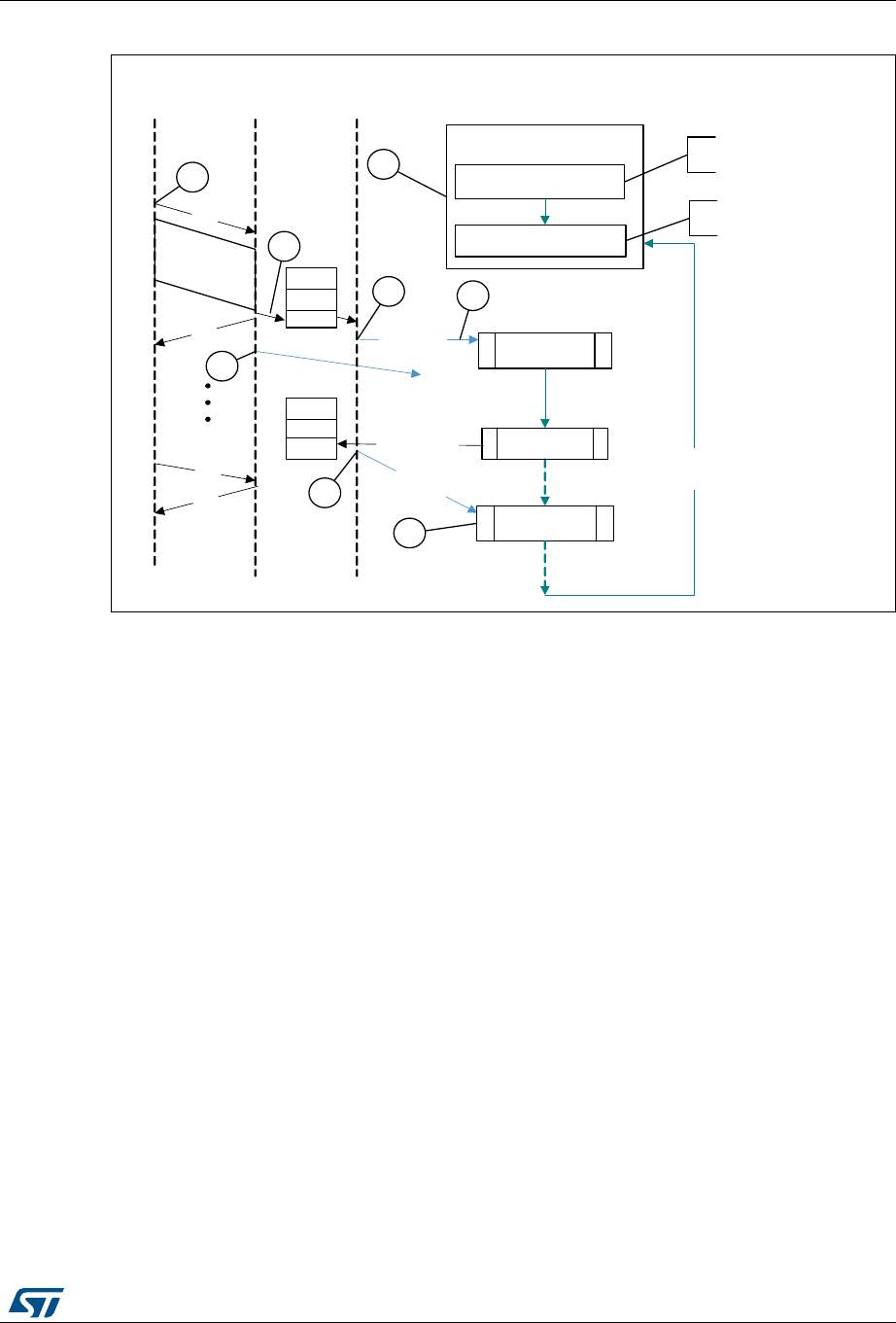
RM0430 Rev 8 1269/1324
RM0430 USB on-the-go full-speed (OTG_FS)
1283
Figure 414. Bulk OUT transaction
After a SetConfiguration/SetInterface command, the application initializes all OUT endpoints
by setting CNAK = 1 and EPENA = 1 (in OTG_DOEPCTLx), and setting a suitable
XFRSIZ and PKTCNT in the OTG_DOEPTSIZx register.
1. host attempts to send data (OUT token) to an endpoint.
2. When the core receives the OUT token on the USB, it stores the packet in the Rx FIFO
because space is available there.
3. After writing the complete packet in the Rx FIFO, the core then asserts the RXFLVL
interrupt (in OTG_GINTSTS).
4. On receiving the PKTCNT number of USB packets, the core internally sets the NAK bit
for this endpoint to prevent it from receiving any more packets.
5. The application processes the interrupt and reads the data from the Rx FIFO.
6. When the application has read all the data (equivalent to XFRSIZ), the core generates
an XFRC interrupt (in OTG_DOEPINTx).
7. The application processes the interrupt and uses the setting of the XFRC interrupt bit
(in OTG_DOEPINTx) to determine that the intended transfer is complete.
IN data transfers
•Packet write
This section describes how the application writes data packets to the endpoint FIFO when
dedicated transmit FIFOs are enabled.
069
LQLW BRXWBHS
287
$&.
5;)/9/ LQW UL
:UBUHJ27*B'2(376,=[
:UBUHJ27*B'2(3&7/[
E\WHV
287
1$.
[DFWB
;)5&
LQWU
;)56,=
U
LGOH XQWLO LQWU
UFYBRXW BSNW
LGOH XQWLO LQWU
2Q QHZ [IHU
RU 5[),)2
QRWHP SW\
;)56,= E\WHV
3.7&17
(3(1$
&1$.
+RVW 86% 'HYLFH $SSOLFDWLRQ
3.7&17
27*B'2(3&7/[1$.

USB on-the-go full-speed (OTG_FS) RM0430
1270/1324 RM0430 Rev 8
1. The application can either choose the polling or the interrupt mode.
– In polling mode, the application monitors the status of the endpoint transmit data
FIFO by reading the OTG_DTXFSTSx register, to determine if there is enough
space in the data FIFO.
– In interrupt mode, the application waits for the TXFE interrupt (in OTG_DIEPINTx)
and then reads the OTG_DTXFSTSx register, to determine if there is enough
space in the data FIFO.
– To write a single non-zero length data packet, there must be space to write the
entire packet in the data FIFO.
– To write zero length packet, the application must not look at the FIFO space.
2. Using one of the above mentioned methods, when the application determines that
there is enough space to write a transmit packet, the application must first write into the
endpoint control register, before writing the data into the data FIFO. Typically, the
application, must do a read modify write on the OTG_DIEPCTLx register to avoid
modifying the contents of the register, except for setting the endpoint enable bit.
The application can write multiple packets for the same endpoint into the transmit FIFO, if
space is available. For periodic IN endpoints, the application must write packets only for one
microframe. It can write packets for the next periodic transaction only after getting transfer
complete for the previous transaction.
•Setting IN endpoint NAK
Internal data flow:
1. When the application sets the IN NAK for a particular endpoint, the core stops
transmitting data on the endpoint, irrespective of data availability in the endpoint’s
transmit FIFO.
2. Non-isochronous IN tokens receive a NAK handshake reply
– Isochronous IN tokens receive a zero-data-length packet reply
3. The core asserts the INEPNE (IN endpoint NAK effective) interrupt in OTG_DIEPINTx
in response to the SNAK bit in OTG_DIEPCTLx.
4. Once this interrupt is seen by the application, the application can assume that the
endpoint is in IN NAK mode. This interrupt can be cleared by the application by setting
the CNAK bit in OTG_DIEPCTLx.
Application programming sequence:
1. To stop transmitting any data on a particular IN endpoint, the application must set the
IN NAK bit. To set this bit, the following field must be programmed.
– SNAK = 1 in OTG_DIEPCTLx
2. Wait for assertion of the INEPNE interrupt in OTG_DIEPINTx. This interrupt indicates
that the core has stopped transmitting data on the endpoint.
3. The core can transmit valid IN data on the endpoint after the application has set the
NAK bit, but before the assertion of the NAK Effective interrupt.
4. The application can mask this interrupt temporarily by writing to the INEPNEM bit in
OTG_DIEPMSK.
– INEPNEM = 0 in OTG_DIEPMSK
5. To exit endpoint NAK mode, the application must clear the NAK status bit (NAKSTS) in
OTG_DIEPCTLx. This also clears the INEPNE interrupt (in OTG_DIEPINTx).

RM0430 Rev 8 1271/1324
RM0430 USB on-the-go full-speed (OTG_FS)
1283
– CNAK = 1 in OTG_DIEPCTLx
6. If the application masked this interrupt earlier, it must be unmasked as follows:
– INEPNEM = 1 in OTG_DIEPMSK
•IN endpoint disable
Use the following sequence to disable a specific IN endpoint that has been previously
enabled.
Application programming sequence:
1. The application must stop writing data on the AHB for the IN endpoint to be disabled.
2. The application must set the endpoint in NAK mode.
– SNAK = 1 in OTG_DIEPCTLx
3. Wait for the INEPNE interrupt in OTG_DIEPINTx.
4. Set the following bits in the OTG_DIEPCTLx register for the endpoint that must be
disabled.
– EPDIS = 1 in OTG_DIEPCTLx
– SNAK = 1 in OTG_DIEPCTLx
5. Assertion of the EPDISD interrupt in OTG_DIEPINTx indicates that the core has
completely disabled the specified endpoint. Along with the assertion of the interrupt, the
core also clears the following bits:
– EPENA = 0 in OTG_DIEPCTLx
– EPDIS = 0 in OTG_DIEPCTLx
6. The application must read the OTG_DIEPTSIZx register for the periodic IN EP, to
calculate how much data on the endpoint were transmitted on the USB.
7. The application must flush the data in the endpoint transmit FIFO, by setting the
following fields in the OTG_GRSTCTL register:
– TXFNUM (in OTG_GRSTCTL) = Endpoint transmit FIFO number
– TXFFLSH in (OTG_GRSTCTL) = 1
The application must poll the OTG_GRSTCTL register, until the TXFFLSH bit is cleared by
the core, which indicates the end of flush operation. To transmit new data on this endpoint,
the application can re-enable the endpoint at a later point.
•Generic non-periodic IN data transfers
Application requirements:
1. Before setting up an IN transfer, the application must ensure that all data to be
transmitted as part of the IN transfer are part of a single buffer.
2. For IN transfers, the transfer size field in the endpoint transfer size register denotes a
payload that constitutes multiple maximum-packet-size packets and a single short
packet. This short packet is transmitted at the end of the transfer.
– To transmit a few maximum-packet-size packets and a short packet at the end of
the transfer:
Transfer size[EPNUM] = x × MPSIZ[EPNUM] + sp
If (sp > 0), then packet count[EPNUM] = x + 1.
Otherwise, packet count[EPNUM] = x
– To transmit a single zero-length data packet:

USB on-the-go full-speed (OTG_FS) RM0430
1272/1324 RM0430 Rev 8
Transfer size[EPNUM] = 0
Packet count[EPNUM] = 1
– To transmit a few maximum-packet-size packets and a zero-length data packet at
the end of the transfer, the application must split the transfer into two parts. The
first sends maximum-packet-size data packets and the second sends the zero-
length data packet alone.
First transfer: transfer size[EPNUM] = x × MPSIZ[epnum]; packet count = n;
Second transfer: transfer size[EPNUM] = 0; packet count = 1;
3. Once an endpoint is enabled for data transfers, the core updates the transfer size
register. At the end of the IN transfer, the application must read the transfer size
register to determine how much data posted in the transmit FIFO have already been
sent on the USB.
4. Data fetched into transmit FIFO = Application-programmed initial transfer size – core-
updated final transfer size
– Data transmitted on USB = (application-programmed initial packet count – core
updated final packet count) × MPSIZ[EPNUM]
– Data yet to be transmitted on USB = (Application-programmed initial transfer size
– data transmitted on USB)
Internal data flow:
1. The application must set the transfer size and packet count fields in the endpoint-
specific registers and enable the endpoint to transmit the data.
2. The application must also write the required data to the transmit FIFO for the endpoint.
3. Every time a packet is written into the transmit FIFO by the application, the transfer size
for that endpoint is decremented by the packet size. The data is fetched from the
memory by the application, until the transfer size for the endpoint becomes 0. After
writing the data into the FIFO, the “number of packets in FIFO” count is incremented
(this is a 3-bit count, internally maintained by the core for each IN endpoint transmit
FIFO. The maximum number of packets maintained by the core at any time in an IN
endpoint FIFO is eight). For zero-length packets, a separate flag is set for each FIFO,
without any data in the FIFO.
4. Once the data are written to the transmit FIFO, the core reads them out upon receiving
an IN token. For every non-isochronous IN data packet transmitted with an ACK
handshake, the packet count for the endpoint is decremented by one, until the packet
count is zero. The packet count is not decremented on a timeout.
5. For zero length packets (indicated by an internal zero length flag), the core sends out a
zero-length packet for the IN token and decrements the packet count field.
6. If there are no data in the FIFO for a received IN token and the packet count field for
that endpoint is zero, the core generates an “IN token received when Tx FIFO is empty”
(ITTXFE) interrupt for the endpoint, provided that the endpoint NAK bit is not set. The
core responds with a NAK handshake for non-isochronous endpoints on the USB.
7. The core internally rewinds the FIFO pointers and no timeout interrupt is generated.
8. When the transfer size is 0 and the packet count is 0, the transfer complete (XFRC)
interrupt for the endpoint is generated and the endpoint enable is cleared.
Application programming sequence:

RM0430 Rev 8 1273/1324
RM0430 USB on-the-go full-speed (OTG_FS)
1283
1. Program the OTG_DIEPTSIZx register with the transfer size and corresponding packet
count.
2. Program the OTG_DIEPCTLx register with the endpoint characteristics and set the
CNAK and EPENA (endpoint enable) bits.
3. When transmitting non-zero length data packet, the application must poll the
OTG_DTXFSTSx register (where x is the FIFO number associated with that endpoint)
to determine whether there is enough space in the data FIFO. The application can
optionally use TXFE (in OTG_DIEPINTx) before writing the data.
•Generic periodic IN data transfers
This section describes a typical periodic IN data transfer.
Application requirements:
1. Application requirements 1, 2, 3, and 4 of Generic non-periodic IN data transfers on
page 1271 also apply to periodic IN data transfers, except for a slight modification of
requirement 2.
– The application can only transmit multiples of maximum-packet-size data packets
or multiples of maximum-packet-size packets, plus a short packet at the end. To
transmit a few maximum-packet-size packets and a short packet at the end of the
transfer, the following conditions must be met:
transfer size[EPNUM] = x × MPSIZ[EPNUM] + sp
(where x is an integer ≥ 0, and 0 ≤ sp < MPSIZ[EPNUM])
If (sp > 0), packet count[EPNUM] = x + 1
Otherwise, packet count[EPNUM] = x;
MCNT[EPNUM] = packet count[EPNUM]
– The application cannot transmit a zero-length data packet at the end of a transfer.
It can transmit a single zero-length data packet by itself. To transmit a single zero-
length data packet:
– transfer size[EPNUM] = 0
packet count[EPNUM] = 1
MCNT[EPNUM] = packet count[EPNUM]
2. The application can only schedule data transfers one frame at a time.
– (MCNT – 1) × MPSIZ ≤ XFERSIZ ≤ MCNT × MPSIZ
– PKTCNT = MCNT (in OTG_DIEPTSIZx)
– If XFERSIZ < MCNT × MPSIZ, the last data packet of the transfer is a short
packet.
– Note that: MCNT is in OTG_DIEPTSIZx, MPSIZ is in OTG_DIEPCTLx, PKTCNT
is in OTG_DIEPTSIZx and XFERSIZ is in OTG_DIEPTSIZx
3. The complete data to be transmitted in the frame must be written into the transmit FIFO
by the application, before the IN token is received. Even when 1 word of the data to be
transmitted per frame is missing in the transmit FIFO when the IN token is received, the
core behaves as when the FIFO is empty. When the transmit FIFO is empty:
– A zero data length packet would be transmitted on the USB for isochronous IN
endpoints
– A NAK handshake would be transmitted on the USB for interrupt IN endpoints
Internal data flow:

USB on-the-go full-speed (OTG_FS) RM0430
1274/1324 RM0430 Rev 8
1. The application must set the transfer size and packet count fields in the endpoint-
specific registers and enable the endpoint to transmit the data.
2. The application must also write the required data to the associated transmit FIFO for
the endpoint.
3. Every time the application writes a packet to the transmit FIFO, the transfer size for that
endpoint is decremented by the packet size. The data are fetched from application
memory until the transfer size for the endpoint becomes 0.
4. When an IN token is received for a periodic endpoint, the core transmits the data in the
FIFO, if available. If the complete data payload (complete packet, in dedicated FIFO
mode) for the frame is not present in the FIFO, then the core generates an IN token
received when Tx FIFO empty interrupt for the endpoint.
– A zero-length data packet is transmitted on the USB for isochronous IN endpoints
– A NAK handshake is transmitted on the USB for interrupt IN endpoints
5. The packet count for the endpoint is decremented by 1 under the following conditions:
– For isochronous endpoints, when a zero- or non-zero-length data packet is
transmitted
– For interrupt endpoints, when an ACK handshake is transmitted
– When the transfer size and packet count are both 0, the transfer completed
interrupt for the endpoint is generated and the endpoint enable is cleared.
6. At the “Periodic frame Interval” (controlled by PFIVL in OTG_DCFG), when the core
finds non-empty any of the isochronous IN endpoint FIFOs scheduled for the current
frame non-empty, the core generates an IISOIXFR interrupt in OTG_GINTSTS.
Application programming sequence:
1. Program the OTG_DIEPCTLx register with the endpoint characteristics and set the
CNAK and EPENA bits.
2. Write the data to be transmitted in the next frame to the transmit FIFO.
3. Asserting the ITTXFE interrupt (in OTG_DIEPINTx) indicates that the application has
not yet written all data to be transmitted to the transmit FIFO.
4. If the interrupt endpoint is already enabled when this interrupt is detected, ignore the
interrupt. If it is not enabled, enable the endpoint so that the data can be transmitted on
the next IN token attempt.
5. Asserting the XFRC interrupt (in OTG_DIEPINTx) with no ITTXFE interrupt in
OTG_DIEPINTx indicates the successful completion of an isochronous IN transfer. A
read to the OTG_DIEPTSIZx register must give transfer size = 0 and packet count = 0,
indicating all data were transmitted on the USB.
6. Asserting the XFRC interrupt (in OTG_DIEPINTx), with or without the ITTXFE interrupt
(in OTG_DIEPINTx), indicates the successful completion of an interrupt IN transfer. A
read to the OTG_DIEPTSIZx register must give transfer size = 0 and packet count = 0,
indicating all data were transmitted on the USB.
7. Asserting the incomplete isochronous IN transfer (IISOIXFR) interrupt in
OTG_GINTSTS with none of the aforementioned interrupts indicates the core did not
receive at least 1 periodic IN token in the current frame.
•Incomplete isochronous IN data transfers
This section describes what the application must do on an incomplete isochronous IN data
transfer.

RM0430 Rev 8 1275/1324
RM0430 USB on-the-go full-speed (OTG_FS)
1283
Internal data flow:
1. An isochronous IN transfer is treated as incomplete in one of the following conditions:
a) The core receives a corrupted isochronous IN token on at least one isochronous
IN endpoint. In this case, the application detects an incomplete isochronous IN
transfer interrupt (IISOIXFR in OTG_GINTSTS).
b) The application is slow to write the complete data payload to the transmit FIFO
and an IN token is received before the complete data payload is written to the
FIFO. In this case, the application detects an IN token received when Tx FIFO
empty interrupt in OTG_DIEPINTx. The application can ignore this interrupt, as it
eventually results in an incomplete isochronous IN transfer interrupt (IISOIXFR in
OTG_GINTSTS) at the end of periodic frame.
The core transmits a zero-length data packet on the USB in response to the
received IN token.
2. The application must stop writing the data payload to the transmit FIFO as soon as
possible.
3. The application must set the NAK bit and the disable bit for the endpoint.
4. The core disables the endpoint, clears the disable bit, and asserts the endpoint disable
interrupt for the endpoint.
Application programming sequence:
1. The application can ignore the IN token received when Tx FIFO empty interrupt in
OTG_DIEPINTx on any isochronous IN endpoint, as it eventually results in an
incomplete isochronous IN transfer interrupt (in OTG_GINTSTS).
2. Assertion of the incomplete isochronous IN transfer interrupt (in OTG_GINTSTS)
indicates an incomplete isochronous IN transfer on at least one of the isochronous IN
endpoints.
3. The application must read the endpoint control register for all isochronous IN endpoints
to detect endpoints with incomplete IN data transfers.
4. The application must stop writing data to the Periodic Transmit FIFOs associated with
these endpoints on the AHB.
5. Program the following fields in the OTG_DIEPCTLx register to disable the endpoint:
– SNAK = 1 in OTG_DIEPCTLx
– EPDIS = 1 in OTG_DIEPCTLx
6. The assertion of the endpoint disabled interrupt in OTG_DIEPINTx indicates that the
core has disabled the endpoint.
– At this point, the application must flush the data in the associated transmit FIFO or
overwrite the existing data in the FIFO by enabling the endpoint for a new transfer
in the next microframe. To flush the data, the application must use the
OTG_GRSTCTL register.
•Stalling non-isochronous IN endpoints
This section describes how the application can stall a non-isochronous endpoint.
Application programming sequence:

USB on-the-go full-speed (OTG_FS) RM0430
1276/1324 RM0430 Rev 8
1. Disable the IN endpoint to be stalled. Set the STALL bit as well.
2. EPDIS = 1 in OTG_DIEPCTLx, when the endpoint is already enabled
– STALL = 1 in OTG_DIEPCTLx
– The STALL bit always takes precedence over the NAK bit
3. Assertion of the endpoint disabled interrupt (in OTG_DIEPINTx) indicates to the
application that the core has disabled the specified endpoint.
4. The application must flush the non-periodic or periodic transmit FIFO, depending on
the endpoint type. In case of a non-periodic endpoint, the application must re-enable
the other non-periodic endpoints that do not need to be stalled, to transmit data.
5. Whenever the application is ready to end the STALL handshake for the endpoint, the
STALL bit must be cleared in OTG_DIEPCTLx.
6. If the application sets or clears a STALL bit for an endpoint due to a
SetFeature.Endpoint Halt command or ClearFeature.Endpoint Halt command, the
STALL bit must be set or cleared before the application sets up the status stage
transfer on the control endpoint.
Special case: stalling the control OUT endpoint
The core must stall IN/OUT tokens if, during the data stage of a control transfer, the host
sends more IN/OUT tokens than are specified in the SETUP packet. In this case, the
application must enable the ITTXFE interrupt in OTG_DIEPINTx and the OTEPDIS interrupt
in OTG_DOEPINTx during the data stage of the control transfer, after the core has
transferred the amount of data specified in the SETUP packet. Then, when the application
receives this interrupt, it must set the STALL bit in the corresponding endpoint control
register, and clear this interrupt.
33.16.6 Worst case response time
When the OTG_FS controller acts as a device, there is a worst case response time for any
tokens that follow an isochronous OUT. This worst case response time depends on the AHB
clock frequency.
The core registers are in the AHB domain, and the core does not accept another token
before updating these register values. The worst case is for any token following an
isochronous OUT, because for an isochronous transaction, there is no handshake and the
next token could come sooner. This worst case value is 7 PHY clocks when the AHB clock
is the same as the PHY clock. When the AHB clock is faster, this value is smaller.
If this worst case condition occurs, the core responds to bulk/interrupt tokens with a NAK
and drops isochronous and SETUP tokens. The host interprets this as a timeout condition
for SETUP and retries the SETUP packet. For isochronous transfers, the Incomplete
isochronous IN transfer interrupt (IISOIXFR) and Incomplete isochronous OUT transfer
interrupt (IISOOXFR) inform the application that isochronous IN/OUT packets were
dropped.
Choosing the value of TRDT in OTG_GUSBCFG
The value in TRDT (OTG_GUSBCFG) is the time it takes for the MAC, in terms of PHY
clocks after it has received an IN token, to get the FIFO status, and thus the first data from
the PFC block. This time involves the synchronization delay between the PHY and AHB
clocks. The worst case delay for this is when the AHB clock is the same as the PHY clock.
In this case, the delay is 5 clocks.
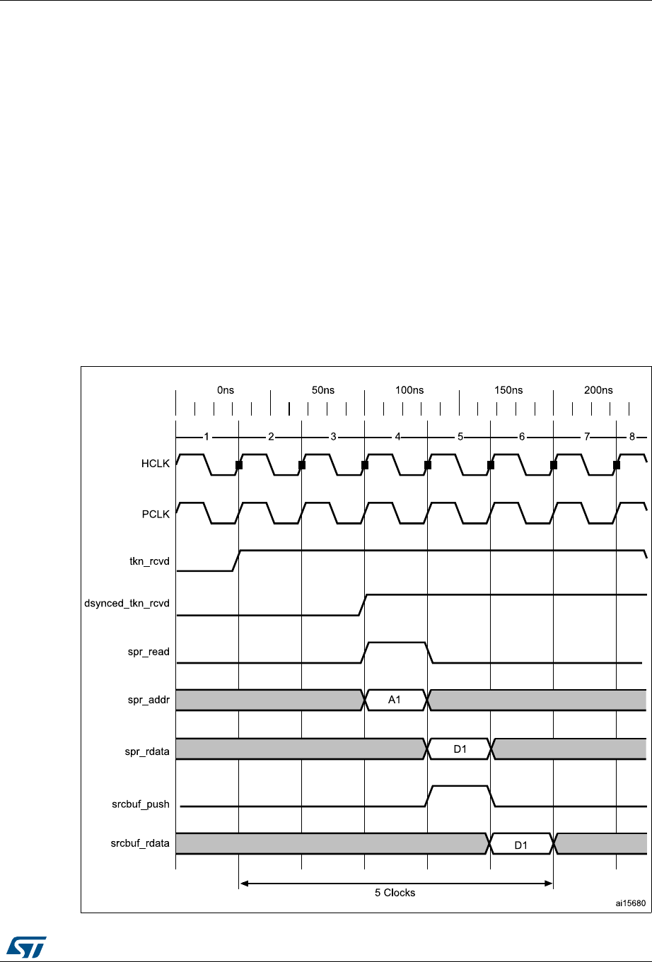
RM0430 Rev 8 1277/1324
RM0430 USB on-the-go full-speed (OTG_FS)
1283
Once the MAC receives an IN token, this information (token received) is synchronized to the
AHB clock by the PFC (the PFC runs on the AHB clock). The PFC then reads the data from
the SPRAM and writes them into the dual clock source buffer. The MAC then reads the data
out of the source buffer (4 deep).
If the AHB is running at a higher frequency than the PHY, the application can use a smaller
value for TRDT (in OTG_GUSBCFG).
Figure 415 has the following signals:
•tkn_rcvd: Token received information from MAC to PFC
•dynced_tkn_rcvd: Doubled sync tkn_rcvd, from PCLK to HCLK domain
•spr_read: Read to SPRAM
•spr_addr: Address to SPRAM
•spr_rdata: Read data from SPRAM
•srcbuf_push: Push to the source buffer
•srcbuf_rdata: Read data from the source buffer. Data seen by MAC
To calculate the value of TRDT, refer to Table 229: TRDT values (FS) .
Figure 415. TRDT max timing case
USB on-the-go full-speed (OTG_FS) RM0430
1278/1324 RM0430 Rev 8
33.16.7 OTG programming model
The OTG_FS controller is an OTG device supporting HNP and SRP. When the core is
connected to an “A” plug, it is referred to as an A-device. When the core is connected to a
“B” plug it is referred to as a B-device. In host mode, the OTG_FS controller turns off VBUS
to conserve power. SRP is a method by which the B-device signals the A-device to turn on
VBUS power. A device must perform both data-line pulsing and VBUS pulsing, but a host can
detect either data-line pulsing or VBUS pulsing for SRP. HNP is a method by which the B-
device negotiates and switches to host role. In Negotiated mode after HNP, the B-device
suspends the bus and reverts to the device role.
A-device session request protocol
The application must set the SRP-capable bit in the core USB configuration register. This
enables the OTG_FS controller to detect SRP as an A-device.
Figure 416. A-device SRP
1. DRV_VBUS = VBUS drive signal to the PHY
VBUS_VALID = VBUS valid signal from PHY
A_VALID = A-peripheral VBUS level signal to PHY
D+ = Data plus line
D- = Data minus line
The following points refer and describe the signal numeration shown in the Figure 416:
1. To save power, the application suspends and turns off port power when the bus is idle
by writing the port suspend and port power bits in the host port control and status
register.
2. PHY indicates port power off by deasserting the VBUS_VALID signal.
3. The device must detect SE0 for at least 2 ms to start SRP when VBUS power is off.
4. To initiate SRP, the device turns on its data line pull-up resistor for 5 to 10 ms. The
OTG_FS controller detects data-line pulsing.
5. The device drives VBUS above the A-device session valid (2.0 V minimum) for VBUS
pulsing.
The OTG_FS controller interrupts the application on detecting SRP. The session
DLF
'59B9%86
9%86B9$/,'
$B9$/,'
'
'
6XVSHQG
9%86SXOVLQJ
'DWDOLQHSXOVLQJ &RQQHFW
/RZ
RM0430 Rev 8 1279/1324
RM0430 USB on-the-go full-speed (OTG_FS)
1283
request detected bit is set in Global interrupt status register (SRQINT set in
OTG_GINTSTS).
6. The application must service the session request detected interrupt and turn on the
port power bit by writing the port power bit in the host port control and status register.
The PHY indicates port power-on by asserting the VBUS_VALID signal.
7. When the USB is powered, the device connects, completing the SRP process.
B-device session request protocol
The application must set the SRP-capable bit in the core USB configuration register. This
enables the OTG_FS controller to initiate SRP as a B-device. SRP is a means by which the
OTG_FS controller can request a new session from the host.
Figure 417. B-device SRP
1. VBUS_VALID = VBUS valid signal from PHY
B_VALID = B-peripheral valid session to PHY
DISCHRG_VBUS = discharge signal to PHY
SESS_END = session end signal to PHY
CHRG_VBUS = charge VBUS signal to PHY
DP = Data plus line
DM = Data minus line
The following points refer and describe the signal numeration shown in the Figure 417:
1. To save power, the host suspends and turns off port power when the bus is idle.
The OTG_FS controller sets the early suspend bit in the core interrupt register after 3
ms of bus idleness. Following this, the OTG_FS controller sets the USB suspend bit in
the core interrupt register.
The OTG_FS controller informs the PHY to discharge VBUS.
2. The PHY indicates the session’s end to the device. This is the initial condition for SRP.
The OTG_FS controller requires 2 ms of SE0 before initiating SRP.
For a USB 1.1 full-speed serial transceiver, the application must wait until VBUS
discharges to 0.2 V after BSVLD (in OTG_GOTGCTL) is deasserted. This discharge
DLF
9%86B9$/,'
%B9$/,'
',6&+5*B9%86
6(66B(1'
'3
'0
&+5*B9%86
6XVSHQG
'DWDOLQHSXOVLQJ &RQQHFW
9%86SXOVLQJ
/RZ
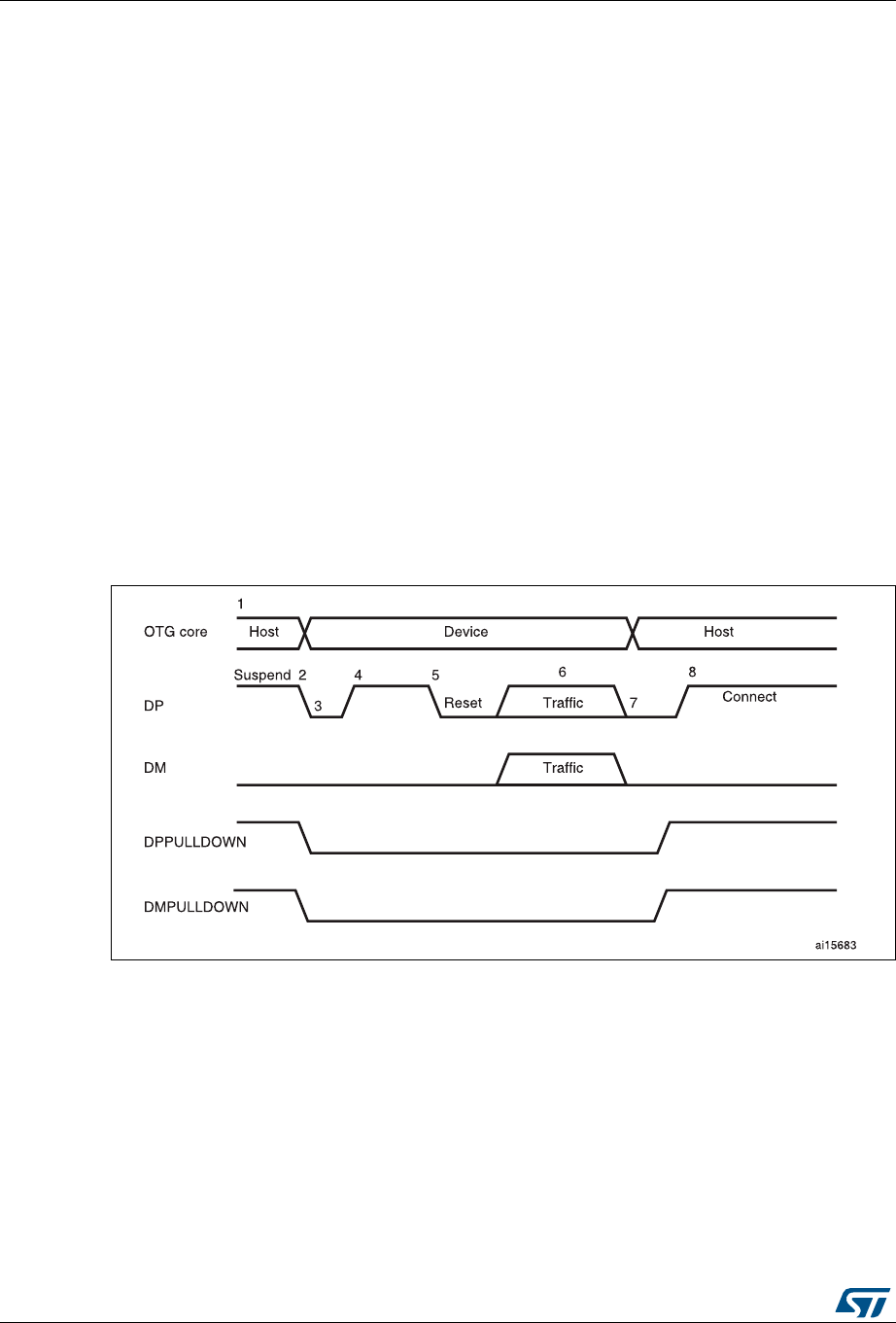
USB on-the-go full-speed (OTG_FS) RM0430
1280/1324 RM0430 Rev 8
time can be obtained from the transceiver vendor and varies from one transceiver to
another.
3. The OTG_FS core informs the PHY to speed up VBUS discharge.
4. The application initiates SRP by writing the session request bit in the OTG control and
status register. The OTG_FS controller perform data-line pulsing followed by VBUS
pulsing.
5. The host detects SRP from either the data-line or VBUS pulsing, and turns on VBUS.
The PHY indicates VBUS power-on to the device.
6. The OTG_FS controller performs VBUS pulsing.
The host starts a new session by turning on VBUS, indicating SRP success. The
OTG_FS controller interrupts the application by setting the session request success
status change bit in the OTG interrupt status register. The application reads the session
request success bit in the OTG control and status register.
7. When the USB is powered, the OTG_FS controller connects, completing the SRP
process.
A-device host negotiation protocol
HNP switches the USB host role from the A-device to the B-device. The application must set
the HNP-capable bit in the core USB configuration register to enable the OTG_FS controller
to perform HNP as an A-device.
Figure 418. A-device HNP
1. DPPULLDOWN = signal from core to PHY to enable/disable the pull-down on the DP line inside the PHY.
DMPULLDOWN = signal from core to PHY to enable/disable the pull-down on the DM line inside the PHY.
The following points refer and describe the signal numeration shown in the Figure 418:
1. The OTG_FS controller sends the B-device a SetFeature b_hnp_enable descriptor to
enable HNP support. The B-device’s ACK response indicates that the B-device
supports HNP. The application must set host Set HNP enable bit in the OTG control

RM0430 Rev 8 1281/1324
RM0430 USB on-the-go full-speed (OTG_FS)
1283
and status register to indicate to the OTG_FS controller that the B-device supports
HNP.
2. When it has finished using the bus, the application suspends by writing the port
suspend bit in the host port control and status register.
3. When the B-device observes a USB suspend, it disconnects, indicating the initial
condition for HNP. The B-device initiates HNP only when it must switch to the host role;
otherwise, the bus continues to be suspended.
The OTG_FS controller sets the host negotiation detected interrupt in the OTG
interrupt status register, indicating the start of HNP.
The OTG_FS controller deasserts the DM pull down and DM pull down in the PHY to
indicate a device role. The PHY enables the OTG_DP pull-up resistor to indicate a
connect for B-device.
The application must read the current mode bit in the OTG control and status register
to determine device mode operation.
4. The B-device detects the connection, issues a USB reset, and enumerates the
OTG_FS controller for data traffic.
5. The B-device continues the host role, initiating traffic, and suspends the bus when
done.
The OTG_FS controller sets the early suspend bit in the core interrupt register after 3
ms of bus idleness. Following this, the OTG_FS controller sets the USB suspend bit in
the core interrupt register.
6. In Negotiated mode, the OTG_FS controller detects the suspend, disconnects, and
switches back to the host role. The OTG_FS controller asserts the DM pull down and
DM pull down in the PHY to indicate its assumption of the host role.
7. The OTG_FS controller sets the connector ID status change interrupt in the OTG
interrupt status register. The application must read the connector ID status in the OTG
control and status register to determine the OTG_FS controller operation as an A-
device. This indicates the completion of HNP to the application. The application must
read the Current mode bit in the OTG control and status register to determine host
mode operation.
8. The B-device connects, completing the HNP process.
B-device host negotiation protocol
HNP switches the USB host role from B-device to A-device. The application must set the
HNP-capable bit in the core USB configuration register to enable the OTG_FS controller to
perform HNP as a B-device.
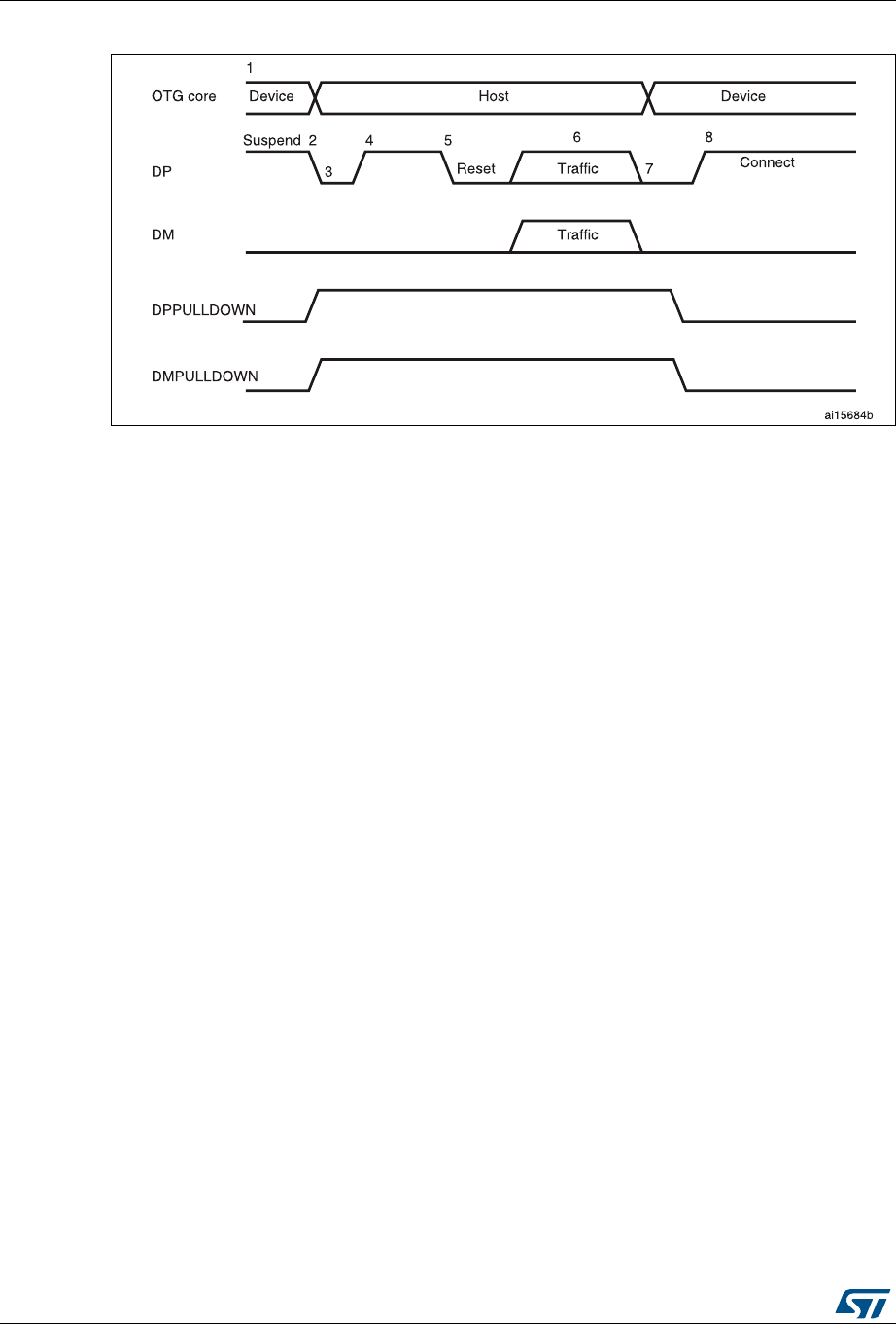
USB on-the-go full-speed (OTG_FS) RM0430
1282/1324 RM0430 Rev 8
Figure 419. B-device HNP
1. DPPULLDOWN = signal from core to PHY to enable/disable the pull-down on the DP line inside the PHY.
DMPULLDOWN = signal from core to PHY to enable/disable the pull-down on the DM line inside the PHY.
The following points refer and describe the signal numeration shown in the Figure 419:
1. The A-device sends the SetFeature b_hnp_enable descriptor to enable HNP support.
The OTG_FS controller’s ACK response indicates that it supports HNP. The application
must set the device HNP enable bit in the OTG control and status register to indicate
HNP support.
The application sets the HNP request bit in the OTG control and status register to
indicate to the OTG_FS controller to initiate HNP.
2. When it has finished using the bus, the A-device suspends by writing the port suspend
bit in the host port control and status register.
The OTG_FS controller sets the Early suspend bit in the core interrupt register after 3
ms of bus idleness. Following this, the OTG_FS controller sets the USB suspend bit in
the core interrupt register.
The OTG_FS controller disconnects and the A-device detects SE0 on the bus,
indicating HNP. The OTG_FS controller asserts the DP pull down and DM pull down in
the PHY to indicate its assumption of the host role.
The A-device responds by activating its OTG_DP pull-up resistor within 3 ms of
detecting SE0. The OTG_FS controller detects this as a connect.
The OTG_FS controller sets the host negotiation success status change interrupt in the
OTG interrupt status register, indicating the HNP status. The application must read the
host negotiation success bit in the OTG control and status register to determine host

RM0430 Rev 8 1283/1324
RM0430 USB on-the-go full-speed (OTG_FS)
1283
negotiation success. The application must read the current Mode bit in the core
interrupt register (OTG_GINTSTS) to determine host mode operation.
3. The application sets the reset bit (PRST in OTG_HPRT) and the OTG_FS controller
issues a USB reset and enumerates the A-device for data traffic.
4. The OTG_FS controller continues the host role of initiating traffic, and when done,
suspends the bus by writing the port suspend bit in the host port control and status
register.
5. In Negotiated mode, when the A-device detects a suspend, it disconnects and switches
back to the host role. The OTG_FS controller deasserts the DP pull down and DM pull
down in the PHY to indicate the assumption of the device role.
6. The application must read the current mode bit in the core interrupt (OTG_GINTSTS)
register to determine the host mode operation.
7. The OTG_FS controller connects, completing the HNP process.
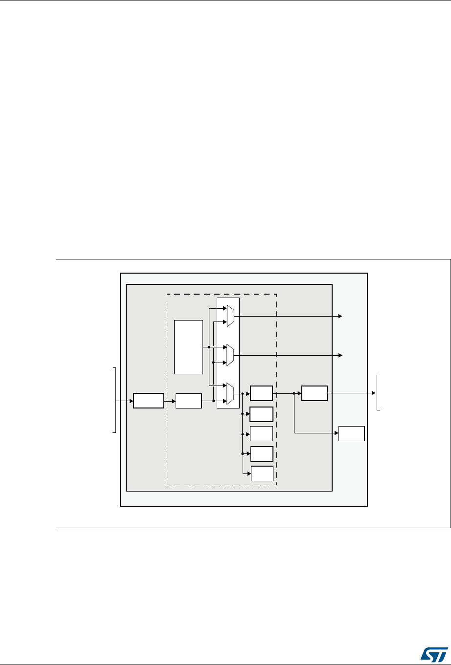
Debug support (DBG) RM0430
1284/1324 RM0430 Rev 8
34 Debug support (DBG)
34.1 Overview
The STM32F413/423 is built around a Cortex®-M4 with FPU core which contains hardware
extensions for advanced debugging features. The debug extensions allow the core to be
stopped either on a given instruction fetch (breakpoint) or data access (watchpoint). When
stopped, the core’s internal state and the system’s external state may be examined. Once
examination is complete, the core and the system may be restored and program execution
resumed.
The debug features are used by the debugger host when connecting to and debugging the
STM32F413/423 MCUs.
Two interfaces for debug are available:
•Serial wire
•JTAG debug port
Figure 420. Block diagram of STM32 MCU and Cortex®-M4 with FPU-level
debug support
Note: The debug features embedded in the Cortex®-M4 with FPU core are a subset of the Arm®
CoreSight Design Kit.
ESTRICTED$I
#ORTEX-
CORE
37*$0 !("!0
"RIDGE
.6)#
$74
&0"
)4-
40)5
$#ODE
INTERFACE
3YSTEM
INTERFACE
)NTERNALPRIVATE
PERIPHERALBUS00"
%XTERNALPRIVATE
PERIPHERALBUS00"
"USMATRIX
$ATA
4R A CE PO R T
$"'-#5
34-&XXDEBUGSUPPORT
#ORTEX-DEBUGSUPPORT
*4-3
*4$)
*4$/
.*4234
*4#+
37$)/
37#,+
42!#%37/
42!#%37/
42!#%#+
42!#%$;=
-36

RM0430 Rev 8 1285/1324
RM0430 Debug support (DBG)
1314
The Arm® Cortex®-M4 with FPU core provides integrated on-chip debug support. It is
comprised of:
•SWJ-DP: Serial wire / JTAG debug port
•AHP-AP: AHB access port
•ITM: Instrumentation trace macrocell
•FPB: Flash patch breakpoint
•DWT: Data watchpoint trigger
•TPUI: Trace port unit interface (available on larger packages, where the corresponding
pins are mapped)
•ETM: Embedded Trace Macrocell (available on larger packages, where the
corresponding pins are mapped)
It also includes debug features dedicated to the STM32F413/423:
•Flexible debug pinout assignment
•MCU debug box (support for low-power modes, control over peripheral clocks, etc.)
Note: For further information on debug functionality supported by the Arm® Cortex®-M4 with FPU
core, refer to the Cortex®-M4 with FPU-r0p1 Technical Reference Manual and to the
CoreSight Design Kit-r0p1 TRM (see Section 34.2: Reference Arm® documentation).
34.2 Reference Arm® documentation
•Cortex®-M4 with FPU r0p1 Technical Reference Manual (TRM)
(see Related documents on page 1)
•Arm® Debug Interface V5
•Arm® CoreSight Design Kit revision r0p1 Technical Reference Manual
34.3 SWJ debug port (serial wire and JTAG)
The STM32F413/423 core of the integrates the Serial Wire / JTAG Debug Port (SWJ-DP). It
is an Arm® standard CoreSight debug port that combines a JTAG-DP (5-pin) interface and a
SW-DP (2-pin) interface.
•The JTAG Debug Port (JTAG-DP) provides a 5-pin standard JTAG interface to the
AHP-AP port.
•The Serial Wire Debug Port (SW-DP) provides a 2-pin (clock + data) interface to the
AHP-AP port.
In the SWJ-DP, the two JTAG pins of the SW-DP are multiplexed with some of the five JTAG
pins of the JTAG-DP.
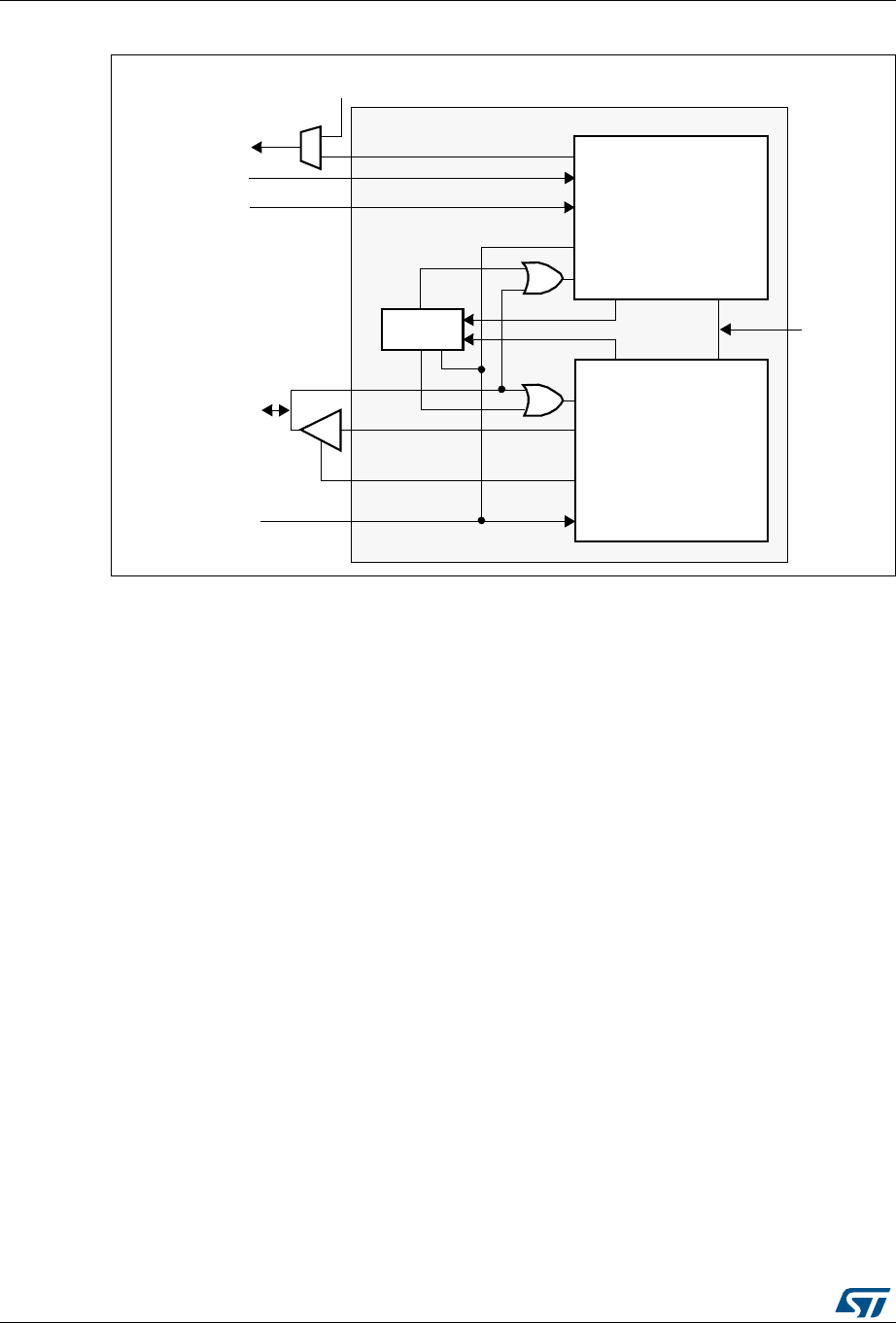
Debug support (DBG) RM0430
1286/1324 RM0430 Rev 8
Figure 421. SWJ debug port
Figure 421 shows that the asynchronous TRACE output (TRACESWO) is multiplexed with
TDO. This means that the asynchronous trace can only be used with SW-DP, not JTAG-DP.
34.3.1 Mechanism to select the JTAG-DP or the SW-DP
By default, the JTAG-Debug Port is active.
If the debugger host wants to switch to the SW-DP, it must provide a dedicated JTAG
sequence on TMS/TCK (respectively mapped to SWDIO and SWCLK) which disables the
JTAG-DP and enables the SW-DP. This way it is possible to activate the SWDP using only
the SWCLK and SWDIO pins.
This sequence is:
1. Send more than 50 TCK cycles with TMS (SWDIO) =1
2. Send the 16-bit sequence on TMS (SWDIO) = 0111100111100111 (MSB transmitted
first)
3. Send more than 50 TCK cycles with TMS (SWDIO) =1
34.4 Pinout and debug port pins
The STM32F413/423 MCUs are available in various packages with different numbers of
available pins. As a result, some functionality (ETM) related to pin availability may differ
between packages.
TRACESWO
JTDO
JTDI
NJTRSTnTRST
TDI
TDO
SWJ-DP
TDO
TDI
nTRST
TCK
TMSnPOTRST
JTAG-DP
nPOTRST
From
power-on
reset
DBGRESETn
DBGDI
DBGDO
DBGDOEN
DBGCLK
SW-DP
SWCLKTCK
SWDOEN
SWDO
SWDITMS
SWD/JTAG
select
JTMS/SWDIO
JTCK/SWCLK
(asynchronous trace)
ai17139
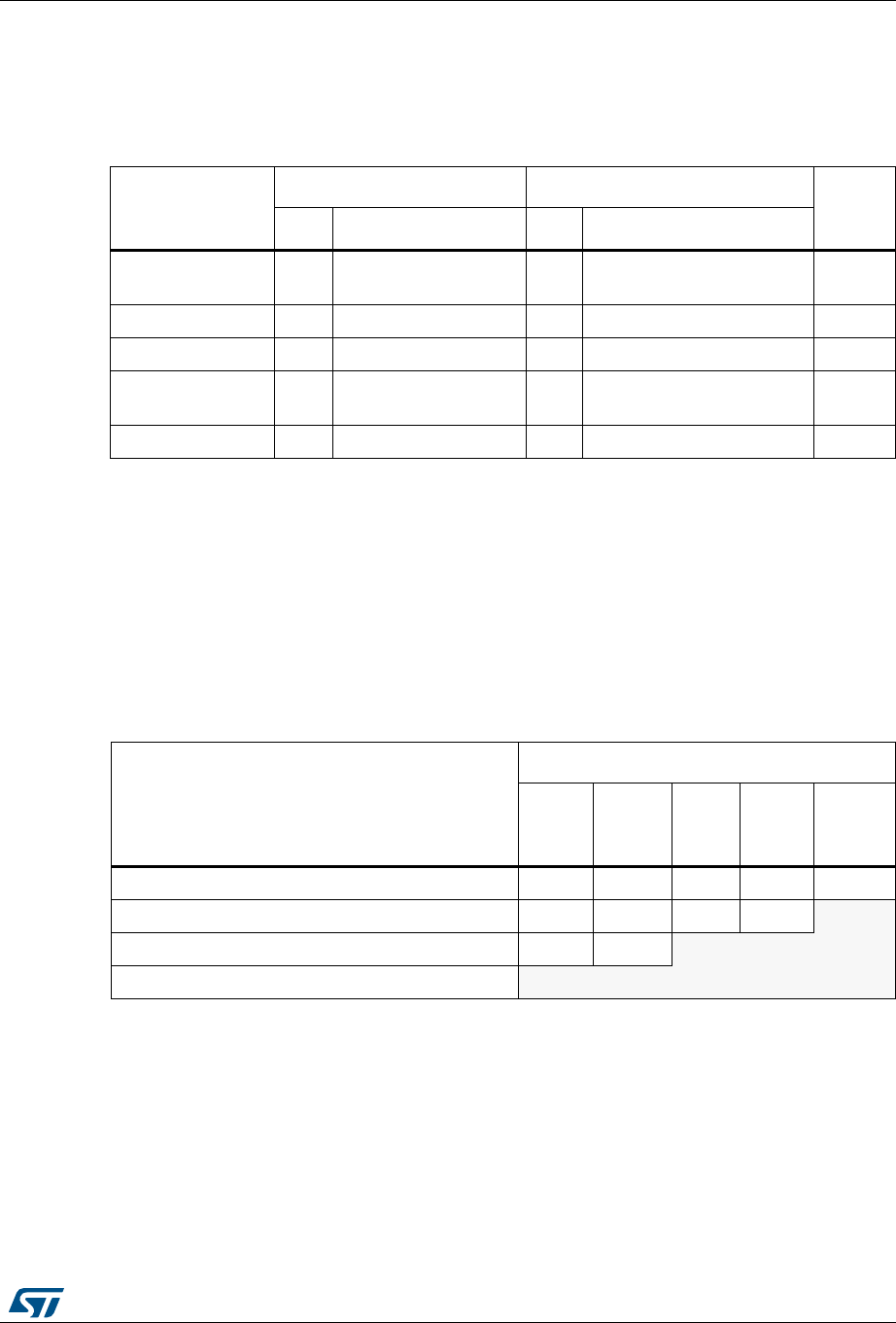
RM0430 Rev 8 1287/1324
RM0430 Debug support (DBG)
1314
34.4.1 SWJ debug port pins
Five pins are used as outputs from the STM32F413/423 for the SWJ-DP as alternate
functions of general-purpose I/Os. These pins are available on all packages.
34.4.2 Flexible SWJ-DP pin assignment
After RESET (SYSRESETn or PORESETn), all five pins used for the SWJ-DP are assigned
as dedicated pins immediately usable by the debugger host (note that the trace outputs are
not assigned except if explicitly programmed by the debugger host).
However, the STM32F413/423 MCUs offers the possibility of disabling some or all of the
SWJ-DP ports and so, of releasing the associated pins for general-purpose IO (GPIO)
usage. For more details on how to disable SWJ-DP port pins, please refer to .
.
Note: When the APB bridge write buffer is full, it takes one extra APB cycle when writing the
GPIO_AFR register. This is because the deactivation of the JTAGSW pins is done in two
cycles to guarantee a clean level on the nTRST and TCK input signals of the core.
•Cycle 1: the JTAGSW input signals to the core are tied to 1 or 0 (to 1 for nTRST, TDI
and TMS, to 0 for TCK)
•Cycle 2: the GPIO controller takes the control signals of the SWJTAG IO pins (like
controls of direction, pull-up/down, Schmitt trigger activation, etc.).
Table 232. SWJ debug port pins
SWJ-DP pin name
JTAG debug port SW debug port Pin
assign
ment
Type Description Type Debug assignment
JTMS/SWDIO I JTAG Test Mode
Selection IO Serial Wire Data
Input/Output PA13
JTCK/SWCLK I JTAG Test Clock I Serial Wire Clock PA14
JTDI I JTAG Test Data Input - - PA15
JTDO/TRACESWO O JTAG Test Data Output - TRACESWO if async trace
is enabled PB3
NJTRST I JTAG Test nReset - - PB4
Table 233. Flexible SWJ-DP pin assignment
Available debug ports
SWJ IO pin assigned
PA13 /
JTMS /
SWDIO
PA14 /
JTCK /
SWCLK
PA15 /
JTDI
PB3 /
JTDO
PB4 /
NJTRST
Full SWJ (JTAG-DP + SW-DP) - Reset State X X X X X
Full SWJ (JTAG-DP + SW-DP) but without NJTRST X X X X
JTAG-DP Disabled and SW-DP Enabled X X
JTAG-DP Disabled and SW-DP Disabled Released

Debug support (DBG) RM0430
1288/1324 RM0430 Rev 8
34.4.3 Internal pull-up and pull-down on JTAG pins
It is necessary to ensure that the JTAG input pins are not floating since they are directly
connected to flip-flops to control the debug mode features. Special care must be taken with
the SWCLK/TCK pin which is directly connected to the clock of some of these flip-flops.
To avoid any uncontrolled IO levels, the devices internal pull-ups and pull-downs on the
JTAG input pins:
•NJTRST: Internal pull-up
•JTDI: Internal pull-up
•JTMS/SWDIO: Internal pull-up
•TCK/SWCLK: Internal pull-down
Once a JTAG IO is released by the user software, the GPIO controller takes control again.
The reset states of the GPIO control registers put the I/Os in the equivalent state:
•NJTRST: AF input pull-up
•JTDI: AF input pull-up
•JTMS/SWDIO: AF input pull-up
•JTCK/SWCLK: AF input pull-down
•JTDO: AF output floating
The software can then use these I/Os as standard GPIOs.
Note: The JTAG IEEE standard recommends to add pull-ups on TDI, TMS and nTRST but there is
no special recommendation for TCK. However, for TCK, the devices needs an integrated
pull-down.
Having embedded pull-ups and pull-downs removes the need to add external resistors.

RM0430 Rev 8 1289/1324
RM0430 Debug support (DBG)
1314
34.4.4 Using serial wire and releasing the unused debug pins as GPIOs
To use the serial wire DP to release some GPIOs, the user software must change the GPIO
(PA15, PB3 and PB4) configuration mode in the GPIO_MODER register. This releases
PA15, PB3 and PB4 which now become available as GPIOs.
When debugging, the host performs the following actions:
•Under system reset, all SWJ pins are assigned (JTAG-DP + SW-DP).
•Under system reset, the debugger host sends the JTAG sequence to switch from the
JTAG-DP to the SW-DP.
•Still under system reset, the debugger sets a breakpoint on vector reset.
•The system reset is released and the Core halts.
•All the debug communications from this point are done using the SW-DP. The other
JTAG pins can then be reassigned as GPIOs by the user software.
Note: For user software designs, note that:
To release the debug pins, remember that they will be first configured either in input-pull-up
(nTRST, TMS, TDI) or pull-down (TCK) or output tristate (TDO) for a certain duration after
reset until the instant when the user software releases the pins.
When debug pins (JTAG or SW or TRACE) are mapped, changing the corresponding IO pin
configuration in the IOPORT controller has no effect.
34.5 JTAG TAP connection
The MCUs integrate two serially connected JTAG TAPs, the boundary scan TAP (IR is 5-bit
wide) and the Cortex®-M4 with FPU TAP (IR is 4-bit wide).
To access the TAP of the Cortex®-M4 with FPU for debug purposes:
1. First, it is necessary to shift the BYPASS instruction of the boundary scan TAP.
2. Then, for each IR shift, the scan chain contains 9 bits (=5+4) and the unused TAP
instruction must be shifted in using the BYPASS instruction.
3. For each data shift, the unused TAP, which is in BYPASS mode, adds 1 extra data bit in
the data scan chain.
Note: Important: Once Serial-Wire is selected using the dedicated Arm® JTAG sequence, the
boundary scan TAP is automatically disabled (JTMS forced high).
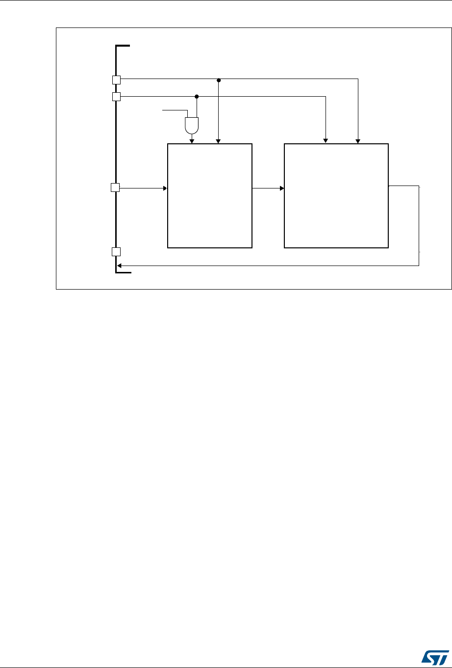
Debug support (DBG) RM0430
1290/1324 RM0430 Rev 8
Figure 422. JTAG TAP connections
"OUNDARYSCAN
4!0
.*4234
#ORTEX-4!0
*4-3
4-3 N42344-3 N4234
*4$)
*4$/
4$) 4$/ 4$) 4$/
37$0
34-&XXX
3ELECTED
)2ISBITWIDE )2ISBITWIDE
-36

RM0430 Rev 8 1291/1324
RM0430 Debug support (DBG)
1314
34.6 ID codes and locking mechanism
There are several ID codes inside the MCUs. ST strongly recommends tools designers to
lock their debuggers using the MCU DEVICE ID code located in the external PPB memory
map at address 0xE0042000.
34.6.1 MCU device ID code
The MCUs integrate an MCU ID code. This ID identifies the ST MCU part-number and the
die revision. It is part of the DBG_MCU component and is mapped on the external PPB bus
(see Section 34.16 on page 1303). This code is accessible using the JTAG debug port (4 to
5 pins) or the SW debug port (two pins) or by the user software. It is even accessible while
the MCU is under system reset.
Only the DEV_ID(11:0) should be used for identification by the debugger/programmer tools.
DBGMCU_IDCODE
Address: 0xE004 2000
Only 32-bits access supported. Read-only.
34.6.2 Boundary scan TAP
JTAG ID code
The TAP of the BSC (boundary scan) integrates a JTAG ID code equal to: 0x0645 8041
34.6.3 Cortex®-M4 with FPU TAP
The TAP of the Arm® Cortex®-M4 with FPU integrates a JTAG ID code. This ID code is the
Arm® default one and has not been modified. This code is only accessible by the JTAG
Debug Port.
This code is 0x4BA0 0477 (corresponds to Cortex®-M4 with FPU r0p1, see Section 34.2:
Reference Arm® documentation).
31 30 29 28 27 26 25 24 23 22 21 20 19 18 17 16
REV_ID
rrrrrr r r r r rrrrrr
1514131211109876543210
Res. Res. Res. Res. DEV_ID
rrrrrrrrrrrr
Bits 31:16 REV_ID(15:0) Revision identifier
This field indicates the revision of the device:
0x1000 = Revision A
Bits 15:12 Reserved, must be kept at reset value.
Bits 11:0 DEV_ID(11:0): Device identifier
The device ID is 0x463

Debug support (DBG) RM0430
1292/1324 RM0430 Rev 8
34.6.4 Cortex®-M4 with FPU JEDEC-106 ID code
The Arm® Cortex®-M4 with FPU integrates a JEDEC-106 ID code. It is located in the 4KB
ROM table mapped on the internal PPB bus at address 0xE00F FFD0_0xE00F FFE0.
This code is accessible by the JTAG Debug Port (4 to 5 pins) or by the SW Debug Port (two
pins) or by the user software.
34.7 JTAG debug port
A standard JTAG state machine is implemented with a 4-bit instruction register (IR) and five
data registers (for full details, refer to the Cortex®-M4 with FPUr0p1 Technical Reference
Manual (TRM), for references, please see Section 34.2: Reference Arm® documentation).
Table 234. JTAG debug port data registers
IR(3:0) Data register Details
1111 BYPASS
[1 bit]
1110 IDCODE
[32 bits]
ID CODE
0x4BA0 0477 (Arm® Cortex®-M4 with FPU r0p1 ID Code)
1010 DPACC
[35 bits]
Debug port access register
This initiates a debug port and allows access to a debug port register.
– When transferring data IN:
Bits 34:3 = DATA[31:0] = 32-bit data to transfer for a write request
Bits 2:1 = A[3:2] = 2-bit address of a debug port register.
Bit 0 = RnW = Read request (1) or write request (0).
– When transferring data OUT:
Bits 34:3 = DATA[31:0] = 32-bit data which is read following a read
request
Bits 2:0 = ACK[2:0] = 3-bit Acknowledge:
010 = OK/FAULT
001 = WAIT
OTHER = reserved
Refer to Table 235 for a description of the A[3:2] bits

RM0430 Rev 8 1293/1324
RM0430 Debug support (DBG)
1314
1011 APACC
[35 bits]
Access port access register
Initiates an access port and allows access to an access port register.
– When transferring data IN:
Bits 34:3 = DATA[31:0] = 32-bit data to shift in for a write request
Bits 2:1 = A[3:2] = 2-bit address (sub-address AP registers).
Bit 0 = RnW= Read request (1) or write request (0).
– When transferring data OUT:
Bits 34:3 = DATA[31:0] = 32-bit data which is read following a read
request
Bits 2:0 = ACK[2:0] = 3-bit Acknowledge:
010 = OK/FAULT
001 = WAIT
OTHER = reserved
There are many AP Registers (see AHB-AP) addressed as the
combination of:
– The shifted value A[3:2]
– The current value of the DP SELECT register
1000 ABORT
[35 bits]
Abort register
– Bits 31:1 = Reserved
– Bit 0 = DAPABORT: write 1 to generate a DAP abort.
Table 235. 32-bit debug port registers addressed through the shifted value A[3:2]
Address A[3:2] value Description
0x0 00 Reserved, must be kept at reset value.
0x4 01
DP CTRL/STAT register. Used to:
– Request a system or debug power-up
– Configure the transfer operation for AP accesses
– Control the pushed compare and pushed verify operations.
– Read some status flags (overrun, power-up acknowledges)
0x8 10
DP SELECT register: Used to select the current access port and the
active 4-words register window.
– Bits 31:24: APSEL: select the current AP
– Bits 23:8: reserved
– Bits 7:4: APBANKSEL: select the active 4-words register window on the
current AP
– Bits 3:0: reserved
0xC 11
DP RDBUFF register: Used to allow the debugger to get the final result
after a sequence of operations (without requesting new JTAG-DP
operation)
Table 234. JTAG debug port data registers (continued)
IR(3:0) Data register Details

Debug support (DBG) RM0430
1294/1324 RM0430 Rev 8
34.8 SW debug port
34.8.1 SW protocol introduction
This synchronous serial protocol uses two pins:
•SWCLK: clock from host to target
•SWDIO: bidirectional
The protocol allows two banks of registers (DPACC registers and APACC registers) to be
read and written to.
Bits are transferred LSB-first on the wire.
For SWDIO bidirectional management, the line must be pulled-up on the board (100 KΩ
recommended by Arm®).
Each time the direction of SWDIO changes in the protocol, a turnaround time is inserted
where the line is not driven by the host nor the target. By default, this turnaround time is one
bit time, however this can be adjusted by configuring the SWCLK frequency.
34.8.2 SW protocol sequence
Each sequence consist of three phases:
1. Packet request (8 bits) transmitted by the host
2. Acknowledge response (3 bits) transmitted by the target
3. Data transfer phase (33 bits) transmitted by the host or the target
Refer to the Cortex®-M4 with FPU r0p1 TRM for a detailed description of DPACC and
APACC registers.
The packet request is always followed by the turnaround time (default 1 bit) where neither
the host nor target drive the line.
Table 236. Packet request (8-bits)
Bit Name Description
0 Start Must be “1”
1 APnDP 0: DP Access
1: AP Access
2RnW 0: Write Request
1: Read Request
4:3 A[3:2] Address field of the DP or AP registers (refer to Table 235)
5 Parity Single bit parity of preceding bits
6Stop 0
7Park Not driven by the host. Must be read as “1” by the target because of
the pull-up

RM0430 Rev 8 1295/1324
RM0430 Debug support (DBG)
1314
The ACK Response must be followed by a turnaround time only if it is a READ transaction
or if a WAIT or FAULT acknowledge has been received.
The DATA transfer must be followed by a turnaround time only if it is a READ transaction.
34.8.3 SW-DP state machine (reset, idle states, ID code)
The State Machine of the SW-DP has an internal ID code which identifies the SW-DP. It
follows the JEP-106 standard. This ID code is the default Arm® one and is set to
0x2BA01477 (corresponding to Cortex®-M4 with FPU r0p1).
Note: Note that the SW-DP state machine is inactive until the target reads this ID code.
•The SW-DP state machine is in RESET STATE either after power-on reset, or after the
DP has switched from JTAG to SWD or after the line is high for more than 50 cycles
•The SW-DP state machine is in IDLE STATE if the line is low for at least two cycles
after RESET state.
•After RESET state, it is mandatory to first enter into an IDLE state AND to perform a
READ access of the DP-SW ID CODE register. Otherwise, the target will issue a
FAULT acknowledge response on another transactions.
Further details of the SW-DP state machine can be found in the Cortex®-M4 with FPU r0p1
TRM and the CoreSight Design Kit r0p1 TRM.
34.8.4 DP and AP read/write accesses
•Read accesses to the DP are not posted: the target response can be immediate (if
ACK=OK) or can be delayed (if ACK=WAIT).
•Read accesses to the AP are posted. This means that the result of the access is
returned on the next transfer. If the next access to be done is NOT an AP access, then
the DP-RDBUFF register must be read to obtain the result.
The READOK flag of the DP-CTRL/STAT register is updated on every AP read access
or RDBUFF read request to know if the AP read access was successful.
•The SW-DP implements a write buffer (for both DP or AP writes), that enables it to
accept a write operation even when other transactions are still outstanding. If the write
buffer is full, the target acknowledge response is “WAIT”. With the exception of
Table 237. ACK response (3 bits)
Bit Name Description
0..2 ACK
001: FAULT
010: WAIT
100: OK
Table 238. DATA transfer (33 bits)
Bit Name Description
0..31 WDATA or RDATA Write or Read data
32 Parity Single parity of the 32 data bits

Debug support (DBG) RM0430
1296/1324 RM0430 Rev 8
IDCODE read or CTRL/STAT read or ABORT write which are accepted even if the write
buffer is full.
•Because of the asynchronous clock domains SWCLK and HCLK, two extra SWCLK
cycles are needed after a write transaction (after the parity bit) to make the write
effective internally. These cycles should be applied while driving the line low (IDLE
state)
This is particularly important when writing the CTRL/STAT for a power-up request. If the
next transaction (requiring a power-up) occurs immediately, it will fail.
34.8.5 SW-DP registers
Access to these registers are initiated when APnDP=0
Table 239. SW-DP registers
A[3:2] R/W
CTRLSEL bit
of SELECT
register
Register Notes
00 Read - IDCODE The manufacturer code is not set to ST
code. 0x2BA01477 (identifies the SW-DP)
00 Write - ABORT -
01 Read/Write 0 DP-
CTRL/STAT
Purpose is to:
– request a system or debug power-up
– configure the transfer operation for AP
accesses
– control the pushed compare and pushed
verify operations.
– read some status flags (overrun, power-
up acknowledges)
01 Read/Write 1 WIRE
CONTROL
Purpose is to configure the physical serial
port protocol (like the duration of the
turnaround time)
10 Read READ
RESEND
Enables recovery of the read data from a
corrupted debugger transfer, without
repeating the original AP transfer.
10 Write SELECT The purpose is to select the current access
port and the active 4-words register window
11 Read/Write READ
BUFFER
This read buffer is useful because AP
accesses are posted (the result of a read AP
request is available on the next AP
transaction).
This read buffer captures data from the AP,
presented as the result of a previous read,
without initiating a new transaction

RM0430 Rev 8 1297/1324
RM0430 Debug support (DBG)
1314
34.8.6 SW-AP registers
Access to these registers are initiated when APnDP=1
There are many AP Registers (see AHB-AP) addressed as the combination of:
•The shifted value A[3:2]
•The current value of the DP SELECT register
34.9 AHB-AP (AHB access port) - valid for both JTAG-DP
and SW-DP
Features:
•System access is independent of the processor status.
•Either SW-DP or JTAG-DP accesses AHB-AP.
•The AHB-AP is an AHB master into the Bus Matrix. Consequently, it can access all the
data buses (Dcode Bus, System Bus, internal and external PPB bus) but the ICode
bus.
•Bitband transactions are supported.
•AHB-AP transactions bypass the FPB.
The address of the 32-bits AHP-AP resisters are 6-bits wide (up to 64 words or 256 bytes)
and consists of:
c) Bits [7:4] = the bits [7:4] APBANKSEL of the DP SELECT register
d) Bits [3:2] = the 2 address bits of A[3:2] of the 35-bit packet request for SW-DP.
The AHB-AP of the Cortex®-M4 with FPU includes 9 x 32-bits registers:
Refer to the Cortex®-M4 with FPU r0p1 TRM for further details.
Table 240. Cortex®-M4 with FPU AHB-AP registers
Address
offset Register name Notes
0x00 AHB-AP Control and Status
Word
Configures and controls transfers through the AHB
interface (size, hprot, status on current transfer, address
increment type
0x04 AHB-AP Transfer Address -
0x0C AHB-AP Data Read/Write -
0x10 AHB-AP Banked Data 0
Directly maps the 4 aligned data words without rewriting
the Transfer Address Register.
0x14 AHB-AP Banked Data 1
0x18 AHB-AP Banked Data 2
0x1C AHB-AP Banked Data 3
0xF8 AHB-AP Debug ROM Address Base Address of the debug interface
0xFC AHB-AP ID Register -

Debug support (DBG) RM0430
1298/1324 RM0430 Rev 8
34.10 Core debug
Core debug is accessed through the core debug registers. Debug access to these registers
is by means of the Advanced High-performance Bus (AHB-AP) port. The processor can
access these registers directly over the internal Private Peripheral Bus (PPB).
It consists of 4 registers:
Note: Important: these registers are not reset by a system reset. They are only reset by a power-
on reset.
Refer to the Cortex®-M4 with FPU r0p1 TRM for further details.
To Halt on reset, it is necessary to:
•enable the bit0 (VC_CORRESET) of the Debug and Exception Monitor Control
Register
•enable the bit0 (C_DEBUGEN) of the Debug Halting Control and Status Register.
Table 241. Core debug registers
Register Description
DHCSR
The 32-bit Debug Halting Control and Status Register
This provides status information about the state of the processor enable core debug
halt and step the processor
DCRSR The 17-bit Debug Core Register Selector Register:
This selects the processor register to transfer data to or from.
DCRDR
The 32-bit Debug Core Register Data Register:
This holds data for reading and writing registers to and from the processor selected
by the DCRSR (Selector) register.
DEMCR
The 32-bit Debug Exception and Monitor Control Register:
This provides Vector Catching and Debug Monitor Control. This register contains a
bit named TRCENA which enable the use of a TRACE.

RM0430 Rev 8 1299/1324
RM0430 Debug support (DBG)
1314
34.11 Capability of the debugger host to connect under system
reset
The reset system of the MCUs comprises the following reset sources:
•POR (power-on reset) which asserts a RESET at each power-up.
•Internal watchdog reset
•Software reset
•External reset
The Cortex®-M4 with FPU differentiates the reset of the debug part (generally
PORRESETn) and the other one (SYSRESETn)
This way, it is possible for the debugger to connect under System Reset, programming the
Core Debug Registers to halt the core when fetching the reset vector. Then the host can
release the system reset and the core will immediately halt without having executed any
instructions. In addition, it is possible to program any debug features under System Reset.
Note: It is highly recommended for the debugger host to connect (set a breakpoint in the reset
vector) under system reset.
34.12 FPB (Flash patch breakpoint)
The FPB unit:
•implements hardware breakpoints
•patches code and data from code space to system space. This feature gives the
possibility to correct software bugs located in the Code Memory Space.
The use of a Software Patch or a Hardware Breakpoint is exclusive.
The FPB consists of:
•2 literal comparators for matching against literal loads from Code Space and remapping
to a corresponding area in the System Space.
•6 instruction comparators for matching against instruction fetches from Code Space.
They can be used either to remap to a corresponding area in the System Space or to
generate a Breakpoint Instruction to the core.

Debug support (DBG) RM0430
1300/1324 RM0430 Rev 8
34.13 DWT (data watchpoint trigger)
The DWT unit consists of four comparators. They are configurable as:
•a hardware watchpoint or
•a trigger to an ETM or
•a PC sampler or
•a data address sampler
The DWT also provides some means to give some profiling informations. For this, some
counters are accessible to give the number of:
•Clock cycle
•Folded instructions
•Load store unit (LSU) operations
•Sleep cycles
•CPI (clock per instructions)
•Interrupt overhead
34.14 ITM (instrumentation trace macrocell)
34.14.1 General description
The ITM is an application-driven trace source that supports printf style debugging to trace
Operating System (OS) and application events, and emits diagnostic system information.
The ITM emits trace information as packets which can be generated as:
•Software trace. Software can write directly to the ITM stimulus registers to emit
packets.
•Hardware trace. The DWT generates these packets, and the ITM emits them.
•Time stamping. Timestamps are emitted relative to packets. The ITM contains a 21-bit
counter to generate the timestamp. The Cortex®-M4 with FPU clock or the bit clock rate
of the Serial Wire Viewer (SWV) output clocks the counter.
The packets emitted by the ITM are output to the TPIU (Trace Port Interface Unit). The
formatter of the TPIU adds some extra packets (refer to TPIU) and then output the complete
packets sequence to the debugger host.
The bit TRCEN of the Debug Exception and Monitor Control Register must be enabled
before you program or use the ITM.
34.14.2 Time stamp packets, synchronization and overflow packets
Time stamp packets encode time stamp information, generic control and synchronization. It
uses a 21-bit timestamp counter (with possible prescalers) which is reset at each time
stamp packet emission. This counter can be either clocked by the CPU clock or the SWV
clock.
A synchronization packet consists of 6 bytes equal to 0x80_00_00_00_00_00 which is
emitted to the TPIU as 00 00 00 00 00 80 (LSB emitted first).
A synchronization packet is a timestamp packet control. It is emitted at each DWT trigger.

RM0430 Rev 8 1301/1324
RM0430 Debug support (DBG)
1314
For this, the DWT must be configured to trigger the ITM: the bit CYCCNTENA (bit0) of the
DWT Control Register must be set. In addition, the bit2 (SYNCENA) of the ITM Trace
Control Register must be set.
Note: If the SYNENA bit is not set, the DWT generates Synchronization triggers to the TPIU which
will send only TPIU synchronization packets and not ITM synchronization packets.
An overflow packet consists is a special timestamp packets which indicates that data has
been written but the FIFO was full.
Table 242. Main ITM registers
Address Register Details
@E0000FB0 ITM lock access Write 0xC5ACCE55 to unlock Write Access to the other ITM
registers
@E0000E80 ITM trace control
Bits 31-24 = Always 0
Bits 23 = Busy
Bits 22-16 = 7-bits ATB ID which identifies the source of the
trace data.
Bits 15-10 = Always 0
Bits 9:8 = TSPrescale = Time Stamp Prescaler
Bits 7-5 = Reserved
Bit 4 = SWOENA = Enable SWV behavior (to clock the
timestamp counter by the SWV clock).
Bit 3 = DWTENA: Enable the DWT Stimulus
Bit 2 = SYNCENA: this bit must be to 1 to enable the DWT to
generate synchronization triggers so that the TPIU can then
emit the synchronization packets.
Bit 1 = TSENA (Timestamp Enable)
Bit 0 = ITMENA: Global Enable Bit of the ITM
@E0000E40 ITM trace privilege
Bit 3: mask to enable tracing ports31:24
Bit 2: mask to enable tracing ports23:16
Bit 1: mask to enable tracing ports15:8
Bit 0: mask to enable tracing ports7:0
@E0000E00 ITM trace enable Each bit enables the corresponding Stimulus port to generate
trace.
@E0000000-
E000007C
Stimulus port
registers 0-31
Write the 32-bits data on the selected Stimulus Port (32
available) to be traced out.

Debug support (DBG) RM0430
1302/1324 RM0430 Rev 8
Example of configuration
To output a simple value to the TPIU:
•Configure the TPIU and assign TRACE I/Os by configuring the DBGMCU_CR (refer to
Section 34.17.2: TRACE pin assignment and Section 34.16.3: Debug MCU
configuration register)
•Write 0xC5ACCE55 to the ITM Lock Access Register to unlock the write access to the
ITM registers
•Write 0x00010005 to the ITM Trace Control Register to enable the ITM with Sync
enabled and an ATB ID different from 0x00
•Write 0x1 to the ITM Trace Enable Register to enable the Stimulus Port 0
•Write 0x1 to the ITM Trace Privilege Register to unmask stimulus ports 7:0
•Write the value to output in the Stimulus Port Register 0: this can be done by software
(using a printf function)
34.15 ETM (Embedded trace macrocell)
34.15.1 General description
The ETM enables the reconstruction of program execution. Data are traced using the Data
Watchpoint and Trace (DWT) component or the Instruction Trace Macrocell (ITM) whereas
instructions are traced using the Embedded Trace Macrocell (ETM).
The ETM transmits information as packets and is triggered by embedded resources. These
resources must be programmed independently and the trigger source is selected using the
Trigger Event Register (0xE0041008). An event could be a simple event (address match
from an address comparator) or a logic equation between 2 events. The trigger source is
one of the fourth comparators of the DWT module, The following events can be monitored:
•Clock cycle matching
•Data address matching
For more informations on the trigger resources refer to Section 34.13: DWT (data
watchpoint trigger).
The packets transmitted by the ETM are output to the TPIU (Trace Port Interface Unit). The
formatter of the TPIU adds some extra packets (refer to Section 34.17: TPIU (trace port
interface unit)) and then outputs the complete packet sequence to the debugger host.
34.15.2 Signal protocol, packet types
This part is described in the chapter 7 ETMv3 Signal Protocol of the Arm® IHI 0014N
document.
34.15.3 Main ETM registers
For more information on registers refer to the chapter 3 of the Arm® IHI 0014N specification.

RM0430 Rev 8 1303/1324
RM0430 Debug support (DBG)
1314
34.15.4 Configuration example
To output a simple value to the TPIU:
1. Configure the TPIU and enable the I/IO_TRACEN to assign TRACE I/Os in the debug
configuration register.
2. Write 0xC5ACCE55 to the ETM Lock Access Register to unlock the write access to the
ITM registers
3. Write 0x00001D1E to the control register (configure the trace)
4. Write 0000406F to the Trigger Event register (define the trigger event)
5. Write 0000006F to the Trace Enable Event register (define an event to start/stop)
6. Write 00000001 to the Trace Start/stop register (enable the trace)
7. Write 0000191E to the ETM Control Register (end of configuration).
34.16 MCU debug component (DBGMCU)
The MCU debug component helps the debugger provide support for:
•Low-power modes
•Clock control for timers, watchdog and I2C during a breakpoint
•Control of the trace pins assignment
34.16.1 Debug support for low-power modes
To enter low-power mode, the instruction WFI or WFE must be executed.
The MCU implements several low-power modes which can either deactivate the CPU clock
or reduce the power of the CPU.
The core does not allow FCLK or HCLK to be turned off during a debug session. As these
are required for the debugger connection, during a debug, they must remain active. The
MCU integrates special means to allow the user to debug software in low-power modes.
Table 243. Main ETM registers
Address Register Details
0xE0041FB0 ETM Lock Access Write 0xC5ACCE55 to unlock the write access to the
other ETM registers.
0xE0041000 ETM Control This register controls the general operation of the ETM,
for instance how tracing is enabled.
0xE0041010 ETM Status This register provides information about the current status
of the trace and trigger logic.
0xE0041008 ETM Trigger Event This register defines the event that will control trigger.
0xE004101C ETM Trace Enable
Control This register defines which comparator is selected.
0xE0041020 ETM Trace Enable Event This register defines the trace enabling event.
0xE0041024 ETM Trace Start/Stop This register defines the traces used by the trigger source
to start and stop the trace, respectively.

Debug support (DBG) RM0430
1304/1324 RM0430 Rev 8
For this, the debugger host must first set some debug configuration registers to change the
low-power mode behavior:
•In Sleep mode, DBG_SLEEP bit of DBGMCU_CR register must be previously set by
the debugger. This will feed HCLK with the same clock that is provided to FCLK
(system clock previously configured by the software).
•In Stop mode, the bit DBG_STOP must be previously set by the debugger. This will
enable the internal RC oscillator clock to feed FCLK and HCLK in STOP mode.
34.16.2 Debug support for timers, watchdog, bxCAN and I2C
During a breakpoint, it is necessary to choose how the counter of timers and watchdog
should behave:
•They can continue to count inside a breakpoint. This is usually required when a PWM is
controlling a motor, for example.
•They can stop to count inside a breakpoint. This is required for watchdog purposes.
For the bxCAN, the user can choose to block the update of the receive register during a
breakpoint.
For the I2C, the user can choose to block the SMBUS timeout during a breakpoint.
34.16.3 Debug MCU configuration register
This register allows the configuration of the MCU under DEBUG. This concerns:
•Low-power mode support
•Timer and watchdog counter support
•Trace pin assignment
This DBGMCU_CR is mapped on the External PPB bus at address 0xE0042004
It is asynchronously reset by the PORESET (and not the system reset). It can be written by
the debugger under system reset.
If the debugger host does not support these features, it is still possible for the user software
to write to these registers.
DBGMCU_CR register
Address: 0xE004 2004
Only 32-bit access supported
POR Reset: 0x0000 0000 (not reset by system reset)
31 30 29 28 27 26 25 24 23 22 21 20 19 18 17 16
Res. Res. Res. Res. Res. Res. Res. Res. Res. Res. Res. Res. Res. Res. Res. Res.
15 14 13 12 11 10 9 8 7 6 5 4 3 2 1 0
Res. Res. Res. Res. Res. Res. Res. Res.
TRACE_
MODE
[1:0]
TRACE
_IOEN Res. Res.
DBG_
STAND
BY
DBG_
STOP
DBG_
SLEEP
rw rw rw rw rw rw

RM0430 Rev 8 1305/1324
RM0430 Debug support (DBG)
1314
34.16.4 Debug MCU APB1 freeze register (DBGMCU_APB1_FZ)
The DBGMCU_APB1_FZ register is used to configure the MCU under Debug. It concerns
APB1 peripherals. It is mapped on the external PPB bus at address 0xE004 2008.
The register is asynchronously reset by the POR (and not the system reset). It can be
written by the debugger under system reset.
Address : 0xE004 2008
Only 32-bits access are supported.
Power-on reset (POR): 0x0000 0000 (not reset by system reset)
Bits 31:8 Reserved, must be kept at reset value.
Bits 7:5 TRACE_MODE[1:0] and TRACE_IOEN: Trace pin assignment control
– With TRACE_IOEN=0:
TRACE_MODE=xx: TRACE pins not assigned (default state)
– With TRACE_IOEN=1:
– TRACE_MODE=00: TRACE pin assignment for Asynchronous Mode
– TRACE_MODE=01: TRACE pin assignment for Synchronous Mode with a
TRACEDATA size of 1
– TRACE_MODE=10: TRACE pin assignment for Synchronous Mode with a
TRACEDATA size of 2
– TRACE_MODE=11: TRACE pin assignment for Synchronous Mode with a
TRACEDATA size of 4
Bits 4:3 Reserved, must be kept at reset value.
Bit 2 DBG_STANDBY: Debug Standby mode
0: (FCLK=Off, HCLK=Off) The whole digital part is unpowered.
From software point of view, exiting from Standby is identical than fetching reset vector
(except a few status bit indicated that the MCU is resuming from Standby)
1: (FCLK=On, HCLK=On) In this case, the digital part is not unpowered and FCLK and
HCLK are provided by the internal RC oscillator which remains active. In addition, the MCU
generate a system reset during Standby mode so that exiting from Standby is identical than
fetching from reset
Bit 1 DBG_STOP: Debug Stop mode
0: (FCLK=Off, HCLK=Off) In STOP mode, the clock controller disables all clocks (including
HCLK and FCLK). When exiting from STOP mode, the clock configuration is identical to the
one after RESET (CPU clocked by the 8 MHz internal RC oscillator (HSI)). Consequently,
the software must reprogram the clock controller to enable the PLL, the Xtal, etc.
1: (FCLK=On, HCLK=On) In this case, when entering STOP mode, FCLK and HCLK are
provided by the internal RC oscillator which remains active in STOP mode. When exiting
STOP mode, the software must reprogram the clock controller to enable the PLL, the Xtal,
etc. (in the same way it would do in case of DBG_STOP=0)
Bit 0 DBG_SLEEP: Debug Sleep mode
0: (FCLK=On, HCLK=Off) In Sleep mode, FCLK is clocked by the system clock as
previously configured by the software while HCLK is disabled.
In Sleep mode, the clock controller configuration is not reset and remains in the previously
programmed state. Consequently, when exiting from Sleep mode, the software does not
need to reconfigure the clock controller.
1: (FCLK=On, HCLK=On) In this case, when entering Sleep mode, HCLK is fed by the same
clock that is provided to FCLK (system clock as previously configured by the software).

Debug support (DBG) RM0430
1306/1324 RM0430 Rev 8
31 30 29 28 27 26 25 24 23 22 21 20 19 18 17 16
Res. Res. Res. Res. Res.
DBG_CAN2_STOP
DBG_CAN1_STOP
DBG_I2CFMP_SMBUS_TIMEOUT
DBG_I2C3_SMBUS_TIMEOUT
DBG_I2C2_SMBUS_TIMEOUT
DBG_I2C1_SMBUS_TIMEOUT
Res. Res. Res. Res. Res.
rw rw rw rw rw rw
1514131211109876543210
Res. Res. Res.
DBG_IWDG_STOP
DBG_WWDG_STOP
DBG_RTC_STOP
Res.
DBG_TIM14_STOP
DBG_TI13_STOP
DBG_TIM12_STOP
DBG_TIM7_STOP
DBG_TIM6_STOP
DBG_TIM5_STOP
DBG_TIM4_STOP
DBG_TIM3_STOP
DBG_TIM2_STOP
rw rw rw rw rw rw rw rw rw rw rw rw
Bits 31:27 Reserved, must be kept at reset value.
Bit 26 DBG_CAN2_STOP: Debug CAN2 stopped when core is halted
0: Same behavior as in normal mode
1: The CAN2 received registers are frozen
Bit 25 DBG_CAN1_STOP: Debug CAN1 stopped when core is halted
0: Same behavior as in normal mode
1: The CAN1 received registers are frozen
Bit 24 DBG_I2CFMP_SMBUS_TIMEOUT: FMPI2C SMBUS timeout mode stopped when Core is
halted
0: Same behavior as in normal mode
1: The SMBUS timeout is frozen
Bit 23 DBG_I2C3_SMBUS_TIMEOUT: SMBUS timeout mode stopped when Core is halted
0: Same behavior as in normal mode
1: The SMBUS timeout is frozen
Bit 22 DBG_I2C2_SMBUS_TIMEOUT: I2C2 SMBUS timeout mode stopped when Core is halted
0: Same behavior as in normal mode
1: The SMBUS timeout is frozen
Bit 21 DBG_I2C1_SMBUS_TIMEOUT: I2C1 SMBUS timeout mode stopped when Core is halted
0: Same behavior as in normal mode
1: The SMBUS timeout is frozen
Bits 20:13 Reserved, must be kept at reset value.
Bit 12 DBG_IWDG_STOP: Debug independent watchdog stopped when core is halted
0: The independent watchdog counter clock continues even if the core is halted
1: The independent watchdog counter clock is stopped when the core is halted
Bit 11 DBG_WWDG_STOP: Debug Window Watchdog stopped when Core is halted
0: The window watchdog counter clock continues even if the core is halted
1: The window watchdog counter clock is stopped when the core is halted

RM0430 Rev 8 1307/1324
RM0430 Debug support (DBG)
1314
34.16.5 Debug MCU APB2 Freeze register (DBGMCU_APB2_FZ)
The DBGMCU_APB2_FZ register is used to configure the MCU under Debug. It concerns
APB2 peripherals.
This register is mapped on the external PPB bus at address 0xE004 200C
It is asynchronously reset by the POR (and not the system reset). It can be written by the
debugger under system reset.
Address: 0xE004 200C
Only 32-bit access is supported.
POR: 0x0000 0000 (not reset by system reset)
34.17 TPIU (trace port interface unit)
34.17.1 Introduction
The TPIU acts as a bridge between the on-chip trace data from the ITM and the ETM.
The output data stream encapsulates the trace source ID, that is then captured by a trace
port analyzer (TPA).
Bit 10 DBG_RTC_STOP: RTC stopped when Core is halted
0: The RTC counter clock continues even if the core is halted
1: The RTC counter clock is stopped when the core is halted
Bit 9 Reserved, must be kept at reset value.
Bits 8:0 DBG_TIMx_STOP: TIMx counter stopped when core is halted (x=2..7, 12..14)
0: The clock of the involved Timer Counter is fed even if the core is halted
1: The clock of the involved Timer counter is stopped when the core is halted
31 30 29 28 27 26 25 24 23 22 21 20 19 18 17 16
Res. Res. Res. Res. Res. Res. Res. Res. Res. Res. Res. Res. Res. DBG_TIM11
_STOP
DBG_TIM10
_STOP
DBG_TIM9_
STOP
rw rw rw
15 14 13 12 11 10 9 8 7 6 5 4 3 2 1 0
Res. Res. Res. Res. Res. Res. Res. Res. Res. Res. Res. Res. Res. Res. DBG_TIM8_
STOP
DBG_TIM1_
STOP
rw rw
Bits 31:19 Reserved, must be kept at reset value.
Bits 18:16 DBG_TIMx_STOP: TIMx counter stopped when core is halted (x=9..11)
0: The clock of the involved Timer Counter is fed even if the core is halted
1: The clock of the involved Timer counter is stopped when the core is halted
Bits 15:2 Reserved, must be kept at reset value.
Bits 1:0 DBG_TIMx_STOP: TIMx counter stopped when core is halted (x=1/8)
0: The clock of the involved Timer Counter is fed even if the core is halted
1: The clock of the involved Timer counter is stopped when the core is halted
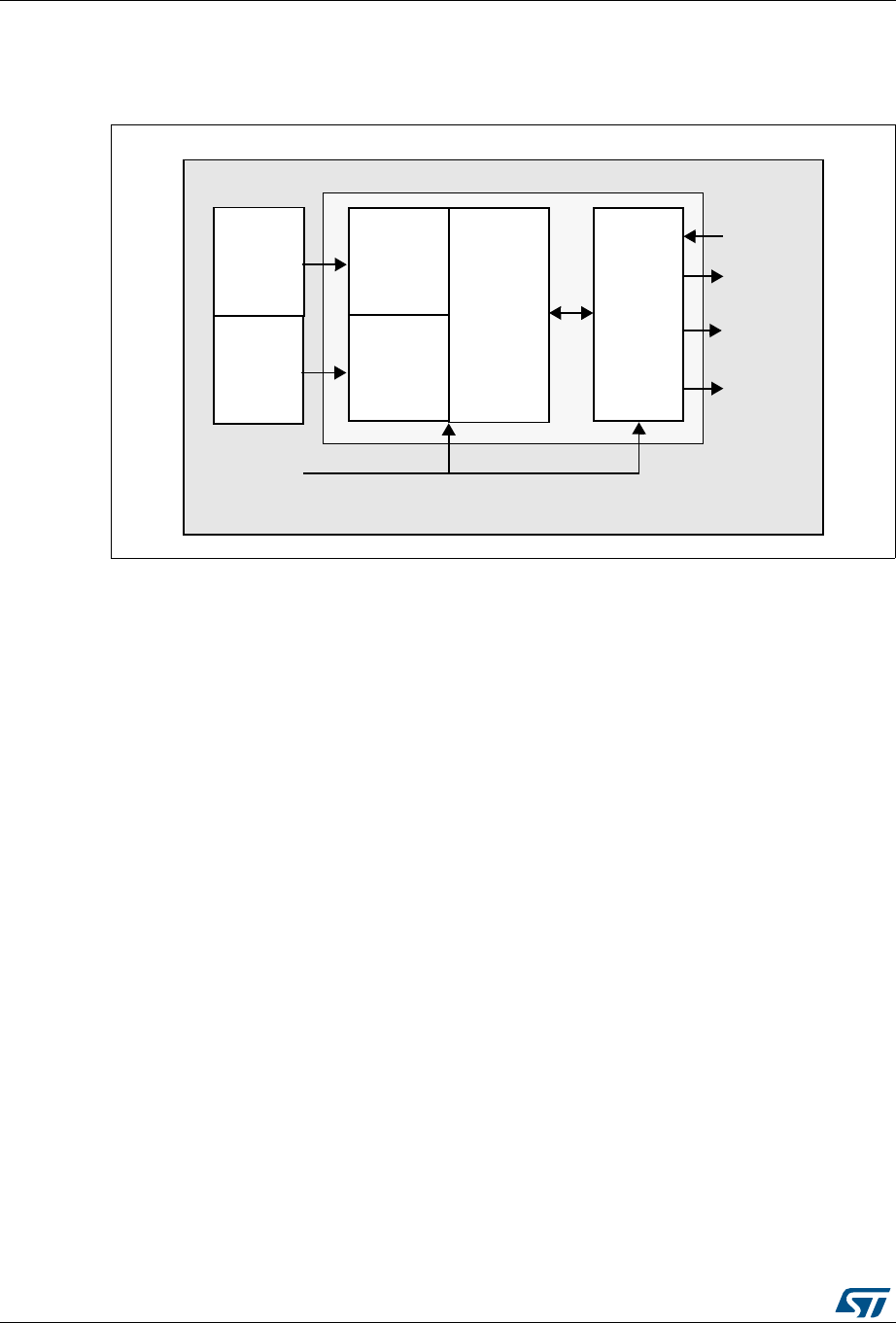
Debug support (DBG) RM0430
1308/1324 RM0430 Rev 8
The core s a simple TPIU, especially designed for low-cost debug (consisting of a special
version of the CoreSight TPIU).
Figure 423. TPIU block diagram
formatter
Trace out
(serializer)
TRACECLKIN
TRACECK
TRACEDATA
[3:0]
TRACESWO
CLK domain TRACECLKIN domain
External PPB bus
TPIU
TPIU
Asynchronous
FIFO
Asynchronous
FIFO
ETM
ITM
ai17114
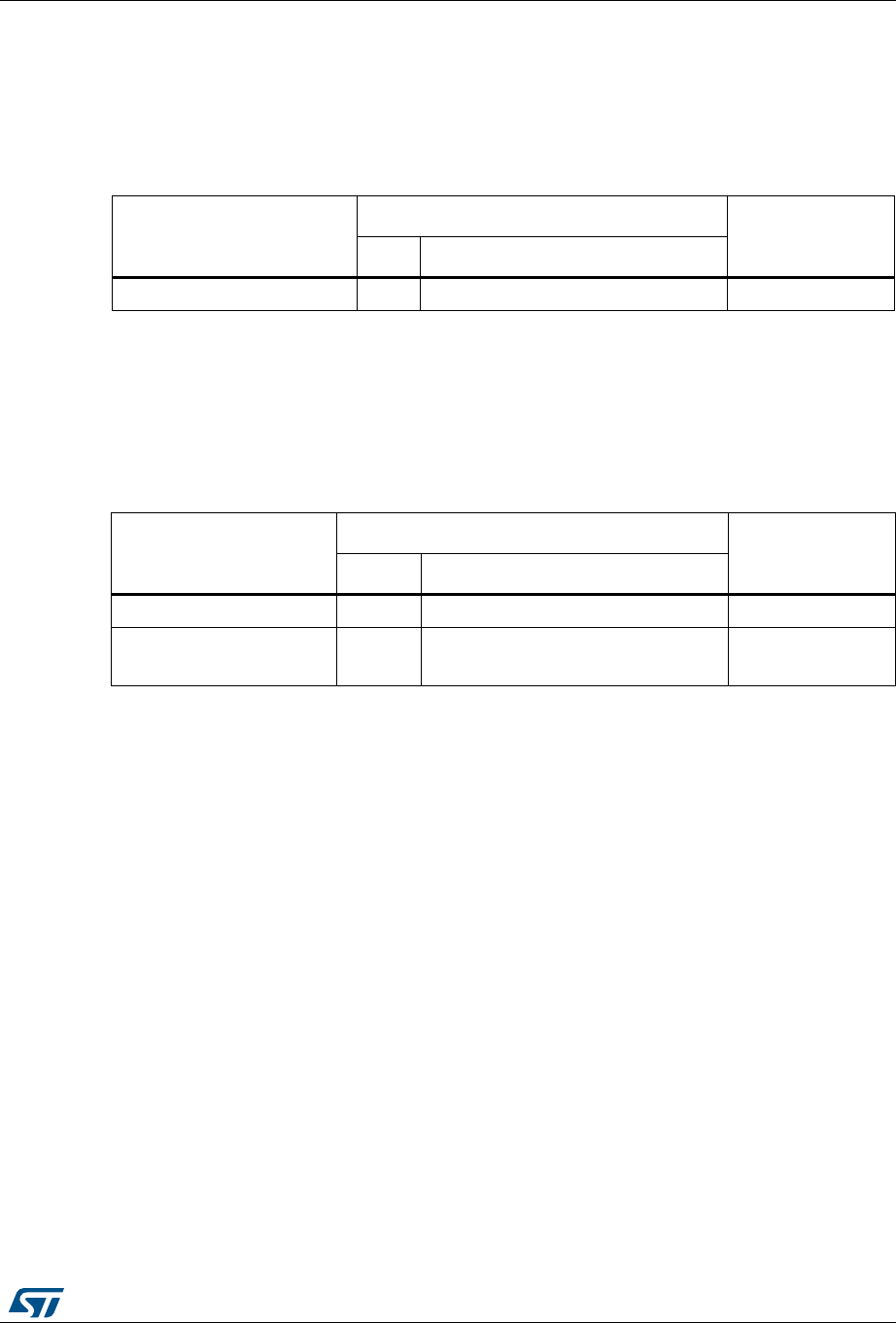
RM0430 Rev 8 1309/1324
RM0430 Debug support (DBG)
1314
34.17.2 TRACE pin assignment
•Asynchronous mode
The asynchronous mode requires 1 extra pin and is available on all packages. It is only
available if using Serial Wire mode (not in JTAG mode).
•Synchronous mode
The synchronous mode requires from 2 to 6 extra pins depending on the data trace
size and is only available in the larger packages. In addition it is available in JTAG
mode and in Serial Wire mode and provides better bandwidth output capabilities than
asynchronous trace.
TPUI TRACE pin assignment
By default, these pins are NOT assigned. They can be assigned by setting the
TRACE_IOEN and TRACE_MODE bits in the MCU Debug component configuration
register. This configuration has to be done by the debugger host.
In addition, the number of pins to assign depends on the trace configuration (asynchronous
or synchronous).
•Asynchronous mode: 1 extra pin is needed
•Synchronous mode: from 2 to 5 extra pins are needed depending on the size of the
data trace port register (1, 2 or 4):
– TRACECK
– TRACED(0) if port size is configured to 1, 2 or 4
– TRACED(1) if port size is configured to 2 or 4
– TRACED(2) if port size is configured to 4
– TRACED(3) if port size is configured to 4
To assign the TRACE pin, the debugger host must program the bits TRACE_IOEN and
TRACE_MODE[1:0] of the Debug MCU configuration Register (DBGMCU_CR). By default
the TRACE pins are not assigned.
This register is mapped on the external PPB and is reset by the PORESET (and not by the
SYSTEM reset). It can be written by the debugger under SYSTEM reset.
Table 244. Asynchronous TRACE pin assignment
TPUI pin name
Trace synchronous mode
Pin assignment
Type Description
TRACESWO O TRACE Async Data Output PB3
Table 245. Synchronous TRACE pin assignment
TPUI pin name
Trace synchronous mode
Pin assignment
Type Description
TRACECK O TRACE Clock PE2
TRACED[3:0] O TRACE Sync Data Outputs
Can be 1, 2 or 4.
PE[6:3], PF[7:6],
PD3, PG[14:13]

Debug support (DBG) RM0430
1310/1324 RM0430 Rev 8
Note: By default, the TRACECLKIN input clock of the TPIU is tied to GND. It is assigned to HCLK
two clock cycles after the bit TRACE_IOEN has been set.
The debugger must then program the Trace Mode by writing the PROTOCOL[1:0] bits in the
SPP_R (Selected Pin Protocol) register of the TPIU.
•PROTOCOL=00: Trace Port Mode (synchronous)
•PROTOCOL=01 or 10: Serial Wire (Manchester or NRZ) Mode (asynchronous mode).
Default state is 01
It then also configures the TRACE port size by writing the bits [3:0] in the CPSPS_R
(Current Sync Port Size Register) of the TPIU:
•0x1 for 1 pin (default state)
•0x2 for 2 pins
•0x8 for 4 pins
34.17.3 TPUI formatter
The formatter protocol outputs data in 16-byte frames:
•seven bytes of data
•eight bytes of mixed-use bytes consisting of:
– 1 bit (LSB) to indicate it is a DATA byte (‘0) or an ID byte (‘1).
– 7 bits (MSB) which can be data or change of source ID trace.
•one byte of auxiliary bits where each bit corresponds to one of the eight mixed-use
bytes:
– if the corresponding byte was a data, this bit gives bit0 of the data.
– if the corresponding byte was an ID change, this bit indicates when that ID change
takes effect.
Table 246. Flexible TRACE pin assignment
DBGMCU_CR
register
Pins
assigned for:
TRACE IO pin assigned(1)
TRACE
_IOEN
TRACE
_MODE
[1:0]
JTDO/
TRACESWO
TRACE
CK
TRACE
D[0]
TRACE
D[1]
TRACE
D[2]
TRACE
D[3]
0XX
No Trace
(default state) Released (2) -
100
Asynchronous
Trace TRACESWO - - Released
(usable as GPIO)
101
Synchronous
Trace 1 bit
Released (2)
TRACECK TRACED[0] - - -
110
Synchronous
Trace 2 bit TRACECK TRACED[0] TRACED[1] - -
111
Synchronous
Trace 4 bit TRACECK TRACED[0] TRACED[1] TRACED[2] TRACED[3]
1. Refer to the datasheet alternate function mapping table.
2. When Serial Wire mode is used, it is released. But when JTAG is used, it is assigned to JTDO.

RM0430 Rev 8 1311/1324
RM0430 Debug support (DBG)
1314
Note: Refer to the Arm® CoreSight Architecture Specification v1.0 (Arm® IHI 0029B) for further
information
34.17.4 TPUI frame synchronization packets
The TPUI can generate two types of synchronization packets:
•The Frame Synchronization packet (or Full Word Synchronization packet)
It consists of the word: 0x7F_FF_FF_FF (LSB emitted first). This sequence can not
occur at any other time provided that the ID source code 0x7F has not been used.
It is output periodically between frames.
In continuous mode, the TPA must discard all these frames once a synchronization
frame has been found.
•The Half-Word Synchronization packet
It consists of the half word: 0x7F_FF (LSB emitted first).
It is output periodically between or within frames.
These packets are only generated in continuous mode and enable the TPA to detect
that the TRACE port is in IDLE mode (no TRACE to be captured). When detected by
the TPA, it must be discarded.
34.17.5 Transmission of the synchronization frame packet
There is no Synchronization Counter register implemented in the TPIU of the core.
Consequently, the synchronization trigger can only be generated by the DWT. Refer to the
registers DWT Control Register (bits SYNCTAP[11:10]) and the DWT Current PC Sampler
Cycle Count Register.
The TPUI Frame synchronization packet (0x7F_FF_FF_FF) is emitted:
•after each TPIU reset release. This reset is synchronously released with the rising
edge of the TRACECLKIN clock. This means that this packet is transmitted when the
TRACE_IOEN bit in the DBGMCU_CFG register is set. In this case, the word
0x7F_FF_FF_FF is not followed by any formatted packet.
•at each DWT trigger (assuming DWT has been previously configured). Two cases
occur:
– If the bit SYNENA of the ITM is reset, only the word 0x7F_FF_FF_FF is emitted
without any formatted stream which follows.
– If the bit SYNENA of the ITM is set, then the ITM synchronization packets will
follow (0x80_00_00_00_00_00), formatted by the TPUI (trace source ID added).
34.17.6 Synchronous mode
The trace data output size can be configured to 4, 2 or 1 pin: TRACED(3:0)
The output clock is output to the debugger (TRACECK)
Here, TRACECLKIN is driven internally and is connected to HCLK only when TRACE is
used.
Note: In this synchronous mode, it is not required to provide a stable clock frequency.
The TRACE I/Os (including TRACECK) are driven by the rising edge of TRACLKIN (equal
to HCLK). Consequently, the output frequency of TRACECK is equal to HCLK/2.

Debug support (DBG) RM0430
1312/1324 RM0430 Rev 8
34.17.7 Asynchronous mode
This is a low cost alternative to output the trace using only 1 pin: this is the asynchronous
output pin TRACESWO. Obviously there is a limited bandwidth.
TRACESWO is multiplexed with JTDO when using the SW-DP pin. This way, this
functionality is available in all packages.
This asynchronous mode requires a constant frequency for TRACECLKIN. For the standard
UART (NRZ) capture mechanism, 5% accuracy is needed. The Manchester encoded
version is tolerant up to 10%.
34.17.8 TRACECLKIN connection
The TRACECLKIN input is internally connected to HCLK. This means that when in
asynchronous trace mode, the application is restricted to use to time frames where the CPU
frequency is stable.
Note: Important: when using asynchronous trace: it is important to be aware that:
The default clock of the MCUs is the internal RC oscillator. Its frequency under reset is
different from the one after reset release. This is because the RC calibration is the default
one under system reset and is updated at each system reset release.
Consequently, the trace port analyzer (TPA) should not enable the trace (with the
TRACE_IOEN bit) under system reset, because a Synchronization Frame Packet will be
issued with a different bit time than trace packets which will be transmitted after reset
release.
34.17.9 TPIU registers
The TPIU APB registers can be read and written only if the bit TRCENA of the Debug
Exception and Monitor Control Register (DEMCR) is set. Otherwise, the registers are read
as zero (the output of this bit enables the PCLK of the TPIU).
Table 247. Important TPIU registers
Address Register Description
0xE0040004 Current port size
Allows the trace port size to be selected:
Bit 0: Port size = 1
Bit 1: Port size = 2
Bit 2: Port size = 3, not supported
Bit 3: Port Size = 4
Only 1 bit must be set. By default, the port size is one bit. (0x00000001)
0xE00400F0 Selected pin
protocol
Allows the Trace Port Protocol to be selected:
Bit1:0=
00: Sync Trace Port Mode
01: Serial Wire Output - manchester (default value)
10: Serial Wire Output - NRZ
11: reserved

RM0430 Rev 8 1313/1324
RM0430 Debug support (DBG)
1314
34.17.10 Example of configuration
•Set the bit TRCENA in the Debug Exception and Monitor Control Register (DEMCR)
•Write the TPIU Current Port Size Register to the desired value (default is 0x1 for a 1-bit
port size)
•Write TPIU Formatter and Flush Control Register to 0x102 (default value)
•Write the TPIU Select Pin Protocol to select the sync or async mode. Example: 0x2 for
async NRZ mode (UART like)
•Write the DBGMCU control register to 0x20 (bit IO_TRACEN) to assign TRACE I/Os
for async mode. A TPIU Sync packet is emitted at this time (FF_FF_FF_7F)
•Configure the ITM and write the ITM Stimulus register to output a value
0xE0040304 Formatter and flush
control
Bits 31-9 = always ‘0
Bit 8 = TrigIn = always ‘1 to indicate that triggers are indicated
Bits 7-4 = always 0
Bits 3-2 = always 0
Bit 1 = EnFCont. In Sync Trace mode (Select_Pin_Protocol register
bit1:0=00), this bit is forced to ‘1: the formatter is automatically enabled
in continuous mode. In asynchronous mode (Select_Pin_Protocol
register bit1:0 <> 00), this bit can be written to activate or not the
formatter.
Bit 0 = always 0
The resulting default value is 0x102
Note: In synchronous mode, because the TRACECTL pin is not mapped
outside the chip, the formatter is always enabled in continuous mode -this
way the formatter inserts some control packets to identify the source of
the trace packets).
0xE0040300 Formatter and flush
status Not used in Cortex®-M4 with FPU, always read as 0x00000008
Table 247. Important TPIU registers (continued)
Address Register Description

Debug support (DBG) RM0430
1314/1324 RM0430 Rev 8
34.18 DBG register map
The following table summarizes the Debug registers.
Table 248. DBG register map and reset values
Addr. Register
31
30
29
28
27
26
25
24
23
22
21
20
19
18
17
16
15
14
13
12
11
10
9
8
7
6
5
4
3
2
1
0
0xE004
2000
DBGMCU
_IDCODE REV_ID
Res.
Res.
Res.
Res.
DEV_ID
Reset value(1) XXXXXXXXXXXXXXXX XXXXXXXXXXXX
0xE004
2004
DBGMCU_CR
Res.
Res.
Res.
Res.
Res.
Res.
Res.
Res.
Res.
Res.
Res.
Res.
Res.
Res.
Res.
Res.
Res.
Res.
Res.
Res.
Res.
Res.
Res.
Res.
TRACE_
MODE[1:0]
TRACE_IOEN
Res.
Res.
DBG_STANDBY
DBG_STOP
DBG_SLEEP
Reset value 000 000
0xE004
2008
DBGMCU_
APB1_FZ
Res.
Res.
Res.
Res.
Res.
DBG_CAN2_STOP
DBG_CAN1_STOP
DBG_I2CFMP_SMBUS_TIMEOUT
DBG_I2C3_SMBUS_TIMEOUT
DBG_I2C2_SMBUS_TIMEOUT
DBG_CAN2_STOP
Res.
Res.
Res.
Res.
Res.
Res.
Res.
Res.
DBG_IWDG_STOP
DBG_WWDG_STOP
DBG_RTC_STOP
DBG_TIM14_STOP
DBG_TI13_STOP
DBG_TIM12_STOP
DBG_TIM7_STOP
DBG_TIM6_STOP
DBG_TIM5_STOP
DBG_TIM4_STOP
DBG_TIM3_STOP
DBG_TIM2_STOP
Reset value 000000 000 000000000
0xE004
200C
DBGMCU_
APB2_FZ
Res.
Res.
Res.
Res.
Res.
Res.
Res.
Res.
Res.
Res.
Res.
Res.
Res.
DBG_TIM11_STOP
DBG_TIM10_STOP
DBG_TIM9_STOP
Res.
Res.
Res.
Res.
Res.
Res.
Res.
Res.
Res.
Res.
Res.
Res.
Res.
Res.
DBG_TIM8_STOP
DBG_TIM1_STOP
Reset value 0 0 0 0 0
1. The reset value is product dependent. For more information, refer to Section 34.6.1: MCU device ID code.

RM0430 Rev 8 1315/1324
RM0430 Device electronic signature
1317
35 Device electronic signature
The electronic signature is stored in the Flash memory area. It can be read using the
JTAG/SWD or the CPU. It contains factory-programmed identification data that allow the
user firmware or other external devices to automatically match its interface to the
characteristics of the STM32F4xx microcontrollers.
35.1 Unique device ID register (96 bits)
The unique device identifier is ideally suited:
•for use as serial numbers
•for use as security keys in order to increase the security of code in Flash memory while
using and combining this unique ID with software cryptographic primitives and
protocols before programming the internal Flash memory
•to activate secure boot processes, etc.
The 96-bit unique device identifier provides a reference number which is unique for any
device and in any context. These bits can never be altered by the user.
The 96-bit unique device identifier can also be read in single bytes/half-words/words in
different ways and then be concatenated using a custom algorithm.
Base address: 0x1FFF 7A10
Address offset: 0x00
Read only = 0xXXXX XXXX where X is factory-programmed
Address offset: 0x04
Read only = 0xXXXX XXXX where X is factory-programmed
313029282726252423222120191817161514131211109876543210
U_ID[31:0]
rrrrrrrrrrrrrrrrrrrrrrrrrrrrrrrr
Bits 31:0 U_ID[31:0]: 31:0 unique ID bits
31 30 29 28 27 26 25 24 23 22 21 20 19 18 17 16
U_ID[63:48]
rrrrrrrrrrrrrrrr
15 14 13 12 11 10 9 8 7 6 5 4 3 2 1 0
U_ID[47:32]
rrrrrrrrrrrrrrrr
Bits 31:0 U_ID[63:32]: 63:32 unique ID bits
Device electronic signature RM0430
1316/1324 RM0430 Rev 8
Address offset: 0x08
Read only = 0xXXXX XXXX where X is factory-programmed
35.2 Flash size
Base address: 0x1FFF 7A22
Address offset: 0x00
Read only = 0xXXXX where X is factory-programmed
35.3 Package data register
Base address: 0x1FFF 7BF0
Address offset: 0x00
Read only = 0xXXXX where X is factory-programmed
31 30 29 28 27 26 25 24 23 22 21 20 19 18 17 16
U_ID[95:80]
rrrrrrrrrrrrrrrr
1514131211109876543210
U_ID[79:64]
rrrrrrrrrrrrrrrr
Bits 31:0 U_ID[95:64]: 95:64 Unique ID bits.
1514131211109876543210
F_SIZE
rrrrrrrrrrrrrrrr
Bits 15:0 F_ID[15:0]: Flash memory size
This bitfield indicates the size of the device Flash memory expressed in Kbytes.
1514131211109876543210
Res. Res. Res. Res. Res. PKG[2:0] Res. Res. Res. Res. Res. Res. Res. Res.
rrr

RM0430 Rev 8 1317/1324
RM0430 Device electronic signature
1317
Bits 15:11 Reserved, must be kept at reset value.
Bits 10:8 PKG[2:0]: Package type
0x111: UFBGA144/LQFP144
0x110: reserved
0x101: reserved
0x100: LQFP100
0x011: UFBGA100/WLCSP81
0x010: reserved
0x001: LQFP64
0x000: UFQFPN48
Bits 7:0 Reserved, must be kept at reset value.

Revision history RM0430
1318/1324 RM0430 Rev 8
36 Revision history
Table 249. Document revision history
Date Revision Changes
03-Nov-2016 1 Initial release.
15-Dec-2016 2
Updated:
–Section 18: General-purpose timers (TIM2 to TIM5)
–Section 19: General-purpose timers (TIM9 to TIM14)
–Section 20: Basic timers (TIM6/7)
09-Mar-2017 3
Updated:
–Section 11.1: FSMC main features
–Section 11.4: External device address mapping
–Section 11.4.1: NOR/PSRAM address mapping
Added:
–Section 12.3.2: QUADSPI pins
–Table 71: QUADSPI pins
03-May-2017 4
Updated:
–Section 13: Analog-to-digital converter (ADC)
–Section 25: Real-time clock (RTC)
–Section 29: Serial peripheral interface/ inter-IC sound
(SPI/I2S)
12-Jun-2017 5
Updated:
–Table 5: Flash module organization
–Section 3.4.1: Relation between CPU clock frequency
and Flash memory read time
–Section 3.5.3: Erase
–Section 3.6.4: Write protections
–Section 3.8.5: Flash control register (FLASH_CR)
–Table 40: Vector table for STM32F413/423
–Section 10.2.5: External interrupt/event line mapping
–Section 10.3: EXTI registers
–Table 41: External interrupt/event controller register
map and reset values
22-Sep-2017 6
Updated:
–Table 13: Flash register map and reset values
–Section 32: Controller area network (bxCAN)

RM0430 Rev 8 1319/1324
RM0430 Revision history
1319
18-Feb-2018 7
Updated:
–Section 24: AES hardware accelerator (AES)
–Section 33: USB on-the-go full-speed (OTG_FS)
23-May-2018 8
Updated:
–Figure 13: Clock tree
–Section 6.3.27: RCC Dedicated Clocks Configuration
Register (RCC_DCKCFGR)
–Section 26.6: FMPI2C interrupts
–Figure 32: FSMC memory banks
Removed:
–Figure 387: I2C interrupt mapping diagram.
Table 249. Document revision history (continued)
Date Revision Changes

RM0430 Index
RM0430 Rev 8 1320/1324
Index
A
ADC_CCR . . . . . . . . . . . . . . . . . . . . . . . . . . .363
ADC_CR1 . . . . . . . . . . . . . . . . . . . . . . . . . . .352
ADC_CR2 . . . . . . . . . . . . . . . . . . . . . . . . . . .354
ADC_CSR . . . . . . . . . . . . . . . . . . . . . . . . . . .362
ADC_DR . . . . . . . . . . . . . . . . . . . . . . . . . . . .362
ADC_HTR . . . . . . . . . . . . . . . . . . . . . . . . . . .357
ADC_JDRx . . . . . . . . . . . . . . . . . . . . . . . . . . .361
ADC_JOFRx . . . . . . . . . . . . . . . . . . . . . . . . .357
ADC_JSQR . . . . . . . . . . . . . . . . . . . . . . . . . .361
ADC_LTR . . . . . . . . . . . . . . . . . . . . . . . . . . . .358
ADC_SMPR1 . . . . . . . . . . . . . . . . . . . . . . . . .356
ADC_SMPR2 . . . . . . . . . . . . . . . . . . . . . . . . .357
ADC_SQR1 . . . . . . . . . . . . . . . . . . . . . . . . . .358
ADC_SQR2 . . . . . . . . . . . . . . . . . . . . . . . . . .359
ADC_SQR3 . . . . . . . . . . . . . . . . . . . . . . . . . .360
ADC_SR . . . . . . . . . . . . . . . . . . . . . . . . . . . . .351
AES_CR . . . . . . . . . . . . . . . . . . . . . . . . . . . . .731
AES_DINR . . . . . . . . . . . . . . . . . . . . . . . . . . .735
AES_DOUTR . . . . . . . . . . . . . . . . . . . . . . . . .736
AES_IVR . . . . . . . . . . . . . . . . . . . . . . . . . . . .738
AES_KEYRx . . . . . . . . . . . . . . . . . . . . . . . . .736
AES_SR . . . . . . . . . . . . . . . . . . . . . . . . . . . . .734
C
CAN_BTR . . . . . . . . . . . . . . . . . . . . . . . . . .1115
CAN_ESR . . . . . . . . . . . . . . . . . . . . . . . . . .1114
CAN_FA1R . . . . . . . . . . . . . . . . . . . . . . . . .1125
CAN_FFA1R . . . . . . . . . . . . . . . . . . . . . . . .1124
CAN_FiRx . . . . . . . . . . . . . . . . . . . . . . . . . .1126
CAN_FM1R . . . . . . . . . . . . . . . . . . . . . . . . .1123
CAN_FMR . . . . . . . . . . . . . . . . . . . . . . . . . .1123
CAN_FS1R . . . . . . . . . . . . . . . . . . . . . . . . .1124
CAN_IER . . . . . . . . . . . . . . . . . . . . . . . . . . .1113
CAN_MCR . . . . . . . . . . . . . . . . . . . . . . . . . .1106
CAN_MSR . . . . . . . . . . . . . . . . . . . . . . . . . .1108
CAN_RDHxR . . . . . . . . . . . . . . . . . . . . . . . .1122
CAN_RDLxR . . . . . . . . . . . . . . . . . . . . . . . .1122
CAN_RDTxR . . . . . . . . . . . . . . . . . . . . . . . .1121
CAN_RF0R . . . . . . . . . . . . . . . . . . . . . . . . .1111
CAN_RF1R . . . . . . . . . . . . . . . . . . . . . . . . .1112
CAN_RIxR . . . . . . . . . . . . . . . . . . . . . . . . . .1120
CAN_TDHxR . . . . . . . . . . . . . . . . . . . . . . . .1119
CAN_TDLxR . . . . . . . . . . . . . . . . . . . . . . . .1119
CAN_TDTxR . . . . . . . . . . . . . . . . . . . . . . . .1118
CAN_TIxR . . . . . . . . . . . . . . . . . . . . . . . . . .1117
CAN_TSR . . . . . . . . . . . . . . . . . . . . . . . . . .1109
CKGATENR . . . . . . . . . . . . . . . . . . . . . . . . . 179
CRC_DR . . . . . . . . . . . . . . . . . . . . . . . . . . . . . 91
CRC_IDR . . . . . . . . . . . . . . . . . . . . . . . . . . . . 92
D
DAC_CR . . . . . . . . . . . . . . . . . . . . . . . . . . . . 378
DAC_DHR12L1 . . . . . . . . . . . . . . . . . . . . . . . 382
DAC_DHR12L2 . . . . . . . . . . . . . . . . . . . . . . . 383
DAC_DHR12LD . . . . . . . . . . . . . . . . . . . . . . 384
DAC_DHR12R1 . . . . . . . . . . . . . . . . . . . . . . 381
DAC_DHR12R2 . . . . . . . . . . . . . . . . . . . . . . 383
DAC_DHR12RD . . . . . . . . . . . . . . . . . . . . . . 384
DAC_DHR8R1 . . . . . . . . . . . . . . . . . . . . . . . 382
DAC_DHR8R2 . . . . . . . . . . . . . . . . . . . . . . . 383
DAC_DHR8RD . . . . . . . . . . . . . . . . . . . . . . . 385
DAC_DOR1 . . . . . . . . . . . . . . . . . . . . . . . . . . 385
DAC_DOR2 . . . . . . . . . . . . . . . . . . . . . . . . . . 385
DAC_SR . . . . . . . . . . . . . . . . . . . . . . . . . . . . 386
DAC_SWTRIGR . . . . . . . . . . . . . . . . . . . . . . 381
DBGMCU_APB1_FZ . . . . . . . . . . . . . . . . . . 1305
DBGMCU_APB2_FZ . . . . . . . . . . . . . . . . . . 1307
DBGMCU_CR . . . . . . . . . . . . . . . . . . . . . . . 1304
DBGMCU_IDCODE . . . . . . . . . . . . . . . . . . 1291
DFSDM_CHyAWSCDR . . . . . . . . . . . . . . . . . 423
DFSDM_CHyCFGR1 . . . . . . . . . . . . . . . . . . 420
DFSDM_CHyCFGR2 . . . . . . . . . . . . . . . . . . 423
DFSDM_CHyDATINR . . . . . . . . . . . . . . . . . . 425
DFSDM_CHyWDATR . . . . . . . . . . . . . . . . . . 424
DFSDM_FLTxAWCFR . . . . . . . . . . . . . . . . . 438
DFSDM_FLTxAWHTR . . . . . . . . . . . . . . . . . 436
DFSDM_FLTxAWLTR . . . . . . . . . . . . . . . . . . 436
DFSDM_FLTxAWSR . . . . . . . . . . . . . . . . . . . 437
DFSDM_FLTxCNVTIMR . . . . . . . . . . . . . . . . 439
DFSDM_FLTxCR1 . . . . . . . . . . . . . . . . . . . . 426
DFSDM_FLTxCR2 . . . . . . . . . . . . . . . . . . . . 429
DFSDM_FLTxEXMAX . . . . . . . . . . . . . . . . . . 438
DFSDM_FLTxEXMIN . . . . . . . . . . . . . . . . . . 439
DFSDM_FLTxFCR . . . . . . . . . . . . . . . . . . . . 433
DFSDM_FLTxICR . . . . . . . . . . . . . . . . . . . . . 432
DFSDM_FLTxISR . . . . . . . . . . . . . . . . . . . . . 430
DFSDM_FLTxJCHGR . . . . . . . . . . . . . . . . . . 433
DFSDM_FLTxJDATAR . . . . . . . . . . . . . . . . . 434
DFSDM_FLTxRDATAR . . . . . . . . . . . . . . . . . 435
DMA_HIFCR . . . . . . . . . . . . . . . . . . . . . . . . . 237
DMA_HISR . . . . . . . . . . . . . . . . . . . . . . . . . . 236
DMA_LIFCR . . . . . . . . . . . . . . . . . . . . . . . . . 237
DMA_LISR . . . . . . . . . . . . . . . . . . . . . . . . . . 235
DMA_SxCR . . . . . . . . . . . . . . . . . . . . . . . . . . 238

Index RM0430
1321/1324 RM0430 Rev 8
DMA_SxFCR . . . . . . . . . . . . . . . . . . . . . . . . .243
DMA_SxM0AR . . . . . . . . . . . . . . . . . . . . . . . .242
DMA_SxM1AR . . . . . . . . . . . . . . . . . . . . . . . .242
DMA_SxNDTR . . . . . . . . . . . . . . . . . . . . . . . .241
DMA_SxPAR . . . . . . . . . . . . . . . . . . . . . . . . .242
E
EXTI_EMR . . . . . . . . . . . . . . . . . . . . . . . . . . .258
EXTI_FTSR . . . . . . . . . . . . . . . . . . . . . . . . . .260
EXTI_IMR . . . . . . . . . . . . . . . . . . . . . . . . . . . .258
EXTI_PR . . . . . . . . . . . . . . . . . . . . . . . . . . . .262
EXTI_RTSR . . . . . . . . . . . . . . . . . . . . . . . . . .259
EXTI_SWIER . . . . . . . . . . . . . . . . . . . . . . . . .261
F
FLASH_ACR . . . . . . . . . . . . . . . . . . . . . . . . . .82
FLASH_CR . . . . . . . . . . . . . . . . . . . . . . . . . . .85
FLASH_KEYR . . . . . . . . . . . . . . . . . . . . . . . . .83
FLASH_OPTCR . . . . . . . . . . . . . . . . . . . . . . . .86
FLASH_OPTKEYR . . . . . . . . . . . . . . . . . . . . .83
FLASH_SR . . . . . . . . . . . . . . . . . . . . . . . . . . . .84
FMPI2C_CR1 . . . . . . . . . . . . . . . . . . . . . . . . .831
FMPI2C_CR2 . . . . . . . . . . . . . . . . . . . . . . . . .834
FMPI2C_ICR . . . . . . . . . . . . . . . . . . . . . . . . .843
FMPI2C_ISR . . . . . . . . . . . . . . . . . . . . . . . . .841
FMPI2C_OAR1 . . . . . . . . . . . . . . . . . . . . . . .837
FMPI2C_OAR2 . . . . . . . . . . . . . . . . . . . . . . .838
FMPI2C_PECR . . . . . . . . . . . . . . . . . . . . . . .844
FMPI2C_RXDR . . . . . . . . . . . . . . . . . . . . . . .845
FMPI2C_TIMEOUTR . . . . . . . . . . . . . . . . . . .840
FMPI2C_TIMINGR . . . . . . . . . . . . . . . . . . . . .839
FMPI2C_TXDR . . . . . . . . . . . . . . . . . . . . . . .845
FSMC_BCRx . . . . . . . . . . . . . . . . . . . . . . . . .297
FSMC_BTRx . . . . . . . . . . . . . . . . . . . . . . . . .299
FSMC_BWTR1..4 . . . . . . . . . . . . . . . . . . . . .302
G
GPIOx_AFRH . . . . . . . . . . . . . . . . . . . . . . . . .201
GPIOx_AFRL . . . . . . . . . . . . . . . . . . . . . . . . .200
GPIOx_BSRR . . . . . . . . . . . . . . . . . . . . . . . .198
GPIOx_IDR . . . . . . . . . . . . . . . . . . . . . . . . . .198
GPIOx_LCKR . . . . . . . . . . . . . . . . . . . . . . . . .199
GPIOx_MODER . . . . . . . . . . . . . . . . . . . . . . .196
GPIOx_ODR . . . . . . . . . . . . . . . . . . . . . . . . .198
GPIOx_OSPEEDR . . . . . . . . . . . . . . . . . . . . .197
GPIOx_OTYPER . . . . . . . . . . . . . . . . . . . . . .196
GPIOx_PUPDR . . . . . . . . . . . . . . . . . . . . . . .197
I
I2C_CCR . . . . . . . . . . . . . . . . . . . . . . . . . . . . 879
I2C_CR1 . . . . . . . . . . . . . . . . . . . . . . . . . . . . 869
I2C_CR2 . . . . . . . . . . . . . . . . . . . . . . . . . . . . 871
I2C_DR . . . . . . . . . . . . . . . . . . . . . . . . . . . . . 874
I2C_OAR1 . . . . . . . . . . . . . . . . . . . . . . . 837, 873
I2C_OAR2 . . . . . . . . . . . . . . . . . . . . . . . 838, 873
I2C_SR1 . . . . . . . . . . . . . . . . . . . . . . . . . . . . 874
I2C_SR2 . . . . . . . . . . . . . . . . . . . . . . . . . . . . 878
I2C_TIMEOUTR . . . . . . . . . . . . . . . . . . . . . . 840
I2C_TIMINGR . . . . . . . . . . . . . . . . . . . . . . . . 839
I2C_TRISE . . . . . . . . . . . . . . . . . . . . . . . . . . 880
I2Cx_CR2 . . . . . . . . . . . . . . . . . . . . . . . . . . . 834
IWDG_KR . . . . . . . . . . . . . . . . . . . . . . . . . . . 680
IWDG_PR . . . . . . . . . . . . . . . . . . . . . . . . . . . 681
IWDG_RLR . . . . . . . . . . . . . . . . . . . . . . . . . . 682
IWDG_SR . . . . . . . . . . . . . . . . . . . . . . . . . . . 682
L
LPTIM_ARR . . . . . . . . . . . . . . . . . . . . . . . . . 674
LPTIM_CFGR . . . . . . . . . . . . . . . . . . . . . . . . 670
LPTIM_CMP . . . . . . . . . . . . . . . . . . . . . . . . . 673
LPTIM_CNT . . . . . . . . . . . . . . . . . . . . . . . . . 674
LPTIM_CR . . . . . . . . . . . . . . . . . . . . . . . . . . . 672
LPTIM_ICR . . . . . . . . . . . . . . . . . . . . . . . . . . 667
LPTIM_IER . . . . . . . . . . . . . . . . . . . . . . . . . . 668
LPTIM_ISR . . . . . . . . . . . . . . . . . . . . . . . . . . 666
LPTIM1_OR . . . . . . . . . . . . . . . . . . . . . . . . . 675
O
OTG_CID . . . . . . . . . . . . . . . . . . . . . . . . . . 1184
OTG_DAINT . . . . . . . . . . . . . . . . . . . . . . . . 1207
OTG_DAINTMSK . . . . . . . . . . . . . . . . . . . . 1208
OTG_DCFG . . . . . . . . . . . . . . . . . . . . . . . . 1200
OTG_DCTL . . . . . . . . . . . . . . . . . . . . . . . . . 1201
OTG_DIEPCTL0 . . . . . . . . . . . . . . . . . . . . . 1210
OTG_DIEPCTLx . . . . . . . . . . . . . . . . . . . . . 1211
OTG_DIEPEMPMSK . . . . . . . . . . . . . . . . . . 1209
OTG_DIEPINTx . . . . . . . . . . . . . . . . . . . . . . 1214
OTG_DIEPMSK . . . . . . . . . . . . . . . . . . . . . 1205
OTG_DIEPTSIZ0 . . . . . . . . . . . . . . . . . . . . 1215
OTG_DIEPTSIZx . . . . . . . . . . . . . . . . . . . . . 1217
OTG_DIEPTXF0 . . . . . . . . . . . . . . . . . . . . . 1180
OTG_DIEPTXFx . . . . . . . . . . . . . . . . . . . . . 1188
OTG_DOEPCTL0 . . . . . . . . . . . . . . . . . . . . 1218
OTG_DOEPCTLx . . . . . . . . . . . . . . . . . . . . 1222
OTG_DOEPINTx . . . . . . . . . . . . . . . . . . . . . 1219
OTG_DOEPMSK . . . . . . . . . . . . . . . . . . . . . 1206
OTG_DOEPTSIZ0 . . . . . . . . . . . . . . . . . . . . 1221
OTG_DOEPTSIZx . . . . . . . . . . . . . . . . . . . . 1224

RM0430 Index
RM0430 Rev 8 1322/1324
OTG_DSTS . . . . . . . . . . . . . . . . . . . . . . . . .1204
OTG_DTXFSTSx . . . . . . . . . . . . . . . . . . . . .1216
OTG_DVBUSDIS . . . . . . . . . . . . . . . . . . . . .1208
OTG_DVBUSPULSE . . . . . . . . . . . . . . . . . .1209
OTG_GAHBCFG . . . . . . . . . . . . . . . . . . . . .1165
OTG_GCCFG . . . . . . . . . . . . . . . . . . . . . . .1182
OTG_GINTMSK . . . . . . . . . . . . . . . . . . . . . .1175
OTG_GINTSTS . . . . . . . . . . . . . . . . . . . . . .1171
OTG_GLPMCFG . . . . . . . . . . . . . . . . . . . . .1184
OTG_GOTGCTL . . . . . . . . . . . . . . . . . . . . .1161
OTG_GOTGINT . . . . . . . . . . . . . . . . . . . . . .1164
OTG_GRSTCTL . . . . . . . . . . . . . . . . . . . . . .1168
OTG_GRXFSIZ . . . . . . . . . . . . . . . . . . . . . .1180
OTG_GRXSTSP . . . . . . . . . . . . . . . . . . . . .1178
OTG_GRXSTSR . . . . . . . . . . . . . . . . . . . . .1178
OTG_GUSBCFG . . . . . . . . . . . . . . . . . . . . .1166
OTG_HAINT . . . . . . . . . . . . . . . . . . . . . . . . .1192
OTG_HAINTMSK . . . . . . . . . . . . . . . . . . . . .1193
OTG_HCCHARx . . . . . . . . . . . . . . . . . . . . .1196
OTG_HCFG . . . . . . . . . . . . . . . . . . . . . . . . .1189
OTG_HCINTMSKx . . . . . . . . . . . . . . . . . . . .1198
OTG_HCINTx . . . . . . . . . . . . . . . . . . . . . . . .1197
OTG_HCTSIZx . . . . . . . . . . . . . . . . . . . . . . .1199
OTG_HFIR . . . . . . . . . . . . . . . . . . . . . . . . . .1190
OTG_HFNUM . . . . . . . . . . . . . . . . . . . . . . .1191
OTG_HNPTXFSIZ . . . . . . . . . . . . . . . . . . . .1180
OTG_HNPTXSTS . . . . . . . . . . . . . . . . . . . .1181
OTG_HPRT . . . . . . . . . . . . . . . . . . . . . . . . .1194
OTG_HPTXFSIZ . . . . . . . . . . . . . . . . . . . . .1188
OTG_HPTXSTS . . . . . . . . . . . . . . . . . . . . . .1191
OTG_PCGCCTL . . . . . . . . . . . . . . . . . . . . .1225
P
PWR_CR . . . . . . . . . . . . . . . . . . . . . . . . . . . .112
PWR_CSR . . . . . . . . . . . . . . . . . . . . . . . . . . .114
Q
QUADSPI _PIR . . . . . . . . . . . . . . . . . . . . . . .334
QUADSPI _PSMAR . . . . . . . . . . . . . . . . . . . .333
QUADSPI _PSMKR . . . . . . . . . . . . . . . . . . . .333
QUADSPI_ABR . . . . . . . . . . . . . . . . . . . . . . .332
QUADSPI_AR . . . . . . . . . . . . . . . . . . . . . . . .331
QUADSPI_CCR . . . . . . . . . . . . . . . . . . . . . . .329
QUADSPI_CR . . . . . . . . . . . . . . . . . . . . . . . .323
QUADSPI_DCR . . . . . . . . . . . . . . . . . . . . . . .326
QUADSPI_DLR . . . . . . . . . . . . . . . . . . . . . . .328
QUADSPI_DR . . . . . . . . . . . . . . . . . . . . . . . .332
QUADSPI_FCR . . . . . . . . . . . . . . . . . . . . . . .328
QUADSPI_LPTR . . . . . . . . . . . . . . . . . . . . . .334
QUADSPI_SR . . . . . . . . . . . . . . . . . . . . . . . .327
R
RCC_AHB1ENR . . . . . . . . . . . . . . . . . . . . . . 149
RCC_AHB1LPENR . . . . . . . . . . . . . . . . . . . . 160
RCC_AHB1RSTR . . . . . . . . . . . . . . . . . . . . . 138
RCC_AHB2ENR . . . . . . . . . . . . . . . . . . 151-153
RCC_AHB2LPENR . . . . . . . . . . . . . . . . 162-163
RCC_AHB2RSTR . . . . . . . . . . . . . . . . . 140-142
RCC_APB1ENR . . . . . . . . . . . . . . . . . . . . . . 153
RCC_APB1LPENR . . . . . . . . . . . . . . . . . . . . 165
RCC_APB2ENR . . . . . . . . . . . . . . . . . . . . . . 157
RCC_APB2LPENR . . . . . . . . . . . . . . . . . . . . 168
RCC_BDCR . . . . . . . . . . . . . . . . . . . . . . . . . 171
RCC_CFGR . . . . . . . . . . . . . . . . . . . . . . . . . 133
RCC_CIR . . . . . . . . . . . . . . . . . . . . . . . . . . . 136
RCC_CR . . . . . . . . . . . . . . . . . . . . . . . . . . . . 129
RCC_CSR . . . . . . . . . . . . . . . . . . . . . . . . . . . 172
RCC_PLLCFGR . . . . . . . . . . . . . . . . . . 131, 175
RCC_SSCGR . . . . . . . . . . . . . . . . . . . . . . . . 174
RNG_CR . . . . . . . . . . . . . . . . . . . . . . . . . . . . 458
RNG_DR . . . . . . . . . . . . . . . . . . . . . . . . . . . . 460
RNG_SR . . . . . . . . . . . . . . . . . . . . . . . . . . . . 459
RTC_ALRMAR . . . . . . . . . . . . . . . . . . . . . . . 769
RTC_ALRMBR . . . . . . . . . . . . . . . . . . . . . . . 770
RTC_ALRMBSSR . . . . . . . . . . . . . . . . . . . . . 778
RTC_BKxR . . . . . . . . . . . . . . . . . . . . . . . . . . 779
RTC_CALIBR . . . . . . . . . . . . . . . . . . . . . . . . 767
RTC_CALR . . . . . . . . . . . . . . . . . . . . . . . . . . 774
RTC_CR . . . . . . . . . . . . . . . . . . . . . . . . . . . . 762
RTC_DR . . . . . . . . . . . . . . . . . . . . . . . . . . . . 761
RTC_ISR . . . . . . . . . . . . . . . . . . . . . . . . . . . . 764
RTC_PRER . . . . . . . . . . . . . . . . . . . . . . . . . . 766
RTC_SHIFTR . . . . . . . . . . . . . . . . . . . . . . . . 772
RTC_SSR . . . . . . . . . . . . . . . . . . . . . . . . . . . 771
RTC_TR . . . . . . . . . . . . . . . . . . . . . . . . . . . . 760
RTC_TSDR . . . . . . . . . . . . . . . . . . . . . . . . . . 773
RTC_TSSSR . . . . . . . . . . . . . . . . . . . . . . . . . 774
RTC_TSTR . . . . . . . . . . . . . . . . . . . . . . . . . . 773
RTC_WPR . . . . . . . . . . . . . . . . . . . . . . . . . . . 771
RTC_WUTR . . . . . . . . . . . . . . . . . . . . . . . . . 767
S
SDIO_ARG . . . . . . . . . . . . . . . . . . . . . . . . . 1070
SDIO_CLKCR . . . . . . . . . . . . . . . . . . . . . . . 1068
SDIO_DCOUNT . . . . . . . . . . . . . . . . . . . . . 1076
SDIO_DCTRL . . . . . . . . . . . . . . . . . . . . . . . 1073
SDIO_DLEN . . . . . . . . . . . . . . . . . . . . . . . . 1073
SDIO_DTIMER . . . . . . . . . . . . . . . . . . . . . . 1072
SDIO_FIFO . . . . . . . . . . . . . . . . . . . . . . . . . 1082
SDIO_FIFOCNT . . . . . . . . . . . . . . . . . . . . . 1081
SDIO_ICR . . . . . . . . . . . . . . . . . . . . . . . . . . 1077
SDIO_MASK . . . . . . . . . . . . . . . . . . . . . . . . 1079

Index RM0430
1323/1324 RM0430 Rev 8
SDIO_POWER . . . . . . . . . . . . . . . . . . . . . . .1068
SDIO_RESPCMD . . . . . . . . . . . . . . . . . . . .1071
SDIO_RESPx . . . . . . . . . . . . . . . . . . . . . . . .1071
SDIO_STA . . . . . . . . . . . . . . . . . . . . . . . . . .1076
SPI_CR1 . . . . . . . . . . . . . . . . . . . . . . . . . . . .976
SPI_CR2 . . . . . . . . . . . . . . . . . . . . . . . . . . . .978
SPI_CRCPR . . . . . . . . . . . . . . . . . . . . . . . . . .981
SPI_DR . . . . . . . . . . . . . . . . . . . . . . . . . . . . .981
SPI_I2SCFGR . . . . . . . . . . . . . . . . . . . . . . . .983
SPI_I2SPR . . . . . . . . . . . . . . . . . . . . . . . . . . .984
SPI_RXCRCR . . . . . . . . . . . . . . . . . . . . . . . .982
SPI_SR . . . . . . . . . . . . . . . . . . . . . . . . . . . . .979
SPI_TXCRCR . . . . . . . . . . . . . . . . . . . . . . . .982
SYSCFG_CFGR . . . . . . . . . . . . . . . . . . . . . .210
SYSCFG_CFGR2 . . . . . . . . . . . . . . . . . . . . .208
SYSCFG_CMPCR . . . . . . . . . . . . . . . . . . . . .209
SYSCFG_EXTICR1 . . . . . . . . . . . . . . . . . . . .206
SYSCFG_EXTICR2 . . . . . . . . . . . . . . . . . . . .206
SYSCFG_EXTICR3 . . . . . . . . . . . . . . . . . . . .207
SYSCFG_EXTICR4 . . . . . . . . . . . . . . . . . . . .208
SYSCFG_MCHDLYCR . . . . . . . . . . . . . . . . .210
SYSCFG_MEMRMP . . . . . . . . . . . . . . . . . . .204
T
TIM2_OR . . . . . . . . . . . . . . . . . . . . . . . . . . . .591
TIM5_OR . . . . . . . . . . . . . . . . . . . . . . . . . . . .592
TIMx_ARR . . . . . . . . . . . . . . 587, 627, 638, 653
TIMx_BDTR . . . . . . . . . . . . . . . . . . . . . . . . . .528
TIMx_CCER . . . . . . . . . . . . . 521, 585, 626, 637
TIMx_CCMR1 . . . . . . . . . . . 517, 581, 622, 634
TIMx_CCMR2 . . . . . . . . . . . . . . . . . . . .520, 584
TIMx_CCR1 . . . . . . . . . . . . . 526, 588, 628, 639
TIMx_CCR2 . . . . . . . . . . . . . . . . . 527, 588, 628
TIMx_CCR3 . . . . . . . . . . . . . . . . . . . . . .527, 589
TIMx_CCR4 . . . . . . . . . . . . . . . . . . . . . .528, 589
TIMx_CNT . . . . . . . . . . 525, 587, 627, 638, 652
TIMx_CR1 . . . . . . . . . . 507, 572, 616, 631, 650
TIMx_CR2 . . . . . . . . . . . . . . . . . . 508, 574, 651
TIMx_DCR . . . . . . . . . . . . . . . . . . . . . . .530, 590
TIMx_DIER . . . . . . . . . . 512, 577, 619, 632, 651
TIMx_DMAR . . . . . . . . . . . . . . . . . . . . . .531, 590
TIMx_EGR . . . . . . . . . . 515, 580, 622, 633, 652
TIMx_PSC . . . . . . . . . . 525, 587, 627, 638, 653
TIMx_RCR . . . . . . . . . . . . . . . . . . . . . . . . . . .526
TIMx_SMCR . . . . . . . . . . . . . . . . . 510, 575, 618
TIMx_SR . . . . . . . . . . . 514, 578, 620, 632, 652
U
USART_BRR . . . . . . . . . . . . . . . . . . . . . . . . .927
USART_CR1 . . . . . . . . . . . . . . . . . . . . . . . . .928
USART_CR2 . . . . . . . . . . . . . . . . . . . . . . . . .930
USART_CR3 . . . . . . . . . . . . . . . . . . . . . . . . . 931
USART_DR . . . . . . . . . . . . . . . . . . . . . . . . . . 927
USART_GTPR . . . . . . . . . . . . . . . . . . . . . . . 933
USART_SR . . . . . . . . . . . . . . . . . . . . . . . . . . 924
W
WWDG_CFR . . . . . . . . . . . . . . . . . . . . . . . . . 689
WWDG_CR . . . . . . . . . . . . . . . . . . . . . . . . . . 688
WWDG_SR . . . . . . . . . . . . . . . . . . . . . . . . . . 689

RM0430
1324/1324 RM0430 Rev 8
IMPORTANT NOTICE – PLEASE READ CAREFULLY
STMicroelectronics NV and its subsidiaries (“ST”) reserve the right to make changes, corrections, enhancements, modifications, and
improvements to ST products and/or to this document at any time without notice. Purchasers should obtain the latest relevant information on
ST products before placing orders. ST products are sold pursuant to ST’s terms and conditions of sale in place at the time of order
acknowledgement.
Purchasers are solely responsible for the choice, selection, and use of ST products and ST assumes no liability for application assistance or
the design of Purchasers’ products.
No license, express or implied, to any intellectual property right is granted by ST herein.
Resale of ST products with provisions different from the information set forth herein shall void any warranty granted by ST for such product.
ST and the ST logo are trademarks of ST. All other product or service names are the property of their respective owners.
Information in this document supersedes and replaces information previously supplied in any prior versions of this document.
© 2018 STMicroelectronics – All rights reserved
