Sanken_Catalog Sanken Catalog
User Manual: Sanken_Catalog
Open the PDF directly: View PDF ![]() .
.
Page Count: 179 [warning: Documents this large are best viewed by clicking the View PDF Link!]
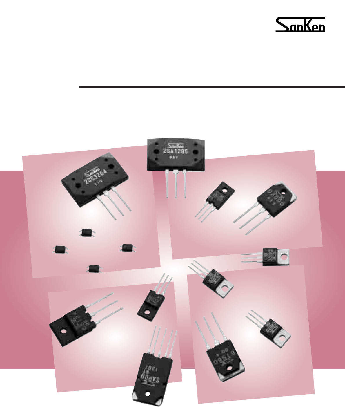
POWER TRANSISTORS
POWER TRANSISTORS
Bulletin No
T01EE0
(July,2001)
SANKEN ELECTRIC CO.,LTD.
CAUTION/WARNING
The information in this publication has been carefully checked and is believed to be
accurate; however, no responsibility is assumed for inaccuracies.
Sanken reserves the right to make changes without further notice to any products herein in
the interest of improvements in the performance, reliability, or manufacturability
of its products. Before placing an order, Sanken advises its customers to obtain the
latest version of the relevant information to verify that the information being relied upon
is current.
Application and operation examples described in this catalog are quoted for the sole
purpose of reference for the use of the products herein and Sanken can assume no
responsibility for any infringement of industrial property rights, intellectual property
rights or any other rights of Sanken or any third party which may result from its use.
When using the products herein, the applicability and suitability of such products for the
intended purpose or object shall be reviewed at the users responsibility.
Although Sanken undertakes to enhance the quality and reliability of its products, the
occurrence of failure and defect of semiconductor products at a certain rate is inevitable.
Users of Sanken products are requested to take, at their own risk, preventative measures
including safety design of the equipment or systems against any possible injury, death, fires
or damages to the society due to device failure or malfunction.
Sanken products listed in this catalog are designed and intended for the use as components
in general purpose electronic equipment or apparatus (home appliances, office equipment,
telecommunication equipment, measuring equipment, etc.).
Before placing an order, the user’s written consent to the specifications is requested.
When considering the use of Sanken products in the applications where higher reliability
is required (transportation equipment and its control systems, traffic signal control
systems or equipment, fire/crime alarm systems, various safety devices, etc.), please
contact your nearest Sanken sales representative to discuss and obtain written confirmation
of your specifications.
The use of Sanken products without the written consent of Sanken in the applications
where extremely high reliability is required (aerospace equipment, nuclear power control
systems, life support systems, etc.) is strictly prohibited.
Anti radioactive ray design is not considered for the products listed herein.
This publication shall not be reproduced in whole or in part without prior written approval
from Sanken.
•
•
•
•
•
•
•
•
•
•

1
Transistor Selection Guide
..2
Reliability.........................6
Temperature Derating in
Safe Operating Area
.........9
Accessories.....................9
Switching Characteristics
Test Circuit
....................10
Symbols and Term
...........10
A1186............................11
A1215............................12
A1216............................13
A1262............................14
A1294............................15
A1295............................16
A1303............................17
A1386/A........................18
A1488/A........................19
A1492............................20
A1493............................21
A1494............................22
A1567............................23
A1568............................24
A1667/8.........................25
A1673............................26
A1693............................27
A1694............................28
A1695............................29
A1725............................30
A1726............................31
A1746............................32
A1859/A ........................33
A1860............................34
A1907............................35
A1908............................36
A1909............................37
A2042............................38
B1257............................39
B1258............................40
B1259............................41
B1351............................42
B1352............................43
B1382............................44
B1383............................45
B1420............................46
B1559............................47
B1560............................48
B1570............................49
B1587............................50
B1588............................51
B1647............................52
B1648............................53
B1649............................54
B1659............................55
B1685............................56
B1686............................57
B1687............................58
C2023 ...........................59
C2837 ...........................60
C2921 ...........................61
C2922 ...........................62
C3179 ...........................63
C3263 ...........................64
C3264 ...........................65
C3284 ...........................66
C3519/A........................67
C3678 ...........................68
C3679 ...........................69
C3680 ...........................70
C3830 ...........................71
C3831 ...........................72
C3832 ...........................73
C3833 ...........................74
C3834 ...........................75
C3835 ...........................76
C3851/A........................77
C3852/A........................78
C3856 ...........................79
C3857 ...........................80
C3858 ...........................81
C3890 ...........................82
C3927 ...........................83
C4020 ...........................84
C4024 ...........................85
C4064 ...........................86
C4065 ...........................87
C4073 ...........................88
C4130 ...........................89
C4131 ...........................90
C4138 ...........................91
C4139 ...........................92
C4140 ...........................93
C4153 ...........................94
C4296 ...........................95
C4297 ...........................96
C4298 ...........................97
C4299 ...........................98
C4300 ...........................99
C4301 .........................100
C4304 .........................101
C4381/2 ......................102
C4388 .........................103
C4418 .........................104
C4434 .........................105
C4445 .........................106
C4466 .........................107
C4467 .........................108
C4468 .........................109
C4495 .........................110
C4511 .........................111
C4512 .........................112
C4517/A......................113
C4518/A......................114
C4546 .........................115
C4557 .........................116
C4662 .........................117
C4706 .........................118
C4883/A......................119
C4886 .........................120
C4907 .........................121
C4908 .........................122
C5002 .........................123
C5003 .........................124
C5071 .........................125
C5099 .........................126
C5100 .........................127
C5101 .........................128
C5124 .........................129
C5130 .........................130
C5239 .........................131
C5249 .........................132
C5271 .........................133
C5287 .........................134
C5333 .........................135
C5370 .........................136
D1769 .........................137
D1785 .........................138
D1796 .........................139
D2014 .........................140
D2015 .........................141
D2016 .........................142
D2017 .........................143
D2045 .........................144
D2081 .........................145
D2082 .........................146
D2083 .........................147
D2141 .........................148
D2389 .........................149
D2390 .........................150
D2401 .........................151
D2438 .........................152
D2439 .........................153
D2557 .........................154
D2558 .........................155
D2560 .........................156
D2561 .........................157
D2562 .........................158
D2589 .........................159
D2641 .........................160
D2642 .........................161
D2643 .........................162
SAH02 ........................163
SAH03 ........................164
SAP09N......................165
SAP09P ......................166
SAP10N......................167
SAP10P ......................168
SAP16N......................169
SAP16P ......................170
SAP Series
Application
Information................171
Discontinued Parts
Guide ........................176
Contents SANKEN POWER TRANSISTORS

2
Collector Current IC(A)
Transistor Selection Guide
■VCEO-IC
Collector–Emitter Voltage VCEO(V)
800
C3678 C3679 C3680 C5124
C4020 C4300 C4301
C4299 C5002
C4304 C5003
C4445
C4908
600
C5249 C4706
550
C4517 C4518 C3927
C4517A C4518A C4557
C5239 C5287
500
C3830 C3831
C4907
400
C4073 C3832 C4138 C3833 C4139 C4140
C4418 C3890 C4296 C4297 C4298
C4662 C4130 C5071 C4434
C5130 C4546
380
D2141
300
C2023
C5333
250
D2017
230
A1294 A1295
C3263 C3264
200
A1668 D2016 C5271 A1493 A1494
C4382 D2557 C3857 C3858
D2558
180
A1859A A1386A A1216
C4883A A1492 C2922
A1673
C3519A
C3856
C4388
160
A1215
A1386
C2921
C3519
150
A1667 B1559 A1186 B1570 A1303 B1647 B1648
A1859 B1587 B1560 D2401 A1860 B1649 D2561
C4381 D2389 B1588 C3284 D2560
C4883 D2438 C2837 C4886 D2562
D2390
D2439
140
A1695
A1909
C4468
C5101
120
D2015 D1769 C3834 A1694 B1259 B1382 B1383
D1785 C3835 A1908 D2081 B1420 D2083
D2045 C4153 C4467 D2082
C5100
110
B1659
B1685
B1686
B1687
D2489
D2641
D2642
D2643
100
B1258
80
C3852A A1488A A1693
C3851A A1725
D2014 A1726
A1907
C4466
C4511
C4512
C5099
60
C3852 A1262 A1568
A1488 B1351
B1257 B1352
C3179 C4065
C3851
D1796
50
C4495 A2042 A1567 C4131
C4024 A1746
C4064
40
C5370
2 3 4 5 6 7 8 10 12 14 15 16 17 18 25

C5271
C4073
C4418
C4662
C3832 C3890
C4130
C4138 C4296
C3833 C4297
C5071
C4139 C4298
C4434
C4140
C5130
C4546
C3830 C4907
C3831
C5249
3
550
600
800
3
5
10
14
3
5
7
900
(1000)
900
200
400
400
5
5
7
10
12
15
18
5
7
6
10
3
250
500
600
■Transistors for Switch Mode Power Supplies (for AC80–130V input)
■Transistors for Switch Mode Power Supplies (for AC180–280V input)
Transistor Selection Guide
VCBO(V) VCEO(V) IC(A) MT-25 FM20 MT–100 FM100
(TO220) (TO220F) (TO3P) (TO3PF)
VCBO(V) VCEO(V) IC(A) MT-25 FM20 MT–100 FM100
(TO220) (TO220F) (TO3P) (TO3PF)
C5239
C4517(A)
C4518(A)
C5287
C3927 C4557
C4706
C4020 C4908
C3678 C4299
C4304 C4445
C3679 C4300
C3680 C4301
500
600
Part No. PC(W) VCEO(V) IC(A) hFE(min) fT(MHz) Package
2SA1860/2SC4886
80
2SA1186/2SC2837
100
2SA1303/2SC3284
125
2SA1386/2SC3519
130
2SA1386A/2SC3519A
130
2SA1294/2SC3263
130
2SA1215/2SC2921
150
2SA1216/2SC2922
200
2SA1295/2SC3264
200
4
Transistors for Audio Amplifiers
FM20 (TO220F)
MT-25 (TO220)
MT-100 (TO3P)
FM100 (TO3PF)
MT-100 (TO3P)
FM100 (TO3PF)
MT-100 (TO3P)
MT-200 (2-screw mount)
●Single Emitter
50 20
●LAPT (Multi emitter for High Frequency)
Transistor Selection Guide
80
120
140
180
140
180
200
6
8
10
15
10
15
15
17
Part No. PC(W) VCEO(V) IC(A) hFE(min) fT(MHz) Package
2SA1725/2SC4511
30
2SA1726/2SC4512
50
2SA1693/2SC4466
60
2SA1907/2SC5099
60
2SA1908/2SC5100
75
2SA1694/2SC4467
80
2SA1909/2SC5101
80
2SA1673/2SC4388
85
2SA1695/2SC4468
100
2SA1492/2SC3856
130
2SA1493/2SC3857
150
2SA1494/2SC3858
200
150
160
180
230
160
180
230
14
10
14
15
17
50
50
60
50
40
35
50
40
35
FM100 (TO3PF)
MT-100 (TO3P)
MT-200 (2-screw mount)
■Single Transistors
●Transistors with built in temperature compensation diodes for audio amplifier
Part No. PC(W) VCEO(V) IC(A) hFE(min) Emitter Resistor(Ω)
SAP09P/SAP09N
80
SAP10P/SAP10N
100
SAP16P/SAP16N
150
150
150
160
10
12
15
5000
5000
5000
0.22
0.22
0.22
Part No. PC(W) VCEO(V) IC(A) hFE(min) fT(MHz) Package
2SB1686
2SD2642
2SB1659
2SD2589
2SB1685
2SD2641
2SB1687
2SD2643
2SB1587
2SD2438
2SB1559
2SD2389
2SB1588
2SD2439
2SB1649
2SD2562
2SB1560
2SD2390
2SB1647
2SD2560
2SB1570
2SD2401
2SB1648
2SD2561
5
FM20 (TO220F)
MT-25 (TO220)
MT-100 (TO3P)
FM100 (TO3PF)
MT-100 (TO3P)
FM100 (TO3PF)
MT-100 (TO3P)
MT-200 (2-screw mount)
■Darlington Transistors
6
8
10
15
10
15
12
17
5000
30
50
60
60
75
80
80
85
100
130
150
200
110
150
200
150
150
Part No. PC(W) VCEO(V) IC(A) hFE(min) fT(MHz) Package Remarks
2SC4495
2SC4883
2SC4883A
2SA1859
2SA1859A
50
150
180
–150
–180
■Temperature compensation Transistors and Driver Transistors
25
20
20
3
2
–2
500
60
60
40
120
60
FM20
(TO220F)
Temperature compensation
Driver, Complement 2SA1859
Driver, Complement 2SA1859A
Driver, Complement 2SC4883
Driver, Complement 2SC4883A
100
60
100
60
100
60
100
60
65
80
65
80
50
55
45
70
50
55
45
70
50
55
45
70
Transistor Selection Guide
4. Applications Considered on Reliability
a) The type and specifications of our transistors and semiconductor
devices vary depending on the application that will be required by
their intended use. Customer should, therefore, determine
which type will best suit their purposes.
b) Note that high temperratures or long soldering periods must be avoid-
ed during soldering, as heat can be transmitted through external
leads into the interior. This may cause deterioration if the maximum
allowable temperature is exceeded.
c) When using the trasistor
under pulse operation or
inductive load, the Safe
Operating Area (SOA) for
the current and voltage must
not be exceeded (Figure 2).
d) The reliability of transistors and semiconductor devices is greatly
affected by the stress of junction temperature. If we accept in general
proceed in the form of Arrhenius equation, the relationship between
the junction temperature Tj and lifespan L can be expressed with
the following empirical formula
n L = A+ Tj
⋅⋅⋅⋅⋅⋅⋅⋅⋅⋅⋅⋅⋅⋅⋅⋅⋅⋅⋅⋅⋅⋅⋅⋅⋅⋅⋅⋅⋅⋅⋅⋅⋅⋅⋅⋅⋅⋅⋅⋅⋅⋅⋅⋅⋅⋅⋅⋅⋅⋅⋅⋅⋅⋅⋅⋅⋅⋅⋅⋅⋅⋅⋅⋅⋅⋅⋅⋅⋅⋅⋅⋅⋅⋅⋅⋅⋅⋅(4)
It is, hence, very important to derate the junction temperature to
assure a high reliability rate.
5. Reliability Test
Sanken bases its test methods and conditions on the following
standards. Tests are conducted under these or stricter conditions,
The details of these are shown in Table 1.
• MIL-STD-202F (Test method for electrical and electronic com-
ponents)
• MIL-STD-750C (Test method for semiconductor equipment)
• JIS C 7021 (Endurance test and environmental test method for
individual semiconductor devices)
• JIS C 7022 (Endurance test and environmental test method for
integrated circuits of semiconductors)
6. Quality Assurance
To ensure high quality and high reliability, quality control and produc-
tion process control procedures are executed from the receipt of parts
through the entire production process. Our quality assurance system
is shown in Figure 3.
1. Definition of Reliability
The word reliablity is an abstract term which refers to the degree to
which equipment or components, such as semiconductor devices, are
resistant to failure. Reliability can be and is often measured quantitatively.
Reliability is defined as “whether equipment or components (such as
a semiconductor device) under given conditions perform the same at
the end of a given period as at the beginning.”
2. Reliability Function
In general, there are three types of failure modes in electronic com-
ponents:
1. Infant failure
2. Random failure
3. Wear-out failure
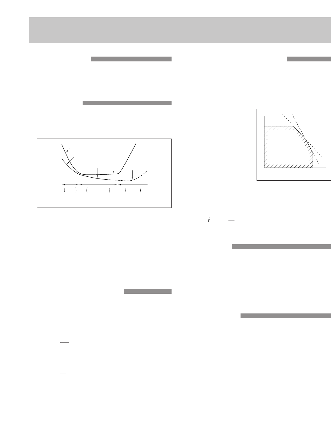
These three types of failure describe “bathtub curve” shown in
Figure 1. Infant failures can be attributed to trouble in the production
process and can be eliminated by aging befor shipment to customers,
stricter control of the production process and quality control measures.
Semiconductor devices such as transistors, unlike electronic equipment,
take a considerable amount of time to reach the stage where wear-out
failure begins to occur. And, as shown in Figure 1 (b), they also last
much longer than electronic equipment. This shows that the longer they
are used the more stable they actually become.
The reduction that occurs in random failures can be approximated by
Weibull distribution, logarithmic normal distribution, or gamma distri-
bution, but Weibull distribution best expresses the phenomenon that
occurs with transistors.
3. Quantitative Expression of Reliability
While there are many ways to quantitatively express reliability, two
criteria, failure rate and life span, are generally used to define the
reliability of semiconductors such as transistrors.
a) Failure Rate (FR)
Failure rate often refers to instantaneous failures or λ (t). In general
of reliability theory, however, the cumulative failure rate, or Relia-
bility Index, is
F
⋅
R = N
⋅
t
⋅⋅⋅⋅⋅⋅⋅⋅⋅⋅⋅⋅⋅⋅⋅⋅⋅⋅⋅⋅⋅⋅⋅⋅⋅⋅⋅⋅⋅⋅⋅⋅⋅⋅⋅⋅⋅⋅⋅⋅⋅⋅⋅⋅⋅⋅⋅⋅⋅⋅⋅⋅⋅⋅⋅⋅⋅⋅⋅⋅⋅⋅⋅⋅⋅⋅⋅⋅⋅⋅⋅⋅⋅⋅⋅⋅⋅⋅⋅⋅⋅⋅⋅(1)
Where N = Net quantity used, and
r(t) = Net quantitiy failed after t hours
If we assign t the arbitrary
F
⋅
R = N ×100 (
%/1,000 hours
)
⋅⋅⋅⋅⋅⋅⋅⋅⋅⋅⋅⋅⋅⋅⋅⋅⋅⋅⋅⋅⋅⋅⋅⋅⋅⋅⋅⋅⋅⋅⋅⋅⋅⋅⋅⋅⋅⋅⋅⋅⋅⋅⋅⋅⋅⋅⋅(2)
In situations where the cumulative failure rate is small, failure is ex-
pressed in units of one Fit, 10-9(failures/hours).
b)
Life Span(L)
Life Span can be expressed in terms of average lifespan or as Mean
Time Between Failure (MTBF), but assuming that random failure
is shown by the Index Distribution [λ (t) = constant], then Life Span
or L can be shown by the equation
L = F
⋅
R
(hours)⋅⋅⋅⋅⋅⋅⋅⋅⋅⋅⋅⋅⋅⋅⋅⋅⋅⋅⋅⋅⋅⋅⋅⋅⋅⋅⋅⋅⋅⋅⋅⋅⋅⋅⋅⋅⋅⋅⋅⋅⋅⋅⋅⋅⋅⋅⋅⋅⋅⋅⋅⋅⋅⋅⋅⋅⋅⋅⋅⋅⋅⋅⋅⋅⋅⋅⋅⋅⋅⋅⋅⋅⋅⋅⋅⋅(3)
6
Reliability
r(t)
(a)
(b)
General Electronic
Equipment or
Components
Semiconductor
Devices
Time (t)
Failure Rate (λ)
Estimation
Initial
Failure Random or
Chance Failure Wear-out
Failure
Figure 1 Bath Tub Curve
r
1
SOA(Safe Operating Area)
Max.Allowable
Current
Max.
Allowable
Voltage Vceo(Max)
Collector-Emitter Voltage Vce(V)
Collector Current Ic(A)
Secondary Breakdown Locus
Max Allowable Power
Figure 2 SOA
B
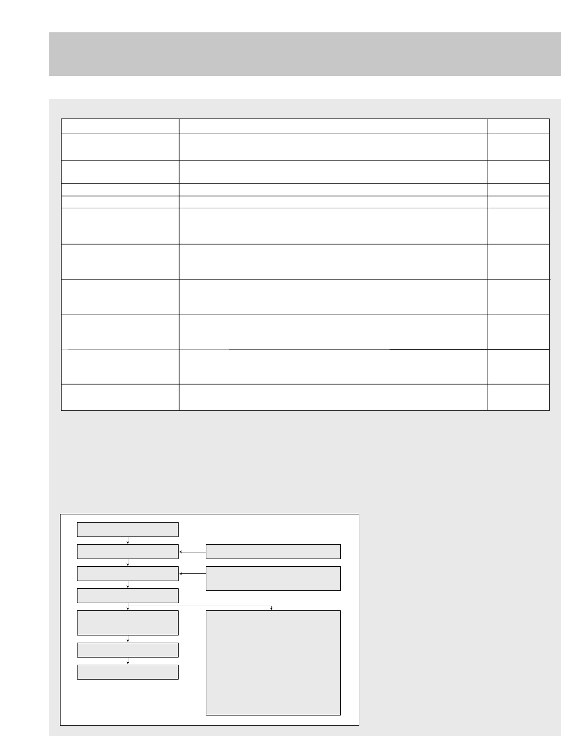
Material Purchasing
Incoming Inspection
Production Process
Physical and Chemical Inspection
Quality Control
Production Process Control
Specialized Tests for all units
Shipping Inspection
Shipment
Marking
Packing Periodical Quality Assurance Test
1. Operational Life (continuous) Test
2. Operational Life (intermittent) Test
3. High Temperature Storage Test
4. Low Temperature Storage Test
5. Moisture Resistance Test
6. Heat Cycle Test
7. Heat Shock Test
8. Soldering Heat Test
9. Vibaration Test
10. Drop Test
7
Test
Continuous Operations Test
Intermittent Operation Test
High Temperature Storage Test
Low Temperature Storage Test
Moisture Resistance Test
Heat Cycle Test
Heat Shock Test
Soldering Heat Test
Vibrations Test
Drop Test
Details of the Testing Method
Collector dissipation with maximum junction temperature is applied continuously at
room temperature to judge lifespan and reliability under transistor operating conditions.
Power equal to that used in the Continuous Operations Test is applied intermittently
to test the transistor’s lifespan and reliability under on and off conditions.
Confirms the highest storage temperature and operating temperature of transistors.
Confirms the lowest storage temperature of transistors.
Tested at RH=85% and TA=85°C for the effects of the interaction between
temperature and humidity, and the effects of surface insulation between electrodes
and high temperature/high humidity.
Tested at Tstg min – Room temp. – Tstg max – Room temp. for 10 cycles (one cycle
30 min. –5 min. –30 min. –5 min.) to detect mechanical faults and characteristic
changes caused by thermal expansion and shrinkage of the transistor.
Tested at 100°C (5 min.), 25°C (within 3 sec.), 0°C (5 min.) for 10 cycles to check for
mechanical faults and characteristic changes caused by thermal expansion and
shrinkage of transistor.
Tested at 260 ±5°C, 10 ±1 sec, by dipping lead wire to 1.5mm from the seating plane
in solder bath to check for characteristic changes caused by drastic temperature rises
of exterior lead wire.
Tested at amplitude 1.52mm, vibration frequency 10-55 Hz in directions of X, Y, Z, for
2 hours each (total 6 hours) to check for characteristic changes caused by vibration
during operation and transportion.
Tested by dropping 10 times from 75 cm height to check for mechanical endurance
and characteristic changes caused by shock during handling.
Table 1: Test Methods and Conditions
LTPD(%)
*5/1000hrs
5/1000hrs
5/1000hrs
5/1000hrs
5/1000hrs
5
5
5
5
5
Figure 3 Quality Assurance System
∗Reliability Standard : 60%
Reliability
7.
Notes Regarding Storage, Characteristic Tests, and Handling
Since reliability can be affected adversely by improper storage
environment and handling methods during Characteristic tests,
please observe the following cautions.
a) Cautions for Storage
1. Ensure that storage conditions comply with the standard
temperature (5 to 35°C) and the standard relative humidity
(arround 40 to 75%) and avoid storage locations that
experience extreme changes in temperature or humidity.
2. Avod locations where dust or harmful gases are present,
and avoid direct sunlight.
3. Reinspect for rust in leads and solderbility that have been
stored for a long time.
b) Cautions for Characteristic Tests and Handling
1. When characteristic tests are carried out during inspection
testing and other standard test periods, protect the transistor
from surges of power from the testing device, shorts between
the transistor and the heatsink
c) Silicone Grease
When using a heatsink, please coat the back surface of the
transistor and both surfaces of the insulating plate with a thin
layer of silicone grease to improve heat transfer between the
transistor and the heatsink.
Recommended Silicone Grease
• G-746 (Shin-Etsu Chemical)
• YG6260 (GE Toshiba Silicone)
• SC102 (Dow Corning Toray Silicone)
d) Torque when Tightening Screws
Thermal resistance increases when tightening torque is small,
and radiation effects are decreased. When the torque is too
high, the screw can cut, the heatsink can be deformed, and/or
distortion can arise in the product’s frame. To avoid these
problems, Table 2 shows the recommended tightening torques
for each product type.
Table 2. Screw Tightening Torques
Package Screw Tightening Torque
MT25 (TO-220) 0.490 to 0.686 N ·m (5 to 7kgf · cm)
FM20 (TO-220 Full Mold) 0.490 to 0.686 N ·m (5 to 7kgf · cm)
MT100 (TO-3P) 0.686 to 0.822 N ·m (7 to 9kgf · cm)
FM100 (TO-3P Full Mold) 0.686 to 0.822 N ·m (7 to 9kgf · cm)
MT200 ( two-point mount) 0.686 to 0.822 N · m (7 to 9kgf· cm)
2GR ( one-point mount) 0.686 to 0.822 N· m (7 to 9kgf · cm)
e) Soldering Temperature
In general, the transistor is subjected to high temperatures when
it is mounted on the printed circuit board, whether from flow solder
from a solderbath, or, in hand operations from a soldering iron.
The testing method and test conditions (JIS-C-7021 standards)
for a transistor’s heat resistance during soldering are:
At a distance of 1.5mm from the transistor’s main body,
apply 260°C for 10 seconds, and 350°C for 3 seconds.
However, please stay well within these limits and for as short
a time as possible during actual soldering.
8
Reliability
9
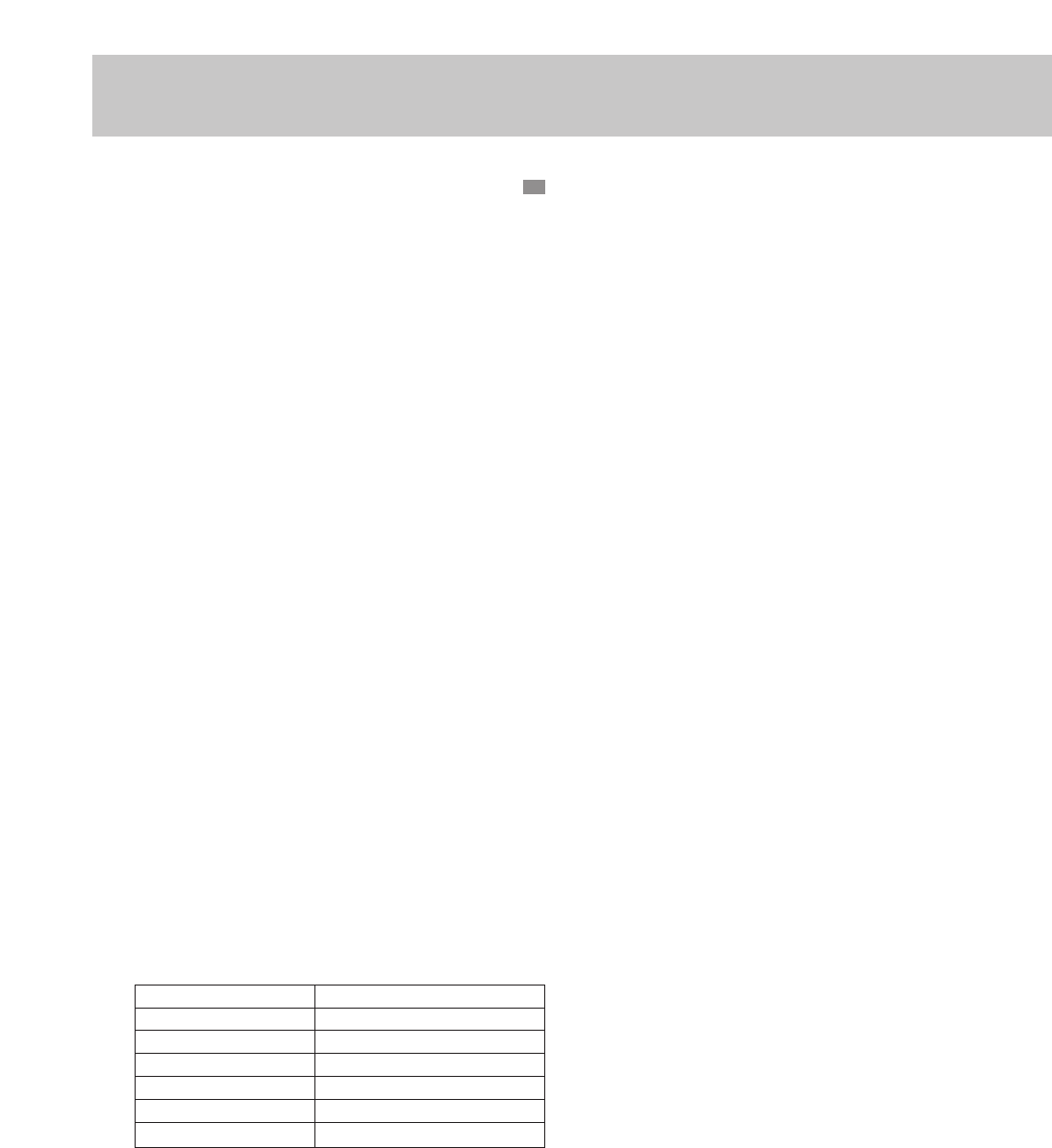
■Temperature Derating in Safe Operating Area
Flange (case) temperature is typically described as 25°C, but it must be derated subject to the operating
temperature.
This derating curve is determined by manufacturing conditions of devices, materials used etc. and in case of a
silicon transistor, breakdown voltage and DC Current Gain are significantly deteriorated in the temperature
range of 260°C to 360°C.
Hence, the collector current must be derated by using the derating curve in Fig.2 where the breakdown point is
set at 260°C.
0
100
50
0 50 100 150 200 250 300
S/B limiting area
Pc limiting area
Case Temp Tc (°C)
Collector Current
Derating coefficient DF (%)
Tc=25°C
S/B limiting area
Pc limiting area
Collector-Emitter Voltage VCE (V)
Collector Current Ic (A)
Fig.1 Safe Operating Area
Derating coefficient is obtained from temperature in Fig.2 and it must be applied to the current value of the safe
operating area in order to obtain the derated current.
■Accessories
✩Sanken Transistors do not include accessories. Accessories may be attached at a cost if requested.
✩Sanken transistor case is a standard size, and can be used with any generally sold accessories.
ø3.75
5.0±0.1
R0.5
19.4±0.1
14.0±0.1
7.0
+0.1
–
0
ø3.2
7.0
R0.5
24.0
20.0
±0.1
±0.1
10.0
+0.1
–
0
+0.2
–
0
+0.2
–
0
2–ø3.2
R0.5
+0.1
–
0
39.0±0.1
24.0±0.1
12.0±0.1
24.38±0.1
6.0±0.2
2.5±0.2 1.5±0.2
3.7±0.1
3.1
±0.1
• Insulater: Mica, with a thickness of 0.06mm, +0.045 –0.005 allowance • Insulation Bush for MT-25 (TO220)
Type Name:Mold(10)Mica Type Name:Mold(14)Mica Type Name:Mold(9)Mica
Reliability
Fig.2 Derating Curve of Safe Operating Area
Symbol
VCBO
VCEO
VEBO
IC
IB
PC
Tj
Tstg
ICBO
IEBO
V(BR)CEO
hFE
VCE(sat)
VBE(sat)
VFEC
fT
Cob
Item
Collector-Base Voltage
Collector-Emitter Voltage
Emitter-Base Voltage
Collector Current
Base Current
Collector Power Dissipation
Operating Junction Temperature
Storage Temperature
Collector Cutoff Current
Emitter Cutoff Current
Collector-Emitter Saturation Voltage
DC Current Gain
Collector-Emitter Saturation Voltage
Base-Emitter Saturation Voltage
Emitter-Collector Diode Forward Voltage
Cut-off Frequency
Collector Junction capacitance
Definition
DC Voltage between Collector and Base when Emitter is open
Voltage between Collector and Emitter when Base is open and voltage is reversely applied to Collector junction
DC voltage between Emitter and Base when Collector is open
DC current passing through Collector electrode
DC current passing through Base electrode
Power consumed at Collector junction
Maximum allowable temperature value at absolute maximum ratings
Maximum allowable range of ambient temperature at non-operation
Collector current when Emitter is open and a specified reverse voltage is applied between Collector and Base
Emitter current when Collector is open and a specified reverse voltage is applied between Emitter and Base
Breakdown voltage between Collector and Emitter when Base is open
Ratio of DC output current and DC input current at a specified voltage and current (Emitter common)
DC voltage between Collector and Emitter under specified saturation conditions
DC voltage between Base and Emitter under specified saturation conditions
Diode forward voltage between Emitter and Collector when Base is open
Frequency at the specified voltage and current where hFE is 1 (0dB)
Junction capacitance between collector and Base at a specified voltage and frequency
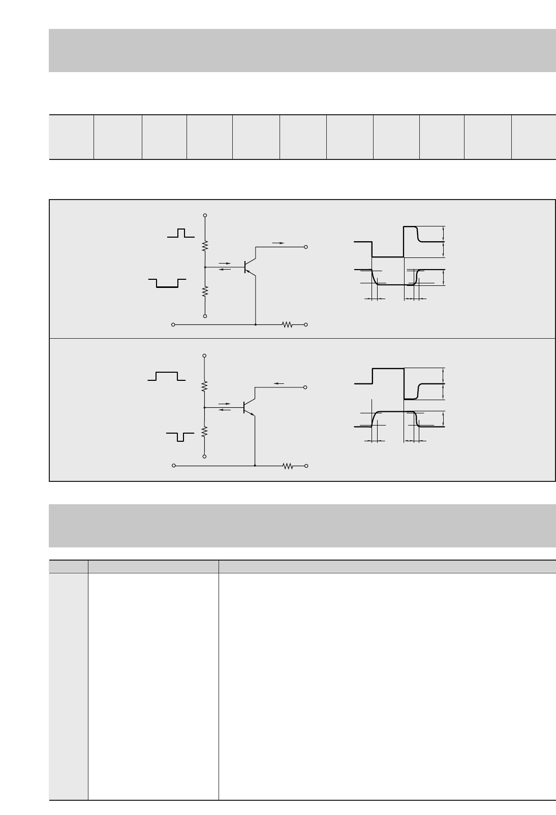
■Typical Switching Characteristics (Common Emitter)
10
■Switching Characteristics Test Circuit/Measurement Wave Forms
VCC RLICVB2 VBB1 VBB2 IB1 IB2 trtstg tf
(V) (Ω) (A) (V) (V) (V) (A) (A) (µs) (µs) (µs)
20µs
+VBB2
–VBB1
R2
R1
–VCC
0
D.U.T
IB2
IC
RL
IB1
50µs
0
0
GND
0.9IC
IB2IB1
IC
ton
0
Base
Current
Collector
Current 0.1IC
tstg tf
0
0
20µs
+VBB1
–VBB2
R1
R2
VCC
0.9IC
IB2IB1
IC
ton
0
0
D.U.T
IB1
IC
RL
IB2
50µs
0
0
GND
0.1IC
tstg tf
0
0
Base
Current
Collector
Current
Symbols
NPN
PNP
Switching Characteristics
• Ta=25°C unless otherwise specified.
Silicon PNP Epitaxial Planar Transistor (Complement to type 2SC2837) Application : Audio and General Purpose
Symbol
VCBO
VCEO
VEBO
IC
IB
PC
Tj
Tstg
Ratings
–150
–150
–5
–10
–2
100(Ta=25°C)
150
–55 to +150
Unit
V
V
V
A
A
W
°C
°C
■
Absolute maximum ratings
■
Electrical Characteristics
■Typical Switching Characteristics (Common Emitter)
External Dimensions MT-100(TO3P)
Symbol
ICBO
IEBO
V(BR)CEO
hFE
VCE(sat)
fT
COB
Ratings
–100max
–100max
–150min
50min∗
–2.0max
60typ
110typ
Unit
µ
A
µ
A
V
V
MHz
pF
Conditions
VCB=–150V
VEB=–5V
IC=–25mA
VCE=–4V, IC=–3A
IC=–5A, IB=–0.5A
VCE=–12V, IE=1A
VCB=–80V, f=1MHz
VCC
(V)
–60
RL
(Ω)
12
IC
(A)
–5
VB2
(V)
5
IB2
(mA)
500
ton
(
µ
s)
0.25typ
tstg
(
µ
s)
0.8typ
tf
(
µ
s)
0.2typ
IB1
(mA)
–500
15.6±0.4
9.6
19.9±0.3
4.0 2.0
5.0±0.2
1.8
ø3.2±0.1
2
3
1.05
+0.2
-0.1
20.0min
4.0max
BE
5.45±0.1 5.45±0.1
C
4.8±0.2
0.65
+0.2
-0.1
1.4
2.0±0.1
a
b
Weight : Approx 6.0g
a. Part No.
b. Lot No.
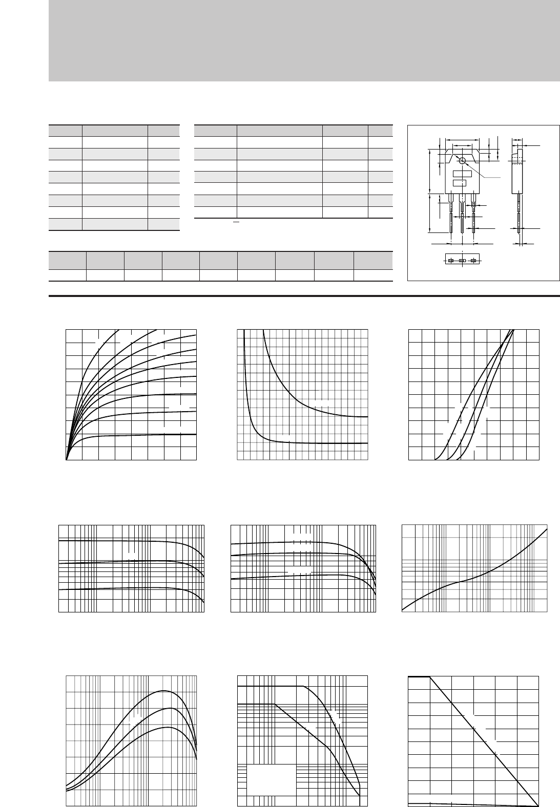
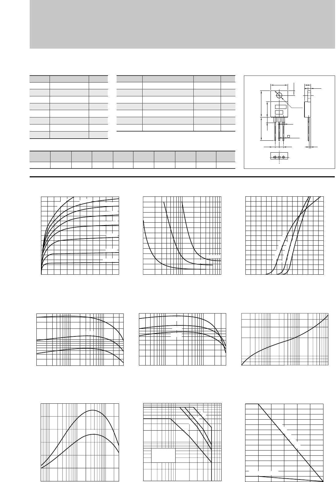
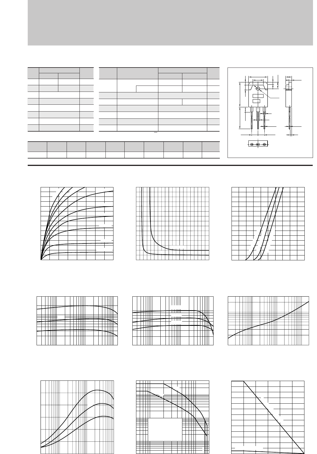
IC–VCE Characteristics
(Typical)
hFE–IC Characteristics
(Typical)
hFE–IC
Temperature Characteristics (Typical)
θj-a–t Characteristics
IC–VBE Temperature Characteristics
(Typical)
VCE(sat)–IB Characteristics
(Typical)
Pc–Ta Derating
0
0
–2
–4
–6
–8
–10
–1 –2 –3 –4
Collector-Emitter Voltage VCE(V)
Collector Current IC(A)
–400mA
I
B
=–20mA
–200mA
–160mA
–120mA
–100mA
–80mA
–60mA
–40mA
0
–3
–2
–1
0 –0.5 –1.0 –2.0–1.5
Base Current IB(A)
Collector-Emitter Saturation Voltage VCE(sat)(V)
IC=–10A
–5A
–0.02 –0.1 –1 –10
20
50
100
300
Collector Current IC(A)
DC Current Gain hFE
(VCE=–4V)
Typ
Safe Operating Area (Single Pulse)
–2 –10 –100 –200
–0.2
–1
–0.5
–10
–30
–5
Collector-Emitter Voltage VCE(V)
Collector Current IC(A)
10ms
DC
Without Heatsink
Natural Cooling
fT–IE Characteristics
(Typical)
0.02 0.1 1 10
0
20
40
60
80
Cut-off Frequency fT(MHZ)
(VCE=–12V)
Emitter Current IE(A)
Typ
0.2
1
3
0.5
1 10 100 1000 2000
Time t(ms)
Transient Thermal Resistance θj-a(˚C/W)
100
50
3.5
00 25 50 75 100 125 150
Ambient Temperature Ta(˚C)
Maximum Power Dissipation PC(W)
With Infinite heatsink
Without Heatsink
0
–10
–2
–6
–4
–8
0–2–1
Base-Emittor Voltage VBE(V)
Collector Current IC(A)
(VCE=–4V)
125˚C (Case Temp)
25˚C (Case Temp)
–30˚C (Case Temp)
(VCE=–4V)
–0.02 –0.1 –0.5 –1 –5–0.5 –5 –10
30
50
100
200
Collector Current IC(A)
DC Current Gain hFE
125˚C
–30˚C
25˚C
(Ta=25°C) (Ta=25°C)
∗hFE Rank O(50to100), P(70to140), Y(90to180)
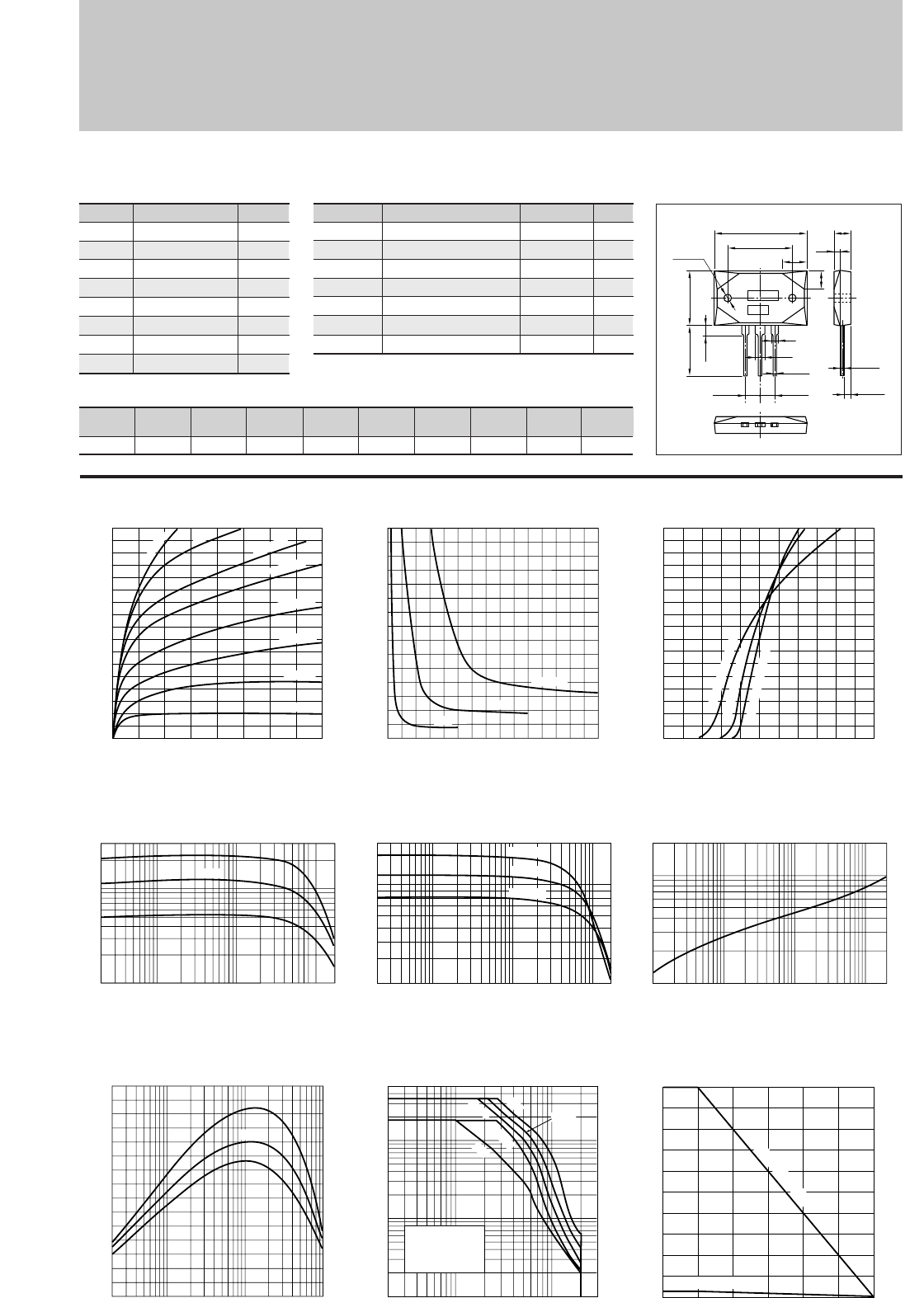
LAPT 2SA1186
11
12
Symbol
VCBO
VCEO
VEBO
IC
IB
PC
Tj
Tstg
Ratings
–160
–160
–5
–15
–4
150(Tc=25°C)
150
–55 to +150
Unit
V
V
V
A
A
W
°C
°C
Symbol
ICBO
IEBO
V(BR)CEO
hFE
VCE(sat)
fT
COB
Ratings
–100max
–100max
–160min
50min∗
–2.0max
50typ
400typ
Unit
µ
A
µ
A
V
V
MHz
pF
Conditions
VCB=–160V
VEB=–5V
IC=–25mA
VCE=–4V, IC=–5A
IC=–5A, IB=–0.5A
VCE=–12V, IE=2A
VCB=–10V, f=1MHz
VCC
(V)
–60
RL
(Ω)
12
IC
(A)
–5
VB2
(V)
5
IB2
(mA)
500
ton
(
µ
s)
0.25typ
tstg
(
µ
s)
0.85typ
tf
(
µ
s)
0.2typ
IB1
(mA)
–500
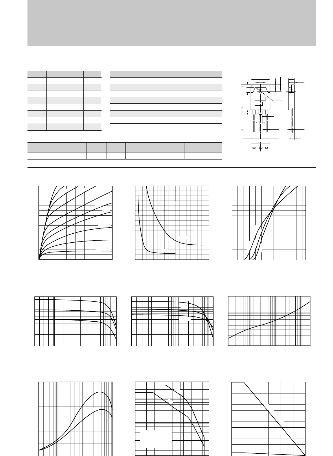
LAPT 2SA1215
2
3
1.05
+0.2
-0.1
BE
5.45±0.1 5.45±0.1
2-ø3.2±0.1
36.4±0.3
9
24.4±0.2
7
21.4±0.3
20.0min
4.0max
0.65
+0.2
-0.1
3.0
+0.3
-0.1
6.0±0.2
2.1
a
b
C
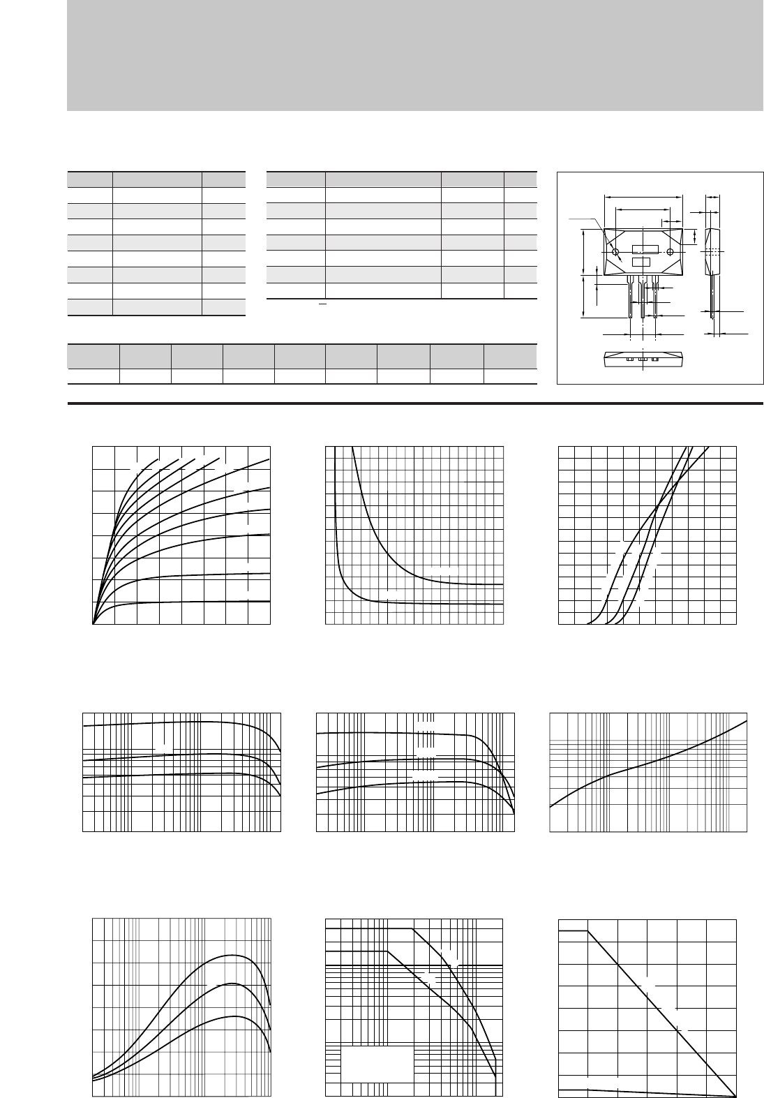
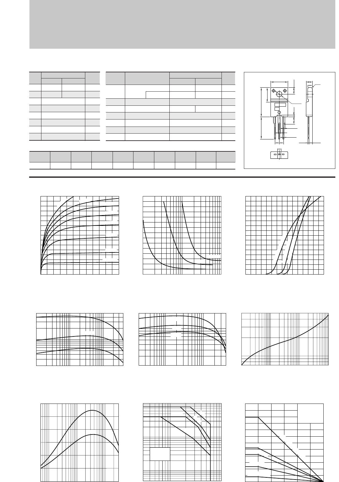
IC–VCE Characteristics
(Typical)
hFE–IC Characteristics
(Typical)
hFE–IC
Temperature Characteristics (Typical)
IC–VBE Temperature Characteristics
(Typical)
VCE(sat)–IB Characteristics
(Typical)
Pc–Ta Derating
0
0
–4
–8
–12
–16
–1 –2 –3 –4
Collector-Emitter Voltage VCE(V)
Collector Current IC(A)
–50mA
–100mA
I
B
=–20mA
–600mA
–500mA
–400mA
–300mA
–200mA
–150mA
–750mA
0
–3
–2
–1
0 –0.2 –0.4 –1.0–0.6 –0.8
Base Current IB(A)
Collector-Emitter Saturation Voltage VCE(sat)(V)
IC=–10A
–5A
–0.02 –0.1 –1 –10 –15
10
50
100
200
Collector Current IC(A)
DC Current Gain hFE
(VCE=–4V)
Typ
Safe Operating Area (Single Pulse)
–2 –10 –100 –200
–0.2
–1
–0.5
–10
–40
–5
Collector-Emitter Voltage VCE(V)
Collector Current IC(A)
Without Heatsink
Natural Cooling
DC
10ms
fT–IE Characteristics
(Typical)
0.02 0.1 1 10
0
20
40
60
80
Cut-off Frequency fT(MHZ)
(VCE=–12V)
Emitter Current IE(A)
Typ
1 10 100 1000 2000
Time t(ms)
0.1
1
2
0.5
Transient Thermal Resistance θj-a(˚C/W)
θj-a–t Characteristics
160
120
80
40
5
00 25 50 75 100 125 150
Ambient Temperature Ta(˚C)
Maximum Power Dissipation PC(W)
0
–15
–10
–5
0–2–1
Base-Emittor Voltage VBE(V)
Collector Current IC(A)
(VCE=–4V)
125˚C (Case Temp)
25˚C (Case Temp)
–30˚C (Case Temp)
(VCE=–4V)
–0.02 –0.1 –0.5 –1 –5–0.5 –5 –10 –15
30
50
100
200
Collector Current IC(A)
DC Current Gain hFE
125˚C
25˚C
–30˚C
With Infinite heatsink
Without Heatsink
∗hFE Rank O(50to100), P(70to140), Y(90to180)
■
Absolute maximum ratings
■
Electrical Characteristics
■Typical Switching Characteristics (Common Emitter)
(Ta=25°C) (Ta=25°C)
Silicon PNP Epitaxial Planar Transistor (Complement to type 2SC2921) Application : Audio and General Purpose
External Dimensions MT-200
Weight : Approx 18.4g
a. Part No.
b. Lot No.
∗hFE Rank O(30to60), Y(50to100), P(70to140), G(90to180)
13
Silicon PNP Epitaxial Planar Transistor (Complement to type 2SC2922) Application : Audio and General Purpose
Symbol
VCBO
VCEO
VEBO
IC
IB
PC
Tj
Tstg
Ratings
–180
–180
–5
–17
–5
200(Tc=25°C)
150
–55 to +150
Unit
V
V
V
A
A
W
°C
°C
■
Absolute maximum ratings
■
Electrical Characteristics
■Typical Switching Characteristics (Common Emitter)
SymboI
VCBO
IEBO
V(BR)CEO
hFE
VCE(sat)
fT
COB
Ratings
–100max
–100max
–180min
30min∗
–2.0max
40typ
500typ
Unit
µ
A
µ
A
V
V
MHz
pF
Conditions
VCB=–180V
VEB=–5V
IC=–25mA
VCE=–4V, IC=–8A
IC=–8A, IB=–0.8A
VCE=–12V, IE=2A
VCB=–10V, f=1MHz
VCC
(V)
–40
RL
(Ω)
4
IC
(A)
–10
VB2
(V)
5
IB2
(A)
1
ton
(
µ
s)
0.3typ
tstg
(
µ
s)
0.7typ
tf
(
µ
s)
0.2typ
IB1
(A)
–1
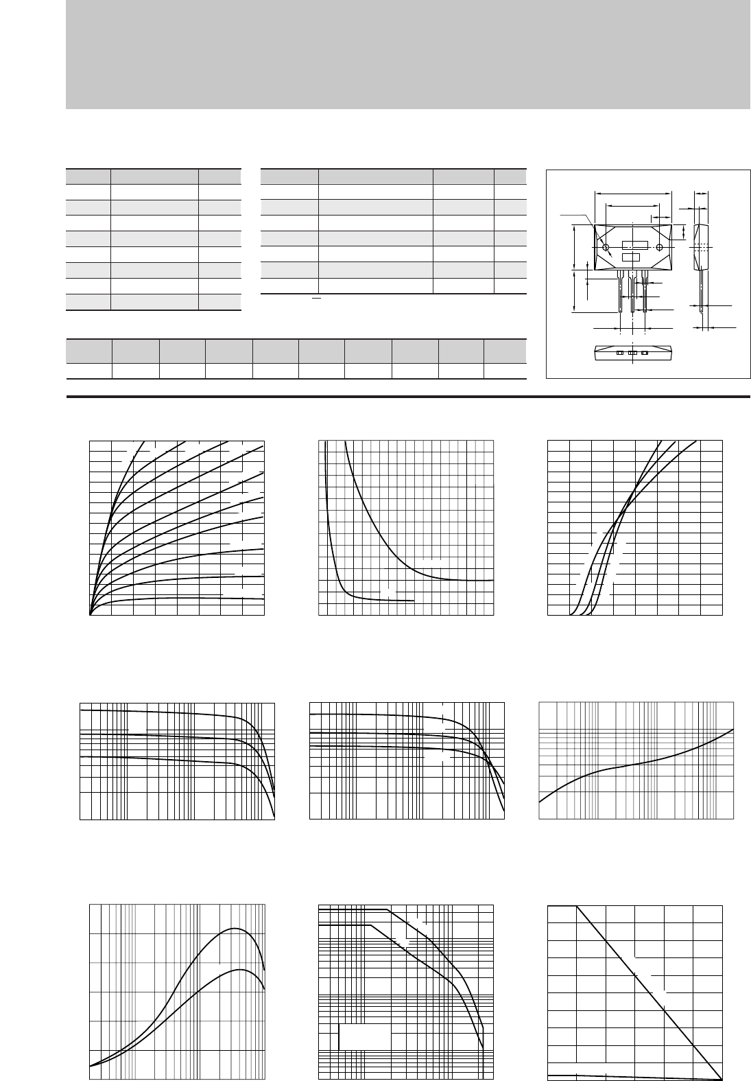
LAPT 2SA1216
(Ta=25°C) (Ta=25°C)
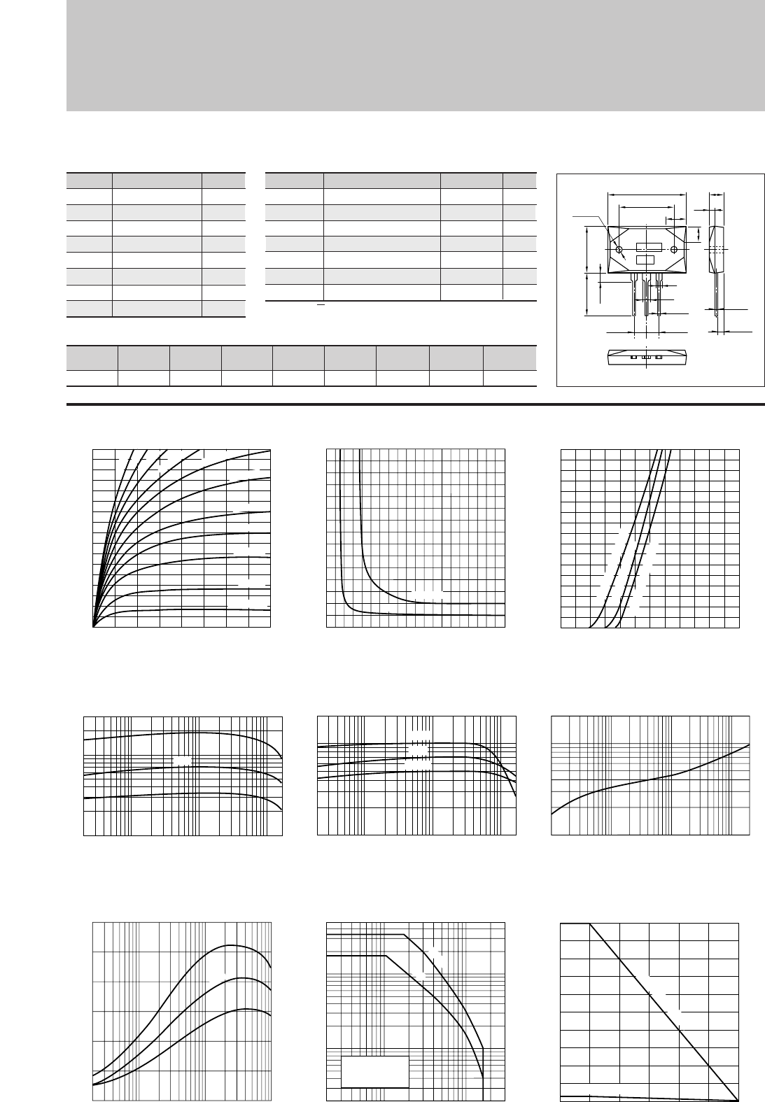
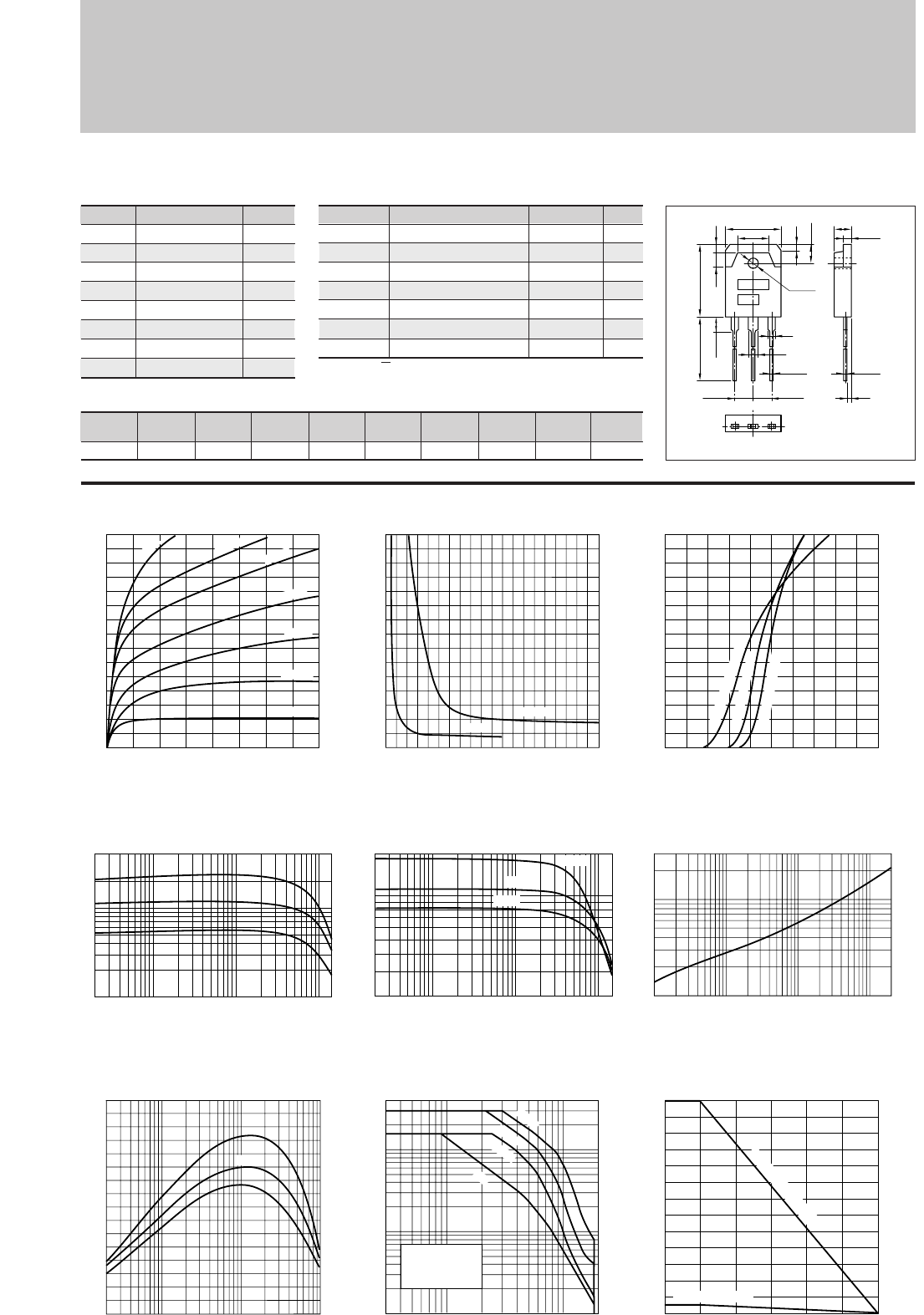
IC–VCE Characteristics
(Typical)
hFE–IC Characteristics
(Typical)
hFE–IC
Temperature Characteristics (Typical)
VCE(sat)–IB Characteristics
(Typical)
Pc–Ta Derating
0
0
–5
–10
–15
–17
–1 –2 –3 –4
Collector-Emitter Voltage VCE(V)
Collector Current IC(A)
–1.5A
–50mA
–100mA
I
B
=–20mA
–700mA
–500mA
–1A
–400mA
–300mA
–200mA
–150mA
0
–3
–2
–1
0 –0.2 –0.4 –1.0–0.6 –0.8
Base Current IB(A)
Collector-Emitter Saturation Voltage VCE(sat)(V)
IC=–10A
–5A
Safe Operating Area (Single Pulse)
–2 –10 –100 –300
–0.2
–1
–0.5
–10
–50
–5
Collector-Emitter Voltage VCE(V)
Collector Current IC(A)
Without Heatsink
Natural Cooling
DC
10ms
0.02 0.1 1 10
0
20
40
60
Cut-off Frequency fT(MHZ)
(VCE=–12V)
Emitter Current IE(A)
Typ
1 10 100 1000 2000
Time t(ms)
0.1
1
2
0.5
Transient Thermal Resistance θj-a(˚C/W)
θj-a–t Characteristics
fT–IE Characteristics
(Typical)
200
160
120
80
40
5
00 25 50 75 100 125 150
Ambient Temperature Ta(˚C)
Maximum Power Dissipation PC(W)
With Infinite heatsink
Without Heatsink
Collector Current IC(A)
(VCE=–4V)
–0.02 –0.1 –0.5 –1 –5 –10 –17
10
50
100
200
DC Current Gain hFE
125˚C
25˚C
–30˚C
–0.02 –0.1 –1 –10–0.5 –5 –17
10
50
100
300
Collector Current IC(A)
DC Current Gain hFE
(VCE=–4V)
Typ
IC–VBE Temperature Characteristics
(Typical)
0
–17
–15
–10
–5
0 –2 –2.4–1
Base-Emittor Voltage VBE(V)
Collector Current IC(A)
(VCE=–4V)
125˚C(Case Temp)
25˚C(Case Temp)
–30˚C(Case Temp)
External Dimensions MT-200
2
3
1.05
+0.2
-0.1
BE
5.45±0.1 5.45±0.1
2-ø3.2±0.1
36.4±0.3
9
24.4±0.2
7
21.4±0.3
20.0min
4.0max
0.65
+0.2
-0.1
3.0
+0.3
-0.1
6.0±0.2
2.1
a
b
C
Weight : Approx 18.4g
a. Part No.
b. Lot No.
14
Silicon PNP Epitaxial Planar Transistor (Complement to type 2SC3179)
External Dimensions MT-25(TO220)
Symbol
VCBO
VCEO
VEBO
IC
IB
PC
Tj
Tstg
Ratings
–60
–60
–6
–4
–1
30(Tc=25°C)
150
–55 to +150
Unit
V
V
V
A
A
W
°C
°C
■
Absolute maximum ratings
■
Electrical Characteristics
■Typical Switching Characteristics (Common Emitter)
Symbol
ICBO
IEBO
V(BR)CEO
hFE
VCE(sat)
fT
COB
Ratings
–100max
–100max
–60min
40min
–0.6max
15typ
90typ
Unit
µ
A
µ
A
V
V
MHz
pF
Conditions
VCB=–60V
VEB=–6V
IC=–25mA
VCE=–4V, IC=–1A
IC=–2A, IB=–0.2A
VCE=–12V, IE=0.2A
VCB=–10V, f=1MHz
VCC
(V)
–20
RL
(Ω)
10
IC
(A)
–2
VBB2
(V)
5
IB2
(mA)
200
ton
(
µ
s)
0.25typ
tstg
(
µ
s)
0.75typ
tf
(
µ
s)
0.25typ
IB1
(mA)
–200
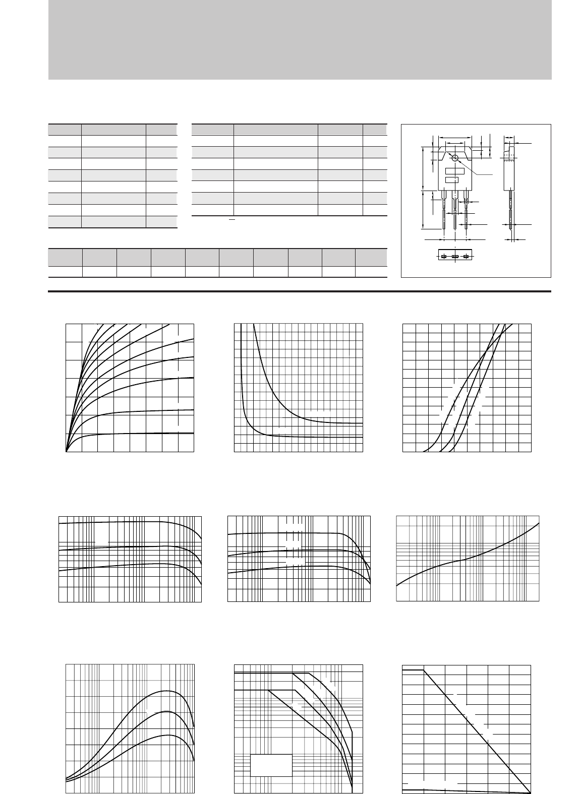
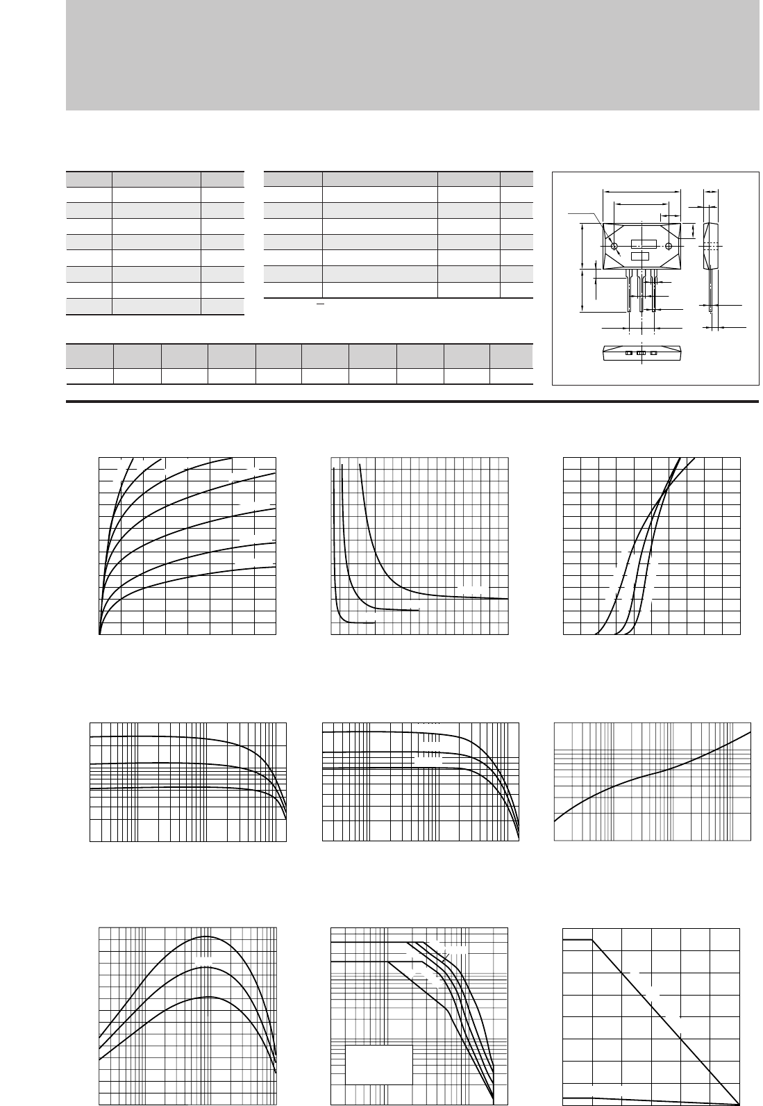
2SA1262
(Ta=25°C) (Ta=25°C)
IC–VCE Characteristics
(Typical)
θj-a–t Characteristics
Pc–Ta Derating
Safe Operating Area (Single Pulse)
–10 –50 –100–2 –5
–1
–0.5
–0.1
–10
–5
Collector-Emitter Voltage VCE(V)
Collector Current IC(A)
Without Heatsink
Natural Cooling
VCE(sat)–IB Characteristics
(Typical)
0
–1.5
–1.0
–0.5
–0.1
–0.1–0.5 –0.5 –1
Base Current IB(A)
Collector-Emitter Saturation Voltage VCE(sat)(V)
IC=–3A
–2A
–1A
hFE–IC Characteristics
(Typical)
1ms
10ms
100ms
DC
IC–VBE Temperature Characteristics
(Typical)
0
–4
–3
–2
–1
0 –1.5–0.5 –1.0
Base-Emittor Voltage VBE(V)
Collector Current IC(A)
(VCE=–4V)
125˚C (Case Temp)
25˚C (Case Temp)
–30˚C (Case Temp)
hFE–IC
Temperature Characteristics (Typical)
(VCE=–4V)
–0.02 –0.1 –1 –4
20
50
100
200
Collector Current IC(A)
DC Current Gain hFE
125˚C
25˚C
–30˚C
–0.01 –0.1 –1 –4
20
50
100
500
Collector Current IC(A)
DC Current Gain hFE
(VCE=–4V)
Typ
–0.5
0
0
–2
–1
–3
–4
–2–1 –3 –4 –5 –6
Collector-Emitter Voltage VCE(V)
Collector Current IC(A)
–30mA
–40mA
–50mA
–60mA
–20mA
–10mA
I
B
=–5mA
–80mA
0.7
1
5
1 10 100 1000
Time t(ms)
Transient Thermal Resistance θj-a(˚C/W)
0.005 0.01 0.05
0.50.1 1 3
0
10
20
30
60
50
40
Cut-off Frequency fT(MHZ)
(VCE=–12V)
Emitter Current IE(A)
Typ
fT–IE Characteristics
(Typical)
30
20
10
2
00 25 50 75 100 125 150
Ambient Temperature Ta(˚C)
Maximum Power Dissipation PC(W)
With Infinite heatsink
Without Heatsink
VBB1
(V)
–10
Application : Audio and General Purpose
BE
2.5 2.5
C
16.0±0.7
12.0min
4.0max 8.8±0.2
1.35
0.65
+0.2
-0.1
10.2±0.2
ø3.75±0.2
3.0±0.2
4.8±0.2
1.4
2.0±0.1
a
b
Weight : Approx 2.6g
a. Part No.
b. Lot No.
Silicon PNP Epitaxial Planar Transistor (Complement to type 2SC3263) Application : Audio and General Purpose
Symbol
VCBO
VCEO
VEBO
IC
IB
PC
Tj
Tstg
Ratings
–230
–230
–5
–15
–4
130(Tc=25°C)
150
–55 to +150
Unit
V
V
V
A
A
W
°C
°C
■
Absolute maximum ratings
■
Electrical Characteristics
■Typical Switching Characteristics (Common Emitter)
Symbol
ICBO
IEBO
V(BR)CEO
hFE
VCE(sat)
fT
COB
Ratings
–100max
–100max
–230min
50min∗
–2.0max
35typ
500typ
Unit
µ
A
µ
A
V
V
MHz
pF
Conditions
VCB=–230V
VEB=–5V
IC=–25mA
VCE=–4V, IC=–5A
IC=–5A, IB=–0.5A
VCE=–12V, IE=2A
VCB=–10V, f=1MHz
VCC
(V)
–60
RL
(Ω)
12
IC
(A)
–5
VBB2
(V)
5
IB2
(mA)
500
ton
(
µ
s)
0.35typ
tstg
(
µ
s)
1.50typ
tf
(
µ
s)
0.30typ
IB1
(mA)
–500
LAPT 2SA1294
(Ta=25°C) (Ta=25°C)
IC–VCE Characteristics
(Typical)
hFE–IC Characteristics
(Typical)
Safe Operating Area (Single Pulse)
hFE–IC
Temperature Characteristics (Typical)
IC–VBE Temperature Characteristics
(Typical)
VCE(sat)–IB Characteristics
(Typical)
Pc–Ta Derating
0
0
–5
–10
–15
–1 –2 –3 –4
Collector-Emitter Voltage VCE(V)
Collector Current IC(A)
–3.0A
–50mA
–100mA
I
B
=–20mA
–1.5A
–1.0A
–500mA
–300mA
–200mA
0
– 3
–2
–1
0 –0.5 –1.0 –2.0–1.5
Base Current IB(A)
Collector-Emitter Saturation Voltage VCE(sat)(V)
IC=–10A
–5A
–0.02 –0.1 –1 –10–5–0.5 –15
10
50
100
200
Collector Current IC(A)
DC Current Gain hFE
(VCE=–4V)
Typ
–3 –10 –100 –300
–0.1
–0.05
–1
–0.5
–10
–40
–5
Collector-Emitter Voltage VCE(V)
Collector Current IC(A)
10ms
DC
Without Heatsink
Natural Cooling
0.02 0.1 1 10
0
20
40
60
Cut-off Frequency fT(MHZ)
(VCE=–12V)
Emitter Current IE(A)
Typ
0.1
1
3
0.5
1 10 100 1000 2000
Time t(ms)
Transient Thermal Resistance θj-a(˚C/W)
θj-a–t Characteristics
fT–IE Characteristics
(Typical)
130
100
50
3.5
0
Ambient Temperature Ta(˚C)
Maximum Power Dissipation PC(W)
With Infinite heatsink
Without Heatsink
0 25 50 75 100 125 150
0
–15
–10
–5
0 –2 –2.5–1
Base-Emittor Voltage VBE(V)
Collector Current IC(A)
(VCE=–4V)
125˚C (CaseTemp)
25˚C (CaseTemp)
–30˚C (CaseTemp)
(VCE=–4V)
–0.02 –0.1 –0.5 –1 –5 –15–10
10
50
100
200
Collector Current IC(A)
DC Current Gain hFE
125˚C
25˚C
–30˚C
–2.0A
VBB1
(V)
–10
External Dimensions MT-100(TO3P)
15.6±0.4
9.6
19.9±0.3
4.0 2.0
5.0±0.2
1.8
ø3.2±0.1
2
3
1.05
+0.2
-0.1
20.0min
4.0max
BE
5.45±0.1 5.45±0.1
C
4.8±0.2
0.65
+0.2
-0.1
1.4
2.0±0.1
a
b
Weight : Approx 6.0g
a. Part No.
b. Lot No.
15
∗hFE Rank O(50to100), Y(70to140)
∗hFE Rank O(50to100), Y(70to140)
16
Silicon PNP Epitaxial Planar Transistor (Complement to type 2SC3264) Application : Audio and General
Symbol
VCBO
VCEO
VEBO
IC
IB
PC
Tj
Tstg
Ratings
–230
–230
–5
–17
–5
200(Tc=25°C)
150
–55 to +150
Unit
V
V
V
A
A
W
°C
°C
■
Absolute maximum ratings
■
Electrical Characteristics
■Typical Switching Characteristics (Common Emitter)
Symbol
ICBO
IEBO
V(BR)CEO
hFE
VCE(sat)
fT
COB
Ratings
–100max
–100max
–230min
50min∗
–2.0max
35typ
500typ
Unit
µ
A
µ
A
V
V
MHz
pF
Conditions
VCB=–230V
VEB=–5V
IC=–25mA
VCE=–4V, IC=–5A
IC=–5A, IB=–0.5A
VCE=–12V, IE=2A
VCB=–10V, f=1MHz
LAPT 2SA1295
(Ta=25°C) (Ta=25°C)
VCC
(V)
–60
RL
(Ω)
12
IC
(A)
–5
VBB2
(V)
5
IB2
(mA)
500
ton
(
µ
s)
0.35typ
tstg
(
µ
s)
1.50typ
tf
(
µ
s)
0.30typ
IB1
(mA)
–500
VBB1
(V)
–10
IC–VCE Characteristics
(Typical)
hFE–IC Characteristics
(Typical)
Safe Operating Area (Single Pulse)
hFE–IC
Temperature Characteristics (Typical)
IC–VBE Temperature Characteristics
(Typical)
VCE(sat)–IB Characteristics
(Typical)
Pc–Ta Derating
0
0
–5
–10
–15
–17
–1 –2 –3 –4
Collector-Emitter Voltage VCE(V)
Collector Current IC(A)
–3.0A
–50mA
–100mA
I
B
=–20mA
–2.0A
–1.5A
–1.0A
–500mA
–300mA
–200mA
0
– 3
–2
–1
0 –0.5 –1.0 –2.0–1.5
Base Current IB(A)
Collector-Emitter Saturation Voltage VCE(sat)(V)
IC=–10A
–5A
–0.02 –0.1 –1 –10–0.5 –5 –17
10
50
100
200
Collector Current IC(A)
DC Current Gain hFE
(VCE=–4V)
Typ
Without Heatsink
Natural Cooling
–3 –10 –100 –300
–0.1
–0.05
–1
–0.5
–10
–40
–5
Collector-Emitter Voltage VCE(V)
Collector Current IC(A)
10ms
DC
0.02 0.1 1 10
0
20
40
60
Cut-off Frequency fT(MHZ)
(VCE=–12V)
Emitter Current IE(A)
Typ
1 10 100 1000 2000
Time t(ms)
0.1
1
2
0.5
Transient Thermal Resistance θj-a(˚C/W)
θj-a–t Characteristics
fT–IE Characteristics
(Typical)
200
160
120
80
40
5
00 25 50 75 100 125 150
Ambient Temperature Ta(˚C)
Maximum Power Dissipation PC(W)
With Infinite heatsink
Without Heatsink
0
–10
–5
–15
–17
0 –3.2–2.4–1.6–0.8
Base-Emittor Voltage VBE(V)
Collector Current IC(A)
(VCE=–4V)
125˚C (Case Temp)
25˚C
–30˚C (Case Temp)
(VCE=–4V)
–0.02 –0.1 –0.5 –1 –5 –10 –17
10
50
100
200
Collector Current IC(A)
DC Current Gain hFE
125˚C
25˚C
–30˚C
External Dimensions MT-200
2
3
1.05
+0.2
-0.1
BE
5.45±0.1 5.45±0.1
2-ø3.2±0.1
36.4±0.3
9
24.4±0.2
7
21.4±0.3
20.0min
4.0max
0.65
+0.2
-0.1
3.0
+0.3
-0.1
6.0±0.2
2.1
a
b
C
Weight : Approx 18.4g
a. Part No.
b. Lot No.
∗hFE Rank O(50to100), P(70to140), Y(90to180)
17
Silicon PNP Epitaxial Planar Transistor (Complement to type 2SC3284) Application : Audio and General Purpose
Symbol
VCBO
VCEO
VEBO
IC
IB
PC
Tj
Tstg
Ratings
–150
–150
–5
–14
–3
125(Tc=25°C)
150
–55 to +150
Unit
V
V
V
A
A
W
°C
°C
■
Absolute maximum ratings
■
Electrical Characteristics
■Typical Switching Characteristics (Common Emitter)
Symbol
ICBO
IEBO
V(BR)CEO
hFE
VCE(sat)
fT
COB
Ratings
–100max
–100max
–150min
50min
–2.0max
50typ
400typ
Unit
µ
A
µ
A
V
V
MHz
pF
Conditions
VCB=–150V
VEB=–5V
IC=–25mA
VCE=–4V, IC=–5A
IC=–5A, IB=–0.5A
VCE=–12V, IE=2A
VCB=–10V, f=1MHz
VCC
(V)
–60
RL
(Ω)
12
IC
(A)
–5
VBB2
(V)
5
IB2
(mA)
500
ton
(
µ
s)
0.25typ
tstg
(
µ
s)
0.85typ
tf
(
µ
s)
0.2typ
IB1
(mA)
–500
LAPT 2SA1303
(Ta=25°C) (Ta=25°C)
IC–VCE Characteristics
(Typical)
hFE–IC Characteristics
(Typical)
Safe Operating Area (Single Pulse)
hFE–IC
Temperature Characteristics (Typical)
VCE(sat)–IB Characteristics
(Typical)
Pc–Ta Derating
0
0
–4
–8
–12
–1 –2 –3 –4
Collector-Emitter Voltage VCE(V)
Collector Current IC(A)
–50mA
–100mA
I
B
=–20mA
–600mA
–700mA
–500mA
–400mA
–300mA
–200mA
–150mA
0
–3
–2
–1
0 –0.2 –0.4 –1.0–0.6 –0.8
Base Current IB(A)
Collector-Emitter Saturation Voltage VCE(sat)(V)
IC=–10A
–5A
–0.02 –0.1 –1–0.5 –10–5 –14
20
50
100
200
Collector Current IC(A)
DC Current Gain hFE
(VCE=–4V)
Typ
–3 –10 –100 –200
–0.2
–1
–0.5
–10
–40
–5
Collector-Emitter Voltage VCE(V)
Collector Current IC(A)
Without Heatsink
Natural Cooling
DC
10ms
1ms
100ms
0.02 0.1 1 10
0
20
40
60
80
Cut-off Frequency fT(MHZ)
(VCE=–12V)
Emitter Current IE(A)
Typ
0.1
1
3
0.5
1 10 100 1000 2000
Time t(ms)
Transient Thermal Resistance θj-a(˚C/W)
θj-a–t Characteristics
fT–IE Characteristics
(Typical)
(VCE=–4V)
–0.02 –0.1 –0.5 –1 –5 –10 –14
30
50
100
200
Collector Current IC(A)
DC Current Gain hFE
125˚C
25˚C
–30˚C
130
100
50
3.5
00 25 50 75 100 125 150
Ambient Temperature Ta(˚C)
Maximum Power Dissipation PC(W)
With Infinite heatsink
Without Heatsink
IC–VBE Temperature Characteristics
(Typical)
0
–14
–10
–5
0–2–1
Base-Emittor Voltage VBE(V)
Collector Current IC(A)
(VCE=–4V)
125˚C (Case Temp)
25˚C (Case Temp)
–30˚C (Case Temp)
VBB1
(V)
–10
External Dimensions MT-100(TO3P)
15.6±0.4
9.6
19.9±0.3
4.0 2.0
5.0±0.2
1.8
ø3.2±0.1
2
3
1.05
+0.2
-0.1
20.0min
4.0max
BE
5.45±0.1 5.45±0.1
C
4.8±0.2
0.65
+0.2
-0.1
1.4
2.0±0.1
a
b
Weight : Approx 6.0g
a. Part No.
b. Lot No.
∗hFE Rank O(50to100), P(70to140), Y(90to180)
18
Silicon PNP Epitaxial Planar Transistor (Complement to type 2SC3519/A) Application : Audio and General Purpose
Symbol
VCBO
VCEO
VEBO
IC
IB
PC
Tj
Tstg
–5
–15
–4
130(Tc=25°C)
150
–55 to +150
Unit
V
V
V
A
A
W
°C
°C
■
Absolute maximum ratings
■
Electrical Characteristics
■Typical Switching Characteristics (Common Emitter)
Symbol
ICBO
IEBO
V(BR)CEO
hFE
VCE(sat)
fT
COB
2SA1386
–100max
–160
–160min
Unit
µ
A
V
µ
A
V
V
MHz
pF
Conditions
VCB=
VEB=–5V
IC=–25mA
VCE=–4V, IC=–5A
IC=–5A, IB=–0.5A
VCE=–12V, IE=2A
VCB=–10V, f=1MHz
LAPT
2SA1386/1386A
(Ta=25°C)
(Ta=25°C)
VCC
(V)
–40
RL
(Ω)
4
IC
(A)
–10
VBB2
(V)
5
IB2
(A)
1
ton
(
µ
s)
0.3typ
tstg
(
µ
s)
0.7typ
tf
(
µ
s)
0.2typ
IB1
(A)
–1
VBB1
(V)
–10
2SA1386A
–100max
–180
–180min
–100max
50min∗
–2.0max
40typ
500typ
IC–VCE Characteristics
(Typical)
hFE–IC Characteristics
(Typical)
Safe Operating Area (Single Pulse)
hFE–IC
Temperature Characteristics (Typical)
IC–VBE Temperature Characteristics
(Typical)
VCE(sat)–IB Characteristics
(Typical)
Pc–Ta Derating
0
0
–5
–10
–15
–1 –2 –3 –4
Collector-Emitter Voltage VCE(V)
Collector Current IC(A)
–50mA
–100mA
I
B
=–20mA
–700mA
–500mA
–400mA
–300mA
–200mA
–150mA
0
–3
–2
–1
0 –0.2 –0.4 –1.0–0.6 –0.8
Base Current IB(A)
Collector-Emitter Saturation Voltage VCE(sat)(V)
IC=–10A
–5A
–0.02 –0.1 –1 –10–0.5 –5 –15
10
100
300
Collector Current IC(A)
DC Current Gain hFE
(VCE=–4V)
Typ
Collector-Emitter Voltage VCE(V)
Collector Current IC(A)
–3 –10 –50 –100 –200
–0.1
–0.05
–1
–0.5
–10
–40
–5
10ms
Without Heatsink
Natural Cooling
1.2SA1386
2.2SA1386A
12
DC
0.02 0.1 1 10
0
20
40
60
Cut-off Frequency fT(MHZ)
(VCE=–12V)
Emitter Current IE(A)
Typ
fT–IE Characteristics
(Typical)
130
100
50
3.5
0
Ambient Temperature Ta(˚C)
Maximum Power Dissipation PC(W)
With Infinite heatsink
Without Heatsink
0 25 50 75 100 125 150
0
–15
–10
–5
0–2–1
Base-Emittor Voltage VBE(V)
Collector Current IC(A)
(VCE=–4V)
125˚C (Case Temp)
25˚C (Case Temp)
–30˚C (Case Temp)
(VCE=–4V)
–0.02 –0.1 –0.5 –1 –5 –10 –15
20
50
100
200
Collector Current IC(A)
DC Current Gain hFE
125˚C
25˚C
–30˚C
θj-a–t Characteristics
0.1
1
3
0.5
1 10 100 1000 2000
Time t(ms)
Transient Thermal Resistance θj-a(˚C/W)
External Dimensions MT-100(TO3P)
15.6±0.4
9.6
19.9±0.3
4.0 2.0
5.0±0.2
1.8
ø3.2±0.1
2
3
1.05
+0.2
-0.1
20.0min
4.0max
BE
5.45±0.1 5.45±0.1
C
4.8±0.2
0.65
+0.2
-0.1
1.4
2.0±0.1
a
b
Weight : Approx 6.0g
a. Part No.
b. Lot No.
2SA1386
–160
–160
2SA1386A
–180
–180
Ratings Ratings
19
Silicon PNP Epitaxial Planar Transistor (Complement to type 2SC3851/A) Application : Audio and General Purpose
Symbol
VCBO
VCEO
VEBO
IC
IB
PC
Tj
Tstg
–6
–4
–1
25(Tc=25°C)
150
–55 to +150
Unit
V
V
V
A
A
W
°C
°C
■
Absolute maximum ratings
■
Electrical Characteristics
■Typical Switching Characteristics (Common Emitter)
Symbol
ICBO
IEBO
V(BR)CEO
hFE
VCE(sat)
fT
COB
2SA1488
–100max
–60
–60min
Unit
µ
A
V
µ
A
V
V
MHz
pF
Conditions
VCB=
VEB=–6V
IC=–25mA
VCE=–4V, IC=–1A
IC=–2A, IB=–0.2A
VCE=–12V, IE=0.2A
VCB=–10V, f=1MHz
2SA1488/1488A
(Ta=25°C)
(Ta=25°C)
VCC
(V)
–12
RL
(Ω)
6
IC
(A)
–2
VBB2
(V)
5
IB2
(mA)
200
ton
(
µ
s)
0.25typ
tstg
(
µ
s)
0.75typ
tf
(
µ
s)
0.25typ
IB1
(mA)
–200
VBB1
(V)
–10
2SA1488A
–100max
–80
–80min
–100max
40min
–0.5max
15typ
90typ
IC–VCE Characteristics
(Typical)
θj-a–t Characteristics
IC–VBE Temperature Characteristics
(Typical)
Pc–Ta Derating
Safe Operating Area (Single Pulse)
0
0
–2
–1
–3
–4
–2–1 –3 –4 –5 –6
Collector-Emitter Voltage VCE(V)
Collector Current IC(A)
–30mA
–40mA
–50mA
–60mA
–20mA
–10mA
I
B
=–5mA
–80mA
0
–4
–3
–2
–1
0 –1.5–0.5 –1.0
Base-Emittor Voltage VBE(V)
Collector Current IC(A)
(VCE=–4V)
125˚C (Case Temp)
25˚C (Case Temp)
–30˚C (Case Temp)
hFE–IC
Temperature Characteristics (Typical)
0.7
1
5
1 10 100 1000
Time t(ms)
Transient Thermal Resistance θj-a(˚C/W)
30
20
10
2
00 25 50 75 100 125 150
Ambient Temperature Ta(˚C)
Maximum Power Dissipation PC(W)
With Infinite heatsink
Without Heatsink
10 50 10035
–1
–0.5
–0.05
–0.1
–10
–5
Collector-Emitter Voltage VCE(V)
Collector Current IC(A)
Without Heatsink
Natural Cooling
VCE(sat)–IB Characteristics
(Typical)
0
–1.5
–1.0
–0.5
–0.1
–0.1–0.5 –0.5 –1
Base Current IB(A)
Collector-Emitter Saturation Voltage VCE(sat)(V)
IC=–3A
–2A
–1A
hFE–IC Characteristics
(Typical)
–0.01 –0.1 –1 –4
20
50
100
500
Collector Current IC(A)
DC Current Gain hFE
(VCE=–4V)
Typ
–0.5
1ms
10ms
100ms
DC
150x150x2
50x50x2
100x
100x2
(VCE=–4V)
–0.02 –0.1 –1 –4
20
50
100
200
Collector Current IC(A)
DC Current Gain hFE
125˚C
25˚C
–30˚C
0.005 0.01 0.05
0.50.1 1 3
0
10
20
30
60
50
40
Cut-off Frequency fT(MHZ)
(VCE=–12V)
Emitter Current IE(A)
Typ
fT–IE Characteristics
(Typical)
Natural Cooling
Silicone Grease
Heatsink: Aluminum
in mm
External Dimensions FM20 (TO220F)
ø3.3±0.2
10.1±0.2
4.0±0.2
16.9±0.3
13.0min
8.4±0.2
0.8±0.2
3.9
±0.2
2.542.54
1.35±0.15
0.85
+0.2
-0.1
1.35±0.15
2.2±0.2
4.2±0.2
2.8 c0.5
2.4±0.2
0.45
+0.2
-0.1
BEC
a
b
Weight : Approx 2.0g
a. Part No.
b. Lot No.
2SA1488A
–80
–80
2SA1488
–60
–60
Ratings Ratings
∗hFE Rank O(50to100), P(70to140), Y(90to180)
20
Silicon PNP Epitaxial Planar Transistor (Complement to type 2SC3856) Application : Audio and General Purpose
Symbol
VCBO
VCEO
VEBO
IC
IB
PC
Tj
Tstg
Ratings
–180
–180
–6
–15
–4
130(Tc=25°C)
150
–55 to +150
Unit
V
V
V
A
A
W
°C
°C
■
Absolute maximum ratings
■
Electrical Characteristics
■Typical Switching Characteristics (Common Emitter)
Symbol
ICBO
IEBO
V(BR)CEO
hFE
VCE(sat)
fT
COB
Ratings
–100max
–100max
–180min
50min∗
–2.0max
20typ
500typ
Unit
µ
A
µ
A
V
V
MHz
pF
Conditions
VCB=–180V
VEB=–6V
IC=–50mA
VCE=–4V, IC=–3A
IC=–5A, IB=–0.5A
VCE=–12V, IE=0.5A
VCB=–10V, f=1MHz
VCC
(V)
–40
RL
(Ω)
4
IC
(A)
–10
VBB2
(V)
5
IB2
(A)
1
ton
(
µ
s)
0.6typ
tstg
(
µ
s)
0.9typ
tf
(
µ
s)
0.2typ
IB1
(A)
–1
2SA1492
(Ta=25°C) (Ta=25°C)
IC–VCE Characteristics
(Typical)
hFE–IC Characteristics
(Typical)
Safe Operating Area (Single Pulse)
hFE–IC
Temperature Characteristics (Typical)
IC–VBE Temperature Characteristics
(Typical)
VCE(sat)–IB Characteristics
(Typical)
Pc–Ta Derating
0
0
–5
–10
–15
–1 –2 –3 –4
Collector-Emitter Voltage VCE(V)
Collector Current IC(A)
–1A
–50mA
–0.1A
I
B
=–20mA
–0.6A
–0.4A
–0.2A
0
– 3
–2
–1
0 –0.5 –1.0 –2.0–1.5
Base Current IB(A)
Collector-Emitter Saturation Voltage VCE(sat)(V)
IC=–10A
–5A
–0.02 –0.1 –1 –10–0.5 –5 –15
10
100
50
300
Collector Current IC(A)
DC Current Gain hFE
(VCE=–4V)
Typ
–3 –10 –100 –200
–0.1
–1
–0.5
–10
–40
–5
Collector-Emitter Voltage VCE(V)
Collector Current IC(A)
DC
10ms
3ms
100ms
Without Heatsink
Natural Cooling
0.02 0.1 1 10
0
10
20
30
Cut-off Frequency fT(MHZ)
(VCE=–12V)
Emitter Current IE(A)
Typ
0.1
1
3
0.5
1 10 100 1000 2000
Time t(ms)
Transient Thermal Resistance θj-a(˚C/W)
θj-a–t Characteristics
fT–IE Characteristics
(Typical)
130
100
50
3.5
0
Ambient Temperature Ta(˚C)
Maximum Power Dissipation PC(W)
With Infinite heatsink
Without Heatsink
0 25 50 75 100 125 150
0
–15
–10
–5
0–2–1
Base-Emittor Voltage VBE(V)
Collector Current IC(A)
(VCE=–4V)
125˚C (Case Temp)
25˚C (Case Temp)
–30˚C (Case Temp)
(VCE=–4V)
–0.02 –0.1 –0.5 –1 –5 –10 –15
20
50
100
200
Collector Current IC(A)
DC Current Gain hFE
125˚C
25˚C
–30˚C
VBB1
(V)
–10
External Dimensions MT-100(TO3P)
15.6±0.4
9.6
19.9±0.3
4.0 2.0
5.0±0.2
1.8
ø3.2±0.1
2
3
1.05
+0.2
-0.1
20.0min
4.0max
BE
5.45±0.1 5.45±0.1
C
4.8±0.2
0.65
+0.2
-0.1
1.4
2.0±0.1
a
b
Weight : Approx 6.0g
a. Part No.
b. Lot No.
21
Silicon PNP Epitaxial Planar Transistor (Complement to type 2SC3857) Application : Audio and General Purpose
Symbol
VCBO
VCEO
VEBO
IC
IB
PC
Tj
Tstg
Ratings
–200
–200
–6
–15
–5
150(Tc=25°C)
150
–55 to +150
Unit
V
V
V
A
A
W
°C
°C
■
Absolute maximum ratings
■
Electrical Characteristics
■Typical Switching Characteristics (Common Emitter)
Symbol
ICBO
IEBO
V(BR)CEO
hFE
VCE(sat)
fT
COB
Ratings
–100max
–100max
–200min
50min∗
– 3.0max
20typ
400typ
Unit
µ
A
µ
A
V
V
MHz
pF
Conditions
VCB=–200V
VEB=–6V
IC=–50mA
VCE=–4V, IC=–5A
IC=–10A, IB=–1A
VCE=–12V, IE=0.5A
VCB=–10V, f=1MHz
2SA1493
(Ta=25°C) (Ta=25°C)
IC–VCE Characteristics
(Typical)
hFE–IC Characteristics
(Typical)
Safe Operating Area (Single Pulse)
hFE–IC
Temperature Characteristics (Typical)
IC–VBE Temperature Characteristics
(Typical)
VCE(sat)–IB Characteristics
(Typical)
Pc–Ta Derating
0
0
–5
–10
–15
–1 –2 –3 –4
Collector-Emitter Voltage VCE(V)
Collector Current IC(A)
–1.5A
I
B
=–50mA
–100mA
–600mA
–1A
–400mA
–200mA
0
–3
–2
–1
0–1–2 –4–3
Base Current IB(A)
Collector-Emitter Saturation Voltage VCE(sat)(V)
IC=–15A
–10A
–5A
–0.02 –0.1 –1 –10–0.5 –5 –15
10
100
50
300
Collector Current IC(A)
DC Current Gain hFE
Typ
–2 –10 –100 –300
–0.1
–1
–0.5
–10
–50
–5
Collector-Emitter Voltage VCE(V)
Collector Current IC(A)
3ms
Without Heatsink
Natural Cooling
DC
100ms
20ms
10ms
0.02 0.1 1 10
0
10
20
30
Cut-off Frequency fT(MHZ)
(VCE=–12V)
(VCE=–4V)
Emitter Current IE(A)
Typ
1 10 100 1000 2000
Time t(ms)
0.1
1
2
0.5
Transient Thermal Resistance θj-a(˚C/W)
θj-a–t Characteristics
fT–IE Characteristics
(Typical)
160
120
80
40
5
00 25 50 75 100 125 150
Ambient Temperature Ta(˚C)
Maximum Power Dissipation PC(W)
With Infinite heatsink
Without Heatsink
0
–15
–10
–5
0–2–1
Base-Emittor Voltage VBE(V)
Collector Current IC(A)
(VCE=–4V)
125˚C (CaseTemp)
25˚C (CaseTemp)
–30˚C (CaseTemp)
(VCE=–4V)
–0.02 –0.1 –0.5 –1 –5 –10 –15
20
50
100
200
Collector Current IC(A)
DC Current Gain hFE
125˚C
25˚C
–30˚C
VCC
(V)
–60
RL
(Ω)
12
IC
(A)
–5
VBB2
(V)
5
IB2
(mA)
500
ton
(
µ
s)
0.3typ
tstg
(
µ
s)
0.9typ
tf
(
µ
s)
0.2typ
IB1
(mA)
–500
VBB1
(V)
–10
External Dimensions MT-200
2
3
1.05
+0.2
-0.1
BE
5.45±0.1 5.45±0.1
2-ø3.2±0.1
36.4±0.3
9
24.4±0.2
7
21.4±0.3
20.0min
4.0max
0.65
+0.2
-0.1
3.0
+0.3
-0.1
6.0±0.2
2.1
a
b
C
Weight : Approx 18.4g
a. Part No.
b. Lot No.
∗hFE Rank O(50to100), P(70to140), Y(90to180)
∗hFE Rank Y(50to100), P(70to140), G(90to180)
Silicon PNP Epitaxial Planar Transistor (Complement to type 2SC3858) Application : Audio and General Purpose
Symbol
VCBO
VCEO
VEBO
IC
IB
PC
Tj
Tstg
Ratings
–200
–200
–6
–17
–5
200(Tc=25°C)
150
–55 to +150
Unit
V
V
V
A
A
W
°C
°C
■
Absolute maximum ratings
■
Electrical Characteristics
■Typical Switching Characteristics (Common Emitter)
Symbol
ICBO
IEBO
V(BR)CEO
hFE
VCE(sat)
fT
COB
Ratings
–100max
–100max
–200min
50min∗
–2.5max
20typ
500typ
Unit
µ
A
µ
A
V
V
MHz
pF
Conditions
VCB=–200V
VEB=–6V
IC=–50mA
VCE=–4V, IC=–8A
IC=–10A, IB=–1A
VCE=–12V, IE=1A
VCB=–10V, f=1MHz
VCC
(V)
–40
RL
(Ω)
4
IC
(A)
–10
VBB2
(V)
5
IB2
(A)
1
ton
(
µ
s)
0.6typ
tstg
(
µ
s)
0.9typ
tf
(
µ
s)
0.2typ
IB1
(A)
–1
2SA1494
(Ta=25°C) (Ta=25°C)
IC–VCE Characteristics
(Typical)
hFE–IC Characteristics
(Typical)
Safe Operating Area (Single Pulse)
hFE–IC
Temperature Characteristics (Typical)
VCE(sat)–IB Characteristics
(Typical)
Pc–Ta Derating
0
0
–5
–10
–15
–17
–1 –2 –3 –4
Collector-Emitter Voltage VCE(V)
Collector Current IC(A)
–1.5A
–50mA
–100mA
–1A
–600mA
–400mA
–200mA
I
B
=–20mA
0
–3
–2
–1
0–1–2–3
Base Current IB(A)
Collector-Emitter Saturation Voltage VCE(sat)(V)
IC=–15A
–10A
–5A
–0.02 –0.1 –1 –17–10–5–0.5
50
10
100
300
Collector Current IC(A)
DC Current Gain hFE
(VCE=–4V)
Typ
Collector-Emitter Voltage VCE(V)
Collector Current IC(A)
–2 –10 –100 –300
–0.1
–1
–0.5
–10
–50
–5
3ms
Without Heatsink
Natural Cooling
DC
100ms
20ms
10ms
0.02 0.1 1 10
0
30
10
20
Cut-off Frequency fT(MHZ)
(VCE=–12V)
Emitter Current IE(A)
Typ
fT–IE Characteristics
(Typical)
200
160
120
80
40
5
00 25 50 75 100 125 150
Ambient Temperature Ta(˚C)
Maximum Power Dissipation PC(W)
With Infinite heatsink
Without Heatsink
(VCE=–4V)
–0.02 –0.1 –0.5 –1 –5 –10 –17
20
50
100
200
Collector Current IC(A)
DC Current Gain hFE
125˚C
25˚C
–30˚C
IC–VBE Temperature Characteristics
(Typical)
0
–17
–15
–10
–5
0–2–1
Base-Emittor Voltage VBE(V)
Collector Current IC(A)
(VCE=–4V)
125˚C (Case Temp)
25˚C (Case Temp)
–30˚C (Case Temp)
θj-a–t Characteristics
1 10 100 1000 2000
Time t(ms)
0.1
1
2
0.5
Transient Thermal Resistance θj-a(˚C/W)
VBB1
(V)
–10
External Dimensions MT-200
2
3
1.05
+0.2
-0.1
BE
5.45±0.1 5.45±0.1
2-ø3.2±0.1
36.4±0.3
9
24.4±0.2
7
21.4±0.3
20.0min
4.0max
0.65
+0.2
-0.1
3.0
+0.3
-0.1
6.0±0.2
2.1
a
b
C
22
Weight : Approx 18.4g
a. Part No.
b. Lot No.
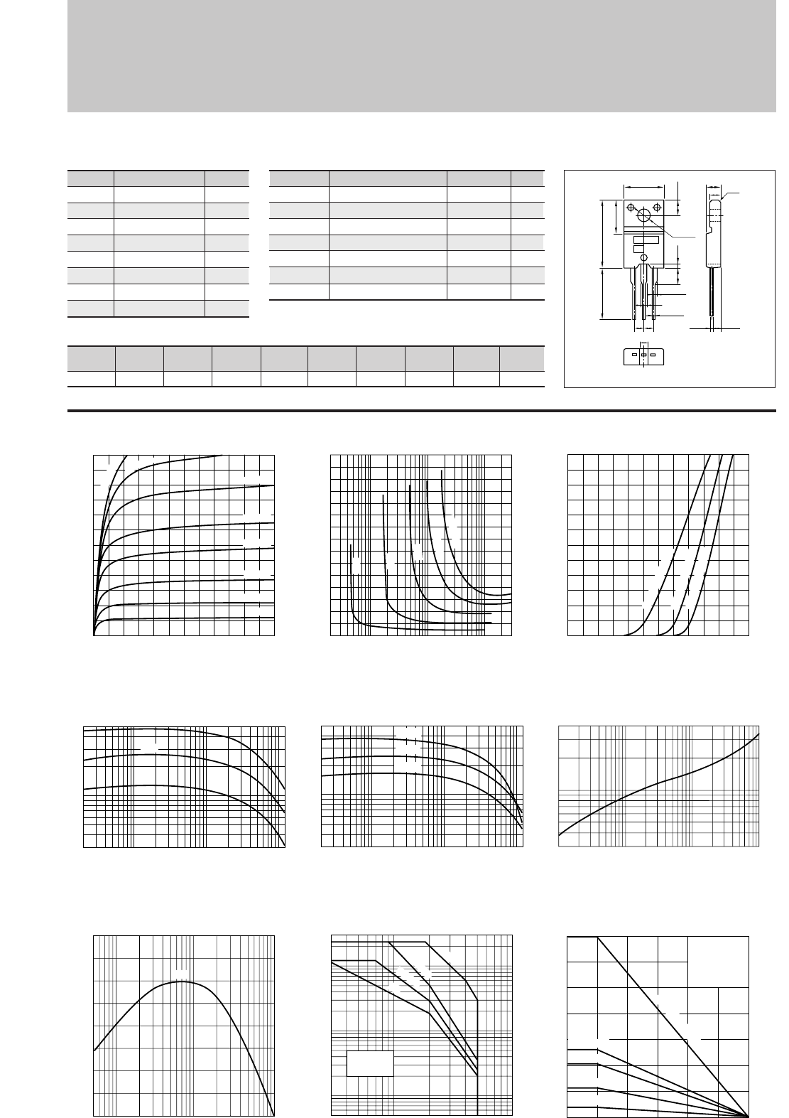
IC–VCE Characteristics
(Typical)
θj-a–t Characteristics
IC–VBE Temperature Characteristics
(Typical)
Safe Operating Area (Single Pulse)
0
0
–8
–4
–12
–6
–2
–10
–2–1 –3 –4 –5 –6
Collector-Emitter Voltage VCE(V)
Collector Current IC(A)
–40mA
–60mA
–100mA
–150mA
–20mA
–10mA
–5mA
I
B
=–200mA
hFE–IC
Temperature Characteristics (Typical)
–10 –50 –100–3 –5
–1
–0.5
–0.05
–0.1
–30
–10
–5
Collector-Emitter Voltage VCE(V)
Collector Current IC(A)
Without Heatsink
Natural Cooling
VCE(sat)–IB Characteristics
(Typical)
0
–1.5
–1.0
–0.5
–2
–100–10 –1000 –3000
Base Current IB(mA)
Collector-Emitter Saturation Voltage VCE(sat)(V)
–1A
hFE–IC Characteristics
(Typical)
–0.02 –0.1 –1 –10
30
50
100
500
Collector Current IC(A)
DC Current Gain hFE
(VCE=–1V)
Typ
1ms
10ms
100ms
DC
–3A
–6A
–9A
I
C
=–12A
0.3
0.5
4
1
1 10 100 1000
Time t(ms)
Transient Thermal Resistance θj-a(˚C/W)
0.05 0.1 1 12
0
20
30
40
50
Cut-off Frequency fT(MHZ)
(VCE=–12V)
Emitter Current IE(A)
Typ
fT–IE Characteristics
(Typical)
0
–12
–6
–8
–10
–4
–2
0 –1.2–0.4–0.2 –0.6 –0.8 –1.0
Base-Emittor Voltage VBE(V)
Collector Current IC(A)
(VCE=–1V)
125˚C (Case Temp)
25˚C (Case Temp)
–30˚C (Case Temp)
(VCE=–1V)
–0.02 –0.1 –1 –10
30
50
100
500
Collector Current IC(A)
DC Current Gain hFE
125˚C
25˚C
–30˚C
Pc–Ta Derating
35
30
20
10
2
00 25 50 75 100 125 150
Ambient Temperature Ta(˚C)
Maximum Power Dissipation PC(W)
With Infinite heatsink
Without Heatsink
50x50x2
100x100x2
150x150x2
Natural Cooling
Silicone Grease
Heatsink: Aluminum
in mm
Silicon PNP Epitaxial Planar Transistor (Complement to type 2SC4064)
Application : DC Motor Driver, Chopper Regulator and General Purpose
Symbol
VCBO
VCEO
VEBO
IC
IB
PC
Tj
Tstg
Ratings
–50
–50
–6
–12
–3
35(Tc=25°C)
150
–55 to +150
Unit
V
V
V
A
A
W
°C
°C
■
Absolute maximum ratings
■
Electrical Characteristics
■Typical Switching Characteristics (Common Emitter)
Symbol
ICBO
IEBO
V(BR)CEO
hFE
VCE(sat)
fT
COB
Ratings
–100max
–100max
–50min
50min
–0.35max
40typ
330typ
Unit
µ
A
µ
A
V
V
MHz
pF
Conditions
VCB=–50V
VEB=–6V
IC=–25mA
VCE=–1V, IC=–6A
IC=–6A, IB=–0.3A
VCE=–12V, IE=0.5A
VCB=–10V, f=1MHz
VCC
(V)
–24
RL
(Ω)
4
IC
(A)
–6
VBB2
(V)
5
IB2
(mA)
120
ton
(
µ
s)
0.4typ
tstg
(
µ
s)
0.4typ
tf
(
µ
s)
0.2typ
IB1
(mA)
–120
LOW VCE (sat)
2SA1567
(Ta=25°C) (Ta=25°C)
VBB1
(V)
–10
External Dimensions FM20 (TO220F)
ø3.3±0.2
10.1±0.2
4.0±0.2
16.9±0.3
13.0min
8.4±0.2
0.8±0.2
3.9
±0.2
2.542.54
1.35±0.15
0.85
+0.2
-0.1
1.35±0.15
2.2±0.2
4.2±0.2
2.8 c0.5
2.4±0.2
0.45
+0.2
-0.1
BEC
a
b
23
Weight : Approx 2.0g
a. Part No.
b. Lot No.
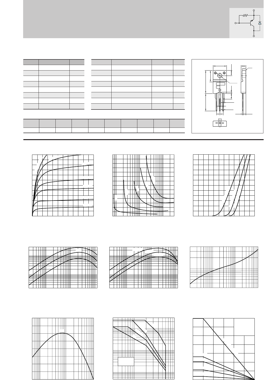
Ratings
–60
–60
–6
–12
–3
35(Tc=25°C)
150
–55 to +150
+
24
Silicon PNP Epitaxial Planar Transistor (Complement to type 2SC4065)
Application : DC Motor Driver, Chopper Regulator and General Purpose
Symbol
VCBO
VCEO
VEBO
IC
IB
PC
Tj
Tstg
Unit
V
V
V
A
A
W
°C
°C
■
Absolute maximum ratings
■
Electrical Characteristics
■Typical Switching Characteristics (Common Emitter)
Symbol
ICBO
IEBO
V(BR)CEO
hFE
VCE(sat)
VFEC
fT
COB
Ratings
–100max
–60max
–60min
50min
–0.35max
–2.5max
40typ
330typ
Unit
µ
A
mA
V
V
V
MHz
pF
Conditions
VCB=–60V
VEB=–6V
IC=–25mA
VCE=–1V, IC=–6A
IC=–6A, IB=–0.3A
IECO=–10A
VCE=–12V, IE=0.5A
VCB=–10V, f=1MHz
VCC
(V)
–24
RL
(Ω)
4
IC
(A)
–6
VBB2
(V)
5
IB2
(mA)
120
ton
(
µ
s)
0.4typ
tstg
(
µ
s)
0.4typ
tf
(
µ
s)
0.2typ
IB1
(mA)
–120
2SA1568
(Ta=25°C) (Ta=25°C)
IC–VCE Characteristics
(Typical)
θj-a–t Characteristics
IC–VBE Temperature Characteristics
(Typical)
Safe Operating Area (Single Pulse)
0
0
–8
–4
–12
–6
–2
–10
–2–1 –3 –4 –5 –6
Collector-Emitter Voltage VCE(V)
Collector Current IC(A)
–40mA
–60mA
–100mA
–150mA
–20mA
–10mA
I
B
=–200mA
hFE–IC
Temperature Characteristics (Typical)
–10 –50 –100–3 –5
–1
–0.5
–0.05
–0.1
–30
–10
–5
Collector-Emitter Voltage VCE(V)
Collector Current IC(A)
Without Heatsink
Natural Cooling
VCE(sat)–IB Characteristics
(Typical)
0
–1.4
–1.0
–0.5
–7
–100–10 –1000 –3000
Base Current IB(mA)
Collector-Emitter Saturation Voltage VCE(sat)(V)
–1A
hFE–IC Characteristics
(Typical)
–0.02 –0.1 –1 –10
2
10
300
100
Collector Current IC(A)
DC Current Gain hFE
(VCE=–1V)
Typ
–0.02 –0.1 –1 –10
2
10
300
100
Collector Current IC(A)
(VCE=–1V)
1ms
10ms
100ms
DC
–3A
–6A
–9A
I
C
=–12A
0.3
0.5
4
1
1 10 100 1000
Time t(ms)
Transient Thermal Resistance θj-a(˚C/W)
0.05 0.1 1 10
0
20
30
50
40
Cut-off Frequency fT(MHZ)
(VCE=–12V)
Emitter Current IE(A)
Typ
fT–IE Characteristics
(Typical)
Pc–Ta Derating
35
30
20
10
2
00 25 50 75 100 125 150
Ambient Temperature Ta(˚C)
Maximum Power Dissipation PC(W)
With Infinite heatsink
Without Heatsink
50x50x2
100x100x2
150x150x2
0
–12
–6
–8
–10
–4
–2
0 –1.2–0.4–0.2 –0.6 –0.8 –1.0
Base-Emittor Voltage VBE(V)
Collector Current IC(A)
(VCE=–1V)
125˚C (Case Temp)
25˚C (Case Temp)
–30˚C (Case Temp)
DC Current Gain hFE
125˚C 25˚C
–30˚C
Natural Cooling
Silicone Grease
Heatsink: Aluminum
in mm
VBB1
(V)
–10
External Dimensions FM20 (TO220F)
ø3.3±0.2
10.1±0.2
4.0±0.2
16.9±0.3
13.0min
8.4±0.2
0.8±0.2
3.9
±0.2
2.542.54
1.35±0.15
0.85
+0.2
-0.1
1.35±0.15
2.2±0.2
4.2±0.2
2.8 c0.5
2.4±0.2
0.45
+0.2
-0.1
BEC
a
b
Built-in Diode at C–E
Low VCE (sat)
B
C
E
(250Ω)
Equivalent
curcuit
Weight : Approx 2.0g
a. Part No.
b. Lot No.
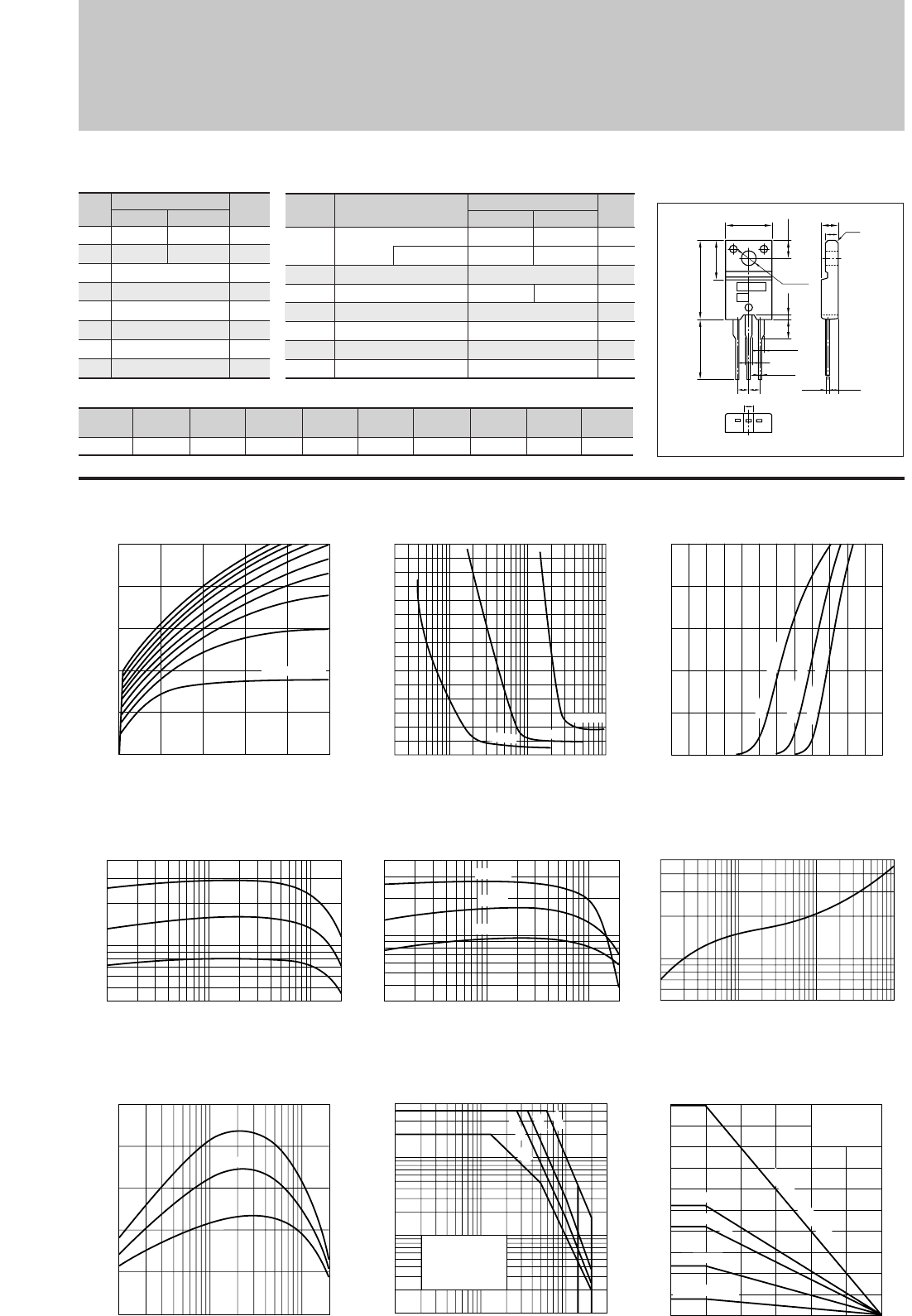
25
Silicon PNP Epitaxial Planar Transistor (Complement to type 2SC4381/4382)
■Typical Switching Characteristics (Common Emitter)
VCC
(V)
–20
RL
(Ω)
20
IC
(A)
–1
VBB2
(V)
5
IB2
(mA)
100
ton
(
µ
s)
0.4typ
tstg
(
µ
s)
1.5typ
tf
(
µ
s)
0.5typ
IB1
(mA)
–100
2SA1667/1668
IC–VCE Characteristics
(Typical)
θj-a–t Characteristics
IC–VBE Temperature Characteristics
(Typical)
Pc–Ta Derating
Safe Operating Area (Single Pulse)
0
0
–0.8
–0.4
–1.2
–2.0
–1.6
–4–2 –6 –8 –10
Collector-Emitter Voltage VCE(V)
Collector Current IC(A)
–50mA
I
B
=–5mA/Step
hFE–IC
Temperature Characteristics (Typical)
–10 –100 –300–1
–1
–0.01
–0.1
–5
Collector-Emitter Voltage VCE(V)
Collector Current IC(A)
VCE(sat)–IB Characteristics
(Typical)
0
–3
–2
–1
–2
–100–10 –1000
Base Current IB(mA)
Collector-Emitter Saturation Voltage VCE(sat)(V)
IC=–2A
–1A
–0.5A
hFE–IC Characteristics
(Typical)
–0.01 –0.1 –1 –2
40
100
400
Collector Current IC(A)
DC Current Gain hFE
(VCE=–10V)
Typ
–0.01 –0.1 –1 –2
30
100
400
Collector Current IC(A)
DC Current Gain hFE
(VCE=–10V)
5ms
1ms
20ms
DC
0.5
5
1
1 10 100 1000
Time t(ms)
Transient Thermal Resistance θj-a(˚C/W)
Without Heatsink
Natural Cooling
1.2SA1667
2.2SA1668
12
25
20
10
2
00 25 50 75 100 125 150
Ambient Temperature Ta(˚C)
Maximum Power Dissipation PC(W)
With Infinite heatsink
Without Heatsink
150x150x2
50x50x2
100x
100x2
0
–1.6
–2
–1.2
–0.8
–0.4
0 –1.2–0.4–0.2 –0.6 –0.8 –1.0
Base-Emittor Voltage VBE(V)
Collector Current IC(A)
(VCE=–10V)
125˚C (Case Temp)
25˚C (Case Temp)
–30˚C (Case Temp)
125˚C
25˚C
–30˚C
0.01 0.1 1 2
0
10
20
30
50
40
Cut-off Frequency fT(MHZ)
(VCE=–12V)
Emitter Current IE(A)
Typ
fT–IE Characteristics
(Typical)
Natural Cooling
Silicone Grease
Heatsink: Aluminum
in mm
VBB1
(V)
–10
External Dimensions FM20 (TO220F)
ø3.3±0.2
10.1±0.2
4.0±0.2
16.9±0.3
13.0min
8.4±0.2
0.8±0.2
3.9
±0.2
2.542.54
1.35±0.15
0.85
+0.2
-0.1
1.35±0.15
2.2±0.2
4.2±0.2
2.8 c0.5
2.4±0.2
0.45
+0.2
-0.1
BEC
a
b
Symbol
VCBO
VCEO
VEBO
IC
IB
PC
Tj
Tstg
–6
–2
–1
25(Tc=25°C)
150
–55 to +150
Unit
V
V
V
A
A
W
°C
°C
■
Absolute maximum ratings
■
Electrical Characteristics
Symbol
ICBO
IEBO
V(BR)CEO
hFE
VCE(sat)
fT
COB
2SA1667
–10max
–150
–150min
Unit
µ
A
V
µ
A
V
V
MHz
pF
Conditions
VCB=
VEB=–6V
IC=–25mA
VCE=–10V, IC=–0.7A
IC=–0.7A, IB=–0.07A
VCE=–12V, IE=0.2A
VCB=–10V, f=1MHz
(Ta=25°C)
(Ta=25°C)
2SA1668
–200
–200
2SA1667
–150
–150
2SA1668
–10max
–200
–200min
–10max
60min
–1.0max
20typ
60typ
Application : TV Vertical Output, Audio Output Driver and General Purpose
Weight : Approx 2.0g
a. Part No.
b. Lot No.
Ratings Ratings
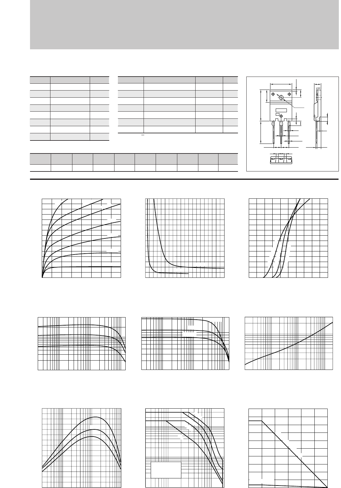
26
Silicon PNP Epitaxial Planar Transistor (Complement to type 2SC4388) Application : Audio and General Purpose
Symbol
VCBO
VCEO
VEBO
IC
IB
PC
Tj
Tstg
Ratings
–180
–180
–6
–15
–4
85(Tc=25°C)
150
–55 to +150
Unit
V
V
V
A
A
W
°C
°C
■
Absolute maximum ratings
■
Electrical Characteristics
■Typical Switching Characteristics (Common Emitter)
Symbol
ICBO
IEBO
V(BR)CEO
hFE
VCE(sat)
fT
COB
Ratings
–10max
–10max
–180min
50min∗
–2.0max
20typ
500typ
Unit
µ
A
µ
A
V
V
MHz
pF
Conditions
VCB=–180V
VEB=–6V
IC=–50mA
VCE=–4V, IC=–3A
IC=–5A, IB=–0.5A
VCE=–12V, IE=0.5A
VCB=–10V, f=1MHz
2SA1673
(Ta=25°C) (Ta=25°C)
IC–VCE Characteristics
(Typical)
hFE–IC Characteristics
(Typical)
Safe Operating Area (Single Pulse)
hFE–IC
Temperature Characteristics (Typical)
IC–VBE Temperature Characteristics
(Typical)
VCE(sat)–IB Characteristics
(Typical)
Pc–Ta Derating
0
0
–5
–10
–15
–1 –2 –3 –4
Collector-Emitter Voltage VCE(V)
Collector Current IC(A)
–1A
–50mA
–0.1A
I
B
=–20mA
–0.6A
–0.4A
–0.2A
0
– 3
–2
–1
0 –0.5 –1.0 –2.0–1.5
Base Current IB(A)
Collector-Emitter Saturation Voltage VCE(sat)(V)
IC=–10A
–5A
–0.02 –0.1 –1 –10–0.5 –5 –15
10
100
50
300
Collector Current IC(A)
DC Current Gain hFE
(VCE=–4V)
Typ
Collector-Emitter Voltage VCE(V)
Collector Current IC(A)
–3 –10 –100 –200
–0.2
–0.1
–1
–2
–0.5
–10
–40
–5
DC
10ms
3ms
100ms
Without Heatsink
Natural Cooling
0.02 0.1 1 10
0
10
20
30
Cut-off Frequency fT(MHZ)
(VCE=–12V)
Emitter Current IE(A)
Typ
0.1
1
3
0.5
1 10 100 1000 2000
Time t(ms)
Transient Thermal Resistance θj-a(˚C/W)
θj-a–t Characteristics
fT–IE Characteristics
(Typical)
100
80
60
40
20
3.5
0
Ambient Temperature Ta(˚C)
Maximum Power Dissipation PC(W)
With Infinite heatsink
Without Heatsink
0 25 50 75 100 125 150
(VCE=–4V)
–0.02 –0.1 –0.5 –1 –5 –10 –15
20
50
100
200
Collector Current IC(A)
DC Current Gain hFE
125˚C
25˚C
–30˚C
Collector Current IC(A)
0
–15
–10
–5
0–2–1
Base-Emittor Voltage VBE(V)
(VCE=–4V)
125˚C (Case Temp)
25˚C (Case Temp)
–30˚C (Case Temp)
VCC
(V)
–40
RL
(Ω)
4
IC
(A)
–10
VBB2
(V)
5
IB2
(A)
1
ton
(
µ
s)
0.6typ
tstg
(
µ
s)
0.9typ
tf
(
µ
s)
0.2typ
IB1
(A)
–1
VBB1
(V)
–10
External Dimensions FM100(TO3PF)
4.41.5 1.5
BEC
5.45±0.1
ø3.3±0.2
1.6
3.3
1.75
0.8±0.2
2.15
1.05
+0.2
-0.1
5.45±0.1
23.0±0.3
16.2
9.5±0.2
5.5
15.6±0.2 5.5±0.2
3.45
3.35
0.65
+0.2
-0.1
±0.2
3.0
0.8
a
b
Weight : Approx 6.5g
a. Part No.
b. Lot No.
∗hFE Rank O(50to100), P(70to140), Y(90to180)
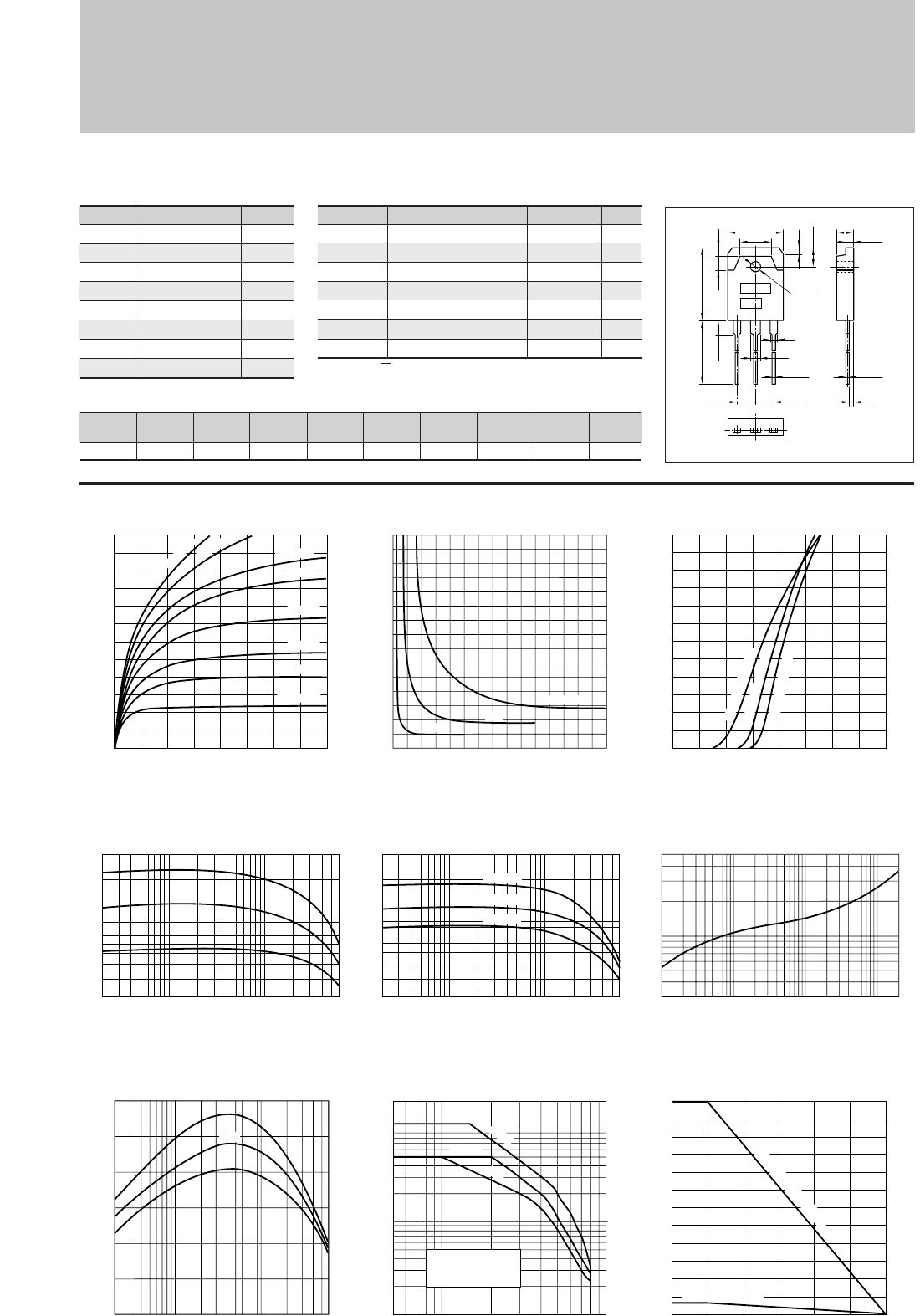
27
Silicon PNP Epitaxial Planar Transistor (Complement to type 2SC4466) Application : Audio and General Purpose
Symbol
VCBO
VCEO
VEBO
IC
IB
PC
Tj
Tstg
Ratings
–80
–80
–6
–6
–3
60(Tc=25°C)
150
–55 to +150
Unit
V
V
V
A
A
W
°C
°C
■
Absolute maximum ratings
■Typical Switching Characteristics (Common Emitter)
Symbol
ICBO
IEBO
V(BR)CEO
hFE
VCE(sat)
fT
COB
Ratings
–10max
–10max
–80min
50min∗
–1.5max
20typ
150typ
Unit
µ
A
µ
A
V
V
MHz
pF
Conditions
VCB=–80V
VEB=–6V
IC=–50mA
VCE=–4V, IC=–2A
IC=–2A, IB=–0.2A
VCE=–12V, IE=0.5A
VCB=–10V, f=1MHz
VCC
(V)
–30
RL
(Ω)
10
IC
(A)
–3
VBB2
(V)
5
IB2
(A)
0.3
ton
(
µ
s)
0.18typ
tstg
(
µ
s)
1.10typ
tf
(
µ
s)
0.21typ
IB1
(A)
–0.3
2SA1693
(Ta=25°C) (Ta=25°C)
IC–VCE Characteristics
(Typical)
hFE–IC Characteristics
(Typical)
Safe Operating Area (Single Pulse)
hFE–IC
Temperature Characteristics (Typical)
IC–VBE Temperature Characteristics
(Typical)
VCE(sat)–IB Characteristics
(Typical)
Pc–Ta Derating
0
0
–2
–4
–6
–1 –2 –3 –4
Collector-Emitter Voltage VCE(V)
Collector Current IC(A)
–200mA
–150mA
–100mA
–80mA
–50mA
–30mA
–20mA
I
B
=–10mA
0
–3
–2
–1
0 –0.5 –1.0 –1.5
Base Current IB(A)
Collector-Emitter Saturation Voltage VCE(sat)(V)
IC=–6A
–4A
–2A
–0.02 –0.1 –0.5 –1 –5–6
30
50
100
300
Collector Current IC(A)
DC Current Gain hFE
(VCE=–4V)
Typ
–5 –10 –100–50
–0.1
–1
–0.5
–10
–20
–5
Collector-Emitter Voltage VCE(V)
Collector Current IC(A)
DC
10ms
100ms
0.02 0.10.05 0.5 1 5 6
0
20
10
30
Cut-off Frequency fT(MHZ)
(VCE=–12V)
Emitter Current IE(A)
Typ
fT–IE Characteristics
(Typical)
60
40
20
3.5
00 25 50 75 100 125 150
Ambient Temperature Ta(˚C)
Maximum Power Dissipation PC(W)
With Infinite heatsink
Without Heatsink
0
–6
–4
–2
0–2–1
Base-Emittor Voltage VBE(V)
Collector Current IC(A)
(VCE=–4V)
125˚C (Case Temp)
25˚C (Case Temp)
–30˚C (Case Temp)
(VCE=–4V)
–0.02 –0.1 –0.5 –1 –5 –6
30
50
100
300
DC Current Gain hFE
125˚C
25˚C
–30˚C
Collector Current IC(A)
θj-a–t Characteristics
0.3
1
5
0.5
1 10 100 1000 2000
Time t(ms)
Transient Thermal Resistance θj-a(˚C/W)
Without Heatsink
Natural Cooling
VBB1
(V)
–10
External Dimensions MT-100(TO3P)
15.6±0.4
9.6
19.9±0.3
4.0 2.0
5.0±0.2
1.8
ø3.2±0.1
2
3
1.05
+0.2
-0.1
20.0min
4.0max
BE
5.45±0.1 5.45±0.1
C
4.8±0.2
0.65
+0.2
-0.1
1.4
2.0±0.1
a
b
Weight : Approx 6.0g
a. Part No.
b. Lot No.
∗hFE Rank O(50to100), P(70to140), Y(90to180)
■
Electrical Characteristics
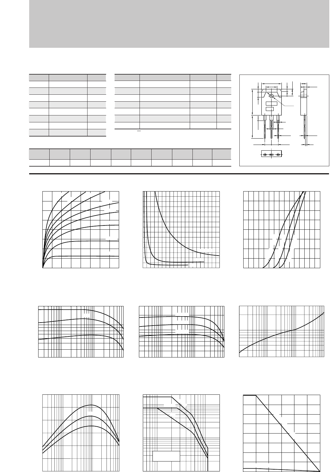
28
Silicon PNP Epitaxial Planar Transistor (Complement to type 2SC4467) Application : Audio and General Purpose
Symbol
VCBO
VCEO
VEBO
IC
IB
PC
Tj
Tstg
Ratings
–120
–120
–6
–8
–3
80(Tc=25°C)
150
–55 to +150
Unit
V
V
V
A
A
W
°C
°C
■
Absolute maximum ratings
■
Electrical Characteristics
■Typical Switching Characteristics (Common Emitter)
Symbol
ICBO
IEBO
V(BR)CEO
hFE
VCE(sat)
fT
COB
Ratings
–10max
–10max
–120min
50min∗
–1.5max
20typ
300typ
Unit
µ
A
µ
A
V
V
MHz
pF
Conditions
VCB=–120V
VEB=–6V
IC=–50mA
VCE=–4V, IC=–3A
IC=–3A, IB=–0.3A
VCE=–12V, IE=0.5A
VCB=–10V, f=1MHz
2SA1694
(Ta=25°C) (Ta=25°C)
VCC
(V)
–40
RL
(Ω)
10
IC
(A)
–4
VBB2
(V)
5
IB2
(A)
0.4
ton
(
µ
s)
0.14typ
tstg
(
µ
s)
1.40typ
tf
(
µ
s)
0.21typ
IB1
(A)
–0.4
VBB1
(V)
–10
IC–VCE Characteristics
(Typical)
hFE–IC Characteristics
(Typical)
Safe Operating Area (Single Pulse)
hFE–IC
Temperature Characteristics (Typical)
IC–VBE Temperature Characteristics
(Typical)
VCE(sat)–IB Characteristics
(Typical)
Pc–Ta Derating
0
0
–2
–4
–6
–8
–1 –2 –3 –4
Collector-Emitter Voltage VCE(V)
Collector Current IC(A)
–350mA
–200mA
–150mA
–25mA
–100mA
–75mA
–50mA
I
B
=–10mA
0
–3
–2
–1
0
–0.1 –0.2 –0.3 –0.4 –0.5 –0.6 –0.7 –0.8 –0.9 –1.0
Base Current IB(A)
Collector-Emitter Saturation Voltage VCE(sat)(V)
IC=–8A
–4A
–2A
–0.02 –0.1 –0.5 –1 –8–5
30
50
100
200
Collector Current IC(A)
DC Current Gain hFE
(VCE=–4V)
Typ
–10 –50–5 –100 –200
–0.1
–1
–0.5
–10
–20
–5
Collector-Emitter Voltage VCE(V)
Collector Current IC(A)
Without Heatsink
Natural Cooling
DC
100ms
10ms
0.02 0.10.05 0.5 1 5 8
0
20
10
30
Cut-off Frequency fT(MHZ)
(VCE=–12V)
Emitter Current IE(A)
Typ
0.3
1
3
0.5
1 10 100 1000
Time t(ms)
Transient Thermal Resistance θj-a(˚C/W)
θj-a–t Characteristics
fT–IE Characteristics
(Typical)
80
60
40
20
3.5
00 25 50 75 100 125 150
Ambient Temperature Ta(˚C)
Maximum Power Dissipation PC(W)
With Infinite heatsink
Without Heatsink
0
–8
–6
–2
–4
0 –1.5–1.0–0.5
Base-Emittor Voltage VBE(V)
Collector Current IC(A)
(VCE=–4V)
125˚C (Case Temp)
25˚C (Case Temp)
–30˚C (Case Temp)
(VCE=–4V)
–0.02 –0.1 –0.5 –1 –5 –8
30
50
100
300
DC Current Gain hFE
125˚C
25˚C
–30˚C
Collector Current IC(A)
External Dimensions MT-100(TO3P)
15.6±0.4
9.6
19.9±0.3
4.0 2.0
5.0±0.2
1.8
ø3.2±0.1
2
3
1.05
+0.2
-0.1
20.0min
4.0max
BE
5.45±0.1 5.45±0.1
C
4.8±0.2
0.65
+0.2
-0.1
1.4
2.0±0.1
a
b
Weight : Approx 6.0g
a. Part No.
b. Lot No.
∗hFE Rank O(50to100), P(70to140), Y(90to180)
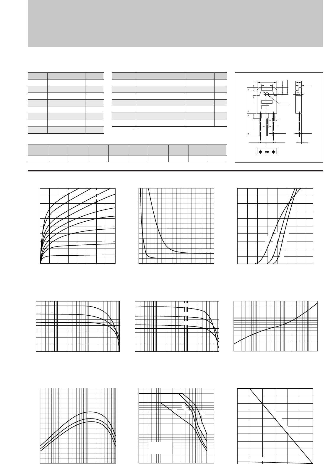
29
Silicon PNP Epitaxial Planar Transistor (Complement to type 2SC4468) Application : Audio and General Purpose
Symbol
VCBO
VCEO
VEBO
IC
IB
PC
Tj
Tstg
Ratings
–140
–140
–6
–10
–4
100(Tc=25°C)
150
–55 to +150
Unit
V
V
V
A
A
W
°C
°C
■
Absolute maximum ratings
■
Electrical Characteristics
Symbol
ICBO
IEBO
V(BR)CEO
hFE
VCE(sat)
fT
COB
Ratings
–10max
–10max
–140min
50min∗
–0.5max
20typ
400typ
Unit
µ
A
µ
A
V
V
MHz
pF
Conditions
VCB=–140V
VEB=–6V
IC=–50mA
VCE=–4V, IC=–3A
IC=–5A, IB=–0.5A
VCE=–12V, IE=0.5A
VCB=–10V, f=1MHz
2SA1695
(Ta=25°C) (Ta=25°C)
IC–VCE Characteristics
(Typical)
hFE–IC Characteristics
(Typical)
Safe Operating Area (Single Pulse)
hFE–IC
Temperature Characteristics (Typical)
IC–VBE Temperature Characteristics
(Typical)
VCE(sat)–IB Characteristics
(Typical)
Pc–Ta Derating
0
0
–2
–4
–6
–8
–10
–1 –2 –3 –4
Collector-Emitter Voltage VCE(V)
Collector Current IC(A)
–400mA
–25mA
I
B
=–10mA
–300mA
–200mA
–150mA
–100mA
–75mA
–50mA
0
–3
–2
–1
0 –2.0–0.5 –1.5–1.0
Base Current IB(A)
Collector-Emitter Saturation Voltage VCE(sat)(V)
IC=–10A
–5A
0
–10
–8
–2
–6
–4
0 –1.5–1
Base-Emittor Voltage VBE(V)
Collector Current IC(A)
(VCE=–4V)
125˚C (Case Temp)
25˚C (Case Temp)
–30˚C (Case Temp)
–0.02 –0.1 –1 –5–0.5 –10
30
50
100
200
Collector Current IC(A)
DC Current Gain hFE
(VCE=–4V)
Typ
–10–5–3 –100 –200–50
–0.1
–1
–0.5
–10
–30
–5
Collector-Emitter Voltage VCE(V)
Collector Current IC(A)
Without Heatsink
Natural Cooling
DC
100ms
3ms
10ms
0.02 0.1 1 10
0
10
30
20
Cut-off Frequency fT(MHZ)
(VCE=–12V)
Emitter Current IE(A)
Typ
fT–IE Characteristics
(Typical)
100
50
3.5
00 25 50 75 100 125 150
Ambient Temperature Ta(˚C)
Maximum Power Dissipation PC(W)
With Infinite heatsink
Without Heatsink
(VCE=–4V)
–0.02 –0.1 –0.5 –1 –5 –10
30
50
100
200
Collector Current IC(A)
DC Current Gain hFE
125˚C
25˚C
–30˚C
θj-a–t Characteristics
0.1
1
3
0.5
1 10 100 1000 2000
Time t(ms)
Transient Thermal Resistance θj-a(˚C/W)
External Dimensions MT-100(TO3P)
15.6±0.4
9.6
19.9±0.3
4.0 2.0
5.0±0.2
1.8
ø3.2±0.1
2
3
1.05
+0.2
-0.1
20.0min
4.0max
BE
5.45±0.1 5.45±0.1
C
4.8±0.2
0.65
+0.2
-0.1
1.4
2.0±0.1
a
b
Weight : Approx 6.0g
a. Part No.
b. Lot No.
■Typical Switching Characteristics (Common Emitter)
VCC
(V)
–60
RL
(Ω)
12
IC
(A)
–5
VBB2
(V)
5
IB2
(A)
0.5
ton
(
µ
s)
0.17typ
tstg
(
µ
s)
1.86typ
tf
(
µ
s)
0.27typ
IB1
(A)
–0.5
VBB1
(V)
–10
∗hFE Rank O(50to100), P(70to140), Y(90to180)
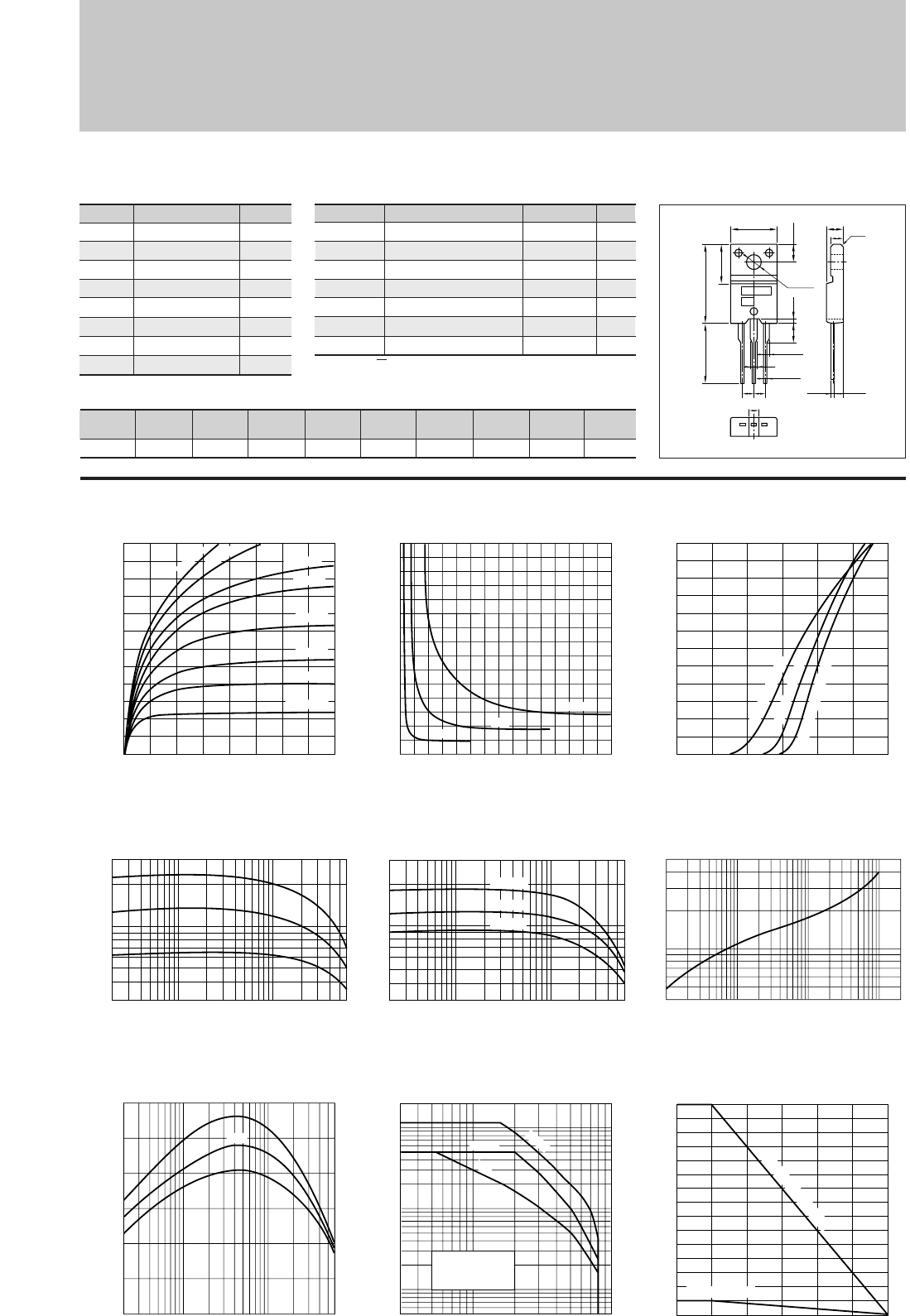
30
Silicon PNP Epitaxial Planar Transistor (Complement to type 2SC4511) Application : Audio and General Purpose
Symbol
VCBO
VCEO
VEBO
IC
IB
PC
Tj
Tstg
Ratings
–80
–80
–6
–6
–3
30(Tc=25°C)
150
–55 to +150
Unit
V
V
V
A
A
W
°C
°C
■
Absolute maximum ratings
■
Electrical Characteristics
■Typical Switching Characteristics (Common Emitter)
Symbol
ICBO
IEBO
V(BR)CEO
hFE
VCE(sat)
fT
COB
Ratings
–10max
–10max
–80min
50min∗
–0.5max
20typ
150typ
Unit
µ
A
µ
A
V
V
MHz
pF
Conditions
VCB=–80V
VEB=–6V
IC=–25mA
VCE=–4V, IC=–2A
IC=–2A, IB=–0.2A
VCE=–12V, IE=0.5A
VCB=–10V, f=1MHz
2SA1725
(Ta=25°C) (Ta=25°C)
IC–VCE Characteristics
(Typical)
hFE–IC Characteristics
(Typical)
Safe Operating Area (Single Pulse)
hFE–IC
Temperature Characteristics (Typical)
IC–VBE Temperature Characteristics
(Typical)
VCE(sat)–IB Characteristics
(Typical)
Pc–Ta Derating
0
0
–2
–1
–4
–3
–5
–6
–1 –2 –3 –4
Collector-Emitter Voltage VCE(V)
Collector Current IC(A)
–200mA
–150mA
–100mA
–80mA
–50mA
–30mA
–20mA
I
B
=–10mA
0
–3
–2
–1
0 –1.0–0.5 –1.5
Base Current IB(A)
Collector-Emitter Saturation Voltage VCE(sat)(V)
IC=–6A
–4A
–2A
–0.02 –0.1 –0.5 –1 –5–6
30
50
100
300
Collector Current IC(A)
DC Current Gain hFE
(VCE=–4V)
Typ
–3 –5 –10 –100–50
–0.05
–0.1
–1
–0.5
–10
–20
–5
Collector-Emitter Voltage VCE(V)
Collector Current IC(A)
Without Heatsink
Natural Cooling
DC
10ms
100ms
0.02 0.10.05 0.5 1 5 6
0
20
10
30
Cut-off Frequency fT(MHZ)
(VCE=–12V)
Emitter Current IE(A)
Typ
0.4
0.5
5
1
1 10 100 1000 2000
Time t(ms)
Transient Thermal Resistance θj-a(˚C/W)
θj-a–t Characteristics
fT–IE Characteristics
(Typical)
30
20
10
2
00 25 50 75 100 125 150
Ambient Temperature Ta(˚C)
Maximum Power Dissipation PC(W)
With Infinite heatsink
Without Heatsink
0
–6
–4
–2
0 –1.5–1
Base-Emittor Voltage VBE(V)
Collector Current IC(A)
(VCE=–4V)
125˚C (Case Temp)
25˚C (Case Temp)
–30˚C (Case Temp)
(VCE=–4V)
–0.02 –0.1 –0.5 –1 –5 –6
30
50
100
300
DC Current Gain hFE
125˚C
25˚C
–30˚C
Collector Current IC(A)
–0.5
VCC
(V)
–30
RL
(Ω)
10
IC
(A)
–3
VBB2
(V)
5
IB2
(A)
0.3
ton
(
µ
s)
0.18typ
tstg
(
µ
s)
1.10typ
tf
(
µ
s)
0.21typ
IB1
(A)
–0.3
VBB1
(V)
–10
External Dimensions FM20(TO220F)
ø3.3±0.2
10.1±0.2
4.0±0.2
16.9±0.3
13.0min
8.4±0.2
0.8±0.2
3.9
±0.2
2.542.54
1.35±0.15
0.85
+0.2
-0.1
1.35±0.15
2.2±0.2
4.2±0.2
2.8 c0.5
2.4±0.2
0.45
+0.2
-0.1
BEC
a
b
Weight : Approx 2.0g
a. Part No.
b. Lot No.
∗hFE Rank O(50to100), P(70to140), Y(90to180)
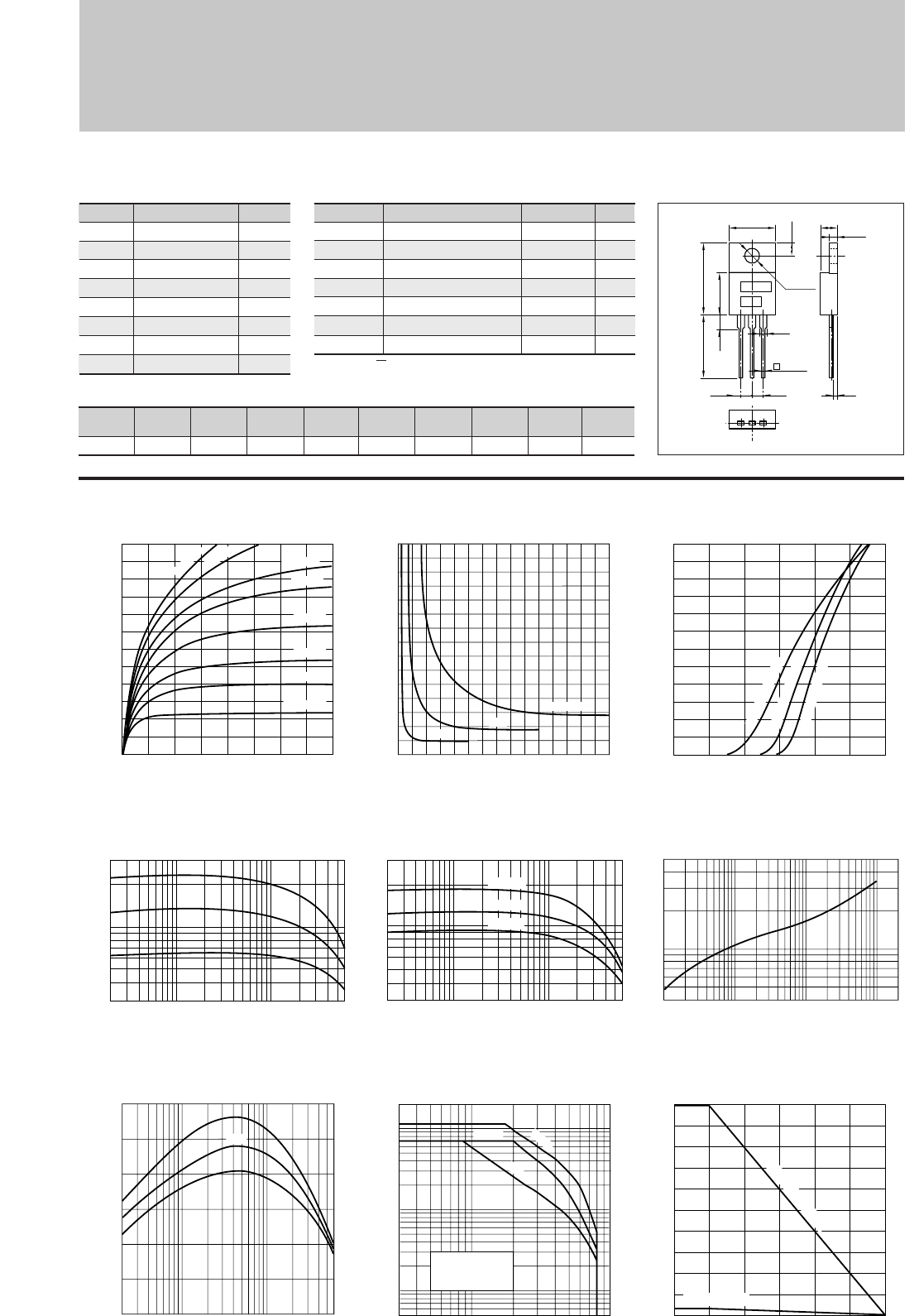
31
(Ta=25°C)
Silicon PNP Epitaxial Planar Transistor (Complement to type 2SC4512) Application : Audio and General Purpose
Symbol
VCBO
VCEO
VEBO
IC
IB
PC
Tj
Tstg
Ratings
–80
–80
–6
–6
–3
50(Tc=25°C)
150
–55 to +150
Unit
V
V
V
A
A
W
°C
°C
■
Absolute maximum ratings
■
Electrical Characteristics
Symbol
ICBO
IEBO
V(BR)CEO
hFE
VCE(sat)
fT
COB
Ratings
–10max
–10max
–80min
50min∗
–0.5max
20typ
150typ
Unit
µ
A
µ
A
V
V
MHz
pF
Conditions
VCB=–80V
VEB=–6V
IC=–25mA
VCE=–4V, IC=–2A
IC=–2A, IB=–0.2A
VCE=–12V, IE=0.5A
VCB=–10V, f=1MHz
2SA1726
(Ta=25°C)
IC–VCE Characteristics
(Typical)
hFE–IC Characteristics
(Typical)
Safe Operating Area (Single Pulse)
hFE–IC
Temperature Characteristics (Typical)
IC–VBE Temperature Characteristics
(Typical)
VCE(sat)–IB Characteristics
(Typical)
Pc–Ta Derating
0
0
–2
–4
–6
–1 –2 –3 –4
Collector-Emitter Voltage VCE(V)
Collector Current IC(A)
–200mA
–150mA
–100mA
–80mA
–50mA
–30mA
–20mA
I
B
=–10mA
0
–3
–2
–1
0 –0.5 –1.0 –1.5
Base Current IB(A)
Collector-Emitter Saturation Voltage VCE(sat)(V)
IC=–6A
–4A
–2A
–0.02 –0.1 –0.5 –1 –5–6
30
50
100
300
Collector Current IC(A)
DC Current Gain hFE
(VCE=–4V)
Typ
–10–3 –5 –100–50
–0.1
–0.05
–1
–0.5
–10
–20
–5
Collector-Emitter Voltage VCE(V)
Collector Current IC(A)
Without Heatsink
Natural Cooling
DC
10ms
100ms
0.02 0.10.05 0.5 1 5 6
0
20
10
30
Cut-off Frequency fT(MHZ)
(VCE=–12V)
Emitter Current IE(A)
Typ
fT–IE Characteristics
(Typical)
50
40
30
20
10
2
00 25 50 75 100 125 150
Ambient Temperature Ta(˚C)
Maximum Power Dissipation PC(W)
With Infinite heatsink
Without Heatsink
0
–6
–4
–2
0 –1.5–1
Base-Emittor Voltage VBE(V)
Collector Current IC(A)
(VCE=–4V)
125˚C (Case Temp)
25˚C (Case Temp)
–30˚C (Case Temp)
(VCE=–4V)
–0.02 –0.1 –0.5 –1 –5 –6
30
50
100
300
DC Current Gain hFE
125˚C
25˚C
–30˚C
Collector Current IC(A)
θj-a–t Characteristics
0.4
1
5
0.5
1 10 100 1000 2000
Time t(ms)
Transient Thermal Resistance θj-a(˚C/W)
–0.5
External Dimensions MT-25(TO220)
BE
2.5 2.5
C
16.0±0.7
12.0min
4.0max 8.8±0.2
1.35
0.65
+0.2
-0.1
10.2±0.2
ø3.75±0.2
3.0±0.2
4.8±0.2
1.4
2.0±0.1
a
b
■Typical Switching Characteristics (Common Emitter)
VCC
(V)
–30
RL
(Ω)
10
IC
(A)
–3
VBB2
(V)
5
IB2
(A)
0.3
ton
(
µ
s)
0.18typ
tstg
(
µ
s)
1.10typ
tf
(
µ
s)
0.21typ
IB1
(A)
–0.3
VBB1
(V)
–10
Weight : Approx 2.6g
a. Part No.
b. Lot No.
∗hFE Rank O(50to100), P(70to140), Y(90to180)
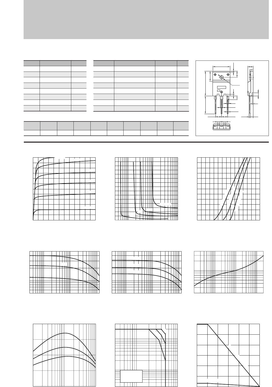
32
Silicon PNP Epitaxial Planar Transistor Application : Chopper Regulator, Switch and General Purpose
Symbol
VCBO
VCEO
VEBO
IC
IB
PC
Tj
Tstg
Ratings
–70
–50
–6
–12(Pulse–20)
–4
60(Tc=25°C)
150
–55 to +150
Unit
V
V
V
A
A
W
°C
°C
■
Absolute maximum ratings
■
Electrical Characteristics
■Typical Switching Characteristics (Common Emitter)
Symbol
ICBO
IEBO
V(BR)CEO
hFE
VCE(sat)
VBE(sat)
fT
COB
Ratings
–10max
–10max
–50min
50min
–0.5max
–1.2max
25typ
400typ
Unit
µ
A
µ
A
V
V
V
MHz
pF
Conditions
VCB=–70V
VEB=–6V
IC=–25mA
VCE=–1V, IC=–5A
IC=–5A, IB=–80mA
IC=–5A, IB=–80mA
VCE=–12V, IE=1A
VCB=–10V, f=1MHz
LOW VCE (sat)
2SA1746
(Ta=25°C) (Ta=25°C)
IC–VCE Characteristics
(Typical)
hFE–IC Characteristics
(Typical)
hFE–IC
Temperature Characteristics (Typical)
θj-a–t Characteristics
IC–VBE Temperature Characteristics
(Typical)
VCE(sat)–IB Characteristics
(Typical)
Pc–Ta Derating
0
0
–4
–8
–12
–2
–6
–10
–2–1 –6–5–4–3
Collector-Emitter Voltage VCE(V)
Collector Current IC(A)
–12mA
–100mA
–50mA
–70mA
–30mA
I
B
=–10mA
Safe Operating Area (Single Pulse)
0
–1.5
–1.0
–0.5
–3
–10 –1000–100
Base Current IB(mA)
Collector-Emitter Saturation Voltage VCE(sat)(V)
–1A
–3A –5A
IC=–10A
–10 –50–3 –100
–0.3
–1
–10
–30
–5
Collector-Emitter Voltage VCE(V)
Collector Current IC(A)
100µs
10ms
1ms
60
40
20
3.5
005025 75 100 125 150
Ambient Temperature Ta(˚C)
Maximum Power Dissipation PC(W)
With Infinite heatsink
Without Heatsink
0
–12
–10
–2
–4
–6
–8
0 –1.5–0.5 –1.0
Base-Emittor Voltage VBE(V)
Collector Current IC(A)
(VCE=–1V)
125˚C (CaseTemp)
25˚C (CaseTemp)
–30˚C (CaseTemp)
–0.03 –0.1 –1–0.5 –10
50
100
500
Collector Current IC(A)
DC Current Gain hFE
(VCE=–1V)
Typ
–5 –0.03 –0.1 –1–0.5 –10
50
100
500
–5
(VCE=–1V)
Collector Current IC(A)
DC Current Gain hFE
125˚C
25˚C
–30˚C
0.2
0.5
4
1
1 10 100 1000
Time t(ms)
Transient Thermal Resistance θj-a(˚C/W)
Without Heatsink
Natural Cooling
0.1 1 10
0
10
20
30
40
Cut-off Frequency fT(MHZ)
(VCE=–12V)
Emitter Current IE(A)
Typ
fT–IE Characteristics
(Typical)
VCC
(V)
–20
RL
(Ω)
4
IC
(A)
–5
VBB2
(V)
5
IB2
(mA)
80
ton
(
µ
s)
0.5typ
tstg
(
µ
s)
0.6typ
tf
(
µ
s)
0.3typ
IB1
(mA)
–80
VBB1
(V)
–10
External Dimensions FM100(TO3PF)
4.41.5 1.5
BEC
5.45±0.1
ø3.3±0.2
1.6
3.3
1.75
0.8±0.2
2.15
1.05
+0.2
-0.1
5.45±0.1
23.0±0.3
16.2
9.5±0.2
5.5
15.6±0.2 5.5±0.2
3.45
3.35
0.65
+0.2
-0.1
±0.2
3.0
0.8
a
b
Weight : Approx 6.5g
a. Part No.
b. Lot No.
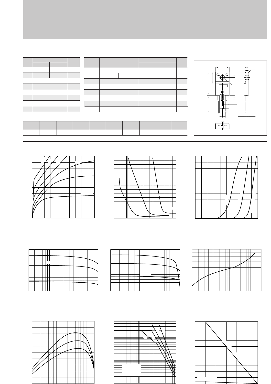
33
Silicon PNP Epitaxial Planar Transistor (Complement to type 2SC4883/A)
Application : Audio Output Driver and TV Velocity-modulation
2SA1859/1859A
IC–VCE Characteristics
(Typical)
hFE–IC Characteristics
(Typical)
Safe Operating Area (Single Pulse)
hFE–IC
Temperature Characteristics (Typical)
IC–VBE Temperature Characteristics
(Typical)
VCE(sat)–IB Characteristics
(Typical)
Pc–Ta Derating
0
0
–1
–2
–2 –4 –6 –10–8
Collector-Emitter Voltage VCE(V)
Collector Current IC(A)
–100mA
I
B
=–5mA
–60mA
–30mA
–15mA
–10mA
0
–3
–2
–1
–2 –5 –10 –50 –100 –500 –1000
Base Current IB(mA)
Collector-Emitter Saturation Voltage VCE(sat)(V)
–0.5A –1A
IC=–2A
–0.01 –0.1 –0.5 –1 –2
50
100
300
Collector Current IC(A)
DC Current Gain hFE
(VCE=–4V)
Typ
–10 –50–5 –100 –200
–0.01
–0.1
–0.5
–1
–1
–5
–0.5
Collector-Emitter Voltage VCE(V)
Collector Current IC(A)
Without Heatsink
Natural Cooling
1.2SA1859
2.2SA1859A
DC
100ms
10ms
1ms
12
0.01 0.10.05 0.5 1 2
0
20
60
40
80
100
Cut-off Frequency fT(MHZ)
(VCE=–12V)
Emitter Current IE(A)
Typ
7
1
5
1 10 100 1000 2000
Time t(ms)
Transient Thermal Resistance θj-a(˚C/W)
θj-a–t Characteristics
fT–IE Characteristics
(Typical)
20
10
2
00 25 50 75 100 125 150
Ambient Temperature Ta(˚C)
Maximum Power Dissipation PC(W)
With Infinite heatsink
Without Heatsink
0
–2
–1
0–1–0.5
Base-Emittor Voltage VBE(V)
Collector Current IC(A)
(VCE=–4V)
125˚C (CaseTemp)
25˚C (CaseTemp)
–30˚C (CaseTemp)
(VCE=–4V)
–0.01 –0.1 –0.5 –1 –2
50
100
300
DC Current Gain hFE
125˚C
25˚C
–30˚C
Collector Current IC(A)
Symbol
VCBO
VCEO
VEBO
IC
IB
PC
Tj
Tstg
–6
–2
–1
20(Tc=25°C)
150
–55 to +150
Unit
V
V
V
A
A
W
°C
°C
■
Absolute maximum ratings
■
Electrical Characteristics
Symbol
ICBO
IEBO
V(BR)CEO
hFE
VCE(sat)
fT
COB
2SA1859
–150
–150min
Unit
µ
A
V
µ
A
V
V
MHz
pF
Conditions
VCB=
VEB=–6V
IC=–10mA
VCE=–10V, IC=–0.7A
IC=–0.7A, IB=–70mA
VCE=–12V, IE=0.7A
VCB=–10V, f=1MHz
(Ta=25°C)
(Ta=25°C)
2SA1859A
–180
–180
2SA1859
–150
–150
2SA1859A
–180
–180min
–10max
60 to 240
–1.0max
60typ
30typ
External Dimensions FM20(TO220F)
ø3.3±0.2
10.1±0.2
4.0±0.2
16.9±0.3
13.0min
8.4±0.2
0.8±0.2
3.9
±0.2
2.542.54
1.35±0.15
0.85
+0.2
-0.1
1.35±0.15
2.2±0.2
4.2±0.2
2.8 c0.5
2.4±0.2
0.45
+0.2
-0.1
BEC
a
b
Weight : Approx 6.5g
a. Part No.
b. Lot No.
■Typical Switching Characteristics (Common Emitter)
VCC
(V)
–20
RL
(Ω)
20
IC
(A)
–1
VBB2
(V)
5
IB2
(mA)
100
ton
(
µ
s)
0.5typ
tstg
(
µ
s)
1.0typ
tf
(
µ
s)
0.5typ
IB1
(mA)
–100
VBB1
(V)
–10
–10max
Ratings Ratings
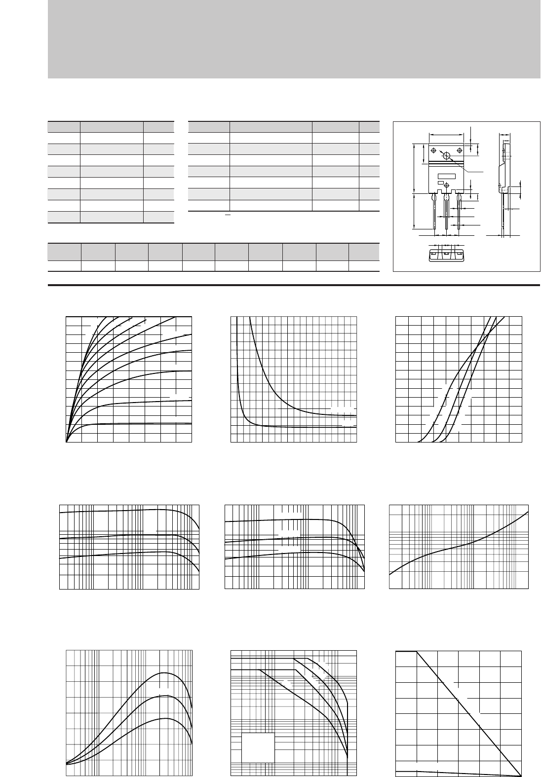
34
Silicon PNP Epitaxial Planar Transistor (Complement to type 2SC4886) Application : Audio and General Purpose
Symbol
VCBO
VCEO
VEBO
IC
IB
PC
Tj
Tstg
Ratings
–150
–150
–5
–14
–3
80(Tc=25°C)
150
–55 to +150
Unit
V
V
V
A
A
W
°C
°C
■
Absolute maximum ratings
■
Electrical Characteristics
■Typical Switching Characteristics (Common Emitter)
Symbol
ICBO
IEBO
V(BR)CEO
hFE
VCE(sat)
fT
COB
Ratings
–100max
–100max
–150min
50min∗
–2.0max
50typ
400typ
Unit
µ
A
µ
A
V
V
MHz
pF
Conditions
VCB=–150V
VEB=–5V
IC=–25mA
VCE=–4V, IC=–5A
IC=–5A, IB=–500mA
VCE=–12V, IE=2A
VCB=–10V, f=1MHz
VCC
(V)
–60
RL
(Ω)
12
IC
(A)
–5
VBB2
(V)
5
IB2
(mA)
500
ton
(
µ
s)
0.25typ
tstg
(
µ
s)
0.85typ
tf
(
µ
s)
0.2typ
IB1
(mA)
–500
LAPT 2SA1860
(Ta=25°C) (Ta=25°C)
IC–VCE Characteristics
(Typical)
hFE–IC Characteristics
(Typical)
Safe Operating Area (Single Pulse)
hFE–IC
Temperature Characteristics (Typical)
IC–VBE Temperature Characteristics
(Typical)
VCE(sat)–IB Characteristics
(Typical)
Pc–Ta Derating
0
0
–5
–10
–14
–1 –2 –3 –4
Collector-Emitter Voltage VCE(V)
Collector Current IC(A)
–50mA
–100mA
I
B
=–20mA
–700mA
–600mA
–500mA
–400mA
–300mA
–200mA
–150mA
0
–3
–2
–1
0 –0.2 –0.4 –0.6 –0.8 –1.0
Base Current IB(A)
Collector-Emitter Saturation Voltage VCE(sat)(V)
IC=–10A
–5A
–0.02 –0.1 –0.5 –5–1 –10–14
20
50
100
200
Collector Current IC(A)
DC Current Gain hFE
(VCE=–4V)
Typ
–10 –50–5–2 –100 –200
–0.05
–1
–0.5
–0.1
–10
–40
–5
Collector-Emitter Voltage VCE(V)
Collector Current IC(A)
Without Heatsink
Natural Cooling
DC
100ms
10ms
1ms
0.02 0.1 1 10
0
20
40
60
80
Cut-off Frequency fT(MHZ)
(VCE=–12V)
Emitter Current IE(A)
Typ
θj-a–t Characteristics
fT–IE Characteristics
(Typical)
0
–14
–10
–5
0–2–1
Base-Emittor Voltage VBE(V)
Collector Current IC(A)
(VCE=–4V)
125˚C (Case Temp)
25˚C (Case Temp)
–30˚C (Case Temp)
(VCE=–4V)
–0.02 –0.1 –0.5 –1 –5 –10 –14
30
50
100
200
Collector Current IC(A)
DC Current Gain hFE
125˚C
25˚C
–30˚C
0.1
1
3
0.5
1 10 100 1000 2000
Time t(ms)
Transient Thermal Resistance θj-a(˚C/W)
80
60
40
20
3.5
00 25 50 75 100 125 150
Ambient Temperature Ta(˚C)
Maximum Power Dissipation PC(W)
With Infinite heatsink
Without Heatsink
VBB1
(V)
–10
External Dimensions FM100(TO3PF)
4.41.5 1.5
BEC
5.45±0.1
ø3.3±0.2
1.6
3.3
1.75
0.8±0.2
2.15
1.05
+0.2
-0.1
5.45±0.1
23.0±0.3
16.2
9.5±0.2
5.5
15.6±0.2 5.5±0.2
3.45
3.35
0.65
+0.2
-0.1
±0.2
3.0
0.8
a
b
Weight : Approx 6.5g
a. Part No.
b. Lot No.
∗hFE Rank O(50to100), P(70to140), Y(90to180)
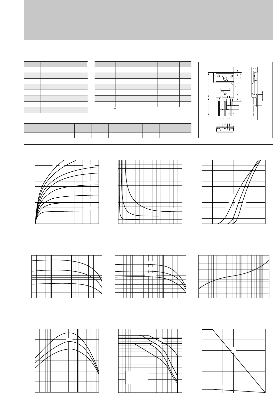
35
Silicon PNP Epitaxial Planar Transistor (Complement to type 2SC5099) Application : Audio and General Purpose
Symbol
VCBO
VCEO
VEBO
IC
IB
PC
Tj
Tstg
Ratings
–80
–80
–6
–6
–3
60(Tc=25°C)
150
–55 to +150
Unit
V
V
V
A
A
W
°C
°C
■
Absolute maximum ratings
■
Electrical Characteristics
■Typical Switching Characteristics (Common Emitter)
Symbol
ICBO
IEBO
V(BR)CEO
hFE
VCE(sat)
fT
COB
Ratings
–10max
–10max
–80min
50min∗
–0.5max
20typ
150typ
Unit
µ
A
µ
A
V
V
MHz
pF
Conditions
VCB=–80V
VEB=–6V
IC=–50mA
VCE=–4V, IC=–2A
IC=–12A, IB=–0.2A
VCE=–12V, IE=0.5A
VCB=–10V, f=1MHz
2SA1907
(Ta=25°C) (Ta=25°C)
IC–VCE Characteristics
(Typical)
hFE–IC Characteristics
(Typical)
Safe Operating Area (Single Pulse)
hFE–IC
Temperature Characteristics (Typical)
IC–VBE Temperature Characteristics
(Typical)
VCE(sat)–IB Characteristics
(Typical)
0
0
–2
–1
–4
–3
–5
–6
–1 –2 –3 –4
Collector-Emitter Voltage VCE(V)
Collector Current IC(A)
–200mA
–150mA
–100mA
–80mA
–50mA
–30mA
–20mA
I
B
=–10mA
0
–3
–2
–1
0 –0.5 –1.0 –1.5
Base Current IB(A)
Collector-Emitter Saturation Voltage VCE(sat)(V)
IC=–6A
–4A
–2A
–0.02 –0.1 –0.5 –1 –5–6
30
50
100
300
Collector Current IC(A)
DC Current Gain hFE
(VCE=–4V)
Typ
–5 –10 –50 –100
–0.1
–1
–0.5
–10
–20
–5
Collector-Emitter Voltage VCE(V)
Collector Current IC(A)
Without Heatsink
Natural Cooling
DC
100ms
10ms
1ms
0.02 0.10.05 0.5 1 5 6
0
20
10
30
Cut-off Frequency fT(MHZ)
(VCE=–12V)
Emitter Current IE(A)
Typ
fT–IE Characteristics
(Typical)
0
–6
–4
–2
0 –1.5–1
Base-Emittor Voltage VBE(V)
Collector Current IC(A)
(VCE=–4V)
125˚C (Case Temp)
25˚C (Case Temp)
–30˚C (Case Temp)
(VCE=–4V)
–0.02 –0.1 –0.5 –1 –5 –6
30
50
100
300
DC Current Gain hFE
125˚C
25˚C
–30˚C
Collector Current IC(A)
θj-a–t Characteristics
0.3
1
5
0.5
1 10 100 1000 2000
Time t(ms)
Transient Thermal Resistance θj-a(˚C/W)
Pc–Ta Derating
60
40
20
3.5
005025 75 100 125 150
Ambient Temperature Ta(˚C)
Maximum Power Dissipation PC(W)
With Infinite heatsink
Without Heatsink
VCC
(V)
–30
RL
(Ω)
10
IC
(A)
–3
VBB2
(V)
5
IB2
(A)
0.3
ton
(
µ
s)
0.18typ
tstg
(
µ
s)
1.10typ
tf
(
µ
s)
0.21typ
IB1
(A)
–0.3
VBB1
(V)
–10
External Dimensions FM100(TO3PF)
4.41.5 1.5
BEC
5.45±0.1
ø3.3±0.2
1.6
3.3
1.75
0.8±0.2
2.15
1.05
+0.2
-0.1
5.45±0.1
23.0±0.3
16.2
9.5±0.2
5.5
15.6±0.2 5.5±0.2
3.45
3.35
0.65
+0.2
-0.1
±0.2
3.0
0.8
a
b
Weight : Approx 6.5g
a. Part No.
b. Lot No.
∗hFE Rank O(50to100), P(70to140), Y(90to180)
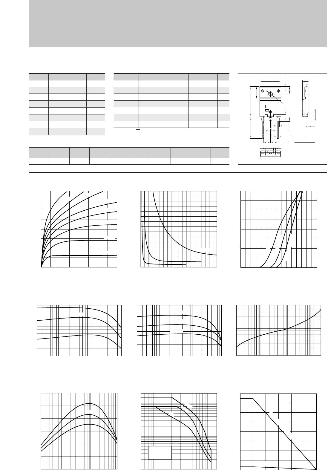
36
Silicon PNP Epitaxial Planar Transistor (Complement to type 2SC5100) Application : Audio and General Purpose
Symbol
VCBO
VCEO
VEBO
IC
IB
PC
Tj
Tstg
Ratings
–120
–120
–6
–8
–3
75(Tc=25°C)
150
–55 to +150
Unit
V
V
V
A
A
W
°C
°C
■
Absolute maximum ratings
■
Electrical Characteristics
■Typical Switching Characteristics (Common Emitter)
Symbol
ICBO
IEBO
V(BR)CEO
hFE
VCE(sat)
fT
COB
Ratings
–10max
–10max
–120min
50min∗
–0.5max
20typ
300typ
Unit
µ
A
µ
A
V
V
MHz
pF
Conditions
VCB=–120V
VEB=–6V
IC=–50mA
VCE=–4V, IC=–3A
IC=–3A, IB=–0.3A
VCE=–12V, IE=0.5A
VCB=–10V, f=1MHz
VCC
(V)
–40
RL
(Ω)
10
IC
(A)
–4
VBB2
(V)
5
IB2
(A)
0.4
ton
(
µ
s)
0.14typ
tstg
(
µ
s)
1.40typ
tf
(
µ
s)
0.21typ
IB1
(A)
–0.4
2SA1908
(Ta=25°C) (Ta=25°C)
IC–VCE Characteristics
(Typical)
hFE–IC Characteristics
(Typical)
Safe Operating Area (Single Pulse)
hFE–IC
Temperature Characteristics (Typical)
IC–VBE Temperature Characteristics
(Typical)
VCE(sat)–IB Characteristics
(Typical)
Pc–Ta Derating
0
0
–2
–4
–6
–8
–1 –2 –3 –4
Collector-Emitter Voltage VCE(V)
Collector Current IC(A)
–350mA
–200mA
–150mA
–25mA
–100mA
–75mA
–50mA
I
B
=–10mA
0
–3
–2
–1
0 –0.2 –0.4 –0.6 –0.8 –1.0
Base Current IB(A)
Collector-Emitter Saturation Voltage VCE(sat)(V)
IC=–8A
–4A
–2A 0
–8
–6
–2
–4
0 –1.5–1.0–0.5
Base-Emittor Voltage VBE(V)
Collector Current IC(A)
(VCE=–4V)
125˚C (Case Temp)
25˚C (Case Temp)
–30˚C (Case Temp)
–0.02 –0.1 –0.5 –1 –8–5
30
50
100
200
Collector Current IC(A)
DC Current Gain hFE
(VCE=–4V)
Typ
DC
Without Heatsink
Natural Cooling
100ms
10ms
–10–5 –50 –100 –150
–0.1
–1
–0.5
–10
–20
–5
Collector-Emitter Voltage VCE(V)
Collector Current IC(A)
0.02 0.10.05 0.5 1 5 8
0
20
10
30
Cut-off Frequency fT(MHZ)
(VCE=–12V)
Emitter Current IE(A)
Typ
0.2
0.5
4
1
1 10 100 1000 2000
Time t(ms)
Transient Thermal Resistance θj-a(˚C/W)
θj-a–t Characteristics
fT–IE Characteristics
(Typical)
80
60
40
20
3.5
005025 75 125100 150
Ambient Temperature Ta(˚C)
Maximum Power Dissipation PC(W)
With Infinite heatsink
Without Heatsink
(VCE=–4V)
–0.02 –0.1 –0.5 –1 –5 –8
30
50
100
300
Collector Current IC(A)
DC Current Gain hFE
125˚C
25˚C
–30˚C
VBB1
(V)
–10
External Dimensions FM100(TO3PF)
4.41.5 1.5
BEC
5.45±0.1
ø3.3±0.2
1.6
3.3
1.75
0.8±0.2
2.15
1.05
+0.2
-0.1
5.45±0.1
23.0±0.3
16.2
9.5±0.2
5.5
15.6±0.2 5.5±0.2
3.45
3.35
0.65
+0.2
-0.1
±0.2
3.0
0.8
a
b
Weight : Approx 6.5g
a. Part No.
b. Lot No.
∗hFE Rank O(50to100), P(70to140), Y(90to180)
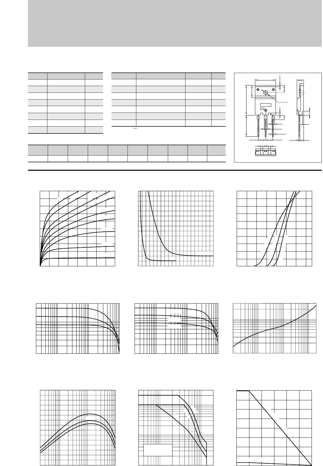
37
Silicon PNP Epitaxial Planar Transistor (Complement to type 2SC5101) Application : Audio and General Purpose
Symbol
VCBO
VCEO
VEBO
IC
IB
PC
Tj
Tstg
Ratings
–140
–140
–6
–10
–4
80(Tc=25°C)
150
–55 to +150
Unit
V
V
V
A
A
W
°C
°C
■
Absolute maximum ratings
■
Electrical Characteristics
Symbol
ICBO
IEBO
V(BR)CEO
hFE
VCE(sat)
fT
COB
Ratings
–10max
–10max
–140min
50min∗
–0.5max
20typ
400typ
Unit
µ
A
µ
A
V
V
MHz
pF
Conditions
VCB=–140V
VEB=–6V
IC=–50mA
VCE=–4V, IC=–3A
IC=–5A, IB=–0.5A
VCE=–12V, IE=0.5A
VCB=–10V, f=1MHz
2SA1909
(Ta=25°C) (Ta=25°C)
IC–VCE Characteristics
(Typical)
hFE–IC Characteristics
(Typical)
Safe Operating Area (Single Pulse)
hFE–IC
Temperature Characteristics (Typical)
IC–VBE Temperature Characteristics
(Typical)
VCE(sat)–IB Characteristics
(Typical)
Pc–Ta Derating
0
0
–2
–4
–6
–8
–10
–1 –2 –3 –4
Collector-Emitter Voltage VCE(V)
Collector Current IC(A)
–400mA
–25mA
I
B
=–10mA
–300mA
–200mA
–150mA
–100mA
–75mA
–50mA
0
–3
–2
–1
0 –2.0–0.5 –1.5–1.0
Base Current IB(A)
Collector-Emitter Saturation Voltage VCE(sat)(V)
IC=–10A
–5A
0
–10
–8
–2
–6
–4
0 –1.5–1
Base-Emittor Voltage VBE(V)
Collector Current IC(A)
(VCE=–4V)
125˚C (Case Temp)
25˚C (Case Temp)
–30˚C (Case Temp)
–10 –50–3 –5 –100 –200
–0.1
–1
–0.5
–10
–30
–5
Collector-Emitter Voltage VCE(V)
Collector Current IC(A)
Without Heatsink
Natural Cooling
DC
100ms
10ms
0.02 0.1 1 10
0
10
30
20
Cut-off Frequency fT(MHZ)
(VCE=–12V)
Emitter Current IE(A)
Typ
0.1
1
3
0.5
1 10 100 1000 2000
Time t(ms)
Transient Thermal Resistance θj-a(˚C/W)
θj-a–t Characteristics
fT–IE Characteristics
(Typical)
(VCE=–4V)
–0.02 –0.1 –0.5 –1 –5 –10
20
50
100
200
Collector Current IC(A)
DC Current Gain hFE
125˚C
–30˚C
25˚C
–0.02 –0.1 –1 –5–0.5 –10
30
50
100
200
Collector Current IC(A)
DC Current Gain hFE
(VCE=–4V)
Typ
80
60
40
20
3.5
00 25 50 75 100 125 150
Ambient Temperature Ta(˚C)
Maximum Power Dissipation PC(W)
With Infinite heatsink
Without Heatsink
■Typical Switching Characteristics (Common Emitter)
VCC
(V)
–60
RL
(Ω)
12
IC
(A)
–5
VBB2
(V)
5
IB2
(A)
0.5
ton
(
µ
s)
0.17typ
tstg
(
µ
s)
1.86typ
tf
(
µ
s)
0.27typ
IB1
(A)
–0.5
VBB1
(V)
–10
External Dimensions FM100(TO3PF)
4.41.5 1.5
BEC
5.45±0.1
ø3.3±0.2
1.6
3.3
1.75
0.8±0.2
2.15
1.05
+0.2
-0.1
5.45±0.1
23.0±0.3
16.2
9.5±0.2
5.5
15.6±0.2 5.5±0.2
3.45
3.35
0.65
+0.2
-0.1
±0.2
3.0
0.8
a
b
Weight : Approx 6.0g
a. Part No.
b. Lot No.
∗hFE Rank O(50to100), P(70to140), Y(90to180)
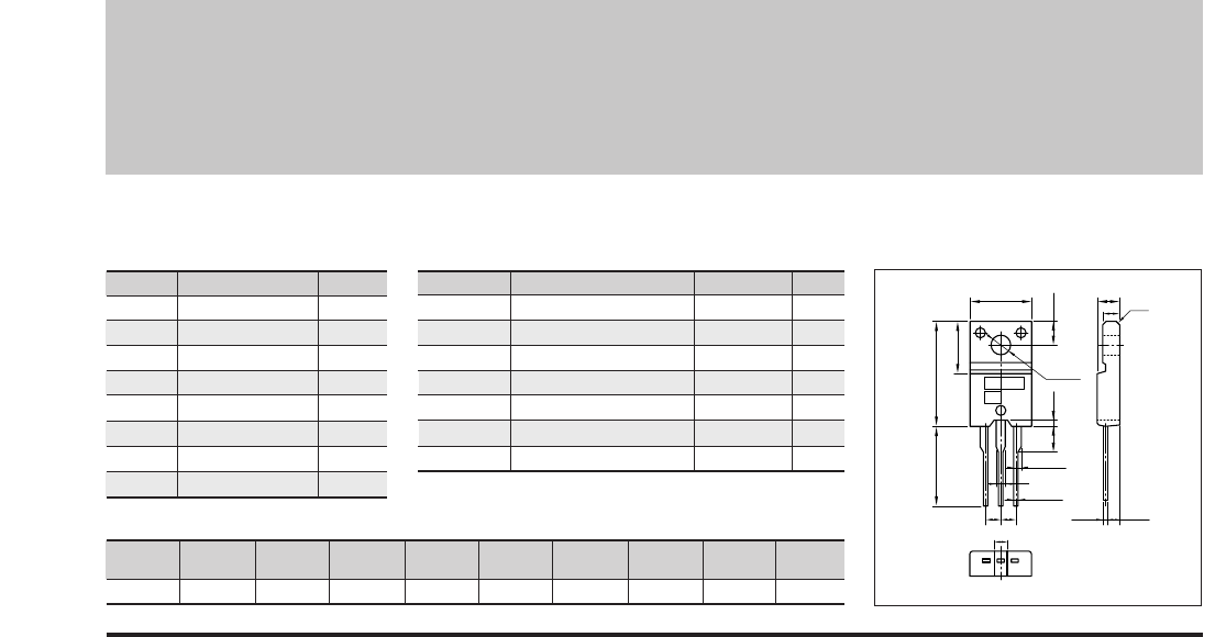
38
Silicon PNP Epitaxial Planar Transistor Application : Audio and General Purpose
Symbol
VCBO
VCEO
VEBO
IC
IB
PC
Tj
Tstg
Ratings
−50
−50
−6
−10
(pulse−20)
−3
30(Tc=25°C)
150
−55 to +150
Unit
V
V
V
A
A
W
°C
°C
■
Absolute maximum ratings
■
Electrical Characteristics
Symbol
ICBO
IEBO
V(BR)CEO
hFE
VCE(sat)
fT
COB
Ratings
−10max
−10max
−50min
130∼310
−0.5max
60typ
375typ
Unit
µ
A
µ
A
V
V
MHz
pF
Conditions
VCB=−50V
VEB=−6V
IC=−25mA
VCE=−2V, IC=−1A
IC=−5A, IB=−0.1A
VCE=−12V, IE=0.5A
VCB=−10V, f=1MHz
2SA2042
(Ta=25°C) (Ta=25°C)
■Typical Switching Characteristics (Common Emitter)
VCC
(V)
–20
RL
(Ω)
4
IC
(A)
–5
VBB2
(V)
5
IB2
(mA)
100
ton
(
µ
s)
0.2typ
tstg
(
µ
s)
0.7typ
tf
(
µ
s)
0.1typ
IB1
(mA)
–100
VBB1
(V)
–10
External Dimensions FM20(TO220F)
ø3.3±0.2
10.1±0.2
4.0±0.2
16.9±0.3
13.0min
8.4±0.2
0.8±0.2
3.9
±0.2
2.542.54
1.35±0.15
0.85
+0.2
-0.1
1.35±0.15
2.2±0.2
4.2±0.2
2.8 c0.5
2.4±0.2
0.45
+0.2
-0.1
BEC
a
b
Weight : Approx 6.5g
a. Part No.
b. Lot No.
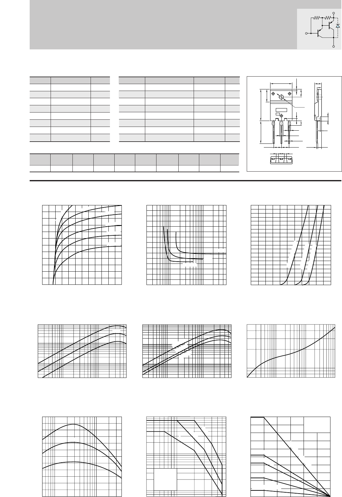
39
Darlington 2SB1257
4.41.5 1.5
BEC
5.45±0.1
ø3.3±0.2
1.6
3.3
1.75
0.8±0.2
2.15
1.05
+0.2
-0.1
5.45±0.1
23.0±0.3
16.2
9.5±0.2
5.5
15.6±0.2 5.5±0.2
3.45
3.35
0.65
+0.2
-0.1
±0.2
3.0
0.8
a
b
Symbol
VCBO
VCEO
VEBO
IC
IB
PC
Tj
Tstg
Ratings
–60
–60
–6
–4(Pulse–6)
–1
25(Tc=25°C)
150
–55 to +150
Unit
V
V
V
A
A
W
°C
°C
■
Absolute maximum ratings
■
Electrical Characteristics
Symbol
ICBO
IEBO
V(BR)CEO
hFE
VCE(sat)
VBE(sat)
fT
COB
Ratings
–10max
–10max
–60min
2000min
–1.5max
–2max
150typ
75typ
Unit
µ
A
µ
A
V
V
V
MHz
pF
Conditions
VCB=–60V
VEB=–6V
IC=–10mA
VCE=–4V, IC=–3A
IC=–3A, IB=–6mA
IC=–3A, IB=–6mA
VCE=–12V, IE=0.2A
VCB=–10V, f=1MHz
(Ta=25°C) (Ta=25°C)
■Typical Switching Characteristics (Common Emitter)
VCC
(V)
–30
RL
(Ω)
10
IC
(A)
–3
VBB2
(V)
5
IB2
(mA)
10
ton
(
µ
s)
0.4typ
tstg
(
µ
s)
0.8typ
tf
(
µ
s)
0.6typ
IB1
(mA)
–10
VBB1
(V)
–10
External Dimensions FM20(TO220F)
Silicon PNP Epitaxial Planar Transistor (Complement to type 2SD2014)
Application : Driver for Solenoid, Relay and Motor and General Purpose
Weight : Approx 2.0g
a. Part No.
b. Lot No.
IC–VCE Characteristics
(Typical)
hFE–IC Characteristics
(Typical)
hFE–IC
Temperature Characteristics (Typical)
θj-a–t Characteristics
IC–VBE Temperature Characteristics
(Typical)
VCE(sat)–IB Characteristics
(Typical)
Pc–Ta Derating
Safe Operating Area (Single Pulse)
fT–IE Characteristics
(Typical)
0
0
–2
–1
–4
–3
–6
–5
–2 –6–4–1 –5–3
Collector-Emitter Voltage VCE(V)
Collector Current IC(A)
I
B
=–2.3mA
–1.8mA
–1.5mA
–1.2mA
–0.8mA
–1.0mA
–0.02 –0.1 –1–0.5 –6–5
Collector Current IC(A)
DC Current Gain hFE
(VCE=–2V)
100
500
20
50
1000
8000
5000
Typ
0.7
5
1
1 10 100 1000
Time t(ms)
Transient Thermal Resistance θj-a(˚C/W)
0.05 0.1 0.5 1 4
120
80
0
40
200
240
160
Cut-off Frequency fT(MHZ)
(VCE=–12V)
Emitter Current IE(A)
Typ
–10–5–3 –70
–0.07
–1
–0.5
–0.1
–10
–5
Collector-Emitter Voltage VCE(V)
Collector Current IC(A)
DC
10ms
1ms
Without Heatsink
Natural Cooling
–0.6
–3
–2
–1
–0.2
–1–0.5 –10–5 –50
Base Current IB(mA)
Collector-Emitter Saturation Voltage VCE(sat)(V)
–2A
–3A
IC=–1A
0
–4
–2
–3
–1
0 –2.2–2–1
Base-Emittor Voltage VBE(V)
Collector Current IC(A)
(VCE=–2V)
125˚C (Case Temp)
25˚C (Case Temp)
–30˚C (Case Temp)
(VCE=–2V)
–0.02 –0.1–0.05 –0.5 –6–5–1
20
100
50
5000
500
1000
8000
Collector Current IC(A)
DC Current Gain hFE
25˚C
–30˚C
125˚C
25
20
10
2
00 25 50 75 100 125 150
Ambient Temperature Ta(˚C)
Maximum Power Dissipation PC(W)
With Infinite heatsink
Without Heatsink
150x150x2
50x50x2
100x
100x2
Natural Cooling
Silicone Grease
Heatsink: Aluminum
in mm
B
C
E
(2kΩ)(650Ω)
Equivalent circuit
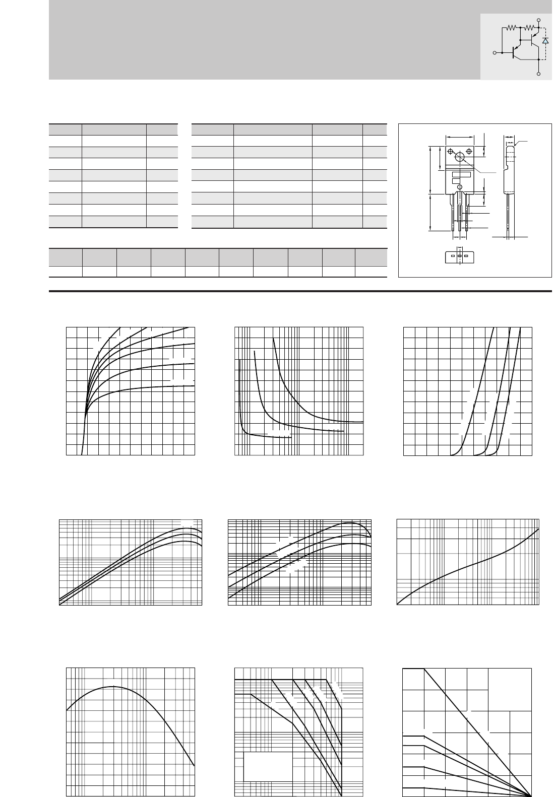
40
IC–VCE Characteristics
(Typical)
hFE–IC Characteristics
(Typical)
hFE–IC
Temperature Characteristics (Typical)
θj-a–t Characteristics
IC–VBE Temperature Characteristics
(Typical)
VCE(sat)–IB Characteristics
(Typical)
Pc–Ta Derating
0
0
–2
–1
–4
–3
–6
–5
–2 –6–4–1 –5–3
Collector-Emitter Voltage VCE(V)
Collector Current IC(A)
I
B
=–3.4mA
–2.4mA
–2.0mA
–1.8mA
–1.2mA
–0.9mA
Safe Operating Area (Single Pulse)
fT–IE Characteristics
(Typical)
–0.6
–3
–2
–1
–0.5
–1 –10 –200–100
Base Current IB(mA)
Collector-Emitter Saturation Voltage VCE(sat)(V)
–4A
–6A
IC=–2A
–0.03
–0.1 –1–0.5 –6
Collector Current IC(A)
DC Current Gain hFE
(VCE=–4V)
500
80
8000
5000
1000
Typ
0.5
5
1
1 10 100 1000
Time t(ms)
Transient Thermal Resistance θj-a(˚C/W)
0.05 0.1 0.5 1 5 6
60
40
0
20
100
120
80
Cut-off Frequency fT(MHZ)
(VCE=–12V)
Emitter Current IE(A)
Typ
–10 –50–5–3 –100 –200
–0.05
–1
–0.5
–0.1
–10
–20
–5
Collector-Emitter Voltage VCE(V)
Collector Current IC(A)
DC
100µs
500µs
30
20
10
2
00 25 50 75 100 125 150
Ambient Temperature Ta(˚C)
Maximum Power Dissipation PC(W)
50x50x2
100x100x2
150x150x2
With Infinite heatsink
Without Heatsink
10ms
1ms
Without Heatsink
Natural Cooling
0
–6
–2
–3
–4
–5
–1
0 –2.2–2–1
Base-Emittor Voltage VBE(V)
Collector Current IC(A)
(VCE=–4V)
125˚C (Case Temp)
25˚C (Case Temp)
–30˚C (Case Temp)
(VCE=–4V)
–0.03 –0.1 –0.5 –6–1
30
100
5000
500
1000
8000
Collector Current IC(A)
DC Current Gain hFE
25˚C
–30˚C
125˚C
Natural Cooling
Silicone Grease
Heatsink: Aluminum
in mm
Silicon PNP Epitaxial Planar Transistor (Complement to type 2SD1785)
Application : Driver for Solenoid, Relay and Motor and General Purpose
Symbol
VCBO
VCEO
VEBO
IC
IB
PC
Tj
Tstg
Ratings
–100
–100
–6
–6(Pulse–10)
–1
30(Tc=25°C)
150
–55 to +150
Unit
V
V
V
A
A
W
°C
°C
■
Absolute maximum ratings
■
Electrical Characteristics
Symbol
ICBO
IEBO
V(BR)CEO
hFE
VCE(sat)
VBE(sat)
fT
COB
Ratings
–10max
–10max
–100min
1000min
–1.5max
–2max
100typ
100typ
Unit
µ
A
µ
A
V
V
V
MHz
pF
Conditions
VCB=–100V
VEB=–6V
IC=–10mA
VCE=–2V, IC=–3A
IC=–3A, IB=–6mA
IC=–3A, IB=–6mA
VCE=–12V, IE=0.2A
VCB=–10V, f=1MHz
Darlington 2SB1258
(Ta=25°C) (Ta=25°C)
■Typical Switching Characteristics (Common Emitter)
VCC
(V)
–30
RL
(Ω)
10
IC
(A)
–3
VBB2
(V)
5
IB2
(mA)
6
ton
(
µ
s)
0.6typ
tstg
(
µ
s)
1.6typ
tf
(
µ
s)
0.5typ
IB1
(mA)
–6
VBB1
(V)
–10
ø3.3±0.2
10.1±0.2
4.0±0.2
16.9±0.3
13.0min
8.4±0.2
0.8±0.2
3.9
±0.2
2.542.54
1.35±0.15
0.85
+0.2
-0.1
1.35±0.15
2.2±0.2
4.2±0.2
2.8 c0.5
2.4±0.2
0.45
+0.2
-0.1
BEC
a
b
External Dimensions FM20(TO220F)
Weight : Approx 2.0g
a. Part No.
b. Lot No.
B
C
E
(3kΩ)(100Ω)
Equivalent circuit
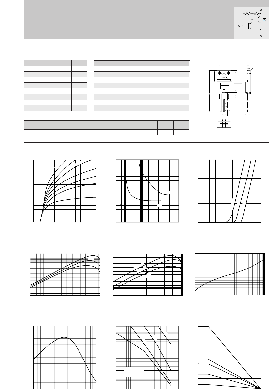
41
ø3.3±0.2
10.1±0.2
4.0±0.2
16.9±0.3
13.0min
8.4±0.2
0.8±0.2
3.9
±0.2
2.542.54
1.35±0.15
0.85
+0.2
-0.1
1.35±0.15
2.2±0.2
4.2±0.2
2.8 c0.5
2.4±0.2
0.45
+0.2
-0.1
BEC
a
b
Symbol
VCBO
VCEO
VEBO
IC
IB
PC
Tj
Tstg
Ratings
–120
–120
–6
–10(Pulse–15)
–1
30(Tc=25°C)
150
–55 to +150
Unit
V
V
V
A
A
W
°C
°C
■
Absolute maximum ratings
■
Electrical Characteristics
Symbol
ICBO
IEBO
V(BR)CEO
hFE
VCE(sat)
VBE(sat)
fT
COB
Ratings
–10max
–10max
–120min
2000min
–1.5max
–2.0max
100typ
145typ
Unit
µ
A
mA
V
V
V
MHz
pF
Conditions
VCB=–120V
VEB=–6V
IC=–10mA
VCE=–4V, IC=–5A
IC=–5A, IB=–10mA
IC=–5A, IB=–10mA
VCE=–12V, IE=0.2A
VCB=–10V, f=1MHz
Darlington 2SB1259
(Ta=25°C) (Ta=25°C)
External Dimensions FM20(TO220F)
Silicon PNP Epitaxial Planar Transistor (Complement to type 2SD2081)
Application : Driver for Solenoid, Relay and Motor and General Purpose
Weight : Approx 2.0g
a. Part No.
b. Lot No.
IC–VCE Characteristics
(Typical)
hFE–IC Characteristics
(Typical)
hFE–IC
Temperature Characteristics (Typical)
θj-a–t Characteristics
IC–VBE Temperature Characteristics
(Typical)
VCE(sat)–IB Characteristics
(Typical)
Pc–Ta Derating
0
0
–5
–10
–15
–2–1 –6–5–4–3
Collector-Emitter Voltage VCE(V)
Collector Current IC(A)
–50mA
–10mA
–5mA
–3mA
–2mA
I
B
=–1mA
–20mA
Safe Operating Area (Single Pulse)
fT–IE Characteristics
(Typical)
0
–3
–2
–1
–0.2
–1 –1000–10 –100
Base Current IB(mA)
Collector-Emitter Saturation Voltage VCE(sat)(V)
–1A
–5A
IC=–10A
–0.03 –0.1 –0.5 –1 –10–5
Collector Current IC(A)
DC Current Gain hFE
(VCE=–4V)
50
100
500
10000
5000
1000
20000
Typ
0.3
0.5
5
1
1 10 100 1000
Time t(ms)
Transient Thermal Resistance θj-a(˚C/W)
–10 –50–5–3 –100 –200
–0.03
–0.05
–1
–0.5
–0.1
–10
–20
–5
Collector-Emitter Voltage VCE(V)
Collector Current IC(A)
DC
100µs
10ms
1ms
Without Heatsink
Natural Cooling
30
20
10
2
00 25 50 75 100 125 150
Ambient Temperature Ta(˚C)
Maximum Power Dissipation PC(W)
50x50x2
100x100x2
150x150x2
With Infinite heatsink
Without Heatsink
0
–10
–4
–6
–8
–2
0 –2.2–2–1
Base-Emittor Voltage VBE(V)
Collector Current IC(A)
(VCE=–4V)
125˚C (Case Temp)
25˚C (Case Temp)
–30˚C (Case Temp)
(VCE=–4V)
–0.02 –0.1 –0.5 –10–5–1
20
100
50
5000
500
1000
20000
10000
Collector Current IC(A)
DC Current Gain hFE
25˚C
–30˚C
125˚C
0.05 0.1 0.5 1 5 10
100
0
200
Cut-off Frequency fT(MHZ)
(VCE=–12V)
Emitter Current IE(A)
Typ
Natural Cooling
Silicone Grease
Heatsink: Aluminum
in mm
■Typical Switching Characteristics (Common Emitter)
VCC
(V)
–30
RL
(Ω)
10
IC
(A)
–3
VBB2
(V)
5
IB2
(mA)
6
ton
(
µ
s)
0.6typ
tstg
(
µ
s)
1.6typ
tf
(
µ
s)
0.5typ
IB1
(mA)
–6
VBB1
(V)
–10
B
C
E
(3kΩ)(100Ω)
Equivalent circuit
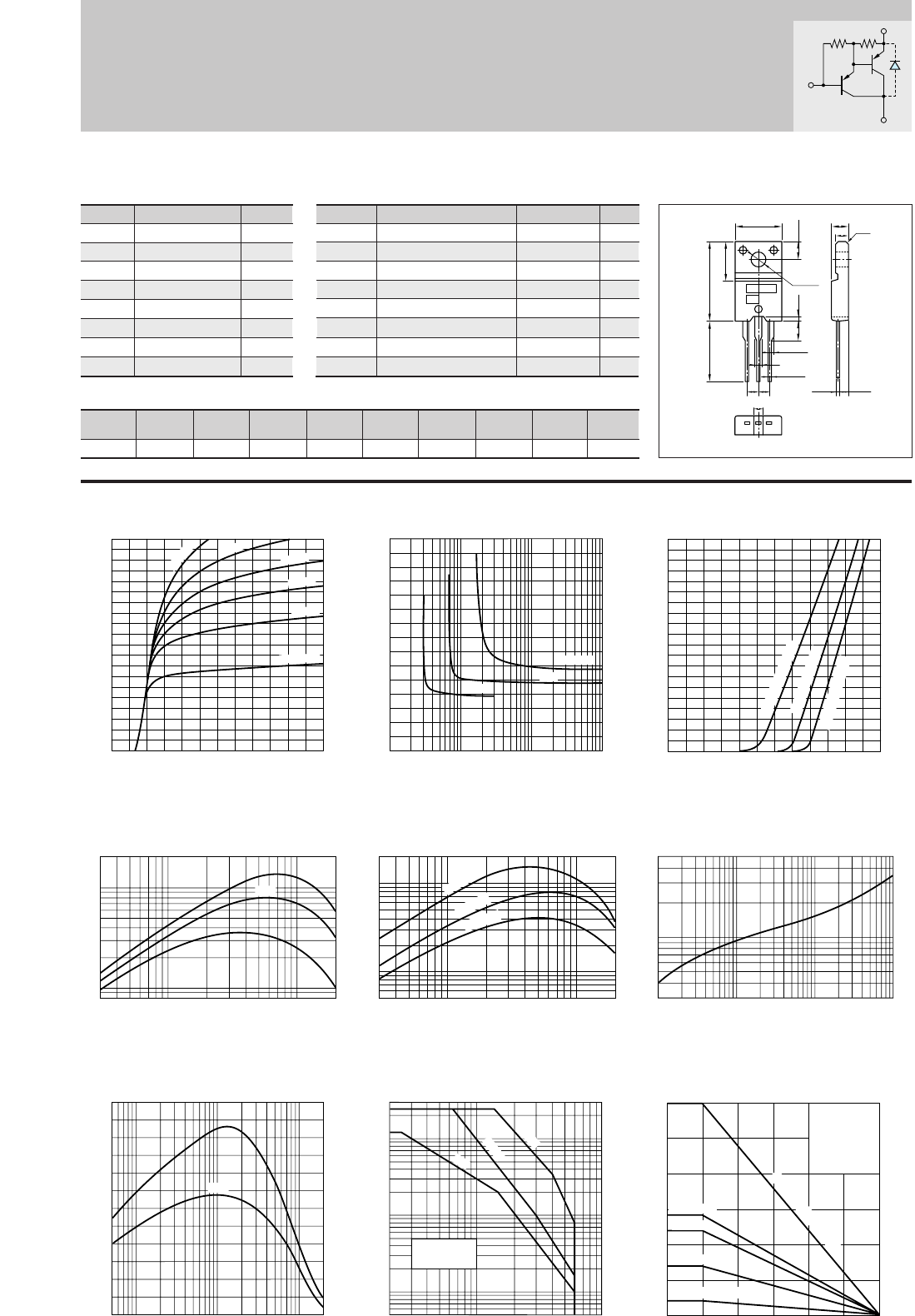
42
IC–VCE Characteristics
(Typical)
hFE–IC Characteristics
(Typical)
hFE–IC
Temperature Characteristics (Typical)
θj-a–t Characteristics
IC–VBE Temperature Characteristics
(Typical)
VCE(sat)–IB Characteristics
(Typical)
Pc–Ta Derating
0
0
–5
–10
–20
–15
–2–1 –6–5–4–3
Collector-Emitter Voltage VCE(V)
Collector Current IC(A)
–10mA
–6mA
–3mA
–4mA
–2mA
I
B
=–1mA
Safe Operating Area (Single Pulse)
fT–IE Characteristics
(Typical)
0
–3
–2
–1
–0.1
–1 –100–10
Base Current IB(mA)
Collector-Emitter Saturation Voltage VCE(sat)(V)
–1A
–5A
IC=–10A
–0.3 –1 –20–10–5
Collector Current IC(A)
DC Current Gain hFE
(VCE=–4V)
800
10000
5000
1000
–10 –50
30
20
10
2
00 25 50 75 100 125 150
Ambient Temperature Ta(˚C)
Maximum Power Dissipation PC(W)
50x50x2
100x100x2
150x150x2
With Infinite heatsink
Without Heatsink
–5–2 –100
–0.05
–1
–0.5
–0.1
–10
–30
–5
Collector-Emitter Voltage VCE(V)
Collector Current IC(A)
DC
10ms
1ms
20000
Typ
Without Heatsink
Natural Cooling
0
–20
–10
–15
–5
0 –2.4–2–1
Base-Emittor Voltage VBE(V)
Collector Current IC(A)
(VCE=–4V)
125˚C (Case Temp)
25˚C (Case Temp)
–30˚C (Case Temp)
(VCE=–4V)
–0.3 –0.5 –1 –5 –20–10
500
5000
1000
20000
10000
Collector Current IC(A)
DC Current Gain hFE
25˚C
–30˚C
125˚C
0.3
0.5
5
1
1 10 100 1000
Time t(ms)
Transient Thermal Resistance θj-a(˚C/W)
0.05 0.1 5 100.5 1 20
120
80
0
40
200
240
160
Cut-off Frequency fT(MHZ)
(VCE=–12V)
Emitter Current IE(A)
Typ
Natural Cooling
Silicone Grease
Heatsink: Aluminum
in mm
Silicon PNP Epitaxial Planar Transistor
Application : Driver for Printer Head, Solenoid, Relay, Motor and General Purpose
Symbol
VCBO
VCEO
VEBO
IC
IB
PC
Tj
Tstg
Ratings
–60
–60
–6
–12(Pulse–20)
–1
30(Tc=25°C)
150
–55 to +150
Unit
V
V
V
A
A
W
°C
°C
■
Absolute maximum ratings
■
Electrical Characteristics
Symbol
ICBO
IEBO
V(BR)CEO
hFE
VCE(sat)
VBE(sat)
fT
COB
Ratings
–10max
–10max
–60min
2000min
–1.5max
–2.0max
130typ
170typ
Unit
µ
A
mA
V
V
V
MHz
pF
Condition
VCB=–60V
VEB=–6V
IC=–10mA
VCE=–4V, IC=–10A
IC=–10A, IB=–20mA
IC=–10A, IB=–20mA
VCE=–12V, IE=1A
VCB=–10V, f=1MHz
Darlington 2SB1351
(Ta=25°C) (Ta=25°C)
■Typical Switching Characteristics (Common Emitter)
VCC
(V)
–40
RL
(Ω)
4
IC
(A)
–10
VBB2
(V)
5
IB2
(mA)
20
ton
(
µ
s)
0.7typ
tstg
(
µ
s)
1.5typ
tf
(
µ
s)
0.6typ
IB1
(mA)
–20
VBB1
(V)
–10
ø3.3±0.2
10.1±0.2
4.0±0.2
16.9±0.3
13.0min
8.4±0.2
0.8±0.2
3.9
±0.2
2.542.54
1.35±0.15
0.85
+0.2
-0.1
1.35±0.15
2.2±0.2
4.2±0.2
2.8 c0.5
2.4±0.2
0.45
+0.2
-0.1
BEC
a
b
External Dimensions FM20(TO220F)
Weight : Approx 2.0g
a. Part No.
b. Lot No.
B
C
E
(2kΩ)(100Ω)
Equivalent circuit
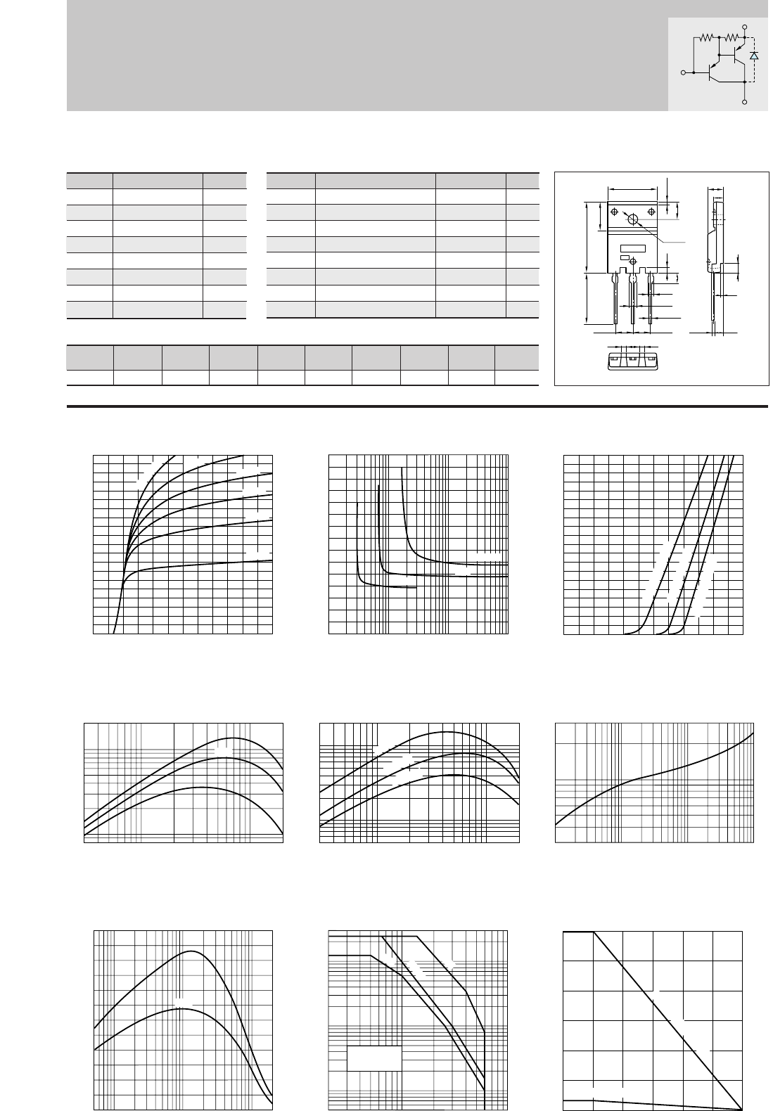
43
4.41.5 1.5
BEC
5.45±0.1
ø3.3±0.2
1.6
3.3
1.75
0.8±0.2
2.15
1.05
+0.2
-0.1
5.45±0.1
23.0±0.3
16.2
9.5±0.2
5.5
15.6±0.2 5.5±0.2
3.45
3.35
0.65
+0.2
-0.1
±0.2
3.0
0.8
a
b
IC–VCE Characteristics
(Typical)
hFE–IC Characteristics
(Typical)
hFE–IC
Temperature Characteristics (Typical)
θj-a–t Characteristics
IC–VBE Temperature Characteristics
(Typical)
VCE(sat)–IB Characteristics
(Typical)
Pc–Ta Derating
0
0
–5
–10
–20
–15
–2–1 –6–5–4–3
Collector-Emitter Voltage VCE(V)
Collector Current IC(A)
I
B
=–10mA
–6mA
–3mA
–4mA
–2mA
–1mA
Safe Operating Area (Single Pulse)
fT–IE Characteristics
(Typical)
0
–3
–2
–1
–0.1
–1 –100–10
Base Current IB(mA)
Collector-Emitter Saturation Voltage VCE(sat)(V)
–1A
–5A
IC=–10A
–0.3 –1 –20–10–5
Collector Current IC(A)
DC Current Gain hFE
(VCE=–4V)
800
10000
5000
1000
20000
Typ
–10 –50–5–2 –100
–0.05
–1
–0.5
–0.1
–10
–30
–5
Collector-Emitter Voltage VCE(V)
Collector Current IC(A)
DC
10ms
1ms
Without Heatsink
Natural Cooling
60
40
20
3.5
00 50 100 150
Ambient Temperature Ta(˚C)
Maximum Power Dissipation PC(W)
With Infinite heatsink
Without Heatsink
0
–20
–10
–15
–5
0 –2.4–2–1
Base-Emittor Voltage VBE(V)
Collector Current IC(A)
(VCE=–4V)
125˚C (Case Temp)
25˚C (Case Temp)
–30˚C (Case Temp)
(VCE=–4V)
–0.3 –0.5 –1 –5 –20–10
500
5000
1000
20000
10000
Collector Current IC(A)
DC Current Gain hFE
25˚C
–30˚C
125˚C
0.05 0.1 5 100.5 1 20
120
80
0
40
200
240
160
Cut-off Frequency fT(MHZ)
(VCE=–12V)
Emitter Current IE(A)
Typ
0.3
0.5
5
1
1 10 100 1000
Time t(ms)
Transient Thermal Resistance θj-a(˚C/W)
Symbol
VCBO
VCEO
VEBO
IC
IB
PC
Tj
Tstg
Ratings
–60
–60
–6
–12(Pulse–20)
–1
60(Tc=25°C)
150
–55 to +150
Unit
V
V
V
A
A
W
°C
°C
■
Absolute maximum ratings
■
Electrical Characteristics
Symbol
ICBO
IEBO
V(BR)CEO
hFE
VCE(sat)
VBE(sat)
fT
COB
Ratings
–10max
–10max
–60min
2000min
–1.5max
–2.0max
130typ
170typ
Unit
µ
A
mA
V
V
V
MHz
pF
Conditions
VCB=–60V
VEB=–6V
IC=–10mA
VCE=–4V, IC=–10A
IC=–10A, IB=–20mA
IC=–10A, IB=–20mA
VCE=–12V, IE=1A
VCB=–10V, f=1MHz
Darlington 2SB1352
(Ta=25°C) (Ta=25°C)
External Dimensions FM100(TO3PF)
Silicon PNP Epitaxial Planar Transistor
Application : Driver for Printer Head, Solenoid, Relay, Motor and General Purpose
Weight : Approx 6.5g
a. Part No.
b. Lot No.
■Typical Switching Characteristics (Common Emitter)
VCC
(V)
–40
RL
(Ω)
4
IC
(A)
–10
VBB2
(V)
5
IB2
(mA)
20
ton
(
µ
s)
0.7typ
tstg
(
µ
s)
1.5typ
tf
(
µ
s)
0.6typ
IB1
(mA)
–20
VBB1
(V)
–10
B
C
E
(2kΩ)(100Ω)
Equivalent circuit
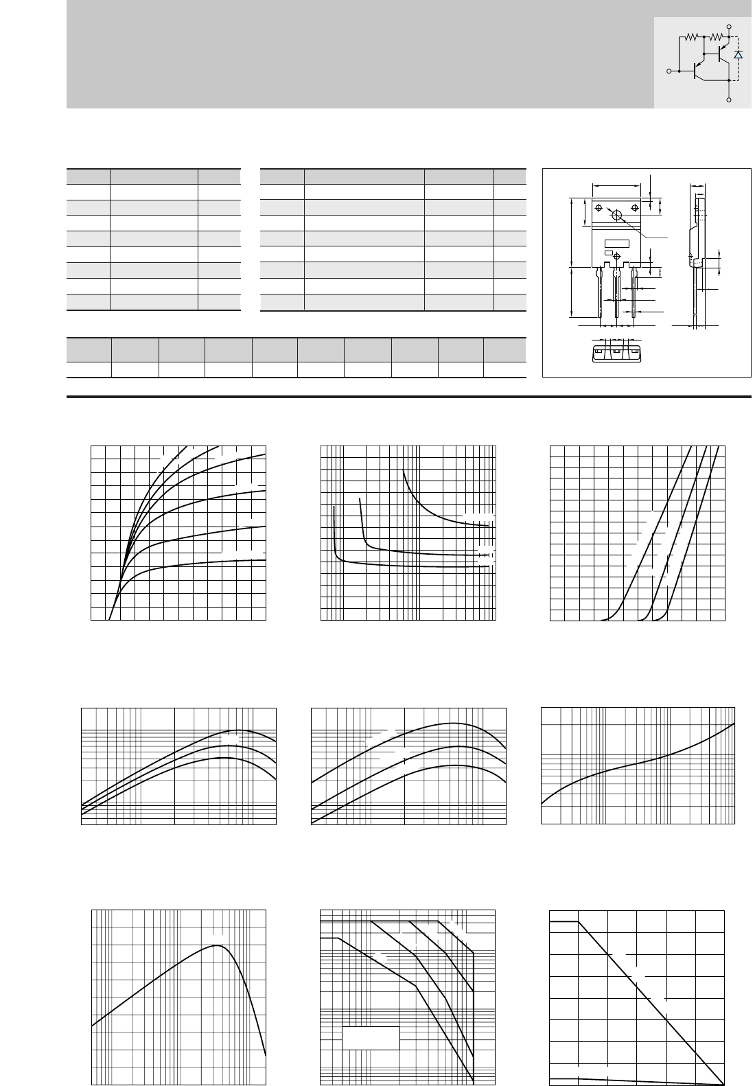
44
IC–VCE Characteristics
(Typical)
hFE–IC Characteristics
(Typical)
θj-a–t Characteristics
IC–VBE Temperature Characteristics
(Typical)
VCE(sat)–IB Characteristics
(Typical)
Pc–Ta Derating
0
0
–10
–20
–26
–2–1 –6–5–4–3
Collector-Emitter Voltage VCE(V)
Collector Current IC(A)
–40mA
–12mA
–6mA
–3mA
IB=–1.5mA
–20mA
Safe Operating Area (Single Pulse)
fT–IE Characteristics
(Typical)
–10 –50–5–3 –100 –200
–0.03
–0.05
–1
–0.5
–0.1
–10
–50
–5
Collector-Emitter Voltage VCE(V)
Collector Current IC(A)
DC
100µs
10ms
1ms
Without Heatsink
Natural Cooling
0
–16
–8
–12
–4
0 –2.4–2–1
Base-Emittor Voltage VBE(V)
Collector Current IC(A)
(VCE=–4V)
125˚C (Case Temp)
25˚C (Case Temp)
–30˚C (Case Temp)
–0.3 –0.5 –1 –16–10–5
Collector Current IC(A)
DC Current Gain hFE
(VCE=–4V)
500
10000
5000
1000
20000
Typ
–0.3 –0.5 –1 –16–10–5
500
10000
5000
1000
20000
hFE–IC
Temperature Characteristics (Typical)
(VCE=–4V)
Collector Current IC(A)
DC Current Gain hFE
25˚C
–30˚C
125˚C
0.05 0.1 5 100.5 1 16
50
0
100
Cut-off Frequency fT(MHZ)
(VCE=–12V)
Emitter Current IE(A)
Typ
0
–3
–2
–1
–0.5
–1 –100–10
Base Current IB(mA)
Collector-Emitter Saturation Voltage VCE(sat)(V)
–4A
–8A
IC=–16A
0.2
0.5
3
1
1 10 100 1000
Time t(ms)
Transient Thermal Resistance θj-a(˚C/W)
80
60
40
20
3.5
00 50 100 150
Ambient Temperature Ta(˚C)
Maximum Power Dissipation PC(W)
With Infinite heatsink
Without Heatsink
Silicon PNP Epitaxial Planar Transistor (Complement to type 2SD2082)
Application : Chopper Regulator, DC Motor Driver and General Purpose
Symbol
VCBO
VCEO
VEBO
IC
IB
PC
Tj
Tstg
Ratings
–120
–120
–6
–16(Pulse–26)
–1
75(Tc=25°C)
150
–55 to +150
Unit
V
V
V
A
A
W
°C
°C
■
Absolute maximum ratings
■
Electrical Characteristics
Symbol
ICBO
IEBO
V(BR)CEO
hFE
VCE(sat)
VBE(sat)
fT
COB
Ratings
–10max
–10max
–120min
2000min
–1.5max
–2.5max
50typ
350typ
Unit
µ
A
mA
V
V
V
MHz
pF
Conditions
VCB=–120V
VEB=–6V
IC=–10mA
VCE=–4V, IC=–8A
IC=–8A, IB=–16mA
IC=–8A, IB=–16mA
VCE=–12V, IE=1A
VCB=–10V, f=1MHz
Darlington 2SB1382
(Ta=25°C) (Ta=25°C)
■Typical Switching Characteristics (Common Emitter)
VCC
(V)
–40
RL
(Ω)
5
IC
(A)
–8
VBB2
(V)
5
IB2
(mA)
16
ton
(
µ
s)
0.8typ
tstg
(
µ
s)
1.8typ
tf
(
µ
s)
1.0typ
IB1
(mA)
–16
VBB1
(V)
–10
4.41.5 1.5
BEC
5.45±0.1
ø3.3±0.2
1.6
3.3
1.75
0.8±0.2
2.15
1.05
+0.2
-0.1
5.45±0.1
23.0±0.3
16.2
9.5±0.2
5.5
15.6±0.2 5.5±0.2
3.45
3.35
0.65
+0.2
-0.1
±0.2
3.0
0.8
a
b
External Dimensions FM100(TO3PF)
Weight : Approx 6.5g
a. Part No.
b. Lot No.
B
C
E
(2kΩ) (80Ω)
Equivalent circuit
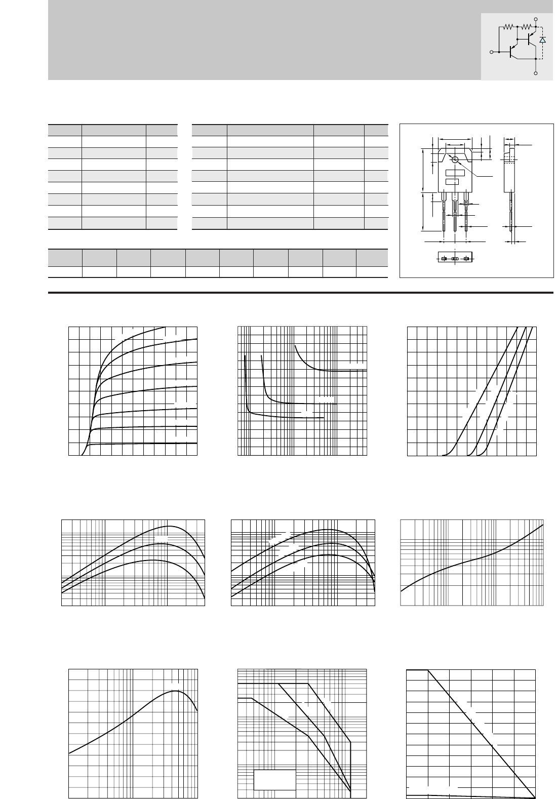
45
Darlington 2SB1383
15.6±0.4
9.6
19.9±0.3
4.0 2.0
5.0±0.2
1.8
ø3.2±0.1
2
3
1.05
+0.2
-0.1
20.0min
4.0max
BE
5.45±0.1 5.45±0.1
C
4.8±0.2
0.65
+0.2
-0.1
1.4
2.0±0.1
a
b
IC–VCE Characteristics
(Typical)
hFE–IC Characteristics
(Typical)
hFE–IC
Temperature Characteristics (Typical)
θj-a–t Characteristics
IC–VBE Temperature Characteristics
(Typical)
VCE(sat)–IB Characteristics
(Typical)
Pc–Ta Derating
0
0
–15
–10
–5
–20
–25
–2–1 –6–5–4–3
Collector-Emitter Voltage VCE(V)
Collector Current IC(A)
–8.0mA
I
B
=–0.6mA
–1.0mA
–1.5mA
–2.5mA
–4.0mA
–6.0mA
Safe Operating Area (Single Pulse)
fT–IE Characteristics
(Typical)
0
–3
–2
–1
–0.5
–1 –500–100–10
Base Current IB(mA)
Collector-Emitter Saturation Voltage VCE(sat)(V)
–6A
–12A
IC=–25A
–0.2 –0.5 –1 –40–10–5
Collector Current IC(A)
DC Current Gain hFE
(VCE=–4V)
200
500
10000
5000
1000
20000
Typ
0.1
0.5
2
1
1 10 100 1000
Time t(ms)
Transient Thermal Resistance θj-a(˚C/W)
0.1 10.5 5 10
40
30
0
10
20
60
50
Cut-off Frequency fT(MHZ)
(VCE=–12V)
Emitter Current IE(A)
Typ
–10 –50–5–3 –100 –200
–0.2
–1
–0.5
–50
–10
–100
–5
Collector-Emitter Voltage VCE(V)
Collector Current IC(A)
DC
10ms
1ms
Without Heatsink
Natural Cooling
120
100
50
3.5
00 25 50 75 100 125 150
Ambient Temperature Ta(˚C)
Maximum Power Dissipation PC(W)
With Infinite heatsink
Without Heatsink
0
–25
–10
–15
–20
–5
0 –2.6–2–1
Base-Emittor Voltage VBE(V)
Collector Current IC(A)
(VCE=–4V)
125˚C (Case Temp)
25˚C (Case Temp)
–30˚C (Case Temp)
(VCE=–4V)
–0.2 –1–0.5 –5 –40–10
200
5000
500
1000
20000
10000
Collector Current IC(A)
DC Current Gain hFE
25˚C
–30˚C
125˚C
Symbol
VCBO
VCEO
VEBO
IC
IB
PC
Tj
Tstg
Ratings
–120
–120
–6
–25(Pulse–40)
–2
120(Tc=25°C)
150
–55 to +150
Unit
V
V
V
A
A
W
°C
°C
■
Absolute maximum ratings
■
Electrical Characteristics
Symbol
ICBO
IEBO
V(BR)CEO
hFE
VCE(sat)
VBE(sat)
fT
COB
Ratings
–10max
–10max
–120min
2000min
–1.8max
–2.5max
50typ
230typ
Unit
µ
A
mA
V
V
V
MHz
pF
Conditions
VCB=–120V
VEB=–6V
IC=–25mA
VCE=–4V, IC=–12A
IC=–12A, IB=–24mA
IC=–12A, IB=–24mA
VCE=–12V, IE=1A
VCB=–10V, f=1MHz
(Ta=25°C) (Ta=25°C)
External Dimensions MT-100(TO3P)
Silicon PNP Epitaxial Planar Transistor (Complement to type 2SD2083)
Application : Chopper Regulator, DC Motor Driver and General Purpose
Weight : Approx 6.0g
a. Part No.
b. Lot No.
■Typical Switching Characteristics (Common Emitter)
VCC
(V)
–24
RL
(Ω)
2
IC
(A)
–12
VBB2
(V)
5
IB2
(mA)
24
ton
(
µ
s)
1.0typ
tstg
(
µ
s)
3.0typ
tf
(
µ
s)
1.0typ
IB1
(mA)
–24
VBB1
(V)
–10
B
C
E
(2kΩ) (80Ω)
Equivalent circuit
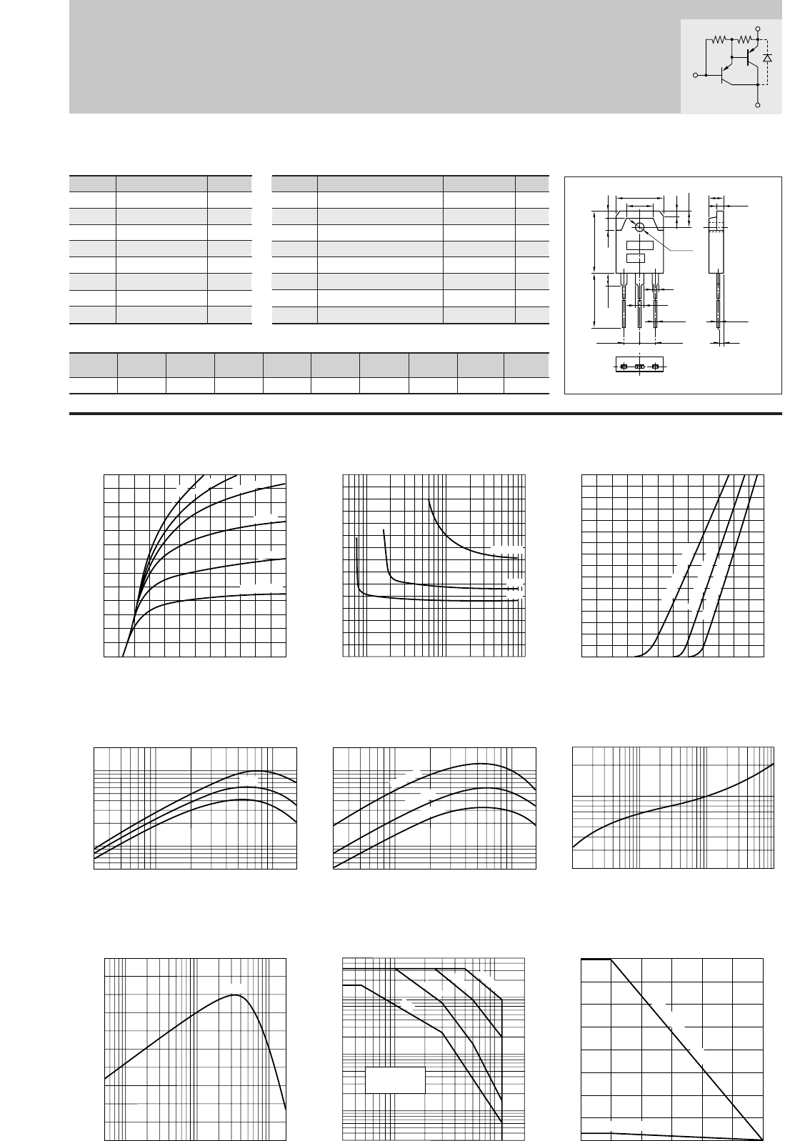
46
IC–VCE Characteristics
(Typical)
hFE–IC Characteristics
(Typical)
hFE–IC
Temperature Characteristics (Typical)
θj-a–t Characteristics
IC–VBE Temperature Characteristics
(Typical)
VCE(sat)–IB Characteristics
(Typical)
Pc–Ta Derating
Safe Operating Area (Single Pulse)
fT–IE Characteristics
(Typical)
0
–3
–2
–1
–0.5
–1 –100–10
Base Current IB(mA)
Collector-Emitter Saturation Voltage VCE(sat)(V)
–4A
–8A
IC=–16A
–0.3 –1 –16–10–5
Collector Current IC(A)
DC Current Gain hFE
(VCE=–4V)
500
10000
5000
1000
20000
Typ
0.2
0.5
3
1
1 10 100 1000
Time t(ms)
Transient Thermal Resistance θj-a(˚C/W)
–10 –50–5–3 –100 –200
–0.03
–0.05
–1
–0.5
–0.1
–10
–50
–5
Collector-Emitter Voltage VCE(V)
Collector Current IC(A)
DC
100µs
10ms
1ms
Without Heatsink
Natural Cooling
80
60
40
20
3.5
00 25 50 75 100 125 150
Ambient Temperature Ta(˚C)
Maximum Power Dissipation PC(W)
With Infinite heatsink
Without Heatsink
0
0
–10
–20
–26
–2–1 –6–5–4–3
Collector-Emitter Voltage VCE(V)
Collector Current IC(A)
–40mA
–12mA
–6mA
–3mA
IB=–1.5mA
–20mA
0
–16
–8
–12
–4
0 –2.4–2–1
Base-Emittor Voltage VBE(V)
Collector Current IC(A)
(VCE=–4V)
125˚C (Case Temp)
25˚C (Case Temp)
–30˚C (Case Temp)
–0.3 –0.5 –1 –16–10–5
500
10000
5000
1000
20000
(VCE=–4V)
Collector Current IC(A)
DC Current Gain hFE
25˚C
–30˚C
125˚C
0.05 0.1 5 100.5 1 16
50
0
100
Cut-off Frequency fT(MHZ)
(VCE=–12V)
Emitter Current IE
(
A
)
Typ
Silicon PNP Epitaxial Planar Transistor
Application : Chopper Regulator, DC Motor Driver and General Purpose
Symbol
VCBO
VCEO
VEBO
IC
IB
PC
Tj
Tstg
Ratings
–120
–120
–6
–16(Pulse–26)
–1
80(Tc=25°C)
150
–55 to +150
Unit
V
V
V
A
A
W
°C
°C
■
Absolute maximum ratings
■
Electrical Characteristics
Symbol
ICBO
IEBO
V(BR)CEO
hFE
VCE(sat)
VBE(sat)
fT
COB
Ratings
–10max
–10max
–120min
2000min
–1.5max
–2.5max
50typ
350typ
Unit
µ
A
mA
V
V
V
MHz
pF
Conditions
VCB=–120V
VEB=–6V
IC=–10mA
VCE=–4V, IC=–8A
IC=–8A, IB=–16mA
IC=–8A, IB=–16mA
VCE=–12V, IE=1A
VCB=–10V, f=1MHz
Darlington 2SB1420
(Ta=25°C) (Ta=25°C)
15.6±0.4
9.6
19.9±0.3
4.0 2.0
5.0±0.2
1.8
ø3.2±0.1
2
3
1.05
+0.2
-0.1
20.0min
4.0max
BE
5.45±0.1 5.45±0.1
C
4.8±0.2
0.65
+0.2
-0.1
1.4
2.0±0.1
a
b
External Dimensions MT-100(TO3P)
Weight : Approx 6.0g
a. Part No.
b. Lot No.
■Typical Switching Characteristics (Common Emitter)
VCC
(V)
–24
RL
(Ω)
2
IC
(A)
–12
VBB2
(V)
5
IB2
(mA)
24
ton
(
µ
s)
1.0typ
tstg
(
µ
s)
3.0typ
tf
(
µ
s)
1.0typ
IB1
(mA)
–24
VBB1
(V)
–10
B
C
E
(2kΩ) (80Ω)
Equivalent circuit
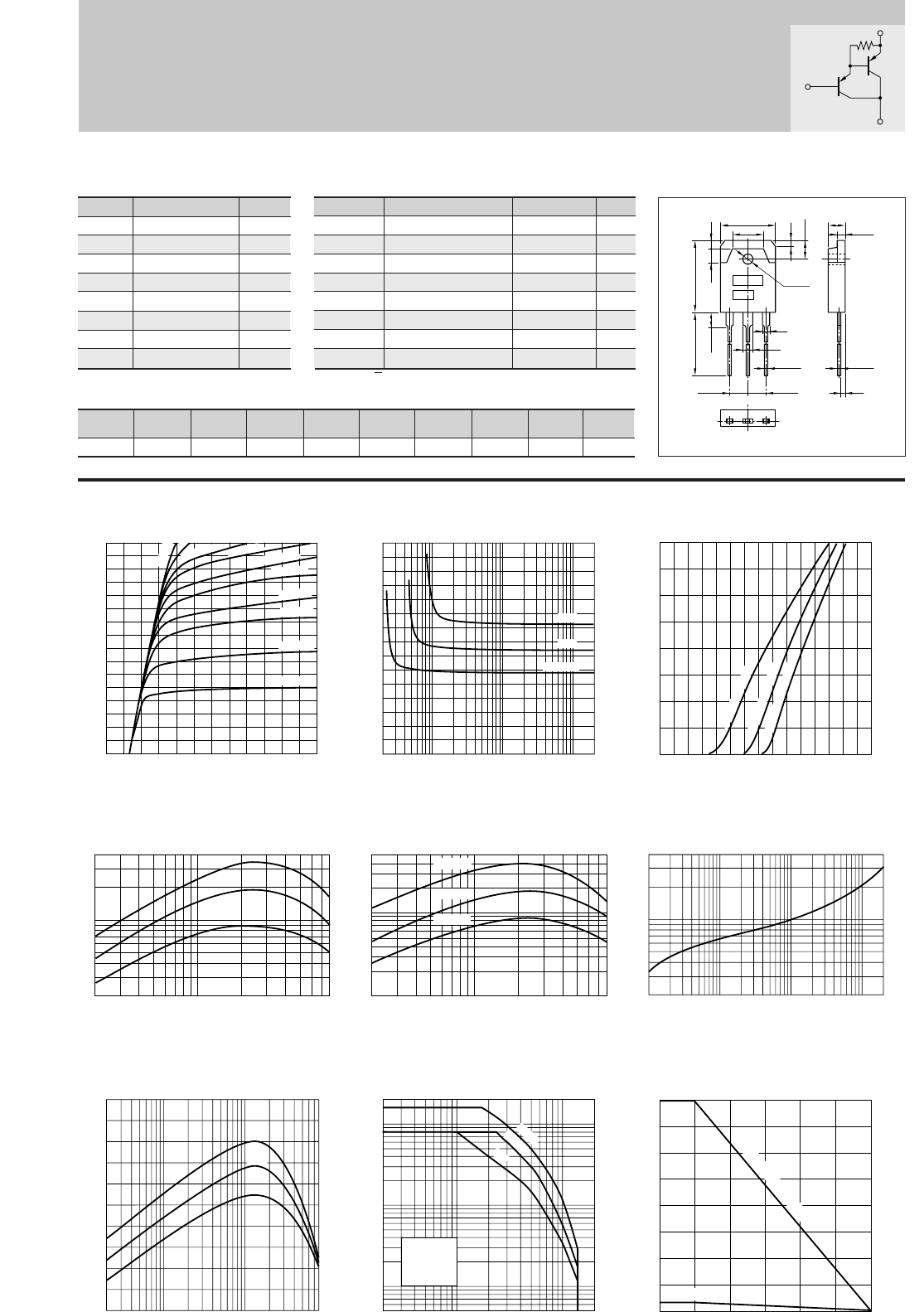
47
∗hFE Rank O(5000to12000), P(6500to20000), Y(15000to30000)
B
E
C
(70Ω)
IC–VCE Characteristics
(Typical)
hFE–IC Characteristics
(Typical)
hFE–IC
Temperature Characteristics (Typical)
IC–VBE Temperature Characteristics
(Typical)
VCE(sat)–IB Characteristics
(Typical)
Pc–Ta Derating
0
0
–2
–4
–6
–8
–2 –4 –6
Collector-Emitter Voltage VCE(V)
Collector Current IC(A)
–10mA
–2.5mA
–2.0mA
–1.8mA
–1.5mA
–1.3mA
–1.0mA
–0.8mA
–0.5mA
I
B
=–0.3mA
0
–3
–2
–1
–0.2
–1–0.5 –10–5 –200–100–50
Base Current IB(mA)
Collector-Emitter Saturation Voltage VCE(sat)(V)
–6A
–8A
IC=–4A
0
–8
–6
–2
–4
0–3–2–1
Base-Emittor Voltage VBE(V)
Collector Current IC(A)
(VCE=–4V)
125˚C (Case Temp)
25˚C (Case Temp)
–30˚C (Case Temp)
–0.2 –1–0.5 –8–5
2,000
5,000
10,000
40,000
Collector Current IC(A)
DC Current Gain hFE
(VCE=–4V)
Typ
(VCE=–4V)
–0.2 –1 –5–0.5 –8
Collector Current IC(A)
1000
5000
10000
50000
DC Current Gain hFE
125˚C
25˚C
–30˚C
0.2
0.5
4
1
110505 100 500 1000 2000
Time t(ms)
Transient Thermal Resistance θj-a(˚C/W)
0.02 0.10.05 0.5 1 5 8
0
40
60
20
100
80
Cut-off Frequency fT(MHZ)
(VCE=–12V)
Emitter Current IE(A)
Typ
–10 –50–5–2 –100 –200
–0.05
–1
–0.5
–0.1
–10
–20
–5
Collector-Emitter Voltage VCE(V)
Collector Current IC(A)
Without Heatsink
Natural Cooling
DC
100ms
10ms
80
60
40
20
3.5
00 25 50 75 100 125 150
Ambient Temperature Ta(˚C)
Maximum Power Dissipation PC(W)
With Infinite heatsink
Without Heatsink
Safe Operating Area (Single Pulse)
θj-a–t Characteristics
fT–IE Characteristics
(Typical)
Silicon PNP Epitaxial Planar Transistor (Complement to type 2SD2389)
Application : Audio, Series Regulator and General Purpose
Symbol
VCBO
VCEO
VEBO
IC
IB
PC
Tj
Tstg
Ratings
–160
–150
–5
–8
–1
80(Tc=25°C)
150
–55 to +150
Unit
V
V
V
A
A
W
°C
°C
■
Absolute maximum ratings
■
Electrical Characteristics
Symbol
ICBO
IEBO
V(BR)CEO
hFE
VCE(sat)
VBE(sat)
fT
COB
Ratings
–100max
–100max
–150min
5000min∗
–2.5max
–3.0max
65typ
160typ
Unit
µ
A
µ
A
V
V
V
MHz
pF
Conditions
VCB=–160V
VEB=–5V
IC=–30mA
VCE=–4V, IC=–6A
IC=–6A, IB=–6mA
IC=–6A, IB=–6mA
VCE=–12V, IE=1A
VCB=–10V, f=1MHz
Darlington 2SB1559
(Ta=25°C) (Ta=25°C)
External Dimensions MT-100(TO3P)
15.6±0.4
9.6
19.9±0.3
4.0 2.0
5.0±0.2
1.8
ø3.2±0.1
2
3
1.05
+0.2
-0.1
20.0min
4.0max
BE
5.45±0.1 5.45±0.1
C
4.8±0.2
0.65
+0.2
-0.1
1.4
2.0±0.1
a
b
■Typical Switching Characteristics (Common Emitter)
VCC
(V)
–60
RL
(Ω)
10
IC
(A)
–6
VBB2
(V)
5
IB2
(mA)
6
ton
(
µ
s)
0.7typ
tstg
(
µ
s)
3.6typ
tf
(
µ
s)
0.9typ
IB1
(mA)
–6
VBB1
(V)
–10
Weight : Approx 6.0g
a. Part No.
b. Lot No.
Equivalent circuit
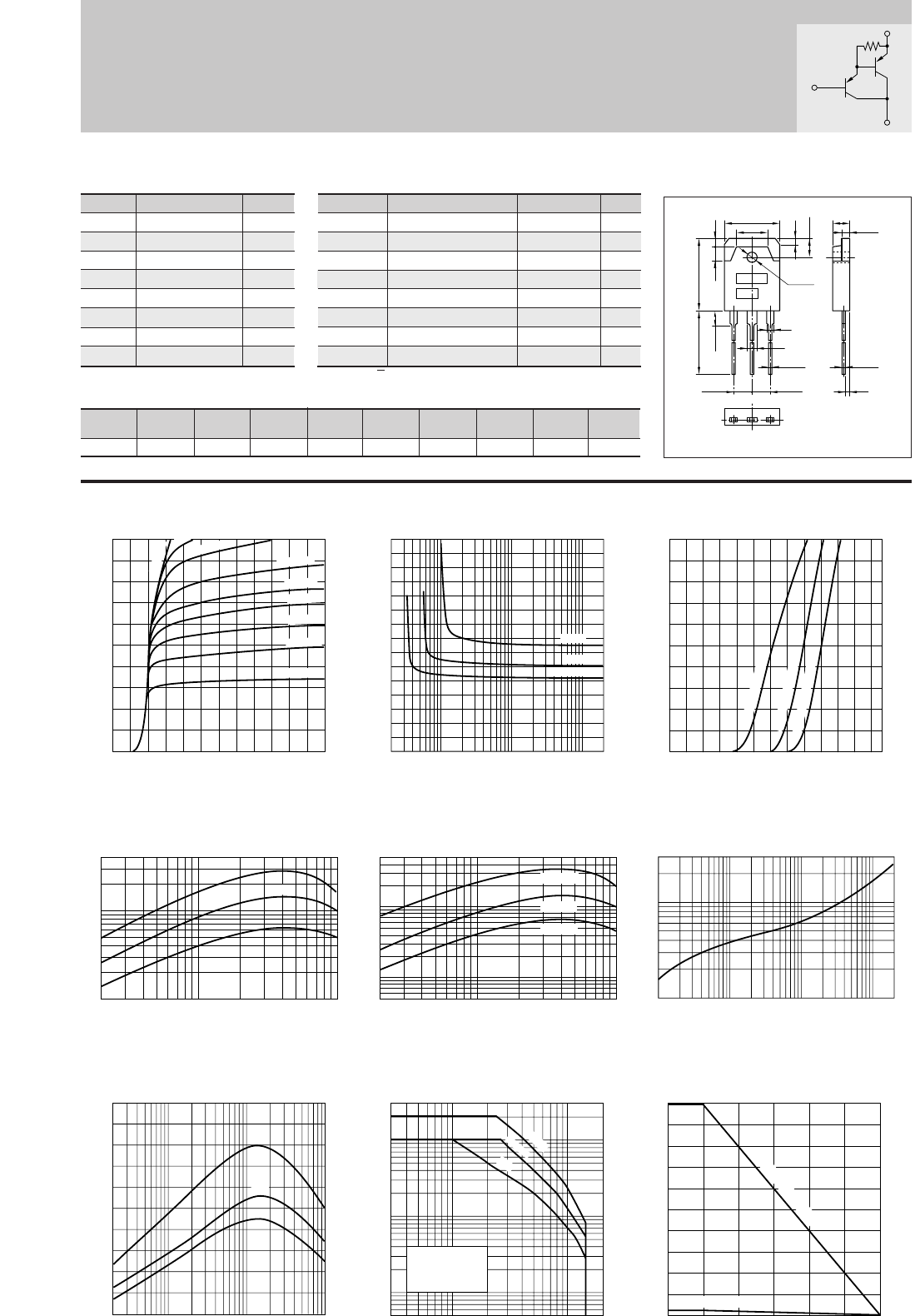
48
∗hFE Rank O(5000to12000), P(6500to20000), Y(15000to30000)
Darlington 2SB1560
IC–VCE Characteristics
(Typical)
hFE–IC Characteristics
(Typical)
hFE–IC
Temperature Characteristics (Typical)
IC–VBE Temperature Characteristics
(Typical)
VCE(sat)–IB Characteristics
(Typical)
Pc–Ta Derating
0
0
–2
–4
–6
–10
–8
–2 –4 –6
Collector-Emitter Voltage VCE(V)
Collector Current IC(A)
–10mA
–2.5mA
–2.0mA
–1.5mA
–1.0mA
–1.2mA
–0.8mA
–0.6mA
I
B
=–0.4mA
0
–3
–2
–1
–0.2
–1–0.5 –10–5 –200–100–50
Base Current IB(mA)
Collector-Emitter Saturation Voltage VCE(sat)(V)
–7A
–10A
IC=–5A
0
–10
–8
–6
–2
–4
0 –2.5–2–1
Base-Emittor Voltage VBE(V)
Collector Current IC(A)
(VCE=–4V)
125˚C (Case Temp)
25˚C (Case Temp)
–30˚C (Case Temp)
1,000
10,000
40,000
5,000
–0.2 –0.5 –1 –5 –10
Collector Current IC(A)
DC Current Gain hFE
(VCE=–4V)
Typ
(VCE=–4V)
–0.2 –1–0.5 –5 –10
500
1000
5000
10000
50000
Collector Current IC(A)
DC Current Gain hFE
125˚C
25˚C
–30˚C
0.1
1
3
0.5
1 5 10 50 100 500 1000 2000
Time t(ms)
Transient Thermal Resistance θj-a(˚C/W)
0.02 0.10.05 0.5 1 5 10
0
40
60
20
100
80
Cut-off Frequency fT(MHZ)
(VCE=–12V)
Emitter Current IE(A)
Typ
10ms
–10 –50–5–3 –100 –200
–0.05
–0.1
–1
–0.5
–10
–30
–5
Collector-Emitter Voltage VCE(V)
Collector Current IC(A)
DC
100ms
Without Heatsink
Natural Cooling
100
50
3.5
00 25 50 75 100 125 150
Ambient Temperature Ta(˚C)
Maximum Power Dissipation PC(W)
With Infinite heatsink
Without Heatsink
Safe Operating Area (Single Pulse)
θj-a–t Characteristics
fT–IE Characteristics
(Typical)
Silicon PNP Epitaxial Planar Transistor (Complement to type 2SD2390)
Application : Audio, Series Regulator and General Purpose
Symbol
VCBO
VCEO
VEBO
IC
IB
PC
Tj
Tstg
Ratings
–160
–150
–5
–10
–1
100(Tc=25°C)
150
–55 to +150
Unit
V
V
V
A
A
W
°C
°C
■
Absolute maximum ratings
■
Electrical Characteristics
Symbol
ICBO
IEBO
V(BR)CEO
hFE
VCE(sat)
VBE(sat)
fr
COB
Ratings
–100max
–100max
–150min
5000min∗
–2.5max
–3.0max
50typ
230typ
Unit
µ
A
µ
A
V
V
V
MHz
pF
Conditions
VCB=–160V
VEB=–5V
IC=–30mA
VCE=–4V, IC=–7A
IC=–7A, IB=–7mA
IC=–7A, IB=–7mA
VCE=–12V, IE=2A
VCB=–10V, f=1MHz
(Ta=25°C) (Ta=25°C)
■Typical Switching Characteristics (Common Emitter)
VCC
(V)
–70
RL
(Ω)
10
IC
(A)
–7
VBB2
(V)
5
IB2
(mA)
7
ton
(
µ
s)
0.8typ
tstg
(
µ
s)
3.0typ
tf
(
µ
s)
1.2typ
IB1
(mA)
–7
VBB1
(V)
–10
External Dimensions MT-100(TO3P)
15.6±0.4
9.6
19.9±0.3
4.0 2.0
5.0±0.2
1.8
ø3.2±0.1
2
3
1.05
+0.2
-0.1
20.0min
4.0max
BE
5.45±0.1 5.45±0.1
C
4.8±0.2
0.65
+0.2
-0.1
1.4
2.0±0.1
a
b
Weight : Approx 6.0g
a. Part No.
b. Lot No.
B
E
C
(70Ω)
Equivalent circuit
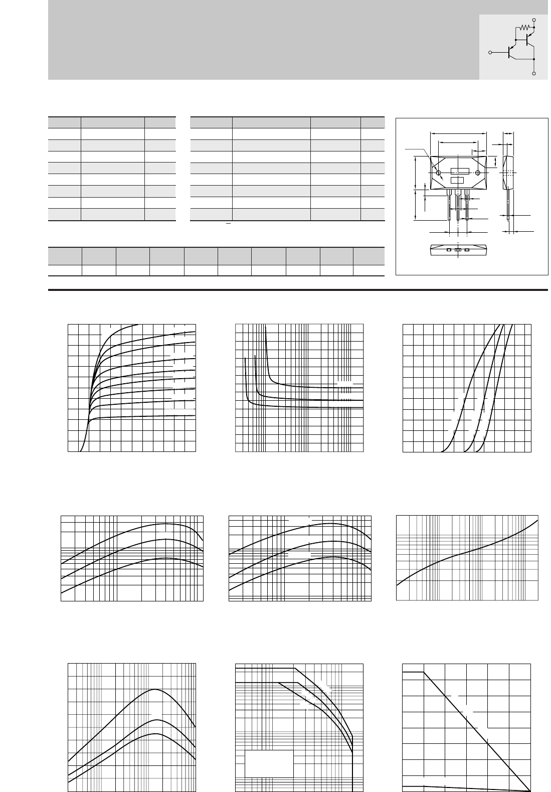
49
∗hFE Rank O(5000to12000), P(6500to20000), Y(15000to30000)
IC–VCE Characteristics
(Typical)
hFE–IC Characteristics
(Typical)
hFE–IC
Temperature Characteristics (Typical)
IC–VBE Temperature Characteristics
(Typical)
VCE(sat)–IB Characteristics
(Typical)
Pc–Ta Derating
0
0
–2
–4
–6
–12
–10
–8
–2 –4 –6
Collector-Emitter Voltage VCE(V)
Collector Current IC(A)
–10mA
–2.0mA
–2.0mA
–1.5mA
–1.0mA
–1.2mA
–0.8mA
–0.6mA
I
B
=–0.4mA
0
–3
–2
–1
–0.2
–1–0.5 –10–5 –200–100–50
Base Current IB(mA)
Collector-Emitter Saturation Voltage VCE(sat)(V)
–7A
–10A
IC=–5A
0
–12
–10
–8
–6
–2
–4
0 –2.5–2–1
Base-Emittor Voltage VBE(V)
Collector Current IC(A)
(VCE=–4V)
125˚C (Case Temp)
25˚C (Case Temp)
–30˚C (Case Temp)
1,000
10,000
40,000
5,000
–0.2 –0.5 –1 –5 –10–12
Collector Current IC(A)
DC Current Gain hFE
(VCE=–4V)
Typ
(VCE=–4V)
–0.2 –1–0.5 –5 –12–10
800
1000
5000
10000
50000
Collector Current IC(A)
DC Current Gain hFE
125˚C
25˚C
–30˚C
1 5 10 50 100 5001000 2000
Time t(ms)
0.1
1
2
0.5
Transient Thermal Resistance θj-a(˚C/W)
0.02 0.10.05 0.5 1 5 10
0
40
60
20
100
80
Cut-off Frequency fT(MHZ)
(VCE=–12V)
Emitter Current IE(A)
Typ
Without Heatsink
Natural Cooling
10ms
–10 –50–5–3 –100 –200
–0.05
–0.1
–1
–0.5
–10
–30
–5
Collector-Emitter Voltage VCE(V)
Collector Current IC(A)
DC
100ms
160
120
80
40
5
00 25 50 75 100 125 150
Ambient Temperature Ta(˚C)
Maximum Power Dissipation PC(W)
With Infinite heatsink
Without Heatsink
Safe Operating Area (Single Pulse)
θj-a–t Characteristics
fT–IE Characteristics
(Typical)
Silicon PNP Epitaxial Planar Transistor (Complement to type 2SD2401)
Application : Audio, Series Regulator and General Purpose
Symbol
VCBO
VCEO
VEBO
IC
IB
PC
Tj
Tstg
Ratings
–160
–150
–5
–12
–1
150(Tc=25°C)
150
–55 to +150
Unit
V
V
V
A
A
W
°C
°C
■
Absolute maximum ratings
■
Electrical Characteristics
Symbol
ICBO
IEBO
V(BR)CEO
hFE
VCE(sat)
VBE(sat)
fT
COB
Ratings
–100max
–100max
–150min
5000min∗
–2.5max
–3.0max
50typ
230typ
Unit
µ
A
µ
A
V
V
V
MHz
pF
Conditions
VCB=–160V
VEB=–5V
IC=–30mA
VCE=–4V, IC=–7A
IC=–7A, IB=–7mA
IC=–7A, IB=–7mA
VCE=–12V, IE=2A
VCB=–10V, f=1MHz
Darlington 2SB1570
(Ta=25°C) (Ta=25°C)
■Typical Switching Characteristics (Common Emitter)
VCC
(V)
–70
RL
(Ω)
10
IC
(A)
–7
VBB2
(V)
5
IB2
(mA)
7
ton
(
µ
s)
0.8typ
tstg
(
µ
s)
3.0typ
tf
(
µ
s)
1.2typ
IB1
(mA)
–7
VBB1
(V)
–10
External Dimensions MT-200
2
3
1.05
+0.2
-0.1
BE
5.45±0.1 5.45±0.1
2-ø3.2±0.1
36.4±0.3
9
24.4±0.2
7
21.4±0.3
20.0min
4.0max
0.65
+0.2
-0.1
3.0
+0.3
-0.1
6.0±0.2
2.1
a
b
C
Weight : Approx 18.4g
a. Part No.
b. Lot No.
B
E
C
(70Ω)
Equivalent circuit
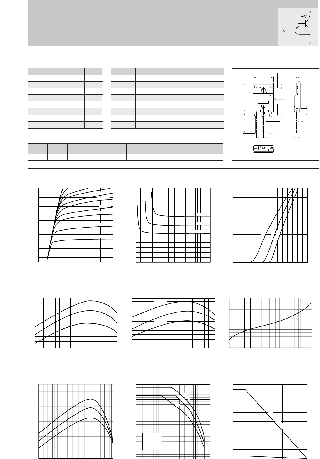
50
∗hFE Rank O(5000to12000), P(6500to20000), Y(15000to30000)
Darlington 2SB1587
IC–VCE Characteristics
(Typical)
hFE–IC Characteristics
(Typical)
hFE–IC
Temperature Characteristics (Typical)
IC–VBE Temperature Characteristics
(Typical)
VCE(sat)–IB Characteristics
(Typical)
Pc–Ta Derating
0
0
–2
–4
–6
–8
–2 –4 –6
Collector-Emitter Voltage VCE(V)
Collector Current IC(A)
–10mA
–2.5mA
–2.0mA
–1.8mA
–1.5mA
–1.3mA
–1.0mA
–0.8mA
–0.5mA
I
B
=–0.3mA
0
–3
–2
–1
–0.2
–1–0.5 –10–5 –200–100–50
Base Current IB(mA)
Collector-Emitter Saturation Voltage VCE(sat)(V)
–6A
–8A
IC=–4A
0
–8
–6
–2
–4
0–3–2–1
Base-Emittor Voltage VBE(V)
Collector Current IC(A)
(VCE=–4V)
125˚C (Case Temp)
25˚C (Case Temp)
–30˚C (Case Temp)
–0.2 –1–0.5 –8–5
2,000
5,000
10,000
40,000
Collector Current IC(A)
DC Current Gain hFE
(VCE=–4V)
Typ
(VCE=–4V)
–0.2 –1 –5–0.5 –8
Collector Current IC(A)
1000
5000
10000
50000
DC Current Gain hFE
125˚C
25˚C
–30˚C
0.2
0.5
4
1
1 5 10 50 100 500 1000 2000
Time t(ms)
Transient Thermal Resistance θj-a(˚C/W)
0.02 0.10.05 0.5 1 5 8
0
40
60
20
100
80
Cut-off Frequency fT(MHZ)
(VCE=–12V)
Emitter Current IE(A)
Typ
–10 –50–5–2 –100 –200
–0.05
–1
–0.5
–0.1
–10
–20
–5
Collector-Emitter Voltage VCE(V)
Collector Current IC(A)
Without Heatsink
Natural Cooling
DC
100ms
10ms
Safe Operating Area (Single Pulse)
θj-a–t Characteristics
fT–IE Characteristics
(Typical)
80
60
40
20
3.5
005025 75 100 125 150
Ambient Temperature Ta(˚C)
Maximum Power Dissipation PC(W)
With Infinite heatsink
Without Heatsink
Silicon PNP Epitaxial Planar Transistor (Complement to type 2SD2438)
Application : Audio, Series Regulator and General Purpose
Symbol
VCBO
VCEO
VEBO
IC
IB
PC
Tj
Tstg
Ratings
–160
–150
–5
–8
–1
75(Tc=25°C)
150
–55 to +150
Unit
V
V
V
A
A
W
°C
°C
■
Absolute maximum ratings
■
Electrical Characteristics
Symbol
ICBO
IEBO
V(BR)CEO
hFE
VCE(sat)
VBE(sat)
fT
COB
Ratings
–100max
–100max
–150min
5000min∗
–2.5max
–3.0max
65typ
160typ
Unit
µ
A
µ
A
V
V
V
MHz
pF
Conditions
VCB=–160V
VEB=–5V
IC=–30mA
VCE=–4V, IC=–6A
IC=–6A, IB=–6mA
IC=–6A, IB=–6mA
VCE=–12V, IE=1A
VCB=–10V, f=1MHz
(Ta=25°C) (Ta=25°C)
External Dimensions FM100(TO3PF)
4.41.5 1.5
BEC
5.45±0.1
ø3.3±0.2
1.6
3.3
1.75
0.8±0.2
2.15
1.05
+0.2
-0.1
5.45±0.1
23.0±0.3
16.2
9.5±0.2
5.5
15.6±0.2 5.5±0.2
3.45
3.35
0.65
+0.2
-0.1
±0.2
3.0
0.8
a
b
■Typical Switching Characteristics (Common Emitter)
VCC
(V)
–60
RL
(Ω)
10
IC
(A)
–6
VBB2
(V)
5
IB2
(mA)
6
ton
(
µ
s)
0.7typ
tstg
(
µ
s)
3.6typ
tf
(
µ
s)
0.9typ
IB1
(mA)
–6
VBB1
(V)
–10
Weight : Approx 6.5g
a. Part No.
b. Lot No.
B
E
C
(70Ω)
Equivalent circuit
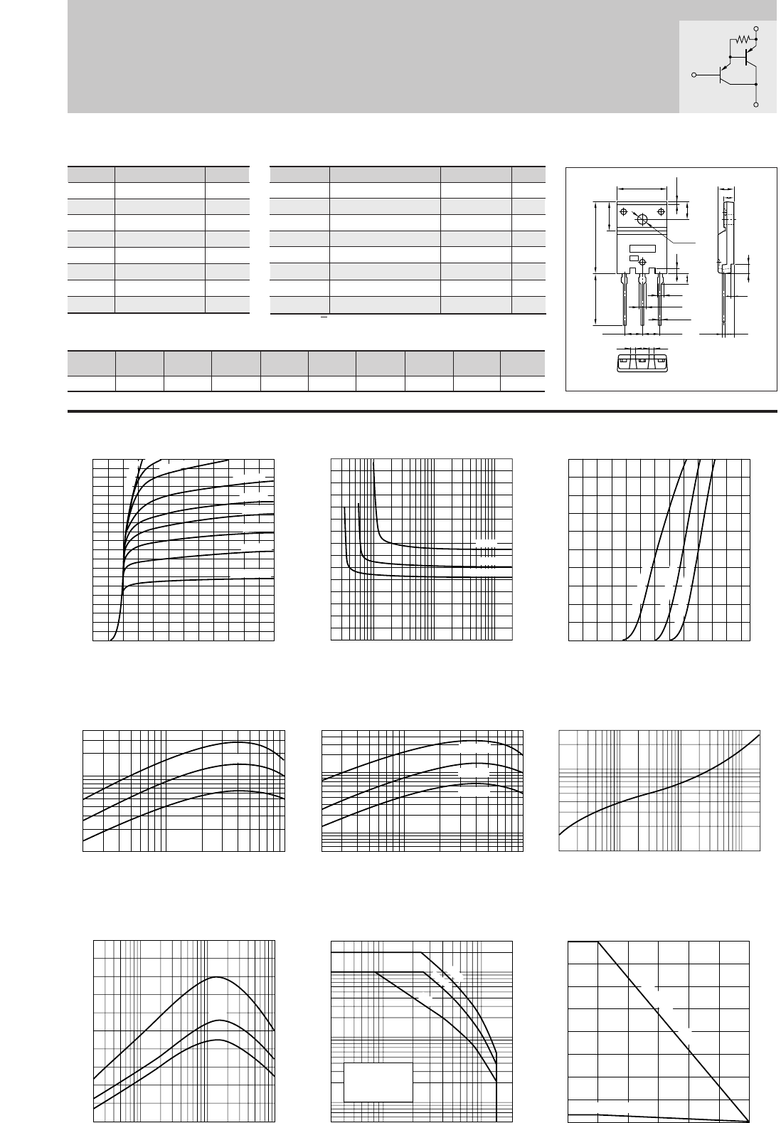
51
∗hFE Rank O(5000to12000), P(6500to20000), Y(15000to30000)
IC–VCE Characteristics
(Typical)
hFE–IC Characteristics
(Typical)
hFE–IC
Temperature Characteristics (Typical)
IC–VBE Temperature Characteristics
(Typical)
VCE(sat)–IB Characteristics
(Typical)
Pc–Ta Derating
0
0
–2
–4
–6
–10
–8
–2 –4 –6
Collector-Emitter Voltage VCE(V)
Collector Current IC(A)
–10mA
–2.5mA
–2.0mA
–1.5mA
–1.0mA
–1.2mA
–0.8mA
–0.6mA
I
B
=–0.4mA
0
–3
–2
–1
–0.2
–1–0.5 –10–5 –200–100–50
Base Current IB(mA)
Collector-Emitter Saturation Voltage VCE(sat)(V)
–7A
–10A
IC=–5A
0
–10
–8
–6
–2
–4
0 –2.5–2–1
Base-Emittor Voltage VBE(V)
Collector Current IC(A)
(VCE=–4V)
125˚C (Case Temp)
25˚C (Case Temp)
–30˚C (Case Temp)
1,000
10,000
40,000
5,000
–0.2 –0.5 –1 –5 –10
Collector Current IC(A)
DC Current Gain hFE
(VCE=–4V)
Typ
(VCE=–4V)
–0.2 –1–0.5 –5 –10
500
1,000
5,000
10,000
50,000
Collector Current IC(A)
DC Current Gain hFE
125˚C
25˚C
–30˚C
0.1
1
3
0.5
1 5 10 50 100 5001000 2000
Time t(ms)
Transient Thermal Resistance θj-a(˚C/W)
0.02 0.10.05 0.5 1 5 10
0
40
60
20
100
80
Cut-off Frequency fT(MHZ)
(VCE=–12V)
Emitter Current IE(A)
Typ
10ms
–10 –50–5–3 –100 –200
–0.05
–0.1
–1
–0.5
–10
–30
–5
Collector-Emitter Voltage VCE(V)
Collector Current IC(A)
DC
100ms
Without Heatsink
Natural Cooling
80
60
40
20
3.5
005025 75 100 125 150
Ambient Temperature Ta(˚C)
Maximum Power Dissipation PC(W)
With Infinite heatsink
Without Heatsink
Safe Operating Area (Single Pulse)
θj-a–t Characteristics
fT–IE Characteristics
(Typical)
Silicon PNP Epitaxial Planar Transistor (Complement to type 2SD2439)
Application : Audio, Series Regulator and General Purpose
Symbol
VCBO
VCEO
VEBO
IC
IB
PC
Tj
Tstg
Ratings
–160
–150
–5
–10
–1
80(Tc=25°C)
150
–55 to +150
Unit
V
V
V
A
A
W
°C
°C
■
Absolute maximum ratings
■
Electrical Characteristics
Symbol
ICBO
IEBO
V(BR)CEO
hFE
VCE(sat)
VBE(sat)
fT
COB
Ratings
–100max
–100max
–150min
5000min∗
–2.5max
–3.0max
50typ
230typ
Unit
µ
A
µ
A
V
V
V
MHz
pF
Conditions
VCB=–160V
VEB=–5V
IC=–30mA
VCE=–4V, IC=–7A
IC=–7A, IB=–7mA
IC=–7A, IB=–7mA
VCE=–12V, IE=2A
VCB=–10V, f=1MHz
Darlington 2SB1588
(Ta=25°C) (Ta=25°C)
■Typical Switching Characteristics (Common Emitter)
VCC
(V)
–70
RL
(Ω)
10
IC
(A)
–7
VBB2
(V)
5
IB2
(mA)
7
ton
(
µ
s)
0.8typ
tstg
(
µ
s)
3.0typ
tf
(
µ
s)
1.2typ
IB1
(mA)
–7
VBB1
(V)
–10
External Dimensions FM100(TO3PF)
4.41.5 1.5
BEC
5.45±0.1
ø3.3±0.2
1.6
3.3
1.75
0.8±0.2
2.15
1.05
+0.2
-0.1
5.45±0.1
23.0±0.3
16.2
9.5±0.2
5.5
15.6±0.2 5.5±0.2
3.45
3.35
0.65
+0.2
-0.1
±0.2
3.0
0.8
a
b
Weight : Approx 6.5g
a. Part No.
b. Lot No.
B
E
C
(70Ω)
Equivalent circuit
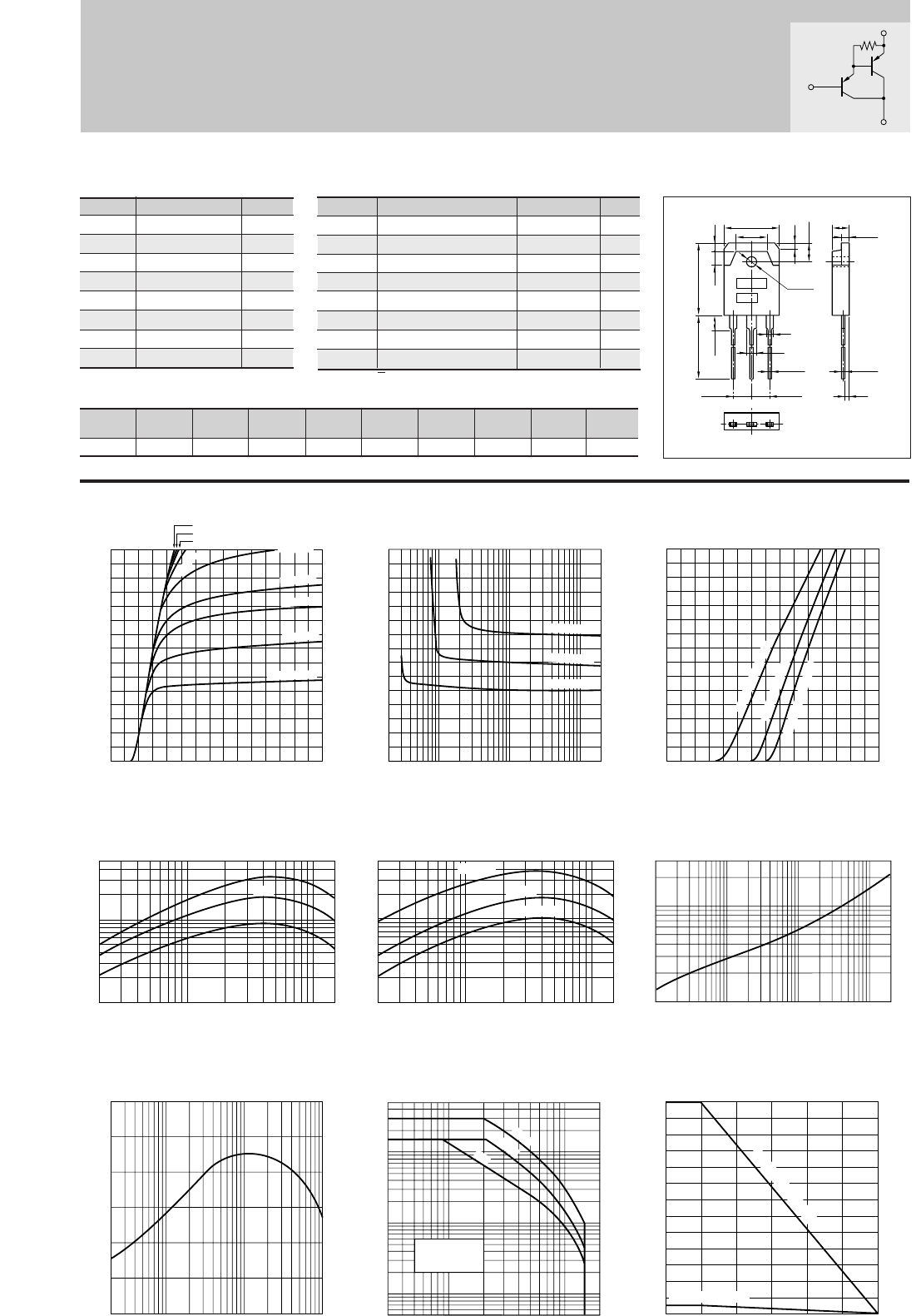
52
∗hFE Rank O(5000to12000), P(6500to20000), Y(15000to30000)
Darlington 2SB1647
IC–VCE Characteristics
(Typical)
hFE–IC Characteristics
(Typical)
hFE–IC
Temperature Characteristics (Typical)
IC–VBE Temperature Characteristics
(Typical)
VCE(sat)–IB Characteristics
(Typical)
Pc–Ta Derating
–10mA
–50mA
–3mA
0
–3
–2
–1
–0.2
–1–0.5 –10–5 –200–100–50
Base Current IB(mA)
Collector-Emitter Saturation Voltage VCE(sat)(V)
I
C
=–10A
I
C
=–15A
IC=–5A
0
–15
–10
–5
0–3–2–1
Base-Emittor Voltage VBE(V)
Collector Current IC(A)
(VCE=–4V)
125˚C (Case Temp)
25˚C (Case Temp)
–30˚C (Case Temp)
–0.2 –0.5 –1 –5 –10 –15
Collector Current IC(A)
DC Current Gain hFE
(VCE=–4V)
1,000
10,000
50,000
5,000
Typ
(VCE=–4V)
–0.2 –1–0.5 –5 –10 –15
1000
5000
10000
50000
Collector Current IC(A)
DC Current Gain hFE
25˚C
–30˚C
125˚C
Time t(ms)
0.1
1
3
0.5
1 10 100 1000 2000
Transient Thermal Resistance θj-a(˚C/W)
0.02 0.10.05 0.5 1 5 10
0
40
20
60
Cut-off Frequency fT(MHZ)
(VCE=–12V)
Emitter Current IE(A)
Safe Operating Area (Single Pulse)
θj-a–t Characteristics
fT–IE Characteristics
(Typical)
0
0
–5
–10
–15
–2 –6–4
Collector-Emitter Voltage VCE(V)
Collector Current IC(A)
–1.5mA
–1.0mA
–0.8mA
I
B
=–0.3mA
–0.5mA
–2mA
130
100
50
3.5
0
Ambient Temperature Ta(˚C)
Maximum Power Dissipation PC(W)
With Infinite heatsink
Without Heatsink
0 25 50 75 100 125 150
–10 –50–5–3 –100 –200
–0.05
–1
–0.5
–0.1
–10
–50
–5
DC
100ms
10ms
Without Heatsink
Natural Cooling
Collector-Emitter Voltage VCE(V)
Collector Current IC(A)
Silicon PNP Epitaxial Planar Transistor (Complement to type 2SD2560)
Application : Audio, Series Regulator and General Purpose
Symbol
VCBO
VCEO
VEBO
IC
IB
PC
Tj
Tstg
Ratings
–150
–150
–5
–15
–1
130(Tc=25°C)
150
–55 to +150
Unit
V
V
V
A
A
W
°C
°C
■
Absolute maximum ratings
■
Electrical Characteristics
Symbol
ICBO
IEBO
V(BR)CEO
hFE
VCE(sat)
VBE(sat)
fT
COB
Ratings
–100max
–100max
–150min
5000min∗
–2.5max
–3.0max
45typ
320typ
Unit
µ
A
µ
A
V
V
V
MHz
pF
Conditions
VCB=–150V
VEB=–5V
IC=–30mA
VCE=–4V, IC=–10A
IC=–10A, IB=–10mA
IC=–10A, IB=–10mA
VCE=–12V, IE=2A
VCB=–10V, f=1MHz
(Ta=25°C) (Ta=25°C)
External Dimensions MT-100(TO3P)
15.6±0.4
9.6
19.9±0.3
4.0 2.0
5.0±0.2
1.8
ø3.2±0.1
2
3
1.05
+0.2
-0.1
20.0min
4.0max
BE
5.45±0.1 5.45±0.1
C
4.8±0.2
0.65
+0.2
-0.1
1.4
2.0±0.1
a
b
■Typical Switching Characteristics (Common Emitter)
VCC
(V)
–40
RL
(Ω)
4
IC
(A)
10
VBB2
(V)
5
IB2
(mA)
10
ton
(
µ
s)
0.7typ
tstg
(
µ
s)
1.6typ
tf
(
µ
s)
1.1typ
IB1
(mA)
–10
VBB1
(V)
–10
Weight : Approx 6.0g
a. Part No.
b. Lot No.
B
E
C
(70Ω)
Equivalent circuit
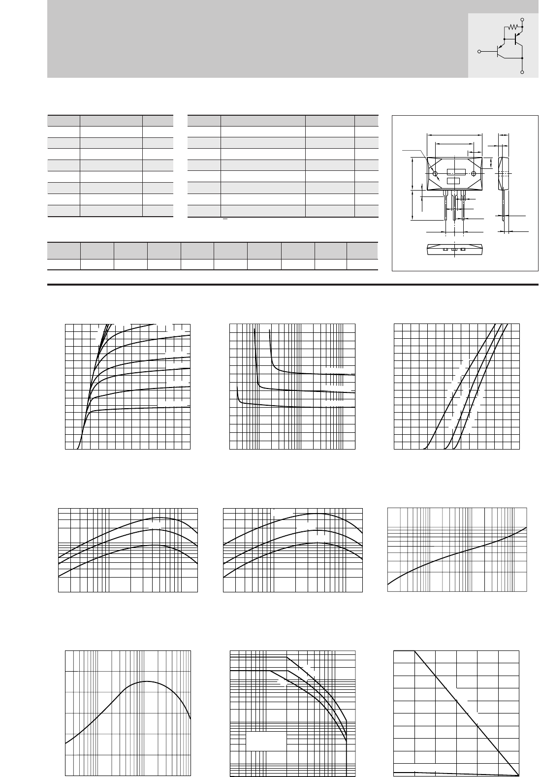
53
∗hFE Rank O(5000to12000), P(6500to20000), Y(15000to30000)
Darlington 2SB1648
IC–VCE Characteristics
(Typical)
hFE–IC Characteristics
(Typical)
hFE–IC
Temperature Characteristics (Typical)
IC–VBE Temperature Characteristics
(Typical)
VCE(sat)–IB Characteristics
(Typical)
Pc–Ta Derating
–10mA
0
17
15
10
5
0–3–2–1
Base-Emittor Voltage VBE(V)
Collector Current IC(A)
(VCE=–4V)
125˚C (Case Temp)
25˚C (Case Temp)
–30˚C (Case Temp)
–0.2 –0.5 –1 –5 –10 –17
Collector Current IC(A)
DC Current Gain hFE
(VCE=–4V)
1,000
10,000
50,000
5,000
Typ
(VCE=–4V)
–0.2 –1–0.5 –5 –10 –17
1000
5000
10000
50000
Collector Current IC(A)
DC Current Gain hFE
Time t(ms)
0.1
1
2
0.5
1 10 100 1000 2000
Transient Thermal Resistance θj-a(˚C/W)
Safe Operating Area (Single Pulse)
θj-a–t Characteristics
fT–IE Characteristics
(Typical)
0
0
–5
–10
–17
–15
–2 –6–4
Collector-Emitter Voltage VCE(V)
Collector Current IC(A)
–1.5mA
–2mA
–3mA
–50mA
–1.0mA
–0.8mA
I
B
=–0.3mA
–0.5mA
25˚C
–30˚C
125˚C
200
160
120
80
40
5
00 25 50 75 100 125 150
Ambient Temperature Ta(˚C)
Maximum Power Dissipation PC(W)
With Infinite heatsink
Without Heatsink
0
–3
–2
–1
–0.2
–1–0.5 –10–5 –200–100–50
Base Current IB(mA)
Collector-Emitter Saturation Voltage VCE(sat)(V)
I
C
=–10A
I
C
=–15A
IC=–5A
0.02 0.10.05 0.5 1 5 10
0
40
20
60
Cut-off Frequency fT(MHZ)
(VCE=–12V)
Emitter Current IE(A)
–10 –50–5–3 –100 –200
–0.05
–1
–0.5
–0.1
–10
–50
–5
DC
100ms
10ms
Collector-Emitter Voltage VCE(V)
Without Heatsink
Natural Cooling
Collector Current IC(A)
Silicon PNP Epitaxial Planar Transistor (Complement to type 2SD2561)
Application : Audio, Series Regulator and General Purpose
Symbol
VCBO
VCEO
VEBO
IC
IB
PC
Tj
Tstg
Ratings
–150
–150
–5
–17
–1
200(Tc=25°C)
150
–55 to +150
Unit
V
V
V
A
A
W
°C
°C
■
Absolute maximum ratings
■
Electrical Characteristics
Symbol
ICBO
IEBO
V(BR)CEO
hFE
VCE(sat)
VBE(sat)
fT
COB
Ratings
–100max
–100max
–150min
5000min∗
–2.5max
–3.0max
45typ
320typ
Unit
µ
A
µ
A
V
V
V
MHz
pF
Conditions
VCB=–150V
VEB=–5V
IC=–30mA
VCE=–4V, IC=–10A
IC=–10A, IB=–10mA
IC=–10A, IB=–10mA
VCE=–12V, IE=2A
VCB=–10V, f=1MHz
(Ta=25°C) (Ta=25°C)
■Typical Switching Characteristics (Common Emitter)
VCC
(V)
–40
RL
(Ω)
4
IC
(A)
–10
VBB2
(V)
5
IB2
(mA)
10
ton
(
µ
s)
0.7typ
tstg
(
µ
s)
1.6typ
tf
(
µ
s)
1.1typ
IB1
(mA)
–10
VBB1
(V)
–10
External Dimensions MT-200
2
3
1.05
+0.2
-0.1
BE
5.45±0.1 5.45±0.1
2-ø3.2±0.1
36.4±0.3
9
24.4±0.2
7
21.4±0.3
20.0min
4.0max
0.65
+0.2
-0.1
3.0
+0.3
-0.1
6.0±0.2
2.1
a
b
C
Weight : Approx 18.4g
a. Part No.
b. Lot No.
B
E
C
(70Ω)
Equivalent circuit
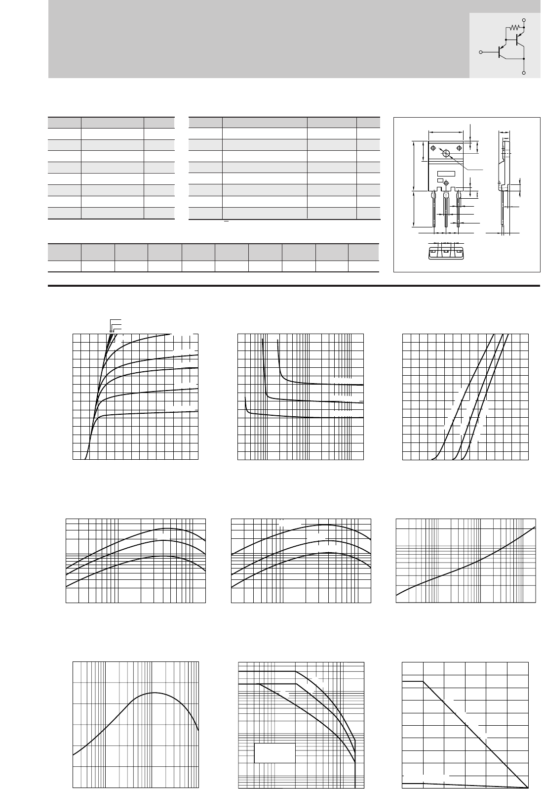
54
∗hFE Rank O(5000to12000), P(6500to20000), Y(15000to30000)
Darlington 2SB1649
IC–VCE Characteristics
(Typical)
hFE–IC Characteristics
(Typical)
hFE–IC
Temperature Characteristics (Typical)
IC–VBE Temperature Characteristics
(Typical)
VCE(sat)–IB Characteristics
(Typical)
Pc–Ta Derating
Safe Operating Area (Single Pulse)
θj-a–t Characteristics
fT–IE Characteristics
(Typical)
0
–3
–2
–1
–0.2
–1–0.5 –10–5 –200–100–50
Base Current IB(mA)
Collector-Emitter Saturation Voltage VCE(sat)(V)
I
C
=–10A
I
C
=–15A
IC=–5A
0
–15
–10
–5
0–3–2–1
Base-Emittor Voltage VBE(V)
Collector Current IC(A)
(VCE=–4V)
125˚C (Case Temp)
25˚C (CaseT emp)
–30˚C (CaseT emp)
–0.2 –0.5 –1 –5 –10 –15
Collector Current IC(A)
DC Current Gain hFE
(VCE=–4V)
1,000
10,000
50,000
5,000
Typ
(VCE=–4V)
–0.2 –1–0.5 –5 –10 –15
1000
5000
10000
50000
Collector Current IC(A)
DC Current Gain hFE
25˚C
–30˚C
125˚C
Time t(ms)
0.1
1
3
0.5
1 10 100 1000 2000
Transient Thermal Resistance θj-a(˚C/W)
0.02 0.10.05 0.5 1 5 10
0
40
20
60
Cut-off Frequency fT(MHZ)
(VCE=–12V)
Emitter Current IE(A)
100
80
60
40
20
3.5
0
Ambient Temperature Ta(˚C)
Maximum Power Dissipation PC(W)
With Infinite heatsink
Without Heatsink
0 25 50 75 100 125 150
–10mA
–50mA
–3mA
0
0
–5
–10
–15
–2 –6–4
Collector-Emitter Voltage VCE(V)
Collector Current IC(A)
–1.5mA
–1.0mA
–0.8mA
I
B
=–0.3mA
–0.5mA
–2mA
–10 –50–5–3 –100 –200
–0.05
–1
–0.5
–0.1
–10
–50
–5
DC
100ms
10ms
Collector-Emitter Voltage VCE(V)
Collector Current IC(A)
Without Heatsink
Natural Cooling
Silicon PNP Epitaxial Planar Transistor (Complement to type 2SD2561)
Application : Audio, Series Regulator and General Purpose
Symbol
VCBO
VCEO
VEBO
IC
IB
PC
Tj
Tstg
Ratings
–150
–150
–5
–15
–1
85(Tc=25°C)
150
–55 to +150
Unit
V
V
V
A
A
W
°C
°C
■
Absolute maximum ratings
■
Electrical Characteristics
Symbol
ICBO
IEBO
V(BR)CEO
hFE
VCE(sat)
VBE(sat)
fT
COB
Ratings
–100max
–100max
–150min
5000min∗
–2.5max
–3.0max
45typ
320typ
Unit
µ
A
µ
A
V
V
V
MHz
pF
Conditions
VCB=–150V
VEB=–5V
IC=–30mA
VCE=–4V, IC=–10A
IC=–10A, IB=–10mA
IC=–10A, IB=–10mA
VCE=–12V, IE=2A
VCB=–10V, f=1MHz
(Ta=25°C) (Ta=25°C)
■Typical Switching Characteristics (Common Emitter)
VCC
(V)
–40
RL
(Ω)
4
IC
(A)
–10
VBB2
(V)
5
IB2
(mA)
10
ton
(
µ
s)
0.7typ
tstg
(
µ
s)
1.6typ
tf
(
µ
s)
1.1typ
IB1
(mA)
–10
VBB1
(V)
–10
External Dimensions FM100(TO3PF)
4.41.5 1.5
BEC
5.45±0.1
ø3.3±0.2
1.6
3.3
1.75
0.8±0.2
2.15
1.05
+0.2
-0.1
5.45±0.1
23.0±0.3
16.2
9.5±0.2
5.5
15.6±0.2 5.5±0.2
3.45
3.35
0.65
+0.2
-0.1
±0.2
3.0
0.8
a
b
Weight : Approx 6.5g
a. Part No.
b. Lot No.
B
E
C
(70Ω)
Equivalent circuit
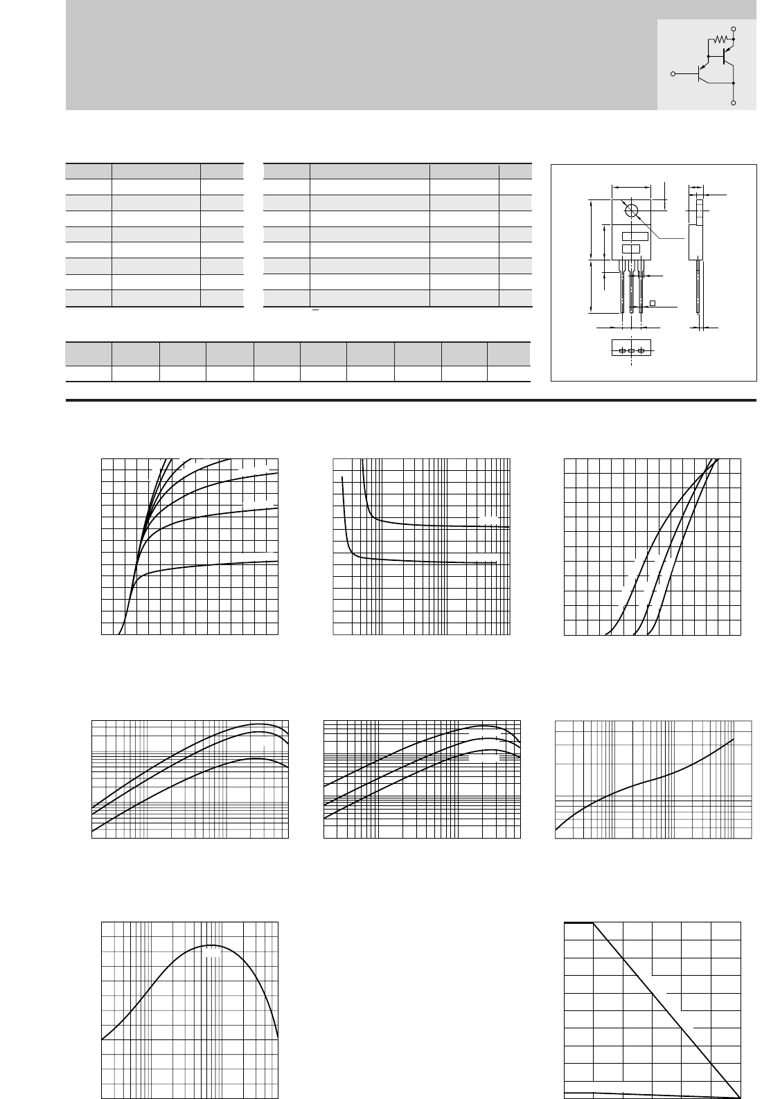
55
∗hFE Rank O(5000to12000), P(6500to20000), Y(15000to30000)
Darlington 2SB1659
Silicon PNP Epitaxial Planar Transistor (Complement to type 2SD2589)
Application : Audio, Series Regulator and General Purpose
Symbol
VCBO
VCEO
VEBO
IC
IB
PC
Tj
Tstg
Ratings
–110
–110
–5
–6
–1
50(Tc=25°C)
150
–55 to +150
Unit
V
V
V
A
A
W
°C
°C
■
Absolute maximum ratings
■
Electrical Characteristics
Symbol
ICBO
IEBO
V(BR)CEO
hFE
VCE(sat)
VBE(sat)
fT
COB
Ratings
–100max
–100max
–110min
5000min∗
–2.5max
–3.0max
100typ
110typ
Unit
µ
A
µ
A
V
V
V
MHz
pF
Conditions
VCB=–110V
VEB=–5V
IC=–30mA
VCE=–4V, IC=–5A
IC=–5A, IB=–5mA
IC=–5A, IB=–5mA
VCE=–12V, IE=0.5A
VCB=–10V, f=1MHz
(Ta=25°C) (Ta=25°C)
■Typical Switching Characteristics (Common Emitter)
VCC
(V)
–30
RL
(Ω)
6
IC
(A)
–5
VBB2
(V)
5
IB2
(mA)
5
ton
(
µ
s)
1.1typ
tstg
(
µ
s)
3.2typ
tf
(
µ
s)
1.1typ
IB1
(mA)
–5
VBB1
(V)
–10
External Dimensions MT-25(TO220)
BE
2.5 2.5
C
16.0±0.7
12.0min
4.0max 8.8±0.2
1.35
0.65
+0.2
-0.1
10.2±0.2
ø3.75±0.2
3.0±0.2
4.8±0.2
1.4
2.0±0.1
a
b
Weight : Approx 2.0g
a. Part No.
b. Lot No.
B
E
C
(70Ω)
Equivalent circuit
Collector Current IC(A)
IC–VCE Characteristics
(Typical)
0
0
–2
–4
–6
–2 –6–4
I
B
=–0.1mA
–5mA
–1mA
–0.5mA
–0.4mA
–0.3mA
–0.2mA
0
–3
–2
–1
–0.1
–1–0.5 –10–5 –100–50
–5A
IC=–3A
0
–6
–4
–2
0–3–2–1
(VCE=–4V)
–0.02 –0.05 –0.1 –1–0.5 –6–5
(VCE=–4V)
500
200
10000
40000
1000
5000
Typ
(VCE=–4V)
–0.02 –0.1–0.05 –0.5 –6–5–1
100
5000
10000
500
1000
50000
25˚C
–30˚C
125˚C
0.02 0.10.05 0.5 1 5 6
60
40
0
20
100
120
80
(VCE=–12V)
Typ
50
40
30
20
10
2
00 25 50 75 100 125 150
0.4
1
5
0.5
1 10 100 1000 2000
hFE–IC Characteristics
(Typical)
hFE–IC
Temperature Characteristics (Typical)
IC–VBE Temperature Characteristics
(Typical)
VCE(sat)–IB Characteristics
(Typical)
Pc–Ta Derating
Safe Operating Area (Single Pulse)
θj-a–t Characteristics
fT–IE Characteristics
(Typical)
125˚C (Case Temp)
25˚C (CaseT emp)
–30˚C (CaseT emp)
Collector Current IC(A) Collector Current IC(A) Time t(ms)
DC Current Gain hFE
DC Current Gain hFE
Transient Thermal Resistance θj-a(˚C/W)
Cut-off Frequency fT(MHZ)
Emitter Current IE(A) Ambient Temperature Ta(˚C)
Maximum Power Dissipation PC(W)
With Infinite heatsink
Without Heatsink
Base Current IB(mA) Base-Emittor Voltage VBE(V)
Collector-Emitter Voltage VCE(V)
Collector-Emitter Saturation Voltage VCE(sat)(V)
Collector Current IC(A)
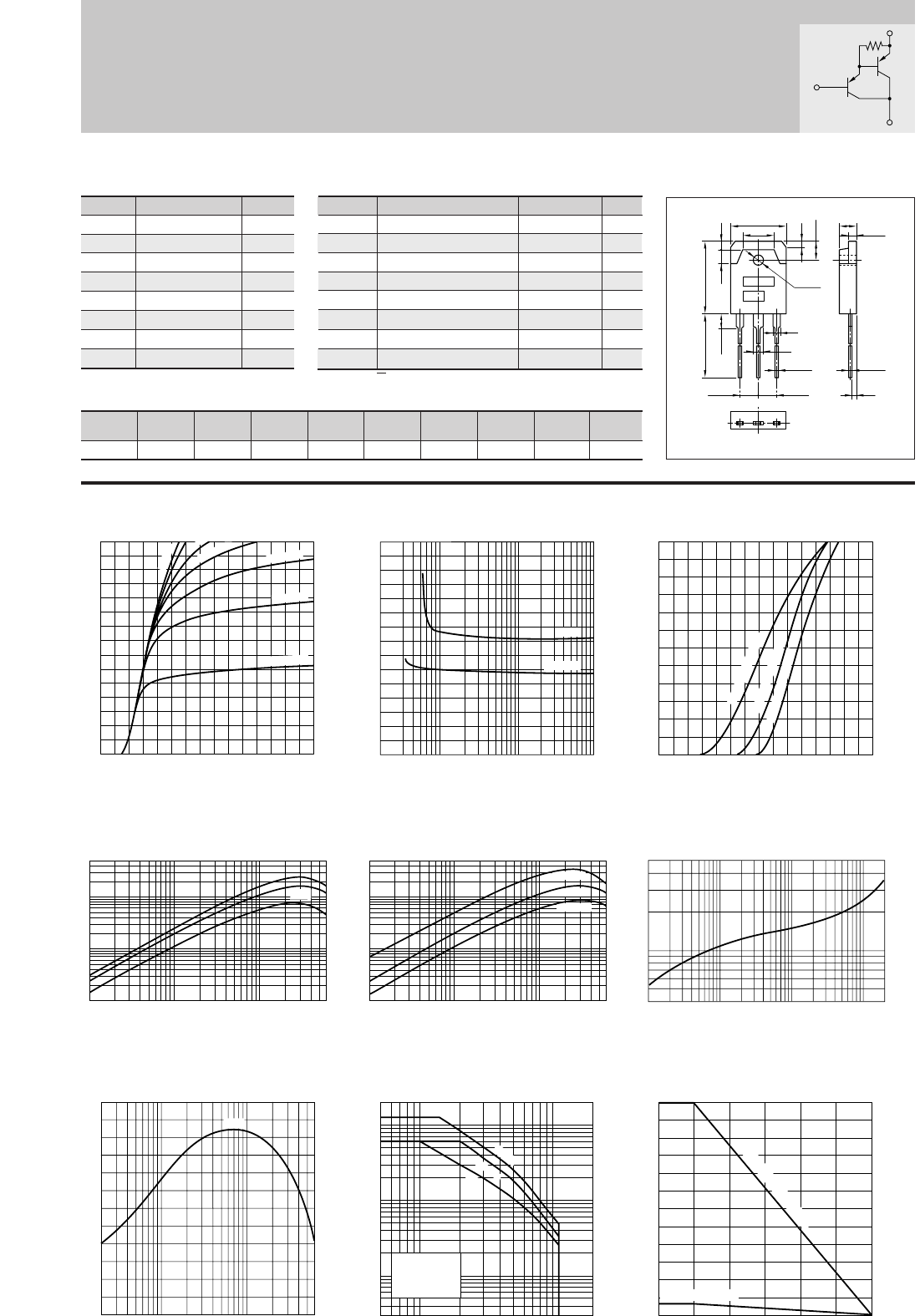
56
∗hFE Rank O(5000to12000), P(6500to20000), Y(15000to30000)
0
–3
–2
–1
–0.1
–1–0.5 –10–5 –100–50
–5A
IC=–3A
–0.01 –0.1–0.05 –0.5 –6–5–1
100
5000
10000
500
1000
50000
25˚C
–30˚C
125˚C
(VCE=–4V)
–0.01 –0.1–0.05 –0.5 –6–5–1
100
5000
10000
500
1000
50000
Typ
(VCE=–4V)
0
–6
–4
–2
0–3–2–1
125˚C (Case Temp)
25˚C (Case Temp)
–30˚C (Case Temp)
(VCE=–4V)
IC–VCE Characteristics
(Typical)
hFE–IC Characteristics
(Typical)
hFE–IC
Temperature Characteristics (Typical)
IC–VBE Temperature Characteristics
(Typical)
VCE(sat)–IB Characteristics
(Typical)
Pc–Ta Derating
0
0
–2
–4
–6
–2 –6–4
Collector-Emitter Voltage VCE(V)
Collector Current IC(A)
I
B
=–0.1mA
–5mA
–1mA
–0.5mA
–0.4mA
–0.3mA
–0.2mA
Base Current IB(mA)
Collector-Emitter Saturation Voltage VCE(sat)(V)
Base-Emittor Voltage VBE(V)
Collector Current IC(A)
Collector Current IC(A)
DC Current Gain hFE
Collector Current IC(A)
DC Current Gain hFE
0.5
5
1
1 5 10 50 100 500 1000 2000
Time t(ms)
Transient Thermal Resistance θj-a(˚C/W)
0.02 0.10.05 0.5 1 5 6
60
40
0
20
100
120
80
Cut-off Frequency fT(MHZ)
(VCE=–12V)
Emitter Current IE(A)
Typ
Collector-Emitter Voltage VCE(V)
Collector Current IC(A)
–5 –10 –50 –100 –200
–0.1
–0.05
–1
–0.5
–10
–20
–5
10ms
DC
100ms
Without Heatsink
Natural Cooling
60
40
20
3.5
00 25 50 75 100 125 150
Ambient Temperature Ta(˚C)
Maximum Power Dissipation PC(W)
With Infinite heatsink
Without Heatsink
Safe Operating Area (Single Pulse)
θj-a–t Characteristics
fT–IE Characteristics
(Typical)
Silicon PNP Epitaxial Planar Transistor (Complement to type 2SD2641)
Application : Audio, Series Regulator and General Purpose
Symbol
VCBO
VCEO
VEBO
IC
IB
PC
Tj
Tstg
Ratings
–110
–110
–5
–6
–1
60(Tc=25°C)
150
–55 to +150
Unit
V
V
V
A
A
W
°C
°C
■
Absolute maximum ratings
■
Electrical Characteristics
Symbol
ICBO
IEBO
V(BR)CEO
hFE
VCE(sat)
VBE(sat)
fT
COB
Ratings
–100max
–100max
–110min
5000min∗
–2.5max
–3.0max
100typ
110typ
Unit
µ
A
µ
A
V
V
V
MHz
pF
Conditions
VCB=–110V
VEB=–5V
IC=–30mA
VCE=–4V, IC=–5A
IC=–5A, IB=–5mA
IC=–5A, IB=–5mA
VCE=–12V, IE=0.5A
VCB=–10V, f=1MHz
Darlington 2SB1685
(Ta=25°C) (Ta=25°C)
■Typical Switching Characteristics (Common Emitter)
VCC
(V)
–30
RL
(Ω)
6
IC
(A)
–5
VBB2
(V)
5
IB2
(mA)
5
ton
(
µ
s)
1.1typ
tstg
(
µ
s)
3.2typ
tf
(
µ
s)
1.1typ
IB1
(mA)
–5
VBB1
(V)
–10
External Dimensions MT-100(TO3P)
15.6±0.4
9.6
19.9±0.3
4.0 2.0
5.0±0.2
1.8
ø3.2±0.1
2
3
1.05
+0.2
-0.1
20.0min
4.0max
BE
5.45±0.1 5.45±0.1
C
4.8±0.2
0.65
+0.2
-0.1
1.4
2.0±0.1
a
b
Weight : Approx 6.0g
a. Part No.
b. Lot No.
B
E
C
(70Ω)
Equivalent circuit
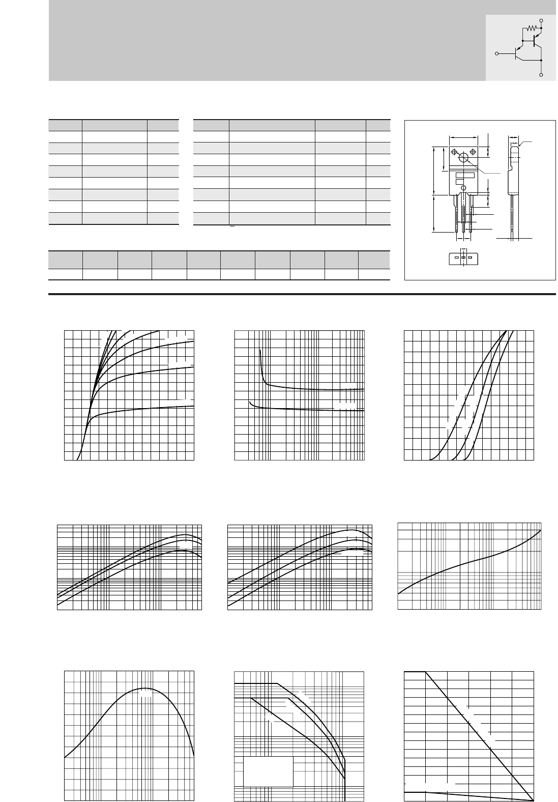
57
∗hFE Rank O(5000to12000), P(6500to20000), Y(15000to30000)
0
–3
–2
–1
–0.1
–1–0.5 –10–5 –100–50
–5A
IC=–3A
–0.01 –0.1–0.05 –0.5 –6–5–1
100
5000
10000
500
1000
50000
25˚C
–30˚C
125˚C
(VCE=–4V)
–0.01 –0.1–0.05 –0.5 –6–5–1
100
5000
10000
500
1000
50000
Typ
(VCE=–4V)
0
–6
–4
–2
0–3–2–1
125˚C (Case Temp)
25˚C (Case Temp)
–30˚C (Case Temp)
(VCE=–4V)
IC–VCE Characteristics
(Typical)
hFE–IC Characteristics
(Typical)
hFE–IC
Temperature Characteristics (Typical)
IC–VBE Temperature Characteristics
(Typical)
VCE(sat)–IB Characteristics
(Typical)
Pc–Ta Derating
0
0
–2
–4
–6
–2 –6–4
Collector-Emitter Voltage VCE(V)
Collector Current IC(A)
I
B
=–0.1mA
–5mA
–1mA
–0.5mA
–0.4mA
–0.3mA
–0.2mA
Base Current IB(mA)
Collector-Emitter Saturation Voltage VCE(sat)(V)
Base-Emittor Voltage VBE(V)
Collector Current IC(A)
Collector Current IC(A)
DC Current Gain hFE
Collector Current IC(A)
DC Current Gain hFE
0.3
0.5
5.0
1.0
1 10 100 1000
Time t(ms)
Transient Thermal Resistance θj-a(˚C/W)
0.02 0.10.05 0.5 1 5 6
60
40
0
20
100
120
80
Cut-off Frequency fT(MHZ)
(VCE=–12V)
Emitter Current IE(A)
Typ
–10 –50–5–3 –100 –200
–0.05
–1
–0.5
–0.1
–10
–20
–5
Collector-Emitter Voltage VCE(V)
Collector Current IC(A)
DC
100ms
10ms
Without Heatsink
Natural Cooling
30
20
10
2
00 25 50 75 100 125 150
Ambient Temperature Ta(˚C)
Maximum Power Dissipation PC(W)
With Infinite heatsink
Without Heatsink
Safe Operating Area (Single Pulse)
θj-a–t Characteristics
fT–IE Characteristics
(Typical)
Silicon PNP Epitaxial Planar Transistor (Complement to type 2SD2642)
Application : Audio, Series Regulator and General Purpose
Symbol
VCBO
VCEO
VEBO
IC
IB
PC
Tj
Tstg
Ratings
–110
–110
–5
–6
–1
30(Tc=25°C)
150
–55 to +150
Unit
V
V
V
A
A
W
°C
°C
■
Absolute maximum ratings
■
Electrical Characteristics
Symbol
ICBO
IEBO
V(BR)CEO
hFE
VCE(sat)
VBE(sat)
fT
COB
Ratings
–100max
–100max
–110min
5000min∗
–2.5max
–3.0max
100typ
110typ
Unit
µ
A
µ
A
V
V
V
MHz
pF
Conditions
VCB=–110V
VEB=–5V
IC=–30mA
VCE=–4V, IC=–5A
IC=–5A, IB=–5mA
IC=–5A, IB=–5mA
VCE=–12V, IE=0.5A
VCB=–10V, f=1MHz
Darlington 2SB1686
(Ta=25°C) (Ta=25°C)
External Dimensions FM20(TO220F)
ø3.3±0.2
10.1±0.2
4.0±0.2
16.9±0.3
13.0min
8.4±0.2
0.8±0.2
3.9
±0.2
2.542.54
1.35±0.15
0.85
+0.2
-0.1
1.35±0.15
2.2±0.2
4.2±0.2
2.8 c0.5
2.4±0.2
0.45
+0.2
-0.1
BEC
a
b
■Typical Switching Characteristics (Common Emitter)
VCC
(V)
–30
RL
(Ω)
6
IC
(A)
–5
VBB2
(V)
5
IB2
(mA)
5
ton
(
µ
s)
1.1typ
tstg
(
µ
s)
3.2typ
tf
(
µ
s)
1.1typ
IB1
(mA)
–5
VBB1
(V)
–10
Weight : Approx 2.0g
a. Part No.
b. Lot No.
B
E
C
(70Ω)
Equivalent circuit
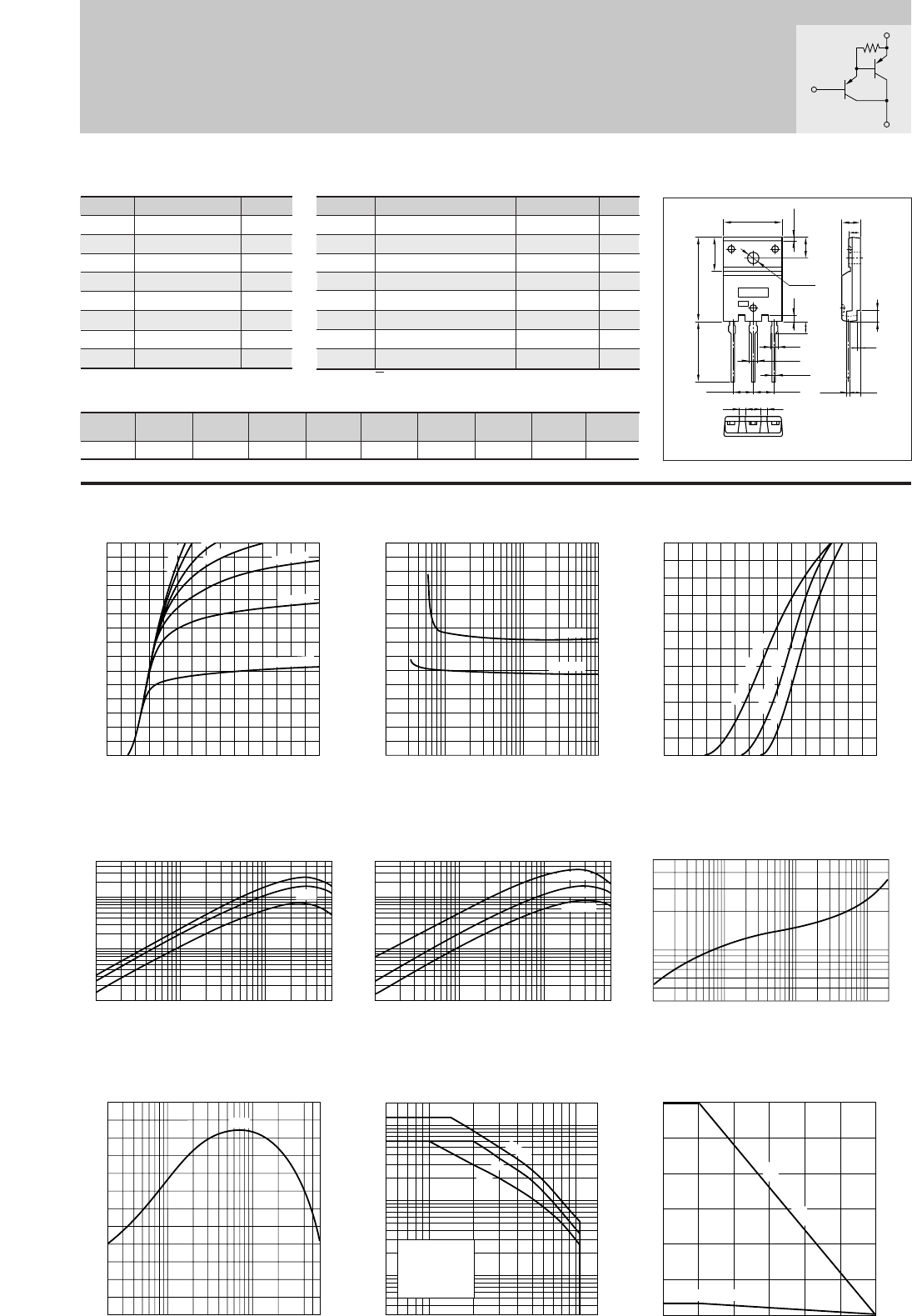
58
Darlington 2SB1687
∗hFE Rank O(5000to12000), P(6500to20000), Y(15000to30000)
0
–3
–2
–1
–0.1
–1–0.5 –10–5 –100–50
–5A
IC=–3A
–0.01 –0.1–0.05 –0.5 –6–5–1
100
5000
10000
500
1000
50000
25˚C
–30˚C
125˚C
(VCE=–4V)
–0.01 –0.1–0.05 –0.5 –6–5–1
100
5000
10000
500
1000
50000
Typ
(VCE=–4V)
0
–6
–4
–2
0–3–2–1
125˚C (Case Temp)
25˚C (Case Temp)
–30˚C (Case Temp)
(VCE=–4V)
IC–VCE Characteristics
(Typical)
hFE–IC Characteristics
(Typical)
hFE–IC
Temperature Characteristics (Typical)
IC–VBE Temperature Characteristics
(Typical)
VCE(sat)–IB Characteristics
(Typical)
Pc–Ta Derating
0
0
–2
–4
–6
–2 –6–4
Collector-Emitter Voltage VCE(V)
Collector Current IC(A)
I
B
=–0.1mA
–5mA
–1mA
–0.5mA
–0.4mA
–0.3mA
–0.2mA
Base Current IB(mA)
Collector-Emitter Saturation Voltage VCE(sat)(V)
Base-Emittor Voltage VBE(V)
Collector Current IC(A)
Collector Current IC(A)
DC Current Gain hFE
Collector Current IC(A)
DC Current Gain hFE
0.5
5
1
1 10 100 1000 2000
Time t(ms)
Transient Thermal Resistance θj-a(˚C/W)
0.02 0.10.05 0.5 1 5 6
60
40
0
20
100
120
80
Cut-off Frequency fT(MHZ)
(VCE=–12V)
Emitter Current IE(A)
Typ
Collector-Emitter Voltage VCE(V)
Collector Current IC(A)
–5 –10 –50 –100 –150
–0.1
–0.05
–1
–0.5
–10
–20
–5
10ms
DC
100ms
Without Heatsink
Natural Cooling
60
40
20
3.5
005025 75 125100 150
Ambient Temperature Ta(˚C)
Maximum Power Dissipation PC(W)
With Infinite heatsink
Without Heatsink
Safe Operating Area (Single Pulse)
θj-a–t Characteristics
fT–IE Characteristics
(Typical)
Application : Audio, Series Regulator and General Purpose
Symbol
VCBO
VCEO
VEBO
IC
IB
PC
Tj
Tstg
Ratings
–110
–110
–5
–6
–1
60(Tc=25°C)
150
–55 to +150
Unit
V
V
V
A
A
W
°C
°C
■
Absolute maximum ratings
■
Electrical Characteristics
Symbol
ICBO
IEBO
V(BR)CEO
hFE
VCE(sat)
VBE(sat)
fT
COB
Ratings
–100max
–100max
–110min
5000min∗
–2.5max
–3.0max
–100typ
–110typ
Unit
µ
A
µ
A
V
V
V
MHz
pF
Conditions
VCB=–110V
VEB=–5V
IC=–30mA
VCE=–4V, IC=–5A
IC=–5A, IB=–5mA
IC=–5A, IB=–5mA
VCE=–12V, IE=0.5A
VCB=–10V, f=1MHz
(Ta=25°C) (Ta=25°C)
■Typical Switching Characteristics (Common Emitter)
VCC
(V)
–30
RL
(Ω)
6
IC
(A)
–5
VBB2
(V)
5
IB2
(mA)
5
ton
(
µ
s)
1.1typ
tstg
(
µ
s)
3.2typ
tf
(
µ
s)
1.1typ
IB1
(mA)
–5
VBB1
(V)
–10
B
E
C
(70Ω)
Equivalent circuit
External Dimensions FM100(TO3P)
4.41.5 1.5
BEC
5.45±0.1
ø3.3±0.2
1.6
3.3
1.75
0.8±0.2
2.15
1.05
+0.2
-0.1
5.45±0.1
23.0±0.3
16.2
9.5±0.2
5.5
15.6±0.2 5.5±0.2
3.45
3.35
0.65
+0.2
-0.1
±0.2
3.0
0.8
a
b
Weight : Approx 6.5g
a. Part No.
b. Lot No.
Silicon PNP Epitaxial Planar Transistor (Complement to type 2SD2643)
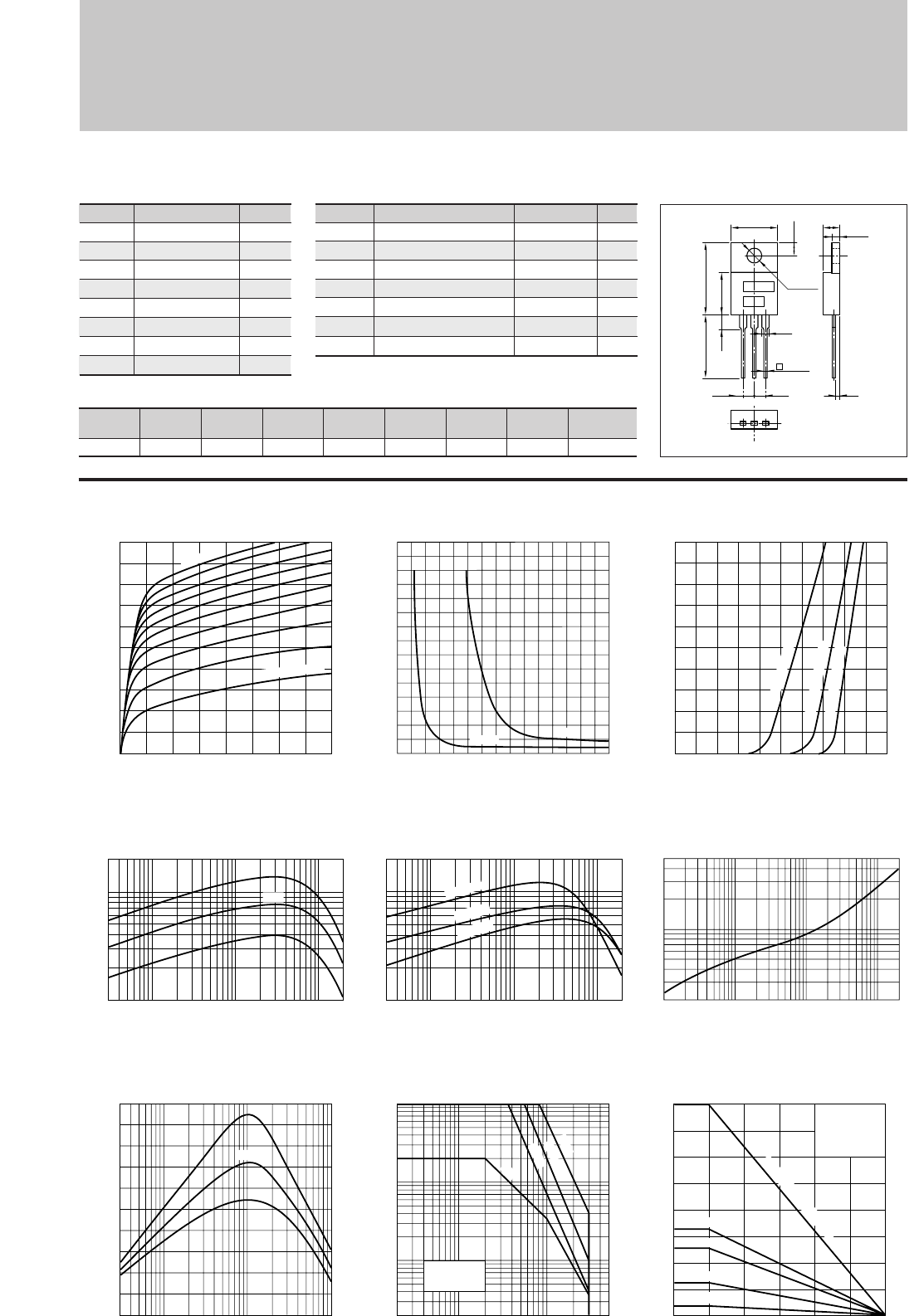
59
IC–VCE Characteristics
(Typical)
hFE–IC Characteristics
(Typical)
hFE–IC
Temperature Characteristics (Typical)
θj-a–t Characteristics
IC–VBE Temperature Characteristics
(Typical)
VCE(sat)–IB Characteristics
(Typical)
Pc–Ta Derating
0
0
1
2
2134
Collector-Emitter Voltage VCE(V)
Collector Current IC(A)
I
B
=200mA
I
B
=20mA/stop
Safe Operating Area (Single Pulse)
fT–IE Characteristics
(Typical)
0
3
2
1
0 0.1 0.2 0.3
Base Current IB(A)
Collector-Emitter Saturation Voltage VCE(sat)(V)
IC=1A 2A
3 10 1000 2000100
10
50
100
200
Collector Current IC(mA)
DC Current Gain hFE
(VCE=4V)
Typ
0.2
0.5
1
5
1 10 100
1000 2000
Time t(ms)
Transient Thermal Resistance θj-a(˚C/W)
10 1002 500
0.02
0.1
1
0.5
0.05
10
5
Collector-Emitter Voltage VCE(V)
Collector Current IC(A)
Without Heatsink
Natural Cooling
DC
20ms
5ms
1ms
40
30
20
10
2
00 25 50 75 100 125 150
Ambient Temperature Ta(˚C)
Maximum Power Dissipation PC(W)
50x50x2
100x100x2
150x150x2
With Infinite heatsink
Without Heatsink
0
2
1
0 1.0
0.80.60.40.2
Base-Emittor Voltage VBE(V)
Collector Current IC(A)
(VCE=4V)
125˚C (Case Temp)
25˚C (Case Temp)
–30˚C (Case Temp)
(VCE=4V)
3 5 10 50 100 500
1000 2000
10
50
200
100
Collector Current IC(mA)
DC Current Gain hFE
25˚C
–30˚C
125˚C
–0.003 –0.01 –0.05
–0.1 –0.5 –1
10
0
20
Cut-off Frequency fT(MHZ)
(VCE=12V)
Emitter Current IE(A)
Typ
Natural Cooling
Silicone Grease
Heatsink: Aluminum
in mm
Silicon NPN Triple Diffused Planar Transistor Application : Series Regulator, Switch, and General Purpose
Symbol
VCBO
VCEO
VEBO
IC
IB
PC
Tj
Tstg
Ratings
300
300
6
2
0.2
40(Tc=25°C)
150
–55 to +150
Unit
V
V
V
A
A
W
°C
°C
■
Absolute maximum ratings
■
Electrical Characteristics
Symbol
ICBO
IEBO
V(BR)CEO
hFE
VCE(sat)
fT
COB
Ratings
1.0max
1.0max
300min
30min
1.0max
10typ
75typ
Unit
mA
mA
V
V
MHz
pF
Conditions
VCB=300V
VEB=6V
IC=25mA
VCE=4V, IC=0.5A
IC=1.0A, IB=0.2A
VCE=12A, IE=–0.2A
VCB=10V, f=1MHz
2SC2023
(Ta=25°C) (Ta=25°C)
External Dimensions MT-25(TO220)
BE
2.5 2.5
C
16.0±0.7
12.0min
4.0max 8.8±0.2
1.35
0.65
+0.2
-0.1
10.2±0.2
ø3.75±0.2
3.0±0.2
4.8±0.2
1.4
2.0±0.1
a
b
■Typical Switching Characteristics (Common Emitter)
VCC
(V)
100
RL
(Ω)
100
IC
(A)
1.0
VB2
(V)
–5
IB2
(mA)
–200
ton
(
µ
s)
0.3typ
tstg
(
µ
s)
4.0typ
tf
(
µ
s)
1.0typ
IB1
(mA)
100
Weight : Approx 2.6g
a. Part No.
b. Lot No.
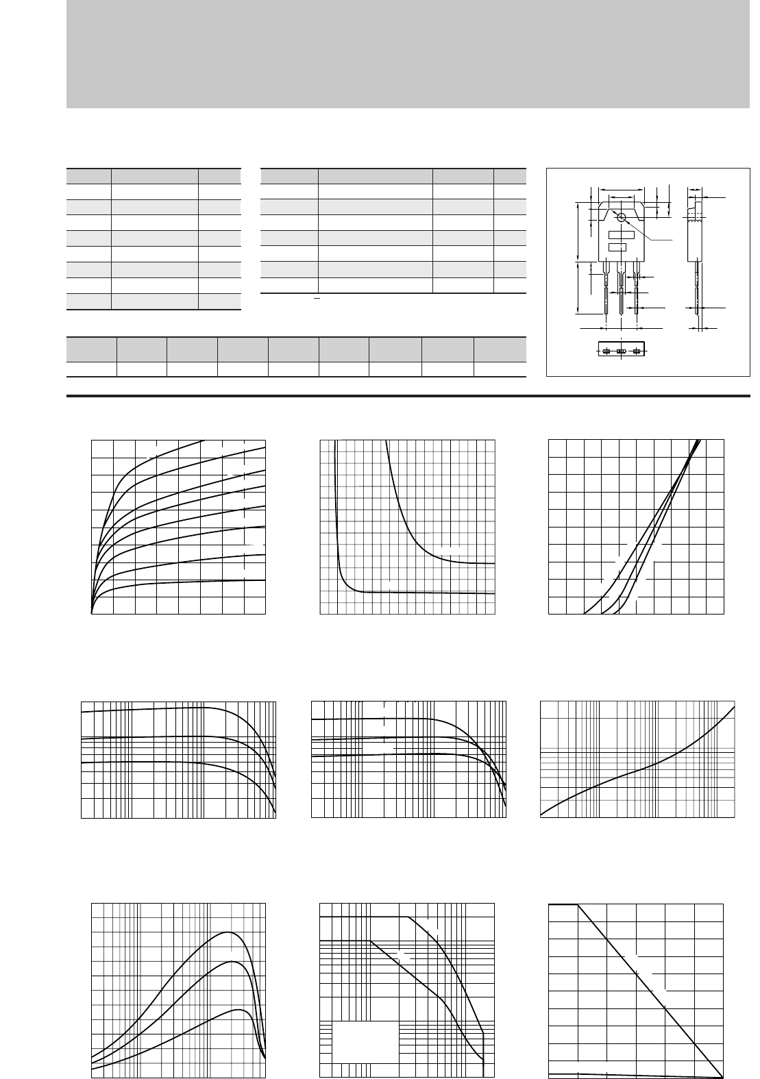
60
Silicon NPN Epitaxial Planar Transistor (Complement to type 2SA1186) Application : Audio and General Purpose
Symbol
VCBO
VCEO
VEBO
IC
IB
PC
Tj
Tstg
Ratings
150
150
5
10
2
100(Tc=25°C)
150
–55 to +150
Unit
V
V
V
A
A
W
°C
°C
■
Absolute maximum ratings
■
Electrical Characteristics
■Typical Switching Characteristics (Common Emitter)
Symbol
ICBO
IEBO
V(BR)CEO
hFE
VCE(sat)
fT
COB
Ratings
100max
100max
150min
50min∗
2.0max
70typ
60typ
Unit
µ
A
µ
A
V
V
MHz
pF
Conditions
VCB=150V
VEB=5V
IC=25mA
VCE=4V, IC=3V
IC=5A, IB=0.5A
VCE=12V, IE=–1A
VCB=80V, f=1MHz
VCC
(V)
60
RL
(Ω)
12
IC
(A)
5
VB2
(V)
–5
IB2
(mA)
–500
ton
(
µ
s)
0.2typ
tstg
(
µ
s)
1.4typ
tf
(
µ
s)
0.35typ
IB1
(mA)
500
LAPT 2SC2837
(Ta=25°C) (Ta=25°C)
IC–VCE Characteristics
(Typical)
hFE–IC Characteristics
(Typical)
hFE–IC
Temperature Characteristics (Typical)
θj-a–t Characteristics
IC–VBE Temperature Characteristics
(Typical)
VCE(sat)–IB Characteristics
(Typical)
Pc–Ta Derating
Safe Operating Area (Single Pulse)
fT–IE Characteristics
(Typical)
0
3
2
1
0 0.5 1.0 2.01.5
Base Current IB(A)
Collector-Emitter Saturation Voltage VCE(sat)(V)
IC=10A
5A
0
10
2
6
4
8
021
Base-Emittor Voltage VBE(V)
Collector Current IC(A)
(VCE=4V)
125˚C (Case Temp)
25˚C
–30˚C (Case Temp)
0.2
1
3
0.5
1 10 100 1000 2000
Time t(ms)
Transient Thermal Resistance θj-a(˚C/W)
100
50
3.5
00 25 50 75 100 125 150
Ambient Temperature Ta(˚C)
Maximum Power Dissipation PC(W)
With Infinite heatsink
Without Heatsink
2 10 100 200
0.2
1
0.5
10
30
5
Collector-Emitter Voltage VCE(V)
Collector Current IC(A)
10ms
DC
Without Heatsink
Natural Cooling
0.02 0.1 1 10
20
50
100
200
Collector Current IC(A)
DC Current Gain hFE
(VCE=4V)
Typ
0
0
2
4
6
10
8
2134
Collector-Emitter Voltage VCE(V)
Collector Current IC(A)
300mA
200mA
160mA
120mA
80mA
40mA
I
B
=20mA
400mA
(VCE=4V)
0.02 0.1 0.50.05 1051
Collector Current IC(A)
DC Current Gain hFE
20
50
100
200
125˚C
25˚C
–30˚C
–0.02 –0.1 –1 –6
40
20
0
120
100
80
60
Cut-off Frequency fT(MHZ)
(VCE=12V)
Emitter Current IE(A)
Typ
External Dimensions MT-100(TO3P)
15.6±0.4
9.6
19.9±0.3
4.0 2.0
5.0±0.2
1.8
ø3.2±0.1
2
3
1.05
+0.2
-0.1
20.0min
4.0max
BE
5.45±0.1 5.45±0.1
C
4.8±0.2
0.65
+0.2
-0.1
1.4
2.0±0.1
a
b
Weight : Approx 6.0g
a. Part No.
b. Lot No.
∗hFE Rank O(50 to 100), P(70 to 140), Y(90 to 180)
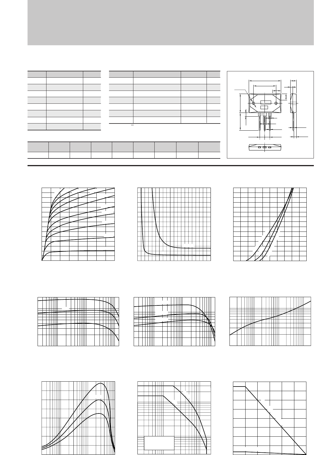
61
2
3
1.05
+0.2
-0.1
BE
5.45±0.1 5.45±0.1
2-ø3.2±0.1
36.4±0.3
9
24.4±0.2
7
21.4±0.3
20.0min
4.0max
0.65
+0.2
-0.1
3.0
+0.3
-0.1
6.0±0.2
2.1
a
b
C
Silicon NPN Epitaxial Planar Transistor (Complement to type 2SA1215) Application : Audio and General Purpose
Symbol
VCBO
VCEO
VEBO
IC
IB
PC
Tj
Tstg
Ratings
160
160
5
15
4
150(Tc=25°C)
150
–55 to +150
Unit
V
V
V
A
A
W
°C
°C
■
Absolute maximum ratings
■
Electrical Characteristics
■Typical Switching Characteristics (Common Emitter)
External Dimensions MT-200
Symbol
ICBO
IEBO
V(BR)CEO
hFE
VCE(sat)
fT
COB
Ratings
100max
100max
160min
50min∗
2.0max
60typ
200typ
Unit
µ
A
µ
A
V
V
MHz
pF
Conditions
VCB=160V
VEB=5V
IC=25mA
VCE=4V, IC=5A
IC=5A, IB=0.5A
VCE=12V, IE=–2A
VCB=10V, f=1MHz
VCC
(V)
60
RL
(Ω)
12
IC
(A)
5
VB2
(V)
–5
IB2
(mA)
–500
ton
(
µ
s)
0.2typ
tstg
(
µ
s)
1.5typ
tf
(
µ
s)
0.35typ
IB1
(mA)
500
LAPT 2SC2921
(Ta=25°C) (Ta=25°C)
IC–VCE Characteristics
(Typical)
hFE–IC Characteristics
(Typical)
hFE–IC
Temperature Characteristics (Typical)
θj-a–t Characteristics
IC–VBE Temperature Characteristics
(Typical)
VCE(sat)–IB Characteristics
(Typical)
Pc–Ta Derating
Safe Operating Area (Single Pulse)
fT–IE Characteristics
(Typical)
0
3
2
1
0 0.2 0.4 0.6 1.00.8
Base Current IB(A)
Collector-Emitter Saturation Voltage VCE(sat)(V)
IC=10A
5A
0
15
10
5
021
Base-Emittor Voltage VBE(V)
Collector Current IC(A)
(VCE=4V)
125˚C (Case Temp)
25˚C
–30˚C (Case Temp)
1 10 100 1000 2000
Time t(ms)
0.1
1
2
0.5
Transient Thermal Resistance θj-a(˚C/W)
160
120
80
40
5
00 25 50 75 100 125 150
Ambient Temperature Ta(˚C)
Maximum Power Dissipation PC(W)
With Infinite heatsink
Without Heatsink
2 10 100 200
0.3
1
0.5
10
40
5
Collector-Emitter Voltage VCE(V)
Collector Current IC(A)
DC
10ms
Without Heatsink
Natural Cooling
0.02 0.1 10.5 10 15
10
50
100
200
Collector Current IC(A)
DC Current Gain hFE
(VCE=4V)
Typ
0
0
15
10
5
2134
Collector-Emitter Voltage VCE(V)
Collector Current IC(A)
400mA
500mA
600mA
300mA
200mA
150mA
100mA
50mA
I
B
=20mA
750mA
(VCE=4V)
0.02 0.5 51
20
50
200
100
0.1 10 15
Collector Current IC(A)
DC Current Gain hFE
125˚C
25˚C
–30˚C
–0.02 –0.1 –1 –10
0
20
40
60
80
Cut-off Frequency fT(MHZ)
(VCE=12V)
Emitter Current IE(A)
Typ
Weight : Approx 18.4g
a. Part No.
b. Lot No.
∗hFE Rank O(50 to 100), P(70 to 140), Y(90 to 180)
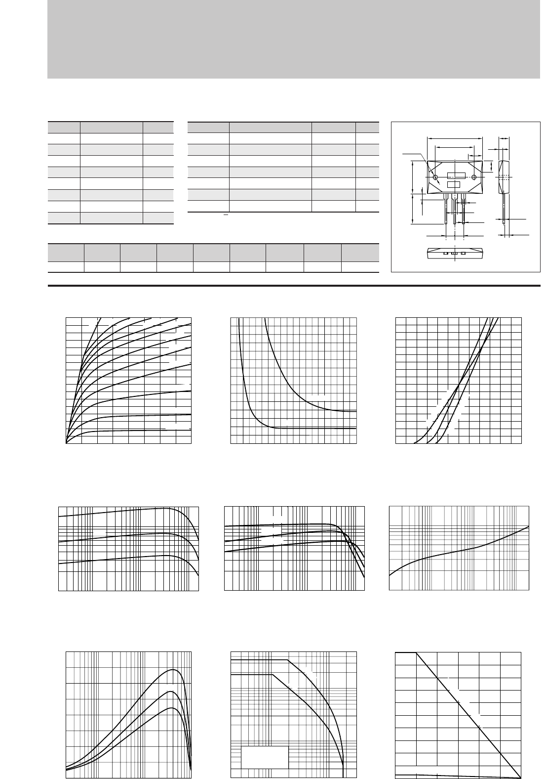
62
Silicon NPN Epitaxial Planar Transistor (Complement to type 2SA1216) Application : Audio and General Purpose
Symbol
VCBO
VCEO
VEBO
IC
IB
PC
Tj
Tstg
Ratings
180
180
5
17
5
200(Tc=25°C)
150
–55 to +150
Unit
V
V
V
A
A
W
°C
°C
■
Absolute maximum ratings
■
Electrical Characteristics
■Typical Switching Characteristics (Common Emitter)
Symbol
ICBO
IEBO
V(BR)CEO
hFE
VCE(sat)
fT
COB
Ratings
100max
100max
180min
30min∗
2.0max
50typ
250typ
Unit
µ
A
µ
A
V
V
MHz
pF
Conditions
VCB=180V
VEB=5V
IC=25mA
VCE=4V, IC=8V
IC=8A, IB=0.8A
VCE=12V, IE=–2A
VCB=10V, f=1MHz
VCC
(V)
40
RL
(Ω)
4
IC
(A)
10
VB2
(V)
–5
IB2
(A)
–1
ton
(
µ
s)
0.2typ
tstg
(
µ
s)
1.3typ
tf
(
µ
s)
0.45typ
IB1
(A)
1
LAPT 2SC2922
(Ta=25°C) (Ta=25°C)
IC–VCE Characteristics
(Typical)
hFE–IC Characteristics
(Typical)
hFE–IC
Temperature Characteristics (Typical)
θj-a–t Characteristics
IC–VBE Temperature Characteristics
(Typical)
VCE(sat)–IB Characteristics
(Typical)
Pc–Ta Derating
Safe Operating Area (Single Pulse)
fT–IE Characteristics
(Typical)
0
3
2
1
0 0.2 0.4 0.6 1.00.8
Base Current IB(A)
Collector-Emitter Saturation Voltage VCE(sat)(V)
IC=10A
5A
0
17
15
10
5
0 2 2.41
Base-Emittor Voltage VBE(V)
Collector Current IC(A)
(VCE=4V)
125˚C (Case Temp)
25˚C
–30˚C (Case Temp)
200
160
120
80
40
5
00 25 50 75 100 125 150
Ambient Temperature Ta(˚C)
Maximum Power Dissipation PC(W)
With Infinite heatsink
Without Heatsink
2 10 100 300
0.2
1
0.5
10
50
5
Collector-Emitter Voltage VCE(V)
Collector Current IC(A)
Without Heatsink
Natural Cooling
DC
10ms
0.02 0.1 1 1050.5 17
10
50
100
200
Collector Current IC(A)
DC Current Gain hFE
(VCE=4V)
Typ
0
0
5
17
15
10
2134
Collector-Emitter Voltage VCE(V)
Collector Current IC(A)
600mA
700mA
1A
500mA
400mA
300mA
200mA
100mA
50mA
I
B
=20mA
1.5A
(VCE=4V)
0.02 0.5 1 5 100.1 17
Collector Current IC(A)
DC Current Gain hFE
125˚C
25˚C
–30˚C
10
50
100
200
–0.02 –0.1 –1 –5 –10
0
40
60
20
80
Cut-off Frequency fT(MHZ)
(VCE=12V)
Emitter Current IE(A)
Typ
1 10 100 1000 2000
Time t(ms)
0.1
1
2
0.5
Transient Thermal Resistance θj-a(˚C/W)
2
3
1.05
+0.2
-0.1
BE
5.45±0.1 5.45±0.1
2-ø3.2±0.1
36.4±0.3
9
24.4±0.2
7
21.4±0.3
20.0min
4.0max
0.65
+0.2
-0.1
3.0
+0.3
-0.1
6.0±0.2
2.1
a
b
C
External Dimensions MT-200
Weight : Approx 18.4g
a. Part No.
b. Lot No.
∗hFE Rank O(30 to 60), Y(50 to 100), P(70 to 140), G(90 to 180)
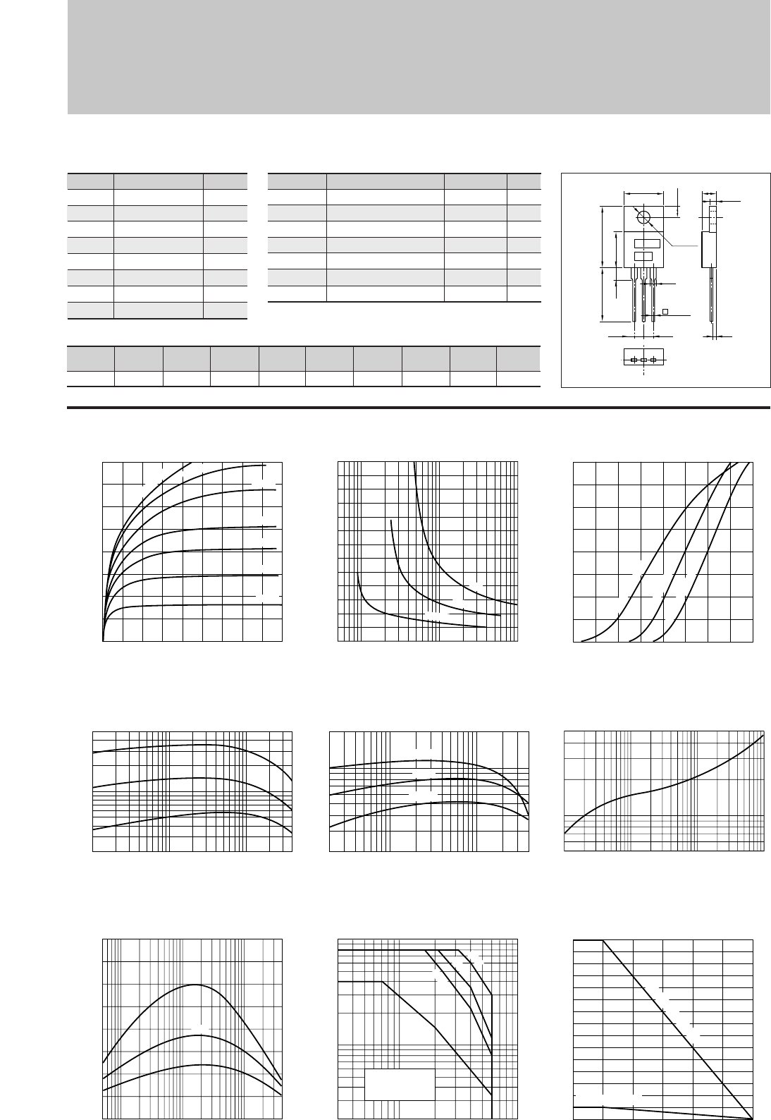
63
Silicon NPN Triple Diffused Planar Transistor (Complement to type 2SA1262) Application : Audio and General Purpose
Symbol
VCBO
VCEO
VEBO
IC
IB
PC
Tj
Tstg
Ratings
80
60
6
4
1
30(Tc=25°C)
150
–55 to +150
Unit
V
V
V
A
A
W
°C
°C
■
Electrical Characteristics
Symbol
ICBO
IEBO
V(BR)CEO
hFE
VCE(sat)
fT
COB
Ratings
100max
100max
60min
40min
0.6max
15typ
60typ
Unit
µ
A
µ
A
V
V
MHz
pF
Conditions
VCB=80V
VEB=6V
IC=25mA
VCE=4V, IC=1V
IC=2A, IB=0.2A
VCE=12V, IE=–0.2A
VCB=10V, f=1MHz
2SC3179
(Ta=25°C) (Ta=25°C)
IC–VCE Characteristics
(Typical)
hFE–IC Characteristics
(Typical)
hFE–IC
Temperature Characteristics (Typical)
θj-a–t Characteristics
IC–VBE Temperature Characteristics
(Typical)
VCE(sat)–IB Characteristics
(Typical)
Pc–Ta Derating
0
0
1
2
3
4
2134
Collector-Emitter Voltage VCE(V)
Collector Current IC(A)
I
B
=100mA
40mA
60mA
80mA
30mA
10mA
20mA
Safe Operating Area (Single Pulse)
fT–IE Characteristics
(Typical)
0
1.0
0.5
0.005
0.01 0.10.05 10.5
Base Current IB(A)
Collector-Emitter Saturation Voltage VCE(sat)(V)
I
C
=1A
2A
3A
0
4
2
1
3
0.4 1.20.80.6 1.0
Base-Emittor Voltage VBE(V)
Collector Current IC(A)
(VCE=4V)
125˚C (Case Temp)
–30˚C (Case Temp)
25˚C (Case Temp)
0.01 0.1 0.5 1 4
20
50
100
500
Collector Current IC(A)
DC Current Gain hFE
(VCE=4V)
Typ
(VCE=4V)
0.02 0.1 0.5 41
Collector Current IC(A)
DC Current Gain hFE
20
50
100
200
125˚C
25˚C
–30˚C
0.5
1
5
1 10 100 1000
Time t(ms)
Transient Thermal Resistance θj-a(˚C/W)
10 503 100
0.2
1
0.5
10
5
Collector-Emitter Voltage VCE(V)
Collector Current IC(A)
Without Heatsink
Natural Cooling
DC
100ms
10ms
1ms
–0.005 –0.01 –0.1 –0.5 –1 –4
20
10
0
30
40
Cut-off Frequency fT(MHZ)
(VCE=12V)
Emitter Current IE(A)
Typ
30
20
10
2
00 25 50 75 100 125 150
Ambient Temperature Ta(˚C)
Maximum Power Dissipation PC(W)
With Infinite heatsink
Without Heatsink
BE
2.5 2.5
C
16.0±0.7
12.0min
4.0max 8.8±0.2
1.35
0.65
+0.2
-0.1
10.2±0.2
ø3.75±0.2
3.0±0.2
4.8±0.2
1.4
2.0±0.1
a
b
External Dimensions MT-25(TO220)
■Typical Switching Characteristics (Common Emitter)
VCC
(V)
20
RL
(Ω)
10
IC
(A)
2
VBB2
(V)
–5
IB2
(mA)
–200
ton
(
µ
s)
0.2typ
tstg
(
µ
s)
1.9typ
tf
(
µ
s)
0.29typ
IB1
(mA)
200
VBB1
(V)
10
Weight : Approx 2.6g
a. Part No.
b. Lot No.
■
Absolute maximum ratings
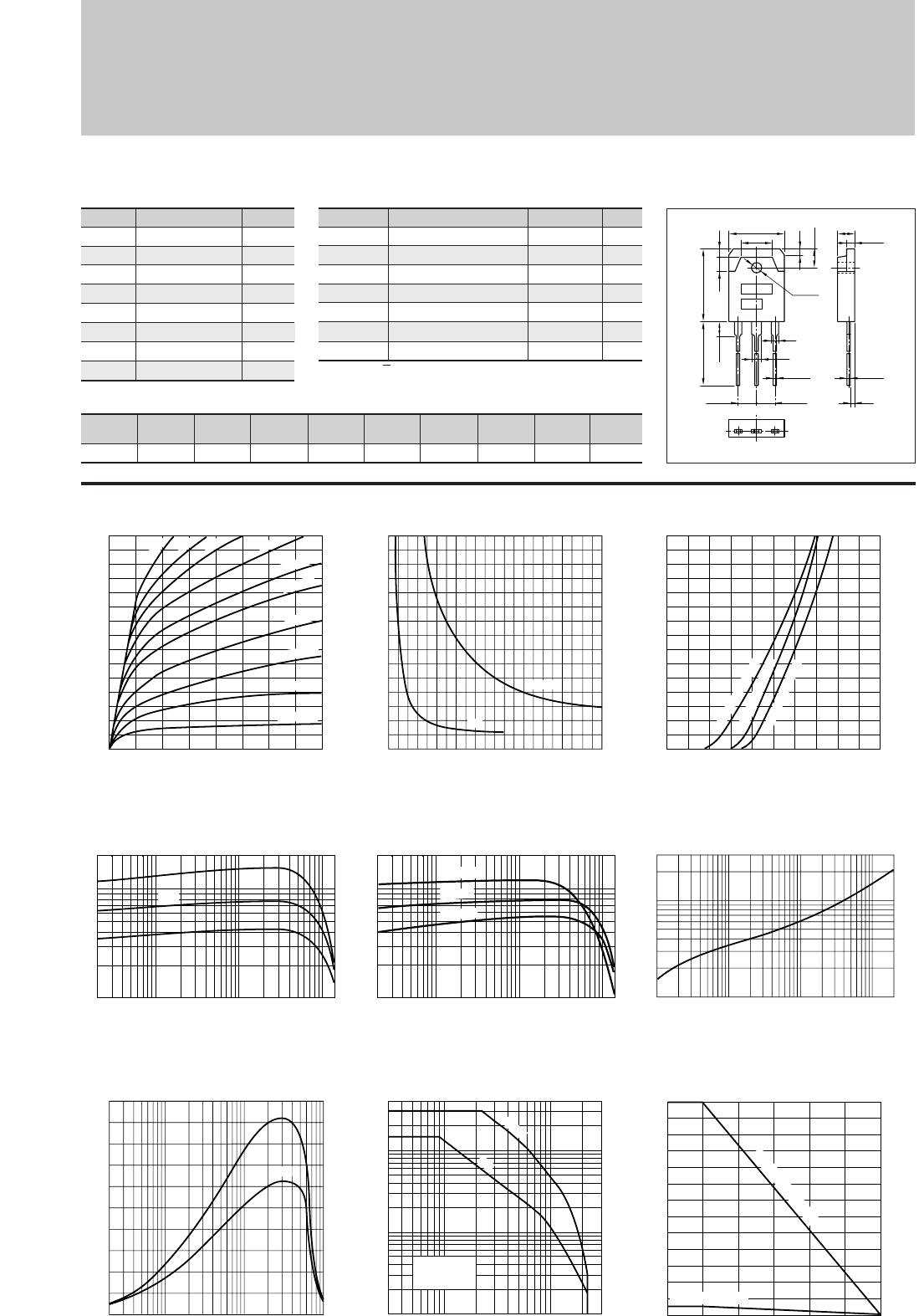
64
Silicon NPN Epitaxial Planar Transistor (Complement to type 2SA1294) Application : Audio and General Purpose
Symbol
VCBO
VCEO
VEBO
IC
IB
PC
Tj
Tstg
Ratings
230
230
5
15
4
130(Tc=25°C)
150
–55 to +150
Unit
V
V
V
A
A
W
°C
°C
■
Absolute maximum ratings
■
Electrical Characteristics
Symbol
ICBO
IEBO
V(BR)CEO
hFE
VCE(sat)
fT
COB
Ratings
100max
100max
230min
50min∗
2.0max
60typ
250typ
Unit
µ
A
µ
A
V
V
MHz
pF
Conditions
VCB=230V
VEB=5V
IC=25mA
VCE=4V, IC=5A
IC=5A, IB=0.5A
VCE=12V, IE=–2A
VCB=10V, f=1MHz
LAPT 2SC3263
(Ta=25°C) (Ta=25°C)
IC–VCE Characteristics
(Typical)
hFE–IC Characteristics
(Typical)
hFE–IC
Temperature Characteristics (Typical)
θj-a–t Characteristics
IC–VBE Temperature Characteristics
(Typical)
VCE(sat)–IB Characteristics
(Typical)
Pc–Ta Derating
Safe Operating Area (Single Pulse)
fT–IE Characteristics
(Typical)
0
3
2
1
0 0.5 1.0 2.01.5
Base Current IB(A)
Collector-Emitter Saturation Voltage VCE(sat)(V)
IC=10A
5A
0
15
10
5
021
Base-Emittor Voltage VBE(V)
Collector Current IC(A)
(VCE=4V)
125˚C (Case Temp)
–30˚C (Case Temp)
25˚C (Case Temp)
0.1
1
3
0.5
1 10 100 1000 2000
Time t(ms)
Transient Thermal Resistance θj-a(˚C/W)
130
100
50
3.5
0
Ambient Temperature Ta(˚C)
Maximum Power Dissipation PC(W)
With Infinite heatsink
Without Heatsink
0 25 50 75 100 125 150
3 10 100 300
0.1
1
0.5
10
40
5
Collector-Emitter Voltage VCE(V)
Collector Current IC(A)
10ms
DC
Without Heatsink
Natural Cooling
0.02 0.1 10.5 10515
10
50
100
200
Collector Current IC(A)
DC Current Gain hFE
(VCE=4V)
Typ
0
0
5
15
10
2134
Collector-Emitter Voltage VCE(V)
Collector Current IC(A)
1.0A
1.5A
2.0A
3.0A
600mA
400mA
200mA
100mA
50mA
I
B
=20mA
(VCE=4V)
Collector Current IC(A)
0.02 0.5 1 5 100.1 15
DC Current Gain hFE
10
50
100
200
125˚C
25˚C
–30˚C
–0.02 –0.1 –1 –10
0
20
40
60
100
80
Cut-off Frequency fT(MHZ)
(VCE=12V)
Emitter Current IE(A)
Typ
■Typical Switching Characteristics (Common Emitter)
VCC
(V)
60
RL
(Ω)
12
IC
(A)
5
VBB2
(V)
–5
IB2
(mA)
–500
ton
(
µ
s)
0.30typ
tstg
(
µ
s)
2.40typ
tf
(
µ
s)
0.50typ
IB1
(mA)
500
VBB1
(V)
10
External Dimensions MT-100(TO3P)
15.6±0.4
9.6
19.9±0.3
4.0 2.0
5.0±0.2
1.8
ø3.2±0.1
2
3
1.05
+0.2
-0.1
20.0min
4.0max
BE
5.45±0.1 5.45±0.1
C
4.8±0.2
0.65
+0.2
-0.1
1.4
2.0±0.1
a
b
Weight : Approx 6.0g
a. Part No.
b. Lot No.
∗hFE Rank O(50 to 100), Y(70 to 140)
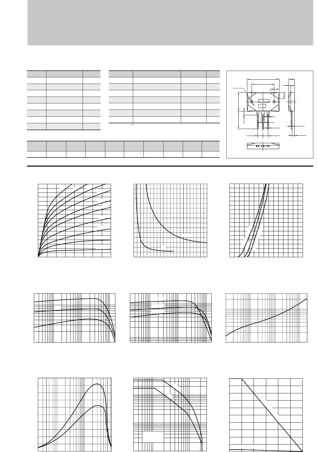
65
Silicon NPN Epitaxial Planar Transistor (Complement to type 2SA1295) Application : Audio and General Purpose
Symbol
VCBO
VCEO
VEBO
IC
IB
PC
Tj
Tstg
Ratings
230
230
5
17
5
200(Tc=25°C)
150
–55 to +150
Unit
V
V
V
A
A
W
°C
°C
■
Absolute maximum ratings
■
Electrical Characteristics
Symbol
ICBO
IEBO
V(BR)CEO
hFE
VCE(sat)
fT
COB
Ratings
100max
100max
230min
50min∗
2.0max
60typ
250typ
Unit
µ
A
µ
A
V
V
MHz
pF
Conditions
VCB=230V
VEB=5V
IC=25mA
VCE=4V, IC=5A
IC=5A, IB=0.5A
VCE=12V, IE=–2A
VCB=10V, f=1MHz
LAPT 2SC3264
(Ta=25°C) (Ta=25°C)
IC–VCE Characteristics
(Typical)
hFE–IC Characteristics
(Typical)
hFE–IC
Temperature Characteristics (Typical)
θj-a–t Characteristics
IC–VBE Temperature Characteristics
(Typical)
VCE(sat)–IB Characteristics
(Typical)
Pc–Ta Derating
Safe Operating Area (Single Pulse)
fT–IE Characteristics
(Typical)
0
3
2
1
0 0.5 1.0 2.01.5
Base Current IB(A)
Collector-Emitter Saturation Voltage VCE(sat)(V)
IC=10A
5A
0
15
17
10
5
0312
Base-Emittor Voltage VBE(V)
Collector Current IC(A)
(VCE=4V)
125˚C (Case Temp)
–30˚C (Case Temp)
25˚C
0.1
1
3
0.5
1 10 100 1000 2000
Time t(ms)
Transient Thermal Resistance θj-a(˚C/W)
200
160
120
80
40
5
00 25 50 75 100 125 150
Ambient Temperature Ta(˚C)
Maximum Power Dissipation PC(W)
With Infinite heatsink
Without Heatsink
3 10 100 300
0.1
1
0.5
10
40
5
Collector-Emitter Voltage VCE(V)
Collector Current IC(A)
10ms
DC
Without Heatsink
Natural Cooling
0.02 0.1 10.5 10517
10
50
100
200
Collector Current IC(A)
DC Current Gain hFE
(VCE=4V)
Typ
0
0
5
10
17
15
2134
Collector-Emitter Voltage VCE(V)
Collector Current IC(A)
1.0A
1.5A
3.0A
600mA
400mA
200mA
100mA
50mA
I
B
=20mA
(VCE=4V)
0.02 0.5 51
10
50
200
100
0.1 10 17
Collector Current IC(A)
DC Current Gain hFE
125˚C
25˚C
–30˚C
–0.02 –0.1 –1 –10
0
20
40
60
100
80
Cut-off Frequency fT(MHZ)
(VCE=12V)
Emitter Current IE(A)
Typ
2.0A
■Typical Switching Characteristics (Common Emitter)
VCC
(V)
60
RL
(Ω)
12
IC
(A)
5
VBB2
(V)
–5
IB2
(A)
–0.5
ton
(
µ
s)
0.30typ
tstg
(
µ
s)
2.40typ
tf
(
µ
s)
0.50typ
IB1
(A)
0.5
VBB1
(V)
10
2
3
1.05
+0.2
-0.1
BE
5.45±0.1 5.45±0.1
2-ø3.2±0.1
36.4±0.3
9
24.4±0.2
7
21.4±0.3
20.0min
4.0max
0.65
+0.2
-0.1
3.0
+0.3
-0.1
6.0±0.2
2.1
a
b
C
External Dimensions MT-200
Weight : Approx 18.4g
a. Part No.
b. Lot No.
∗hFE Rank O(50 to 100), Y(70 to 140)
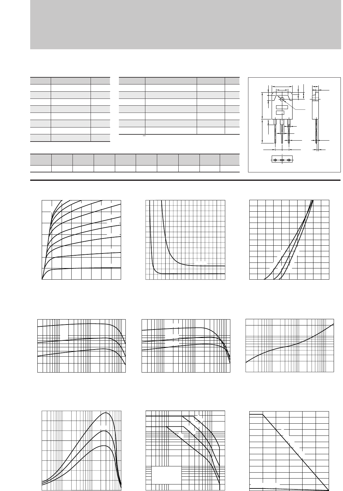
66
Silicon NPN Epitaxial Planar Transistor (Complement to type 2SA1303) Application : Audio and General Purpose
Symbol
VCBO
VCEO
VEBO
IC
IB
PC
Tj
Tstg
Ratings
150
150
5
14
3
125(Tc=25°C)
150
–55 to +150
Unit
V
V
V
A
A
W
°C
°C
■
Absolute maximum ratings
■
Electrical Characteristics
Symbol
ICBO
IEBO
V(BR)CEO
hFE
VCE(sat)
fT
COB
Ratings
100max
100max
150min
50min∗
2.0max
60typ
200typ
Unit
µ
A
µ
A
V
V
MHz
pF
Conditions
VCB=150V
VEB=5V
IC=25mA
VCE=4V, IC=5A
IC=5A, IB=0.5A
VCE=12V, IE=–2A
VCB=10V, f=1MHz
LAPT 2SC3284
(Ta=25°C) (Ta=25°C)
IC–VCE Characteristics
(Typical)
hFE–IC Characteristics
(Typical)
hFE–IC
Temperature Characteristics (Typical)
θj-a–t Characteristics
IC–VBE Temperature Characteristics
(Typical)
VCE(sat)–IB Characteristics
(Typical)
Pc–Ta Derating
Safe Operating Area (Single Pulse)
fT–IE Characteristics
(Typical)
0
3
2
1
0 0.2 0.4 0.6 1.00.8
Base Current IB(A)
Collector-Emitter Saturation Voltage VCE(sat)(V)
IC=10A
5A
0
14
10
5
021
Base-Emittor Voltage VBE(V)
Collector Current IC(A)
(VCE=4V)
125˚C (Case Temp)
25˚C
–30˚C (Case Temp)
0.1
1
3
0.5
1 10 100 1000 2000
Time t(ms)
Transient Thermal Resistance θj-a(˚C/W)
130
100
50
3.5
00 25 50 75 100 125 150
Ambient Temperature Ta(˚C)
Maximum Power Dissipation PC(W)
With Infinite heatsink
Without Heatsink
3 10 100 200
0.2
1
0.5
10
40
5
Collector-Emitter Voltage VCE(V)
Collector Current IC(A)
10ms
100ms
1ms
DC
Without Heatsink
Natural Cooling
0
0
4
14
12
8
2134
Collector-Emitter Voltage VCE(V)
Collector Current IC(A)
400mA
500mA
600mA
300mA
200mA
150mA
100mA
50mA
I
B
=20mA
750mA
(VCE=4V)
0.02 0.5 51
20
50
200
100
0.1 1014
Collector Current IC(A)
DC Current Gain hFE
125˚C
25˚C
–30˚C
–0.02 –0.1 –1 –10
0
20
40
60
80
Cut-off Frequency fT(MHZ)
(VCE=12V)
Emitter Current IE(A)
Typ
0.02 0.1 0.5 1 5 1410
20
50
100
200
Collector Current IC(A)
DC Current Gain hFE
(VCE=4V)
Typ
■Typical Switching Characteristics (Common Emitter)
VCC
(V)
60
RL
(Ω)
12
IC
(A)
5
VBB2
(V)
–5
IB2
(A)
–0.5
ton
(
µ
s)
0.2typ
tstg
(
µ
s)
1.5typ
tf
(
µ
s)
0.35typ
IB1
(A)
0.5
VBB1
(V)
10
External Dimensions MT-100(TO3P)
15.6±0.4
9.6
19.9±0.3
4.0 2.0
5.0±0.2
1.8
ø3.2±0.1
2
3
1.05
+0.2
-0.1
20.0min
4.0max
BE
5.45±0.1 5.45±0.1
C
4.8±0.2
0.65
+0.2
-0.1
1.4
2.0±0.1
a
b
Weight : Approx 6.0g
a. Part No.
b. Lot No.
∗hFE Rank O(50 to 100), P(70 to 140), Y(90 to 180)
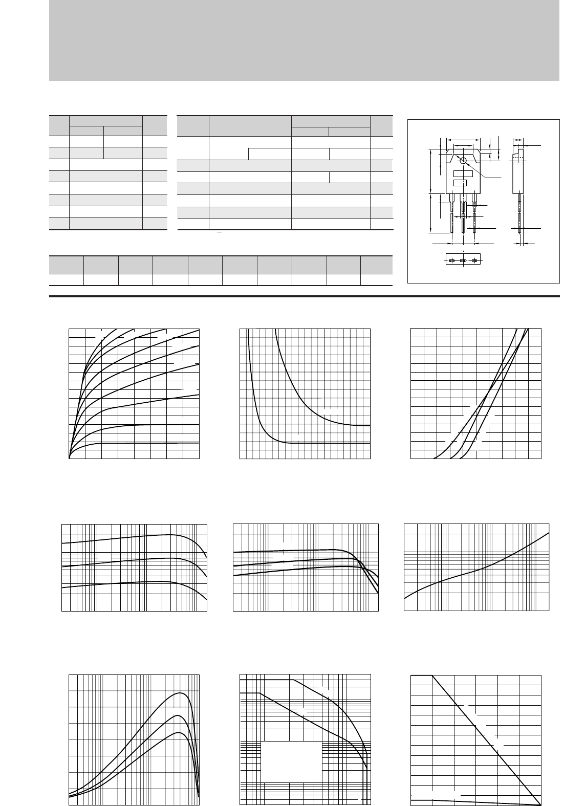
67
Silicon NPN Epitaxial Planar Transistor (Complement to type 2SA1386/A) Application : Audio and General Purpose
LAPT
2SC3519/3519A
IC–VCE Characteristics
(Typical)
hFE–IC Characteristics
(Typical)
hFE–IC
Temperature Characteristics (Typical)
θj-a–t Characteristics
IC–VBE Temperature Characteristics
(Typical)
VCE(sat)–IB Characteristics
(Typical)
Pc–Ta Derating
Safe Operating Area (Single Pulse)
fT–IE Characteristics
(Typical)
0
3
2
1
0 0.2 0.4 0.6 1.00.8
Base Current IB(A)
Collector-Emitter Saturation Voltage VCE(sat)(V)
IC=10A
5A
0
15
10
5
021
Base-Emittor Voltage VBE(V)
Collector Current IC(A)
(VCE=4V)
125˚C (Case Temp)
25˚C
–30˚C (Case Temp)
0.1
1
3
0.5
1 10 100 1000 2000
Time t(ms)
Transient Thermal Resistance θj-a(˚C/W)
130
100
50
3.5
0
Ambient Temperature Ta(˚C)
Maximum Power Dissipation PC(W)
With Infinite heatsink
Without Heatsink
0 25 50 75 100 125 150
Collector-Emitter Voltage VCE(V)
Collector Current IC(A)
5 10 50 100 200
0.1
0.05
1
0.5
10
40
5
10ms
Without Heatsink
Natural Cooling
1.2SC3519
2.2SC3519A
12
DC
0.02 0.1 1 100.5 5 15
10
50
100
300
Collector Current IC(A)
DC Current Gain hFE
(VCE=4V)
Typ
0
0
15
10
5
2134
Collector-Emitter Voltage VCE(V)
Collector Current IC(A)
400mA
500mA
600mA
300mA
200mA
100mA
50mA
I
B
=20mA
700mA
(VCE=4V)
Collector Current IC(A)
0.02 0.5 1 5 100.1 15
DC Current Gain hFE
10
50
100
300
125˚C
25˚C
–30˚C
–0.02 –0.1 –1 –5 –10
0
40
60
20
80
Cut-off Frequency fT(MHZ)
(VCE=12V)
Emitter Current IE(A)
Typ
■Typical Switching Characteristics (Common Emitter)
VCC
(V)
40
RL
(Ω)
4
IC
(A)
10
VBB2
(V)
–5
IB2
(A)
–1
ton
(
µ
s)
0.2typ
tstg
(
µ
s)
1.3typ
tf
(
µ
s)
0.45typ
IB1
(A)
1
VBB1
(V)
10
Symbol
VCBO
VCEO
VEBO
IC
IB
PC
Tj
Tstg
5
15
4
130(Tc=25°C)
150
–55 to +150
Unit
V
V
V
A
A
W
°C
°C
■
Absolute maximum ratings
■
Electrical Characteristics
Unit
µ
A
V
µ
A
V
V
MHz
pF
(Ta=25°C)
(Ta=25°C)
2SC3519A
180
180
2SC3519
160
160 100max
50min∗
2.0max
50typ
250typ
External Dimensions MT-100(TO3P)
15.6±0.4
9.6
19.9±0.3
4.0 2.0
5.0±0.2
1.8
ø3.2±0.1
2
3
1.05
+0.2
-0.1
20.0min
4.0max
BE
5.45±0.1 5.45±0.1
C
4.8±0.2
0.65
+0.2
-0.1
1.4
2.0±0.1
a
b
Weight : Approx 6.0g
a. Part No.
b. Lot No.
∗hFE Rank O(50 to 100), P(70 to 140), Y(90 to 180)
100max
2SC3519A
180
180min
Conditions
VCB=
VEB=5V
IC=25mA
VCE=4V, IC=5A
IC=5A, IB=0.5A
VCE=12V, IE=–2A
VCB=10V, f=1MHz
Symbol
ICBO
IEBO
V(BR)CEO
hFE
VCE(sat)
fT
COB
2SC3519
160
160min
Ratings Ratings
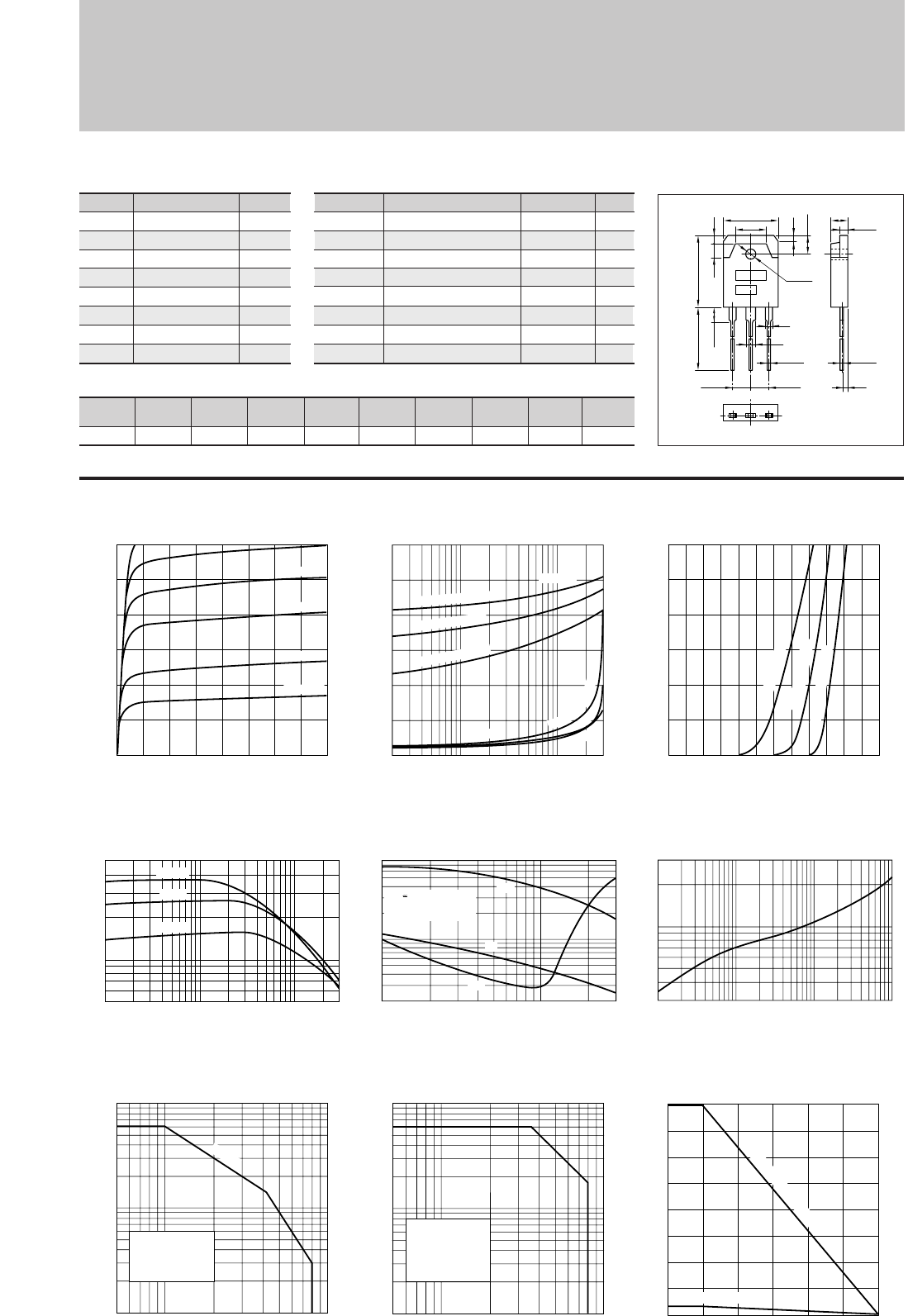
68
Silicon NPN Triple Diffused Planar Transistor (High Voltage Switching Transistor)
Application : Switching Regulator and General Purpose
2SC3678
Symbol
VCBO
VCEO
VEBO
IC
IB
PC
Tj
Tstg
Ratings
900
800
7
3(Pulse6)
1.5
80(Tc=25°C)
150
–55 to +150
Unit
V
V
V
A
A
W
°C
°C
■
Absolute maximum ratings
■
Electrical Characteristics
Symbol
ICBO
IEBO
V(BR)CEO
hFE
VCE(sat)
VBE(sat)
fT
COB
Ratings
100max
100max
800min
10to30
0.5max
1.2max
6typ
50typ
Unit
µ
A
µ
A
V
V
V
MHz
pF
Conditions
VCB=800V
VEB=7V
IC=10mA
VCE=4V, IC=1A
IC=1A, IB=0.2A
IC=1A, IB=0.2A
VCE=12V, IE=–0.3A
VCB=10V, f=1MHz
(Ta=25°C) (Ta=25°C)
■Typical Switching Characteristics (Common Emitter)
VCC
(V)
250
RL
(Ω)
250
IC
(A)
1
VBB2
(V)
–5
IB2
(A)
–0.5
ton
(
µ
s)
1max
tstg
(
µ
s)
5max
tf
(
µ
s)
1max
IB1
(A)
0.15
VBB1
(V)
10
IC–VCE Characteristics
(Typical)
hFE–IC Characteristics
(Typical)
ton•tstg•tf–IC Characteristics
(Typical)
θj-a–t Characteristics
IC–VBE Temperature Characteristics
(Typical)
VCE(sat),VBE(sat)–IC Temperature Characteristics (Typical)
Pc–Ta Derating
Reverse Bias Safe Operating Area
Safe Operating Area (Single Pulse)
0
0
2
1
3
2134
Collector-Emitter Voltage VCE(V)
Collector Current IC(A)
300mA
200mA
100mA
I
B
=50mA
500mA 400mA
0.02 0.10.05 10.5 3
0
1
Collector-Emitter Saturation Voltage VCE(sat)(V)
Base-Emitter Saturation Voltage VBE(sat)(V)
(IC/IB=5)
Collector Current IC(A)
VBE(sat)
125˚C (Case Temp)
25˚C (Case Temp)
–55˚C (Case Temp)
25˚C
125˚C
VCE(sat)
–
5
5
˚
C
(
C
a
s
e
T
e
m
p
)
0.01 0.10.05 1 30.5
5
10
50
Collector Current IC(A)
DC Current Gain hFE
(VCE=4V)
125˚C
25˚C
–55˚C
0.1 10.5 3
0.2
0.5
5
8
1
Switching Time ton•tstg•tf(µs)
Collector Current IC(A)
tstg
ton
tf
VCC 250V
IC:IB1:–IB2
=2:0.3:1Const.
0.3
1
3
0.5
1 10 100 10005 50 500
Time t(ms)
Transient Thermal Resistance θj-a(˚C/W)
80
60
40
20
3.5
00 25 50 75 100 125 150
Ambient Temperature Ta(˚C)
Maximum Power Dissipation PC(W)
With Infinite heatsink
Without Heatsink
100 50050 1000
1
0.5
0.1
10
5
Collector-Emitter Voltage VCE(V)
Collector Current IC(A)
Without Heatsink
Natural Cooling
L=3mH
IB2=–1.0A
Duty:less than 1%
100 500 100050
1
0.5
0.1
10
5
Collector-Emitter Voltage VCE(V)
Collector Current IC(A)
100µs
Without Heatsink
Natural Cooling
0
3
1
2
0 1.20.4 0.6 0.8 1.00.2
Base-Emittor Voltage VBE(V)
Collector Current IC(A)
(VCE=4V)
125˚C (Case Temp)
25˚C (Case Temp)
–55˚C (Case Temp)
External Dimensions MT-100(TO3P)
15.6±0.4
9.6
19.9±0.3
4.0 2.0
5.0±0.2
1.8
ø3.2±0.1
2
3
1.05
+0.2
-0.1
20.0min
4.0max
BE
5.45±0.1 5.45±0.1
C
4.8±0.2
0.65
+0.2
-0.1
1.4
2.0±0.1
a
b
Weight : Approx 6.0g
a. Part No.
b. Lot No.
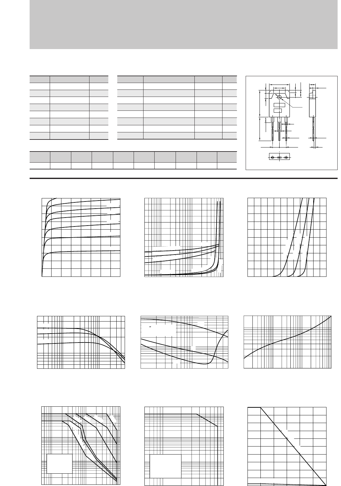
69
Silicon NPN Triple Diffused Planar Transistor (High Voltage Switching Transistor)
Application : Switching Regulator and General Purpose
Symbol
VCBO
VCEO
VEBO
IC
IB
PC
Tj
Tstg
Ratings
900
800
7
5(Pulse10)
2.5
100(Tc=25°C)
150
–55 to +150
Unit
V
V
V
A
A
W
°C
°C
■
Absolute maximum ratings
■
Electrical Characteristics
Symbol
ICBO
IEBO
V(BR)CEO
hFE
VCE(sat)
VBE(sat)
fT
COB
Ratings
100max
100max
800min
10to30
0.5max
1.2max
6typ
75typ
Unit
µ
A
µ
A
V
V
V
MHz
pF
Conditions
VCB=800V
VEB=7V
IC=10mA
VCE=4V, IC=2A
IC=2A, IB=0.4A
IC=2A, IB=0.4A
VCE=12V, IE=–0.5A
VCB=10V, f=1MHz
2SC3679
(Ta=25°C) (Ta=25°C)
IC–VCE Characteristics
(Typical)
hFE–IC Characteristics
(Typical)
ton•tstg•tf–IC Characteristics
(Typical)
θj-a–t Characteristics
IC–VBE Temperature Characteristics
(Typical)
VCE(sat),VBE(sat)–IC Temperature Characteristics (Typical)
Pc–Ta Derating
Reverse Bias Safe Operating Area
Safe Operating Area (Single Pulse)
0
0
2
1
3
4
5
2134
Collector-Emitter Voltage VCE(V)
Collector Current IC(A)
500mA
400mA
300mA
200mA
700mA 600mA
I
B
=100mA
0.03
0.1
0.05
15100.5
0
2
1
Collector-Emitter Saturation Voltage VCE(sat)(V)
Base-Emitter Saturation Voltage VBE(sat)(V)
(IC/IB=5)
Collector Current IC(A)
VBE(sat)
125˚C (Case Temp)
25˚C (Case Temp)
–55˚C (Case Temp)
25˚C
–55˚C
VCE(sat)
1
2
5
˚
C
(
C
a
s
e
T
e
m
p
)
0.1 10.5 5
0.2
0.5
5
10
1
Switching Time ton•tstg•tf(µs)
Collector Current IC(A)
tstg
ton
tf
VCC 250V
IC:IB1:–IB2
=2:0.3:1Const.
0.1
1
2
0.5
1 10 100 1000
Time t(ms)
Transient Thermal Resistance θj-a(˚C/W)
100
50
3.5
00 25 50 75 100 125 150
Ambient Temperature Ta(˚C)
Maximum Power Dissipation PC(W)
With Infinite heatsink
Without Heatsink
100 50050 1000
1
0.5
0.1
0.05
0.01
10
20
5
Collector-Emitter Voltage VCE(V)
Collector Current IC(A)
Without Heatsink
Natural Cooling
L=3mH
IB2=–1.0A
Duty:less than1%
10 505 100 500 1000
0.05
0.01
1
0.5
0.1
10
20
5
Collector-Emitter Voltage VCE(V)
Collector Current IC(A)
Without Heatsink
Natural Cooling
100µs
10ms
1ms
100ms
10µs
DC(Tc=25 C)
0
5
1
2
3
4
0 1.20.4 0.6 0.8 1.00.2
Base-Emittor Voltage VBE(V)
Collector Current IC(A)
(VCE=4V)
125˚C (Case Temp)
25˚C (Case Temp)
–55˚C (Case Temp)
0.02 0.10.05 1 50.5
5
10
50
Collector Current IC(A)
DC Current Gain hFE
(VCE=4V)
125˚C
25˚C
–55˚C
■Typical Switching Characteristics (Common Emitter)
VCC
(V)
250
RL
(Ω)
125
IC
(A)
2
VBB2
(V)
–5
IB2
(A)
–1
ton
(
µ
s)
1max
tstg
(
µ
s)
5max
tf
(
µ
s)
1max
IB1
(A)
0.3
VBB1
(V)
10
External Dimensions MT-100(TO3P)
15.6±0.4
9.6
19.9±0.3
4.0 2.0
5.0±0.2
1.8
ø3.2±0.1
2
3
1.05
+0.2
-0.1
20.0min
4.0max
BE
5.45±0.1 5.45±0.1
C
4.8±0.2
0.65
+0.2
-0.1
1.4
2.0±0.1
a
b
Weight : Approx 6.0g
a. Part No.
b. Lot No.
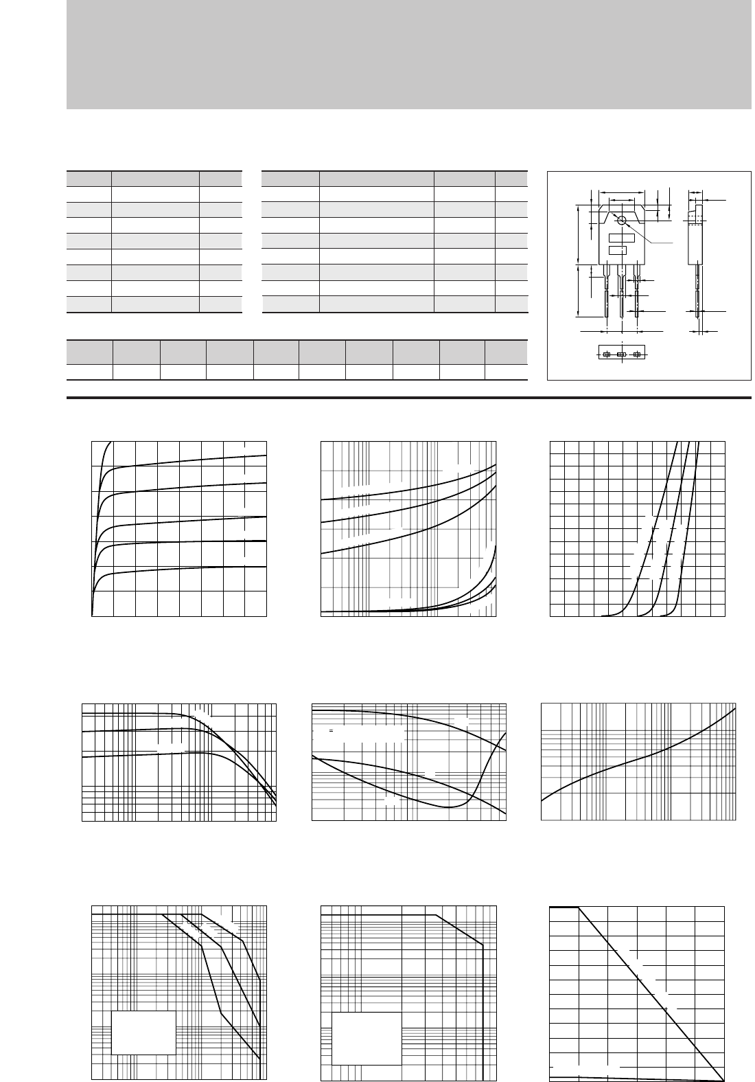
70
Silicon NPN Triple Diffused Planar Transistor (High Voltage Switching Transistor)
Application : Switching Regulator and General Purpose
Symbol
VCBO
VCEO
VEBO
IC
IB
PC
Tj
Tstg
Ratings
900
800
7
7(Pulse14)
3.5
120(Tc=25°C)
150
–55 to +150
Unit
V
V
V
A
A
W
°C
°C
■
Absolute maximum ratings
■
Electrical Characteristics
Symbol
ICBO
IEBO
V(BR)CEO
hFE
VCE(sat)
VBE(sat)
fT
COB
Ratings
100max
100max
800min
10to30
0.5max
1.2max
6typ
105typ
Unit
µ
A
µ
A
V
V
V
MHz
pF
Conditions
VCB=800V
VEB=7V
IC=10mA
VCE=4V, IC=3A
IC=3A, IB=0.6A
IC=3A, IB=0.6A
VCE=12V, IE=–2A
VCB=10V, f=1MHz
2SC3680
(Ta=25°C) (Ta=25°C)
IC–VCE Characteristics
(Typical)
hFE–IC Characteristics
(Typical)
ton•tstg•tf–IC Characteristics
(Typical)
θj-a–t Characteristics
IC–VBE Temperature Characteristics
(Typical)
VCE(sat),VBE(sat)–IC Temperature Characteristics (Typical)
Collector-Emitter Saturation Voltage VCE(sat)(V)
Base-Emitter Saturation Voltage VBE(sat)(V)
Pc–Ta Derating
Reverse Bias Safe Operating Area
Safe Operating Area (Single Pulse)
0
0
4
2
6
7
2134
Collector-Emitter Voltage VCE(V)
Collector Current IC(A)
700mA
500mA
300mA
200mA
I
B
=100mA
1A
0.02 0.10.05 1 50.5 7
0
1
(IC/IB=5)
Collector Current IC(A)
VBE(sat)
125˚C (Case Temp)
25˚C (Case Temp)
–55˚C (Case Temp)
25˚C
–55˚C
VCE(sat)
1
2
5
˚
C
(
C
a
s
e
T
e
m
p
)
0.1 10.5 75
0.2
0.5
5
10
1
Switching Time ton•tstg•tf(µs)
Collector Current IC(A)
tstg
ton
tf
VCC 250V
IC:IB1:IB2=2:0.3:–1Const.
0.1
1
2
0.5
1 10 100 1000
Time t(ms)
Transient Thermal Resistance θj-a(˚C/W)
100 50050 1000
1
0.5
0.01
0.1
0.05
10
20
5
Collector-Emitter Voltage VCE(V)
Collector Current IC(A)
Without Heatsink
Natural Cooling
L=3mH
IB2=–1.0A
Duty:less than 1%
10 5052 100 500 1000
0.05
0.01
1
0.5
0.1
10
20
5
Collector-Emitter Voltage VCE(V)
Collector Current IC(A)
Without Heatsink
Natural Cooling
100µs
10ms
1ms
0
7
2
4
6
0 1.20.4 0.6 0.8 1.00.2
Base-Emittor Voltage VBE(V)
Collector Current IC(A)
(VCE=4V)
125˚C (Case Temp)
25˚C (Case Temp)
–55˚C (Case Temp)
0.02 0.10.05 1 750.5
5
10
50
Collector Current IC(A)
DC Current Gain hFE
(VCE=4V)
125˚C
25˚C
–55˚C
120
100
50
3.5
00 25 50 75 100 125 150
Ambient Temperature Ta(˚C)
Maximum Power Dissipation PC(W)
With Infinite heatsink
Without Heatsink
■Typical Switching Characteristics (Common Emitter)
VCC
(V)
250
RL
(Ω)
83
IC
(A)
3
VBB2
(V)
–5
IB2
(A)
–1.5
ton
(
µ
s)
1max
tstg
(
µ
s)
5max
tf
(
µ
s)
1max
IB1
(A)
0.45
VBB1
(V)
10
External Dimensions MT-100(TO3P)
15.6±0.4
9.6
19.9±0.3
4.0 2.0
5.0±0.2
1.8
ø3.2±0.1
2
3
1.05
+0.2
-0.1
20.0min
4.0max
BE
5.45±0.1 5.45±0.1
C
4.8±0.2
0.65
+0.2
-0.1
1.4
2.0±0.1
a
b
Weight : Approx 6.0g
a. Part No.
b. Lot No.
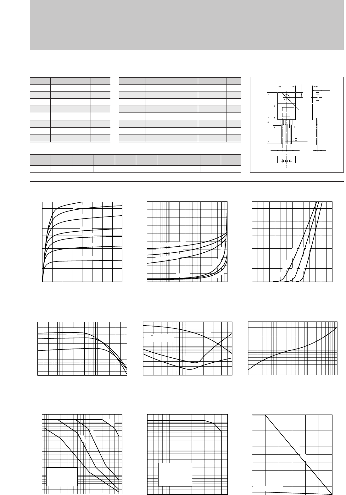
71
Silicon NPN Triple Diffused Planar Transistor
(High Voltage and High Speed Switching Transistor)
Application : Switching Regulator and General Purpose
Symbol
VCBO
VCEO
VEBO
IC
IB
PC
Tj
Tstg
Ratings
600
500
10
6(Pulse12)
2
50(Tc=25°C)
150
–55 to +150
Unit
V
V
V
A
A
W
°C
°C
■
Absolute maximum ratings
■
Electrical Characteristics
Symbol
ICBO
IEBO
V(BR)CEO
hFE
VCE(sat)
VBE(sat)
fT
COB
Ratings
1max
100max
500min
10to30
0.5max
1.3max
8typ
45typ
Unit
mA
µ
A
V
V
V
MHz
pF
Conditions
VCB=600V
VEB=10V
IC=25mA
VCE=4V, IC=2A
IC=2A, IB=0.4A
IC=2A, IB=0.4A
VCE=12V, IE=–0.5A
VCB=10V, f=1MHz
2SC3830
(Ta=25°C) (Ta=25°C)
IC–VCE Characteristics
(Typical)
hFE–IC Characteristics
(Typical)
ton•tstg•tf–IC Characteristics
(Typical)
θj-a–t Characteristics
IC–VBE Temperature Characteristics
(Typical)
VCE(sat),VBE(sat)–IC Temperature Characteristics (Typical)
Pc–Ta Derating
Reverse Bias Safe Operating Area
Safe Operating Area (Single Pulse)
0
0
2
1
3
4
5
6
2134
Collector-Emitter Voltage VCE(V)
Collector Current IC(A)
800mA
600mA
400mA
300mA
200mA
1A
I
B
=100mA
0.02 0.10.05 1 50.5
0
2
1
Collector-Emitter Saturation Voltage VCE(sat)(V)
Base-Emitter Saturation Voltage VBE(sat)(V)
(IC/IB=5)
Collector Current IC(A)
VBE(sat)
125˚C (Case Temp)
25˚C (Case Temp)
–55˚C (Case Temp)
25˚C
–55˚C
VCE(sat)
1
2
5
˚
C
(
C
a
s
e
T
e
m
p
)
0.2 10.5 65
0.1
0.5
5
7
1
Switching Time ton•tstg•tf(µs)
Collector Current IC(A)
tstg
ton
tf
VCC 200V
IC:IB1:IB2=10:1:–2
0.3
1
4
0.5
1 10 100 1000
Time t(ms)
Transient Thermal Resistance θj-a(˚C/W)
50
40
30
20
10
2
00 25 50 75 100 125 150
Ambient Temperature Ta(˚C)
Maximum Power Dissipation PC(W)
With Infinite heatsink
Without Heatsink
10050
1
0.5
0.02
0.1
0.05
10
20
5
Collector-Emitter Voltage VCE(V)
Collector Current IC(A)
10 507 100
500 600 500 600
0.05
0.02
1
0.5
0.1
10
20
5
Collector-Emitter Voltage VCE(V)
Collector Current IC(A)
Without Heatsink
Natural Cooling
100µs
10ms
1ms
DC
0
6
2
1
4
3
5
0 1.41.20.4 0.6 0.8 1.00.2
Base-Emittor Voltage VBE(V)
Collector Current IC(A)
(VCE=4V)
125˚C (Case Temp)
–55˚C (Case Temp)
0.02 0.10.05 1 650.5
5
10
50
Collector Current IC(A)
DC Current Gain hFE
(VCE=4V)
125˚C
25˚C
–55˚C
25˚C (Case Temp)
Without Heatsink
Natural Cooling
L=3mH
IB2=–0.5A
Duty:less than 1%
■Typical Switching Characteristics (Common Emitter)
VCC
(V)
200
RL
(Ω)
100
IC
(A)
2
VBB2
(V)
–5
IB2
(A)
–0.4
ton
(
µ
s)
1max
tstg
(
µ
s)
4.5max
tf
(
µ
s)
0.5max
IB1
(A)
0.2
VBB1
(V)
10
External Dimensions MT-25(TO220)
BE
2.5 2.5
C
16.0±0.7
12.0min
4.0max 8.8±0.2
1.35
0.65
+0.2
-0.1
10.2±0.2
ø3.75±0.2
3.0±0.2
4.8±0.2
1.4
2.0±0.1
a
b
Weight : Approx 2.6g
a. Part No.
b. Lot No.

72
Silicon NPN Triple Diffused Planar Transistor
(High Voltage and High Speed Switching Transistor)
Application : Switching Regulator and General Purpose
Symbol
VCBO
VCEO
VEBO
IC
IB
PC
Tj
Tstg
Ratings
600
500
10
10(Pulse20)
4
100(Tc=25°C)
150
–55 to +150
Unit
V
V
V
A
A
W
°C
°C
■
Absolute maximum ratings
■
Electrical Characteristics
Symbol
ICBO
IEBO
V(BR)CEO
hFE
VCE(sat)
VBE(sat)
fT
COB
Ratings
1max
100max
500min
10to30
0.5max
1.3max
8typ
105typ
Unit
mA
µ
A
V
V
V
MHz
pF
Conditions
VCB=600V
VEB=10V
IC=25mA
VCE=4V, IC=5A
IC=5A, IB=1A
IC=5A, IB=1A
VCE=12V, IE=–1A
VCB=10V, f=1MHz
2SC3831
(Ta=25°C) (Ta=25°C)
IC–VCE Characteristics
(Typical)
hFE–IC Characteristics
(Typical)
ton•tstg•tf–IC Characteristics
(Typical)
θj-a–t Characteristics
IC–VBE Temperature Characteristics
(Typical)
VCE(sat),VBE(sat)–IC Temperature Characteristics (Typical)
Pc–Ta Derating
Reverse Bias Safe Operating Area
Safe Operating Area (Single Pulse)
0
0
2
4
6
8
10
2134
Collector-Emitter Voltage VCE(V)
Collector Current IC(A)
800mA
1A
600mA
400mA
200mA
I
B
=1.2A
100mA
0.02
0.1
0.05
15100.5
0
1
(IC/IB=5)
Collector Current IC(A)
VBE(sat)
125˚C (Case Temp)
25˚C (Case Temp)
–55˚C (Case Temp)
25˚C
–55˚C
VCE(sat)
1
2
5
˚
C
(
C
a
s
e
T
e
m
p
)
0.2 10.5 105
0.1
0.5
5
10
1
Switching Time ton•tstg•tf(µs)
Collector Current IC(A)
tstg
ton
tf
VCC 200V
IC:IB1:IB2=10:1:–2
0.1
1
2
0.5
1 10 100 1000
Time t(ms)
Transient Thermal Resistance θj-a(˚C/W)
100
50
3.5
00 25 50 75 100 125 150
Ambient Temperature Ta(˚C)
Maximum Power Dissipation PC(W)
With Infinite heatsink
Without Heatsink
100 500 60050
1
0.5
1
0.05
0.01
10
30
5
Collector-Emitter Voltage VCE(V)
Collector Current IC(A)
10 508 100
500 600
0.05
0.02
1
0.5
0.1
10
30
5
Collector-Emitter Voltage VCE(V)
Collector Current IC(A)
Without Heatsink
Natural Cooling
DC
100µs
10ms
1ms
Collector-Emitter Saturation Voltage VCE(sat)(V)
Base-Emitter Saturation Voltage VBE(sat)(V)
0
10
4
2
8
6
0 1.20.4 0.6 0.8 1.00.2
Base-Emittor Voltage VBE(V)
Collector Current IC(A)
(VCE=4V)
125˚C (Case Temp)
–55˚C (Case Temp)
0.02 0.10.05 1 1050.5
5
10
50
Collector Current IC(A)
DC Current Gain hFE
(VCE=4V)
125˚C
25˚C
–55˚C
25˚C (Case Temp)
Without Heatsink
Natural Cooling
L=3mH
IB2 =–0.5A
Duty:less than 1%
■Typical Switching Characteristics (Common Emitter)
VCC
(V)
200
RL
(Ω)
40
IC
(A)
5
VBB2
(V)
–5
IB2
(A)
–1.0
ton
(
µ
s)
1max
tstg
(
µ
s)
4.5max
tf
(
µ
s)
0.5max
IB1
(A)
0.5
VBB1
(V)
10
External Dimensions MT-100(TO3P)
15.6±0.4
9.6
19.9±0.3
4.0 2.0
5.0±0.2
1.8
ø3.2±0.1
2
3
1.05
+0.2
-0.1
20.0min
4.0max
BE
5.45±0.1 5.45±0.1
C
4.8±0.2
0.65
+0.2
-0.1
1.4
2.0±0.1
a
b
Weight : Approx 6.0g
a. Part No.
b. Lot No.
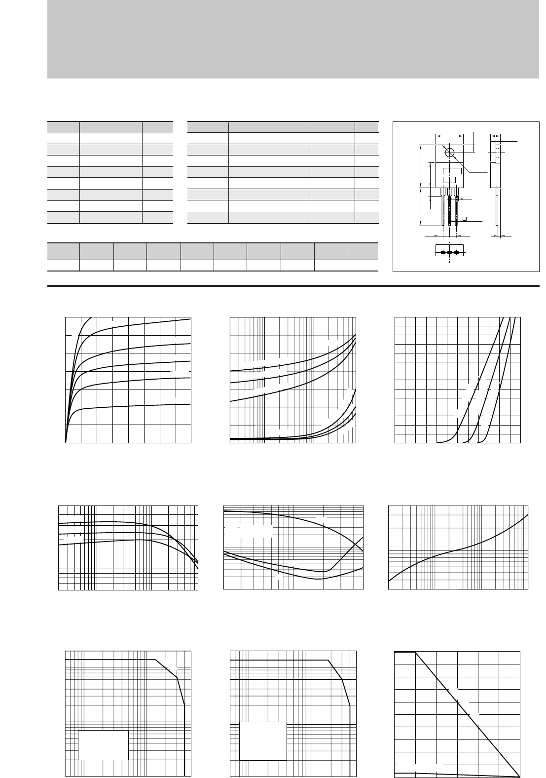
73
Silicon NPN Triple Diffused Planar Transistor
(High Voltage and High Speed Switching Transistor)
Application : Switching Regulator and General Purpose
Symbol
VCBO
VCEO
VEBO
IC
IB
PC
Tj
Tstg
Ratings
500
400
10
7(Pulse14)
2
50(Tc=25°C)
150
–55 to +150
Unit
V
V
V
A
A
W
°C
°C
■
Absolute maximum ratings
■
Electrical Characteristics
Symbol
ICBO
IEBO
V(BR)CEO
hFE
VCE(sat)
VBE(sat)
fT
COB
Ratings
100max
100max
400min
10to30
0.5max
1.3max
10typ
50typ
Unit
µ
A
µ
A
V
V
V
MHz
pF
Conditions
VCB=500V
VEB=10V
IC=25mA
VCE=4V, IC=3A
IC=3A, IB=0.6A
IC=3A, IB=0.6A
VCE=12V, IE=–0.5A
VCB=10V, f=1MHz
2SC3832
(Ta=25°C) (Ta=25°C)
IC–VCE Characteristics
(Typical)
hFE–IC Characteristics
(Typical)
ton•tstg•tf–IC Characteristics
(Typical)
θj-a–t Characteristics
IC–VBE Temperature Characteristics
(Typical)
VCE(sat),VBE(sat)–IC Temperature Characteristics (Typical)
Collector-Emitter Saturation Voltage VCE(sat)(V)
Base-Emitter Saturation Voltage VBE(sat)(V)
Pc–Ta Derating
Reverse Bias Safe Operating Area
Safe Operating Area (Single Pulse)
0
0
4
2
6
7
2134
Collector-Emitter Voltage VCE(V)
Collector Current IC(A)
400mA
300mA
600mA
800mA
200mA
I
B
=100mA
0.02 0.10.05 1 50.5 7
0
1
(IC/IB=5)
Collector Current IC(A)
VBE(sat)
125˚C (Case Temp)
25˚C (Case Temp)
–55˚C (Case Temp)
25˚C
–55˚C
VCE(sat)
1
2
5
˚
C
(
C
a
s
e
T
e
m
p
)
0.2 10.5 5
0.1
0.5
5
10
1
Switching Time ton•tstg•tf(µs)
Collector Current IC(A)
tstg
ton
tf
VCC 200V
IC:IB1:–IB2=10:1:2
0.3
1
4
0.5
1 10 100 1000
Time t(ms)
Transient Thermal Resistance θj-a(˚C/W)
50
40
30
20
10
2
00 25 50 75 100 125 150
Ambient Temperature Ta(˚C)
Maximum Power Dissipation PC(W)
With Infinite heatsink
Without Heatsink
10 505 500100
1
0.5
0.1
10
20
5
Collector-Emitter Voltage VCE(V)
Collector Current IC(A)
Without Heatsink
Natural Cooling
L=3mH
–IB2=1A
Duty:less than 1%
10 505 100 500
1
0.5
0.1
10
20
5
Collector-Emitter Voltage VCE(V)
Collector Current IC(A)
Without Heatsink
Natural Cooling
100µs
0
7
2
4
6
0 1.20.4 0.6 0.8 1.00.2
Base-Emittor Voltage VBE(V)
Collector Current IC(A)
(VCE=4V)
125˚C (Case Temp)
25˚C (Case Temp)
–55˚C (Case Temp)
0.02 0.10.05 1 750.5
5
10
50
Collector Current IC(A)
DC Current Gain hFE
(VCE=4V)
125˚C
25˚C
–30˚C
■Typical Switching Characteristics (Common Emitter)
VCC
(V)
200
RL
(Ω)
66.7
IC
(A)
3
VBB2
(V)
–5
IB2
(A)
–0.6
ton
(
µ
s)
1max
tstg
(
µ
s)
3max
tf
(
µ
s)
0.5max
IB1
(A)
0.3
VBB1
(V)
10
External Dimensions MT-25(TO220)
BE
2.5 2.5
C
16.0±0.7
12.0min
4.0max 8.8±0.2
1.35
0.65
+0.2
-0.1
10.2±0.2
ø3.75±0.2
3.0±0.2
4.8±0.2
1.4
2.0±0.1
a
b
Weight : Approx 2.6g
a. Part No.
b. Lot No.
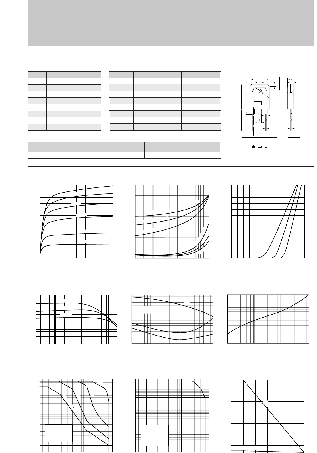
74
Silicon NPN Triple Diffused Planar Transistor
(High Voltage and High Speed Switching Transistor)
Application : Switching Regulator and General Purpose
Symbol
VCBO
VCEO
VEBO
IC
IB
PC
Tj
Tstg
Ratings
500
400
10
12(Pulse24)
4
100(Tc=25°C)
150
–55 to +150
Unit
V
V
V
A
A
W
°C
°C
■
Absolute maximum ratings
■
Electrical Characteristics
Symbol
ICBO
IEBO
V(BR)CEO
hFE
VCE(sat)
VBE(sat)
fT
COB
Ratings
100max
100max
400min
10to30
0.5max
1.3max
10typ
105typ
Unit
µ
A
µ
A
V
V
V
MHz
pF
Conditions
VCB=500V
VEB=10V
IC=25mA
VCE=4V, IC=7A
IC=7A, IB=1.4A
IC=7A, IB=1.4A
VCE=12V, IE=–1A
VCB=10V, f=1MHz
2SC3833
(Ta=25°C) (Ta=25°C)
IC–VCE Characteristics
(Typical)
hFE–IC Characteristics
(Typical)
ton•tstg•tf–IC Characteristics
(Typical)
θj-a–t Characteristics
IC–VBE Temperature Characteristics
(Typical)
VCE(sat),VBE(sat)–IC Temperature Characteristics (Typical)
Pc–Ta Derating
Reverse Bias Safe Operating Area
Safe Operating Area (Single Pulse)
0
0
4
2
6
8
10
12
2134
Collector-Emitter Voltage VCE(V)
Collector Current IC(A)
600mA
400mA
200mA
800mA
1000mA
IB=100mA
0.02 0.10.05 1 5 100.5
0
1
(IC/IB=5)
Collector Current IC(A)
VBE(sat)
125˚C (Case Temp)
25˚C (Case Temp)
–55˚C (Case Temp)
25˚C
–55˚C
VCE(sat)
1
2
5
˚
C
(
C
a
s
e
T
e
m
p
)
10.5 105
0.1
0.5
5
8
1
Switching Time ton•tstg•tf(µs)
Collector Current IC(A)
tstg
ton
tf
VCC 200V
IC:IB1:–IB2=10:1:2
0.1
1
2
0.5
1 10 100 1000
Time t(ms)
Transient Thermal Resistance θj-a(˚C/W)
100
50
3.5
00 25 50 75 100 125 150
Ambient Temperature Ta(˚C)
Maximum Power Dissipation PC(W)
With Infinite heatsink
Without Heatsink
10 505 500100
1
0.5
0.1
0.05
0.01
10
30
5
Collector-Emitter Voltage VCE(V)
Collector Current IC(A)
Without Heatsink
Natural Cooling
L=3mH
–IB2=1A
Duty:less than 1%
10 505 100 500
0.05
0.01
1
0.5
0.1
10
30
5
Collector-Emitter Voltage VCE(V)
Collector Current IC(A)
100µs
10ms
1ms
DC(Tc=25 C)
Collector-Emitter Saturation Voltage VCE(sat)(V)
Base-Emitter Saturation Voltage VBE(sat)(V)
Without Heatsink
Natural Cooling
0
12
10
4
2
8
6
0 1.20.4 0.6 0.8 1.00.2
Base-Emittor Voltage VBE(V)
Collector Current IC(A)
(VCE=4V)
125˚C (Case Temp)
–55˚C (Case Temp)
0.02 0.10.05 1 121050.5
5
10
50
Collector Current IC(A)
DC Current Gain hFE
(VCE=4V)
125˚C
25˚C
–30˚C
25˚C (Case Temp)
■Typical Switching Characteristics (Common Emitter)
VCC
(V)
200
RL
(Ω)
28.5
IC
(A)
7
VBB2
(V)
–5
IB2
(A)
–1.4
ton
(
µ
s)
1.0max
tstg
(
µ
s)
3.0max
tf
(
µ
s)
0.5max
IB1
(A)
0.7
VBB1
(V)
10
External Dimensions MT-100(TO3P)
15.6±0.4
9.6
19.9±0.3
4.0 2.0
5.0±0.2
1.8
ø3.2±0.1
2
3
1.05
+0.2
-0.1
20.0min
4.0max
BE
5.45±0.1 5.45±0.1
C
4.8±0.2
0.65
+0.2
-0.1
1.4
2.0±0.1
a
b
Weight : Approx 6.0g
a. Part No.
b. Lot No.
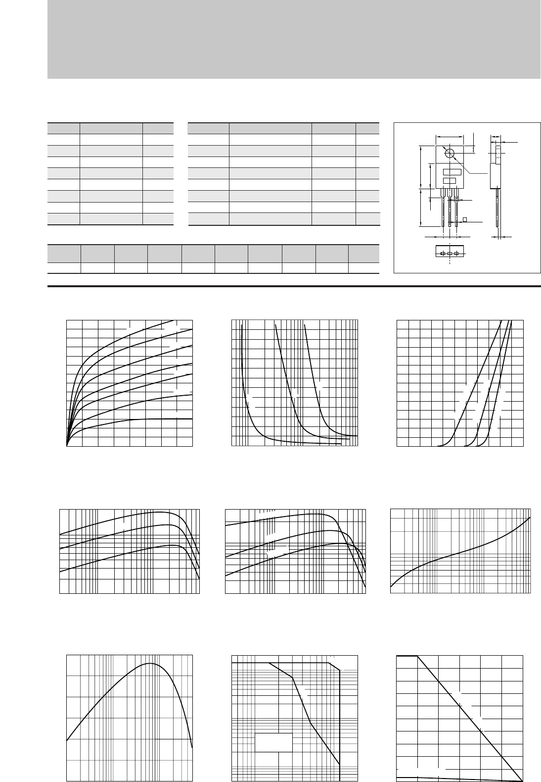
75
Silicon NPN Triple Diffused Planar Transistor (Switching Transistor)
Application : Humidifier, DC-DC Converter, and General Purpose
Symbol
VCBO
VCEO
VEBO
IC
IB
PC
Tj
Tstg
Ratings
200
120
8
7(Pulse14)
3
50(Tc=25°C)
150
–55 to +150
Unit
V
V
V
A
A
W
°C
°C
■
Absolute maximum ratings
■
Electrical Characteristics
Symbol
ICBO
IEBO
V(BR)CEO
hFE
VCE(sat)
VBE(sat)
fT
COB
Ratings
100max
100max
120min
70to220
0.5max
1.2max
30typ
110typ
Unit
µ
A
µ
A
V
V
V
MHz
pF
Conditions
VCB=200V
VEB=8V
IC=50mA
VCE=4V, IC=3A
IC=3A, IB=0.3A
IC=3A, IB=0.3A
VCE=12V, IE=–0.5A
VCB=10V, f=1MHz
2SC3834
(Ta=25°C) (Ta=25°C)
■Typical Switching Characteristics (Common Emitter)
VCC
(V)
50
RL
(Ω)
16.7
IC
(A)
3
VBB2
(V)
–5
IB2
(A)
–0.6
ton
(
µ
s)
0.5max
tstg
(
µ
s)
3.0max
tf
(
µ
s)
0.5max
IB1
(A)
0.3
VBB1
(V)
10
IC–VCE Characteristics
(Typical)
hFE–IC Characteristics
(Typical)
hFE–IC
Temperature Characteristics (Typical)
θj-a–t Characteristics
IC–VBE Temperature Characteristics
(Typical)
VCE(sat)–IB Characteristics
(Typical)
Pc–Ta Derating
Safe Operating Area (Single Pulse)
fT–IE Characteristics
(Typical)
0
2
2.6
1
0.005
0.01 0.10.05 10.5
Base Current IB(A)
Collector-Emitter Saturation Voltage VCE(sat)(V)
I
C
=1A
3A
5A
0.02 0.1 0.5 1 75
20
50
100
200
Collector Current IC(A)
DC Current Gain hFE
(VCE=4V)
Typ
–0.01
–0.1 –1
–0.05
–0.5 –5
20
10
0
30
Cut-off Frequency fT(MHZ)
(VCE=12V)
Emitter Current IE(A)
10 120505 200
0.05
1
0.5
0.1
20
10
5
Collector-Emitter Voltage VCE(V)
Collector Current IC(A)
Without Heatsink
Natural Cooling
100ms
10ms
50
40
30
20
10
2
00 25 50 75 100 125 150
Ambient Temperature Ta(˚C)
Maximum Power Dissipation PC(W)
With Infinite heatsink
Without Heatsink
0
0
1
2
3
4
5
6
7
2134
Collector-Emitter Voltage VCE(V)
Collector Current IC(A)
60mA
40mA
20mA
100mA
150mA
200mA
I
B
=10mA
0
7
2
3
4
5
6
1
0 1.1
1.00.5
Base-Emittor Voltage VBE(V)
Collector Current IC(A)
(VCE=4V)
125˚C (Case Temp)
25˚C (Case Temp)
–30˚C (Case Temp)
(VCE=4V)
0.01 0.05 0.1 0.5 1 5
7
20
50
300
100
Collector Current IC(A)
DC Current Gain hFE
25˚C
–30˚C
125˚C
0.3
0.5
1
4
1 10 100
1000
Time t(ms)
Transient Thermal Resistance θj-a(˚C/W)
External Dimensions MT-25(TO220)
BE
2.5 2.5
C
16.0±0.7
12.0min
4.0max 8.8±0.2
1.35
0.65
+0.2
-0.1
10.2±0.2
ø3.75±0.2
3.0±0.2
4.8±0.2
1.4
2.0±0.1
a
b
Weight : Approx 2.6g
a. Part No.
b. Lot No.
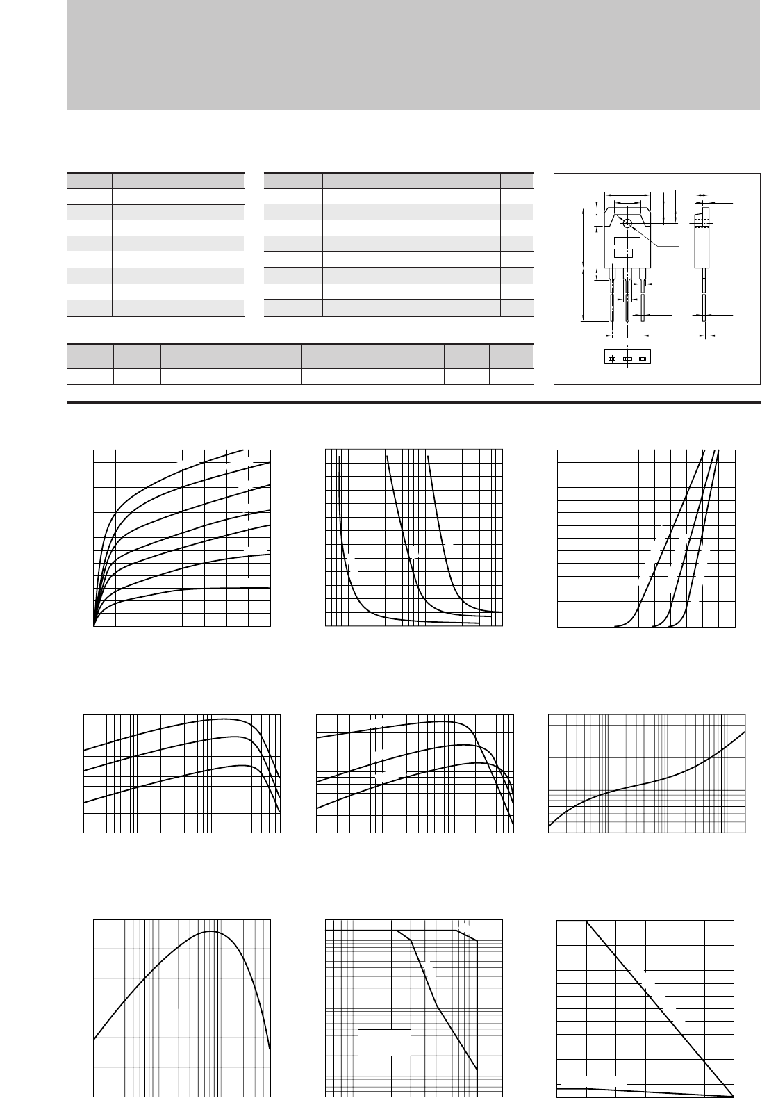
76
Silicon NPN Triple Diffused Planar Transistor
(Switching Transistor)
Application : Humidifier, DC-DC Converter, and General Purpose
Symbol
VCBO
VCEO
VEBO
IC
IB
PC
Tj
Tstg
Ratings
200
120
8
7(Pulse14)
3
70(Tc=25°C)
150
–55 to +150
Unit
V
V
V
A
A
W
°C
°C
■
Absolute maximum ratings
■
Electrical Characteristics
Symbol
ICBO
IEBO
V(BR)CEO
hFE
VCE(sat)
VBE(sat)
fT
COB
Ratings
100max
100max
120min
70to220
0.5max
1.2max
30typ
110typ
Unit
µ
A
µ
A
V
V
V
MHz
pF
Conditions
VCB=200V
VEB=8V
IC=50mA
VCE=4V, IC=3A
IC=3A, IB=0.3A
IC=3A, IB=0.3A
VCE=12V, IE=–0.5A
VCB=10V, f=1MHz
2SC3835
(Ta=25°C) (Ta=25°C)
IC–VCE Characteristics
(Typical)
hFE–IC Characteristics
(Typical)
hFE–IC
Temperature Characteristics (Typical)
θj-a–t Characteristics
IC–VBE Temperature Characteristics
(Typical)
VCE(sat)–IB Characteristics
(Typical)
Pc–Ta Derating
0
2
2.6
1
0.005
0.01 0.10.05 10.5
Base Current IB(A)
Collector-Emitter Saturation Voltage VCE(sat)(V)
I
C
=1A
3A
0.02 0.1 0.5 1 75
20
50
100
200
Collector Current IC(A)
DC Current Gain hFE
(VCE=4V)
5A
Safe Operating Area (Single Pulse)
fT–IE Characteristics
(Typical)
Typ
–0.01
–0.1 –1
–0.05
–0.5 –5
20
10
0
30
Cut-off Frequency fT(MHZ)
(VCE=12V)
Emitter Current IE(A)
10 120505 200
0.05
1
0.5
0.1
20
10
5
Collector-Emitter Voltage VCE(V)
Collector Current IC(A)
Without Heatsink
Natural Cooling
100µs
10ms
0
0
1
2
3
4
5
6
7
2134
Collector-Emitter Voltage VCE(V)
Collector Current IC(A)
60mA
40mA
20mA
100mA
150mA
200mA
I
B
=10mA
0.4
0.5
1
5
1 10 100
1000 2000
Time t(ms)
Transient Thermal Resistance θj-a(˚C/W)
0
7
2
3
4
5
6
1
0 1.1
1.00.5
Base-Emittor Voltage VBE(V)
Collector Current IC(A)
(VCE=4V)
125˚C (Case Temp)
25˚C (Case Temp)
–30˚C (Case Temp)
(VCE=4V)
0.01 0.05 0.1 0.5 1 5
7
20
50
300
100
Collector Current IC(A)
DC Current Gain hFE
25˚C
–30˚C
125˚C
70
60
50
40
30
20
10
3.5
00 25 50 75 100 125 150
Ambient Temperature Ta(˚C)
Maximum Power Dissipation PC(W)
With Infinite heatsink
Without Heatsink
■Typical Switching Characteristics (Common Emitter)
VCC
(V)
50
RL
(Ω)
16.7
IC
(A)
3
VBB2
(V)
–5
IB2
(A)
–0.6
ton
(
µ
s)
0.5max
tstg
(
µ
s)
3.0max
tf
(
µ
s)
0.5max
IB1
(A)
0.3
VBB1
(V)
10
External Dimensions MT-100(TO3P)
15.6±0.4
9.6
19.9±0.3
4.0 2.0
5.0±0.2
1.8
ø3.2±0.1
2
3
1.05
+0.2
-0.1
20.0min
4.0max
BE
5.45±0.1 5.45±0.1
C
4.8±0.2
0.65
+0.2
-0.1
1.4
2.0±0.1
a
b
Weight : Approx 6.0g
a. Part No.
b. Lot No.
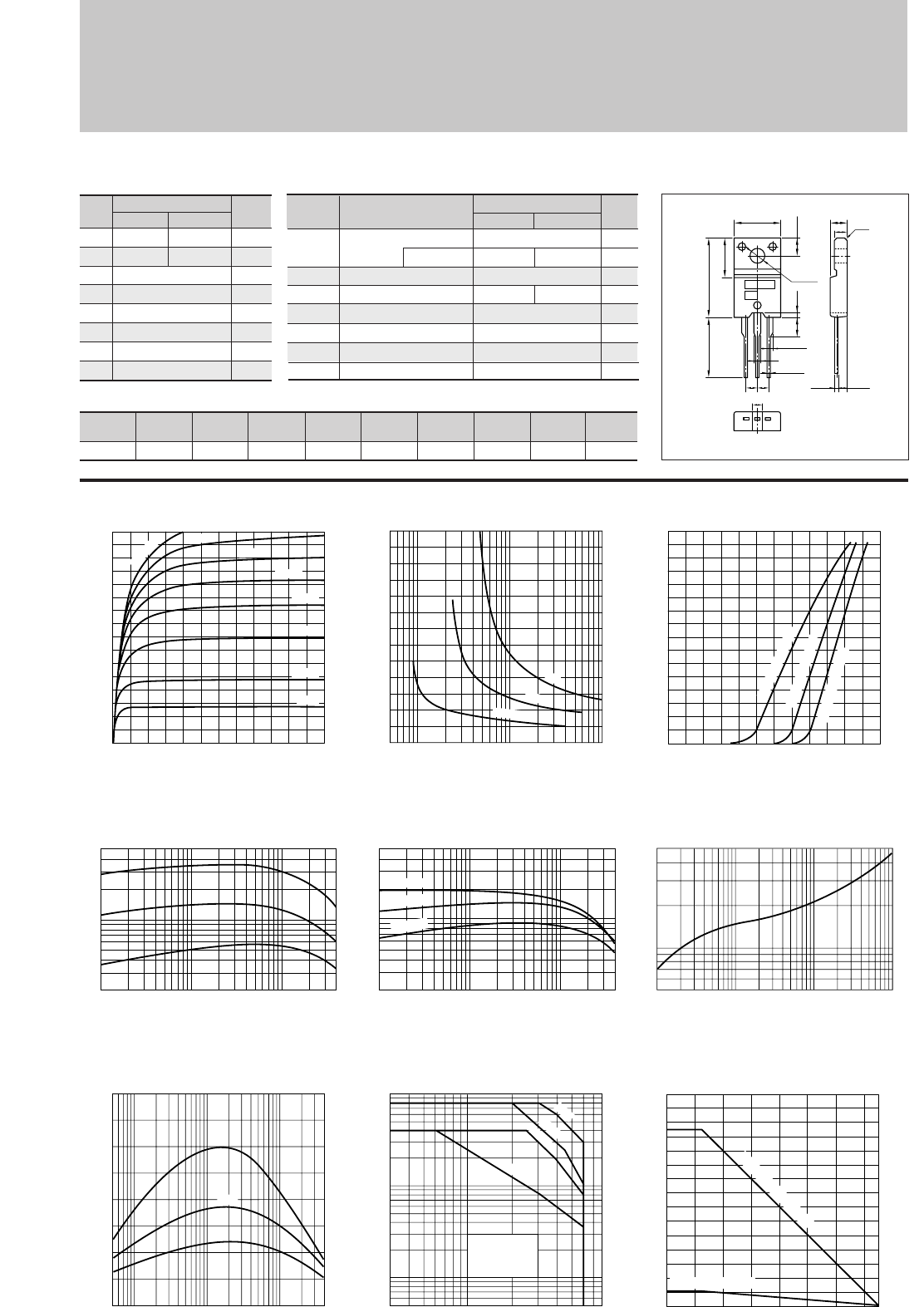
77
2SC3851/3851A
IC–VCE Characteristics
(Typical)
hFE–IC Characteristics
(Typical)
hFE–IC
Temperature Characteristics (Typical)
θj-a–t Characteristics
IC–VBE Temperature Characteristics
(Typical)
VCE(sat)–IB Characteristics
(Typical)
Pc–Ta Derating
0
0
1
2
3
4
21 3456
Collector-Emitter Voltage VCE(V)
Collector Current IC(A)
60mA
I
B
=70mA
Safe Operating Area (Single Pulse)
fT–IE Characteristics
(Typical)
50mA
40mA
30mA
20mA
10mA
5mA
30
20
10
00 50 100 150
Ambient Temperature Ta(˚C)
Maximum Power Dissipation PC(W)
With Infinite heatsink
Without Heatsink
0
1.0
0.5
0.005
0.01 0.10.05 10.5
Base Current IB(A)
Collector-Emitter Saturation Voltage VCE(sat)(V)
I
C
=1A
2A
3A
0.01 0.1 0.5 1 4
20
50
100
500
Collector Current IC(A)
DC Current Gain hFE
(VCE=4V)
Typ
0.5
1
5
1 10 100 1000
Time t(ms)
Transient Thermal Resistance θj-a(˚C/W)
10 5035 80
0.05
0.1
1
0.5
10
5
Collector-Emitter Voltage VCE(V)
Collector Current IC(A)
Without Heatsink
Natural Cooling
DC
100ms
10ms
1ms
(VCE=4V)
0.01 0.10.05 10.5 4
20
50
100
500
Collector Current IC(A)
DC Current Gain hFE
25˚C
–30˚C
125˚C
0
4
2
3
1
0 1.21.00.5
Base-Emittor Voltage VBE(V)
Collector Current IC(A)
(VCE=4V)
125˚C (Case Temp)
25˚C (Case Temp)
–30˚C (Case Temp)
–0.005 –0.1 –0.5 –1 –4
20
10
0
30
40
Cut-off Frequency fT(MHZ)
(VCE=12V)
Emitter Current IE(A)
Typ
Silicon NPN Epitaxial Planar Transistor (Complement to type 2SA1488/A)
Application : Audio and PPC High Voltage Power Supply, and General Purpose
■Typical Switching Characteristics (Common Emitter)
VCC
(V)
12
RL
(Ω)
6
IC
(A)
2
VBB2
(V)
–5
IB2
(mA)
–200
ton
(
µ
s)
0.2typ
tstg
(
µ
s)
1typ
tf
(
µ
s)
0.3typ
IB1
(mA)
200
VBB1
(V)
10
Symbol
VCBO
VCEO
VEBO
IC
IB
PC
Tj
Tstg
6
4
1
25(Tc=25°C)
150
–55 to +150
Unit
V
V
V
A
A
W
°C
°C
■
Absolute maximum ratings
■
Electrical Characteristics
2SC3851
80
60min
Unit
µ
A
V
µ
A
V
V
MHz
pF
(Ta=25°C)
(Ta=25°C)
2SC3851A
100
80
2SC3851
80
60
2SC3851A
100
80min
100max
40to320
0.5max
15typ
60typ
External Dimensions FM20(TO220F)
ø3.3±0.2
10.1±0.2
4.0±0.2
16.9±0.3
13.0min
8.4±0.2
0.8±0.2
3.9
±0.2
2.542.54
1.35±0.15
0.85
+0.2
-0.1
1.35±0.15
2.2±0.2
4.2±0.2
2.8 c0.5
2.4±0.2
0.45
+0.2
-0.1
BEC
a
b
Weight : Approx 2.0g
a. Part No.
b. Lot No.
100max
Conditions
VCB=
VEB=6V
IC=25mA
VCE=4V, IC=1A
IC=2A, IB=0.2A
VCE=12V, IE=–0.2A
VCB=10V, f=1MHz
Symbol
ICBO
IEBO
V(BR)CEO
hFE
VCE(sat)
fT
COB
Ratings Ratings
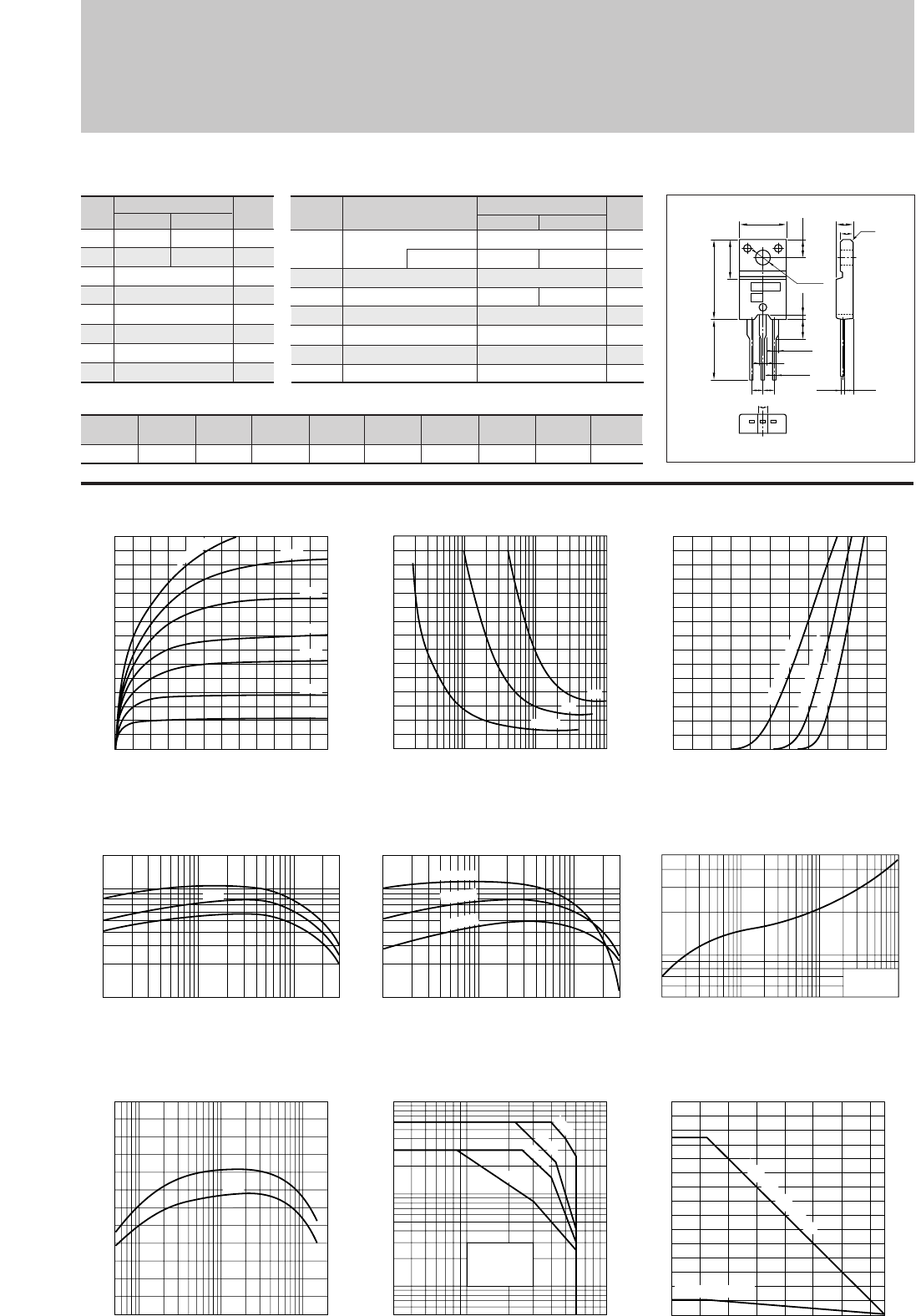
78
2SC3852/3852A
High hFE
LOW VCE (sat)
IC–VCE Characteristics
(Typical)
hFE–IC Characteristics
(Typical)
hFE–IC
Temperature Characteristics (Typical)
θj-a–t Characteristics
IC–VBE Temperature Characteristics
(Typical)
VCE(sat)–IB Characteristics
(Typical)
Pc–Ta Derating
0
0
1
2
3
21 3456
Collector-Emitter Voltage VCE(V)
Collector Current IC(A)
I
B
=12mA
0.5mA
1mA
2mA
3mA
5mA
8mA
Safe Operating Area (Single Pulse)
fT–IE Characteristics
(Typical)
0.01 0.1 0.5 1 3
100
500
2000
1000
Collector Current IC(A)
DC Current Gain hFE
(VCE=4V)
Typ
0.01 0.1 0.5 1 3
100
500
2000
1000
Collector Current IC(A)
DC Current Gain hFE
(VCE=4V)
0.5
1
5
1 10 100 1000
VCB=10V
IE=–2A
Time t(ms)
Transient Thermal Resistance θj-a(˚C/W)
10 503 5 100
0.05
0.1
1
0.5
10
5
Collector-Emitter Voltage VCE(V)
Collector Current IC(A)
Without Heatsink
Natural Cooling
DC
100ms
10ms
1ms
0
1.0
1.0
0.5
0.001 0.005
0.01 0.10.05 10.5
Base Current IB(A)
Collector-Emitter Saturation Voltage VCE(sat)(V)
I
C
=1A
2A
3A
0
2
3
1
0 1.1
1.00.5
Base-Emittor Voltage VBE(V)
Collector Current IC(A)
(VCE=4V)
125˚C (Case Temp)
25˚C (Case Temp)
–30˚C (Case Temp)
25˚C
–30˚C
125˚C
–0.005 –0.01
–0.1
–0.5
–0.05
–2–1
20
10
0
30
Cut-off Frequency fT(MHZ)
(VCE=12V)
Emitter Current IE(A)
Typ
30
20
10
00 50 100 150
Ambient Temperature Ta(˚C)
Maximum Power Dissipation PC(W)
With Infinite heatsink
Without Heatsink
Silicon NPN Epitaxial Planar Transistor
Application : Driver for Solenoid and Motor, Series Regulator and General Purpose
■Typical Switching Characteristics (Common Emitter)
VCC
(V)
20
RL
(Ω)
20
IC
(A)
1.0
VBB2
(V)
–5
IB2
(mA)
–30
ton
(
µ
s)
0.8typ
tstg
(
µ
s)
3.0typ
tf
(
µ
s)
1.2typ
IB1
(mA)
15
VBB1
(V)
10
Symbol
VCBO
VCEO
VEBO
IC
IB
PC
Tj
Tstg
6
3
1
25(Tc=25°C)
150
–55 to +150
Unit
V
V
V
A
A
W
°C
°C
■
Absolute maximum ratings
■
Electrical Characteristics
Symbol
ICBO
IEBO
V(BR)CEO
hFE
VCE(sat)
fT
COB
2SC3852
80
60min
Unit
µ
A
V
µ
A
V
V
MHz
pF
Conditions
VCB=
VEB=6V
IC=25mA
VCE=4V, IC=0.5A
IC=2A, IB=50mA
VCE=12V, IE=–0.2A
VCB=10V, f=1MHz
(Ta=25°C)
(Ta=25°C)
2SC3852A
100
80min
100max
500min
0.5max
15typ
50typ
External Dimensions FM20(TO220F)
ø3.3±0.2
10.1±0.2
4.0±0.2
16.9±0.3
13.0min
8.4±0.2
0.8±0.2
3.9
±0.2
2.542.54
1.35±0.15
0.85
+0.2
-0.1
1.35±0.15
2.2±0.2
4.2±0.2
2.8 c0.5
2.4±0.2
0.45
+0.2
-0.1
BEC
a
b
Weight : Approx 2.0g
a. Part No.
b. Lot No.
10max
2SC3852
80
60
2SC3852A
100
80
Ratings Ratings
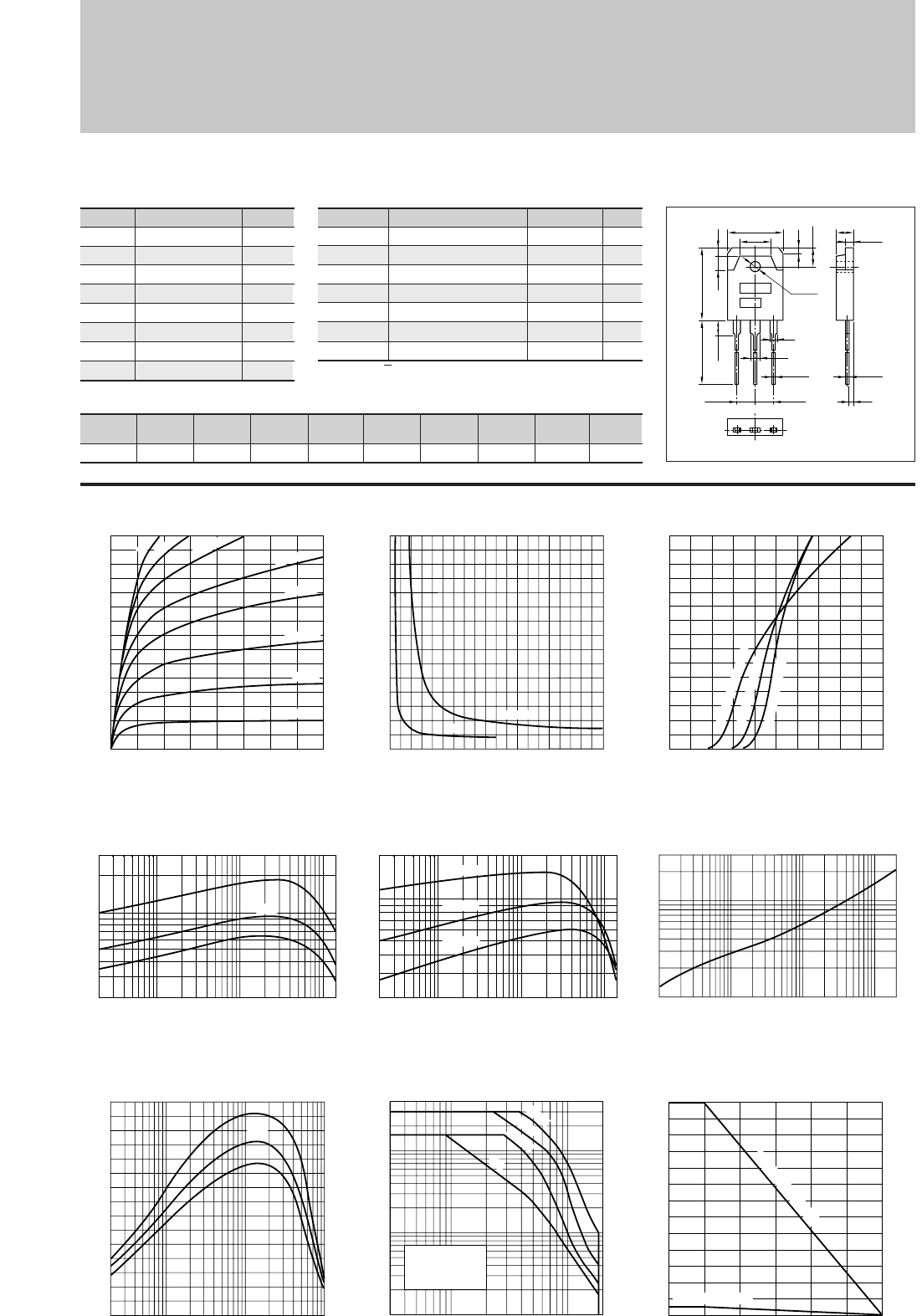
79
Silicon NPN Triple Diffused Planar Transistor (Complement to type 2SA1492) Application : Audio and General Purpose
Symbol
VCBO
VCEO
VEBO
IC
IB
PC
Tj
Tstg
Ratings
200
180
6
15
4
130(Tc=25°C)
150
–55 to +150
Unit
V
V
V
A
A
W
°C
°C
■
Absolute maximum ratings
■
Electrical Characteristics
Symbol
ICBO
IEBO
V(BR)CEO
hFE
VCE(sat)
fT
COB
Ratings
100max
100max
180min
50min∗
2.0max
20typ
300typ
Unit
µ
A
µ
A
V
V
MHz
pF
Conditions
VCB=200V
VEB=6V
IC=50mA
VCE=4V, IC=3A
IC=5A, IB=0.5A
VCE=12V, IE=–0.5A
VCB=10V, f=1MHz
2SC3856
(Ta=25°C) (Ta=25°C)
IC–VCE Characteristics
(Typical)
hFE–IC Characteristics
(Typical)
hFE–IC
Temperature Characteristics (Typical)
θj-a–t Characteristics
IC–VBE Temperature Characteristics
(Typical)
VCE(sat)–IB Characteristics
(Typical)
Pc–Ta Derating
Safe Operating Area (Single Pulse)
fT–IE Characteristics
(Typical)
0
3
2
1
0 0.5 1.0 2.01.5
Base Current IB(A)
Collector-Emitter Saturation Voltage VCE(sat)(V)
IC=10A
5A
Collector Current IC(A)
0
15
10
5
021
Base-Emittor Voltage VBE(V)
(VCE=4V)
125˚C (Case Temp)
25˚C (Case Temp)
–30˚C (Case Temp)
0.1
1
3
0.5
1 10 100 1000 2000
Time t(ms)
Transient Thermal Resistance θj-a(˚C/W)
130
100
50
3.5
0
Ambient Temperature Ta(˚C)
Maximum Power Dissipation PC(W)
With Infinite heatsink
Without Heatsink
0 25 50 75 100 125 150
3 10 100 200
0.1
1
0.5
10
40
5
Collector-Emitter Voltage VCE(V)
Collector Current IC(A)
DC
10ms
3ms
100ms
Without Heatsink
Natural Cooling
0.02 0.1 1 100.5 5 15
20
50
100
300
Collector Current IC(A)
DC Current Gain hFE
(VCE=4V)
Typ
0
0
5
15
10
2134
Collector-Emitter Voltage VCE(V)
Collector Current IC(A)
700mA
300mA
500mA
200mA
100mA
50mA
I
B
=20mA
1A
(VCE=4V)
0.02 0.5 51
20
50
200
100
0.1 10 15
Collector Current IC(A)
DC Current Gain hFE
125˚C
25˚C
–30˚C
–0.02 –0.1 –1 –10
0
10
20
30
Cut-off Frequency fT(MHZ)
(VCE=12V)
Emitter Current IE(A)
Typ
■Typical Switching Characteristics (Common Emitter)
VCC
(V)
40
RL
(Ω)
4
IC
(A)
10
VBB2
(V)
–5
IB2
(A)
–1
ton
(
µ
s)
0.5typ
tstg
(
µ
s)
1.8typ
tf
(
µ
s)
0.6typ
IB1
(A)
1
VBB1
(V)
10
External Dimensions MT-100(TO3P)
15.6±0.4
9.6
19.9±0.3
4.0 2.0
5.0±0.2
1.8
ø3.2±0.1
2
3
1.05
+0.2
-0.1
20.0min
4.0max
BE
5.45±0.1 5.45±0.1
C
4.8±0.2
0.65
+0.2
-0.1
1.4
2.0±0.1
a
b
Weight : Approx 6.0g
a. Part No.
b. Lot No.
∗hFE Rank O(50 to 100), P(70 to 140), Y(90 to 180)
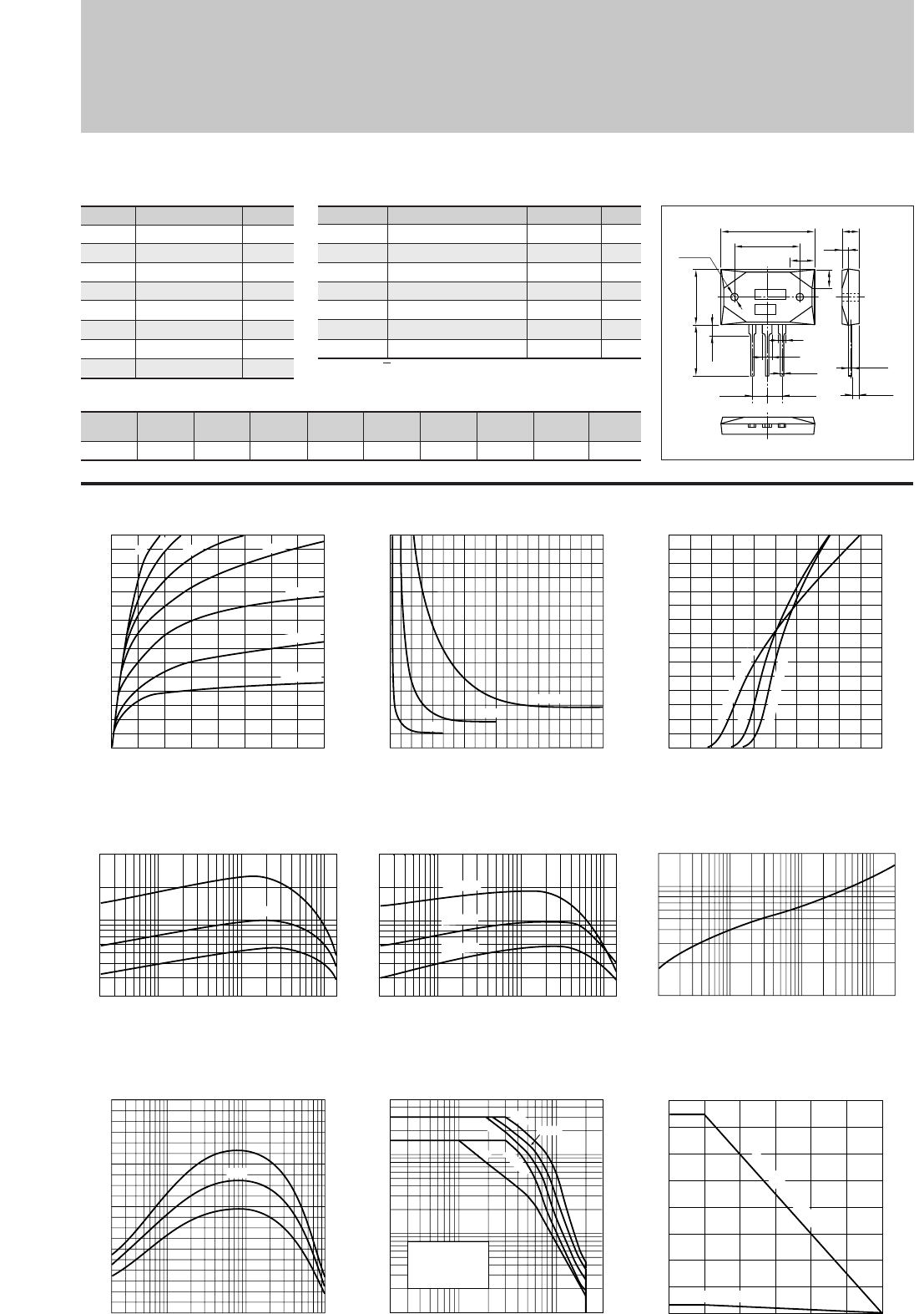
80
2SC3857
IC–VCE Characteristics
(Typical)
hFE–IC Characteristics
(Typical)
hFE–IC
Temperature Characteristics (Typical)
θj-a–t Characteristics
IC–VBE Temperature Characteristics
(Typical)
VCE(sat)–IB Characteristics
(Typical)
Pc–Ta Derating
Safe Operating Area (Single Pulse)
fT–IE Characteristics
(Typical)
0
3
2
1
012 43
Base Current IB(A)
Collector-Emitter Saturation Voltage VCE(sat)(V)
IC=15A
10A
5A
Collector Current IC(A)
0
15
10
5
021
Base-Emittor Voltage VBE(V)
(VCE=4V)
125˚C (Case Temp)
25˚C
–30˚C (Case Temp)
1 10 100 1000 2000
Time t(ms)
0.1
1
2
0.5
Transient Thermal Resistance θj-a(˚C/W)
160
120
80
40
5
00 25 50 75 100 125 150
Ambient Temperature Ta(˚C)
Maximum Power Dissipation PC(W)
With Infinite heatsink
Without Heatsink
2 10 100 300
0.1
1
0.5
10
50
5
Collector-Emitter Voltage VCE(V)
Collector Current IC(A)
3ms
Without Heatsink
Natural Cooling
DC
100ms
20ms
10ms
0.02 0.1 1 100.5 5 15
20
50
100
300
Collector Current IC(A)
DC Current Gain hFE
(VCE=4V)
Typ
0
0
5
15
10
2134
Collector-Emitter Voltage VCE(V)
Collector Current IC(A)
1A
400mA
600mA
200mA
100mA
I
B
=50mA
1.5A
(VCE=4V)
0.02 0.5 51
20
50
300
100
0.1 10 15
Collector Current IC(A)
DC Current Gain hFE
125˚C
25˚C
–30˚C
–0.02 –0.1 –1 –10
0
10
20
40
30
Cut-off Frequency fT(MHZ)
(VCE=12V)
Emitter Current IE(A)
Typ
Silicon NPN Triple Diffused Planar Transistor (Complement to type 2SA1493) Application : Audio and General Purpose
Symbol
VCBO
VCEO
VEBO
IC
IB
PC
Tj
Tstg
Ratings
200
200
6
15
5
150(Tc=25°C)
150
–55 to +150
Unit
V
V
V
A
A
W
°C
°C
■
Absolute maximum ratings
■
Electrical Characteristics
Symbol
ICBO
IEBO
V(BR)CEO
hFE
VCE(sat)
fT
COB
Ratings
100max
100max
200min
50min∗
3.0max
20typ
250typ
Unit
µ
A
µ
A
V
V
MHz
pF
Conditions
VCB=200V
VEB=6V
IC=50mA
VCE=4V, IC=5A
IC=10A, IB=1A
VCE=12V, IE=–0.5A
VCB=10V, f=1MHz
(Ta=25°C) (Ta=25°C)
■Typical Switching Characteristics (Common Emitter)
VCC
(V)
60
RL
(Ω)
12
IC
(A)
5
VBB2
(V)
–5
IB2
(A)
–0.5
ton
(
µ
s)
0.3typ
tstg
(
µ
s)
2.4typ
tf
(
µ
s)
0.4typ
IB1
(A)
0.5
VBB1
(V)
10
2
3
1.05
+0.2
-0.1
BE
5.45±0.1 5.45±0.1
2-ø3.2±0.1
36.4±0.3
9
24.4±0.2
7
21.4±0.3
20.0min
4.0max
0.65
+0.2
-0.1
3.0
+0.3
-0.1
6.0±0.2
2.1
a
b
C
External Dimensions MT-200
Weight : Approx 18.4g
a. Part No.
b. Lot No.
∗hFE Rank O(50 to 100), P(70 to 140), Y(90 to 180)
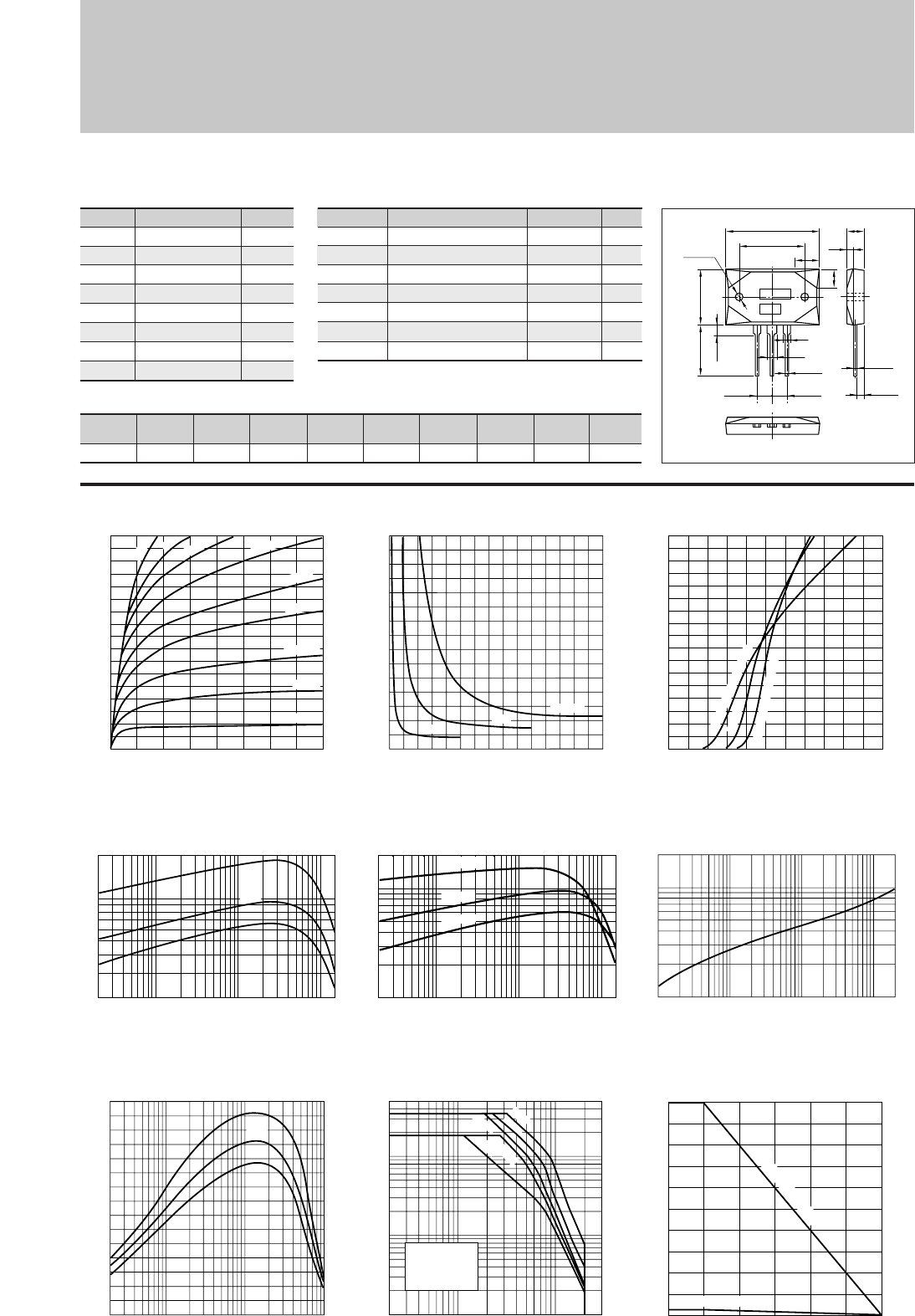
81
Silicon NPN Triple Diffused Planar Transistor (Complement to type 2SA1494) Application : Audio and General Purpose
Symbol
VCBO
VCEO
VEBO
IC
IB
PC
Tj
Tstg
Ratings
200
200
6
17
5
200(Tc=25°C)
150
–55 to +150
Unit
V
V
V
A
A
W
°C
°C
■
Absolute maximum ratings
■
Electrical Characteristics
Symbol
ICBO
IEBO
V(BR)CEO
hFE
VCE(sat)
fT
COB
Ratings
100max
100max
200min
50min∗
2.5max
20typ
300typ
Unit
µ
A
µ
A
V
V
MHz
pF
Conditions
VCB=200V
VEB=6V
IC=50mA
VCE=4V, IC=8A
IC=10A, IB=1A
VCE=12V, IE=–1A
VCB=10V, f=1MHz
2SC3858
(Ta=25°C) (Ta=25°C)
IC–VCE Characteristics
(Typical)
hFE–IC Characteristics
(Typical)
hFE–IC
Temperature Characteristics (Typical)
θj-a–t Characteristics
IC–VBE Temperature Characteristics
(Typical)
VCE(sat)–IB Characteristics
(Typical)
Pc–Ta Derating
Safe Operating Area (Single Pulse)
fT–IE Characteristics
(Typical)
0
3
2
1
0123
Base Current IB(A)
Collector-Emitter Saturation Voltage VCE(sat)(V)
IC=15A
10A
5A
Collector Current IC(A)
0
15
17
10
5
021
Base-Emittor Voltage VBE(V)
(VCE=4V)
125˚C (Case Temp)
25˚C
–30˚C (Case Temp)
1 10 100 1000 2000
Time t(ms)
0.1
1
2
0.5
Transient Thermal Resistance θj-a(˚C/W)
200
160
120
80
40
5
00 25 50 75 100 125 150
Ambient Temperature Ta(˚C)
Maximum Power Dissipation PC(W)
With Infinite heatsink
Without Heatsink
Collector-Emitter Voltage VCE(V)
Collector Current IC(A)
2 10 100 300
0.1
1
0.5
10
50
5
3ms
Without Heatsink
Natural Cooling
DC
100ms
20ms
10ms
0.02 0.1 10.5 17105
20
50
100
300
Collector Current IC(A)
DC Current Gain hFE
(VCE=4V)
Typ
0
0
5
10
17
15
2134
Collector-Emitter Voltage VCE(V)
Collector Current IC(A)
500mA
700mA
1A
300mA
200mA
50mA
I
B
=20mA
1.5A
(VCE=4V)
0.02 0.5 1 5 100.1 17
Collector Current IC(A)
DC Current Gain hFE
125˚C
25˚C
–30˚C
10
50
100
200
–0.02 –0.1 –1 –10
0
10
20
30
Cut-off Frequency fT(MHZ)
(VCE=12V)
Emitter Current IE(A)
Typ
100mA
■Typical Switching Characteristics (Common Emitter)
VCC
(V)
40
RL
(Ω)
4
IC
(A)
10
VBB2
(V)
–5
IB2
(A)
–1
ton
(
µ
s)
0.5typ
tstg
(
µ
s)
1.8typ
tf
(
µ
s)
0.6typ
IB1
(A)
1
VBB1
(V)
10
2
3
1.05
+0.2
-0.1
BE
5.45±0.1 5.45±0.1
2-ø3.2±0.1
36.4±0.3
9
24.4±0.2
7
21.4±0.3
20.0min
4.0max
0.65
+0.2
-0.1
3.0
+0.3
-0.1
6.0±0.2
2.1
a
b
C
External Dimensions MT-200
Weight : Approx 18.4g
a. Part No.
b. Lot No.
∗hFE Rank Y(50 to 100), P(70 to 140), G(90 to 180)
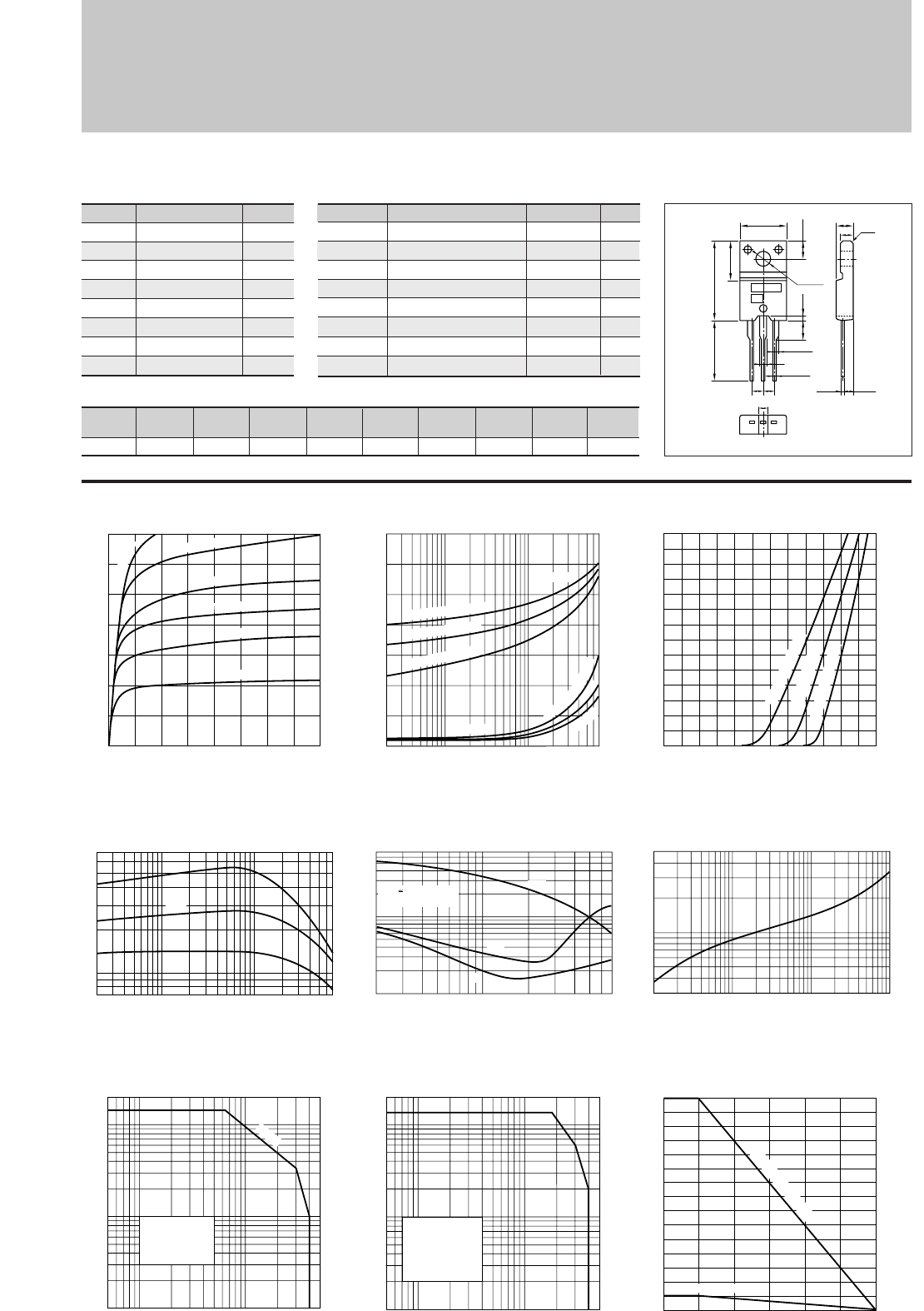
82
Silicon NPN Triple Diffused Planar Transistor (High Voltage and High Speed Switchihg Transistor)
Application : Switching Regulator and General Purpose
Symbol
VCBO
VCEO
VEBO
IC
IB
PC
Tj
Tstg
Ratings
500
400
10
7(Pulse14)
2
30(Tc=25°C)
150
–55 to +150
Unit
V
V
V
A
A
W
°C
°C
■
Absolute maximum ratings
■
Electrical Characteristics
Symbol
ICBO
IEBO
V(BR)CEO
hFE
VCE(sat)
VBE(sat)
fT
COB
Ratings
100max
100max
400min
10to30
0.5max
1.3max
10typ
50typ
Unit
µ
A
µ
A
V
V
V
MHz
pF
Conditions
VCB=500V
VEB=10V
IC=25mA
VCE=4V, IC=3A
IC=3A, IB=0.6A
IC=3A, IB=0.6A
VCE=12V, IE=–0.5A
VCB=10V, f=1MHz
2SC3890
(Ta=25°C) (Ta=25°C)
IC–VCE Characteristics
(Typical)
ton•tstg•tf–IC Characteristics
(Typical)
θj-a–t Characteristics
IC–VBE Temperature Characteristics
(Typical)
VCE(sat),VBE(sat)–IC Temperature Characteristics (Typical)
Collector-Emitter Saturation Voltage VCE(sat)(V)
Base-Emitter Saturation Voltage VBE(sat)(V)
Pc–Ta Derating
Reverse Bias Safe Operating Area
Safe Operating Area (Single Pulse)
0
0
4
2
6
7
2134
Collector-Emitter Voltage VCE(V)
Collector Current IC(A)
400mA
300mA
600mA
200mA
100mA
I
B
=800mA
0.02 0.10.05 1 50.5 7
0
1
(IC/IB=5)
Collector Current IC(A)
VBE(sat)
125˚C (Case Temp)
25˚C (Case Temp)
–55˚C (Case Temp)
25˚C
–55˚C
VCE(sat)
1
2
5
˚
C
(
C
a
s
e
T
e
m
p
)
0.02 0.1 0.50.05 5 71
10
7
50
70
Collector Current IC(A)
DC Current Gain hFE
(VCE=4V)
hFE–IC Characteristics
(Typical)
Typ
10.2 0.5 75
0.1
0.5
5
7
1
Switching Time ton•tstg•tf(µs)
Collector Current IC(A)
tstg
ton
tf
VCC 200V
IC:IB1:IB2=10:1:–2
0.3
1
5
0.5
1 10 100 1000
Time t(ms)
Transient Thermal Resistance θj-a(˚C/W)
30
20
10
2
00 25 50 75 100 125 150
Ambient Temperature Ta(˚C)
Maximum Power Dissipation PC(W)
With Infinite heatsink
Without Heatsink
10 505 500100
1
0.5
0.1
10
20
5
Collector-Emitter Voltage VCE(V)
Collector Current IC(A)
Without Heatsink
Natural Cooling
L=3mH
–IB2=1A
Duty:less than 1%
10 505 100 500
1
0.5
0.1
10
20
5
Collector-Emitter Voltage VCE(V)
Collector Current IC(A)
100µs
Without Heatsink
Natural Cooling
0
7
2
4
6
0 1.20.4 0.6 0.8 1.00.2
Base-Emittor Voltage VBE(V)
Collector Current IC(A)
(VCE=4V)
125˚C (Case Temp)
25˚C (Case Temp)
–55˚C (Case Temp)
■Typical Switching Characteristics (Common Emitter)
VCC
(V)
200
RL
(Ω)
66
IC
(A)
3
VBB2
(V)
–5
IB2
(A)
–0.6
ton
(
µ
s)
1max
tstg
(
µ
s)
3max
tf
(
µ
s)
0.5max
IB1
(A)
0.3
VBB1
(V)
10
External Dimensions FM20(TO220F)
ø3.3±0.2
10.1±0.2
4.0±0.2
16.9±0.3
13.0min
8.4±0.2
0.8±0.2
3.9
±0.2
2.542.54
1.35±0.15
0.85
+0.2
-0.1
1.35±0.15
2.2±0.2
4.2±0.2
2.8 c0.5
2.4±0.2
0.45
+0.2
-0.1
BEC
a
b
Weight : Approx 2.0g
a. Part No.
b. Lot No.
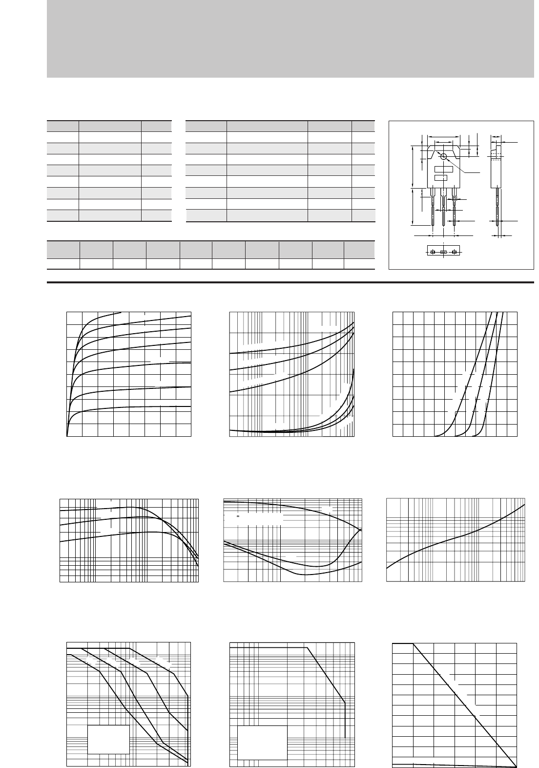
83
Silicon NPN Triple Diffused Planar Transistor (High Voltage Switchihg Transistor)
Application : Switching Regulator and General Purpose
Symbol
VCBO
VCEO
VEBO
IC
IB
PC
Tj
Tstg
Ratings
900
550
7
10(Pulse15)
5
120(Tc=25°C)
150
–55 to +150
Unit
V
V
V
A
A
W
°C
°C
■
Absolute maximum ratings
■
Electrical Characteristics
Symbol
ICBO
IEBO
V(BR)CEO
hFE
VCE(sat)
VBE(sat)
fT
COB
Ratings
100max
100max
550min
10to28
0.5max
1.2max
6typ
105typ
Unit
µ
A
µ
A
V
V
V
MHz
pF
Conditions
VCB=800V
VEB=7V
IC=10mA
VCE=4V, IC=5A
IC=5A, IB=1A
IC=5A, IB=1A
VCE=12V, IE=–1A
VCB=10V, f=1MHz
2SC3927
(Ta=25°C) (Ta=25°C)
IC–VCE Characteristics
(Typical)
hFE–IC Characteristics
(Typical)
ton•tstg•tf–IC Characteristics
(Typical)
θj-a–t Characteristics
IC–VBE Temperature Characteristics
(Typical)
VCE(sat),VBE(sat)–IC Temperature Characteristics (Typical)
Collector-Emitter Saturation Voltage VCE(sat)(V)
Base-Emitter Saturation Voltage VBE(sat)(V)
Pc–Ta Derating
Reverse Bias Safe Operating Area
Safe Operating Area (Single Pulse)
0
0
2
4
6
8
10
2134
Collector-Emitter Voltage VCE(V)
Collector Current IC(A)
800mA
1A
600mA
400mA
200mA
1.2A
I
B
=100mA
0.02
0.1
0.05
15100.5
0
1
(IC/IB=5)
Collector Current IC(A)
VBE(sat)
125˚C (Case Temp)
25˚C (Case Temp)
–55˚C (Case Temp)
25˚C
–55˚C
VCE(sat)
1
2
5
˚
C
(
C
a
s
e
T
e
m
p
)
0.2 10.5 105
0.1
0.5
5
10
1
Switching Time ton•tstg•tf(µs)
Collector Current IC(A)
tstg
ton
tf
VCC 250V
IC:IB1:–IB2=10:1.5:3
0.1
1
2
0.5
1 10 100 1000
Time t(ms)
Transient Thermal Resistance θj-a(˚C/W)
120
100
50
3.5
00 25 50 75 100 125 150
Ambient Temperature Ta(˚C)
Maximum Power Dissipation PC(W)
With Infinite heatsink
Without Heatsink
100 50050 1000
1
0.5
0.1
0.05
0.02
10
20
5
Collector-Emitter Voltage VCE(V)
Collector Current IC(A)
Without Heatsink
Natural Cooling
L=3mH
IB2=–1.0A
Duty:less than 1%
10 50 100
500 600
0.05
0.02
1
0.5
0.1
10
20
5
Collector-Emitter Voltage VCE(V)
Collector Current IC(A)
Without Heatsink
Natural Cooling
100µs
10ms
1ms
DC
0
10
4
2
8
6
0 1.20.4 0.6 0.8 1.00.2
Base-Emittor Voltage VBE(V)
Collector Current IC(A)
(VCE=4V)
125˚C (Case Temp)
–55˚C (Case Temp)
0.02 0.10.05 1 1050.5
5
10
50
Collector Current IC(A)
DC Current Gain hFE
(VCE=4V)
125˚C
25˚C
–55˚C
25˚C (Case Temp)
■Typical Switching Characteristics (Common Emitter)
VCC
(V)
250
RL
(Ω)
50
IC
(A)
5
VBB2
(V)
–5
IB2
(A)
–1.5
ton
(
µ
s)
1max
tstg
(
µ
s)
5max
tf
(
µ
s)
0.5max
IB1
(A)
0.75
VBB1
(V)
10
External Dimensions MT-100(TO3P)
15.6±0.4
9.6
19.9±0.3
4.0 2.0
5.0±0.2
1.8
ø3.2±0.1
2
3
1.05
+0.2
-0.1
20.0min
4.0max
BE
5.45±0.1 5.45±0.1
C
4.8±0.2
0.65
+0.2
-0.1
1.4
2.0±0.1
a
b
Weight : Approx 6.0g
a. Part No.
b. Lot No.
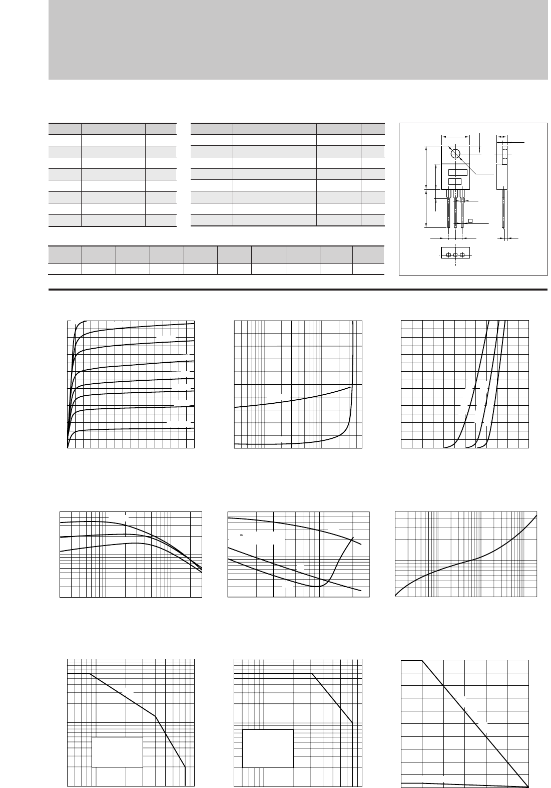
84
Silicon NPN Triple Diffused Planar Transistor (High Voltage Switchihg Transistor)
Application : Switching Regulator and General Purpose
Symbol
VCBO
VCEO
VEBO
IC
IB
PC
Tj
Tstg
Ratings
900
800
7
3(Pulse6)
1.5
50(Tc=25°C)
150
–55 to +150
Unit
V
V
V
A
A
W
°C
°C
■
Absolute maximum ratings
■
Electrical Characteristics
Symbol
ICBO
IEBO
V(BR)CEO
hFE
VCE(sat)
VBE(sat)
fT
COB
Ratings
100max
100max
800min
10to30
0.5max
1.2max
6typ
40typ
Unit
µ
A
µ
A
V
V
V
MHz
pF
Conditions
VCB=800V
VEB=7V
IC=10mA
VCE=4V, IC=0.7A
IC=0.7A, IB=0.14A
IC=0.7A, IB=0.14A
VCE=12V, IE=–0.3A
VCB=10V, f=1MHz
2SC4020
(Ta=25°C) (Ta=25°C)
IC–VCE Characteristics
(Typical)
ton•tstg•tf–IC Characteristics
(Typical)
θj-a–t Characteristics
IC–VBE Temperature Characteristics
(Typical)
VCE(sat),VBE(sat)–IC Temperature Characteristics (Typical)
Pc–Ta Derating
Reverse Bias Safe Operating Area
Safe Operating Area (Single Pulse)
0.03
0.1
0.05
150.5
0
2
1
Collector-Emitter Saturation Voltage VCE(sat)(V)
Base-Emitter Saturation Voltage VBE(sat)(V)
Collector Current IC(A)
VBE(sat)
VCE(sat)
hFE–IC Characteristics
(Typical)
0.1 10.5 3
0.2
0.5
5
6
1
Switching Time ton•tstg•tf(µs)
Collector Current IC(A)
tstg
ton
tf
VCC 250V
IC:IB1:–IB2=2:0.3:1 Const.
0.3
1
5
0.5
1 10 100 1000 2000
Time t(ms)
Transient Thermal Resistance θj-a(˚C/W)
50
40
30
20
10
2
00 25 50 75 100 125 150
Ambient Temperature Ta(˚C)
Maximum Power Dissipation PC(W)
With Infinite heatsink
Without Heatsink
100 50050 1000
1
0.5
0.1
10
5
Collector-Emitter Voltage VCE(V)
Collector Current IC(A)
Without Heatsink
Natural Cooling
L=3mH
IB2=–1.0A
Duty:less than 1%
50 100 500 1000
1
0.5
0.1
10
5
Collector-Emitter Voltage VCE(V)
Collector Current IC(A)
Without Heatsink
Natural Cooling
100µs
(IC/IB=5)
0.02 0.10.05 1 30.5
2
5
10
50
Collector Current IC(A)
DC Current Gain hFE
(VCE=4V)
0
3
1
2
0 1.20.4 0.6 0.8 1.00.2
Base-Emittor Voltage VBE(V)
Collector Current IC(A)
(VCE=4V)
125˚C (Case Temp)
25˚C (Case Temp)
–30˚C (Case Temp)
125˚C
25˚C
–30˚C
0
0
2
1
3
2134
Collector-Emitter Voltage VCE(V)
Collector Current IC(A)
300mA
400mA
500mA
140mA
200mA
100mA
60mA
I
B
=20mA
■Typical Switching Characteristics (Common Emitter)
VCC
(V)
250
RL
(Ω)
357
IC
(A)
0.7
VBB2
(V)
–5
IB2
(A)
–0.35
ton
(
µ
s)
1max
tstg
(
µ
s)
5max
tf
(
µ
s)
1max
IB1
(A)
0.1
VBB1
(V)
10
External Dimensions MT-25(TO220)
BE
2.5 2.5
C
16.0±0.7
12.0min
4.0max 8.8±0.2
1.35
0.65
+0.2
-0.1
10.2±0.2
ø3.75±0.2
3.0±0.2
4.8±0.2
1.4
2.0±0.1
a
b
Weight : Approx 2.6g
a. Part No.
b. Lot No.
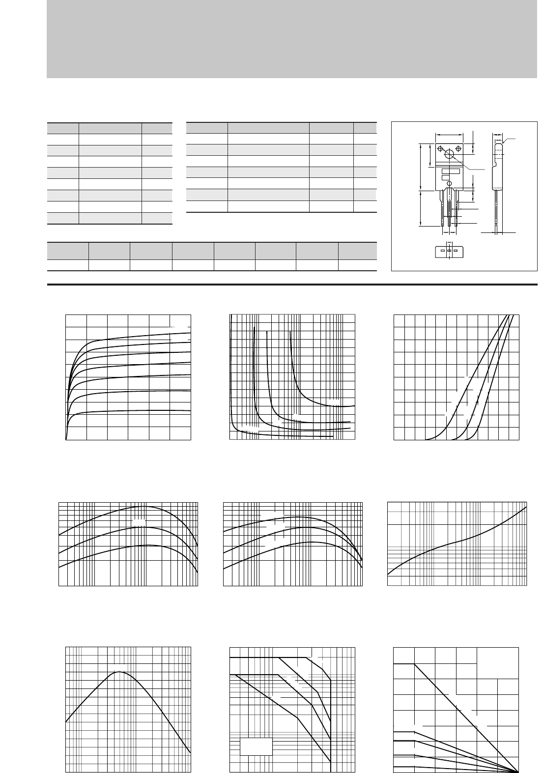
85
2SC4024
Silicon NPN Epitaxial Planar Transistor
Application : DC-DC Converter, Emergency Lighting Inverter and General Purpose
Symbol
VCBO
VCEO
VEBO
IC
IB
PC
Tj
Tstg
Ratings
100
50
15
10
3
35(Tc=25°C)
150
–55 to +150
Unit
V
V
V
A
A
W
°C
°C
■
Absolute maximum ratings
■
Electrical Characteristics
Symbol
ICBO
IEBO
V(BR)CEO
hFE
VCE(sat)
fT
COB
Ratings
10max
10max
50min
300to1600
0.5max
24typ
150typ
Unit
µ
A
µ
A
V
V
MHz
pF
Conditions
VCB=100V
VEB=15V
IC=25mA
VCE=4V, IC=1A
IC=5A, IB=0.1A
VCE=12V, IE=–0.5A
VCB=10V, f=1MHz
(Ta=25°C) (Ta=25°C)
IC–VCE Characteristics
(Typical)
hFE–IC Characteristics
(Typical)
hFE–IC
Temperature Characteristics (Typical)
θj-a–t Characteristics
IC–VBE Temperature Characteristics
(Typical)
VCE(sat)–IB Characteristics
(Typical)
Pc–Ta Derating
0
0
4
2
6
10
8
246
Collector-Emitter Voltage VCE(V)
Collector Current IC(A)
I
B
=35mA
5mA
25mA
30mA
10mA
15mA
20mA
Safe Operating Area (Single Pulse)
fT–IE Characteristics
(Typical)
0
1.0
1.5
0.5
0.002
0.01 0.1 21
Base Current IB(A)
Collector-Emitter Saturation Voltage VCE(sat)(V)
0.02 0.1 0.5 5110
100
500
1000
Collector Current IC(A)
DC Current Gain hFE
(VCE=4V)
Typ
0.02 0.1 0.5 5110
100
500
1000
Collector Current IC(A)
DC Current Gain hFE
(VCE=4V)
I
C
=1A
5A
10A
3A
0.3
0.5
1
4
1 10 100 1000
Time t(ms)
Transient Thermal Resistance θj-a(˚C/W)
10 503 5 100
0.2
1
0.5
30
10
5
Collector-Emitter Voltage VCE(V)
Collector Current IC(A)
Without Heatsink
Natural Cooling
DC
100ms
10ms
1ms
40
30
20
10
2
00 25 50 75 100 125 150
Ambient Temperature Ta(˚C)
Maximum Power Dissipation PC(W)
With Infinite heatsink
Without Heatsink
50x50x2
100x100x2
150x150x2
0
10
2
4
8
6
0 1.2
1.00.5
Base-Emittor Voltage VBE(V)
Collector Current IC(A)
(VCE=4V)
125˚C (Case Temp)
25˚C (Case Temp)
–30˚C (Case Temp)
25˚C
–30˚C
125˚C
–0.05
–0.1 –1–0.5 –5 –10
20
10
0
30
Cut-off Frequency fT(MHZ)
(VCE=12V)
Emitter Current IE(A)
Typ
Natural Cooling
Silicone Grease
Heatsink: Aluminum
in mm
■Typical Switching Characteristics (Common Emitter)
VCC
(V)
20
RL
(Ω)
4
IC
(A)
5
IB2
(A)
–0.1
ton
(
µ
s)
0.5typ
tstg
(
µ
s)
2.0typ
tf
(
µ
s)
0.5typ
IB1
(A)
0.1
External Dimensions FM20(TO220F)
ø3.3±0.2
10.1±0.2
4.0±0.2
16.9±0.3
13.0min
8.4±0.2
0.8±0.2
3.9
±0.2
2.542.54
1.35±0.15
0.85
+0.2
-0.1
1.35±0.15
2.2±0.2
4.2±0.2
2.8 c0.5
2.4±0.2
0.45
+0.2
-0.1
BEC
a
b
Weight : Approx 2.0g
a. Part No.
b. Lot No.
High hFE
LOW VCE (sat)
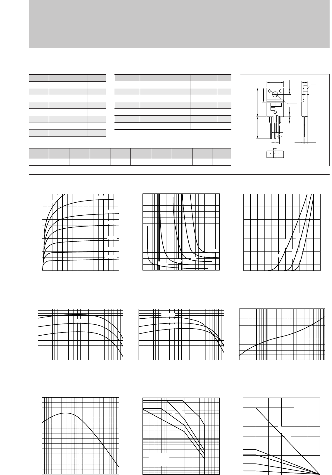
86
Application : DC Motor Driver and General Purpose
Symbol
VCBO
VCEO
VEBO
IC
IB
PC
Tj
Tstg
Ratings
50
50
6
12
3
35(Tc=25°C)
150
–55 to +150
Unit
V
V
V
A
A
W
°C
°C
■
Absolute maximum ratings
■
Electrical Characteristics
Symbol
ICBO
IEBO
V(BR)CEO
hFE
VCE(sat)
fT
COB
Ratings
100max
10max
50min
50min
0.35max
40typ
180typ
Unit
µ
A
µ
A
V
V
MHz
pF
Conditions
VCB=50V
VEB=6V
IC=25mA
VCE=1V, IC=6A
IC=6A, IB=0.3A
VCE=12V, IE=–0.5A
VCB=12V, f=1MHz
2SC4064
(Ta=25°C) (Ta=25°C)
IC–VCE Characteristics
(Typical)
hFE–IC Characteristics
(Typical)
hFE–IC
Temperature Characteristics (Typical)
θj-a–t Characteristics
IC–VBE Temperature Characteristics
(Typical)
VCE(sat)–IB Characteristics
(Typical)
Pc–Ta Derating
0
0
2
4
8
6
10
12
1.60.8 2.4 3.2 4 4.8 5.6 6
Collector-Emitter Voltage VCE(V)
Collector Current IC(A)
20mA
100mA
60mA
40mA
20mA
10mA
I
B
=5mA
Safe Operating Area (Single Pulse)
fT–IE Characteristics
(Typical)
0
1.0
1.3
0.5
0.002
0.01 0.1 31
Base Current IB(A)
Collector-Emitter Saturation Voltage VCE(sat)(V)
I
C
=1A
12A
3A
6A
9A
0.02 0.1 1 10 12
20
50
100
1000
500
Collector Current IC(A)
DC Current Gain hFE
(VCE=1V)
Typ
0.02 0.1 1 10 12
20
50
100
1000
500
Collector Current IC(A)
DC Current Gain hFE
(VCE=1V)
0.3
0.5
1
5
1 10 100 1000
Time t(ms)
Transient Thermal Resistance θj-a(˚C/W)
10 503 5 100
0.05
0.1
1
0.5
30
10
5
Collector-Emitter Voltage VCE(V)
Collector Current IC(A)
Without Heatsink
Natural Cooling
DC
100ms
10ms
1ms
0
12
10
2
4
8
6
0 1.1
1.00.5
Base-Emittor Voltage VBE(V)
Collector Current IC(A)
(VCE=1V)
125˚C (Case Temp)
25˚C (Case Temp)
–30˚C (Case Temp)
25˚C
–30˚C
125˚C
–0.05
–0.1 –1–0.5 –5 –12–10
20
10
0
30
Cut-off Frequency fT(MHZ)
(VCE=12V)
Emitter Current IE(A)
Typ
40
30
20
10
2
00 25 50 75 100 125 150
Ambient Temperature Ta(˚C)
Maximum Power Dissipation PC(W)
With Infinite heatsink
Without Heatsink
50x50x2
100x100x2
150x150x2
Natural Cooling
Silicone Grease
Heatsink: Aluminum
in mm
■Typical Switching Characteristics (Common Emitter)
VCC
(V)
24
RL
(Ω)
4
IC
(A)
6
VBB2
(V)
–5
IB2
(A)
–0.12
ton
(
µ
s)
0.6typ
tstg
(
µ
s)
1.4typ
tf
(
µ
s)
0.4typ
IB1
(A)
0.12
VBB1
(V)
10
Silicon NPN Epitaxial Planar Transistor (Complement to type 2SA1567)
External Dimensions FM20(TO220F)
ø3.3±0.2
10.1±0.2
4.0±0.2
16.9±0.3
13.0min
8.4±0.2
0.8±0.2
3.9
±0.2
2.542.54
1.35±0.15
0.85
+0.2
-0.1
1.35±0.15
2.2±0.2
4.2±0.2
2.8 c0.5
2.4±0.2
0.45
+0.2
-0.1
BEC
a
b
Weight : Approx 2.0g
a. Part No.
b. Lot No.
LOW VCE (sat)
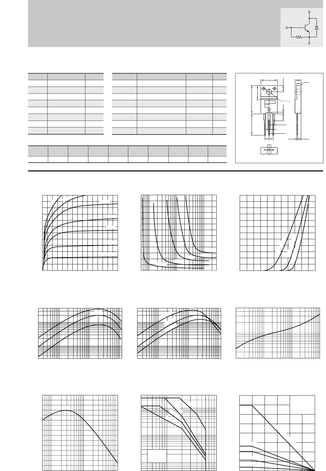
87
2SC4065
Silicon NPN Epitaxial Planar Transistor (Complement to type 2SA1568)
Symbol
VCBO
VCEO
VEBO
IC
IB
PC
Tj
Tstg
Ratings
60
60
6
±12
3
35(Tc=25°C)
150
–55 to +150
Unit
V
V
V
A
A
W
°C
°C
■
Absolute maximum ratings
■
Electrical Characteristics
Symbol
ICBO
IEBO
V(BR)CEO
hFE
VCE(sat)
VFEC
fT
COB
Ratings
100max
60max
60min
50min
0.35max
2.5max
24typ
180typ
Unit
µ
A
mA
V
V
V
MHz
PF
Conditions
VCB=60V
VEB=6V
IC=25mA
VCE=1V, IC=6A
IC=6A, IB=1.3A
VECO=10A
VCE=12V, IE=–0.5A
VCB=10V, f=1MHz
(Ta=25°C) (Ta=25°C)
IC–VCE Characteristics
(Typical)
hFE–IC Characteristics
(Typical)
hFE–IC
Temperature Characteristics (Typical)
θj-a–t Characteristics
IC–VBE Temperature Characteristics
(Typical)
VCE(sat)–IB Characteristics
(Typical)
Pc–Ta Derating
0
0
4
2
8
6
12
10
246
Collector-Emitter Voltage VCE(V)
Collector Current IC(A)
200mA
I
B
=10mA
20mA
40mA
60mA
100mA
150mA
Safe Operating Area (Single Pulse)
fT–IE Characteristics
(Typical)
0
1.0
1.3
0.5
0.005
0.01
0.1 31
Base Current IB(A)
Collector-Emitter Saturation Voltage VCE(sat)(V)
I
C
=1A
12A
3A
6A
9A
0.02 0.1 1 10 12
3
5
50
10
100
400
Collector Current IC(A)
DC Current Gain hFE
(VCE=1V)
Typ
0.02 0.1 1 10 12
3
5
50
10
100
400
Collector Current IC(A)
DC Current Gain hFE
(VCE=1V)
0.2
0.5
1
5
1 10 100 1000
Time t(ms)
Transient Thermal Resistance θj-a(˚C/W)
10 503 5 100
0.05
0.1
1
0.5
30
10
5
Collector-Emitter Voltage VCE(V)
Collector Current IC(A)
Without Heatsink
Natural Cooling
DC
100ms
10ms
1ms
40
30
20
10
2
00 25 50 75 100 125 150
Ambient Temperature Ta(˚C)
Maximum Power Dissipation PC(W)
With Infinite heatsink
Without Heatsink
50x50x2
100x100x2
150x150x2
0
12
10
2
4
8
6
0 1.1
1.00.5
Base-Emittor Voltage VBE(V)
Collector Current IC(A)
(VCE=1V)
125˚C (Case Temp)
25˚C (Case Temp)
–30˚C (Case Temp)
25˚C
–30˚C
125˚C
–0.05
–0.1 –1–0.5 –5 –12–10
20
10
0
30
Cut-off Frequency fT(MHZ)
(VCE=12V)
Emitter Current IE(A)
Typ
Natural Cooling
Silicone Grease
Heatsink: Aluminum
in mm
External Dimensions FM20(TO220F)
ø3.3±0.2
10.1±0.2
4.0±0.2
16.9±0.3
13.0min
8.4±0.2
0.8±0.2
3.9
±0.2
2.542.54
1.35±0.15
0.85
+0.2
-0.1
1.35±0.15
2.2±0.2
4.2±0.2
2.8 c0.5
2.4±0.2
0.45
+0.2
-0.1
BEC
a
b
Weight : Approx 2.0g
a. Part No.
b. Lot No.
Application : DC Motor Driver and General Purpose
■Typical Switching Characteristics (Common Emitter)
VCC
(V)
24
RL
(Ω)
4
IC
(A)
6
VBB2
(V)
–5
IB2
(A)
–0.12
ton
(
µ
s)
0.6typ
tstg
(
µ
s)
1.4typ
tf
(
µ
s)
0.4typ
IB1
(A)
0.12
VBB1
(V)
10
Built-in Diode at C–E
Low VCE (sat)
B
C
E
(400Ω)
Equivalent
circuit
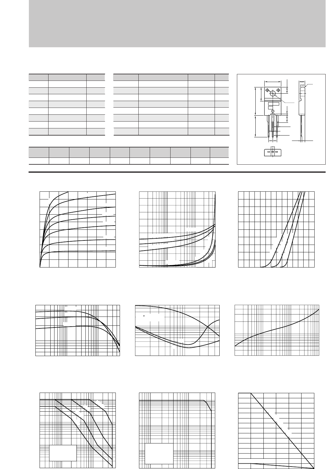
88
Silicon NPN Triple Diffused Planar Transistor (High Voltage and High Speed Switchihg Transistor)
Application : Switching Regulator and General Purpose
Symbol
VCBO
VCEO
VEBO
IC
IB
PC
Tj
Tstg
Ratings
500
400
10
5(Pulse10)
2
30(Tc=25°C)
150
–55 to +150
Unit
V
V
V
A
A
W
°C
°C
■
Absolute maximum ratings
■
Electrical Characteristics
Symbol
ICBO
IEBO
V(BR)CEO
hFE
VCE(sat)
VBE(sat)
fT
COB
Ratings
100max
100max
400min
10to30
0.5max
1.3max
10typ
30typ
Unit
µ
A
µ
A
V
V
V
MHz
pF
Conditions
VCB=500V
VEB=10V
IC=25mA
VCE=4V, IC=2A
IC=2A, IB=0.4A
IC=2A, IB=0.4A
VCE=12V, IE=–0.3A
VCB=10V, f=1MHz
2SC4073
(Ta=25°C) (Ta=25°C)
IC–VCE Characteristics
(Typical)
hFE–IC Characteristics
(Typical)
ton•tstg•tf–IC Characteristics
(Typical)
θj-a–t Characteristics
IC–VBE Temperature Characteristics
(Typical)
VCE(sat),VBE(sat)–IC Temperature Characteristics (Typical)
Collector-Emitter Saturation Voltage VCE(sat)(V)
Base-Emitter Saturation Voltage VBE(sat)(V)
Pc–Ta Derating
Reverse Bias Safe Operating Area
Safe Operating Area (Single Pulse)
0
0
1
2
3
4
5
2134
Collector-Emitter Voltage VCE(V)
Collector Current IC(A)
600mA
400mA
300mA
200mA
I
B
=800mA
100mA
50mA
0.01 0.10.05 1 50.5
0
2
1
(IC/IB=5)
Collector Current IC(A)
VBE(sat)
125˚C (Case Temp)
25˚C (Case Temp)
–55˚C (Case Temp)
25˚C
–55˚C
VCE(sat)
1
2
5
˚
C
(
C
a
s
e
T
e
m
p
)
0.1 10.5 5
0.1
0.5
5
1
Switching Time ton•tstg•tf(µs)
Collector Current IC(A)
tstg
ton
tf
VCC 200V
IC:IB1:–IB2=10:1:2
0.3
1
5
0.5
1 10 100 1000
Time t(ms)
Transient Thermal Resistance θj-a(˚C/W)
30
20
10
2
00 25 50 75 100 125 150
Ambient Temperature Ta(˚C)
Maximum Power Dissipation PC(W)
With Infinite heatsink
Without Heatsink
10 505 500100
1
0.5
0.1
0.05
0.01
10
20
5
Collector-Emitter Voltage VCE(V)
Collector Current IC(A)
Without Heatsink
Natural Cooling
L=3mH
IB2=–0.5A
Duty:less than1%
10 5052 100 500
0.05
0.01
1
0.5
0.1
10
20
5
Collector-Emitter Voltage VCE(V)
Collector Current IC(A)
Without Heatsink
Natural Cooling
DC
10ms
100µs
1ms
0.01 0.10.05 1 50.5
5
10
50
Collector Current IC(A)
DC Current Gain hFE
(VCE=4V)
125˚C
25˚C
–55˚C
0
2
1
4
3
5
0 1.41.20.4 0.6 0.8 1.00.2
Base-Emittor Voltage VBE(V)
Collector Current IC(A)
(VCE=4V)
125˚C (Case Temp)
–55˚C (Case Temp)
25˚C (Case Temp)
■Typical Switching Characteristics (Common Emitter)
VCC
(V)
200
RL
(Ω)
100
IC
(A)
2
VBB2
(V)
–5
IB2
(A)
–0.4
ton
(
µ
s)
1max
tstg
(
µ
s)
3max
tf
(
µ
s)
0.5max
IB1
(A)
0.2
VBB1
(V)
10
External Dimensions FM20(TO220F)
ø3.3±0.2
10.1±0.2
4.0±0.2
16.9±0.3
13.0min
8.4±0.2
0.8±0.2
3.9
±0.2
2.542.54
1.35±0.15
0.85
+0.2
-0.1
1.35±0.15
2.2±0.2
4.2±0.2
2.8 c0.5
2.4±0.2
0.45
+0.2
-0.1
BEC
a
b
Weight : Approx 2.0g
a. Part No.
b. Lot No.
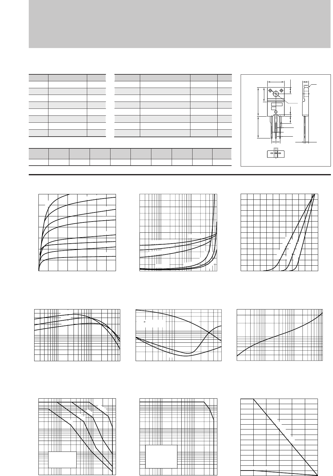
89
Silicon NPN Epitaxial Planar Transistor (High Voltage and High Speed Switchihg Transistor)
Application : Switching Regulator and General Purpose
Symbol
VCBO
VCEO
VEBO
IC
IB
PC
Tj
Tstg
Ratings
500
400
10
7(Pulse14)
2
30(Tc=25°C)
150
–55 to +150
Unit
V
V
V
A
A
W
°C
°C
■
Absolute maximum ratings
■
Electrical Characteristics
Symbol
ICBO
IEBO
V(BR)CEO
hFE
VCE(sat)
VBE(sat)
fT
COB
Ratings
100max
100max
400min
10to30
0.5max
1.3max
15typ
50typ
Unit
µ
A
µ
A
V
V
V
MHz
pF
Conditions
VCB=500V
VEB=10V
IC=25mA
VCE=4V, IC=3A
IC=3A, IB=0.6A
IC=3A, IB=0.6A
VCE=12V, IE=–0.5A
VCB=10V, f=1MHz
2SC4130
(Ta=25°C) (Ta=25°C)
IC–VCE Characteristics
(Typical)
hFE–IC Characteristics
(Typical)
ton•tstg•tf–IC Characteristics
(Typical)
θj-a–t Characteristics
IC–VBE Temperature Characteristics
(Typical)
VCE(sat),VBE(sat)–IC Temperature Characteristics (Typical)
Collector-Emitter Saturation Voltage VCE(sat)(V)
Base-Emitter Saturation Voltage VBE(sat)(V)
Pc–Ta Derating
Reverse Bias Safe Operating Area
Safe Operating Area (Single Pulse)
0
0
4
2
6
7
2134
Collector-Emitter Voltage VCE(V)
Collector Current IC(A)
400mA
600mA
1000mA
200mA
100mA
50mA
I
B
=1400mA
0.02
0.1
0.05
1570.5
0
2
1
(IC/IB=5)
Collector Current IC(A)
VBE(sat)
125˚C (Case Temp)
25˚C (Case Temp)
–55˚C (Case Temp)
25˚C
–55˚C
VCE(sat)
1
2
5
˚
C
(
C
a
s
e
T
e
m
p
)
0.2 10.5 75
0.1
0.5
5
1
Switching Time ton•tstg•tf(µs)
Collector Current IC(A)
tstg
ton
tf
VCC 200V
IC:IB1:–IB2=10:1:2
0.3
1
4
0.5
1 10 100 1000
Time t(ms)
Transient Thermal Resistance θj-a(˚C/W)
30
20
10
2
00 25 50 75 100 125 150
Ambient Temperature Ta(˚C)
Maximum Power Dissipation PC(W)
With Infinite heatsink
Without Heatsink
10 5052 500100
1
0.5
0.1
0.01
0.05
10
20
5
Collector-Emitter Voltage VCE(V)
Collector Current IC(A)
Without Heatsink
Natural Cooling
L=3mH
IB2=–0.5A
Duty:less than 1%
10 5052 100 500
0.05
0.01
1
0.5
0.1
10
20
5
Collector-Emitter Voltage VCE(V)
Collector Current IC(A)
Without Heatsink
Natural Cooling
DC
10ms
100µs
1ms
0.02 0.10.05 1 750.5
2
5
10
50
Collector Current IC(A)
DC Current Gain hFE
(VCE=4V)
125˚C
25˚C
–55˚C
0
7
2
4
6
0 1.20.4 0.6 0.8 1.00.2
Base-Emittor Voltage VBE(V)
Collector Current IC(A)
(VCE=4V)
125˚C (Case Temp)
25˚C (Case Temp)
–55˚C (Case Temp)
■Typical Switching Characteristics (Common Emitter)
VCC
(V)
200
RL
(Ω)
67
IC
(A)
3
VBB2
(V)
–5
IB2
(A)
–0.6
ton
(
µ
s)
1max
tstg
(
µ
s)
2.2max
tf
(
µ
s)
0.5max
IB1
(A)
0.3
VBB1
(V)
10
External Dimensions FM20(TO220F)
ø3.3±0.2
10.1±0.2
4.0±0.2
16.9±0.3
13.0min
8.4±0.2
0.8±0.2
3.9
±0.2
2.542.54
1.35±0.15
0.85
+0.2
-0.1
1.35±0.15
2.2±0.2
4.2±0.2
2.8 c0.5
2.4±0.2
0.45
+0.2
-0.1
BEC
a
b
Weight : Approx 2.0g
a. Part No.
b. Lot No.
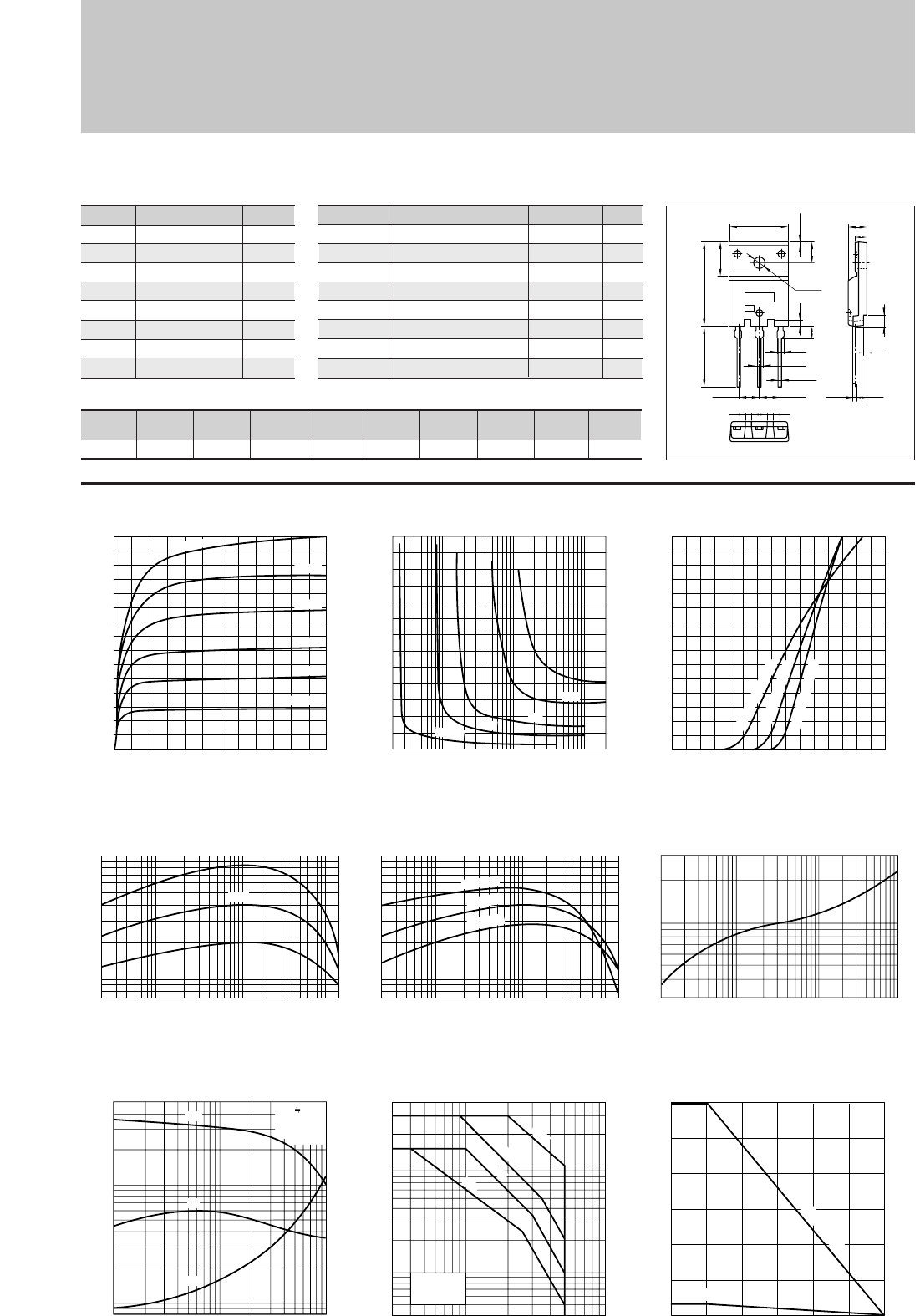
90
Silicon NPN Epitaxial Planar Transistor
Symbol
VCBO
VCEO
VEBO
IC
IB
PC
Tj
Tstg
Ratings
100
50
15
15(Pulse25)
4
60(Tc=25°C)
150
–55 to +150
Unit
V
V
V
A
A
W
°C
°C
■
Absolute maximum ratings
■
Electrical Characteristics
Symbol
ICBO
IEBO
V(BR)CEO
hFE
VCE(sat)
VBE(sat)
fT
COB
Ratings
10max
10max
50min
60to360
0.5max
1.2max
18typ
210typ
Unit
µ
A
µ
A
V
V
V
MHz
pF
Conditions
VCB=100V
VEB=15V
IC=25mA
VCE=1V, IC=5A
IC=5A, IB=80mA
IC=5A, IB=80mA
VCE=12V, IE=–1A
VCB=10V, f=1MHz
2SC4131
(Ta=25°C) (Ta=25°C)
IC–VCE Characteristics
(Typical)
hFE–IC Characteristics
(Typical)
hFE–IC
Temperature Characteristics (Typical)
θj-a–t Characteristics
IC–VBE Temperature Characteristics
(Typical)
VCE(sat)–IB Characteristics
(Typical)
Pc–Ta Derating
0
0
4
15
8
12
246
Collector-Emitter Voltage VCE(V)
Collector Current IC(A)
85mA
15mA
25mA
40mA
80mA
Safe Operating Area (Single Pulse)
I
B
=7mA
0
1.0
1.3
0.5
0.002
0.10.01 21
Base Current IB(A)
Collector-Emitter Saturation Voltage VCE(sat)(V)
I
C
=1A
15A
3A
5A
10A
0.02 0.1 1 10 15
70
100
500
1000
Collector Current IC(A)
DC Current Gain hFE
(VCE=1V)
Typ
0.02 0.1 1 10 15
70
100
500
1000
Collector Current IC(A)
DC Current Gain hFE
(VCE=1V)
0.3
0.5
1
3
1 10 100 1000
Time t(ms)
Transient Thermal Resistance θj-a(˚C/W)
ton•tstg•tf–IC Characteristics
(Typical)
0.1 10.5 105
0.08
0.1
0.5
5
1
Switching Time ton•tstg•tf(µs)
Collector Current IC(A)
tstg
ton
tf
VCC 20V
IC=5A
IB1=–IB2
=80mA
10 503 5 100
0.4
1
40
10
5
Collector-Emitter Voltage VCE(V)
Collector Current IC(A)
Without Heatsink
Natural Cooling
DC
100ms
10ms
1ms
60
40
20
3.5
00 50 100 150
Ambient Temperature Ta(˚C)
Maximum Power Dissipation PC(W)
With Infinite heatsink
Without Heatsink
25˚C
–30˚C
125˚C
0
15
10
5
0 1.5
1.00.5
Base-Emittor Voltage VBE(V)
Collector Current IC(A)
(VCE=1V)
125˚C (Case Temp)
25˚C (Case Temp)
–30˚C (Case Temp)
■Typical Switching Characteristics (Common Emitter)
VCC
(V)
20
RL
(Ω)
4
IC
(A)
5
VBB2
(V)
–5
IB2
(A)
–0.08
ton
(
µ
s)
0.5typ
tstg
(
µ
s)
2.0typ
tf
(
µ
s)
0.4typ
IB1
(A)
0.08
VBB1
(V)
10
Application : DC-DC Converter, Emergency Lighting Inverter and General Purpose
External Dimensions FM100(TO3PF)
4.41.5 1.5
BEC
5.45±0.1
ø3.3±0.2
1.6
3.3
1.75
0.8±0.2
2.15
1.05
+0.2
-0.1
5.45±0.1
23.0±0.3
16.2
9.5±0.2
5.5
15.6±0.2 5.5±0.2
3.45
3.35
0.65
+0.2
-0.1
±0.2
3.0
0.8
a
b
Weight : Approx 2.0g
a. Part No.
b. Lot No.
LOW VCE (sat)
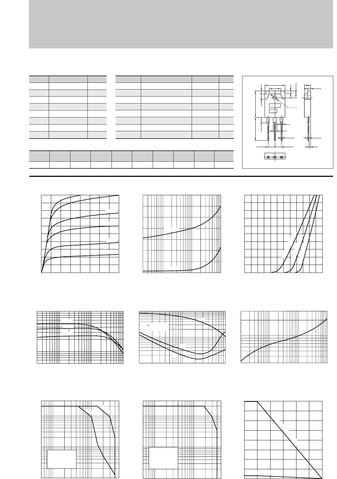
91
Silicon NPN Triple Diffused Planar Transistor (High Voltage and High Speed Switchihg Transistor)
Application : Switching Regulator and General Purpose
Symbol
VCBO
VCEO
VEBO
IC
IB
PC
Tj
Tstg
Ratings
500
400
10
10(Pulse20)
4
80(Tc=25°C)
150
–55 to +150
Unit
V
V
V
A
A
W
°C
°C
■
Absolute maximum ratings
■
Electrical Characteristics
Symbol
ICBO
IEBO
V(BR)CEO
hFE
VCE(sat)
VBE(sat)
fT
COB
Ratings
100max
100max
400min
10to30
0.5max
1.3max
10typ
85typ
Unit
µ
A
µ
A
V
V
V
MHz
pF
Conditions
VCB=500V
VEB=10V
IC=25mA
VCE=4V, IC=6A
IC=6A, IB=1.2A
IC=6A, IB=1.2A
VCE=12V, IE=–0.7A
VCB=10V, f=1MHz
2SC4138
(Ta=25°C) (Ta=25°C)
IC–VCE Characteristics
(Typical)
hFE–IC Characteristics
(Typical)
ton•tstg•tf–IC Characteristics
(Typical)
θj-a–t Characteristics
IC–VBE Temperature Characteristics
(Typical)
VCE(sat),VBE(sat)–IC Temperature Characteristics (Typical)
Pc–Ta Derating
Reverse Bias Safe Operating Area
Safe Operating Area (Single Pulse)
0
0
2
4
6
8
10
2134
Collector-Emitter Voltage VCE(V)
Collector Current IC(A)
1A
600mA
400mA
200mA
1.2A
I
B
=100mA
0.02
0.1
0.05
11050.5
0
1.4
1
Collector-Emitter Saturation Voltage VCE(sat)(V)
Base-Emitter Saturation Voltage VBE(sat)(V)
Collector Current IC(A)
VBE(sat)
VCE(sat)
0.1 10.5 105
0.1
0.5
5
10
1
Switching Time ton•tstg•tf(µs)
Collector Current IC(A)
tstg
ton
tf
VCC 200V
IC:IB1:–IB2=10:1:2
0.3
1
3
0.5
1 10 100 1000
Time t(ms)
Transient Thermal Resistance θj-a(˚C/W)
80
60
40
20
3.5
00 25 50 75 100 125 150
Ambient Temperature Ta(˚C)
Maximum Power Dissipation PC(W)
With Infinite heatsink
Without Heatsink
10 505 500100
1
0.5
0.1
10
30
5
Collector-Emitter Voltage VCE(V)
Collector Current IC(A)
Without Heatsink
Natural Cooling
L=3mH
–IB2=1A
Duty:less than 1%
10 505 100 500
1
0.5
0.1
10
30
5
Collector-Emitter Voltage VCE(V)
Collector Current IC(A)
Without Heatsink
Natural Cooling
100µs
1ms
(IC/IB=5)
0
10
4
2
8
6
0 1.20.4 0.6 0.8 1.00.2
Base-Emittor Voltage VBE(V)
Collector Current IC(A)
(VCE=4V)
125˚C (Case Temp)
–55˚C (Case Temp)
25˚C (Case Temp)
0.02 0.10.05 1 1050.5
5
10
100
50
Collector Current IC(A)
DC Current Gain hFE
(VCE=4V)
125˚C
25˚C
–55˚C
■Typical Switching Characteristics (Common Emitter)
VCC
(V)
200
RL
(Ω)
33.3
IC
(A)
6
VBB2
(V)
–5
IB2
(A)
–1.2
ton
(
µ
s)
1max
tstg
(
µ
s)
3max
tf
(
µ
s)
0.5max
IB1
(A)
0.6
VBB1
(V)
10
External Dimensions MT-100(TO3P)
15.6±0.4
9.6
19.9±0.3
4.0 2.0
5.0±0.2
1.8
ø3.2±0.1
2
3
1.05
+0.2
-0.1
20.0min
4.0max
BE
5.45±0.1 5.45±0.1
C
4.8±0.2
0.65
+0.2
-0.1
1.4
2.0±0.1
a
b
Weight : Approx 2.0g
a. Part No.
b. Lot No.
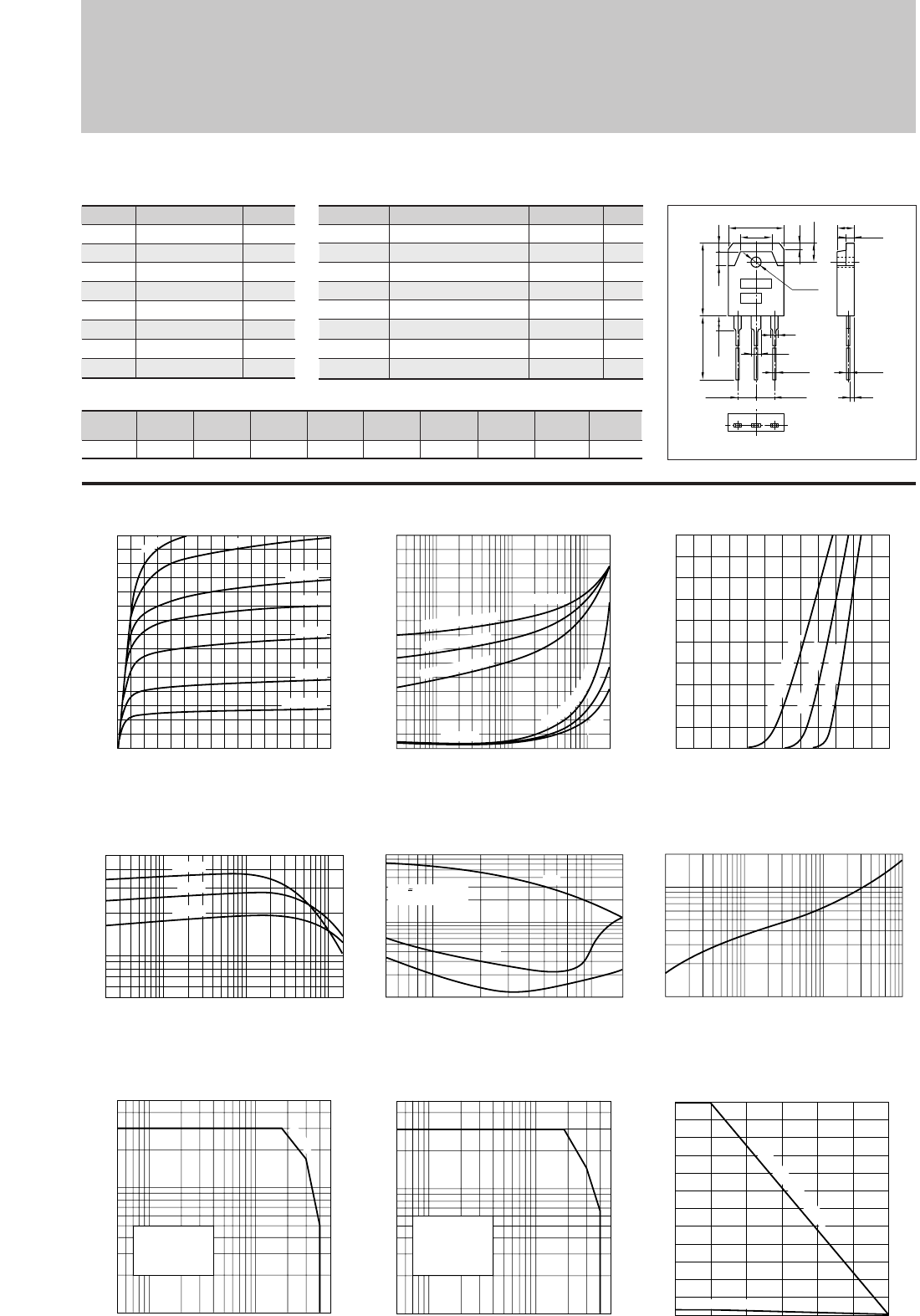
92
Silicon NPN Triple Diffused Planar Transistor (High Voltage and High Speed Switchihg Transistor)
Application : Switching Regulator and General Purpose
Symbol
VCBO
VCEO
VEBO
IC
IB
PC
Tj
Tstg
Ratings
500
400
10
15(Pulse30)
5
120(Tc=25°C)
150
–55 to +150
Unit
V
V
V
A
A
W
°C
°C
■
Absolute maximum ratings
■
Electrical Characteristics
Symbol
ICBO
IEBO
V(BR)CEO
hFE
VCE(sat)
VBE(sat)
fT
COB
Ratings
100max
100max
400min
10to30
0.5max
1.3max
10typ
85typ
Unit
µ
A
µ
A
V
V
V
MHz
pF
Conditions
VCB=500V
VEB=10V
IC=25mA
VCE=4V, IC=8A
IC=8A, IB=1.6A
IC=8A, IB=1.6A
VCE=12V, IE=–1.5A
VCB=10V, f=1MHz
2SC4139
(Ta=25°C) (Ta=25°C)
IC–VCE Characteristics
(Typical)
hFE–IC Characteristics
(Typical)
ton•tstg•tf–IC Characteristics
(Typical)
θj-a–t Characteristics
IC–VBE Temperature Characteristics
(Typical)
VCE(sat),VBE(sat)–IC Temperature Characteristics (Typical)
Collector-Emitter Saturation Voltage VCE(sat)(V)
Base-Emitter Saturation Voltage VBE(sat)(V)
Pc–Ta Derating
Reverse Bias Safe Operating Area
Safe Operating Area (Single Pulse)
0.1
0.050.03
1 5 10 200.5
0
1.5
0.5
1.0
(IC/IB=5)
Collector Current IC(A)
VBE(sat)
125˚C (Case Temp)
25˚C (Case Temp)
–55˚C (Case Temp)
25˚C
–55˚C
VCE(sat)
1
2
5
˚
C
(
C
a
s
e
T
e
m
p
)
10.5 10 155
0.1
0.5
5
8
1
Switching Time ton•tstg•tf(µs)
Collector Current IC(A)
tstg
ton
tf
VCC 200V
IC:IB1:IB2=10:1:–2
0.1
1
2
0.5
1 10 100 1000
Time t(ms)
Transient Thermal Resistance θj-a(˚C/W)
120
100
50
3.5
00 25 50 75 100 125 150
Ambient Temperature Ta(˚C)
Maximum Power Dissipation PC(W)
With Infinite heatsink
Without Heatsink
10 505 500100
1
10
50
5
Collector-Emitter Voltage VCE(V)
Collector Current IC(A)
Without Heatsink
Natural Cooling
L=3mH
IB2=–1A
Duty:less than 1%
10 505 100 500
5
1
10
50
Collector-Emitter Voltage VCE(V)
Collector Current IC(A)
Without Heatsink
Natural Cooling
100µs
0
10
4
2
8
6
0 1.20.4 0.6 0.8 1.00.2
Base-Emittor Voltage VBE(V)
Collector Current IC(A)
(VCE=4V)
125˚C (Case Temp)
–55˚C (Case Temp)
25˚C (Case Temp)
0.02 0.10.05 1 151050.5
5
10
50
Collector Current IC(A)
DC Current Gain hFE
(VCE=4V)
125˚C
25˚C
–55˚C
0
0
5
10
15
2134
Collector-Emitter Voltage VCE(V)
Collector Current IC(A)
1.2A
600mA
800mA
400mA
200mA
1.5A
I
B
=100mA
■Typical Switching Characteristics (Common Emitter)
VCC
(V)
200
RL
(Ω)
25
IC
(A)
8
VBB2
(V)
–5
IB2
(A)
–1.6
ton
(
µ
s)
1max
tstg
(
µ
s)
3max
tf
(
µ
s)
0.5max
IB1
(A)
0.8
VBB1
(V)
10
External Dimensions MT-100(TO3P)
15.6±0.4
9.6
19.9±0.3
4.0 2.0
5.0±0.2
1.8
ø3.2±0.1
2
3
1.05
+0.2
-0.1
20.0min
4.0max
BE
5.45±0.1 5.45±0.1
C
4.8±0.2
0.65
+0.2
-0.1
1.4
2.0±0.1
a
b
Weight : Approx 6.0g
a. Part No.
b. Lot No.
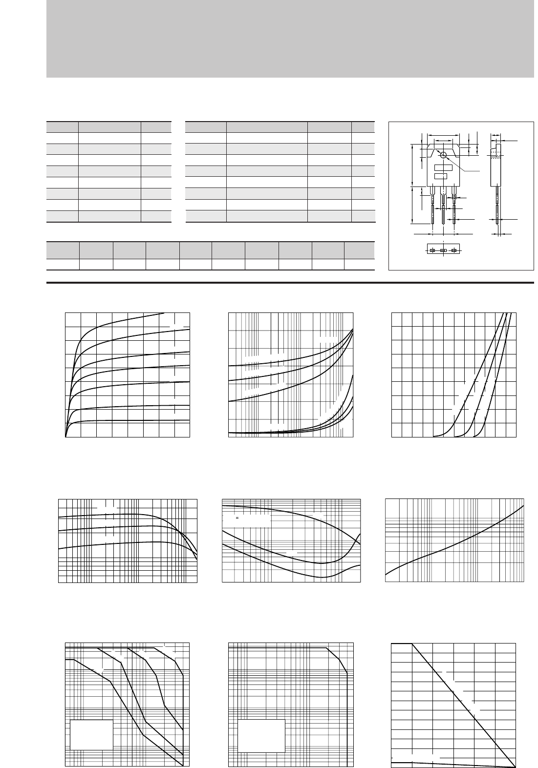
Silicon NPN Triple Diffused Planar Transistor (High Voltage and High Speed Switchihg Transistor)
Application : Switching Regulator and General Purpose
Symbol
VCBO
VCEO
VEBO
IC
IB
PC
Tj
Tstg
Ratings
500
400
10
18(Pulse36)
6
130(Tc=25°C)
150
–55 to +150
Unit
V
V
V
A
A
W
°C
°C
■
Absolute maximum ratings
■
Electrical Characteristics
Symbol
ICBO
IEBO
V(BR)CEO
hFE
VCE(sat)
VBE(sat)
fT
COB
Ratings
100max
100max
400min
10to30
0.5max
1.3max
10typ
165typ
Unit
µ
A
µ
A
V
V
V
MHz
pF
Conditions
VCB=500V
VEB=10V
IC=25mA
VCE=4V, IC=10A
IC=10A, IB=2A
IC=10A, IB=2A
VCE=12V, IE=–2.0A
VCB=10V, f=1MHz
2SC4140
(Ta=25°C) (Ta=25°C)
IC–VCE Characteristics
(Typical)
hFE–IC Characteristics
(Typical)
ton•tstg•tf–IC Characteristics
(Typical)
θj-a–t Characteristics
IC–VBE Temperature Characteristics
(Typical)
VCE(sat),VBE(sat)–IC Temperature Characteristics (Typical)
Pc–Ta Derating
Reverse Bias Safe Operating Area
Safe Operating Area (Single Pulse)
0
0
8
4
12
16
18
2134
Collector-Emitter Voltage VCE(V)
Collector Current IC(A)
800mA
1.2A
600mA
400mA
200mA
1.6A
I
B
=100mA
0.02 0.10.05 1 5 10 180.5
0
1
1.4
Collector-Emitter Saturation Voltage VCE(sat)(V)
Base-Emitter Saturation Voltage VBE(sat)(V)
(IC/IB=5)
Collector Current IC(A)
VBE(sat)
125˚C (Case Temp)
25˚C (Case Temp)
–55˚C (Case Temp)
25˚C
–55˚C
VCE(sat)
1
2
5
˚
C
(
C
a
s
e
T
e
m
p
)
10.2 0.5 10 185
0.1
0.5
5
10
1
Switching Time ton•tstg•tf(µs)
Collector Current IC(A)
tstg
ton
tf
VCC 200V
IC:IB1:–IB2=10:1:2
0.1
1
2
0.5
1 10 100 1000
Time t(ms)
Transient Thermal Resistance θj-a(˚C/W)
130
100
50
3.5
0
Ambient Temperature Ta(˚C)
Maximum Power Dissipation PC(W)
With Infinite heatsink
Without Heatsink
0 25 50 75 100 125 150
10 505 500100
1
0.5
0.03
0.1
0.05
10
50
5
Collector-Emitter Voltage VCE(V)
Collector Current IC(A)
Without Heatsink
Natural Cooling
L=3mH
IB2=–0.5A
Duty:less than 1%
10 505 100 500
0.05
0.03
5
1
0.5
0.1
10
50
Collector-Emitter Voltage VCE(V)
Collector Current IC(A)
Without Heatsink
Natural Cooling
100µs
10ms
1ms
DC
0.02 0.10.05 1 181050.5
5
10
50
Collector Current IC(A)
DC Current Gain hFE
(VCE=4V)
125˚C
25˚C
–55˚C
0
18
8
4
16
12
0 1.20.4 0.6 0.8 1.00.2
Base-Emittor Voltage VBE(V)
Collector Current IC(A)
(VCE=4V)
125˚C (Case Temp)
–55˚C (Case Temp)
25˚C (Case Temp)
■Typical Switching Characteristics (Common Emitter)
VCC
(V)
200
RL
(Ω)
20
IC
(A)
10
VBB2
(V)
–5
IB2
(A)
–2
ton
(
µ
s)
1max
tstg
(
µ
s)
3max
tf
(
µ
s)
0.5max
IB1
(A)
1
VBB1
(V)
10
External Dimensions MT-100(TO3P)
15.6±0.4
9.6
19.9±0.3
4.0 2.0
5.0±0.2
1.8
ø3.2±0.1
2
3
1.05
+0.2
-0.1
20.0min
4.0max
BE
5.45±0.1 5.45±0.1
C
4.8±0.2
0.65
+0.2
-0.1
1.4
2.0±0.1
a
b
Weight : Approx 6.0g
a. Part No.
b. Lot No.
93
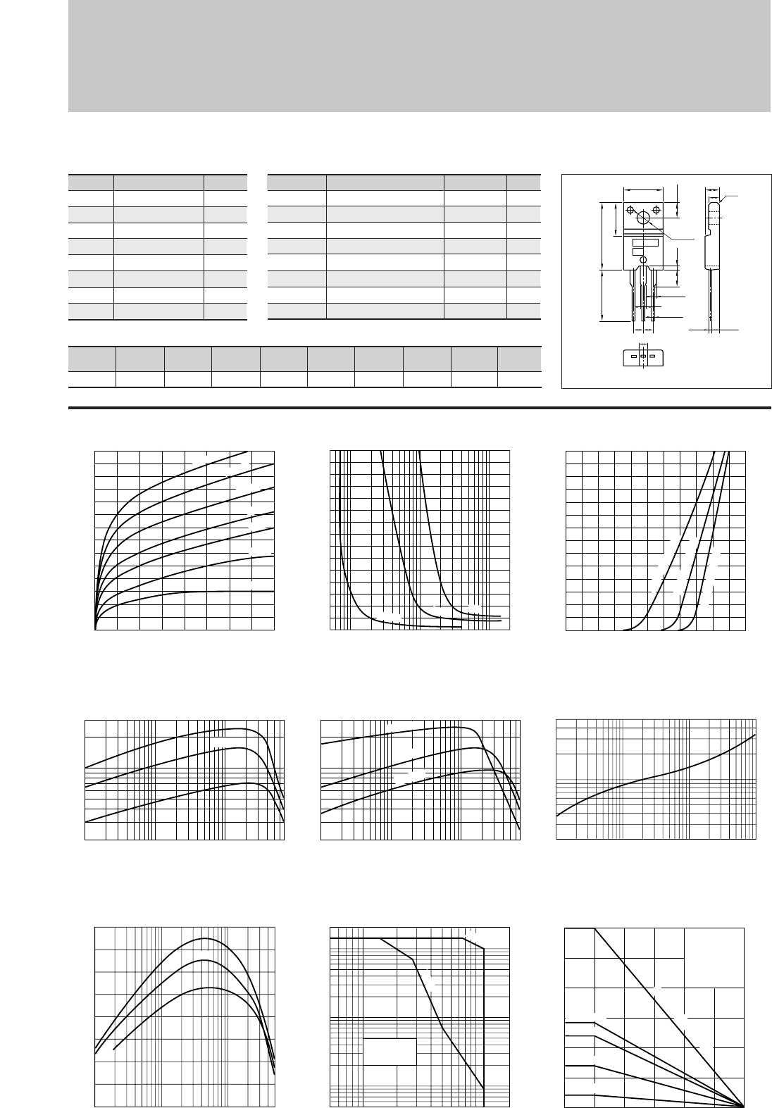
94
Silicon NPN Triple Diffused Planar Transistor ( Switchihg Transistor)
Application : Humidifier, DC-DC Converter, and General Purpose
Symbol
VCBO
VCEO
VEBO
IC
IB
PC
Tj
Tstg
Ratings
200
120
8
7(Pulse14)
3
30(Tc=25°C)
150
–55 to +150
Unit
V
V
V
A
A
W
°C
°C
■
Absolute maximum ratings
■
Electrical Characteristics
Symbol
ICBO
IEBO
V(BR)CEO
hFE
VCE(sat)
VBE(sat)
fT
COB
Ratings
100max
100max
120min
70to220
0.5max
1.2max
30typ
110typ
Unit
µ
A
µ
A
V
V
V
MHz
pF
Conditions
VCB=200V
VEB=8V
IC=50mA
VCE=4V, IC=3A
IC=3A, IB=0.3A
IC=3A, IB=0.3A
VCE=12V, IE=–0.5A
VCB=10V, f=1MHz
2SC4153
(Ta=25°C) (Ta=25°C)
IC–VCE Characteristics
(Typical)
hFE–IC Characteristics
(Typical)
hFE–IC
Temperature Characteristics (Typical)
θj-a–t Characteristics
IC–VBE Temperature Characteristics
(Typical)
VCE(sat)–IB Characteristics
(Typical)
Pc–Ta Derating
0
0
3
4
2
1
5
7
5
2134
Collector-Emitter Voltage VCE(V)
Collector Current IC(A)
200mA
150mA
100mA
Safe Operating Area (Single Pulse)
fT–IE Characteristics
(Typical)
I
B
=10mA
20mA
40mA
60mA
0
2
3
1
0.005
0.01 0.1 21
Base Current IB(A)
Collector-Emitter Saturation Voltage VCE(sat)(V)
I
C
=1A
3A
5A
0.01 0.1 0.5 1 75
20
50
100
300
Collector Current IC(A)
DC Current Gain hFE
(VCE=4V)
Typ
0.01 0.1 0.5 1 75
20
50
100
300
Collector Current IC(A)
DC Current Gain hFE
(VCE=4V)
0.2
0.5
1
5
1 10 100 1000
Time t(ms)
Transient Thermal Resistance θj-a(˚C/W)
–0.01 –0.1 –1 –5
0
10
20
40
30
Cut-off Frequency fT(MHZ)
(VCE=12V)
Typ
Emitter Current IE(A)
10 100505 200
0.05
1
0.5
0.1
20
10
5
Collector-Emitter Voltage VCE(V)
Collector Current IC(A)
Without Heatsink
Natural Cooling
100µs
10ms
30
20
10
2
00 25 50 75 100 125 150
Ambient Temperature Ta(˚C)
Maximum Power Dissipation PC(W)
50x50x2
100x100x2
150x150x2
With Infinite heatsink
Without Heatsink
0
7
2
3
4
5
6
1
0 1.1
1.00.5
Base-Emittor Voltage VBE(V)
Collector Current IC(A)
(VCE=4V)
125˚C (Case Temp)
25˚C (Case Temp)
–30˚C (Case Temp)
25˚C
–30˚C
125˚C
Natural Cooling
Silicone Grease
Heatsink: Aluminum
in mm
■Typical Switching Characteristics (Common Emitter)
VCC
(V)
50
RL
(Ω)
16.7
IC
(A)
3
VBB2
(V)
–5
IB2
(A)
–0.6
ton
(
µ
s)
0.5max
tstg
(
µ
s)
3max
tf
(
µ
s)
0.5max
IB1
(A)
0.3
VBB1
(V)
10
External Dimensions FM20(TO220F)
ø3.3±0.2
10.1±0.2
4.0±0.2
16.9±0.3
13.0min
8.4±0.2
0.8±0.2
3.9
±0.2
2.542.54
1.35±0.15
0.85
+0.2
-0.1
1.35±0.15
2.2±0.2
4.2±0.2
2.8 c0.5
2.4±0.2
0.45
+0.2
-0.1
BEC
a
b
Weight : Approx 2.0g
a. Part No.
b. Lot No.
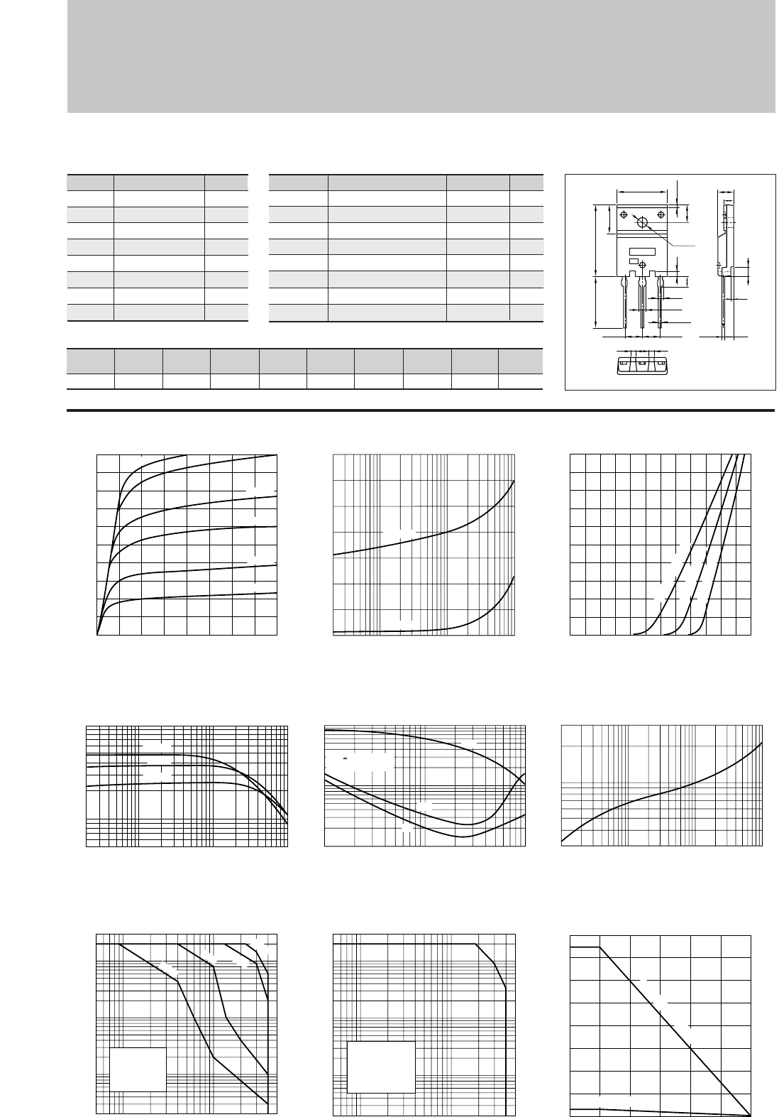
Silicon NPN Triple Diffused Planar Transistor (High Voltage and High Speed Switchihg Transistor)
Application : Switching Regulator and General Purpose
Symbol
VCBO
VCEO
VEBO
IC
IB
PC
Tj
Tstg
Ratings
500
400
10
10(Pulse20)
4
75(Tc=25°C)
150
–55 to +150
Unit
V
V
V
A
A
W
°C
°C
■
Absolute maximum ratings
■
Electrical Characteristics
Symbol
ICBO
IEBO
V(BR)CEO
hFE
VCE(sat)
VBE(sat)
fT
COB
Ratings
100max
100max
400min
10to30
0.5max
1.3max
10typ
85typ
Unit
µ
A
µ
A
V
V
V
MHz
pF
Conditions
VCB=500V
VEB=10V
IC=25mA
VCE=4V, IC=6A
IC=6A, IB=1.2A
IC=6A, IB=1.2A
VCE=12V, IE=–0.7A
VCB=10V, f=1MHz
2SC4296
(Ta=25°C) (Ta=25°C)
IC–VCE Characteristics
(Typical)
hFE–IC Characteristics
(Typical)
ton•tstg•tf–IC Characteristics
(Typical)
θj-a–t Characteristics
IC–VBE Temperature Characteristics
(Typical)
VCE(sat),VBE(sat)–IC Temperature Characteristics (Typical)
Pc–Ta Derating
Reverse Bias Safe Operating Area
Safe Operating Area (Single Pulse)
0
0
2
4
6
8
10
2134
Collector-Emitter Voltage VCE(V)
Collector Current IC(A)
1A
600mA
400mA
200mA
1.2A
I
B
=
100mA
0.02
0.1
0.05
11050.5
0
1.4
1
Collector-Emitter Saturation Voltage VCE(sat)(V)
Base-Emitter Saturation Voltage VBE(sat)(V)
Collector Current IC(A)
VBE(sat)
VCE(sat)
0.1 10.5 105
0.1
0.5
5
10
1
Switching Time ton•tstg•tf(µs)
Collector Current IC(A)
tstg
ton
tf
VCC 200V
IC:IB1:–IB2=10:1:2
0.3
1
3
0.5
1 10 100 1000
Time t(ms)
Transient Thermal Resistance θj-a(˚C/W)
80
60
40
20
3.5
00 50 100 150
Ambient Temperature Ta(˚C)
Maximum Power Dissipation PC(W)
With Infinite heatsink
Without Heatsink
10 505 500100
1
0.5
0.02
0.1
0.05
10
30
5
Collector-Emitter Voltage VCE(V)
Collector Current IC(A)
Without Heatsink
Natural Cooling
L=3mH
–IB2=1A
Duty:less than 1%
10 505 100 500
0.05
0.02
1
0.5
0.1
10
30
5
Collector-Emitter Voltage VCE(V)
Collector Current IC(A)
50µs
100µs
10ms
1ms
(IC/IB=5)
Without Heatsink
Natural Cooling
0
10
4
2
8
6
0 1.20.4 0.6 0.8 1.00.2
Base-Emittor Voltage VBE(V)
Collector Current IC(A)
(VCE=4V)
125˚C (Case Temp)
–55˚C (Case Temp)
25˚C (Case Temp)
0.02 0.10.05 1 1050.5
5
10
100
50
Collector Current IC(A)
DC Current Gain hFE
(VCE=4V)
125˚C
25˚C
–55˚C
■Typical Switching Characteristics (Common Emitter)
VCC
(V)
200
RL
(Ω)
33
IC
(A)
6
VBB2
(V)
–5
IB2
(A)
–1.2
ton
(
µ
s)
1max
tstg
(
µ
s)
3max
tf
(
µ
s)
0.5max
IB1
(A)
0.6
VBB1
(V)
10
External Dimensions FM100(TO3PF)
4.41.5 1.5
BEC
5.45±0.1
ø3.3±0.2
1.6
3.3
1.75
0.8±0.2
2.15
1.05
+0.2
-0.1
5.45±0.1
23.0±0.3
16.2
9.5±0.2
5.5
15.6±0.2 5.5±0.2
3.45
3.35
0.65
+0.2
-0.1
±0.2
3.0
0.8
a
b
Weight : Approx 6.5g
a. Part No.
b. Lot No.
95
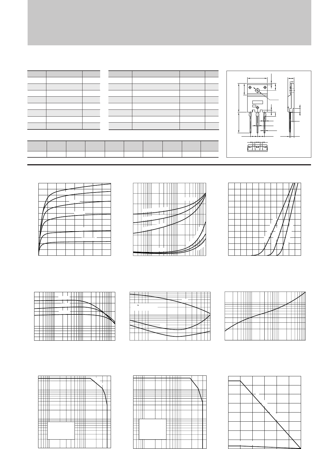
96
Silicon NPN Triple Diffused Planar Transistor (High Voltage and High Speed Switchihg Transistor)
Application : Switching Regulator and General Purpose
Symbol
VCBO
VCEO
VEBO
IC
IB
PC
Tj
Tstg
Ratings
500
400
10
12(Pulse24)
4
75(Tc=25°C)
150
–55 to +150
Unit
V
V
V
A
A
W
°C
°C
■
Absolute maximum ratings
■
Electrical Characteristics
Symbol
ICBO
IEBO
V(BR)CEO
hFE
VCE(sat)
VBE(sat)
fT
COB
Ratings
100max
100max
400min
10to30
0.5max
1.3max
10typ
105typ
Unit
µ
A
µ
A
V
V
V
MHz
pF
Conditions
VCB=500V
VEB=10V
IC=25mA
VCE=4V, IC=7A
IC=7A, IB=1.4A
IC=7A, IB=1.4A
VCE=12V, IE=–1A
VCB=10V, f=1MHz
2SC4297
(Ta=25°C) (Ta=25°C)
IC–VCE Characteristics
(Typical)
hFE–IC Characteristics
(Typical)
ton•tstg•tf–IC Characteristics
(Typical)
θj-a–t Characteristics
VCE(sat),VBE(sat)–IC Temperature Characteristics (Typical)
Pc–Ta Derating
Reverse Bias Safe Operating Area
Safe Operating Area (Single Pulse)
0
0
4
2
6
8
10
12
2134
Collector-Emitter Voltage VCE(V)
Collector Current IC(A)
600mA
400mA
200mA
800mA
1A
IB=100mA
0.02 0.10.05 1 5 100.5
0
1
Collector-Emitter Saturation Voltage VCE(sat)(V)
Base-Emitter Saturation Voltage VBE(sat)(V)
(IC/IB=5)
Collector Current IC(A)
VBE(sat)
125˚C (Case Temp)
25˚C (Case Temp)
–55˚C (Case Temp)
25˚C
–55˚C
VCE(sat)
1
2
5
˚
C
(
C
a
s
e
T
e
m
p
)
IC–VBE Temperature Characteristics
(Typical)
0
12
10
4
2
8
6
0 1.20.4 0.6 0.8 1.00.2
Base-Emittor Voltage VBE(V)
Collector Current IC(A)
(VCE=4V)
125˚C (Case Temp)
–55˚C (Case Temp)
25˚C (Case Temp)
10.5 105
0.1
0.5
5
8
1
Switching Time ton•tstg•tf(µs)
Collector Current IC(A)
tstg
ton
tf
VCC 200V
IC:IB1:–IB2=10:1:2
0.1
1
2
0.5
1 10 100 1000
Time t(ms)
Transient Thermal Resistance θj-a(˚C/W)
10 505 500100
1
0.5
0.1
10
30
5
Collector-Emitter Voltage VCE(V)
Collector Current IC(A)
Without Heatsink
Natural Cooling
L=3mH
–IB2=1A
Duty:less than 1%
10 505 100 500
1
5
0.5
0.1
10
30
Collector-Emitter Voltage VCE(V)
Collector Current IC(A)
Without Heatsink
Natural Cooling
100µs
80
60
40
20
3.5
00 50 100 150
Ambient Temperature Ta(˚C)
Maximum Power Dissipation PC(W)
With Infinite heatsink
Without Heatsink
0.02 0.10.05 1 121050.5
5
10
50
Collector Current IC(A)
DC Current Gain hFE
(VCE=4V)
125˚C
25˚C
–30˚C
■Typical Switching Characteristics (Common Emitter)
VCC
(V)
200
RL
(Ω)
28.5
IC
(A)
7
VBB2
(V)
–5
IB2
(A)
–1.4
ton
(
µ
s)
1max
tstg
(
µ
s)
3max
tf
(
µ
s)
0.5max
IB1
(A)
0.7
VBB1
(V)
10
External Dimensions FM100(TO3PF)
4.41.5 1.5
BEC
5.45±0.1
ø3.3±0.2
1.6
3.3
1.75
0.8±0.2
2.15
1.05
+0.2
-0.1
5.45±0.1
23.0±0.3
16.2
9.5±0.2
5.5
15.6±0.2 5.5±0.2
3.45
3.35
0.65
+0.2
-0.1
±0.2
3.0
0.8
a
b
Weight : Approx 6.5g
a. Part No.
b. Lot No.
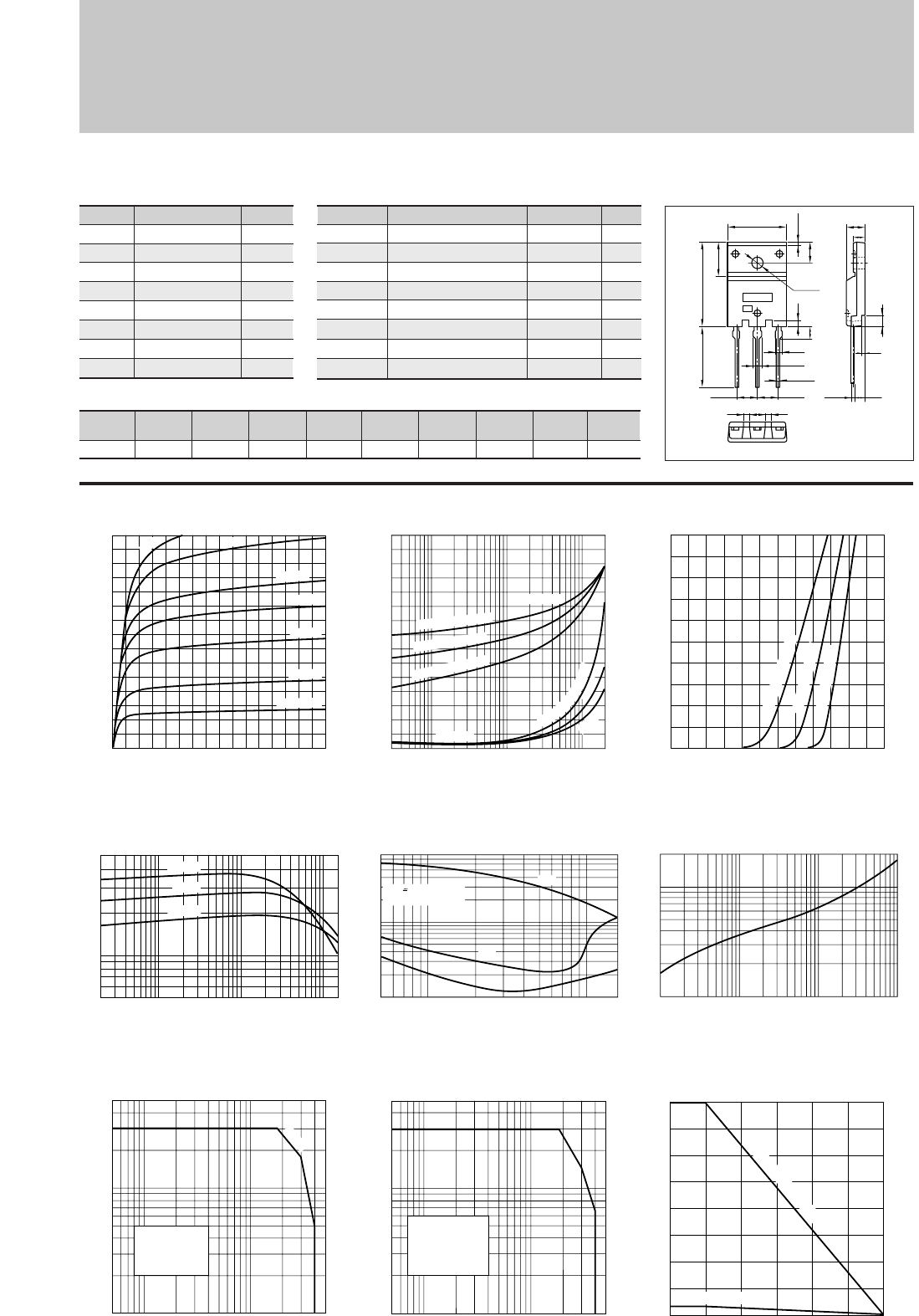
Silicon NPN Triple Diffused Planar Transistor (High Voltage and High Speed Switchihg Transistor)
Application : Switching Regulator and General Purpose
Symbol
VCBO
VCEO
VEBO
IC
IB
PC
Tj
Tstg
Ratings
500
400
10
15(Pulse30)
5
80(Tc=25°C)
150
–55 to +150
Unit
V
V
V
A
A
W
°C
°C
■
Absolute maximum ratings
■
Electrical Characteristics
Symbol
ICBO
IEBO
V(BR)CEO
hFE
VCE(sat)
VBE(sat)
fT
COB
Ratings
100max
100max
400min
10to30
0.5max
1.3max
10typ
85typ
Unit
µ
A
µ
A
V
V
V
MHz
pF
Conditions
VCB=500V
VEB=10V
IC=25mA
VCE=4V, IC=8A
IC=8A, IB=1.6A
IC=8A, IB=1.6A
VCE=12V, IE=–1.5A
VCB=10V, f=1MHz
2SC4298
(Ta=25°C) (Ta=25°C)
IC–VCE Characteristics
(Typical)
hFE–IC Characteristics
(Typical)
ton•tstg•tf–IC Characteristics
(Typical)
θj-a–t Characteristics
VCE(sat),VBE(sat)–IC Temperature Characteristics (Typical)
Pc–Ta Derating
Reverse Bias Safe Operating Area
Safe Operating Area (Single Pulse)
0.1
0.050.03
1 5 10 200.5
0
1.5
0.5
1.0
(IC/IB=5)
Collector Current IC(A)
VBE(sat)
125˚C (Case Temp)
25˚C (Case Temp)
–55˚C (Case Temp)
25˚C
–55˚C
VCE(sat)
1
2
5
˚
C
(
C
a
s
e
T
e
m
p
)
10.5 10 155
0.1
0.5
5
8
1
Switching Time ton•tstg•tf(µs)
Collector Current IC(A)
tstg
ton
tf
VCC 200V
IC:IB1:IB2=10:1:–2
0.1
1
2
0.5
1 10 100 1000
Time t(ms)
Transient Thermal Resistance θj-a(˚C/W)
80
60
40
20
3.5
00 25 50 75 100 125 150
Ambient Temperature Ta(˚C)
Maximum Power Dissipation PC(W)
With Infinite heatsink
Without Heatsink
10 505 500100
1
10
50
5
Collector-Emitter Voltage VCE(V)
Collector Current IC(A)
Without Heatsink
Natural Cooling
L=3mH
IB2=–1A
Duty:less than 1%
10 505 100 500
1
5
10
50
Collector-Emitter Voltage VCE(V)
Collector Current IC(A)
Without Heatsink
Natural Cooling
100µs
Collector-Emitter Saturation Voltage VCE(sat)(V)
Base-Emitter Saturation Voltage VBE(sat)(V)
IC–VBE Temperature Characteristics
(Typical)
0
10
4
2
8
6
0 1.20.4 0.6 0.8 1.00.2
Base-Emittor Voltage VBE(V)
Collector Current IC(A)
(VCE=4V)
125˚C (Case Temp)
–55˚C (Case Temp)
25˚C (Case Temp)
0.02 0.10.05 1 151050.5
5
10
50
Collector Current IC(A)
DC Current Gain hFE
(VCE=4V)
125˚C
25˚C
–55˚C
0
0
15
5
10
2134
Collector-Emitter Voltage VCE(V)
Collector Current IC(A)
1.2A
1.5A
600mA
800mA
400mA
200mA
I
B
=100mA
■Typical Switching Characteristics (Common Emitter)
VCC
(V)
200
RL
(Ω)
25
IC
(A)
8
VBB2
(V)
–5
IB2
(A)
–1.6
ton
(
µ
s)
1max
tstg
(
µ
s)
3max
tf
(
µ
s)
0.5max
IB1
(A)
0.8
VBB1
(V)
10
External Dimensions FM100(TO3PF)
4.41.5 1.5
BEC
5.45±0.1
ø3.3±0.2
1.6
3.3
1.75
0.8±0.2
2.15
1.05
+0.2
-0.1
5.45±0.1
23.0±0.3
16.2
9.5±0.2
5.5
15.6±0.2 5.5±0.2
3.45
3.35
0.65
+0.2
-0.1
±0.2
3.0
0.8
a
b
Weight : Approx 6.5g
a. Part No.
b. Lot No.
97
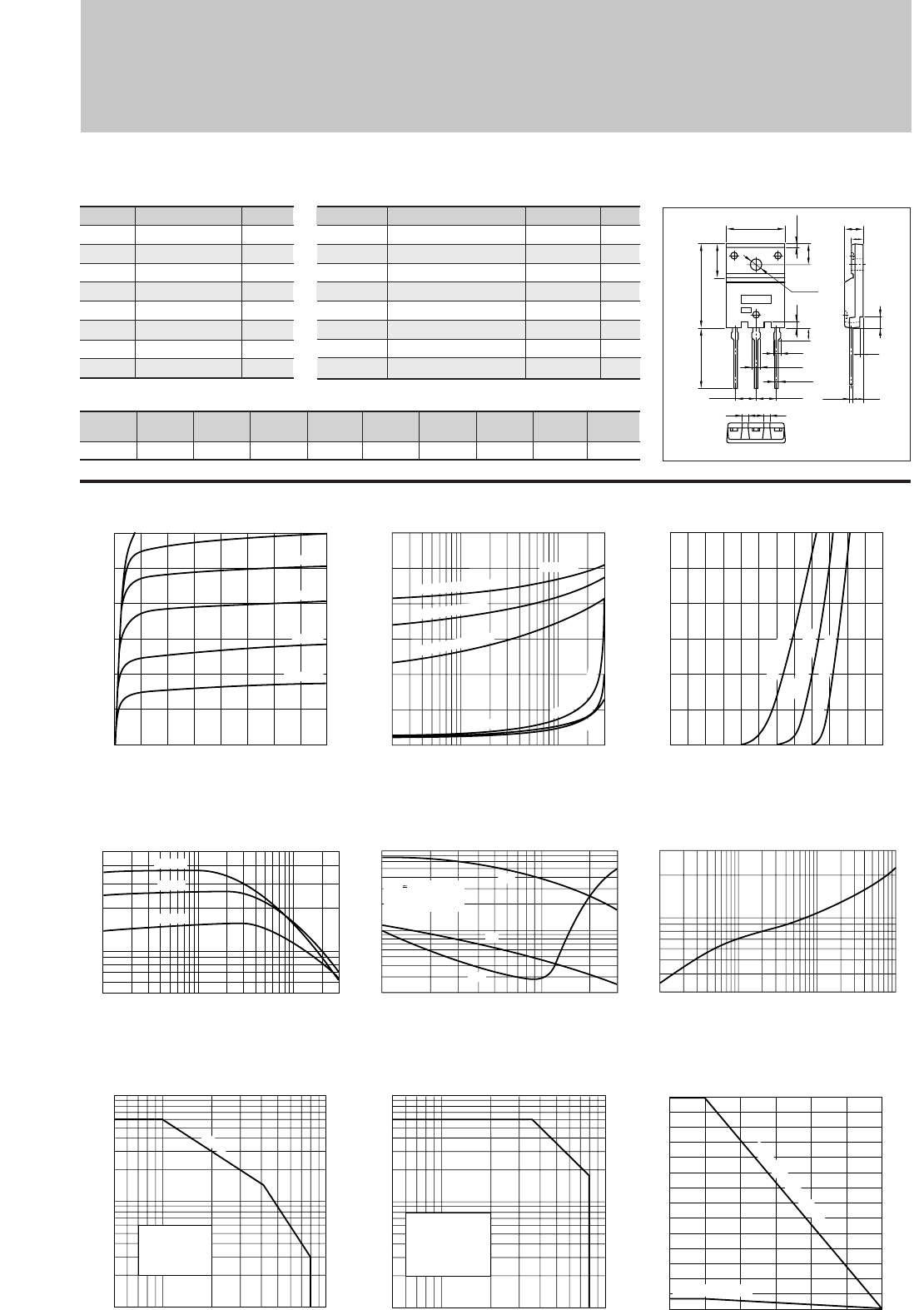
98
Silicon NPN Triple Diffused Planar Transistor (High Voltage Switchihg Transistor)
Application : Switching Regulator and General Purpose
Symbol
VCBO
VCEO
VEBO
IC
IB
PC
Tj
Tstg
Ratings
900
800
7
3(Pulse6)
1.5
70(Tc=25°C)
150
–55 to +150
Unit
V
V
V
A
A
W
°C
°C
■
Absolute maximum ratings
■
Electrical Characteristics
Symbol
ICBO
IEBO
V(BR)CEO
hFE
VCE(sat)
VBE(sat)
fT
COB
Ratings
100max
100max
800min
10to30
0.5max
1.2max
6typ
50typ
Unit
µ
A
µ
A
V
V
V
MHz
pF
Conditions
VCB=800V
VEB=7V
IC=10mA
VCE=4V, IC=1A
IC=1A, IB=0.2A
IC=1A, IB=0.2A
VCE=12V, IE=–0.3A
VCB=10V, f=1MHz
2SC4299
(Ta=25°C) (Ta=25°C)
IC–VCE Characteristics
(Typical)
hFE–IC Characteristics
(Typical)
ton•tstg•tf–IC Characteristics
(Typical)
θj-a–t Characteristics
IC–VBE Temperature Characteristics
(Typical)
VCE(sat),VBE(sat)–IC Temperature Characteristics (Typical)
Pc–Ta Derating
Reverse Bias Safe Operating Area
Safe Operating Area (Single Pulse)
0
0
2
1
3
2134
Collector-Emitter Voltage VCE(V)
Collector Current IC(A)
300mA
200mA
100mA
I
B
=50mA
500mA 400mA
0.02 0.10.05 10.5 3
0
1
Collector-Emitter Saturation Voltage VCE(sat)(V)
Base-Emitter Saturation Voltage VBE(sat)(V)
(IC/IB=5)
Collector Current IC(A)
VBE(sat)
125˚C (Case Temp)
25˚C (Case Temp)
–55˚C (Case Temp)
25˚C
125˚C
VCE(sat)
–
5
5
˚
C
(
C
a
s
e
T
e
m
p
)
0.01 0.10.05 1 30.5
5
10
50
Collector Current IC(A)
DC Current Gain hFE
(VCE=4V)
125˚C
25˚C
–55˚C
0.1 10.5 3
0.2
0.5
5
8
1
Switching Time ton•tstg•tf(µs)
Collector Current IC(A)
tstg
ton
tf
VCC 250V
IC:IB1:–IB2
=2:0.3:1 Const.
0.3
1
3
0.5
1 10 100 1000
Time t(ms)
Transient Thermal Resistance θj-a(˚C/W)
70
60
50
40
30
20
10
3.5
00 25 50 75 100 125 150
Ambient Temperature Ta(˚C)
Maximum Power Dissipation PC(W)
With Infinite heatsink
Without Heatsink
100 50050 1000
1
0.5
0.1
10
5
Collector-Emitter Voltage VCE(V)
Collector Current IC(A)
Without Heatsink
Natural Cooling
L=3mH
IB2=–1.0A
Duty:less than 1%
50 100 500 1000
1
0.5
0.1
10
5
Collector-Emitter Voltage VCE(V)
Collector Current IC(A)
Without Heatsink
Natural Cooling
100µs
0
3
1
2
0 1.20.4 0.6 0.8 1.00.2
Base-Emittor Voltage VBE(V)
Collector Current IC(A)
(VCE=4V)
125˚C (Case Temp)
25˚C (Case Temp)
–55˚C (Case Temp)
■Typical Switching Characteristics (Common Emitter)
VCC
(V)
250
RL
(Ω)
250
IC
(A)
1
VBB2
(V)
–5
IB2
(A)
–0.5
ton
(
µ
s)
1max
tstg
(
µ
s)
5max
tf
(
µ
s)
1max
IB1
(A)
0.15
VBB1
(V)
10
External Dimensions FM100(TO3PF)
4.41.5 1.5
BEC
5.45±0.1
ø3.3±0.2
1.6
3.3
1.75
0.8±0.2
2.15
1.05
+0.2
-0.1
5.45±0.1
23.0±0.3
16.2
9.5±0.2
5.5
15.6±0.2 5.5±0.2
3.45
3.35
0.65
+0.2
-0.1
±0.2
3.0
0.8
a
b
Weight : Approx 6.5g
a. Part No.
b. Lot No.
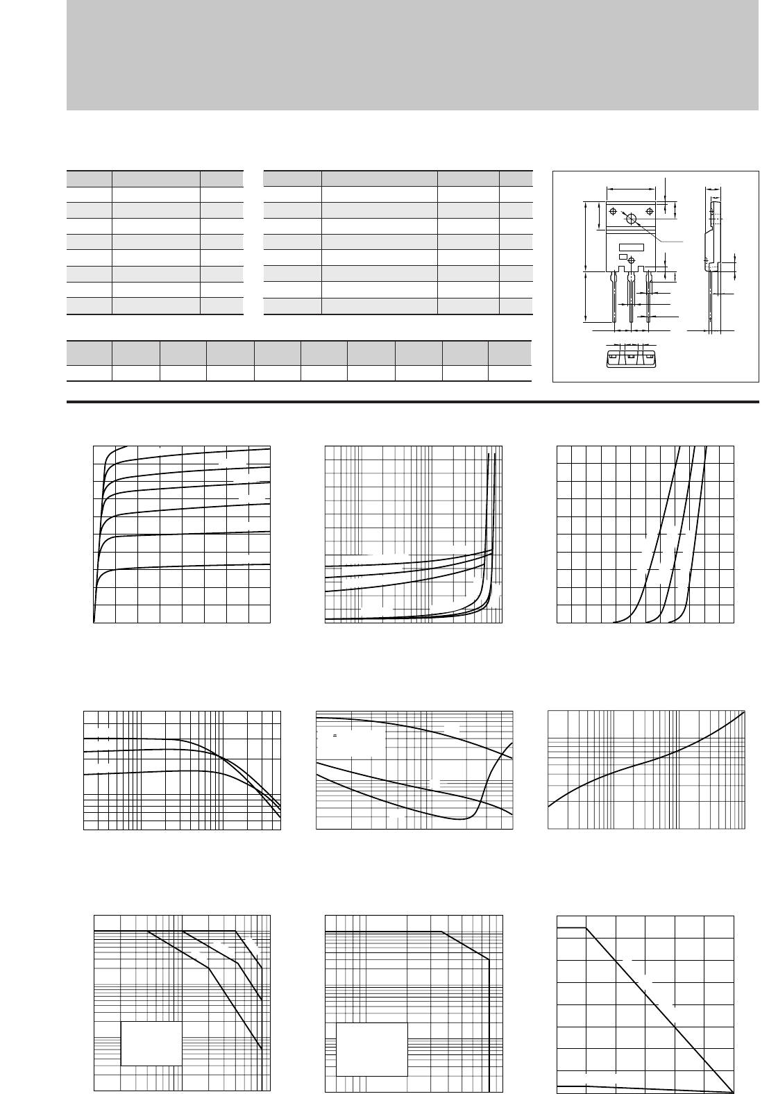
Silicon NPN Triple Diffused Planar Transistor (High Voltage Switchihg Transistor)
Application : Switching Regulator and General Purpose
Symbol
VCBO
VCEO
VEBO
IC
IB
PC
Tj
Tstg
Ratings
900
800
7
5(Pulse10)
2.5
75(Tc=25°C)
150
–55 to +150
Unit
V
V
V
A
A
W
°C
°C
■
Absolute maximum ratings
■
Electrical Characteristics
Symbol
ICBO
IEBO
V(BR)CEO
hFE
VCE(sat)
VBE(sat)
fT
COB
Ratings
100max
100max
800min
10to30
0.5max
1.2max
6typ
75typ
Unit
µ
A
µ
A
V
V
V
MHz
pF
Conditions
VCB=800V
VEB=7V
IC=10mA
VCE=4V, IC=2A
IC=2A, IB=0.4A
IC=2A, IB=0.4A
VCE=12V, IE=–0.5A
VCB=10V, f=1MHz
2SC4300
(Ta=25°C) (Ta=25°C)
IC–VCE Characteristics
(Typical)
hFE–IC Characteristics
(Typical)
ton•tstg•tf–IC Characteristics
(Typical)
θj-a–t Characteristics
IC–VBE Temperature Characteristics
(Typical)
VCE(sat),VBE(sat)–IC Temperature Characteristics (Typical)
Pc–Ta Derating
Reverse Bias Safe Operating Area
Safe Operating Area (Single Pulse)
0
0
2
1
3
4
5
2134
Collector-Emitter Voltage VCE(V)
Collector Current IC(A)
600mA
500mA
400mA
300mA
200mA
700mA
I
B
=100mA
0.03
0.1
0.05
15100.5
0
2
1
(IC/IB=5)
Collector Current IC(A)
VBE(sat)
125˚C (Case Temp)
25˚C (Case Temp)
–55˚C (Case Temp)
25˚C
–55˚C
VCE(sat)
1
2
5
˚
C
(
C
a
s
e
T
e
m
p
)
0.1 10.5 5
0.2
0.5
5
10
1
Switching Time ton•tstg•tf(µs)
Collector Current IC(A)
tstg
ton
tf
VCC 250V
IC:IB1:–IB2
=2:0.3:1 Const.
0.1
1
2
0.5
1 10 100 1000
Time t(ms)
Transient Thermal Resistance θj-a(˚C/W)
80
60
40
20
3.5
00 50 100 150
Ambient Temperature Ta(˚C)
Maximum Power Dissipation PC(W)
With Infinite heatsink
Without Heatsink
100 50050 1000
1
0.5
0.1
0.05
0.01
10
20
5
Collector-Emitter Voltage VCE(V)
Collector Current IC(A)
Without Heatsink
Natural Cooling
L=3mH
IB2=–1.0A
Duty:less than 1%
10 50 100 500 1000
0.05
0.01
1
0.5
0.1
10
20
5
Collector-Emitter Voltage VCE(V)
Collector Current IC(A)
100µs
1ms
10µs
Collector-Emitter Saturation Voltage VCE(sat)(V)
Base-Emitter Saturation Voltage VBE(sat)(V)
Without Heatsink
Natural Cooling
0
5
1
2
3
4
0 1.20.4 0.6 0.8 1.00.2
Base-Emittor Voltage VBE(V)
Collector Current IC(A)
(VCE=4V)
125˚C (Case Temp)
25˚C (Case Temp)
–55˚C (Case Temp)
0.02 0.10.05 1 50.5
5
10
50
Collector Current IC(A)
DC Current Gain hFE
(VCE=4V)
125˚C
25˚C
–55˚C
■Typical Switching Characteristics (Common Emitter)
VCC
(V)
250
RL
(Ω)
125
IC
(A)
2
VBB2
(V)
–5
IB2
(A)
–1
ton
(
µ
s)
1max
tstg
(
µ
s)
5max
tf
(
µ
s)
1max
IB1
(A)
0.3
VBB1
(V)
10
External Dimensions FM100(TO3PF)
4.41.5 1.5
BEC
5.45±0.1
ø3.3±0.2
1.6
3.3
1.75
0.8±0.2
2.15
1.05
+0.2
-0.1
5.45±0.1
23.0±0.3
16.2
9.5±0.2
5.5
15.6±0.2 5.5±0.2
3.45
3.35
0.65
+0.2
-0.1
±0.2
3.0
0.8
a
b
Weight : Approx 6.5g
a. Part No.
b. Lot No.
99
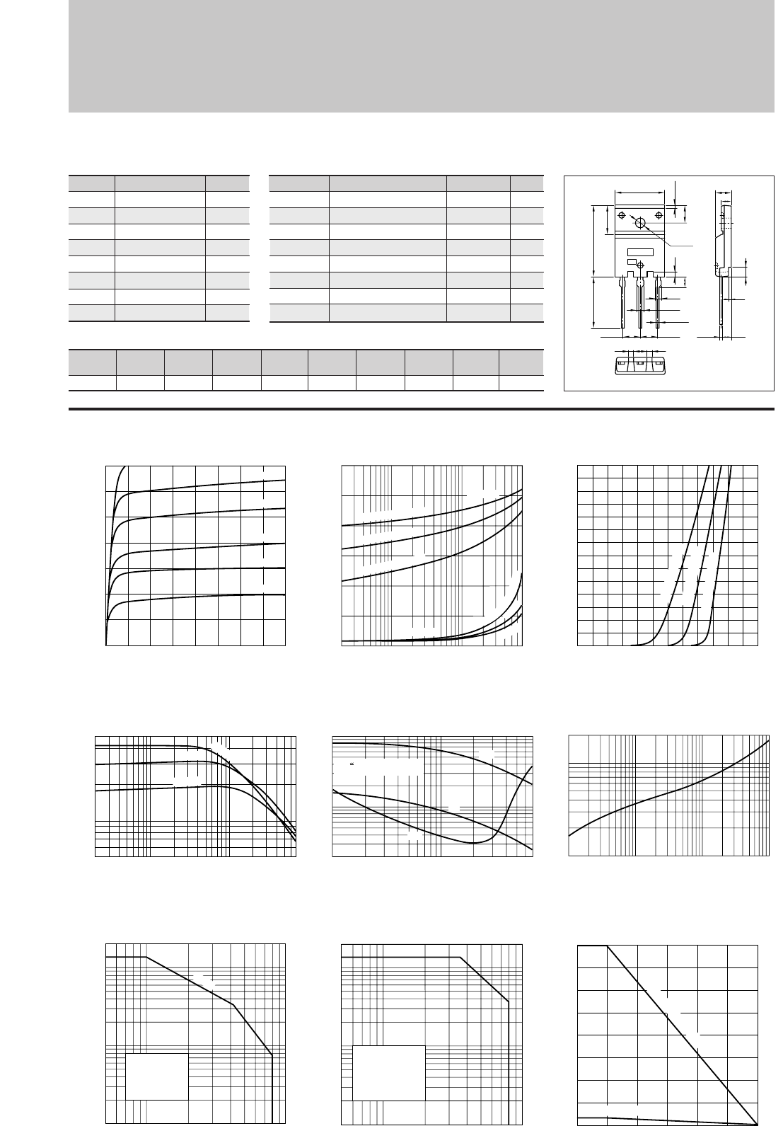
100
Silicon NPN Triple Diffused Planar Transistor (High Voltage Switchihg Transistor)
Application : Switching Regulator, Lighting Inverter and General Purpose
Symbol
VCBO
VCEO
VEBO
IC
IB
PC
Tj
Tstg
Ratings
900
800
7
7(Pulse14)
3.5
80(Tc=25°C)
150
–55 to +150
Unit
V
V
V
A
A
W
°C
°C
■
Absolute maximum ratings
■
Electrical Characteristics
Symbol
ICBO
IEBO
V(BR)CEO
hFE
VCE(sat)
VBE(sat)
fT
COB
Ratings
100max
100max
800min
10to30
0.5max
1.2max
6typ
105typ
Unit
µ
A
µ
A
V
V
V
MHz
pF
Conditions
VCB=800V
VEB=7V
IC=10mA
VCE=4V, IC=3A
IC=3A, IB=0.6A
IC=3A, IB=0.6A
VCE=12V, IE=–1A
VCB=10V, f=1MHz
2SC4301
(Ta=25°C) (Ta=25°C)
IC–VCE Characteristics
(Typical)
hFE–IC Characteristics
(Typical)
ton•tstg•tf–IC Characteristics
(Typical)
θj-a–t Characteristics
IC–VBE Temperature Characteristics
(Typical)
VCE(sat),VBE(sat)–IC Temperature Characteristics (Typical)
Pc–Ta Derating
Reverse Bias Safe Operating Area
Safe Operating Area (Single Pulse)
0
0
4
2
6
2134
Collector-Emitter Voltage VCE(V)
Collector Current IC(A)
700mA
500mA
300mA
200mA
I
B
=100mA
1A
0.02 0.10.05 1 50.5 7
0
1
(IC/IB=5)
Collector Current IC(A)
VBE(sat)
125˚C (Case Temp)
25˚C (Case Temp)
–55˚C (Case Temp)
25˚C
–55˚C
VCE(sat)
1
2
5
˚
C
(
C
a
s
e
T
e
m
p
)
0.1 10.5 75
0.2
0.5
5
10
1
Switching Time ton•tstg•tf(µs)
Collector Current IC(A)
tstg
ton
tf
VCC 250V
IC:IB1:IB2=2:0.3:–1 Const.
0.1
1
2
0.5
1 10 100 1000
Time t(ms)
Transient Thermal Resistance θj-a(˚C/W)
80
60
40
20
3.5
00 25 50 75 100 125 150
Ambient Temperature Ta(˚C)
Maximum Power Dissipation PC(W)
With Infinite heatsink
Without Heatsink
100 50050 1000
1
0.5
0.1
10
20
5
Collector-Emitter Voltage VCE(V)
Collector Current IC(A)
Without Heatsink
Natural Cooling
L=3mH
IB2=–1.0A
Duty :less than1%
50 100 500 1000
1
0.5
0.1
10
20
5
Collector-Emitter Voltage VCE(V)
Collector Current IC(A)
Without Heatsink
Natural Cooling
100µs
Collector-Emitter Saturation Voltage VCE(sat)(V)
Base-Emitter Saturation Voltage VBE(sat)(V)
0
7
2
4
6
0 1.20.4 0.6 0.8 1.00.2
Base-Emittor Voltage VBE(V)
Collector Current IC(A)
(VCE=4V)
125˚C (Case Temp)
25˚C (Case Temp)
–55˚C (Case Temp)
0.02 0.10.05 1 750.5
5
10
50
Collector Current IC(A)
DC Current Gain hFE
(VCE=4V)
125˚C
25˚C
–55˚C
■Typical Switching Characteristics (Common Emitter)
VCC
(V)
250
RL
(Ω)
83
IC
(A)
3
VBB2
(V)
–5
IB2
(A)
–1.5
ton
(
µ
s)
1max
tstg
(
µ
s)
5max
tf
(
µ
s)
1max
IB1
(A)
0.45
VBB1
(V)
10
External Dimensions FM100(TO3PF)
4.41.5 1.5
BEC
5.45±0.1
ø3.3±0.2
1.6
3.3
1.75
0.8±0.2
2.15
1.05
+0.2
-0.1
5.45±0.1
23.0±0.3
16.2
9.5±0.2
5.5
15.6±0.2 5.5±0.2
3.45
3.35
0.65
+0.2
-0.1
±0.2
3.0
0.8
a
b
Weight : Approx 6.5g
a. Part No.
b. Lot No.
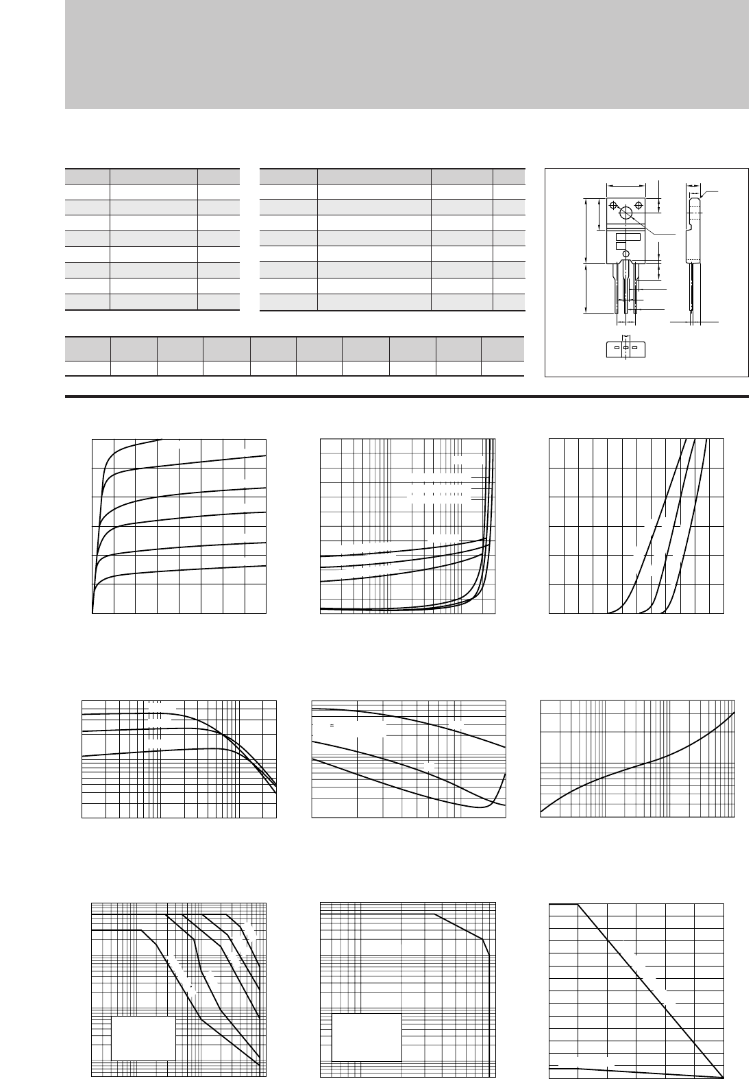
101
Silicon NPN Triple Diffused Planar Transistor (High Voltage High Speed Switchihg Transistor)
Application : Switching Regulator and General Purpose
Symbol
VCBO
VCEO
VEBO
IC
IB
PC
Tj
Tstg
Ratings
900
800
7
3(Pulse6)
1.5
35(Tc=25°C)
150
–55 to +150
Unit
V
V
V
A
A
W
°C
°C
■
Absolute maximum ratings
■
Electrical Characteristics
Symbol
ICBO
IEBO
V(BR)CEO
hFE
VCE(sat)
VBE(sat)
fT
COB
Ratings
100max
100max
800min
10to30
0.5max
1.2max
15typ
50typ
Unit
µ
A
µ
A
V
V
V
MHz
pF
Conditions
VCB=800V
VEB=7V
IC=10mA
VCE=4V, IC=0.7A
IC=0.7A, IB=0.14A
IC=0.7A, IB=0.14A
VCE=12V, IE=–0.3A
VCB=10V, f=1MHz
2SC4304
(Ta=25°C) (Ta=25°C)
IC–VCE Characteristics
(Typical)
hFE–IC Characteristics
(Typical)
ton•tstg•tf–IC Characteristics
(Typical)
θj-a–t Characteristics
IC–VBE Temperature Characteristics
(Typical)
VCE(sat),VBE(sat)–IC Temperature Characteristics (Typical)
Collector-Emitter Saturation Voltage VCE(sat)(V)
Base-Emitter Saturation Voltage VBE(sat)(V)
Pc–Ta Derating
Reverse Bias Safe Operating Area
Safe Operating Area (Single Pulse)
0
0
2
1
3
2134
Collector-Emitter Voltage VCE(V)
Collector Current IC(A)
500mA
300mA
200mA
100mA
I
B
=50mA
700mA
0.1
0.050.01
310.5
0
1
2
(IC/IB=5)
Collector Current IC(A)
VBE(sat)
125˚C (Case Temp)
25˚C (Case Temp)
–55˚C (Case Temp)
125˚C (Case Temp)
25˚C (Case Temp)
–55˚C (Case Temp)
VCE(sat)
0.1 10.5 2
0.1
0.5
5
7
1
Switching Time ton•tstg•tf(µs)
Collector Current IC(A)
tstg
ton
tf
VCC 250V
IC:IB1:–IB2=10:1.5:5
0.3
1
4
0.5
1 10 100 1000
Time t(ms)
Transient Thermal Resistance θj-a(˚C/W)
35
30
20
10
2
00 25 50 75 100 125 150
Ambient Temperature Ta(˚C)
Maximum Power Dissipation PC(W)
With Infinite heatsink
Without Heatsink
100 50050 1000
1
0.5
0.005
0.05
0.1
0.01
10
5
Collector-Emitter Voltage VCE(V)
Collector Current IC(A)
Without Heatsink
Natural Cooling
L=3mH
IB2=–1.0A
Duty:less than 1%
10 5052 100 500 1000
0.05
0.01
0.005
1
0.5
0.1
10
5
Collector-Emitter Voltage VCE(V)
Collector Current IC(A)
Without Heatsink
Natural Cooling
100µs
50µs
10ms
1ms
DC(Tc=25 C)
0
3
1
2
0 1.20.4 0.6 0.8 1.00.2
Base-Emittor Voltage VBE(V)
Collector Current IC(A)
(VCE=4V)
125˚C (Case Temp)
0.01 0.10.05 1 30.5
2
5
10
50
Collector Current IC(A)
DC Current Gain hFE
(VCE=4V)
125˚C
25˚C
–55˚C
25˚C (Case Temp)
–55˚C (Case Temp)
■Typical Switching Characteristics (Common Emitter)
VCC
(V)
250
RL
(Ω)
357
IC
(A)
0.7
VBB2
(V)
–5
IB2
(A)
–0.35
ton
(
µ
s)
0.7max
tstg
(
µ
s)
4.0max
tf
(
µ
s)
0.7max
IB1
(A)
0.1
VBB1
(V)
10
External Dimensions FM20(TO220F)
ø3.3±0.2
10.1±0.2
4.0±0.2
16.9±0.3
13.0min
8.4±0.2
0.8±0.2
3.9
±0.2
2.542.54
1.35±0.15
0.85
+0.2
-0.1
1.35±0.15
2.2±0.2
4.2±0.2
2.8 c0.5
2.4±0.2
0.45
+0.2
-0.1
BEC
a
b
Weight : Approx 2.0g
a. Part No.
b. Lot No.
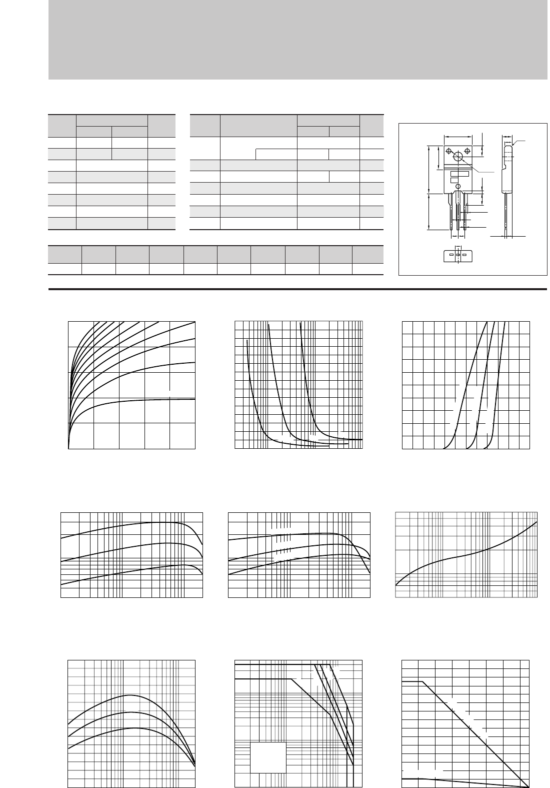
102
Silicon NPN Triple Diffused Planar Transistor (Complement to type 2SA1667/1668)
Application : TV Vertical Output, Audio Output Driver and General Purpose
2SC4381/4382
IC–VCE Characteristics
(Typical)
hFE–IC Characteristics
(Typical)
hFE–IC
Temperature Characteristics (Typical)
θj-a–t Characteristics
IC–VBE Temperature Characteristics
(Typical)
VCE(sat)–IB Characteristics
(Typical)
Pc–Ta Derating
0
0
2
1.6
1.2
0.4
0.8
6824 10
Collector-Emitter Voltage VCE(V)
Collector Current IC(A)
50mA
I
B
=5mA/Step
Safe Operating Area (Single Pulse)
fT–IE Characteristics
(Typical)
0
3
1
2
1002 10 1000
Base Current IB(mA)
Collector-Emitter Saturation Voltage VCE(sat)(V)
I
C
=0.5A
1A
2A
210.10.01
30
50
100
400
Collector Current IC(A)
DC Current Gain hFE
(VCE=10V)
Typ
210.10.01
30
50
100
400
Collector Current IC(A)
DC Current Gain hFE
(VCE=10V)
0.5
1
6
1 10 100 1000
Time t(ms)
Transient Thermal Resistance θj-a(˚C/W)
10 100 3001
0.01
0.1
5
1
Collector-Emitter Voltage VCE(V)
Collector Current IC(A)
Without Heatsink
Natural Cooling
1.2SC4381
2.2SC4382
DC
1ms
5ms
20ms
12
25˚C
–30˚C
125˚C
–0.01 –0.1 –0.5 –1 –2
20
10
0
30
Cut-off Frequency fT(MHZ)
(VCE=12V)
Emitter Current IE(A)
Typ
30
20
10
00 50 100 150
Ambient Temperature Ta(˚C)
Maximum Power Dissipation PC(W)
With Infinite heatsink
Without Heatsink
0
2
1
0 1.00.5
Base-Emittor Voltage VBE(V)
Collector Current IC(A)
(VCE=10V)
125˚C (Case Temp)
25˚C (Case Temp)
–55˚C (Case Temp)
■Typical Switching Characteristics (Common Emitter)
VCC
(V)
20
RL
(Ω)
20
IC
(A)
1
VBB2
(V)
–5
IB2
(mA)
–100
ton
(
µ
s)
1.0typ
tstg
(
µ
s)
3.0typ
tf
(
µ
s)
1.5typ
IB1
(mA)
100
VBB1
(V)
10
External Dimensions FM20(TO220F)
ø3.3±0.2
10.1±0.2
4.0±0.2
16.9±0.3
13.0min
8.4±0.2
0.8±0.2
3.9
±0.2
2.542.54
1.35±0.15
0.85
+0.2
-0.1
1.35±0.15
2.2±0.2
4.2±0.2
2.8 c0.5
2.4±0.2
0.45
+0.2
-0.1
BEC
a
b
Weight : Approx 2.0g
a. Part No.
b. Lot No.
Symbol
VCBO
VCEO
VEBO
IC
IB
PC
Tj
Tstg
2SC4381 2SC4382
150 200
150 200
6
2
1
25(Tc=25°C)
150
–55 to +150
Unit
V
V
V
A
A
W
°C
°C
■
Absolute maximum ratings
■
Electrical Characteristics
Symbol
ICBO
IEBO
V(BR)CEO
hFE
VCE(sat)
fT
COB
2SC4381 2SC4382
10max
150 200
10max
150min 200min
60min
1.0max
15typ
35typ
Unit
µ
A
V
µ
A
V
V
MHz
pF
Conditions
VCB=
VEB=6V
IC=25mA
VCE=10V, IC=0.7A
IC=0.7A, IB=0.07A
VCE=12V, IE=–0.2A
VCB=10V, f=1MHz
(Ta=25°C) (Ta=25°C)
Ratings Ratings
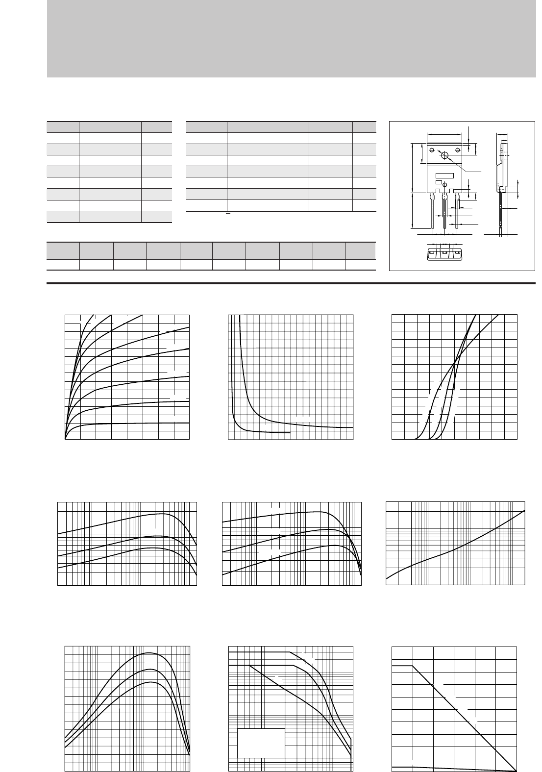
103
Silicon NPN Triple Diffused Planar Transistor (Complement to type 2SA1673)
Application : Audio and General Purpose
Symbol
VCBO
VCEO
VEBO
IC
IB
PC
Tj
Tstg
Ratings
200
180
6
15
4
85(Tc=25°C)
150
–55 to +150
Unit
V
V
V
A
A
W
°C
°C
■
Absolute maximum ratings
■
Electrical Characteristics
Symbol
ICBO
IEBO
V(BR)CEO
hFE
VCE(sat)
fT
COB
Ratings
10max
10max
180min
50min∗
2.0max
20typ
300typ
Unit
µ
A
µ
A
V
V
MHz
pF
Conditions
VCB=200V
VEB=6V
IC=50mA
VCE=4V, IC=3A
IC=5A, IB=0.5A
VCE=12V, IE=–0.5A
VCB=10V, f=1MHz
2SC4388
(Ta=25°C) (Ta=25°C)
IC–VCE Characteristics
(Typical)
hFE–IC Characteristics
(Typical)
hFE–IC
Temperature Characteristics (Typical)
θj-a–t Characteristics
IC–VBE Temperature Characteristics
(Typical)
VCE(sat)–IB Characteristics
(Typical)
Pc–Ta Derating
Safe Operating Area (Single Pulse)
fT–IE Characteristics
(Typical)
0
3
2
1
0 0.5 1.0 2.01.5
Base Current IB(A)
Collector-Emitter Saturation Voltage VCE(sat)(V)
IC=10A
5A
Collector Current IC(A)
0
15
10
5
021
Base-Emittor Voltage VBE(V)
(VCE=4V)
125˚C (Case Temp)
25˚C (Case Temp)
–30˚C (Case Temp)
0.1
1
3
0.5
1 10 100 1000 2000
Time t(ms)
Transient Thermal Resistance θj-a(˚C/W)
10 5053 100 200
0.05
1
0.5
0.1
10
40
5
Collector-Emitter Voltage VCE(V)
Collector Current IC(A)
Without Heatsink
Natural Cooling
DC
100ms
10ms
0.02 0.1 1 100.5 5 15
20
50
100
300
Collector Current IC(A)
DC Current Gain hFE
(VCE=4V)
Typ
0
0
5
15
10
2134
Collector-Emitter Voltage VCE(V)
Collector Current IC(A)
50mA
I
B
=20mA
(VCE=4V)
0.02 0.5 51
20
50
200
100
0.1 10 15
Collector Current IC(A)
DC Current Gain hFE
125˚C
25˚C
–30˚C
–0.02 –0.1 –1 –10
0
10
20
30
Cut-off Frequency fT(MHZ)
(VCE=12V)
Emitter Current IE(A)
Typ
1A
700mA
500mA
300mA
200mA
100mA
100
80
60
40
20
3.5
0
Ambient Temperature Ta(˚C)
Maximum Power Dissipation PC(W)
With Infinite heatsink
Without Heatsink
0 25 50 75 100 125 150
External Dimensions FM100(TO3PF)
4.41.5 1.5
BEC
5.45±0.1
ø3.3±0.2
1.6
3.3
1.75
0.8±0.2
2.15
1.05
+0.2
-0.1
5.45±0.1
23.0±0.3
16.2
9.5±0.2
5.5
15.6±0.2 5.5±0.2
3.45
3.35
0.65
+0.2
-0.1
±0.2
3.0
0.8
a
b
Weight : Approx 6.5g
a. Part No.
b. Lot No.
■Typical Switching Characteristics (Common Emitter)
VCC
(V)
40
RL
(Ω)
4
IC
(A)
10
VBB2
(V)
–5
IB2
(A)
–1
ton
(
µ
s)
0.5max
tstg
(
µ
s)
1.8max
tf
(
µ
s)
0.6max
IB1
(A)
1
VBB1
(V)
10
∗hFE Rank O(50to100), P(70to140), Y(90to180)
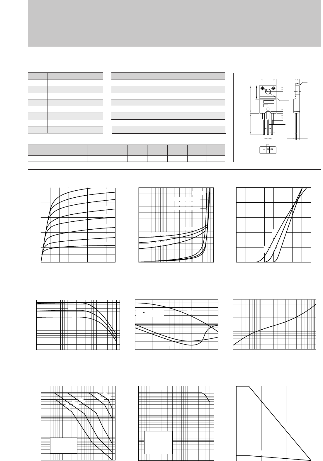
104
Silicon NPN Triple Diffused Planar Transistor (High Voltage and High Speed Switchihg Transistor)
Application : Switching Regulator and General Purpose
Symbol
VCBO
VCEO
VEBO
IC
IB
PC
Tj
Tstg
Ratings
500
400
10
5(Pulse10)
2
30(Tc=25°C)
150
–55 to +150
Unit
V
V
V
A
A
W
°C
°C
■
Absolute maximum ratings
■
Electrical Characteristics
Symbol
ICBO
IEBO
V(BR)CEO
hFE
VCE(sat)
VBE(sat)
fT
COB
Ratings
100max
100max
400min
10to30
0.5max
1.3max
20typ
30typ
Unit
µ
A
µ
A
V
V
V
MHz
pF
Conditions
VCB=500V
VEB=10V
IC=25mA
VCE=4V, IC=1.5A
IC=1.5A, IB=0.3A
IC=1.5A, IB=0.3A
VCE=12V, IE=–0.3A
VCB=10V, f=1MHz
2SC4418
(Ta=25°C) (Ta=25°C)
IC–VCE Characteristics
(Typical)
hFE–IC Characteristics
(Typical)
ton•tstg•tf–IC Characteristics
(Typical)
θj-a–t Characteristics
IC–VBE Temperature Characteristics
(Typical)
VCE(sat),VBE(sat)–IC Temperature Characteristics (Typical)
Pc–Ta Derating
Reverse Bias Safe Operating Area
Safe Operating Area (Single Pulse)
0
0
1
2
3
4
5
2134
Collector-Emitter Voltage VCE(V)
Collector Current IC(A)
600mA
1A
1.4A
400mA
200mA
1.8A
100mA
I
B
=50mA
0.01
0.1
0.05
150.5
0
2
1
(IC/IB=5)
Collector Current IC(A)
VBE(sat)
125˚C (Case Temp)
25˚C (Case Temp)
–55˚C (Case Temp)
125˚C (Case Temp)
25˚C (Case Temp)
–55˚C (Case Temp)
VCE(sat)
0.1 10.5 3
0.1
0.5
5
8
1
Switching Time ton•tstg•tf(µs)
Collector Current IC(A)
tstg
ton
tf
VCC 200V
IC:IB1:IB2=10:1:–2
0.4
1
5
0.5
1 10 100 1000
Time t(ms)
Transient Thermal Resistance θj-a(˚C/W)
30
20
10
2
00 25 50 75 100 125 150
Ambient Temperature Ta(˚C)
Maximum Power Dissipation PC(W)
With Infinite heatsink
Without Heatsink
10 505 500100
1
0.5
0.01
0.1
0.05
10
20
5
Collector-Emitter Voltage VCE(V)
Collector Current IC(A)
Without Heatsink
Natural Cooling
L=3mH
IB2=–0.5A
Duty:less than 1%
10 5052 100 500
0.05
0.01
1
0.5
0.1
10
20
5
Collector-Emitter Voltage VCE(V)
Collector Current IC(A)
Without Heatsink
Natural Cooling
DC
10ms
100µs
50µs
1ms
Collector-Emitter Saturation Voltage VCE(sat)(V)
Base-Emitter Saturation Voltage VBE(sat)(V)
0
5
1
2
3
4
0 1.61.0
Base-Emittor Voltage VBE(V)
Collector Current IC(A)
(VCE=4V)
125˚C (Case Temp)
25˚C (Case Temp)
–55˚C (Case Temp)
0.01 0.10.05 1 50.5
2
5
10
100
50
Collector Current IC(A)
DC Current Gain hFE
(VCE=4V)
Typ
■Typical Switching Characteristics (Common Emitter)
VCC
(V)
200
RL
(Ω)
133
IC
(A)
1.5
VBB2
(V)
–5
IB2
(A)
–0.3
ton
(
µ
s)
1max
tstg
(
µ
s)
2.5max
tf
(
µ
s)
0.5max
IB1
(A)
0.15
VBB1
(V)
10
External Dimensions FM20(TO220F)
ø3.3±0.2
10.1±0.2
4.0±0.2
16.9±0.3
13.0min
8.4±0.2
0.8±0.2
3.9
±0.2
2.542.54
1.35±0.15
0.85
+0.2
-0.1
1.35±0.15
2.2±0.2
4.2±0.2
2.8 c0.5
2.4±0.2
0.45
+0.2
-0.1
BEC
a
b
Weight : Approx 2.0g
a. Part No.
b. Lot No.
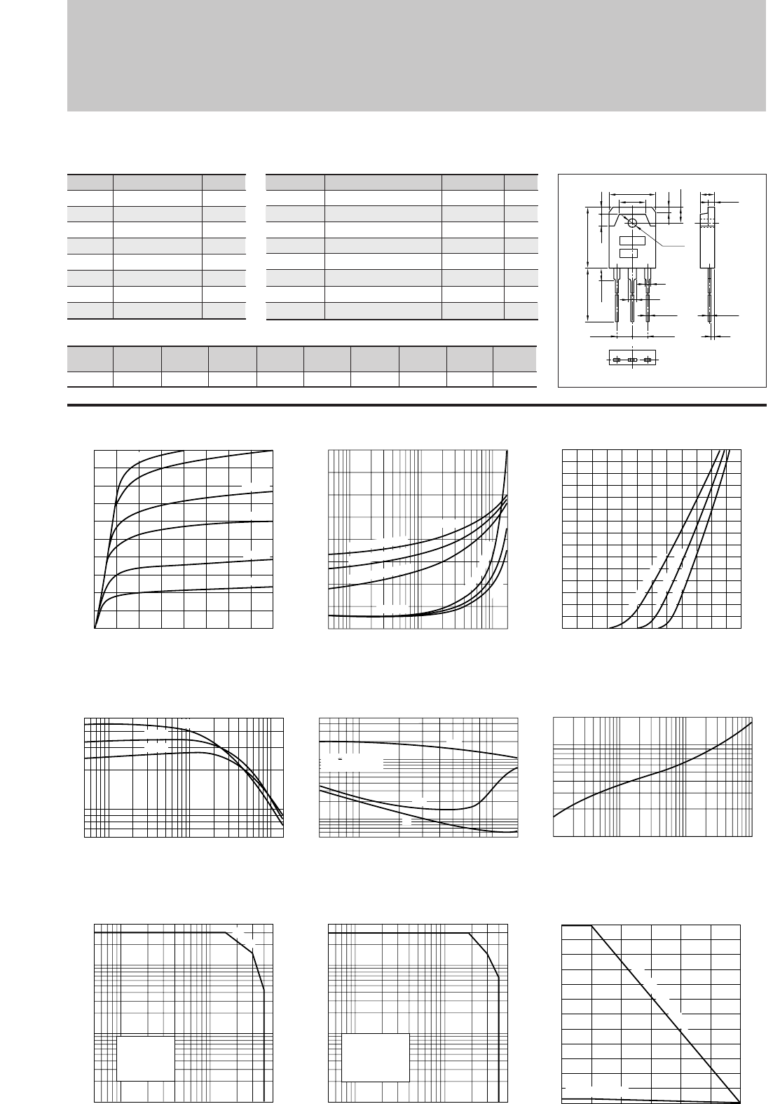
105
Silicon NPN Triple Diffused Planar Transistor (High Voltage and High Speed Switchihg Transistor)
Application : Switching Regulator, Lighting Inverter, and General Purpose
Symbol
VCBO
VCEO
VEBO
IC
IB
PC
Tj
Tstg
Ratings
500
400
10
15(Pulse30)
5
120(Tc=25°C)
150
–55 to +150
Unit
V
V
V
A
A
W
°C
°C
■
Absolute maximum ratings
■
Electrical Characteristics
Symbol
ICBO
IEBO
V(BR)CEO
hFE
VCE(sat)
VBE(sat)
fT
COB
Ratings
100max
100max
400min
10to25
0.7max
1.3max
10typ
135typ
Unit
µ
A
µ
A
V
V
V
MHz
pF
Conditions
VCB=500V
VEB=10V
IC=25mA
VCE=4V, IC=8A
IC=8A, IB=1.6A
IC=8A, IB=1.6A
VCE=12V, IE=–1.5A
VCB=10V, f=1MHz
2SC4434
(Ta=25°C) (Ta=25°C)
IC–VCE Characteristics
(Typical)
hFE–IC Temperature Characteristics
(Typical)
ton•tstg•tf–IC Characteristics
(Typical)
θj-a–t Characteristics
IC–VBE Temperature Characteristics
(Typical)
VCE(sat),VBE(sat)–IC Temperature Characteristics (Typical)
Pc–Ta Derating
Reverse Bias Safe Operating Area
Safe Operating Area (Single Pulse)
0
0
2
4
6
8
10
2134
Collector-Emitter Voltage VCE(V)
Collector Current IC(A)
1A
600mA
400mA
200mA
1.2A
I
B
=100mA
0.10.05 1 5 100.5
0
1
Collector-Emitter Saturation Voltage VCE(sat)(V)
Base-Emitter Saturation Voltage VBE(sat)(V)
Collector-Emitter Voltage VCE(V)
(IC/IB=5)
Collector Current IC(A)
VBE(sat)
150˚C (Case Temp)
25˚C (Case Temp)
75˚C (Case Temp)
75˚C
25˚C
VCE(sat)
1
5
0
˚
C
(
C
a
s
e
T
e
m
p
)
0
15
14
12
10
8
6
4
2
0 1.00.5
Base-Emittor Voltage VBE(V)
Collector Current IC(A)
(VCE=4V)
150˚C (Case Temp)
75˚C (Case Temp)
25˚C (Case Temp)
0.05 10.50.1 10 155
5
10
50
Collector Current IC(A)
DC Current Gain hFE
(VCE=4V)
150˚C
75˚C
25˚C
10.5 10 155
0.05
0.1
0.5
5
1
Switching Time ton•tstg•tf(µs)
Collector Current IC(A)
tstg
ton
tf
VCC 200V
IC:IB1:–IB2=5:1:2
0.1
1
2
0.5
1 10 100 1000
Time t(ms)
Transient Thermal Resistance θj-a(˚C/W)
120
100
50
3.5
00 25 50 75 100 125 150
Ambient Temperature Ta(˚C)
Maximum Power Dissipation PC(W)
With Infinite heatsink
Without Heatsink
10 505 500100
1
0.5
0.1
10
40
5
Collector Current IC(A)
Without Heatsink
Natural Cooling
L=3mH
IB2=–1A
Duty:less than 1%
10 505 100 500
1
0.5
0.1
10
40
5
Collector-Emitter Voltage VCE(V)
Collector Current IC(A)
100µs
Without Heatsink
Natural Cooling
■Typical Switching Characteristics (Common Emitter)
VCC
(V)
200
RL
(Ω)
25
IC
(A)
8
VBB2
(V)
–5
IB2
(A)
–3.2
ton
(
µ
s)
0.5max
tstg
(
µ
s)
2.0max
tf
(
µ
s)
0.15max
IB1
(A)
1.6
VBB1
(V)
10
External Dimensions MT-100(TO3P)
15.6±0.4
9.6
19.9±0.3
4.0 2.0
5.0±0.2
1.8
ø3.2±0.1
2
3
1.05
+0.2
-0.1
20.0min
4.0max
BE
5.45±0.1 5.45±0.1
C
4.8±0.2
0.65
+0.2
-0.1
1.4
2.0±0.1
a
b
Weight : Approx 6.0g
a. Part No.
b. Lot No.
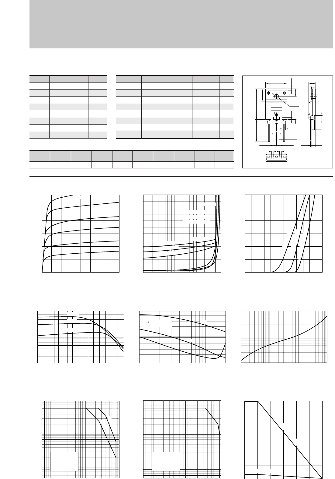
106
Silicon NPN Triple Diffused Planar Transistor (High Voltage and High Speed Switchihg Transistor)
Application : Switching Regulator and General Purpose
Symbol
VCBO
VCEO
VEBO
IC
IB
PC
Tj
Tstg
Ratings
900
800
7
3(Pulse6)
1.5
60(Tc=25°C)
150
–55 to +150
Unit
V
V
V
A
A
W
°C
°C
■
Absolute maximum ratings
■
Electrical Characteristics
Symbol
ICBO
IEBO
V(BR)CEO
hFE
VCE(sat)
VBE(sat)
fT
COB
Ratings
100max
100max
800min
10to30
0.5max
1.2max
15typ
50typ
Unit
µ
A
µ
A
V
V
V
MHz
pF
Conditions
VCB=800V
VEB=7V
IC=10mA
VCE=4V, IC=0.7A
IC=0.7A, IB=0.14A
IC=0.7A, IB=0.14A
VCE=12V, IE=–0.3A
VCB=10V, f=1MHz
2SC4445
(Ta=25°C) (Ta=25°C)
IC–VCE Characteristics
(Typical)
hFE–IC Temperature Characteristics
(Typical)
ton•tstg•tf–IC Characteristics
(Typical)
θj-a–t Characteristics
IC–VBE Temperature Characteristics
(Typical)
VCE(sat),VBE(sat)–IC Temperature Characteristics (Typical)
Pc–Ta Derating
Reverse Bias Safe Operating Area
Safe Operating Area (Single Pulse)
0
0
2
1
3
2134
Collector-Emitter Voltage VCE(V)
Collector Current IC(A)
500mA
300mA
200mA
100mA
50mA
I
B
=700mA
0.1 10.5 2
0.1
0.5
5
7
1
Switching Time ton•tstg•tf(µs)
Collector Current IC(A)
tstg
ton
tf
VCC 250V
IC:IB1:–IB2=10:1.5:5
60
40
20
3.5
00 50 100 150
Ambient Temperature Ta(˚C)
Maximum Power Dissipation PC(W)
With Infinite heatsink
Without Heatsink
10 505 500 1000100
1
0.5
0.1
0.05
10
5
Collector-Emitter Voltage VCE(V)
Collector Current IC(A)
Without Heatsink
Natural Cooling
L=3mH
IB2=–1.0A
Duty:less than 1%
10 505 100 500 1000
0.05
1
0.5
0.1
10
5
Collector-Emitter Voltage VCE(V)
Collector Current IC(A)
Without Heatsink
Natural Cooling
50µs
100µs
Collector-Emitter Saturation Voltage VCE(sat)(V)
Base-Emitter Saturation Voltage VBE(sat)(V)
0.1
0.050.01
310.5
0
1
2
(IC/IB=5)
Collector Current IC(A)
VBE(sat)
125˚C (Case Temp)
25˚C (Case Temp)
–55˚C (Case Temp)
125˚C (Case Temp)
25˚C (Case Temp)
–55˚C (Case Temp)
VCE(sat)
0.3
1
4
0.5
1 10 100 1000
Time t(ms)
Transient Thermal Resistance θj-a(˚C/W)
0
3
1
2
0 1.20.4 0.6 0.8 1.00.2
Base-Emittor Voltage VBE(V)
Collector Current IC(A)
(VCE=4V)
125˚C (Case Temp)
0.01 0.10.05 1 30.5
2
5
10
50
Collector Current IC(A)
DC Current Gain hFE
(VCE=4V)
125˚C
25˚C
–55˚C
25˚C (Case Temp)
–55˚C (Case Temp)
■Typical Switching Characteristics (Common Emitter)
VCC
(V)
250
RL
(Ω)
357
IC
(A)
0.7
VBB2
(V)
–5
IB2
(A)
–0.35
ton
(
µ
s)
0.7max
tstg
(
µ
s)
4max
tf
(
µ
s)
0.7max
IB1
(A)
0.1
VBB1
(V)
10
External Dimensions FM100(TO3PF)
4.41.5 1.5
BEC
5.45±0.1
ø3.3±0.2
1.6
3.3
1.75
0.8±0.2
2.15
1.05
+0.2
-0.1
5.45±0.1
23.0±0.3
16.2
9.5±0.2
5.5
15.6±0.2 5.5±0.2
3.45
3.35
0.65
+0.2
-0.1
±0.2
3.0
0.8
a
b
Weight : Approx 6.5g
a. Part No.
b. Lot No.
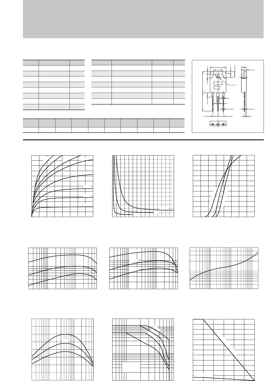
107
Silicon NPN Triple Diffused Planar Transistor (Complement to type 2SA1693)
Application : Audio and General Purpose
Symbol
VCBO
VCEO
VEBO
IC
IB
PC
Tj
Tstg
Ratings
120
80
6
6
3
60(Tc=25°C)
150
–55 to +150
Unit
V
V
V
A
A
W
°C
°C
■
Absolute maximum ratings
■
Electrical Characteristics
Symbol
ICBO
IEBO
V(BR)CEO
hFE
VCE(sat)
fT
COB
Ratings
10max
10max
80min
50min∗
1.5max
20typ
110typ
Unit
µ
A
µ
A
V
V
MHz
pF
Conditions
VCB=120V
VEB=6V
IC=50mA
VCE=4V, IC=2A
IC=2A, IB=0.2A
VCE=12V, IE=–0.5A
VCB=10V, f=1MHz
2SC4466
(Ta=25°C) (Ta=25°C)
■Typical Switching Characteristics (Common Emitter)
VCC
(V)
30
RL
(Ω)
10
IC
(A)
3
VBB2
(V)
–5
IB2
(A)
–0.3
ton
(
µ
s)
0.16typ
tstg
(
µ
s)
2.60typ
tf
(
µ
s)
0.34typ
IB1
(A)
0.3
VBB1
(V)
10
External Dimensions MT-100(TO3P)
15.6±0.4
9.6
19.9±0.3
4.0 2.0
5.0±0.2
1.8
ø3.2±0.1
2
3
1.05
+0.2
-0.1
20.0min
4.0max
BE
5.45±0.1 5.45±0.1
C
4.8±0.2
0.65
+0.2
-0.1
1.4
2.0±0.1
a
b
Weight : Approx 6.0g
a. Part No.
b. Lot No.
IC–VCE Characteristics
(Typical)
hFE–IC Characteristics
(Typical)
hFE–IC
Temperature Characteristics (Typical)
θj-a–t Characteristics
IC–VBE Temperature Characteristics
(Typical)
VCE(sat)–IB Characteristics
(Typical)
Pc–Ta Derating
Safe Operating Area (Single Pulse)
fT–IE Characteristics
(Typical)
0
3
2
1
0 0.5 1.0 1.5
Base Current IB(A)
Collector-Emitter Saturation Voltage VCE(sat)(V)
IC=6A
2A 4A
0
6
4
2
021
Base-Emittor Voltage VBE(V)
Collector Current IC(A)
(VCE=4V)
125˚C (Case Temp)
25˚C (Case Temp)
–30˚C (Case Temp)
60
40
20
3.5
00 25 50 75 100 125 150
Ambient Temperature Ta(˚C)
Maximum Power Dissipation PC(W)
With Infinite heatsink
Without Heatsink
5 10 10050
0.1
1
0.5
10
20
5
Collector-Emitter Voltage VCE(V)
Collector Current IC(A)
Without Heatsink
Natural Cooling
DC
10ms
1ms
100ms
0.02 0.1 10.5 5 6
30
50
100
300
Collector Current IC(A)
DC Current Gain hFE
(VCE=4V)
Typ
0
0
2
4
6
2134
Collector-Emitter Voltage VCE(V)
Collector Current IC(A)
80mA
50mA
30mA
20mA
150mA
100mA
I
B
=10mA
200mA
(VCE=4V)
0.02 0.5 651
20
50
200
100
0.1
Collector Current IC(A)
DC Current Gain hFE
125˚C
25˚C
–30˚C
–0.02 –0.1 –1 –6
0
20
10
40
30
Cut-off Frequency fT(MHZ)
(VCE=12V)
Emitter Current IE(A)
Typ
0.3
1
5
0.5
1 10 100 1000 2000
Time t(ms)
Transient Thermal Resistance θj-a(˚C/W)
∗hFE Rank O(50to100), P(70to140), Y(90to180)
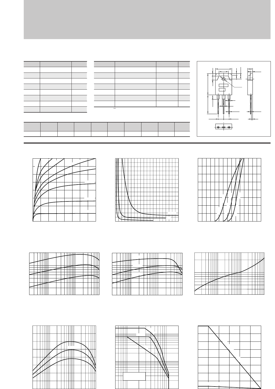
108
Silicon NPN Triple Diffused Planar Transistor (Complement to type 2SA1694)
Application : Audio and General Purpose
Symbol
VCBO
VCEO
VEBO
IC
IB
PC
Tj
Tstg
Ratings
160
120
6
8
3
80(Tc=25°C)
150
–55 to +150
Unit
V
V
V
A
A
W
°C
°C
■
Absolute maximum ratings
■
Electrical Characteristics
Symbol
ICBO
IEBO
V(BR)CEO
hFE
VCE(sat)
fT
COB
Ratings
10max
10max
120min
50min∗
1.5max
20typ
200typ
Unit
µ
A
µ
A
V
V
MHz
pF
Conditions
VCB=160V
VEB=6V
IC=50mA
VCE=4V, IC=3A
IC=3A, IB=0.3A
VCE=12V, IE=–0.5A
VCB=10V, f=1MHz
2SC4467
(Ta=25°C) (Ta=25°C)
IC–VCE Characteristics
(Typical)
hFE–IC Characteristics
(Typical)
hFE–IC
Temperature Characteristics (Typical)
θj-a–t Characteristics
IC–VBE Temperature Characteristics
(Typical)
VCE(sat)–IB Characteristics
(Typical)
Pc–Ta Derating
Safe Operating Area (Single Pulse)
fT–IE Characteristics
(Typical)
0
3
2
1
0 0.1 0.2 0.3 0.4 0.5 0.6 0.7 0.8 0.9 1.0
Base Current IB(A)
Collector-Emitter Saturation Voltage VCE(sat)(V)
IC=8A
2A 4A
0
8
6
2
4
0 1.51.00.5
Base-Emittor Voltage VBE(V)
Collector Current IC(A)
(VCE=4V)
125˚C (Case Temp)
25˚C (Case Temp)
–30˚C (Case Temp)
80
60
40
20
3.5
00 25 50 75 100 125 150
Ambient Temperature Ta(˚C)
Maximum Power Dissipation PC(W)
With Infinite heatsink
Without Heatsink
10 505 100 200
0.1
1
0.5
10
20
5
Collector-Emitter Voltage VCE(V)
Collector Current IC(A)
Without Heatsink
Natural Cooling
DC
100ms
10ms
0.02 0.1 0.5 1 5 8
20
50
100
200
Collector Current IC(A)
DC Current Gain hFE
(VCE=4V)
Typ
0
0
2
4
6
8
2134
Collector-Emitter Voltage VCE(V)
Collector Current IC(A)
100mA
150mA
200mA
350mA
75mA
50mA
20mA
I
B
=10mA
(VCE=4V)
0.02 0.5 5 81
20
50
200
100
0.1
Collector Current IC(A)
DC Current Gain hFE
125˚C
25˚C
–30˚C
–0.02 –0.1 –1 –8
0
10
20
40
30
Cut-off Frequency fT(MHZ)
(VCE=12V)
Emitter Current IE(A)
Typ
0.3
1
3
0.5
1 10 100 1000
Time t(ms)
Transient Thermal Resistance θj-a(˚C/W)
■Typical Switching Characteristics (Common Emitter)
VCC
(V)
40
RL
(Ω)
10
IC
(A)
4
VBB2
(V)
–5
IB2
(A)
–0.4
ton
(
µ
s)
0.13typ
tstg
(
µ
s)
3.50typ
tf
(
µ
s)
0.32typ
IB1
(A)
0.4
VBB1
(V)
10
External Dimensions MT-100(TO3P)
15.6±0.4
9.6
19.9±0.3
4.0 2.0
5.0±0.2
1.8
ø3.2±0.1
2
3
1.05
+0.2
-0.1
20.0min
4.0max
BE
5.45±0.1 5.45±0.1
C
4.8±0.2
0.65
+0.2
-0.1
1.4
2.0±0.1
a
b
Weight : Approx 6.0g
a. Part No.
b. Lot No.
∗hFE Rank O(50to100), P(70to140), Y(90to180)
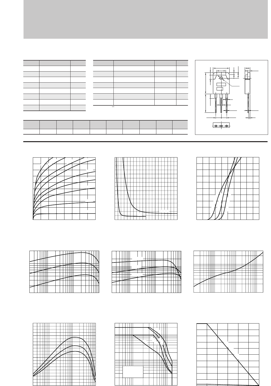
109
Silicon NPN Triple Diffused Planar Transistor (Complement to type 2SA1695)
Application : Audio and General Purpose
Symbol
VCBO
VCEO
VEBO
IC
IB
PC
Tj
Tstg
Ratings
200
140
6
10
4
100(Tc=25°C)
150
–55 to +150
Unit
V
V
V
A
A
W
°C
°C
■
Absolute maximum ratings
■
Electrical Characteristics
Symbol
ICBO
IEBO
V(BR)CEO
hFE
VCE(sat)
fT
COB
Ratings
10max
10max
140min
50min∗
0.5max
20typ
250typ
Unit
µ
A
µ
A
V
V
MHz
pF
Conditions
VCB=200V
VEB=6V
IC=50mA
VCE=4V, IC=3A
IC=5A, IB=0.5A
VCE=12V, IE=–0.5A
VCB=10V, f=1MHz
2SC4468
(Ta=25°C) (Ta=25°C)
IC–VCE Characteristics
(Typical)
hFE–IC Characteristics
(Typical)
hFE–IC
Temperature Characteristics (Typical)
θj-a–t Characteristics
IC–VBE Temperature Characteristics
(Typical)
VCE(sat)–IB Characteristics
(Typical)
Pc–Ta Derating
Safe Operating Area (Single Pulse)
fT–IE Characteristics
(Typical)
0
3
2
1
0 0.5 1.0 2.01.5
Base Current IB(A)
Collector-Emitter Saturation Voltage VCE(sat)(V)
IC=10A
5A
0
10
2
6
4
8
021
Base-Emittor Voltage VBE(V)
Collector Current IC(A)
(VCE=4V)
125˚C (Case Temp)
25˚C (Case Temp)
–30˚C (Case Temp)
0.1
1
3
0.5
1 10 100 1000 2000
Time t(ms)
Transient Thermal Resistance θj-a(˚C/W)
100
50
3.5
00 25 50 75 100 125 150
Ambient Temperature Ta(˚C)
Maximum Power Dissipation PC(W)
With Infinite heatsink
Without Heatsink
1053 100 20050
0.1
1
0.5
10
30
5
Collector-Emitter Voltage VCE(V)
Collector Current IC(A)
DC
100ms
3ms
10ms
Without Heatsink
Natural Cooling
0.02 0.1 0.5 1 5 10
20
50
100
200
Collector Current IC(A)
DC Current Gain hFE
(VCE=4V) (VCE=4V)
Typ
0
0
2
4
6
10
8
2134
Collector-Emitter Voltage VCE(V)
Collector Current IC(A)
150mA
200mA
100mA
75mA
50mA
20mA
I
B
=10mA
300mA
400mA
0.02 0.5 51
20
50
300
100
0.1 10
Collector Current IC(A)
DC Current Gain hFE
125˚C
25˚C
–30˚C
–0.02 –0.1 –1 –10
0
10
20
40
30
Cut-off Frequency fT(MHZ)
(VCE=12V)
Emitter Current IE(A)
Typ
■Typical Switching Characteristics (Common Emitter)
VCC
(V)
60
RL
(Ω)
12
IC
(A)
5
VBB2
(V)
–5
IB2
(A)
–0.5
ton
(
µ
s)
0.24typ
tstg
(
µ
s)
4.32typ
tf
(
µ
s)
0.40typ
IB1
(A)
0.5
VBB1
(V)
10
External Dimensions MT-100(TO3P)
15.6±0.4
9.6
19.9±0.3
4.0 2.0
5.0±0.2
1.8
ø3.2±0.1
2
3
1.05
+0.2
-0.1
20.0min
4.0max
BE
5.45±0.1 5.45±0.1
C
4.8±0.2
0.65
+0.2
-0.1
1.4
2.0±0.1
a
b
Weight : Approx 6.0g
a. Part No.
b. Lot No.
∗hFE Rank O(50to100), P(70to140), Y(90to180)
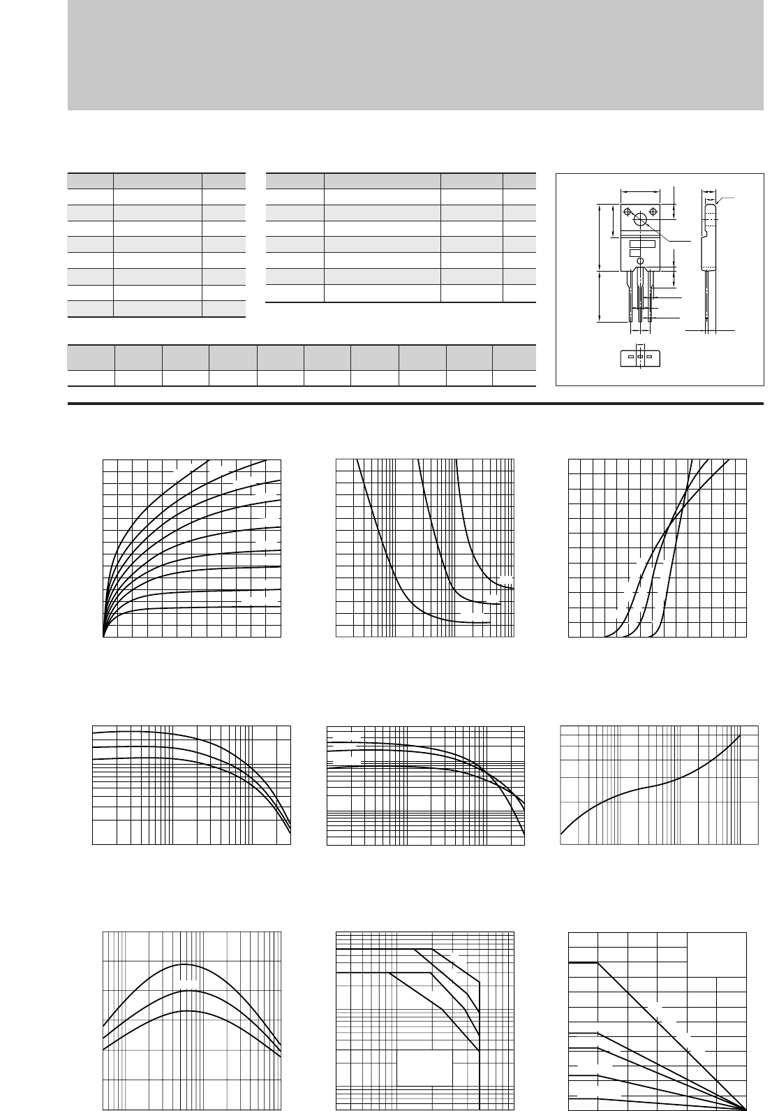
110
Silicon NPN Triple Diffused Planar Transistor
Application : Audio Temperature Compensation and General Purpose
Symbol
VCBO
VCEO
VEBO
IC
IB
PC
Tj
Tstg
Ratings
80
50
6
3
1
25(Tc=25°C)
150
–55 to +150
Unit
V
V
V
A
A
W
°C
°C
■
Absolute maximum ratings
■
Electrical Characteristics
Symbol
ICBO
IEBO
V(BR)CEO
hFE
VCE(sat)
fT
COB
Ratings
10max
10max
50min
500min
0.5max
40typ
30typ
Unit
µ
A
µ
A
V
V
MHz
pF
Conditions
VCB=80V
VEB=6V
IC=25mA
VCE=4V, IC=0.5A
IC=1A, IB=20mA
VCE=12V, IE=–0.1A
VCB=10V,f=1MHz
2SC4495
(Ta=25°C) (Ta=25°C)
IC–VCE Characteristics
(Typical)
hFE–IC Characteristics
(Typical)
hFE–IC
Temperature Characteristics (Typical)
θj-a–t Characteristics
IC–VBE Temperature Characteristics
(Typical)
VCE(sat)–IB Characteristics
(Typical)
Pc–Ta Derating
0
0
1
2
3
21 3456
Collector-Emitter Voltage VCE(V)
Collector Current IC(A)
30mA
I
B
=0.5mA
18mA
12mA
1mA
2mA
3mA
8mA
5mA
Safe Operating Area (Single Pulse)
fT–IE Characteristics
(Typical)
0
1.5
0.5
1
1001 10 1000
Base Current IB(mA)
Collector-Emitter Saturation Voltage VCE(sat)(V)
IC=1A
2A
3A
310.1 0.50.01
100
500
1000
3000
Collector Current IC(A)
DC Current Gain hFE
(VCE=4V)
Typ
–0.005
–0.01
–0.1 –1
0
20
40
60
Cut-off Frequency fT(MHZ)
(VCE=12V)
Emitter Current IE(A)
Typ
10 503 5 100
0.05
0.1
1
0.5
10
5
Collector-Emitter Voltage VCE(V)
Collector Current IC(A)
Without Heatsink
Natural Cooling
DC
100ms
10ms
1ms
30
20
10
2
00 25 50 75 100 125 150
Ambient Temperature Ta(˚C)
Maximum Power Dissipation PC(W)
With Infinite heatsink
Without Heatsink
150x150x2
50x50x2
100x
100x2
0
3
2.5
0.5
1.5
1
2
0 1.510.5
Base-Emittor Voltage VBE(V)
Collector Current IC(A)
(VCE=4V)
125˚C (Case Temp)
25˚C (Case Temp)
–55˚C (Case Temp)
Collector Current IC(A)
DC Current Gain hFE
1
7
5
1 10 100 1000 2000
Time t(ms)
Transient Thermal Resistance θj-a(˚C/W)
310.1 0.50.01
20
100
50
500
1000
5000
(VCE=4V)
125˚C
–55˚C
25˚C
Natural Cooling
Silicone Grease
Heatsink: Aluminum
in mm
■Typical Switching Characteristics (Common Emitter)
VCC
(V)
20
RL
(Ω)
20
IC
(A)
1
VBB2
(V)
–5
IB2
(mA)
–30
ton
(
µ
s)
0.45typ
tstg
(
µ
s)
1.60typ
tf
(
µ
s)
0.85typ
IB1
(mA)
15
VBB1
(V)
10
External Dimensions FM20(TO220F)
ø3.3±0.2
10.1±0.2
4.0±0.2
16.9±0.3
13.0min
8.4±0.2
0.8±0.2
3.9
±0.2
2.542.54
1.35±0.15
0.85
+0.2
-0.1
1.35±0.15
2.2±0.2
4.2±0.2
2.8 c0.5
2.4±0.2
0.45
+0.2
-0.1
BEC
a
b
Weight : Approx 2.0g
a. Part No.
b. Lot No.
High hFE
LOW VCE (sat)
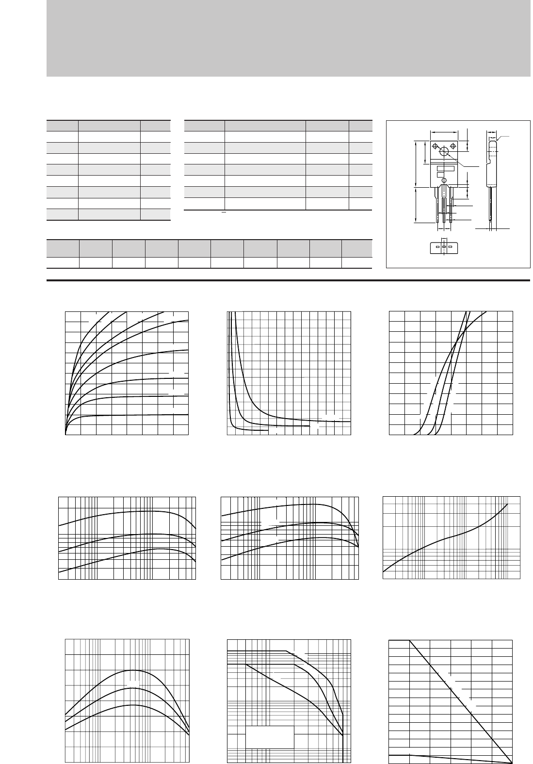
111
Silicon NPN Triple Diffused Planar Transistor (Complement to type 2SA1725)
Symbol
VCBO
VCEO
VEBO
IC
IB
PC
Tj
Tstg
Ratings
120
80
6
6
3
30(Tc=25°C)
150
–55 to +150
Unit
V
V
V
A
A
W
°C
°C
■
Absolute maximum ratings
■
Electrical Characteristics
Symbol
ICBO
IEBO
V(BR)CEO
hFE
VCE(sat)
fT
COB
Ratings
10max
10max
80min
50min∗
0.5max
20typ
110typ
Unit
µ
A
µ
A
V
V
MHz
pF
Conditions
VCB=120V
VEB=6V
IC=25mA
VCE=4V, IC=2A
IC=2A, IB=0.2A
VCE=12V, IE=–0.5A
VCB=10V, f=1MHz
2SC4511
(Ta=25°C) (Ta=25°C)
IC–VCE Characteristics
(Typical)
hFE–IC Characteristics
(Typical)
hFE–IC
Temperature Characteristics (Typical)
θj-a–t Characteristics
IC–VBE Temperature Characteristics
(Typical)
VCE(sat)–IB Characteristics
(Typical)
Pc–Ta Derating
Safe Operating Area (Single Pulse)
fT–IE Characteristics
(Typical)
0
3
2
1
0 0.5 1.0 1.5
Base Current IB(A)
Collector-Emitter Saturation Voltage VCE(sat)(V)
IC=6A
2A 4A
0
6
4
2
021
Base-Emittor Voltage VBE(V)
Collector Current IC(A)
(VCE=4V)
125˚C (Case Temp)
25˚C (Case Temp)
–30˚C (Case Temp)
0.4
1
5
0.5
1 10 100 1000 2000
Time t(ms)
Transient Thermal Resistance θj-a(˚C/W)
30
20
10
2
00 25 50 75 100 125 150
Ambient Temperature Ta(˚C)
Maximum Power Dissipation PC(W)
With Infinite heatsink
Without Heatsink
3 5 10 10050
0.05
0.1
1
0.5
10
20
5
Collector-Emitter Voltage VCE(V)
Collector Current IC(A)
Without Heatsink
Natural Cooling
DC
10ms
100ms
0.02 0.1 10.5 5 6
30
50
100
300
Collector Current IC(A)
DC Current Gain hFE
(VCE=4V)
Typ
0
0
1
3
2
4
6
5
2134
Collector-Emitter Voltage VCE(V)
Collector Current IC(A)
80mA
50mA
30mA
20mA
150mA
100mA
I
B
=10mA
200mA
(VCE=4V)
0.02 0.5 651
20
50
200
100
0.1
Collector Current IC(A)
DC Current Gain hFE
125˚C
25˚C
–30˚C
–0.02 –0.1 –1 –6
0
20
10
40
30
Cut-off Frequency fT(MHZ)
(VCE=12V)
Emitter Current IE(A)
Typ
■Typical Switching Characteristics (Common Emitter)
VCC
(V)
30
RL
(Ω)
10
IC
(A)
3
VBB2
(V)
–5
IB2
(A)
–0.3
ton
(
µ
s)
0.16typ
tstg
(
µ
s)
2.60typ
tf
(
µ
s)
0.34typ
IB1
(A)
0.3
VBB1
(V)
10
External Dimensions FM20(TO220F)
ø3.3±0.2
10.1±0.2
4.0±0.2
16.9±0.3
13.0min
8.4±0.2
0.8±0.2
3.9
±0.2
2.542.54
1.35±0.15
0.85
+0.2
-0.1
1.35±0.15
2.2±0.2
4.2±0.2
2.8 c0.5
2.4±0.2
0.45
+0.2
-0.1
BEC
a
b
Weight : Approx 2.0g
a. Part No.
b. Lot No.
∗hFE Rank O(50to100), P(70to140), Y(90to180)
Application : Audio and General Purpose
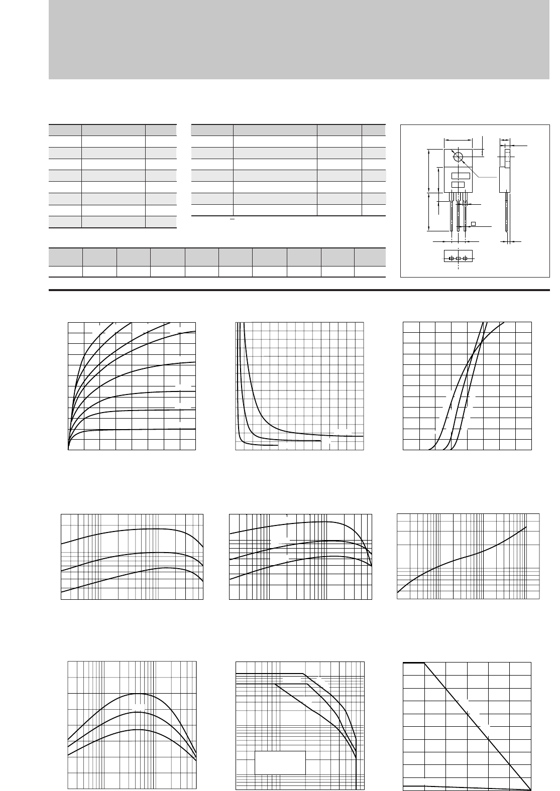
112
Silicon NPN Triple Diffused Planar Transistor (Complement to type 2SA1726)
Application : Audio and General Purpose
Symbol
VCBO
VCEO
VEBO
IC
IB
PC
Tj
Tstg
Ratings
120
80
6
6
3
50(Tc=25°C)
150
–55 to +150
Unit
V
V
V
A
A
W
°C
°C
■
Absolute maximum ratings
■
Electrical Characteristics
Symbol
ICBO
IEBO
V(BR)CEO
hFE
VCE(sat)
fT
COB
Ratings
10max
10max
80min
50min
0.5max
20typ
110typ
Unit
µ
A
µ
A
V
V
MHz
pF
Conditions
VCB=120V
VEB=6V
IC=25mA
VCE=4V, IC=2A
IC=5A, IB=0.2A
VCE=12V, IE=–0.5A
VCB=10V, f=1MHz
2SC4512
(Ta=25°C) (Ta=25°C)
IC–VCE Characteristics
(Typical)
hFE–IC Characteristics
(Typical)
hFE–IC
Temperature Characteristics (Typical)
θj-a–t Characteristics
IC–VBE Temperature Characteristics
(Typical)
VCE(sat)–IB Characteristics
(Typical)
Pc–Ta Derating
Safe Operating Area (Single Pulse)
fT–IE Characteristics
(Typical)
0
3
2
1
0 0.5 1.0 1.5
Base Current IB(A)
Collector-Emitter Saturation Voltage VCE(sat)(V)
IC=6A
2A 4A
0
6
4
2
021
Base-Emittor Voltage VBE(V)
Collector Current IC(A)
(VCE=4V)
125˚C (Case Temp)
25˚C (Case Temp)
–30˚C (Case Temp)
0.4
1
5
0.5
1 10 100 1000 2000
Time t(ms)
Transient Thermal Resistance θj-a(˚C/W)
50
40
30
20
10
2
00 25 50 75 100 125 150
Ambient Temperature Ta(˚C)
Maximum Power Dissipation PC(W)
With Infinite heatsink
Without Heatsink
103 5 10050
0.1
0.05
1
0.5
10
20
5
Collector-Emitter Voltage VCE(V)
Collector Current IC(A)
Without Heatsink
Natural Cooling
DC
10ms
100ms
0.02 0.1 1 5 6
30
50
100
300
Collector Current IC(A)
DC Current Gain hFE
(VCE=4V)
Typ
0
0
2
4
6
2134
Collector-Emitter Voltage VCE(V)
Collector Current IC(A)
80mA
50mA
30mA
20mA
150mA
100mA
I
B
=10mA
200mA
(VCE=4V)
0.02 0.50.5 651
20
50
200
100
0.1
Collector Current IC(A)
DC Current Gain hFE
125˚C
25˚C
–30˚C
–0.02 –0.1 –1 –6
0
20
10
40
30
Cut-off Frequency fT(MHZ)
(VCE=12V)
Emitter Current IE(A)
Typ
■Typical Switching Characteristics (Common Emitter)
VCC
(V)
30
RL
(Ω)
10
IC
(A)
3
VBB2
(V)
–5
IB2
(A)
–0.3
ton
(
µ
s)
0.16typ
tstg
(
µ
s)
2.60typ
tf
(
µ
s)
0.34typ
IB1
(A)
0.3
VBB1
(V)
10
External Dimensions MT-25(TO220)
BE
2.5 2.5
C
16.0±0.7
12.0min
4.0max 8.8±0.2
1.35
0.65
+0.2
-0.1
10.2±0.2
ø3.75±0.2
3.0±0.2
4.8±0.2
1.4
2.0±0.1
a
b
Weight : Approx 2.6g
a. Part No.
b. Lot No.
∗hFE Rank O(50to100), P(70to140), Y(90to180)
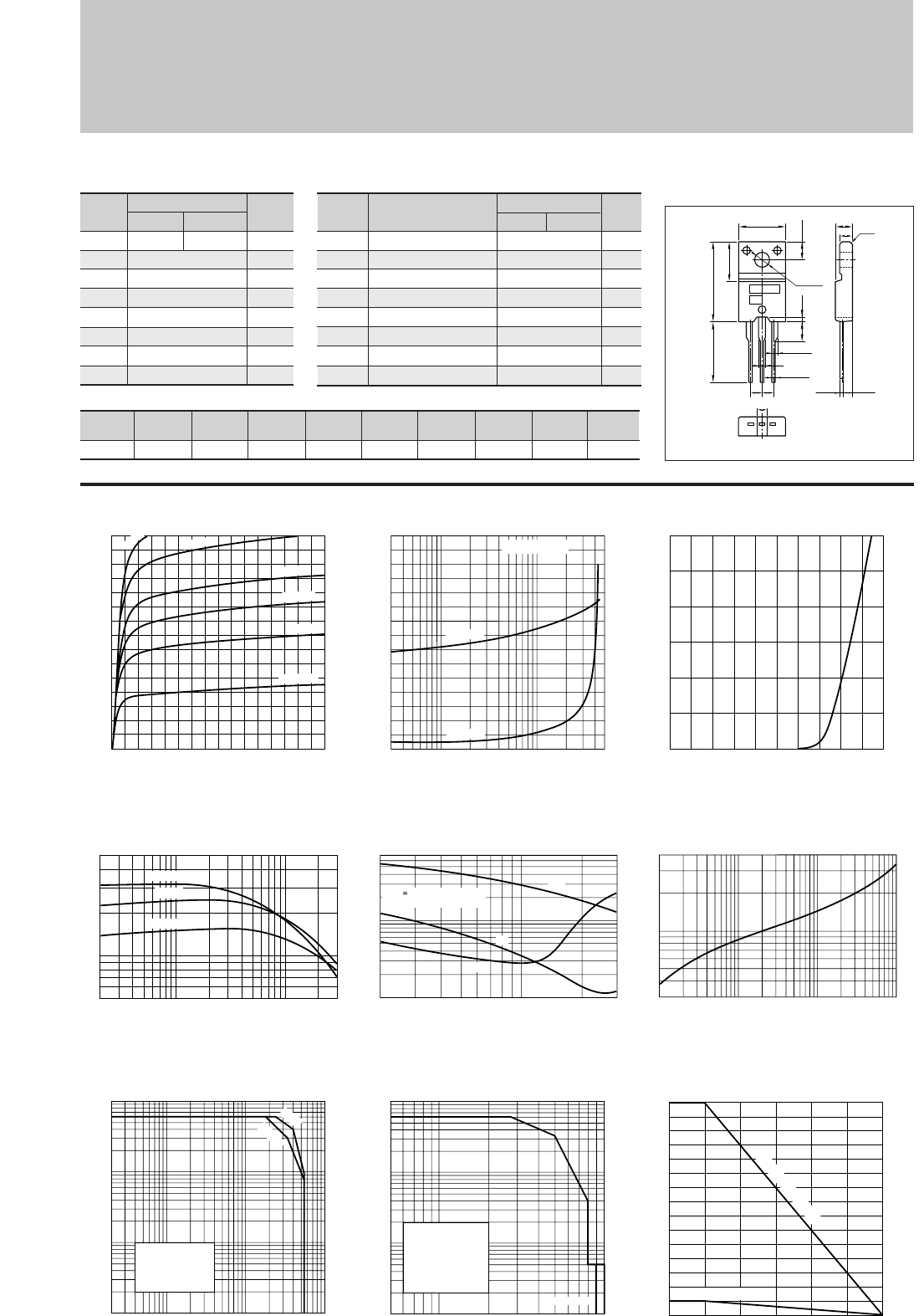
113
Silicon NPN Triple Diffused Planar Transistor (High Voltage Switchihg Transistor)
Application : Switching Regulator and General Purpose
Symbol
VCBO
VCEO
VEBO
IC
IB
PC
Tj
Tstg
2SC4517 2SC4517A
900 1000
550
7
3(Pulse6)
1.5
30(Tc=25°C)
150
–55 to +150
Unit
V
V
V
A
A
W
°C
°C
■
Absolute maximum ratings
■
Electrical Characteristics
Symbol
ICBO
IEBO
V(BR)CEO
hFE
VCE(sat)
VBE(sat)
fT
COB
2SC4517 2SC4517A
100max
100max
550min
10to30
0.5max
1.2max
6typ
35typ
Unit
µ
A
µ
A
V
V
V
MHz
pF
Conditions
VCB=800V
VEB=7V
IC=10mA
VCE=4V, IC=1A
IC=1A, IB=0.2A
IC=1A, IB=0.2A
VCE=12V, IE=–0.25A
VCB=10V, f=1MHz
2SC4517/4517A
(Ta=25°C) (Ta=25°C)
IC–VCE Characteristics
(Typical)
hFE–IC Temperature Characteristics (Typical)
ton•tstg•tf–IC Characteristics
(Typical)
θj-a–t Characteristics
IC–VBE Temperature Characteristics
(Typical)
VCE(sat),VBE(sat)–IC Temperature Characteristics (Typical)
Pc–Ta Derating
Reverse Bias Safe Operating Area
Safe Operating Area (Single Pulse)
0.03
0.1
0.05
150.5
0
1.5
1.0
0.5
Collector-Emitter Saturation Voltage VCE(sat)(V)
Base-Emitter Saturation Voltage VBE(sat)(V)
Collector Current IC(A)
VBE(sat)
VCE(sat)
IC/IB=5 Const.
0.2 10.5 3
0.1
0.5
5
7
1
Switching Time ton•tstg•tf(µs)
Collector Current IC(A)
tstg
ton
tf
VCC 250V
IC:IB1:IB2=1:0.15:–0.45
0.3
1
4
0.5
1 10 100 1000
Time t(ms)
Transient Thermal Resistance θj-a(˚C/W)
30
20
10
2
00 25 50 75 100 125 150
Ambient Temperature Ta(˚C)
Maximum Power Dissipation PC(W)
With Infinite heatsink
Without Heatsink
50 500 1000100
1
0.5
0.1
0.01
0.05
10
5
Collector-Emitter Voltage VCE(V)
Collector Current IC(A)
Without Heatsink
Natural Cooling
L=3mH
IB2=–1.0A
Duty:less than 1%
2SC4517 2SC4517A
10 5052 100 1000500
0.05
0.01
1
0.5
0.1
10
5
Collector-Emitter Voltage VCE(V)
Collector Current IC(A)
100µs
50µs
Without Heatsink
Natural Cooling
0.02 0.10.05 1 30.5
5
10
50
Collector Current IC(A)
DC Current Gain hFE
(VCE=4V)
125˚C
25˚C
–55˚C
0
3
1
2
0 0.4 0.6 0.8 1.00.2
Base-Emittor Voltage VBE(V)
Collector Current IC(A)
(VCE=4V)
0
0
2
1
3
2134
Collector-Emitter Voltage VCE(V)
Collector Current IC(A)
300mA
400mA
200mA
150mA
100mA
I
B
=40mA
■Typical Switching Characteristics (Common Emitter)
VCC
(V)
250
RL
(Ω)
250
IC
(A)
1
VBB2
(V)
–5
IB2
(A)
–0.45
ton
(
µ
s)
0.7max
tstg
(
µ
s)
4max
tf
(
µ
s)
0.5max
IB1
(A)
0.15
VBB1
(V)
10
External Dimensions FM20(TO220F)
ø3.3±0.2
10.1±0.2
4.0±0.2
16.9±0.3
13.0min
8.4±0.2
0.8±0.2
3.9
±0.2
2.542.54
1.35±0.15
0.85
+0.2
-0.1
1.35±0.15
2.2±0.2
4.2±0.2
2.8 c0.5
2.4±0.2
0.45
+0.2
-0.1
BEC
a
b
Weight : Approx 2.0g
a. Part No.
b. Lot No.
Ratings Ratings
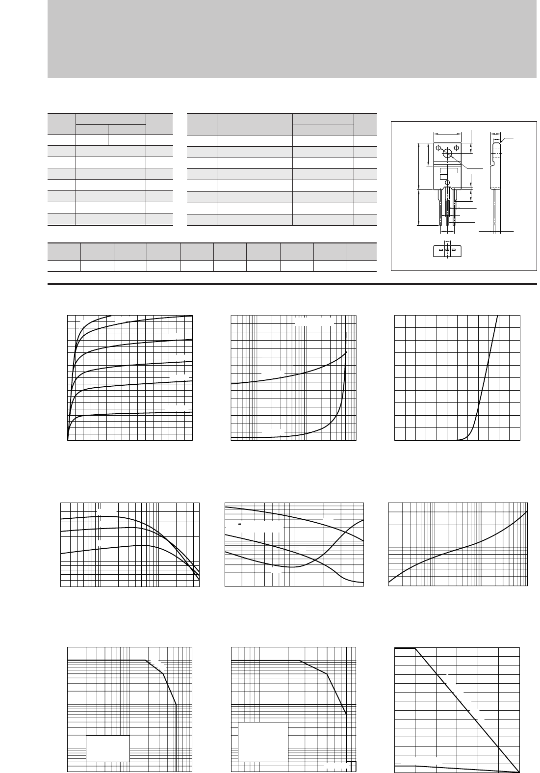
114
Silicon NPN Triple Diffused Planar Transistor (High Voltage Switchihg Transistor)
Application : Switching Regulator, Lighting Inverter and General Purpose
2SC4518/4518A
IC–VCE Characteristics
(Typical)
hFE–IC Temperature Characteristics (Typical)
ton•tstg•tf–IC Characteristics
(Typical)
θj-a–t Characteristics
IC–VBE Temperature Characteristics
(Typical)
VCE(sat),VBE(sat)–IC Temperature Characteristics (Typical)
Collector-Emitter Saturation Voltage VCE(sat)(V)
Base-Emitter Saturation Voltage VBE(sat)(V)
Pc–Ta Derating
Reverse Bias Safe Operating Area
Safe Operating Area (Single Pulse)
0.03
0.1
0.05
11050.5
0
1.5
1.0
0.5
Collector Current IC(A)
VBE(sat)
VCE(sat)
IC/IB=5 Const.
0.2 10.5 5
0.1
0.5
5
7
1
Switching Time ton•tstg•tf(µs)
Collector Current IC(A)
tstg
ton
tf
VCC 250V
IC:IB1:IB2=1:0.15:–0.5
35
30
20
10
2
00 25 50 75 100 125 150
Ambient Temperature Ta(˚C)
Maximum Power Dissipation PC(W)
With Infinite heatsink
Without Heatsink
50 500 1000100
1
5
0.5
0.1
0.03
0.05
20
10
Collector-Emitter Voltage VCE(V)
Collector Current IC(A)
Without Heatsink
Natural Cooling
L=3mH
IB2=–1.0A
Duty:less than 1%
2SC4518 2SC4518A
10 50 100 500 1000
1
0.5
0.03
0.05
0.1
10
20
5
Collector-Emitter Voltage VCE(V)
Collector Current IC(A)
Without Heatsink
Natural Cooling
100µs
0.02 0.10.05 1 50.5
5
10
50
Collector Current IC(A)
DC Current Gain hFE
(VCE=4V)
125˚C
25˚C
–55˚C
0
5
1
2
3
4
0 1.20.4 0.6 0.8 1.00.2
Base-Emittor Voltage VBE(V)
Collector Current IC(A)
(VCE=4V)
0.3
1
4
0.5
1 10 100 1000
Time t(ms)
Transient Thermal Resistance θj-a(˚C/W)
0
0
2
1
5
3
4
2134
Collector-Emitter Voltage VCE(V)
Collector Current IC(A)
600mA
700mA
400mA
150mA
250mA
IB=50mA
■Typical Switching Characteristics (Common Emitter)
VCC
(V)
250
RL
(Ω)
139
IC
(A)
1.8
VBB2
(V)
–5
IB2
(A)
–0.9
ton
(
µ
s)
0.7max
tstg
(
µ
s)
4max
tf
(
µ
s)
0.5max
IB1
(A)
0.27
VBB1
(V)
10
Symbol
VCBO
VCEO
VEBO
IC
IB
PC
Tj
Tstg
2SC4518 2SC4518A
900 1000
550
7
5(Pulse10)
2.5
35(Tc=25°C)
150
–55 to +150
Unit
V
V
V
A
A
W
°C
°C
■
Absolute maximum ratings
■
Electrical Characteristics
Symbol
ICBO
IEBO
V(BR)CEO
hFE
VCE(sat)
VBE(sat)
fT
COB
2SC4518 2SC4518A
100max
100max
550min
10to25
0.5max
1.2max
6typ
50typ
Unit
µ
A
µ
A
V
V
V
MHz
pF
Conditions
VCB=800V
VEB=7V
IC=10mA
VCE=4V, IC=1.8A
IC=1.8A, IB=0.36A
IC=1.8A, IB=0.36A
VCE=12V, IE=–0.35A
VCB=10V, f=1MHz
(Ta=25°C) (Ta=25°C)
External Dimensions FM20(TO220F)
ø3.3±0.2
10.1±0.2
4.0±0.2
16.9±0.3
13.0min
8.4±0.2
0.8±0.2
3.9
±0.2
2.542.54
1.35±0.15
0.85
+0.2
-0.1
1.35±0.15
2.2±0.2
4.2±0.2
2.8 c0.5
2.4±0.2
0.45
+0.2
-0.1
BEC
a
b
Weight : Approx 2.0g
a. Part No.
b. Lot No.
Ratings Ratings
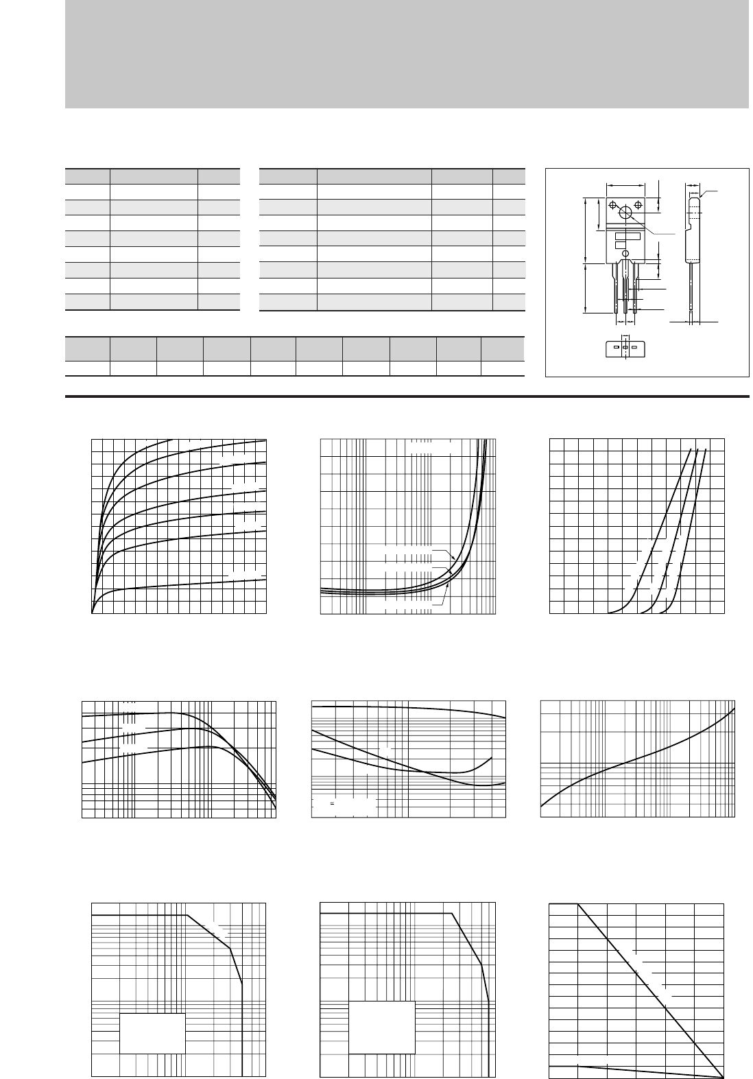
115
Silicon NPN Triple Diffused Planar Transistor (High Voltage and Ultra-high Speed Switchihg Transistor)
Application : Switching Regulator, Lighting Inverter and General Purpose
Symbol
VCBO
VCEO
VEBO
IC
IB
PC
Tj
Tstg
Ratings
600
400
7
7(Pulse14)
2
30(Tc=25°C)
150
–55 to +150
Unit
V
V
V
A
A
W
°C
°C
■
Absolute maximum ratings
■
Electrical Characteristics
Symbol
ICBO
IEBO
V(BR)CEO
hFE
VCE(sat)
VBE(sat)
fT
COB
Ratings
100max
100max
400min
10to25
0.7max
1.3max
10typ
55typ
Unit
µ
A
µ
A
V
V
V
MHz
pF
Conditions
VCB=600V
VEB=7V
IC=25mA
VCE=4V, IC=3A
IC=3A, IB=0.6A
IC=3A, IB=0.6A
VCE=12V, IE=–0.5A
VCB=10V, f=1MHz
2SC4546
(Ta=25°C) (Ta=25°C)
IC–VCE Characteristics
(Typical)
hFE–IC Temperature Characteristics (Typical)
ton•tstg•tf–IC Characteristics
(Typical)
θj-a–t Characteristics
IC–VBE Temperature Characteristics
(Typical)
VCE(sat)–IC Characteristics (Typical)
Pc–Ta Derating
Reverse Bias Safe Operating Area
Safe Operating Area (Single Pulse)
0.02 0.05
0.1 0.5 1 105
0
0.5
1.0
Collector Current IC(A)
IC/IB=5 Const.
125˚C (Case Temp)
25˚C (Case Temp)
–30˚C (Case Temp)
Collector-Emitter Saturation Voltage VCE(sat)(V)
0
7
6
5
4
3
2
1
0 1.00.5
Base-Emittor Voltage VBE(V)
Collector Current IC(A)
(VCE=4V)
125˚C (Case Temp)
25˚C (Case Temp)
–30˚C (Case Temp)
0.2 10.5 5
0.02
0.1
0.05
0.5
2
1
Switching Time ton•tstg•tf(µs)
Collector Current IC(A)
tstg
ton
tf
VCC 200V
IC:IB1:IB2=5:1:–2 0.3
1
4
0.5
1 10 100 1000
Time t(ms)
Transient Thermal Resistance θj-a(˚C/W)
30
20
10
2
00 25 50 75 100 125 150
Ambient Temperature Ta(˚C)
Maximum Power Dissipation PC(W)
With Infinite heatsink
Without Heatsink
10 50 700500100
1
0.5
0.1
10
20
5
Collector-Emitter Voltage VCE(V)
Collector Current IC(A)
Without Heatsink
Natural Cooling
L=3mH
IB2=–0.5A
Duty:less than 1%
10 50 100 700500
1
0.5
0.1
10
20
5
Collector-Emitter Voltage VCE(V)
Collector Current IC(A)
100µs
Without Heatsink
Natural Cooling
0.02 0.10.05 1 750.5
5
10
50
Collector Current IC(A)
DC Current Gain hFE
(VCE=4V)
125˚C
25˚C
–30˚C
0
0
2
1
7
3
4
5
6
2134
Collector-Emitter Voltage VCE(V)
Collector Current IC(A)
1A
800mA
400mA
600mA
300mA
200mA
IB=50mA
■Typical Switching Characteristics (Common Emitter)
VCC
(V)
200
RL
(Ω)
67
IC
(A)
3
VBB2
(V)
–5
IB2
(A)
–1.2
ton
(
µ
s)
0.5max
tstg
(
µ
s)
2max
tf
(
µ
s)
0.15max
IB1
(A)
0.6
VBB1
(V)
10
External Dimensions FM20(TO220F)
ø3.3±0.2
10.1±0.2
4.0±0.2
16.9±0.3
13.0min
8.4±0.2
0.8±0.2
3.9
±0.2
2.542.54
1.35±0.15
0.85
+0.2
-0.1
1.35±0.15
2.2±0.2
4.2±0.2
2.8 c0.5
2.4±0.2
0.45
+0.2
-0.1
BEC
a
b
Weight : Approx 2.0g
a. Part No.
b. Lot No.
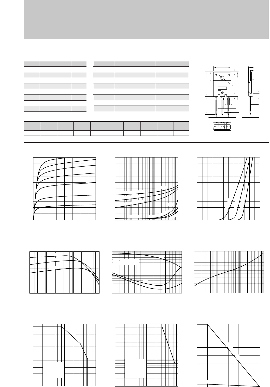
116
Silicon NPN Triple Diffused Planar Transistor (High Voltage Switchihg Transistor)
Application : Switching Regulator and General Purpose
Symbol
VCBO
VCEO
VEBO
IC
IB
PC
Tj
Tstg
Ratings
900
550
7
10(Pulse20)
5
80(Tc=25°C)
150
–55 to +150
Unit
V
V
V
A
A
W
°C
°C
■
Absolute maximum ratings
■
Electrical Characteristics
Symbol
ICBO
IEBO
V(BR)CEO
hFE
VCE(sat)
VBE(sat)
fT
COB
Ratings
100max
100max
550min
10to28
0.5max
1.2max
6typ
105typ
Unit
µ
A
µ
A
V
V
V
MHz
pF
Conditions
VCB=800V
VEB=7V
IC=10mA
VCE=4V, IC=5A
IC=5A, IB=1A
IC=5A, IB=1A
VCE=12V, IE=–1A
VCB=10V, f=1MHz
2SC4557
(Ta=25°C) (Ta=25°C)
IC–VCE Characteristics
(Typical)
hFE–IC Temperature Characteristics (Typical)
ton•tstg•tf–IC Characteristics
(Typical)
θj-a–t Characteristics
IC–VBE Temperature Characteristics
(Typical)
VCE(sat),VBE(sat)–IC Temperature Characteristics (Typical)
Pc–Ta Derating
Reverse Bias Safe Operating Area
Safe Operating Area (Single Pulse)
0
0
2
4
6
8
10
2134
Collector-Emitter Voltage VCE(V)
Collector Current IC(A)
1A
600mA
800mA
400mA
200mA
1.2A
I
B
=100mA
0.1
0.050.02
15100.5
0
2
1
Collector-Emitter Saturation Voltage VCE(sat)(V)
Base-Emitter Saturation Voltage VBE(sat)(V)
(IC/IB=5)
Collector Current IC(A)
VBE(sat)
125˚C (Case Temp)
25˚C (Case Temp)
–55˚C (Case Temp)
25˚C
–55˚C
VCE(sat)
1
2
5
˚
C
(
C
a
s
e
T
e
m
p
)
0.2 10.5 105
0.1
0.5
5
10
1
Switching Time ton•tstg•tf(µs)
Collector Current IC(A)
tstg
ton
tf
VCC 250V
IC:IB1:–IB2=10:1.5:3
0.1
1
2
0.5
1 10 100 1000
Time t(ms)
Transient Thermal Resistance θj-a(˚C/W)
80
60
40
20
3.5
00 25 50 75 100 125 150
Ambient Temperature Ta(˚C)
Maximum Power Dissipation PC(W)
With Infinite heatsink
Without Heatsink
100 50010 50 1000
1
0.5
0.1
10
20
5
Collector-Emitter Voltage VCE(V)
Collector Current IC(A)
Without Heatsink
Natural Cooling
L=3mH
IB2=–1.0A
Duty:less than 1%
10 50 100 500 1000
0.1
1
0.5
10
20
5
Collector-Emitter Voltage VCE(V)
Collector Current IC(A)
100µs
Without Heatsink
Natural Cooling
0
10
4
2
8
6
0 1.20.4 0.6 0.8 1.00.2
Base-Emittor Voltage VBE(V)
Collector Current IC(A)
(VCE=4V)
125˚C (Case Temp)
–55˚C (Case Temp)
0.02 0.10.05 1 1050.5
5
10
50
Collector Current IC(A)
DC Current Gain hFE
(VCE=4V)
125˚C
25˚C
–55˚C
25˚C (Case Temp)
■Typical Switching Characteristics (Common Emitter)
VCC
(V)
250
RL
(Ω)
50
IC
(A)
5
VBB2
(V)
–5
IB2
(A)
–1.5
ton
(
µ
s)
1max
tstg
(
µ
s)
5max
tf
(
µ
s)
0.5max
IB1
(A)
0.75
VBB1
(V)
10
External Dimensions FM100(TO3PF)
4.41.5 1.5
BEC
5.45±0.1
ø3.3±0.2
1.6
3.3
1.75
0.8±0.2
2.15
1.05
+0.2
-0.1
5.45±0.1
23.0±0.3
16.2
9.5±0.2
5.5
15.6±0.2 5.5±0.2
3.45
3.35
0.65
+0.2
-0.1
±0.2
3.0
0.8
a
b
Weight : Approx 2.0g
a. Part No.
b. Lot No.
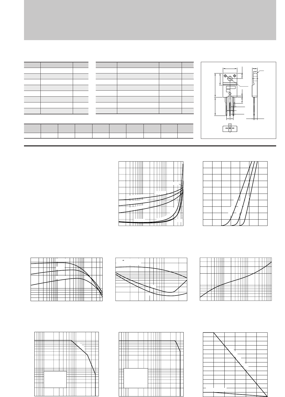
117
Silicon NPN Triple Diffused Planar Transistor (High Voltage and High Speed Switchihg Transistor)
Application : Switching Regulator and General Purpose
Symbol
VCBO
VCEO
VEBO
IC
IB
PC
Tj
Tstg
Ratings
500
400
10
5(Pulse10)
2
30(Tc=25°C)
150
–55 to +150
Unit
V
V
V
A
A
W
°C
°C
■
Absolute maximum ratings
■
Electrical Characteristics
Symbol
ICBO
IEBO
V(BR)CEO
hFE
VCE(sat)
VBE(sat)
fT
COB
Ratings
100max
100max
400min
10to30
0.5max
1.3max
20typ
30typ
Unit
µ
A
µ
A
V
V
V
MHz
pF
Conditions
VCB=500V
VEB=10V
IC=25mA
VCE=4V, IC=1.5A
IC=1.5A, IB=0.3A
IC=1.5A, IB=0.3A
VCE=12V, IE=–0.3A
VCB=10V, f=1MHz
(Ta=25°C) (Ta=25°C)
IC–VCE Characteristics
(Typical)
hFE–IC
Temperature Characteristics (Typical)
ton•tstg•tf–IC Characteristics
(Typical)
θj-a–t Characteristics
IC–VBE Temperature Characteristics
(Typical)
VCE(sat),VBE(sat)–IC Temperature Characteristics (Typical)
Collector-Emitter Saturation Voltage VCE(sat)(V)
Base-Emitter Saturation Voltage VBE(sat)(V)
Pc–Ta Derating
Reverse Bias Safe Operating Area
Safe Operating Area (Single Pulse)
0.1
0.050.01
150.5
0
2
1
(IC/IB=5)
Collector Current IC(A)
VBE(sat)
125˚C (Case Temp)
25˚C (Case Temp)
–55˚C (Case Temp)
25˚C
–55˚C
VCE(sat)
1
2
5
˚
C
(
C
a
s
e
T
e
m
p
)
0.1 10.5 3
0.1
0.5
3
1
Switching Time ton•tstg•tf(µs)
Collector Current IC(A)
tstg
ton
tf
VCC 200V
IC:IB1:IB2=10:1:–2
0.4
1
5
0.5
1 10 100 1000
Time t(ms)
Transient Thermal Resistance θj-a(˚C/W)
30
20
10
2
00 25 50 75 100 125 150
Ambient Temperature Ta(˚C)
Maximum Power Dissipation PC(W)
With Infinite heatsink
Without Heatsink
10 505 500100
1
0.5
0.1
10
20
5
Collector-Emitter Voltage VCE(V)
Collector Current IC(A)
Without Heatsink
Natural Cooling
L=3mH
IB2=–0.5A
Duty:less than 1%
10 505 100 500
0.1
1
0.5
10
20
5
Collector-Emitter Voltage VCE(V)
Collector Current IC(A)
100µs
Without Heatsink
Natural Cooling
0.01 0.10.05 1 50.5
5
10
50
Collector Current IC(A)
DC Current Gain hFE
(VCE=4V)
125˚C
25˚C
–55˚C
0
2
1
4
3
5
0 1.41.20.4 0.6 0.8 1.00.2
Base-Emittor Voltage VBE(V)
Collector Current IC(A)
(VCE=4V)
125˚C (Case Temp)
–55˚C (Case Temp)
25˚C (Case Temp)
■Typical Switching Characteristics (Common Emitter)
VCC
(V)
200
RL
(Ω)
133
IC
(A)
1.5
VBB2
(V)
–5
IB2
(A)
–0.3
ton
(
µ
s)
1max
tstg
(
µ
s)
2.5max
tf
(
µ
s)
0.5max
IB1
(A)
0.15
VBB1
(V)
10
External Dimensions FM20(TO220F)
ø3.3±0.2
10.1±0.2
4.0±0.2
16.9±0.3
13.0min
8.4±0.2
0.8±0.2
3.9
±0.2
2.542.54
1.35±0.15
0.85
+0.2
-0.1
1.35±0.15
2.2±0.2
4.2±0.2
2.8 c0.5
2.4±0.2
0.45
+0.2
-0.1
BEC
a
b
Weight : Approx 2.0g
a. Part No.
b. Lot No.
2SC4662
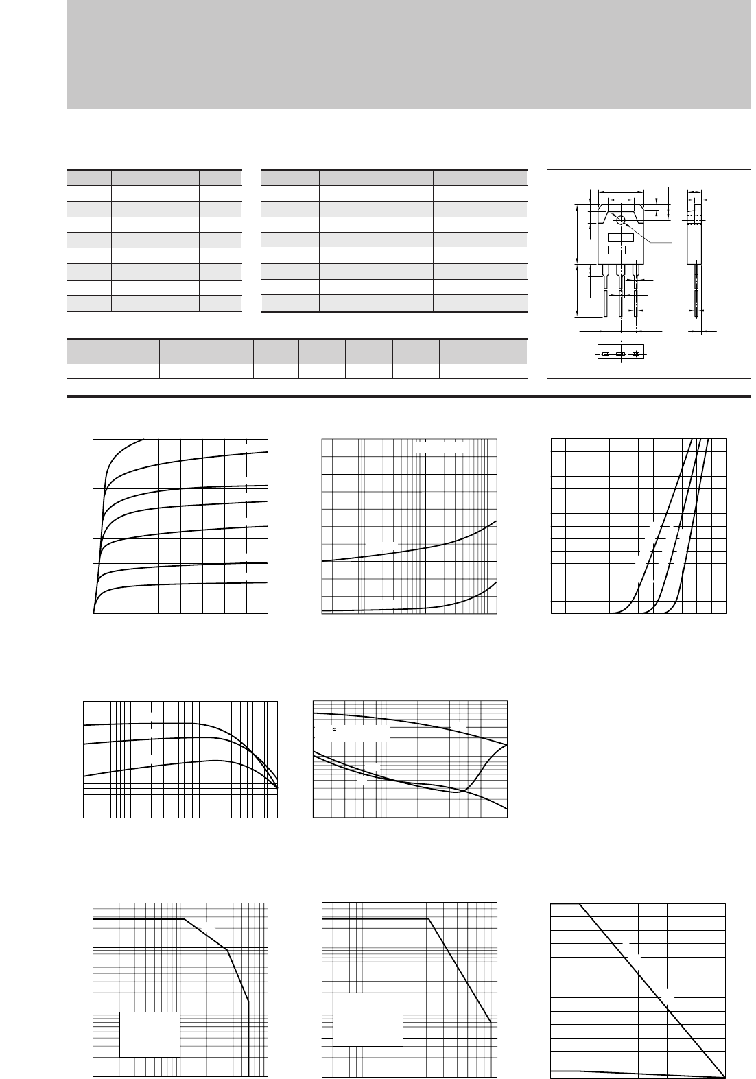
118
Silicon NPN Triple Diffused Planar Transistor (High Voltage Switchihg Transistor)
Application : Switching Regulator and General Purpose
Symbol
VCBO
VCEO
VEBO
IC
IB
PC
Tj
Tstg
Ratings
900
600
7
14(Pulse28)
7
130(Tc=25°C)
150
–55to+150
Unit
V
V
V
A
A
W
°C
°C
■
Absolute maximum ratings
■
Electrical Characteristics
Symbol
ICBO
IEBO
V(BR)CEO
hFE
VCE(sat)
VBE(sat)
fT
COB
Ratings
100max
100max
600min
10to25
0.5max
1.2max
6typ
160typ
Unit
µ
A
µ
A
V
V
V
MHz
pF
Conditions
VCB=800V
VEB=7V
IC=10mA
VCE=4V, IC=7A
IC=7A, IB=1.4A
IC=7A, IB=1.4A
VCE=12V, IE=–1.5A
VCB=10V, f=1MHz
2SC4706
(Ta=25°C) (Ta=25°C)
IC–VCE Characteristics
(Typical)
hFE–IC Temperature Characteristics (Typical)
ton•tstg•tf–IC Characteristics
(Typical)
θj-a–t Characteristics
IC–VBE Temperature Characteristics
(Typical)
VCE(sat),VBE(sat)–IC Temperature Characteristics (Typical)
Pc–Ta Derating
Reverse Bias Safe Operating Area
Safe Operating Area (Single Pulse)
0
0
2
4
6
8
12
10
14
2134
Collector-Emitter Voltage VCE(V)
Collector Current IC(A)
600mA
800mA
1.2A
400mA
200mA
I
B
=100mA
1.6A
Collector-Emitter Saturation Voltage VCE(sat)(V)
Base-Emitter Saturation Voltage VBE(sat)(V)
0.02
0.1
0.05
11050.5
0
2
1
Collector Current IC(A)
VBE(sat)
VCE(sat)
IC/IB=5 Const.
10.2 0.5 10 145
0.1
0.5
5
8
1
Switching Time ton•tstg•tf(µs)
Collector Current IC(A)
tstg
ton
tf
VCC 250V
IC:IB1:–IB2=10:1.5:5
130
100
50
3.5
0
Ambient Temperature Ta(˚C)
Maximum Power Dissipation PC(W)
With Infinite heatsink
Without Heatsink
0 25 50 75 100 125 150
100 50050 1000
1
0.5
0.1
10
50
5
Collector-Emitter Voltage VCE(V)
Collector Current IC(A)
Without Heatsink
Natural Cooling
L=3mH
IB2=–1.0A
Duty:less than 1%
10 50 100 500 1000
10
1
0.5
0.1
50
Collector-Emitter Voltage VCE(V)
Collector Current IC(A)
Without Heatsink
Natural Cooling
100µs
0
14
12
10
4
2
8
6
0 1.20.4 0.6 0.8 1.00.2
Base-Emittor Voltage VBE(V)
Collector Current IC(A)
(VCE=4V)
125˚C (Case Temp)
–55˚C (Case Temp)
25˚C (Case Temp)
0.02 0.10.05 1 141050.5
5
10
50
Collector Current IC(A)
DC Current Gain hFE
(VCE=4V)
125˚C
25˚C
–55˚C
■Typical Switching Characteristics (Common Emitter)
VCC
(V)
250
RL
(Ω)
35.7
IC
(A)
7
VBB2
(V)
–5
IB2
(A)
–3.5
ton
(
µ
s)
1max
tstg
(
µ
s)
5max
tf
(
µ
s)
0.7max
IB1
(A)
1.05
VBB1
(V)
10
External Dimensions MT-100(TO3P)
15.6±0.4
9.6
19.9±0.3
4.0 2.0
5.0±0.2
1.8
ø3.2±0.1
2
3
1.05
+0.2
-0.1
20.0min
4.0max
BE
5.45±0.1 5.45±0.1
C
4.8±0.2
0.65
+0.2
-0.1
1.4
2.0±0.1
a
b
Weight : Approx 6.0g
a. Part No.
b. Lot No.
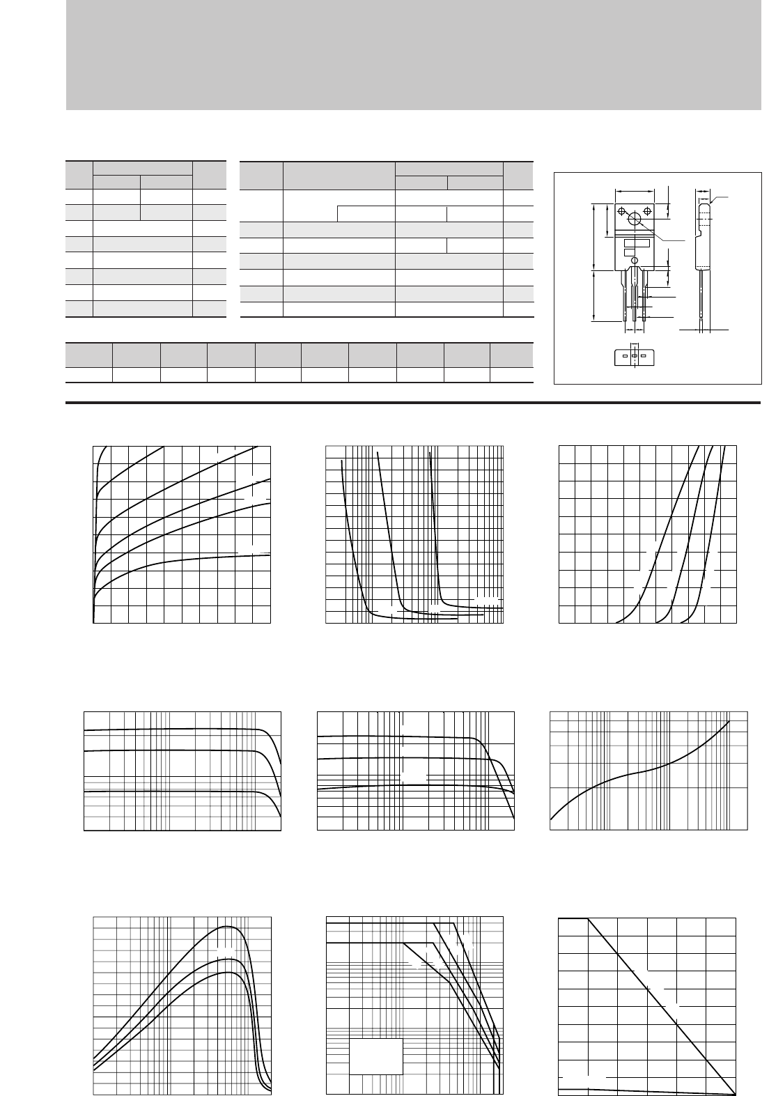
119
2SC4883/4883A
IC–VCE Characteristics
(Typical)
hFE–IC Characteristics
(Typical)
hFE–IC
Temperature Characteristics (Typical)
θj-a–t Characteristics
IC–VBE Temperature Characteristics
(Typical)
VCE(sat)–IB Characteristics
(Typical)
Pc–Ta Derating
Safe Operating Area (Single Pulse)
fT–IE Characteristics
(Typical)
0
3
2
1
2
105 10050 1000500
Base Current IB(mA)
Collector-Emitter Saturation Voltage VCE(sat)(V)
0.5A 1A IC=2A
0
2
1
0 1.00.5
Base-Emittor Voltage VBE(V)
Collector Current IC(A)
(VCE=4V)
125˚C (Case Temp)
25˚C (Case Temp)
–55˚C (Case Temp)
1
7
5
1 10 100 1000 2000
Time t(ms)
Transient Thermal Resistance θj-a(˚C/W)
20
10
2
00 25 50 75 100 125 150
Ambient Temperature Ta(˚C)
Maximum Power Dissipation PC(W)
With Infinite heatsink
Without Heatsink
10 505 100 200
0.01
0.1
0.5
1
1
5
0.5
Collector-Emitter Voltage VCE(V)
Collector Current IC(A)
Without Heatsink
Natural Cooling
1.2SC4883
2.2SC4883A
DC
100ms
10ms
1ms
12
0.01 0.1 0.50.05 1 2
50
40
100
300
Collector Current IC(A)
DC Current Gain hFE
(VCE=4V)
Typ
0
0
1
2
462810
Collector-Emitter Voltage VCE(V)
Collector Current IC(A)
30mA
15mA
10mA
I
B
=5mA
100mA 60mA
(VCE=4V)
0.01 0.05 0.5 2
30
50
300
100
0.1
Collector Current IC(A)
DC Current Gain hFE
1
125˚C
25˚C
–55˚C
–0.01 –0.1 –1 –2
0
60
80
100
120
140
40
20
160
Cut-off Frequency fT(MHZ)
(VCE=12V)
Emitter Current IE(A)
Typ
Silicon NPN Epitaxial Planar Transistor (Complement to type 2SA1859/A)
Application : Audio Output Driver and TV Velocity-modulation
ø3.3±0.2
10.1±0.2
4.0±0.2
16.9±0.3
13.0min
8.4±0.2
0.8±0.2
3.9
±0.2
2.542.54
1.35±0.15
0.85
+0.2
-0.1
1.35±0.15
2.2±0.2
4.2±0.2
2.8 c0.5
2.4±0.2
0.45
+0.2
-0.1
BEC
a
b
External Dimensions FM20(TO220F)
Weight : Approx 2.0g
a. Part No.
b. Lot No.
Symbol
VCBO
VCEO
VEBO
IC
IB
PC
Tj
Tstg
6
2
1
20(Tc=25°C)
150
–55 to +150
Unit
V
V
V
A
A
W
°C
°C
■
Absolute maximum ratings
■
Electrical Characteristics
Symbol
ICBO
IEBO
V(BR)CEO
hFE
VCE(sat)
fT
COB
2SC4883
150
150min
Unit
µ
A
V
µ
A
V
V
MHz
pF
Conditions
VCB=
VEB=6V
IC=10mA
VCE=10V, IC=0.7A
IC=0.7A, IB=70mA
VCE=12V, IE=–0.7A
VCB=10V, f=1MHz
(Ta=25°C)
(Ta=25°C)
2SC4883A
180
180
2SC4883
150
150
2SC4883A
180
180min
10max
60to240
1.0max
120typ
30typ
■Typical Switching Characteristics (Common Emitter)
VCC
(V)
20
RL
(Ω)
20
IC
(A)
1
VBB2
(V)
–5
IB2
(mA)
–100
ton
(
µ
s)
0.5typ
tstg
(
µ
s)
1.5typ
tf
(
µ
s)
0.5typ
IB1
(mA)
100
VBB1
(V)
10
10max
Ratings Ratings

120
Silicon NPN Epitaxial Planar Transistor (Complement to type 2SA1860)
Application : Audio and General Purpose
Symbol
VCBO
VCEO
VEBO
IC
IB
PC
Tj
Tstg
Ratings
150
150
5
14
3
80(Tc=25°C)
150
–55 to +150
Unit
V
V
V
A
A
W
°C
°C
■
Absolute maximum ratings
■
Electrical Characteristics
Symbol
ICBO
IEBO
V(BR)CEO
hFE
VCE(sat)
fT
COB
Ratings
100max
100max
150min
50min∗
2.0max
60typ
200typ
Unit
µ
A
µ
A
V
V
MHz
pF
Conditions
VCB=150V
VEB=5V
IC=25mA
VCE=4V, IC=5A
IC=5A, IB=500mA
VCE=12V, IE=–2A
VCB=10V, f=1MHz
LAPT 2SC4886
(Ta=25°C) (Ta=25°C)
IC–VCE Characteristics
(Typical)
hFE–IC Characteristics
(Typical)
hFE–IC
Temperature Characteristics (Typical)
θj-a–t Characteristics
IC–VBE Temperature Characteristics
(Typical)
VCE(sat)–IB Characteristics
(Typical)
Pc–Ta Derating
Safe Operating Area (Single Pulse)
fT–IE Characteristics
(Typical)
0
3
2
1
0 0.2 0.4 0.6 1.00.8
Base Current IB(A)
IC=10A
5A
0
14
10
5
021
Base-Emittor Voltage VBE(V)
Collector Current IC(A)
(VCE=4V)
125˚C (Case Temp)
25˚C
–30˚C (Case Temp)
0.1
1
3
0.5
1 10 100 1000 2000
Time t(ms)
Transient Thermal Resistance θj-a(˚C/W)
80
60
40
20
3.5
005025 75 125100 150
Ambient Temperature Ta(˚C)
Maximum Power Dissipation PC(W)
With Infinite heatsink
Without Heatsink
10 5052 100 200
150
0.05
1
0.5
0.1
10
40
5
Collector-Emitter Voltage VCE(V)
Collector Current IC(A)
Without Heatsink
Natural Cooling
DC
100ms
10ms
1ms
0.02 0.1 0.5 1 5 1410
20
50
100
200
Collector Current IC(A)
DC Current Gain hFE
(VCE=4V)
Typ
0
0
5
14
10
2134
Collector-Emitter Voltage VCE(V)
Collector Current IC(A)
400mA
500mA
600mA
300mA
100mA
150mA
200mA
I
B
=20mA
750mA
(VCE=4V)
0.02 0.5 51
20
50
200
100
0.1 1014
Collector Current IC(A)
DC Current Gain hFE
125˚C
25˚C
–30˚C
–0.02 –0.1 –1 –10
0
20
40
60
80
Cut-off Frequency fT(MHZ)
(VCE=12V)
Emitter Current IE(A)
Typ
50mA
Collector-Emitter Saturation Voltage VCE(sat)(V)
4.41.5 1.5
BEC
5.45±0.1
ø3.3±0.2
1.6
3.3
1.75
0.8±0.2
2.15
1.05
+0.2
-0.1
5.45±0.1
23.0±0.3
16.2
9.5±0.2
5.5
15.6±0.2 5.5±0.2
3.45
3.35
0.65
+0.2
-0.1
±0.2
3.0
0.8
a
b
External Dimensions FM100(TO3PF)
■Typical Switching Characteristics (Common Emitter)
VCC
(V)
60
RL
(Ω)
12
IC
(A)
5
VBB2
(V)
–5
IB2
(A)
–0.5
ton
(
µ
s)
0.26typ
tstg
(
µ
s)
1.5typ
tf
(
µ
s)
0.35typ
IB1
(A)
0.5
VBB1
(V)
10
Weight : Approx 6.5g
a. Part No.
b. Lot No.
∗hFE Rank O(50to100), P(70to140), Y(90to180)
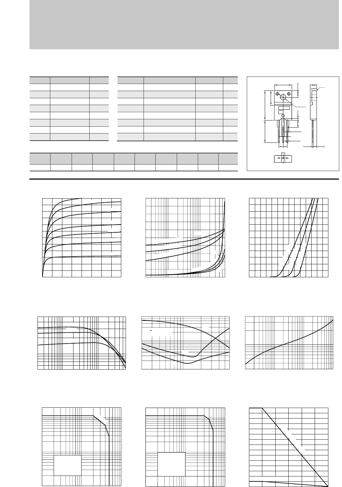
121
Silicon NPN Triple Diffused Planar Transistor (High Voltage and High Speed Switchihg Transistor)
Application : Switching Regulator and General Purpose
Symbol
VCBO
VCEO
VEBO
IC
IB
PC
Tj
Tstg
Ratings
600
500
10
6(Pulse12)
2
30(Tc=25°C)
150
–55 to +150
Unit
V
V
V
A
A
W
°C
°C
■
Absolute maximum ratings
■
Electrical Characteristics
Symbol
ICBO
IEBO
V(BR)CEO
hFE
VCE(sat)
VBE(sat)
fT
COB
Ratings
1max
100max
500min
10to30
0.5max
1.3max
8typ
45typ
Unit
mA
µ
A
V
V
V
MHz
pF
Conditions
VCB=600V
VEB=10V
IC=25mA
VCE=4V, IC=2A
IC=2A, IB=0.4A
IC=2A, IB=0.4A
VCE=12V, IE=–0.5A
VCB=10V, f=1MHz
2SC4907
(Ta=25°C) (Ta=25°C)
IC–VCE Characteristics
(Typical)
hFE–IC Characteristics
(Typical)
ton•tstg•tf–IC Characteristics
(Typical)
θj-a–t Characteristics
IC–VBE Temperature Characteristics
(Typical)
VCE(sat),VBE(sat)–IC Temperature Characteristics (Typical)
Pc–Ta Derating
Reverse Bias Safe Operating Area
Safe Operating Area (Single Pulse)
0
0
2
1
3
4
5
6
2134
Collector-Emitter Voltage VCE(V)
Collector Current IC(A)
600mA
800mA
400mA
300mA
200mA
1A
I
B
=100mA
0.1
0.050.02
150.5
0
2
1
Collector-Emitter Saturation Voltage VCE(sat)(V)
Base-Emitter Saturation Voltage VBE(sat)(V)
(IC/IB=5)
Collector Current IC(A)
VBE(sat)
125˚C (Case Temp)
25˚C (Case Temp)
–55˚C (Case Temp)
25˚C
–55˚C
VCE(sat)
1
2
5
˚
C
(
C
a
s
e
T
e
m
p
)
0.2 10.5 65
0.1
0.5
5
7
1
Switching Time ton•tstg•tf(µs)
Collector Current IC(A)
tstg
ton
tf
VCC 200V
IC:IB1:IB2=10:1:–2
0.3
1
4
0.5
1 10 100 1000
Time t(ms)
Transient Thermal Resistance θj-a(˚C/W)
30
20
10
2
00 25 50 75 100 125 150
Ambient Temperature Ta(˚C)
Maximum Power Dissipation PC(W)
With Infinite heatsink
Without Heatsink
50010010 50 1000
1
0.5
0.1
10
20
5
Collector-Emitter Voltage VCE(V)
Collector Current IC(A)
Without Heatsink
Natural Cooling
L=3mH
IB2=–0.5A
Duty:less than 1%
10 50 100 500 1000
0.1
1
0.5
10
20
5
Collector-Emitter Voltage VCE(V)
Collector Current IC(A)
Without Heatsink
Natural Cooling
100µs
0
6
2
1
4
3
5
0 1.41.20.4 0.6 0.8 1.00.2
Base-Emittor Voltage VBE(V)
Collector Current IC(A)
(VCE=4V)
125˚C (Case Temp)
–55˚C (Case Temp)
0.02 0.10.05 1 650.5
5
10
50
Collector Current IC(A)
DC Current Gain hFE
(VCE=4V)
125˚C
25˚C
–55˚C
25˚C (Case Temp)
■Typical Switching Characteristics (Common Emitter)
VCC
(V)
200
RL
(Ω)
100
IC
(A)
2
VBB2
(V)
–5
IB2
(A)
–0.4
ton
(
µ
s)
1max
tstg
(
µ
s)
4.5max
tf
(
µ
s)
0.5max
IB1
(A)
0.2
VBB1
(V)
10
External Dimensions FM20(TO220F)
ø3.3±0.2
10.1±0.2
4.0±0.2
16.9±0.3
13.0min
8.4±0.2
0.8±0.2
3.9
±0.2
2.542.54
1.35±0.15
0.85
+0.2
-0.1
1.35±0.15
2.2±0.2
4.2±0.2
2.8 c0.5
2.4±0.2
0.45
+0.2
-0.1
BEC
a
b
Weight : Approx 2.0g
a. Part No.
b. Lot No.
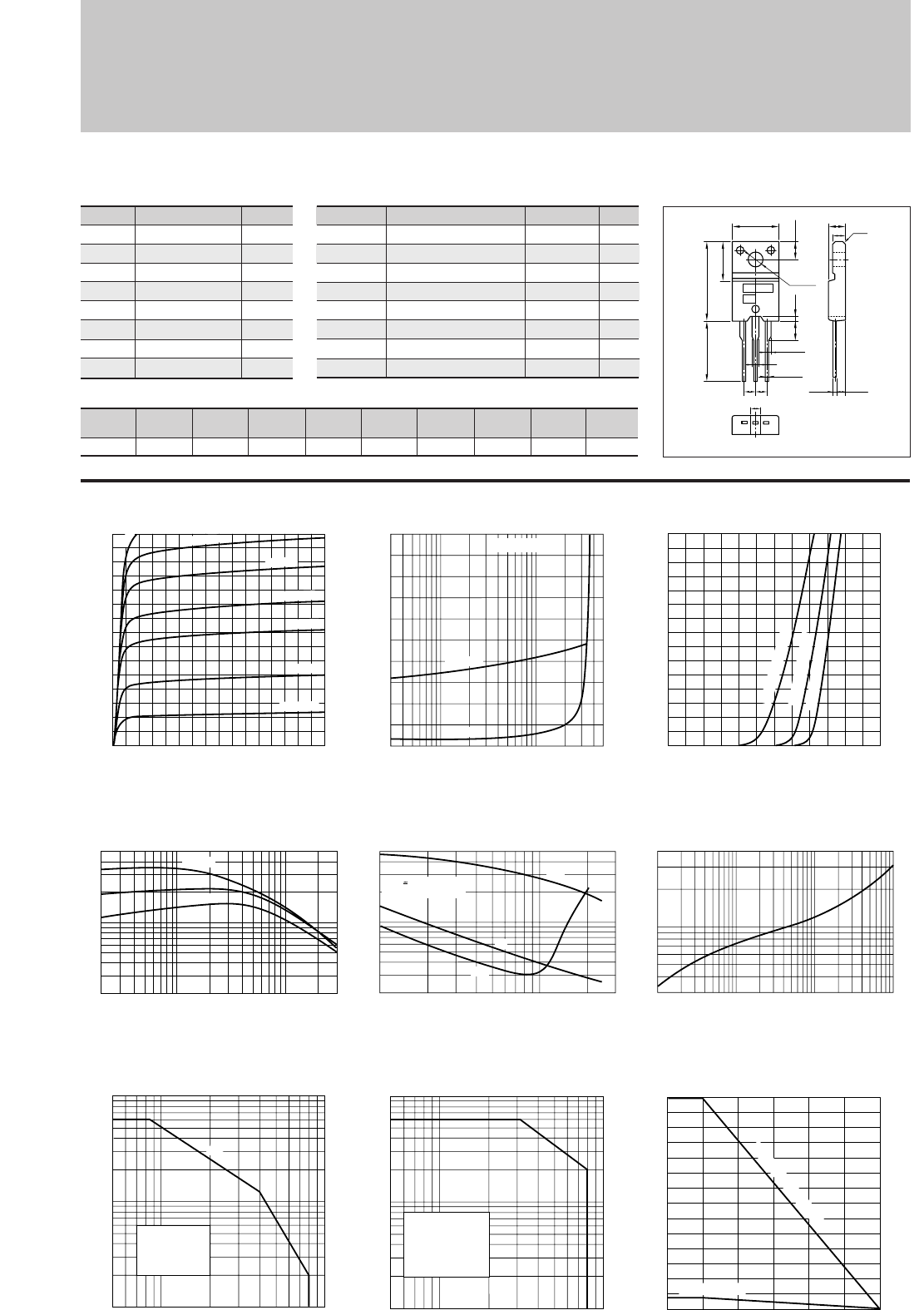
122
Silicon NPN Triple Diffused Planar Transistor (High Voltage Switchihg Transistor)
Application : Switching Regulator and General Purpose
Symbol
VCBO
VCEO
VEBO
IC
IB
PC
Tj
Tstg
Ratings
900
800
7
3(Pulse6)
1.5
35(Tc=25°C)
150
–55 to +150
Unit
V
V
V
A
A
W
°C
°C
■
Absolute maximum ratings
■
Electrical Characteristics
Symbol
ICBO
IEBO
V(BR)CEO
hFE
VCE(sat)
VBE(sat)
fT
COB
Ratings
100max
100max
800min
10to30
0.5max
1.2max
6typ
40typ
Unit
µ
A
µ
A
V
V
V
MHz
pF
Conditions
VCB=800V
VEB=7V
IC=10mA
VCE=4V, IC=0.7A
IC=0.7A, IB=0.14A
IC=0.7A, IB=0.14A
VCE=12V, IE=–0.3A
VCB=10V, f=1MHz
2SC4908
(Ta=25°C) (Ta=25°C)
IC–VCE Characteristics
(Typical)
ton•tstg•tf–IC Characteristics
(Typical)
θj-a–t Characteristics
IC–VBE Temperature Characteristics
(Typical)
VCE(sat),VBE(sat)–IC Temperature Characteristics (Typical)
Pc–Ta Derating
Reverse Bias Safe Operating Area
Safe Operating Area (Single Pulse)
0.03
0.1
0.05
150.5
0
2
1
Collector-Emitter Saturation Voltage VCE(sat)(V)
Base-Emitter Saturation Voltage VBE(sat)(V)
Collector Current IC(A)
VBE(sat)
VCE(sat)
IC/IB=5 Const,
0.02 0.10.05 1 30.5
2
5
10
50
Collector Current IC(A)
DC Current Gain hFE
(VCE=4V)
hFE–IC Characteristics
(Typical)
0.1 10.5 3
0.2
0.5
5
1
Switching Time ton•tstg•tf(µs)
Collector Current IC(A)
tstg
ton
tf
VCC 250V
IC:IB1:IB2=2:0.3:–1
0
3
1
2
0 1.20.4 0.6 0.8 1.00.2
Base-Emittor Voltage VBE(V)
Collector Current IC(A)
(VCE=4V)
125˚C (Case Temp)
25˚C (Case Temp)
–30˚C (Case Temp)
0.3
1
4
0.5
1 10 100 1000
Time t(ms)
Transient Thermal Resistance θj-a(˚C/W)
35
30
20
10
2
00 25 50 75 100 125 150
Ambient Temperature Ta(˚C)
Maximum Power Dissipation PC(W)
With Infinite heatsink
Without Heatsink
100 50050 1000
1
0.5
0.1
10
5
Collector-Emitter Voltage VCE(V)
Collector Current IC(A)
Without Heatsink
Natural Cooling
L=3mH
IB2=–1.0A
Duty:less than 1%
50 100 1000500
1
0.5
0.1
10
5
Collector-Emitter Voltage VCE(V)
Collector Current IC(A)
Without Heatsink
Natural Cooling
100µs
125˚C
25˚C
–30˚C
0
0
2
1
3
2134
Collector-Emitter Voltage VCE(V)
Collector Current IC(A)
400mA
300mA
500mA
200mA
140mA
60mA
I
B
=20mA
■Typical Switching Characteristics (Common Emitter)
VCC
(V)
250
RL
(Ω)
357
IC
(A)
0.7
VBB2
(V)
–5
IB2
(A)
–0.35
ton
(
µ
s)
1max
tstg
(
µ
s)
5max
tf
(
µ
s)
1max
IB1
(A)
0.1
VBB1
(V)
10
External Dimensions FM20(TO220F)
ø3.3±0.2
10.1±0.2
4.0±0.2
16.9±0.3
13.0min
8.4±0.2
0.8±0.2
3.9
±0.2
2.542.54
1.35±0.15
0.85
+0.2
-0.1
1.35±0.15
2.2±0.2
4.2±0.2
2.8 c0.5
2.4±0.2
0.45
+0.2
-0.1
BEC
a
b
Weight : Approx 2.0g
a. Part No.
b. Lot No.
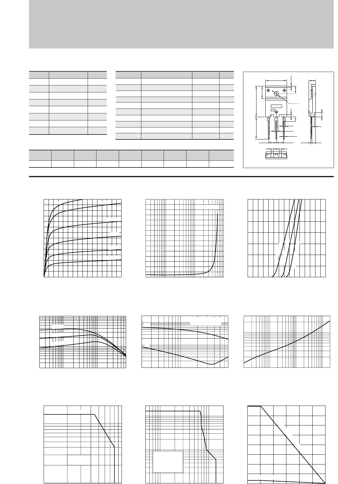
123
Silicon NPN Triple Diffused Planar Transistor (High Voltage Switchihg Transistor)
Application : Display Horizontal Deflection Output, Switching Regulator and General Purpose
Symbol
VCBO
VCEO
VEBO
IC
IB
PC
Tj
Tstg
Ratings
1500
800
6
7(Pulse14)
3.5
80(Tc=25°C)
150
–55 to +150
Unit
V
V
V
A
A
W
°C
°C
■
Absolute maximum ratings
■
Electrical Characteristics
Symbol
ICBO1
ICBO2
IEBO
V(BR)CEO
hFE1
hFE2
VCE(sat)
VBE(sat)
fT
COB
Ratings
100max
1max
100max
800min
8min
4to9
5max
1.5max
4typ
100typ
Unit
µ
A
mA
µ
A
V
V
V
MHz
pF
Conditions
VCB=1200V
VCB=1500V
VEB=6V
IC=10mA
VCE=5V, IC=1A
VCE=5V, IC=5A
IC=5A, IB=1.2A
IC=5A, IB=1.2A
VCE=12V, IE=–0.5A
VCB=10V, f=1MHz
2SC5002
(Ta=25°C) (Ta=25°C)
■Typical Switching Characteristics (Common Emitter)
VCC
(V)
200
RL
(Ω)
50
IC
(A)
4
VBB2
(V)
–5
IB2
(A)
–1.6
tstg
(
µ
s)
4.0max
tf
(
µ
s)
0.2max
IB1
(A)
0.8
VBB1
(V)
10
External Dimensions FM100(TO3PF)
4.41.5 1.5
BEC
5.45±0.1
ø3.3±0.2
1.6
3.3
1.75
0.8±0.2
2.15
1.05
+0.2
-0.1
5.45±0.1
23.0±0.3
16.2
9.5±0.2
5.5
15.6±0.2 5.5±0.2
3.45
3.35
0.65
+0.2
-0.1
±0.2
3.0
0.8
a
b
Weight : Approx 6.5g
a. Part No.
b. Lot No.
hFE–IC Characteristics
(Typical)
IC–VBE Temperature Characteristics
(Typical)
VCE(sat)–IC Characteristics (Typical)
Pc–Ta Derating
0
7
6
4
2
0 1.50.5 1.0
Base-Emittor Voltage VBE(V)
Collector Current IC(A)
(VCE=5V)
125˚C (Case Temp)
25˚C (Case Temp)
–30˚C (Case Temp)
80
60
40
20
3.5
00 50 100 150
Ambient Temperature Ta(˚C)
Maximum Power Dissipation PC(W)
With Infinite heatsink
Without Heatsink
Safe Operating Area (Single Pulse)
500100 1000
1
10
20
5
Collector-Emitter Voltage VCE(V)
Collector Current IC(A)
Without Heatsink
Natural Cooling
0.02 0.10.05 0.5 1 5 7
2
5
10
100
50
Collector Current IC(A)
DC Current Gain hFE
(VCE=5V)
125˚C
25˚C
–30˚C
tstg•tf–IC Characteristics
(Typical)
0.2 1 50.5 7
0.1
0.5
5
20
10
1
Switching Time tstg•tf(µs)
Collector Current IC(A)
tstg
tf
VCC=200V
IC:IB1:–IB2 =5 :1: 2
100µs
0
3
2
1
0.02 0.1 0.5 1 105
Collector Current IC(A)
Collector-Emitter Saturation Voltage VCE(sat)(V)
(IC:IB=5 :1)
Reverse Bias Safe Operating Area
100 50050 20001000
1
0.5
0.1
10
20
5
Collector-Emitter Voltage VCE(V)
Collector Current IC(A)
Without Heatsink
Natural Cooling
L=3mH
–IB2=1A
Duty:less than 1%
Time t(ms)
0.1
1
3
0.5
1 10 100 1000 2000
Transient Thermal Resistance θj-a(˚C/W)
θj-a–t Characteristics
IC–VCE Characteristics
(Typical)
0
0
2
1
7
3
4
5
6
2134
Collector-Emitter Voltage VCE(V)
Collector Current IC(A)
1.5A
1.2A
400mA
700mA
200mA
I
B
=100mA
..
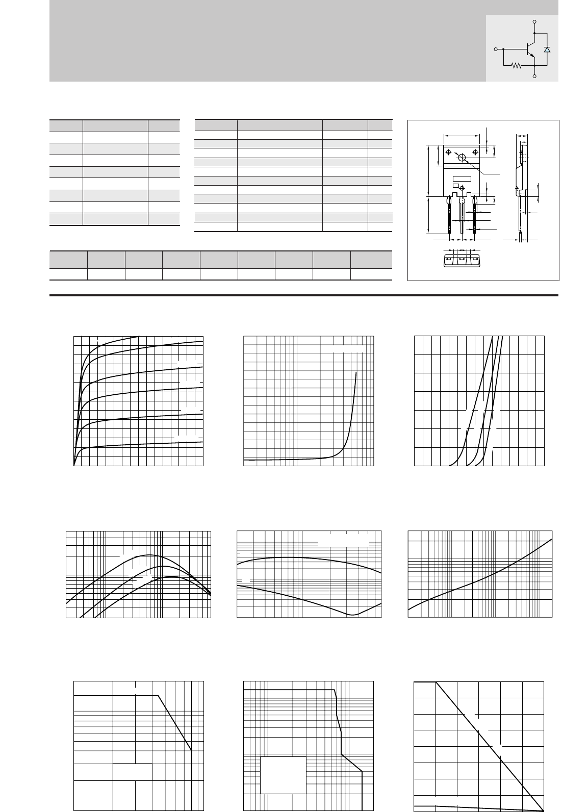
124
Silicon NPN Triple Diffused Planar Transistor (High Voltage Switchihg Transistor)
Application : Display Horizontal Deflection Output, Switching Regulator and General Purpose
Symbol
VCBO
VCEO
VEBO
IC
IB
PC
Tj
Tstg
Ratings
1500
800
6
7(Pulse14)
3.5
80(Tc=25°C)
150
–55 to +150
Unit
V
V
V
A
A
W
°C
°C
■
Absolute maximum ratings
■
Electrical Characteristics
Symbol
ICBO1
ICBO2
ICEO
VEBO
hFE1
hFE2
VCE(sat)
VBE(sat)
VFEC
fT
COB
Ratings
100max
1max
1max
6min
8min
4to9
5max
1.5max
2.0max
4typ
100typ
Unit
µ
A
mA
mA
V
V
V
V
MHz
pF
Conditions
VCB=1200V
VCB=1500V
VCE=800V
IEB=300mA
VCE=5V, IC=1A
VCE=5V, IC=5A
IC=5A, IB=1.2A
IC=5A, IB=1.2A
IEC=7A
VCE=12V, IE=–0.5A
VCB=10V, f=1MHz
2SC5003
(Ta=25°C) (Ta=25°C)
■Typical Switching Characteristics (Common Emitter)
VCC
(V)
200
RL
(Ω)
50
IC
(A)
4
VBB2
(V)
–5
IB2
(A)
–1.6
tstg
(
µ
s)
4.0max
tf
(
µ
s)
0.2max
IB1
(A)
0.8
VBB1
(V)
10
External Dimensions FM100(TO3PF)
4.41.5 1.5
BEC
5.45±0.1
ø3.3±0.2
1.6
3.3
1.75
0.8±0.2
2.15
1.05
+0.2
-0.1
5.45±0.1
23.0±0.3
16.2
9.5±0.2
5.5
15.6±0.2 5.5±0.2
3.45
3.35
0.65
+0.2
-0.1
±0.2
3.0
0.8
a
b
Weight : Approx 6.5g
a. Part No.
b. Lot No.
Built-in Damper Diode
hFE–IC Characteristics
(Typical)
IC–VBE Temperature Characteristics
(Typical)
VCE(sat)–IC Characteristics (Typical)
Pc–Ta Derating
0
3
2
1
0.2 0.5 1 105
Collector Current IC(A)
80
60
40
20
3.5
005025 75 125100 150
Ambient Temperature Ta(˚C)
Maximum Power Dissipation PC(W)
With Infinite heatsink
Without Heatsink
Safe Operating Area (Single Pulse)
500100 1000
1
10
20
5
Collector-Emitter Voltage VCE(V)
Collector Current IC(A)
Without Heatsink
Natural Cooling
Collector-Emitter Saturation Voltage VCE(sat)(V)
(IC:IB=5 :1)
tstg•tf–IC Characteristics
(Typical)
100µs
0
7
6
4
2
0 1.50.5 1.0
Base-Emittor Voltage VBE(V)
Collector Current IC(A)
(VCE=5V)
125˚C (Case Temp)
25˚C (Case Temp)
–30˚C (Case Temp)
0.02 0.10.05 0.5 1 5 7
2
5
10
50
Collector Current IC(A)
DC Current Gain hFE
(VCE=5V)
125˚C
25˚C
–30˚C
0.2 1 50.5 7
0.1
0.5
5
20
10
1
Switching Time tstg•tf(µs)
Collector Current IC(A)
tstg
tf
VCC=200V
IC:IB1: –IB2 =5 :1: 2
Time t(ms)
0.1
1
3
0.5
1 10 100 1000 2000
Transient Thermal Resistance θj-a(˚C/W)
θj-a–t Characteristics
Reverse Bias Safe Operating Area
100 50050 20001000
1
0.5
0.1
10
20
5
Collector-Emitter Voltage VCE(V)
Collector Current IC(A)
Without Heatsink
Natural Cooling
L=3mH
–IB2=1A
Duty:less than 1%
IC–VCE Characteristics
(Typical)
0
0
2
1
7
3
4
5
6
2134
Collector-Emitter Voltage VCE(V)
Collector Current IC(A)
1.7A
1.4A
600mA
900mA
300mA
I
B
=100mA
..
B
C
E
(50Ω)
Equivalent
circuit
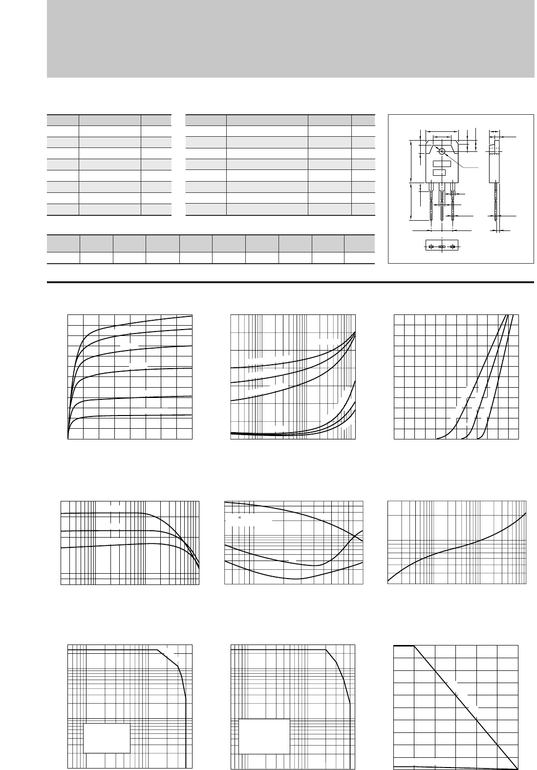
125
Silicon NPN Triple Diffused Planar Transistor (High Voltage and High Speed Switchihg Transistor)
Application : Switching Regulator and General Purpose
Symbol
VCBO
VCEO
VEBO
IC
IB
PC
Tj
Tstg
Ratings
500
400
10
12(Pulse24)
4
100(Tc=25°C)
150
–55 to +150
Unit
V
V
V
A
A
W
°C
°C
■
Absolute maximum ratings
■
Electrical Characteristics
Symbol
ICBO
IEBO
V(BR)CEO
hFE
VCE(sat)
VBE(sat)
fT
COB
Ratings
100max
100max
400min
10to30
0.5max
1.3max
10typ
105typ
Unit
µ
A
µ
A
V
V
V
MHz
pF
Conditions
VCB=500V
VEB=10V
IC=25mA
VCE=4V, IC=7A
IC=7A, IB=1.4A
IC=7A, IB=1.4A
VCE=12V, IE=–1A
VCB=10V, f=1MHz
2SC5071
(Ta=25°C) (Ta=25°C)
IC–VCE Characteristics
(Typical)
hFE–IC Characteristics
(Typical)
ton•tstg•tf–IC Characteristics
(Typical)
θj-a–t Characteristics
IC–VBE Temperature Characteristics
(Typical)
VCE(sat),VBE(sat)–IC Temperature Characteristics (Typical)
Collector-Emitter Saturation Voltage VCE(sat)(V)
Base-Emitter Saturation Voltage VBE(sat)(V)
Pc–Ta Derating
Reverse Bias Safe Operating Area
Safe Operating Area (Single Pulse)
0
0
4
2
6
8
10
12
2134
Collector-Emitter Voltage VCE(V)
Collector Current IC(A)
600mA
400mA
200mA
800mA
1A
IB=100mA
0.02 0.10.05 1 5 100.5
0
1
(IC/IB=5)
Collector Current IC(A)
VBE(sat)
125˚C (Case Temp)
25˚C (Case Temp)
–55˚C (Case Temp)
25˚C
–55˚C
VCE(sat)
1
2
5
˚
C
(
C
a
s
e
T
e
m
p
)
0
12
10
8
6
4
2
0 1.00.5
Base-Emittor Voltage VBE(V)
Collector Current IC(A)
(VCE=4V)
125˚C (Case Temp)
25˚C (Case Temp)
–55˚C (Case Temp)
0.02 0.10.05 1 101250.5
8
10
40
Collector Current IC(A)
DC Current Gain hFE
(VCE=4V)
125˚C
25˚C
–30˚C
10.5 12105
0.1
0.5
5
1
Switching Time ton•tstg•tf(µs)
Collector Current IC(A)
tstg
ton
tf
VCC 200V
IC:IB1:IB2=10:1:–2
100
50
3.5
00 25 50 75 100 125 150
Ambient Temperature Ta(˚C)
Maximum Power Dissipation PC(W)
With Infinite heatsink
Without Heatsink
10 505 500100
1
0.5
0.1
10
30
5
Collector-Emitter Voltage VCE(V)
Collector Current IC(A)
Without Heatsink
Natural Cooling
L=3mH
IB2 =1.0A
Duty:less than 1%
10 505 100 500
1
0.5
0.1
10
30
5
Collector-Emitter Voltage VCE(V)
Collector Current IC(A)
100µs
Without Heatsink
Natural Cooling
0.3
1
3
0.5
1 10 100 1000
Time t(ms)
Transient Thermal Resistance θj-a(˚C/W)
■Typical Switching Characteristics (Common Emitter)
VCC
(V)
200
RL
(Ω)
28.5
IC
(A)
7
VBB2
(V)
–5
IB2
(A)
–1.4
ton
(
µ
s)
1.0max
tstg
(
µ
s)
3.0max
tf
(
µ
s)
0.5max
IB1
(A)
0.7
VBB1
(V)
10
15.6±0.4
9.6
19.9±0.3
4.0 2.0
5.0±0.2
1.8
ø3.2±0.1
2
3
1.05
+0.2
-0.1
20.0min
4.0max
BE
5.45±0.1 5.45±0.1
C
4.8±0.2
0.65
+0.2
-0.1
1.4
2.0±0.1
a
b
External Dimensions MT-100(TO3P)
Weight : Approx 6.0g
a. Part No.
b. Lot No.
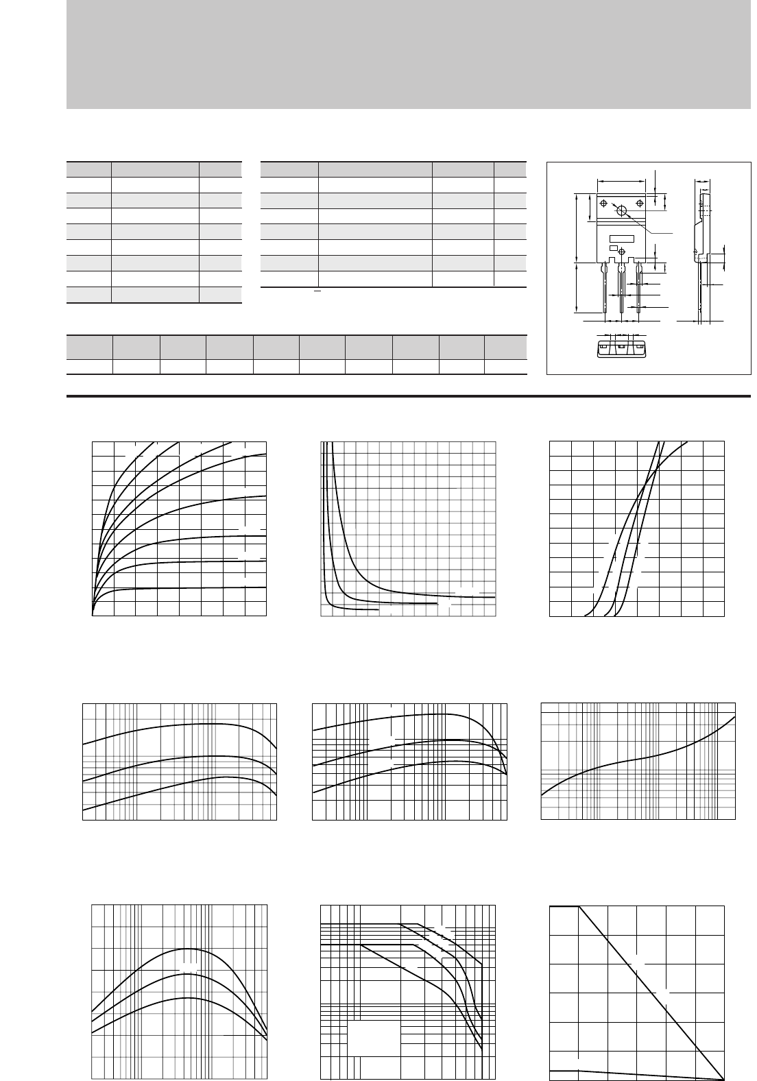
126
2SC5099
IC–VCE Characteristics
(Typical)
hFE–IC Characteristics
(Typical)
hFE–IC
Temperature Characteristics (Typical)
θj-a–t Characteristics
IC–VBE Temperature Characteristics
(Typical)
VCE(sat)–IB Characteristics
(Typical)
Pc–Ta Derating
Safe Operating Area (Single Pulse)
fT–IE Characteristics
(Typical)
0
3
2
1
0 0.5 1.0 1.5
Base Current IB(A)
Collector-Emitter Saturation Voltage VCE(sat)(V)
IC=6A
2A 4A
0
6
4
2
021
Base-Emittor Voltage VBE(V)
Collector Current IC(A)
(VCE=4V)
125˚C (Case Temp)
25˚C (Case Temp)
–30˚C (Case Temp)
0.3
1
5
0.5
1 10 100 1000 2000
Time t(ms)
Transient Thermal Resistance θj-a(˚C/W)
60
40
20
3.5
005025 75 125100 150
Ambient Temperature Ta(˚C)
Maximum Power Dissipation PC(W)
With Infinite heatsink
Without Heatsink
5 10 10050
0.1
1
0.5
10
20
5
Collector-Emitter Voltage VCE(V)
Collector Current IC(A)
Without Heatsink
Natural Cooling
DC
10ms
1ms
100ms
0.02 0.1 1 5 6
30
50
100
300
Collector Current IC(A)
DC Current Gain hFE
(VCE=4V)
Typ
0
0
2
4
6
2134
Collector-Emitter Voltage VCE(V)
Collector Current IC(A)
80mA
50mA
30mA
20mA
150mA
100mA
I
B
=10mA
200mA
(VCE=4V)
0.02 0.50.5 651
20
50
200
100
0.1
Collector Current IC(A)
DC Current Gain hFE
125˚C
25˚C
–30˚C
–0.02 –0.1 –1 –6
0
20
10
40
30
Cut-off Frequency fT(MHZ)
(VCE=12V)
Emitter Current IE(A)
Typ
Silicon NPN Triple Diffused Planar Transistor (Complement to type 2SA1907)
Application : Audio and General Purpose
Symbol
VCBO
VCEO
VEBO
IC
IB
PC
Tj
Tstg
Ratings
120
80
6
6
3
60(Tc=25°C)
150
–55 to +150
Unit
V
V
V
A
A
W
°C
°C
■
Absolute maximum ratings
■
Electrical Characteristics
Symbol
ICBO
IEBO
V(BR)CEO
hFE
VCE(sat)
fT
COB
Ratings
10max
10max
80min
50min∗
0.5max
20typ
110typ
Unit
µ
A
µ
A
V
V
MHz
pF
Conditions
VCB=120V
VEB=6V
IC=50mA
VCE=4V, IC=2A
IC=2A, IB=0.2A
VCE=12V, IE=–0.5A
VCB=10V, f=1MHz
(Ta=25°C) (Ta=25°C)
■Typical Switching Characteristics (Common Emitter)
VCC
(V)
30
RL
(Ω)
10
IC
(A)
3
VBB2
(V)
–5
IB2
(A)
–0.3
ton
(
µ
s)
0.16typ
tstg
(
µ
s)
2.60typ
tf
(
µ
s)
0.34typ
IB1
(A)
0.3
VBB1
(V)
10
4.41.5 1.5
BEC
5.45±0.1
ø3.3±0.2
1.6
3.3
1.75
0.8±0.2
2.15
1.05
+0.2
-0.1
5.45±0.1
23.0±0.3
16.2
9.5±0.2
5.5
15.6±0.2 5.5±0.2
3.45
3.35
0.65
+0.2
-0.1
±0.2
3.0
0.8
a
b
External Dimensions FM100(TO3PF)
Weight : Approx 6.5g
a. Part No.
b. Lot No.
∗hFE Rank O(50to100), P(70to140), Y(90to180)
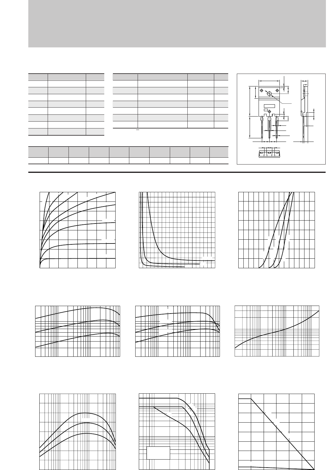
127
2SC5100
IC–VCE Characteristics
(Typical)
hFE–IC Characteristics
(Typical)
hFE–IC
Temperature Characteristics (Typical)
θj-a–t Characteristics
IC–VBE Temperature Characteristics
(Typical)
VCE(sat)–IB Characteristics
(Typical)
Pc–Ta Derating
Safe Operating Area (Single Pulse)
fT–IE Characteristics
(Typical)
0
3
2
1
0 0.2 0.4 0.6 0.8 1.0
Base Current IB(A)
Collector-Emitter Saturation Voltage VCE(sat)(V)
IC=8A
2A 4A
0
8
6
2
4
0 1.51.00.5
Base-Emittor Voltage VBE(V)
Collector Current IC(A)
(VCE=4V)
125˚C (Case Temp)
25˚C (Case Temp)
–30˚C (Case Temp)
0.2
1
4
0.5
1 10 100 1000 2000
Time t(ms)
Transient Thermal Resistance θj-a(˚C/W)
80
60
40
20
3.5
005025 75 125100 150
Ambient Temperature Ta(˚C)
Maximum Power Dissipation PC(W)
With Infinite heatsink
Without Heatsink
DC
Without Heatsink
Natural Cooling
100ms
10ms
105 50 100 150
0.1
1
0.5
10
20
5
Collector-Emitter Voltage VCE(V)
Collector Current IC(A)
0.02 0.1 0.5 1 5 8
20
50
100
200
Collector Current IC(A)
DC Current Gain hFE
(VCE=4V)
Typ
0
0
2
4
6
8
2134
Collector-Emitter Voltage VCE(V)
Collector Current IC(A)
100mA
150mA
200mA
350mA
75mA
50mA
20mA
I
B
=10mA
(VCE=4V)
0.02 0.5 5 81
20
50
200
100
0.1
Collector Current IC(A)
DC Current Gain hFE
125˚C
25˚C
–30˚C
–0.02 –0.1 –1 –8
0
10
20
40
30
Cut-off Frequency fT(MHZ)
(VCE=12V)
Emitter Current IE(A)
Typ
Silicon NPN Triple Diffused Planar Transistor (Complement to type 2SA1908)
Application : Audio and General Purpose
Symbol
VCBO
VCEO
VEBO
IC
IB
PC
Tj
Tstg
Ratings
160
120
6
8
3
75(Tc=25°C)
150
–55 to +150
Unit
V
V
V
A
A
W
°C
°C
■
Absolute maximum ratings
■
Electrical Characteristics
Symbol
ICBO
IEBO
V(BR)CEO
hFE
VCE(sat)
fT
COB
Ratings
10max
10max
120min
50min∗
0.5max
20typ
200typ
Unit
µ
A
µ
A
V
V
MHz
pF
Conditions
VCB=160V
VEB=6V
IC=50mA
VCE=4V, IC=3A
IC=3A, IB=0.3A
VCE=12V, IE=–0.5A
VCB=10V, f=1MHz
(Ta=25°C) (Ta=25°C)
4.41.5 1.5
BEC
5.45±0.1
ø3.3±0.2
1.6
3.3
1.75
0.8±0.2
2.15
1.05
+0.2
-0.1
5.45±0.1
23.0±0.3
16.2
9.5±0.2
5.5
15.6±0.2 5.5±0.2
3.45
3.35
0.65
+0.2
-0.1
±0.2
3.0
0.8
a
b
External Dimensions FM100(TO3PF)
Weight : Approx 6.5g
a. Part No.
b. Lot No.
■Typical Switching Characteristics (Common Emitter)
VCC
(V)
40
RL
(Ω)
10
IC
(A)
4
VBB2
(V)
–5
IB2
(A)
–0.4
ton
(
µ
s)
0.13typ
tstg
(
µ
s)
3.50typ
tf
(
µ
s)
0.32typ
IB1
(A)
0.4
VBB1
(V)
10
∗hFE Rank O(50to100), P(70to140), Y(90to180)
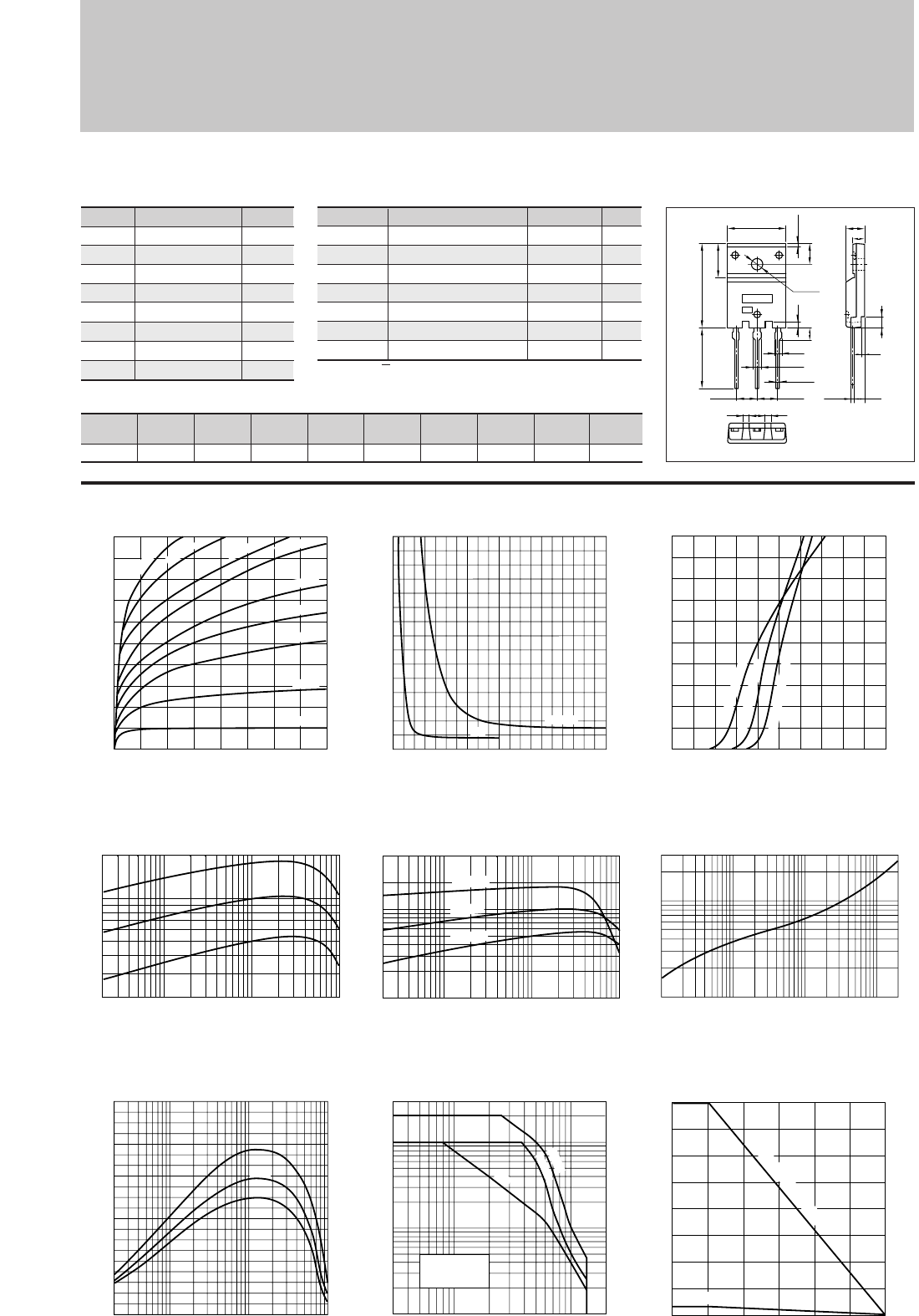
128
Silicon NPN Triple Diffused Planar Transistor (Complement to type 2SA1909)
Application : Audio and General Purpose
Symbol
VCBO
VCEO
VEBO
IC
IB
PC
Tj
Tstg
Ratings
200
140
6
10
4
80(Tc=25°C)
150
–55 to +150
Unit
V
V
V
A
A
W
°C
°C
■
Absolute maximum ratings
■
Electrical Characteristics
Symbol
ICBO
IEBO
V(BR)CEO
hFE
VCE(sat)
fT
COB
Ratings
10max
10max
140min
50min∗
0.5max
20typ
250typ
Unit
µ
A
µ
A
V
V
MHz
pF
Conditions
VCB=200V
VEB=6V
IC=50mA
VCE=4V, IC=3A
IC=5A, IB=0.5A
VCE=12V, IE=–0.5A
VCB=10V, f=1MHz
2SC5101
(Ta=25°C) (Ta=25°C)
IC–VCE Characteristics
(Typical)
hFE–IC Characteristics
(Typical)
hFE–IC
Temperature Characteristics (Typical)
θj-a–t Characteristics
IC–VBE Temperature Characteristics
(Typical)
VCE(sat)–IB Characteristics
(Typical)
Pc–Ta Derating
Safe Operating Area (Single Pulse)
fT–IE Characteristics
(Typical)
0
3
2
1
0 0.5 1.0 2.01.5
Base Current IB(A)
Collector-Emitter Saturation Voltage VCE(sat)(V)
IC=10A
5A
0
10
2
6
4
8
021
Base-Emitter Voltage VBE(V)
Collector Current IC(A)
(VCE=4V)
125˚C (Case Temp)
25˚C (Case Temp)
–30˚C (Case Temp)
0.1
1
3
0.5
1 10 100 1000 2000
Time t(ms)
Transient Thermal Resistance θj-a(˚C/W)
80
60
40
20
3.5
005025 75 125100 150
Ambient Temperature Ta(˚C)
Maximum Power Dissipation PC(W)
With Infinite heatsink
Without Heatsink
10 503 5 100 200
0.1
1
0.5
10
30
5
Collector-Emitter Voltage VCE(V)
Collector Current IC(A)
Without Heatsink
Natural Cooling
DC
100ms
10ms
0.02 0.1 0.5 1 5 10
20
50
100
200
Collector Current IC(A)
DC Current Gain hFE
(VCE=4V) (VCE=4V)
Typ
0
0
2
4
6
10
8
2134
Collector-Emitter Voltage VCE(V)
Collector Current IC(A)
150mA
200mA
100mA
75mA
50mA
20mA
10mA
300mA
I
B
=400mA
0.02 0.5 51
20
50
300
100
0.1 10
Collector Current IC(A)
DC Current Gain hFE
125˚C
25˚C
–30˚C
–0.02 –0.1 –1 –10
0
10
20
40
30
Cut-off Frequency fT(MHZ)
(VCE=12V)
Emitter Current IE(A)
Typ
4.41.5 1.5
BEC
5.45±0.1
ø3.3±0.2
1.6
3.3
1.75
0.8±0.2
2.15
1.05
+0.2
-0.1
5.45±0.1
23.0±0.3
16.2
9.5±0.2
5.5
15.6±0.2 5.5±0.2
3.45
3.35
0.65
+0.2
-0.1
±0.2
3.0
0.8
a
b
External Dimensions FM100(TO3PF)
Weight : Approx 6.5g
a. Part No.
b. Lot No.
■Typical Switching Characteristics (Common Emitter)
VCC
(V)
60
RL
(Ω)
12
IC
(A)
5
VBB2
(V)
–5
IB2
(A)
–0.5
ton
(
µ
s)
0.24typ
tstg
(
µ
s)
4.32typ
tf
(
µ
s)
0.40typ
IB1
(A)
0.5
VBB1
(V)
10
∗hFE Rank O(50to100), P(70to140), Y(90to180)
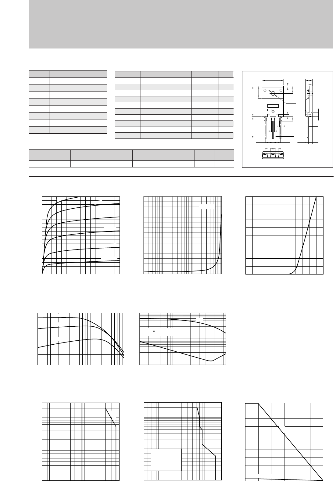
129
Symbol
VCBO
VCEO
VEBO
IC
IB
PC
Tj
Tstg
Ratings
1500
800
6
10(Pulse20)
5
100(Tc=25°C)
150
–55 to +150
Unit
V
V
V
A
A
W
°C
°C
■
Absolute maximum ratings
2SC5124
(Ta=25°C)
hFE–IC Characteristics
(Typical)
θj-a–t Characteristics
IC–VBE Temperature Characteristics
(Typical)
VCE(sat)–IC Characteristics (Typical)
Pc–Ta Derating
0.02 0.1 1 1050.5
3
5
10
40
Collector Current IC(A)
DC Current Gain hFE
(VCE=5V)
125˚C
25˚C
–55˚C
0
10
2
6
4
8
0 1.00.5
Base-Emittor Voltage VBE(V)
Collector Current IC(A)
(VCE=5V)
Safe Operating Area (Single Pulse)
5 10 10050 500 1000
0.1
1
0.5
10
30
5
Collector-Emitter Voltage VCE(V)
Collector Current IC(A)
100µs
100
50
3.5
00 25 50 75 100 125 150
Ambient Temperature Ta(˚C)
Maximum Power Dissipation PC(W)
With Infinite heatsink
Without Heatsink
0.02 0.05
0.1 0.5 1 105
0
2
1
3
Collector Current IC(A)
Collector-Emitter Saturation Voltage VCE(sat)(V)
IC/IB=5:1
0.2 10.5 105
0.1
0.5
5
10
1
Switching Time ton•tstg•tf(µs)
Collector Current IC(A)
tstg
tf
VCC 200V
IC:IB1:–IB2=5:1:2
tstg•tf–IC Characteristics
(Typical)
Reverse Bias Safe Operating Area
100 50050 20001000
1
0.5
0.1
10
30
5
Collector-Emitter Voltage VCE(V)
Collector Current IC(A)
Without Heatsink
Natural Cooling
L=3mH
–IB2=1A
Duty:less than 1%
IC–VCE Characteristics
(Typical)
0
0
2
10
4
6
8
2134
Collector-Emitter Voltage VCE(V)
Collector Current IC(A)
2.4A
700mA
1.2A
1.8A
300mA
I
B
=100mA
External Dimensions FM100(TO3PF)
4.41.5 1.5
BEC
5.45±0.1
ø3.3±0.2
1.6
3.3
1.75
0.8±0.2
2.15
1.05
+0.2
-0.1
5.45±0.1
23.0±0.3
16.2
9.5±0.2
5.5
15.6±0.2 5.5±0.2
3.45
3.35
0.65
+0.2
-0.1
±0.2
3.0
0.8
a
b
Weight : Approx 6.5g
a. Part No.
b. Lot No.
■Typical Switching Characteristics (Common Emitter)
VCC
(V)
200
RL
(Ω)
33.3
IC
(A)
6
VBB2
(V)
–5
IB2
(A)
–2.4
ton
(
µ
s)
0.1typ
tstg
(
µ
s)
4.0typ
tf
(
µ
s)
0.2typ
IB1
(A)
1.2
VBB1
(V)
10
Application : Display Horizontal Deflection Output, Switching Regulator and General Purpose
Silicon NPN Triple Diffused Planar Transistor (High Voltage Switchihg Transistor)
■
Electrical Characteristics
Symbol
ICBO1
ICBO2
IEBO
V(BR)CEO
hFE1
hFE2
VCE(sat)
VBE(sat)
fT
COB
Ratings
100max
1max
100max
800min
8min
4to9
5max
1.5max
3typ
130typ
Unit
µ
A
mA
µ
A
V
V
V
MHz
pF
Conditions
VCB=1200V
VCB=1500V
VEB=6V
IC=10mA
VCE=5V, IC=1A
VCE=5V, IC=8A
IC=8A, IB=2A
IC=8A, IB=2A
VCE=12V, IE=–1A
VCB=10V, f=1MHz
(Ta=25°C)
19.1
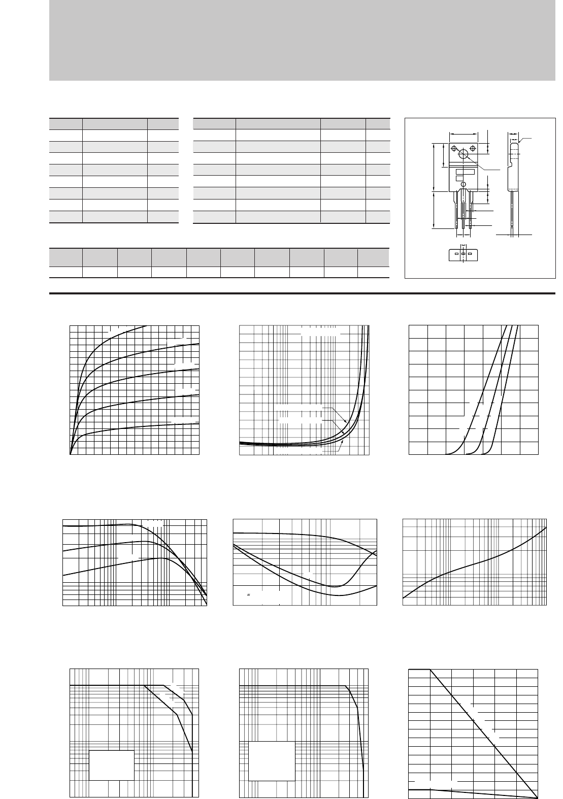
130
Silicon NPN Triple Diffused Planar Transistor (High Voltage and High Speed Switchihg Transistor)
Application : Switching Regulator and General Purpose
Symbol
VCBO
VCEO
VEBO
IC
IB
PC
Tj
Tstg
Ratings
600
400
10
5(Pulse10)
2
30(Tc=25°C)
150
–55 to +150
Unit
V
V
V
A
A
W
°C
°C
■
Absolute maximum ratings
■
Electrical Characteristics
Symbol
ICBO
IEBO
V(BR)CEO
hFE
VCE(sat)
VBE(sat)
fT
COB
Ratings
100max
10max
400min
10to30
0.5max
1.3max
20typ
30typ
Unit
µ
A
µ
A
V
V
V
MHz
pF
Conditions
VCB=500V
VEB=10V
IC=25mA
VCE=4V, IC=1.5A
IC=1.5A, IB=0.3A
IC=1.5A, IB=0.3A
VCE=12V, IE=–0.3A
VCB=10V, f=1MHz
2SC5130
(Ta=25°C) (Ta=25°C)
■Typical Switching Characteristics (Common Emitter)
VCC
(V)
200
RL
(Ω)
133
IC
(A)
1.5
VBB2
(V)
–5
IB2
(A)
–0.3
ton
(
µ
s)
1max
tstg
(
µ
s)
2max
tf
(
µ
s)
0.3max
IB1
(A)
0.15
VBB1
(V)
10
External Dimensions FM20(TO220F)
ø3.3±0.2
10.1±0.2
4.0±0.2
16.9±0.3
13.0min
8.4±0.2
0.8±0.2
3.9
±0.2
2.542.54
1.35±0.15
0.85
+0.2
-0.1
1.35±0.15
2.2±0.2
4.2±0.2
2.8 c0.5
2.4±0.2
0.45
+0.2
-0.1
BEC
a
b
Weight : Approx 2.0g
a. Part No.
b. Lot No.
IC–VCE Characteristics
(Typical)
hFE–IC Characteristics
(Typical)
ton•tstg•tf–IC Characteristics
(Typical)
θj-a–t Characteristics
IC–VBE Temperature Characteristics
(Typical)
VCE(sat)–IC Characteristics (Typical)
Pc–Ta Derating
Reverse Bias Safe Operating Area
Safe Operating Area (Single Pulse)
0.01 0.05
0.1 0.5 1 5
0
0.5
1.5
1.0
Collector Current IC(A)
IC/IB=5 Const.
125˚C (Case Temp)
25˚C (Case Temp)
–55˚C (Case Temp)
Collector-Emitter Saturation Voltage VCE(sat)(V)
0.01 0.10.05 1 50.5
5
10
50
Collector Current IC(A)
DC Current Gain hFE
(VCE=4V)
125˚C
25˚C
–55˚C
0.1 310.5
0.1
0.5
2
1
Switching Time ton•tstg•tf(µs)
0
2
1
4
3
5
0 1.41.20.4 0.6 0.8 1.00.2
Base-Emittor Voltage VBE(V)
Collector Current IC(A)
(VCE=4V)
125˚C (Case Temp)
–55˚C (Case Temp)
25˚C (Case Temp)
Collector Current IC(A)
tstg
ton
tf
VCC 200V
IC:IB1:–IB2=10:1:2 0.4
1
5
0.5
1 10 100 1000
Time t(ms)
Transient Thermal Resistance θj-a(˚C/W)
30
20
10
2
00 25 50 75 100 125 150
Ambient Temperature Ta(˚C)
Maximum Power Dissipation PC(W)
With Infinite heatsink
Without Heatsink
10 505 500100
1
0.5
0.1
10
20
5
Collector-Emitter Voltage VCE(V)
Collector Current IC(A)
Without Heatsink
Natural Cooling
L=3mH
–IB2=0.5A
Duty:less than 1%
10 505 100 500
1
0.5
0.1
10
20
5
Collector-Emitter Voltage VCE(V)
Collector Current IC(A)
100µs
50µs
Without Heatsink
Natural Cooling
0
0
2
1
5
3
4
2134
Collector-Emitter Voltage VCE(V)
Collector Current IC(A)
800mA
500mA
150mA
300mA
IB=50mA
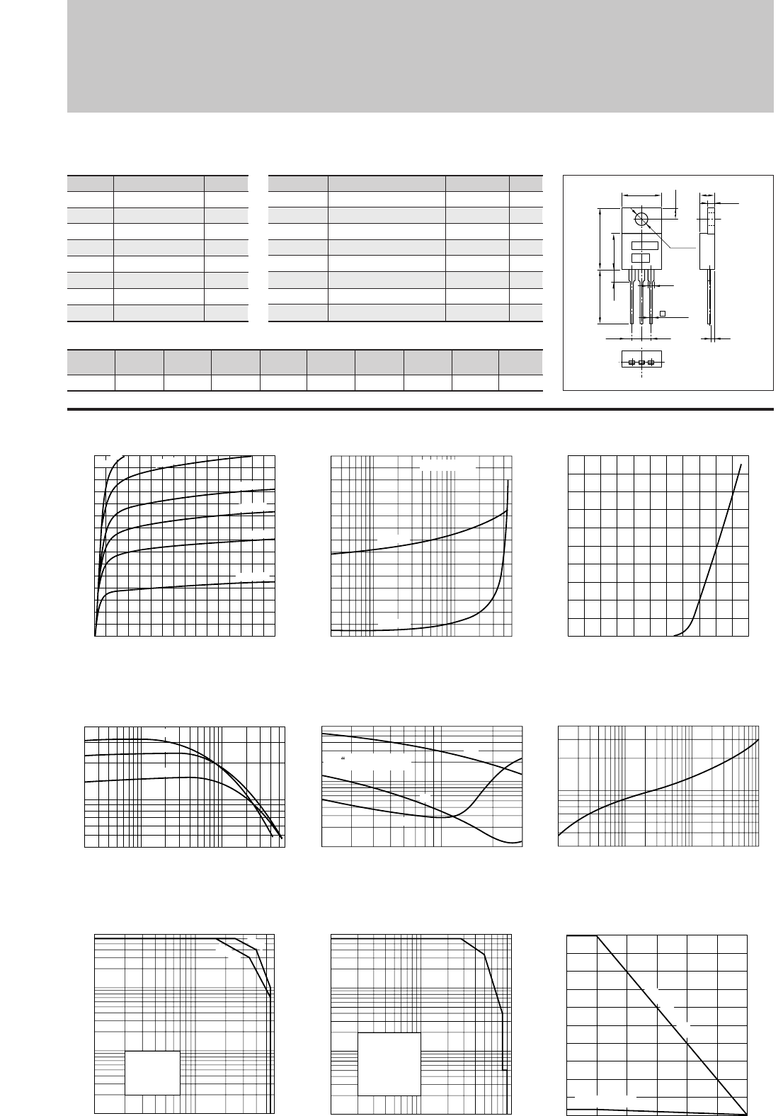
131
Silicon NPN Triple Diffused Planar Transistor (High Voltage Switchihg Transistor)
Application : Switching Regulator and General Purpose
Symbol
VCBO
VCEO
VEBO
IC
IB
PC
Tj
Tstg
Ratings
900
550
7
3(Pulse6)
1.5
50(Tc=25°C)
150
–55 to +150
Unit
V
V
V
A
A
W
°C
°C
■
Absolute maximum ratings
■
Electrical Characteristics
Symbol
ICBO
IEBO
V(BR)CEO
hFE
VCE(sat)
VBE(sat)
fT
COB
Ratings
100max
100max
550min
10to30
0.5max
1.2max
6typ
35typ
Unit
µ
A
µ
A
V
V
V
MHz
pF
Conditions
VCB=800V
VEB=7V
IC=10mA
VCE=4V, IC=1A
IC=1A, IB=0.2A
IC=1A, IB=0.2A
VCE=12V, IE=–0.25A
VCB=10V, f=1MHz
2SC5239
(Ta=25°C) (Ta=25°C)
IC–VCE Characteristics
(Typical)
hFE–IC Characteristics
(Typical)
ton•tstg•tf–IC Characteristics
(Typical)
θj-a–t Characteristics
IC–VBE Temperature Characteristics
(Typical)
VCE(sat),VBE(sat)–IC Temperature Characteristics (Typical)
Collector-Emitter Saturation Voltage VCE(sat)(V)
Base-Emitter Saturation Voltage VBE(sat)(V)
Pc–Ta Derating
Reverse Bias Safe Operating Area
Safe Operating Area (Single Pulse)
0.03
0.1
0.05
150.5
0
1.5
1.0
0.5
Collector Current IC(A)
VBE(sat)
VCE(sat)
IC/IB=5 Const.
0
5
4
3
2
1
0 1.00.5
Base-Emittor Voltage VBE(V)
Collector Current IC(A)
(VCE=4V)
0.02 0.10.05 1 5 60.5
5
4
10
40
Collector Current IC(A)
DC Current Gain hFE
(VCE=4V)
125˚C
25˚C
–55˚C
0.2 10.5 3
0.1
0.5
5
7
1
Switching Time ton•tstg•tf(µs)
Collector Current IC(A)
tstg
ton
tf
VCC 250V
IC:IB1:IB2=1:0.15:–0.45
0.3
1
4
0.5
1 10 100 1000
Time t(ms)
Transient Thermal Resistance θj-a(˚C/W)
50
40
30
20
10
2
00 25 50 75 100 125 150
Ambient Temperature Ta(˚C)
Maximum Power Dissipation PC(W)
With Infinite heatsink
Without Heatsink
10 50 500 1000100
1
0.5
0.1
0.01
0.05
5
7
Collector-Emitter Voltage VCE(V)
Collector Current IC(A)
Without Heatsink
Natural Cooling
L=3mH
IB2=–1.0A
Duty:less than 1%
10 50 100 500
0.05
0.01
1
0.5
0.1
5
7
Collector-Emitter Voltage VCE(V)
Collector Current IC(A)
100µs
50µs
Without Heatsink
Natural Cooling
0
0
2
1
3
2134
Collector-Emitter Voltage VCE(V)
Collector Current IC(A)
300mA
400mA
200mA
150mA
100mA
I
B
=40mA
■Typical Switching Characteristics (Common Emitter)
VCC
(V)
250
RL
(Ω)
250
IC
(A)
1
VBB2
(V)
–5
IB2
(A)
–0.45
ton
(
µ
s)
0.7max
tstg
(
µ
s)
4.0max
tf
(
µ
s)
0.5max
IB1
(A)
0.15
VBB1
(V)
10
External Dimensions MT-25(TO220)
BE
2.5 2.5
C
16.0±0.7
12.0min
4.0max 8.8±0.2
1.35
0.65
+0.2
-0.1
10.2±0.2
ø3.75±0.2
3.0±0.2
4.8±0.2
1.4
2.0±0.1
a
b
Weight : Approx 2.6g
a. Part No.
b. Lot No.
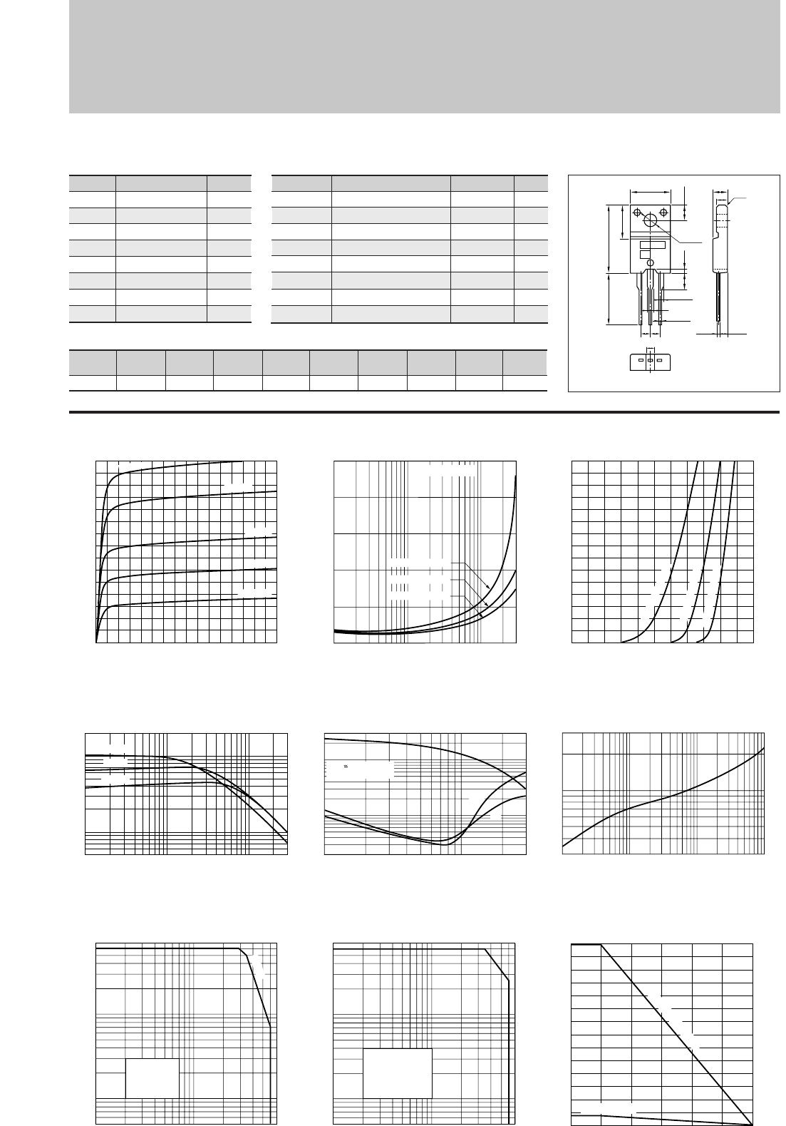
132
Silicon NPN Triple Diffused Planar Transistor (High Voltage Switchihg Transistor)
Application : Switching Regulator and General Purpose
Symbol
VCBO
VCEO
VEBO
IC
IB
PC
Tj
Tstg
Ratings
600
600
7
3(Pulse6)
1.5
35(Tc=25°C)
150
–55 to +150
Unit
V
V
V
A
A
W
°C
°C
■
Absolute maximum ratings
■
Electrical Characteristics
Symbol
ICBO
IEBO
V(BR)CEO
hFE
VCE(sat)
VBE(sat)
fT
COB
Ratings
100max
100max
600min
20to40
0.5max
1.2max
6typ
50typ
Unit
µ
A
µ
A
V
V
V
MHz
pF
Conditions
VCB=600V
VEB=7V
IC=10mA
VCE=4V, IC=1A
IC=1A, IB=0.2A
IC=1A, IB=0.2A
VCE=12V, IE=–0.3A
VCB=10V, f=1MHz
2SC5249
(Ta=25°C) (Ta=25°C)
IC–VCE Characteristics
(Typical)
hFE–IC Characteristics
(Typical)
ton•tstg•tf–IC Characteristics
(Typical)
θj-a–t Characteristics
IC–VBE Temperature Characteristics
(Typical)
VCE(sat)–IC Characteristics (Typical)
Pc–Ta Derating
Reverse Bias Safe Operating Area
Safe Operating Area (Single Pulse)
0.01 0.05
0.1 0.5 1 3
0
0.5
Collector Current IC(A)
IC/IB=5 Const.
125˚C (Case Temp)
25˚C (Case Temp)
–55˚C (Case Temp)
Collector-Emitter Saturation Voltage VCE(sat)(V)
0
3
2
1
0 1.00.5
Base-Emittor Voltage VBE(V)
Collector Current IC(A)
(VCE=4V)
125˚C (Case Temp)
25˚C (Case Temp)
–55˚C (Case Temp)
0.01 0.10.05 1 30.5
5
50
10
200
100
Collector Current IC(A)
DC Current Gain hFE
(VCE=4V)
125˚C
25˚C
–55˚C
0.1 10.5 3
0.2
0.5
10
5
30
1
Switching Time ton•tstg•tf(µs)
Collector Current IC(A)
tstg
ton
tf
VCC 200V
IC:IB1:–IB2=10:1:1
0.3
1
3
0.5
1 10 100 1000
Time t(ms)
Transient Thermal Resistance θj-a(˚C/W)
35
30
20
10
2
00 25 50 75 100 125 150
Ambient Temperature Ta(˚C)
Maximum Power Dissipation PC(W)
With Infinite heatsink
Without Heatsink
10 50 500100
1
0.5
0.1
0.05
5
7
Collector-Emitter Voltage VCE(V)
Collector Current IC(A)
Without Heatsink
Natural Cooling
L=3mH
–IB2=–1.0A
Duty:less than 1%
10 50 100 500
0.05
1
0.5
0.1
5
7
Collector-Emitter Voltage VCE(V)
Collector Current IC(A)
100µs
Without Heatsink
Natural Cooling
0
0
2
1
3
2134
Collector-Emitter Voltage VCE(V)
Collector Current IC(A)
300mA
200mA
50mA
100mA
I
B
=20mA
■Typical Switching Characteristics (Common Emitter)
VCC
(V)
200
RL
(Ω)
200
IC
(A)
1
VBB2
(V)
–5
IB2
(A)
–0.1
ton
(
µ
s)
1.0max
tstg
(
µ
s)
19max
tf
(
µ
s)
1.0max
IB1
(A)
0.1
VBB1
(V)
10
External Dimensions FM20(TO220F)
ø3.3±0.2
10.1±0.2
4.0±0.2
16.9±0.3
13.0min
8.4±0.2
0.8±0.2
3.9
±0.2
2.542.54
1.35±0.15
0.85
+0.2
-0.1
1.35±0.15
2.2±0.2
4.2±0.2
2.8 c0.5
2.4±0.2
0.45
+0.2
-0.1
BEC
a
b
Weight : Approx 2.0g
a. Part No.
b. Lot No.
133
Silicon NPN Triple Diffused Planar Transistor
Application : Resonant Switching Regulator and General Purpose
Symbol
VCBO
VCEO
VEBO
IC
IB
PC
Tj
Tstg
Ratings
300
200
7
5(Pulse10)
2
30(Tc=25°C)
150
–55 to +150
Unit
V
V
V
A
A
W
°C
°C
■
Absolute maximum ratings
■
Electrical Characteristics
Symbol
ICBO
IEBO
V(BR)CEO
hFE1
hFE2
VCE(sat)
VBE(sat)
fT
COB
Ratings
100max
100max
200min
10to30
15min
1.0max
1.5max
10typ
45typ
Unit
µ
A
µ
A
V
V
V
MHz
pF
Conditions
VCB=300V
VEB=7V
IC=10mA
VCE=2V, IC=2.5A
VCE=2V, IC=1mA
IC=2.5A, IB=0.5A
IC=2.5A, IB=0.5A
VCE=12V, IE=–0.5A
VCB=10V, f=1MHz
2SC5271
(Ta=25°C) (Ta=25°C)
External Dimensions FM20(TO220F)
ø3.3±0.2
10.1±0.2
4.0±0.2
16.9±0.3
13.0min
8.4±0.2
0.8±0.2
3.9
±0.2
2.542.54
1.35±0.15
0.85
+0.2
-0.1
1.35±0.15
2.2±0.2
4.2±0.2
2.8 c0.5
2.4±0.2
0.45
+0.2
-0.1
BEC
a
b
Weight : Approx 2.0g
a. Part No.
b. Lot No.
■Typical Switching Characteristics (Common Emitter)
VCC
(V)
150
RL
(Ω)
60
IC
(A)
2.5
VBB2
(V)
–5
IB2
(A)
–1.0
ton
(
µ
s)
0.3max
tstg
(
µ
s)
1.0max
tf
(
µ
s)
0.1max
IB1
(A)
0.5
VBB1
(V)
10
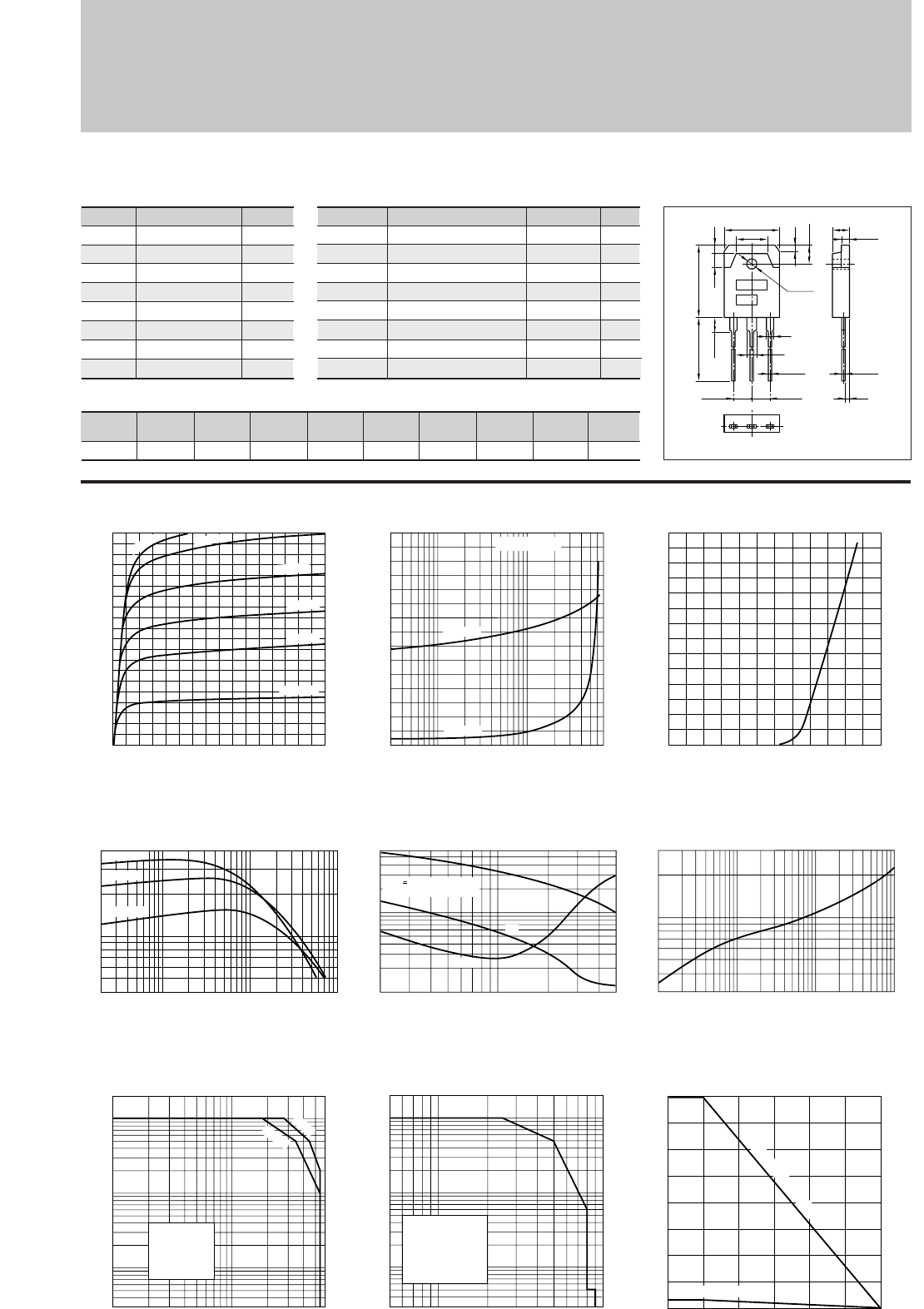
134
Silicon NPN Triple Diffused Planar Transistor (High Voltage Switchihg Transistor)
Application : Switching Regulator and General Purpose
Symbol
VCBO
VCEO
VEBO
IC
IB
PC
Tj
Tstg
Ratings
900
550
7
5(Pulse10)
2.5
80(Tc=25°C)
150
–55 to +150
Unit
V
V
V
A
A
W
°C
°C
■
Absolute maximum ratings
■
Electrical Characteristics
Symbol
ICBO
IEBO
V(BR)CEO
hFE
VCE(sat)
VBE(sat)
fT
COB
Ratings
100max
100max
550min
10to25
0.5max
1.2max
6typ
50typ
Unit
µ
A
µ
A
V
V
V
MHz
pF
Conditions
VCB=800V
VEB=7V
IC=10mA
VCE=4V, IC=1.8A
IC=1.8A, IB=0.36A
IC=1.8A, IB=0.36A
VCE=12V, IE=–0.35A
VCB=10V, f=1MHz
2SC5287
(Ta=25°C) (Ta=25°C)
IC–VCE Characteristics
(Typical)
hFE–IC Characteristics
(Typical)
ton•tstg•tf–IC Characteristics
(Typical)
θj-a–t Characteristics
IC–VBE Temperature Characteristics
(Typical)
VCE(sat),VBE(sat)–IC Temperature Characteristics (Typical)
Collector-Emitter Saturation Voltage VCE(sat)(V)
Base-Emitter Saturation Voltage VBE(sat)(V)
Pc–Ta Derating
Reverse Bias Safe Operating Area
Safe Operating Area (Single Pulse)
0.03
0.1
0.05
1750.5
0
1.5
1.0
0.5
Collector Current IC(A)
VBE(sat)
VCE(sat)
IC/IB=5 Const.
0
7
5
6
4
3
2
1
0 1.00.5
Base-Emittor Voltage VBE(V)
Collector Current IC(A)
(VCE=4V)
0.02 0.10.05 1 1050.5
4
5
10
40
Collector Current IC(A)
DC Current Gain hFE
(VCE=4V)
125˚C
25˚C
–55˚C
0.2 10.5 5
0.1
0.5
5
6
1
Switching Time ton•tstg•tf(µs)
Collector Current IC(A)
tstg
ton
tf
VCC 250V
IC:IB1:IB2=1:0.15:–0.5
0.3
1
3
0.5
1 10 100 1000
Time t(ms)
Transient Thermal Resistance θj-a(˚C/W)
80
60
40
20
3.5
00 25 50 75 100 125 150
Ambient Temperature Ta(˚C)
Maximum Power Dissipation PC(W)
With Infinite heatsink
Without Heatsink
50 500 1000100
1
5
0.5
0.1
0.03
0.05
20
10
Collector-Emitter Voltage VCE(V)
Collector Current IC(A)
Without Heatsink
Natural Cooling
IB2=–1.0A
L=3mH
Duty:less than 1%
10 50 100 500
1
0.5
0.03
0.1
0.05
10
20
5
Collector-Emitter Voltage VCE(V)
Collector Current IC(A)
100µs
50µs
0
0
2
1
5
3
4
2134
Collector-Emitter Voltage VCE(V)
Collector Current IC(A)
600mA
700mA
400mA
150mA
250mA
IB=50mA
Without Heatsink
Natural Cooling
■Typical Switching Characteristics (Common Emitter)
VCC
(V)
250
RL
(Ω)
139
IC
(A)
1.8
VBB2
(V)
–5
IB2
(A)
–0.9
ton
(
µ
s)
0.7max
tstg
(
µ
s)
4.0max
tf
(
µ
s)
0.5max
IB1
(A)
0.27
VBB1
(V)
10
External Dimensions MT-100(TO3P)
15.6±0.4
9.6
19.9±0.3
4.0 2.0
5.0±0.2
1.8
ø3.2±0.1
2
3
1.05
+0.2
-0.1
20.0min
4.0max
BE
5.45±0.1 5.45±0.1
C
4.8±0.2
0.65
+0.2
-0.1
1.4
2.0±0.1
a
b
Weight : Approx 6.0g
a. Part No.
b. Lot No.
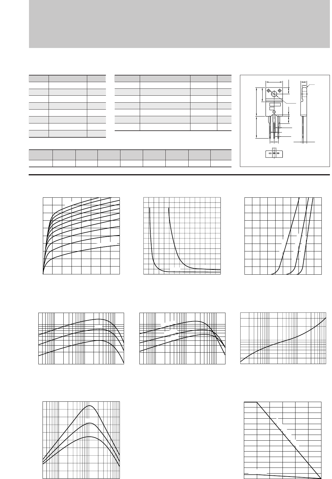
135
Silicon NPN Triple Diffused Planar Transistor
Application : Series Regulator, Switch, and General Purpose
Symbol
VCBO
VCEO
VEBO
IC
IB
PC
Tj
Tstg
Ratings
300
300
6
2
0.2
35(Tc=25°C)
150
–55to+150
Unit
V
V
V
A
A
W
°C
°C
■
Absolute maximum ratings
■
Electrical Characteristics
Symbol
ICBO
IEBO
V(BR)CEO
hFE
VCE(sat)
fT
COB
Ratings
1.0max
1.0max
300min
30min
1.0max
10typ
75typ
Unit
mA
mA
V
V
MHz
pF
Conditions
VCB=300V
VEB=6V
IC=25mA
VCE=4V, IC=0.5A
IC=1.0A, IB=0.2A
VCE=12V, IE=–0.2A
VCB=10V, f=1MHz
2SC5333
(Ta=25°C) (Ta=25°C)
IC–VCE Characteristics
(Typical)
hFE–IC Characteristics
(Typical)
hFE–IC
Temperature Characteristics (Typical)
IC–VBE Temperature Characteristics
(Typical)
VCE(sat)–IB Characteristics
(Typical)
0
0
1
2
2134
Collector-Emitter Voltage VCE(V)
Collector Current IC(A)
I
B
=200mA
I
B
=20mA/stop
Safe Operating Area (Single Pulse)
fT–IE Characteristics
(Typical)
0
3
2
1
0 0.1 0.2 0.3
Base Current IB(A)
Collector-Emitter Saturation Voltage VCE(sat)(V)
IC=1A 2A
3 10 1000 2000100
10
50
100
200
Collector Current IC(mA)
DC Current Gain hFE
(VCE=4V)
Typ
0
2
1
0 1.0
0.80.60.40.2
Base-Emittor Voltage VBE(V)
Collector Current IC(A)
(VCE=4V)
125˚C (Case Temp)
25˚C (Case Temp)
–30˚C (Case Temp)
(VCE=4V)
3 5 10 50 100 500
1000 2000
10
50
200
100
Collector Current IC(mA)
DC Current Gain hFE
25˚C
–30˚C
125˚C
–0.003 –0.01 –0.05
–0.1 –0.5 –1
10
0
20
Cut-off Frequency fT(MHZ)
(VCE=12V)
Emitter Current IE(A)
Typ
θj-a–t Characteristics
Pc–Ta Derating
0.3
1
4
0.5
1 10 100 1000
Time t(ms)
Transient Thermal Resistance θj-a(˚C/W)
35
30
20
10
2
00 25 50 75 100 125 150
Ambient Temperature Ta(˚C)
Maximum Power Dissipation PC(W)
With Infinite heatsink
Without Heatsink
■Typical Switching Characteristics (Common Emitter)
VCC
(V)
100
RL
(Ω)
100
IC
(A)
1.0
IB2
(A)
–0.2
ton
(
µ
s)
0.3typ
tstg
(
µ
s)
4.0typ
tf
(
µ
s)
1.0typ
IB1
(A)
0.1
External Dimensions FM20(TO220F)
ø3.3±0.2
10.1±0.2
4.0±0.2
16.9±0.3
13.0min
8.4±0.2
0.8±0.2
3.9
±0.2
2.542.54
1.35±0.15
0.85
+0.2
-0.1
1.35±0.15
2.2±0.2
4.2±0.2
2.8 c0.5
2.4±0.2
0.45
+0.2
-0.1
BEC
a
b
Weight : Approx 2.0g
a. Part No.
b. Lot No.
VB2
(V)
–5
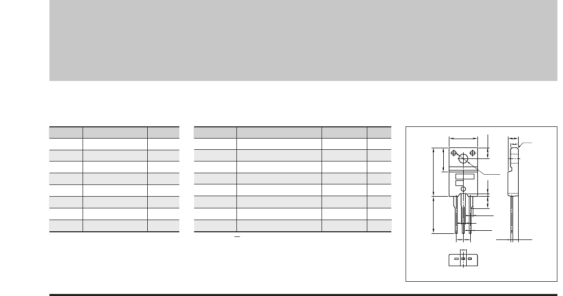
136
Silicon NPN Epitaxial Planar Transistor
Application : Emergency Lighting Inverter and General Purpose
Symbol
VCBO
VCEO
VEBO
IC
IB
PC
Tj
Tstg
Ratings
60
40
7
12
3
30(Tc=25°C)
150
–55to+150
Unit
V
V
V
A
A
W
°C
°C
■
Absolute maximum ratings
■
Electrical Characteristics
Symbol
ICBO
IEBO
V(BR)CEO
hFE
VCE(sat)
VBE(sat)
fT
COB
Ratings
10max
10max
40min
70min∗
0.3max
1.2max
90typ
120typ
Unit
µ
A
µ
A
V
V
V
MHz
pF
Conditions
VCB=60V
VEB=7V
IC=25mA
VCE=2V, IC=6A
IC=6A, IB=0.3A
IC=6A, IB=0.3A
VCE=12V, IE=–3A
VCB=10V, f=1MHz
2SC5370
(Ta=25°C) (Ta=25°C)
External Dimensions FM20(TO220F)
ø3.3±0.2
10.1±0.2
4.0±0.2
16.9±0.3
13.0min
8.4±0.2
0.8±0.2
3.9
±0.2
2.542.54
1.35±0.15
0.85
+0.2
-0.1
1.35±0.15
2.2±0.2
4.2±0.2
2.8 c0.5
2.4±0.2
0.45
+0.2
-0.1
BEC
a
b
Weight : Approx 2.0g
a. Part No.
b. Lot No.
∗hFE Rank O(70to140), Y(120to240), G(200to400)
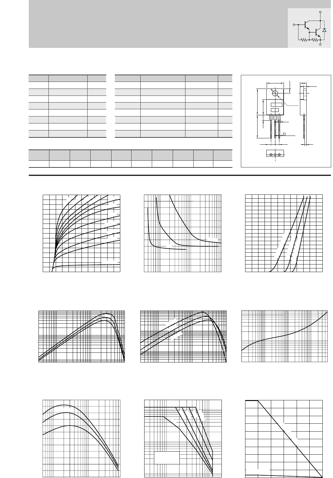
137
Darlington 2SD1769
IC–VCE Characteristics
(Typical)
hFE–IC Characteristics
(Typical)
θj-a–t Characteristics
IC–VBE Temperature Characteristics
(Typical)
VCE(sat)–IB Characteristics
(Typical)
Pc–Ta Derating
Safe Operating Area (Single Pulse)
0
3
2
1
0.3 5 101 10050
Base Current IB(mA)
Collector-Emitter Saturation Voltage VCE(sat)(V)
0
6
8
4
2
021
Base-Emittor Voltage VBE(V)
Collector Current IC(A)
(VCE=2V)
125˚C (Case Temp)
25˚C (Case Temp)
–30˚C (Case Temp)
0.2
1
10
5
0.5
1 10 10050 10005 5000
Time t(ms)
Transient Thermal Resistance θj-a(˚C/W)
50
40
30
20
10
2
00 25 50 75 100 125 150
Ambient Temperature Ta(˚C)
Maximum Power Dissipation PC(W)
With Infinite heatsink
Without Heatsink
103 5 20010050
0.08
1
0.5
10
20
5
Collector-Emitter Voltage VCE(V)
Collector Current IC(A)
Without Heatsink
Natural Cooling
DC
10ms
3ms
1ms
0.03 0.1 1 5 10
80
500
1000
10000
5000
Collector Current IC(A)
DC Current Gain hFE
(VCE=2V)
0
0
2
4
8
6
264
Collector-Emitter Voltage VCE(V)
Collector Current IC(A)
0.7mA
1.5mA
1mA
2mA
3mA
5mA
10mA
20mA
0.5mA
0.4mA
I
B
=0.3mA
0.5
Typ
500µs
I
C
=6A
2A
4A
Collector Current IC(A)
DC Current Gain hFE
0.03 0.05 0.5 1 5 100.1
100
50
30
500
1000
5000
10000
(VCE=2V)
125˚C
25˚C
–30˚C
fT–IE Characteristics
(Typical)
–0.05 –1–0.5 –8–5
0
50
120
100
Cut-off Frequency fT(MHZ)
(VCE=12V)
Emitter Current IE(A)
Typ
hFE–IC
Temperature Characteristics (Typical)
Silicon NPN Triple Diffused Planar Transistor
Application : Driver for Solenoid, Relay and Motor, Series Regulator, and General Purpose
Symbol
VCBO
VCEO
VEBO
IC
IB
PC
Tj
Tstg
Ratings
120
120
6
6(Pulse10)
1
50(Tc=25°C)
150
–55 to +150
Unit
V
V
V
A
A
W
°C
°C
■
Absolute maximum ratings
■
Electrical Characteristics
Ratings
10max
20max
120min
2000min
1.5max
2.0max
100typ
typ
Unit
µ
A
mA
V
V
V
MHz
pF
Conditions
VCB=120V
VEB=6V
IC=10mA
VCE=2V, IC=3A
IC=3A, IB=3mA
IC=3A, IB=3mA
VCE=12V, IE=–0.2A
VCB=10V, f=1MHz
(Ta=25°C) (Ta=25°C)
Symbol
ICBO
IEBO
V(BR)CEO
hFE
VCE(sat)
VBE(sat)
fT
COB
External Dimensions MT-25(TO220)
BE
2.5 2.5
C
16.0±0.7
12.0min
4.0max 8.8±0.2
1.35
0.65
+0.2
-0.1
10.2±0.2
ø3.75±0.2
3.0±0.2
4.8±0.2
1.4
2.0±0.1
a
b
■Typical Switching Characteristics (Common Emitter)
VCC
(V)
30
RL
(Ω)
10
IC
(A)
3
VBB2
(V)
–1.5
IB2
(mA)
–3
ton
(
µ
s)
0.5typ
tstg
(
µ
s)
5.5typ
tf
(
µ
s)
1.5typ
IB1
(mA)
3
VBB1
(V)
10
Weight : Approx 2.6g
a. Part No.
b. Lot No.
B
C
E
(2.5kΩ)(200Ω)
Equivalent
circuit
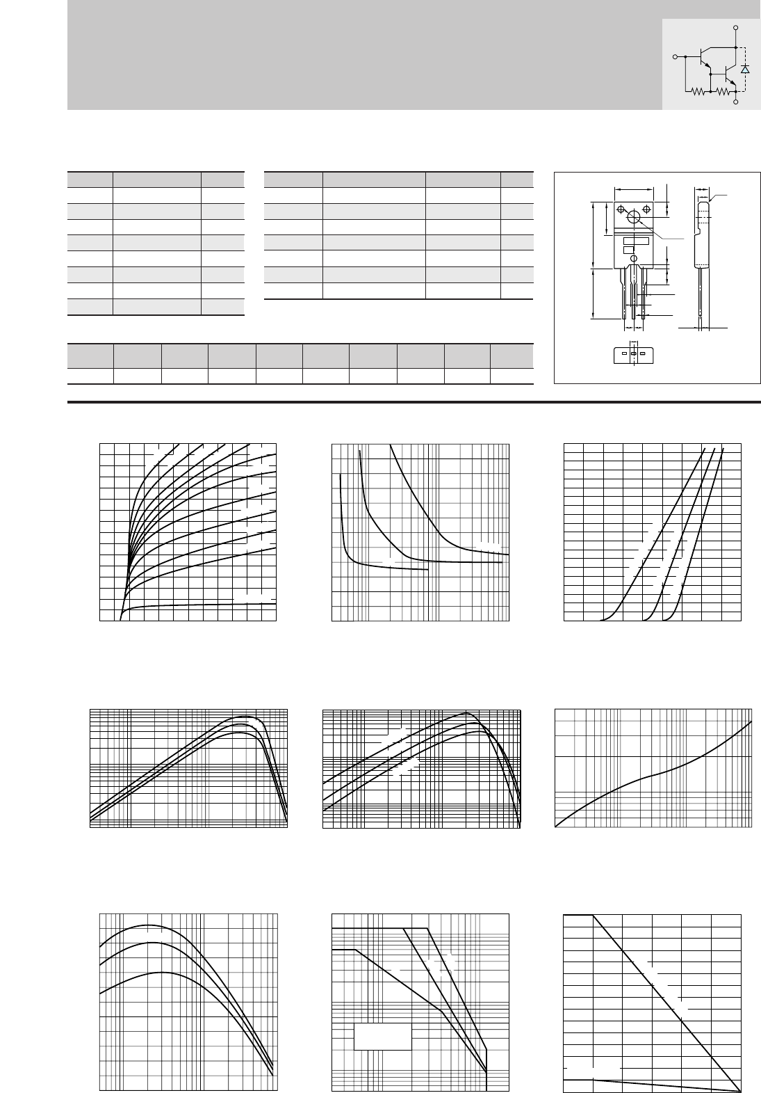
138
Darlington 2SD1785
IC–VCE Characteristics
(Typical)
hFE–IC Characteristics
(Typical)
θj-a–t Characteristics
IC–VBE Temperature Characteristics
(Typical)
Pc–Ta Derating
Safe Operating Area (Single Pulse)
fT–IE Characteristics
(Typical)
0.4 21
Base-Emittor Voltage VBE(V)
Collector Current IC(A)
(VCE=2V)
0.5
1
5
1 10 100 1000
Time t(ms)
Transient Thermal Resistance θj-a(˚C/W)
30
20
10
2
00 25 50 75 100 125 150
Ambient Temperature Ta(˚C)
Maximum Power Dissipation PC(W)
With Infinite heatsink
Without Heatsink
–0.05
–0.1 –1–0.5 –8–5
0
50
120
100
Cut-off Frequency fT(MHZ)
(VCE=12V)
Emitter Current IE(A)
Typ
0
0
2
4
8
6
264
Collector-Emitter Voltage VCE(V)
Collector Current IC(A)
0.7mA
1.5mA
1mA
2mA
3mA
5mA
10mA
20mA
0.5mA
0.4mA
I
B
=0.3mA
0
6
8
4
2
125˚C (Case Temp)
25˚C (Case Temp)
–30˚C (Case Temp)
0.03 0.1 1 5 10
100
500
1000
10000
5000
Collector Current IC(A)
DC Current Gain hFE
(VCE=2V)
0.5
Typ
103 5 20010050
0.05
1
0.1
0.5
10
20
5
Collector-Emitter Voltage VCE(V)
Collector Current IC(A)
Without Heatsink
Natural Cooling
DC
10ms
1ms
VCE(sat)–IB Characteristics
(Typical)
0
3
2
1
0.3 5 101 10050
Base Current IB(mA)
Collector-Emitter Saturation Voltage VCE(sat)(V)
I
C
=6A
2A
4A
Collector Current IC(A)
DC Current Gain hFE
0.03 0.05 0.5 1 5 100.1
100
50
30
500
1000
5000
10000
(VCE=2V)
125˚C
25˚C
–30˚C
hFE–IC
Temperature Characteristics (Typical)
Silicon NPN Triple Diffused Planar Transistor (Complement to type 2SB1258)
Application : Driver for Solenoid, Relay and Motor, Series Regulator, and General Purpose
Symbol
VCBO
VCEO
VEBO
IC
IB
PC
Tj
Tstg
Ratings
120
120
6
6(Pulse10)
1
30(Tc=25°C)
150
–55 to +150
Unit
V
V
V
A
A
W
°C
°C
■
Absolute maximum ratings
■
Electrical Characteristics
Ratings
10max
10max
120min
2000min
1.5max
100typ
70typ
Unit
µ
A
mA
V
V
MHz
pF
Conditions
VCB=120V
VEB=6V
IC=10mA
VCE=2V, IC=3A
IC=2A, IB=3mA
VCE=12V, IE=–0.1A
VCB=10V, f=1MHz
(Ta=25°C) (Ta=25°C)
Symbol
ICBO
IEBO
V(BR)CEO
hFE
VCE(sat)
fT
COB
External Dimensions FM20(TO220F)
ø3.3±0.2
10.1±0.2
4.0±0.2
16.9±0.3
13.0min
8.4±0.2
0.8±0.2
3.9
±0.2
2.542.54
1.35±0.15
0.85
+0.2
-0.1
1.35±0.15
2.2±0.2
4.2±0.2
2.8 c0.5
2.4±0.2
0.45
+0.2
-0.1
BEC
a
b
■Typical Switching Characteristics (Common Emitter)
VCC
(V)
30
RL
(Ω)
10
IC
(A)
3
VBB2
(V)
–1.5
IB2
(mA)
–3
ton
(
µ
s)
0.5typ
tstg
(
µ
s)
5.5typ
tf
(
µ
s)
1.5typ
IB1
(mA)
3
VBB1
(V)
10
Weight : Approx 2.0g
a. Part No.
b. Lot No.
B
C
E
(2.5kΩ)(200Ω)
Equivalent
circuit
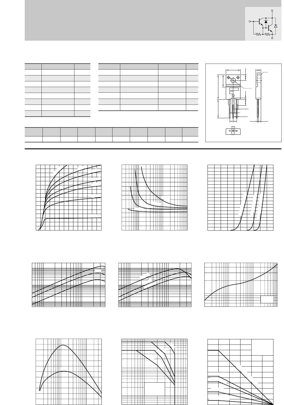
139
2SD1796
IC–VCE Characteristics
(Typical)
hFE–IC Characteristics
(Typical)
hFE–IC
Temperature Characteristics (Typical)
θj-a–t Characteristics
Pc–Ta Derating
0
0
1
2
3
4
2134
Collector-Emitter Voltage VCE(V)
Collector Current IC(A)
I
B
=20mA
0.3mA
1.0mA
0.4mA
0.5mA
0.8mA
0.6mA
Safe Operating Area (Single Pulse)
fT–IE Characteristics
(Typical)
410.1 0.50.05
50
500
100
1000
10000
20000
5000
Collector Current IC(A)
DC Current åGain hFE
(VCE=4V)
–0.01 –0.1 –1 –4
0
20
40
120
100
60
80
Cut-off Frequency fT(MHZ)
(VCE=10V)
Emitter Current IE(A)
Typ
10 503 5 100
0.05
0.1
1
0.5
10
5
Collector-Emitter Voltage VCE(V)
Collector Current IC(A)
Without Heatsink
Natural Cooling
DC
100ms
10ms
1ms
0.5
1
5
1 10 100 1000
Time t(ms)
Transient Thermal Resistance θj-a(˚C/W)
Typ
VCB=10V
IE=–2V
VCE(sat)–IB Characteristics
(Typical)
0
3
2
1
0.2 0.5 5 101 10050
Base Current IB(mA)
Collector-Emitter Saturation Voltage VCE(sat)(V)
I
C
=4A
I
C
=3A
I
C
=2A
I
C
=1A
IC–VBE Temperature Characteristics
(Typical)
021
Base-Emittor Voltage VBE(V)
Collector Current IC(A)
(VCE=2V)
0
3
4
2
1
125˚C (Case Temp)
25˚C (Case Temp)
–30˚C (Case Temp)
Collector Current IC(A)
DC Current åGain hFE
0.05 0.5 1 40.1
100
50
500
1000
5000
10000
20000
(VCE=4V)
125˚C
25˚C
–30˚C
30
20
10
2
00 25 50 75 100 125 150
Ambient Temperature Ta(˚C)
Maximum Power Dissipation PC(W)
With Infinite heatsink
Without Heatsink
150x150x2
50x50x2
100x
100x2
Natural Cooling
Silicone Grease
Heatsink: Aluminum
in mm
Silicon NPN Triple Diffused Planar Transistor
Application : Driver for Solenoid, Relay and Motor and General Purpose
Symbol
VCBO
VCEO
VEBO
IC
IB
PC
Tj
Tstg
Ratings
60±10
60±10
6
4
0.5
25(Tc=25°C)
150
–55 to +150
Unit
V
V
V
A
A
W
°C
°C
■
Absolute maximum ratings
■
Electrical Characteristics
Ratings
10max
10max
60±10
2000min
1.5max
60typ
45 typ
Unit
µ
A
mA
V
V
MHz
pF
Conditions
VCB=50V
VEB=6V
IC=10mA
VCE=4V, IC=3A
IC=3A, IB=10mA
VCE=12V, IE=–0.2A
VCB=10V, f=1MHz
(Ta=25°C) (Ta=25°C)
Symbol
ICBO
IEBO
V(BR)CEO
hFE
VCE(sat)
fT
COB
External Dimensions FM20(TO220F)
ø3.3±0.2
10.1±0.2
4.0±0.2
16.9±0.3
13.0min
8.4±0.2
0.8±0.2
3.9
±0.2
2.542.54
1.35±0.15
0.85
+0.2
-0.1
1.35±0.15
2.2±0.2
4.2±0.2
2.8 c0.5
2.4±0.2
0.45
+0.2
-0.1
BEC
a
b
■Typical Switching Characteristics (Common Emitter)
VCC
(V)
30
RL
(Ω)
10
IC
(A)
3
VBB2
(V)
–5
IB2
(mA)
–10
ton
(
µ
s)
1.0typ
tstg
(
µ
s)
4.0typ
tf
(
µ
s)
1.5typ
IB1
(mA)
10
VBB1
(V)
10
Weight : Approx 2.0g
a. Part No.
b. Lot No.
Built-in Avalanche Diode
for Surge Absorbing
Darlington
B
C
E
(3kΩ)(150Ω)
Equivalent
circuit
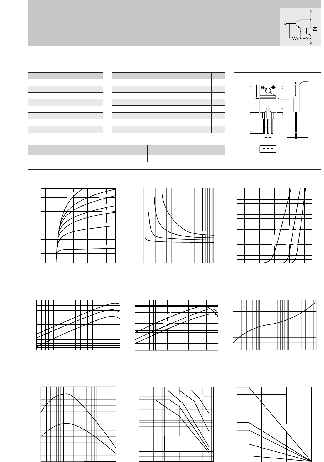
140
Darlington 2SD2014
IC–VCE Characteristics
(Typical)
hFE–IC Characteristics
(Typical)
θj-a–t Characteristics
0
0
1
2
4
3
2134
Collector-Emitter Voltage VCE(V)
Collector Current IC(A)
I
B
=20mA
0.3mA
1.0mA
0.4mA
0.5mA
0.8mA
0.6mA
Safe Operating Area (Single Pulse)
410.1 0.50.03
50
30
500
100
1000
10000
20000
5000
Collector Current IC(A)
DC Current Gain hFE
(VCE=4V)
10 503 5 100
0.05
0.1
1
0.5
10
5
Collector-Emitter Voltage VCE(V)
Collector Current IC(A)
Without Heatsink
Natural Cooling
DC
100ms
10ms
1ms
0.5
1
5
1 10 100 10005 50 500
Time t(ms)
Transient Thermal Resistance θj-a(˚C/W)
Typ
VCE(sat)–IB Characteristics
(Typical)
0
3
2
1
0.2 5 101 10050
Base Current IB(mA)
Collector-Emitter Saturation Voltage VCE(sat)(V)
I
C
=4A
2A
1A
3A
300µs
IC–VBE Temperature Characteristics
(Typical)
021
Base-Emittor Voltage VBE(V)
Collector Current IC(A)
(VCE=4V)
0
3
4
2
1
125˚C (Case Temp)
25˚C (Case Temp)
–30˚C (Case Temp)
hFE–IC
Temperature Characteristics (Typical)
Collector Current IC(A)
DC Current Gain hFE
0.03 0.5 1 40.1
100
50
30
500
1000
5000
10000
20000
(VCE=4V)
125˚C
25˚C
–30˚C
fT–IE Characteristics
(Typical)
–0.02 –0.05 –0.1 –0.5 –1 –4
0
20
40
120
100
60
80
Cut-off Frequency fT(MHZ)
(VCE=10V)
Emitter Current IE(A)
Typ
Pc–Ta Derating
25
20
10
2
00 25 50 75 100 125 150
Ambient Temperature Ta(˚C)
Maximum Power Dissipation PC(W)
With Infinite heatsink
Without Heatsink
150x150x2
50x50x2
100x
100x2
Natural Cooling
Silicone Grease
Heatsink: Aluminum
in mm
Silicon NPN Triple Diffused Planar Transistor (Complement to type 2SB1257)
Application : Driver for Solenoid, Relay and Motor, Series Regulator, and General Purpose
Symbol
VCBO
VCEO
VEBO
IC
IB
PC
Tj
Tstg
Ratings
120
80
6
4
0.5
25(Tc=25°C)
150
–55 to +150
Unit
V
V
V
A
A
W
°C
°C
■
Absolute maximum ratings
■
Electrical Characteristics
Ratings
10max
10max
80min
2000min
1.5max
2.0max
75typ
45typ
Unit
µ
A
mA
V
V
V
MHz
pF
Conditions
VCB=120V
VEB=6V
IC=10mA
VCE=2V, IC=3A
IC=3A, IB=3mA
IC=3A, IB=3mA
VCE=12V, IE=–0.1A
VCB=10V, f=1MHz
(Ta=25°C) (Ta=25°C)
Symbol
ICBO
IEBO
V(BR)CEO
hFE
VCE(sat)
VBE(sat)
fT
COB
External Dimensions FM20(TO220F)
ø3.3±0.2
10.1±0.2
4.0±0.2
16.9±0.3
13.0min
8.4±0.2
0.8±0.2
3.9
±0.2
2.542.54
1.35±0.15
0.85
+0.2
-0.1
1.35±0.15
2.2±0.2
4.2±0.2
2.8 c0.5
2.4±0.2
0.45
+0.2
-0.1
BEC
a
b
■Typical Switching Characteristics (Common Emitter)
VCC
(V)
30
RL
(Ω)
10
IC
(A)
3
VBB2
(V)
–5
IB2
(mA)
–10
ton
(
µ
s)
1.0typ
tstg
(
µ
s)
4.0typ
tf
(
µ
s)
1.5typ
IB1
(mA)
10
VBB1
(V)
10
Weight : Approx 2.0g
a. Part No.
b. Lot No.
B
C
E
(3kΩ)(200Ω)
Equivalent
circuit
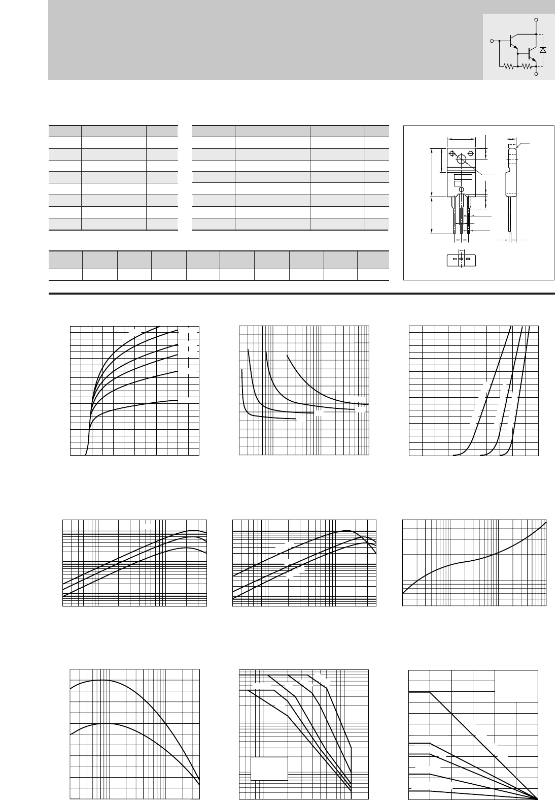
141
Darlington 2SD2015
IC–VCE Characteristics
(Typical)
hFE–IC Characteristics
(Typical)
θj-a–t Characteristics
Pc–Ta Derating
0
0
1
2
4
3
213546
Collector-Emitter Voltage VCE(V)
Collector Current IC(A)
IB=1mA
0.3mA
0.4mA
0.5mA
0.8mA
0.6mA
Safe Operating Area (Single Pulse)
410.1 0.50.03
50
500
100
1000
10000
20000
5000
Collector Current IC(A)
DC Current Gain hFE
(VCE=4V)
10 505 200100
0.03
0.05
0.1
1
0.5
10
5
Collector-Emitter Voltage VCE(V)
Collector Current IC(A)
Without Heatsink
Natural Cooling
DC
100ms
10ms
1ms
0.5
1
5
1 10 100 10005 50 500
Time t(ms)
Transient Thermal Resistance θj-a(˚C/W)
Typ
VCE(sat)–IB Characteristics
(Typical)
0
3
2
1
0.2 5 101 10050
Base Current IB(mA)
Collector-Emitter Saturation Voltage VCE(sat)(V)
I
C
=4A
2A
1A
3A
300µs
IC–VBE Temperature Characteristics
(Typical)
021
Base-Emittor Voltage VBE(V)
Collector Current IC(A)
(VCE=4V)
0
3
4
2
1
125˚C (Case Temp)
25˚C (Case Temp)
–30˚C (Case Temp)
hFE–IC
Temperature Characteristics (Typical)
Collector Current IC(A)
DC Current Gain hFE
0.050.03 0.5 1 40.1
100
50
500
1000
5000
10000
20000
(VCE=4V)
125˚C
25˚C
–30˚C
fT–IE Characteristics
(Typical)
–0.02 –0.05 –0.1 –0.5 –1 –4
0
10
20
60
50
30
40
Cut-off Frequency fT(MHZ)
(VCE=12V)
Emitter Current IE(A)
Typ
30
20
10
2
00 25 50 75 100 125 150
Ambient Temperature Ta(˚C)
Maximum Power Dissipation PC(W)
With Infinite heatsink
Without Heatsink
150x150x2
50x50x2
100x
100x2
Natural Cooling
Silicone Grease
Heatsink: Aluminum
in mm
Silicon NPN Triple Diffused Planar Transistor
Application : Driver for Solenoid, Relay and Motor and General Purpose
Symbol
VCBO
VCEO
VEBO
IC
IB
PC
Tj
Tstg
Ratings
150
120
6
4
0.5
25(Tc=25°C)
150
–55 to +150
Unit
V
V
V
A
A
W
°C
°C
■
Absolute maximum ratings
■
Electrical Characteristics
Ratings
10max
10max
120min
2000min
1.5max
2.0max
40typ
40typ
Unit
µ
A
mA
V
V
V
MHz
pF
Conditions
VCB=150V
VEB=6V
IC=10mA
VCE=2V, IC=2A
IC=2A, IB=2mA
IC=2A, IB=2mA
VCE=12V, IE=–0.1A
VCB=10V, f=1MHz
(Ta=25°C) (Ta=25°C)
Symbol
ICBO
IEBO
V(BR)CEO
hFE
VCE(sat)
VBE(sat)
fT
COB
External Dimensions FM20(TO220F)
ø3.3±0.2
10.1±0.2
4.0±0.2
16.9±0.3
13.0min
8.4±0.2
0.8±0.2
3.9
±0.2
2.542.54
1.35±0.15
0.85
+0.2
-0.1
1.35±0.15
2.2±0.2
4.2±0.2
2.8 c0.5
2.4±0.2
0.45
+0.2
-0.1
BEC
a
b
■Typical Switching Characteristics (Common Emitter)
VCC
(V)
40
RL
(Ω)
20
IC
(A)
2
VBB2
(V)
–5
IB2
(mA)
–10
ton
(
µ
s)
0.6typ
tstg
(
µ
s)
5.0typ
tf
(
µ
s)
2.0typ
IB1
(mA)
10
VBB1
(V)
10
Weight : Approx 2.0g
a. Part No.
b. Lot No.
B
C
E
(3kΩ)(500Ω)
Equivalent
circuit
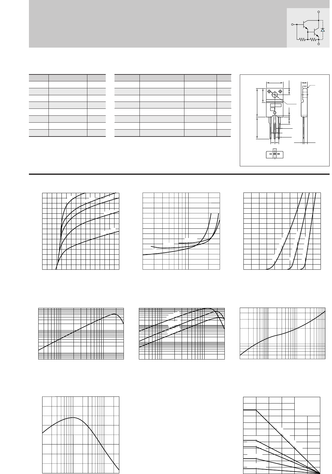
142
Darlington 2SD2016
IC–VBE Temperature Characteristics
(Typical)
VCE(sat)–IB Characteristics
(Typical)
Pc–Ta Derating
0.03 0.1 10.5 3
5000
10000
1000
500
100
50
10
Collector Current IC(A)
DC Current Gain hFE
(VCE=4V)
Safe Operating Area (Single Pulse)
125˚C
–55˚C
25˚C
0
3
2
1
021
Base-Emittor Voltage VBE(V)
Collector Current IC(A)
(VCE=4V)
125˚C (Case Temp)
25˚C (Case Temp)
–55˚C (Case Temp)
IC–VCE Characteristics
(Typical)
0
0
1
2
3
2134
Collector-Emitter Voltage VCE(V)
Collector Current IC(A)
3mA
1.5mA
I
B
=0.3mA
0.5mA
1mA
0
3
2
1
0.2 1 3
Base Current IB(mA)
Collector-Emitter Saturation Voltage VCE(sat)(V)
125˚C
25˚C
–55˚C
hFE–IC
Temperature Characteristics (Typical)
hFE–IC Characteristics
(Typical)
0.03 0.1 1 3
100
50
500
1000
10000
5000
Collector Current IC(A)
DC Current Gain hFE
(VCE=4V)
0.5
θj-a–t Characteristics
0.5
1
5
1 10 100 10005 50 500
Time t(ms)
Transient Thermal Resistance θj-a(˚C/W)
fT–IE Characteristics
(Typical)
–0.01 –0.1 –1–0.5–0.05 –3
0
20
40
60
80
Cut-off Frequency fT(MHZ)
(VCE=12V)
Emitter Current IE(A)
30
20
10
2
00 25 50 75 100 125 150
Ambient Temperature Ta(˚C)
Maximum Power Dissipation PC(W)
With Infinite heatsink
Without Heatsink
150x150x2
50x50x2
100x
100x2
Natural Cooling
Silicone Grease
Heatsink: Aluminum
in mm
Silicon NPN Triple Diffused Planar Transistor
Application : Igniter, Relay and General Purpose
Symbol
VCBO
VCEO
VEBO
IC
IB
PC
Tj
Tstg
Ratings
200
200
6
3
0.5
25(Tc=25°C)
150
–55 to +150
Unit
V
V
V
A
A
W
°C
°C
■
Absolute maximum ratings
■
Electrical Characteristics
Ratings
10max
10max
200min
1000to15000
1.5max
2.0max
90typ
40typ
Unit
µ
A
mA
V
V
V
MHz
pF
Conditions
VCB=200V
VEB=6V
IC=10mA
VCE=4V, IC=1A
IC=1A, IB=1.5mA
IC=1A, IB=1.5mA
VCE=12V, IE=–0.1A
VCB=10V, f=1MHz
(Ta=25°C) (Ta=25°C)
Symbol
ICBO
IEBO
V(BR)CEO
hFE
VCE(sat)
VBE(sat)
fT
COB
External Dimensions FM20(TO220F)
ø3.3±0.2
10.1±0.2
4.0±0.2
16.9±0.3
13.0min
8.4±0.2
0.8±0.2
3.9
±0.2
2.542.54
1.35±0.15
0.85
+0.2
-0.1
1.35±0.15
2.2±0.2
4.2±0.2
2.8 c0.5
2.4±0.2
0.45
+0.2
-0.1
BEC
a
b
Weight : Approx 2.0g
a. Part No.
b. Lot No.
B
C
E
(2kΩ)(200Ω)
Equivalent
circuit
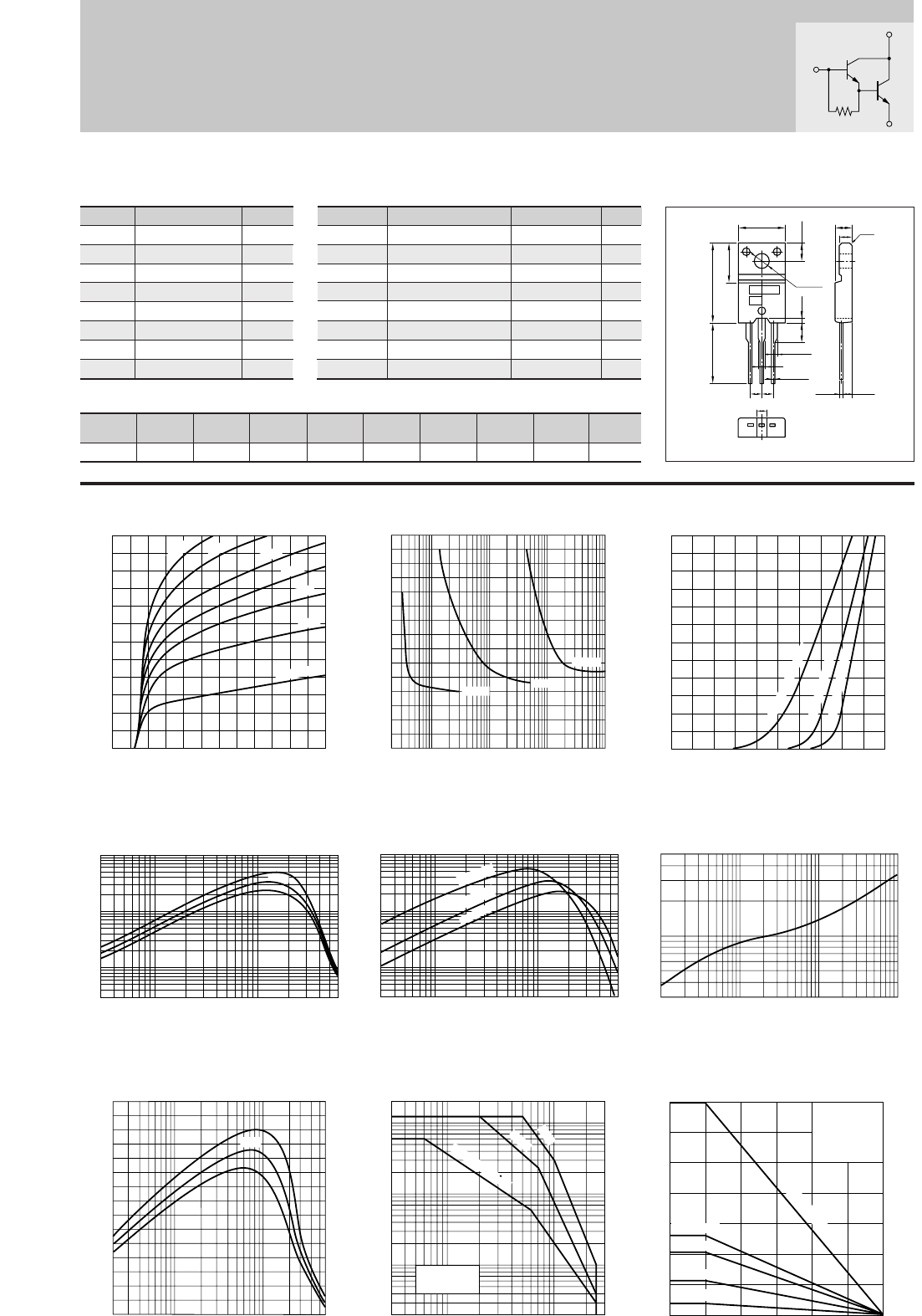
143
Darlington 2SD2017
IC–VCE Characteristics
(Typical)
hFE–IC Characteristics
(Typical)
IC–VBE Temperature Characteristics
(Typical)
Pc–Ta Derating
35
30
20
10
2
00 25 50 75 100 125 150
Ambient Temperature Ta(˚C)
Maximum Power Dissipation PC(W)
With Infinite heatsink
Without Heatsink
50x50x2
100x100x2
150x150x2
0
0
4
2
6
3
1
5
21 3456
Collector-Emitter Voltage VCE(V)
Collector Current IC(A)
40mA
20mA
8mA
4mA
2mA
1mA
I
B
=0.4mA
0.03 0.1 10.5 65
5000
10000
1000
500
100
30
50
Collector Current IC(A)
DC Current Gain hFE
(VCE=2V)
Typ
VCE(sat)–IB Characteristics
(Typical)
0
3
2
1
0.2 0.5 5 101 100 500 100050
Base Current IB(mA)
Collector-Emitter Saturation Voltage VCE(sat)(V)
I
C
=1A
I
C
=3A
I
C
=8A
0
3
4
5
6
2
1
021
Base-Emittor Voltage VBE(V)
Collector Current IC(A)
(VCE=2V)
0.03 0.1 10.5 5 6
5000
10000
1000
500
100
50
30
Collector Current IC(A)
DC Current Gain hFE
(VCE=2V)
125˚C
25˚C
hFE–IC
Temperature Characteristics (Typical)
–30˚C
θj-a–t Characteristics
0.3
1
5
0.5
1 10 10050 5005 1000
Time t(ms)
Transient Thermal Resistance θj-a(˚C/W)
fT–IE Characteristics
(Typical)
–0.02 –0.05 –0.1 –0.5 –1 –5–6
0
20
10
30
Cut-off Frequency fT(MHZ)
(VCE=12V)
Emitter Current IE(A)
Natural Cooling
Silicone Grease
Heatsink: Aluminum
in mm
Typ
Safe Operating Area (Single Pulse)
103530010050
0.05
0.02
1
0.1
0.5
10
20
5
Collector-Emitter Voltage VCE(V)
Collector Current IC(A)
Without Heatsink
Natural Cooling
10ms
1ms
D.C (T
C
=25C)
125˚C (Case Temp)
25˚C (Case Temp)
–30˚C (Case Temp)
Silicon NPN Triple Diffused Planar Transistor
Application : Driver for Solenoid, Relay and Motor and General Purpose
Symbol
VCBO
VCEO
VEBO
IC
IB
PC
Tj
Tstg
Ratings
300
250
20
6
1
35(Tc=25°C)
150
–55 to +150
Unit
V
V
V
A
A
W
°C
°C
■
Absolute maximum ratings
■
Electrical Characteristics
Ratings
100max
10max
250min
2000min
1.5max
2.0max
20typ
65typ
Unit
µ
A
mA
V
V
V
MHz
pF
Conditions
VCB=300V
VEB=20V
IC=25mA
VCE=2V, IC=2A
IC=2A, IB=2mA
IC=2A, IB=2mA
VCE=12V, IE=–1A
VCB=10V, f=1MHz
(Ta=25°C) (Ta=25°C)
Symbol
ICBO
IEBO
V(BR)CEO
hFE
VCE(sat)
VBE(sat)
fT
COB
External Dimensions FM20(TO220F)
ø3.3±0.2
10.1±0.2
4.0±0.2
16.9±0.3
13.0min
8.4±0.2
0.8±0.2
3.9
±0.2
2.542.54
1.35±0.15
0.85
+0.2
-0.1
1.35±0.15
2.2±0.2
4.2±0.2
2.8 c0.5
2.4±0.2
0.45
+0.2
-0.1
BEC
a
b
■Typical Switching Characteristics (Common Emitter)
VCC
(V)
100
RL
(Ω)
50
IC
(A)
2
VBB2
(V)
–5
IB2
(mA)
–10
ton
(
µ
s)
0.6typ
tstg
(
µ
s)
16.0typ
tf
(
µ
s)
3.0typ
IB1
(mA)
5
VBB1
(V)
10
Weight : Approx 2.0g
a. Part No.
b. Lot No.
B
(4kΩ)
C
E
Equivalent
circuit
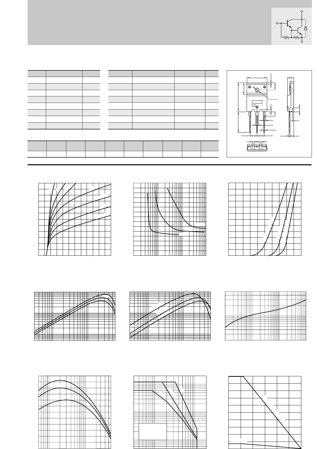
144
.
Darlington 2SD2045
IC–VCE Characteristics
(Typical)
hFE–IC Characteristics
(Typical)
θj-a–t Characteristics
VCE(sat)–IB Characteristics
(Typical)
Safe Operating Area (Single Pulse)
0
0
4
2
6
3
1
5
21 3456
Collector-Emitter Voltage VCE(V)
Collector Current IC(A)
20mA
5mA
2mA
1mA
0.7mA
0.5mA
I
B
=0.4mA
0.03 0.1 10.5 65
5000
10000
1000
500
100
50
Collector Current IC(A)
DC Current Gain hFE
(VCE=2V)
Typ
0
3
2
1
0.1
10510.5 50 100
Base Current IB(mA)
Collector-Emitter Saturation Voltage VCE(sat)(V)
2A
4A
I
C
=8A
0.2
1
5
0.5
1 10 100 1000
Transient Thermal Resistance θj-a(˚C/W)
1ms
10ms
10 5053 100 200
0.05
0.1
1
0.5
10
20
5
Collector-Emitter Voltage VCE(V)
Collector Current IC(A)
DC
Without Heatsink
Natural Cooling
IC–VBE Temperature Characteristics
(Typical)
0
3
4
5
6
2
1
021
Base-Emittor Voltage VBE(V)
Collector Current IC(A)
(VCE=2V)
0.03 0.1 10.5 5 6
5000
10000
1000
500
100
50
Collector Current IC(A) Time t(ms)
DC Current Gain hFE
(VCE=2V)
125˚C
25˚C
hFE–IC
Temperature Characteristics (Typical)
–30˚C
fT–IE Characteristics
(Typical)
–0.05 –0.1 –0.5 –1 –5–6
0
80
100
60
40
20
120
Cut-off Frequency fT(MHZ)
(VCE=12V)
Emitter Current IE(A)
Typ
Pc–Ta Derating
50
40
30
20
10
00 25 50 75 100 125 150
Ambient Temperature Ta(˚C)
Maximum Power Dissipation PC(W)
125˚C (Case Temp)
25˚C (Case Temp)
–30˚C (Case Temp)
With Infinite heatsink
Without Heatsink
Silicon NPN Triple Diffused Planar Transistor
Application : Driver for Solenoid, Motor and General Purpose
Symbol
VCBO
VCEO
VEBO
IC
IB
PC
Tj
Tstg
Ratings
120
120
6
6(Pulse10)
1
50(Tc=25°C)
150
–55 to +150
Unit
V
V
V
A
A
W
°C
°C
■
Absolute maximum ratings
■
Electrical Characteristics
Ratings
10max
10max
120min
2000min
1.5max
2.0max
50typ
70typ
Unit
µ
A
mA
V
V
V
MHz
pF
Conditions
VCB=120V
VEB=6V
IC=10mA
VCE=2V, IC=3A
IC=3A, IB=3mA
IC=3A, IB=3mA
VCE=12V, IE=–1A
VCB=10V, f=1MHz
(Ta=25°C) (Ta=25°C)
Symbol
ICBO
IEBO
V(BR)CEO
hFE
VCE(sat)
VBE(sat)
fT
COB
External Dimensions FM100(TO3PF)
4.41.5 1.5
BEC
5.45±0.1
ø3.3±0.2
1.6
3.3
1.75
0.8±0.2
2.15
1.05
+0.2
-0.1
5.45±0.1
23.0±0.3
16.2
9.5±0.2
5.5
15.6±0.2 5.5±0.2
3.45
3.35
0.65
+0.2
-0.1
±0.2
3.0
0.8
a
b
■Typical Switching Characteristics (Common Emitter)
VCC
(V)
30
RL
(Ω)
10
IC
(A)
3
VBB2
(V)
–5
IB2
(mA)
–3
ton
(
µ
s)
0.5typ
tstg
(
µ
s)
5.5typ
tf
(
µ
s)
1.5typ
IB1
(mA)
3
VBB1
(V)
10
Weight : Approx 2.0g
a. Part No.
b. Lot No.
B
C
E
(2.5kΩ)(200Ω)
Equivalent
circuit
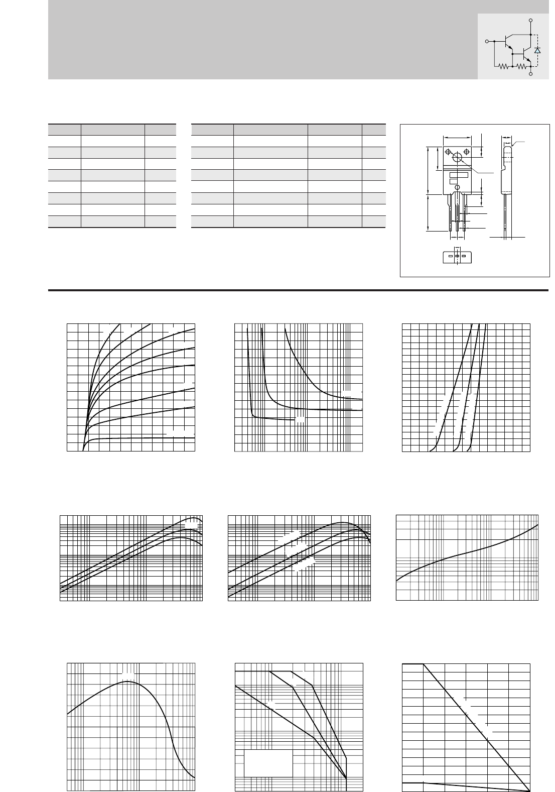
145
Darlington 2SD2081
IC–VCE Characteristics
(Typical)
hFE–IC Characteristics
(Typical)
hFE–IC
Temperature Characteristics (Typical)
θj-a–t Characteristics
IC–VBE Temperature Characteristics
(Typical)
VCE(sat)–IB Characteristics
(Typical)
Pc–Ta Derating
0
3
2
1
0.2
10.5 105 20010050
Base Current IB(mA)
Collector-Emitter Saturation Voltage VCE(sat)(V)
1A
5A
IC=10A
Safe Operating Area (Single Pulse)
0
0
5
10
15
213546
Collector-Emitter Voltage VCE(V)
Collector Current IC(A)
1mA
2mA
3mA
5mA
0.7mA
10mA
50mA
I
B
=0.5mA
0
10
8
6
4
2
0231
Base-Emittor Voltage VBE(V)
Collector Current IC(A)
(VCE=4V)
125˚C (Case Temp)
25˚C (Case Temp)
–30˚C (Case Temp)
0.03 0.1 10.5 105
5000
20000
10000
1000
500
100
30
50
Collector Current IC(A)
DC Current Gain hFE
(VCE=4V)
Typ
0.03 0.1 10.5 105
5000
20000
10000
1000
500
100
30
50
Collector Current IC(A)
DC Current Gain hFE
(VCE=4V)
125˚C
–30˚C
25˚C
1ms
10ms
10 5053 100 200
0.05
0.1
1
0.5
10
30
5
Collector-Emitter Voltage VCE(V)
Collector Current IC(A)
DC
Without Heatsink
Natural Cooling
0.2
1
5
0.5
1 10 100 1000
Time t(ms)
Transient Thermal Resistance θj-a(˚C/W)
30
20
10
2
00 25 50 75 100 125 150
Ambient Temperature Ta(˚C)
Maximum Power Dissipation PC(W)
With Infinite heatsink
Without Heatsink
fT–IE Characteristics
(Typical)
–0.05 –0.1 –0.5 –1 –5 –10
0
80
100
60
40
20
120
Cut-off Frequency fT(MHZ)
(VCE=12V)
Emitter Current IE(A)
Typ
Silicon NPN Triple Diffused Planar Transistor (Complement to type 2SB1259)
Application : Driver for Solenoid, Motor and General Purpose
Symbol
VCBO
VCEO
VEBO
IC
IB
PC
Tj
Tstg
Ratings
120
120
6
10(Pulse15)
1
30(Tc=25°C)
150
–55 to +150
Unit
V
V
V
A
A
W
°C
°C
■
Absolute maximum ratings
■
Electrical Characteristics
Ratings
10max
10max
120min
2000min
1.5max
2.0max
60typ
95typ
Unit
µ
A
mA
V
V
V
MHz
pF
Conditions
VCB=120V
VEB=6V
IC=10mA
VCE=4V, IC=5A
IC=5A, IB=5mA
IC=5A, IB=5mA
VCE=12V, IE=–0.5A
VCB=10V, f=1MHz
(Ta=25°C) (Ta=25°C)
Symbol
ICBO
IEBO
V(BR)CEO
hFE
VCE(sat)
VBE(sat)
fT
COB
External Dimensions FM20(TO220F)
ø3.3±0.2
10.1±0.2
4.0±0.2
16.9±0.3
13.0min
8.4±0.2
0.8±0.2
3.9
±0.2
2.542.54
1.35±0.15
0.85
+0.2
-0.1
1.35±0.15
2.2±0.2
4.2±0.2
2.8 c0.5
2.4±0.2
0.45
+0.2
-0.1
BEC
a
b
Weight : Approx 2.0g
a. Part No.
b. Lot No.
B
C
E
(2kΩ)(200Ω)
Equivalent
circuit
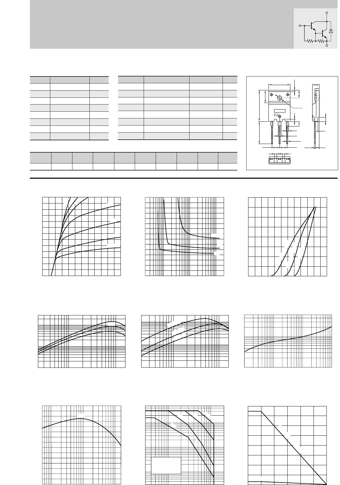
146
Darlington 2SD2082
IC–VCE Characteristics
(Typical)
hFE–IC Characteristics
(Typical)
θj-a–t Characteristics
IC–VBE Temperature Characteristics
(Typical)
VCE(sat)–IB Characteristics
(Typical)
Pc–Ta Derating
0
0
10
20
26
246135
Collector-Emitter Voltage VCE(V)
Collector Current IC(A)
3mA
6mA
1.5mA
12mA
40mA
20mA
I
B
=1mA
Safe Operating Area (Single Pulse)
0
3
2
1
0.2
10.5 105 20010050
Base Current IB(mA)
Collector-Emitter Saturation Voltage VCE(sat)(V)
4A
8A
IC=16A
0.2 10.5 10 165
5000
30000
10000
1000
500
100
Collector Current IC(A)
DC Current Gain hFE
(VCE=4V)
Typ
1ms
10ms
10 5053 100 200
0.03
0.05
0.1
1
0.5
10
50
5
Collector-Emitter Voltage VCE(V)
Collector Current IC(A)
DC
Without Heatsink
Natural Cooling
0.1
1
5
0.5
1 10 100 1000
Time t(ms)
Transient Thermal Resistance θj-a(˚C/W)
100µs
0
16
12
8
4
021
Base-Emittor Voltage VBE(V)
Collector Current IC(A)
(VCE=4V)
125˚C (Case Temp)
25˚C (Case Temp)
–30˚C (Case Temp)
hFE–IC
Temperature Characteristics (Typical)
0.02 1 10
516
5000
20000
10000
1000
500
100
Collector Current IC(A)
DC Current Gain hFE
(VCE=4V)
125˚C
–30˚C
25˚C
0.5
fT–IE Characteristics
(Typical)
–0.05–0.1 –0.5 –1 –5 –10 –16
0
20
10
30
Cut-off Frequency fT(MHZ)
(VCE=12V)
Emitter Current IE(A)
80
60
40
20
3.5
005025 75 125100 150
Ambient Temperature Ta(˚C)
Maximum Power Dissipation PC(W)
With Infinite heatsink
Without Heatsink
Typ
Silicon NPN Triple Diffused Planar Transistor (Complement to type 2SB1382)
Application : Driver for Solenoid, Motor and General Purpose
Symbol
VCBO
VCEO
VEBO
IC
IB
PC
Tj
Tstg
Ratings
120
120
6
16(Pulse26)
1
75(Tc=25°C)
150
–55 to +150
Unit
V
V
V
A
A
W
°C
°C
■
Absolute maximum ratings
■
Electrical Characteristics
Ratings
10max
10max
120min
2000min
1.5max
2.5max
20typ
210typ
Unit
µ
A
mA
V
V
V
MHz
pF
Conditions
VCB=120V
VEB=6V
IC=10mA
VCE=4V, IC=8A
IC=8A, IB=16mA
IC=8A, IB=16mA
VCE=12V, IE=–1A
VCB=10V, f=1MHz
(Ta=25°C) (Ta=25°C)
Symbol
ICBO
IEBO
V(BR)CEO
hFE
VCE(sat)
VBE(sat)
fT
COB
External Dimensions FM100(TO3PF)
4.41.5 1.5
BEC
5.45±0.1
ø3.3±0.2
1.6
3.3
1.75
0.8±0.2
2.15
1.05
+0.2
-0.1
5.45±0.1
23.0±0.3
16.2
9.5±0.2
5.5
15.6±0.2 5.5±0.2
3.45
3.35
0.65
+0.2
-0.1
±0.2
3.0
0.8
a
b
■Typical Switching Characteristics (Common Emitter)
VCC
(V)
40
RL
(Ω)
5
IC
(A)
8
VBB2
(V)
–5
IB2
(mA)
–16
ton
(
µ
s)
0.6typ
tstg
(
µ
s)
7.0typ
tf
(
µ
s)
1.5typ
IB1
(mA)
16
VBB1
(V)
10
Weight : Approx 2.0g
a. Part No.
b. Lot No.
B
C
E
(2kΩ)(100Ω)
Equivalent
circuit
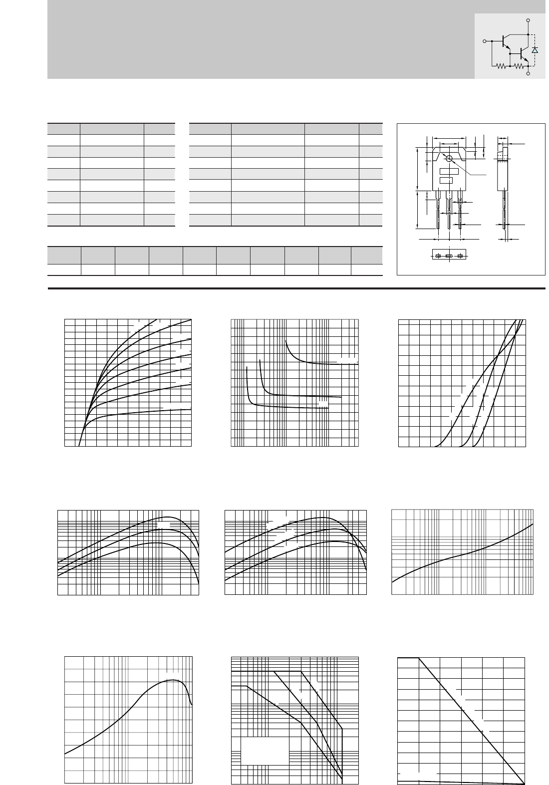
147
Darlington 2SD2083
IC–VCE Characteristics
(Typical)
hFE–IC Characteristics
(Typical)
θj-a–t Characteristics
IC–VBE Temperature Characteristics
(Typical)
VCE(sat)–IB Characteristics
(Typical)
Pc–Ta Derating
0
0
20
30
10
40
213546
Collector-Emitter Voltage VCE(V)
Collector Current IC(A)
3mA
5mA
8mA
12mA
30mA
20mA
I
B
=1.5mA
Safe Operating Area (Single Pulse)
fT–IE Characteristics
(Typical)
0
3
2
1
10.5 105 50010050
Base Current IB(mA)
Collector-Emitter Saturation Voltage VCE(sat)(V)
6A
12A
IC=25A
0.2 0.5 1 5 10 40
5000
20000
10000
1000
500
100
Collector Current IC(A)
DC Current Gain hFE
(VCE=4V)
Typ
–0.5–0.1 –1 –5 –10
0
50
100
Cut-off Frequency fT(MHZ)
(VCE=12V)
Emitter Current IE(A)
Typ
0.1
1
3
0.5
1 10 100 1000
Time t(ms)
Transient Thermal Resistance θj-a(˚C/W)
1ms
10ms
10 5053 100 200
0.2
1
0.5
10
50
100
5
Collector-Emitter Voltage VCE(V)
Collector Current IC(A)
DC
Without Heatsink
Natural Cooling
120
100
50
3.5
00 25 50 75 100 125 150
Ambient Temperature Ta(˚C)
Maximum Power Dissipation PC(W)
With Infinite heatsink
Without Heatsink
0
25
20
10
0 2 2.21
Base-Emittor Voltage VBE(V)
Collector Current IC(A)
(VCE=4V)
125˚C (Case Temp)
25˚C (Case Temp)
–30˚C (Case Temp)
hFE–IC
Temperature Characteristics (Typical)
0.02 1 10
540
5000
20000
10000
1000
500
100
Collector Current IC(A)
DC Current Gain hFE
(VCE=4V)
125˚C
–30˚C
25˚C
0.5
Silicon NPN Triple Diffused Planar Transistor (Complement to type 2SB1383)
Application : Driver for Solenoid, Motor and General Purpose
Symbol
VCBO
VCEO
VEBO
IC
IB
PC
Tj
Tstg
Ratings
120
120
6
25(Pulse40)
2
120(Tc=25°C)
150
–55 to +150
Unit
V
V
V
A
A
W
°C
°C
■
Absolute maximum ratings
■
Electrical Characteristics
Ratings
10max
10max
120min
2000min
1.8max
2.5max
20typ
340typ
Unit
µ
A
mA
V
V
V
MHz
pF
Conditions
VCB=120V
VEB=6V
IC=25mA
VCE=4V, IC=12A
IC=12A, IB=24mA
IC=12A, IB=24mA
VCE=12V, IE=–1A
VCB=10V, f=1MHz
(Ta=25°C) (Ta=25°C)
Symbol
ICBO
IEBO
V(BR)CEO
hFE
VCE(sat)
VBE(sat)
fT
COB
External Dimensions MT-100(TO3P)
15.6±0.4
9.6
19.9±0.3
4.0 2.0
5.0±0.2
1.8
ø3.2±0.1
2
3
1.05
+0.2
-0.1
20.0min
4.0max
BE
5.45±0.1 5.45±0.1
C
4.8±0.2
0.65
+0.2
-0.1
1.4
2.0±0.1
a
b
■Typical Switching Characteristics (Common Emitter)
VCC
(V)
24
RL
(Ω)
2
IC
(A)
12
VBB2
(V)
–5
IB2
(mA)
–24
ton
(
µ
s)
1.0typ
tstg
(
µ
s)
6.0typ
tf
(
µ
s)
1.0typ
IB1
(mA)
24
VBB1
(V)
10
Weight : Approx 6.0g
a. Part No.
b. Lot No.
B
C
E
(2kΩ)(100Ω)
Equivalent
circuit
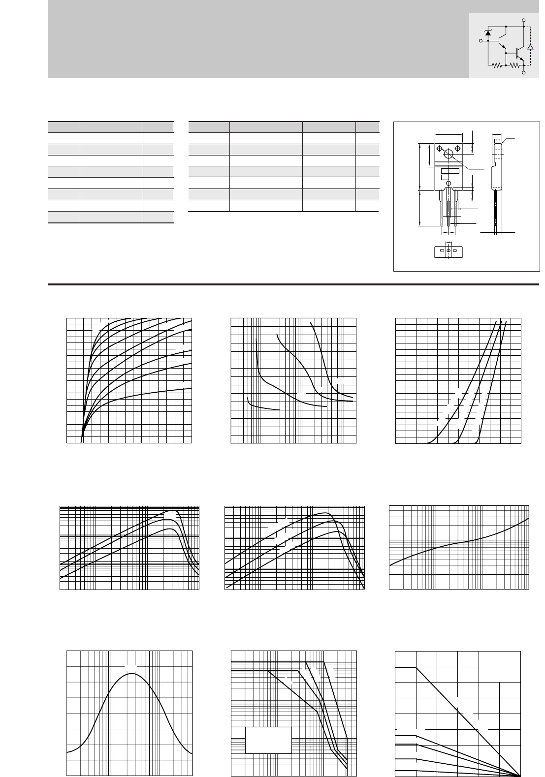
148
2SD2141
IC–VCE Characteristics
(Typical)
hFE–IC Characteristics
(Typical)
θj-a–t Characteristics
VCE(sat)–IB Characteristics
(Typical)
Pc–Ta Derating
0
0
5
10
246
Collector-Emitter Voltage VCE(V)
Collector Current IC(A)
Safe Operating Area (Single Pulse)
150mA
I
B
=1mA
2mA
4mA
18mA
20mA
120mA 90mA 60mA
0
3
2
1
0.2
10.5 105 20010050
Base Current IB(mA)
Collector Current IC(A)
1A
3A 5A
IC=7A
0.02 0.1 10.5 105
5000
10000
1000
500
100
10
50
Collector Current IC(A)
DC Current Gain hFE
(VCE=2V)
Typ
0.1
1
5
0.5
1 10 100 1000
Time t(ms)
Transient Thermal Resistance θj-a(˚C/W)
1ms
10ms
100ms
501051 100 500
0.01
0.05
0.1
1
0.5
10
20
5
Collector-Emitter Voltage VCE(V)
Collector Current IC(A)
DC
Without Heatsink
Natural Cooling
40
30
20
10
2
00 25 50 75 100 125 150
Ambient Temperature Ta(˚C)
Maximum Power Dissipation PC(W)
With Infinite heatsink
Without Heatsink
50x50x2
100x100x2
150x150x2
IC–VBE Temperature Characteristics
(Typical)
0
10
5
0 2.0 2.41.0
Base-Emittor Voltage VBE(V)
Collector Current IC(A)
(VCE=4V)
125˚C (Case Temp)
25˚C (Case Temp)
–30˚C (Case Temp)
hFE–IC
Temperature Characteristics (Typical)
0.02 0.1 1.0 5
0.5 10
5000
10000
1000
500
100
50
20
Collector Current IC(A)
DC Current Gain hFE
(VCE=2V)
125˚C
–55˚C
25˚C
fT–IE Characteristics
(Typical)
(VCE=12V)
Emitter Current IE(A)
0.050.01 01 0.5 1 5
0
20
10
30
40
Cut-off Frequency fT(MHZ)
Typ
Natural Cooling
Silicone Grease
Heatsink: Aluminum
in mm
Silicon NPN Triple Diffused Planar Transistor
Application : Ignitor, Driver for Solenoid and Motor, and General Purpose
Symbol
VCBO
VCEO
VEBO
IC
IB
PC
Tj
Tstg
Ratings
380±50
380±50
6
6(Pulse10)
1
35(Tc=25°C)
150
–55 to +150
Unit
V
V
V
A
A
W
°C
°C
■
Absolute maximum ratings
■
Electrical Characteristics
Ratings
10max
20max
330to430
1500min
1.5max
20typ
95typ
Unit
µ
A
mA
V
V
MHz
pF
Conditions
VCB=330V
VEB=6V
IC=25mA
VCE=2V, IC=3A
IC=4A, IB=20mA
VCE=12V, IE=–0.5A
VCB=10V, f=1MHz
(Ta=25°C) (Ta=25°C)
Symbol
ICBO
IEBO
V(BR)CEO
hFE
VCE(sat)
fT
COB
External Dimensions FM20(TO220F)
ø3.3±0.2
10.1±0.2
4.0±0.2
16.9±0.3
13.0min
8.4±0.2
0.8±0.2
3.9
±0.2
2.542.54
1.35±0.15
0.85
+0.2
-0.1
1.35±0.15
2.2±0.2
4.2±0.2
2.8 c0.5
2.4±0.2
0.45
+0.2
-0.1
BEC
a
b
Weight : Approx 2.0g
a. Part No.
b. Lot No.
Built-in Avalanche Diode
for Surge Absorbing
Darlington
B
C
E
(1.5kΩ)(100Ω)
Equivalent circuit
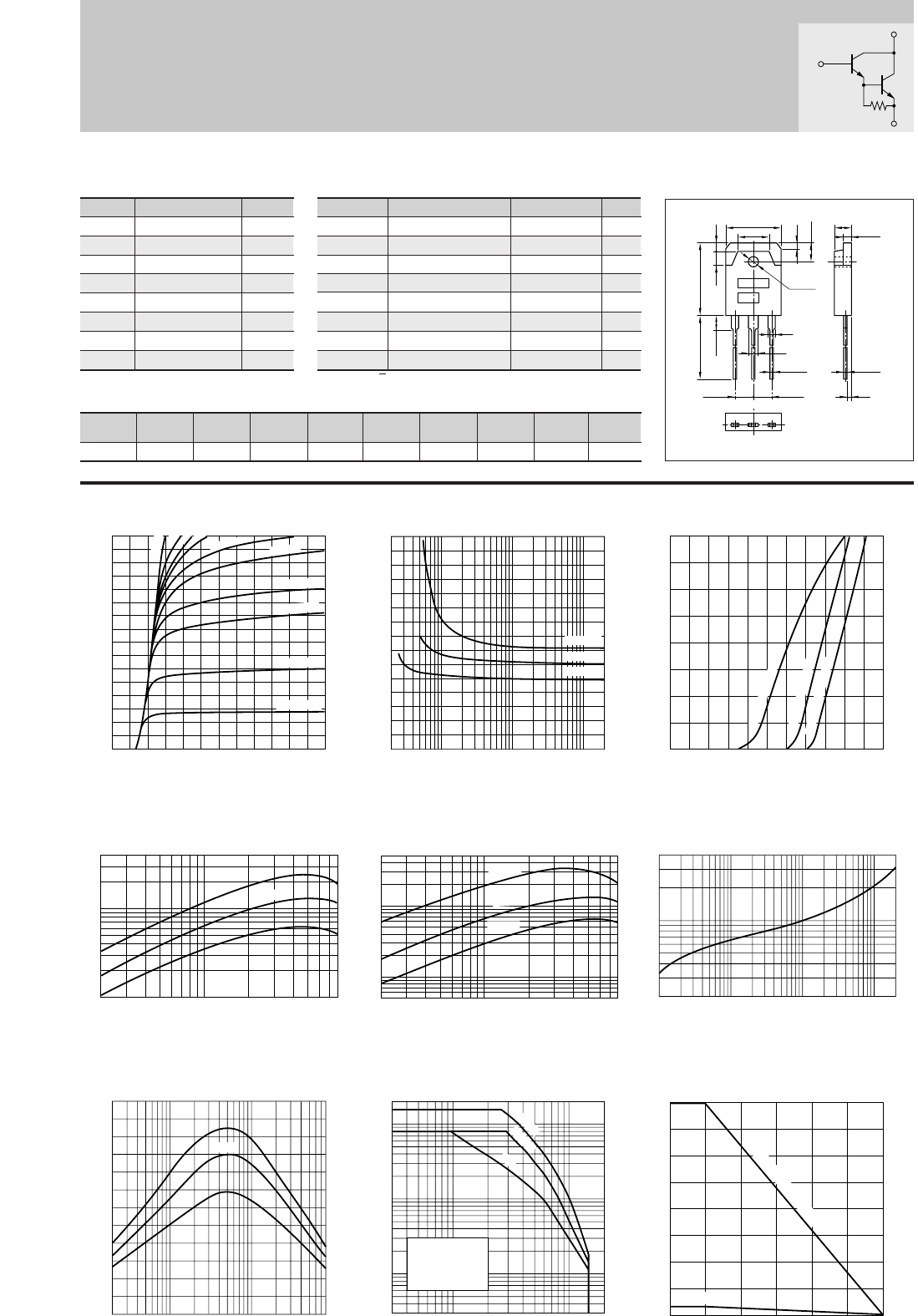
149
Darlington 2SD2389
IC–VCE Characteristics
(Typical)
hFE–IC Characteristics
(Typical)
hFE–IC
Temperature Characteristics (Typical)
θj-a–t Characteristics
IC–VBE Temperature Characteristics
(Typical)
VCE(sat)–IB Characteristics
(Typical)
Pc–Ta Derating
Safe Operating Area (Single Pulse)
fT–IE Characteristics
(Typical)
0
0
2
4
6
8
246
Collector-Emitter Voltage VCE(V)
Collector Current IC(A)
10mA
2.5mA
2.0mA
1.8mA
1.5mA
1.3mA
1.0mA
0.8mA
0.5mA
I
B
=0.3mA
02 0.5 1 5 8
Collector Current IC(A)
DC Current Gain hFE
(VCE=4V)
1000
5000
10000
40000
Typ
0
8
6
4
2
021
Base-Emittor Voltage VBE(V)
Collector Current IC(A)
(VCE=4V)
125˚C (Case Temp)
25˚C (Case Temp)
–30˚C (Case Temp)
80
60
40
20
3.5
00 25 50 75 100 125 150
Ambient Temperature Ta(˚C)
Maximum Power Dissipation PC(W)
With Infinite heatsink
Without Heatsink
10 5053 100 200
150
0.05
0.03
1
0.5
0.1
10
20
5
Collector-Emitter Voltage VCE(V)
Collector Current IC(A)
Without Heatsink
Natural Cooling
DC
100ms
10ms
0
3
2
1
0.2
10.5 105 20010050
Base Current IB(mA)
Collector-Emitter Saturation Voltage VCE(sat)(V)
IC=4A
IC=6A
IC=8A
(VCE=4V)
0.2 0.5 5 81
Collector Current IC(A)
DC Current Gain hFE
1000
500
5000
10000
50000
125˚C
25˚C
–30˚C
–0.02 –0.1 –1 –8
0
20
40
120
100
80
60
Cut-off Frequency fT(MHZ)
(VCE=12V)
Emitter Current IE(A)
Typ
0.2
0.5
4
1
110505 100 500 1000 2000
Time t(ms)
Transient Thermal Resistance θj-a(˚C/W)
Silicon NPN Triple Diffused Planar Transistor (Complement to type 2SB1559)
Application : Audio, Series Regulator and General Purpose
Symbol
VCBO
VCEO
VEBO
IC
IB
PC
Tj
Tstg
Ratings
160
150
5
8
1
80(Tc=25°C)
150
–55 to +150
Unit
V
V
V
A
A
W
°C
°C
■
Absolute maximum ratings
■
Electrical Characteristics
Ratings
100max
100max
150min
5000min∗
2.5max
3.0max
80typ
85typ
Unit
µ
A
µ
A
V
V
V
MHz
pF
Conditions
VCB=160V
VEB=5V
IC=30mA
VCE=4V, IC=6A
IC=6A, IB=6mA
IC=6A, IB=6mA
VCE=12V, IE=–1A
VCB=10V, f=1MHz
(Ta=25°C) (Ta=25°C)
Symbol
ICBO
IEBO
V(BR)CEO
hFE
VCE(sat)
VBE(sat)
fT
COB
External Dimensions MT-100(TO3P)
15.6±0.4
9.6
19.9±0.3
4.0 2.0
5.0±0.2
1.8
ø3.2±0.1
2
3
1.05
+0.2
-0.1
20.0min
4.0max
BE
5.45±0.1 5.45±0.1
C
4.8±0.2
0.65
+0.2
-0.1
1.4
2.0±0.1
a
b
■Typical Switching Characteristics (Common Emitter)
VCC
(V)
60
RL
(Ω)
10
IC
(A)
6
VBB2
(V)
–5
IB2
(mA)
–6
ton
(
µ
s)
0.6typ
tstg
(
µ
s)
10.0typ
tf
(
µ
s)
0.9typ
IB1
(mA)
6
VBB1
(V)
10
Weight : Approx 2.0g
a. Part No.
b. Lot No.
B
C
E
(70Ω)
Equivalent circuit
∗hFE Rank O(5000to12000), P(6500to20000), Y(15000to30000)
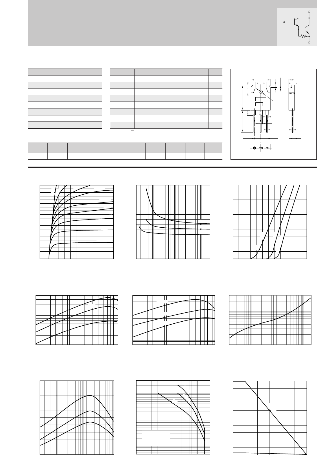
150
Silicon NPN Triple Diffused Planar Transistor (Complement to type 2SB1560)
Application : Audio, Series Regulator and General Purpose
Symbol
VCBO
VCEO
VEBO
IC
IB
PC
Tj
Tstg
Ratings
160
150
5
10
1
100(Tc=25°C)
150
–55 to +150
Unit
V
V
V
A
A
W
°C
°C
■
Absolute maximum ratings
■
Electrical Characteristics
Symbol
ICBO
IEBO
V(BR)CEO
hFE
VCE(sat)
VBE(sat)
fT
COB
Ratings
100max
100max
150min
5000min∗
2.5max
3.0max
55typ
95typ
Unit
µ
A
µ
A
V
V
V
MHz
pF
Conditions
VCB=160V
VEB=5V
IC=30mA
VCE=4V, IC=7A
IC=7A, IB=7mA
IC=7A, IB=7mA
VCE=12V, IE=–2A
VCB=10V, f=1MHz
Darlington 2SD2390
(Ta=25°C) (Ta=25°C)
IC–VCE Characteristics
(Typical)
hFE–IC Characteristics
(Typical)
hFE–IC
Temperature Characteristics (Typical)
θj-a–t Characteristics
IC–VBE Temperature Characteristics
(Typical)
VCE(sat)–IB Characteristics
(Typical)
Pc–Ta Derating
Safe Operating Area (Single Pulse)
fT–IE Characteristics
(Typical)
0
0
2
4
6
10
8
246
Collector-Emitter Voltage VCE(V)
Collector Current IC(A)
10mA
2.5mA
2mA
1.5mA
1.2mA
0.8mA
1mA
0.6mA
I
B
=0.4mA
02 0.5 1 5 10
Collector Current IC(A)
DC Current Gain hFE
(VCE=4V)
1000
5000
10000
40000
Typ
0.1
1
3
0.5
1 10 100 10005 50 500 2000
Time t(ms)
Transient Thermal Resistance θj-a(˚C/W)
0
10
8
2
4
6
0 2 2.51
Base-Emittor Voltage VBE(V)
Collector Current IC(A)
(VCE=4V)
125˚C (Case Temp)
25˚C (Case Temp)
–30˚C (Case Temp)
100
50
3.5
00 25 50 75 100 125 150
Ambient Temperature Ta(˚C)
Maximum Power Dissipation PC(W)
With Infinite heatsink
Without Heatsink
10ms
10 5053 100 200
0.05
0.1
1
0.5
10
30
5
Collector-Emitter Voltage VCE(V)
Collector Current IC(A)
DC
100ms
Without Heatsink
Natural Cooling
0
3
2
1
0.2
10.5 105 20010050
Base Current IB(mA)
Collector-Emitter Saturation Voltage VCE(sat)(V)
IC=5A
IC=7A
IC=10A
(VCE=4V)
0.2 0.5 5 101
Collector Current IC(A)
DC Current Gain hFE
1000
500
5000
10000
50000
70000
125˚C
25˚C
–30˚C
–0.02 –0.1 –1 –10
0
20
40
100
80
60
Cut-off Frequency fT(MHZ)
(VCE=12V)
Emitter Current IE(A)
Typ
■Typical Switching Characteristics (Common Emitter)
VCC
(V)
70
RL
(Ω)
10
IC
(A)
7
VBB2
(V)
–5
IB2
(mA)
–7
ton
(
µ
s)
0.5typ
tstg
(
µ
s)
10.0typ
tf
(
µ
s)
1.1typ
IB1
(mA)
7
VBB1
(V)
10
External Dimensions MT-100(TO3P)
15.6±0.4
9.6
19.9±0.3
4.0 2.0
5.0±0.2
1.8
ø3.2±0.1
2
3
1.05
+0.2
-0.1
20.0min
4.0max
BE
5.45±0.1 5.45±0.1
C
4.8±0.2
0.65
+0.2
-0.1
1.4
2.0±0.1
a
b
Weight : Approx 2.0g
a. Part No.
b. Lot No.
B
C
E
(70Ω)
Equivalent circuit
∗hFE Rank O(5000to12000), P(6500to20000), Y(15000to30000)
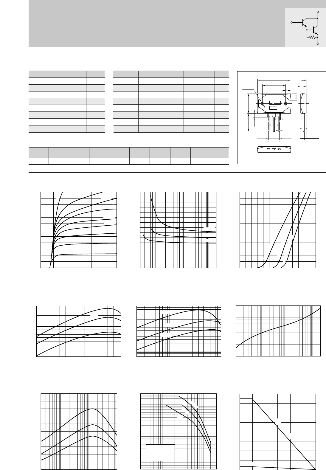
151
Darlington 2SD2401
IC–VCE Characteristics
(Typical)
hFE–IC Characteristics
(Typical)
hFE–IC
Temperature Characteristics (Typical)
θj-a–t Characteristics
IC–VBE Temperature Characteristics
(Typical)
VCE(sat)–IB Characteristics
(Typical)
Pc–Ta Derating
Safe Operating Area (Single Pulse)
fT–IE Characteristics
(Typical)
0
0
2
4
6
12
10
8
246
Collector-Emitter Voltage VCE(V)
Collector Current IC(A)
10mA
2.5mA
1.2mA
1.5mA
1.0mA
2.0mA
0.8mA
0.6mA
I
B
=0.4mA
02 0.5 1 5 1012
Collector Current IC(A)
DC Current Gain hFE
(VCE=4V)
1000
5000
10000
40000
Typ
0.1
1
2
0.5
1 10 100 10005 50 500 2000
Time t(ms)
Transient Thermal Resistance θj-a(˚C/W)
0
12
8
10
2
4
6
0 2.621
Base-Emittor Voltage VBE(V)
Collector Current IC(A)
(VCE=4V)
125˚C (Case Temp)
25˚C (Case Temp)
–30˚C (Case Temp)
160
120
80
40
5
00 25 50 75 100 125 150
Ambient Temperature Ta(˚C)
Maximum Power Dissipation PC(W)
With Infinite heatsink
Without Heatsink
10ms
10 5053 100 200
150
0.05
0.1
1
0.5
10
30
5
Collector-Emitter Voltage VCE(V)
Collector Current IC(A)
DC
100ms
Without Heatsink
Natural Cooling
0
3
2
1
0.2
10.5 105 20010050
Base Current IB(mA)
Collector-Emitter Saturation Voltage VCE(sat)(V)
IC=5A
IC=7A
IC=10A
(VCE=4V)
0.2 0.5 5 10 121
Collector Current IC(A)
DC Current Gain hFE
1000
600
5000
10000
50000
70000
125˚C
25˚C
–30˚C
–0.02 –0.1 –1 –10
0
20
40
100
80
60
Cut-off Frequency fT(MHZ)
(VCE=12V)
Emitter Current IE(A)
Typ
Silicon NPN Triple Diffused Planar Transistor (Complement to type 2SB1570)
Application : Audio, Series Regulator and General Purpose
Symbol
VCBO
VCEO
VEBO
IC
IB
PC
Tj
Tstg
Ratings
160
150
5
12
1
150(Tc=25°C)
150
–55 to +150
Unit
V
V
V
A
A
W
°C
°C
■
Absolute maximum ratings
■
Electrical Characteristics
Symbol
ICBO
IEBO
V(BR)CEO
hFE
VCE(sat)
VBE(sat)
fT
COB
Ratings
100max
100max
150min
5000min∗
2.5max
3.0max
55typ
95typ
Unit
µ
A
µ
A
V
V
V
MHz
pF
Conditions
VCB=160V
VEB=5V
IC=30mA
VCE=4V, IC=7A
IC=7A, IB=7mA
IC=7A, IB=7mA
VCE=12V, IE=–2A
VCB=10V, f=1MHz
(Ta=25°C) (Ta=25°C)
External Dimensions MT-200
■Typical Switching Characteristics (Common Emitter)
VCC
(V)
70
RL
(Ω)
10
IC
(A)
7
VBB2
(V)
–5
IB2
(mA)
–7
ton
(
µ
s)
0.5typ
tstg
(
µ
s)
10.0typ
tf
(
µ
s)
1.1typ
IB1
(mA)
7
VBB1
(V)
10
2
3
1.05
+0.2
-0.1
BE
5.45±0.1 5.45±0.1
2-ø3.2±0.1
36.4±0.3
9
24.4±0.2
7
21.4±0.3
20.0min
4.0max
0.65
+0.2
-0.1
3.0
+0.3
-0.1
6.0±0.2
2.1
a
b
C
Weight : Approx 18.4g
a. Part No.
b. Lot No.
B
C
E
(70Ω)
Equivalent circuit
∗hFE Rank O(5000to12000), P(6500to20000), Y(15000to30000)

152
Silicon NPN Triple Diffused Planar Transistor (Complement to type 2SB1587)
Application : Audio, Series Regulator and General Purpose
Symbol
VCBO
VCEO
VEBO
IC
IB
PC
Tj
Tstg
Ratings
160
150
5
8
1
75(Tc=25°C)
150
–55 to +150
Unit
V
V
V
A
A
W
°C
°C
■
Absolute maximum ratings
■
Electrical Characteristics
Symbol
ICBO
IEBO
V(BR)CEO
hFE
VCE(sat)
VBE(sat)
fT
COB
Ratings
100max
100max
150min
5000min∗
2.5max
3.0max
80typ
85typ
Unit
µ
A
µ
A
V
V
V
MHz
pF
Conditions
VCB=160V
VEB=5V
IC=30mA
VCE=4V, IC=6A
IC=6A, IB=6mA
IC=6A, IB=6mA
VCE=12V, IE=–1A
VCB=10V, f=1MHz
Darlington 2SD2438
(Ta=25°C) (Ta=25°C)
IC–VCE Characteristics
(Typical)
hFE–IC Characteristics
(Typical)
hFE–IC
Temperature Characteristics (Typical)
θj-a–t Characteristics
IC–VBE Temperature Characteristics
(Typical)
VCE(sat)–IB Characteristics
(Typical)
Pc–Ta Derating
Safe Operating Area (Single Pulse)
fT–IE Characteristics
(Typical)
0
0
2
4
6
8
246
Collector-Emitter Voltage VCE(V)
Collector Current IC(A)
10mA
2.5mA
2.0mA
1.8mA
1.5mA
1.3mA
1.0mA
0.8mA
0.5mA
I
B
=0.3mA
02 0.5 1 5 8
Collector Current IC(A)
DC Current Gain hFE
(VCE=4V)
1000
5000
10000
40000
Typ
0.2
1
4
0.5
1 10 100 10005 50 500 2000
Time t(ms)
Transient Thermal Resistance θj-a(˚C/W)
0
8
6
4
2
0 2 2.51
Base-Emittor Voltage VBE(V)
Collector Current IC(A)
(VCE=4V)
125˚C (Case Temp)
25˚C (Case Temp)
–30˚C (Case Temp)
80
60
40
20
3.5
00 50 100 150
Ambient Temperature Ta(˚C)
Maximum Power Dissipation PC(W)
With Infinite heatsink
Without Heatsink
10ms
10 5053 100 200
0.05
0.1
1
0.5
10
20
5
Collector-Emitter Voltage VCE(V)
Collector Current IC(A)
DC
100ms
0
3
2
1
0.2
10.5 105 20010050
Base Current IB(mA)
Collector-Emitter Saturation Voltage VCE(sat)(V)
IC=4A
IC=6A
IC=8A
(VCE=4V)
0.2 0.5 5 81
Collector Current IC(A)
DC Current Gain hFE
1000
500
5000
10000
50000
125˚C
25˚C
–30˚C
–0.02 –0.1 –1 –8
0
20
40
120
100
80
60
Cut-off Frequency fT(MHZ)
(VCE=12V)
Emitter Current IE(A)
Typ
Without Heatsink
Natural Cooling
■Typical Switching Characteristics (Common Emitter)
VCC
(V)
60
RL
(Ω)
10
IC
(A)
6
VBB2
(V)
–2
IB2
(mA)
–6
ton
(
µ
s)
0.6typ
tstg
(
µ
s)
10.0typ
tf
(
µ
s)
0.9typ
IB1
( mA)
6
VBB1
(V)
10
External Dimensions FM100(TO3PF)
4.41.5 1.5
BEC
5.45±0.1
ø3.3±0.2
1.6
3.3
1.75
0.8±0.2
2.15
1.05
+0.2
-0.1
5.45±0.1
23.0±0.3
16.2
9.5±0.2
5.5
15.6±0.2 5.5±0.2
3.45
3.35
0.65
+0.2
-0.1
±0.2
3.0
0.8
a
b
Weight : Approx 6.5g
a. Part No.
b. Lot No.
B
C
E
(70Ω)
Equivalent circuit
∗hFE Rank O(5000to12000), P(6500to20000), Y(15000to30000)
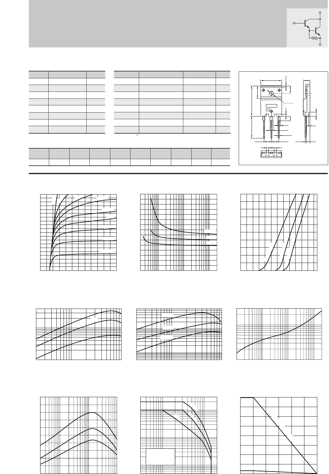
153
Darlington 2SD2439
IC–VCE Characteristics
(Typical)
hFE–IC Characteristics
(Typical)
hFE–IC
Temperature Characteristics (Typical)
θj-a–t Characteristics
IC–VBE Temperature Characteristics
(Typical)
VCE(sat)–IB Characteristics
(Typical)
Pc–Ta Derating
Safe Operating Area (Single Pulse)
fT–IE Characteristics
(Typical)
0
0
2
4
6
10
8
246
Collector-Emitter Voltage VCE(V)
Collector Current IC(A)
10mA
2.5mA
2mA
1.5mA
1.2mA
0.8mA
1mA
0.6mA
I
B
=0.4mA
02 0.5 1 5 10
Collector Current IC(A)
DC Current Gain hFE
(VCE=4V)
1000
5000
10000
40000
Typ
0.1
1
3
0.5
1 10 100 10005 50 500 2000
Time t(ms)
Transient Thermal Resistance θj-a(˚C/W)
0
10
8
2
4
6
0 2 2.51
Base-Emittor Voltage VBE(V)
Collector Current IC(A)
(VCE=4V)
125˚C (Case Temp)
25˚C (Case Temp)
–30˚C (Case Temp)
80
60
40
20
3.5
00 50 100 150
Ambient Temperature Ta(˚C)
Maximum Power Dissipation PC(W)
With Infinite heatsink
Without Heatsink
10ms
10 5053 100 200
0.05
0.1
1
0.5
10
30
5
Collector-Emitter Voltage VCE(V)
Collector Current IC(A)
DC
100ms
0
3
2
1
0.2
10.5 105 20010050
Base Current IB(mA)
Collector-Emitter Saturation Voltage VCE(sat)(V)
IC=5A
IC=7A
IC=10A
(VCE=4V)
0.2 0.5 5 101
Collector Current IC(A)
DC Current Gain hFE
1000
500
5000
10000
50000
70000
125˚C
25˚C
–30˚C
–0.02 –0.1 –1 –10
0
20
40
100
80
60
Cut-off Frequency fT(MHZ)
(VCE=12V)
Emitter Current IE(A)
Typ
Without Heatsink
Natural Cooling
Silicon NPN Triple Diffused Planar Transistor (Complement to type 2SB1588)
Application : Audio, Series Regulator and General Purpose
Symbol
VCBO
VCEO
VEBO
IC
IB
PC
Tj
Tstg
Ratings
160
150
5
10
1
80(Tc=25°C)
150
–55 to +150
Unit
V
V
V
A
A
W
°C
°C
■
Absolute maximum ratings
■
Electrical Characteristics
Symbol
ICBO
IEBO
V(BR)CEO
hFE
VCE(sat)
VBE(sat)
fT
COB
Ratings
100max
100max
150min
5000min∗
2.5max
3.0max
55typ
95typ
Unit
µ
A
µ
A
V
V
V
MHz
pF
Conditions
VCB=160V
VEB=5V
IC=30mA
VCE=4V, IC=7A
IC=7A, IB=7mA
IC=7A, IB=7mA
VCE=12V, IE=–2A
VCB=10V, f=1MHz
(Ta=25°C) (Ta=25°C)
■Typical Switching Characteristics (Common Emitter)
VCC
(V)
70
RL
(Ω)
10
IC
(A)
7
VBB2
(V)
–5
IB2
(mA)
–7
ton
(
µ
s)
0.5typ
tstg
(
µ
s)
10.0typ
tf
(
µ
s)
1.1typ
IB1
(mA)
7
VBB1
(V)
10
External Dimensions FM100(TO3PF)
4.41.5 1.5
BEC
5.45±0.1
ø3.3±0.2
1.6
3.3
1.75
0.8±0.2
2.15
1.05
+0.2
-0.1
5.45±0.1
23.0±0.3
16.2
9.5±0.2
5.5
15.6±0.2 5.5±0.2
3.45
3.35
0.65
+0.2
-0.1
±0.2
3.0
0.8
a
b
Weight : Approx 6.5g
a. Part No.
b. Lot No.
B
C
E
(70Ω)
Equivalent circuit
∗hFE Rank O(5000to12000), P(6500to20000), Y(15000to30000)
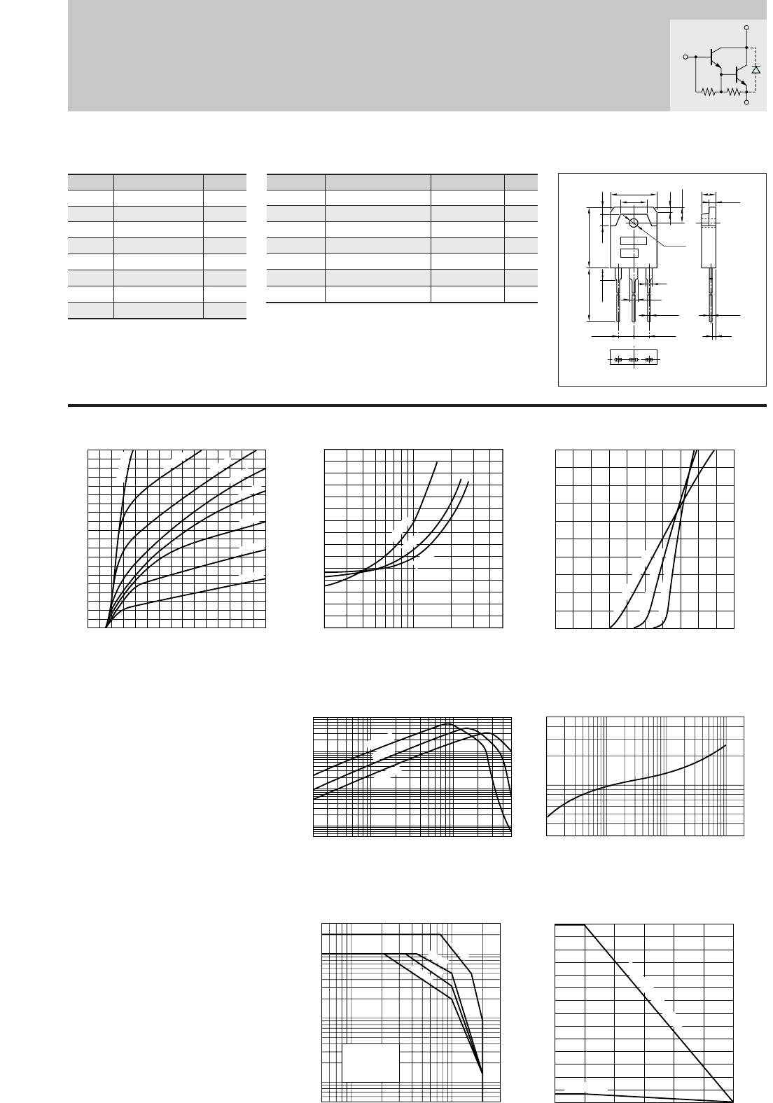
154
Silicon NPN Triple Diffused Planar Transistor
Application : Series Regulator and General Purpose
Symbol
VCBO
VCEO
VEBO
IC
IB
PC
Tj
Tstg
Ratings
200
200
6
5
2
70(Tc=25°C)
150
–55 to +150
Unit
V
V
V
A
A
W
°C
°C
■
Absolute maximum ratings
■
Electrical Characteristics
Symbol
ICBO
IEBO
V(BR)CEO
hFE
VCE(sat)
fT
COB
Ratings
100max
5max
200min
1500to6500
1.5max
15typ
110typ
Unit
µ
A
mA
V
V
MHz
pF
Conditions
VCB=200V
VEB=6V
IC=10mA
VCE=5V, IC=1A
IC=1A, IB=5mA
VCE=10V, IE=–0.5A
VCB=10V, f=1MHz
Darlington 2SD2557
(Ta=25°C) (Ta=25°C)
IC–VCE Characteristics
(Typical)
hFE–IC Characteristics
(Typical)
hFE–IC
Temperature Characteristics (Typical)
θj-a–t Characteristics
IC–VBE Temperature Characteristics
(Typical)VCE(sat)–IC Temperature Characteristics
(Typical)
Safe Operating Area (Single Pulse)
fT–IE Characteristics
(Typical)
0
5
4
2
1
3
0 2.521
Base-Emittor Voltage VBE(V)
Collector Current IC(A)
Collector to Emitter Saturation Voltage VCE(sat) (V)
(VCE=4V)
125˚C (Case Temp)
25˚C (Case Temp)
–30˚C (Case Temp)
10ms
50ms
1ms
10 505 100 300
0.05
0.1
1
0.5
10
30
5
Collector-Emitter Voltage VCE(V)
Collector Current IC(A)
100ms
(VCE=5V)
0.02 0.1 510.5
Collector Current IC(A)
DC Current Gain hFE
1000
500
5
10
100
50
5000
8000
Pc–Ta Derating
70
60
50
40
30
20
10
3.5
00 25 50 75 100 125 150
Ambient Temperature Ta(˚C)
Maximum Power Dissipation PC(W)
With Infinite heatsink
Without Heatsink
125˚C
25˚C
–30˚C
Without Heatsink
Natural Cooling
0.3
0.5
5.0
1.0
1105 10050
20001000500
Time t(ms)
Transient Thermal Resistance θj-a(˚C/W)
0
0
1
2
4
3
5
264
Collector-Emitter Voltage VCE(V) Collector Current Ic(A)
Collector Current IC(A)
I
B
=1.0A
250mA
50mA
10mA
2.5mA
1.2mA
0.6mA
0.3mA
0
3
2
1
0.2
10.5 5
125˚C
25˚C
–30˚C
(IC/IB=1000)
External Dimensions MT-100(TO3P)
15.6±0.4
9.6
19.9±0.3
4.0 2.0
5.0±0.2
1.8
ø3.2±0.1
2
3
1.05
+0.2
-0.1
20.0min
4.0max
BE
5.45±0.1 5.45±0.1
C
4.8±0.2
0.65
+0.2
-0.1
1.4
2.0±0.1
a
b
Weight : Approx 6.0g
a. Part No.
b. Lot No.
B
C
E
(3.2kΩ)(450Ω)
Equivalent circuit
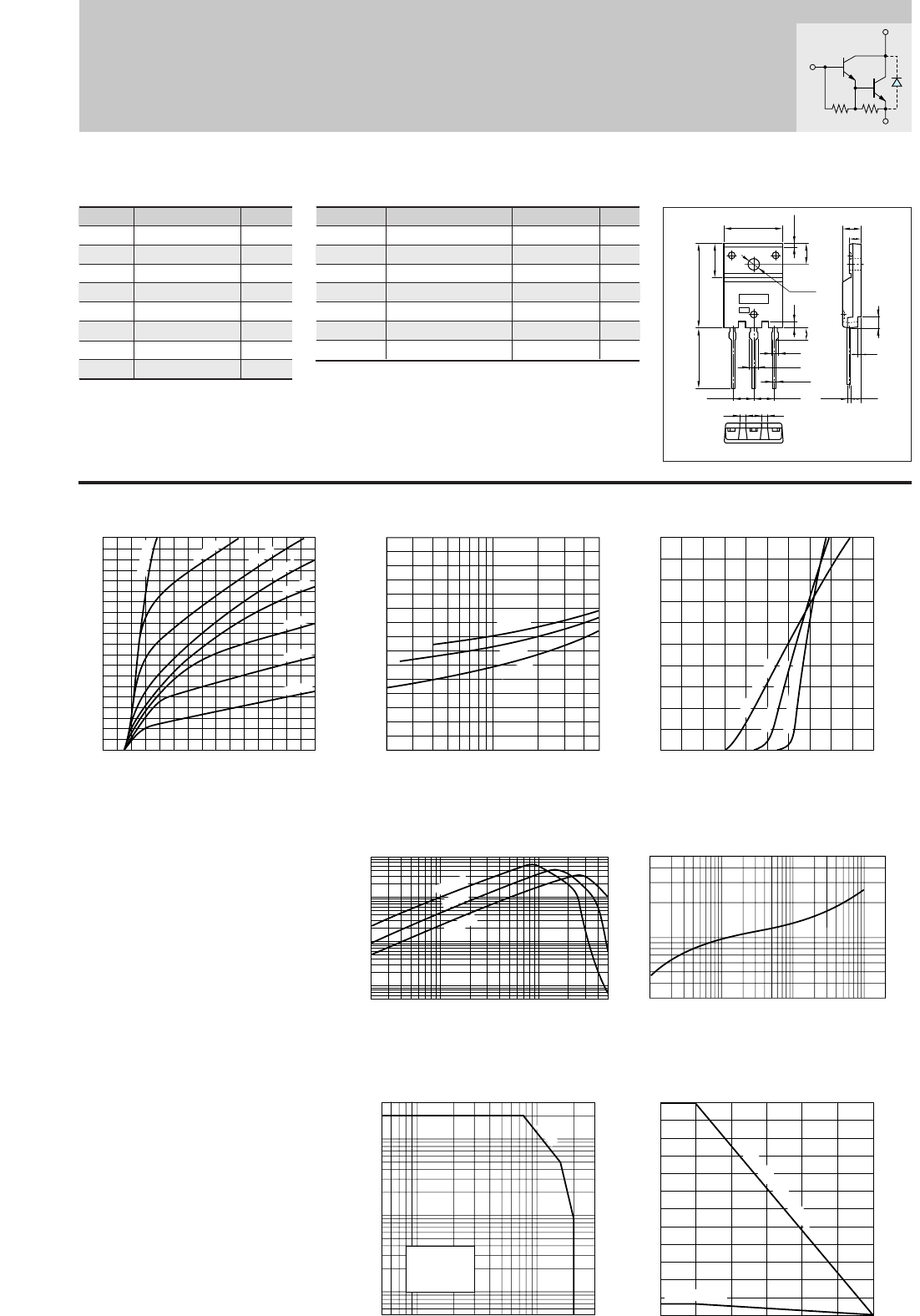
155
Silicon NPN Triple Diffused Planar Transistor
Application : Series Regulator and General Purpose
Symbol
VCBO
VCEO
VEBO
IC
IB
PC
Tj
Tstg
Ratings
200
200
6
5
2
60(Tc=25°C)
150
–55 to +150
Unit
V
V
V
A
A
W
°C
°C
■
Absolute maximum ratings
■
Electrical Characteristics
Symbol
ICBO
IEBO
V(BR)CEO
hFE
VCE(sat)
fT
COB
Ratings
100max
5max
200min
1500to6500
1.5max
15typ
110typ
Unit
µ
A
mA
V
V
MHz
pF
Conditions
VCB=200V
VEB=6V
IC=10mA
VCE=5V, IC=1A
IC=1A, IB=5mA
VCE=10V, IE=–0.5A
VCB=10V, f=1MHz
Darlington 2SD2558
(Ta=25°C) (Ta=25°C)
IC–VCE Characteristics
(Typical)
hFE–IC Characteristics
(Typical)
hFE–IC
Temperature Characteristics (Typical)
θj-a–t Characteristics
IC–VBE Temperature Characteristics
(Typical)VBE(sat)–IC Temperature Characteristics
(Typical)
60
40
20
3.5
00 25 50 75 100 125 150
Ambient Temperature Ta(˚C)
Maximum Power Dissipation PC(W)
With Infinite heatsink
Without Heatsink
Safe Operating Area (Single Pulse)
fT–IE Characteristics
(Typical)
0
5
4
2
1
3
0 2.521
Base-Emittor Voltage VBE(V)
Collector Current IC(A)
(VCE=4V)
125˚C (Case Temp)
25˚C (Case Temp)
–30˚C (Case Temp)
1ms
10 505 100 300
0.05
0.1
1
0.5
10
30
5
Collector-Emitter Voltage VCE(V)
Collector Current IC(A)
(VCE=5V)
0.02 0.1 510.5
Collector Current IC(A)
DC Current Gain hFE
1000
500
5
10
100
50
5000
8000
Pc–Ta Derating
125˚C
25˚C
–30˚C
Without Heatsink
Natural Cooling
0.3
0.5
5.0
1.0
1105 10050
20001000500
Time t(ms)
Transient Thermal Resistance θj-a(˚C/W)
0
0
1
2
4
3
5
264
Collector-Emitter Voltage VCE(V) Collector Current IC(A)
Collector Current IC(A)
Base to Emitter Saturation Voltage VBE(sat)(V)
I
B
=1.0A
250mA
50mA
10mA
2.5mA
1.2mA
0.6mA
0.3mA
(IC/IB=1000)
0
3
2
1
0.2
10.5 5
125˚C
25˚C
–30˚C
B
C
E
(3.2kΩ)(450Ω)
Equivalent circuit
External Dimensions FM100(TO3PF)
4.41.5 1.5
BEC
5.45±0.1
ø3.3±0.2
1.6
3.3
1.75
0.8±0.2
2.15
1.05
+0.2
-0.1
5.45±0.1
23.0±0.3
16.2
9.5±0.2
5.5
15.6±0.2 5.5±0.2
3.45
3.35
0.65
+0.2
-0.1
±0.2
3.0
0.8
a
b
Weight : Approx 6.5g
a. Part No.
b. Lot No.
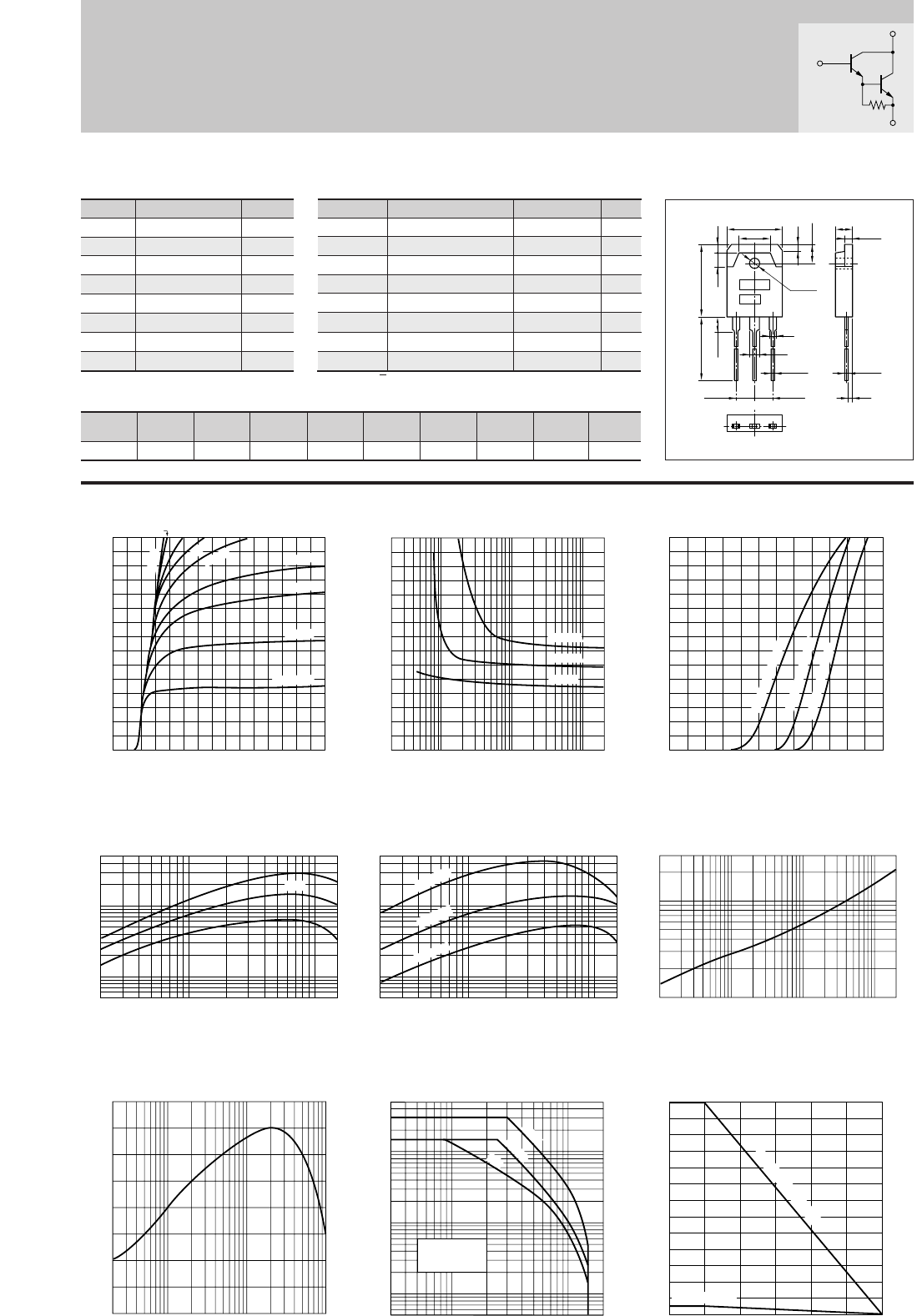
156
Silicon NPN Triple Diffused Planar Transistor (Complement to type 2SB1647)
Application : Audio, Series Regulator and General Purpose
Symbol
VCBO
VCEO
VEBO
IC
IB
PC
Tj
Tstg
Ratings
150
150
5
15
1
130(Tc=25°C)
150
–55to+150
Unit
V
V
V
A
A
W
°C
°C
■
Absolute maximum ratings
■
Electrical Characteristics
Symbol
ICBO
IEBO
V(BR)CEO
hFE
VCE(sat)
VBE(sat)
fT
COB
Ratings
100max
100max
150min
5000min∗
2.5max
3.0max
70typ
120typ
Unit
µ
A
µ
A
V
V
V
MHz
pF
Conditions
VCB=150V
VEB=5V
IC=30mA
VCE=4V, IC=10A
IC=10A, IB=10mA
IC=10A, IB=10mA
VCE=12V, IE=–2A
VCB=10V, f=1MHz
Darlington 2SD2560
(Ta=25°C) (Ta=25°C)
IC–VCE Characteristics
(Typical)
Safe Operating Area (Single Pulse)
0
0
10
5
15
246
Collector-Emitter Voltage VCE(V)
Collector Current IC(A)
50mA
I
B
=0.3mA
0.5mA
0.8mA
2mA
1.0mA
3mA
10mA
1.5mA
VCE(sat)–IB Characteristics
(Typical)
0
3
2
1
0.2
10.5 105 20010050
Base Current IB(mA)
Collector-Emitter Saturation Voltage VCE(sat)(V)
IC=.15A
IC=.10A
IC=.5A
IC–VBE Temperature Characteristics
(Typical)
0
15
5
10
0 2 2.21
Base-Emittor Voltage VBE(V)
Collector Current IC(A)
(VCE=4V)
125˚C (Case Temp)
25˚C (Case Temp)
–30˚C (Case Temp)
hFE–IC Characteristics
(Typical)
Collector Current IC(A)
02 0.5 1 10 155
50000
1000
5000
10000
500
DC Current Gain hFE
(VCE=4V)
Typ
02 0.5 1 10 155
50000
1000
5000
10000
500
DC Current Gain hFE
(VCE=4V)
hFE–IC
Temperature Characteristics (Typical)
Collector Current IC(A)
125˚C
–30˚C
25˚C
θj-a–t Characteristics
0.1
1.0
3.0
0.5
1 10 100 1000 2000
Time t(ms)
Transient Thermal Resistance θj-a(˚C/W)
fT–IE Characteristics
(Typical)
(VCE=12V)
Emitter Current IE(A)
–0.05–0.02 –01 –0.5 –1 –5 –10
0
40
20
60
80
Cut-off Frequency fT(MHZ)
Pc–Ta Derating
130
100
50
3.5
0
Ambient Temperature Ta(˚C)
Maximum Power Dissipation PC(W)
With Infinite heatsink
Without Heatsink
0 25 50 75 100 125 150
10 5053 100 200
0.05
1
0.5
0.1
10
50
5
DC
100ms
10ms
Collector-Emitter Voltage VCE(V)
Collector Current IC(A)
Without Heatsink
Natural Cooling
External Dimensions MT-100(TO3P)
15.6±0.4
9.6
19.9±0.3
4.0 2.0
5.0±0.2
1.8
ø3.2±0.1
2
3
1.05
+0.2
-0.1
20.0min
4.0max
BE
5.45±0.1 5.45±0.1
C
4.8±0.2
0.65
+0.2
-0.1
1.4
2.0±0.1
a
b
Weight : Approx 6.0g
a. Part No.
b. Lot No.
■Typical Switching Characteristics (Common Emitter)
VCC
(V)
40
RL
(Ω)
4
IC
(A)
10
VBB2
(V)
–5
IB2
(mA)
–10
ton
(
µ
s)
0.8typ
tstg
(
µ
s)
4.0typ
tf
(
µ
s)
1.2typ
IB1
(mA)
10
VBB1
(V)
10
B
C
E
(70Ω)
Equivalent circuit
∗hFE Rank O(5000to12000), P(6500to20000), Y(15000to30000)
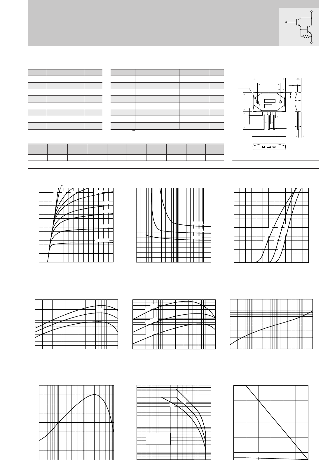
157
Silicon NPN Triple Diffused Planar Transistor (Complement to type 2SB1648)
Application : Audio, Series Regulator and General Purpose
Symbol
VCBO
VCEO
VEBO
IC
IB
PC
Tj
Tstg
Ratings
150
150
5
17
1
200(Tc=25°C)
150
–55 to +150
Unit
V
V
V
A
A
W
°C
°C
■
Absolute maximum ratings
■
Electrical Characteristics
Symbol
ICBO
IEBO
V(BR)CEO
hFE
VCE(sat)
VBE(sat)
fT
COB
Ratings
100max
100max
150min
5000min∗
2.5max
3.0max
70typ
120typ
Unit
µ
A
µ
A
V
V
V
MHz
pF
Conditions
VCB=150V
VEB=5V
IC=30mA
VCE=4V, IC=10A
IC=10A, IB=10mA
IC=10A, IB=10mA
VCE=12V, IE=–2A
VCB=10V, f=1MHz
Darlington 2SD2561
(Ta=25°C) (Ta=25°C)
Safe Operating Area (Single Pulse)
IC–VCE Characteristics
(Typical)
0
0
10
5
15
17
246
Collector-Emitter Voltage VCE(V)
Collector Current IC(A)
50mA
I
B
=0.3mA
0.5mA
0.8mA
2mA
1.0mA
10mA
1.5mA
3mA
VCE(sat)–IB Characteristics
(Typical)
0
3
2
1
0.2
10.5 105 20010050
Base Current IB(mA)
Collector-Emitter Saturation Voltage VCE(sat)(V)
IC=.15A
IC=.10A
IC=.5A
IC–VBE Temperature Characteristics
(Typical)
0
15
17
5
10
0 2 2.61
Base-Emittor Voltage VBE(V)
Collector Current IC(A)
(VCE=4V)
125˚C (Case Temp)
25˚C (Case Temp)
–30˚C (Case Temp)
hFE–IC Characteristics
(Typical)
Collector Current IC(A)
02 0.5 1 10 175
50000
1000
5000
10000
500
DC Current Gain hFE
(VCE=4V)
Typ
02 0.5 1 10 175
50000
1000
5000
10000
500
DC Current Gain hFE
(VCE=4V)
hFE–IC
Temperature Characteristics (Typical)
Collector Current IC(A)
125˚C
–30˚C
25˚C
Time t(ms)
0.1
1
2
0.5
1 10 100 1000 2000
Transient Thermal Resistance θj-a(˚C/W)
θj-a–t Characteristics
fT–IE Characteristics
(Typical)
–0.02 –0.1 –1 –10
0
20
40
80
60
Cut-off Frequency fT(MHZ)
(VCE=12V)
Emitter Current IE(A)
Pc–Ta Derating
200
160
120
80
40
5
00 25 50 75 100 125 150
Ambient Temperature Ta(˚C)
Maximum Power Dissipation PC(W)
With Infinite heatsink
Without Heatsink
10 5053 100 200
0.05
1
0.5
0.1
10
50
5
DC
100ms
10ms
Collector-Emitter Voltage VCE(V)
Collector Current IC(A)
Without Heatsink
Natural Cooling
External Dimensions MT-200
2
3
1.05
+0.2
-0.1
BE
5.45±0.1 5.45±0.1
2-ø3.2±0.1
36.4±0.3
9
24.4±0.2
7
21.4±0.3
20.0min
4.0max
0.65
+0.2
-0.1
3.0
+0.3
-0.1
6.0±0.2
2.1
a
b
C
Weight : Approx 18.4g
a. Part No.
b. Lot No.
■Typical Switching Characteristics (Common Emitter)
VCC
(V)
40
RL
(Ω)
4
IC
(A)
10
VBB2
(V)
–5
IB2
(mA)
–10
ton
(
µ
s)
0.8typ
tstg
(
µ
s)
4.0typ
tf
(
µ
s)
1.2typ
IB1
(mA)
10
VBB1
(V)
10
B
C
E
(70Ω)
Equivalent circuit
∗hFE Rank O(5000to12000), P(6500to20000), Y(15000to30000)
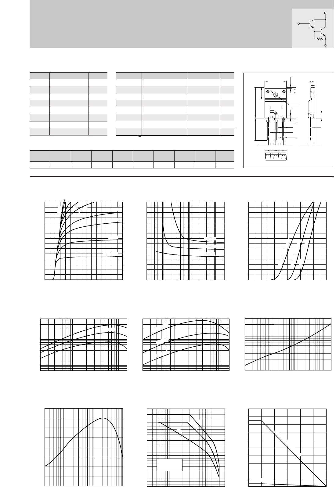
158
Silicon NPN Triple Diffused Planar Transistor (Complement to type 2SB1649)
Application : Audio, Series Regulator and General Purpose
Symbol
VCBO
VCEO
VEBO
IC
IB
PC
Tj
Tstg
Ratings
150
150
5
15
1
85(Tc=25°C)
150
–55 to +150
Unit
V
V
V
A
A
W
°C
°C
■
Absolute maximum ratings
■
Electrical Characteristics
Symbol
ICBO
IEBO
V(BR)CEO
hFE
VCE(sat)
VBE(sat)
fT
COB
Ratings
100max
100max
150min
5000min∗
2.5max
3.0max
70typ
120typ
Unit
µ
A
µ
A
V
V
V
MHz
pF
Conditions
VCB=150V
VEB=5V
IC=30mA
VCE=4V, IC=10A
IC=10A, IB=10mA
IC=10A, IB=10mA
VCE=12V, IE=–2A
VCB=10V, f=1MHz
Darlington 2SD2562
(Ta=25°C) (Ta=25°C)
IC–VCE Characteristics
(Typical)
Safe Operating Area (Single Pulse)
0
0
10
5
15
246
Collector-Emitter Voltage VCE(V)
Collector Current IC(A)
50mA
I
B
=0.3mA
0.5mA
0.8mA
2mA
1.0mA
3mA
10mA
1.5mA
VCE(sat)–IB Characteristics
(Typical)
0
3
2
1
0.2
10.5 105 20010050
Base Current IB(mA)
Collector-Emitter Saturation Voltage VCE(sat)(V)
IC=.15A
IC=.10A
IC=.5A
IC–VBE Temperature Characteristics
(Typical)
0
15
5
10
0 2 2.21
Base-Emittor Voltage VBE(V)
Collector Current IC(A)
(VCE=4V)
125˚C (Case Temp)
25˚C (Case Temp)
–30˚C (Case Temp)
hFE–IC Characteristics
(Typical)
Collector Current IC(A)
02 0.5 1 10 155
50000
1000
5000
10000
500
DC Current Gain hFE
(VCE=4V)
Typ
02 0.5 1 10 155
50000
1000
5000
10000
500
DC Current Gain hFE
(VCE=4V)
hFE–IC
Temperature Characteristics (Typical)
Collector Current IC(A)
125˚C
–30˚C
25˚C
θj-a–t Characteristics
0.1
1.0
3.0
0.5
1 10 100 1000 2000
Time t(ms)
Transient Thermal Resistance θj-a(˚C/W)
fT–IE Characteristics
(Typical)
(VCE=12V)
Emitter Current IE(A)
–0.05–0.02 –01 –0.5 –1 –5 –10
0
40
20
60
80
Cut-off Frequency fT(MHZ)
Pc–Ta Derating
100
80
60
40
20
3.5
0
Ambient Temperature Ta(˚C)
Maximum Power Dissipation PC(W)
With Infinite heatsink
Without Heatsink
0 25 50 75 100 125 150
10 5053 100 200
0.05
1
0.5
0.1
10
50
5
DC
100ms
10ms
Collector-Emitter Voltage VCE(V)
Collector Current IC(A)
Without Heatsink
Natural Cooling
External Dimensions FM100(TO3PF)
4.41.5 1.5
BEC
5.45±0.1
ø3.3±0.2
1.6
3.3
1.75
0.8±0.2
2.15
1.05
+0.2
-0.1
5.45±0.1
23.0±0.3
16.2
9.5±0.2
5.5
15.6±0.2 5.5±0.2
3.45
3.35
0.65
+0.2
-0.1
±0.2
3.0
0.8
a
b
Weight : Approx 6.5g
a. Part No.
b. Lot No.
■Typical Switching Characteristics (Common Emitter)
VCC
(V)
40
RL
(Ω)
4
IC
(A)
10
VBB2
(V)
–5
IB2
(mA)
–10
ton
(
µ
s)
0.8typ
tstg
(
µ
s)
4.0typ
tf
(
µ
s)
1.2typ
IB1
(mA)
10
VBB1
(V)
10
B
C
E
(70Ω)
Equivalent circuit
∗hFE Rank O(5000to12000), P(6500to20000), Y(15000to30000)
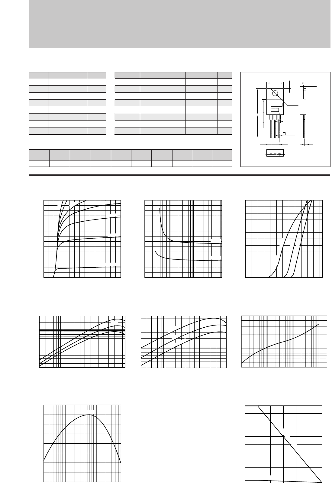
159
Silicon NPN Triple Diffused Planar Transistor (Complement to type 2SB1659)
Application : Audio, Series Regulator and General Purpose
Symbol
VCBO
VCEO
VEBO
IC
IB
PC
Tj
Tstg
Ratings
110
110
5
6
1
50(Tc=25°C)
150
–55 to +150
Unit
V
V
V
A
A
W
°C
°C
■
Absolute maximum ratings
■
Electrical Characteristics
Symbol
ICBO
IEBO
V(BR)CEO
hFE
VCE(sat)
VBE(sat)
fT
COB
Ratings
100max
100max
110min
5000min∗
2.5max
3.0max
60typ
55typ
Unit
µ
A
µ
A
V
V
V
MHz
pF
Conditions
VCB=110V
VEB=5V
IC=30mA
VCE=4V, IC=5A
IC=5A, IB=5mA
IC=5A, IB=5mA
VCE=12V, IE=–0.5A
VCB=10V, f=1MHz
Darlington 2SD2589
(Ta=25°C) (Ta=25°C)
External Dimensions FM-25(TO220)
BE
2.5 2.5
C
16.0±0.7
12.0min
4.0max 8.8±0.2
1.35
0.65
+0.2
-0.1
10.2±0.2
ø3.75±0.2
3.0±0.2
4.8±0.2
1.4
2.0±0.1
a
b
Weight : Approx 2.6g
a. Part No.
b. Lot No.
■Typical Switching Characteristics (Common Emitter)
VCC
(V)
30
RL
(Ω)
6
IC
(A)
5
VBB2
(V)
–5
IB2
(mA)
–5
ton
(
µ
s)
0.8typ
tstg
(
µ
s)
6.2typ
tf
(
µ
s)
1.1typ
IB1
(mA)
5
VBB1
(V)
10
∗hFE Rank O(5000to12000), P(6500to20000), Y(15000to30000)
0
0
2
4
6
264
IB=0.1mA
5mA
1mA
0.5mA
0.4mA
0.3mA
0.2mA
0.02 0.1 0.5 1 65
(VCE=4V)
1000
500
200
5000
10000
40000
Typ
0
6
4
2
0 2.521
(VCE=4V)
0
3
2
1
0.1
10.5 105 10050
IC=5A
IC=3A
(VCE=4V)
0.02 0.1 5160.5
1000
500
100
5000
10000
40000
125˚C
25˚C
–0.02 –0.1 –1 –6
0
40
20
80
60
(VCE=12V)
Typ
0.4
1
5
0.5
1 10 100 1000 2000
50
40
30
20
10
2
00 25 50 75 100 125 150
IC–VCE Characteristics
(Typical)
VCE(sat)–IB Characteristics
(Typical)
IC–VBE Temperature Characteristics
(Typical)
Collector-Emitter Voltage VCE(V) Base Current IB(mA) Base-Emittor Voltage VBE(V)
Collector Current IC(A)
Collector-Emitter Saturation Voltage VCE(sat)(V)
Collector Current IC(A)
125˚C (Case Temp)
25˚C (Case Temp)
–30˚C (Case Temp)
hFE–IC Characteristics
(Typical)
hFE–IC
Temperature Characteristics (Typical)
θj-a–t Characteristics
Collector Current IC(A) Collector Current IC(A) Time t(ms)
DC Current Gain hFE
DC Current Gain hFE
Transient Thermal Resistance θj-a(˚C/W)
Safe Operating Area (Single Pulse)
fT–IE Characteristics
(Typical)
Pc–Ta Derating
Cut-off Frequency fT(MHZ)
Maximum Power Dissipation PC(W)
With Infinite heatsink
Emitter Current IE(A) Ambient Temperature Ta(˚C)
Without Heatsink
–30˚C
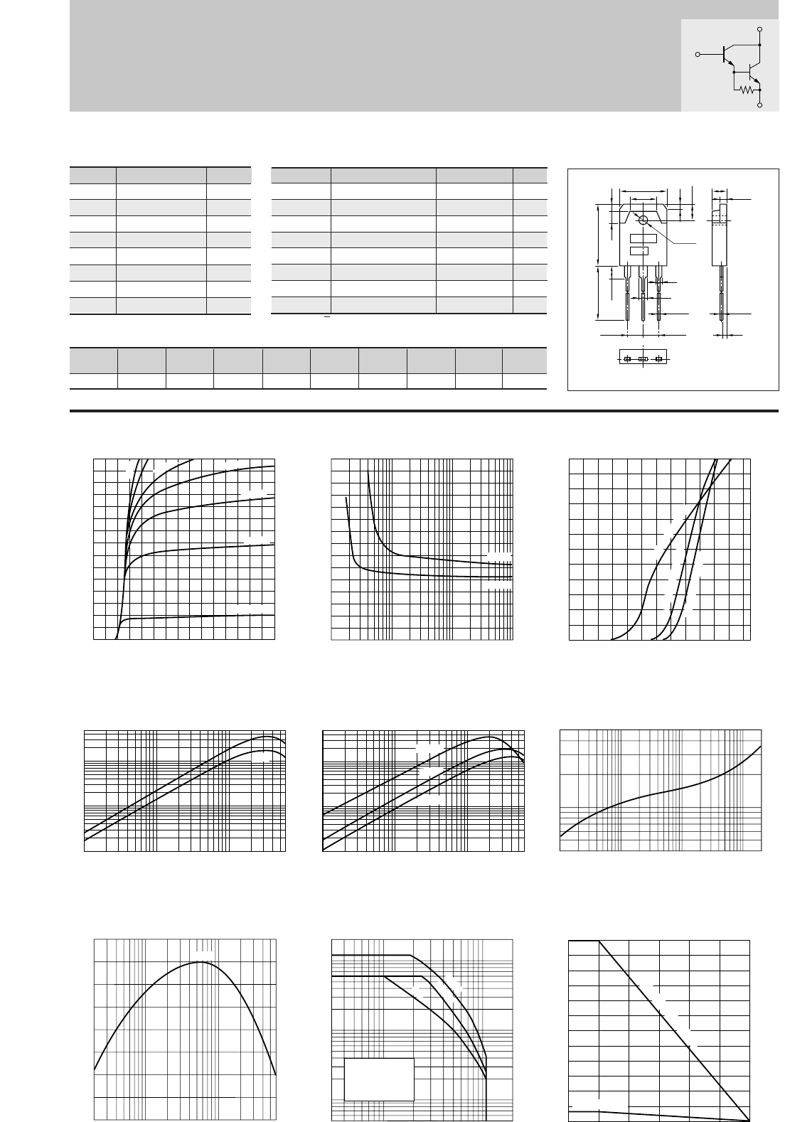
160
Darlington 2SD2641
IC–VCE Characteristics
(Typical)
hFE–IC Characteristics
(Typical)
hFE–IC
Temperature Characteristics (Typical)
θj-a–t Characteristics
IC–VBE Temperature Characteristics
(Typical)
VCE(sat)–IB Characteristics
(Typical)
Pc–Ta Derating
Safe Operating Area (Single Pulse)
fT–IE Characteristics
(Typical)
0
0
2
4
6
264
Collector-Emitter Voltage VCE(V)
Collector Current IC(A)
IB=0.1mA
5mA
1mA
0.5mA
0.4mA
0.3mA
0.2mA
Collector Current IC(A)
DC Current Gain hFE
0.5
1
5
1 10 100 10005 50 500 2000
Time t(ms)
Transient Thermal Resistance θj-a(˚C/W)
Base-Emittor Voltage VBE(V)
Collector Current IC(A)
60
40
20
3.5
00 25 50 75 100 125 150
Ambient Temperature Ta(˚C)
Maximum Power Dissipation PC(W)
With Infinite heatsink
Without Heatsink
10 5053 100 200
0.05
1
0.5
0.1
10
20
5
Collector-Emitter Voltage VCE(V)
Collector Current IC(A)
DC
100ms
10ms
Base Current IB(mA)
Collector-Emitter Saturation Voltage VCE(sat)(V)
Collector Current IC(A)
DC Current Gain hFE
–0.02 –0.1 –1 –6
0
40
20
80
60
Cut-off Frequency fT(MHZ)
(VCE=12V)
Emitter Current IE(A)
Typ
Without Heatsink
Natural Cooling
0
3
2
1
0.1
10.5 105 10050
IC=5A
IC=3A
0.01 0.1 0.5 1 65
1000
500
100
5000
10000
50000
Typ
(VCE=4V)
0
6
4
2
0 2.521
(VCE=4V)
125˚C (Case Temp)
25˚C (Case Temp)
–30˚C (Case Temp)
0.01 0.1 0.5 1 65
1000
500
100
5000
10000
50000
(VCE=4V)
125˚C
25˚C
–30˚C
Application : Audio, Series Regulator and General Purpose
Symbol
VCBO
VCEO
VEBO
IC
IB
PC
Tj
Tstg
Ratings
110
110
5
6
1
60(Tc=25°C)
150
–55 to +150
Unit
V
V
V
A
A
W
°C
°C
■
Absolute maximum ratings
■
Electrical Characteristics
Symbol
ICBO
IEBO
V(BR)CEO
hFE
VCE(sat)
VBE(sat)
fT
COB
Ratings
100max
100max
110min
5000min∗
2.5max
3.0max
60typ
55typ
Unit
µ
A
µ
A
V
V
V
MHz
pF
Conditions
VCB=110V
VEB=5V
IC=30mA
VCE=4V, IC=5A
IC=5A, IB=5mA
IC=5A, IB=5mA
VCE=12V, IE=–2A
VCB=10V, f=1MHz
(Ta=25°C) (Ta=25°C)
Silicon NPN Triple Diffused Planar Transistor (Complement to type 2SB1685)
■Typical Switching Characteristics (Common Emitter)
VCC
(V)
30
RL
(Ω)
6
IC
(A)
5
VBB2
(V)
–5
IB2
(mA)
–5
ton
(
µ
s)
0.8typ
tstg
(
µ
s)
6.2typ
tf
(
µ
s)
1.1typ
IB1
(mA)
5
VBB1
(V)
10
External Dimensions MT-100(TO3P)
15.6±0.4
9.6
19.9±0.3
4.0 2.0
5.0±0.2
1.8
ø3.2±0.1
2
3
1.05
+0.2
-0.1
20.0min
4.0max
BE
5.45±0.1 5.45±0.1
C
4.8±0.2
0.65
+0.2
-0.1
1.4
2.0±0.1
a
b
Weight : Approx 6.0g
a. Part No.
b. Lot No.
B
C
E
(70Ω)
Equivalent circuit
∗hFE Rank O(5000to12000), P(6500to20000), Y(15000to30000)
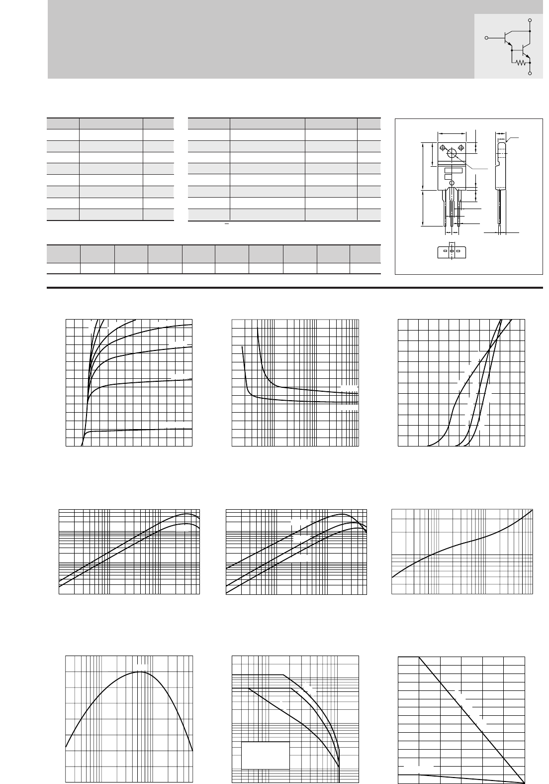
161
.
Darlington 2SD2642
IC–VCE Characteristics
(Typical)
hFE–IC Characteristics
(Typical)
hFE–IC
Temperature Characteristics (Typical)
θj-a–t Characteristics
IC–VBE Temperature Characteristics
(Typical)
VCE(sat)–IB Characteristics
(Typical)
Pc–Ta Derating
Safe Operating Area (Single Pulse)
fT–IE Characteristics
(Typical)
0
0
2
4
6
264
Collector-Emitter Voltage VCE(V)
Collector Current IC(A)
IB=0.1mA
5mA
1mA
0.5mA
0.4mA
0.3mA
0.2mA
Collector Current IC(A)
DC Current Gain hFE
0.5
0.3
1
4
1 10 100 10005 50 500
Time t(ms)
Transient Thermal Resistance θj-a(˚C/W)
Base-Emittor Voltage VBE(V)
Collector Current IC(A)
30
20
10
2
00 25 50 75 100 125 150
Ambient Temperature Ta(˚C)
Maximum Power Dissipation PC(W)
With Infinite heatsink
Without Heatsink
10ms
10 5053 100 200
0.05
0.1
1
0.5
10
30
5
Collector-Emitter Voltage VCE(V)
Collector Current IC(A)
DC
100ms
Base Current IB(mA)
Collector-Emitter Saturation Voltage VCE(sat)(V)
Collector Current IC(A)
DC Current Gain hFE
–0.02 –0.1 –1 –6
0
40
20
80
60
Cut-off Frequency fT(MHZ)
(VCE=12V)
Emitter Current IE(A)
Typ
Without Heatsink
Natural Cooling
0
3
2
1
0.1
10.5 105 10050
IC=5A
IC=3A
0.01 0.1 0.5 1 65
1000
500
100
5000
10000
50000
Typ
(VCE=4V)
0
6
4
2
0 2.521
(VCE=4V)
125˚C (Case Temp)
25˚C (Case Temp)
–30˚C (Case Temp)
0.01 0.1 0.5 1 65
1000
500
100
5000
10000
50000
(VCE=4V)
125˚C
25˚C
–30˚C
Silicon NPN Triple Diffused Planar Transistor (Complement to type 2SB1687)
Application : Audio, Series Regulator and General Purpose
Symbol
VCBO
VCEO
VEBO
IC
IB
PC
Tj
Tstg
Ratings
110
110
5
6
1
30(Tc=25°C)
150
–55 to +150
Unit
V
V
V
A
A
W
°C
°C
■
Absolute maximum ratings
■
Electrical Characteristics
Symbol
ICBO
IEBO
V(BR)CEO
hFE
VCE(sat)
VBE(sat)
fT
COB
Ratings
100max
100max
110min
5000min∗
2.5max
3.0max
60typ
55typ
Unit
µ
A
µ
A
V
V
V
MHz
pF
Conditions
VCB=110V
VEB=5V
IC=30mA
VCE=4V, IC=5A
IC=5A, IB=5mA
IC=5A, IB=5mA
VCE=12V, IE=–0.5A
VCB=10V, f=1MHz
(Ta=25°C) (Ta=25°C)
External Dimensions FM20(TO220F)
ø3.3±0.2
10.1±0.2
4.0±0.2
16.9±0.3
13.0min
8.4±0.2
0.8±0.2
3.9
±0.2
2.542.54
1.35±0.15
0.85
+0.2
-0.1
1.35±0.15
2.2±0.2
4.2±0.2
2.8 c0.5
2.4±0.2
0.45
+0.2
-0.1
BEC
a
b
Weight : Approx 2.0g
a. Part No.
b. Lot No.
■Typical Switching Characteristics (Common Emitter)
VCC
(V)
30
RL
(Ω)
6
IC
(A)
5
VBB2
(V)
–5
IB2
(mA)
–5
ton
(
µ
s)
0.8typ
tstg
(
µ
s)
6.2typ
tf
(
µ
s)
1.1typ
IB1
(mA)
5
VBB1
(V)
10
B
C
E
(70Ω)
Equivalent circuit
∗hFE Rank O(5000to12000), P(6500to20000), Y(15000to30000)
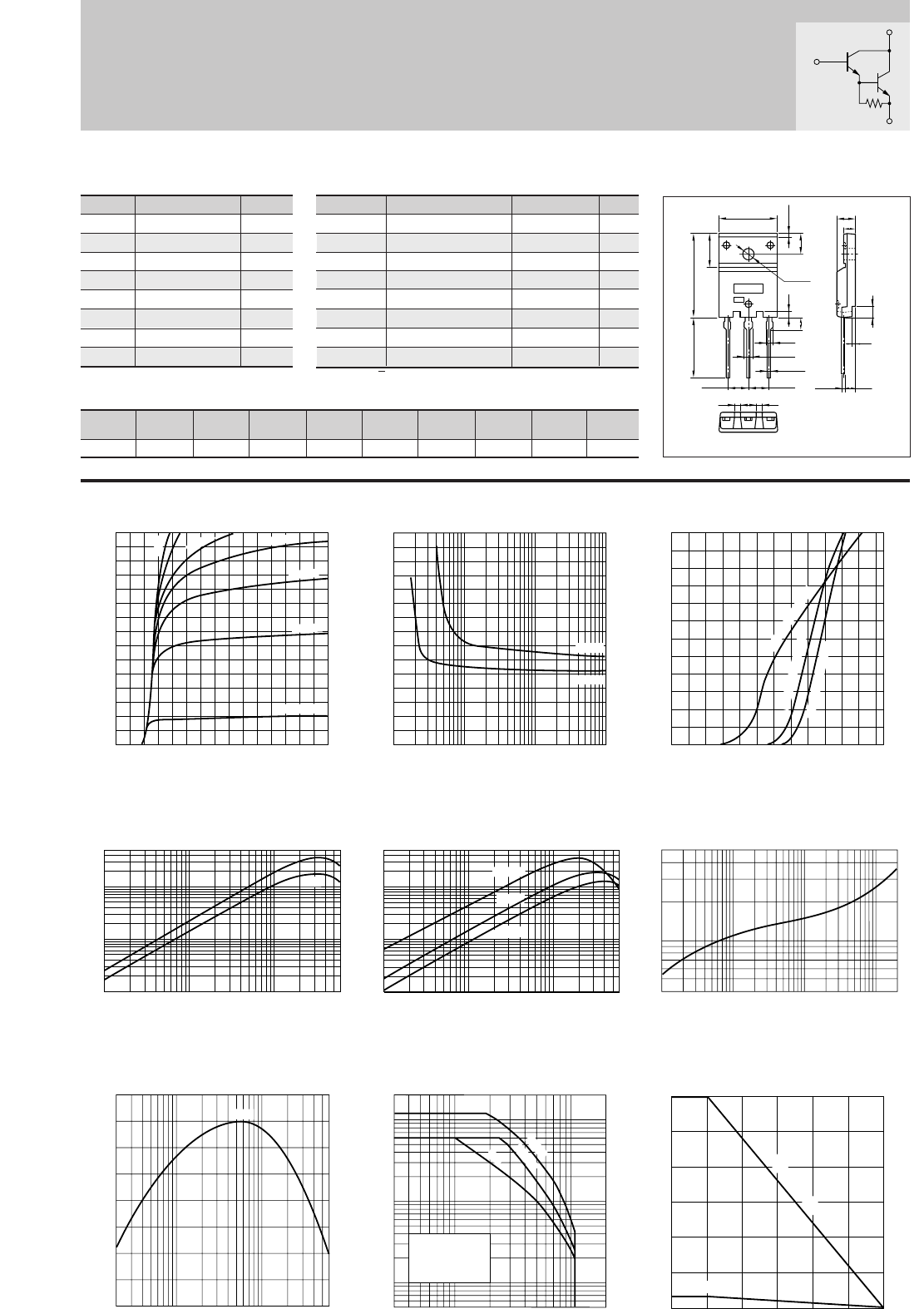
162
Silicon NPN Triple Diffused Planar Transistor (Complement to type 2SB1687)
Application : Audio, Series Regulator and General Purpose
Symbol
VCBO
VCEO
VEBO
IC
IB
PC
Tj
Tstg
Ratings
110
110
5
6
1
60(Tc=25°C)
150
–55 to +150
Unit
V
V
V
A
A
W
°C
°C
■
Absolute maximum ratings
■
Electrical Characteristics
Symbol
ICBO
IEBO
V(BR)CEO
hFE
VCE(sat)
VBE(sat)
fT
COB
Ratings
100max
100max
110min
5000min∗
2.5max
3.0max
60typ
55typ
Unit
µ
A
µ
A
V
V
V
MHz
pF
Conditions
VCB=110V
VEB=5V
IC=30mA
VCE=4V, IC=5A
IC=5A, IB=5mA
IC=5A, IB=5mA
VCE=12V, IE=–0.5A
VCB=10V, f=1MHz
Darlington 2SD2643
(Ta=25°C) (Ta=25°C)
IC–VCE Characteristics
(Typical)
hFE–IC Characteristics
(Typical)
hFE–IC
Temperature Characteristics (Typical)
θj-a–t Characteristics
IC–VBE Temperature Characteristics
(Typical)
VCE(sat)–IB Characteristics
(Typical)
Pc–Ta Derating
Safe Operating Area (Single Pulse)
fT–IE Characteristics
(Typical)
0
0
2
4
6
264
Collector-Emitter Voltage VCE(V)
Collector Current IC(A)
IB=0.1mA
5mA
1mA
0.5mA
0.4mA
0.3mA
0.2mA
Collector Current IC(A)
DC Current Gain hFE
0.5
1
5
1 10 100 10005 50 500 2000
Time t(ms)
Transient Thermal Resistance θj-a(˚C/W)
Base-Emittor Voltage VBE(V)
Collector Current IC(A)
60
40
20
3.5
005025 75 125100 150
Ambient Temperature Ta(˚C)
Maximum Power Dissipation PC(W)
With Infinite heatsink
Without Heatsink
10 5053 100 200
0.05
1
0.5
0.1
10
20
5
Collector-Emitter Voltage VCE(V)
Collector Current IC(A)
DC
100ms
10ms
Base Current IB(mA)
Collector-Emitter Saturation Voltage VCE(sat)(V)
Collector Current IC(A)
DC Current Gain hFE
–0.02 –0.1 –1 –6
0
40
20
80
60
Cut-off Frequency fT(MHZ)
(VCE=12V)
Emitter Current IE(A)
Typ
Without Heatsink
Natural Cooling
0
3
2
1
0.1
10.5 105 10050
IC=5A
IC=3A
0.01 0.1 0.5 1 65
1000
500
100
5000
10000
50000
Typ
(VCE=4V)
0
6
4
2
0 2.521
(VCE=4V)
125˚C (Case Temp)
25˚C (Case Temp)
–30˚C (Case Temp)
0.01 0.1 0.5 1 65
1000
500
100
5000
10000
50000
(VCE=4V)
125˚C
25˚C
–30˚C
External Dimensions FM100(TO3PF)
4.41.5 1.5
BEC
5.45±0.1
ø3.3±0.2
1.6
3.3
1.75
0.8±0.2
2.15
1.05
+0.2
-0.1
5.45±0.1
23.0±0.3
16.2
9.5±0.2
5.5
15.6±0.2 5.5±0.2
3.45
3.35
0.65
+0.2
-0.1
±0.2
3.0
0.8
a
b
Weight : Approx 6.5g
a. Part No.
b. Lot No.
■Typical Switching Characteristics (Common Emitter)
VCC
(V)
30
RL
(Ω)
6
IC
(A)
5
VBB2
(V)
–5
IB2
(mA)
–5
ton
(
µ
s)
0.8typ
tstg
(
µ
s)
6.2typ
tf
(
µ
s)
1.1typ
IB1
(mA)
5
VBB1
(V)
10
B
C
E
(70Ω)
Equivalent circuit
∗hFE Rank O(5000to12000), P(6500to20000), Y(15000to30000)
163
Silicon PNP Epitaxial Planar Transistor with Shottky Barrier Diode Application : Chopper Regulator
Symbol
VCBO
VCEO
VEBO
IC
IB
PC
Tj
Tstg
Ratings
–30
–30
–10
–3
–0.5
800(Ta=25°C)
125
–40 to +125
Unit
V
V
V
A
A
mW
°C
°C
■
Absolute maximum ratings
■
Electrical Characteristics
Symbol
ICBO
IEBO
V(BR)CEO
hFE1
hFE2
VCE(sat)
fT
COB
Ratings
–
10max
–
10max
–
30min
100min
150min
–
0.3max
100typ
45typ
Unit
µ
A
µ
A
V
V
MHz
pF
Conditions
VCB=–30V
VEB=–10V
IC=–10mA
VCE=–2V, IC=–1A
VCE=–2V, IC=–0.5A
IC=–0.5A, IB=–20mA
VCE=–12V, IE=0.3A
VCB=–10V, f=1MHz
SAH02
(Ta=25°C) (Ta=25°C)
IC–VCE Characteristics
(Typical)
hFE–IC Temperature Characteristics (Typical)
θj-a–t Characteristics
IC–VBE Temperature Characteristics
(Typical)
Pc–Ta Derating
0
0
–1
–2
–3
–1 –2 –3 –6–4 –5
Collector-Emitter Voltage VCE(V)
Collector Current IC(A)
I
B
=–3mA
–100mA –20mA
–10mA
–15mA
–5mA
–5mA
Safe Operating Area (Single Pulse)
–3 –10–5 –50
–0.03
–0.1
–0.05
–1
–5
–0.5
Collector-Emitter Voltage VCE(V)
Collector Current IC(A)
1ms
10ms
Without Heatsink
Natural Cooling
0.3
100
300
10
1
0.001 0.01 0.1 1 10 100 1000
Time t(ms)
Transient Thermal Resistance θj-a(˚C/W)
1.0
0.5
00 25 50 75 100 125
Ambient Temperature Ta(˚C)
Maximum Power Dissipation PC(W)
Glass epoxy substrate
(95 x 69 x 1.2mm)
Natural Cooling
0
–3
–1
–2
0 –1.5–0.5 –1.0
Base-Emittor Voltage VBE(V)
Collector Current IC(A)
(VCE=–2V)
125˚C (Case Temp)
25˚C (Case Temp)
–30˚C (Case Temp)
Diode IF–VF Characteristics
0
3
1
2
0 1.00.5
Forward Voltage VF(V)
Forward Current IF(A)
(VCE=–2V)
–0.01 –0.05 –0.1 –0.5 –1 –3
100
500
1000
Collector Current IC(A)
DC Current Gain hFE
125˚C
–30˚C
25˚C
125˚C
–30˚C
25˚C
–0.1 –1–0.5 –3
1.0
0.8
0.6
0.4
0.2
0
Switching Time ton•tstg•tf(µs)
Collector Current IC(A)
tstg
ton
tf
VCC 12V
–IB1=IB2=30mA
ton•tstg•tf–IC Characteristics
(Typical)
VCE(sat)–IB Temperature Characteristics (Typical)
0
–1.0
–1.5
–0.5
–300–10 –100–50–5–1
Base Current IB(mA)
Collector-Emitter Saturation Voltage VCE(sat)(V)
125˚C
25˚C
–30˚C
(IC=–0.5A)
100µs
External Dimensions PS Pack
2.54±0.25
1.4±0.2
3.6±0.2
6.3±0.2
8.0±0.5
1.0±0.3
3.0±0.2
9.8±0.3
0~0.1
0.25
4.32±0.2
0.89±0.15
4.8max
6.8max 4.0max
ab 1
2
3
4
0.75
+0.15
-0.05
0.3
+0.15
-0.05
2
13
4
Equivalent circuit
VRIR=100
µ
A 30 min V
VFIF=0.5A 0.55 max V
t r r IF=±100mA 15 typ ns
Weight : Approx 0.23g
a. Part No.
b. Lot No.
164
SAH03
2
13
4
(4kΩ)
(100Ω)
Silicon PNP Epitaxial Planar Transistor with Fast-Recovery Rectifier Diode
Symbol
VCBO
VCEO
VEBO
IC
IB
PC
Tj
Tstg
Ratings
–60
–60
–6
–1.2
–0.1
1.0(Ta=25°C)
150
–40to+150
Unit
V
V
V
A
A
W
°C
°C
■
Absolute maximum ratings
■
Electrical Characteristics
Symbol
ICBO
IEBO
V(BR)CEO
hFE
VCE(sat)
fT
COB
Ratings
–
10max
–
3max
–
60min
2000to12000
–
1.4max
100typ
30typ
Unit
µ
A
mA
V
V
MHz
pF
Conditions
VCB=–60V
VEB=–6V
IC=–10mA
VCE=–4V, IC=–1A
IC=–1A, IB=–2mA
VCE=–12V, IE=0.1A
VCB=–10V, f=1MHz
(Ta=25°C) (Ta=25°C)
Equivalent
circuit
VRIR=100
µ
A 100 min V
VFIF=0.5A 1.5 max V
t r r IF=±100mA 100 typ ns
External Dimensions PS Pack
2.54±0.25
1.4±0.2
3.6±0.2
6.3±0.2
8.0±0.5
1.0±0.3
3.0±0.2
9.8±0.3
0~0.1
0.25
4.32±0.2
0.89±0.15
4.8max
6.8max 4.0max
ab 1
2
3
4
0.75
+0.15
-0.05
0.3
+0.15
-0.05
Weight : Approx 0.23g
a. Part No.
b. Lot No.
IC–VCE Characteristics
(Typical)
hFE–IC Temperature Characteristics (Typical)
θj-a–t Characteristics
IC–VBE Temperature Characteristics
(Typical)
Pc–Ta Derating
0
0
–1
–2
–2.4
–1 –2 –3 –6–4 –5
Collector-Emitter Voltage VCE(V)
Collector Current IC(A)
I
B
=–0.3mA
–1.2mA
–0.4mA
–0.5mA
–0.6mA
–0.8mA
–1.0mA
Safe Operating Area (Single Pulse)
–1 –10–5 –100–50
–0.05
–0.1
–1
–3
–0.5
Collector-Emitter Voltage VCE(V)
Collector Current IC(A)
0.3
100
300
10
1
0.001 0.01 0.1 1 10 100 1000
Time t(ms)
Transient Thermal Resistance θj-a(˚C/W)
1.5
0.5
1.0
00 25 50 75 100 150125
Ambient Temperature Ta(˚C)
Maximum Power Dissipation PC(W)
0
–2.4
–1
–2
0–3–1 –2
Base-Emittor Voltage VBE(V)
Collector Current IC(A)
(VCE=–4V)
125˚C (Case Temp)
25˚C (Case Temp)
–30˚C (Case Temp)
Diode IF–VF Characteristics
0.01
1.2
1
0.1
0.05
0.5
0 1 1.6
Forward Voltage VF(V)
Forward Current IF(A)
(VCE=–4V)
–0.02 –0.05 –0.1 –0.5 –1 –2.4
50
100
1000
5000
500
10000
Collector Current IC(A)
DC Current Gain hFE
125˚C
–30˚C
25˚C
125˚C
–10˚C
25˚C
–0.2 –1–0.5 –2.4
0.1
1
2
0.5
Switching Time ton•tstg•tf(µs)
Collector Current IC(A)
tstg
ton
tf
VCC 30V
–IB1=IB2=2mA
ton•tstg•tf–IC Characteristics
(Typical)
0
–2
–3
–1
–5–1–0.5–0.1
Base Current IB(mA)
Collector-Emitter Saturation Voltage VCE(sat)(V)
125˚C
–30˚C
(IC=–0.5A)
Glass epoxy substrate
(95 x 69 x 1.2mm)
Natural Cooling
–5.0mA
–2.0mA
–10.0mA
Without Heatsink
Natural Cooling
1ms
100µs
10ms
25˚C
VCE(sat)–IB Temperature Characteristics (Typical)
Application : Voltage change switch for motor
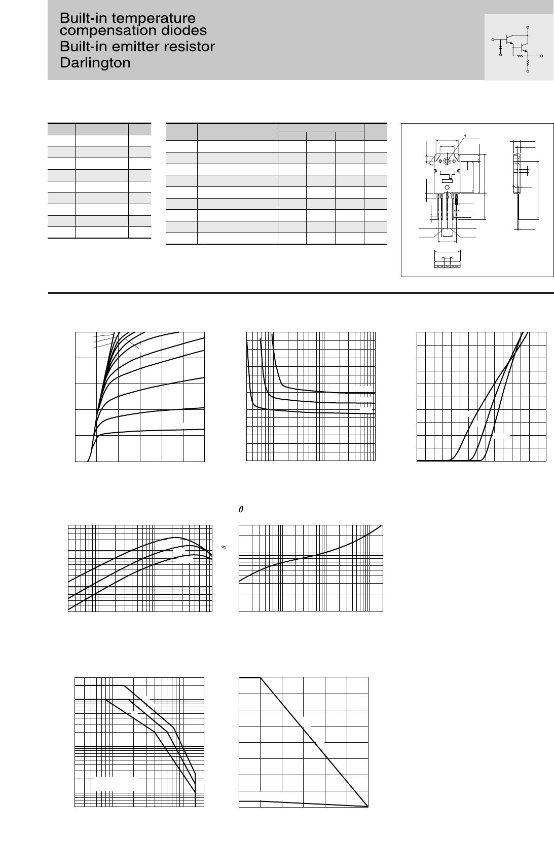
SAP09N
VCBO
80 (Tc=25°C)
150
–40 to +150
V
VCEO 150 V
VEBO 5 V
IC 10 A
IB 1 A
PCW
Tj °C150
Tstg °C
(Ta=25°C)
(Ta=25°C)
ICBO
IC=6A, IB=6mA
VCB=150V
IE=1A
µA 100
100
150
5000 20000
2.0
2.5
1220
705
0.176 0.22 0.264
IEBO VEB=5V µA
VCEO IC=30mA V
hFE ✽VCE=4V, IC=6A
VCE(sat) IC=6A, IB=6mA V
VBE(sat) V
Di VFmVIF=2.5mA
REΩ
min typ max
10Di IFmA VCE=20V, IC=40mAVBE mV
External Dimensions (Unit: mm)
15.4±0.3 4.5±0.2
17.8±0.3
4±0.1
3.3±0.2
3.4max
5±0.2
22±0.3
23±0.3
28±0.3
2±0.1
(18)
(2.5)
(41)
7±0.2
9.9±0.2 1.6±0.2
3.2±0.2
1.35
(36°)
+0.2
–0.1
0.65+0.2
–0.1
0.8+0.2
–0.1
0.65+0.2
–0.1
1±0.1
BD C SE
2.54±0.1
2.54±0.1
3.81±0.1
3.81±0.1
B
D
R: 70Ω Typ.
C
S
E
RE: 0.22Ω Typ.
Emitter resistor
Application: Audio
Collector-Emitter Voltage VCE (V)
Collector Current IC (A)
2
2
0
4
6
8
10
DC Current Gain hFE
1000
200
500
5000
10000
50000
04
0.3mA
0.5mA
0.8mA
1.0mA
1.3mA
2.0mA
2.5mA
10mA
6Base Current IB (mA)
Collector-Emitter Saturation Voltage VCE(sat) (V)
150.3 0.5
0
1
2
3
10 10050 Base-Emitter Voltage VBE (V)
Collector Current IC (A)
10
0
6
4
2
8
10
23
Collector Current IC (A)
0.1 0.50.03 1 5 10 0.1
0.5
1
3
Time t (ms)
101 5 50 100 500 20001000
IC–VCE Characteristics (Typical)
Collector-Emitter Voltage VCE (V)
Collector Current IC (A)
1035
0.1
0.05
0.5
1
5
30
10
50 200100
Safe Operating Area
(Single Pulse)
VCE(sat)–IB
Characteristics
(Typical)
IC–VBE
Temperature Characteristics
hFE –IC Characteristics (Typical) j-a –t Characteristics
IC=8A
(VCE=4V)
6A
4A 125°C
25°C
–30°C
D.C
100ms
10ms
1.8mA
125°C
25°C
–30°C
1.5mA
IB=0.2mA
(VCE=4V)
Ambient Temperature Ta (°C)
Maximum Power Dissipation Pc (W)
50 75025
20
0
3.5
40
80
60
100 150125
PC–T
a Derating
With Infinite heatsink
(Complement to type SAP09P)
■
Absolute maximum ratings
■Electrical Characteristics
Equivalent
circuit
Weight: Approx 8.3g
a. Part No.
b. Lot No.
Symbol
Ratings Unit Symbol Conditions Ratings Unit
Transient Thermal Resistance j-a (°C/W)
Without Heatsink
Natural Cooling
Without Heatsink
(7.62)
(12.7)
ab
✽hFE Rank O (5000 to 12000), Y (8000 to 20000)
165
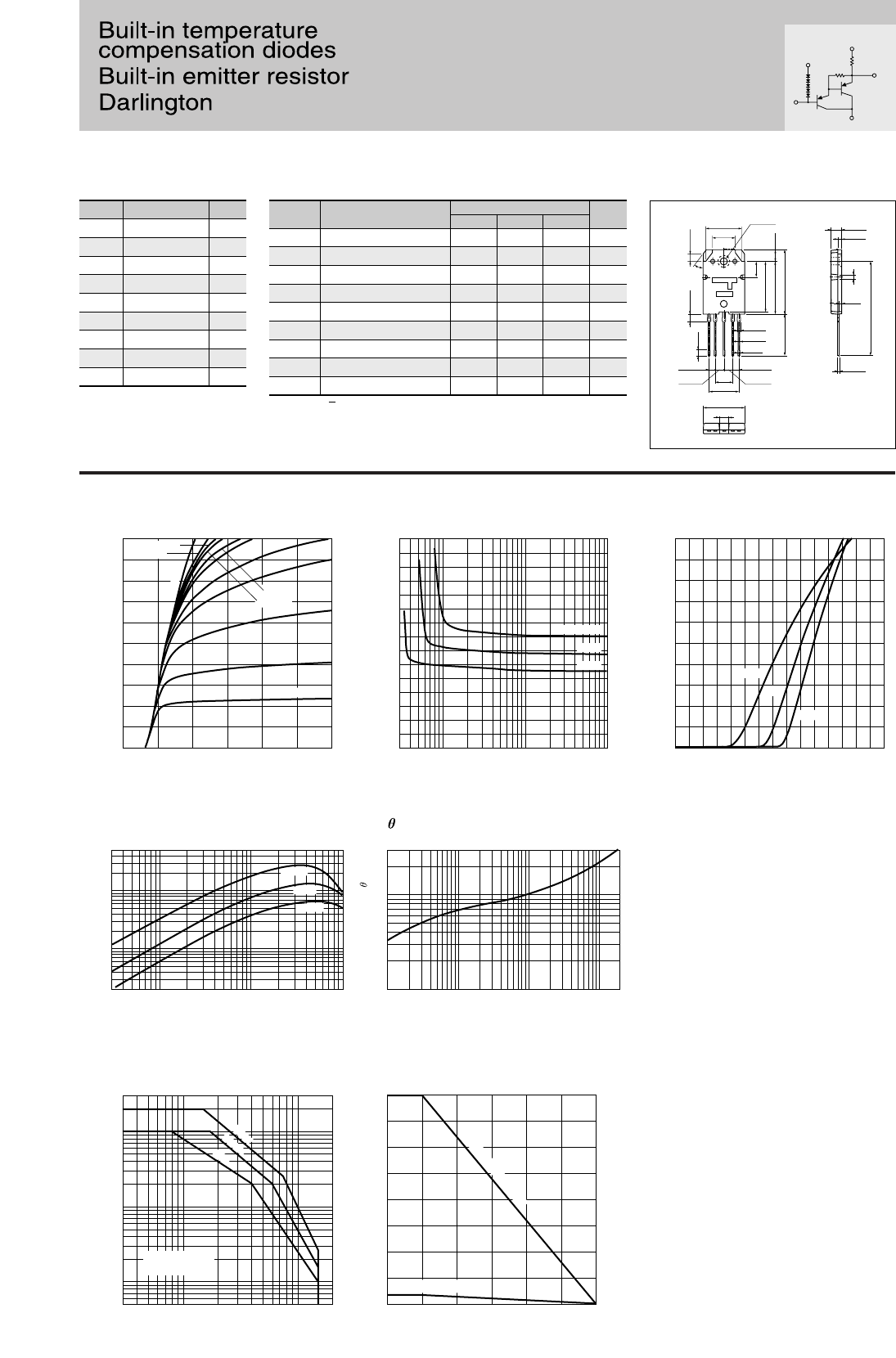
SAP09P
Symbol
Ratings Unit
VCBO
80(Tc=25°C)
150
–40 to +150
V
VCEO –150 V
VEBO –5 V
IC–10 A
IB–1 A
PCW
Tj °C150
Tstg °C
■
Absolute maximum ratings
(Ta=25°C)
Symbol Conditions Unit
ICBO
IC=–6A, IB= –6mA
VCE= –150V
IE=1A
µA–100
–100
–150
5000 20000
–2.0
–2.5
1230
1580
0.176 0.22 0.264
IEBO VEB=–5V µA
VCEO IC=–30mA V
hFE ✽VCE=–4V, IC=–6A
VCE(sat) IC=–6A, IB= –6mA V
VBE(sat) V
Di VFmVIF=2.5mA
REΩ
Ratings
min typ max
10Di IFmA
VCE
=–
20V, IC
=–
40mA
VBE mV
15.4±0.3 4.5±0.2
(7.62)
(12.7)
17.8±0.3
4±0.1
3.3±0.2
3.4max
5±0.2
22±0.3
23±0.3
28±0.3
2±0.1
7±0.2
9.9±0.2 1.6±0.2
φ3.2±0.2
1.35+0.2
–0.1
0.65+0.2
–0.1
0.8+0.2
–0.1
0.65+0.2
–0.1
1±0.1
2.54±0.1
2.54±0.1
3.81±0.1
3.81±0.1
BDCSE
D
S
E
C
B
Collector-Emitter Voltage VCE (V)
Collector Current IC (A)
–2
–2
0
–4
–6
–8
–10
DC Current Gain hFE
1000
200
500
5000
10000
50000
0–4
–0.3mA
–0.5mA
–0.8mA
–1.0mA
–1.3mA
–6 Base Current IB (mA)
Collector-Emitter Saturation Voltage VCE(sat) (V)
–1 –5–0.3
0
–1
–2
–3
–10 –50 –100 Base-Emitter Voltage VBE (V)
Collector Current IC (A)
–10
0
–6
–4
–2
–8
–10
–2 –3
Collector Current IC (A)
–0.1 –0.5–0.03 –1 –5 –10 0.1
0.5
1
3
Time t (ms)
101 5 50 100 500 20001000
–2.0mA
–2.5mA
–10mA
–1.5mA
–1.8mA
IC–VCE Characteristics (Typical)
Collector-Emitter Voltage VCE (V)
Collector Current IC (A)
–10–3 –5
–0.1
–0.05
–0.5
–1
–5
–30
–10
–50 –200–100
Safe Operating Area
(Single Pulse)
VCE(sat)–IB
Characteristics
(Typical)
IC–VBE
Temperature Characteristics (Typical)
hFE –IC Characteristics (Typical)
125°C
25°C
–30°C
IC=–8A
(VCE=–4V)
–6A
–4A 125°C
25°C
–30°C
D.C
100ms
10ms
IB=–0.2mA
(VCE=–4V)
Ambient Temperature Ta (°C)
Maximum Power Dissipation Pc (W)
50 75025
20
0
3.5
40
80
60
100 150125
PC–T
a Derating
(Ta=25°C) External Dimensions (Unit: mm)
(18)
(2.5)
(41)
(36°)
R: 70Ω Typ. RE: 0.22Ω Typ.
Emitter resistor
Application: Audio
j-a –t Characteristics
(Complement to type SAP09N)
■Electrical Characteristics
Equivalent
circuit
Weight: Approx 8.3g
a. Part No.
b. Lot No.
Transient Thermal Resistance j-a (°C/W)
ab
Without Heatsink
Natural Cooling
With Infinite heatsink
Without Heatsink
✽hFE Rank O (5000 to 12000), Y (8000 to 20000)
166
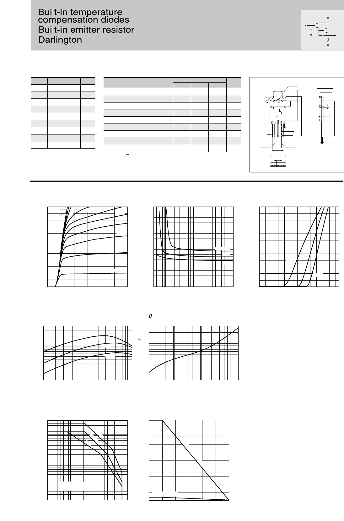
SAP10N
VCBO
100(Tc=25°C)
150
–40 to +150
V
VCEO 150 V
VEBO 5 V
IC 12 A
IB 1 A
PCW
Tj °C150
Tstg °C
ICBO
IC=7A, IB=7mA
VCB=150V
IE=1A
µA 100
100
150
5000 20000
2.0
2.5
1200
705
0.176 0.22 0.264
IEBO VEB=5V µA
VCEO IC=30mA V
hFE ✽VCE=4V, IC=7A
VCE(sat) IC=7A, IB=7mA V
VBE(sat) V
Di VFmVIF=2.5mA
REΩ
min typ max
10Di IFmA VCE=20V, IC=40mAVBE mV
15.4±0.3 4.5±0.2
(7.62)
(12.7)
17.8±0.3
4±0.1
3.3±0.2
3.4max
5±0.2
22±0.3
23±0.3
28±0.3
2±0.1
(18)
(41)
(2.5)
7±0.2
9.9±0.2 1.6±0.2
φ3.2±0.2
1.35
(36°)
+0.2
–0.1
0.65+0.2
–0.1
0.8+0.2
–0.1
0.65+0.2
–0.1
1±0.1
2.54±0.1
2.54±0.1
3.81±0.1
3.81±0.1
BD C SE
B
D
C
S
E
Collector-Emitter Voltage VCE (V)
Collector Current IC (A)
2
0
4
8
12
DC Current Gain hFE
1000
5000
10000
40000
04
0.4mA
0.8mA
1.2mA
2.5mA
10mA
6Base Current IB (mA)
Collector-Emitter Saturation Voltage VCE(sat) (V)
150.4
0
1
2
3
10 50 200100 Base-Emitter Voltage VBE (V)
Collector Current IC (A)
10
0
8
6
4
2
10
12
2 2.5
Collector Current IC (A)
0.5 10.3 5 1210 0.1
0.5
1
3
Time t (ms)
101 5 50 100 500 20001000
IC–VCE Characteristics (Typical)
Collector-Emitter Voltage VCE (V)
Collector Current IC (A)
1035
0.1
0.05
0.5
1
5
30
10
50 200100
Safe Operating Area
(Single Pulse)
VCE(sat)–IB
Characteristics
(Typical)
IC–VBE
Temperature Characteristics (Typical)
hFE –IC Characteristics (Typical)
(VCE=4V)
IC=10A
7A
5A 125°C
25°C
–30°C
D.C
100ms
10ms
0.6mA
2.0mA
1.5mA
1.0mA
125°C
25°C
–30°C
IB=0.2mA
(VCE=4V)
Ambient Temperature Ta (°C)
Maximum Power Dissipation Pc (W)
50 75025
20
0
3.5
40
100
80
60
100 150125
PC–T
a Derating
(Ta=25°C)
(Ta=25°C) External Dimensions (Unit: mm)
R: 70Ω Typ. RE: 0.22Ω Typ.
Emitter resistor
Application: Audio
j-a –t Characteristics
(Complement to type SAP10P)
■
Absolute maximum ratings
■Electrical Characteristics
Equivalent
circuit
Weight: Approx 8.3g
a. Part No.
b. Lot No.
Symbol
Ratings Unit Symbol Conditions Ratings Unit
Transient Thermal Resistance j-a (°C/W)
ab
With Infinite heatsink
Without Heatsink
Natural Cooling
Without Heatsink
✽hFE Rank O (5000 to 12000), Y (8000 to 20000)
167
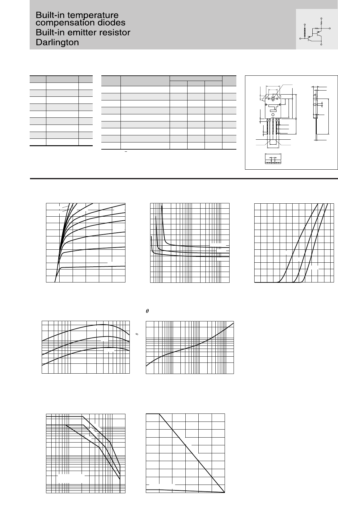
BDCSE
SAP10P
VCBO
100(Tc=25°C)
–150
–40 to +150
V
VCEO –150 V
VEBO –5 V
IC –12 A
IB –1 A
PCW
Tj °C150
Tstg °C
ICBO
IC=–7A, IB=–7mA
VCB=–150V
IE=1A
µA–100
–100
–150
5000 20000
–2.0
–2.5
1210
1540
0.176 0.22 0.264
IEBO VEB=–5V µA
VCEO IC=–30mA V
hFE ✽VCE=–4V, IC=–7A
VCE(sat) IC=–7A, IB=–7mA V
VBE(sat) V
Di VFmVIF=2.5mA
REΩ
min typ max
10Di IFmA
VCE
=–
20V, IC
=–
40mA
VBE mV
15.4±0.3 4.5±0.2
17.8±0.3
4±0.1
3.3±0.2
3.4max
5±0.2
22±0.3
23±0.3
28±0.3
2±0.1
7±0.2
9.9±0.2 1.6±0.2
φ3.2±0.2
1.35+0.2
–0.1
0.65+0.2
–0.1
0.8+0.2
–0.1
0.65+0.2
–0.1
1±0.1
2.54±0.1
2.54±0.1
3.81±0.1
3.81±0.1
D
S
E
C
B
✽hFE Rank O (5000 to 12000), Y (8000 to 20000)
–2
0
–4
–8
–12
1000
5000
10000
40000
0–4
–0.4mA
–0.8mA
–6 –1 –5–0.4
0
–1
–2
–3
–10 –50 –200–100 –10
0
–8
–6
–4
–2
–10
–12
–2 –2.5
–0.5 –1–0.3 –5 –12–10 0.1
0.5
1
3
101 5 50 100 500 20001000
–10–3 –5
–0.1
–0.05
–0.5
–1
–5
–30
–10
–50 –200–100
(VCE=–4V)
(VCE=–4V)
D.C
100ms
10ms
–0.6mA
–1.0mA
–1.2mA
–1.5mA
–2.0mA
IC=–10A
–7A
–5A
125°C
25°C
–30°C
125°C
25°C
–30°C
–10mA
–2.5mA
IB=–0.2mA
50 75025
20
0
3.5
40
100
80
60
100 150125
(Ta=25°C)
(18)
(2.5)
(41)
(36°)
R: 70Ω Typ. RE: 0.22Ω Typ.
Emitter resistor
Application: Audio
Collector-Emitter Voltage VCE (V)
Collector Current IC (A)
Safe Operating Area
(Single Pulse)
Ambient Temperature Ta (°C)
Maximum Power Dissipation Pc (W)
PC–T
a Derating
(Complement to type SAP10N)
■
Absolute maximum ratings
(Ta=25°C)
■Electrical Characteristics
Equivalent
circuit
External Dimensions (Unit: mm)
Weight: Approx 8.3g
a. Part No.
b. Lot No.
Symbol
Ratings Unit Symbol Conditions Ratings Unit
Collector-Emitter Voltage VCE (V)
Collector Current IC (A)
DC Current Gain hFE
Base Current IB (mA)
Collector-Emitter Saturation Voltage VCE(sat) (V)
Base-Emitter Voltage VBE (V)
Collector Current IC (A)
Collector Current IC (A) Time t (ms)
IC–VCE Characteristics (Typical) VCE(sat)–IB
Characteristics
(Typical)
IC–VBE
Temperature Characteristics (Typical)
hFE –IC Characteristics (Typical) j-a –t Characteristics
Transient Thermal Resistance j-a (°C/W)
(7.62)
(12.7)
ab
With Infinite heatsink
Without Heatsink
Natural Cooling
Without Heatsink
168
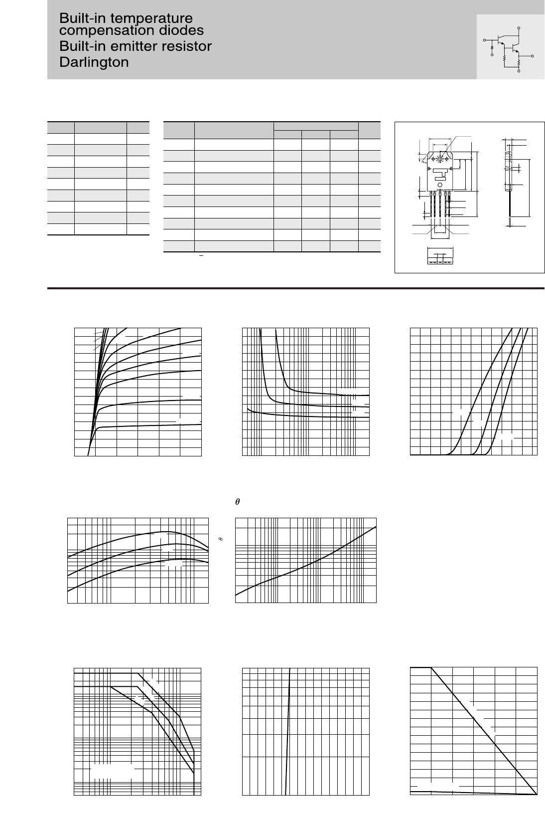
SAP16N
VCBO
150(Tc=25°C)
160
–40 to +150
V
VCEO 160 V
VEBO 5 V
IC 15 A
IB 1 A
PCW
Tj °C150
Tstg °C
ICBO
IC=10A, IB=10mA
VCB=160V
IE=1A
µA 100
100
160
5000 20000
2.0
2.5
1190
705
0.176 0.22 0.264
IEBO VEB=5V µA
VCEO IC=30mA V
hFE ✽VCE=4V, IC=10A
VCE(sat) IC=10A, IB=10mA V
VBE(sat) V
Di VFmVIF=2.5mA
REΩ
90 100 110REB Ω
min typ max
10Di IFmA VCE=20V, IC=40mAVBE mV
15.4±0.3 4.5±0.2
17.8±0.3
4±0.1
3.3±0.2
3.4max
5±0.2
22±0.3
23±0.3
28±0.3
2±0.1
7±0.2
9.9±0.2 1.6±0.2
φ3.2±0.2
1.35+0.2
–0.1
0.65+0.2
–0.1
0.8+0.2
–0.1
0.65+0.2
–0.1
1±0.1
2.54±0.1
2.54±0.1
3.81±0.1
3.81±0.1
BD C SE
2
0
5
10
15
1000
5000
10000
40000
04
0.8mA
1.2mA
50mA
5.0mA
3.0mA
6150.4
0
1
2
3
10 50 200100 10
0
5
10
15
2 2.5
0.5 10.3 5 1510 0.1
0.5
1
3
101 5 50 100 500 20001000
Collector-Emitter Voltage VCE (V)
Collector Current IC (A)
1035
0.1
0.05
0.5
1
5
40
10
50 200100
Safe Operating Area
(Single Pulse)
Forward Voltage VF (V)
Forward Current IF (mA)
0.5 1.0 1.5 2.00
10
5
1
Di IF–VF Characteristics
(Typical)
(VCE=4V)
125°C
25°C
–30°C
D.C
100ms
10ms
125°C
25°C
–30°C
IB=0.3mA
0.5mA
1.0mA
1.5mA
2.0mA
IC=15A
10A
5A
(VCE=4V)
Ambient Temperature Ta (°C)
Maximum Power Dissipation Pc (W)
50 75025
0
3.5
50
150
100
100 150125
PC–T
a Derating
External Dimensions (Unit: mm)
(18)
(2.5)
(41)
(36°)
Application: Audio
Collector-Emitter Voltage VCE (V)
Collector Current IC (A)
DC Current Gain hFE
Base Current IB (mA)
Collector-Emitter Saturation Voltage VCE(sat) (V)
Base-Emitter Voltage VBE (V)
Collector Current IC (A)
Collector Current IC (A) Time t (ms)
IC–VCE Characteristics (Typical) VCE(sat)–IB
Characteristics
(Typical)
IC–VBE
Temperature Characteristics (Typical)
hFE –IC Characteristics (Typical) j-a –t Characteristics
With Infinite heatsink
(Complement to type SAP16P)
(Ta=25°C)
■
Absolute maximum ratings
Equivalent
circuit
Weight: Approx 8.3g
a. Part No.
b. Lot No.
Symbol
Ratings Unit
(Ta=25°C)
■Electrical Characteristics
Symbol Conditions Ratings Unit
Transient Thermal Resistance j-a (°C/W)
Without Heatsink
Natural Cooling
Without Heatsink
(7.62)
(12.7)
ab
Emitter resistor
B
D
R: 100Ω Typ.
C
S
E
RE: 0.22Ω Typ.
✽hFE Rank O (5000 to 12000), Y (8000 to 20000)
169
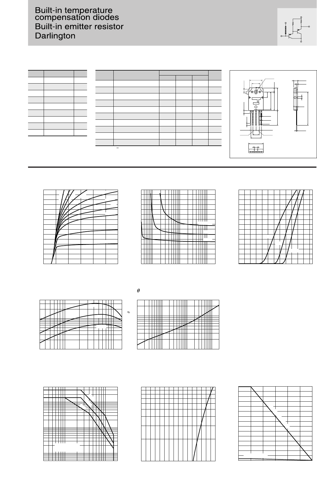
BDCSE
SAP16P
VCBO
150(Tc=25°C)
–160
–40 to +150
V
VCEO –160 V
VEBO –5 V
IC –15 A
IB –1 A
PCW
Tj °C150
Tstg °C
ICBO
IC=–10A, IB=–10mA
VCB=–160V
IE=1A
µA–100
–100
–160
5000 20000
–2.0
–2.5
1200
1540
0.176 0.22 0.264
IEBO VEB=–5V µA
VCEO IC=–30mA V
hFE ✽VCE=–4V, IC=–10A
VCE(sat) IC=–10A, IB=–10mA V
VBE(sat) V
Di VFmVIF=2.5mA
REΩ
90 100 110REB Ω
min typ max
10Di IFmA
VCE
=–
20V, IC
=–
40mA
VBE mV
15.4±0.3 4.5±0.2
17.8±0.3
4±0.1
3.3±0.2
3.4max
5±0.2
22±0.3
23±0.3
28±0.3
2±0.1
7±0.2
9.9±0.2 1.6±0.2
φ3.2±0.2
1.35+0.2
–0.1
0.65+0.2
–0.1
0.8+0.2
–0.1
0.65+0.2
–0.1
1±0.1
2.54±0.1
2.54±0.1
3.81±0.1
3.81±0.1
–2
0
–5
–10
–15
1000
5000
10000
40000
0–4–6–1–5–0.4
0
–1
–2
–3
–10 –50 –200–100 –10
0
–5
–10
–15
–2 –2.5
–0.5 –1–0.3 –5 –15–10 0.1
0.5
1
3
101 5 50 100 500 20001000
–10–3 –5
–0.1
–0.05
–0.5
–1
–5
–40
–10
–50 –200–100 Forward Voltage VF (V)
Forward Current IF (mA)
0.5 1.0 1.5 2.00
10
5
1
Di IF–VF Characteristics
(Typical)
(VCE=–4V)
D.C
100ms
10ms
125°C
25°C
–30°C
IC=–15A
–10A
–5A
–0.5mA
–50mA
–5.0mA
–3.0mA
–2.0mA
–1.5mA
–1.2mA
–1.0mA
–0.8mA
IB=–0.3mA
125°C
25°C
–30°C
(VCE=–4V)
Ambient Temperature Ta (°C)
Maximum Power Dissipation Pc (W)
50 75025
0
3.5
50
150
100
100 150125
PC–T
a Derating
External Dimensions (Unit: mm)
Application: Audio
Collector-Emitter Voltage VCE (V)
Collector Current IC (A)
DC Current Gain hFE
Base Current IB (mA)
Collector-Emitter Saturation Voltage VCE(sat) (V)
Base-Emitter Voltage VBE (V)
Collector Current IC (A)
Collector Current IC (A) Time t (ms)
IC–VCE Characteristics (Typical)
Collector-Emitter Voltage VCE (V)
Collector Current IC (A)
Safe Operating Area
(Single Pulse)
VCE(sat)–IB
Characteristics
(Typical)
IC–VBE
Temperature Characteristics (Typical)
hFE –IC Characteristics (Typical) j-a –t Characteristics
With Infinite heatsink
(Complement to type SAP16N)
Equivalent
circuit
Weight: Approx 8.3g
a. Part No.
b. Lot No.
(Ta=25°C)
■
Absolute maximum ratings
Symbol
Ratings Unit
(Ta=25°C)
■Electrical Characteristics
Symbol Conditions Ratings Unit
Transient Thermal Resistance j-a (°C/W)
Without Heatsink
Natural Cooling
Without Heatsink
ab
(18)
(2.5)
(41)
(36°)
(7.62)
(12.7)
Emitter resistor
D
S
E
C
B
RE: 0.22Ω Typ.
R: 100Ω Typ.
✽hFE Rank O (5000 to 12000), Y (8000 to 20000)
170
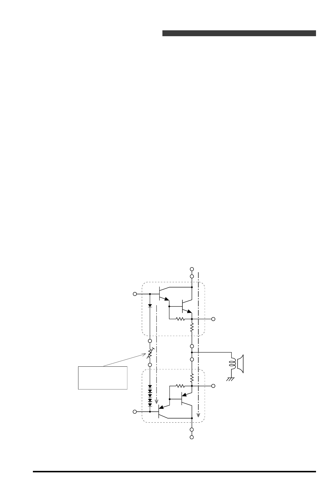
B
D
2.5mA 40mA
D
C
NPN
S
S
E
E
PNP C
B
–VCC
+VCC
Application Information
1. Recommended Operating Conditions
➀Add a variable resistor (VR) between diode terminals to adjust the idling current. The
resistor having 0 to 200Ω is to be used.
➁Adjust the forward current flowing over the diodes at 2.5mA.
➂Adjust the idling current at 40mA with the external variable resistor.
Both the temperature coefficients for the transistor and the diodes are matched under the above conditions.
Both the PNP and the NPN are Darlington transistors, so the temperature change ratio of the total four VBE
of the transistors is subject to the compensation. One PN junction diode in the NPN and five Schottky
barrier diodes in the PNP are built-in, and the total six diodes are operating as the temperature compensation.
The temperature coefficient of the total diodes (its variable value) becomes smaller with a larger forward
current (approximately —0.2mV/℃ to 1mA), and the coefficient of the total transistors (its variable value)
also becomes smaller with a larger idling current (approximately —0.1mV/℃ to 10mA), but the both variable
values are small.
Thus, the distortion of the temperature coefficient caused by the different current is small, so the thermal
runaway may not be occurred due to the changes of the recommended ratings; however, the actual operation
is to be confirmed by using an experimental equipment or board.
External variable
resistor (VR)
(0 to 200Ω)
SAP Series
171
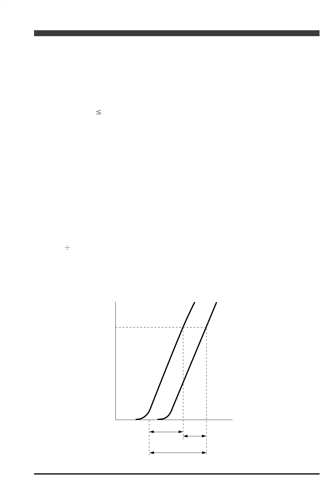
Di VFTR VBE
Variations Variations
VBE
VBE Min.
(P and N: hFE Max.) VBE Max.
(P and N: hFE Min.)
IC
40mA
∆VF=500mV
2. External Variable Resistor
Total forward voltage (at IF=2.5mA) of the diodes is designed to be equal or less than that of total VBE (at IC
= 40mA) of the transistor, thus the idling current is required to be adjusted at 40mA with an additional
external variable resistor.
The relations are shown as below:
Total VF of Diode Total VBE of Transistor + Total VRE of Emitter Resistor
∆V=0 to 500mV
The VBE of the transistor is dependent to the hFE, and the VBE is lower with higher hFE and vice versa. The
hFE for both the PNP and the NPN varies between 5k and 20k; thus the VBE is the lowest with the
combination of maximum hFE (20k) each and it is the highest with the combination of minimum hFE (5k)
each.
Presuming the voltage difference between the VF of the diodes and the VBE of the transistors (including the
total voltage drops of the two emitter resistors) as ∆V.
Minimum VBE – Maximum VF variations of the diodes = 0
Maximum VBE – Minimum VF variations of the diodes = 500mV
The current flowing over the diodes and the VR is adjusted at 2.5mA; therefore
500mV 2.5mA = 200Ω
Consequently, the applicable VR value is to be 0 to 200‰
172
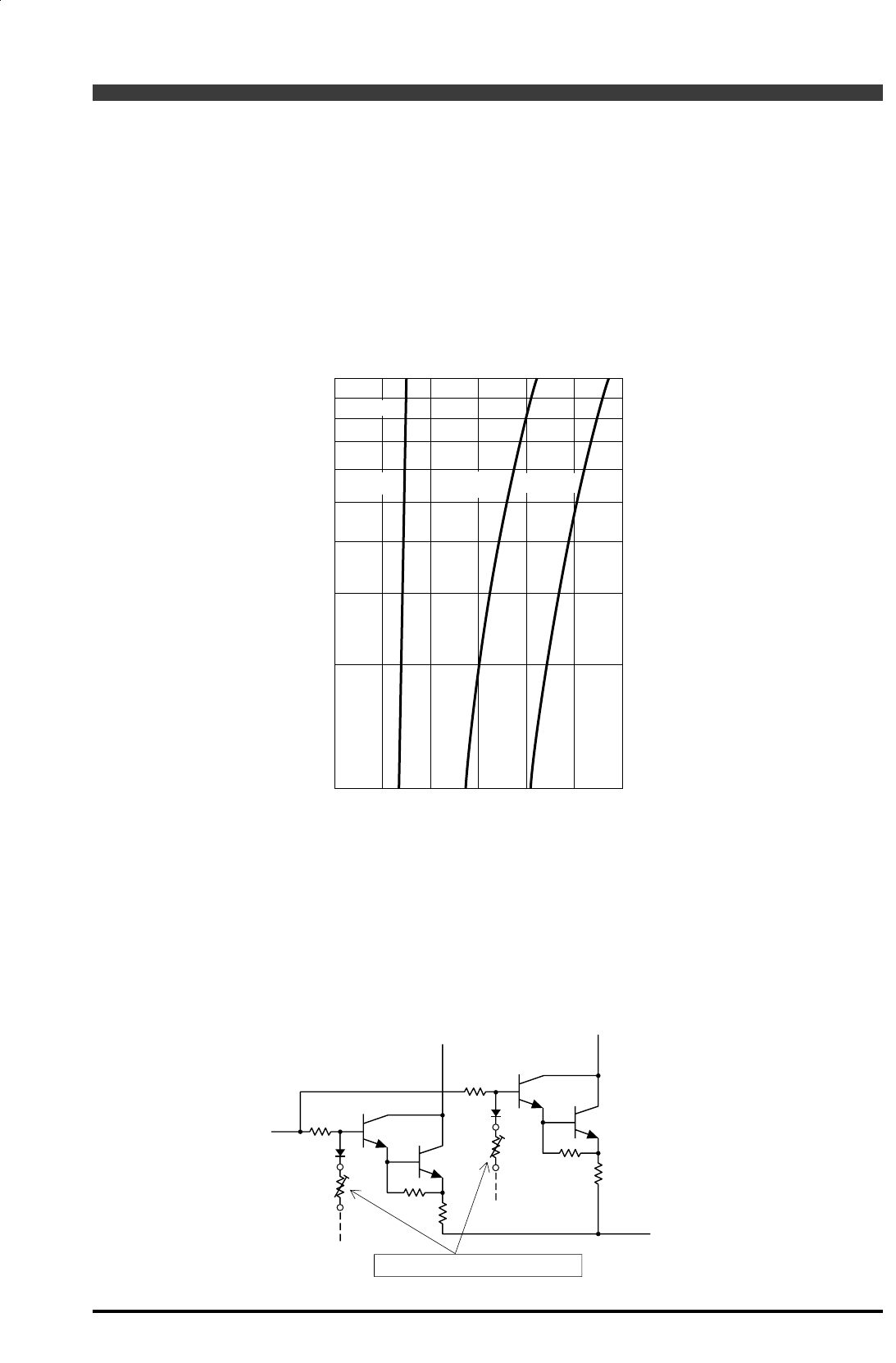
1.0
10.0
5.0
0 500 1000 1500
VF (mV)
IF (mA)
IF – VF Characteristics
2000 2500 3000
PN-Di SBD
(5 diodes Total) PN–Di+SBD
3. Characteristics of the temperature compensation diodes
The several temperature compensation diodes are connected in series, so the forward voltage is varied with
small current fluctuations. Therefore, in case the forward current flowing over the diodes is set at 2.5mA and
over, the forward voltage rises, and in the worst combinations, the idling current reaches to 40mA and over
with minimum VR of 0Ω. On the contrary, in case the forward current is set at 2.5mA or below, the idling
current may not reach to 40mA with maximum VR of 200Ω.
4. Parallel push-pull application
Adjustments of the idling current are required by each the resistor in parallel push-pull applications. One
side adjustment will cause the idling current to be unstable (seesaw operation) because of the different hFE.
Ta=25°C
To be adjusted individually
173
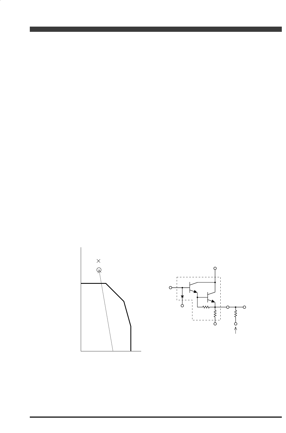
IC
VCE
Transistor destruction point
Thick-film resistor
destruction point
A.S.O.
Curve
B
D
C
S
E
5. Destruction capacity of the built-in emitter resistor
A thick-film resistor is used for the built-in resistor. The thick-film resistor has weaker destruction point in
the Pc area (especially for large current flowing area) than that of the transistor chip itself. There is less
concern, however, as this is subject to the area beyond an Are of Safe Operation (A.S.O.).
However, under the evaluation like a short circuit test in which the current exceeds the guaranteed value, it
may cause the emitter resistor to be destroyed before the transistor itself is destroyed.
Consequently, the current value (or time) that operates the protection circuit is to be set at lower than that of
discrete device configurations. In the application of car audio amplifiers, the same manners as the above
need to be considered because the large current is flowed at low impedance.
In addition, once the transistor falls into thermal runaway due to a soldering failure to the external VR added
between diodes or other failure manners, as the worst case, there may cause a resin crack or smoke emissions
by flare up. Flame retardant molding resin is used, and the material of the product is conformed to the most
sever standard UL94V0. However it is recommended that the careful consideration be given to a protection
circuit, and the protection circuits should be provided appropriately in due course.
If the operating conditions are not to be matched to the ratings, it is also recommended that the E (Emitter
resistor) terminal should be opened and the external emitter resistor should be added to the S (Sensing)
terminal shown as below.
External
emitter resistor
Output terminal
174

MEMO
175
Discontinued Parts Guide
Repair Parts Replacement Parts
2SA768to769 2SA1262,1488,1488A
2SA770to771 2SA1725,1726
2SA957to958 2SA1667,1668
2SA1489 2SA1693
2SA1490 2SA1694
2SA1491 2SA1695
2SA1643 2SA1725
2SA1670 2SA1907
2SA1671 2SA1908
2SA1672 2SA1909
2SB1624 2SB1685
2SB1625 2SB1687
2SB1626 2SB1686
2SC1826to1827 2SC3179,3851,3851A
2SC1983to1984 2SC3852,3852A
2SC1985to1986 2SC4511,4512
2SC2167to2168 2SC4381,4382
2SC2315to2316 2SC4558
2SC2810 2SC3890
2SC3300 2SC4131
2SC3853 2SC4466
2SC3854 2SC4467
2SC3855 2SC4468
2SC4385 2SC5099
2SC4386 2SC5100
2SC4387 2SC5101
2SC4503 2SD2083
2SC4558 2SD2495
2SC4820 2SC4518
2SD2493 2SD2641
2SD2494 2SD2643
2SD2495 2SD2642
Discontinued Parts Replace ment Parts
2SA744to745 2SA1694to1695
2SA746to747 2SA1695
2SA764to765 2SA1725to1726
2SA807to808 2SA1693to1694
2SA878 –
2SA892 2SB1351
2SA907to909 2SA1215to1216,1295
2SA971 –
2SA980to982 2SA1694
2SA1067 –
2SA1068 –
2SA1102 2SA1693
2SA1103 2SA1694
2SA1104 2SA1694
2SA1105 2SA1695
2SA1106 2SA1695
2SA1116 2SA1493
2SA1117 2SA1494
2SA1135 2SA1693
2SA1169 2SA1493
2SA1170 2SA1494
2SA1187 –
2SA1205 2SA1746
2SA1355 2SA1262,1488
2SB622 –
2SB711to712 2SB1259,1351
2SB1005 2SB1257
2SB1476 2SB1624
2SB1586 2SB1625
2SC1107 2SC3179,3851
2SC1108 2SC3851A
2SC1109 2SC3179,3851
2SC1110 2SC3851A
2SC1111to1112 2SC4467to4468
2SC1113 2SC4511to4512
2SC1114 –
2SC1115to1116 2SC4468
2SC1402to1403 2SC4467to4468
2SC1436 –
2SC1437 –
2SC1440to1441 –
2SC1442to1443 –
2SC1444to1445 2SC4511to4512
2SC1454 –
2SC1477 –
2SC1504 2SC2023
2SC1577to1578 2SC3833,3831
2SC1579to1580 2SC4706
2SC1584to1585 2SC2921-2922,3264
2SC1618to1619 2SC4466-4467
2SC1629 2SD2045
2SC1664 2SC4558
2SC1768 –
2SC1777 –
2SC1783 –
2SC1786 –
2SC1828 2SC3832,3830
Discontinued Parts Replacement Parts
2SC1829 –
2SC1830 2SD2082,2083
2SC1831 –
2SC1832 –
2SC1888to1889 2SC3852,3852A
2SC2022 2SC2023
2SC2147 –
2SC2198 2SC4024
2SC2199 2SC4131
2SC2256 –
2SC2260to2262 2SC4467
2SC2302 2SC3832
2SC2303 2SC3833
2SC2304 2SC3833
2SC2305 –
2SC2306 2SC4140
2SC2307 2SC3833
2SC2317 2SD2016
2SC2354 2SC2023
2SC2364 –
2SC2365 2SC3831
2SC2491 2SC4024
2SC2492 –
2SC2493 –
2SC2577 2SC4466
2SC2578 2SC4467
2SC2579 2SC4467
2SC2580 2SC4468
2SC2581 2SC4468
2SC2607 2SC3857
2SC2608 2SC3858
2SC2665 2SC4466
2SC2723 2SC4140
2SC2761 –
2SC2773 2SC3857
2SC2774 2SC3858
2SC2809 –
2SC2810A 2SC4820
2SC2825 2SD2045
2SC2838 –
2SC2900 –
2SC3409 2SC3679
2SC3520 2SC4140
2SC3706 –
2SC3909 2SC3680
2SC4023 2SC5124
2SC4199,4199A
2SC5124
2SC4302 2SC4301
2SC4303,4303A
2SC5002
2SC4494 2SC4495
2SC4756 2SC5002
2SD15to18 2SC4468
2SD80to84 2SC4466,4467
2SD90to94 2SC3179,3851,3851A
2SD163to166 2SC4468
2SD201to203 2SC4466to4467
2SD211to214 2SC4468
Discontinued Parts Replacement Parts
2SD219to221
2SC3179,3851,3851A
2SD219Fto221F
2SC3179,3851,3851A
2SD222to224
2SC3179,3851,3851A
2SD236to238
2SC3179,3851,3851A
2SD241to244
2SC3179,3851,3851A
2SD256to259
2SC3179,3851,3851A
2SD419to421 2SD1769,1785
2SD556to557 2SC4468
2SD593to594 2SC4020
2SD605 –
2SD606 –
2SD614to615 2SD1769,1785
2SD617 2SD2082
2SD721 2SD2081
2SD722 2SD2081
2SD807 2SC3679
2SD810 2SC4024
2SD971 –
2SD972 2SD1796
2SD1031 2SD1769,1785
2SD1170 2SD2045
2SD1532 2SD2015
2SD2231 2SD2493
2SD2437 2SD2494
176

PRINTED in JAPAN H1-T01EE0-0107020SB
Sanken Electric Co.,Ltd.
1-11-1 Nishi-Ikebukuro,Toshima-ku, Tokyo
PHONE: 03-3986-6164
FAX: 03-3986-8637
Overseas Sales Offices
●Asia
Sanken Electric Korea Co.,Ltd.
SK Life B/D 6F,
168 Kongduk-dong, Mapo-ku, Seoul, 121-705, Korea
PHONE: 82-2-714-3700
FAX: 82-2-3272-2145
Taiwan Sanken Electric Co.,Ltd.
Room 902, No.88, Chung Hsiao E. Rd., Sec. 2
Taipei, Taiwan R.O.C.
PHONE: 886-2-2356-8161
FAX: 886-2-2356-8261
Sanken Electric Singapore Pte.Ltd.
150 Beach Road, #14-03 The Gateway West,
Singapore 0718
PHONE: 291-4755
FAX: 297-1744
Sanken Electric Hong Kong Co.,Ltd.
1018 Ocean Centre, Canton Road,
Kowloon, Hong Kong
PHONE: 2735-5262
FAX: 2735-5494
●North America
Allegro MicroSystems,Inc.
115 Northeast Cutoff, Box 15036
Worcester, Massachusetts 01615, U.S.A.
PHONE: (508) 853-5000
FAX: (508) 853-7861
●Europe
Allegro MicroSystems Europe Limited.
Balfour House, Churchfield Road,
Walton-on-Thames, Surrey KT12 2TD, U.K.
PHONE: 01932-253355
FAX: 01932-246622
Contents of this catalog are subject to change due to modification
