Solution Manual Ability
User Manual:
Open the PDF directly: View PDF ![]() .
.
Page Count: 47
Solutions to Problems
from “Essentials of Electronic Testing”
c
M. L. Bushnell and V. D. Agrawal, 2002
February 10, 2006
Please Read This
This manual contains solutions to all problems that appear at the end of the chapters
in the book. At the end of the manual we have included the solutions to problems
we used for the examinations in the Spring 2002 course at Rutgers University, and
Spring 2004 and Spring 2005 courses at Auburn University.
In spite of all the care taken to ensure accuracy, we caution the user that some
answers may contain errors as it is the first release of this manual. We will appreciate
if any errors or comments are forwarded to us by email: vagrawal@eng.auburn.edu
or bushnell@caip.rutgers.edu.
This manual has been created as teaching material that accompanies the book.
To preserve its effectiveness, it should not be distributed. If necessary, only a very
small set of solutions can be copied for distribution in the class. Please do not pass
your copy on to others and ask any one requesting it to contact the authors.
Teachers can also use the presentation slides for 31 lectures (or an alternative
sequence of 23-lectures), based on the book and available at the following websites:
http://www.eng.auburn.edu/∼vagrawal/COURSE/lectures.html
http://www.caip.rutgers.edu/∼bushnell/rutgers.html
We hope the readers of our book, both teachers and students, will benefit from
this work. We acknowledge the help from colleagues and students in completing
this solution manual and the assistance of the University of Wisconsin-Madison in
its initial distribution.
Solution Manual V1.4 – c
M. L. Bushnell and V. D. Agrawal – For Teachers only Page 1
A-PDF Merger DEMO : Purchase from www.A-PDF.com to remove the watermark

Chapter 1: Introduction
1.1 Chip testing
The events of Example 1.1 are redefined as follows:
PQ: chip is good P: chip passes the test
FQ: chip is bad F: chip fails the test
A 70% yield means, Prob(PQ)=0.7andProb(FQ)=0.3. Following the analysis
of Example 1.1, Prob(P)=0.68. Then,
Defect level = Bad chips that pass tests
All chips that pass tests
=Prob(FQ|P)
=Prob(P|FQ)Prob(FQ)
Prob(P)
=0.05 ×0.3
0.68 =0.022
The defect level is 22,000 ppm (parts per million).
1.2 Chip testing
Let xdenote the escape probability, Prob(P|FQ). Referring to the formula derived
in Problem 1.1, a defect level of 500 ppm means,
Prob(P|FQ)Prob(FQ)
Prob(P)=x×0.3
0.95 ×0.7+x×0.3=0.0005
This gives,
x=0.0003325
0.29985
Next, we obtain,
Defect coverage = Prob(F|FQ)=1−Prob(P|FQ)
=1−x=0.99889
The required defect coverage is 99.889%. This represents the capability of the
test in detecting the actual “defects” that occur and should not be confused with
the “fault coverage,” which is defined for the “single stuck-at” fault model.
1.3 Test cost
Assuming that one vector is applied per clock cycle during the digital test, the rate
of test application is 200 million vectors per second. Therefore,
Digital test time = 1000 ×106
200 ×106=5s
Solution Manual V1.4 – c
M. L. Bushnell and V. D. Agrawal – For Teachers only Page 2

Adding the analog test time, we get
Total test time = 1.5+5.0=6.5s
The testing cost for a 500 MHz, 1,024 pin tester was obtained as 4.56 cents in
Example 1.2 (see page 11 of the book.) Thus,
Cost of testing a chip = 6.5×4.56 = 29.64 cents
The cost of testing bad chips should also be recovered from the price of good chips.
Since the yield of good chips is 70%, we obtain
Test cost in the price of a chip = 29.64
0.7≈42 cents
41.8 cents should be included as the cost of testing while figuring out the
price of chips.
1.4 Test cost and self-test
Following Example 1.2 of the book (pp. 10-11), we obtain
ATE purchase price = $1.2M+ 256 ×$3,000 = $1.968M
Assuming a 20% per year linear rate of depreciation, a maintenance cost of 2% of
the price, and an annual operating cost of $0.5M,
Running cost = $1.968M×0.2+$1.968M×0.02 + $0.5M= $932,960/year
Testing cost = $932,960
365 ×24 ×3600 =2.96 cents/second
Testing cost of the self-test design is 2.96 cents per second, down from
4.56 cents per second calculated in Example 1.2
1.5 Test complexity
Consider a cube of side d. The number of transistors (Nt) is proportional to the
volume d3, and the number of pins (Np) is proportional to the surface area 6d2.
Thus, the Rent’s rule for the cube can be expressed as,
Np=K×Nt2/3
where Kis a constant, which depends on such technology parameters as the mini-
mum feature spacing. For simplicity, we will assume that this constant is the same
for the flat and cubic chips. Following Example 1.3 (pp. 12-13 of book), we define
the test complexity, TC, as transistors per pin, or TC =Nt/Np. For the cube,
TC
cube =Nt
Np
=Nt
KNt2/3=1
KNt1/3
Solution Manual V1.4 – c
M. L. Bushnell and V. D. Agrawal – For Teachers only Page 3

Using the Rent’s rule for a flat chip (Equation 1.5 on page 13 of book), we obtain
TC
square =Nt
KNt1/2=1
KNt1/2
Therefore,
TC
square
TC
cube
=Nt1/6
This ratio of test complexities continues to increase as the number of transistors (Nt)
on the VLSI device grows. For example, for Nt=1million, the square-chip test
complexity is ten times greater than that of the cubic-device. The test problem
of the cubic configuration is less complex than that for the flat chip.
Note: Although chips at present are not designed as three-dimensional objects,
three-dimensional packages and interconnects are in use. An interested reader may
see the article: H. Goldstein, “Packages Go Vertical,” IEEE Spectrum, vol. 38,
no. 8, pp. 46-51, August 2001. Recently, Matrix Semiconductor announced plans
to produce a three-dimensional memory chip. See, “Adding a Third Dimension to
Chips,” Computer, vol. 35, no. 3, p. 29, March 2002.
Solution Manual V1.4 – c
M. L. Bushnell and V. D. Agrawal – For Teachers only Page 4
Chapter 2: VLSI Testing Process and Test Equipment
2.1 Test types
To reduce the warranty and product liability costs, the manufacturer must adopt a
thorough but cost-effective test plan. A low failure rate, which may be as low as 100
parts per million, means that among one million chips shipped by the manufacturer
there should be no more than 100 defective chips. A suitable test strategy requires
adjustments to tests as the production ramps up. A realistic plan is as follows:
•Initial production: The manufacturer uses parametric tests and vector tests,
the latter with coverage in the 95-100% stuck-at fault range. For high-speed
microprocessor chips, at-speed critical path tests are run. The chips should
be subjected to burn-in test for infant mortality.
•Matured production: If burn-in failures are lower than the required defect level
then that test is eliminated or reduced to a sample basis. Any field returns
are re-tested by the manufacturing tests. If these pass then the manufacturing
tests are augmented, when necessary, by customer-supplied tests.
•Test optimization: Tests are optimized to reduce the manufacturing cost.
First, test sequences that fail a larger number of devices are moved to the
beginning. Second, test sequences that do not fail any devices are dropped.
Such modifications change the emphasis from detection of modeled faults to
detection of actual defects.
•Process monitoring: Once the chip goes into high-volume production, the
manufacturing process and the outgoing product (chips) should be moni-
tored to keep any variations within statistical limits. This means that var-
ious parameters, such as metal resistivity, polysilicon conductivity, transistor
parameters, etc., should be within their three-sigma range (average ±3×
standard deviation). Any excursions outside such a range are immediately
diagnosed and the causes remedied.
2.2 Contact test
Assume a diode drop of 0.7V. Then, the pin voltage range for contact test is given
by:
Upper range : Vpin =0V−0.7V−100μA ×2000Ω
=−0.9V
Lower range : Vpin =0V−0.7V−250μA ×2000Ω
=−1.2V
2.3 Set-up time test
To test a set-up time, tset−up = 360ps, apply the following waveforms to the chip (a
clock-to-Qdelay of 400ps is assumed):
Solution Manual V1.4 – c
M. L. Bushnell and V. D. Agrawal – For Teachers only Page 5
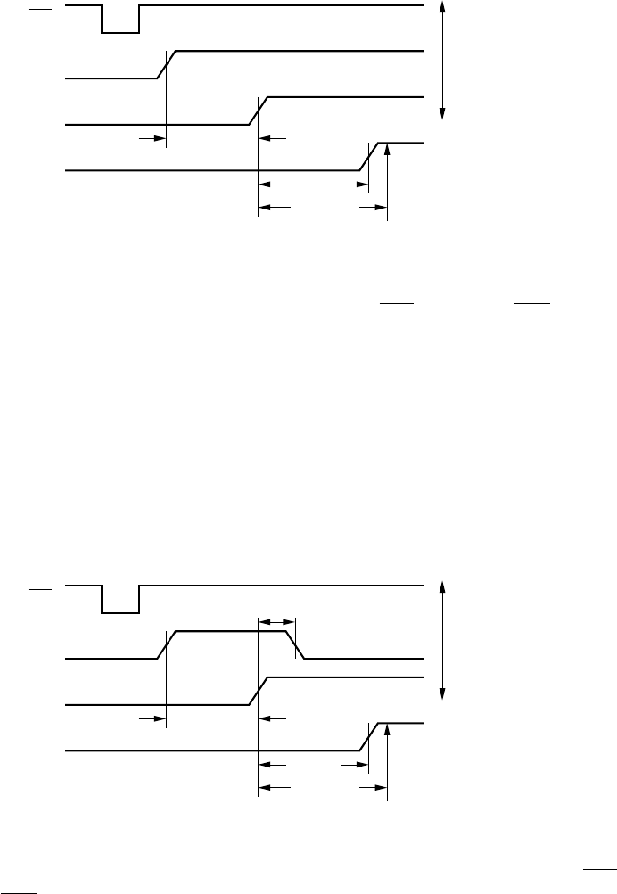
ps
MC
Q
CLK
D
400
360ps
450ps
Measure Q
Inputs
Output
At an interval of 450ps after the rising CLK edge, measure Qon the ATE.
If Q= 1, the device passes, otherwise it fails. Using MS instead of MC, repeat
the above waveform sequence, but with Dinverted and the expected Qsignal also
inverted. At an interval of 450μs after the rising CLK edge, again measure Qon
the ATE. If Q= 0, the device passes, otherwise it fails. The same waveforms are
applied simultaneously to all five Dlines, and five simultaneous measurements are
made on the five Qlines.
2.4 Hold time test
To test a hold time, thold = 120ps, apply the following waveforms to the chip (a
clock-to-Qdelay of 400ps is assumed):
400ps
MC
Q
CLK
D
Output
120ps
400ps
Inputs
Measure Q
ps450
At an interval of 120ps after the rising CLK edge, we lower the Dline. If Q=1
450ps after the rising CLK edge, the device passes, otherwise it fails. Using MS
instead of MC, repeat the above waveform sequence, but with Dinverted and the
expected Qsignal also inverted. At an interval of 450μs after the rising CLK edge,
again measure Qon the ATE. If Q= 0, the device passes, otherwise it fails. The
same waveforms are applied simultaneously to all five Dlines, and five simultaneous
measurements are made on the five Qlines.
Solution Manual V1.4 – c
M. L. Bushnell and V. D. Agrawal – For Teachers only Page 6
2.5 Threshold test
Perform the threshold test as given on page 32 of the book, but with the following
changes: Assume a 5Vsupply, and perform binary search to find VIL and VIH. The
following procedure determines VIL:
Incorrect
Incorrect
Incorrect
Incorrect
Incorrect
Incorrect
Incorrect
Incorrect
Read output pin.
Correct
Correct
Correct
Correct
Correct
Correct
Correct
Correct
input pin and a propagating pattern.
Read input voltage as V
If it is 0.8V or greater,
the chip passes.
IL
Read the expected output
Correct
Incorrect
Write a 1.25V signal to the
Subtract 0.6V to input pin.
Read output pin.
Subtract 0.3V to input pin.
Read output pin.
Read output pin.
Subtract 0.1V to input pin.
Read output pin.
Subtract 0.15V to input pin.
Add 0.6V to input pin.
.
Read output pin.
Read output pin.
Add 0.1V to input pin.
Add 0.15V to input pin.
Add 0.3V to input pin.
Read output pin.
The advantage of this procedure is that it greatly speeds up the test. The test
for VIH is analogous.
Solution Manual V1.4 – c
M. L. Bushnell and V. D. Agrawal – For Teachers only Page 7

Chapter 3: Test Economics and Product Quality
3.1 Economic decision
We start with the following formula for the price of the car deriven by John (Equa-
tion 3.2 on page 38 of the book):
P=20,000 + 20,000
ndollars
where nis the number of breakdowns per 15,000 miles since John’s car is driven
15,000 miles in a year. Because Laura drives only 5,000 miles per year, her car is
expected to have n/3 breakdowns per year. Assuming a linear depreciation to zero
value over 20 years and an average repair cost of $250 per breakdown, the annual
cost of driving is
C=P
20 +K+ 250n/3dollars
=1,000 + 1,000
n+K+ 250n/3dollars
where Kis the cost of gasoline and regular maintenance, assumed to be the same
for all models. To minimize this cost, we write
dC
dn =−1,000
n2+250
3=0 or n=√12
This is a minimum because d2C
dn2>0. The price of a car for minimum transportation
cost is,
P=20,000 + 20,000
√12 =25,774 dollars
Laura should invest in a car priced around 25,774 dollars.
3.2 Economic decision
(a) Let xbe the daily wages of a technician and cbe the cost of components on a
board. When ntechnicians work in the assembly shop, the cost of one board is,
C(n)=W arehouse cost
n+technicianswages+component cost
+workspace cost
=10,000
n+x+c+500n2
n
To minimize this cost, we write
dC(n)
dn =−10,000
n2+1,000n=0 or n=√20 = 4.47
Solution Manual V1.4 – c
M. L. Bushnell and V. D. Agrawal – For Teachers only Page 8

This is a minimum since d2C(n)
dn2>0. We obtain the minimum cost as,
C(4) = C(5) = $4,500 + x+c
To minimize the cost we should either hire four technicians, or reduce
the workforce to five if more than five technicians were already employed.
(b) Substituting x= 200 and c=10,000 in the last equation, we get
C(4 or 5) = $4,500 + 200 + 10,000 = $14,700
The minimum cost of a single-board system is $14,700.
3.3 Benefit-cost analysis
Please note a correction in the statement of this problem. The part (a) should read:
Show that this scheme is beneficial for chips whose total cost is less than ten times
the burn-in cost when the burn-in yield is 90%.
(a) Complete elimination of burn-in: Let Ctbe the total cost of a chip in the present
scheme where burn-in test is applied to every chip that passes the conventional test.
Let Cbbe the per chip cost of burn-in. Ctincludes Cb, as well as another component,
Cf, which accounts for the costs of fabrication, conventional test, etc. It is given by,
Ct=Cf+ycCb
ycyb
where ycis the yield with the conventional test and ybis the yield reduction due to
burn-in. Since the cost of IDDQ test is 10% of the burn-in cost and there is a 10%
yield loss, the cost of a chip when burn-in is replaced by IDDQ test is given by,
C
t=Cf+0.1ycCb
0.9ycyb
For the new scheme to be beneficial, we must have
C
t<C
tor Ct<9Cb
yb
For the given 90% burn-in yield, yb=0.9, and Ct<10Cb.The total cost should
not exceed ten times the burn-in cost.
(b) Apply burn-in test only to chips that fail IDDQ test: Let ybbe the burn-in yield.
Consider all chips that have passed pre-burn-in tests. A fraction ybof these is “good”
chips. We apply IDDQ test to all chips passing the pre-burn-in test. Due to the 10%
yield loss, this will produce a fraction 0.9ybconsisting of good chips. The remaining
fraction, 1 −0.9yb, must be subjected to the burn-in test to recover the lost yield.
For the new scheme to be beneficial, we must have
0.1Cb+(1−0.9yb)Cb<C
bor yb>1
9
Burn-in yield should be greater than 1/9 or 11.1%.
Solution Manual V1.4 – c
M. L. Bushnell and V. D. Agrawal – For Teachers only Page 9

3.4 Yield and cost
Let Cwbe the cost of processing a wafer having Nchips and let y(A) be the yield
of chips, where Ais the chip area. Then the cost per good chip is obtained as,
Cc=Cw
Ny(A)
DFT changes the chip area to (1 + Δ)A. The number of chips on a wafer of area
NA is now given by, NA/(A+ΔA)=N/(1 + Δ). The cost of a good chip with
DFT is given by,
Cc(DFT)= Cw
N
1+Δ y(A+ΔA)
Therefore, the cost increase due to DFT is,
Cost increase = Cc(DFT )−Cc
Cc×100 percent
=(1 + Δ)y(A)
y(A+ΔA)−1×100 percent
Using the yield formula of Equation 3.12 (p. 46 in the book), we get
Cost increase = (1 + Δ) (1 + Ad/α)−α
(1 + (1 + Δ)Ad/α)−α×percent
=(1 + Δ)1+ AdΔ
α+Adα
−1×100 percent
which is the required result.
For the given data, d=1.25 defects/cm2,α=0.5, Δ = 0.1, and A=1cm2,
we obtain
Cost increase = 1.11+1.25 ×0.1
0.5×1.250.5
−1×100 percent
=13.86%
There is a 13.86% increase in the chip cost due to DFT.
3.5 Defect level and fault coverage
Defect level, DL, is given by Equation 3.20 (p. 50 of the book), as follows:
DL =1−β+TAf
β+Af β
where Tis the fault coverage, Af is the average number of faults on a chip of area
A,andβis a fault clustering parameter. Further manipulation of this equation
Solution Manual V1.4 – c
M. L. Bushnell and V. D. Agrawal – For Teachers only Page 10

leads to the following result:
(1 −DL)1/β =β+TAf
β+Af
or T=(β+Af)(1 −DL)1/β −β
Af ×100 percent
which is the required result.
3.6 Defect level and fault coverage
Substituting the given fault density, f=1.45 f aults/cm2, the fault clustering pa-
rameter, β=0.11, and the fault coverage, T=0.95, in Equation 3.20 (page 50 of
the book), we obtain the defect level as,
DL(T)=1−β+TAf
β+Af β
=1−0.11 + 0.95 ×1.0×1.45
0.11 + 1.0×1.45 0.11
=0.00522 or 5,220 parts per million
The defect level is 5,220 parts per million (ppm).
(a) To obtain the fault coverage Tfor a required defect level of 1,000 ppm, we
substitute DL =0.001 in the formula derived in Problem 3.5. Thus,
T=(0.11 + 1.45) ×0.9991/0.11 −0.11
1.45 ×100 = 0.990
The required fault coverage is 99%.
(b) For a defect level of 500 ppm (DL =0.0005), we get
T=(0.11 + 1.45) ×0.99951/0.11 −0.11
1.45 ×100 = 0.995
The required fault coverage is 99.5%.
3.7 Defect level
Defect level, DL(T), given by Equation 3.20 (p. 50 of the book), can be written as:
DL(T)=1−(1 + TAf/β)β
(1 + Af/β)β
=1−eTAf
eAf =1−e−Af(1−T),as β→∞
Also, as β→∞, Equation 3.19 (p. 50 of the book) gives the yield,
Y=1+Af
β−β
=e−Af
Solution Manual V1.4 – c
M. L. Bushnell and V. D. Agrawal – For Teachers only Page 11
Substituting this expression for yield in the defect level, we get
DL(T)=1−(e−Af )1−T=1−Y1−T
which is the required result.
Solution Manual V1.4 – c
M. L. Bushnell and V. D. Agrawal – For Teachers only Page 12

Chapter 4: Fault Modeling
4.1 Boolean functions
An n-variable Boolean function is completely specified by its truth-table. The output
column in this table is a 2n-bit vector that can be in 22ndistinct states, each
specifying a different Boolean function.
4.2 Initialization faults
In the circuit of Figure 4.1 (p. 62 of the book), let Qpdenote the present state at
the output of the FF. Let the next state, i.e., the output of the AND gate, be Qn.
We can write the next state function,as
Qn=(Qp+A)(A+B)
If we set A= 1, the next state function, Qn=B, becomes independent of the
present state. That is, irrespective of the present state, the next state can be set to
a value, which is uniquely determined by primary inputs. This makes the fault-free
circuit initializable. When the fault As-a-0 is present, the above equation reduces to
Qn=Qp. Thus, starting with Qp=X,Qncan never be changed to any value other
than Xand, therefore, the circuit will remain uninitialized in the presence
of this fault.
Using the next-state expression, we can easily determine that no other single
stuck-at fault in this circuit will prevent initialization. For example, consider the
s-a-0 fault on the top branch of the fanout of A. The faulty next state function is
Qn=Qp(A+B), which can be set to 0, when Qp=X, by applying A=1,B=0.
4.3 Fault counting
See Section 4.5 (last paragraph on p. 70 of the book.)
4.4 Fault counting
For the circuit of Figure 4.6 (p. 72 of book), we have
Number of fault sites = PIs + gates + fanout branches
= 2+4+6=12
Therefore,
Number of single and multiple faults = 3number of fault sites −1
=3
12 −1 = 531,440
The circuit has 531,440 single and multiple stuck-at faults.
Solution Manual V1.4 – c
M. L. Bushnell and V. D. Agrawal – For Teachers only Page 13
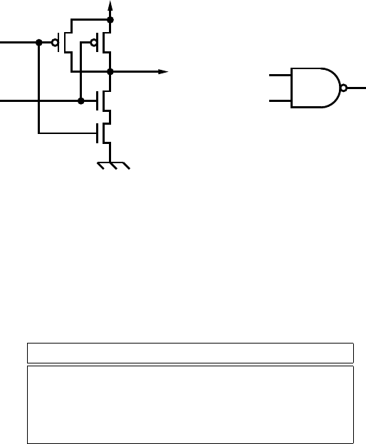
Ground
DD
V
N2
N1
P2
Circuit for Problem 4.5.
CMOS NAND gate.
A
B
C
P1
Logic NAND gate.
A
BC
4.5 CMOS faults
(a) A two-input NAND gate is shown in the above figure. The following table gives
tests for transistor stuck-open (sop) faults:
Test No. Fault Test: Vector 1, Vector 2
1 P1 sop 11, 01
2 P2 sop 11, 10
3 N1 sop 01, 11 or 10, 11 or 00, 11
4 N2 sop 01, 11 or 10, 11 or 00, 11
Notice that the sop faults of N1 and N2 have exactly the same tests. These two
faults are equivalent. Equivalence of transistor faults is discussed in the following
paper:
M.-L Flottes, C. Landrault and S. Provossoudovitch, “Fault Modeling and Fault
Equivalence in CMOS Technology,” J. Electronic Testing: Theory and Applications,
vol. 2, pp. 229-241, August 1991.
(b) The following sequence of four vectors contains one vector pair for each fault in
the above table:
11,01,11,10
Notice that this sequence also detects all single stuck-at faults in the logic model of
the NAND gate.
(c) A stuck-at fault in a signal affects two transistors in the two-input NAND gate.
For example, the fault As-a-1 will mean that N1 remains permanently shorted
(N1-ssh) and P1 remains permanently open (P1-sop). The following table gives all
equivalences:
Solution Manual V1.4 – c
M. L. Bushnell and V. D. Agrawal – For Teachers only Page 14

Stuck-at fault Equivalent transistor faults
As-a-1 N1-ssh and P1-sop
Bs-a-1 N1-ssh and P2-sop
Cs-a-1 (P1-ssh or P2-ssh) and (N1-sop or N2-sop)
As-a-0 N1-sop and P1-ssh
Bs-a-0 N2-sop and P2-ssh
Cs-a-0 N1-ssh, N2-ssh, P1-sop and P2-sop
Notice that the three equivalent faults, As-a-0, Bs-a-0 and Cs-a-0, are actually
caused by different faulty transistors. They are detected by the same test (11).
4.6 Fault models
See Section 4.4 in the book.
4.7 Fault indistinguishability
Without loss of information we will write a function f(V)asf. Thus, the left hand
side of Equation 4.3 is:
[f0⊕f1]⊕[f0⊕f2]
=[f0f1+f0f1]⊕[f0f2+f0f2]
=(f0f1+f0f1)(f0f2+f0f2)+(f0f1+f0f1)(f0f2+f0f2)
=(f0f1+f0f1)(f0f2)(f0f2)+(f0f1)(f0f1)(f0f2+f0f2)
=(f0f1+f0f1)(f0+f2)(f0+f2)+(f0+f1)(f0+f1)(f0f2+f0f2)
=(f0f1+f0f1)(f0f2+f0f2)+(f0f1+f0f1)(f0f2+f0f2)
=f0f1f2+f0f1f2+f0f1f2+f0f1f2
=(f1f2)(f0+f0)+f1f2(f0+f0)
=f1f2+f1f2
=f1⊕f2
= Left hand side of Equation 4.4
This completes the derivation of Equation 4.4 from Equation 4.3.
4.8 Functional equivalence
Faulty functions for the circuit of Figure 4.12 corresponding to the two faults are:
i(cs−a−0) = b(ab)=ab
i(fs−a−1) = (a+b)a=ab
The two faulty functions are indistinguishable and hence the two faults are equiv-
alent.
Solution Manual V1.4 – c
M. L. Bushnell and V. D. Agrawal – For Teachers only Page 15
4.9 Functional equivalence
Faulty functions for the circuit of Figure 4.6 corresponding to the two faults are:
z(cs−a−1) = ab.(ab.b)
=ab.(ab +b)=ab
z(fs−a−1) = ab
The two faulty functions are indistinguishable and hence thefaultsareequiva-
lent.
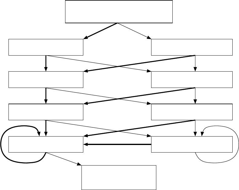
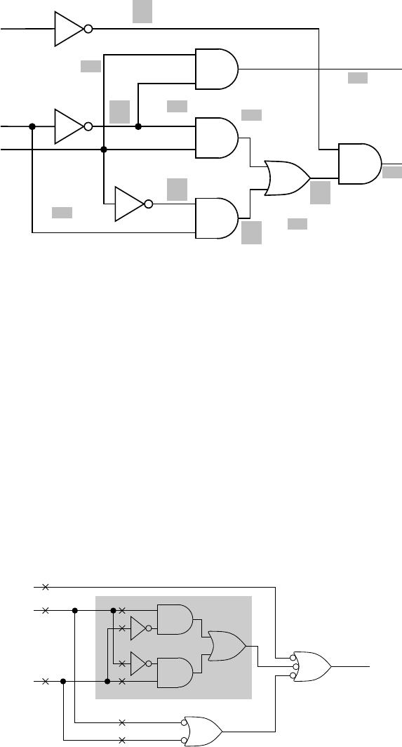
4.10 Fault collapsing for test generation
The circuit of Figure 4.9 has 18 single stuck-at faults. Gate-level fault equivalence,
as shown in the following figure, reduces the number to 12. The faults in shaded
boxes have been collapsed as shown by arrows. Many ATPG and fault simulation
B
A1
sa0 sa1
sa0
sa1
sa0
sa1 sa0
sa0
sa1
sa0
sa1 sa0 sa1
sa1 sa1
sa0
sa0 sa1
C
B2
A2
B1
A
programs will collapse faults as shown above. However, functional fault collapsing
can further reduce the number of faults to 10. As shown in Example 4.11 (see page
75 of the book), the s-a-1 faults on A1andB1 are equivalent, and so are the s-a-1
faults on A2andB2.
Whetherwetakethesetof12faultsorthesetof10faults,their
detection requires all four input vectors.
4.11 Equivalence and dominance fault collapsing
(a) The given circuit is shown below with fault sites marked by numbers. The
number of potential fault sites is 18. The total number of faults is 36.
(b) The figure shows deletion of equivalent faults using an output to input pass.
Of the 36 faults, 20 remain, giving a collapse ratio 20/36 = 0.56.
(c) Checkpoint lines are shown by boldface numbers. These are three PIs and seven
fanout branches. Line 2 fans out to 4 and 5. Line 3 fans out to 6, 7 and 8.
Line 10 fans out to 12 and 13. There are ten checkpoints and 20 checkpoint
faults. Further, s-a-0 faults on lines 6 and 12 are equivalent and any one of
them can be chosen. Similarly, s-a-0 faults on 7 and 13 are equivalent, and so
are s-a-0 on 5 and s-a-1 on 8. Thus, the size of the fault set is reduced to 17,
giving a collapse ratio 17/36 = 0.47.
Solution Manual V1.4 – c
M. L. Bushnell and V. D. Agrawal – For Teachers only Page 16
sa0
sa1
sa0
s
a1
s
a0
sa1
sa1
sa0
sa1
sa0
sa0 1
8
sa1 4
10 7
11
15
16
14
17
9
2
sa0
sa1
sa1
sa0
5
12
13
6
8
Circuit for Problem 4.11: (b) Equivalence collapse ratio = 20/36 = 0.56
Deleted due to
equivalence
1
3
sa1
sa0
sa0
sa1
sa0
sa1
sa0
sa
1
sa
0
sa0
sa1
sa1
sa0
sa1
sa0
sa1
sa0
sa1
sa0
sa1
Checkpoints are shown in boldface
(c) Dominance (uncollapsed faults at checkpoints) collapse ratio = 17/36 = 0.47
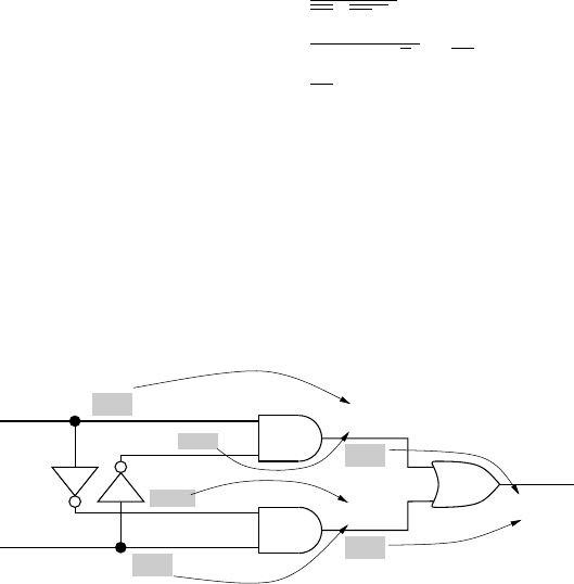
4.12 Dominance fault collapsing
(a) Checkpoints are defined for the signals in a combinational circuit. These signals
are the interconnects between Boolean gates, a fact not always explicitly stated. To
avoid ambiguity, the definition on page 78 of the book should read as:
Definition 4.7 Checkpoints. Primary inputs and fanout branches of a combina-
tional circuit consisting only of Boolean gates are called the checkpoints.
To find checkpoints of the circuit of Figure 4.12, we must replace the exclusive-
OR (XOR) function by a primitive Boolean gate implementation. AND, OR, NAND,
NOR and NOT are called the primitive Boolean gates. Functions such as XOR are
sometimes referred to as complex gates. In the following figure, we have assumed
one such implementation. Our result is, therefore, based on this assumption. Other
implementations of the XOR function are possible and can give a different set of
checkpoints.
c
a
b
d
e
e1
e2
d1
d2
h
i
k
XOR
f
g
There are nine checkpoints in this circuit. These include three primary inputs,
a,band c, and six fanout branches, d1, d2, f,e1, e2andg. The checkpoint fault
set consists of eighteen faults – s-a-0 and s-a-1 faults on the nine lines.
Notice that lines dand eof the original circuit are not checkpoints. If we did
Solution Manual V1.4 – c
M. L. Bushnell and V. D. Agrawal – For Teachers only Page 17
not model the XOR block with Boolean gates, then those lines will appear to be
checkpoints, whose number will be fourteen. However, detection of those faults will
not guarantee detection of faults on the fanouts that are internal to the XOR block.
Considering the Boolean gate structure, a fault on dcorresponds to a simultaneous
(multiple) fault on d1andd2 and, in general, the detection of a multiple fault is not
equivalent to detection of the component faults.
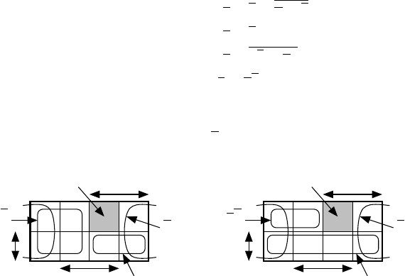
(b) We evaluate the output function kcorresponding to the two faults:
k(ds−a−0) = c+b+a+b
=c+b+ab
k(gs−a−1) = c+ab +ab +a
=c+ab +a
The two faulty functions are shown by Karnaugh maps below. In both cases, the
functions have exactly one false minterm, abc.Since the two faulty functions
are identical the corresponding faults are equivalent.
a
false minterm
k with d s-a-0
b
c
ab
b
k with g s-a-1
cc
b
c
a
ab
false minterm
a
Note: this type of fault equivalence is functional and is often difficult to find by
typical fault analysis tools, which rely on structurally identifiable equivalences.
Solution Manual V1.4 – c
M. L. Bushnell and V. D. Agrawal – For Teachers only Page 18
١
٢
٣
۴
۵
۶
٧
٨
٩
١٠
١١
١٢
١٣
١۴
١۵
١۶
١٧
١٨
١٩
٢٠
٢١
٢٢
٢٣
٢۴
٢۵
٢۶
٢٧
٢٨
٢٩
