TMS320C6000 Chip Support Library API Reference Guide (Rev. I) CSL
User Manual:
Open the PDF directly: View PDF ![]() .
.
Page Count: 1113 [warning: Documents this large are best viewed by clicking the View PDF Link!]

TMS320C6000
Chip Support Library
API Reference Guide
Literature Number SPRU401I
May 2004
Printed on Recycled Pape
r
IMPORTANT NOTICE
Texas Instruments Incorporated and its subsidiaries (TI) reserve the right to make corrections,
modifications, enhancements, improvements, and other changes to its products and services at any
time and to discontinue any product or service without notice. Customers should obtain the latest
relevant information before placing orders and should verify that such information is current and
complete. All products are sold subject to TI’s terms and conditions of sale supplied at the time of order
acknowledgment.
TI warrants performance of its hardware products to the specifications applicable at the time of sale
in accordance with TI’s standard warranty. Testing and other quality control techniques are used to the
extent TI deems necessary to support this warranty. Except where mandated by government
requirements, testing of all parameters of each product is not necessarily performed.
TI assumes no liability for applications assistance or customer product design. Customers are
responsible for their products and applications using TI components. To minimize the risks associated
with customer products and applications, customers should provide adequate design and operating
safeguards.
TI does not warrant or represent that any license, either express or implied, is granted under any TI
patent right, copyright, mask work right, or other TI intellectual property right relating to any
combination, machine, or process in which TI products or services are used. Information published by
TI regarding third-party products or services does not constitute a license from TI to use such products
or services or a warranty or endorsement thereof. Use of such information may require a license from
a third party under the patents or other intellectual property of the third party, or a license from TI under
the patents or other intellectual property of TI.
Reproduction of information in TI data books or data sheets is permissible only if reproduction is without
alteration and is accompanied by all associated warranties, conditions, limitations, and notices.
Reproduction of this information with alteration is an unfair and deceptive business practice. TI is not
responsible or liable for such altered documentation.
Resale of TI products or services with statements different from or beyond the parameters stated by
TI for that product or service voids all express and any implied warranties for the associated TI product
or service and is an unfair and deceptive business practice. TI is not responsible or liable for any such
statements.
Following are URLs where you can obtain information on other Texas Instruments products and
application solutions:
Products Applications
Amplifiers amplifier.ti.com Audio www.ti.com/audio
Data Converters dataconverter.ti.com Automotive www.ti.com/automotive
DSP dsp.ti.com Broadband www.ti.com/broadband
Interface interface.ti.com Digital Control www.ti.com/digitalcontrol
Logic logic.ti.com Military www.ti.com/military
Power Mgmt power.ti.com Optical Networking www.ti.com/opticalnetwork
Microcontrollers microcontroller.ti.com Security www.ti.com/security
Telephony www.ti.com/telephony
Video & Imaging www.ti.com/video
Wireless www.ti.com/wireless
Mailing Address: Texas Instruments
Post Office Box 655303 Dallas, Texas 75265
Copyright 2004, Texas Instruments Incorporated

iii
Read This First
Preface
Read This First
About This Manual
The TMS320C6000 Chip Support Library (CSL) is a set of application pro-
gramming interfaces (APIs) used to configure and control all on-chip peripher-
als. It is intended to make it easier for developers by eliminating much of the
tedious work usually needed to get algorithms up and running in a real system.
Some of the advantages offered by the CSL include: peripheral ease of use,
a level of compatibility between devices, shortened development time, porta-
bility, and standardization. A version of the CSL is available for all
TMS320C6000 devices.
This document is organized as follows:
-Introduction − a high level overview of the CSL
-27 CSL API module chapters
-HAL macro chapter
-Using CSL APIs Without DSP/BIOS
-Register description
-How to Use the CSL
-Cache register comparison
-Glossary
How to Use This Manual
The information in this document describes the contents of the
TMS320C6000 chip support library (CSL) as follows:
-Chapter 1 provides an overview of the CSL, includes a table showing CSL
API module support for various C6000 devices, and lists the API modules.

Notational Conventions
iv
-Each additional chapter discusses an individual CSL API module and
provides:
JA description of the API module
JA table showing the APIs within the module and a page reference for
more specific information
JA table showing the macros within the module and a page reference
for more specific information
JA module API Reference section in alphabetical order listing the CSL
API functions, enumerations, type definitions, structures, constants,
and global variables. Examples are given to show how these elements
are used.
-Chapter 28 describes the hardware abstraction layer (HAL) and provides
a HAL macro reference section.
-Appendix A provides an example of using CSL independently of
DSP/BIOS.
-Appendix B provides a list of the registers associated with current
TMS320C6000 DSP devices.
-Appendix C provides a comparison of the old and new CACHE register
names, as they have recently been changed.
-Appendix D provides a glossary.
Notational Conventions
This document uses the following conventions:
-Program listings, program examples, and interactive displays are shown
in a special typeface.
-In syntax descriptions, the function or macro appears in a bold typeface
and the parameters appear in plainface within parentheses. Portions of a
syntax that are in bold should be entered as shown; portions of a syntax
that are within parentheses describe the type of information that should be
entered.
-Macro names are written in uppercase text; function names are written in
lowercase.
-TMS320C6000 devices are referred to throughout this reference guide as
C6201, C6202, etc.

Related Documentation From Texas Instruments
v
Read This First
Related Documentation From Texas Instruments
The following books describe the TMS320C6000 devices and related support
tools. To obtain a copy of any of these TI documents, call the Texas Instru-
ments Literature Response Center at (800) 477−8924. When ordering, please
identify the book by its title and literature number. Many of these documents
can be found on the Internet at http://www.ti.com.
TMS320C62x/C67x Technical Brief (literature number SPRU197) gives an
introduction to the C62x/C67x digital signal processors, development
tools, and third-party support.
TMS320C6000 CPU and Instruction Set Reference Guide (literature
number SPRU189) describes the TMS320C6000 CPU architecture,
instruction set, pipeline, and interrupts for these digital signal proces-
sors.
TMS320C6x C Source Debugger User’s Guide (literature number
SPRU188) tells you how to invoke the TMS320C6x simulator and
emulator versions of the C source debugger interface. This book
discusses various aspects of the debugger, including command entry,
code execution, data management, breakpoints, profiling, and analysis.
TMS320C6000 DSP Peripherals Overview Reference Guide (literature
number SPRU190) describes the peripherals available on the C6000
platform of devices.
TMS320C6000 Programmer’s Guide (literature number SPRU198)
describes ways to optimize C and assembly code for the
TMS320C6000 DSPs and includes application program examples.
TMS320C6000 Assembly Language Tools User’s Guide (literature number
SPRU186) describes the assembly language tools (assembler, linker,
and other tools used to develop assembly language code), assembler
directives, macros, common object file format, and symbolic debugging
directives for the TMS320C6000 generation of devices.
TMS320C6000 Optimizing Compiler User’s Guide (literature number
SPRU187) describes the TMS320C6000 C compiler and the assembly
optimizer. This C compiler accepts ANSI standard C source code and
produces assembly language source code for the TMS320C6000 gen-
eration of devices. The assembly optimizer helps you optimize your
assembly code.
TMS320C62x DSP Library (literature number SPRU402) describes the 32
high-level, C-callable, optimized DSP functions for general signal proc-
essing, math, and vector operations.

Related Documentation From Texas Instruments
vi
TMS320C64x Technical Overview (SPRU395) The TMS320C64x technical
overview gives an introduction to the TMS320C64x digital signal proc-
essor, and discusses the application areas that are enhanced by the
TMS320C64x VelociTI.
TMS320C62x Image/Video Processing Library (literature number
SPRU400) describes the optimized image/video processing functions
including many C-callable, assembly-optimized, general-purpose
image/video processing routines.
TMS320C6000 DSP External Memory Interface (EMIF) Reference Guide
(literature number SPRU266) describes the operation of the external
memory interface (EMIF) in the digital signal processors of the
TMS320C6000 DSP family.
TMS320C6000 DSP Enhanced Direct Memory Access (EDMA) Controller
Reference Guide (literature number SPRU234) describes the operation
of the EDMA controller in the digital signal processors of the
TMS320C6000 DSP family. This document also describes the quick
DMA (QDMA) used for fast data requests by the CPU.
TMS320C6000 DSP EMAC/MDIO Module Reference Guide (literature
number SPRU628) describes the EMAC and MDIO module in the digital
signal processors of the TMS320C6000 DSP family.
TMS320C6000 DSP General-Purpose Input/Output (GPIO) Reference
Guide (literature number SPRU584) describes the general-purpose
input/output (GPIO) peripheral in the digital signal processors (DSPs) of
the TMS320C6000 DSP family.
TMS320C6000 DSP Host Port Interface (HPI) Reference Guide (literature
number SPRU578) describes the host−port interface (HPI) in the digital
signal processors (DSPs) of the TMS320C6000 DSP family that external
processors use to access the memory space.
TMS320C6000 DSP Interrupt Selector Reference Guide (literature number
SPRU646) describes the interrupt selector, interrupt selector registers,
and the available interrupts in the digital signal processors (DSPs) of the
TMS320C6000 DSP family.
TMS320C6000 DSP Inter-Integrated Circuit (I2C) Module Reference
Guide (literature number SPRU175) describes the I2C module that pro-
vides an interface between a TMS320C6000 digital signal processor
(DSP) and any I2C-bus-compatible device that connects by way of an
I2C bus.
TMS320C6000 DSP Multichannel Audio Serial Port (McASP) Reference
Guide (literature number SPRU041) describes the multichannel audio
serial port (McASP) in the digital signal processors (DSPs) of the
TMS320C6000 DSP family.

Related Documentation From Texas Instruments
vii
Read This First
TMS320C6000 DSP Multichannel Buffered Serial Port (McBSP) Refer-
ence Guide (literature number SPRU580) describes the operation of the
multichannel buffered serial port (McBSP) in the digital signal processors
(DSPs) of the TMS320C6000 DSP family.
TMS320C6000 DSP Peripheral Component Interconnect (PCI) Reference
Guide (literature number SPRU581) describes the peripheral compo-
nent interconnect (PCI) port in the digital signal processors (DSPs) of the
TMS320C6000 DSP family. The PCI port supports connection of the
DSP to a PCI host via the integrated PCI master/slave bus interface.
TMS320C6000 DSP Software Programmable Phase-Locked Loop (PLL)
Controller RG (literature number SPRU233) describes the operation of
the software-programmable phase-locked loop (PLL) controller in the
digital signal processors (DSPs) of the TMS320C6000 DSP family.
TMS320C6000 DSP 32-Bit Timer Reference Guide (literature number
SPRU582) describes the 32-bit timer in the TMS320C6000 DSP family.
TMS320C64x DSP Turbo-Decoder Coprocessor (TCP) Reference Guide
(literature number SPRU534) describes the operation and programming
of the turbo decoder coprocessor (TCP) embedded in the
TMS320C6416 digital signal processor (DSP) of the TMS320C6000
DSP family.
TMS320C64x DSP Viterbi-Decoder Coprocessor (VCP) Reference Guide
(literature number SPRU533) describes the operation and programming
of the Viterbi-decoder coprocessor (VCP) embedded in the
TMS320C6416 digital signal processor (DSP) of the TMS320C6000
DSP family.
TMS320C64x DSP Video Port/ /VCXO Interpolated Control (VIC) Port
Reference Guide (literature number SPRU629) describes the video port
and VCXO interpolated control (VIC) port in the TMS320C64x digital
signal processors (DSPs) of the TMS320C6000 DSP family.
TMS320C64x DSP Universal Test and Operations Interface for ATM
(UTOPIA) Reference Guide (literature number SPRU583) describes
the universal test and operations PHY interface for asynchronous trans-
fer mode (UTOPIA) in the TMS320C64x digital signal processors (DSPs)
of the TMS320C6000 DSP family.
TMS320C62x DSP Expansion Bus (XBUS) Reference Guide (literature
number SPRU579) describes the expansion bus (XBUS) used by the
CPU to access off-chip peripherals, FIFOs, and peripheral component
interconnect (PCI) interface devices in the TMS320C62x digital signal
processors (DSPs) of the TMS320C6000 DSP family.

Trademarks
viii
TMS320C620x/C670x DSP Program and Data Memory Controller/DMA
Controller Reference Guide (literature number SPRU577) describes
the program memory modes, program and data memory organizations,
and the program and data memory controller in the
TMS320C620x/C670x digital signal processors (DSPs) of the
TMS320C6000 DSP family.
Trademarks
The Texas Instruments logo and Texas Instruments are registered trademarks
of Texas Instruments. Trademarks of Texas Instruments include: TI, Code
Composer Studio, DSP/BIOS, and TMS320C6000.
All other brand or product names are trademarks or registered trademarks of
their respective companies or organizations.

Contents
ix
Contents
1 CSL Overview 1-1. . . . . . . . . . . . . . . . . . . . . . . . . . . . . . . . . . . . . . . . . . . . . . . . . . . . . . . . . . . . . . . . . . .
Provides an overview of the chip support library (CSL), shows which TMS320C6000 devices
support the various APIs, and lists each of the API modules.
1.1 CSL Introduction 1-2. . . . . . . . . . . . . . . . . . . . . . . . . . . . . . . . . . . . . . . . . . . . . . . . . . . . . . . . . . .
1.1.1 Benefits of the CSL 1-2. . . . . . . . . . . . . . . . . . . . . . . . . . . . . . . . . . . . . . . . . . . . . . . . . .
1.1.2 CSL Architecture 1-2. . . . . . . . . . . . . . . . . . . . . . . . . . . . . . . . . . . . . . . . . . . . . . . . . . . .
1.1.3 Interdependencies 1-4. . . . . . . . . . . . . . . . . . . . . . . . . . . . . . . . . . . . . . . . . . . . . . . . . . .
1.2 CSL Naming Conventions 1-5. . . . . . . . . . . . . . . . . . . . . . . . . . . . . . . . . . . . . . . . . . . . . . . . . . .
1.3 CSL Data Types 1-6. . . . . . . . . . . . . . . . . . . . . . . . . . . . . . . . . . . . . . . . . . . . . . . . . . . . . . . . . . . .
1.4 CSL Functions 1-7. . . . . . . . . . . . . . . . . . . . . . . . . . . . . . . . . . . . . . . . . . . . . . . . . . . . . . . . . . . . .
1.4.1 Peripheral Initialization via Registers 1-8. . . . . . . . . . . . . . . . . . . . . . . . . . . . . . . . . . .
1.5 CSL Macros 1-9. . . . . . . . . . . . . . . . . . . . . . . . . . . . . . . . . . . . . . . . . . . . . . . . . . . . . . . . . . . . . . .
1.6 CSL Symbolic Constant Values 1-12. . . . . . . . . . . . . . . . . . . . . . . . . . . . . . . . . . . . . . . . . . . . . .
1.7 Resource Management 1-13. . . . . . . . . . . . . . . . . . . . . . . . . . . . . . . . . . . . . . . . . . . . . . . . . . . . .
1.7.1 Using CSL Handles 1-13. . . . . . . . . . . . . . . . . . . . . . . . . . . . . . . . . . . . . . . . . . . . . . . . .
1.8 CSL API Module Support 1-15. . . . . . . . . . . . . . . . . . . . . . . . . . . . . . . . . . . . . . . . . . . . . . . . . . .
1.8.1 CSL Endianess/Device Support Library 1-17. . . . . . . . . . . . . . . . . . . . . . . . . . . . . . .
2 CACHE Module 2-1. . . . . . . . . . . . . . . . . . . . . . . . . . . . . . . . . . . . . . . . . . . . . . . . . . . . . . . . . . . . . . . . . .
Describes the CACHE module, gives a description of the two CACHE architectures, lists the
functions and macros within the module, and provides a CACHE API reference section.
2.1 Overview 2-2. . . . . . . . . . . . . . . . . . . . . . . . . . . . . . . . . . . . . . . . . . . . . . . . . . . . . . . . . . . . . . . . . .
2.2 Macros 2-4. . . . . . . . . . . . . . . . . . . . . . . . . . . . . . . . . . . . . . . . . . . . . . . . . . . . . . . . . . . . . . . . . . . .
2.3 Functions 2-6. . . . . . . . . . . . . . . . . . . . . . . . . . . . . . . . . . . . . . . . . . . . . . . . . . . . . . . . . . . . . . . . . .
3 CHIP Module 3-1. . . . . . . . . . . . . . . . . . . . . . . . . . . . . . . . . . . . . . . . . . . . . . . . . . . . . . . . . . . . . . . . . . . .
Describes the CHIP module, lists the API functions and macros within the CHIP module, and
provides a CHIP API reference section.
3.1 Overview 3-2. . . . . . . . . . . . . . . . . . . . . . . . . . . . . . . . . . . . . . . . . . . . . . . . . . . . . . . . . . . . . . . . . .
3.2 Macros 3-3. . . . . . . . . . . . . . . . . . . . . . . . . . . . . . . . . . . . . . . . . . . . . . . . . . . . . . . . . . . . . . . . . . . .
3.3 Functions 3-4. . . . . . . . . . . . . . . . . . . . . . . . . . . . . . . . . . . . . . . . . . . . . . . . . . . . . . . . . . . . . . . . . .
4 CSL Module 4-1. . . . . . . . . . . . . . . . . . . . . . . . . . . . . . . . . . . . . . . . . . . . . . . . . . . . . . . . . . . . . . . . . . . . .
Describes the CSL module, shows the single API function within the module, and provides a
CSL API reference section.
4.1 Overview 4-2. . . . . . . . . . . . . . . . . . . . . . . . . . . . . . . . . . . . . . . . . . . . . . . . . . . . . . . . . . . . . . . . . .
4.2 Functions 4-3. . . . . . . . . . . . . . . . . . . . . . . . . . . . . . . . . . . . . . . . . . . . . . . . . . . . . . . . . . . . . . . . . .

Contents
x
5 DAT Module 5-1. . . . . . . . . . . . . . . . . . . . . . . . . . . . . . . . . . . . . . . . . . . . . . . . . . . . . . . . . . . . . . . . . . . . .
Describes the DAT module, lists the API functions within the module, discusses how the module
manages the DMA/EDMA peripheral, and provides a DAT API reference section.
5.1 Overview 5-2. . . . . . . . . . . . . . . . . . . . . . . . . . . . . . . . . . . . . . . . . . . . . . . . . . . . . . . . . . . . . . . . . .
5.1.1 DAT Routines 5-2. . . . . . . . . . . . . . . . . . . . . . . . . . . . . . . . . . . . . . . . . . . . . . . . . . . . . . .
5.1.2 DAT Macros 5-3. . . . . . . . . . . . . . . . . . . . . . . . . . . . . . . . . . . . . . . . . . . . . . . . . . . . . . . .
5.1.3 DMA/EDMA Management 5-3. . . . . . . . . . . . . . . . . . . . . . . . . . . . . . . . . . . . . . . . . . . .
5.1.4 Devices With DMA 5-3. . . . . . . . . . . . . . . . . . . . . . . . . . . . . . . . . . . . . . . . . . . . . . . . . . .
5.1.5 Devices With EDMA 5-3. . . . . . . . . . . . . . . . . . . . . . . . . . . . . . . . . . . . . . . . . . . . . . . . .
5.2 Functions 5-4. . . . . . . . . . . . . . . . . . . . . . . . . . . . . . . . . . . . . . . . . . . . . . . . . . . . . . . . . . . . . . . . . .
6 DMA Module 6-1. . . . . . . . . . . . . . . . . . . . . . . . . . . . . . . . . . . . . . . . . . . . . . . . . . . . . . . . . . . . . . . . . . . .
Describes the DMA module, lists the API functions and macros within the module, and provides
a DMA API reference section.
6.1 Overview 6-2. . . . . . . . . . . . . . . . . . . . . . . . . . . . . . . . . . . . . . . . . . . . . . . . . . . . . . . . . . . . . . . . . .
6.1.1 Using a DMA Channel 6-4. . . . . . . . . . . . . . . . . . . . . . . . . . . . . . . . . . . . . . . . . . . . . . .
6.2 Macros 6-5. . . . . . . . . . . . . . . . . . . . . . . . . . . . . . . . . . . . . . . . . . . . . . . . . . . . . . . . . . . . . . . . . . . .
6.3 Configuration Structures 6-7. . . . . . . . . . . . . . . . . . . . . . . . . . . . . . . . . . . . . . . . . . . . . . . . . . . . .
6.4 Functions 6-9. . . . . . . . . . . . . . . . . . . . . . . . . . . . . . . . . . . . . . . . . . . . . . . . . . . . . . . . . . . . . . . . . .
6.4.1 Primary Functions 6-9. . . . . . . . . . . . . . . . . . . . . . . . . . . . . . . . . . . . . . . . . . . . . . . . . . .
6.4.2 DMA Global Register Functions 6-14. . . . . . . . . . . . . . . . . . . . . . . . . . . . . . . . . . . . . .
6.4.3 DMA Auxiliary Functions, Constants, and Macros 6-23. . . . . . . . . . . . . . . . . . . . . . .
7 EDMA Module 7-1. . . . . . . . . . . . . . . . . . . . . . . . . . . . . . . . . . . . . . . . . . . . . . . . . . . . . . . . . . . . . . . . . . .
Describes the EDMA module, lists the API functions and macros within the module, discusses
how to use an EDMA channel, and provides an EDMA reference section.
7.1 Overview 7-2. . . . . . . . . . . . . . . . . . . . . . . . . . . . . . . . . . . . . . . . . . . . . . . . . . . . . . . . . . . . . . . . . .
7.1.1 Using an EDMA Channel 7-4. . . . . . . . . . . . . . . . . . . . . . . . . . . . . . . . . . . . . . . . . . . . .
7.2 Macros 7-5. . . . . . . . . . . . . . . . . . . . . . . . . . . . . . . . . . . . . . . . . . . . . . . . . . . . . . . . . . . . . . . . . . . .
7.3 Configuration Structure 7-7. . . . . . . . . . . . . . . . . . . . . . . . . . . . . . . . . . . . . . . . . . . . . . . . . . . . . .
7.4 Functions 7-8. . . . . . . . . . . . . . . . . . . . . . . . . . . . . . . . . . . . . . . . . . . . . . . . . . . . . . . . . . . . . . . . . .
7.4.1 EDMA Primary Functions 7-8. . . . . . . . . . . . . . . . . . . . . . . . . . . . . . . . . . . . . . . . . . . . .
7.4.2 EDMA Auxiliary Functions and Constants 7-16. . . . . . . . . . . . . . . . . . . . . . . . . . . . . .
8 EMAC Module 8-1. . . . . . . . . . . . . . . . . . . . . . . . . . . . . . . . . . . . . . . . . . . . . . . . . . . . . . . . . . . . . . . . . . .
Describes the EMAC module, lists the API functions and macros within the module, and pro-
vides an EMAC reference section.
8.1 Overview 8-2. . . . . . . . . . . . . . . . . . . . . . . . . . . . . . . . . . . . . . . . . . . . . . . . . . . . . . . . . . . . . . . . . .
8.2 Macros 8-4. . . . . . . . . . . . . . . . . . . . . . . . . . . . . . . . . . . . . . . . . . . . . . . . . . . . . . . . . . . . . . . . . . . .
8.3 Configuration Structure 8-6. . . . . . . . . . . . . . . . . . . . . . . . . . . . . . . . . . . . . . . . . . . . . . . . . . . . . .
8.4 Functions 8-13. . . . . . . . . . . . . . . . . . . . . . . . . . . . . . . . . . . . . . . . . . . . . . . . . . . . . . . . . . . . . . . . .
9 EMIF Module 9-1. . . . . . . . . . . . . . . . . . . . . . . . . . . . . . . . . . . . . . . . . . . . . . . . . . . . . . . . . . . . . . . . . . . .
Describes the EMIF module, lists the API functions and macros within the module, and provides
an EMIF API reference section.
9.1 Overview 9-2. . . . . . . . . . . . . . . . . . . . . . . . . . . . . . . . . . . . . . . . . . . . . . . . . . . . . . . . . . . . . . . . . .
9.2 Macros 9-3. . . . . . . . . . . . . . . . . . . . . . . . . . . . . . . . . . . . . . . . . . . . . . . . . . . . . . . . . . . . . . . . . . . .
9.3 Configuration Structure 9-5. . . . . . . . . . . . . . . . . . . . . . . . . . . . . . . . . . . . . . . . . . . . . . . . . . . . . .
9.4 Functions 9-6. . . . . . . . . . . . . . . . . . . . . . . . . . . . . . . . . . . . . . . . . . . . . . . . . . . . . . . . . . . . . . . . . .

Contents
xi
Contents
10 EMIFA/EMIFB Modules 10-1. . . . . . . . . . . . . . . . . . . . . . . . . . . . . . . . . . . . . . . . . . . . . . . . . . . . . . . . . .
Describes the EMIFA and EMIFB modules, lists the API functions and macros within the
modules, and provides an API reference section.
10.1 Overview 10-2. . . . . . . . . . . . . . . . . . . . . . . . . . . . . . . . . . . . . . . . . . . . . . . . . . . . . . . . . . . . . . . . .
10.2 Macros 10-3. . . . . . . . . . . . . . . . . . . . . . . . . . . . . . . . . . . . . . . . . . . . . . . . . . . . . . . . . . . . . . . . . . .
10.3 Configuration Structure 10-5. . . . . . . . . . . . . . . . . . . . . . . . . . . . . . . . . . . . . . . . . . . . . . . . . . . . .
10.4 Functions 10-7. . . . . . . . . . . . . . . . . . . . . . . . . . . . . . . . . . . . . . . . . . . . . . . . . . . . . . . . . . . . . . . . .
11 GPIO Module 11-1. . . . . . . . . . . . . . . . . . . . . . . . . . . . . . . . . . . . . . . . . . . . . . . . . . . . . . . . . . . . . . . . . . .
Describes the GPIO module, lists the API functions and macros within the module, and
provides an GPIO API reference section.
11.1 Overview 11-2. . . . . . . . . . . . . . . . . . . . . . . . . . . . . . . . . . . . . . . . . . . . . . . . . . . . . . . . . . . . . . . . .
11.1.1 Using GPIO 11-4. . . . . . . . . . . . . . . . . . . . . . . . . . . . . . . . . . . . . . . . . . . . . . . . . . . . . . . .
11.2 Macros 11-5. . . . . . . . . . . . . . . . . . . . . . . . . . . . . . . . . . . . . . . . . . . . . . . . . . . . . . . . . . . . . . . . . . .
11.3 Configuration Structure 11-7. . . . . . . . . . . . . . . . . . . . . . . . . . . . . . . . . . . . . . . . . . . . . . . . . . . . .
11.4 Functions 11-8. . . . . . . . . . . . . . . . . . . . . . . . . . . . . . . . . . . . . . . . . . . . . . . . . . . . . . . . . . . . . . . . .
11.4.1 Primary GPIO Functions 11-8. . . . . . . . . . . . . . . . . . . . . . . . . . . . . . . . . . . . . . . . . . . . .
11.4.2 Auxiliary GPIO Functions and Constants 11-11. . . . . . . . . . . . . . . . . . . . . . . . . . . . .
12 HPI Module 12-1. . . . . . . . . . . . . . . . . . . . . . . . . . . . . . . . . . . . . . . . . . . . . . . . . . . . . . . . . . . . . . . . . . . .
Describes the HPI module, lists the API functions and macros within the module, and provides
an HPI API reference section.
12.1 Overview 12-2. . . . . . . . . . . . . . . . . . . . . . . . . . . . . . . . . . . . . . . . . . . . . . . . . . . . . . . . . . . . . . . . .
12.2 Macros 12-3. . . . . . . . . . . . . . . . . . . . . . . . . . . . . . . . . . . . . . . . . . . . . . . . . . . . . . . . . . . . . . . . . . .
12.3 Functions 12-5. . . . . . . . . . . . . . . . . . . . . . . . . . . . . . . . . . . . . . . . . . . . . . . . . . . . . . . . . . . . . . . . .
13 I2C Module 13-1. . . . . . . . . . . . . . . . . . . . . . . . . . . . . . . . . . . . . . . . . . . . . . . . . . . . . . . . . . . . . . . . . . . . .
Describes the I2C module, lists the API functions and macros within the module, and provides
an I2C API reference section.
13.1 Overview 13-2. . . . . . . . . . . . . . . . . . . . . . . . . . . . . . . . . . . . . . . . . . . . . . . . . . . . . . . . . . . . . . . . .
13.1.1 Using an I2C Device 13-3. . . . . . . . . . . . . . . . . . . . . . . . . . . . . . . . . . . . . . . . . . . . . . . .
13.2 Macros 13-5. . . . . . . . . . . . . . . . . . . . . . . . . . . . . . . . . . . . . . . . . . . . . . . . . . . . . . . . . . . . . . . . . . .
13.3 Configuration Structure 13-7. . . . . . . . . . . . . . . . . . . . . . . . . . . . . . . . . . . . . . . . . . . . . . . . . . . . .
13.4 Functions 13-8. . . . . . . . . . . . . . . . . . . . . . . . . . . . . . . . . . . . . . . . . . . . . . . . . . . . . . . . . . . . . . . . .
13.4.1 Primary Functions 13-8. . . . . . . . . . . . . . . . . . . . . . . . . . . . . . . . . . . . . . . . . . . . . . . . . .
13.4.2 Auxiliary Functions and Constants 13-13. . . . . . . . . . . . . . . . . . . . . . . . . . . . . . . . . . .
13.4.3 Auxiliary Functions Defined for C6410 and C6413 13-22. . . . . . . . . . . . . . . . . . . . .
14 IRQ Module 14-1. . . . . . . . . . . . . . . . . . . . . . . . . . . . . . . . . . . . . . . . . . . . . . . . . . . . . . . . . . . . . . . . . . . .
Describes the IRQ module, lists the API functions and macros within the module, and provides
an IRQ API reference section.
14.1 Overview 14-2. . . . . . . . . . . . . . . . . . . . . . . . . . . . . . . . . . . . . . . . . . . . . . . . . . . . . . . . . . . . . . . . .
14.2 Macros 14-4. . . . . . . . . . . . . . . . . . . . . . . . . . . . . . . . . . . . . . . . . . . . . . . . . . . . . . . . . . . . . . . . . . .
14.3 Configuration Structure 14-6. . . . . . . . . . . . . . . . . . . . . . . . . . . . . . . . . . . . . . . . . . . . . . . . . . . . .
14.4 Functions 14-9. . . . . . . . . . . . . . . . . . . . . . . . . . . . . . . . . . . . . . . . . . . . . . . . . . . . . . . . . . . . . . . . .
14.4.1 Primary IRQ Functions 14-9. . . . . . . . . . . . . . . . . . . . . . . . . . . . . . . . . . . . . . . . . . . . . .
14.4.2 Auxiliary IRQ Functions and Constants 14-15. . . . . . . . . . . . . . . . . . . . . . . . . . . . . . .

Contents
xii
15 McASP Module 15-1. . . . . . . . . . . . . . . . . . . . . . . . . . . . . . . . . . . . . . . . . . . . . . . . . . . . . . . . . . . . . . . . .
Describes the McASP module, lists the API functions and macros within the module, discusses
using a McASP device, and provides a McASP API reference section.
15.1 Overview 15-2. . . . . . . . . . . . . . . . . . . . . . . . . . . . . . . . . . . . . . . . . . . . . . . . . . . . . . . . . . . . . . . . .
15.1.1 Using a McASP Device 15-4. . . . . . . . . . . . . . . . . . . . . . . . . . . . . . . . . . . . . . . . . . . . . .
15.2 Macros 15-5. . . . . . . . . . . . . . . . . . . . . . . . . . . . . . . . . . . . . . . . . . . . . . . . . . . . . . . . . . . . . . . . . . .
15.3 Configuration Structure 15-7. . . . . . . . . . . . . . . . . . . . . . . . . . . . . . . . . . . . . . . . . . . . . . . . . . . . .
15.4 Functions 15-10. . . . . . . . . . . . . . . . . . . . . . . . . . . . . . . . . . . . . . . . . . . . . . . . . . . . . . . . . . . . . . . .
15.4.1 Primary Functions 15-10. . . . . . . . . . . . . . . . . . . . . . . . . . . . . . . . . . . . . . . . . . . . . . . . .
15.4.2 Parameters and Constants 15-14. . . . . . . . . . . . . . . . . . . . . . . . . . . . . . . . . . . . . . . . .
15.4.3 Auxiliary Functions 15-17. . . . . . . . . . . . . . . . . . . . . . . . . . . . . . . . . . . . . . . . . . . . . . . .
15.4.4 Interrupt Control Functions 15-30. . . . . . . . . . . . . . . . . . . . . . . . . . . . . . . . . . . . . . . . .
16 McBSP Module 16-1. . . . . . . . . . . . . . . . . . . . . . . . . . . . . . . . . . . . . . . . . . . . . . . . . . . . . . . . . . . . . . . . .
Describes the McBSP module, lists the API functions and macros within the module, and
provides a McBSP API reference section.
16.1 Overview 16-2. . . . . . . . . . . . . . . . . . . . . . . . . . . . . . . . . . . . . . . . . . . . . . . . . . . . . . . . . . . . . . . . .
16.1.1 Using a McBSP Port 16-4. . . . . . . . . . . . . . . . . . . . . . . . . . . . . . . . . . . . . . . . . . . . . . . .
16.2 Macros 16-5. . . . . . . . . . . . . . . . . . . . . . . . . . . . . . . . . . . . . . . . . . . . . . . . . . . . . . . . . . . . . . . . . . .
16.3 Configuration Structure 16-7. . . . . . . . . . . . . . . . . . . . . . . . . . . . . . . . . . . . . . . . . . . . . . . . . . . . .
16.4 Functions 16-9. . . . . . . . . . . . . . . . . . . . . . . . . . . . . . . . . . . . . . . . . . . . . . . . . . . . . . . . . . . . . . . . .
16.4.1 Primary Functions 16-9. . . . . . . . . . . . . . . . . . . . . . . . . . . . . . . . . . . . . . . . . . . . . . . . . .
16.4.2 Auxiliary Functions and Constants 16-15. . . . . . . . . . . . . . . . . . . . . . . . . . . . . . . . . . .
16.4.3 Interrupt Control Functions 16-23. . . . . . . . . . . . . . . . . . . . . . . . . . . . . . . . . . . . . . . . .
17 MDIO Module 17-1. . . . . . . . . . . . . . . . . . . . . . . . . . . . . . . . . . . . . . . . . . . . . . . . . . . . . . . . . . . . . . . . . . .
Describes the MDIO module, lists the API functions and macros within the module, and
provides an MDIO reference section.
17.1 Overview 17-2. . . . . . . . . . . . . . . . . . . . . . . . . . . . . . . . . . . . . . . . . . . . . . . . . . . . . . . . . . . . . . . . .
17.2 Macros 17-3. . . . . . . . . . . . . . . . . . . . . . . . . . . . . . . . . . . . . . . . . . . . . . . . . . . . . . . . . . . . . . . . . . .
17.3 Functions 17-4. . . . . . . . . . . . . . . . . . . . . . . . . . . . . . . . . . . . . . . . . . . . . . . . . . . . . . . . . . . . . . . . .
18 PCI Module 18-1. . . . . . . . . . . . . . . . . . . . . . . . . . . . . . . . . . . . . . . . . . . . . . . . . . . . . . . . . . . . . . . . . . . .
Describes the PCI module, lists the API functions and macros within the module, discusses the
three application domains, and provides a PCI API reference section.
18.1 Overview 18-2. . . . . . . . . . . . . . . . . . . . . . . . . . . . . . . . . . . . . . . . . . . . . . . . . . . . . . . . . . . . . . . . .
18.2 Macros 18-4. . . . . . . . . . . . . . . . . . . . . . . . . . . . . . . . . . . . . . . . . . . . . . . . . . . . . . . . . . . . . . . . . . .
18.3 Configuration Structure 18-6. . . . . . . . . . . . . . . . . . . . . . . . . . . . . . . . . . . . . . . . . . . . . . . . . . . . .
18.4 Functions 18-7. . . . . . . . . . . . . . . . . . . . . . . . . . . . . . . . . . . . . . . . . . . . . . . . . . . . . . . . . . . . . . . . .

Contents
xiii
Contents
19 PLL Module 19-1. . . . . . . . . . . . . . . . . . . . . . . . . . . . . . . . . . . . . . . . . . . . . . . . . . . . . . . . . . . . . . . . . . . .
Describes the PLL module, lists the API functions and macros within the module, discusses the
three application domains, and provides a PLL API reference section.
19.1 Overview 19-2. . . . . . . . . . . . . . . . . . . . . . . . . . . . . . . . . . . . . . . . . . . . . . . . . . . . . . . . . . . . . . . . .
19.1.1 Using the PLL Controller 19-3. . . . . . . . . . . . . . . . . . . . . . . . . . . . . . . . . . . . . . . . . . . .
19.2 Macros 19-4. . . . . . . . . . . . . . . . . . . . . . . . . . . . . . . . . . . . . . . . . . . . . . . . . . . . . . . . . . . . . . . . . . .
19.3 Configuration Structures 19-6. . . . . . . . . . . . . . . . . . . . . . . . . . . . . . . . . . . . . . . . . . . . . . . . . . . .
19.4 Functions 19-7. . . . . . . . . . . . . . . . . . . . . . . . . . . . . . . . . . . . . . . . . . . . . . . . . . . . . . . . . . . . . . . . .
20 PWR Module 20-1. . . . . . . . . . . . . . . . . . . . . . . . . . . . . . . . . . . . . . . . . . . . . . . . . . . . . . . . . . . . . . . . . . .
Describes the PWR module, lists the API functions and macros within the module, and provides
a PWR API reference section.
20.1 Overview 20-2. . . . . . . . . . . . . . . . . . . . . . . . . . . . . . . . . . . . . . . . . . . . . . . . . . . . . . . . . . . . . . . . .
20.2 Macros 20-3. . . . . . . . . . . . . . . . . . . . . . . . . . . . . . . . . . . . . . . . . . . . . . . . . . . . . . . . . . . . . . . . . . .
20.3 Configuration Structure 20-5. . . . . . . . . . . . . . . . . . . . . . . . . . . . . . . . . . . . . . . . . . . . . . . . . . . . .
20.4 Functions 20-6. . . . . . . . . . . . . . . . . . . . . . . . . . . . . . . . . . . . . . . . . . . . . . . . . . . . . . . . . . . . . . . . .
21 TCP Module 21-1. . . . . . . . . . . . . . . . . . . . . . . . . . . . . . . . . . . . . . . . . . . . . . . . . . . . . . . . . . . . . . . . . . . .
Describes the TCP module, lists the API functions and macros within the module, discusses
how to use the TPC, and provides a TCP API reference section.
21.1 Overview 21-2. . . . . . . . . . . . . . . . . . . . . . . . . . . . . . . . . . . . . . . . . . . . . . . . . . . . . . . . . . . . . . . . .
21.1.1 Using the TCP 21-5. . . . . . . . . . . . . . . . . . . . . . . . . . . . . . . . . . . . . . . . . . . . . . . . . . . . .
21.2 Macros 21-6. . . . . . . . . . . . . . . . . . . . . . . . . . . . . . . . . . . . . . . . . . . . . . . . . . . . . . . . . . . . . . . . . . .
21.3 Configuration Structures 21-8. . . . . . . . . . . . . . . . . . . . . . . . . . . . . . . . . . . . . . . . . . . . . . . . . . . .
21.4 Functions 21-13. . . . . . . . . . . . . . . . . . . . . . . . . . . . . . . . . . . . . . . . . . . . . . . . . . . . . . . . . . . . . . . .
22 TIMER Module 22-1. . . . . . . . . . . . . . . . . . . . . . . . . . . . . . . . . . . . . . . . . . . . . . . . . . . . . . . . . . . . . . . . . .
Describes the TIMER module, lists the API functions and macros within the module, discusses
how to use a TIMER device, and provides a TIMER API reference section.
22.1 Overview 22-2. . . . . . . . . . . . . . . . . . . . . . . . . . . . . . . . . . . . . . . . . . . . . . . . . . . . . . . . . . . . . . . . .
22.1.1 Using a TIMER Device 22-3. . . . . . . . . . . . . . . . . . . . . . . . . . . . . . . . . . . . . . . . . . . . . .
22.2 Macros 22-4. . . . . . . . . . . . . . . . . . . . . . . . . . . . . . . . . . . . . . . . . . . . . . . . . . . . . . . . . . . . . . . . . . .
22.3 Configuration Structure 22-6. . . . . . . . . . . . . . . . . . . . . . . . . . . . . . . . . . . . . . . . . . . . . . . . . . . . .
22.4 Functions 22-7. . . . . . . . . . . . . . . . . . . . . . . . . . . . . . . . . . . . . . . . . . . . . . . . . . . . . . . . . . . . . . . . .
22.4.1 Primary Functions 22-7. . . . . . . . . . . . . . . . . . . . . . . . . . . . . . . . . . . . . . . . . . . . . . . . . .
22.4.2 Auxiliary Functions and Constants 22-11. . . . . . . . . . . . . . . . . . . . . . . . . . . . . . . . . . .
23 UTOPIA Module 23-1. . . . . . . . . . . . . . . . . . . . . . . . . . . . . . . . . . . . . . . . . . . . . . . . . . . . . . . . . . . . . . . .
Describes the UTOPIA module, lists the API functions and macros within the module, discusses
how to use the UTOPIA interface, and provides a UTOP API reference section.
23.1 Overview 23-2. . . . . . . . . . . . . . . . . . . . . . . . . . . . . . . . . . . . . . . . . . . . . . . . . . . . . . . . . . . . . . . . .
23.1.1 Using UTOPIA APIs 23-3. . . . . . . . . . . . . . . . . . . . . . . . . . . . . . . . . . . . . . . . . . . . . . . .
23.2 Macros 23-4. . . . . . . . . . . . . . . . . . . . . . . . . . . . . . . . . . . . . . . . . . . . . . . . . . . . . . . . . . . . . . . . . . .
23.3 Configuration Structure 23-6. . . . . . . . . . . . . . . . . . . . . . . . . . . . . . . . . . . . . . . . . . . . . . . . . . . . .
23.4 Functions 23-7. . . . . . . . . . . . . . . . . . . . . . . . . . . . . . . . . . . . . . . . . . . . . . . . . . . . . . . . . . . . . . . . .

Contents
xiv
24 VCP Module 24-1. . . . . . . . . . . . . . . . . . . . . . . . . . . . . . . . . . . . . . . . . . . . . . . . . . . . . . . . . . . . . . . . . . . .
Describes the VCP module, lists the API functions and macros within the module, discusses
how to use the VCP, and provides a VCP API reference section.
24.1 Overview 24-2. . . . . . . . . . . . . . . . . . . . . . . . . . . . . . . . . . . . . . . . . . . . . . . . . . . . . . . . . . . . . . . . .
24.1.1 Using the VCP 24-4. . . . . . . . . . . . . . . . . . . . . . . . . . . . . . . . . . . . . . . . . . . . . . . . . . . . .
24.2 Macros 24-5. . . . . . . . . . . . . . . . . . . . . . . . . . . . . . . . . . . . . . . . . . . . . . . . . . . . . . . . . . . . . . . . . . .
24.3 Configuration Structure 24-7. . . . . . . . . . . . . . . . . . . . . . . . . . . . . . . . . . . . . . . . . . . . . . . . . . . . .
24.4 Functions 24-11. . . . . . . . . . . . . . . . . . . . . . . . . . . . . . . . . . . . . . . . . . . . . . . . . . . . . . . . . . . . . . . .
25 VIC Module 25-1. . . . . . . . . . . . . . . . . . . . . . . . . . . . . . . . . . . . . . . . . . . . . . . . . . . . . . . . . . . . . . . . . . . .
Describes the VIC module, lists the API functions and macros within the module, and provides
a VIC reference section.
25.1 Overview 25-2. . . . . . . . . . . . . . . . . . . . . . . . . . . . . . . . . . . . . . . . . . . . . . . . . . . . . . . . . . . . . . . . .
25.2 Macros 25-3. . . . . . . . . . . . . . . . . . . . . . . . . . . . . . . . . . . . . . . . . . . . . . . . . . . . . . . . . . . . . . . . . . .
25.3 Functions 25-4. . . . . . . . . . . . . . . . . . . . . . . . . . . . . . . . . . . . . . . . . . . . . . . . . . . . . . . . . . . . . . . . .
26 VP Module 26-1. . . . . . . . . . . . . . . . . . . . . . . . . . . . . . . . . . . . . . . . . . . . . . . . . . . . . . . . . . . . . . . . . . . . .
Describes the VP module, lists the API functions and macros within the module, and provides
a VP reference section.
26.1 Overview 26-2. . . . . . . . . . . . . . . . . . . . . . . . . . . . . . . . . . . . . . . . . . . . . . . . . . . . . . . . . . . . . . . . .
26.2 Configuration Structures 26-4. . . . . . . . . . . . . . . . . . . . . . . . . . . . . . . . . . . . . . . . . . . . . . . . . . . .
26.3 Functions and Constants 26-9. . . . . . . . . . . . . . . . . . . . . . . . . . . . . . . . . . . . . . . . . . . . . . . . . . .
27 XBUS Module 27-1. . . . . . . . . . . . . . . . . . . . . . . . . . . . . . . . . . . . . . . . . . . . . . . . . . . . . . . . . . . . . . . . . .
Describes the XBUS module, lists the API functions and macros within the module, discusses
how to use the XBUS device, and provides an XBUS API reference section.
27.1 Overview 27-2. . . . . . . . . . . . . . . . . . . . . . . . . . . . . . . . . . . . . . . . . . . . . . . . . . . . . . . . . . . . . . . . .
27.2 Macros 27-2. . . . . . . . . . . . . . . . . . . . . . . . . . . . . . . . . . . . . . . . . . . . . . . . . . . . . . . . . . . . . . . . . . .
27.3 Configuration Structure 27-4. . . . . . . . . . . . . . . . . . . . . . . . . . . . . . . . . . . . . . . . . . . . . . . . . . . . .
27.4 Functions 27-5. . . . . . . . . . . . . . . . . . . . . . . . . . . . . . . . . . . . . . . . . . . . . . . . . . . . . . . . . . . . . . . . .
28 Using the HAL Macros 28-1. . . . . . . . . . . . . . . . . . . . . . . . . . . . . . . . . . . . . . . . . . . . . . . . . . . . . . . . . .
Describes the hardware abstraction layer (HAL), gives a summary of the HAL macros, dis-
cusses RMK macros and macro token pasting, and provides a HAL macro reference section.
28.1 Introduction 28-2. . . . . . . . . . . . . . . . . . . . . . . . . . . . . . . . . . . . . . . . . . . . . . . . . . . . . . . . . . . . . . .
28.1.1 HAL Macro Symbols 28-2. . . . . . . . . . . . . . . . . . . . . . . . . . . . . . . . . . . . . . . . . . . . . . . .
28.1.2 HAL Header Files 28-2. . . . . . . . . . . . . . . . . . . . . . . . . . . . . . . . . . . . . . . . . . . . . . . . . .
28.1.3 HAL Macro Summary 28-3. . . . . . . . . . . . . . . . . . . . . . . . . . . . . . . . . . . . . . . . . . . . . . .
28.2 Generic Macro Notation and Table of Macros 28-4. . . . . . . . . . . . . . . . . . . . . . . . . . . . . . . . . .
28.3 General Comments Regarding HAL Macros 28-6. . . . . . . . . . . . . . . . . . . . . . . . . . . . . . . . . . .
28.3.1 Right-Justified Fields 28-6. . . . . . . . . . . . . . . . . . . . . . . . . . . . . . . . . . . . . . . . . . . . . . . .
28.3.2 _OF Macros 28-7. . . . . . . . . . . . . . . . . . . . . . . . . . . . . . . . . . . . . . . . . . . . . . . . . . . . . . .
28.3.3 RMK Macros 28-8. . . . . . . . . . . . . . . . . . . . . . . . . . . . . . . . . . . . . . . . . . . . . . . . . . . . . . .
28.3.4 Macro Token Pasting 28-11. . . . . . . . . . . . . . . . . . . . . . . . . . . . . . . . . . . . . . . . . . . . . . .
28.3.5 Peripheral Register Data Sheet 28-11. . . . . . . . . . . . . . . . . . . . . . . . . . . . . . . . . . . . . .
28.4 HAL Macro Reference 28-12. . . . . . . . . . . . . . . . . . . . . . . . . . . . . . . . . . . . . . . . . . . . . . . . . . . . .

Contents
xv
Contents
A Using CSL APIs Without DSP/BIOS ConfigTool A-1. . . . . . . . . . . . . . . . . . . . . . . . . . . . . . . . . . . .
Provides an example of using CSL independently of the DSP/BIOS configuration tool.
A.1 Using CSL APIs A-2. . . . . . . . . . . . . . . . . . . . . . . . . . . . . . . . . . . . . . . . . . . . . . . . . . . . . . . . . . . .
A.1.1 Using DMA_config() A-2. . . . . . . . . . . . . . . . . . . . . . . . . . . . . . . . . . . . . . . . . . . . . . . . .
A.1.2 Using DMA_configArgs() A-5. . . . . . . . . . . . . . . . . . . . . . . . . . . . . . . . . . . . . . . . . . . . .
A.2 Compiling and Linking With CSL Using Code Composer Studio IDE A-7. . . . . . . . . . . . . . .
A.2.1 CSL Directory Structure A-7. . . . . . . . . . . . . . . . . . . . . . . . . . . . . . . . . . . . . . . . . . . . . .
A.2.2 Using the Code Composer Studio Project Environment A-7. . . . . . . . . . . . . . . . . . .
B TMS320C6000 CSL Registers B-1. . . . . . . . . . . . . . . . . . . . . . . . . . . . . . . . . . . . . . . . . . . . . . . . . . . . .
Shows the registers associated with current TMS320C6000 DSPs.
B.1 Cache Registers B-2. . . . . . . . . . . . . . . . . . . . . . . . . . . . . . . . . . . . . . . . . . . . . . . . . . . . . . . . . . . .
B.2 Direct Memory Access (DMA) Registers B-17. . . . . . . . . . . . . . . . . . . . . . . . . . . . . . . . . . . . . .
B.3 Enhanced DMA (EDMA) Registers B-31. . . . . . . . . . . . . . . . . . . . . . . . . . . . . . . . . . . . . . . . . . .
B.4 EMAC Control Module Registers B-60. . . . . . . . . . . . . . . . . . . . . . . . . . . . . . . . . . . . . . . . . . . .
B.5 EMAC Module Registers B-64. . . . . . . . . . . . . . . . . . . . . . . . . . . . . . . . . . . . . . . . . . . . . . . . . . .
B.6 External Memory Interface (EMIF) Registers B-122. . . . . . . . . . . . . . . . . . . . . . . . . . . . . . . . .
B.7 General-Purpose Input/Output (GPIO) Registers B-149. . . . . . . . . . . . . . . . . . . . . . . . . . . . . .
B.8 Host Port Interface (HPI) Register B-159. . . . . . . . . . . . . . . . . . . . . . . . . . . . . . . . . . . . . . . . . .
B.9 Inter-Integrated Circuit (I2C) Registers B-168. . . . . . . . . . . . . . . . . . . . . . . . . . . . . . . . . . . . . .
B.10 Interrupt Request (IRQ) Registers B-203. . . . . . . . . . . . . . . . . . . . . . . . . . . . . . . . . . . . . . . . . .
B.11 Multichannel Audio Serial Port (McASP) Registers B-207. . . . . . . . . . . . . . . . . . . . . . . . . . . .
B.12 Multichannel Buffered Serial Port (McBSP) Registers B-284. . . . . . . . . . . . . . . . . . . . . . . . . .
B.13 MDIO Module Registers B-311. . . . . . . . . . . . . . . . . . . . . . . . . . . . . . . . . . . . . . . . . . . . . . . . . . .
B.14 Peripheral Component Interconnect (PCI) Registers B-328. . . . . . . . . . . . . . . . . . . . . . . . . . .
B.15 Phase-Locked Loop (PLL) Registers B-353. . . . . . . . . . . . . . . . . . . . . . . . . . . . . . . . . . . . . . . .
B.16 Power-Down Control Register B-359. . . . . . . . . . . . . . . . . . . . . . . . . . . . . . . . . . . . . . . . . . . . . .
B.17 TCP Registers B-360. . . . . . . . . . . . . . . . . . . . . . . . . . . . . . . . . . . . . . . . . . . . . . . . . . . . . . . . . . .
B.18 Timer Registers B-382. . . . . . . . . . . . . . . . . . . . . . . . . . . . . . . . . . . . . . . . . . . . . . . . . . . . . . . . . .
B.19 UTOPIA Registers B-386. . . . . . . . . . . . . . . . . . . . . . . . . . . . . . . . . . . . . . . . . . . . . . . . . . . . . . . .
B.20 VCP Registers B-396. . . . . . . . . . . . . . . . . . . . . . . . . . . . . . . . . . . . . . . . . . . . . . . . . . . . . . . . . . .
B.21 VIC Port Registers B-409. . . . . . . . . . . . . . . . . . . . . . . . . . . . . . . . . . . . . . . . . . . . . . . . . . . . . . . .
B.22 Video Port Control Registers B-413. . . . . . . . . . . . . . . . . . . . . . . . . . . . . . . . . . . . . . . . . . . . . . .
B.23 Video Capture Registers B-427. . . . . . . . . . . . . . . . . . . . . . . . . . . . . . . . . . . . . . . . . . . . . . . . . . .
B.24 Video Display Registers B-462. . . . . . . . . . . . . . . . . . . . . . . . . . . . . . . . . . . . . . . . . . . . . . . . . . .
B.25 Video Port GPIO Registers B-504. . . . . . . . . . . . . . . . . . . . . . . . . . . . . . . . . . . . . . . . . . . . . . . . .
B.26 Expansion Bus (XBUS) Registers B-529. . . . . . . . . . . . . . . . . . . . . . . . . . . . . . . . . . . . . . . . . . .
C Old and New CACHE APIs C-1. . . . . . . . . . . . . . . . . . . . . . . . . . . . . . . . . . . . . . . . . . . . . . . . . . . . . . . .
Describes how the CACHE APIs have changed.
D Glossary D-1. . . . . . . . . . . . . . . . . . . . . . . . . . . . . . . . . . . . . . . . . . . . . . . . . . . . . . . . . . . . . . . . . . . . . . . .
Explains terms, abbreviations, and acronyms used throughout this book.

Figures
xvi
Figures
1−1 API Module Architecture 1-3. . . . . . . . . . . . . . . . . . . . . . . . . . . . . . . . . . . . . . . . . . . . . . . . . . . . . . .
5−1 2D Transfer 5-7. . . . . . . . . . . . . . . . . . . . . . . . . . . . . . . . . . . . . . . . . . . . . . . . . . . . . . . . . . . . . . . . . .
A−1 Defining the Target Device in the Build Options Dialog Box A-8. . . . . . . . . . . . . . . . . . . . . . . . .
B−1 Cache Configuration Register (CCFG) B-3. . . . . . . . . . . . . . . . . . . . . . . . . . . . . . . . . . . . . . . . . . .
B−2 L2 EDMA Access Control Register (EDMAWEIGHT) B-5. . . . . . . . . . . . . . . . . . . . . . . . . . . . . . .
B−3 L2 Writeback Base Address Register (L2WBAR) B-5. . . . . . . . . . . . . . . . . . . . . . . . . . . . . . . . . .
B−4 L2 Writeback Word Count Register (L2WWC) B-6. . . . . . . . . . . . . . . . . . . . . . . . . . . . . . . . . . . . .
B−5 L2 Writeback−Invalidate Base Address Register (L2WIBAR) B-6. . . . . . . . . . . . . . . . . . . . . . . .
B−6 L2 Writeback−Invalidate Word Count Register (L2WIWC) B-7. . . . . . . . . . . . . . . . . . . . . . . . . .
B−7 L2 Invalidate Base Address Register (L2IBAR) B-7. . . . . . . . . . . . . . . . . . . . . . . . . . . . . . . . . . . .
B−8 L2 Writeback−Invalidate Word Count Register (L2IWC) B-8. . . . . . . . . . . . . . . . . . . . . . . . . . . .
B−9 L2 Allocation Registers (L2ALLOC0−L2ALLOC3) B-8. . . . . . . . . . . . . . . . . . . . . . . . . . . . . . . . . .
B−10 L1P Invalidate Base Address Register (L1PIBAR) B-9. . . . . . . . . . . . . . . . . . . . . . . . . . . . . . . . .
B−11 L1P Invalidate Word Count Register (L1PIWC) B-9. . . . . . . . . . . . . . . . . . . . . . . . . . . . . . . . . . . .
B−12 L1D Writeback−Invalidate Base Address Register (L1DWIBAR) B-10. . . . . . . . . . . . . . . . . . . .
B−13 L1D Writeback−Invalidate Word Count Register (L1DWIWC) B-10. . . . . . . . . . . . . . . . . . . . . .
B−14 L1P Invalidate Base Address Register (L1PIBAR) B-11. . . . . . . . . . . . . . . . . . . . . . . . . . . . . . . .
B−15 L1D Invalidate Word Count Register (L1DIWC) B-11. . . . . . . . . . . . . . . . . . . . . . . . . . . . . . . . . .
B−16 L2 Writeback All Register (L2WB) B-12. . . . . . . . . . . . . . . . . . . . . . . . . . . . . . . . . . . . . . . . . . . . . .
B−17 L2 Writeback−Invalidate All Register (L2WBINV) B-13. . . . . . . . . . . . . . . . . . . . . . . . . . . . . . . . .
B−18 L2 Memory Attribute Registers (MAR0−MAR15) B-14. . . . . . . . . . . . . . . . . . . . . . . . . . . . . . . . . .
B−19 L2 Memory Attribute Registers (MAR96−MAR111) B-15. . . . . . . . . . . . . . . . . . . . . . . . . . . . . . . .
B−20 L2 Memory Attribute Registers (MAR128−MAR191) B-16. . . . . . . . . . . . . . . . . . . . . . . . . . . . . .
B−21 DMA Auxiliary Control Register (AUXCTL) B-17. . . . . . . . . . . . . . . . . . . . . . . . . . . . . . . . . . . . . .
B−22 DMA Channel Primary Control Register (PRICTL) B-19. . . . . . . . . . . . . . . . . . . . . . . . . . . . . . . .
B−23 DMA Channel Secondary Control Register (SECCTL) B-24. . . . . . . . . . . . . . . . . . . . . . . . . . . .
B−24 DMA Channel Source Address Register (SRC) B-28. . . . . . . . . . . . . . . . . . . . . . . . . . . . . . . . . .
B−25 DMA Channel Destination Address Register (DST) B-28. . . . . . . . . . . . . . . . . . . . . . . . . . . . . . .
B−26 DMA Channel Transfer Counter Register (XFRCNT) B-29. . . . . . . . . . . . . . . . . . . . . . . . . . . . . .
B−27 DMA Global Count Reload Register (GBLCNT) B-29. . . . . . . . . . . . . . . . . . . . . . . . . . . . . . . . . .
B−28 DMA Global Index Register (GBLIDX) B-30. . . . . . . . . . . . . . . . . . . . . . . . . . . . . . . . . . . . . . . . . .
B−29 DMA Global Address Reload Register (GBLADDR) B-30. . . . . . . . . . . . . . . . . . . . . . . . . . . . . . .
B−30 EDMA Channel Options Register (OPT) B-32. . . . . . . . . . . . . . . . . . . . . . . . . . . . . . . . . . . . . . . . .
B−31 EDMA Channel Source Address Register (SRC) B-36. . . . . . . . . . . . . . . . . . . . . . . . . . . . . . . . .
B−32 EDMA Channel Transfer Count Register (CNT) B-37. . . . . . . . . . . . . . . . . . . . . . . . . . . . . . . . . .
B−33 EDMA Channel Destination Address Register (DST) B-37. . . . . . . . . . . . . . . . . . . . . . . . . . . . . .

Figures
xvii
Contents
B−34 EDMA Channel Index Register (IDX) B-38. . . . . . . . . . . . . . . . . . . . . . . . . . . . . . . . . . . . . . . . . . .
B−35 EDMA Channel Count Reload/Link Register (RLD) B-38. . . . . . . . . . . . . . . . . . . . . . . . . . . . . . .
B−36 EDMA Event Selector Register 0 (ESEL0) B-39. . . . . . . . . . . . . . . . . . . . . . . . . . . . . . . . . . . . . . .
B−37 EDMA Event Selector Register 1 (ESEL1) B-40. . . . . . . . . . . . . . . . . . . . . . . . . . . . . . . . . . . . . . .
B−38 EDMA Event Selector Register 3 (ESEL3) B-41. . . . . . . . . . . . . . . . . . . . . . . . . . . . . . . . . . . . . . .
B−39 Priority Queue Allocation Register (PQAR) B-42. . . . . . . . . . . . . . . . . . . . . . . . . . . . . . . . . . . . . .
B−40 Priority Queue Status Register (PQSR) B-43. . . . . . . . . . . . . . . . . . . . . . . . . . . . . . . . . . . . . . . . .
B−41 Priority Queue Status Register (PQSR) B-43. . . . . . . . . . . . . . . . . . . . . . . . . . . . . . . . . . . . . . . . .
B−42 EDMA Channel Interrupt Pending Register (CIPR) B-44. . . . . . . . . . . . . . . . . . . . . . . . . . . . . . .
B−43 EDMA Channel Interrupt Pending Low Register (CIPRL) B-45. . . . . . . . . . . . . . . . . . . . . . . . . .
B−44 EDMA Channel Interrupt Pending High Register (CIPRH) B-45. . . . . . . . . . . . . . . . . . . . . . . . .
B−45 EDMA Channel Interrupt Enable Register (CIER) B-46. . . . . . . . . . . . . . . . . . . . . . . . . . . . . . . . .
B−46 EDMA Channel Interrupt Enable Low Register (CIERL) B-47. . . . . . . . . . . . . . . . . . . . . . . . . . .
B−47 EDMA Channel Interrupt Enable High Register (CIERH) B-47. . . . . . . . . . . . . . . . . . . . . . . . . .
B−48 EDMA Channel Chain Enable Register (CCER) B-48. . . . . . . . . . . . . . . . . . . . . . . . . . . . . . . . . .
B−49 EDMA Channel Chain Enable Low Register (CCERL) B-49. . . . . . . . . . . . . . . . . . . . . . . . . . . . .
B−50 EDMA Channel Chain Enable High Register (CCERH) B-49. . . . . . . . . . . . . . . . . . . . . . . . . . . .
B−51 EDMA Event Register (ER) B-50. . . . . . . . . . . . . . . . . . . . . . . . . . . . . . . . . . . . . . . . . . . . . . . . . . . .
B−52 1EDMA Event High Register (ERH) B-51. . . . . . . . . . . . . . . . . . . . . . . . . . . . . . . . . . . . . . . . . . . .
B−53 EDMA Event Enable Register (EER) B-52. . . . . . . . . . . . . . . . . . . . . . . . . . . . . . . . . . . . . . . . . . . .
B−54 EDMA Event Enable Low Register (EERL) B-53. . . . . . . . . . . . . . . . . . . . . . . . . . . . . . . . . . . . . .
B−55 EDMA Event Enable High Register (EERH) B-53. . . . . . . . . . . . . . . . . . . . . . . . . . . . . . . . . . . . .
B−56 EDMA Event Clear Register (ECR) B-54. . . . . . . . . . . . . . . . . . . . . . . . . . . . . . . . . . . . . . . . . . . . .
B−57 EDMA Event Clear Low Register (ECRL) B-55. . . . . . . . . . . . . . . . . . . . . . . . . . . . . . . . . . . . . . . .
B−58 EDMA Event Clear High Register (ECRH) B-55. . . . . . . . . . . . . . . . . . . . . . . . . . . . . . . . . . . . . . .
B−59 EDMA Event Set Register (ESR) B-56. . . . . . . . . . . . . . . . . . . . . . . . . . . . . . . . . . . . . . . . . . . . . . .
B−60 EDMA Event Set Low Register (ESRL) B-57. . . . . . . . . . . . . . . . . . . . . . . . . . . . . . . . . . . . . . . . .
B−61 EDMA Event Set High Register (ESRH) B-57. . . . . . . . . . . . . . . . . . . . . . . . . . . . . . . . . . . . . . . . .
B−62 EDMA Event Polarity Low Register (EPRL) B-58. . . . . . . . . . . . . . . . . . . . . . . . . . . . . . . . . . . . . .
B−63 EDMA Event Polarity High Register (EPRH) B-59. . . . . . . . . . . . . . . . . . . . . . . . . . . . . . . . . . . . .
B−64 EMAC Control Module Transfer Control Register (EWTRCTRL) B-60. . . . . . . . . . . . . . . . . . . .
B−65 EMAC Control Module Interrupt Control Register (EWCTL) B-62. . . . . . . . . . . . . . . . . . . . . . . .
B−66 EMAC Control Module Interrupt Timer Count Register (EWINTTCNT) B-63. . . . . . . . . . . . . . .
B−67 Transmit Identification and Version Register (TXIDVER) B-67. . . . . . . . . . . . . . . . . . . . . . . . . . .
B−68 Transmit Control Register (TXCONTROL) B-68. . . . . . . . . . . . . . . . . . . . . . . . . . . . . . . . . . . . . . .
B−69 Transmit Teardown Register (TXTEARDOWN) B-69. . . . . . . . . . . . . . . . . . . . . . . . . . . . . . . . . . .
B−70 Receive Identification and Version Register (RXIDVER) B-70. . . . . . . . . . . . . . . . . . . . . . . . . . .
B−71 Receive Control Register (RXCONTROL) B-71. . . . . . . . . . . . . . . . . . . . . . . . . . . . . . . . . . . . . . .
B−72 Receive Teardown Register (RXTEARDOWN) B-72. . . . . . . . . . . . . . . . . . . . . . . . . . . . . . . . . . .
B−73 Receive Multicast/Broadcast/Promiscuous Channel Enable Register
(RXMBPENABLE) B-73. . . . . . . . . . . . . . . . . . . . . . . . . . . . . . . . . . . . . . . . . . . . . . . . . . . . . . . . . . .
B−74 Receive Unicast Set Register (RXUNICASTSET) B-78. . . . . . . . . . . . . . . . . . . . . . . . . . . . . . . .
B−75 Receive Unicast Clear Register (RXUNICASTCLEAR) B-80. . . . . . . . . . . . . . . . . . . . . . . . . . . .
B−76 Receive Maximum Length Register (RXMAXLEN) B-82. . . . . . . . . . . . . . . . . . . . . . . . . . . . . . . .

Figures
xviii
B−77 Receive Buffer Offset Register (RXBUFFEROFFSET) B-83. . . . . . . . . . . . . . . . . . . . . . . . . . . .
B−78 Receive Filter Low Priority Packets Threshold Register (RXFILTERLOWTHRESH) B-84. . .
B−79 Receive Channel n Flow Control Threshold Registers (RXnFLOWTHRESH) B-85. . . . . . . . .
B−80 Receive Channel n Free Buffer Count Registers (RXnFREEBUFFER) B-86. . . . . . . . . . . . . .
B−81 MAC Control Register (MACCONTROL) B-87. . . . . . . . . . . . . . . . . . . . . . . . . . . . . . . . . . . . . . . .
B−82 MAC Status Register (MACSTATUS) B-89. . . . . . . . . . . . . . . . . . . . . . . . . . . . . . . . . . . . . . . . . . .
B−83 Transmit Interrupt Status (Unmasked) Register (TXINTSTATRAW) B-93. . . . . . . . . . . . . . . . .
B−84 Transmit Interrupt Status (Masked) Register (TXINTSTATMASKED) B-94. . . . . . . . . . . . . . . .
B−85 Transmit Interrupt Mask Set Register (TXINTMASKSET) B-95. . . . . . . . . . . . . . . . . . . . . . . . . .
B−86 Transmit Interrupt Mask Clear Register (TXINTMASKCLEAR) B-97. . . . . . . . . . . . . . . . . . . . .
B−87 MAC Input Vector Register (MACINVECTOR) B-99. . . . . . . . . . . . . . . . . . . . . . . . . . . . . . . . . . .
B−88 Receive Interrupt Status (Unmasked) Register (RXINTSTATRAW) B-100. . . . . . . . . . . . . . . . .
B−89 Receive Interrupt Status (Masked) Register (RXINTSTATMASKED) B-101. . . . . . . . . . . . . . .
B−90 Receive Interrupt Mask Set Register (RXINTMASKSET) B-102. . . . . . . . . . . . . . . . . . . . . . . . .
B−91 Receive Interrupt Mask Clear Register (RXINTMASKCLEAR) B-104. . . . . . . . . . . . . . . . . . . . .
B−92 MAC Interrupt Status (Unmasked) Register (MACINTSTATRAW) B-106. . . . . . . . . . . . . . . . . .
B−93 MAC Interrupt Status (Masked) Register (MACINTSTATMASKED) B-107. . . . . . . . . . . . . . . .
B−94 MAC Interrupt Mask Set Register (MACINTMASKSET) B-108. . . . . . . . . . . . . . . . . . . . . . . . . .
B−95 MAC Interrupt Mask Clear Register (MACINTMASKCLEAR) B-109. . . . . . . . . . . . . . . . . . . . . .
B−96 MAC Address Channel n Lower Byte Register (MACADDRLn) B-110. . . . . . . . . . . . . . . . . . . .
B−97 MAC Address Middle Byte Register (MACADDRM) B-110. . . . . . . . . . . . . . . . . . . . . . . . . . . . . .
B−98 MAC Address High Bytes Register (MACADDRH) B-111. . . . . . . . . . . . . . . . . . . . . . . . . . . . . . .
B−99 MAC Address Hash 1 Register (MACHASH1) B-112. . . . . . . . . . . . . . . . . . . . . . . . . . . . . . . . . . .
B−100 MAC Address Hash 2 Register (MACHASH2) B-113. . . . . . . . . . . . . . . . . . . . . . . . . . . . . . . . . . .
B−101 Backoff Test Register (BOFFTEST) B-114. . . . . . . . . . . . . . . . . . . . . . . . . . . . . . . . . . . . . . . . . . . .
B−102 Transmit Pacing Test Register (TPACETEST) B-115. . . . . . . . . . . . . . . . . . . . . . . . . . . . . . . . . . .
B−103 Receive Pause Timer Register (RXPAUSE) B-116. . . . . . . . . . . . . . . . . . . . . . . . . . . . . . . . . . . .
B−104 Transmit Pause Timer Register (TXPAUSE) B-117. . . . . . . . . . . . . . . . . . . . . . . . . . . . . . . . . . . .
B−105 Transmit Channel n DMA Head Descriptor Pointer Register (TXnHDP) B-118. . . . . . . . . . . . .
B−106 Receive Channel n DMA Head Descriptor Pointer Register (RXnHDP) B-118. . . . . . . . . . . . .
B−107 Transmit Channel n Interrupt Acknowledge Register (TXnINTACK) B-119. . . . . . . . . . . . . . . .
B−108 Receive Channel n Interrupt Acknowledge Register (RXnINTACK) B-120. . . . . . . . . . . . . . . .
B−109 Statistics Register B-121. . . . . . . . . . . . . . . . . . . . . . . . . . . . . . . . . . . . . . . . . . . . . . . . . . . . . . . . . . .
B−110 EMIF Global Control Register (GBLCTL) B-123. . . . . . . . . . . . . . . . . . . . . . . . . . . . . . . . . . . . . . .
B−111 EMIF Global Control Register (GBLCTL) B-126. . . . . . . . . . . . . . . . . . . . . . . . . . . . . . . . . . . . . . .
B−112 EMIF Global Control Register (GBLCTL) B-128. . . . . . . . . . . . . . . . . . . . . . . . . . . . . . . . . . . . . . .
B−113 EMIF CE Space Control Register (CECTL) B-131. . . . . . . . . . . . . . . . . . . . . . . . . . . . . . . . . . . . .
B−114 EMIF CE Space Control Register (CECTL) B-133. . . . . . . . . . . . . . . . . . . . . . . . . . . . . . . . . . . . .
B−115 EMIF CE Space Control Register (CECTL) B-135. . . . . . . . . . . . . . . . . . . . . . . . . . . . . . . . . . . . .
B−116 EMIF CE Space Secondary Control Register (CESEC) B-137. . . . . . . . . . . . . . . . . . . . . . . . . . .
B−117 EMIF SDRAM Control Register (SDCTL) B-139. . . . . . . . . . . . . . . . . . . . . . . . . . . . . . . . . . . . . . .
B−118 EMIF SDRAM Control Register (SDCTL) B-141. . . . . . . . . . . . . . . . . . . . . . . . . . . . . . . . . . . . . . .
B−119 EMIF SDRAM Control Register (SDCTL) B-143. . . . . . . . . . . . . . . . . . . . . . . . . . . . . . . . . . . . . . .
B−120 EMIF SDRAM Timing Register (SDTIM) (C620x/C670x) B-145. . . . . . . . . . . . . . . . . . . . . . . . . .

Figures
xix
Contents
B−121 EMIF SDRAM Timing Register (SDTIM) (C621x/C671x/C64x) B-145. . . . . . . . . . . . . . . . . . . .
B−122 EMIF SDRAM Extension Register (SDEXT) B-146. . . . . . . . . . . . . . . . . . . . . . . . . . . . . . . . . . . .
B−123 EMIF Peripheral Device Transfer Control Register (PDTCTL) B-148. . . . . . . . . . . . . . . . . . . . .
B−124 GPIO Enable Register (GPEN) B-149. . . . . . . . . . . . . . . . . . . . . . . . . . . . . . . . . . . . . . . . . . . . . . .
B−125 GPIO Direction Register (GPDIR) B-150. . . . . . . . . . . . . . . . . . . . . . . . . . . . . . . . . . . . . . . . . . . . .
B−126 GPIO Value Register (GPVAL) B-151. . . . . . . . . . . . . . . . . . . . . . . . . . . . . . . . . . . . . . . . . . . . . . . .
B−127 GPIO Delta High Register (GPDH) B-152. . . . . . . . . . . . . . . . . . . . . . . . . . . . . . . . . . . . . . . . . . . .
B−128 GPIO High Mask Register (GPHM) B-153. . . . . . . . . . . . . . . . . . . . . . . . . . . . . . . . . . . . . . . . . . . .
B−129 GPIO Delta Low Register (GPDL) B-154. . . . . . . . . . . . . . . . . . . . . . . . . . . . . . . . . . . . . . . . . . . . .
B−130 GPIO Low Mask Register (GPLM) B-155. . . . . . . . . . . . . . . . . . . . . . . . . . . . . . . . . . . . . . . . . . . . .
B−131 GPIO Global Control Register (GPGC) B-156. . . . . . . . . . . . . . . . . . . . . . . . . . . . . . . . . . . . . . . . .
B−132 GPIO Interrupt Polarity Register (GPPOL) B-158. . . . . . . . . . . . . . . . . . . . . . . . . . . . . . . . . . . . . .
B−133 HPI Control Register (HPIC)—C620x/C670x DSP B-162. . . . . . . . . . . . . . . . . . . . . . . . . . . . . . .
B−134 HPI Control Register (HPIC)—C621x/C671x DSP B-163. . . . . . . . . . . . . . . . . . . . . . . . . . . . . . .
B−135 HPI Control Register (HPIC)—C64x DSP B-164. . . . . . . . . . . . . . . . . . . . . . . . . . . . . . . . . . . . . .
B−136 HPI Transfer Request Control Register (TRCTL) B-167. . . . . . . . . . . . . . . . . . . . . . . . . . . . . . . .
B−137 I2C Own Address Register (I2COAR) B-169. . . . . . . . . . . . . . . . . . . . . . . . . . . . . . . . . . . . . . . . . .
B−138 I2C Interrupt Enable Register (I2CIER) B-170. . . . . . . . . . . . . . . . . . . . . . . . . . . . . . . . . . . . . . . . .
B−139 I2C Status Register (I2CSTR) B-171. . . . . . . . . . . . . . . . . . . . . . . . . . . . . . . . . . . . . . . . . . . . . . . .
B−140 Roles of the Clock Divide-Down Values (ICCL and ICCH) B-177. . . . . . . . . . . . . . . . . . . . . . . .
B−141 I2C Clock Low-Time Divider Register (I2CCLKL) B-177. . . . . . . . . . . . . . . . . . . . . . . . . . . . . . . .
B−142 I2C Clock High-Time Divider Register (I2CCLKH) B-178. . . . . . . . . . . . . . . . . . . . . . . . . . . . . . .
B−143 I2C Data Count Register (I2CCNT) B-179. . . . . . . . . . . . . . . . . . . . . . . . . . . . . . . . . . . . . . . . . . . .
B−144 I2C Data Receive Register (I2CDRR) B-180. . . . . . . . . . . . . . . . . . . . . . . . . . . . . . . . . . . . . . . . . .
B−145 I2C Slave Address Register (I2CSAR) B-181. . . . . . . . . . . . . . . . . . . . . . . . . . . . . . . . . . . . . . . . .
B−146 I2C Data Transmit Register (I2CDXR) B-182. . . . . . . . . . . . . . . . . . . . . . . . . . . . . . . . . . . . . . . . .
B−147 I2C Mode Register (I2CMDR) B-183. . . . . . . . . . . . . . . . . . . . . . . . . . . . . . . . . . . . . . . . . . . . . . . . .
B−148 Block Diagram Showing the Effects of the Digital Loopback Mode (DLB) Bit B-190. . . . . . . .
B−149 I2C Interrupt Source Register (I2CISRC) B-191. . . . . . . . . . . . . . . . . . . . . . . . . . . . . . . . . . . . . . .
B−150 I2C Extended Mode Register (I2CEMDR) B-192. . . . . . . . . . . . . . . . . . . . . . . . . . . . . . . . . . . . . .
B−151 I2C Prescaler Register (I2CPSC) B-193. . . . . . . . . . . . . . . . . . . . . . . . . . . . . . . . . . . . . . . . . . . . . .
B−152 I2C Peripheral Identification Register 1 (I2CPID1) B-194. . . . . . . . . . . . . . . . . . . . . . . . . . . . . . .
B−153 I2C Peripheral Identification Register 2 (I2CPID2) B-195. . . . . . . . . . . . . . . . . . . . . . . . . . . . . . .
B−154 I2C Pin Function Register (I2CPFUNC) B-196. . . . . . . . . . . . . . . . . . . . . . . . . . . . . . . . . . . . . . . .
B−155 I2C Pin Direction Register (I2CPDIR) B-197. . . . . . . . . . . . . . . . . . . . . . . . . . . . . . . . . . . . . . . . . .
B−156 I2C Pin Data Input Register (I2CPDIN) B-198. . . . . . . . . . . . . . . . . . . . . . . . . . . . . . . . . . . . . . . . .
B−157 I2C Pin Data Output Register (I2CPDOUT) B-199. . . . . . . . . . . . . . . . . . . . . . . . . . . . . . . . . . . . .
B−158 I2C Pin Data Set Register (I2CPDSET) B-201. . . . . . . . . . . . . . . . . . . . . . . . . . . . . . . . . . . . . . . .
B−159 I2C Pin Data Clear Register (I2CPDCLR) B-202. . . . . . . . . . . . . . . . . . . . . . . . . . . . . . . . . . . . . .
B−160 Interrupt Multiplexer High Register (MUXH) B-203. . . . . . . . . . . . . . . . . . . . . . . . . . . . . . . . . . . . .
B−161 Interrupt Multiplexer Low Register (MUXL) B-205. . . . . . . . . . . . . . . . . . . . . . . . . . . . . . . . . . . . .
B−162 External Interrupt Polarity Register (EXTPOL) B-206. . . . . . . . . . . . . . . . . . . . . . . . . . . . . . . . . .
B−163 Peripheral Identification Register (PID) B-212. . . . . . . . . . . . . . . . . . . . . . . . . . . . . . . . . . . . . . . . .
B−164 Power Down and Emulation Management Register (PWRDEMU) B-213. . . . . . . . . . . . . . . . .

Figures
xx
B−165 Pin Function Register (PFUNC) B-214. . . . . . . . . . . . . . . . . . . . . . . . . . . . . . . . . . . . . . . . . . . . . . .
B−166 Pin Direction Register (PDIR) B-216. . . . . . . . . . . . . . . . . . . . . . . . . . . . . . . . . . . . . . . . . . . . . . . . .
B−167 Pin Data Output Register (PDOUT) B-219. . . . . . . . . . . . . . . . . . . . . . . . . . . . . . . . . . . . . . . . . . . .
B−168 Pin Data Input Register (PDIN) B-221. . . . . . . . . . . . . . . . . . . . . . . . . . . . . . . . . . . . . . . . . . . . . . .
B−169 Pin Data Set Register (PDSET) B-223. . . . . . . . . . . . . . . . . . . . . . . . . . . . . . . . . . . . . . . . . . . . . . .
B−170 PDCLR Pin Data Clear Register (PDCLR) B-225. . . . . . . . . . . . . . . . . . . . . . . . . . . . . . . . . . . . . .
B−171 Global Control Register (GBLCTL) B-227. . . . . . . . . . . . . . . . . . . . . . . . . . . . . . . . . . . . . . . . . . . .
B−172 Audio Mute Control Register (AMUTE) B-230. . . . . . . . . . . . . . . . . . . . . . . . . . . . . . . . . . . . . . . . .
B−173 Digital Loopback Control Register (DLBCTL) B-234. . . . . . . . . . . . . . . . . . . . . . . . . . . . . . . . . . .
B−174 DIT Mode Control Register (DITCTL) B-235. . . . . . . . . . . . . . . . . . . . . . . . . . . . . . . . . . . . . . . . . .
B−175 Receiver Global Control Register (RGBLCTL) B-236. . . . . . . . . . . . . . . . . . . . . . . . . . . . . . . . . .
B−176 Receive Format Unit Bit Mask Register (RMASK) B-238. . . . . . . . . . . . . . . . . . . . . . . . . . . . . . .
B−177 Receive Bit Stream Format Register (RFMT) B-239. . . . . . . . . . . . . . . . . . . . . . . . . . . . . . . . . . .
B−178 Receive Frame Sync Control Register (AFSRCTL) B-242. . . . . . . . . . . . . . . . . . . . . . . . . . . . . .
B−179 Receive Clock Control Register (ACLKRCTL) B-243. . . . . . . . . . . . . . . . . . . . . . . . . . . . . . . . . . .
B−180 Receive High-Frequency Clock Control Register (AHCLKRCTL) B-245. . . . . . . . . . . . . . . . . .
B−181 Receive TDM Time Slot Register (RTDM) B-247. . . . . . . . . . . . . . . . . . . . . . . . . . . . . . . . . . . . . .
B−182 Receiver Interrupt Control Register (RINTCTL) B-248. . . . . . . . . . . . . . . . . . . . . . . . . . . . . . . . .
B−183 Receiver Status Register (RSTAT) B-250. . . . . . . . . . . . . . . . . . . . . . . . . . . . . . . . . . . . . . . . . . . . .
B−184 Current Receive TDM Time Slot Register (RSLOT) B-253. . . . . . . . . . . . . . . . . . . . . . . . . . . . . .
B−185 Receive Clock Check Control Register (RCLKCHK) B-254. . . . . . . . . . . . . . . . . . . . . . . . . . . . .
B−186 Receiver DMA Event Control Register (REVTCTL) B-256. . . . . . . . . . . . . . . . . . . . . . . . . . . . . .
B−187 Transmitter Global Control Register (XGBLCTL) B-257. . . . . . . . . . . . . . . . . . . . . . . . . . . . . . . .
B−188 Transmit Format Unit Bit Mask Register (XMASK) B-260. . . . . . . . . . . . . . . . . . . . . . . . . . . . . . .
B−189 Transmit Bit Stream Format Register (XFMT) B-261. . . . . . . . . . . . . . . . . . . . . . . . . . . . . . . . . . .
B−190 Transmit Frame Sync Control Register (AFSXCTL) B-264. . . . . . . . . . . . . . . . . . . . . . . . . . . . . .
B−191 Transmit Clock Control Register (ACLKXCTL) B-265. . . . . . . . . . . . . . . . . . . . . . . . . . . . . . . . . .
B−192 Transmit High Frequency Clock Control Register (AHCLKXCTL) B-267. . . . . . . . . . . . . . . . . .
B−193 Transmit TDM Time Slot Register (XTDM) B-269. . . . . . . . . . . . . . . . . . . . . . . . . . . . . . . . . . . . . .
B−194 Transmitter Interrupt Control Register (XINTCTL) B-270. . . . . . . . . . . . . . . . . . . . . . . . . . . . . . .
B−195 Transmitter Status Register (XSTAT) B-272. . . . . . . . . . . . . . . . . . . . . . . . . . . . . . . . . . . . . . . . . .
B−196 Current Transmit TDM Time Slot Register (XSLOT) B-275. . . . . . . . . . . . . . . . . . . . . . . . . . . . . .
B−197 Transmit Clock Check Control Register (XCLKCHK) B-276. . . . . . . . . . . . . . . . . . . . . . . . . . . . .
B−198 Transmitter DMA Event Control Register (XEVTCTL) B-278. . . . . . . . . . . . . . . . . . . . . . . . . . . .
B−199 Serializer Control Registers (SRCTLn) B-279. . . . . . . . . . . . . . . . . . . . . . . . . . . . . . . . . . . . . . . . .
B−200 DIT Left Channel Status Registers (DITCSRA0−DITCSRA5) B-281. . . . . . . . . . . . . . . . . . . . . .
B−201 DIT Right Channel Status Registers (DITCSRB0−DITCSRB5) B-281. . . . . . . . . . . . . . . . . . . .
B−202 DIT Left Channel User Data Registers (DITUDRA0−DITUDRA5) B-282. . . . . . . . . . . . . . . . . .
B−203 DIT Right Channel User Data Registers (DITUDRB0−DITUDRB5) B-282. . . . . . . . . . . . . . . . .
B−204 Transmit Buffer Registers (XBUFn) B-283. . . . . . . . . . . . . . . . . . . . . . . . . . . . . . . . . . . . . . . . . . . .
B−205 Receive Buffer Registers (RBUFn) B-283. . . . . . . . . . . . . . . . . . . . . . . . . . . . . . . . . . . . . . . . . . . .
B−206 Data Receive Register (DRR) B-284. . . . . . . . . . . . . . . . . . . . . . . . . . . . . . . . . . . . . . . . . . . . . . . . .
B−207 Data Transmit Register (DXR) B-285. . . . . . . . . . . . . . . . . . . . . . . . . . . . . . . . . . . . . . . . . . . . . . . .
B−208 Serial Port Control Register (SPCR) B-285. . . . . . . . . . . . . . . . . . . . . . . . . . . . . . . . . . . . . . . . . . .

Figures
xxi
Contents
B−209 Pin Control Register (PCR) B-290. . . . . . . . . . . . . . . . . . . . . . . . . . . . . . . . . . . . . . . . . . . . . . . . . . .
B−210 Receive Control Register (RCR) B-293. . . . . . . . . . . . . . . . . . . . . . . . . . . . . . . . . . . . . . . . . . . . . .
B−211 Transmit Control Register (XCR) B-296. . . . . . . . . . . . . . . . . . . . . . . . . . . . . . . . . . . . . . . . . . . . . .
B−212 Sample Rate Generator Register (SRGR) B-299. . . . . . . . . . . . . . . . . . . . . . . . . . . . . . . . . . . . . .
B−213 Multichannel Control Register (MCR) B-301. . . . . . . . . . . . . . . . . . . . . . . . . . . . . . . . . . . . . . . . . .
B−214 Receive Channel Enable Register (RCER) B-305. . . . . . . . . . . . . . . . . . . . . . . . . . . . . . . . . . . . .
B−215 Transmit Channel Enable Register (XCER) B-306. . . . . . . . . . . . . . . . . . . . . . . . . . . . . . . . . . . . .
B−216 Enhanced Receive Channel Enable Registers (RCERE0−3) B-307. . . . . . . . . . . . . . . . . . . . . .
B−217 Enhanced Transmit Channel Enable Registers (XCERE0−3) B-309. . . . . . . . . . . . . . . . . . . . . .
B−218 MDIO Version Register (VERSION) B-312. . . . . . . . . . . . . . . . . . . . . . . . . . . . . . . . . . . . . . . . . . .
B−219 MDIO Control Register (CONTROL) B-313. . . . . . . . . . . . . . . . . . . . . . . . . . . . . . . . . . . . . . . . . . .
B−220 MDIO PHY Alive Indication Register (ALIVE) B-315. . . . . . . . . . . . . . . . . . . . . . . . . . . . . . . . . . .
B−221 MDIO PHY Link Status Register (LINK) B-316. . . . . . . . . . . . . . . . . . . . . . . . . . . . . . . . . . . . . . . .
B−222 MDIO Link Status Change Interrupt Register (LINKINTRAW) B-317. . . . . . . . . . . . . . . . . . . . .
B−223 MDIO Link Status Change Interrupt (Masked) Register (LINKINTMASKED) B-318. . . . . . . . .
B−224 MDIO User Command Complete Interrupt Register (USERINTRAW) B-319. . . . . . . . . . . . . . .
B−225 MDIO User Command Complete Interrupt (Masked) Register (USERINTMASKED) B-320. .
B−226 MDIO User Command Complete Interrupt Mask Set Register
(USERINTMASKSET) B-321. . . . . . . . . . . . . . . . . . . . . . . . . . . . . . . . . . . . . . . . . . . . . . . . . . . . . . .
B−227 MDIO User Command Complete Interrupt Mask Clear Register
(USERINTMASKCLEAR) B-322. . . . . . . . . . . . . . . . . . . . . . . . . . . . . . . . . . . . . . . . . . . . . . . . . . . .
B−228 MDIO User Access Register 0 (USERACCESS0) B-323. . . . . . . . . . . . . . . . . . . . . . . . . . . . . . .
B−229 MDIO User Access Register 1 (USERACCESS1) B-324. . . . . . . . . . . . . . . . . . . . . . . . . . . . . . .
B−230 MDIO User PHY Select Register 0 (USERPHYSEL0) B-326. . . . . . . . . . . . . . . . . . . . . . . . . . . .
B−231 MDIO User PHY Select Register 1 (USERPHYSEL1) B-327. . . . . . . . . . . . . . . . . . . . . . . . . . . .
B−232 DSP Reset Source/Status Register (RSTSRC) B-329. . . . . . . . . . . . . . . . . . . . . . . . . . . . . . . . . .
B−233 Power Management DSP Control/Status Register (PMDCSR) B-332. . . . . . . . . . . . . . . . . . . .
B−234 PCI Interrupt Source Register (PCIIS) B-335. . . . . . . . . . . . . . . . . . . . . . . . . . . . . . . . . . . . . . . . .
B−235 PCI Interrupt Enable Register (PCIIEN) B-338. . . . . . . . . . . . . . . . . . . . . . . . . . . . . . . . . . . . . . . .
B−236 DSP Master Address Register (DSPMA) B-341. . . . . . . . . . . . . . . . . . . . . . . . . . . . . . . . . . . . . . .
B−237 PCI Master Address Register (PCIMA) B-342. . . . . . . . . . . . . . . . . . . . . . . . . . . . . . . . . . . . . . . . .
B−238 PCI Master Control Register (PCIMC) B-343. . . . . . . . . . . . . . . . . . . . . . . . . . . . . . . . . . . . . . . . .
B−239 Current DSP Address (CDSPA) B-344. . . . . . . . . . . . . . . . . . . . . . . . . . . . . . . . . . . . . . . . . . . . . . .
B−240 Current PCI Address Register (CPCIA) B-344. . . . . . . . . . . . . . . . . . . . . . . . . . . . . . . . . . . . . . . .
B−241 Current Byte Count Register (CCNT) B-345. . . . . . . . . . . . . . . . . . . . . . . . . . . . . . . . . . . . . . . . . .
B−242 EEPROM Address Register (EEADD) B-346. . . . . . . . . . . . . . . . . . . . . . . . . . . . . . . . . . . . . . . . .
B−243 EEPROM Data Register (EEDAT) B-347. . . . . . . . . . . . . . . . . . . . . . . . . . . . . . . . . . . . . . . . . . . . .
B−244 EEPROM Control Register (EECTL) B-348. . . . . . . . . . . . . . . . . . . . . . . . . . . . . . . . . . . . . . . . . . .
B−245 PCI Transfer Halt Register (HALT) B-350. . . . . . . . . . . . . . . . . . . . . . . . . . . . . . . . . . . . . . . . . . . . .
B−246 PCI Transfer Request Control Register (TRCTL) B-351. . . . . . . . . . . . . . . . . . . . . . . . . . . . . . . .
B−247 PLL Controller Peripheral Identification Register (PLLPID) B-353. . . . . . . . . . . . . . . . . . . . . . . .
B−248 PLL Control/Status Register (PLLCSR) B-354. . . . . . . . . . . . . . . . . . . . . . . . . . . . . . . . . . . . . . . .
B−249 PLL Multiplier Control Register (PLLM) B-356. . . . . . . . . . . . . . . . . . . . . . . . . . . . . . . . . . . . . . . . .
B−250 PLL Controller Divider Register (PLLDIV) B-357. . . . . . . . . . . . . . . . . . . . . . . . . . . . . . . . . . . . . .

Figures
xxii
B−251 Oscillator Divider 1 Register (OSCDIV1) B-358. . . . . . . . . . . . . . . . . . . . . . . . . . . . . . . . . . . . . . .
B−252 Power-Down Control Register (PDCTL) B-359. . . . . . . . . . . . . . . . . . . . . . . . . . . . . . . . . . . . . . . .
B−253 TCP Input Configuration Register 0 (TCPIC0) B-361. . . . . . . . . . . . . . . . . . . . . . . . . . . . . . . . . . .
B−254 TCP Input Configuration Register 1 (TCPIC1) B-363. . . . . . . . . . . . . . . . . . . . . . . . . . . . . . . . . . .
B−255 TCP Input Configuration Register 2 (TCPIC2) B-364. . . . . . . . . . . . . . . . . . . . . . . . . . . . . . . . . . .
B−256 TCP Input Configuration Register 3 (TCPIC3) B-365. . . . . . . . . . . . . . . . . . . . . . . . . . . . . . . . . . .
B−257 TCP Input Configuration Register 4 (TCPIC4) B-366. . . . . . . . . . . . . . . . . . . . . . . . . . . . . . . . . . .
B−258 TCP Input Configuration Register 5 (TCPIC5) B-367. . . . . . . . . . . . . . . . . . . . . . . . . . . . . . . . . . .
B−259 TCP Input Configuration Register 6 (TCPIC6) B-369. . . . . . . . . . . . . . . . . . . . . . . . . . . . . . . . . . .
B−260 TCP Input Configuration Register 7 (TCPIC7) B-370. . . . . . . . . . . . . . . . . . . . . . . . . . . . . . . . . . .
B−261 TCP Input Configuration Register 8 (TCPIC8) B-371. . . . . . . . . . . . . . . . . . . . . . . . . . . . . . . . . . .
B−262 TCP Input Configuration Register 9 (TCPIC9) B-372. . . . . . . . . . . . . . . . . . . . . . . . . . . . . . . . . . .
B−263 TCP Input Configuration Register 10 (TCPIC10) B-373. . . . . . . . . . . . . . . . . . . . . . . . . . . . . . . .
B−264 TCP Input Configuration Register 11 (TCPIC11) B-374. . . . . . . . . . . . . . . . . . . . . . . . . . . . . . . . .
B−265 TCP Output Parameter Register (TCPOUT) B-375. . . . . . . . . . . . . . . . . . . . . . . . . . . . . . . . . . . .
B−266 TCP Execution Register (TCPEXE) B-376. . . . . . . . . . . . . . . . . . . . . . . . . . . . . . . . . . . . . . . . . . . .
B−267 TCP Endian Register (TCPEND) B-377. . . . . . . . . . . . . . . . . . . . . . . . . . . . . . . . . . . . . . . . . . . . . .
B−268 TCP Error Register (TCPERR) B-378. . . . . . . . . . . . . . . . . . . . . . . . . . . . . . . . . . . . . . . . . . . . . . . .
B−269 TCP Status Register (TCPSTAT) B-380. . . . . . . . . . . . . . . . . . . . . . . . . . . . . . . . . . . . . . . . . . . . . .
B−270 Timer Control Register (CTL) B-382. . . . . . . . . . . . . . . . . . . . . . . . . . . . . . . . . . . . . . . . . . . . . . . . .
B−271 Timer Period Register (PRD) B-385. . . . . . . . . . . . . . . . . . . . . . . . . . . . . . . . . . . . . . . . . . . . . . . . .
B−272 Timer Count Register (CNT) B-385. . . . . . . . . . . . . . . . . . . . . . . . . . . . . . . . . . . . . . . . . . . . . . . . . .
B−273 UTOPIA Control Register (UCR) B-386. . . . . . . . . . . . . . . . . . . . . . . . . . . . . . . . . . . . . . . . . . . . . .
B−274 UTOPIA Interrupt Enable Register (UIER) B-389. . . . . . . . . . . . . . . . . . . . . . . . . . . . . . . . . . . . . .
B−275 UTOPIA Interrupt Pending Register (UIPR) B-390. . . . . . . . . . . . . . . . . . . . . . . . . . . . . . . . . . . . .
B−276 Clock Detect Register (CDR) B-391. . . . . . . . . . . . . . . . . . . . . . . . . . . . . . . . . . . . . . . . . . . . . . . . .
B−277 Error Interrupt Enable Registers (EIER) B-392. . . . . . . . . . . . . . . . . . . . . . . . . . . . . . . . . . . . . . . .
B−278 Error Interrupt Pending Register (EIPR) B-394. . . . . . . . . . . . . . . . . . . . . . . . . . . . . . . . . . . . . . . .
B−279 VCP Input Configuration Register 0 (VCPIC0) B-397. . . . . . . . . . . . . . . . . . . . . . . . . . . . . . . . . .
B−280 VCP Input Configuration Register 1 (VCPIC1) B-398. . . . . . . . . . . . . . . . . . . . . . . . . . . . . . . . . .
B−281 VCP Input Configuration Register 2 (VCPIC2) B-399. . . . . . . . . . . . . . . . . . . . . . . . . . . . . . . . . .
B−282 VCP Input Configuration Register 3 (VCPIC3) B-399. . . . . . . . . . . . . . . . . . . . . . . . . . . . . . . . . .
B−283 VCP Input Configuration Register 4 (VCPIC4) B-400. . . . . . . . . . . . . . . . . . . . . . . . . . . . . . . . . .
B−284 VCP Input Configuration Register 5 (VCPIC5) B-401. . . . . . . . . . . . . . . . . . . . . . . . . . . . . . . . . .
B−285 VCP Output Register 0 (VCPOUT0) B-402. . . . . . . . . . . . . . . . . . . . . . . . . . . . . . . . . . . . . . . . . . .
B−286 VCP Output Register 1 (VCPOUT1) B-403. . . . . . . . . . . . . . . . . . . . . . . . . . . . . . . . . . . . . . . . . . .
B−287 VCP Execution Register (VCPEXE) B-404. . . . . . . . . . . . . . . . . . . . . . . . . . . . . . . . . . . . . . . . . . .
B−288 VCP Endian Mode Register (VCPEND) B-405. . . . . . . . . . . . . . . . . . . . . . . . . . . . . . . . . . . . . . . .
B−289 VCP Status Register 0 (VCPSTAT0) B-406. . . . . . . . . . . . . . . . . . . . . . . . . . . . . . . . . . . . . . . . . . .
B−290 VCP Status Register 1 (VCPSTAT1) B-407. . . . . . . . . . . . . . . . . . . . . . . . . . . . . . . . . . . . . . . . . . .
B−291 VCP Error Register (VCPERR) B-408. . . . . . . . . . . . . . . . . . . . . . . . . . . . . . . . . . . . . . . . . . . . . . .
B−292 VIC Control Register (VICCTL) B-409. . . . . . . . . . . . . . . . . . . . . . . . . . . . . . . . . . . . . . . . . . . . . . .
B−293 VIC Input Register (VICIN) B-411. . . . . . . . . . . . . . . . . . . . . . . . . . . . . . . . . . . . . . . . . . . . . . . . . . .
B−294 VIC Clock Divider Register (VICDIV) B-412. . . . . . . . . . . . . . . . . . . . . . . . . . . . . . . . . . . . . . . . . . .

Figures
xxiii
Contents
B−295 Video Port Control Register (VPCTL) B-414. . . . . . . . . . . . . . . . . . . . . . . . . . . . . . . . . . . . . . . . . .
B−296 Video Port Status Register (VPSTAT) B-417. . . . . . . . . . . . . . . . . . . . . . . . . . . . . . . . . . . . . . . . . .
B−297 Video Port Interrupt Enable Register (VPIE) B-418. . . . . . . . . . . . . . . . . . . . . . . . . . . . . . . . . . . .
B−298 Video Port Interrupt Status Register (VPIS) B-421. . . . . . . . . . . . . . . . . . . . . . . . . . . . . . . . . . . . .
B−299 Video Capture Channel x Status Register (VCASTAT, VCBSTAT) B-429. . . . . . . . . . . . . . . . . .
B−300 Video Capture Channel A Control Register (VCACTL) B-431. . . . . . . . . . . . . . . . . . . . . . . . . . .
B−301 Video Capture Channel x Field 1 Start Register (VCASTRT1, VCBSTRT1) B-436. . . . . . . . .
B−302 Video Capture Channel x Field 1 Stop Register (VCASTOP1, VCBSTOP1) B-438. . . . . . . . .
B−303 Video Capture Channel x Field 2 Start Register (VCASTRT2, VCBSTRT2) B-439. . . . . . . . .
B−304 Video Capture Channel x Field 2 Stop Register (VCASTOP2, VCBSTOP2) B-440. . . . . . . . .
B−305 Video Capture Channel x Vertical Interrupt Register (VCAVINT, VCBVINT) B-441. . . . . . . . .
B−306 Video Capture Channel x Threshold Register (VCATHRLD, VCBTHRLD) B-444. . . . . . . . . . .
B−307 Video Capture Channel x Event Count Register (VCAEVTCT, VCBEVTCT) B-445. . . . . . . . .
B−308 Video Capture Channel B Control Register (VCBCTL) B-446. . . . . . . . . . . . . . . . . . . . . . . . . . .
B−309 TSI Capture Control Register (TSICTL) B-451. . . . . . . . . . . . . . . . . . . . . . . . . . . . . . . . . . . . . . . .
B−310 TSI Clock Initialization LSB Register (TSICLKINITL) B-453. . . . . . . . . . . . . . . . . . . . . . . . . . . . .
B−311 TSI Clock Initialization MSB Register (TSICLKINITM) B-454. . . . . . . . . . . . . . . . . . . . . . . . . . . .
B−312 TSI System Time Clock LSB Register (TSISTCLKL) B-455. . . . . . . . . . . . . . . . . . . . . . . . . . . . .
B−313 TSI System Time Clock MSB Register (TSISTCLKM) B-456. . . . . . . . . . . . . . . . . . . . . . . . . . . .
B−314 TSI System Time Clock Compare LSB Register (TSISTCMPL) B-457. . . . . . . . . . . . . . . . . . . .
B−315 TSI System Time Clock Compare MSB Register (TSISTCMPM) B-458. . . . . . . . . . . . . . . . . . .
B−316 TSI System Time Clock Compare Mask LSB Register (TSISTMSKL) B-459. . . . . . . . . . . . . .
B−317 TSI System Time Clock Compare Mask MSB Register (TSISTMSKM) B-460. . . . . . . . . . . . .
B−318 TSI System Time Clock Ticks Interrupt Register (TSITICKS) B-461. . . . . . . . . . . . . . . . . . . . . .
B−319 Video Display Status Register (VDSTAT) B-463. . . . . . . . . . . . . . . . . . . . . . . . . . . . . . . . . . . . . . .
B−320 Video Display Control Register (VDCTL) B-465. . . . . . . . . . . . . . . . . . . . . . . . . . . . . . . . . . . . . . .
B−321 Video Display Frame Size Register (VDFRMSZ) B-470. . . . . . . . . . . . . . . . . . . . . . . . . . . . . . . .
B−322 Video Display Horizontal Blanking Register (VDHBLNK) B-471. . . . . . . . . . . . . . . . . . . . . . . . .
B−323 Video Display Field 1 Vertical Blanking Start Register (VDVBLKS1) B-473. . . . . . . . . . . . . . . .
B−324 Video Display Field 1 Vertical Blanking End Register (VDVBLKE1) B-474. . . . . . . . . . . . . . . .
B−325 Video Display Field 2 Vertical Blanking Start Register (VDVBLKS2) B-476. . . . . . . . . . . . . . . .
B−326 Video Display Field 2 Vertical Blanking End Register (VDVBLKE2) B-477. . . . . . . . . . . . . . . .
B−327 Video Display Field 1 Image Offset Register (VDIMGOFF1) B-479. . . . . . . . . . . . . . . . . . . . . .
B−328 Video Display Field 1 Image Size Register (VDIMGSZ1) B-480. . . . . . . . . . . . . . . . . . . . . . . . .
B−329 Video Display Field 2 Image Offset Register (VDIMGOFF2) B-481. . . . . . . . . . . . . . . . . . . . . .
B−330 Video Display Field 2 Image Size Register (VDIMGSZ2) B-483. . . . . . . . . . . . . . . . . . . . . . . . .
B−331 Video Display Field 1 Timing Register (VDFLDT1) B-484. . . . . . . . . . . . . . . . . . . . . . . . . . . . . . .
B−332 Video Display Field 2 Timing Register (VDFLDT2) B-485. . . . . . . . . . . . . . . . . . . . . . . . . . . . . . .
B−333 Video Display Threshold Register (VDTHRLD) B-486. . . . . . . . . . . . . . . . . . . . . . . . . . . . . . . . . .
B−334 Video Display Horizontal Synchronization Register (VDHSYNC) B-488. . . . . . . . . . . . . . . . . . .
B−335 Video Display Field 1 Vertical Synchronization Start Register (VDVSYNS1) B-489. . . . . . . . .
B−336 Video Display Field 1 Vertical Synchronization End Register (VDVSYNE1) B-490. . . . . . . . .
B−337 Video Display Field 2 Vertical Synchronization Start Register (VDVSYNS2) B-491. . . . . . . . .
B−338 Video Display Field 2 Vertical Synchronization End Register (VDVSYNE2) B-492. . . . . . . . .

Figures
xxiv
B−339 Video Display Counter Reload Register (VDRELOAD) B-493. . . . . . . . . . . . . . . . . . . . . . . . . . .
B−340 Video Display Display Event Register (VDDISPEVT) B-494. . . . . . . . . . . . . . . . . . . . . . . . . . . . .
B−341 Video Display Clipping Register (VDCLIP) B-495. . . . . . . . . . . . . . . . . . . . . . . . . . . . . . . . . . . . . .
B−342 Video Display Default Display Value Register (VDDEFVAL) B-496. . . . . . . . . . . . . . . . . . . . . . .
B−343 Video Display Default Display Value Register (VDDEFVAL)—Raw Data Mode B-497. . . . . .
B−344 Video Display Vertical Interrupt Register (VDVINT) B-498. . . . . . . . . . . . . . . . . . . . . . . . . . . . . .
B−345 Video Display Field Bit Register (VDFBIT) B-499. . . . . . . . . . . . . . . . . . . . . . . . . . . . . . . . . . . . . .
B−346 Video Display Field 1 Vertical Blanking Bit Register (VDVBIT1) B-501. . . . . . . . . . . . . . . . . . . .
B−347 Video Display Field 2 Vertical Blanking Bit Register (VDVBIT2) B-502. . . . . . . . . . . . . . . . . . . .
B−348 Video Port Peripheral Identification Register (VPPID) B-505. . . . . . . . . . . . . . . . . . . . . . . . . . . .
B−349 Video Port Peripheral Control Register (PCR) B-506. . . . . . . . . . . . . . . . . . . . . . . . . . . . . . . . . . .
B−350 Video Port Pin Function Register (PFUNC) B-508. . . . . . . . . . . . . . . . . . . . . . . . . . . . . . . . . . . . .
B−351 Video Port Pin Direction Register (PDIR) B-510. . . . . . . . . . . . . . . . . . . . . . . . . . . . . . . . . . . . . . .
B−352 Video Port Pin Data Input Register (PDIN) B-513. . . . . . . . . . . . . . . . . . . . . . . . . . . . . . . . . . . . . .
B−353 Video Port Pin Data Output Register (PDOUT) B-515. . . . . . . . . . . . . . . . . . . . . . . . . . . . . . . . . .
B−354 Video Port Pin Data Set Register (PDSET) B-517. . . . . . . . . . . . . . . . . . . . . . . . . . . . . . . . . . . . .
B−355 Video Port Pin Data Clear Register (PDCLR) B-519. . . . . . . . . . . . . . . . . . . . . . . . . . . . . . . . . . .
B−356 Video Port Pin Interrupt Enable Register (PIEN) B-521. . . . . . . . . . . . . . . . . . . . . . . . . . . . . . . .
B−357 Video Port Pin Interrupt Polarity Register (PIPOL) B-523. . . . . . . . . . . . . . . . . . . . . . . . . . . . . .
B−358 Video Port Pin Interrupt Status Register (PISTAT) B-525. . . . . . . . . . . . . . . . . . . . . . . . . . . . . . .
B−359 Video Port Pin Interrupt Clear Register (PICLR) B-527. . . . . . . . . . . . . . . . . . . . . . . . . . . . . . . .
B−360 Expansion Bus Global Control Register (XBGC) B-529. . . . . . . . . . . . . . . . . . . . . . . . . . . . . . . . .
B−361 Expansion Bus XCE Space Control Register (XCECTL) B-531. . . . . . . . . . . . . . . . . . . . . . . . . .
B−362 Expansion Bus Host Port Interface Control Register (XBHC) B-533. . . . . . . . . . . . . . . . . . . . . .
B−363 Expansion Bus Internal Master Address Register (XBIMA) B-535. . . . . . . . . . . . . . . . . . . . . . . .
B−364 Expansion Bus External Address Register (XBEA) B-535. . . . . . . . . . . . . . . . . . . . . . . . . . . . . .
B−365 Expansion Bus Data Register (XBD) B-536. . . . . . . . . . . . . . . . . . . . . . . . . . . . . . . . . . . . . . . . . . .
B−366 Expansion Bus Internal Slave Address Register (XBISA) B-536. . . . . . . . . . . . . . . . . . . . . . . . .

Tables
xxv
Contents
Tables
1−1 CSL Modules and Include Files 1-3. . . . . . . . . . . . . . . . . . . . . . . . . . . . . . . . . . . . . . . . . . . . . . . . .
1−2 CSL Naming Conventions 1-5. . . . . . . . . . . . . . . . . . . . . . . . . . . . . . . . . . . . . . . . . . . . . . . . . . . . . .
1−3 CSL Data Types 1-6. . . . . . . . . . . . . . . . . . . . . . . . . . . . . . . . . . . . . . . . . . . . . . . . . . . . . . . . . . . . . .
1−4 Generic CSL Functions 1-7. . . . . . . . . . . . . . . . . . . . . . . . . . . . . . . . . . . . . . . . . . . . . . . . . . . . . . . .
1−5 Generic CSL Macros 1-10. . . . . . . . . . . . . . . . . . . . . . . . . . . . . . . . . . . . . . . . . . . . . . . . . . . . . . . . .
1−6 Generic CSL Handle-Based Macros 1-11. . . . . . . . . . . . . . . . . . . . . . . . . . . . . . . . . . . . . . . . . . . .
1−7 Generic CSL Symbolic Constants 1-12. . . . . . . . . . . . . . . . . . . . . . . . . . . . . . . . . . . . . . . . . . . . . .
1−8 CSL API Module Support for TMS320C6000 Devices 1-15. . . . . . . . . . . . . . . . . . . . . . . . . . . . .
1−9 CSL API Module Support for TMS320C641x and DM642 Devices 1-16. . . . . . . . . . . . . . . . . .
1−10 CSL Device Support Library Name and Symbol Conventions 1-17. . . . . . . . . . . . . . . . . . . . . .
2−1 CACHE APIs 2-2. . . . . . . . . . . . . . . . . . . . . . . . . . . . . . . . . . . . . . . . . . . . . . . . . . . . . . . . . . . . . . . . .
2−2 CACHE Macros that Access Registers and Fields 2-4. . . . . . . . . . . . . . . . . . . . . . . . . . . . . . . . .
2−3 CACHE Macros that Construct Register and Field Values 2-5. . . . . . . . . . . . . . . . . . . . . . . . . .
3−1 CHIP APIs 3-2. . . . . . . . . . . . . . . . . . . . . . . . . . . . . . . . . . . . . . . . . . . . . . . . . . . . . . . . . . . . . . . . . . .
3−2 CHIP Macros that Access Registers and Fields 3-3. . . . . . . . . . . . . . . . . . . . . . . . . . . . . . . . . . .
3−3 CHIP Macros that Construct Register and Field Values 3-3. . . . . . . . . . . . . . . . . . . . . . . . . . . . .
4−1 CSL API 4-2. . . . . . . . . . . . . . . . . . . . . . . . . . . . . . . . . . . . . . . . . . . . . . . . . . . . . . . . . . . . . . . . . . . . .
5−1 DAT APIs 5-2. . . . . . . . . . . . . . . . . . . . . . . . . . . . . . . . . . . . . . . . . . . . . . . . . . . . . . . . . . . . . . . . . . . .
6−1 DMA Configuration Structures 6-2. . . . . . . . . . . . . . . . . . . . . . . . . . . . . . . . . . . . . . . . . . . . . . . . . .
6−2 DMA APIs 6-2. . . . . . . . . . . . . . . . . . . . . . . . . . . . . . . . . . . . . . . . . . . . . . . . . . . . . . . . . . . . . . . . . . . .
6−3 DMA Macros that Access Registers and Fields 6-5. . . . . . . . . . . . . . . . . . . . . . . . . . . . . . . . . . . .
6−4 DMA Macros that Construct Register and Field Values 6-6. . . . . . . . . . . . . . . . . . . . . . . . . . . . .
7−1 EDMA Configuration Structure 7-2. . . . . . . . . . . . . . . . . . . . . . . . . . . . . . . . . . . . . . . . . . . . . . . . . .
7−2 EDMA APIs 7-2. . . . . . . . . . . . . . . . . . . . . . . . . . . . . . . . . . . . . . . . . . . . . . . . . . . . . . . . . . . . . . . . . .
7−3 EDMA Macros That Access Registers and Fields 7-5. . . . . . . . . . . . . . . . . . . . . . . . . . . . . . . . . .
7−4 EDMA Macros that Construct Register and Field Values 7-6. . . . . . . . . . . . . . . . . . . . . . . . . . . .
8−1 EMAC Configuration Structure 8-2. . . . . . . . . . . . . . . . . . . . . . . . . . . . . . . . . . . . . . . . . . . . . . . . . .
8−2 EMAC APIs 8-2. . . . . . . . . . . . . . . . . . . . . . . . . . . . . . . . . . . . . . . . . . . . . . . . . . . . . . . . . . . . . . . . . .
8−3 EMAC Macros That Access Registers and Fields 8-4. . . . . . . . . . . . . . . . . . . . . . . . . . . . . . . . . .
8−4 EMAC Macros that Construct Registers and Fields 8-5. . . . . . . . . . . . . . . . . . . . . . . . . . . . . . . .
9−1 EMIF Configuration Structure 9-2. . . . . . . . . . . . . . . . . . . . . . . . . . . . . . . . . . . . . . . . . . . . . . . . . . .
9−2 EMIF APIs 9-2. . . . . . . . . . . . . . . . . . . . . . . . . . . . . . . . . . . . . . . . . . . . . . . . . . . . . . . . . . . . . . . . . . .
9−3 EMIF Macros that Access Registers and Fields 9-3. . . . . . . . . . . . . . . . . . . . . . . . . . . . . . . . . . .
9−4 EMIF Macros that Construct Register and Field Values 9-4. . . . . . . . . . . . . . . . . . . . . . . . . . . . .
10−1 EMIFA/EMIFB Configuration Structure 10-2. . . . . . . . . . . . . . . . . . . . . . . . . . . . . . . . . . . . . . . . . .
10−2 EMIFA/EMIFB APIs 10-2. . . . . . . . . . . . . . . . . . . . . . . . . . . . . . . . . . . . . . . . . . . . . . . . . . . . . . . . . .
10−3 EMIFA/EMIFB Macros that Access Registers and Fields 10-3. . . . . . . . . . . . . . . . . . . . . . . . . .
10−4 EMIFA/EMIFB Macros that Construct Register and Field Values 10-4. . . . . . . . . . . . . . . . . . . .

Tables
xxvi
11−1 GPIO Configuration Structure 11-2. . . . . . . . . . . . . . . . . . . . . . . . . . . . . . . . . . . . . . . . . . . . . . . . . .
11−2 GPIO APIs 11-2. . . . . . . . . . . . . . . . . . . . . . . . . . . . . . . . . . . . . . . . . . . . . . . . . . . . . . . . . . . . . . . . . .
11−3 GPIO Macros that Access Registers and Fields 11-5. . . . . . . . . . . . . . . . . . . . . . . . . . . . . . . . . .
11−4 GPIO Macros that Construct Register and Field Values 11-6. . . . . . . . . . . . . . . . . . . . . . . . . . .
12−1 HPI APIs 12-2. . . . . . . . . . . . . . . . . . . . . . . . . . . . . . . . . . . . . . . . . . . . . . . . . . . . . . . . . . . . . . . . . . . .
12−2 HPI Macros that Access Registers and Fields 12-3. . . . . . . . . . . . . . . . . . . . . . . . . . . . . . . . . . . .
12−3 HPI Macros that Construct Register and Field Values 12-4. . . . . . . . . . . . . . . . . . . . . . . . . . . . .
13−1 I2C Configuration Structures 13-2. . . . . . . . . . . . . . . . . . . . . . . . . . . . . . . . . . . . . . . . . . . . . . . . . . .
13−2 I2C APIs 13-2. . . . . . . . . . . . . . . . . . . . . . . . . . . . . . . . . . . . . . . . . . . . . . . . . . . . . . . . . . . . . . . . . . . .
13−3 I2C Macros that Access Registers and Fields 13-5. . . . . . . . . . . . . . . . . . . . . . . . . . . . . . . . . . . .
13−4 I2C Macros that Construct Register and Field Values 13-6. . . . . . . . . . . . . . . . . . . . . . . . . . . . .
14−1 IRQ Configuration Structure 14-2. . . . . . . . . . . . . . . . . . . . . . . . . . . . . . . . . . . . . . . . . . . . . . . . . . .
14−2 IRQ APIs 14-2. . . . . . . . . . . . . . . . . . . . . . . . . . . . . . . . . . . . . . . . . . . . . . . . . . . . . . . . . . . . . . . . . . .
14−3 IRQ Macros that Access Registers and Fields 14-4. . . . . . . . . . . . . . . . . . . . . . . . . . . . . . . . . . .
14−4 IRQ Macros that Construct Register and Field Values 14-5. . . . . . . . . . . . . . . . . . . . . . . . . . . . .
15−1 McASP Configuration Structures 15-2. . . . . . . . . . . . . . . . . . . . . . . . . . . . . . . . . . . . . . . . . . . . . . .
15−2 McASP APIs 15-2. . . . . . . . . . . . . . . . . . . . . . . . . . . . . . . . . . . . . . . . . . . . . . . . . . . . . . . . . . . . . . . .
15−3 McASP Macros that Access Registers and Fields 15-5. . . . . . . . . . . . . . . . . . . . . . . . . . . . . . . .
15−4 McASP Macros that Construct Register and Field Values 15-6. . . . . . . . . . . . . . . . . . . . . . . . . .
16−1 McBSP Configuration Structure 16-2. . . . . . . . . . . . . . . . . . . . . . . . . . . . . . . . . . . . . . . . . . . . . . . .
16−2 McBSP APIs 16-2. . . . . . . . . . . . . . . . . . . . . . . . . . . . . . . . . . . . . . . . . . . . . . . . . . . . . . . . . . . . . . . .
16−3 McBSP Macros that Access Registers and Fields 16-5. . . . . . . . . . . . . . . . . . . . . . . . . . . . . . . .
16−4 McBSP Macros that Construct Register and Field Values 16-6. . . . . . . . . . . . . . . . . . . . . . . . . .
17−1 MDIO Functions and Constants 17-2. . . . . . . . . . . . . . . . . . . . . . . . . . . . . . . . . . . . . . . . . . . . . . . .
17−2 MDIO Macros That Access Registers and Fields 17-3. . . . . . . . . . . . . . . . . . . . . . . . . . . . . . . . .
17−3 MDIO Macros that Construct Register and Field Values 17-3. . . . . . . . . . . . . . . . . . . . . . . . . . .
18−1 PCI Configuration Structure 18-2. . . . . . . . . . . . . . . . . . . . . . . . . . . . . . . . . . . . . . . . . . . . . . . . . . .
18−2 PCI APIs 18-2. . . . . . . . . . . . . . . . . . . . . . . . . . . . . . . . . . . . . . . . . . . . . . . . . . . . . . . . . . . . . . . . . . . .
18−3 PCI Macros that Access Registers and Fields 18-4. . . . . . . . . . . . . . . . . . . . . . . . . . . . . . . . . . . .
18−4 PCI Macros that Construct Register and Field Values 18-5. . . . . . . . . . . . . . . . . . . . . . . . . . . . .
19−1 PLL Configuration Structures 19-2. . . . . . . . . . . . . . . . . . . . . . . . . . . . . . . . . . . . . . . . . . . . . . . . . .
19−2 PLL APIs 19-2. . . . . . . . . . . . . . . . . . . . . . . . . . . . . . . . . . . . . . . . . . . . . . . . . . . . . . . . . . . . . . . . . . .
19−3 PLL Macros that Access Registers and Fields 19-4. . . . . . . . . . . . . . . . . . . . . . . . . . . . . . . . . . .
19−4 PLL Macros that Construct Register and Field Values 19-5. . . . . . . . . . . . . . . . . . . . . . . . . . . . .
20−1 PWR Configuration Structure 20-2. . . . . . . . . . . . . . . . . . . . . . . . . . . . . . . . . . . . . . . . . . . . . . . . . .
20−2 PWR APIs 20-2. . . . . . . . . . . . . . . . . . . . . . . . . . . . . . . . . . . . . . . . . . . . . . . . . . . . . . . . . . . . . . . . . .
20−3 PWR Macros that Access Registers and Fields 20-3. . . . . . . . . . . . . . . . . . . . . . . . . . . . . . . . . .
20−4 PWR Macros that Construct Register and Field Values 20-4. . . . . . . . . . . . . . . . . . . . . . . . . . . .
21−1 TCP Configuration Structures 21-2. . . . . . . . . . . . . . . . . . . . . . . . . . . . . . . . . . . . . . . . . . . . . . . . . .
21−2 TCP APIs 21-2. . . . . . . . . . . . . . . . . . . . . . . . . . . . . . . . . . . . . . . . . . . . . . . . . . . . . . . . . . . . . . . . . . .
21−3 TCP Macros that Access Registers and Fields 21-7. . . . . . . . . . . . . . . . . . . . . . . . . . . . . . . . . . .
21−4 TCP Macros that Construct Register and Field Values 21-7. . . . . . . . . . . . . . . . . . . . . . . . . . . .
22−1 TIMER Configuration Structure 22-2. . . . . . . . . . . . . . . . . . . . . . . . . . . . . . . . . . . . . . . . . . . . . . . .
22−2 TIMER APIs 22-2. . . . . . . . . . . . . . . . . . . . . . . . . . . . . . . . . . . . . . . . . . . . . . . . . . . . . . . . . . . . . . . . .
22−3 TIMER Macros that Access Registers and Fields 22-4. . . . . . . . . . . . . . . . . . . . . . . . . . . . . . . . .
22−4 TIMER Macros that Construct Register and Field Values 22-5. . . . . . . . . . . . . . . . . . . . . . . . . .

Tables
xxvii
Contents
23−1 UTOPIA Configuration Structure 23-2. . . . . . . . . . . . . . . . . . . . . . . . . . . . . . . . . . . . . . . . . . . . . . .
23−2 UTOPIA APIs 23-2. . . . . . . . . . . . . . . . . . . . . . . . . . . . . . . . . . . . . . . . . . . . . . . . . . . . . . . . . . . . . . . .
23−3 UTOP Macros that Access Registers and Fields 23-4. . . . . . . . . . . . . . . . . . . . . . . . . . . . . . . . .
23−4 UTOP Macros that Construct Register and Field Values 23-5. . . . . . . . . . . . . . . . . . . . . . . . . . .
24−1 VCP Configuration Structures 24-2. . . . . . . . . . . . . . . . . . . . . . . . . . . . . . . . . . . . . . . . . . . . . . . . . .
24−2 VCP APIs 24-2. . . . . . . . . . . . . . . . . . . . . . . . . . . . . . . . . . . . . . . . . . . . . . . . . . . . . . . . . . . . . . . . . . .
24−3 VCP Macros that Access Registers and Fields 24-5. . . . . . . . . . . . . . . . . . . . . . . . . . . . . . . . . . .
24−4 VCP Macros that Construct Register and Field Values 24-6. . . . . . . . . . . . . . . . . . . . . . . . . . . .
25−1 VIC Functions and Constants 25-2. . . . . . . . . . . . . . . . . . . . . . . . . . . . . . . . . . . . . . . . . . . . . . . . . .
25−2 VIC Macros That Access Registers and Fields 25-3. . . . . . . . . . . . . . . . . . . . . . . . . . . . . . . . . . .
25−3 VIC Macros That Construct Register and Field Values 25-3. . . . . . . . . . . . . . . . . . . . . . . . . . . .
26−1 Configuration Structures (Macros) 26-2. . . . . . . . . . . . . . . . . . . . . . . . . . . . . . . . . . . . . . . . . . . . . .
26−2 VP APIs and Constants 26-2. . . . . . . . . . . . . . . . . . . . . . . . . . . . . . . . . . . . . . . . . . . . . . . . . . . . . . .
27−1 XBUS Configuration Structure 27-2. . . . . . . . . . . . . . . . . . . . . . . . . . . . . . . . . . . . . . . . . . . . . . . . .
27−2 XBUS APIs 27-2. . . . . . . . . . . . . . . . . . . . . . . . . . . . . . . . . . . . . . . . . . . . . . . . . . . . . . . . . . . . . . . . . .
27−3 XBUS Macros that Access Registers and Fields 27-3. . . . . . . . . . . . . . . . . . . . . . . . . . . . . . . . . .
27−4 XBUS Macros that Construct Register and Field Values 27-3. . . . . . . . . . . . . . . . . . . . . . . . . . .
28−1 CSL HAL Macros 28-5. . . . . . . . . . . . . . . . . . . . . . . . . . . . . . . . . . . . . . . . . . . . . . . . . . . . . . . . . . . .
A−1 CSL Directory Structure A-7. . . . . . . . . . . . . . . . . . . . . . . . . . . . . . . . . . . . . . . . . . . . . . . . . . . . . . . .
B−1 Cache Registers B-2. . . . . . . . . . . . . . . . . . . . . . . . . . . . . . . . . . . . . . . . . . . . . . . . . . . . . . . . . . . . . .
B−2 Cache Configuration Register (CCFG) Field Values B-3. . . . . . . . . . . . . . . . . . . . . . . . . . . . . . . .
B−3 L2 EDMA Access Control Register (EDMAWEIGHT) Field Values B-5. . . . . . . . . . . . . . . . . . .
B−4 L2 Writeback Base Address Register (L2WBAR) Field Values B-5. . . . . . . . . . . . . . . . . . . . . . .
B−5 L2 Writeback Word Count Register (L2WWC) Field Values B-6. . . . . . . . . . . . . . . . . . . . . . . . .
B−6 L2 Writeback−Invalidate Base Address Register (L2WIBAR) Field Values B-6. . . . . . . . . . . .
B−7 L2 Writeback−Invalidate Word Count Register (L2WIWC) Field Values B-7. . . . . . . . . . . . . . .
B−8 L2 Invalidate Base Address Register (L2IBAR) Field Values B-7. . . . . . . . . . . . . . . . . . . . . . . .
B−9 L2 Invalidate Word Count Register (L2IWC) Field Values B-8. . . . . . . . . . . . . . . . . . . . . . . . . . .
B−10 L2 Allocation Registers (L2ALLOC0−L2ALLOC3) Field Values B-8. . . . . . . . . . . . . . . . . . . . . .
B−11 L1P Invalidate Base Address Register (L1PIBAR) Field Values B-9. . . . . . . . . . . . . . . . . . . . . .
B−12 L1P Invalidate Word Count Register (L1PIWC) Field Values B-9. . . . . . . . . . . . . . . . . . . . . . . .
B−13 L1D Writeback−Invalidate Base Address Register (L1DWIBAR) Field Values B-10. . . . . . . .
B−14 L1D Writeback−Invalidate Word Count Register (L1DWIWC) Field Values B-10. . . . . . . . . . .
B−15 L1D Invalidate Base Address Register (L1DIBAR) Field Values B-11. . . . . . . . . . . . . . . . . . . .
B−16 L1D Invalidate Word Count Register (L1DIWC) Field Values B-11. . . . . . . . . . . . . . . . . . . . . . .
B−17 L2 Writeback All Register (L2WB) Field Values B-12. . . . . . . . . . . . . . . . . . . . . . . . . . . . . . . . . . .
B−18 L2 Writeback−Invalidate All Register (L2WBINV) Field Values B-13. . . . . . . . . . . . . . . . . . . . . .
B−19 L2 Memory Attribute Registers (MAR0−MAR15) Field Values B-14. . . . . . . . . . . . . . . . . . . . . .
B−20 L2 Memory Attribute Registers (MAR96−MAR111) Field Values B-15. . . . . . . . . . . . . . . . . . . .
B−21 L2 Memory Attribute Registers (MAR128−MAR191) Field Values B-16. . . . . . . . . . . . . . . . . . .
B−22 DMA Registers B-17. . . . . . . . . . . . . . . . . . . . . . . . . . . . . . . . . . . . . . . . . . . . . . . . . . . . . . . . . . . . . .
B−23 DMA Auxiliary Control Register (AUXCTL) Field Values B-18. . . . . . . . . . . . . . . . . . . . . . . . . . .
B−24 DMA Channel Primary Control Register (PRICTL) Field Values B-19. . . . . . . . . . . . . . . . . . . .
B−25 DMA Channel Secondary Control Register (SECCTL) Field Values B-24. . . . . . . . . . . . . . . . .

Tables
xxviii
B−26 DMA Channel Source Address Register (SRC) Field Values B-28. . . . . . . . . . . . . . . . . . . . . . .
B−27 DMA Channel Destination Address Register (DST) Field Values B-28. . . . . . . . . . . . . . . . . . . .
B−28 DMA Channel Transfer Counter Register (XFRCNT) Field Values B-29. . . . . . . . . . . . . . . . . .
B−29 DMA Global Count Reload Register (GBLCNT) Field Values B-29. . . . . . . . . . . . . . . . . . . . . . .
B−30 DMA Global Index Register (GBLIDX) Field Values B-30. . . . . . . . . . . . . . . . . . . . . . . . . . . . . . .
B−31 DMA Global Address Reload Register (GBLADDR) Field Values B-30. . . . . . . . . . . . . . . . . . .
B−32 EDMA Registers B-31. . . . . . . . . . . . . . . . . . . . . . . . . . . . . . . . . . . . . . . . . . . . . . . . . . . . . . . . . . . . .
B−33 EDMA Channel Options Register (OPT) Field Values B-33. . . . . . . . . . . . . . . . . . . . . . . . . . . . .
B−34 EDMA Channel Source Address Register (SRC) Field Values B-36. . . . . . . . . . . . . . . . . . . . . .
B−35 EDMA Channel Transfer Count Register (CNT) Field Values B-37. . . . . . . . . . . . . . . . . . . . . . .
B−36 EDMA Channel Destination Address Register (DST) Field Values B-37. . . . . . . . . . . . . . . . . .
B−37 EDMA Channel Index Register (IDX) Field Values B-38. . . . . . . . . . . . . . . . . . . . . . . . . . . . . . . .
B−38 EDMA Channel Count Reload/Link Register (RLD) Field Values B-38. . . . . . . . . . . . . . . . . . . .
B−39 EDMA Event Selector Register 0 (ESEL0) Field Values B-39. . . . . . . . . . . . . . . . . . . . . . . . . . .
B−40 EDMA Event Selector Register 0 (ESEL1) Field Values B-40. . . . . . . . . . . . . . . . . . . . . . . . . . .
B−41 EDMA Event Selector Register 0 (ESEL3) Field Values B-41. . . . . . . . . . . . . . . . . . . . . . . . . . .
B−42 Priority Queue Allocation Register (PQAR) Field Values B-42. . . . . . . . . . . . . . . . . . . . . . . . . . .
B−43 Priority Queue Status Register (PQSR) Field Values B-43. . . . . . . . . . . . . . . . . . . . . . . . . . . . . .
B−44 Priority Queue Status Register (PQSR) Field Values B-43. . . . . . . . . . . . . . . . . . . . . . . . . . . . . .
B−45 EDMA Channel Interrupt Pending Register (CIPR) Field Values B-44. . . . . . . . . . . . . . . . . . . .
B−46 EDMA Channel Interrupt Pending Low Register (CIPRL) Field Values B-45. . . . . . . . . . . . . . .
B−47 EDMA Channel Interrupt Pending High Register (CIPRH) Field Values B-45. . . . . . . . . . . . . .
B−48 C621x/C671x: Channel Interrupt Enable Register (CIER) Field Values B-46. . . . . . . . . . . . . .
B−49 EDMA Channel Interrupt Enable Low Register (CIERL) Field Values B-47. . . . . . . . . . . . . . . .
B−50 EDMA Channel Interrupt Enable High Register (CIERH) Field Values B-47. . . . . . . . . . . . . . .
B−51 EDMA Channel Chain Enable Register (CCER) Field Values B-48. . . . . . . . . . . . . . . . . . . . . .
B−52 EDMA Channel Chain Enable Low Register (CCERL) Field Values B-49. . . . . . . . . . . . . . . . .
B−53 EDMA Channel Chain Enable High Register (CCERH) Field Values B-49. . . . . . . . . . . . . . . .
B−54 EDMA Event Register (ER) Field Values B-50. . . . . . . . . . . . . . . . . . . . . . . . . . . . . . . . . . . . . . . .
B−55 EDMA Event Low Register (ERL) Field Values B-51. . . . . . . . . . . . . . . . . . . . . . . . . . . . . . . . . . .
B−56 EDMA Event High Register (ERH) Field Values B-51. . . . . . . . . . . . . . . . . . . . . . . . . . . . . . . . . .
B−57 EDMA Event Enable Register (EER) Field Values B-52. . . . . . . . . . . . . . . . . . . . . . . . . . . . . . . .
B−58 EDMA Event Low Register (EERL) Field Values B-53. . . . . . . . . . . . . . . . . . . . . . . . . . . . . . . . . .
B−59 EDMA Event Enable High Register (EERH) Field Values B-53. . . . . . . . . . . . . . . . . . . . . . . . . .
B−60 EDMA Event Clear Register (ERC) Field Values B-54. . . . . . . . . . . . . . . . . . . . . . . . . . . . . . . . .
B−61 EDMA Event Clear Low Register (ERCL) Field Values B-55. . . . . . . . . . . . . . . . . . . . . . . . . . . .
B−62 EDMA Event Clear High Register (ECRH) Field Values B-55. . . . . . . . . . . . . . . . . . . . . . . . . . .
B−63 EDMA Event Set Register (ESR) Field Values B-56. . . . . . . . . . . . . . . . . . . . . . . . . . . . . . . . . . .
B−64 EDMA Event Set Low Register (ESRL) Field Values B-57. . . . . . . . . . . . . . . . . . . . . . . . . . . . . .
B−65 EDMA Event Set High Register (ESRH) Field Values B-57. . . . . . . . . . . . . . . . . . . . . . . . . . . . .
B−66 EDMA Event Polarity Low Register (EPRL) Field Values B-58. . . . . . . . . . . . . . . . . . . . . . . . . .
B−67 EDMA Event Polarity High Register (EPRH) Field Values B-59. . . . . . . . . . . . . . . . . . . . . . . . . .
B−68 EMAC Control Module Registers B-60. . . . . . . . . . . . . . . . . . . . . . . . . . . . . . . . . . . . . . . . . . . . . . .
B−69 EMAC Control Module Transfer Control Register (EWTRCTRL) Field Values B-61. . . . . . . .

Tables
xxix
Contents
B−70 EMAC Control Module Interrupt Control Register (EWCTL) Field Values B-62. . . . . . . . . . . . .
B−71 EMAC Control Module Interrupt Timer Count Register (EWINTTCNT) Field Values B-63. . .
B−72 EMAC Module Registers B-64. . . . . . . . . . . . . . . . . . . . . . . . . . . . . . . . . . . . . . . . . . . . . . . . . . . . . .
B−73 Transmit Identification and Version Register (TXIDVER) Field Values B-67. . . . . . . . . . . . . . .
B−74 Transmit Control Register (TXCONTROL) Field Values B-68. . . . . . . . . . . . . . . . . . . . . . . . . . .
B−75 Transmit Teardown Register (TXTEARDOWN) Field Values B-69. . . . . . . . . . . . . . . . . . . . . . .
B−76 Receive Identification and Version Register (RXIDVER) Field Values B-70. . . . . . . . . . . . . . .
B−77 Receive Control Register (RXCONTROL) Field Values B-71. . . . . . . . . . . . . . . . . . . . . . . . . . . .
B−78 Receive Teardown Register (RXTEARDOWN) Field Values B-72. . . . . . . . . . . . . . . . . . . . . . . .
B−79 Receive Multicast/Broadcast/Promiscuous Channel Enable Register (RXMBPENABLE)
Field Values B-73. . . . . . . . . . . . . . . . . . . . . . . . . . . . . . . . . . . . . . . . . . . . . . . . . . . . . . . . . . . . . . . . .
B−80 Receive Unicast Set Register (RXUNICASTSET) Field Values B-78. . . . . . . . . . . . . . . . . . . . .
B−81 Receive Unicast Clear Register (RXUNICASTCLEAR) Field Values B-80. . . . . . . . . . . . . . . .
B−82 Receive Maximum Length Register (RXMAXLEN) Field Values B-82. . . . . . . . . . . . . . . . . . . .
B−83 Receive Buffer Offset Register (RXBUFFEROFFSET) Field Values B-83. . . . . . . . . . . . . . . . .
B−84 Receive Filter Low Priority Packets Threshold Register (RXFILTERLOWTHRESH)
Field Values B-84. . . . . . . . . . . . . . . . . . . . . . . . . . . . . . . . . . . . . . . . . . . . . . . . . . . . . . . . . . . . . . . . .
B−85 Receive Channel n Flow Control Threshold Registers (RXnFLOWTHRESH)
Field Values B-85. . . . . . . . . . . . . . . . . . . . . . . . . . . . . . . . . . . . . . . . . . . . . . . . . . . . . . . . . . . . . . . . .
B−86 Receive Channel n Free Buffer Count Registers (RXnFREEBUFFER) Field Values B-86. . .
B−87 MAC Control Register (MACCONTROL) Field Values B-87. . . . . . . . . . . . . . . . . . . . . . . . . . . . .
B−88 MAC Status Register (MACSTATUS) Field Values B-90. . . . . . . . . . . . . . . . . . . . . . . . . . . . . . . .
B−89 Transmit Interrupt Status (Unmasked) Register (TXINTSTATRAW) Field Values B-93. . . . . .
B−90 Transmit Interrupt Status (Masked) Register (TXINTSTATMASKED) Field Values B-94. . . . .
B−91 Transmit Interrupt Mask Set Register (TXINTMASKSET) Field Values B-95. . . . . . . . . . . . . .
B−92 Transmit Interrupt Mask Clear Register (TXINTMASKCLEAR) Field Values B-97. . . . . . . . . .
B−93 MAC Input Vector Register (MACINVECTOR) Field Values B-99. . . . . . . . . . . . . . . . . . . . . . . .
B−94 Receive Interrupt Status (Unmasked) Register (RXINTSTATRAW) Field Values B-100. . . . .
B−95 Receive Interrupt Status (Masked) Register (RXINTSTATMASKED) Field Values B-101. . . .
B−96 Receive Interrupt Mask Set Register (RXINTMASKSET) Field Values B-102. . . . . . . . . . . . . .
B−97 Receive Interrupt Mask Clear Register (RXINTMASKCLEAR) Field Values B-104. . . . . . . . .
B−98 MAC Interrupt Status (Unmasked) Register (MACINTSTATRAW) Field Values B-106. . . . . .
B−99 MAC Interrupt Status (Masked) Register (MACINTSTATMASKED) Field Values B-107. . . . .
B−100 MAC Interrupt Mask Set Register (MACINTMASKSET) Field Values B-108. . . . . . . . . . . . . . .
B−101 MAC Interrupt Mask Clear Register (MACINTMASKCLEAR) Field Values B-109. . . . . . . . . .
B−102 MAC Address Channel n Lower Byte Register (MACADDRLn) Field Values B-110. . . . . . . . .
B−103 MAC Address Middle Byte Register (MACADDRM) Field Values B-110. . . . . . . . . . . . . . . . . .
B−104 MAC Address High Bytes Register (MACADDRH) Field Values B-111. . . . . . . . . . . . . . . . . . .
B−105 MAC Address Hash 1 Register (MACHASH1) Field Values B-112. . . . . . . . . . . . . . . . . . . . . . .
B−106 MAC Address Hash 2 Register (MACHASH2) Field Values B-113. . . . . . . . . . . . . . . . . . . . . . .
B−107 Backoff Test Register (BOFFTEST) Field Values B-114. . . . . . . . . . . . . . . . . . . . . . . . . . . . . . . .
B−108 Transmit Pacing Test Register (TPACETEST) Field Values B-115. . . . . . . . . . . . . . . . . . . . . . .
B−109 Receive Pause Timer Register (RXPAUSE) Field Values B-116. . . . . . . . . . . . . . . . . . . . . . . . .
B−110 Transmit Pause Timer Register (TXPAUSE) Field Values B-117. . . . . . . . . . . . . . . . . . . . . . . . .

Tables
xxx
B−111 Transmit Channel n DMA Head Descriptor Pointer Register (TXnHDP)
Field Values B-118. . . . . . . . . . . . . . . . . . . . . . . . . . . . . . . . . . . . . . . . . . . . . . . . . . . . . . . . . . . . . . . .
B−112 Receive Channel n DMA Head Descriptor Pointer Register (RXnHDP)
Field Values B-118. . . . . . . . . . . . . . . . . . . . . . . . . . . . . . . . . . . . . . . . . . . . . . . . . . . . . . . . . . . . . . . .
B−113 Transmit Channel n Interrupt Acknowledge Register (TXnINTACK) Field Values B-119. . . . .
B−114 Receive Channel n Interrupt Acknowledge Register (RXnINTACK) Field Values B-120. . . . .
B−115 EMIF Registers B-122. . . . . . . . . . . . . . . . . . . . . . . . . . . . . . . . . . . . . . . . . . . . . . . . . . . . . . . . . . . . .
B−116 EMIF Global Control Register (GBLCTL) Field Values B-123. . . . . . . . . . . . . . . . . . . . . . . . . . . .
B−117 EMIF Global Control Register (GBLCTL) Field Values B-126. . . . . . . . . . . . . . . . . . . . . . . . . . . .
B−118 EMIF Global Control Register (GBLCTL) Field Values B-128. . . . . . . . . . . . . . . . . . . . . . . . . . . .
B−119 EMIF CE Space Control Register (CECTL) Field Values B-131. . . . . . . . . . . . . . . . . . . . . . . . . .
B−120 EMIF CE Space Control Register (CECTL) Field Values B-133. . . . . . . . . . . . . . . . . . . . . . . . . .
B−121 EMIF CE Space Control Register (CECTL) Field Values B-135. . . . . . . . . . . . . . . . . . . . . . . . . .
B−122 EMIF CE Space Secondary Control Register (CESEC) Field Values B-137. . . . . . . . . . . . . . .
B−123 EMIF SDRAM Control Register (SDCTL) Field Values B-139. . . . . . . . . . . . . . . . . . . . . . . . . . .
B−124 EMIF SDRAM Control Register (SDCTL) Field Values B-141. . . . . . . . . . . . . . . . . . . . . . . . . . .
B−125 EMIF SDRAM Control Register (SDCTL) Field Values B-143. . . . . . . . . . . . . . . . . . . . . . . . . . .
B−126 EMIF SDRAM Timing Register (SDTIM) Field Values B-145. . . . . . . . . . . . . . . . . . . . . . . . . . .
B−127 EMIF SDRAM Extension Register (SDEXT) Field Values B-146. . . . . . . . . . . . . . . . . . . . . . . . .
B−128 EMIF Peripheral Device Transfer Control Register (PDTCTL) Field Values B-148. . . . . . . . . .
B−129 GPIO Registers B-149. . . . . . . . . . . . . . . . . . . . . . . . . . . . . . . . . . . . . . . . . . . . . . . . . . . . . . . . . . . . .
B−130 GPIO Enable Register (GPEN) Field Values B-150. . . . . . . . . . . . . . . . . . . . . . . . . . . . . . . . . . . .
B−131 GPIO Direction Register (GPDIR) Field Values B-150. . . . . . . . . . . . . . . . . . . . . . . . . . . . . . . . . .
B−132 GPIO Value Register (GPVAL) Field Values B-151. . . . . . . . . . . . . . . . . . . . . . . . . . . . . . . . . . . .
B−133 GPIO Delta High Register (GPDH) Field Values B-152. . . . . . . . . . . . . . . . . . . . . . . . . . . . . . . . .
B−134 GPIO High Mask Register (GPHM) Field Values B-153. . . . . . . . . . . . . . . . . . . . . . . . . . . . . . . .
B−135 GPIO Delta Low Register (GPDL) Field Values B-154. . . . . . . . . . . . . . . . . . . . . . . . . . . . . . . . . .
B−136 GPIO Low Mask Register (GPLM) Field Values B-155. . . . . . . . . . . . . . . . . . . . . . . . . . . . . . . . .
B−137 GPIO Global Control Register (GPGC) Field Values B-156. . . . . . . . . . . . . . . . . . . . . . . . . . . . .
B−138 GPIO Interrupt Polarity Register (GPPOL) Field Values B-158. . . . . . . . . . . . . . . . . . . . . . . . . .
B−139 HPI Registers for C62x/C67x DSP B-159. . . . . . . . . . . . . . . . . . . . . . . . . . . . . . . . . . . . . . . . . . . .
B−140 HPI Registers for C64x DSP B-159. . . . . . . . . . . . . . . . . . . . . . . . . . . . . . . . . . . . . . . . . . . . . . . . . .
B−141 HPI Control Register (HPIC) Field Values B-165. . . . . . . . . . . . . . . . . . . . . . . . . . . . . . . . . . . . . .
B−142 HPI Transfer Request Control Register (TRCTL) Field Values B-167. . . . . . . . . . . . . . . . . . . . .
B−143 I2C Module Registers B-168. . . . . . . . . . . . . . . . . . . . . . . . . . . . . . . . . . . . . . . . . . . . . . . . . . . . . . . .
B−144 I2C Own Address Register (I2COAR) Field Values B-169. . . . . . . . . . . . . . . . . . . . . . . . . . . . . .
B−145 I2C Interrupt Enable Register (I2CIER) Field Values B-170. . . . . . . . . . . . . . . . . . . . . . . . . . . . .
B−146 I2C Status Register (I2CSTR) Field Values B-172. . . . . . . . . . . . . . . . . . . . . . . . . . . . . . . . . . . . .
B−147 I2C Clock Low-Time Divider Register (I2CCLKL) Field Values B-178. . . . . . . . . . . . . . . . . . . . .
B−148 I2C Clock High-Time Divider Register (I2CCLKH) Field Values B-178. . . . . . . . . . . . . . . . . . . .
B−149 I2C Data Count Register (I2CCNT) Field Values B-179. . . . . . . . . . . . . . . . . . . . . . . . . . . . . . . .
B−150 I2C Data Receive Register (I2CDRR) Field Values B-180. . . . . . . . . . . . . . . . . . . . . . . . . . . . . .
B−151 I2C Slave Address Register (I2CSAR) Field Values B-181. . . . . . . . . . . . . . . . . . . . . . . . . . . . . .
B−152 I2C Data Transmit Register (I2CDXR) Field Values B-182. . . . . . . . . . . . . . . . . . . . . . . . . . . . . .

Tables
xxxi
Contents
B−153 I2C Mode Register (I2CMDR) Field Values B-183. . . . . . . . . . . . . . . . . . . . . . . . . . . . . . . . . . . . .
B−154 Master-Transmitter/Receiver Bus Activity Defined by RM, STT, and STP Bits B-189. . . . . . .
B−155 How the MST and FDF Bits Affect the Role of TRX Bit B-189. . . . . . . . . . . . . . . . . . . . . . . . . . .
B−156 I2C Interrupt Source Register (I2CISRC) Field Values B-191. . . . . . . . . . . . . . . . . . . . . . . . . . . .
B−157 I2C Extended Mode Register (I2CEMDR) Field Values B-192. . . . . . . . . . . . . . . . . . . . . . . . . . .
B−158 I2C Prescaler Register (I2CPSC) Field Values B-193. . . . . . . . . . . . . . . . . . . . . . . . . . . . . . . . . .
B−159 I2C Peripheral Identification Register 1 (I2CPID1) Field Values B-194. . . . . . . . . . . . . . . . . . . .
B−160 I2C Peripheral Identification Register 2 (I2CPID2) Field Values B-195. . . . . . . . . . . . . . . . . . . .
B−161 I2C Pin Function Register (I2CPFUNC) Field Values B-196. . . . . . . . . . . . . . . . . . . . . . . . . . . . .
B−162 I2C Pin Direction Register (I2CPDIR) Field Values B-197. . . . . . . . . . . . . . . . . . . . . . . . . . . . . . .
B−163 I2C Pin Data Input Register (I2CPDIN) Field Values B-198. . . . . . . . . . . . . . . . . . . . . . . . . . . . .
B−164 I2C Pin Data Output Register (I2CPDOUT) Field Values B-200. . . . . . . . . . . . . . . . . . . . . . . . .
B−165 I2C Pin Data Set Register (I2CPDSET) Field Values B-201. . . . . . . . . . . . . . . . . . . . . . . . . . . . .
B−166 I2C Pin Data Clear Register (I2CPDCLR) Field Values B-202. . . . . . . . . . . . . . . . . . . . . . . . . . .
B−167 IRQ Registers B-203. . . . . . . . . . . . . . . . . . . . . . . . . . . . . . . . . . . . . . . . . . . . . . . . . . . . . . . . . . . . . .
B−168 Interrupt Multiplexer High Register (MUXH) Field Values B-204. . . . . . . . . . . . . . . . . . . . . . . . .
B−169 Interrupt Multiplexer Low Register (MUXL) Field Values B-205. . . . . . . . . . . . . . . . . . . . . . . . . .
B−170 External Interrupt Polarity Register (EXTPOL) Field Values B-206. . . . . . . . . . . . . . . . . . . . . . .
B−171 McASP Registers Accessed Through Configuration Bus B-207. . . . . . . . . . . . . . . . . . . . . . . . .
B−172 McASP Registers Accessed Through Data Port B-211. . . . . . . . . . . . . . . . . . . . . . . . . . . . . . . . .
B−173 Peripheral Identification Register (PID) Field Values B-212. . . . . . . . . . . . . . . . . . . . . . . . . . . . .
B−174 Power Down and Emulation Management Register (PWRDEMU) Field Values B-213. . . . . .
B−175 Pin Function Register (PFUNC) Field Values B-215. . . . . . . . . . . . . . . . . . . . . . . . . . . . . . . . . . .
B−176 Pin Direction Register (PDIR) Field Values B-217. . . . . . . . . . . . . . . . . . . . . . . . . . . . . . . . . . . . .
B−177 Pin Data Output Register (PDOUT) Field Values B-220. . . . . . . . . . . . . . . . . . . . . . . . . . . . . . . .
B−178 Pin Data Input Register (PDIN) Field Values B-222. . . . . . . . . . . . . . . . . . . . . . . . . . . . . . . . . . . .
B−179 Pin Data Set Register (PDSET) Field Values B-224. . . . . . . . . . . . . . . . . . . . . . . . . . . . . . . . . . . .
B−180 Pin Data Clear Register (PDCLR) Field Values B-226. . . . . . . . . . . . . . . . . . . . . . . . . . . . . . . . . .
B−181 Global Control Register (GBLCTL) Field Values B-228. . . . . . . . . . . . . . . . . . . . . . . . . . . . . . . . .
B−182 Audio Mute Control Register (AMUTE) Field Values B-231. . . . . . . . . . . . . . . . . . . . . . . . . . . . .
B−183 Digital Loopback Control Register (DLBCTL) Field Values B-234. . . . . . . . . . . . . . . . . . . . . . . .
B−184 DIT Mode Control Register (DITCTL) Field Values B-235. . . . . . . . . . . . . . . . . . . . . . . . . . . . . . .
B−185 Receiver Global Control Register (RGBLCTL) Field Values B-236. . . . . . . . . . . . . . . . . . . . . . .
B−186 Receive Format Unit Bit Mask Register (RMASK) Field Values B-238. . . . . . . . . . . . . . . . . . . .
B−187 Receive Bit Stream Format Register (RFMT) Field Values B-239. . . . . . . . . . . . . . . . . . . . . . . .
B−188 Receive Frame Sync Control Register (AFSRCTL) Field Values B-242. . . . . . . . . . . . . . . . . . .
B−189 Receive Clock Control Register (ACLKRCTL) Field Values B-244. . . . . . . . . . . . . . . . . . . . . . .
B−190 Receive High-Frequency Clock Control Register (AHCLKRCTL) Field Values B-245. . . . . . .
B−191 Receive TDM Time Slot Register (RTDM) Field Values B-247. . . . . . . . . . . . . . . . . . . . . . . . . . .
B−192 Receiver Interrupt Control Register (RINTCTL) Field Values B-248. . . . . . . . . . . . . . . . . . . . . .
B−193 Receiver Status Register (RSTAT) Field Values B-250. . . . . . . . . . . . . . . . . . . . . . . . . . . . . . . . .
B−194 Current Receive TDM Time Slot Register (RSLOT) Field Values B-253. . . . . . . . . . . . . . . . . .
B−195 Receive Clock Check Control Register (RCLKCHK) Field Values B-254. . . . . . . . . . . . . . . . . .
B−196 Receiver DMA Event Control Register (REVTCTL) Field Values B-256. . . . . . . . . . . . . . . . . . .

Tables
xxxii
B−197 Transmitter Global Control Register (XGBLCTL) Field Values B-257. . . . . . . . . . . . . . . . . . . . .
B−198 Transmit Format Unit Bit Mask Register (XMASK) Field Values B-260. . . . . . . . . . . . . . . . . . . .
B−199 Transmit Bit Stream Format Register (XFMT) Field Values B-261. . . . . . . . . . . . . . . . . . . . . . .
B−200 Transmit Frame Sync Control Register (AFSXCTL) Field Values B-264. . . . . . . . . . . . . . . . . .
B−201 Transmit Clock Control Register (ACLKXCTL) Field Values B-266. . . . . . . . . . . . . . . . . . . . . . .
B−202 Transmit High-Frequency Clock Control Register (AHCLKXCTL) Field Values B-267. . . . . . .
B−203 Transmit TDM Time Slot Register (XTDM) Field Values B-269. . . . . . . . . . . . . . . . . . . . . . . . . .
B−204 Transmitter Interrupt Control Register (XINTCTL) Field Values B-270. . . . . . . . . . . . . . . . . . . .
B−205 Transmitter Status Register (XSTAT) Field Values B-273. . . . . . . . . . . . . . . . . . . . . . . . . . . . . . .
B−206 Current Transmit TDM Time Slot Register (XSLOT) Field Values B-275. . . . . . . . . . . . . . . . . .
B−207 Transmit Clock Check Control Register (XCLKCHK) Field Values B-276. . . . . . . . . . . . . . . . . .
B−208 Transmitter DMA Event Control Register (XEVTCTL) Field Values B-278. . . . . . . . . . . . . . . . .
B−209 Serializer Control Registers (SRCTLn) Field Values B-279. . . . . . . . . . . . . . . . . . . . . . . . . . . . .
B−210 McBSP Registers B-284. . . . . . . . . . . . . . . . . . . . . . . . . . . . . . . . . . . . . . . . . . . . . . . . . . . . . . . . . . .
B−211 Data Receive Register (DRR) Field Values B-284. . . . . . . . . . . . . . . . . . . . . . . . . . . . . . . . . . . . .
B−212 Data Transmit Register (DXR) Field Values B-285. . . . . . . . . . . . . . . . . . . . . . . . . . . . . . . . . . . . .
B−213 Serial Port Control Register (SPCR) Field Values B-286. . . . . . . . . . . . . . . . . . . . . . . . . . . . . . . .
B−214 Pin Control Register (PCR) Field Values B-290. . . . . . . . . . . . . . . . . . . . . . . . . . . . . . . . . . . . . . .
B−215 Receive Control Register (RCR) Field Values B-294. . . . . . . . . . . . . . . . . . . . . . . . . . . . . . . . . . .
B−216 Transmit Control Register (XCR) Field Values B-296. . . . . . . . . . . . . . . . . . . . . . . . . . . . . . . . . . .
B−217 Sample Rate Generator Register (SRGR) Field Values B-299. . . . . . . . . . . . . . . . . . . . . . . . . . .
B−218 Multichannel Control Register (MCR) Field Values B-301. . . . . . . . . . . . . . . . . . . . . . . . . . . . . . .
B−219 Receive Channel Enable Register (RCER) Field Values B-305. . . . . . . . . . . . . . . . . . . . . . . . . .
B−220 Transmit Channel Enable Register (XCER) Field Values B-306. . . . . . . . . . . . . . . . . . . . . . . . .
B−221 Enhanced Receive Channel Enable Registers (RCERE0−3) Field Values B-307. . . . . . . . . . .
B−222 Channel Enable Bits in RCEREn for a 128-Channel Data Stream B-308. . . . . . . . . . . . . . . . . .
B−223 Enhanced Transmit Channel Enable Registers (XCERE0−3) Field Values B-309. . . . . . . . . .
B−224 Channel Enable Bits in XCEREn for a 128-Channel Data Stream B-310. . . . . . . . . . . . . . . . . .
B−225 MDIO Module Registers B-311. . . . . . . . . . . . . . . . . . . . . . . . . . . . . . . . . . . . . . . . . . . . . . . . . . . . .
B−226 MDIO Version Register (VERSION) Field Values B-312. . . . . . . . . . . . . . . . . . . . . . . . . . . . . . . .
B−227 MDIO Control Register (CONTROL) Field Values B-313. . . . . . . . . . . . . . . . . . . . . . . . . . . . . . .
B−228 MDIO PHY Alive Indication Register (ALIVE) Field Values B-315. . . . . . . . . . . . . . . . . . . . . . . .
B−229 MDIO PHY Link Status Register (LINK) Field Values B-316. . . . . . . . . . . . . . . . . . . . . . . . . . . . .
B−230 MDIO Link Status Change Interrupt Register (LINKINTRAW) Field Values B-317. . . . . . . . . .
B−231 MDIO Link Status Change Interrupt (Masked) Register (LINKINTMASKED)
Field Values B-318. . . . . . . . . . . . . . . . . . . . . . . . . . . . . . . . . . . . . . . . . . . . . . . . . . . . . . . . . . . . . . . .
B−232 MDIO User Command Complete Interrupt Register (USERINTRAW) Field Values B-319. . .
B−233 MDIO User Command Complete Interrupt (Masked) Register (USERINTMASKED)
Field Values B-320. . . . . . . . . . . . . . . . . . . . . . . . . . . . . . . . . . . . . . . . . . . . . . . . . . . . . . . . . . . . . . . .
B−234 MDIO User Command Complete Interrupt Mask Set Register (USERINTMASKSET)
Field Values B-321. . . . . . . . . . . . . . . . . . . . . . . . . . . . . . . . . . . . . . . . . . . . . . . . . . . . . . . . . . . . . . . .
B−235 MDIO User Command Complete Interrupt Mask Clear Register
(USERINTMASKCLEAR) Field Values B-322. . . . . . . . . . . . . . . . . . . . . . . . . . . . . . . . . . . . . . . . .
B−236 MDIO User Access Register 0 (USERACCESS0) Field Values B-323. . . . . . . . . . . . . . . . . . . .
B−237 MDIO User Access Register 1 (USERACCESS1) Field Values B-325. . . . . . . . . . . . . . . . . . . .

Tables
xxxiii
Contents
B−238 MDIO User PHY Select Register 0 (USERPHYSEL0) Field Values B-326. . . . . . . . . . . . . . . .
B−239 MDIO User PHY Select Register 1 (USERPHYSEL1) Field Values B-327. . . . . . . . . . . . . . . .
B−240 PCI Memory-Mapped Registers B-328. . . . . . . . . . . . . . . . . . . . . . . . . . . . . . . . . . . . . . . . . . . . . . .
B−241 DSP Reset Source/Status Register (RSTSRC) Field Values B-329. . . . . . . . . . . . . . . . . . . . . .
B−242 Power Management DSP Control/Status Register (PMDCSR) Field Values B-332. . . . . . . . .
B−243 PCI Interrupt Source Register (PCIIS) Field Values B-335. . . . . . . . . . . . . . . . . . . . . . . . . . . . . .
B−244 PCI Interrupt Enable Register (PCIIEN) Field Values B-338. . . . . . . . . . . . . . . . . . . . . . . . . . . . .
B−245 DSP Master Address Register (DSPMA) Field Values B-341. . . . . . . . . . . . . . . . . . . . . . . . . . . .
B−246 PCI Master Address Register (PCIMA) Field Values B-342. . . . . . . . . . . . . . . . . . . . . . . . . . . . .
B−247 PCI Master Control Register (PCIMC) Field Values B-343. . . . . . . . . . . . . . . . . . . . . . . . . . . . . .
B−248 Current DSP Address (CDSPA) Field Values B-344. . . . . . . . . . . . . . . . . . . . . . . . . . . . . . . . . . . .
B−249 Current PCI Address Register (CPCIA) Field Values B-344. . . . . . . . . . . . . . . . . . . . . . . . . . . . .
B−250 Current Byte Count Register (CCNT) Field Values B-345. . . . . . . . . . . . . . . . . . . . . . . . . . . . . . .
B−251 EEPROM Address Register (EEADD) Field Values B-346. . . . . . . . . . . . . . . . . . . . . . . . . . . . . .
B−252 EEPROM Data Register (EEDAT) Field Values B-347. . . . . . . . . . . . . . . . . . . . . . . . . . . . . . . . . .
B−253 EEPROM Control Register (EECTL) Field Values B-348. . . . . . . . . . . . . . . . . . . . . . . . . . . . . . .
B−254 PCI Transfer Halt Register (HALT) Field Values B-350. . . . . . . . . . . . . . . . . . . . . . . . . . . . . . . . .
B−255 PCI Transfer Request Control Register (TRCTL) Field Values B-352. . . . . . . . . . . . . . . . . . . . .
B−256 PLL Controller Registers B-353. . . . . . . . . . . . . . . . . . . . . . . . . . . . . . . . . . . . . . . . . . . . . . . . . . . . .
B−257 PLL Controller Peripheral Identification Register (PLLPID) Field Values B-354. . . . . . . . . . . .
B−258 PLL Control/Status Register (PLLCSR) Field Values B-355. . . . . . . . . . . . . . . . . . . . . . . . . . . . .
B−259 PLL Multiplier Control Register (PLLM) Field Values B-356. . . . . . . . . . . . . . . . . . . . . . . . . . . . .
B−260 PLL Controller Divider Register (PLLDIV) Field Values B-357. . . . . . . . . . . . . . . . . . . . . . . . . . .
B−261 Oscillator Divider 1 Register (OSCDIV1) Field Values B-358. . . . . . . . . . . . . . . . . . . . . . . . . . . .
B−262 Power-Down Control Register (PDCTL) Field Values B-359. . . . . . . . . . . . . . . . . . . . . . . . . . . .
B−263 TCP Registers B-360. . . . . . . . . . . . . . . . . . . . . . . . . . . . . . . . . . . . . . . . . . . . . . . . . . . . . . . . . . . . . .
B−264 TCP Input Configuration Register 0 (TCPIC0) Field Values B-361. . . . . . . . . . . . . . . . . . . . . . .
B−265 TCP Input Configuration Register 1 (TCPIC1) Field Values B-363. . . . . . . . . . . . . . . . . . . . . . .
B−266 TCP Input Configuration Register 2 (TCPIC2) Field Values B-364. . . . . . . . . . . . . . . . . . . . . . .
B−267 TCP Input Configuration Register 3 (TCPIC3) Field Values B-365. . . . . . . . . . . . . . . . . . . . . . .
B−268 TCP Input Configuration Register 4 (TCPIC4) Field Values B-366. . . . . . . . . . . . . . . . . . . . . . .
B−269 TCP Input Configuration Register 5 (TCPIC5) Field Values B-367. . . . . . . . . . . . . . . . . . . . . . .
B−270 TCP Input Configuration Register 6 (TCPIC6) Field Values B-369. . . . . . . . . . . . . . . . . . . . . . .
B−271 TCP Input Configuration Register 7 (TCPIC7) Field Values B-370. . . . . . . . . . . . . . . . . . . . . . .
B−272 TCP Input Configuration Register 8 (TCPIC8) Field Values B-371. . . . . . . . . . . . . . . . . . . . . . .
B−273 TCP Input Configuration Register 9 (TCPIC9) Field Values B-372. . . . . . . . . . . . . . . . . . . . . . .
B−274 TCP Input Configuration Register 10 (TCPIC10) Field Values B-373. . . . . . . . . . . . . . . . . . . . .
B−275 TCP Input Configuration Register 11 (TCPIC11) Field Values B-374. . . . . . . . . . . . . . . . . . . . .
B−276 TCP Output Parameter Register (TCPOUT) Field Values B-375. . . . . . . . . . . . . . . . . . . . . . . . .
B−277 TCP Execution Register (TCPEXE) Field Values B-376. . . . . . . . . . . . . . . . . . . . . . . . . . . . . . . .
B−278 TCP Endian Register (TCPEND) Field Values B-377. . . . . . . . . . . . . . . . . . . . . . . . . . . . . . . . . .
B−279 TCP Error Register (TCPERR) Field Values B-378. . . . . . . . . . . . . . . . . . . . . . . . . . . . . . . . . . . .
B−280 TCP Status Register (TCPSTAT) Field Values B-380. . . . . . . . . . . . . . . . . . . . . . . . . . . . . . . . . .
B−281 Timer Registers B-382. . . . . . . . . . . . . . . . . . . . . . . . . . . . . . . . . . . . . . . . . . . . . . . . . . . . . . . . . . . . .

Tables
xxxiv
B−282 Timer Control Register (CTL) Field Values B-383. . . . . . . . . . . . . . . . . . . . . . . . . . . . . . . . . . . . . .
B−283 Timer Period Register (PRD) Field Values B-385. . . . . . . . . . . . . . . . . . . . . . . . . . . . . . . . . . . . . .
B−284 Timer Count Register (CNT) Field Values B-385. . . . . . . . . . . . . . . . . . . . . . . . . . . . . . . . . . . . . .
B−285 UTOPIA Configuration Registers B-386. . . . . . . . . . . . . . . . . . . . . . . . . . . . . . . . . . . . . . . . . . . . . .
B−286 UTOPIA Control Register (UCR) Field Values B-387. . . . . . . . . . . . . . . . . . . . . . . . . . . . . . . . . . .
B−287 UTOPIA Interrupt Enable Register (UIER) Field Values B-389. . . . . . . . . . . . . . . . . . . . . . . . . .
B−288 UTOPIA Interrupt Pending Register (UIPR) Field Values B-390. . . . . . . . . . . . . . . . . . . . . . . . .
B−289 Clock Detect Register (CDR) Field Values B-391. . . . . . . . . . . . . . . . . . . . . . . . . . . . . . . . . . . . . .
B−290 Error Interrupt Enable Register (EIER) Field Values B-393. . . . . . . . . . . . . . . . . . . . . . . . . . . . . .
B−291 Error Interrupt Pending Register (EIPR) Field Values B-394. . . . . . . . . . . . . . . . . . . . . . . . . . . .
B−292 EDMA Bus Accesses Memory Map B-396. . . . . . . . . . . . . . . . . . . . . . . . . . . . . . . . . . . . . . . . . . . .
B−293 VCP Input Configuration Register 0 (VCPIC0) Field Values B-397. . . . . . . . . . . . . . . . . . . . . . .
B−294 VCP Input Configuration Register 1 (VCPIC1) Field Values B-398. . . . . . . . . . . . . . . . . . . . . . .
B−295 VCP Input Configuration Register 2 (VCPIC2) Field Values B-399. . . . . . . . . . . . . . . . . . . . . . .
B−296 VCP Input Configuration Register 3 (VCPIC3) Field Values B-399. . . . . . . . . . . . . . . . . . . . . . .
B−297 VCP Input Configuration Register 4 (VCPIC4) Field Values B-400. . . . . . . . . . . . . . . . . . . . . . .
B−298 VCP Input Configuration Register 5 (VCPIC5) Field Values B-401. . . . . . . . . . . . . . . . . . . . . . .
B−299 VCP Output Register 0 (VCPOUT0) Field Values B-402. . . . . . . . . . . . . . . . . . . . . . . . . . . . . . . .
B−300 VCP Output Register 1 (VCPOUT1) Field Values B-403. . . . . . . . . . . . . . . . . . . . . . . . . . . . . . . .
B−301 VCP Execution Register (VCPEXE) Field Values B-404. . . . . . . . . . . . . . . . . . . . . . . . . . . . . . . .
B−302 VCP Endian Mode Register (VCPEND) Field Values B-405. . . . . . . . . . . . . . . . . . . . . . . . . . . . .
B−303 VCP Status Register 0 (VCPSTAT0) Field Values B-406. . . . . . . . . . . . . . . . . . . . . . . . . . . . . . .
B−304 VCP Status Register 1 (VCPSTAT1) Field Values B-407. . . . . . . . . . . . . . . . . . . . . . . . . . . . . . .
B−305 VCP Error Register (VCPERR) Field Values B-408. . . . . . . . . . . . . . . . . . . . . . . . . . . . . . . . . . . .
B−306 VIC Port Registers B-409. . . . . . . . . . . . . . . . . . . . . . . . . . . . . . . . . . . . . . . . . . . . . . . . . . . . . . . . . .
B−307 VIC Control Register (VICCTL) Field Values B-410. . . . . . . . . . . . . . . . . . . . . . . . . . . . . . . . . . . .
B−308 VIC Input Register (VICIN) Field Values B-411. . . . . . . . . . . . . . . . . . . . . . . . . . . . . . . . . . . . . . . .
B−309 VIC Clock Divider Register (VICDIV) Field Values B-412. . . . . . . . . . . . . . . . . . . . . . . . . . . . . . .
B−310 Video Port Control Registers B-413. . . . . . . . . . . . . . . . . . . . . . . . . . . . . . . . . . . . . . . . . . . . . . . . .
B−311 Video Port Control Register (VPCTL) Field Values B-414. . . . . . . . . . . . . . . . . . . . . . . . . . . . . . .
B−312 Video Port Operating Mode Selection B-416. . . . . . . . . . . . . . . . . . . . . . . . . . . . . . . . . . . . . . . . . .
B−313 Video Port Status Register (VPSTAT) Field Values B-417. . . . . . . . . . . . . . . . . . . . . . . . . . . . . .
B−314 Video Port Interrupt Enable Register (VPIE) Field Values B-418. . . . . . . . . . . . . . . . . . . . . . . . .
B−315 Video Port Interrupt Status Register (VPIS) Field Values B-421. . . . . . . . . . . . . . . . . . . . . . . . .
B−316 Video Capture Control Registers B-427. . . . . . . . . . . . . . . . . . . . . . . . . . . . . . . . . . . . . . . . . . . . . .
B−317 Video Capture Channel x Status Register (VCxSTAT) Field Values B-429. . . . . . . . . . . . . . . .
B−318 Video Capture Channel A Control Register (VCACTL) Field Values B-431. . . . . . . . . . . . . . . .
B−319 Video Capture Channel x Field 1 Start Register (VCxSTRT1) Field Values B-437. . . . . . . . . .
B−320 Video Capture Channel x Field 1 Stop Register (VCxSTOP1) Field Values B-438. . . . . . . . . .
B−321 Video Capture Channel x Field 2 Start Register (VCxSTRT2) Field Values B-439. . . . . . . . . .
B−322 Video Capture Channel x Field 2 Stop Register (VCxSTOP2) Field Values B-440. . . . . . . . . .
B−323 Video Capture Channel x Vertical Interrupt Register (VCxVINT) Field Values B-442. . . . . . . .
B−324 Video Capture Channel x Threshold Register (VCxTHRLD) Field Values B-444. . . . . . . . . . .
B−325 Video Capture Channel x Event Count Register (VCxEVTCT) Field Values B-445. . . . . . . . .

Tables
xxxv
Contents
B−326 Video Capture Channel B Control Register (VCBCTL) Field Values B-446. . . . . . . . . . . . . . . .
B−327 TSI Capture Control Register (TSICTL) Field Values B-451. . . . . . . . . . . . . . . . . . . . . . . . . . . . .
B−328 TSI Clock Initialization LSB Register (TSICLKINITL) Field Values B-453. . . . . . . . . . . . . . . . . .
B−329 TSI Clock Initialization MSB Register (TSICLKINITM) Field Values B-454. . . . . . . . . . . . . . . .
B−330 TSI System Time Clock LSB Register (TSISTCLKL) Field Values B-455. . . . . . . . . . . . . . . . . .
B−331 TSI System Time Clock MSB Register (TSISTCLKM) Field Values B-456. . . . . . . . . . . . . . . . .
B−332 TSI System Time Clock Compare LSB Register (TSISTCMPL) Field Values B-457. . . . . . . .
B−333 TSI System Time Clock Compare MSB Register (TSISTCMPM) Field Values B-458. . . . . . .
B−334 TSI System Time Clock Compare Mask LSB Register (TSISTMSKL) Field Values B-459. . .
B−335 TSI System Time Clock Compare Mask MSB Register (TSISTMSKM) Field Values B-460. .
B−336 TSI System Time Clock Ticks Interrupt Register (TSITICKS) Field Values B-461. . . . . . . . . .
B−337 Video Display Control Registers B-462. . . . . . . . . . . . . . . . . . . . . . . . . . . . . . . . . . . . . . . . . . . . . . .
B−338 Video Display Status Register (VDSTAT) Field Values B-464. . . . . . . . . . . . . . . . . . . . . . . . . . .
B−339 Video Display Control Register (VDCTL) Field Values B-465. . . . . . . . . . . . . . . . . . . . . . . . . . . .
B−340 Video Display Frame Size Register (VDFRMSZ) Field Values B-470. . . . . . . . . . . . . . . . . . . . .
B−341 Video Display Horizontal Blanking Register (VDHBLNK) Field Values B-472. . . . . . . . . . . . . .
B−342 Video Display Field 1 Vertical Blanking Start Register (VDVBLKS1) Field Values B-473. . . .
B−343 Video Display Field 1 Vertical Blanking End Register (VDVBLKE1) Field Values B-475. . . . .
B−344 Video Display Field 2 Vertical Blanking Start Register (VDVBLKS2) Field Values B-476. . . .
B−345 Video Display Field 2 Vertical Blanking End Register (VDVBLKE2) Field Values B-478. . . . .
B−346 Video Display Field 1 Image Offset Register (VDIMGOFF1) Field Values B-479. . . . . . . . . . .
B−347 Video Display Field 1 Image Size Register (VDIMGSZ1) Field Values B-480. . . . . . . . . . . . . .
B−348 Video Display Field 2 Image Offset Register (VDIMGOFF2) Field Values B-482. . . . . . . . . . .
B−349 Video Display Field 2 Image Size Register (VDIMGSZ2) Field Values B-483. . . . . . . . . . . . . .
B−350 Video Display Field 1 Timing Register (VDFLDT1) Field Values B-484. . . . . . . . . . . . . . . . . . .
B−351 Video Display Field 2 Timing Register (VDFLDT2) Field Values B-485. . . . . . . . . . . . . . . . . . .
B−352 Video Display Threshold Register (VDTHRLD) Field Values B-487. . . . . . . . . . . . . . . . . . . . . .
B−353 Video Display Horizontal Synchronization Register (VDHSYNC) Field Values B-488. . . . . . .
B−354 Video Display Field 1 Vertical Synchronization Start Register (VDVSYNS1)
Field Values B-489. . . . . . . . . . . . . . . . . . . . . . . . . . . . . . . . . . . . . . . . . . . . . . . . . . . . . . . . . . . . . . . .
B−355 Video Display Field 1 Vertical Synchronization End Register (VDVSYNE1)
Field Values B-490. . . . . . . . . . . . . . . . . . . . . . . . . . . . . . . . . . . . . . . . . . . . . . . . . . . . . . . . . . . . . . . .
B−356 Video Display Field 2 Vertical Synchronization Start Register (VDVSYNS2)
Field Values B-491. . . . . . . . . . . . . . . . . . . . . . . . . . . . . . . . . . . . . . . . . . . . . . . . . . . . . . . . . . . . . . . .
B−357 Video Display Field 2 Vertical Synchronization End Register (VDVSYNE2)
Field Values B-492. . . . . . . . . . . . . . . . . . . . . . . . . . . . . . . . . . . . . . . . . . . . . . . . . . . . . . . . . . . . . . . .
B−358 Video Display Counter Reload Register (VDRELOAD) Field Values B-493. . . . . . . . . . . . . . . .
B−359 Video Display Display Event Register (VDDISPEVT) Field Values B-494. . . . . . . . . . . . . . . . .
B−360 Video Display Clipping Register (VDCLIP) Field Values B-495. . . . . . . . . . . . . . . . . . . . . . . . . .
B−361 Video Display Default Display Value Register (VDDEFVAL) Field Values B-497. . . . . . . . . . .
B−362 Video Display Vertical Interrupt Register (VDVINT) Field Values B-498. . . . . . . . . . . . . . . . . . .
B−363 Video Display Field Bit Register (VDFBIT) Field Values B-500. . . . . . . . . . . . . . . . . . . . . . . . . .
B−364 Video Display Field 1 Vertical Blanking Bit Register (VDVBIT1) Field Values B-501. . . . . . . .
B−365 Video Display Field 2 Vertical Blanking Bit Register (VDVBIT2) Field Values B-503. . . . . . . .
B−366 Video Port GPIO Registers B-504. . . . . . . . . . . . . . . . . . . . . . . . . . . . . . . . . . . . . . . . . . . . . . . . . . .

Tables
xxxvi
B−367 Video Port Peripheral Identification Register (VPPID) Field Values B-505. . . . . . . . . . . . . . . . .
B−368 Video Port Peripheral Control Register (PCR) Field Values B-507. . . . . . . . . . . . . . . . . . . . . . .
B−369 Video Port Pin Function Register (PFUNC) Field Values B-508. . . . . . . . . . . . . . . . . . . . . . . . . .
B−370 Video Port Pin Direction Register (PDIR) Field Values B-510. . . . . . . . . . . . . . . . . . . . . . . . . . .
B−371 Video Port Pin Data Input Register (PDIN) Field Values B-514. . . . . . . . . . . . . . . . . . . . . . . . . .
B−372 Video Port Pin Data Out Register (PDOUT) Field Values B-516. . . . . . . . . . . . . . . . . . . . . . . . .
B−373 Video Port Pin Data Set Register (PDSET) Field Values B-518. . . . . . . . . . . . . . . . . . . . . . . . . .
B−374 Video Port Pin Data Clear Register (PDCLR) Field Values B-520. . . . . . . . . . . . . . . . . . . . . . . .
B−375 Video Port Pin Interrupt Enable Register (PIEN) Field Values B-522. . . . . . . . . . . . . . . . . . . . .
B−376 Video Port Pin Interrupt Polarity Register (PIPOL) Field Values B-524. . . . . . . . . . . . . . . . . . . .
B−377 Video Port Pin Interrupt Status Register (PISTAT) Field Values B-526. . . . . . . . . . . . . . . . . . . .
B−378 Video Port Pin Interrupt Clear Register (PICLR) Field Values B-528. . . . . . . . . . . . . . . . . . . . .
B−379 Expansion Bus Registers B-529. . . . . . . . . . . . . . . . . . . . . . . . . . . . . . . . . . . . . . . . . . . . . . . . . . . .
B−380 Expansion Bus Global Control Register (XBGC) Field Values B-530. . . . . . . . . . . . . . . . . . . . .
B−381 Expansion Bus XCE Space Control Register (XCECTL) Field Values B-531. . . . . . . . . . . . . .
B−382 Expansion Bus Host Port Interface Control Register (XBHC) Field Values B-533. . . . . . . . . .
B−383 Expansion Bus Internal Master Address Register (XBIMA) Field Values B-535. . . . . . . . . . . .
B−384 Expansion Bus External Address Register (XBEA) Field Values B-535. . . . . . . . . . . . . . . . . . .
B−385 Expansion Bus Data Register (XBD) Field Values B-536. . . . . . . . . . . . . . . . . . . . . . . . . . . . . . .
B−386 Expansion Bus Internal Slave Address Register (XBISA) Field Values B-536. . . . . . . . . . . . . .
C−1 CSL APIs for L2 Cache Operations C-1. . . . . . . . . . . . . . . . . . . . . . . . . . . . . . . . . . . . . . . . . . . . . .
C−2 CSL APIs for L1 Cache Operations C-2. . . . . . . . . . . . . . . . . . . . . . . . . . . . . . . . . . . . . . . . . . . . . .
C−3 Mapping of Old L2 Register Names to New L2 Register Names C-2. . . . . . . . . . . . . . . . . . . . .
C−4 Mapping of New L2ALLOCx Bit Field Names to Old Bit Field Names (C64x only) C-3. . . . . .

1-1
CSL Overview
This chapter provides an overview of the chip support library (CSL), shows
which TMS320C6000 devices support the various application programming
interfaces (APIs), and lists each of the API modules.
Topic Page
1.1 CSL Introduction 1-2. . . . . . . . . . . . . . . . . . . . . . . . . . . . . . . . . . . . . . . . . . . . . .
1.2 CSL Naming Conventions 1-5. . . . . . . . . . . . . . . . . . . . . . . . . . . . . . . . . . . . .
1.3 CSL Data Types 1-6. . . . . . . . . . . . . . . . . . . . . . . . . . . . . . . . . . . . . . . . . . . . . . .
1.4 CSL Functions 1-7. . . . . . . . . . . . . . . . . . . . . . . . . . . . . . . . . . . . . . . . . . . . . . . .
1.5 CSL Macros 1-9. . . . . . . . . . . . . . . . . . . . . . . . . . . . . . . . . . . . . . . . . . . . . . . . . .
1.6 CSL Symbolic Constant Values 1-12. . . . . . . . . . . . . . . . . . . . . . . . . . . . . . .
1.7 Resource Management 1-13. . . . . . . . . . . . . . . . . . . . . . . . . . . . . . . . . . . . . . .
1.8 CSL API Module Support 1-15. . . . . . . . . . . . . . . . . . . . . . . . . . . . . . . . . . . . .
Chapter 1

CSL Introduction
1-2
1.1 CSL Introduction
The chip support library (CSL) provides a C-language interface for configuring
and controlling on-chip peripherals. It consists of discrete modules that are
built and archived into a library file. Each module relates to a single peripheral
with the exception of several modules that provide general programming
support, such as the interrupt request (IRQ) module which contains APIs for
interrupt management, and the CHIP module which allows the global setting
of the chip.
1.1.1 Benefits of the CSL
The benefits of the CSL include peripheral ease of use, shortened
development time, portability, hardware abstraction, and a level of
standardization and compatibility among devices. Specifically, the CSL offers:
-Standard Protocol-to-Program Peripherals
The CSL provides a standard protocol for programming the on-chip
peripherals. This includes data types and macros to define a peripheral’s
configuration, and functions to implement the various operations of each
peripheral.
-Basic Resource Management
Basic resource management is provided through the use of Open and
Close functions for many of the peripherals. This is especially helpful for
peripherals that support multiple channels.
-Symbolic Peripheral Descriptions
As a side benefit to the creation of the CSL, a complete symbolic
description of all peripheral registers and register fields has been created.
You will find it advantageous to use the higher−level protocols described in
the first two benefits, because these are less device−specific, thus making
it easier to migrate your code to newer versions of TI DSPs.
The symbolic constants used to program any peripheral are listed in its
peripheral reference guide among the register descriptions.
1.1.2 CSL Architecture
The CSL granularity is designed such that each peripheral is covered by a
single API module. Hence, there is a direct memory access (DMA) API module
for the DMA peripheral, a multichannel buffered serial port (McBSP) API
module for the McBSP peripheral, and so on.

CSL Introduction
1-3
CSL Overview
Figure 1−1 illustrates some of the individual API modules (see section 1.8 for
a complete list). This architecture allows for future expansion of the CSL
because new API modules can be added as new peripheral devices emerge.
Figure 1−1. API Module Architecture
...
TIMERMCBSP
...
DMADATCSLCACHE CHIP
It is important to note that not all devices support all API modules. This
depends on if the device actually has the peripheral to which an API relates.
For example, the enhanced direct memory access (EDMA) API module is not
supported on a C6201 because this device does not have an EDMA
peripheral. Other modules such as the interrupt request (IRQ) module,
however, are supported on all devices.
Table 1−1 lists general and peripheral modules with their associated include
file and the module support symbol. These components must be included in
your application.
Table 1−1. CSL Modules and Include Files
Peripheral
Module (PER) Description Include File Module Support
Symbol†
CACHE Cache module csl_cache.h CACHE_SUPPORT
CHIP Chip-specific module csl_chip.h CHIP_SUPPORT
CSL Top-level module csl.h NA
DAT Device independent data copy/fill module csl_dat.h DAT_SUPPORT
DMA Direct memory access module csl_dma.h DMA_SUPPORT
EMAC Ethernet media access controller module csl_emac.h EMAC_SUPPORT
EDMA Enhanced direct memory access module csl_edma.h EDMA_SUPPORT
EMIF External memory interface module csl_emif.h EMIF_SUPPORT
EMIFA External memory interface A module csl_emifa.h EMIFA_SUPPORT
EMIFB External memory interface B module csl_emifb.h EMIFB_SUPPORT
GPIO General-Purpose input/output module csl_gpio.h GPIO_SUPPORT

CSL Introduction
1-4
Peripheral
Module (PER) Module Support
Symbol†
Include FileDescription
HPI Host port interface module csl_hpi.h HPI_SUPPORT
I2C Inter−Integrated circuit module csl_i2c.h I2C_SUPPORT
IRQ Interrupt controller module csl_irq.h IRQ_SUPPORT
McASP Multichannel audio serial port module csl_mcasp.h MCASP_SUPPORT
McBSP Multichannel buffered serial port module csl_mcbsp.h MCBSP_SUPPORT
MDIO Management data I/O module csl_mdio.h MDIO_SUPPORT
PCI Peripheral component interconnect interface
module csl_pci.h PCI_SUPPORT
PWR Power-down module csl_pwr.h PWR_SUPPORT
TCP Turbo decoder coprocessor module csl_tcp.h TCP_SUPPORT
TIMER Timer module csl_timer.h TIMER_SUPPORT
UTOP Utopia interface module csl_utop.h UTOP_SUPPORT
VCP Viterbi decoder coprocessor module csl_vcp.h VCP_SUPPORT
VIC VCXO interpolated control csl_vic.h VIC_SUPPORT
VP Video port module csl_vp.h VP_SUPPORT
XBUS Expansion bus module csl_xbus.h XBUS_SUPPORT
†See definition in the related CSL module.
1.1.3 Interdependencies
Although each API module is unique, there exists some interdependency
between the modules. For example, the DMA module depends on the IRQ
module. This comes into play when linking code because if you use the DMA
module, the IRQ module automatically gets linked also.

CSL Naming Conventions
1-5
CSL Overview
1.2 CSL Naming Conventions
Table 1−2 shows the conventions used when naming CSL functions, macros,
and data types.
Table 1−2. CSL Naming Conventions
Object Type Naming Convention
Function PER_funcName()†
Variable PER_varName†
Macro PER_MACRO_NAME†
Typedef PER_Typename†
Function Argument funcArg
Structure Member memberName
†PER is the placeholder for the module name.
-All functions, variables, macros, and data types start with PER_ (where
PER is the module/peripheral name) in caps (uppercase letters)
-Function names follow the peripheral name and use all small (lower-case)
letters. Capital letters are used only if the function name consists of two
separate words, such as PER_getConfig()
-Macro names follow the peripheral name and use all caps, for example,
DMA_PRICTL_RMK
-Data types start with uppercase letters followed by lowercase letters, such
as DMA_Handle
Note: CSL Macro and Function Names
The CSL macro and constant names are defined for each register and each
field in CSL include files. Therefore, you will need to be careful not to redefine
macros using similar names.
Because many CSL functions are predefined in CSL libraries, you will need
to name your own functions carefully.

CSL Data Types
1-6
1.3 CSL Data Types
The CSL provides its own set of data types. Table 1−3 lists the CSL data types
as defined in the stdinc.h file.
Table 1−3. CSL Data Types
Data Type Description
Uint8 unsigned char
Uint16 unsigned short
Uint32 unsigned int
Uint40 unsigned long
Int8 char
Int16 short
Int32 int
Int40 long
These data types are available to all CSL modules. Additional data types are
defined within each module and are described by each module’s chapter.

CSL Functions
1-7
CSL Overview
1.4 CSL Functions
Table 1−4 provides a generic description of the most common CSL functions
where PER indicates a peripheral as listed in Table 1−1. Because not all of the
functions are available for all the modules, specific descriptions and functions
are listed in each module chapter.
The following conventions are used and are shown in Table 1−4.
-Italics indicate variable names.
-Brackets [...] indicate optional parameters.
J[handle] is required only for the handle-based peripherals: DAT, DMA,
EDMA, GPIO, McBSP, and TIMER. See section 1.7.1.
J[priority] is required only for the DAT peripheral module.
Table 1−4. Generic CSL Functions
Function Description
handle = PER_open(
channelNumber,
[priority]
flags
)
Opens a peripheral channel and then performs the operation indicated by flags;
must be called before using a channel. The return value is a unique device handle
to use in subsequent API calls.
The priority parameter applies only to the DAT module.
PER_config(
[handle,]
*configStructure
)
Writes the values of the configuration structure to the peripheral registers. You can
initialize the configuration structure with:
-Integer constants
-Integer variables
-CSL symbolic constants, PER_REG_DEFAULT (See Section 1.6 CSL Sym-
bolic Constant Values)
-Merged field values created with the PER_REG_RMK macro
PER_configArgs(
[handle,]
regval_1,
.
.
.
regval_n
)
Writes the individual values (regval_n) to the peripheral registers. These values
can be any of the following:
-Integer constants
-Integer variables
-CSL symbolic constants, PER_REG_DEFAULT
-Merged field values created with the PER_REG_RMK macro
PER_reset(
[handle]
)
Resets the peripheral to its power-on default values.
PER_close(
handle
)
Closes a peripheral channel previously opened with PER_open(). The registers
for the channel are set to their power-on defaults, and any pending interrupt is
cleared.

CSL Functions
1-8
1.4.1 Peripheral Initialization via Registers
The CSL provides two types of functions for initializing the registers of a
peripheral: PER_config() and PER_configArgs() (where PER is the
peripheral as listed in Table 1−1).
-PER_config() initializes the control registers of the PER peripheral,
where PER is one of the CSL modules. This function requires an address
as its one parameter. The address specifies the location of a structure that
represents the peripherals register values. The configuration structure
data type is defined for each peripheral module that contains the
PER_config() function. Example 1−1 shows an example of this method.
Example 1−1. Using PER_config() with the configuration structure PER_Config
PER_Config MyConfig = {
reg0,
reg1,
…
};
…
PER_config(&MyConfig);
-PER_configArgs() allows you to pass the individual register values as
arguments to the function, which then writes those individual values to the
register. Example 1−2 shows an example of this method.
You can use these two initialization functions interchangeably but you still
need to generate the register values. To simplify the process of defining the
values to write to the peripheral registers, the CSL provides the PER_REG_RMK
(make) macros, which form merged values from a list of field arguments.
Macros are discussed in Section 1.5, CSL Macros.
Example 1−2. Using PER_configArgs
PER_configArgs(reg0, reg1, …);

CSL Macros
1-9
CSL Overview
1.5 CSL Macros
Table 1−5 provides a generic description of the most common CSL macros,
where:
-PER indicates a peripheral. (e.g., DMA)
-REG indicates, if applicable, a register name (e.g., PRICTL0, AUXCTL)
-FIELD indicates a field in a register (e.g., ESIZE)
-regval indicates an integer constant, an integer variable, a symbolic
constant (PER_REG_DEFAULT), or a merged field value created with the
peripheral field make macro, PER_FMK().
-fieldval indicates an integer constant, integer variable, or symbolic
constant (PER_REG_FIELD_SYMVAL) as explained in section 1.6); all
field values are right justified
-x indicates an integer constant, integer variable.
-sym indicates a symbolic constant
-CSL also offers equivalent macros to those listed in Table 1−5, but instead
of using REG to identify which channel the register belongs to, it uses the
handle value. The handle value is returned by the PER_open() function
(see section 1.7). These macros are shown in Table 1−6.
Each API chapter provides specific descriptions of the macros within that
module. Page references to the macros in the hardware abstraction layer
(Chapter 28, Using the HAL Macros), are provided for additional information.

CSL Macros
1-10
Table 1−5. Generic CSL Macros
Macro Description
PER_REG_RMK(
fieldval_n,
.
.
.
fieldval_0
)
Creates a value to store in the peripheral register; _RMK macros make it easier
to construct register values based on field values.
The following rules apply to the _RMK macros:
-Include only fields that are writable.
-Specify field arguments as most-significant bit first.
-Whether or not they are used, all writable field values must be included.
-If you pass a field value exceeding the number of bits allowed for that
particular field, the _RMK macro truncates that field value.
PER_RGET(REG
)Returns the value in the peripheral register.
PER_RSET(REG,
regval
)
Writes the value to the peripheral register.
PER_FMK (REG,
FIELD,
fieldval
)
Creates a shifted version of fieldval that you could OR with the result of other
_FMK macros to initialize register REG. This allows the user to initialize few fields
in REG as an alternative to the _RMK macro, which requires that ALL register
fields be initialized.
PER_FGET(REG,
FIELD
)
Returns the value of the specified FIELD in the peripheral register.
PER_FSET(REG,
FIELD,
fieldval
)
Writes fieldval to the specified FIELD in the peripheral register.
PER_REG_ADDR(REG
)If applicable, gets the memory address (or subaddress) of the peripheral register
REG.
PER_FSETS (REG,
FIELD,
sym
)
Writes the symbol value to the specified field in the peripheral.
PER_FMKS (REG,
FIELD,
sym
)
Creates a shifted version of the symbol value that you can OR with the result of
other _FMK/_FMKS macros to initialize register REG. (See also PER_FMK()
macro.)

CSL Macros
1-11
CSL Overview
Table 1−6. Generic CSL Handle-Based Macros
Macro Description
PER_ADDRH (h,
REG
)
Returns the address of a memory-mapped register for a given handle.
PER_RGETH (h,
REG
)
Returns the value of a register for a given handle.
PER_RSETH (h,
REG,
x
)
Sets the register value to x for a given handle.
PER_FGETH (h,
REG,
FIELD
)
Returns the value of the field for a given handle.
PER_FSETH (h,
REG,
FIELD,
x
)
Sets the field value to x for a given handle.
PER_FSETSH (h,
REG,
FIELD,
SYM
)
Sets the field value to the symbol value for a given handle.
Handle-based CSL macros are applicable to the following peripherals:
-DMA
-EDMA
-GPIO
-McBSP
-TIMER
-I2C
-McASP
-VP

CSL Symbolic Constant Values
1-12
1.6 CSL Symbolic Constant Values
To facilitate initialization of values in your application code, the CSL provides
symbolic constants for registers and writable field values as described in
Table 1−7, where:
-PER indicates a peripheral
-REG indicates a peripheral register
-FIELD indicates a field in the register
-SYMVAL indicates the symbolic value of a register field
Each API chapter provides specific descriptions of the symbolic constants
within that module. Page references to the constants in the hardware
abstraction layer (Chapter 28, Using the HAL Macros), are provided for
additional information.
Table 1−7. Generic CSL Symbolic Constants
(a) Constant Values for Registers
Constant Description
PER_REG_DEFAULT Default value for a register; corresponds to the register value after a
reset or to 0 if a reset has no effect.
(b) Constant Values for Fields
Constant Description
PER_REG_FIELD_SYMVAL Symbolic constant to specify values for individual fields in the specified
peripheral register. See the CSL Registers in Appendix B for the symbolic
values.
PER_REG_FIELD_DEFAULT Default value for a field; corresponds to the field value after a reset or to
0 if a reset has no effect.

Resource Management
1-13
CSL Overview
1.7 Resource Management
CSL provides a limited set of functions that enable resource management for
applications which may support multiple algorithms, such as two McBSP or
two TIMERs, and may reuse the same type of peripheral device.
Resource management in CSL is achieved through API calls to the
PER_open() and PER_close() functions. The PER_open() function
normally takes a device number and a reset flag as the primary arguments and
returns a pointer to a handle structure that contains information about which
channel (DMA) or port (McBSP) was opened, then set “Allocate” flag defined
in the handle structure to 1, meaning the channel or port is in use. When given
a specific device number, the open function checks a global “allocate” flag to
determine its availability. If the device/channel is available, then it returns a
pointer to a predefined handle structure for this device. If the device has
already been opened by another process, then an invalid handle is returned
whose value is equal to the CSL symbolic constant, INV. Note that CSL does
nothing other than return an invalid handle from PER_open(). You must use
this to insure that no resource-usage conflicts occur. It is left to the user to
check the value returned from the PER_open() function to guarantee that the
resource has been allocated.
A device/channel may be freed for use by other processes by a call to
PER_close(). PER_close() clears the allocate flag defined under the
handle structure object and resets the device/channel.
All CSL modules that support multiple devices or channels, such as McBSP
and DMA, require a device handle as a primary argument to most API
functions. For these APIs, the definition of a PER_Handle object is required.
1.7.1 Using CSL Handles
Handles are required only for peripherals that have multiple channels or ports,
such as DMA, EDMA, GPIO, McBSP, TIMER, I2C, and VP.
You obtain a handle by calling the PER_open() function. When you no longer
need a particular channel, free those resources by calling the PER_close()
function. The PER_open() and PER_close() functions ensure that you do
not initialize the same channel more than once.
CSL handle objects are used to uniquely identify an open peripheral
channel/port or device. Handle objects must be declared in the C source, and
initialized by a call to a PER_open() function before calling any other API
functions that require a handle object as an argument. PER_open() returns
a value of “INV” if the resource is already allocated.

Resource Management
1-14
DMA_Handle myDma;
/* Defines a DMA_Handle object, myDma */
Once defined, the CSL handle object is initialized by a call to PER_open.
•
•
myDma = DMA_open (DMA_CHA0, DMA_OPEN_RESET);
/* Open DMA channel 0 */
The call to DMA_open initializes the handle, myDma. This handle can then be
used in calls to other API functions.
if(myDma != INV) {
DMA_start (myDma); /* Begin transfer */
•
•
DMA_close (myDma); } /* Free DMA channel */

CSL API Module Support
1-15
CSL Overview
1.8 CSL API Module Support
Not all CSL API modules are supported on all devices. For example, the EDMA
API module is not supported on the C6201 because the C6201 does not have
EDMA hardware. When an API module is not supported, all of its header file
information is conditionally compiled out, meaning the declarations will not
exist. Because of this, calling an EDMA API function on devices not supporting
EDMA will result in a compiler and/or linker error.
Note:
To build the program with the right library, the device support symbol must
be set in the compiler option window. For example, if using C6201, the com-
piler option set in the preprocessor tab would be −dCHIP_6201.
Table 1−8 and Table 1−9 show which devices support the API modules.
Table 1−8. CSL API Module Support for TMS320C6000 Devices
Module 6201 6202 6203 6204 6205 6211 6701 6711 6712 6713 DA610
CACHE X X X X X X X X X X X
CHIP X X X X X X X X X X X
DAT X X X X X X X X X X X
DMA XXXXX X
EDMA X X X X X
EMIF X X X X X X X X X X X
GPIO X X
HPI X X X X X X
I2C XX
IRQ X X X X X X X X X X X
McASP XX
McBSP X X X X X X X X X X X
PCI X
PLL X X
PWR XXXXXXXXXXX
TIMER X X X X X X X X X X X
XBUS X X X

CSL API Module Support
1-16
Table 1−9. CSL API Module Support for TMS320C641x and DM642 Devices
Module 6414 6415 6416 6410 6413 DM642
CACHE X X X X X X
CHIP XXXXXX
DAT X X X X X X
DMA
EDMA X X X X X X
EMAC X
EMIFA X X X X X
EMIFB XXXXX
EMU X
GPIO XXXXXX
HPI X X X X X X
IRQ XXXXXX
McASP X X X
McBSP XXXXXX
MDIO X
PCI X X X
PWR X X X X X X
TCP X
TIMER X X X X X X
UTOP X X
VCP X
VIC X
VP X
XBUS

CSL API Module Support
1-17
CSL Overview
1.8.1 CSL Endianess/Device Support Library
Table 1−10. CSL Device Support Library Name and Symbol Conventions
Device Little Endian
Library Big Endian
Library Device Support
Symbol
C6201 csl6201.lib csl6201e.lib CHIP_6201
C6202 csl6202.lib csl6202e.lib CHIP_6202
C6203 csl6203.lib csl6203e.lib CHIP_6203
C6204 csl6204.lib csl6204e.lib CHIP_6204
C6205 csl6205.lib csl6205e.lib CHIP_6205
C6211 csl6211.lib csl6211e.lib CHIP_6211
C6701 csl6701.lib csl6701e.lib CHIP_6701
C6711 csl6711.lib csl6711e.lib CHIP_6711
C6712 csl6712.lib csl6712e.lib CHIP_6712
C6713 csl6713.lib csl6713e.lib CHIP_6713
C6414 csl6414.lib csl6414e.lib CHIP_6414
C6415 csl6415.lib csl6415e.lib CHIP_6415
C6416 csl6416.lib csl6416e.lib CHIP_6416
DA610 cslDA610.lib cslDA610e.lib CHIP_DA610
DM642 cslDM642.lib cslDM642e.lib CHIP_DM642
C6410 csl6410.lib csl6410.lib CHIP_6410
C6413 csl6413.lib csl6413.lib CHIP_6413

2-1
CACHE Module
This chapter describes the CACHE module, gives a description of the two
CACHE architectures, lists the functions and macros within the module, and
provides a CACHE API reference section.
Topic Page
2.1 Overview 2-2. . . . . . . . . . . . . . . . . . . . . . . . . . . . . . . . . . . . . . . . . . . . . . . . . . . . .
2.2 Macros 2-4. . . . . . . . . . . . . . . . . . . . . . . . . . . . . . . . . . . . . . . . . . . . . . . . . . . . . . .
2.3 Functions 2-6. . . . . . . . . . . . . . . . . . . . . . . . . . . . . . . . . . . . . . . . . . . . . . . . . . . .
Chapter 2

Overview
2-2
2.1 Overview
The CACHE module functions are used for managing data and program
cache.
Currently, TMS320C6x devices use three cache architectures. The first type,
as seen on the C620x device, provides program cache by disabling on-chip
program RAM and turning it into cache. The second and third types, seen on
C621x/C671x and C64x devices respectively, are the two−level (L2) cache
architectures. For the differences between C621x/C671x and C64x cache
architectures, refer to SPRU610 TMS320C64x DSP Two Level Internal
Memory Reference Guide.
The CACHE module has APIs that are specific for the L2 cache and specific
for the older program cache architecture. However, the API functions are
callable on both types of platforms to make application code portable. On
devices without L2, the L2-specific cache API calls do nothing but return
immediately.
Table 2−1 shows the API functions within the CACHE module.
Table 2−1. CACHE APIs
Syntax Type Description See page ...
CACHE_clean{FCleans a specific cache region 2-6
CACHE_enableCaching F Enables caching for a specified block of address
space 2-7
CACHE_flush{F Flushes a region of cache 2-9
CACHE_getL2Mode F Gets the L2 cache mode 2-19
CACHE_getL2SramSize F Returns current L2 size configured as SRAM 2-10
CACHE_invalidate{F Invalidates a region of cache 2-10
CACHE_invAllL1p F L1P invalidate all 2-11
CACHE_invL1d F L1D block invalidate (C64x only) 2-11
CACHE_invL1p F L1P block invalidate 2-12
CACHE_invL2 F L2 block invalidate (C64x only) 2-13
CACHE_L1D_LINESIZE CA compile time constant whose value is the L1D line
size. 2-14
Note: F = Function; C = Constant; M = Macro
†This API function is provided for backward compatibility. Users should use the new APIs.
‡Only for C6414, C6415, C6416 devices

Overview
2-3
CACHE Module
Table 2−1. CACHE APIs (Continued)
See page ...DescriptionTypeSyntax
CACHE_L1P_LINESIZE C A compile time constant whose value is the L1P line
size. 2-14
CACHE_L2_LINESIZE C A compile time constant whose value is the L2 line
size. 2-15
CACHE_reset F Resets cache to power-on default 2-15
CACHE_resetEMIFA F Resets the MAR registers dedicated to the EMIFA 2-15
CACHE_resetEMIFB‡F Resets the MAR registers dedicated to the EMIFB 2-15
CACHE_resetL2Queue F Resets the queue length of a given queue to default
value 2-16
CACHE_ROUND_TO_LINESIZE
(CACHE,ELCNT,ELSIZE) M Rounds to cache line size 2-16
CACHE_setL2Mode F Sets L2 cache mode 2-17
CACHE_setL2Queue F Sets the queue length of a given L2 queue 2-20
CACHE_setPriL2Req F Sets the L2 requestor priority level 2-20
CACHE_setPccMode F Sets program cache mode 2-21
CACHE_SUPPORT C A compile time constant whose value is 1 if the
device supports the CACHE module 2-21
CACHE_wait F Waits for completion of the last cache operation 2-21
CACHE_wbAllL2 F L2 writeback all 2-22
CACHE_wbInvL1d F L1D block writeback and invalidate 2-23
CACHE_wbInvAllL2 F L2 writeback and invalidate all 2-24
CACHE_wbInvL2 F L2 block writeback and invalidate 2-25
CACHE_wbL2 FL2 block writeback 2-26
Note: F = Function; C = Constant; M = Macro
†This API function is provided for backward compatibility. Users should use the new APIs.
‡Only for C6414, C6415, C6416 devices

Macros
2-4
2.2 Macros
There are two types of CACHE macros: those that access registers and fields,
and those that construct register and field values.
Table 2−2 lists the CACHE macros that access registers and fields, and
Table 2−3 lists the CACHE macros that construct register and field values. The
macros themselves are found in Chapter 28, Using the HAL Macros.
CACHE macros are not handle-based.
Table 2−2. CACHE Macros that Access Registers and Fields
Macro Description/Purpose See page...
CACHE_ADDR(<REG>) Register address 28-12
CACHE_RGET(<REG>) Returns the value in the peripheral register 28-18
CACHE_RSET(<REG>,x) Register set 28-20
CACHE_FGET(<REG>,<FIELD>) Returns the value of the specified field in the
peripheral register 28-13
CACHE_FSET(<REG>,<FIELD>,fieldval) Writes fieldval to the specified field in the
peripheral register 28-15
CACHE_FSETS(<REG>,<FIELD>,<SYM>) Writes the symbol value to the specified field in
the peripheral 28-17
CACHE_RGETA(addr,<REG>) Gets register for a given address 28-19
CACHE_RSETA(addr,<REG>,x) Sets register for a given address 28-20
CACHE_FGETA(addr,<REG>,<FIELD>) Gets field for a given address 28-13
CACHE_FSETA(addr,<REG>,<FIELD>,
fieldval) Sets field for a given address 28-16
CACHE_FSETSA(addr,<REG>,<FIELD>,
<SYM>) Sets field symbolically for a given address 28-17

Macros
2-5
CACHE Module
Table 2−3. CACHE Macros that Construct Register and Field Values
Macro Description/Purpose See page ...
CACHE_<REG>_DEFAULT Register default value 28-21
CACHE_<REG>_RMK() Register make 28-23
CACHE_<REG>_OF() Register value of ... 28-22
CACHE_<REG>_<FIELD>_DEFAULT Field default value 28-24
CACHE_FMK() Field make 28-14
CACHE_FMKS() Field make symbolically 28-15
CACHE_<REG>_<FIELD>_OF() Field value of ... 28-24
CACHE_<REG>_<FIELD>_<SYM> Field symbolic value 28-24

CACHE_clean
2-6
2.3 Functions
Cleans a range of L2 cache
CACHE_clean
Note:
This function is provided for backward compatibility only. The user is strongly
advised to use the new functions as shown in Appendix D.
Function void CACHE_clean(
CACHE_Region region,
void *addr,
Uint32 wordCnt
);
Arguments region Specifies which cache region to clean; must be one of the
following:
-CACHE_L2
-CACHE_L2ALL
addr Beginning address of range to clean; word aligned
wordCnt Number of 32-bit words to clean. IMPORTANT: Maximum allowed
wordCnt is 65535.
Return Value none
Description Cleans a range of L2 cache. All lines within the range defined by addr and
wordCnt are cleaned out of L2. If CACHE_L2ALL is specified, then all of L2
is cleaned, addr and wordCnt are ignored. A clean operation involves writing
back all dirty cache lines and then invalidating those lines. This routine waits
until the operation completes before returning.
Note: This function does nothing on devices without L2 cache.
Example If you want to clean a 4K-byte range that starts at 0x80000000 out of L2, use:
CACHE_clean(CACHE_L2,(void*)0x80000000,0x00000400);
If you want to clean all lines out of L2 use:
CACHE_clean(CACHE_L2ALL,(void*)0x00000000,0x00000000);

CACHE_enableCaching
2-7
CACHE Module
Specifies block of ext. memory for caching
CACHE_enableCaching
Function void CACHE_enableCaching(
Uint32 block
);
Arguments block Specifies a block of external memory to enable caching for; must
be one of the following:
For devices other than C64x−
-CACHE_CE33 −(0xB3000000 to 0xB3FFFFFF)
-CACHE_CE32 −(0xB2000000 to 0xB2FFFFFF)
-CACHE_CE31 −(0xB1000000 to 0xB1FFFFFF)
-CACHE_CE30 −(0xB0000000 to 0xB0FFFFFF)
-CACHE_CE23 −(0xA3000000 to 0xA3FFFFFF)
-CACHE_CE22 −(0xA2000000 to 0xA2FFFFFF)
-CACHE_CE21 −(0xA1000000 to 0xA1FFFFFF)
-CACHE_CE20 −(0xA0000000 to 0xA0FFFFFF)
-CACHE_CE13 −(0x93000000 to 0x93FFFFFF)
-CACHE_CE12 −(0x92000000 to 0x92FFFFFF)
-CACHE_CE11 −(0x91000000 to 0x91FFFFFF)
-CACHE_CE10 −(0x90000000 to 0x90FFFFFF)
-CACHE_CE03 −(0x83000000 to 0x83FFFFFF)
-CACHE_CE02 −(0x82000000 to 0x82FFFFFF)
-CACHE_CE01 −(0x81000000 to 0x81FFFFFF)
-CACHE_CE00 −(0x80000000 to 0x80FFFFFF)
For C6414, C6415, and C6416 EMIFB
-CACHE_EMIFB_CE00 −(60000000h to 60FFFFFFh)
-CACHE_EMIFB_CE01 −(61000000h to 61FFFFFFh)
-CACHE_EMIFB_CE02 −(62000000h to 62FFFFFFh)
-CACHE_EMIFB_CE03 −(63000000h to 63FFFFFFh)
-CACHE_EMIFB_CE010 −(64000000h to 64FFFFFFh)
-CACHE_EMIFB_CE011 −(65000000h to 65FFFFFFh)
-CACHE_EMIFB_CE012 −(66000000h to 66FFFFFFh)
-CACHE_EMIFB_CE013 −(67000000h to 67FFFFFFh)
-CACHE_EMIFB_CE020 −(68000000h to 68FFFFFFh)
-CACHE_EMIFB_CE021 −(69000000h to 69FFFFFFh)
-CACHE_EMIFB_CE022 −(6A000000h to 6AFFFFFFh)
-CACHE_EMIFB_CE023 −(6B000000h to 6BFFFFFFh)
-CACHE_EMIFB_CE030 −(6C000000h to 6CFFFFFFh)
-CACHE_EMIFB_CE031 −(6D000000h to 6DFFFFFFh)
-CACHE_EMIFB_CE032 −(6E000000h to 6EFFFFFFh)
-CACHE_EMIFB_CE033 −(6F000000h to 6FFFFFFFh)

CACHE_enableCaching
2-8
For EMIFA CE0−
-CACHE_EMIFA_CE00 −(80000000h to 80FFFFFFh)
-CACHE_EMIFA_CE01 −(81000000h to 81FFFFFFh)
-CACHE_EMIFA_CE02 −(82000000h to 82FFFFFFh)
-CACHE_EMIFA_CE03 −(83000000h to 83FFFFFFh)
-CACHE_EMIFA_CE04 −(84000000h to 84FFFFFFh)
-CACHE_EMIFA_CE05 −(85000000h to 85FFFFFFh)
-CACHE_EMIFA_CE06 −(86000000h to 86FFFFFFh)
-CACHE_EMIFA_CE07 −(87000000h to 87FFFFFFh)
-CACHE_EMIFA_CE08 −(88000000h to 88FFFFFFh)
-CACHE_EMIFA_CE09 −(89000000h to 89FFFFFFh)
-CACHE_EMIFA_CE010 −(8A000000h to 8AFFFFFFh)
-CACHE_EMIFA_CE011 −(8B000000h to 8BFFFFFFh)
-CACHE_EMIFA_CE012 −(8C000000h to 8CFFFFFFh)
-CACHE_EMIFA_CE013 −(8D000000h to 8DFFFFFFh)
-CACHE_EMIFA_CE014 −(8E000000h to 8EFFFFFFh)
-CACHE_EMIFA_CE015 −(8F000000h to 8FFFFFFFh)
For CACHE_EMIFA_CE1, CACHE_EMIFA_CE2, and CACHE_EMIFA_CE3
the symbols are the same as CACHE_EMIFA_CE0, with start addresses
90000000h, A0000000h, and B0000000h, respectively.
Return Value none
Description Enables caching for the specified block of memory. This is accomplished by
setting the CE bit in the appropriate memory attribute register (MAR). By
default, caching is disabled for all memory spaces.
Note: This function does nothing on devices without L2 cache.
Example To enable caching for the range of memory from 0x80000000 to 0x80FFFFFF
use:
For C64x −
CACHE_enableCaching(CACHE_EMIFA_CE00);
For other devices −
CACHE_enableCaching(CACHE_CE00);

CACHE_flush
2-9
CACHE Module
Flushes region of cache (obsolete)
CACHE_flush
Note:
This function is provided for backward compatibility only. The user is strongly
advised to use the new functions as shown in Appendix D.
Function void CACHE_flush(
CACHE_Region region,
void *addr,
Uint32 wordCnt
);
Arguments region Specifies which cache region to flush from; must be one of the
following:
-CACHE_L2
-CACHE_L2ALL
-CACHE_L1D
addr Beginning address of range to flush; word aligned
wordCnt Number of 32-bit words to flush. IMPORTANT: Maximum allowed
wordCnt is 65535.
Return Value none
Description Flushes a range of L2 cache. All lines within the range defined by addr and
wordCnt are flushed out of L2. If CACHE_L2ALL is specified, then all of L2 is
flushed; addr and wordCnt are ignored. A flush operation involves writing
back all dirty cache lines, but the lines are not invalidated. This routine waits
until the operation completes before returning.
Note: This function does nothing on devices without L2 cache.
Example If you want to flush a 4K-byte range that starts at 0x80000000 out of L2, use:
CACHE_flush(CACHE_L2,(void*)0x80000000,0x00000400);
If you want to flush all lines out of L2, use:
CACHE_flush(CACHE_L2ALL,(void*)0x00000000,0x00000000);

CACHE_getL2SramSize
2-10
Returns current size of L2 that is configured as SRAM
CACHE_getL2SramSize
Function Uint32 CACHE_getL2SramSize();
Arguments none
Return Value size Returns number of bytes of on-chip SRAM
Description This function returns the current size of L2 that is configured as SRAM.
Note: This function does nothing on devices without L2 cache.
Example SramSize = CACHE_getL2SramSize();
Invalidates a region of cache (obsolete)
CACHE_invalidate
Note:
This function is provided for backward compatibility only. The user is strongly
advised to use the new functions as shown in Appendix D.
Function void CACHE_invalidate(
CACHE_Region region,
void *addr,
Uint32 wordCnt
);
Arguments region Specifies which cache region to invalidate; must be one of the
following:
-CACHE_L1P Invalidate L1P
-CACHE_L1PALL Invalidate all of L1P
-CACHE_L1DALL Invalidate all of L1D
addr Beginning address of range to invalidate; word aligned
wordCnt Number of 32-bit words to invalidate. IMPORTANT: Maximum
allowed wordCnt is 65535.
Return Value none
Description Invalidates a range from cache. All lines within the range defined by addr and
wordCnt are invalidated from region. If CACHE_L1PALL is specified, then
all of L1P is invalidated; addr and wordCnt are ignored. Likewise, if
CACHE_L1DALL is specified, then all of L1D is invalidated; addr and
wordCnt are ignored. This routine waits until the operation completes before
returning.

CACHE_invAllL1p
2-11
CACHE Module
Note: This function does nothing on devices without L2 cache.
Example If you want to invalidate a 4K-byte range that starts at 0x80000000 from L1P,
use:
CACHE_invalidate(CACHE_L1P,(void*)0x80000000,0x00000400);
If you want to invalidate all lines from L1D, use:
CACHE_invalidate(CACHE_L1DALL,(void*)0x00000000,0x00000000);
L1P invalidates all
CACHE_invAllL1p
Function void CACHE_invAllL1p();
Arguments none
Return Value none
Description This function issues an L1P invalidate all command to the cache controller.
Please see the TMS320C621x/C671x DSP Two Level Internal Memory
Reference Guide (literature number SPRU609) and the TMS320C64x DSP
Two Level Internal Memory Reference Guide (literature number SPRU610) for
details of this operation.
Example CACHE_invAllL1p();
L1D block invalidate (C64x only)
CACHE_invL1d
Function void CACHE_invL1d(
void *blockPtr,
Uint32 byteCnt,
int wait
);
Arguments blockPtr Pointer to the beginning of the block
byteCnt Number of bytes in the block. This value must be a multiple of four.
The largest size this can be in 65535*4.
wait Wait flag:
-CACHE_NOWAIT − return immediately
-CACHE_WAIT − wait until the operation completes
Return Value none

CACHE_invL1p
2-12
Description This function issues an L1D block invalidate command to the cache controller.
Please see the TMS320C64x DSP Two Level Internal Memory Reference
Guide (literature number SPRU610) for details of this operation. If a previous
cache operation is still active, the function waits for its completion before
initiating the new operation, in order to prevent lockout of interrupts.
If the user specifies CACHE_NOWAIT, then the function returns immediately,
regardless of whether the operation has completed. The user can call
CACHE_wait() afterwards to wait for the operation to complete.
Although the block size can be specified in number of bytes, the cache
controller operates on whole cache lines only.
This function is only supported on C64x devices.
Example char buffer[1024];
/* call with wait flag set */
CACHE_invL1d(buffer, 1024, CACHE_WAIT);
...
/* call without the wait flag set */
CACHE_invL1d(buffer, 1024, CACHE_NOWAIT);
...
...
CACHE_wait();
L1P block invalidate
CACHE_invL1p
Function void CACHE_invL1p(
void *blockPtr,
Uint32 byteCnt,
int wait
);
Arguments blockPtr Pointer to the beginning of the block
byteCnt Number of bytes in the block. This value must be a multiple of four.
The largest size this can be in 65535*4.
wait Wait flag:
-CACHE_NOWAIT − return immediately
-CACHE_WAIT − wait until the operation completes
Return Value none

CACHE_invL2
2-13
CACHE Module
Description This function issues an L1P block invalidate command to the cache controller.
Please see the TMS320C621x/C671x DSP Two Level Internal Memory
Reference Guide (literature number SPRU609) and the TMS320C64x DSP
Two Level Internal Memory Reference Guide (literature number SPRU610) for
details of this operation. If a previous cache operation is still active, the function
waits for its completion before initiating the new operation, in order to prevent
lockout of interrupts.
If the user specifies CACHE_NOWAIT, then the function returns immediately,
regardless of whether the operation has completed. The user can call
CACHE_wait() afterwards to wait for the operation to complete.
Although the block size can be specified in number of bytes, the cache
controller operates on whole cache lines only.
Example char buffer[1024];
/* call with wait flag set */
CACHE_invL1p(buffer, 1024, CACHE_WAIT);
...
/* call without the wait flag set */
CACHE_invL1p(buffer, 1024, CACHE_NOWAIT);
...
...
CACHE_wait();
L2 block invalidate (C64x devices only)
CACHE_invL2
Function void CACHE_invL2(
void *blockPtr,
Uint32 byteCnt,
int wait
);
Arguments blockPtr Pointer to the beginning of the block
byteCnt Number of bytes in the block. This value must be a multiple of four.
The largest size this can be in 65535*4.
wait Wait flag:
-CACHE_NOWAIT − return immediately
-CACHE_WAIT − wait until the operation completes
Return Value none

CACHE_L1D_LINESIZE
2-14
Description This function issues an L2 block invalidate command to the cache controller.
Please see the TMS320C64x DSP Two Level Internal Memory Reference
Guide (literature number SPRU610) for details of this operation. If a previous
cache operation is still active, the function waits for its completion before
initiating the new operation, in order to prevent lockout of interrupts.
If the user specifies CACHE_NOWAIT, then the function returns immediately,
regardless of whether the operation has completed. The user can call
CACHE_wait() afterwards to wait for the operation to complete.
Although the block size can be specified in number of bytes, the cache
controller operates on whole cache lines only. To prevent unintended behavior,
blockPtr and byteCnt should be multiples of the cache line size.
This function is supported on C64x devices only.
Example char buffer[1024];
/* call with wait flag set */
CACHE_invL2(buffer, 1024, CACHE_WAIT);
...
/* call without the wait flag set */
CACHE_invL2(buffer, 1024, CACHE_NOWAIT);
...
...
CACHE_wait();
L1D line size
CACHE_L1D_LINESIZE
Constant CACHE_L1D_LINESIZE
Description Compile-time constant that is set equal to the L1D cache line size of the device.
Example #pragma DATA_ALIGN(array, CACHE_L1D_LINESIZE)
L1P line size
CACHE_L1P_LINESIZE
Constant CACHE_L1P_LINESIZE
Description Compile-time constant that is set equal to the L1P cache line size of the device.
Example #pragma DATA_ALIGN(array, CACHE_L1P_LINESIZE)

CACHE_L2_LINESIZE
2-15
CACHE Module
L2 line size
CACHE_L2_LINESIZE
Constant CACHE_L2_LINESIZE
Description Compile-time constant that is set equal to the L2 cache line size of the device.
Example #pragma DATA_ALIGN(array, CACHE_L2_LINESIZE)
Resets cache to power-on default
CACHE_reset
Function void CACHE_reset();
Arguments none
Return Value none
Description Resets cache to power-on default.
Devices with L2 Cache: All MAR bits are cleared
Devices without L2 Cache: PCC field of CSR set to zero (mapped)
Note: If you reset the cache, any dirty data will be lost. If you want to preserve
this data, flush it out first.
Example CACHE_reset();
Resets the MAR registers dedicated to the EMIFA CE spaces
CACHE_resetEMIFA
Function void CACHE_resetEMIFA();
Arguments none
Return Value none
Description This function resets the MAR registers dedicated to the EMIFA CE spaces.
Example CACHE_enableCaching(CACHE_EMIFA_CE00);
CACHE_enableCaching(CACHE_EMIFA_CE13);
CACHE_resetEMIFA();
Resets the MAR registers dedicated to the EMIFB CE spaces
CACHE_resetEMIFB
Function void CACHE_resetEMIFB();
Arguments none
Return Value none
Description This function resets all the MAR registers dedicated to the EMIFB CE spaces.
This is defined only for C6414, C6415 and C6416 devices.
Example CACHE_enableCaching(CACHE_EMIFB_CE00);
CACHE_enableCaching(CACHE_EMIFB_CE13);
CACHE_resetEMIFB();

CACHE_resetL2Queue
2-16
Resets the queue length of the L2 queue to its default value
CACHE_resetL2Queue
Function void CACHE_resetL2Queue(
Uint32 queueNum
);
Arguments queueNum Queue number to be reset to the default length: The following
constants may be used for L2 queue number:
-CACHE_L2Q0
-CACHE_L2Q1
-CACHE_L2Q2
-CACHE_L2Q3
Return Value none
Description This functions allows the user to reset the queue length of the given L2 queue
to its default value. See the CACHE_setL2Queue() function.
Example EDMA_setL2Queue(CACHE_L2Q2,4);
EDMA_resetL2Queue(CACHE_L2Q2);
Rounds to cache line size
CACHE_ROUND_TO_LINESIZE
Macro CACHE_ROUND_TO_LINESIZE(
CACHE,
ELCNT,
ELSIZE
);
Arguments CACHE Cache type: L1D, L1P, or L2
ELCNT Element count
ELSIZE Element size
Return Value Rounded up element count
Description This macro rounds an element up to make an array size a multiple number of
cache lines.
Arrays located in external memory that require user-controlled coherence
maintenance must be aligned at a cache line boundary and be a multiple of
cache lines large to prevent incoherency problems. Please see the
TMS320C6000 DSP Cache User’s Guide (literature number SPRU656) for
details.

CACHE_setL2Mode
2-17
CACHE Module
Example /* assume an L2 line size of 128 bytes */
/* align arrays y and x at the cache line border */
#pragma DATA_ALIGN(y, CACHE_L2_LINESIZE)
#pragma DATA_ALIGN(x, CACHE_L2_LINESIZE)
/* array y spans 7 full lines and 104 bytes of the next line*/
short y[500];
/* the array element count is increased such that the array x
spans a multiple number of cache lines, i.e. 8 lines */
short x[CACHE_ROUNT_TO_LINESIZE(L2, 500, sizeof(short))]
Sets L2 cache mode
CACHE_setL2Mode
Function CACHE_L2Mode CACHE_setL2Mode(
CACHE_L2Mode newMode
);
Arguments newMode New L2 cache mode; must be one of the following:
(For C6711/C6211)
-CACHE_64KSRAM
-CACHE_0KCACHE
-CACHE_48KSRAM
-CACHE_16KCACHE
-CACHE_32KSRAM
-CACHE_32KCACHE
-CACHE_16KSRAM
-CACHE_48KCACHE
-CACHE_0KSRAM
-CACHE_64KCACHE
(For C6713 and DA610)
-CACHE_256KSRAM
-CACHE_0KCACHE
-CACHE_240KSRAM
-CACHE_16KCACHE
-CACHE_224KSRAM
-CACHE_32KCACHE
-CACHE_208KSRAM
-CACHE_48KCACHE
-CACHE_192KSRAM
-CACHE_64KCACHE

CACHE_setL2Mode
2-18
(For C6414/C6415/C6416)
-CACHE_1024KSRAM
-CACHE_0KCACHE
-CACHE_992KSRAM
-CACHE_32KCACHE
-CACHE_960KSRAM
-CACHE_64KCACHE
-CACHE_896KSRAM
-CACHE_128KCACHE
-CACHE_768KSRAM
-CACHE_256KCACHE
(For C6410)
-CACHE_128KSRAM
-CACHE_0KCACHE
-CACHE_96KSRAM
-CACHE_32KCACHE
-CACHE_64KSRAM
-CACHE_64KCACHE
-CACHE_128KCACHE
(For C6413)
-CACHE_256KSRAM
-CACHE_0KCACHE
-CACHE_224KSRAM
-CACHE_32KCACHE
-CACHE_192KSRAM
-CACHE_64KSRAM
-CACHE_128KSRAM
-CACHE_128KCACHE
-CACHE_256KCACHE
(For DM642)
-CACHE_256KSRAM
-CACHE_0KCACHE
-CACHE_224KSRAM
-CACHE_32KCACHE
-CACHE_192KSRAM
-CACHE_64KCACHE
-CACHE_128KSRAM
-CACHE_128KCACHE
-CACHE_0KSRAM

CACHE_getL2Mode
2-19
CACHE Module
-CACHE_256KCACHE
Return Value oldMode Returns old cache mode, one of those listed above.
Description This function sets the mode of the L2 cache. There are three conditions that
may occur as a result of changing cache modes:
1. A decrease in cache size
2. An increase in cache size
3. No change in cache size
If the cache size decreases, all of L2 is writeback-invalidated, then the mode
is changed. If the cache size increases, the part of SRAM that is about to be
turned into cache is writeback-invalidated from L1D and all of L2 is
writeback-invalidated; then the mode is changed. Nothing happens when
there is no change.
Increasing cache size means that some of the SRAM is lost. If there is data
in the SRAM that should not be lost, it must be preserved before changing
cache modes. Some of the cache modes are identical. For example, on the
C6211, there are 64KBytes of L2; hence, CACHE_16KSRAM is equivalent to
CACHE_48KCACHE. However, if the L2 size changes on a future device, this
will not be the case. Note: This function does nothing on devices without L2
cache.
Example CACHE_L2Mode OldMode;
OldMode = CACHE_setL2Mode(CACHE_32KCACHE);
Returns Level 2 Cache mode
CACHE_getL2Mode
Function voide CACHE_getL2Mode();
Arguments None
Return Value Leve 2 Cache mode (listed under CACHE_setL2Mode function explanation)
Description This retuns the current L2 cache mode. If L2 cache is not supported, it returns
CACHE_0KCACHE.
Example CACHE_L2Mode oldMode:
OldMode = CACHE_getL2Mode();

CACHE_setL2Queue
2-20
Sets the queue length of the L2 queue
CACHE_setL2Queue
Function void CACHE_setL2Queue(
Uint32 queueNum;
Uint32 length
);
Arguments queueNum Queue number to be set. The following constants may be
used for L2 queue number:
-CACHE_L2Q0
-CACHE_L2Q1
-CACHE_L2Q2
-CACHE_L2Q3
length Queue length to be set
Return Value none
Description This function allows the user to set the queue length of a specified L2 also
CACHE_resetL2Queue() function.
Example CACHE_setL2Queue(CACHE_L2Q1,5);
Sets the L2 priority level “P” of the CCFG register
CACHE_setPriL2Req
Function void CACHE_setPriL2Req(
Uint32 priority
);
Arguments priority Priority request level to be set. The following constants may be
used:
-CACHE_L2PRIURG (0)
-CACHE_L2PRIHIGH (1)
-CACHE_L2PRIMED (2)
-CACHE_L2PRILOW (3)
Return Value none
Description This function allows the user to set the L2 priority level “P” of the CCFG
register.
Example CACHE_setPriL2Req(CACHE_L2PRIHIGH);

CACHE_setPccMode
2-21
CACHE Module
Sets program cache mode
CACHE_setPccMode
Function CACHE_Pcc CACHE_setPccMode(
CACHE_Pcc newMode
);
Arguments newMode New program cache mode; must be one of the following:
-CACHE_PCC_MAPPED
-CACHE_PCC_ENABLE
Return Value OldMode Returns the old program cache mode; will be one of the following:
-CACHE_PCC_MAPPED
-CACHE_PCC_ENABLE
Description This function sets the program cache mode for devices that do not have an L2
cache. For devices that do have an L2 cache such as the C6211, this function
does nothing. See the TMS320C6000 Peripherals Reference Guide
(SPRU190) for the meaning of the cache modes.
Example To enable the program cache in normal mode, use:
CACHE_Pcc OldMode;
OldMode = CACHE_setPccMode(CACHE_PCC_ENABLE);
Compile time constant
CACHE_SUPPORT
Constant CACHE_SUPPORT
Description Compile time constant that has a value of 1 if the device supports the CACHE
module and 0 otherwise. You are not required to use this constant.
Currently, all devices support this module.
Example #if (CACHE_SUPPORT)
/* user cache configuration */
#endif
Waits for completion of the last cache operation
CACHE_wait
Function int CACHE_wait();
Arguments none
Return Value none

CACHE_wbAllL2
2-22
Description This function waits for the completion of the last cache operation.
This function ONLY works in conjunction with the following operations:
-CACHE_wbL2()
-CACHE_invL2()
-CACHE_wbInvL2()
-CACHE_wbAllL2()
-CACHE_wbInvAllL2()
-CACHE_invL1d()
-CACHE_wbInvL1d()
-CACHE_invL1p()
Example CACHE_wbInvAllL2(CACHE_NOWAIT);
...
...
CACHE_wait();
L2 writeback all
CACHE_wbAllL2
Function void CACHE_wbAllL2(
int wait
);
Arguments wait Wait flag:
-CACHE_NOWAIT − return immediately
-CACHE_WAIT − wait until the operation completes
Return Value none
Description This function issues an L2 writeback all command to the cache controller.
Please see the TMS320C621x/C671x DSP Two Level Internal Memory
Reference Guide (literature number SPRU609) and the TMS320C64x DSP
Two Level Internal Memory Reference Guide (literature number SPRU610) for
details of this operation.
If the user specifies CACHE_NOWAIT, then the function returns immediately,
regardless of whether the operation has completed. The user can call
CACHE_wait() afterwards to wait for the operation to complete.
Example /* call with wait flag set */
CACHE_wbAllL2(CACHE_WAIT);
...
/* call without the wait flag set */
CACHE_wbAllL2(CACHE_NOWAIT);
...
CACHE_wait();

CACHE_wbInvL1d
2-23
CACHE Module
L1D block writeback and invalidate
CACHE_wbInvL1d
Function void CACHE_wbInvL1d(
void *blockPtr,
Uint32 byteCnt,
int wait
);
Arguments blockPtr Pointer to the beginning of the block
byteCnt Number of bytes in the block. This value must be a multiple of four.
The largest size this can be in 65535*4.
wait Wait flag:
-CACHE_NOWAIT − return immediately
-CACHE_WAIT − wait until the operation completes
Return Value none
Description This function issues an L1D block writeback and invalidate command to the
cache controller. Please see the TMS320C621x/C671x DSP Two Level
Internal Memory Reference Guide (literature number SPRU609) and the
TMS320C64x DSP Two Level Internal Memory Reference Guide (literature
number SPRU610) for details of this operation. If a previous cache operation
is still active, the function waits for its completion before initiating the new
operation, in order to prevent lockout of interrupts.
If the user specifies CACHE_NOWAIT, then the function returns immediately,
regardless of whether the operation has completed. The user can call
CACHE_wait() afterwards to wait for the operation to complete.
Although the block size can be specified in number of bytes, the cache
controller operates on whole cache lines only.
Example char buffer[1024];
/* call with wait flag set */
CACHE_wbInvL1d(buffer, 1024, CACHE_WAIT);
...
/* call without the wait flag set */
CACHE_wbInvL1d(buffer, 1024, CACHE_NOWAIT);
...
...
CACHE_wait();

CACHE_wbInvAllL2
2-24
L2 writeback and invalidate all
CACHE_wbInvAllL2
Function void CACHE_wbInvAllL2(
int wait
);
Arguments wait Wait flag:
-CACHE_NOWAIT − return immediately
-CACHE_WAIT − wait until the operation completes
Return Value none
Description This function issues an L2 writeback and invalidate all command to the cache
controller. Please see the TMS320C621x/C671x DSP Two Level Internal
Memory Reference Guide (literature number SPRU609) and the
TMS320C64x DSP Two Level Internal Memory Reference Guide (literature
number SPRU610) for details of this operation.
If the user specifies CACHE_NOWAIT, then the function returns immediately,
regardless of whether the operation has completed. The user can call
CACHE_wait() afterwards to wait for the operation to complete.
Example /* call with wait flag set */
CACHE_wbInvAllL2(CACHE_WAIT);
...
/* call without the wait flag set */
CACHE_wbInvAllL2(CACHE_NOWAIT);
...
...
CACHE_wait();

CACHE_wbInvL2
2-25
CACHE Module
L2 block writeback and invalidate
CACHE_wbInvL2
Function void CACHE_wbInvL2(
void *blockPtr,
Uint32 byteCnt,
int wait
);
Arguments blockPtr Pointer to the beginning of the block
byteCnt Number of bytes in the block. This value must be a multiple of four.
The largest size this can be in 65535*4.
wait Wait flag:
-CACHE_NOWAIT − return immediately
-CACHE_WAIT − wait until the operation completes
Return Value none
Description This function issues an L2 block writeback and invalidate command to the
cache controller. Please see the TMS320C621x/C671x DSP Two Level
Internal Memory Reference Guide (literature number SPRU609) and the
TMS320C64x DSP Two Level Internal Memory Reference Guide (literature
number SPRU610) for details of this operation. If a previous cache operation
is still active, the function waits for its completion before initiating the new
operation, in order to prevent lockout of interrupts.
If the user specifies CACHE_NOWAIT, then the function returns immediately,
regardless of whether the operation has completed. The user can call
CACHE_wait() afterwards to wait for the operation to complete.
Although the block size can be specified in number of bytes, the cache
controller operates on whole cache lines only. To prevent unintended behavior,
blockPtr and byteCnt should be multiples of the cache line size.
Example char buffer[1024];
/* call with wait flag set */
CACHE_wbInvL2(buffer, 1024, CACHE_WAIT);
...
/* call without the wait flag set */
CACHE_wbInvL2(buffer, 1024, CACHE_NOWAIT);
...
...
CACHE_wait();

CACHE_wbL2
2-26
L2 block writeback
CACHE_wbL2
Function void CACHE_wbL2(
void *blockPtr,
Uint32 byteCnt,
int wait
);
Arguments blockPtr Pointer to the beginning of the block
byteCnt Number of bytes in the block. This value must be a multiple of four.
The largest size this can be in 65535*4.
wait Wait flag:
-CACHE_NOWAIT − return immediately
-CACHE_WAIT − wait until the operation completes
Return Value none
Description This function issues an L2 block writeback command to the cache controller.
Please see the TMS320C621x/C671x DSP Two Level Internal Memory
Reference Guide (literature number SPRU609) and the TMS320C64x DSP
Two Level Internal Memory Reference Guide (literature number SPRU610) for
details of this operation for details of this operation. If a previous cache
operation is still active, the function waits for its completion before initiating the
new operation, in order to prevent lockout of interrupts.
If the user specifies CACHE_NOWAIT, then the function returns immediately,
regardless of whether the operation has completed. The user can call
CACHE_wait() afterwards to wait for the operation to complete.
Although the block size can be specified in number of bytes, the cache
controller operates on whole cache lines only. To prevent unintended behavior,
blockPtr and byteCnt should be multiples of the cache line size.
Example char buffer[1024];
/* call with wait flag set */
CACHE_wbL2(buffer, 1024, CACHE_WAIT);
...
/* call without the wait flag set */
CACHE_wbL2(buffer, 1024, CACHE_NOWAIT);
...
...
CACHE_wait();

3-1
CHIP Module
This chapter describes the CHIP module, lists the API functions and macros
within the module, and provides a CHIP API reference section.
Topic Page
3.1 Overview 3-2. . . . . . . . . . . . . . . . . . . . . . . . . . . . . . . . . . . . . . . . . . . . . . . . . . . . .
3.2 Macros 3-3. . . . . . . . . . . . . . . . . . . . . . . . . . . . . . . . . . . . . . . . . . . . . . . . . . . . . . .
3.3 Functions 3-4. . . . . . . . . . . . . . . . . . . . . . . . . . . . . . . . . . . . . . . . . . . . . . . . . . . .
Chapter 3

Overview
3-2
3.1 Overview
The CHIP module is where chip-specific and chip-related code resides. This
module has the potential to grow in the future as more devices are placed on
the market. Currently, CHIP has some API functions for obtaining device
endianess, memory map mode if applicable, and CPU and REV IDs. The
CHIP_Config structure contains a single field which holds the unsigned device
configuration value.
Table 3−1 shows the API functions within the CHIP module.
Table 3−1. CHIP APIs
Syntax Type Description See page ...
CHIP_6XXX C Current device identification symbols 3-4
CHIP_getCpuId F Returns the CPU ID field of the CSR register 3-5
CHIP_getEndian F Returns the current endian mode of the device 3-5
CHIP_getMapMode F Returns the current map mode of the device 3-6
CHIP_getRevId F Returns the CPU revision ID 3-6
CHIP_SUPPORT C A compile time constant whose value is 1 if the device
supports the CHIP module 3-6
CHIP_config†F Set device configuration 3-7
CHIP_getConfig†F Get device configuration 3-7
CHIP_configArgs†FSet device configuration 3-7
Note: F = Function; C = Constant
†Only for C6713, DA610, C6412, C6711C, C6712C, DM642, C6410, and C6413 devices.

Macros
3-3
CHIP Module
3.2 Macros
There are two types of CHIP macros: those that access registers and fields,
and those that construct register and field values.
Table 3−2 lists the CHIP macros that access registers and fields, and
Table 3−3 lists the CHIP macros that construct register and field values. The
macros themselves are found in Chapter 28, Using the HAL Macros.
CHIP macros are not handle-based.
Table 3−2. CHIP Macros that Access Registers and Fields
Macro Description/Purpose See page...
CHIP_CRGET(<REG>) Gets the value of CPU register 28-12
CHIP_CRSET(<REG>,x) Sets the value of CPU register 28-13
CHIP_RGET(<REG>) Returns the value in the memory-mapped
register 28-18
CHIP_RSET(<REG>,x) Writes the value to the memory-mapped register 28-20
CHIP_FGET(<REG>,<FIELD>) Returns the value of the specified field in the
register 28-13
CHIP_FSET(<REG>,<FIELD>,fieldval) Writes fieldval to the specified field of the register 28-15
CHIP_FSETS(<REG>,<FIELD>,<SYM>) Writes the symbol value to the specified field in
the peripheral 28-17
Table 3−3. CHIP Macros that Construct Register and Field Values
Macro Description/Purpose See page...
CHIP_<REG>_DEFAULT Register default value 28-21
CHIP_<REG>_RMK() Register make 28-23
CHIP_<REG>_OF() Register value of ... 28-22
CHIP_<REG>_<FIELD>_DEFAULT Field default value 28-24
CHIP_FMK() Field make 28-14
CHIP_FMKS() Field make symbolically 28-15
CHIP_<REG>_<FIELD>_OF() Field value of ... 28-24
CHIP_<REG>_<FIELD>_<SYM> Field symbolic value 28-24

CHIP_6XXX
3-4
3.3 Functions
Current chip identification symbols
CHIP_6XXX
Constant CHIP_6201
CHIP_6202
CHIP_6203
CHIP_6204
CHIP_6205
CHIP_6211
CHIP_6414
CHIP_6415
CHIP_6416
CHIP_6701
CHIP_6711
CHIP_6712
CHIP_6713
CHIP_DA610
CHIP_6410
CHIP_6413
CHIP_DM642
Description These are the current chip identification symbols. They are used throughout
the CSL code to make compile-time decisions. When using the CSL, you have
to select the right chip type under Global Setting module. The chip type will
generate the associated macro CHIP_6XXX.
You may also use these symbols to perform conditional compilation; for
example:
#if (CHIP_6201)
/* user CHIP configuration for 6201 /
#elif (CHIP_6211)
/ user CHIP configuration for 6211 */
#endif

CHIP_getCpuId
3-5
CHIP Module
Returns CPU ID field of CSR register
CHIP_getCpuId
Function Uint32 CHIP_getCpuId();
Arguments none
Return Value CPU ID Returns the CPU ID
Description This function returns the CPU ID field of the CSR register.
Example Uint32 CpuId;
CpuId = CHIP_getCpuId();
Returns current endian mode of device
CHIP_getEndian
Function int CHIP_getEndian();
Arguments none
Return Value endian mode Returns the current endian mode of the device; will be one of
the following:
-CHIP_ENDIAN_BIG
-CHIP_ENDIAN_LITTLE
Description Returns the current endian mode of the device as determined by the EN bit of
the CSR register.
Example Uint32 Endian;
0
Endian = CHIP_getEndian();
if (Endian == CHIP_ENDIAN_BIG) {
/* user big endian configuration /
} else {
/ user little endian configuration */
}

CHIP_getMapMode
3-6
Returns current map mode of device
CHIP_getMapMode
Function int CHIP_getMapMode();
Arguments none
Return Value map mode Returns current device MAP mode; will be one of the
following:
-CHIP_MAP_0
-CHIP_MAP_1
Description Returns the current MAP mode of the device as determined by the MAP bit of
the EMIF global control register.
Example Uint32 MapMode;
0
MapMode = CHIP_getMapMode();
if (MapMode == CHIP_MAP_0) {
/* user map 0 configuration /
} else {
/ user map 1 configuration */
}
Returns CPU revision ID
CHIP_getRevId
Function Uint32 CHIP_getRevId();
Arguments none
Return Value revision ID Returns CPU revision ID
Description This function returns the CPU revision ID as determined by the Revision ID
field of the CSR register.
Example Uint32 RevId;
RevId = CHIP_getRevId();
Compile-time constant
CHIP_SUPPORT
Constant CHIP_SUPPORT
Description Compile-time constant that has a value of 1 if the device supports the CHIP
module and 0 otherwise. You are not required to use this constant.
Currently, all devices support this module.
Example #if (CHIP_SUPPORT)
/* user CHIP configuration */
#endif

CHIP_SUPPORT
3-7
CHIP Module
Set device configuration
CHIP_config
Function void CHIP_config(
CHIP_Config *config
);
Arguments Address of config structure
Return Value None
Description Writes the device configuration value held in the config structure to config
address
Gets the device configuration
CHIP_getConfig
Function void CHIP_getConfig(
CHIP_Config *config
);
Arguments Address of config structure
Return Value None
Description Gets the device configuration value stored in the config structure to
configuration address. This value is written to the devcfg field of the structure.
Sets the device configuration
CHIP_configArgs
Function void CHIP_configArgs(
unit32 devcfg
);
Arguments devcfg
Return Value None
Description Writes the devcfg value to the device configuration address.

4-1
CSL Module
This chapter describes the CSL module, shows the single API function within
the module, and provides a CSL API reference section.
Topic Page
4.1 Overview 4-2. . . . . . . . . . . . . . . . . . . . . . . . . . . . . . . . . . . . . . . . . . . . . . . . . . . . .
4.2 Functions 4-3. . . . . . . . . . . . . . . . . . . . . . . . . . . . . . . . . . . . . . . . . . . . . . . . . . . .
Chapter 4

Overview
4-2
4.1 Overview
The CSL module is the top-level API module whose primary purpose is to
initialize the library.
The CSL_init() function must be called once at the beginning of your program
before calling any other CSL API functions.
Table 4−1 shows the only function exported by the CSL module.
Table 4−1. CSL API
Syntax Type Description See page ...
CSL_init F Initializes the CSL library 4-3
Note: F = Function

CSL_init
4-3
CSL Module
4.2 Functions
Calls initialization function of all CSL API modules
CSL_init
Function void CSL_init();
Arguments none
Return Value none
Description The CSL module is the top-level API module whose primary purpose is to
initialize the library. Only one function is exported:
CSL_init()
The CSL_init() function must be called once at the beginning of your program
before calling any other CSL API functions.
Example CSL_init();

5-1
DAT Module
This chapter describes the DAT module, lists the API functions within the DAT
module, discusses how the DAT module manages the DMA/EDMA peripheral,
and provides a DAT API reference section.
Topic Page
5.1 Overview 5-2. . . . . . . . . . . . . . . . . . . . . . . . . . . . . . . . . . . . . . . . . . . . . . . . . . . . .
5.2 Functions 5-4. . . . . . . . . . . . . . . . . . . . . . . . . . . . . . . . . . . . . . . . . . . . . . . . . . . .
Chapter 5

Overview
5-2
5.1 Overview
The data module (DAT) is used to move data around by means of DMA/EDMA
hardware. This module serves as a level of abstraction such that it works the
same for devices that have the DMA peripheral as for devices that have the
EDMA peripheral. Therefore, application code that uses the DAT module is
compatible across all current devices regardless of which type of DMA
controller it has.
Table 5−1 shows the API functions within the DAT module.
Table 5−1. DAT APIs
Syntax Type Description See page ...
DAT_busy F Checks to see if a previous transfer has completed 5-4
DAT_close F Closes the DAT module 5-4
DAT_copy F Copies a linear block of data from Src to Dst using DMA
or EDMA hardware 5-5
DAT_copy2d F Performs a 2-dimensional data copy using DMA or
EDMA hardware. 5-6
DAT_fill F Fills a linear block of memory with the specified fill value
using DMA or EDMA hardware 5-8
DAT_open F Opens the DAT module 5-10
DAT_setPriority F Sets the priority CPU vs DMA/EDMA 5-11
DAT_SUPPORT C A compile time constant whose value is 1 if the device
supports the DAT module 5-12
DAT_wait FWaits for a previous transfer to complete 5-13
Note: F = Function; C = Constant
5.1.1 DAT Routines
The DAT module has been intentionally kept simple. There are routines to
copy data from one location to another and routines to fill a region of memory.
These operations occur in the background on dedicated DMA hardware
independent of the CPU. Because of this asynchronous nature, there is API
support that enables waiting until a given copy/fill operation completes. It
works like this: call one of the copy/fill functions and get an ID number as a
return value. Then use this ID number later on to wait for the operation to
complete. This allows the operation to be submitted and performed in the
background while the CPU performs other tasks in the foreground. Then as
needed, the CPU can block on completion of the operation before moving on.

Overview
5-3
DAT Module
5.1.2 DAT Macros
There are no register and field access macros dedicated to the DAT module.
The only macros used by DAT are equivalent to the DMA or EDMA macros.
5.1.3 DMA/EDMA Management
Since the DAT module uses the DMA/EDMA peripheral, it must do so in a
managed way. In other words, it must not use a DMA channel that is already
allocated by the application. To ensure that this does not happen, the DAT
module must be opened before use, this is accomplished using the
DAT_open() API function. Opening the DAT module allocates a DMA
channel for exclusive use. If the module is no longer needed, the DMA
resource may be freed up by closing the DAT module with DAT_close().
Note:
For devices that have EDMA, the DAT module uses the quick DMA feature.
This means that the module does not have to internally allocate a DMA chan-
nel. However, you are still required to open the DAT module before use.
5.1.4 Devices With DMA
On devices that have the DMA peripheral, such as the 6201, only one request
may be active at once since only one DMA channel is used. If you submit two
requests one after the other, the first one will be programmed into the DMA
hardware immediately but the second one will have to wait until the first
completes. The APIs will block (spin) if called while a request is still busy by
polling the transfer complete interrupt flag. The completion interrupt is not
actually enabled to eliminate the overhead of taking an interrupt, but the
interrupt flag is still active.
5.1.5 Devices With EDMA
On devices with EDMA, it is possible to have multiple requests pending
because of hardware request queues. Each call into the DAT_copy() or
DAT_fill() function returns a unique transfer ID number. This ID number
is then used by the user so that the transfer can be completed. The ID number
allows the library to distinguish between multiple pending transfers. As with the
DMA, transfer completion is determined by monitoring EDMA transfer
complete codes (interrupt flags).

DAT_busy
5-4
5.2 Functions
Checks to see if a previous transfer has completed
DAT_busy
Function Uint32 DAT_busy(
Uint32 id);
Arguments id Transfer identifier, returned by one of the DAT copy or DAT fill routines.
Return Value busy Returns non-zero if transfer is still busy, zero otherwise.
Description Checks to see if a previous transfer has completed or not, identified by the
transfer ID.
Example DAT_open(DAT_CHAANY, DAT_PRI_LOW, 0);
...
transferId = DAT_copy(src,dst,len);
...
while (DAT_busy(transferId));
Closes DAT module
DAT_close
Function void DAT_close();
Arguments none
Return Value none
Description Closes the DAT module. First, any pending requests are allowed to complete;
then if applicable, any DMA channels used by the DAT module are closed.
Example DAT_close();

DAT_copy
5-5
DAT Module
Copies linear block of data from Src to Dst using DMA or EDMA hardware
DAT_copy
Function Uint32 DAT_copy(
void *src,
void *dst,
Uint16 byteCnt
);
Arguments src Pointer to source data
dst Pointer to destination location
byteCnt Number of bytes to copy
Return Value xfrId Transfer ID
Description Copies a linear block of data from Src to Dst using DMA or EDMA hardware,
depending on the device. The arguments are checked for alignment and the
DMA is submitted accordingly. For best performance in devices other than
C64x devices, you should ensure that the source and destination addresses
are aligned on a 4-byte boundary and the transfer length is a multiple of four.
A maximum of 65,535 bytes may be copied. A byteCnt of zero has
unpredictable results.
For C64x devices, the EDMA uses a 64-bit bus (8 bytes) to L2 SRAM. For best
efficiency, the source and destination addresses should be aligned on an
8-byte boundary, with the transfer rate a multiple of eight.
If the DMA channel is busy with one or more previous requests, the function
will block and wait for completion before submitting this request.
The DAT module must be opened before calling this function. See
DAT_open().
The return value is a transfer identifier that may be used later on to wait for
completion. See DAT_wait().
Example #define DATA_SIZE 256
Uint32 BuffA[DATA_SIZE/sizeof(Uint32)];
Uint32 BuffB[DATA_SIZE/sizeof(Uint32)];
…
DAT_open(DAT_CHAANY,DAT_PRI_LOW,0);
DAT_copy(BuffA,BuffB,DATA_SIZE);
…

DAT_copy2d
5-6
Performs 2-dimensional data copy
DAT_copy2d
Function Uint32 DAT_copy2d(
Uint32 type,
void *src,
void *dst,
Uint16 lineLen,
Uint16 lineCnt,
Uint16 linePitch
);
Arguments type Transfer type:
-DAT_1D2D
-DAT_2D1D
-DAT_2D2D
src Pointer to source data
dst Pointer to destination location
lineLen Number of bytes per line
lineCnt Number of lines
linePitch Number of bytes between start of one line to start of next line
Return Value xfrId Transfer ID
Description Performs a 2-dimensional data copy using DMA or EDMA hardware,
depending on the device. The arguments are checked for alignment and the
hardware configured accordingly. For best performance on devices other than
C64x devices, you should ensure that the source address and destination
address are aligned on a 4-byte boundary and that the lineLen and
linePitch are multiples of 4-bytes.
For C64x devices, the EDMA uses a 64-bit bus (8 bytes) to L2 SRAM. For best
efficiency, the source and destination addresses should be aligned on an
8-byte boundary with the transfer rate a multiple of eight.
If the channel is busy with previous requests, this function will block (spin) and
wait until it frees up before submitting this request.
Note: The DAT module must be opened with the DAT_OPEN_2D flag before
calling this function. See DAT_open().
There are three ways to submit a 2D transfer: 1D to 2D, 2D to 1D, and 2D to
2D. This is specified using the type argument. In all cases, the number of bytes
copied is lineLen × lineCnt. The 1D part of the transfer is just a linear block
of data. The 2D part is illustrated in Figure 5−1.
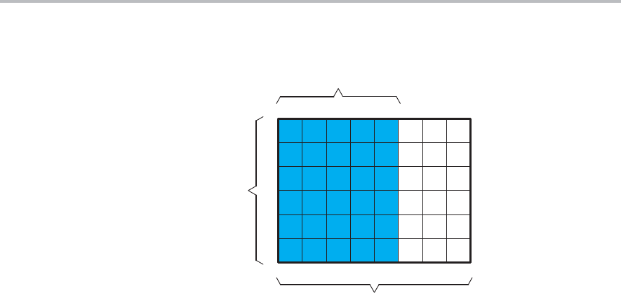
DAT_copy2d
5-7
DAT Module
Figure 5−1. 2D Transfer
LineLen
LineCnt
LinePitch
LineLen = 5
LineCnt = 6
LinePitch = 8
If a 2D to 2D transfer is specified, both the source and destination have the
same lineLen, lineCnt, and linePitch.
The return value is a transfer identifier that may be used later on to wait for
completion. See DAT_wait().
Example DAT_copy2d (DAT_1D2D, buffA, buffB, 16, 8, 32);

DAT_fill
5-8
Fills linear block of memory with specified fill value using DMA hardware
DAT_fill
Function Uint32 DAT_fill(
void *dst,
Uint16 byteCnt,
Uint32 *fillValue
);
Arguments dst Pointer to destination location
byteCnt Number of bytes to fill
fillValue Pointer to fill value
Return Value xfrId Transfer ID
Description Fills a linear block of memory with the specified fill value using DMA hardware.
The arguments are checked for alignment and the DMA is submitted
accordingly. For best performance, you should ensure that the destination
address is aligned on a 4-byte boundary and the transfer length is a multiple
of 4. A maximum of 65,535 bytes may be filled.
For devices other than C64x devices, the fill value is 8-bits in size but must be
contained in a 32-bit word. This is due to the way the DMA hardware works.
If the arguments are 32-bit aligned, then the DMA transfer element size is set
to 32-bits to maximize performance. This means that the source of the transfer,
the fill value, must be 32-bits in size. So, the 8-bit fill value must be repeated
to fill the 32-bit value. For example, if you want to fill a region of memory with
the value 0xA5, the fill value should contain 0xA5A5A5A5 before calling this
function. If the arguments are 16-bit aligned, a 16-bit element size is used.
Finally, if any of the arguments are 8-bit aligned, an 8-bit element size is used.
It is a good idea to always fill in the entire 32-bit fill value to eliminate any endian
issues.
For C64x devices, the fill count must be a multiple of 8 bytes. The EDMA uses
a 64-bit bus to store data in L2 SRAM. A pointer of 64-bit value must be passed
to the “fillvalue” parameter (a set of 8 consecutive bytes, aligned). The EDMA
transfer element size is set to 64-bits. If you want to fill the memory region with
a value of 0x1234, the pointer should point to two consecutive 32-bit words set
to 0x12341234 value .
If the DMA channel is busy with a previous request, the function will block and
wait for completion before submitting this request.
The DAT module must be opened before calling this function. See
DAT_open().

DAT_fill
5-9
DAT Module
The return value is a transfer identifier that may be used later on to wait for
completion. See DAT_wait().
Note:
You should be aware that if the fill value is in cache, the DMA always uses
the external address and not the value that is in cache. It is up to you to en-
sure that the fill value is flushed before calling this function. Also, since the
user specifies a pointer to the fill value, it is important not to write to it while
the fill is in progress.
Example Uint32 BUFF_SIZE 256;
Uint32 buff[BUFF_SIZE/sizeof(Uint32)];
Uint32 fillValue = 0xA5A5A5A5;
…
DAT_open(DAT_CHAANY,DAT_PRI_LOW,0);
DAT_fill(buff,BUFF_SIZE,&fillValue);
For 64x devices:
Uint32 BUFF_SIZE 256; /* 8 * 8bytes */
Uint32 buff[BUFF_SIZE/sizeof(Uint32)];
Uint32 fillValue[2] = {0x12341234,0x12341234};
Uint32 *fillValuePtr = fillValue;
…
DAT_open(DAT_CHAANY,DAT_PRI_LOW,0);
DAT_fill(buff,BUFF_SIZE,&fillValue);

DAT_open
5-10
Opens DAT module
DAT_open
Function Uint32 DAT_open(
int chaNum,
int priority,
Uint32 flags
);
Arguments chaNum Specifies which DMA channel to allocate; must be one of the
following:
-DAT_CHAANY
-DAT_CHA0
-DAT_CHA1
-DAT_CHA2
-DAT_CHA3
priority Specifies the priority of the DMA channel; must be one of the
following:
-DAT_PRI_LOW
-DAT_PRI_HIGH
flags Miscellaneous open flags
-DAT_OPEN_2D
Return Value success Returns zero on failure and non-zero if successful. Reasons
for failure are:
-The DAT module is already open.
-Required resources could not be allocated.
Description This function opens up the DAT module and must be called before calling any
of the other DAT API functions. The ChaNum argument specifies which DMA
channel to open for exclusive use by the DAT module. For devices with EDMA,
the ChaNum argument is ignored because the quick DMA is used which does
not have a channel associated with it.
For DMA Devices:
-ChaNum specifies which DMA channel to use
-DAT_PRI_LOW sets the DMA channel up for CPU priority
-DAT_PRI_HIGH sets the DMA channel up for DMA priority
For EDMA Devices:
-ChaNum is ignored

DAT_setPriority
5-11
DAT Module
-DAT_PRI_LOW sets LOW priority
-DAT_PRI_HIGH sets HIGH priority
Once the DAT module is opened, any resources allocated, such as DMA
channels, remain allocated. You can call DAT_close() to free these
resources.
If 2D transfers are planned via DAT_copy2d, the DAT_OPEN_2D flag must
be specified. Specifying this flag for devices with the DMA peripheral will cause
allocation of one global count reload register and one global index register.
These global registers are freed when DAT_close() is called.
Note:
For devices with EDMA, the DAT module uses the EDMA registers to submit
transfer requests. Also used is the channel interrupt pending register (CIPR).
Interrupts are not enabled but the completion flags in CIPR are used. The
DAT module uses interrupt completion codes 1 through 4 which amounts to
a mask of 0x00000001E in the CIPR register. If you use the DAT module on
devices with EDMA, you must avoid using transfer completion codes 1
through 4.
Example To open the DAT module using any available DMA channel, use:
DAT_open(DAT_CHAANY,DAT_PRI_LOW,0);
To open the DAT module using DMA channel 2 in high-priority mode, use:
DAT_open(DAT_CHA2,DAT_PRI_HIGH,0);
To open the DAT module for 2D copies, use:
DAT_open (DAT_CHAANY, DAT_PRI_HIGH, DAT_OPEN_2D);
Sets the priority of DMA or EDMA channel
DAT_setPriority
Function void DAT_setPriority(
int priority
);
Arguments priority Priority bit value
Return Value none
Description Sets the priority bit value PRI of PRICTL register for devices supporting DMA,
and the PRI of OPT register for devices supporting EDMA. See also
DAT_open() function. The priority value can be set by using the following
predefined constants:

DAT_SUPPORT
5-12
-DAT_PRI_LOW
-DAT_PRI_HIGH
Example /* Open DAT channel with priority Low */
DAT_open(DMA_CHAANY,DAT_PRI_LOW,0)
/* Set transfer with priority high */
DAT_setPriority(DAT_PRI_HI);
Compile-time constant
DAT_SUPPORT
Constant DAT_SUPPORT
Description Compile-time constant that has a value of 1 if the device supports the DAT
module and 0 otherwise. You are not required to use this constant.
Note: The DAT module is supported by all devices that have an EDMA or DMA
peripheral.
Example #if (DAT_SUPPORT)
/* user DAT configuration */
#endif

DAT_wait
5-13
DAT Module
Waits for previous transfer to complete identification by transfer ID
DAT_wait
Function void DAT_wait(
Uint32 id
);
Arguments id Transfer identifier, returned by one of the DAT copy or DAT fill routines.
Two predefined transfer IDs may be used:
-DAT_XFRID_WAITALL
-DAT_XFRID_WAITNONE
Using DAT_XFRID_WAITALL means wait until all transfers have
completed. Using DAT_XFRID_WAITNONE means do not wait for any
transfers to complete. This can be useful as the first operation in a
pipelined copy sequence.
Return Value none
Description This function waits for a previous transfer to complete, identified by the transfer
ID. If the transfer has already completed, this function returns immediately.
Interrupts are not disabled during the wait.
Example Uint32 transferId;
…
DAT_open(DAT_CHAANY, DAT_PRI_LOW, 0);
…
transferId = DAT_copy(src,dst,len);
/* user DAT configuration */
DAT_wait(transferId);

6-1
DMA Module
This chapter describes the DMA module, lists the API functions and macros
within the module, discusses how to use a DMA channel, and provides a DMA
API reference section.
Topic Page
6.1 Overview 6-2. . . . . . . . . . . . . . . . . . . . . . . . . . . . . . . . . . . . . . . . . . . . . . . . . . . . .
6.2 Macros 6-5. . . . . . . . . . . . . . . . . . . . . . . . . . . . . . . . . . . . . . . . . . . . . . . . . . . . . . .
6.3 Configuration Structures 6-7. . . . . . . . . . . . . . . . . . . . . . . . . . . . . . . . . . . . . .
6.4 Functions 6-9. . . . . . . . . . . . . . . . . . . . . . . . . . . . . . . . . . . . . . . . . . . . . . . . . . . .
Chapter 6

Overview
6-2
6.1 Overview
Currently, the are two DMA architectures used on TMS320C6x devices are:
DMA and EDMA (enhanced DMA). Devices such as the C6201 have the
DMA peripheral, whereas the C6211 has the EDMA peripheral. The two
architectures are different enough to warrant a separate API module for each.
Table 6−1 lists the configuration structures for use with the DMA functions.
Table 6−2 lists the functions and constants available in the CSL DMA module.
Table 6−1. DMA Configuration Structures
Structure Purpose See page ...
DMA_Config DMA structure that contains all local registers required to set up
a specific DMA channel 6-7
DMA_GlobalConfig Global DMA structure that contains all global registers that you
may need to initialize a DMA channel 6-8
Table 6−2. DMA APIs
(a) DMA Primary Functions
Syntax Type Description See page ...
DMA_close F Closes a DMA channel opened via DMA_open() 6-9
DMA_config F Sets up the DMA channel using the configuration
structure 6-9
DMA_configArgs F Sets up the DMA channel using the register values
passed in 6-10
DMA_open F Opens a DMA channel for use 6-11
DMA_pause F Pauses the DMA channel by setting the START bits in
the primary control register appropriately 6-12
DMA_reset F Resets the DMA channel by setting its registers to
power-on defaults 6-12
DMA_start F Starts a DMA channel running without auto−initialization 6-13
DMA_stop FStops a DMA channel by setting the START bits in the
primary control register appropriately 6-13
Note: F = Function; C = Constant; M = Macro

Overview
6-3
DMA Module
Table 6−2. DMA APIs (Continued)
(b) DMA Global Register Functions
Syntax Type Description See page ...
DMA_allocGlobalReg F Provides resource management for the DMA global
registers 6-14
DMA_freeGlobalReg F Frees a global DMA register previously allocated by
calling DMA_AllocGlobalReg()
6-16
DMA_getGlobalReg F Reads a global DMA register that was previously
allocated by calling DMA_AllocGlobalReg()
6-16
DMA_getGlobalRegAddr F Gets DMA global register address 6-17
DMA_globalAlloc F Allocates DMA global registers 6-18
DMA_globalConfig F Configures entry for DMA configuration structure 6-19
DMA_globalConfigArgs F Configures entry for DMA registers 6-20
DMA_globalFree F Frees Allocated DMA global register 6-22
DMA_globalGetConfig F Returns the entry for the DMA configuration structure 6-22
DMA_setGlobalReg FSets value of a global DMA register previously allocated
by calling DMA_AllocGlobalReg()
6-23
(c) DMA Auxiliary Functions, Constants, and Macros
Syntax Type Description See page ...
DMA_autoStart F Starts a DMA channel with auto−initialization 6-23
DMA_CHA_CNT C Number of DMA channels for the current device 6-24
DMA_CLEAR_CONDITION M Clears condition flag 6-24
DMA_GBLADDRA C DMA global address register A mask 6-24
DMA_GBLADDRB C DMA global address register B mask 6-24
DMA_GBLADDRC C DMA global address register C mask 6-25
DMA_GBLADDRD C DMA global address register D mask 6-25
DMA_GBLCNTA C DMA global count reload register A mask 6-25
DMA_GBLCNTB C DMA global count reload register B mask 6-25
DMA_GBLIDXA CDMA global index register A mask 6-25
Note: F = Function; C = Constant; M = Macro

Overview
6-4
Table 6−2. DMA APIs (Continued)
DMA_GBLIDXB C DMA global index register B mask 6-26
DMA_GET_CONDITION M Gets condition flag 6-26
DMA_getConfig F Reads the current DMA configuration structure 6-26
DMA_getEventId F Returns the IRQ event ID for the DMA completion
interrupt 6-27
DMA_getStatus F Reads the status bits of the DMA channel 6-27
DMA_restoreStatus F Restores the status from DMA_getStatus() by setting
the START bit of the PRICTL primary control register 6-27
DMA_setAuxCtl F Sets the DMA AUXCTL register 6-28
DMA_SUPPORT C A compile time constant whose value is 1 if the device
supports the DMA module 6-28
DMA_wait FEnters a spin loop that polls the DMA status bits until
the DMA completes 6-29
Note: F = Function; C = Constant; M = Macro
6.1.1 Using a DMA Channel
To use a DMA channel, you must first open it and obtain a device handle using
DMA_open(). Once opened, you use the device handle to call the other API
functions. The channel may be configured by passing a DMA_Config
structure to DMA_config() or by passing register values to the
DMA_configArgs() function. To assist in creating register values, there are
DMA_RMK (make) macros that construct register values based on field
values. In addition, there are symbol constants that may be used for the field
values.
There are functions for managing shared global DMA registers,
DMA_allocGlobalReg(), DMA_freeGlobalReg(),
DMA_setGlobalReg(), and DMA_getGlobalReg().

Macros
6-5
DMA Module
6.2 Macros
There are two types of DMA macros: those that access registers and fields,
and those that construct register and field values.
Table 6−3 lists the DMA macros that access registers and fields, and
Table 6−4 lists the DMA macros that construct register and field values. The
macros themselves are found in Chapter 28, Using the HAL Macros.
The DMA module includes handle-based macros.
Table 6−3. DMA Macros that Access Registers and Fields
Macro Description/Purpose See page ...
DMA_ADDR(<REG>) Register address 28-12
DMA_RGET(<REG>) Returns the value in the peripheral register 28-18
DMA_RSET(<REG>,x) Register set 28-20
DMA_FGET(<REG>,<FIELD>) Returns the value of the specified field in the
peripheral register 28-13
DMA_FSET(<REG>,<FIELD>,fieldval) Writes fieldval to the specified field in the
peripheral register 28-15
DMA_FSETS(<REG>,<FIELD>,<SYM>) Writes the symbol value to the specified field
in the peripheral 28-17
DMA_RGETA(addr,<REG>) Gets register for a given address 28-19
DMA_RSETA(addr,<REG>,x) Sets register for a given address 28-20
DMA_FGETA(addr,<REG>,<FIELD>) Gets field for a given address 28-13
DMA_FSETA(addr,<REG>,<FIELD>,fieldval) Sets field for a given address 28-16
DMA_FSETSA(addr,<REG>,<FIELD>,
<SYM>) Sets field symbolically for a given address 28-17
DMA_ADDRH(h,<REG>) Returns the address of a memory-mapped
register for a given handle 28-12
DMA_RGETH(h,<REG>) Returns the value of a register for a given
handle 28-19
DMA_RSETH(h,<REG>,x) Sets the register value to x for a given handle 28-21
DMA_FGETH(h,<REG>,<FIELD>) Returns the value of the field for a given
handle 28-14
DMA_FSETH(h,<REG>,<FIELD>,fieldval) Sets the field value to x for a given handle 28-16

Macros
6-6
Table 6−4. DMA Macros that Construct Register and Field Values
Macro Description/Purpose See page ...
DMA_<REG>_DEFAULT Register default value 28-21
DMA_<REG>_RMK() Register make 28-23
DMA_<REG>_OF() Register value of ... 28-22
DMA_<REG>_<FIELD>_DEFAULT Field default value 28-24
DMA_FMK() Field make 28-14
DMA_FMKS() Field make symbolically 28-15
DMA_<REG>_<FIELD>_OF() Field value of ... 28-24
DMA_<REG>_<FIELD>_<SYM> Field symbolic value 28-24

DMA_Config
6-7
DMA Module
6.3 Configuration Structures
Because the DMA has both local and global registers for each channel, the
CSL DMA module has two configuration structures:
-DMA_Config (channel configuration structure) contains all the local
registers required to set up a specific DMA channel.
-DMA_GlobalConfig (global configuration structure) contains all the
global registers needed to initialize a DMA channel. These global registers
are resources shared across the different DMA channels, and include
element/frame indexes and reload registers, as well as src/dst page
registers.
You can use literal values or the _RMK macros to create the structure member
values.
DMA configuration structure used to set up DMA channel
DMA_Config
Structure DMA_Config
Members Uint32 prictl DMA primary control register value
Uint32 secctl DMA secondary control register value
Uint32 src DMA source address register value
Uint32 dst DMA destination address register value
Uint32 xfrcnt DMA transfer count register value
Description This DMA configuration structure is used to set up a DMA channel. You create
and initialize this structure and then pass its address to the DMA_config()
function. You can use literal values or the _RMK macros to create the structure
member values.
Example DMA_Config MyConfig = {
0x00000050, /* prictl */
0x00000080, /* secctl */
0x80000000, /* src */
0x80010000, /* dst */
0x00200040 /* xfrcnt */
};
…
DMA_config(hDma,&MyConfig);

DMA_GlobalConfig
6-8
DMA global register configuration structure
DMA_GlobalConfig
Structure typedef struct {
Uint32 addrA;
Uint32 addrB;
Uint32 addrC;
Uint32 addrD;
Uint32 idxA;
Uint32 idxB;
Uint32 cntA;
Uint32 cntB;
} DMA_GlobalConfig;
Members addrA Global address register A value.
addrB Global address register B value.
addrC Global address register C value.
addrD Global address register D value.
idxA Global index register A value.
idxB Global index register B value.
cntA Global count reload register A value.
cntB Global count reload register B value.
Description This is the DMA global register configuration structure used to set up a DMA
global register configuration. You create and initialize this structure, then pass
its address to the DMA_globalConfig() function.
Example Uint32 dmaGblRegMsk;
Uint32 dmaGblRegId = DMA_GBLADDRB | DMA_GBLADDRC;
DMA_GlobalConfig dmaGblCfg = {
0x00000000, /* Global Address Register A */
0x80001000, /* Global Address Register B */
0x80002000, /* Global Address Register C */
0x00000000, /* Global Address Register D */
0x00000000, /* Global Index Register A */
0x00000000, /* Global Index Register B */
0x00000000, /* Global Count Reload Register A */
0x00000000 /* Global Count Reload Register B */
};
dmaGblRegMsk = DMA_globalAlloc(dmaGblRegId);
DMA_globalConfig(dmaGblRegMsk, &dmaGblCfg);

DMA_close
6-9
DMA Module
6.4 Functions
6.4.1 Primary Functions
Closes DMA channel opened via DMA_open()
DMA_close
Function void DMA_close(
DMA_Handle hDma
);
Arguments hDma Handle to DMA channel, see DMA_open()
Return Value none
Description This function closes a DMA channel previously opened via DMA_open(). The
registers for the DMA channel are set to their power-on defaults and the
completion interrupt is disabled and cleared.
Example DMA_close(hDma);
Sets up DMA channel using configuration structure
DMA_config
Function void DMA_config(
DMA_Handle hDma,
DMA_Config *Config
);
Arguments hDma Handle to DMA channel. See DMA_open()
Config Pointer to an initialized configuration structure
Return Value none
Description Sets up the DMA channel using the configuration structure. The values of the
structure are written to the DMA registers. The primary control register (prictl)
is written last. See also DMA_configArgs() and DMA_Config.
Example DMA_Config MyConfig = {
0x00000050, /* prictl */
0x00000080, /* secctl */
0x80000000, /* src */
0x80010000, /* dst */
0x00200040 /* xfrcnt */
};
…
DMA_config(hDma,&MyConfig);

DMA_configArgs
6-10
Sets up DMA channel using register values passed in
DMA_configArgs
Function void DMA_configArgs(
DMA_Handle hDma,
Uint32 prictl,
Uint32 secctl,
Uint32 src,
Uint32 dst,
Uint32 xfrcnt
);
Arguments hDma Handle to DMA channel. See DMA_open()
prictl Primary control register value
secctl Secondary control register value
src Source address register value
dst Destination address register value
xfrcnt Transfer count register value
Return Value none
Description Sets up the DMA channel using the register values passed in. The register
values are written to the DMA registers. The primary control register (prictl) is
written last. See also DMA_config().
You may use literal values for the arguments or for readability. You may use
the _RMK macros to create the register values based on field values.
Example DMA_configArgs(hDma,
0x00000050, /* prictl */
0x00000080, /* secctl */
0x80000000, /* src */
0x80010000, /* dst */
0x00200040 /* xfrcnt */
);

DMA_open
6-11
DMA Module
Opens DMA channel for use
DMA_open
Function DMA_Handle DMA_open(
int chaNum,
Uint32 flags
);
Arguments chaNum DMA channel to open:
-DMA_CHAANY
-DMA_CHA0
-DMA_CHA1
-DMA_CHA2
-DMA_CHA3
flags Open flags (logical OR of DMA_OPEN_RESET)
Return Value Device Handle Handle to newly opened device
Description Before a DMA channel can be used, it must first be opened by this function.
Once opened, it cannot be opened again until closed. See DMA_close(). You
have the option of either specifying exactly which physical channel to open or
you can let the library pick an unused one for you by specifying DMA_CHAANY.
The return value is a unique device handle that you use in subsequent DMA
API calls. If the open fails, INV is returned.
If the DMA_OPEN_RESET is specified, the DMA channel registers are set to
their power-on defaults and the channel interrupt is disabled and cleared.
Example DMA_Handle hDma;
…
hDma = DMA_open(DMA_CHAANY,DMA_OPEN_RESET);

DMA_pause
6-12
Pauses DMA channel by setting START bits in primary control register
DMA_pause
Function void DMA_pause(
DMA_Handle hDma
);
Arguments hDma Handle to DMA channel. See DMA_open()
Return Value none
Description This function pauses the DMA channel by setting the START bits in the primary
control register accordingly. See also DMA_start(), DMA_stop(), and
DMA_autoStart().
Example DMA_pause(hDma);
Resets DMA channel by setting its registers to power-on defaults
DMA_reset
Function void DMA_reset(
DMA_Handle hDma
);
Arguments hDma Handle to DMA channel. See DMA_open()
Return Value none
Description Resets the DMA channel by setting its registers to power-on defaults and
disabling and clearing the channel interrupt. You may use INV as the device
handle to reset all channels.
Example /* reset an open DMA channel /
DMA_reset(hDma);
/ reset all DMA channels */
DMA_reset(INV);

DMA_start
6-13
DMA Module
Starts DMA channel running without auto−initialization
DMA_start
Function void DMA_start(
DMA_Handle hDma
);
Arguments hDma Handle to DMA channel, see DMA_open()
Return Value none
Description Starts a DMA channel running without auto−initialization by setting the START
bits in the primary control register accordingly. See also DMA_pause(),
DMA_stop(), and DMA_autoStart().
Example DMA_start(hDma);
Stops DMA channel by setting START bits in primary control register
DMA_stop
Function void DMA_stop(
DMA_Handle hDma
);
Arguments hDma Handle to DMA channel. See DMA_open()
Return Value none
Description Stops a DMA channel by setting the START bits in the primary control register
accordingly. See also DMA_pause(), DMA_start(), and
DMA_autoStart().
Example DMA_stop(hDma);

DMA_allocGlobalReg
6-14
6.4.2 DMA Global Register Functions
Allocates global DMA register
DMA_allocGlobalReg
Function Uint32 DMA_allocGlobalReg(
DMA_Gbl regType,
Uint32 initVal
);
Arguments regType Global register type; must be one of the following:
-DMA_GBL_ADDRRLD
-DMA_GBL_INDEX
-DMA_GBL_CNTRLD
-DMA_GBL_SPLIT
initVal Value to initialize the register to
Return Value Global Register ID Unique ID number for the global register
Description Since the DMA global registers are shared, they must be controlled using
resource management. This is done using DMA_allocGlobalReg() and
DMA_freeGlobalReg() functions. Allocating a register ensures that it will
not be reallocated until it is freed. The register ID may then be used to get or
set the register value by calling DMA_getGlobalReg() and
DMA_setGlobalReg() respectively. If the register cannot be allocated, a
register ID of 0 is returned.
The register ID may directly be used with the DMA_PRICTL_RMK macro.
-DMA_GBL_ADDRRLD
Allocate global address register for use as DMA DST RELOAD or DMA
SRC RELOAD. Will allocate one of the following DMA registers:
JGlobal Address Register B
JGlobal Address Register C
JGlobal Address Register D
-DMA_GBL_INDEX
Allocate global index register for use as DMA INDEX. Will allocate one of
the following DMA registers:
JGlobal Index Register A
JGlobal Index Register B

DMA_allocGlobalReg
6-15
DMA Module
-DMA_GBL_CNTRLD
Allocate global count reload register for use as DMA CNT RELOAD. Will
allocate one of the following DMA registers:
JGlobal Count Reload Register A
JGlobal Count Reload Register B
-DMA_GBL_SPLIT
Allocate global address register for use as DMA SPLIT. Will allocated one
of the following DMA registers:
JGlobal Address Register A
JGlobal Address Register B
JGlobal Address Register C
Example Uint32 RegId;
…
/* allocate global index register and initialize it */
RegId = DMA_allocGlobalReg(DMA_GBL_
INDEX,0x00200040);

DMA_freeGlobalReg
6-16
Frees global DMA register that was previously allocated
DMA_freeGlobalReg
Function void DMA_freeGlobalReg(
Uint32 regId
);
Arguments regId Global register ID obtained from DMA_allocGlobalReg().
Return Value none
Description This function frees a global DMA register that was previously allocated by
calling DMA_allocGlobalReg(). Once freed, the register is available for
reallocation.
Example Uint32 RegId;
…
/* allocate global index register and initialize it */
RegId = DMA_allocGlobalReg(DMA_GBL_INDEX,0x00200040);
…
/* some time later on when you’re done with it */
DMA_freeGlobalReg(RegId);
Reads global DMA register that was previously allocated
DMA_getGlobalReg
Function Uint32 DMA_getGlobalReg(
Uint32 regId
);
Arguments regId Global register ID obtained from DMA_allocGlobalReg().
Return Value Register Value Value read from register
Description This function returns the register value of the global DMA register that was
previously allocated by calling DMA_allocGlobalReg().
If you prefer not to use the alloc/free paradigm for the global register
management, the predefined register IDs may be used. You should be aware
that use of predefined register IDs precludes the use of alloc/free. The list of
predefined IDs are shown below:

DMA_getGlobalRegAddr
6-17
DMA Module
-DMA_GBL_ADDRRLDB
-DMA_GBL_ADDRRLDC
-DMA_GBL_ADDRRLDD
-DMA_GBL_INDEXA
-DMA_GBL_INDEXB
-DMA_GBL_CNTRLDA
-DMA_GBL_CNTRLDB
-DMA_GBL_SPLITA
-DMA_GBL_SPLITB
-DMA_GBL_SPLITC
Note:
DMA_GBL_ADDRRLDB denotes the same physical register as
DMA_GBL_SPLITB and DMA_GBL_ADDRRLDC denotes the same physical
register as DMA_GBL_SPLITC.
Example Uint32 RegId;
Uint32 RegValue;
…
/* allocate global index register and initialize it /
RegId = DMA_allocGlobalReg(DMA_GBL_
INDEX,0x00200040);
…
RegValue = DMA_getGlobalReg(RegId);
Gets DMA global register address
DMA_getGlobalRegAddr
Function Uint32 DMA_getGlobalRegAddr(
Uint32 regId
);
Arguments regId DMA global registers ID
Return Value Uint32 DMA global register address corresponding to regId
Description Get DMA global register address and return the address value.
Example Uint32 regId = DMA_GBL_ADDRRLDB;
Uint32 regAddr;
regAddr = DMA_getGlobalRegAddr(regId);

DMA_globalAlloc
6-18
Allocates DMA global registers
DMA_globalAlloc
Function Uint32 DMA_globalAlloc(
Uint32 regs
);
Arguments regs DMA global registers ID
Return Value Uint32 Allocated DMA global registers mask
Description Allocates DMA global registers and returns a mask of allocated DMA global
registers. Mask depends on DMA global register ID and the availability of the
register.
Example Uint32 dmaGblRegMsk;
Uint32 regs = DMA_GBLADDRB | DMA_GBLADDRC;
DmaGblRegMsk = DMA_globalAlloc(regs);

DMA_globalConfig
6-19
DMA Module
Sets up the DMA global registers using the configuration structure
DMA_globalConfig
Function void DMA_globalConfig(
Uint32 regs,
DMA_GlobalConfig *cfg
);
Arguments regs DMA global register mask
cfg Pointer to an initialized configuration structure.
Return Value none
Description Sets up the DMA global registers using the configuration structure. The values
of the structure that are written to the DMA global registers depend on the DMA
global register mask.
Example Uint32 dmaGblRegMsk;
Uint32 dmaGblRegId = DMA_GBLADDRB | DMA_GBLADDRC;
DMA_GlobalConfig dmaGblCfg = {
0x00000000, /* Global Address Register A */
0x80001000, /* Global Address Register B */
0x80002000, /* Global Address Register C */
0x00000000, /* Global Address Register D */
0x00000000, /* Global Index Register A */
0x00000000, /* Global Index Register B */
0x00000000, /* Global Count Reload Register A */
0x00000000 /* Global Count Reload Register B */
};
dmaGblRegMsk = DMA_globalAlloc(dmaGblRegId);
DMA_globalConfig(dmaGblRegMsk, &dmaGblCfg);

DMA_globalConfigArgs
6-20
Establishes DMA global register value
DMA_globalConfigArgs
Function void DMA_globalConfigArgs(
Uint32 regs,
Uint32 addrA,
Uint32 addrB,
Uint32 addrC,
Uint32 addrD,
Uint32 idxA,
Uint32 idxB,
Uint32 cntA,
Uint32 cntB
);
Arguments regs DMA global register mask value.
addrA Global address register A value.
addrB Global address register B value.
addrC Global address register C value.
addrD Global address register D value.
idxA Global index register A value.
idxB Global index register B value.
cntA Global count reload register A value.
cntB Global count reload register B value.
Return Value none
Description Sets up the DMA global registers using the register values passed in. The
register values that are written to the DMA global registers depend on the DMA
global register mask.

DMA_globalConfigArgs
6-21
DMA Module
Example Uint32 dmaGblRegMsk;
Uint32 dmaGblRegId = DMA_GBLADDRB | DMA_GBLADDRC;
Uint32 addrA = 0x00000000;
Uint32 addrB = 0x80001000;
Uint32 addrC = 0x80002000;
Uint32 addrD = 0x00000000;
Uint32 idxA = 0x00000000;
Uint32 idxB = 0x00000000;
Uint32 cntA = 0x00000000;
Uint32 cntB = 0x00000000;
dmaGblRegMsk = DMA_globalAlloc(dmaGblRegId);
DMA_globalConfigArgs(
dmaGblRegMsk,
addrA,
addrB,
addrC,
addrD,
idxA,
idxB,
cntA,
cntB
);

DMA_globalFree
6-22
Frees allocated DMA global registers
DMA_globalFree
Function Void DMA_globalFree(
Uint32 regs
);
Arguments regs DMA global registers ID
Return Value none
Description Frees previously allocated DMA global registers; depends on regs.
Example Uint32 dmaGblRegId = DMA_GBLADDRB | DMA_GBLADDRC;
DMA_globalFree(dmaGblRegId);
Gets current DMA global register configuration value
DMA_globalGetConfig
Function void DMA_globalGetConfig(
Uint32 regs,
DMA_GlobalConfig *cfg
);
Arguments regs DMA global register ID
cfg Pointer to an initialized configuration structure.
Return Value none
Description Gets DMA global registers current configuration value depending on DMA
global register ID.
Example Uint32 dmaGblRegId = DMA_GBLADDRB | DMA_GBLADDRC;
DMA_GlobalConfig dmaGblCfg;
DMA_globalGetConfig(dmaGblRegId, &dmaGblCfg);

DMA_setGlobalReg
6-23
DMA Module
Sets value of global DMA register that was previously allocated
DMA_setGlobalReg
Function void DMA_setGlobalReg(
Uint32 regId,
Uint32 val
);
Arguments regId Global register ID obtained from DMA_allocGlobalReg().
val Value to set register to
Return Value none
Description This function sets the value of a global DMA register that was previously
allocated by calling DMA_allocGlobalReg().
Example Uint32 RegId;
…
/* allocate global index register and initialize it /
RegId = DMA_allocGlobalReg(DMA_GBL_INDEX,0x00200040);
…
DMA_setGlobalReg(RegId,0x12345678);
6.4.3 DMA Auxiliary Functions, Constants, and Macros
Starts DMA channel with autoinitialization
DMA_autoStart
Function void DMA_autoStart(
DMA_Handle hDma
);
Arguments hDma Handle to DMA channel, see DMA_open()
Return Value none
Description Starts a DMA channel running with autoinitialization by setting the START bits
in the primary control register accordingly. See also DMA_pause(),
DMA_stop(), and DMA_start().
Example DMA_autoStart(hDma);

DMA_CHA_CNT
6-24
Number of DMA channels for current device
DMA_CHA_CNT
Constant DMA_CHA_CNT
Description This constant holds the number of physical DMA channels for the current
device.
Clears one of the condition flags in DMA secondary control register
DMA_CLEAR_CONDITION
Macro DMA_CLEAR_CONDITION(
hDma,
COND
);
Arguments hDma Handle to DMA channel, see DMA_open()
COND Condition to clear, must be one of the following:
-DMA_SECCTL_SXCOND
-DMA_SECCTL_FRAMECOND
-DMA_SECCTL_LASTCOND
-DMA_SECCTL_BLOCKCOND
-DMA_SECCTL_RDROPCOND
-DMA_SECCTL_WDROPCOND
Return Value none
Description This macro clears one of the condition flags in the DMA secondary control
register. See the TMS320C6000 Peripherals Reference Guide (SPRU190) for
a description of the condition flags.
Example DMA_CLEAR_CONDITION(hDma,DMA_SECCTL_BLOCKCOND);
DMA global address register A mask
DMA_GBLADDRA
Constant DMA_GBLADDRA
Description This constant allows selection of the global address register A. See
DMA_globalAlloc(), DMA_globalConfig(), and
DMA_globalConfigArgs() functions.
DMA global address register B mask
DMA_GBLADDRB
Constant DMA_GBLADDRB
Description This constant allows selection of the global address register B. See
DMA_globalAlloc(), DMA_globalConfig(), and
DMA_globalConfigArgs() functions.

DMA_GBLADDRC
6-25
DMA Module
DMA global address register C mask
DMA_GBLADDRC
Constant DMA_GBLADDRC
Description This constant allows selection of the global address register C. See
DMA_globalAlloc(), DMA_globalConfig(), and
DMA_globalConfigArgs() functions.
DMA global address register D mask
DMA_GBLADDRD
Constant DMA_GBLADDRD
Description This constant allows selection of the global address register D. See
DMA_globalAlloc(), DMA_globalConfig(), and
DMS_globalConfigArgs() functions.
DMA global count reload register A mask
DMA_GBLCNTA
Constant DMA_GBLCNTA
Description This constant allows selection of the global count reload register A. See
DMA_globalAlloc(), DMA_globalConfig(), and
DMA_globalConfigArgs() functions.
DMA global count reload register B mask
DMA_GBLCNTB
Constant DMA_GBLCNTB
Description This constant allows selection of the global count reload register B. See
DMA_globalAlloc(), DMA_globalConfig(), and
DMA_globalConfigArgs() functions.
DMA global index register A mask
DMA_GBLIDXA
Constant DMA_GBLIDXA
Description This constant allows selection of the global index register A. See
DMA_globalAlloc(), DMA_globalConfigArgs(), and
DMA_globalConfig() functions.

DMA_GBLIDXB
6-26
DMA global index register B mask
DMA_GBLIDXB
Constant DMA_GBLIDXB
Description This constant allows selection of the global index register B. See
DMA_globalAlloc(), DMA_globalConfig(), and
DMA_globalConfigArgs() functions.
Gets one of the condition flags in DMA secondary control register
DMA_GET_CONDITION
Macro DMA_GET_CONDITION(
hDma,
COND
);
Arguments hDma Handle to DMA channel. See DMA_open()
COND Condition to get; must be one of the following:
-DMA_SECCTL_SXCOND
-DMA_SECCTL_FRAMECOND
-DMA_SECCTL_LASTCOND
-DMA_SECCTL_BLOCKCOND
-DMA_SECCTL_RDROPCOND
-DMA_SECCTL_WDROPCOND
Return Value Condition Condition, 0 if clear, 1 if set
Description This macro gets one of the condition flags in the DMA secondary control
register. See the TMS320C6000 Peripherals Reference Guide (SPRU190) for
a description of the condition flags.
Example if (DMA_GET_CONDITION(hDma,DMA_SECCTL_BLOCKCOND)) {
/* user DMA configuration */
}
Reads the current DMA configuration values
DMA_getConfig
Function void DMA_getConfig(
DMA_Handle hDma,
DMA_Config *config
);
Arguments hDma DMA handle. See DMA_open()
config Pointer to a configuration structure

DMA_getEventId
6-27
DMA Module
Return Value none
Description Get DMA current configuration value
Example DMA_config dmaCfg;
DMA_getConfig(hDma, &dmaCfg);
Returns IRQ event ID for DMA completion interrupt
DMA_getEventId
Function Uint32 DMA_getEventId(
DMA_Handle hDma
);
Arguments hDma Handle to DMA channel. See DMA_open()
Return Value Event ID IRQ Event ID for DMA Channel
Description Returns the IRQ Event ID for the DMA completion interrupt. Use this ID to
manage the event using the IRQ module.
Example EventId = DMA_getEventId(hDma);
IRQ_enable(EventId);
Reads status bits of DMA channel
DMA_getStatus
Function Uint32 DMA_getStatus(
DMA_Handle hDma
);
Arguments hDma Handle to DMA channel, see DMA_open()
Return Value Status Value Current DMA channel status:
-DMA_STATUS_STOPPED
-DMA_STATUS_RUNNING
-DMA_STATUS_PAUSED
-DMA_STATUS_AUTORUNNING
Description This function reads the STATUS bits of the DMA channel.
Example while (DMA_getStatus(hDma)==DMA_STATUS_RUNNING);
Restores the status from DMA_getStatus()
DMA_restoreStatus
Function void DMA_restoreStatus(
Uint32 hDma,
Uint32 status
);
Arguments hDma Handle to DMA channel. See DMA_open()
status Status from DMA_getStatus() function

DMA_setAuxCtl
6-28
Return Value none
Description Restores the status from DMA_getStatus() by setting the START bit of the
PRICTL primary control register.
Example status = DMA_getStatus(hDma);
...
DMA_restoreStatus(hDma, status);
Sets DMA AUXCTL register
DMA_setAuxCtl
Function void DMA_setAuxCtl(
Uint32 auxCtl
);
Arguments auxCtl Value to set AUXCTL register to
Return Value none
Description This function sets the DMA AUXCTL register. You may use the
DMA_AUXCTL_RMK macro to construct the register value based on field
values. The default value for this register is DMA_AUXCTL_DEFAULT.
Example DMA_setAuxCtl(0x00000000);
Compile time constant
DMA_SUPPORT
Constant DMA_SUPPORT
Description Compile time constant that has a value of 1 if the device supports the DMA
module and 0 otherwise. You are not required to use this constant.
Note:
The DMA module is not supported on devices that do not have the DMA pe-
ripheral. In these cases, the EDMA module is supported instead.
Example #if (DMA_SUPPORT)
/* user DMA configuration /
#elif (EDMA_SUPPORT)
/ user EDMA configuration */
#endif

DMA_wait
6-29
DMA Module
Enters spin loop that polls DMA status bits until DMA completes
DMA_wait
Function void DMA_wait(
DMA_Handle hDma
);
Arguments hDma Handle to DMA channel. See DMA_open()
Return Value none
Description This function enters a spin loop that polls the DMA status bits until the DMA
completes. Interrupts are not disabled during this loop. This function is
equivalent to the following line of code:
while (DMA_getStatus(hDma)&DMA_STATUS_RUNNING);
Example DMA_wait(hDma);

7-1
EDMA Module
This chapter describes the EDMA module, lists the API functions and macros
within the module, discusses how to use an EDMA channel, and provides an
EDMA API reference section.
Topic Page
7.1 Overview 7-2. . . . . . . . . . . . . . . . . . . . . . . . . . . . . . . . . . . . . . . . . . . . . . . . . . . . .
7.2 Macros 7-5. . . . . . . . . . . . . . . . . . . . . . . . . . . . . . . . . . . . . . . . . . . . . . . . . . . . . . .
7.3 Configuration Structure 7-7. . . . . . . . . . . . . . . . . . . . . . . . . . . . . . . . . . . . . . .
7.4 Functions 7-8. . . . . . . . . . . . . . . . . . . . . . . . . . . . . . . . . . . . . . . . . . . . . . . . . . . .
Chapter 7

Overview
7-2
7.1 Overview
Currently, there are two DMA architectures used on C6x devices: DMA and
EDMA (Enhanced DMA). Devices such as the C6201 have the DMA
peripheral whereas C6211 devices have the EDMA peripheral. The two
architectures are different enough to warrant a separate API module for each.
Table 7−1 lists the configuration structures for use with the EDMA functions.
Table 7−2 lists the functions and constants available in the CSL EDMA
module.
Table 7−1. EDMA Configuration Structure
Structure Purpose See page ...
EDMA_Config The EDMA configuration structure used to set up an EDMA
channel 7-7
Table 7−2. EDMA APIs
(a) EDMA Primary Functions
Syntax Type Description See page ...
EDMA_close F Closes a previously opened EDMA channel 7-8
EDMA_config F Sets up the EDMA channel using the configuration
structure 7-8
EDMA_configArgs F Sets up the EDMA channel using the EDMA parameter
arguments 7-9
EDMA_open F Opens an EDMA channel 7-10
EDMA_reset FResets the given EDMA channel 7-15
(b) EDMA Auxiliary Functions and Constants
Syntax Type Description See page ...
EDMA_allocTable F Allocates a parameter RAM table from PRAM 7-16
EDMA_allocTableEx F Allocates set of parameter RAM tables from PRAM 7-17
EDMA_CHA_CNT C Number of EDMA channels 7-17
EDMA_chain F Sets the TCC,TCINT fields of the parent EDMA handle 7-18
EDMA_clearChannel F Clears the EDMA event flag in the EDMA channel event
register 7-19
EDMA_clearPram FClears the EDMA parameter RAM (PRAM) 7-20
Note: F = Function; C = Constant

Overview
7-3
EDMA Module
Table 7−2. EDMA APIs (Continued)
See page ...DescriptionTypeSyntax
EDMA_disableChaining F Disables EDMA chaining 7-20
EDMA_enableChaining F Enables EDMA chaining 7-20
EDMA_disableChannel F Disables an EDMA channel 7-21
EDMA_enableChannel F Enables an EDMA channel 7-21
EDMA_freeTable F Frees up a PRAM table previously allocated 7-22
EDMA_freeTableEx F Frees a previously allocated set of parameter RAM
tables 7-22
EDMA_getChannel F Returns the current state of the channel event 7-23
EDMA_getConfig F Reads the current EDMA configuration values 7-23
EDMA_getPriQStatus F Returns the value of the priority queue status register
(PQSR) 7-24
EDMA_getScratchAddr F Returns the starting address of the EDMA PRAM used
as non-cacheable on-chip SRAM (scratch area) 7-24
EDMA_getScratchSize F Returns the size (in bytes) of the EDMA PRAM used as
non-cacheable on-chip SRAM (scratch area) 7-24
EDMA_getTableAddress F Returns the 32-bit absolute address of the table 7-25
EDMA_intAlloc F Allocates a transfer complete code 7-25
EDMA_intClear F Clears EDMA transfer completion interrupt pending flag 7-25
EDMA_intDefaultHandler F Default function called by EDMA_intDispatcher() 7-26
EDMA_intDisable F Disables EDMA transfer completion interrupt 7-26
EDMA_intDispatcher F Calls an ISR when CIER[x] and CIPR[x] are
both set
7-26
EDMA_intEnable F Enables EDMA transfer completion interrupt 7-27
EDMA_intFree F Frees a transfer complete code previously allocated 7-27
EDMA_intHook F Hooks to an ISR channel which is called by
EDMA_intDispatcher()
7-28
EDMA_intTest F Tests EDMA transfer completion interrupt pending flag 7-29
EDMA_link F Links two EDMA transfers together 7-29
EDMA_qdmaConfig F Sets up QDMA registers using configuration structure 7-30
EDMA_qdmaConfigArgs FSets up QDMA registers using arguments 7-31
Note: F = Function; C = Constant

Overview
7-4
Table 7−2. EDMA APIs (Continued)
See page ...DescriptionTypeSyntax
EDMA_resetAll F Resets all EDMA channels supported by the chip device 7-32
EDMA_resetPriQLength F Resets the Priority queue length to the default value 7-32
EDMA_setChannel F Triggers an EDMA channel by writing to the appropriate
bit in the event set register (ESR) 7-32
EDMA_setEvtPolarity F Sets the polarity of the event associated with the EDMA
handle. 7-33
EDMA_setPriQLength F Sets the length of a given priority queue allocation
register 7-33
EDMA_SUPPORT C A compile-time constant whose value is 1 if the device
supports the EDMA module 7-34
EDMA_TABLE_CNT CA compile-time constant that holds the total number of
parameter table entries in the EDMA PRAM 7-34
Note: F = Function; C = Constant
7.1.1 Using an EDMA Channel
To use an EDMA channel, you must first open it and obtain a device handle
using EDMA_open(). Once opened, use the device handle to call the other
API functions. The channel may be configured by passing an EDMA_Config
structure to EDMA_config() or by passing register values to the
EDMA_configArgs() function. To assist in creating register values, the
_RMK (make) macros construct register values based on field values. In
addition, the symbol constants may be used for the field values.
Two functions manage the parameter RAM (PRAM) tables:
EDMA_allocTable() and EDMA_freeTable().

Macros
7-5
EDMA Module
7.2 Macros
There are two types of EDMA macros: those that access registers and fields,
and those that construct register and field values.
Table 7−3 lists the EDMA macros that access registers and fields, and
Table 7−4 lists the EDMA macros that construct register and field values. The
macros themselves are found in Chapter 28, Using the HAL Macros.
The EDMA module includes handle-based macros.
Table 7−3. EDMA Macros That Access Registers and Fields
Macro Description/Purpose See page...
EDMA_ADDR(<REG>) Register address 28-12
EDMA_RGET(<REG>) Returns the current value of a register 28-18
EDMA_RSET(<REG>,x) Register set 28-20
EDMA_FGET(<REG>,<FIELD>) Returns the value of the specified field in a
register 28-13
EDMA_FSET(<REG>,<FIELD>,x) Writes fieldval to the specified field in a register 28-15
EDMA_FSETS(<REG>,<FIELD>,<SYM>) Writes the symbol value to the specified field in
the peripheral 28-17
EDMA_RGETA(addr,<REG>) Gets register value for a given address 28-19
EDMA_RSETA(addr,<REG>,x) Sets register for a given address 28-20
EDMA_FGETA(addr,<REG>,<FIELD>) Gets field for a given address 28-13
EDMA_FSETA(addr,<REG>,<FIELD>,x) Sets field for a given address 28-16
EDMA_FSETSA(addr,<REG>,<FIELD>,
<SYM>) Sets field symbolically for a given address 28-17
EDMA_ADDRH(h,<REG>) Returns the address of a memory-mapped
register for a given handle 28-12
EDMA_RGETH(h,<REG>) Returns the value of a register for a given handle 28-19
EDMA_RSETH(h,<REG>,x) Sets the register value to x for a given handle 28-21
EDMA_FGETH(h,<REG>,<FIELD>) Returns the value of the field for a given handle 28-14
EDMA_FSETH(h,<REG>,<FIELD>,x) Sets the field value to x for a given handle 28-16
EDMA_FSETSH(h,<REG>,<FIELD>,
<SYM>) Sets the field symbolically for a given handle 28-18

Macros
7-6
Table 7−4. EDMA Macros that Construct Register and Field Values
Macro Description/Purpose See page...
EDMA_<REG>_DEFAULT Register default value 28-21
EDMA_<REG>_RMK() Register make 28-23
EDMA_<REG>_OF() Register value of ... 28-22
EDMA_<REG>_<FIELD>_DEFAULT Field default value 28-24
EDMA_FMK() Field make 28-14
EDMA_FMKS() Field make symbolically 28-15
EDMA_<REG>_<FIELD>_OF() Field value of ... 28-24
EDMA_<REG>_<FIELD>_<SYM> Field symbolic value 28-24

EDMA_Config
7-7
EDMA Module
7.3 Configuration Structure
EDMA configuration structure used to set up EDMA channel
EDMA_Config
Structure EDMA_Config
Members Uint32 opt Options
Uint32 src Source address
Uint32 cnt Transfer count
Uint32 dst Destination address
Uint32 idx Index
Uint32 rld Element count reload and link address
Description This is the EDMA configuration structure used to set up an EDMA channel. You
create and initialize this structure and then pass its address to the
EDMA_config() function.
Example EDMA_Config myConfig = {
0x41200000, /* opt */
0x80000000, /* src */
0x00000040, /* cnt */
0x80010000, /* dst */
0x00000004, /* idx */
0x00000000 /* rld */
};
…
EDMA_config(hEdma,&myConfig);

EDMA_close
7-8
7.4 Functions
7.4.1 EDMA Primary Functions
Closes previously opened EDMA channel
EDMA_close
Function void EDMA_close(
EDMA_Handle hEdma
);
Arguments hEdma Device handle. See EDMA_open().
Return Value none
Description Closes a previously opened EDMA channel.
This function accepts the following device handle:
From EDMA_open()
Example EDMA_close(hEdma);
Sets up EDMA channel using configuration structure
EDMA_config
Function void EDMA_config(
EDMA_Handle hEdma,
EDMA_Config *config
);
Arguments hEdma Device handle. See EDMA_open() and EDMA_allocTable().
config Pointer to an initialized configuration structure
Return Value none
Description Sets up the EDMA channel using the configuration structure. The values of the
structure are written to the EDMA PRAM entries. The options value (opt) is
written last. See also EDMA_configArgs() and EDMA_Config.
This function accepts the following device handles:
-From EDMA_open()
-From EDMA_allocTable()

EDMA_configArgs
7-9
EDMA Module
Example EDMA_Config myConfig = {
0x41200000, /* opt */
0x80000000, /* src */
0x00000040, /* cnt */
0x80010000, /* dst */
0x00000004, /* idx */
0x00000000 /* rld */
};
…
EDMA_config(hEdma,&myConfig);
Sets up EDMA channel using EDMA parameter arguments
EDMA_configArgs
Function void EDMA_configArgs(
EDMA_Handle hEdma,
Uint32 opt,
Uint32 src,
Uint32 cnt,
Uint32 dst,
Uint32 idx,
Uint32 rld
);
Arguments hEdma Device handle. See EDMA_open() and EDMA_allocTable().
opt Options
src Source address
cnt Transfer count
dst Destination address
idx Index
rld Element count reload and link address
Return Value none
Description Sets up the EDMA channel using the EDMA parameter arguments. The values
of the arguments are written to the EDMA PRAM entries. The options value
(opt) is written last. See also EDMA_config().
This function accepts the following device handles:

EDMA_open
7-10
-From EDMA_open()
-From EDMA_allocTable()
Example EDMA_configArgs(hEdma,
0x41200000, /* opt */
0x80000000, /* src */
0x00000040, /* cnt */
0x80010000, /* dst */
0x00000004, /* idx */
0x00000000 /* rld */
);
Opens EDMA channel
EDMA_open
Function EDMA_Handle EDMA_open(
int chaNum,
Uint32 flags
);
Arguments chaNum EDMA channel to open:
(For C6201, C6202, C6203, C6204, C6205, C6701, C6211, C6711, C6711C,
C6712 and C6712C)
-EDMA_CHA_ANY
-EDMA_CHA_DSPINT
-EDMA_CHA_TINT0
-EDMA_CHA_TINT1
-EDMA_CHA_SDINT
-EDMA_CHA_EXTINT4
-EDMA_CHA_EXTINT5
-EDMA_CHA_EXTINT6
-EDMA_CHA_EXTINT7
-EDMA_CHA_TCC8
-EDMA_CHA_TCC9
-EDMA_CHA_TCC10
-EDMA_CHA_TCC11
-EDMA_CHA_XEVT0
-EDMA_CHA_REVT0
-EDMA_CHA_XEVT1
-EDMA_CHA_REVT1
-EDMA_CHA_ANY
-EDMA_CHA_DSPINT
-EDMA_CHA_TINT0

EDMA_open
7-11
EDMA Module
-EDMA_CHA_TINT1
-EDMA_CHA_SDINT
-EDMA_CHA_EXTINT4
-EDMA_CHA_EXTINT5
-EDMA_CHA_EXTINT6
-EDMA_CHA_EXTINT7
-EDMA_CHA_TCC8
-EDMA_CHA_TCC9
-EDMA_CHA_TCC10
-EDMA_CHA_TCC11
-EDMA_CHA_XEVT0
-EDMA_CHA_REVT0
-EDMA_CHA_XEVT1
-EDMA_CHA_REVT1
(In addition, for C6711C and C6712C)
-EDMA_CHA_GPINT4
-EDMA_CHA_GPINT5
-EDMA_CHA_GPINT6
-EDMA_CHA_GPINT7
-EDMA_CHA_GPINT2
(For C6713, DA610, C6414, C6415, C6416, DM642, C6412, and C6413)
-EDMA_CHA_ANY
-EDMA_CHA_DSPINT
-EDMA_CHA_TINT0
-EDMA_CHA_TINT1
-EDMA_CHA_SDINT
-EDMA_CHA_EXTINT4
-EDMA_CHA_GPINT4
-EDMA_CHA_EXTINT5
-EDMA_CHA_GPINT5
-EDMA_CHA_EXTINT6
-EDMA_CHA_GPINT6
-EDMA_CHA_EXTINT7
-EDMA_CHA_GPINT7
-EDMA_CHA_TCC8
-EDMA_CHA_GPINT0
-EDMA_CHA_TCC9
-EDMA_CHA_GPINT1
-EDMA_CHA_TCC10
-EDMA_CHA_GPINT2
-EDMA_CHA_TCC11

EDMA_open
7-12
-EDMA_CHA_GPINT3
-EDMA_CHA_XEVT0
-EDMA_CHA_REVT0
-EDMA_CHA_XEVT1
-EDMA_CHA_REVT1
-EDMA_CHA_GPINT8
-EDMA_CHA_GPINT9
-EDMA_CHA_GPINT10
-EDMA_CHA_GPINT11
-EDMA_CHA_GPINT12
-EDMA_CHA_GPINT13
-EDMA_CHA_GPINT14
-EDMA_CHA_GPINT15
(In addition, for C6713 and DA610)
-EDMA_CHA_AXEVTE0
-EDMA_CHA_AXEVTO0
-EDMA_CHA_AXEVT0
-EDMA_CHA_AREVTE0
-EDMA_CHA_AREVTO0
-EDMA_CHA_AREVT0
-EDMA_CHA_AXEVTE1
-EDMA_CHA_AXEVTO1
-EDMA_CHA_AXEVT1
-EDMA_CHA_AREVTE1
-EDMA_CHA_AREVTO1
-EDMA_CHA_AREVT1
-EDMA_CHA_ICREVT0
-EDMA_CHA_ICXEVT0
-EDMA_CHA_ICREVT1
-EDMA_CHA_ICXEVT1
(In addition, for C6410, and C6413)
-EDMA_CHA_TINT2
-EDMA_CHA_VCPREVT0
-EDMA_CHA_VCPXEVT0
-EDMA_CHA_AXEVTE0
-EDMA_CHA_AXEVTO0
-EDMA_CHA_AXEVT0
-EDMA_CHA_AREVTE0
-EDMA_CHA_AREVTO0
-EDMA_CHA_AREVT0
-EDMA_CHA_AXEVTE1

EDMA_open
7-13
EDMA Module
-EDMA_CHA_AXEVTO1
-EDMA_CHA_AXEVT1
-EDMA_CHA_AXEVTE1
-EDMA_CHA_AXEVTO1
-EDMA_CHA_AXEVT1
-EDMA_CHA_ICREVT0
-EDMA_CHA_ICXEVT0
-EDMA_CHA_ICREVT1
-EDMA_CHA_ICXEVT1
(In addition, for DM642)
-EDMA_CHA_VP0EVTYA
-EDMA_CHA_VP0EVTUA
-EDMA_CHA_VP0EVTVA
-EDMA_CHA_TINT2
-EDMA_CHA_PCI
-EDMA_CHA_MACEVT
-EDMA_CHA_ICREVT0
-EDMA_CHA_ICXEVT0
-EDMA_CHA_VP0EVTYB
-EDMA_CHA_VP0EVTUB
-EDMA_CHA_VP0EVTVB
-EDMA_CHA_AXEVTE0
-EDMA_CHA_AXEVTO0
-EDMA_CHA_AXEVT0
-EDMA_CHA_AREVTE0
-EDMA_CHA_AREVTO0
-EDMA_CHA_AREVT0
-EDMA_CHA_VP1EVTYB
-EDMA_CHA_VP1EVTUB
-EDMA_CHA_VP1EVTVB
-EDMA_CHA_VP2EVTYB
-EDMA_CHA_VP2EVTUB
-EDMA_CHA_VP2EVTVB
-EDMA_CHA_VP1EVTYA
-EDMA_CHA_VP1EVTUA
-EDMA_CHA_VP1EVTVA
-EDMA_CHA_VP2EVTYA
-EDMA_CHA_VP2EVTUA
-EDMA_CHA_VP2EVTVA

EDMA_open
7-14
(In addition, for C6414, C6415 and C6416)
-EDMA_CHA_XEVT2
-EDMA_CHA_REVT2
-EDMA_CHA_TINT2
-EDMA_CHA_SDINTB
-EDMA_CHA_PCI
-EDMA_CHA_VCPREVT
-EDMA_CHA_VCPXEVT
-EDMA_CHA_TCPREVT
-EDMA_CHA_TCPXEVT
-EDMA_CHA_UREVT
-EDMA_CHA_UREVT0
-EDMA_CHA_UREVT1
-EDMA_CHA_UREVT2
-EDMA_CHA_UREVT3
-EDMA_CHA_UREVT4
-EDMA_CHA_UREVT5
-EDMA_CHA_UREVT6
-EDMA_CHA_UREVT7
-EDMA_CHA_UXEVT
-EDMA_CHA_UXEVT0
-EDMA_CHA_UXEVT1
-EDMA_CHA_UXEVT2
-EDMA_CHA_UXEVT3
-EDMA_CHA_UXEVT4
-EDMA_CHA_UXEVT5
-EDMA_CHA_UXEVT6
-EDMA_CHA_UXEVT7
(In addition, for C6412)
-EDMA_CHA_TINT2
-EDMA_CHA_PCI
-EDMA_CHA_MACEVT
-EDMA_CHA_ICREVT0
-EDMA_CHA_ICXEVT0
flags Open flags, logical OR of any of the following:
-EDMA_OPEN_RESET
-EDMA_OPEN_ENABLE
Return Value Device Handle Device handle to be used by other EDMA API function calls.

EDMA_reset
7-15
EDMA Module
Description Before an EDMA channel can be used, it must first be opened by this function.
Once opened, it cannot be opened again until closed. See EDMA_close().
You have the option of either specifying exactly which physical channel to open
or you can let the library pick an unused one for you by specifying
EDMA_CHA_ANY. The return value is a unique device handle that you use in
subsequent EDMA API calls. If the open fails, INV is returned.
If the EDMA_OPEN_RESET is specified, the EDMA channel is reset and the
channel interrupt is disabled and cleared. If the EDMA_OPEN_ENABLE flag is
specified, the channel will be enabled.
If the channel cannot be opened, INV is returned.
Note: If the DAT module is open [see DAT_open()], then EDMA transfer
completion interrupts 1 through 4 are reserved.
Refer to the TMS320C6000 Peripherals Reference Guide (SPRU190) for
details regarding the EDMA channels.
Example EDMA_Handle hEdma;
...
hEdma = EDMA_open(EDMA_CHA_TINT0,EDMA_OPEN_RESET);
...
Resets given EDMA channel
EDMA_reset
Function void EDMA_reset(
EDMA_Handle hEdma
);
Arguments hEdma Device handle obtained by EDMA_open().
Return Value none
Description Resets the given EDMA channel.
The following steps are taken:
-The channel is disabled
-The channel event flag is cleared
This function accepts the following device handle:
From EDMA_open()
Example EDMA_reset(hEdma);

EDMA_allocTable
7-16
7.4.2 EDMA Auxiliary Functions and Constants
Allocates a parameter RAM table from PRAM
EDMA_allocTable
Function EDMA_Handle EDMA_allocTable(
int tableNum
);
Arguments tableNum Table number to allocate. Valid values are 0 to
EDMA_TABLE_CNT–1; –1 for any.
Return Value Device Handle Returns a device handle
Description This function allocates the PRAM tables dedicated to the Reload/Link
parameters. You use the Reload/Link PRAM tables for linking transfers
together. You can either specify a table number or specify –1 and the function
will pick an unused one for you. The return value is a device handle and may
be used for APIs that require a device handle. If the table could not be
allocated, then INV is returned.
If you finish with the table and wish to free it up again, call
EDMA_freeTable().
For TMS320C621x/C671x, the first two tables located at 0x01A00180 and
0x01A00198, respectively, are reserved. The first parameter table is initialized
to zero, and the second table is reserved for CSL code. The first available table
for the user starts at address 0x01A001B0. There are 67 available tables, with
table numbers from 0 to 66.
For TMS320C64xx, the first two tables located at 0x01A00600 and
0x01A00618 are reserved. The first parameter table is initialized to zero, and
the second table is reserved for CSL code. The first available table for the user
starts at address 0x01A00630. There are 19 available tables, with table
numbers from 0 to 18.
hEdmaTable=EDMA_allocTable(0);
will allocate the Reload/Link parameter table located at:
-0x01A001B0 for C621x/C671x devices
-0x01A00630 for C64xx devices
Example EDMA_Handle hEdmaTable;
...
hEdmaTable = EDMA_allocTable(–1);

EDMA_allocTableEx
7-17
EDMA Module
Allocates set of parameter RAM tables from PRAM
EDMA_allocTableEx
Function int EDMA_allocTableEx(
int cnt,
EDMA_Handle *array
);
Arguments cnt Number of tables to allocate
array An array to hold the table handles for each table allocated
Return Value numAllocated Returns the actual number of tables allocated. It will either be
cnt or 0.
Description This function allocates a set of parameter RAM tables from PRAM. The tables
are not guaranteed to be contiguous in memory. You use PRAM tables for
linking transfers together. The array passed in is filled with table handles and
each one may be used for APIs that require a device handle.
If you finish with the tables and wish to free them up again, call
EDMA_freeTableEx().
Example EDMA_Handle hEdmaTableArray[16];
...
if (EDMA_allocTableEx(16,hEdmaTableArray)) {
...
}
Number of EDMA channels
EDMA_CHA_CNT
Constant EDMA_CHA_CNT
Description Compile time constant that holds the number of EDMA channels.

EDMA_chain
7-18
Sets the TCC, TCINT fields of the parent EDMA handle
EDMA_chain
Function void EDMA_chain(
EDMA_Handle parent,
EDMA_Handle nextChannel,
int flag_tcc,
int flag_atcc
);
Arguments parent EDMA handle following the chainable transfer.
nextChannel EDMA handle associated with the channel to be chained.
flag_tcc Flag for TCC,TCINT setting (and TCCM for C64x devices).
The following constants must be used:
-0
-EDMA_TCC_SET or 1
flag_atcc Flag for ATCC, ATCINT setting (C64x devices only).
The following constants must be used:
-0
-EDMA_ATCC_SET or 1
Return Value none
Description Sets the TCC,TCINT fields (and TCCM field for C64x devices) of the “parent”
EDMA handle based on the “nextChannel” EDMA handle.
For C621x/C671x, only channels from 8 to 11 are chainable.

EDMA_clearChannel
7-19
EDMA Module
Example EDMA_Handle hEdmaChain,hEdmaPar;
Unit32 Tcc;
/*Open and Configure parent Channel*/
hEdmaPar=EDMA_open(EDMA_CHA_TINT1,EDMA_OPEN_RESET);
EDMA_config(hEdmaPar,&myConfig);
/*Allocate a transfer complete code*/
Tcc=intAlloc(–1);
/*Open the Channel for the next transfer with TCC value*/
hEdmaChain=EDMA_open(Tcc,EDMA_OPEN_RESET);
/*Update the TCC, TCINT, (TCCM) fields of the parent channel
configuration*/
EDMA_chain(hEdmaPar,hEdmaChain,EDMA_TCC_SET,0)
/*Enable chaining: CCER (CCERL/CCERH) setting*/
);
EDMA_enableChaining(hEdmaChain);
Clears EDMA event flag in EDMA channel event register
EDMA_clearChannel
Function void EDMA_clearChannel(
EDMA_Handle hEdma
);
Arguments hEdma Device handle, see EDMA_open().
Return Value none
Description This function clears the EDMA event flag in the EDMA channel event register
by writing to the appropriate bit in the EDMA event clear register (ECR).
This function accepts the following device handle:
From EDMA_open()
Example EDMA_clearChannel(hEdma);

EDMA_clearPram
7-20
Clears the EDMA parameter RAM (PRAM)
EDMA_clearPram
Function void EDMA_clearPram(
Uint32 val
);
Arguments val Value to clear the PRAM with
Return Value none
Description This function clears all of the EDMA parameter RAM with the value specified.
This function should not be called if EDMA channels are active.
Example EDMA_clearPram(0);
Disables EDMA chaining
EDMA_disableChaining
Function void EDMA_disableChaining(
EDMA_Handle hEdma
);
Arguments hEdma EDMA handle to be chained
Return Value none
Description Disables the CCE bit in the Channel Chaining Enable Register associated with
the EDMA handle. See also EDMA_enableChaining().
For C621x/C671x, only channels from 8 to 11 are chainable.
Example EDMA_enableChaining(hEdmaCha8);
EDMA_disableChaining(hEdmaCha8);
Enables EDMA chaining
EDMA_enableChaining
Function void EDMA_enableChaining(
EDMA_Handle hEdma
);
Arguments hEdma EDMA handle to be chained
Return Value none
Description Enables the CCE bit in the Channel Chaining Enable Register associated with
the EDMA handle.

EDMA_disableChannel
7-21
EDMA Module
For C621x/C671x, only channels from 8 to 11 are chainable.
Example EDMA _Handle hEdmaCha8
Uint32 Tcc;
/*Allocate the transfer complete code*/
Tcc=EDMA_intAlloc(8);
/*Open the channel related to the TCC*/
hEdmaCha8=EDMA_open(Tcc,EDMA_OPEN_RESET);
/*Enable chaining*/
EDMA_enableChaining(hEdmaCha8);
Disables EDMA channel
EDMA_disableChannel
Function void EDMA_disableChannel(
EDMA_Handle hEdma
);
Arguments hEdma Device handle, see EDMA_open().
Return Value none
Description Disables an EDMA channel by clearing the corresponding bit in the EDMA
event enable register. See also EDMA_enableChannel().
This function accepts the following device handle:
From EDMA_open()
Example EDMA_disableChannel(hEdma);
Enables EDMA channel
EDMA_enableChannel
Function void EDMA_enableChannel(
EDMA_Handle hEdma
);
Arguments hEdma Device handle, see EDMA_open().
Return Value none
Description Enables an EDMA channel by setting the corresponding bit in the EDMA event
enable register. See also EDMA_disableChannel(). When you open an
EDMA channel it is disabled, so you must enable it explicitly.

EDMA_freeTable
7-22
This function accepts the following device handle:
From EDMA_open()
Example EDMA_enableChannel(hEdma);
Frees up PRAM table previously allocated
EDMA_freeTable
Function void EDMA_freeTable(
EDMA_Handle hEdma
);
Arguments hEdma Device handle. See EDMA_allocTable().
Return Value none
Description This function frees up a PRAM table previously allocated via
EDMA_allocTable().
This function accepts the following device handle:
From EDMA_allocTable()
Example EDMA_freeTable(hEdmaTable);
Frees a previously allocated set of parameter RAM tables
EDMA_freeTableEx
Function void EDMA_freeTableEx(
int cnt,
EDMA_Handle *array
);
Arguments cnt Number of table handles in array to free
array An array containing table handles for each table to be freed
Return Value none
Description This function frees a set of parameter RAM tables that were previously
allocated. You use PRAM tables for linking transfers together. The array that
is passed in must contain the table handles for each one to be freed.
Example EDMA_Handle hEdmaTableArray[16];
...
if (EDMA_allocTableEx(16,hEdmaTableArray)) {
...
}
...
EDMA_freeTableEx(16,hEdmaTableArray);

EDMA_getChannel
7-23
EDMA Module
Returns current state of channel event
EDMA_getChannel
Function Uint32 EDMA_getChannel(
EDMA_Handle hEdma
);
Arguments hEdma Device handle. See EDMA_open().
Return Value Channel Flag Channel event flag:
-0 – event not detected
-1 – event detected
Description Returns the current state of the channel event by reading the event flag from
the EDMA channel event register (ER).
This function accepts the following device handle:
From EDMA_open()
Example flag = EDMA_getChannel(hEdma);
Reads the current EDMA configuration values
EDMA_getConfig
Function void EDMA_getConfig(
EDMA_Handle hEdma,
EDMA_Config *config
);
Arguments hEdma Device handle. See EDMA_open().
config Pointer to a configuration structure.
Return Value none
Description Get EDMA current configuration value
Example EDMA_Config edmaCfg;
EDMA_getConfig(hEdma,&edmaCfg);

EDMA_getPriQStatus
7-24
Returns value of priority queue status register (PQSR)
EDMA_getPriQStatus
Function Uint32 EDMA_getPriQStatus();
Arguments none
Return Value Status Returns status of the priority queue
Description Returns the value of the priority queue status register (PQSR). May be the
logical OR of any of the following:
-0x00000001– PQ0
-0x00000002– PQ1
-0x00000004 – PQ2
Example pqStat = EDMA_getPriQStatus();
Returns starting address of EDMA PRAM scratch area
EDMA_getScratchAddr
Function Uint32 EDMA_getScratchAddr();
Arguments none
Return Value Scratch Address 32-bit starting address of PRAM scratch area
Description There is a small portion of the EDMA PRAM that is not used for parameter
tables and is free for use as non-cacheable on-chip SRAM. This function
returns the starting address of this scratch area. See also
EDMA_getScratchSize().
Example Uint32 *scratchWord;
scratchWord = (Uint32*)EDMA_getScratchAddr();
Returns size (in bytes) of EDMA PRAM scratch area
EDMA_getScratchSize
Function Uint32 EDMA_getScratchSize();
Arguments none
Return Value Scratch Size Size of PRAM scratch area in bytes
Description There is a small portion of the EDMA PRAM that is not used for parameter
tables and is free for use as non-cacheable on-chip SRAM. This function
returns the size of this scratch area in bytes. See also
EDMA_getScratchAddr().
Example scratchSize = EDMA_getScratchSize();

EDMA_getTableAddress
7-25
EDMA Module
Returns 32-bit absolute address of table
EDMA_getTableAddress
Function Uint32 EDMA_getTableAddress(
EDMA_Handle hEdma
);
Arguments hEdma Device handle obtained by EDMA_allocTable().
Return Value Table Address 32-bit address of table
Description Given a device handle obtained from EDMA_allocTable(), this function
returns the 32-bit absolute address of the table.
This function accepts the following device handle:
From EDMA_allocTable()
Example addr = EDMA_getTableAddress(hEdmaTable);
Allocates a transfer complete code
EDMA_intAlloc
Function int EDMA_intAlloc(
int tcc
);
Arguments tcc Transfer-complete code number or −1
Return Value tccReturn Transfer-complete code number or –1
Description This function allocates the transfer-complete code passed in and returns the
same TCC number if successful, or –1 otherwise. If −1 is used as an argument,
the first available TCC number is allocated.
Example EDMA_intAlloc(5);
EDMA_intAlloc(43);
tcc=EDMA_intAlloc(−1);;
Clears EDMA transfer-completion interrupt-pending flag
EDMA_intClear
Function void EDMA_intClear(
Uint32 intNum
);
Arguments intNum Transfer-completion interrupt number [0..31].

EDMA_intDefaultHandler
7-26
Return Value none
Description This function clears a transfer-completion interrupt flag by modifying the CIPR
register appropriately.
Note: If the DAT module is open [see DAT_open()], then EDMA
transfer-completion interrupts 1 through 4 are reserved.
Example EDMA_intClear(12);
Default function called by EDMA_intDispatcher()
EDMA_intDefaul-
tHandler
Function void EDMA_intDefaultHandler(
int tccNum
);
Arguments tccNum Channel completion number
Return Value none
Description This is the default function that is called by EDMA_intDispatcher(). It does
nothing, it just returns. See also EDMA_intDispatcher() and
EDMA_intHook().
Disables EDMA transfer-completion interrupt
EDMA_intDisable
Function void EDMA_intDisable(
Uint32 intNum
);
Arguments intNum Transfer-completion interrupt number [0..31].
Return Value none
Description This function disables a transfer-completion interrupt by modifying the CIER
register appropriately.
Note: If the DAT module is open [see DAT_open()], then EDMA
transfer-completion interrupts 1 through 4 are reserved.
Example EDMA_intDisable(12);
Calls an ISR when CIER[x] and CIPR[x] are both set
EDMA_intDispatcher
Function void EDMA_intDispatcher(
void
);
Arguments none

EDMA_intEnable
7-27
EDMA Module
Return Value none
Description This function checks for CIER and CIPR for all those bits which are set in both
the registers and calls the corresponding ISR. For example, if CIER[14] = 1
and CIPR[14] =1 then it calls the ISR corresponding to channel 14. By default,
this ISR is EDMA_intHandler(), however, this can be changed by
EDMA_intHook(). See also EDMA_intDefaultHandler() and
EDMA_intHook().
Example EDMA_intDispatcher();
Enables the EDMA transfer-completion interrupt
EDMA_intEnable
Function void EDMA_intEnable(
Uint32 intNum
);
Arguments intNum Transfer-completion interrupt number [0..31].
Return Value none
Description This function enables a transfer completion interrupt by modifying the CIER
register appropriately.
Note: If the DAT module is open [see DAT_open()], then EDMA
transfer-completion interrupts 1 through 4 are reserved.
Example EDMA_intEnable(12);
Frees the transfer-complete code number
EDMA_intFree
Function void EDMA_intFree(
int tcc
);
Arguments tcc Transfer-complete code number to be free
Return Value none
Description This function frees a transfer-complete code number previously allocated.
Example EDMA_intAlloc(17);
...
EDMA_intFree(17);

EDMA_intHook
7-28
Hooks an isr to a channel, which is called by EDMA_intDsipatcher()
EDMA_intHook
Function EDMA_IntHandler EDMA_intHook(
int tccNum
EDMA_IntHandler funcAddr
);
Arguments tccNum Channel to which the ISR is to be hooked
funcAddr ISR name
Return Value IntHandler Returns the old ISR address
Description This function hooks an ISR to the specified channel.
When the tcint is ’1’ and tccNum is specified in the EDMA options, the EDMA
controller sets the corresponding bit in the CIPR register. If the corresponding
bit in the CIER register is also set, then calling EDMA_intDispatcher()
would call the ISR corresponding the the tccNum, which by default is nothing.
To change this default ISR to a different one, use EDMA_intHook(). Only
when an ISR is hooked this way would it be called. See also
EDMA_intDefaultHandler() and EDMA_intDispatcher().
Example void complete();
EDMA_intHook(13, complete); //Hooks complete function to
channel 13
Resets a specified interrupt
EDMA_intReset
Function void EDMA_intReset(
Uint32 tccIntNum
);
Arguments tccIntNum Interrupt mask of interrupt to be reset
Return Value None
Description A single interrupt can be turned off using this function. This function turns off
the corresponding bit for the interrupt number in the CIERL or CIERH in case
of C64xx devices and int the CIER in case of others.
Example EDMA_intReset(0x1);
//turn off interrupt related to bit 1 of CIER (or CIERL in
case of C64xx devices)

EDMA_intResetAll
7-29
EDMA Module
Resets all interrupts for the device
EDMA_intResetAll
Function void EDMA_intResetAll();
Arguments None
Return Value None
Description This function resets the CIER register (CIERL and CIERH in case of C64xx
devices) so that all interrupts are disabled. It also sets all the bits of the CIPR
register (CIPRL and CIPRH in case of C64xx devices).
Tests EDMA transfer-completion interrupt-pending flag
EDMA_intTest
Function Uint32 EDMA_intTest(
Uint32 intNum
);
Arguments intNum Transfer-completion interrupt number [0..31].
Return Value Uint32 Result:
0 = flag was clear
1 = flag was set
Description This function tests a transfer-completion interrupt flag by reading the CIPR
register appropriately.
Note: If the DAT module is open [see DAT_open()], then EDMA
transfer-completion interrupts 1 through 4 are reserved.
Example if (EDMA_intTest(12)) {
...
}
Links two EDMA transfers together
EDMA_link
Function void EDMA_link(
EDMA_Handle parent,
EDMA_Handle child
);
Arguments parent Handle of the parent (link from parent)
child Handle of the child (link to child)

EDMA_map
7-30
Return Value none
Description This function links two EDMA transfers together by setting the LINK field of the
parent’s RLD parameter appropriately. Both parent and child handles may be
from EDMA_open(), EDMA_allocTable(), or a combination of both.
parent–>child
Note: This function does not attempt to set the LINK field of the OPT
parameter; this is still up to the user.
Example EDMA_Handle hEdma;
EDMA_Handle hEdmaTable;
...
hEdma = EDMA_open(EDMA_CHA_TINT1,0);
hEdmaTable = EDMA_allocTable(–1);
EDMA_link(hEdma,hEdmaTable);
EDMA_link(hEdmaTable,hEdmaTable);
Maps EDMA event to a channel
EDMA_map
Function void EDMA_map(
int eventNum,
int chNum
Arguments eventNum EDMA event to be mapped to channel
chNum Channel to which event is to be mapped
Return Value int Returns channel selected for mapping
Description This function maps the given EDMA event to specified channel
Example EDMA_map(12, 3); //Maps event 12 to channel 3
Sets up QDMA registers using configuration structure
EDMA_qdmaConfig
Function void EDMA_qdmaConfig(
EDMA_Config *config
);
Arguments config Pointer to an initialized configuration structure
Return Value none
Description Sets up the QDMA registers using the configuration structure. The src, cnt, dst,
and idx values are written to the normal QDMA registers, then the opt value
is written to the pseudo-OPT register which initiates the transfer. The rld
member of the structure is ignored, since the QDMA does not support reloads
or linking. See also EDMA_qdmaConfigArgs() and EDMA_Config.

EDMA_qdmaConfigArgs
7-31
EDMA Module
Example EDMA_Config myConfig = {
0x41200000, /* opt */
0x80000000, /* src */
0x00000040, /* cnt */
0x80010000, /* dst */
0x00000004, /* idx */
0x00000000 /* rld will be ignored */
};
…
EDMA_qdmaConfig(&myConfig);
Sets up QDMA registers using arguments
EDMA_qdmaConfigArgs
Function void EDMA_qdmaConfigArgs(
Uint32 opt,
Uint32 src,
Uint32 cnt,
Uint32 dst,
Uint32 idx
);
Arguments opt Options
src Source address
cnt Transfer count
dst Destination address
idx Index
Return Value none
Description Sets up the QDMA registers using the arguments passed in. The src, cnt, dst,
and idx values are written to the normal QDMA registers, then the opt value
is written to the pseudo-OPT register which initiates the transfer. See also
EDMA_qdmaConfig() and EDMA_Config.
Example EDMA_qdmaConfigArgs(
0x41200000, /* opt */
0x80000000, /* src */
0x00000040, /* cnt */
0x80010000, /* dst */
0x00000004 /* idx */
);

EDMA_resetAll
7-32
Resets all EDMA channels supported by the chip device
EDMA_resetAll
Function void EDMA_resetAll();
Arguments none
Return Value none
Description This function resets all EDMA channels supported by the device by disabling
EDMA enable bits, disabling and clearing the channel interrupt registers, and
clearing the PRAM tables associated to the EDMA events.
Example EDMA_resetAll();
Resets the priority queue length (C64x devices only)
EDMA_resetPriQLength
Function void EDMA_resetPriQLength(
Uint32 priNum
)
Arguments priNum Queue Number [0–3] associated to the following constants:
-EDMA_Q0
-EDMA_Q1
-EDMA_Q2
-EDMA_Q3
Return Value none
Description Resets the queue length of the associated priority queue allocation register to
the default value. See also EDMA_setPriQLength() function
Example /* Sets the queue length of the PQAR0 register */
EDMA_setPriQLength(EDMA_Q0,4);
/* Resets the queue length of the PQAR0 */
EDMA_resetPriQLength(EDMA_Q0);
Triggers EDMA channel by writing to appropriate bit in ESR
EDMA_setChannel
Function void EDMA_setChannel(
EDMA_Handle hEdma
);
Arguments hEdma Device handle obtained by EDMA_open().

EDMA_setEvtPolarity
7-33
EDMA Module
Return Value none
Description Software triggers an EDMA channel by writing to the appropriate bit in the
EDMA event set register (ESR).
This function accepts the following device handle:
From EDMA_open()
Example EDMA_setChannel(hEdma);
Sets the event polarity associated with an EDMA channel
EDMA_setEvtPolarity
Function void EDMA_setEvtPolarity(
EDMA_handle hEdma,
int polarity
);
Arguments hEdma Device handle associated with the EDMA channel obtained by
EDMA_open()
polarity Event polarity (0 or 1)
-EDMA_EVT_LOWHIGH (0)
-EDMA_EVT_HIGHLOW (1)
Return Value none
Description Sets the polarity of the event associated with the EDMA channel.
Example /* Sets the polarity of the event to falling-edge of
transition*/
hEdma=EDMA_open(EDMA_CHA_TINT1,0);
EDMA_setEvtPolarity(hEdma,EDMA_EVT_HIGHLOW);
Sets the priority queue length (C64x devices only)
EDMA_setPriQLength
Function EDMA_setPriQLength(
Uint32 priNum,
Uint32 length
);
Arguments priNum Queue Number [0–3] associated to the following constants:
-EDMA_Q0
-EDMA_Q1
-EDMA_Q2
-EDMA_Q3
length length of the queue

EDMA_SUPPORT
7-34
Return Value none
Description Sets the queue length of the associated priority queue allocation register (See
EDMA_resetPriQLength() function.)
Example /* Sets the queue length of the PQAR1 register to 4 */
EDMA_setPriQLength(EDMA_Q1,4);
EDMA_resetPriQLength(EDMA_Q1);
Compile-time constant
EDMA_SUPPORT
Constant EDMA_SUPPORT
Description Compile-time constant that has a value of 1 if the device supports the EDMA
module and 0 otherwise. You are not required to use this constant.
Note: The EDMA module is not supported on devices that do not have the
EDMA peripheral. In these cases, the DMA module is supported instead.
Example #if (EDMA_SUPPORT)
/* user EDMA configuration /
#elif (DMA_SUPPORT)
/ user DMA configuration */
#endif
Compile-time constant
EDMA_TABLE_CNT
Constant EDMA_TABLE_CNT
Description Compile-time constant that holds the total number of reload/link
parameter-table entries in the EDMA PRAM.

8-1
EMAC Module
This chapter describes the EMAC module, lists the API functions and macros
within the module, and provides an EMAC reference section.
Topic Page
8.1 Overview 8-2. . . . . . . . . . . . . . . . . . . . . . . . . . . . . . . . . . . . . . . . . . . . . . . . . . . . .
8.2 Macros 8-4. . . . . . . . . . . . . . . . . . . . . . . . . . . . . . . . . . . . . . . . . . . . . . . . . . . . . . .
8.3 Configuration Structure 8-6. . . . . . . . . . . . . . . . . . . . . . . . . . . . . . . . . . . . . . .
8.4 Functions 8-13. . . . . . . . . . . . . . . . . . . . . . . . . . . . . . . . . . . . . . . . . . . . . . . . . . .
Chapter 8

Overview
8-2
8.1 Overview
The ethernet media access controller (EMAC) module provides an efficient
interface between the DSP core processor and the networked community. The
EMAC supports both 10Base-T (10Mbits/sec) and 100BaseTX
(100Mbits/sec), in either half or full duplex, with hardware flow control and
quality-of-service (QOS) support.
Note: When used in a multitasking environment, no EMAC function may be
called while another EMAC function is operating on the same device handle
in another thread. It is the responsibility of the application to assure adherence
to this restriction.
Table 8−1 lists the configuration structures for use with the EMAC functions.
Table 8−2 lists the functions and constants available in the CSL EMAC
module.
Table 8−1. EMAC Configuration Structure
Structure Purpose See page
EMAC_Config The config structure defines how the EMAC device should operate 8-6
EMAC_Pkt The packet structure defines the basic unit of memory used to hold
data packets for the EMAC device 8-8
EMAC_Status The status structure contains information about the MAC’s run-time
status 8-10
EMAC_Statistics The statistics structure is used to retreive the current count of
various packet events in the system 8-11
Table 8−2. EMAC APIs
Syntax Type Description See page
EMAC_close F Closes the EMAC peripheral indicated by the supplied
instance handle 8-13
EMAC_enumerate F Enumerates the EMAC peripherals installed in the system
and returns an integer count 8-13
EMAC_getReceiveFilter F Called to get the current packet filter setting for received
packets. 8-14
EMAC_getStatistics F Called to get the current device statistics 8-15
EMAC_getStatus F Called to get the current device status 8-16
EMAC_open F Opens the EMAC peripheral at the given physical index 8-17
EMAC_setReceiveFilter FCalled to set the packet filter for received packets 8-18

Overview
8-3
EMAC Module
Table 8−2. EMAC APIs (Continued)
See pageDescriptionTypeSyntax
EMAC_setMulticast F Called to install a list of multicast addresses for use in
multicast address filtering 8-19
EMAC_sendPacket F Sends a Ethernet data packet out the EMAC device 8-20
EMAC_serviceCheck F This function should be called every time there is an
EMAC device interrupt 8-21
EMAC_SUPPORT C A compile-time constant whose value is 1 if the device
supports the EMAC module 8-22
EMAC_timerTick FThis function should be called for each device in the
system on a periodic basis of 100 mS 8-22

Macros
8-4
8.2 Macros
There are two types of EMAC macros: those that access registers and fields,
and those that construct register and field values. Table 8−3 lists the EMAC
macros that access registers and fields, and Table 8−3 lists the EMAC macros
that construct register and field values. The macros themselves are found in
Chapter 28, Using the HAL Macros.
Table 8−3. EMAC Macros That Access Registers and Fields
Macro Description/Purpose See page
EMAC_ADDR(<REG>) Register address 28-12
EMAC_RGET(<REG>) Returns the value in the peripheral register 28-18
EMAC_RGETI(<REGBASE>,<IDX>) Returns the value of register at position IDX from
REGBASE
EMAC_RSET(<REG>,x) Register set 28-20
EMAC_RSETI(<REGBASE>,<IDX>,x) Sets the value of register at position IDX from
REGBASE
EMAC_FGET(<REG>,<FIELD>) Returns the value of the specified field in the
peripheral register 28-13
EMAC_FGETI(<REGBASE>,<IDX>,
<FIELD>) Returns the value of field of register at position
IDX from REGBASE
EMAC_FSET(<REG>,<FIELD>,fieldval) Writes fieldval to the specified field in the
peripheral register 28-15
EMAC_FSETI(<REGBASE>,<IDX>,
<FIELD>,x) Sets the value of field of register at position IDX
from REGBASE
EMAC_FSETS(<REG>,<FIELD>,<SYM>) Writes the symbol value to the specified field in
the peripheral 28-17
EMAC_FSETSI(<REGBASE>,<IDX>,
<FIELD>,<SYM>) Writes the symbol value to field of register at
position IDX from REGBASE

Macros
8-5
EMAC Module
Table 8−4. EMAC Macros that Construct Registers and Fields
Macro Description/Purpose See page
EMAC_<REG>_DEFAULT Register default value 28-21
EMAC_<REG>_RMK() Register make 28-23
EMAC_<REG>_OF() Register value of 28-22
EMAC_<REG>_<FIELD>_DEFAULT Field default value 28-24
EMAC_FMK() Field make 28-14
EMAC_FMKS() Field make symbolically 28-15
EMAC_<REG>_<FIELD>_OF() Field value of 28-24
EMAC_<REG>_<FIELD>_<SYM> Field symbolic value 28-24

EMAC_Config
8-6
8.3 Configuration Structure
EMAC configuration defines how the EMAC device should operate
EMAC_Config
Members Uint ModeFlags: /* Configuation Mode Flags */
Uint MdioModeFlags; /* csl_mdio Mode Flags (see csl_mdio.h) */
Uint TxChannels; /* Number of Tx Channels to use (1−8) */
Uint8 MacAddr[6]; /* Mac Address */
Uint RxMaxPktPool; /* Max Rx packet buffers to get from pool */
EMACPkt EMAC_Pkt * (*pfcbGetPacket)(Handle hApplication);
/* Callback function */
void (*pfcbFreePacket)(Handle hApplication, EMAC_Pkt *pPacket);
/* Callback function */
EMAC_Pkt *(*pfcbRxPacket)(Handle hApplication, EMAC_Pkt *pPacket);
/*Callback function */
void (*pfcbStatus)(Handle hApplication);
/* Callback function */
void (*pfcbStatistics)(Handle hApplication);
/* Callback function */
Description The config structure defines how the EMAC device should operate. It is passed
to the device when the device is opened, and remains in effect until the device
is closed.
A list of callback functions is used to register callback functions with a particular
instance of the EMAC peripheral. Callback functions are used by EMAC to
communicate with the application. These functions are REQUIRED for
operation. The same callback table can be used for multiple driver instances.
The callback functions can be used by EMAC during any EMAC function, but
mostly occur during calls to EMAC_statusIsr() and EMAC_statusPoll().

EMAC_Config
8-7
EMAC Module
-* pfcbGetPacket
Called by EMAC to get a free packet buffer from the application layer for
receive data. This function should return NULL is no free packets are
available. The size of the packet buffer must be large enough to
accommodate a full sized packet (1514 or 1518 depending on the
EMAC_CONFIG_MODEFLG_RXCRC flag), plus any application buffer
padding (DataOffset).
-* pfcbFreePacket
Called by EMAC to give a free packet buffer back to the application layer.
This function is used to return transmit packets. Note that at the time of the
call, structure fields other than pDataBuffer and BufferLen are in an
undefined state.
-* pfcbRxPacket
Called to give a received data packet to the application layer. The
applicaiton must accept the packet. When the application is finished with
the packet, it can return it to its own free queue. This function also returns a
pointer to a free packet to replace the received packet on the EMAC free
list. It returns NULL when no free packets are available. The return packet
is the same as would be returned by pfcbGetPacket. Therefore, if a newly
received packet is not desired, it can simply be returned to EMAC via the
return value.
-* pfcbStatus
Called to indicate to the application that it should call EMAC_getStatus() to
read the current device status. This call is made when device status
changes.
-* pfcbStatistics
Called to indicate to the application that it should call EMAC_getStatistics()
to read the current Ethernet statistics. Called when the statistic counters
are to the point of overflow. The hApplication calling calling argument is the
application’s handle as supplied to the EMAC device in the EMAC_open()
function.

EMAC_Pkt
8-8
Defines the basic unit of memory used to hold data packets for the
EMAC
EMAC_Pkt
Members Uint32 AppPrivate; /*For use by the application
struct _EMAC_Pkt *pPrev; /*Previous record */
struct _EMAC_Pkt *pNext; /*Next record */
Uint8 *pDataBuffer; /*Pointer to Data Buffer (read only) */
Uint32 BufferLen; /*Physical Length of buffer (read only) */
Uint32 Flags; /*Packet Flags */
Uint32 ValidLen; /*Length of valid data in buffer */
Uint32 DataOffset; /*Byte offset to valid data */
Uint32 PktChannel; /*Tx/Rx Channel/Priority 0−7 (SOP only) */
Uint32 PktLength; /*Length of Packet (SOP only) */
/*(same as ValidLen on single frag Pkt) */
Uint32 PktFrags; /*Number of frags in packet (SOP only) */
/*(frag is EMAC_Pkt record − normally 1)*/
Description The packet structure defines the basic unit of memory used to hold data
packets for the EMAC device.
A packet is comprised of one or more packet buffers. Each packet buffer
contains a packet buffer header, and a pointer to the buffer data. The
EMAC_Pkt structure defines the packet buffer header.
The pDataBuffer field points to the packet data. This is set when the buffer is
allocated, and is not altered.
BufferLen holds the the total length of the data buffer that is used to store the
packet (or packet fragment). This size is set by the entity that originally
allocates the buffer, and is not altered.
The Flags field contains additional information about the packet.
ValidLen holds the length of the valid data currently contained in the data
buffer.
DataOffset is the byte offset from the start of the data buffer to the first byte of
valid data. Therefore, (ValidLen+DataOffet)<=BufferLen.
Note that for receive buffer packets, the DataOffset field may be assigned
before there is any valid data in the packet buffer. This allows the application
to reserve space at the top of data buffer for private use. In all instances, the

EMAC_Pkt
8-9
EMAC Module
DataOffset field must be valid for all packets handled by EMAC.
The data portion of the packet buffer represents a packet or a fragment of a
larger packet. This is determined by the Flags parameter. At the start of every
packet, the SOP bit is set in Flags. If the EOP bit is also set, then the packet
is not fragmented. Otherwise; the next packet structure pointed to by the pNext
field will contain the next fragment in the packet. On either type of buffer, when
the SOP bit is set in Flags, then the PktChannel, PktLength, and PktFrags
fields must also be valid. These fields contain additional information about the
packet.
The PktChannel field detetmines what channel the packet has arrived on, or
what channel it should be transmitted on. The EMAC library supports only a
single receive channel, but allows for up to eight transmit channels. Transmit
channels can be treated as round−robin or priority queues.
The PktLength field holds the size of the entire packet. On single frag packets
(both SOP and EOP set in BufFlags), PktLength and ValidLen will be equal.
The PktFrags field holds the number of fragments (EMAC_Pkt records) usedto
describe the packet. If more than 1 frag is present, the first recordmust have
EMAC_PKT_FLAGS_SOP flag set, with corresponding fields validated.Each
frag/record must be linked list using the pNext field, and the finalfrag/record
must have EMAC_PKT_FLAGS_EOP flag set and pNext=0.
In systems where the packet resides in cacheable memory, the data buffer
must start on a cache line boundary and be an even multiple of cache lines in
size. The EMAC_Pkt header must not appear in the same cache line as the
data portion of the packet. On multi-fragment packets, some packet fragments
may reside in cacheable memory where others do not.
Note: It is up to the caller to assure that all packet buffers residing in cacheable
memory are not currently stored in L1 or L2 cache when passed to any EMAC
function.
Some of the packet Flags can only be set if the device is in the proper
configuration to receive the corresponding frames. In order to enable these
flags, the following modes must be set:
RxCrc Flag : RXCRC Mode in EMAC_Config
RxErr Flags : PASSERROR Mode in EMAC_Config
RxCtl Flags : PASSCONTROL Mode in EMAC_Config
RxPrm Flag : EMAC_RXFILTER_ALL in EMAC_setReceiveFilter()

EMAC_Status
8-10
Contains Information about the MAC’s run-time status
EMAC_Status
Members uint dioLinkStatus; /* csl_mdio Link status (see csl_mdio.h) */
uint PhyDev; /* Current PHY device in use (0−31) */
uint RxPktHeld; /* Number of packets held for Rx */
uint TxPktHeld; /* Number of packets held for Tx */
uint FatalError; /* Fatal Error when non-zero */
Description The status structure contains information about the MAC’s run-time status.
The following is a short description of the configuration fields:
-MdioLinkStatus
Current link status (non-zero on link) (see csl_mdio.h)
-PhyDev
Current PHY device in use (0−31)
-RxPktHeld
Current number of Rx packets held by the EMAC device
-TxPktHeld
Current number of Tx packets held by the EMAC device
-FatalError
Fatal Error Code

EMAC_Statistics
8-11
EMAC Module
Retreives the current count of various packet events in the system
EMAC_Statistics
Members Uint32 RxGoodFrames; /* Good Frames Received */
Uint32 RxBCastFrames; /* Good Broadcast Frames Received */
Uint32 RxMCastFrames; /* Good Multicast Frames Received */
Uint32 RxPauseFrames; /* PauseRx Frames Received */
Uint32 RxCRCErrors; /* Frames Received with CRC Errors */
Uint32 RxAlignCodeErrors; /* Frames Received with Alignment/Code
Errors */
Uint32 RxOversized; /* Oversized Frames Received */
Uint32 RxJabber; /* Jabber Frames Received */
Uint32 RxUndersized; /* Undersized Frames Received */
Uint32 RxFragments; /* Rx Frame Fragments Received */
Uint32 RxFiltered; /* Rx Frames Filtered Based on Address */
Uint32 RxQOSFiltered; /* Rx Frames Filtered Based on QoS
Filtering */
Uint32 RxOctets; /* Total Received Bytes in Good Frames */
Uint32 TxGoodFrames; /* Good Frames Sent */
Uint32 TxBCastFrames; * Good Broadcast Frames Sent */
Uint32 TxMCastFrames; /* Good Multicast Frames Sent */
Uint32 TxPauseFrames; /* PauseTx Frames Sent */
Uint32 TxDeferred; /* Frames Where Transmission was
Deferred */
Uint32 TxCollision; /* Total Frames Sent With Collision */
Uint32 TxSingleColl; /* Frames Sent with Exactly One Collision*/
Uint32 TxMultiColl; /* Frames Sent with Multiple Colisions */
Uint32 TxExcessiveColl; /* Tx Frames Lost Due to Excessive
Collisions */
Uint32 TxLateColl; /* Tx Frames Lost Due to a Late Collision*/
Uint32 TxUnderrun; /* Tx Frames Lost with Transmit Underrun
Error */
Uint32 TxCarrierSLoss; /* Tx Frames Lost Due to Carrier Sense
Loss */
Uint32 TxOctets; /* Total Transmitted Bytes in Good
Frames*/
Uint32 Frame64; /* Total Tx&Rx with Octet Size of 64 */
Uint32 Frame65t127; /* Total Tx&Rx with Octet Size of 65 to
127 */
Uint32 Frame128t255; /* Total Tx&Rx with Octet Size of 128 to

EMAC_Statistics
8-12
255 */
Uint32 Frame256t511; /* Total Tx&Rx with Octet Size of 256 to
511 */
Uint32 Frame512t1023; /* Total Tx&Rx with Octet Size of 512 to
1023 */
Uint32 Frame1024tUp; /* Total Tx&Rx with Octet Size of
>=1024 */
Uint32 NetOctets; /* Sum of all Octets Tx or Rx on the
Network */
Uint32 RxSOFOverruns; /* Total Rx Start of Frame Overruns */
Uint32 RxMOFOverruns; /* Total Rx Middle of Frame Overruns */
Uint32 RxDMAOverruns; /* Total Rx DMA Overruns */
Description The statistics structure is the used to retrieve the current count of various
packet events in the system. These values represent the delta values from the
last time the statistics were read.
Note: The application is charged with verifying that only one of the following
API calls may only be executing at a given time across all threads and all
interrupt functions.

EMAC_close
8-13
EMAC Module
8.4 Functions
In the function descriptions, uint is defined as unsigned int and Handle as void*
Closes the EMAC peripheral indicated by the supplied instance
handle
EMAC_close
Function uint EMAC_close(
Handle hEMAC
);
Arguments Handle hEMAC
Return Value uint
Description When called, the EMAC device will shutdown both send and receive
operations, and free all pending transmit and receive packets. See
EMAC_open for more details.
The function returns zero on success, or an error code on failure.
Possible error codes include:
EMAC_ERROR_INVALID − A calling parameter is invalid
Example Handle hEMAC;
uint retStat;
...
retStat = EMAC_close(hEMAC);
Enumerates the peripherals installed in the system and returns an
integer count
EMAC_enumerate
Function uint EMAC_enumerate();
Arguments None
Return Value uint
Description Enumerates the EMAC peripherals installed in the system and returns an
integer count. The EMAC devices are enumerated in a consistent fashion so
that each device can be later referenced by its physical index value ranging
from ”1” to ”n” where ”n” is the count returned by this function.
Example uint numOfEmac;
...
numOfEmac = EMAC_enumerate();

EMAC_getReceiveFilter
8-14
Called to get the current packet filter setting for received
packets
EMAC_getReceiveFilter
Function uint EMAC_getReceiveFilter(
Handle hEMAC,
uint *pReceiveFilter
);
Arguments Handle hEMAC
uint *pReceiveFilter
Return Value uint
Description Called to get the current packet filter setting for received packets. The filter
values are the same as those used in EMAC_setReceiveFilter(). The current
filter value is written to the pointer supplied in pReceiveFilter. The function
returns zero on success, or an error code on failure.
Possible error code include:
EMAC_ERROR_INVALID − A calling parameter is invalid
Example Handle hEMAC;
uint *pReceiveFilter;
uint retStat;
...
retStat = EMAC_getReceiveFilter(hEMAC, pReceiveFilter);

EMAC_getStatistics
8-15
EMAC Module
Called to get the current device statistics
EMAC_getStatistics
Function uint EMAC_getStatistics(
Handle hEMAC,
EMAC_Statistics *pStatistics
);
Arguments Handle hEMAC
EMAC_Statistics *pStatistics
Return Value uint
Description Called to get the current device statistics. The statistics structure contains a
collection of event counts for various packet sent and receive properties.
Reading the statistics also clears the current statistic counters, so the values
read represent a delta from the last call. The statistics information is copied into
the structure pointed to by the pStatistics argument. The function returns zero
on success, or an error code on failure.
Possible error code include:
EMAC_ERROR_INVALID − A calling parameter is invalid
Example uint retVal;
Handle hEMAC;
EMAC_Statistics *pStatistics;
...
retVal = EMAC_getStatistics(hEMAC, pStatistics);

EMAC_getStatus
8-16
Called to get the current device status
EMAC_getStatus
Function uint EMAC_getStatus(
Handle hEMAC,
EMAC_Status *pStatus
);
Arguments Handle hEMAC
EMAC_Status *pStatus
Return Value uint
Description Called to get the current status of the device. The device status is copied into
the supplied data structure. The function returns zero on success, or an error
code on failure.
Possible error code include:
EMAC_ERROR_INVALID − A calling parameter is invalid
Example uint retVal;
Handle hEMAC;
EMAC_Status *pStatus;
...
retVal = EMAC_getStatus(hEMAC, pStatus);

EMAC_open
8-17
EMAC Module
Opens the EMAC peripheral at the given physical index
EMAC_open
Function uint EMAC_open(
int physicalIndex,
Handle hApplication,
EMAC_Config *pEMACConfig,
Handle *phEMAC
);
Arguments int physicalIndex
Handle hApplication
EMAC_Config *pEMACConfig
Handle *phEMAC
Return Value uint
Description Opens the EMAC peripheral at the given physical index and initializes it to an
embryonic state. The calling application must supply a operating configuration
that includes a callback function table. Data from this config structure is copied
into the device’s internal instance structure so the structure may be discarded
after EMAC_open() returns. In order to change an item in the configuration,
the the EMAC device must be closed and then re-opened with the new
configuration. The application layer may pass in an hApplication callback
handle, that will be supplied by the EMAC device when making calls to the
application callback functions. An EMAC device handle is written to phEMAC.
This handle must be saved by the caller and then passed to other EMAC
device functions.
The default receive filter prevents normal packets from being received until the
receive filter is specified by calling EMAC_receiveFilter(). A device reset is
achieved by calling EMAC_close() followed by EMAC_open(). The function
returns zero on success, or an error code on failure.
Possible error codes include:
EMAC_ERROR_ALREADY − The device is already open
EMAC_ERROR_INVALID − A calling parameter is invalid
Example uint retVal;
Handle hApplication;
EMAC_Config *pEMACConfig;
Handle *phEMAC;
...
retVal = EMAC_open(1, hApplication, pEMACConfig, phEMAC);

EMAC_setReceiveFilter
8-18
Called to set the packet filter for received packets
EMAC_setReceiveFilter
Function uint EMAC_setReceiveFilter(
Handle hEMAC,
uint ReceiveFilter
);
Arguments Handle hEMAC
uint ReceiveFilter
Return Value uint
Description Called to set the packet filter for received packets. The filtering level is
inclusive, so BROADCAST would include both BROADCAST and DIRECTED
(UNICAST) packets.
Available filtering modes include the following:
EMAC_RXFILTER_NOTHING − Receive nothing
EMAC_RXFILTER_DIRECT − Receive only Unicast to local MAC addr
EMAC_RXFILTER_BROADCAST − Receive direct and broadcast
EMAC_RXFILTER_MULTICAST − Receive above plus multicast in mcast list
EMAC_RXFILTER_ALLMULTICAST − Receive above plus all multicast
EMAC_RXFILTER_ALL − Receive all packets
Note that if error frames and control frames are desired, reception of these
must be specified in the device configuration.
Possible error code include:
EMAC_ERROR_INVALID − A calling parameter is invalid
Example uint retVal;
Handle hEMAC;
...
retVal = EMAC_setReceiveFilter(hEMAC, EMAC_RXFILTER_DIRECT);

EMAC_setMulticast
8-19
EMAC Module
Called to install a list of multicast addresses for use in multicast
address filtering
EMAC_setMulticast
Function uint EMAC_setMulticast(
Handle hEMAC,
uint AddrCnt,
Uint8 *pMCastList
);
Arguments Handle hEMAC
uint AddrCnt
Uint8 *pMCastList
Return Value uint
Description This function is called to install a list of multicast addresses for use in multicast
address filtering. Each time this function is called, any current multicast
configuration is discarded in favor of the new list. Therefore, a set with a list
size of zero removes all multicast addresses from the device.
Note that the multicast list configuration is stateless in that the list of multicast
addresses used to build the configuration is not retained. Therefore, it is
impossible to examine a list of currently installed addresses.
The addresses to install are pointed to by pMCastList. The length of this list
in bytes is 6 times the value of AddrCnt. When AddrCnt is zero, the pMCastList
parameter can be NULL.. The function returns zero on success, or an error
code on failure. The multicast list settings are not altered in the event of a
failure code.
Possible error code include:
EMAC_ERROR_INVALID − A calling parameter is invalid
Example uint retVal;
Handle hEMAC;
Uint8 *pMCastList;
...
retVal = EMAC_setMulticast(hEMAC, 0, NULL);

EMAC_sendPacket
8-20
Sends a Ethernet data packet out the EMAC device
EMAC_sendPacket
Function uint EMAC_sendPacket(
Handle hEMAC,
EMAC_Pkt *pPacket
);
Arguments Handle hEMAC
EMAC_Pkt *pPacket
Return Value uint
Description Sends a Ethernet data packet out the EMAC device. On a non-error return, the
EMAC device takes ownership of the packet. The packet is returned to the
application’s free pool once it has been transmitted.
The function returns zero on success, or an error code on failure. When an
error code is returned, the EMAC device has not taken ownership of the
packet.
Possible error codes include:
EMAC_ERROR_INVALID − A calling parameter is invalid
EMAC_ERROR_BADPACKET − The packet structure is invalid
Example uint retVal;
Handle hEMAC;
EMAC_Pkt *pPacket;
...
retVal = EMAC_sendPacket(hEMAC, pPacket);

EMAC_serviceCheck
8-21
EMAC Module
Called every time there is an EMAC device interrupt
EMAC_serviceCheck
Function uint EMAC_serviceCheck(
Handle hEMAC
);
Arguments Handle hEMAC
Return Value uint
Description This function should be called every time there is an EMAC device interrupt.
It maintains the status the EMAC.
Note that the application has the responsibility for mapping the physical device
index to the correct EMAC_serviceCheck() function. If more than one EMAC
device is on the same interrupt, the function must be called for each device.
Possible error codes include:
EMAC_ERROR_INVALID − A calling parameter is invalid
EMAC_ERROR_MACFATAL − Fatal error in the MAC − Call EMAC_close()
Example uint retVal;
Handle hEMAC;
...
retVal = EMAC_serviceCheck(hEMAC);

EMAC_SUPPORT
8-22
Compile-time constant
EMAC_SUPPORT
Description Compile-time constant that has a value of 1 if the device supports the EMAC
module and 0 otherwise. You are not required to use this constant.
Called for each device in the system on a periodic basis of 100 ms
EMAC_timerTICK
Function uint EMAC_timerTick(
Handle hEMAC
);
Arguments Handle hEMAC
Return Value uint
Description This function should be called for each device in the system on a periodic basis
of 100 mS (10 times a second). It is used to check the status of the EMAC and
MDIO device, and to potentially recover from low Rx buffer conditions. Strict
timing is not required, but the application should make a reasonable attempt
to adhere to the 100 mS mark. A missed call should not be ”made up” by
making mulitple sequential calls A ”polling” driver (one that calls
EMAC_serviceCheck() in a tight loop), must also adhere to the 100 mS timing
on this function.
Possible error codes include:
EMAC_ERROR_INVALID − A calling parameter is invalid
Example uint retVal;
Handle hEMAC;
retVal = EMAC_timerTick(hEMAC);

9-1
EMIF Module
This chapter describes the EMIF module, lists the API functions and macros
within the module, and provides an EMIF API reference section.
Note: This module has not been updated for C64x devices.
Topic Page
9.1 Overview 9-2. . . . . . . . . . . . . . . . . . . . . . . . . . . . . . . . . . . . . . . . . . . . . . . . . . . . .
9.2 Macros 9-3. . . . . . . . . . . . . . . . . . . . . . . . . . . . . . . . . . . . . . . . . . . . . . . . . . . . . . .
9.3 Configuration Structures 9-5. . . . . . . . . . . . . . . . . . . . . . . . . . . . . . . . . . . . . .
9.4 Functions 9-6. . . . . . . . . . . . . . . . . . . . . . . . . . . . . . . . . . . . . . . . . . . . . . . . . . . .
Chapter 9

Overview
9-2
9.1 Overview
The EMIF module has a simple API for configuring the EMIF registers.
The EMIF may be configured by passing an EMIF_Config() structure to
EMIF_config() or by passing register values to the EMIF_configArgs()
function. To assist in creating register values, there are EMIF_MK (make)
macros that construct register values based on field values. In addition, there
are symbol constants that may be used for the field values.
Table 9−1 lists the configuration structure for use with the EMIF functions.
Table 9−2 lists the functions and constants available in the CSL EMIF module.
Table 9−1. EMIF Configuration Structure
Structure Purpose See page ...
EMIF_Config Structure used to set up the EMIF peripheral 9-5
Table 9−2. EMIF APIs
Syntax Type Description See page ...
EMIF_config F Sets up the EMIF using the configuration structure 9-6
EMIF_configArgs F Sets up the EMIF using the register value arguments 9-6
EMIF_getConfig F Reads the current EMIF configuration values 9-8
EMIF_SUPPORT CA compile time constant that has a value of 1 if the
device supports the EMIF module 9-8
Note: F = Function; C = Constant

Macros
9-3
EMIF Module
9.2 Macros
There are two types of EMIF macros: those that access registers and fields,
and those that construct register and field values.
Table 9−3 lists the EMIF macros that access registers and fields, and
Table 9−4 lists the EMIF macros that construct register and field values. The
macros themselves are found in Chapter 28, Using the HAL Macros.
EMIF macros are not handle based.
Table 9−3. EMIF Macros that Access Registers and Fields
Macro Description/Purpose See page ...
EMIF_ADDR(<REG>) Register address 28-12
EMIF_RGET(<REG>) Returns the value in the peripheral register 28-18
EMIF_RSET(<REG>,x) Register set 28-20
EMIF_FGET(<REG>,<FIELD>) Returns the value of the specified field in the
peripheral register 28-13
EMIF_FSET(<REG>,<FIELD>,fieldval) Writes fieldval to the specified field in the
peripheral register 28-15
EMIF_FSETS(<REG>,<FIELD>,<SYM>) Writes the symbol value to the specified field
in the peripheral 28-17
EMIF_RGETA(addr,<REG>) Gets register for a given address 28-19
EMIF_RSETA(addr,<REG>,x) Sets register for a given address 28-20
EMIF_FGETA(addr,<REG>,<FIELD>) Gets field for a given address 28-13
EMIF_FSETA(addr,<REG>,<FIELD>,fieldval) Sets field for a given address 28-16
EMIF_FSETSA(addr,<REG>,<FIELD>,<SYM>) Sets field symbolically for a given address 28-17

Macros
9-4
Table 9−4. EMIF Macros that Construct Register and Field Values
Macro Description/Purpose See page ...
EMIF_<REG>_DEFAULT Register default value 28-21
EMIF_<REG>_RMK() Register make 28-23
EMIF_<REG>_OF() Register value of ... 28-22
EMIF_<REG>_<FIELD>_DEFAULT Field default value 28-24
EMIF_FMK() Field make 28-14
EMIF_FMKS() Field make symbolically 28-15
EMIF_<REG>_<FIELD>_OF() Field value of ... 28-24
EMIF_<REG>_<FIELD>_<SYM> Field symbolic value 28-24

EMIF_Config
9-5
EMIF Module
9.3 Configuration Structure
Structure used to set up EMIF peripheral
EMIF_Config
Structure EMIF_Config
Members Uint32 gblctl EMIF global control register value
Uint32 cectl0 CE0 space control register value
Uint32 cectl1 CE1 space control register value
Uint32 cectl2 CE2 space control register value
Uint32 sdctl3 CE3 space control register value
Uint32 cectl SDRAM control register value
Uint32 sdtim SDRAM timing register value
Uint32 sdext SDRAM extension register value
(for 6211/6711 only)
Description This is the EMIF configuration structure used to set up the EMIF peripheral.
You create and initialize this structure and then pass its address to the
EMIF_config() function. You can use literal values or the EMIF_MK macros
to create the structure member values.
Example EMIF_Config MyConfig = { /* example for 6211/6711 */
0x00003060, /* gblctl */
0x00000040, /* cectl0 */
0x404F0323, /* cectl1 */
0x00000030, /* cectl2 */
0x00000030, /* cectl3 */
0x72270000, /* sdctl */
0x00000410, /* sdtim */
0x00000000 /* sdext */
};
…
EMIF_config(&MyConfig);

EMIF_config
9-6
9.4 Functions
Sets up EMIF using configuration structure
EMIF_config
Function void EMIF_config(
EMIF_Config *config
);
Arguments config Pointer to an initialized configuration structure
Return Value none
Description Sets up the EMIF using the configuration structure. The values of the structure
are written to the EMIF registers. See also EMIF_configArgs() and
EMIF_Config.
Example EMIF_Config MyConfig = { /* example for 6211/6711 */
0x00003060, /* gblctl */
0x00000040, /* cectl0 */
0x404F0323, /* cectl1 */
0x00000030, /* cectl2 */
0x00000030, /* cectl3 */
0x72270000, /* sdctl */
0x00000410, /* sdtim */
0x00000000 /* sdext */
};
…
EMIF_config(&MyConfig);
Sets up EMIF using register value arguments
EMIF_configArgs
Function /* for 6211/6711 only*/
void EMIF_configArgs(
Uint32 gblctl,
Uint32 cectl0,
Uint32 cectl1,
Uint32 cectl2,
Uint32 cectl3,
Uint32 sdctl,
Uint32 sdtim,
Uint32 sdext

EMIF_configArgs
9-7
EMIF Module
);
/* for all other devices*/
void EMIF_configArgs(
Uint32 gblctl,
Uint32 cectl0,
Uint32 cectl1,
Uint32 cectl2,
Uint32 cectl3,
Uint32 sdctl,
Uint32 sdtim
);
Arguments gblctl EMIF global control register value
cectl0 CE0 space control register value
cectl1 CE1 space control register value
cectl2 CE2 space control register value
cectl3 CE3 space control register value
sdctl SDRAM control register value
sdtim SDRAM timing register value
sdext SDRAM extension register value
(optional − reserved for 6211/6711 only)
Return Value none
Description Sets up the EMIF using the register value arguments. The arguments are
written to the EMIF registers. See also EMIF_config().
Example EMIF_configArgs( /* devices other than 6211/6711 */
0x00003060, /* gblctl */
0x00000040, /* cectl0 */
0x404F0323, /* cectl1 */
0x00000030, /* cectl2 */
0x00000030, /* cectl3 */
0x72270000, /* sdctl */
0x00000410 /* sdtim */
);

EMIF_getConfig
9-8
Reads the current EMIF configuration values
EMIF_getConfig
Function void EMIF_getConfig(
EMIF_Config *config
);
Arguments config Pointer to a configuration structure.
Return Value none
Description Get EMIF current configuration value
Example EMIF_config emifCfg;
EMIF_getConfig(&emifCfg);
Compile time constant
EMIF_SUPPORT
Constant EMIF_SUPPORT
Description Compile time constant that has a value of 1 if the device supports the EMIF
module and 0 otherwise. You are not required to use this constant.
Currently, all devices support this module.
Example #if (EMIF_SUPPORT)
/* user EMIF configuration /
#endif

10-1
EMIFA/EMIFB Modules
This chapter describes the EMIFA and EMIFB modules, lists the API functions
and macros within the modules, and provides an API reference section.
Topic Page
10.1 Overview 10-2. . . . . . . . . . . . . . . . . . . . . . . . . . . . . . . . . . . . . . . . . . . . . . . . . . . .
10.2 Macros 10-3. . . . . . . . . . . . . . . . . . . . . . . . . . . . . . . . . . . . . . . . . . . . . . . . . . . . . .
10.3 Configuration Structure 10-5. . . . . . . . . . . . . . . . . . . . . . . . . . . . . . . . . . . . . .
10.4 Functions 10-7. . . . . . . . . . . . . . . . . . . . . . . . . . . . . . . . . . . . . . . . . . . . . . . . . . .
Chapter 10

Overview
10-2
10.1 Overview
The EMIFA and EMIFB modules have simple APIs for configuring the EMIFA
and EMIFB registers respectively.
The EMIFA and EMIFB may be configured by passing a configuration
structure to EMIFA_config() and EMIFB_config() or by passing register
values to the EMIFA_configArgs() and EMIFB_configArgs()
functions. To assist in creating register values, the EMIFA_<REG>_RMK() and
EMIFB_<REG>_RMK() (make) macros construct register values based on
field values. In addition, the symbol constants may be used for the field values.
Table 10−1 lists the configuration structure for use with the EMIFA/EMIFB
functions.
Table 10−2 lists the functions and constants available in the CSL
EMIFA/EMIFB modules.
Table 10−1. EMIFA/EMIFB Configuration Structure
Syntax Type Description See page ...
EMIFA_Config
EMIFB_Config SStructure used to set up the EMIFA(B) peripheral 10-5
Table 10−2. EMIFA/EMIFB APIs
Syntax Type Description See page ...
EMIFA_config
EMIFB_config FSets up the EMIFA(B) using the configuration structure 10-7
EMIFA_configArgs
EMIFB_configArgs F Sets up the EMIFA(B) using the register value
arguments 10-9
EMIFA_getConfig
EMIFB_getConfig F Reads the current EMIFA(B) configuration values 10-11
EMIFA_SUPPORT
EMIFB_SUPPORT CA compile time constant that has a value of 1 if the
device supports the EMIFA and/or EMIFB modules 10-11
Note: F = Function; C = Constant

Macros
10-3
EMIFA/EMIFB Modules
10.2 Macros
There are two types of macros: those that access registers and fields, and
those that construct register and field values.
Table 10−3 lists the EMIFA and EMIFB macros that access registers and
fields, and Table 10−4 lists the EMIFA and EMIFB macros that construct
register and field values. The macros themselves are found in Chapter 28,
Using the HAL Macros.
EMIFA and EMIFB macros are not handle-based.
Table 10−3. EMIFA/EMIFB Macros that Access Registers and Fields
Macro Description/Purpose See page ...
EMIFA_ADDR(<REG>)
EMIFB_ADDR(<REG>) Register address 28-12
EMIFA_RGET(<REG>)
EMIFB_RGET(<REG>) Return the value in the peripheral register 28-18
EMIFA_RSET(<REG>,x)
EMIFB_RSET(<REG>,x) Register set 28-20
EMIFA_FGET(<REG>,<FIELD>)
EMIFB_FGET(<REG>,<FIELD>) Return the value of the specified field in the
peripheral register 28-13
EMIFA_FSET(<REG>,<FIELD>,fieldval)
EMIFB_FSET(<REG>,<FIELD>,fieldval) Write fieldval to the specified field in the
peripheral register 28-13
EMIFA_FSETS(<REG>,<FIELD>,<SYM>)
EMIFB_FSETS(<REG>,<FIELD>,<SYM>) Write the symbol value to the specified field in
the peripheral 28-17
EMIFA_RGETA(addr,<REG>)
EMIFB_RGETA(addr,<REG>) Get register for a given address 28-19
EMIFA_RSETA(addr,<REG>,x)
EMIFB_RSETA(addr,<REG>,x) Set register for a given address 28-20
EMIFA_FGETA(addr,<REG>,<FIELD>)
EMIFB_FGETA(addr,<REG>,<FIELD>) Get field for a given address 28-13
EMIFA_FSETA(addr,<REG>,<FIELD>,x)
EMIFB_FSETA(addr,<REG>,<FIELD>,x) Set field for a given address 28-16
EMIFA_FSETSA(addr,<REG>,<FIELD>,
<SYM>)
EMIFB_FSETSA(addr,<REG>,<FIELD>,
<SYM>)
Set field symbolically for a given address 28-12

Macros
10-4
Table 10−4. EMIFA/EMIFB Macros that Construct Register and Field Values
Macro Description/Purpose See page ...
EMIFA_<REG>_DEFAULT
EMIFB_<REG>_DEFAULT Register default value 28-21
EMIFA_<REG>_RMK()
EMIFB_<REG>_RMK() Register make 28-23
EMIFA_<REG>_OF()
EMIFB_<REG>_OF() Register value of ... 28-22
EMIFA_<REG>_<FIELD>_DEFAULT
EMIFB_<REG>_<FIELD>_DEFAULT Field default value 28-24
EMIFA_FMK()
EMIFB_FMK() Field make 28-14
EMIFA_FMKS()
EMIFB_FMKS() Field make symbolically 28-15
EMIFA_<REG>_<FIELD>_OF()
EMIFB_<REG>_<FIELD>_OF() Field value of ... 28-24
EMIFA_<REG>_<FIELD>_<SYM>
EMIFB_<REG>_<FIELD>_<SYM> Field symbolic value 28-24

EMIFA_Config EMIFB_Config
10-5
EMIFA/B Modules
10.3 Configuration Structure
Structures used to set up EMIFA and EMIFB peripherals
EMIFA_Config
EMIFB_Config
Structure EMIFA_Config
EMIFB_Config
Members Uint32 gblctl EMIFA(B)global control register value
Uint32 cectl0 CE0 space control register value
Uint32 cectl1 CE1 space control register value
Uint32 cectl2 CE2 space control register value
Uint32 cectl3 CE3 space control register value
Uint32 sdctl SDRAM control register value
Uint32 sdtim SDRAM timing register value
Uint32 sdext SDRAM extension register value
Uint32 cesec0 CE0 space secondary control register value
Uint32 cesec1 CE1 space secondary control register value
Uint32 cesec2 CE2 space secondary control register value
Uint32 cesec3 CE3 space secondary control register value
Description These are the EMIFA and EMIFB configuration structures used to set up the
EMIFA and EMIFB peripherals, respectively. You create and initialize these
structures and then pass their addresses to the EMIFA_config() and
EMIFB_config() functions. You can use literal values or the
EMIFA_<REG>_RMK and EMIFB_<REG>_RMK macros to create the
structure member values.

EMIFA_Config EMIFB_Config
10-6
Example EMIFA_Config MyConfigA = {
0x00003060, /* gblctl */
0x00000040, /* cectl0 */
0x404F0323, /* cectl1 */
0x00000030, /* cectl2 */
0x00000030, /* cectl3 */
0x07117000, /* sdctl */
0x00000610, /* sdtim */
0x00000000, /* sdext */
0x00000000, /* cesec0 */
0x00000000, /* cesec1 */
0x00000000, /* cesec2 */
0x00000000 /* cesec3 */
};
EMIFB_Config MyConfigB = {
0x00003060, /* gblctl */
0x00000040, /* cectl0 */
0x404F0323, /* cectl1 */
0x00000030, /* cectl2 */
0x00000030, /* cectl3 */
0x07117000, /* sdctl */
0x00000610, /* sdtim */
0x00000000, /* sdext */
0x00000000, /* cesec0 */
0x00000000, /* cesec1 */
0x00000000, /* cesec2 */
0x00000000 /* cesec3 */
};
…
EMIFA_config(&MyConfigA);
EMIFB_config(&MyConfigB);

EMIFA_config EMIFB_config
10-7
EMIFA/B Modules
10.4 Functions
Sets up EMIFA and EMIFB using configuration structures
EMIFA_config
EMIFB_config
Function void EMIFA_config(
EMIFA_Config *config
);
void EMIFB_config(
EMIFB_Config *config
);
Arguments config Pointer to an initialized configuration structure
Return Value none
Description Sets up the EMIFA and/or EMIFB using the configuration respective
structures. The values of the structures are written to the EMIFA and EMIFB
registers respectively.

EMIFA_config EMIFB_config
10-8
Example EMIFA_Config MyConfigA = {
0x00003060, /* gblctl */
0x00000040, /* cectl0 */
0x404F0323, /* cectl1 */
0x00000030, /* cectl2 */
0x00000030, /* cectl3 */
0x07117000, /* sdctl */
0x00000610, /* sdtim */
0x00000000, /* sdext */
0x00000000, /* cesec0 */
0x00000000, /* cesec1 */
0x00000000, /* cesec2 */
0x00000000. /* cesec3 */
};
EMIFB_Config MyConfigB = {
0x00003060, /* gblctl */
0x00000040, /* cectl0 */
0x404F0323, /* cectl1 */
0x00000030, /* cectl2 */
0x00000030, /* cectl3 */
0x07117000, /* sdctl */
0x00000610, /* sdtim */
0x00000000, /* sdext */
0x00000000, /* cesec0 */
0x00000000, /* cesec1 */
0x00000000, /* cesec2 */
0x00000000 /* cesec3 */
};
…
EMIFA_config(&MyConfigA);
EMIFB_config(&MyConfigB);

EMIFA_configArgs EMIFB_configArgs
10-9
EMIFA/B Modules
Sets up EMIFA and EMIFB using register value arguments
EMIFA_configArgs
EMIFB_configArgs
Function void EMIFA_configArgs(
Uint32 gblctl,
Uint32 cectl0,
Uint32 cectl1,
Uint32 cectl2,
Uint32 cectl3,
Uint32 sdctl,
Uint32 sdtim,
Uint32 sdext,
Uint32 cesec0,
Uint32 cesec1,
Uint32 cesec2,
Uint32 cesec3
);
void EMIFB_configArgs(
Uint32 gblctl,
Uint32 cectl0,
Uint32 cectl1,
Uint32 cectl2,
Uint32 cectl3,
Uint32 sdctl,
Uint32 sdtim,
Uint32 sdext,
Uint32 cesec0,
Uint32 cesec1,
Uint32 cesec2,
Uint32 cesec3
);
Arguments gblctl EMIFA(B) global control register value
cectl0 CE0 space control register value
cectl1 CE1 space control register value
cectl2 CE2 space control register value
cectl3 CE3 space control register value
sdctl SDRAM control register value
sdtim SDRAM timing register value
sdext SDRAM extension register value
cesec0 CE0 space secondary register value
cesec1 CE1 space secondary register value

EMIFA_configArgs EMIFB_configArgs
10-10
cesec2 CE2 space secondary register value
cesec3 CE3 space secondary register value
Return Value none
Description Set up the EMIFA and EMIFB using the register value arguments. The
arguments are written to the EMIFA and EMIFB registers respectively. See
also EMIFA_config(),EMIFB_config() functions.
Example EMIFA_configArgs(
0x00003060, /* gblctl */
0x00000040, /* cectl0 */
0x404F0323, /* cectl1 */
0x00000030, /* cectl2 */
0x00000030, /* cectl3 */
0x07117000, /* sdctl */
0x00000610, /* sdtim */
0x00000000, /* sdext */
0x00000000, /* cesec0 */
0x00000000, /* cesec1 */
0x00000000, /* cesec2 */
0x00000000 /* cesec3 */
);
EMIFB_configArgs(
0x00003060, /* gblctl */
0x00000040, /* cectl0 */
0x404F0323, /* cectl1 */
0x00000030, /* cectl2 */
0x00000030, /* cectl3 */
0x07117000, /* sdctl */
0x00000610, /* sdtim */
0x00000000, /* sdext */
0x00000000, /* cesec0 */
0x00000000, /* cesec1 */
0x00000000, /* cesec2 */
0x00000000 /* cesec3 */
);

EMIFA_getConfig EMIFB_getConfig
10-11
EMIFA/B Modules
Reads the current EMIFA and EMIFB configuration values
EMIFA_getConfig
EMIFB_getConfig
Function void EMIFA_getConfig(
EMIFA_Config *config
);
void EMIFB_getConfig(
EMIFB_Config *config
);
Arguments config Pointer to a configuration structure.
Return Value none
Description Get EMIFA and EMIFB current configuration values.
Example EMIFA_config emifCfgA;
EMIFB_config emifCfgB;
EMIFA_getConfig(&emifCfgA);
EMIFB_getConfig(&emifCfgB);
Compile-time constants
EMIFA_SUPPORT
EMIFB_SUPPORT
Constant EMIFA_SUPPORT
EMIFB_SUPPORT
Description Compile time constants that have a value of 1 if the device supports the EMIFA
and EMIFB modules respectively, and 0 otherwise. You are not required to use
this constant.
Currently, all devices support this module.
Example #if (EMIFA_SUPPORT)
/* user EMIFA configuration /
#endif

11-1
GPIO Module
This chapter describes the GPIO module, lists the GPIO functions and macros
within the module, and provides a GPIO API reference section.
Topic Page
11.1 Overview 11-2. . . . . . . . . . . . . . . . . . . . . . . . . . . . . . . . . . . . . . . . . . . . . . . . . . . .
11.2 Macros 11-5. . . . . . . . . . . . . . . . . . . . . . . . . . . . . . . . . . . . . . . . . . . . . . . . . . . . . .
11.3 Configuration Structure 11-7. . . . . . . . . . . . . . . . . . . . . . . . . . . . . . . . . . . . . .
11.4 Functions 11-8. . . . . . . . . . . . . . . . . . . . . . . . . . . . . . . . . . . . . . . . . . . . . . . . . . .
Chapter 11

Overview
11-2
11.1 Overview
For TMS320C64x devices, the GPIO peripheral provides 16 dedicated
general-purpose pins that can be configured as either inputs or outputs. Each
GPx pin configured as an input can directly trigger a CPU interrupt or a GPIO
event. The properties and functionalities of the GPx pins are covered by a set
of CSL APIs.
Table 11−1 lists the configuration structure for use with the GPIO functions.
Table 11−2 lists the functions and constants available in the CSL GPIO
module.
Table 11−1. GPIO Configuration Structure
Syntax Type Description See page ...
GPIO_Config S The GPIO configuration structure used to set the GPIO
Global control register 11-7
Table 11−2. GPIO APIs
(a) Primary GPIO Functions
Syntax Type Description See page ...
GPIO_close F Closes a GPIO port previously opened via
GPIO_open()
11-8
GPIO_config F Sets up the GPIO global control register using the
configuration structure 11-8
GPIO_configArgs F Sets up the GPIO global control register using the
register values passed in 11-9
GPIO_open F Opens a GPIO port for use 11-10
GPIO_reset CResets the given GPIO channel 11-10
(b) Auxiliary GPIO Functions
Syntax Type Description See page ...
GPIO_clear F Clears the GPIO Delta registers 11-11
GPIO_deltaLowClear F Clears bits of given input pins in Delta Low register 11-11
GPIO_deltaLowGet FIndicates if a given input pin has undergone a
high-to-low transition. Returns 0 if the transition is not
detected.
11-12

Overview
11-3
GPIO Module
See page ...DescriptionTypeSyntax
GPIO_deltaHighClear F Clears the bit of a given input pin in Delta High register 11-12
GPIO_deltaHighGet F Indicates if a given input pin has undergone a
low-to-high transition. Returns 0 if the transition is not
detected.
11-13
GPIO_getConfig F Reads the current GPIO configuration structure 11-13
GPIO_GPINTx C Constants dedicated to GPIO interrupt/event signals:
GPIO_GPINT0, GPIO_GPINT4, GPIO_GPINT5,
GPIO_GPINT6, GPIO_GPINT7
11-14
GPIO_intPolarity F Sets the polarity of the GPINTx interrupt/event signals
when configured in Pass Through mode 11-14
GPIO_maskLowClear F Clears the bits of given input pins in Mask Low register 11-15
GPIO_maskLowSet F Enables given pins to cause a CPU interrupt or EDMA
event based on corresponding GPxDL or inverted
GPxVAL by setting the associated mask bit.
11-15
GPIO_maskHighClear F Clears the bits of input pins in Mask High register 11-16
GPIO_maskHighSet F Enables given pins to cause a CPU interrupt or EGPIO
event based on corresponding GPxDH or GPxVAL by
setting the associated mask bit.
11-16
GPIO_pinDisable F Disables given pins under the Global Enable register 11-17
GPIO_pinDirection F Sets the direction of the given pins. Applies only if the
corresponding pins are enabled. 11-17
GPIO_pinEnable F Enables the given pins under the Global Enable register 11-18
GPIO_pinRead F Reads the detected values of pins configured as inputs
and the values to be driven on given output pins. 11-18
GPIO_pinWrite F Writes the values to be driven on given output pins. 11-19
GPIO_PINx C Constants dedicated to GPIO pins: GPIO_PIN0
–GPIO_PIN15. 11-19
GPIO_read C Reads data from a set of pins. 11-20
GPIO_SUPPORT C A compile time constant whose value is 1 if the device
supports the GPIO module. 11-20
GPIO_write CWrites the value to the specified set of GPIO pins. 11-20
Note: F = Function; C = Constant

Overview
11-4
11.1.1 Using GPIO
To use the GPIO pins, you must first allocate a device using GPIO_open(),
and then configure the Global Control register to determine the peripheral
mode by using the configuration structure to GPIO_config() or by passing
register value to the GPIO_configArgs() function. To assist in creating
register values, there are GPIO_<REG>_RMK (make) macros that construct
register value based on field values. In addition, there are symbol constants
that may be used for the field values.
Note that most functions apply to enabled pins only. In order to enable the pins,
GPIO_enablePins() must be called before using any other functions on
these pins.
Important note for C64x users: Migration CSL 2.1 to CSL 2.2
All GPIO APIs have changed with the addition of the handle passed as an input
parameter. Although it is possible to include the header file <csl_legacy.h> to
avoid any changes to the user’s code, it is strongly recommended to update
the APIs using the handle−based methodology described in section 1.7.1,
Using CSL Handles.

Macros
11-5
GPIO Module
11.2 Macros
There are two types of GPIO macros: those that access registers and fields,
and those that construct register and field values.
Table 11−3 lists the GPIO macros that access registers and fields, and
Table 11−4 lists the GPIO macros that construct register and field values. The
macros themselves are found in Chapter 28, Using the HAL Macros.
The GPIO module includes handle-based macros.
Table 11−3. GPIO Macros that Access Registers and Fields
Macro Description/Purpose See page ...
GPIO_ADDR(<REG>) Register address 28-12
GPIO_RGET(<REG>) Returns the value in the peripheral register 28-18
GPIO_RSET(<REG>,x) Register set 28-20
GPIO_FGET(<REG>,<FIELD>) Returns the value of the specified field in the
peripheral register 28-13
GPIO_FSET(<REG>,<FIELD>,fieldval) Writes fieldval to the specified field in the
peripheral register 28-15
GPIO_FSETS(<REG>,<FIELD>,<SYM>) Writes the symbol value to the specified field in
the peripheral 28-17
GPIO_RGETA(addr,<REG>) Gets register for a given address 28-19
GPIO_RSETA(addr,<REG>,x) Sets register for a given address 28-20
GPIO_FGETA(addr,<REG>,<FIELD>) Gets field for a given address 28-13
GPIO_FSETA(addr,<REG>,<FIELD>,
fieldval) Sets field for a given address 28-16
GPIO_FSETSA(addr,<REG>,<FIELD>,
<SYM>) Sets field symbolically for a given address 28-17
GPIO_ADDRH(h,<REG>) Returns the address of a memory-mapped
register for a given handle
GPIO_RGETH(h,<REG>) Returns the value of a register for a given handle
GPIO_RSETH(h,<REG>,x) Sets the register value to x for a given handle
GPIO_FGETH(h,<REG>,<FIELD>) Returns the value of the field for a given handle

Macros
11-6
Table 11−3. GPIO Macros that Access Registers and Fields (Continued)
Macro See page ...Description/Purpose
GPIO_FSETH(h,<REG>,<FIELD>,
fieldval) Sets the field value to x for a given handle
GPIO_FSETSH(h,<REG>,<FIELD>,
<SYM>) Sets field for a given address
Table 11−4. GPIO Macros that Construct Register and Field Values
Macro Description/Purpose See page ...
GPIO_<REG>_DEFAULT Register default value 28-21
GPIO_<REG>_RMK() Register make 28-23
GPIO_<REG>_OF() Register value of ... 28-22
GPIO_<REG>_<FIELD>_DEFAULT Field default value 28-24
GPIO_FMK() Field make 28-14
GPIO_FMKS() Field make symbolically 28-15
GPIO_<REG>_<FIELD>_OF() Field value of ... 28-24
GPIO_<REG>_<FIELD>_<SYM> Field symbolic value 28-24

GPIO_Config
11-7
GPIO Module
11.3 Configuration Structure
GPIO configuration structure used to set up GPIO registers
GPIO_Config
Structure GPIO_Config
Members Uint32 gpgc GPIO Global control register value
Uint32 gpen GPIO Enable register value
Uint32 gpdir GPIO Direction register value
Uint32 gpval GPIO Value register value
Uint32 gphm GPIO High Mask register value
Uint32 gplm GPIO Low Mask register value
Uint32 gppol GPIO Interrupt Polarity register value
Description This is the GPIO configuration structure used to set up the GPIO registers. You
create and initialize this structure, then pass its address to the
GPIO_config() function. You can use literal values or the _RMK macros to
create the structure register value.
Example GPIO_Config MyConfig = {
0x00000031, /* gpgc */
0x000000F9, /* gpen */
0x00000070, /* gdir */
0x00000082, /* gpval */
0x00000000, /* gphm */
0x00000000, /* gplm */
0x00000030 /* gppol */
};
...
GPIO_config(hGpio,&MyConfig);

GPIO_close
11-8
11.4 Functions
11.4.1 Primary GPIO Functions
Closes GPIO channel previously opened via GPIO_open()
GPIO_close
Function void GPIO_close(
GPIO_Handle hGpio
);
Arguments hGpio Handle to GPIO device, see GPIO_open()
Return Value none
Description This function closes a GPIO channel previously opened via GPIO_open().
This function accepts the following device handle: From GPIO_open().
Example GPIO_close(hGpio);
Sets up GPIO modes using a configuration structure
GPIO_config
Function void GPIO_config(
GPIO_Handle hGpio,
GPIO_Config *config
);
Arguments hGpio Handle to GPIO device, see GPIO_open()
config Pointer to an initialized configuration structure
Return Value none
Description Sets up the GPIO mode using the configuration structure. The values of the
structure are written to the GPIO Global control register. See also
GPIO_configArgs() and GPIO_Config.
Example GPIO_Config MyConfig = {
0x00000031, /* gpgc */
GPIO_GPEN_RMK(0x000000F9), /* gpen */
0x00000070, /* gdir */
0x00000082, /* gpval */
0x00000000, /* gphm */
0x00000000, /* gplm */
0x00000030 /* gppol */
};
…
GPIO_config(hGpio,&MyConfig);

GPIO_configArgs
11-9
GPIO Module
Sets up GPIO mode using register value passed in
GPIO_configArgs
Function void GPIO_configArgs(
GPIO_Handle hGpio,
Uint32 gpgc,
Uint32 gpen,
Uint32 gpdir,
Uint32 gpval,
Uint32 gphm,
Uint32 gplm,
Uint32 gppol
);
Arguments hGpio Handle to GPIO device, see GPIO_open()
gpgc Global control register value
gpen GPIO Enable register value
gpdir GPIO Direction register value
gpval GPIO Value register value
gphm GPIO High Mask register value
gplm GPIO Low Mask register value
gppol GPIO Interrupt Polarity register value
Return Value none
Description Sets up the GPIO mode using the register value passed in. The register value
is written to the GPIO Global Control register. See also GPIO_config().
You may use literal values for the arguments or for readability. You may use
the _RMK macros to create the register values based on field values.
Example GPIO_configArgs(hGpio,
0x00000031, /* gpgc */
0x000000F9, /* gpen */
0x00000070, /* gdir */
0x00000082, /* gpval */
0x00000000, /* gphm */
0x00000000, /* gplm */
0x00000030 /* gppol */
);

GPIO_reset
11-10
Resets a given GPIO channel
GPIO_reset
Function void GPIO_reset(
GPIO_Handle hGpio
);
Arguments hGpio Device handle obtained by GPIO_open()
Return Value none
Description Resets the given GPIO channel. The registers are set to their default values,
with the exceptions of the Delta High and Delta Low registers, which may be
cleared using the GPIO_clear() function.
Example GPIO_reset(hGpio);
Opens GPIO device
GPIO_open
Function GPIO_Handle GPIO_open(
int chaNum,
Uint32 flags
);
Arguments hGpio Handle to GPIO device, see GPIO_open()
chaNum GPIO channel to open:
-GPIO_DEV0
flags Open flags; may be logical OR of any of the following:
-GPIO_OPEN_RESET
Return Value Device Handle Returns a device handle to be used by other GPIO API
function calls
Description Before a GPIO device can be used, it must first be opened by this function.
Once opened, it cannot be opened again until closed. See GPIO_close().
The return value is a unique device handle that is used in subsequent GPIO
API calls. If the open fails, INV is returned.
If the GPIO_OPEN_RESET is specified, the GPIO channel is reset, the channel
interrupt is disabled and cleared. If the device cannot be opened, INV is
returned.
Example GPIO_Handle hGpio;
...
hGpio = GPIO_open(GPIO_DEV0,GPIO_OPEN_RESET);
...

GPIO_clear
11-11
GPIO Module
11.4.2 Auxiliary GPIO Functions and Constants
Clears GPIO Delta registers
GPIO_clear
Function void GPIO_clear(
GPIO_Handle hGpio
);
Arguments hGpio Handle to GPIO device, see GPIO_open()
Return Value none
Description This function clears the GPIO Delta Low (GPDL) and Delta High (GPDH)
registers by writing 1 to every bit in these registers.
Example GPIO_clear(hGpio);
Clears bits of given input pins in Delta Low Register
GPIO_deltaLowClear
Function void GPIO_deltaLowClear(
GPIO_Handle hGpio,
Uint32 pinId
);
Arguments hGpio Handle to GPIO device, see GPIO_open()
pinId Pin ID to the associated pin to be cleared
Return Value none
Description This function clears the bits of given pins register in Delta Low Register.
Example /* Clears one pin */
GPIO_deltaLowClear (hGpio,GPIO_PIN2);
/* Clears several pins */
Uint32 PinID= GPIO_PIN2 | GPIO_PIN3;
GPIO_deltaLowClear (hGpio,PinID);

GPIO_deltaLowGet
11-12
Returns high-to-low transition detection status for given input pins
GPIO_deltaLowGet
Function Uint32 GPIO_deltaLowGet(
GPIO_Handle hGpio,
Uint32 pinId
);
Arguments hGpio Handle to GPIO device, see GPIO_open()
pinId Pin ID to the associated pin to be cleared
Return Value status Returns the transition detection status of pinID.
Description This function indicates if a given input pin has undergone a high-to-low
transition. Returns the status of the transition detection for the pins associated
with the pinId.
Example /* Get transition Detection Status for pin2 */
Uint32 detectionHL;
detectionHL = GPIO_deltaLowGet (hGpio,GPIO_PIN2);
/* Get transition Detection Status for several pins */
Uint32 PinID= GPIO_PIN2 | GPIO_PIN3;
Uint32 detectionHL;
detectionHL = GPIO_deltaLowGet (hGpio,PinID);
/* detectionHL can take the following values : */
/* 0x00000000 : No high-low transition detected */
/* 0x00000004 : transition detected for GP2 */
/* 0x00000008 : transition detected for GP3 */
/* 0x0000000C : transitions detected for GP2 and GP3 */
Clears bits of given input pins in Delta High Register
GPIO_deltaHighClear
Function void GPIO_deltaHighClear(
GPIO_Handle hGpio,
Uint32 pinId
);
Arguments hGpio Handle to GPIO device, see GPIO_open()
pinId Pin ID to the associated pin to be cleared
Return Value none
Description This function clears the bits of given pin register in Delta High Register.

GPIO_deltaHighGet
11-13
GPIO Module
Example /* Clears one pin */
GPIO_deltaHighClear (hGpio,GPIO_PIN2);
/* Clears several pins */
Uint32 PinID= GPIO_PIN2 | GPIO_PIN3;
GPIO_deltaHighClear (hGpio,PinID);
Returns low-to-high transition detection status for given input pins
GPIO_deltaHighGet
Function Uint32 GPIO_deltaHighGet(
GPIO_Handle hGpio,
Uint32 pinId
);
Arguments hGpio Handle to GPIO device, see GPIO_open()
pinId Pin ID to the associated pin to be cleared
Return Value status Returns the transition detection status of pinID.
Description This function indicates if a given input pin has undergone a low-to-high
transition. Returns the status of the transition detection for the pins associated
to the pinId.
Example /* Get transition Detection Status for pin2 */
Uint32 detectionLH;
detectionLH = GPIO_deltaHighGet (hGpio,GPIO_PIN2);
/* Get transition Detection Status for several pins */
Uint32 PinID= GPIO_PIN2 | GPIO_PIN3;
Uint32 detectionLH;
detectionLH = GPIO_deltaHighGet (hGpio,PinID);
/* detectionLH can take the following values : */
/* 0x00000000 : no high-low transitions detected*/
/* 0x00000004 : transition detected for GP2 */
/* 0x00000008 : transition detected for GP3 */
/* 0x0000000C : transitions detected for GP2 and GP3 */
Reads the current GPIO Configuration Structure
GPIO_getConfig
Function void GPIO_getConfig(
GPIO_Handle hGpio,
GPIO_Config *Config
);
Arguments hGpio Handle to GPIO device, see GPIO_open()
Config Pointer to a configuration structure.

GPIO_GPINTx
11-14
Return Value none
Description Get GPIO current configuration value
Example GPIO_config GPIOCfg;
GPIO_getConfig(hGpio,&GPIOCfg);
Compiler constant dedicated to identify GPIO interrupt/event pins
GPIO_GPINTx
Constant GPIO_GPINTx with x={0,4,5,6,7}
Description Set of constants that takes the value of the masks of the associated
interrupt/event pins.
These constants are used by the GPIO functions that use signal as the input
parameter. Bits of several pins can be set simultaneously by using the logic
OR between the masks. See GPIO_intPolarity().
Example GPIO_intPolarity(GPIO_GPINT7,GPIO_RISING);
GPIO_intPolarity(GPIO_GPINT8,GPIO_FALLING);
Sets the polarity of the GPINTx interrupt/even signals
GPIO_intPolarity
Function void GPIO_intPolarity(
GPIO_Handle hGpio,
Uint32 signal,
Uint32 polarity
);
Arguments hGpio Handle to GPIO device, see GPIO_open()
signal The interrupt/event signal to be configured
polarity Polarity of the given signal , 2 constants are predefined
-GPIO_RISING
-GPIO_FALLING
Return Value none

GPIO_maskLowClear
11-15
GPIO Module
Clears bits which cause a CPU interrupt or EDMA event
GPIO_maskLowClear
Function void GPIO_maskLowClear(
GPIO_Handle hGpio,
Uint32 pinId
);
Arguments hGpio Handle to GPIO device, see GPIO_open()
pinId Pin ID to the associated pin to be cleared
Return Value none
Description This function clears the bits of given pins in Mask Low Register. See also
GPIO_maskLowSet() function.
Example /* Clears one pin mask */
GPIO_maskLowClear (hGpio,GPIO_PIN2);
/* Clears several pins */
Uint32 PinID= GPIO_PIN2 | GPIO_PIN3;
GPIO_maskLowClear (hGpio,PinID);
Sets bits which cause a CPU interrupt or EDMA event
GPIO_maskLowSet
Function void GPIO_maskLowSet(
GPIO_Handle hGpio,
Uint32 pinId
);
Arguments hGpio Handle to GPIO device, see GPIO_open()
pinId Pin ID to the associated pin to be set
Return Value none
Description This function sets the bits of given pins to generate an interrupt/event based
on corresponding GPxDL or inverted GPxVAL values. See also the
GPIO_maskLowClear() function.
Example /* Sets one pin mask */
GPIO_maskLowSet (hGpio,GPIO_PIN2);
/* Sets several pins */
Uint32 PinID= GPIO_PIN2 | GPIO_PIN3;
GPIO_maskLowSet (hGpio,PinID);

GPIO_maskHighClear
11-16
Clears bits which cause a CPU interrupt or EDMA event
GPIO_maskHighClear
Function void GPIO_maskHighClear(
GPIO_Handle hGpio,
Uint32 pinId
);
Arguments hGpio Handle to GPIO device, see GPIO_open()
pinId Pin ID to the associated pin to be cleared
Return Value none
Description This function clears the bits of given pins in Mask High Register. See also
GPIO_maskHighSet() function.
Example /* Clears one pin mask */
GPIO_maskHighClear (hGpio,GPIO_PIN2);
/* Clears several pins */
Uint32 PinID= GPIO_PIN2 | GPIO_PIN3;
GPIO_maskHighClear (hGpio,PinID);
Sets bits which cause a CPU interrupt or EDMA event
GPIO_maskHighSet
Function void GPIO_maskHighSet(
GPIO_Handle hGpio,
Uint32 pinId
);
Arguments hGpio Handle to GPIO device, see GPIO_open()
pinId Pin ID to the associated pin to be set
Return Value none
Description This function sets the bits of given pins to generate an interrupt/event based
on corresponding GPxDH or GPxVAL values. See also the
GPIO_maskHighClear() function.
Example /* Sets one pin mask */
GPIO_maskHighSet (hGpio,GPIO_PIN2);
/* Sets several pins */
Uint32 PinID= GPIO_PIN2 | GPIO_PIN3;
GPIO_maskHighSet (hGpio,PinID);

GPIO_pinDisable
11-17
GPIO Module
Disables the General Purpose Input/Output pins
GPIO_pinDisable
Function void GPIO_pinDisable (
GPIO_Handle hGpio,
Uint32 pinId
);
Arguments hGpio Handle to GPIO device, see GPIO_open()
pinId pin ID to the associated pin to be cleared
Return Value none
Description This function disables the given GPIO pins by setting the associated bits to
0 under the GPEN register. This function is used after having enabled some
pins. See also the GPIO_pinEnable() function.
Example /* Enables Pins */
GPIO_pinEnable(hGpio,GPIO_PIN1 | GPIO_PIN2 | GPIO_PIN3);
…
/* Disable GP1 pin */
GPIO_pinDisable(hGpio,GPIO_PIN1);
Sets the direction of the given pins as input or output
GPIO_pinDirection
Function Uint32 GPIO_pinDirection(
GPIO_Handle hGpio,
Uint32 pinId
);
Arguments hGpio Handle to GPIO device, see GPIO_open()
pinId Pin ID to the associated pin to be cleared
direction Determines the direction of the given pins, 2 constants are
predefined:
-GPIO_INPUT
-GPIO_OUTPUT
Return Value CurrentSet Returns the current pin direction setting
Description This function sets the associated direction bits of given pins as input or output.
Applies only if the given are enabled previously.

GPIO_pinEnable
11-18
Example Uint32 Current_dir;
/* Sets GP1 as input pin */
Current_dir = GPIO_pinDirection(hGpio,GPIO_PIN1,GPIO_INPUT);
/* Sets GP2 and GP3 as output pins */
Uint32 PinID= GPIO_PIN2 | GPIO_PIN3;
Current_dir = GPIO_ pinDirection(hGpio,PinID,GPIO_OUTPUT);
Enables the General Purpose Input/Output pins
GPIO_pinEnable
Function void GPIO_pinEnable(
GPIO_Handle hGpio,
Uint32 pinId
);
Arguments hGpio Handle to GPIO device, see GPIO_open()
pinId Pin ID to the associated pin to be cleared
Return Value none
Description This function enables the given GPIO pins by setting the associated bits to 1
under the GPEN register. This function is used after using the given pins as
GPIO pins. See also the GPIO_pinDisable() function.
Example /* Enables Pins */
GPIO_pinEnable(hGpio,GPIO_PIN1 | GPIO_PIN2 | GPIO_PIN3);
Gets value of given pins
GPIO_pinRead
Function Uint32 GPIO_pinRead(
GPIO_Handle hGpio,
Uint32 pinId
);
Arguments hGpio Handle to GPIO device, see GPIO_open()
pinId Pin ID to the associated pin to be set
Return Value val 0 or 1
Description If the specified pin has been previously configured as an input, this function
returns the value “0” or “1”. If the specified pin has been configured as an
output pin, this function returns the value to be driven on the pin.

GPIO_pinWrite
11-19
GPIO Module
Example Uint32 val;
/* returns value of pin #2 */
val = GPIO_pinRead (hGpio,GPIO_PIN2);
Writes value of given output pins
GPIO_pinWrite
Function void GPIO_pinWrite(
GPIO_Handle hGpio,
Uint32 pinId,
Uint32 val
);
Arguments hGpio Handle to GPIO device, see GPIO_open()
pinId Pin ID to the associated pin to be set
val Value to be driven on the given output pin: 0 or 1
Return Value none
Description This function sets the value 0 or 1 to be driven on given output pins.
Example Uint32 val;
/* Sets value of one pin to 1*/
GPIO_pinWrite(hGpio,GPIO_PIN2,1);
/* Sets values of several pins to 0*/
Uint32 PinID= GPIO_PIN2 | GPIO_PIN3;
GPIO_ pinWrite(hGpio,PinID,0);
Compile constant dedicated to identify each GPIO pin
GPIO_PINx
Constant GPIO_PINx with x from 0 to 15
Description Set of constants that takes the value of the masks of the associated pins.
These constants are used by the GPIO functions that use pinID as the input
parameter. Bits of several pins can be set simultaneously by using the logic
OR between the masks.
Example /* Enables pins */
GPIO_pinEnable (hGpio,GPIO_PIN2 | GPIO_PIN3);
/* Sets Pin3 as an output pin */
Current_dir = GPIO_pinDirection(hGpio,GPIO_PIN3, 1)
/* Sets one pin mask */
GPIO_maskHighSet (hGpio,GPIO_PIN2);

GPIO_read
11-20
Reads data from a set of pins
GPIO_read
Function Uint32 GPIO_read(
GPIO_Handle hGpio,
Uint32 pinMask
);
Arguments hGpio Handle to GPIO device, see GPIO_open()
pinMask GPIO pin mask for a set of pins
Return Value Uint32 Returns the value read on the pins for the pinMask
Description This function reads data from a set of pins passed on as a pinmask to the function.
See also GPIO_write(), GPIO_pinWrite() and GPIO_pinRead().
Example pinVal = GPIO_read(hGpio,GPIO_PIN8|GPIO_PIN7|GPIO_PIN6);
Compile-time constant
GPIO_SUPPORT
Constant GPIO_SUPPORT
Description Compile-time constant that has a value of 1 if the device supports the GPIO
module and 0 otherwise. You are not required to use this constant.
Note: The GPIO module is not supported on devices without the GPIO peripheral.
Example #if (GPIO_SUPPORT)
/* user GPIO configuration /
#endif
Writes the value to the specified set of GPIO pins
GPIO_write
Function void GPIO_write(
GPIO_Handle hGpio,
Uint32 pinMask,
Uint32 val
);
Arguments hGpio Handle to GPIO device, see GPIO_open()
pinMask GPIO pin mask
val bit value
Return Value none
Description This function writes the value to a set of GPIO pins. See also GPIO_read().
Example GPIO_ write(hGpio,GPIO_PIN2|GPIO_PIN3,0x4);

12-1
HPI Module
This chapter describes the HPI module, lists the API functions and macros
within the module, and provides an HPI API reference section.
Topic Page
12.1 Overview 12-2. . . . . . . . . . . . . . . . . . . . . . . . . . . . . . . . . . . . . . . . . . . . . . . . . . . .
12.2 Macros 12-3. . . . . . . . . . . . . . . . . . . . . . . . . . . . . . . . . . . . . . . . . . . . . . . . . . . . . .
12.3 Functions 12-5. . . . . . . . . . . . . . . . . . . . . . . . . . . . . . . . . . . . . . . . . . . . . . . . . . .
Chapter 12

Overview
12-2
12.1 Overview
The HPI module has a simple API for configuring the HPI registers. Functions
are provided for reading HPI status bits and setting interrupt events. For
C64x devices, write and Read memory addresses can be accessed.
Table 12−1 shows the API functions within the HPI module.
Table 12−1. HPI APIs
Syntax Type Description See page ...
HPI_getDspint F Reads the DSPINT bit from the HPIC register 12-5
HPI_getEventId F Obtain the IRQ event associated with the HPI device 12-5
HPI_getFetch F Reads the FETCH flag from the HPIC register and
returns its value. 12-5
HPI_getHint F Returns the value of the HINT bit of the HPIC register 12-6
HPI_getHrdy F Returns the value of the HRDY bit of the HPIC register 12-6
HPI_getHwob F Returns the value of the HWOB bit of the HPIC register 12-6
HPI_getReadAddr F Returns the Read memory address (HPIAR C64x only) 12-6
HPI_getWriteAddr F Returns the Write memory address (HPIAW C64x only) 12-7
HPI_setDspint F Writes the value to the DSPINT field of the HPIC
register 12-7
HPI_setHint F Writes the value to the HINT field of the HPIC register 12-7
HPI_setReadAddr F Sets the Read memory address (HPIAR C64x only) 12-8
HPI_setWriteAddr F Sets the Write memory address (HPIAW C64x only) 12-8
HPI_SUPPORT CA compile-time constant whose value is 1 if the device
supports the HPI module 12-8
Note: F = Function; C = Constant

Macros
12-3
HPI Module
12.2 Macros
There are two types of HPI macros: those that access registers and fields, and
those that construct register and field values.
Table 12−2 lists the HPI macros that access registers and fields, and
Table 12−3 lists the HPI macros that construct register and field values. The
macros themselves are found in Chapter 28, Using the HAL Macros.
HPI macros are not handle-based.
Table 12−2. HPI Macros that Access Registers and Fields
Macro Description/Purpose See page ...
HPI_ADDR(<REG>) Register address 28-12
HPI_RGET(<REG>) Returns the value in the peripheral register 28-18
HPI_RSET(<REG>,x) Register set 28-20
HPI_FGET(<REG>,<FIELD>) Returns the value of the specified field in the
peripheral register 28-13
HPI_FSET(<REG>,<FIELD>,fieldval) Writes fieldval to the specified field in the
peripheral register 28-15
HPI_FSETS(<REG>,<FIELD>,<SYM>) Writes the symbol value to the specified field in
the peripheral 28-17
HPI_RGETA(addr,<REG>) Gets register for a given address 28-19
HPI_RSETA(addr,<REG>,x) Sets register for a given address 28-20
HPI_FGETA(addr,<REG>,<FIELD>) Gets field for a given address 28-13
HPI_FSETA(addr,<REG>,<FIELD>,
fieldval) Sets field for a given address 28-16
HPI_FSETSA(addr,<REG>,<FIELD>,
<SYM>) Sets field symbolically for a given address 28-17

Macros
12-4
Table 12−3. HPI Macros that Construct Register and Field Values
Macro Description/Purpose See page ...
HPI_<REG>_DEFAULT Register default value 28-21
HPI_<REG>_RMK() Register make 28-23
HPI_<REG>_OF() Register value of ... 28-22
HPI_<REG>_<FIELD>_DEFAULT Field default value 28-24
HPI_FMK() Field make 28-14
HPI_FMKS() Field make symbolically 28-15
HPI_<REG>_<FIELD>_OF() Field value of ... 28-24
HPI_<REG>_<FIELD>_<SYM> Field symbolic value 28-24

HPI_getDspint
12-5
HPI Module
12.3 Functions
Reads DSPINT bit from HPIC register
HPI_getDspint
Function Uint32 HPI_getDspint();
Arguments none
Return Value DSPINT Returns the value of the DSPINT bit, 0 or 1
Description This function reads the DSPINT bit from the HPIC register.
Example if (HPI_getDspint()) {
}
Obtains IRQ event associated with HPI device
HPI_getEventId
Function Uint32 HPI_getEventId();
Arguments none
Return Value Event ID Returns the IRQ event for the HPI device
Description Use this function to obtain the IRQ event associated with the HPI device.
Currently this is IRQ_EVT_DSPINT.
Example HpiEventId = HPI_getEventId();
Reads FETCH flag from HPIC register and returns its value
HPI_getFetch
Function Uint32 HPI_getFetch();
Arguments none
Return Value FETCH Returns the value 0 (always read at 0)
Description This function reads the FETCH flag from the HPIC register and returns its
value.
Example flag = HPI_getFetch();

HPI_getHint
12-6
Returns value of HINT bit of HPIC register
HPI_getHint
Function Uint32 HPI_getHint();
Arguments none
Return Value HINT Returns the value of the HINT bit, 0 or 1
Description This function returns the value of the HINT bit of the HPIC register.
Example hint = HPI_getHint();
Returns value of HRDY bit of HPIC register
HPI_getHrdy
Function Uint32 HPI_getHrdy();
Arguments none
Return Value HRDY Returns the value of the HRDY bit, 0 or 1
Description This function returns the value of the HRDY bit of the HPIC register.
Example hrdy = HPI_getHrdy();
Returns value of HWOB bit of HPIC register
HPI_getHwob
Function Uint32 HPI_getHwob();
Arguments none
Return Value HWOB Returns the value of the HWOB bit, 0 or 1
Description This function returns the value of the HWOB bit of the HPIC register.
Example hwob = HPI_getHwob();
Returns the Read memory address (HPIAR C64x devices only)
HPI_getReadAddr
Function Uint32 HPI_getReadAddr();
Arguments none
Return Value HPIAR Read Memory Address
Description This function returns the read memory address set under the HPIAR register
(supported by C64x devices only)
Example Uint32 addR;
addR = HPI_getReadAddr();

HPI_getWriteAddr
12-7
HPI Module
Returns the Write memory address (HPIAW C64x devices only)
HPI_getWriteAddr
Function Uint32 HPI_getWriteAddr();
Arguments none
Return Value HPIAW Write Memory Address
Description This function returns the write memory address set under the HPIAW register
(supported by C64x devices only)
Example Uint32 addW;
addW = HPI_getWriteAddr();
Writes value to DSPINT field of HPIC register
HPI_setDspint
Function void HPI_setDspint(
Uint32 Val
);
Arguments Val Value to write to DSPINT: 1 (writing 0 has no effect)
Return Value none
Description This function writes the value to the DSPINT file of the HPIC register
Example HPI_setDspint(0);
HPI_setDspint(1);
Writes value to HINT field of HPIC register
HPI_setHint
Function void HPI_setHint(
Uint32 Val
);
Arguments Val Value to write to HINT: 0 or 1
Return Value none
Description This function writes the value to the HINT file of the HPIC register
Example HPI_setHint(0);
HPI_setHint(1);

HPI_setReadAddr
12-8
Sets the Read memory address (HPIAR C64x devices only)
HPI_setReadAddr
Function void HPI_setReadAddr(
Uint32 address;
);
Arguments address Read Memory Address to be set
Return Value none
Description This function sets the read memory address in the HPIAR register (supported
by C64x devices only)
Example Uint32 addR = 0x80000400;
HPI_setReadAddr(addR);
Sets the Write memory address (HPIAW C64x devices only)
HPI_setWriteAddr
Function void HPI_setWriteAddr(
Uint32 address;
);
Arguments address Write Memory Address to be set
Return Value none
Description This function sets the write memory address in the HPIAW register (supported
by C64x devices only)
Example Uint32 addW = 0x80000000;
HPI_setWriteAddr(addW);
Compile-time constant
HPI_SUPPORT
Constant HPI_SUPPORT
Description Compile time constant that has a value of 1 if the device supports the HPI
module and 0 otherwise. You are not required to use this constant.
Example #if (HPI_SUPPORT)
/* user HPI configuration /
#endif

13-1
I2C Module
This chapter describes the I2C module, lists the API functions and macros
within the module, and provides an I2C API reference section.
Topic Page
13.1 Overview 13-2. . . . . . . . . . . . . . . . . . . . . . . . . . . . . . . . . . . . . . . . . . . . . . . . . . . .
13.2 Macros 13-5. . . . . . . . . . . . . . . . . . . . . . . . . . . . . . . . . . . . . . . . . . . . . . . . . . . . . .
13.3 Configuration Structure 13-7. . . . . . . . . . . . . . . . . . . . . . . . . . . . . . . . . . . . . .
13.4 Functions 13-8. . . . . . . . . . . . . . . . . . . . . . . . . . . . . . . . . . . . . . . . . . . . . . . . . . .
Chapter 13

Overview
13-2
13.1 Overview
The inter-integrated circuit (I2C) module provides an interface between a
TMS320c6000 DSP and other devices compliant with Phillips
Semiconductors Inter−IC bus (I2C−bus) Specification version 2.1 and
connected by way of an I2C−bus.
Refer to TMS320c6000 DSP Inter−Integrated Circuit (I2C) Module Reference
Guide (SPRU175) for more details.
Table 13−1 lists the configuration structure for use with the I2C functions.
Table 13−2 lists the functions and constants available in the CSL I2C module.
Table 13−1. I2C Configuration Structures
Structure Purpose See page ...
I2C_Config Structure used to configure an I2C interface 13-7
Table 13−2. I2C APIs
(a) Primary I2C Functions
Syntax Type Description See page ...
I2C_close F Closes a previously opened I2C device 13-8
I2C_config F Configures an I2C using the configuration structure 13-8
I2C_configArgs F Configures an I2C using register values 13-9
I2C_open F Opens an I2C device for use 13-10
I2C_reset F Resets an I2C device 13-11
I2C_resetAll F Resets all I2C device registers 13-12
I2C_sendStop F Generates a stop condition 13-12
I2C_start FGenerates a start condition 13-13
(b) Secondary I2C Functions and Constants
Syntax Type Description See page ...
I2C_bb F Returns the bus−busy status 13-13
I2C_getConfig F Reads the current I2C configuration values 13-14
I2C_getEventId F Obtains the event ID for the specified I2C devices 13-14
I2C_getRcvAddr FReturns the data receive register address 13-15

Overview
13-3
I2C Module
Table 13−2. I2C APIs
See page ...DescriptionTypeSyntax
I2C_getXmtAddr F Returns the data transmit register address 13-15
I2C_getPins†F Returns value of I2CPDIN register 13-23
I2C_setPins†F Sets value of I2CPDSET register 13-23
I2C_clearPins†F Sets value of I2CPDCLR register 13-24
I2C_getExtMode†F Returns status of transmit data receive ready mode 13-24
I2C_setMstAck†F Sets the transmit data receive ready mode to MSTACK 13-25
I2C_setDxrCpy†F Sets the transmit data receive ready mode to DXRCPY 13-25
I2C_intClear F Clears the highest priority interrupt flag 13-16
I2C_intClearAll F Clears all interrupt flags 13-16
I2C_intEvtDisable F Disables the specified I2C interrupt 13-17
I2C_intEvtEnable F Enables the specified I2C interrupt 13-18
I2C_OPEN_RESET C I2C reset flag, used while opening 13-18
I2C_outOfReset F De−asserts the I2C device from reset 13-19
I2C_readByte F Performs an 8−bit data read 13-19
I2C_rfull F Returns the overrun status of the receiver 13-20
I2C_rrdy F Returns the receive data ready interrupt flag value 13-20
I2C_SUPPORT C Compile time constant whose value is 1 if the device
supports the I2C module 13-19
I2C_writeByte F Writes and 8−bit value to the I2C data transmit register 13-21
I2C_xempty F Returns the transmitter underflow status 13-21
I2C_xrdy FReturns the data transmit ready status 13-22
Note: F = Function; C = Constant;
†Only in C6410 and C6413 devices.
13.1.1 Using an I2C Device
To use an I2C device, the user must first open it and obtain a device handle
using I2C_open(). Once opened, the device handle is used to call the other
APIs.

Overview
13-4
The I2C device can be configured by passing an I2C_Config structure to
I2C_config() or by passing register values to the I2C_configArgs()
function. To assist in creating register values, the _RMK(make) macros
construct register values based on field values. In addition, the symbol
constants may be used for the field values.
Once the I2C is used and is no longer needed, it should be closed by passing
the corresponding handle to I2C_close().

Macros
13-5
I2C Module
13.2 Macros
There are two types of I2C macros: those that access registers and fields, and
those that construct register and field values.
Table 13−3 lists the I2C macros that access registers and fields, and
Table 13−4 lists the I2C macros that construct register and field values. The
macros themselves are found in Chapter 28, Using the HAL Macros.
I2C macros are handle-based.
Table 13−3. I2C Macros that Access Registers and Fields
Macro Description/Purpose See page ...
I2C_ADDR(<REG>) Register address 28-12
I2C_RGET(<REG>) Returns the value in the peripheral register 28-18
I2C_RSET(<REG>,x) Register set 28-20
I2C_FGET(<REG>,<FIELD>) Returns the value of the specified field in the
peripheral register 28-13
I2C_FSET(<REG>,<FIELD>,fieldval) Writes fieldval to the specified field in the
peripheral register 28-15
I2C_FSETS(<REG>,<FIELD>,<SYM>) Writes the symbol value to the specified field in
the peripheral 28-17
I2C_RGETA(addr,<REG>) Gets register for a given address 28-19
I2C_RSETA(addr,<REG>,x) Sets register for a given address 28-20
I2C_FGETA(addr,<REG>,<FIELD>) Gets field for a given address 28-13
I2C_FSETA(addr,<REG>,<FIELD>,
fieldval) Sets field for a given address 28-16
I2C_FSETSA(addr,<REG>,<FIELD>,
<SYM>) Sets field symbolically for a given address 28-17
I2C_ADDRH(h,<REG>) Returns the address of a memory-mapped
register for a given handle 28-12
I2C_RGETH(h,<REG>) Returns the value of a register for a given handle 28-19
I2C_RSETH(h,<REG>,x) Sets the register value to x for a given handle 28-21
I2C_FGETH(h,<REG>,<FIELD>) Returns the value of the field for a given handle 28-14
I2C_FSETH(h,<REG>,<FIELD>, fieldval) Sets the field value to x for a given handle 28-16

Macros
13-6
Table 13−4. I2C Macros that Construct Register and Field Values
Macro Description/Purpose See page...
I2C_<REG>_DEFAULT Register default value 28-21
I2C_<REG>_RMK() Register make 28-23
I2C_<REG>_OF() Register value of ... 28-22
I2C_<REG>_<FIELD>_DEFAULT Field default value 28-24
I2C_FMK() Field make 28-14
I2C_FMKS() Field make symbolically 28-15
I2C_<REG>_<FIELD>_OF() Field value of ... 28-24
I2C_<REG>_<FIELD>_<SYM> Field symbolic value 28-24

I2C_Config
13-7
I2C Module
13.3 Configuration Structure
Structure used to configure an I2C interface
I2C_Config
Structure I2C_Config;
Members Uint32 i2coar Own address register
Uint32 i2cimr Interrupt mask register
Uint32 i2cclkl Clock control low register
Uint32 i2cclkh Clock control high register
Uint32 i2ccnt Data count register
Uint32 i2csar Slave address register
Uint32 i2cmdr Mode register
Uint32 i2cpsc Prescalar register
Uint32 i2cemdr†Extended mode register
Uint32 i2cpfunc†Pin function register
Uint32 i2cpdir†Pin direction register
†Additional configuration entries for C6410 and C6413 devices.
Description This is the configuration structure used to dynamically configure the I2C
device. The user should create and initialize this structure before passing its
address to the I2C_config() function.

I2C_close
13-8
13.4 Functions
13.4.1 Primary Functions
Closes a previously opened I2C device
I2C_close
Function void I2C_close(
I2C_Handle hI2c
);
Arguments hI2c Device handle; see I2C_open()
Return Value none
Description This function closes a previously opened I2C device. The following tasks are
performed:
1) The I2C event is disabled and cleared.
2) The I2C registers are set to their default values
Example I2C_Handle hI2c;
...
I2C_close(hI2c);
Configures I2C using the configuration structure
I2C_config
Function void I2C_config(
I2C_Handle hI2c,
I2C_Config *myConfig
);
Arguments hI2c Device handle; see I2C_open()
myConfig Pointer to an initialized configuration structure
Return Value none
Description This function configures the I2C device using the configuration structure which
contains members corresponding to each of the I2C registers. These values
are directly written to the corresponding I2C device registers.
Example I2C_Handle hI2c
I2C_Config myConfig
...
I2C_config(hI2c,&myConfig);

I2C_configArgs
13-9
I2C Module
Configures I2C using register values
I2C_configArgs
For C6410 and C6413
Function void I2C_configArgs(
I2C_Handle hI2c
Uint32 i2coar,
Uint32 i2cimr,
Uint32 i2cclkl,
Uint32 i2cclkh,
Uint32 i2ccnt,
Uint32 i2csar,
Uint32 i2cmdr,
Uint32 i2cpsc
Uint32 icemdr
Uint32 i2cpfunc
Uint32 i2cpdir
);
Arguments hI2c Device handle; see I2C_open()
i2coar Own address register
i2cimr Interrupt mask register
i2cclkl Clock control low register
i2cclkh Clock control high register
i2ccnt Data count register
i2csar Slave address register
i2cmdr Mode register
i2cpsc Prescalar register
i2cemdr Extended mode register
i2cpfunc Pin function register
i2cpdir Pin direction register
Return Value none
Description This function configures the I2C module using the register values passed in
as arguments.
Example I2C_Handle hI2c;
...
IRQ_configArgs(hI2c,0x10,0x00,0x08,0x10,0x05,0x10,0x6E0,0x19,
0x1, 0x2);

I2C_open
13-10
For other devices
Function void I2C_configArgs(
I2C_Handle hI2c
Uint32 i2coar,
Uint32 i2cimr,
Uint32 i2cclkl,
Uint32 i2cclkh,
Uint32 i2ccnt,
Uint32 i2csar,
Uint32 i2cmdr,
Uint32 i2cpsc
);
Arguments hI2c Device handle; see I2C_open()
i2coar Own address register
i2cimr Interrupt mask register
i2cclkl Clock control low register
i2cclkh Clock control high register
i2ccnt Data count register
i2csar Slave address register
i2cmdr Mode register
i2cpsc Prescalar register
Return Value none
Description This function configures the I2C module using the register values passed in
as arguments.
Example I2C_Handle hI2c;
...
IRQ_configArgs(hI2c,0x10,0x00,0x08,0x10,0x05,0x10,0x6E0,0x19);
Opens and I2C device for use
I2C_open
Function I2C_Handle I2C_open(
Uint16 devNum
Uint16 flags
);
Arguments devNum Specifies the device to be opened
flags Open flags
-I2C_OPEN_RESET: resets the I2C

I2C_reset
13-11
I2C Module
Return Value I2C_Handle Device handle
INV: open failed
Description Before the I2C device can be used, it must be opened using this function. Once
opened, it cannot be opened again until it is closed. (See I2C_close().) The
return value is a unique device handle that is used in subsequent I2C API calls.
If the open fails, ’INV’ is returned.
Example I2C_Handle hI2c;
...
hI2c = I2C_open(OPEN_RESET);
Resets an I2C device
I2C_reset
Function void I2C_reset(
I2C_Handle hI2c
);
Arguments hI2c Device handle; see I2C_open()
Return Value none
Description This function resets the I2C device specified by the handle.
Example I2C_Handle hI2c;
...
I2C_reset(hI2c);

I2C_resetAll
13-12
Resets all I2C device registers
I2C_resetAll
Function void I2C_resetAll(
void
);
Arguments none
Return Value none
Description This function resets all I2C device registers.
Example I2C_resetAll();
Generates a stop condition
I2C_sendStop
Function void I2C_sendStop(
I2C_Handle hI2c
);
Arguments hI2c Device handle; see I2C_open()
Return Value none
Description This function sets the STP bit in the I2CMDR register, which generates stop
conditions.
Example I2C_Handle hI2c;
...
I2C_sendStop(hI2c);

I2C_start
13-13
I2C Module
Generates a start condition
I2C_start
Function void I2C_start(
I2C_Handle hI2c
);
Arguments hI2c Device handle; see I2C_open()
Return Value none
Description This function sets the STP bit in the I2CMDR register, which generates data
transmission/reception start condition. It is reset to ’0’ by the hardware after
the start condition has been generated.
Example I2C_Handle hI2c;
...
I2C_start(hI2c);
13.4.2 Auxiliary Functions and Constants
Returns the bus−busy status
I2C_bb
Function Uint32 I2C_bb(
I2C_Handle hI2c
);
Arguments hI2c Device handle; see I2C_open()
Return Value Uint32 bus status
-0 − free
-1 − busy
Description This function returns the state of the serial bus.
Example I2C_Handle hI2c;
...
if(I2C_bb(hI2c)){
...
;

I2C_getConfig
13-14
Reads the current I2C configuration values
I2C_getConfig
Function void I2C_getConfig(
I2C_Handle hI2c,
I2C_Config *myConfig
);
Arguments hI2c Device handle; see I2C_open()
myConfig Pointer to the configuration structure
Return Value none
Description This function gets the current I2C configuration values.
Example I2C_Handle hI2c;
I2C_Config i2cCfg;
...
I2C_getConfig(hI2c, &i2cCfg);
Obtains the event ID for the specified I2C device
I2C_getEventId
Function Uint32 I2C_getEventId(
I2C_Handle hI2c
);
Arguments hI2c Device handle; see I2C_open()
Return Value Uint32 Event ID
Description This function returns the event ID of the interrupt associated with the I2C
device.
Example I2C_Handle hI2c;
Uint16 evt;
...
evt = I2C_getEventId(hI2c);
IRQ_enable(evt);

I2C_getRcvAddr
13-15
I2C Module
Returns data receive register address
I2C_getRcvAddr
Function Uint32 I2C_getRcvAddr(
I2C_Handle hI2c
);
Arguments hI2c Device handle; see I2C_open()
Return Value Uint32 Data receive register address
Description This function returns the data receive register address.
Example I2C_Handle hI2c;
Uint32 val;
...
val = I2C_getRcvAddr(hI2c);
Returns the data transmit register address
I2C_getXmtAddr
Function Uint32 I2C_getXmtAddr(
I2C_Handle hI2c
);
Arguments hI2c Device handle; see I2C_open()
Return Value Uint32 Data transmit register address
Description This function returns the data transmit register address.
Example I2C_Handle hI2c;
Uint32 val;
...
val = I2C_getXmtAddr(hI2c);

I2C_intClear
13-16
Clears the highest priority interrupt flag
I2C_intClear
Function Uint32 I2C_intClear(
I2C_Handle hI2c
);
Arguments hI2c Device handle; see I2C_open()
Return Value Uint32 Interrupt vector register content
Description This function clears the interrupt flag. If there is more than one interrupt flag,
it clears the highest priority flag and returns the content of the interrupt vector
register (I2CIVR).
Example I2C_Handle hI2c;
Uint32 val;
...
val = I2C_intClear(hI2c);
Clears all interrupt flags
I2C_intClearAll
Function void I2C_intClearAll(
I2C_Handle hI2c
);
Arguments hI2c Device handle; see I2C_open()
Return Value none
Description This function clears all the interrupt flags.
Example I2C_Handle hI2c;
Uint32 val;
...
val = I2C_intClearAll(hI2c);

I2C_intEvtDisable
13-17
I2C Module
Disables the specified I2C interrupt
I2C_intEvtDisable
Function void I2C_intEvtDisable(
I2C_Handle hI2c,
Uint32 maskFlag
);
Arguments hI2c Device handle; see I2C_open()
maskFlag Interrupt mask
Return Value none
Description This function disables the I2C interrupt specified by the maskFlag.
maskFlag can be an OR−ed combination of one or more of the following:
I2C_EVT_AL − Arbitration Lost Interrupt Enable
I2C_EVT_NACK − No Acknowledgement Interrupt Enable
I2C_EVT_ARDY − Register Access Ready Interrupt
I2C_EVT_RRDY − Data Receive Ready Interrupt
I2C_EVT_XRDY − Data Transmit Ready Interrupt
Example I2C_Handle hI2c;
Uint32 maskFlag = I2C_EVT_AL|I2C_EVT_RRDY;
...
I2C_intEvtDisable(hI2c, maskFlag);

I2C_intEvtEnable
13-18
Enables the specified I2C interrupt
I2C_intEvtEnable
Function void I2C_intEvtEnable(
I2C_Handle hI2c,
Uint32 maskFlag
);
Arguments hI2c Device handle; see I2C_open()
maskFlag Interrupt mask
Return Value none
Description This function enables the I2C interrupt specified by the maskFlag.
maskFlag can be an OR−ed combination of one or more of the following:
I2C_EVT_AL − Arbitration Lost Interrupt Enable
I2C_EVT_NACK − No Acknowledgement Interrupt Enable
I2C_EVT_ARDY − Register Access Ready Interrupt
I2C_EVT_RRDY − Data Receive Ready Interrupt
I2C_EVT_XRDY − Data Transmit Ready Interrupt
Example I2C_Handle hI2c;
Uint32 maskFlag = I2C_EVT_AL|I2C_EVT_RRDY;
...
I2C_intEvtEnable(hI2c, maskFlag);
I2C reset flag, used while opening
I2C_OPEN_RESET
Constant I2C_OPEN_RESET
Description This flag is used while opening and I2C device. To open with reset, use
I2C_OPEN_RESET. Otherwise, use 0.
Example See I2C_open()

I2C_outOfReset
13-19
I2C Module
De−asserts the I2C device from reset
I2C_outOfReset
Function void I2C_outOfReset(
I2C_Handle hI2c
);
Arguments hI2c Device handle; see I2C_open()
Return Value none
Description I2C comes out out reset by setting the IRS field of the I2CMDR register.
Example I2C_Handle hI2c;
...
I2C_outOfReset(hI2c);
Compile time constant
I2C_SUPPORT
Constant I2C_SUPPORT
Description Compile time constant that has a value of 1 if the device supports the I2C
module and 0 otherwise. You are not required to use this constant.
Currently, only the C6713 device supports this module.
Example #if (I2C_SUPPORT)
/* user I2C configuration */
#endif
Performs an 8−bit data read
I2C_readByte
Function Uint8 I2C_readByte(
I2C_Handle hI2c
);
Arguments hI2c Device handle; see I2C_open()
Return Value Uint8 Received data
Description This function performs a direct 8−bit read from the data receive register
(I2CDRR). This function does not check the receive ready status. To check the
receive ready status, use I2C_rrdy().
Example I2C_Handle hI2c;
Uint8 data;
...
data = I2C_readByte(hI2c);

I2C_rfull
13-20
Returns the overrun status of the receiver
I2C_rfull
Function Uint32 I2C_rfull(
I2C_Handle hI2c
);
Arguments hI2c Device handle; see I2C_open()
Return Value Uint32 Overrun status
-0 − Normal
-1 − Overrun
Description This function returns the overrun status of the receive shift register. This field
is cleared by reading the data receive register or resetting the I2C.
Example I2C_Handle hI2c;
...
if(I2C_rfull(hI2c)){
...
}
Returns the receive data ready interrupt flag value
I2C_rrdy
Function Uint32 I2C_rrdy(
I2C_Handle hI2c
);
Arguments hI2c Device handle; see I2C_open()
Return Value Uint32 Interrupt flag value
-0 − Receive Data Not Ready
-1 − Receive Data Ready
Description This function returns the receive data ready interrupt flag value. The bit is
cleared to ’0’ when I2CDRR is read.
Example I2C_Handle hI2c;
...
if(I2C_rrdy(hI2c)){
...
}

I2C_writeByte
13-21
I2C Module
Writes an 8−bit value to the I2C data transmit register
I2C_writeByte
Function void I2C_writeByte(
I2C_Handle hI2c,
Uint8 val
);
Arguments hI2c Device handle; see I2C_open()
val 8−bit data to send
Return Value none
Description This function writes an 8−bit value to the I2C data transmit register. This
function does not check the transfer ready status. To check the transfer ready
status, use I2C_xrdy().
Example I2C_Handle hI2c;
...
I2C_writeByte(hI2c, 0x34);
Returns the transmitter underflow status
I2C_xempty
Function Uint32 I2C_xempty(
I2C_Handle hI2c
);
Arguments hI2c Device handle; see I2C_open()
Return Value Uint32 Underflow status
-0 − Underflow
Description This function returns the transmitter underflow status. The value is ’0’ when
underflow occurs.
Example I2C_Handle hI2c;
...
if(I2C_xempty(hI2c)){
...
}

I2C_xrdy
13-22
Returns the data transmit ready status
I2C_xrdy
Function Uint32 I2C_xrdy(
I2C_Handle hI2c
);
Arguments hI2c Device handle; see I2C_open()
Return Value Uint32 Interrupt flag value
-0 − Transmit Data Not Ready
-1 − Transmit Data Ready
Description This function returns the transmit data ready interrupt flag value.
Example I2C_Handle hI2c;
...
if(I2C_xrdy(hI2c)){
...
}
13.4.3 Auxiliary Functions Defined for C6410 and C6413
The SDA and SCL pins of the I2C can be used for GPIO. To use the GPIO
mode of the I2C pins:
-Place the I2C in reset by setting IRS = ’0’ in I2CMDR.
-Enable GPIO mode by setting GPMODE = ’1’ in I2CPFUNC.
Some DSPs may require pullups on the SDA and SCL pins in order to use
GPIO mode. Please refer to the device specific data manual to determine if this
is the case for the DSP being used.

I2C_getPins
13-23
I2C Module
Returns value of I2CPDIN register
I2C_getPins
Function Uint32 I2C_getPins(
I2C_Handle hI2C
);
Return Value Uint32 Value of I2CPDIN register
Description Indicates the logic level present on the SDA and SCL pins. If a value of 0 is read
for SDAIN, it indicates that the logic level corresponding to LOW is present on
the SDA pin. A value of 1 indicates that the logic level corresponding to HIGH
is present on the SDA pin. The SCLIN similarly indicates the status of the SCL
pin.
Example I2C_Handle hI2C;
Uint32 pinStatus;
. . .
pinStatus = I2C_getPins(hI2C):
Sets value of SDA and SCL pins when they are configured as
output
I2C_setPins
Function void I2C_setPins(
I2C_Handle hI2C,
Uint32 pins
);
Return Value None
Description This bit sets the value of the I2CPDOUT by setting the SDAOUT and SCLOUT
bits of the I2CPDSET register. A write of 0 has no effect. When 1 is written to
either of these bits, the corresponding bit in I2COUT is set to 1. This drives the
SDA and SCL pins HIGH.
Example I2C_Handle hI2C;
. . .
I2C_setPins(hI2C,0x3);

I2C_clearPins
13-24
Clears the value of SDA and SCL pins where they are configured as
output
I2C_clearPins
Function void I2C_clearPins(
I2C_Handle hI2C,
Uint32 pins
);
Return Value None
Description This bit sets the value of the I2CPDOUT by setting the SDAOUT and SCLOUT
bits of the I2CPDCLR register. A write of 0 has no effect. When 1 is written to
either of these bits, the corresponding bit in I2COUT is cleared to 0. This drives
the SDA and SCL pins LOW.
Example I2C_Handle hI2C;
. . .
I2C_clearPins(hI2C,0x3);
Returns status of transmit data receive ready mode
I2C_getExtMode
Function Uint32 I2C_getExtMode(
I2C_Handle hI2C
);
Return Value Uint32 Returns status of transmit data receive ready mode.
Description The XRDYM bit of the I2CEMDR register determines which condition
generates a transmit-data-receive interrupt. This has an effect only when the
I2C is operating as a slave-transmitter. A value of 0 indicates that the
transmit-data-ready interrupt is generated when the master requests more
data by sending an acknowledge signal after the transmission of the last data.
Example I2C_Handle hI2C;
Uint32 emdrStat;
...
emdrStat = I2C_getExtMode(hI2C);

I2C_setMstAck
13-25
I2C Module
Sets the transmit data receive ready mode to MSTACK
I2C_setMstAck
Function void I2C_setMstAck(
I2C_Handle hI2C;
);
Return Value None
Description The XRDYM bit of the I2CEMDR register determines which condition
generates a transmit-data-receive interrupt. This has an effect only when the
I2C is operating as a slave-transmitter. This function sets the
transmit-data-ready interrupt to be generated when the master requests more
data by sending an acknowledge signal after the transmission of the last data.
Sets the transmit data receive ready mode to MSTACK
I2C_setDxrCpy
Function void I2C_setDxrCpy(
I2C_Handle hI2C;
);
Return Value None
Description The XRDYM bit of the I2CEMDR register determines which condition
generates a transmit-data-receive interrupt. This has an effect only when the
I2C is operating as a slave-transmitter. This function sets the
transmit-data-ready interrupt to be generated when the data in I2CDXR is
copied to the I2CXSR.

14-1
IRQ Module
This chapter describes the IRQ module, lists the API functions and macros
within the module, and provides an IRQ API reference section.
Topic Page
14.1 Overview 14-2. . . . . . . . . . . . . . . . . . . . . . . . . . . . . . . . . . . . . . . . . . . . . . . . . . . .
14.2 Macros 14-4. . . . . . . . . . . . . . . . . . . . . . . . . . . . . . . . . . . . . . . . . . . . . . . . . . . . . .
14.3 Configuration Structure 14-6. . . . . . . . . . . . . . . . . . . . . . . . . . . . . . . . . . . . . .
14.4 Functions 14-9. . . . . . . . . . . . . . . . . . . . . . . . . . . . . . . . . . . . . . . . . . . . . . . . . . .
Chapter 14

Overview
14-2
14.1 Overview
The IRQ module is used to manage CPU interrupts.
Table 14−1 lists the configuration structure for use with the IRQ functions.
Table 14−2 lists the functions and constants available in the CSL IRQ module.
Table 14−1. IRQ Configuration Structure
Structure Purpose See page ...
IRQ_Config Interrupt dispatcher configuration structure 14-6
Table 14−2. IRQ APIs
(a) Primary IRQ Functions
Syntax Type Description See page ...
IRQ_clear F Clears the event flag from the IFR register 14-9
IRQ_config F Dynamically configures an entry in the interrupt
dispatcher table 14-9
IRQ_configArgs F Dynamically configures an entry in the interrupt
dispatcher table 14-10
IRQ_disable F Disables the specified event 14-11
IRQ_enable F Enables the specified event 14-11
IRQ_globalDisable F Globally disables interrupts 14-12
IRQ_globalEnable F Globally enables interrupts 14-12
IRQ_globalRestore F Restores the global interrupt enable state 14-12
IRQ_reset F Resets an event by disabling and then clearing it 14-13
IRQ_restore F Restores an event enable state 14-13
IRQ_setVecs F Sets the base address of the interrupt vectors 14-14
IRQ_test FAllows testing of an event to see if its flag is set in the
IFR register 14-14

Overview
14-3
IRQ Module
Table 14−2. IRQ APIs (Continued)
See page ...DescriptionTypeSyntax
(b) Auxiliary IRQ Functions
IRQ_EVT_NNNN C These are the IRQ events 14-15
IRQ_getArg F Reads the user-defined interrupt service routine
argument 14-17
IRQ_getConfig F Returns the current IRQ set-up using configuration
structure 14-18
IRQ_map F Maps an event to a physical interrupt number by
configuring the interrupt selector MUX registers 14-19
IRQ_nmiDisable F Disables the nmi interrupt event 14-19
IRQ_nmiEnable F Enables the nmi interrupt event 14-19
IRQ_resetAll F Resets all interrupt events by setting the GIE bit to 0
and then disabling and clearing them 14-20
IRQ_set F Sets specified event by writing to appropriate ISR
register 14-20
IRQ_setArg F Sets the user-defined interrupt service routine argument 14-21
IRQ_SUPPORT CA compile time constant whose value is 1 if the device
supports the IRQ module 14-21
Note: F = Function; C = Constant;

Macros
14-4
14.2 Macros
There are two types of IRQ macros: those that access registers and fields, and
those that construct register and field values.
Table 14−3 lists the IRQ macros that access registers and fields, and
Table 14−4 lists the IRQ macros that construct register and field values. The
macros themselves are found in Chapter 28, Using the HAL Macros.
IRQ macros are not handle-based.
Table 14−3. IRQ Macros that Access Registers and Fields
Macro Description/Purpose See page ...
IRQ_ADDR(<REG>) Register address 28-12
IRQ_RGET(<REG>) Returns the value in the peripheral register 28-18
IRQ_RSET(<REG>,x) Register set 28-20
IRQ_FGET(<REG>,<FIELD>) Returns the value of the specified field in the
peripheral register 28-13
IRQ_FSET(<REG>,<FIELD>,fieldval) Writes fieldval to the specified field in the
peripheral register 28-15
IRQ_FSETS(<REG>,<FIELD>,<SYM>) Writes the symbol value to the specified field in
the peripheral 28-17
IRQ_RGETA(addr,<REG>) Gets register for a given address 28-19
IRQ_RSETA(addr,<REG>,x) Sets register for a given address 28-20
IRQ_FGETA(addr,<REG>,<FIELD>) Gets field for a given address 28-13
IRQ_FSETA(addr,<REG>,<FIELD>,
fieldval) Sets field for a given address 28-16
IRQ_FSETSA(addr,<REG>,<FIELD>,
<SYM>) Sets field symbolically for a given address 28-17

Macros
14-5
IRQ Module
Table 14−4. IRQ Macros that Construct Register and Field Values
Macro Description/Purpose See page...
IRQ_<REG>_DEFAULT Register default value 28-21
IRQ_<REG>_RMK() Register make 28-23
IRQ_<REG>_OF() Register value of ... 28-22
IRQ_<REG>_<FIELD>_DEFAULT Field default value 28-24
IRQ_FMK() Field make 28-14
IRQ_FMKS() Field make symbolically 28-15
IRQ_<REG>_<FIELD>_OF() Field value of ... 28-24
IRQ_<REG>_<FIELD>_<SYM> Field symbolic value 28-24

IRQ_Config
14-6
14.3 Configuration Structure
Interrupt dispatcher configuration structure
IRQ_Config
Structure typedef struct {
void *funcAddr;
Uint32 funcArg;
Uint32 ccMask;
Uint32 ieMask;
} IRQ_Config;
Members funcAddr This is the address of the interrupt service routine to be called
when the interrupt happens. This function must be C-callable
and must NOT be declared using the interrupt keyword. The
prototype has the form:
void myIsr(
Uint32 funcArg,
Uint32 eventId
);
funcArg – user defined argument
eventId – the ID of the event that caused the interrupt
funcArg This is an arbitrary user-defined argument that gets passed to
the interrupt service routine. This is useful when the application
code wants to pass information to an ISR without using global
variables. This argument is also accessible using
IRQ_getArg() and IRQ_setArg().
ccMask Cache control mask: determines how the DSP/BIOS dispatcher
handles the cache settings when calling an interrupt service
routine (ISR). When an interrupt occurs and that event is being
handled by the dispatcher, the dispatcher modifies the cache
settings based on this argument before calling the ISR. Then
when the ISR exits and control is returned back to the
dispatcher, the cache settings are restored back to their original
state.
The following list shows valid values for ccMask:
(a) IRQ_CCMASK_NONE
(b) IRQ_CCMASK_DEFAULT

IRQ_Config
14-7
IRQ Module
(c) IRQ_CCMASK_PCC_MAPPED
(d) IRQ_CCMASK_PCC_ENABLE
(e) IRQ_CCMASK_PCC_FREEZE
(f) IRQ_CCMASK_PCC_BYPASS
(g) IRQ_CCMASK_DCC_MAPPED
(h) IRQ_CCMASK_DCC_ENABLE
(i) IRQ_CCMASK_DCC_FREEZE
(j) IRQ_CCMASK_DCC_BYPASS
Only certain combinations of the above values are valid:
(a) and (b) are mutually exclusive with all others. This means
that if (a) is used, it is used by itself, likewise for (b).
IRQ_CCMASK_NONE means do not touch the cache at all.
IRQ_CCMASK_DEFAULT has the same meaning.
If neither (a) nor (b) is used, then one value from (c) through
(f) bitwise OR’ed with a value from (g) through (j) may be used.
In other words, choose one value for the PCC control and one
value for the DCC control. It is possible to use a PCC value
without a DCC value and vise-versa.
ieMask Interrupt enable mask: determines how interrupts are masked
during the processing of the event. The DSP/BIOS interrupt
dispatcher allows nested interrupts such that interrupts of
higher priority may preempt those of lower priority (priority here
is determined by hardware). The ieMask argument determines
which interrupts to mask out during processing. Each bit in
ieMask corresponds to bits in the interrupt enable
register (IER). A “1” bit in ieMask means disable the
corresponding interrupt. When processing the interrupt service
routine is complete, the dispatcher restores IER back to its
original state.
The user may specify a numeric value for the mask or use one
of the following predefined symbols:
-IRQ_IEMASK_ALL
-IRQ_IEMASK_SELF
-IRQ_IEMASK_DEFAULT
Use IRQ_IEMASK_ALL to mask out all interrupts including self,

IRQ_Config
14-8
use IRQ_IEMASK_SELF to mask self (prevent an ISR from
preempting itself), or use the default which is the same as
IRQ_IEMASK_SELF.
Description This is the configuration structure used to dynamically configure the
DSP/BIOS interrupt dispatcher. The interrupt dispatcher may be statically
configured using the configuration tool and also dynamically configured
using the CSL functions IRQ_config(), IRQ_configArgs(), and
IRQ_getConfig(). These functions allow the user to dynamically hook new
interrupt service routines at runtime.
The DSP/BIOS dispatcher uses a lookup table to gather information for each
interrupt. Each entry of this built-in table contains the same members as this
configuration structure. Calling IRQ_config() simply copies the
configuration structure members into the appropriate locations in the dispatch
table.
Example 1 IRQ_Config myConfig = {
myIsr,
0x00000000,
IRQ_CCMASK_DEFAULT,
IRQ_IEMASK_DEFAULT
};
...
IRQ_config(eventId,&myConfig);
...
void myIsr(Uint32 funcArg, Uint32 eventId) {
...
}
Example 2 IRQ_Config myConfig = {
myIsr,
0x00000000,
IRQ_CCMASK_PCC_ENABLE | IRQ_CCMASK_DCC_MAPPED,
IRQ_IEMASK_ALL
};
...
IRQ_config(eventId,&myConfig);
...
void myIsr(Uint32 funcArg, Uint32 eventId) {
...
}

IRQ_clear
14-9
IRQ Module
14.4 Functions
14.4.1 Primary IRQ Functions
Clears event flag
IRQ_clear
Function void IRQ_clear(
Uint32 eventId
);
Arguments eventId Event ID. See IRQ_EVT_NNNN for a complete list of events.
Return Value none
Description Clears the event flag from the interrupt flag register (IFR). If the event is not
mapped to an interrupt, then no action is taken.
Example IRQ_clear(IRQ_EVT_TINT0);
Dynamically configures an entry in the interrupt dispatcher table
IRQ_config
Function void IRQ_config(
Uint32 eventId,
IRQ_Config *config
);
Arguments eventId Event ID. See IRQ_EVT_NNNN for a complete list of events.
config Pointer to a configuration structure that contains the new
configuration information. See IRQ_Config for a complete
description of this structure.
Return Value none
Description This function dynamically configures an entry in the interrupt dispatcher table
with the information contained in the configuration structure.
To use this function, a DSP/BIOS configuration .cdb must be defined.
Two constraints must be met before this function has any effect:
1) The event must be mapped to an interrupt
2) The interrupt this event is mapped to must be using the dispatcher

IRQ_configArgs
14-10
If either of the above two conditions are not met, this function will have no
effect.
Example IRQ_Config myConfig = {
myIsr,
0x00000000,
IRQ_CCMASK_DEFAULT,
IRQ_IEMASK_DEFAULT
};
...
IRQ_config(eventId,&myConfig);
Dynamically configures an entry in the interrupt dispatcher table
IRQ_configArgs
Function void IRQ_configArgs(
Uint32 eventId,
void *funcAddr,
Uint32 funcArg,
Uint32 ccMask,
Uint32 ieMask
);
Arguments eventId Event ID. See IRQ_EVT_NNNN for a complete list of events.
funcAddr Address of the interrupt service routine. See the IRQ_Config
structure definition for more details.
funcArg Argument that gets passed to the interrupt service routine See the
IRQ_Config structure definition for more details.
ccMask Cache control mask. See the IRQ_Config structure definition for
more details.
ieMask Interrupt enable mask. See the IRQ_Config structure definition
for more details.
Return Value none
Description This function dynamically configures an entry in the interrupt dispatcher table.
It does the same thing as IRQ_config() except this function takes the
information as arguments rather than passed in a configuration structure.
This function dynamically configures an entry in the interrupt dispatcher table
with the information passed in the arguments.

IRQ_disable
14-11
IRQ Module
To use this function, a DSP/BIOS configuration .cdb must be defined.
Two constraints must be met before this function has any effect:
1) The event must be mapped to an interrupt
2) The interrupt this event is mapped to must be using the dispatcher
If either of the above two conditions are not met, this function will have no
effect.
Example IRQ_configArgs(
eventId,
myIsr,
0x00000000,
IRQ_CCMASK_DEFAULT,
IRQ_IEMASK_DEFAULT
);
Disables specified event
IRQ_disable
Function Uint32 IRQ_disable(
Uint32 eventId
);
Arguments eventId Event ID. See IRQ_EVT_NNNN for a complete list of events.
Return Value state Returns the old event state. Use with IRQ_restore().
Description Disables the interrupt associated with the specified event by modifying the
interrupt enable register (IER). If the event is not mapped to an interrupt, then
no action is taken.
Example IRQ_disable(IRQ_EVT_TINT0);
Enables specified event
IRQ_enable
Function void IRQ_enable(
Uint32 eventId
);
Arguments eventId Event ID. See IRQ_EVT_NNNN for a complete list of events.
Return Value none

IRQ_globalDisable
14-12
Description Enables the event by modifying the interrupt enable register (IER). If the event
is not mapped to an interrupt, then no action is taken.
Example IRQ_enable(IRQ_EVT_TINT0);
Globally disables interrupts
IRQ_globalDisable
Function Uint32 IRQ_globalDisable();
Arguments none
Return Value gie Returns the old GIE value
Description This function globally disables interrupts by clearing the GIE bit of the CSR
register. The old value of GIE is returned. This is useful for temporarily
disabling global interrupts, then restoring them back.
Example Uint32 gie;
gie = IRQ_globalDisable();
...
IRQ_globalRestore(gie);
Globally enables interrupts
IRQ_globalEnable
Function void IRQ_globalEnable();
Arguments none
Return Value none
Description This function globally enables interrupts by setting the GIE bit of the CSR
register to 1.This function must be called if the GIE bit is not set before enabling
an interrupt event. See also IRQ_globalDisable();
Example IRQ_globalEnable();
IRQ_enable(IRQ_EVT_TINT1);
Restores the global interrupt enable state
IRQ_globalRestore
Function void IRQ_globalRestore(
Uint32 gie
);
Arguments gie Value to restore the global interrupt enable to, (0=disable, 1=enable)

IRQ_reset
14-13
IRQ Module
Return Value none
Description This function restores the global interrupt enable state to the value passed in
by writing to the GIE bit of the CSR register. This is useful for temporarily
disabling global interrupts, then restoring them back.
Example Uint32 gie;
gie = IRQ_globalDisable();
...
IRQ_globalRestore(gie);
Resets an event by disabling then clearing it
IRQ_reset
Function void IRQ_reset(
Uint32 eventId
);
Arguments eventId Event ID. See IRQ_EVT_NNNN for a complete list of events.
Return Value none
Description This function serves as a shortcut method of performing IRQ_disable(eventId)
followed by IRQ_clear(eventId).
Example eventId = DMA_getEventId(hDma);
IRQ_reset(eventId);
Restores an event-enable state
IRQ_restore
Function void IRQ_restore(
Uint32 eventId,
Uint32 ie
);
Arguments eventId Event ID. See IRQ_EVT_NNNN for a complete list of events.
ie State to restore the event to (0=disable, 1=enable).
Return Value none
Description This function restores the enable state of the event to the value passed in. This
is useful for temporarily disabling an event, then restoring it back.
Example Uint32 ie;
ie = IRQ_disable(eventId);
...
IRQ_restore(ie);

IRQ_setVecs
14-14
Sets the base address of the interrupt vectors
IRQ_setVecs
Function void *IRQ_setVecs(
void *vecs
);
Arguments vecs Pointer to the interrupt vector table
Return Value oldVecs Returns a pointer to the old vector table
Description Use this function to set the base address of the interrupt vector table.
CAUTION: Changing the interrupt vector table base can have adverse effects
on your system because you will be effectively eliminating all interrupt settings
that were there previously. The DSP/BIOS kernel and RTDX will more than
likely fail if care is not taken when using this function.
Example IRQ_setVecs((void*)0x800000000);
Allows testing event to see if its flag is set in IFR register
IRQ_test
Function Uint IRQ_test(
Uint32 eventId
);
Arguments eventId Event ID. See IRQ_EVT_NNNN for a complete list of events.
Return Value flag Returns event flag; 0 or 1
Description Use this function to test an event to see if its flag is set in the interrupt flag
register (IFR). If the event is not mapped to an interrupt, then no action is taken
and this function returns 0.
Example while (!IRQ_test(IRQ_EVT_TINT0));

IRQ_EVT_NNNN
14-15
IRQ Module
14.4.2 Auxiliary IRQ Functions and Constants
IRQ events
IRQ_EVT_NNNN
Constant (For C6410 and C6413 devices)
IRQ_EVT_DSPINT
IRQ_EVT_TINT0
IRQ_EVT_TINT1
IRQ_EVT_SDINTA
IRQ_EVT_EXTINT4
IRQ_EVT_GPINT4
IRQ_EVT_EXTINT5
IRQ_EVT_GPINT5
IRQ_EVT_EXTINT6
IRQ_EVT_GPINT6
IRQ_EVT_EXTINT7
IRQ_EVT_GPINT7
IRQ_EVT_EDMAINT
IRQ_EVT_EMUDTDMA
IRQ_EVT_EMURTDXRX
IRQ_EVT_EMURTDXTX
IRQ_EVT_XINT0
IRQ_EVT_RINT0
IRQ_EVT_XINT1
IRQ_EVT_RINT1
IRQ_EVT_GPINT0
IRQ_EVT_TINT2
IRQ_EVT_I2CINT0
IRQ_EVT_I2CINT1
IRQ_EVT_AXINT1
IRQ_EVT_ARINT1
IRQ_EVT_AXINT0
IRQ_EVT_ARINT0
IRQ_EVT_VCPINT
(For DM642)
IRQ_EVT_DSPINT
IRQ_EVT_TINT0
IRQ_EVT_TINT1
IRQ_EVT_SDINTA
IRQ_EVT_EXTINT4
IRQ_EVT_GPINT4

IRQ_EVT_NNNN
14-16
IRQ_EVT_EXTINT5
IRQ_EVT_GPINT5
IRQ_EVT_EXTINT6
IRQ_EVT_GPINT6
IRQ_EVT_EXTINT7
IRQ_EVT_GPINT7
IRQ_EVT_EDMAINT
IRQ_EVT_EMUDTDMA
IRQ_EVT_EMURTDXRX
IRQ_EVT_EMURTDXTX
IRQ_EVT_XINT0
IRQ_EVT_RINT0
IRQ_EVT_XINT1
IRQ_EVT_RINT1
IRQ_EVT_GPINT0
IRQ_EVT_TINT2
IRQ_EVT_I2CINT0
IRQ_EVT_MACINT
IRQ_EVT_VINT0
IRQ_EVT_VINT1
IRQ_EVT_VINT2
IRQ_EVT_AXINT0
IRQ_EVT_ARINT0
(For other devices)
IRQ_EVT_DSPINT
IRQ_EVT_TINT0
IRQ_EVT_TINT1
IRQ_EVT_TINT2 C64x only
IRQ_EVT_SDINT
IRQ_EVT_SDINTA C64x only
IRQ_EVT_SDINTB C64x only
IRQ_EVT_GPINT0 C64x only
IRQ_EVT_GPINT4 C64x only
IRQ_EVT_GPINT5 C64x only
IRQ_EVT_GPINT6 C64x only
IRQ_EVT_GPINT7 C64x only
IRQ_EVT_EXTINT4
IRQ_EVT_EXTINT5
IRQ_EVT_EXTINT6
IRQ_EVT_EXTINT7
IRQ_EVT_DMAINT0
IRQ_EVT_DMAINT1

IRQ_getArg
14-17
IRQ Module
IRQ_EVT_DMAINT2
IRQ_EVT_DMAINT3
IRQ_EVT_EDMAINT
IRQ_EVT_XINT0
IRQ_EVT_RINT0
IRQ_EVT_XINT1
IRQ_EVT_RINT1
IRQ_EVT_XINT2
IRQ_EVT_RINT2
IRQ_EVT_PCIWAKE
IRQ_EVT_UINTC64x only
Description These are the IRQ events. Refer to the TMS320C6000 Peripherals Reference
Guide (SPRU190) for more details regarding these events.
Reads the user defined interrupt service routine argument
IRQ_getArg
Function Uint32 IRQ_getArg(
Uint32 eventId
);
Arguments eventId Event ID. See IRQ_EVT_NNNN for a complete list of events.
Return Value funcArg Current value of the interrupt service routine argument. For more
details, see the IRQ_Config structure definition.
Description This function reads the user defined argument from the interrupt dispatcher
table and returns it to the user.
Two constraints must be met before this function has any effect:
1) The event must be mapped to an interrupt
2) The interrupt this event is mapped to must be using the dispatcher
If either of the above two conditions are not met, this function will have no
effect.
Example Uint32 a = IRQ_getArg(eventId);

IRQ_getConfig
14-18
Returns the current IRQ set-up using configuration structure
IRQ_getConfig
Function void IRQ_getConfig(
Uint32 eventId,
IRQ_Config *config
);
Arguments eventId Event ID. See IRQ_EVT_NNNN for a complete list of events.
config Pointer to a configuration structure that will be filled in with
information from the dispatcher table. See IRQ_Config for a
complete description of this structure.
Return Value none
Description This function reads information from the interrupt dispatcher table and stores
it in the configuration structure.
Two constraints must be met before this function has any effect:
1) The event must be mapped to an interrupt.
2) The interrupt this event is mapped to must be using the dispatcher.
If either of the above two conditions are not met, this function will have no
effect.
Example IRQ_Config myConfig;
...
IRQ_getConfig(eventId,&myConfig);

IRQ_map
14-19
IRQ Module
Maps event to physical interrupt number
IRQ_map
Function void IRQ_map(
Uint32 eventId,
int intNumber
);
Arguments eventId Event ID. See IRQ_EVT_NNNN for a complete list of events.
intNumber Interrupt number, 4 to 15
Return Value none
Description This function maps an event to a physical interrupt number by configuring the
interrupt selector MUX registers. For most cases, the default map is sufficient
and does not need to be changed.
Example IRQ_map(IRQ_EVT_TINT0,12);
Disables the NMI interrupt event
IRQ_nmiDisable
Function void IRQ_nmiDisable();
Arguments none
Return Value none
Description This function disables the NMI interrupt by setting the corresponding bit in IER
register to 0.
Example IRQ_nmiDisable();
Enables the NMI interrupt event
IRQ_nmiEnable
Function void IRQ_nmiEnable();
Arguments none
Return Value none
Description This function enables the NMI interrupt by setting the corresponding bit in IER
register to 1. Note: When using the DSP/BIOS tool, NMIE interrupt is enabled
automatically.
Example IRQ_nmiEnable();

IRQ_resetAll
14-20
Resets all interrupts events supported by the chip device
IRQ_resetAll
Function void IRQ_resetAll();
Arguments none
Return Value none
Description Resets all the interrupt events supported by the chip device by disabling the
global interrupt enable bit (GIE) and then disabling and clearing all the interrupt
bits of IER and IFR, respectively.
Example IRQ_resetAll();
Sets specified event by writing to appropriate ISR register
IRQ_set
Function void IRQ_set(
Uint32 eventId
);
Arguments eventId Event ID. See IRQ_EVT_NNNN for a complete list of events.
Return Value none
Description Sets the specified event by writing to the appropriate bit in the interrupt set
register (ISR). This basically allows software triggering of events. If the event
is not mapped to an interrupt, then no action is taken.
Example IRQ_set(IRQ_EVT_TINT0);

IRQ_setArg
14-21
IRQ Module
Sets the user-defined interrupt service routine argument
IRQ_setArg
Function void IRQ_setArg(
Uint32 eventId,
Uint32 funcArg
);
Arguments eventId Event ID. See IRQ_EVT_NNNN for a complete list of events.
funcArg New value for the interrupt service routine argument. See the
IRQ_Config structure definition for more details.
Return Value none
Description This function sets the user-defined argument in the interrupt dispatcher table.
Two constraints must be met before this function has any effect:
1) The event must be mapped to an interrupt
2) The interrupt this event is mapped to must be using the dispatcher
If either of the above two conditions are not met, this function will have no
effect.
Example IRQ_setArg(eventId,0x12345678);
Compile time constant
IRQ_SUPPORT
Constant IRQ_SUPPORT
Description Compile time constant that has a value of 1 if the device supports the IRQ
module and 0 otherwise. You are not required to use this constant.
Currently, all devices support this module.
Example #if (IRQ_SUPPORT)
/* user IRQ configuration */
#endif

15-1
McASP Module
This chapter describes the McASP module, lists the API functions and macros
within the module, discusses using a McASP device, and provides a McASP
API reference section.
Topic Page
15.1 Overview 15-2. . . . . . . . . . . . . . . . . . . . . . . . . . . . . . . . . . . . . . . . . . . . . . . . . . . .
15.2 Macros 15-5. . . . . . . . . . . . . . . . . . . . . . . . . . . . . . . . . . . . . . . . . . . . . . . . . . . . . .
15.3 Configuration Structure 15-7. . . . . . . . . . . . . . . . . . . . . . . . . . . . . . . . . . . . . .
15.4 Functions 15-10. . . . . . . . . . . . . . . . . . . . . . . . . . . . . . . . . . . . . . . . . . . . . . . . . .
Chapter 15

Overview
15-2
15.1 Overview
The McASP module contains a set of API functions for configuring the McASP
registers.
Table 15−1 lists the configuration structure for use with the McASP functions.
Table 15−2 lists the functions and constants available in the CSL McASP
module.
Table 15−1. McASP Configuration Structures
Syntax Type Description See page ...
MCASP_Config S Used to configure a McASP device 15-7
MCASP_ConfigGbl S Used to configure McASP global receive registers 15-7
MCASP_ConfigRcv S Used to configure McASP receive registers 15-8
MCASP_ConfigSrctl S Used to configure McASP serial control 15-8
MCASP_ConfigXmt SUsed to configure McASP transmit registers 15-9
Table 15−2. McASP APIs
(a) Primary Functions
Syntax Type Description See page ...
MCASP_close F Closes a McASP device previously opened via
MCASP_open()
15-10
MCASP_config F Configures the McASP device using the configuration
structure 15-10
MCBSP_open F Opens a McASP device for use 15-11
MCASP_read32 F Reads data when the receiver is configured to receive
from the data bus 15-12
MCASP_reset F Resets McASP registers to their default values 15-12
MCASP_write32 F Writes data when the transmitter is configured to
transmit by the data bus 15-13
(b) Parameters and Constants
Syntax Type Description See page ...
MCASP_DEVICE_CNT C McASP device count 15-14
MCASP_OPEN_RESET C McASP open reset flag 15-14
Note: S = Structure, T = Typedef, F = Function; C = Constant

Overview
15-3
McASP Module
Table 15−2. McASP APIs (Continued)
See page ...DescriptionTypeSyntax
MCASP_SetupClk T Parameters for McASP transmit and receive clock
registers 15-14
MCASP_SetupFormat T Parameters for data stream format: XFMT−RFMT 15-15
MCASP_SetupFsync T Parameters for frame synchronization control:
AFSXCTL−AFSRCTL 15-16
MCASP_SetupHclk T Parameters for McASP transmit and receive high
registers 15-16
MCASP_SUPPORT CCompile time constant whose value is 1 if the device
supports the McASP module 15-17
(c)Auxiliary Functions
Syntax Type Description See page ...
MCASP_clearPins F Clears pins which are enabled as GPIO and output 15-17
MCASP_configDit F Configures XMASK, XTDM, and AFSXCTL registers for
DIT transmission 15-18
MCASP_configGbl F Configures McASP device global registers 15-18
MCASP_configRcv F Configures McASP device receive registers 15-19
MCASP_configSrctl F Configures McASP device serial control registers 15-19
MCASP_configXmt F Configures McASP device transmit registers 15-20
MCASP_enableClk F Wakes up transmit and/or receive clock, depending on
direction 15-20
MCASP_enableFsync F Enables frame sync if receiver has internal frame sync 15-21
MCASP_enableHclk F Wakes up transmit and or receive high clock, depending
on direction 15-22
MCASP_enableSers F Enables transmit or receive serializers, depending on
direction 15-23
MCASP_enableSm F Wakes up transmit and or receive state machine,
depending on direction 15-24
MCASP_getConfig F Reads the current McASP configuration values 15-25
MCASP_getGblctl FReads the GBLCTL register, depending on direction 15-25
Note: S = Structure, T = Typedef, F = Function; C = Constant

Overview
15-4
Table 15−2. McASP APIs (Continued)
See page ...DescriptionTypeSyntax
MCASP_read32Cfg F Reads the data from rbufNum 15-26
MCASP_resetRcv F Resets the receiver fields in the Global Control register 15-26
MCASP_resetXmt F Resets the transmitter fields in the Global Control
register 15-27
MCASP_setPins F Sets pins which are enabled as GPIO and output 15-27
MCASP_setupClk F Sets up McASP transmit and receive clock registers 15-28
MCASP_setupFormat F Sets up McASP transmit and receive format registers 15-28
MCASP_setupFsync F Sets up McASP transmit and receive frame sync
registers 15-29
MCASP_setupHclk F Sets up McASP transmit and receive high clock
registers 15-29
MCASP_write32Cfg FWrites the val into rbufNum 15-30
(c) Interrupt Control Functions
Syntax Type Description See page ...
MCASP_getRcvEventId F Retrieves the receive event ID for the given device 15-30
MCASP_getXmtEventId F Retrieves the transmit event ID for the given device 15-31
Note: S = Structure, T = Typedef, F = Function; C = Constant
15.1.1 Using a McASP Device
To use a McASP device, the user must first open it and obtain a device handle
using MCASP_open(). Once opened, the device handle should then be
passed to other APIs along with other arguments. The McASP device can be
configured by passing a MCASP_Config structure to MCASP_config(). To
assist in creating register values, the MCASP_RMK (make) macros construct
register values based on field values. Once the McASP device is no longer
needed, it should be closed by passing the corresponding handle to
MCASP_close().

Macros
15-5
McASP Module
15.2 Macros
There are two types of McASP macros: those that access registers and fields,
and those that construct register and field values.
Table 15−3 lists the McASP macros that access registers and fields, and
Table 15−4 lists the McASP macros that construct register and field values.
The macros themselves are found in Chapter 28, Using the HAL Macros.
The McASP module includes handle-based macros.
Table 15−3. McASP Macros that Access Registers and Fields
Macro Description/Purpose See page ...
MCASP_ADDR(<REG>) Register address 28-12
MCASP_RGET(<REG>) Returns the value in the peripheral register 28-18
MCASP_RSET(<REG>,x) Register set 28-20
MCASP_FGET(<REG>,<FIELD>) Returns the value of the specified field in the
peripheral register 28-13
MCASP_FSET(<REG>,<FIELD>,fieldval) Writes fieldval to the specified field in the
peripheral register 28-15
MCASP_FSETS(<REG>,<FIELD>,
<SYM>) Writes the symbol value to the specified field in
the peripheral 28-17
MCASP_RGETA(addr,<REG>) Gets register for a given address 28-19
MCASP_RSETA(addr,<REG>,x) Sets register for a given address 28-20
MCASP_FGETA(addr,<REG>,<FIELD>) Gets field for a given address 28-13
MCASP_FSETA(addr,<REG>,<FIELD>,
fieldval) Sets field for a given address 28-16
MCASP_FSETSA(addr,<REG>,<FIELD>,
<SYM>) Sets field symbolically for a given address 28-17
MCASP_ADDRH(h,<REG>) Returns the address of a memory-mapped
register for a given handle 28-12
MCASP_RGETH(h,<REG>) Returns the value of a register for a given handle 28-19
MCASP_RSETH(h,<REG>,x) Sets the register value to x for a given handle 28-21
MCASP_FGETH(h,<REG>,<FIELD>) Returns the value of the field for a given handle 28-14
MCASP_FSETH(h,<REG>,<FIELD>,
fieldval) Sets the field value to x for a given handle 28-16

Macros
15-6
Table 15−4. McASP Macros that Construct Register and Field Values
Macro Description/Purpose See page ...
MCASP_<REG>_DEFAULT Register default value 28-21
MCASP_<REG>_RMK() Register make 28-23
MCASP_<REG>_OF() Register value of ... 28-22
MCASP_<REG>_<FIELD>_DEFAULT Field default value 28-24
MCASP_FMK() Field make 28-14
MCASP_FMKS() Field make symbolically 28-15
MCASP_<REG>_<FIELD>_OF() Field value of ... 28-24
MCASP_<REG>_<FIELD>_<SYM> Field symbolic value 28-24

MCASP_Config
15-7
McASP Module
15.3 Configuration Structure
Structure used to configure a McASP device
MCASP_Config
Structure MCASP_Config
Members MCASP_ConfigGbl *global Global registers
MCASP_ConfigRcv *receive Receive registers
MCASP_ConfigXmt *transmit Transmit registers
MCASP_ConfigSrctl *srctl Serial control registers
Description This is the McASP configuration structure used to set up a McASP device. The
user can create and initialize this structure and then pass its address to the
MCASP_config() function.
Structure used to configure McASP global registers
MCASP_ConfigGbl
Structure MCASP_ConfigGbl
Members Uint32 pfunc Specifies if the McASP pins are McASP or GPIO pins.
Default is 0 = McASP.
Uint32 pdir Specifies the direction of pins as input/output.
Default is 0 = input.
Uint32 ditctl Specifies the DIT configuration.
Uint32 dlbctl Specifies the loopback mode and kind loopback (odd
serializers (receiver) to even serializers(receivers) or vice
versa).
Uint32 amute Specifies the AMUTE register configuration.
Description This is the McASP configuration structure used to configure McASP device
global registers. The user can create and initialize this structure and then pass
its address to the MCASP_configGbl() function.

MCASP_ConfigRcv
15-8
Structure used to configure McASP receive registers
MCASP_ConfigRcv
Structure MCASP_ConfigRcv
Members Uint32 rmask Specifies the mask value for receive data.
Uint32 rfmt Specifies the format for receive data.
Uint32 afsrctl Specifies the receive frame sync configuration.
Uint32 aclkrctl Specifies the receive serial clock configuration.
Uint32 ahclkrctl Specifies the receive high clock configuration.
Uint32 rtdm Specifies the active receive tdm slots.
Uint32 rintct Specifies the active events for receive.
Uint32 rclkchk Specifies the receive serial clock control configuration.
Description This is the McASP configuration structure used to configure McASP device
receive registers. The user can create and initialize this structure and then
pass its address to the MCASP_configRcv() function.
Structure used to configure McASP serial control registers
MCASP_ConfigSrctl
Structure MCASP_ConfigSrctl
Members Uint32 srctl0 Configures the serial control for pin 0.
Uint32 srctl1 Configures the serial control for pin 1.
Uint32 srctl2 Configures the serial control for pin 2.
Uint32 srctl3 Configures the serial control for pin 3.
Uint32 srctl4 Configures the serial control for pin 4.
Uint32 srctl5 Configures the serial control for pin 5.
Uint32 srctl6†Configures the serial control for pin 6.
Uint32 srctl7†Configures the serial control for pin 7.
Uint32 srctl8‡Configures the serial control for pin 8.
Uint32 srctl9‡Configures the serial control for pin 9.
Uint32 srctl10‡Configures the serial control for pin 10.
Uint32 srctl11‡Configures the serial control for pin 11.
Uint32 srctl12‡Configures the serial control for pin 12.
Uint32 srctl13‡Configures the serial control for pin 13.
Uint32 srctl14‡Configures the serial control for pin 14.
Uint32 srctl15‡Configures the serial control for pin 15.
†Only for DM642, C6713 and DA610
‡Only for DA610
Description This is the McASP configuration structure used to configure McASP device
serial control registers. The user can create and initialize this structure and
then pass its address to the MCASP_configSrctl() function.

MCASP_ConfigXmt
15-9
McASP Module
Structure used to configure McASP transmit registers
MCASP_ConfigXmt
Structure MCASP_ConfigXmt
Members Uint32 xmask Specifies the mask value for transmit data.
Uint32 xfmt Specifies the format for transmit data.
Uint32 afsxctl Specifies the transmit frame sync configuration.
Uint32 aclkxctl Specifies the transmit serial clock configuration.
Uint32 ahclkxctl Specifies the transmit high clock configuration.
Uint32 xtdm Specifies the active transmit tdm slots.
Uint32 xintct Specifies the active events for transmit.
Uint32 xclkchk Specifies the transmit serial clock control configuration.
Description This is the McASP configuration structure used to configure McASP device
transmit registers. The user can create and initialize this structure and then
pass its address to the MCASP_configXmt() function.

MCASP_close
15-10
15.4 Functions
15.4.1 Primary Functions
Closes a McASP device previously opened via MCASP_open()
MCASP_close
Function void MCASP_close(
MCASP_Handle hMcasp
);
Arguments hMcasp Handle to McASP device, see MCASP_open()
Return Value none
Description This function closes a McASP device previously opened via MCASP_open().
The following tasks are performed: the registers for the McASP device are set
to their defaults, and the McASP handle is closed.
Example MCASP_close(hMcasp);
Configures the McASP device using the configuration structure
MCASP_config
Function void MCASP_config(
MCASP_Handle hMcasp,
MCASP_Config *myConfig
);
Arguments hMcasp Handle to McASP device. See MCASP_open()
myConfig Pointer to an initialized configuration structure
Return Value none
Description This function configures the McASP device using the configuration
structure. The values of the structure members are written to the McASP
registers. This structure is passed on to the MCASP_config() functions.
See also MCASP_getConfig(), MCASP_configGbl(),
MCASP_configRcv(), MCASP_configXmt(), and
MCASP_configSrctl().
Example MCASP_Config MyConfig = {
…
MCASP_config(hMcasp,&MyConfig);

MCASP_open
15-11
McASP Module
Opens a McASP device
MCASP_open
Function MCASP_Handle MCASP_open(
int devNum,
Uint32 flags
);
Arguments devNum McBSP device to be opened:
-MCASP_DEV0
-MCASP_DEV1
flags Open flags
-MCBSP_OPEN_RESET: resets the McASP
Return Value Device Handle Returns a device handle
Description Before a McASP device can be used, it must first be opened by this function.
Once opened, it cannot be opened again until it is closed. See
MCASP_close().The return value is a unique device handle that is used in
subsequent McBSP API calls. If the open fails, ’INV’ is returned.
If the MCASP_OPEN_RESET is specified, the McASP device registers are set
to their power-on defaults.
Example MCASP_Handle hMcasp;
…
hMcasp = MCASP_open(MCASP_DEV0,MCASP_OPEN_RESET);
or
hMcasp = MCASP_open(MCASP_DEV1, 0);

MCASP_read32
15-12
Reads data when the receiver is configured to receive from data bus
MCASP_read32
Function Uint32 MCASP_read32(
MCASP_Handle hMcasp
);
Arguments hMcasp Handle to McASP port. See MCASP_open()
Return Value Uint32 Returns the data received by McASP
Description This function reads data when the receiver is configured to receive from the
peripheral data bus.
Example MCASP_Handle hMcasp;
...
val = MCASP_read32(hMcasp);// Read data from the Address space
for the McASP
MCASP_Handle hMcasp;
Uint32 i;
extern far dstBuf[8];
...
for (i = 0;i < 8; i++)
{
val = MCASP_read32(hMcasp); //Reads data
}
Resets McASP registers to their default values
MCASP_reset
Function void MCASP_reset(
MCASP_Handle hMcasp
);
Arguments hMcbsp Handle to McBSP port. See MCBSP_open()
Return Value none
Description This function resets the McASP registers to their default values.
Example MCASP_Handle hMcasp;
...
MCASP_reset(hMcasp);

MCASP_write32
15-13
McASP Module
Writes data when the transmitter is configured to transmit by data bus
MCASP_write32
Function void MCASP_write32(
MCASP_Handle hMcasp,
Uint32 val
);
Arguments hMcasp Handle to McASP port. See MCASP_open()
val Value to be transmitted
Return Value none
Description This function writes data when the transmitter is configured to transmit to the
peripheral data bus.
Example MCASP_Handle hMcasp;
Uint32 val;
val = 30;
...
MCASP_write32(hMcasp);// Writes data into the Address space
for the McASP
MCASP_Handle hMcasp;
Uint32 i;
...
for (i = 0;i < 8; i++)
{
MCASP_write32(hMcasp,i); // Writes data through the
peripheral data bus for McASP
}

MCASP_DEVICE_CNT
15-14
15.4.2 Parameters and Constants
McASP device count
MCASP_DEVICE_CNT
Constant MCASP_DEVICE_CNT
Description Compile-time constant that holds the number of McASP devices present on
the current device.
McASP open reset flag
MCASP_OPEN_RESET
Constant MCASP_OPEN_RESET
Description Compile-time constant that holds the number of McASP devices present on
the current device.
Example See MCASP_open().
Parameters for McASP transmit and receive clock registers
MCASP_SetupClk
Structure MCASP_SetupClk
Members Uint32 syncmodeTransmit and receive clock synchronous flag
Uint32 xclksrc Transmit clock source
Uint32 xclkpol Transmit clock polarity
Uint32 xclkdiv Transmit clock div
Uint32 rclksrc Receive clock source
Uint32 rclkpol Receive clock polarity
Uint32 rclkdiv Receive clock div
Description This is the clock configuration structure used to set up transmit and receive
clocks for the McASP device. The user can create and initialize this structure
and then pass its address to the MCASP_setupClk() function.

MCASP_SetupFormat
15-15
McASP Module
Parameters for data streams format: XFMT−RFMT
MCASP_SetupFormat
Structure MCASP_SetupFormat
Members Uint32 xbusel Selects peripheral config/data bus for transmit
MCASP_Dsprep xdsprep DSP representation:Q31/Integer
Uint32 xslotsize 8−32 bits XSSZ field − XFMT register
Uint32 xwordsize Rotation right
Uint32 xalign Left/right aligned
Uint32 xpad Pad value for extra bits
Uint32 xpbit Which bit to pad the extra bits
Uint32 xorder MSB/LSB XRVRS field − XFMT register
Uint32 xdelay Bit delay − XFMT register
Uint32 rbusel Selects peripheral config/data bus for receive
MCASP_Dsprep rdsprep DSP representation:Q31/Integer
Uint32 rslotsize 8−32 bits RSSZ field − RFMT register
Uint32 rwordsize Rotation right
Uint32 ralign Left/right aligned
Uint32 rpad Pad value for extra bits
Uint32 rpbit Which bit to pad the extra bits
Uint32 rorder MSB/LSB XRVRS field − RFMT register
Uint32 rdelay FSXDLY Bit delay − RFMT register
Description This is the format configuration structure used to set up transmit and receive
formats for the McASP device. The user can create and initialize this structure
and then pass its address to the MCASP_setupFormat() function.

MCASP_SetupFsync
15-16
Parameters for frame sync control: AFSXCTL − AFSRCTL
MCASP_SetupFsync
Structure MCASP_SetupFsync
Members Uint32 xmode TDM−BURST: FSXMOD − AFSXCTL register
Uint32 xslotsize Number of slots for TDM: FSXMOD − AFSXCTL register
Uint32 xfssrc Internal/external AFSXE − AFSXCTL register
Uint32 xfspol Transmit clock polarity FSXPOL − AFSXCTL register
Uint32 fxwid Transmit frame duration FXWID − AFSXCTL register
Uint32 rmode TDM−BURST: FSRMOD − AFSRCTL register
Uint32 rslotsize Number of slots for TDM: FSRMOD − AFSRCTL register
Uint32 rfssrc Receive internal/external AFSRE − AFSRCTL register
Uint32 rfspol Receive clock polarity FSRPOL − AFSRCTL register
Uint32 rxwid Receive frame duration FRWID − AFSRCTL register
Description This is the frame sync configuration structure used to set up transmit and
receive frame sync for the McASP device. The user can create and initialize
this structure and then pass its address to the MCASP_setupFsync()
function.
Parameters for McASP transmit and receive high clock registers
MCASP_SetupHclk
Structure MCASP_SetupHclk
Members Uint32 xhclksrc Transmit high clock source
Uint32 xhclkpol Transmit high clock polarity
Uint32 xhclkdiv Transmit high clock div
Uint32 rhclksrc Receive high clock source
Uint32 rhclkpol Receive high clock polarity
Uint32 rhclkdiv Receive high clock div
Description This is the high clock configuration structure used to set up transmit and
receive high clocks for the McASP device. The user can create and initialize
this structure and then pass its address to the MCASP_setupHclk()
function.

MCASP_SUPPORT
15-17
McASP Module
Compile time constant
MCASP_SUPPORT
Constant MCASP_SUPPORT
Description Compile-time constant that has a value of 1 if the device supports the McASP
module and 0 otherwise. You are not required to use this constant.
Currently, the C6713 device supports this module.
Example #if (MCASP_SUPPORT)
/* user MCASP configuration /
#endif
15.4.3 Auxiliary Functions
Clear pins which are enabled as GPIO and output
MCASP_clearPins
Function void MCASP_clearPins(
MCASP_Handle hMcasp,
Uint32 pins
)
Arguments hMcasp Handle to McASP device. See MCASP_open()
pins Mask value for the pins
Return Value none
Description This function sets the the PDCLR register with the mask value pins specified
in ’pins’. This function is used for those McASP pins which are configured as
GPIO and are in output direction. Writing a 1 clears the corresponding bit in
PDOUT as 1. Writing a 0 leaves it unchanged. The PDCLR register is an alias
of the PDOUT register.
Example MCASP_Handle hMcasp;
...
MCASP_clearPins(hMcasp, 0x101);// Clears bits 0,4 in PDOUT

MCASP_configDit
15-18
Configures XMASK/XTDM/AFSXCTL registers for DIT transmission
MCASP_configDit
Function void MCASP_configDit(
MCASP_Handle hMcasp,
Dsprep dpsrep,
Uint32 datalen
)
Arguments hMcasp Handle to McASP device. See MCASP_open()
dsprep Q31/Integer
datalen 16−24 bits
Return Value none
Description This function sets up XMAS, XTDM and AFSXCTL registers depending on the
representation MCASP_Dsprep and datalen.
Example MCASP_Handle hMcasp;
...
MCASP_configDit(hMcasp, 1, 24);//Set up DIT transmission for
Q31 24−bit data type
MCASP_configDit(hMcasp, 0, 20);//Set up DIT transmission for
Int 20−bit data type
Configures McASP device global registers
MCASP_configGbl
Function void MCASP_configGbl(
MCASP_Handle hMcasp,
MCASP_ConfigGbl *myConfigGbl
)
Arguments hMcasp Handle to McASP device. See MCASP_open()
myConfigGbl Pointer to the configuration structure
Return Value none
Description This function configures McASP device global registers using the
configuration structure MCASP_ConfigGbl. The values of the
structure−members are written to McASP registers. See also
MCASP_getConfig(), MCASP_config(), MCASP_configRcv(),
MCASP_configXmt(), and MCASP_configSrctl().

MCASP_configRcv
15-19
McASP Module
Example MCASP_ConfigGbl MyConfigGbl;
...
MCASP_configGbl(hMcasp, &MyConfigGbl);
Configures McASP device receive registers
MCASP_configRcv
Function void MCASP_configRcv(
MCASP_Handle hMcasp,
MCASP_ConfigRcv *myConfigRcv
)
Arguments hMcasp Handle to McASP device. See MCASP_open()
myConfigRcv Pointer to the configuration structure
Return Value none
Description This function configures McASP device receive registers using the
configuration structure MCASP_ConfigRcv. The values of the
structure−members are written to McASP registers. See also
MCASP_getConfig(), MCASP_config(), MCASP_configGbl(),
MCASP_configXmt(), and MCASP_configSrctl().
Example MCASP_ConfigRcv MyConfigRcv;
...
MCASP_configRcv(hMcasp, &MyConfigRcv);
Configures McASP device serial control registers
MCASP_configSrctl
Function void MCASP_configSrctl(
MCASP_Handle hMcasp,
MCASP_ConfigSrctl *myConfigSrctl
)
Arguments hMcasp Handle to McASP device. See MCASP_open()
myConfigSrctl Pointer to the configuration structure
Return Value none
Description This function configures McASP device serial control registers using the
configuration structure MCASP_ConfigSrctl. The values of the
structure−members are written to McASP registers. See also
MCASP_getConfig(), MCASP_config(), MCASP_configGbl(),
MCASP_configXmt(), and MCASP_configRcv().

MCASP_configXmt
15-20
Example MCASP_ConfigSrctl MyConfigSrctl;
...
MCASP_configSrctl(hMcasp, &MyConfigSrctl);
Configures McASP device transmit registers
MCASP_configXmt
Function void MCASP_configXmt(
MCASP_Handle hMcasp,
MCASP_ConfigXmt *myConfigXmt
)
Arguments hMcasp Handle to McASP device. See MCASP_open()
myConfigXmt Pointer to the configuration structure
Return Value none
Description This function configures McASP device transmit registers using the
configuration structure MCASP_ConfigXmt. The values of the
structure−members are written to McASP registers. See also
MCASP_getConfig(), MCASP_config(), MCASP_configGbl(),
MCASP_configSrctl(), and MCASP_configRcv().
Example MCASP_ConfigXmt MyConfigXmt;
...
MCASP_configXmt(hMcasp, &MyConfigXmt);
Wakes up transmit and/or receive clock, depending on direction
MCASP_enableClk
Function void MCASP_enableClk(
MCASP_Handle hMcasp,
Uint32 direction
)
Arguments hMcasp Handle to McASP device. See MCASP_open()
direction direction of the clock
-MCASP_RCV
-MCASP_XMT
-MCASP_RCVXMT
-MCASP_XMTRCV

MCASP_enableFsync
15-21
McASP Module
Return Value none
Description This function wakes up the transmit or receive (or both) clock out of reset
by writing into RCLKRST and XCLKRST of GBLCTL. This function should
only be used when the corresponding clock is internal.
Example MCASP_Handle hMcasp;
...
MCASP_enableClk(hMcasp, MCASP_RCV); //Wakes up receive clock
MCASP_enableClk(hMcasp, MCASP_XMT); //Wakes up transmit clock
MCASP_enableClk(hMcasp, MCASP_XMTRCV); //Wakes up transmit and
receive clock
MCASP_enableClk(hMcasp, MCASP_RCVXMT); //Wakes up receive and
transmit clock
Enables frame sync if receiver has internal frame sync
MCASP_enableFsync
Function void MCASP_enableFsync(
MCASP_Handle hMcasp,
Uint32 direction
)
Arguments hMcasp Handle to McASP device. See MCASP_open()
direction direction of frame sync
-MCASP_RCV
-MCASP_XMT
-MCASP_RCVXMT
-MCASP_XMTRCV
Return Value none
Description This function wakes up the transmit or recieve (or both) frame sync out of
reset by writing into RFSRST and XFSRST of GBLCTL. This function
should only be used when the corresponding frame sync is internal.

MCASP_enableHclk
15-22
Example MCASP_Handle hMcasp;
...
MCASP_enableFsync(hMcasp, MCASP_RCV); //Wakes up receive frame
sync
MCASP_enableFsync(hMcasp, MCASP_XMT); //Wakes up transmit
frame sync
MCASP_enableFsync(hMcasp, MCASP_XMTRCV); //Wakes up transmit
and receive frame sync
MCASP_enableFsync(hMcasp, MCASP_RCVXMT); //Wakes up receive
and transmit frame sync
Wakes up transmit and/or receive high clock, depending on direction
MCASP_enableHclk
Function void MCASP_enableHclk(
MCASP_Handle hMcasp,
Uint32 direction
)
Arguments hMcasp Handle to McASP device. See MCASP_open()
direction direction of the high clock
-MCASP_RCV
-MCASP_XMT
-MCASP_RCVXMT
-MCASP_XMTRCV
Return Value none
Description This function wakes up the transmit or recieve (or both) high clock out of
reset by writing into RHCLKRST and XHCLKRST of GBLCTL. This function
should only be used when the corresponding high clock is internal.
Example MCASP_Handle hMcasp;
...
MCASP_enableHclk(hMcasp, MCASP_RCV); //Wakes up receive high
clock
MCASP_enableHclk(hMcasp, MCASP_XMT); //Wakes up transmit high
clock
MCASP_enableHclk(hMcasp, MCASP_XMTRCV); //Wakes up transmit
and receive high clock
MCASP_enableHclk(hMcasp, MCASP_RCVXMT); //Wakes up receive and
transmit high clock

MCASP_enableSers
15-23
McASP Module
Enables transmit and/or receive serializers, depending on direction
MCASP_enableSers
Function void MCASP_enableSers(
MCASP_Handle hMcasp,
Uint32 direction
)
Arguments hMcasp Handle to McASP device. See MCASP_open()
direction direction of the serializers
-MCASP_RCV
-MCASP_XMT
-MCASP_RCVXMT
-MCASP_XMTRCV
Return Value none
Description This function wakes up the transmit or recieve (or both) serializers out of
reset by writing into RSRCRL and XSRCLR of GBLCTL.
Example MCASP_Handle hMcasp;
...
MCASP_enableSers(hMcasp, MCASP_RCV); //Receive serializers are
made active
MCASP_enableSers(hMcasp, MCASP_XMT); //Transmit serializers
are made active
MCASP_enableSers(hMcasp, MCASP_XMTRCV); //Transmit and receive
serializers are made active
MCASP_enableSers(hMcasp, MCASP_RCVXMT); //Receive and transmit
serializers are made active

MCASP_enableSm
15-24
Wakes up transmit and/or receive state machine, depending on direction
MCASP_enableSm
Function void MCASP_enableSm(
MCASP_Handle hMcasp,
Uint32 direction
)
Arguments hMcasp Handle to McASP device. See MCASP_open()
direction direction of the state machine
-MCASP_RCV
-MCASP_XMT
-MCASP_RCVXMT
-MCASP_XMTRCV
Return Value none
Description This function wakes up the transmit or recieve (or both) serializers out of
reset by writing into RSMRST and XSMRST of GBLCTL.
Example MCASP_Handle hMcasp;
...
MCASP_enableSm(hMcasp, MCASP_RCV); //Wakes up receive
state machine
MCASP_enableSm(hMcasp, MCASP_XMT); //Wakes up transmit
state machine
MCASP_enableSm(hMcasp, MCASP_XMTRCV); //Wakes up transmit and
receive state machine
MCASP_enableSm(hMcasp, MCASP_RCVXMT); //Wakes up receive and
transmit state machine

MCASP_getConfig
15-25
McASP Module
Reads the current McASP configuration values
MCASP_getConfig
Function void MCASP_getConfig(
MCASP_Handle hMcasp,
MCASP_Config *config
)
Arguments hMcasp Handle to McASP device. See MCASP_open()
config Pointer to the source configuration structure
Return Value none
Description This function gets the current McASP configuration values, as configured in
the Global, Receive, Transmit, and Serial Control registers. See
MCASP_config().
Example MCASP_Config mcaspCfg;
...
MCASP_getConfig(hMcasp, &mcaspCfg);
Reads GBLCTL register, depending on the direction
MCASP_getGblctl
Function Uint32 MCASP_getGblctl(
MCASP_Handle hMcasp,
Uint32 direction
)
Arguments hMcasp Handle to McASP device. See MCASP_open()
direction direction
-MCASP_RCV
-MCASP_XMT
-MCASP_RCVXMT
-MCASP_XMTRCV
Return Value Uint32 Returns GBCTL, depending on direction
Description This function returns the XGBLCTL value for MCASP_XMT direction, and
the RGBLCTL value for MCASP_RCV direction. It returns GBLCTL
otherwise.
Example MCASP_Handle hMcasp;
Uint32 gblVal;
hMcasp = MCASP_open(MCASP_DEV0, MCASP_OPEN_RESET);
...
gblVal = MCASP_getGblctl(hMcasp, MCASP_RCV); //RGBLCTL
gblVal = MCASP_getGblctl(hMcasp, MCASP_XMT); //XGBLCTL
gblVal = MCASP_getGblctl(hMcasp, MCASP_XMTRCV); //GBLCTL

MCASP_read32Cfg
15-26
Reads the data from rbufNum
MCASP_read32Cfg
Function Uint32 MCASP_read32Cfg(
MCASP_Handle hMcasp,
Uint32 rbufNum
);
Arguments hMcasp Handle to McASP device. See MCASP_open()
rbufNum RBUF[0:15]
Return Value Uint32 Returns data in RBUF[rbufNum]
Description This function reads data from RBUF[0:15]. It should be used only when the
corresponding AXR[0:15] is configured as a receiver and the receiver uses the
peripheral configuration bus.
Example MCASP_Handle hMcasp;
Uint32 val;
...
val = MCASP_read32Cfg(hMcasp,9);// Read data from RBUF9, which
is configured as receiver
Resets the receiver fields in the Global Control register
MCASP_resetRcv
Function Uint32void MCASP_resetRcv(
MCASP_Handle hMcasp
);
Arguments hMcasp Handle to McASP device. See MCASP_open()
Return Value none
Description This function resets the state machine, clears the serial buffer, resets the frame
synchronization generator, and resets clocks for the receiver. That is, it clears
the RSRCLR, RSMRST, RFRST, RCLKRST, and RHCLKRST in GBLCTL.
Note: It takes 32 receive clock cycles for GBLCTL to update.
Example MCASP_Handle hMcasp;
hMcasp = MCASP_open(MCASP_DEV0, MCASP_OPEN_RESET);
...
MCASP_resetRcv(hMcasp);

MCASP_resetXmt
15-27
McASP Module
Resets the transmitter fields in the Global Control register
MCASP_resetXmt
Function Uint32void MCASP_resetXmt(
MCASP_Handle hMcasp
);
Arguments hMcasp Handle to McASP device. See MCASP_open()
Return Value none
Description This function resets the state machine, clears the serial buffer, resets the frame
synchronization generator, and resets clocks for the transmitter. That is, it
clears the XSRCLR, XSMRST, XFRST, XCLKRST, and XHCLKRST in
GBLCTL.
Note: It takes 32 transmit clock cycles for GBLCTL to update.
Example MCASP_Handle hMcasp;
hMcasp = MCASP_open(MCASP_DEV0, MCASP_OPEN_RESET);
...
MCASP_resetXmt(hMcasp);
Sets pins which are enabled as GPIO and output
MCASP_setPins
Function void MCASP_setPins(
MCASP_Handle hMcasp,
Uint32 pins
)
Arguments hMcasp Handle to McASP device. See MCASP_open()
pins Mask value for the pins
Return Value none
Description This function sets up the the PDSET register with the mask value pins
specified in ’pins’. This function is used for those McASP pins which are
configured as GPIO and are in output direction. Writing a 1 sets the
corresponding bit in PDOUT as 1. Writing a 0 leaves it unchanged. The PDSET
register is an alias of the PDOUT register.
Example MCASP_Handle hMcasp;
...
MCASP_setPins(hMcasp, 0x101);// Sets bits 0,4 in PDOUT

MCASP_setupClk
15-28
Sets up McASP transmit and receive clock registers
MCASP_setupClk
Function void MCASP_setupClk(
MCASP_Handle hMcasp,
MCASP_SetupClk *setupclk
)
Arguments hMcasp Handle to McASP device. See MCASP_open()
setupclk Pointer to the configuration structure
Return Value none
Description This function configures the McASP device clock registers using the
configuration structure MCASP_SetupClk. The values of the structure
members are written to McASP transmit and receive clock registers.
Example MCASP_SetupClk setupclk;
...
MCASP_setupClk(hMcasp, &setupclk);
Sets up McASP transmit and receive format registers
MCASP_setupFormat
Function void MCASP_setupFormat(
MCASP_Handle hMcasp,
MCASP_SetupFormat *setupformat
)
Arguments hMcasp Handle to McASP device. See MCASP_open()
setupformat Pointer to the configuration structure
Return Value none
Description This function configures the McASP device format registers using the
configuration structure MCASP_SetupFormat. The values of the structure
members are written to McASP transmit and receive format registers.
Example MCASP_SetupFormat setupformat;
...
MCASP_setupFormat(hMcasp, &setupformat);

MCASP_setupFsync
15-29
McASP Module
Sets up McASP transmit and receive frame sync registers
MCASP_setupFsync
Function void MCASP_setupFsync(
MCASP_Handle hMcasp,
MCASP_SetupFsync *setupfsync
)
Arguments hMcasp Handle to McASP device. See MCASP_open()
setupfsync Pointer to the configuration structure
Return Value none
Description This function configures the McASP device frame sync registers using the
configuration structure MCASP_SetupFsync. The values of the structure
members are written to McASP transmit and receive frame sync registers.
Example MCASP_SetupFsync setupfsync;
...
MCASP_setupFsync(hMcasp, &setupfsync);
Sets up McASP transmit and receive high clock registers
MCASP_setupHclk
Function void MCASP_setupHclk(
MCASP_Handle hMcasp,
MCASP_SetupHclk *setuphclk
)
Arguments hMcasp Handle to McASP device. See MCASP_open()
setuphclk Pointer to the configuration structure
Return Value none
Description This function configures the McASP device high clock registers using the
configuration structure MCASP_SetupHclk. The values of the structure
members are written to McASP transmit and receive high clock registers.
Example MCASP_SetupHclk setuphclk;
...
MCASP_setupHclk(hMcasp, &setuphclk);

MCASP_write32Cfg
15-30
Writes the val into xbufNum
MCASP_write32Cfg
Function void MCASP_write32Cfg(
MCASP_Handle hMcasp,
Uint32 xbufNum,
Uint32 val
);
Arguments hMcasp Handle to McASP device. See MCASP_open()
xbufNum XBUF[0:15]
val Value to be transmitted
Return Value none
Description This function writes data into XBUF[0:15]. It should be used only when the
corresponding AXR[0:15] is configured as a transmitter and the transmitter
uses the peripheral configuration bus.
Example MCASP_Handle hMcasp;
...
MCASP_write32Cfg(hMcasp,4);// Write data into XBUF4, which
is configured as transmitter
15.4.4 Interrupt Control Functions
Returns the receive event ID
MCASP_getRcvE-
ventId
Function Uint32 MCASP_getRcvEventId(
MCASP_Handle hMcasp
);
Arguments hMcasp Handle to McASP device. See MCASP_open()
Return Value Uint32 Receiver event ID
Description Retrieves the receive event ID for the given device.
Example MCASP_Handle hMcasp
Uint32 eventNo;
hMcasp = MCASP_open(MCASP_DEV0, MCASP_OPEN_RESET);
...
eventNo = MCASP_getRcvEventId(hMcasp);

MCASP_getXmtEventId
15-31
McASP Module
Returns the transmit event ID
MCASP_getXmtE-
ventId
Function Uint32 MCASP_getXmtEventId(
MCASP_Handle hMcasp
);
Arguments hMcasp Handle to McASP device. See MCASP_open()
Return Value Uint32 Transmit event ID
Description Retrieves the transmit event ID for the given device.
Example MCASP_Handle hMcasp
Uint32 eventNo;
hMcasp = MCASP_open(MCASP_DEV0, MCASP_OPEN_RESET);
...
eventNo = MCASP_getXmtEventId(hMcasp);

16-1
McBSP Module
This chapter describes the McBSP module, lists the API functions and macros
within the module, discusses using a McBSP port, and provides a McBSP API
reference section.
Topic Page
16.1 Overview 16-2. . . . . . . . . . . . . . . . . . . . . . . . . . . . . . . . . . . . . . . . . . . . . . . . . . . .
16.2 Macros 16-5. . . . . . . . . . . . . . . . . . . . . . . . . . . . . . . . . . . . . . . . . . . . . . . . . . . . . .
16.3 Configuration Structure 16-7. . . . . . . . . . . . . . . . . . . . . . . . . . . . . . . . . . . . . .
16.4 Functions 16-9. . . . . . . . . . . . . . . . . . . . . . . . . . . . . . . . . . . . . . . . . . . . . . . . . . .
Chapter 16

Overview
16-2
16.1 Overview
The McBSP module contains a set of API functions for configuring the McBSP
registers.
Table 16−1 lists the configuration structure for use with the McBSP functions.
Table 16−2 lists the functions and constants available in the CSL McBSP
module.
Table 16−1. McBSP Configuration Structure
Syntax Type Description See page ...
MCBSP_Config S Used to setup a McBSP port 16-7
Table 16−2. McBSP APIs
(a) Primary Functions
Syntax Type Description See page ...
MCBSP_close F Closes a McBSP port previously opened via
MCBSP_open()
16-9
MCBSP_config F Sets up the McBSP port using the configuration
structure 16-9
MCBSP_configArgs F Sets up the McBSP port using the register values
passed in 16-11
MCBSP_open F Opens a McBSP port for use 16-13
MCBSP_start FStarts the McBSP device 16-14
(b) Auxiliary Functions and Constants
Syntax Type Description See page ...
MCBSP_enableFsync F Enables the frame sync generator for the given port 16-15
MCBSP_enableRcv F Enables the receiver for the given port 16-15
MCBSP_enableSrgr F Enables the sample rate generator for the given port 16-16
MCBSP_enableXmt F Enables the transmitter for the given port 16-16
MCBSP_getConfig F Reads the current McBSP configuration values 16-16
MCBSP_getPins FReads the values of the port pins when configured as
general purpose I/Os 16-17
Note: F = Function; C = Constant

Overview
16-3
McBSP Module
Table 16−2. McBSP APIs (Continued)
See page ...DescriptionTypeSyntax
MCBSP_getRcvAddr F Returns the address of the data receive register (DRR) 16-17
MCBSP_getXmtAddr F Returns the address of the data transmit register, DXR 16-18
MCBSP_PORT_CNT C A compile time constant that holds the number of serial
ports present on the current device 16-18
MCBSP_read F Performs a direct 32-bit read of the data receive register
DRR 16-18
MCBSP_reset F Resets the given serial port 16-19
MCBSP_resetAll F Resets all serial ports supported by the device 16-19
MCBSP_rfull F Reads the RFULL bit of the serial port control register 16-19
MCBSP_rrdy F Reads the RRDY status bit of the SPCR register 16-20
MCBSP_rsyncerr F Reads the RSYNCERR status bit of the SPCR register 16-20
MCBSP_setPins F Sets the state of the serial port pins when configured as
general purpose IO 16-21
MCBSP_SUPPORT C A compile time constant whose value is 1 if the device
supports the McBSP module 16-21
MCBSP_write F Writes a 32-bit value directly to the serial port data
transmit register, DXR 16-22
MCBSP_xempty F Reads the XEMPTY bit from the SPCR register 16-22
MCBSP_xrdy F Reads the XRDY status bit of the SPCR register 16-22
MCBSP_xsyncerr F Reads the XSYNCERR status bit of the SPCR register 16-23
(c) Interrupt Control Functions
Syntax Type Description See page ...
MCBSP_getRcvEventId F Retrieves the receive event ID for the given port 16-23
MCBSP_getXmtEventId F Retrieves the transmit event ID for the given port 16-24
Note: F = Function; C = Constant

Overview
16-4
16.1.1 Using a McBSP Port
To use a McBSP port, you must first open it and obtain a device handle using
MCBSP_open(). Once opened, use the device handle to call the other API
functions. The port may be configured by passing a MCBSP_Config structure
to MCBSP_config() or by passing register values to the
MCBSP_configArgs() function. To assist in creating register values, the
MCBSP_MK (make) macros construct register values based on field values.
In addition, the symbol constants may be used for the field values.
There are functions for directly reading and writing to the data registers DRR
and DXR, MCBSP_read() and MCBSP_write(). The addresses of the
DXR and DRR registers are also obtainable for use with DMA configuration,
MCBSP_getRcvAddr() and MCBSP_getXmtAddr().
McBSP status bits are easily read using efficient inline functions.

Macros
16-5
McBSP Module
16.2 Macros
There are two types of McBSP macros: those that access registers and fields,
and those that construct register and field values.
Table 16−3 lists the McBSP macros that access registers and fields, and
Table 16−4 lists the McBSP macros that construct register and field values.
The macros themselves are found in Chapter 28, Using the HAL Macros.
The McBSP module includes handle-based macros.
Table 16−3. McBSP Macros that Access Registers and Fields
Macro Description/Purpose See page ...
MCBSP_ADDR(<REG>) Register address 28-12
MCBSP_RGET(<REG>) Returns the value in the peripheral register 28-18
MCBSP_RSET(<REG>,x) Register set 28-20
MCBSP_FGET(<REG>,<FIELD>) Returns the value of the specified field in the
peripheral register 28-13
MCBSP_FSET(<REG>,<FIELD>,fieldval) Writes fieldval to the specified field in the
peripheral register 28-15
MCBSP_FSETS(<REG>,<FIELD>,
<SYM>) Writes the symbol value to the specified field in
the peripheral 28-17
MCBSP_RGETA(addr,<REG>) Gets register for a given address 28-19
MCBSP_RSETA(addr,<REG>,x) Sets register for a given address 28-20
MCBSP_FGETA(addr,<REG>,<FIELD>) Gets field for a given address 28-13
MCBSP_FSETA(addr,<REG>,<FIELD>,
fieldval) Sets field for a given address 28-16
MCBSP_FSETSA(addr,<REG>,<FIELD>,
<SYM>) Sets field symbolically for a given address 28-17
MCBSP_ADDRH(h,<REG>) Returns the address of a memory-mapped
register for a given handle 28-12
MCBSP_RGETH(h,<REG>) Returns the value of a register for a given handle 28-19
MCBSP_RSETH(h,<REG>,x) Sets the register value to x for a given handle 28-21
MCBSP_FGETH(h,<REG>,<FIELD>) Returns the value of the field for a given handle 28-14
MCBSP_FSETH(h,<REG>,<FIELD>,
fieldval) Sets the field value to x for a given handle 28-16

Macros
16-6
Table 16−4. McBSP Macros that Construct Register and Field Values
Macro Description/Purpose See page ...
MCBSP_<REG>_DEFAULT Register default value 28-21
MCBSP_<REG>_RMK() Register make 28-23
MCBSP_<REG>_OF() Register value of ... 28-22
MCBSP_<REG>_<FIELD>_DEFAULT Field default value 28-24
MCBSP_FMK() Field make 28-14
MCBSP_FMKS() Field make symbolically 28-15
MCBSP_<REG>_<FIELD>_OF() Field value of ... 28-24
MCBSP_<REG>_<FIELD>_<SYM> Field symbolic value 28-24

MCBSP_Config
16-7
McBSP Module
16.3 Configuration Structure
Used to setup McBSP port
MCBSP_Config
Structure MCBSP_Config
Members Uint32 spcr Serial port control register value
Uint32 rcr Receive control register value
Uint32 xcr Transmit control register value
Uint32 srgr Sample rate generator register value
Uint32 mcr Multichannel control register value
Uint32 rcer Receive channel enable register value
Uint32 xcer Transmit channel enable register value
Uint32 pcr Pin control register value
Configuration structure for C64x devices only:
Uint32 spcr Serial port control register value
Uint32 rcr Receive control register value
Uint32 xcr Transmit control register value
Uint32 srgr Sample rate generator register value
Uint32 mcr Multichannel control register value
Uint32 rcere0 Enhanced Receive channel enable register 0 value
Uint32 rcere1 Enhanced Receive channel enable register 1 value
Uint32 rcere2 Enhanced Receive channel enable register 2 value
Uint32 rcere3 Enhanced Receive channel enable register 3 value
Uint32 xcere0 Enhanced Transmit channel enable register 0 value
Uint32 xcere1 Enhanced Transmit channel enable register 1 value
Uint32 xcere2 Enhanced Transmit channel enable register 2 value
Uint32 xcere3 Enhanced Transmit channel enable register 3 value
UInt32 pcr Pin Control register value
Description This is the McBSP configuration structure used to set up a McBSP port. You
create and initialize this structure and then pass its address to the
MCBSP_config() function. You can use literal values or the MCBSP_RMK
macros to create the structure member values.

MCBSP_Config
16-8
Example MCBSP_Config MyConfig = {
0x00012001, /* spcr */
0x00010140, /* rcr */
0x00010140, /* xcr */
0x00000000, /* srgr */
0x00000000, /* mcr */
0x00000000, /* rcer */
0x00000000, /* xcer */
0x00000000 /* pcr */
};
…
MCBSP_config(hMcbsp,&MyConfig);
/* Configuration structure for C64x devices only */
MCBSP_Config MyConfig = {
0x00012001, /* spcr ..*/
0x00010140, /* rcr ..*/
0x00010140, /* xcr ..*/
0x00000000, /* srgr ..*/
0x00000000, /* mcr ..*/
0x00000000, /* rcere0 */
0x00000000, /* rcere1 */
0x00000000, /* rcere2 */
0x00000000, /* rcere3 */
0x00000000, /* xcere0 */
0x00000000, /* xcere1 */
0x00000000, /* xcere2 */
0x00000000, /* xcere3 */
0x00000000 /* pcr ..*/
};
…
MCBSP_config(hMcbsp,&MyConfig);

MCBSP_close
16-9
McBSP Module
16.4 Functions
16.4.1 Primary Functions
Closes McBSP port previously opened via MCBSP_open()
MCBSP_close
Function void MCBSP_close(
MCBSP_Handle hMcbsp
);
Arguments hMcbsp Handle to McBSP port, see MCBSP_open()
Return Value none
Description This function closes a McBSP port previously opened via MCBSP_open().
The registers for the McBSP port are set to their power-on defaults. Any
associated interrupts are disabled and cleared.
Example MCBSP_close(hMcbsp);
Sets up McBSP port using configuration structure
MCBSP_config
Function void MCBSP_config(
MCBSP_Handle hMcbsp,
MCBSP_Config *Config
);
Arguments hMcbsp Handle to McBSP port. See MCBSP_open()
Config Pointer to an initialized configuration structure
Return Value none
Description Sets up the McBSP port using the configuration structure. The values of the
structure are written to the port registers. The serial port control register (spcr)
is written last. See also MCBSP_configArgs() and MCBSP_Config.

MCBSP_config
16-10
Example #if (!C64_SUPPORT)
MCBSP_Config MyConfig = {
0x00012001, /* spcr */
0x00010140, /* rcr */
0x00010140, /* xcr */
0x00000000, /* srgr */
0x00000000, /* mcr */
0x00000000, /* rcer */
0x00000000, /* xcer */
0x00000000 /* pcr */
};
#else
/* Configuration structure for C64x devices only */
MCBSP_Config MyConfig = {
0x00012001, /* spcr */
0x00010140, /* rcr */
0x00010140, /* xcr */
0x00000000, /* srgr */
0x00000000, /* mcr */
0x00000000, /* rcere0 */
0x00000000, /* rcere1 */
0x00000000, /* rcere2 */
0x00000000, /* rcere3 */
0x00000000, /* xcere0 */
0x00000000, /* xcere1 */
0x00000000, /* xcere2 */
0x00000000, /* xcere3 */
0x00000000 /* pcr */
};
#endif
…
MCBSP_config(hMcbsp,&MyConfig);

MCBSP_configArgs
16-11
McBSP Module
Sets up McBSP port using register values passed in
MCBSP_configArgs
Function void MCBSP_configArgs(
MCBSP_Handle hMcbsp,
Uint32 spcr,
Uint32 rcr,
Uint32 xcr,
Uint32 srgr,
Uint32 mcr,
Uint32 rcer,
Uint32 xcer,
Uint32 pcr
);
For C64x devices:
void MCBSP_configArgs(
MCBSP_Handle hMcbsp,
Uint32 spcr,
Uint32 rcr,
Uint32 xcr,
Uint32 srgr,
Uint32 mcr,
Uint32 rcere0,
Uint32 rcere1,
Uint32 rcere2,
Uint32 rcere3,
Uint32 xcere0,
Uint32 xcere1,
Uint32 xcere2,
Uint32 xcere3,
Uint32 pcr
);
Arguments hMcbsp Handle to McBSP port. See MCBSP_open()
spcr Serial port control register value
rcr Receive control register value
xcr Transmit control register value
srgr Sample rate generator register value
mcr Multichannel control register value
rcer Receive channel enable register value
xcer Transmit channel enable register value
pcr Pin control register value

MCBSP_configArgs
16-12
For C64x devices:
rcere0 Enhanced Receive channel enable register 0 value
rcere1 Enhanced Receive channel enable register 1 value
rcere2 Enhanced Receive channel enable register 2 value
rcere3 Enhanced Receive channel enable register 3 value
xcere0 Enhanced Transmit channel enable register 0 value
xcere1 Enhanced Transmit channel enable register 1 value
xcere2 Enhanced Transmit channel enable register 2 value
xcere3 Enhanced Transmit channel enable register 3 value
Return Value none
Description Sets up the McBSP port using the register values passed in. The register
values are written to the port registers. The serial port control register (spcr)
is written last. See also MCBSP_config().
You may use literal values for the arguments or for readability. You may use
the _RMK macros to create the register values based on field values.
Example MCBSP_configArgs(hMcbsp,
0x00012001, /* spcr */
0x00010140, /* rcr */
0x00010140, /* xcr */
0x00000000, /* srgr */
0x00000000, /* mcr */
0x00000000, /* rcer */
0x00000000, /* xcer */
0x00000000 /* pcr */
);
/* C64x devices */

MCBSP_open
16-13
McBSP Module
MCBSP_configArgs(hMcbsp,
0x00012001, /* spcr */
0x00010140, /* rcr */
0x00010140, /* xcr */
0x00000000, /* srgr */
0x00000000, /* mcr */
0x00000000, /* rcere0 */
0x00000000, /* rcere1 */
0x00000000, /* rcere2 */
0x00000000, /* rcere3 */
0x00000000, /* xcere0 */
0x00000000, /* xcere1 */
0x00000000, /* xcere2 */
0x00000000, /* xcere3 */
0x00000000 /* pcr */
);
Opens McBSP port for use
MCBSP_open
Function MCBSP_Handle MCBSP_open(
int devNum,
Uint32 flags
);
Arguments devNum McBSP device (port) number:
-MCBSP_DEV0
-MCBSP_DEV1
-MCBSP_DEV2 (if supported by the C64x device)
flags Open flags; may be logical OR of any of the following:
-MCBSP_OPEN_RESET
Return Value Device Handle Returns a device handle
Description Before a McBSP port can be used, it must first be opened by this function.
Once opened, it cannot be opened again until closed. See
MCBSP_close().The return value is a unique device handle that you use in
subsequent McBSP API calls. If the open fails, INV is returned.
If the MCBSP_OPEN_RESET is specified, the McBSP port registers are set to
their power-on defaults and any associated interrupts are disabled and
cleared.
Example MCBSP_Handle hMcbsp;
…
hMcbsp = MCBSP_open(MCBSP_DEV0,MCBSP_OPEN_RESET);

MCBSP_start
16-14
Starts McBSP device
MCBSP_start
Function void MCBSP_start(
MCBSP_Handle hMcbsp,
Uint32 startMask,
Uint32 SampleRateGenDelay
);
Arguments hMcbsp Handle to McBSP port. See MCBSP_open()
startMask Allows setting of the different start fields using the
following macros:
-MCBSP_XMIT_START: start transmit (XRST)
-MCBSP_RCV_START: start receive (RRST)
-MCBSP_SRGR_START: start Sample rate
generator (GRST)
-MCBSP_SRGR_FRAMESYNC: Start frame
sync. Generation (FRST)
SampleRateGenDelay Sample rate generated delay. McBSP logic requires
two SRGR clock periods after enabling the sample
rate generator for itsl logic to stabilize.
Use this parameter to provide the appropriate delay.
Value = 2 x SRGR clock period/ 4 x C6x
Instruction cycle
Default value is 0xFFFFFFFF
Return Value none
Description Use this function to start a transmit and/or receive operation for a McBSP port
by passing the handle and mask.
Equivalent to MCBSP_enableXmt(), MCBSP_enableRcv(),
MCBSP_enableSrgr(), and MCBSP_enableFsync().
Example MCBSP_start( hMcbsp, MCBSP_RCV_START, 0x00003000);
MCBSP_start( hMcbsp, MCBSP_RCV_START | MCBSP_XMT_START,
0x00003000);

MCBSP_enableFsync
16-15
McBSP Module
16.4.2 Auxiliary Functions and Constants
Enables frame sync generator for given port
MCBSP_enableFsync
Function void MCBSP_enableFsync(
MCBSP_Handle hMcbsp
);
Arguments hMcbsp Handle to McBSP port. See MCBSP_open()
Return Value none
Description Use this function to enable the frame sync generator for the given port.
Example MCBSP_enableFsync(hMcbsp);
Enables receiver for given port
MCBSP_enableRcv
Function void MCBSP_enableRcv(
MCBSP_Handle hMcbsp
);
Arguments hMcbsp Handle to McBSP port. See MCBSP_open()
Return Value none
Description Use this function to enable the receiver for the given port.
Example MCBSP_enableRcv(hMcbsp);

MCBSP_enableSrgr
16-16
Enables sample rate generator for given port
MCBSP_enableSrgr
Function void MCBSP_enableSrgr(
MCBSP_Handle hMcbsp
);
Arguments hMcbsp Handle to McBSP port. See MCBSP_open()
Return Value none
Description Use this function to enable the sample rate generator for the given port.
Example MCBSP_enableSrgr(hMcbsp);
Enables transmitter for given port
MCBSP_enableXmt
Function void MCBSP_enableXmt(
MCBSP_Handle hMcbsp
);
Arguments hMcbsp Handle to McBSP port. See MCBSP_open()
Return Value none
Description Use this function to enable the transmitter for the given port.
Example MCBSP_enableXmt(hMcbsp);
Reads the current McBSP configuration values
MCBSP_getConfig
Function void MCBSP_getConfig(
MCBSP_Handle hMcbsp,
MCBSP_Config *config
);
Arguments hMcbsp Handle to McBSP port. See MCBSP_open()
config Pointer to a configuration structure.
Return Value none
Description Get McBSP current configuration value
Example MCBSP_config mcbspCfg;
MCBSP_getConfig(hMcbsp,&msbspCfg);

MCBSP_getPins
16-17
McBSP Module
Reads values of port pins when configured as general purpose I/Os
MCBSP_getPins
Function Uint32 MCBSP_getPins(
MCBSP_Handle hMcbsp
);
Arguments hMcbsp Handle to McBSP port. See MCBSP_open()
Return Value Pin Mask Bit-Mask of pin values
-MCBSP_PIN_CLKX
-MCBSP_PIN_FSX
-MCBSP_PIN_DX
-MCBSP_PIN_CLKR
-MCBSP_PIN_FSR
-MCBSP_PIN_DR
-MCBSP_PIN_CLKS
Description This function reads the values of the port pins when configured as general
purpose input/outputs.
Example Uint32 PinMask;
...
PinMask = MCBSP_getPins(hMcbsp);
if (PinMask & MCBSP_PIN_DR) {
...
}
Returns address of data receive register (DRR)
MCBSP_getRcvAddr
Function Uint32 MCBSP_getRcvAddr(
MCBSP_Handle hMcbsp
);
Arguments hMcbsp Handle to McBSP port. See MCBSP_open()
Return Value Receive Address DRR register address
Description Returns the address of the data receive register, DRR. This value is needed
when setting up DMA transfers to read from the serial port. See also
MCBSP_getXmtAddr().
Example Addr = MCBSP_getRcvAddr(hMcbsp);

MCBSP_getXmtAddr
16-18
Returns address of data transmit register, DXR
MCBSP_getXmtAddr
Function Uint32 MCBSP_getXmtAddr(
MCBSP_Handle hMcbsp
);
Arguments hMcbsp Handle to McBSP port. See MCBSP_open()
Return Value Transmit Address DXR register address
Description Returns the address of the data transmit register, DXR. This value is needed
when setting up DMA transfers to write to the serial port. See also
MCBSP_getRcvAddr().
Example Addr = MCBSP_getXmtAddr(hMcbsp);
Compile-time constant
MCBSP_PORT_CNT
Constant MCBSP_PORT_CNT
Description Compile-time constant that holds the number of serial ports present on the
current device.
Example #if (MCBSP_PORT_CNT==3)
…
#endif
Performs direct 32-bit read of data receive register DRR
MCBSP_read
Function Uint32 MCBSP_read(
MCBSP_Handle hMcbsp
);
Arguments hMcbsp Handle to McBSP port. See MCBSP_open()
Return Value Data
Description This function performs a direct 32-bit read of the data receive register DRR.
Example Data = MCBSP_read(hMcbsp);

MCBSP_reset
16-19
McBSP Module
Resets given serial port
MCBSP_reset
Function void MCBSP_reset(
MCBSP_Handle hMcbsp
);
Arguments hMcbsp Handle to McBSP port. See MCBSP_open()
Return Value none
Description Resets the given serial port.
Actions Taken:
-All serial port registers are set to their power-on defaults. The PCR register
will be reset to the McBSP reset value and not the device reset value
-All associated interrupts are disabled and cleared
Example MCBSP_reset(hMcbsp);
Resets all serial ports supported by the chip device
MCBSP_resetAll
Function void MCBSP_resetAll();
Arguments none
Return Value none
Description Resets all serial ports supported by the chip device
Executed Actions:
-All serial port registers are set to their power-on defaults. The PCR register
will be reset to the McBSP reset value and not the device reset value
-All associated interrupts are disabled and cleared
Example MCBSP_resetAll();
Reads RFULL bit of serial port control register
MCBSP_rfull
Function Uint32 MCBSP_rfull(
MCBSP_Handle hMcbsp
);
Arguments hMcbsp Handle to McBSP port. See MCBSP_open()

MCBSP_rrdy
16-20
Return Value RFULL Returns RFULL status bit of SPCR register; 0 or 1
Description This function reads the RFULL bit of the serial port control register. A 1
indicates a receive shift register full error.
Example if (MCBSP_rfull(hMcbsp)) {
…
}
Reads RRDY status bit of SPCR register
MCBSP_rrdy
Function Uint32 MCBSP_rrdy(
MCBSP_Handle hMcbsp
);
Arguments hMcbsp Handle to McBSP port. See MCBSP_open()
Return Value RRDY Returns RRDY status bit of SPCR; 0 or 1
Description Reads the RRDY status bit of the SPCR register. A 1 indicates the receiver is
ready with data to be read.
Example if (MCBSP_rrdy(hMcbsp)) {
…
}
Reads RSYNCERR status bit of SPCR register
MCBSP_rsyncerr
Function Uint32 MCBSP_rsyncerr(
MCBSP_Handle hMcbsp
);
Arguments hMcbsp Handle to McBSP port. See MCBSP_open()
Return Value RSYNCERR Returns RSYNCERR bit of the SPCR register; 0 or 1
Description Reads the RSYNCERR status bit of the SPCR register. A 1 indicates a receiver
frame sync error.
Example if (MCBSP_ rsyncerr(hMcbsp)) {
…
}

MCBSP_setPins
16-21
McBSP Module
Sets state of serial port pins when configured as general purpose IO
MCBSP_setPins
Function void MCBSP_setPins(
MCBSP_Handle hMcbsp,
Uint32 pins
);
Arguments hMcbsp Handle to McBSP port. See MCBSP_open()
pins Bit-mask of pin values (logical OR)
-MCBSP_PIN_CLKX
-MCBSP_PIN_FSX
-MCBSP_PIN_DX
-MCBSP_PIN_CLKR
-MCBSP_PIN_FSR
-MCBSP_PIN_DR
-MCBSP_PIN_CLKS
Return Value none
Description Use this function to set the state of the serial port pins when configured as
general purpose IO.
Example MCBSP_setPins(hMcbsp,
MCBSP_PIN_FSX |
MCBSP_PIN_DX
);
Compile-time constant
MCBSP_SUPPORT
Constant MCBSP_SUPPORT
Description Compile-time constant that has a value of 1 if the device supports the McBSP
module and 0 otherwise. You are not required to use this constant.
Currently, all devices support this module.
Example #if (MCBSP_SUPPORT)
/* user MCBSP configuration /
#endif

MCBSP_write
16-22
Writes 32-bit value directly to serial port data transmit register, DXR
MCBSP_write
Function void MCBSP_write(
MCBSP_Handle hMcbsp,
Uint32 val
);
Arguments hMcbsp Handle to McBSP port. See MCBSP_open()
val 32-bit data value
Return Value none
Description Use this function to directly write a 32-bit value to the serial port data transmit
register, DXR.
Example MCBSP_write(hMcbsp,0x12345678);
Reads XEMPTY bit from SPCR register
MCBSP_xempty
Function Uint32 MCBSP_xempty(
MCBSP_Handle hMcbsp
);
Arguments hMcbsp Handle to McBSP port. See MCBSP_open()
Return Value XEMPTY Returns XEMPTY bit of SPCR register; 0 or 1
Description Reads the XEMPTY bit from the SPCR register. A 0 indicates the transmit shift
(XSR) is empty.
Example if (MCBSP_xempty(hMcbsp)) {
…
}
Reads XRDY status bit of SPCR register
MCBSP_xrdy
Function Uint32 MCBSP_xrdy(
MCBSP_Handle hMcbsp
);
Arguments hMcbsp Handle to McBSP port. See MCBSP_open()
Return Value XRDY Returns XRDY status bit of SPCR; 0 or 1

MCBSP_xsyncerr
16-23
McBSP Module
Description Reads the XRDY status bit of the SPCR register. A 1 indicates the transmitter
is ready to be written to.
Example if (MCBSP_xrdy(hMcbsp)) {
…
}
Reads XSYNCERR status bit of SPCR register
MCBSP_xsyncerr
Function Uint32 MCBSP_xsyncerr(
MCBSP_Handle hMcbsp
);
Arguments hMcbsp Handle to McBSP port. See MCBSP_open()
Return Value XSYNCERR Returns XSYNCERR bit of the SPCR register; 0 or 1
Description Reads the XSYNCERR status bit of the SPCR register. A 1 indicates a
transmitter frame sync error.
Example if (MCBSP_ xsyncerr(hMcbsp)) {
…
}
16.4.3 Interrupt Control Functions
Retrieves transmit event ID for given port
MCBSP_getRcvEventId
Function Uint32 MCBSP_getRcvEventId(
MCBSP_Handle hMcbsp
);
Arguments hMcbsp Handle to McBSP port. See MCBSP_open()
Return Value Receive Event ID Receiver event ID
Description Retrieves the receive event ID for the given port.
Example Uint32 RecvEventId;
...
RecvEventId = MCBSP_getRcvEventId(hMcbsp);
IRQ_enable(RecvEventId);

MCBSP_getXmtEventId
16-24
Retrieves transmit event ID for given port
MCBSP_getXmtEventId
Function Uint32 MCBSP_getXmtEventId(
MCBSP_Handle hMcbsp
);
Arguments hMcbsp Handle to McBSP port. See MCBSP_open()
Return Value Transmit Event ID Event ID of transmitter
Description Retrieves the transmit event ID for the given port.
Example Uint32 XmtEventId;
...
XmtEventId = MCBSP_getXmtEventId(hMcbsp);
IRQ_enable(XmtEventId);

17-1
MDIO Module
This chapter describes the MDIO module, lists the API functions and macros
within the module, and provides an MDIO reference section.
Topic Page
17.1 Overview 17-2. . . . . . . . . . . . . . . . . . . . . . . . . . . . . . . . . . . . . . . . . . . . . . . . . . . .
17.2 Macros 17-3. . . . . . . . . . . . . . . . . . . . . . . . . . . . . . . . . . . . . . . . . . . . . . . . . . . . . .
17.3 Functions 17-4. . . . . . . . . . . . . . . . . . . . . . . . . . . . . . . . . . . . . . . . . . . . . . . . . . .
Chapter 17

Overview
17-2
17.1 Overview
The management data input/output (MDIO) module implements the 802.3
serial management interface to interrogate and control Ethernet PHY(s) using
a shared two-wire bus. Host software uses the MDIO module to configure the
auto-negotiation parameters of each PHY attached to the EMAC, retrieve the
negotiation results, and configure required parameters in the EMAC module
for correct operation. The module is designed to allow almost transparent
operation of the MDIO interface, with very little maintenance from the core
processor.
Table 17−1 lists the functions and constants available in the CSL MDIO
module.
When used in a multitasking environment, no MDIO function may be called
while another MDIO function is operating on the same device handle in
another thread. It is the responsibility of the application to assure adherence
to this restriction. When using the CSL EMAC module, the EMAC module
makes use of this MDIO module. It is not necessary for the application to call
any MDIO functions directly when the CSL EMAC module is in use. In the
function descriptions, uint is defined as unsigned int and Handle as void*.
Table 17−1. MDIO Functions and Constants
Syntax Type Description See page
MDIO_close F Close the MDIO peripheral and disables further operation 17-4
MDIO_getStatus F Called to get the status of the MDIO/PHY 17-4
MDIO_initPHY F Force a switch to the specified PHY, and start negotiation 17-5
MDIO_open F Opens the MDIO peripheral and starts searching for a
PHY device 17-5
MDIO_phyRegRead F Raw data read of a PHY register 17-6
MDIO_phyRegWrite F Raw data write of a PHY register 17-6
MDIO_SUPPORT C A compile-time constant whose value is 1 if the device
supports the MDIO module 17-7
MDIO_timerTick FCalled to signify that approx 100mS have elapsed 17-7

Macros
17-3
MDIO Module
17.2 Macros
There are two types of MDIO macros: those that access registers and fields,
and those that construct register and field values. Table 17−2 lists the MDIO
macros that access registers and fields, and Table 17−3 lists the MDIO macros
that construct register and field values. The macros themselves are found in
Chapter 28, Using the HAL Macros.
Table 17−2. MDIO Macros That Access Registers and Fields
Macro Description/Purpose See page
MDIO_ADDR(<REG>) Register address
MDIO_RGET(<REG>) Returns the value in the peripheral register
MDIO_RSET(<REG>,x) Register set
MDIO_FGET(<REG>,<FIELD>) Returns the value of the specified field in the
peripheral register
MDIO_FSET(<REG>,<FIELD>,fieldval) Writes fieldval to the specified field in the
peripheral register
MDIO_FSETS(<REG>,<FIELD>,<SYM>) Writes the symbol value to the specified field in
the peripheral
MDIO_<REG>_<FIELD>_DEFAULT Field default value
MDIO_FMK() Field make
MDIO_FMKS() Field make symbolically
MDIO_<REG>_<FIELD>_<SYM> Field symbolic value
Table 17−3. MDIO Macros that Construct Register and Field Values
Macro Description/Purpose See page

MDIO_close
17-4
17.3 Functions
Close the MDIO peripheral and disables further operation
MDIO_close
Function void MDIO_close(
Handle hMDIO
);
Arguments Handle hMDIO
Return Value None
Description Closes the MDIO peripheral and disable further operation. See MDIO_open
for more details
Example Handle hMDIO;
...
hMDIO = MDIO_open(0);
MDIO_close(hMDIO);
Called to get the status of the MDIO/PHY
MDIO_getStatus
Function void MDIO_getStatus(
Handle hMDIO,
uint *pPhy,
uint *pLinkStatus
);
Arguments Handle hMDIO
uint *pPhy Pointer to store physical address
uint *pLinkStatus Pointer to store Link Status
Return Value None
Description Called to get the status of the MDIO/PHY
Example Handle hMDIO;
uint *pPhy;
uint *pLinkStatus;
...
MDIO_getStatus(hMDIO, pPhy, pLinkStatus);

MDIO_initPHY
17-5
MDIO Module
Force a switch to the specified PHY, and start negotiation
MDIO_initPHY
Function uint MDIO_initPHY(
Handle hMDIO,
uint phyAddr
);
Arguments Handle hMDIO
uint phyAddr
Return Value uint
Description Force a switch to the specified PHY, and start negotiation. This call is only used
to override the normal PHY detection process. Returns 1 if the PHY selection
completed OK, else 0
Example Handle hMDIO;
uint retStat;
...
retStat = MDIO_initPHY(hMDIO, 0);
Opens the MDIO peripheral and starts searching for a PHY device
MDIO_open
Function Handle MDIO_open(
uint mdioModeFlags
);
Arguments uint mdioModeFlags Mode flags for initializing device
Return Value void*
Description Opens the MDIO peripheral and start searching for a PHY device. It is
assumed that the MDIO module is reset prior to calling this function.
Example Handle hMDIO;
...
hMDIO = MDIO_open(MDIO_MODEFLG_HD10);

MDIO_phyRegRead
17-6
Raw data read of a PHY register
MDIO_phyRegRead
Function uint MDIO_phyRegRead(
uint phyIdx,
uint phyReg,
Uint16 *pData
);
Arguments uint phyIdx PHYADR value
uint phyReg REGADR value
Uint16 *pData Pointer to store data read
Return Value uint
Description Raw data read of a PHY register.
Returns 1 if the PHY ACK’d the read, else 0
Example uint retStat;
Uint16 *pData;
...
retStat = MDIO_phyRegRead(0, 0, pData);
Raw data write of a PHY register
MDIO_phyRegWrite
Function uint MDIO_phyRegWrite(
uint phyIdx,
uint phyReg,
Uint16 data
);
Arguments uint phyIdx PHYADR value
uint phyReg REGADR value
Uint16 data Data to be written
Return Value uint
Description Raw data write of a PHY register.
Returns 1 if the PHY ACK’d the write, else 0
Example uint retStat;
...
retStat = MDIO_phyRegWrite(0, 0, 0);

MDIO_SUPPORT
17-7
MDIO Module
Compile-time constant
MDIO_SUPPORT
Constant MDIO_SUPPORT
Description Compile-time constant that has a value of 1 if the device supports the MDIO
module and 0 otherwise. You are not required to use this constant.
Called to signify that approximately 100 mS have elapsed
MDIO_timerTick
Function uint MDIO_timerTick(
Handle hMDIO
);
Arguments Handle hMDIO
Return Value uint
Description Called to signify that approx 100 mS have elapsed
Returns an MDIO event code (see MDIO Events in csl_mdio.h)
Example Handle hMDIO;
uint evtCode;
...
evtCode = MDIO_timerTick(hMDIO);

18-1
PCI Module
This chapter describes the PCI module, lists the API functions and macros
within the module, discusses the three application domains, and provides a
PCI API reference section.
Topic Page
18.1 Overview 18-2. . . . . . . . . . . . . . . . . . . . . . . . . . . . . . . . . . . . . . . . . . . . . . . . . . . .
18.2 Macros 18-4. . . . . . . . . . . . . . . . . . . . . . . . . . . . . . . . . . . . . . . . . . . . . . . . . . . . . .
18.3 Configuration Structure 18-6. . . . . . . . . . . . . . . . . . . . . . . . . . . . . . . . . . . . . .
18.4 Functions 18-7. . . . . . . . . . . . . . . . . . . . . . . . . . . . . . . . . . . . . . . . . . . . . . . . . . .
Chapter 18

Overview
18-2
18.1 Overview
The PCI module APIs cover the following three application domains:
-APIs that are dedicated to DSP-PCI Master transfers (mainly starting with
the prefix xfr)
-APIs that are dedicated to EEPROM operations such as write, read, and
erase (starting with the prefix eeprom)
-APIs that are dedicated to power management
Table 18−1 lists the configuration structure for use with the PCI functions.
Table 18−2 lists the functions and constants available in the CSL PCI module.
Table 18−1. PCI Configuration Structure
Syntax Type Description See page ...
PCI_ConfigXfr S PCI configuration structure 18-6
Table 18−2. PCI APIs
Syntax Type Description See page ...
PCI_curByteCntGet F Returns the current number of bytes left (CCNT) 18-7
PCI_curDspAddrGet F Returns the current DSP address (CDSPA) 18-7
PCI_curPciAddrGet F Returns the current PCI address (CPCIA) 18-7
PCI_dspIntReqClear F Clears the DSP-to-PCI interrupt request bit 18-8
PCI_dspIntReqSet F Sets the DSP-to-PCI interrupt request bit 18-8
PCI_eepromErase F Erases the specified EEPROM 16-bit address 18-8
PCI_eepromEraseAll F Erases the whole EEPROM 18-9
PCI_eepromIsAutoCfg F Tests if the PCI reads the configure values from
EEPROM 18-9
PCI_eepromRead F Reads a 16-bit data from the EEPROM 18-9
PCI_eepromSize F Returns EEPROM size 18-10
PCI_eepromTest F Tests if EEPROM present 18-10
PCI_eepromWrite FWrites a 16-bit data into the EEPROM 18-10
Note: F = Function; C = Constant
†Not supported by 6415/6416 devices

Overview
18-3
PCI Module
Table 18−2. PCI APIs (Continued)
See page ...DescriptionTypeSyntax
PCI_eepromWriteAll F Writes a 16-bit data through the whole EEPROM 18-11
PCI_EVT_NNNN C PCI events 18-11
PCI_inClear F Clears the specified event flag of PCIIS register 18-11
PCI_intDisable F Disables the specified PCI event 18-12
PCI_intEnable F Enables the specified PCI event 18-12
PCI_intTest F Tests an event to see if its flag is set in the PCIIS 18-12
PCI_pwrStatTest†F Tests if Current State is equal to Requested State 18-13
PCI_pwrStatUpdate†F Updates the Power-Management State 18-13
PCI_SUPPORT C Compile time constant 18-13
PCI_xfrByteCntSet F Sets the number of bytes to be transferred 18-14
PCI_xfrConfig F Configures the PCI registers related to the data transfer
between the DSP and PCI 18-14
PCI_xfrConfigArgs F Configures the PCI registers related to the data transfer
between the DSP and PCI 18-15
PCI_xfrEnable†F Enables the internal transfer request to the auxiliary
DMA channel 18-15
PCI_xfrFlush F Flushes the current transaction 18-16
PCI_xfrGetConfig F Returns the current PCI register setting related to the
transfer between the DSP and PCI 18-16
PCI_xfrHalt†F Prevents the PCI from performing an auxiliary. DMA
transfer request 18-16
PCI_xfrStart F Enables the specified transaction 18-17
PCI_xfrTest F Tests if the transaction is complete 18-17
Note: F = Function; C = Constant
†Not supported by 6415/6416 devices

Macros
18-4
18.2 Macros
There are two types of PCI macros: those that access registers and fields, and
those that construct register and field values.
Table 18−3 lists the PCI macros that access registers and fields, and
Table 18−4 lists the PCI macros that construct register and field values. The
macros themselves are found in Chapter 28, Using the HAL Macros.
PCI macros are not handle-based.
Table 18−3. PCI Macros that Access Registers and Fields
Macro Description/Purpose See page ...
PCI_ADDR(<REG>) Register address 28-12
PCI_RGET(<REG>) Returns the value in the peripheral register 28-18
PCI_RSET(<REG>,x) Register set 28-20
PCI_FGET(<REG>,<FIELD>) Returns the value of the specified field in the
peripheral register 28-13
PCI_FSET(<REG>,<FIELD>,fieldval) Writes fieldval to the specified field in the
peripheral register 28-15
PCI_FSETS(<REG>,<FIELD>,<SYM>) Writes the symbol value to the specified field in
the peripheral 28-17
PCI_RGETA(addr,<REG>) Gets register for a given address 28-19
PCI_RSETA(addr,<REG>,x) Sets register for a given address 28-20
PCI_FGETA(addr,<REG>,<FIELD>) Gets field for a given address 28-13
PCI_FSETA(addr,<REG>,<FIELD>,
fieldval) Sets field for a given address 28-16
PCI_FSETSA(addr,<REG>,<FIELD>,
<SYM>) Sets field symbolically for a given address 28-17

Macros
18-5
PCI Module
Table 18−4. PCI Macros that Construct Register and Field Values
Macro Description/Purpose See page ...
PCI_<REG>_DEFAULT Register default value 28-21
PCI_<REG>_RMK() Register make 28-23
PCI_<REG>_OF() Register value of ... 28-22
PCI_<REG>_<FIELD>_DEFAULT Field default value 28-24
PCI_FMK() Field make 28-14
PCI_FMKS() Field make symbolically 28-15
PCI_<REG>_<FIELD>_OF() Field value of ... 28-24
PCI_<REG>_<FIELD>_<SYM> Field symbolic value 28-24

PCI_ConfigXfr
18-6
18.3 Configuration Structure
Structure that sets up registers related to master transfer
PCI_ConfigXfr
Structure PCI_ConfigXfr
Members dspma DSP master address register
pcima PCI master address register
pcimc PCI master control register
Description This is the PCI configuration structure used to set up the registers related to
the master transfer. You can create and initialize this structure then pass its
address to the PCI_xfrConfigA() function. You can use literal values.
Example PCI_ConfigXfr myXfrConfig = {
0x80000000, /* dspma register Addr to be read*/
0xFBE80000, /* pcima register XBIAS1 CPLD addr*/
0x00040000 /* pcimc register 4-byte transfer*/
);
PCI_xfrConfig(&myXfrConfig);

PCI_curByteCntGet
18-7
PCI Module
18.4 Functions
Returns number of bytes left (CCNT)
PCI_curByteCntGet
Function Uint32 PCI_curByteCntGet();
Arguments none
Return Value number of bytes
Description Returns number of bytes left on the current master transaction.
Example Uint32 nbBytes;
nbBytes = PCI_curByteCntGet();
Returns current DSP address
PCI_curDspAddrGet
Function Uint32 PCI_curDspAddrGet();
Arguments none
Return Value DSP Address
Description Returns the current DSP Address of the master transactions.
Example Uint32 dspAddr;
dspAddr = PCI_curDspAddrGet();
Returns current PCI address
PCI_curPciAddrGet
Function Uint32 PCI_curPciAddrGet();
Arguments none
Return Value PCI Address
Description Returns the current PCI Address of the master transactions.
Example Uint32 pciAddr;
pciAddr = PCI_curPciAddrGet();

PCI_dspIntReqClear
18-8
Clears DSP-to-PCI interrupt request bit
PCI_dspIntReqClear
Function void PCI_dspIntReqClear();
Arguments none
Return Value none
Description Clears the DSP-to-PCI interrupt request bit of the RSTSRC register.
Example PCI_dspIntReqClear();
Sets DSP-to-PCI interrupt request bit
PCI_dspIntReqSet
Function void PCI_dspIntReqSet();
Arguments none
Return Value none
Description Sets the DSP-to-PCI interrupt request bit of the RSTSRC register.
Example PCI_dspIntReqSet();
Erases specified EEPROM byte
PCI_eepromErase
Function Uint32 PCI_eepromErase(
Uint32 eeaddr
);
Arguments eeaddr address of the 16-bit data to be erased
Return Value 0 or 1 (success)
Description Erases the 16-bit data at the specified address. The “Enable Write EWEN” is
performed under this function.
Example Uint32 success;
success = PCI_eepromErase(0x00000002);

PCI_eepromEraseAll
18-9
PCI Module
Erases entire EEPROM
PCI_eepromEraseAll
Function Uint32 PCI_eepromEraseAll()
Arguments none address of the 16-bit data to be erased
Return Value 0 or 1 (success)
Description Erases the full EEPROM.
Example Uint32 success;
success = PCI_eepromEraseAll();
Tests if PCI reads configure-values from EEPROM
PCI_eepromIsAutoCfg
Function Uint32 PCI_eepromIsAutoCfg();
Arguments none
Return Value 0 or 1
Description Tests if the PCI reads configure-values from EEPROM. Returns value of the
EEAI field of EECTL register.
Example Uint32 x;
x = PCI_eepromIsAutoCfg();
Reads 16-bit data from EEPROM
PCI_eepromRead
Function Uint16 PCI_eepromRead(
Uint32 eeaddr
);
Arguments eeaddr Address of the 16-bit data to be read from EEPROM.
Return Value value of the 16-bit data
Description Reads the 16-bit data at the specified address from EEPROM.
Example Uint16 eepromdata;
eepromdata = PCI_eepromRead(0x00000001);

PCI_eepromSize
18-10
Returns EEPROM size
PCI_eepromSize
Function Uint32 PCI_eepromSize();
Arguments none
Return Value value of the size code
Description Returns the code associated with the size of the EEPROM.
-0x0 :000 No EEPROM present
-0x1 :001 1K_EEPROM
-0x2 :010 2K_EEPROM
-0x3 :011 4K_EEPROM (6415/6416 devices support the 4K_EEPROM
only)
-0x4 :100 16K_EEPROM
Example Uint32 eepromSZ;
eepromSZ = PCI_eepromSize();
Tests if EEPROM is present
PCI_eepromTest
Function Uint32 PCI_eepromTest();
Arguments none
Return Value 0 or 1
Description Tests if EEPROM is present by reading the code size bits EESZ[2:0]
Example Uint32 eepromIs;
eepromIs = PCI_eepromTest();
Writes 8-bit data into EEPROM
PCI_eepromWrite
Function Uint32 PCI_eepromWrite(
Uint32 eeaddr,
Uint16 eedata
);
Arguments eeaddr Address of the byte to read from EEPROM.
eedata 16-bit data to be written.
Return Value 0 or 1

PCI_eepromWriteAll
18-11
PCI Module
Description Writes the 16-bit data into the specified EEPROM address. The “Enable Write
EWEN” is performed under this function.
Example Uint16 x;
x = PCI_eepromWrite(0x123,0x8888);
Writes 16-bit data into entire EEPROM
PCI_
eepromWriteAll
Function Uint32 PCI_eepromWriteAll(
Uint16 eedata
);
Arguments eedata 16-bit data to be written.
Return Value 0 or 1
Description Writes the 16-bit data into the entire EEPROM.
Example Uint16 x;
x = PCI_eepromWriteAll(0x1234);
PCI events (PCIIEN register)
PCI_EVT_NNN
Constant PCI_EVT_DMAHALTED
PCI_EVT_PRST
PCI_EVT_EERDY
PCI_EVT_CFGERR
PCI_EVT_CFGDONE
PCI_EVT_MASTEROK
PCI_EVT_PWRHL
PCI_EVT_PWRLH
PCI_EVT_HOSTSW
PCI_EVT_PCIMASTER
PCI_EVT_PCITARGET
PCI_EVT_PWRMGMT
Description These are the PCI events. For more details regarding these events, refer to
the TMS320C6000 Peripherals Reference Guide (SPRU190).
Clears the specified event flag
PCI_intClear
Function void PCI_intClear(
Uint32 eventPci
);
Arguments eventPci See PCI_EVT_NNNN for a complete list of PCI events.

PCI_intDisable
18-12
Return Value none
Description Clears the specified event flag of PCIIS register by writing ’1’ to the associated
bit.
Example PCI_intClear(PCI_EVT_MASTEROK);
Disable specified PCI event
PCI_intDisable
Function void PCI_intDisable(
Uint32 eventPci
);
Arguments eventPci See PCI_EVT_NNNN for a complete list of PCI events.
Return Value none
Description Disables the specified PCI event.
Example PCI_intDisable(PCI_EVT_MASTEROK);
Enables specified PCI event
PCI_intEnable
Function void PCI_intEnable(
Uint32 eventPci
);
Arguments eventPci See PCI_EVT_NNNN for a complete list of PCI events.
Return Value none
Description Enables the specified PCI event.
Example PCI_intEnable(PCI_EVT_MASTEROK);
Test if specified PCI event flag is set
PCI_intTest
Function Uint32 PCI_intTest(
Uint32 eventPci
);
Arguments eventPci See PCI_EVT_NNNN for a complete list of PCI events.

PCI_pwrStatTest
18-13
PCI Module
Return Value 0 or 1
Description Tests if the specified event flag was set in the PCIIS register.
Example Uint32 x;
x = PCI_intTest(PCI_EVT_MASTEROK);
Tests if DSP has changed state
PCI_pwrStatTest
Function Uint32 PCI_pwrStatTest();
Arguments none
Return Value Returns the following value if state change has occurred:
-0:No State change request
-1: Requested State D0/D1
-2: Requested State D2
-3: Requested State D3
Description Tests if the DSP has received an event related to a state change (not supported
by 64x devices).
Example PCI_pwrStatTest();
Updates current state of power management
PCI_
pwrStatUpdate
Function void PCI_pwrStatUpdate();
Arguments none
Return Value none
Description Updates the current state field of the PWDSRC register with the request state
field value (not supported by 64x devices).
Example PCI_pwrStatUpdate();
Compile-time constant
PCI_SUPPORT
Constant PCI_SUPPORT
Description Compile-time constant that has a value of 1 if the device supports the PCI
module and 0 otherwise. You are not required to use this constant.

PCI_xfrByteCntSet
18-14
Currently, all devices support this module.
Example #if (PCI_SUPPORT)
/* user PCI configuration */
#endif
Sets number of bytes to be transferred
PCI_xfrByteCntSet
Function void PCI_xfrByteCntSet(
Uint16 nbbyte
);
Arguments nbbyte Number of bytes to be transferred for the next transaction.
1 < nbbyte < 65K max
Return Value 0 or 1
Description Sets the number of bytes to transfer.
Example PCI_xfrByteCntSet(0xFFFF); /* maximum of bytes */
Sets up registers related to master transfer using config structure
PCI_xfrConfig
Function void PCI_xfrConfig(
PCI_ConfigXfr *config
);
Arguments config Pointer to an initialized configuration structure.
Return Value none
Description Sets up the PCI registers related to the master transfer using the configuration
structure. The values of the structure are written to the PCI registers. See also
PCI_xfrConfigArgs() and PCI_ConfigXfr.
Example PCI_ConfigXfr myXfrConfig = {
0x80000000, /* dspma reg location data (src or dst)*/
0xFBE8000, /* pcima reg CPLD XBISA */
0x0004000 /* pcimc register */
);
PCI_xfrConfig(&myXfrConfig);

PCI_xfrConfigArgs
18-15
PCI Module
Sets up registers related to master transfer using register values
PCI_xfrConfigArgs
Function void PCI_xfrConfigArgs(
Uint32 dspma,
Uint32 pcima,
Uint32 pcimc
);
Arguments dspma DSP master address register value.
pcima PCI master address register value.
pcimc PCI master control register value.
Return Value none
Description Sets up the PCI registers related to the master transfer using the register
values passed in. The register values are written to the PCI registers. See also
PCI_xfrConfig().
Example PCI_xfrConfigArgs{
0x80001000, /* dspma register */
0xFBE00000, /* pcima register CPLD XBISA DSP reg*/
0x0100000 /* pcimc register 256-byte transfer*/
);
Enables internal transfer request to auxiliary DMA channel
PCI_xfrEnable
Function void PCI_xfrEnable();
Arguments none
Return Value none
Description Enables the internal transfer request to the auxilliary DMA channel by clearing
the HALT bit field of the HALT register (C620x/C670x only, not supported by
64x devices).
Example PCI_xfrEnable();

PCI_xfrFlush
18-16
Flushes current transaction
PCI_xfrFlush
Function void PCI_xfrFlush();
Arguments none
Return Value none
Description Flushes the current transaction. The transfer will stop and the FIFOs will be
flushed.
Example PCI_xfrFlush();
Reads configuration by returning values through config structure
PCI_xfrGetConfig
Function void PCI_xfrGetConfig(
PCI_ConfigXfr *config
);
Arguments config Pointer to the returned configuration structure.
Return Value none
Description Reads the current PCI configuration by returning values through the
configuration structure. The values of the PCI register are written to the
configuration structure. See also PCI_ConfigXfr.
Example PCI_ConfigXfr myXfrConfig;
PCI_xfrGetConfig(&myXfrConfig);
Terminates internal transfer requests to auxilliary DMA channel
PCI_xfrHalt
Function void PCI_xfrHalt();
Arguments none
Return Value none
Description Halts the internal transfer requests to the auxilliary DMA channel by setting the
HALT bit field of the HALT register (C620x/C670x only, not supported by 64x
devices).
Example PCI_xfrHalt();

PCI_xfrStart
18-17
PCI Module
Starts transaction
PCI_xfrStart
Function void PCI_xfrStart(
Uint32 modeXfr
);
Arguments modeXfr Specified one of the following transfer modes (macros):
-PCI_WRITE or 0x1
-PCI_READ_PREF or 0x2
-PCI_READ_NOPREF or 0x3
Return Value none
Description Starts the specified transaction.
Example PCI_xfrStart(PCI_WRITE);
Tests if current transaction is complete
PCI_xfrTest
Function Uint32 PCI_xfrTest();
Arguments none
Return Value 0 to 7
Description Tests the status of the master transaction and returns one of the following
status values:
-PCI_PCIMC_START_FLUSH: Transaction not started/flush current
transaction
-PCI_PCIMC_START_WRITE: Start a master write transaction
-PCI_PCIMC_START_READPREF: Start a master read transaction to
prefetchable memory
-PCI_PCIMC_START_READNOPREF: Start a master read transaction to
nonprefetchable memory
-PCI_PCIMC_START_CONFIGWRITE: Start a configuration write
-PCI_PCIMC_START_CONFIGREAD: Start a configuration read
-PCI_PCIMC_START_IOWRITE: Start an I/O write
-PCI_PCIMC_START_IOREAD: Start an I/O read
Example PCI_xfrTest();

19-1
PLL Module
This chapter describes the PLL module, lists the API functions and macros
within the module, discusses the three application domains, and provides a
PLL API reference section.
Topic Page
19.1 Overview 19-2. . . . . . . . . . . . . . . . . . . . . . . . . . . . . . . . . . . . . . . . . . . . . . . . . . . .
19.2 Macros 19-4. . . . . . . . . . . . . . . . . . . . . . . . . . . . . . . . . . . . . . . . . . . . . . . . . . . . . .
19.3 Configuration Structures 19-6. . . . . . . . . . . . . . . . . . . . . . . . . . . . . . . . . . . . .
19.4 Functions 19-7. . . . . . . . . . . . . . . . . . . . . . . . . . . . . . . . . . . . . . . . . . . . . . . . . . .
Chapter 19

Overview
19-2
19.1 Overview
This module provides functions and macros to configure the PLL controller.
The PLL controller peripheral is in charge of controlling the DSP clock.
Table 19−1 lists the configuration structure for use with the PLL functions.
Table 19−2 lists the functions and constants available in the CSL PLL module.
Table 19−1. PLL Configuration Structures
Syntax Type Description See page ...
PLL_Config S Structure used to configure the PLL controller 19-6
PLL_Init S Structure used to initialize the PLL controller 19-6
Table 19−2. PLL APIs
Syntax Type Description See page ...
PLL_bypass F Sets the PLL in bypass mode 19-7
PLL_clkTest F Checks and returns the oscillator input stable condition 19-7
PLL_config F Configures the PLL using the configuration structure 19-8
PLL_configArgs F Configures the PLL using register fields as arguments 19-8
PLL_deassert F Releases the PLL from reset 19-9
PLL_disableOscDiv F Disables the oscillator divider OD1 19-9
PLL_disablePllDiv F Disables the specified divider 19-9
PLL_enable F Enables the PLL 19-10
PLL_enableOscDiv F Enables the oscillator divider OD1 19-10
PLL_enablePllDiv F Enables the specified divider 19-11
PLL_getConfig F Reads the current PLL controller configuration values 19-11
PLL_getMultiplier F Returns the PLL multiplier value 19-11
PLL_getOscRatio F Returns the oscillator divide ratio 19-12
PLL_getPllRatio F Returns the PLL divide ratio 19-12
PLL_init F Initializes the PLL using the PLL_Init structure 19-12
PLL_operational FSets the PLL in operational mode 19-13
Note: F = Function; C = Constant

Overview
19-3
PLL Module
Table 19−2. PLL APIs (Continued)
See page ...DescriptionTypeSyntax
PLL_pwrdwn F Sets the PLL in power down state 19-13
PLL_reset F Resets the PLL 19-14
PLL_setMultiplier F Sets the PLL multiplier value 19-14
PLL_setOscRatio F Sets the oscillator divide ratio (CLKOUT3 divider) 19-14
PLL_setPllRatio F Sets the PLL divide ratio 19-15
PLL_SUPPORT CA compile time constant whose value is 1 if the device
supports PLL 19-16
Note: F = Function; C = Constant
19.1.1 Using the PLL Controller
The PLL controller can be used by passing an initialized PLL_Config
structure to PLL_config() or by passing register values to the
PLL_configArgs() function. To assist in creating register values, the
_RMK(make) macros construct register values based on field values. In
addition, the symbol constants may be used for the field values.
The PLL can also be initialized based on parameters by passing a PLL_Init
structure to the PLL_init() function.

Macros
19-4
19.2 Macros
There are two types of PLL macros: those that access registers and fields, and
those that construct register and field values.
Table 19−3 lists the PLL macros that access registers and fields, and
Table 19−4 lists the PLL macros that construct register and field values. The
macros themselves are found in Chapter 28, Using the HAL Macros.
PLL macros are not handle-based.
Table 19−3. PLL Macros that Access Registers and Fields
Macro Description/Purpose See page ...
PLL_ADDR(<REG>) Register address 28-12
PLL_RGET(<REG>) Returns the value in the peripheral register 28-18
PLL_RSET(<REG>,x) Register set 28-20
PLL_FGET(<REG>,<FIELD>) Returns the value of the specified field in the
peripheral register 28-13
PLL_FSET(<REG>,<FIELD>,fieldval) Writes fieldval to the specified field in the
peripheral register 28-15
PLL_FSETS(<REG>,<FIELD>,<SYM>) Writes the symbol value to the specified field in
the peripheral 28-17
PLL_RGETA(addr,<REG>) Gets register for a given address 28-19
PLL_RSETA(addr,<REG>,x) Sets register for a given address 28-20
PLL_FGETA(addr,<REG>,<FIELD>) Gets field for a given address 28-13
PLL_FSETA(addr,<REG>,<FIELD>,
fieldval) Sets field for a given address 28-16
PLL_FSETSA(addr,<REG>,<FIELD>,
<SYM>) Sets field symbolically for a given address 28-17

Macros
19-5
PLL Module
Table 19−4. PLL Macros that Construct Register and Field Values
Macro Description/Purpose See page ...
PLL_<REG>_DEFAULT Register default value 28-21
PLL_<REG>_RMK() Register make 28-23
PLL_<REG>_OF() Register value of ... 28-22
PLL_<REG>_<FIELD>_DEFAULT Field default value 28-24
PLL_FMK() Field make 28-14
PLL_FMKS() Field make symbolically 28-15
PLL_<REG>_<FIELD>_OF() Field value of ... 28-24
PLL_<REG>_<FIELD>_<SYM> Field symbolic value 28-24

PLL_Config
19-6
19.3 Configuration Structures
Structure used to configure the PLL controller
PLL_Config
Structure PLL_Config
Members Uint32 pllcsr PLL control/status register
Uint32 pllm PLL multiplier control register
Uint32 plldiv0 PLL controller divider 0 register
Uint32 plldiv1 PLL controller divider 1 register
Uint32 plldiv2 PLL controller divider 2 register
Uint32 plldiv3 PLL controller divider 3 register
Uint32 oscdiv1 Oscillator divider 1 register
Description This is the PLL configuration structure used to configure the PLL controller.
The user should create and initialize this structure before passing its address
to the PLL_config() function.
Structure used to initialize the PLL controller
PLL_Init
Structure PLL_Init
Members Uint32 mdiv PLL multiplier
Uint32 d0ratio PLL divider 0 ratio
Uint32 d1ratio PLL divider 1 ratio
Uint32 d2ratio PLL divider 2 ratio
Uint32 d3ratio PLL divider 3 ratio
Uint32 od1ratio Oscillator divider 1 ratio
Description This is the PLL initialization structure used to initialize the PLL controller. The
user should create and initialize this structure before passing its address to the
PLL_init() function.

PLL_bypass
19-7
PLL Module
19.4 Functions
Sets the PLL in bypass mode
PLL_bypass
Function void PLL_bypass(
void
);
Arguments none
Return Value none
Description This function sets the PLL in bypass mode wherein Divider D0 and PLL are
bypassed. SYSCLK1 to SYSCLK3 are divided down directly from the input
reference clock.
Example PLL_bypass();
Checks and returns the oscillator input stable condition
PLL_clkTest
Function void Uint32 PLL_clkTest(
void
);
Arguments none
Return Value Uint32 Oscillator condition
-0 − Not stable
-1 − Stable
Description This function checks and returns the oscillator input stable condition.
0 − OSCIN/CLKIN input not yet stable. This is true if the synchronous counter
has not finished counting.
1 − OSCIN/CLKIN input is stable. This is true if any one of the following three
cases is true:
HSynchronous counter has finished counting the number of OS-
CIN/CLKIN cycles
HSynchronous counter is disabled
HTest mode
Example Uint32 val;
val = PLL_clkTest();

PLL_config
19-8
Configures the PLL using the configuration structure
PLL_config
Function void PLL_config(
PLL_Config *myConfig
);
Arguments myConfig Pointer to the configuration structure
Return Value none
Description This function configures the PLL controller using the configuration structure.
The values of the structure variables are written to the PLL controller registers.
Example PLL_Config MyConfig
...
PLL_config(&MyConfig);
Configures the PLL controller using register fields as arguments
PLL_configArgs
Function void PLL_configArgs(
Uint32 pllcsr,
Uint32 pllm,
Uint32 plldiv0,
Uint32 plldiv1,
Uint32 plldiv2,
Uint32 plldiv3,
Uint32 oscdiv1
)
Arguments pllcsr PLL control/status register
pllm PLL multiplier control register
plldiv0 PLL controller divider 0 register
plldiv1 PLL controller divider 1 register
plldiv2 PLL controller divider 2 register
plldiv3 PLL controller divider 3 register
oscdiv1 Oscillator divider 1 register
Return Value none
Description This function configures the PLL controller as per the register field values given.
Example PLL_configArgs(0x8000,0x01,0x800A,0x800B,0x800C,0x800D,0x0009);

PLL_deassert
19-9
PLL Module
Releases the PLL from reset
PLL_deassert
Function void PLL_deassert(
void
);
Arguments none
Return Value none
Description This function releases the PLL from reset.
Example PLL_deassert();
Disables the oscillator divider OD1
PLL_disableOscDiv
Function void PLL_disableOscDiv(
void
);
Arguments none
Return Value none
Description This function disables the oscillator divider OD1.
Example PLL_disableOscDiv();
Disables the specified divider
PLL_disablePllDiv
Function void PLL_disablePllDiv(
Uint32 divId
);
Arguments divId Divider ID
-PLL_DIV0 − Divider 0
-PLL_DIV1 − Divider 1
-PLL_DIV2 − Divider 2
-PLL_DIV3 − Divider 3
Return Value none

PLL_enable
19-10
Description This function disables the divider specified by the ’divId’ parameter.
Example PLL_disablePllDiv(PLL_DIV0);
Enables the PLL
PLL_enable
Function void PLL_enable(
void
);
Arguments none
Return Value none
Description This function enables the PLL and sets it in ’PLL’ mode.
Note that here divider D0 is not bypassed. SYSCLK1 to SYSCLK3 are divided
down directly from the input reference clock.
Example PLL_enable();
Enables the oscillator divider OD1
PLL_enableOscDiv
Function void PLL_enableOscDiv(
void
);
Arguments none
Return Value none
Description This function enables the oscillator divider OD1.
Example PLL_enableOscDiv();

PLL_enablePllDiv
19-11
PLL Module
Enables the specified divider
PLL_enablePllDiv
Function void PLL_enablePllDiv(
Uint32 divId
);
Arguments divId Divider ID
-PLL_DIV0 − Divider 0
-PLL_DIV1 − Divider 1
-PLL_DIV2 − Divider 2
-PLL_DIV3 − Divider 3
Return Value none
Description This function enables the divider specified by the ’divId’ parameter.
Example PLL_enablePllDiv(PLL_DIV0);
Reads the current PLL controller configuration values
PLL_getConfig
Function void PLL_getConfig(
PLL_Config *myConfig
);
Arguments myConfig Pointer to the configuration structure
Return Value none
Description This function gets the current PLL configuration values.
Example PLL_Config pllCfg;
...
PLL_getConfig(&pllCfg);
Returns the PLL multiplier value
PLL_getMultiplier
Function Uint32 PLL_getMultiplier(
void
);
Arguments none

PLL_getOscRatio
19-12
Return Value Uint32 PLL multiplier value. See PLL_setMultiplier().
Description This function gets the current PLL multiplier value. For PLL multiplier values,
see PLL_setMultiplier().
Example Uint32 val;
val = PLL_getMultiplier();
Returns the oscillator divide ratio
PLL_getOscRatio
Function Uint32 PLL_getOscRatio(
void
);
Arguments none
Return Value Uint32 Oscillator divide ratio. See PLL_setOscRatio().
Description This function returns the oscillator divide ratio. For oscillator divide values, see
PLL_setOscRatio().
Example Uint32 val;
val = PLL_getOscRatio();
Returns the PLL divide ratio
PLL_getPllRatio
Function Uint32 PLL_getPllcRatio(
void
);
Arguments divId PLL divider ID. See PLL_setPllRatio().
Return Value Uint32 PLL divide ratio. See PLL_setPllRatio().
Description This function returns the PLL divide ratio. For PLL divide values, see
PLL_setPllRatio().
Example Uint32 val;
val = PLL_getPllRatio(PLL_DIV0);
Initialize PLL using PLL_Init structure
PLL_init
Function void PLL_init(
PLL_Init *myInit
);
Arguments myInit Pointer to the initialization structure.

PLL_operational
19-13
PLL Module
Return Value none
Description This function initializes the PLL controller using the PLL_Init structure. The
values of the structure variables are written to the corresponding PLL
controller register fields.
Example PLL_Init myInit;
...
PLL_init(&myInit);
Sets PLL in operational mode
PLL_operational
Function void PLL_operational(
void
);
Arguments none
Return Value none
Description This function sets the PLL in operational mode. See PLL_pwrdwn(). This
function enables the PLL and Divider 0 path.
Example PLL_operational();
Sets the PLL in power down mode
PLL_pwrdwn
Function void PLL_pwrdwn(
void
);
Arguments none
Return Value none
Description This function sets the PLL in power down state. Divider D0 and the PLL are
bypassed. SYSCLK1 to SYSCLK3 are divided down directly from the input
reference clock.
Example PLL_prwdwn();

PLL_reset
19-14
Resets the PLL device
PLL_reset
Function void PLL_reset(
void
);
Arguments none
Return Value none
Description This function asserts reset to the PLL.
Example PLL_reset();
Sets the PLL multiplier value
PLL_setMultiplier
Function void PLL_setMultiplier(
Uint32 val
);
Arguments val Multiplier select
Return Value none
Description This function sets the PLL multiplier value.
PLL multiplier select
00000 = x1 00001=x2 00010=x3 00011=x4,
00000 = x5 00001=x6 00010=x7 00011=x8,
00000 = x9 00001=x10 00010=x11 00011=x12,
00000 = x13 00001=x14 00010=x15 00011=x16
00000 = x17 00001=x18 00010=x19 00011=x20,
00000 = x21 00001=x22 00010=x23 00011=x24,
00000 = x25 00001=x26 00010=x28 00011=x28,
00000 = x29 00001=x30 00010=x31 00011=Not Supported
Example PLL_setMultiplier(0x04);
Sets the oscillator divide ratio (CLKOUT3 divider)
PLL_setOscRatio
Function void PLL_setOscRatio(
Uint32 val
);
Arguments val Divider values

PLL_setPllRatio
19-15
PLL Module
Return Value none
Description This function sets the oscillator divide ratio (CLKOUT3 divider).
Divider values
00000 = /1 00001=/2 00010=/3 00011=/4,
00000 = /5 00001=/6 00010=/7 00011=/8,
00000 = /9 00001=/10 00010=/11 00011=/12,
00000 = /13 00001=/14 00010=/15 00011=/16
00000 = /17 00001=/18 00010=/19 00011=/20,
00000 = /21 00001=/22 00010=/23 00011=/24,
00000 = /25 00001=/26 00010=/28 00011=/28,
00000 = /29 00001=/30 00010=/31 00011=/32
Example PLL_setOscRatio(0x05);
Sets the PLL divide ratio
PLL_setPllRatio
Function void PLL_setPllDiv(
Uint32 divId,
Uint32 val
);
Arguments divId Divider ID
-PLL_DIV0 − Divider 0
-PLL_DIV1 − Divider 1
-PLL_DIV2 − Divider 2
-PLL_DIV3 − Divider 3
val Divider values
Return Value none
Description This function sets the divide ratio for the clock divider specified by the ’divId’
parameter.

PLL_SUPPORT
19-16
Description This function sets the divide ratio for the clock divider specified by the ’divId’
parameter.
Divider values
00000 = /1 00001=/2 00010=/3 00011=/4,
00000 = /5 00001=/6 00010=/7 00011=/8,
00000 = /9 00001=/10 00010=/11 00011=/12,
00000 = /13 00001=/14 00010=/15 00011=/16
00000 = /17 00001=/18 00010=/19 00011=/20,
00000 = /21 00001=/22 00010=/23 00011=/24,
00000 = /25 00001=/26 00010=/28 00011=/28,
00000 = /29 00001=/30 00010=/31 00011=/32
Example PLL_setPllDiv(PLL_DIV0,0x05);
Compile time constant
PLL_SUPPORT
Constant PLL_SUPPORT
Description Compile-time constant that has a value of 1 if the device supports the PLL
module and 0 otherwise. You are not required to use this constant.
Currently, only the C6713 device supports this module.
Example #if (PLL_SUPPORT)
/* user PLL configuration */
#endif

20-1
PWR Module
This chapter describes the PWR module, lists the API functions and macros
within the module, and provides a PWR API reference section.
Topic Page
20.1 Overview 20-2. . . . . . . . . . . . . . . . . . . . . . . . . . . . . . . . . . . . . . . . . . . . . . . . . . . .
20.2 Macros 20-3. . . . . . . . . . . . . . . . . . . . . . . . . . . . . . . . . . . . . . . . . . . . . . . . . . . . . .
20.3 Configuration Structure 20-5. . . . . . . . . . . . . . . . . . . . . . . . . . . . . . . . . . . . . .
20.4 Functions 20-6. . . . . . . . . . . . . . . . . . . . . . . . . . . . . . . . . . . . . . . . . . . . . . . . . . .
Chapter 20

Overview
20-2
20.1 Overview
The PWR module is used to configure the power-down control registers, if
applicable, and to invoke various power-down modes.
Table 20−1 lists the configuration structure for use with the PWR functions.
Table 20−2 lists the functions and constants available in the CSL PWR
module.
Table 20−1. PWR Configuration Structure
Syntax Purpose See page ...
PWR_Config Structure used to set up the PWR options 20-5
Table 20−2. PWR APIs
Syntax Type Description See page ...
PWR_config F Sets up the PWR register using the configuration
structure 20-6
PWR_configArgs F Sets up the power-down logic using the register value
passed in 20-6
PWR_getConfig F Reads the current PWR configuration values 20-7
PWR_powerDown F Forces the DSP to enter a power-down state 20-7
PWR_SUPPORT CA compile time constant whose value is 1 if the device
supports the PWR module 20-8
Note: F = Function; C = Constant

Macros
20-3
PWR Module
20.2 Macros
There are two types of PWR macros: those that access registers and fields,
and those that construct register and field values.
Table 20−3 lists the PWR macros that access registers and fields, and
Table 20−4 lists the PWR macros that construct register and field values. The
macros themselves are found in Chapter 28, Using the HAL Macros.
PWR macros are not handle-based.
Table 20−3. PWR Macros that Access Registers and Fields
Macro Description/Purpose See page ...
PWR_ADDR(<REG>) Register address 28-12
PWR_RGET(<REG>) Returns the value in the peripheral register 28-18
PWR_RSET(<REG>,x) Register set 28-20
PWR_FGET(<REG>,<FIELD>) Returns the value of the specified field in the
peripheral register 28-13
PWR_FSET(<REG>,<FIELD>,fieldval) Writes fieldval to the specified field in the
peripheral register 28-15
PWR_FSETS(<REG>,<FIELD>,<SYM>) Writes the symbol value to the specified field in
the peripheral 28-17
PWR_RGETA(addr,<REG>) Gets register for a given address 28-19
PWR_RSETA(addr,<REG>,x) Sets register for a given address 28-20
PWR_FGETA(addr,<REG>,<FIELD>) Gets field for a given address 28-13
PWR_FSETA(addr,<REG>,<FIELD>,
fieldval) Sets field for a given address 28-16
PWR_FSETSA(addr,<REG>,<FIELD>,
<SYM>) Sets field symbolically for a given address 28-17

Macros
20-4
Table 20−4. PWR Macros that Construct Register and Field Values
Macro Description/Purpose See page ...
PWR_<REG>_DEFAULT Register default value 28-21
PWR_<REG>_RMK() Register make 28-23
PWR_<REG>_OF() Register value of ... 28-22
PWR_<REG>_<FIELD>_DEFAULT Field default value 28-24
PWR_FMK() Field make 28-14
PWR_FMKS() Field make symbolically 28-15
PWR_<REG>_<FIELD>_OF() Field value of ... 28-24
PWR_<REG>_<FIELD>_<SYM> Field symbolic value 28-24

PWR_Config
20-5
PWR Module
20.3 Configuration Structure
Structure used to set up the PWR options
PWR_Config
Structure PWR_Config
Members Uint32 pdctl Power-down control register (6202 and 6203 devices)
Description This is the PWR configuration structure used to set up the PWR option of the
6202 device. You create and initialize this structure and then pass its address
to the PWR_config() function. You can use literal values or the _RMK
macros to create the structure member values.
Example PWR_Config pwrCfg = {
0x00000000
};
…
PWR_config(&pwrCfg);

PWR_config
20-6
20.4 Functions
Sets up the PWR register using the configuration structure
PWR_config
Function void PWR_config(
PWR_Config *config
);
Arguments config Pointer to a configuration structure.
Return Value none
Description Sets up the PWR register using the configuration structure.
Example PWR_Config pwrCfg = {
0x00000000
};
PWR_config(&pwrCfg);
Sets up power-down logic using register value passed in
PWR_configArgs
Function void PWR_configArgs(
Uint32 pdctl
);
Arguments pdctl Power-down control register value
Return Value none
Description Sets up the power-down logic using the register value passed in.
You may use literal values for the argument or for readability. You may use the
PWR_PDCTL_RMK macro to create the register value based on field values.
Example PWR_configArgs(0x00000000);

PWR_getConfig
20-7
PWR Module
Reads the current PWR configuration values
PWR_getConfig
Function void PWR_config(
PWR_Config *config
);
Arguments config Pointer to a configuration structure.
Return Value none
Description Gets PWR current configuration value.
Example PWR_Config pwrCfg;
PWR_getConfig(&pwrCfg);
Forces DSP to enter power-down state
PWR_powerDown
Function void PWR_powerDown(
PWR_MODE mode
);
Arguments mode Power-down mode:
-PWR_NONE
-PWR_PD1A
-PWR_PD1B
-PWR_PD2
-PWR_PD3
-PWR_IDLE
Return Value none
Description Calling this function forces the DSP to enter a power-down state. Refer to the
TMS320C6000 Peripherals Reference Guide (SPRU190) for a description of
the power-down modes.
Example PWR_powerDown(PWR_PD2);

PWR_SUPPORT
20-8
Compile-time constant
PWR_SUPPORT
Constant PWR_SUPPORT
Description Compile-time constant that has a value of 1 if the device supports the PWR
module and 0 otherwise. You are not required to use this constant.
Currently, all devices support this module.
Example #if (PWR_SUPPORT)
/* user PWR configuration /
#endif

21-1
TCP Module
This chapter describes the TCP module, lists the API functions and macros
within the module, discusses how to use the TCP, and provides a TCP API
reference section.
Topic Page
21.1 Overview 21-2. . . . . . . . . . . . . . . . . . . . . . . . . . . . . . . . . . . . . . . . . . . . . . . . . . . .
21.2 Macros 21-6. . . . . . . . . . . . . . . . . . . . . . . . . . . . . . . . . . . . . . . . . . . . . . . . . . . . . .
21.3 Configuration Structures 21-8. . . . . . . . . . . . . . . . . . . . . . . . . . . . . . . . . . . . .
21.4 Functions 21-13. . . . . . . . . . . . . . . . . . . . . . . . . . . . . . . . . . . . . . . . . . . . . . . . . .
Chapter 21

Overview
21-2
21.1 Overview
Currently, there is one TMS320C6000 device with a turbo coprocessor
(TCP): the TMS320C6416. The TCP is intended to be serviced using the
EDMA for most accesses, but the CPU must first configure the TCP control
values. There are also a number of functions available to the CPU to monitor
the TCP status and access decision and output parameter data.
Table 21−1 lists the configuration structures for use with the TCP functions.
Table 21−2 lists the functions and constants available in the CSL TCP module.
Table 21−1. TCP Configuration Structures
Syntax Type Description See page ...
TCP_BaseParams S Structure used to set basic TCP parameters 21-8
TCP_ConfigIc S Structure containing the IC register values 21-9
TCP_Params SStructure containing all channel characteristics 21-10
Table 21−2. TCP APIs
Syntax Type Description See page ...
TCP_calcSubBlocksSA F Calculates the sub-blocks within a frame for standalone
mode 21-13
TCP_calcSubBlocksSP F Calculates the sub-frames and -blocks within a frame for
shared processing mode 21-13
TCP_calcCountsSA F Calculates the number of elements for each data buffer
to be transmitted to/from the TCP using the EDMA for
standalone mode
21-13
TCP_calcCountsSP F Calculates the number of elements for each data buffer
to be transmitted to/from the TCP using the EDMA for
shared processing mode
21-13
TCP_calculateHd F Calculates hard decisions for shared processing mode 21-14
TCP_ceil F Ceiling function 21-14
TCP_deinterleaveExt F De-interleaves extrinsics data for shared processing
mode 21-15
TCP_demuxInput F Demultiplexes input into two working data sets for
shared processing mode 21-15
TCP_END_NATIVE CValue indicating native endian format 21-16
Note: F = Function; C = Constant

Overview
21-3
TCP Module
Table 21−2. TCP APIs (Continued)
Syntax See page ...DescriptionType
TCP_END_PACKED32 C Value indicating little endian format within packed 32-bit
words 21-16
TCP_errTest F Returns the error bit of ERR register 21-16
TCP_FLEN_MAX F Maximum frame length 21-17
TCP_genIc F Generates the TCP_ConfigIc struct based on the TCP
parameters provided by the TCP_Params struct 21-17
TCP_genParams F Function used to set basic TCP parameters 21-17
TCP_getAccessErr F Returns access error flag 21-18
TCP_getAprioriEndian F Returns Apriori data endian configuration 21-18
TCP_getExtEndian F Returns the Extrinsics data endian configuration 21-19
TCP_getFrameLenErr C Returns the frame length error status 21-19
TCP_getIcConfig F Returns the IC values already programmed into the TCP 21-19
TCP_getInterEndian F Returns the Interleaver Table data endian configuration 21-20
TCP_getInterleaveErr F Returns the interleaver table error status 21-20
TCP_getLastRelLenErr F Returns the error status for a bad reliability length 21-21
TCP_getModeErr F Returns the error status for a bad TCP mode 21-21
TCP_getNumIt F Returns the number of iterations performed by the TCP 21-22
TCP_getOutParmErr F Returns the output parameters error status 21-22
TCP_getProlLenErr F Returns the error status for an invalid prolog length 21-22
TCP_getRateErr F Returns the error status for an invalid rate 21-23
TCP_getRelLenErr F Returns the error status for an invalid reliability length 21-23
TCP_getSubFrameErr F Returns the error status indicating an invalid number of
sub frames 21-23
TCP_getSysParEndian F Returns the Systematics and Parities data endian
configuration 21-24
TCP_icConfig F Stores the IC values into the TCP 21-24
TCP_icConfigArgs FStores the IC values into the TCP using arguments 21-25
Note: F = Function; C = Constant

Overview
21-4
Table 21−2. TCP APIs (Continued)
Syntax See page ...DescriptionType
TCP_interleaveExt F Interleaves extrinsics data for shared processing mode 21-26
TCP_makeTailArgs F Builds the Tail values used for IC6–IC11 21-27
TCP_MAP_MAP1A C Value indicating that the first iteration of a MAP1
decoding 21-27
TCP_MAP_MAP1B C Value indicating a MAP1 decoding (any iteration after
the first) 21-27
TCP_MAP_MAP2 C Value indicating a MAP2 decoding 21-27
TCP_MODE_SA C Value indicating standalone processing mode 21-28
TCP_MODE_SP C Value indicating shared processing mode 21-28
TCP_normalCeil F Normalized ceiling function 21-28
TCP_pause F Pauses the TCP 21-28
TCP_RATE_1_2 C Value indicating a rate of 1/2 21-28
TCP_RATE_1_3 C Value indicating a rate of 1/3 21-29
TCP_RATE_1_4 C Value indicating a rate of 1/4 21-29
TCP_RLEN_MAX C Maximum reliability length 21-29
TCP_setAprioriEndian F Sets the Apriori data endian configuration 21-29
TCP_setExtEndian F Sets the Extrinsics data endian configuration 21-30
TCP_setInterEndian F Sets the Interleaver Table data endian configuration 21-30
TCP_setNativeEndian F Sets all data formats to be native (not packed data) 21-31
TCP_setPacked32Endian F Sets all data formats to be packed data 21-31
TCP_setParams F Generates IC0–IC5 based on the channel parameters 21-31
TCP_setSysParEndian F Sets the Systematics and Parities data endian
configuration 21-32
TCP_STANDARD_3GPP C Value indicating the 3GPP standard 21-32
TCP_STANDARD_IS2000 C Value indicating the IS2000 standard 21-32
TCP_start F Starts the TCP 21-33
TCP_statError FReturns the error status 21-33
Note: F = Function; C = Constant

Overview
21-5
TCP Module
Table 21−2. TCP APIs (Continued)
Syntax See page ...DescriptionType
TCP_statPause F Returns the pause status 21-33
TCP_statRun F Returns the run status 21-34
TCP_statWaitApriori F Returns the Apriori data status 21-34
TCP_statWaitExt F Returns the Extrinsics data status 21-34
TCP_statWaitHardDec F Returns the Hard Decisions status 21-35
TCP_statWaitIc F Returns the IC values status 21-35
TCP_statWaitInter F Returns the Interleaver Table status 21-35
TCP_statWaitOutParm F Returns the Output Parameters status 21-36
TCP_statWaitSysPar F Returns the Systematics and Parities data status 21-36
TCP_tailConfig F Generates IC6–IC11 by calling either
TCP_tailConfig3GPP or TCP_tailConfigIS2000
21-37
TCP_tailConfig3GPP F Generates tail values for 3GPP channel data 21-38
TCP_tailConfigIs2000 F Generates tail values for IS2000 channel data 21-39
TCP_unpause F Unpauses the TCP 21-40
Note: F = Function; C = Constant
21.1.1 Using the TCP
To use the TCP, you must first configure the control values, or IC values, that
will be sent via the EDMA to program its operation. To do this, the
TCP_Params structure and TCP_XabData pointer are passed to
TCP_icConfig(). TCP_Params contains all of the channel characteristics
and TCP_XabData is a pointer to the tail data located at the end of the
received channel data. This configuration function returns a pointer to the IC
values that are to be sent using the EDMA. If desired, the configuration
function can be bypassed and the user can generate each IC value
independently, using several TCP_RMK (make) macros that construct
register values based on field values. In addition, the symbol constants may
be used for the field values.
When operating in big endian mode, the CPU must configure the format of all
the data to be transferred to and from the TCP. This is accomplished by
programming the TCP Endian register (TCP_END). Typically, the data will all
be of the same format, either following the native element size (either 8-bit or

Macros
21-6
16−bit) or being packed into a 32-bit word. This being the case, the endian
mode values can be set using a single function call to either
TCP_setNativeEndian() or TCP_setPacked32Endian().
Alternatively, the data format of individual data types can be programmed with
independent functions.
The user can monitor the status of the TCP during operation and also monitor
error flags if there is a problem.
21.2 Macros
There are two types of TCP macros: those that access registers and fields, and
those that construct register and field values. These are not required as all
TCP configuring and monitoring can be done through the provided functions.
These TCP functions make use of a number of macros.
Table 21−3 lists the TCP macros that access registers and fields. Table 21−4
lists the TCP macros that construct register and field values. The macros
themselves are found in Chapter 28, Using the HAL Macros.
The TCP module includes handle-based macros.

Macros
21-7
TCP Module
Table 21−3. TCP Macros that Access Registers and Fields
Macro Description/Purpose See page ...
TCP_ADDR(<REG>) Register address 28-12
TCP_RGET(<REG>) Returns the value in the peripheral register 28-18
TCP_RSET(<REG>,x) Register set 28-20
TCP_FGET(<REG>,<FIELD>) Returns the value of the specified field in the
peripheral register 28-13
TCP_FSET(<REG>,<FIELD>,fieldval) Writes fieldval to the specified field in the
peripheral register 28-15
TCP_FSETS(<REG>,<FIELD>,<SYM>) Writes the symbol value to the specified field in
the peripheral 28-17
TCP_RGETA(addr,<REG>) Gets register for a given address 28-19
TCP_RSETA(addr,<REG>,x) Sets register for a given address 28-20
TCP_FGETA(addr,<REG>,<FIELD>) Gets field for a given address 28-13
TCP_FSETA(addr,<REG>,<FIELD>,
fieldval) Sets field for a given address 28-16
TCP_FSETSA(addr,<REG>,<FIELD>,
<SYM>) Sets field symbolically for a given address 28-17
Table 21−4. TCP Macros that Construct Register and Field Values
Macro Description/Purpose See page ...
TCP_<REG>_DEFAULT Register default value 28-21
TCP_<REG>_RMK() Register make 28-23
TCP_<REG>_OF() Register value of ... 28-22
TCP_<REG>_<FIELD>_DEFAULT Field default value 28-24
TCP_FMK() Field make 28-14
TCP_FMKS() Field make symbolically 28-15
TCP_<REG>_<FIELD>_OF() Field value of ... 28-24
TCP_<REG>_<FIELD>_<SYM> Field symbolic value 28-24

TCP_BaseParams
21-8
21.3 Configuration Structures
Structure used to set basic TCP Parameters
TCP_BaseParams
Structure TCP_BaseParams
Members TCP_Standard standard; TCP Decoded Standard3GPP/IS2000
TCP_Rate rate; Code rate
Uint16 frameLen; Frame Length
Uint8 prologSize; Prolog Size
Uint8 maxIter; Maximum Iteration
Uint8 snr; SNR Threshold
Uint8 intFlag; Interleaver flag
Uint8 outParmFlag Output Parameter read flag
Description This is the TCP base parameters structure used to set up the TCP
programmable parameters. You create the object and pass it to the
TCP_genParams() function which returns the TCP_Params structure.
Example TCP_BaseParams tcpBaseParam0 = {
TCP_STANDARD_3GPP, /* Decoder Standard */
TCP_RATE_1_3, /* Rate */
40, /*Frame Length (FL: 40 to 20730)*/
24, /*Prolog Size (P: 24 to 48) */
8, /*Max of Iterations (MAXIT−SA mode only)*/
0, /*SNR Threshold (SNR − SA mode only) */
1, /*Interleaver Write Flag */
1 /*Output Parameters Read Flag */
};
…
TCP_genParams(&tcpBaseParam0, &tcpParam0);

TCP_ConfigIc
21-9
TCP Module
Structure containing the IC register values
TCP_ConfigIc
Structure typedef struct {
Uint32 ic0;
Uint32 ic1;
Uint32 ic2;
Uint32 ic3;
Uint32 ic4;
Uint32 ic5;
Uint32 ic6;
Uint32 ic7;
Uint32 ic8;
Uint32 ic9;
Uint32 ic10;
Uint32 ic11;
} TCP_ConfigIc;
Members ic0 Input Configuration word 0 value
ic1 Input Configuration word 1 value
ic2 Input Configuration word 2 value
ic3 Input Configuration word 3 value
ic4 Input Configuration word 4 value
ic5 Input Configuration word 5 value
ic6 Input Configuration word 6 value
ic7 Input Configuration word 7 value
ic8 Input Configuration word 8 value
ic9 Input Configuration word 9 value
ic10 Input Configuration word 10 value
ic11 Input Configuration word 11 value
Description This is the TCP input configuration structure that holds all of the configuration
values that are to be transferred to the TCP via the EDMA. Though using the
EDMA is highly recommended, the values can be written to the TCP using the
CPU with the TCP_icConfig() function.
Example extern TCP_Params *params;
extern TCP_UserData *xabData;
TCP_ConfigIc *config;
...
TCP_genIc(params, xabData, config);
...

TCP_Params
21-10
Structure containing all channel characteristics
TCP_Params
Structure typedef struct {
TCP_Standard standard;
TCP_Mode mode;
TCP_Map map;
TCP_Rate rate;
Uint32 intFlag;
Uint32 outParmFlag;
Uint32 frameLen;
Uint32 subFrameLen;
Uint32 relLen;
Uint32 relLenLast;
Uint32 prologSize;
Uint32 numSubBlock;
Uint32 numSubBlockLast;
Uint32 maxIter;
Uint32 snr;
Uint32 numInter;
Uint32 numSysPar;
Uint32 numApriori;
Uint32 numExt;
Uint32 numHd;
} TCP_Params;

TCP_Params
21-11
TCP Module
Members standard The 3G standard used: 3GPP or IS2000
The available constants are:
-TCP_STANDARD_3GPP
-TCP_STANDARD_IS2000
mode The processing mode: Shared or Standalone
The available constants are:
-TCP_MODE_SA
-TCP_MODE_SP
map The map mode constants are:
-TCP_MAP_MAP1A
-TCP_MAP_MAP1B
-TCP_MAP_MAP2
rate The rate: 1/2, 1/3,1/4
The rate constants are:
-TCP_RATE_1_2
-TCP_RATE_1_3
-TCP_RATE_1_4
intFlag Interleaver write flag
outParmFlag Output parameters flag
frameLen Number of symbols in the frame to be decoded
subFrameLen The number of symbols in a sub-frame
relLen Reliability length
relLenLast Reliability length of the last sub-frame
prologSize Prolog Size
numSubBlock Number of sub-blocks
numSubBlockLast Number of sub-blocks in the last sub-frame
maxIter Maximum number of iterations
snr Signal to noise ratio threshold
numInter Number of interleaver words per event
numSysPar Number of systematics and parities words per
event
numApriori Number of apriori words per event
numExt Number of extrinsics per event
numHd Number of hard decisions words per event

TCP_Params
21-12
Description This is the TCP parameters structure that holds all of the information
concerning the user channel. These values are used to generate the
appropriate input configuration values for the TCP and to program the EDMA.
Example extern TCP_Params *params;
extern TCP_UserData *xabData;
TCP_ConfigIc *config;
...
TCP_genIc(params, xabData, config);
...

TCP_calcSubBlocksSA
21-13
TCP Module
21.4 Functions
Calculates sub-blocks for standalone processing
TCP_calcSubBlocksSA
Function void TCP_calcSubBlocksSA(TCP_Params *configParms);
Arguments ConfigParms Configuration parameters
Return Value none
Description Divides the data frames into sub-blocks for standalone processing mode.
Example TCP_calcSubBlocksSA(configParms);
Calculates sub-blocks for shared processing
TCP_calcSubBlocksSP
Function Uint32 TCP_calcSubBlocksSP(TCP_Params *configParms;
Arguments ConfigParms Configuration parameters
Return Value numSubFrames Number of sub-frames
Description Divides the data frames into sub-frames and sub-blocks for shared processing
mode. The number of subframes into which the data frame was divided is
returned.
Example Uint32 numSubFrames;
NumSubFrames = TCP_calcSubBlocksSP(configParms);
Calculates the count values for standalone processing
TCP_calcCountsSA
Function Void TCP_calcCountsSA(TCP_Params *configParms);
Arguments configParms Configuration parameters
Return Value none
Description This function calculates all of the count values required to transfer all data
to/from the TCP using the EDMA. This function is for standalone processing
mode.
Example TCP_calcCountsSA(configParms);
Calculates the count values for shared processing
TCP_calcCountsSP
Function Void TCP_calcCountsSP(TCP_Params *configParms);
Arguments configParms Configuration parameters

TCP_calculateHd
21-14
Return Value none
Description This function calculates all of the count values required to transfer all data
to/from the TCP using the EDMA. This function is for shared processing mode.
Example TCP_calcCountsSP(configParms);
Calculate hard decisions
TCP_calculateHd
Function void TCP_calculateHd(
const TCP_ExtrinsicData *restrict extrinsicsMap1,
const TCP_ExtrinsicData *restrict apriori,
const TCP_UserData *restrict channel_data,
Uint32 *restrict hardDecisions,
Uint16 numExt,
Uint8 rate);
Arguments extrinsicsMap1 Extrinsics data following MAP1 decode
apriori Apriori data following MAP2 decode
channel_data Input channel data
harddecisions Hard decisions
numext Number of extrinsics
rate Channel rate
Return Value none
Description This function calculates the hard decisions following multiple MAP decodings
in shared processing mode.
Example <...Iterate through MAP1 and MAP2 decodes...>
void TCP_calculateHd(extrinsicsMap1, apriori,
channel_data, hardDecisions, numExt, rate);
Ceiling function
TCP_ceil
Function Uint32 TCP_ceil(Uint32 val, Uint32 pwr2);
Arguments val Value to be augmented
pwr2 The power of two by which val must be divisible
Return Value ceilVal The smallest number which when multiplied by 2^pwr2 is greater
than val.
Description This function calculates the ceiling for a given value and a power of 2. The
arguments follow the formula: ceilVal * 2^pwr2 = ceiling(val, pwr2).

TCP_deinterleaveExt
21-15
TCP Module
Example numSysPar = TCP_ceil((frameLen * rate), 4);
De-interleave extrinsics data
TCP_deinterleaveExt
Function Void TCP_deinterleaveExt(
TCP_ExtrinsicData *restrict aprioriMap1,
const TCP_ExtrinsicData *restrict extrinsicsMap2,
const Uint16 *restrict interleaverTable,
Uint32 numExt);
Arguments aprioriMap1 Apriori data for MAP1 decode
extrinsicsMap2 Extrinsics data following MAP2 decode
interleaverTable Interleaver data table
numExt Number of Extrinsics
Return Value none
Description This function de-interleaves the MAP2 extrinsics data to generate apriori data
for the MAP1 decode. This function is for use in performing shared processing.
Example <...MAP 2 decode...>
TCP_deinterleaveExt(aprioriMap2, extrinsicsMap1,
interleaverTable, numExt);
<...MAP 1 decode...>
Demultiplexes the input data
TCP_demuxInput
Function Void TCP_demuxInput(Uint32 rate,
Uint32 frameLen,
const TCP_UserData *restrict input,
const Uint16 *restrict interleaver,
TCP_ExtrinsicData *restrict nonInterleaved,
TCP_ExtrinsicData *restrict interleaved);
Arguments rate Channel rate
frameLen Frame length
input Input channel data
interleaver Interleaver data table
nonInterleaved Non-interleaved input data
interleaved Interleaved input data

TCP_END_NATIVE
21-16
Return Value none
Description This function splits the input data into two working sets. One set contains the
non-interleaved input data and is used with the MAP 1 decoding. The other
contains the interleaved input data and is used with the MAP2 decoding. This
function is used in shared processing mode.
Example TCP_demuxInput(rate, frameLen, input,
interleaver, nonInterleaved, interleaved);
Value indicating native endian format
TCP_END_NATIVE
Constant TCP_END_NATIVE
Description This constant allows selection of the native format for all data transferred to
and from the TCP. That is to say that all data is contiguous in memory with
incrementing addresses.
Value indicating little endian format within packed 32-bit words
TCP_END_PACKED32
Constant TCP_END_PACKED32
Description This constant allows selection of the packed 32-bit format for data transferred
to and from the TCP. That is to say that all data is packed into 32-bit words in
little endian format and these words are contiguous in memory.
Returns the error code
TCP_errTest
Function Uint32 TCP_errTest();
Arguments none
Return Value Error code Code error value
Description Returns an ERR bit indicating what TCP error has occurred.
Example /* check whether an error has occurred */
if (TCP_errorStat()){
error = TCP_ErrGet();
} /* end if */

TCP_FLEN_MAX
21-17
TCP Module
Maximum frame length
TCP_FLEN_MAX
Constant TCP_FLEN_MAX
Description This constant equals the maximum frame length programmable into the TCP.
Generates the TCP_ConfigIc structure
TCP_genIc
Function void TCP_genIc(
TCP_Params *restrict configParms,
TCP_UserData *restrict xabData,
TCP_ConfigIc *restrict configIc
)
Arguments configParms Pointer to Channel parameters structure
xabData Pointer to tail values at the end of the channel data
configIc Pointer to Input Configuration structure
Return Value none
Description Generates the required input configuration values needed to program the TCP
based on the parameters provided by configParms.
Example extern TCP_Params *params;
extern TCP_UserData *xabData;
TCP_ConfigIc *config;
...
TCP_genIc(params, xabData, config);
...
Sets basic TCP Parameters
TCP_genParams
Function Uint32 TCP_genParams(
TCP_BaseParams *configBase,
TCP_Params *configParams
)
Arguments configBase Pointer to TCP_BaseParams structure
configParams Output TCP_Params structure pointer
Return Value number of sub-blocks
Description Copies the basic parameters under the output TCP_Params parameters
structure and returns the number of sub-blocks.

TCP_getAccessErr
21-18
Example Uint32 numSubblk;
TCP_Params tcpParam0;
TCP_ConfigIc *config;
numSubblk = TCP_genParams(&tcpBaseParam0, &tcpParam0);
Returns access error flag
TCP_getAccessErr
Function Uint32 TCP_getAccessErr();
Arguments none
Return Value Error value of access error bit
Description Returns the ACC bit value indicating whether an invalid access has been made
to the TCP during operation.
Example /* check whether an invalid access has been made */
if (TCP_getAccessErr()){
...
} /* end if */
Returns Apriori data endian configuration
TCP_getAprioriEndian
Function Uint32 TCP_getAprioriEndian();
Arguments none
Return Value Endian Endian setting for apriori data
Description Returns the value programmed into the TCP_END register for the apriori data
indicating whether the data is in its native 8-bit format (‘1’) or consists of values
packed in little endian format into 32-bit words (‘0’). This should always be ‘0’
for little endian operation.
See also TCP_aprioriEndianSet, TCP_nativeEndianSet,
TCP_packed32EndianSet, TCP_extEndianGet,
TCP_interEndianGet, TCP_sysParEndianGet,
TCP_extEndianSet, TCP_interEndianSet,
TCP_sysParEndianSet.
Example If (TCP_getAprioriEndian()){
...
} /* end if */

TCP_getExtEndian
21-19
TCP Module
Returns the Extrinsics data endian configuration
TCP_getExtEndian
Function Uint32 TCP_getExtEndian();
Arguments none
Return Value Endian Endian setting for extrinsics data
Description Returns the value programmed into the TCP_END register for the extrinsics
data indicating whether the data is in its native 8-bit format (‘1’) or consists of
values packed in little endian format into 32-bit words (‘0’). This should always
be ‘0’ for little endian operation.
See also TCP_setExtEndian, TCP_setNativeEndian,
TCP_setPacked32Endian, TCP_getAprioriEndian,
TCP_getInterEndian, TCP_getSysParEndian,
TCP_setAprioriEndian, TCP_setInterEndian,
TCP_setSysParEndian.
Example If (TCP_getExtEndian()){
...
} /* end if */
Returns the frame length error status
TCP_getFrameLenErr
Function Uint32 TCP_getFrameLenErr();
Arguments none
Return Value Error flag Boolean indication of frame length error
Description Returns a Boolean value indicating whether an invalid frame length has been
programmed in the TCP during operation.
Example /* check whether an invalid access has been made */
if (TCP_getFrameLenErr()){
...
} /* end if */
Returns the IC values already programmed into the TCP
TCP_getIcConfig
Function void TCP_getIcConfig(TCP_ConfigIc *config)
Arguments config Pointer to Input Configuration structure

TCP_getInterEndian
21-20
Return Value none
Description Reads the input configuration values currently programmed into the TCP.
Example TCP_ConfigIc *config;
...
TCP_getIcConfig(config);
...
Returns the interleaver table data endian
TCP_getInterEndian
Function Uint32 TCP_getInterEndian();
Arguments none
Return Value Endian Endian setting for interleaver table data
Description Returns the value programmed into the TCP_END register for the interleaver
table data indicating whether the data is in its native 8-bit format (‘1’) or
consists of values packed in little endian format into 32-bit words (‘0’). This
should always be ‘0’ for little endian operation.
See also TCP_setExtEndian, TCP_setNativeEndian,
TCP_setPacked32Endian, TCP_getAprioriEndian,
TCP_getExtEndian, TCP_getSysParEndian,
TCP_setAprioriEndian, TCP_setInterEndian,
TCP_setSysParEndian.
Example If (TCP_getInterEndian()){
...
} /* end if */
Returns the interleaver table error status
TCP_getInterleaveErr
Function Uint32 TCP_getInterleaveErr();
Arguments none
Return Value Error flag value of interleaver table error bit
Description Returns an INTER value bit indicating whether the TCP was incorrectly
programmed to receive an interleaver table. An interleaver table can only be
sent when operating in standalone mode. This bit indicates if an interleaver
table was sent when in shared processing mode.

TCP_getLastRelLenErr
21-21
TCP Module
Example /* check whether the TCP was programmed to receive
an interleaver table when in shared processing
mode. */
if (TCP_getInterleaveErr()){
...
} /* end if */
Returns the error status for a bad reliability length
TCP_getLastRelLenErr
Function Uint32 TCP_getLastRelLenErr();
Arguments none
Return Value Error flag value of an error for the reliability length of the last subframe
(LR bit)
Description Returns the LR bit value indicating whether the TCP was programmed with a
bad reliability length for the last subframe. The reliability length must be
greater than or equal to 40 to be valid.
Example /* check whether the TCP was programmed with a bad
reliability length for the last frame. */
if (TCP_getLastRelLenErr()){
...
} /* end if */
Returns the error status for a bad TCP mode
TCP_getModeErr
Function Uint32 TCP_getModeErr();
Arguments none
Return Value Error flag Value of mode error bit
Description Returns the MODE bit value indicating whether an invalid MAP mode was
programmed into the TCP. Only values of 4, 5, and 7 are valid.
Example /* check whether the TCP was programmed using an
invalid mode. */
if (TCP_getModeErr()){
...
} /* end if */

TCP_getNumIt
21-22
Returns the number of iterations performed by the TCP
TCP_getNumIt
Function Uint32 TCP_getNumit();
Arguments none
Return Value iterations The number of iterations performed by the TCP
Description Returns the number of iterations executed by the TCP in standalone
processing mode. This function reads the output parameters register.
Alternatively, the EDMA can be used to transfer the output parameters
following the hard decisions (recommended).
Example numIter = TCP_getNumit();
Returns the output parameter
TCP_getOutParmErr
Function Uint32 TCP_getOutParmErr();
Arguments none
Return Value Error flag value of output parameters error
Description Returns the OP bit value indicating whether the TCP was programmed to
transfer output parameters in shared processing mode. The output
parameters are only valid when operating in standalone mode.
Example /* check whether the TCP was programmed to provide
output parameters when in Shared Processing mode. */
if (TCP_getOutParmErr()){
...
} /* end if */
Returns the error status for an invalid prolog length
TCP_getProlLenErr
Function Uint32 TCP_getProlLenErr();
Arguments none
Return Value Error flag Value of Prolog Length error
Description Returns the P bit value indicating whether an invalid prolog length has been
programmed into the TCP.
Example /* check whether an invalid prolog length has been
programmed. */
if (TCP_getProlLenErr()){
...
} /* end if */

TCP_getRateErr
21-23
TCP Module
Returns the error status for an invalid rate
TCP_getRateErr
Function Uint32 TCP_getRateErr();
Arguments none
Return Value Error flag Value of rate error
Description Returns the RATE bit value indicating whether an invalid rate has been
programmed into the TCP.
Example /* check whether an invalid rate has been programmed */
if (TCP_getRateErr()){
...
} /* end if */
Returns the error status for and invalid reliability length
TCP_getRelLenErr
Function Uint32 TCP_getRelLenErr();
Arguments none
Return Value Error flag Value of reliability length error
Description Returns the R bit value indicating whether an invalid reliability length has been
programmed into the TCP.
Example /* check whether an invalid reliability length has been
programmed. */
if (TCP_getRelLenErrG()){
...
} /* end if */
Returns sub-frame error flag
TCP_getSubFrameErr
Function Uint32 TCP_getSubFrameErr();
Arguments none
Return Value Error flag Boolean indication of sub-frame error
Description Returns a Boolean value indicating whether the sub-frame length
programmed into the TCP is invalid.
Example /* check whether an invalid sub-frame length has been
programmed. */
if (TCP_getSubFrameErr()){
...
} /* end if */

TCP_getSysParEndian
21-24
Returns Systematics and Parities data endian configuration
TCP_getSysParEndian
Function Uint32 TCP_getSysParEndian();
Arguments none
Return Value Endian Endian setting for systematics and parities data
Description Returns the value programmed into the TCP_END register for the systematics
and parities data, indicating whether the data is in its native 8-bit format (‘1’)
or consists of values packed in little endian format into 32-bit words (‘0’). This
should always be ‘0’ for little endian operation.
See also TCP_setSysParEndian, TCP_setNativeEndian,
TCP_setPacked32Endian.
Example If (TCP_getSysParEndian()){
...
} /* end if */
Stores the IC values into the TCP
TCP_icConfig
Function void TCP_icConfig(TCP_ConfigIc *config)
Arguments Config Pointer to Input Configuration structure
Return Value none
Description Stores the input configuration values currently programmed into the TCP. This
is not the recommended means by which to program the TCP, as it is more
efficient to transfer the IC values using the EDMA, but can be used in test code.
Example extern TCP_Params *params;
extern TCP_UserData *xabData;
TCP_ConfigIc *config;
...
TCP_genIc(params, xabData, config);
TCP_icConfig(config);
...

TCP_icConfigArgs
21-25
TCP Module
Stores the IC values into the TCP using arguments
TCP_icConfigArgs
Function Void TCP_icConfigArgs(
Uint32 ic0,
Uint32 ic1,
Uint32 ic2,
Uint32 ic3,
Uint32 ic4,
Uint32 ic5,
Uint32 ic6,
Uint32 ic7,
Uint32 ic8,
Uint32 ic9,
Uint32 ic10,
Uint32 ic11
)
Arguments ic0 Input Configuration word 0 value
ic1 Input Configuration word 1 value
ic2 Input Configuration word 2 value
ic3 Input Configuration word 3 value
ic4 Input Configuration word 4 value
ic5 Input Configuration word 5 value
ic6 Input Configuration word 6 value
ic7 Input Configuration word 7 value
ic8 Input Configuration word 8 value
ic9 Input Configuration word 9 value
ic10 Input Configuration word 10 value
ic11 Input Configuration word 11 value
Return Value none
Description Stores the input configuration values currently programmed into the TCP. This
is not the recommended means by which to program the TCP, as it is more
efficient to transfer the IC values using the EDMA, but can be used in test code.

TCP_interleaveExt
21-26
Example TCP_icConfigArgs(
0x00283200 /* IC0 */
0x00270000 /* IC1 */
0x00080118 /* IC2 */
0x001E0014 /* IC3 */
0x00000000 /* IC4 */
0x00000002 /* IC5 */
0x00E3E6F2 /* IC6 */
0x00E40512 /* IC7 */
0x00000000 /* IC8 */
0x00F5FA1E /* IC9 */
0x00F00912 /* IC10 */
0x00000000 /* IC11 */
);
Interleaves extrinsics data
TCP_interleaveExt
Function Void TCP_interleaveExt(
TCP_ExtrinsicData *restrict aprioriMap2,
const TCP_ExtrinsicData *restrict extrinsicsMap1,
const Uint16 *restrict interleaverTable,
Uint32 numExt);
Arguments aprioriMap2 Apriori data for MAP2 decode
extrinsicsMap1 Extrinsics data following MAP1 decode
interleaverTable Interleaver data table
NumExt Number of Extrinsics
Return Value none
Description This function interleaves the MAP1 extrinsics data to generate apriori data for
the MAP2 decode. This function is for use in performing shared processing.
Example <...MAP 1 decode...>
TCP_interleaveExt(aprioriMap2, extrinsicsMap1,
InterleaverTable, numExt);
<...MAP 2 decode...>

TCP_makeTailArgs
21-27
TCP Module
Generates the Tail values used for ICCIC11
TCP_makeTailArgs
Function Uint32 TCP_makeTailArgs(
Uint8 byte31_24,
Uint8 byte23_16,
Uint8 byte15_8,
Uint8 byte7_0
)
Arguments byte31_24 Byte to be placed in bits 31−24 of the 32-bit value
byte23_16 Byte to be placed in bits 23−16 of the 32-bit value
byte15_8 Byte to be placed in bits 15−8 of the 32-bit value
byte7_0 Byte to be placed in bits 7−0 of the 32-bit value
Return Value none
Description Formats individual bytes into a 32-bit word
Example tail1 = TCP_makeTailArgs(0 , xabData[10],
xabData[8], xabData[6]);
Value indicating the first iteration of a MAP1 decoding
TCP_MAP_MAP1A
Constant TCP_MAP_MAP1A
Description This constant allows selection of the Map 1 decoding mode used when
operating in shared processing mode on the first iteration through the data.
The first iteration through the Map 1 decoding is unique in that no apriori data
is set to the TCP.
Value indicating a MAP1 decoding (any iteration after the first)
TCP_MAP_MAP1B
Constant TCP_MAP_MAP1B
Description This constant allows selection of the Map 1decoding mode used when
operating in shared processing mode on any but the first iteration through the
data. The first iteration through the Map 1 decoding is unique in that no apriori
data is set to the TCP.
Value indicating a MAP2 decoding
TCP_MAP_MAP2
Constant TCP_MAP_MAP2
Description This constant allows selection of the Map 2decoding mode used when
operating in shared processing mode.

TCP_MODE_SA
21-28
Value indicating standalone processing
TCP_MODE_SA
Constant TCP_MODE_SA
Description This constant allows selection of standalone processing mode.
Value indicating shared processing mode
TCP_MODE_SP
Constant TCP_MODE_SP
Description This constant allows selection of shared processing mode.
Normalized ceiling function
TCP_normalCeil
Function Uint32 TCP_normalCeil(Uint32 val1, Uint32 val2) ;
Arguments val1 Value to be augmented
val2 Value by which val1 must be divisible
Return Value ceilVal The smallest number greater than or equal to val1 that is divisible
by val2.
Description Returns the smallest number greater than or equal to val1 that is divisible by
val2.
Example winSize = TCP_normalCeil(winSize, numSlidingWindow);
Pauses the TCP by writing a ‘1’ to the pause bit in TCP_EXE
TCP_pause
Function void TCP_pause();
Arguments none
Return Value none
Description This function pauses the TCP by writing a ‘1’ to the PAUSE field of the
TCP_EXE register. See also TCP_start() and TCP_unpause().
Example TCP_pause();
Value indicating a rate of 1/2
TCP_RATE_1_2
Constant TCP_RATE_1_2
Description This constant allows selection of a rate of 1/2.

TCP_RATE_1_3
21-29
TCP Module
Value indicating a rate of 1/3
TCP_RATE_1_3
Constant TCP_RATE_1_3
Description This constant allows selection of a rate of 1/3.
Value indicating a rate of 1/4
TCP_RATE_1_4
Constant TCP_RATE_1_4
Description This constant allows selection of a rate of 1/4.
Maximum reliability length
TCP_RLEN_MAX
Constant TCP_RLEN_MAX
Description This constant equals the maximum reliability length programmable into the
TCP.
Sets Apriori data endian configuration
TCP_setAprioriEndian
Function Void TCP_setAprioriEndian(Uint32 endianMode);
Arguments Endian Endian setting for apriori data
Return Value none
Description This function programs TCP to view the format of the apriori data as either
native 8-bit format (‘1’) or values packed into 32-bit words in little endian format
(‘0’). This should always be ‘0’ for little endian operation.
See also TCP_getAprioriEndian, TCP_setNativeEndian,
TCP_setPacked32Endian, TCP_getExtEndian,
TCP_getInterEndian, TCP_getSysParEndian,
TCP_setExtEndian, TCP_setInterEndian,
TCP_setSysParEndian.
Example TCP_setAprioriEndian(TCP_END_PACKED32);

TCP_setExtEndian
21-30
Sets the Extrinsics data endian configuration
TCP_setExtEndian
Function Void TCP_setExtEndian(Uint32 endianMode);
Arguments Endian Endian setting for extrinsics data
Return Value none
Description This function programs TCP to view the format of the extrinsics data as either
native 8-bit format (‘1’) or values packed into 32-bit words in little endian format
(‘0’). This should always be ‘0’ for little endian operation.
See also TCP_getExtEndian, TCP_setNativeEndian,
TCP_setPacked32Endian, TCP_getAprioriEndian,
TCP_getInterEndian, TCP_getSysParEndian,
TCP_setAprioriEndian, TCP_setInterEndian,
TCP_setSysParEndian.
Example TCP_setAprioriEndian(TCP_END_PACKED32);
Sets the interleaver table data endian
TCP_setInterEndian
Function Void TCP_setInterEndian(Uint32 endianMode);
Arguments Endian Endian setting for interleaver table data
The following constants can be used:
-TCP_END_PACKED32 or 0
-TCP_END_NATIVE or 1
Return Value none
Description This function programs TCP to view the format of the interleaver table data as
either native 8-bit format (‘1’) or values packed into 32-bit words in little endian
format (‘0’). This should always be ‘0’ for little endian operation.
See also TCP_getInterEndian, TCP_setNativeEndian,
TCP_setPacked32Endian, TCP_getAprioriEndian,
TCP_getExtEndian, TCP_getSysParEndian,
TCP_setAprioriEndian, TCP_setExtEndian,
TCP_setSysParEndian.
Example TCP_setInterEndian(TCP_END_PACKED32);

TCP_setNativeEndian
21-31
TCP Module
Sets all data formats to be native (not packed)
TCP_setNativeEndian
Function void TCP_setNativeEndian();
Arguments none
Return Value none
Description This function programs the TCP to view the format of all data as native 8-/16-bit
format. This should only be used when running in big endian mode.
See also TCP_setExtEndian, TCP_setPacked32Endian,
TCP_getAprioriEndian, TCP_getExtEndian,
TCP_getSysParEndian, TCP_setAprioriEndian,
TCP_setInterEndian, TCP_setSysParEndian.
Example TCP_setNativeEndian();
Sets all data formats to packed data
TCP_setPacked32Endian
Function void TCP_setPacked32Endian();
Arguments none
Return Value none
Description This function programs the TCP to view the format of all data as packed data
in 32-bit words. This should always be used when running in little endian mode
and should be used in big endian mode only if the CPU is formatting the data.
See also TCP_setNativeEndian, TCP_setExtEndian,
TCP_getAprioriEndian, TCP_getExtEndian,
TCP_getSysParEndian, TCP_setAprioriEndian,
TCP_setInterEndian, TCP_setSysParEndian.
Example TCP_setPacked32Endian();
Generates IC0–C5 based on channel parameters
TCP_setParams
Function void TCP_setParams(
TCP_Params *configParms,
TCP_ConfigIc *configIc
);
Arguments configParms Pointer to the user channel parameters structure
configIc Pointer to the IC values structure

TCP_setSysParEndian
21-32
Return Value none
Description This function generates the input control values IC0–IC5 based on the user
channel parameters contained in the configParms structure.
Example extern TCP_Params *configParms;
TCP_ConfigIc *configIC;
...
TCP_setParams(configParms, configIc);
Sets Systematics and Parities data endian configuration
TCP_setSysParEndian
Function Void TCP_setSysParEndian(Uint32 endianMode);
Arguments Endian Endian setting for systematics and parities data
Return Value none
Description This function programs the TCP to view the format of the systematics and
parities data as either native 8-bit format (‘1’) or values packed into 32-bit
words in little endian format (‘0’). This should always be ‘0’ for little endian
operation.
See also TCP_getSysParEndian, TCP_setNativeEndian,
TCP_setPacked32Endian.
Example TCP_setSysParEndian(TCP_END_PACKED32);
Value indicating the 3GPP standard
TCP_STANDARD_3GPP
Constant TCP_STANDARD_3GPP
Description This constant allows selection of the 3GPP standard.
Value indicating the IS2000 standard
TCP_STANDARD_IS2000
Constant TCP_STANDARD_IS2000
Description This constant allows selection of the IS2000 standard.

TCP_start
21-33
TCP Module
Starts the TCP by writing a ’1’ to the start bit in TCP_EXE
TCP_start
Function void TCP_start();
Arguments none
Return Value none
Description This function starts the TCP by writing a ‘1’ to the START field of the TCP_EXE
register. See also TCP_pause() and TCP_unpause().
Example TCP_start();
Returns the error status
TCP_statError
Function Uint32 TCP_statError();
Arguments none
Return Value Error status Value of error bit
Description Returns the ERR bit value indicating whether any TCP error has occurred.
Example /* check whether an error has occurred */
if (TCP_statError()){
...
} /* end if */
Returns the pause status
TCP_statPause
Function Uint32 TCP_statPause();
Arguments none
Return Value Status Boolean status
Description Returns a Boolean status indicating whether the TCP is paused or not.
Example /* pause the TCP */
TCP_pause();
/* wait for pause to take place */
while (!TCP_statPause());

TCP_statRun
21-34
Returns the run status
TCP_statRun
Function Uint32 TCP_statRun();
Arguments none
Return Value Status Boolean status
Description Returns a Boolean status indicating whether the TCP is running
Example /* start the TCP */
TCP_start();
/* check that the TCP is running */
while (!TCP_statRun());
Returns the apriori data status
TCP_statWaitApriori
Function Uint32 TCP_statWaitApriori();
Arguments none
Return Value Status Boolean WAP status
Description Returns the WAP bit status indicating whether the TCP is waiting to receive
apriori data.
Example /* check if TCP is waiting on apriori data */
if (TCP_statWaitApriori()){
...
} /* end if */
Returns the extrinsics data
TCP_statWaitExt
Function Uint32 TCP_statWaitExt();
Arguments none
Return Value Status Boolean REXTstatus
Description Returns the REXT bit status indicating whether the TCP is waiting for extrinsic
data to be read.
Example /* check if TCP has extrinsic data pending */
if (TCP_statWaitExt()){
...
} /* end if */

TCP_statWaitHardDec
21-35
TCP Module
Returns the hard decisions data status
TCP_statWaitHardDec
Function Uint32 TCP_statWaitHardDec();
Arguments none
Return Value Status RHD status
Description Returns the RHD bit status indicating whether the TCP is waiting for the hard
decisions data to be read.
Example /* check if TCP has hard decisions data pending*/
if (TCP_statWaitHardDec()){
...
} /* end if */
Returns the IC data status
TCP_statWaitIc
Function Uint32 TCP_statWaitIc();
Arguments none
Return Value Status WIC status
Description Returns the WIC bit status indicating whether the TCP is waiting to receive new
IC values.
Example /* check if TCP is waiting on new IC values */
if (TCP_statWaitIc()){
...
} /* end if */
Returns the interleaver table data status
TCP_statWaitInter
Function Uint32 TCP_statWaitInter();
Arguments none
Return Value Status WINT status
Description Returns the WINT status indicating whether the TCP is waiting to receive
interleaver table data.
Example /* check if TCP is waiting on interleaver data */
if (TCP_statWaitInter()){
...
} /* end if */

TCP_statWaitOutParm
21-36
Returns the output parameters data status
TCP_statWaitOutParm
Function Uint32 TCP_statWaitOutParm();
Arguments none
Return Value Status ROP status
Description Returns the ROP bit status indicating whether the TCP is waiting for the output
parameters to be read.
Example /* check if TCP has output parameters data pending */
if (TCP_statWaitOutParm()){
...
} /* end if */
Returns the systematics and parities data status
TCP_statWaitSysPar
Function Uint32 TCP_statWaitSysPar();
Arguments none
Return Value Status WSP status
Description Returns the WSP bit status indicating whether the TCP is waiting to receive
systematic and parity data.
Example /* check if TCP is waiting on systematic and parity
data */
if (TCP_statWaitSysPar()){
...
} /* end if */

TCP_tailConfig
21-37
TCP Module
Generates IC6–IC11 tail values
TCP_tailConfig
Function void TCP_tailConfig(
TCP_Standard standard,
TCP_Mode mode,
TCP_Map map,
TCP_Rate rate,
TCP_UserData *xabData,
TCP_ConfigIc *configIc
);
Arguments standard 3G standard
mode Processing mode
map Map mode for shared processing
rate Rate
xabData Pointer to the tail data
configIc Pointer to the IC values structure
Return Value none
Description This function generates the input control values IC6−IC11 based on the
processing to be performed by the TCP. These values consist of the tail data
following the systematics and parities data.
This function actually calls specific tail generation functions depending on the
standard followed: TCP_tailConfig3GPP or TCP_tailConfigIS2000.
Example extern TCP_Params *configParms;
extern TCP_UserData *userData;
TCP_ConfigIc *configIC;
TCP_Standard standard = configParms–>standard;
TCP_Mode mode = configParms–>mode;
TCP_Map map = configParms–>map;
TCP_Rate rate = configParms−>rate;
Uint16 index = configParms−>frameLen * rate;
TCP_UserData *xabData = &userData[index];
...
TCP_setParams(standard, mode, map, rate, xabData,
configIc);

TCP_tailConfig3GPP
21-38
Generates IC6−IC11 tail values for G3PP channels
TCP_tailConfig3GPP
Function void TCP_tailConfig3GPP(
TCP_Mode mode,
TCP_Map map,
TCP_UserData *xabData,
TCP_ConfigIc *configIc
);
Arguments mode Processing mode
map Map mode for shared processing
xabData Pointer to the tail data
configIc Pointer to the IC values structure
Return Value none
Description This function generates the input control values IC6–IC11 for 3GPP channels.
These values consist of the tail data following the systematics and parities
data. This function is called from the generic TCP_tailConfig function.
See also: TCP_tailConfig and TCP_tailConfigIS2000.
Example extern TCP_Params *configParms;
extern TCP_UserData *userData;
TCP_ConfigIc *configIC;
TCP_Mode mode = configParms−>mode;
TCP_Map map = configParms−>map;
Uint16 index = configParms−>frameLen * rate;
TCP_UserData *xabData = &userData[index];
...
TCP_setParams(mode, map, xabData, configIc);

TCP_tailConfigIS2000
21-39
TCP Module
Generates IC6–IC11 tail values for IS2000 channels
TCP_tailConfigIS2000
Function Void TCP_tailConfigIS2000(
TCP_Mode mode,
TCP_Map map,
TCP_Rate rate,
TCP_UserData *xabData,
TCP_ConfigIc *configIc
);
Arguments Mode Processing mode
Map Map mode for shared processing
Rate Rate
XabData Pointer to the tail data
configIc Pointer to the IC values structure
Return Value none
Description This function generates the input control values IC6 – IC11 for IS2000
channels. These values consist of the tail data following the systematic and
parity data. This function is called from the generic TCP_tailConfig
function.
See also: TCP_tailConfig and TCP_tailConfig3GPP.
Example extern TCP_Params *configParms;
extern TCP_UserData *userData;
TCP_ConfigIc *configIC;
TCP_Mode mode = configParms−>mode;
TCP_Map map = configParms−>map;
TCP_Rate rate = configParms−>rate;
Uint16 index = configParms−>frameLen *
rate;TCP_UserData *xabData = &userData[index];
...
TCP_setParams(standard, mode, map, rate, xabData,
configIc);

TCP_unpause
21-40
Unpauses the TCP by writing a ’1’ to the unpause bit in TCP_EXE
TCP_unpause
Function void TCP_unpause();
Arguments none
Return Value none
Description This function un-pauses the TCP by writing a ‘1’ to the UNPAUSE field of the
TCP_EXE register. See also TCP_start() and TCP_pause().
Example TCP_pause();
...
TCP_unpause();

22-1
TIMER Module
This chapter describes the TIMER module, lists the API functions and macros
within the module, discusses how to use a TIMER device, and provides a
TIMER API reference section.
Topic Page
22.1 Overview 22-2. . . . . . . . . . . . . . . . . . . . . . . . . . . . . . . . . . . . . . . . . . . . . . . . . . . .
22.2 Macros 22-4. . . . . . . . . . . . . . . . . . . . . . . . . . . . . . . . . . . . . . . . . . . . . . . . . . . . . .
22.3 Configuration Structure 22-6. . . . . . . . . . . . . . . . . . . . . . . . . . . . . . . . . . . . . .
22.4 Functions 22-7. . . . . . . . . . . . . . . . . . . . . . . . . . . . . . . . . . . . . . . . . . . . . . . . . . .
Chapter 22

Overview
22-2
22.1 Overview
The TIMER module has a simple API for configuring the timer registers.
Table 22−1 lists the configuration structure for use with the TIMER functions.
Table 22−2 lists the functions and constants available in the CSL TIMER
module.
Table 22−1. TIMER Configuration Structure
Syntax Type Description See page ...
TIMER_Config S Structure used to set up a timer device 22-6
Table 22−2. TIMER APIs
(a) Primary Functions
Syntax Type Description See page ...
TIMER_close F Closes a previously opened timer device 22-7
TIMER_config F Configure timer using configuration structure 22-7
TIMER_configArgs F Sets up the timer using the register values passed in 22-8
TIMER_open F Opens a TIMER device for use 22-9
TIMER_pause F Pauses the timer 22-9
TIMER_reset F Resets the timer device associated to the handle 22-10
TIMER_resume F Resumes the timer after a pause 22-10
TIMER_start FStarts the timer device running 22-10
(b) Auxiliary Functions and Constants
Syntax Type Description See page ...
TIMER_DEVICE_CNT C A compile time constant; number of timer devices
present 22-11
TIMER_getConfig F Reads the current Timer configuration values 22-11
TIMER_getCount F Returns the current timer count value 22-11
TIMER_getDatIn F Reads the value of the TINP pin 22-12
TIMER_getEventId F Obtains the event ID for the timer device 22-12
TIMER_getPeriod FReturns the period of the timer device 22-12
Note: F = Function; C = Constant

Overview
22-3
TIMER Module
See page ...DescriptionTypeSyntax
TIMER_getTStat F Reads the timer status; value of timer output 22-13
TIMER_resetAll F Resets all timer devices 22-13
TIMER_setCount F Sets the count value of the timer 22-13
TIMER_setDatOut F Sets the data output value 22-14
TIMER_setPeriod F Sets the timer period 22-14
TIMER_SUPPORT CA compile time constant whose value is 1 if the device
supports the TIMER module 22-14
Note: F = Function; C = Constant
22.1.1 Using a TIMER Device
To use a TIMER device, you must first open it and obtain a device handle using
TIMER_open(). Once opened, use the device handle to call the other API
functions. The timer device may be configured by passing a TIMER_Config
structure to TIMER_config() or by passing register values to the
TIMER_configArgs() function. To assist in creating register values, there
are TIMER_RMK (make) macros that construct register values based on field
values. In addition, the symbol constants may be used for the field values.

Macros
22-4
22.2 Macros
There are two types of TIMER macros: those that access registers and fields,
and those that construct register and field values.
Table 22−3 lists the TIMER macros that access registers and fields, and
Table 22−4 lists the TIMER macros that construct register and field values.
The macros themselves are found in Chapter 28, Using the HAL Macros.
The TIMER module includes handle-based macros.
Table 22−3. TIMER Macros that Access Registers and Fields
Macro Description/Purpose See page ...
TIMER_ADDR(<REG>) Register address 28-12
TIMER_RGET(<REG>) Returns the value in the peripheral register 28-18
TIMER_RSET(<REG>,x) Register set 28-20
TIMER_FGET(<REG>,<FIELD>) Returns the value of the specified field in the
peripheral register 28-13
TIMER_FSET(<REG>,<FIELD>,fieldval) Writes fieldval to the specified field in the
peripheral register 28-15
TIMER_FSETS(<REG>,<FIELD>,<SYM>) Writes the symbol value to the specified field in
the peripheral 28-17
TIMER_RGETA(addr,<REG>) Gets register for a given address 28-19
TIMER_RSETA(addr,<REG>,x) Sets register for a given address 28-20
TIMER_FGETA(addr,<REG>,<FIELD>) Gets field for a given address 28-13
TIMER_FSETA(addr,<REG>,<FIELD>,
fieldval) Sets field for a given address 28-16
TIMER_FSETSA(addr,<REG>,<FIELD>,
<SYM>) Sets field symbolically for a given address 28-17
TIMER_ADDRH(h,<REG>) Returns the address of a memory-mapped
register for a given handle 28-12
TIMER_RGETH(h,<REG>) Returns the value of a register for a given handle 28-19
TIMER_RSETH(h,<REG>,x) Sets the register value to x for a given handle 28-21
TIMER_FGETH(h,<REG>,<FIELD>) Returns the value of the field for a given handle 28-14
TIMER_FSETH(h,<REG>,<FIELD>,
fieldval) Sets the field value to x for a given handle 28-16

Macros
22-5
TIMER Module
Table 22−4. TIMER Macros that Construct Register and Field Values
Macro Description/Purpose See page ...
TIMER_<REG>_DEFAULT Register default value 28-21
TIMER_<REG>_RMK() Register make 28-23
TIMER_<REG>_OF() Register value of ... 28-22
TIMER_<REG>_<FIELD>_DEFAULT Field default value 28-24
TIMER_FMK() Field make 28-14
TIMER_FMKS() Field make symbolically 28-15
TIMER_<REG>_<FIELD>_OF() Field value of ... 28-24
TIMER_<REG>_<FIELD>_<SYM> Field symbolic value 28-24

TIMER_Config
22-6
22.3 Configuration Structure
Structure used to setup timer device
TIMER_Config
Structure TIMER_Config
Members Uint32 ctl Control register value
Uint32 prd Period register value
Uint32 cnt Count register value
Description This is the TIMER configuration structure used to set up a timer device. You
create and initialize this structure and then pass its address to the
TIMER_config() function. You can use literal values or the _RMK macros
to create the structure member values.
Example TIMER_Config MyConfig = {
0x000002C0, /* ctl */
0x00010000, /* prd */
0x00000000 /* cnt */
};
…
TIMER_config(hTimer,&MyConfig);

TIMER_close
22-7
TIMER Module
22.4 Functions
22.4.1 Primary Functions
Closes previously opened timer device
TIMER_close
Function void TIMER_close(
TIMER_Handle hTimer
);
Arguments hTimer Device handle. See TIMER_open().
Return Value none
Description This function closes a previously opened timer device. See TIMER_open().
The following tasks are performed:
-The timer event is disabled and cleared
-The timer registers are set to their default values
Example TIMER_close(hTimer);
Configure timer using configuration structure
TIMER_config
Function void TIMER_config(
TIMER_Handle hTimer,
TIMER_Config *config
);
Arguments hTimer Device handle. See TIMER_open().
config Pointer to initialize configuration structure.
Return Value none
Description This function sets up the timer device using the configuration structure. The
values of the structure are written to the TIMER registers. The timer control
register (CTL) is written last. See TIMER_configArgs() and
TIMER_Config.
Example TIMER_Config MyConfig = {
0x000002C0, /* ctl */
0x00010000, /* prd */
0x00000000 /* cnt */
};
…
TIMER_config(hTimer,&MyConfig);

TIMER_configArgs
22-8
Sets up timer using register values passed in
TIMER_configArgs
Function void TIMER_configArgs(
TIMER_Handle hTimer,
Uint32 ctl,
Uint32 prd,
Uint32 cnt
);
Arguments hTimer Device handle. See TIMER_open().
ctl Control register value
prd Period register value
cnt Count register value
Return Value none
Description This function sets up the timer using the register values passed in. The register
values are written to the timer registers. The timer control register (ctl) is written
last. See also TIMER_config().
You may use literal values for the arguments or for readability. You may use
the _RMK macros to create the register values based on field values.
Example TIMER_configArgs (LTimer, 0x000002C0, 0x00010000, 0x00000000);

TIMER_open
22-9
TIMER Module
Opens timer device for use
TIMER_open
Function TIMER_Handle TIMER_open(
int devNum,
Uint32 flags
);
Arguments devNum Device Number:
-TIMER_DEVANY
-TIMER_DEV0
-TIMER_DEV1
-TIMER_DEV2
flags Open flags, logical OR of any of the following:
TIMER_OPEN_RESET
Return Value Device Handle Device handle
Description Before a TIMER device can be used, it must first be opened by this function.
Once opened, it cannot be opened again until closed. See
TIMER_close().The return value is a unique device handle that is used in
subsequent TIMER API calls. If the open fails, INV is returned.
If the TIMER_OPEN_RESET is specified, the timer device registers are set to
their power-on defaults and any associated interrupts are disabled and
cleared.
Example TIMER_Handle hTimer;
…
hTimer = TIMER_open(TIMER_DEV0,0);
Pauses timer
TIMER_pause
Function void TIMER_pause(
TIMER_Handle hTimer
);
Arguments hTimer Device handle. See TIMER_open().
Return Value none
Description This function pauses the timer. May be restarted using TIMER_resume().
Example TIMER_pause(hTimer);
…
TIMER_resume(hTimer);

TIMER_reset
22-10
Resets timer device associated to the Timer handle
TIMER_reset
Function void TIMER_reset(
TIMER_Handle hTimer
);
Arguments hTimer Device handle. See TIMER_open().
Return Value none
Description This function resets the timer device. Disables and clears the interrupt event
and sets the timer registers to default values.
Example TIMER_reset(hTimer);
Resumes timer after pause
TIMER_resume
Function void TIMER_resume(
TIMER_Handle hTimer
);
Arguments hTimer Device handle. See TIMER_open().
Return Value none
Description This function resumes the timer after a pause. See TIMER_pause().
Example TIMER_pause(hTimer);
…
TIMER_resume(hTimer);
Starts timer device running
TIMER_start
Function void TIMER_start(
TIMER_Handle hTimer
);
Arguments hTimer Device handle. See TIMER_open().
Return Value none
Description This function starts the timer device running. HLD of the CTL control register
is released and the GO bit field is set.
Example TIMER_start(hTimer);

TIMER_DEVICE_CNT
22-11
TIMER Module
22.4.2 Auxiliary Functions and Constants
Compile time constant
TIMER_DEVICE_CNT
Constant TIMER_DEVICE_CNT
Description Compile-time constant; number of timer devices present.
Reads the current TIMER configuration values
TIMER_getConfig
Function void TIMER_getConfig(
TIMER_Handle hTimer,
TIMER_Config *config
);
Arguments hTimer Device handle. See TIMER_open()
config Pointer to a configuration structure.
Return Value none
Description This function reads the TIMER current configuration value
Example TIMER_Config timerCfg;
TIMER_getConfig(hTimer,&timerCfg);
Returns current timer count value
TIMER_getCount
Function Uint32 TIMER_getCount(
TIMER_Handle hTimer
);
Arguments hTimer Device handle. See TIMER_open().
Return Value Count Value
Description This function returns the current timer count value.
Example cnt = TIMER_getCount(hTimer);

TIMER_getDatIn
22-12
Reads value of TINP pin
TIMER_getDatIn
Function int TIMER_getDatIn(
TIMER_Handle hTimer
);
Arguments hTimer Device handle. See TIMER_open().
Return Value DATIN Returns DATIN, value on TINP pin; 0 or 1
Description This function reads the value of the TINP pin.
Example tinp = TIMER_getDatIn(hTimer);
Obtains event ID for timer device
TIMER_getEventId
Function Uint32 TIMER_getEventId(
TIMER_Handle hTimer
);
Arguments hTimer Device handle. See TIMER_open().
Return Value Event ID IRQ Event ID for the timer device
Description Use this function to obtain the event ID for the timer device.
Example TimerEventId = TIMER_getEventId(hTimer);
IRQ_enable(TimerEventId);
Returns period of timer device
TIMER_getPeriod
Function Uint32 TIMER_getPeriod(
TIMER_Handle hTimer
);
Arguments hTimer Device handle. See TIMER_open().
Return Value Period Value Timer period
Description This function returns the period of the timer device.
Example p = TIMER_getPeriod(hTimer);

TIMER_getTstat
22-13
TIMER Module
Reads timer status; value of timer output
TIMER_getTstat
Function int TIMER_getTstat(
TIMER_Handle hTimer
);
Arguments hTimer Device handle. See TIMER_open().
Return Value TSTAT Timer status; 0 or 1
Description This function reads the timer status; value of timer output.
Example status = TIMER_getTstat(hTimer);
Resets all timer devices supported by the chip device
TIMER_resetAll
Function void TIMER_resetAll();
Arguments none
Return Value none
Description This function resets all timer devices supported by the chip device by clearing
and disabling the interrupt event and setting the default timer register values
for each timer device. See also TIMER_reset() function.
Example TIMER_resetAll();
Sets count value of timer
TIMER_setCount
Function void TIMER_setCount(
TIMER_Handle hTimer,
Uint32 count
);
Arguments hTimer Device handle. See TIMER_open().
count Count value
Return Value none
Description This function sets the count value of the timer. The timer is not paused during
the update.
Example TIMER_setCount(hTimer,0x00000000);

TIMER_setDatOut
22-14
Sets data output value
TIMER_setDatOut
Function void TIMER_setDatOut(
TIMER_Handle hTimer,
int val
);
Arguments hTimer Device handle. See TIMER_open().
val 0 or 1
Return Value none
Description This function sets the data output value.
Example TIMER_setDatOut(hTimer,0);
Sets timer period
TIMER_setPeriod
Function void TIMER_setPeriod(
TIMER_Handle hTimer,
Uint32 period
);
Arguments hTimer Device handle. See TIMER_open().
period Period value
Return Value none
Description This function sets the timer period. The timer is not paused during the update.
Example TIMER_setPeriod(hTimer,0x00010000);
Compile time constant
TIMER_SUPPORT
Constant TIMER_SUPPORT
Description Compile-time constant that has a value of 1 if the device supports the TIMER
module and 0 otherwise. You are not required to use this constant.
Currently, all devices support this module.
Example #if (TIMER_SUPPORT)
/* user TIMER configuration /
#endif

23-1
UTOPIA Module
This chapter describes the UTOPIA module, lists the API functions and
macros within the module, discusses how to set the UTOPIA interface, and
provides a UTOP API reference section.
Topic Page
23.1 Overview 23-2. . . . . . . . . . . . . . . . . . . . . . . . . . . . . . . . . . . . . . . . . . . . . . . . . . . .
23.2 Macros 23-4. . . . . . . . . . . . . . . . . . . . . . . . . . . . . . . . . . . . . . . . . . . . . . . . . . . . . .
23.3 Configuration Structure 23-6. . . . . . . . . . . . . . . . . . . . . . . . . . . . . . . . . . . . . .
23.4 Functions 23-7. . . . . . . . . . . . . . . . . . . . . . . . . . . . . . . . . . . . . . . . . . . . . . . . . . .
Chapter 23

Overview
23-2
23.1 Overview
For TMS320C64x devices, the UTOPIA consists of a transmit interface and a
receive interface. Both interfaces are configurable via the configuration
registers. The properties and functionalities of each interface can be set and
controlled by using the CSL APIs dedicated to the UTOPIA interface.
Table 23−1 lists the configuration structure for use with the UTOP functions.
Table 23−2 lists the functions and constants available in the CSL UTOPIA
module.
Table 23−1. UTOPIA Configuration Structure
Syntax Type Description See page ...
UTOP_Config S The UTOPIA configuration structure used to set the
control register and the Clock Detect register 23-6
Table 23−2. UTOPIA APIs
Syntax Type Description See page ...
UTOP_config F Sets up the UTOPIA interface using the configuration
structure 23-7
UTOP_configArgs F Sets up the UTOPIA control register and Clock detect
register using the register values passed in 23-7
UTOP_enableRcv F Enables the receiver interface 23-8
UTOP_enableXmt F Enables the transmitter interface 23-8
UTOP_errClear F Clears a pending error bit 23-8
UTOP_errDisable F Disables an error bit event 23-9
UTOP_errEnable F Enables an error bit event 23-9
UTOP_errReset F Reset an error bit event by clearing and disabling the
corresponding bits under EIPR and EIER respectively. 23-10
UTOP_errTest F Tests an error bit event 23-10
UTOP_getConfig F Reads the current UTOPIA configuration structure 23-11
UTOP_getEventId F Returns the CPU interrupt event number dedicated to
the UTOPIA interface 23-11
UTOP_getRcvAddr FReturns the Slave Receive Queue Address. 23-11

Overview
23-3
UTOPIA Module
Table 23−2. UTOPIA APIs (Continued)
See page ...DescriptionTypeSyntax
UTOP_getXmtAddr F Returns the Slave Transmit Queue Address. 23-12
UTOP_intClear F Clears the relevant interrupt pending queue bit of the
UTOPIA queue interfaces. 23-12
UTOP_intDisable F Disables the relevant interrupt queue bit of the UTOPIA
queue interfaces. 23-12
UTOP_intEnable F Enables the relevant interrupt queue event of the
UTOPIA queue interfaces. 23-13
UTOP_intReset F Clears and disables the interrupt queue event of the
UTOPIA queue interfaces. 23-13
UTOP_intTest F Tests a queue event interrupt 23-14
UTOP_read F Reads from the slave receive queue 23-14
UTOP_SUPPORT C A compile time constant whose value is 1 if the device
supports the UTOPIA module 23-14
UTOP_write FWrites into the slave transmit queue 23-15
Note: F = Function; C = Constant
23.1.1 Using UTOPIA APIs
To use the UTOPIA interfaces, you must first configure the Control register and
the Clock Detect register by using the configuration structure to
UTOP_config() or by passing register values to the
UTOP_configArgs() function. To assist in creating a register value, there is
the UTOP_<REG>_RMK (make) macro that builds register value based on
field values. In addition, the symbol constants may be used for the field setting.

Macros
23-4
23.2 Macros
There are two types of UTOP macros: those that access registers and fields,
and those that construct register and field values.
Table 23−3 lists the UTOP macros that access registers and fields, and
Table 23−4 lists the UTOP macros that construct register and field values. The
macros themselves are found in Chapter 28, Using the HAL Macros.
The UTOPIA module includes handle-based macros.
Table 23−3. UTOP Macros that Access Registers and Fields
Macro Description/Purpose See page ...
UTOP_ADDR(<REG>) Register address 28-12
UTOP_RGET(<REG>) Returns the value in the peripheral register 28-18
UTOP_RSET(<REG>,x) Register set 28-20
UTOP_FGET(<REG>,<FIELD>) Returns the value of the specified field in the
peripheral register 28-13
UTOP_FSET(<REG>,<FIELD>,fieldval) Writes fieldval to the specified field in the
peripheral register 28-15
UTOP_FSETS(<REG>,<FIELD>,<SYM>) Writes the symbol value to the specified field in
the peripheral 28-17
UTOP_RGETA(addr,<REG>) Gets register for a given address 28-19
UTOP_RSETA(addr,<REG>,x) Sets register for a given address 28-20
UTOP_FGETA(addr,<REG>,<FIELD>) Gets field for a given address 28-13
UTOP_FSETA(addr,<REG>,<FIELD>,
fieldval) Sets field for a given address 28-16
UTOP_FSETSA(addr,<REG>,<FIELD>,
<SYM>) Sets field symbolically for a given address 28-17

Macros
23-5
UTOPIA Module
Table 23−4. UTOP Macros that Construct Register and Field Values
Macro Description/Purpose See page ...
UTOP_<REG>_DEFAULT Register default value 28-21
UTOP_<REG>_RMK() Register make 28-23
UTOP_<REG>_OF() Register value of ... 28-22
UTOP_<REG>_<FIELD>_DEFAULT Field default value 28-24
UTOP_FMK() Field make 28-14
UTOP_FMKS() Field make symbolically 28-15
UTOP_<REG>_<FIELD>_OF() Field value of ... 28-24
UTOP_<REG>_<FIELD>_<SYM> Field symbolic value 28-24

UTOP_Config
23-6
23.3 Configuration Structure
UTOP configuration structure
UTOP_Config
Structure UTOP_Config
Members Uint32 ucr UTOP control register value
Uint32 cdr UTOP Clock Detect register value
Description This is the UTOP configuration structure used to set up the UTOPIA registers.
You create and initialize this structure then pass its address to the
UTOP_config() function. You can use literal values or the _RMK macros to
create the structure register value.
Example UTOP_Config MyConfig = {
0x00010001, /* ucr */ 0x00FF00FF, /* cdr */
};
…
UTOP_config(MyConfig);

UTOP_config
23-7
UTOPIA Module
23.4 Functions
Sets up UTOP modes using a configuration structure
UTOP_config
Function void UTOP_config(
UTOP_Config *config
);
Arguments config Pointer to an initialized configuration structure
Return Value none
Description Sets up the UTOPIA using the configuration structure. The values of the
structure are written to the UTOP associated register. See also
UTOP_configArgs() and UTOP_Config.
Example UTOP_Config MyConfig = {
0x00010000, /* ucr */
0x00FF00FF, /* cdr */
};
…
UTOP_config(&MyConfig);
Sets up UTOP mode using register value passed in
UTOP_configArgs
Function Void UTOP_configArgs(
Uint32 ucr,
Uint32 cdr
);
Arguments ucr Control register value
cdr Clock Detect value
Return Value none
Description Sets up the UTOP mode using the register value passed in. The register value
is written to the associated registers. See also UTOP_config().
You may use literal values for the arguments or for readability. You may use
the _RMK macros to create the register values based on field values.
Example UTOP_configArgs(
0x00010000, /* ucr */
0x00FF00FF, /* cdr */
);

UTOP_enableRcv
23-8
Enables UTOPIA receiver interface
UTOP_enableRcv
Function void UTOP_enableRcv();
Arguments none
Return Value none
Description This function enables the UTOPIA receiver port.
Example /* Configures UTOPIA */
UTOP_configArgs(
0x00040004, /*ucr*/
0x00FF00FF /*cdr*/
);
/* Enables Receiver port */
UTOP_enableRcv();
Enables the UTOPIA transmitter interface
UTOP_enableXmt
Function void UTOP_enableXmt();
Arguments none
Return Value none
Description This function enables the UTOPIA transmitter port.
Example /* Configures UTOPIA*/
UTOP_configArgs(
0x00040004, /*ucr*/
0x00FF00FF /*cdr*/|
);
/* Enables Transmitter port */
UTOP_enableXmt();
Clears error condition bit
UTOP_errClear
Function void UTOP_errClear(
Uint32 errNum
);
Arguments errNum Error condition ID from the following constant list:
-UTOP_ERR_RQS
-UTOP_ERR_RCF
-UTOP_ERR_RCP
-UTOP_ERR_XQS
-UTOP_ERR_XCF
-UTOP_ERR_XCP

UTOP_errDisable
23-9
UTOPIA Module
Return Value none
Description This function clears the bit of given error condition ID of EIPR.
Example /* Clears bit error condition*/
UTOP_errClear(UTOP_ERR_RCF);
Disables the error interrupt bit
UTOP_errDisable
Function void UTOP_errDisable(
Uint32 errNum
);
Arguments errNum Error condition ID from the following constant list:
-UTOP_ERR_RQS
-UTOP_ERR_RCF
-UTOP_ERR_RCP
-UTOP_ERR_XQS
-UTOP_ERR_XCF
-UTOP_ERR_XCP
Return Value none
Description This function disables the error interrupt event
Example /* Disables error condition interrupt*/
UTOP_errDisable(UTOP_ERR_RCF);
Enables the error interrupt bit
UTOP_errEnable
Function void UTOP_errEnable(
Uint32 errNum
);
Arguments errNum Error condition ID from the following constant list:
-UTOP_ERR_RQS
-UTOP_ERR_RCF
-UTOP_ERR_RCP
-UTOP_ERR_XQS
-UTOP_ERR_XCF
-UTOP_ERR_XCP
Return Value none

UTOP_errReset
23-10
Description This function enables the error interrupt event.
Example /* Enables error condition interrupt */
UTOP_errEnable(UTOP_ERR_RCF);
Resets the error interrupt event bit
UTOP_errReset
Function void UTOP_errReset(
Uint32 errNum
);
Arguments errNum Error condition ID from the following constant list:
-UTOP_ERR_RQS
-UTOP_ERR_RCF
-UTOP_ERR_RCP
-UTOP_ERR_XQS
-UTOP_ERR_XCF
-UTOP_ERR_XCP
Return Value none
Description This function resets the error interrupt event by disabling and clearing the error
interrupt bit associated to the error condition.
Example /* Resets error condition interrupt */
UTOP_errReset(UTOP_ERR_RCF);
Tests the error interrupt event bit
UTOP_errTest
Function Uint32 UTOP_errTest(
Uint32 errNum
);
Arguments errNum Error condition ID from the following constant list:
-UTOP_ERR_RQS
-UTOP_ERR_RCF
-UTOP_ERR_RCP
-UTOP_ERR_XQS
-UTOP_ERR_XCF
-UTOP_ERR_XCP
Return Value val Equals to 1 if Error event has occurred and 0 otherwise
Description This function tests the error interrupt event by returning the bit status.

UTOP_getConfig
23-11
UTOPIA Module
Example /* Enables error condition interrupt */
Uint32 errDetect;
UTOP_errEnable(UTOP_ERR_RCF);
errDetect = UTOP_errTest(UTOP_ERR_RCF)
Reads the current UTOP configuration structure
UTOP_getConfig
Function Uint32 UTOP_getConfig(
UTOP_Config *Config
);
Arguments Config Pointer to a configuration structure.
Return Value none
Description Get UTOP current configuration value. See also UTOP_config() and
UTOP_configArgs() functions.
Example UTOP_config UTOPCfg;
UTOP_getConfig(&UTOPCfg);
Returns the UTOPIA interrupt Event ID
UTOP_getEventId
Function Uint32 UTOP_getEventId();
Arguments none
Return Value val UTOPIA Event ID
Description This function returns the event ID associated to the UTOPIA CPU-interrupt.
See also IRQ_EVT_NNNN (IRQ Chapter 13)
Example Uint32 UtopEventId;
UtopEventId = UTOP_getEventId();
Returns the Receiver Queue address
UTOP_getRcvAddr
Function Uint32 UTOP_getRcvAddr();
Arguments none
Return Value val UTOPIA Event ID

UTOP_getXmtAddr
23-12
Description This function returns the address of the Receiver Queue. This address is
needed when you read from the Receiver Port.
Example Uint32 UtopRcvAddr;
UtopRcvAddr = UTOP_getRcvAddr();
Returns the Transmit Queue address
UTOP_getXmtAddr
Function Uint32 UTOP_getXmtAddr();
Arguments none
Return Value val UTOPIA Event ID
Description This function returns the address of the Transmit Queue. This address is
needed when you write to the Transmit Port.
Example Uint32 UtopXmtAddr;
UtopXmtAddr = UTOP_getXmtAddr();
Clears the interrupt bit related to Receive and Transmit Queues
UTOP_intClear
Function void UTOP_intClear(
Uint32 intNum
);
Arguments intNum The interrupt ID from the following list:
-UTOP_INT_XQ
-UTOP_INT_RQ
Return Value none
Description Clears the associated bit to the interrupt ID of the utopia interrupt pending
register (UIPR).
Example /* Clears the flag of the receive event */
UTOP_intClear(UTOP_INT_RQ);
Disables the interrupt to the CPU
UTOP_intDisable
Function void UTOP_intDisable(
Uint32 intNum
);
Arguments intNum The interrupt ID from the following list:
-UTOP_INT_XQ
-UTOP_INT_RQ

UTOP_intEnable
23-13
UTOPIA Module
Return Value none
Description Disables the interrupt bit to the CPU. No interrupts are sent if the
corresponding event occurs.
Example /* Disables the interrupt of the receive event */
UTOP_intDisable(UTOP_INT_RQ);
Enables the interrupt to the CPU
UTOP_intEnable
Function void UTOP_intEnable(
Uint32 intNum
);
Arguments intNum The interrupt ID from the following list:
-UTOP_INT_XQ
-UTOP_INT_RQ
Return Value none
Description Enables the interrupt to the CPU by setting the bit to 1. The interrupt event is
sent to the CPU selector. The CPU interrupt is generated only if the relevant
bit is set under UIER register.
Example /* Enables the interrupt of the receive event */
UTOP_intEnable(UTOP_INT_RQ);
IRQ_enable(IRQ_EVT_UINT);
Resets the interrupt to the CPU
UTOP_intReset
Function void UTOP_intReset(
Uint32 intNum
);
Arguments intNum The interrupt ID from the following list:
-UTOP_INT_XQ
-UTOP_INT_RQ
Return Value none
Description Resets the interrupt to the CPU by disabling the interrupt bit uner UIER and
clearing the pending bit of UIPR.
Example /* Resets the interrupt of the receive event */
UTOP_intReset(UTOP_INT_RQ);

UTOP_intTest
23-14
Tests the interrupt event
UTOP_intTest
Function Uint32 UTOP_intReset(
Uint32 intNum
);
Arguments intNum The interrupt ID from the following list:
-UTOP_INT_XQ
-UTOP_INT_RQ
Return Value val Equal to 1 if the event has occurred and 0 otherwise
Description Tests the interrupt to the CPU has occurred by reading the corresponding flag
of UIPR register.
Example Uint32 UtopEvent;
/* Tests the interrupt of the receive event */
UtopEvent = UTOP_intTest(UTOP_INT_RQ);
Reads the UTOPIA receive queue
UTOP_read
Function Uint32 UTOP_read();
Arguments none
Return Value val Value from the receive queue
Description Reads data from the receive queue.
Example Uint32 UtopData;
/* Reads data from the receive queue */
UtopData = UTOP_read();
Compile-time constant
UTOP_SUPPORT
Constant UTOP_SUPPORT
Description Compile-time constant that has a value of 1 if the device supports the UTOP
module and 0 otherwise. You are not required to use this constant.
Note: The UTOP module is not supported on devices that do not have the
UTOP peripheral.
Example #if (UTOP_SUPPORT)
/* user UTOP configuration /
#endif

UTOP_write
23-15
UTOPIA Module
Writes to the UTOPIA transmit queue
UTOP_write
Function void UTOP_write(
Uint32 val
);
Arguments val Value to be written into transmit queue
Return Value none
Description Writes data into the transmit queue.
Example Uint32 UtopData = 0x1111FFFF;
/* Writes data into the transmit queue */
UTOP_write(UtopData);

24-1
VCP Module
This chapter describes the VCP module, lists the API functions and macros
within the module, discusses how to use the VCP, and provides a VCP API
reference section.
Topic Page
24.1 Overview 24-2. . . . . . . . . . . . . . . . . . . . . . . . . . . . . . . . . . . . . . . . . . . . . . . . . . . .
24.2 Macros 24-5. . . . . . . . . . . . . . . . . . . . . . . . . . . . . . . . . . . . . . . . . . . . . . . . . . . . . .
24.3 Configuration Structures 24-7. . . . . . . . . . . . . . . . . . . . . . . . . . . . . . . . . . . . .
24.4 Functions 24-11. . . . . . . . . . . . . . . . . . . . . . . . . . . . . . . . . . . . . . . . . . . . . . . . . .
Chapter 24

Overview
24-2
24.1 Overview
The Viterbi co-processor is supported only on TMS320C6416. The VCP
should be serviced using the EDMA for most accesses, but the CPU must first
configure the VCP control values. There are also a number of functions
available to the CPU to monitor the VCP status and access decision and output
parameter data.
Table 24−1 lists the configuration structures for use with the VCP functions.
Table 24−2 lists the functions and constants available in the CSL VCP module.
Table 24−1. VCP Configuration Structures
Syntax Type Description See page ...
VCP_BaseParams S Structure used to set basic VCP Parameters 24-7
VCP_ConfigIc S Structure containing the IC register values 24-8
VCP_Params SStructure containing all channel
characteristics 24-9
Table 24−2. VCP APIs
Syntax Type Description See page ...
VCP_ceil F Ceiling function 24-11
VCP_DECISION_HARD C Value indicating hard decisions output 24-11
VCP_DECISION_SOFT C Value indicating soft decisions output 24-11
VCP_END_NATIVE C Value indicating native data format 24-11
VCP_END_PACKED32 C Value indicating packed data format 24-12
VCP_errTest F Returns the error code 24-12
VCP_genIc F Generates the VCP_ConfigIc struct based
on the VCP parameters provided by the
VCP_Params struct
24-12
VCP_genParams F Function used to set basic VCP Parameters 24-13
VCP_getBmEndian FReturns branch metrics data endian
configuration 24-14
Note: F = Function; C = Constant

Overview
24-3
VCP Module
Table 24−2. VCP APIs (Continued)
See page ...DescriptionTypeSyntax
VCP_getIcConfig F Returns the IC values already programmed
into the VCP 24-14
VCP_getMaxSm F Returns the final maximum state metric 24-15
VCP_getMinSm F Returns the final minimum state metric 24-15
VCP_getNumInFifo F Returns the number of symbols in the input
FIFO 24-15
VCP_getNumOutFifo F Returns the number of symbols in the output
FIFO 24-16
VCP_getSdEndian F Returns the soft decisions data configuration 24-16
VCP_getYamBit F Returns the Yamamoto bit result 24-16
VCP_icConfig F Stores the IC values into the VCP 24-17
VCP_icConfigArgs F Stores the IC values into the VCP using
arguments 24-18
VCP_normalCeil F Normalized ceiling function 24-18
VCP_pause F Pauses the VCP 24-19
VCP_RATE_1_2 C Value indicating a rate of 1/2 24-19
VCP_RATE_1_3 C Value indicating a rate of 1/3 24-19
VCP_RATE_1_4 C Value indicating a rate of 1/4 24-19
VCP_reset F Resets the VCP 24-19
VCP_setBmEndian F Sets the branch metrics data endian
configuration 24-20
VCP_setNativeEndian F Sets all data formats to be native (not
packed data) 24-20
VCP_setPacked32Endian F Sets all data formats to be packed data 24-21
VCP_setSdEndian F Sets the soft decisions data configuration 24-21
VCP_start F Starts the VCP 24-21
VCP_statError F Returns the error status 24-22
VCP_statInFifo FReturns the input FIFO status 24-22
Note: F = Function; C = Constant

Overview
24-4
Table 24−2. VCP APIs (Continued)
See page ...DescriptionTypeSyntax
VCP_statOutFifo F Returns the output FIFO status 24-22
VCP_statPause F Returns the pause status 24-23
VCP_statRun F Returns the run status 24-23
VCP_statSymProc F Returns the Number of Symbols processed
status bit 24-23
VCP_statWaitIc F Returns the input control status 24-24
VCP_stop F Stops the VCP 24-24
VCP_TRACEBACK_CONVERGENT C Value indicating convergent traceback mode 24-24
VCP_TRACEBACK_MIXED C Value indicating mixed traceback mode 24-24
VCP_TRACEBACK_TAILED C Value indicating tailed traceback mode 24-25
VCP_unpause F Unpauses the VCP 24-25
Note: F = Function; C = Constant
24.1.1 Using the VCP
To use the VCP, you must first configure the control values, or IC values, that
will be sent via the EDMA to program its operation. To do this, the
VCP_Params structure is passed to VCP_icConfig(). VCP_Params
contains all of the channel characteristics required to configure the VCP. This
configuration function returns a pointer to the IC values that are to be sent
using the EDMA. If desired, the configuration function can be bypassed and
the user can generate each IC value independently using several VCP_RMK
(make) macros that construct register values based on field values. In
addition, the symbol constants may be used for the field values.
When operating in big endian mode the CPU must configure the format of all
the data to be transferred to and from the VCP. This is accomplished by
programming the VCP Endian register (VCP_END). Typically, the data will all
be of the same format, either following the native element size (either 8-bit or
16-bit) or packed into a 32-bit word. This being the case, the values can be set
using a single function call to either VCP_nativeEndianSet() or
VCP_packed32EndianSet(). Alternatively, the data format of individual
data types can be programmed with independent functions.
The user can monitor the status of the VCP during operation and also monitor
error flags if there is a problem.

Macros
24-5
VCP Module
24.2 Macros
There are two types of VCP macros: those that access registers and fields, and
those that construct register and field values. These are not required as all
VCP configuring and monitoring can be done through the provided functions.
These VCP functions make use of a number of macros.
Table 24−3 lists the VCP macros that access registers and fields, and
Table 24−4 lists the VCP macros that construct register and field values. The
macros themselves are found in Chapter 28, Using the HAL Macros.
The VCP module includes handle-based macros.
Table 24−3. VCP Macros that Access Registers and Fields
Macro Description/Purpose See page ...
VCP_ADDR(<REG>) Register address 28-12
VCP_RGET(<REG>) Returns the value in the peripheral register 28-18
VCP_RSET(<REG>,x) Register set 28-20
VCP_FGET(<REG>,<FIELD>) Returns the value of the specified field in the
peripheral register 28-13
VCP_FSET(<REG>,<FIELD>,fieldval) Writes fieldval to the specified field in the
peripheral register 28-15
VCP_FSETS(<REG>,<FIELD>,<SYM>) Writes the symbol value to the specified field in
the peripheral 28-17
VCP_RGETA(addr,<REG>) Gets register for a given address 28-19
VCP_RSETA(addr,<REG>,x) Sets register for a given address 28-20
VCP_FGETA(addr,<REG>,<FIELD>) Gets field for a given address 28-13
VCP_FSETA(addr,<REG>,<FIELD>,
fieldval) Sets field for a given address 28-16
VCP_FSETSA(addr,<REG>,<FIELD>,
<SYM>) Sets field symbolically for a given address 28-17

Macros
24-6
Table 24−4. VCP Macros that Construct Register and Field Values
Macro Description/Purpose See page ...
VCP_<REG>_DEFAULT Register default value 28-21
VCP_<REG>_RMK() Register make 28-23
VCP_<REG>_OF() Register value of ... 28-22
VCP_<REG>_<FIELD>_DEFAULT Field default value 28-24
VCP_FMK() Field make 28-14
VCP_FMKS() Field make symbolically 28-15
VCP_<REG>_<FIELD>_OF() Field value of ... 28-24
VCP_<REG>_<FIELD>_<SYM> Field symbolic value 28-24

VCP_BaseParams
24-7
VCP Module
24.3 Configuration Structure
Structure used to set basic TCP parameters
VCP_BaseParams
Structure VCP_BaseParams
Members VCP_Rate rate; Code rate
Uint8 constLen; Code rate
Uint16 frameLen; Frame Length
Uint16 yamTh; Yamamoto Threshold
Uint8 stateNum; State Index
Uint8 decision; Hard/soft Decision
Uint8 readFlag; Output Parameter Read flag
Description This is the VCP base parameters structure used to set up the VCP
programmable parameters. You create the object and pass it to the
VCP_genParams() function which returns the VCP_Params structure. See
the VCP_genParams() function.
Example VCP_BaseParams vcpBaseParam0 = {
3, /* Rate */
9, /*Constraint Length (K=5,6,7,8, OR 9)*/
81, /*Frame Length (FL) */
0, /*Yamamoto Threshold (YAMT)*/
0, /*Stat Index to set to IMAXS (IMAXI) */
0, /*Output Hard Decision Type */
0 /*Output Parameters Read Flag */
};
…
VCP_genParams(&vcpBaseParam0, &vcpParam0);

VCP_ConfigIc
24-8
Structure containing the IC register values
VCP_ConfigIc
Structure typedef struct {
Uint32 ic0;
Uint32 ic1;
Uint32 ic2;
Uint32 ic3;
Uint32 ic4;
Uint32 ic5;
} VCP_ConfigIc;
Members ic0 Input Configuration word 0 value
ic1 Input Configuration word 1 value
ic2 Input Configuration word 2 value
ic3 Input Configuration word 3 value
ic4 Input Configuration word 4 value
ic5 Input Configuration word 5 value
Description This is the VCP input configuration structure that holds all of the configuration
values that are to be transferred to the VCP via the EDMA. Though using the
EDMA is highly recommended, the values can be written to the VCP using the
CPU with the VCP_icConfig() function.
Example extern VCP_Params *params;
VCP_ConfigIc *config;
...
VCP_genIc(params, config);

VCP_Params
24-9
VCP Module
Structure containing all channel characteristics
VCP_Params
Structure typedef struct {
VCP_Rate rate;
Uint32 constLen;
Uint32 poly0;
Uint32 poly1;
Uint32 poly2;
Uint32 poly3;
Uint32 yamTh;
Uint32 frameLen;
Uint32 relLen;
Uint32 convDist;
Uint32 maxSm;
Uint32 minSm;
Uint32 stateNum;
Uint32 bmBuffLen;
Uint32 decBuffLen;
Uint32 traceBack;
Uint32 readFlag;
Uint32 decision;
Uint32 numBranchMetrics;
Uint32 numDecisions;
} VCP_Params;
Members rate The rate: 1/2, 1/3, 1/4
The available constants are:
-VCP_RATE_1_2
-VCP_RATE_1_3
-VCP_RATE_1_4
constLen Constraint length
poly0 Polynomial 0
poly1 Polynomial 1
poly2 Polynomial 2
poly3 Polynomial 3
yamTh Yamamoto Threshold value
frameLen The number of symbols in a frame
relLen Reliability length
convDist Convergence distance
maxSm Maximum initial state metric
minSm Minimum initial state metric
stateNum State index set to the maximum initial state metric

VCP_Params
24-10
bmBuffLen Branch metrics buffer length in input FIFO
decBuffLen Decisions buffer length in output FIFO
traceBack Traceback mode
The available constants are:
-VCP_TRACEBACK_NONE
-VCP_TRACEBACK_TAILED
-VCP_TRACEBACK_MIXED
-VCP_TRACEBACK_CONVERGENT
readFlag Output parameters read flag
decision Decision selection: hard or soft
The following constants are available:
-VCP_DECISION_HARD
-VCP_DECISION_SOFT
numBranchMetrics Number of branch metrics per event
numDecisions Number of decisions words per event
Description This is the VCP parameters structure that holds all of the information
concerning the user channel. These values are used to generate the
appropriate input configuration values for the VCP and to program the EDMA.
Example extern VCP_Params *params;
VCP_ConfigIc *config;
...
VCP_genIc(params, config);
...

VCP_ceil
24-11
VCP Module
24.4 Functions
Ceiling function
VCP_ceil
Function Uint32 VCP_ceil(Uint32 val, Uint32 pwr2);
Arguments val Value to be augmented
pwr2 The power of two by which val must be divisible
Return Value ceilVal The smallest number which when multiplied by 2^pwr2 is greater
than val.
Description This function calculates the ceiling for a given value and a power of 2. The
arguments follow the formula: ceilVal * 2^pwr2 = ceiling(val, pwr2).
Example numSysPar = VCP_ceil((frameLen * rate), 4);
Value indicating hard decisions output
VCP_DECISION_HARD
Constant VCP_DECISION_HARD
Description This constant allows selection of hard decisions output from the VCP.
Value indicating soft decisions output
VCP_DECISION_SOFT
Constant VCP_DECISION_SOFT
Description This constant allows selection of soft decisions output from the VCP.
Value indicating native endian format
VCP_END_NATIVE
Constant VCP_END_NATIVE
Description This constant allows selection of the native format for all data transferred to
and from the VCP. That is to say that all data is contiguous in memory with
incrementing addresses.

VCP_END_PACKED32
24-12
Value indicating little endian format within packed 32-bit words
VCP_END_PACKED32
Constant VCP_END_PACKED32
Description This constant allows selection of the packed 32-bit format for data transferred
to and from the VCP. That is to say that all data is packed into 32-bit words in
little endian format and these words are contiguous in memory.
Returns the error code
VCP_errTest
Function Uint32 VCP_errTest();
Arguments None
Return Value Error code Code error value
Description This function returns an ERR bit indicating what VCP error has occurred.
Example /* check whether an error has occurred */
if (VCP_errTest()){
} /* end if */
Generates the VCP_ConfigIc struct
VCP_genIc
Function void VCP_genIc(
VCP_Params *restrict configParms,
VCP_ConfigIc *restrict configIc
)
Arguments configParms Pointer to Channel parameters structure
configIc Pointer to Input Configuration structure
Return Value None
Description This function generates the required input configuration values needed to
program the VCP based on the parameters provided by configParms.
Example extern VCP_Params *params;
VCP_ConfigIc *config;
...
VCP_genIc(params, config);
...

VCP_genParams
24-13
VCP Module
Sets basic VCP Parameters
VCP_genParams
Function void VCP_genParams(
VCP_BaseParams *configBase,
VCP_Params *configParams
)
Arguments configBase Pointer to VCP_BaseParams structure
configParams Output VCP_Params structure pointer
Return Value None
Description This function calculates the TCP parameters based on the input
VCP_BaseParams object values and set the values to the output
VCP_Params parameters structure.
The calculated parameters are:
Polynomial constants:
-G0-G3 (POLY1-POLY3)
-Traceback (TB)
-Convergence Distance (CD)
-Reliability Length (R)
-Decision Buffer Length (SYMR +1)
-Branch Metric Buffer Length (SYMX +1)
-Max Initial Metric State (IMAXS)
-Min Initial Metric State (IMINS)
Example VCP_Params vcpParam0;
VCP_genParams(&vcpBaseParam0, &vcpParam0);

VCP_getBmEndian
24-14
Returns branch metrics data endian configuration
VCP_getBmEndian
Function Uint32 VCP_getBmEndian();
Arguments None
Return Value Endian Endian setting for branch metrics data
Description This function returns the value programmed into the END register for the
branch metrics data indicating whether the data is in its native 8-bit format (‘1’)
or consists of values packed in little endian format into 32-bit words (‘0’). This
should always be ‘0’ for little endian operation.
See also VCP_setBmEndian, VCP_setNativeEndian,
VCP_setPacked32Endian, VCP_getSdEndian,
VCP_setSdEndian.
Example If (VCP_getBmEndian()){
...
} /* end if */
Returns the IC values already programmed into the VCP
VCP_getIcConfig
Function void VCP_getIcConfig(VCP_ConfigIc *config)
Arguments config Pointer to Input Configuration structure
Return Value None
Description This function reads the input configuration values currently programmed into
the VCP.
Example VCP_ConfigIc *config;
...
VCP_getIcConfig(config);
...

VCP_getMaxSm
24-15
VCP Module
Returns the final maximum state metric
VCP_getMaxSm
Function Uint32 VCP_getMaxSm();
Arguments None
Return Value State Metric Final maximum state metric
Description This function returns the final maximum state metric after the VCP has
completed its decoding.
See also VCP_getMinSm.
Example Uint32 maxSm;
MaxSm = VCP_getMaxSm();
Returns the final minimum state metric
VCP_getMinSm
Function Uint32 VCP_getMinSm();
Arguments None
Return Value State Metric Final minimum state metric
Description This function returns the final minimum state metric after the VCP has
completed its decoding.
See also VCP_getMaxSm.
Example Uint32 minSm;
MinSm = VCP_getMinSm();
Returns the number of symbols in the input FIFO
VCP_getNumInFifo
Function Uint32 VCP_getNumInFifo();
Arguments None
Return Value count The number of symbols currently in the input FIFO
Description this function returns the number of symbols currently in the input FIFO.
Example numSym = VCP_getNumInFifo();

VCP_getNumOutFifo
24-16
Returns the number of symbols in the output FIFO
VCP_getNumOutFifo
Function Uint32 VCP_getNumOutFifo();
Arguments None
Return Value count The number of symbols currently in the output FIFO
Description this function returns the number of symbols currently in the output FIFO.
Example numSym = VCP_getNumOutFifo();
Returns soft decision data endian configuration
VCP_getSdEndian
Function Uint32 VCP_getSdEndian();
Arguments None
Return Value Endian Endian setting for soft decision data
Description This function returns the value programmed into the VCP_END register for the
soft decision data indicating whether the data is in its native 16-bit format (‘1’)
or consists of values packed in little endian format into 32-bit words (‘0’). This
should always be ‘0’ for little endian operation.
See also VCP_setSdEndian, VCP_setNativeEndian,
VCP_setPacked32Endian.
Example If (VCP_getBmEndian()){
...
} /* end if */
Returns the Yamamoto bit result
VCP_getYamBit
Function Uint32 VCP_getYamBit();
Arguments None
Return Value bit Yamamoto bit result
Description Returns the value of the Yamamoto bit after the VCP decoding.
Example Uint32 yamBit;
YamBit = VCP_getYamBit();

VCP_icConfig
24-17
VCP Module
Stores the IC values into the VCP
VCP_icConfig
Function void VCP_icConfig(VCP_ConfigIc *config)
Arguments Config Pointer to Input Configuration structure
Return Value None
Description This function stores the input configuration values currently programmed into
the VCP. This is not the recommended means by which to program the VCP,
as it is more efficient to transfer the IC values using the EDMA, but can be used
in test code.
Example extern VCP_Params *params;
VCP_ConfigIc *config;
...
VCP_genIc(params, config);
VCP_icConfig(config);
...

VCP_icConfigArgs
24-18
Stores the IC values into the VCP using arguments
VCP_icConfigArgs
Function void VCP_icConfigArgs(
Uint32 ic0, Uint32 ic1, Uint32 ic2,
Uint32 ic3, Uint32 ic4, Uint32 ic5
)
Arguments ic0 Input Configuration word 0 value
ic1 Input Configuration word 1 value
ic2 Input Configuration word 2 value
ic3 Input Configuration word 3 value
ic4 Input Configuration word 4 value
ic5 Input Configuration word 5 value
Return Value None
Description This function stores the input configuration values currently programmed into
the VCP. This is not the recommended means by which to program the VCP,
as it is more efficient to transfer the IC values using the EDMA, but can be used
in test code.
Example VCP_icConfigArgs(
0x00283200 /* IC0 */
0x00270000 /* IC1 */
0x00080118 /* IC2 */
0x001E0014 /* IC3 */
0x00000000 /* IC4 */
0x00000002 /* IC5 */
);
Normalized ceiling function
VCP_normalCeil
Function Uint32 VCP_normalCeil(Uint32 val1, Uint32 val2) ;
Arguments val1 Value to be augmented
val2 Value by which val1 must be divisible
Return Value ceilVal The smallest number greater than or equal to val1 that is divisible
by val2.
Description This function returns the smallest number greater than or equal to val1 that is
divisible by val2.
Example winSize = VCP_normalCeil(winSize, numSlidingWindow);

VCP_pause
24-19
VCP Module
Pauses VCP by writing a pause command in VCP_EXE
VCP_pause
Function void VCP_pause();
Arguments None
Return Value None
Description This function pauses the VCP by writing a pause command in the VCP_EXE
register. See also VCP_start(), VCP_unpause(), and VCP_stop().
Example VCP_pause();
Value indicating a rate of 1/2
VCP_RATE_1_2
Constant VCP_RATE_1_2
Description This constant allows selection of a rate of 1/2.
Value indicating a rate of 1/3
VCP_RATE_1_3
Constant VCP_RATE_1_3
Description This constant allows selection of a rate of 1/3.
Value indicating a rate of 1/4
VCP_RATE_1_4
Constant VCP_RATE_1_4
Description This constant allows selection of a rate of 1/4.
Resets VCP registers to default values
VCP_reset
Function Uint32 VCP_reset();
Arguments None
Return Value None
Description This function sets all of the VCP control registers to their default values.
Example VCP_reset();

VCP_setBmEndian
24-20
Sets the branch metrics data endian configuration
VCP_setBmEndian
Function Void VCP_setBmEndian(
Uint32 bmEnd
);
Arguments bmEnd Endian setting for branch metrics data
The following constants can be used:
-VCP_END_NATIVE
-VCP_END_PACKED32
Return Value None
Description This function programs the VCP to view the format of the branch metrics data
as either native 8-bit format (‘1’) or values packed into 32-bit words in little
endian format (‘0’). This should always be ‘0’ for little endian operation.
See also VCP_getBmEndian, VCP_setNativeEndian,
VCP_setPacked32Endian.
Example VCP_setBmEndian(VCP_END_PACKED32);
Sets all data formats to native (not packed data)
VCP_setNativeEndian
Function void VCP_setNativeEndian();
Arguments None
Return Value None
Description This function programs the VCP to view the format of all data as native 8-/16-bit
format. This should only be used when running in big endian mode.
See also VCP_setPacked32Endian, VCP_getBmEndian,
VCP_getSdEndian, VCP_setBmEndian, VCP_setSdEndian.
Example VCP_setNativeEndian();

VCP_setPacked32Endian
24-21
VCP Module
Sets all data formats to packed data
VCP_setPacked32Endian
Function void VCP_setPacked32Endian();
Arguments None
Return Value None
Description This function programs the VCP to view the format of all data as packed data
in 32-bit words. This should always be used when running in little endian mode
and should be used in big endian mode only if the CPU is formatting the data.
See also VCP_setNativeEndian, VCP_getBmEndian,
VCP_getSdEndian, VCP_setBmEndian, VCP_setSdEndian.
Example VCP_setPacked32Endian();
Sets soft decision data endian configuration
VCP_setSdEndian
Function Void VCP_setSdEndian
(Uint32 sdEnd
);
Arguments SdEnd Endian setting for soft decision data
The following constants can be used:
-VCP_END_NATIVE
-VCP_END_PACKED32
Return Value None
Description This function programs the VCP to view the format of the soft decision data as
either native 8-bit format (‘1’) or values packed into 32-bit words in little endian
format (‘0’). This should always be ‘0’ for little endian operation.
See also VCP_getSdEndian, VCP_setNativeEndian,
VCP_setPacked32Endian.
Example VCP_setSdEndian(VCP_END_PACKED32);
Starts VCP by writing a start command in VCP_EXE
VCP_start
Function void VCP_start();
Arguments None
Return Value None
Description This function starts the VCP by writing a start command to the VCP_EXE
register. See also VCP_pause(), VCP_unpause(), and VCP_stop().
Example VCP_start();

VCP_statError
24-22
Returns the error status
VCP_statError
Function Uint32 VCP_statError();
Arguments None
Return Value Error status Boolean indication of any error
Description This function returns a Boolean value indicating whether any VCP error has
occurred.
Example /* check whether an error has occurred */
if (VCP_statError()){
error = VCP_errTest();
} /* end if */
Returns the input FIFO status
VCP_statInFifo
Function Uint32 VCP_statInFifo();
Arguments None
Return Value Empty Flag Flag indicating FIFO empty
Description This function returns the input FIFO’s empty status flag. A ‘1’ indicates that the
input FIFO is empty and a ‘0’ indicates it is not empty.
Example If (VCP_statInFifo()){
...
} /* end if */
Returns the output FIFO status
VCP_statOutFifo
Function Uint32 VCP_statOutFifo();
Arguments None
Return Value Empty Flag Flag indicating FIFO full
Description This function returns the output FIFO’s full status flag. A ‘1’ indicates that the
output FIFO is full and a ‘1’ indicates it is not full.
Example If (VCP_statOutFifo()){
...
} /* end if */

VCP_statPause
24-23
VCP Module
Returns pause status
VCP_statPause
Function Uint32 VCP_statPause();
Arguments None
Return Value Status Boolean status
Description This function returns the PAUSE bit status indicating whether the VCP is
paused or not.
Example /* pause the VCP */
VCP_pause();
/* wait for pause to take place */
while (!VCP_statPause());
Returns the run status
VCP_statRun
Function Uint32 VCP_statRun();
Arguments None
Return Value Status Boolean status
Description This function returns the RUN bit status indicating whether the VCP is running.
Example /* start the VCP */
VCP_start();
/* check that the VCP is running */
while (!VCP_statRun());
Returns number of symbols processed
VCP_statSymProc
Function Uint32 VCP_statSymProc();
Arguments None
Return Value count The number of symbols processed
Description This function returns the NSYMPROC status bit of the VCP.
Example numSym = VCP_statSymProc();

VCP_statWaitIc
24-24
Returns input control status
VCP_statWaitIc
Function Uint32 VCP_statWaitIc();
Arguments None
Return Value Status Boolean status
Description This function returns the WIC bit status indicating whether the VCP is waiting
to receive new IC values.
Example If (statWaitIc()){
...
} /* end if */
Stops the VCP by writing a stop command in VCP_EXE
VCP_stop
Function void VCP_stop();
Arguments None
Return Value None
Description This function stops the VCP by writing a stop command to the VCP_EXE
register. See also VCP_pause(), VCP_unpause(), and VCP_start().
Example VCP_stop();
Value indicating convergent tracebackmode
VCP_TRACEBACK_CONVERGENT
Constant VCP_TRACEBACK_CONVERGENT
Description This constant allows selection of convergent traceback mode.
Value indicating mixed traceback mode
VCP_TRACEBACK_MIXED
Constant VCP_TRACEBACK_MIXED
Description This constant allows selection of mixed traceback mode.

VCP_TRACEBACK_TAILED
24-25
VCP Module
Value indicating tailed traceback mode
VCP_TRACEBACK_TAILED
Constant VCP_TRACEBACK_TAILED
Description This constant allows selection of tailed traceback mode.
Un-pauses the VCP by writing an unpause command in VCP_EXE
VCP_unpause
Function void VCP_unpause();
Arguments None
Return Value None
Description This function un-pauses the VCP by writing an un-pause command to the
VCP_EXE register. See also VCP_pause(), VCP_start(), and
VCP_stop().
Example VCP_unpause();

25-1
VIC Module
Describes the VIC module, lists the API functions and macros within the
module, and provides a VIC reference section.
Topic Page
25.1 Overview 25-2. . . . . . . . . . . . . . . . . . . . . . . . . . . . . . . . . . . . . . . . . . . . . . . . . . . .
25.2 Macros 25-3. . . . . . . . . . . . . . . . . . . . . . . . . . . . . . . . . . . . . . . . . . . . . . . . . . . . . .
25.3 Functions 25-4. . . . . . . . . . . . . . . . . . . . . . . . . . . . . . . . . . . . . . . . . . . . . . . . . . .
Chapter 25

Overview
25-2
25.1 Overview
The VCXO interpolated control (VIC) port provides single-bit interpolated
VCXO control with resolution from 9 bits to up to 16 bits. The frequency of
interpolation is dependent on the resolution needed. The VIC module is
currently supported only on the DM642 device.
Table 25−1 lists the functions and constants available in the CSL VIC module.
Table 25−1. VIC Functions and Constants
Syntax Type Description See page
VIC_getPrecision F Gets the resolution of the interpolation 25-4
VIC_getGo F Gets the value of the GO bit of the VICCTL register 25-4
VIC_getInputBits F Gets the value written by the DSP 25-5
VIC_getClkDivider F Gets the clock divider for the interpolation frequency 25-5
VIC_setPrecision F Sets the resolution of the interpolation 25-6
VIC_setGo F Sets the value of the GO bit of the VICCTL register 25-6
VIC_setInputBits F Writes to the VICIN register 25-7
VIC_setClkDivider FSets the clock divider for the interpolation frequency 25-7

Overview
25-3
VIC Module
25.2 Macros
There are two types of VIC macros: those that access registers and fields, and
those that construct register and field values. Table 25−2 lists the VIC macros
that access registers and fields, and Table 25−3 lists the VIC macros that
construct register and field values. The macros themselves are found in
Chapter 28, Using the HAL Macros.
Table 25−2. VIC Macros That Access Registers and Fields
Macro Description/Purpose See page
VIC_ADDR(<REG>) Register address 28-12
VIC_RGET(<REG>) Returns the value in the peripheral register 28-18
VIC_RSET(<REG>,x) Returns the value of the specified field in the
peripheral register 28-20
VIC_FGET(<REG>,<FIELD>) Register set 28-13
VIC_FSET(<REG>,<FIELD>,fieldval) Writes fieldval to the specified field in the
peripheral register 28-15
VIC_FSETS(<REG>,<FIELD>,<SYM>) Writes the symbol value to the specified field
in the peripheral 28-17
VIC_RGETA(addr,<REG>) Gets register for a given address 28-19
VIC_RSETA(addr,<REG>,x) Sets register for a given address 28-20
VIC_FGETA(addr,<REG>,<FIELD>) Gets field for a given address 28-13
VIC_FSETA(addr,<REG>,<FIELD>, fieldval) Sets field for a given address 28-16
VIC_FSETSA(addr,<REG>,<FIELD>, <SYM>) Sets field symbolically for a given address 28-17
Table 25−3. VIC Macros That Construct Register and Field Values
Macro Description/Purpose See page
VIC_<REG>_DEFAULT Register default value 28-21
VIC_<REG>_RMK() Register make 28-23
VIC_<REG>_OF() Register value of ... 28-22
VIC_<REG>_<FIELD>_DEFAULT Field default value 28-24
VIC_FMK() Field make 28-14
VIC_FMKS() Field make symbolically 28-15
VIC_<REG>_<FIELD>_OF() Field value of ... 28-24
VIC_<REG>_<FIELD>_<SYM> Field symbolic value 28-24

VIC_getPrecision
25-4
25.3 Functions
Gets the value of the precision bits
VIC_getPrecision
Function Uint32 VIC_getPrecision();
Arguments None
Return Value Uint32 Returns the precision of resolution of the interpolation
Description Precision bits determine the resolution of the interpolation.
Example Uint32 precision;
...
precision = VIC_getPrecision();
Gets the value of the GO bit of the VICCTL register
VIC_getGo
Function Uint32 VIC_getGo();
Arguments None
Return Value Uint32 Returns precision of resolution of the interpolation
Description Gets the status of the GO bit. If this is 0, writes to the VICCTL and VICDIV
registers are permitted. A GO bit value of 1 disallows writes to these registers.
Example Uint32 getGoStatus;
...
getGoStatus = VIC_getGo();

VIC_getInputBits
25-5
VIC Module
Gets the value written by the DSP
VIC_getInputBits
Function Uint32 VIC_getInputBits
Arguments None
Return Value Uint32 Returns value written by DSP to the VICIN register
Description The DSP writes the input bits for VCXO interpolated control in the VIC input
register (VICIN). The DSP can write to VICIN only when the GO bit in the VIC
control register (VICCTL) is set to 1.
This API returns the value written by the DSP to the VICINBITS field of the
VICIN register.
Example Uint32 getInputBits;
...
getInputBits = VIC_getInputBits();
Gets the clock divider for the interpolation frequency
VIC_getClkDivider
Function Uint32 VIC_getClkDivider
Arguments None
Return Value Uint32 Returns value of the VICCLKDIV field of the VICDIV register
Description The VIC clock divider register (VICDIV) defines the clock divider for the VIC
interpolation frequency. This API returns this value.
Example Uint32 getClkDivider;
...
getClkDivider = VIC_getClkDivider();

VIC_setPrecision
25-6
Sets the resolution of the interpolation
VIC_setPrecision
Function void VIC_setPrecision
Arguments Uint32 Precision value
Return Value None
Description Precision bits determine the resolution of the interpolation. The PRECISION
bits can only be written when the GO bit is cleared to 0. If the GO bit is set to
1, a write to the PRECISION bits does not change the bits.
Example VIC_setPrecision(VIC_VICCTL_PRECISION_16BITS);
Sets the value of the GO bit of the VICCTL register
VIC_setGo
Function void VIC_setGo
Arguments Uint32 Value
Return Value None
Description The GO bit can be written to at any time. This bit controls whether writes to
VICDIV and VICCTL registers are permitted or are invalid. If the GO bit is 0,
these registers can be updated. A write to VICCTL programs the VICCTL
register and sets the GO bit to 1, disallowing any further changes to the
VICCTL and VICDIV registers.
If the GO bit is 1, the VICDIV and VICCTL (except for the GO bit) registers
cannot be written. If a write is performed to the VICDIV or VICCTL registers
when the GO bit is set, the values of these registers remain unchanged. If a
write is performed that clears the GO bit to 0 and changes the values of other
VICCTL bits, it results in GO = 0 while keeping the rest of the VICCTL bits
unchanged. The VIC port is in its normal working mode in this state.
Example VIC_setGo(VIC_VICCTL_GO_0);

VIC_setInputBits
25-7
VIC Module
Writes to the VICIN register
VIC_setInputBits
Function VIC_setInputBits
Arguments Uint32 Value
Return Value None
Description Sets the given value to the VICINBITS of the VICIN register
Example VIC_setInputBits(0x00000001);
Sets the clock divider for the interpolation frequency
VIC_setClkDivider
Function VIC_setClkDivider
Arguments Uint32 Value
Return Value None
Description Sets the value of the clock divider for the interpolation frequency
Example VIC_setClkDivider(0x00000001);

26-1
VP Module
This chapter describes the VP module, lists the API functions and macros
within the module, and provides a VP reference section.
Topic Page
26.1 Overview 26-2
26.2 Configuration Structures 26-4
26.3 Functions and Constants 26-9
Chapter 26

Overview
26-2
26.1 Overview
The video port peripheral can operate as a video capture port, video display
port, or transport stream interface (TSI) capture port. For more information
about the peripheral, refer to the TMS320C64x DSP Video Port Reference
Guide (SPRU629).
Table 26−1 lists the configuration structures available in the CSL VP module.
Table 26−2 lists the functions and constants available in the CSL VP module.
Table 26−1. Configuration Structures (Macros)
Syntax Type Description See page
VP_Config T Structure used to configure video port peripherals 26-4
VP_ConfigCapture T Structure used to configure video capture mode 26-4
VP_ConfigCaptureChA T Structure used to configure the Channel A video capture
mode 26-5
VP_ConfigCaptureChB T Structure used to configure the Channel B video capture
mode 26-5
VP_ConfigCaptureTSI T Structure used to configurethe transport stream interface
(TSI) capture mode 26-6
VP_ConfigDisplay T Structure used to configure video display mode 26-7
VP_ConfigGpio T Structure used to enable use of VP pins for GPIO 26-8
VP_ConfigPort TStructure used to configure video port control and
interrupt registers 26-8
Table 26−2. VP APIs and Constants
Syntax Type Description See page
VP_OPEN_RESET C VP reset flag used while opening 26-9
VP_clearPins F Writes value to PDCLR 26-9
VP_close F Closes previously opened VP device 26-9
VP_config F Configure VP using configuration structure 26-10
VP_configCapture F Configures capture mode of video port 26-10
VP_configCaptureChA F Configures capture mode of Channel A of video port 26-11
VP_configCaptureChB F Configures capture mode of Channel B of video port 26-11
VP_configCaptureTSI FConfigures transfer stream interface (TSI) mode of video
port 26-12

Overview
26-3
VP Module
See pageDescriptionTypeSyntax
VP_configDisplay F Sets display characteristics for video port 26-12
VP_configGpio F Enables pins to be used as GPIO pins 26-13
VP_configPort F Configures port characteristics of VP 26-13
VP_getCbdstAddr F Gets the address of the Cb FIFO Destination Register 26-14
VP_getCbsrcaAddr F Gets the address of the Cb FIFO Source Register A 26-14
VP_getCbsrcbAddr F Gets the address of the Cb FIFO Source Register B 26-14
VP_getConfig F Reads the VP configuration values 26-15
VP_getCrdstAddr F Gets the address of the Cr FIFO Destination Register 26-15
VP_getCrsrcaAddr F Gets the address of the Cr FIFO Source Register A 26-16
VP_getCrsrcbAddr F Gets the address of the Cr FIFO Source Register B 26-16
VP_getEventId F Gets event id specified in device handle 26-17
VP_getPins F Returns value of PDIN. This reflects the state of the video
port pins. 26-17
VP_getYdstaAddr F Gets the address of the Y FIFO Destination Register A 26-18
VP_getYdstbAddr F Gets the address of the Y FIFO Destination Register B 26-18
VP_getYsrcaAddr F Gets the address of the Y FIFO Source Register A 26-19
VP_getYsrcbAddr F Gets the address of the Y FIFO Source Register B 26-19
VP_open F Opens VP device for use 26-20
VP_reset F Resets the VP device 26-20
VP_resetAll F Resets all video ports 26-21
VP_resetCaptureChA F Resets the Capture Channel A and disables all its
interrupts 26-21
VP_resetCaptureChB F Resets the Capture Channel B and disables all its
interrupts 26-21
VP_resetDisplay F Resets the video display module and disables all its
interrupts 26-22
VP_setPins FWrites value to PDSET 26-22

VP_Config
26-4
26.2 Configuration Structures
Structure used to configure video port peripheral
VP_Config
Members VP_ConfigPort *port Port Address
VP_ConfigCapture *capture Video Capture Mode Configuration
VP_ConfigDisplay *display Video Display Mode Configuration
VP_ConfigGpio *gpio Configures pins used for GPIO
Description This is the VP configuration structure used to configure Video Port(s).
You create and initialize this structure and then pass its address to the
VP_config function.
Display code at selected address
VP_ConfigCapture
Members Uint32 vcactl Video Capture Channel A Control Register
Uint32 vcastrt1 Video Capture Channel A Field 1 Start Register
Uint32 vcastop1 Video Capture Channel A Field 1 Stop Register
Uint32 vcastrt2 Video Capture Channel A Field 2 Start Register
Uint32 vcastop2 Video Capture Channel A Field 2 Stop Register
Uint32 vcavint Video Capture Channel A Vertical Interrupt Register
Uint32 vcathrld Video Capture Channel A Threshold Register
Uint32 vcaevtct Video Capture Channel A Event Count Register
Uint32 vcbctl Video Capture Channel B Control Register
Uint32 vcbstrt1 Video Capture Channel B Field 1 Start Register
Uint32 vcbstop1 Video Capture Channel B Field 1 Stop Register
Uint32 vcbstrt2 Video Capture Channel B Field 2 Start Register
Uint32 vcbstop2 Video Capture Channel B Field 2 Stop Register
Uint32 vcbvint Video Capture Channel B Vertical Interrupt Register
Uint32 vcbthrld Video Capture Channel B Threshold Register
Uint32 vcbevtct Video Capture Channel B Event Count Register
Uint32 tsictl TSI Capture Control Register
Uint32 tsiclkinitl TSI Clock Initialization LSB Register
Uint32 tsiclkinitm TSI Clock Initialization MSB Register
Uint32 tsistcmpl TSI System Time Clock Compare LSB Register
Uint32 tsistcmpm TSI System Time Clock Compare MSB Register
Uint32 tsistmskl TSI System Time Clock Compare Mask LSB Register
Uint32 tsistmskm TSI System Time Clock Compare Mask MSB Register
Uint32 tsiticks TSI System Time Clock Ticks Interrupt Register

VP_ConfigCaptureChA
26-5
VP Module
Description This structure is used to configure the Video Port Capture Mode. This is used
as a parameter in VP_Config.
Structure used to configure the channel A video capture mode
VP_ConfigCaptureChA
Members Uint32 vcactl Video Capture Channel A Control Register
Uint32 vcastrt1 Video Capture Channel A Field 1 Start Register
Uint32 vcastop1 Video Capture Channel A Field 1 Stop Register
Uint32 vcastrt2 Video Capture Channel A Field 2 Start Register
Uint32 vcastop2 Video Capture Channel A Field 2 Stop Register
Uint32 vcavint Video Capture Channel A Vertical Interrupt Register
Uint32 vcathrld Video Capture Channel A Threshold Register
Uint32 vcaevtct Video Capture Channel A Event Count Register
Description This structure is used to configure the Channel A Video Port Capture Mode.
Structure used to configure the channel B video capture mode
VP_ConfigCaptureChB
Members Uint32 vcbctl Video Capture Channel B Control Register
Uint32 vcbstrt1 Video Capture Channel B Field 1 Start Register
Uint32 vcbstop1 Video Capture Channel B Field 1 Stop Register
Uint32 vcbstrt2 Video Capture Channel B Field 2 Start Register
Uint32 vcbstop2 Video Capture Channel B Field 2 Stop Register
Uint32 vcbvint Video Capture Channel B Vertical Interrupt Register
Uint32 vcbthrld Video Capture Channel B Threshold Register
Uint32 vcbevtct Video Capture Channel B Event Count Register
Description This structure is used to configure the Channel B Video Port Capture Mode.

VP_ConfigCaptureTSI
26-6
Structure used to configure the transport stream interface mode
(TSI) capture mode
VP_ConfigCaptureTSI
Members Uint32 vcactl Video Capture Channel A Control Register
Uint32 tsictl TSI Capture Control Register
Uint32 tsiclkinitl TSI Clock Initialization LSB Register
Uint32 tsiclkinitm TSI Clock Initialization MSB Register
Uint32 tsistcmpl TSI System Time Clock Compare LSB Register
Uint32 tsistcmpm TSI System Time Clock Compare MSB Register
Uint32 tsistmskl TSI System Time Clock Compare Mask LSB Register
Uint32 tsistmskm TSI System Time Clock Compare Mask MSB Register
Uint32 tsiticks TSI System Time Clock Ticks Interrupt Register
Description This structure is used to configure the Transport Stream Interface Mode (TSI)
Port Capture Mode.

VP_ConfigDisplay
26-7
VP Module
Structure used to configure video display mode
VP_ConfigDisplay
Members Uint32 vdctl Video Display Control Register
Uint32 vdfrmsz Video Display Frame Size Register
Uint32 vdhblnk Video Display Horizontal Blanking Register
Uint32 vdvblks1 Video Display Field 1 Vertical Blanking Start Register
Uint32 vdvblke1 Video Display Field 1 Vertical Blanking End Register
Uint32 vdvblks2 Video Display Field 2 Vertical Blanking Start Register
Uint32 vdvblke2 Video Display Field 2 Vertical Blanking End Register
Uint32 vdimoff1 Video Display Field 1 Image Offset Register
Uint32 vdimgsz1 Video Display Field 1 Image Size Register
Uint32 vdimoff2 Video Display Field 2 Image Offset Register
Uint32 vdimgsz2 Video Display Field 2 Image Size Register
Uint32 vdfldt1 Video Display Field 1 Timing Register
Uint32 vdfldt2 Video Display Field 2 Timing Register
Uint32 vdthrld Video Display Threshold Register
Uint32 vdhsync Video Display Horizontal Sync Register
Uint32 vdvsyns1 Video Display Field 1 Vertical Sync Start Register
Uint32 vdvsyne1 Video Display Field 1 Vertical Sync End Register
Uint32 vdvsyns2 Video Display Field 2 Vertical Sync Start Register
Uint32 vdvsyne2 Video Display Field 2 Vertical Sync End Register
Uint32 vdreload Video Display Counter Reload Register
Uint32 vddispevt Video Display Display Event Register
Uint32 vdclip Video Display Clipping Register
Uint32 vddefval Video Display Default Display Value Register
Uint32 vdvint Video Display Vertical Interrupt Register
Uint32 vdfbit Video Display Field Bit Register
Uint32 vdvbit1 Video Display Field 1 Vertical Blanking Bit Register
Uint32 vdvbit2 Video Display Field 2 Vertical Blanking Bit Register
Description This structure is used to configure the Video Display Mode. This is used as a
parameter in VP_Config.

VP_ConfigGpio
26-8
Structure used to enable use of VP pins for GPIO
VP_ConfigGpio
Members Uint32 pfunc Video Port Pin Function Register
Uint32 pdir Video Port GPIO Direction Control Register
Uint32 pdout Video Port GPIO Data Output Register
Uint32 pdset Video Port GPIO Data Set Register
Uint32 pdclr Video Port GPIO Data Clear Register
Uint32 pien Video Port GPIO Interrupt Enable Register
Uint32 pipol Video Port GPIO Interrupt Polarity Register
Uint32 piclr Video Port GPIO Interrupt Clear Regsiter
Description Signals not used for Video display and capture can be used as GPIO pins. The
GPIO register set includes registers to set for using pins in GPIO mode. This
structure is used as a parameter in VP_Config.
Structure used to configure video port control and interrupt
registers
VP_ConfigPort
Members Uint32 vpctl Video Port Control Register
Uint32 vpie Video Port Interrupt Enable Register
Uint32 vpis Video Port Interrupt Status Register
Description This structure is used to configure the Video Port control and interrupt
registers. This is used as a parameter in VP_Config.

VP_OPEN_RESET
26-9
VP Module
26.3 Functions and Constants
VP reset flag,used while opening
VP_OPEN_RESET
Description This flag is used while opening VP device To open with reset; use
VP_OPEN_RESET; otherwise use 0
Example See VP_open
Writes value to PDCLR
VP_clearPins
Function void VP_clearPins(
VP_Handle hVP,
Uint32 val
)
Arguments hVP Device Handle; see VP_open
val Value to be written to PDCLR
Return Value None
Description Writes value to PDCLR. Writing a 1 to a bit of PDCLR clears the corresponding
bit in PDOUT. Writing a 0 has no effect.
Example VP_Handle hVP;
Uint32 val;
...
VP_clearPins(hVP, val);
Closes previously opened VP device
VP_close
Function void VP_close(
VP_Handle hVP
)
Arguments hVP Device handle; see VP_open
Return Value None
Description Closes a previously opened VP device (see VP_open).
The following tasks are performed:
The VP event is disabled and cleared
The VP registers are set to their default values
Example VP_close(hVP);

VP_config
26-10
Configure VP using configuration structure
VP_config
Function void VP_config(
VP_Handle hVP,
VP_Config *myConfig
)
Arguments hVP Device Handle; see VP_open
myConfig; see VP_Config
Return Value None
Description Configure the Video Port
Example VP_Config myConfig;
VP_Handle hVP;
....
VP_config(hVP, &myConfig);
Configures capture mode of video port
VP_configCapture
Function void VP_configCapture(
VP_Handle hVP,
VP_ConfigCapture *myPort
)
Arguments hVP Device Handle; see VP_open
myPort; see VP_ConfigCapture
Return Value None
Description Used to configure the Capture mode of Video Port.
Example VP_ConfigCapture myCapture;
VP_Handle hVP;
....
VP_configCapture(hVP,&myCapture);

VP_configCaptureChA
26-11
VP Module
Configures capture mode of channel A of video port
VP_configCaptureChA
Function void VP_configCaptureChA(
VP_Handle hVP,
VP_ConfigCaptureChA *myCaptureChA
)
Arguments hVP Device Handle; see VP_open
myCaptureChA; see VP_ConfigCaptureChA
Return Value None
Description Used to configure the Capture mode of Channel A of Video Port
Example VP_ConfigCaptureChA myCaptureChA;
VP_Handle hVP;
....
VP_configCaptureChA(hVP,&myCaptureChA);
Configures capture mode of channel B of video port
VP_configCaptureChB
Function void VP_configCaptureChB(
VP_Handle hVP,
VP_ConfigCaptureChB *myCaptureChB
)
Arguments hVP Device Handle; see VP_open
myCaptureChB; see VP_ConfigCaptureChB
Return Value None
Description Used to configure the Capture mode of Channel B of Video Port
Example VP_ConfigCaptureChB myCaptureChB;
VP_Handle hVP;
....
VP_configCaptureChB(hVP,&myCaptureChB);

VP_configCaptureTSI
26-12
Configures Transfer stream interface (TSI) mode of video port
VP_configCaptureTSI
Function void VP_configCaptureTSI(
VP_Handle hVP,
VP_ConfigCaptureTSI *myCaptureTSI
)
Arguments hVP Device Handle; see VP_open
myCaptureTSI; see VP_ConfigCaptureTSI
Return Value None
Description Used to configure the Transfer Stream Interface (TSI) mode of Video Port
Example VP_ConfigCaptureTSI myCaptureTSI;
VP_Handle hVP;
....
VP_configCaptureTSI(hVP,&myCaptureTSI);
Sets display characteristics for video port
VP_configDisplay
Function void VP_configDisplay(
VP_Handle hVP,
VP_ConfigDisplay *myDisplay
)
Arguments hVP Device Handle; see VP_open
myDisplay; see VP_ConfigDisplay
Return Value None
Description Used to configure the Display settings of Video Port
Example VP_ConfigDisplay myDisplay;
VP_Handle hVP;
....
VP_configDisplay(hVP,&myDisplay);

VP_configGpio
26-13
VP Module
Enables pins to be Used as GPIO pins
VP_configGpio
Function void VP_configGpio(
VP_Handle hVP,
VP_ConfigGpio *myGpio
)
Arguments hVP Device Handle; see VP_open
myGpio; see VP_ConfigGpio
Return Value None
Description Enables pins to be used as GPIO pins.
Example VP_ConfigGpio myGpio;
VP_Handle hVP;
....
VP_configGpio(hVP,&myGpio);
Configures port characteristics of VP
VP_configPort
Function void VP_configPort(
VP_Handle hVP,
VP_ConfigPort *myPort
)
Arguments hVP Device Handle; see VP_open
myPort; see VP_ConfigPort
Return Value None
Description Used to configure the port characteristics of video port.
Example
Example VP_ConfigPort myPort;
VP_Handle hVP;
....
VP_configPort(hVP,&myPort);

VP_getCbdstAddr
26-14
Gets the address of the Cb FIFO destination register
VP_getCbdstAddr
Function Uint32 VP_getCbdstAddr(
VP_Handle hVP
)
Arguments hVP Device Handle; see VP_open
Return Value Uint32
Description Gets the address of the Cb FIFO Destination Register
Example VP_Handle hVP;
Uint32 getVal;
getVal = VP_getCbdstAddr(hVP);
Gets the address of the Cb FIFO source register A
VP_getCbsrcaAddr
Function Uint32 VP_getCbsrcaAddr(
VP_Handle hVP
)
Arguments hVP Device Handle; see VP_open
Return Value Uint32
Description Gets the address of the Cb FIFO Source Register A
Example VP_Handle hVP;
Uint32 getVal;
getVal = VP_getCbsrcaAddr(hVP);
Gets the address of the Cb FIFO source register B
VP_getCbsrcbAddr
Function Uint32 VP_getCbsrcbAddr(
VP_Handle hVP
)
Arguments hVP Device Handle; see VP_open
Return Value Uint32
Description Gets the address of the Cb FIFO Source Register B
Example VP_Handle hVP;
Uint32 getVal;
getVal = VP_getCbsrcbAddr(hVP);

VP_getConfig
26-15
VP Module
Reads the VP configuration values
VP_getConfig
Function void VP_getConfig(
VP_Handle hVP,
VP_Config *myConfig
)
Arguments hVP Device Handle; see VP_open
myConfig; see VP_Config
Return Value None
Description Gets the current VP configuration values
Example VP_Config vpCfg;
VP_getConfig(hVP, &vpCfg);
Gets the address of the Cr FIFO destination register
VP_getCrdstAddr
Function Uint32 VP_getCrdstAddr(
VP_Handle hVP
)
Arguments hVP Device Handle; see VP_open
Return Value Uint32
Description Gets the address of the Cr FIFO Destination Register
Example VP_Handle hVP;
Uint32 getVal;
getVal = VP_getCrdstAddr(hVP);

VP_getCrsrcaAddr
26-16
Gets the address of the Cr FIFO source register A
VP_getCrsrcaAddr
Function Uint32 VP_getCrsrcaAddr(
VP_Handle hVP
)
Arguments hVP Device Handle; see VP_open
Return Value Uint32
Description Gets the address of the Cr FIFO Source Register A
Example VP_Handle hVP;
Uint32 getVal;
getVal = VP_getCrsrcaAddr(hVP);
Gets the address of the Cr FIFO source register B
VP_getCrsrcbAddr
Function Uint32 VP_getCrsrcbAddr(
VP_Handle hVP
)
Arguments hVP Device Handle; see VP_open
Return Value Uint32
Description Gets the address of the Cr FIFO Source Register B
Example VP_Handle hVP;
Uint32 getVal;
getVal = VP_getCrsrcbAddr(hVP);

VP_getEventID
26-17
VP Module
Gets event id specified in device handle
VP_getEventID
Function Uint32 VP_getEventId(
VP_Handle hVP
)
Arguments hVP Device Handle; see VP_open
Return Value Uint32
Description Gets event id specified in device handle
Example VP_Handle hVP;
Uint32 evtId;
evtId = VP_getEventId(hVP);
Returns value of PDIN. This reflects the state of the video port pins
VP_getPins
Function Uint32 VP_getPins(
VP_Handle hVP
)
Arguments hVP Device Handle; see VP_open
Return Value Uint32
Description Returns value of PDIN. This reflects the state of the video port pins.
Example VP_Handle hVP;
Uint32 getVal;
getVal = VP_getPins(hVP);

VP_getYdstaAddr
26-18
Gets the address of the Y FIFO destination register A
VP_getYdstaAddr
Function Uint32 VP_getYdstaAddr(
VP_Handle hVP
)
Arguments hVP Device Handle; see VP_open
Return Value Uint32
Description Gets the address of the Y FIFO Destination Register A
Example VP_Handle hVP;
Uint32 getVal;
getVal = VP_getYdstaAddr(hVP);
Gets the address of the Y FIFO destination register B
VP_getYdstbAddr
Function Uint32 VP_getYdstbAddr(
VP_Handle hVP
)
Arguments hVP Device Handle; see VP_open
Return Value Uint32
Description Gets the address of the Y FIFO Destination Register B
Example VP_Handle hVP;
Uint32 getVal;
getVal = VP_getYdstbAddr(hVP);

VP_getYsrcaAddr
26-19
VP Module
Gets the address of the Y FIFO source register A
VP_getYsrcaAddr
Function Uint32 VP_getYsrcaAddr(
VP_Handle hVP
)
Arguments hVP Device Handle; see VP_open
Return Value Uint32
Description Gets the address of the Y FIFO Source Register A
Example VP_Handle hVP;
Uint32 getVal;
getVal = VP_getYsrcaAddr(hVP);
Gets the address of the Y FIFO source register B
VP_getYsrcbAddr
Function Uint32 VP_getYsrcbAddr(
VP_Handle hVP
)
Arguments hVP Device Handle; see VP_open
Return Value Uint32
Description Gets the address of the Y FIFO Source Register B
Example VP_Handle hVP;
Uint32 getVal;
getVal = VP_getYsrcbAddr(hVP);

VP_open
26-20
Opens VP device for use
VP_open
Function VP_Handle VP_open(
Uint16 devNum,
Uint16 flags
)
Arguments devNum specifies the device to be opened
flags Open flags
OPEN_RESET : resets the VP
Return Value VP_Handle Device Handle
INV : open failed
Description Before the VP device can be used, it must be ’opened’ using this function.
Once opened it cannot be opened again until it is ’closed’ (see VP_close). The
return value is a unique device handle that is used in subsequent VP API calls.
If the open fails, ’INV’ is returned. If the OPEN_RESET flag is specified, the
VP module registers are set to their power−on defaults and any associated
interrupts are disabled and cleared.
Example Handle hVP;
...
hVP = VP_open(OPEN_RESET);
Resets the VP device
VP_reset
Function void VP_reset(
VP_Handle hVP
)
Arguments hVP Device Handle; see VP_open
Return Value None
Description Sets the VP registers to their default values.
Example VP_Handle hVP;
....
VP_reset(hVP);

VP_resetAll
26-21
VP Module
Resets all video ports
VP_resetAll
Function void VP_resetAll(
)
Return Value None
Description Resets all video ports
Example VP_resetAll();
Resets the capture channel A and disables all its interrupts
VP_resetCaptureChA
Function void VP_resetCaptureChA(
VP_Handle hVP
)
Arguments hVP Device Handle; see VP_open
Return Value None
Description Resets the channel bit in VCACTL, disables interrupts for this channel and
clears status bits in VPIS set for this channel. All further DMA event generation
is blocked and the FIFO is flushed upon completion of pending DMA events.
Example VP_Handle hVP;
VP_resetCaptureChA(hVP);
Resets the capture channel B and disables all its interrupts
VP_resetCaptureChB
Function void VP_resetCaptureChB(
VP_Handle hVP
)
Arguments hVP Device Handle; see VP_open
Return Value None
Description Resets the channel bit in VCBCTL, disables interrupts for this channel and
clears status bits in VPIS set for this channel. All further DMA event generation
is blocked and the FIFO is flushed upon completion of pending DMA events.
Example VP_Handle hVP;
VP_resetCaptureChB(hVP);

VP_resetDisplay
26-22
Resets the video display module and disables all its interrupts
VP_resetDisplay
Function void VP_resetDisplay(
VP_Handle hVP
)
Arguments hVP Device Handle; see VP_open
Return Value None
Description Resets the video display module and sets its registers to their initial values. All
related interrupts are disabled and the status bits set in VPIS are cleared
Example VP_Handle hVP;
VP_resetDisplay(hVP);
Writes value to PDSET
VP_setPins
Function void VP_setPins(
VP_Handle hVP,
Uint32 val
)
Arguments hVP Device Handle; see VP_open
val Value to be written to PDSET
Return Value None
Description Writes value to PDSET. Writing a 1 to a bit of PDSET sets the corresponding
bit in PDOUT. Writing a 0 has no effect.
Example VP_Handle hVP;
Uint32 val;
...
VP_setPins(hVP, val);

27-1
XBUS Module
This chapter describes the XBUS module, lists the API functions and macros
within the module, discusses how to use the XBUS device, and provides an
XBUS API reference section.
Topic Page
27.1 Overview 27-2. . . . . . . . . . . . . . . . . . . . . . . . . . . . . . . . . . . . . . . . . . . . . . . . . . . .
27.2 Macros 27-2. . . . . . . . . . . . . . . . . . . . . . . . . . . . . . . . . . . . . . . . . . . . . . . . . . . . . .
27.3 Configuration Structure 27-4. . . . . . . . . . . . . . . . . . . . . . . . . . . . . . . . . . . . . .
27.4 Functions 27-5. . . . . . . . . . . . . . . . . . . . . . . . . . . . . . . . . . . . . . . . . . . . . . . . . . .
Chapter 27

Overview
27-2
27.1 Overview
This module has a simple API for configuring the XBUS registers. The XBUS
may be configured by passing an XBUS_CONFIG structure to
XBUS_Config() or by passing register values to the XBUS_ConfigArgs()
function.
Table 27−1 lists the configuration structure for use with the XBUS functions.
Table 27−2 lists the functions and constants available in the CSL DMA module.
Table 27−1. XBUS Configuration Structure
Syntax Type Description See page ...
XBUS_Config S XBUS configuration structure 27-4
Table 27−2. XBUS APIs
Syntax Type Description See page ...
XBUS_config F Configures entry for XBUS configuration structure 27-5
XBUS_configArgs F Configures entry for XBUS registers 27-5
XBUS_getConfig F Returns the current XBUS configuration structure 27-6
XBUS_SUPPORT CCompile time constant 27-7
Note: F = Function; C = Constant
27.2 Macros
There are two types of XBUS macros: those that access registers and fields,
and those that construct register and field values.
Table 27−3 lists the XBUS macros that access registers and fields, and
Table 27−4 lists the XBUS macros that construct register and field values. The
macros themselves are found in Chapter 28, Using the HAL Macros.
XBUS macros are not handle-based.

Macros
27-3
XBUS Module
Table 27−3. XBUS Macros that Access Registers and Fields
Macro Description/Purpose See page ...
XBUS_ADDR(<REG>) Register address 28-12
XBUS_RGET(<REG>) Returns the value in the peripheral register 28-18
XBUS_RSET(<REG>,x) Register set 28-20
XBUS_FGET(<REG>,<FIELD>) Returns the value of the specified field in the
peripheral register 28-13
XBUS_FSET(<REG>,<FIELD>,fieldval) Writes fieldval to the specified field in the
peripheral register 28-15
XBUS_FSETS(<REG>,<FIELD>,<SYM>) Writes the symbol value to the specified field in
the peripheral 28-17
XBUS_RGETA(addr,<REG>) Gets register for a given address 28-19
XBUS_RSETA(addr,<REG>,x) Sets register for a given address 28-20
XBUS_FGETA(addr,<REG>,<FIELD>) Gets field for a given address 28-13
XBUS_FSETA(addr,<REG>,<FIELD>,
fieldval) Sets field for a given address 28-16
XBUS_FSETSA(addr,<REG>,<FIELD>,
<SYM>) Sets field symbolically for a given address 28-17
Table 27−4. XBUS Macros that Construct Register and Field Values
Macro Description/Purpose See page ...
XBUS_<REG>_DEFAULT Register default value 28-21
XBUS_<REG>_RMK() Register make 28-23
XBUS_<REG>_OF() Register value of ... 28-22
XBUS_<REG>_<FIELD>_DEFAULT Field default value 28-24
XBUS_FMK() Field make 28-14
XBUS_FMKS() Field make symbolically 28-15
XBUS_<REG>_<FIELD>_OF() Field value of ... 28-24
XBUS_<REG>_<FIELD>_<SYM> Field symbolic value 28-24

XBUS_Config
27-4
27.3 Configuration Structure
XBUS configuration structure
XBUS_Config
Structure XBUS_Config
Members Uint32 xbgc Expansion Bus global control register value
Uint32 xce0ctl XCE0 space control register value
Uint32 xce1ctl XCE1 space control register value
Uint32 xce2ctl XCE2 space control register value
Uint32 xce3ctl XCE3 space control register value
Uint32 xbhc Expansion Bus host port interface control register
value
Uint32 xbima Expansion Bus internal master address register value
Uint32 xbea Expansion Bus external address register value
Description This is the XBUS configuration structure used to set up an XBUS configuration.
You create and initialize this structure then pass its address to the
XBUS_config() function.
Example XBUS_Config xbusCfg = {
0x00000000, /* Global Control Register(XBGC) */
0xFFFF3F23, /* XCE0 Space Control Register(XCE0CTL) */
0xFFFF3F23, /* XCE1 Space Control Register(XCE1CTL) */
0xFFFF3F23, /* XCE2 Space Control Register(XCE2CTL) */
0xFFFF3F23, /* XCE3 Space Control Register(XCE3CTL) */
0x00000000, /* XBUS HPI Control Register(XBHC) */
0x00000000, /* XBUS Internal Master Address
Register(XBIMA) */
0x00000000 /* XBUS External Address Register(XBEA) */
};
.
.
XBUS_config(&xbusCfg);

XBUS_config
27-5
XBUS Module
27.4 Functions
Establishes XBUS configuration structure
XBUS_config
Function void XBUS_config(
XBUS_Config *config
);
Arguments config Pointer to an initialized configuration structure
Return Value none
Description Sets up the XBUS using the configuration structure. The values of the structure
are written to the XBUS registers.
Example XBUS_Config xbusCfg = {
0x00000000, /* Global Control Register(XBGC) */
0xFFFF3F23, /* XCE0 Space Control Register(XCE0CTL) */
0xFFFF3F23, /* XCE1 Space Control Register(XCE1CTL) */
0xFFFF3F23, /* XCE2 Space Control Register(XCE2CTL) */
0xFFFF3F23, /* XCE3 Space Control Register(XCE3CTL) */
0x00000000, /* XBUS HPI Control Register(XBHC) */
0x00000000, /* XBUS Internal Master Address
Register(XBIMA) */
0x00000000 /* XBUS External Address Register(XBEA) */
};
XBUS_config(&xbusCfg);
Establishes XBUS register value
XBUS_configArgs
Function void XBUS_configArgs(
Uint32 xbgc,
Uint32 xce0ctl,
Uint32 xce1ctl,
Uint32 xce2ctl,
Uint32 xce3ctl,
Uint32 xbhc,
Uint32 xbima,
Uint32 xbea
);

XBUS_getConfig
27-6
Arguments xbgc Expansion Bus global control register value
xce0ctl XCE0 space control register value
xce1ctl XCE1 space control register value
xce2ctl XCE2 space control register value
xce3ctl XCE3 space control register value
xbhc Expansion Bus host port interface control register value
xbima Expansion Bus internal master address register value
xbea Expansion Bus external address register value
Return Value none
Description Sets up the XBUS using the register values passed in. The register values are
written to the XBUS registers.
Example xbgc = 0x00000000;
xce0ctl = 0xFFFF3F23;
xce1ctl = 0xFFFF3F23;
xce2ctl = 0xFFFF3F23;
xce3ctl = 0xFFFF3F23;
xbhc = 0x00000000;
xbima = 0x00000000;
xbea = 0x00000000;
XBUS_configArgs(
xbgc,
xce0ctl,
xce1ctl,
xce2ctl,
xce3ctl,
xbhc,
xbima,
xbea
);
Gets XBUS current configuration value
XBUS_getConfig
Function void XBUS_getConfig(
XBUS_Config *config
);
Arguments config Pointer to a configuration structure
Return Value none
Description Get XBUS current configuration value.

XBUS_SUPPORT
27-7
XBUS Module
Example XBUS_config xbusCfg;
XBUS_getConfig(&xbusCfg);
Compile time constant
XBUS_SUPPORT
Constant XBUS_SUPPORT
Description The compile time constant has a value of 1 if the device supports the XBUS
module, and 0 otherwise. You are not required to use this constant.
Example #if (XBUS_SUPPORT)
/* user XBUS configuration */
#endif

28-1
Using the HAL Macros
This chapter describes the hardware abstraction layer (HAL), gives a
summary of the HAL macros, discusses RMK macros and macro token
pasting, and provides a HAL macro reference section.
Topic Page
28.1 Introduction 28-2. . . . . . . . . . . . . . . . . . . . . . . . . . . . . . . . . . . . . . . . . . . . . . . . .
28.2 Generic Macro Notation and Table of Macros 28-4. . . . . . . . . . . . . . . . . . .
28.3 General Comments Regarding HAL Macros 28-6. . . . . . . . . . . . . . . . . . . .
28.4 HAL Macro Reference 28-12. . . . . . . . . . . . . . . . . . . . . . . . . . . . . . . . . . . . . . .
Chapter 28

Introduction
28-2
28.1 Introduction
The chip support library (CSL) has two layers: the service layer and the
hardware abstraction layer (HAL). The service layer contains the API
functions, data types, and constants as defined in the various chapters of this
reference guide. The HAL is made up of a set of header files that define an
orthogonal set of C macros and constants which abstract registers and
bit-fields into symbols.
28.1.1 HAL Macro Symbols
These HAL macro symbols define memory-mapped register addresses,
register bit-field mask and shift values, symbolic names for bit-field values, and
access macros for reading/writing registers and individual bit-fields. In other
high-level OS environments, HAL usually refers to a set of functions that
completely abstract hardware. In the context of the CSL, the abstraction is
limited to processor-dependent changes of register/bit-field definitions. For
example, if a bit-field changes width from one chip to another, this is reflected
in the HAL macros. If a memory-mapped register is specific to a chip, the
register is described in the HAL file with a condition. For example, the
memory-mapped register SDEXT (EMIF register) is supported only by 6211
and 6711 devices, and the register description is set for these devices with a
condition access. Devices other than 6211/6711 cannot access the abstract
macros related to the SDEXT register.
Prior to the HAL definition, almost all application programmers found
themselves defining a HAL in one form or another. Users would go through and
add many symbols (#defines) to map registers, and they would define bit-field
positions and values. Consequently, that process generated a large
development time for programmers, all with their own HAL macros and no
standardization. With the development of the CSL, TI has generated a set of
HAL macros and made it available to all users in order to make peripheral
configuration easy. The HAL macros add a level of compatibility and
standardization and, more importantly, reduce development time.
28.1.2 HAL Header Files
The HAL macros are defined in the HAL header file (e.g., csl_dmahal.h,
csl_mcbsphal.h, etc.) The user does not directly include these files; instead,
the service layer header file is included, which indirectly includes the HAL file.
For example, if the DMA HAL file is needed (csl_dmahal.h), include
csl_dma.h, which will indirectly include csl_dmahal.h.
The HAL is nothing more than a large set of C macros; there is no compiled
C code involved. In an application where only the HAL gets used, the result
will be that zero CSL library code gets linked in.

Introduction
28-3
Using the HAL Macros
28.1.3 HAL Macro Summary
TMS320C6000 CSL macros can be divided into two functionality groups:
-Macros that access registers and fields (set, get). These macros are
implemented at the beginning of the HAL files and include:
JMacro for reading a register
JMacro for writing to a register
JMacro that returns the address of a memory-mapped register
JMacro for inserting a field value into a register
JMacro for extracting a field value from a register
JMacro for inserting a field value into a register using a symbolic name
JVariations of the above for handle-based registers
JVariations of the above for given register addresses
-Macros that construct register and field values. These macros are
register-specific and implemented for each value. They include:
JMacro constant for the default value of a register
JMacro that constructs register values based on field values
JMacro constant for the default value of a register field
JMacro that constructs a field value
JMacro that constructs a field value given a symbolic constant

Generic Macro Notation and Table of Macros
28-4
28.2 Generic Macro Notation and Table of Macros
Table 28−1 lists the macros defined in the HAL using the following generic
notation:
-<PER> = placeholder for peripheral (module) name: DMA, MCBSP, IRQ,
etc.
-<REG> = placeholder for a register name: PRICTL, SPCR, AUXCTL, etc.
-<FIELD> = placeholder for a field name: PRI, STATUS, XEMPTY, etc.
-<SYM> = placeholder for a value name: ENABLE, YES, HIGH, etc.
<PER> represents a placeholder for the peripheral (module) name; i.e., DMA,
MCBSP, etc. When the table lists something like <PER>_ADDR, it actually
represents a whole set of macros defined in the different modules:
DMA_ADDR(…), MCBSP_ADDR(…), etc. Likewise, whenever <REG> is
used, it is a placeholder for a register name. For example,
<PER>_<REG>_DEFAULT represents a set of macros including
DMA_AUXCTL_DEFAULT, MCBSP_SPCR_DEFAULT, TIMER_CTL_DEFA
ULT, etc. There are also field name place holders such as in the macro
<PER>_<REG>_<FIELD>_DEFAULT. In this case it represents a set of
macros including: DMA_PRICTL_PRI_DEFAULT, MCBSP_SPCR_GRST_D
EFAULT, etc.

Generic Macro Notation and Table of Macros
28-5
Using the HAL Macros
Table 28−1. CSL HAL Macros
HAL Macro Type Purpose See page ...
<PER>_ADDR Register Address 28-12
<PER>_ADDRH Register Address For Given Handle 28-12
<PER>_CRGET Gets the Value of CPU Register 28-12
<PER>_CRSET Sets the Value of CPU Register 28-13
<PER>_FGET Field Get 28-13
<PER>_FGETA Field Get Given Address 28-13
<PER>_FGETH Field Get For Given Handle 28-14
<PER>_FMK Field Make 28-14
<PER>_FMKS Field Make Symbolically 28-15
<PER>_FSET Field Set 28-15
<PER>_FSETA Field Set Given Address 28-16
<PER>_FSETH Field Set For Given Handle 28-16
<PER>_FSETS Field Set Symbolically 28-17
<PER>_FSETSA Field Set Symbolically For Given Address 28-17
<PER>_FSETSH Field Set Symbolically For Given Handle 28-18
<PER>_RGET Register Get 28-18
<PER>_RGETA Register Get Given Address 28-19
<PER>_RGETH Register Get For Given Handle 28-19
<PER>_RSET Register Set 28-20
<PER>_RSETA Register Set Given Address 28-20
<PER>_RSETH Register Set For Given Handle 28-21
<PER>_<REG>_DEFAULT Register Default Value 28-21
<PER>_<REG>_OF Register Value Of …28-22
<PER>_<REG>_RMK Register Make 28-23
<PER>_<REG>_<FIELD>_DEFAULT Field Default Value 28-24
<PER>_<REG>_<FIELD>_OF Field Value Of …28-24
<PER>_<REG>_<FIELD>_<SYM> Field Symbolic Value 28-24

General Comments Regarding HAL Macros
28-6
28.3 General Comments Regarding HAL Macros
This section contains some general comments of interest regarding the HAL
macros.
28.3.1 Right-Justified Fields
Whenever field values are referenced, they are always right-justified. This
makes it easier to deal with them and it also adds some processor
independence. To illustrate, consider the following:
Assume that you have a register (MYREG) in a peripheral named MYPER with
a field that spans bits 17 to 21 − a 5-bit field named (MYFIELD). Also assume
that this field can take on three valid values, 00000b = V1, 01011b = V2, and
11111b = V3. It will look like this:
MYREG:
31 21 17 0
MYFIELD
If you wanted to extract this field, you would first mask the register value with
0x003E0000 then right-shift it by 17 bits. This would give the right-justified field
value.
If you start with the right justified field value and want to create the in-place field
value, you would first left-shift it by 17 bits then mask it with 0x003E0000.
If we had HAL macros for this hypothetical register, then we would have a
MYPER_FGET(MYREG, MYFIELD) macro that would return the MYFIELD
value right-justified. We would also have the MYPER_FSET(MYREG,
MYFIELD, x) macro that accepts a right-justified field value and inserts it into
the register.
All of the FGET type of macros return the right-justified field value and all of
the FSET type of macros take a right-justified field value as an argument. The
FMK and RMK macros also deal with right-justified field values.

General Comments Regarding HAL Macros
28-7
Using the HAL Macros
28.3.2 _OF Macros
The HAL defines a set of value-of macros for registers and fields:
<PER>_<REG>_OF(x)
<PER>_<REG>_<FIELD>_OF(x)
These macros serve the following two purposes:
-They typecast the argument
-They make code readable
Typecasting the Argument
The macros do nothing more than return the original argument but with a
typecast.
#define <PER>_<REG>_OF(x) ((Uint32)(x))
So, you could pass just about anything as an argument and it will get
typecasted into a Uint32.
Making Code More Readable
The second purpose of these macros is to make code more readable. When
you are assigning a value to a register or field, it may not be clear what you are
assigning to. However, if you enclose the value with an _OF() macro, then it
becomes perfectly clear what the value is.
Consider the following example where a DMA configuration structure is being
statically initialized with hard-coded values. You can see from the example that
it is not very clear what the values mean.
/* create a config structure using hard coded values */
DMA_Config cfg = {
0x10002050,
0x00000080,
(Uint32)buffa,
(Uint32)buffb,
0x00010008
);
However, using the _OF() macros, the code now becomes clear. The above
code and the below code both do the same thing. Also notice that the _OF()
macros help out by eliminating the need to do manual typecasts.

General Comments Regarding HAL Macros
28-8
/* create a config structure using the _OF() macros */
DMA_Config cfg = {
DMA_PRICTL_OF(0x10002050),
DMA_SECCTL_OF(0x00000080),
DMA_SRC_OF(buffa),
DMA_DST_OF(buffb),
DMA_XFRCNT_OF(0x00010008)
);
Every register has an _OF() macro:
-DMA_PRICTL_OF(x)
-DMA_AUXCTL_OF(x)
-MCBSP_SPCR_OF(x)
-TIMER_PRD_OF(x)
-etc…
The same principle applies for field values. Every field has an _OF() macro
defined for it:
-DMA_PRICTL_ESIZE_OF(x)
-DMA_PRICTL_PRI_OF(x)
-DMA_AUXCTL_CHPRI_OF(x)
-MCBSP_SPCR_DLB_OF(x)
-etc…
The field _OF() macros are generally used with the RMK macros. However,
they are also useful when a field is very wide and it is not practical to #define
a symbol for every value the field could take on.
28.3.3 RMK Macros
This set of macros allows you to create or make a value suitable for a particular
register by specifying its individual field values. It basically shifts and masks
all of the field values then ORs them together bit-wise to form a value. No writes
are actually performed, only a value is returned.
The RMK macros take an argument for each writable field and they are passed
in the order of most significant field first down to the least-significant field.

General Comments Regarding HAL Macros
28-9
Using the HAL Macros
<PER>_<REG>_RMK(field_ms,…,field_ls)
For illustrative purposes, we will pick a register that does not have too many
fields, such as the MCBSP multichannel control register, or MCR. Here is the
MCR register comment header pulled directly from the MCBSP HAL file:
/********************************************************\
* _____________________
* | |
* | M C R |
* |___________________|
*
* MCR0 − serial port 0 multichannel control register
* MCR1 − serial port 1 multichannel control register
* MCR2 − serial port 2 multichannel control register (1)
*
* (1) only supported on devices with three serial ports
*
* FIELDS (msb −> lsb)
* (rw) XPBBLK
* (rw) XPABLK
* (r) XCBLK
* (rw) XMCM
* (rw) RPBBLK
* (rw) RPABLK
* (r) RCBLK
* (rw) RMCM
*
\********************************************************/
Out of the eight fields, only six are writable; hence, the RMK macro takes six
arguments.
MCBSP_MCR_RMK(xpbblk,xpablk,xmcm,rpbblk,rpablk,rmcm)

General Comments Regarding HAL Macros
28-10
This macro will take each of the field values xpbblk to rmcm and form a 32-bit
value. There are several ways you could use this macro each with a differing
level of readability.
You could just hardcode the field values
x = MCBSP_MCR_RMK(1,0,0,1,0,1);
Or you could use the field value symbols
x = MCBSP_MCR_RMK(
MCBSP_MCR_XPBBLK_SF1,
MCBSP_MCR_XPABLK_SF0,
MCBSP_MCR_XMCM_DISXP,
MCBSP_MCR_RPBBLK_SF3,
MCBSP_MCR_RPABLK_SF0,
MCBSP_MCR_RMCM_CHENABLE
);
As you can see, the second method is much easier to understand and, in the
long run, will be much easier to maintain.
Another consideration is when you use a variable for one of the field value
arguments. Let’s say that the XMCM argument is based on a variable in your
program.
Just like before, but with the variable
x = MCBSP_MCR_RMK(
MCBSP_MCR_XPBBLK_SF1,
MCBSP_MCR_XPABLK_SF0,
myVar,
MCBSP_MCR_RPBBLK_SF3,
MCBSP_MCR_RPABLK_SF0,
MCBSP_MCR_RMCM_CHENABLE
);
Now use the field _OF() macro
x = MCBSP_MCR_RMK(
MCBSP_MCR_XPBBLK_SF1,
MCBSP_MCR_XPABLK_SF0,
MCBSP_MCR_XMCM_OF(myVar),
MCBSP_MCR_RPBBLK_SF3,
MCBSP_MCR_RPABLK_SF0,
MCBSP_MCR_RMCM_CHENABLE
);
In the first method, it’s a little unclear what myVar is; however, in the second
method, it’s very clear because of the _OF() macro.

General Comments Regarding HAL Macros
28-11
Using the HAL Macros
One thing that needs to be re-emphasized is the fact that the RMK macros do
not write to anything; they simply return a value. As a matter of fact, if you used
all symbolic constants for the field values, then the whole macro resolves down
to a single integer from the compilers standpoint. The RMK macros may be
used anywhere in your code, in static initializers, function arguments,
arguments to other macros, etc.
28.3.4 Macro Token Pasting
The HAL macros rely heavily on token pasting, a feature of the C language.
Basically, the argument of a macro is used to form identifiers.
For example, consider:
#define MYMAC(ARG) MYMAC##ARG##()
If you call MYMAC(0), then it resolves into MYMAC0() which can be a totally
different macro definition.
The HAL uses this in many instances.
#define DMA_RGET(REG) _PER_RGET(_DMA_##REG##_ADDR, DMA,
REG)
Where,
#define _PER_RGET(addr,PER,REG) (*(volatile Uint32*)(addr))
Because of this token pasting, there is the possibility of side effects if you
define macros that match the token names.
28.3.5 Peripheral Register Data Sheet
It is beyond the scope of this document to list every register name and every
bit-field name. Instead, it is anticipated that you will have all applicable
supplemental documentation available when working with this user’s guide.
One option is to look inside the HAL header files where it is fairly easy to
determine the register names, field names, and field values.

<PER>_ADDR
28-12
28.4 HAL Macro Reference
Register Address
<PER>_ADDR
Macro <PER>_ADDR(<REG>)
Arguments <REG> Register name
Return Value Uint32 Address
Description Returns the address of a memory mapped register. <PER> is a placeholder
for the peripheral name: DMA, MCBSP, TIMER, etc.
Example Uint32 regAddr;
regAddr = DMA_ADDR(PRICTL0);
regAddr = DMA_ADDR(AUXCTL);
regAddr = MCBSP_ADDR(SPCR0);
Register Address for a Given Handle
<PER>_ADDRH
Macro <PER>_ADDRH(h,<REG>)
Arguments h Peripheral handle
<REG> Register name
Return Value Uint32 Address
Description Returns the address of the memory-mapped register given a handle. Only
registers covered by the handle structure are valid, if any. <PER> is a
placeholder for the peripheral name: DMA, MCBSP, TIMER, etc.
Example DMA_Handle hDma;
Uint32 regAddr;
hDma = DMA_open(DMA_CHA2, 0);
regAddr = DMA_ADDRH(hDma, PRICTL);
regAddr = DMA_ADDRH(hDma, SRC);
Gets the Value of CPU Register
<PER>_CRGET
Macro <PER>_CRGET(<REG>)
Arguments <REG> CPU register name (i.e. CSL, IER, ISR...)
Return Value Uint32 Register value
Description Returns the current value of a CPU register. The value returned is
right-justified. <PER> is a placeholder for the peripheral name (applies to
CHIP module only).
Example Uint32 valReg;
valReg = CHIP_CRGET(CSR);

<PER>_CRSET
28-13
Using the HAL Macros
Sets the Value of CPU Register
<PER>_CRSET
Macro <PER>_CRSET(<REG>)
Arguments <REG> CPU register name (i.e. CSL, IER, ISR...)
x Uint 32 value to set the register
Return Value none
Description Writes the value x into the CPU <REG> register. x may be any valid C
expression. <PER> is a placeholder for the peripheral name (applies to CHIP
module only).
Example /* set the IER register */
CHIP_CRSET(IER,0x00010001);
Gets a Field Value From a Register
<PER>_FGET
Macro <PER>_FGET(<REG>,<FIELD>)
Arguments <REG> Register name
<FIELD> Field name
Return Value Uint32 Field value, right-justified
Description Returns a field value from a register. The value returned is right-justified.
<PER> is a placeholder for the peripheral name: DMA, MCBSP, TIMER, etc.
Example Uint32 fieldVal;
fieldVal = DMA_FGET(PRICTL0, INDEX);
fieldVal = DMA_FGET(AUXCTL, CHPRI);
fieldVal = MCBSP_FGET(SPCR0, XRDY);
Gets Field for a Given Address
<PER>_FGETA
Macro <PER>_FGETA(addr,<REG>,<FIELD>)
Arguments addr Uint32 address
<REG> Register name
<FIELD> Field name
Return Value Uint32 Field value, right-justified
Description Returns the value of the field given the address of the memory mapped
register. The return value is right-justified. This macro is useful in those
situations where an arbitrary memory location is treated like a register such as
in a configuration structure. <PER> is a placeholder for the peripheral name:
DMA, MCBSP, TIMER, etc.

<PER>_FGETH
28-14
Example Uint32 fieldVal;
Uint32 regAddr = 0x01840000;
DMA_Config cfg;
fieldVal = DMA_FGETA(0x01840000, PRICTL, INDEX);
fieldVal = DMA_FGETA(regAddr, PRICTL, PRI);
fieldVal = DMA_FGETA(0x01840070, AUXCTL, CHPRI);
fieldVal = DMA_FGETA(&(cfg.prictl), PRICTL, EMOD);
Gets Field for a Given Handle
<PER>_FGETH
Macro <PER>_FGETH(h,<REG>,<FIELD>)
Arguments h Peripheral handle
<REG> Register name
<FIELD> Field name
Return Value Uint32 Field value, right-justified
Description Returns the value of the field given a handle. Only registers covered by
handles per peripheral are valid, if any. <PER> is a placeholder for the
peripheral name: DMA, MCBSP, TIMER, etc.
Example DMA_Handle hDma;
Uint32 fieldVal;
hDma = DMA_open(DMA_CHA1, 0);
fieldVal = DMA_FGETH(hDma, PRICTL , ESIZE);
Field Make
<PER>_FMK
Macro <PER>_FMK(<REG>,<FIELD>,x)
Arguments <REG> Register name
<FIELD> Field name
x Field value, right-justified
Return Value Uint32 In-place and masked-field value
Description This macro takes the right-justified field value then shifts it over and masks it
to form the in-place field value. It can be bit-wise OR’ed with other FMK or
FMKS macros to form a register value as an alternative to the RMK macro.
Example Uint32 x;
x = DMA_FMK(AUXCTL, CHPRI, 0)
| DMA_FMK(AUXCTL, AUXPRI, 0);

<PER>_FMKS
28-15
Using the HAL Macros
Field Make Symbolically
<PER>_FMKS
Macro <PER>_FMKS(<REG>,<FIELD>,<SYM>)
Arguments <REG> Register name
<FIELD> Field name
<SYM> Symbolic field value
Return Value Uint32 In-place and masked-field value
Description This macro takes the symbolic field value then shifts it over and masks it to
form the in-place field value. It can be bit-wise OR’ed with other FMK or FMKS
macros to form a register value as an alternative to the RMK macro.
Example Uint32 x;
x = DMA_FMKS(AUXCTL, CHPRI, HIGHEST)
| DMA_FMKS(AUXCTL, AUXPRI, CPU);
Field Set
<PER>_FSET
Macro <PER>_FSET(<REG>,<FIELD>,x)
Arguments <REG> Register name
<FIELD> Field name
x Uint32 right-justified field value
Return Value none
Description Sets a field of a register to the specified value. The value is right-justified.
<PER> is a placeholder for the peripheral name: DMA, MCBSP, TIMER, etc.
Example Uint32 fieldVal = 0;
DMA_FSET(PRICTL0, INDEX, 0);
DMA_FSET(PRICTL0, INDEX, fieldVal);
DMA_FSET(AUXCTL, CHPRI, 1);
TIMER_FSET(CTL0, GO, 0);

<PER>_FSETA
28-16
Sets Field for a Given Address
<PER>_FSETA
Macro <PER>_FSETA(addr,<REG>,<FIELD>,x)
Arguments addr Uint32 address
<REG> Register name
<FIELD> Field name
x Uint32 field value, right-justified
Return Value none
Description Sets the field value to x where x is right-justified. This macro is useful in those
situations where an arbitrary memory location is treated like a register such as
in a configuration structure. <PER> is a placeholder for the peripheral name:
DMA, MCBSP, TIMER, etc.
Example Uint32 fieldVal = 0;
Uint32 regAddr = 0x01840000;
DMA_FSETA(0x01840000, PRICTL ,INDEX, 0);
DMA_FSETA(regAddr, PRICTL, INDEX, fieldVal);
DMA_FSETA(0x01840000, PRICTL, INDEX, fieldVal);
MCBSP_FSETA(0x018C0008, SPCR, DLB, 0);
Uint32 dummyReg = DMA_PRICTL_DEFAULT;
DMA_FSETA(&dummyReg, PRICTL, EMOD, 1);
Sets Field for a Given Handle
<PER>_FSETH
Macro <PER>_FSETH(h,<REG>,<FIELD>,x)
Arguments h Peripheral handle
<REG> Register name
<FIELD> Field name
x Uint32 field value, right-justified
Return Value none
Description Sets the field value to x given a handle. Only registers covered by handles per
peripheral are valid, if any. <PER> is a placeholder for the peripheral name:
DMA, MCBSP, TIMER, etc.
Example DMA_Handle hDma;
hDma = DMA_open(DMA_CHA2, DMA_OPEN_RESET);
DMA_FSETH(hDma, PRICTL, ESIZE, 3);

<PER>_FSETS
28-17
Using the HAL Macros
Sets a Field Symbolically
<PER>_FSETS
Macro <PER>_FSETS(<REG>,<FIELD>,<SYM>)
Arguments <REG> Register name
<FIELD> Field name
<SYM> Symbolic value name
Return Value none
Description Sets a register field to the specified symbol value. The value MUST be one of
the predefined symbolic names for that field for that register. <PER> is a
placeholder for the peripheral name: DMA, MCBSP, TIMER, etc.
Example DMA_FSETS(PRICTL0, INDEX, A);
DMA_FSETS(AUXCTL, CHPRI, HIGHEST);
MCBSP_FSETS(SPCR0, DLB, OFF);
MCBSP_FSETS(SPCR1, DLB, DEFAULT);
Sets Field Symbolically for a Given Address
<PER>_FSETSA
Macro <PER>_FSETSA(addr,<REG>,<FIELD>,<SYM>)
Arguments addr Uint32 address
<REG> Register name
<FIELD> Field name
<SYM> Field value name
Return Value none
Description Sets a register field to the specified value. The value MUST be one of the
predefined symbolic names for that field in that register. This macro is useful
in those situations where an arbitrary memory location is treated like a register
such as in a configuration structure. <PER> is a placeholder for the peripheral
name: DMA, MCBSP, TIMER, etc.
Example Uint32 regAddr = 0x01840000;
DMA_FSETSA(0x01840000, PRICTL ,INDEX, A);
DMA_FSETSA(regAddr, PRICTL, INDEX, B);
DMA_FSETSA(0x01840000, PRICTL, INDEX, A);
MCBSP_FSETSA(0x018C0008, SPCR, DLB, OFF);
Uint32 dummyReg = DMA_PRICTL_DEFAULT;
DMA_FSETSA(&dummyReg, PRICTL, EMOD, HALT);

<PER>_FSETSH
28-18
Sets Field Symbolically for a Given Handle
<PER>_FSETSH
Macro <PER>_FSETSH(h,<REG>,<FIELD>,<SYM>)
Arguments h Peripheral handle
<REG> Register name
<FIELD> Field name
<SYM> Symbolic field value
Return Value none
Description Sets a register field to the specified value given a handle. The value MUST be
one of the predefined symbolic names for that field in that register. Only
registers covered by handles per peripheral are valid, if any. <PER> is a
placeholder for the peripheral name: DMA, MCBSP, TIMER, etc.
Example DMA_Handle hDma;
hDma = DMA_open(DMA_CHA0, DMA_OPEN_RESET);
DMA_FSETSH(hDma, PRICTL, ESIZE, 32BIT);
Gets Register Current Value
<PER>_RGET
Macro <PER>_RGET(<REG>)
Arguments <REG> Register name
Return Value Uint32 Register value
Description Returns the current value of a register. <PER> is a placeholder for the
peripheral name: DMA, MCBSP, TIMER, etc.
Example Uint32 regVal;
regVal = DMA_RGET(PRICTL0);
regVal = MCBSP_RGET(SPCR0);
regVal = DMA_RGET(AUXCTL);
regVal = TIMER_RGET(CTL0);

<PER>_RGETA
28-19
Using the HAL Macros
Gets Register Address
<PER>_RGETA
Macro <PER>_RGETA(addr,<REG>)
Arguments addr Uint32 address
<REG> Register name
Return Value Uint32 Register value
Description Returns the current value of a register given the address of the register. This
macro is useful in those situations where an arbitrary memory location is
treated like a register such as in a configuration structure. <PER> is a
placeholder for the peripheral name: DMA, MCBSP, TIMER, etc.
Example Uint32 regVal;
DMA_Config cfg;
regVal = DMA_RGETA(0x01840000, PRICTL);
regVal = DMA_RGETA(0x01840070, AUXCTL);
regVal = DMA_RGETA(&(cfg.prictl), PRICTL);
Gets Register for a Given Handle
<PER>_RGETH
Macro <PER>_RGETH(h,<REG>)
Arguments h Peripheral handle
<REG> Register name
Return Value Uint32 Uint32 register value
Description Returns the value of a register given a handle. Only registers covered by the
handle structure are valid, if any. <PER> is a placeholder for the peripheral
name: DMA, MCBSP, TIMER, etc.
Example DMA_Handle hDma;
Uint32 regVal;
hDma = DMA_open(DMA_CHA2, DMA_OPEN_RESET);
regVal = DMA_RGETH(hDma, PRICTL);

<PER>_RSET
28-20
Register Set
<PER>_RSET
Macro <PER>_RSET(<REG>,x)
Arguments <REG> Register name
x Uint32 value to set register to
Return Value none
Description Write the value x to the register. x may be any valid C expression. <PER> is
a placeholder for the peripheral name: DMA, MCBSP, TIMER, etc.
Example Uint32 regVal = 0x09000101;
DMA_RSET(PRICTL0, 0x09000101);
DMA_RSET(PRICTL0, regVal);
DMA_RSET(AUXCTL, DMA_AUXCTL_DEFAULT);
MCBSP_RSET(SPCR0, 0x00000000);
DMA_RSET(PRICTL0, DMA_RGET(PRICTL0)&0xFFFFFFFC);
Sets Register for a Given Address
<PER>_RSETA
Macro <PER>_RSETA(addr,<REG>,x)
Arguments addr Uint32 address
<REG> Register name
x Uint32 register value
Return Value none
Description Sets the value of a register given its address. This macro is useful in those
situations where an arbitrary memory location is treated like a register such as
in a configuration structure. <PER> is a placeholder for the peripheral name:
DMA, MCBSP, TIMER, etc.
Example Uint32 regVal = 0x09000101;
DMA_Config cfg;
DMA_RSETA(0x01840000, PRICTL, 0x09000101);
DMA_RSETA(0x01840000, PRICTL, regVal);
DMA_RSETA(0x01840070, AUXCTL, 0);
DMA_RSETA(&(cfg.secctl), SECCTL, 0);

<PER>_RSETH
28-21
Using the HAL Macros
Sets Register for a Given Handle
<PER>_RSETH
Macro <PER>_RSETH(h,<REG>,x)
Arguments h Peripheral handle
<REG> Register name
x Uint32 register value
Return Value none
Description Sets the register value to x given a handle. Only registers covered by handles
per peripheral are valid, if any. <PER> is a placeholder for the peripheral name:
DMA, MCBSP, TIMER, etc.
Example DMA_Handle hDma;
hDma = DMA_open(DMA_CHA0, DMA_OPEN_RESET);
DMA_RSETH(hDma, PRICTL, 0x09000101);
DMA_RSETH(hDma, SECCTL, 0x00000080);
Register Default Value
<PER>_<REG>_DEFAULT
Macro <PER>_<REG>_DEFAULT
Arguments none
Return Value Uint32 Register default value
Description Returns the default (power-on) value for the specified register.
Example Uint32 defRegVal;;
defRegVal = DMA_AUXCTL_DEFAULT;
defRegVal = DMA_PRICTL_DEFAULT;
defRegVal = EMIF_GBLCTL_DEFAULT;

<PER>_<REG>_OF
28-22
Returns Value Of
<PER>_<REG>_OF
Macro <PER>_<REG>_OF(x)
Arguments x Register value
Return Value Uint32 Returns x casted into a Uint32
Description This macro simply takes the argument x and returns it. It is type-casted into
a Uint32. The intent is to make code more readable. The examples illustrate
this: Example 1 does not use these macros and Example 2 does. Notice how
Example 2 is easier to follow. You are not required to use these macros;
however, they can be helpful.
Example 1 /* create a config structure using hard coded values */
DMA_Config cfg = {
0x10002050,
0x00000080,
(Uint32)buffa,
(Uint32)buffb,
0x00010008
);
Example 2 /* create a config structure using the OF macros */
DMA_Config cfg = {
DMA_PRICTL_OF(0x10002050),
DMA_SECCTL_OF(0x00000080),
DMA_SRC_OF(buffa),
DMA_DST_OF(buffb),
DMA_XFRCNT_OF(0x00010008)
);

<PER>_<REG>_RMK
28-23
Using the HAL Macros
Register Make
<PER>_<REG>_RMK
Macro <PER>_<REG>_RMK(field_ms,…,field_ls)
Arguments field_ms Most-significant field value, right-justified
…Intermediate-field values, right-justified
field_ls Least-significant field value, right-justified
Return Value Uint32 Value suitable for this register
Description This macro constructs (makes) a register value based on individual field
values. It does not do any writes; it just returns a value suitable for this register.
Use this macro to make your code readable.
Only writable fields are specified and they are ordered from most significant
to least significant. Also, note that this macro may vary from one device to
another for the same register.
Example Uint32 prictl;
prictl = DMA_PRICTL_RMK(
DMA_PRICTL_DSTRLD_NONE,
DMA_PRICTL_SRCRLD_NONE,
DMA_PRICTL_EMOD_HALT,
DMA_PRICTL_FS_DISABLE,
DMA_PRICTL_TCINT_DISABLE,
DMA_PRICTL_PRI_CPU,
DMA_PRICTL_WSYNC_NONE,
DMA_PRICTL_RSYNC_NONE,
DMA_PRICTL_INDEX_DEFAULT,
DMA_PRICTL_CNTRLD_DEFAULT,
DMA_PRICTL_SPLIT_DISABLE,
DMA_PRICTL_ESIZE_32BIT,
DMA_PRICTL_DSTDIR_INC,
DMA_PRICTL_SRCDIR_INC,
DMA_PRICTL_START_NORMAL
);

<PER>_<REG>_<FIELD>_DEFAULT
28-24
Field Default Value
<PER>_<REG>_<FIELD>_DEFAULT
Macro <PER>_<REG>_<FIELD>_DEFAULT
Arguments none
Return Value Uint32 Register default value
Description Returns the default (power-on) value for the specified field.
Example Uint32 defFieldVal;;
defRegVal = DMA_AUXCTLCHPRI_DEFAULT;
defRegVal = DMA_PRICTLESIZE_DEFAULT;
Field Value Of
<PER>_<REG>_<FIELD>_OF
Macro <PER>_<REG>_<FIELD>_OF(x)
Arguments x Field value, right-justified
Return Value Uint32 Returns x casted into a Uint32
Description This macro simply takes the argument x and returns it. It is type-casted into
a Uint32. The intent is to make code more readable. It serves a similar purpose
to the <PER>_<REG>_OF() macros. Generally, these macros are used in
conjunction with the <PER>_RMK(…) macros. You are not required to use
these macros; however, they can be helpful.
Example Uint32 idx;
idx = DMA_PRICTL_INDEX_OF(1);
Field Symbolic Value
<PER>_<REG>_<FIELD>_<SYM>
Macro <PER>_<REG>_<FIELD>_<SYM>
Arguments none
Return Value Uint32 field value
Description Sets the specified value to the bit field
Example MCBSP_SRGR_RMK(
MCBSP_SRGR_GSYNC_FREE,
MCBSP_SRGR_CLKSP_RISING,
MCBSP_SRGR_CLKSM_INTERNAL,
MCBSP_SRGR_FSGM_DXR2XSR,
MCBSP_SRGR_FPER_OF(63),
MCBSP_SRGR_FWID_OF(31),
MCBSP_SRGR_CLKGDV_OF(15)
),

A-1
Appendix A
Using CSL APIs Without DSP/BIOS
ConfigTool
You are not required to use the DSP/BIOS Configuration Tool when working
with the CSL library. As GUI−based configuration of the CSL is getting
deprecated, it is recommended to avoid its usage.
Note:
You can continue to use the CDB file in your application but only for configur-
ing CSL peripherals; you can choose not to use CSL GUI in the CDB file.
For 6713 and DA610 CSL, the GUI configuration supports only the peripherals
already supported in GUI for 6711.
This appendix provides an example of using CSL independently of the
DSP/BIOS kernel.
Topic Page
A.1 Using CSL APIs A-2. . . . . . . . . . . . . . . . . . . . . . . . . . . . . . . . . . . . . . . . . . . . . . .
A.2 Compiling/Linking With CSL Using Code Composer Studio IDE A-7. . .
Appendix A

Using CSL APIs
A-2
A.1 Using CSL APIs
Example A−1 illustrates the use of CSL to initialize DMA channel 0 and copy
table BuffA to another table BuffB of 1024 bytes (1024/4 elements).
A.1.1 Using DMA_config()
Example A−1 uses the DMA_config() function to initialize the registers.
Example A−1. Initializing a DMA Channel with DMA_config()
// Step 1: Include the generic csl.h include file and
// the header file of the module/peripheral you
// will use. The different header files are shown
// in Table 1−1, CSL Modules and Include Files, on page 1-3.
// The order of inclusion does not matter.
#include <csl.h>
#include <csl_dma.h>
// Example−specific initialization
#define BUFFSZ 1024
#define Uint32 BuffA[BUFFSZ/sizeof(Uint32)]
#define Uint32 BuffB[BUFFSZ/sizeof(Uint32)]
//Step 2: Define and initialize the DMA channel
// configuration structure.

Using CSL APIs
A-3
Using CSL APIs Without DSP/BIOS
DMA_Config myconfig = {
/* DMA_PRICTL */
DMA_PRICTL_RMK(
DMA_PRICTL_DSTRLD_NONE,
DMA_PRICTL_SRCRLD_NONE,
DMA_PRICTL_EMOD_NOHALT,
DMA_PRICTL_FS_DISABLE,
DMA_PRICTL_TCINT_DISABLE,
DMA_PRICTL_PRI_DMA,
DMA_PRICTL_WSYNC_NONE,
DMA_PRICTL_RSYNC_NONE,
DMA_PRICTL_INDEX_NA,
DMA_PRICTL_CNTRLD_NA,
DMA_PRICTL_SPLIT_DISABLE,
DMA_PRICTL_ESIZE_32BIT,
DMA_PRICTL_DSTDIR_INC,
DMA_PRICTL_SRCDIR_INC,
DMA_PRICTL_STATUS_STOPPED,
DMA_PRICTL_START_NORMAL,
),
/* DMA_SECCTL */
DMA_SECCTL_RMK(
DMA_SECCTL_WSPOL_NA,
DMA_SECCTL_RSPOL_NA,
DMA_SECCTL_FSIG_NA,
DMA_SECCTL_DMACEN_LOW,
DMA_SECCTL_WSYNCCLR_NOTHING,
DMA_SECCTL_WSYNCSTAT_CLEAR,
DMA_SECCTL_RSYNCCLR_NOTHING,
DMA_SECCTL_RSYNCSTAT_CLEAR,
DMA_SECCTL_WDROPIE_DISABLE,
DMA_SECCTL_WDROPCOND_CLEAR,
DMA_SECCTL_RDROPIE_DISABLE,
DMA_SECCTL_RDROPCOND_CLEAR,
DMA_SECCTL_BLOCKIE_ENABLE,
DMA_SECCTL_BLOCKCOND_CLEAR,
DMA_SECCTL_LASTIE_DISABLE,
DMA_SECCTL_LASTCOND_CLEAR,
DMA_SECCTL_FRAMEIE_DISABLE,
DMA_SECCTL_FRAMECOND_CLEAR,
DMA_SECCTL_SXIE_DISABLE,
DMA_SECCTL_SXCOND_CLEAR,
),
/* src */
(Uint32) BuffA,
/* dst */
(Uint32) BuffB,
/* xfrcnt */
BUFFSZ/sizeof(Uint32)
};

Using CSL APIs
A-4
Example A−1. Initializing a DMA Channel with DMA_config() (Continued)
//Step 3: Define a DMA_Handle pointer. DMA_open returns
// a pointer to a DMA_Handle when a DMA channel is
// opened.
DMA_Handle myhDma;
void main(void) {
// Initialize Buffer tables
for (x=0;x<BUFFSZ/sizeof(Uint32);x++) {
BuffA[x]=x;
BuffB[x]=0;
}
//Step 4: One-time only initialization of the CSL library
// and of the CSL module to be used. Must be done
// before calling any CSL module API.
CSL_init(); /* Init CSL */
//Step 5: Open, configure and start the DMA channel.
// To configure the channel you can use the
// DMA_config or DMA_configArgs functions.
myhDma = DMA_open(DMA_CHA0,0);/*Open Channel(Optional) */
DMA_config(myhDma, &myconfig); /* Configure Channel */
DMA_start(myhDma); /* Begin Transfer */
//Step 6: (Optional)
// Use CSL DMA APIs to track DMA channel status.
while(DMA_getStatus(myhDma)); /* Wait for complete */
//Step 7: Close DMA channel after using.
DMA_close(myhDma); /* Close channel (Optional) */
}
Note:
The usage of the RMK macro for configuring registers is recommended as
shown above in Step 2. This is because it is using symbolic constants pro-
vided by CSL for setting fields of the register.
Refer to Table 1−5 for further help on the RMK macro. Also refer to Appendix
B for the symbolic constants provided by CSL for registers and bit−fields of
any peripherals.

Using CSL APIs
A-5
Using CSL APIs Without DSP/BIOS
A.1.2 Using DMA_configArgs()
Example A−2 performs the same task as Example A−1 but uses
DMA_configArgs() to initialize the registers.
Example A−2. Initializing a DMA Channel with DMA_configArgs()
// Step 1: Include the generic csl.h include file and
// the header file of the module/peripheral you
// will use. The different header files are shown
// in Table 1−1, CSL Modules and Include Files, on page 1-3.
// The order of inclusion does not matter.
#include <csl.h>
#include <csl_dma.h>
// Example−specific initialization
#define BUFFSZ 1024
#define Uint32 BuffA[BUFFSZ/sizeof(Uint32)]
#define Uint32 BuffB[BUFFSZ/sizeof(Uint32)]
//Step 2: Define a DMA_Handle pointer. DMA_open returns
// a pointer to a DMA_Handle when a DMA channel is
// opened.
DMA_Handle myhDma;
void main(void) {
// Initialize Buffer tables
for (x=0;x<BUFFSZ/sizeof(Uint32);x++) {
BuffA[x]=x;
BuffB[x]=0;
}
//Step 3: One-time only initialization of the CSL library
// and of the CSL module to be used. Must be done
// before calling any CSL module API.
CSL_init(); /* Init CSL */
//Step 4: Open, configure, and start the DMA channel.
// To configure the channel you can use the
// DMA_config() or DMA_configArgs() functions.

Using CSL APIs
A-6
Example A−2. Initializing a DMA Channel with DMA_configArgs() (Continued)
myhDma = DMA_open(DMA_CHA0,0);/*Open Channel(Optional) */
DMA_configArgs(myhDma,
0x01000051, /* prictl */
0x00000080, /* secctl */
(Uint32) BuffA, /* src */
(Uint32) BuffB, /* dst */
BUFFSZ/sizeof(Uint32) /* xfrcnt */
};
);
DMA_start(myhDma); /* Begin Transfer */
//Step 6: (Optional)
// Use CSL DMA APIs to track DMA channel status.
while(DMA_getStatus(myhDma)); /* Wait for complete */
//Step 7: Close DMA channel after using.
DMA_close(myhDma); /* Close channel (Optional) */
}

Compiling and Linking With CSL Using Code Composer Studio IDE
A-7
Using CSL APIs Without DSP/BIOS
A.2 Compiling and Linking With CSL Using Code Composer Studio IDE
A.2.1 CSL Directory Structure
Table A−1 lists the locations of the CSL components. Use this information
when you set up the compiler and linker search paths.
Table A−1. CSL Directory Structure
This CSL component... is located in this directory...
Libraries c:\ti\c6000\bios\lib
Source library c:\ti\c6000\bios\src
Include files c:\ti\c6000\bios\include
Examples c:\ti\examples\dsk6211\csl
c:\ti\examples\evm6201\csl
Documentation c:\ti\docs
A.2.2 Using the Code Composer Studio Project Environment
To configure the CCS project environment to work with CSL, follow these steps
to specify the target device you are using:
1) Select Project→Options... from the menu bar.
2) Select the Compiler tab in the Build Options dialog box (Figure A−1), and
highlight Symbols in the category list box.
3) In the Define Symbols field, enter one and only one of the compiler
symbols in Table 1−10, CSL Device Support Library Name and Symbol
Conventions, on page 1-17.
For example, if you are using the 6201 device, enter CHIP_6201.
4) Click OK.
Compiling and Linking With CSL Using Code Composer Studio IDE
A-8
Figure A−1. Defining the Target Device in the Build Options Dialog Box

B-1
Appendix A
TMS320C6000 CSL Registers
This appendix shows the registers associated with current TMS320C6000
digital signal processor (DSP) devices. The individual peripheral reference
guides also include the registers and may also have a list of symbolic
constants. The symbolic constants and registers in the peripheral reference
guides are to be used as the latest updates. For a list of peripheral reference
guides for your device, see TMS320C6000 DSP Peripherals Overview
Reference Guide (SPRU190).
Topic Page
B.1 Cache Registers B-2. . . . . . . . . . . . . . . . . . . . . . . . . . . . . . . . . . . . . . . . . . . . . .
B.2 Direct Memory Access (DMA) Registers B-17. . . . . . . . . . . . . . . . . . . . . . .
B.3 Enhanced DMA (EDMA) Registers B-31. . . . . . . . . . . . . . . . . . . . . . . . . . . . .
B.4 EMAC Control Module Registers B-60. . . . . . . . . . . . . . . . . . . . . . . . . . . . . .
B.5 EMAC Module Registers B-64. . . . . . . . . . . . . . . . . . . . . . . . . . . . . . . . . . . . . .
B.6 External Memory Interface (EMIF) Registers B-122. . . . . . . . . . . . . . . . . .
B.7 General-Purpose Input/Output (GPIO) Registers B-149. . . . . . . . . . . . . .
B.8 Host Port Interface (HPI) Register B-159. . . . . . . . . . . . . . . . . . . . . . . . . . .
B.9 Inter-Integrated Circuit (I2C) Registers B-168. . . . . . . . . . . . . . . . . . . . . . .
B.10 Interrupt Request (IRQ) Registers B-203. . . . . . . . . . . . . . . . . . . . . . . . . . .
B.11 Multichannel Audio Serial Port (McASP) Registers B-207. . . . . . . . . . . .
B.12 Multichannel Buffered Serial Port (McBSP) Registers B-284. . . . . . . . .
B.13 MDIO Module Registers B-311. . . . . . . . . . . . . . . . . . . . . . . . . . . . . . . . . . . . .
B.14 Peripheral Component Interconnect (PCI) Registers B-328. . . . . . . . . .
B.15 Phase-Locked Loop (PLL) Registers B-353. . . . . . . . . . . . . . . . . . . . . . . . .
B.16 Power-Down Control Register B-359. . . . . . . . . . . . . . . . . . . . . . . . . . . . . . .
B.17 TCP Registers B-360. . . . . . . . . . . . . . . . . . . . . . . . . . . . . . . . . . . . . . . . . . . . .
B.18 Timer Registers B-382. . . . . . . . . . . . . . . . . . . . . . . . . . . . . . . . . . . . . . . . . . . .
B.19 UTOPIA Registers B-386. . . . . . . . . . . . . . . . . . . . . . . . . . . . . . . . . . . . . . . . . .
B.20 VCP Registers B-396. . . . . . . . . . . . . . . . . . . . . . . . . . . . . . . . . . . . . . . . . . . . .
B.21 VIC Port Registers B-409. . . . . . . . . . . . . . . . . . . . . . . . . . . . . . . . . . . . . . . . .
B.22 Video Port Control Registers B-413. . . . . . . . . . . . . . . . . . . . . . . . . . . . . . . .
B.23 Video Capture Registers B-427. . . . . . . . . . . . . . . . . . . . . . . . . . . . . . . . . . . .
B.24 Video Display Registers B-462. . . . . . . . . . . . . . . . . . . . . . . . . . . . . . . . . . . .
B.25 Video Port GPIO Registers B-504. . . . . . . . . . . . . . . . . . . . . . . . . . . . . . . . . .
B.26 Expansion Bus (XBUS) Registers B-529. . . . . . . . . . . . . . . . . . . . . . . . . . .
Appendix B

Cache Registers
TMS320C6000 CSL Registers
B-2 SPRU401I
B.1 Cache Registers
Table B−1. Cache Registers
Acronym Register Name Section
CCFG Cache configuration register B.1.1
EDMAWEIGHT‡L2 EDMA access control register B.1.2
L2WBAR L2 writeback base address register B.1.3
L2WWC L2 writeback word count B.1.4
L2WIBAR L2 writeback− invalidate base address register B.1.5
L2WIWC L2 writeback− invalidate word count B.1.6
L2IBAR‡L2 invalidate base address register B.1.7
L2IWC‡L2 invalidate word count B.1.8
L2ALLOC0−
L2ALLOC3‡L2 allocation priority queue registers B.1.9
L1PIBAR L1P invalidate base address register B.1.10
L1PIWC L1P invalidate word count B.1.11
L1DWIBAR L1D writeback− invalidate base address register B.1.12
L1DWIWC L1D writeback− invalidate word count B.1.13
L1DIBAR‡L1D invalidate base address register B.1.14
L1DIWC‡L1D invalidate word count B.1.15
L2WB L2 writeback all B.1.16
L2WBINV L2 writeback− invalidate all B.1.17
MAR0−15†L2 memory attribute registers B.1.18
MAR96−111‡L2 memory attribute registers for EMIFB only B.1.19
MAR128−191‡L2 memory attribute registers for EMIFA only B.1.20
Notes: 1) The names of the registers have been changed, Appendix D contains a comparison table of old versus new names.
†For C621x/C671x only.
‡For C64x only.

Cache Registers
B-3
TMS320C6000 CSL RegistersSPRU401I
B.1.1 Cache Configuration Register (CCFG)
Figure B−1. Cache Configuration Register (CCFG)
31 29 28 16
P{Reserved
R/W-000 R-0
15 10 9 8 7 3 2 0
Reserved IP ID Reserved L2MODE
R-0 W-0 W-0 R-0 R/W-000
†Applicable on C64 only. On C621x/C671x, bit field P is Reserved, R-000b.
Legend: R/W-x = Read/Write-Reset value
Table B−2. Cache Configuration Register (CCFG) Field Values
Bit field†symval†Value Description
31−29 P L2 Requestor Priority (for C64x only, reserved for
C621x/C671x)
URGENT 0 L2 controller requests are placed on urgent priority level
HIGH 1h L2 controller requests are placed on high priority level
MEDIUM 2h L2 controller requests are placed on medium priority level
LOW 3h L2 controller requests are placed on low priority level
28−10 Reserved − 0 Reserved. The reserved bit location is always read as
zero. A value written to this field has no effect.
9 IP L1P operation
NORMAL 0 Normal L1P operation
INVALIDATE 1 All L1P lines invalidated
8 ID Invalidate L1D
NORMAL 0 Normal L1D operation
INVALIDATE 1 All L1D lines invalidated Invalidate LIP
7−3 Reserved − 0 Reserved. The reserved bit location is always read as
zero. A value written to this field has no effect.
†For CSL implementation, use the notation CACHE_CCFG_field_symval

Cache Registers
TMS320C6000 CSL Registers
B-4 SPRU401I
Table B−2. Cache Configuration Register (CCFG) Field Values (Continued)
Description
Valuesymval†
field†
Bit
2−0 L2MODE L2 Operation Mode
0KC 0 No L2 Cache (All SRAM mode)
16KC 1h 1-way cache (16K L2 cache) C621x/C671x only
32KC 1h 4-way cache (32K L2 cache) C64x only
32KC 2h 2-way cache (32K L2 cache) C621x/C671x only
64KC 2h 4-way cache (64K L2 cache) C64x only
48KC 3h 3-way cache (48K L2 cache) C621x/C671x only
128KC 3h 4-way cache (128K L2 cache) C64x only
− 4h−6h Reserved
64KC 7h 4-way cache (64K L2 cache) C621x/C671x only
256KC 7h 4-way cache (256K L2 cache) C64x only
†For CSL implementation, use the notation CACHE_CCFG_field_symval

Cache Registers
B-5
TMS320C6000 CSL RegistersSPRU401I
B.1.2 L2 EDMA Access Control Register (C64x)
Figure B−2. L2 EDMA Access Control Register (EDMAWEIGHT)
31 21 0
Reserved EDMAWEIGHT
R-0 R/W-1
Legend: R = Read only; R/W = Read/Write; -n = value after reset
Table B−3. L2 EDMA Access Control Register (EDMAWEIGHT) Field Values
Bit Field Value Description
31−2 Reserved 0 Reserved. The reserved bit location is always read as zero. A value
written to this field has no effect.
1−0 EDMAWEIGHT EDMA weight limits the amount of time L1D blocks EDMA access to L2.
0L1D access always a higher priority than EDMA access to L2.
EDMA never receives priority.
1h EDMA receives priority after 16 L1D priority cycles.
2h EDMA receives priority after 4 L1D priority cycles.
3h EDMA receives priority after 1 L1D priority cycle.
B.1.3 L2 Writeback Base Address Register (L2WBAR)
Figure B−3. L2 Writeback Base Address Register (L2WBAR)
31 0
L2 Writeback Base Address (L2WBAR)
R/W-0
Legend: R/W-x = Read/Write-Reset value
Table B−4. L2 Writeback Base Address Register (L2WBAR) Field Values
Bit field†symval†Value Description
31−0 LWFBAR OF(value) 0−FFFF FFFFh L2 Writeback Base Address.
†For CSL implementation, use the notation CACHE_L2WBAR_field_symval

Cache Registers
TMS320C6000 CSL Registers
B-6 SPRU401I
B.1.4 L2 Writeback Word Count Register (L2WWC)
Figure B−4. L2 Writeback Word Count Register (L2WWC)
31 16 15 0
Reserved L2 Writeback Word Count (L2WWC)
R-0 R/W-0
Legend: R/W-x = Read/Write-Reset value
Table B−5. L2 Writeback Word Count Register (L2WWC) Field Values
Bit field†symval†Value Description
31−16 Reserved − 0 Reserved. The reserved bit location is always read as
zero. A value written to this field has no effect.
15−0 L2WWC OF(value) 0−FFFFh L2 Writeback Word Count.
†For CSL implementation, use the notation CACHE_L2WWC_field_symval
B.1.5 L2 Writeback−Invalidate Base Address Register (L2WIBAR)
Figure B−5. L2 Writeback−Invalidate Base Address Register (L2WIBAR)
31 0
L2 Writeback−Invalidate Base Address (L2WIBAR)
R/W-0
Legend: R/W-x = Read/Write-Reset value
Table B−6. L2 Writeback−Invalidate Base Address Register (L2WIBAR) Field Values
Bit field†symval†Value Description
31−0 L2WIBAR OF(value) 0−FFFF FFFFh L2 Writeback−Invalidate Base Address.
†For CSL implementation, use the notation CACHE_L2WIBAR_field_symval

Cache Registers
B-7
TMS320C6000 CSL RegistersSPRU401I
B.1.6 L2 Writeback−Invalidate Count Register (L2WIWC)
Figure B−6. L2 Writeback−Invalidate Word Count Register (L2WIWC)
31 16 15 0
Reserved L2 Writeback−Invalidate Clean Word Count (L2WIWC)
R-0 R/W-0
Legend: R/W-x = Read/Write-Reset value
Table B−7. L2 Writeback−Invalidate Word Count Register (L2WIWC) Field Values
Bit field†symval†Value Description
31−16 Reserved − 0 Reserved. The reserved bit location is always read as
zero. A value written to this field has no effect.
15−0 L2WIWC OF(value) 0−FFFFh L2 Writeback−Invalidate Clean Word Count.
†For CSL implementation, use the notation CACHE_L2WIWC_field_symval
B.1.7 L2 Invalidate Base Address Register (L2IBAR) (C64x only)
Figure B−7. L2 Invalidate Base Address Register (L2IBAR)
31 0
L2 Invalidate Base Address (L2IBAR)
R/W-0
Legend: R/W-x = Read/Write-Reset value
Table B−8. L2 Invalidate Base Address Register (L2IBAR) Field Values
Bit field†symval†Value Description
31−0 L2IBAR OF(value) 0−FFFF FFFFh L2 Invalidate Base Address.
†For CSL implementation, use the notation CACHE_L2IBAR_field_symval

Cache Registers
TMS320C6000 CSL Registers
B-8 SPRU401I
B.1.8 L2 Invalidate Count Register (L2IWC) (C64x only)
Figure B−8. L2 Writeback−Invalidate Word Count Register (L2IWC)
31 16 15 0
Reserved L2 Invalidate Clean Word Count (L2IWC)
R-0 R/W-0
Legend: R/W-x = Read/Write-Reset value
Table B−9. L2 Invalidate Word Count Register (L2IWC) Field Values
Bit field†symval†Value Description
31−16 Reserved − 0 Reserved. The reserved bit location is always read as
zero. A value written to this field has no effect.
15−0 L2IWC OF(value) 0−FFFFh L2 Invalidate Clean Word Count.
†For CSL implementation, use the notation CACHE_L2IWC_field_symval
B.1.9 L2 Allocation Priority Queue Registers (L2ALLOC0−L2ALLOC3) (C64x)
Figure B−9. L2 Allocation Registers (L2ALLOC0−L2ALLOC3)
31 16
Reserved
15 32 0
Reserved QnCNT
R/W-0
Legend: R/W-x = Read/Write-Reset value
Table B−10. L2 Allocation Registers (L2ALLOC0−L2ALLOC3) Field Values
Bit field†symval†Value Description
31−3 Reserved − 0 Reserved. The reserved bit location is always read as zero.
A value written to this field has no effect.
2−0 QnCNT OF(value) 0−7h
†For CSL implementation, use the notation CACHE_L2ALLOCn_field_symval

Cache Registers
B-9
TMS320C6000 CSL RegistersSPRU401I
B.1.10 L1P Invalidate Base Address Register (L1PIBAR)
Figure B−10. L1P Invalidate Base Address Register (L1PIBAR)
31 0
L1P Invalidate Base Address (L1PIBAR)
R/W-0
Legend: R/W-x = Read/Write-Reset value
Table B−11. L1P Invalidate Base Address Register (L1PIBAR) Field Values
Bit field†symval†Value Description
31−0 L1PIBAR OF(value) 0−FFFF FFFFh L1P Invalidate Base Address.
†For CSL implementation, use the notation CACHE_L1PIBAR_field_symval
B.1.11 L1P Invalidate Word Count Register (L1PIWC)
Figure B−11. L1P Invalidate Word Count Register (L1PIWC)
31 16 15 0
Reserved L1P Invalidate Word Count (L1PIWC)
R-0 R/W-x
Legend: R/W-x = Read/Write-Reset value
Table B−12. L1P Invalidate Word Count Register (L1PIWC) Field Values
Bit field†symval†Value Description
31−16 Reserved − 0 Reserved. The reserved bit location is always read as
zero. A value written to this field has no effect.
15−0 L1PIWC OF(value) 0−FFFFh L1P Invalidate Word Count.
†For CSL implementation, use the notation CACHE_L1PIWC_field_symval

Cache Registers
TMS320C6000 CSL Registers
B-10 SPRU401I
B.1.12 L1D Writeback−Invalidate Base Address Register (L1DWIBAR)
Figure B−12. L1D Writeback−Invalidate Base Address Register (L1DWIBAR)
31 0
L1D Writeback−Invalidate Base Address (L1DWIBAR)
R/W-0
Legend: R/W-x = Read/Write-Reset value
Table B−13. L1D Writeback−Invalidate Base Address Register (L1DWIBAR) Field Values
Bit field†symval†Value Description
31−0 L1DWIBAR OF(value) 0−FFFF FFFFh L1D Writeback−Invalidate Base Address.
†For CSL implementation, use the notation CACHE_L1DWIBAR_field_symval
B.1.13 L1D Writeback−Invalidate Word Count Register (L1DWIWC)
Figure B−13. L1D Writeback−Invalidate Word Count Register (L1DWIWC)
31 16 15 0
Reserved L1D Writeback−Invalidate Word Count (L1DWIWC)
R-0 R/W-0
Legend: R/W-x = Read/Write-Reset value
Table B−14. L1D Writeback−Invalidate Word Count Register (L1DWIWC) Field Values
Bit field†symval†Value Description
31−16 Reserved − 0 Reserved. The reserved bit location is always read as
zero. A value written to this field has no effect.
15−0 L1DWIWC OF(value) 0−FFFFh L1D Writeback−Invalidate Word Count.
†For CSL implementation, use the notation CACHE_L1DWIWC_field_symval

Cache Registers
B-11
TMS320C6000 CSL RegistersSPRU401I
B.1.14 L1D Invalidate Base Address Register (L1DIBAR) (C64x only)
Figure B−14. L1P Invalidate Base Address Register (L1PIBAR)
31 0
L1D Invalidate Base Address (L1DIBAR)
R/W-0
Legend: R/W-x = Read/Write-Reset value
Table B−15. L1D Invalidate Base Address Register (L1DIBAR) Field Values
Bit field†symval†Value Description
31−0 L1DIBAR OF(value) 0−FFFF FFFFh L1D Invalidate Base Address.
†For CSL implementation, use the notation CACHE_L1DIBAR_field_symval
B.1.15 L1D Invalidate Word Count Register (L1DIWC) (C64x only)
Figure B−15. L1D Invalidate Word Count Register (L1DIWC)
31 16 15 0
Reserved L1D Invalidate Word Count (L1DIWC)
R-0 R/W-0
Legend: R/W-x = Read/Write-Reset value
Table B−16. L1D Invalidate Word Count Register (L1DIWC) Field Values
Bit field†symval†Value Description
31−16 Reserved − 0 Reserved. The reserved bit location is always read as
zero. A value written to this field has no effect.
15−0 L1DIWC OF(value) 0−FFFFh L1D Invalidate Word Count.
†For CSL implementation, use the notation CACHE_L1DIWC_field_symval

Cache Registers
TMS320C6000 CSL Registers
B-12 SPRU401I
B.1.16 L2 Writeback All Register (L2WB)
The L2 offers both global writeback and global writeback-invalidate
operations. Global cache operations in L2 are initiated by writing a 1 to the C
bit in L2WB (Figure B−16). Writing a 1 to the C bit of L2WB initiates a global
writeback of L2. The C bit continues to read as 1 until the cache operation is
complete. Programs can poll to determine when a cache operation is
complete.
Figure B−16. L2 Writeback All Register (L2WB)
31 16
Reserved
R-0
15 10
Reserved C
R-0 R/W-0
Legend: R/W-x = Read/Write-Reset value
Table B−17. L2 Writeback All Register (L2WB) Field Values
Bit field†symval†Value Description
31−1 Reserved − 0 Reserved. The reserved bit location is always read as zero.
A value written to this field has no effect.
0 C Writeback All L2
NORMAL 0 Normal L2 operation
FLUSH 1 All L2 lines writeback all
†For CSL implementation, use the notation CACHE_L2WB_field_symval

Cache Registers
B-13
TMS320C6000 CSL RegistersSPRU401I
B.1.17 L2 Writeback−Invalidate All Register (L2WBINV)
The L2 offers both global writeback and global writeback-invalidate
operations. Global cache operations in L2 are initiated by writing a 1 to the C
bit in L2WBINV (Figure B−17). Writing a 1 to the C bit of L2WBINV initiates a
global writeback-invalidate of L2. The C bit continues to read as 1 until the
cache operation is complete. Programs can poll to determine when a cache
operation is complete.
Figure B−17. L2 Writeback−Invalidate All Register (L2WBINV)
31 16
Reserved
R-0
15 10
Reserved C
R-0 R/W-0
Legend: R/W-x = Read/Write-Reset value
Table B−18. L2 Writeback−Invalidate All Register (L2WBINV) Field Values
Bit field†symval†Value Description
31−1 Reserved − 0 Reserved. The reserved bit location is always read as zero.
A value written to this field has no effect.
0 C Clean L2
NORMAL 0 Normal L2 operation
CLEAN 1 All L2 lines writeback−invalidate all
†For CSL implementation, use the notation CACHE_L2WBINV_field_symval

Cache Registers
TMS320C6000 CSL Registers
B-14 SPRU401I
B.1.18 L2 Memory Attribute Registers (MAR0−MAR15)
The cache enable (CE) bit in each MAR determines whether the L1D, L1P, and
L2 are allowed to cache the corresponding address range. After reset, the CE
bit in each MAR is cleared to 0, thereby disabling caching of external memory
by default. This is in contrast to L2 SRAM, which is always considered cacheable.
To enable caching on a particular external address range, an application
should set the CE bit in the appropriate MAR to 1. No special procedure is
necessary. Subsequent accesses to the affected address range are cached
by the two-level memory system.
Figure B−18. L2 Memory Attribute Registers (MAR0−MAR15)
31 16
Reserved
R-0
15 10
Reserved CE
R-0 R/W-0
Legend: R/W-x = Read/Write-Reset value
Table B−19. L2 Memory Attribute Registers (MAR0−MAR15) Field Values
Bit field†symval†Value Description
31−1 Reserved − 0 Reserved. The reserved bit location is always read as zero.
A value written to this field has no effect.
0 CE Cache enable bit.
DISABLE 0 Memory range is not cacheable.
ENABLE 1 Memory range is cacheable.
†For CSL implementation, use the notation CACHE_MAR_field_symval

Cache Registers
B-15
TMS320C6000 CSL RegistersSPRU401I
B.1.19 L2 Memory Attribute Registers for EMIFB Only (MAR96−MAR111)
The cache enable (CE) bit in each MAR determines whether the L1D, L1P, and
L2 are allowed to cache the corresponding address range. After reset, the CE
bit in each MAR is cleared to 0, thereby disabling caching of external memory
by default. This is in contrast to L2 SRAM, which is always considered cacheable.
To enable caching on a particular external address range, an application
should set the CE bit in the appropriate MAR to 1. No special procedure is
necessary. Subsequent accesses to the affected address range are cached
by the two-level memory system.
Figure B−19. L2 Memory Attribute Registers (MAR96−MAR111)
31 16
Reserved
R-0
15 10
Reserved CE
R-0 R/W-0
Legend: R/W-x = Read/Write-Reset value
Table B−20. L2 Memory Attribute Registers (MAR96−MAR111) Field Values
Bit field†symval†Value Description
31−1 Reserved − 0 Reserved. The reserved bit location is always read as zero.
A value written to this field has no effect.
0 CE Cache enable bit.
DISABLE 0 Memory range is not cacheable.
ENABLE 1 Memory range is cacheable.
†For CSL implementation, use the notation CACHE_MAR_field_symval

Cache Registers
TMS320C6000 CSL Registers
B-16 SPRU401I
B.1.20 L2 Memory Attribute Registers for EMIFA Only (MAR128−MAR191)
The cache enable (CE) bit in each MAR determines whether the L1D, L1P, and
L2 are allowed to cache the corresponding address range. After reset, the CE
bit in each MAR is cleared to 0, thereby disabling caching of external memory
by default. This is in contrast to L2 SRAM, which is always considered cacheable.
To enable caching on a particular external address range, an application
should set the CE bit in the appropriate MAR to 1. No special procedure is
necessary. Subsequent accesses to the affected address range are cached
by the two-level memory system.
Figure B−20. L2 Memory Attribute Registers (MAR128−MAR191)
31 16
Reserved
R-0
15 10
Reserved CE
R-0 R/W-0
Legend: R/W-x = Read/Write-Reset value
Table B−21. L2 Memory Attribute Registers (MAR128−MAR191) Field Values
Bit field†symval†Value Description
31−1 Reserved − 0 Reserved. The reserved bit location is always read as zero.
A value written to this field has no effect.
0 CE Cache enable bit.
DISABLE 0 Memory range is not cacheable.
ENABLE 1 Memory range is cacheable.
†For CSL implementation, use the notation CACHE_MAR_field_symval
Direct Memory Access (DMA) Registers
B-17
TMS320C6000 CSL RegistersSPRU401I
B.2 Direct Memory Access (DMA) Registers
Table B−22. DMA Registers
Acronym Register Name Section
AUXCTL DMA auxiliary control register B.2.1
PRICTL DMA channel primary control register B.2.2
SECCTL DMA channel secondary control register B.2.3
SRC DMA channel source address register B.2.4
DST DMA channel destination address register B.2.5
XFRCNT DMA channel transfer counter register B.2.6
GBLCNT DMA global count reload register B.2.7
GBLIDX DMA global index register B.2.8
GBLADDR DMA global address reload register B.2.9
B.2.1 DMA Auxiliary Control Register (AUXCTL)
Figure B−21. DMA Auxiliary Control Register (AUXCTL)
31
Reserved
R-0
543 0
Reserved AUXPRI CHPRI
R-0 R/W-0 R/W-0
Legend: R/W-x = Read/Write-Reset value

Direct Memory Access (DMA) Registers
TMS320C6000 CSL Registers
B-18 SPRU401I
Table B−23. DMA Auxiliary Control Register (AUXCTL) Field Values
Bit field†symval†Value Description
31−5 Reserved − 0 Reserved. The reserved bit location is always read as
zero. A value written to this field has no effect.
4 AUXPRI Auxiliary channel priority mode
CPU 0 CPU priority
DMA 1 DMA priority
3−0 CHPRI DMA channel priority. In the case when the auxiliary
channel is used to service the expansion bus host port
operation, CHPRI must be 0000b (auxiliary channel
highest priority).
HIGHEST 0 Fixed channel priority mode auxiliary channel highest
priority
2ND 1h Fixed channel priority mode auxiliary channel
2nd-highest priority
3RD 2h Fixed channel priority mode auxiliary channel
3rd-highest priority
4TH 3h Fixed channel priority mode auxiliary channel
4th-highest priority
LOWEST 4h Fixed channel priority mode auxiliary channel lowest
priority
− 5h−Fh Reserved
†For CSL implementation, use the notation DMA_AUXCTL_field_symval

Direct Memory Access (DMA) Registers
B-19
TMS320C6000 CSL RegistersSPRU401I
B.2.2 DMA Channel Primary Control Register (PRICTL)
Figure B−22. DMA Channel Primary Control Register (PRICTL)
31 30 29 28 27 26 25 24
DSTRLD SRCRLD EMOD FS TCINT PRI
R/W-0 R/W-0 R/W-0 R/W-0 R/W-0 R/W-0
23 19 18
WSYNC RSYNC
R/W-0 R/W-0
14 13 12 11 10 9 8
RSYNC INDEX CNTRLD SPLIT ESIZE
R/W-0 R/W-0 R/W-0 R/W-0 R/W-0
7654321 0
DSTDIR SRCDIR STATUS START
R/W-0 R/W-0 R-0 R/W-0
Legend: R/W-x = Read/Write-Reset value
Table B−24. DMA Channel Primary Control Register (PRICTL) Field Values
Bit field†symval†Value Description
31−30 DSTRLD Destination address reload for autoinitialization
NONE 0 Do not reload during autoinitialization
B 1h Use DMA global address register B as reload
C 2h Use DMA global address register C as reload
D 3h Use DMA global address register D as reload
29−28 SRCRLD Source address reload for autoinitialization
NONE 0 Do not reload during autoinitialization
B 1h Use DMA global address register B as reload
C 2h Use DMA global address register C as reload
D 3h Use DMA global address register D as reload
†For CSL implementation, use the notation DMA_PRICTL_field_symval

Direct Memory Access (DMA) Registers
TMS320C6000 CSL Registers
B-20 SPRU401I
Table B−24. DMA Channel Primary Control Register (PRICTL) Field Values (Continued)
DescriptionValuesymval†
field†
Bit
27 EMOD Emulation mode
NOHALT 0 DMA channel keeps running during an emulation
halt
HALT 1 DMA channel pauses during an emulation halt
26 FS Frame synchronization
DISABLE 0 Disable
RSYNC 1 RSYNC event used to synchronize entire frame
25 TCINT Transfer controller interrupt
DISABLE 0 Interrupt disabled
ENABLE 1 Interrupt enabled
24 PRI Priority mode: DMA versus CPU
CPU 0 CPU priority
DMA 1 DMA priority
23−19 WSYNC Write transfer synchronization
NONE 0 No synchronization
TINT0 1h Timer interrupt event 0
TINT1 2h Timer interrupt event 1
SDINT 3h
EXTINT4 4h External interrupt event 4
EXTINT5 5h External interrupt event 5
EXTINT6 6h External interrupt event 6
EXTINT7 7h External interrupt event 7
DMAINT0 8h DMA interrupt event 0
DMAINT1 9h DMA interrupt event 1
DMAINT2 Ah DMA interrupt event 2
†For CSL implementation, use the notation DMA_PRICTL_field_symval

Direct Memory Access (DMA) Registers
B-21
TMS320C6000 CSL RegistersSPRU401I
Table B−24. DMA Channel Primary Control Register (PRICTL) Field Values (Continued)
DescriptionValuesymval†
field†
Bit
DMAINT3 Bh DMA interrupt event 3
XEVT0 Ch McBSP 0 transmit event 0
REVT0 Dh McBSP 0 receive event
XEVT1 Eh McBSP 1 transmit event
REVT1 Fh McBSP 1 receive event
DSPINT 10h DSP interrupt event
XEVT2 11h McBSP 2 transmit event
REVT2 12h McBSP 2 receive event
− 13h−1Fh Reserved
18−14 RSYNC Read synchronization
NONE 0 No synchronization
TINT0 1h Timer interrupt event 0
TINT1 2h Timer interrupt event 1
SDINT 3h
EXTINT4 4h External interrupt event 4
EXTINT5 5h External interrupt event 5
EXTINT6 6h External interrupt event 6
EXTINT7 7h External interrupt event 7
DMAINT0 8h DMA interrupt event 0
DMAINT1 9h DMA interrupt event 1
DMAINT2 Ah DMA interrupt event 2
DMAINT3 Bh DMA interrupt event 3
XEVT0 Ch McBSP 0 transmit event 0
REVT0 Dh McBSP 0 receive event
XEVT1 Eh McBSP 1 transmit event
†For CSL implementation, use the notation DMA_PRICTL_field_symval

Direct Memory Access (DMA) Registers
TMS320C6000 CSL Registers
B-22 SPRU401I
Table B−24. DMA Channel Primary Control Register (PRICTL) Field Values (Continued)
DescriptionValuesymval†
field†
Bit
REVT1 Fh McBSP 1 receive event
DSPINT 10h DSP interrupt event
XEVT2 11h McBSP 2 transmit event
REVT2 12h McBSP 2 receive event
1−18 13−1Fh Reserved
13 INDEX Selects the DMA global data register to use as a
programmable index
A 0 Use DMA global index register A
B 1 Use DMA global index register B
12 CNTRLD Transfer counter reload for autoinitialization and
multiframe transfers
A 0 Reload with DMA global count reload register A
B 1 Reload with DMA global count reload register B
11−10 SPLIT Split channel mode
DISABLE 0 Split-channel mode disabled
A 1h Split-channel mode enabled; use DMA global
address register A as split address
B 2h Split-channel mode enabled; use DMA global
address register B as split address
C 3h Split-channel mode enabled; use DMA global
address register C as split address
9−8 ESIZE Element size
32 BIT 0 32-bit
16 BIT 1h 16-bit
8 BIT 2h 8-bit
− 3h Reserved
†For CSL implementation, use the notation DMA_PRICTL_field_symval

Direct Memory Access (DMA) Registers
B-23
TMS320C6000 CSL RegistersSPRU401I
Table B−24. DMA Channel Primary Control Register (PRICTL) Field Values (Continued)
DescriptionValuesymval†
field†
Bit
7−6 DSTDIR Destination address modification after element
transfers
NONE 0 No modification
INC 1h Increment by element size in bytes
DEC 2h Decrement by element size in bytes
IDX 3h Adjust using DMA global index register selected by
INDEX
5−4 SRCDIR Source address modification after element
transfers
NONE 0 No modification
INC 1h Increment by element size in bytes
DEC 2h Decrement by element size in bytes
IDX 3h Adjust using DMA global index register selected by
INDEX
3−2 STATUS
STOPPED 0 Stopped
RUNNING 1h Running without autoinitialization
PAUSED 2h Paused
AUTORUNNING 3h Running with autoinitialization
1−0 START
STOP 0 Stopped
NORMAL 1h Running without autoinitialization
PAUSE 2h Paused
AUTOINIT 3h Running with autoinitialization
†For CSL implementation, use the notation DMA_PRICTL_field_symval
Direct Memory Access (DMA) Registers
TMS320C6000 CSL Registers
B-24 SPRU401I
B.2.3 DMA Channel Secondary Control Register (SECCTL)
Figure B−23. DMA Channel Secondary Control Register (SECCTL)
31
Reserved
R-0
22 21 20 19 18 16
Reserved WSPOL†RSPOL†FSIG†DMACEN
R-0 R/W-0 R/W-0 R/W-0 R/W-000
15 14 13 12 11 10 9 8
WSYNCCLR WSYNCSTAT RSYNCCLR RSYNCSTAT WDROPIE WDROPCOND RDROPIE RDROPCOND
R/W-0 R/W-0 R/W-0 R/W-0 R/W-0 R/W-0 R/W-0 R/W-0
7 6 543 210
BLOCKIE BLOCKCOND LASTIE LASTCOND FRAMEIE FRAMECOND SXIE SXCOND
R/W-1 R/W-0 R/W-0 R/W-0 R/W-0 R/W-0 R/W-0 R/W-0
†These bits are not available on the C6201 and C6701 devices. These bits are R+0 on the C6201 and C6701 devices.
Legend: R/W-x = Read/Write-Reset value
Table B−25. DMA Channel Secondary Control Register (SECCTL) Field Values
Bit field†symval†Value Description
31−22 Reserved − 0 Reserved. The reserved bit location is always read as
zero. A value written to this field has no effect.
21 WSPOL Write synchronization event polarity (not applicable for
C6201 and C6701 devices). This field is valid only if
EXT_INTx is selected.
ACTIVEHIGH 0 Active high
ACTIVELOW 1 Active low
20 RSPOL Read and frame synchronization event polarity (not
applicable for C6201 and C6701 devices). This field is
valid only if EXT_INTx is selected.
ACTIVEHIGH 0 Active high
ACTIVELOW 1 Active low
†For CSL implementation, use the notation DMA_SECCTL_field_symval

Direct Memory Access (DMA) Registers
B-25
TMS320C6000 CSL RegistersSPRU401I
Table B−25. DMA Channel Secondary Control Register (SECCTL) Field Values (Continued)
Bit DescriptionValuesymval†
field†
19 FSIG Level/edge detect mode selection. FSIG must be
cleared to 0 for non-frame-synchronized transfers (not
applicable for C6201 and C6701 devices).
NORMAL 0 Edge detect mode (FS = 1 or FS = 0).
IGNORE 1 Level detect mode (valid only when FS = 1).
In level detect mode, synchronization inputs received
during a frame transfer are ignored unless still set after
the frame transfer completes.
18−16 DMACEN DMA action complete pins reflect status and condition.
LOW 0 DMAC pin is held low.
HIGH 1h DMAC pin is held high.
RSYNCSTAT 2h DMAC reflects RSYNCSTAT.
WSYNCSTAT 3h DMAC reflects WSYNCSTAT.
FRAMECOND 4h DMAC reflects FRAMECOND.
BLOCKCOND 5h DMAC reflects BLOCKCOND.
− 6h−7h Reserved
15 WSYNCCLR Write synchronization status clear bit.
NOTHING 0 No effect.
CLEAR 1 Clear write synchronization status.
14 WSYNCSTAT Write synchronization status.
CLEAR 0 Synchronization is not received.
SET 1 Synchronization is received.
13 RSYNCCLR Read synchronization status clear bit.
NOTHING 0 No effect.
CLEAR 1 Clear read synchronization status.
†For CSL implementation, use the notation DMA_SECCTL_field_symval

Direct Memory Access (DMA) Registers
TMS320C6000 CSL Registers
B-26 SPRU401I
Table B−25. DMA Channel Secondary Control Register (SECCTL) Field Values (Continued)
Bit DescriptionValuesymval†
field†
12 RSYNCSTAT Read synchronization status.
CLEAR 0 Synchronization is not received.
SET 1 Synchronization is received.
11 WDROPIE Write synchronization dropped interrupt enable.
DISABLE 0 WDROP condition does not enable DMA channel
interrupt.
ENABLE 1 WDROP condition enables DMA channel interrupt.
10 WDROPCOND Write drop condition.
CLEAR 0 WDROP condition is not detected.
SET 1 WDROP condition is detected.
9 RDROPIE Read synchronization dropped interrupt enable.
DISABLE 0 RDROP condition does not enable DMA channel
interrupt.
ENABLE 1 RDROP condition enables DMA channel interrupt.
8 RDROPCOND Read drop condition.
CLEAR 0 RDROP condition is not detected.
SET 1 RDROP condition is detected.
7 BLOCKIE Block transfer finished interrupt enable.
DISABLE 0 BLOCK condition does not enable DMA channel
interrupt.
ENABLE 1 BLOCK condition enables DMA channel interrupt.
6 BLOCKCOND Block transfer finished condition.
CLEAR 0 BLOCK condition is not detected.
SET 1 BLOCK condition is detected.
†For CSL implementation, use the notation DMA_SECCTL_field_symval

Direct Memory Access (DMA) Registers
B-27
TMS320C6000 CSL RegistersSPRU401I
Table B−25. DMA Channel Secondary Control Register (SECCTL) Field Values (Continued)
Bit DescriptionValuesymval†
field†
5 LASTIE Last frame finished interrupt enable.
DISABLE 0 LAST condition does not enable DMA channel interrupt.
ENABLE 1 LAST condition enables DMA channel interrupt.
4 LASTCOND Last frame finished condition.
CLEAR 0 LAST condition is not detected.
SET 1 LAST condition is detected.
3 FRAMEIE Frame complete interrupt enable.
DISABLE 0 FRAME condition does not enable DMA channel
interrupt.
ENABLE 1 FRAME condition enables DMA channel interrupt.
2 FRAMECOND Frame complete condition.
CLEAR 0 FRAME condition is not detected.
SET 1 FRAME condition is detected.
1 SXIE Split transmit overrun receive interrupt enable.
DISABLE 0 SX condition does not enable DMA channel interrupt.
ENABLE 1 SX condition enables DMA channel interrupt.
0 SXCOND Split transmit condition.
CLEAR 0 SX condition is not detected.
SET 1 SX condition is detected.
†For CSL implementation, use the notation DMA_SECCTL_field_symval
Direct Memory Access (DMA) Registers
TMS320C6000 CSL Registers
B-28 SPRU401I
B.2.4 DMA Channel Source Address Register (SRC)
Figure B−24. DMA Channel Source Address Register (SRC)
31 0
Source Address (SRC)
R/W-0
Legend: R/W-x = Read/Write-Reset value
Table B−26. DMA Channel Source Address Register (SRC) Field Values
Bit Field symval†Value Description
31−0 SRC OF(value) 0−FFFF FFFFh Source Address
†For CSL implementation, use the notation DMA_SRC_SRC_symval
B.2.5 DMA Channel Destination Address Register (DST)
Figure B−25. DMA Channel Destination Address Register (DST)
31 0
Destination Address (DST)
R/W-0
Legend: R/W-x = Read/Write-Reset value
Table B−27. DMA Channel Destination Address Register (DST) Field Values
Bit Field symval†Value Description
31−0 DST OF(value) 0−FFFF FFFFh Destination Address
†For CSL implementation, use the notation DMA_DST_DST_symval

Direct Memory Access (DMA) Registers
B-29
TMS320C6000 CSL RegistersSPRU401I
B.2.6 DMA Channel Transfer Counter Register (XFRCNT)
Figure B−26. DMA Channel Transfer Counter Register (XFRCNT)
31 16 15 0
Frame Count (FRMCNT) Element Count (ELECNT)
R/W-0 R/W-0
Legend: R/W-x = Read/Write-Reset value
Table B−28. DMA Channel Transfer Counter Register (XFRCNT) Field Values
Bit field†symval†Value Description
31−16 FRMCNT OF(value) 0−FFFFh Frame Count
15−0 ELECNT OF(value) 0−FFFFh Element Count
†For CSL implementation, use the notation DMA_XFRCNT_field_symval
B.2.7 DMA Global Count Reload Register (GBLCNT)
Figure B−27. DMA Global Count Reload Register (GBLCNT)
31 16 15 0
Frame Count Reload (FRMCNT) Element Count Reload (ELECNT)
R/W-0 R/W-0
Legend: R/W-x = Read/Write-Reset value
Table B−29. DMA Global Count Reload Register (GBLCNT) Field Values
Bit field†symval†Value Description
31−16 FRMCNT OF(value) 0−FFFFh This 16-bit value reloads FRMCNT bits in XFRCNT.
15−0 ELECNT OF(value) 0−FFFFh This 16-bit value reloads ELECNT bits in XFRCNT.
†For CSL implementation, use the notation DMA_GBLCNT_field_symval
Direct Memory Access (DMA) Registers
TMS320C6000 CSL Registers
B-30 SPRU401I
B.2.8 DMA Global Index Register (GBLIDX)
Figure B−28. DMA Global Index Register (GBLIDX)
31 16 15 0
Frame Index (FRMIDX) Element Index (ELEIDX)
R/W-0 R/W-0
Legend: R/W-x = Read/Write-Reset value
Table B−30. DMA Global Index Register (GBLIDX) Field Values
Bit field†symval†Value Description
31−16 FRMIDX OF(value) 0−FFFFh Frame Index
15−0 ELEIDX OF(value) 0−FFFFh Element Index
†For CSL implementation, use the notation DMA_GBLIDX_field_symval
B.2.9 DMA Global Address Reload Register (GBLADDR)
Figure B−29. DMA Global Address Reload Register (GBLADDR)
31 0
Global Address Reload (GBLADDR)
R/W-0
Legend: R/W-x = Read/Write-Reset value
Table B−31. DMA Global Address Reload Register (GBLADDR) Field Values
Bit Field symval†Value Description
31−0 GBLADDR OF(value) 0−FFFF FFFFh Global Address Reload
†For CSL implementation, use the notation DMA_GBLADDR_GBLADDR_symval

Enhanced DMA (EDMA) Registers
B-31
TMS320C6000 CSL RegistersSPRU401I
B.3 Enhanced DMA (EDMA) Registers
Table B−32. EDMA Registers
Acronym Register Name Section
OPT EDMA channel options register B.3.1
SRC EDMA channel source address register B.3.2
CNT EDMA channel transfer count register B.3.3
DST EDMA channel destination address register B.3.4
IDX EDMA channel index register B.3.5
RLD EDMA channel count reload/link register B.3.6
ESEL EDMA event selector registers (C621x/C671x) B.3.7
PQAR EDMA priority queue allocation registers (C64x) B.3.8
PQSR EDMA priority queue status register (C621x/C671x) B.3.9
PQSR EDMA priority queue status register (C64x) B.3.10
CIPR EDMA channel interrupt pending register (C621x/C671x) B.3.11
CIPRL EDMA channel interrupt pending low register (C64x) B.3.12
CIPRH EDMA channel interrupt pending high register (C64x) B.3.13
CIER EDMA channel interrupt enable register (C621x/C671x) B.3.14
CIERL EDMA channel interrupt enable low register (C64x) B.3.15
CIERH EDMA channel interrupt enable high register (C64x) B.3.16
CCER EDMA channel chain enable register (C621x/C671x) B.3.17
CCERL EDMA channel chain enable low register (C64x) B.3.18
CCERH EDMA channel chain enable high register (C64x) B.3.19
ER EDMA event register (C621x/C671x) B.3.20
ERL EDMA event low register (C64x) B.3.21
ERH EDMA event high register (C64x) B.3.22
EER EDMA event enable register (C621x/C671x) B.3.23
EERL EDMA event enable low register (C64x) B.3.24
EERH EDMA event enable high register (C64x) B.3.25
Enhanced DMA (EDMA) Registers
TMS320C6000 CSL Registers
B-32 SPRU401I
Table B−32. EDMA Registers (Continued)
Acronym SectionRegister Name
ECR EDMA event clear register (C621x/C671x) B.3.26
ECRL EDMA event clear low register (C64x) B.3.27
ECRH EDMA event clear high register (C64x) B.3.28
ESR EDMA event set register (C621x/C671x) B.3.29
ESRL EDMA event set low register (C64x) B.3.30
ESRH EDMA event set high register (C64x) B.3.31
EPRL EDMA event polarity low register (C64x) B.3.32
EPRH EDMA event set polarity register (C64x) B.3.33
B.3.1 EDMA Channel Options Register (OPT)
Figure B−30. EDMA Channel Options Register (OPT)
31 29 28 27 26 25 24
PRI ESIZE 2DS SUM
R/W-0 R/W-0 R/W-0 R/W-0
23 22 21 20 19 16
2DD DUM TCINT TCC
R/W-0 R/W-0 R/W-0 R/W-0
15 14 13 12 11 10
Reserved TCCM{ATCINT†Reserved ATCC†
R-0 R/W-00 R/W-0 R-0 R/W-0
54 3 210
ATCC†Reserved PDTS†PDTD†LINK FS
R/W-0 R-0 R/W-0 R/W-0 R/W-0 R/W-0
†Applies to C64x only. On C621x/C671x, these bits are Reserved, R+0.
Legend: R/W-x = Read/Write-Reset value

Enhanced DMA (EDMA) Registers
B-33
TMS320C6000 CSL RegistersSPRU401I
Table B−33. EDMA Channel Options Register (OPT) Field Values
Bit field†symval†Value Description
31−29 PRI Priority levels for EDMA events
For C64x:
URGENT 0 Urgent priority.
HIGH 1h This level is available for CPU and EDMA transfer requests.
MEDIUM 2h Medium priority EDMA transfer
LOW 3h Low priority EDMA transfer
For C62x, C67x:
HIGH 1h This level is reserved only for L2 requests and not valid for
EDMA transfer requests.
LOW 2h Low priority EDMA transfer requests.
28−27 ESIZE Element size
32 BIT 032-bit word
16 BIT 1h 16-bit half-word
8 BIT 2h 8-bit byte
− 3h Reserved
26 2DS Source dimension
NO 0 1-dimensional source.
YES 1 2-dimensional source.
25−24 SUM Source address update mode
NONE 0 Fixed address mode. No source address modification
INC 1h Source address increment depends on 2DS and FS bits
DEC 2h Source address decrement depends on 2DS and FS bits
IDX 3h Source address modified by the element index/frame index
depending on 2DS and FS bits.
†For CSL implementation, use the notation EDMA_OPT_field_symval.

Enhanced DMA (EDMA) Registers
TMS320C6000 CSL Registers
B-34 SPRU401I
Table B−33. EDMA Channel Options Register (OPT) Field Values (Continued)
DescriptionValuesymval†
field†
Bit
23 2DD Destination dimension
NO 0 1-dimensional destination
YES 1 2-dimensional destination
22−21 DUM Destination address update mode
NONE 0 Fixed address mode. No destination address modification
INC 1h Destination address increment depends on 2DD and FS bits
DEC 2h Destination address decrement depends on 2DD and FS bits
IDX 3h Destination address modified by the element index/frame
index depending on 2DD and FS bits.
20 TCINT Transfer complete interrupt
NO 0 Transfer complete indication disabled. CIPR bits are not set
upon completion of a transfer.
YES 1 The relevant CIPR bit is set on channel transfer completion.
The bit (position) set in the CIPR is the TCC value specified.
19−16 TCC OF(value) 0−Fh Transfer complete code 4-bit code is used to set the relevant
bit in CIPR (i.e. CIPR[TCC] bit) provided.
For C64x, the 4-bit TCC code is used in conjunction with bit field
TCCM for a 6-bit transfer complete code.
15 Reserved − 0 Reserved. The reserved bit location is always read as zero. A
value written to this field has no effect.
14−13 TCCM OF(value) 0−3h Transfer complete code most-significant bits. This 2-bit value
works in conjunction with the TCC bits to provide a 6-bit transfer
complete code. The 6-bit code is used to set the relevant bit in
the EDMA channel interrupt pending register (CIPRL or
CIPRH) provided TCINT = 1, when the current set is
exhausted.
†For CSL implementation, use the notation EDMA_OPT_field_symval.

Enhanced DMA (EDMA) Registers
B-35
TMS320C6000 CSL RegistersSPRU401I
Table B−33. EDMA Channel Options Register (OPT) Field Values (Continued)
DescriptionValuesymval†
field†
Bit
12 ATCINT Alternate transfer complete interrupt.
NO 0 Alternate transfer complete indication is disabled. The EDMA
channel interrupt pending register (CIPRL or CIPRH) bits are
not set upon completion of intermediate transfers in a block.
YES 1 Alternate transfer complete indication is enabled. The EDMA
channel interrupt pending register (CIPRL or CIPRH) bit is set
upon completion of intermediate transfers in a block. The bit
(position) set in CIPRL or CIPRH is the ATCC value specified.
11 Reserved − 0 Reserved. The reserved bit location is always read as zero. A
value written to this field has no effect.
10−5 ATCC OF(value) 0−3Fh Alternate transfer complete code. This 6-bit value is used to set
the bit in the EDMA channel interrupt pending register (CIPRL
or CIPRH) (CIP[ATCC] bit) provided ATCINT = 1, upon
completion of an intermediate transfer in a block. This bit can
be used for chaining and interrupt generation.
4 Reserved − 0 Reserved. The reserved bit location is always read as zero. A
value written to this field has no effect.
3 PDTS Peripheral device transfer (PDT) mode for source.
DISABLE 0 PDT read is disabled.
ENABLE 1 PDT read is enabled.
2 PDTD Peripheral device transfer (PDT) mode for destination.
DISABLE 0 PDT write is disabled.
ENABLE 1 PDT write is enabled.
1 LINK Linking of event parameters enable.
NO 0 Linking of event parameters disabled. Entry not reloaded.
YES 1 Linking of event parameters enabled. After the current set is
exhausted, the channel entry is reloaded with the parameter
set specified by the link address. The link address must be on
a 24-byte boundary and within the EDMA PaRAM. The link
address is a 16-bit address offset from the PaRAM base
address.
†For CSL implementation, use the notation EDMA_OPT_field_symval.
Enhanced DMA (EDMA) Registers
TMS320C6000 CSL Registers
B-36 SPRU401I
Table B−33. EDMA Channel Options Register (OPT) Field Values (Continued)
DescriptionValuesymval†
field†
Bit
0 FS Frame synchronization
NO 0 Channel is element/array synchronized.
YES 1 Channel is frame synchronized. The relevant event for a given
EDMA channel is used to synchronize a frame.
†For CSL implementation, use the notation EDMA_OPT_field_symval.
B.3.2 EDMA Channel Source Address Register (SRC)
Figure B−31. EDMA Channel Source Address Register (SRC)
31 0
Source Address (SRC)
Table B−34. EDMA Channel Source Address Register (SRC) Field Values
Bit Field symval†Value Description
31−0 SRC OF(value) 0−FFFF FFFFh This 32-bit source address specifies the starting byte
address of the source. The address is modified using the
SUM bits in the EDMA channel options parameter (OPT).
†For CSL implementation, use the notation EDMA_SRC_SRC_symval.

Enhanced DMA (EDMA) Registers
B-37
TMS320C6000 CSL RegistersSPRU401I
B.3.3 EDMA Channel Transfer Count Register (CNT)
Figure B−32. EDMA Channel Transfer Count Register (CNT)
31 16 15 0
FRMCNT ELECNT
Table B−35. EDMA Channel Transfer Count Register (CNT) Field Values
Bit field†symval†Value Description
31−16 FRMCNT OF(value) 0−FFFFh Frame/array count. A 16-bit unsigned value plus 1 that specifies
the number of frames in a 1D block or number of arrays in a 2D
block. Valid values for the frame/array count: 0−65535.
15−0 ELECNT OF(value) 1−FFFFh Element count. A 16-bit unsigned value that specifies the number
of elements in a frame for (1D transfers) or an array (for 2D
transfers). Valid values for the element count: 1−65535.
†For CSL implementation, use the notation EDMA_CNT_field_symval.
B.3.4 EDMA Channel Destination Address Register (DST)
Figure B−33. EDMA Channel Destination Address Register (DST)
31 0
Destination Address (DST)
Table B−36. EDMA Channel Destination Address Register (DST) Field Values
Bit Field symval†Value Description
31−0 DST OF(value) 0−FFFF FFFFh This 32-bit destination address specifies the starting byte
address of the destination. The address is modified using
the DUM bits in the EDMA channel options parameter (OPT).
†For CSL implementation, use the notation EDMA_DST_DST_symval.
Enhanced DMA (EDMA) Registers
TMS320C6000 CSL Registers
B-38 SPRU401I
B.3.5 EDMA Channel Index Register (IDX)
Figure B−34. EDMA Channel Index Register (IDX)
31 16 15 0
FRMIDX ELEIDX
Table B−37. EDMA Channel Index Register (IDX) Field Values
Bit field†symval†Value Description
31−16 FRMIDX OF(value) 0−FFFFh Frame/array index. A 16-bit signed value that specifies the
frame/array index used for an address offset to the next frame/
array. Valid values for the frame/array index: –32768 to 32767.
15−0 ELEIDX OF(value) 0−FFFFh Element index. A 16-bit signed value that specifies the element
index used for an address offset to the next element in a frame.
Element index is used only for 1D transfers. Valid values for the
element index: –32768 to 32767.
†For CSL implementation, use the notation EDMA_IDX_field_symval.
B.3.6 EDMA Channel Count Reload/Link Register (RLD)
Figure B−35. EDMA Channel Count Reload/Link Register (RLD)
31 16 15 0
ELERLD LINK
Table B−38. EDMA Channel Count Reload/Link Register (RLD) Field Values
Bit field†symval†Value Description
31−16 ELERLD OF(value) 0−FFFFh Element count reload. A 16-bit unsigned value used to reload
the element count field in the EDMA channel transfer count
parameter (CNT) once the last element in a frame is transferred.
This field is used only for a 1D element sync (FS = 0) transfer,
since the EDMA has to keep track of the next element address
using the element count. This is necessary for multi-frame
EDMA transfers where frame count value is greater than 0.
15−0 LINK OF(value) 0−FFFFh This 16-bit link address specifies the lower 16-bit address in
the parameter RAM from which the EDMA loads/reloads the
parameters of the next event in the chain.
†For CSL implementation, use the notation EDMA_RLD_field_symval.
Enhanced DMA (EDMA) Registers
B-39
TMS320C6000 CSL RegistersSPRU401I
B.3.7 EDMA Event Selector Registers (ESEL0, 1, 3)
Figure B−36. EDMA Event Selector Register 0 (ESEL0)
31 30 29 24 23 22 21 16
Reserved EVTSEL3 Reserved EVTSEL2
R-0 R/W-00 0011b R-0 R/W-00 0010b
15 14 13 8 7 6 5 0
Reserved EVTSEL1 Reserved EVTSEL0
R-0 R/W-00 0001b R-0 R/W-00 0000b
Legend: R = Read only, R/W = Read/Write; -n = value after reset
Table B−39. EDMA Event Selector Register 0 (ESEL0) Field Values
Bit Field Value Description
31−30 Reserved 0 Reserved. You should always write 0 to this field.
29−24 EVTSEL3 0−3Fh Event selector 3. This 6-bit value maps event 3 to any EDMA channel.
23−22 Reserved 0 Reserved. You should always write 0 to this field.
21−16 EVTSEL2 0−3Fh Event selector 2. This 6-bit value maps event 2 to any EDMA channel.
15−14 Reserved 0 Reserved. You should always write 0 to this field.
13−8 EVTSEL1 0−3Fh Event selector 1. This 6-bit value maps event 1 to any EDMA channel.
7−6 Reserved 0 Reserved. You should always write 0 to this field.
5−0 EVTSEL0 0−3Fh Event selector 0. This 6-bit value maps event 0 to any EDMA channel.

Enhanced DMA (EDMA) Registers
TMS320C6000 CSL Registers
B-40 SPRU401I
Figure B−37. EDMA Event Selector Register 1 (ESEL1)
31 30 29 24 23 22 21 16
Reserved EVTSEL7 Reserved EVTSEL6
R-0 R/W-00 0111b R-0 R/W-00 0110b
15 14 13 8 7 6 5 0
Reserved EVTSEL5 Reserved EVTSEL4
R-0 R/W-00 0101b R-0 R/W-00 0100b
Legend: R = Read only, R/W = Read/Write; -n = value after reset
Table B−40. EDMA Event Selector Register 0 (ESEL1) Field Values
Bit Field Value Description
31−30 Reserved 0 Reserved. You should always write 0 to this field.
29−24 EVTSEL7 0−3Fh Event selector 7. This 6-bit value maps event 7 to any EDMA channel.
23−22 Reserved 0 Reserved. You should always write 0 to this field.
21−16 EVTSEL6 0−3Fh Event selector 6. This 6-bit value maps event 6 to any EDMA channel.
15−14 Reserved 0 Reserved. You should always write 0 to this field.
13−8 EVTSEL5 0−3Fh Event selector 5. This 6-bit value maps event 5 to any EDMA channel.
7−6 Reserved 0 Reserved. You should always write 0 to this field.
5−0 EVTSEL4 0−3Fh Event selector 4. This 6-bit value maps event 4 to any EDMA channel.

Enhanced DMA (EDMA) Registers
B-41
TMS320C6000 CSL RegistersSPRU401I
Figure B−38. EDMA Event Selector Register 3 (ESEL3)
31 30 29 24 23 22 21 16
Reserved EVTSEL15 Reserved EVTSEL14
R-0 R/W-00 1111b R-0 R/W-00 1110b
15 14 13 8 7 6 5 0
Reserved EVTSEL13 Reserved EVTSEL12
R-0 R/W-00 1101b R-0 R/W-00 1100b
Legend: R = Read only, R/W = Read/Write; -n = value after reset
Table B−41. EDMA Event Selector Register 0 (ESEL3) Field Values
Bit Field Value Description
31−30 Reserved 0 Reserved. You should always write 0 to this field.
29−24 EVTSEL15 0−3Fh Event selector 15. This 6-bit value maps event 15 to any EDMA channel.
23−22 Reserved 0 Reserved. You should always write 0 to this field.
21−16 EVTSEL14 0−3Fh Event selector 14. This 6-bit value maps event 14 to any EDMA channel.
15−14 Reserved 0 Reserved. You should always write 0 to this field.
13−8 EVTSEL13 0−3Fh Event selector 13. This 6-bit value maps event 13 to any EDMA channel.
7−6 Reserved 0 Reserved. You should always write 0 to this field.
5−0 EVTSEL12 0−3Fh Event selector 12. This 6-bit value maps event 12 to any EDMA channel.

Enhanced DMA (EDMA) Registers
TMS320C6000 CSL Registers
B-42 SPRU401I
B.3.8 Priority Queue Allocation Registers (PQAR0−3) (C64x)
Figure B−39. Priority Queue Allocation Register (PQAR)
31 3210
Reserved Rsvd†PQA2 PQA1 PQA0
R-0 R/W-0 R-0‡R-1‡R-0‡
Legend: R = Read only; R/W = Read/Write; -n = value after reset
†Always write 0 to the reserved bit.
‡For PQAR0 and PQAR2, the default value is 010b; for PQAR1 and PQAR3, the default value is 110b.
Table B−42. Priority Queue Allocation Register (PQAR) Field Values
Bit Field symval†Value Description
31−4 Reserved − 0 Reserved. You should always write 0 to this field.
3 Reserved − 0 Reserved. The reserved bit location is always read as 0. If writing
to this field, always write a 0.
2−0 PQA OF(value) 0−7h Priority queue allocation bits determine the queue length available
to EDMA requests.
†For CSL implementation, use the notation EDMA_PQAR0_PQA_symval, EDMA_PQAR1_PQA_symval,
EDMA_PQAR2_PQA_symval, and EDMA_PQAR3_PQA_symval.

Enhanced DMA (EDMA) Registers
B-43
TMS320C6000 CSL RegistersSPRU401I
B.3.9 Priority Queue Status Register (PQSR) (C621x/C671x)
Figure B−40. Priority Queue Status Register (PQSR)
31 3210
Reserved PQ2 PQ1 PQ0
R-0 R-1 R-1 R-1
Legend: R/W-x = Read/Write-Reset value
Table B−43. Priority Queue Status Register (PQSR) Field Values
Bit Field symval†Value Description
31−3 Reserved − 0 Reserved. You should always write 0 to this field.
2−0 PQ OF(value) 0−7h Priority queue status. A 1 in the PQ bit indicates that there are no
requests pending in the respective priority level queue.
†For CSL implementation, use the notation EDMA_PQSR_PQ_symval.
B.3.10 Priority Queue Status Register (PQSR) (C64x)
Figure B−41. Priority Queue Status Register (PQSR)
31 43210
Reserved PQ3 PQ2 PQ1 PQ0
R-0 R-1 R-1 R-1 R-1
Legend: R/W-x = Read/Write-Reset value
Table B−44. Priority Queue Status Register (PQSR) Field Values
Bit Field symval Value Description
31−4 Reserved Reserved. The reserved bit location is always read as zero.
A value written to this field has no effect.
3−0 PQ OF(value) 0−Fh Priority queue status. A 1 in the PQ bit indicates that there
are no requests pending in the respective priority level
queue.
†For CSL implementation, use the notation EDMA_PQSR_PQ_symval.

Enhanced DMA (EDMA) Registers
TMS320C6000 CSL Registers
B-44 SPRU401I
B.3.11 EDMA Channel Interrupt Pending Register (CIPR) (C621x/C671x)
Figure B−42. EDMA Channel Interrupt Pending Register (CIPR)
31 16 15 0
Reserved CIP
R-0 R/W-0
Legend: R/W-x = Read/Write-Reset value
Table B−45. EDMA Channel Interrupt Pending Register (CIPR) Field Values
Bit Field symval†Value Description
31−16 Reserved − 0 Reserved. You should always write 0 to this field.
15−0 CIP OF(value) 0−FFFFh Channel interrupt pending. When the TCINT bit in the channel
options parameter (OPT) is set to 1 for an EDMA channel and
a specific transfer complete code (TCC) is provided by the
EDMA transfer controller, the EDMA channel controller sets a
bit in the CIP field.
†For CSL implementation, use the notation EDMA_CIPR_CIP_symval.

Enhanced DMA (EDMA) Registers
B-45
TMS320C6000 CSL RegistersSPRU401I
B.3.12 EDMA Channel Interrupt Pending Low Register (CIPRL) (C64x)
Figure B−43. EDMA Channel Interrupt Pending Low Register (CIPRL)
31 0
CIP
R/W-0
Legend: R/W-x = Read/Write-Reset value
Table B−46. EDMA Channel Interrupt Pending Low Register (CIPRL) Field Values
Bit Field symval†Value Description
31−0 CIP OF(value) 0−FFFF FFFFh Channel 0−31 interrupt pending. When the TCINT or ATCINT
bit in the channel options parameter (OPT) is set to 1 for an
EDMA channel and a specific transfer complete code (TCC)
or alternate transfer complete code (ATCC) is provided by the
EDMA transfer controller, the EDMA channel controller sets a
bit in the CIP field.
†For CSL implementation, use the notation EDMA_CIPRL_CIP_symval.
B.3.13 EDMA Channel Interrupt Pending High Register (CIPRH) (C64x)
Figure B−44. EDMA Channel Interrupt Pending High Register (CIPRH)
31 0
CIP
R/W-0
Legend: R/W-x = Read/Write-Reset value
Table B−47. EDMA Channel Interrupt Pending High Register (CIPRH) Field Values
Bit Field symval†Value Description
31−0 CIP OF(value) 0−FFFF FFFFh Channel 32−63 interrupt pending. When the TCINT or
ATCINT bit in the channel options parameter (OPT) is set to
1 for an EDMA channel and a specific transfer complete
code (TCC) or alternate transfer complete code (ATCC) is
provided by the EDMA transfer controller, the EDMA channel
controller sets a bit in the CIP field.
†For CSL implementation, use the notation EDMA_CIPRH_CIP_symval.
Enhanced DMA (EDMA) Registers
TMS320C6000 CSL Registers
B-46 SPRU401I
B.3.14 EDMA Channel Interrupt Enable Register (CIER) (C621x/C671x)
Figure B−45. EDMA Channel Interrupt Enable Register (CIER)
31 16 15 0
Reserved CIE
R/W-0
Legend: R/W-x = Read/Write-Reset value
Table B−48. C621x/C671x: Channel Interrupt Enable Register (CIER) Field Values
Bit Field symval†Value Description
31−16 Reserved − 0 Reserved. You should always write 0 to this field.
15−0 CIE OF(value) 0−FFFFh Channel interrupt enable. A 16-bit unsigned value used to
disable (bit value = 0) or enable (bit value = 1) an interrupt for an
EDMA channel.
†For CSL implementation, use the notation EDMA_CIER_CIE_symval.

Enhanced DMA (EDMA) Registers
B-47
TMS320C6000 CSL RegistersSPRU401I
B.3.15 EDMA Channel Interrupt Enable Low Register (CIERL) (C64x)
Figure B−46. EDMA Channel Interrupt Enable Low Register (CIERL)
31 0
CIE
R/W-0
Legend: R/W-x = Read/Write-Reset value
Table B−49. EDMA Channel Interrupt Enable Low Register (CIERL) Field Values
Bit Field symval†Value Description
31−0 CIE OF(value) 0−FFFF FFFFh Channel 0−31 interrupt enable. A 32-bit unsigned value used
to disable (bit value = 0) or enable (bit value = 1) an interrupt
for an EDMA channel.
†For CSL implementation, use the notation EDMA_CIERL_CIE_symval.
B.3.16 EDMA Channel Interrupt Enable High Register (CIERH) (C64x)
Figure B−47. EDMA Channel Interrupt Enable High Register (CIERH)
31 0
CIE
R/W-0
Legend: R/W-x = Read/Write-Reset value
Table B−50. EDMA Channel Interrupt Enable High Register (CIERH) Field Values
Bit Field symval†Value Description
31−0 CIE OF(value) 0−FFFF FFFFh Channel 32−63 interrupt enable. A 32-bit unsigned value
used to disable (bit value = 0) or enable (bit value = 1) an
interrupt for an EDMA channel.
†For CSL implementation, use the notation EDMA_CIERH_CIE_symval.
Enhanced DMA (EDMA) Registers
TMS320C6000 CSL Registers
B-48 SPRU401I
B.3.17 EDMA Channel Chain Enable Register (CCER) (C621x/C671x)
Figure B−48. EDMA Channel Chain Enable Register (CCER)
31
Reserved
12 11 87 0
Reserved CCE Reserved
R/W-0
Legend: R/W-x = Read/Write-Reset value
Table B−51. EDMA Channel Chain Enable Register (CCER) Field Values
Bit Field symval†Value Description
31−12 Reserved − 0 Reserved. You should always write 0 to this field.
11−8 CCE OF(value) 0−Fh Channel chain enable. To enable the EDMA controller to chain
channels by way of a single event, set the TCINT bit in the channel
options parameter (OPT) to 1. Additionally, set the relevant bit in the
CCE field to trigger off the next channel transfer specified by TCC.
7−0 Reserved − 0 Reserved. You should always write 0 to this field.
†For CSL implementation, use the notation EDMA_CCER_CCE_symval.

Enhanced DMA (EDMA) Registers
B-49
TMS320C6000 CSL RegistersSPRU401I
B.3.18 EDMA Channel Chain Enable Low Register (CCERL) (C64x)
Figure B−49. EDMA Channel Chain Enable Low Register (CCERL)
31 0
CCE
R/W-0
Legend: R/W-x = Read/Write-Reset value
Table B−52. EDMA Channel Chain Enable Low Register (CCERL) Field Values
Bit Field symval†Value Description
31−0 CCE OF(value) 0−FFFF FFFFh Channel 0−31 chain enable. To enable the EDMA controller
to chain channels by way of a single event, set the TCINT or
ATCINT bit in the channel options parameter (OPT) to 1.
Additionally, set the relevant bit in the CCE field to trigger off
the next channel transfer specified by the transfer complete
code (TCC) or alternate transfer complete code (ATCC).
†For CSL implementation, use the notation EDMA_CCERL_CCE_symval.
B.3.19 EDMA Channel Chain Enable High Register (CCERH) (C64x)
Figure B−50. EDMA Channel Chain Enable High Register (CCERH)
31 0
CCE
R/W-0
Legend: R/W-x = Read/Write-Reset value
Table B−53. EDMA Channel Chain Enable High Register (CCERH) Field Values
Bit Field symval†Value Description
31−0 CCE OF(value) 0−FFFF FFFFh Channel 32−63 chain enable. To enable the EDMA controller
to chain channels by way of a single event, set the TCINT or
ATCINT bit in the channel options parameter (OPT) to 1.
Additionally, set the relevant bit in the CCE field to trigger off
the next channel transfer specified by the transfer complete
code (TCC) or alternate transfer complete code (ATCC).
†For CSL implementation, use the notation EDMA_CCERH_CCE_symval.

Enhanced DMA (EDMA) Registers
TMS320C6000 CSL Registers
B-50 SPRU401I
B.3.20 EDMA Event Register (ER) (C621x/C671x)
Figure B−51. EDMA Event Register (ER)
31 16 15 0
Reserved EVT
R-0
Legend: R/W-x = Read/Write-Reset value
Table B−54. EDMA Event Register (ER) Field Values
Bit Field symval†Value Description
31−16 Reserved − 0 Reserved. You should always write 0 to this field.
15−0 EVT OF(value) 0−FFFFh Event. All events that are captured by the EDMA are latched in
ER, even if that event is disabled.
†For CSL implementation, use the notation EDMA_ER_EVT_symval.

Enhanced DMA (EDMA) Registers
B-51
TMS320C6000 CSL RegistersSPRU401I
B.3.21 EDMA Event Low Register (ERL) (C64x)
Figure B−51. EDMA Event Low Register (ERL)
31 0
EVT
R-0
Legend: R/W-x = Read/Write-Reset value
Table B−55. EDMA Event Low Register (ERL) Field Values
Bit Field symval†Value Description
31−0 EVT OF(value) 0−FFFF FFFFh Event 0−31. Events 0−31 captured by the EDMA are latched
in ERL, even if that event is disabled.
†For CSL implementation, use the notation EDMA_ERL_EVT_symval.
B.3.22 EDMA Event High Register (ERH) (C64x)
Figure B−52. 1EDMA Event High Register (ERH)
31 0
EVT
R-0
Legend: R/W-x = Read/Write-Reset value
Table B−56. EDMA Event High Register (ERH) Field Values
Bit Field symval†Value Description
31−0 EVT OF(value) 0−FFFF FFFFh Event 32−63. Events 32−63 captured by the EDMA are
latched in ERH, even if that event is disabled.
†For CSL implementation, use the notation EDMA_ERH_EVT_symval.

Enhanced DMA (EDMA) Registers
TMS320C6000 CSL Registers
B-52 SPRU401I
B.3.23 EDMA Event Enable Register (EER) (C621x/C671x)
Figure B−53. EDMA Event Enable Register (EER)
31 16 15 0
Reserved EE
R/W-0
Legend: R/W-x = Read/Write-Reset value
Table B−57. EDMA Event Enable Register (EER) Field Values
Bit Field symval†Value Description
31−16 Reserved − 0 Reserved. You should always write 0 to this field.
15−0 EE OF(value) 0−FFFFh Event enable. Any of the event bits can be set to 1 to enable
that event or be cleared to 0 to disable that event. Note that
bits 11−8 are only available for chaining of EDMA events;
therefore, they are enabled in the channel chain enable
register (CCER). Bits 11−8 are reserved and should only be
written with 0.
†For CSL implementation, use the notation EDMA_EER_EE_symval.

Enhanced DMA (EDMA) Registers
B-53
TMS320C6000 CSL RegistersSPRU401I
B.3.24 EDMA Event Enable Low Register (EERL) (C64x)
Figure B−54. EDMA Event Enable Low Register (EERL)
31 0
EE
R/W-0
Legend: R/W-x = Read/Write-Reset value
Table B−58. EDMA Event Low Register (EERL) Field Values
Bit Field symval†Value Description
31−0 EE OF(value) 0−FFFF FFFFh Event 0−31 enable. Any of the event bits can be set to 1 to
enable that event or be cleared to 0 to disable that event.
†For CSL implementation, use the notation EDMA_EERL_EE_symval.
B.3.25 EDMA Event Enable High Register (EERH) (C64x)
Figure B−55. EDMA Event Enable High Register (EERH)
31 0
EE
R/W-0
Legend: R/W-x = Read/Write-Reset value
Table B−59. EDMA Event Enable High Register (EERH) Field Values
Bit Field symval†Value Description
31−0 EE OF(value) 0−FFFF FFFFh Event 32−63 enable. Any of the event bits can be set to 1 to
enable that event or be cleared to 0 to disable that event.
†For CSL implementation, use the notation EDMA_EERH_EE_symval.

Enhanced DMA (EDMA) Registers
TMS320C6000 CSL Registers
B-54 SPRU401I
B.3.26 EDMA Event Clear Register (ECR) (C621x/C671x)
Figure B−56. EDMA Event Clear Register (ECR)
31 16 15 0
Reserved EC
R/W-0
Legend: R/W-x = Read/Write-Reset value
Table B−60. EDMA Event Clear Register (ERC) Field Values
Bit Field symval†Value Description
31−16 Reserved − 0 Reserved. You should always write 0 to this field.
15−0 EC OF(value) 0−FFFFh Event clear. Any of the event bits can be set to 1 to clear that
event; a write of 0 has no effect.
†For CSL implementation, use the notation EDMA_ECR_EC_symval.

Enhanced DMA (EDMA) Registers
B-55
TMS320C6000 CSL RegistersSPRU401I
B.3.27 EDMA Event Clear Low Register (ECRL) (C64x)
Figure B−57. EDMA Event Clear Low Register (ECRL)
31 0
EC
R/W-0
Legend: R/W-x = Read/Write-Reset value
Table B−61. EDMA Event Clear Low Register (ERCL) Field Values
Bit Field symval†Value Description
31−0 EC OF(value) 0−FFFF FFFFh Event 0−31 clear. Any of the event bits can be set to 1 to
clear that event; a write of 0 has no effect.
†For CSL implementation, use the notation EDMA_ECRL_EC_symval.
B.3.28 EDMA Event Clear High Register (ECRH) (C64x)
Figure B−58. EDMA Event Clear High Register (ECRH)
31 0
EC
R/W-0
Legend: R/W-x = Read/Write-Reset value
Table B−62. EDMA Event Clear High Register (ECRH) Field Values
Bit Field symval†Value Description
31−0 EC OF(value) 0−FFFF FFFFh Event 32−63 clear. Any of the event bits can be set to 1 to
clear that event; a write of 0 has no effect.
†For CSL implementation, use the notation EDMA_ECRH_EC_symval.

Enhanced DMA (EDMA) Registers
TMS320C6000 CSL Registers
B-56 SPRU401I
B.3.29 EDMA Event Set Register (ESR) (C621x/C671x)
Figure B−59. EDMA Event Set Register (ESR)
31 16 15 0
Reserved ES
R/W-0
Legend: R/W-x = Read/Write-Reset value
Table B−63. EDMA Event Set Register (ESR) Field Values
Bit Field symval†Value Description
31−16 Reserved − 0 Reserved. You should always write 0 to this field.
15−0 ES OF(value) 0−FFFFh Event set. Any of the event bits can be set to 1 to set the
corresponding bit in the event register (ER); a write of 0 has no
effect.
†For CSL implementation, use the notation EDMA_ESR_ES_symval.

Enhanced DMA (EDMA) Registers
B-57
TMS320C6000 CSL RegistersSPRU401I
B.3.30 EDMA Event Set Low Register (ESRL) (C64x)
Figure B−60. EDMA Event Set Low Register (ESRL)
31 0
ES
R/W-0
Legend: R/W-x = Read/Write-Reset value
Table B−64. EDMA Event Set Low Register (ESRL) Field Values
Bit Field symval†Value Description
31−0 ES OF(value) 0−FFFF FFFFh Event 0−31 set. Any of the event bits can be set to 1 to set
the corresponding bit in the event low register (ERL); a write
of 0 has no effect.
†For CSL implementation, use the notation EDMA_ESRL_ES_symval.
B.3.31 EDMA Event Set High Register (ESRH) (C64x)
Figure B−61. EDMA Event Set High Register (ESRH)
31 0
ES
R/W-0
Legend: R/W-x = Read/Write-Reset value
Table B−65. EDMA Event Set High Register (ESRH) Field Values
Bit Field symval†Value Description
31−0 ES OF(value) 0−FFFF FFFFh Event 32−63 set. Any of the event bits can be set to 1 to set
the corresponding bit in the event high register (ERH); a
write of 0 has no effect.
†For CSL implementation, use the notation EDMA_ESRH_ES_symval.

Enhanced DMA (EDMA) Registers
TMS320C6000 CSL Registers
B-58 SPRU401I
B.3.32 EDMA Event Polarity Low Register (EPRL)
Figure B−62. EDMA Event Polarity Low Register (EPRL)
31 30 29 28 27 26 25 24
EP31 EP30 EP29 EP28 EP27 EP26 EP25 EP24
R/W-0 R/W-0 R/W-0 R/W-0 R/W-0 R/W-0 R/W-0 R/W-0
23 22 21 20 19 18 17 16
EP23 EP22 EP21 EP20 EP19 EP18 EP17 EP16
R/W-0 R/W-0 R/W-0 R/W-0 R/W-0 R/W-0 R/W-0 R/W-0
15 14 13 12 11 10 9 8
EP15 EP14 EP13 EP12 EP11 EP10 EP9 EP8
R/W-0 R/W-0 R/W-0 R/W-0 R/W-0 R/W-0 R/W-0 R/W-0
76543210
EP7 EP6 EP5 EP4 EP3 EP2 EP1 EP0
R/W-0 R/W-0 R/W-0 R/W-0 R/W-0 R/W-0 R/W-0 R/W-0
Legend: R/W = Read/Write; -n = value after reset
Table B−66. EDMA Event Polarity Low Register (EPRL) Field Values
Bit Field symval†Value Description
31−0 EP OF(value) 0−FFFF FFFFh Event 0−31 polarity. A 32-bit unsigned value used to select
a rising edge (bit value = 0) or falling edge (bit value = 1) to
determine when an event is triggered on its input.
†For CSL implementation, use the notation EDMA_EPRL_EP_symval.

Enhanced DMA (EDMA) Registers
B-59
TMS320C6000 CSL RegistersSPRU401I
B.3.33 EDMA Event Polarity High Register (EPRH)
Figure B−63. EDMA Event Polarity High Register (EPRH)
31 30 29 28 27 26 25 24
EP63 EP62 EP61 EP60 EP59 EP58 EP57 EP56
R/W-0 R/W-0 R/W-0 R/W-0 R/W-0 R/W-0 R/W-0 R/W-0
23 22 21 20 19 18 17 16
EP55 EP54 EP53 EP52 EP51 EP50 EP49 EP48
R/W-0 R/W-0 R/W-0 R/W-0 R/W-0 R/W-0 R/W-0 R/W-0
15 14 13 12 11 10 9 8
EP47 EP46 EP45 EP44 EP43 EP42 EP41 EP40
R/W-0 R/W-0 R/W-0 R/W-0 R/W-0 R/W-0 R/W-0 R/W-0
76543210
EP39 EP38 EP37 EP36 EP35 EP34 EP33 EP32
R/W-0 R/W-0 R/W-0 R/W-0 R/W-0 R/W-0 R/W-0 R/W-0
Legend: R/W = Read/Write; -n = value after reset
Table B−67. EDMA Event Polarity High Register (EPRH) Field Values
Bit Field symval†Value Description
31−0 EP OF(value) 0−FFFF FFFFh Event 32−63 polarity. A 32-bit unsigned value used to select
a rising edge (bit value = 0) or falling edge (bit value = 1) to
determine when an event is triggered on its input.
†For CSL implementation, use the notation EDMA_EPRH_EP_symval.

EMAC Control Module Registers
TMS320C6000 CSL Registers
B-60 SPRU401I
B.4 EMAC Control Module Registers
Control registers for the EMAC control module are summarized in Table B−68.
See the device-specific datasheet for the memory address of these registers.
Table B−68. EMAC Control Module Registers
Acronym Register Name Section
EWTRCTRL EMAC Control Module Transfer Control Register B.4.1
EWCTL EMAC Control Module Interrupt Control Register B.4.2
EWINTTCNT EMAC Control Module Interrupt Timer Count Register B.4.3
B.4.1 EMAC Control Module Transfer Control Register (EWTRCTRL)
The EMAC control module transfer control register (EWTRCTRL) is shown in
Figure B−64 and described in Table B−69. EWTRCTRL is used to control the
priority and allocation of transfer requests generated by the EMAC.
EWTRCTRL should be written only when the EMAC is idle or when being held
in reset using the EWCTL register.
Figure B−64. EMAC Control Module Transfer Control Register (EWTRCTRL)
31 8
Reserved
R-0
76 43 0
Reserved PRIORITY ALLOC
R-0 R/W-2h R/W-3h
Legend: R = Read only; R/W = Read/Write; -n = value after reset

EMAC Control Module Registers
B-61
TMS320C6000 CSL RegistersSPRU401I
Table B−69. EMAC Control Module Transfer Control Register (EWTRCTRL) Field Values
Bit field†symval†Value Description
31−7 Reserved − 0 Reserved. The reserved bit location is always read as 0.
A value written to this field has no effect.
6−4 PRIORITY 0−7h Priority bits specify the relative priority of EMAC packet
data transfers relative to other memory operations in the
system. Although the default value is medium priority,
since the EMAC data transfer is real time (once a packet
transfer begins), this priority may need to be raised in
some system.
0 Urgent priority
1h High priority
2h Medium priority
3h Low priority
4h−7h Reserved
3−0 ALLOC 0−Fh Allocation bits specifiy the number of outstanding EMAC
requests that can be pending at any given time. Since the
EMAC has only three internal FIFOs, an allocation
amount of 3 is ideal.
†For CSL implementation, use the notation EMAC_EWTRCTRL_field_symval

EMAC Control Module Registers
TMS320C6000 CSL Registers
B-62 SPRU401I
B.4.2 EMAC Control Module Interrupt Control Register (EWCTL)
The EMAC control module interrupt control register (EWCTL) is shown in
Figure B−65 and described in Table B−70. EWCTL is used to enable and
disable the central interrupt from the EMAC and MDIO modules and to reset
both modules or either module independently.
It is expected that any time, the EMAC and MDIO interrupt is being serviced,
the software disables the INTEN bit in EWCTL. This ensures that the interrupt
line goes back to zero. The software reenables the INTEN bit after clearing all
the pending interrupts and before leaving the interrupt service routine. At this
point, if the EMAC control module monitors any interrupts still pending, it
reasserts the interrupt line, and generates a new edge that the DSP can recognize.
Figure B−65. EMAC Control Module Interrupt Control Register (EWCTL)
31 16
Reserved
R-0
15 3 2 1 0
EMACRST MDIORST INTEN
R-0 R/W-0 R/W-0 R/W-0
Legend: R = Read only; R/W = Read/Write; -n = value after reset
Table B−70. EMAC Control Module Interrupt Control Register (EWCTL) Field Values
Bit field†symval†Value Description
31−3 Reserved − 0 Reserved. The reserved bit location is always read as 0.
A value written to this field has no effect.
2 EMACRST EMAC reset bit.
NO 0 EMAC is not in reset.
YES 1 EMAC is held in reset.
1MDIORST MDIO reset bit.
NO 0 MDIO is not in reset.
YES 1 MDIO is held in reset.
0INTEN EMAC and MDIO interrupt enable bit.
DISABLE 0 EMAC and MDIO interrupts are disabled.
ENABLE 1 EMAC and MDIO interrupts are enabled.
†For CSL implementation, use the notation EMAC_EWCTL_field_symval

EMAC Control Module Registers
B-63
TMS320C6000 CSL RegistersSPRU401I
B.4.3 EMAC Control Module Interrupt Timer Count Register (EWINTTCNT)
The EMAC control module interrupt timer count register (EWINTTCNT) is
shown in Figure B−66 and described in Table B−71. EWINTTCNT is used to
control the generation of back-to-back interrupts from the EMAC and MDIO
modules. The value of this timer count is loaded into an internal counter every
time interrupts are enabled using the EWCTL register. A second interrupt
cannot be generated until this count reaches 0. The counter is decremented
at a frequency of CPUclock/4; its default reset count is 0 (inactive), its
maximum value is 1 FFFFh (131 071).
Figure B−66. EMAC Control Module Interrupt Timer Count Register (EWINTTCNT)
31 17 16 0
Reserved EWINTTCNT
R-0 R/W-0
Legend: R = Read only; R/W = Read/Write; -n = value after reset
Table B−71. EMAC Control Module Interrupt Timer Count Register (EWINTTCNT)
Field Values
Bit Field symval†Value Description
31−17 Reserved − 0 Reserved. The reserved bit location is always read as 0.
A value written to this field has no effect.
16−0 EWINTTCNT 0−1 FFFFh Interrupt timer count.
†For CSL implementation, use the notation EMAC_EWINTTCNT_EWINTTCNT_symval

EMAC Module Registers
TMS320C6000 CSL Registers
B-64 SPRU401I
B.5 EMAC Module Registers
Control registers for the EMAC module are summarized in Table B−72. See
the device-specific datasheet for the memory address of these registers.
Table B−72. EMAC Module Registers
Acronym Register Name Section
TXIDVER Transmit Identification and Version Register B.5.1
TXCONTROL Transmit Control Register B.5.2
TXTEARDOWN Transmit Teardown Register B.5.3
RXIDVER Receive Identification and Version Register B.5.4
RXCONTROL Receive Control Register B.5.5
RXTEARDOWN Receive Teardown Register B.5.6
RXMBPENABLE Receive Multicast/Broadcast/Promiscuous Channel Enable Register B.5.7
RXUNICASTSET Receive Unicast Set Register B.5.8
RXUNICASTCLEAR Receive Unicast Clear Register B.5.9
RXMAXLEN Receive Maximum Length Register B.5.10
RXBUFFEROFFSET Receive Buffer Offset Register B.5.11
RXFILTERLOWTHRESH Receive Filter Low Priority Packets Threshold Register B.5.12
RXnFLOWTHRESH Receive Channel 0−7 Flow Control Threshold Registers B.5.13
RXnFREEBUFFER Receive Channel 0−7 Free Buffer Count Registers B.5.14
MACCONTROL MAC Control Register B.5.15
MACSTATUS MAC Status Register B.5.16
TXINTSTATRAW Transmit Interrupt Status (Unmasked) Register B.5.17
TXINTSTATMASKED Transmit Interrupt Status (Masked) Register B.5.18
TXINTMASKSET Transmit Interrupt Mask Set Register B.5.19
TXINTMASKCLEAR Transmit Interrupt Mask Clear Register B.5.20
MACINVECTOR MAC Input Vector Register B.5.21
RXINTSTATRAW Receive Interrupt Status (Unmasked) Register B.5.22
RXINTSTATMASKED Receive Interrupt Status (Masked) Register B.5.23
RXINTMASKSET Receive Interrupt Mask Set Register B.5.24
RXINTMASKCLEAR Receive Interrupt Mask Clear Register B.5.25

EMAC Module Registers
B-65
TMS320C6000 CSL RegistersSPRU401I
Table B−72. EMAC Module Registers (Continued)
Acronym SectionRegister Name
MACINTSTATRAW MAC Interrupt Status (Unmasked) Register B.5.26
MACINTSTATMASKED MAC Interrupt Status (Masked) Register B.5.27
MACINTMASKSET MAC Interrupt Mask Set Register B.5.28
MACINTMASKCLEAR MAC Interrupt Mask Clear Register B.5.29
MACADDRLnMAC Address Channel 0−7 Lower Byte Register B.5.30
MACADDRM MAC Address Middle Byte Register B.5.31
MACADDRH MAC Address High Bytes Register B.5.32
MACHASH1 MAC Address Hash 1 Register B.5.33
MACHASH2 MAC Address Hash 2 Register B.5.34
BOFFTEST Backoff Test Register B.5.35
TPACETEST Transmit Pacing Test Register B.5.36
RXPAUSE Receive Pause Timer Register B.5.37
TXPAUSE Transmit Pause Timer Register B.5.38
TXnHDP Transmit Channel 0−7 DMA Head Descriptor Pointer Registers B.5.39
RXnHDP Receive Channel 0−7 DMA Head Descriptor Pointer Registers B.5.40
TXnINTACK Transmit Channel 0−7 Interrupt Acknowledge Registers B.5.41
RXnINTACK Receive Channel 0−7 Interrupt Acknowledge Registers B.5.42
RXGOODFRAMES Good Receive Frames Register B.5.43
RXBCASTFRAMES Broadcast Receive Frames Register B.5.43
RXMCASTFRAMES Multicast Receive Frames Register B.5.43
RXPAUSEFRAMES Pause Receive Frames Register B.5.43
RXCRCERRORS Receive CRC Errors Register B.5.43
RXALIGNCODEERRORS Receive Alignment/Code Errors Register B.5.43
RXOVERSIZED Receive Oversized Frames Register B.5.43
RXJABBER Receive Jabber Frames Register B.5.43
RXUNDERSIZED Receive Undersized Frames Register B.5.43
RXFRAGMENTS Receive Frame Fragments Register B.5.43
RXFILTERED Filtered Receive Frames Register B.5.43

EMAC Module Registers
TMS320C6000 CSL Registers
B-66 SPRU401I
Table B−72. EMAC Module Registers (Continued)
Acronym SectionRegister Name
RXQOSFILTERED Receive QOS Filtered Frames Register B.5.43
RXOCTETS Receive Octet Frames Register B.5.43
RXSOFOVERRUNS Receive Start of Frame Overruns Register B.5.43
RXMOFOVERRUNS Receive Middle of Frame Overruns Register B.5.43
RXDMAOVERRUNS Receive DMA Overruns Register B.5.43
TXGOODFRAMES Good Transmit Frames Register B.5.43
TXBCASTFRAMES Broadcast Transmit Frames Register B.5.43
TXMCASTFRAMES Multicast Transmit Frames Register B.5.43
TXPAUSEFRAMES Pause Transmit Frames Register B.5.43
TXDEFERRED Deferred Transmit Frames Register B.5.43
TXCOLLISION Collision Register B.5.43
TXSINGLECOLL Single Collision Transmit Frames Register B.5.43
TXMULTICOLL Multiple Collision Transmit Frames Register B.5.43
TXEXCESSIVECOLL Excessive Collisions Register B.5.43
TXLATECOLL Late Collisions Register B.5.43
TXUNDERRUN Transmit Underrun Register B.5.43
TXCARRIERSLOSS Transmit Carrier Sense Errors Register B.5.43
TXOCTETS Transmit Octet Frames Register B.5.43
FRAME64 Transmit and Receive 64 Octet Frames Register B.5.43
FRAME65T127 Transmit and Receive 65 to 127 Octet Frames Register B.5.43
FRAME128T255 Transmit and Receive 128 to 255 Octet Frames Register B.5.43
FRAME256T511 Transmit and Receive 256 to 511 Octet Frames Register B.5.43
FRAME512T1023 Transmit and Receive 512 to 1023 Octet Frames Register B.5.43
FRAME1024TUP Transmit and Receive 1024 or Above Octet Frames Register B.5.43
NETOCTETS Network Octet Frames Register B.5.43

EMAC Module Registers
B-67
TMS320C6000 CSL RegistersSPRU401I
B.5.1 Transmit Identification and Version Register (TXIDVER)
The transmit identification and version register (TXIDVER) is shown in
Figure B−67 and described in Table B−73.
Figure B−67. Transmit Identification and Version Register (TXIDVER)
31 16
TXIDENT
R-0004h
15 8 7 0
TXMAJORVER TXMINORVER
R-x†R-x†
Legend: R = Read only; -n = value after reset
†See the device-specific datasheet for the default value of this field.
Table B−73. Transmit Identification and Version Register (TXIDVER) Field Values
Bit field†symval†Value Description
31−16 TXIDENT Transmit identification value bits.
4h EMAC
15−8 TXMAJORVER Transmit major version value is the major version number.
x See the device-specific datasheet for the value.
7−0 TXMINORVER Transmit minor version value is the minor version number.
xSee the device-specific datasheet for the value.
†For CSL implementation, use the notation EMAC_TXIDVER_field_symval

EMAC Module Registers
TMS320C6000 CSL Registers
B-68 SPRU401I
B.5.2 Transmit Control Register (TXCONTROL)
The transmit control register (TXCONTROL) is shown in Figure B−68 and
described in Table B−74.
Figure B−68. Transmit Control Register (TXCONTROL)
31 10
Reserved TXEN
R-0 R/W-0
Legend: R = Read only; R/W = Read/Write; -n = value after reset
Table B−74. Transmit Control Register (TXCONTROL) Field Values
Bit Field symval†Value Description
31−1 Reserved − 0 Reserved. The reserved bit location is always read as 0. A value
written to this field has no effect.
0 TXEN Transmit enable bit.
DISABLE 0 Transmit is disabled.
ENABLE 1 Transmit is enabled.
†For CSL implementation, use the notation EMAC_TXCONTROL_TXEN_symval

EMAC Module Registers
B-69
TMS320C6000 CSL RegistersSPRU401I
B.5.3 Transmit Teardown Register (TXTEARDOWN)
The transmit teardown register (TXTEARDOWN) is shown in Figure B−69 and
described in Table B−75.
Figure B−69. Transmit Teardown Register (TXTEARDOWN)
31 32 0
Reserved TXTDNCH
R-0 R/W-0
Legend: R = Read only; R/W = Read/Write; -n = value after reset
Table B−75. Transmit Teardown Register (TXTEARDOWN) Field Values
Bit Field symval†Value Description
31−3 Reserved − 0 Reserved. The reserved bit location is always read as 0. A value
written to this field has no effect.
2−0 TXTDNCH 0−7h Transmit teardown channel bits determine the transmit channel to
be torn down. The teardown register is read as 0.
0 Teardown transmit channel 0.
1h Teardown transmit channel 1.
2h Teardown transmit channel 2.
3h Teardown transmit channel 3.
4h Teardown transmit channel 4.
5h Teardown transmit channel 5.
6h Teardown transmit channel 6.
7h Teardown transmit channel 7.
†For CSL implementation, use the notation EMAC_TXTEARDOWN_TXTDNCH_symval

EMAC Module Registers
TMS320C6000 CSL Registers
B-70 SPRU401I
B.5.4 Receive Identification and Version Register (RXIDVER)
The receive identification and version register (RXIDVER) is shown in
Figure B−70 and described in Table B−76.
Figure B−70. Receive Identification and Version Register (RXIDVER)
31 16
RXIDENT
R-0004h
15 8 7 0
RXMAJORVER RXMINORVER
R-x†R-x†
Legend: R = Read only; -n = value after reset
†See the device-specific datasheet for the default value of this field.
Table B−76. Receive Identification and Version Register (RXIDVER) Field Values
Bit field†symval†Value Description
31−16 RXIDENT Receive identification value bits.
4h EMAC
15−8 RXMAJORVER Receive major version value is the major version number.
x See the device-specific datasheet for the value.
7−0 RXMINORVER Receive minor version value is the minor version number.
xSee the device-specific datasheet for the value.
†For CSL implementation, use the notation EMAC_RXIDVER_field_symval

EMAC Module Registers
B-71
TMS320C6000 CSL RegistersSPRU401I
B.5.5 Receive Control Register (RXCONTROL)
The receive control register (RXCONTROL) is shown in Figure B−71 and
described in Table B−77.
Figure B−71. Receive Control Register (RXCONTROL)
31 10
Reserved RXEN
R-0 R/W-0
Legend: R = Read only; R/W = Read/Write; -n = value after reset
Table B−77. Receive Control Register (RXCONTROL) Field Values
Bit Field symval†Value Description
31−1 Reserved − 0 Reserved. The reserved bit location is always read as 0. A value
written to this field has no effect.
0 RXEN Receive DMA enable bit.
DISABLE 0 Receive is disabled.
ENABLE 1 Receive is enabled.
†For CSL implementation, use the notation EMAC_RXCONTROL_RXEN_symval
EMAC Module Registers
TMS320C6000 CSL Registers
B-72 SPRU401I
B.5.6 Receive Teardown Register (RXTEARDOWN)
The receive teardown register (RXTEARDOWN) is shown in Figure B−72 and
described in Table B−78.
Figure B−72. Receive Teardown Register (RXTEARDOWN)
31 32 0
Reserved RXTDNCH
R-0 R/W-0
Legend: R = Read only; R/W = Read/Write; -n = value after reset
Table B−78. Receive Teardown Register (RXTEARDOWN) Field Values
Bit Field symval†Value Description
31−3 Reserved − 0 Reserved. The reserved bit location is always read as 0. A value
written to this field has no effect.
2−0 RXTDNCH 0−7h Receive teardown channel bits determine the receive channel to
be torn down. The teardown register is read as 0.
0 Teardown receive channel 0.
1h Teardown receive channel 1.
2h Teardown receive channel 2.
3h Teardown receive channel 3.
4h Teardown receive channel 4.
5h Teardown receive channel 5.
6h Teardown receive channel 6.
7h Teardown receive channel 7.
†For CSL implementation, use the notation EMAC_RXTEARDOWN_RXTDNCH_symval

EMAC Module Registers
B-73
TMS320C6000 CSL RegistersSPRU401I
B.5.7 Receive Multicast/Broadcast/Promiscuous Channel Enable Register
(RXMBPENABLE)
The receive multicast/broadcast/promiscuous channel enable register
(RXMBPENABLE) is shown in Figure B−73 and described in Table B−79.
Figure B−73. Receive Multicast/Broadcast/Promiscuous Channel Enable Register
(RXMBPENABLE)
31 30 29 28 27 25 24
Reserved RXPASSCRC RXQOSEN RXNOCHAIN Reserved RXCMFEN
R-0 R/W-0 R/W-0 R/W-0 R-0 R/W-0
23 22 21 20 19 18 16
RXCSFEN RXCEFEN RXCAFEN Reserved PROMCH
R/W-0 R/W-0 R/W-0 R-0 R/W-0
15 14 13 12 11 10 8
Reserved BROADEN Reserved BROADCH
R-0 R/W-0 R-0 R/W-0
7 654 32 0
Reserved MULTEN Reserved MULTCH
R-0 R/W-0 R-0 R/W-0
Legend: R = Read only; R/W = Read/Write; -n = value after reset
Table B−79. Receive Multicast/Broadcast/Promiscuous Channel Enable Register
(RXMBPENABLE) Field Values
Bit field†symval†Value Description
31 Reserved − 0 Reserved. The reserved bit location is always read as 0. A
value written to this field has no effect.
30 RXPASSCRC Pass received CRC enable bit.
DISCARD 0 Received CRC is discarded for all channels and is not included
in the buffer descriptor packet length field.
INCLUDE 1 Received CRC is transferred to memory for all channels and
is included in the buffer descriptor packet length.
†For CSL implementation, use the notation EMAC_RXMBPENABLE_field_symval

EMAC Module Registers
TMS320C6000 CSL Registers
B-74 SPRU401I
Table B−79. Receive Multicast/Broadcast/Promiscuous Channel Enable Register
(RXMBPENABLE) Field Values (Continued)
Bit DescriptionValuesymval†
field†
29 RXQOSEN Receive quality of service (QOS) enable bit.
DISABLE 0 Receive QOS is disabled.
ENABLE 1 Receive QOS is enabled.
28 RXNOCHAIN Receive no buffer chaining bit.
DISABLE 0 Received frames can span multiple buffers.
ENABLE 1 Receive DMA controller transfers each frame into a single
buffer regardless of the frame or buffer size. All remaining
frame data after the first buffer is discarded.
27−25 Reserved − 0 Reserved. The reserved bit location is always read as 0. A
value written to this field has no effect.
24 RXCMFEN Receive copy MAC control frames enable bit. Enables MAC
control frames to be transferred to memory. MAC control
frames are normally acted upon (if enabled), but not copied to
memory. MAC control frames that are pause frames will be
acted upon if enabled in MACCONTROL, regardless of the
value of RXCMFEN. Frames transferred to memory due to
RXCMFEN will have the control bit set in their EOP buffer
descriptor.
DISABLE 0 MAC control frames are filtered (but acted upon if enabled).
ENABLE 1 MAC control frames are transferred to memory.
23 RXCSFEN Receive copy short frames enable bit. Enables frames or
fragments shorter than 64 bytes to be copied to memory.
Frames transferred to memory due to RXCSFEN will have the
fragment or undersized bit set in their EOP buffer descriptor.
Fragments are short frames that contain CRC/align/code
errors and undersized are short frames without errors.
DISABLE 0 Short frames are filtered.
ENABLE 1 Short frames are transferred to memory.
†For CSL implementation, use the notation EMAC_RXMBPENABLE_field_symval

EMAC Module Registers
B-75
TMS320C6000 CSL RegistersSPRU401I
Table B−79. Receive Multicast/Broadcast/Promiscuous Channel Enable Register
(RXMBPENABLE) Field Values (Continued)
Bit DescriptionValuesymval†
field†
22 RXCEFEN Receive copy error frames enable bit. Enables frames
containing errors to be transferred to memory. The appropriate
error bit will be set in the frame EOP buffer descriptor.
DISABLE 0 Frames containing errors are filtered.
ENABLE 1 Frames containing errors are transferred to memory.
21 RXCAFEN Receive copy all frames enable bit. Enables frames that do not
address match (includes multicast frames that do not hash
match) to be transferred to the promiscuous channel selected
by PROMCH bits. Such frames will be marked with the
no_match bit in their EOP buffer descriptor.
DISABLE 0
ENABLE 1 Frames that do not address match (includes multicast frames
that do not hash match) are transferred to the promiscuous
channel selected by PROMCH bits.
20−19 Reserved − 0 Reserved. The reserved bit location is always read as 0. A
value written to this field has no effect.
18−16 PROMCH 0−7h Receive promiscuous channel select bits.
0 Select channel 0 to receive promiscuous frames.
1h Select channel 1 to receive promiscuous frames.
2h Select channel 2 to receive promiscuous frames.
3h Select channel 3 to receive promiscuous frames.
4h Select channel 4 to receive promiscuous frames.
5h Select channel 5 to receive promiscuous frames.
6h Select channel 6 to receive promiscuous frames.
7h Select channel 7 to receive promiscuous frames.
15−14 Reserved − 0 Reserved. The reserved bit location is always read as 0. A
value written to this field has no effect.
†For CSL implementation, use the notation EMAC_RXMBPENABLE_field_symval

EMAC Module Registers
TMS320C6000 CSL Registers
B-76 SPRU401I
Table B−79. Receive Multicast/Broadcast/Promiscuous Channel Enable Register
(RXMBPENABLE) Field Values (Continued)
Bit DescriptionValuesymval†
field†
13 BROADEN Receive broadcast enable bit. Enable received broadcast
frames to be copied to the channel selected by BROADCH
bits.
DISABLE 0 Broadcast frames are filtered.
ENABLE 1 Broadcast frames are copied to the channel selected by
BROADCH bits.
12−11 Reserved − 0 Reserved. The reserved bit location is always read as 0. A
value written to this field has no effect.
10−8 BROADCH 0−7h Receive broadcast channel select bits. Selects the receive
channel for reception of all broadcast frames when enabled by
BROADEN bit.
0 Select channel 0 to receive broadcast frames.
1h Select channel 1 to receive broadcast frames.
2h Select channel 2 to receive broadcast frames.
3h Select channel 3 to receive broadcast frames.
4h Select channel 4 to receive broadcast frames.
5h Select channel 5 to receive broadcast frames.
6h Select channel 6 to receive broadcast frames.
7h Select channel 7 to receive broadcast frames.
7−6 Reserved − 0 Reserved. The reserved bit location is always read as 0. A
value written to this field has no effect.
5 MULTEN Receive multicast enable bit. Enable received hash matching
multicast frames to be copied to the channel selected by
MULTCH bits.
DISABLE 0 Multicast (group addressed) frames are filtered.
ENABLE 1 Multicast frames are copied to the channel selected by
MULTCH bits.
†For CSL implementation, use the notation EMAC_RXMBPENABLE_field_symval

EMAC Module Registers
B-77
TMS320C6000 CSL RegistersSPRU401I
Table B−79. Receive Multicast/Broadcast/Promiscuous Channel Enable Register
(RXMBPENABLE) Field Values (Continued)
Bit DescriptionValuesymval†
field†
4−3 Reserved − 0 Reserved. The reserved bit location is always read as 0. A
value written to this field has no effect.
2−0 MULTCH 0−7h Receive multicast channel select bits selects the receive
channel for reception of all hash matching multicast frames
when enabled by MULTEN bit.
0 Select channel 0 to receive hash matching multicast frames.
1h Select channel 1 to receive hash matching multicast frames.
2h Select channel 2 to receive hash matching multicast frames.
3h Select channel 3 to receive hash matching multicast frames.
4h Select channel 4 to receive hash matching multicast frames.
5h Select channel 5 to receive hash matching multicast frames.
6h Select channel 6 to receive hash matching multicast frames.
7h Select channel 7 to receive hash matching multicast frames.
†For CSL implementation, use the notation EMAC_RXMBPENABLE_field_symval

EMAC Module Registers
TMS320C6000 CSL Registers
B-78 SPRU401I
B.5.8 Receive Unicast Set Register (RXUNICASTSET)
The receive unicast set register (RXUNICASTSET) is shown in Figure B−74
and described in Table B−80.
Each unicast channel is disabled by a write to the corresponding
MACADDRLn, regardless of the setting of the corresponding bit in
RXUNICASTCLEAR. Each unicast channel is enabled by a write to the
MACADDRH, if the corresponding bit in RXUNICASTCLEAR is set. Reading
the RXUNICASTCLEAR address returns the actual value of the unicast
enable register. Reading the RXUNICASTSET address returns the value of
the unicast enable register after gating with the MAC address logic.
Figure B−74. Receive Unicast Set Register (RXUNICASTSET)
31 8
Reserved
R-0
76543210
RXCH7SET RXCH6SET RXCH5SET RXCH4SET RXCH3SET RXCH2SET RXCH1SET RXCH0SET
R/WS-0 R/WS-0 R/WS-0 R/WS-0 R/WS-0 R/WS-0 R/WS-0 R/WS-0
Legend: R = Read only; WS = Write 1 to set, write of 0 has no effect; -n = value after reset
Table B−80. Receive Unicast Set Register (RXUNICASTSET)
Field Values
Bit field†symval†Value Description
31−8 Reserved − 0 Reserved. The reserved bit location is always read as 0. A value
written to this field has no effect.
7 RXCH7SET Receive channel 7 unicast enable set bit. Write 1 to set the
enable, a write of 0 has no effect.
0 No effect.
1 Sets receive channel 7 unicast enable.
6RXCH6SET Receive channel 6 unicast enable set bit. Write 1 to set the
enable, a write of 0 has no effect.
0 No effect.
1Sets receive channel 6 unicast enable.
†For CSL implementation, use the notation EMAC_RXUNICASTSET_field_symval

EMAC Module Registers
B-79
TMS320C6000 CSL RegistersSPRU401I
Table B−80. Receive Unicast Set Register (RXUNICASTSET)
Field Values (Continued)
Bit DescriptionValuesymval†
field†
5 RXCH5SET Receive channel 5 unicast enable set bit. Write 1 to set the
enable, a write of 0 has no effect.
0 No effect.
1 Sets receive channel 5 unicast enable.
4RXCH4SET Receive channel 4 unicast enable set bit. Write 1 to set the
enable, a write of 0 has no effect.
0 No effect.
1 Sets receive channel 4 unicast enable.
3RXCH3SET Receive channel 3 unicast enable set bit. Write 1 to set the
enable, a write of 0 has no effect.
0 No effect.
1 Sets receive channel 3 unicast enable.
2RXCH2SET Receive channel 2 unicast enable set bit. Write 1 to set the
enable, a write of 0 has no effect.
0 No effect.
1 Sets receive channel 2 unicast enable.
1RXCH1SET Receive channel 1 unicast enable set bit. Write 1 to set the
enable, a write of 0 has no effect.
0 No effect.
1 Sets receive channel 1 unicast enable.
0RXCH0SET Receive channel 0 unicast enable set bit. Write 1 to set the
enable, a write of 0 has no effect.
0 No effect.
1Sets receive channel 0 unicast enable.
†For CSL implementation, use the notation EMAC_RXUNICASTSET_field_symval

EMAC Module Registers
TMS320C6000 CSL Registers
B-80 SPRU401I
B.5.9 Receive Unicast Clear Register (RXUNICASTCLEAR)
The receive unicast clear register (RXUNICASTCLEAR) is shown in
Figure B−75 and described in Table B−81.
Each unicast channel is disabled by a write to the corresponding
MACADDRLn, regardless of the setting of the corresponding bit in
RXUNICASTCLEAR. Each unicast channel is enabled by a write to the
MACADDRH, if the corresponding bit in RXUNICASTCLEAR is set. Reading
the RXUNICASTCLEAR address returns the actual value of the unicast
enable register. Reading the RXUNICASTSET address returns the value of
the unicast enable register after gating with the MAC address logic.
Figure B−75. Receive Unicast Clear Register (RXUNICASTCLEAR)
31 8
Reserved
R-0
76543210
RXCH7CLR RXCH6CLR RXCH5CLR RXCH4CLR RXCH3CLR RXCH2CLR RXCH1CLR RXCH0CLR
R/WC-0 R/WC-0 R/WC-0 R/WC-0 R/WC-0 R/WC-0 R/WC-0 R/WC-0
Legend: R = Read only; WC = Write 1 to clear, write of 0 has no effect; -n = value after reset
Table B−81. Receive Unicast Clear Register (RXUNICASTCLEAR)
Field Values
Bit field†symval†Value Description
31−8 Reserved − 0 Reserved. The reserved bit location is always read as 0. A value
written to this field has no effect.
7 RXCH7CLR Receive channel 7 unicast enable clear bit. Write 1 to clear the
enable, a write of 0 has no effect.
0 No effect.
1 Clears receive channel 7 unicast enable.
6RXCH6CLR Receive channel 6 unicast enable clear bit. Write 1 to clear the
enable, a write of 0 has no effect.
0 No effect.
1Clears receive channel 6 unicast enable.
†For CSL implementation, use the notation EMAC_RXUNICASTCLEAR_field_symval

EMAC Module Registers
B-81
TMS320C6000 CSL RegistersSPRU401I
Table B−81. Receive Unicast Clear Register (RXUNICASTCLEAR)
Field Values (Continued)
Bit DescriptionValuesymval†
field†
5 RXCH5CLR Receive channel 5 unicast enable clear bit. Write 1 to clear the
enable, a write of 0 has no effect.
0 No effect.
1 Clears receive channel 5 unicast enable.
4RXCH4CLR Receive channel 4 unicast enable clear bit. Write 1 to clear the
enable, a write of 0 has no effect.
0 No effect.
1 Clears receive channel 4 unicast enable.
3RXCH3CLR Receive channel 3 unicast enable clear bit. Write 1 to clear the
enable, a write of 0 has no effect.
0 No effect.
1 Clears receive channel 3 unicast enable.
2RXCH2CLR Receive channel 2 unicast enable clear bit. Write 1 to clear the
enable, a write of 0 has no effect.
0 No effect.
1 Clears receive channel 2 unicast enable.
1RXCH1CLR Receive channel 1 unicast enable clear bit. Write 1 to clear the
enable, a write of 0 has no effect.
0 No effect.
1 Clears receive channel 1 unicast enable.
0RXCH0CLR Receive channel 0 unicast enable clear bit. Write 1 to clear the
enable, a write of 0 has no effect.
0 No effect.
1Clears receive channel 0 unicast enable.
†For CSL implementation, use the notation EMAC_RXUNICASTCLEAR_field_symval

EMAC Module Registers
TMS320C6000 CSL Registers
B-82 SPRU401I
B.5.10 Receive Maximum Length Register (RXMAXLEN)
The receive maximum length register (RXMAXLEN) is shown in Figure B−76
and described in Table B−82.
Figure B−76. Receive Maximum Length Register (RXMAXLEN)
31 16 15 0
Reserved RXMAXLEN
R-0 R/W-5EEh
Legend: R = Read only; R/W = Read/Write; -n = value after reset
Table B−82. Receive Maximum Length Register (RXMAXLEN) Field Values
Bit Field symval†Value Description
31−16 Reserved − 0 Reserved. The reserved bit location is always read as 0. A
value written to this field has no effect.
15−0 RXMAXLEN 0−FFFFh Received maximum frame length bits determine the
maximum length of a received frame. The reset value is
5EEh (1518). Frames with byte counts greater than
RXMAXLEN are long frames. Long frames with no errors are
oversized frames. Long frames with CRC, code, or alignment
error are jabber frames.
†For CSL implementation, use the notation EMAC_RXMAXLEN_RXMAXLEN_symval

EMAC Module Registers
B-83
TMS320C6000 CSL RegistersSPRU401I
B.5.11 Receive Buffer Offset Register (RXBUFFEROFFSET)
The receive buffer offset register (RXBUFFEROFFSET) is shown in
Figure B−77 and described in Table B−83.
Figure B−77. Receive Buffer Offset Register (RXBUFFEROFFSET)
31 16 15 0
Reserved BUFFEROFFSET
R-0 R/W-0
Legend: R = Read only; R/W = Read/Write; -n = value after reset
Table B−83. Receive Buffer Offset Register (RXBUFFEROFFSET) Field Values
Bit Field symval†Value Description
31−16 Reserved − 0 Reserved. The reserved bit location is always read as
0. A value written to this field has no effect.
15−0 BUFFEROFFSET 0−FFFFh Receive buffer offset bits are written by the EMAC into
each frame SOP buffer descriptor Buffer Offset field.
The frame data begins after the BUFFEROFFSET
value of bytes. A value of 0 indicates that there are no
unused bytes at the beginning of the data and that
valid data begins on the first byte of the buffer. A value
of Fh indicates that the first 15 bytes of the buffer are
to be ignored by the EMAC and that valid buffer data
starts on byte 16 of the buffer. This value is used for all
channels.
†For CSL implementation, use the notation EMAC_RXBUFFEROFFSET_BUFFEROFFSET_symval

EMAC Module Registers
TMS320C6000 CSL Registers
B-84 SPRU401I
B.5.12 Receive Filter Low Priority Packets Threshold Register (RXFILTERLOWTHRESH)
The receive filter low priority packets threshold register
(RXFILTERLOWTHRESH) is shown in Figure B−78 and described in
Table B−84.
Figure B−78. Receive Filter Low Priority Packets Threshold Register
(RXFILTERLOWTHRESH)
31 16
Reserved
R-0
15 8 7 0
Reserved FILTERTHRESH
R-0 R/W-0
Legend: R = Read only; R/W = Read/Write; -n = value after reset
Table B−84. Receive Filter Low Priority Packets Threshold Register
(RXFILTERLOWTHRESH) Field Values
Bit Field symval†Value Description
31−8 Reserved − 0 Reserved. The reserved bit location is always read as 0. A
value written to this field has no effect.
7−0 FILTERTHRESH 0−FFh Receive filter low threshold bits contain the free buffer
count threshold value for filtering low priority incoming
frames. This field should remain zero, if no filtering is
desired.
†For CSL implementation, use the notation EMAC_RXFILTERLOWTHRESH_FILTERTHRESH_symval

EMAC Module Registers
B-85
TMS320C6000 CSL RegistersSPRU401I
B.5.13 Receive Channel 0−7 Flow Control Threshold Registers (RXnFLOWTHRESH)
The receive channel n flow control threshold registers (RXnFLOWTHRESH)
is shown in Figure B−79 and described in Table B−85.
Figure B−79. Receive Channel n Flow Control Threshold Registers (RXnFLOWTHRESH)
31 16
Reserved
R-0
15 8 7 0
Reserved FLOWTHRESH
R-0 R/W-0
Legend: R = Read only; R/W = Read/Write; -n = value after reset
Table B−85. Receive Channel n Flow Control Threshold Registers (RXnFLOWTHRESH)
Field Values
Bit Field symval†Value Description
31−8 Reserved − 0 Reserved. The reserved bit location is always read as 0. A
value written to this field has no effect.
7−0 FLOWTHRESH 0−FFh Receive flow threshold bits contain the threshold value for
issuing flow control on incoming frames (when enabled).
†For CSL implementation, use the notation EMAC_RXnFLOWTHRESH_FLOWTHRESH_symval

EMAC Module Registers
TMS320C6000 CSL Registers
B-86 SPRU401I
B.5.14 Receive Channel 0−7 Free Buffer Count Registers (RXnFREEBUFFER)
The receive channel n free buffer count registers (RXnFREEBUFFER) is
shown in Figure B−80 and described in Table B−86.
Figure B−80. Receive Channel n Free Buffer Count Registers (RXnFREEBUFFER)
31 16 15 0
Reserved FREEBUF
R-0 R/W-0
Legend: R = Read only; R/W = Read/Write; -n = value after reset
Table B−86. Receive Channel n Free Buffer Count Registers (RXnFREEBUFFER)
Field Values
Bit Field symval†Value Description
31−16 Reserved − 0 Reserved. The reserved bit location is always read as 0. A
value written to this field has no effect.
15−0 FREEBUF 0−FFFFh Receive free buffer count bits contain the count of free buffers
available. The RXFILTERLOWTHRESH value is compared with
this field to determine if low priority frames should be filtered. The
RXnFLOWTHRESH value is compared with this field to
determine if receive flow control should be issued against
incoming packets (if enabled). This is a write-to-increment field.
This field rolls over to zero on overflow.
If hardware flow control or QOS is used, the host must initialize
this field to the number of available buffers (one register per
channel). The EMAC decrements (by the number of buffers in
the received frame) the associated channel register for each
received frame. This is a write-to-increment field. The host must
write this field with the number of buffers that have been freed
due to host processing.
†For CSL implementation, use the notation EMAC_RXnFREEBUFFER_FREEBUF_symval

EMAC Module Registers
B-87
TMS320C6000 CSL RegistersSPRU401I
B.5.15 MAC Control Register (MACCONTROL)
The MAC control register (MACCONTROL) is shown in Figure B−81 and
described in Table B−87.
Figure B−81. MAC Control Register (MACCONTROL)
31 16
Reserved
R-0
15 10 9 8
Reserved TXPTYPE Reserved
R-0 R/W-0 R-0
7654321 0
Reserved TXPACE MIIEN TXFLOWEN RXFLOWEN MTEST LOOPBACK FULLDUPLEX
R-0 R/W-0 R/W-0 R/W-0 R/W-0 R/W-0 R/W-0 R/W-0
Legend: R = Read only; R/W = Read/Write; -n = value after reset
Table B−87. MAC Control Register (MACCONTROL) Field Values
Bit field†symval†Value Description
31−10 Reserved − 0 Reserved. The reserved bit location is always read as
0. A value written to this field has no effect.
9 TXPTYPE Transmit queue priority type bit.
RROBIN 0 The queue uses a round-robin scheme to select the next
channel for transmission.
CHANNELPRI 1 The queue uses a fixed-priority (channel 7 highest
priority) scheme to select the next channel for
transmission.
8−7 Reserved − 0 Reserved. The reserved bit location is always read as
0. A value written to this field has no effect.
6 TXPACE Transmit pacing enable bit.
DISABLE 0 Transmit pacing is disabled.
ENABLE 1 Transmit pacing is enabled.
†For CSL implementation, use the notation EMAC_MACCONTROL_field_symval

EMAC Module Registers
TMS320C6000 CSL Registers
B-88 SPRU401I
Table B−87. MAC Control Register (MACCONTROL) Field Values (Continued)
Bit DescriptionValuesymval†
field†
5 MIIEN MII enable bit.
DISABLE 0 MII receive and transmit are disabled (state machine
reset).
ENABLE 1 MII receive and transmit are enabled.
4TXFLOWEN Transmit flow control enable bit determines if incoming
pause frames are acted upon in full-duplex mode.
Incoming pause frames are not acted upon in half-duplex
mode, regardless of this bit setting. The RXMBPENABLE
bits determine whether or not received pause frames are
transferred to memory.
DISABLE 0 Transmit flow control is disabled. Full-duplex mode:
incoming pause frames are not acted upon.
ENABLE 1 Transmit flow control is enabled. Full-duplex mode:
incoming pause frames are acted upon.
3RXFLOWEN Receive flow control enable bit.
DISABLE 0 Receive flow control is disabled. Half-duplex mode: no
flow control generated collisions are sent. Full-duplex
mode: no outgoing pause frames are sent.
ENABLE 1 Receive flow control is enabled. Half-duplex mode:
collisions are initiated when receive flow control is
triggered. Full-duplex mode: outgoing pause frames are
sent when receive flow control is triggered.
2MTEST Manufacturing test mode bit.
DISABLE 0 Writes to the BOFFTEST, RXPAUSE, and TXPAUSE
registers are disabled.
ENABLE 1 Writes to the BOFFTEST, RXPAUSE, and TXPAUSE
registers are enabled.
1LOOPBACK Loopback mode enable bit. Loopback mode forces
internal full-duplex mode regardless of the FULLDUPLEX
bit. The loopback bit should be changed only when MIIEN
bit is deasserted.
DISABLE 0 Loopback mode is disabled.
ENABLE 1 Loopback mode is enabled.
†For CSL implementation, use the notation EMAC_MACCONTROL_field_symval

EMAC Module Registers
B-89
TMS320C6000 CSL RegistersSPRU401I
Table B−87. MAC Control Register (MACCONTROL) Field Values (Continued)
Bit DescriptionValuesymval†
field†
0 FULLDUPLEX Full-duplex mode enable bit.
DISABLE 0 Half-duplex mode is enabled.
ENABLE 1 Full-duplex mode is enabled.
†For CSL implementation, use the notation EMAC_MACCONTROL_field_symval
B.5.16 MAC Status Register (MACSTATUS)
The MAC status register (MACSTATUS) is shown in Figure B−82 and
described in Table B−88.
Figure B−82. MAC Status Register (MACSTATUS)
31 24
Reserved
R-0
23 20 19 18 16
TXERRCODE Reserved TXERRCH
R-0 R-0 R-0
15 12 11 10 8
RXERRCODE Reserved RXERRCH
R-0 R-0 R-0
73210
Reserved RXQOSACT RXFLOWACT TXFLOWACT
R-0 R-0 R-0 R-0
Legend: R = Read only; -n = value after reset

EMAC Module Registers
TMS320C6000 CSL Registers
B-90 SPRU401I
Table B−88. MAC Status Register (MACSTATUS) Field Values
Bit field†symval†Value Description
31−24 Reserved − 0 Reserved. The reserved bit location is always read as 0.
A value written to this field has no effect.
23−20 TXERRCODE 0−Fh Transmit host error code bits indicate EMAC detected
transmit DMA related host errors. The host should read
this field after a host error interrupt (HOSTERRINT) to
determine the error. Host error interrupts require
hardware reset in order to recover.
NOERROR 0 No error
SOPERROR 1h SOP error
OWNERSHIP 2h Ownership bit is not set in SOP buffer
NOEOP 3h Zero next buffer descriptor pointer is without EOP
NULLPTR 4h Zero buffer pointer
NULLEN 5h Zero buffer length
LENRRROR 6h Packet length error
− 7h−Fh Reserved
19 Reserved − 0 Reserved. The reserved bit location is always read as 0.
A value written to this field has no effect.
18−16 TXERRCH 0−7h Transmit host error channel bits indicate which transmit
channel the host error occurred on. This field is cleared
to 0 on a host read.
DEFAULT 0 The host error occurred on transmit channel 0.
1h The host error occurred on transmit channel 1.
2h The host error occurred on transmit channel 2.
3h The host error occurred on transmit channel 3.
4h The host error occurred on transmit channel 4.
5h The host error occurred on transmit channel 5.
6h The host error occurred on transmit channel 6.
7h The host error occurred on transmit channel 7.
†For CSL implementation, use the notation EMAC_MACSTATUS_field_symval

EMAC Module Registers
B-91
TMS320C6000 CSL RegistersSPRU401I
Table B−88. MAC Status Register (MACSTATUS) Field Values (Continued)
Bit DescriptionValuesymval†
field†
15−12 RXERRCODE 0−Fh Receive host error code bits indicate EMAC detected
receive DMA related host errors. The host should read
this field after a host error interrupt (HOSTERRINT) to
determine the error. Host error interrupts require
hardware reset in order to recover.
NOERROR 0 No error
SOPERROR 1h SOP error
OWNERSHIP 2h Ownership bit is not set in input buffer
NOEOP 3h Zero next buffer descriptor pointer is without eop
NULLPTR 4h Zero buffer pointer
NULLEN 5h Zero buffer length
LENRRROR 6h Packet length error
− 7h−Fh Reserved
11 Reserved − 0 Reserved. The reserved bit location is always read as 0.
A value written to this field has no effect.
10−8 RXERRCH 0−7h Receive host error channel bits indicate which receive
channel the host error occurred on. This field is cleared
to 0 on a host read.
DEFAULT 0 The host error occurred on receive channel 0.
1h The host error occurred on receive channel 1.
2h The host error occurred on receive channel 2.
3h The host error occurred on receive channel 3.
4h The host error occurred on receive channel 4.
5h The host error occurred on receive channel 5.
6h The host error occurred on receive channel 6.
7h The host error occurred on receive channel 7.
7−3 Reserved − 0 Reserved. The reserved bit location is always read as 0.
A value written to this field has no effect.
†For CSL implementation, use the notation EMAC_MACSTATUS_field_symval

EMAC Module Registers
TMS320C6000 CSL Registers
B-92 SPRU401I
Table B−88. MAC Status Register (MACSTATUS) Field Values (Continued)
Bit DescriptionValuesymval†
field†
2 RXQOSACT Receive quality of service (QOS) active bit.
DEFAULT 0 Receive quality of service is disabled.
1 Receive quality of service is enabled and that at least
one channel freebuffer count (RXnFREEBUFFER) value
is less than or equal to the RXFILTERLOWTHRESH value.
1RXFLOWACT Receive flow control active bit.
DEFAULT 0
1 At least one channel freebuffer count (RXnFREEBUFFER)
value is less than or equal to the channel’s
corresponding RXnFLOWTHRESH value.
0TXFLOWACT Transmit flow control active bit.
DEFAULT 0
1The pause time period is being observed for a received
pause frame. No new transmissions begin while this bit
is asserted except for the transmission of pause frames.
Any transmission in progress when this bit is asserted
will complete.
†For CSL implementation, use the notation EMAC_MACSTATUS_field_symval

EMAC Module Registers
B-93
TMS320C6000 CSL RegistersSPRU401I
B.5.17 Transmit Interrupt Status (Unmasked) Register (TXINTSTATRAW)
The transmit interrupt status (unmasked) register (TXINTSTATRAW) is shown
in Figure B−83 and described in Table B−89.
Figure B−83. Transmit Interrupt Status (Unmasked) Register (TXINTSTATRAW)
31 8
Reserved
R-0
76543210
TX7PEND TX6PEND TX5PEND TX4PEND TX3PEND TX2PEND TX1PEND TX0PEND
R-0 R-0 R-0 R-0 R-0 R-0 R-0 R-0
Legend: R = Read only; -n = value after reset
Table B−89. Transmit Interrupt Status (Unmasked) Register (TXINTSTATRAW)
Field Values
Bit field†symval†Value Description
31−8 Reserved − 0 Reserved. The reserved bit location is always read as 0. A
value written to this field has no effect.
7 TX7PEND TX7PEND raw interrupt read (before mask)
6 TX6PEND TX6PEND raw interrupt read (before mask)
5 TX5PEND TX5PEND raw interrupt read (before mask)
4 TX4PEND TX4PEND raw interrupt read (before mask)
3 TX3PEND TX3PEND raw interrupt read (before mask)
2 TX2PEND TX2PEND raw interrupt read (before mask)
1 TX1PEND TX1PEND raw interrupt read (before mask)
0 TX0PEND TX0PEND raw interrupt read (before mask)
†For CSL implementation, use the notation EMAC_TXINTSTATRAW_field_symval

EMAC Module Registers
TMS320C6000 CSL Registers
B-94 SPRU401I
B.5.18 Transmit Interrupt Status (Masked) Register (TXINTSTATMASKED)
The transmit interrupt status (masked) register (TXINTSTATMASKED) is
shown in Figure B−84 and described in Table B−90.
Figure B−84. Transmit Interrupt Status (Masked) Register (TXINTSTATMASKED)
31 8
Reserved
R-0
76543210
TX7PEND TX6PEND TX5PEND TX4PEND TX3PEND TX2PEND TX1PEND TX0PEND
R-0 R-0 R-0 R-0 R-0 R-0 R-0 R-0
Legend: R = Read only; -n = value after reset
Table B−90. Transmit Interrupt Status (Masked) Register (TXINTSTATMASKED)
Field Values
Bit field†symval†Value Description
31−8 Reserved − 0 Reserved. The reserved bit location is always read as 0. A
value written to this field has no effect.
7 TX7PEND TX7PEND masked interrupt read
6 TX6PEND TX6PEND masked interrupt read
5 TX5PEND TX5PEND masked interrupt read
4 TX4PEND TX4PEND masked interrupt read
3 TX3PEND TX3PEND masked interrupt read
2 TX2PEND TX2PEND masked interrupt read
1 TX1PEND TX1PEND masked interrupt read
0 TX0PEND TX0PEND masked interrupt read
†For CSL implementation, use the notation EMAC_TXINTSTATMASKED_field_symval

EMAC Module Registers
B-95
TMS320C6000 CSL RegistersSPRU401I
B.5.19 Transmit Interrupt Mask Set Register (TXINTMASKSET)
The transmit interrupt mask set register (TXINTMASKSET) is shown in
Figure B−85 and described in Table B−91.
Figure B−85. Transmit Interrupt Mask Set Register (TXINTMASKSET)
31 8
Reserved
R-0
76543210
TX7MASK TX6MASK TX5MASK TX4MASK TX3MASK TX2MASK TX1MASK TX0MASK
R/WS-0 R/WS-0 R/WS-0 R/WS-0 R/WS-0 R/WS-0 R/WS-0 R/WS-0
Legend: R = Read only; WS = Write 1 to set, write of 0 has no effect; -n = value after reset
Table B−91. Transmit Interrupt Mask Set Register (TXINTMASKSET)
Field Values
Bit field†symval†Value Description
31−8 Reserved − 0 Reserved. The reserved bit location is always read as 0. A
value written to this field has no effect.
7 TX7MASK Transmit channel 7 interrupt mask set bit. Write 1 to enable
interrupt, a write of 0 has no effect.
0 No effect.
1 Transmit channel 7 interrupt is enabled.
6TX6MASK Transmit channel 6 interrupt mask set bit. Write 1 to enable
interrupt, a write of 0 has no effect.
0 No effect.
1 Transmit channel 6 interrupt is enabled.
5TX5MASK Transmit channel 5 interrupt mask set bit. Write 1 to enable
interrupt, a write of 0 has no effect.
0 No effect.
1Transmit channel 5 interrupt is enabled.
†For CSL implementation, use the notation EMAC_TXINTMASKSET_field_symval

EMAC Module Registers
TMS320C6000 CSL Registers
B-96 SPRU401I
Table B−91. Transmit Interrupt Mask Set Register (TXINTMASKSET)
Field Values (Continued)
Bit DescriptionValuesymval†
field†
4 TX4MASK Transmit channel 4 interrupt mask set bit. Write 1 to enable
interrupt, a write of 0 has no effect.
0 No effect.
1 Transmit channel 4 interrupt is enabled.
3TX3MASK Transmit channel 3 interrupt mask set bit. Write 1 to enable
interrupt, a write of 0 has no effect.
0 No effect.
1 Transmit channel 3 interrupt is enabled.
2TX2MASK Transmit channel 2 interrupt mask set bit. Write 1 to enable
interrupt, a write of 0 has no effect.
0 No effect.
1 Transmit channel 2 interrupt is enabled.
1TX1MASK Transmit channel 1 interrupt mask set bit. Write 1 to enable
interrupt, a write of 0 has no effect.
0 No effect.
1 Transmit channel 1 interrupt is enabled.
0TX0MASK Transmit channel 0 interrupt mask set bit. Write 1 to enable
interrupt, a write of 0 has no effect.
0 No effect.
1Transmit channel 0 interrupt is enabled.
†For CSL implementation, use the notation EMAC_TXINTMASKSET_field_symval

EMAC Module Registers
B-97
TMS320C6000 CSL RegistersSPRU401I
B.5.20 Transmit Interrupt Mask Clear Register (TXINTMASKCLEAR)
The transmit interrupt mask clear register (TXINTMASKCLEAR) is shown in
Figure B−86 and described in Table B−92.
Figure B−86. Transmit Interrupt Mask Clear Register (TXINTMASKCLEAR)
31 8
Reserved
R-0
76543210
TX7MASK TX6MASK TX5MASK TX4MASK TX3MASK TX2MASK TX1MASK TX0MASK
R/WC-0 R/WC-0 R/WC-0 R/WC-0 R/WC-0 R/WC-0 R/WC-0 R/WC-0
Legend: R = Read only; WC = Write 1 to clear, write of 0 has no effect; -n = value after reset
Table B−92. Transmit Interrupt Mask Clear Register (TXINTMASKCLEAR)
Field Values
Bit field†symval†Value Description
31−8 Reserved − 0 Reserved. The reserved bit location is always read as 0. A
value written to this field has no effect.
7 TX7MASK Transmit channel 7 interrupt mask clear bit. Write 1 to disable
interrupt, a write of 0 has no effect.
0 No effect.
1 Transmit channel 7 interrupt is disabled.
6TX6MASK Transmit channel 6 interrupt mask clear bit. Write 1 to disable
interrupt, a write of 0 has no effect.
0 No effect.
1 Transmit channel 6 interrupt is disabled.
5TX5MASK Transmit channel 5 interrupt mask clear bit. Write 1 to disable
interrupt, a write of 0 has no effect.
0 No effect.
1Transmit channel 5 interrupt is disabled.
†For CSL implementation, use the notation EMAC_TXINTMASKCLEAR_field_symval

EMAC Module Registers
TMS320C6000 CSL Registers
B-98 SPRU401I
Table B−92. Transmit Interrupt Mask Clear Register (TXINTMASKCLEAR)
Field Values (Continued)
Bit DescriptionValuesymval†
field†
4 TX4MASK Transmit channel 4 interrupt mask clear bit. Write 1 to disable
interrupt, a write of 0 has no effect.
0 No effect.
1 Transmit channel 4 interrupt is disabled.
3TX3MASK Transmit channel 3 interrupt mask clear bit. Write 1 to disable
interrupt, a write of 0 has no effect.
0 No effect.
1 Transmit channel 3 interrupt is disabled.
2TX2MASK Transmit channel 2 interrupt mask clear bit. Write 1 to disable
interrupt, a write of 0 has no effect.
0 No effect.
1 Transmit channel 2 interrupt is disabled.
1TX1MASK Transmit channel 1 interrupt mask clear bit. Write 1 to disable
interrupt, a write of 0 has no effect.
0 No effect.
1 Transmit channel 1 interrupt is disabled.
0TX0MASK Transmit channel 0 interrupt mask clear bit. Write 1 to disable
interrupt, a write of 0 has no effect.
0 No effect.
1Transmit channel 0 interrupt is disabled.
†For CSL implementation, use the notation EMAC_TXINTMASKCLEAR_field_symval

EMAC Module Registers
B-99
TMS320C6000 CSL RegistersSPRU401I
B.5.21 MAC Input Vector Register (MACINVECTOR)
The MAC input vector register (MACINVECTOR) is shown in Figure B−87 and
described in Table B−93. MACINVECTOR contains the current interrupt status
of all individual EMAC and MDIO module interrupts. With a single
MACINVECTOR read, you can monitor the status of all device interrupts.
Figure B−87. MAC Input Vector Register (MACINVECTOR)
31 30 29 18 17 16
USERINT LINKINT Reserved HOSTPEND STATPEND
R-0 R-0 R-0 R-0 R-0
15 8 7 0
RXPEND TXPEND
R-0 R-0
Legend: R = Read only; -n = value after reset
Table B−93. MAC Input Vector Register (MACINVECTOR) Field Values
Bit field†symval†Value Description
31 USERINT MDIO module user interrupt (USERINT) pending status bit.
30 LINKINT MDIO module link change interrupt (LINKINT) pending status
bit.
29−18 Reserved − 0 Reserved. The reserved bit location is always read as 0. A
value written to this field has no effect.
17 HOSTPEND EMAC module host error interrupt pending (HOSTPEND)
status bit.
16 STATPEND EMAC module statistics interrupt pending (STATPEND) status
bit.
15−8 RXPEND 0−FFh Receive channel 0−7 interrupt pending (RXPEND) status bit.
Bit 8 is receive channel 0.
7−0 TXPEND 0−FFh Transmit channel 0−7 interrupt pending (TXPEND) status bit.
Bit 0 is transmit channel 0.
†For CSL implementation, use the notation EMAC_MACINVECTOR_field_symval

EMAC Module Registers
TMS320C6000 CSL Registers
B-100 SPRU401I
B.5.22 Receive Interrupt Status (Unmasked) Register (RXINTSTATRAW)
The receive interrupt status (unmasked) register (RXINTSTATRAW) is shown
in Figure B−88 and described in Table B−94.
Figure B−88. Receive Interrupt Status (Unmasked) Register (RXINTSTATRAW)
31 8
Reserved
R-0
76543210
RX7PEND RX6PEND RX5PEND RX4PEND RX3PEND RX2PEND RX1PEND RX0PEND
R-0 R-0 R-0 R-0 R-0 R-0 R-0 R-0
Legend: R = Read only; -n = value after reset
Table B−94. Receive Interrupt Status (Unmasked) Register (RXINTSTATRAW)
Field Values
Bit field†symval†Value Description
31−8 Reserved − 0 Reserved. The reserved bit location is always read as 0. A
value written to this field has no effect.
7 RX7PEND RX7PEND raw interrupt read (before mask)
6 RX6PEND RX6PEND raw interrupt read (before mask)
5 RX5PEND RX5PEND raw interrupt read (before mask)
4 RX4PEND RX4PEND raw interrupt read (before mask)
3 RX3PEND RX3PEND raw interrupt read (before mask)
2 RX2PEND RX2PEND raw interrupt read (before mask)
1 RX1PEND RX1PEND raw interrupt read (before mask)
0 RX0PEND RX0PEND raw interrupt read (before mask)
†For CSL implementation, use the notation EMAC_RXINTSTATRAW_field_symval

EMAC Module Registers
B-101
TMS320C6000 CSL RegistersSPRU401I
B.5.23 Receive Interrupt Status (Masked) Register (RXINTSTATMASKED)
The receive interrupt status (masked) register (RXINTSTATMASKED) is
shown in Figure B−89 and described in Table B−95.
Figure B−89. Receive Interrupt Status (Masked) Register (RXINTSTATMASKED)
31 8
Reserved
R-0
76543210
RX7PEND RX6PEND RX5PEND RX4PEND RX3PEND RX2PEND RX1PEND RX0PEND
R-0 R-0 R-0 R-0 R-0 R-0 R-0 R-0
Legend: R = Read only; -n = value after reset
Table B−95. Receive Interrupt Status (Masked) Register (RXINTSTATMASKED)
Field Values
Bit field†symval†Value Description
31−8 Reserved − 0 Reserved. The reserved bit location is always read as 0. A
value written to this field has no effect.
7 RX7PEND RX7PEND masked interrupt read
6 RX6PEND RX6PEND masked interrupt read
5 RX5PEND RX5PEND masked interrupt read
4 RX4PEND RX4PEND masked interrupt read
3 RX3PEND RX3PEND masked interrupt read
2 RX2PEND RX2PEND masked interrupt read
1 RX1PEND RX1PEND masked interrupt read
0 RX0PEND RX0PEND masked interrupt read
†For CSL implementation, use the notation EMAC_RXINTSTATMASKED_field_symval

EMAC Module Registers
TMS320C6000 CSL Registers
B-102 SPRU401I
B.5.24 Receive Interrupt Mask Set Register (RXINTMASKSET)
The receive interrupt mask set register (RXINTMASKSET) is shown in
Figure B−90 and described in Table B−96.
Figure B−90. Receive Interrupt Mask Set Register (RXINTMASKSET)
31 8
Reserved
R-0
76543210
RX7MASK RX6MASK RX5MASK RX4MASK RX3MASK RX2MASK RX1MASK RX0MASK
R/WS-0 R/WS-0 R/WS-0 R/WS-0 R/WS-0 R/WS-0 R/WS-0 R/WS-0
Legend: R = Read only; WS = Write 1 to set, write of 0 has no effect; -n = value after reset
Table B−96. Receive Interrupt Mask Set Register (RXINTMASKSET)
Field Values
Bit field†symval†Value Description
31−8 Reserved − 0 Reserved. The reserved bit location is always read as 0. A
value written to this field has no effect.
7 RX7MASK Receive channel 7 interrupt mask set bit. Write 1 to enable
interrupt, a write of 0 has no effect.
0 No effect.
1 Receive channel 7 interrupt is enabled.
6RX6MASK Receive channel 6 interrupt mask set bit. Write 1 to enable
interrupt, a write of 0 has no effect.
0 No effect.
1 Receive channel 6 interrupt is enabled.
5RX5MASK Receive channel 5 interrupt mask set bit. Write 1 to enable
interrupt, a write of 0 has no effect.
0 No effect.
1Receive channel 5 interrupt is enabled.
†For CSL implementation, use the notation EMAC_RXINTMASKSET_field_symval

EMAC Module Registers
B-103
TMS320C6000 CSL RegistersSPRU401I
Table B−96. Receive Interrupt Mask Set Register (RXINTMASKSET)
Field Values (Continued)
Bit DescriptionValuesymval†
field†
4 RX4MASK Receive channel 4 interrupt mask set bit. Write 1 to enable
interrupt, a write of 0 has no effect.
0 No effect.
1 Receive channel 4 interrupt is enabled.
3RX3MASK Receive channel 3 interrupt mask set bit. Write 1 to enable
interrupt, a write of 0 has no effect.
0 No effect.
1 Receive channel 3 interrupt is enabled.
2RX2MASK Receive channel 2 interrupt mask set bit. Write 1 to enable
interrupt, a write of 0 has no effect.
0 No effect.
1 Receive channel 2 interrupt is enabled.
1RX1MASK Receive channel 1 interrupt mask set bit. Write 1 to enable
interrupt, a write of 0 has no effect.
0 No effect.
1 Receive channel 1 interrupt is enabled.
0RX0MASK Receive channel 0 interrupt mask set bit. Write 1 to enable
interrupt, a write of 0 has no effect.
0 No effect.
1Receive channel 0 interrupt is enabled.
†For CSL implementation, use the notation EMAC_RXINTMASKSET_field_symval

EMAC Module Registers
TMS320C6000 CSL Registers
B-104 SPRU401I
B.5.25 Receive Interrupt Mask Clear Register (RXINTMASKCLEAR)
The receive interrupt mask clear register (RXINTMASKCLEAR) is shown in
Figure B−91 and described in Table B−97.
Figure B−91. Receive Interrupt Mask Clear Register (RXINTMASKCLEAR)
31 8
Reserved
R-0
76543210
RX7MASK RX6MASK RX5MASK RX4MASK RX3MASK RX2MASK RX1MASK RX0MASK
R/WC-0 R/WC-0 R/WC-0 R/WC-0 R/WC-0 R/WC-0 R/WC-0 R/WC-0
Legend: R = Read only; WC = Write 1 to clear, write of 0 has no effect; -n = value after reset
Table B−97. Receive Interrupt Mask Clear Register (RXINTMASKCLEAR)
Field Values
Bit field†symval†Value Description
31−8 Reserved − 0 Reserved. The reserved bit location is always read as 0. A
value written to this field has no effect.
7 RX7MASK Receive channel 7 interrupt mask clear bit. Write 1 to disable
interrupt, a write of 0 has no effect.
0 No effect.
1 Receive channel 7 interrupt is disabled.
6RX6MASK Receive channel 6 interrupt mask clear bit. Write 1 to disable
interrupt, a write of 0 has no effect.
0 No effect.
1 Receive channel 6 interrupt is disabled.
5RX5MASK Receive channel 5 interrupt mask clear bit. Write 1 to disable
interrupt, a write of 0 has no effect.
0 No effect.
1Receive channel 5 interrupt is disabled.
†For CSL implementation, use the notation EMAC_RXINTMASKCLEAR_field_symval

EMAC Module Registers
B-105
TMS320C6000 CSL RegistersSPRU401I
Table B−97. Receive Interrupt Mask Clear Register (RXINTMASKCLEAR)
Field Values (Continued)
Bit DescriptionValuesymval†
field†
4 RX4MASK Receive channel 4 interrupt mask clear bit. Write 1 to disable
interrupt, a write of 0 has no effect.
0 No effect.
1 Receive channel 4 interrupt is disabled.
3RX3MASK Receive channel 3 interrupt mask clear bit. Write 1 to disable
interrupt, a write of 0 has no effect.
0 No effect.
1 Receive channel 3 interrupt is disabled.
2RX2MASK Receive channel 2 interrupt mask clear bit. Write 1 to disable
interrupt, a write of 0 has no effect.
0 No effect.
1 Receive channel 2 interrupt is disabled.
1RX1MASK Receive channel 1 interrupt mask clear bit. Write 1 to disable
interrupt, a write of 0 has no effect.
0 No effect.
1 Receive channel 1 interrupt is disabled.
0RX0MASK Receive channel 0 interrupt mask clear bit. Write 1 to disable
interrupt, a write of 0 has no effect.
0 No effect.
1Receive channel 0 interrupt is disabled.
†For CSL implementation, use the notation EMAC_RXINTMASKCLEAR_field_symval

EMAC Module Registers
TMS320C6000 CSL Registers
B-106 SPRU401I
B.5.26 MAC Interrupt Status (Unmasked) Register (MACINTSTATRAW)
The MAC interrupt status (unmasked) register (MACINTSTATRAW) is shown
in Figure B−92 and described in Table B−98.
Figure B−92. MAC Interrupt Status (Unmasked) Register (MACINTSTATRAW)
31 16
Reserved
R-0
15 21 0
Reserved HOSTERRINT STATINT
R-0 R-0 R-0
Legend: R = Read only; -n = value after reset
Table B−98. MAC Interrupt Status (Unmasked) Register (MACINTSTATRAW)
Field Values
Bit field†symval†Value Description
31−2 Reserved − 0 Reserved. The reserved bit location is always read as 0. A
value written to this field has no effect.
1 HOSTERRINT Host error interrupt bit. Raw interrupt read (before mask).
0 STATINT Statistics interrupt bit. Raw interrupt read (before mask).
†For CSL implementation, use the notation EMAC_MACINTSTATRAW_field_symval

EMAC Module Registers
B-107
TMS320C6000 CSL RegistersSPRU401I
B.5.27 MAC Interrupt Status (Masked) Register (MACINTSTATMASKED)
The MAC interrupt status (masked) register (MACINTSTATMASKED) is
shown in Figure B−93 and described in Table B−99.
Figure B−93. MAC Interrupt Status (Masked) Register (MACINTSTATMASKED)
31 16
Reserved
R-0
15 21 0
Reserved HOSTERRINT STATINT
R-0 R-0 R-0
Legend: R = Read only; -n = value after reset
Table B−99. MAC Interrupt Status (Masked) Register (MACINTSTATMASKED)
Field Values
Bit field†symval†Value Description
31−2 Reserved − 0 Reserved. The reserved bit location is always read as 0. A
value written to this field has no effect.
1 HOSTERRINT Host error interrupt bit. Masked interrupt read.
0 STATINT Statistics interrupt bit. Masked interrupt read.
†For CSL implementation, use the notation EMAC_MACINTSTATMASKED_field_symval
EMAC Module Registers
TMS320C6000 CSL Registers
B-108 SPRU401I
B.5.28 MAC Interrupt Mask Set Register (MACINTMASKSET)
The MAC interrupt mask set register (MACINTMASKSET) is shown in
Figure B−94 and described in Table B−100.
Figure B−94. MAC Interrupt Mask Set Register (MACINTMASKSET)
31 16
Reserved
R-0
15 21 0
Reserved HOSTERRINT STATINT
R-0 R/WS-0 R/WS-0
Legend: R = Read only; WS = Write 1 to set, write of 0 has no effect; -n = value after reset
Table B−100. MAC Interrupt Mask Set Register (MACINTMASKSET) Field Values
Bit field†symval†Value Description
31−2 Reserved − 0 Reserved. The reserved bit location is always read as 0. A
value written to this field has no effect.
1 HOSTERRINT Host error interrupt mask set bit. Write 1 to enable interrupt, a
write of 0 has no effect.
0 No effect.
1 Host error interrupt is enabled.
0STATINT Statistics interrupt mask set bit. Write 1 to enable interrupt, a
write of 0 has no effect.
0 No effect.
1Statistics interrupt is enabled.
†For CSL implementation, use the notation EMAC_MACINTMASKSET_field_symval

EMAC Module Registers
B-109
TMS320C6000 CSL RegistersSPRU401I
B.5.29 MAC Interrupt Mask Clear Register (MACINTMASKCLEAR)
The MAC interrupt mask clear register (MACINTMASKCLEAR) is shown in
Figure B−95 and described in Table B−101.
Figure B−95. MAC Interrupt Mask Clear Register (MACINTMASKCLEAR)
31 16
Reserved
R-0
15 21 0
Reserved HOSTERRINT STATINT
R-0 R/WC-0 R/WC-0
Legend: R = Read only; WC = Write 1 to clear, write of 0 has no effect; -n = value after reset
Table B−101. MAC Interrupt Mask Clear Register (MACINTMASKCLEAR) Field Values
Bit field†symval†Value Description
31−2 Reserved − 0 Reserved. The reserved bit location is always read as 0. A
value written to this field has no effect.
1 HOSTERRINT Host error interrupt mask clear bit. Write 1 to disable interrupt,
a write of 0 has no effect.
0 No effect.
1 Host error interrupt is disabled.
0STATINT Statistics interrupt mask clear bit. Write 1 to disable interrupt,
a write of 0 has no effect.
0 No effect.
1Statistics interrupt is disabled.
†For CSL implementation, use the notation EMAC_MACINTMASKCLEAR_field_symval

EMAC Module Registers
TMS320C6000 CSL Registers
B-110 SPRU401I
B.5.30 MAC Address Channel 0−7 Lower Byte Registers (MACADDRLn)
The MAC address channel n lower byte register (MACADDRLn) is shown in
Figure B−96 and described in Table B−102.
In order to facilitate changing the MACADDR values while the device is
operating, a channel is disabled when MACADDRLn is written and enabled
when MACADDRH is written (provided that the unicast, broadcast, or
multicast enable is set). MACADDRH should be written last.
Figure B−96. MAC Address Channel n Lower Byte Register (MACADDRLn)
31 87 0
Reserved MACADDR8 [7−0]
R-0 R/W-0
Legend: R = Read only; R/W = Read/Write; -n = value after reset
Table B−102. MAC Address Channel n Lower Byte Register (MACADDRLn)
Field Values
Bit Field symval†Value Description
31−8 Reserved − 0 Reserved. The reserved bit location is always read as 0. A
value written to this field has no effect.
7−0 MACADDR8 0−FFh Sixth byte (bits 0−7) of MAC specific address.
†For CSL implementation, use the notation EMAC_MACADDRLn_MACADDR8_symval
B.5.31 MAC Address Middle Byte Register (MACADDRM)
The MAC address middle byte register (MACADDRM) is shown in
Figure B−97 and described in Table B−103.
Figure B−97. MAC Address Middle Byte Register (MACADDRM)
31 87 0
Reserved MACADDR8 [15−8]
R-0 R/W-0
Legend: R = Read only; R/W = Read/Write; -n = value after reset
Table B−103. MAC Address Middle Byte Register (MACADDRM) Field Values
Bit Field symval†Value Description
31−8 Reserved − 0 Reserved. The reserved bit location is always read as 0. A
value written to this field has no effect.
7−0 MACADDR8 0−FFh Fifth byte (bits 8−15) of MAC specific address.
†For CSL implementation, use the notation EMAC_MACADDRM_MACADDR8_symval

EMAC Module Registers
B-111
TMS320C6000 CSL RegistersSPRU401I
B.5.32 MAC Address High Bytes Register (MACADDRH)
The MAC address high bytes register (MACADDRH) is shown in Figure B−98
and described in Table B−104.
Figure B−98. MAC Address High Bytes Register (MACADDRH)
31 0
MACADDR32 ([23−16], [31−24], [39−32], [47−40]) 0
R/W-0
Legend: R/W = Read/Write; -n = value after reset
Table B−104. MAC Address High Bytes Register (MACADDRH) Field Values
Bit Field symval†Value Description
31−0 MACADDR32 0−FFFF FFFEh First 32 bits (bits 16−47) of MAC specific address.
Bit 0 is considered the group/specific bit and is
hardwired to 0, writes have no effect. Bit 0
corresponds to the group/specific address bit.
Specific addresses always have this bit cleared to 0.
†For CSL implementation, use the notation EMAC_MACADDRH_MACADDR32_symval

EMAC Module Registers
TMS320C6000 CSL Registers
B-112 SPRU401I
B.5.33 MAC Address Hash 1 Register (MACHASH1)
The MAC hash registers allow group addressed frames to be accepted on the
basis of a hash function of the address. The hash function creates a 6-bit data
value (Hash_fun) from the 48-bit destination address (DA) as follows:
Hash_fun(0)=DA(0) XOR DA(6) XOR DA(12) XOR DA(18) XOR DA(24) XOR DA(30) XOR DA(36) XOR DA(42);
Hash_fun(1)=DA(1) XOR DA(7) XOR DA(13) XOR DA(19) XOR DA(25) XOR DA(31) XOR DA(37) XOR DA(43);
Hash_fun(2)=DA(2) XOR DA(8) XOR DA(14) XOR DA(20) XOR DA(26) XOR DA(32) XOR DA(38) XOR DA(44);
Hash_fun(3)=DA(3) XOR DA(9) XOR DA(15) XOR DA(21) XOR DA(27) XOR DA(33) XOR DA(39) XOR DA(45);
Hash_fun(4)=DA(4) XOR DA(10) XOR DA(16) XOR DA(22) XOR DA(28) XOR DA(34) XOR DA(40) XOR DA(46);
Hash_fun(5)=DA(5) XOR DA(11) XOR DA(17) XOR DA(23) XOR DA(29) XOR DA(35) XOR DA(41) XOR DA(47);
This function is used as an offset into a 64-bit hash table stored in MACHASH1
and MACHASH2 that indicates whether a particular address should be
accepted or not.
The MAC address hash 1 register (MACHASH1) is shown in Figure B−99 and
described in Table B−105.
Figure B−99. MAC Address Hash 1 Register (MACHASH1)
31 0
HASHBITS
R/W-0
Legend: R/W = Read/Write; -n = value after reset
Table B−105. MAC Address Hash 1 Register (MACHASH1) Field Values
Bit Field symval†Value Description
31−0 HASHBITS 0−FFFF FFFFh Least-significant 32 bits of the hash table corresponding
to hash values 0 to 31. If a hash table bit is set, then a
group address that hashes to that bit index is accepted.
†For CSL implementation, use the notation EMAC_MACHASH1_HASHBITS_symval

EMAC Module Registers
B-113
TMS320C6000 CSL RegistersSPRU401I
B.5.34 MAC Address Hash 2 Register (MACHASH2)
The MAC address hash 2 register (MACHASH2) is shown in Figure B−100
and described in Table B−106.
Figure B−100. MAC Address Hash 2 Register (MACHASH2)
31 0
HASHBITS
R/W-0
Legend: R/W = Read/Write; -n = value after reset
Table B−106. MAC Address Hash 2 Register (MACHASH2) Field Values
Bit Field symval†Value Description
31−0 HASHBITS 0−FFFF FFFFh Most-significant 32 bits of the hash table corresponding
to hash values 32 to 63. If a hash table bit is set, then a
group address that hashes to that bit index is accepted.
†For CSL implementation, use the notation EMAC_MACHASH2_HASHBITS_symval
EMAC Module Registers
TMS320C6000 CSL Registers
B-114 SPRU401I
B.5.35 Backoff Test Register (BOFFTEST)
The backoff test register (BOFFTEST) is shown in Figure B−101 and
described in Table B−107.
Figure B−101. Backoff Test Register (BOFFTEST)
31 30 27 26 16
BOFFHALT ATTEMPT BOFFRNG
R/W-0 R/W-0 R/W-0
15 12 11 10 9 0
RETRYCOUNT Reserved BOFFCOUNT
R/W-0 R-0 R/W-0
Legend: R = Read only; R/W = Read/Write; -n = value after reset
Table B−107. Backoff Test Register (BOFFTEST) Field Values
Field field†symval†Value Function
31 BOFFHALT
30−27 ATTEMPT 0−Fh Initial collision attempt count bits is the number of
collisions the current frame has experienced.
26−16 BOFFRNG 0−7FFh Backoff random number generator bits allow the backoff
random number generator to be read (or written in test
mode only). This field can be written only when the
MTEST bit in MACCONTROL has previously been set.
Reading this field returns the generator’s current value.
The value is reset to 0 and begins counting on the clock
after the deassertion of reset.
15−12 RETRYCOUNT 0−Fh
11−10 Reserved − 0 Reserved. The reserved bit location is always read as 0.
A value written to this field has no effect.
9−0 BOFFCOUNT 0−3FFh Backoff current count bits allow the current value of the
backoff counter to be observed for test purposes. This
field is loaded automatically according to the backoff
algorithm and is decremented by 1 for each slot time
after the collision.
†For CSL implementation, use the notation EMAC_BOFFTEST_field_symval

EMAC Module Registers
B-115
TMS320C6000 CSL RegistersSPRU401I
B.5.36 Transmit Pacing Test Register (TPACETEST)
The transmit pacing test register (TPACETEST) is shown in Figure B−102 and
described in Table B−108.
Figure B−102. Transmit Pacing Test Register (TPACETEST)
31 54 0
Reserved PACEVAL
R-0 R/W-0
Legend: R = Read only; R/W = Read/Write; -n = value after reset
Table B−108. Transmit Pacing Test Register (TPACETEST) Field Values
Bit Field symval†Value Description
31−5 Reserved − 0 Reserved. The reserved bit location is always read as 0. A value
written to this field has no effect.
4−0 PACEVAL 0−1Fh Pacing register current value. A nonzero value in this field
indicates that transmit pacing is active. A transmit frame collision
or deferral causes PACEVAL to be loaded with 1Fh (31), good
frame transmissions (with no collisions or deferrals) cause
PACEVAL to be decremented down to 0. When PACEVAL is
nonzero, the transmitter delays four IPGs between new frame
transmissions after each successfully transmitted frame that had
no deferrals or collisions. If a transmit frame is deferred or suffers
a collision, the IPG time is not stretched to four times the normal
value. Transmit pacing helps reduce capture effects, which
improves overall network bandwidth.
†For CSL implementation, use the notation EMAC_TPACETEST_PACEVAL_symval

EMAC Module Registers
TMS320C6000 CSL Registers
B-116 SPRU401I
B.5.37 Receive Pause Timer Register (RXPAUSE)
The receive pause timer register (RXPAUSE) is shown in Figure B−103 and
described in Table B−109.
Figure B−103. Receive Pause Timer Register (RXPAUSE)
31 16 15 0
Reserved PAUSETIMER
R-0 R/W-0
Legend: R = Read only; R/W = Read/Write; -n = value after reset
Table B−109. Receive Pause Timer Register (RXPAUSE) Field Values
Bit Field symval†Value Description
31−16 Reserved − 0 Reserved. The reserved bit location is always read as 0. A
value written to this field has no effect.
15−0 PAUSETIMER 0−FFFFh Pause timer value bits. This field allows the contents of the
receive pause timer to be observed (and written in test
mode). The receive pause timer is loaded with FF00h
when the EMAC sends an outgoing pause frame (with
pause time of FFFFh). The receive pause timer is
decremented at slot time intervals. If the receive pause
timer decrements to 0, then another outgoing pause frame
is sent and the load/decrement process is repeated.
†For CSL implementation, use the notation EMAC_RXPAUSE_PAUSETIMER_symval

EMAC Module Registers
B-117
TMS320C6000 CSL RegistersSPRU401I
B.5.38 Transmit Pause Timer Register (TXPAUSE)
The transmit pause timer register (TXPAUSE) is shown in Figure B−104 and
described in Table B−110.
Figure B−104. Transmit Pause Timer Register (TXPAUSE)
31 16 15 0
Reserved PAUSETIMER
R-0 R/W-0
Legend: R = Read only; R/W = Read/Write; -n = value after reset
Table B−110. Transmit Pause Timer Register (TXPAUSE) Field Values
Bit Field symval†Value Description
31−16 Reserved − 0 Reserved. The reserved bit location is always read as 0. A
value written to this field has no effect.
15−0 PAUSETIMER 0−FFFFh Pause timer value bits – This field allows the contents of
the transmit pause timer to be observed (and written in
test mode). The transmit pause timer is loaded by a
received (incoming) pause frame, and then decremented
at slot time intervals down to 0 at which time EMAC
transmit frames are again enabled.
†For CSL implementation, use the notation EMAC_TXPAUSE_PAUSETIMER_symval

EMAC Module Registers
TMS320C6000 CSL Registers
B-118 SPRU401I
B.5.39 Transmit Channel 0−7 DMA Head Descriptor Pointer Registers (TXnHDP)
The transmit channel n DMA head descriptor pointer register (TXnHDP) is
shown in Figure B−105 and described in Table B−111.
Figure B−105. Transmit Channel n DMA Head Descriptor Pointer Register (TXnHDP)
31 0
DESCPTR
R/W-0
Legend: R/W = Read/Write; -n = value after reset
Table B−111. Transmit Channel n DMA Head Descriptor Pointer Register (TXnHDP)
Field Values
Bit Field symval†Value Description
31−0 DESCPTR 0−FFFF FFFFh Descriptor pointer bits. Writing a transmit DMA buffer
descriptor address to a head pointer location initiates
transmit DMA operations in the queue for the selected
channel. Writing to these locations when they are
nonzero is an error (except at reset). Host software
must initialize these locations to zero on reset.
†For CSL implementation, use the notation EMAC_TXnHDP_DESCPTR_symval
B.5.40 Receive Channel 0−7 DMA Head Descriptor Pointer Registers (RXnHDP)
The receive channel n DMA head descriptor pointer register (RXnHDP) is
shown in Figure B−106 and described in Table B−112.
Figure B−106. Receive Channel n DMA Head Descriptor Pointer Register (RXnHDP)
31 0
DESCPTR
R/W-0
Legend: R/W = Read/Write; -n = value after reset
Table B−112. Receive Channel n DMA Head Descriptor Pointer Register (RXnHDP)
Field Values
Bit Field symval†Value Description
31−0 DESCPTR 0−FFFF FFFFh Descriptor pointer bits. Writing a receive DMA buffer
descriptor address to this location allows receive DMA
operations in the selected channel when a channel
frame is received. Writing to these locations when they
are nonzero is an error (except at reset). Host software
must initialize these locations to zero on reset.
†For CSL implementation, use the notation EMAC_RXnHDP_DESCPTR_symval

EMAC Module Registers
B-119
TMS320C6000 CSL RegistersSPRU401I
B.5.41 Transmit Channel 0−7 Interrupt Acknowledge Registers (TXnINTACK)
The transmit channel n interrupt acknowledge register (TXnINTACK) is shown
in Figure B−107 and described in Table B−113.
Figure B−107. Transmit Channel n Interrupt Acknowledge Register (TXnINTACK)
31 0
DESCPTR
R/W-0
Legend: R/W = Read/Write; -n = value after reset
Table B−113. Transmit Channel n Interrupt Acknowledge Register (TXnINTACK)
Field Values
Bit Field symval†Value Description
31−0 DESCPTR 0−FFFF FFFFh Transmit host interrupt acknowledge register bits. This
register is written by the host with the buffer descriptor
address for the last buffer processed by the host during
interrupt processing. The EMAC uses the value written
to determine if the interrupt should be deasserted.
†For CSL implementation, use the notation EMAC_TXnINTACK_DESCPTR_symval

EMAC Module Registers
TMS320C6000 CSL Registers
B-120 SPRU401I
B.5.42 Receive Channel 0−7 Interrupt Acknowledge Registers (RXnINTACK)
The receive channel n interrupt acknowledge registers (RXnINTACK) is
shown in Figure B−108 and described in Table B−114.
The value read is the interrupt acknowledge value that was written by the
EMAC DMA controller. The value written to RXnINTACK by the host is
compared with the value that the EMAC wrote to determine if the interrupt
should remain asserted. The value written is not actually stored in this location.
The interrupt is deasserted, if the two values are equal.
Figure B−108. Receive Channel n Interrupt Acknowledge Register (RXnINTACK)
31 0
DESCPTR
R/W-0
Legend: R/W = Read/Write; -n = value after reset
Table B−114. Receive Channel n Interrupt Acknowledge Register (RXnINTACK)
Field Values
Bit Field symval†Value Description
31−0 DESCPTR 0−FFFF FFFFh Receive host interrupt acknowledge register bits. This
register is written by the host with the buffer descriptor
address for the last buffer processed by the host during
interrupt processing. The EMAC uses the value written
to determine if the interrupt should be deasserted.
†For CSL implementation, use the notation EMAC_RXnINTACK_DESCPTR_symval

EMAC Module Registers
B-121
TMS320C6000 CSL RegistersSPRU401I
B.5.43 Network Statistics Registers
The EMAC has a set of statistics that record events associated with frame
traffic. The statistics values are cleared to zero, 38 clocks after the rising edge
of reset. When the MIIEN bit in the MACCONTROL register is set, all statistics
registers are write-to-decrement. The value written is subtracted from the
register value with the result stored in the register. If a value greater than the
statistics value is written, then zero is written to the register (writing
FFFF FFFFh clears a statistics location). When the MIIEN bit is cleared, all
statistics registers are read/write (normal write direct, so writing 0000 0000h
clears a statistics location). All write accesses must be 32-bit accesses.
The statistics interrupt (STATPEND) is issued, if enabled, when any statistics
value is greater than or equal to 8000 0000h. The statistics interrupt is
removed by writing to decrement any statistics value greater than 8000 0000h.
The statistics are mapped into internal memory space and are 32-bits wide.
All statistics rollover from FFFF FFFFh to 0000 0000h.
The statistics registers are 32-bit registers as shown in Figure B−109.
For CSL implementation, use: EMAC_register name_COUNT_symval
Figure B−109. Statistics Register
31 0
COUNT
R/W-0
Legend: R/W = Read/Write; -n = value after reset

External Memory Interface (EMIF) Registers
TMS320C6000 CSL Registers
B-122 SPRU401I
B.6 External Memory Interface (EMIF) Registers
Table B−115. EMIF Registers
Acronym Register Name Section
GBLCTL EMIF global control register (C620x/C670x) B.6.1
GBLCTL EMIF global control register (C621x/C671x) B.6.2
GBLCTL EMIF global control register (C64x) B.6.3
CECTL EMIF CE space control registers (C620x/C670x) B.6.4
CECTL EMIF CE space control registers (C621x/C671x) B.6.5
CECTL EMIF CE space control registers (C64x) B.6.6
CESEC EMIF CE space secondary control registers (C64x) B.6.7
SDCTL EMIF SDRAM control register (C620x/C670x) B.6.8
SDCTL EMIF SDRAM control register (C621x/C671x/C64x) B.6.9
SDCTL EMIF SDRAM control register (C64x with EMIFA and EMIFB) B.6.10
SDTIM EMIF SDRAM timing register B.6.11
SDEXT EMIF SDRAM extension register (C621x/C671x/C64x) B.6.12
PDTCTL EMIF peripheral device transfer control register (C64x) B.6.13
External Memory Interface (EMIF) Registers
B-123
TMS320C6000 CSL RegistersSPRU401I
B.6.1 EMIF Global Control Register (GBLCTL) (C620x/C670x)
Figure B−110. EMIF Global Control Register (GBLCTL)
31 16
Reserved
R/W-0
15 12 11 10 9 8
Reserved†Reserved ARDY HOLD HOLDA
R/W-0 R/W-0 R/W-1 R/W-1 R-0 R-0 R-0 R-0
76543210
NOHOLD SDCEN SSCEN CLK1EN CLK2EN‡SSCRT‡RBTR8 MAP
R/W-0 R/W-1 R/W-1 R/W-1 R/W-1 R/W-0 R/W-0 R-x
†The reserved bit fields should always be written with their default values when modifying the GBLCTL. Writing a value other
than the default value to these fields may cause improper operation.
‡For C6202/C6203/C6204/C6205 this field is Reserved. The reserved bit fields should always be written with their default values
when modifying the GBLCTL. Writing a value other than the default value to these fields may cause improper operation.
Legend: R/W = Read/Write; R = Read only; -n = value after reset; -x = value is indeterminate after reset
Table B−116. EMIF Global Control Register (GBLCTL) Field Values
Bit field†symval†Value Description
31−11 Reserved − 0 Reserved. The reserved bit location is always read as 0. A value
written to this field has no effect.
10 ARDY ARDY input bit.
LOW 0 ARDY input is low. External device is not ready.
HIGH 1 ARDY input is high. External device is ready.
9HOLD HOLD input bit.
LOW 0 HOLD input is low. External device requesting EMIF.
HIGH 1 HOLD input is high. No external request pending.
8HOLDA HOLDA output bit.
LOW 0 HOLDA output is low. External device owns EMIF.
HIGH 1 HOLDA output is high. External device does not own EMIF.
†For CSL implementation, use the notation EMIF_GBLCTL_field_symval.

External Memory Interface (EMIF) Registers
TMS320C6000 CSL Registers
B-124 SPRU401I
Table B−116. EMIF Global Control Register (GBLCTL) Field Values (Continued)
Bit DescriptionValuesymval†
field†
7NOHOLD External NOHOLD enable bit.
DISABLE 0 No hold is disabled. Hold requests via the HOLD input are
acknowledged via the HOLDA output at the earliest possible time.
ENABLE 1 No hold is enabled. Hold requests via the HOLD input are
ignored.
6SDCEN SDCLK enable bit. This bit enables CLKOUT2 if SDRAM is used
in system (specified by the MTYPE field in in the CE space
control register).
DISABLE 0 SDCLK is held high.
ENABLE 1 SDCLK is enabled to clock.
5SSCEN SSCLK enable bit. This bit enables CLKOUT2 if SBSRAM is
used in the system (specified by the MTYPE field in in the CE
space control register).
DISABLE 0 SSCLK is held high.
ENABLE 1 SSCLK is enabled to clock.
4CLK1EN CLKOUT1 enable bit.
DISABLE 0 CLKOUT1 is held high.
ENABLE 1 CLKOUT1 is enabled to clock.
3CLK2EN For C6201/C6701 DSP: CLKOUT2 is enabled/disabled using
SSCEN/SDCEN bits.
DISABLE 0 CLKOUT2 is held high.
ENABLE 1 CLKOUT2 is enabled to clock.
2SSCRT For C6201/C6701 DSP: SBSRAM clock rate select bit.
CPUOVR2 0 SSCLK runs at 1/2 CPU clock rate.
CPU 1 SSCLK runs at CPU clock rate.
1RBTR8 Requester arbitration mode bit.
HPRI 0 The requester controls the EMIF until a high-priority request occurs.
8ACC 1 The requester controls the EMIF for a minimum of eight accesses.
†For CSL implementation, use the notation EMIF_GBLCTL_field_symval.

External Memory Interface (EMIF) Registers
B-125
TMS320C6000 CSL RegistersSPRU401I
Table B−116. EMIF Global Control Register (GBLCTL) Field Values (Continued)
Bit DescriptionValuesymval†
field†
0 MAP Map mode bit contains the value of the memory map mode of the
device.
MAP0 0 Map 0 is selected. External memory located at address 0.
MAP1 1 Map 1 is selected. Internal memory located at address 0.
†For CSL implementation, use the notation EMIF_GBLCTL_field_symval.
External Memory Interface (EMIF) Registers
TMS320C6000 CSL Registers
B-126 SPRU401I
B.6.2 EMIF Global Control Register (GBLCTL) (C621x/C671x)
Figure B−111. EMIF Global Control Register (GBLCTL)
31 16
Reserved
R/W-0
15 12 11 10 9 8
Reserved†BUSREQ ARDY HOLD HOLDA
R/W-0 R/W-0 R/W-1 R/W-1 R-0 R-0 R-0 R-0
765432 0
NOHOLD Reserved EKEN‡CLK1EN§CLK2EN Reserved
R/W-0 R-1 R/W-1 R/W-1§R/W-1 R/W-0
†The reserved bit fields should always be written with their default values when modifying the GBLCTL. Writing a value other
than the default value to these fields may cause improper operation.
‡Available on C6713, C6712C, and C6711C devices only; on other C621x/C671x devices, this field is reserved with R/W-1.
§This bit is reserved on C6713, C6712C, and C6711C devices with R/W-0. Writing a value other than 0 to this bit may cause
improper operation.
Legend: R/W = Read/Write; R = Read only; -n = value after reset
Table B−117. EMIF Global Control Register (GBLCTL) Field Values
Bit field†symval†Value Description
31−12 Reserved − 0 Reserved. The reserved bit location is always read as 0. A value
written to this field has no effect.
11 BUSREQ Bus request (BUSREQ) output bit indicates if the EMIF has an
access/refresh pending or in progress.
LOW 0 BUSREQ output is low. No access/refresh pending.
HIGH 1 BUSREQ output is high. Access/refresh pending or in progress.
10 ARDY ARDY input bit.
LOW 0 ARDY input is low. External device is not ready.
HIGH 1 ARDY input is high. External device is ready.
†For CSL implementation, use the notation EMIF_GBLCTL_field_symval.
‡ECLKOUT does not turn off/on glitch free via EKEN.

External Memory Interface (EMIF) Registers
B-127
TMS320C6000 CSL RegistersSPRU401I
Table B−117. EMIF Global Control Register (GBLCTL) Field Values (Continued)
Bit DescriptionValuesymval†
field†
9HOLD HOLD input bit.
LOW 0 HOLD input is low. External device requesting EMIF.
HIGH 1 HOLD input is high. No external request pending.
8HOLDA HOLDA output bit.
LOW 0 HOLDA output is low. External device owns EMIF.
HIGH 1 HOLDA output is high. External device does not own EMIF.
7NOHOLD External NOHOLD enable bit.
DISABLE 0 No hold is disabled. Hold requests via the HOLD input are
acknowledged via the HOLDA output at the earliest possible time.
ENABLE 1 No hold is enabled. Hold requests via the HOLD input are ignored.
6Reserved − 1 Reserved. The reserved bit location is always read as 1. A value
written to this field has no effect.
5EKEN‡For C6713, C6712C, and C6711C DSP: ECLKOUT enable bit.
DISABLE 0 ECLKOUT is held low.
ENABLE 1 ECLKOUT is enabled to clock (default).
4CLK1EN Not on C6713, C6712C, and C6711C DSP: CLKOUT1 enable bit.
On C6713, C6712C, and C6711C DSP, this bit must be
programmed to 0 for proper operation.
DISABLE 0 CLKOUT1 is held high.
ENABLE 1 CLKOUT1 is enabled to clock.
3CLK2EN CLKOUT2 is enabled/disabled using SSCEN/SDCEN bits.
DISABLE 0 CLKOUT2 is held high.
ENABLE 1 CLKOUT2 is enabled to clock.
2−0 Reserved − 0 Reserved. The reserved bit location is always read as 0. A value
written to this field has no effect.
†For CSL implementation, use the notation EMIF_GBLCTL_field_symval.
‡ECLKOUT does not turn off/on glitch free via EKEN.

External Memory Interface (EMIF) Registers
TMS320C6000 CSL Registers
B-128 SPRU401I
B.6.3 EMIF Global Control Register (GBLCTL) (C64x)
Figure B−112. EMIF Global Control Register (GBLCTL)
31 20 19 18 17 16
Reserved EK2RATE EK2HZ EK2EN
R/W-0 R/W-10 R/W-0 R/W-1
15 14 13 12 11 10 9 8
Reserved BRMODE Reserved BUSREQ ARDY HOLD HOLDA
R/W-0 R/W-1 R-0 R-0 R-0 R-0 R-0
7654321 0
NOHOLD EK1HZ EK1EN CLK4EN CLK6EN Reserved Reserved
R/W-0 R/W-1 R/W-1 R/W-1 R/W-1 R/W-1 R/W-0
Legend: R/W = Read/Write; R = Read only; -n = value after reset
Table B−118. EMIF Global Control Register (GBLCTL) Field Values
Bit field†symval†Value Description
31−20 Reserved − 0 Reserved. The reserved bit location is always read as 0. A
value written to this field has no effect.
19−18 EK2RATE§0−3h ECLKOUT2 rate. ECLKOUT2 runs at:
FULLCLK 0 1× EMIF input clock (ECLKIN, CPU/4 clock, or CPU/6 clock) rate.
HALFCLK 1h 1/2× EMIF input clock (ECLKIN, CPU/4 clock, or CPU/6 clock)
rate.
QUARCLK 2h 1/4× EMIF input clock (ECLKIN, CPU/4 clock, or CPU/6 clock)
rate.
− 3h Reserved.
17 EK2HZ‡ECLKOUT2 high-impedance control bit.
CLK 0 ECLKOUT2 continues clocking during Hold (if EK2EN = 1).
HIGHZ 1 ECLKOUT2 is in high-impedance state during Hold.
†For CSL implementation, use the notation EMIFA_GBLCTL_field_symval or EMIFB_GBLCTL_field_symval.
‡ECLKOUTn does not turn off/on glitch free via EKnEN or via EKnHZ.
§ECLKOUT2 rate should only be changed once during EMIF initialization from the default (1/4x) to either 1/2x or 1x.
¶Applies to EMIFA only.

External Memory Interface (EMIF) Registers
B-129
TMS320C6000 CSL RegistersSPRU401I
Table B−118. EMIF Global Control Register (GBLCTL) Field Values (Continued)
Bit DescriptionValuesymval†
field†
16 EK2EN‡ECLKOUT2 enable bit.
DISABLE 0 ECLKOUT2 is held low.
ENABLE 1 ECLKOUT2 is enabled to clock.
15−14 Reserved − 0 Reserved. The reserved bit location is always read as 0. A
value written to this field has no effect.
13 BRMODE Bus request mode (BRMODE) bit indicates if BUSREQ shows
memory refresh status.
MSTATUS 0 BUSREQ indicates memory access pending or in progress.
MRSTATUS 1 BUSREQ indicates memory access or refresh pending or in
progress.
12 Reserved − 0 Reserved. The reserved bit location is always read as 0. A
value written to this field has no effect.
11 BUSREQ Bus request (BUSREQ) output bit indicates if the EMIF has an
access/refresh pending or in progress.
LOW 0 BUSREQ output is low. No access/refresh pending.
HIGH 1 BUSREQ output is high. Access/refresh pending or in progress.
10 ARDY ARDY input bit. Valid ARDY bit is shown only when performing
asynchronous memory access (when async CEn is active).
LOW 0 ARDY input is low. External device is not ready.
HIGH 1 ARDY input is high. External device is ready.
9HOLD HOLD input bit.
LOW 0 HOLD input is low. External device requesting EMIF.
HIGH 1 HOLD input is high. No external request pending.
8HOLDA HOLDA output bit.
LOW 0 HOLDA output is low. External device owns EMIF.
HIGH 1 HOLDA output is high. External device does not own EMIF.
†For CSL implementation, use the notation EMIFA_GBLCTL_field_symval or EMIFB_GBLCTL_field_symval.
‡ECLKOUTn does not turn off/on glitch free via EKnEN or via EKnHZ.
§ECLKOUT2 rate should only be changed once during EMIF initialization from the default (1/4x) to either 1/2x or 1x.
¶Applies to EMIFA only.

External Memory Interface (EMIF) Registers
TMS320C6000 CSL Registers
B-130 SPRU401I
Table B−118. EMIF Global Control Register (GBLCTL) Field Values (Continued)
Bit DescriptionValuesymval†
field†
7NOHOLD External NOHOLD enable bit.
DISABLE 0 No hold is disabled. Hold requests via the HOLD input are
acknowledged via the HOLDA output at the earliest possible time.
ENABLE 1 No hold is enabled. Hold requests via the HOLD input are ignored.
6EK1HZ‡ECLKOUT1 high-impedance control bit.
CLK 0 ECLKOUT1 continues clocking during Hold (if EK1EN = 1).
HIGHZ 1 ECLKOUT1 is in high-impedance state during Hold.
5EK1EN‡ECLKOUT1 enable bit.
DISABLE 0 ECLKOUT1 is held low.
ENABLE 1 ECLKOUT1 is enabled to clock.
4CLK4EN¶CLKOUT4 enable bit. CLKOUT4 pin is muxed with GP1 pin.
Upon exiting reset, CLKOUT4 is enabled and clocking. After
reset, CLKOUT4 may be configured as GP1 via the GPIO enable
register (GPEN).
DISABLE 0 CLKOUT4 is held high.
ENABLE 1 CLKOUT4 is enabled to clock.
3CLK6EN¶CLKOUT 6 enable bit. CLKOUT6 pin is muxed with GP2 pin.
Upon exiting reset, CLKOUT6 is enabled and clocking. After
reset, CLKOUT6 may be configured as GP2 via the GPIO enable
register (GPEN).
DISABLE 0 CLKOUT6 is held high.
ENABLE 1 CLKOUT6 is enabled to clock.
2Reserved − 1 Reserved. The reserved bit location is always read as 1. A
value written to this field has no effect.
1−0 Reserved − 0 Reserved. The reserved bit location is always read as 0. A
value written to this field has no effect.
†For CSL implementation, use the notation EMIFA_GBLCTL_field_symval or EMIFB_GBLCTL_field_symval.
‡ECLKOUTn does not turn off/on glitch free via EKnEN or via EKnHZ.
§ECLKOUT2 rate should only be changed once during EMIF initialization from the default (1/4x) to either 1/2x or 1x.
¶Applies to EMIFA only.
External Memory Interface (EMIF) Registers
B-131
TMS320C6000 CSL RegistersSPRU401I
B.6.4 EMIF CE Space Control Register (CECTL) (C620x/C670x)
Figure B−113. EMIF CE Space Control Register (CECTL)
31 28 27 22 21 20 19 16
WRSETUP WRSTRB WRHLD RDSETUP
R/W-1111 R/W-11 1111 R/W-11 R/W-1111
15 14 13 8 7 6 4 3 2 1 0
Reserved RDSTRB Rsvd MTYPE Reserved RDHLD
R/W-0 R/W-11 1111 R/W-0 R/W-010 R/W-0 R/W-11
Legend: R/W-x = Read/Write-Reset value
Table B−119. EMIF CE Space Control Register (CECTL) Field Values
Bit field†symval†Value Description
31−28 WRSETUP OF(value) 0−Fh Write setup width. Number of clock cycles‡ of setup time for
address (EA), chip enable (CE), and byte enables (BE[0-3])
before write strobe falls. For asynchronous read accesses, this
is also the setup time of AOE before ARE falls.
27−22 WRSTRB OF(value) 0−3Fh Write strobe width. The width of write strobe (AWE) in clock
cycles.‡
21−20 WRHLD OF(value) 0−3h Write hold width. Number of clock cycles‡ that address (EA)
and byte strobes (BE[0-3]) are held after write strobe rises. For
asynchronous read accesses, this is also the hold time of AOE
after ARE rising.
19−16 RDSETUP OF(value) 0−Fh Read setup width. Number of clock cycles‡ of setup time for
address (EA), chip enable (CE), and byte enables (BE[0-3])
before read strobe falls. For asynchronous read accesses, this
is also the setup time of AOE before ARE falls.
15−14 Reserved − 0 Reserved. The reserved bit location is always read as zero. A
value written to this field has no effect.
13−8 RDSTRB OF(value) 0−3Fh Read strobe width. The width of read strobe (ARE) in clock
cycles.‡
7 Reserved − 0 Reserved. The reserved bit location is always read as zero. A
value written to this field has no effect.
†For CSL implementation, use the notation EMIF_CECTL_field_symval.
‡Clock cycles are in terms of CLKOUT1 for C620x/C670x DSP.

External Memory Interface (EMIF) Registers
TMS320C6000 CSL Registers
B-132 SPRU401I
Table B−119. EMIF CE Space Control Register (CECTL) Field Values (Continued)
DescriptionValuesymval†
field†
Bit
6−4 MTYPE Memory type of the corresponding CE spaces.
ASYNC8 0 8-bit-wide ROM (CE1 only)
ASYNC16 1h 16-bit-wide ROM (CE1 only)
ASYNC32 2h 32-bit-wide asynchronous interface
SDRAM32 3h 32-bit-wide SDRAM (CE0, CE2, CE3 only)
SBSRAM32 4h 32-bit-wide SBSRAM
− 5h−7h Reserved
3−2 Reserved − 0 Reserved. The reserved bit location is always read as zero. A
value written to this field has no effect.
1−0 RDHLD OF(value) 0−3h Read hold width. Number of clock cycles‡ that address (EA)
and byte strobes (BE[0-3]) are held after read strobe rises. For
asynchronous read accesses, this is also the hold time of AOE
after ARE rising.
†For CSL implementation, use the notation EMIF_CECTL_field_symval.
‡Clock cycles are in terms of CLKOUT1 for C620x/C670x DSP.
External Memory Interface (EMIF) Registers
B-133
TMS320C6000 CSL RegistersSPRU401I
B.6.5 EMIF CE Space Control Register (CECTL) (C621x/C671x)
Figure B−114. EMIF CE Space Control Register (CECTL)
31 28 27 22 21 20 19 16
WRSETUP WRSTRB WRHLD RDSETUP
R/W-1111 R/W-11 1111 R/W-11 R/W-1111
15 14 13 8 7 4 3 2 0
TA RDSTRB MTYPE Reserved RDHLD
R/W-11 R/W-11 1111 R/W-0010 R-0 R/W-011
Legend: R/W-x = Read/Write-Reset value
Table B−120. EMIF CE Space Control Register (CECTL) Field Values
Bit field†symval†Value Description
31−28 WRSETUP OF(value) 0−Fh Write setup width. Number of clock cycles‡ of setup time for
address (EA), chip enable (CE), and byte enables (BE) before
write strobe falls. For asynchronous read accesses, this is also
the setup time of AOE before ARE falls.
27−22 WRSTRB OF(value) 0−3Fh Write strobe width. The width of write strobe (AWE) in clock
cycles.‡
21−20 WRHLD OF(value) 0−3h Write hold width. Number of clock cycles‡ that address (EA)
and byte strobes (BE) are held after write strobe rises. For
asynchronous read accesses, this is also the hold time of AOE
after ARE rising.
19−16 RDSETUP OF(value) 0−Fh Read setup width. Number of clock cycles‡ of setup time for
address (EA), chip enable (CE), and byte enables (BE) before
read strobe falls. For asynchronous read accesses, this is also
the setup time of AOE before ARE falls.
15−14 TA OF(value) 0−3h Minimum Turn-Around time. Turn-around time controls the
minimum number of ECLKOUT cycles‡ between a read followed
by a write (same or different CE spaces), or between reads from
different CE spaces. Applies only to asynchronous memory types.
13−8 RDSTRB OF(value) 0−3Fh Read strobe width. The width of read strobe (ARE) in clock
cycles‡
†For CSL implementation, use the notation EMIF_CECTL_field_symval.
‡Clock cycles are in terms of ECLKOUT for C621x/C671x DSP.
§32-bit interfaces (MTYPE=0010b, 0011b, 0100b) do not apply to C6712 DSP.

External Memory Interface (EMIF) Registers
TMS320C6000 CSL Registers
B-134 SPRU401I
Table B−120. EMIF CE Space Control Register (CECTL) Field Values (Continued)
DescriptionValuesymval†
field†
Bit
7−4 MTYPE§0−Fh Memory type of the corresponding CE spaces.
ASYNC8 0 8-bit-wide asynchronous interface.
ASYNC16 1h 16-bit-wide asynchronous interface.
ASYNC32 2h 32-bit-wide asynchronous interface.
SDRAM32 3h 32-bit-wide SDRAM.
SBSRAM32 4h 32-bit-wide SBSRAM.
− 5h−7h Reserved.
SDRAM8 8h 8-bit-wide SDRAM.
SDRAM16 9h 16-bit-wide SDRAM.
SBSRAM8 Ah 8-bit-wide SBSRAM.
SYNC8 Ah If C6712 DSP: 8-bit-wide programmable synchronous memory.
SBSRAM16 Bh 16-bit-wide SBSRAM.
SYNC16 Bh If C6712 DSP: 16-bit-wide programmable synchronous
memory.
− Ch−Fh Reserved.
3 Reserved − 0 Reserved. The reserved bit location is always read as 0. A
value written to this field has no effect.
2−0 RDHLD OF(value) 0−7h Read hold width. Number of clock cycles‡ that address (EA)
and byte strobes (BE) are held after read strobe rises. For
asynchronous read accesses, this is also the hold time of AOE
after ARE rising.
†For CSL implementation, use the notation EMIF_CECTL_field_symval.
‡Clock cycles are in terms of ECLKOUT for C621x/C671x DSP.
§32-bit interfaces (MTYPE=0010b, 0011b, 0100b) do not apply to C6712 DSP.
External Memory Interface (EMIF) Registers
B-135
TMS320C6000 CSL RegistersSPRU401I
B.6.6 EMIF CE Space Control Register (CECTL) (C64x)
Figure B−115. EMIF CE Space Control Register (CECTL)
31 28 27 22 21 20 19 16
WRSETUP WRSTRB WRHLD RDSETUP
R/W-1111 R/W-11 1111 R/W-11 R/W-1111
15 14 13 8 7 4 3 2 0
TA RDSTRB MTYPE WRHLDMSB RDHLD
R/W-11 R/W-11 1111 R/W-0 R/W-0 R/W-011
Legend: R/W-x = Read/Write-Reset value
Table B−121. EMIF CE Space Control Register (CECTL) Field Values
Bit field†symval†Value Description
31−28 WRSETUP OF(value) 0−Fh Write setup width. Number of clock cycles‡ of setup time for
address (EA), chip enable (CE), and byte enables (BE)
before write strobe falls. For asynchronous read accesses,
this is also the setup time of AOE before ARE falls.
27−22 WRSTRB OF(value) 0−3Fh Write strobe width. The width of write strobe (AWE) in clock
cycles.‡
21−20 WRHLD OF(value) 0−3h Write hold width. Number of clock cycles‡ that address (EA)
and byte strobes (BE) are held after write strobe rises. For
asynchronous read accesses, this is also the hold time of
AOE after ARE rising.
19−16 RDSETUP OF(value) 0−Fh Read setup width. Number of clock cycles‡ of setup time for
address (EA), chip enable (CE), and byte enables (BE)
before read strobe falls. For asynchronous read accesses,
this is also the setup time of AOE before ARE falls.
15−14 TA OF(value) 0−3h Minimum Turn-Around time. Turn-around time controls the
minimum number of ECLKOUT cycles‡ between a read
followed by a write (same or different CE spaces), or between
reads from different CE spaces. Applies only to asynchronous
memory types.
13−8 RDSTRB OF(value) 0−3Fh Read strobe width. The width of read strobe (ARE) in clock
cycles.‡
†For CSL implementation, use the notation EMIFA_CECTL_field_symval or EMIFB_CECTL_field_symval.
‡Clock cycles are in terms of ECLKOUT1 for C64x DSP.
§32-bit and 64-bit interfaces (MTYPE=0010b, 0011b, 0100b, 1100b, 1101b, 1110b) do not apply to C64x EMIFB.

External Memory Interface (EMIF) Registers
TMS320C6000 CSL Registers
B-136 SPRU401I
Table B−121. EMIF CE Space Control Register (CECTL) Field Values (Continued)
DescriptionValuesymval†
field†
Bit
7−4 MTYPE§0−Fh Memory type of the corresponding CE spaces.
ASYNC8 0 8-bit-wide asynchronous interface.
ASYNC16 1h 16-bit-wide asynchronous interface.
ASYNC32 2h 32-bit-wide asynchronous interface.
SDRAM32 3h 32-bit-wide SDRAM.
SYNC32 4h 32-bit-wide programmable synchronous memory.
− 5h−7h Reserved.
SDRAM8 8h 8-bit-wide SDRAM.
SDRAM16 9h 16-bit-wide SDRAM.
SYNC8 Ah 8-bit-wide programmable synchronous memory.
SYNC16 Bh 16-bit-wide programmable synchronous memory.
ASYNC64 Ch 64-bit-wide asynchronous interface.
SDRAM64 Dh 64-bit-wide SDRAM.
SYNC64 Eh 64-bit-wide programmable synchronous memory.
− Fh Reserved.
3 WRHLDMSB OF(value) 0−1 Write hold width MSB is the most-significant bit of write hold.
2−0 RDHLD OF(value) 0−7h Read hold width. Number of clock cycles‡ that address (EA)
and byte strobes (BE) are held after read strobe rises. For
asynchronous read accesses, this is also the hold time of
AOE after ARE rising.
†For CSL implementation, use the notation EMIFA_CECTL_field_symval or EMIFB_CECTL_field_symval.
‡Clock cycles are in terms of ECLKOUT1 for C64x DSP.
§32-bit and 64-bit interfaces (MTYPE=0010b, 0011b, 0100b, 1100b, 1101b, 1110b) do not apply to C64x EMIFB.
External Memory Interface (EMIF) Registers
B-137
TMS320C6000 CSL RegistersSPRU401I
B.6.7 EMIF CE Space Secondary Control Register (CESEC) (C64x)
Figure B−116. EMIF CE Space Secondary Control Register (CESEC)
31 16
Reserved
R/W-0
15 76 5 43210
Reserved SNCCLK RENEN CEEXT SYNCWL SYNCRL
R/W-0 R/W-0 R/W-0 R/W-0 R/W-0 R/W-10
Legend: R/W = Read/Write; -n = value after reset
Table B−122. EMIF CE Space Secondary Control Register (CESEC)
Field Values
Bit field†symval†Value Description
31−7 Reserved − 0 Reserved. The reserved bit location is always read as 0. A value
written to this field has no effect.
6 SNCCLK Synchronization clock selection bit.
ECLKOUT1 0 Control/data signals for this CE space are synchronized to
ECLKOUT1.
ECLKOUT2 1 Control/data for this CE space are synchronized to ECLKOUT2.
5 RENEN Read Enable enable bit.
ADS 0 ADS mode. SADS/SRE signal acts as SADS signal. SADS goes
active for reads, writes, and deselect. Deselect is issued after a
command is completed if no new commands are pending from
the EDMA. (used for SBSRAM or ZBT SRAM interface).
READ 1 Read enable mode. SADS/SRE signal acts as SRE signal. SRE
goes low only for reads. No deselect cycle is issued. (used for
FIFO interface).
4 CEEXT CE extension register ENABLE BIT.
INACTIVE 0 CE goes inactive after the final command has been issued (not
necessarily when all the data has been latched).
ACTIVE 1 On read cycles, the CE signal will go active when SOE goes
active and will stay active until SOE goes inactive. The SOE
timing is controlled by SYNCRL. (used for synchronous FIFO
reads with glue, where CE gates OE).
†For CSL implementation, use the notation EMIFA_CESEC_field_symval or EMIFB_CESEC_field_symval.

External Memory Interface (EMIF) Registers
TMS320C6000 CSL Registers
B-138 SPRU401I
Table B−122. EMIF CE Space Secondary Control Register (CESEC)
Field Values (Continued)
DescriptionValuesymval†
field†
Bit
3−2 SYNCWL 0−3h Synchronous interface data write latency.
0CYCLE 0 0 cycle read latency.
1CYCLE 1h 1 cycle read latency.
2CYCLE 2h 2 cycle read latency.
3CYCLE 3h 3 cycle read latency.
1−0 SYNCRL 0−3h Synchronous interface data read latency.
0CYCLE 0 0 cycle read latency.
1CYCLE 1h 1 cycle read latency.
2CYCLE 2h 2 cycle read latency.
3CYCLE 3h 3 cycle read latency.
†For CSL implementation, use the notation EMIFA_CESEC_field_symval or EMIFB_CESEC_field_symval.

External Memory Interface (EMIF) Registers
B-139
TMS320C6000 CSL RegistersSPRU401I
B.6.8 EMIF SDRAM Control Register (SDCTL) (C620x/C670x)
Figure B−117. EMIF SDRAM Control Register (SDCTL)
31 27 26 25 24 23 20 19 16
Reserved SDWID RFEN INIT TRCD TRP
R/W-0 R/W-0 R/W-1 W-1 R/W-1000 R/W-1000
15 12 11 0
TRC Reserved
R/W-1111 R/W-0
Legend: R/W-x = Read/Write-Reset value
Table B−123. EMIF SDRAM Control Register (SDCTL) Field Values
Bit field†symval†Value Description
31−27 Reserved − 0 Reserved. The reserved bit location is always read as 0. A value
written to this field has no effect.
26 SDWID SDRAM column width select.
4X8BIT 0 9 column address pins (512 elements per row).
2X16BIT 1 8 column address pins (256 elements per row).
25 RFEN Refresh enable bit. If SDRAM is not used, be sure RFEN = 0;
otherwise, BUSREQ may become asserted when SDRAM timer
counts down to 0.
DISABLE 0 SDRAM refresh is disabled.
ENABLE 1 SDRAM refresh is enabled.
24 INIT Initialization bit. This write-only bit forces initialization of all
SDRAM present. Reading this bit returns an undefined value.
NO 0 No effect.
YES 1 Initialize SDRAM in each CE space configured for SDRAM. The
CPU should initialize all of the CE space control registers before
setting INIT = 1.
23−20 TRCD OF(value) 0−Fh Specifies the tRCD value of the SDRAM in EMIF clock cycles.‡
TRCD = tRCD / tcyc − 1
†For CSL implementation, use the notation EMIF_SDCTL_field_symval.
‡tcyc refers to the EMIF clock period, which is equal to CLKOUT2 period for C620x/C670x DSP.

External Memory Interface (EMIF) Registers
TMS320C6000 CSL Registers
B-140 SPRU401I
Table B−123. EMIF SDRAM Control Register (SDCTL) Field Values (Continued)
DescriptionValuesymval†
field†
Bit
19−16 TRP OF(value) 0−Fh Specifies the tRC value of the SDRAM in EMIF clock cycles.‡
TRP = tRP / tcyc − 1
15−12 TRC OF(value) 0−Fh Specifies the tRC value of the SDRAM in EMIF clock cycles.‡
TRC = tRC / tcyc − 1
11−0 Reserved − 0 Reserved. The reserved bit location is always read as 0. A value
written to this field has no effect.
†For CSL implementation, use the notation EMIF_SDCTL_field_symval.
‡tcyc refers to the EMIF clock period, which is equal to CLKOUT2 period for C620x/C670x DSP.

External Memory Interface (EMIF) Registers
B-141
TMS320C6000 CSL RegistersSPRU401I
B.6.9 EMIF SDRAM Control Register (SDCTL) (C621x/C671x/C64x)
Figure B−118. EMIF SDRAM Control Register (SDCTL)
31 30 29 28 27 26 25 24 23 20 19 16
Reserved SDBSZ SDRSZ SDCSZ RFEN INIT TRCD TRP
R/W-0 R/W-0 R/W-0 R/W-0 R/W-1 W-0 R/W-0100 R/W-1000
15 12 11 0
TRC Reserved
R/W-1111 R/W-0
Legend: R/W-x = Read/Write-Reset value
Table B−124. EMIF SDRAM Control Register (SDCTL) Field Values
Bit field†symval†Value Description
31 Reserved − 0 Reserved. The reserved bit location is always read as 0. A value
written to this field has no effect.
30 SDBSZ SDRAM bank size bit.
2BANKS 0 One bank-select pin (two banks).
4BANKS 1 Two bank-select pins (four banks).
29−28 SDRSZ 0−3h SDRAM row size bits.
11ROW 0 11 row address pins (2048 rows per bank).
12ROW 1h 12 row address pins (4096 rows per bank).
13ROW 2h 13 row address pins (8192 rows per bank).
− 3h Reserved.
27−26 SDCSZ 0−3h SDRAM column size bits.
9COL 0 9 column address pins (512 elements per row).
8COL 1h 8 column address pins (256 elements per row).
10COL 2h 10 column address pins (1024 elements per row).
− 3h Reserved.
†For CSL implementation, use the notation EMIF_SDCTL_field_symval.
‡tcyc refers to the EMIF clock period, which is equal to ECLKOUT period for C621x/C671x DSP; ECLKOUT1 period for the
C64x.

External Memory Interface (EMIF) Registers
TMS320C6000 CSL Registers
B-142 SPRU401I
Table B−124. EMIF SDRAM Control Register (SDCTL) Field Values (Continued)
DescriptionValuesymval†
field†
Bit
25 RFEN Refresh enable bit. If SDRAM is not used, be sure RFEN = 0;
otherwise, BUSREQ may become asserted when SDRAM timer
counts down to 0.
DISABLE 0 SDRAM refresh is disabled.
ENABLE 1 SDRAM refresh is enabled.
24 INIT Initialization bit. This write-only bit forces initialization of all SDRAM
present. Reading this bit returns an undefined value.
NO 0 No effect.
YES 1 Initialize SDRAM in each CE space configured for SDRAM. The
CPU should initialize all of the CE space control registers and
SDRAM extension register before setting INIT = 1.
23−20 TRCD OF(value) 0−Fh Specifies the tRCD value of the SDRAM in EMIF clock cycles.‡
TRCD = tRCD / tcyc − 1
19−16 TRP OF(value) 0−Fh Specifies the tRC value of the SDRAM in EMIF clock cycles.‡
TRP = tRP / tcyc − 1
15−12 TRC OF(value) 0−Fh Specifies the tRC value of the SDRAM in EMIF clock cycles.‡
TRC = tRC / tcyc − 1
11−0 Reserved − 0 Reserved. The reserved bit location is always read as 0. A value
written to this field has no effect.
†For CSL implementation, use the notation EMIF_SDCTL_field_symval.
‡tcyc refers to the EMIF clock period, which is equal to ECLKOUT period for C621x/C671x DSP; ECLKOUT1 period for the
C64x.

External Memory Interface (EMIF) Registers
B-143
TMS320C6000 CSL RegistersSPRU401I
B.6.10 EMIF SDRAM Control Register (SDCTL) (C64x with EMIFA and EMIFB)
Figure B−119. EMIF SDRAM Control Register (SDCTL)
31 30 29 28 27 26 25 24 23 20 19 16
Reserved SDBSZ SDRSZ SDCSZ RFEN INIT TRCD TRP
R/W-0 R/W-0 R/W-0 R/W-0 R/W-1 W-0 R/W-0100 R/W-1000
15 12 11 1 0
TRC Reserved SLFRFR†
R/W-1111 R/W-0 R/W-0
Legend: R/W-x = Read/Write-Reset value
†SLFRFR only applies to EMIFA. Bit 0 is Reserved, R/W-0, on EMIFB.
Table B−125. EMIF SDRAM Control Register (SDCTL) Field Values
Bit field symval Value Description
31 Reserved − 0 Reserved. The reserved bit location is always read as zero. A
value written to this field has no effect.
30 SDBSZ SDRAM bank size
2BANKS 0 One bank-select pin (two banks)
4BANKS 1 Two bank-select pins (four banks)
29−28 SDRSZ SDRAM row size
11ROW 0 11 row address pins (2048 rows per bank)
12ROW 1h 12 row address pins (4096 rows per bank)
13ROW 2h 13 row address pins (8192 rows per bank)
− 3h Reserved
27−26 SDCSZ SDRAM column size
9COL 0 9 column address pins (512 elements per row)
8COL 1h 8 column address pins (256 elements per row)
10COL 2h 10 column address pins (1024 elements per row)
− 3h Reserved
†For CSL implementation, use the notation EMIFA_SDCTL_field_symval or EMIFB_SDCTL_field_symval.
‡TRCD specifies the number of ECLKOUT1 cycles between an ACTV command and a READ or WRT command (CAS). The
specified separation is maintained while driving write data one cycle earlier.
§tcyc refers to the EMIF clock period, which is equal to or ECLKOUT1 period for the C64x.

External Memory Interface (EMIF) Registers
TMS320C6000 CSL Registers
B-144 SPRU401I
Table B−125. EMIF SDRAM Control Register (SDCTL) Field Values (Continued)
DescriptionValuesymvalfieldBit
25 RFEN Refresh enable bit. If SDRAM is not used, be sure RFEN = 0;
otherwise, BUSREQ may become asserted when SDRAM
timer counts down to 0.
DISABLE 0 SDRAM refresh is disabled
ENABLE 1 SDRAM refresh is enabled
24 INIT Initialization bit. This write-only bit forces initialization of all
SDRAM present. Reading this bit returns an undefined value.
NO 0 No effect
YES 1 Initialize SDRAM in each CE space configured for SDRAM.
EMIF automatically changes INIT back to 0 after SDRAM
initialization is performed.
23−20 TRCD‡OF(value) 0−Fh Specifies the tRCD value of the SDRAM in EMIF clock cycles§
TRCD = tRCD / tcyc − 1
19−16 TRP OF(value) 0−Fh Specifies the tRP value of the SDRAM in EMIF clock cycles§
TRP = tRP / tcyc − 1
15−12 TRC OF(value) 0−Fh Specifies the tRC value of the SDRAM in EMIF clock cycles§
TRC = tRC / tcyc − 1
11−1 Reserved − 0 Reserved. The reserved bit location is always read as zero. A
value written to this field has no effect.
0 SLFRFR Self-refresh mode, if SDRAM is used in the system:
0Self-refresh mode disabled
1Self-refresh mode enabled
If SDRAM is not used:
0General-purpose output SDCKE = 1
1General-purpose output SDCKE = 0
†For CSL implementation, use the notation EMIFA_SDCTL_field_symval or EMIFB_SDCTL_field_symval.
‡TRCD specifies the number of ECLKOUT1 cycles between an ACTV command and a READ or WRT command (CAS). The
specified separation is maintained while driving write data one cycle earlier.
§tcyc refers to the EMIF clock period, which is equal to or ECLKOUT1 period for the C64x.

External Memory Interface (EMIF) Registers
B-145
TMS320C6000 CSL RegistersSPRU401I
B.6.11 EMIF SDRAM Timing Register (SDTIM)
Figure B−120. EMIF SDRAM Timing Register (SDTIM) (C620x/C670x)
31 24 23 12 11 0
Reserved CNTR PERIOD
R/W-0 R-040h R/W-040h
Legend: R/W-x = Read/Write-Reset value
Figure B−121. EMIF SDRAM Timing Register (SDTIM) (C621x/C671x/C64x)
31 26 25 24 23 12 11 0
Reserved XRFR CNTR PERIOD
R/W-0 R/W-0 R-5DCh R/W-5DCh
Legend: R/W-x = Read/Write-Reset value
Table B−126. EMIF SDRAM Timing Register (SDTIM) Field Values
Bit field†symval†Value Description
31−24 Reserved − 0 Reserved. The reserved bit location is always read as 0. A value
written to this field has no effect.
25−24 XRFR OF(value) 0−3h Extra refreshes controls the number of refreshes performed to
SDRAM when the refresh counter expires.
01 refresh.
1h 2 refreshes.
2h 3 refreshes.
3h 4 refreshes.
23−12 CNTR OF(value) 0−FFFh Current value of the refresh counter.
11−0 PERIOD OF(value) 0−FFFh Refresh period in EMIF clock cycles.‡
†For CSL implementation, use the notation EMIF_SDTIM_field_symval, EMIFA_SDTIM_field_symval, or
EMIFB_SDTIM_field_symval.
‡For C620x/C670x, EMIF clock cycles = CLKOUT2 cycles.
For C621x/C671x, EMIF clock cycles = ECLKOUT cycles.
For C64x, EMIF clock cycles = ECLKOUT1 cycles.

External Memory Interface (EMIF) Registers
TMS320C6000 CSL Registers
B-146 SPRU401I
B.6.12 EMIF SDRAM Extension Register (SDEXT) (C621x/C671x/C64x)
Figure B−122. EMIF SDRAM Extension Register (SDEXT)
31 21 20 19 18 17 16 15 14 12
Reserved WR2RD WR2DEAC WR2WR R2WDQM RD2WR
R/W-0 R/W-1 R/W-01 R/W-1 R/W-11 R/W-101
11 10 9 8 7 6 5 4 3 1 0
RD2DEAC RD2RD THZP TWR TRRD TRAS TCL
R/W-11 R/W-1 R/W-10 R/W-01 R/W-1 R/W-111 R/W-1
Legend: R/W-x = Read/Write-Reset value
Table B−127. EMIF SDRAM Extension Register (SDEXT) Field Values
Bit field†symval†Value Description
31−21 Reserved − 0 Reserved. The reserved bit location is always read as zero. A
value written to this field has no effect.
20 WR2RD OF(value) Specifies minimum number of cycles between WRITE to READ
command of the SDRAM in ECLKOUT cycles‡
WR2RD = (# of cycles WRITE to READ) − 1
19−18 WR2DEAC OF(value) 0−3h Specifies minimum number of cycles between WRITE to
DEAC/DCAB command of the SDRAM in ECLKOUT cycles‡
WR2DEAC = (# of cycles WRITE to DEAC/DCAB) − 1
17 WR2WR OF(value)Specifies minimum number of cycles between WRITE to
WRITE command of the SDRAM in ECLKOUT cycles‡
WR2WR = (# of cycles WRITE to WRITE) − 1
16−15 R2WDQM OF(value) 0−3h Specifies number of of cycles that BEx signals must be high
preceding a WRITE interrupting a READ
R2WDQM = (# of cycles BEx high) − 1
14−12 RD2WR OF(value) 0−7h Specifies number of cycles between READ to WRITE
command of the SDRAM in ECLKOUT cycles‡
RD2WR = (# of cycles READ to WRITE) − 1
11−10 RD2DEAC OF(value) 0−3h Specifies number of cycles between READ to DEAC/DCAB of
the SDRAM in ECLKOUT cycles‡
RD2DEAC = (# of cycles READ to DEAC/DCAB) − 1
†For CSL implementation, use the notation EMIF_SDEXT_field_symval, EMIFA_SDEXT_field_symval, or
EMIFB_SDEXT_field_symval.
‡For C64x, ECLKOUT referenced in this table is equivalent to ECLKOUT1.
§tcyc refers to the EMIF clock period, which is equal to ECLKOUT period for the C621x/C671x, ECLKOUT1 period for C64x.

External Memory Interface (EMIF) Registers
B-147
TMS320C6000 CSL RegistersSPRU401I
Table B−127. EMIF SDRAM Extension Register (SDEXT) Field Values (Continued)
DescriptionValuesymval†
field†
Bit
9 RD2RD OF(value) Specifies number of cycles between READ to READ command
(same CE space) of the SDRAM in ECLKOUT cycles‡
0READ to READ = 1 ECLKOUT cycle
1READ to READ = 2 ECLKOUT cycle
8−7 THZP OF(value) 0−3h Specifies tHZP (also known as tROH) value of the SDRAM in
ECLKOUT cycles‡
THZP = tHZP / tcyc − 1§
6−5 TWR OF(value) 0−3h Specifies tWR value of the SDRAM in ECLKOUT cycles‡
TWR = tWR / tcyc − 1§
4 TRRD OF(value)Specifies tRRD value of the SDRAM in ECLKOUT cycles‡
0TRRD = 2 ECLKOUT cycles
1TRRD = 3 ECLKOUT cycles
3−1 TRAS OF(value) 0−7h Specifies tRAS value of the SDRAM in ECLKOUT cycles‡
TRAS = tRAS / tcyc − 1§
0 TCL OF(value)Specified CAS latency of the SDRAM in ECLKOUT cycles‡
0CAS latency = 2 ECLKOUT cycles
1CAS latency = 3 ECLKOUT cycles
†For CSL implementation, use the notation EMIF_SDEXT_field_symval, EMIFA_SDEXT_field_symval, or
EMIFB_SDEXT_field_symval.
‡For C64x, ECLKOUT referenced in this table is equivalent to ECLKOUT1.
§tcyc refers to the EMIF clock period, which is equal to ECLKOUT period for the C621x/C671x, ECLKOUT1 period for C64x.
External Memory Interface (EMIF) Registers
TMS320C6000 CSL Registers
B-148 SPRU401I
B.6.13 EMIF Peripheral Device Transfer Control Register (PDTCTL) (C64x)
Figure B−123. EMIF Peripheral Device Transfer Control Register (PDTCTL)
31 43 21 0
Reserved PDTWL PDTRL
R-0 R/W-0 R/W-0
Legend: R/W = Read/Write; R = Read only; -n = value after reset
Table B−128. EMIF Peripheral Device Transfer Control Register (PDTCTL) Field Values
Bit field†symval†Value Description
31−4 Reserved − 0 Reserved. The reserved bit location is always read as 0. A value
written to this field has no effect.
3−2 PDTWL 0−3h PDT write latency bits.
0CYCLE 0 PDT signal is asserted 0 cycles prior to the data phase of a write
transaction.
1CYCLE 1h PDT signal is asserted 1 cycle prior to the data phase of a write
transaction.
2CYCLE 2h PDT signal is asserted 2 cycles prior to the data phase of a write
transaction.
3CYCLE 3h PDT signal is asserted 3 cycles prior to the data phase of a write
transaction.
1−0 PDTRL 0−3h PDT read latency bits.
0CYCLE 0 PDT signal is asserted 0 cycles prior to the data phase of a read
transaction.
1CYCLE 1h PDT signal is asserted 1 cycle prior to the data phase of a read
transaction.
2CYCLE 2h PDT signal is asserted 2 cycles prior to the data phase of a read
transaction.
3CYCLE 3h PDT signal is asserted 3 cycles prior to the data phase of a read
transaction.
†For CSL implementation, use the notation EMIFA_PDTCTL_field_symval.

General-Purpose Input/Output (GPIO) Registers
B-149
TMS320C6000 CSL RegistersSPRU401I
B.7 General-Purpose Input/Output (GPIO) Registers
Table B−129. GPIO Registers
Acronym Register Name Section
GPEN GPIO enabling register B.7.1
GPDIR GPIO direction register B.7.2
GPVAL GPIO value register B.7.3
GPDH GPIO delta high register B.7.4
GPHM GPIO high mask register B.7.5
GPDL GPIO delta low register B.7.6
GPLM GPIO low mask register B.7.7
GPGC GPIO global control register B.7.8
GPPOL GPIO interrupt polarity register B.7.9
B.7.1 GPIO Enable Register (GPEN)
Figure B−124. GPIO Enable Register (GPEN)
31 16
Reserved
R-0
15 0
GPXEN
R/W-0
Legend: R/W = Read/Write; -n = value after reset

General-Purpose Input/Output (GPIO) Registers
TMS320C6000 CSL Registers
B-150 SPRU401I
Table B−130. GPIO Enable Register (GPEN) Field Values
Bit Field symval†Value Description
31−16 Reserved − 0 Reserved. The reserved bit location is always read as zero. A
value written to this field has no effect.
15−0 GPXEN OF(value)GPIO Mode enable
0GPx pin is disabled as general-purpose input/output pin. It does
not function as a GPIO pin and defaults to high impedance state.
1GPx pin is enabled as general-purpose input/output pin. It defaults
to high impedance state.
†For CSL implementation, use the notation GPIO_GPEN_GPXEN_symval
B.7.2 GPIO Direction Register (GPDIR)
Figure B−125. GPIO Direction Register (GPDIR)
31 16
Reserved
R-0
15 0
GPXDIR
R/W-0
Legend: R/W = Read/Write; -n = value after reset
Table B−131. GPIO Direction Register (GPDIR) Field Values
Bit Field symval†Value Description
31−16 Reserved − 0 Reserved. The reserved bit location is always read as zero. A
value written to this field has no effect.
15−0 GPXDIR OF(value)GPx Direction. Controls direction (input or output) of GPIO pin.
Applies when the corresponding GPxEN bit in the GPEN register
is set to 1.
0GPx pin is an input.
1GPx pin is an output.
†For CSL implementation, use the notation GPIO_GPDIR_GPXDIR_symval

General-Purpose Input/Output (GPIO) Registers
B-151
TMS320C6000 CSL RegistersSPRU401I
B.7.3 GPIO Value Register (GPVAL)
Figure B−126. GPIO Value Register (GPVAL)
31 16
Reserved
R-0
15 0
GPXVAL
R/W-0
Legend: R/W = Read/Write; -n = value after reset
Table B−132. GPIO Value Register (GPVAL) Field Values
Bit Field symval†Value Description
31−16 Reserved − 0 Reserved. The reserved bit location is always read as zero. A
value written to this field has no effect.
15−0 GPXVAL OF(value)Value detected at GPx input/output. Applies when the
corresponding GPXEN bit in the GPEN register is set to 1.
When GPx pin is an input.
0A value of 0 is latched from the GPx input pin.
1A value of 1 is latched from the GPx input pin.
When GPx pin is an output.
0 GPx signal is driven low.
1GPx signal is driven high.
†For CSL implementation, use the notation GPIO_GPVAL_GPXVAL_symval

General-Purpose Input/Output (GPIO) Registers
TMS320C6000 CSL Registers
B-152 SPRU401I
B.7.4 GPIO Delta High Register (GPDH)
Figure B−127. GPIO Delta High Register (GPDH)
31 16
Reserved
R-0
15 0
GPXDH
R/W-0
Legend: R/W = Read/Write; -n = value after reset
Table B−133. GPIO Delta High Register (GPDH) Field Values
Bit Field symval†Value Description
31−16 Reserved − 0 Reserved. The reserved bit location is always read as zero. A
value written to this field has no effect.
15−0 GPXDH OF(value)GPx Delta High. A low-to-high transition is detected on the GPx
input. Applies when the corresponding GPx pin is enabled as an
input (GPXEN = 1 and GPXDIR = 0)
0A low-to-high transition is not detected on GPx
1A low-to-high transition is detected on GPx
†For CSL implementation, use the notation GPIO_GPDH_GPXDH_symval

General-Purpose Input/Output (GPIO) Registers
B-153
TMS320C6000 CSL RegistersSPRU401I
B.7.5 GPIO High Mask Register (GPHM)
Figure B−128. GPIO High Mask Register (GPHM)
31 16
Reserved
R-0
15 0
GPXHM
R/W-0
Legend: R/W = Read/Write; -n = value after reset
Table B−134. GPIO High Mask Register (GPHM) Field Values
Bit Field symval†Value Description
31−16 Reserved − 0 Reserved. The reserved bit location is always read as zero. A
value written to this field has no effect.
15−0 GPXHM OF(value)GPx high mask. Enable interrupt/event generation based on either
the corresponding GPxDH or GPxVAL bit in the GPDH and
GPVAL registers, respectively. Applies when the corresponding
GPxEN bit is enabled as an input (GPXEN = 1 and GPXDIR = 0)
0Interrupt/event generation disabled for GPx. The value or
transition on GPx does not cause an interrupt/event generation.
1Interrupt/event generation enabled for GPx.
†For CSL implementation, use the notation GPIO_GPHM_GPXHM_symval

General-Purpose Input/Output (GPIO) Registers
TMS320C6000 CSL Registers
B-154 SPRU401I
B.7.6 GPIO Delta Low Register (GPDL)
Figure B−129. GPIO Delta Low Register (GPDL)
31 16
Reserved
R-0
15 0
GPXDL
R/W-0
Legend: R/W = Read/Write; -n = value after reset
Table B−135. GPIO Delta Low Register (GPDL) Field Values
Bit Field symval†Value Description
31−16 Reserved − 0 Reserved. The reserved bit location is always read as zero. A
value written to this field has no effect.
15−0 GPXDL OF(value)GPx Delta Low. A high-to-low transition is detected on the GPx
input. Applies when the corresponding GPx pin is enabled as an
input (GPXEN = 1 and GPxDIR = 0).
0A high-to-low transition is not detected on GPx.
1A high-to-low transition is detected on GPx.
†For CSL implementation, use the notation GPIO_GPDL_GPXDL_symval

General-Purpose Input/Output (GPIO) Registers
B-155
TMS320C6000 CSL RegistersSPRU401I
B.7.7 GPIO Low Mask Register (GPLM)
Figure B−130. GPIO Low Mask Register (GPLM)
31 16
Reserved
R-0
15 0
GPXLM
R/W-0
Legend: R/W = Read/Write; -n = value after reset
Table B−136. GPIO Low Mask Register (GPLM) Field Values
Bit Field symval†Value Description
31−16 Reserved − 0 Reserved. The reserved bit location is always read as zero. A
value written to this field has no effect.
15−0 GPXLM OF(value)GPx low mask. Enable interrupt/event generation based on either
the corresponding GPXDL or inverted GPXVAL bit in the GPDL
and GPVAL registers, respectively. Applies when the
corresponding GPxEN bit is enabled as an input (GPXEN = 1 and
GPXDIR = 0)
0Interrupt/event generation disabled for GPx. The value or
transition on GPx does not cause an interrupt/event generation.
1Interrupt/event generation enabled for GPx.
†For CSL implementation, use the notation GPIO_GPLM_GPXLM_symval

General-Purpose Input/Output (GPIO) Registers
TMS320C6000 CSL Registers
B-156 SPRU401I
B.7.8 GPIO Global Control Register (GPGC)
Figure B−131. GPIO Global Control Register (GPGC)
31 8
Reserved
R-0
7 654 3 210
Reserved GP0M GPINT0M Reserved GPINTPOL LOGIC GPINTDV
R-0 R/W-0 R/W-0 R-0 R/W-0 R/W-0 R/W-0
Legend: R/W = Read/Write; -n = value after reset
Table B−137. GPIO Global Control Register (GPGC) Field Values
Bit field†symval†Value Description
31−6 Reserved − 0 Reserved. The reserved bit location is always read as zero.
A value written to this field has no effect.
5 GP0M GP0 Output Mode. Applies only if GP0 is configured as an
output (GP0DIR = 1 in the GPDIR register).
GPIOMODE 0 GPIO Mode—GP0 output is based on GP0 value (GP0VAL
in GPVAL register)
LOGICMODE 1 Logic Mode—GP0 output is based on the value of internal
Logic Mode interrupt/event signal GPINT.
4 GPINT0M GPINT0 interrupt/event generation mode.
PASSMODE 0 Pass Through Mode—GPINT0 interrupt/event generation is
based on GP0 input value (GP0VAL in the GPVAL register).
LOGICMODE 1 Logic Mode—GPINT0 interrupt/event generation is based
on GPINT.
3 Reserved − 0 Reserved. The reserved bit location is always read as zero.
A value written to this field has no effect.
2 GPINTPOL GPINT Polarity. Applies to Logic Mode (GPINT0M = 1) only.
LOGICTRUE 0 GPINT is active (high) when the logic combination of the
GPIO inputs is evaluated true.
LOGICFALSE 1 GPINT is active (high) when the logic combination of the
GPIO inputs is evaluated false.
†For CSL implementation, use the notation GPIO_GPGC_field_symval

General-Purpose Input/Output (GPIO) Registers
B-157
TMS320C6000 CSL RegistersSPRU401I
Table B−137. GPIO Global Control Register (GPGC) Field Values (Continued)
DescriptionValuesymval†
field†
Bit
1 LOGIC GPINT Logic. Applies to Logic Mode (GPINT0M = 1) only.
ORMODE 0 OR Mode—GPINT is generated based on the logical-OR of
all GPx events enabled in the GPHM or GPLM registers.
ANDMODE 1 AND Mode—GPINT is generated based on the logical-AND
of all GPx events enabled in the GPHM or GPLM registers.
0 GPINTDV GPINT Delta/Value Mode. Applies to Logic Mode (GPINT0M
= 1) only.
DELTAMODE 0 Delta Mode—GPINT is generated based on a logic
combination of transitions on the GPx pins. The
corresponding bits in the GPHM and/or GPLM registers
must be set.
VALUEMODE 1 Value Mode—GPINT is generated based on a logic
combination of values on the GPx pins. The corresponding
bits in the GPHM and/or GPLM registers must be set.
†For CSL implementation, use the notation GPIO_GPGC_field_symval

General-Purpose Input/Output (GPIO) Registers
TMS320C6000 CSL Registers
B-158 SPRU401I
B.7.9 GPIO Interrupt Polarity Register (GPPOL)
Figure B−132. GPIO Interrupt Polarity Register (GPPOL)
31 16
Reserved
R-0
15 8 7 0
Reserved GPINTXPOL
R-0 R/W-0
Legend: R/W = Read/Write; -n = value after reset
Table B−138. GPIO Interrupt Polarity Register (GPPOL) Field Values
Bit Field symval†Value Description
31−8 Reserved − 0 Reserved. The reserved bit location is always read as zero. A
value written to this field has no effect.
7−0 GPINTXPOL OF(value)GPINTx polarity bit. Applies to pass-through mode only
(GPINT0M = 0 in GPGC).
0GPINTx is asserted (high) based on a rising edge of GPx
(effectively based on the value of the corresponding GPXVAL)
1GPINTx is asserted (high) based on a falling edge of GPx
(effectively based on the inverted value of the corresponding
GPXVAL)
†For CSL implementation, use the notation GPIO_GPPOL_GPINTXPOL_symval

Host Port Interface (HPI) Register
B-159
TMS320C6000 CSL RegistersSPRU401I
B.8 Host Port Interface (HPI) Register
Table B−139. HPI Registers for C62x/C67x DSP
Read/Write Access
Acronym Register Name Host CPU Section
HPID HPI data register R/W − B.8.1
HPIA HPI address register R/W − B.8.2
HPIC HPI control register R/W R/W B.8.3
Table B−140. HPI Registers for C64x DSP
Read/Write Access
Acronym Register Name Host CPU Section
HPID HPI data register R/W − B.8.1
HPIAW†HPI address write register R/W R/W B.8.2
HPIAR†HPI address read register R/W R/W B.8.2
HPIC HPI control register R/W R/W B.8.3
TRCTL HPI transfer request control register − R/W B.8.4
†Host access to the HPIA updates both HPIAW and HPIAR. The CPU can access HPIAW and HPIAR, independently.
B.8.1 HPI Data Register (HPID)
The HPI data register (HPID) contains the data that was read from the memory
accessed by the HPI, if the current access is a read; HPID contains the data that
is written to the memory, if the current access is a write.

Host Port Interface (HPI) Register
TMS320C6000 CSL Registers
B-160 SPRU401I
B.8.2 HPI Address Register (HPIA)
The HPI address register (HPIA) contains the address of the memory
accessed by the HPI at which the current access occurs. This address is a
32-bit word address with all 32-bits readable/writable. The two LSBs always
function as 0, regardless of the value read from their location. The C62x/C67x
HPIA is only accessible by the host, it is not mapped to the DSP memory.
The C64x HPIA is separated into two registers internally: the HPI address write
register (HPIAW) and the HPI address read register (HPIAR). The HPIA is
accessible by both the host and the CPU. By separating the HPIA into HPIAW
and HPIAR internally, the CPU can update the read and write memory address
independently to allow the host to perform read and write to different address
ranges. When reading HPIA from the CPU, the value returned corresponds to
the address currently being used by the HPI and DMA to transfer data inside
the DSP. It is not the address for the current transfer at the external pins. Thus,
reading HPIA does not indicate the status of a transfer, and should not be relied
upon to do so.
For the C64x HPI, a host access to HPIA is identical to the operation of the
C62x/C67x HPI. The HCNTL[1−0] control bits are set to 01b to indicate an
access to HPIA. A host write to HPIA updates both HPIAW and HPIAR internally.
A host read of HPIA returns the value in the most-recently-used HPIAx
register. For example, if the most recent HPID access was a read, then an
HPIA read by the external host returns the value in HPIAR; if the most recent
HPID access was a write, then an HPIA read by the external host returns the
value in HPIAW.
Systems that update HPIAR/HPIAW internally via the CPU must not allow
HPIA updates via the external bus and conversely. The HPIAR/HPIAW
registers can be read independently by both the CPU and the external host.
The system must not allow HPID accesses via the external host while the DSP
is updating the HPIAR/W registers internally. This can be controlled by any
convenient means, including the use of general-purpose input/output pins to
perform handshaking between the host and the DSP.

Host Port Interface (HPI) Register
B-161
TMS320C6000 CSL RegistersSPRU401I
B.8.3 HPI Control Register (HPIC)
The HPI control register (HPIC) is normally the first register accessed to set
configuration bits and initialize the interface. The HPIC is shown in
Figure B−133, Figure B−134, and Figure B−135, and described in
Table B−141. From the host’s view (Figure B−133(a), Figure B−134(a), and
Figure B−135(a)), HPIC is organized as a 32-bit register with two identical
halves, meaning the high halfword and low halfword contents are the same. On
a host write, both halfwords must be identical, except when writing the DSPINT
bits in HPI16 mode. In HPI16 mode when setting DSPINT = 1, the host must
only write 1 to the lower 16-bit halfword or upper 16-bit halfword, but not both.
On C64x DSP in HPI16 mode, the value of DSPINT in the first halfword write
is latched. The DSPINT bit must be cleared to 0 in the second halfword write.
In HPI32 mode, the upper and lower halfwords must always be identical.
From the C6000 CPU view (Figure B−133(b), Figure B−134(b), and
Figure B−135(b)), HPIC is a 32-bit register with only 16 bits of useful data.
Only CPU writes to the lower halfword affect HPIC values and HPI operation.
On C64x DSP, the HWOB bit is writable by the CPU. Therefore, care must be
taken when writing to HPIC in order not to write an undesired value to HWOB.

Host Port Interface (HPI) Register
TMS320C6000 CSL Registers
B-162 SPRU401I
Figure B−133. HPI Control Register (HPIC)—C620x/C670x DSP
(a) Host Reference View
31 21 20 19 18 17 16
Reserved FETCH HRDY HINT DSPINT HWOB
HR-0 HR/W-0 HR-1 HR/W-0 HR/W-0 HR/W-0
15 543210
Reserved FETCH HRDY HINT DSPINT HWOB
HR-0 HR/W-0 HR-1 HR/W-0 HR/W-0 HR/W-0
Legend: H = Host access; R = Read only; R/W = Read/Write; -n = value after reset
(b) CPU Reference View
31 16
Reserved
R-0
15 543210
Reserved FETCH HRDY HINT DSPINT HWOB
R-0 R-0 R-1 R/W-0 R/W-0 R-0
Legend: R = Read only; R/W = Read/Write; -n = value after reset

Host Port Interface (HPI) Register
B-163
TMS320C6000 CSL RegistersSPRU401I
Figure B−134. HPI Control Register (HPIC)—C621x/C671x DSP
(a) Host Reference View
31 20 19 18 17 16
Reserved Reserved HINT DSPINT HWOB
HR-0 HR-x HR/W-0 HR/W-0 HR/W-0
15 43210
Reserved Reserved HINT DSPINT HWOB
HR-0 HR-x HR/W-0 HR/W-0 HR/W-0
Legend: H = Host access; R = Read only; R/W = Read/Write; -n = value after reset; -x = value is indeterminate after reset
(b) CPU Reference View
31 16
Reserved
R-0
15 43210
Reserved HRDY HINT DSPINT HWOB
R-0 R-1 R/W-0 R/W-0 R-0
Legend: R = Read only; R/W = Read/Write; -n = value after reset

Host Port Interface (HPI) Register
TMS320C6000 CSL Registers
B-164 SPRU401I
Figure B−135. HPI Control Register (HPIC)—C64x DSP
(a) Host Reference View
31 30 24 23 22 20 19 18 17 16
Reserved†Reserved Reserved†Reserved Reserved HINT DSPINT HWOB
HR/W-0 HR-0 HR-0 HR-0 HR-x HR/W-0 HR/W-0 HR/W-0
1514 876 43210
Reserved†Reserved Reserved†Reserved Reserved HINT DSPINT HWOB
HR/W-0 HR-0 HR-0 HR-0 HR-x HR/W-0 HR/W-0 HR/W-0
Legend: H = Host access; R = Read only; R/W = Read/Write; -n = value after resett; -x = value is indeterminate after reset
†These bits are writable fields and must be written with 0; otherwise, operation is undefined.
(b) CPU Reference View
31 16
Reserved
R-0
1514 876 43210
Reserved†Reserved Reserved†Reserved HRDY HINT DSPINT HWOB
R/W-0 R-0 R-0 R-0 R-1 R/W-0 R/W-0 R-0
Legend: R = Read only; R/W = Read/Write; -n = value after reset
†These bits are writable fields and must be written with 0; otherwise, operation is undefined.

Host Port Interface (HPI) Register
B-165
TMS320C6000 CSL RegistersSPRU401I
Table B−141. HPI Control Register (HPIC) Field Values
Bit field†symval†Value Description
31−21 Reserved − 0 Reserved. The reserved bit location is always read as 0.
20, 4 FETCH Host fetch request bit.
0 0 The value read by the host or CPU is always 0.
1 1 The host writes a 1 to this bit to request a fetch into HPID of the
word at the address pointed to by HPIA. The 1 is never actually
written to this bit, however.
19, 3 HRDY Ready signal to host bit. Not masked by HCS (as the HRDY pin is).
0 0 The internal bus is waiting for an HPI data access request to finish.
1 1
18, 2 HINT DSP-to-host interrupt bit. The inverted value of this bit determines
the state of the CPU HINT output.
0 0 CPU HINT output is logic 1.
1 1 CPU HINT output is logic 0.
17, 1 DSPINT The host processor-to-CPU/DMA interrupt bit.
0 0
1 1
16, 0 HWOB Halfword ordering bit affects both data and address transfers. Only
the host can modify this bit. HWOB must be initialized before the
first data or address register access.
For HPI32, HWOB is not used and the value of HWOB is
irrelevant.
0 0 The first halfword is most significant.
1 1 The first halfword is least significant.
15−5 Reserved − 0 Reserved. The reserved bit location is always read as 0.
†For CSL implementation, use the notation HPI_HPIC_field_symval

Host Port Interface (HPI) Register
TMS320C6000 CSL Registers
B-166 SPRU401I
B.8.4 HPI Transfer Request Control Register (TRCTL) (C64x)
The HPI transfer request control register (TRCTL) controls how the HPI submits
its requests to the EDMA subsystem. The TRCTL is shown in Figure B−246
and described in Table B−255.
To safely change the PALLOC or PRI bits in TRCTL, the TRSTALL bit needs
to be used to ensure a proper transition. The following procedure must be
followed to change the PALLOC or PRI bits:
1) Set the TRSTALL bit to 1 to stop the HPI from submitting TR requests on
the current PRI level. In the same write, the desired new PALLOC and PRI
fields may be specified.
2) Clear all EDMA event enables (EER) corresponding to both old and new
PRI levels to stop EDMA from submitting TR requests on both PRI levels.
Do not manually submit additional events via the EDMA.
3) Do not submit new QDMA requests on either old or new PRI level.
4) Stop L2 cache misses on either old or new PRI level. This can be done by
forcing program execution or data accesses in internal memory. Another
way is to have the CPU executing a tight loop that does not cause
additional cache misses.
5) Poll the appropriate PQ bits in the priority queue status register (PQSR)
of the EDMA until both queues are empty (see the Enhanced DMA
(EDMA) Controller Reference Guide, SPRU234).
6) Clear the TRSTALL bit to 0 to allow the HPI to continue normal operation.
Requestors are halted on the old HPI PRI level so that memory ordering can
be preserved. In this case, all pending requests corresponding to the old PRI
level must be let to complete before HPI is released from stall state.
Requestors are halted on the new PRI level to ensure that at no time can the
sum of all requestor allocations exceed the queue length. By halting all
requestors at a given level, you can be free to modify the queue allocation
counters of each requestor.

Host Port Interface (HPI) Register
B-167
TMS320C6000 CSL RegistersSPRU401I
Figure B−136. HPI Transfer Request Control Register (TRCTL)
31 16
Reserved
R-0
15 98
Reserved TRSTALL
R-0 R/W-0
76543 0
Reserved PRI PALLOC
R-x R/W-10 R/W-0100
Legend: R = Read only; R/W = Read/Write; -n = value after reset; -x = value is indeterminate after reset
Table B−142. HPI Transfer Request Control Register (TRCTL) Field Values
Bit field†symval†Value Description
31−9 Reserved − 0 Reserved. The reserved bit location is always read as 0.
8 TRSTALL Forces the HPI to stall all HPI requests to the EDMA. This bit
allows the safe changing of the PALLOC and PRI fields.
0Allows HPI requests to be submitted to the EDMA.
1Halts the creation of new HPI requests to the EDMA.
7−6 Reserved − 0 Reserved. The reserved bit location is always read as 0.
5−4 PRI 0−3h Controls the priority queue level that HPI requests are submitted to.
0Urgent priority
1h High priority
2h Medium priority
3h Low priority
3−0 PALLOC 0−Fh Controls the total number of outstanding requests that can be
submitted by the HPI to the EDMA.
†For CSL implementation, use the notation HPI_TRCTL_field_symval

Inter-Integrated Circuit (I2C) Registers
TMS320C6000 CSL Registers
B-168 SPRU401I
B.9 Inter-Integrated Circuit (I2C) Registers
Table B−143. I2C Module Registers
Acronym Register Name Address
Offset (hex) Section
I2COAR I2C own address register 00 B.9.1
I2CIER I2C interrupt enable register 04 B.9.2
I2CSTR I2C status register 08 B.9.3
I2CCLKL I2C clock low-time divider register 0C B.9.4
I2CCLKH I2C clock high-time divider register 10 B.9.4
I2CCNT I2C data count register 14 B.9.5
I2CDRR I2C data receive register 18 B.9.6
I2CSAR I2C slave address register 1C B.9.7
I2CDXR I2C data transmit register 20 B.9.8
I2CMDR I2C mode register 24 B.9.9
I2CISRC I2C interrupt source register 28 B.9.10
I2CEMDR†I2C extended mode register 2C B.9.11
I2CPSC I2C prescaler register 30 B.9.12
I2CPID1 I2C peripheral identification register 1 34 B.9.13
I2CPID2 I2C peripheral identification register 2 38 B.9.13
I2CPFUNC†I2C pin function register 48 B.9.14
I2CPDIR†I2C pin direction register 4C B.9.15
I2CPDIN†I2C pin data input register 50 B.9.16
I2CPDOUT†I2C pin data output register 54 B.9.17
I2CPDSET†I2C pin data set register 58 B.9.18
I2CPDCLR†I2C pin data clear register 5C B.9.19
I2CRSR I2C receive shift register (not accessible to the CPU or EDMA) — —
I2CXSR I2C transmit shift register (not accessible to the CPU or EDMA) — —
†Available only on C6410/C6413 DSP.

Inter-Integrated Circuit (I2C) Registers
B-169
TMS320C6000 CSL RegistersSPRU401I
B.9.1 I2C Own Address Register (I2COAR)
The I2C own address register (I2COAR) is a 32-bit register mapped used to
specify its own slave address, which distinguishes it from other slaves
connected to the I2C-bus. If the 7-bit addressing mode is selected (XA = 0 in
I2CMDR), only bits 6−0 are used; bits 9−7 are ignored. The I2COAR is shown
in Figure B−137 and described in Table B−144.
Figure B−137. I2C Own Address Register (I2COAR)
31 16
Reserved
R-0
15 10 9 0
Reserved A
R-0 R/W-0
Legend: R = Read only; R/W = Read/write; -n = value after reset
Table B−144. I2C Own Address Register (I2COAR) Field Values
Bit Field symval†Value Description
31−10 Reserved − 0 These Reserved bit locations are always read as zeros. A
value written to this field has no effect.
9−0 A OF(value)In 7-bit addressing mode (XA = 0 in I2CMDR):
0−7Fh Bits 6−0 provide the 7-bit slave address of the I2C module.
Bits 9−7 are ignored.
In 10-bit addressing mode (XA = 1 in I2CMDR):
0−3FFh Bits 9−0 provide the 10-bit slave address of the I2C module.
†For CSL C macro implementation, use the notation I2C_I2COAR_A_symval

Inter-Integrated Circuit (I2C) Registers
TMS320C6000 CSL Registers
B-170 SPRU401I
B.9.2 I2C Interrupt Enable Register (I2CIER)
The I2C interrupt enable register (I2CIER) is used by the CPU to individually
enable or disable I2C interrupt requests. The I2CIER is shown in Figure B−138
and described Table B−145.
Figure B−138. I2C Interrupt Enable Register (I2CIER)
31 16
Reserved
R-0
15 765 4 3 210
Reserved AAS†SCD†ICXRDY ICRRDY ARDY NACK AL
R-0 R/W-0 R/W-0 R/W-0 R/W-0 R/W-0 R/W-0 R/W-0
Legend: R = Read only; R/W = Read/write; -n = value after reset
†Available only on C6410/C6413 DSP, reserved on all other devices.
Table B−145. I2C Interrupt Enable Register (I2CIER) Field Values
Bit field†symval†Value Description
31−7 Reserved − 0 These Reserved bit locations are always read as zeros. A value
written to this field has no effect.
6 AAS Address as slave interrupt enable bit.
MSK 0 Interrupt request is disabled.
UNMSK 1 Interrupt request is enabled.
5SCD Stop condition detected interrupt enable bit.
MSK 0 Interrupt request is disabled.
UNMSK 1 Interrupt request is enabled.
4ICXRDY Transmit-data-ready interrupt enable bit.
MSK 0 Interrupt request is disabled.
UNMSK 1 Interrupt request is enabled.
3ICRRDY Receive-data-ready interrupt enable bit.
MSK 0 Interrupt request is disabled.
UNMSK 1 Interrupt request is enabled.
†For CSL C macro implementation, use the notation I2C_I2CIER_field_symval

Inter-Integrated Circuit (I2C) Registers
B-171
TMS320C6000 CSL RegistersSPRU401I
Table B−145. I2C Interrupt Enable Register (I2CIER) Field Values (Continued)
Bit DescriptionValuesymval†
field†
2 ARDY Register-access-ready interrupt enable bit.
MSK 0 Interrupt request is disabled.
UNMSK 1 Interrupt request is enabled.
1NACK No-acknowledgement interrupt enable bit.
MSK 0 Interrupt request is disabled.
UNMSK 1 Interrupt request is enabled.
0AL Arbitration-lost interrupt enable bit
MSK 0 Interrupt request is disabled.
UNMSK 1 Interrupt request is enabled.
†For CSL C macro implementation, use the notation I2C_I2CIER_field_symval
B.9.3 I2C Status Register (I2CSTR)
The I2C status register (I2CSTR) is used by the CPU to determine which
interrupt has occurred and to read status information. The I2CSTR is shown
in Figure B−139 and described in Table B−146.
Figure B−139. I2C Status Register (I2CSTR)
31 16
Reserved
R-0
15 14 13 12 11 10 9 8
Reserved SDIR†NACKSNT BB RSFULL XSMT AAS AD0
R-0 R/W1C-0 R/W1C-0 R/W1C-0 R-0 R-1 R-0 R-0
7 6543210
Reserved SCD†ICXRDY ICRRDY ARDY NACK AL
R-0 R/W-0 R/W1C-1 R/W1C-0 R/W1C-0 R/W1C-0 R/W1C-0
Legend: R = Read; W1C = Write 1 to clear (writing 0 has no effect); -n = value after reset
†Available only on C6410/C6413 DSP, reserved on all other devices.

Inter-Integrated Circuit (I2C) Registers
TMS320C6000 CSL Registers
B-172 SPRU401I
Table B−146. I2C Status Register (I2CSTR) Field Values
Bit field†symval†Value Description
31−15 Reserved − 0 These Reserved bit locations are always read as zeros. A value
written to this field has no effect.
14 SDIR Slave direction bit. In digital-loopback mode, the SDIR bit is
cleared to 0.
NONE 0 I2C module is acting as a master-transmitter/receiver or a
slave-receiver. SDIR is cleared by any one of the following
events:
-A STOP or a START condition.
-SDIR is manually cleared. To clear this bit, write a 1 to it.
INT
CLR
1 I2C module is acting as a slave-transmitter.
13 NACKSNT NACK sent bit is used when the I2C module is in the receiver
mode. One instance in which NACKSNT is affected is when the
NACK mode is used (see the description for NACKMOD in
section B.9.9).
NONE 0 NACK is not sent. NACKSNT bit is cleared by any one of the
following events:
-It is manually cleared. To clear this bit, write a 1 to it.
-The I2C module is reset (either when 0 is written to the IRS bit
of I2CMDR or when the whole DSP is reset).
INT
CLR
1 NACK is sent: A no-acknowledge bit was sent during the
acknowledge cycle on the I2C-bus.
12 BB Bus busy bit. BB indicates whether the I2C-bus is busy or is free
for another data transfer.
NONE 0 Bus is free. BB is cleared by any one of the following events:
-The I2C module receives or transmits a STOP bit (bus free).
-BB is manually cleared. To clear this bit, write a 1 to it.
-The I2C module is reset.
INT
CLR
1Bus is busy: The I2C module has received or transmitted a
START bit on the bus.
†For CSL C macro implementation, use the notation I2C_I2CSTR_field_symval

Inter-Integrated Circuit (I2C) Registers
B-173
TMS320C6000 CSL RegistersSPRU401I
Table B−146. I2C Status Register (I2CSTR) Field Values (Continued)
Bit DescriptionValuesymval†
field†
11 RSFULL Receive shift register full bit. RSFULL indicates an overrun
condition during reception. Overrun occurs when the receive shift
register (I2CRSR) is full with new data but the previous data has
not been read from the data receive register (I2CDRR). The new
data will not be copied to I2CDRR until the previous data is read.
As new bits arrive from the SDA pin, they overwrite the bits in
I2CRSR.
NONE 0 No overrun is detected. RSFULL is cleared by any one of the
following events:
-I2CDRR is read.
-The I2C module is reset.
INT 1 Overrun is detected.
10 XSMT Transmit shift register empty bit. XSMT indicates that the
transmitter has experienced underflow. Underflow occurs when
the transmit shift register (I2CXSR) is empty but the data transmit
register (I2CDXR) has not been loaded since the last
I2CDXR-to-I2CXSR transfer. The next I2CDXR-to-I2CXSR
transfer will not occur until new data is in I2CDXR. If new data is
not transferred in time, the previous data may be re-transmitted
on the SDA pin.
NONE 0 Underflow is detected.
INT 1 No underflow is detected. XSMT is set by one of the following
events:
-Data is written to I2CDXR.
-The I2C module is reset.
9AAS Addressed-as-slave bit.
NONE 0 The AAS bit has been cleared by a repeated START condition or
by a STOP condition.
INT 1 The I2C module has recognized its own slave address or an
address of all zeros (general call). The AAS bit is also set if the
first data word has been received in the free data format (FDF = 1
in I2CMDR).
8AD0 Address 0 bit.
NONE 0 AD0 has been cleared by a START or STOP condition.
INT 1 An address of all zeros (general call) is detected.
†For CSL C macro implementation, use the notation I2C_I2CSTR_field_symval

Inter-Integrated Circuit (I2C) Registers
TMS320C6000 CSL Registers
B-174 SPRU401I
Table B−146. I2C Status Register (I2CSTR) Field Values (Continued)
Bit DescriptionValuesymval†
field†
7−6 Reserved − 0 These Reserved bit locations are always read as zeros. A value
written to this field has no effect.
5 SCD Stop condition detected bit. SCD indicates when a STOP
condition has been detected on the I2C bus. The STOP condition
could be generated by the I2C module or by another I2C device
connected to the bus.
NONE 0 No STOP condition has been detected. SCD is cleared by any
one of the following events:
-By reading INCODE bits in I2CICR as 110b.
-SCD is manually cleared. To clear this bit, write a 1 to it.
INT
CLR
1 A STOP condition has been detected.
4ICXRDY Transmit-data-ready interrupt flag bit. ICXRDY indicates that the
data transmit register (I2CDXR) is ready to accept new data
because the previous data has been copied from I2CDXR to the
transmit shift register (I2CXSR). The CPU can poll ICXRDY or
use the XRDY interrupt request.
NONE 0 I2CDXR is not ready. ICXRDY is cleared by one of the following
events:
-Data is written to I2CDXR.
-ICXRDY is manually cleared. To clear this bit, write a 1 to it.
INT
CLR
1I2CDXR is ready: Data has been copied from I2CDXR to
I2CXSR.
ICXRDY is forced to 1 when the I2C module is reset.
†For CSL C macro implementation, use the notation I2C_I2CSTR_field_symval

Inter-Integrated Circuit (I2C) Registers
B-175
TMS320C6000 CSL RegistersSPRU401I
Table B−146. I2C Status Register (I2CSTR) Field Values (Continued)
Bit DescriptionValuesymval†
field†
3 ICRRDY Receive-data-ready interrupt flag bit. ICRRDY indicates that the
data receive register (I2CDRR) is ready to be read because data
has been copied from the receive shift register (I2CRSR) to
I2CDRR. The CPU can poll ICRRDY or use the RRDY interrupt
request.
NONE 0 I2CDRR is not ready. ICRRDY is cleared by any one of the
following events:
-I2CDRR is read.
-ICRRDY is manually cleared. To clear this bit, write a 1 to it.
-The I2C module is reset.
INT
CLR
1 I2CDRR is ready: Data has been copied from I2CRSR to
I2CDRR.
2ARDY Register-access-ready interrupt flag bit (only applicable when the
I2C module is in the master mode). ARDY indicates that the I2C
module registers are ready to be accessed because the
previously programmed address, data, and command values
have been used. The CPU can poll ARDY or use the ARDY
interrupt request.
NONE 0 The registers are not ready to be accessed. ARDY is cleared by
any one of the following events:
-The I2C module starts using the current register contents.
-ARDY is manually cleared. To clear this bit, write a 1 to it.
-The I2C module is reset.
INT
CLR
1The registers are ready to be accessed.
In the nonrepeat mode (RM = 0 in I2CMDR): If STP = 0 in
I2CMDR, the ARDY bit is set when the internal data counter
counts down to 0. If STP = 1, ARDY is not affected (instead, the
I2C module generates a STOP condition when the counter
reaches 0).
In the repeat mode (RM = 1): ARDY is set at the end of each
data word transmitted from I2CDXR.
†For CSL C macro implementation, use the notation I2C_I2CSTR_field_symval

Inter-Integrated Circuit (I2C) Registers
TMS320C6000 CSL Registers
B-176 SPRU401I
Table B−146. I2C Status Register (I2CSTR) Field Values (Continued)
Bit DescriptionValuesymval†
field†
1 NACK No-acknowledgement interrupt flag bit. NACK applies when the
I2C module is a transmitter (master or slave). NACK indicates
whether the I2C module has detected an acknowledge bit (ACK)
or a no-acknowledge bit (NACK) from the receiver. The CPU can
poll NACK or use the NACK interrupt request.
NONE 0 ACK received/NACK is not received. This bit is cleared by any
one of the following events:
-An acknowledge bit (ACK) has been sent by the receiver.
-NACK is manually cleared. To clear this bit, write a 1 to it.
-The CPU reads the interrupt source register (I2CISR) when the
register contains the code for a NACK interrupt.
-The I2C module is reset.
INT
CLR
1 NACK bit is received. The hardware detects that a
no-acknowledge (NACK) bit has been received.
Note: While the I2C module performs a general call transfer,
NACK is 1, even if one or more slaves send acknowledgement.
0AL Arbitration-lost interrupt flag bit (only applicable when the I2C
module is a master-transmitter). AL primarily indicates when the
I2C module has lost an arbitration contest with another
master-transmitter. The CPU can poll AL or use the AL interrupt
request.
NONE 0 Arbitration is not lost. AL is cleared by any one of the following
events:
-AL is manually cleared. To clear this bit, write a 1 to it.
-The CPU reads the interrupt source register (I2CISR) when the
register contains the code for an AL interrupt.
-The I2C module is reset.
INT
CLR
1Arbitration is lost. AL is set by any one of the following events:
-The I2C module senses that it has lost an arbitration with two
or more competing transmitters that started a transmission
almost simultaneously.
-The I2C module attempts to start a transfer while the BB (bus
busy) bit is set to 1.
When AL becomes 1, the MST and STP bits of I2CMDR are
cleared, and the I2C module becomes a slave-receiver.
†For CSL C macro implementation, use the notation I2C_I2CSTR_field_symval
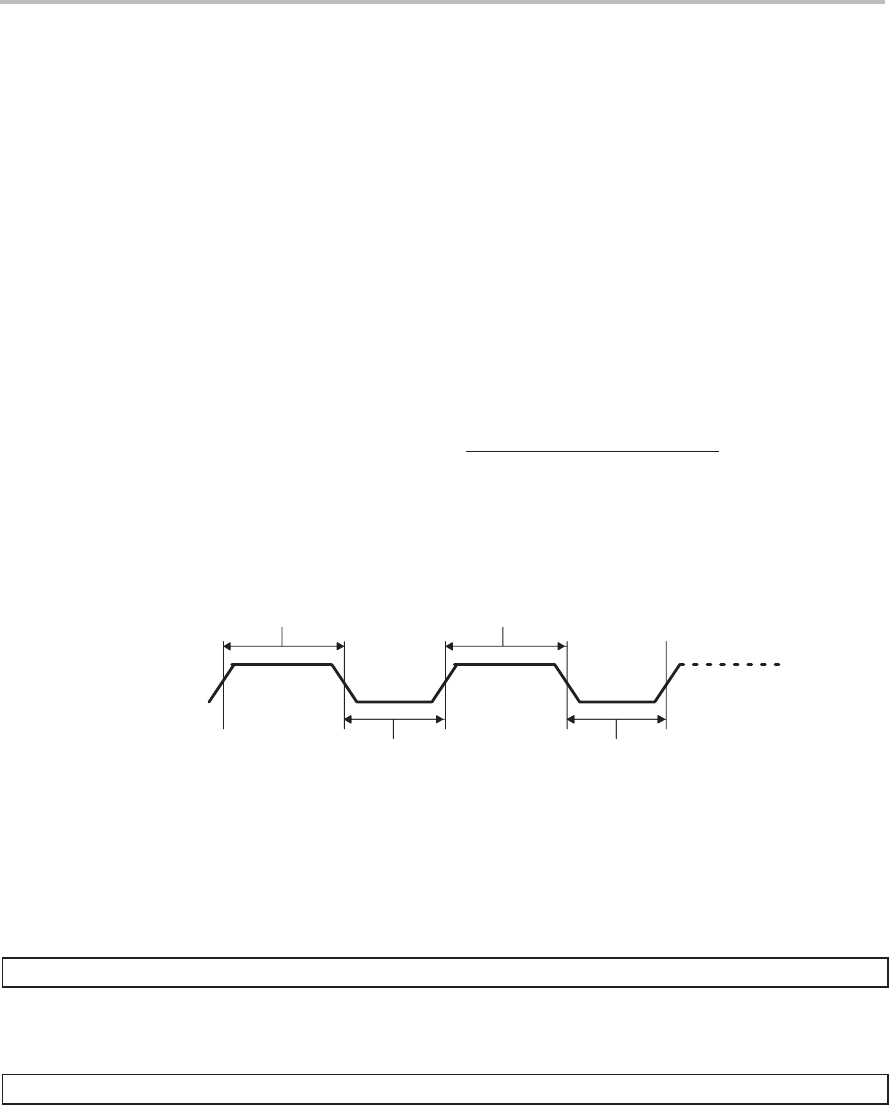
Inter-Integrated Circuit (I2C) Registers
B-177
TMS320C6000 CSL RegistersSPRU401I
B.9.4 I2C Clock Divider Registers (I2CCLKL and I2CCLKH)
When the I2C module is a master, the module clock is divided down for use
as the master clock on the SCL pin. As shown in Figure B−140, the shape of
the master clock depends on two divide-down values:
-ICCL in I2CCLKL (shown in Figure B−141 and described in Table B−147).
For each master clock cycle, ICCL determines the amount of time the
signal is low.
-ICCH in I2CCLKH (shown in Figure B−142 and described in
Table B−148). For each master clock cycle, ICCH determines the amount
of time the signal is high.
The frequency of the master clock can be calculated as:
master clock frequency +module clock frequency
(ICCL )6))(ICCH )6)
Figure B−140. Roles of the Clock Divide-Down Values (ICCL and ICCH)
SCL
High-time duration:
Tmod × (ICCH + 6)†High-time duration:
Tmod × (ICCH + 6)†
Low-time duration:
Tmod × (ICCL + 6)†Low-time duration:
Tmod × (ICCL + 6)†
†Tmod = module clock period = 1 / module clock frequency
Figure B−141. I2C Clock Low-Time Divider Register (I2CCLKL)
31 16
Reserved
R-0
15 0
ICCL
R/W-0
Legend: R = Read only; R/W = Read/write; -n = value after reset

Inter-Integrated Circuit (I2C) Registers
TMS320C6000 CSL Registers
B-178 SPRU401I
Table B−147. I2C Clock Low-Time Divider Register (I2CCLKL) Field Values
Bit Field symval†Value Description
31−16 Reserved − 0 These Reserved bit locations are always read as zeros. A
value written to this field has no effect.
15−0 ICCL OF(value) 0−FFFFh Clock low-time divide-down value of 1−65536. The period of
the module clock is multiplied by (ICCL + 6) to produce the
low-time duration of the master clock on the SCL pin.
†For CSL C macro implementation, use the notation I2C_I2CCLKL_ICCL_symval
Figure B−142. I2C Clock High-Time Divider Register (I2CCLKH)
31 16
Reserved
R-0
15 0
ICCH
R/W-0
Legend: R = Read only; R/W = Read/write; -n = value after reset
Table B−148. I2C Clock High-Time Divider Register (I2CCLKH) Field Values
Bit Field symval†Value Description
31−16 Reserved − 0 These Reserved bit locations are always read as zeros. A
value written to this field has no effect.
15−0 ICCH OF(value) 0−FFFFh Clock high-time divide-down value of 1−65536. The period of
the module clock is multiplied by (ICCH + 6) to produce the
high-time duration of the master clock on the SCL pin.
†For CSL C macro implementation, use the notation I2C_I2CCLKH_ICCH_symval

Inter-Integrated Circuit (I2C) Registers
B-179
TMS320C6000 CSL RegistersSPRU401I
B.9.5 I2C Data Count Register (I2CCNT)
The I2C data count register (I2CCNT) is used to indicate how many data words
to transfer when the I2C module is configured as a master-transmitter
(MST = 1 and TRX = 1 in I2CMDR) and the repeat mode is off (RM = 0 in
I2CMDR). In the repeat mode (RM = 1), I2CCNT is not used. The I2CCNT is
shown in Figure B−143 and described in Table B−149.
The value written to I2CCNT is copied to an internal data counter. The internal
data counter is decremented by 1 for each data word transferred (I2CCNT
remains unchanged). If a STOP condition is requested (STP = 1 in I2CMDR),
the I2C module terminates the transfer with a STOP condition when the
countdown is complete (that is, when the last data word has been transferred).
Figure B−143. I2C Data Count Register (I2CCNT)
31 16
Reserved
R-0
15 0
ICDC
R/W-0
Legend: R = Read only; R/W = Read/write; -n = value after reset
Table B−149. I2C Data Count Register (I2CCNT) Field Values
Bit Field symval†Value Description
31−16 Reserved − 0 These Reserved bit locations are always read as zeros. A
value written to this field has no effect.
15−0 ICDC OF(value)Data count value. ICDC indicates the number of data words
to transfer in the nonrepeat mode (RM = 0 in I2CMDR). The
value in I2CCNT is a don’t care when the RM bit in I2CMDR
is set to 1.
0 The start value loaded to the internal data counter is 65536.
1h−FFFFh The start value loaded to internal data counter is 1−65535.
†For CSL C macro implementation, use the notation I2C_I2CCNT_ICDC_symval

Inter-Integrated Circuit (I2C) Registers
TMS320C6000 CSL Registers
B-180 SPRU401I
B.9.6 I2C Data Receive Register (I2CDRR)
The I2C data receive register (I2CDRR) is used by the DSP to read the receive
data. The I2CDRR can receive a data value of up to 8 bits; data values with
fewer than 8 bits are right-aligned in the D bits and the remaining D bits are
undefined. The number of data bits is selected by the bit count bits (BC) of
I2CMDR. The I2C receive shift register (I2CRSR) shifts in the received data
from the SDA pin. Once data is complete, the I2C module copies the contents
of I2CRSR into I2CDRR. The CPU and the EDMA controller cannot access
I2CRSR. The I2CDRR is shown in Figure B−144 and described in
Table B−150.
Figure B−144. I2C Data Receive Register (I2CDRR)
31 16
Reserved
R-0
15 8 7 0
Reserved D
R-0 R/W-0
Legend: R = Read only; R/W = Read/write; -n = value after reset
Table B−150. I2C Data Receive Register (I2CDRR) Field Values
Bit Field symval†Value Description
31−8 Reserved −0These Reserved bit locations are always read as zeros. A
value written to this field has no effect.
7−0 D OF(value) 0−FFh Receive data.
†For CSL C macro implementation, use the notation I2C_I2CDRR_D_symval

Inter-Integrated Circuit (I2C) Registers
B-181
TMS320C6000 CSL RegistersSPRU401I
B.9.7 I2C Slave Address Register (I2CSAR)
The I2C slave address register (I2CSAR) contains a 7-bit or 10-bit slave
address. When the I2C module is not using the free data format (FDF = 0 in
I2CMDR), it uses this address to initiate data transfers with a slave or slaves.
When the address is nonzero, the address is for a particular slave. When the
address is 0, the address is a general call to all slaves. If the 7-bit addressing
mode is selected (XA = 0 in I2CMDR), only bits 6−0 of I2CSAR are used; bits
9−7 are ignored. The I2CSAR is shown in Figure B−145 and described in
Table B−151.
Figure B−145. I2C Slave Address Register (I2CSAR)
31 16
Reserved
R-0
15 10 9 0
Reserved A
R-0 R/W-3FFh
Legend: R = Read; W = Write; -n = Value after reset
Table B−151. I2C Slave Address Register (I2CSAR) Field Values
Bit Field symval†Value Description
31−10 Reserved − 0 These Reserved bit locations are always read as zeros. A
value written to this field has no effect.
9−0 A OF(value)In 7-bit addressing mode (XA = 0 in I2CMDR):
0−7Fh Bits 6−0 provide the 7-bit slave address that the I2C module
transmits when it is in the master-transmitter mode. Bits 9−7
are ignored.
In 10-bit addressing mode (XA = 1 in I2CMDR):
0−3FFh Bits 9−0 provide the 10-bit slave address that the I2C module
transmits when it is in the master-transmitter mode.
†For CSL C macro implementation, use the notation I2C_I2CSAR_A_symval

Inter-Integrated Circuit (I2C) Registers
TMS320C6000 CSL Registers
B-182 SPRU401I
B.9.8 I2C Data Transmit Register (I2CDXR)
The DSP writes transmit data to the I2C data transmit register (I2CDXR). The
I2CDXR can accept a data value of up to 8 bits. When writing a data value with
fewer than 8 bits, the DSP must make sure that the value is right-aligned in the
D bits. The number of data bits is selected by the bit count bits (BC) of I2CMDR.
Once data is written to I2CDXR, the I2C module copies the contents of
I2CDXR into the I2C transmit shift register (I2CXSR). The I2CXSR shifts out
the transmit data from the SDA pin. The CPU and the EDMA controller cannot
access I2CXSR. The I2CDXR is shown in Figure B−146 and described in
Table B−152.
Figure B−146. I2C Data Transmit Register (I2CDXR)
31 16
Reserved
R-0
15 8 7 0
Reserved D
R-0 R/W-0
Legend: R = Read only; R/W = Read/write; -n = value after reset
Table B−152. I2C Data Transmit Register (I2CDXR) Field Values
Bit Field symval†Value Description
31−8 Reserved −0These Reserved bit locations are always read as zeros. A
value written to this field has no effect.
7−0 D OF(value) 0−FFh Transmit data
†For CSL C macro implementation, use the notation I2C_I2CDXR_D_symval

Inter-Integrated Circuit (I2C) Registers
B-183
TMS320C6000 CSL RegistersSPRU401I
B.9.9 I2C Mode Register (I2CMDR)
The I2C mode register (I2CMDR) contains the control bits of the I2C module.
The I2CMDR is shown in Figure B−147 and described in Table B−153.
Figure B−147. I2C Mode Register (I2CMDR)
31 16
Reserved
R-0
15 14 13 12 11 10 9 8
NACKMOD FREE STT Reserved STP MST TRX XA
R/W-0 R/W-0 R/W-0 R-0 R/W-0 R/W-0 R/W-0 R/W-0
7 65432 0
RM DLB IRS STB FDF BC
R/W-0 R/W-0 R/W-0 R/W-0 R/W-0 R/W-0
Legend: R/W = Read/write; -n = value after reset
Table B−153. I2C Mode Register (I2CMDR) Field Values
Bit field†symval†Value Description
31−16 Reserved − 0 These Reserved bit locations are always read as zeros. A value
written to this field has no effect.
15 NACKMOD NACK mode bit is only applicable when the I2C module is
acting as a receiver.
ACK 0 In slave-receiver mode: The I2C module sends an
acknowledge (ACK) bit to the transmitter during the each
acknowledge cycle on the bus. The I2C module only sends a
no-acknowledge (NACK) bit if you set the NACKMOD bit.
In master-receiver mode: The I2C module sends an ACK
bit during each acknowledge cycle until the internal data
counter counts down to 0. At that point, the I2C module
sends a NACK bit to the transmitter. To have a NACK bit
sent earlier, you must set the NACKMOD bit.
NACK 1 In either slave-receiver or master-receiver mode: The I2C
module sends a NACK bit to the transmitter during the next
acknowledge cycle on the bus. Once the NACK bit has been
sent, NACKMOD is cleared.
To send a NACK bit in the next acknowledge cycle, you must
set NACKMOD before the rising edge of the last data bit.
†For CSL C macro implementation, use the notation I2C_I2CMDR_field_symval

Inter-Integrated Circuit (I2C) Registers
TMS320C6000 CSL Registers
B-184 SPRU401I
Table B−153. I2C Mode Register (I2CMDR) Field Values (Continued)
Bit DescriptionValuesymval†
field†
14 FREE This emulation mode bit is used to determine what the state
of the I2C module will be when a breakpoint is encountered
in the high-level language debugger.
BSTOP 0 When I2C module is master:
If SCL is low when the breakpoint occurs, the I2C module
stops immediately and keeps driving SCL low, whether the
I2C module is the transmitter or the receiver. If SCL is high,
the I2C module waits until SCL becomes low and then stops.
When I2C module is slave:
A breakpoint forces the I2C module to stop when the current
transmission/reception is complete.
RFREE 1 The I2C module runs free; that is, it continues to operate
when a breakpoint occurs.
13 STT START condition bit (only applicable when the I2C module is
a master). The RM, STT, and STP bits determine when the
I2C module starts and stops data transmissions (see
Table B−154). Note that the STT and STP bits can be used
to terminate the repeat mode.
NONE 0 In the master mode, STT is automatically cleared after the
START condition has been generated.
In the slave mode, if STT is 0, the I2C module does not
monitor the bus for commands from a master. As a result,
the I2C module performs no data transfers.
START 1 In the master mode, setting STT to 1 causes the I2C module
to generate a START condition on the I2C-bus.
In the slave mode, if STT is 1, the I2C module monitors the
bus and transmits/receives data in response to commands
from a master.
12 Reserved − 0 This Reserved bit location is always read as zero. A value
written to this field has no effect.
†For CSL C macro implementation, use the notation I2C_I2CMDR_field_symval

Inter-Integrated Circuit (I2C) Registers
B-185
TMS320C6000 CSL RegistersSPRU401I
Table B−153. I2C Mode Register (I2CMDR) Field Values (Continued)
Bit DescriptionValuesymval†
field†
11 STP STOP condition bit (only applicable when the I2C module is
a master). In the master mode, the RM, STT, and STP bits
determine when the I2C module starts and stops data
transmissions (see Table B−154). Note that the STT and
STP bits can be used to terminate the repeat mode.
NONE 0 STP is automatically cleared after the STOP condition has
been generated.
STOP 1 STP has been set by the DSP to generate a STOP condition
when the internal data counter of the I2C module counts
down to 0.
10 MST Master mode bit. MST determines whether the I2C module is
in the slave mode or the master mode. MST is automatically
changed from 1 to 0 when the I2C master generates a STOP
condition.
SLAVE 0 Slave mode. The I2C module is a slave and receives the
serial clock from the master.
MASTER 1 Master mode. The I2C module is a master and generates the
serial clock on the SCL pin.
9TRX Transmitter mode bit. When relevant, TRX selects whether
the I2C module is in the transmitter mode or the receiver
mode. Table B−155 summarizes when TRX is used and
when it is a don’t care.
RCV 0 Receiver mode. The I2C module is a receiver and receives
data on the SDA pin.
XMT 1 Transmitter mode. The I2C module is a transmitter and
transmits data on the SDA pin.
8XA Expanded address enable bit.
7BIT 0 7-bit addressing mode (normal address mode). The I2C
module transmits 7-bit slave addresses (from bits 6−0 of
I2CSAR), and its own slave address has 7 bits (bits 6−0 of
I2COAR).
10BIT 1 10-bit addressing mode (expanded address mode). The I2C
module transmits 10-bit slave addresses (from bits 9−0 of
I2CSAR), and its own slave address has 10 bits (bits 9−0 of
I2COAR).
†For CSL C macro implementation, use the notation I2C_I2CMDR_field_symval

Inter-Integrated Circuit (I2C) Registers
TMS320C6000 CSL Registers
B-186 SPRU401I
Table B−153. I2C Mode Register (I2CMDR) Field Values (Continued)
Bit DescriptionValuesymval†
field†
7 RM Repeat mode bit (only applicable when the I2C module is a
master-transmitter). The RM, STT, and STP bits determine
when the I2C module starts and stops data transmissions
(see Table B−154).
NONE 0 Nonrepeat mode. The value in the data count register
(I2CCNT) determines how many data words are
received/transmitted by the I2C module.
REPEAD 1 Repeat mode. Data words are continuously
received/transmitted by the I2C module until the STP bit is
manually set to 1, regardless of the value in I2CCNT.
6DLB Digital loopback mode bit. This bit disables or enables the
digital loopback mode of the I2C module. The effects of this
bit are shown in Figure B−148. Note that DLB in the free
data format mode (DLB = 1 and FDF = 1) is not supported.
NONE 0 Digital loopback mode is disabled.
LOOPBACK 1 Digital loopback mode is enabled. In this mode, the MST bit
must be set to 1 and data transmitted out of I2CDXR is
received in I2CDRR after n DSP cycles by an internal path,
where:
n = ((I2C input clock frequency/module clock
frequency) 8)
The transmit clock is also the receive clock. The address
transmitted on the SDA pin is the address in I2COAR.
5IRS I2C module reset bit.
RST 0 The I2C module is in reset/disabled. When this bit is cleared
to 0, all status bits (in I2CSTR) are set to their default values.
NRST 1 The I2C module is enabled.
†For CSL C macro implementation, use the notation I2C_I2CMDR_field_symval

Inter-Integrated Circuit (I2C) Registers
B-187
TMS320C6000 CSL RegistersSPRU401I
Table B−153. I2C Mode Register (I2CMDR) Field Values (Continued)
Bit DescriptionValuesymval†
field†
4 STB START byte mode bit. This bit is only applicable when the
I2C module is a master. As described in version 2.1 of the
Philips I2C-bus specification, the START byte can be used to
help a slave that needs extra time to detect a START
condition. When the I2C module is a slave, the I2C module
ignores a START byte from a master, regardless of the value
of the STB bit.
NONE 0 The I2C module is not in the START byte mode.
SET 1 The I2C module is in the START byte mode. When you set
the START condition bit (STT), the I2C module begins the
transfer with more than just a START condition. Specifically,
it generates:
1) A START condition
2) A START byte (0000 0001b)
3) A dummy acknowledge clock pulse
4) A repeated START condition
The I2C module sends the slave address that is in I2CSAR.
3FDF Free data format mode bit. Note that DLB in the free data
format mode (DLB = 1 and FDF = 1) is not supported.
NONE 0 Free data format mode is disabled. Transfers use the
7-/10-bit addressing format selected by the XA bit.
SET 1 Free data format mode is enabled. Transfers have the free
data (no address) format.
†For CSL C macro implementation, use the notation I2C_I2CMDR_field_symval

Inter-Integrated Circuit (I2C) Registers
TMS320C6000 CSL Registers
B-188 SPRU401I
Table B−153. I2C Mode Register (I2CMDR) Field Values (Continued)
Bit DescriptionValuesymval†
field†
2−0 BC OF(value)Bit count bits. BC defines the number of bits (1 to 8) in the
next data word that is to be received or transmitted by the
I2C module. The number of bits selected with BC must
match the data size of the other device. Notice that when
BC = 000b, a data word has 8 bits.
If the bit count is less than 8, receive data is right aligned in
the D bits of I2CDRR and the remaining D bits are
undefined. Also, transmit data written to I2CDXR must be
right aligned.
BIT8FDF 0 8 bits per data word
BIT1FDF 1h 1 bit per data word
BIT2FDF 2h 2 bits per data word
BIT3FDF 3h 3 bits per data word
BIT4FDF 4h 4 bits per data word
BIT5FDF 5h 5 bits per data word
BIT6FDF 6h 6 bits per data word
BIT7FDF 7h 7 bits per data word
†For CSL C macro implementation, use the notation I2C_I2CMDR_field_symval

Inter-Integrated Circuit (I2C) Registers
B-189
TMS320C6000 CSL RegistersSPRU401I
Table B−154. Master-Transmitter/Receiver Bus Activity Defined by RM, STT, and STP Bits
I2CMDR Bit
RM STT STP Bus Activity†Description
00 0 None No activity
0 0 1 P STOP condition
0 1 0 S-A-D..(n)..D START condition, slave address, n data words
(n = value in I2CCNT)
0 1 1 S-A-D..(n)..D-P START condition, slave address, n data words, STOP
condition (n = value in I2CCNT)
1 0 0 None No activity
1 0 1 P STOP condition
1 1 0 S-A-D-D-D….. Repeat mode transfer:
START condition, slave address, continuous data
transfers until STOP condition or next START condition
1 1 1 None Reserved bit combination (No activity)
†A = Address; D = Data word; P = STOP condition; S = START condition
Table B−155. How the MST and FDF Bits Affect the Role of TRX Bit
I2CMDR Bit
MST FDF I2C Module State Function of TRX Bit
00In slave mode but not free
data format mode TRX is a don’t care. Depending on the command from
the master, the I2C module responds as a receiver or
a transmitter.
0 1 In slave mode and free data
format mode The free data format mode requires that the transmitter
and receiver be fixed. TRX identifies the role of the
I2C module:
TRX = 0: The I2C module is a receiver.
TRX = 1: The I2C module is a transmitter.
1 X In master mode; free data
format mode on or off TRX = 0: The I2C module is a receiver.
TRX = 1: The I2C module is a transmitter.
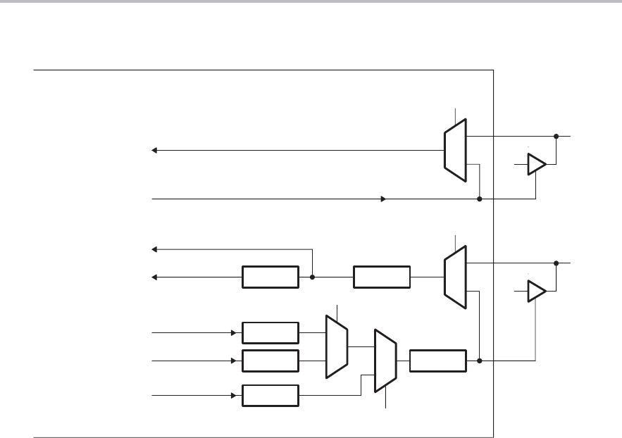
Inter-Integrated Circuit (I2C) Registers
TMS320C6000 CSL Registers
B-190 SPRU401I
Figure B−148. Block Diagram Showing the Effects of the Digital Loopback Mode (DLB) Bit
I2CDRR I2CRSR 0
1
I2CSAR
I2COAR
0
1
I2CDXR
I2CXSR
0
10
0
DLB
SCL_IN
SCL_OUT
Address/data
To internal I2C logic
From internal I2C logic
To internal I2C logic
To CPU or EDMA
From CPU or EDMA
From CPU or EDMA
From CPU or EDMA
SCL
SDA
I2C module
DLB
DLB

Inter-Integrated Circuit (I2C) Registers
B-191
TMS320C6000 CSL RegistersSPRU401I
B.9.10 I2C Interrupt Source Register (I2CISRC)
The I2C interrupt source register (I2CISRC) is used by the CPU to determine
which event generated the I2C interrupt. The I2CISRC is shown in
Figure B−149 and described in Table B−156.
Figure B−149. I2C Interrupt Source Register (I2CISRC)
31 16
Reserved
R-0
15 32 0
Reserved INTCODE
R-0 R-0
Legend: R = Read only; R/W = Read/write; -n = value after reset
Table B−156. I2C Interrupt Source Register (I2CISRC) Field Values
Bit Field symval†Value Description
31−3 Reserved − 0 These Reserved bit locations are always read as zeros. Always
write 0 to this field.
2−0 INTCODE Interrupt code bits. The binary code in INTCODE indicates
which event generated an I2C interrupt.
NONE 0 None
AL 1h Arbitration is lost.
NACK 2h No-acknowledgement condition is detected.
RAR 3h Registers are ready to be accessed.
RDR 4h Receive data is ready.
XDR 5h Transmit data is ready.
− 6h−7h Reserved
†For CSL C macro implementation, use the notation I2C_I2CISR_INTCODE_symval

Inter-Integrated Circuit (I2C) Registers
TMS320C6000 CSL Registers
B-192 SPRU401I
B.9.11 I2C Extended Mode Register (I2CEMDR) (C6410/C6413)
The I2C extended mode register (I2CEMDR) is used to indicate which
condition generates a transmit data ready interrupt. The I2CEMDR is shown
in Figure B−150 and described in Table B−157.
Figure B−150. I2C Extended Mode Register (I2CEMDR)
31 10
Reserved XRDYM
R-0 R/W-1
Legend: R = Read only; R/W = Read/write; -n = value after reset
Table B−157. I2C Extended Mode Register (I2CEMDR) Field Values
Bit Field symval†Value Description
31−1 Reserved − 0 These reserved bit locations are always read as 0. A value written
to this field has no effect.
0 XRDYM Transmit data ready interrupt mode bit. Determines which condition
generates a transmit data ready interrupt.
The XRDYM bit only has an effect when the I2C module is
operating as a slave-transmitter.
MSTACK 0 The transmit data ready interrupt is generated when the master
requests more data by sending an acknowledge signal after the
transmission of the last data.
DXRCPY 1 The transmit data ready interrupt is generated when the data in
I2CDXR is copied to I2CXSR.
†For CSL C macro implementation, use the notation I2C_I2CEMDR_XRDYM_symval

Inter-Integrated Circuit (I2C) Registers
B-193
TMS320C6000 CSL RegistersSPRU401I
B.9.12 I2C Prescaler Register (I2CPSC)
The I2C prescaler register (I2CPSC) is used for dividing down the I2C input
clock to obtain the desired module clock for the operation of the I2C module.
The I2CPSC is shown in Figure B−151 and described in Table B−158.
The IPSC bits must be initialized while the I2C module is in reset (IRS = 0 in
I2CMDR). The prescaled frequency takes effect only when the IRS bit is
changed to 1. Changing the IPSC value while IRS = 1 has no effect.
Figure B−151. I2C Prescaler Register (I2CPSC)
31 16
Reserved
R-0
15 8 7 0
Reserved IPSC
R-0 R/W-0
Legend: R = Read; W = Write; -n = Value after reset
Table B−158. I2C Prescaler Register (I2CPSC) Field Values
Bit Field symval†Value Description
31−8 Reserved − 0 These Reserved bit locations are always read as zeros. A
value written to this field has no effect.
7−0 IPSC OF(value) 0−FFh I2C prescaler divide-down value. IPSC determines how much
the CPU clock is divided to create the module clock of the I2C
module:
module clock frequency = I2C input clock frequency/(IPSC + 1)
Note: IPSC must be initialized while the I2C module is in reset
(IRS = 0 in I2CMDR).
†For CSL C macro implementation, use the notation I2C_I2CPSC_IPSC_symval

Inter-Integrated Circuit (I2C) Registers
TMS320C6000 CSL Registers
B-194 SPRU401I
B.9.13 I2C Peripheral Identification Registers (I2CPID1 and I2CPID2)
The peripheral identification registers (PID) contain identification data for the
I2C module. I2CPID1 is shown in Figure B−152 and described in Table B−159.
I2CPID2 is shown in Figure B−153 and described in Table B−160.
Figure B−152. I2C Peripheral Identification Register 1 (I2CPID1)
31 16
Reserved
R-0
15 8 7 0
CLASS REV
R-0000 0001 R-x†
Legend: R = Read only; -x = value after reset
†See the device-specific datasheet for the default value of this field.
Table B−159. I2C Peripheral Identification Register 1 (I2CPID1) Field Values
Bit Field Value Description
31−16 Reserved 0 These Reserved bit locations are always read as zeros. A value written to this
field has no effect.
15−8 CLASS Identifies class of peripheral.
1 Serial port
7−0 REV Identifies revision of peripheral.
xSee the device-specific datasheet for the value.

Inter-Integrated Circuit (I2C) Registers
B-195
TMS320C6000 CSL RegistersSPRU401I
Figure B−153. I2C Peripheral Identification Register 2 (I2CPID2)
31 16
Reserved
R-0
15 8 7 0
Reserved TYPE
R-0 R-0000 0101
Legend: R = Read only; -x = value after reset
Table B−160. I2C Peripheral Identification Register 2 (I2CPID2) Field Values
Bit Field Value Description
31−8 Reserved 0 These Reserved bit locations are always read as zeros. A value written to this
field has no effect.
7−0 TYPE Identifies type of peripheral.
05h I2C

Inter-Integrated Circuit (I2C) Registers
TMS320C6000 CSL Registers
B-196 SPRU401I
B.9.14 I2C Pin Function Register (I2CPFUNC) (C6410/C6413)
The I2C pin function register (I2CPFUNC) selects the SDA and SCL pins as
GPIO. The I2CPFUNC is shown in Figure B−154 and described in
Table B−161.
Figure B−154. I2C Pin Function Register (I2CPFUNC)
31 10
Reserved GPMODE
R-0 R/W-0
Legend: R = Read only; R/W = Read/write; -n = value after reset
Table B−161. I2C Pin Function Register (I2CPFUNC) Field Values
Bit Field symval†Value Description
31−1 Reserved −0These reserved bit locations have an indeterminate value when
read. A value written to this field has no effect.
0 GPMODE GPIO mode enable bit for SCL and SDA pins. The I2C module
must be placed in reset (IRS = 0 in I2CMDR) before enabling the
GPIO function of the SCL and SDA pins.
DISABLED 0 GPIO mode is disabled; SCL and SDA pins have I2C functionality.
ENABLED 1 GPIO mode is enabled; SCL and SDA pins have GPIO functionality.
†For CSL C macro implementation, use the notation I2C_I2CPFUNC_GPMODE_symval

Inter-Integrated Circuit (I2C) Registers
B-197
TMS320C6000 CSL RegistersSPRU401I
B.9.15 I2C Pin Direction Register (I2CPDIR) (C6410/C6413)
The I2C pin direction register (I2CPDIR) controls the direction of the SDA and
SCL pins. The I2CPDIR is shown in Figure B−155 and described in
Table B−162. If a bit is set to 1, the pin functions as an output; if a bit is cleared
to 0, the pin functions as an input.
Figure B−155. I2C Pin Direction Register (I2CPDIR)
31 21 0
Reserved SDADIR SCLDIR
R-0 R/W-0 R/W-0
Legend: R = Read only; R/W = Read/write; -n = value after reset
Table B−162. I2C Pin Direction Register (I2CPDIR) Field Values
Bit field†symval†Value Description
31−2 Reserved −0These reserved bit locations have an indeterminate value when
read. A value written to this field has no effect.
1 SDADIR SDA direction bit. Controls the direction of the SDA pin when
configured as GPIO.
INPUT 0 SDA pin functions as input.
OUTPUT 1 SDA pin functions as output.
0SCLDIR SCL direction bit. Controls the direction of the SCL pin when
configured as GPIO.
INPUT 0 SCL pin functions as input.
OUTPUT 1 SCL pin functions as output.
†For CSL C macro implementation, use the notation I2C_I2CPDIR_field_symval

Inter-Integrated Circuit (I2C) Registers
TMS320C6000 CSL Registers
B-198 SPRU401I
B.9.16 I2C Pin Data Input Register (I2CPDIN) (C6410/C6413)
The I2C pin data input register (I2CPDIN) reflects the state of the SDA and
SCL pins. The I2CPDIN is shown in Figure B−156 and described in
Table B−163. When read, I2CPDIN returns the value from the pin’s input buffer
regardless of the state of the corresponding I2CPFUNC or I2CPDIR bits.
Figure B−156. I2C Pin Data Input Register (I2CPDIN)
31 21 0
Reserved SDAIN SCLIN
R-0 R/W-pin R/W-pin
Legend: R = Read only; R/W = Read/write; -n = value after reset;-pin = external pin value after reset
Table B−163. I2C Pin Data Input Register (I2CPDIN) Field Values
Bit field†symval†Value Description
31−2 Reserved −0These reserved bit locations have an indeterminate value when
read. A value written to this field has no effect.
1 SDAIN Indicates the logic level present on the SDA pin. SDAIN is set
regardless of the GPMODE setting. A value written to this bit has
no effect.
LOW 0 A logic low is present at the SDA pin.
HIGH 1 A logic high is present at the SDA pin.
0SCLIN Indicates the logic level present on the SCL pin. SCLIN is set
regardless of the GPMODE setting. A value written to this bit has
no effect.
LOW 0 A logic low is present at the SCL pin.
HIGH 1 A logic high is present at the SCL pin.
†For CSL C macro implementation, use the notation I2C_I2CPDIN_field_symval

Inter-Integrated Circuit (I2C) Registers
B-199
TMS320C6000 CSL RegistersSPRU401I
B.9.17 I2C Pin Data Output Register (I2CPDOUT) (C6410/C6413)
The I2C pin data output register (I2CPDOUT) determines the value driven on
the SDA and SCL pins, if the pin is configured as an output. The I2CPDOUT
is shown in Figure B−157 and described in Table B−164. Writes do not affect
pins not configured as GPIO outputs.
The I2CPDOUT bits are set or cleared by writing to this register directly. A read
of I2CPDOUT returns the value of the register not the value at the pin (that
might be configured as an input). An alternative way to set bits in I2CPDOUT
is to write a 1 to the corresponding bit of I2CPDSET. An alternative way to clear
bits in I2CPDOUT is to write a 1 to the corresponding bit of I2CPDCLR.
I2CPDOUT has these aliases:
-I2CPDSET — writing a 1 to a bit in I2CPDSET sets the corresponding bit
in I2CPDOUT to 1; writing a 0 has no effect and keeps the bits in
I2CPDOUT unchanged.
-I2CPDCLR — writing a 1 to a bit in I2CPDCLR clears the corresponding
bit in I2CPDOUT to 0; writing a 0 has no effect and keeps the bits in
I2CPDOUT unchanged.
Figure B−157. I2C Pin Data Output Register (I2CPDOUT)
31 21 0
Reserved SDAOUT SCLOUT
R-0 R/W-0 R/W-0
Legend: R = Read only; R/W = Read/write; -n = value after reset

Inter-Integrated Circuit (I2C) Registers
TMS320C6000 CSL Registers
B-200 SPRU401I
Table B−164. I2C Pin Data Output Register (I2CPDOUT) Field Values
Bit field†symval†Value Description
31−2 Reserved −0These reserved bit locations have an indeterminate value when
read. A value written to this field has no effect.
1 SDAOUT Controls the value driven on the SDA pin when the pin is
configured as an output (GPIO mode must be enabled by setting
GPMODE = 1).
When reading data, returns the value in the SDAOUT bit, does not
return the level on the pin. When writing data, writes to the
SDAOUT bit.
LOW 0 SDA pin is driven to a logic low.
HIGH 1 SDA pin is driven to a logic high.
0SCLOUT Controls the value driven on the SCL pin when the pin is
configured as an output (GPIO mode must be enabled by setting
GPMODE = 1).
When reading data, returns the value in the SCLOUT bit, does not
return the level on the pin. When writing data, writes to the
SCLOUT bit.
LOW 0 SCL pin is driven to a logic low.
HIGH 1 SCL pin is driven to a logic high.
†For CSL C macro implementation, use the notation I2C_I2CPDOUT_field_symval

Inter-Integrated Circuit (I2C) Registers
B-201
TMS320C6000 CSL RegistersSPRU401I
B.9.18 I2C Pin Data Set Register (I2CPDSET) (C6410/C6413)
The I2C pin data set register (I2CPDSET) is shown in Figure B−158 and
described in Table B−165. I2CPDSET is an alias of the I2C pin data output reg-
ister (I2CPDOUT) for writes only and provides an alternate means of driving
GPIO outputs high. Writing a 1 to a bit of I2CPDSET sets the corresponding
bit in I2CPDOUT. Writing a 0 has no effect. Register reads are indeterminate.
Figure B−158. I2C Pin Data Set Register (I2CPDSET)
31 21 0
Reserved SDAOUT SCLOUT
R-0 R/W-0 R/W-0
Legend: R = Read only; R/W = Read/write; -n = value after reset
Table B−165. I2C Pin Data Set Register (I2CPDSET) Field Values
Bit field†symval†Value Description
31−2 Reserved −0These reserved bit locations have an indeterminate value when
read. A value written to this field has no effect.
1 SDAOUT Sets the value of the SDAOUT bit in I2CPDOUT. A write of 0 to
this bit has no effect. This bit location has an indeterminate value
when read.
UNCHGN 0 No effect.
SET 1 Sets the SDAOUT bit in I2CPDOUT to 1.
0SCLOUT Sets the value of the SCLOUT bit in I2CPDOUT. A write of 0 to
this bit has no effect. This bit location has an indeterminate value
when read.
UNCHGN 0 No effect.
SET 1 Sets the SCLOUT bit in I2CPDOUT to 1.
†For CSL C macro implementation, use the notation I2C_I2CPDSET_field_symval

Inter-Integrated Circuit (I2C) Registers
TMS320C6000 CSL Registers
B-202 SPRU401I
B.9.19 I2C Pin Data Clear Register (I2CPDCLR) (C6410/C6413)
The I2C pin data clear register (I2CPDCLR) is shown in Figure B−159 and
described in Table B−166. I2CPDCLR is an alias of the I2C pin data output reg-
ister (I2CPDOUT) for writes only and provides an alternate means of driving
GPIO outputs low. Writing a 1 to a bit of I2CPDCLR clears the corresponding
bit in I2CPDOUT. Writing a 0 has no effect. Register reads are indeterminate.
Figure B−159. I2C Pin Data Clear Register (I2CPDCLR)
31 21 0
Reserved SDAOUT SCLOUT
R-0 R/W-0 R/W-0
Legend: R = Read only; R/W = Read/write; -n = value after reset
Table B−166. I2C Pin Data Clear Register (I2CPDCLR) Field Values
Bit field†symval†Value Description
31−2 Reserved −0These reserved bit locations have an indeterminate value when
read. A value written to this field has no effect.
1 SDAOUT Clears the value of the SDAOUT bit in I2CPDOUT. A write of 0 to
this bit has no effect. This bit location has an indeterminate value
when read.
UNCHGN 0 No effect.
CLR 1 Clears the SDAOUT bit in I2CPDOUT to 0.
0SCLOUT Clears the value of the SCLOUT bit in I2CPDOUT. A write of 0 to
this bit has no effect. This bit location has an indeterminate value
when read.
UNCHGN 0 No effect.
CLR 1 Clears the SCLOUT bit in I2CPDOUT to 0.
†For CSL C macro implementation, use the notation I2C_I2CPDCLR_field_symval

Interrupt Request (IRQ) Registers
B-203
TMS320C6000 CSL RegistersSPRU401I
B.10 Interrupt Request (IRQ) Registers
Table B−167 shows the interrupt selector registers. The interrupt multiplexer
registers determine the mapping between the interrupt sources and the CPU
interrupts 4 through 15 (INT4−INT15). The external interrupt polarity register
sets the polarity of external interrupts. See the device-specific datasheet for
the memory address of these registers.
Table B−167. IRQ Registers
Acronym Register Name Section
MUXH Interrupt multiplexer high register B.10.1
MUXL Interrupt multiplexer low register B.10.2
EXTPOL External interrupt polarity register B.10.3
B.10.1 Interrupt Multiplexer High Register (MUXH)
The interrupt multiplexer high register (MUXH) maps the interrupt sources to
particular interrupts. The MUXH is shown in Figure B−160 and described in
Table B−168. The INTSEL10−INTSEL15 fields correspond to the CPU
interrupts INT10−INT15. By setting the INTSEL bits to the value of the desired
interrupt selection number, you can map any interrupt source to any CPU
interrupt. The default values of the INTSEL bits are shown in Figure B−160.
For the default mapping of interrupt sources to CPU interrupts, see the
device-specific datasheet.
Figure B−160. Interrupt Multiplexer High Register (MUXH)
31 30 26 25 21 20 16
Reserved INTSEL15 INTSEL14 INTSEL13
R-0 R/W-0 0010 R/W-0 0001 R/W-0 0000
15 14 10 9 5 4 0
Reserved INTSEL12 INTSEL11 INTSEL10
R-0 R/W-0 1011 R/W-0 1010 R/W-0 0011
Legend: R/W-x = Read/Write-Reset value

Interrupt Request (IRQ) Registers
TMS320C6000 CSL Registers
B-204 SPRU401I
Table B−168. Interrupt Multiplexer High Register (MUXH) Field Values
Bit field†symval†Value Description
31 Reserved − 0 Reserved. The reserved bit location is always read as 0. A
value written to this field has no effect.
30−26 INTSEL15 OF(value) 0−1Fh Interrupt selector 15 bits. This value maps interrupt 15 to any
CPU interrupt.
25−21 INTSEL14 OF(value) 0−1Fh Interrupt selector 14 bits. This value maps interrupt 14 to any
CPU interrupt.
20−16 INTSEL13 OF(value) 0−1Fh Interrupt selector 13 bits. This value maps interrupt 13 to any
CPU interrupt.
15 Reserved − 0 Reserved. The reserved bit location is always read as 0. A
value written to this field has no effect.
14−10 INTSEL12 OF(value) 0−1Fh Interrupt selector 12 bits. This value maps interrupt 12 to any
CPU interrupt.
9−5 INTSEL11 OF(value) 0−1Fh Interrupt selector 11 bits. This value maps interrupt 11 to any
CPU interrupt.
4−0 INTSEL10 OF(value) 0−1Fh Interrupt selector 10 bits. This value maps interrupt 10 to any
CPU interrupt.
†For CSL implementation, use the notation IRQ_MUXH_INTSELn_symval
B.10.2 Interrupt Multiplexer Low Register (MUXL)
The interrupt multiplexer low register (MUXL) maps the interrupt sources to
particular interrupts. The MUXL is shown in Figure B−161 and described in
Table B−169. The INTSEL4−INTSEL9 fields correspond to the CPU interrupts
INT4−INT9. By setting the INTSEL bits to the value of the desired interrupt
selection number, you can map any interrupt source to any CPU interrupt. The
default values of the INTSEL bits are shown in Figure B−161. For the default
mapping of interrupt sources to CPU interrupts, see the device-specific
datasheet.

Interrupt Request (IRQ) Registers
B-205
TMS320C6000 CSL RegistersSPRU401I
Figure B−161. Interrupt Multiplexer Low Register (MUXL)
31 30 26 25 21 20 16
Reserved INTSEL9 INTSEL8 INTSEL7
R-0 R/W-0 1001 R/W-0 1000 R/W-0 0111
15 14 10 9 5 4 0
Reserved INTSEL6 INTSEL5 INTSEL4
R-0 R/W-0 0110 R/W-0 0101 R/W-0 0100
Legend: R/W-x = Read/Write-Reset value
Table B−169. Interrupt Multiplexer Low Register (MUXL) Field Values
Bit field†symval†Value Description
31 Reserved − 0 Reserved. The reserved bit location is always read as 0. A
value written to this field has no effect.
30−26 INTSEL9 OF(value) 0−1Fh Interrupt selector 9 bits. This value maps interrupt 9 to any
CPU interrupt.
25−21 INTSEL8 OF(value) 0−1Fh Interrupt selector 8 bits. This value maps interrupt 8 to any
CPU interrupt.
20−16 INTSEL7 OF(value) 0−1Fh Interrupt selector 7 bits. This value maps interrupt 7 to any
CPU interrupt.
15 Reserved − 0 Reserved. The reserved bit location is always read as 0. A
value written to this field has no effect.
14−10 INTSEL6 OF(value) 0−1Fh Interrupt selector 6 bits. This value maps interrupt 6 to any
CPU interrupt.
9−5 INTSEL5 OF(value) 0−1Fh Interrupt selector 5 bits. This value maps interrupt 5 to any
CPU interrupt.
4−0 INTSEL4 OF(value) 0−1Fh Interrupt selector 4 bits. This value maps interrupt 4 to any
CPU interrupt.
†For CSL implementation, use the notation IRQ_MUXL_INTSELn_symval

Interrupt Request (IRQ) Registers
TMS320C6000 CSL Registers
B-206 SPRU401I
B.10.3 External Interrupt Polarity Register (EXTPOL)
The external interrupt polarity register (EXTPOL) allows you to change the
polarity of the four external interrupts (EXT_INT4−EXT_INT7). The EXTPOL
is shown in Figure B−162 and described in Table B−170. When the XIP bit is
its default value of 0, a low-to-high transition on an interrupt source is recog-
nized as an interrupt. By setting the corresponding XIP bit to 1, you can invert
the external interrupt source and effectively have the CPU detect high-to-low
transitions of the external interrupt. Changing an XIP bit value creates transi-
tions on the related CPU interrupt (INT4−INT7) that the external interrupt
(EXT_INT) is selected to drive. For example, if XIP4 is changed from 0 to 1 and
EXT_INT4 is low or if XIP4 is changed from 1 to 0 and EXT_INT4 is high, the
CPU interrupt that is mapped to EXT_INT4 becomes set. EXTPOL only affects
interrupts to the CPU and has no effect on DMA events.
Figure B−162. External Interrupt Polarity Register (EXTPOL)
31 8
Reserved
R-0
7 43210
Reserved XIP7 XIP6 XIP5 XIP4
R-0 R/W-0 R/W-0 R/W-0 R/W-0
Legend: R/W-x = Read/Write-Reset value
Table B−170. External Interrupt Polarity Register (EXTPOL) Field Values
Bit Field symval†Value Description
31−4 Reserved − 0 Reserved. The reserved bit location is always read as 0. A value
written to this field has no effect.
3−0 XIP OF(value) 0−Fh External interrupt polarity bits. A 4-bit unsigned value used to
change the polarity of the four external interrupts (EXT_INT4 to
EXT_INT7).
0A low-to-high transition on an interrupt source is recognized as an
interrupt.
1A high-to-low transition on an interrupt source is recognized as an
interrupt.
†For CSL implementation, use the notation IRQ_EXTPOL_XIP_symval

Multichannel Audio Serial Port (McASP) Registers
B-207
TMS320C6000 CSL RegistersSPRU401I
B.11 Multichannel Audio Serial Port (McASP) Registers
Table B−171. McASP Registers Accessed Through Configuration Bus
Acronym Register Name Address
Offset (hex) Section
PID Peripheral identification register 0000 B.11.1
PWRDEMU Power down and emulation management register 0004 B.11.2
PFUNC Pin function register 0010 B.11.3
PDIR Pin direction register 0014 B.11.4
PDOUT Pin data output register 0018 B.11.5
PDIN Read returns: Pin data input register 001C B.11.6
PDSET Writes affect: Pin data set register (alternate write address: PDOUT) 001C B.11.7
PDCLR Pin data clear register (alternate write address: PDOUT) 0020 B.11.8
GBLCTL Global control register 0044 B.11.9
AMUTE Audio mute control register 0048 B.11.10
DLBCTL Digital loopback control register 004C B.11.11
DITCTL DIT mode control register 0050 B.11.12
RGBLCTL Receiver global control register. Alias of GBLCTL, only receive
bits are affected − allows receiver to be reset independently from
transmitter
0060 B.11.13
RMASK Receive format unit bit mask register 0064 B.11.14
RFMT Receive bit stream format register 0068 B.11.15
AFSRCTL Receive frame sync control register 006C B.11.16
ACLKRCTL Receive clock control register 0070 B.11.17
AHCLKRCTL Receive high-frequency clock control register 0074 B.11.18
RTDM Receive TDM time slot 0−31 register 0078 B.11.19
RINTCTL Receiver interrupt control register 007C B.11.20
RSTAT Receiver status register 0080 B.11.21
RSLOT Current receive TDM time slot register 0084 B.11.22
RCLKCHK Receive clock check control register 0088 B.11.23
†Available only on DA6x DSP.
‡CFG BUS only if XBUSEL = 1.
§CFG BUS only if RBUSEL = 1.

Multichannel Audio Serial Port (McASP) Registers
TMS320C6000 CSL Registers
B-208 SPRU401I
Table B−171. McASP Registers Accessed Through Configuration Bus (Continued)
Acronym Section
Address
Offset (hex)
Register Name
REVCTL†Receiver DMA event control register 008C B.11.24
XGBLCTL Transmitter global control register. Alias of GBLCTL, only transmit
bits are affected− allows transmitter to be reset independently
from receiver
00A0 B.11.25
XMASK Transmit format unit bit mask register 00A4 B.11.26
XFMT Transmit bit stream format register 00A8 B.11.27
AFSXCTL Transmit frame sync control register 00AC B.11.28
ACLKXCTL Transmit clock control register 00B0 B.11.29
AHCLKXCTL Transmit high-frequency clock control register 00B4 B.11.30
XTDM Transmit TDM time slot 0−31 register 00B8 B.11.31
XINTCTL Transmitter interrupt control register 00BC B.11.32
XSTAT Transmitter status register 00C0 B.11.33
XSLOT Current transmit TDM time slot register 00C4 B.11.34
XCLKCHK Transmit clock check control register 00C8 B.11.35
XEVCTL†Transmitter DMA event control register 00CC B.11.36
DITCSRA0 Left (even TDM time slot) channel status register (DIT mode) 0 0100 B.11.38
DITCSRA1 Left (even TDM time slot) channel status register (DIT mode) 1 0104 B.11.38
DITCSRA2 Left (even TDM time slot) channel status register (DIT mode) 2 0108 B.11.38
DITCSRA3 Left (even TDM time slot) channel status register (DIT mode) 3 010C B.11.38
DITCSRA4 Left (even TDM time slot) channel status register (DIT mode) 4 0110 B.11.38
DITCSRA5 Left (even TDM time slot) channel status register (DIT mode) 5 0114 B.11.38
DITCSRB0 Right (odd TDM time slot) channel status register (DIT mode) 0 0118 B.11.39
DITCSRB1 Right (odd TDM time slot) channel status register (DIT mode) 1 011C B.11.39
DITCSRB2 Right (odd TDM time slot) channel status register (DIT mode) 2 0120 B.11.39
DITCSRB3 Right (odd TDM time slot) channel status register (DIT mode) 3 0124 B.11.39
DITCSRB4 Right (odd TDM time slot) channel status register (DIT mode) 4 0128 B.11.39
†Available only on DA6x DSP.
‡CFG BUS only if XBUSEL = 1.
§CFG BUS only if RBUSEL = 1.

Multichannel Audio Serial Port (McASP) Registers
B-209
TMS320C6000 CSL RegistersSPRU401I
Table B−171. McASP Registers Accessed Through Configuration Bus (Continued)
Acronym Section
Address
Offset (hex)
Register Name
DITCSRB5 Right (odd TDM time slot) channel status register (DIT mode) 5 012C B.11.39
DITUDRA0 Left (even TDM time slot) channel user data register (DIT mode) 0 0130 B.11.40
DITUDRA1 Left (even TDM time slot) channel user data register (DIT mode) 1 0134 B.11.40
DITUDRA2 Left (even TDM time slot) channel user data register (DIT mode) 2 0138 B.11.40
DITUDRA3 Left (even TDM time slot) channel user data register (DIT mode) 3 013C B.11.40
DITUDRA4 Left (even TDM time slot) channel user data register (DIT mode) 4 0140 B.11.40
DITUDRA5 Left (even TDM time slot) channel user data register (DIT mode) 5 0144 B.11.40
DITUDRB0 Right (odd TDM time slot) channel user data register (DIT mode) 0 0148 B.11.41
DITUDRB1 Right (odd TDM time slot) channel user data register (DIT mode) 1 014C B.11.41
DITUDRB2 Right (odd TDM time slot) channel user data register (DIT mode) 2 0150 B.11.41
DITUDRB3 Right (odd TDM time slot) channel user data register (DIT mode) 3 0154 B.11.41
DITUDRB4 Right (odd TDM time slot) channel user data register (DIT mode) 4 0158 B.11.41
DITUDRB5 Right (odd TDM time slot) channel user data register (DIT mode) 5 015C B.11.41
SRCTL0 Serializer control register 0 0180 B.11.37
SRCTL1 Serializer control register 1 0184 B.11.37
SRCTL2 Serializer control register 2 0188 B.11.37
SRCTL3 Serializer control register 3 018C B.11.37
SRCTL4 Serializer control register 4 0190 B.11.37
SRCTL5 Serializer control register 5 0194 B.11.37
SRCTL6 Serializer control register 6 0198 B.11.37
SRCTL7 Serializer control register 7 019C B.11.37
SRCTL8†Serializer control register 8 01A0 B.11.37
SRCTL9†Serializer control register 9 01A4 B.11.37
SRCTL10†Serializer control register 10 01A8 B.11.37
SRCTL11†Serializer control register 11 01AC B.11.37
†Available only on DA6x DSP.
‡CFG BUS only if XBUSEL = 1.
§CFG BUS only if RBUSEL = 1.

Multichannel Audio Serial Port (McASP) Registers
TMS320C6000 CSL Registers
B-210 SPRU401I
Table B−171. McASP Registers Accessed Through Configuration Bus (Continued)
Acronym Section
Address
Offset (hex)
Register Name
SRCTL12†Serializer control register 12 01B0 B.11.37
SRCTL13†Serializer control register 13 01B4 B.11.37
SRCTL14†Serializer control register 14 01B8 B.11.37
SRCTL15†Serializer control register 15 01BC B.11.37
XBUF0‡Transmit buffer register for serializer 0 0200 B.11.42
XBUF1‡Transmit buffer register for serializer 1 0204 B.11.42
XBUF2‡Transmit buffer register for serializer 2 0208 B.11.42
XBUF3‡Transmit buffer register for serializer 3 020C B.11.42
XBUF4‡Transmit buffer register for serializer 4 0210 B.11.42
XBUF5‡Transmit buffer register for serializer 5 0214 B.11.42
XBUF6‡Transmit buffer register for serializer 6 0218 B.11.42
XBUF7‡Transmit buffer register for serializer 7 021C B.11.42
XBUF8†‡ Transmit buffer register for serializer 8 0220 B.11.42
XBUF9†‡ Transmit buffer register for serializer 9 0224 B.11.42
XBUF10†‡ Transmit buffer register for serializer 10 0228 B.11.42
XBUF11†‡ Transmit buffer register for serializer 11 022C B.11.42
XBUF12†‡ Transmit buffer register for serializer 12 0230 B.11.42
XBUF13†‡ Transmit buffer register for serializer 13 0234 B.11.42
XBUF14†‡ Transmit buffer register for serializer 14 0238 B.11.42
XBUF15†‡ Transmit buffer register for serializer 15 023C B.11.42
RBUF0§Receive buffer register for serializer 0 0280 B.11.43
RBUF1§Receive buffer register for serializer 1 0284 B.11.43
RBUF2§Receive buffer register for serializer 2 0288 B.11.43
RBUF3§Receive buffer register for serializer 3 028C B.11.43
RBUF4§Receive buffer register for serializer 4 0290 B.11.43
†Available only on DA6x DSP.
‡CFG BUS only if XBUSEL = 1.
§CFG BUS only if RBUSEL = 1.

Multichannel Audio Serial Port (McASP) Registers
B-211
TMS320C6000 CSL RegistersSPRU401I
Table B−171. McASP Registers Accessed Through Configuration Bus (Continued)
Acronym Section
Address
Offset (hex)
Register Name
RBUF5§Receive buffer register for serializer 5 0294 B.11.43
RBUF6§Receive buffer register for serializer 6 0298 B.11.43
RBUF7§Receive buffer register for serializer 7 029C B.11.43
RBUF8†§ Receive buffer register for serializer 8 02A0 B.11.43
RBUF9†§ Receive buffer register for serializer 9 02A4 B.11.43
RBUF10†§ Receive buffer register for serializer 10 02A8 B.11.43
RBUF11†§ Receive buffer register for serializer 11 02AC B.11.43
RBUF12†§ Receive buffer register for serializer 12 02B0 B.11.43
RBUF13†§ Receive buffer register for serializer 13 02B4 B.11.43
RBUF14†§ Receive buffer register for serializer 14 02B8 B.11.43
RBUF15†§ Receive buffer register for serializer 15 02BC B.11.43
†Available only on DA6x DSP.
‡CFG BUS only if XBUSEL = 1.
§CFG BUS only if RBUSEL = 1.
Table B−172. McASP Registers Accessed Through Data Port
Hex Address Register
Name Register Description
Read Accesses RBUF Receive buffer data port address. Cycles through receive serializers,
skipping over transmit serializers and inactive serializers. Starts at the
lowest serializer at the beginning of each time slot. DAT BUS only if
XBUSEL = 0.
Write Accesses XBUF Transmit buffer data port address. Cycles through transmit serializers,
skipping over receive and inactive serializers. Starts at the lowest
serializer at the beginning of each time slot. DAT BUS only if RBUSEL = 0.

Multichannel Audio Serial Port (McASP) Registers
TMS320C6000 CSL Registers
B-212 SPRU401I
B.11.1 Peripheral Identification Register (PID)
The peripheral identification register (PID) is shown in Figure B−163 and
described in Table B−173.
Figure B−163. Peripheral Identification Register (PID)
31 24 23 16
Reserved‡TYPE
R-0 R-0001 0000
15 8 7 0
CLASS REV
R-0000 0001 R-x†
Legend: R = Read only; -n = value after reset
†See the device-specific datasheet for the default value of this field.
‡If writing to this field, always write the default value for future device compatibility.
Table B−173. Peripheral Identification Register (PID) Field Values
Bit field†symval†Value Description
31−24 Reserved − 0 Reserved. The reserved bit location always returns the default
value. A value written to this field has no effect. If writing to this
field, always write the default value for future device compatibility.
23−16 TYPE Identifies type of peripheral.
MCASP 10h McASP
15−8 CLASS Identifies class of peripheral.
SERPORT 1 Serial port
7−0 REV Identifies revision of peripheral.
− x See the device-specific datasheet for the value.
†For CSL implementation, use the notation MCASP_PID_field_symval

Multichannel Audio Serial Port (McASP) Registers
B-213
TMS320C6000 CSL RegistersSPRU401I
B.11.2 Power Down and Emulation Management Register (PWRDEMU)
The power down and emulation management register (PWRDEMU) is shown
in Figure B−164 and described in Table B−174.
Figure B−164. Power Down and Emulation Management Register (PWRDEMU)
31 10
Reserved†FREE
R-0 R/W-0
Legend: R = Read only; R/W = Read/Write; -n = value after reset
†If writing to this field, always write the default value for future device compatibility.
Table B−174. Power Down and Emulation Management Register (PWRDEMU) Field Values
Bit Field symval†Value Description
31−1 Reserved − 0 Reserved. The reserved bit location always returns the default
value. A value written to this field has no effect. If writing to this
field, always write the default value for future device compatibility.
0 FREE Free-running mode enable bit. This bit determines the state of the
serial port clock during emulation halt.
OFF 0 Reserved.
ON 1 Free-running mode is enabled. Peripheral ignores the emulation
suspend signal and continues to function as normal. During
emulation suspend, EDMA requests continue to be generated and
are serviced by the EDMA. Error conditions are flagged as usual.
†For CSL implementation, use the notation MCASP_PWRDEMU_FREE_symval

Multichannel Audio Serial Port (McASP) Registers
TMS320C6000 CSL Registers
B-214 SPRU401I
B.11.3 Pin Function Register (PFUNC)
The pin function register (PFUNC) specifies the function of AXR[n], ACLKX,
AHCLKX, AFSX, ACLKR, AHCLKR, and AFSR pins as either a McASP pin or
a general-purpose input/output (GPIO) pin. The PFUNC is shown in
Figure B−165 and described in Table B−175.
Writing to Reserved Bits
Writing a value other than 0 to reserved bits in this register may
cause improper device operation. This includes bits that are not
implemented on a particular DSP.
Figure B−165. Pin Function Register (PFUNC)
31 30 29 28 27 26 25 24
AFSR AHCLKR ACLKR AFSX AHCLKX ACLKX AMUTE Reserved†
R/W-0 R/W-0 R/W-0 R/W-0 R/W-0 R/W-0 R/W-0 R-0
23 16
Reserved†
R-0
15 14 13 12 11 10 9 8
AXR15‡AXR14‡AXR13‡AXR12‡AXR11‡AXR10‡AXR9‡AXR8‡
R/W-0 R/W-0 R/W-0 R/W-0 R/W-0 R/W-0 R/W-0 R/W-0
76543210
AXR7 AXR6 AXR5 AXR4 AXR3 AXR2 AXR1 AXR0
R/W-0 R/W-0 R/W-0 R/W-0 R/W-0 R/W-0 R/W-0 R/W-0
Legend: R = Read only; R/W = Read/Write; -n = value after reset
†If writing to this field, always write the default value for future device compatibility.
‡On DA6x DSP only; reserved on C6713 DSP.

Multichannel Audio Serial Port (McASP) Registers
B-215
TMS320C6000 CSL RegistersSPRU401I
Table B−175. Pin Function Register (PFUNC) Field Values
Bit field†symval†Value Description
31
30
29
28
27
26
25
AFSR
AHCLKR
ACLKR
AFSX
AHCLKX
ACLKX
AMUTE
MCASP
GPIO
0
1
Determines if specified pin functions as McASP or GPIO.
Pin functions as McASP pin.
Pin functions as GPIO pin.
24−16 Reserved − 0 Reserved. The reserved bit location always returns the default
value. A value written to this field has no effect. If writing to this
field, always write the default value for future device
compatibility.
15−8 AXR[15−8]‡Determines if AXR[n] pin functions as McASP or GPIO.
MCASP 0 Pin functions as McASP pin.
GPIO 1 Pin functions as GPIO pin.
7−0 AXR[7−0] Determines if AXR[n] pin functions as McASP or GPIO.
MCASP 0 Pin functions as McASP pin.
GPIO 1 Pin functions as GPIO pin.
†For CSL implementation, use the notation MCASP_PFUNC_field_symval
‡On DA6x DSP only; reserved on C6713 DSP.

Multichannel Audio Serial Port (McASP) Registers
TMS320C6000 CSL Registers
B-216 SPRU401I
B.11.4 Pin Direction Register (PDIR)
The pin direction register (PDIR) specifies the direction of AXR[n], ACLKX,
AHCLKX, AFSX, ACLKR, AHCLKR, and AFSR pins as either an input or an
output pin. The PDIR is shown in Figure B−166 and described in Table B−176.
Regardless of the pin function register (PFUNC) setting, each PDIR bit must
be set to 1 for the specified pin to be enabled as an output and each PDIR bit
must be cleared to 0 for the specified pin to be an input.
For example, if the McASP is configured to use an internally-generated bit
clock and the clock is to be driven out to the system, the PFUNC bit must be
cleared to 0 (McASP function) and the PDIR bit must be set to 1 (an output).
When AXR[n] is configured to transmit, the PFUNC bit must be cleared to 0
(McASP function) and the PDIR bit must be set to 1 (an output). Similarly, when
AXR[n] is configured to receive, the PFUNC bit must be cleared to 0 (McASP
function) and the PDIR bit must be cleared to 0 (an input).
Writing to Reserved Bits
Writing a value other than 0 to reserved bits in this register may
cause improper device operation. This includes bits that are not
implemented on a particular DSP.
Figure B−166. Pin Direction Register (PDIR)
31 30 29 28 27 26 25 24
AFSR AHCLKR ACLKR AFSX AHCLKX ACLKX AMUTE Reserved†
R/W-0 R/W-0 R/W-0 R/W-0 R/W-0 R/W-0 R/W-0 R-0
23 16
Reserved†
R-0
15 14 13 12 11 10 9 8
AXR15‡AXR14‡AXR13‡AXR12‡AXR11‡AXR10‡AXR9‡AXR8‡
R/W-0 R/W-0 R/W-0 R/W-0 R/W-0 R/W-0 R/W-0 R/W-0
76543210
AXR7 AXR6 AXR5 AXR4 AXR3 AXR2 AXR1 AXR0
R/W-0 R/W-0 R/W-0 R/W-0 R/W-0 R/W-0 R/W-0 R/W-0
Legend: R = Read only; R/W = Read/Write; -n = value after reset
†If writing to this field, always write the default value for future device compatibility.
‡On DA6x DSP only; reserved on C6713 DSP.

Multichannel Audio Serial Port (McASP) Registers
B-217
TMS320C6000 CSL RegistersSPRU401I
Table B−176. Pin Direction Register (PDIR) Field Values
Bit field†symval†Value Description
31
30
29
28
27
26
25
AFSR
AHCLKR
ACLKR
AFSX
AHCLKX
ACLKX
AMUTE
IN
OUT
0
1
Determines if specified pin functions as an input or output.
Pin functions as input.
Pin functions as output.
24−16 Reserved − 0 Reserved. The reserved bit location always returns the default
value. A value written to this field has no effect. If writing to this
field, always write the default value for future device
compatibility.
15−8 AXR[15−8]‡Determines if AXR[n] pin functions as an input or output.
IN 0 Pin functions as input.
OUT 1 Pin functions as output.
7−0 AXR[7−0] Determines if AXR[n] pin functions as an input or output.
IN 0 Pin functions as input.
OUT 1 Pin functions as output.
†For CSL implementation, use the notation MCASP_PDIR_field_symval
‡On DA6x DSP only; reserved on C6713 DSP.

Multichannel Audio Serial Port (McASP) Registers
TMS320C6000 CSL Registers
B-218 SPRU401I
B.11.5 Pin Data Output Register (PDOUT)
The pin data output register (PDOUT) holds a value for data out at all times,
and may be read back at all times. The value held by PDOUT is not affected
by writing to PDIR and PFUNC. However, the data value in PDOUT is driven
out onto the McASP pin only if the corresponding bit in PFUNC is set to 1 (GPIO
function) and the corresponding bit in PDIR is set to 1 (output). The PDOUT
is shown in Figure B−167 and described in Table B−177.
PDOUT has these aliases or alternate addresses:
-PDSET — when written to at this address, writing a 1 to a bit in PDSET
sets the corresponding bit in PDOUT to 1; writing a 0 has no effect and
keeps the bits in PDOUT unchanged.
-PDCLR — when written to at this address, writing a 1 to a bit in PDCLR
clears the corresponding bit in PDOUT to 0; writing a 0 has no effect and
keeps the bits in PDOUT unchanged.
There is only one set of data out bits, PDOUT[31−0]. The other registers,
PDSET and PDCLR, are just different addresses for the same control bits, with
different behaviors during writes.
Writing to Reserved Bits
Writing a value other than 0 to reserved bits in this register may
cause improper device operation. This includes bits that are not
implemented on a particular DSP.

Multichannel Audio Serial Port (McASP) Registers
B-219
TMS320C6000 CSL RegistersSPRU401I
Figure B−167. Pin Data Output Register (PDOUT)
31 30 29 28 27 26 25 24
AFSR AHCLKR ACLKR AFSX AHCLKX ACLKX AMUTE Reserved†
R/W-0 R/W-0 R/W-0 R/W-0 R/W-0 R/W-0 R/W-0 R-0
23 16
Reserved†
R-0
15 14 13 12 11 10 9 8
AXR15‡AXR14‡AXR13‡AXR12‡AXR11‡AXR10‡AXR9‡AXR8‡
R/W-0 R/W-0 R/W-0 R/W-0 R/W-0 R/W-0 R/W-0 R/W-0
76543210
AXR7 AXR6 AXR5 AXR4 AXR3 AXR2 AXR1 AXR0
R/W-0 R/W-0 R/W-0 R/W-0 R/W-0 R/W-0 R/W-0 R/W-0
Legend: R = Read only; R/W = Read/Write; -n = value after reset
†If writing to this field, always write the default value for future device compatibility.
‡On DA6x DSP only; reserved on C6713 DSP.

Multichannel Audio Serial Port (McASP) Registers
TMS320C6000 CSL Registers
B-220 SPRU401I
Table B−177. Pin Data Output Register (PDOUT) Field Values
Bit field†symval†Value Description
31
30
29
28
27
26
25
AFSR
AHCLKR
ACLKR
AFSX
AHCLKX
ACLKX
AMUTE
LOW
HIGH
0
1
Determines drive on specified output pin when the corresponding
PFUNC[n] and PDIR[n] bits are set to 1.
When reading data, returns the corresponding bit value in
PDOUT[n], does not return input from I/O pin. When writing data,
writes to the corresponding PDOUT[n] bit.
Pin drives low.
Pin drives high.
24−16 Reserved − 0 Reserved. The reserved bit location always returns the default
value. A value written to this field has no effect. If writing to this
field, always write the default value for future device
compatibility.
15−8 AXR[15−8]‡Determines drive on AXR[n] pin when PFUNC[n] and PDIR[n]
bits are set to 1.
When reading data, returns the bit value in PDOUT[n], does not
return input from I/O pin. When writing data, writes to PDOUT[n]
bit.
LOW 0 Pin drives low.
HIGH 1 Pin drives high.
7−0 AXR[7−0] Determines drive on AXR[n] pin when PFUNC[n] and PDIR[n]
bits are set to 1.
When reading data, returns the bit value in PDOUT[n], does not
return input from I/O pin. When writing data, writes to PDOUT[n]
bit.
LOW 0 Pin drives low.
HIGH 1 Pin drives high.
†For CSL implementation, use the notation MCASP_PDOUT_field_symval
‡On DA6x DSP only; reserved on C6713 DSP.

Multichannel Audio Serial Port (McASP) Registers
B-221
TMS320C6000 CSL RegistersSPRU401I
B.11.6 Pin Data Input Register (PDIN)
The pin data input register (PDIN) holds the I/O pin state of each of the McASP
pins. PDIN allows the actual value of the pin to be read, regardless of the state
of PFUNC and PDIR. The value after reset for registers 1 through 15 and 24
through 31 depends on how the pins are being driven. The PDIN is shown in
Figure B−168 and described in Table B−178.
Writing to Reserved Bits
Writing a value other than 0 to reserved bits in this register may
cause improper device operation. This includes bits that are not
implemented on a particular DSP.
Figure B−168. Pin Data Input Register (PDIN)
31 30 29 28 27 26 25 24
AFSR AHCLKR ACLKR AFSX AHCLKX ACLKX AMUTE Reserved†
R/W-0 R/W-0 R/W-0 R/W-0 R/W-0 R/W-0 R/W-0 R-0
23 16
Reserved†
R-0
15 14 13 12 11 10 9 8
AXR15‡AXR14‡AXR13‡AXR12‡AXR11‡AXR10‡AXR9‡AXR8‡
R/W-0 R/W-0 R/W-0 R/W-0 R/W-0 R/W-0 R/W-0 R/W-0
76543210
AXR7 AXR6 AXR5 AXR4 AXR3 AXR2 AXR1 AXR0
R/W-0 R/W-0 R/W-0 R/W-0 R/W-0 R/W-0 R/W-0 R/W-0
Legend: R = Read only; R/W = Read/Write; -n = value after reset
†If writing to this field, always write the default value for future device compatibility.
‡On DA6x DSP only; reserved on C6713 DSP.

Multichannel Audio Serial Port (McASP) Registers
TMS320C6000 CSL Registers
B-222 SPRU401I
Table B−178. Pin Data Input Register (PDIN) Field Values
Bit field†symval†Value Description
31
30
29
28
27
26
25
AFSR
AHCLKR
ACLKR
AFSX
AHCLKX
ACLKX
AMUTE
SET
0
1
Provides logic level of the specified pin.
Pin is logic low.
Pin is logic high.
24−16 Reserved − 0 Reserved. The reserved bit location always returns the default
value. A value written to this field has no effect. If writing to this
field, always write the default value for future device
compatibility.
15−8 AXR[15−8]‡Provides logic level of AXR[n] pin.
0 Pin is logic low.
SET 1 Pin is logic high.
7−0 AXR[7−0] Provides logic level of AXR[n] pin.
0 Pin is logic low.
SET 1 Pin is logic high.
†For CSL implementation, use the notation MCASP_PDIN_field_symval
‡On DA6x DSP only; reserved on C6713 DSP.

Multichannel Audio Serial Port (McASP) Registers
B-223
TMS320C6000 CSL RegistersSPRU401I
B.11.7 Pin Data Set Register (PDSET)
The pin data set register (PDSET) is an alias of the pin data output register
(PDOUT) for writes only. Writing a 1 to the PDSET bit sets the corresponding
bit in PDOUT and, if PFUNC = 1 (GPIO function) and PDIR = 1 (output), drives
a logic high on the pin. PDSET is useful for a multitasking system because it
allows you to set to a logic high only the desired pin(s) within a system without
affecting other I/O pins controlled by the same McASP. The PDSET is shown
in Figure B−169 and described in Table B−179.
Writing to Reserved Bits
Writing a value other than 0 to reserved bits in this register may
cause improper device operation. This includes bits that are not
implemented on a particular DSP.
Figure B−169. Pin Data Set Register (PDSET)
31 30 29 28 27 26 25 24
AFSR AHCLKR ACLKR AFSX AHCLKX ACLKX AMUTE Reserved†
R/W-0 R/W-0 R/W-0 R/W-0 R/W-0 R/W-0 R/W-0 R-0
23 16
Reserved†
R-0
15 14 13 12 11 10 9 8
AXR15†AXR14†AXR13†AXR12†AXR11†AXR10†AXR9†AXR8†
R/W-0 R/W-0 R/W-0 R/W-0 R/W-0 R/W-0 R/W-0 R/W-0
76543210
AXR7 AXR6 AXR5 AXR4 AXR3 AXR2 AXR1 AXR0
R/W-0 R/W-0 R/W-0 R/W-0 R/W-0 R/W-0 R/W-0 R/W-0
Legend: R = Read only; R/W = Read/Write; -n = value after reset
†If writing to this field, always write the default value for future device compatibility.
†On DA6x DSP only; reserved on C6713 DSP.

Multichannel Audio Serial Port (McASP) Registers
TMS320C6000 CSL Registers
B-224 SPRU401I
Table B−179. Pin Data Set Register (PDSET) Field Values
Bit field†symval†Value Description
31
30
29
28
27
26
25
AFSR
AHCLKR
ACLKR
AFSX
AHCLKX
ACLKX
AMUTE
SET
0
1
Allows the corresponding PDOUT[n] bit to be set to a logic high
without affecting other I/O pins controlled by the same port.
No effect.
Sets corresponding PDOUT[n] bit to 1.
24−16 Reserved − 0 Reserved. The reserved bit location always returns the default
value. A value written to this field has no effect. If writing to this
field, always write the default value for future device
compatibility.
15−8 AXR[15−8]‡Allows PDOUT[n] bit to be set to a logic high without affecting
other I/O pins controlled by the same port.
0 No effect.
SET 1 Sets PDOUT[n] bit to 1.
7−0 AXR[7−0] Allows PDOUT[n] bit to be set to a logic high without affecting
other I/O pins controlled by the same port.
0 No effect.
SET 1 Sets PDOUT[n] bit to 1.
†For CSL implementation, use the notation MCASP_PDSET_field_symval
‡On DA6x DSP only; reserved on C6713 DSP.

Multichannel Audio Serial Port (McASP) Registers
B-225
TMS320C6000 CSL RegistersSPRU401I
B.11.8 Pin Data Clear Register (PDCLR)
The pin data clear register (PDCLR) is an alias of the pin data output register
(PDOUT) for writes only. Writing a 1 to the PDCLR bit clears the corresponding
bit in PDOUT and, if PFUNC = 1 (GPIO function) and PDIR = 1 (output), drives
a logic low on the pin. PDCLR is useful for a multitasking system because it
allows you to clear to a logic low only the desired pin(s) within a system without
affecting other I/O pins controlled by the same McASP. The PDCLR is shown
in Figure B−170 and described in Table B−180.
Writing to Reserved Bits
Writing a value other than 0 to reserved bits in this register may
cause improper device operation. This includes bits that are not
implemented on a particular DSP.
Figure B−170. PDCLR Pin Data Clear Register (PDCLR)
31 30 29 28 27 26 25 24
AFSR AHCLKR ACLKR AFSX AHCLKX ACLKX AMUTE Reserved†
R/W-0 R/W-0 R/W-0 R/W-0 R/W-0 R/W-0 R/W-0 R-0
23 16
Reserved†
R-0
15 14 13 12 11 10 9 8
AXR15‡AXR14‡AXR13‡AXR12‡AXR11‡AXR10‡AXR9‡AXR8‡
R/W-0 R/W-0 R/W-0 R/W-0 R/W-0 R/W-0 R/W-0 R/W-0
76543210
AXR7 AXR6 AXR5 AXR4 AXR3 AXR2 AXR1 AXR0
R/W-0 R/W-0 R/W-0 R/W-0 R/W-0 R/W-0 R/W-0 R/W-0
Legend: R = Read only; R/W = Read/Write; -n = value after reset
†If writing to this field, always write the default value for future device compatibility.
‡On DA6x DSP only; reserved on C6713 DSP.

Multichannel Audio Serial Port (McASP) Registers
TMS320C6000 CSL Registers
B-226 SPRU401I
Table B−180. Pin Data Clear Register (PDCLR) Field Values
Bit field†symval†Value Description
31
30
29
28
27
26
25
AFSR
AHCLKR
ACLKR
AFSX
AHCLKX
ACLKX
AMUTE
CLR
0
1
Allows the corresponding PDOUT[n] bit to be cleared to a logic
low without affecting other I/O pins controlled by the same port.
No effect.
Clears corresponding PDOUT[n] bit to 0.
24−16 Reserved − 0 Reserved. The reserved bit location always returns the default
value. A value written to this field has no effect. If writing to this
field, always write the default value for future device
compatibility.
15−8 AXR[15−8]‡Allows PDOUT[n] bit to be cleared to a logic low without affecting
other I/O pins controlled by the same port.
0 No effect.
CLR 1 Clears PDOUT[n] bit to 0.
7−0 AXR[7−0] Allows PDOUT[n] bit to be cleared to a logic low without affecting
other I/O pins controlled by the same port.
0 No effect.
CLR 1 Clears PDOUT[n] bit to 0.
†For CSL implementation, use the notation MCASP_PDCLR_field_symval
‡On DA6x DSP only; reserved on C6713 DSP.

Multichannel Audio Serial Port (McASP) Registers
B-227
TMS320C6000 CSL RegistersSPRU401I
B.11.9 Global Control Register (GBLCTL)
The global control register (GBLCTL) provides initialization of the transmit and
receive sections. The GBLCTL is shown in Figure B−171 and described in
Table B−181.
The bit fields in GBLCTL are synchronized and latched by the corresponding
clocks (ACLKX for bits 12−8 and ACLKR for bits 4−0). Before GBLCTL is
programmed, you must ensure that serial clocks are running. If the
corresponding external serial clocks, ACLKX and ACLKR, are not yet running,
you should select the internal serial clock source in AHCLKXCTL,
AHCLKRCTL, ACLKXCTL, and ACLKRCTL before GBLCTL is programmed.
Also, after programming any bits in GBLCTL you should not proceed until you
have read back from GBLCTL and verified that the bits are latched in GBLCTL.
Figure B−171. Global Control Register (GBLCTL)
31 16
Reserved†
R-0
15 13 12 11 10 9 8
Reserved†XFRST XSMRST XSRCLR XHCLKRST XCLKRST
R-0 R/W-0 R/W-0 R/W-0 R/W-0 R/W-0
7543210
Reserved†RFRST RSMRST RSRCLR RHCLKRST RCLKRST
R-0 R/W-0 R/W-0 R/W-0 R/W-0 R/W-0
Legend: R = Read only; R/W = Read/Write; -n = value after reset
†If writing to this field, always write the default value for future device compatibility.

Multichannel Audio Serial Port (McASP) Registers
TMS320C6000 CSL Registers
B-228 SPRU401I
Table B−181. Global Control Register (GBLCTL) Field Values
Bit field†symval†Value Description
31−13 Reserved − 0 Reserved. The reserved bit location always returns the default
value. A value written to this field has no effect. If writing to this
field, always write the default value for future device
compatibility.
12 XFRST Transmit frame sync generator reset enable bit.
RESET 0 Transmit frame sync generator is reset.
ACTIVE 1 Transmit frame sync generator is active. When released from
reset, the transmit frame sync generator begins counting serial
clocks and generating frame sync as programmed.
11 XSMRST Transmit state machine reset enable bit.
RESET 0 Transmit state machine is held in reset. AXR[n] pin state:
If PFUNC[n] = 0 and PDIR[n] = 1; then the serializer drives the
AXR[n] pin to the state specified for inactive time slot (as
determined by DISMOD bits in SRCTL).
ACTIVE 1 Transmit state machine is released from reset. When released
from reset, the transmit state machine immediately transfers
data from XRBUF[n] to XRSR[n]. The transmit state machine
sets the underrun flag (XUNDRN) in XSTAT, if XRBUF[n] have
not been preloaded with data before reset is released. The
transmit state machine also immediately begins detecting frame
sync and is ready to transmit.
Transmit TDM time slot begins at slot 0 after reset is released.
10 XSRCLR Transmit serializer clear enable bit. By clearing then setting this
bit, the transmit buffer is flushed to an empty state (XDATA = 1).
If XSMRST = 1, XSRCLR = 1, XDATA = 1, and XBUF is not
loaded with new data before the start of the next active time
slot, an underrun will occur.
CLEAR 0 Transmit serializers are cleared.
ACTIVE 1 Transmit serializers are active. When the transmit serializers
are first taken out of reset (XSRCLR changes from 0 to 1), the
transmit data ready bit (XDATA) in XSTAT is set to indicate
XBUF is ready to be written.
†For CSL implementation, use the notation MCASP_GBLCTL_field_symval

Multichannel Audio Serial Port (McASP) Registers
B-229
TMS320C6000 CSL RegistersSPRU401I
Table B−181. Global Control Register (GBLCTL) Field Values (Continued)
Bit DescriptionValuesymval†
field†
9 XHCLKRST Transmit high-frequency clock divider reset enable bit.
RESET 0 Transmit high-frequency clock divider is held in reset.
ACTIVE 1 Transmit high-frequency clock divider is running.
8XCLKRST Transmit clock divider reset enable bit.
RESET 0 Transmit clock divider is held in reset. When the clock divider is
in reset, it passes through a divide-by-1 of its input.
ACTIVE 1 Transmit clock divider is running.
7−5 Reserved − 0 Reserved. The reserved bit location always returns the default
value. A value written to this field has no effect. If writing to this
field, always write the default value for future device
compatibility.
4 RFRST Receive frame sync generator reset enable bit.
RESET 0 Receive frame sync generator is reset.
ACTIVE 1 Receive frame sync generator is active. When released from
reset, the receive frame sync generator begins counting serial
clocks and generating frame sync as programmed.
3RSMRST Receive state machine reset enable bit.
RESET 0 Receive state machine is held in reset.
ACTIVE 1 Receive state machine is released from reset. When released
from reset, the receive state machine immediately begins
detecting frame sync and is ready to receive.
Receive TDM time slot begins at slot 0 after reset is released.
2RSRCLR Receive serializer clear enable bit. By clearing then setting this
bit, the receive buffer is flushed.
CLEAR 0 Receive serializers are cleared.
ACTIVE 1 Receive serializers are active.
1RHCLKRST Receive high-frequency clock divider reset enable bit.
RESET 0 Receive high-frequency clock divider is held in reset.
ACTIVE 1 Receive high-frequency clock divider is running.
†For CSL implementation, use the notation MCASP_GBLCTL_field_symval
Multichannel Audio Serial Port (McASP) Registers
TMS320C6000 CSL Registers
B-230 SPRU401I
Table B−181. Global Control Register (GBLCTL) Field Values (Continued)
Bit DescriptionValuesymval†
field†
0 RCLKRST Receive clock divider reset enable bit.
RESET 0 Receive clock divider is held in reset. When the clock divider is
in reset, it passes through a divide-by-1 of its input.
ACTIVE 1 Receive clock divider is running.
†For CSL implementation, use the notation MCASP_GBLCTL_field_symval
B.11.10 Audio Mute Control Register (AMUTE)
The audio mute control register (AMUTE) controls the McASP audio mute
(AMUTE) output pin. The value after reset for register 4 depends on how the
pins are being driven. The AMUTE is shown in Figure B−172 and described
in Table B−182.
Figure B−172. Audio Mute Control Register (AMUTE)
31 16
Reserved†
R-0
15 13 12 11 10 9 8
Reserved†XDMAERR RDMAERR XCKFAIL RCKFAIL XSYNCERR
R-0 R/W-0 R/W-0 R/W-0 R/W-0 R/W-0
7654321 0
RSYNCERR XUNDRN ROVRN INSTAT INEN INPOL MUTEN
R/W-0 R/W-0 R/W-0 R-0 R/W-0 R/W-0 R/W-0
Legend: R = Read only; R/W = Read/Write; -n = value after reset
†If writing to this field, always write the default value for future device compatibility.

Multichannel Audio Serial Port (McASP) Registers
B-231
TMS320C6000 CSL RegistersSPRU401I
Table B−182. Audio Mute Control Register (AMUTE) Field Values
Bit field†symval†Value Description
31−13 Reserved − 0 Reserved. The reserved bit location always returns the default
value. A value written to this field has no effect. If writing to this
field, always write the default value for future device
compatibility.
12 XDMAERR If transmit EDMA error (XDMAERR), drive AMUTE active enable bit.
DISABLE 0 Drive is disabled. Detection of transmit EDMA error is ignored by
AMUTE.
ENABLE 1 Drive is enabled (active). Upon detection of transmit EDMA
error, AMUTE is active and is driven according to MUTEN bit.
11 RDMAERR If receive EDMA error (RDMAERR), drive AMUTE active enable bit.
DISABLE 0 Drive is disabled. Detection of receive EDMA error is ignored by
AMUTE.
ENABLE 1 Drive is enabled (active). Upon detection of receive EDMA error,
AMUTE is active and is driven according to MUTEN bit.
10 XCKFAIL If transmit clock failure (XCKFAIL), drive AMUTE active enable bit.
DISABLE 0 Drive is disabled. Detection of transmit clock failure is ignored by
AMUTE.
ENABLE 1 Drive is enabled (active). Upon detection of transmit clock failure,
AMUTE is active and is driven according to MUTEN bit.
9RCKFAIL If receive clock failure (RCKFAIL), drive AMUTE active enable bit.
DISABLE 0 Drive is disabled. Detection of receive clock failure is ignored by
AMUTE.
ENABLE 1 Drive is enabled (active). Upon detection of receive clock failure,
AMUTE is active and is driven according to MUTEN bit.
8XSYNCERR If unexpected transmit frame sync error (XSYNCERR), drive
AMUTE active enable bit.
DISABLE 0 Drive is disabled. Detection of unexpected transmit frame sync
error is ignored by AMUTE.
ENABLE 1 Drive is enabled (active). Upon detection of unexpected transmit
frame sync error, AMUTE is active and is driven according to
MUTEN bit.
†For CSL implementation, use the notation MCASP_AMUTE_field_symval

Multichannel Audio Serial Port (McASP) Registers
TMS320C6000 CSL Registers
B-232 SPRU401I
Table B−182. Audio Mute Control Register (AMUTE) Field Values (Continued)
Bit DescriptionValuesymval†
field†
7 RSYNCERR If unexpected receive frame sync error (RSYNCERR), drive
AMUTE active enable bit.
DISABLE 0 Drive is disabled. Detection of unexpected receive frame sync
error is ignored by AMUTE.
ENABLE 1 Drive is enabled (active). Upon detection of unexpected receive
frame sync error, AMUTE is active and is driven according to
MUTEN bit.
6XUNDRN If transmit underrun error (XUNDRN), drive AMUTE active
enable bit.
DISABLE 0 Drive is disabled. Detection of transmit underrun error is ignored
by AMUTE.
ENABLE 1 Drive is enabled (active). Upon detection of transmit underrun
error, AMUTE is active and is driven according to MUTEN bit.
5ROVRN If receiver overrun error (ROVRN), drive AMUTE active enable bit.
DISABLE 0 Drive is disabled. Detection of receiver overrun error is ignored
by AMUTE.
ENABLE 1 Drive is enabled (active). Upon detection of receiver overrun
error, AMUTE is active and is driven according to MUTEN bit.
4INSTAT OF(value)Audio mute in (AMUTEIN) error detection status pin.
0 AMUTEIN pin is inactive.
1 AMUTEIN pin is active. Audio mute in error is detected.
3INEN Drive AMUTE active when AMUTEIN error is active (INSTAT = 1).
DISABLE 0 Drive is disabled. AMUTEIN is ignored by AMUTE.
ENABLE 1 Drive is enabled (active). INSTAT = 1 drives AMUTE active.
2INPOL Audio mute in (AMUTEIN) polarity select bit.
ACTHIGH 0 Polarity is active high. A high on AMUTEIN sets INSTAT to 1.
ACTLOW 1 Polarity is active low. A low on AMUTEIN sets INSTAT to 1.
†For CSL implementation, use the notation MCASP_AMUTE_field_symval

Multichannel Audio Serial Port (McASP) Registers
B-233
TMS320C6000 CSL RegistersSPRU401I
Table B−182. Audio Mute Control Register (AMUTE) Field Values (Continued)
Bit DescriptionValuesymval†
field†
1−0 MUTEN 0−3h AMUTE pin enable bit (unless overridden by GPIO registers).
DISABLE 0 AMUTE pin is disabled, pin goes to tri-state condition.
ERRHIGH 1h AMUTE pin is driven high if error is detected.
ERRLOW 2h AMUTE pin is driven low if error is detected.
− 3h Reserved
†For CSL implementation, use the notation MCASP_AMUTE_field_symval

Multichannel Audio Serial Port (McASP) Registers
TMS320C6000 CSL Registers
B-234 SPRU401I
B.11.11 Digital Loopback Control Register (DLBCTL)
The digital loopback control register (DLBCTL) controls the internal loopback
settings of the McASP in TDM mode. The DLBCTL is shown in Figure B−173
and described in Table B−183.
Figure B−173. Digital Loopback Control Register (DLBCTL)
31 4 3 2 1 0
Reserved†MODE ORD DLBEN
R-0 R/W-0 R/W-0 R/W-0
Legend: R = Read only; R/W = Read/Write; -n = value after reset
†If writing to this field, always write the default value for future device compatibility.
Table B−183. Digital Loopback Control Register (DLBCTL) Field Values
Bit field†symval†Value Description
31−4 Reserved − 0 Reserved. The reserved bit location always returns the default
value. A value written to this field has no effect. If writing to this
field, always write the default value for future device compatibility.
3−2 MODE 0−3h Loopback generator mode bits. Applies only when loopback
mode is enabled (DLBEN = 1).
DEFAULT 0 Default and reserved on loopback mode (DLBEN = 1). When in
non−loopback mode (DLBEN = 0), MODE should be left at
default (00). When in loopback mode (DLBEN = 1), MODE = 00
is reserved and not applicable.
XMTCLK 1h Transmit clock and frame sync generators used by both transmit
and receive sections. When in loopback mode (DLBEN = 1),
MODE must be 01.
− 2h−3h Reserved
1ORD Loopback order bit when loopback mode is enabled (DLBEN = 1).
XMTODD 0 Odd serializers N+1 transmit to even serializers N that receive.
The corresponding serializers must be programmed properly.
XMTEVEN 1 Even serializers N transmit to odd serializers N+1 that receive.
The corresponding serializers must be programmed properly.
0DLBEN Loopback mode enable bit.
DISABLE 0 Loopback mode is disabled.
ENABLE 1 Loopback mode is enabled.
†For CSL implementation, use the notation MCASP_DLBCTL_field_symval

Multichannel Audio Serial Port (McASP) Registers
B-235
TMS320C6000 CSL RegistersSPRU401I
B.11.12 DIT Mode Control Register (DITCTL)
The DIT mode control register (DITCTL) controls DIT operations of the McASP.
The DITCTL is shown in Figure B−174 and described in Table B−184.
Figure B−174. DIT Mode Control Register (DITCTL)
31 43210
Reserved†VB VA Rsvd†DITEN
R-0 R/W-0 R/W-0 R-0 R/W-0
Legend: R = Read only; R/W = Read/Write; -n = value after reset
†If writing to this field, always write the default value for future device compatibility.
Table B−184. DIT Mode Control Register (DITCTL) Field Values
Bit field†symval†Value Description
31−4 Reserved − 0 Reserved. The reserved bit location always returns the default
value. A value written to this field has no effect. If writing to this
field, always write the default value for future device compatibility.
3 VB Valid bit for odd time slots (DIT right subframe).
ZERO 0 V bit is 0 during odd DIT subframes.
ONE 1 V bit is 1 during odd DIT subframes.
2VA Valid bit for even time slots (DIT left subframe).
ZERO 0 V bit is 0 during even DIT subframes.
ONE 1 V bit is 1 during even DIT subframes.
1Reserved − 0 Reserved. The reserved bit location always returns the default
value. A value written to this field has no effect. If writing to this
field, always write the default value for future device compatibility.
0 DITEN DIT mode enable bit. DITEN should only be changed while
XSMRST in GBLCTL is in reset (and for startup, XSRCLR also in
reset). However, it is not necessary to reset XCLKRST or
XHCLKRST in GBLCTL to change DITEN.
TDM 0 DIT mode is disabled. Transmitter operates in TDM or burst mode.
DIT 1 DIT mode is enabled. Transmitter operates in DIT encoded mode.
†For CSL implementation, use the notation MCASP_DITCTL_field_symval

Multichannel Audio Serial Port (McASP) Registers
TMS320C6000 CSL Registers
B-236 SPRU401I
B.11.13 Receiver Global Control Register (RGBLCTL)
Alias of the global control register (GBLCTL). Writing to the receiver global
control register (RGBLCTL) affects only the receive bits of GBLCTL (bits 4−0).
Reads from RGBLCTL return the value of GBLCTL. RGBLCTL allows the
receiver to be reset independently from the transmitter. The RGBLCTL is
shown in Figure B−175 and described in Table B−185. See section B.11.9 for
a detailed description of GBLCTL.
Figure B−175. Receiver Global Control Register (RGBLCTL)
31 16
Reserved†
R-0
15 13 12 11 10 9 8
Reserved†XFRST XSMRST XSRCLR XHCLKRST XCLKRST
R-0 R-0 R-0 R-0 R-0 R-0
7543210
Reserved†RFRST RSMRST RSRCLR RHCLKRST RCLKRST
R-0 R/W-0 R/W-0 R/W-0 R/W-0 R/W-0
Legend: R = Read only; R/W = Read/Write; -n = value after reset
†If writing to this field, always write the default value for future device compatibility.
Table B−185. Receiver Global Control Register (RGBLCTL) Field Values
Bit field†symval†Value Description
31−13 Reserved − 0 Reserved. The reserved bit location always returns the default
value. A value written to this field has no effect. If writing to this
field, always write the default value for future device
compatibility.
12 XFRST − x Transmit frame sync generator reset enable bit. A read of this
bit returns the XFRST bit value of GBLCTL. Writes have no
effect.
11 XSMRST − x Transmit state machine reset enable bit. A read of this bit
returns the XSMRST bit value of GBLCTL. Writes have no
effect.
10 XSRCLR − x Transmit serializer clear enable bit. A read of this bit returns the
XSRCLR bit value of GBLCTL. Writes have no effect.
†For CSL implementation, use the notation MCASP_RGBLCTL_field_symval

Multichannel Audio Serial Port (McASP) Registers
B-237
TMS320C6000 CSL RegistersSPRU401I
Table B−185. Receiver Global Control Register (RGBLCTL) Field Values (Continued)
Bit DescriptionValuesymval†
field†
9 XHCLKRST − x Transmit high-frequency clock divider reset enable bit. A read of
this bit returns the XHCLKRST bit value of GBLCTL. Writes
have no effect.
8 XCLKRST − x Transmit clock divider reset enable bit. a read of this bit returns
the XCLKRST bit value of GBLCTL. Writes have no effect.
7−5 Reserved − 0 Reserved. The reserved bit location always returns the default
value. A value written to this field has no effect. If writing to this
field, always write the default value for future device
compatibility.
4 RFRST Receive frame sync generator reset enable bit. A write to this
bit affects the RFRST bit of GBLCTL.
RESET 0 Receive frame sync generator is reset.
ACTIVE 1 Receive frame sync generator is active.
3RSMRST Receive state machine reset enable bit. A write to this bit
affects the RSMRST bit of GBLCTL.
RESET 0 Receive state machine is held in reset.
ACTIVE 1 Receive state machine is released from reset.
2RSRCLR Receive serializer clear enable bit. A write to this bit affects the
RSRCLR bit of GBLCTL.
CLEAR 0 Receive serializers are cleared.
ACTIVE 1 Receive serializers are active.
1RHCLKRST Receive high-frequency clock divider reset enable bit. A write to
this bit affects the RHCLKRST bit of GBLCTL.
RESET 0 Receive high-frequency clock divider is held in reset.
ACTIVE 1 Receive high-frequency clock divider is running.
0RCLKRST Receive clock divider reset enable bit. A write to this bit affects
the RCLKRST bit of GBLCTL.
RESET 0 Receive clock divider is held in reset.
ACTIVE 1 Receive clock divider is running.
†For CSL implementation, use the notation MCASP_RGBLCTL_field_symval

Multichannel Audio Serial Port (McASP) Registers
TMS320C6000 CSL Registers
B-238 SPRU401I
B.11.14 Receive Format Unit Bit Mask Register (RMASK)
The receive format unit bit mask register (RMASK) determines which bits of
the received data are masked off and padded with a known value before being
read by the CPU or EDMA. The RMASK is shown in Figure B−176 and
described in Table B−186.
Figure B−176. Receive Format Unit Bit Mask Register (RMASK)
31 30 29 28 27 26 25 24
RMASK31 RMASK30 RMASK29 RMASK28 RMASK27 RMASK26 RMASK25 RMASK24
R/W-0 R/W-0 R/W-0 R/W-0 R/W-0 R/W-0 R/W-0 R/W-0
23 22 21 20 19 18 17 16
RMASK23 RMASK22 RMASK21 RMASK20 RMASK19 RMASK18 RMASK17 RMASK16
R/W-0 R/W-0 R/W-0 R/W-0 R/W-0 R/W-0 R/W-0 R/W-0
15 14 13 12 11 10 9 8
RMASK15 RMASK14 RMASK13 RMASK12 RMASK11 RMASK10 RMASK9 RMASK8
R/W-0 R/W-0 R/W-0 R/W-0 R/W-0 R/W-0 R/W-0 R/W-0
76543210
RMASK7 RMASK6 RMASK5 RMASK4 RMASK3 RMASK2 RMASK1 RMASK0
R/W-0 R/W-0 R/W-0 R/W-0 R/W-0 R/W-0 R/W-0 R/W-0
Legend: R/W = Read/Write; -n = value after reset
Table B−186. Receive Format Unit Bit Mask Register (RMASK) Field Values
Bit field†symval†Value Description
31−0 RMASK[31−0] Receive data mask enable bit.
USEMASK 0 Corresponding bit of receive data (after passing through
reverse and rotate units) is masked out and then padded with
the selected bit pad value (RPAD and RPBIT bits in RFMT).
NOMASK 1 Corresponding bit of receive data (after passing through
reverse and rotate units) is returned to CPU or EDMA.
†For CSL implementation, use the notation MCASP_RMASK_RMASKn_symval

Multichannel Audio Serial Port (McASP) Registers
B-239
TMS320C6000 CSL RegistersSPRU401I
B.11.15 Receive Bit Stream Format Register (RFMT)
The receive bit stream format register (RFMT) configures the receive data
format. The RFMT is shown in Figure B−177 and described in Table B−187.
Figure B−177. Receive Bit Stream Format Register (RFMT)
31 18 17 16
Reserved†RDATDLY
R-0 R/W-0
15 14 13 12 8 7 4 3 2 0
RRVRS RPAD RPBIT RSSZ RBUSEL RROT
R/W-0 R/W-0 R/W-0 R/W-0 R/W-0 R/W-0
Legend: R = Read only; R/W = Read/Write; -n = value after reset
†If writing to this field, always write the default value for future device compatibility.
Table B−187. Receive Bit Stream Format Register (RFMT) Field Values
Bit field†symval†Value Description
31−18 Reserved − 0 Reserved. The reserved bit location always returns the default
value. A value written to this field has no effect. If writing to this
field, always write the default value for future device
compatibility.
17−16 RDATDLY 0−3h Receive bit delay.
0BIT 0 0-bit delay. The first receive data bit, AXR[n], occurs in the same
ACLKR cycle as the receive frame sync (AFSR).
1BIT 1h 1-bit delay. The first receive data bit, AXR[n], occurs one ACLKR
cycle after the receive frame sync (AFSR).
2BIT 2h 2-bit delay. The first receive data bit, AXR[n], occurs two ACLKR
cycles after the receive frame sync (AFSR).
− 3h Reserved
15 RRVRS Receive serial bitstream order.
LSBFIRST 0 Bitstream is LSB first. No bit reversal is performed in receive
format bit reverse unit.
MSBFIRST 1 Bitstream is MSB first. Bit reversal is performed in receive format
bit reverse unit.
†For CSL implementation, use the notation MCASP_RFMT_field_symval

Multichannel Audio Serial Port (McASP) Registers
TMS320C6000 CSL Registers
B-240 SPRU401I
Table B−187. Receive Bit Stream Format Register (RFMT) Field Values (Continued)
Bit DescriptionValuesymval†
field†
14−13 RPAD 0−3h Pad value for extra bits in slot not belonging to the word. This
field only applies to bits when RMASK[n] = 0.
ZERO 0 Pad extra bits with 0.
ONE 1h Pad extra bits with 1.
RPBIT 2h Pad extra bits with one of the bits from the word as specified by
RPBIT bits.
− 3h Reserved
12−8 RPBIT OF(value) 0−1Fh RPBIT value determines which bit (as read by the CPU or EDMA
from RBUF[n]) is used to pad the extra bits. This field only applies
when RPAD = 2h.
DEFAULT 0 Pad with bit 0 value.
1h−1Fh Pad with bit 1 to bit 31 value.
7−4 RSSZ 0−Fh Receive slot size.
− 0−2h Reserved
8BITS 3h Slot size is 8 bits.
− 4h Reserved
12BITS 5h Slot size is 12 bits.
− 6h Reserved
16BITS 7h Slot size is 16 bits.
− 8h Reserved
20BITS 9h Slot size is 20 bits.
− Ah Reserved
24BITS Bh Slot size is 24 bits.
− Ch Reserved
28BITS Dh Slot size is 28 bits.
− Eh Reserved
32BITS Fh Slot size is 32 bits.
†For CSL implementation, use the notation MCASP_RFMT_field_symval

Multichannel Audio Serial Port (McASP) Registers
B-241
TMS320C6000 CSL RegistersSPRU401I
Table B−187. Receive Bit Stream Format Register (RFMT) Field Values (Continued)
Bit DescriptionValuesymval†
field†
3 RBUSEL Selects whether reads from serializer buffer XRBUF[n] originate
from the configuration bus (CFG) or the data (DAT) port.
DAT 0 Reads from XRBUF[n] originate on data port. Reads from
XRBUF[n] on configuration bus are ignored.
CFG 1 Reads from XRBUF[n] originate on configuration bus. Reads
from XRBUF[n] on data port are ignored.
2−0 RROT 0−7h Right-rotation value for receive rotate right format unit.
NONE 0 Rotate right by 0 (no rotation).
4BITS 1h Rotate right by 4 bit positions.
8BITS 2h Rotate right by 8 bit positions.
12BITS 3h Rotate right by 12 bit positions.
16BITS 4h Rotate right by 16 bit positions.
20BITS 5h Rotate right by 20 bit positions.
24BITS 6h Rotate right by 24 bit positions.
28BITS 7h Rotate right by 28 bit positions.
†For CSL implementation, use the notation MCASP_RFMT_field_symval

Multichannel Audio Serial Port (McASP) Registers
TMS320C6000 CSL Registers
B-242 SPRU401I
B.11.16 Receive Frame Sync Control Register (AFSRCTL)
The receive frame sync control register (AFSRCTL) configures the receive
frame sync (AFSR). The AFSRCTL is shown in Figure B−178 and described
in Table B−188.
Figure B−178. Receive Frame Sync Control Register (AFSRCTL)
31 16
Reserved†
R-0
15 7 6 5 4 3 2 1 0
RMOD Reserved†FRWID Reserved†FSRM FSRP
R/W-0 R-0 R/W-0 R-0 R/W-0 R/W-0
Legend: R = Read only; R/W = Read/Write; -n = value after reset
†If writing to this field, always write the default value for future device compatibility.
Table B−188. Receive Frame Sync Control Register (AFSRCTL) Field Values
Bit field†symval†Value Description
31−16 Reserved − 0 value for future device compatibility.
15−7 RMOD OF(value) 0−180h Receive frame sync mode select bits.
BURST 0 Burst mode
1h Reserved
2h−20h 2-slot TDM (I2S mode) to 32-slot TDM
21h−17Fh Reserved
180h 384-slot TDM (external DIR IC inputting 384-slot DIR
frames to McASP over I2S interface)
6−5 Reserved − 0 value for future device compatibility.
4 FRWID Receive frame sync width select bit indicates the width of
the receive frame sync (AFSR) during its active period.
BIT 0 Single bit
WORD 1 Single word
3−2 Reserved − 0 value for future device compatibility.
†For CSL implementation, use the notation MCASP_AFSRCTL_field_symval
Multichannel Audio Serial Port (McASP) Registers
B-243
TMS320C6000 CSL RegistersSPRU401I
Table B−188. Receive Frame Sync Control Register (AFSRCTL) Field Values (Continued)
Bit DescriptionValuesymval†
field†
1 FSRM Receive frame sync generation select bit.
EXTERNAL 0 Externally-generated receive frame sync
INTERNAL 1 Internally-generated receive frame sync
0FSRP Receive frame sync polarity select bit.
ACTIVEHIGH 0 A rising edge on receive frame sync (AFSR) indicates the
beginning of a frame.
ACTIVELOW 1 A falling edge on receive frame sync (AFSR) indicates the
beginning of a frame.
†For CSL implementation, use the notation MCASP_AFSRCTL_field_symval
B.11.17 Receive Clock Control Register (ACLKRCTL)
The receive clock control register (ACLKRCTL) configures the receive bit
clock (ACLKR) and the receive clock generator. The ACLKRCTL is shown in
Figure B−179 and described in Table B−189.
Figure B−179. Receive Clock Control Register (ACLKRCTL)
31 8 7 6 5 4 0
Reserved†CLKRP Rsvd†CLKRM CLKRDIV
R-0 R/W-0 R-0 R/W-1 R/W-0
Legend: R = Read only; R/W = Read/Write; -n = value after reset
†If writing to this field, always write the default value for future device compatibility.

Multichannel Audio Serial Port (McASP) Registers
TMS320C6000 CSL Registers
B-244 SPRU401I
Table B−189. Receive Clock Control Register (ACLKRCTL) Field Values
Bit field symval†Value Description
31−8 Reserved − 0 Reserved. The reserved bit location always returns the
default value. A value written to this field has no effect. If
writing to this field, always write the default value for future
device compatibility.
7 CLKRP Receive bitstream clock polarity select bit.
FALLING 0 Falling edge. Receiver samples data on the falling edge of
the serial clock, so the external transmitter driving this
receiver must shift data out on the rising edge of the serial
clock.
RISING 1 Rising edge. Receiver samples data on the rising edge of the
serial clock, so the external transmitter driving this receiver
must shift data out on the falling edge of the serial clock.
6Reserved − 0 Reserved. The reserved bit location always returns the
default value. A value written to this field has no effect. If
writing to this field, always write the default value for future
device compatibility.
5 CLKRM Receive bit clock source bit.
EXTERNAL 0 External receive clock source from ACLKR pin.
INTERNAL 1 Internal receive clock source from output of programmable bit
clock divider.
4−0 CLKRDIV OF(value) 0−1Fh Receive bit clock divide ratio bits determine the divide-down
ratio from AHCLKR to ACLKR.
DEFAULT 0 Divide-by-1
1h Divide-by-2
2h−1Fh Divide-by-3 to divide-by-32
†For CSL implementation, use the notation MCASP_ACLKRCTL_field_symval

Multichannel Audio Serial Port (McASP) Registers
B-245
TMS320C6000 CSL RegistersSPRU401I
B.11.18 Receive High-Frequency Clock Control Register (AHCLKRCTL)
The receive high-frequency clock control register (AHCLKRCTL) configures
the receive high-frequency master clock (AHCLKR) and the receive clock
generator. The AHCLKRCTL is shown in Figure B−180 and described in
Table B−190.
Figure B−180. Receive High-Frequency Clock Control Register (AHCLKRCTL)
31 16
Reserved†
R-0
15 14 13 12 11 0
HCLKRM HCLKRP Reserved†HCLKRDIV
R/W-1 R/W-0 R-0 R/W-0
Legend: R = Read only; R/W = Read/Write; -n = value after reset
†If writing to this field, always write the default value for future device compatibility.
Table B−190. Receive High-Frequency Clock Control Register (AHCLKRCTL)
Field Values
Bit field symval†Value Description
31−16 Reserved − 0 Reserved. The reserved bit location always returns the
default value. A value written to this field has no effect. If
writing to this field, always write the default value for future
device compatibility.
15 HCLKRM Receive high-frequency clock source bit.
EXTERNAL 0 External receive high-frequency clock source from AHCLKR
pin.
INTERNAL 1 Internal receive high-frequency clock source from output of
programmable high clock divider.
†For CSL implementation, use the notation MCASP_AHCLKRCTL_field_symval

Multichannel Audio Serial Port (McASP) Registers
TMS320C6000 CSL Registers
B-246 SPRU401I
Table B−190. Receive High-Frequency Clock Control Register (AHCLKRCTL)
Field Values (Continued)
Bit DescriptionValuesymval†
field
14 HCLKRP Receive bitstream high-frequency clock polarity select bit.
RISING 0 Rising edge. AHCLKR is not inverted before programmable
bit clock divider. In the special case where the receive bit
clock (ACLKR) is internally generated and the programmable
bit clock divider is set to divide-by-1 (CLKRDIV = 0 in
ACLKRCTL), AHCLKR is directly passed through to the
ACLKR pin.
FALLING 1 Falling edge. AHCLKR is inverted before programmable bit
clock divider. In the special case where the receive bit clock
(ACLKR) is internally generated and the programmable bit
clock divider is set to divide-by-1 (CLKRDIV = 0 in
ACLKRCTL), AHCLKR is directly passed through to the
ACLKR pin.
13−12 Reserved − 0 Reserved. The reserved bit location always returns the
default value. A value written to this field has no effect. If
writing to this field, always write the default value for future
device compatibility.
11−0 HCLKRDIV OF(value) 0−FFFh Receive high-frequency clock divide ratio bits determine the
divide-down ratio from AUXCLK to AHCLKR.
DEFAULT 0 Divide-by-1
1h Divide-by-2
2h−FFFh Divide-by-3 to divide-by-4096
†For CSL implementation, use the notation MCASP_AHCLKRCTL_field_symval

Multichannel Audio Serial Port (McASP) Registers
B-247
TMS320C6000 CSL RegistersSPRU401I
B.11.19 Receive TDM Time Slot Register (RTDM)
The receive TDM time slot register (RTDM) specifies which TDM time slot the
receiver is active. The RTDM is shown in Figure B−181 and described in
Table B−191.
Figure B−181. Receive TDM Time Slot Register (RTDM)
31 30 29 28 27 26 25 24
RTDMS31 RTDMS30 RTDMS29 RTDMS28 RTDMS27 RTDMS26 RTDMS25 RTDMS24
R/W-0 R/W-0 R/W-0 R/W-0 R/W-0 R/W-0 R/W-0 R/W-0
23 22 21 20 19 18 17 16
RTDMS23 RTDMS22 RTDMS21 RTDMS20 RTDMS19 RTDMS18 RTDMS17 RTDMS16
R/W-0 R/W-0 R/W-0 R/W-0 R/W-0 R/W-0 R/W-0 R/W-0
15 14 13 12 11 10 9 8
RTDMS15 RTDMS14 RTDMS13 RTDMS12 RTDMS11 RTDMS10 RTDMS9 RTDMS8
R/W-0 R/W-0 R/W-0 R/W-0 R/W-0 R/W-0 R/W-0 R/W-0
76543210
RTDMS7 RTDMS6 RTDMS5 RTDMS4 RTDMS3 RTDMS2 RTDMS1 RTDMS0
R/W-0 R/W-0 R/W-0 R/W-0 R/W-0 R/W-0 R/W-0 R/W-0
Legend: R/W = Read/Write; -n = value after reset
Table B−191. Receive TDM Time Slot Register (RTDM) Field Values
Bit field†symval†Value Description
31−0 RTDMS[31−0] Receiver mode during TDM time slot n.
INACTIVE 0 Receive TDM time slot n is inactive. The receive serializer
does not shift in data during this slot.
ACTIVE 1 Receive TDM time slot n is active. The receive serializer
shifts in data during this slot.
†For CSL implementation, use the notation MCASP_RTDM_RTDMSn_symval

Multichannel Audio Serial Port (McASP) Registers
TMS320C6000 CSL Registers
B-248 SPRU401I
B.11.20 Receiver Interrupt Control Register (RINTCTL)
The receiver interrupt control register (RINTCTL) controls generation of the
McASP receive interrupt (RINT). When the register bit(s) is set to 1, the
occurrence of the enabled McASP condition(s) generates RINT. The
RINTCTL is shown in Figure B−182 and described in Table B−192. See
section B.11.21 for a description of the interrupt conditions.
Figure B−182. Receiver Interrupt Control Register (RINTCTL)
31 8
Reserved†
R-0
765432 1 0
RSTAFRM Reserved†RDATA RLAST RDMAERR RCKFAIL RSYNCERR ROVRN
R/W-0 R-0 R/W-0 R/W-0 R/W-0 R/W-0 R/W-0 R/W-0
Legend: R = Read only; R/W = Read/Write; -n = value after reset
†If writing to this field, always write the default value for future device compatibility.
Table B−192. Receiver Interrupt Control Register (RINTCTL) Field Values
Bit field†symval†Value Description
31−8 Reserved − 0 Reserved. The reserved bit location always returns the default
value. A value written to this field has no effect. If writing to this
field, always write the default value for future device
compatibility.
7 RSTAFRM Receive start of frame interrupt enable bit.
DISABLE 0 Interrupt is disabled. A receive start of frame interrupt does not
generate a McASP receive interrupt (RINT).
ENABLE 1 Interrupt is enabled. A receive start of frame interrupt
generates a McASP receive interrupt (RINT).
6Reserved − 0 Reserved. The reserved bit location always returns the default
value. A value written to this field has no effect. If writing to this
field, always write the default value for future device
compatibility.
†For CSL implementation, use the notation MCASP_RINTCTL_field_symval

Multichannel Audio Serial Port (McASP) Registers
B-249
TMS320C6000 CSL RegistersSPRU401I
Table B−192. Receiver Interrupt Control Register (RINTCTL) Field Values (Continued)
Bit DescriptionValuesymval†
field†
5 RDATA Receive data ready interrupt enable bit.
DISABLE 0 Interrupt is disabled. A receive data ready interrupt does not
generate a McASP receive interrupt (RINT).
ENABLE 1 Interrupt is enabled. A receive data ready interrupt generates a
McASP receive interrupt (RINT).
4RLAST Receive last slot interrupt enable bit.
DISABLE 0 Interrupt is disabled. A receive last slot interrupt does not
generate a McASP receive interrupt (RINT).
ENABLE 1 Interrupt is enabled. A receive last slot interrupt generates a
McASP receive interrupt (RINT).
3RDMAERR Receive EDMA error interrupt enable bit.
DISABLE 0 Interrupt is disabled. A receive EDMA error interrupt does not
generate a McASP receive interrupt (RINT).
ENABLE 1 Interrupt is enabled. A receive EDMA error interrupt generates
a McASP receive interrupt (RINT).
2RCKFAIL Receive clock failure interrupt enable bit.
DISABLE 0 Interrupt is disabled. A receive clock failure interrupt does not
generate a McASP receive interrupt (RINT).
ENABLE 1 Interrupt is enabled. A receive clock failure interrupt generates
a McASP receive interrupt (RINT).
1RSYNCERR Unexpected receive frame sync interrupt enable bit.
DISABLE 0 Interrupt is disabled. An unexpected receive frame sync
interrupt does not generate a McASP receive interrupt (RINT).
ENABLE 1 Interrupt is enabled. An unexpected receive frame sync
interrupt generates a McASP receive interrupt (RINT).
0ROVRN Receiver overrun interrupt enable bit.
DISABLE 0 Interrupt is disabled. A receiver overrun interrupt does not
generate a McASP receive interrupt (RINT).
ENABLE 1 Interrupt is enabled. A receiver overrun interrupt generates a
McASP receive interrupt (RINT).
†For CSL implementation, use the notation MCASP_RINTCTL_field_symval

Multichannel Audio Serial Port (McASP) Registers
TMS320C6000 CSL Registers
B-250 SPRU401I
B.11.21 Receiver Status Register (RSTAT)
The receiver status register (RSTAT) provides the receiver status and receive
TDM time slot number. If the McASP logic attempts to set an interrupt flag in
the same cycle that the CPU writes to the flag to clear it, the McASP logic has
priority and the flag remains set. This also causes a new interrupt request to
be generated. The RSTAT is shown in Figure B−183 and described in
Table B−193.
Figure B−183. Receiver Status Register (RSTAT)
31 98
Reserved†RERR
R-0 R/W-0
7654 3 2 10
RDMAERR RSTAFRM RDATA RLAST RTDMSLOT RCKFAIL RSYNCERR ROVRN
R/W-0 R/W-0 R/W-0 R/W-0 R-0 R/W-0 R/W-0 R/W-0
Legend: R = Read only; R/W = Read/Write; -n = value after reset
†If writing to this field, always write the default value for future device compatibility.
Table B−193. Receiver Status Register (RSTAT) Field Values
Bit field†symval†Value Description
31−9 Reserved − 0 Reserved. The reserved bit location always returns the default
value. A value written to this field has no effect. If writing to this
field, always write the default value for future device
compatibility.
8 RERR OF(value)RERR bit always returns a logic-OR of:
ROVRN | RSYNCERR | RCKFAIL | RDMAERR
Allows a single bit to be checked to determine if a receiver
error interrupt has occurred.
DEFAULT 0 No errors have occurred.
1An error has occurred.
†For CSL implementation, use the notation MCASP_RSTAT_field_symval

Multichannel Audio Serial Port (McASP) Registers
B-251
TMS320C6000 CSL RegistersSPRU401I
Table B−193. Receiver Status Register (RSTAT) Field Values (Continued)
Bit DescriptionValuesymval†
field†
7 RDMAERR OF(value)Receive EDMA error flag. RDMAERR is set when the CPU or
EDMA reads more serializers through the data port in a given
time slot than were programmed as receivers. Causes a
receive interrupt (RINT), if this bit is set and RDMAERR in
RINTCTL is set. This bit is cleared by writing a 1 to this bit.
Writing a 0 to this bit has no effect.
DEFAULT 0 Receive EDMA error did not occur.
1 Receive EDMA error did occur.
6RSTAFRM Receive start of frame flag. Causes a receive interrupt (RINT),
if this bit is set and RSTAFRM in RINTCTL is set. This bit is
cleared by writing a 1 to this bit. Writing a 0 to this bit has no
effect.
NO 0 No new receive frame sync (AFSR) is detected.
YES 1 A new receive frame sync (AFSR) is detected.
5RDATA Receive data ready flag. Causes a receive interrupt (RINT), if
this bit is set and RDATA in RINTCTL is set. This bit is cleared
by writing a 1 to this bit. Writing a 0 to this bit has no effect.
NO 0 No new data in RBUF.
YES 1 Data is transferred from XRSR to RBUF and ready to be
serviced by the CPU or EDMA. When RDATA is set, it always
causes an EDMA event (AREVT).
4RLAST Receive last slot flag. RLAST is set along with RDATA, if the
current slot is the last slot in a frame. Causes a receive
interrupt (RINT), if this bit is set and RLAST in RINTCTL is set.
This bit is cleared by writing a 1 to this bit. Writing a 0 to this bit
has no effect.
NO 0 Current slot is not the last slot in a frame.
YES 1 Current slot is the last slot in a frame. RDATA is also set.
3RTDMSLOT OF(value)Returns the LSB of RSLOT. Allows a single read of RSTAT to
determine whether the current TDM time slot is even or odd.
DEFAULT 0 Current TDM time slot is odd.
1Current TDM time slot is even.
†For CSL implementation, use the notation MCASP_RSTAT_field_symval

Multichannel Audio Serial Port (McASP) Registers
TMS320C6000 CSL Registers
B-252 SPRU401I
Table B−193. Receiver Status Register (RSTAT) Field Values (Continued)
Bit DescriptionValuesymval†
field†
2 RCKFAIL Receive clock failure flag. RCKFAIL is set when the receive
clock failure detection circuit reports an error. Causes a receive
interrupt (RINT), if this bit is set and RCKFAIL in RINTCTL is
set. This bit is cleared by writing a 1 to this bit. Writing a 0 to
this bit has no effect.
NO 0 Receive clock failure did not occur.
YES 1 Receive clock failure did occur.
1RSYNCERR Unexpected receive frame sync flag. RSYNCERR is set when
a new receive frame sync (AFSR) occurs before it is expected.
Causes a receive interrupt (RINT), if this bit is set and
RSYNCERR in RINTCTL is set. This bit is cleared by writing a
1 to this bit. Writing a 0 to this bit has no effect.
NO 0 Unexpected receive frame sync did not occur.
YES 1 Unexpected receive frame sync did occur.
0ROVRN Receiver overrun flag. ROVRN is set when the receive
serializer is instructed to transfer data from XRSR to RBUF, but
the former data in RBUF has not yet been read by the CPU or
EDMA. Causes a receive interrupt (RINT), if this bit is set and
ROVRN in RINTCTL is set. This bit is cleared by writing a 1 to
this bit. Writing a 0 to this bit has no effect.
NO 0 Receiver overrun did not occur.
YES 1 Receiver overrun did occur.
†For CSL implementation, use the notation MCASP_RSTAT_field_symval

Multichannel Audio Serial Port (McASP) Registers
B-253
TMS320C6000 CSL RegistersSPRU401I
B.11.22 Current Receive TDM Time Slot Registers (RSLOT)
The current receive TDM time slot register (RSLOT) indicates the current time
slot for the receive data frame. The RSLOT is shown in Figure B−184 and
described in Table B−194.
Figure B−184. Current Receive TDM Time Slot Register (RSLOT)
31 16
Reserved†
R-0
15 10 9 0
Reserved†RSLOTCNT
R-0 R-0
Legend: R = Read only; -n = value after reset
†If writing to this field, always write the default value for future device compatibility.
Table B−194. Current Receive TDM Time Slot Register (RSLOT) Field Values
Bit Field symval†Value Description
31−10 Reserved − 0 Reserved. The reserved bit location always returns the
default value. A value written to this field has no effect. If
writing to this field, always write the default value for future
device compatibility.
9−0 RSLOTCNT OF(value) 0−17Fh Current receive time slot count. Legal values: 0 to 383.
TDM function is not supported for > 32 time slots. However,
TDM time slot counter may count to 383 when used to
receive a DIR block (transferred over TDM format).
†For CSL implementation, use the notation MCASP_RSLOT_RSLOTCNT_symval

Multichannel Audio Serial Port (McASP) Registers
TMS320C6000 CSL Registers
B-254 SPRU401I
B.11.23 Receive Clock Check Control Register (RCLKCHK)
The receive clock check control register (RCLKCHK) configures the receive
clock failure detection circuit. The RCLKCHK is shown in Figure B−185 and
described in Table B−195.
Figure B−185. Receive Clock Check Control Register (RCLKCHK)
31 24 23 16
RCNT RMAX
R-0 R/W-0
15 8 7 4 3 0
RMIN Reserved†RPS
R/W-0 R-0 R/W-0
Legend: R = Read only; R/W = Read/Write; -n = value after reset
†If writing to this field, always write the default value for future device compatibility.
Table B−195. Receive Clock Check Control Register (RCLKCHK) Field Values
Bit field†symval†Value Description
31−24 RCNT OF(value) 0−FFh Receive clock count value (from previous measurement).
The clock circuit continually counts the number of DSP
system clocks for every 32 receive high-frequency master
clock (AHCLKR) signals, and stores the count in RCNT until
the next measurement is taken.
23−16 RMAX OF(value) 0−FFh Receive clock maximum boundary. This 8-bit unsigned value
sets the maximum allowed boundary for the clock check
counter after 32 receive high-frequency master clock
(AHCLKR) signals have been received. If the current counter
value is greater than RMAX after counting 32 AHCLKR
signals, RCKFAIL in RSTAT is set. The comparison is
performed using unsigned arithmetic.
15−8 RMIN OF(value) 0−FFh Receive clock minimum boundary. This 8-bit unsigned value
sets the minimum allowed boundary for the clock check
counter after 32 receive high-frequency master clock
(AHCLKR) signals have been received. If RCNT is less than
RMIN after counting 32 AHCLKR signals, RCKFAIL in
RSTAT is set. The comparison is performed using unsigned
arithmetic.
†For CSL implementation, use the notation MCASP_RCLKCHK_field_symval

Multichannel Audio Serial Port (McASP) Registers
B-255
TMS320C6000 CSL RegistersSPRU401I
Table B−195. Receive Clock Check Control Register (RCLKCHK) Field Values (Continued)
Bit DescriptionValuesymval†
field†
7−4 Reserved − 0 Reserved. The reserved bit location always returns the
default value. A value written to this field has no effect. If
writing to this field, always write the default value for future
device compatibility.
3−0 RPS 0−Fh Receive clock check prescaler value.
DIVBY1 0 McASP system clock divided by 1
DIVBY2 1h McASP system clock divided by 2
DIVBY4 2h McASP system clock divided by 4
DIVBY8 3h McASP system clock divided by 8
DIVBY16 4h McASP system clock divided by 16
DIVBY32 5h McASP system clock divided by 32
DIVBY64 6h McASP system clock divided by 64
DIVBY128 7h McASP system clock divided by 128
DIVBY256 8h McASP system clock divided by 256
− 9h−Fh Reserved
†For CSL implementation, use the notation MCASP_RCLKCHK_field_symval

Multichannel Audio Serial Port (McASP) Registers
TMS320C6000 CSL Registers
B-256 SPRU401I
B.11.24 Receiver DMA Event Control Register (REVTCTL)
The receiver DMA event control register (REVTCTL) contains a disable bit for
the receiver DMA event. The REVTCTL is shown in Figure B−186 and
described in Table B−196.
DSP specific registers
Accessing REVTCTL not implemented on a specific DSP may
cause improper device operation.
Figure B−186. Receiver DMA Event Control Register (REVTCTL)
31 10
Reserved†RDATDMA
R-0 R/W-0
Legend: R = Read only; R/W = Read/Write; -n = value after reset
†If writing to this field, always write the default value for future device compatibility.
Table B−196. Receiver DMA Event Control Register (REVTCTL) Field Values
Bit field symval†Value Description
31−1 Reserved − 0 Reserved. The reserved bit location always returns the
default value. A value written to this field has no effect. If
writing to this field, always write the default value for future
device compatibility.
0 RDATDMA Receive data DMA request enable bit.
ENABLE 0 Receive data DMA request is enabled.
DISABLE 1 Receive data DMA request is disabled.
†For CSL implementation, use the notation MCASP_REVTCTL_RDATDMA_symval

Multichannel Audio Serial Port (McASP) Registers
B-257
TMS320C6000 CSL RegistersSPRU401I
B.11.25 Transmitter Global Control Register (XGBLCTL)
Alias of the global control register (GBLCTL). Writing to the transmitter global
control register (XGBLCTL) affects only the transmit bits of GBLCTL (bits
12−8). Reads from XGBLCTL return the value of GBLCTL. XGBLCTL allows
the transmitter to be reset independently from the receiver. The XGBLCTL is
shown in Figure B−187 and described in Table B−197. See section B.11.9 for
a detailed description of GBLCTL.
Figure B−187. Transmitter Global Control Register (XGBLCTL)
31 16
Reserved†
R-0
15 13 12 11 10 9 8
Reserved†XFRST XSMRST XSRCLR XHCLKRST XCLKRST
R-0 R/W-0 R/W-0 R/W-0 R/W-0 R/W-0
7543210
Reserved†RFRST RSMRST RSRCLR RHCLKRST RCLKRST
R-0 R-0 R-0 R-0 R-0 R-0
Legend: R = Read only; R/W = Read/Write; -n = value after reset
†If writing to this field, always write the default value for future device compatibility.
Table B−197. Transmitter Global Control Register (XGBLCTL) Field Values
Bit field†symval†Value Description
31−13 Reserved − 0 Reserved. The reserved bit location always returns the default
value. A value written to this field has no effect. If writing to this
field, always write the default value for future device
compatibility.
12 XFRST Transmit frame sync generator reset enable bit. A write to this
bit affects the XFRST bit of GBLCTL.
RESET 0 Transmit frame sync generator is reset.
ACTIVE 1 Transmit frame sync generator is active.
†For CSL implementation, use the notation MCASP_XGBLCTL_field_symval

Multichannel Audio Serial Port (McASP) Registers
TMS320C6000 CSL Registers
B-258 SPRU401I
Table B−197. Transmitter Global Control Register (XGBLCTL) Field Values (Continued)
Bit DescriptionValuesymval†
field†
11 XSMRST Transmit state machine reset enable bit. A write to this bit
affects the XSMRST bit of GBLCTL.
RESET 0 Transmit state machine is held in reset.
ACTIVE 1 Transmit state machine is released from reset.
10 XSRCLR Transmit serializer clear enable bit. A write to this bit affects the
XSRCLR bit of GBLCTL.
CLEAR 0 Transmit serializers are cleared.
ACTIVE 1 Transmit serializers are active.
9XHCLKRST Transmit high-frequency clock divider reset enable bit. A write
to this bit affects the XHCLKRST bit of GBLCTL.
RESET 0 Transmit high-frequency clock divider is held in reset.
ACTIVE 1 Transmit high-frequency clock divider is running.
8XCLKRST Transmit clock divider reset enable bit. A write to this bit affects
the XCLKRST bit of GBLCTL.
RESET 0 Transmit clock divider is held in reset.
ACTIVE 1 Transmit clock divider is running.
7−5 Reserved − 0 Reserved. The reserved bit location always returns the default
value. A value written to this field has no effect. If writing to this
field, always write the default value for future device
compatibility.
4 RFRST − x Receive frame sync generator reset enable bit. A read of this bit
returns the RFRST bit value of GBLCTL. Writes have no effect.
3 RSMRST − x Receive state machine reset enable bit. A read of this bit
returns the RSMRST bit value of GBLCTL. Writes have no
effect.
2 RSRCLR − x Receive serializer clear enable bit. A read of this bit returns the
RSRSCLR bit value of GBLCTL. Writes have no effect.
†For CSL implementation, use the notation MCASP_XGBLCTL_field_symval

Multichannel Audio Serial Port (McASP) Registers
B-259
TMS320C6000 CSL RegistersSPRU401I
Table B−197. Transmitter Global Control Register (XGBLCTL) Field Values (Continued)
Bit DescriptionValuesymval†
field†
1 RHCLKRST − x Receive high-frequency clock divider reset enable bit. A read of
this bit returns the RHCLKRST bit value of GBLCTL. Writes
have no effect.
0 RCLKRST − x Receive clock divider reset enable bit. A read of this bit returns
the RCLKRST bit value of GBLCTL. Writes have no effect.
†For CSL implementation, use the notation MCASP_XGBLCTL_field_symval

Multichannel Audio Serial Port (McASP) Registers
TMS320C6000 CSL Registers
B-260 SPRU401I
B.11.26 Transmit Format Unit Bit Mask Register (XMASK)
The transmit format unit bit mask register (XMASK) determines which bits of
the transmitted data are masked off and padded with a known value before
being shifted out the McASP. The XMASK is shown in Figure B−188 and
described in Table B−198.
Figure B−188. Transmit Format Unit Bit Mask Register (XMASK)
31 30 29 28 27 26 25 24
XMASK31 XMASK30 XMASK29 XMASK28 XMASK27 XMASK26 XMASK25 XMASK24
R/W-0 R/W-0 R/W-0 R/W-0 R/W-0 R/W-0 R/W-0 R/W-0
23 22 21 20 19 18 17 16
XMASK23 XMASK22 XMASK21 XMASK20 XMASK19 XMASK18 XMASK17 XMASK16
R/W-0 R/W-0 R/W-0 R/W-0 R/W-0 R/W-0 R/W-0 R/W-0
15 14 13 12 11 10 9 8
XMASK15 XMASK14 XMASK13 XMASK12 XMASK11 XMASK10 XMASK9 XMASK8
R/W-0 R/W-0 R/W-0 R/W-0 R/W-0 R/W-0 R/W-0 R/W-0
76543210
XMASK7 XMASK6 XMASK5 XMASK4 XMASK3 XMASK2 XMASK1 XMASK0
R/W-0 R/W-0 R/W-0 R/W-0 R/W-0 R/W-0 R/W-0 R/W-0
Legend: R/W = Read/Write; -n = value after reset
Table B−198. Transmit Format Unit Bit Mask Register (XMASK) Field Values
Bit field†symval†Value Description
31−0 XMASK[31−0] Transmit data mask enable bit.
USEMASK 0 Corresponding bit of transmit data (before passing through
reverse and rotate units) is masked out and then padded
with the selected bit pad value (XPAD and XPBIT bits in
XFMT), which is transmitted out the McASP in place of the
original bit.
NOMASK 1 Corresponding bit of transmit data (before passing through
reverse and rotate units) is transmitted out the McASP.
†For CSL implementation, use the notation MCASP_XMASK_XMASKn_symval

Multichannel Audio Serial Port (McASP) Registers
B-261
TMS320C6000 CSL RegistersSPRU401I
B.11.27 Transmit Bit Stream Format Register (XFMT)
The transmit bit stream format register (XFMT) configures the transmit data
format. The XFMT is shown in Figure B−189 and described in Table B−199.
Figure B−189. Transmit Bit Stream Format Register (XFMT)
31 18 17 16
Reserved†XDATDLY
R-0 R/W-0
15 14 13 12 8 7 4 3 2 0
XRVRS XPAD XPBIT XSSZ XBUSEL XROT
R/W-0 R/W-0 R/W-0 R/W-0 R/W-0 R/W-0
Legend: R = Read only; R/W = Read/Write; -n = value after reset
†If writing to this field, always write the default value for future device compatibility.
Table B−199. Transmit Bit Stream Format Register (XFMT) Field Values
Bit field†symval†Value Description
31−18 Reserved − 0 Reserved. The reserved bit location always returns the default
value. A value written to this field has no effect. If writing to this
field, always write the default value for future device
compatibility.
17−16 XDATDLY 0−3h Transmit sync bit delay.
0BIT 0 0-bit delay. The first transmit data bit, AXR[n], occurs in the
same ACLKX cycle as the transmit frame sync (AFSX).
1BIT 1h 1-bit delay. The first transmit data bit, AXR[n], occurs one
ACLKX cycle after the transmit frame sync (AFSX).
2BIT 2h 2-bit delay. The first transmit data bit, AXR[n], occurs two
ACLKX cycles after the transmit frame sync (AFSX).
− 3h Reserved
15 XRVRS Transmit serial bitstream order.
LSBFIRST 0 Bitstream is LSB first. No bit reversal is performed in transmit
format bit reverse unit.
MSBFIRST 1 Bitstream is MSB first. Bit reversal is performed in transmit
format bit reverse unit.
†For CSL implementation, use the notation MCASP_XFMT_field_symval

Multichannel Audio Serial Port (McASP) Registers
TMS320C6000 CSL Registers
B-262 SPRU401I
Table B−199. Transmit Bit Stream Format Register (XFMT) Field Values (Continued)
Bit DescriptionValuesymval†
field†
14−13 XPAD 0−3h Pad value for extra bits in slot not belonging to word defined by
XMASK. This field only applies to bits when XMASK[n] = 0.
ZERO 0 Pad extra bits with 0.
ONE 1h Pad extra bits with 1.
XPBIT 2h Pad extra bits with one of the bits from the word as specified by
XPBIT bits.
− 3h Reserved
12−8 XPBIT OF(value) 0−1Fh XPBIT value determines which bit (as written by the CPU or
EDMA to XBUF[n]) is used to pad the extra bits before shifting.
This field only applies when XPAD = 2h.
DEFAULT 0 Pad with bit 0 value.
1h−1Fh Pad with bit 1 to bit 31 value.
7−4 XSSZ 0−Fh Transmit slot size.
− 0−2h Reserved
8BITS 3h Slot size is 8 bits.
− 4h Reserved
12BITS 5h Slot size is 12 bits.
− 6h Reserved
16BITS 7h Slot size is 16 bits.
− 8h Reserved
20BITS 9h Slot size is 20 bits.
− Ah Reserved
24BITS Bh Slot size is 24 bits.
− Ch Reserved
28BITS Dh Slot size is 28 bits.
− Eh Reserved
32BITS Fh Slot size is 32 bits.
†For CSL implementation, use the notation MCASP_XFMT_field_symval

Multichannel Audio Serial Port (McASP) Registers
B-263
TMS320C6000 CSL RegistersSPRU401I
Table B−199. Transmit Bit Stream Format Register (XFMT) Field Values (Continued)
Bit DescriptionValuesymval†
field†
3 XBUSEL Selects whether writes to serializer buffer XRBUF[n] originate
from the configuration bus (CFG) or the data (DAT) port.
DAT 0 Writes to XRBUF[n] originate from the data port. Writes to
XRBUF[n] from the configuration bus are ignored with no effect
to the McASP.
CFG 1 Writes to XRBUF[n] originate from the configuration bus. Writes
to XRBUF[n] from the data port are ignored with no effect to the
McASP.
2−0 XROT 0−7h Right-rotation value for transmit rotate right format unit.
NONE 0 Rotate right by 0 (no rotation).
4BITS 1h Rotate right by 4 bit positions.
8BITS 2h Rotate right by 8 bit positions.
12BITS 3h Rotate right by 12 bit positions.
16BITS 4h Rotate right by 16 bit positions.
20BITS 5h Rotate right by 20 bit positions.
24BITS 6h Rotate right by 24 bit positions.
28BITS 7h Rotate right by 28 bit positions.
†For CSL implementation, use the notation MCASP_XFMT_field_symval

Multichannel Audio Serial Port (McASP) Registers
TMS320C6000 CSL Registers
B-264 SPRU401I
B.11.28 Transmit Frame Sync Control Register (AFSXCTL)
The transmit frame sync control register (AFSXCTL) configures the transmit
frame sync (AFSX). The AFSXCTL is shown in Figure B−190 and described
in Table B−200.
Figure B−190. Transmit Frame Sync Control Register (AFSXCTL)
31 16
Reserved†
R-0
15 7 6 5 4 3 2 1 0
XMOD Reserved†FXWID Reserved†FSXM FSXP
R/W-0 R-0 R/W-0 R-0 R/W-0 R/W-0
Legend: R = Read only; R/W = Read/Write; -n = value after reset
†If writing to this field, always write the default value for future device compatibility.
Table B−200. Transmit Frame Sync Control Register (AFSXCTL) Field Values
Bit field†symval†Value Description
31−16 Reserved − 0 Reserved. The reserved bit location always returns the
default value. A value written to this field has no effect. If
writing to this field, always write the default value for future
device compatibility.
15−7 XMOD OF(value) 0−180h Transmit frame sync mode select bits.
BURST 0 Burst mode
1h Reserved
2h−20h 2-slot TDM (I2S mode) to 32-slot TDM
21h−17Fh Reserved
180h 384-slot DIT mode
6−5 Reserved − 0 Reserved. The reserved bit location always returns the
default value. A value written to this field has no effect. If
writing to this field, always write the default value for future
device compatibility.
†For CSL implementation, use the notation MCASP_AFSXCTL_field_symval

Multichannel Audio Serial Port (McASP) Registers
B-265
TMS320C6000 CSL RegistersSPRU401I
Table B−200. Transmit Frame Sync Control Register (AFSXCTL) Field Values
Bit DescriptionValuesymval†
field†
4 FXWID Transmit frame sync width select bit indicates the width of
the transmit frame sync (AFSX) during its active period.
BIT 0 Single bit
WORD 1 Single word
3−2 Reserved − 0 Reserved. The reserved bit location always returns the
default value. A value written to this field has no effect. If
writing to this field, always write the default value for future
device compatibility.
1 FSXM Transmit frame sync generation select bit.
EXTERNAL 0 Externally-generated transmit frame sync
INTERNAL 1 Internally-generated transmit frame sync
0FSXP Transmit frame sync polarity select bit.
ACTIVEHIGH 0 A rising edge on transmit frame sync (AFSX) indicates the
beginning of a frame.
ACTIVELOW 1 A falling edge on transmit frame sync (AFSX) indicates the
beginning of a frame.
†For CSL implementation, use the notation MCASP_AFSXCTL_field_symval
B.11.29 Transmit Clock Control Register (ACLKXCTL)
The transmit clock control register (ACLKXCTL) configures the transmit bit
clock (ACLKX) and the transmit clock generator. The ACLKXCTL is shown in
Figure B−191 and described in Table B−201.
Figure B−191. Transmit Clock Control Register (ACLKXCTL)
31 8 7 6 5 4 0
Reserved†CLKXP ASYNC CLKXM CLKXDIV
R-0 R/W-0 R/W-1 R/W-1 R/W-0
Legend: R = Read only; R/W = Read/Write; -n = value after reset
†If writing to this field, always write the default value for future device compatibility.

Multichannel Audio Serial Port (McASP) Registers
TMS320C6000 CSL Registers
B-266 SPRU401I
Table B−201. Transmit Clock Control Register (ACLKXCTL) Field Values
Bit field symval†Value Description
31−8 Reserved − 0 Reserved. The reserved bit location always returns the
default value. A value written to this field has no effect. If
writing to this field, always write the default value for future
device compatibility.
7 CLKXP Transmit bitstream clock polarity select bit.
RISING 0 Rising edge. External receiver samples data on the falling
edge of the serial clock, so the transmitter must shift data out
on the rising edge of the serial clock.
FALLING 1 Falling edge. External receiver samples data on the rising
edge of the serial clock, so the transmitter must shift data out
on the falling edge of the serial clock.
6ASYNC Transmit/receive operation asynchronous enable bit.
SYNC 0 Synchronous. Transmit clock and frame sync provides the
source for both the transmit and receive sections.
ASYNC 1 Asynchronous. Separate clock and frame sync used by
transmit and receive sections.
5CLKXM Transmit bit clock source bit.
EXTERNAL 0 External transmit clock source from ACLKX pin.
INTERNAL 1 Internal transmit clock source from output of programmable
bit clock divider.
4−0 CLKXDIV OF(value) 0−1Fh Transmit bit clock divide ratio bits determine the divide-down
ratio from AHCLKX to ACLKX.
DEFAULT 0 Divide-by-1
1h Divide-by-2
2h−1Fh Divide-by-3 to divide-by-32
†For CSL implementation, use the notation MCASP_ACLKXCTL_field_symval

Multichannel Audio Serial Port (McASP) Registers
B-267
TMS320C6000 CSL RegistersSPRU401I
B.11.30 Transmit High-Frequency Clock Control Register (AHCLKXCTL)
The transmit high-frequency clock control register (AHCLKXCTL) configures
the transmit high-frequency master clock (AHCLKX) and the transmit clock
generator. The AHCLKXCTL is shown in Figure B−192 and described in
Table B−202.
Figure B−192. Transmit High Frequency Clock Control Register (AHCLKXCTL)
31 16
Reserved†
R-0
15 14 13 12 11 0
HCLKXM HCLKXP Reserved†HCLKXDIV
R/W-1 R/W-0 R-0 R/W-0
Legend: R = Read only; R/W = Read/Write; -n = value after reset
†If writing to this field, always write the default value for future device compatibility.
Table B−202. Transmit High-Frequency Clock Control Register (AHCLKXCTL)
Field Values
Bit field symval†Value Description
31−16 Reserved − 0 Reserved. The reserved bit location always returns the
default value. A value written to this field has no effect. If
writing to this field, always write the default value for future
device compatibility.
15 HCLKXM Transmit high-frequency clock source bit.
EXTERNAL 0 External transmit high-frequency clock source from
AHCLKX pin.
INTERNAL 1 Internal transmit high-frequency clock source from output of
programmable high clock divider.
†For CSL implementation, use the notation MCASP_AHCLKXCTL_field_symval

Multichannel Audio Serial Port (McASP) Registers
TMS320C6000 CSL Registers
B-268 SPRU401I
Table B−202. Transmit High-Frequency Clock Control Register (AHCLKXCTL)
Field Values (Continued)
Bit DescriptionValuesymval†
field
14 HCLKXP Transmit bitstream high-frequency clock polarity select bit.
RISING 0 Rising edge. AHCLKX is not inverted before programmable
bit clock divider. In the special case where the transmit bit
clock (ACLKX) is internally generated and the programmable
bit clock divider is set to divide-by-1 (CLKXDIV = 0 in
ACLKXCTL), AHCLKX is directly passed through to the
ACLKX pin.
FALLING 1 Falling edge. AHCLKX is inverted before programmable bit
clock divider. In the special case where the transmit bit clock
(ACLKX) is internally generated and the programmable bit
clock divider is set to divide-by-1 (CLKXDIV = 0 in
ACLKXCTL), AHCLKX is directly passed through to the
ACLKX pin.
13−12 Reserved − 0 Reserved. The reserved bit location always returns the
default value. A value written to this field has no effect. If
writing to this field, always write the default value for future
device compatibility.
11−0 HCLKXDIV OF(value) 0−FFFh Transmit high-frequency clock divide ratio bits determine
the divide-down ratio from AUXCLK to AHCLKX.
DEFAULT 0 Divide-by-1
1h Divide-by-2
2h−FFFh Divide-by-3 to divide-by-4096
†For CSL implementation, use the notation MCASP_AHCLKXCTL_field_symval

Multichannel Audio Serial Port (McASP) Registers
B-269
TMS320C6000 CSL RegistersSPRU401I
B.11.31 Transmit TDM Time Slot Register (XTDM)
The transmit TDM time slot register (XTDM) specifies in which TDM time slot
the transmitter is active. TDM time slot counter range is extended to 384 slots
(to support SPDIF blocks of 384 subframes). XTDM operates modulo 32, that
is, XTDMS specifies the TDM activity for time slots 0, 32, 64, 96, 128, etc. The
XTDM is shown in Figure B−193 and described in Table B−203.
Figure B−193. Transmit TDM Time Slot Register (XTDM)
31 30 29 28 27 26 25 24
XTDMS31 XTDMS30 XTDMS29 XTDMS28 XTDMS27 XTDMS26 XTDMS25 XTDMS24
R/W-0 R/W-0 R/W-0 R/W-0 R/W-0 R/W-0 R/W-0 R/W-0
23 22 21 20 19 18 17 16
XTDMS23 XTDMS22 XTDMS21 XTDMS20 XTDMS19 XTDMS18 XTDMS17 XTDMS16
R/W-0 R/W-0 R/W-0 R/W-0 R/W-0 R/W-0 R/W-0 R/W-0
15 14 13 12 11 10 9 8
XTDMS15 XTDMS14 XTDMS13 XTDMS12 XTDMS11 XTDMS10 XTDMS9 XTDMS8
R/W-0 R/W-0 R/W-0 R/W-0 R/W-0 R/W-0 R/W-0 R/W-0
76543210
XTDMS7 XTDMS6 XTDMS5 XTDMS4 XTDMS3 XTDMS2 XTDMS1 XTDMS0
R/W-0 R/W-0 R/W-0 R/W-0 R/W-0 R/W-0 R/W-0 R/W-0
Legend: R/W = Read/Write; -n = value after reset
Table B−203. Transmit TDM Time Slot Register (XTDM) Field Values
Bit field†symval†Value Description
31−0 XTDMS[31−0] Transmitter mode during TDM time slot n.
INACTIVE 0 Transmit TDM time slot n is inactive. The transmit serializer
does not shift out data during this slot.
ACTIVE 1 Transmit TDM time slot n is active. The transmit serializer
shifts out data during this slot according to the serializer
control register (SRCTL).
†For CSL implementation, use the notation MCASP_XTDM_XTDMSn_symval

Multichannel Audio Serial Port (McASP) Registers
TMS320C6000 CSL Registers
B-270 SPRU401I
B.11.32 Transmitter Interrupt Control Register (XINTCTL)
The transmitter interrupt control register (XINTCTL) controls generation of the
McASP transmit interrupt (XINT). When the register bit(s) is set to 1, the
occurrence of the enabled McASP condition(s) generates XINT. The XINTCTL
is shown in Figure B−194 and described in Table B−204. See section B.11.33
for a description of the interrupt conditions.
Figure B−194. Transmitter Interrupt Control Register (XINTCTL)
31 8
Reserved†
R-0
765432 1 0
XSTAFRM Reserved†XDATA XLAST XDMAERR XCKFAIL XSYNCERR XUNDRN
R/W-0 R-0 R/W-0 R/W-0 R/W-0 R/W-0 R/W-0 R/W-0
Legend: R = Read only; R/W = Read/Write; -n = value after reset
†If writing to this field, always write the default value for future device compatibility.
Table B−204. Transmitter Interrupt Control Register (XINTCTL) Field Values
Bit field†symval†Value Description
31−8 Reserved − 0 Reserved. The reserved bit location always returns the default
value. A value written to this field has no effect. If writing to this
field, always write the default value for future device
compatibility.
7 XSTAFRM Transmit start of frame interrupt enable bit.
DISABLE 0 Interrupt is disabled. A transmit start of frame interrupt does not
generate a McASP transmit interrupt (XINT).
ENABLE 1 Interrupt is enabled. A transmit start of frame interrupt
generates a McASP transmit interrupt (XINT).
6Reserved − 0 Reserved. The reserved bit location always returns the default
value. A value written to this field has no effect. If writing to this
field, always write the default value for future device
compatibility.
†For CSL implementation, use the notation MCASP_XINTCTL_field_symval

Multichannel Audio Serial Port (McASP) Registers
B-271
TMS320C6000 CSL RegistersSPRU401I
Table B−204. Transmitter Interrupt Control Register (XINTCTL) Field Values (Continued)
Bit DescriptionValuesymval†
field†
5 XDATA Transmit data ready interrupt enable bit.
DISABLE 0 Interrupt is disabled. A transmit data ready interrupt does not
generate a McASP transmit interrupt (XINT).
ENABLE 1 Interrupt is enabled. A transmit data ready interrupt generates a
McASP transmit interrupt (XINT).
4XLAST Transmit last slot interrupt enable bit.
DISABLE 0 Interrupt is disabled. A transmit last slot interrupt does not
generate a McASP transmit interrupt (XINT).
ENABLE 1 Interrupt is enabled. A transmit last slot interrupt generates a
McASP transmit interrupt (XINT).
3XDMAERR Transmit EDMA error interrupt enable bit.
DISABLE 0 Interrupt is disabled. A transmit EDMA error interrupt does not
generate a McASP transmit interrupt (XINT).
ENABLE 1 Interrupt is enabled. A transmit EDMA error interrupt generates
a McASP transmit interrupt (XINT).
2XCKFAIL Transmit clock failure interrupt enable bit.
DISABLE 0 Interrupt is disabled. A transmit clock failure interrupt does not
generate a McASP transmit interrupt (XINT).
ENABLE 1 Interrupt is enabled. A transmit clock failure interrupt generates
a McASP transmit interrupt (XINT).
1XSYNCERR Unexpected transmit frame sync interrupt enable bit.
DISABLE 0 Interrupt is disabled. An unexpected transmit frame sync
interrupt does not generate a McASP transmit interrupt (XINT).
ENABLE 1 Interrupt is enabled. An unexpected transmit frame sync
interrupt generates a McASP transmit interrupt (XINT).
†For CSL implementation, use the notation MCASP_XINTCTL_field_symval

Multichannel Audio Serial Port (McASP) Registers
TMS320C6000 CSL Registers
B-272 SPRU401I
Table B−204. Transmitter Interrupt Control Register (XINTCTL) Field Values (Continued)
Bit DescriptionValuesymval†
field†
0 XUNDRN Transmitter underrun interrupt enable bit.
DISABLE 0 Interrupt is disabled.
Interrupt is disabled. A transmitter underrun interrupt does not
generate a McASP transmit interrupt (XINT).
ENABLE 1 Interrupt is enabled. A transmitter underrun interrupt generates
a McASP transmit interrupt (XINT).
†For CSL implementation, use the notation MCASP_XINTCTL_field_symval
B.11.33 Transmitter Status Register (XSTAT)
The transmitter status register (XSTAT) provides the transmitter status and
transmit TDM time slot number. If the McASP logic attempts to set an interrupt
flag in the same cycle that the CPU writes to the flag to clear it, the McASP logic
has priority and the flag remains set. This also causes a new interrupt request
to be generated. The XSTAT is shown in Figure B−195 and described in
Table B−205.
Figure B−195. Transmitter Status Register (XSTAT)
31 98
Reserved†XERR
R-0 R/W-0
7654 3 2 10
XDMAERR XSTAFRM XDATA XLAST XTDMSLOT XCKFAIL XSYNCERR XUNDRN
R/W-0 R/W-0 R/W-0 R/W-0 R-0 R/W-0 R/W-0 R/W-0
Legend: R = Read only; R/W = Read/Write; -n = value after reset
†If writing to this field, always write the default value for future device compatibility.

Multichannel Audio Serial Port (McASP) Registers
B-273
TMS320C6000 CSL RegistersSPRU401I
Table B−205. Transmitter Status Register (XSTAT) Field Values
Bit field†symval†Value Description
31−9 Reserved − 0 Reserved. The reserved bit location always returns the default
value. A value written to this field has no effect. If writing to this
field, always write the default value for future device
compatibility.
8 XERR OF(value)XERR bit always returns a logic-OR of:
XUNDRN | XSYNCERR | XCKFAIL | XDMAERR
Allows a single bit to be checked to determine if a transmitter
error interrupt has occurred.
DEFAULT 0 No errors have occurred.
1 An error has occurred.
7XDMAERR OF(value)Transmit EDMA error flag. XDMAERR is set when the CPU or
EDMA writes more serializers through the data port in a given
time slot than were programmed as transmitters. Causes a
transmit interrupt (XINT), if this bit is set and XDMAERR in
XINTCTL is set. This bit is cleared by writing a 1 to this bit.
Writing a 0 has no effect.
DEFAULT 0 Transmit EDMA error did not occur.
1 Transmit EDMA error did occur.
6XSTAFRM Transmit start of frame flag. Causes a transmit interrupt (XINT),
if this bit is set and XSTAFRM in XINTCTL is set. This bit is
cleared by writing a 1 to this bit. Writing a 0 has no effect.
NO 0 No new transmit frame sync (AFSX) is detected.
YES 1 A new transmit frame sync (AFSX) is detected.
5XDATA Transmit data ready flag. Causes a transmit interrupt (XINT), if
this bit is set and XDATA in XINTCTL is set. This bit is cleared
by writing a 1 to this bit. Writing a 0 has no effect.
NO 0 XBUF is written and is full.
YES 1 Data is copied from XBUF to XRSR. XBUF is empty and ready
to be written. XDATA is also set when the transmit serializers
are taken out of reset. When XDATA is set, it always causes an
EDMA event (AXEVT).
†For CSL implementation, use the notation MCASP_XSTAT_field_symval

Multichannel Audio Serial Port (McASP) Registers
TMS320C6000 CSL Registers
B-274 SPRU401I
Table B−205. Transmitter Status Register (XSTAT) Field Values (Continued)
Bit DescriptionValuesymval†
field†
4 XLAST Transmit last slot flag. XLAST is set along with XDATA, if the
current slot is the last slot in a frame. Causes a transmit
interrupt (XINT), if this bit is set and XLAST in XINTCTL is set.
This bit is cleared by writing a 1 to this bit. Writing a 0 has no
effect.
NO 0 Current slot is not the last slot in a frame.
YES 1 Current slot is the last slot in a frame. XDATA is also set.
3XTDMSLOT OF(value)Returns the LSB of XSLOT. Allows a single read of XSTAT to
determine whether the current TDM time slot is even or odd.
DEFAULT 0 Current TDM time slot is odd.
1 Current TDM time slot is even.
2XCKFAIL Transmit clock failure flag. XCKFAIL is set when the transmit
clock failure detection circuit reports an error. Causes a
transmit interrupt (XINT), if this bit is set and XCKFAIL in
XINTCTL is set. This bit is cleared by writing a 1 to this bit.
Writing a 0 has no effect.
NO 0 Transmit clock failure did not occur.
YES 1 Transmit clock failure did occur.
1XSYNCERR Unexpected transmit frame sync flag. XSYNCERR is set when
a new transmit frame sync (AFSX) occurs before it is
expected. Causes a transmit interrupt (XINT), if this bit is set
and XSYNCERR in XINTCTL is set. This bit is cleared by
writing a 1 to this bit. Writing a 0 has no effect.
NO 0 Unexpected transmit frame sync did not occur.
YES 1 Unexpected transmit frame sync did occur.
0XUNDRN Transmitter underrun flag. XUNDRN is set when the transmit
serializer is instructed to transfer data from XBUF to XRSR, but
XBUF has not yet been serviced with new data since the last
transfer. Causes a transmit interrupt (XINT), if this bit is set and
XUNDRN in XINTCTL is set. This bit is cleared by writing a 1
to this bit. Writing a 0 has no effect.
NO 0 Transmitter underrun did not occur.
YES 1 Transmitter underrun did occur.
†For CSL implementation, use the notation MCASP_XSTAT_field_symval

Multichannel Audio Serial Port (McASP) Registers
B-275
TMS320C6000 CSL RegistersSPRU401I
B.11.34 Current Transmit TDM Time Slot Register (XSLOT)
The current transmit TDM time slot register (XSLOT) indicates the current time
slot for the transmit data frame. The XSLOT is shown in Figure B−196 and
described in Table B−206.
Figure B−196. Current Transmit TDM Time Slot Register (XSLOT)
31 16
Reserved†
R-0
15 10 9 0
Reserved†XSLOTCNT
R-0 R-17Fh
Legend: R = Read only; -n = value after reset
†If writing to this field, always write the default value for future device compatibility.
Table B−206. Current Transmit TDM Time Slot Register (XSLOT) Field Values
Bit Field symval†Value Description
31−10 Reserved − 0 Reserved. The reserved bit location always returns the
default value. A value written to this field has no effect. If
writing to this field, always write the default value for future
device compatibility.
9−0 XSLOTCNT OF(value) 0−17Fh Current transmit time slot count. Legal values: 0 to 383.
During reset, this counter value is 383 so the next count
value, which is used to encode the first DIT group of data, will
be 0 and encodes the B preamble.
TDM function is not supported for >32 time slots. However,
TDM time slot counter may count to 383 when used to
transmit a DIT block.
†For CSL implementation, use the notation MCASP_XSLOT_XSLOTCNT_symval

Multichannel Audio Serial Port (McASP) Registers
TMS320C6000 CSL Registers
B-276 SPRU401I
B.11.35 Transmit Clock Check Control Register (XCLKCHK)
The transmit clock check control register (XCLKCHK) configures the transmit
clock failure detection circuit. The XCLKCHK is shown in Figure B−197 and
described in Table B−207.
Figure B−197. Transmit Clock Check Control Register (XCLKCHK)
31 24 23 16
XCNT XMAX
R-0 R/W-0
15 8 7 6 4 3 0
XMIN XCKFAILSW Reserved†XPS
R/W-0 R/W-0 R-0 R/W-0
Legend: R = Read only; R/W = Read/Write; -n = value after reset
†If writing to this field, always write the default value for future device compatibility.
Table B−207. Transmit Clock Check Control Register (XCLKCHK) Field Values
Bit field†symval†Value Description
31−24 XCNT OF(value) 0−FFh Transmit clock count value (from previous measurement). The
clock circuit continually counts the number of DSP system
clocks for every 32 transmit high-frequency master clock
(AHCLKX) signals, and stores the count in XCNT until the next
measurement is taken.
23−16 XMAX OF(value) 0−FFh Transmit clock maximum boundary. This 8-bit unsigned value
sets the maximum allowed boundary for the clock check
counter after 32 transmit high-frequency master clock
(AHCLKX) signals have been received. If the current counter
value is greater than XMAX after counting 32 AHCLKX signals,
XCKFAIL in XSTAT is set. The comparison is performed using
unsigned arithmetic.
15−8 XMIN OF(value) 0−FFh Transmit clock minimum boundary. This 8-bit unsigned value
sets the minimum allowed boundary for the clock check
counter after 32 transmit high-frequency master clock
(AHCLKX) signals have been received. If XCNT is less than
XMIN after counting 32 AHCLKX signals, XCKFAIL in XSTAT
is set. The comparison is performed using unsigned arithmetic.
†For CSL implementation, use the notation MCASP_XCLKCHK_field_symval

Multichannel Audio Serial Port (McASP) Registers
B-277
TMS320C6000 CSL RegistersSPRU401I
Table B−207. Transmit Clock Check Control Register (XCLKCHK) Field Values (Continued)
Bit DescriptionValuesymval†
field†
7 XCKFAILSW Transmit clock failure detect autoswitch enable bit.
DISABLE 0 Transmit clock failure detect autoswitch is disabled.
ENABLE 1 Transmit clock failure detect autoswitch is enabled.
6−4 Reserved − 0 Reserved. The reserved bit location always returns the default
value. A value written to this field has no effect. If writing to this
field, always write the default value for future device
compatibility.
3−0 XPS 0−Fh Transmit clock check prescaler value.
DIVBY1 0 McASP system clock divided by 1
DIVBY2 1h McASP system clock divided by 2
DIVBY4 2h McASP system clock divided by 4
DIVBY8 3h McASP system clock divided by 8
DIVBY16 4h McASP system clock divided by 16
DIVBY32 5h McASP system clock divided by 32
DIVBY64 6h McASP system clock divided by 64
DIVBY128 7h McASP system clock divided by 128
DIVBY256 8h McASP system clock divided by 256
− 9h−Fh Reserved
†For CSL implementation, use the notation MCASP_XCLKCHK_field_symval

Multichannel Audio Serial Port (McASP) Registers
TMS320C6000 CSL Registers
B-278 SPRU401I
B.11.36 Transmitter DMA Event Control Register (XEVTCTL)
The transmitter DMA event control register (XEVTCTL) contains a disable bit
for the transmit DMA event. The XEVTCTL is shown in Figure B−198 and
described in Table B−208.
DSP specific registers
Accessing XEVTCTL not implemented on a specific DSP may
cause improper device operation.
Figure B−198. Transmitter DMA Event Control Register (XEVTCTL)
31 10
Reserved†XDATDMA
R-0 R/W-0
Legend: R = Read only; R/W = Read/Write; -n = value after reset
†If writing to this field, always write the default value for future device compatibility.
Table B−208. Transmitter DMA Event Control Register (XEVTCTL) Field Values
Bit field symval†Value Description
31−1 Reserved − 0 Reserved. The reserved bit location always returns the
default value. A value written to this field has no effect. If
writing to this field, always write the default value for future
device compatibility.
0 XDATDMA Transmit data DMA request enable bit.
ENABLE 0 Transmit data DMA request is enabled.
DISABLE 1 Transmit data DMA request is disabled.
†For CSL implementation, use the notation MCASP_XEVTCTL_XDATDMA_symval

Multichannel Audio Serial Port (McASP) Registers
B-279
TMS320C6000 CSL RegistersSPRU401I
B.11.37 Serializer Control Registers (SRCTLn)
Each serializer on the McASP has a serializer control register (SRCTL). There
are up to 16 serializers per McASP. The SRCTL is shown in Figure B−199 and
described in Table B−209.
DSP specific registers
Accessing SRCTLn not implemented on a specific DSP may cause
improper device operation.
Figure B−199. Serializer Control Registers (SRCTLn)
31 16
Reserved†
R-0
15 6 5 4 3 2 1 0
Reserved†RRDY XRDY DISMOD SRMOD
R-0 R-0 R-0 R/W-0 R/W-0
Legend: R = Read only; R/W = Read/Write; -n = value after reset
†If writing to this field, always write the default value for future device compatibility.
Table B−209. Serializer Control Registers (SRCTLn) Field Values
Bit field symval†Value Description
31−6 Reserved − 0 Reserved. The reserved bit location always returns the default
value. A value written to this field has no effect. If writing to this
field, always write the default value for future device compatibility.
5 RRDY OF(value)Receive buffer ready bit. RRDY indicates the current receive
buffer state. Always reads 0 when programmed as a transmitter or
as inactive. If SRMOD bit is set to receive (2h), RRDY switches
from 0 to 1 whenever data is transferred from XRSR to RBUF.
DEFAULT 0 Receive buffer (RBUF) is empty.
1Receive buffer (RBUF) contains data and needs to be read before
the start of the next time slot or a receiver overrun occurs.
†For CSL implementation, use the notation MCASP_SRCTL_field_symval

Multichannel Audio Serial Port (McASP) Registers
TMS320C6000 CSL Registers
B-280 SPRU401I
Table B−209. Serializer Control Registers (SRCTLn) Field Values (Continued)
Bit DescriptionValuesymval†
field
4 XRDY OF(value)Transmit buffer ready bit. XRDY indicates the current transmit
buffer state. Always reads 0 when programmed as a receiver or
as inactive. If SRMOD bit is set to transmit (1h), XRDY switches
from 0 to 1 when XSRCLR in GBLCTL is switched from 0 to 1 to
indicate an empty transmitter. XRDY remains set until XSRCLR is
forced to 0, data is written to the corresponding transmit buffer, or
SRMOD bit is changed to receive (2h) or inactive (0).
DEFAULT 0 Transmit buffer (XBUF) contains data.
1 Transmit buffer (XBUF) is empty and needs to be written before
the start of the next time slot or a transmit underrun occurs.
3−2 DISMOD 0−3h Serializer pin drive mode bit. Drive on pin when in inactive TDM
slot of transmit mode or when serializer is inactive. This field only
applies if the pin is configured as a McASP pin (PFUNC = 0).
3STATE 0 Drive on pin is 3-state.
− 1h Reserved
LOW 2h Drive on pin is logic low.
HIGH 3h Drive on pin is logic high.
1−0 SRMOD 0−3h Serializer mode bit.
INACTIVE 0 Serializer is inactive.
XMT 1h Serializer is transmitter.
RCV 2h Serializer is receiver.
− 3h Reserved
†For CSL implementation, use the notation MCASP_SRCTL_field_symval

Multichannel Audio Serial Port (McASP) Registers
B-281
TMS320C6000 CSL RegistersSPRU401I
B.11.38 DIT Left Channel Status Registers (DITCSRA0−DITCSRA5)
The DIT left channel status registers (DITCSRA) provide the status of each
left channel (even TDM time slot). Each of the six 32-bit registers
(Figure B−200) can store 192 bits of channel status data for a complete block
of transmission. The DIT reuses the same data for the next block. It is your
responsibility to update the register file in time, if a different set of data need
to be sent.
Figure B−200. DIT Left Channel Status Registers (DITCSRA0−DITCSRA5)
31 0
DITCSRAn
R/W-0
Legend: R/W = Read/Write; -n = value after reset
B.11.39 DIT Right Channel Status Registers (DITCSRB0−DITCSRB5)
The DIT right channel status registers (DITCSRB) provide the status of each
right channel (odd TDM time slot). Each of the six 32-bit registers
(Figure B−201) can store 192 bits of channel status data for a complete block
of transmission. The DIT reuses the same data for the next block. It is your
responsibility to update the register file in time, if a different set of data need
to be sent.
Figure B−201. DIT Right Channel Status Registers (DITCSRB0−DITCSRB5)
31 0
DITCSRBn
R/W-0
Legend: R/W = Read/Write; -n = value after reset

Multichannel Audio Serial Port (McASP) Registers
TMS320C6000 CSL Registers
B-282 SPRU401I
B.11.40 DIT Left Channel User Data Registers (DITUDRA0−DITUDRA5)
The DIT left channel user data registers (DITUDRA) provides the user data of
each left channel (even TDM time slot). Each of the six 32-bit registers
(Figure B−202) can store 192 bits of user data for a complete block of
transmission. The DIT reuses the same data for the next block. It is your
responsibility to update the register in time, if a different set of data need to be
sent.
Figure B−202. DIT Left Channel User Data Registers (DITUDRA0−DITUDRA5)
31 0
DITUDRAn
R/W-0
Legend: R/W = Read/Write; -n = value after reset
B.11.41 DIT Right Channel User Data Registers (DITUDRB0−DITUDRB5)
The DIT right channel user data registers (DITUDRB) provides the user data
of each right channel (odd TDM time slot). Each of the six 32-bit registers
(Figure B−203) can store 192 bits of user data for a complete block of
transmission. The DIT reuses the same data for the next block. It is your
responsibility to update the register in time, if a different set of data need to be
sent.
Figure B−203. DIT Right Channel User Data Registers (DITUDRB0−DITUDRB5)
31 0
DITUDRBn
R/W-0
Legend: R/W = Read/Write; -n = value after reset

Multichannel Audio Serial Port (McASP) Registers
B-283
TMS320C6000 CSL RegistersSPRU401I
B.11.42 Transmit Buffer Registers (XBUFn)
The transmit buffers for the serializers (XBUF) hold data from the transmit
format unit. For transmit operations, the XBUF (Figure B−204) is an alias of
the XRBUF in the serializer. The XBUF can be accessed through the
configuration bus (Table B−256) or through the data port (Table B−172).
DSP specific registers
Accessing XBUF registers not implemented on a specific DSP may
cause improper device operation.
Figure B−204. Transmit Buffer Registers (XBUFn)
31 0
XBUFn
R/W-0
Legend: R/W = Read/Write; -n = value after reset
B.11.43 Receive Buffer Registers (RBUFn)
The receive buffers for the serializers (RBUF) hold data from the serializer
before the data goes to the receive format unit. For receive operations, the
RBUF (Figure B−205) is an alias of the XRBUF in the serializer. The RBUF can
be accessed through the configuration bus (Table B−256) or through the data
port (Table B−172).
DSP specific registers
Accessing RBUF registers not implemented on a specific DSP may
cause improper device operation.
Figure B−205. Receive Buffer Registers (RBUFn)
31 0
RBUFn
R/W-0
Legend: R/W = Read/Write; -n = value after reset

Multichannel Buffered Serial Port (McBSP) Registers
TMS320C6000 CSL Registers
B-284 SPRU401I
B.12 Multichannel Buffered Serial Port (McBSP) Registers
Table B−210. McBSP Registers
Acronym Register Name Section
DRR Data receive register B.12.1
DXR Data transmit register B.12.2
SPCR Serial port control register B.12.3
PCR Pin control register B.12.4
RCR Receive control register B.12.5
XCR Transmit control register B.12.6
SRGR Sample rate generator register B.12.7
MCR Multichannel control register B.12.8
RCER Receive channel enable register B.12.9
XCER Transmit channel enable register B.12.10
RCERE Enhanced receive channel enable registers (C64x) B.12.11
XCERE Enhanced transmit channel enable registers (C64x) B.12.12
B.12.1 Data Receive Register (DRR)
Figure B−206. Data Receive Register (DRR)
31 0
DR
R-0
Legend: R/W-x = Read/Write-Reset value
Table B−211. Data Receive Register (DRR) Field Values
Bit Field symval†Value Description
31−0 DR OF(value)0−FFFF FFFFh Data receive register value to be written to the data bus.
†For CSL implementation, use the notation MCBSP_DRR_DR_symval.

Multichannel Buffered Serial Port (McBSP) Registers
B-285
TMS320C6000 CSL RegistersSPRU401I
B.12.2 Data Transmit Register (DXR)
Figure B−207. Data Transmit Register (DXR)
31 0
DX
R/W-0
Legend: R/W-x = Read/Write-Reset value
Table B−212. Data Transmit Register (DXR) Field Values
Bit Field symval†Value Description
31−0 DX OF(value)0−FFFF FFFFh Data transmit register value to be loaded into the data
transmit shift register (XSR).
†For CSL implementation, use the notation MCBSP_DXR_DX_symval
B.12.3 Serial Port Control Register (SPCR)
Figure B−208. Serial Port Control Register (SPCR)
31 26 25 24
Reserved FREE†SOFT†
R-0 R/W-0 R/W-0
23 22 21 20 19 18 17 16
FRST GRST XINTM XSYNCERR‡XEMPTY XRDY XRST
R/W-0 R/W-0 R/W-0 R/W-0 R-0 R-0 R/W-0
15 14 13 12 11 10 8
DLB RJUST CLKSTP Reserved
R/W-0 R/W-0 R/W-0 R-0
765 43 210
DXENA†Reserved RINTM RSYNCERR‡RFULL RRDY RRST
R/W-0 R-0 R/W-0 R/W-0 R-0 R-0 R/W-0
†Available in the C621x/C671x/C64x only.
‡Writing a 1 to XSYNCERR or RSYNCERR sets the error condition when the transmitter or receiver (XRST=1 or RRST=1),
respectively, are enabled. Thus, it is used mainly for testing purposes or if this operation is desired.
Legend: R/W-x = Read/Write-Reset value

Multichannel Buffered Serial Port (McBSP) Registers
TMS320C6000 CSL Registers
B-286 SPRU401I
Table B−213. Serial Port Control Register (SPCR) Field Values
Bit field†symval†Value Description
31−26 Reserved − 0 Reserved. The reserved bit location is always read as 0. A
value written to this field has no effect.
25 FREE For C621x/C671x and C64x DSP: Free-running enable
mode bit. This bit is used in conjunction with SOFT bit to
determine state of serial port clock during emulation halt.
NO 0 Free-running mode is disabled. During emulation halt, SOFT
bit determines operation of McBSP.
YES 1 Free-running mode is enabled. During emulation halt, serial
clocks continue to run.
24 SOFT For C621x/C671x and C64x DSP: Soft bit enable mode bit.
This bit is used in conjunction with FREE bit to determine
state of serial port clock during emulation halt. This bit has
no effect if FREE = 1.
NO 0 Soft mode is disabled. Serial port clock stops immediately
during emulation halt, thus aborting any transmissions.
YES 1 Soft mode is enabled. During emulation halt, serial port clock
stops after completion of current transmission.
23 FRST Frame-sync generator reset bit.
YES 0 Frame-synchronization logic is reset. Frame-sync signal
(FSG) is not generated by the sample-rate generator.
NO 1 Frame-sync signal (FSG) is generated after (FPER + 1)
number of CLKG clocks; that is, all frame counters are
loaded with their programmed values.
22 GRST Sample-rate generator reset bit.
YES 0 Sample-rate generator is reset.
NO 1 Sample-rate generator is taken out of reset. CLKG is driven
as per programmed value in sample-rate generator register
(SRGR).
†For CSL implementation, use the notation MCBSP_SPCR_field_symval

Multichannel Buffered Serial Port (McBSP) Registers
B-287
TMS320C6000 CSL RegistersSPRU401I
Table B−213. Serial Port Control Register (SPCR) Field Values (Continued)
Bit DescriptionValuesymval†
field†
21−20 XINTM 0−3h Transmit interrupt (XINT) mode bit.
XRDY 0 XINT is driven by XRDY (end-of-word) and end-of-frame in
A-bis mode.
EOS 1h XINT is generated by end-of-block or end-of-frame in
multichannel operation.
FRM 2h XINT is generated by a new frame synchronization.
XSYNCERR 3h XINT is generated by XSYNCERR.
19 XSYNCERR Transmit synchronization error bit. Writing a 1 to XSYNCERR
sets the error condition when the transmitter is enabled
(XRST = 1). Thus, it is used mainly for testing purposes or if
this operation is desired.
NO 0 No synchronization error is detected.
YES 1 Synchronization error is detected.
18 XEMPTY Transmit shift register empty bit.
YES 0 XSR is empty.
NO 1 XSR is not empty.
17 XRDY Transmitter ready bit.
NO 0 Transmitter is not ready.
YES 1 Transmitter is ready for new data in DXR.
16 XRST Transmitter reset bit resets or enables the transmitter.
YES 0 Serial port transmitter is disabled and in reset state.
NO 1 Serial port transmitter is enabled.
15 DLB Digital loop back mode enable bit.
OFF 0 Digital loop back mode is disabled.
ON 1 Digital loop back mode is enabled.
†For CSL implementation, use the notation MCBSP_SPCR_field_symval

Multichannel Buffered Serial Port (McBSP) Registers
TMS320C6000 CSL Registers
B-288 SPRU401I
Table B−213. Serial Port Control Register (SPCR) Field Values (Continued)
Bit DescriptionValuesymval†
field†
14−13 RJUST 0−3h Receive sign-extension and justification mode bit.
RZF 0 Right-justify and zero-fill MSBs in DRR.
RSE 1h Right-justify and sign-extend MSBs in DRR.
LZF 2h Left-justify and zero-fill LSBs in DRR.
− 3h Reserved
12−11 CLKSTP 0−3h Clock stop mode bit. In SPI mode, operates in conjunction
with CLKXP bit of pin control register (PCR).
DISABLE 0−1h Clock stop mode is disabled. Normal clocking for non-SPI mode.
In SPI mode with data sampled on rising edge (CLKXP = 0):
NODELAY 2h Clock starts with rising edge without delay.
DELAY 3h Clock starts with rising edge with delay.
In SPI mode with data sampled on falling edge (CLKXP = 1):
NODELAY 2h Clock starts with falling edge without delay.
DELAY 3h Clock starts with falling edge with delay.
10−8 Reserved − 0 Reserved. The reserved bit location is always read as 0. A
value written to this field has no effect.
7 DXENA For C621x/C671x and C64x DSP: DX enabler bit.
OFF 0 DX enabler is off.
ON 1 DX enabler is on.
6Reserved − 0 Reserved. The reserved bit location is always read as 0. A
value written to this field has no effect.
†For CSL implementation, use the notation MCBSP_SPCR_field_symval

Multichannel Buffered Serial Port (McBSP) Registers
B-289
TMS320C6000 CSL RegistersSPRU401I
Table B−213. Serial Port Control Register (SPCR) Field Values (Continued)
Bit DescriptionValuesymval†
field†
5−4 RINTM 0−3h Receive interrupt (RINT) mode bit.
RRDY 0 RINT is driven by RRDY (end-of-word) and end-of-frame in
A-bis mode.
EOS 1h RINT is generated by end-of-block or end-of-frame in
multichannel operation.
FRM 2h RINT is generated by a new frame synchronization.
RSYNCERR 3h RINT is generated by RSYNCERR.
3RSYNCERR Receive synchronization error bit. Writing a 1 to RSYNCERR
sets the error condition when the receiver is enabled
(RRST = 1). Thus, it is used mainly for testing purposes or if
this operation is desired.
NO 0 No synchronization error is detected.
YES 1 Synchronization error is detected.
2RFULL Receive shift register full bit.
NO 0 RBR is not in overrun condition.
YES 1 DRR is not read, RBR is full, and RSR is also full with new
word.
1RRDY Receiver ready bit.
NO 0 Receiver is not ready.
YES 1 Receiver is ready with data to be read from DRR.
0RRST Receiver reset bit resets or enables the receiver.
YES 0 The serial port receiver is disabled and in reset state.
NO 1 The serial port receiver is enabled.
†For CSL implementation, use the notation MCBSP_SPCR_field_symval
Multichannel Buffered Serial Port (McBSP) Registers
TMS320C6000 CSL Registers
B-290 SPRU401I
B.12.4 Pin Control Register (PCR)
Figure B−209. Pin Control Register (PCR)
31 24
Reserved
R-0
23 16
Reserved
R-0
15 14 13 12 11 10 9 8
Reserved XIOEN RIOEN FSXM FSRM CLKXM CLKRM
R-0 R/W-0 R/W-0 R/W-0 R/W-0 R/W-0 R/W-0
76543210
Reserved CLKSSTAT DXSTAT DRSTAT FSXP FSRP CLKXP CLKRP
R-0 R/W-0 R/W-0 R-0 R/W-0 R/W-0 R/W-0 R/W-0
Legend: R/W-x = Read/Write-Reset value
Table B−214. Pin Control Register (PCR) Field Values
No. field†symval†Value Function
31−14 Reserved − 0 Reserved. The reserved bit location is always read as zero.
A value written to this field has no effect.
13 XIOEN Transmit general-purpose I/O mode only when transmitter
is disabled (XRST = 0 in SPCR).
SP 0 DX, FSX, and CLKX pins are configured as serial port pins
and do not function as general-purpose I/O pins.
GPIO 1 DX pin is configured as general-purpose output pin; FSX
and CLKX pins are configured as general-purpose I/O pins.
These serial port pins do not perform serial port operations.
†For CSL implementation, use the notation MCBSP_PCR_field_symval

Multichannel Buffered Serial Port (McBSP) Registers
B-291
TMS320C6000 CSL RegistersSPRU401I
Table B−214. Pin Control Register (PCR) Field Values (Continued)
FunctionValuesymval†
field†
No.
12 RIOEN Receive general-purpose I/O mode only when receiver is
disabled (RRST = 0 in SPCR).
SP 0 DR, FSR, CLKR, and CLKS pins are configured as serial
port pins and do not function as general-purpose I/O pins.
GPIO 1 DR and CLKS pins are configured as general-purpose input
pins; FSR and CLKR pins are configured as
general-purpose I/O pins. These serial port pins do not
perform serial port operations.
11 FSXM Transmit frame-synchronization mode bit.
EXTERNAL 0 Frame-synchronization signal is derived from an external
source.
INTERNAL 1 Frame-synchronization signal is determined by FSGM bit in
SRGR.
10 FSRM Receive frame-synchronization mode bit.
EXTERNAL 0 Frame-synchronization signal is derived from an external
source. FSR is an input pin.
INTERNAL 1 Frame-synchronization signal is generated internally by the
sample-rate generator. FSR is an output pin, except when
GSYNC = 1 in SRGR.
9CLKXM Transmitter clock mode bit.
INPUT 0 CLKX is an input pin and is driven by an external clock.
OUTPUT 1 CLKX is an output pin and is driven by the internal
sample-rate generator.
In SPI mode when CLKSTP in SPCR is a non-zero value:
INPUT 0 MCBSP is a slave and clock (CLKX) is driven by the SPI
master in the system. CLKR is internally driven by CLKX.
OUTPUT 1 MCBSP is a master and generates the clock (CLKX) to drive
its receive clock (CLKR) and the shift clock of the
SPI-compliant slaves in the system.
†For CSL implementation, use the notation MCBSP_PCR_field_symval

Multichannel Buffered Serial Port (McBSP) Registers
TMS320C6000 CSL Registers
B-292 SPRU401I
Table B−214. Pin Control Register (PCR) Field Values (Continued)
FunctionValuesymval†
field†
No.
8 CLKRM Receiver clock mode bit.
Digital loop back mode is disabled (DLB = 0 in SPCR):
INPUT 0 CLKR is an input pin and is driven by an external clock.
OUTPUT 1 CLKR is an output pin and is driven by the internal
sample-rate generator.
Digital loop back mode is enabled (DLB = 1 in SPCR):
INPUT 0 Receive clock (not the CLKR pin) is driven by transmit clock
(CLKX) that is based on CLKXM bit. CLKR pin is in
high-impedance state.
OUTPUT 1 CLKR is an output pin and is driven by the transmit clock.
The transmit clock is based on CLKXM bit.
7Reserved − 0 Reserved. The reserved bit location is always read as zero.
A value written to this field has no effect.
6 CLKSSTAT CLKS pin status reflects value on CLKS pin when
configured as a general-purpose input pin.
0 0 CLKS pin reflects a logic low.
1 1 CLKS pin reflects a logic high.
5DXSTAT DX pin status reflects value driven to DX pin when
configured as a general-purpose output pin.
0 0 DX pin reflects a logic low.
1 1 DX pin reflects a logic high.
4DRSTAT DR pin status reflects value on DR pin when configured as
a general-purpose input pin.
0 0 DR pin reflects a logic low.
1 1 DR pin reflects a logic high.
3FSXP Transmit frame-synchronization polarity bit.
ACTIVEHIGH 0 Transmit frame-synchronization pulse is active high.
ACTIVELOW 1 Transmit frame-synchronization pulse is active low.
†For CSL implementation, use the notation MCBSP_PCR_field_symval
Multichannel Buffered Serial Port (McBSP) Registers
B-293
TMS320C6000 CSL RegistersSPRU401I
Table B−214. Pin Control Register (PCR) Field Values (Continued)
FunctionValuesymval†
field†
No.
2 FSRP Receive frame-synchronization polarity bit.
ACTIVEHIGH 0 Receive frame-synchronization pulse is active high.
ACTIVELOW 1 Receive frame-synchronization pulse is active low.
1CLKXP Transmit clock polarity bit.
RISING 0 Transmit data sampled on rising edge of CLKX.
FALLING 1 Transmit data sampled on falling edge of CLKX.
0CLKRP Receive clock polarity bit.
FALLING 0 Receive data sampled on falling edge of CLKR.
RISING 1 Receive data sampled on rising edge of CLKR.
†For CSL implementation, use the notation MCBSP_PCR_field_symval
B.12.5 Receive Control Register (RCR)
Figure B−210. Receive Control Register (RCR)
31 30 24
RPHASE RFRLEN2
R/W-0 R/W-0
23 21 20 19 18 17 16
RWDLEN2 RCOMPAND RFIG RDATDLY
R/W-0 R/W-0 R/W-0 R/W-0
15 14 8
Reserved RFRLEN1
R-0 R/W-0
7543 0
RWDLEN1 RWDREVRS†Reserved
R/W-0 R/W-0 R-0
Legend: R/W-x = Read/Write-Reset value

Multichannel Buffered Serial Port (McBSP) Registers
TMS320C6000 CSL Registers
B-294 SPRU401I
Table B−215. Receive Control Register (RCR) Field Values
Bit field†symval†Value Description
31 RPHASE Receive phases bit.
SINGLE 0 Single-phase frame
DUAL 1 Dual-phase frame
30−24 RFRLEN2 OF(value) 0−7Fh Specifies the receive frame length (number of words) in phase 2.
23−21 RWDLEN2 0−7h Specifies the receive word length (number of bits) in phase 2.
8BIT 0 Receive word length is 8 bits.
12BIT 1h Receive word length is 12 bits.
16BIT 2h Receive word length is 16 bits.
20BIT 3h Receive word length is 20 bits.
24BIT 4h Receive word length is 24 bits.
32BIT 5h Receive word length is 32 bits.
− 6h−7h Reserved
20−19 RCOMPAND 0−3h Receive companding mode bit. Modes other than 00 are only
enabled when RWDLEN1/2 bit is 000 (indicating 8-bit data).
MSB 0 No companding, data transfer starts with MSB first.
8BITLSB 1h No companding, 8-bit data transfer starts with LSB first.
ULAW 2h Compand using µ-law for receive data.
ALAW 3h Compand using A-law for receive data.
18 RFIG Receive frame ignore bit.
NO 0 Receive frame-synchronization pulses after the first pulse
restarts the transfer.
YES 1 Receive frame-synchronization pulses after the first pulse
are ignored.
†For CSL implementation, use the notation MCBSP_RCR_field_symval

Multichannel Buffered Serial Port (McBSP) Registers
B-295
TMS320C6000 CSL RegistersSPRU401I
Table B−215. Receive Control Register (RCR) Field Values (Continued)
DescriptionValuesymval†
field†
Bit
17−16 RDATDLY 0−3h Receive data delay bit.
0BIT 0 0-bit data delay
1BIT 1h 1-bit data delay
2BIT 2h 2-bit data delay
− 3h Reserved
15 Reserved − 0 Reserved. The reserved bit location is always read as 0. A
value written to this field has no effect.
14−8 RFRLEN1 OF(value) 0−7Fh Specifies the receive frame length (number of words) in phase 1.
7−5 RWDLEN1 0−7h Specifies the receive word length (number of bits) in phase 1.
8BIT 0 Receive word length is 8 bits.
12BIT 1h Receive word length is 12 bits.
16BIT 2h Receive word length is 16 bits.
20BIT 3h Receive word length is 20 bits.
24BIT 4h Receive word length is 24 bits.
32BIT 5h Receive word length is 32 bits.
− 6h−7h Reserved
4 RWDREVRS For C621x/C671x and C64x DSP: Receive 32-bit bit reversal
enable bit.
DISABLE 032-bit bit reversal is disabled.
ENABLE 132-bit bit reversal is enabled. 32-bit data is received LSB
first. RWDLEN1/2 bit should be set to 5h (32-bit operation);
RCOMPAND bit should be set to 1h (transfer starts with LSB
first); otherwise, operation is undefined.
3−0 Reserved − 0 Reserved. The reserved bit location is always read as 0. A
value written to this field has no effect.
†For CSL implementation, use the notation MCBSP_RCR_field_symval

Multichannel Buffered Serial Port (McBSP) Registers
TMS320C6000 CSL Registers
B-296 SPRU401I
B.12.6 Transmit Control Register (XCR)
Figure B−211. Transmit Control Register (XCR)
31 30 24
XPHASE XFRLEN2
R/W-0 R/W-0
23 21 20 19 18 17 16
XWDLEN2 XCOMPAND XFIG XDATDLY
R/W-0 R/W-0 R/W-0 R/W-0
15 14 8
Reserved XFRLEN1
R-0 R/W-0
7543 0
XWDLEN1 XWDREVRS†Reserved
R/W-0 R/W-0 R-0
Legend: R/W-x = Read/Write-Reset value
Table B−216. Transmit Control Register (XCR) Field Values
Bit field†symval†Value Description
31 XPHASE Transmit phases bit.
SINGLE 0 Single-phase frame
DUAL 1 Dual-phase frame
30−24 XFRLEN2 OF(value) 0−7Fh Specifies the transmit frame length (number of words) in
phase 2.
†For CSL implementation, use the notation MCBSP_XCR_field_symval

Multichannel Buffered Serial Port (McBSP) Registers
B-297
TMS320C6000 CSL RegistersSPRU401I
Table B−216. Transmit Control Register (XCR) Field Values (Continued)
Bit DescriptionValuesymval†
field†
23−21 XWDLEN2 0−7h Specifies the transmit word length (number of bits) in phase 2.
8BIT 0 Transmit word length is 8 bits.
12BIT 1h Transmit word length is 12 bits.
16BIT 2h Transmit word length is 16 bits.
20BIT 3h Transmit word length is 20 bits.
24BIT 4h Transmit word length is 24 bits.
32BIT 5h Transmit word length is 32 bits.
− 6h−7h Reserved
20−19 XCOMPAND 0−3h Transmit companding mode bit. Modes other than 00 are only
enabled when XWDLEN1/2 bit is 000 (indicating 8-bit data).
MSB 0 No companding, data transfer starts with MSB first.
8BITLSB 1h No companding, 8-bit data transfer starts with LSB first.
ULAW 2h Compand using µ-law for transmit data.
ALAW 3h Compand using A-law for transmit data.
18 XFIG Transmit frame ignore bit.
NO 0 Transmit frame-synchronization pulses after the first pulse
restarts the transfer.
YES 1 Transmit frame-synchronization pulses after the first pulse
are ignored.
17−16 XDATDLY 0−3h Transmit data delay bit.
0BIT 0 0-bit data delay
1BIT 1h 1-bit data delay
2BIT 2h 2-bit data delay
− 3h Reserved
15 Reserved − 0 Reserved. The reserved bit location is always read as 0. A
value written to this field has no effect.
14−8 XFRLEN1 OF(value) 0−7Fh Specifies the transmit frame length (number of words) in
phase 1.
†For CSL implementation, use the notation MCBSP_XCR_field_symval

Multichannel Buffered Serial Port (McBSP) Registers
TMS320C6000 CSL Registers
B-298 SPRU401I
Table B−216. Transmit Control Register (XCR) Field Values (Continued)
Bit DescriptionValuesymval†
field†
7−5 XWDLEN1 0−7h Specifies the transmit word length (number of bits) in phase 1.
8BIT 0 Transmit word length is 8 bits.
12BIT 1h Transmit word length is 12 bits.
16BIT 2h Transmit word length is 16 bits.
20BIT 3h Transmit word length is 20 bits.
24BIT 4h Transmit word length is 24 bits.
32BIT 5h Transmit word length is 32 bits.
− 6h−7h Reserved
4XWDREVRS For C621x/C671x and C64x DSP: Transmit 32-bit bit reversal
feature enable bit.
DISABLE 0 32-bit bit reversal is disabled.
ENABLE 1 32-bit bit reversal is enabled. 32-bit data is transmitted LSB
first. XWDLEN1/2 bit should be set to 5h (32-bit operation);
XCOMPAND bit should be set to 1h (transfer starts with LSB
first); otherwise, operation is undefined.
3−0 Reserved − 0 Reserved. The reserved bit location is always read as 0. A
value written to this field has no effect.
†For CSL implementation, use the notation MCBSP_XCR_field_symval

Multichannel Buffered Serial Port (McBSP) Registers
B-299
TMS320C6000 CSL RegistersSPRU401I
B.12.7 Sample Rate Generator Register (SRGR)
Figure B−212. Sample Rate Generator Register (SRGR)
31 30 29 28 27 24
GSYNC CLKSP CLKSM FSGM FPER
R/W-0 R/W-0 R/W-1 R/W-0 R/W-0
23 16
FPER
R/W-0
15 8
FWID
R/W-0
7 0
CLKGDV
R/W-1
Legend: R/W-x = Read/Write-Reset value
Table B−217. Sample Rate Generator Register (SRGR) Field Values
Bit field†symval†Value Description
31 GSYNC Sample-rate generator clock synchronization bit only used when
the external clock (CLKS) drives the sample-rate generator
clock (CLKSM = 0).
FREE 0 The sample-rate generator clock (CLKG) is free running.
SYNC 1 The sample-rate generator clock (CLKG) is running; however,
CLKG is resynchronized and frame-sync signal (FSG) is
generated only after detecting the receive
frame-synchronization signal (FSR). Also, frame period (FPER)
is a don’t care because the period is dictated by the external
frame-sync pulse.
†For CSL implementation, use the notation MCBSP_SRGR_field_symval

Multichannel Buffered Serial Port (McBSP) Registers
TMS320C6000 CSL Registers
B-300 SPRU401I
Table B−217. Sample Rate Generator Register (SRGR) Field Values (Continued)
Bit DescriptionValuesymval†
field†
30 CLKSP CLKS polarity clock edge select bit only used when the external
clock (CLKS) drives the sample-rate generator clock
(CLKSM = 0).
RISING 0 Rising edge of CLKS generates CLKG and FSG.
FALLING 1 Falling edge of CLKS generates CLKG and FSG.
29 CLKSM MCBSP sample-rate generator clock mode bit.
CLKS 0 Sample-rate generator clock derived from the CLKS pin.
INTERNAL 1 Sample-rate generator clock derived from CPU clock.
28 FSGM Sample-rate generator transmit frame-synchronization mode bit
used when FSXM = 1 in PCR.
DXR2XSR 0 Transmit frame-sync signal (FSX) due to DXR-to-XSR copy.
When FSGM = 0, FWID bit and FPER bit are ignored.
FSG 1 Transmit frame-sync signal (FSX) driven by the sample-rate
generator frame-sync signal (FSG).
27−16 FPER OF(value) 0−FFFh The value plus 1 specifies when the next frame-sync signal
becomes active. Range: 1 to 4096 sample-rate generator
clock (CLKG) periods.
15−8 FWID OF(value) 0−FFh The value plus 1 specifies the width of the frame-sync pulse
(FSG) during its active period.
7−0 CLKGDV OF(value) 0−FFh The value is used as the divide-down number to generate the
required sample-rate generator clock frequency.
†For CSL implementation, use the notation MCBSP_SRGR_field_symval

Multichannel Buffered Serial Port (McBSP) Registers
B-301
TMS320C6000 CSL RegistersSPRU401I
B.12.8 Multichannel Control Register (MCR)
Figure B−213. Multichannel Control Register (MCR)
31 26 25 24
Reserved XMCME†XPBBLK
R-0 R/W-0 R/W-0
23 22 21 20 18 17 16
XPBBLK XPABLK XCBLK XMCM
R/W-0 R/W-0 R-0 R/W-0
15 10 9 8
Reserved RMCME†RPBBLK
R-0 R/W-0 R/W-0
76 54 21 0
RPBBLK RPABLK RCBLK Reserved RMCM
R/W-0 R/W-0 R-0 R-0 R/W-0
†XMCME and RMCME are only available on C64x devices. These bit fields are Reserved (R-0) on all other C6000 devices.
Legend: R/W-x = Read/Write-Reset value
Table B−218. Multichannel Control Register (MCR) Field Values
Bit field†symval†Value Description
31−26 Reserved − 0 Reserved. The reserved bit location is always read as zero. A
value written to this field has no effect.
25 XMCME For devices with 128-channel selection capability:
Transmit 128-channel selection enable bit.
NORMAL 0 Normal 32-channel selection is enabled.
ENHANCED 1 Six additional registers (XCERC−XCERH) are used to enable
128-channel selection.
†For CSL implementation, use the notation MCBSP_MCR_field_symval
‡DX is masked or driven to a high-impedance state during (a) interpacket intervals, (b) when a channel is masked regardless
of whether it is enabled, or (c) when a channel is disabled.

Multichannel Buffered Serial Port (McBSP) Registers
TMS320C6000 CSL Registers
B-302 SPRU401I
Table B−218. Multichannel Control Register (MCR) Field Values (Continued)
Bit DescriptionValuesymval†
field†
24−23 XPBBLK 0−3h Transmit partition B block bit. Enables 16 contiguous channels
in each block.
SF1 0 Block 1. Channel 16 to channel 31
SF3 1h Block 3. Channel 48 to channel 63
SF5 2h Block 5. Channel 80 to channel 95
SF7 3h Block 7. Channel 112 to channel 127
22−21 XPABLK 0−3h Transmit partition A block bit. Enables 16 contiguous channels
in each block.
SF0 0 Block 0. Channel 0 to channel 15
SF2 1h Block 2. Channel 32 to channel 47
SF4 2h Block 4. Channel 64 to channel 79
SF6 3h Block 6. Channel 96 to channel 111
20−18 XCBLK 0−7h Transmit current block bit.
SF0 0 Block 0. Channel 0 to channel 15
SF1 1h Block 1. Channel 16 to channel 31
SF2 2h Block 2. Channel 32 to channel 47
SF3 3h Block 3. Channel 48 to channel 63
SF4 4h Block 4. Channel 64 to channel 79
SF5 5h Block 5. Channel 80 to channel 95
SF6 6h Block 6. Channel 96 to channel 111
SF7 7h Block 7. Channel 112 to channel 127
†For CSL implementation, use the notation MCBSP_MCR_field_symval
‡DX is masked or driven to a high-impedance state during (a) interpacket intervals, (b) when a channel is masked regardless
of whether it is enabled, or (c) when a channel is disabled.

Multichannel Buffered Serial Port (McBSP) Registers
B-303
TMS320C6000 CSL RegistersSPRU401I
Table B−218. Multichannel Control Register (MCR) Field Values (Continued)
Bit DescriptionValuesymval†
field†
17−16 XMCM 0−3h Transmit multichannel selection enable bit.
ENNOMASK 0 All channels enabled without masking (DX is always driven
during transmission of data).‡
DISXP 1h All channels disabled and, therefore, masked by default.
Required channels are selected by enabling XP[A, B]BLK and
XCER[A, B] appropriately. Also, these selected channels are
not masked and, therefore, DX is always driven.
ENMASK 2h All channels enabled, but masked. Selected channels enabled
using XP[A, B]BLK and XCER[A, B] are unmasked.
DISRP 3h All channels disabled and, therefore, masked by default.
Required channels are selected by enabling RP[A, B]BLK and
RCER[A, B] appropriately. Selected channels can be
unmasked by RP[A, B]BLK and XCER[A, B]. This mode is
used for symmetric transmit and receive operation.
15−10 Reserved − 0 Reserved. The reserved bit location is always read as zero. A
value written to this field has no effect.
9 RMCME For devices with 128-channel selection capability: Receive
128-channel selection enable bit.
NORMAL 0 Normal 32-channel selection is enabled.
ENHANCED 1 Six additional registers (RCERC−RCERH) are used to enable
128-channel selection.
8−7 RPBBLK 0−3h Receive partition B block bit. Enables 16 contiguous channels
in each block.
SF1 0 Block 1. Channel 16 to channel 31
SF3 1h Block 3. Channel 48 to channel 63
SF5 2h Block 5. Channel 80 to channel 95
SF7 3h Block 7. Channel 112 to channel 127
†For CSL implementation, use the notation MCBSP_MCR_field_symval
‡DX is masked or driven to a high-impedance state during (a) interpacket intervals, (b) when a channel is masked regardless
of whether it is enabled, or (c) when a channel is disabled.

Multichannel Buffered Serial Port (McBSP) Registers
TMS320C6000 CSL Registers
B-304 SPRU401I
Table B−218. Multichannel Control Register (MCR) Field Values (Continued)
Bit DescriptionValuesymval†
field†
6−5 RPABLK 0−3h Receive partition A block bit. Enables 16 contiguous channels
in each block.
SF0 0 Block 0. Channel 0 to channel 15
SF2 1h Block 2. Channel 32 to channel 47
SF4 2h Block 4. Channel 64 to channel 79
SF6 3h Block 6. Channel 96 to channel 111
4−2 RCBLK 0−7h Receive current block bit.
SF0 0 Block 0. Channel 0 to channel 15
SF1 1h Block 1. Channel 16 to channel 31
SF2 2h Block 2. Channel 32 to channel 47
SF3 3h Block 3. Channel 48 to channel 63
SF4 4h Block 4. Channel 64 to channel 79
SF5 5h Block 5. Channel 80 to channel 95
SF6 6h Block 6. Channel 96 to channel 111
SF7 7h Block 7. Channel 112 to channel 127
1Reserved − 0 Reserved. The reserved bit location is always read as zero. A
value written to this field has no effect.
0 RMCM Receive multichannel selection enable bit.
CHENABLE 0 All 128 channels enabled.
ELDISABLE 1 All channels disabled by default. Required channels are
selected by enabling RP[A, B]BLK and RCER[A, B]
appropriately.
†For CSL implementation, use the notation MCBSP_MCR_field_symval
‡DX is masked or driven to a high-impedance state during (a) interpacket intervals, (b) when a channel is masked regardless
of whether it is enabled, or (c) when a channel is disabled.

Multichannel Buffered Serial Port (McBSP) Registers
B-305
TMS320C6000 CSL RegistersSPRU401I
B.12.9 Receive Channel Enable Register (RCER) (C62x/C67x)
Figure B−214. Receive Channel Enable Register (RCER)
31 16
RCEB
R/W-0
15 0
RCEA
R/W-0
Legend: R/W-x = Read/Write-Reset value
Table B−219. Receive Channel Enable Register (RCER) Field Values
Bit field†symval†Value Description
31−16 RCEB OF(value) 0−FFFFh A 16-bit unsigned value used to disable (bit value = 0) or
enable (bit value = 1) reception of the nth channel within the
16-channel-wide block in partition B. The 16-channel-wide
block is selected by the RPBBLK bit in MCR.
15−0 RCEA OF(value) 0−FFFFh A 16-bit unsigned value used to disable (bit value = 0) or
enable (bit value = 1) reception of the nth channel within the
16-channel-wide block in partition A. The 16-channel-wide
block is selected by the RPABLK bit in MCR.
†For CSL implementation, use the notation MCBSP_RCER_field_symval

Multichannel Buffered Serial Port (McBSP) Registers
TMS320C6000 CSL Registers
B-306 SPRU401I
B.12.10 Transmit Channel Enable Register (XCER) (C62x/C67x)
Figure B−215. Transmit Channel Enable Register (XCER)
31 16
XCEB
R/W-0
15 0
XCEA
R/W-0
Legend: R/W-x = Read/Write-Reset value
Table B−220. Transmit Channel Enable Register (XCER) Field Values
Bit field†symval†Value Description
31−16 XCEB OF(value) 0−FFFFh A 16-bit unsigned value used to disable (bit value = 0) or
enable (bit value = 1) transmission of the nth channel
within the 16-channel-wide block in partition B. The
16-channel-wide block is selected by the XPBBLK bit in
MCR.
15−0 XCEA OF(value) 0−FFFFh A 16-bit unsigned value used to disable (bit value = 0) or
enable (bit value = 1) transmission of the nth channel
within the 16-channel-wide block in partition A. The
16-channel-wide block is selected by the XPABLK bit in
MCR.
†For CSL implementation, use the notation MCBSP_XCER_field_symval

Multichannel Buffered Serial Port (McBSP) Registers
B-307
TMS320C6000 CSL RegistersSPRU401I
B.12.11 Enhanced Receive Channel Enable Registers (RCERE0−3) (C64x)
The enhanced receive channel enable registers (RCERE0, RCERE1,
RCERE2, and RCERE3) are used to enable any of the 128 elements for receive.
Partitions A and B do not apply to the enhanced multichannel selection mode;
therefore, the bit fields in RCERE0−3 are numbered from 0 to 127,
representing the 128 channels. The RCEREn is shown in Figure B−216 and
described in Table B−221. Table B−222 shows the 128 channels in a
multichannel data stream and their corresponding enable bits in RCEREn.
Figure B−216. Enhanced Receive Channel Enable Registers (RCERE0−3)
31 0
RCE
R/W-0
Legend: R/W = Read/Write; -n = value after reset
Table B−221. Enhanced Receive Channel Enable Registers (RCERE0−3) Field Values
Bit Field symval†Value Description
31−0 RCE OF(value) 0−FFFF FFFFh A 32-bit unsigned value used to disable (bit value = 0) or
enable (bit value = 1) reception of the nth channel of the
128 elements. See Table B−222 for the bit number of a
specific channel.
†For CSL implementation, use the notation MCBSP_RCEREn_RCE_symval, where n is the register number, 0−3.

Multichannel Buffered Serial Port (McBSP) Registers
TMS320C6000 CSL Registers
B-308 SPRU401I
Table B−222. Channel Enable Bits in RCEREn for a 128-Channel Data Stream
Channel Number of a 128-Channel Data Stream (RCEn)
RCEREn
Bit 0 - 15 16 - 31 32 - 47 48 - 63 64 - 79 80 - 95 96 - 111 112-127
0 RCERE0 RCERE1 RCERE2 RCERE3
1 RCERE0 RCERE1 RCERE2 RCERE3
2 RCERE0 RCERE1 RCERE2 RCERE3
3 RCERE0 RCERE1 RCERE2 RCERE3
4 RCERE0 RCERE1 RCERE2 RCERE3
5 RCERE0 RCERE1 RCERE2 RCERE3
6 RCERE0 RCERE1 RCERE2 RCERE3
7 RCERE0 RCERE1 RCERE2 RCERE3
8 RCERE0 RCERE1 RCERE2 RCERE3
9 RCERE0 RCERE1 RCERE2 RCERE3
10 RCERE0 RCERE1 RCERE2 RCERE3
11 RCERE0 RCERE1 RCERE2 RCERE3
12 RCERE0 RCERE1 RCERE2 RCERE3
13 RCERE0 RCERE1 RCERE2 RCERE3
14 RCERE0 RCERE1 RCERE2 RCERE3
15 RCERE0 RCERE1 RCERE2 RCERE3
16 RCERE0 RCERE1 RCERE2 RCERE3
17 RCERE0 RCERE1 RCERE2 RCERE3
18 RCERE0 RCERE1 RCERE2 RCERE3
19 RCERE0 RCERE1 RCERE2 RCERE3
20 RCERE0 RCERE1 RCERE2 RCERE3
21 RCERE0 RCERE1 RCERE2 RCERE3
22 RCERE0 RCERE1 RCERE2 RCERE3
23 RCERE0 RCERE1 RCERE2 RCERE3
24 RCERE0 RCERE1 RCERE2 RCERE3
25 RCERE0 RCERE1 RCERE2 RCERE3
26 RCERE0 RCERE1 RCERE2 RCERE3
27 RCERE0 RCERE1 RCERE2 RCERE3
28 RCERE0 RCERE1 RCERE2 RCERE3
29 RCERE0 RCERE1 RCERE2 RCERE3
30 RCERE0 RCERE1 RCERE2 RCERE3
31 RCERE0 RCERE1 RCERE2 RCERE3

Multichannel Buffered Serial Port (McBSP) Registers
B-309
TMS320C6000 CSL RegistersSPRU401I
B.12.12 Enhanced Transmit Channel Enable Registers (XCERE0−3) (C64x)
The enhanced transmit channel enable registers (XCERE0, XCERE1,
XCERE2, and XCERE3) are used to enable any of the 128 elements for transmit.
Partitions A and B do not apply to the enhanced multichannel selection mode;
therefore, the bit fields in XCERE0−3 are numbered from 0 to 127,
representing the 128 channels. The XCEREn is shown in Figure B−217 and
described in Table B−223. Table B−224 shows the 128 channels in a
multichannel data stream and their corresponding enable bits in XCEREn.
Figure B−217. Enhanced Transmit Channel Enable Registers (XCERE0−3)
31 0
XCE
R/W-0
Legend: R/W = Read/Write; -n = value after reset
Table B−223. Enhanced Transmit Channel Enable Registers (XCERE0−3) Field Values
Bit Field symval†Value Description
31−0 XCE OF(value) 0−FFFF FFFFh A 32-bit unsigned value used to disable (bit value = 0) or
enable (bit value = 1) transmission of the nth channel of the
128 elements. See Table B−224 for the bit number of a
specific channel.
†For CSL implementation, use the notation MCBSP_XCEREn_XCE_symval, where n is the register number, 0−3.

Multichannel Buffered Serial Port (McBSP) Registers
TMS320C6000 CSL Registers
B-310 SPRU401I
Table B−224. Channel Enable Bits in XCEREn for a 128-Channel Data Stream
Channel Number of a 128-Channel Data Stream (XCEn)
XCEREn
Bit 0 - 15 16 - 31 32 - 47 48 - 63 64 - 79 80 - 95 96 - 111 112-127
0 XCERE0 XCERE1 XCERE2 XCERE3
1 XCERE0 XCERE1 XCERE2 XCERE3
2 XCERE0 XCERE1 XCERE2 XCERE3
3 XCERE0 XCERE1 XCERE2 XCERE3
4 XCERE0 XCERE1 XCERE2 XCERE3
5 XCERE0 XCERE1 XCERE2 XCERE3
6 XCERE0 XCERE1 XCERE2 XCERE3
7 XCERE0 XCERE1 XCERE2 XCERE3
8 XCERE0 XCERE1 XCERE2 XCERE3
9 XCERE0 XCERE1 XCERE2 XCERE3
10 XCERE0 XCERE1 XCERE2 XCERE3
11 XCERE0 XCERE1 XCERE2 XCERE3
12 XCERE0 XCERE1 XCERE2 XCERE3
13 XCERE0 XCERE1 XCERE2 XCERE3
14 XCERE0 XCERE1 XCERE2 XCERE3
15 XCERE0 XCERE1 XCERE2 XCERE3
16 XCERE0 XCERE1 XCERE2 XCERE3
17 XCERE0 XCERE1 XCERE2 XCERE3
18 XCERE0 XCERE1 XCERE2 XCERE3
19 XCERE0 XCERE1 XCERE2 XCERE3
20 XCERE0 XCERE1 XCERE2 XCERE3
21 XCERE0 XCERE1 XCERE2 XCERE3
22 XCERE0 XCERE1 XCERE2 XCERE3
23 XCERE0 XCERE1 XCERE2 XCERE3
24 XCERE0 XCERE1 XCERE2 XCERE3
25 XCERE0 XCERE1 XCERE2 XCERE3
26 XCERE0 XCERE1 XCERE2 XCERE3
27 XCERE0 XCERE1 XCERE2 XCERE3
28 XCERE0 XCERE1 XCERE2 XCERE3
29 XCERE0 XCERE1 XCERE2 XCERE3
30 XCERE0 XCERE1 XCERE2 XCERE3
31 XCERE0 XCERE1 XCERE2 XCERE3

MDIO Module Registers
B-311
TMS320C6000 CSL RegistersSPRU401I
B.13 MDIO Module Registers
Control registers for the MDIO module are summarized in Table B−225. See
the device-specific datasheet for the memory address of these registers.
Table B−225. MDIO Module Registers
Acronym Register Name Section
VERSION MDIO Version Register B.13.1
CONTROL MDIO Control Register B.13.2
ALIVE MDIO PHY Alive Indication Register B.13.3
LINK MDIO PHY Link Status Register B.13.4
LINKINTRAW MDIO Link Status Change Interrupt Register B.13.5
LINKINTMASKED MDIO Link Status Change Interrupt (Masked) Register B.13.6
USERINTRAW MDIO User Command Complete Interrupt Register B.13.7
USERINTMASKED MDIO User Command Complete Interrupt (Masked) Register B.13.8
USERINTMASKSET MDIO User Command Complete Interrupt Mask Set Register B.13.9
USERINTMASKCLEAR MDIO User Command Complete Interrupt Mask Clear Register B.13.10
USERACCESS0 MDIO User Access Register 0 B.13.11
USERACCESS1 MDIO User Access Register 1 B.13.12
USERPHYSEL0 MDIO User PHY Select Register 0 B.13.13
USERPHYSEL1 MDIO User PHY Select Register 1 B.13.14

MDIO Module Registers
TMS320C6000 CSL Registers
B-312 SPRU401I
B.13.1 MDIO Version Register (VERSION)
The MDIO version register (VERSION) is shown in Figure B−218 and
described in Table B−226.
Figure B−218. MDIO Version Register (VERSION)
31 16
MODID
R-0007h
15 8 7 0
REVMAJ REVMIN
R-x†R-x†
Legend: R = Read only; -n = value after reset
†See the device-specific datasheet for the default value of this field.
Table B−226. MDIO Version Register (VERSION) Field Values
Bit field†symval†Value Description
31−16 MODID Identifies type of peripheral.
7h MDIO
15−8 REVMAJ Identifies major revision of peripheral.
x See the device-specific datasheet for the value.
7−0 REVMIN Identifies minor revision of peripheral.
xSee the device-specific datasheet for the value.
†For CSL implementation, use the notation MDIO_VERSION_field_symval

MDIO Module Registers
B-313
TMS320C6000 CSL RegistersSPRU401I
B.13.2 MDIO Control Register (CONTROL)
The MDIO control register (CONTROL) is shown in Figure B−219 and
described in Table B−227.
Figure B−219. MDIO Control Register (CONTROL)
31 30 29 24
IDLE ENABLE Reserved
R-1 R/W-0 R-0
23 21 20 19 18 17 16
Reserved PREAMBLE FAULT FAULTENB INTTESTENB Reserved
R-0 R/W-0 R/WC-0 R/W-0 R/W-0 R-0
15 13 12 8 7 0
Reserved Highest_User_Channel CLKDIV
R-0 R-1 R/W-1111 1111
Legend: R = Read only; WC = Write to clear; R/W = Read/Write; -n = value after reset
Table B−227. MDIO Control Register (CONTROL) Field Values
Bit field†symval†Value Description
31 IDLE MDIO state machine IDLE status bit.
NO 0 State machine is not in the idle state.
YES 1 State machine is in the idle state.
30 ENABLE MDIO state machine enable control bit. If the MDIO state
machine is active at the time it is disabled, it completes the
current operation before halting and setting the IDLE bit. If
using byte access, the ENABLE bit has to be the last bit
written in this register.
NO 0 Disables the MDIO state machine.
YES 1 Enables the MDIO state machine.
29−21 Reserved − 0 Reserved. The reserved bit location is always read as 0. A
value written to this field has no effect.
†For CSL implementation, use the notation MDIO_CONTROL_field_symval

MDIO Module Registers
TMS320C6000 CSL Registers
B-314 SPRU401I
Table B−227. MDIO Control Register (CONTROL) Field Values (Continued)
Bit DescriptionValuesymval†
field†
20 PREAMBLE MDIO frame preamble disable bit.
ENABLED 0 Standard MDIO preamble is used.
DISABLED 1 Disables this device from sending MDIO frame preambles.
19 FAULT Fault indicator bit. Writing a 1 to this bit clears this bit.
NO 0 No failure.
YES 1 The MDIO pins fail to read back what the device is driving
onto them indicating a physical layer fault. The MDIO state
machine is reset.
18 FAULTENB Fault detect enable bit.
NO 0 Disables the physical layer fault detection.
YES 1 Enables the physical layer fault detection.
17 INTTESTENB Interrupt test enable bit.
NO 0 Interrupt test bits are not set.
YES 1 Enables the host to set the USERINTRAW,
USERINTMASKED, LINKINTRAW, and LINKINTMASKED
register bits for test purposes.
16−13 Reserved − 0 Reserved. The reserved bit location is always read as 0. A
value written to this field has no effect.
12−8 Highest_User
_Channel − 1 Highest user-access channel bits specify the highest
user-access channel that is available in the MDIO and is
currently set to 1.
7−0 CLKDIV 0−FFh Clock divider bits. Specifies the division ratio between
peripheral clock and the frequency of MDCLK. MDCLK is
disabled when CLKDIV is cleared to 0.
MDCLK frequency = peripheral clock/(CLKDIV + 1).
0 MDCLK is disabled.
DEFAULT FFh MDCLK frequency = peripheral clock/256.
†For CSL implementation, use the notation MDIO_CONTROL_field_symval

MDIO Module Registers
B-315
TMS320C6000 CSL RegistersSPRU401I
B.13.3 MDIO PHY Alive Indication Register (ALIVE)
The MDIO PHY alive indication register (ALIVE) is shown in Figure B−220 and
described in Table B−228.
Figure B−220. MDIO PHY Alive Indication Register (ALIVE)
31 0
ALIVE
R/WC-0
Legend: R = Read only; WC = Write 1 to clear, write of 0 has no effect; -n = value after reset
Table B−228. MDIO PHY Alive Indication Register (ALIVE) Field Values
Bit Field Value Description
31−0 ALIVE MDIO ALIVE bits. Both user and polling accesses to a PHY cause the
corresponding ALIVE bit to be updated. The ALIVE bits are only meant to give an
indication of the presence or not of a PHY with the corresponding address.
Writing a 1 to any bit clears that bit, writing a 0 has no effect.
0 The PHY fails to acknowledge the access.
1The most recent access to the PHY with an address corresponding to the register
bit number was acknowledged by the PHY.

MDIO Module Registers
TMS320C6000 CSL Registers
B-316 SPRU401I
B.13.4 MDIO PHY Link Status Register (LINK)
The MDIO PHY link status register (LINK) is shown in Figure B−221 and
described in Table B−229.
Figure B−221. MDIO PHY Link Status Register (LINK)
31 0
LINK
R-0
Legend: R = Read only; -n = value after reset
Table B−229. MDIO PHY Link Status Register (LINK) Field Values
Bit Field Value Description
31−0 LINK MDIO link state bits. These bits are updated after a read of the PHY generic
status register. Writes to these bits have no effect.
0 The PHY indicates it does not have a link or fails to acknowledge the read
transaction.
1The PHY with the corresponding address has a link and the PHY acknowledges
the read transaction.

MDIO Module Registers
B-317
TMS320C6000 CSL RegistersSPRU401I
B.13.5 MDIO Link Status Change Interrupt Register (LINKINTRAW)
The MDIO PHY link status change interrupt register (LINKINTRAW) is shown
in Figure B−222 and described in Table B−230.
Figure B−222. MDIO Link Status Change Interrupt Register (LINKINTRAW)
31 21 0
Reserved MAC1 MAC0
R-0 R/WC-0 R/WC-0
Legend: R = Read only; WC = Write 1 to clear, write of 0 has no effect; -n = value after reset
Table B−230. MDIO Link Status Change Interrupt Register (LINKINTRAW) Field Values
Bit field†symval†Value Description
31−2 Reserved − 0 Reserved. The reserved bit location is always read as 0. A value
written to this field has no effect.
1 MAC1 MDIO link change event bit. Writing a 1 clears the event and
writing a 0 has no effect. If the INTTESTENB bit in the MDIO
control register is set to 1, the host may set the MAC1 bit to 1 for
test purposes.
NO 0 No MDIO link change event.
YES 1 An MDIO link change event (change in the MDIO PHY link status
register) corresponding to the PHY address in MDIO user PHY
select register 1 (USERPHYSEL1).
0MAC0 MDIO link change event bit. Writing a 1 clears the event and
writing a 0 has no effect. If the INTTESTENB bit in the MDIO
control register is set to 1, the host may set the MAC0 bit to 1 for
test purposes.
NO 0 No MDIO link change event.
YES 1 An MDIO link change event (change in the MDIO PHY link status
register) corresponding to the PHY address in MDIO user PHY
select register 0 (USERPHYSEL0).
†For CSL implementation, use the notation MDIO_LINKINTRAW_field_symval

MDIO Module Registers
TMS320C6000 CSL Registers
B-318 SPRU401I
B.13.6 MDIO Link Status Change Interrupt (Masked) Register (LINKINTMASKED)
The MDIO PHY link status change interrupt (masked) register (LINKINTMASKED)
is shown in Figure B−223 and described in Table B−231.
Figure B−223. MDIO Link Status Change Interrupt (Masked) Register (LINKINTMASKED)
31 21 0
Reserved MAC1 MAC0
R-0 R/WC-0 R/WC-0
Legend: R = Read only; WC = Write 1 to clear, write of 0 has no effect; -n = value after reset
Table B−231. MDIO Link Status Change Interrupt (Masked) Register (LINKINTMASKED)
Field Values
Bit field†symval†Value Description
31−2 Reserved − 0 Reserved. The reserved bit location is always read as 0. A value
written to this field has no effect.
1 MAC1 MDIO link change interrupt bit. Writing a 1 clears the interrupt and
writing a 0 has no effect. If the INTTESTENB bit in the MDIO
control register is set to 1, the host may set the MAC1 bit to 1 for
test purposes.
NO 0 No MDIO link change event.
YES 1 An MDIO link change event (change in the MDIO PHY link status
register) corresponding to the PHY address in MDIO user PHY
select register 1 (USERPHYSEL1) and the LINKINTENB bit in
USERPHYSEL1 is set to 1.
0MAC0 MDIO link change interrupt bit. Writing a 1 clears the interrupt and
writing a 0 has no effect. If the INTTESTENB bit in the MDIO
control register is set to 1, the host may set the MAC0 bit to 1 for
test purposes.
NO 0 No MDIO link change event.
YES 1 An MDIO link change event (change in the MDIO PHY link status
register) corresponding to the PHY address in MDIO user PHY
select register 0 (USERPHYSEL0) and the LINKINTENB bit in
USERPHYSEL0 is set to 1.
†For CSL implementation, use the notation MDIO_LINKINTMASKED_field_symval

MDIO Module Registers
B-319
TMS320C6000 CSL RegistersSPRU401I
B.13.7 MDIO User Command Complete Interrupt Register (USERINTRAW)
The MDIO user command complete interrupt register (USERINTRAW) is
shown in Figure B−224 and described in Table B−232.
Figure B−224. MDIO User Command Complete Interrupt Register (USERINTRAW)
31 21 0
Reserved MAC1 MAC0
R-0 R/WC-0 R/WC-0
Legend: R = Read only; WC = Write 1 to clear, write of 0 has no effect; -n = value after reset
Table B−232. MDIO User Command Complete Interrupt Register (USERINTRAW)
Field Values
Bit field†symval†Value Description
31−2 Reserved − 0 Reserved. The reserved bit location is always read as 0. A value
written to this field has no effect.
1 MAC1 MDIO user command complete event bit. Writing a 1 clears the
event and writing a 0 has no effect. If the INTTESTENB bit in the
MDIO control register is set to 1, the host may set the MAC1 bit to
1 for test purposes.
NO 0 No MDIO user command complete event.
YES 1 The previously scheduled PHY read or write command using
MDIO user access register 1 (USERACCESS1) has completed.
0MAC0 MDIO user command complete event bit. Writing a 1 clears the
event and writing a 0 has no effect. If the INTTESTENB bit in the
MDIO control register is set to 1, the host may set the MAC0 bit to
1 for test purposes.
NO 0 No MDIO user command complete event.
YES 1 The previously scheduled PHY read or write command using
MDIO user access register 0 (USERACCESS0) has completed.
†For CSL implementation, use the notation MDIO_USERINTRAW_field_symval

MDIO Module Registers
TMS320C6000 CSL Registers
B-320 SPRU401I
B.13.8 MDIO User Command Complete Interrupt (Masked) Register
(USERINTMASKED)
The MDIO user command complete interrupt (masked) register
(USERINTMASKED) is shown in Figure B−225 and described in
Table B−233.
Figure B−225. MDIO User Command Complete Interrupt (Masked) Register
(USERINTMASKED)
31 21 0
Reserved MAC1 MAC0
R-0 R/WC-0 R/WC-0
Legend: R = Read only; WC = Write 1 to clear, write of 0 has no effect; -n = value after reset
Table B−233. MDIO User Command Complete Interrupt (Masked) Register
(USERINTMASKED) Field Values
Bit field†symval†Value Description
31−2 Reserved − 0 Reserved. The reserved bit location is always read as 0. A value
written to this field has no effect.
1 MAC1 MDIO user command complete interrupt bit. Writing a 1 clears the
interrupt and writing a 0 has no effect. If the INTTESTENB bit in
the MDIO control register is set to 1, the host may set the MAC1 bit
to 1 for test purposes.
NO 0 No MDIO user command complete event.
YES 1 The previously scheduled PHY read or write command using
MDIO user access register 1 (USERACCESS1) has completed
and the MAC1 bit in USERINTMASKSET is set to 1.
0MAC0 MDIO user command complete interrupt bit. Writing a 1 clears the
interrupt and writing a 0 has no effect. If the INTTESTENB bit in
the MDIO control register is set to 1, the host may set the MAC0 bit
to 1 for test purposes.
NO 0 No MDIO user command complete event.
YES 1 The previously scheduled PHY read or write command using
MDIO user access register 0 (USERACCESS0) has completed
and the MAC0 bit in USERINTMASKSET is set to 1.
†For CSL implementation, use the notation MDIO_USERINTMASKED_field_symval

MDIO Module Registers
B-321
TMS320C6000 CSL RegistersSPRU401I
B.13.9 MDIO User Command Complete Interrupt Mask Set Register
(USERINTMASKSET)
The MDIO user command complete interrupt mask set register
(USERINTMASKSET) is shown in Figure B−226 and described in
Table B−234.
Figure B−226. MDIO User Command Complete Interrupt Mask Set Register
(USERINTMASKSET)
31 21 0
Reserved MAC1 MAC0
R-0 R/WS-0 R/WS-0
Legend: R = Read only; WS = Write 1 to set, write of 0 has no effect; -n = value after reset
Table B−234. MDIO User Command Complete Interrupt Mask Set Register
(USERINTMASKSET) Field Values
Bit field†symval†Value Description
31−2 Reserved − 0 Reserved. The reserved bit location is always read as 0. A value
written to this field has no effect.
1 MAC1 MDIO user command complete interrupt mask set bit for MAC1 in
USERINTMASKED. Writing a 1 sets the bit and writing a 0 has no
effect.
NO 0 MDIO user command complete interrupts for the MDIO user
access register 1 (USERACCESS1) are disabled.
YES 1 MDIO user command complete interrupts for the MDIO user
access register 1 (USERACCESS1) are enabled.
0MAC0 MDIO user command complete interrupt mask set bit for MAC0 in
USERINTMASKED. Writing a 1 sets the bit and writing a 0 has no
effect.
NO 0 MDIO user command complete interrupts for the MDIO user
access register 0 (USERACCESS0) are disabled.
YES 1 MDIO user command complete interrupts for the MDIO user
access register 0 (USERACCESS0) are enabled.
†For CSL implementation, use the notation MDIO_USERINTMASKSET_field_symval

MDIO Module Registers
TMS320C6000 CSL Registers
B-322 SPRU401I
B.13.10 MDIO User Command Complete Interrupt Mask Clear Register
(USERINTMASKCLEAR)
The MDIO user command complete interrupt mask clear register
(USERINTMASKCLEAR) is shown in Figure B−227 and described in
Table B−235.
Figure B−227. MDIO User Command Complete Interrupt Mask Clear Register
(USERINTMASKCLEAR)
31 21 0
Reserved MAC1 MAC0
R-0 R/WC-0 R/WC-0
Legend: R = Read only; WC = Write 1 to clear, write of 0 has no effect; -n = value after reset
Table B−235. MDIO User Command Complete Interrupt Mask Clear Register
(USERINTMASKCLEAR) Field Values
Bit field†symval†Value Description
31−2 Reserved − 0 Reserved. The reserved bit location is always read as 0. A value
written to this field has no effect.
1 MAC1 MDIO user command complete interrupt mask clear bit for MAC1
in USERINTMASKED. Writing a 1 clears the bit and writing a 0 has
no effect.
NO 0 MDIO user command complete interrupts for the MDIO user
access register 1 (USERACCESS1) are enabled.
YES 1 MDIO user command complete interrupts for the MDIO user
access register 1 (USERACCESS1) are disabled.
0MAC0 MDIO user command complete interrupt mask clear bit for MAC0
in USERINTMASKED. Writing a 1 clears the bit and writing a 0 has
no effect.
NO 0 MDIO user command complete interrupts for the MDIO user
access register 0 (USERACCESS0) are enabled.
YES 1 MDIO user command complete interrupts for the MDIO user
access register 0 (USERACCESS0) are disabled.
†For CSL implementation, use the notation MDIO_USERINTMASKCLEAR_field_symval

MDIO Module Registers
B-323
TMS320C6000 CSL RegistersSPRU401I
B.13.11 MDIO User Access Register 0 (USERACCESS0)
The MDIO user access register 0 (USERACCESS0) is shown in Figure B−228
and described in Table B−236.
Figure B−228. MDIO User Access Register 0 (USERACCESS0)
31 30 29 28 26 25 21 20 16
GO WRITE ACK Reserved REGADR PHYADR
R/WS-0 R/W-0 R/W-0 R-0 R/W-0 R/W-0
15 0
DATA
R/W-0
Legend: R = Read only; R/W = Read/Write; WS = Write 1 to set, write of 0 has no effect; -n = value after reset
Table B−236. MDIO User Access Register 0 (USERACCESS0) Field Values
Bit field†symval†Value Description
31 GO GO bit is writable only if the MDIO state machine is enabled
(ENABLE bit in MDIO control register is set to 1). If byte
access is being used, the GO bit should be written last. Writing
a 1 sets the bit and writing a 0 has no effect.
DEFAULT 0 No effect. The GO bit clears when the requested access has
been completed.
1 The MDIO state machine performs an MDIO access when it is
convenient, this is not an instantaneous process. Any writes to
USERACCESS0 are blocked.
30 WRITE Write enable bit determines the MDIO transaction type.
DEFAULT 0 MDIO transaction is a register read.
1 MDIO transaction is a register write.
29 ACK Acknowledge bit determines if the PHY acknowledges the read
transaction.
DEFAULT 0 No acknowledge.
1 PHY acknowledges the read transaction.
28−26 Reserved − 0 Reserved. The reserved bit location is always read as 0. A
value written to this field has no effect.
†For CSL implementation, use the notation MDIO_USERACCESS0_field_symval
MDIO Module Registers
TMS320C6000 CSL Registers
B-324 SPRU401I
Table B−236. MDIO User Access Register 0 (USERACCESS0) Field Values (Continued)
Bit DescriptionValuesymval†
field†
25−21 REGADR 0−1Fh Register address bits specify the PHY register to be accessed
for this transaction.
20−16 PHYADR 0−1Fh PHY address bits specify the PHY to be accessed for this
transaction.
15−0 DATA 0−FFFFh User data bits specify the data value read from or to be written
to the specified PHY register.
†For CSL implementation, use the notation MDIO_USERACCESS0_field_symval
B.13.12 MDIO User Access Register 1 (USERACCESS1)
The MDIO user access register 1 (USERACCESS1) is shown in Figure B−229
and described in Table B−237.
Figure B−229. MDIO User Access Register 1 (USERACCESS1)
31 30 29 28 26 25 21 20 16
GO WRITE ACK Reserved REGADR PHYADR
R/WS-0 R/W-0 R/W-0 R-0 R/W-0 R/W-0
15 0
DATA
R/W-0
Legend: R = Read only; R/W = Read/Write; WS = Write 1 to set, write of 0 has no effect; -n = value after reset

MDIO Module Registers
B-325
TMS320C6000 CSL RegistersSPRU401I
Table B−237. MDIO User Access Register 1 (USERACCESS1) Field Values
Bit field†symval†Value Description
31 GO GO bit is writable only if the MDIO state machine is enabled
(ENABLE bit in MDIO control register is set to 1). If byte
access is being used, the GO bit should be written last. Writing
a 1 sets the bit and writing a 0 has no effect.
DEFAULT 0 No effect. The GO bit clears when the requested access has
been completed.
1 The MDIO state machine performs an MDIO access when it is
convenient, this is not an instantaneous process. Any writes to
USERACCESS1 are blocked.
30 WRITE Write enable bit determines the MDIO transaction type.
DEFAULT 0 MDIO transaction is a register read.
1 MDIO transaction is a register write.
29 ACK Acknowledge bit determines if the PHY acknowledges the read
transaction.
DEFAULT 0 No acknowledge.
1 PHY acknowledges the read transaction.
28−26 Reserved − 0 Reserved. The reserved bit location is always read as 0. A
value written to this field has no effect.
25−21 REGADR 0−1Fh Register address bits specify the PHY register to be accessed
for this transaction.
20−16 PHYADR 0−1Fh PHY address bits specify the PHY to be accessed for this
transaction.
15−0 DATA 0−FFFFh User data bits specify the data value read from or to be written
to the specified PHY register.
†For CSL implementation, use the notation MDIO_USERACCESS1_field_symval

MDIO Module Registers
TMS320C6000 CSL Registers
B-326 SPRU401I
B.13.13 MDIO User PHY Select Register 0 (USERPHYSEL0)
The MDIO user PHY select register 0 (USERPHYSEL0) is shown in
Figure B−230 and described in Table B−238.
Figure B−230. MDIO User PHY Select Register 0 (USERPHYSEL0)
31 16
Reserved
R-0
15 8 7 6 5 4 0
Reserved LINKSEL LINKINTENB Rsvd PHYADDR
R-0 R/W-0 R/W-0 R-0 R/W-0
Legend: R = Read only; R/W = Read/Write; -n = value after reset
Table B−238. MDIO User PHY Select Register 0 (USERPHYSEL0) Field Values
Bit field†symval†Value Description
31−8 Reserved − 0 Reserved. The reserved bit location is always read as 0. A
value written to this field has no effect.
7 LINKSEL Link status determination select bit.
MDIO 0 Link status is determined by the MDIO state machine.
MLINK 1 Value must be set to MDIO.
6LINKINTENB Link change interrupt enable bit.
DISABLE 0 Link change interrupts are disabled.
ENABLE 1 Link change status interrupts for PHY address specified in
PHYADDR bits are enabled.
5Reserved − 0 Reserved. The reserved bit location is always read as 0. A
value written to this field has no effect.
4−0 PHYADDR 0−1Fh PHY address bits specify the PHY address to be monitored.
†For CSL implementation, use the notation MDIO_USERPHYSEL0_field_symval

MDIO Module Registers
B-327
TMS320C6000 CSL RegistersSPRU401I
B.13.14 MDIO User PHY Select Register 1 (USERPHYSEL1)
The MDIO user PHY select register 1 (USERPHYSEL1) is shown in
Figure B−231 and described in Table B−239.
Figure B−231. MDIO User PHY Select Register 1 (USERPHYSEL1)
31 16
Reserved
R-0
15 8 7 6 5 4 0
Reserved LINKSEL LINKINTENB Rsvd PHYADDR
R-0 R/W-0 R/W-0 R-0 R/W-0
Legend: R = Read only; R/W = Read/Write; -n = value after reset
Table B−239. MDIO User PHY Select Register 1 (USERPHYSEL1) Field Values
Bit field†symval†Value Description
31−8 Reserved − 0 Reserved. The reserved bit location is always read as 0. A
value written to this field has no effect.
7 LINKSEL Link status determination select bit.
MDIO 0 Link status is determined by the MDIO state machine.
MLINK 1 Value must be set to MDIO.
6LINKINTENB Link change interrupt enable bit.
DISABLE 0 Link change interrupts are disabled.
ENABLE 1 Link change status interrupts for PHY address specified in
PHYADDR bits are enabled.
5Reserved − 0 Reserved. The reserved bit location is always read as 0. A
value written to this field has no effect.
4−0 PHYADDR 0−1Fh PHY address bits specify the PHY address to be monitored.
†For CSL implementation, use the notation MDIO_USERPHYSEL1_field_symval

Peripheral Component Interconnect (PCI) Registers
TMS320C6000 CSL Registers
B-328 SPRU401I
B.14 Peripheral Component Interconnect (PCI) Registers
Table B−240. PCI Memory-Mapped Registers
Acronym Register Name Section
RSTSRC DSP reset source/status register B.14.1
PMDCSR†Power management DSP control/status register B.14.2
PCIIS PCI interrupt source register B.14.3
PCIIEN PCI interrupt enable register B.14.4
DSPMA DSP master address register B.14.5
PCIMA PCI master address register B.14.6
PCIMC PCI master control register B.14.7
CDSPA Current DSP address register B.14.8
CPCIA Current PCI address register B.14.9
CCNT Current byte count register B.14.10
EEADD EEPROM address register B.14.11
EEDAT EEPROM data register B.14.12
EECTL EEPROM control register B.14.13
HALT1PCI transfer halt register B.14.14
TRCTL‡PCI transfer request control register B.14.15
†This register only applies to C62x/C67x DSP.
‡TRCTL register only applies to C64x DSP.

Peripheral Component Interconnect (PCI) Registers
B-329
TMS320C6000 CSL RegistersSPRU401I
B.14.1 DSP Reset Source/Status Register (RSTSRC)
The DSP reset source/status register (RSTSRC) shows the reset status of the
DSP. It gives the DSP visibility to which reset source caused the last reset. The
RSTSRC is shown in Figure B−232 and described in Table B−241. The RST,
PRST, and WARMRST bits are cleared by a read of RSTSRC.
Figure B−232. DSP Reset Source/Status Register (RSTSRC)
31 8
Reserved†
R-0
76543210
Reserved†CFGERR CFGDONE INTRST INTREQ WARMRST PRST RST
R-0 R-0 R-0 W-0 W-0 R-0 R-0 R-1
Legend: R = Read only; W = Write only; -n = value after reset
†If writing to this field, always write the default value for future device compatibility.
Table B−241. DSP Reset Source/Status Register (RSTSRC) Field Values
Bits field†symval†Value Description
31−7 Reserved − 0 Reserved. The reserved bit location always returns the default
value. A value written to this field has no effect. If writing to this
field, always write the default value for future device compatibility.
6 CFGERR OF(value)Configuration error bit. An error occurred when trying to load the
configuration registers from EEPROM (Checksum failure).
Read-only bit, writes have no effect.
0No configuration error.
1Checksum error during EEPROM autoinitialization.
5 CFGDONE OF(value)Configuration hold bit. EEPROM has finished loading the PCI
configuration registers. Read-only bit, writes have no effect.
0Configuration registers have not been loaded.
1Configuration registers load from EEPROM is complete.
†For CSL implementation, use the notation PCI_RSTSRC_field_symval
Peripheral Component Interconnect (PCI) Registers
TMS320C6000 CSL Registers
B-330 SPRU401I
Table B−241. DSP Reset Source/Status Register (RSTSRC) Field Values (Continued)
DescriptionValuesymval†
field†
Bits
4 INTRST PINTA reset bit. This bit must be asserted before another host
interrupt can be generated. Write-only bit, reads return 0.
NO 0 Writes of 0 have no effect.
YES 1 When a 1 is written to this bit, PINTA is deasserted and the
interrupt logic is reset to enable future interrupts.
3 INTREQ Request a DSP-to-PCI interrupt when written with a 1. Write-only
bit, reads return 0.
NO 0 Writes of 0 have no effect.
YES 1 Causes assertion of PINTA if the INTAM bit in the host status
register (HSR) is 0.
2 WARMRST OF(value)A host software reset of the DSP or a power management warm
reset occurred since the last RSTSRC read or last RESET.
Read-only bit, writes have no effect.
This bit is set by a host write of 0 to the WARMRESET bit in the
host-to-DSP control register (HDCR) or a power management
request from D2 or D3. Cleared by a read of RSTSRC or RESET
assertion.
0No warm reset since last RSTSRC read or RESET.
1Warm reset since last RSTSRC read or RESET.
1 PRST OF(value) Indicates occurrence of a PRST reset since the last RSTSRC
read or RESET assertion. Read-only bit, writes have no effect.
Cleared by a read of RSTSRC or RESET active. When PRST is
held active (low), this bit always reads as 1.
0No PRST reset since last RSTSRC read.
1 PRST reset has occurred since last RSTSRC read.
0 RST OF(value)Indicates a device reset (RESET) occurred since the last
RSTSRC read. Read-only bit, writes have no effect.
Cleared by a read of RSTSRC.
0No device reset (RESET) since last RSTSRC read
1Device reset (RESET) has occurred since last RSTSRC read
†For CSL implementation, use the notation PCI_RSTSRC_field_symval

Peripheral Component Interconnect (PCI) Registers
B-331
TMS320C6000 CSL RegistersSPRU401I
B.14.2 Power Management DSP Control/Status Register (PMDCSR) (C62x/C67x)
The power management DSP control/status register (PMDCSR) allows power
management control. The PMDCSR is shown in Figure B−233 and described
in Table B−242.
B.14.2.1 3.3 Vaux Presence Detect Status Bit (AUXDETECT)
The 3.3 VauxDET pin is used to indicate the presence of 3.3 Vaux
when VDDcore
is removed. The DSP can monitor this pin by reading the AUXDETECT bit in
PMDCSR. The PMEEN bit in the power management control/status register
(PMCSR) is held clear by the 3.3 VauxDET pin being low.
B.14.2.2 PCI Port Response to PWR_WKP and PME Generation
The PCI port responds differently to an active PWR_WKP input, depending on
whether VDDcore is alive when 3.3 Vaux is alive. The PCI port response to
PWR_WKP is powered by 3.3 Vaux.
When VDDcore is alive and 3.3 Vaux is alive (that is, all device power states but
D3cold), bits are set in the PCI interrupt source register (PCIIS) for the detection
of the PWR_WKP high-to-low and low-to-high transition. The PWR_WKP
signal is directly connected to the DSP PCI_WAKEUP interrupt.
When VDDcore is shut down and 3.3 Vaux is alive (in D3cold), a PWR_WKP
transition causes the PMESTAT bit in PMCSR to be set (regardless of the
PMEEN bit value). If the PMEEN bit is set, PWR_WKP activity also causes the
PME pin to be asserted and held active.
The PCI port can also generate PME depending on the HWPMECTL bits in
PMDCSR. PME can be generated from any state or on transition to any state
on an active PWR_WKP signal, if the corresponding bit in the HWPMECTL bits
is set.
Transitions on the PWR_WKP pin can cause a CPU interrupt (PCI_WAKEUP).
The PWRHL and PWRLH bits in PCIIS indicate a high-to-low or low-to-high
transition on the PWR_WKP pin. If the corresponding interrupts are enabled
in the PCI interrupt enable register (PCIIEN), a PCI_WAKEUP interrupt is
generated to the CPU.
If 3.3 Vaux is not powered, the PME pin is in a high-impedance state. Once
PME is driven active by the DSP, it is only deasserted when the PMESTAT bit
in PMCSR is written with a 1 or the PMEEN bit is written with a 0. Neither PRST,
RESET, or warm reset active can cause PME to go into a high-impedance
state if it was already asserted before the reset.

Peripheral Component Interconnect (PCI) Registers
TMS320C6000 CSL Registers
B-332 SPRU401I
Figure B−233. Power Management DSP Control/Status Register (PMDCSR)
31 19 18 11 10 9 8
Reserved†HWPMECTL D3WARMONWKP D2WARMONWKP PMEEN
R-0 R/W-1000 1000 R-x R-x R/W-x
7654321 0
PWRWKP PMESTAT PMEDRVN AUXDETECT CURSTATE REQSTATE
R-x R-x/W-0 R-0 R-x R/W-0 R-0
Legend: R = Read only; R/W = Read/Write; -n = value after reset; -x = value is indeterminate after reset
†If writing to this field, always write the default value for future device compatibility.
Table B−242. Power Management DSP Control/Status Register (PMDCSR)
Field Values
Bits field†symval†Value Description
31−19 Reserved − 0 Reserved. The reserved bit location always returns the
default value. A value written to this field has no effect.
If writing to this field, always write the default value for
future device compatibility.
18−11 HWPMECTL 0−FFh Hardware PME control. Allows PME to be generated
automatically by hardware on active PWR_WKP if the
corresponding bit is set.
− 0 Reserved
REQD0 1h Requested state = 00
REQD1 2h Requested state = 01
REQD2 3h Requested state = 10
REQD3 4h Requested state = 11
− 5h−FFh Reserved
†For CSL implementation, use the notation PCI_PMDCSR_field_symval

Peripheral Component Interconnect (PCI) Registers
B-333
TMS320C6000 CSL RegistersSPRU401I
Table B−242. Power Management DSP Control/Status Register (PMDCSR)
Field Values (Continued)
DescriptionValuesymval†
field†
Bits
10 D3WARMONWKP OF(value)Warm reset from D3. Read-only bit, writes have no effect.
Warm resets are only generated from PWR_WKP if the
following conditions are true:
• PRST (PCI reset ) is deasserted
• PCLK is active.
0No warm reset is generated on PWR_WKP asserted
(low).
1Warm reset is generated on PWR_WKP asserted if the
current state is D3.
9 D2WARMONWKP OF(value)Warm reset from D2. Read-only bit, writes have no effect.
Warm resets are only generated from PWR_WKP if the
following conditions are true:
• PRST (PCI reset) is deasserted
• PCLK is active.
0No warm reset is generated on PWR_WKP asserted
(low).
1Warm reset is generated on PWR_WKP asserted if the
current state is D2.
8 PMEEN PME assertion enable bit. Reads return current value of
PMEEN bit in the power management control/status register
(PMCSR). Writes of 1 clear both the PMEEN and PMESTAT
bits in PMCSR, writes of 0 have no effect.
0PMEEN bit in PMCSR is 0; PME assertion is disabled.
CLR 1 PMEEN bit in PMCSR is 1; PME assertion is enabled.
7 PWRWKP OF(value) PWRWKP pin value. Read-only bit, writes have no effect.
0 PWR_WKP pin is low.
1 PWR_WKP pin is high.
†For CSL implementation, use the notation PCI_PMDCSR_field_symval

Peripheral Component Interconnect (PCI) Registers
TMS320C6000 CSL Registers
B-334 SPRU401I
Table B−242. Power Management DSP Control/Status Register (PMDCSR)
Field Values (Continued)
DescriptionValuesymval†
field†
Bits
6 PMESTAT PMESTAT sticky bit value. Reads return the current
status of the PMESTAT bit in the power management
control/status register (PMCSR). If the PMESTAT and
PMEEN bits are written with a 1 at the same time, the
PMEEN and PMESTAT bits are cleared. Writes of 0 have
no effect.
0No effect.
SET 1 Forces the PMESTAT bit in PMCSR to 1.
5 PMEDRVN OF(value)PME driven high. The DSP has driven the PME pin active
high. Read-only bit, writes have no effect.
0DSP read of PMDCSR, but bit would be set if the PMEEN
and PMESTAT bits are both still high.
1PMEEN and PMESTAT bits in the power management
control/status register (PMCSR) are high.
4 AUXDETECT OF(value) 3.3VauxDET pin value. Read-only bit, writes have no
effect.
03.3 VauxDET is low.
13.3 VauxDET is high.
3−2 CURSTATE 0−3h Current power state. Reflects the current power
management state of the device. On changing state, the
device must change the CURSTATE bits. The value
written here is used for PCI reads of the PWRSTATE bits
in the power management control/status register
(PMCSR).
D0 0 Current state = 00
D1 1h Current state = 01
D2 2h Current state = 10
D3 3h Current state = 11
1−0 REQSTATE OF(value) 0−3h Last requested power state. Last value written by the host
to the PCI PWRSTATE bits in the power management
control/status register (PMCSR). Cleared to 00b on
RESET or PRST. Read-only bit, writes have no effect.
†For CSL implementation, use the notation PCI_PMDCSR_field_symval

Peripheral Component Interconnect (PCI) Registers
B-335
TMS320C6000 CSL RegistersSPRU401I
B.14.3 PCI Interrupt Source Register (PCIIS)
The PCI interrupt source register (PCIIS) shows the status of the interrupt
sources. Writing a 1 to the bit(s) clears the condition. Writes of 0 to, and reads
from, the bit(s) have no effect. The PCIIS is shown in Figure B−234 and
described in Table B−243.
Figure B−234. PCI Interrupt Source Register (PCIIS)
31 16
Reserved†
R-0
15 13 12 11 10 9 8
Reserved†DMAHALTED‡PRST Reserved†EERDY CFGERR
R-0 R/W-0 R/W-0 R-0 R/W-0 R/W-0
7 6 543 2 1 0
CFGDONE MASTEROK PWRHL PWRLH HOSTSW PCIMASTER PCITARGET PWRMGMT
R/W-0 R/W-0 R/W-0 R/W-0 R/W-0 R/W-0 R/W-0 R/W-0
Legend: R = Read only; R/W = Read/Write; -n = value after reset
†If writing to this field, always write the default value for future device compatibility.
‡This bit is reserved on C64x DSP.
Table B−243. PCI Interrupt Source Register (PCIIS) Field Values
Bit field†symval†Value Description
31−13 Reserved − 0 Reserved. The reserved bit location always returns the
default value. A value written to this field has no effect. If
writing to this field, always write the default value for future
device compatibility.
12 DMAHALTED DMA transfers halted enable bit. (C62x/C67x DSP only)
CLR 0 Auxiliary DMA transfers are not halted.
1Auxiliary DMA transfers have stopped.
11 PRST PCI reset change state bit.
NOCHG 0 No change of state on PCI reset.
CHGSTATE 1 PCI reset changed state.
†For CSL implementation, use the notation PCI_PCIIS_field_symval

Peripheral Component Interconnect (PCI) Registers
TMS320C6000 CSL Registers
B-336 SPRU401I
Table B−243. PCI Interrupt Source Register (PCIIS) Field Values (Continued)
DescriptionValuesymval†
field†
Bit
10 Reserved − 0 Reserved. The reserved bit location always returns the
default value. A value written to this field has no effect. If
writing to this field, always write the default value for future
device compatibility.
9 EERDY EEPROM ready bit.
0EEPROM is not ready to accept a new command.
CLR 1 EEPROM is ready to accept a new command and the data
register can be read.
8 CFGERR Configuration error bit.
0No checksum failure during PCI autoinitialization.
CLR 1 Checksum failed during PCI autoinitialization. Set after an
initialization due to PRST asserted and checksum error. Set
after WARM if initialization has been done, but had checksum
error.
7 CFGDONE Configuration hold bit.
0Configuration of PCI configuration registers is not complete.
CLR 1 Configuration of PCI configuration registers is complete. Set
after an initialization due to PRST asserted. Set after WARM
if initialization has been done.
6 MASTEROK PCI master transaction completes bit.
0No PCI master transaction completes interrupt.
CLR 1 PCI master transaction completes interrupt.
5 PWRHL High-to-low transition on PWRWKP bit.
0No high-to-low transition on PWRWKP.
CLR 1 High-to-low transition on PWRWKP.
4 PWRLH Low-to-high transition on PWRWKP bit.
0No low-to-high transition on PWRWKP.
CLR 1 Low-to-high transition on PWRWKP.
†For CSL implementation, use the notation PCI_PCIIS_field_symval

Peripheral Component Interconnect (PCI) Registers
B-337
TMS320C6000 CSL RegistersSPRU401I
Table B−243. PCI Interrupt Source Register (PCIIS) Field Values (Continued)
DescriptionValuesymval†
field†
Bit
3 HOSTSW Host software requested bit.
0No host software requested interrupt.
CLR 1 Host software requested interrupt (this bit must be set after
boot from PCI to wake up DSP).
2 PCIMASTER Master abort received bit.
0No master abort received.
CLR 1 Master abort received.
1 PCITARGET Target abort received bit.
0No target abort received.
CLR 1 Target abort received.
0 PWRMGMT Power management state transition bit.
0No power management state transition interrupt.
CLR 1 Power management state transition interrupt (is not set if the
DSP clocks are not running).
†For CSL implementation, use the notation PCI_PCIIS_field_symval

Peripheral Component Interconnect (PCI) Registers
TMS320C6000 CSL Registers
B-338 SPRU401I
B.14.4 PCI Interrupt Enable Register (PCIIEN)
The PCI interrupt enable register (PCIIEN) enables the PCI interrupts. For the
DSP to monitor the interrupts, the DSP software must also set the appropriate
bits in the CPU control status register (CSR) and CPU interrupt enable register
(IER).
The only interrupt enabled after device reset (RESET) is the HOSTSW interrupt.
In this way, the PCI host can wake up the DSP by writing the DSPINT bit in the
host-to-DSP control register (HDCR). The PCIIEN is shown in Figure B−235
and described in Table B−244.
Figure B−235. PCI Interrupt Enable Register (PCIIEN)
31 16
Reserved†
R-0
15 13 12 11 10 9 8
Reserved†Reserved‡PRST Reserved‡EERDY CFGERR
R-0 R/W-0 R/W-0 R/W-0 R/W-0 R/W-0
7 6 543 2 1 0
CFGDONE MASTEROK PWRHL PWRLH HOSTSW PCIMASTER PCITARGET PWRMGMT
R/W-0 R/W-0 R/W-0 R/W-0 R/W-1 R/W-0 R/W-0 R/W-0
Legend: R = Read only; R/W = Read/Write; -n = value after reset
†If writing to this field, always write the default value for future device compatibility.
‡These reserved bits must always be written with 0, writing 1 to these bits result in an undefined operation.
Table B−244. PCI Interrupt Enable Register (PCIIEN) Field Values
Bit field†symval†Value Description
31−13 Reserved − 0 Reserved. The reserved bit location always returns the default
value. A value written to this field has no effect. If writing to this
field, always write the default value for future device
compatibility.
12 Reserved − 0 Reserved. The reserved bit location is always read as 0. This
reserved bit must always be written with a 0. Writing 1 to this
bit results in an undefined operation.
†For CSL implementation, use the notation PCI_PCIIEN_field_symval

Peripheral Component Interconnect (PCI) Registers
B-339
TMS320C6000 CSL RegistersSPRU401I
Table B−244. PCI Interrupt Enable Register (PCIIEN) Field Values (Continued)
DescriptionValuesymval†
field†
Bit
11 PRST PRST transition interrupts enable bit.
DISABLE 0 PRST transition interrupts are not enabled.
ENABLE 1 PRST transition interrupts are enabled.
10 Reserved − 0 Reserved. The reserved bit location is always read as 0. This
reserved bit must always be written with a 0. Writing 1 to this
bit results in an undefined operation.
9 EERDY EEPROM ready interrupts enable bit.
DISABLE 0 EEPROM ready interrupts are not enabled.
ENABLE 1 EEPROM ready interrupts are enabled.
8 CFGERR Configuration error interrupts enable bit.
DISABLE 0 Configuration error interrupts are not enabled.
ENABLE 1 Configuration error interrupts are enabled.
7 CFGDONE Configuration complete interrupts enable bit.
DISABLE 0 Configuration complete interrupts are not enabled.
ENABLE 1 Configuration complete interrupts are enabled.
6 MASTEROK PCI master transaction complete interrupts enable bit.
DISABLE 0 PCI master transaction complete interrupts are not enabled.
ENABLE 1 PCI master transaction complete interrupts are enabled.
5 PWRHL High-to-low PWRWKP interrupts enable bit.
DISABLE 0 High-to-low PWRWKP interrupts are not enabled.
ENABLE 1 High-to-low PWRWKP interrupts are enabled.
4 PWRLH Low-to-high PWRKWP interrupts enable bit.
DISABLE 0 Low-to-high PWRWKP interrupts are not enabled.
ENABLE 1 Low-to-high PWRKWP interrupts are enabled.
†For CSL implementation, use the notation PCI_PCIIEN_field_symval

Peripheral Component Interconnect (PCI) Registers
TMS320C6000 CSL Registers
B-340 SPRU401I
Table B−244. PCI Interrupt Enable Register (PCIIEN) Field Values (Continued)
DescriptionValuesymval†
field†
Bit
3 HOSTSW Host software requested interrupt enable bit.
DISABLE 0 Host software requested interrupts are not enabled.
ENABLE 1 Host software requested interrupt are enabled.
2 PCIMASTER PCI master abort interrupt enable bit.
DISABLE 0 PCI master abort interrupt is not enabled.
ENABLE 1 PCI master abort interrupt is enabled.
1 PCITARGET PCI target abort interrupt enable bit.
DISABLE 0 PCI target abort interrupt is not enabled.
ENABLE 1 PCI target abort interrupt is enabled.
0 PWRMGMT Power management state transition interrupt enable bit.
DISABLE 0 Power management state transition interrupt is not enabled.
ENABLE 1 Power management state transition interrupt is enabled.
†For CSL implementation, use the notation PCI_PCIIEN_field_symval

Peripheral Component Interconnect (PCI) Registers
B-341
TMS320C6000 CSL RegistersSPRU401I
B.14.5 DSP Master Address Register (DSPMA)
The DSP master address register (DSPMA) contains the DSP address location
of the destination data for DSP master reads, or the address location of source
data for DSP master writes. DSPMA also contains bits to control the address
modification. DSPMA is doubleword aligned on the C64x DSP and word
aligned on the C6205 DSP. The DSPMA is shown in Figure B−236 and
described in Table B−245.
Figure B−236. DSP Master Address Register (DSPMA)
31 21 0
ADDRMA AINC†Rsvd‡
R/W-0 R/W-0 R-0
Legend: R = Read only; R/W = Read/Write; -n = value after reset
†This bit is valid on C6205 DSP only; on C64x DSP, this bit is reserved and must be written with a 0.
‡If writing to this field, always write the default value for future device compatibility.
Table B−245. DSP Master Address Register (DSPMA) Field Values
Bit field†symval†Value Description
31−2 ADDRMA OF(value) 0−3FFF FFFFh DSP word address for PCI master transactions.
1 AINC Autoincrement mode of DSP master address (C6205
DSP only). Autoincrement only affects the lower 24 bits
of DSPMA. As a result, autoincrement does not cross
16M-byte boundaries and wraps around if incrementing
past the boundary.
On the C64x DSP, this bit is reserved and must be
written with a 0. The PCI port on the C64x DSP does not
support fixed addressing for master PCI transfers. All
transfers are issued to linear incrementing addresses in
DSP memory.
DISABLE 0 ADDRMA autoincrement is disabled.
ENABLE 1 ADDRMA autoincrement is enabled.
0 Reserved − 0 Reserved. The reserved bit location always returns the
default value. A value written to this field has no effect. If
writing to this field, always write the default value for
future device compatibility.
†For CSL implementation, use the notation PCI_DSPMA_field_symval

Peripheral Component Interconnect (PCI) Registers
TMS320C6000 CSL Registers
B-342 SPRU401I
B.14.6 PCI Master Address Register (PCIMA)
The PCI master address register (PCIMA) contains the PCI word address. For
DSP master reads, PCIMA contains the source address;.for DSP master
writes, PCIMA contains the destination address. The PCIMA is shown in
Figure B−237 and described in Table B−246.
Figure B−237. PCI Master Address Register (PCIMA)
31 21 0
ADDRMA Reserved†
R/W-0 R-0
Legend: R = Read only; R/W = Read/Write; -n = value after reset
†If writing to this field, always write the default value for future device compatibility.
Table B−246. PCI Master Address Register (PCIMA) Field Values
Bit Field symval†Value Description
31−2 ADDRMA OF(value)0−3FFF FFFFh PCI word address for PCI master transactions.
1−0 Reserved − 0 Reserved. The reserved bit location always returns the
default value. A value written to this field has no effect. If
writing to this field, always write the default value for
future device compatibility.
†For CSL implementation, use the notation PCI_PCIMA_ADDRMA_symval
B.14.7 PCI Master Control Register (PCIMC)
The PCI master control register (PCIMC) contains:
-Start bits to initiate the transfer between the DSP and PCI.
-The transfer count, which specifies the number of bytes to transfer
(65K bytes maximum).
-Reads indicate transfer status
The PCIMC is shown in Figure B−238 and described in Table B−247.

Peripheral Component Interconnect (PCI) Registers
B-343
TMS320C6000 CSL RegistersSPRU401I
Figure B−238. PCI Master Control Register (PCIMC)
31 16
CNT
R/W-0
15 432 0
Reserved†Reserved‡START
R-0 R/W-0 R/W-0
Legend: R = Read only; R/W = Read/Write; -n = value after reset
†If writing to this field, always write the default value for future device compatibility.
‡This reserved bit must always be written with 0, writing 1 to this bit results in an undefined operation.
Table B−247. PCI Master Control Register (PCIMC) Field Values
Bit field†symval†Value Description
31−16 CNT OF(value) 0−FFFFh Transfer count specifies the number of bytes to transfer.
15−4 Reserved − 0 Reserved. The reserved bit location always returns the
default value. A value written to this field has no effect. If
writing to this field, always write the default value for
future device compatibility.
3 Reserved − 0 Reserved. The reserved bit location is always read as 0.
This reserved bit must always be written with a 0. Writing
1 to this bit results in an undefined operation.
2−0 START 0−7h Start the read or write master transaction. The START
bits return to 000b when the transaction is complete. The
START bits must not be written/changed during an active
master transfer. If the PCI bus is reset during a transfer,
the transfer stops and the FIFOs are flushed. (A CPU
interrupt can be generated on a PRST transition.) The
START bits only get set if the CNT bits are not 0000h.
FLUSH 0 Transaction not started/flush current transaction.
WRITE 1h Start a master write transaction.
READPREF 2h Start a master read transaction to prefetchable memory.
READNOPREF 3h Start a master read transaction to nonprefetchable memory.
CONFIGWRITE 4h Start a configuration write.
CONFIGREAD 5h Start a configuration read.
IOWRITE 6h Start an I/O write.
IOREAD 7h Start an I/O read.
†For CSL implementation, use the notation PCI_PCIMC_field_symval

Peripheral Component Interconnect (PCI) Registers
TMS320C6000 CSL Registers
B-344 SPRU401I
B.14.8 Current DSP Address Register (CDSPA)
The current DSP address register (CDSPA) contains the current DSP address
for master transactions. The CDSPA is shown in Figure B−239 and described
in Table B−248.
Figure B−239. Current DSP Address (CDSPA)
31 0
CDSPA
R-0
Legend: R = Read only; -n = value after reset
Table B−248. Current DSP Address (CDSPA) Field Values
Bit Field symval†Value Description
31−0 CDSPA OF(value) 0−FFFF FFFFh The current DSP address for master transactions.
†For CSL implementation, use the notation PCI_CDSPA_CDSPA_symval
B.14.9 Current PCI Address Register (CPCIA)
The current PCI address register (CPCIA) contains the current PCI address
for master transactions. The CPCIA is shown in Figure B−240 and described
in Table B−249.
Figure B−240. Current PCI Address Register (CPCIA)
31 0
CPCIA
R-0
Legend: R = Read only; -n = value after reset
Table B−249. Current PCI Address Register (CPCIA) Field Values
Bit Field symval†Value Description
31−0 CPCIA OF(value) 0−FFFF FFFFh The current PCI address for master transactions
†For CSL implementation, use the notation PCI_CPCIA_CPCIA_symval

Peripheral Component Interconnect (PCI) Registers
B-345
TMS320C6000 CSL RegistersSPRU401I
B.14.10 Current Byte Count Register (CCNT)
The current byte count register (CCNT) contains the number of bytes left on
the current master transaction. The CCNT is shown in Figure B−241 and
described in Table B−250.
Figure B−241. Current Byte Count Register (CCNT)
31 16
Reserved†
R-0
15 0
CCNT
R-0
Legend: R = Read only; -n = value after reset
†If writing to this field, always write the default value for future device compatibility.
Table B−250. Current Byte Count Register (CCNT) Field Values
Bit Field symval†Value Description
31−16 Reserved − 0 Reserved. The reserved bit location always returns the default
value. A value written to this field has no effect. If writing to this
field, always write the default value for future device
compatibility.
15−0 CCNT OF(value) 0−FFFFh The number of bytes left on the master transaction.
†For CSL implementation, use the notation PCI_CCNT_CCNT_symval

Peripheral Component Interconnect (PCI) Registers
TMS320C6000 CSL Registers
B-346 SPRU401I
B.14.11 EEPROM Address Register (EEADD)
The EEPROM address register (EEADD) contains the EEPROM address. The
EEADD is shown in Figure B−242 and described in Table B−251.
Figure B−242. EEPROM Address Register (EEADD)
31 16
Reserved†
R-0
15 10 9 0
Reserved†EEADD
R-0 R/W-0
Legend: R = Read only; R/W = Read/Write; -n = value after reset
†If writing to this field, always write the default value for future device compatibility.
Table B−251. EEPROM Address Register (EEADD) Field Values
Bit Field symval†Value Description
31−10 Reserved − 0 Reserved. The reserved bit location always returns the default
value. A value written to this field has no effect. If writing to this
field, always write the default value for future device
compatibility.
9−0 EEADD OF(value) 0−3FFh EEPROM address.
†For CSL implementation, use the notation PCI_EEADD_EEADD_symval

Peripheral Component Interconnect (PCI) Registers
B-347
TMS320C6000 CSL RegistersSPRU401I
B.14.12 EEPROM Data Register (EEDAT)
The EEPROM data register (EEDAT) is used to clock out user data to the
EEPROM on writes and store EEPROM data on reads. For EEPROM writes,
data written to EEDAT is immediately transferred to an internal register. A DSP
read from EEDAT at this point does not return the value of the EEPROM data
just written. The write data (stored in the internal register) is shifted out on the
pins as soon as the two-bit op code is written to the EECNT bits in the
EEPROM control register (EECTL). For EEPROM reads, data is available in
EEDAT as soon as the READY bit in EECTL is set to 1. The EEDAT is shown
in Figure B−243 and described in Table B−252.
Figure B−243. EEPROM Data Register (EEDAT)
31 16
Reserved†
R-0
15 0
EEDAT
R/W-0
Legend: R = Read only; R/W = Read/Write; -n = value after reset
†If writing to this field, always write the default value for future device compatibility.
Table B−252. EEPROM Data Register (EEDAT) Field Values
Bit Field symval†Value Description
31−16 Reserved − 0 Reserved. The reserved bit location always returns the default
value. A value written to this field has no effect. If writing to this
field, always write the default value for future device
compatibility.
15−0 EEDAT OF(value) 0−FFFFh EEPROM data.
†For CSL implementation, use the notation PCI_EEDAT_EEDAT_symval
Peripheral Component Interconnect (PCI) Registers
TMS320C6000 CSL Registers
B-348 SPRU401I
B.14.13 EEPROM Control Register (EECTL)
The EEPROM control register (EECTL) has fields for the two-bit opcode
(EECNT) and read-only bits that indicate the size of the EEPROM (EESZ
latched from the EESZ[2−0] pins on power-on reset). The READY bit in EECTL
indicates when the last operation is complete, and the EEPROM is ready for
a new instruction. The READY bit is cleared when a new op code is written to
the EECNT bits. An interrupt can also be generated on EEPROM command
completion. The EERDY bit in the PCI interrupt source register (PCIIS) and in
the PCI interrupt enable register (PCIIEN) control the operation of the
interrupt. The EECTL is shown in Figure B−244 and described in Table B−253.
Figure B−244. EEPROM Control Register (EECTL)
31 16
Reserved†
R-0
15 98
Reserved†CFGDONE
R-0 R-0
7 65 321 0
CFGERR EEAI EESZ READY EECNT
R-0 R-x R-x R-0 R/W-0
Legend: R = Read only; R/W = Read/Write; -n = value after reset; -x = value is indeterminate after reset
†If writing to this field, always write the default value for future device compatibility.
Table B−253. EEPROM Control Register (EECTL) Field Values
Bit field†symval†Value Description
31−9 Reserved − 0 Reserved. The reserved bit location always returns the default
value. A value written to this field has no effect. If writing to this
field, always write the default value for future device
compatibility.
8 CFGDONE OF(value)Configuration done bit.
0Configuration is not done.
1Configuration is done.
†For CSL implementation, use the notation PCI_EECTL_field_symval

Peripheral Component Interconnect (PCI) Registers
B-349
TMS320C6000 CSL RegistersSPRU401I
Table B−253. EEPROM Control Register (EECTL) Field Values (Continued)
DescriptionValuesymval†
field†
Bit
7 CFGERR OF(value)Checksum failed error bit.
0No checksum error.
1Checksum error.
6 EEAI OF(value)EEAI pin state at power-on reset.
0PCI uses default values.
1Read PCI configuration register values from EEPROM.
5−3 EESZ OF(value)EESZ pins state at power-on reset.
0No EEPROM
1h 1K bits (C6205 DSP only)
2h 2K bits (C6205 DSP only)
3h 4K bits
4h 16K bits (C6205 DSP only)
5h−7h Reserved
2 READY OF(value)EEPROM is ready for a new command. Cleared on writes to the
EECNT bit.
0EEPROM is not ready for a new command.
1EEPROM is ready for a new command.
1−0 EECNT EEPROM op code. Writes to this field cause the serial operation
to commence.
EWEN 0 Write enable (address = 11xxxx)
ERAL 0 Erases all memory locations (address = 10xxxx)
WRAL 0 Writes all memory locations (address = 01xxxx)
EWDS 0 Disables programming instructions (address = 00xxxx)
WRITE 1h Write memory at address
READ 2h Reads data at specified address
ERASE 3h Erase memory at address
†For CSL implementation, use the notation PCI_EECTL_field_symval

Peripheral Component Interconnect (PCI) Registers
TMS320C6000 CSL Registers
B-350 SPRU401I
B.14.14 PCI Transfer Halt Register (HALT) (C62x/C67x)
The PCI transfer halt register (HALT) allows the C62x/C67x DSP to terminate
internal transfer requests to the auxiliary DMA channel. The HALT is shown
in Figure B−245 and described in Table B−254.
Figure B−245. PCI Transfer Halt Register (HALT)
31 10
Reserved†HALT
R-0 R/W-0
Legend: R = Read only; R/W = Read/Write; -n = value after reset
†If writing to this field, always write the default value for future device compatibility.
Table B−254. PCI Transfer Halt Register (HALT) Field Values
Bit Field symval†Value Description
31−1 Reserved − 0 Reserved. The reserved bit location always returns the default
value. A value written to this field has no effect. If writing to this
field, always write the default value for future device compatibility.
0 HALT Halt internal transfer requests bit.
0No effect.
SET 1 HALT prevents the PCI port from performing master/slave auxiliary
DMA transfer requests.
†For CSL implementation, use the notation PCI_HALT_HALT_symval

Peripheral Component Interconnect (PCI) Registers
B-351
TMS320C6000 CSL RegistersSPRU401I
B.14.15 PCI Transfer Request Control Register (TRCTL) (C64x)
The PCI transfer request control register (TRCTL) controls how the PCI submits
its requests to the EDMA subsystem. The TRCTL is shown in Figure B−246
and described in Table B−255.
To safely change the PALLOC or PRI bits in TRCTL, the TRSTALL bit needs
to be used to ensure a proper transition. The following procedure must be
followed to change the PALLOC or PRI bits:
1) Set the TRSTALL bit to 1 to stop the PCI from submitting TR requests on
the current PRI level. In the same write, the desired new PALLOC and PRI
bits may be specified.
2) Clear all EDMA event enables (EER) corresponding to both old and new
PRI levels to stop the EDMA from submitting TR requests on both PRI levels.
Do not manually submit additional events via the EDMA.
3) Do not submit new QDMA requests on either old or new PRI level.
4) Stop L2 cache misses on either old or new PRI level. This can be done by
forcing program execution or data accesses in internal memory. Another
way is to have the CPU executing a tight loop that does not cause additional
cache misses.
5) Poll the appropriate PQ bits in the priority queue status register (PQSR)
of the EDMA until both queues are empty (see the Enhanced DMA
(EDMA) Controller Reference Guide, SPRU234).
6) Clear the TRSTALL bit to 0 to allow the PCI to continue normal operation.
Requestors are halted on the old PCI PRI level so that memory ordering can
be preserved. In this case, all pending requests corresponding to the old PRI
level must be allowed to complete before PCI is released from stall state.
Requestors are halted on the new PRI level to ensure that at no time can the
sum of all requestor allocations exceed the queue length. By halting all
requestors at a given level, you can be free to modify the queue allocation
counters of each requestor.
Figure B−246. PCI Transfer Request Control Register (TRCTL)
31 98
Reserved†TRSTALL
R-0 R/W-0
76543 0
Reserved†PRI PALLOC
R-0 R/W-10 R/W-0100
Legend: R = Read only; R/W = Read/Write; -n = value after reset
†If writing to this field, always write the default value for future device compatibility.

Peripheral Component Interconnect (PCI) Registers
TMS320C6000 CSL Registers
B-352 SPRU401I
Table B−255. PCI Transfer Request Control Register (TRCTL) Field Values
Bit field†symval†Value Description
31−9 Reserved − 0 Reserved. The reserved bit location always returns the default
value. A value written to this field has no effect. If writing to this
field, always write the default value for future device
compatibility.
8 TRSTALL OF(value)Forces the PCI to stall all PCI requests to the EDMA. This bit
allows the safe changing of the PALLOC and PRI fields.
DEFAULT 0 Allows PCI requests to be submitted to the EDMA.
1Halts the creation of new PCI requests to the EDMA.
7−6 Reserved − 0 Reserved. The reserved bit location always returns the default
value. A value written to this field has no effect. If writing to this
field, always write the default value for future device
compatibility.
5−4 PRI OF(value) 0−3h Controls the priority queue level that PCI requests are submitted
to.
0Urgent priority
1h High priority
DEFAULT 2h Medium priority
3h Low priority
3−0 PALLOC OF(value) 0−Fh Controls the total number of outstanding requests that can be
submitted by the PCI to the EDMA. Valid values of PALLOC are
1 to 15, all other values are reserved. PCI may have the
programmed number of outstanding requests.
− 0 Reserved
DEFAULT 4h Four outstanding requests can be submitted by the PCI to the
EDMA.
†For CSL implementation, use the notation PCI_TRCTL_field_symval

Phase-Locked Loop (PLL) Registers
B-353
TMS320C6000 CSL RegistersSPRU401I
B.15 Phase-Locked Loop (PLL) Registers
Table B−256. PLL Controller Registers
Acronym Register Name Section
PLLPID PLL controller peripheral identification register B.15.1
PLLCSR PLL control/status register B.15.2
PLLM PLL multiplier control register B.15.3
PLLDIV0−3 PLL controller divider registers B.15.4
OSCDIV1 Oscillator divider 1 register B.15.5
B.15.1 PLL Controller Peripheral Identification Register (PLLPID)
The PLL controller peripheral identification register (PLLPID) contains
identification code for the PLL controller. PLLPID is shown in Figure B−152
and described in Table B−159.
Figure B−247. PLL Controller Peripheral Identification Register (PLLPID)
31 24 23 16
Reserved TYPE
R-0 R-0001 0000
15 8 7 0
CLASS REV
R-0000 0001 R-x†
Legend: R = Read only; -x = value after reset
†See the device-specific datasheet for the default value of this field.
Phase-Locked Loop (PLL) Registers
TMS320C6000 CSL Registers
B-354 SPRU401I
Table B−257. PLL Controller Peripheral Identification Register (PLLPID) Field Values
Bit field†symval†Value Description
31−24 Reserved − 0 These Reserved bit locations are always read as zeros. A value
written to this field has no effect.
23−16 TYPE OF(value)Identifies type of peripheral.
10h PLL controller
15−8 CLASS OF(value)Identifies class of peripheral.
1 Serial port
7−0 REV OF(value)Identifies revision of peripheral.
xSee the device-specific datasheet for the value.
†For CSL implementation, use the notation PLL_PID_field_symval
B.15.2 PLL Control/Status Register (PLLCSR)
The PLL control/status register (PLLCSR) is shown in Figure B−248 and
described in Table B−258.
Figure B−248. PLL Control/Status Register (PLLCSR)
31 16
Reserved
R-0
15 7 6 5 4 3 2 1 0
Reserved STABLE Reserved PLLRST Rsvd PLLPWRDN PLLEN
R-0 R-1 R-0 R/W-1 R/W-0 R/W-0 R/W-0
Legend: R = Read only; R/W = Read/write; -n = value after reset

Phase-Locked Loop (PLL) Registers
B-355
TMS320C6000 CSL RegistersSPRU401I
Table B−258. PLL Control/Status Register (PLLCSR) Field Values
Bit field†symval†Value Description
31−7 Reserved − 0 Reserved. The reserved bit location is always read as zero. A
value written to this field has no effect.
6 STABLE OF(value)Oscillator input stable bit indicates if the OSCIN/CLKIN input
has stabilized. The STABLE bit is set to 1 after the reset
controller counts 4096 input clock cycles after the RESET
signal is asserted high.
0OSCIN/CLKIN input is not yet stable. Oscillator counter is not
finished counting.
1OSCIN/CLKIN input is stable.
5−4 Reserved − 0 Reserved. The reserved bit location is always read as zero.
Always write a 0 to this location.
3 PLLRST PLL reset bit.
0 0 PLL reset is released.
1 1 PLL reset is asserted.
2 Reserved − 0 Reserved. The reserved bit location is always read as zero.
Always write a 0 to this location.
1 PLLPWRDN PLL power-down mode select bit.
NO 0 PLL is operational.
YES 1 PLL is placed in power-down state.
0 PLLEN PLL enable bit.
BYPASS 0 Bypass mode. Divider D0 and PLL are bypassed.
SYSCLK1/SYSCLK2/SYSCLK3 are divided down directly from
input reference clock.
ENABLE 1 PLL mode. PLL output path is enabled. Divider D0 and PLL are
not bypassed. SYSCLK1/SYSCLK2/SYSCLK3 are divided
down from PLL output.
†For CSL implementation, use the notation PLL_PLLCSR_field_symval

Phase-Locked Loop (PLL) Registers
TMS320C6000 CSL Registers
B-356 SPRU401I
B.15.3 PLL Multiplier Control Register (PLLM)
The PLL multiplier control register (PLLM) is shown in Figure B−249 and
described in Table B−259. The PLLM defines the input reference clock
frequency multiplier in conjunction with the PLL divider ratio bits (RATIO) in the
PLL controller divider 0 register (PLLDIV0).
Figure B−249. PLL Multiplier Control Register (PLLM)
31 16
Reserved
R-0
15 5 4 0
Reserved PLLM
R-0 R/W-0 0111
Legend: R = Read only; R/W = Read/write; -n = value after reset
Table B−259. PLL Multiplier Control Register (PLLM) Field Values
Bit Field symval†Value Description
31−5 Reserved − 0 Reserved. The reserved bit location is always read as zero. A
value written to this field has no effect.
4−0 PLLM OF(value) 0−1Fh PLL multiplier bits. Defines the frequency multiplier of the input
reference clock in conjunction with the PLL divider ratio bits
(RATIO) in PLLDIV0. See the device-specific datasheet for the
PLL multiplier rates supported on your device.
DEFAULT 7h
†For CSL implementation, use the notation PLL_PLLM_PLLM_symval

Phase-Locked Loop (PLL) Registers
B-357
TMS320C6000 CSL RegistersSPRU401I
B.15.4 PLL Controller Divider Registers (PLLDIV0−3)
The PLL controller divider register (PLLDIV) is shown in Figure B−250 and
described in Table B−260.
Figure B−250. PLL Controller Divider Register (PLLDIV)
31 16
Reserved
R-0
15 14 5 4 0
DnEN Reserved RATIO
R/W-1 R-0 R/W-0†
Legend: R = Read only; R/W = Read/write; -n = value after reset
†For PLLDIV0 and PLLDIV1; for PLLDIV2 and PLLDIV3, reset value is 0 0001.
Table B−260. PLL Controller Divider Register (PLLDIV) Field Values
Bit field†symval†Value Description
31−16 Reserved − 0 Reserved. The reserved bit location is always read as zero. A
value written to this field has no effect.
15 DnEN Divider Dn enable bit.
DISABLE 0 Divider n is disabled. No clock output.
ENABLE 1 Divider n is enabled.
14−5 Reserved − 0 Reserved. The reserved bit location is always read as zero. A
value written to this field has no effect.
4−0 RATIO OF(value)PLL divider ratio bits. For PLLDIV0, defines the input reference
clock frequency multiplier in conjunction with the PLL multiplier
bits (PLLM) in PLLM. For PLLDIV1−3, defines the PLL output
clock frequency divider ratio.
0÷1. Divide frequency by 1.
1h ÷2. Divide frequency by 2.
2h−1Fh ÷3 to ÷32. Divide frequency by 3 to divide frequency by 32.
†For CSL implementation, use the notation PLL_PLLDIVn_field_symval

Phase-Locked Loop (PLL) Registers
TMS320C6000 CSL Registers
B-358 SPRU401I
B.15.5 Oscillator Divider 1 Register (OSCDIV1)
The oscillator divider 1 register (OSCDIV1) is shown in Figure B−251 and
described in Table B−261.
Figure B−251. Oscillator Divider 1 Register (OSCDIV1)
31 16
Reserved
R-0
15 14 5 4 0
OD1EN Reserved RATIO
R/W-1 R-0 R/W-0 0111
Legend: R = Read only; R/W = Read/write; -n = value after reset
Table B−261. Oscillator Divider 1 Register (OSCDIV1) Field Values
Bit field†symval†Value Description
31−16 Reserved − 0 Reserved. The reserved bit location is always read as zero. A
value written to this field has no effect.
15 OD1EN Oscillator divider enable bit.
DISABLE 0 Oscillator divider is disabled. No clock output.
ENABLE 1 Oscillator divider is enabled.
14−5 Reserved − 0 Reserved. The reserved bit location is always read as zero. A
value written to this field has no effect.
4−0 RATIO OF(value) 0−1Fh Oscillator divider ratio bits. Defines the input reference clock
frequency divider ratio for output clock CLKOUT3.
0÷1. Divide input reference clock frequency by 1.
1h ÷2. Divide input reference clock frequency by 2.
2h−6h ÷3 to ÷7. Divide input reference clock frequency by 3 to divide
input reference clock frequency by 7.
DEFAULT 7h ÷8. Divide input reference clock frequency by 8.
8h−1Fh ÷9 to ÷32. Divide input reference clock frequency by 9 to divide
input reference clock frequency by 32.
†For CSL implementation, use the notation PLL_OSCDIV1_field_symval

Power-Down Control Register
B-359
TMS320C6000 CSL RegistersSPRU401I
B.16 Power-Down Control Register
Figure B−252. Power-Down Control Register (PDCTL)
31 16
Reserved
R-0
15 543210
Reserved MCBSP2 MCBSP1 MCBSP0 EMIF DMA
R-0 R/W-0 R/W-0 R/W-0 R/W-0 R/W-0
Legend: R/W-x = Read/Write-Reset value
Table B−262. Power-Down Control Register (PDCTL) Field Values
Bit field†symval†Value Description
31−5 Reserved − 0 Reserved. The reserved bit location is always read as zero. A
value written to this field has no effect.
4 MCBSP2 Internal McBSP2 clock enable bit.
CLKON 0 Internal McBSP2 clock is enabled.
CLKOFF 1 Internal McBSP2 clock is disabled. McBSP2 is not functional.
3 MCBSP1 Internal McBSP1 clock enable bit.
CLKON 0 Internal McBSP1 clock is enabled.
CLKOFF 1 Internal McBSP1 clock is disabled. McBSP1 is not functional.
2 MCBSP0 Internal McBSP0 clock enable bit.
CLKON 0 Internal McBSP0 clock is enabled.
CLKOFF 1 Internal McBSP0 clock is disabled. McBSP1 is not functional.
1 EMIF Internal EMIF clock enable bit.
CLKON 0 Internal EMIF clock is enabled.
CLKOFF 1 Internal EMIF clock is disabled. EMIF is not functional.
0DMA Internal DMA clock enable bit.
CLKON 0 Internal DMA clock is enabled.
CLKOFF 1 Internal DMA clock is disabled. DMA is not functional.
†For CSL implementation, use the notation PWR_PDCTL_field_symval

TCP Registers
TMS320C6000 CSL Registers
B-360 SPRU401I
B.17 TCP Registers
The TCP contains several memory-mapped registers accessible by way of the
CPU, QDMA, and EDMA. A peripheral-bus access is faster than an EDMA-bus
access for isolated accesses (typically when accessing control registers).
EDMA-bus accesses are intended to be used for EDMA transfers and are
meant to provide maximum throughput to/from the TCP.
The memory map is listed in Table B−263. All TCP memories (systematic and
parity, interleaver, hard decisions, a priori, and extrinsic) are regarded as
FIFOs by the DSP, meaning you do not have to perform any indexing on the
addresses.
Table B−263. TCP Registers
Start Address (hex)
EDMA Bus Peripheral Bus Acronym Register Name Section
5800 0000 01BA 0000 TCPIC0 TCP input configuration register 0 B.17.1
5800 0004 01BA 0004 TCPIC1 TCP input configuration register 1 B.17.2
5800 0008 01BA 0008 TCPIC2 TCP input configuration register 2 B.17.3
5800 000C 01BA 000C TCPIC3 TCP input configuration register 3 B.17.4
5800 0010 01BA 0010 TCPIC4 TCP input configuration register 4 B.17.5
5800 0014 01BA 0014 TCPIC5 TCP input configuration register 5 B.17.6
5800 0018 01BA 0018 TCPIC6 TCP input configuration Register 6 B.17.7
5800 001C 01BA 001C TCPIC7 TCP input configuration register 7 B.17.8
5800 0020 01BA 0020 TCPIC8 TCP input configuration register 8 B.17.9
5800 0024 01BA 0024 TCPIC9 TCP input configuration register 9 B.17.10
5800 0028 01BA 0028 TCPIC10 TCP input configuration register 10 B.17.11
5800 002C 01BA 002C TCPIC11 TCP input configuration register 11 B.17.12
5800 0030 01BA 0030 TCPOUT TCP output parameters register B.17.13
− 01BA 0038 TCPEXE TCP execution register B.17.14
− 01BA 0040 TCPEND TCP endian register B.17.15
− 01BA 0050 TCPERR TCP error register B.17.16
−01BA 0058 TCPSTAT TCP status register B.17.17

TCP Registers
B-361
TMS320C6000 CSL RegistersSPRU401I
B.17.1 TCP Input Configuration Register 0 (TCPIC0)
The TCP input configuration register 0 (TCPIC0) is shown in Figure B−253
and described in Table B−264. TCPIC0 is used to configure the TCP.
Figure B−253. TCP Input Configuration Register 0 (TCPIC0)
31 16
FL
R/W-0
15 14 13 12 11 10 9 8 7 4 3 1 0
Reserved OUTF INTER Reserved RATE Reserved OPMOD Resvd
R/W-0 R/W-0 R/W-0 R/W-0 R/W-0 R/W-0 R/W-0 R/W-0
Legend: R/W = Read/Write; -n = value after reset
Table B−264. TCP Input Configuration Register 0 (TCPIC0) Field Values
Bit field†symval†Value Description
31−16 FL OF(value) 40−20730 Frame length. Number of symbols in the frame to be
decoded (not including tail symbols).
15−14 Reserved − 0 Reserved. The reserved bit location is always read as 0. A
value written to this field has no effect.
13 OUTF Output parameters read flag (SA mode only; in SP mode,
must be cleared to 0).
NO 0 No REVT generation. Output parameters are not read via
EDMA.
YES 1 REVT generation. Output parameters are read via EDMA.
12 INTER Interleaver write flag.
NO 0 Interleaver table is not sent to the TCP (required for SP mode)
YES 1 Interleaver table is sent to the TCP (required for SA mode)
11−10 Reserved − 0 Reserved. The reserved bit location is always read as 0. A
value written to this field has no effect.
†For CSL implementation, use the notation TCP_IC0_field_symval

TCP Registers
TMS320C6000 CSL Registers
B-362 SPRU401I
Table B−264. TCP Input Configuration Register 0 (TCPIC0) Field Values (Continued)
Bit DescriptionValuesymval†
field†
9−8 RATE 0−3h Code rate.
DEFAULT 0 Reserved
1_2 1h Rate 1/2
1_3 2h Rate 1/3
1_4 3h Rate 1/4
7−4 Reserved − 0 Reserved. The reserved bit location is always read as 0. A
value written to this field has no effect.
3−1 OPMOD 0−7h Operational mode.
SA 0 SA mode
− 1h−3h Reserved
MAP1A 4h SP mode MAP1 (first iteration)
MAP1B 5h SP mode MAP1 (any other iteration)
− 6h Reserved
MAP2 7h SP mode MAP2
0Reserved − 0 Reserved. The reserved bit location is always read as 0. A
value written to this field has no effect.
†For CSL implementation, use the notation TCP_IC0_field_symval

TCP Registers
B-363
TMS320C6000 CSL RegistersSPRU401I
B.17.2 TCP Input Configuration Register 1 (TCPIC1)
The TCP input configuration register 1 (TCPIC1) is shown in Figure B−254
and described in Table B−265. TCPIC1 is used to configure the TCP.
Figure B−254. TCP Input Configuration Register 1 (TCPIC1)
31 30 24 23 22 16
Rsvd LASTR Rsvd R
R/W-0 R/W-0 R/W-0 R/W-0
15 0
SFL
R/W-0
Legend: R/W = Read/Write; -n = value after reset
Table B−265. TCP Input Configuration Register 1 (TCPIC1) Field Values
Bit field†symval†Value Description
31 Reserved − 0 Reserved. The reserved bit location is always read as 0. A
value written to this field has no effect.
30−24 LASTR OF(value) 0−127 Last subframe reliability length − 1: (SP mode only; don’t
care in SA mode). Number of symbols − 1 to be used in the
reliability portion the last subframe.
23 Reserved − 0 Reserved. The reserved bit location is always read as 0. A
value written to this field has no effect.
22−16 R OF(value) 39−127 Reliability length − 1 (from 39 to 127). Number of
symbols − 1 to be used in the reliability portion of a frame or
subframe.
15−0 SFL OF(value) 98−5114 Subframe length (from 98 to 5114): (SP mode only; don’t
care in SA mode). Number of symbols in a subframe
including the header and tail prolog symbols. Maximum is
5114.
†For CSL implementation, use the notation TCP_IC1_field_symval

TCP Registers
TMS320C6000 CSL Registers
B-364 SPRU401I
B.17.3 TCP Input Configuration Register 2 (TCPIC2)
The TCP input configuration register 2 (TCPIC2) is shown in Figure B−255
and described in Table B−266. TCPIC2 is used to configure the TCP.
Figure B−255. TCP Input Configuration Register 2 (TCPIC2)
31 24 23 21 20 16
SNR Reserved MAXIT
RW-0 RW-0 RW-0
15 12 11 8 7 6 5 0
LASTNSB NSB Reserved P
R/W-0 RW-0 RW-0 RW-0
Legend: R/W = Read/Write; -n = value after reset
Table B−266. TCP Input Configuration Register 2 (TCPIC2) Field Values
Bit field†symval†Value Description
31−24 SNR OF(value) 0−100 SNR threshold (from 0 to 100) (SA mode only; don’t care in
SP mode).
DEFAULT 0 Disables stopping criteria.
23−21 Reserved − 0 Reserved. The reserved bit location is always read as 0. A
value written to this field has no effect.
20−16 MAXIT OF(value) 0−31 Maximum number of iterations (from 0 to 32) (SA mode only;
don’t care in SP mode).
DEFAULT 0 Sets MAXIT to 32.
15−12 LASTNSB OF(value) 0−15 Number of subblocks in the last subframe (SP mode only;
don’t care in SA mode).
11−8 NSB OF(value) 0−15 Number of subblocks.
7−6 Reserved − 0 Reserved. The reserved bit location is always read as 0. A
value written to this field has no effect.
5−0 P OF(value) 24−48 Prolog size (from 24 to 48). Number of symbols for the
prolog. TCP forces value to 24, if the size is smaller than 24.
In SP mode, P must be a multiple of 8 for rate 1/2 and 1/3,
and a multiple of 16 for rate 1/4.
†For CSL implementation, use the notation TCP_IC2_field_symval

TCP Registers
B-365
TMS320C6000 CSL RegistersSPRU401I
B.17.4 TCP Input Configuration Register 3 (TCPIC3)
The TCP input configuration register 3 (TCPIC3) is shown in Figure B−256
and described in Table B−267. TCPIC3 is used to inform the TCP on the EDMA
data flow segmentation.
Figure B−256. TCP Input Configuration Register 3 (TCPIC3)
31 16
NWDSYPAR
R/W-0
15 0
NWDINTER
R/W-0
Legend: R/W = Read/Write; -n = value after reset
Table B−267. TCP Input Configuration Register 3 (TCPIC3) Field Values
Bit field†symval†Value Description
31−16 NWDSYPAR OF(value) 0−FFFFh Number of systematic and parity words per XEVT.
15−0 NWDINTER OF(value) 0−FFFFh Number of interleaver words per XEVT (SA mode only;
don’t care in SP mode).
†For CSL implementation, use the notation TCP_IC3_field_symval

TCP Registers
TMS320C6000 CSL Registers
B-366 SPRU401I
B.17.5 TCP Input Configuration Register 4 (TCPIC4)
The TCP input configuration register 4 (TCPIC4) is shown in Figure B−257
and described in Table B−268. TCPIC4 is used to inform the TCP on the EDMA
data flow segmentation.
Figure B−257. TCP Input Configuration Register 4 (TCPIC4)
31 16
NWDTEXT
R/W-0
15 0
NWDAP
R/W-0
Legend: R/W = Read/Write; -n = value after reset
Table B−268. TCP Input Configuration Register 4 (TCPIC4) Field Values
Bit field†symval†Value Description
31−16 NWDTEXT OF(value) 0−FFFFh Number of extrinsic words per REVT (SP mode only; don’t
care in SA mode).
15−0 NWDAP OF(value) 0−FFFFh Number of a priori words per XEVT (SP mode only; don’t
care in SA mode).
†For CSL implementation, use the notation TCP_IC4_field_symval

TCP Registers
B-367
TMS320C6000 CSL RegistersSPRU401I
B.17.6 TCP Input Configuration Register 5 (TCPIC5)
The TCP input configuration register 5 (TCPIC5) is shown in Figure B−258
and described in Table B−269. TCPIC5 is used to inform the TCP on the EDMA
data flow segmentation.
Figure B−258. TCP Input Configuration Register 5 (TCPIC5)
31 16
Reserved
R/W-0
15 0
NWDHD
R/W-0
Legend: R/W = Read/Write; -n = value after reset
Table B−269. TCP Input Configuration Register 5 (TCPIC5) Field Values
Bit field†symval†Value Description
31−16 Reserved − 0 Reserved. The reserved bit location is always read as 0. A
value written to this field has no effect.
15−0 NWDHD OF(value) 0−FFFFh Number of hard decisions words per REVT (SA mode only;
don’t care in SP mode).
†For CSL implementation, use the notation TCP_IC5_field_symval

TCP Registers
TMS320C6000 CSL Registers
B-368 SPRU401I
B.17.7 TCP Input Configuration Register 6 (TCPIC6)
The TCP input configuration register 6 (TCPIC6) is shown in Figure B−259
and described in Table B−270. TCPIC6 is used to set the tail bits used by the
TCP.
Tail bits value must be set as following:
-SA mode and SP mode MAP1:
JFor IS2000 rate 1/2 and 3GPP rate 1/3:
31−24 23−16 15−8 7−0
0XF+2 XF+1 XF
JFor IS2000 rate 1/3 and 1/4: the systematics are repeated twice at the
transmitter but are not necessarily the same at the receiver. You can
program the first (X1F+2) or the second (X2F+2) received systematic tail
symbol, or the addition and saturation of the two (*).
31−24 23−16 15−8 7−0
0
(X1F+2 + X2F+2)*
or X1F+2
or X2F+2
(X1F+1 + X2F+1)*
or X1F+1
or X2F+1
(X1F + X2F)*
or X1F
or X2F
-SP mode MAP2:
JFor IS2000 rate 1/2 and 3GPP rate 1/3:
31−24 23−16 15−8 7−0
0X’F+2 X’F+1 X’F
JFor IS2000 rate 1/3 and 1/4: the systematics are repeated twice at the
transmitter but are not necessarily the same at the receiver. You can
program the first (X’1F+2) or the second (X’2F+2) received systematic tail
symbol, or the addition and saturation of the two (*).
31−24 23−16 15−8 7−0
0
(X’1F+2 + X’2F+2)*
or X’1F+2
or X’2F+2
(X’1F+1 + X’2F+1)*
or X’1F+1
or X’2F+1
(X’1F + X’2F)*
or X’1F
or X’2F

TCP Registers
B-369
TMS320C6000 CSL RegistersSPRU401I
Figure B−259. TCP Input Configuration Register 6 (TCPIC6)
31 0
TAIL1
R/W-0
Legend: R/W = Read/Write; -n = value after reset
Table B−270. TCP Input Configuration Register 6 (TCPIC6) Field Values
Bit field†symval†Value Description
31−0 TAIL1 OF(value) 0−FFFF FFFFh Tail bits.
†For CSL implementation, use the notation TCP_IC6_field_symval
TCP Registers
TMS320C6000 CSL Registers
B-370 SPRU401I
B.17.8 TCP Input Configuration Register 7 (TCPIC7)
The TCP input configuration register 7 (TCPIC7) is shown in Figure B−260
and described in Table B−271. TCPIC7 is used to set the tail bits used by the
TCP.
Tail bits value must be set as following:
-SA mode and SP mode MAP1 all rates:
31−24 23−16 15−8 7−0
0At+2 At+1 At
-SP mode MAP2 rate 1/2 and rate 1/3:
31−24 23−16 15−8 7−0
0A’t+2 A’t+1 A’t
-SP mode MAP2 rate 1/4:
31−24 23−16 15−8 7−0
0B’t+2 B’t+1 B’t
Figure B−260. TCP Input Configuration Register 7 (TCPIC7)
31 0
TAIL2
R/W-0
Legend: R/W = Read/Write; -n = value after reset
Table B−271. TCP Input Configuration Register 7 (TCPIC7) Field Values
Bit field†symval†Value Description
31−0 TAIL2 OF(value) 0−FFFF FFFFh Tail bits.
†For CSL implementation, use the notation TCP_IC7_field_symval

TCP Registers
B-371
TMS320C6000 CSL RegistersSPRU401I
B.17.9 TCP Input Configuration Register 8 (TCPIC8)
The TCP input configuration register 8 (TCPIC8) is shown in Figure B−261
and described in Table B−272. TCPIC8 is used to set the tail bits used by the
TCP.
Tail bits value must be set as following:
-SA mode and SP mode MAP1:
JFor rate 1/2 and 1/3:
31−24 23−16 15−8 7−0
00 0 0
JFor rate 1/4:
31−24 23−16 15−8 7−0
0Bt+2 Bt+1 Bt
-SP mode MAP2:
JFor rate 1/2 and 1/3:
31−24 23−16 15−8 7−0
00 0 0
JFor rate 1/4:
31−24 23−16 15−8 7−0
0A’t+2 A’t+1 A’t
Figure B−261. TCP Input Configuration Register 8 (TCPIC8)
31 0
TAIL3
R/W-0
Legend: R/W = Read/Write; -n = value after reset
Table B−272. TCP Input Configuration Register 8 (TCPIC8) Field Values
Bit field†symval†Value Description
31−0 TAIL3 OF(value) 0−FFFF FFFFh Tail bits.
†For CSL implementation, use the notation TCP_IC8_field_symval
TCP Registers
TMS320C6000 CSL Registers
B-372 SPRU401I
B.17.10 TCP Input Configuration Register 9 (TCPIC9)
The TCP input configuration register 9 (TCPIC9) is shown in Figure B−262
and described in Table B−273. TCPIC9 is used to set the tail bits used by the
TCP.
Tail bits value must be set as following:
-For IS2000 rate 1/2 and 3GPP rate 1/3:
31−24 23−16 15−8 7−0
0X’F+2 X’F+1 X’F
-For IS2000 rate 1/3 and 1/4: the systematics are repeated twice at the
transmitter but are not necessarily the same at the receiver. You can
program the first (X’1F+2) or the second (X’2F+2) or the average of the two.
31−24 23−16 15−8 7−0
0
(X’1F+2 + X’2F+2)/2
or X’1F+2
or X’2F+2
(X’1F+1 + X’2F+1)/2
or X’1F+1
or X’2F+1
(X’1F + X’2F)/2
or X’1F
or X’2F
Figure B−262. TCP Input Configuration Register 9 (TCPIC9)
31 0
TAIL4
R/W-0
Legend: R/W = Read/Write; -n = value after reset
Table B−273. TCP Input Configuration Register 9 (TCPIC9) Field Values
Bit field†symval†Value Description
31−0 TAIL4 OF(value) 0−FFFF FFFFh Tail bits. (SA mode only; don’t care in SP mode.)
†For CSL implementation, use the notation TCP_IC9_field_symval

TCP Registers
B-373
TMS320C6000 CSL RegistersSPRU401I
B.17.11 TCP Input Configuration Register 10 (TCPIC10)
The TCP input configuration register 10 (TCPIC10) is shown in Figure B−263
and described in Table B−274. TCPIC10 is used to set the tail bits used by the
TCP.
Tail bits value must be set as following:
31−24 23−16 15−8 7−0
0A’t+2 A’t+1 A’t
Figure B−263. TCP Input Configuration Register 10 (TCPIC10)
31 0
TAIL5
R/W-0
Legend: R/W = Read/Write; -n = value after reset
Table B−274. TCP Input Configuration Register 10 (TCPIC10) Field Values
Bit field†symval†Value Description
31−0 TAIL5 OF(value) 0−FFFF FFFFh Tail bits. (SA mode only; don’t care in SP mode.)
†For CSL implementation, use the notation TCP_IC10_field_symval
TCP Registers
TMS320C6000 CSL Registers
B-374 SPRU401I
B.17.12 TCP Input Configuration Register 11 (TCPIC11)
The TCP input configuration register 11 (TCPIC11) is shown in Figure B−264
and described in Table B−275. TCPIC11 is used to set the tail bits used by the
TCP.
Tail bits value must be set as following:
-For rate 1/4:
31−24 23−16 15−8 7−0
0B’t+2 B’t+1 B’t
-For rate 1/2 and 1/3:
31−24 23−16 15−8 7−0
00 0 0
Figure B−264. TCP Input Configuration Register 11 (TCPIC11)
31 0
TAIL6
R/W-0
Legend: R/W = Read/Write; -n = value after reset
Table B−275. TCP Input Configuration Register 11 (TCPIC11) Field Values
Bit field†symval†Value Description
31−0 TAIL6 OF(value) 0−FFFF FFFFh Tail bits. (SA mode only; don’t care in SP mode.)
†For CSL implementation, use the notation TCP_IC11_field_symval

TCP Registers
B-375
TMS320C6000 CSL RegistersSPRU401I
B.17.13 TCP Output Parameter Register (TCPOUT)
The TCP output parameter register (TCPOUT) is shown in Figure B−265 and
described in Table B−276.
Figure B−265. TCP Output Parameter Register (TCPOUT)
31 16
NIT
R/W-0
15 0
Reserved
R/W-0
Legend: R/W = Read/Write; -n = value after reset
Table B−276. TCP Output Parameter Register (TCPOUT) Field Values
Bit field†symval†Value Description
31−16 NIT OF(value) 0−FFFFh Indicates the number of executed iterations − 1 and has no
meaning in SP mode.
15−0 Reserved − 0 Reserved. The reserved bit location is always read as 0. A
value written to this field has no effect.
†For CSL implementation, use the notation TCP_OUT_field_symval

TCP Registers
TMS320C6000 CSL Registers
B-376 SPRU401I
B.17.14 TCP Execution Register (TCPEXE)
The TCP execution register (TCPEXE) is shown in Figure B−266 and
described in Table B−277.
Figure B−266. TCP Execution Register (TCPEXE)
31 16
Reserved
R/W-0
15 3 2 1 0
Reserved UNPAUSE PAUSE START
R/W-0 R/W-0 R/W-0 R/W-0
Legend: R/W = Read/Write; -n = value after reset
Table B−277. TCP Execution Register (TCPEXE) Field Values
Bit field†symval†Value Description
31−3 Reserved − 0 Reserved. The reserved bit location is always read as 0. A
value written to this field has no effect.
2 UNPAUSE Used to unpause the TCP.
DEFAULT 0 No effect.
UNPAUSE 1 Unpause TCP.
1PAUSE Used to pause the TCP.
DEFAULT 0 No effect.
PAUSE 1 Pause TCP.
0START Used to start the TCP.
DEFAULT 0 No effect.
START 1 Start TCP.
†For CSL implementation, use the notation TCP_EXE_field_symval

TCP Registers
B-377
TMS320C6000 CSL RegistersSPRU401I
B.17.15 TCP Endian Register (TCPEND)
The TCP endian register (TCPEND) is shown in Figure B−267 and described
in Table B−278. TCPEND should only be used when the DSP is set to
big-endian mode.
Figure B−267. TCP Endian Register (TCPEND)
31 16
Reserved
R/W-0
15 43210
Reserved EXT AP INTER SYSPAR
R/W-0 R/W-0 R/W-0 R/W-0 R/W-0
Legend: R/W = Read/Write; -n = value after reset
Table B−278. TCP Endian Register (TCPEND) Field Values
Bit field†symval†Value Description
31−4 Reserved − 0 Reserved. The reserved bit location is always read as 0. A
value written to this field has no effect.
3 EXT Extrinsics memory format.
32BIT 0 32-bit word packed
NATIVE 1 Native format (7 bits logically right aligned on 8 bits)
2AP A prioris memory format.
32BIT 0 32-bit word packed
NATIVE 1 Native format (7 bits logically right aligned on 8 bits)
1INTER Interleaver indexes memory format.
32BIT 0 32-bit word packed
NATIVE 1 Native format (16 bits)
0SYSPAR Systematics and parities memory format.
32BIT 0 32-bit word packed
NATIVE 1 Native format (8 bits)
†For CSL implementation, use the notation TCP_END_field_symval

TCP Registers
TMS320C6000 CSL Registers
B-378 SPRU401I
B.17.16 TCP Error Register (TCPERR)
The TCP error register (TCPERR) is shown in Figure B−268 and described in
Table B−279.
Figure B−268. TCP Error Register (TCPERR)
31 16
Reserved
R/W-0
15 12 11 10 9 8 7 6 5 4 3 2 1 0
Reserved ACC OP INT LR R MODE Rsvd SF RATE P F ERR
R/W-0 R-0 R-0 R-0 R-0 R-0 R-0 R-0 R-0 R-0 R-0 R-0 R-0
Legend: R = Read only; R/W = Read/Write; -n = value after reset
Table B−279. TCP Error Register (TCPERR) Field Values
Bit field†symval†Value Description
31−12 Reserved − 0 Reserved. The reserved bit location is always read as 0. A value
written to this field has no effect.
11 ACC Memory access error bit.
NO 0 No error.
YES 1 TCP memories access not allowed in current state.
10 OP Output parameters load error bit.
NO 0 No error.
YES 1 Output parameters load bit set to 1 in SP mode.
9INT Interleaver table load error bit.
NO 0 No error.
YES 1 Interleaver load bit set to 1 in SP mode.
8LR Last subframe reliability length error bit.
NO 0 No error.
YES 1 Last subframe reliability length < 40
†For CSL implementation, use the notation TCP_ERR_field_symval

TCP Registers
B-379
TMS320C6000 CSL RegistersSPRU401I
Table B−279. TCP Error Register (TCPERR) Field Values (Continued)
Bit DescriptionValuesymval†
field†
7 R Reliability length error bit.
NO 0 No error.
YES 1 Reliability length < 40
6MODE Operational mode error bit.
NO 0 No error.
YES 1 Operational mode is different from 4, 5, and 7.
5Reserved − 0 Reserved. The reserved bit location is always read as 0. A value
written to this field has no effect.
4 SF Subframe length error bit.
NO 0 No error.
YES 1 Subframe length > 5114.
3RATE Rate error bit.
NO 0 No error.
YES 1 Rate different from 1/2, 1/3, and 1/4.
2PProlog length error bit.
NO 0 No error.
YES 1 Prolog length > 48.
1FFrame length error bit.
NO 0 No error.
YES 1 In SA mode frame length > 5114 or frame length < 40.
In SP mode, frame length >20730 or frame length < 40.
0ERR Error bit.
NO 0 No error.
YES 1 Error has occurred.
†For CSL implementation, use the notation TCP_ERR_field_symval

TCP Registers
TMS320C6000 CSL Registers
B-380 SPRU401I
B.17.17 TCP Status Register (TCPSTAT)
The TCP status register (TCPSTAT) is shown in Figure B−269 and described
in Table B−280.
Figure B−269. TCP Status Register (TCPSTAT)
31 16
Reserved
R/W-0
15 10 9 8 7 6 5 4 3 2 1 0
Reserved ROP RHD REXT WAP WSP WINT WIC ERR RUN PAUS
RW-0 R-0 R-0 R-0 R-0 R-0 R-0 R-0 R-0 R-0 R-0
Legend: R = Read only; R/W = Read/Write; -n = value after reset
Table B−280. TCP Status Register (TCPSTAT) Field Values
Bit field†symval†Value Description
31−10 Reserved − 0 Reserved. The reserved bit location is always read as 0. A value
written to this field has no effect.
9 ROP Defines if the TCP is waiting for output parameter data to be read.
NREADY 0 Not waiting
READY 1 Waiting
8RHD Defines if the TCP is waiting for hard decision data to be read.
NREADY 0 Not waiting
READY 1 Waiting
7REXT Defines if the TCP is waiting for extrinsic data to be read.
NREADY 0 Not waiting
READY 1 Waiting
6WAP Defines if the TCP is waiting for a priori data to be written.
NREADY 0 Not waiting
READY 1 Waiting
†For CSL implementation, use the notation TCP_STAT_field_symval

TCP Registers
B-381
TMS320C6000 CSL RegistersSPRU401I
Table B−280. TCP Status Register (TCPSTAT) Field Values (Continued)
Bit DescriptionValuesymval†
field†
5 WSP Defines if the TCP is waiting for systematic and parity data to be
written.
NREADY 0 Not waiting
READY 1 Waiting
4WINT Defines if the TCP is waiting for interleaver indexes to be written.
NREADY 0 Not waiting
READY 1 Waiting
3WIC Defines if the TCP is waiting for input control words to be written.
NREADY 0 Not waiting
READY 1 Waiting
2ERR Defines if the TCP has encountered an error.
NO 0 No error.
YES 1 Error
1RUN Defines if the TCP is running.
NO 0 Not running.
YES 1 Running.
0PAUS Defines if the TCP is paused.
NO 0 No activity − waiting for start instruction
YES 1 Paused
†For CSL implementation, use the notation TCP_STAT_field_symval

Timer Registers
TMS320C6000 CSL Registers
B-382 SPRU401I
B.18 Timer Registers
Table B−281. Timer Registers
Acronym Register Name Section
CTL Timer control register B.18.1
PRD Timer period register B.18.2
CNT Timer count register B.18.3
B.18.1 Timer Control Register (CTL)
Figure B−270. Timer Control Register (CTL)
31 16
Reserved
R-0
15 14 12 11 10 9 8
SPND†Reserved TSTAT INVINP CLKSRC CP
R/W-0 R-0 R-0 R/W-0 R/W-0 R/W-0
76543210
HLD GO Reserved PWID DATIN DATOUT INVOUT FUNC
R/W-0 R/W-0 R-0 R/W-0 R-x R/W-0 R/W-0 R/W-0
Legend: R = Read only; R/W = Read/Write; -n = value after reset; -x = value is indeterminate after reset
†For C64x DSP only; for C621x/C671x DSP, this bit is reserved.

Timer Registers
B-383
TMS320C6000 CSL RegistersSPRU401I
Table B−282. Timer Control Register (CTL) Field Values
Bit field†symval†Value Description
31−16 Reserved − 0 Reserved. The reserved bit location is always read as 0. A
value written to this field has no effect.
15 SPND‡Suspend mode bit. Stops timer from counting during an emulation
halt. Only affects operation if the clock source is internal,
CLKSRC = 1. Reads always return a 0.
EMURUN 0 Timer continues counting during an emulation halt.
EMUSTOP 1 Timer stops counting during an emulation halt.
14−12 Reserved − 0 Reserved. The reserved bit location is always read as 0. A
value written to this field has no effect.
11 TSTAT Timer status bit. Value of timer output.
0 0
1 1
10 INVINP TINP inverter control bit. Only affects operation if CLKSRC = 0.
NO 0 Noninverted TINP drives timer.
YES 1 Inverted TINP drives timer.
9 CLKSRC Timer input clock source bit.
EXTERNAL 0 External clock source drives the TINP pin.
CUPOVR4 1 For C62x/C67x DSP: Internal clock source.
CPU clock/4
CUPOVR8 1 For C64x DSP: Internal clock source.
CPU clock/8
8 CP Clock/pulse mode enable bit.
PULSE 0 Pulse mode. TSTAT is active one CPU clock after the timer
reaches the timer period. PWID determines when it goes
inactive.
CLOCK 1 Clock mode. TSTAT has a 50% duty cycle with each high and
low period one countdown period wide.
†For CSL implementation, use the notation TIMER_CTL_field_symval
‡For C64x DSP only; for C621x/C671x DSP, this bit is reserved.

Timer Registers
TMS320C6000 CSL Registers
B-384 SPRU401I
Table B−282. Timer Control Register (CTL) Field Values (Continued)
DescriptionValuesymval†
field†
Bit
7 HLD Hold bit. Counter may be read or written regardless of HLD
value.
YES 0 Counter is disabled and held in the current state.
NO 1 Counter is allowed to count.
6 GO GO bit. Resets and starts the timer counter.
NO 0 No effect on the timers.
YES 1 If HLD = 1, the counter register is zeroed and begins counting on
the next clock.
5 Reserved − 0 Reserved. The reserved bit location is always read as 0. A
value written to this field has no effect.
4 PWID Pulse width bit. Only used in pulse mode (CP = 0).
ONE 0 TSTAT goes inactive one timer input clock cycle after the timer
counter value equals the timer period value.
TWO 1 TSTAT goes inactive two timer input clock cycles after the
timer counter value equals the timer period value.
3 DATIN Data in bit. Value on TINP pin.
0 0 Value on TINP pin is logic low.
1 1 Value on TINP pin is logic high.
2 DATOUT Data output bit.
0 0 DATOUT is driven on TOUT.
1 1 TSTAT is driven on TOUT after inversion by INVOUT.
1 INVOUT TOUT inverter control bit (used only if FUNC = 1).
NO 0 Noninverted TSTAT drives TOUT.
YES 1 Inverted TSTAT drives TOUT.
0 FUNC Function of TOUT pin.
GPIO 0 TOUT is a general-purpose output pin.
TOUT 1 TOUT is a timer output pin.
†For CSL implementation, use the notation TIMER_CTL_field_symval
‡For C64x DSP only; for C621x/C671x DSP, this bit is reserved.

Timer Registers
B-385
TMS320C6000 CSL RegistersSPRU401I
B.18.2 Timer Period Register (PRD)
Figure B−271. Timer Period Register (PRD)
31 0
Timer Period (PRD)
R/W-0
Legend: R/W-x = Read/Write-Reset value
Table B−283. Timer Period Register (PRD) Field Values
Bit Field symval†Value Description
31−0 PRD OF(value) 0−FFFF FFFFh Period bits. This 32-bit value is the number of timer input
clock cycles to count and is used to reload the timer count
register (CNT). This number controls the frequency of the
timer output status bit (TSTAT).
†For CSL implementation, use the notation TIMER_PRD_PRD_symval
B.18.3 Timer Count Register (CNT)
Figure B−272. Timer Count Register (CNT)
31 0
Timer Count (CNT)
R/W-0
Legend: R/W-x = Read/Write-Reset value
Table B−284. Timer Count Register (CNT) Field Values
Bit Field symval†Value Description
31−0 CNT OF(value) 0−FFFF FFFFh Main count bits. This 32-bit value is the current count of the
main counter. This value is incremented by 1 every input
clock cycle.
†For CSL implementation, use the notation TIMER_CNT_CNT_symval

UTOPIA Registers
TMS320C6000 CSL Registers
B-386 SPRU401I
B.19 UTOPIA Registers
The UTOPIA port is configured via the configuration registers listed in
Table B−285. See the device-specific datasheet for the memory address of
these registers.
Table B−285. UTOPIA Configuration Registers
Acronym Register Name Section
UCR UTOPIA Control Register B.19.1
UIER UTOPIA Interrupt Enable Register B.19.2
UIPR UTOPIA Interrupt Pending Register B.19.3
CDR Clock Detect Register B.19.4
EIER Error Interrupt Enable Register B.19.5
EIPR Error Interrupt Pending Register B.19.6
B.19.1 UTOPIA Control Register (UCR)
The UTOPIA interface is configured via the UTOPIA control register (UCR)
and contains UTOPIA status and control bits. The UCR is shown in
Figure B−273 and described in Table B−286.
Figure B−273. UTOPIA Control Register (UCR)
31 30 29 28 24 23 22 21 18 17 16
BEND Reserved SLID Reserved XUDC Rsvd UXEN
R/W-0 R-0 R/W-0 R-0 R/W-0 R-0 R/W-0
15 14 13 6 5 2 1 0
Rsvd MPHY Reserved RUDC Rsvd UREN
R-0 R/W-0 R-0 R/W-0 R-0 R/W-0
Legend: R = Read only; R/W = Read/Write; -n = value after reset

UTOPIA Registers
B-387
TMS320C6000 CSL RegistersSPRU401I
Table B−286. UTOPIA Control Register (UCR) Field Values
Bit field†symval†Value Description
31 BEND Big-endian mode enable bit for data transferred by way of the
UTOPIA interface.
LITTLE 0 Data is assembled to conform to little-endian format.
BIG 1 Data is assembled to conform to big-endian format.
30−29 Reserved − 0 Reserved. The reserved bit location always returns the default
value. A value written to this field has no effect. If writing to this
field, always write the default value for future device compatibility.
28−24 SLID OF(value) 0−1Fh Slave ID bits. Applicable in MPHY mode. This 5-bit value is used
to identify the UTOPIA in a MPHY set up. Does not apply to
single-PHY slave operation.
23−22 Reserved − 0 Reserved. The reserved bit location always returns the default
value. A value written to this field has no effect. If writing to this
field, always write the default value for future device compatibility.
21−18 XUDC OF(value) 0−Fh Transmit user-defined cell bits. Valid values are 0 to 11, the
remaining values are reserved.
DEFAULT 0 XUDC feature is disabled. The UTOPIA interface transmits a
normal ATM cell of 53 bytes.
1h−Bh UTOPIA interface transmits the programmed number (1 to 11) of
bytes as extra header. A UDC may have a minimum of 54 bytes
(XUDC = 1h) up to a maximum of 64 bytes (XUDC = Bh).
− Ch−Fh Reserved
17 Reserved − 0 Reserved. The reserved bit location always returns the default
value. A value written to this field has no effect. If writing to this
field, always write the default value for future device compatibility.
16 UXEN UTOPIA transmitter enable bit.
DISABLE 0 UTOPIA port transmitter is disabled and in reset state.
ENABLE 1 UTOPIA port transmitter is enabled.
15 Reserved − 0 Reserved. The reserved bit location always returns the default
value. A value written to this field has no effect. If writing to this
field, always write the default value for future device compatibility.
†For CSL implementation, use the notation UTOP_UCR_field_symval

UTOPIA Registers
TMS320C6000 CSL Registers
B-388 SPRU401I
Table B−286. UTOPIA Control Register (UCR) Field Values (Continued)
DescriptionValuesymval†
field†
Bit
14 MPHY UTOPIA receive/transmit multi-PHY mode enable bit.
SINGLE 0 Single PHY mode is selected for receive and transmit UTOPIA.
MULTI 1 Multi-PHY mode is selected for receive and transmit UTOPIA.
13−6 Reserved − 0 Reserved. The reserved bit location always returns the default
value. A value written to this field has no effect. If writing to this
field, always write the default value for future device compatibility.
5−2 RUDC OF(value) 0−Fh Receive user-defined cell bits. Valid values are 0 to 11, the
remaining values are reserved.
DEFAULT 0 RUDC feature is disabled. The UTOPIA interface expects a
normal ATM cell of 53 bytes.
1h−Bh UTOPIA interface expects to receive the programmed number (1
to 11) of bytes as extra header. A UDC may have a minimum of
54 bytes (RUDC = 1h) up to a maximum of 64 bytes
(RUDC = Bh).
− Ch−Fh Reserved
1 Reserved − 0 Reserved. The reserved bit location always returns the default
value. A value written to this field has no effect. If writing to this
field, always write the default value for future device compatibility.
0 UREN UTOPIA receiver enable bit.
DISABLE 0 UTOPIA port receiver is disabled and in reset state.
ENABLE 1 UTOPIA port receiver is enabled.
†For CSL implementation, use the notation UTOP_UCR_field_symval

UTOPIA Registers
B-389
TMS320C6000 CSL RegistersSPRU401I
B.19.2 UTOPIA Interrupt Enable Register (UIER)
The relevant interrupts for each queue are enabled in the UTOPIA interrupt
enable register (UIER). The UIER is shown in Figure B−274 and described in
Table B−287.
Figure B−274. UTOPIA Interrupt Enable Register (UIER)
31 17 16
Reserved RQIE
R-0 R/W-0
15 10
Reserved XQIE
R-0 R/W-0
Legend: R = Read only; R/W = Read/Write; -n = value after reset
Table B−287. UTOPIA Interrupt Enable Register (UIER) Field Values
Bit field†symval†Value Description
31−17 Reserved − 0 Reserved. The reserved bit location always returns the default
value. A value written to this field has no effect. If writing to this
field, always write the default value for future device compatibility.
16 RQIE OF(value)Receive queue interrupt enable bit.
DEFAULT 0 Receive queue interrupt is disabled. No interrupts are sent to the
CPU upon the UREVT event.
1 Receive queue interrupt is enabled. Upon UREVT, interrupt UINT
is sent to the CPU interrupt selector.
15−1 Reserved − 0 Reserved. The reserved bit location always returns the default
value. A value written to this field has no effect. If writing to this
field, always write the default value for future device compatibility.
0 XQIE OF(value)Transmit queue interrupt enable bit.
DEFAULT 0 Transmit queue interrupt is disabled. No interrupts are sent to the
CPU upon the UXEVT event.
1Transmit queue interrupt is enabled. Upon UXEVT, interrupt UINT
is sent to the CPU interrupt selector.
†For CSL implementation, use the notation UTOP_UIER_field_symval

UTOPIA Registers
TMS320C6000 CSL Registers
B-390 SPRU401I
B.19.3 UTOPIA Interrupt Pending Register (UIPR)
Interrupts are captured in the UTOPIA interrupt pending register (UIPR). The
UIPR is shown in Figure B−275 and described in Table B−288.
Figure B−275. UTOPIA Interrupt Pending Register (UIPR)
31 17 16
Reserved RQIP
R-0 R/W-0
15 10
Reserved XQIP
R-0 R/W-0
Legend: R = Read only; R/W = Read/Write; -n = value after reset
Table B−288. UTOPIA Interrupt Pending Register (UIPR) Field Values
Bit field†symval†Value Description
31−17 Reserved − 0 Reserved. The reserved bit location always returns the default
value. A value written to this field has no effect. If writing to this
field, always write the default value for future device compatibility.
16 RQIP Receive queue interrupt pending bit.
DEFAULT 0 No receive queue interrupt is pending.
CLEAR 1 Receive queue interrupt is pending.
15−1 Reserved − 0 Reserved. The reserved bit location always returns the default
value. A value written to this field has no effect. If writing to this
field, always write the default value for future device compatibility.
0 XQIP Transmit queue interrupt pending bit.
DEFAULT 0 No transmit queue interrupt is pending.
CLEAR 1 Transmit queue interrupt is pending.
†For CSL implementation, use the notation UTOP_UIPR_field_symval

UTOPIA Registers
B-391
TMS320C6000 CSL RegistersSPRU401I
B.19.4 Clock Detect Register (CDR)
The clock detect register (CDR) and the UTOPIA clock detection feature
allows the DSP to detect the presence of the URCLK and/or UXCLK. The CDR
is shown in Figure B−276 and described in Table B−289.
If a URCLK or a UXCLK edge is not detected within the respective time period
specified in CDR, an error bit, RCFP or XCFP, respectively, is set in the error
interrupt pending register (EIPR). In addition, the RCPP and XCPP bits in
EIPR indicate the presence of the URCLK and UXCLK, respectively.
Figure B−276. Clock Detect Register (CDR)
31 24 23 16
Reserved XCCNT
R-0 R/W-FFh
15 8 7 0
Reserved RCCNT
R-0 R/W-FFh
Legend: R = Read only; R/W = Read/Write; -n = value after reset
Table B−289. Clock Detect Register (CDR) Field Values
Bit field†symval†Value Description
31−24 Reserved − 0 Reserved. The reserved bit location always returns the default
value. A value written to this field has no effect. If writing to this
field, always write the default value for future device
compatibility.
23−16 XCCNT OF(value) 0−FFh Transmit clock count bits specify the number of peripheral clock
cycles that the external UTOPIA transmit clock (UXCLK) must
have a low-to-high transition to avoid a reset of the transmit
interface.
0 Transmit clock detect feature is disabled.
1h−FFh Transmit clock detect feature is enabled. This 8-bit value is the
number of peripheral clock cycles before the next UTOPIA
clock edge (UXCLK) must be present. If a UXCLK clock edge is
undetected within XCCNT peripheral clock cycles, the transmit
UTOPIA port is reset by hardware. The XCF error bit (XCFP) in
the error interrupt pending register (EIPR) is set.
DEFAULT FFh
†For CSL implementation, use the notation UTOP_CDR_field_symval

UTOPIA Registers
TMS320C6000 CSL Registers
B-392 SPRU401I
Table B−289. Clock Detect Register (CDR) Field Values (Continued)
Bit DescriptionValuesymval†
field†
15−8 Reserved − 0 Reserved. The reserved bit location always returns the default
value. A value written to this field has no effect. If writing to this
field, always write the default value for future device
compatibility.
7−0 RCCNT OF(value) 0−FFh Receive clock count bits specify the number of peripheral clock
cycles that the external UTOPIA receive clock must have a
low-to-high transition to avoid a reset of the receive interface.
0 Receive clock detect feature is disabled.
1h−FFh Receive clock detect feature is enabled. This 8-bit value is the
number of peripheral clock cycles before the next UTOPIA
clock edge (URCLK) must be present. If a URCLK clock edge is
undetected within RCCNT peripheral clock cycles, the receive
UTOPIA port is reset by hardware. The RCF error bit (RCFP) in
the error interrupt pending register (EIPR) is set.
DEFAULT FFh
†For CSL implementation, use the notation UTOP_CDR_field_symval
B.19.5 Error Interrupt Enable Register (EIER)
If an error condition is set in the error interrupt enable register (EIER) and the
corresponding error is set in the error interrupt pending register (EIPR), an
interrupt is generated to the CPU. The EIER is shown in Figure B−277 and
described in Table B−290.
Figure B−277. Error Interrupt Enable Registers (EIER)
31 19 18 17 16
Reserved XCPE XCFE XQSE
R-0 R/W-0 R/W-0 R/W-0
15 3210
Reserved RCPE RCFE RQSE
R-0 R/W-0 R/W-0 R/W-0
Legend: R = Read only; R/W = Read/Write; -n = value after reset

UTOPIA Registers
B-393
TMS320C6000 CSL RegistersSPRU401I
Table B−290. Error Interrupt Enable Register (EIER) Field Values
Bit field†symval†Value Description
31−19 Reserved − 0 Reserved. The reserved bit location always returns the default
value. A value written to this field has no effect. If writing to this
field, always write the default value for future device compatibility.
18 XCPE Transmit clock present interrupt enable bit.
DISABLE 0 Transmit clock present interrupt is disabled.
ENABLE 1 Transmit clock present interrupt is enabled.
17 XCFE Transmit clock failed interrupt enable bit.
DISABLE 0 Transmit clock failed interrupt is disabled.
ENABLE 1 Transmit clock failed interrupt is enabled.
16 XQSE Transmit queue stall interrupt enable bit.
DISABLE 0 Transmit queue stall interrupt is disabled.
ENABLE 1 Transmit queue stall interrupt is enabled.
15−3 Reserved − 0 Reserved. The reserved bit location always returns the default
value. A value written to this field has no effect. If writing to this
field, always write the default value for future device compatibility.
2 RCPE Receive clock present interrupt enable bit.
DISABLE 0 Receive clock present interrupt is disabled.
ENABLE 1 Receive clock present interrupt is enabled.
1 RCFE Receive clock failed interrupt enable bit.
DISABLE 0 Receive clock failed interrupt is disabled.
ENABLE 1 Receive clock failed interrupt is enabled.
0 RQSE Receive queue stall interrupt enable bit.
DISABLE 0 Receive queue stall interrupt is disabled.
ENABLE 1 Receive queue stall interrupt is enabled.
†For CSL implementation, use the notation UTOP_EIER_field_symval

UTOPIA Registers
TMS320C6000 CSL Registers
B-394 SPRU401I
B.19.6 Error Interrupt Pending Register (EIPR)
The UTOPIA error conditions are recorded in the error interrupt pending
register (EIPR). The EIPR is shown in Figure B−278 and described in
Table B−291. A write of 1 to the XCPP, XCFP, RCPP, or RCFP bit clears the
corresponding bit. A write of 0 has no effect. The XQSP and RQSP bits are
read-only bits and are cleared automatically by the UTOPIA interface once the
error conditions cease. The error conditions in EIPR can generate an interrupt
to the CPU, if the corresponding bits are set in the error interrupt enable
register (EIER).
Figure B−278. Error Interrupt Pending Register (EIPR)
31 19 18 17 16
Reserved XCPP XCFP XQSP
R-0 R/W-0 R/W-0 R-0
15 3210
Reserved RCPP RCFP RQSP
R-0 R/W-0 R/W-0 R-0
Legend: R = Read only; R/W = Read/Write; -n = value after reset
Table B−291. Error Interrupt Pending Register (EIPR) Field Values
Bit field†symval†Value Description
31−19 Reserved − 0 Reserved. The reserved bit location always returns the default
value. A value written to this field has no effect. If writing to this
field, always write the default value for future device compatibility.
18 XCPP Transmit clock present interrupt pending bit indicates if the
UTOPIA transmit clock (UXCLK) is present. XCPP is valid
regardless if the transmit interface is enabled or disabled.
DEFAULT 0 UXCLK is not present.
CLEAR 1 UXCLK is present. If the corresponding bit in EIER is set, an
interrupt UINT is sent to the CPU.
17 XCFP Transmit clock failed interrupt pending bit is activated only when
the UTOPIA transmit interface is enabled (UXEN in UCR = 1).
DEFAULT 0 UXCLK is present.
CLEAR 1 UXCLK failed. No UXCLK is detected for a period longer than
that specified in the XCCNT field of CDR. If the corresponding bit
in EIER is set, an interrupt UINT is sent to the CPU.
†For CSL implementation, use the notation UTOP_EIPR_field_symval

UTOPIA Registers
B-395
TMS320C6000 CSL RegistersSPRU401I
Table B−291. Error Interrupt Pending Register (EIPR) Field Values (Continued)
DescriptionValuesymval†
field†
Bit
16 XQSP OF(value)Transmit queue stall interrupt pending bit.
DEFAULT 0 No transmit queue stall condition.
1Transmit queue stalled, a write is performed to a full transmit
queue. The write is stalled until the queue is drained and space is
available. Data is not overwritten. XQSP is cleared once the
queue has space available and writes can continue.
15−3 Reserved − 0 Reserved. The reserved bit location always returns the default
value. A value written to this field has no effect. If writing to this
field, always write the default value for future device compatibility.
2 RCPP Receive clock present interrupt pending bit indicates if the
UTOPIA receive clock (URCLK) is present. RCPP is valid
regardless if the receive interface is enabled or disabled.
DEFAULT 0 URCLK is not present.
CLEAR 1 URCLK is present. If the corresponding bit in EIER is set, an
interrupt UINT is sent to the CPU.
1 RCFP Receive clock failed interrupt pending bit is activated only when
the UTOPIA receive interface is enabled (UREN in UCR = 1).
DEFAULT 0 URCLK is present.
CLEAR 1 URCLK failed. No URCLK is detected for a period longer than
that specified in the RCCNT field of CDR. If the corresponding bit
in EIER is set, an interrupt UINT is sent to the CPU.
0 RQSP OF(value)Receive queue stall interrupt pending bit.
DEFAULT 0 No receive queue stall condition.
1Receive queue stalled, a read is performed from an empty
receive queue. The read is stalled until valid data is available in
the queue. RQSP is cleared as soon as valid data is available
and the read is performed.
†For CSL implementation, use the notation UTOP_EIPR_field_symval

VCP Registers
TMS320C6000 CSL Registers
B-396 SPRU401I
B.20 VCP Registers
The VCP contains several memory-mapped registers accessible via CPU load
and store instructions, the QDMA, and the EDMA. A peripheral-bus access is
faster than an EDMA-bus access for isolated accesses (typically when
accessing control registers). EDMA-bus accesses are intended to be used for
EDMA transfers and are meant to provide maximum throughput to/from the
VCP.
The memory map is listed in Table B−292. The branch metric and decision
memories contents are not accessible and the memories can be regarded as
FIFOs by the DSP, meaning you do not have to perform any indexing on the
addresses.
Table B−292. EDMA Bus Accesses Memory Map
Start Address (hex)
EDMA bus Peripheral Bus Acronym Register Name Section
5000 0000 01B8 0000 VCPIC0 VCP Input Configuration Register 0 B.20.1
5000 0004 01B8 0004 VCPIC1 VCP Input Configuration Register 1 B.20.2
5000 0008 01B8 0008 VCPIC2 VCP Input Configuration Register 2 B.20.3
5000 000C 01B8 000C VCPIC3 VCP Input Configuration Register 3 B.20.4
5000 0010 01B8 0010 VCPIC4 VCP Input Configuration Register 4 B.20.5
5000 0014 01B8 0014 VCPIC5 VCP Input Configuration Register 5 B.20.6
5000 0048 01B8 0048 VCPOUT0 VCP Output Register 0 B.20.7
5000 004C 01B8 004C VCPOUT1 VCP Output Register 1 B.20.8
5000 0080 − VCPWBM VCP Branch Metrics Write Register −
5000 0088 − VCPRDECS VCP Decisions Read Register −
− 01B8 0018 VCPEXE VCP Execution Register B.20.9
− 01B8 0020 VCPEND VCP Endian Mode Register B.20.10
− 01B8 0040 VCPSTAT0 VCP Status Register 0 B.20.11
− 01B8 0044 VCPSTAT1 VCP Status Register 1 B.20.12
−01B8 0050 VCPERR VCP Error Register B.20.13

VCP Registers
B-397
TMS320C6000 CSL RegistersSPRU401I
B.20.1 VCP Input Configuration Register 0 (VCPIC0)
The VCP input configuration register 0 (VCPIC0) is shown in Figure B−279
and described in Table B−293.
Figure B−279. VCP Input Configuration Register 0 (VCPIC0)
31 24 23 16 15 8 7 0
POLY3 POLY2 POLY1 POLY0
R/W-0 R/W-0 R/W-0 R/W-0
Legend: R/W = Read/write; -n = value after reset
Table B−293. VCP Input Configuration Register 0 (VCPIC0) Field Values
Bit field†symval†Value Description‡
31−24 POLY3 OF(value) 0−FFh Polynomial generator G3 .
23−16 POLY2 OF(value) 0−FFh Polynomial generator G2 .
15−8 POLY1 OF(value) 0−FFh Polynomial generator G1 .
7−0 POLY0 OF(value) 0−FFh Polynomial generator G0 .
†For CSL implementation, use the notation VCP_IC0_POLYn_symval
‡The polynomial generators are 9-bit values defined as G(z) = b8z−8 + b7z−7 + b6z−6 + b5z−5 + b4z−4 + b3z−3 + b2z−2 + b1z−1
+ b0, but only 8 bits are passed in the POLYn bitfields so that b1 is the most significant bit and b8 the least significant bit (b0 is
not passed but set to 1 by the internal VCP hardware).

VCP Registers
TMS320C6000 CSL Registers
B-398 SPRU401I
B.20.2 VCP Input Configuration Register 1 (VCPIC1)
The VCP input configuration register 1 (VCPIC1) is shown in Figure B−280
and described in Table B−294.
Figure B−280. VCP Input Configuration Register 1 (VCPIC1)
31 29 28 27 16
Reserved YAMEN YAMT
R-0 R/W-0 R/W-0
15 0
Reserved
R-0
Legend: R/W = Read/write; -n = value after reset
Table B−294. VCP Input Configuration Register 1 (VCPIC1) Field Values
Bit field†symval†Value Description
31−29 Reserved − 0 Reserved. The reserved bit location is always read as 0. A value
written to this field has no effect.
28 YAMEN Yamamoto algorithm enable bit.
DISABLE 0 Yamamoto algorithm is disabled.
ENABLE 1 Yamamoto algorithm is enabled.
27−16 YAMT OF(value) 0−FFFh Yamamoto threshold value bits.
15−0 Reserved − 0 Reserved. These Reserved bit locations must be 0. A value written
to this field has no effect.
†For CSL implementation, use the notation VCP_IC1_field_symval

VCP Registers
B-399
TMS320C6000 CSL RegistersSPRU401I
B.20.3 VCP Input Configuration Register 2 (VCPIC2)
The VCP input configuration register 2 (VCPIC2) is shown in Figure B−281
and described in Table B−295.
Figure B−281. VCP Input Configuration Register 2 (VCPIC2)
31 16 15 0
RF
R/W-0 R/W-0
Legend: R/W = Read/write; -n = value after reset
Table B−295. VCP Input Configuration Register 2 (VCPIC2) Field Values
Bit field†symval†Value Description
31−16 R OF(value) 0−FFFFh Reliability length bits.
15−0 F OF(value) 0−FFFFh Frame length bits.
†For CSL implementation, use the notation VCP_IC2_field_symval
B.20.4 VCP Input Configuration Register 3 (VCPIC3)
The VCP input configuration register 3 (VCPIC3) is shown in Figure B−282
and described in Table B−296.
Figure B−282. VCP Input Configuration Register 3 (VCPIC3)
31 16 15 0
Reserved C
R-0 R/W-0
Legend: R/W = Read/write; -n = value after reset
Table B−296. VCP Input Configuration Register 3 (VCPIC3) Field Values
Bit Field symval†Value Description
31−16 Reserved − 0 Reserved. The reserved bit location is always read as 0. A value
written to this field has no effect.
15−0 C OF(value) 0−FFFFh Convergence distance bits.
†For CSL implementation, use the notation VCP_IC3_C_symval
VCP Registers
TMS320C6000 CSL Registers
B-400 SPRU401I
B.20.5 VCP Input Configuration Register 4 (VCPIC4)
The VCP input configuration register 4 (VCPIC4) is shown in Figure B−283
and described in Table B−297.
Figure B−283. VCP Input Configuration Register 4 (VCPIC4)
31 28 27 16
Reserved IMINS
R-0 R/W-0
15 12 11 0
Reserved IMAXS
R-0 R/W-0
Legend: R/W = Read/write; -n = value after reset
Table B−297. VCP Input Configuration Register 4 (VCPIC4) Field Values
Bit field†symval†Value Description
31−28 Reserved − 0 Reserved. The reserved bit location is always read as 0. A value
written to this field has no effect.
27−16 IMINS OF(value) 0−FFFh Minimum initial state metric value bits.
15−12 Reserved − 0 Reserved. The reserved bit location is always read as 0. A value
written to this field has no effect.
11−0 IMAXS OF(value) 0−FFFh Maximum initial state metric value bits.
†For CSL implementation, use the notation VCP_IC4_field_symval

VCP Registers
B-401
TMS320C6000 CSL RegistersSPRU401I
B.20.6 VCP Input Configuration Register 5 (VCPIC5)
The VCP input configuration register 5 (VCPIC5) is shown in Figure B−284
and described in Table B−298.
Figure B−284. VCP Input Configuration Register 5 (VCPIC5)
31 30 29 26 25 24 23 20 19 16
SDHD OUTF Reserved TB SYMR SYMX
R/W-0 R/W-0 R-0 R/W-0 R/W-0 R/W-0
15 8 7 0
Reserved IMAXI
R-0 R/W-0
Legend: R/W = Read/write; -n = value after reset
Table B−298. VCP Input Configuration Register 5 (VCPIC5) Field Values
Bit field†symval†Value Description
31 SDHD Output decision type select bit.
HARD 0 Hard decisions.
SOFT 1 Soft decisions.
30 OUTF Output parameters read flag bit.
NO 0 VCPREVT is not generated by VCP for output parameters read.
YES 1 VCPREVT generated by VCP for output parameters read.
29−26 Reserved − 0 Reserved. The reserved bit location is always read as 0. A value
written to this field has no effect.
25−24 TB Traceback mode select bits.
NO 0 Not allowed.
TAIL 1h Tailed.
CONV 2h Convergent.
MIX 3h Mixed.
23−20 SYMR OF(value) 0−Fh Determines decision buffer length in output FIFO. When
programming register values for the SYMR bits, always subtract 1
from the value calculated. Valid values for the SYMR bits are from
0 to Fh.
†For CSL implementation, use the notation VCP_IC5_field_symval
VCP Registers
TMS320C6000 CSL Registers
B-402 SPRU401I
Table B−298. VCP Input Configuration Register 5 (VCPIC5) Field Values (Continued)
Bit DescriptionValuesymval†
field†
19−16 SYMX OF(value) 0−Fh Determines branch metrics buffer length in input FIFO. When
programming register values for the SYMX bits, always subtract 1
from the value calculated. Valid values for the SYMX bits are from
0 to Fh.
15−8 Reserved − 0 Reserved. The reserved bit location is always read as 0. A value
written to this field has no effect.
7−0 IMAXI OF(value) 0−FFh Maximum initial state metric value bits. IMAXI bits determine which
state should be initialized with the maximum state metrics value
(IMAXS) bits in VCPIC4; all the other states will be initialized with the
value in the IMINS bits.
†For CSL implementation, use the notation VCP_IC5_field_symval
B.20.7 VCP Output Register 0 (VCPOUT0)
The VCP output register 0 (VCPOUT0) is shown in Figure B−285 and
described in Table B−299.
Figure B−285. VCP Output Register 0 (VCPOUT0)
31 28 27 16
Reserved FMINS
R-0 R-0
15 12 11 0
Reserved FMAXS
R-0 R-0
Legend: R = Read only; R/W = Read/Write; -n = value after reset
Table B−299. VCP Output Register 0 (VCPOUT0) Field Values
Bit field†symval†Value Description
31−28 Reserved − 0 Reserved. The reserved bit location is always read as 0. A value
written to this field has no effect.
27−16 FMINS OF(value) 0−FFFh Final minimum state metric value bits.
15−12 Reserved − 0 Reserved. The reserved bit location is always read as 0. A value
written to this field has no effect.
11−0 FMAXS OF(value) 0−FFFh Final maximum state metric value bits.
†For CSL implementation, use the notation VCP_OUT0_field_symval

VCP Registers
B-403
TMS320C6000 CSL RegistersSPRU401I
B.20.8 VCP Output Register 1 (VCPOUT1)
The VCP output register 1 (VCPOUT1) is shown in Figure B−286 and
described in Table B−300.
Figure B−286. VCP Output Register 1 (VCPOUT1)
31 17 16
Reserved YAM
R-0 R-0
15 12 11 0
Reserved FMAXI
R-0 R-0
Legend: R = Read only; R/W = Read/Write; -n = value after reset
Table B−300. VCP Output Register 1 (VCPOUT1) Field Values
Bit field†symval†Value Description
31−17 Reserved − 0 Reserved. The reserved bit location is always read as 0. A value
written to this field has no effect.
16 YAM Yamamoto bit result.
NO 0
YES 1
15−12 Reserved − 0 Reserved. The reserved bit location is always read as 0. A value
written to this field has no effect.
11−0 FMAXI OF(value) 0−FFFh State index for the state with the final maximum state metric.
†For CSL implementation, use the notation VCP_OUT1_field_symval

VCP Registers
TMS320C6000 CSL Registers
B-404 SPRU401I
B.20.9 VCP Execution Register (VCPEXE)
The VCP execution register (VCPEXE) is shown in Figure B−287 and
described in Table B−301.
Figure B−287. VCP Execution Register (VCPEXE)
31 87 0
Reserved COMMAND
R-0 W-0
Legend: R/W = Read/write; W = Write only; -n = value after reset
Table B−301. VCP Execution Register (VCPEXE) Field Values
Bit Field symval†Value Description
31−8 Reserved − 0 Reserved. The reserved bit location is always read as 0. A value
written to this field has no effect.
7−0 COMMAND 0−FFh VCP command select bits.
DEFAULT 0 Reserved.
START 1h Start.
PAUSE 2h Pause.
− 3h Reserved
UNPAUSE 4h Unpause.
STOP 5h Stop
− 6h−FFh Reserved.
†For CSL implementation, use the notation VCP_EXE_COMMAND_symval

VCP Registers
B-405
TMS320C6000 CSL RegistersSPRU401I
B.20.10 VCP Endian Mode Register (VCPEND)
The VCP endian mode register (VCPEND) is shown in Figure B−288 and
described in Table B−302. VCPEND has an effect only in big-endian mode.
Figure B−288. VCP Endian Mode Register (VCPEND)
31 21 0
Reserved SD BM
R-0 R/W-0 R/W-0
Legend: R/W = Read/write; -n = value after reset
Table B−302. VCP Endian Mode Register (VCPEND) Field Values
Bit field†symval†Value Description
31−2 Reserved − 0 Reserved. The reserved bit location is always read as 0. A value
written to this field has no effect.
1 SD Soft-decisions memory format select bit.
32BIT 0 32-bit-word packed.
NATIVE 1 Native format (16 bits).
0BM Branch metrics memory format select bit.
32BIT 0 32-bit-word packed.
NATIVE 1 Native format (7 bits).
†For CSL implementation, use the notation VCP_END_field_symval

VCP Registers
TMS320C6000 CSL Registers
B-406 SPRU401I
B.20.11 VCP Status Register 0 (VCPSTAT0)
The VCP status register 0 (VCPSTAT0) is shown in Figure B−289 and
described in Table B−303.
Figure B−289. VCP Status Register 0 (VCPSTAT0)
31 16
NSYMPROC
R-0
15 654321 0
Reserved OFFUL IFEMP WIC ERR RUN PAUS
R-0 R-0 R-0 R-0 R-0 R-0 R-0
Legend: R = Read only; R/W = Read/Write; -n = value after reset
Table B−303. VCP Status Register 0 (VCPSTAT0) Field Values
Bit field†symval†Value Description
31−16 NSYMPROC OF(value) 0−FFFFh Number of symbols processed bits. The NSYMPROC bits
indicate how many symbols have been processed in the
state metric unit.
15−6 Reserved − 0 Reserved. The reserved bit location is always read as 0. A
value written to this field has no effect.
5 OFFUL Output FIFO buffer full status bit.
NO 0 Output FIFO buffer is not full.
YES 1 Output FIFO buffer is full.
4IFEMP Input FIFO buffer empty status bit.
NO 0 Input FIFO buffer is not empty.
YES 1 Input FIFO buffer is empty.
3WIC Waiting for input configuration bit. The WIC bit indicates
that the VCP is waiting for new input control parameters to
be written. This bit is always set after decoding of a user
channel.
NO 0 Not waiting for input configuration words.
YES 1 Waiting for input configuration words.
†For CSL implementation, use the notation VCP_STAT0_field_symval

VCP Registers
B-407
TMS320C6000 CSL RegistersSPRU401I
Table B−303. VCP Status Register 0 (VCPSTAT0) Field Values (Continued)
Bit DescriptionValuesymval†
field†
2 ERR VCP error status bit. The ERR bit is cleared as soon as the
DSP reads the VCP error register (VCPERR).
NO 0 No error.
YES 1 VCP paused due to error.
1RUN VCP running status bit.
NO 0 VCP is not running.
YES 1 VCP is running.
0PAUS VCP pause status bit.
NO 0 VCP is not paused. The UNPAUSE command is
acknowledged by clearing the PAUS bit.
YES 1 VCP is paused. The PAUSE command is acknowledged by
setting the PAUS bit. The PAUS bit can also be set, if the
input FIFO buffer is becoming empty or if the output FIFO
buffer is full.
†For CSL implementation, use the notation VCP_STAT0_field_symval
B.20.12 VCP Status Register 1 (VCPSTAT1)
The VCP status register 1 (VCPSTAT1) is shown in Figure B−290 and
described in Table B−304.
Figure B−290. VCP Status Register 1 (VCPSTAT1)
31 16 15 0
NSYMOF NSYMIF
R-0 R-0
Legend: R = Read only; -n = value after reset
Table B−304. VCP Status Register 1 (VCPSTAT1) Field Values
Bit field†symval†Value Description
31−16 NSYMOF OF(value) 0−FFFFh Number of symbols in the output FIFO buffer.
15−0 NSYMIF OF(value) 0−FFFFh Number of symbols in the input FIFO buffer.
†For CSL implementation, use the notation VCP_STAT1_field_symval

VCP Registers
TMS320C6000 CSL Registers
B-408 SPRU401I
B.20.13 VCP Error Register (VCPERR)
The VCP error register (VCPERR) is shown in Figure B−291 and described in
Table B−305.
Figure B−291. VCP Error Register (VCPERR)
31 32 0
Reserved ERROR
R-0 R-0
Legend: R = Read only; R/W = Read/Write; -n = value after reset
Table B−305. VCP Error Register (VCPERR) Field Values
Bit Field symval†Value Description
31−3 Reserved − 0 Reserved. The reserved bit location is always read as 0. A
value written to this field has no effect.
2−0 ERROR 0−7h VCP error indicator bits.
NO 0 No error is detected.
TBNA 1h Traceback mode is not allowed.
FTL 2h F too large for tailed traceback mode.
FCTL 3h R + C too large for mixed or convergent traceback modes.
− 4h−7h Reserved
†For CSL implementation, use the notation VCP_ERR_ERROR_symval

VIC Port Registers
B-409
TMS320C6000 CSL RegistersSPRU401I
B.21 VIC Port Registers
The VIC port registers are listed in Table B−306. See the device-specific
datasheet for the memory address of these registers.
Table B−306. VIC Port Registers
Offset
Address†Acronym Register Name Section
00h VICCTL VIC Control Register B.21.1
04h VICIN VIC Input Register B.21.2
08h VICDIV VIC Clock Divider Register B.21.3
†The absolute address of the registers is device specific and is equal to the base address + offset address. See the device-specific
datasheet to verify the register addresses.
B.21.1 VIC Control Register (VICCTL)
The VIC control register (VICCTL) is shown in Figure B−292 and described in
Table B−307.
Figure B−292. VIC Control Register (VICCTL)
31 16
Reserved
R-0
15 43 1 0
Reserved PRECISION GO
R-0 R/W-0 R/W-0
Legend: R = Read only; R/W = Read/Write; -n = value after reset

VIC Port Registers
TMS320C6000 CSL Registers
B-410 SPRU401I
Table B−307. VIC Control Register (VICCTL) Field Values
Bit field†symval†Value Description
31−4 Reserved − 0 Reserved. The reserved bit location is always read as 0. A
value written to this field has no effect.
3−1 PRECISION 0−7h Precision bits determine the resolution of the interpolation. The
PRECISION bits can only be written when the GO bit is cleared
to 0. If the GO bit is set to 1, a write to the PRECISION bits
does not change the bits.
16BITS 0 16 bits
15BITS 1 15 bits
14BITS 2h 14 bits
13BITS 3h 13 bits
12BITS 4h 12 bits
11BITS 5h 11 bits
10BITS 6h 10 bits
9BITS 7h 9 bits
0GO The GO bit can be written to at any time.
0 0 The VICDIV and VICCTL registers can be written to without
affecting the operation of the VIC port. All the logic in the VIC
port is held in reset state and a 0 is output on the VCTL output
line. A write to VICCTL bits as well as setting GO to 1 is allowed
in a single write operation. The VICCTL bits change and the GO
bit is set, disallowing any further changes to the VICCTL and
VICDIV registers.
1 1 The VICDIV and VICCTL (except for the GO bit) registers
cannot be written. If a write is performed to the VICDIV or
VICCTL registers when the GO bit is set, the values of these
registers remain unchanged. If a write is performed that clears
the GO bit to 0 and changes the values of other VICCTL bits, it
results in GO = 0 while keeping the rest of the VICCTL bits
unchanged. The VIC port is in its normal working mode in this
state.
†For CSL implementation, use the notation VIC_VICCTL_field_symval

VIC Port Registers
B-411
TMS320C6000 CSL RegistersSPRU401I
B.21.2 VIC Input Register (VICIN)
The DSP writes the input bits for VCXO interpolated control in the VIC input
register (VICIN). The DSP decides how often to update VICIN. The DSP can
write to VICIN only when the GO bit in the VIC control register (VICCTL) is set
to 1. The VIC module uses the MSBs of VICIN for precision values less than
16. The VICIN is shown in Figure B−293 and described in Table B−308.
Figure B−293. VIC Input Register (VICIN)
31 16
Reserved
R-0
15 0
VICINBITS
R/W-0
Legend: R = Read only; R/W = Read/Write; -n = value after reset
Table B−308. VIC Input Register (VICIN) Field Values
Bit Field symval†Value Description
31−16 Reserved − 0 Reserved. The reserved bit location is always read as 0. A
value written to this field has no effect.
15−0 VICINBITS OF(value) 0−FFFFh The DSP writes the input bits for VCXO interpolated control
to the VIC input bits.
†For CSL implementation, use the notation VIC_VICIN_VICINBITS_symval

VIC Port Registers
TMS320C6000 CSL Registers
B-412 SPRU401I
B.21.3 VIC Clock Divider Register (VICDIV)
The VIC clock divider register (VICDIV) defines the clock divider for the VIC
interpolation frequency. The VIC interpolation frequency is obtained by
dividing the module clock. The divider value written to VICDIV is:
Divider +RoundƪDCLKńR]
where DCLK is the CPU clock divided by 2, and R is the desired interpolation
frequency. The interpolation frequency depends on precision β.
The default value of VICDIV is 0001h; 0000h is an illegal value. The VIC module
uses a value of 0001h whenever 0000h is written to this register.
The DSP can write to VICDIV only when the GO bit in VICCTL is cleared to 0.
If a write is performed when the GO bit is set to 1, the VICDIV bits remain
unchanged. The VICDIV is shown in Figure B−294 and described in
Table B−309.
Figure B−294. VIC Clock Divider Register (VICDIV)
31 16
Reserved
R-0
15 0
VICCLKDIV
R/W-0001h
Legend: R = Read only; R/W = Read/Write; -n = value after reset
Table B−309. VIC Clock Divider Register (VICDIV) Field Values
Bit Field symval†Value Description
31−16 Reserved − 0 Reserved. The reserved bit location is always read as 0. A
value written to this field has no effect.
15−0 VICCLKDIV OF(value) 0−FFFFh The VIC clock divider bits define the clock divider for the
VIC interpolation frequency.
DEFAULT 1
†For CSL implementation, use the notation VIC_VICDIV_VICCLKDIV_symval

Video Port Control Registers
B-413
TMS320C6000 CSL RegistersSPRU401I
B.22 Video Port Control Registers
The video port control registers are listed in Table B−310. See the
device-specific datasheet for the memory address of these registers.
After enabling the video port in the peripheral configuration register
(PERCFG), there should be a delay of 64 CPU cycles before accessing the
video port registers.
Table B−310. Video Port Control Registers
Offset
Address†Acronym Register Name Section
C0h VPCTL Video Port Control Register B.22.1
C4h VPSTAT Video Port Status Register B.22.2
C8h VPIE Video Port Interrupt Enable Register B.22.3
CCh VPIS Video Port Interrupt Status Register B.22.4
†The absolute address of the registers is device/port specific and is equal to the base address + offset address. See the device-
specific datasheet to verify the register addresses.

Video Port Control Registers
TMS320C6000 CSL Registers
B-414 SPRU401I
B.22.1 Video Port Control Register (VPCTL)
The video port control register (VPCTL) determines the basic operation of the
video port. The VPCTL is shown in Figure B−295 and described in
Table B−311.
Not all combinations of the port control bits are unique. The control bit encoding
is shown in Table B−312. Additional mode options are selected using the video
capture channel A control register (VCACTL) and video display control register
(VDCTL).
Figure B−295. Video Port Control Register (VPCTL)
31 16
Reserved
R-0
15 14 13 8
VPRST VPHLT Reserved
R/WS-0 R/WC-1 R-0
76543210
VCLK1P VCT2P VCT1P VCT0P Reserved TSI DISP DCHNL
R/W-0 R/W-0 R/W-0 R/W-0 R-0 R/W-0 R/W-0 R/W-0
Legend: R = Read only; R/W = Read/Write; WC = Write a 1 to clear; WS = Write 1 to set, write of 0 has no effect; -n = value after
reset
Table B−311. Video Port Control Register (VPCTL) Field Values
Bit field†symval†Value Description
31−16 Reserved − 0 Reserved. The reserved bit location is always read as 0. A
value written to this field has no effect.
15 VPRST Video port software reset enable bit. VPRST is set by writing a
1. Writing 0 has no effect.
NO 0
RESET 1 Flush all FIFOs and set all port registers to their initial values.
VCLK0 and VCLK1 are configured as inputs and all VDATA
and VCTL pins are placed in high impedance. Auto-cleared
after reset is complete.
†For CSL implementation, use the notation VP_VPCTL_field_symval

Video Port Control Registers
B-415
TMS320C6000 CSL RegistersSPRU401I
Table B−311. Video Port Control Register (VPCTL) Field Values (Continued)
Bit DescriptionValuesymval†
field†
14 VPHLT Video port halt bit. This bit is set upon hardware or software
reset. The other VPCTL bits (except VPRST) can only be
changed when VPHLT is 1. VPHLT is cleared by writing a 1.
Writing 0 has no effect.
NONE 0
CLEAR 1
13−6 Reserved − 0 Reserved. The reserved bit location is always read as 0. A
value written to this field has no effect.
7 VCLK1P VCLK1 pin polarity bit. Has no effect in capture mode.
NONE 0
REVERSE 1 Inverts the VCLK1 output clock polarity in display mode.
6 VCT2P VCTL2 pin polarity. Does not affect GPIO operation. If VCTL2
pin is used as a FLD input on the video capture side, then the
VCTL2 polarity is not considered; the field inverse is controlled
by the FINV bit in the video capture channel x control register
(VCxCTL).
NONE 0
ACTIVELOW 1 Indicates the VCTL2 control signal (input or output) is active
low.
5VCT1P VCTL1 pin polarity bit. Does not affect GPIO operation.
NONE 0
ACTIVELOW 1 Indicates the VCTL1 control signal (input or output) is active
low.
4VCT0P VCTL0 pin polarity bit. Does not affect GPIO operation.
NONE 0
ACTIVELOW 1 Indicates the VCTL0 control signal (input or output) is active
low.
3Reserved − 0 Reserved. The reserved bit location is always read as 0. A
value written to this field has no effect.
†For CSL implementation, use the notation VP_VPCTL_field_symval

Video Port Control Registers
TMS320C6000 CSL Registers
B-416 SPRU401I
Table B−311. Video Port Control Register (VPCTL) Field Values (Continued)
Bit DescriptionValuesymval†
field†
2 TSI TSI capture mode select bit.
NONE 0 TSI capture mode is disabled.
CAPTURE 1 TSI capture mode is enabled.
1DISP Display mode select bit. VDATA pins are configured for output.
VCLK1 pin is configured as VCLKOUT output.
CAPTURE 0 Capture mode is enabled.
DISPLAY 1 Display mode is enabled.
0DCHNL Dual channel operation select bit. If the DCDIS bit in VPSTAT
is set, this bit is forced to 0.
SINGLE 0 Single-channel operation is enabled.
DUAL 1 Dual-channel operation is enabled.
†For CSL implementation, use the notation VP_VPCTL_field_symval
Table B−312. Video Port Operating Mode Selection
VPCTL Bit
TSI DISP DCHNL Operating Mode
00 0 Single channel video capture. BT.656, Y/C or raw mode as selected in VCACTL.
Video capture B channel not used.
0 0 1 Dual channel video capture. Either BT.656 or raw 8/10-bit as selected in
VCACTL and VCBCTL. Option is available only if DCDIS is 0.
0 1 x Single channel video display. BT.656, Y/C or raw mode as selected in VDCTL.
Video display B channel is only used for dual channel sync raw mode.
1x x Single channel TSI capture.

Video Port Control Registers
B-417
TMS320C6000 CSL RegistersSPRU401I
B.22.2 Video Port Status Register (VPSTAT)
The video port status register (VPSTAT) indicates the current condition of the
video port. The VPSTAT is shown in Figure B−296 and described in
Table B−313.
Figure B−296. Video Port Status Register (VPSTAT)
31 16
Reserved
R-0
15 4 3 2 1 0
Reserved DCDIS HIDATA Reserved
R-0 R-x R-x R-0
Legend: R = Read only; -n = value after reset; -x = value is determined by chip-level configuration
Table B−313. Video Port Status Register (VPSTAT) Field Values
Bit field†symval†Value Description
31−4 Reserved − 0 Reserved. The reserved bit location is always read as 0. A value
written to this field has no effect.
3 DCDIS Dual-channel disable bit. The default value is determined by the
chip-level configuration.
ENABLE 0 Dual-channel operation is enabled.
DISABLE 1 Port muxing selections prevent dual-channel operation.
2HIDATA High data bus half. HIDATA does not affect video port operation
but is provided to inform you which VDATA pins may be controlled
by the video port GPIO registers. HIDATA is never set unless
DCDIS is also set. The default value is determined by the
chip-level configuration.
NONE 0
USE 1 Indicates that another peripheral is using VDATA[9−0] and the
video port channel A (VDIN[9−0] or VDOUT[9−0]) is muxed onto
VDATA[19−10].
1−0 Reserved − 0 Reserved. The reserved bit location is always read as 0. A value
written to this field has no effect.
†For CSL implementation, use the notation VP_VPSTAT_field_symval

Video Port Control Registers
TMS320C6000 CSL Registers
B-418 SPRU401I
B.22.3 Video Port Interrupt Enable Register (VPIE)
The video port interrupt enable register (VPIE) enables sources of the video
port interrupt to the DSP. The VPIE is shown in Figure B−297 and described
in Table B−314.
Figure B−297. Video Port Interrupt Enable Register (VPIE)
31 24
Reserved
R-0
23 22 21 20 19 18 17 16
LFDB SFDB VINTB2 VINTB1 SERRB CCMPB COVRB GPIO
R/W-0 R/W-0 R/W-0 R/W-0 R/W-0 R/W-0 R/W-0 R/W-0
15 14 13 12 11 10 9 8
Reserved DCNA DCMP DUND TICK STC Reserved
R-0 R/W-0 R/W-0 R/W-0 R/W-0 R/W-0 R-0
76543210
LFDA SFDA VINTA2 VINTA1 SERRA CCMPA COVRA VIE
R/W-0 R/W-0 R/W-0 R/W-0 R/W-0 R/W-0 R/W-0 R/W-0
Legend: R = Read only; R/W = Read/Write; -n = value after reset
Table B−314. Video Port Interrupt Enable Register (VPIE) Field Values
Bit field†symval†Value Description
31−24 Reserved − 0 Reserved. The reserved bit location is always read as 0. A value
written to this field has no effect.
23 LFDB Long field detected on channel B interrupt enable bit.
DISABLE 0 Interrupt is disabled.
ENABLE 1 Interrupt is enabled.
22 SFDB Short field detected on channel B interrupt enable bit.
DISABLE 0 Interrupt is disabled.
ENABLE 1 Interrupt is enabled.
21 VINTB2 Channel B field 2 vertical interrupt enable bit.
DISABLE 0 Interrupt is disabled.
ENABLE 1 Interrupt is enabled.
†For CSL implementation, use the notation VP_VPIE_field_symval

Video Port Control Registers
B-419
TMS320C6000 CSL RegistersSPRU401I
Table B−314. Video Port Interrupt Enable Register (VPIE) Field Values (Continued)
Bit DescriptionValuesymval†
field†
20 VINTB1 Channel B field 1 vertical interrupt enable bit.
DISABLE 0 Interrupt is disabled.
ENABLE 1 Interrupt is enabled.
19 SERRB Channel B synchronization error interrupt enable bit.
DISABLE 0 Interrupt is disabled.
ENABLE 1 Interrupt is enabled.
18 CCMPB Capture complete on channel B interrupt enable bit.
DISABLE 0 Interrupt is disabled.
ENABLE 1 Interrupt is enabled.
17 COVRB Capture overrun on channel B interrupt enable bit.
DISABLE 0 Interrupt is disabled.
ENABLE 1 Interrupt is enabled.
16 GPIO Video port general purpose I/O interrupt enable bit.
DISABLE 0 Interrupt is disabled.
ENABLE 1 Interrupt is enabled.
15 Reserved − 0 Reserved. The reserved bit location is always read as 0. A value
written to this field has no effect.
14 DCNA Display complete not acknowledged bit.
DISABLE 0 Interrupt is disabled.
ENABLE 1 Interrupt is enabled.
13 DCMP Display complete interrupt enable bit.
DISABLE 0 Interrupt is disabled.
ENABLE 1 Interrupt is enabled.
12 DUND Display underrun interrupt enable bit.
DISABLE 0 Interrupt is disabled.
ENABLE 1 Interrupt is enabled.
11 TICK System time clock tick interrupt enable bit.
DISABLE 0 Interrupt is disabled.
ENABLE 1 Interrupt is enabled.
†For CSL implementation, use the notation VP_VPIE_field_symval

Video Port Control Registers
TMS320C6000 CSL Registers
B-420 SPRU401I
Table B−314. Video Port Interrupt Enable Register (VPIE) Field Values (Continued)
Bit DescriptionValuesymval†
field†
10 STC System time clock interrupt enable bit.
DISABLE 0 Interrupt is disabled.
ENABLE 1 Interrupt is enabled.
9−8 Reserved − 0 Reserved. The reserved bit location is always read as 0. A value
written to this field has no effect.
7 LFDA Long field detected on channel A interrupt enable bit.
DISABLE 0 Interrupt is disabled.
ENABLE 1 Interrupt is enabled.
6SFDA Short field detected on channel A interrupt enable bit.
DISABLE 0 Interrupt is disabled.
ENABLE 1 Interrupt is enabled.
5VINTA2 Channel A field 2 vertical interrupt enable bit.
DISABLE 0 Interrupt is disabled.
ENABLE 1 Interrupt is enabled.
4VINTA1 Channel A field 1 vertical interrupt enable bit.
DISABLE 0 Interrupt is disabled.
ENABLE 1 Interrupt is enabled.
3SERRA Channel A synchronization error interrupt enable bit.
DISABLE 0 Interrupt is disabled.
ENABLE 1 Interrupt is enabled.
2CCMPA Capture complete on channel A interrupt enable bit.
DISABLE 0 Interrupt is disabled.
ENABLE 1 Interrupt is enabled.
1COVRA Capture overrun on channel A interrupt enable bit.
DISABLE 0 Interrupt is disabled.
ENABLE 1 Interrupt is enabled.
0VIE Video port global interrupt enable bit. Must be set for interrupt to be
sent to DSP.
DISABLE 0 Interrupt is disabled.
ENABLE 1 Interrupt is enabled.
†For CSL implementation, use the notation VP_VPIE_field_symval

Video Port Control Registers
B-421
TMS320C6000 CSL RegistersSPRU401I
B.22.4 Video Port Interrupt Status Register (VPIS)
The video port interrupt status register (VPIS) displays the status of video port
interrupts to the DSP. The interrupt is only sent to the DSP if the corresponding
enable bit in VPIE is set. All VPIS bits are cleared by writing a 1, writing a 0 has
no effect. The VPIS is shown in Figure B−298 and described in Table B−315.
Figure B−298. Video Port Interrupt Status Register (VPIS)
31 24
Reserved
R-0
23 22 21 20 19 18 17 16
LFDB SFDB VINTB2 VINTB1 SERRB CCMPB COVRB GPIO
R/WC-0 R/WC-0 R/WC-0 R/WC-0 R/WC-0 R/WC-0 R/WC-0 R/WC-0
15 14 13 12 11 10 9 8
Reserved DCNA DCMP DUND TICK STC Reserved
R-0 R/WC-0 R/WC-0 R/WC-0 R/WC-0 R/WC-0 R-0
76543210
LFDA SFDA VINTA2 VINTA1 SERRA CCMPA COVRA Reserved
R/WC-0 R/WC-0 R/WC-0 R/WC-0 R/WC-0 R/WC-0 R/WC-0 R-0
Legend: R = Read only; WC = Write 1 to clear, write of 0 has no effect; -n = value after reset
Table B−315. Video Port Interrupt Status Register (VPIS) Field Values
Bit field symval Value Description
31−24 Reserved − 0 Reserved. The reserved bit location is always read as 0. A value
written to this field has no effect.
23 LFDB Long field detected on channel B interrupt detected bit. (A long
field is only detected when the VRST bit in VCBCTL is cleared to
0; when VRST = 1, a long field is always detected.)
BT.656 or Y/C capture mode – LFDB is set when long field
detection is enabled and VCOUNT is not reset before
VCOUNT = YSTOP + 1.
Raw data mode, or TSI capture mode or display mode – Not used.
NONE 0 No interrupt is detected.
CLEAR 1 Interrupt is detected. Bit is cleared.
†For CSL implementation, use the notation VP_VPIS_field_symval

Video Port Control Registers
TMS320C6000 CSL Registers
B-422 SPRU401I
Table B−315. Video Port Interrupt Status Register (VPIS) Field Values (Continued)
Bit DescriptionValuesymvalfield
22 SFDB Short field detected on channel B interrupt detected bit.
BT.656 or Y/C capture mode – SFDB is set when short field
detection is enabled and VCOUNT is reset before
VCOUNT = YSTOP.
Raw data mode, or TSI capture mode or display mode – Not used.
NONE 0 No interrupt is detected.
CLEAR 1 Interrupt is detected. Bit is cleared.
21 VINTB2 Channel B field 2 vertical interrupt detected bit.
BT.656 or Y/C capture mode – VINTB2 is set when a vertical
interrupt occurred in field 2.
Raw data mode or TSI capture mode – Not used.
NONE 0 No interrupt is detected.
CLEAR 1 Interrupt is detected. Bit is cleared.
20 VINTB1 Channel B field 1 vertical interrupt detected bit.
BT.656 or Y/C capture mode – VINTB1 is set when a vertical
interrupt occurred in field 1.
Raw data mode or TSI capture mode – Not used.
NONE 0 No interrupt is detected.
CLEAR 1 Interrupt is detected. Bit is cleared.
19 SERRB Channel B synchronization error interrupt detected bit.
BT.656 or Y/C capture mode − Synchronization parity error on
channel B. An SERRB typically requires resetting the channel
(RSTCH) or the port (VPRST).
Raw data mode or TSI capture mode – Not used.
NONE 0 No interrupt is detected.
CLEAR 1 Interrupt is detected. Bit is cleared.
†For CSL implementation, use the notation VP_VPIS_field_symval

Video Port Control Registers
B-423
TMS320C6000 CSL RegistersSPRU401I
Table B−315. Video Port Interrupt Status Register (VPIS) Field Values (Continued)
Bit DescriptionValuesymvalfield
18 CCMPB Capture complete on channel B interrupt detected bit. (Data is not
in memory until the DMA transfer is complete.)
BT.656 or Y/C capture mode – CCMPB is set after capturing an
entire field or frame (when F1C, F2C, or FRMC in VCBSTAT are
set) depending on the CON, FRAME, CF1, and CF2 control bits in
VCBCTL.
Raw data mode – RDFE is not set, CCMPB is set when FRMC in
VCBSTAT is set (when the data counter = the combined
VCYSTOP/VCXSTOP value).
TSI capture mode – CCMPB is set when FRMC in VCBSTAT is set
(when the data counter = the combined VCYSTOP/VCXSTOP
value).
NONE 0 No interrupt is detected.
CLEAR 1 Interrupt is detected. Bit is cleared.
17 COVRB Capture overrun on channel B interrupt detected bit. COVRB is set
when data in the FIFO was overwritten before being read out (by
the DMA).
NONE 0 No interrupt is detected.
CLEAR 1 Interrupt is detected. Bit is cleared.
16 GPIO Video port general purpose I/O interrupt detected bit.
NONE 0 No interrupt is detected.
CLEAR 1 Interrupt is detected. Bit is cleared.
15 Reserved − 0 Reserved. The reserved bit location is always read as 0. A value
written to this field has no effect.
14 DCNA Display complete not acknowledged. Indicates that the F1D, F2D,
or FRMD bit that caused the display complete interrupt was not
cleared prior to the start of the next gating field or frame.
NONE 0 No interrupt is detected.
CLEAR 1 Interrupt is detected. Bit is cleared.
†For CSL implementation, use the notation VP_VPIS_field_symval

Video Port Control Registers
TMS320C6000 CSL Registers
B-424 SPRU401I
Table B−315. Video Port Interrupt Status Register (VPIS) Field Values (Continued)
Bit DescriptionValuesymvalfield
13 DCMP Display complete. Indicates that the entire frame has been driven
out of the port. The DMA complete interrupt can be used to
determine when the last data has been transferred from memory to
the FIFO.
DCMP is set after displaying an entire field or frame (when F1D,
F2D or FRMD in VDSTAT are set) depending on the CON,
FRAME, DF1, and DF2 control bits in VDCTL.
NONE 0 No interrupt is detected.
CLEAR 1 Interrupt is detected. Bit is cleared.
12 DUND Display underrun. Indicates that the display FIFO ran out of data.
NONE 0 No interrupt is detected.
CLEAR 1 Interrupt is detected. Bit is cleared.
11 TICK System time clock tick interrupt detected bit.
BT.656, Y/C capture mode or raw data mode – Not used.
TSI capture mode –TICK is set when the TCKEN bit in TSICTL is
set and the desired number of system time clock ticks has
occurred as programmed in TSITICKS.
NONE 0 No interrupt is detected.
CLEAR 1 Interrupt is detected. Bit is cleared.
10 STC System time clock interrupt detected bit.
BT.656, Y/C capture mode or raw data mode – Not used.
TSI capture mode – STC is set when the system time clock
reaches an absolute time as programmed in TSISTCMPL and
TSISTCMPM registers and the STEN bit in TSICTL is set.
NONE 0 No interrupt is detected.
CLEAR 1 Interrupt is detected. Bit is cleared.
9−8 Reserved − 0 Reserved. The reserved bit location is always read as 0. A value
written to this field has no effect.
†For CSL implementation, use the notation VP_VPIS_field_symval

Video Port Control Registers
B-425
TMS320C6000 CSL RegistersSPRU401I
Table B−315. Video Port Interrupt Status Register (VPIS) Field Values (Continued)
Bit DescriptionValuesymvalfield
7 LFDA Long field detected on channel A interrupt detected bit. (A long
field is only detected when the VRST bit in VCACTL is cleared to
0; when VRST = 1, a long field is always detected.)
BT.656 or Y/C capture mode – LFDA is set when long field
detection is enabled and VCOUNT is not reset before
VCOUNT = YSTOP + 1.
Raw data mode, or TSI capture mode or display mode – Not used.
NONE 0 No interrupt is detected.
CLEAR 1 Interrupt is detected. Bit is cleared.
6SFDA Short field detected on channel A interrupt detected bit.
BT.656 or Y/C capture mode – SFDA is set when short field
detection is enabled and VCOUNT is reset before
VCOUNT = YSTOP.
Raw data mode, or TSI capture mode or display mode – Not used.
NONE 0 No interrupt is detected.
CLEAR 1 Interrupt is detected. Bit is cleared.
5VINTA2 Channel A field 2 vertical interrupt detected bit.
BT.656, or Y/C capture mode or any display mode – VINTA2 is set
when a vertical interrupt occurred in field 2.
Raw data mode or TSI capture mode – Not used.
NONE 0 No interrupt is detected.
CLEAR 1 Interrupt is detected. Bit is cleared.
4VINTA1 Channel A field 1 vertical interrupt detected bit.
BT.656, or Y/C capture mode or any display mode – VINTA1 is set
when a vertical interrupt occurred in field 1.
Raw data mode or TSI capture mode – Not used.
NONE 0 No interrupt is detected.
CLEAR 1 Interrupt is detected. Bit is cleared.
†For CSL implementation, use the notation VP_VPIS_field_symval

Video Port Control Registers
TMS320C6000 CSL Registers
B-426 SPRU401I
Table B−315. Video Port Interrupt Status Register (VPIS) Field Values (Continued)
Bit DescriptionValuesymvalfield
3 SERRA Channel A synchronization error interrupt detected bit.
BT.656 or Y/C capture mode − Synchronization parity error on
channel A. An SERRA typically requires resetting the channel
(RSTCH) or the port (VPRST).
Raw data mode or TSI capture mode – Not used.
NONE 0 No interrupt is detected.
CLEAR 1 Interrupt is detected. Bit is cleared.
2CCMPA Capture complete on channel A interrupt detected bit. (Data is not
in memory until the DMA transfer is complete.)
BT.656 or Y/C capture mode – CCMPA is set after capturing an
entire field or frame (when F1C, F2C, or FRMC in VCASTAT are
set) depending on the CON, FRAME, CF1, and CF2 control bits in
VCACTL.
Raw data mode – If RDFE bit is set, CCMPA is set when F1C,
F2C, or FRMC in VCASTAT is set (when the data counter = the
combined VCYSTOP/VCXSTOP value) depending on the CON,
FRAME, CF1, and CF2 control bits in VCACTL. If RDFE bit is not
set, CCMPA is set when FRMC in VCASTAT is set (when the data
counter = the combined VCYSTOP/VCXSTOP value).
TSI capture mode – CCMPA is set when FRMC in VCASTAT is set
(when the data counter = the combined VCYSTOP/VCXSTOP
value).
NONE 0 No interrupt is detected.
CLEAR 1 Interrupt is detected. Bit is cleared.
1COVRA Capture overrun on channel A interrupt detected bit. COVRA is set
when data in the FIFO was overwritten before being read out (by
the DMA).
NONE 0 No interrupt is detected.
CLEAR 1 Interrupt is detected. Bit is cleared.
0Reserved − 0 Reserved. The reserved bit location is always read as 0. A value
written to this field has no effect.
†For CSL implementation, use the notation VP_VPIS_field_symval

Video Capture Registers
B-427
TMS320C6000 CSL RegistersSPRU401I
B.23 Video Capture Registers
The registers for controlling the video capture mode of operation are listed in
Table B−316. See the device-specific datasheet for the memory address of
these registers.
Table B−316. Video Capture Control Registers
Offset
Address†Acronym Register Name Section
100h VCASTAT Video Capture Channel A Status Register B.23.1
104h VCACTL Video Capture Channel A Control Register B.23.2
108h VCASTRT1 Video Capture Channel A Field 1 Start Register B.23.3
10Ch VCASTOP1 Video Capture Channel A Field 1 Stop Register B.23.4
110h VCASTRT2 Video Capture Channel A Field 2 Start Register B.23.5
114h VCASTOP2 Video Capture Channel A Field 2 Stop Register B.23.6
118h VCAVINT Video Capture Channel A Vertical Interrupt Register B.23.7
11Ch VCATHRLD Video Capture Channel A Threshold Register B.23.8
120h VCAEVTCT Video Capture Channel A Event Count Register B.23.9
140h VCBSTAT Video Capture Channel B Status Register B.23.1
144h VCBCTL Video Capture Channel B Control Register B.23.10
148h VCBSTRT1 Video Capture Channel B Field 1 Start Register B.23.3
14Ch VCBSTOP1 Video Capture Channel B Field 1 Stop Register B.23.4
150h VCBSTRT2 Video Capture Channel B Field 2 Start Register B.23.5
154h VCBSTOP2 Video Capture Channel B Field 2 Stop Register B.23.6
158h VCBVINT Video Capture Channel B Vertical Interrupt Register B.23.7
15Ch VCBTHRLD Video Capture Channel B Threshold Register B.23.8
160h VCBEVTCT Video Capture Channel B Event Count Register B.23.9
180h TSICTL TSI Capture Control Register B.23.11
184h TSICLKINITL TSI Clock Initialization LSB Register B.23.12
188h TSICLKINITM TSI Clock Initialization MSB Register B.23.13
†The absolute address of the registers is device/port specific and is equal to the base address + offset address. See the device-
specific datasheet to verify the register addresses.

Video Capture Registers
TMS320C6000 CSL Registers
B-428 SPRU401I
Table B−316. Video Capture Control Registers (Continued)
Offset
Address†SectionRegister NameAcronym
18Ch TSISTCLKL TSI System Time Clock LSB Register B.23.14
190h TSISTCLKM TSI System Time Clock MSB Register B.23.15
194h TSISTCMPL TSI System Time Clock Compare LSB Register B.23.16
198h TSISTCMPM TSI System Time Clock Compare MSB Register B.23.17
19Ch TSISTMSKL TSI System Time Clock Compare Mask LSB Register B.23.18
1A0h TSISTMSKM TSI System Time Clock Compare Mask MSB Register B.23.19
1A4h TSITICKS TSI System Time Clock Ticks Interrupt Register B.23.20
†The absolute address of the registers is device/port specific and is equal to the base address + offset address. See the device-
specific datasheet to verify the register addresses.
B.23.1 Video Capture Channel x Status Register (VCASTAT, VCBSTAT)
The video capture channel x status register (VCASTAT, VCBSTAT) indicates
the current status of the video capture channel. The VCxSTAT is shown in
Figure B−299 and described in Table B−317.
In BT.656 capture mode, the VCXPOS and VCYPOS bits indicate the
HCOUNT and VCOUNT values, respectively, to track the coordinates of the
most recently received pixel. The F1C, F2C, and FRMC bits indicate
completion of fields or frames and may need to be cleared by the DSP for
capture to continue, depending on the selected frame capture operation.
In raw data and TSI modes, the VCXPOS and VCYPOS bits reflect the lower
and upper 12 bits, respectively, of the 24-bit data counter that tracks the
number of received data samples. The FRMC bit indicates when an entire data
packet has been received and may need to be cleared by the DSP for capture
to continue, depending on the selected frame operation.

Video Capture Registers
B-429
TMS320C6000 CSL RegistersSPRU401I
Figure B−299. Video Capture Channel x Status Register (VCASTAT, VCBSTAT)
31 30 29 28 27 16
FSYNC FRMC F2C F1C VCYPOS
R-0 R/WC-0 R/WC-0 R/WC-0 R-0
15 13 12 11 0
Reserved VCFLD VCXPOS
R-0 R-0 R-0
Legend: R = Read only; WC = Write 1 to clear, write of 0 has no effect; -n = value after reset
Table B−317. Video Capture Channel x Status Register (VCxSTAT)
Field Values
Description
Bit field†symval†Value BT.656 or Y/C Mode Raw Data Mode TSI Mode
31 FSYNC Current frame sync bit.
CLEARD 0 VCOUNT = VINT1 or
VINT2, as selected
by the FSCL2 bit
in VCxVINT.
Not used. Not used.
SET 1 VCOUNT = 1
in field 1. Not used. Not used.
30 FRMC Frame (data) captured bit. Write 1 to clear the bit, a write of 0
has no effect.
NONE 0 Complete frame has
not been captured. Complete data
block has not
been captured.
Entire data packet
has not been
captured.
CAPTURED
CLEAR
1 Complete frame has
been captured. Complete data
block has been
captured.
Entire data packet
has been
captured.
29 F2C Field 2 captured bit. Write 1 to clear the bit, a write of 0 has no
effect.
NONE 0 Field 2 has not been
captured. Not used. Not used.
CAPTURED
CLEAR
1Field 2 has been
captured. Not used. Not used.
†For CSL implementation, use the notation VP_VCxSTAT_field_symval

Video Capture Registers
TMS320C6000 CSL Registers
B-430 SPRU401I
Table B−317. Video Capture Channel x Status Register (VCxSTAT)
Field Values (Continued)
Bit
Description
Valuesymval†
field†
Bit TSI ModeRaw Data ModeBT.656 or Y/C Mode
Valuesymval†
field†
28 F1C Field 1 captured bit. Write 1 to clear the bit, a write of 0 has no
effect.
NONE 0 Field 1 has not been
captured. Not used. Not used.
CAPTURED
CLEAR
1 Field 1 has been
captured. Not used. Not used.
27−16 VCYPOS OF(value) 0−FFFh Current VCOUNT
value and the line
that is currently being
received (within the
current field).
Upper 12 bits of
the data counter. Upper 12 bits of
the data counter.
15−13 Reserved − 0 Reserved. The reserved bit location is always read as 0. A
value written to this field has no effect.
12 VCFLD VCFLD bit indicates which field is currently being captured.
The VCFLD bit is updated based on the field detection logic
selected by the FLDD bit in VCACTL.
NONE 0 Field 1 is active. Not used. Not used.
DETECTED 1 Field 2 is active. Not used. Not used.
11−0 VCXPOS OF(value) 0−FFFh Current HCOUNT
value. The pixel
index of the last
received pixel.
Lower 12 bits of
the data counter. Lower 12 bits of
the data counter.
†For CSL implementation, use the notation VP_VCxSTAT_field_symval

Video Capture Registers
B-431
TMS320C6000 CSL RegistersSPRU401I
B.23.2 Video Capture Channel A Control Register (VCACTL)
Video capture is controlled by the video capture channel A control register
(VCACTL) shown in Figure B−300 and described in Table B−318.
Figure B−300. Video Capture Channel A Control Register (VCACTL)
31 30 29 24
RSTCH BLKCAP Reserved
R/WS-0 R/W-1 R-0
23 22 21 20 19 18 17 16
Reserved RDFE FINV EXC FLDD VRST HRST
R-0 R/W-0 R/W-0 R/W-0 R/W-0 R/W-1 R/W-0
15 14 13 12 11 10 9 8
VCEN PK10B LFDE SFDE RESMPL Reserved SCALE
R/W-0 R/W-0 R/W-0 R/W-0 R/W-0 R-0 R/W-0
765432 0
CON FRAME CF2 CF1 Reserved CMODE
R/W-0 R/W-0 R/W-1 R/W-1 R-0 R/W-0
Legend: R = Read only; R/W = Read/Write; WS = Write 1 to reset, write of 0 has no effect; -n = value after reset
Table B−318. Video Capture Channel A Control Register (VCACTL)
Field Values
Description
Bit field†symval†Value BT.656 or Y/C Mode Raw Data Mode TSI Mode
31 RSTCH Reset channel bit. Write 1 to reset the bit, a write of 0 has no
effect.
NONE 0 No effect.
RESET 1 Resets the channel by blocking further DMA event generation
and flushing the FIFO upon completion of any pending DMAs.
Also clears the VCEN bit. All channel registers are set to their
initial values. RSTCH is autocleared after channel reset is complete.
†For CSL implementation, use the notation VP_VCACTL_field_symval
‡For complete encoding of these bits, see TMS320C64x DSP Video Port/VCXO Interpolated Control (VIC) Port Reference
Guide (SPRU629).

Video Capture Registers
TMS320C6000 CSL Registers
B-432 SPRU401I
Table B−318. Video Capture Channel A Control Register (VCACTL)
Field Values (Continued)
Description
Bit TSI ModeRaw Data ModeBT.656 or Y/C ModeValuesymval†
field†
30 BLKCAP Block capture events bit. BLKCAP functions as a capture FIFO
reset without affecting the current programmable register values.
The F1C, F2C, and FRMC status bits, in VCASTAT, are not
updated. Field or frame complete interrupts and vertical interrupts
are also not generated.
Clearing BLKCAP does not enable DMA events during the field
where the bit is cleared. Whenever BLKCAP is set and then
cleared, the software needs to clear the field and frame status
bits (F1C, F2C, and FRMC) as part of the BLKCAP clear
operation.
CLEAR 0 Enables DMA events in the video frame that follows the video
frame where the bit is cleared. (The capture logic must sync to
the start of the next frame after BLKCAP is cleared.)
BLOCK 1 Blocks DMA events and flushes the capture channel FIFOs.
29−22 Reserved − 0 Reserved. The reserved bit location is always read as 0. A value
written to this field has no effect.
21 RDFE Field identification enable bit. (Channel A only)
DISABLE 0 Not used. Field identification
is disabled. Not used.
ENABLE 1 Not used. Field identification
is enabled. Not used.
20 FINV Detected field invert bit.
FIELD1 0 Detected 0 is field 1. Not used. Not used.
FIELD2 1 Detected 0 is field 2. Not used. Not used.
19 EXC External control select bit. (Channel A only)
EAVSAV 0 Use EAV/SAV codes. Not used. Not used.
EXTERN 1 Use external control
signals. Not used. Not used.
†For CSL implementation, use the notation VP_VCACTL_field_symval
‡For complete encoding of these bits, see TMS320C64x DSP Video Port/VCXO Interpolated Control (VIC) Port Reference
Guide (SPRU629).

Video Capture Registers
B-433
TMS320C6000 CSL RegistersSPRU401I
Table B−318. Video Capture Channel A Control Register (VCACTL)
Field Values (Continued)
Description
Bit TSI ModeRaw Data ModeBT.656 or Y/C ModeValuesymval†
field†
18 FLDD Field detect method bit. (Channel A only)
EAVFID 0 1st line EAV or FID
input. Not used. Not used.
FDL 1 Field detect logic. Not used. Not used.
17 VRST VCOUNT reset method bit.
V1EAV 0 Start of vertical blank
(1st V = 1 EAV or
VCTL1 active edge)
Not used. Not used.
V0EAV 1 End of vertical blank
(1st V = 0 EAV or
VCTL1 inactive edge)
Not used. Not used.
16 HRST HCOUNT reset method bit.
EAV 0 EAV or
VCTL0 active edge. Not used. Not used.
SAV 1 SAV or
VCTL0 inactive edge. Not used. Not used.
15 VCEN Video capture enable bit. Other bits in VCACTL (except RSTCH
and BLKCAP bits) may only be changed when VCEN = 0.
DISABLE 0 Video capture is disabled.
ENABLE 1 Video capture is enabled.
14−13 PK10B 0−3h 10-bit packing format select bit.
ZERO 0 Zero extend Zero extend Not used.
SIGN 1h Sign extend Sign extend Not used.
DENSEPK 2h Dense pack (zero
extend) Dense pack (zero
extend) Not used.
− 3h Reserved Reserved Not used.
†For CSL implementation, use the notation VP_VCACTL_field_symval
‡For complete encoding of these bits, see TMS320C64x DSP Video Port/VCXO Interpolated Control (VIC) Port Reference
Guide (SPRU629).

Video Capture Registers
TMS320C6000 CSL Registers
B-434 SPRU401I
Table B−318. Video Capture Channel A Control Register (VCACTL)
Field Values (Continued)
Description
Bit TSI ModeRaw Data ModeBT.656 or Y/C ModeValuesymval†
field†
12 LFDE Long field detect enable bit.
DISABLE 0 Long field detect
is disabled. Not used. Not used.
ENABLE 1 Long field detect
is enabled. Not used. Not used.
11 SFDE Short field detect enable bit.
DISABLE 0 Short field detect
is disabled. Not used. Not used.
ENABLE 1 Short field detect
is enabled. Not used. Not used.
10 RESMPL Chroma resampling enable bit.
DISABLE 0 Chroma resampling is
disabled. Not used. Not used.
ENABLE 1 Chroma is horizontally
resampled from
4:2:2 co-sited to
4:2:0 interspersed
before saving to
chroma buffers.
Not used. Not used.
9 Reserved − 0 Reserved. The reserved bit location is always read as 0. A value
written to this field has no effect.
8 SCALE Scaling select bit.
NONE 0 No scaling Not used. Not used.
HALF 1 ½ scaling Not used. Not used.
7 CON‡Continuous capture enable bit.
DISABLE 0 Continuous capture is disabled.
ENABLE 1 Continuous capture is enabled.
†For CSL implementation, use the notation VP_VCACTL_field_symval
‡For complete encoding of these bits, see TMS320C64x DSP Video Port/VCXO Interpolated Control (VIC) Port Reference
Guide (SPRU629).

Video Capture Registers
B-435
TMS320C6000 CSL RegistersSPRU401I
Table B−318. Video Capture Channel A Control Register (VCACTL)
Field Values (Continued)
Description
Bit TSI ModeRaw Data ModeBT.656 or Y/C ModeValuesymval†
field†
6 FRAME‡Capture frame (data) bit.
NONE 0 Do not capture frame. Do not capture
single data block. Do not capture
single packet.
FRMCAP 1 Capture frame. Capture single
data block. Capture single
packet.
5 CF2‡Capture field 2 bit.
NONE 0 Do not capture field 2. Do not capture
field 2. Not used.
FLDCAP 1 Capture field 2. Capture field 2. Not used.
4 CF1‡Capture field 1 bit.
NONE 0 Do not capture field 1. Do not capture
field 1. Not used.
FLDCAP 1 Capture field 1. Capture field 1. Not used.
3 Reserved − 0 Reserved. The reserved bit location is always read as 0. A value
written to this field has no effect.
2−0 CMODE 0−7h Capture mode select bit.
BT656B 0 Enables 8-bit BT.656 mode. Not used.
BT656D 1h Enables 10-bit BT.656 mode. Not used.
RAWB 2h Enables 8-bit raw data mode. 8-bit TSI mode.
RAWD 3h Enables 10-bit raw data mode. Not used.
YCB 4h Enables 16-bit Y/C mode. Not used.
YCD 5h Enables 20-bit Y/C mode. Not used.
RAW16 6h Enables 16-bit raw mode. Not used.
RAW20 7h Enables 20-bit raw mode. Not used.
†For CSL implementation, use the notation VP_VCACTL_field_symval
‡For complete encoding of these bits, see TMS320C64x DSP Video Port/VCXO Interpolated Control (VIC) Port Reference
Guide (SPRU629).

Video Capture Registers
TMS320C6000 CSL Registers
B-436 SPRU401I
B.23.3 Video Capture Channel x Field 1 Start Register (VCASTRT1, VCBSTRT1)
The captured image is a subset of the incoming image. The video capture
channel x field 1 start register (VCASTRT1, VCBSTRT1) defines the start of
the field 1 captured image. Note that the size is defined relative to incoming
data (before scaling). VCxSTRT1 is shown in Figure B−301 and described in
Table B−319.
In BT.656 or Y/C modes, the horizontal (pixel) counter is reset (to 0) by the
horizontal event (as selected by the HRST bit in VCxCTL) and the vertical (line)
counter is reset (to 1) by the vertical event (as selected by the VRST bit in
VCxCTL). Field 1 capture starts when HCOUNT = VCXSTART,
VCOUNT = VCYSTART, and field 1 capture is enabled.
In raw capture mode, the VCVBLNKP bits defines the minimum vertical
blanking period. If CAPEN stays deasserted longer than VCVBLNKP clocks,
then a vertical blanking interval is considered to have occurred. If the SSE bit
is set when the capture first begins (the VCEN bit is set in VCxCTL), the
capture does not start until two intervals are counted. This allows the video port
to synchronize its capture to the top of a frame when first started.
In TSI capture mode, the capture starts when the CAPEN signal is asserted,
the FRMC bit (in VCxSTAT) is cleared, and a SYNC byte is detected.
Figure B−301. Video Capture Channel x Field 1 Start Register (VCASTRT1, VCBSTRT1)
31 28 27 16
Reserved VCYSTART
R-0 R/W-0
15 14 12 11 0
SSE Reserved VCXSTART/VCVBLNKP
R/W-1 R-0 R/W-0
Legend: R = Read only; R/W = Read/Write; -n = value after reset

Video Capture Registers
B-437
TMS320C6000 CSL RegistersSPRU401I
Table B−319. Video Capture Channel x Field 1 Start Register (VCxSTRT1) Field Values
Description
Bit field†symval†Value BT.656 or Y/C Mode Raw Data Mode TSI Mode
31−28 Reserved − 0 Reserved. The reserved bit location is always read as 0. A
value written to this field has no effect.
27−16 VCYSTART OF(value) 0−FFFh Starting line number. Not used. Not used.
15 SSE Startup synchronization enable bit.
DISABLE 0 Not used. Startup
synchronization is
disabled.
Not used.
ENABLE 1 Not used. Startup
synchronization is
enabled.
Not used.
14−12 Reserved − 0 Reserved. The reserved bit location is always read as 0. A
value written to this field has no effect.
11−0 VCXSTART
VCVBLNKP
OF(value) 0−FFFh VCXSTART bits define
the starting pixel
number. Must be an
even number (LSB is
treated as 0).
VCVBLNKP bits
define the minimum
CAPEN inactive
time to be
interpreted as a
vertical blanking
period.
Not used.
†For CSL implementation, use the notation VP_VCxSTRT1_field_symval
Video Capture Registers
TMS320C6000 CSL Registers
B-438 SPRU401I
B.23.4 Video Capture Channel x Field 1 Stop Register (VCASTOP1, VCBSTOP1)
The video capture channel x field 1 stop register (VCASTOP1, VCBSTOP1)
defines the end of the field 1-captured image or the end of the raw data or TSI
packet. VCxSTOP1 is shown in Figure B−302 and described in Table B−320.
In raw capture mode, the horizontal and vertical counters are combined into
a single counter that keeps track of the total number of samples received.
In TSI capture mode, the horizontal and vertical counters are combined into
a single data counter that keeps track of the total number of bytes received.
The capture starts when a SYNC byte is detected. The data counter counts
bytes as they are received. The FRMC bit (in VCxSTAT) gets set each time a
packet has been received.
Figure B−302. Video Capture Channel x Field 1 Stop Register (VCASTOP1, VCBSTOP1)
31 28 27 16
Reserved VCYSTOP
R-0 R/W-0
15 12 11 0
Reserved VCXSTOP
R-0 R/W-0
Legend: R = Read only; R/W = Read/Write; -n = value after reset
Table B−320. Video Capture Channel x Field 1 Stop Register (VCxSTOP1) Field Values
Description
Bit field†symval†Value BT.656 or Y/C Mode Raw Data Mode TSI Mode
31−28 Reserved − 0 Reserved. The reserved bit location is always read as 0. A
value written to this field has no effect.
27−16 VCYSTOP OF(value) 0−FFFh Last captured line. Upper 12 bits of the
data size (in data
samples).
Upper 12 bits of
the data size (in
data samples).
15−12 Reserved − 0 Reserved. The reserved bit location is always read as 0. A
value written to this field has no effect.
11−0 VCXSTOP OF(value) 0−FFFh Last captured pixel
(VCXSTOP – 1).
Must be an even
value (the LSB is
treated as 0).
Lower 12 bits of the
data size (in data
samples).
Lower 12 bits of
the data size (in
data samples).
†For CSL implementation, use the notation VP_VCxSTOP1_field_symval

Video Capture Registers
B-439
TMS320C6000 CSL RegistersSPRU401I
B.23.5 Video Capture Channel x Field 2 Start Register (VCASTRT2, VCBSTRT2)
The captured image is a subset of the incoming image. The video capture
channel x field 2 start register (VCASTRT2, VCBSTRT2) defines the start of
the field 2 captured image. (This allows different window alignment or size for
each field.) Note that the size is defined relative to incoming data (before
scaling). VCxSTRT2 is shown in Figure B−303 and described in Table B−321.
In BT.656 or Y/C modes, the horizontal (pixel) counter is reset by the horizontal
event (as selected by the HRST bit in VCxCTL) and the vertical (line) counter
is reset by the vertical event (as selected by the VRST bit in VCxCTL). Field 2
capture starts when HCOUNT = VCXSTART, VCOUNT = VCYSTART, and
field 2 capture is enabled.
These registers are not used in raw data mode or TSI mode because their
capture sizes are completely defined by the field 1 start and stop registers.
Figure B−303. Video Capture Channel x Field 2 Start Register (VCASTRT2, VCBSTRT2)
31 28 27 16
Reserved VCYSTART
R-0 R/W-0
15 12 11 0
Reserved VCXSTART
R-0 R/W-0
Legend: R = Read only; R/W = Read/Write; -n = value after reset
Table B−321. Video Capture Channel x Field 2 Start Register (VCxSTRT2) Field Values
Description
Bit field†symval†Value BT.656 or Y/C Mode Raw Data Mode TSI Mode
31−28 Reserved − 0 Reserved. The reserved bit location is always read as 0. A
value written to this field has no effect.
27−16 VCYSTART OF(value) 0−FFFh Starting line number. Not used. Not used.
15−12 Reserved − 0 Reserved. The reserved bit location is always read as 0. A
value written to this field has no effect.
11−0 VCXSTART OF(value) 0−FFFh Starting pixel number.
Must be an even number
(LSB is treated as 0).
Not used. Not used.
†For CSL implementation, use the notation VP_VCxSTRT2_field_symval
Video Capture Registers
TMS320C6000 CSL Registers
B-440 SPRU401I
B.23.6 Video Capture Channel x Field 2 Stop Register (VCASTOP2, VCBSTOP2)
The video capture channel x field 2 stop register (VCASTOP2, VCBSTOP2)
defines the end of the field 2-captured image. VCxSTOP2 is shown in
Figure B−304 and described in Table B−322.
These registers are not used in raw data mode or TSI mode because their
capture sizes are completely defined by the field 1 start and stop registers.
Figure B−304. Video Capture Channel x Field 2 Stop Register (VCASTOP2, VCBSTOP2)
31 28 27 16
Reserved VCYSTOP
R-0 R/W-0
15 12 11 0
Reserved VCXSTOP
R-0 R/W-0
Legend: R = Read only; R/W = Read/Write; -n = value after reset
Table B−322. Video Capture Channel x Field 2 Stop Register (VCxSTOP2) Field Values
Description
Bit field†symval†Value BT.656 or Y/C Mode Raw Data Mode TSI Mode
31−28 Reserved − 0 Reserved. The reserved bit location is always read as 0. A
value written to this field has no effect.
27−16 VCYSTOP OF(value) 0−FFFh Last captured line. Not used. Not used.
15−12 Reserved − 0 Reserved. The reserved bit location is always read as 0. A
value written to this field has no effect.
11−0 VCXSTOP OF(value) 0−FFFh Last captured pixel
(VCXSTOP – 1). Must be
an even value (the LSB is
treated as 0).
Not used. Not used.
†For CSL implementation, use the notation VP_VCxSTOP2_field_symval
Video Capture Registers
B-441
TMS320C6000 CSL RegistersSPRU401I
B.23.7 Video Capture Channel x Vertical Interrupt Register (VCAVINT, VCBVINT)
The video capture channel x vertical interrupt register (VCAVINT, VCBVINT)
controls the generation of vertical interrupts in each field. VCxVINT is shown
in Figure B−305 and described in Table B−323.
In BT.656 or Y/C mode, an interrupt can be generated upon completion of the
specified line in a field (end of line when VCOUNT = VINTn). This allows the
software to synchronize to the frame or field. The interrupt can be programmed
to occur in one or both fields (or not at all) using the VIF1 and VIF2 bits. The
VINTn bits also determine when the FSYNC bit in VCxSTAT is cleared. If
FSCL2 is 0, then the FSYNC bit is cleared in field 1 when VCOUNT = VINT1;
if FSCL2 is 1, then the FSYNC bit is cleared in field 2 when VCOUNT = VINT2.
Figure B−305. Video Capture Channel x Vertical Interrupt Register (VCAVINT, VCBVINT)
31 30 29 28 27 16
VIF2 FSCL2 Reserved VINT2
R/W-0 R/W-0 R-0 R/W-0
15 14 12 11 0
VIF1 Reserved VINT1
R/W-0 R-0 R/W-0
Legend: R = Read only; R/W = Read/Write; -n = value after reset

Video Capture Registers
TMS320C6000 CSL Registers
B-442 SPRU401I
Table B−323. Video Capture Channel x Vertical Interrupt Register (VCxVINT) Field Values
Description
Bit field†symval†Value BT.656 or Y/C Mode Raw Data Mode TSI Mode
31 VIF2 Setting of VINT in field 2 enable bit.
DISABLE 0 Setting of VINT in field 2 is
disabled. Not used. Not used.
ENABLE 1 Setting of VINT in field 2 is
enabled. Not used. Not used.
30 FSCL2 FSYNC bit cleared in field 2 enable bit.
NONE 0 FSYNC bit is not cleared. Not used. Not used.
FIELD2 1 FSYNC bit is cleared in
field 2 instead of field 1. Not used. Not used.
29−28 Reserved − 0 Reserved. The reserved bit location is always read as 0. A
value written to this field has no effect.
27−16 VINT2 OF(value) 0−FFFh Line that vertical interrupt
occurs if VIF2 bit is set. Not used. Not used.
15 VIF1 Setting of VINT in field 1 enable bit.
DISABLE 0 Setting of VINT in field 1 is
disabled. Not used. Not used.
ENABLE 1 Setting of VINT in field 1 is
enabled. Not used. Not used.
14−12 Reserved − 0 Reserved. The reserved bit location is always read as 0. A
value written to this field has no effect.
11−0 VINT1 OF(value) 0−FFFh Line that vertical interrupt
occurs if VIF1 bit is set. Not used. Not used.
†For CSL implementation, use the notation VP_VCxVINT_field_symval

Video Capture Registers
B-443
TMS320C6000 CSL RegistersSPRU401I
B.23.8 Video Capture Channel x Threshold Register (VCATHRLD, VCBTHRLD)
The video capture channel x threshold register (VCATHRLD, VCBTHRLD)
determines when DMA requests are sent. VCxTHRLD is shown in
Figure B−306 and described in Table B−324.
The VCTHRLD1 bits determine when capture DMA events are generated.
Once the threshold is reached, generation of further DMA events is disabled
until service of the previous event(s) begins (the first FIFO read by the DMA
occurs).
In BT.656 and Y/C modes, every two captured pixels represent 2 luma values
in the Y FIFO and 2 chroma values (1 each in the Cb and Cr FIFOs).
Depending on the data size and packing mode, each value may be a byte (8-bit
BT.656 or Y/C), half-word (10-bit BT.656 or Y/C), or subword (dense pack
10-bit BT.656 or Y/C) within the FIFOs. Therefore, the VCTHRLD1
doubleword number represents 8 pixels in 8-bit modes, 4 pixels in 10-bit
modes, or 6 pixels in dense pack 10-bit modes. Since the Cb and Cr FIFO
thresholds are represented by ½ VCTHRLD1, certain restrictions are placed
on what VCTHRLD1 values are valid.
In raw data mode, each data sample may occupy a byte (8-bit raw mode),
half-word (10-bit or 16-bit raw mode), subword (dense pack 10-bit raw mode),
or word (20-bit raw mode) within the FIFO, depending on the data size and
packing mode. Therefore, the VCTHRLD1 doubleword number represents 8
samples, 4, samples, 6 samples, or 2 samples, respectively.
In TSI mode, VCTHRLD1 represents groups of 8 samples with each sample
occupying a byte in the FIFO.
The VCTHRLD2 bits behave identically to VCTHRLD1, but are used during
field 2 capture. It is only used if the field 2 DMA size needs to be different from
the field 1 DMA size for some reason (for example, different captured line
lengths in field 1 and field 2). If VT2EN is not set, then the VCTHRLD1 value
is used for both fields.
Note that the VCTHRLDn applies to data being written into the FIFO. In the
case of 8-bit BT.656 or Y/C modes, this means the output of any selected filter.

Video Capture Registers
TMS320C6000 CSL Registers
B-444 SPRU401I
Figure B−306. Video Capture Channel x Threshold Register (VCATHRLD, VCBTHRLD)
31 26 25 16
Reserved VCTHRLD2
R-0 R/W-0
15 10 9 0
Reserved VCTHRLD1
R-0 R/W-0
Legend: R = Read only; R/W = Read/Write; -n = value after reset
Table B−324. Video Capture Channel x Threshold Register (VCxTHRLD) Field Values
Description
Bit field†symval†Value BT.656 or Y/C Mode Raw Data Mode TSI Mode
31−26 Reserved − 0 Reserved. The reserved bit location is always read as 0. A
value written to this field has no effect.
25−16 VCTHRLD2 OF(value) 0−3FFh Number of field 2
doublewords
required to generate
DMA events.
Not used. Not used.
15−10 Reserved − 0 Reserved. The reserved bit location is always read as 0. A
value written to this field has no effect.
9−0 VCTHRLD1 OF(value) 0−3FFh Number of field 1
doublewords
required to generate
DMA events.
Number of raw
data doublewords
required to
generate a DMA
event.
Number of
doublewords
required to
generate a DMA
event.
†For CSL implementation, use the notation VP_VCxTHRLD_VCTHRLDn_symval

Video Capture Registers
B-445
TMS320C6000 CSL RegistersSPRU401I
B.23.9 Video Capture Channel x Event Count Register (VCAEVTCT, VCBEVTCT)
The video capture channel x event count register (VCAEVTCT, VCBEVTCT)
is programmed with the number of DMA events to be generated for each
capture field. VCxEVTCT is shown in Figure B−307 and described in
Table B−325.
An event counter tracks how many events have been generated and indicates
which threshold value (VCTHRLD1 or VCTHRLD2 in VCxTHRLD) to use in
event generation and in the outgoing data counter. Once the CAPEVTCTn
number of events have been generated, the DMA logic switches to the other
threshold value.
Figure B−307. Video Capture Channel x Event Count Register (VCAEVTCT, VCBEVTCT)
31 28 27 16
Reserved CAPEVTCT2
R-0 R/W-0
15 12 11 0
Reserved CAPEVTCT1
R-0 R/W-0
Legend: R = Read only; R/W = Read/Write; -n = value after reset
Table B−325. Video Capture Channel x Event Count Register (VCxEVTCT) Field Values
Description
Bit field†symval†Value BT.656 or Y/C Mode Raw Data Mode TSI Mode
31−28 Reserved − 0 Reserved. The reserved bit location is always read as 0. A
value written to this field has no effect.
27−16 CAPEVTCT2 OF(value) 0−FFFh Number of DMA event
sets (YEVT, CbEVT,
CrEVT) to be generated
for field 2 capture.
Not used. Not used.
15−12 Reserved − 0 Reserved. The reserved bit location is always read as 0. A
value written to this field has no effect.
11−0 CAPEVTCT1 OF(value) 0−FFFh Number of DMA event
sets (YEVT, CbEVT,
CrEVT) to be generated
for field 1 capture.
Not used. Not used.
†For CSL implementation, use the notation VP_VCxEVTCT_CAPEVTCTn_symval
Video Capture Registers
TMS320C6000 CSL Registers
B-446 SPRU401I
B.23.10 Video Capture Channel B Control Register (VCBCTL)
Video capture is controlled by the video capture channel B control register
(VCBCTL) shown in Figure B−308 and described in Table B−326.
Figure B−308. Video Capture Channel B Control Register (VCBCTL)
31 30 29 24
RSTCH BLKCAP Reserved
R/WS-0 R/W-1 R-0
23 21 20 19 18 17 16
Reserved FINV Reserved VRST HRST
R-0 R/W-0 R-0 R/W-1 R/W-0
15 14 13 12 11 10 9 8
VCEN PK10B LFDE SFDE RESMPL Reserved SCALE
R/W-0 R/W-0 R/W-0 R/W-0 R/W-0 R-0 R/W-0
76543 21 0
CON FRAME CF2 CF1 Reserved CMODE
R/W-0 R/W-0 R/W-1 R/W-1 R-0 R/W-0
Legend: R = Read only; R/W = Read/Write; WS = Write 1 to reset, write of 0 has no effect; -n = value after reset
Table B−326. Video Capture Channel B Control Register (VCBCTL)
Field Values
Description
Bit field†symval†Value BT.656 or Y/C Mode Raw Data Mode TSI Mode
31 RSTCH Reset channel bit. Write 1 to reset the bit, a write of 0 has no
effect.
NONE 0 No effect.
RESET 1 Resets the channel by blocking further DMA event generation
and flushing the FIFO upon completion of any pending DMAs.
Also clears the VCEN bit. All channel registers are set to their
initial values. RSTCH is autocleared after channel reset is complete.
†For CSL implementation, use the notation VP_VCBCTL_field_symval
‡For complete encoding of these bits, see TMS320C64x DSP Video Port/VCXO Interpolated Control (VIC) Port Reference
Guide (SPRU629).

Video Capture Registers
B-447
TMS320C6000 CSL RegistersSPRU401I
Table B−326. Video Capture Channel B Control Register (VCBCTL)
Field Values (Continued)
Description
Bit TSI ModeRaw Data ModeBT.656 or Y/C ModeValuesymval†
field†
30 BLKCAP Block capture events bit. BLKCAP functions as a capture FIFO
reset without affecting the current programmable register values.
The F1C, F2C, and FRMC status bits, in VCBSTAT, are not
updated. Field or frame complete interrupts and vertical interrupts
are also not generated.
Clearing BLKCAP does not enable DMA events during the field
where the bit is cleared. Whenever BLKCAP is set and then
cleared, the software needs to clear the field and frame status
bits (F1C, F2C, and FRMC) as part of the BLKCAP clear
operation.
CLEAR 0 Enables DMA events in the video frame that follows the video
frame where the bit is cleared. (The capture logic must sync to
the start of the next frame after BLKCAP is cleared.)
BLOCK 1 Blocks DMA events and flushes the capture channel FIFOs.
29−21 Reserved − 0 Reserved. The reserved bit location is always read as 0. A value
written to this field has no effect.
20 FINV Detected field invert bit.
FIELD1 0 Detected 0 is field 1. Not used. Not used.
FIELD2 1 Detected 0 is field 2. Not used. Not used.
19−18 Reserved − 0 Reserved. The reserved bit location is always read as 0. A value
written to this field has no effect.
17 VRST VCOUNT reset method bit.
V1EAV 0 Start of vertical blank
(1st V = 1 EAV or
VCTL1 active edge)
Not used. Not used.
V0EAV 1 End of vertical blank
(1st V = 0 EAV or
VCTL1 inactive edge)
Not used. Not used.
†For CSL implementation, use the notation VP_VCBCTL_field_symval
‡For complete encoding of these bits, see TMS320C64x DSP Video Port/VCXO Interpolated Control (VIC) Port Reference
Guide (SPRU629).

Video Capture Registers
TMS320C6000 CSL Registers
B-448 SPRU401I
Table B−326. Video Capture Channel B Control Register (VCBCTL)
Field Values (Continued)
Description
Bit TSI ModeRaw Data ModeBT.656 or Y/C ModeValuesymval†
field†
16 HRST HCOUNT reset method bit.
EAV 0 EAV or
VCTL0 active edge. Not used. Not used.
SAV 1 SAV or
VCTL0 inactive edge. Not used. Not used.
15 VCEN Video capture enable bit. Other bits in VCBCTL (except RSTCH
and BLKCAP bits) may only be changed when VCEN = 0.
DISABLE 0 Video capture is disabled.
ENABLE 1 Video capture is enabled.
14−13 PK10B 0−3h 10-bit packing format select bit.
ZERO 0 Zero extend Zero extend Not used.
SIGN 1h Sign extend Sign extend Not used.
DENSEPK 2h Dense pack (zero
extend) Dense pack (zero
extend) Not used.
− 3h Reserved Reserved Not used.
12 LFDE Long field detect enable bit.
DISABLE 0 Long field detect
is disabled. Not used. Not used.
ENABLE 1 Long field detect
is enabled. Not used. Not used.
11 SFDE Short field detect enable bit.
DISABLE 0 Short field detect
is disabled. Not used. Not used.
ENABLE 1 Short field detect
is enabled. Not used. Not used.
†For CSL implementation, use the notation VP_VCBCTL_field_symval
‡For complete encoding of these bits, see TMS320C64x DSP Video Port/VCXO Interpolated Control (VIC) Port Reference
Guide (SPRU629).

Video Capture Registers
B-449
TMS320C6000 CSL RegistersSPRU401I
Table B−326. Video Capture Channel B Control Register (VCBCTL)
Field Values (Continued)
Description
Bit TSI ModeRaw Data ModeBT.656 or Y/C ModeValuesymval†
field†
10 RESMPL Chroma resampling enable bit.
DISABLE 0 Chroma resampling is
disabled. Not used. Not used.
ENABLE 1 Chroma is horizontally
resampled from
4:2:2 co-sited to
4:2:0 interspersed
before saving to
chroma buffers.
Not used. Not used.
9 Reserved − 0 Reserved. The reserved bit location is always read as 0. A value
written to this field has no effect.
8 SCALE Scaling select bit.
NONE 0 No scaling Not used. Not used.
HALF 1 ½ scaling Not used. Not used.
7 CON‡Continuous capture enable bit.
DISABLE 0 Continuous capture is disabled.
ENABLE 1 Continuous capture is enabled.
6FRAME‡Capture frame (data) bit.
NONE 0 Do not capture frame. Do not capture
single data block. Do not capture
single packet.
FRMCAP 1 Capture frame. Capture single
data block. Capture single
packet.
5 CF2‡Capture field 2 bit.
NONE 0 Do not capture field 2. Not used. Not used.
FLDCAP 1 Capture field 2. Not used. Not used.
†For CSL implementation, use the notation VP_VCBCTL_field_symval
‡For complete encoding of these bits, see TMS320C64x DSP Video Port/VCXO Interpolated Control (VIC) Port Reference
Guide (SPRU629).

Video Capture Registers
TMS320C6000 CSL Registers
B-450 SPRU401I
Table B−326. Video Capture Channel B Control Register (VCBCTL)
Field Values (Continued)
Description
Bit TSI ModeRaw Data ModeBT.656 or Y/C ModeValuesymval†
field†
4 CF1‡Capture field 1 bit.
NONE 0 Do not capture field 1. Not used. Not used.
FLDCAP 1 Capture field 1. Not used. Not used.
3−2 Reserved − 0 Reserved. The reserved bit location is always read as 0. A value
written to this field has no effect.
1−0 CMODE 0−3h Capture mode select bit.
BT656B 0 Enables 8-bit BT.656 mode. Not used.
BT656D 1h Enables 10-bit BT.656 mode. Not used.
RAWB 2h Enables 8-bit raw data mode. Not used.
RAWD 3h Enables 10-bit raw data mode. Not used.
†For CSL implementation, use the notation VP_VCBCTL_field_symval
‡For complete encoding of these bits, see TMS320C64x DSP Video Port/VCXO Interpolated Control (VIC) Port Reference
Guide (SPRU629).

Video Capture Registers
B-451
TMS320C6000 CSL RegistersSPRU401I
B.23.11 TSI Capture Control Register (TSICTL)
The transport stream interface capture control register (TSICTL) controls TSI
capture operation. TSICTL is shown in Figure B−309 and described in
Table B−327.
The ERRFILT, STEN, and TCKEN bits may be written at any time. To ensure
stable counter operation, writes to the CTMODE bit are disabled unless the
system time counter is halted (ENSTC = 0).
Figure B−309. TSI Capture Control Register (TSICTL)
31 16
Reserved
R-0
15 6 5 4 3 2 1 0
Reserved ENSTC TCKEN STEN CTMODE ERRFILT —
R-0 R/W-0 R/W-0 R/W-0 R/W-0 R/W-0 R-0
Legend: R = Read only; R/W = Read/Write; -n = value after reset
Table B−327. TSI Capture Control Register (TSICTL) Field Values
Description
Bit field†symval†Value BT.656, Y/C Mode,
or Raw Data Mode TSI Mode
31−6 Reserved − 0 Reserved. The reserved bit location is always read as 0. A value
written to this field has no effect.
5 ENSTC System time clock enable bit.
HALTED 0 Not used. System time clock input is disabled (to
save power). The system time clock
counters and tick counter do not increment.
CLKED 1 Not used. System time input is enabled. The system
time clock counters and tick counters are
incremented by STCLK.
4 TCKEN Tick count interrupt enable bit.
DISABLE 0 Not used. Setting of the TICK bit is disabled.
SET 1 Not used. The TICK bit in VPIS is set whenever the
tick count is reached.
Video Capture Registers
TMS320C6000 CSL Registers
B-452 SPRU401I
Table B−327. TSI Capture Control Register (TSICTL) Field Values (Continued)
Description
Bit TSI Mode
BT.656, Y/C Mode,
or Raw Data Mode
Valuesymval†
field†
3 STEN System time clock interrupt enable bit.
DISABLE 0 Not used. Setting of the STC bit is disabled.
SET 1 Not used. A valid STC compare sets the STC bit in
VPIS.
2 CTMODE Counter mode select bit.
90KHZ 0 Not used. The 33-bit PCR portion of the system time
counter increments at 90 kHz (when PCRE
rolls over from 299 to 0).
STCLK 1 Not used. The 33-bit PCR portion of the system time
counter increments by the STCLK input.
1 ERRFILT Error filtering enable bit.
ACCEPT 0 Not used. Packets with errors are received and the
PERR bit is set in the timestamp inserted at
the end of the packet.
REJECT 1 Not used. Packets with errors are filtered out (not
received in the FIFO).
0 Reserved − 0 Reserved. The reserved bit location is always read as 0. A value
written to this field has no effect.
†For CSL implementation, use the notation VP_TSICTL_field_symval

Video Capture Registers
B-453
TMS320C6000 CSL RegistersSPRU401I
B.23.12 TSI Clock Initialization LSB Register (TSICLKINITL)
The transport stream interface clock initialization LSB register (TSICLKINITL)
is used to initialize the hardware counter to synchronize with the system time
clock. TSICLKINITL is shown in Figure B−310 and described in Table B−328.
On receiving the first packet containing a program clock reference (PCR) and
the PCR extension value, the DSP writes the 32 least-significant bits (LSBs)
of the PCR into TSICLKINITL. This initializes the counter to the system time
clock. TSICLKINITL should also be updated by the DSP whenever a
discontinuity in the PCR field is detected.
To ensure synchronization and prevent false compare detection, the software
should disable the system time clock interrupt (clear the STEN bit in TSICTL)
prior to writing to TSICLKINITL. All bits of the system time counter are
initialized whenever either TSICLKINITL or TSICLKINITM are written.
Figure B−310. TSI Clock Initialization LSB Register (TSICLKINITL)
31 0
INPCR
R/W-0
Legend: R/W = Read/Write; -n = value after reset
Table B−328. TSI Clock Initialization LSB Register (TSICLKINITL) Field Values
Description
Bit Field symval†Value BT.656, Y/C Mode,
or Raw Data Mode TSI Mode
31−0 INPCR OF(value) 0−FFFF FFFFh Not used. Initializes the 32 LSBs of the
system time clock.
†For CSL implementation, use the notation VP_TSICLKINITL_INPCR_symval
Video Capture Registers
TMS320C6000 CSL Registers
B-454 SPRU401I
B.23.13 TSI Clock Initialization MSB Register (TSICLKINITM)
The transport stream interface clock initialization MSB register (TSICLKINITM)
is used to initialize the hardware counter to synchronize with the system time
clock. TSICLKINITM is shown in Figure B−311 and described in Table B−329.
On receiving the first packet containing a program clock reference (PCR)
header, the DSP writes the most-significant bit (MSB) of the PCR and the 9-bit
PCR extension into TSICLKINITM. This initializes the counter to the system
time clock. TSICLKINITM should also be updated by the DSP whenever a
discontinuity in the PCR field is detected.
To ensure synchronization and prevent false compare detection, the software
should disable the system time clock interrupt (clear the STEN bit in TSICTL)
prior to writing to TSICLKINITM. All bits of the system time counter are
initialized whenever either TSICLKINITL or TSICLKINITM are written.
Figure B−311. TSI Clock Initialization MSB Register (TSICLKINITM)
31 16
Reserved
R-0
15 10 9 1 0
Reserved INPCRE INPCRM
R-0 R/W-0 R/W-0
Legend: R = Read only; R/W = Read/Write; -n = value after reset
Table B−329. TSI Clock Initialization MSB Register (TSICLKINITM) Field Values
Description
Bit field†symval†Value BT.656, Y/C Mode,
or Raw Data Mode TSI Mode
31−10 Reserved − 0 Reserved. The reserved bit location is always read as 0. A
value written to this field has no effect.
9−1 INPCRE OF(value) 0−1FFh Not used. Initializes the extension portion of the
system time clock.
0 INPCRM OF(value) 0−1 Not used. Initializes the MSB of the system time
clock.
†For CSL implementation, use the notation VP_TSICLKINITM_field_symval

Video Capture Registers
B-455
TMS320C6000 CSL RegistersSPRU401I
B.23.14 TSI System Time Clock LSB Register (TSISTCLKL)
The transport stream interface system time clock LSB register (TSISTCLKL)
contains the 32 least-significant bits (LSBs) of the program clock reference
(PCR). The system time clock value is obtained by reading TSISTCLKL and
TSISTCLKM. TSISTCLKL is shown in Figure B−312 and described in
Table B−330.
TSISTCLKL represents the current value of the 32 LSBs of the base PCR that
normally counts at a 90-kHz rate. Since the system time clock counter
continues to count, the DSP may need to read TSISTCLKL twice in a row to
ensure an accurate value.
Figure B−312. TSI System Time Clock LSB Register (TSISTCLKL)
31 0
PCR
R/W-0
Legend: R/W = Read/Write; -n = value after reset
Table B−330. TSI System Time Clock LSB Register (TSISTCLKL) Field Values
Description
Bit Field symval†Value BT.656, Y/C Mode,
or Raw Data Mode TSI Mode
31−0 PCR OF(value) 0−FFFF FFFFh Not used. Contains the 32 LSBs of the
program clock reference.
†For CSL implementation, use the notation VP_TSISTCLKL_PCR_symval
Video Capture Registers
TMS320C6000 CSL Registers
B-456 SPRU401I
B.23.15 TSI System Time Clock MSB Register (TSISTCLKM)
The transport stream interface system time clock MSB register (TSISTCLKM)
contains the most-significant bit (MSB) of the program clock reference (PCR)
and the 9 bits of the PCR extension. The system time clock value is obtained
by reading TSISTCLKM and TSISTCLKL. TSISTCLKM is shown in
Figure B−313 and described in Table B−331.
The PCRE value changes at a 27-MHz rate and is probably not reliably read
by the DSP. The PCRM bit normally changes at a 10.5-µHz rate (every
26 hours).
Figure B−313. TSI System Time Clock MSB Register (TSISTCLKM)
31 16
Reserved
R-0
15 10 9 1 0
Reserved PCRE PCRM
R-0 R/W-0 R/W-0
Legend: R = Read only; R/W = Read/Write; -n = value after reset
Table B−331. TSI System Time Clock MSB Register (TSISTCLKM) Field Values
Description
Bit field†symval†Value BT.656, Y/C Mode,
or Raw Data Mode TSI Mode
31−10 Reserved − 0 Reserved. The reserved bit location is always read as 0. A
value written to this field has no effect.
9−1 PCRE OF(value) 0−1FFh Not used. Contains the extension portion of the
program clock reference.
0 PCRM OF(value) 0−1 Not used. Contains the MSB of the program clock
reference.
†For CSL implementation, use the notation VP_TSISTCLKM_field_symval

Video Capture Registers
B-457
TMS320C6000 CSL RegistersSPRU401I
B.23.16 TSI System Time Clock Compare LSB Register (TSISTCMPL)
The transport stream interface system time clock compare LSB register
(TSISTCMPL) is used to generate an interrupt at some absolute time based
on the STC. TSISTCMPL holds the 32 least-significant bits (LSBs) of the
absolute time compare (ATC). Whenever the value in TSISTCMPL and
TSISTCMPM match the unmasked bits of the time kept by the STC hardware
counter and the STEN bit in TSICTL is set, the STC bit in VPIS is set.
TSISTCMPL is shown in Figure B−314 and described in Table B−332.
To prevent inaccurate comparisons caused by changing register bits, the
software should disable the system time clock interrupt (clear the STEN bit in
TSICTL) prior to writing to TSISTCMPL.
Figure B−314. TSI System Time Clock Compare LSB Register (TSISTCMPL)
31 0
ATC
R/W-0
Legend: R/W = Read/Write; -n = value after reset
Table B−332. TSI System Time Clock Compare LSB Register (TSISTCMPL) Field Values
Description
Bit Field symval†Value BT.656, Y/C Mode,
or Raw Data Mode TSI Mode
31−0 ATC OF(value) 0−FFFF FFFFh Not used. Contains the 32 LSBs of the
absolute time compare.
†For CSL implementation, use the notation VP_TSISTCMPL_ATC_symval

Video Capture Registers
TMS320C6000 CSL Registers
B-458 SPRU401I
B.23.17 TSI System Time Clock Compare MSB Register (TSISTCMPM)
The transport stream interface system time clock compare MSB register
(TSISTCMPM) is used to generate an interrupt at some absolute time based
on the STC. TSISTCMPM holds the most-significant bit (MSB) of the absolute
time compare (ATC). Whenever the value in TSISTCMPM and TSISTCMPL
match the unmasked bits of the time kept by the STC hardware counter and
the STEN bit in TSICTL is set, the STC bit in VPIS is set. TSISTCMPM is shown
in Figure B−315 and described in Table B−333.
To prevent inaccurate comparisons caused by changing register bits, the
software should disable the system time clock interrupt (clear the STEN bit in
TSICTL) prior to writing to TSISTCMPM.
Figure B−315. TSI System Time Clock Compare MSB Register (TSISTCMPM)
31 10
Reserved ATC
R-0 R/W-0
Legend: R = Read only; R/W = Read/Write; -n = value after reset
Table B−333. TSI System Time Clock Compare MSB Register (TSISTCMPM) Field Values
Description
Bit Field symval†Value BT.656, Y/C Mode,
or Raw Data Mode TSI Mode
31−1 Reserved − 0 Reserved. The reserved bit location is always read as 0. A
value written to this field has no effect.
0ATC OF(value) 0−1 Not used. Contains the MSB of the absolute time
compare.
†For CSL implementation, use the notation VP_TSISTCMPM_ATC_symval

Video Capture Registers
B-459
TMS320C6000 CSL RegistersSPRU401I
B.23.18 TSI System Time Clock Compare Mask LSB Register (TSISTMSKL)
The transport stream interface system time clock compare mask LSB register
(TSISTMSKL) holds the 32 least-significant bits (LSBs) of the absolute time
compare mask (ATCM). This value is used with TSISTMSKM to mask out bits
during the comparison of the ATC to the system time clock for absolute time.
The bits that are set to one mask the corresponding ATC bits during the
compare. TSISTMSKL is shown in Figure B−316 and described in
Table B−334.
To prevent inaccurate comparisons caused by changing register bits, the
software should disable the system time clock interrupt (clear the STEN bit in
TSICTL) prior to writing to TSISTMSKL.
Figure B−316. TSI System Time Clock Compare Mask LSB Register (TSISTMSKL)
31 0
ATCM
R/W-0
Legend: R/W = Read/Write; -n = value after reset
Table B−334. TSI System Time Clock Compare Mask LSB Register (TSISTMSKL)
Field Values
Description
Bit Field symval†Value BT.656, Y/C Mode,
or Raw Data Mode TSI Mode
31−0 ATCM OF(value) 0−FFFF FFFFh Not used. Contains the 32 LSBs of the
absolute time compare mask.
†For CSL implementation, use the notation VP_TSISTMSKL_ATCM_symval

Video Capture Registers
TMS320C6000 CSL Registers
B-460 SPRU401I
B.23.19 TSI System Time Clock Compare Mask MSB Register (TSISTMSKM)
The transport stream interface system time clock compare mask MSB register
(TSISTMSKM) holds the most-significant bit (MSB) of the absolute time
compare mask (ATCM). This value is used with TSISTMSKL to mask out bits
during the comparison of the ATC to the system time clock for absolute time.
The bits that are set to one mask the corresponding ATC bits during the
compare. TSISTMSKM is shown in Figure B−317 and described in
Table B−335.
To prevent inaccurate comparisons caused by changing register bits, the
software should disable the system time clock interrupt (clear the STEN bit in
TSICTL) prior to writing to TSISTMSKM.
Figure B−317. TSI System Time Clock Compare Mask MSB Register (TSISTMSKM)
31 10
Reserved ATCM
R-0 R/W-0
Legend: R = Read only; R/W = Read/Write; -n = value after reset
Table B−335. TSI System Time Clock Compare Mask MSB Register (TSISTMSKM)
Field Values
Description
Bit Field symval†Value BT.656, Y/C Mode,
or Raw Data Mode TSI Mode
31−1 Reserved − 0 Reserved. The reserved bit location is always read as 0. A
value written to this field has no effect.
0 ATCM OF(value) 0−1 Not used. Contains the MSB of the absolute time
compare mask.
†For CSL implementation, use the notation VP_TSISTMSKM_ATCM_symval

Video Capture Registers
B-461
TMS320C6000 CSL RegistersSPRU401I
B.23.20 TSI System Time Clock Ticks Interrupt Register (TSITICKS)
The transport stream interface system time clock ticks interrupt register
(TSITICKS) is used to generate an interrupt after a certain number of ticks of
the 27-MHz system time clock. When the TICKCT value is set to X and the
TCKEN bit in TSICTL is set, the TICK bit in VPIS is set every X + 1 STCLK
cycles. Note that the tick interrupt counter and comparison logic function are
separate from the PCR logic and always count STCLK cycles regardless of the
value of the CTMODE bit in TSICTL. TSITICKS is shown in Figure B−318 and
described in Table B−336.
A write to TSITICKS resets the tick counter 0. Whenever the tick counter
reaches the TICKCT value, the TICK bit in VPIS is set and the counter resets
to 0.
To prevent inaccurate comparisons caused by changing register bits, the
software should disable the tick count interrupt (clear the TCKEN bit in
TSICTL) prior to writing to TSITICKS.
Figure B−318. TSI System Time Clock Ticks Interrupt Register (TSITICKS)
31 0
TICKCT
R/W-0
Legend: R/W = Read/Write; -n = value after reset
Table B−336. TSI System Time Clock Ticks Interrupt Register (TSITICKS) Field Values
Description
Bit Field symval†Value BT.656, Y/C Mode,
or Raw Data Mode TSI Mode
31−0 TICKCT OF(value) 0−FFFF FFFFh Not used. Contains the number of ticks of the
27-MHz system time clock required
to generate a tick count interrupt.
†For CSL implementation, use the notation VP_TSITICKS_TICKCT_symval

Video Display Registers
TMS320C6000 CSL Registers
B-462 SPRU401I
B.24 Video Display Registers
The registers for controlling the video display mode of operation are listed in
Table B−337. See the device-specific datasheet for the memory address of
these registers.
Table B−337. Video Display Control Registers
Offset
Address†Acronym Register Name Section
200h VDSTAT Video Display Status Register B.24.1
204h VDCTL Video Display Control Register B.24.2
208h VDFRMSZ Video Display Frame Size Register B.24.3
20Ch VDHBLNK Video Display Horizontal Blanking Register B.24.4
210h VDVBLKS1 Video Display Field 1 Vertical Blanking Start Register B.24.5
214h VDVBLKE1 Video Display Field 1 Vertical Blanking End Register B.24.6
218h VDVBLKS2 Video Display Field 2 Vertical Blanking Start Register B.24.7
21Ch VDVBLKE2 Video Display Field 2 Vertical Blanking End Register B.24.8
220h VDIMGOFF1 Video Display Field 1 Image Offset Register B.24.9
224h VDIMGSZ1 Video Display Field 1 Image Size Register B.24.10
228h VDIMGOFF2 Video Display Field 2 Image Offset Register B.24.11
22Ch VDIMGSZ2 Video Display Field 2 Image Size Register B.24.12
230h VDFLDT1 Video Display Field 1 Timing Register B.24.13
234h VDFLDT2 Video Display Field 2 Timing Register B.24.14
238h VDTHRLD Video Display Threshold Register B.24.15
23Ch VDHSYNC Video Display Horizontal Synchronization Register B.24.16
240h VDVSYNS1 Video Display Field 1 Vertical Synchronization Start Register B.24.17
244h VDVSYNE1 Video Display Field 1 Vertical Synchronization End Register B.24.18
248h VDVSYNS2 Video Display Field 2 Vertical Synchronization Start Register B.24.19
24Ch VDVSYNE2 Video Display Field 2 Vertical Synchronization End Register B.24.20
250h VDRELOAD Video Display Counter Reload Register B.24.21
†The absolute address of the registers is device/port specific and is equal to the base address + offset address. See the device-
specific datasheet to verify the register addresses.

Video Display Registers
B-463
TMS320C6000 CSL RegistersSPRU401I
Table B−337. Video Display Control Registers (Continued)
Offset
Address†SectionRegister NameAcronym
254h VDDISPEVT Video Display Display Event Register B.24.22
258h VDCLIP Video Display Clipping Register B.24.23
25Ch VDDEFVAL Video Display Default Display Value Register B.24.24
260h VDVINT Video Display Vertical Interrupt Register B.24.25
264h VDFBIT Video Display Field Bit Register B.24.26
268h VDVBIT1 Video Display Field 1 Vertical Blanking Bit Register B.24.27
26Ch VDVBIT2 Video Display Field 2 Vertical Blanking Bit Register B.24.28
†The absolute address of the registers is device/port specific and is equal to the base address + offset address. See the device-
specific datasheet to verify the register addresses.
B.24.1 Video Display Status Register (VDSTAT)
The video display status register (VDSTAT) indicates the current display status
of the video port. The VDSTAT is shown in Figure B−319 and described in
Table B−338.
The VDXPOS and VDYPOS bits track the coordinates of the most-recently
displayed pixel. The F1D, F2D, and FRMD bits indicate the completion of fields
or frames and may need to be cleared by the DSP to prevent a DCNA interrupt
from being generated, depending on the selected frame operation. The F1D,
F2D, and FRMD bits are set when the final pixel from the appropriate field has
been sent to the output pad.
Figure B−319. Video Display Status Register (VDSTAT)
31 30 29 28 27 16
—FRMD F2D F1D VDYPOS
R-0 R/WC-0 R/WC-0 R/WC-0 R-0
15 14 13 12 11 0
Reserved VBLNK VDFLD VDXPOS
R-0 R-0 R-0 R-0
Legend: R = Read only; WC = Write 1 to clear, write of 0 has no effect; -n = value after reset

Video Display Registers
TMS320C6000 CSL Registers
B-464 SPRU401I
Table B−338. Video Display Status Register (VDSTAT) Field Values
Bit field†symval†Value Description
31 Reserved − 0 Reserved. The reserved bit location is always read as 0. A
value written to this field has no effect.
30 FRMD Frame displayed bit. Write 1 to clear the bit, a write of 0 has
no effect.
NONE 0 Complete frame has not been displayed.
DISPLAYED 1 Complete frame has been displayed.
29 F2D Field 2 displayed bit. Write 1 to clear the bit, a write of 0 has
no effect.
NONE 0 Field 2 has not been displayed.
DISPLAYED 1 Field 2 has been displayed.
28 F1D Field 1 displayed bit. Write 1 to clear the bit, a write of 0 has
no effect.
NONE 0 Field 1 has not been displayed.
DISPLAYED 1 Field 1 has been displayed.
27−16 VDYPOS OF(value) 0−FFFh Current frame line counter (FLCOUNT) value. Index of the
current line in the current field being displayed by the
module.
15−14 Reserved − 0 Reserved. The reserved bit location is always read as 0. A
value written to this field has no effect.
13 VBLNK Vertical blanking bit.
EMPTY 0 Video display is not in a vertical-blanking interval.
NOTEMPTY 1 Video display is in a vertical-blanking interval.
12 VDFLD VDFLD bit indicates which field is currently being displayed.
The VDFLD bit is updated at the start of the vertical blanking
interval of the next field.
FIELD1ACT 0 Field 1 is active.
FIELD2ACT 1 Field 2 is active.
11−0 VDXPOS OF(value) 0−FFFh Current frame pixel counter (FPCOUNT) value. Index of the
most recently output pixel.
†For CSL implementation, use the notation VD_VDSTAT_field_symval

Video Display Registers
B-465
TMS320C6000 CSL RegistersSPRU401I
B.24.2 Video Display Control Register (VDCTL)
The video display is controlled by the video display control register (VDCTL).
The VDCTL is shown in Figure B−320 and described in Table B−339.
Figure B−320. Video Display Control Register (VDCTL)
31 30 29 28 27 24
RSTCH BLKDIS Reserved PVPSYN Reserved
R/WS-0 R/W-1 R-0 R/W-0 R-0
23 22 21 20 19 18 17 16
FXS VXS HXS VCTL2S VCTL1S VCTL0S
R/W-0 R/W-0 R/W-0 R/W-0 R/W-0 R/W-0
15 14 13 12 11 10 9 8
VDEN DPK RGBX RSYNC DVEN RESMPL Reserved SCALE
R/W-0 R/W-0 R/W-0 R/W-0 R/W-0 R/W-0 R-0 R/W-0
765432 0
CON FRAME DF2 DF1 Reserved DMODE
R/W-0 R/W-0 R/W-0 R/W-0 R-0 R/W-0
Legend: R = Read only; R/W = Read/Write; WS = Write 1 to reset, write of 0 has no effect; -n = value after reset
Table B−339. Video Display Control Register (VDCTL) Field Values
Description
Bit field†symval†Value BT.656 and Y/C Mode Raw Data Mode
31 RSTCH Reset channel bit. Write 1 to reset the bit, a write of 0 has no effect.
NONE 0 No effect.
RESET 1 Resets the video display module and sets its registers to their
initial values. Also clears the VDEN bit. The video display module
automatically clears RSTCH after software reset is completed.
†For CSL implementation, use the notation VP_VDCTL_field_symval
‡For complete encoding of these bits, see TMS320C64x DSP Video Port/VCXO Interpolated Control (VIC) Port Reference Guide
(SPRU629).

Video Display Registers
TMS320C6000 CSL Registers
B-466 SPRU401I
Table B−339. Video Display Control Register (VDCTL) Field Values (Continued)
Bit
Description
Valuesymval†
field†
Bit Raw Data ModeBT.656 and Y/C Mode
Valuesymval†
field†
30 BLKDIS Block display events bit. BLKDIS functions as a display FIFO reset
without affecting the current programmable register values.
The video display module continues to function normally, the
counters count, control outputs are generated, EAV/SAV codes are
generated for BT.656 and Y/C modes, and default or blanking data
is output during active display time. No data is moved to the
display FIFOs because no events occur. The F1D, F2D, and
FRMD bits in VDSTAT are still set when fields or frames are
complete.
CLEAR 0 Clearing BLKDIS does not enable DMA events during the field in
which the bit is cleared. DMA events are enabled at the start of the
next frame after the one in which the bit is cleared. This allows the
DMA to always be synced to the proper field.
BLOCK 1 Blocks DMA events and flushes the display FIFOs.
29 Reserved − 0 Reserved. The reserved bit location is always read as 0. A value
written to this field has no effect.
28 PVPSYN Previous video port synchronization enable bit.
DISABLE 0
ENABLE 1 Output timing is locked to preceding video port (VP2 is locked to
VP1 or VP1 is locked to VP0.
27−24 Reserved − 0 Reserved. The reserved bit location is always read as 0. A value
written to this field has no effect.
23 FXS Field external synchronization enable bit.
OUTPUT 0 VCTL2 is an output.
FSINPUT 1 VCTL2 is an external field sync input.
22 VXS Vertical external synchronization enable bit.
OUTPUT 0 VCTL1 is an output.
VSINPUT 1 VCTL1 is an external vertical sync input.
†For CSL implementation, use the notation VP_VDCTL_field_symval
‡For complete encoding of these bits, see TMS320C64x DSP Video Port/VCXO Interpolated Control (VIC) Port Reference Guide
(SPRU629).

Video Display Registers
B-467
TMS320C6000 CSL RegistersSPRU401I
Table B−339. Video Display Control Register (VDCTL) Field Values (Continued)
Bit
Description
Valuesymval†
field†
Bit Raw Data ModeBT.656 and Y/C Mode
Valuesymval†
field†
21 HXS Horizontal external synchronization enable bit.
OUTPUT 0 VCTL0 is an output.
HSINPUT 1 VCTL0 is an external horizontal sync input.
20 VCTL2S VCTL2 output select bit.
CBLNK 0 Output CBLNK
FLD 1 Output FLD
19−18 VCTL1S 0−3h VCTL1 output select bit.
VYSYNC 0 Output VSYNC
VBLNK 1h Output VBLNK
CSYNC 2h Output CSYNC
FLD 3h Output FLD
17−16 VCTL0S 0−3h VCTL0 output select bit.
HYSYNC 0 Output HSYNC
HBLNK 1h Output HBLNK
AVID 2h Output AVID
FLD 3h Output FLD
15 VDEN Video display enable bit. Other bits in VDCTL (except RSTCH and
BLKDIS bits) may only be changed when VDEN = 0.
DISABLE 0 Video display is disabled.
ENABLE 1 Video display is enabled.
14 DPK 10-bit packing format select bit.
N10UNPK 0 Normal 10-bit unpacking
D10UNPK 1 Dense 10-bit unpacking
†For CSL implementation, use the notation VP_VDCTL_field_symval
‡For complete encoding of these bits, see TMS320C64x DSP Video Port/VCXO Interpolated Control (VIC) Port Reference Guide
(SPRU629).

Video Display Registers
TMS320C6000 CSL Registers
B-468 SPRU401I
Table B−339. Video Display Control Register (VDCTL) Field Values (Continued)
Bit
Description
Valuesymval†
field†
Bit Raw Data ModeBT.656 and Y/C Mode
Valuesymval†
field†
13 RGBX RGB extract enable bit.
DISABLE 0 Not used.
ENABLE 1 Not used. Perform ¾ FIFO unpacking.
12 RSYNC Second, synchronized raw data channel enable bit.
DISABLE 0 Not used. Second, synchronized raw data
channel is disabled.
ENABLE 1 Not used. Second, synchronized raw data
channel is enabled.
11 DVEN Default value enable bit.
BLANKING 0 Blanking value is output during
non-sourced active pixels. Not used.
DV 1 Default value is output during
non-sourced active pixels. Not used.
10 RESMPL Chroma resampling enable bit.
DISABLE 0 Chroma resampling is disabled. Not used.
ENABLE 1 Chroma is horizontally
resampled from 4:2:0
interspersed to 4:2:2 co-sited
before output.
Not used.
9 Reserved − 0 Reserved. The reserved bit location is always read as 0. A value
written to this field has no effect.
8 SCALE Scaling select bit.
NONE 0 No scaling Not used.
X2 1 2× scaling Not used.
7 CON‡Continuous display enable bit.
DISABLE 0 Continuous display is disabled.
ENABLE 1 Continuous display is enabled.
†For CSL implementation, use the notation VP_VDCTL_field_symval
‡For complete encoding of these bits, see TMS320C64x DSP Video Port/VCXO Interpolated Control (VIC) Port Reference Guide
(SPRU629).

Video Display Registers
B-469
TMS320C6000 CSL RegistersSPRU401I
Table B−339. Video Display Control Register (VDCTL) Field Values (Continued)
Bit
Description
Valuesymval†
field†
Bit Raw Data ModeBT.656 and Y/C Mode
Valuesymval†
field†
6 FRAME‡Display frame bit.
NONE 0 Do not display frame.
FRMDIS 1 Display frame.
5DF2‡Display field 2 bit.
NONE 0 Do not display field 2.
FLDDIS 1 Display field 2.
4DF1‡Display field 1 bit.
NONE 0 Do not display field 1.
FLDDIS 1 Display field 1.
3Reserved − 0 Reserved. The reserved bit location is always read as 0. A value
written to this field has no effect.
2−0 DMODE 0−7h Display mode select bit.
BT656B 0 Enables 8-bit BT.656 mode.
BT656D 1h Enables 10-bit BT.656 mode.
RAWB 2h Enables 8-bit raw data mode.
RAWD 3h Enables 10-bit raw data mode.
YC16 4h Enables 8-bit Y/C mode.
YC20 5h Enables 10-bit Y/C mode.
RAW16 6h Enables 16-bit raw data mode.
RAW20 7h Enables 20-bit raw data mode.
†For CSL implementation, use the notation VP_VDCTL_field_symval
‡For complete encoding of these bits, see TMS320C64x DSP Video Port/VCXO Interpolated Control (VIC) Port Reference Guide
(SPRU629).

Video Display Registers
TMS320C6000 CSL Registers
B-470 SPRU401I
B.24.3 Video Display Frame Size Register (VDFRMSZ)
The video display frame size register (VDFRMSZ) sets the display channel
frame size by setting the ending values for the frame line counter (FLCOUNT)
and the frame pixel counter (FPCOUNT). The VDFRMSZ is shown in
Figure B−321 and described in Table B−340.
The FPCOUNT starts at 0 and counts to FRMWIDTH – 1 before restarting. The
FLCOUNT starts at 1 and counts to FRMHEIGHT before restarting.
Figure B−321. Video Display Frame Size Register (VDFRMSZ)
31 28 27 16
Reserved FRMHEIGHT
R-0 R/W-0
15 12 11 0
Reserved FRMWIDTH
R-0 R/W-0
Legend: R = Read only; R/W = Read/Write; -n = value after reset
Table B−340. Video Display Frame Size Register (VDFRMSZ) Field Values
Bit field†symval†Value Description
31−28 Reserved − 0 Reserved. The reserved bit location is always read as 0. A
value written to this field has no effect.
27−16 FRMHEIGHT OF(value) 0−FFFh Defines the total number of lines per frame. The number is
the ending value of the frame line counter (FLCOUNT).
For BT.656 operation, the FRMHIGHT is set to 525
(525/60 operation) or 625 (625/50 operation).
15−12 Reserved − 0 Reserved. The reserved bit location is always read as 0. A
value written to this field has no effect.
11−0 FRMWIDTH OF(value) 0−FFFh Defines the total number of pixels per line including blanking.
The number is the frame pixel counter (FPCOUNT) ending
value + 1.
For BT.656 operation, the FRMWIDTH is typically 858 or
864.
†For CSL implementation, use the notation VP_VDFRMSZ_field_symval

Video Display Registers
B-471
TMS320C6000 CSL RegistersSPRU401I
B.24.4 Video Display Horizontal Blanking Register (VDHBLNK)
The video display horizontal blanking register (VDHBLNK) controls the display
horizontal blanking. The VDHBLNK is shown in Figure B−322 and described
in Table B−341.
Every time the frame pixel counter (FPCOUNT) is equal to HBLNKSTART,
HBLNK is asserted. HBLNKSTART also determines where the EAV code is
inserted in the BT.656 and Y/C output.
Every time FPCOUNT = HBLNKSTOP, the HBLNK signal is deasserted. In
BT.656 and Y/C modes, HBLNKSTOP determines the SAV code insertion
point and HBLNK deassertion point. The HBLNK inactive edge may optionally
be delayed by 4 pixel clocks using the HBDLA bit.
Figure B−322. Video Display Horizontal Blanking Register (VDHBLNK)
31 28 27 16
Reserved HBLNKSTOP
R-0 R/W-0
15 14 12 11 0
HBDLA Reserved HBLNKSTART
R/W-0 R-0 R/W-0
Legend: R = Read only; R/W = Read/Write; -n = value after reset

Video Display Registers
TMS320C6000 CSL Registers
B-472 SPRU401I
Table B−341. Video Display Horizontal Blanking Register (VDHBLNK) Field Values
Description
Bit field†symval†Value BT.656 and Y/C Mode Raw Data Mode
31−28 Reserved − 0 Reserved. The reserved bit location is always read as 0.
A value written to this field has no effect.
27−16 HBLNKSTOP OF(value) 0−FFFh Location of SAV code and
HBLNK inactive edge
within the line. HBLNK
inactive edge may be
optionally delayed by
4 VCLKs.
Ending pixel (FPCOUNT)
of blanking video area
(HBLNK inactive) within
the line.
15 HBDLA Horizontal blanking delay enable bit.
NONE 0 Horizontal blanking delay
is disabled. Not used.
DELAY 1 HBLNK inactive edge is
delayed by 4 VCLKs. Not used.
14−12 Reserved − 0 Reserved. The reserved bit location is always read as 0.
A value written to this field has no effect.
11−0 HBLNKSTART OF(value) 0−FFFh Location of EAV code and
HBLNK active edge within
the line.
Starting pixel (FPCOUNT)
of blanking video area
(HBLNK active) within the
line.
†For CSL implementation, use the notation VP_VDHBLNK_field_symval
B.24.5 Video Display Field 1 Vertical Blanking Start Register (VDVBLKS1)
The video display field 1 vertical blanking start register (VDVBLKS1) controls
the start of vertical blanking in field 1. The VDVBLKS1 is shown in
Figure B−323 and described in Table B−342.
In raw data mode, VBLNK is asserted whenever the frame line counter
(FLCOUNT) is equal to VBLNKYSTART1 and the frame pixel counter
(FPCOUNT) is equal to VBLNKXSTART1.
In BT.656 and Y/C mode, VBLNK is asserted whenever
FLCOUNT = VBLNKYSTART1 and FPCOUNT = VBLNKXSTART1. This
VBLNK output control is completely independent of the timing control codes.
The V bit in the EAV/SAV codes for field 1 is controlled by the VDVBIT1 register.

Video Display Registers
B-473
TMS320C6000 CSL RegistersSPRU401I
Figure B−323. Video Display Field 1 Vertical Blanking Start Register (VDVBLKS1)
31 28 27 16
Reserved VBLNKYSTART1
R-0 R/W-0
15 12 11 0
Reserved VBLNKXSTART1
R-0 R/W-0
Legend: R = Read only; R/W = Read/Write; -n = value after reset
Table B−342. Video Display Field 1 Vertical Blanking Start Register (VDVBLKS1)
Field Values
Description
Bit field†symval†Value BT.656 and Y/C Mode Raw Data Mode
31−28 Reserved − 0 Reserved. The reserved bit location is always read as
0. A value written to this field has no effect.
27−16 VBLNKYSTART1 OF(value) 0−FFFh Specifies the line (in
FLCOUNT) where
VBLNK active edge
occurs for field 1. Does
not affect EAV/SAV V bit
operation.
Specifies the line (in
FLCOUNT) where vertical
blanking begins (VBLNK
active edge) for field 1.
15−12 Reserved − 0 Reserved. The reserved bit location is always read as
0. A value written to this field has no effect.
11−0 VBLNKXSTART1 OF(value) 0−FFFh Specifies the pixel (in
FPCOUNT) where
VBLNK active edge
occurs for field 1.
Specifies the pixel (in
FPCOUNT) where
vertical blanking begins
(VBLNK active edge) for
field 1.
†For CSL implementation, use the notation VP_VDVBLKS1_field_symval

Video Display Registers
TMS320C6000 CSL Registers
B-474 SPRU401I
B.24.6 Video Display Field 1 Vertical Blanking End Register (VDVBLKE1)
The video display field 1 vertical blanking end register (VDVBLKE1) controls
the end of vertical blanking in field 1. The VDVBLKE1 is shown in
Figure B−324 and described in Table B−343.
In raw data mode, VBLNK is deasserted whenever the frame line counter
(FLCOUNT) is equal to VBLNKYSTOP1 and the frame pixel counter (FPCOUNT)
is equal to VBLNKXSTOP1.
In BT.656 and Y/C mode, VBLNK is deasserted whenever
FLCOUNT = VBLNKYSTOP1 and FPCOUNT = VBLNKXSTOP1. This
VBLNK output control is completely independent of the timing control codes.
The V bit in the EAV/SAV codes for field 1 is controlled by the VDVBIT1 register.
Figure B−324. Video Display Field 1 Vertical Blanking End Register (VDVBLKE1)
31 28 27 16
Reserved VBLNKYSTOP1
R-0 R/W-0
15 12 11 0
Reserved VBLNKXSTOP1
R-0 R/W-0
Legend: R = Read only; R/W = Read/Write; -n = value after reset

Video Display Registers
B-475
TMS320C6000 CSL RegistersSPRU401I
Table B−343. Video Display Field 1 Vertical Blanking End Register (VDVBLKE1)
Field Values
Description
Bit field†symval†Value BT.656 and Y/C Mode Raw Data Mode
31−28 Reserved − 0 Reserved. The reserved bit location is always read as
0. A value written to this field has no effect.
27−16 VBLNKYSTOP1 OF(value) 0−FFFh Specifies the line (in
FLCOUNT) where
VBLNK inactive edge
occurs for field 1. Does
not affect EAV/SAV V bit
operation.
Specifies the line (in
FLCOUNT) where vertical
blanking ends (VBLNK
inactive edge) for field 1.
15−12 Reserved − 0 Reserved. The reserved bit location is always read as
0. A value written to this field has no effect.
11−0 VBLNKXSTOP1 OF(value) 0−FFFh Specifies the pixel (in
FPCOUNT) where
VBLNK inactive edge
occurs for field 1.
Specifies the pixel (in
FPCOUNT) where
vertical blanking ends
(VBLNK inactive edge)
for field 1.
†For CSL implementation, use the notation VP_VDVBLKE1_field_symval
B.24.7 Video Display Field 2 Vertical Blanking Start Register (VDVBLKS2)
The video display field 2 vertical blanking start register (VDVBLKS2) controls
the start of vertical blanking in field 2. The VDVBLKS2 is shown in
Figure B−325 and described in Table B−344.
In raw data mode, VBLNK is asserted whenever the frame line counter
(FLCOUNT) is equal to VBLNKYSTART2 and the frame pixel counter (FPCOUNT)
is equal to VBLNKXSTART2.
In BT.656 and Y/C mode, VBLNK is asserted whenever
FLCOUNT = VBLNKYSTART2 and FPCOUNT = VBLNKXSTART2. This
VBLNK output control is completely independent of the timing control codes.
The V bit in the EAV/SAV codes for field 2 is controlled by the VDVBIT2 register.
Video Display Registers
TMS320C6000 CSL Registers
B-476 SPRU401I
Figure B−325. Video Display Field 2 Vertical Blanking Start Register (VDVBLKS2)
31 28 27 16
Reserved VBLNKYSTART2
R-0 R/W-0
15 12 11 0
Reserved VBLNKXSTART2
R-0 R/W-0
Legend: R = Read only; R/W = Read/Write; -n = value after reset
Table B−344. Video Display Field 2 Vertical Blanking Start Register (VDVBLKS2)
Field Values
Description
Bit field†symval†Value BT.656 and Y/C Mode Raw Data Mode
31−28 Reserved − 0 Reserved. The reserved bit location is always read as
0. A value written to this field has no effect.
27−16 VBLNKYSTART2 OF(value) 0−FFFh Specifies the line (in
FLCOUNT) where
VBLNK active edge
occurs for field 2. Does
not affect EAV/SAV V bit
operation.
Specifies the line (in
FLCOUNT) where vertical
blanking begins (VBLNK
active edge) for field 2.
15−12 Reserved − 0 Reserved. The reserved bit location is always read as
0. A value written to this field has no effect.
11−0 VBLNKXSTART2 OF(value) 0−FFFh Specifies the pixel (in
FPCOUNT) where
VBLNK active edge
occurs for field 2.
Specifies the pixel (in
FPCOUNT) where
vertical blanking begins
(VBLNK active edge) for
field 2.
†For CSL implementation, use the notation VP_VDVBLKS2_field_symval

Video Display Registers
B-477
TMS320C6000 CSL RegistersSPRU401I
B.24.8 Video Display Field 2 Vertical Blanking End Register (VDVBLKE2)
The video display field 2 vertical blanking end register (VDVBLKE2) controls
the end of vertical blanking in field 2. The VDVBLKE2 is shown in
Figure B−326 and described in Table B−345.
In raw data mode, VBLNK is deasserted whenever the frame line counter
(FLCOUNT) is equal to VBLNKYSTOP2 and the frame pixel counter (FPCOUNT)
is equal to VBLNKXSTOP2.
In BT.656 and Y/C mode, VBLNK is deasserted whenever
FLCOUNT = VBLNKYSTOP2 and FPCOUNT = VBLNKXSTOP2. This
VBLNK output control is completely independent of the timing control codes.
The V bit in the EAV/SAV codes for field 2 is controlled by the VDVBIT2 register.
Figure B−326. Video Display Field 2 Vertical Blanking End Register (VDVBLKE2)
31 28 27 16
Reserved VBLNKYSTOP2
R-0 R/W-0
15 12 11 0
Reserved VBLNKXSTOP2
R-0 R/W-0
Legend: R = Read only; R/W = Read/Write; -n = value after reset

Video Display Registers
TMS320C6000 CSL Registers
B-478 SPRU401I
Table B−345. Video Display Field 2 Vertical Blanking End Register (VDVBLKE2)
Field Values
Description
Bit field†symval†Value BT.656 and Y/C Mode Raw Data Mode
31−28 Reserved − 0 Reserved. The reserved bit location is always read as
0. A value written to this field has no effect.
27−16 VBLNKYSTOP2 OF(value) 0−FFFh Specifies the line (in
FLCOUNT) where
VBLNK inactive edge
occurs for field 2. Does
not affect EAV/SAV V bit
operation.
Specifies the line (in
FLCOUNT) where vertical
blanking ends (VBLNK
inactive edge) for field 2.
15−12 Reserved − 0 Reserved. The reserved bit location is always read as
0. A value written to this field has no effect.
11−0 VBLNKXSTOP2 OF(value) 0−FFFh Specifies the pixel (in
FPCOUNT) where
VBLNK inactive edge
occurs for field 2.
Specifies the pixel (in
FPCOUNT) where
vertical blanking ends
(VBLNK inactive edge)
for field 2.
†For CSL implementation, use the notation VP_VDVBLKE2_field_symval
B.24.9 Video Display Field 1 Image Offset Register (VDIMGOFF1)
The video display field 1 image offset register (VDIMGOFF1) defines the
field 1 image offset and specifies the starting location of the displayed image
relative to the start of the active display. The VDIMGOFF1 is shown in
Figure B−327 and described in Table B−346.
The image line counter (ILCOUNT) is reset to 1 on the first image line (when
FLCOUNT = VBLNKYSTOP1 + IMGVOFF1). If the NV bit is set, ILCOUNT is
reset to 1 when FLCOUNT = VBLNKYSTOP1 – IMGVOFF1. Display image
pixels are output in field 1 beginning on the line where ILCOUNT = 1. The
default output values or blanking values are output during active lines prior to
ILCOUNT = 1. For a negative offset, IMGVOFF1 must not be greater than
VBLNKYSTOP1. The field 1 active image must not overlap the field 2 active image.
The image pixel counter (IPCOUNT) is reset to 0 at the start of an active line
image. Once ILCOUNT = 1, image pixels from the FIFO are output on each
line in field 1 beginning when FPCOUNT = IMGHOFF1. If the NH bit is set,
IPCOUNT is reset when FPCOUNT = FRMWIDTH – IMGHOFF1. The default
output values or blanking values are output during active pixels prior to
IMGHOFF1.

Video Display Registers
B-479
TMS320C6000 CSL RegistersSPRU401I
Figure B−327. Video Display Field 1 Image Offset Register (VDIMGOFF1)
31 30 28 27 16
NV Reserved IMGVOFF1
R/W-0 R-0 R/W-0
15 14 12 11 0
NH Reserved IMGHOFF1
R/W-0 R-0 R/W-0
Legend: R = Read only; R/W = Read/Write; -n = value after reset
Table B−346. Video Display Field 1 Image Offset Register (VDIMGOFF1) Field Values
Description
Bit field†symval†Value BT.656 and Y/C Mode Raw Data Mode
31 NV Negative vertical image offset enable bit.
NONE 0 Not used.
NEGOFF 1 Display image window
begins before the first active
line of field 1. (Used for VBI
data output.)
Not used.
30−28 Reserved − 0 Reserved. The reserved bit location is always read as 0. A
value written to this field has no effect.
27−16 IMGVOFF1 OF(value) 0−FFFh Specifies the display image vertical offset in lines from the
first active line of field 1.
15 NH Negative horizontal image offset.
NONE 0 Not used.
NEGOFF 1 Display image window
begins before the start of
active video. (Used for
HANC data output.)
Not used.
14−12 Reserved − 0 Reserved. The reserved bit location is always read as 0. A
value written to this field has no effect.
11−0 IMGHOFF1 OF(value) 0−FFFh Specifies the display image
horizontal offset in pixels
from the start of each line of
active video in field 1. This
must be an even number
(the LSB is treated as 0).
Specifies the display image
horizontal offset in pixels
from the start of each line of
active video in field 1.
†For CSL implementation, use the notation VP_VDIMGOFF1_field_symval
Video Display Registers
TMS320C6000 CSL Registers
B-480 SPRU401I
B.24.10 Video Display Field 1 Image Size Register (VDIMGSZ1)
The video display field 1 image size register (VDIMGSZ1) defines the field 1
image area and specifies the size of the displayed image within the active
display. The VDIMGSZ1 is shown in Figure B−328 and described in
Table B−347.
The image pixel counter (IPCOUNT) counts displayed image pixel output on
each of the displayed image. Displayed image pixel output stops when
IPCOUNT = IMGHSIZE1. The default output values or blanking values are
output for the remainder of the active line.
The image line counter (ILCOUNT) counts displayed image lines. Displayed
image output stops when ILCOUNT = IMGVSIZE1. The default output values
or blanking values are output for the remainder of the active field.
Figure B−328. Video Display Field 1 Image Size Register (VDIMGSZ1)
31 28 27 16
Reserved IMGVSIZE1
R-0 R/W-0
15 12 11 0
Reserved IMGHSIZE1
R-0 R/W-0
Legend: R = Read only; R/W = Read/Write; -n = value after reset
Table B−347. Video Display Field 1 Image Size Register (VDIMGSZ1) Field Values
Description
Bit field†symval†Value BT.656 and Y/C Mode Raw Data Mode
31−28 Reserved − 0 Reserved. The reserved bit location is always read as 0. A
value written to this field has no effect.
27−16 IMGVSIZE1 OF(value) 0−FFFh Specifies the display image height in lines.
15−12 Reserved − 0 Reserved. The reserved bit location is always read as 0. A
value written to this field has no effect.
11−0 IMGHSIZE1 OF(value) 0−FFFh Specifies the display image
width in pixels. This number
must be even (the LSB is
treated as 0)
Specifies the display image
width in pixels.
†For CSL implementation, use the notation VP_VDIMGSZ1_field_symval
Video Display Registers
B-481
TMS320C6000 CSL RegistersSPRU401I
B.24.11 Video Display Field 2 Image Offset Register (VDIMGOFF2)
The video display field 2 image offset register (VDIMGOFF2) defines the
field 2 image offset and specifies the starting location of the displayed image
relative to the start of the active display. The VDIMGOFF2 is shown in
Figure B−329 and described in Table B−348.
The image line counter (ILCOUNT) is reset to 1 on the first image line (when
FLCOUNT = VBLNKYSTOP2 + IMGVOFF2). If the NV bit is set, ILCOUNT is
reset to 1 when FLCOUNT = VBLNKYSTOP2 – IMGVOFF2. Display image
pixels are output in field 2 beginning on the line where ILCOUNT = 1. The
default output values or blanking values are output during active lines prior to
ILCOUNT = 1. For a negative offset, IMGVOFF2 must not be greater than
VBLNKYSTOP2. The field 2 active image must not overlap the field 2 active image.
The image pixel counter (IPCOUNT) is reset to 0 at the start of an active line
image. Once ILCOUNT = 1, image pixels from the FIFO are output on each
line in field 2 beginning when FPCOUNT = IMGHOFF2. If the NH bit is set,
IPCOUNT is reset when FPCOUNT = FRMWIDTH – IMGHOFF2. The default
output values or blanking values are output during active pixels prior to
IMGHOFF2.
Figure B−329. Video Display Field 2 Image Offset Register (VDIMGOFF2)
31 30 28 27 16
NV Reserved IMGVOFF2
R/W-0 R-0 R/W-0
15 14 12 11 0
NH Reserved IMGHOFF2
R/W-0 R-0 R/W-0
Legend: R = Read only; R/W = Read/Write; -n = value after reset

Video Display Registers
TMS320C6000 CSL Registers
B-482 SPRU401I
Table B−348. Video Display Field 2 Image Offset Register (VDIMGOFF2) Field Values
Description
Bit field†symval†Value BT.656 and Y/C Mode Raw Data Mode
31 NV Negative vertical image offset enable bit.
NONE 0 Not used.
NEGOFF 1 Display image window
begins before the first active
line of field 2. (Used for VBI
data output.)
Not used.
30−28 Reserved − 0 Reserved. The reserved bit location is always read as 0. A
value written to this field has no effect.
27−16 IMGVOFF2 OF(value) 0−FFFh Specifies the display image vertical offset in lines from the
first active line of field 2.
15 NH Negative horizontal image offset.
NONE 0 Not used.
NEGOFF 1 Display image window
begins before the start of
active video. (Used for
HANC data output.)
Not used.
14−12 Reserved − 0 Reserved. The reserved bit location is always read as 0. A
value written to this field has no effect.
11−0 IMGHOFF2 OF(value) 0−FFFh Specifies the display image
horizontal offset in pixels
from the start of each line of
active video in field 2. This
must be an even number
(the LSB is treated as 0).
Specifies the display image
horizontal offset in pixels
from the start of each line of
active video in field 2.
†For CSL implementation, use the notation VP_VDIMGOFF2_field_symval

Video Display Registers
B-483
TMS320C6000 CSL RegistersSPRU401I
B.24.12 Video Display Field 2 Image Size Register (VDIMGSZ2)
The video display field 2 image size register (VDIMGSZ2) defines the field 2
image area and specifies the size of the displayed image within the active
display. The VDIMGSZ2 is shown in Figure B−330 and described in
Table B−349.
The image pixel counter (IPCOUNT) counts displayed image pixel output on
each of the displayed image. Displayed image pixel output stops when
IPCOUNT = IMGHSIZE2. The default output values or blanking values are
output for the remainder of the active line.
The image line counter (ILCOUNT) counts displayed image lines. Displayed
image output stops when ILCOUNT = IMGVSIZE2. The default output values
or blanking values are output for the remainder of the active field.
Figure B−330. Video Display Field 2 Image Size Register (VDIMGSZ2)
31 28 27 16
Reserved IMGVSIZE2
R-0 R/W-0
15 12 11 0
Reserved IMGHSIZE2
R-0 R/W-0
Legend: R = Read only; R/W = Read/Write; -n = value after reset
Table B−349. Video Display Field 2 Image Size Register (VDIMGSZ2) Field Values
Description
Bit field†symval†Value BT.656 and Y/C Mode Raw Data Mode
31−28 Reserved − 0 Reserved. The reserved bit location is always read as 0. A
value written to this field has no effect.
27−16 IMGVSIZE2 OF(value) 0−FFFh Specifies the display image height in lines.
15−12 Reserved − 0 Reserved. The reserved bit location is always read as 0. A
value written to this field has no effect.
11−0 IMGHSIZE2 OF(value) 0−FFFh Specifies the display image
width in pixels. This number
must be even (the LSB is
treated as 0)
Specifies the display image
width in pixels.
†For CSL implementation, use the notation VP_VDIMGSZ2_field_symval

Video Display Registers
TMS320C6000 CSL Registers
B-484 SPRU401I
B.24.13 Video Display Field 1 Timing Register (VDFLDT1)
The video display field 1 timing register (VDFLDT1) sets the timing of the field
identification signal. The VDFLDT1 is shown in Figure B−331 and described
in Table B−350.
In raw data mode, the FLD signal is deasserted to indicate field 1 display
whenever the frame line counter (FLCOUNT) is equal to FLD1YSTART and
the frame pixel counter (FPCOUNT) is equal to FLD1XSTART.
In BT.656 and Y/C mode, the FLD signal is deasserted to indicate field 1
display whenever FLCOUNT = FLD1YSTART and
FPCOUNT = FLD1XSTART. The FLD output is completely independent of the
timing control codes. The F bit in the EAV/SAV codes is controlled by the
VDFBIT register.
Figure B−331. Video Display Field 1 Timing Register (VDFLDT1)
31 28 27 16
Reserved FLD1YSTART
R-0 R/W-0
15 12 11 0
Reserved FLD1XSTART
R-0 R/W-0
Legend: R = Read only; R/W = Read/Write; -n = value after reset
Table B−350. Video Display Field 1 Timing Register (VDFLDT1) Field Values
Bit field†symval†Value Description
31−28 Reserved − 0 Reserved. The reserved bit location is always read as 0.
A value written to this field has no effect.
27−16 FLD1YSTART OF(value) 0−FFFh Specifies the first line of field 1. (The line where FLD is
deasserted.)
15−12 Reserved − 0 Reserved. The reserved bit location is always read as 0.
A value written to this field has no effect.
11−0 FLD1XSTART OF(value) 0−FFFh Specifies the pixel on the first line of field 1 where the FLD
output is deasserted.
†For CSL implementation, use the notation VP_VDFLDT1_field_symval

Video Display Registers
B-485
TMS320C6000 CSL RegistersSPRU401I
B.24.14 Video Display Field 2 Timing Register (VDFLDT2)
The video display field 2 timing register (VDFLDT2) sets the timing of the field
identification signal. The VDFLDT2 is shown in Figure B−332 and described
in Table B−351.
In raw data mode, the FLD signal is asserted whenever the frame line counter
(FLCOUNT) is equal to FLD2YSTART and the frame pixel counter (FPCOUNT)
is equal to FLD2XSTART.
In BT.656 and Y/C mode, the FLD signal is asserted to indicate field 2 display
whenever FLCOUNT = FLD2YSTART and FPCOUNT = FLD2XSTART. The
FLD output is completely independent of the timing control codes. The F bit
in the EAV/SAV codes is controlled by the VDFBIT register.
Figure B−332. Video Display Field 2 Timing Register (VDFLDT2)
31 28 27 16
Reserved FLD2YSTART
R-0 R/W-0
15 12 11 0
Reserved FLD2XSTART
R-0 R/W-0
Legend: R = Read only; R/W = Read/Write; -n = value after reset
Table B−351. Video Display Field 2 Timing Register (VDFLDT2) Field Values
Bit field†symval†Value Description
31−28 Reserved − 0 Reserved. The reserved bit location is always read as 0.
A value written to this field has no effect.
27−16 FLD2YSTART OF(value) 0−FFFh Specifies the first line of field 2. (The line where FLD is
asserted.)
15−12 Reserved − 0 Reserved. The reserved bit location is always read as 0.
A value written to this field has no effect.
11−0 FLD2XSTART OF(value) 0−FFFh Specifies the pixel on the first line of field 2 where the FLD
output is asserted.
†For CSL implementation, use the notation VP_VDFLDT2_field_symval

Video Display Registers
TMS320C6000 CSL Registers
B-486 SPRU401I
B.24.15 Video Display Threshold Register (VDTHRLD)
The video display threshold register (VDTHRLD) sets the display FIFO
threshold to determine when to load more display data. The VDTHRLD is
shown in Figure B−333 and described in Table B−352.
The VDTHRLDn bits determines how much space must be available in the
display FIFOs before the appropriate DMA event may be generated. The
Y FIFO uses the VDTHRLDn value directly while the Cb and Cr values use
½ the VDTHRLDn value rounded up to the next doubleword
(1/2 (VDTHRLDn + VTHRLDn mod 2). The DMA transfer size must be less
than the value used for each FIFO. Typically, VDTHRLDn is set to the horizontal
line length rounded up to the next doubleword boundary. For nonline length
thresholds, the display data unpacking mechanism places certain restrictions
of what VDTHRLDn values are valid.
The VDTHRLD2 bits behaves identically to VDTHRLD1, but are used during
field 2 capture. It is only used if the field 2 DMA size needs to be different from
the field 1 DMA size for some reason (for example, different display line
lengths in field 1 and field 2).
In raw display mode, the INCPIX bits determine when the frame pixel counter
(FPCOUNT) is incremented . If, for example, each output value represents the
R, G, or B portion of a display pixel, then the INCPIX bits are set to 3h so that
the pixel counter is incremented only on every third output clock. An INCPIX
value of 0h represents a count of 16 rather than 0.
Figure B−333. Video Display Threshold Register (VDTHRLD)
31 26 25 16
Reserved VDTHRLD2
R-0 R/W-0
15 12 11 10 9 0
INCPIX Reserved VDTHRLD1
R/W-0001 R-0 R/W-0
Legend: R = Read only; R/W = Read/Write; -n = value after reset

Video Display Registers
B-487
TMS320C6000 CSL RegistersSPRU401I
Table B−352. Video Display Threshold Register (VDTHRLD) Field Values
Description
Bit field†symval†Value BT.656 and Y/C Mode Raw Data Mode
31−26 Reserved − 0 Reserved. The reserved bit location is always read as 0. A
value written to this field has no effect.
25−16 VDTHRLD2 OF(value) 0−3FFh Field 2 threshold. Whenever
there are at least VDTHRLD
doublewords of space in the
Y display FIFO, a new Y
DMA event may be
generated. Whenever there
are at least ½ VDTHRLD
doublewords of space in the
Cb or Cr display FIFO, a
new Cb or Cr DMA event
may be generated.
Field 2 threshold. Whenever
there are at least VDTHRLD
doublewords of space in the
display FIFO, a new Y DMA
event may be generated.
15−12 INCPIX OF(value) 0−Fh Not used. FPCOUNT is incremented
every INCPIX output clocks.
11−10 Reserved − 0 Reserved. The reserved bit location is always read as 0. A
value written to this field has no effect.
9−0 VDTHRLD1 OF(value) 0−3FFh Field 1 threshold. Whenever
there are at least VDTHRLD
doublewords of space in the
Y display FIFO, a new Y
DMA event may be
generated. Whenever there
are at least ½ VDTHRLD
doublewords of space in the
Cb or Cr display FIFO, a
new Cb or Cr DMA event
may be generated.
Field 1 threshold. Whenever
there are at least VDTHRLD
doublewords of space in the
display FIFO, a new Y DMA
event may be generated.
†For CSL implementation, use the notation VP_VDTHRLD_field_symval

Video Display Registers
TMS320C6000 CSL Registers
B-488 SPRU401I
B.24.16 Video Display Horizontal Synchronization Register (VDHSYNC)
The video display horizontal synchronization register (VDHSYNC) controls
the timing of the horizontal synchronization signal. The VDHSYNC is shown
in Figure B−334 and described in Table B−353.
The HSYNC signal is asserted to indicate the start of the horizontal sync pulse
whenever the frame pixel counter (FPCOUNT) is equal to HSYNCSTART. The
HSYNC signal is deasserted to indicate the end of the horizontal sync pulse
whenever FPCOUNT = HSYNCSTOP.
Figure B−334. Video Display Horizontal Synchronization Register (VDHSYNC)
31 28 27 16
Reserved HSYNCSTOP
R-0 R/W-0
15 12 11 0
Reserved HSYNCSTART
R-0 R/W-0
Legend: R = Read only; R/W = Read/Write; -n = value after reset
Table B−353. Video Display Horizontal Synchronization Register (VDHSYNC) Field Values
Bit field†symval†Value Description
31−28 Reserved − 0 Reserved. The reserved bit location is always read as 0.
A value written to this field has no effect.
27−16 HSYNCSTOP OF(value) 0−FFFh Specifies the pixel where HSYNC is deasserted.
15−12 Reserved − 0 Reserved. The reserved bit location is always read as 0.
A value written to this field has no effect.
11−0 HSYNCSTART OF(value) 0−FFFh Specifies the pixel where HSYNC is asserted.
†For CSL implementation, use the notation VP_VDHSYNC_field_symval

Video Display Registers
B-489
TMS320C6000 CSL RegistersSPRU401I
B.24.17 Video Display Field 1 Vertical Synchronization Start Register (VDVSYNS1)
The video display field 1 vertical synchronization start register (VDVSYNS1)
controls the start of vertical synchronization in field 1. The VDVSYNS1 is
shown in Figure B−335 and described in Table B−354.
The VSYNC signal is asserted whenever the frame line counter (FLCOUNT)
is equal to VSYNCYSTART1 and the frame pixel counter (FPCOUNT) is equal
to VSYNCXSTART1.
Figure B−335. Video Display Field 1 Vertical Synchronization Start Register (VDVSYNS1)
31 28 27 16
Reserved VSYNCYSTART1
R-0 R/W-0
15 12 11 0
Reserved VSYNCXSTART1
R-0 R/W-0
Legend: R = Read only; R/W = Read/Write; -n = value after reset
Table B−354. Video Display Field 1 Vertical Synchronization Start Register (VDVSYNS1)
Field Values
Bit field†symval†Value Description
31−28 Reserved − 0 Reserved. The reserved bit location is always read as
0. A value written to this field has no effect.
27−16 VSYNCYSTART1 OF(value) 0−FFFh Specifies the line where VSYNC is asserted for
field 1.
15−12 Reserved − 0 Reserved. The reserved bit location is always read as
0. A value written to this field has no effect.
11−0 VSYNCXSTART1 OF(value) 0−FFFh Specifies the pixel where VSYNC is asserted in
field 1.
†For CSL implementation, use the notation VP_VDVSYNS1_field_symval

Video Display Registers
TMS320C6000 CSL Registers
B-490 SPRU401I
B.24.18 Video Display Field 1 Vertical Synchronization End Register (VDVSYNE1)
The video display field 1 vertical synchronization end register (VDVSYNE1)
controls the end of vertical synchronization in field 1. The VDVSYNE1 is
shown in Figure B−336 and described in Table B−355.
The VSYNC signal is deasserted whenever the frame line counter (FLCOUNT)
is equal to VSYNCYSTOP1 and the frame pixel counter (FPCOUNT) is equal
to VSYNCXSTOP1.
Figure B−336. Video Display Field 1 Vertical Synchronization End Register (VDVSYNE1)
31 28 27 16
Reserved VSYNCYSTOP1
R-0 R/W-0
15 12 11 0
Reserved VSYNCXSTOP1
R-0 R/W-0
Legend: R = Read only; R/W = Read/Write; -n = value after reset
Table B−355. Video Display Field 1 Vertical Synchronization End Register (VDVSYNE1)
Field Values
Bit field†symval†Value Description
31−28 Reserved − 0 Reserved. The reserved bit location is always read as
0. A value written to this field has no effect.
27−16 VSYNCYSTOP1 OF(value) 0−FFFh Specifies the line where VSYNC is deasserted for
field 1.
15−12 Reserved − 0 Reserved. The reserved bit location is always read as
0. A value written to this field has no effect.
11−0 VSYNCXSTOP1 OF(value) 0−FFFh Specifies the pixel where VSYNC is deasserted in
field 1.
†For CSL implementation, use the notation VP_VDVSYNE1_field_symval

Video Display Registers
B-491
TMS320C6000 CSL RegistersSPRU401I
B.24.19 Video Display Field 2 Vertical Synchronization Start Register (VDVSYNS2)
The video display field 2 vertical synchronization start register (VDVSYNS2)
controls the start of vertical synchronization in field 2. The VDVSYNS2 is
shown in Figure B−337 and described in Table B−356.
The VSYNC signal is asserted whenever the frame line counter (FLCOUNT)
is equal to VSYNCYSTART2 and the frame pixel counter (FPCOUNT) is equal
to VSYNCXSTART2.
Figure B−337. Video Display Field 2 Vertical Synchronization Start Register (VDVSYNS2)
31 28 27 16
Reserved VSYNCYSTART2
R-0 R/W-0
15 12 11 0
Reserved VSYNCXSTART2
R-0 R/W-0
Legend: R = Read only; R/W = Read/Write; -n = value after reset
Table B−356. Video Display Field 2 Vertical Synchronization Start Register (VDVSYNS2)
Field Values
Bit field†symval†Value Description
31−28 Reserved − 0 Reserved. The reserved bit location is always read as
0. A value written to this field has no effect.
27−16 VSYNCYSTART2 OF(value) 0−FFFh Specifies the line where VSYNC is asserted for
field 2.
15−12 Reserved − 0 Reserved. The reserved bit location is always read as
0. A value written to this field has no effect.
11−0 VSYNCXSTART2 OF(value) 0−FFFh Specifies the pixel where VSYNC is asserted in
field 2.
†For CSL implementation, use the notation VP_VDVSYNS2_field_symval
Video Display Registers
TMS320C6000 CSL Registers
B-492 SPRU401I
B.24.20 Video Display Field 2 Vertical Synchronization End Register (VDVSYNE2)
The video display field 2 vertical synchronization end register (VDVSYNE2)
controls the end of vertical synchronization in field 2. The VDVSYNE2 is
shown in Figure B−338 and described in Table B−357.
The VSYNC signal is deasserted whenever the frame line counter (FLCOUNT)
is equal to VSYNCYSTOP2 and the frame pixel counter (FPCOUNT) is equal
to VSYNCXSTOP2.
Figure B−338. Video Display Field 2 Vertical Synchronization End Register (VDVSYNE2)
31 28 27 16
Reserved VSYNCYSTOP2
R-0 R/W-0
15 12 11 0
Reserved VSYNCXSTOP2
R-0 R/W-0
Legend: R = Read only; R/W = Read/Write; -n = value after reset
Table B−357. Video Display Field 2 Vertical Synchronization End Register (VDVSYNE2)
Field Values
Bit field†symval†Value Description
31−28 Reserved − 0 Reserved. The reserved bit location is always read as
0. A value written to this field has no effect.
27−16 VSYNCYSTOP2 OF(value) 0−FFFh Specifies the line where VSYNC is deasserted for
field 2.
15−12 Reserved − 0 Reserved. The reserved bit location is always read as
0. A value written to this field has no effect.
11−0 VSYNCXSTOP2 OF(value) 0−FFFh Specifies the pixel where VSYNC is deasserted in
field 2.
†For CSL implementation, use the notation VP_VDVSYNE2_field_symval

Video Display Registers
B-493
TMS320C6000 CSL RegistersSPRU401I
B.24.21 Video Display Counter Reload Register (VDRELOAD)
When external horizontal or vertical synchronization are used, the video
display counter reload register (VDRELOAD) determines what values are
loaded into the counters when an external sync is activated. The VDRELOAD
is shown in Figure B−339 and described in Table B−358.
Figure B−339. Video Display Counter Reload Register (VDRELOAD)
31 28 27 16
Reserved VRLD
R-0 R/W-0
15 12 11 0
CRLD HRLD
R/W-0 R/W-0
Legend: R = Read only; R/W = Read/Write; -n = value after reset
Table B−358. Video Display Counter Reload Register (VDRELOAD) Field Values
Bit field†symval†Value Description
31−28 Reserved − 0 Reserved. The reserved bit location is always read as 0. A
value written to this field has no effect.
27−16 VRLD OF(value) 0−FFFh Value loaded into frame line counter (FLCOUNT) when
external VSYNC occurs.
15−12 CRLD OF(value) 0−Fh Value loaded into video clock counter (VCCOUNT) when
external HSYNC occurs.
11−0 HRLD OF(value) 0−FFFh Value loaded into frame pixel counter (FPCOUNT) when
external HSYNC occurs.
†For CSL implementation, use the notation VP_VDRELOAD_field_symval

Video Display Registers
TMS320C6000 CSL Registers
B-494 SPRU401I
B.24.22 Video Display Display Event Register (VDDISPEVT)
The video display display event register (VDDISPEVT) is programmed with
the number of DMA events to be generated for display field 1 and field 2. The
VDDISPEVET is shown in Figure B−340 and described in Table B−359.
Figure B−340. Video Display Display Event Register (VDDISPEVT)
31 28 27 16
Reserved DISPEVT2
R-0 R/W-0
15 12 11 0
Reserved DISPEVT1
R-0 R/W-0
Legend: R = Read only; R/W = Read/Write; -n = value after reset
Table B−359. Video Display Display Event Register (VDDISPEVT) Field Values
Description
Bit field†symval†Value BT.656 and Y/C Mode Raw Data Mode
31−28 Reserved − 0 Reserved. The reserved bit location is always read as 0. A
value written to this field has no effect.
27−16 DISPEVT2 OF(value) 0−FFFh Specifies the number of DMA
event sets (YEVT, CbEVT,
CrEVT) to be generated for
field 2 output.
Specifies the number of DMA
events (YEVT) to be
generated for field 2 output.
15−12 Reserved − 0 Reserved. The reserved bit location is always read as 0. A
value written to this field has no effect.
11−0 DISPEVT1 OF(value) 0−FFFh Specifies the number of DMA
event sets (YEVT, CbEVT,
CrEVT) to be generated for
field 1 output.
Specifies the number of DMA
events (YEVT) to be
generated for field 1 output.
†For CSL implementation, use the notation VP_VDDISPEVT_DISPEVTn_symval

Video Display Registers
B-495
TMS320C6000 CSL RegistersSPRU401I
B.24.23 Video Display Clipping Register (VDCLIP)
The video display clipping register (VDCLIP) is shown in Figure B−341 and
described in Table B−360.
The video display module in the BT.656 and Y/C modes performs
programmable clipping. The clipping is performed as the last step of the video
pipeline. It is applied only on the image areas defined by VDIMGSZn and
VDIMGOFFn inside the active video area (blanking values are not clipped).
VDCLIP allows output values to be clamped within the specified values. The
default values are the BT.601-specified peak black level of 16 and peak white
level of 235 for luma and the maximum quantization levels of 16 and 240 for
chroma. For 10-bit operation, the clipping is applied to the 8 MSBs of the value
with the 2 LSBs cleared. (For example, a Y value of FF.8h is clipped to EB.0h
and a Y value of 0F.4h is clipped to 10.0h.)
Figure B−341. Video Display Clipping Register (VDCLIP)
31 24 23 16
CLIPCHIGH CLIPCLOW
R/W-1111 0000 R/W-0001 0000
15 8 7 0
CLIPYHIGH CLIPYLOW
R/W-1110 1011 R/W-0001 0000
Legend: R/W = Read/Write; -n = value after reset
Table B−360. Video Display Clipping Register (VDCLIP) Field Values
Description
Bit field†symval†Value BT.656 and Y/C Mode Raw Data Mode
31−24 CLIPCHIGH OF(value) 0−FFh A Cb or Cr value greater than
CLIPCHIGH is forced to the
CLIPCHIGH value.
Not used.
23−16 CLIPCLOW OF(value) 0−FFh A Cb or Cr value less than
CLIPCLOW is forced to the
CLIPCLOW value.
Not used.
15−8 CLIPYHIGH OF(value) 0−FFh A Y value greater than CLIPYHIGH is
forced to the CLIPYHIGH value. Not used.
7−0 CLIPYLOW OF(value) 0−FFh A Y value less than CLIPYLOW is
forced to the CLIPYLOW value. Not used.
†For CSL implementation, use the notation VP_VDCLIP_field_symval

Video Display Registers
TMS320C6000 CSL Registers
B-496 SPRU401I
B.24.24 Video Display Default Display Value Register (VDDEFVAL)
The video display default display value register (VDDEFVAL) defines the
default value to be output during the portion of the active video window that is
not part of the displayed image. The VDDEFVAL is shown in Figure B−342 for
the BT.656 and Y/C modes and in Figure B−343 for the raw data mode, and
described in Table B−361.
The default value is output during the nonimage display window portions of the
active video. This is the region between ILCOUNT = 0 and
ILCOUNT = IMGVOFFn vertically, and between IPCOUNT = 0 and
IPCOUNT = IMGHOFFn horizontally. In BT.656 mode, CBDEFVAL,
YDEFVAL, and CRDEFVAL are multiplexed on the output in the standard
CbYCrY manner. In Y/C mode, YDEFVAL is output on the VDOUT[9−0] bus
and CBDEFVAL and CRDEFVAL are multiplexed on the VDOUT[19−10] bus.
In all cases, the default values are output on the 8 MSBs of the bus ([9−2] or
[19−12]) and the 2 LSBs ([1−0] or [11−10]) are driven as 0s.
In raw data mode, the least significant 8, 10, 16, or 20 bits of DEFVAL are
output depending on the bus width. The default value is also output during the
horizontal and vertical blanking periods in raw data mode.
The default value is also output during the entire active video region when the
BLKDIS bit in VDCTL is set and the FIFO is empty.
Figure B−342. Video Display Default Display Value Register (VDDEFVAL)
31 24 23 16
CRDEFVAL CBDEFVAL
R/W-0 R/W-0
15 8 7 0
Reserved YDEFVAL
R/W-0 R/W-0
Legend: R/W = Read/Write; -n = value after reset

Video Display Registers
B-497
TMS320C6000 CSL RegistersSPRU401I
Figure B−343. Video Display Default Display Value Register (VDDEFVAL)—Raw Data Mode
31 20 19 16
Reserved DEFVAL
R/W-0 R/W-0
15 0
DEFVAL
R/W-0
Legend: R/W = Read/Write; -n = value after reset
Table B−361. Video Display Default Display Value Register (VDDEFVAL) Field Values
Description
Bit field†symval†Value BT.656 and Y/C Mode Raw Data Mode
31−24 CRDEFVAL OF(value) 0−FFh Specifies the 8 MSBs of the
default Cr display value. Not used.
31−20‡Reserved − 0 Not used. Reserved. The reserved bit
location is always read as 0.
A value written to this field
has no effect.
19−0‡DEFVAL OF(value) 0−FFFFFh Not used. Specifies the default raw
data display value.
23−16 CBDEFVAL OF(value) 0−FFh Specifies the 8 MSBs of the
default Cb display value. Not used.
15−8 Reserved − 0 Reserved. The reserved bit
location is always read as 0.
A value written to this field
has no effect.
Not used.
7−0 YDEFVAL OF(value) 0−FFh Specifies the 8 MSBs of the
default Y display value. Not used.
†For CSL implementation, use the notation VP_VDDEFVAL_field_symval
‡Raw data mode only.

Video Display Registers
TMS320C6000 CSL Registers
B-498 SPRU401I
B.24.25 Video Display Vertical Interrupt Register (VDVINT)
The video display vertical interrupt register (VDVINT) controls the generation
of vertical interrupts in field 1 and field 2. The VDVINT is shown in
Figure B−344 and described in Table B−362.
An interrupt can be generated upon completion of the specified line in a field
(when FLCOUNT = VINTn). This allows the software to synchronize itself to
the frame or field. The interrupt can be programmed to occur in one, both, or
no fields using the VIF1 and VIF2 bits.
Figure B−344. Video Display Vertical Interrupt Register (VDVINT)
31 30 28 27 16
VIF2 Reserved VINT2
R/W-0 R-0 R/W-0
15 14 12 11 0
VIF1 Reserved VINT1
R/W-0 R-0 R/W-0
Legend: R = Read only; R/W = Read/Write; -n = value after reset
Table B−362. Video Display Vertical Interrupt Register (VDVINT) Field Values
Bit field†symval†Value Description
31 VIF2 Vertical interrupt (VINT) in field 2 enable bit.
DISABLE 0 Vertical interrupt (VINT) in field 2 is disabled.
ENABLE 1 Vertical interrupt (VINT) in field 2 is enabled.
30−28 Reserved − 0 Reserved. The reserved bit location is always read as 0. A
value written to this field has no effect.
27−16 VINT2 OF(value) 0−FFFh Line where vertical interrupt (VINT) occurs, if VIF2 bit is set.
15 VIF1 Vertical interrupt (VINT) in field 1 enable bit.
DISABLE 0 Vertical interrupt (VINT) in field 1 is disabled.
ENABLE 1 Vertical interrupt (VINT) in field 1 is enabled.
14−12 Reserved − 0 Reserved. The reserved bit location is always read as 0. A
value written to this field has no effect.
11−0 VINT1 OF(value) 0−FFFh Line where vertical interrupt (VINT) occurs, if VIF1 bit is set.
†For CSL implementation, use the notation VP_VDVINT_field_symval

Video Display Registers
B-499
TMS320C6000 CSL RegistersSPRU401I
B.24.26 Video Display Field Bit Register (VDFBIT)
The video display field bit register (VDFBIT) controls the F bit value in the EAV
and SAV timing control codes. The VDFBIT is shown in Figure B−345 and
described in Table B−363.
The FBITCLR and FBITSET bits control the F bit value in the EAV and SAV
timing control codes. The F bit is cleared to 0 (indicating field 1 display) in the
EAV code at the beginning of the line whenever the frame line counter (FLCOUNT)
is equal to FBITCLR. It remains a 0 for all subsequent EAV/SAV codes until
the EAV at the beginning of the line when FLCOUNT = FBITSET where it
changes to 1 (indicating field 2 display). The F bit operation is completely
independent of the FLD control signal.
For interlaced operation, FBITCLR and FBITSET are typically programmed
such that the F bit changes coincidently with or some time after the V bit
transitions from 1 to 0 (as determined by VBITCLR1 and VBITCLR2 in
VDVBITn). For progressive scan operation no field 2 output occurs, so
FBITSET should be programmed to a value greater than FRMHEIGHT so that
the condition FLCOUNT = FBITSET never occurs and the F bit is always 0.
Figure B−345. Video Display Field Bit Register (VDFBIT)
31 28 27 16
Reserved FBITSET
R-0 R/W-0
15 12 11 0
Reserved FBITCLR
R-0 R/W-0
Legend: R = Read only; R/W = Read/Write; -n = value after reset

Video Display Registers
TMS320C6000 CSL Registers
B-500 SPRU401I
Table B−363. Video Display Field Bit Register (VDFBIT) Field Values
Description
Bit field†symval†Value BT.656 and Y/C Mode Raw Data Mode
31−28 Reserved − 0 Reserved. The reserved bit location is always read as 0. A
value written to this field has no effect.
27−16 FBITSET OF(value) 0−FFFh Specifies the first line with an EAV of
F = 1 indicating field 2 display. Not used.
15−12 Reserved − 0 Reserved. The reserved bit location is always read as 0. A
value written to this field has no effect.
11−0 FBITCLR OF(value) 0−FFFh Specifies the first line with an EAV of
F = 0 indicating field 1 display. Not used.
†For CSL implementation, use the notation VP_VDFBIT_field_symval
B.24.27 Video Display Field 1 Vertical Blanking Bit Register (VDVBIT1)
The video display field 1 vertical blanking bit register (VDVBIT1) controls the
V bit value in the EAV and SAV timing control codes for field 1. The VDVBIT1
is shown in Figure B−346 and described in Table B−364.
The VBITSET1 and VBITCLR1 bits control the V bit value in the EAV and SAV
timing control codes. The V bit is set to 1 (indicating the start of field 1 digital
vertical blanking) in the EAV code at the beginning of the line whenever the
frame line counter (FLCOUNT) is equal to VBITSET1. It remains a 1 for all
EAV/SAV codes until the EAV at the beginning of the line on when
FLCOUNT = VBITCLR1 where it changes to 0 (indicating the start of the
field 1 digital active display). The V bit operation is completely independent of
the VBLNK control signal.
The VBITSET1 and VBITCLR1 bits should be programmed so that FLCOUNT
becomes set to 1 during field 1 vertical blanking. The hardware only starts
generating field 1 EDMA events when FLCOUNT = 1.

Video Display Registers
B-501
TMS320C6000 CSL RegistersSPRU401I
Figure B−346. Video Display Field 1 Vertical Blanking Bit Register (VDVBIT1)
31 28 27 16
Reserved VBITCLR1
R-0 R/W-0
15 12 11 0
Reserved VBITSET1
R-0 R/W-0
Legend: R = Read only; R/W = Read/Write; -n = value after reset
Table B−364. Video Display Field 1 Vertical Blanking Bit Register (VDVBIT1) Field Values
Description
Bit field†symval†Value BT.656 and Y/C Mode Raw Data Mode
31−28 Reserved − 0 Reserved. The reserved bit location is always read as 0. A
value written to this field has no effect.
27−16 VBITCLR1 OF(value) 0−FFFh Specifies the first line with an EAV of
V = 0 indicating the start of field 1
active display.
Not used.
15−12 Reserved − 0 Reserved. The reserved bit location is always read as 0. A
value written to this field has no effect.
11−0 VBITSET1 OF(value) 0−FFFh Specifies the first line with an EAV of
V = 1 indicating the start of field 1
vertical blanking.
Not used.
†For CSL implementation, use the notation VP_VDVBIT1_field_symval
Video Display Registers
TMS320C6000 CSL Registers
B-502 SPRU401I
B.24.28 Video Display Field 2 Vertical Blanking Bit Register (VDVBIT2)
The video display field 2 vertical blanking bit register (VDVBIT2) controls the
V bit in the EAV and SAV timing control words for field 2. The VDVBIT2 is
shown in Figure B−347 and described in Table B−365.
The VBITSET2 and VBITCLR2 bits control the V bit value in the EAV and SAV
timing control codes. The V bit is set to 1 (indicating the start of field 2 digital
vertical blanking) in the EAV code at the beginning of the line whenever the
frame line counter (FLCOUNT) is equal to VBITSET2. It remains a 1 for all
EAV/SAV codes until the EAV at the beginning of the line on when
FLCOUNT = VBITCLR2 where it changes to 0 (indicating the start of the
field 2 digital active display). The V bit operation is completely independent of
the VBLNK control signal.
For correct interlaced operation, the region defined by VBITSET2 and
VBITCLR2 must not overlap the region defined by VBITSET1 and VBITCLR1.
For progressive scan operation, VBITSET2 and VBITCLR2 should be
programmed to a value greater than FRMHEIGHT.
Figure B−347. Video Display Field 2 Vertical Blanking Bit Register (VDVBIT2)
31 28 27 16
Reserved VBITCLR2
R-0 R/W-0
15 12 11 0
Reserved VBITSET2
R-0 R/W-0
Legend: R = Read only; R/W = Read/Write; -n = value after reset

Video Display Registers
B-503
TMS320C6000 CSL RegistersSPRU401I
Table B−365. Video Display Field 2 Vertical Blanking Bit Register (VDVBIT2) Field Values
Description
Bit field†symval†Value BT.656 and Y/C Mode Raw Data Mode
31−28 Reserved − 0 Reserved. The reserved bit location is always read as 0. A
value written to this field has no effect.
27−16 VBITCLR2 OF(value) 0−FFFh Specifies the first line with an EAV of
V = 0 indicating the start of field 2
active display.
Not used.
15−12 Reserved − 0 Reserved. The reserved bit location is always read as 0. A
value written to this field has no effect.
11−0 VBITSET2 OF(value) 0−FFFh Specifies the first line with an EAV of
V = 1 indicating the start of field 2
vertical blanking.
Not used.
†For CSL implementation, use the notation VP_VDVBIT2_field_symval

Video Port GPIO Registers
TMS320C6000 CSL Registers
B-504 SPRU401I
B.25 Video Port GPIO Registers
The GPIO register set includes required registers such as peripheral
identification and emulation control. The GPIO registers are listed in
Table B−366. See the device-specific datasheet for the memory address of
these registers.
Table B−366. Video Port GPIO Registers
Offset
Address†Acronym Register Name Section
00h VPPID Video Port Peripheral Identification Register B.25.1
04h PCR Video Port Power Management Register B.25.2
20h PFUNC Video Port Pin Function Register B.25.3
24h PDIR Video Port GPIO Direction Control Register 0 B.25.5
28h PDIN Video Port GPIO Data Input Register B.25.6
2Ch PDOUT Video Port GPIO Data Output Register B.25.7
30h PDSET Video Port GPIO Data Set Register B.25.8
34h PDCLR Video Port GPIO Data Clear Register B.25.8
38h PIEN Video Port GPIO Interrupt Enable Register B.25.9
3Ch PIPOL Video Port GPIO Interrupt Polarity Register B.25.10
40h PISTAT Video Port GPIO Interrupt Status Register B.25.11
44h PICLR Video Port GPIO Interrupt Clear Register B.25.12
†The absolute address of the registers is device/port specific and is equal to the base address + offset address. See the device-
specific datasheet to verify the register addresses.

Video Port GPIO Registers
B-505
TMS320C6000 CSL RegistersSPRU401I
B.25.1 Video Port Peripheral Identification Register (VPPID)
The video port peripheral identification register (VPPID) is a read-only register
used to store information about the peripheral. The VPPID is shown in
Figure B−348 and described in Table B−367.
Figure B−348. Video Port Peripheral Identification Register (VPPID)
31 24 23 16
Reserved TYPE
R-0 R-0000 0001
15 8 7 0
CLASS REVISION
R-0000 1001 R-x†
Legend: R = Read only; -n = value after reset
†See the device-specific datasheet for the default value of this field.
Table B−367. Video Port Peripheral Identification Register (VPPID) Field Values
Bit field†symval†Value Description
31−24 Reserved − 0 Reserved. The reserved bit location is always read as 0. A
value written to this field has no effect.
23−16 TYPE Identifies type of peripheral.
OF(value) 01h Video port.
15−8 CLASS Identifies class of peripheral.
OF(value) 09h Video
7−0 REVISION Identifies revision of peripheral.
OF(value) x See the device-specific datasheet for the value.
†For CSL implementation, use the notation VP_VPPID_field_symval

Video Port GPIO Registers
TMS320C6000 CSL Registers
B-506 SPRU401I
B.25.2 Video Port Peripheral Control Register (PCR)
The video port peripheral control register (PCR) determines operation during
emulation. The video port peripheral control register is shown in Figure B−349
and described in Table B−368.
Normal operation is to not halt the port during emulation suspend. This allows
a displayed image to remain visible during suspend. However, this will only
work if one of the continuous capture/display modes is selected because
non-continuous modes require CPU intervention for DMAs to continue
indefinitely (and the CPU is halted during emulation suspend).
When FREE = 0, emulation suspend can occur. Clocks and counters continue
to run in order to maintain synchronization with external devices. The video
port waits until a field boundary to halt DMA event generation, so that upon
restart the video port can begin generating events again at the precise point
it left off. After exiting suspend, the video port waits for the correct field
boundary to occur and then reenables DMA events. The DMA pointers will be
at the correct location for capture/display to resume where it left off. The
emulation suspend operation is similar to the BLKCAP or BLKDISP operation
with the difference being that BLKCAP and BLKDISP operations take effect
immediately rather than at field completion and rely on you to reset the DMA
mechanism before they are cleared.
There is no separate emulation suspend mechanism on the video capture
side. The field and frame operation can be used as emulation suspend.
Figure B−349. Video Port Peripheral Control Register (PCR)
31 16
Reserved
R-0
15 32 1 0
Reserved PEREN SOFT FREE
R-0 R/W-0 R-0 R/W-1
Legend: R = Read only; R/W = Read/Write; -n = value after reset

Video Port GPIO Registers
B-507
TMS320C6000 CSL RegistersSPRU401I
Table B−368. Video Port Peripheral Control Register (PCR) Field Values
Bit field†symval†Value Description
31−3 Reserved − 0 Reserved. The reserved bit location is always read as 0. A value
written to this field has no effect.
2 PEREN Peripheral enable bit.
DISABLE 0 Video port is disabled. Port clock (VCLK0, VCLK1, STCLK) inputs
are gated off to save power. DMA access to the video port is still
acknowledged but indeterminate read data is returned and write
data is discarded.
ENABLE 1 Video port is enabled.
1SOFT Soft bit enable mode bit. This bit is used in conjunction with FREE
bit to determine state of video port clock during emulation suspend.
This bit has no effect if FREE = 1.
STOP 0 The current field is completed upon emulation suspend. After
completion, no new DMA events are generated. The port clocks
and counters continue to run in order to maintain synchronization.
No interrupts are generated. If the port is in display mode, video
control signals continue to be output and the default data value is
output during the active video window.
COMP 1 Is not defined for this peripheral; the bit is hardwired to 0.
0FREE Free-running enable mode bit. This bit is used in conjunction with
SOFT bit to determine state of video port during emulation suspend.
SOFT 0 Free-running mode is disabled. During emulation suspend, SOFT
bit determines operation of video port.
1Free-running mode is enabled. Video port ignores the emulation
suspend signal and continues to function as normal.
†For CSL implementation, use the notation VP_PCR_field_symval

Video Port GPIO Registers
TMS320C6000 CSL Registers
B-508 SPRU401I
B.25.3 Video Port Pin Function Register (PFUNC)
The video port pin function register (PFUNC) selects the video port pins as
GPIO. The PFUNC is shown in Figure B−350 and described in Table B−369.
Each bit controls either one pin or a set of pins. When a bit is set to 1, it enables
the pin(s) that map to it as GPIO. The GPIO feature should not be used for pins
that are used as part of the capture or display operation. For pins that have
been muxed out for use by another peripheral, the PFUNC bits will have no
effect.
The VDATA pins are broken into two functional groups: VDATA[9−0] and
VDATA[19−10]. Thus, each entire half of the data bus must be configured as
either functional pins or GPIO pins. In the case of single BT.656 or raw 8/10-bit
mode, the upper 10 VDATA pins (VDATA[19−10]) can be used as GPIOs. If the
video port is disabled, all pins can be used as GPIO.
Figure B−350. Video Port Pin Function Register (PFUNC)
31 23 22 21 20 19 16
Reserved PFUNC22 PFUNC21 PFUNC20 Reserved
R-0 R/W-0 R/W-0 R/W-0 R/W-0
15 11 10 9 1 0
Reserved PFUNC10 Reserved PFUNC0
R-0 R/W-0 R-0 R/W-0
Legend: R = Read only; R/W = Read/Write; -n = value after reset
Table B−369. Video Port Pin Function Register (PFUNC) Field Values
Bit field†symval†Value Description
31−23 Reserved − 0 Reserved. The reserved bit location is always read as 0. A
value written to this field has no effect.
22 PFUNC22 PFUNC22 bit determines if VCTL2 pin functions as GPIO.
NORMAL 0 Pin functions normally.
VCTL2 1 Pin functions as GPIO pin.
21 PFUNC21 PFUNC21 bit determines if VCTL1 pin functions as GPIO.
NORMAL 0 Pin functions normally.
VCTL1 1 Pin functions as GPIO pin.
†For CSL implementation, use the notation VP_PFUNC_field_symval

Video Port GPIO Registers
B-509
TMS320C6000 CSL RegistersSPRU401I
Table B−369. Video Port Pin Function Register (PFUNC) Field Values (Continued)
Bit DescriptionValuesymval†
field†
20 PFUNC20 PFUNC20 bit determines if VCTL0 pin functions as GPIO.
NORMAL 0 Pin functions normally.
VCTL0 1 Pin functions as GPIO pin.
19−11 Reserved − 0 Reserved. The reserved bit location is always read as 0. A
value written to this field has no effect.
10 PFUNC10 PFUNC10 bit determines if VDATA[19−10] pins function as
GPIO.
NORMAL 0 Pins function normally.
VDATA10TO19 1 Pins function as GPIO pin.
9−1 Reserved − 0 Reserved. The reserved bit location is always read as 0. A
value written to this field has no effect.
0 PFUNC0 PFUNC0 bit determines if VDATA[9−0] pins function as
GPIO.
NORMAL 0 Pins function normally.
VDATA0TO9 1 Pins function as GPIO pin.
†For CSL implementation, use the notation VP_PFUNC_field_symval

Video Port GPIO Registers
TMS320C6000 CSL Registers
B-510 SPRU401I
B.25.4 Video Port Pin Direction Register (PDIR)
The video port pin direction register (PDIR) is shown in Figure B−351 and
described in Table B−370. The PDIR controls the direction of IO pins in the
video port for those pins set by PFUNC. If a bit is set to 1, the relevant pin or
pin group acts as an output. If a bit is cleared to 0, the pin or pin group functions
as an input. The PDIR settings do not affect pins where the corresponding
PFUNC bit is not set.
Figure B−351. Video Port Pin Direction Register (PDIR)
31 24
Reserved
R-0
23 22 21 20 19 17 16
Reserved PDIR22 PDIR21 PDIR20 Reserved PDIR16
R-0 R/W-0 R/W-0 R/W-0 R-0 R/W-0
15 13 12 11 10 9 8
Reserved PDIR12 Reserved PDIR10 Reserved PDIR8
R-0 R/W-0 R-0 R/W-0 R-0 R/W-0
754310
Reserved PDIR4 Reserved PDIR0
R-0 R/W-0 R-0 R/W-0
Legend: R = Read only; R/W = Read/Write; -n = value after reset
Table B−370. Video Port Pin Direction Register (PDIR) Field Values
Bit field†symval†Value Description
31−23 Reserved − 0 Reserved. The reserved bit location is always read as 0.
A value written to this field has no effect.
22 PDIR22 PDIR22 bit controls the direction of the VCTL2 pin.
VCTL2IN 0 Pin functions as input.
VCTL2OUT 1 Pin functions as output.
†For CSL implementation, use the notation VP_PDIR_field_symval

Video Port GPIO Registers
B-511
TMS320C6000 CSL RegistersSPRU401I
Table B−370. Video Port Pin Direction Register (PDIR) Field Values (Continued)
Bit DescriptionValuesymval†
field†
21 PDIR21 PDIR21 bit controls the direction of the VCTL1 pin.
VCTL1IN 0 Pin functions as input.
VCTL1OUT 1 Pin functions as output.
20 PDIR20 PDIR20 bit controls the direction of the VCTL0 pin.
VCTL0IN 0 Pin functions as input.
VCTL0OUT 1 Pin functions as output.
19−17 Reserved − 0 Reserved. The reserved bit location is always read as 0.
A value written to this field has no effect.
16 PDIR16 PDIR16 bit controls the direction of the VDATA[19−16]
pins.
VDATA16TO19IN 0 Pins function as input.
VDATA16TO19OUT 1 Pins function as output.
15−13 Reserved − 0 Reserved. The reserved bit location is always read as 0.
A value written to this field has no effect.
12 PDIR12 PDIR12 bit controls the direction of the VDATA[15−12]
pins.
VDATA12TO15IN 0 Pins function as input.
VDATA12TO15OUT 1 Pins function as output.
11 Reserved − 0 Reserved. The reserved bit location is always read as 0.
A value written to this field has no effect.
10 PDIR10 PDIR10 bit controls the direction of the VDATA[11−10]
pins.
VDATA10TO11IN 0 Pins function as input.
VDATA10TO11OUT 1 Pins function as output.
9Reserved − 0 Reserved. The reserved bit location is always read as 0.
A value written to this field has no effect.
†For CSL implementation, use the notation VP_PDIR_field_symval

Video Port GPIO Registers
TMS320C6000 CSL Registers
B-512 SPRU401I
Table B−370. Video Port Pin Direction Register (PDIR) Field Values (Continued)
Bit DescriptionValuesymval†
field†
8 PDIR8 PDIR8 bit controls the direction of the VDATA[9−8] pins.
VDATA8TO9IN 0 Pins function as input.
VDATA8TO9OUT 1 Pins function as output.
7−5 Reserved − 0 Reserved. The reserved bit location is always read as 0.
A value written to this field has no effect.
4 PDIR4 PDIR4 bit controls the direction of the VDATA[7−4] pins.
VDATA4TO7IN 0 Pins function as input.
VDATA4TO7OUT 1 Pins function as output.
3−1 Reserved − 0 Reserved. The reserved bit location is always read as 0.
A value written to this field has no effect.
0 PDIR0 PDIR0 bit controls the direction of the VDATA[3−0] pins.
VDATA0TO3IN 0 Pins function as input.
VDATA0TO3OUT 1 Pins function as output.
†For CSL implementation, use the notation VP_PDIR_field_symval

Video Port GPIO Registers
B-513
TMS320C6000 CSL RegistersSPRU401I
B.25.5 Video Port Pin Data Input Register (PDIN)
The read-only video port pin data input register (PDIN) is shown in
Figure B−352 and described in Table B−371. PDIN reflects the state of the
video port pins. When read, PDIN returns the value from the pin’s input buffer
(with appropriate synchronization) regardless of the state of the corresponding
PFUNC or PDIR bit.
Figure B−352. Video Port Pin Data Input Register (PDIN)
31 24
Reserved
R-0
23 22 21 20 19 18 17 16
Reserved PDIN22 PDIN21 PDIN20 PDIN19 PDIN18 PDIN17 PDIN16
R-0 R-0 R-0 R-0 R-0 R-0 R-0 R-0
15 14 13 12 11 10 9 8
PDIN15 PDIN14 PDIN13 PDIN12 PDIN11 PDIN10 PDIN9 PDIN8
R-0 R-0 R-0 R-0 R-0 R-0 R-0 R-0
76543210
PDIN7 PDIN6 PDIN5 PDIN4 PDIN3 PDIN2 PDIN1 PDIN0
R-0 R-0 R-0 R-0 R-0 R-0 R-0 R-0
Legend: R = Read only; -n = value after reset

Video Port GPIO Registers
TMS320C6000 CSL Registers
B-514 SPRU401I
Table B−371. Video Port Pin Data Input Register (PDIN) Field Values
Bit field†symval†Value Description
31−23 Reserved − 0 Reserved. The reserved bit location is always read as 0. A
value written to this field has no effect.
22 PDIN22 PDIN22 bit returns the logic level of the VCTL2 pin.
VCTL2LO 0 Pin is logic low.
VCTL2HI 1 Pin is logic high.
21 PDIN21 PDIN21 bit returns the logic level of the VCTL1 pin.
VCTL1LO 0 Pin is logic low.
VCTL1HI 1 Pin is logic high.
20 PDIN20 PDIN20 bit returns the logic level of the VCTL0 pin.
VCTL0LO 0 Pin is logic low.
VCTL0HI 1 Pin is logic high.
19−0 PDIN[19−0] PDIN[19−0] bit returns the logic level of the corresponding
VDATA[n] pin.
VDATAnLO 0 Pin is logic low.
VDATAnHI 1 Pin is logic high.
†For CSL implementation, use the notation VP_PDIN_PDINn_symval

Video Port GPIO Registers
B-515
TMS320C6000 CSL RegistersSPRU401I
B.25.6 Video Port Pin Data Output Register (PDOUT)
The video port pin data output register (PDOUT) is shown in Figure B−353 and
described in Table B−372. The bits of PDOUT determine the value driven on
the corresponding GPIO pin, if the pin is configured as an output. Writes do not
affect pins not configured as GPIO outputs. The bits in PDOUT are set or
cleared by writing to this register directly. A read of PDOUT returns the value
of the register not the value at the pin (that might be configured as an input).
An alternative way to set bits in PDOUT is to write a 1 to the corresponding bit
of PDSET. An alternative way to clear bits in PDOUT is to write a 1 to the
corresponding bit of PDCLR.
PDOUT has these aliases:
-PDSET — writing a 1 to a bit in PDSET sets the corresponding bit in
PDOUT to 1; writing a 0 has no effect and keeps the bits in PDOUT
unchanged.
-PDCLR — writing a 1 to a bit in PDCLR clears the corresponding bit in
PDOUT to 0; writing a 0 has no effect and keeps the bits in PDOUT
unchanged.
Figure B−353. Video Port Pin Data Output Register (PDOUT)
31 24
Reserved
R-0
23 22 21 20 19 18 17 16
Reserved PDOUT22 PDOUT21 PDOUT20 PDOUT19 PDOUT18 PDOUT17 PDOUT16
R-0 R/W-0 R/W-0 R/W-0 R/W-0 R/W-0 R/W-0 R/W-0
15 14 13 12 11 10 9 8
PDOUT15 PDOUT14 PDOUT13 PDOUT12 PDOUT11 PDOUT10 PDOUT9 PDOUT8
R/W-0 R/W-0 R/W-0 R/W-0 R/W-0 R/W-0 R/W-0 R/W-0
76543210
PDOUT7 PDOUT6 PDOUT5 PDOUT4 PDOUT3 PDOUT2 PDOUT1 PDOUT0
R/W-0 R/W-0 R/W-0 R/W-0 R/W-0 R/W-0 R/W-0 R/W-0
Legend: R = Read only; R/W = Read/Write; -n = value after reset

Video Port GPIO Registers
TMS320C6000 CSL Registers
B-516 SPRU401I
Table B−372. Video Port Pin Data Out Register (PDOUT) Field Values
Bit field†symval†Value Description
31−23 Reserved − 0 Reserved. The reserved bit location is always read as 0. A
value written to this field has no effect.
22 PDOUT22 PDOUT22 bit drives the VCTL2 pin only when the GPIO is
configured as output.
When reading data, returns the bit value in PDOUT22,
does not return input from pin. When writing data, writes to
PDOUT22 bit.
VCTL2LO 0 Pin drives low.
VCTL2HI 1 Pin drives high.
21 PDOUT21 PDOUT21 bit drives the VCTL1 pin only when the GPIO is
configured as output.
When reading data, returns the bit value in PDOUT21,
does not return input from pin. When writing data, writes to
PDOUT21 bit.
VCTL1LO 0 Pin drives low.
VCTL1HI 1 Pin drives high.
20 PDOUT20 PDOUT20 bit drives the VCTL0 pin only when the GPIO is
configured as output.
When reading data, returns the bit value in PDOUT20,
does not return input from pin. When writing data, writes to
PDOUT20 bit.
VCTL0LO 0 Pin drives low.
VCTL0HI 1 Pin drives high.
19−0 PDOUT[19−0] PDOUT[19−0] bit drives the corresponding VDATA[19−0]
pin only when the GPIO is configured as output.
When reading data, returns the bit value in PDOUT[n],
does not return input from pin. When writing data, writes to
PDOUT[n] bit.
VDATAnLO 0 Pin drives low.
VDATAnHI 1 Pin drives high.
†For CSL implementation, use the notation VP_PDOUT_PDOUTn_symval

Video Port GPIO Registers
B-517
TMS320C6000 CSL RegistersSPRU401I
B.25.7 Video Port Pin Data Set Register (PDSET)
The video port pin data set register (PDSET) is shown in Figure B−354 and
described in Table B−373. PDSET is an alias of the video port pin data output
register (PDOUT) for writes only and provides an alternate means of driving
GPIO outputs high. Writing a 1 to a bit of PDSET sets the corresponding bit
in PDOUT. Writing a 0 has no effect. Register reads return all 0s.
Figure B−354. Video Port Pin Data Set Register (PDSET)
31 24
Reserved
R-0
23 22 21 20 19 18 17 16
Reserved PDSET22 PDSET21 PDSET20 PDSET19 PDSET18 PDSET17 PDSET16
R-0 W-0 W-0 W-0 W-0 W-0 W-0 W-0
15 14 13 12 11 10 9 8
PDSET15 PDSET14 PDSET13 PDSET12 PDSET11 PDSET10 PDSET9 PDSET8
W-0 W-0 W-0 W-0 W-0 W-0 W-0 W-0
76543210
PDSET7 PDSET6 PDSET5 PDSET4 PDSET3 PDSET2 PDSET1 PDSET0
W-0 W-0 W-0 W-0 W-0 W-0 W-0 W-0
Legend: R = Read only; W = Write only; -n = value after reset

Video Port GPIO Registers
TMS320C6000 CSL Registers
B-518 SPRU401I
Table B−373. Video Port Pin Data Set Register (PDSET) Field Values
Bit field†symval†Value Description
31−23 Reserved − 0 Reserved. The reserved bit location is always read as 0. A
value written to this field has no effect.
22 PDSET22 Allows PDOUT22 bit to be set to a logic high without
affecting other I/O pins controlled by the same port.
NONE 0 No effect.
VCTL2HI 1 Sets PDOUT22 (VCTL2) bit to 1.
21 PDSET21 Allows PDOUT21 bit to be set to a logic high without
affecting other I/O pins controlled by the same port.
NONE 0 No effect.
VCTL1HI 1 Sets PDOUT21 (1) bit to 1.
20 PDSET20 Allows PDOUT20 bit to be set to a logic high without
affecting other I/O pins controlled by the same port.
NONE 0 No effect.
VCTL0HI 1 Sets PDOUT20 (VCTL0) bit to 1.
19−0 PDSET[19−0] Allows PDOUT[19−0] bit to be set to a logic high without
affecting other I/O pins controlled by the same port.
NONE 0 No effect.
VDATAnHI 1 Sets PDOUT[n] (VDATA[n]) bit to 1.
†For CSL implementation, use the notation VP_PDSET_PDSETn_symval

Video Port GPIO Registers
B-519
TMS320C6000 CSL RegistersSPRU401I
B.25.8 Video Port Pin Data Clear Register (PDCLR)
The video port pin data clear register (PDCLR) is shown in Figure B−355 and
described in Table B−374. PDCLR is an alias of the video port pin data output
register (PDOUT) for writes only and provides an alternate means of driving
GPIO outputs low. Writing a 1 to a bit of PDCLR clears the corresponding bit
in PDOUT. Writing a 0 has no effect. Register reads return all 0s.
Figure B−355. Video Port Pin Data Clear Register (PDCLR)
31 24
Reserved
R-0
23 22 21 20 19 18 17 16
Reserved PDCLR22 PDCLR21 PDCLR20 PDCLR19 PDCLR18 PDCLR17 PDCLR16
R-0 W-0 W-0 W-0 W-0 W-0 W-0 W-0
15 14 13 12 11 10 9 8
PDCLR15 PDCLR14 PDCLR13 PDCLR12 PDCLR11 PDCLR10 PDCLR9 PDCLR8
W-0 W-0 W-0 W-0 W-0 W-0 W-0 W-0
76543210
PDCLR7 PDCLR6 PDCLR5 PDCLR4 PDCLR3 PDCLR2 PDCLR1 PDCLR0
W-0 W-0 W-0 W-0 W-0 W-0 W-0 W-0
Legend: R = Read only; W = Write only; -n = value after reset

Video Port GPIO Registers
TMS320C6000 CSL Registers
B-520 SPRU401I
Table B−374. Video Port Pin Data Clear Register (PDCLR) Field Values
Bit field†symval†Value Description
31−23 Reserved − 0 Reserved. The reserved bit location is always read as 0. A
value written to this field has no effect.
22 PDCLR22 Allows PDOUT22 bit to be cleared to a logic low without
affecting other I/O pins controlled by the same port.
NONE 0 No effect.
VCTL2CLR 1 Clears PDOUT22 (VCTL2) bit to 0.
21 PDCLR21 Allows PDOUT21 bit to be cleared to a logic low without
affecting other I/O pins controlled by the same port.
NONE 0 No effect.
VCTL1CLR 1 Clears PDOUT21 (VCTL1) bit to 0.
20 PDCLR20 Allows PDOUT20 bit to be cleared to a logic low without
affecting other I/O pins controlled by the same port.
NONE 0 No effect.
VCTL0CLR 1 Clears PDOUT20 (VCTL0) bit to 0.
19−0 PDCLR[19−0] Allows PDOUT[19−0] bit to be cleared to a logic low without
affecting other I/O pins controlled by the same port.
NONE 0 No effect.
VDATAnCLR 1 Clears PDOUT[n] (VDATA[n]) bit to 0.
†For CSL implementation, use the notation VP_PDCLR_PDCLRn_symval

Video Port GPIO Registers
B-521
TMS320C6000 CSL RegistersSPRU401I
B.25.9 Video Port Pin Interrupt Enable Register (PIEN)
The video port pin interrupt enable register (PIEN) is shown in Figure B−356
and described in Table B−375. The GPIOs can be used to generate DSP
interrupts or DMA events. The PIEN selects which pins may be used to
generate an interrupt. Only pins whose corresponding bits in PIEN are set may
cause their corresponding PISTAT bit to be set.
Interrupts are enabled on a GPIO pin when the corresponding bit in PIEN is
set, the pin is enabled for GPIO in PFUNC, and the pin is configured as an input
in PDIR.
Figure B−356. Video Port Pin Interrupt Enable Register (PIEN)
31 24
Reserved
R-0
23 22 21 20 19 18 17 16
Reserved PIEN22 PIEN21 PIEN20 PIEN19 PIEN18 PIEN17 PIEN16
R-0 R/W-0 R/W-0 R/W-0 R/W-0 R/W-0 R/W-0 R/W-0
15 14 13 12 11 10 9 8
PIEN15 PIEN14 PIEN13 PIEN12 PIEN11 PIEN10 PIEN9 PIEN8
R/W-0 R/W-0 R/W-0 R/W-0 R/W-0 R/W-0 R/W-0 R/W-0
76543210
PIEN7 PIEN6 PIEN5 PIEN4 PIEN3 PIEN2 PIEN1 PIEN0
R/W-0 R/W-0 R/W-0 R/W-0 R/W-0 R/W-0 R/W-0 R/W-0
Legend: R = Read only; R/W = Read/Write; -n = value after reset

Video Port GPIO Registers
TMS320C6000 CSL Registers
B-522 SPRU401I
Table B−375. Video Port Pin Interrupt Enable Register (PIEN) Field Values
Bit field†symval†Value Description
31−23 Reserved − 0 Reserved. The reserved bit location is always read as 0. A
value written to this field has no effect.
22 PIEN22 PIEN22 bit enables the interrupt on the VCTL2 pin.
VCTL2LO 0 Interrupt is disabled.
VCTL2HI 1 Pin enables the interrupt.
21 PIEN21 PIEN21 bit enables the interrupt on the VCTL1 pin.
VCTL1LO 0 Interrupt is disabled.
VCTL1HI 1 Pin enables the interrupt.
20 PIEN20 PIEN20 bit enables the interrupt on the VCTL0 pin.
VCTL0LO 0 Interrupt is disabled.
VCTL0HI 1 Pin enables the interrupt.
19−0 PIEN[19−0] PIEN[19−0] bits enable the interrupt on the corresponding
VDATA[n] pin.
VDATAnLO 0 Interrupt is disabled.
VDATAnHI 1 Pin enables the interrupt.
†For CSL implementation, use the notation VP_PIEN_PIENn_symval

Video Port GPIO Registers
B-523
TMS320C6000 CSL RegistersSPRU401I
B.25.10 Video Port Pin Interrupt Polarity Register (PIPOL)
The video port pin interrupt polarity register (PIPOL) is shown in Figure B−357
and described in Table B−376. The PIPOL determines the GPIO pin signal
polarity that generates an interrupt.
Figure B−357. Video Port Pin Interrupt Polarity Register (PIPOL)
31 24
Reserved
R-0
23 22 21 20 19 18 17 16
Reserved PIPOL22 PIPOL21 PIPOL20 PIPOL19 PIPOL18 PIPOL17 PIPOL16
R-0 R/W-0 R/W-0 R/W-0 R/W-0 R/W-0 R/W-0 R/W-0
15 14 13 12 11 10 9 8
PIPOL15 PIPOL14 PIPOL13 PIPOL12 PIPOL11 PIPOL10 PIPOL9 PIPOL8
R/W-0 R/W-0 R/W-0 R/W-0 R/W-0 R/W-0 R/W-0 R/W-0
76543210
PIPOL7 PIPOL6 PIPOL5 PIPOL4 PIPOL3 PIPOL2 PIPOL1 PIPOL0
R/W-0 R/W-0 R/W-0 R/W-0 R/W-0 R/W-0 R/W-0 R/W-0
Legend: R = Read only; R/W = Read/Write; -n = value after reset

Video Port GPIO Registers
TMS320C6000 CSL Registers
B-524 SPRU401I
Table B−376. Video Port Pin Interrupt Polarity Register (PIPOL) Field Values
Bit field†symval†Value Description
31−23 Reserved − 0 Reserved. The reserved bit location is always read as 0.
A value written to this field has no effect.
22 PIPOL22 PIPOL22 bit determines the VCTL2 pin signal polarity
that generates an interrupt.
VCTL2ACTHI 0 Interrupt is caused by a low-to-high transition on the
VCTL2 pin.
VCTL2ACTLO 1 Interrupt is caused by a high-to-low transition on the
VCTL2 pin.
21 PIPOL21 PIPOL21 bit determines the VCTL1 pin signal polarity
that generates an interrupt.
VCTL1ACTHI 0 Interrupt is caused by a low-to-high transition on the
VCTL1 pin.
VCTL1ACTLO 1 Interrupt is caused by a high-to-low transition on the
VCTL1 pin.
20 PIPOL20 PIPOL20 bit determines the VCTL0 pin signal polarity
that generates an interrupt.
VCTL0ACTHI 0 Interrupt is caused by a low-to-high transition on the
VCTL0 pin.
VCTL0ACTLO 1 Interrupt is caused by a high-to-low transition on the
VCTL0 pin.
19−0 PIPOL[19−0] PIPOL[19−0] bit determines the corresponding VDATA[n]
pin signal polarity that generates an interrupt.
VDATAnACTHI 0 Interrupt is caused by a low-to-high transition on the
VDATA[n] pin.
VDATAnACTLO 1 Interrupt is caused by a high-to-low transition on the
VDATA[n] pin.
†For CSL implementation, use the notation VP_PIPOL_PIPOLn_symval

Video Port GPIO Registers
B-525
TMS320C6000 CSL RegistersSPRU401I
B.25.11 Video Port Pin Interrupt Status Register (PISTAT)
The video port pin interrupt status register (PISTAT) is shown in Figure B−358
and described in Table B−377. PISTAT is a read-only register that indicates the
GPIO pin that has a pending interrupt.
A bit in PISTAT is set when the corresponding GPIO pin is configured as an
interrupt (the corresponding bit in PIEN is set, the pin is enabled for GPIO in
PFUNC, and the pin is configured as an input in PDIR) and the appropriate
transition (as selected by the corresponding PIPOL bit) occurs on the pin.
Whenever a PISTAT bit is set to 1, the GPIO bit in VPIS is set. The PISTAT bits
are cleared by writing a 1 to the corresponding bit in PICLR. Writing a 0 has
no effect. Clearing all the PISTAT bits does not clear the GPIO bit in VPIS, it
must be explicitly cleared. If any bits in PISTAT are still set when the GPIO bit
is cleared, the GPIO bit is set again.
Figure B−358. Video Port Pin Interrupt Status Register (PISTAT)
31 24
Reserved
R-0
23 22 21 20 19 18 17 16
Reserved PISTAT22 PISTAT21 PISTAT20 PISTAT19 PISTAT18 PISTAT17 PISTAT16
R-0 R-0 R-0 R-0 R-0 R-0 R-0 R-0
15 14 13 12 11 10 9 8
PISTAT15 PISTAT14 PISTAT13 PISTAT12 PISTAT11 PISTAT10 PISTAT9 PISTAT8
R-0 R-0 R-0 R-0 R-0 R-0 R-0 R-0
76543210
PISTAT7 PISTAT6 PISTAT5 PISTAT4 PISTAT3 PISTAT2 PISTAT1 PISTAT0
R-0 R-0 R-0 R-0 R-0 R-0 R-0 R-0
Legend: R = Read only; -n = value after reset

Video Port GPIO Registers
TMS320C6000 CSL Registers
B-526 SPRU401I
Table B−377. Video Port Pin Interrupt Status Register (PISTAT) Field Values
Bit field†symval†Value Description
31−23 Reserved − 0 Reserved. The reserved bit location is always read as 0. A
value written to this field has no effect.
22 PISTAT22 PISTAT22 bit indicates if there is a pending interrupt on the
VCTL2 pin.
NONE 0 No pending interrupt on the VCTL2 pin.
VCTL2INT 1 Pending interrupt on the VCTL2 pin.
21 PISTAT21 PISTAT21 bit indicates if there is a pending interrupt on the
VCTL1 pin.
NONE 0 No pending interrupt on the VCTL1 pin.
VCTL1INT 1 Pending interrupt on the VCTL1 pin.
20 PISTAT20 PISTAT20 bit indicates if there is a pending interrupt on the
VCTL0 pin.
NONE 0 No pending interrupt on the VCTL0 pin.
VCTL0INT 1 Pending interrupt on the VCTL0 pin.
19−0 PISTAT[19−0] PISTAT[19−0] bit indicates if there is a pending interrupt on
the corresponding VDATA[n] pin.
NONE 0 No pending interrupt on the VDATA[n] pin.
VDATAnINT 1 Pending interrupt on the VDATA[n] pin.
†For CSL implementation, use the notation VP_PISTAT_PISTATn_symval

Video Port GPIO Registers
B-527
TMS320C6000 CSL RegistersSPRU401I
B.25.12 Video Port Pin Interrupt Clear Register (PICLR)
The video port pin interrupt clear register (PICLR) is shown in Figure B−359
and described in Table B−378. PICLR is an alias of the video port pin interrupt
status register (PISTAT) for writes only. Writing a 1 to a bit of PICLR clears the
corresponding bit in PISTAT. Writing a 0 has no effect. Register reads return
all 0s.
Figure B−359. Video Port Pin Interrupt Clear Register (PICLR)
31 24
Reserved
R-0
23 22 21 20 19 18 17 16
Reserved PICLR22 PICLR21 PICLR20 PICLR19 PICLR18 PICLR17 PICLR16
R-0 W-0 W-0 W-0 W-0 W-0 W-0 W-0
15 14 13 12 11 10 9 8
PICLR15 PICLR14 PICLR13 PICLR12 PICLR11 PICLR10 PICLR9 PICLR8
W-0 W-0 W-0 W-0 W-0 W-0 W-0 W-0
76543210
PICLR7 PICLR6 PICLR5 PICLR4 PICLR3 PICLR2 PICLR1 PICLR0
W-0 W-0 W-0 W-0 W-0 W-0 W-0 W-0
Legend: R = Read only; W = Write only; -n = value after reset

Video Port GPIO Registers
TMS320C6000 CSL Registers
B-528 SPRU401I
Table B−378. Video Port Pin Interrupt Clear Register (PICLR) Field Values
Bit field†symval†Value Description
31−23 Reserved − 0 Reserved. The reserved bit location is always read as 0. A
value written to this field has no effect.
22 PICLR22 Allows PISTAT22 bit to be cleared to a logic low.
NONE 0 No effect.
VCTL2CLR 1 Clears PISTAT22 (VCTL2) bit to 0.
21 PICLR21 Allows PISTAT21 bit to be cleared to a logic low.
NONE 0 No effect.
VCTL1CLR 1 Clears PISTAT21 (VCTL1) bit to 0.
20 PICLR20 Allows PISTAT20 bit to be cleared to a logic low.
NONE 0 No effect.
VCTL0CLR 1 Clears PISTAT20 (VCTL0) bit to 0.
19−0 PICLR[19−0] Allows PISTAT[19−0] bit to be cleared to a logic low.
NONE 0 No effect.
VDATAnCLR 1 Clears PISTAT[n] (VDATA[n]) bit to 0.
†For CSL implementation, use the notation VP_PICLR_PICLRn_symval
Expansion Bus (XBUS) Registers
B-529
TMS320C6000 CSL RegistersSPRU401I
B.26 Expansion Bus (XBUS) Registers
Table B−379. Expansion Bus Registers
Read/Write Access
Acronym Register Name DSP Host Section
XBGC Expansion bus global control register B.26.1
XCECTL0-3 Expansion bus XCE space control registers B.26.2
XBHC Expansion bus host port interface control register R/W — B.26.3
XBIMA Expansion bus internal master address register R/W — B.26.4
XBEA Expansion bus external address register R/W — B.26.5
XBD Expansion bus data register — R/W B.26.6
XBISA Expansion bus internal slave address register — R/W B.26.7
B.26.1 Expansion Bus Global Control Register (XBGC)
Figure B−360. Expansion Bus Global Control Register (XBGC)
31 16
Reserved
R-0
15 14 13 12 11 10 0
FMOD XFCEN XFRAT XARB Reserved
R-0 R/W-0 R/W-0 R-0 R-0
Legend: R = Read only; R/W = Read/Write; -n = value after reset

Expansion Bus (XBUS) Registers
TMS320C6000 CSL Registers
B-530 SPRU401I
Table B−380. Expansion Bus Global Control Register (XBGC) Field Values
Bit field†symval†Value Description
31−16 Reserved − 0 Reserved. The reserved bit location is always read as 0. A value
written to this field has no effect.
15 FMOD FIFO boot-mode selection bit.
GLUE 0 Glue logic is used for FIFO read interface in all XCE spaces
operating in FIFO mode.
GLUELESS 1 Glueless read FIFO interface. If XCE3 is selected for FIFO
mode, then XOE acts as FIFO output enable and XCE3 acts
as FIFO read enable. XOE is disabled in all other XCE spaces
regardless of MTYPE setting in XCECTL.
14 XFCEN FIFO clock enable bit. The FIFO clock enable cannot be
changed while a DMA request to XCE space is active.
DISABLE 0 XFCLK is held high.
ENABLE 1 XFCLK is enabled to clock.
13−12 XFRAT 0−3h FIFO clock rate bits. The FIFO clock setting cannot be changed
while a DMA request to XCE space is active. The XFCLK should
be disabled before changing the XFRAT bits. There is no delay
required between enabling/disabling XFCLK and changing the
XFRAT bits.
ONEEIGHTH 0 XFCLK = 1/8 CPU clock rate
ONESIXTH 1h XFCLK = 1/6 CPU clock rate
ONEFOURTH 2h XFCLK = 1/4 CPU clock rate
ONEHALF 3h XFCLK = 1/2 CPU clock rate
11 XARB Arbitration mode select bit.
DISABLE 0 Internal arbiter is disabled. DSP wakes up from reset as the
bus slave.
ENABLE 1 Internal arbiter is enabled. DSP wakes up from reset as the
bus master.
10−0 Reserved − 0 Reserved. The reserved bit location is always read as 0. A value
written to this field has no effect.
†For CSL implementation, use the notation XBUS_XBGC_field_symval
Expansion Bus (XBUS) Registers
B-531
TMS320C6000 CSL RegistersSPRU401I
B.26.2 Expansion Bus XCE Space Control Registers (XCECTL0−3)
Figure B−361. Expansion Bus XCE Space Control Register (XCECTL)
31 28 27 22 21 20 19 16
WRSETUP WRSTRB WRHLD RDSETUP
R/W-1111 R/W-11 1111 R/W-11 R/W-1111
15 14 13 8 7 6 4 3 2 1 0
Reserved RDSTRB — MTYPE Reserved RDHLD
R-0 R/W-11 1111 R-0 R/W-0 R-0 R/W-11
Legend: R = Read only; R/W = Read/Write; -n = value after reset
Table B−381. Expansion Bus XCE Space Control Register (XCECTL)
Field Values
Bit field†symval†Value Description
31−28 WRSETUP OF(value) 0−Fh Write setup width. Number of CLKOUT1 cycles of setup time
for byte-enable/address (XBE/XA) and chip enable (XCE)
before write strobe falls. For asynchronous read accesses,
this is also the setup time of XOE before XRE falls.
DEFAULT Fh Write setup width is15 CLKOUT1 cycles.
27−22 WRSTRB OF(value) 0−3Fh Write strobe width. The width of write strobe (XWE) in
CLKOUT1 cycles.
DEFAULT 3Fh Width of write strobe (XWE) is 63 CLKOUT1 cycles
21−20 WRHLD OF(value) 0−3h Write hold width. Number of CLKOUT1 cycles that
byte-enable/address (XBE/XA) and chip enable (XCE) are
held after write strobe rises. For asynchronous read
accesses, this is also the hold time of XCE after XRE rising.
DEFAULT 3h Write hold width is 3 CLKOUT1 cycles.
19−16 RDSETUP OF(value) 0−Fh Read setup width. Number of CLKOUT1 cycles of setup time
for byte-enable/address (XBE/XA) and chip enable (XCE)
before read strobe falls. For asynchronous read accesses,
this is also the setup time of XOE before XRE falls.
DEFAULT Fh Read setup width is15 CLKOUT1 cycles.
†For CSL implementation, use the notation XBUS_XCECTL_field_symval

Expansion Bus (XBUS) Registers
TMS320C6000 CSL Registers
B-532 SPRU401I
Table B−381. Expansion Bus XCE Space Control Register (XCECTL)
Field Values (Continued)
DescriptionValuesymval†
field†
Bit
15−14 Reserved − 0 Reserved. The reserved bit location is always read as 0. A
value written to this field has no effect.
13−8 RDSTRB OF(value) 0−3Fh Read strobe width. The width of read strobe (XRE) in
CLKOUT1 cycles.
DEFAULT 3Fh Width of read strobe (XRE) is 63 CLKOUT1 cycles
7 Reserved − 0 Reserved. The reserved bit location is always read as 0. A
value written to this field has no effect.
6−4 MTYPE 0−7h Memory type is configured during boot using pull-up or
pull-down resistors on the expansion bus.
− 0−1h Reserved
32BITASYN 2h 32-bit wide asynchronous interface
− 3h−4h Reserved
32BITFIFO 5h 32-bit wide FIFO interface
− 6h−7h Reserved
3−2 Reserved − 0 Reserved. The reserved bit location is always read as 0. A
value written to this field has no effect.
1−0 RDHLD OF(value) 0−3h Read hold width. Number of CLKOUT1 cycles that
byte-enable/address (XBE/XA) and chip enable (XCE) are
held after read strobe rises. For asynchronous read
accesses, this is also the hold time of XCE after XRE rising.
DEFAULT 3h Read hold width is 3 CLKOUT1 cycles.
†For CSL implementation, use the notation XBUS_XCECTL_field_symval

Expansion Bus (XBUS) Registers
B-533
TMS320C6000 CSL RegistersSPRU401I
B.26.3 Expansion Bus Host Port Interface Control Register (XBHC)
Figure B−362. Expansion Bus Host Port Interface Control Register (XBHC)
31 16
XFRCT
R/W-0
15 6 5 4 3 2 1 0
Reserved INTSRC START Rsvd DSPINT Rsvd
R-0 R/W-0 R/W-0 R-0 R/W-0 R-0
Legend: R = Read only; R/W = Read/Write; -n = value after reset
Table B−382. Expansion Bus Host Port Interface Control Register (XBHC)
Field Values
Bit field†symval†Value Description
31−16 XFRCT OF(value) 0−
FFFFh Transfer counter bits control the number of 32-bit words transferred
between the expansion bus and an external slave when the CPU is
mastering the bus (range of up to 64k).
15−6 Reserved − 0 Reserved. The reserved bit location is always read as 0. A value
written to this field has no effect.
5 INTSRC The interrupt source bit selects between the DSPINT bit of the
expansion bus internal slave address register (XBISA) and the
XFRCT counter. An XBUS host port interrupt can be caused either
by the DSPINT bit or by the XFRCT counter.
INTSRC 0 Interrupt source is the DSPINT bit of XBISA. When a zero is written
to the INTSRC bit, the DSPINT bit of XBISA is copied to the DSPINT
bit of XBHC.
INTSRC 1 Interrupt is generated at the completion of the master transfer
initiated by writing to the START bits.
†For CSL implementation, use the notation XBUS_XBHC_field_symval

Expansion Bus (XBUS) Registers
TMS320C6000 CSL Registers
B-534 SPRU401I
Table B−382. Expansion Bus Host Port Interface Control Register (XBHC)
Field Values (Continued)
DescriptionValuesymval†
field†
Bit
4−3 START 0−3h Start bus master transaction bit.
ABORT 0 Writing 00 to the the START field while an active transfer is stalled
by XRDY high, aborts the transfer. When a transfer is aborted, the
XBUS registers reflect the state of the aborted transfer. Using this
state information, you can restart the transfer.
WRITE 1h Starts a burst write transaction from the address pointed to by the
expansion bus internal master address register (XBIMA) to the
address pointed to by the expansion bus external address register
(XBEA).
READ 2h Starts a burst read transaction from the address pointed to by the
expansion bus external address register (XBEA) to the address
pointed to by the expansion bus internal master address register
(XBIMA).
− 3h Reserved
2 Reserved − 0 Reserved. The reserved bit location is always read as 0. A value
written to this field has no effect.
1 DSPINT The expansion bus to DSP interrupt (set either by the external host
or the completion of a master transfer) is cleared when this bit is set.
The DSPINT bit must be manually cleared before another one can
be set.
NONE 0 DSP interrupt bit is not cleared.
CLR 1 DSP interrupt bit is cleared.
0 Reserved − 0 Reserved. The reserved bit location is always read as 0. A value
written to this field has no effect.
†For CSL implementation, use the notation XBUS_XBHC_field_symval

Expansion Bus (XBUS) Registers
B-535
TMS320C6000 CSL RegistersSPRU401I
B.26.4 Expansion Bus Internal Master Address Register (XBIMA)
Figure B−363. Expansion Bus Internal Master Address Register (XBIMA)
31 0
XBIMA
R/W-0
Legend: R/W = Read/Write; -n = value after reset
Table B−383. Expansion Bus Internal Master Address Register (XBIMA) Field Values
Bit Field symval†Value Description
31−0 XBIMA OF(value)0−FFFF FFFFh Specifies the source or destination address in the DSP
memory map where the transaction starts.
†For CSL implementation, use the notation XBUS_XBIMA_XBIMA_symval
B.26.5 Expansion Bus External Address Register (XBEA)
Figure B−364. Expansion Bus External Address Register (XBEA)
31 0
XBEA
R/W-0
Legend: R/W = Read/Write; -n = value after reset
Table B−384. Expansion Bus External Address Register (XBEA) Field Values
Bit Field symval†Value Description
31−0 XBEA OF(value)0−FFFF FFFFh Specifies the source or destination address in the external
slave memory map where the data is accessed.
†For CSL implementation, use the notation XBUS_XBEA_XBEA_symval

Expansion Bus (XBUS) Registers
TMS320C6000 CSL Registers
B-536 SPRU401I
B.26.6 Expansion Bus Data Register (XBD)
Figure B−365. Expansion Bus Data Register (XBD)
31 0
XBD
HR/W-0
Legend: H = Host access; R/W = Read/Write; -n = value after reset
Table B−385. Expansion Bus Data Register (XBD) Field Values
Bit Field Value Description
31−0 XBD 0−FFFF FFFFh Contains the data that was read from the memory accessed by the
XBUS host port, if the current access is a read; contains the data that is
written to the memory, if the current access is a write.
B.26.7 Expansion Bus Internal Slave Address Register (XBISA)
Figure B−366. Expansion Bus Internal Slave Address Register (XBISA)
31 21 0
XBSA AINC DSPINT
HR/W-0 HR/W-0 HR/W-0
Legend: H = Host access; R/W = Read/Write; -n = value after reset
Table B−386. Expansion Bus Internal Slave Address Register (XBISA) Field Values
Bit Field Value Description
31−2 XBSA 0−3FFF FFFFh This 30-bit word address specifies the memory location in the DSP
memory map being accessed by the host.
1 AINC Autoincrement mode enable bit. (Asynchronous mode only)
0The expansion bus data register (XBD) is accessed with
autoincrement of XBSA bits.
1The expansion bus data register (XBD) is accessed without
autoincrement of XBSA bits.
0 DSPINT 0−1 The external master to DSP interrupt bit. Used to wake up the DSP from
reset. The DSPINT bit is cleared by the corresponding DSPINT bit in the
expansion bus host port interface control register (XBHC).

C-1
Appendix A
Old and New CACHE APIs
The L2 cache register names and the CSL cache coherence APIs have been
renamed to better reflect the actual operation. All users are encouraged to
switch from the old APIs to the new ones. The old APIs will still work, but will
no longer be updated. Also, the old CSL version does not support some new
C64x cache operations. Table C−1 and Table C−2 show the correct function
calls for the new APIs, to replace the old ones. Table C−3 shows the mapping
of the old L2 register names to the new L2 register names. Table C−4 shows
the mapping of the new L2ALLOCx bit field names to the old bit field names
(C64x only).
Table C−1. CSL APIs for L2 Cache Operations
Scope Operation Old API New API†
Block L2 Invalidate
(C64x only)
N/A CACHE_invL2(start address, byte
count, CACHE_WAIT)
L2 Writeback CACHE_flush(CACHE_L2, start
address, word count) CACHE_wbL2(start address, byte
count, CACHE_WAIT)
L2
Writeback−Inval
idate
CACHE_clean(CACHE_L2, start
address, word count) CACHE_wbInvL2(start address, byte
count, CACHE_WAIT)
All L2 Cache L2 Writeback
All CACHE_flush(CACHE_L2ALL,
[ignored], [ignored]) CACHE_wbAllL2(CACHE_WAIT)
L2
Writeback−Inval
idate All
CACHE_clean(CACHE_L2ALL,
[ignored], [ignored]) CACHE_wbInvAllL2(CACHE_WAIT)
†Refer CACHE chapter for the complete description of API.
Appendix C

Old and New CACHE APIs
C-2
Table C−2. CSL APIs for L1 Cache Operations
Scope Operation Old CSL Commands New CSL Commands
Block L1D Invalidate
(C64x only) N/A CACHE_invL1d(start address,
byte count, CACHE_WAIT)
L1D
Writeback−Inval
idate
CACHE_flush(CACHE_L1D, start
address, word count) CACHE_wbInvL1d(start address,
byte count, CACHE_WAIT)
L1P Invalidate CACHE_invalidate(CACHE_L1P, start
address, word count) CACHE_invL1p(start address,
byte count, CACHE_WAIT)
All L1P Invalidate CACHE_invalidate(CACHE_L1PALL,
[ignored], [ignored]) CACHE_invAllL1p()
Table C−3. Mapping of Old L2 Register Names to New L2 Register Names
Old Register Name New Register Name Description
L2CLEAN L2WBINV L2 Writeback−Invalidate All
L2FLUSH L2WB L2 Writeback All
L2CBAR L2WIBAR L2 Writeback−Invalidate Base Address
Register
L2CWC L2WIWC L2 Writeback−Invalidate Word Count
L2FBAR L2WBAR L2 Writeback Base Address Register
L2FWC L2WWC L2 Writeback Word Count
L2IBAR L2IBAR L2 Invalidate Base Address Register
(C64x only)
L2IWC L2IWC L2 Invalidate Word Count (C64x only)
L1DFBAR L1DWIBAR L1D Writeback−Invalidate Base Address
Register
L1DFWC L1DWIWC L1D Writeback−Invalidate Word Count
L1DIBAR L1DIBAR L1D Invalidate Base Address Register
(C64x only)
L1DIWC L1DIWC L1D Invalidate Word Count (C64x only)
L1PFBAR L1PIBAR L1P Invalidate Base Address Register
L1PFWC L1PIWC L1P Invalidate Word Count

Old and New CACHE APIs
C-3
Old and New CACHE APIs
Table C−4. Mapping of New L2ALLOCx Bit Field Names to Old Bit Field Names (C64x
only)
Register Old Bit Field Names New Bit Field Names Description
L2ALLOC1 L2ALLOC Q1CNT L2 allocation priority queue 1
L2ALLOC2 L2ALLOC Q2CNT L2 allocation priority queue 2
L2ALLOC3 L2ALLOC Q3CNT L2 allocation priority queue 3
L2ALLOC4 L2ALLOC Q4CNT L2 allocation priority queue 4

D-1
Appendix A
Glossary
A
address: The location of program code or data stored; an individually acces-
sible memory location.
A-law companding: See compress and expand (compand).
API: See application programming interface.
API module: A set of API functions designed for a specific purpose.
application programming interface (API): Used for proprietary applica-
tion programs to interact with communications software or to conform to
protocols from another vendor’s product.
assembler: A software program that creates a machine language program
from a source file that contains assembly language instructions, direc-
tives, and macros. The assembler substitutes absolute operation codes
for symbolic operation codes and absolute or relocatable addresses for
symbolic addresses.
assert: To make a digital logic device pin active. If the pin is active low, then
a low voltage on the pin asserts it. If the pin is active high, then a high
voltage asserts it.
B
bit: A binary digit, either a 0 or 1.
big endian: An addressing protocol in which bytes are numbered from left
to right within a word. More significant bytes in a word have lower num-
bered addresses. Endian ordering is specific to hardware and is deter-
mined at reset. See also little endian.
block: The three least significant bits of the program address. These corre-
spond to the address within a fetch packet of the first instruction being
addressed.
Appendix D

Glossary
D-2
board support library (BSL): The BSL is a set of application programming
interfaces (APIs) consisting of target side DSP code used to configure
and control board level peripherals.
boot: The process of loading a program into program memory.
boot mode: The method of loading a program into program memory. The
C6000 DSP supports booting from external ROM or the host port inter-
face (HPI).
BSL: See board support library.
byte: A sequence of eight adjacent bits operated upon as a unit.
C
cache: A fast storage buffer in the central processing unit of a computer.
cache module: CACHE is an API module containing a set of functions for
managing data and program cache.
cache controller: System component that coordinates program accesses
between CPU program fetch mechanism, cache, and external memory.
CCS: Code Composer Studio.
central processing unit (CPU): The portion of the processor involved in
arithmetic, shifting, and Boolean logic operations, as well as the genera-
tion of data- and program-memory addresses. The CPU includes the
central arithmetic logic unit (CALU), the multiplier, and the auxiliary regis-
ter arithmetic unit (ARAU).
CHIP: See CHIP module.
CHIP module: The CHIP module is an API module where chip-specific and
device-related code resides. CHIP has some API functions for obtaining
device endianess, memory map mode if applicable, CPU and REV IDs,
and clock speed.
chip support library (CSL): The CSL is a set of application programming
interfaces (APIs) consisting of target side DSP code used to configure
and control all on-chip peripherals.
clock cycle: A periodic or sequence of events based on the input from the
external clock.
clock modes: Options used by the clock generator to change the internal
CPU clock frequency to a fraction or multiple of the frequency of the input
clock signal.

Glossary
D-3
Glossary
code: A set of instructions written to perform a task; a computer program or
part of a program.
coder-decoder or compression/decompression (codec): A device that
codes in one direction of transmission and decodes in another direction
of transmission.
compiler: A computer program that translates programs in a high-level lan-
guage into their assembly-language equivalents.
compress and expand (compand): A quantization scheme for audio sig-
nals in which the input signal is compressed and then, after processing,
is reconstructed at the output by expansion. There are two distinct com-
panding schemes: A-law (used in Europe) and µ-law (used in the United
States).
control register: A register that contains bit fields that define the way a
device operates.
control register file: A set of control registers.
CSL: See chip support library.
CSL module: The CSL module is the top-level CSL API module.It interfaces
to all other modules and its main purpose is to initialize the CSL library.
D
DAT: Data; see DAT module.
DAT module: The DAT is an API module that is used to move data around
by means of DMA/EDMA hardware. This module serves as a level of
abstraction that works the same for devices that have the DMA or EDMA
peripheral.
device ID: Configuration register that identifies each peripheral component
interconnect (PCI).
digital signal processor (DSP): A semiconductor that turns analog signals
such as sound or light into digital signals (discrete or discontinuous
electrical impulses) so that they can be manipulated.
direct memory access (DMA): A mechanism whereby a device other than
the host processor contends for and receives mastery of the memory bus
so that data transfers can take place independent of the host.
DMA : See direct memory access.

Glossary
D-4
DMA module: DMA is an API module that currently has two architectures
used on C6x devices: DMA and EDMA (enhanced DMA). Devices such
as the 6201 have the DMA peripheral, whereas the 6211 has the EDMA
peripheral.
DMA source: The module where the DMA data originates. DMA data is read
from the DMA source.
DMA transfer: The process of transferring data from one part of memory to
another. Each DMA transfer consists of a read bus cycle (source to DMA
holding register) and a write bus cycle (DMA holding register to destina-
tion).
E
EDMA: Enhanced direct memory access; see EDMA module.
EDMA module: EDMA is an API module that currently has two architectures
used on C6x devices: DMA and EDMA (enhanced DMA). Devices such
as the 6201 have the DMA peripheral, whereas the 6211 has the EDMA
peripheral.
:EMAC:EMAC is an API module for the Ethernet Media Access Control
Module of the DM64x devices.
EMIF: See external memory interface; see also EMIF module.
EMIF module: EMIF is an API module that is used for configuring the EMIF
registers.
evaluation module (EVM): Board and software tools that allow the user to
evaluate a specific device.
external interrupt: A hardware interrupt triggered by a specific value on a
pin.
external memory interface (EMIF): Microprocessor hardware that is used
to read to and write from off-chip memory.
F
fetch packet: A contiguous 8-word series of instructions fetched by the CPU
and aligned on an 8-word boundary.
flag: A binary status indicator whose state indicates whether a particular
condition has occurred or is in effect.

Glossary
D-5
Glossary
frame: An 8-word space in the cache RAMs. Each fetch packet in the cache
resides in only one frame. A cache update loads a frame with the
requested fetch packet. The cache contains 512 frames.
G
global interrupt enable bit (GIE): A bit in the control status register (CSR)
that is used to enable or disable maskable interrupts.
H
host: A device to which other devices (peripherals) are connected and that
generally controls those devices.
host port interface (HPI): A parallel interface that the CPU uses to commu-
nicate with a host processor.
HPI: See host port interface; see also HPI module.
HPI module: HPI is an API module used for configuring the HPI registers.
Functions are provided for reading HPI status bits and setting interrupt
events.
I
index: A relative offset in the program address that specifies which of the
512 frames in the cache into which the current access is mapped.
indirect addressing: An addressing mode in which an address points to
another pointer rather than to the actual data; this mode is prohibited in
RISC architecture.
instruction fetch packet: A group of up to eight instructions held in memory
for execution by the CPU.
internal interrupt: A hardware interrupt caused by an on-chip peripheral.
interrupt: A signal sent by hardware or software to a processor requesting
attention. An interrupt tells the processor to suspend its current opera-
tion, save the current task status, and perform a particular set of instruc-
tions. Interrupts communicate with the operating system and prioritize
tasks to be performed.
interrupt service fetch packet (ISFP): A fetch packet used to service inter-
rupts. If eight instructions are insufficient, the user must branch out of this
block for additional interrupt service. If the delay slots of the branch do
not reside within the ISFP, execution continues from execute packets in
the next fetch packet (the next ISFP).

Glossary
D-6
interrupt service routine (ISR): A module of code that is executed in
response to a hardware or software interrupt.
interrupt service table (IST) A table containing a corresponding entry for
each of the 16 physical interrupts. Each entry is a single-fetch packet and
has a label associated with it.
Internal peripherals: Devices connected to and controlled by a host device.
The C6x internal peripherals include the direct memory access (DMA)
controller, multichannel buffered serial ports (McBSPs), host port inter-
face (HPI), external memory-interface (EMIF), and runtime support
timers.
IRQ: Interrupt request; see IRQ module.
IRQ module: IRQ is an API module that manages CPU interrupts.
IST: See interrupt service table.
L
least significant bit (LSB): The lowest-order bit in a word.
linker: A software tool that combines object files to form an object module,
which can be loaded into memory and executed.
little endian: An addressing protocol in which bytes are numbered from right
to left within a word. More significant bytes in a word have
higher-numbered addresses. Endian ordering is specific to hardware
and is determined at reset. See also big endian.
M
µ-law companding: See compress and expand (compand).
maskable interrupt: A hardware interrupt that can be enabled or disabled
through software.
MCBSP: See multichannel buffered serial port; see also MCBSP module.
MCBSP module: MCBSP is an API module that contains a set of functions
for configuring the McBSP registers.
:MDIO MDIO is an API module for the Management of Data I/O module of
the DM642 device.
memory map: A graphical representation of a computer system’s memory,
showing the locations of program space, data space, reserved space,
and other memory-resident elements.

Glossary
D-7
Glossary
memory-mapped register: An on-chip register mapped to an address in
memory. Some memory-mapped registers are mapped to data memory,
and some are mapped to input/output memory.
most significant bit (MSB): The highest order bit in a word.
multichannel buffered serial port (McBSP): An on-chip full-duplex circuit
that provides direct serial communication through several channels to
external serial devices.
multiplexer: A device for selecting one of several available signals.
N
nonmaskable interrupt (NMI): An interrupt that can be neither masked nor
disabled.
O
object file: A file that has been assembled or linked and contains machine
language object code.
off chip: A state of being external to a device.
on chip: A state of being internal to a device.
P
PCI: Peripheral component interconnect interface; see PCI module.
PCI module: PCI is an API module that includes APIs which are dedicated
to DSP-PCI Master transfers, EEPROM operations, and power manage-
ment
peripheral: A device connected to and usually controlled by a host device.
program cache: A fast memory cache for storing program instructions
allowing for quick execution.
program memory: Memory accessed through the C6x’s program fetch
interface.
PWR: Power; see PWR module.
PWR module: PWR is an API module that is used to configure the power-
down control registers, if applicable, and to invoke various power-down
modes.

Glossary
D-8
R
random-access memory (RAM): A type of memory device in which the
individual locations can be accessed in any order.
register: A small area of high speed memory located within a processor or
electronic device that is used for temporarily storing data or instructions.
Each register is given a name, contains a few bytes of information, and
is referenced by programs.
reduced-instruction-set computer (RISC): A computer whose instruction
set and related decode mechanism are much simpler than those of micro-
programmed complex instruction set computers. The result is a higher
instruction throughput and a faster real-time interrupt service response
from a smaller, cost-effective chip.
reset: A means of bringing the CPU to a known state by setting the registers
and control bits to predetermined values and signaling execution to start
at a specified address.
RTOS Real-time operating system.
S
synchronous-burst static random-access memory (SBSRAM): RAM
whose contents does not have to be refreshed periodically. Transfer of
data is at a fixed rate relative to the clock speed of the device, but the
speed is increased.
synchronous dynamic random-access memory (SDRAM): RAM whose
contents is refreshed periodically so the data is not lost. Transfer of data
is at a fixed rate relative to the clock speed of the device.
syntax: The grammatical and structural rules of a language. All higher-level
programming languages possess a formal syntax.
system software: The blanketing term used to denote collectively the chip
support libraries and board support libraries.

Glossary
D-9
Glossary
T
tag: The 18 most significant bits of the program address. This value corre-
sponds to the physical address of the fetch packet that is in that frame.
timer: A programmable peripheral used to generate pulses or to time
events.
TIMER module: TIMER is an API module used for configuring the timer
registers.
V
:VCP: VCP is an API module for the Viterbi co-processor peripheral on the
TMS320C6416 device.
:VIC: VIC is an API module for the VCXO interpolated control peripheral.
:VP: VP is an API module for the video port peripheral.
W
word: A multiple of eight bits that is operated upon as a unit. For the C6000,
a word is 32 bits in length.
X
xbus: Expansion bus.
XBUS module: The XBUS module is an API module used for configuring the
tXBUS registers.

Index
Index-1
Index
A
A−law companding, defined D-1
address, defined D-1
API, defined D-1
API module, defined D-1
API reference, DAT API reference, DAT_wait 5-13
DMA configuration structure
DMA_Config 6-7
DMA_GlobalConfig 6-8
application programming interface (API)
defined D-1
module architecture 1-3
module introduction
I2C 13-2
IRQ 14-2
TCP, using a TCP device 21-5
module support, TMS320C6000 devices 1-15,
1-16
using CSL APIs, without using DSP/BIOS A-2
architecture, chip support library 1-2
assembler, defined D-1
assert, defined D-1
B
big endian, defined D-1
bit, defined D-1
block, defined D-1
board support library, defined D-2
boot, defined D-2
boot mode, defined D-2
BSL, defined D-2
build options dialog box, defining the target device,
without using DSP/BIOS A-8
byte, defined D-2
C
CACHE functions
CACHE_clean 2-6
CACHE_enableCaching 2-7
CACHE_flush 2-9
CACHE_getL2Mode 2-19
CACHE_getL2SramSize 2-10
CACHE_invalidate 2-10
CACHE_invAllL1p 2-11
CACHE_invL1d 2-11
CACHE_invL1p 2-12
CACHE_invL2 2-13
CACHE_L1D_LINESIZE 2-14
CACHE_L2_LINESIZE 2-15
CACHE_reset 2-15
CACHE_resetEMIFA 2-15
CACHE_resetEMIFB 2-15
CACHE_resetL2Queue 2-16
CACHE_ROUND_TO_LINESIZE 2-16
CACHE_setL2Mode 2-17
CACHE_setL2PriReq 2-20
CACHE_setL2Queue 2-20
CACHE_setPccMode 2-21
CACHE_SUPPORT 2-21
CACHE_wait 2-21
CACHE_wbAllL2 2-22
CACHE_wbInvAllL2 2-24
CACHE_wbInvL1d 2-23
CACHE_wbInvL2 2-25
CACHE_wbL2 2-26
CACHE module 2-1
API table 2-2
cache, defined D-2
CACHE functions 2-6
cache module, defined D-2
macros 2-4
for accessing registers and fields 2-4
that construct register and field values 2-5

Index
Index-2
overview 2-2
cache module, cache controller, defined D-2
CCS, defined D-2
central processing unit (CPU), defined D-2
CHIP functions
CHIP_getCpuId 3-5
CHIP_getEndian 3-5
CHIP_getMapMode 3-6
CHIP_getRevId 3-6
CHIP module 3-1
API table 3-2
CHIP , defined D-2
CHIP functions 3-4
CHIP module, defined D-2
macros 3-3
for accessing registers and fields 3-3
that construct register and field values 3-3
overview 3-2
chip support library, defined D-2
chip support library (CSL)
API module architecture, figure 1-3
API module support for 6000 devices,
table 1-15, 1-16
API modules 1-3
API table 4-2
architecture 1-2
benefits 1-2
build options dialog box, defining the target de-
vice, without using DSP/BIOS A-8
compiling and linking with CSL, using Code Com-
poser Studio, without using DSP/BIOS A-7
configuring the Code Composer Studio project
environment, without using DSP/BIOS A-7
CSL, defined D-3
data types 1-6
device support library, name and symbol conven-
tions 1-17
directory structure, without using DSP/BIOS A-7
generic CSL functions 1-7
generic CSL handle−based macros, table 1-11
generic CSL macros, table 1-10
generic CSL symbolic constants 1-12
initializing registers 1-8
introduction 1-2
macros, generic descriptions 1-9
module interdependencies 1-4
module introduction 4-2
modules and include files 1-3
naming conventions 1-5
overview 1-1
resource management 1-13
using CSL APIs, without using DSP/BIOS A-2
using CSL handles 1-13
using CSL without DSP/BIOS A-1
using CSL APIs A-2
clock cycle, defined D-2
clock modes, defined D-2
code, defined D-3
Code Composer Studio
compiling and linking with CSL, without using
DSP/BIOS A-7
configuring the project environment, without using
DSP/BIOS A-7
coder−decoder, defined D-3
compiler, defined D-3
compress and expand (compand), defined D-3
constants, generic CSL symbolic constants 1-12
control register, defined D-3
control register file, defined D-3
CSL Module 4-1
functions 4-3
CSL_init 4-3
CSL module 4-1
CSL functions 4-3
defined D-3
D
DAT functions
DAT_busy 5-4
DAT_close 5-4
DAT_copy 5-5
DAT_copy2d 5-6
DAT_fill 5-8
DAT_open 5-10
DAT_setPriority 5-11
DAT module 5-1
API table 5-2
DAT, defined D-3
DAT functions 5-4
DAT module, defined D-3
macros 5-3
module introduction 5-2
DAT routines 5-2
devices with DMA 5-3
devices with EDMA 5-3
DMA/EDMA management 5-3
DAT_wait, API reference 5-13

Index
Index-3
data types, CSL data types 1-6
device ID, defined D-3
digital signal processor (DSP), defined D-3
direct memory access (DMA)
defined D-3
source, defined D-4
transfer, defined D-4
directory structure, chip support library (CSL), with-
out using DSP/BIOS A-7
DMA functions
DMA_allocGlobalReg 6-14
DMA_autoStart 6-23
DMA_close 6-9
DMA_config 6-9
DMA_configArgs 6-10
DMA_freeGlobalReg 6-16
DMA_getConfig 6-26
DMA_getEventId 6-27
DMA_getGlobalReg 6-16
DMA_getGlobalRegAddr 6-17
DMA_getStatus 6-27
DMA_globalAlloc 6-18
DMA_globalConfig 6-19
DMA_globalConfigArgs 6-20
DMA_globalFree 6-22
DMA_globalGetConfig 6-22
DMA_open 6-11
DMA_pause 6-12
DMA_reset 6-12
DMA_restoreStatus 6-27
DMA_setAuxCtl 6-28
DMA_setGlobalReg 6-23
DMA_start 6-13
DMA_stop 6-13
DMA_wait 6-29
DMA module 6-1
API table 6-2
channel
initializing with DMA_config(), without using
DSP/BIOS A-2
initializing with DMA_configArgs(), without
using DSP/BIOS A-5
configuration structure 6-7
configuration structures 6-2
devices with DMA 5-3
DMA, defined D-3
DMA functions 6-9
DMA module, defined D-4
introduction 6-2
using a DMA channel 6-4
macros 6-5
for accessing registers and fields 6-5
that construct register and field values 6-6
DMA/EDMA management 5-3
DMA_Config 6-7
DMA_config(), example using without DSP/
BIOS A-2
DMA_configArgs(), example using without using
DSP/BIOS A-5
DMA_GlobalConfig 6-8
E
EDMA configuration structure, EDMA_Config 7-7
EDMA functions
EDMA_allocTable 7-16
EDMA_allocTableEx 7-17
EDMA_chain 7-18
EDMA_clearChannel 7-19
EDMA_clearPram 7-20
EDMA_close 7-8
EDMA_config 7-8
EDMA_configArgs 7-9
EDMA_disableChaining 7-20
EDMA_disableChannel 7-21
EDMA_enableChaining 7-20
EDMA_enableChannel 7-21
EDMA_freeTable 7-22
EDMA_freeTableEx 7-22
EDMA_getChannel 7-23
EDMA_getConfig 7-23
EDMA_getPriQStatus 7-24
EDMA_getScratchAddr 7-24
EDMA_getScratchSize 7-24
EDMA_getTableAddress 7-25
EDMA_intAlloc 7-25
EDMA_intClear 7-25
EDMA_intDefaultHandler 7-26
EDMA_intDisable 7-26
EDMA_intDispatcher 7-26
EDMA_intEnable 7-27
EDMA_intFree 7-27
EDMA_intHook 7-28
EDMA_intTest 7-29
EDMA_link 7-29
EDMA_open 7-10
EDMA_qdmaConfig 7-30

Index
Index-4
EDMA functions (continued)
EDMA_qdmaConfigArgs 7-31
EDMA_reset 7-15
EDMA_resetAll 7-32
EDMA_resetPriQLength 7-32
EDMA_setChannel 7-32
EDMA_setEvtPolarity 7-33
EDMA_setPriQLength 7-33
EDMA module 7-1
API table 7-2
configuration structure 7-2, 7-7
defined D-4
devices with EDMA 5-3
EDMA, defined D-4
EDMA functions 7-8
introduction, using an EDMA channel 7-4
macros 7-5
for accessing registers and fields 7-5
that construct register and field values 7-6
module introduction 7-2
EDMA_Config 7-7
EMAC Module 8-1
APIs 8-2
Configuration structure 8-2, 8-6
EMAC_close 8-13
EMAC_Config 8-6
EMAC_enumerate 8-13
EMAC_getReceiveFilter 8-14
EMAC_getStatistics 8-15
EMAC_getStatus 8-16
EMAC_open 8-17
EMAC_Pkt 8-8
EMAC_sendPacket 8-20
EMAC_serviceCheck 8-21
EMAC_setMulticast 8-19
EMAC_setReceiveFilter 8-18
EMAC_Statistics 8-11
EMAC_Status 8-10
EMAC_SUPPORT 8-22
EMAC_timerTick 8-22
EMIF configuration structure, EMIF_Config 9-5
EMIF functions
EMIF_config 9-6
EMIF_configArgs 9-7
EMIF_getConfig 9-8
EMIF module 9-1
API table 9-2
configuration structure 9-2, 9-5
EMIF, defined D-4
EMIF functions 9-6
EMIF module, defined D-4
introduction 9-2
macros 9-3
for accessing registers and fields 9-3
that construct register and field values 9-4
EMIF_Config 9-5
EMIFA module 10-1
EMIFA/B configuration structure
EMIFA_Config 10-5
EMIFB_Config 10-5
EMIFA/B functions
EMIFA_config 10-7
EMIFA_configArgs 10-9
EMIFA_getConfig 10-11
EMIFB_config 10-7
EMIFB_configArgs 10-9
EMIFB_getConfig 10-11
EMIFA/B module
configuration structure 10-5
EMIFA/B functions 10-7
EMIFA/EMIFB modules
API table 10-2
configuration structure 10-2
introduction 10-2
macros 10-3
for accessing registers and fields 10-3
that construct register and field values 10-4
EMIFA_Config 10-5
EMIFB module 10-1
EMIFB_Config 10-5
endianess, chip support library 1-17
evaluation module, defined D-4
external interrupt, defined D-4
external memory interface (EMIF), defined D-4
F
fetch packet, defined D-4
flag, defined D-4
frame, defined D-5
functions, generic CSL functions 1-7

Index
Index-5
G
GIE bit, defined D-5
GPIO configuration structure, GPIO_Config 11-7
GPIO functions
GPIO_clear 11-11
GPIO_close 11-8
GPIO_config 11-8
GPIO_configArgs 11-9
GPIO_deltaHighClear 11-12
GPIO_deltaHighGet 11-13
GPIO_deltaLowClear 11-11
GPIO_deltaLowGet 11-12
GPIO_getConfig 11-13
GPIO_intPolarity 11-14
GPIO_maskHighClear 11-16
GPIO_maskHighSet 11-16
GPIO_maskLowClear 11-15
GPIO_maskLowSet 11-15
GPIO_open 11-10
GPIO_pinDirection 11-17
GPIO_pinDisable 11-17
GPIO_pinEnable 11-18
GPIO_pinRead 11-18
GPIO_pinWrite 11-19
GPIO_read 11-20
GPIO_reset 11-10
GPIO_write 11-20
GPIO module 11-1
API table 11-2
configuration structure 11-2, 11-7
introduction 11-2
macros 11-5
for accessing registers and fields 11-5
that construct register and field values 11-6
module introduction, using a GPIO device 11-4
GPIO_Config 11-7
H
HAL macro reference 28-12
PER_ADDR 28-12
PER_ADDRH 28-12
PER_CRGET 28-12
PER_CRSET 28-13
PER_FGET 28-13
PER_FGETA 28-14
PER_FGETH 28-14
PER_FMK 28-14
PER_FMKS 28-15
PER_FSET 28-15
PER_FSETA 28-16
PER_FSETH 28-16
PER_FSETS 28-17
PER_FSETSA 28-17
PER_FSETSH 28-18
PER_REG_DEFAULT 28-21
PER_REG_FIELD_DEFAULT 28-24
PER_REG_FIELD_OF 28-24
PER_REG_FIELD_SYM 28-24
PER_REG_OF 28-22
PER_REG_RMK 28-23
PER_RGET 28-18
PER_RGETA 28-19
PER_RGETH 28-19
PER_RSET 28-20
PER_RSETA 28-20
PER_RSETH 28-21
HAL macros 28-1
generic comments regarding HAL macros 28-6
_OF macros 28-7
macro token pasting 28-11
right−justified fields 28-6
RMK macros 28-8
generic macro notation 28-4
introduction 28-2
HAL header files 28-2
HAL macro summary 28-3
HAL macro symbols 28-2
table 28-5
handles, using CSL handles 1-13
host, defined D-5
host port interface (HPI), defined D-5
HPI functions
HPI_getDspint 12-5
HPI_getEventId 12-5
HPI_getFetch 12-5
HPI_getHint 12-6
HPI_getHrdy 12-6
HPI_getHwob 12-6
HPI_getReadAddr 12-6
HPI_getWriteAddr 12-7
HPI_setDspint 12-7
HPI_setHint 12-7
HPI_setReadAddr 12-8
HPI_setWriteAddr 12-8

Index
Index-6
HPI module 12-1
API table 12-2
HPI, defined D-5
HPI functions 12-5
HPI module, defined D-5
introduction 12-2
macros 12-3
for accessing registers and fields 12-3
that construct register and field values 12-4
I
I2C configuration structure, I2C_Config 13-7
I2C functions
I2C_bb 13-13
I2C_clear 13-8
I2C_config 13-8
I2C_configArgs 13-9, 13-10
I2C_getConfig 13-14
I2C_getEventId 13-14
I2C_getRcvAddr 13-15
I2C_getXmtAddr 13-15
I2C_intClear 13-16
I2C_intClearAll 13-16
I2C_intEvtDisable 13-17
I2C_intEvtEnable 13-18
I2C_open 13-10
I2C_OPEN_RESET 13-18
I2C_outOfReset 13-19
I2C_readByte 13-19
I2C_reset 13-11
I2C_resetAll 13-12
I2C_rfull 13-20
I2C_rrdy 13-20
I2C_sendStop 13-12
I2C_start 13-13
I2C_writeByte 13-21
I2C_xempty 13-21
I2C_xrdy 13-22
I2C module 13-1
API table 13-2
configuration structure 13-7
configuration structures 13-2
I2C functions 13-8
introduction 13-2
macros 13-5
for accessing registers and fields 13-5
that construct register and field values 13-6
I2C_Config 13-7
index, defined D-5
indirect addressing, defined D-5
initializing a DMA channel with DMA_config(), with-
out using DSP/BIOS A-2
initializing a DMA channel with DMA_configArgs(),
without using DSP/BIOS A-5
initializing registers 1-8
instruction fetch packet, defined D-5
internal interrupt, defined D-5
internal peripherals, defined D-6
interrupt, defined D-5
interrupt service fetch packet (ISFP), defined D-5
interrupt service routine (ISR), defined D-6
interrupt service table (IST), defined D-6
IRQ configuration structure, IRQ_Config 14-6
IRQ functions
IRQ_clear 14-9
IRQ_config 14-9
IRQ_configArgs 14-10
IRQ_disable 14-11
IRQ_enable 14-11
IRQ_getArg 14-17
IRQ_getConfig 14-18
IRQ_globalDisable 14-12
IRQ_globalEnable 14-12
IRQ_globalRestore 14-12
IRQ_map 14-19
IRQ_nmiDisable 14-19
IRQ_nmiEnable 14-19
IRQ_reset 14-13
IRQ_resetAll 14-20
IRQ_restore 14-13
IRQ_set 14-20
IRQ_setArg 14-21
IRQ_setVecs 14-14
IRQ_test 14-14
IRQ module 14-1
API table 14-2
configuration structure 14-2, 14-6
introduction 14-2
IRQ, defined D-6
IRQ functions 14-9
IRQ module, defined D-6
macros 14-4
for accessing registers and fields 14-4
that construct register and field values 14-5
IRQ_Config 14-6
IST, defined D-6

Index
Index-7
L
least significant bit (LSB), defined D-6
linker, defined D-6
little endian, defined D-6
M
µ−law companding, defined D-6
macro reference, HAL macro reference 28-12
PER_ADDR 28-12
PER_ADDRH 28-12
PER_CRGET 28-12
PER_CRSET 28-13
PER_FGET 28-13
PER_FGETA 28-14
PER_FGETH 28-14
PER_FMK 28-14
PER_FMKS 28-15
PER_FSET 28-15
PER_FSETA 28-16
PER_FSETH 28-16
PER_FSETS 28-17
PER_FSETSA 28-17
PER_FSETSH 28-18
PER_REG_DEFAULT 28-21
PER_REG_FIELD_DEFAULT 28-24
PER_REG_FIELD_OF 28-24
PER_REG_FIELD_SYM 28-24
PER_REG_OF 28-22
PER_REG_RMK 28-23
PER_RGET 28-18
PER_RGETA 28-19
PER_RGETH 28-19
PER_RSET 28-20
PER_RSETA 28-20
PER_RSETH 28-21
Macros, MDIO 17-3
macros
CACHE 2-4
for accessing registers and fields 2-4
macros that construct register and field
values 2-5
CHIP 3-3
for accessing registers and fields 3-3
macros that construct register and field
values 3-3
chip support library, generic descriptions 1-9
DAT 5-3
DMA 6-5
for accessing registers and fields 6-5
macros that construct register and field
values 6-6
EDMA 7-5
for accessing registers and fields 7-5
macros that construct register and field
values 7-6
EMIF 9-3
for accessing registers and fields 9-3
macros that construct register and field
values 9-4
EMIFA/EMIFB 10-3
for accessing registers and fields 10-3
macros that construct register and field
values 10-4
generic CSL handle−based macros, table 1-11
generic CSL macros, table 1-10
GPIO 11-5
for accessing registers and fields 11-5
macros that construct register and field
values 11-6
HPI 12-3
for accessing registers and fields 12-3
macros that construct register and field
values 12-4
I2C 13-5
for accessing registers and fields 13-5
macros that construct register and field
values 13-6
IRQ 14-4
for accessing registers and fields 14-4
macros that construct register and field
values 14-5
MCASP 15-5
for accessing registers and fields 15-5
macros that construct register and field
values 15-6
MCBSP 16-5
for accessing registers and fields 16-5
macros that construct register and field
values 16-6
PCI 18-4
for accessing registers and fields 18-4
macros that construct register and field
values 18-5
PLL 19-4
for accessing registers and fields 19-4
macros that construct register and field
values 19-5

Index
Index-8
macros (continued)
PWR 20-3
for accessing registers and fields 20-3
macros that construct register and field
values 20-4
TCP 21-6
for accessing registers and fields 21-7
macros that construct register and field
values 21-7
TIMER 22-4
for accessing registers and fields 22-4
macros that construct register and field
values 22-5
UTOP
for accessing registers and fields 23-4
macros that construct register and field
values 23-5
UTOPIA 23-4
VCP 24-5
for accessing registers and fields 24-5
macros that construct register and field
values 24-6
maskable interrupt, defined D-6
McASP configuration structure
MCASP_Config 15-7
MCASP_ConfigGbl 15-7
MCASP_ConfigRcv 15-8
MCASP_ConfigSrctl 15-8
MCASP_ConfigXmt 15-9
McASP functions
MCASP_close 15-10
MCASP_config 15-10
MCASP_configDit 15-18
MCASP_configGbl 15-18
MCASP_configRcv 15-19
MCASP_configSrctl 15-19
MCASP_configXmt 15-20
MCASP_enableClk 15-20
MCASP_enableFsync 15-21
MCASP_enableHclk 15-22
MCASP_enablePins 15-17
MCASP_enableSers 15-23
MCASP_enableSm 15-24
MCASP_getConfig 15-25
MCASP_getGblctl 15-25
MCASP_getRcvEventId 15-30
MCASP_getXmtEventId 15-31
MCASP_open 15-11
MCASP_read32 15-12
MCASP_read32Cfg 15-26
MCASP_reset 15-12
MCASP_resetRcv 15-26
MCASP_resetXmt 15-27
MCASP_setPins 15-27
MCASP_setupClk 15-28
MCASP_setupFormat 15-28
MCASP_setupFsync 15-29
MCASP_write32 15-13
MCASP_write32Cfg 15-30
McASP module 15-1
API table 15-2
configuration structures 15-2
introduction 15-2
using a McASP device 15-4
macros 15-5
for accessing registers and fields 15-5
that construct register and field values 15-6
MCASP_Config 15-7
MCASP_ConfigGbl 15-7
MCASP_ConfigRcv 15-8
MCASP_ConfigSrctl 15-8
MCASP_ConfigXmt 15-9
MCASP_SetupClk 15-14
MCASP_SetupFormat 15-15
MCASP_SetupFsync 15-16
MCASP_SetupHclk 15-16
MCASP_SUPPORT 15-17
McBSP configuration structure, MCBSP_Con-
fig 16-7
McBSP functions
MCBSP_close 16-9
MCBSP_config 16-9
MCBSP_configArgs 16-11
MCBSP_enableFsync 16-15
MCBSP_enableRcv 16-15
MCBSP_enableSrgr 16-16
MCBSP_enableXmt 16-16
MCBSP_getConfig 16-16
MCBSP_getPins 16-17
MCBSP_getRcvAddr 16-17
MCBSP_getRcvEventId 16-23
MCBSP_getXmtAddr 16-18
MCBSP_getXmtEventId 16-24
MCBSP_open 16-13
MCBSP_read 16-18
MCBSP_reset 16-19
MCBSP_resetAll 16-19
MCBSP_rfull 16-19
MCBSP_rrdy 16-20

Index
Index-9
McBSP functions (continued)
MCBSP_rsyncerr 16-20
MCBSP_setPins 16-21
MCBSP_start 16-14
MCBSP_write 16-22
MCBSP_xempty 16-22
MCBSP_xrdy 16-22
MCBSP_xsyncerr 16-23
MCBSP module
configuration structure 16-7
macros 16-5
for accessing registers and fields 16-5
that construct register and field values 16-6
MCBSP, defined D-6
MCBSP module, defined D-6
McASP module
configuration structure 15-7
functions 15-10
McBSP module 16-1
API table 16-2
configuration structure 16-2
functions 16-9
introduction 16-2
using a McBSP port 16-4
MCBSP_Config 16-7
MDIO functions
MDIO_close 17-4
MDIO_getStatus 17-4
MDIO_initPHY 17-5
MDIO_open 17-5
MDIO_phyRegRead 17-6
MDIO_phyRegWrite 17-6
MDIO_SUPPORT 17-7
MDIO_timerTick 17-7
MDIO module 17-1
memory map, defined D-6
memory-mapped register, defined D-7
most significant bit (MSB), defined D-7
multichannel buffered serial port (McBSP),
defined D-7
multiplexer, defined D-7
N
naming conventions, chip support library 1-5
nonmaskable interrupt (NMI), defined D-7
O
object file, defined D-7
off chip, defined D-7
on chip, defined D-7
P
PCI configuration structure, PCI_ConfigXfr 18-6
PCI functions
PCI_curByteCntGet 18-7
PCI_curDSPAddrGet 18-7
PCI_curPciAddrGet 18-7
PCI_dspIntReqClear 18-8
PCI_dspIntReqSet 18-8
PCI_eepromErase 18-8
PCI_eepromEraseAll 18-9
PCI_eepromIsAutoCfg 18-9
PCI_eepromRead 18-9
PCI_eepromSize 18-10
PCI_eepromTest 18-10
PCI_eepromWrite 18-10
PCI_eepromWriteAll 18-11
PCI_intClear 18-11
PCI_intDisable 18-12
PCI_intEnable 18-12
PCI_intTest 18-12
PCI_pwrStatTest 18-13
PCI_pwrStatUpdate 18-13
PCI_xfrByteCntSet 18-14
PCI_xfrConfig 18-14
PCI_xfrConfigArgs 18-15
PCI_xfrEnable 18-15
PCI_xfrFlush 18-16
PCI_xfrGetConfig 18-16
PCI_xfrHalt 18-16
PCI_xfrStart 18-17
PCI_xfrTest 18-17

Index
Index-10
PCI module 18-1
API table 18-2
configuration structure 18-2, 18-6
introduction 18-2
macros 18-4
for accessing registers and fields 18-4
that construct register and field values 18-5
PCI, defined D-7
PCI functions 18-7
PCI module, defined D-7
PCI_ConfigXfr 18-6
PER_Config, example using 1-8
PER_config(), example using 1-8
PER_configArgs, example using 1-8
peripheral, defined D-7
PLL functions
PLL_bypass 19-7
PLL_clkTest 19-7
PLL_config 19-8
PLL_configArgs 19-8
PLL_deassert 19-9
PLL_disableOscDiv 19-9
PLL_disablePllDiv 19-9
PLL_enable 19-10
PLL_enableOscDiv 19-10
PLL_enablePllDiv 19-11
PLL_getConfig 19-11
PLL_getMultiplier 19-11
PLL_getOscRatio 19-12
PLL_getPllRatio 19-12
PLL_init 19-12
PLL_operational 19-13
PLL_pwrdwn 19-13
PLL_reset 19-14
PLL_setMultiplier 19-14
PLL_setOscRatio 19-14
PLL_setPllRatio 19-15
PLL module 19-1
API table 19-2
configuration structure 19-2
introduction 19-2
macros 19-4
for accessing registers and fields 19-4
that construct register and field values 19-5
PLL functions 19-7
PLL structures 19-6
PLL structures, PLL_Config 19-6
PLL_Config 19-6
program cache, defined D-7
program memory, defined D-7
protocol-to-program peripherals 1-2
PWR configuration structure, PWR_Config 20-5
PWR functions
PWR_config 20-6
PWR_configArgs 20-6
PWR_getConfig 20-7
PWR_powerDown 20-7
PWR module 20-1
API table 20-2
configuration structure 20-2, 20-5
introduction 20-2
macros 20-3
for accessing registers and fields 20-3
that construct register and field values 20-4
PWR, defined D-7
PWR functions 20-6
PWR module, defined D-7
PWR_Config 20-5
R
random-access memory (RAM), defined D-8
reduced-instruction-set computer (RISC),
defined D-8
register, defined D-8
registers
CACHE B-2
cache configuration register (CCFG) B-3
L1D writeback−invalidate base address
register (L1DWIBAR) B-10
L1D writeback−invalidate word count register
(L1DWIWC) B-10, B-11
L1P invalidate base address register
(L1PIBAR) B-9, B-11
L1P invalidate word count register
(L1PIWC) B-9
L2 allocation registers
(L2ALLOC0−L2ALLOC3) (C64x) B-8
L2 EDMA access control register
(EDMAWEIGHT) (C64x) B-5
L2 memory attribute registers
(MAR0−MAR15) B-14, B-15, B-16
L2 writeback all register (L2WB) B-12
L2 writeback base address register
(L2WBAR) B-5
L2 writeback word count register
(L2WWC) B-6
L2 writeback−invalidate all register
(L2WBINV) B-13

Index
Index-11
registers (continued)
CACHE
L2 writeback−invalidate base address register
(L2WIBAR) B-6, B-7
L2 writeback−invalidate word count register
(L2WIWC) B-7, B-8
DMA B-17
DMA auxiliary control register
(AUXCTL) B-17
DMA channel destination address register
(DST) B-28
DMA channel priority control register
(PRICTL) B-19
DMA channel secondary control register
(SECCTL) B-24
DMA channel source address register
(SRC) B-28
DMA channel transfer counter register
(XFRCNT) B-29
DMA global address reload register
(GBLADDR) B-30
DMA global count reload register
(GBLCNT) B-29
DMA global index register (GBLIDX) B-30
EDMA B-31
EDMA channel chain enable high register
(CCERH) (C64x) B-49
EDMA channel chain enable low register
(CCERL) (C64x) B-49
EDMA channel chain enable register (CCER)
(C621x/C671x) B-48
EDMA channel count reload/link register
(RLD) B-38
EDMA channel destination address register
(DST) B-37
EDMA channel index register (IDX) B-38
EDMA channel interrupt enable high register
(CIERH) (C64x) B-47
EDMA channel interrupt enable low register
(CIERL) (C64x) B-47
EDMA channel interrupt enable register
(CIER) (C621x/C671x) B-46
EDMA channel interrupt pending high register
(CIPRH) (C64x) B-45
EDMA channel interrupt pending low register
(CIPRL) (C64x) B-45
EDMA channel interrupt pending register
(CIPR) (C621x/C671x) B-44
EDMA channel options register (OPT) B-32
EDMA channel source address register
(SRC) B-36
EDMA channel transfer count register
(CNT) B-37
EDMA event clear high register (ECRH)
(C64x) B-55
EDMA event clear low register (ECRL)
(C64x) B-55
EDMA event clear register (ECR)
(C621x/C671x) B-54
EDMA event enable high register (EERH)
(C64x) B-53
EDMA event enable low register (EERL)
(C64x) B-53
EDMA event enable register (EER)
(C621x/C671x) B-52
EDMA event high register (ERH)
(C64x) B-51
EDMA event low register (ERL) (C64x) B-51
EDMA event polarity high register
(EPRH) B-59
EDMA event polarity low register
(EPRL) B-58
EDMA event register (ER)
(C621x/C671x) B-50
EDMA event selector registers (ESEL0, 1,
3) B-39
EDMA event set high register (ESRH)
(C64x) B-57
EDMA event set low register (ESRL)
(C64x) B-57
EDMA event set register (ESR)
(C621x/C671x) B-56
EDMA priority queue allocation register
(PQAR) B-42
priority queue status register (PQSR)
(C621x/C671x) B-43
priority queue status register (PQSR)
(C64x) B-43
EMAC control module B-60
EMAC control module interrupt control register
(EWCTL) B-62
EMAC control module interrupt timer count
register (EWINTTCNT) B-63
EMAC control module transfer control register
(EWTRCTRL) B-60

Index
Index-12
registers (continued)
EMAC module B-64
backoff test register (BOFFTEST) B-114
MAC address channel 0−7 lower byte
registers (MACADDRLn) B-110
MAC address hash 1 register
(MACHASH1) B-112
MAC address hash 2 register
(MACHASH2) B-113
MAC address high bytes register
(MACADDRH) B-111
MAC address middle byte register
(MACADDRM) B-110
MAC control register (MACCONTROL) B-87
MAC input vector register
(MACINVECTOR) B-99
MAC interrupt mask clear register
(MACINTMASKCLEAR) B-109
MAC interrupt mask set register
(MACINTMASKSET) B-108
MAC interrupt status (masked) register
(MACINTSTATMASKED) B-107
MAC interrupt status (unmasked) register
(MACINTSTATRAW) B-106
MAC status register (MACSTATUS) B-89
network statistics B-121
receive buffer offset register
(RXBUFFEROFFSET) B-83
receive channel 0−7 DMA head descriptor
pointer registers (RXnHDP) B-118
receive channel 0−7 flow control threshold
registers (RXnFLOWTHRESH) B-85
receive channel 0−7 free buffer count registers
(RXnFREEBUFFER) B-86
receive channel 0−7 interrupt acknowledge
registers (RXnINTACK) B-120
receive control register (RXCONTROL) B-71
receive filter low priority packets threshold
register (RXFILTERLOWTHRESH) B-84
receive identification and version register
(RXIDVER) B-70
receive interrupt mask clear register
(RXINTMASKCLEAR) B-104
receive interrupt mask set register
(RXINTMASKSET) B-102
receive interrupt status (masked) register
(RXINTSTATMASKED) B-101
receive interrupt status (unmasked) register
(RXINTSTATRAW) B-100
receive maximum length register
(RXMAXLEN) B-82
receive multicast/broadcast/promiscuous
channel enable register
(RXMBPENABLE) B-73
receive pause timer register
(RXPAUSE) B-116
receive statistics registers B-121
receive teardown register
(RXTEARDOWN) B-72
receive unicast clear register
(RXUNICASTCLEAR) B-80
receive unicast set register
(RXUNICASTSET) B-78
shared receive and transmit statistics
registers B-121
transmit channel 0−7 DMA head descriptor
pointer registers (TXnHDP) B-118
transmit channel 0−7 interrupt acknowledge
registers (TXnINTACK) B-119
transmit control register (TXCONTROL) B-68
transmit identification and version register
(TXIDVER) B-67
transmit interrupt mask clear register
(TXINTMASKCLEAR) B-97
transmit interrupt mask set register
(TXINTMASKSET) B-95
transmit interrupt status (masked) register
(TXINTSTATMASKED) B-94
transmit interrupt status (unmasked) register
(TXINTSTATRAW) B-93
transmit pacing test register
(TPACETEST) B-115
transmit pause timer register
(TXPAUSE) B-117
transmit statistics registers B-121
transmit teardown register
(TXTEARDOWN) B-69
EMIF B-122
EMIF CE space control register (CECTL)
(C620x/C670x) B-131
EMIF CE space control register (CECTL)
(C621x/C671x) B-133
EMIF CE space control register (CECTL)
(C64x) B-135
EMIF CE space secondary control registers
(CESEC) (C64x) B-137
EMIF global control register (GBLCTL)
(C620x/C670x) B-123

Index
Index-13
registers (continued)
EMIF
EMIF global control register (GBLCTL)
(C621x/C671x) B-126
EMIF global control register (GBLCTL)
(C64x) B-128
EMIF peripheral device transfer control
register (PDTCTL) (C64x) B-148
EMIF SDRAM control register (SDCTL)
(C620x/C670x) B-139
EMIF SDRAM control register (SDCTL)
(C621x/C671x/C64x) B-141
EMIF SDRAM control register (SDCTL) (C64x
with EMIFA and EMIFB) B-143
EMIF SDRAM extension register (SDEXT)
(C621x/C671x/C64x) B-146
EMIF SDRAM timing register (SDTIM) B-145
GPIO B-149
GPIO delta high register B-152
GPIO delta low register B-154
GPIO direction register B-150
GPIO enable register B-149
GPIO global control register B-156
GPIO high mask register B-153
GPIO interrupt polarity register B-158
GPIO low mask register B-155
GPIO value register B-151
HPI B-159
HPI address register (HPIA) B-160
HPI control register (HPIC) B-161
HPI data register (HPID) B-159
HPI transfer request control register (TRCTL)
(C64x) B-166
I2C B-168
I2C clock high divider register
(I2CCLKH) B-177
I2C clock low divider register
(I2CCLKL) B-177
I2C data count register (I2CCNT) B-179
I2C data receive register (I2CDRR) B-180
I2C data transmit register (I2CDXR) B-182
I2C extended mode register (I2CEMDR)
(C6410/C6413) B-192
I2C interrupt enable register (I2CIER) B-170
I2C interrupt source register
(I2CISRC) B-191
I2C mode register (I2CMDR) B-183
I2C own address register (I2COAR) B-169
I2C peripheral identification register
(I2CPID) B-194
I2C pin data clear register (I2CPDCLR)
(C6410/C6413) B-202
I2C pin data input register (I2CPDIN)
(C6410/C6413) B-198
I2C pin data output register (I2CPDOUT)
(C6410/C6413) B-199
I2C pin data set register (I2CPDSET)
(C6410/C6413) B-201
I2C pin direction register (I2CPDIR)
(C6410/C6413) B-197
I2C pin function register (I2CPFUNC)
(C6410/C6413) B-196
I2C prescaler register (I2CPSC) B-193
I2C slave address register (I2CSAR) B-181
I2C status register (I2CSTR) B-171
initializing registers 1-8
IRQ B-203
external interrupt polarity register
(EXTPOL) B-206
interrupt multiplexer high register
(MUXH) B-203
interrupt multiplexer low register
(MUXL) B-204
McASP B-207
audio mute control register (AMUTE) B-230
current receive TDM time slot register
(RSLOT) B-253
current transmit TDM time slot register
(XSLOT) B-274
digital loopback control register
(DLBCTL) B-234
DIT left channel status registers
(DITCSRAn) B-280
DIT left channel user data registers
(DITUDRAn) B-281
DIT mode control register (DITCTL) B-235
DIT right channel status registers
(DITCSRBn) B-280
DIT right channel user data registers
(DITUDRBn) B-281
global control register (GBLCTL) B-227
peripheral identification register (PID) B-212
pin data clear register (PDCLR) B-225
pin data input register (PDIN) B-221
pin data output register (PDOUT) B-218
pin data set register (PDSET) B-223
pin direction register (PDIR) B-216
pin function register (PFUNC) B-214
power down and emulation management
register (PWRDEMU) B-213

Index
Index-14
registers (continued)
McASP
receive bit stream format register
(RFMT) B-239
receive buffer registers (RBUFn) B-282
receive clock check control register
(RCLKCHK) B-254
receive clock control register
(ACLKRCTL) B-243
receive DMA event control register
(REVTCTL) B-256
receive format unit bit mask register
(RMASK) B-238
receive frame sync control register
(AFSRCTL) B-242
receive high frequency clock control register
(AHCLKRCTL) B-245
receive TDM time slot register (RTDM) B-247
receiver global control register
(RGBLCTL) B-236
receiver interrupt control register
(RINTCTL) B-248
receiver status register (RSTAT) B-250
serializer control registers (SRCTLn) B-278
transmit bit stream format register
(XFMT) B-260
transmit buffer registers (XBUFn) B-282
transmit clock check control register
(XCLKCHK) B-275
transmit clock control register
(ACLKXCTL) B-264
transmit format unit bit mask register
(XMASK) B-259
transmit frame sync control register
(AFSXCTL) B-263
transmit high frequency clock control register
(AHCLKXCTL) B-266
transmit TDM time slot register
(XTDM) B-268
transmitter DMA event control register
(XEVTCTL) B-277
transmitter global control register
(XGBLCTL) B-257
transmitter interrupt control register
(XINTCTL) B-269
transmitter status register (XSTAT) B-271
McBSP B-283
data receive register (DRR) B-283
data transmit register (DXR) B-284
enhanced receive channel enable register
(RCERE) B-306
enhanced transmit channel enable register
(XCERE) B-308
multichannel control register (MCR) B-300
pin control register (PCR) B-288
receive channel enable register
(RCER) B-304
receive control register (RCR) B-292
sample rate generator register
(SRGR) B-298
serial port control register (SPCR) B-284
transmit channel enable register
(XCER) B-305
transmit control register (XCR) B-294
MDIO module B-310
MDIO control register (CONTROL) B-312
MDIO link status change interrupt (masked)
register (LINKINTMASKED) B-317
MDIO link status change interrupt register
(LINKINTRAW) B-316
MDIO PHY alive indication register
(ALIVE) B-314
MDIO PHY link status register (LINK) B-315
MDIO user access register 0
(USERACCESS0) B-322
MDIO user access register 1
(USERACCESS1) B-323
MDIO user command complete interrupt
(masked) register
(USERINTMASKED) B-319
MDIO user command complete interrupt mask
clear register
(USERINTMASKCLEAR) B-321
MDIO user command complete interrupt mask
set register (USERINTMASKSET) B-320
MDIO user command complete interrupt
register (USERINTRAW) B-318
MDIO user PHY select register 0
(USERPHYSEL0) B-325
MDIO user PHY select register 1
(USERPHYSEL1) B-326
MDIO version register (VERSION) B-311

Index
Index-15
registers (continued)
PCI B-327
current byte count register (CCNT) B-344
current DSP address register
(CDSPA) B-343
current PCI address register (CPCIA) B-343
DSP master address register
(DSPMA) B-340
DSP reset source/status register
(RSTSRC) B-328
EEPROM address register (EEADD) B-345
EEPROM control register (EECTL) B-347
EEPROM data register (EEDAT) B-346
PCI interrupt enable register (PCIIEN) B-337
PCI interrupt source register (PCIIS) B-334
PCI master address register (PCIMA) B-341
PCI master control register (PCIMC) B-341
PCI transfer halt register (HALT)
(C62x/C67x) B-349
PCI transfer request control register (TRCTL)
(C64x) B-350
power management DSP control/status
register (PMDCSR) (C62x/C67x) B-330
PLL B-352
oscillator divider 1 register (OSCDIV1) B-357
PLL control/status register (PLLCSR) B-353
PLL controller divider register
(PLLDIV) B-356
PLL multiplier control register (PLLM) B-355
PLL peripheral identification register
(PLLPID) B-352
power-down logic, power-down control register
(PDCTL) B-358
TCP B-359
TCP endian register (TCPEND) B-376
TCP error register (TCPERR) B-377
TCP execution register (TCPEXE) B-375
TCP input configuration register 0
(TCPIC0) B-360
TCP input configuration register 1
(TCPIC1) B-362
TCP input configuration register 10
(TCPIC10) B-372
TCP input configuration register 11
(TCPIC11) B-373
TCP input configuration register 2
(TCPIC2) B-363
TCP input configuration register 3
(TCPIC3) B-364
TCP input configuration register 4
(TCPIC4) B-365
TCP input configuration register 5
(TCPIC5) B-366
TCP input configuration register 6
(TCPIC6) B-367
TCP input configuration register 7
(TCPIC7) B-369
TCP input configuration register 8
(TCPIC8) B-370
TCP input configuration register 9
(TCPIC9) B-371
TCP output parameter register
(TCPOUT) B-374
TCP status register (TCPSTAT) B-379
TIMER B-381
timer control register (CTL) B-381
timer count register (CNT) B-384
timer period register (PRD) B-384
UTOPIA B-385
clock detect register (CDR) B-390
error interrupt enable register (EIER) B-391
error interrupt pending register (EIPR) B-393
UTOPIA control register (UCR) B-385
UTOPIA interrupt enable register
(UIER) B-388
UTOPIA interrupt pending register
(UIPR) B-389
VCP B-395
VCP endian mode register (VCPEND) B-404
VCP error register (VCPERR) B-407
VCP execution register (VCPEXE) B-403
VCP input configuration register 0
(VCPIC0) B-396
VCP input configuration register 1
(VCPIC1) B-397
VCP input configuration register 2
(VCPIC2) B-398
VCP input configuration register 3
(VCPIC3) B-398
VCP input configuration register 4
(VCPIC4) B-399
VCP input configuration register 5
(VCPIC5) B-400
VCP output register 0 (VCPOUT0) B-401
VCP output register 1 (VCPOUT1) B-402
VCP status register 0 (VCPSTAT0) B-405
VCP status register 1 (VCPSTAT1) B-406

Index
Index-16
registers (continued)
VIC port B-408
VIC clock divider register (VICDIV) B-411
VIC control register (VICCTL) B-408
VIC input register (VICIN) B-410
video capture B-426
channel A control register (VCACTL) B-430
channel A event count register
(VCAEVTCT) B-444
channel A field 1 start register
(VCASTRT1) B-435
channel A field 1 stop register
(VCASTOP1) B-437
channel A field 2 start register
(VCASTRT2) B-438
channel A field 2 stop register
(VCASTOP2) B-439
channel A status register (VCASTAT) B-427
channel A threshold register
(VCATHRLD) B-442
channel A vertical interrupt register
(VCAVINT) B-440
channel B control register (VCBCTL) B-445
channel B event count register
(VCBEVTCT) B-444
channel B field 1 start register
(VCBSTRT1) B-435
channel B field 1 stop register
(VCBSTOP1) B-437
channel B field 2 start register
(VCBSTRT2) B-438
channel B field 2 stop register
(VCBSTOP2) B-439
channel B status register (VCBSTAT) B-427
channel B threshold register
(VCBTHRLD) B-442
channel B vertical interrupt register
(VCBVINT) B-440
TSI clock initialization LSB register
(TSICLKINITL) B-452
TSI clock initialization MSB register
(TSICLKINITM) B-453
TSI control register (TSICTL) B-450
TSI system time clock compare LSB register
(TSISTCMPL) B-456
TSI system time clock compare mask LSB
register (TSISTMSKL) B-458
TSI system time clock compare mask MSB
register (TSISTMSKM) B-459
TSI system time clock compare MSB register
(TSISTCMPM) B-457
TSI system time clock LSB register
(TSISTCLKL) B-454
TSI system time clock MSB register
(TSISTCLKM) B-455
TSI system time clock ticks interrupt register
(TSITICKS) B-460
video display B-461
clipping register (VDCLIP) B-494
control register (VDCTL) B-464
counter reload register (VDRELOAD) B-492
default display value register
(VDDEFVAL) B-495
display event register (VDDISPEVT) B-493
field 1 image offset register
(VDIMGOFF1) B-477
field 1 image size register
(VDIMGSZ1) B-479
field 1 timing register (VDFLDT1) B-483
field 1 vertical blanking bit register
(VDVBIT1) B-499
field 1 vertical blanking end register
(VDVBLKE1) B-473
field 1 vertical blanking start register
(VDVBLKS1) B-471
field 1 vertical synchronization end register
(VDVSYNE1) B-489
field 1 vertical synchronization start register
(VDVSYNS1) B-488
field 2 image offset register
(VDIMGOFF2) B-480
field 2 image size register
(VDIMGSZ2) B-482
field 2 timing register (VDFLDT2) B-484
field 2 vertical blanking bit register
(VDVBIT2) B-501
field 2 vertical blanking end register
(VDVBLKE2) B-476
field 2 vertical blanking start register
(VDVBLKS2) B-474
field 2 vertical synchronization end register
(VDVSYNE2) B-491
field 2 vertical synchronization start register
(VDVSYNS2) B-490
field bit register (VDFBIT) B-498
frame size register (VDFRMSZ) B-469
horizontal blanking register
(VDHBLNK) B-470

Index
Index-17
registers (continued)
video display
horizontal synchronization register
(VDHSYNC) B-487
status register (VDSTAT) B-462
threshold register (VDTHRLD) B-485
vertical interrupt register (VDVINT) B-497
video port B-412
control register (VPCTL) B-413
interrupt enable register (VPIE) B-417
interrupt status register (VPIS) B-420
status register (VPSTAT) B-416
video port GPIO B-503
peripheral control register (PCR) B-505
peripheral identification register
(VPPID) B-504
pin data clear register (PDCLR) B-518
pin data input register (PDIN) B-512
pin data output register (PDOUT) B-514
pin data set register (PDSET) B-516
pin direction register (PDIR) B-509
pin function register (PFUNC) B-507
pin interrupt clear register (PICLR) B-526
pin interrupt enable register (PIEN) B-520
pin interrupt polarity register (PIPOL) B-522
pin interrupt status register (PISTAT) B-524
XBUS B-528
expansion bus data register (XBD) B-535
expansion bus external address register
(XBEA) B-534
expansion bus global control register
(XBGC) B-528
expansion bus host port interface control
register (XBHC) B-532
expansion bus internal master address
register (XBIMA) B-534
expansion bus internal slave address register
(XBISA) B-535
expansion bus XCE space control register
(XCECTL) B-530
reset, defined D-8
resource management 1-2
chip support library 1-13
RTOS, defined D-8
S
STDINC module, defined D-8
symbolic peripheral descriptions 1-2
synchronous dynamic random-access memory
(SDRAM), defined D-8
synchronous-burst static random-access memory
(SBSRAM), defined D-8
syntax, defined D-8
system software, defined D-8
T
tag, defined D-9
target device, defining in the build options dialog
box, without using DSP/BIOS A-8
TCP configuration structures
TCP_BaseParams 21-8
TCP_ConfigIc 21-9
TCP_Params 21-10
TCP functions
TCP_accessErrGet 21-18
TCP_calcCountsSA 21-13
TCP_calcCountsSP 21-13
TCP_calcSubBlocksSA 21-13
TCP_calcSubBlocksSP 21-13
TCP_calculateHd 21-14
TCP_ceil 21-14
TCP_deinterleaveExt 21-15
TCP_demuxInput 21-15
TCP_errTest 21-16
TCP_genParams 21-17
TCP_getAprioriEndian 21-18
TCP_getExtEndian 21-19
TCP_getFrameLenErr 21-19
TCP_getIc 21-17
TCP_getIcConfig 21-19
TCP_getInterEndian 21-20
TCP_getInterleaveErr 21-20
TCP_getLastRelLenErr 21-21
TCP_getModeErr 21-21
TCP_getNumIt 21-22
TCP_getOutParmErr 21-22
TCP_getProlLenErr 21-22
TCP_getRateErr 21-23
TCP_getRelLenErr 21-23
TCP_getSubFrameErr 21-23
TCP_getSysParEndian 21-24
TCP_icConfig 21-24
TCP_icConfigArgs 21-25
TCP_interleaveExt 21-26
TCP_makeTailArgs 21-27
TCP_normalCeil 21-28
TCP_pause 21-28

Index
Index-18
TCP functions (continued)
TCP_setAprioriEndian 21-29
TCP_setExtEndian 21-30
TCP_setInterEndian 21-30
TCP_setNativeEndian 21-31
TCP_setPacked32Endian 21-31
TCP_setParams 21-31
TCP_setSysParEndian 21-32
TCP_start 21-33
TCP_statError 21-33
TCP_statPause 21-33
TCP_statRun 21-34
TCP_statWaitApriori 21-34
TCP_statWaitExt 21-34
TCP_statWaitHardDec 21-35
TCP_statWaitIc 21-35
TCP_statWaitInter 21-35
TCP_statWaitOutParm 21-36
TCP_statWaitSysPar 21-36
TCP_tailConfig 21-37
TCP_tailConfig3GPP 21-38
TCP_tailConfigIs2000 21-39
TCP_unpause 21-40
TCP module 21-1
API table 21-2
configuration structures 21-8
introduction 21-2
macros 21-6
for accessing registers and fields 21-7
that construct register and field values 21-7
module introduction, using a TCP device 21-5
TCP functions 21-13
TCP_BaseParams 21-8
TCP_ConfigIc 21-9
TCP_Params 21-10
timer, defined D-9
TIMER configuration structure,
TIMER_Config 22-6
TIMER functions
TIMER_close 22-7
TIMER_config 22-7
TIMER_configArgs 22-8
TIMER_getConfig 22-11
TIMER_getCount 22-11
TIMER_getDatIn 22-12
TIMER_getEventId 22-12
TIMER_getPeriod 22-12
TIMER_getTstat 22-13
TIMER_open 22-9
TIMER_pause 22-9
TIMER_reset 22-10
TIMER_resetAll 22-13
TIMER_resume 22-10
TIMER_setCount 22-13
TIMER_setDataOut 22-14
TIMER_setPeriod 22-14
TIMER_start 22-10
TIMER module 22-1
API table 22-2
configuration structure 22-2, 22-6
defined D-9
functions 22-7
introduction 22-2
macros 22-4
for accessing registers and fields 22-4
that construct register and field values 22-5
module introduction, using a TIMER
device 22-3
TIMER_Config 22-6
U
UTOP_Config 23-6
UTOPIA configuration structure,
UTOPIA_Config 23-6
UTOPIA functions
UTOP_config 23-7
UTOP_configArgs 23-7
UTOP_enableRcv 23-8
UTOP_enableXmt 23-8
UTOP_errClear 23-8
UTOP_errDisable 23-9
UTOP_errEnable 23-9
UTOP_errReset 23-10
UTOP_errTest 23-10
UTOP_getConfig 23-11
UTOP_getEventId 23-11
UTOP_getRcvAddr 23-11
UTOP_getXmtAddr 23-12
UTOP_intClear 23-12
UTOP_intDisable 23-12
UTOP_intEnable 23-13
UTOP_intReset 23-13
UTOP_intTest 23-14
UTOP_read 23-14
UTOP_write 23-15

Index
Index-19
UTOPIA module 23-1
API table 23-2
configuration structure 23-2, 23-6
functions 23-7
macros 23-4
for accessing registers and fields 23-4
that construct register and field values 23-5
module introduction 23-2
using UTOPIA APIs 23-3
V
VCP, defined D-9
VCP configuration structures
VCP_BaseParams 24-7
VCP_ConfigIc 24-8
VCP_Params 24-9
VCP_statRun 24-23
VCP functions
VCP_ceil 24-11
VCP_errTest 24-12
VCP_genIc 24-12
VCP_genParams 24-13
VCP_getBmEndian 24-14
VCP_getIcConfig 24-14
VCP_getMaxSm 24-15
VCP_getMinSm 24-15
VCP_getNumInFifo 24-15
VCP_getNumOutFifo 24-16
VCP_getSdEndian 24-16
VCP_getYamBit 24-16
VCP_icConfig 24-17
VCP_icConfigArgs 24-18
VCP_normalCeil 24-18
VCP_pause 24-19
VCP_reset 24-19
VCP_setBmEndian 24-20
VCP_setNativeEndian 24-20
VCP_setPacked32Endian 24-21
VCP_setSdEndian 24-21
VCP_start 24-21
VCP_statError 24-22
VCP_statInFifo 24-22
VCP_statOutFifo 24-22
VCP_statPause 24-23
VCP_statSymProc 24-23
VCP_statWaitIc 24-24
VCP_stop 24-24
VCP_unpause 24-25
VCP module 24-1
API table 24-2
configuration structure 24-7
configuration structures 24-2
functions 24-11
introduction 24-2
macros 24-5
for accessing registers and fields 24-5
that construct register and field values 24-6
module introduction, using the VCP 24-4
VCP_BaseParams 24-7
VCP_ConfigIc 24-8
VCP_Params 24-9
VIC, defined D-9
VIC functions
VIC_getClkDivider 25-5
VIC_getGo 25-4
VIC_getInputBits 25-5
VIC_getPrecision 25-4
VIC_setClkDivider 25-7
VIC_setGo 25-6
VIC_setInputBits 25-7
VIC_setPrecision 25-6
VIC module 25-1
Functions 25-2
Macros 25-3
Overview 25-2
video port, operating mode selection B-415
VP, defined D-9
VP functions 26-9
VP module 26-1
configuration structures
VP_Config 26-4
VP_ConfigCapture 26-4
VP_ConfigCaptureChA 26-5
VP_ConfigCaptureChB 26-5
VP_ConfigCaptureTSI 26-6
VP_ConfigDisplay 26-7
VP_ConfigGpio 26-8
VP_ConfigPort 26-8
functions 26-2
VP_clearPins 26-9
VP_close 26-9
VP_config 26-10
VP_configCapture 26-10
VP_configCaptureChA 26-11
VP_configCaptureChB 26-11
VP_configCaptureTSI 26-12
VP_configDisplay 26-12

Index
Index-20
VP module (continued)
functions
VP_configGpio 26-13
VP_configPort 26-13
VP_getCbdstAddr 26-14
VP_getCbsrcaAddr 26-14
VP_getCbsrcbAddr 26-14
VP_getConfig 26-15
VP_getCrdstAddr 26-15
VP_getCrsrcaAddr 26-16
VP_getCrsrcbAddr 26-16
VP_getEventID 26-17
VP_getPins 26-17
VP_getYdstaAddr 26-18
VP_getYdstbAddr 26-18
VP_getYsrcaAddr 26-19
VP_getYsrcbAddr 26-19
VP_open 26-20
VP_OPEN_RESET 26-9
VP_reset 26-20
VP_resetAll 26-21
VP_resetCaptureChA 26-21
VP_resetCaptureChB 26-21
VP_resetDisplay 26-22
VP_setPins 26-22
macros 26-2
overview 26-2
W
word, defined D-9
X
XBUS module, defined D-9
XBUS module 27-1
APIs 27-2
configuration structure 27-2
XBUS_Config 27-4
functions 27-5
XBUS_config 27-5
XBUS_configArgs 27-5
XBUS_getConfig 27-6
XBUS_SUPPORT 27-7
macros 27-2
overview 27-2
