TN1176 LatticeECP3 SERDES/PCS Usage Guide Lattice ECP3 SERDES PCS
User Manual:
Open the PDF directly: View PDF ![]() .
.
Page Count: 113 [warning: Documents this large are best viewed by clicking the View PDF Link!]
- LatticeECP3 SERDES/PCS Usage Guide
- Introduction
- Features
- Using This Technical Note
- Standards Supported
- Architecture Overview
- SERDES/PCS Functional Description
- SERDES
- Equalizer
- Pre-Emphasis
- Reference Clocks
- SERDES Clock Architecture
- Rate Modes
- Reference Clock from an FPGA Core
- Full Data, Div 2 and Div 11 Data Rates
- Dynamic Switching Between Full Rate and Half Rate (DIV2)
- Reference Clock Sources
- Spread Spectrum Clocking (SSC) Support
- Loss of Signal
- Loss Of Lock
- TX Lane-to-Lane Skew
- SERDES PCS Configuration Setup
- Auto-Configuration File
- Transmit Data
- Receive Data
- 8b10b Decoder
- External Link State Machine Option
- Idle Insert for Gigabit Ethernet Mode
- Clock Tolerance Compensation
- Calculating Minimum Interpacket Gap
- PCS Module Generation in IPexpress
- 8-Bit and 10-Bit SERDES-Only Modes
- Generic 8b10b Mode
- LatticeECP3 PCS in Gigabit Ethernet and SGMII Modes
- XAUI Mode
- LatticeECP3 PCS in PCI Express Revision 1.1 (2.5Gpbs) Mode
- PCI Express Beacon Support
- SDI (SMPTE) Mode
- Serial RapidIO (SRIO) Mode
- Serial Digital Video and Out-Of-Band Low Speed SERDES Operation
- Open Base Station Architecture Initiative (OBSAI)
- Common Public Radio Interface (CPRI)
- SONET/SDH
- FPGA Interface Clocks
- Case I_a: 8/10-Bit, CTC FIFO and RX/TX FIFOs Not Bypassed
- Case I_b: 8/10-Bit, CTC FIFO Bypassed
- Case I_c: 8/10-Bit, RX/TX FIFO Bypassed
- Case I_d: 8/10-Bit, CTC FIFO and RX/TX FIFOs Bypassed
- Case II_a: 16/20-bit, CTC FIFO and RX/TX FIFOs NOT Bypassed
- Case II_b: 16/20-bit, CTC FIFO Bypassed
- SERDES/PCS Block Latency
- SERDES Debug Capabilities
- SERDES/PCS RESET
- References
- Technical Support Assistance
- Revision History
- Appendix A. Configuration Registers
- Quad Registers Overview
- Per Quad PCS Control Registers Details
- Per Quad PCS Control Registers Details
- Per Quad Reset and Clock Control Registers Details
- Per Quad PCS Status Registers Details
- Per Quad SERDES Status Registers Details
- Channel Registers Overview
- Per Channel PCS Control Registers Details
- Per Channel SERDES Control Registers Details
- Per Channel Reset and Clock Control Registers Details
- Per Channel PCS Status Registers Details
- Per Channel SERDES Status Registers Details
- Appendix B. Register Settings for Various Standards
- Appendix C. Attribute Cross Reference Table
- Appendix D. Lattice Diamond Overview

www.latticesemi.com 8-1 tn1176_2.8
August 2014 Technical Note TN1176
© 2014 Lattice Semiconductor Corp. All Lattice trademarks, registered trademarks, patents, and disclaimers are as listed at www.latticesemi.com/legal. All other brand
or product names are trademarks or registered trademarks of their respective holders. The specifications and information herein are subject to change without notice.
Introduction
The LatticeECP3™ FPGA family combines a high-performance FPGA fabric, high-performance I/Os and up to 16
channels of embedded SERDES with associated Physical Coding Sublayer (PCS) logic. The PCS logic can be
configured to support numerous industry-standard, high-speed serial data transfer protocols.
Each channel of PCS logic contains dedicated transmit and receive SERDES for high-speed, full-duplex serial data
transfer at data rates up to 3.2 Gbps. The PCS logic in each channel can be configured to support an array of pop-
ular data protocols including GbE, XAUI, SONET/SDH, PCI Express, SRIO, CPRI, OBSAI, SD-SDI, HD-SDI and
3G-SDI. In addition, the protocol-based logic can be fully or partially bypassed in a number of configurations to
allow users flexibility in designing their own high-speed data interface.
The PCS also provides bypass modes that allow a direct 8-bit or 10-bit interface from the SERDES to the FPGA
logic. Each SERDES pin can be independently DC-coupled and can allow for both high-speed and low-speed oper-
ation on the same SERDES pin for applications such as Serial Digital Video.
Features
• Up to 16 Channels of High-Speed SERDES
– 150 Mbps to 3.2 Gbps for Generic 8b10b, 10-bit SERDES and 8-bit SERDES modes. Refer to Table 8-1.
– 230 Mbps to 3.2 Gbps per channel for all other protocols
– 3.2 Gbps operation with low 110 mW power per channel
– Receive equalization and transmit pre-emphasis for small form factor backplane operation
– Supports PCI Express, Gigabit Ethernet (1GbE and SGMII) and XAUI, plus multiple other standards
– Supports user-specified generic 8b10b mode
– Out-of-band (OOB) signal interface for low-speed inputs (video application)
• Multiple Clock Rate Support
– Separate reference clocks for each PCS quad allow easy handling of multiple protocol rates on a single
device
• Full-Function Embedded Physical Coding Sub-layer (PCS) Logic Supporting Industry Standard Protocols
– Up to 16 channels of full-duplex data supported per device
– Multiple protocol support on one chip
– Supports popular 8b10b-based packet protocols
– SERDES Only mode allows direct 8-bit or 10-bit interface to FPGA logic
• Multiple Protocol Compliant Clock Tolerance Compensation (CTC) Logic
– Compensates for frequency differential between reference clock and received data rate
– Allows user-defined skip pattern of 1, 2, or 4 bytes in length
• Integrated Loopback Modes for System Debugging
– Three loopback modes are provided for system debugging
New Features Over LatticeECP2M™ SERDES/PCS
• Supports multiple protocols/standards within one quad of SERDES. The standards are required to have nominal
frequencies either at the full rate or half rate of the supported standards listed in Table 8-1. Configuration flexibil-
ity should not be a barrier to supporting different mixes of protocols and standards. PCI Express, Gigabit Ether-
net, SGMII and Serial RapidIO modes are supported in the multi-protocol grouping.
• Supports XAUI compliance features and extended SERDES maximum performance to 3.2 Gbps.
LatticeECP3 SERDES/PCS
Usage Guide
8-2
LatticeECP3 SERDES/PCS
Usage Guide
• Supports SONET/SDH OC-3/STM-1, OC-12/STM-4 and OC-48/STM-16 rates.
• Added support for per RX and TX DIV11 for SD-SDI, HD-SDI and 3G-SDI. Multi-rate SDI support.
Using This Technical Note
The ispLEVER® design tools from Lattice support all modes of the PCS. Most modes are dedicated to applications
for a specific industry standard data protocol. Other modes are more general purpose in nature and allow design-
ers to define their own custom application settings. ispLEVER design tools allow the user to define the mode for
each quad in their design. This technical note describes operation of the SERDES and PCS for all modes sup-
ported by ispLEVER. If you are using Lattice Diamond® design software, see Appendix D.
This document provides a thorough description of the complete functionality of the embedded SERDES and asso-
ciated PCS logic. Electrical and timing characteristics of the embedded SERDES are provided in the LatticeECP3
Family Data Sheet. Operation of the PCS logic is provided in the PCS section of this document. A table of all status
and control registers associated with the SERDES and PCS logic which can be accessed via the SCI Bus is pro-
vided in the appendices. Package pinout information is provided in the Pinout Information section of the
LatticeECP3 Family Data Sheet.
Standards Supported
The supported standards are listed in Table 8-1.
Table 8-1. Standards Supported by the SERDES
Standard
Data Rate
(Mbps)
System Reference
Clock (MHz)
FPGA Clock
(MHz)
Number of
General/Link
Width Encoding Style
PCI Express 1.1 2500 100 250 x1, x2, x4 8b10b
Gigabit Ethernet,
SGMII
1250 125 125 x1 8b10b
2500 125 250 x1 8b10b
3125 156.25 156.25 x1 8b10b
XAUI 3125 156.25 156.25 x4 8b10b
Serial RapidIO Type I,
Serial RapidIO Type II,
Serial RapidIO Type III
1250,
2500,
3125
125,
125,
156.25
125,
250,
156.25
x1, x4 8b10b
OBSAI-1,
OBSAI-2,
OBSAI-3,
OBSAI-4
768,
1536,
2304,
3072
76.8,
76.8, 153.6,
115.2,
153.6
76.8,
153.6,
230.4,
153.6
x1 8b10b
CPRI-1,
CPRI-2,
CPRI-3,
CPRI-4
614.4,
1228.8,
2457.6,
3072.0
61.44,
61.44, 122.88,
122.88,
153.6
61.44,
122.88,
122.88
153.6
x1 8b10b
SD-SDI
(259M, 344M)
1431,
1771,
270,
360,
540
14.31,
17.71,
27,
36,
54
143,
177,
27,
36,
54
x1 NRZI/Scrambled
HD-SDI
(292M)
1483.5,
1485
74.175, 148.35,
74.25, 148.50
74.175, 148.35,
74.25, 148.5 x1 NRZI/Scrambled
3G-SDI
(424M)
2967,
2970
148.35,
148.5
148.35,
148.5 x1 NRZI/Scrambled
SONET STS-32
SONET STS-122
SONET STS-482
155.52
622.08
2488
15.552
62.208
248.8
15.552
62.208
248.8
x1 N/A
10-Bit SERDES 150 - 3125 15 - 312.5 15 - 312.5 x1, x2, x3, x4 N/A
8-3
LatticeECP3 SERDES/PCS
Usage Guide
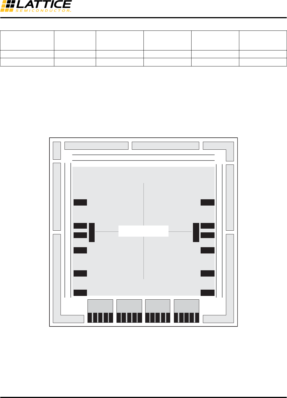
Architecture Overview
The SERDES/PCS block is arranged in quads containing logic for four independent full-duplex data channels.
Figure 8-1 shows the arrangement of SERDES/PCS quads on the LatticeECP3-150 FPGA (other devices have
fewer quads).
Figure 8-1. LatticeECP3-150 Block Diagram
Table 8-2 shows the number of available SERDES/PCS quads for each device in the LatticeECP3 family.
8-Bit SERDES 150 - 3125 15 - 312.5 15 - 312.5 x1, x2, x3, x4 N/A
Generic 8b10b 150 - 3125 15 - 312.5 15 - 312.5 x1, x2, x3, x4 8b10b
1. For slower rates, the SERDES are bypassed and signals are directly fed to the FPGA core.
2. The SONET protocol is supported in 8-Bit SERDES mode. Refer to the SONET section of this document for detailed information.
Table 8-1. Standards Supported by the SERDES (Continued)
Standard
Data Rate
(Mbps)
System Reference
Clock (MHz)
FPGA Clock
(MHz)
Number of
General/Link
Width Encoding Style
QUADRANT TL QUADRANT TR
QUADRANT BRQUADRANT BL
Primary Clocks
CL K D I V
CL K D I V
ECLK1
ECLK2
ECLK2
ECLK1
ECLK1
ECLK2
PLL
DLL
PLL
PLL
PLL
PLL
PLL
DLL
PLL
PLL
PLL
PLL
SERDES/PCS
Quad D
CH0
CH3
CH2
CH1
AUX
SERDES/PCS
Quad B
CH0
CH3
CH2
CH1
AUX
SERDES/PCS
Quad A
CH0
CH3
CH2
CH1
AUX
SERDES/PCS
Quad C
CH0
CH3
CH2
CH1
AUX
sysIO Bank 0 sysIO Bank 1
sysIO Bank 2
Configuration Logic
JTAG
sysIO Bank 3
sysIO Bank 7sysIO Bank 6

8-4
LatticeECP3 SERDES/PCS
Usage Guide
Table 8-2. Number of SERDES/PCS Quads per LatticeECP3 Device
Every quad can be programmed into one of several protocol-based modes. Each quad requires its own reference
clock which can be sourced externally from package pins or internally from the FPGA logic.
Each quad can be programmed with select protocols that have nominal frequencies which can utilize the full and
half-rate options per channel. For example, a PCI Express x1 at 2.5Gbps and a Gigabit Ethernet channel can be
utilized in the same quad using the half-rate option on the Gigabit Ethernet channel. If a quad shares a PCI
Express x1 channel with a non-PCI Express channel, ensure that the reference clock for the quad is compatible
with all protocols within the quad. For example, a PCI Express spread spectrum reference clock is not compatible
with most Gigabit Ethernet applications.
Since each quad has its own reference clock, different quads can support different standards on the same chip.
This feature makes the LatticeECP3 family of devices ideal for bridging between different standards.
PCS quads are not dedicated solely to industry standard protocols. Each quad (and each channel within a quad)
can be programmed for many user-defined data manipulation modes. For example, word alignment and clock toler-
ance compensation can be programmed for user-defined operation.
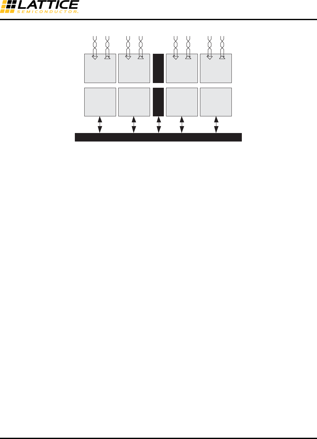
PCS Quads and Channels
Each quad on a device supports up to four channels of full-duplex data. One to four channels in a quad can be uti-
lized, depending on the application. Users can set many options for each channel independently within a given
quad.
Figure 8-1 shows an example of a device with four PCS quads which contain a total of 16 PCS channels.
Per Channel SERDES/PCS and FPGA Interface Ports
All PCS quads regardless of the mode used have the same external high-speed serial interface at the package
pins. However, every PCS mode has its own unique list of input/output ports from/to the FPGA logic appropriate to
the protocol chosen for the quad. A detailed description of the quad input/output signals for each mode is provided
in this document. Figure 8-2 describes a simplified SERDES/PCS quad.
Package ECP3-17 ECP3-35 ECP3-70 ECP3-95 ECP3-150
256-ball ftBGA 1 1 — — —
328-ball csBGA 2 channels1————
484-ball ftBGA1111
672-ball ftBGA—1222
1156-ball ftBGA — — 3 3 4
1. Channels 0 and 3 are available.
8-5
LatticeECP3 SERDES/PCS
Usage Guide
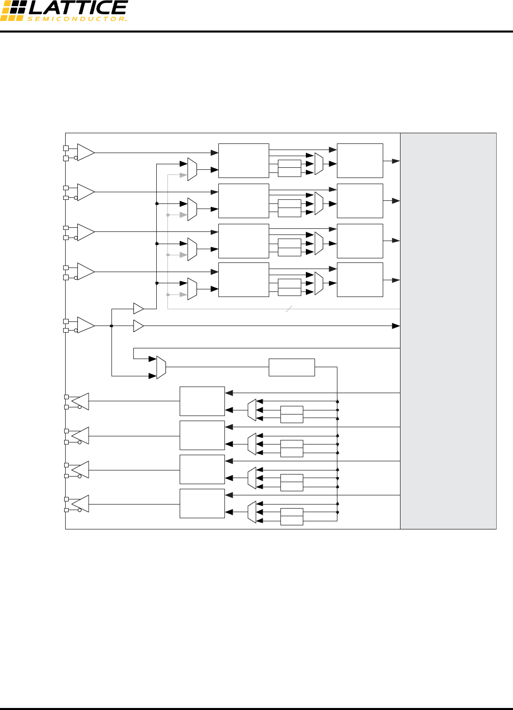
Figure 8-2. SERDES/PCS Quad Block Diagram
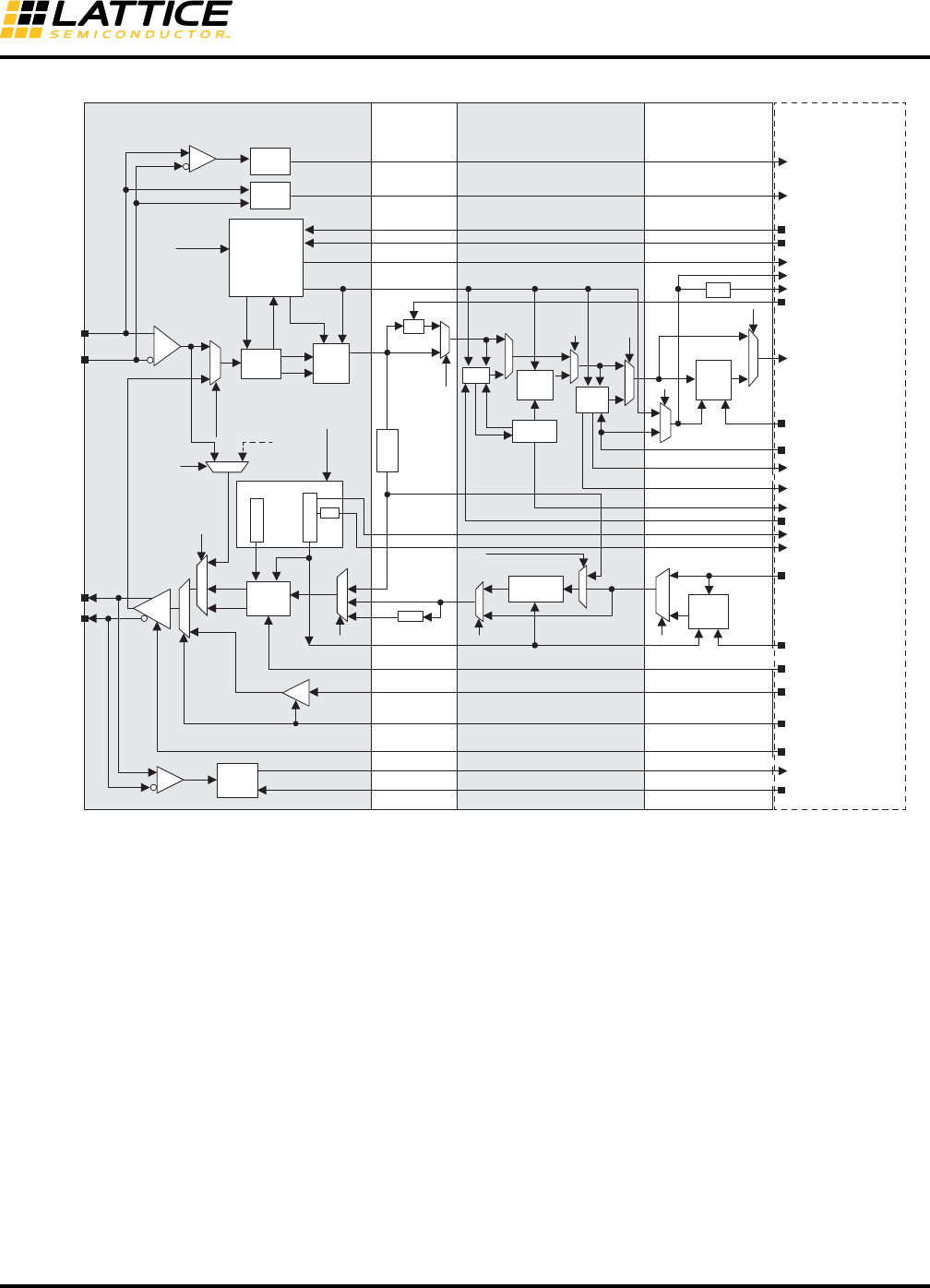
Detailed Channel Block Diagram
Figure 8-3 is a detailed block diagram representation of the major functionality in a single channel of the
LatticeECP3 SERDES/PCS. This diagram shows all the major blocks and the majority of the control and status sig-
nals that are visible to the user logic in the FPGA. This diagram also shows the major sub-blocks in the channel –
SERDES, SERDES Bridge, PCS Core and the FPGA Bridge.
SERDES
Channel 3
Rx + Tx
FPGA Core
AUX
Channel
Quad
Control
SERDES
Channel 2
Rx + Tx
SERDES
Channel 1
Rx + Tx
SERDES
Channel 0
Rx + Tx
PCS
Channel 3
Rx + Tx
PCS
Channel 2
Rx + Tx
PCS
Channel 1
Rx + Tx
PCS
Channel 0
Rx + Tx
8-6
LatticeECP3 SERDES/PCS
Usage Guide
Figure 8-3. LatticeECP3 SERDES/PCS Detailed Channel Block Diagram
Clocks and Resets
A PCS quad supplies per-channel locked reference clocks and per-channel recovered receive clocks to the FPGA
logic interface. Each PCS quad provides clocks on both primary and secondary FPGA clock routing. The
PCS/FPGA interface also has ports for the transmit and receive clocks supplied from the FPGA fabric for all four
channels in each quad.
Each quad has reset inputs to force reset of both the SERDES and PCS logic in a quad or just the SERDES. In
addition, separate resets dedicated for the PCS logic are provided for each channel for both the transmit and
receive directions.
Transmit Data Bus
The signals for the transmit data path are from the FPGA to the FPGA Bridge in the PCS Block. The datapath can
be geared 2:1 to the internal PCS data path, which is 8 bits wide (plus control/status signals). The highest speed of
the interface for PCI Express x1 is 250 MHz in 1:1 geared mode. With 2:1 gearing (i.e. a 16-bit wide data path), a
possible speed is 156.25 MHz (for XAUI 4x channel mode). The SERDES and PCS will support data rates up to
3.2 Gbps data that correspond to an interface speed of 160 MHz (with 2:1 gearing).
SLB _T2R_ EN
SLB_T2R
SLB_EQ2T
hdoutp_ch0
hdoutn_ch0
WA
CTC
FIFO
LSM
rlos_low_ch0_s
rx_invert_ch0_c
rxdata[23:0]_ch0
rxiclk_ch0
lsm_status_ch0_s
word_align_en_ch0_c
TX_GEAR_BYPASS
txdata[23:0]_ch0
R X_SB_ BYPASS
INV
CK
D
TDRV_DAT_SEL[1:0]
BYPASS
SERDES SERDES
Bridge (SB)
PCS Core FPGA Bridge (FB)
SER
8:1/10:1
8b10b
Encoder
Upsample
FIFO
EQ
hdinp_ch0
hdinn_ch0
Recovered (Byte) Clock
PD/
Sampler CK
D
8b10b
Decoder
REFCLK
INV
txiclk_ch0
REFCLK
tx_half_clk_ch0
tx_full_clk_ch0
FPGA Core
Detect
Logic rxd_ldr_ch0
Down-
sample
FIFO
TXPLL
Bit Clock
DES
1:8/1:10
1/2
Recovered
Bit Clock
rx_div11_mode_ch0_c
rx_full_clk_ch0
rx_half_clk_ch0
rx_gear_bypass
tx_div11_mode_ch0_c, tx_div2_mode_ch0_c, tx_sync_qd_c
txd_ldr_en_ch0_c
tx_idle_ch0_c
SEL_BIST_TXD4ENC
rx_cdr_lol_ch0_s
LOS
CDR
ebrd_clk_ch0
ctc_urun_ch0_s, ctc_orun_ch0_s
ctc_ins_ch0_s, ctc_del_ch0_s
1/2
rx_div2_mode_ch0_c
SLB_EQ2T_EN
FIFO
txd_ldr_ch0
Detect
Logic
pcie_con_ch0_s, pcie_done_ch0_s
pcie_det_en_ch0_c, pcie_ct_ch0_c
wa_bypass
decoder
bypass ctc
bypass
Byte Clock
8-7
LatticeECP3 SERDES/PCS
Usage Guide
Receive Data Bus
The signals for the receive path are from the FPGA Bridge in the PCS Block to the FPGA. The data path may be
geared 2:1 to the internal PCS data path which is 8 bits wide. The data bus width at the FPGA interface is 16 bits
wide. It is possible to disable the 2:1 gearing via a software register bit, in which case, the bus widths are halved (8
bits wide). When the data is geared 2:1, the lower bits (rxdata[9:0]) correspond to the word that has been received
first and the higher bits (rxdata[19:10]) correspond to the word that has been received second. If the data is not
geared 2:1, the lower bits ((rxdata[9:0]) are the active bits and the higher bits should not be used. Table 8-3
describes the use of the data bus for each protocol mode.
Table 8-3. Data Bus Usage by Mode
Data Bus PCS
Cell Name4G8B10B CPRI OBSAI PCI Express SRIO Gigabit Ethernet XAUI
8-Bit
SERDES
10-Bit
SERDES SDI
FF_TX_D_0_0 txdata_ch0[0]
FF_TX_D_0_1 txdata_ch0[1]
FF_TX_D_0_2 txdata_ch0[2]
FF_TX_D_0_3 txdata_ch0[3]
FF_TX_D_0_4 txdata_ch0[4]
FF_TX_D_0_5 txdata_ch0[5]
FF_TX_D_0_6 txdata_ch0[6]
FF_TX_D_0_7 txdata_ch0[7]
FF_TX_D_0_8 tx_k_ch0[0] txc_ch0[0] GND txdata_ch0[8]
FF_TX_D_0_9 tx_force_disp_ch0[0]1GND txdata_ch0[9]
FF_TX_D_0_10 tx_disp_sel_ch0[0]1GND xmit_ch0[0]2GND
FF_TX_D_0_11 GND pci_ei_en_ch0[0] GND tx_disp_correct_ch0[0] GND
FF_TX_D_0_12 txdata_ch0[8] txdata_ch0[10]
FF_TX_D_0_13 txdata_ch0[9] txdata_ch0[11]
FF_TX_D_0_14 txdata_ch0[10] txdata_ch0[12]
FF_TX_D_0_15 txdata_ch0[11] txdata_ch0[13]
FF_TX_D_0_16 txdata_ch0[12] txdata_ch0[14]
FF_TX_D_0_17 txdata_ch0[13] txdata_ch0[15]
FF_TX_D_0_18 txdata_ch0[14] txdata_ch0[16]
FF_TX_D_0_19 txdata_ch0[15] txdata_ch0[17]
FF_TX_D_0_20 tx_k_ch0[1] txc_ch0[1] GND txdata_ch0[18]
FF_TX_D_0_21 tx_force_disp_ch0[1]1GND txdata_ch0[19]
FF_TX_D_0_22 tx_disp_sel_ch0[1]1GND xmit_ch0[1]2GND
FF_TX_D_0_23 GND pci_ei_en_ch0[1] GND tx_disp_correct_ch0[1] GND
FF_RX_D_0_0 rxdata_ch0[0]
FF_RX_D_0_1 rxdata_ch0[1]
FF_RX_D_0_2 rxdata_ch0[2]
FF_RX_D_0_3 rxdata_ch0[3]
FF_RX_D_0_4 rxdata_ch0[4]
FF_RX_D_0_5 rxdata_ch0[5]
FF_RX_D_0_6 rxdata_ch0[6]
FF_RX_D_0_7 rxdata_ch0[7]
FF_RX_D_0_8 rx_k_ch0[0] rxc_ch0[0] NC rxdata_ch0[8]
FF_RX_D_0_9 rx_disp_err_ch0[0] rxstatus0_ch0[0] rx_disp_err_ch0[0] NC rxdata_ch0[9]
FF_RX_D_0_10 rx_cv_err_ch0[0]3rxstatus0_ch0[1] rx_cv_err_ch0[0]3NC
FF_RX_D_0_11 NC rxstatus0_ch0[2] NC
FF_RX_D_0_12 rxdata_ch0[8] rxdata_ch0[10]
FF_RX_D_0_13 rxdata_ch0[9] rxdata_ch0[11]
FF_RX_D_0_14 rxdata_ch0[10] rxdata_ch0[12]
FF_RX_D_0_15 rxdata_ch0[11] rxdata_ch0[13]
FF_RX_D_0_16 rxdata_ch0[12] rxdata_ch0[14]
FF_RX_D_0_17 rxdata_ch0[13] rxdata_ch0[15]
8-8
LatticeECP3 SERDES/PCS
Usage Guide
Mode-Specific Control/Status Signal Descriptions
Table 8-4 describes the mode-specific control/status signals.
Table 8-4. Control Signals and their Functions
Control
Each mode has its own set of control signals which allows direct control of various PCS features from the FPGA
logic. In general, each of these control inputs duplicates the effect of writing to a corresponding control register bit
or bits.
{signal}_c is the control signal from the FPGA core to the FPGA bridge. All of the control signals are used asyn-
chronously inside the SERDES/PCS.
Status
Each mode has its own set of status or alarm signals that can be monitored by the FPGA logic. In general, each of
these status outputs corresponds to a specific status register bit or bits. The Diamond design tools give the user
the option to bring these ports out to the PCS FPGA interface.
{signal}_s is the status the signal to the FPGA core from the FPGA bridge. All of the status signals are asynchro-
nous from the SERDES/PCS. These should be synchronized to a clock domain before they are used in the FPGA
design.
Please refer to the Mode-Specific Control/Status Signals section of this document for detailed information about
control and status signals.
FF_RX_D_0_18 rxdata_ch0[14] rxdata_ch0[16]
FF_RX_D_0_19 rxdata_ch0[15] rxdata_ch0[17]
FF_RX_D_0_20 rx_k_ch0[1] rxc_ch0[1] NC rxdata_ch0[18]
FF_RX_D_0_21 rx_disp_err_ch0[1] rxstatus1_ch0[0] rx_disp_err_ch0[1] NC rxdata_ch0[19]
FF_RX_D_0_22 rx_cv_err_ch0[1]3rxstatus1_ch0[1] rx_cv_err_ch0[1]3NC
FF_RX_D_0_23 NC rxstatus1_ch0[2] NC
1. The force_disp signal will force the disparity for the associated data word on bits [7:0] to the column selected by the tx_disp_sel signal. If disp_sel is a one, the
10-bit code is taken from the 'current RD+' column (positive disparity). If the tx_disp_sel is a zero, the 10-bit code is taken from the 'current RD-' (negative dispar-
ity) column.
2. The Lattice Gigabit Ethernet PCS IP core provides an auto-negotiation state machine that generates the signal xmit. It is used to interact with the Gigabit Ether-
net Idle State Machine in the hard logic.
3. When there is a code violation, the packet PCS 8b10b decoder will replace the output from the decoder with hex EE and K asserted (K=1 and d=EE is not part
of the 8b10b coding space).
4. FF_TX_D_0_0: FPGA Fabric Transmit Data Bus Channel 0 Bit 0.
Signal Name Description
Transmit Control Signals
tx_k_ch[3:0] Per channel, active-high control character indicator.
tx_force_disp_ch[3:0] Per channel, active-high signal which instructs the PCS to accept disparity value from the
disp_sel_ch(0-3) FPGA interface input.
tx_disp_sel_ch[3:0] Per channel, disparity value supplied from FPGA logic. Valid when force_disp_ch(0-3) is high.
tx_correct_disp_ch[3:0] Corrects disparity identifier when asserted by adjusting the 8b10b encoder to begin in the negative
disparity state.
Receive Status Signals
rx_k_ch[3:0] Per channel, active-high control character indicator.
rx_disp_err_ch[3:0] Per channel, active-high signal driven by the PCS to indicate a disparity error was detected with
the associated data.
rx_cv_err_ch[3:0] Per channel, code violation signal to indicate an error was detected with the associated data.
Table 8-3. Data Bus Usage by Mode (Continued)
Data Bus PCS
Cell Name4G8B10B CPRI OBSAI PCI Express SRIO Gigabit Ethernet XAUI
8-Bit
SERDES
10-Bit
SERDES SDI
8-9
LatticeECP3 SERDES/PCS
Usage Guide
SERDES/PCS
The quad contains four channels with both RX and TX circuits, and an auxiliary channel that contains the TX PLL.
The reference clock to the TX PLL can be provided either by the primary differential reference clock pins or by the
FPGA core. The quad SERDES/PCS macro performs the serialization and de-serialization function for four lanes
of data. In addition, the TxPLL within the SERDES/PCS block provides the system clock for the FPGA logic. The
quad also supports both full-data-rate and half-data-rate modes of operation on each TX and RX circuit indepen-
dently. The block-level diagram is shown in Figure 8-4.
Figure 8-4. SERDES/PCS Block Signal Interface
SERDES/PCS
Quad
rx_full_clk_ch[3:0]
rx_half_clk_ch[3:0]
tx_full_clk_ch[3:0]
tx_half_clk_ch[3:0]
refclk2fpga
fpga_txrefclk
fpga_rxrefclk_ch[3:0]
rxiclk_ch[3:0]
txiclk_ch[3:0]
rxdata_ch0[23:0]
rxdata_ch1[23:0]
rxdata_ch2[23:0]
rxdata_ch3[23:0]
txdata_ch0[23:0]
txdata_ch1[23:0]
txdata_ch2[23:0]
txdata_ch3[23:0]
rxd_ldr_ch[3:0]
txd_ldr_ch[3:0]
lsm_status_ch[3:0]_s
ctc_ins_ch[3:0]_s
ctc_del_ch[3:0]_s
ctc_urun_ch[3:0]_s
ctc_orun_ch[3:0]_s
pcie_done_ch[3:0]_s
pcie_con_ch[3:0]_s
rx_los_low_ch[3:0]_s
rx_cdr_lol_ch[3:0]_s
tx_pll_lol_qd_s
Primary I/O
SERDES
Client
Interface
Control
Signals
from
FPGA
Clocks to &
from FPGA
RX Data
TX Data
Status
Signals
to
FPGA
refclkp
refclkn
hdinp_ch[3:0]
hdinn_ch[3:0]
hdoutp_ch[3:0]
hdoutn_ch[3:0]
sci_sel_quad
sci_sel_ch[3:0]
sci_wrdata[7:0]
sci_wrn
sci_addr[5:0]
sci_rd
sci_rddata[7:0]
sci_int
txd_ldr_en_ch[3:0]_c
tx_div2_mode_ch[3:0]_c
rx_div2_mode_ch[3:0]_c
tx_div11_mode_ch[3:0]_c
rx_div11_mode_ch[3:0]_c
tx_idle_ch[3:0]_c
pcie_ct_ch[3:0]_c
pcie_det_en_ch[3:0]_c
sb_felb_ch[3:0]_c
rx_invert_ch[3:0]_c
rx_pcs_rst_ch[3:0]_c
tx_pcs_rst_ch[3:0]_c
rx_serdes_rst_ch[3:0]_c
tx_serdes_rst_c
rst_qd_c
serdes_rst_qd_c
tx_sync_qd_c
word_align_en_ch[3:0]_c
tx_pwrup_ch[3:0]_c
rx_pwrup_ch[3:0]_c
sb_felb_rst_ch[3:0]_c
Low-speed
Data

8-10
LatticeECP3 SERDES/PCS
Usage Guide
I/O Descriptions
Table 8-5 lists all default and optional inputs and outputs to/from a PCS quad. Users can choose optional ports for
a PCS quad using the IPexpress™ GUI.
Table 8-5. SERDES_PCS I/O Descriptions
Signal Name I/O Type Description
Primary I/O, SERDES Quad
hdinp_ch0 I Channel High-speed CML input, positive, channel 0
hdinn_ch0 I Channel High-speed CML input, negative, channel 0
hdinp_ch1 I Channel High-speed CML input, positive, channel 1
hdinn_ch1 I Channel High-speed CML input, negative, channel 1
hdinp_ch2 I Channel High-speed CML input, positive, channel 2
hdinn_ch2 I Channel High-speed CML input, negative, channel 2
hdinp_ch3 I Channel High-speed CML input, positive, channel 3
hdinn_ch3 I Channel High-speed CML input, negative, channel 3
hdoutp_ch0 O Channel High-speed CML output, positive, channel 0
hdoutn_ch0 O Channel High-speed CML output, negative, channel 0
hdoutp_ch1 O Channel High-speed CML output, positive, channel 1
hdoutn_ch1 O Channel High-speed CML output, negative, channel 1
hdoutp_ch2 O Channel High-speed CML output, positive, channel 2
hdoutn_ch2 O Channel High-speed CML output, negative, channel 2
hdoutp_ch3 O Channel High-speed CML output, positive, channel 3
hdoutn_ch3 O Channel High-speed CML output, negative, channel 3
refclkp I Quad Reference Clock input, positive, dedicated CML input
refclkn I Quad Reference Clock input, negative, dedicated CML input
Receive / Transmit Data Bus (See Tables 8-3 and 8-4 for Detailed Data Bus Usage)
rxdata_ch0[23:0] O Channel Data signals for the channel 0 receive path
rxdata_ch1[23:0] O Channel Data signals for the channel 1 receive path
rxdata_ch2[23:0] O Channel Data signals for the channel 2 receive path
rxdata_ch3[23:0] O Channel Data signals for the channel 3 receive path
txdata_ch0[23:0] I Channel Data signals for the channel 0 transmit path
txdata_ch1[23:0] I Channel Data signals for the channel 1 transmit path
txdata_ch2[23:0] I Channel Data signals for the channel 2 transmit path
txdata_ch3[23:0] I Channel Data signals for the channel 3 transmit path
Control Signals
tx_idle_ch[3:0] _c I Channel
Controls transmission of electrical idle by SERDES transmitter.
1 = Force SERDES transmitter to output electrical idle
0 = Normal operation
pcie_det_en_ch[3:0]_c I Channel
FPGA logic (user logic) informs the SERDES block that it will be
requesting for a PCI Express Receiver Detection operation.
1 = Enable PCI Express receiver detect, 0 = Normal operation
pcie_ct_ch[3:0]_c I Channel 1 = Request transmitter to do far-end receiver detection
0 = Normal data operation
rx_invert_ch[3:0]_c I Channel Control the inversion of received data.
1 = Invert the data, 0 = Don’t invert the data
word_align_en_ch[3:0]_c I Channel
Control comma aligner.
1 = Re-acquire COMMA alignment, 0 = Clears internal aligned status
Once alignment is found, it is locked at current position until the signal
is pulsed to HIGH.

8-11
LatticeECP3 SERDES/PCS
Usage Guide
sb_felb_ch[3:0]_c I Channel SERDES Bridge Parallel Loopback
1 = Enable loopback from RX to TX, 0 = Normal data operation
sb_felb_rst_ch[3:0]_c I Channel SERDES Bridge Parallel Loopback FIFO Clear
1 = Reset Loopback FIFO, 0 = Normal Loopback operation
tx_sync_qd_c I Quad Serializer Reset
Transition = Reset, Level = Normal Operation
rx_div2_mode_ch[3:0]_c I Channel Receiver Rate Mode Select (Full/Half Rate)
1 = Half Rate, 0 = Full Rate
tx_div2_mode_ch[3:0]_c I Channel Transmitter Rate Mode Select (Full/Half Rate)
1 = Half Rate, 0 = Full Rate
rx_div11_mode_ch[3:0]_c I Channel Receiver Rate Mode Select (Div11/Full Rate)
1 = Div11 Rate, 0 = Full Rate
tx_div11_mode_ch[3:0]_c I Channel Transmitter Rate Mode Select (Div11/Full Rate)
1 = Div11 Rate, 0 = Full Rate
txd_ldr_en_ch{3:0]_c I Channel Low Data Rate TX Serial Path Enable
1 = Enable, 0 = Disable
Reset Signals
rx_pcs_rst_ch[3:0]_c I Channel Active-high, asynchronous input. Resets individual receive channel
logic only in PCS.
tx_pcs_rst_ch[3:0]_c I Channel Active-high, asynchronous input. Resets individual transmit channel
logic only in PCS.
rx_serdes_rst_ch[3:0]_c I Channel Active-high. Resets selected digital logic in the SERDES receive chan-
nel.
tx_serdes_rst_c I Quad Active-high. Resets selected digital logic in all SERDES transmit chan-
nels.
rst_qd_c I Quad Active-high, asynchronous input. Resets all SERDES channels includ-
ing the auxiliary channel and PCS.
serdes_rst_qd_c I Quad Active-high, asynchronous input to SERDES quad. Resets all SERDES
channels including the Quad channel but not PCS logic.
tx_pwrup_ch[3:0]_c I Channel Active-high transmit channel power up. 0 = Transmit channel power-
down.
rx_pwrup_ch[3:0]_c I Channel Active-high receive channel power up. 0 = Receive channel power-
down.
Status Signals
pcie_done_ch[0:3]_s O Channel 1 = Far-end receiver detection complete
0 = Far-end receiver detection incomplete
pcie_con_ch[3:0]_s O Channel
Result of far-end receiver detection.
1 = Far-end receiver detected
0 = Far end receiver not detected.
rx_los_low_ch[3:0]_s O Channel Loss of signal (LO THRESHOLD RANGE) detection for each channel.
lsm_status_ch[3:0]_s O Channel 1 = Lane is synchronous to commas
0 = Lane has not found comma
ctc_urrun_ch[3:0]_s O Channel 1 = Receive clock compensator FIFO underrun error
0 = No FFIFO errors
ctc_orun_ch[3:0]_s O Channel 1 = Receive clock compensator FIFO overrun error
0 = No FIFO errors
rx_cdr_lol_ch[3:0]_s O Channel 1 = Receive CDR loss of lock
0 = Lock maintained
tx_pll_lol_qd_s O Quad 1 = Transmit PLL loss of lock
0 = Lock maintained
ctc_ins_ch[3:0]_s O Channel 1 = SKIP Character Added by CTC
Table 8-5. SERDES_PCS I/O Descriptions (Continued)
Signal Name I/O Type Description

8-12
LatticeECP3 SERDES/PCS
Usage Guide
ctc_del_ch[3:0]_s O Channel 1 = SKIP Character Deleted by CTC
FPGA Interface Clocks
rx_full_clk_ch[3:0] O Channel
Receive channel recovered clock. In user mode, the source is always
the channel’s recovered clock. For standards such as 10 GbE that sup-
port clock compensation, the source is the respective transmit chan-
nel’s system clock. For PCS bypass modes, it is also the transmit
system clock, thus requiring raw mode to actually be done using either
8b10b mode with the 8b10b decoder disabled (10-bit or 20-bit data
path).
rx_half_clk_ch[3:0] O Channel Receive channel recovered half clock. In 2:1 gearing mode, it is a
divide-by-2 output.
tx_full_clk_ch[3:0] O Channel
TX PLL full rate clock. Only tx_full_clk_ch0 can drive the primary clock
routing directly. All of the tx_full_clk_ch[3:0] signals can drive the sec-
ondary clock routing by applying a USE SECONDARY clocking prefer-
ence.3
tx_half_clk_ch[3:0] O Channel
TX PLL half clock. Only tx_half_clk_ch0 can drive the primary clock
routing directly. All of the tx_half_clk_ch[3:0] signals can drive the sec-
ondary clock routing by applying a USE SECONDARY clocking prefer-
ence.3
refclk2fpga O Quad
Reference clock to FPGA core. If selected, this clock is always active as
long as reference clock is active even when the quad is in power down
mode.
fpga_rxrefclk_ch[3:0] I Quad RX reference clock from FPGA logic, for CDR PLL
fpga_txrefclk I Quad TX reference clock from FPGA logic, for TX SERDES PLL
ebrd_clk_ch[3:0]2I Channel Receive channel clock input from FPGA for CTC FIFO read.
rxiclk_ch[3:0] I Channel
Receive channel clock input from FPGA. Used to clock the RX FPGA
Interface FIFO with a clock synchronous to the reference and/or receive
reference clock.
txiclk_ch[3:0] I Channel
Transmit channel clock input from FPGA.Per channel transmit clock
inputs from FPGA. Used to clock the TX FPGA Interface FIFO with a
clock synchronous to the reference clock. Also used to clock the RX
FPGA Interface FIFO with a clock synchronous to the reference clock
when CTC is used.
Low-Speed Receive/Transmit Data and SERDES Client Interface Signals
rxd_ldr_ch[3:0] O Channel Single-ended serial low data rate outputs (RX) to FPGA core
txd_ldr_ch[3:0] I Channel Single-ended serial low data rate inputs (TX) from FPGA core
sci_wrdata[7:0] I — Write data input
sci_wrn I — Write input strobe
sci_sel_quad I — Selects quad registers
sci_sel_ch[3:0] I — Selects channel registers
sci_addr[5:0] I — Address bus input
sci_rd I — Read data select
sci_rddata[7:0] O — Read data output
sci_int O — Interrupt output
1. During configuration, both hdoutp and hdoutn are pulled high to VCCOB.
2. This clock is not provided in the wrapper module port list. Software automatically assigns the clock depending on the CTC mode. See the
FPGA Interface Clocks section of this document for detailed information.
3. General routing is used to access the Secondary Clock Net. The user may get a PAR warning but the delay will be small enough to ignore
in most applications. Use the Timing Preferences and review the Trace Report to make sure the timing is not violated.
Table 8-5. SERDES_PCS I/O Descriptions (Continued)
Signal Name I/O Type Description

8-13
LatticeECP3 SERDES/PCS
Usage Guide
SERDES/PCS Functional Description
LatticeECP3 devices have from one to four quads of embedded SERDES/PCS logic. Each quad, in turn, supports
four independent full-duplex data channels. A single channel can support a data link and each quad can support up
to four such channels.
The embedded SERDES CDR PLLs and TX PLLs support data rates that cover a wide range of industry standard
protocols.
Refer to Figure 8-3 for each of the items below.
• SERDES
– Equalizer
– CDR (Clock and Data Recovery)
– Deserializer
– PreEmphasis
– Serializer
– Two Serial Loopback modes, TX-to-RX or RX-to-TX
• SERDES Bridge (SB)
– Inverter – Inverts receive data, required by PCI Express
– SERDES Bridge Parallel Loopback
•PCS Core
– Word Alignment
– 8b10b Decoder
– 8b10b Encoder
– Link State Machine
– Clock Tolerance Compensation
• FPGA Bridge (FB)
– Downsample FIFO
– Upsample FIFO
SERDES
Equalizer
As the data rate of digital transmission advances over Gbps, frequency-dependent attenuation results in severe
intersymbol interference in the received signal and makes it mandatory to use an equalizer in the data transceiver
to recover data correctly. Six pole positions are provided: Mid_Low, Mid_Med, Mid_High, Long_Low, Long_Med,
Long_High frequency ranges.
A default selection of the pole position is included when a protocol standard is selected. This selection is based on
most commonly used condition on user’s system board. However, user may wish to optimize the signal by adjusting
this setting. User has to perform bit-error-rate tests on all different pole settings to determine the optimal one.
Pre-Emphasis
Pre-emphasis refers to a system process designed to increase the magnitude of some frequencies with respect to
the magnitude of other frequencies. The goal is to improve the overall signal-to-noise ratio by minimizing the
adverse effects of such phenomena as attenuation differences. Users can select up to 80% of pre-emphasis.
By default, pre-emphasis is not enabled. User can determine if the Tx drive signal has to route a long distance to
the Rx side. If the routing trance length is long, he can try out different pre-emphasis settings to determine the best
signal eye at the Rx-end of the trace.
8-14
LatticeECP3 SERDES/PCS
Usage Guide
Reference Clocks
The SERDES quad contains four channels with both RX and TX circuits, and an auxiliary channel that contains the
TX PLL. The reference clock to the TX PLL can be provided either by the primary differential reference clock pins,
by the neighbor quad’s reference clock or by the FPGA core. In addition, the PLL within the SERDES block pro-
vides an output clock that can be used as the system clock driving the FPGA fabric.
The reference clock to the RX can be provided either by the reference clock to the TX PLL or by the FPGA core.
The reference clocks from the FPGA core to the TX PLL and to the RX may come from different sources.
SERDES Clock Architecture
Figure 8-5 shows the overall SERDES clock architecture. The diagram is split into two halves, Quad and Channel.
Only one per-channel section is shown for the sake of brevity. Also, the various control bits for the different blocks
are shown. These could be quad-based control register bits or channel-based control register bits. In some cases,
it can be channel control port based. Some are a combination of both register and control ports. Using both modes
enables dynamic control of certain functional properties.
Figure 8-5. SERDES Clock Architecture
The main components of the clock architecture include:
• Per RX and per TX Divider (DIV) modes – DIV2, DIV11
• Multi-quad REFCLK connections
• Multiple channel transmit synchronization using the tx_sync_qd_c signal from the FPGA
• OOB low data rate application support
1. All control bits are quad based.
2. All control bits are channel based, except as indicated (*).
3. These clocks are user-transparent.
REFCLKP
REFCLKN
0
1
TXREFCLK from FPGA Core
TXREFCLK_SEL (Reg)
REFCLK_OUT_SEL[0] (Reg)REFCLK_OUT_SEL[1] (Reg)
REFCLK to FPGA Core
TX_PLL(QD)
8X, 10X,
16X, 20X,
25X
D Q
PULSE SYNC
(To All TX Channels)
TX_SYNC_QD_C
(Reg or Core)
CLK3G4TX
0
1
RX_REFCLK_SEL (Reg)
RX_CDR
(CH)
REFCLK_MODE[1:0]
REFCLK25X (QD_REG*)
REFCLK from FPGA Core
REFFC2D CO_FLOOP (Reg)
/11
/2
0
1
0
1
TX_DIV11_MODE (Reg/Core)
Serializer(CH)
8:1/10:1
/11
/2
0
1
0
1DeSerializer(CH)
8:1/10:1
RX_DIV2_MODE (Reg/Core)
RX_DIV11_MODE (Reg/Core) /2
RX_FULL_CLK (CH)
RX_HALF_CLK (CH)
/2
TX_FULL_CLK (CH)
TX_HALF_CLK (CH)
BUS8B_SEL
(QD_REG*)
Channel 2
Quad1
8-15
LatticeECP3 SERDES/PCS
Usage Guide
Rate Modes
The TX in each channel can be independently programmed to run at one of the following rates:
• FULL_RATE
• HALF_RATE (DIV2)
•DIV11
The RX can also use a separate reference clock per channel, allowing the transmitter and receiver to run at com-
pletely different rates.
It is important to note that the PLL VCO is left untouched, supporting the highest rate for that protocol. All divided
rates required by that protocol are supported by programming the divider mux selects. This enables very quick data
rate changeover since the PLL does not need to be reprogrammed. This is valuable in many applications.
Note: The LatticeECP3 PCS cannot handle a change in rates at runtime. Simply changing the refclk rate will not
allow the SERDES to work at a new range. The SERDES settings must be re-configured, either with a new bit-
stream, or changed via the SERDES' SCI interface. The SERDES link must be reset after the settings are
changed.
The TX PLL and the four CDR PLLs generally run at the same frequency, which is a multiple of the reference clock
frequency. Table 8-6 illustrates the various clock rate modes possible. The bit clock indicated is a multiple of the ref-
erence clock frequency.
Table 8-6. TXPLL and RX CDRPLL Supported Modes
Reference Clock Mode refclkPmode (Quad) Bus_width Bit Clock (Full Rate) Bit Clock (div2, div11)
20x 0 10 Refclk x 20 Refclk x 10
16x 0 8 Refclk x 16 Refclk x 8
10x 1 10 Refclk x 10 Refclk x 5
8x 1 8 Refclk x 8 Refclk x 4
25x — 8 Refclk x 25 Refclk x 12.5
25x — 10 Refclk x 25 Refclk x 12.5
20x 0 10 Refclk x 20 Refclk x 20/111
1. DIV11 mode.
8-16
LatticeECP3 SERDES/PCS
Usage Guide
Reference Clock from an FPGA Core
As described in Figure 8-5, the TX reference clock can be brought from the FPGA core. In this case, the extra jitter
caused by the FPGA resources to route the clock to the SERDES will be passed onto the transmit data and may
violate TX jitter specifications on a case-by-case basis. Caution should be used when using an FPGA-originated
SERDES TX reference clock.
Figure 8-6. Reference Clock Block Diagram
SER0
1/2
1/11
HDOUT_ch0
SER3
1/2
1/11
HDOUT_ch3
SER2
1/2
1/11
HDOUT_ch2
SER1
1/2
1/11
HDOUT_ch1
TX PLL
REFCLK to TX PLL(QUAD)
REFCLKP
REFCLKN
CDR PLL 3 DES3
1/2
1/11
CDR PLL 2 DES2
1/2
1/11
CDR PLL 1 DES1
1/2
1/11
CDR PLL 0 DES0
1/2
1/11
HDIN_ch0
HDIN_ch3
HDIN_ch2
HDIN_ch1
PCS/FPGA Core
Data to PCS
RX_REFCLK
from FPGA Core(ch[3:0])
REFCLK to FPGA Core
Data from PCS
SERDES
[3:0]
[0]
[3]
[2]
[1]
8-17
LatticeECP3 SERDES/PCS
Usage Guide
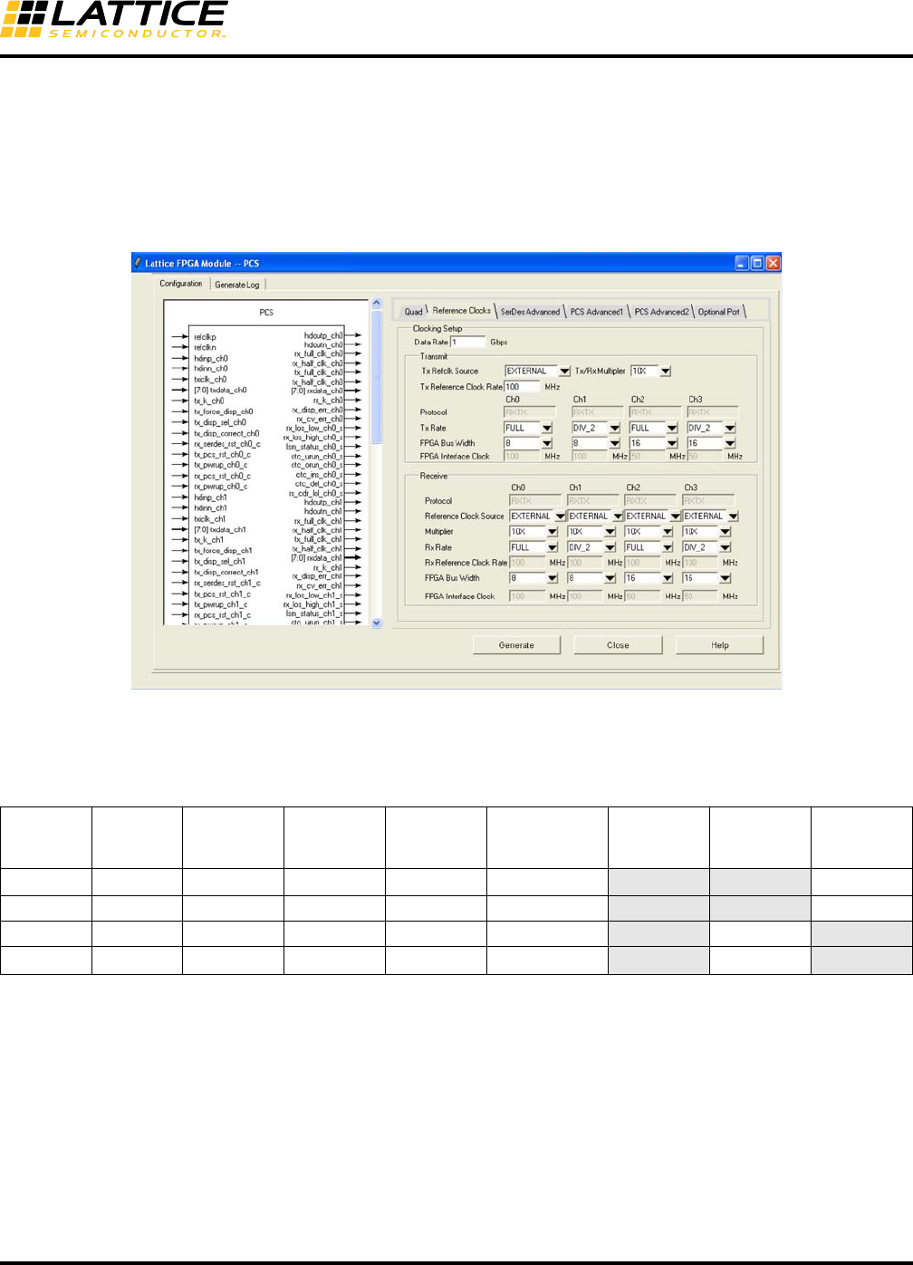
Full Data, Div 2 and Div 11 Data Rates
Each TX Serializer and RX Deserializer can be split into full data rate and div2 rate or div11 rate depending on the
protocol, allowing for different data rates in each direction and in each channel. Refer to Figure 8-6 for further infor-
mation.
As shown in Figure 8-7, all four channels can be configured differently.
Figure 8-7. Example of Full Data Rate and Half Data Rate in the IPexpress GUI
The actual data rate and FPGA interface clock rate for this example are described in Table 8-7. The IPexpress GUI
will be discussed in detail later in this document.
Table 8-7. Clock Rate Example
Channel Data Rate
Reference
Clock
Multiplier
Data Rate
Mode
Calculated
Reference
Clock Rate
FPGA
Interface Data
Bus Width
FPGA
Interface
Clock Rate tx_full_clk tx_half_clk
Channel 0 1 Gbps 10 x FULL 100 MHz 8 (10)3100 MHz 100 MHz 50 MHz
Channel 1 500 Mbps 10 x DIV2 100 MHz 8 (10) 50 MHz 50 MHz 25 MHz
Channel 2 1 Gbps 10 x FULL 100 MHz 16 (20) 50 MHz 100 MHz 50 MHz
Channel 3 500 Mbps 10 x DIV22100 MHz 16 (20) 25 MHz 50 MHz 25 MHz
1. The clocks in the shaded cells are used as the FPGA interface clocks in each mode.
2. In DIV2 mode, the tx_full_clk is adjusted to half rate. tx_half_clk is used for the 16-bit bus interface only.
3. 10-bit SERDES only mode or SDI mode.
8-18
LatticeECP3 SERDES/PCS
Usage Guide
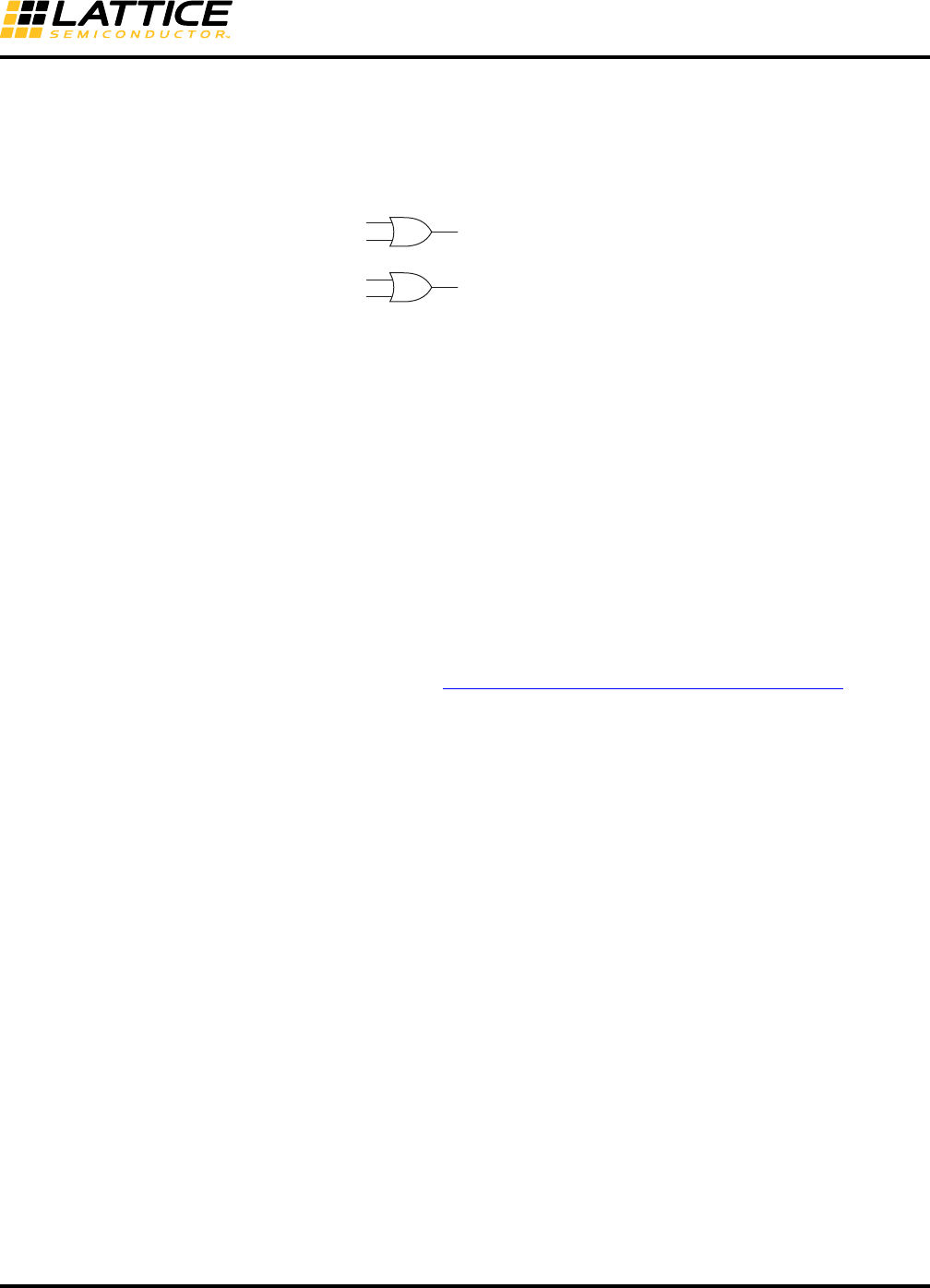
Dynamic Switching Between Full Rate and Half Rate (DIV2)
This section describes how to switch between Full Rate and Half Rate (DIV) dynamically.
The two rate mode control signals are or’ed as shown in Figure 8-8.
Figure 8-8. Rate Mode Control Signals
tx_div2_mode_chx_c is an input control signal to the TX path from the FPGA fabric.
rx_div2_mode_chx_c is an input control signal to the RX path from the FPGA fabric.
Rate_Mode_Tx(CH_14[1]) is the Control Register bit for the TX path.
Rate_Mode_Rx(CH_15[1]) is the Control Register bit for the RX path.
In the rx lane, the pcs_rst should be applied after switching.
In the tx lane, no reset is required for the new rate to take place.
Reference Clock Sources
refclkp, refclkn
Dedicated CML input. This is the first choice unless different clock sources for RX and TX are used. The clock sig-
nal may be CML, LVDS or LVPECL. Refer to TN1114, Electrical Recommendations for Lattice SERDES, for exam-
ple interface circuits.
fpga_txrefclk, fpga_rxrefclk
Reference clock from FPGA logic. The Primary Clock pad (PCLK) should be used as the clock input pin to the
FPGA. The clock signal may be CML, LVDS, LVPECL or single-ended.
FPGA PLL
When an FPGA PLL is used as the reference clock, the reference clock to the PLL should be assigned to a dedi-
cated PLL input pad. The FPGA PLL output jitter may not meet system specifications at higher data rates. Use of
an FPGA PLL is not recommended in jitter-sensitive applications.
Spread Spectrum Clocking (SSC) Support
The ports on the two ends of Link must transmit data at a rate that is within 600pm of each other at all times. This
is specified to allow bit-rate clock source with a +/- 300ppm tolerance. The minimum clock period cannot be vio-
lated. The preferred method is to adjust the spread technique to not allow for modulation above the nominal fre-
quency. The data rate can be modulated from +0% to -0.5% of the nominal data rate frequency, at a modulation
rate in the range not exceeding 30KHz to 33KHz. Along with the +/- 300ppm tolerance limit, both ports require the
same bit rate clock when the data is modulated with an SSC.
In PCI Express applications, the root complex is responsible for spreading the reference clock. The endpoint will
use the same clock to pass back the spectrum through the TX. Thus, there is no need for a separate RXREFCLK.
The predominant application is an add-in card. Add-in cards are not required to use the REFCLK from the connec-
tor but must receive and transmit with the same SSC as the PCI Express connector REFCLK.
While the LatticeECP3 architecture will allow the mixing of a PCI Express channel and a Gigabit Ethernet, Serial
RapidIO or SGMII channel within the same quad, using a PCI Express SSC as the transmit reference clock will
cause a violation of the Gigabit Ethernet, Serial RapidIO and SGMII transmit jitter specifications.
rx_div2_mode_ch[3:0]_c
Rate_Mode_Rx(CH_15[1]) Receiver Rate ( 0: Full Rate, 1: Half Rate)
tx_div2_mode_ch[3:0]_c
Rate_Mode_Tx(CH_14[1]) Transmitter Rate ( 0: Full Rate, 1: Half Rate)
8-19
LatticeECP3 SERDES/PCS
Usage Guide
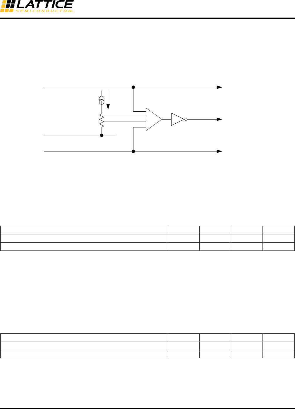
Loss of Signal
Each channel contains a programmable loss-of-signal detector as shown in Figure 8-9.
The loss-of-signal threshold depends on the value of the programmable current source. The current source value is
chosen using the rlos_lset[2:0] control bit. The result of threshold detection is indicated to the FPGA through the
rx_los_low status signal.
Figure 8-9. Loss of Signal Detector
Table 8-8. Response Time for Loss of Signal Detector
Loss Of Lock
Both the transmit PLL and the individual channel CDRs have digital counter-based, loss-of-lock detectors. If the
transmit PLL loses lock, the loss-of-lock for the PLL is asserted and remains asserted until the PLL reacquires lock.
If a CDR loses lock, the loss-of-lock for that channel is asserted and locking to the reference clock retrains the VCO
in the CDR. When this is achieved, loss-of-lock for that channel is de-asserted and the CDR is switched back over
to lock to the incoming data. The CDR will either remain locked to the data, or will go back out of lock again in which
case the re-training cycle will repeat. For detailed information on CDR loss-of-lock, refer to the SERDES/PCS
RESET section of this document.
Table 8-9. Response Time for Loss-of-Lock Detector
TX Lane-to-Lane Skew
A control signal, tx_sync_qd_c, resets all of the active TX channels to start serialization with bit 0. Most multi-chan-
nel protocol standards have requirements to ensure that the TX lane-to-lane skew is within a certain specification.
The reset to the TX serializers is generated either by toggling the tx_sync_qd_c signal or by a transition in PLL loss
of lock.
Description Min. Typ. Max. Units
Time to detect that signal is lost (rx_los_low 0 to 1) — 8 10 ns
Time to detect that signal is present (rx_los_low 1 to 0) — 8 10 ns
Description Min. Typ. Max. Units
Time to detect that loop is unlocked (tx_pll_lol, rx_cdr_lol, 0 to 1) — 200 500 us
Time to detect that loop is locked (tx_pll_lol, rx_cdr_lol, 1 to 0) — 200 500 us
Note: rx_los_low shows that a signal has been detected for data rates above 1 Gbps with a maximum
CID (Consecutive Identical Digits) of 7 bits (i.e., a minimum input signal transition density as is sent by 8b10b).
rx_los_low is supported with a default setting of rlos_lset[2:0] = 2, except in PCI Express mode and
SDI mode. In PCI Express mode, 2 and 3 are supported.
In SDI mode, it is recommended to use the carrier detect output signal (/CD) from the external SDI cable equalizer.
Current source
value depends on
rlos_lset[2:0]
HDINP
rx_los_low
Reference voltage on this
node is derived from VCM
HDINN

8-20
LatticeECP3 SERDES/PCS
Usage Guide
SERDES PCS Configuration Setup
The LatticeECP3 PCS can be configured for use in various applications. Setup is chosen with the IPexpress mod-
ule generation tool which allows the user to select the mode and feature options for the PCS. Option selections are
saved in an auto-configuration file which is subsequently used by the Bitstream Generator to write the user selec-
tions into the bitstream. To change PCS option selections it is recommended that the user rerun IPexpress to
regenerate a PCS module and create a new auto-configuration file. Some options can be changed by manually
editing the auto-configuration file before running the Bitstream Generator. After configuration, PCS options can be
changed dynamically by writing to PCS registers via the optional SERDES Client Interface bus. The SERDES Cli-
ent Interface allows the SERDES/PCS quad to be controlled by registers as opposed to configuration memory
cells. A table of control and status registers accessible through the SCI is provided in Appendix A.
Auto-Configuration File
Initial register setup for each PCS mode can be performed by using the auto-configuration feature in IPexpress.
The module generator provides an auto-configuration file which contains the quad and channel register settings for
the chosen mode. This file can be referred to for front-end simulation and also can be integrated into the bitstream.
When an auto-configuration file is integrated into the bitstream all the quad and channel registers will be set to val-
ues defined in the auto-configuration file during configuration. The SCI must be included in a design if the user
needs to change control registers or monitor status registers during operation.
Transmit Data
The PCS quad transmit data path consists of an 8b10b encoder and serializer per channel.
8b10b Encoder
This module implements an 8b10b encoder as described within the IEEE 802.3ae-2002 1000BASE-X specifica-
tion. The encoder performs the 8-bit to 10-bit code conversion as described in the specification, along with main-
taining the running disparity rules as specified. The 8b10b encoder can be bypassed on a per-channel basis by
setting the attribute CHx_8B10B to “BYPASS” where x is the channel number.
Serializer
The 8b10b encoded data undergoes parallel-to-serial conversion and is transmitted off-chip via the embedded
SERDES.
Receive Data
The PCS quad receive data path consists of the following sub-blocks per channel: Deserializer, Word Aligner,
8b10b Decoder, Optional Link State Machine, and Optional Receive Clock Tolerance Compensation (CTC) FIFO.
Deserializer
Data is brought on-chip to the embedded SERDES where it goes from serial to parallel.
Word Alignment (Byte Boundary Detect)
This module performs the comma codeword detection and alignment operation. The comma character is used by
the receive logic to perform 10-bit word alignment upon the incoming data stream. The comma description can be
found in section 36.2.4.9 of the 802.3.2002 1000BASE-X specification as well as section 48.2.6.3, Figure 48-7 of
the 10GBASE-X specification.
A number of programmable options are supported within the word alignment module:
• Word alignment control from either embedded Link State Machine (LSM) or from FPGA control. Supported in 8-
bit SERDES Only, 10-bit SERDES Only and SDI modes, in addition to 8b10b packet mode.

8-21
LatticeECP3 SERDES/PCS
Usage Guide
• Ability to set two programmable word alignment characters (typically one for positive and one for negative dispar-
ity) and a programmable per bit mask register for alignment comparison. Alignment characters and the mask reg-
ister is set on a per quad basis. For many protocols, the word alignment characters can be set to “XX00000011”
(jhgfiedcba bits for positive running disparity comma character matching code groups K28.1, K28.5, and K28.7)
and “XX01111100” (jhgfiedcba bits for negative running disparity comma character matching code groups K28.1,
K28.5, and K28.7). However, the user can define any 10-bit pattern.
• The first alignment character is defined by the 10-bit value assigned to attribute COMMA_A. This value applies to
all channels in a PCS quad.
• The second alignment character is defined by the 10-bit value assigned to attribute COMMA_B. This value
applies to all channels in a PCS quad.
• The mask register defines which word alignment bits to compare (a ‘1’ in a bit of the mask register means check
the corresponding bit in the word alignment character register). The mask registers defined by the 10-bit value
assigned to attribute COMMA_M. This value applies to all channels in a PCS quad. When the attribute
CHx_RXWA (word alignment) is set to “ENABLED” and CHx_ILSM (Internal Link State Machine) is set to
“ENABLED”, one of the protocol-based Link State Machines will control word alignment. For more information on
the operation of the protocol-based Link State Machines, see the Protocol-Specific Link State Machine section
below.
8b10b Decoder
The 8b10b decoder implements an 8b10b decoder operation as described with the IEEE 802.3-2002 specification.
The decoder performs the 10-bit to 8-bit code conversion along with verifying the running disparity. When a code
violation is detected, the receive data, rxdata, is set to 0xEE with rx_k_chn set to ‘1’.
External Link State Machine Option
When the attribute CHx_ILSM (Internal Link State Machine) is set to DISABLED, and CHx_RXWA (word align-
ment) is set to ENABLED, the control signal word_align_en_ch(0-3)_c is used to enable the word aligner. This sig-
nal should be sourced from a FPGA external Link State Machine implemented in the FPGA fabric.
When the CHx_RXWA is set to ENABLED, the word_align_enable CH_01[7] shown in Figure 8-10 is set to HIGH,
enabling the word_align_en_ch(0-3)_c signal to be controlled by FPGA fabric. When the signal
word_align_en_ch(0-3)_c is HIGH, the Word Aligner looks for incoming data for either COMMA_A or COMMA_B
for alignment. Once it is aligned, it stays locked and aligned, and stops comparing incoming data.
If re-alignment is required, the word_align_en_ch(0-3)_c should be pulsed from HIGH to LOW, then to HIGH. Driv-
ing the signal to LOW clears up the Word Aligner internal status to unlock. Alignment does not start until the
word_align_en_ch(0-3)_c signal is driven back to HIGH. When it is driven to HIGH, it constantly compares the
incoming data to either COMMA_A or COMMA_B for alignment. When alignment is found, it stays locked and
aligned, and stops comparing data.
After each alignment or re-alignment, the Word Aligner keeps aligning to that state, until the signal
word_algin_en_ch(0-3)_c is pulsing to HIGH and either COMMA_A or COMMA_B character is found. Before that,
when the signal is LOW, or pulsed to HIGH but before the comma character is detected, the Word Aligner would
still keep aligning to the current state.
External Link State Machine allows the user to perform re-alignment with a change in word alignment under spe-
cific conditions, and also allows the user to perform re-alignment if the External Link State Machine finds some
issue with the link.
Figure 8-10 illustrates the Link State Machine options.
8-22
LatticeECP3 SERDES/PCS
Usage Guide
Figure 8-10. PCS Word Aligner and Link State Machine Options
When a Link State Machine is selected and enabled for a particular channel, that channel’s lsm_status_ch(0-3)_s
status signal will go high upon successful link synchronization.
Note that the lsm_status_ch(0:3)_s status signal may have glitches. User should add deglitch logic on this output to
ensure stable signal transition.
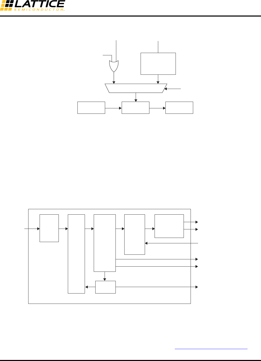
Idle Insert for Gigabit Ethernet Mode
The PCS set to Gigabit Ethernet Mode provides for insertion of /I2/ symbols into the receive data stream for auto-
negotiation. Gigabit Ethernet auto-negotiation is performed in soft logic. This function inserts a sequence of 8 /I2/
ordered sets every 2048 clock cycles. /I2/ insertion is controlled by the xmit_ch(0-3) input to the PCS which is
driven from the autonegotiation soft logic. Figure 8-11 shows one channel (channel 0 in this example) of receive
logic when the PCS is set to Gigabit Ethernet Mode showing these control/status signals.
Figure 8-11. PCS Receive Path for Gigabit Ethernet Mode (Channel 0 Example)
Clock Tolerance Compensation
The Clock Tolerance Compensation (CTC) module performs clock rate adjustment between the recovered receive
clocks and the locked reference clock. Clock compensation is performed by inserting or deleting bytes at pre-
defined positions, without causing loss of packet data. A 16-byte CTC FIFO is used to transfer data between the
two clock domains and will accommodate clock differences of up to the specified ppm tolerance for the
LatticeECP3 SERDES (see DC and Switching Characteristics section of the LatticeECP3 Family Data Sheet).
1:8 / 1:10
Deserializer
1
External
0
Internal
Word
Aligner
8b10b
Decoder
EN
Internal Link
State Machine
word_align_en_ch0_c
from FPGA fabric
word_align_enable
CH_01[7] ilsm_en
CH_04[6]
lsm_sel
CH_04[7]
De-
Serializer
Word
Aligner
8b10b
Decoder
rxdata_ch0[7:0]
rx_k_ch0[0]
xmit_ch0[0]
rx_disp_err_ch0[0]
rx_cv_err_ch0[0]
lsm_status_ch[0]_s
Gigabit
Ethernet
/I2/
Insert
Clock
Tolerance
Compensation
(CTC)
Link State
Machine
8-23
LatticeECP3 SERDES/PCS
Usage Guide
A channel has the Clock Tolerance Compensation block enable when that channel’s attribute CHx_CTC is set to
“ENABLED”. The CTC is bypassed when that channel’s attribute CHx_CTC is set to “DISABLED”.
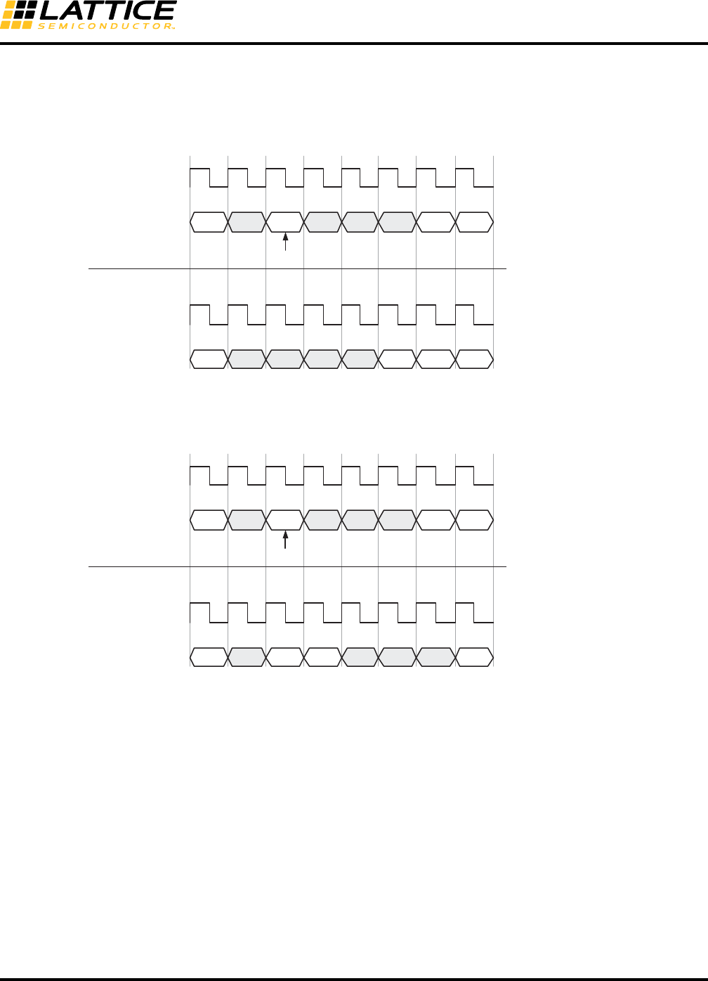
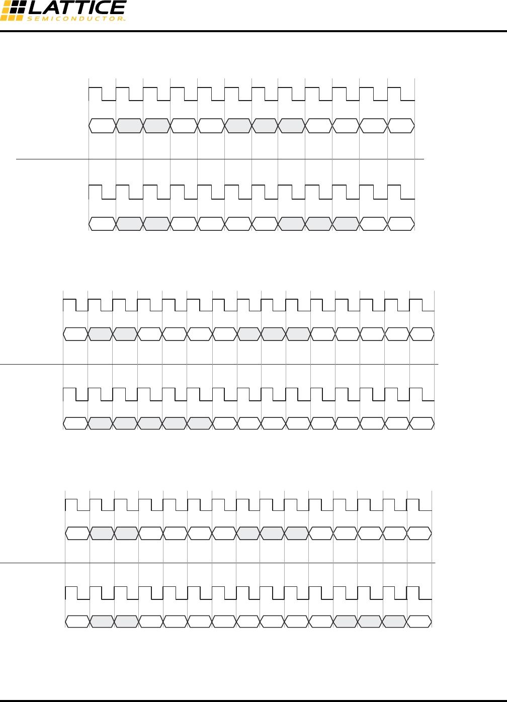
A diagram illustrating 1-byte deletion is shown in Figure 8-12.
Figure 8-12. Clock Tolerance Compensation 1-Byte Deletion Example
A diagram illustrating 1-byte insertion is shown in Figure 8-13.
Figure 8-13. Clock Tolerance Compensation 1-Byte Insertion Example
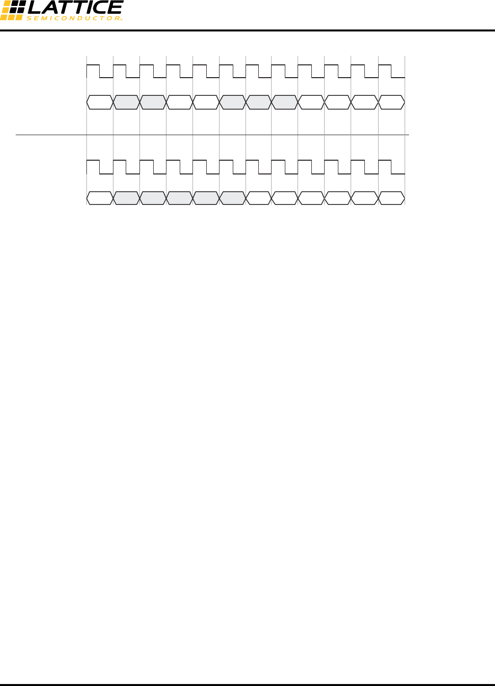
A diagram illustrating 2-byte deletion is shown in Figure 8-14.
rxiclk_ch0 or
ebrd_clk_ch0
Before CTC
rxdata_ch0[7:0] E = End of Packet
I = Logical Idle
SK = Skip
S = Start of Packet
D = Data
After CTC
rxdata_ch0[7:0]
E IIISKI DS
E III DI DS
Delete if CTC FIFO Almost Full & SK = CC_MATCH4
rxiclk_ch0 or
ebrd_clk_ch0
rxiclk_ch0 or
ebrd_clk_ch0
Before CTC
rxdata_ch0[7:0] E = End of Packet
I = Logical Idle
SK = Skip
S = Start of Packet
D = Data
After CTC
rxdata_ch0[7:0]
E IIISKI DS
E ISKSK SI
Insert if CTC FIFO Almost Empty & SK = CC_MATCH4
rxiclk_ch0 or
ebrd_clk_ch0
I I
8-24
LatticeECP3 SERDES/PCS
Usage Guide
Figure 8-14. Clock Tolerance Compensation 2-Byte Deletion Example
rxiclk_ch0 or
ebrd_clk_ch0
Before CTC
rxdata_ch0[7:0] E = End of Packet
I = Logical Idle
SK1 = CC_MATCH3
SK2 = CC_MATCH4
S = Start of Packet
D = Data
After CTC
rxdata_ch0[7:0]
E I II SK1I DS
E III DI DS
rxiclk_ch0 or
ebrd_clk_ch0
SK2 I
I D D
DD
D
8-25
LatticeECP3 SERDES/PCS
Usage Guide
A diagram illustrating 2-byte insertion is shown in Figure 8-15.
Figure 8-15. Clock Tolerance Compensation 2-Byte Insertion Example
A diagram illustrating 4-byte deletion is shown in Figure 8-16.
Figure 8-16. Clock Tolerance Compensation 4-Byte Deletion Example
A diagram illustrating 4-byte insertion is shown in Figure 8-17.
Figure 8-17. Clock Tolerance Compensation 4-Byte Insertion Example
rxiclk_ch0 or
ebrd_clk_ch0
Before CTC
rxdata_ch0[7:0] E = End of Packet
I = Logical Idle
SK1 = CC_MATCH3
SK2 = CC_MATCH4
S = Start of Packet
D = Data
After CTC
rxdata_ch0[7:0]
E I II SK1I DS
E IIII DS
rxiclk_ch0 or
ebrd_clk_ch0
SK2 I
ISK1 SK2 SK1 SK2
DD
rxiclk_ch0 or
ebrd_clk_ch0
Before CTC
rxdata_ch0[7:0]
E = End of Packet
I = Logical Idle
SK1 = CC_MATCH1
SK2 = CC_MATCH2
SK3 = CC_MATCH3
SK4 = CC_MATCH4
S = Start of Packet
D = Data
After CTC
rxdata_ch0[7:0]
E II
E II
rxiclk_ch0 or
ebrd_clk_ch0
I I DS
DDS
I
D D
DD
D
SK1
II
SK2 SK3
I
SK4
DD
D
D
rxiclk_ch0 or
ebrd_clk_ch0
Before CTC
rxdata_ch0[7:0]
E = End of Packet
I = Logical Idle
SK1 = CC_MATCH1
SK2 = CC_MATCH2
SK3 = CC_MATCH3
SK4 = CC_MATCH4
S = Start of Packet
D = Data
After CTC
rxdata_ch0[7:0]
E II
E II
rxiclk_ch0 or
ebrd_clk_ch0
I I DS
S
I DSK1
II
SK2 SK3 SK4
SK1 SK2 SK3 SK4 SK1 SK2 SK3 SK4
DD
I

8-26
LatticeECP3 SERDES/PCS
Usage Guide
When the CTC is used, the following settings for clock compensation must be set, as appropriate, for the intended
application:
•Set the insertion/deletion pattern length using the CC_MATCH_MODE attribute. This sets the number of
skip bytes the CTC compares to before performing an insertion or deletion. Values for CC_MATCH_MODE are
“1” (1-byte insertion/deletion), “2” (2-byte insertion/deletion), and “4” (4-byte insertion/deletion). The minimum
interpacket gap must also be set as appropriate for the targeted application. The interpacket gap is set by
assigning values to attribute CC_MIN_IPG. Allowed values for CC_MIN_IPG are “0”, “1”, “2”, and “3”. The mini-
mum allowed interpacket gap after skip character deletion is performed based on these attribute settings is
described in Table 8-10.
•The skip byte or ordered set must be set corresponding to the CC_MATCH_MODE chosen. For 4-byte
insertion/deletion (CC_MATCH_MODE = “4”), the first byte must be assigned to attribute CC_MATCH1, the sec-
ond byte must be assigned to attribute CC_MATCH2, the third byte must be assigned to attribute CC_MATCH3,
and the fourth byte must be assigned to attribute CC_MATCH4. Values assigned are 10-bit binary values.
For example:
If a 4-byte skip ordered set is /K28.5/D21.4/D21.5/D21.5, then “CC_MATCH1” should be “0110111100”,
“CC_MATCH2” = “0010010101”, “CC_MATCH3” = “0010110101” and “CC_MATCH4” = “0010110101”.
For a 2-byte insertion/deletion (CC_MATCH_MODE = “2”), the first byte must be assigned to attribute
CC_MATCH3, and the second byte must be assigned to attribute CC_MATCH4.
For a 1-byte insertion/deletion (CC_MATCH_MODE = “1”), the skip byte must be assigned to attribute
CC_MATCH4.
•The clock compensation FIFO high water and low water marks must be set to appropriate values for the
targeted protocol. Values can range from 0 to 15 and the high water mark must be set to a higher value than the
low water mark (they should not be set to equal values). The high water mark is set by assigning a value to attri-
bute CCHMARK. Allowed values for CCHMARK are hex values ranging from “0” to “F”. The low water mark is set
by assigning a value to attribute CCLMARK. Allowed values for CCLMARK are hex values ranging from “0” to
“F”.
• Clock compensation FIFO overrun can be monitored on a per-channel basis on the PCS/FPGA interface port
labeled cc_overrun_ch(0-3) if “Error Status Ports” is selected when generating the PCS block with the module
generator.
• Clock compensation FIFO underrun can be monitored on a per-channel basis on the PCS/FPGA interface port
labeled cc_underrun_ch(0-3) if “Error Status Ports” is selected when generating the PCS block with the module
generator.
8-27
LatticeECP3 SERDES/PCS
Usage Guide
Calculating Minimum Interpacket Gap
Table 8-10 shows the relationship between the user-defined values for interpacket gap (defined by the
CC_MIN_IPG attribute), and the guaranteed minimum number of bytes between packets after a skip character
deletion from the PCS. The table shows the interpacket gap as a multiplier number. The minimum number of bytes
between packets is equal to the number of bytes per insertion/deletion times the multiplier number shown in the
table. For example, if the number of bytes per insertion/deletion is 4 (CC_MATCH_MODE is set to “4”), and the
minimum interpacket gap attribute CC_MIN_IPG is set to “2”, then the minimum interpacket gap is equal to 4
(CC_MATCH_MODE = “4”) times 3 (Table 8-10 with CC_MIN_IPG = “2”) or 12 bytes. The PCS will not perform a
skip character deletion until the minimum number of interpacket bytes have passed through the CTC.
Table 8-10. Minimum Interpacket Gap Multiplier
Note on CTC support in the LatticeECP3-150EA device family with TW suffix: For the initial release of
LatticeECP3-150EA device with TW suffix, the CTC in the PCS is not supported. The CTC feature can be
bypassed and implemented in soft IP. Many IP cores from Lattice implement the CTC logic in soft form.
Using IPexpress with Diamond
IPexpress is used to create and configure SERDES and PCS blocks. Designers use the GUI to select the SERDES
Protocol Standard for a particular quad or channel. IPexpress takes the input from this GUI and generates a config-
uration file (.txt file) and HDL netlist. The HDL model is used in the simulation and synthesis flow. The configuration
file contains attribute-level map information. This file is input for simulation and the bitgen program. It is strongly
recommended that designers make changes and updates in IPexpress and then regenerate the configuration file.
In some exceptional situations, users can modify the configuration file.
CC_MIN_IPG
Insert/Deletion
Multiplier Factor
01x
12x
23x
34x
8-28
LatticeECP3 SERDES/PCS
Usage Guide
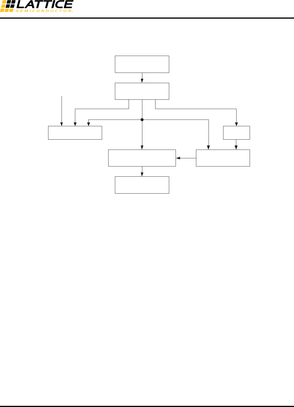
Figure 8-18 shows the tools flow when using IPexpress to generate the SERDES/PCS block for the SERDES Pro-
tocol Standard.
Figure 8-18. SERDES_PCS Diamond User Flow
IPexpress
SERDES/PCS Module
GUI Configuration
IPexpress
SCUBA Engine
CAE Simulator Synthesis
Diamond
Map, Place and Route
SERDES/PCS
Behavioral Model
Module netlist
(.v or .vhd)
Module netlist
(.v or .vhd)
.ptx file converted from .txt file
(Autoconfig file: Attribute Info)
Bitstream
(includes register map
memory cell configuration)
LatticeECP3
Device
8-30
LatticeECP3 SERDES/PCS
Usage Guide
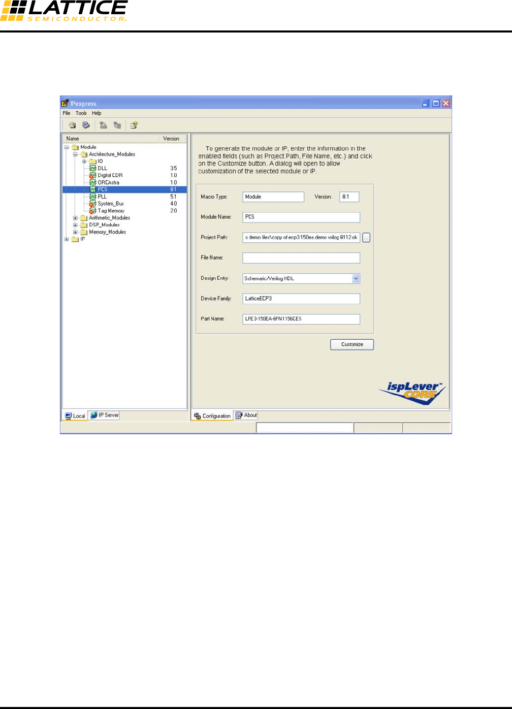
Quad Setup Tab
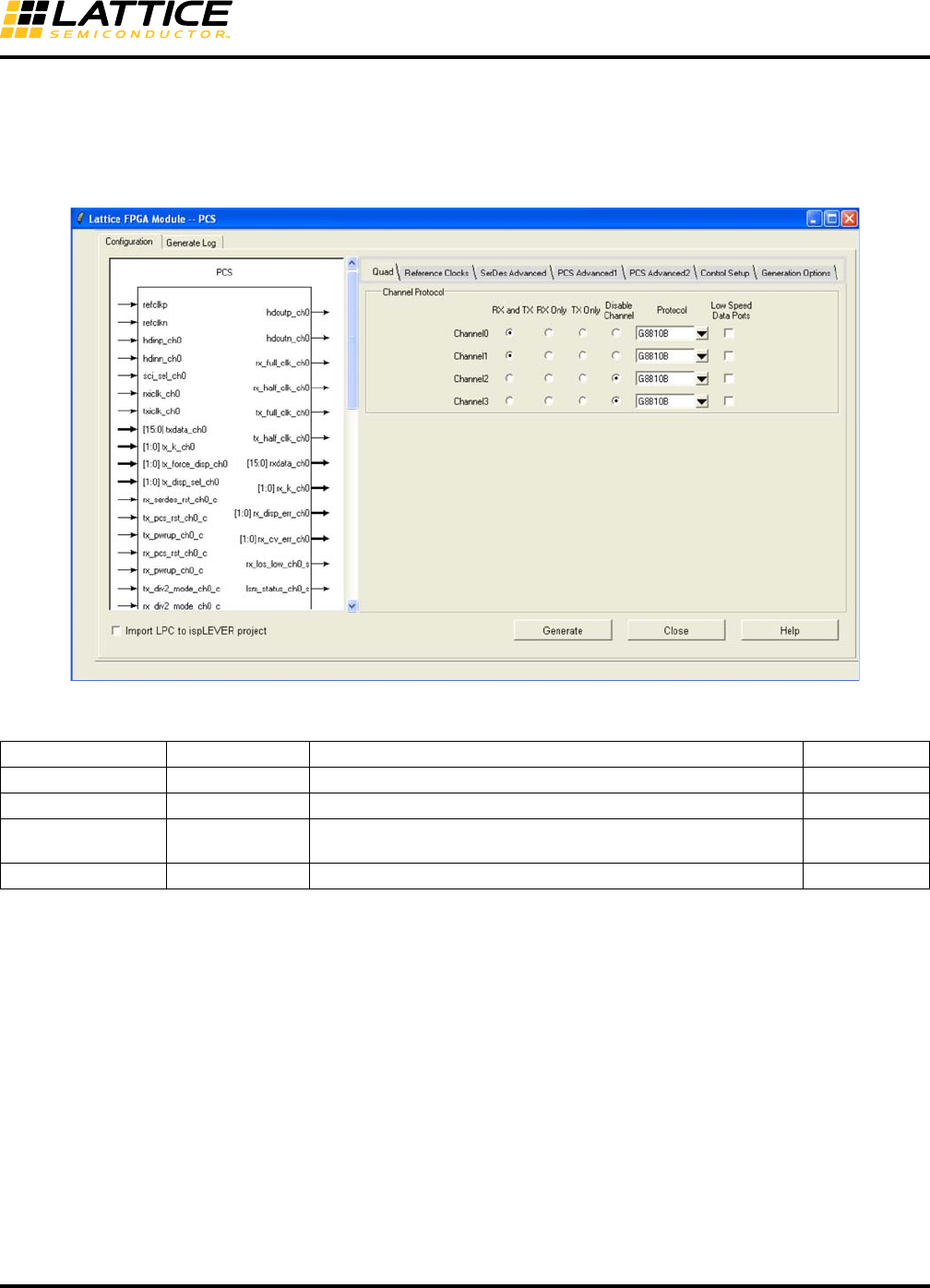
Figure 8-20 shows the Quad Setup Tab window when the file name is entered and the Customize button is
checked in the main window. The first entry required in this window is to select a Protocol Mode for each channel.
Each channel can be configured as ‘RX and TX’, ‘RX Only’, ‘TX Only’, ‘Disabled’ or ‘Low Speed Data Port’.
Figure 8-20. Configuration GUI - Quad Setup Tab
Table 8-11. SERDES_PCS GUI Attributes - Quad Tab Setup
GUI Text Attribute Name Range Default Value
Channel Protocol CHx_MODE RX and TX, RX Only, TX Only DISABLED
Disable Channel1CHx_MODE ENABLE, DISABLE DISABLED
Protocol CHx_PROTOCOL GIGE, SGMII, XAUI, SRIO, PCIE, SDI, G8B10B, 10BSER,
8BSER, CPRI, OBSAI G8B10B
Low Speed Data Port CHx_LDR RX and TX, RX Only, TX Only DISABLED
1. For the LatticeECP3-17EA device in the 328-ball csBGA package, only channels 0 and 3 are available.
8-31
LatticeECP3 SERDES/PCS
Usage Guide
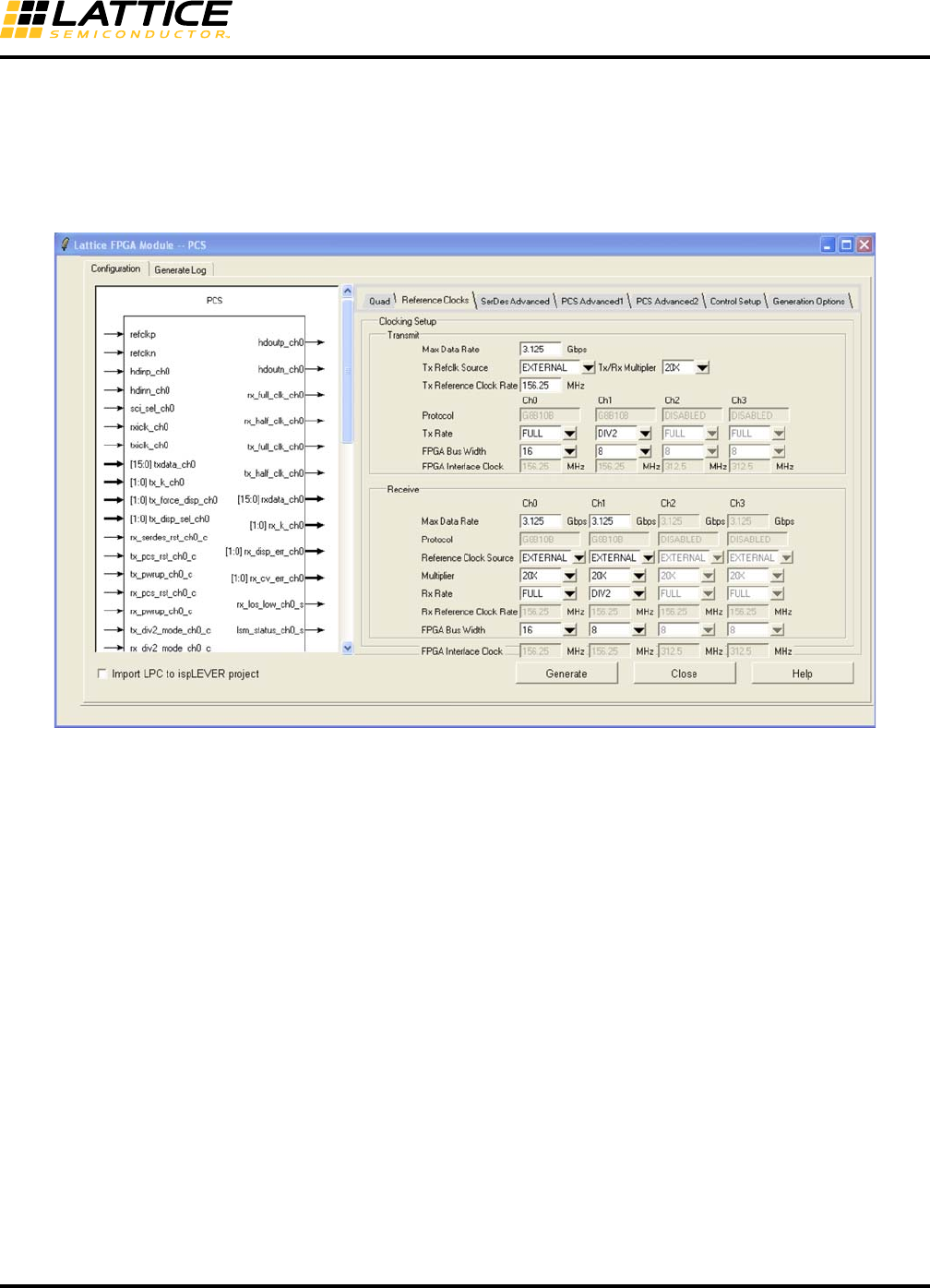
Reference Clock Setup Tab
In this tab, the attributes of the TX and RX reference clock sources are selected. Users can select either a EXTER-
NAL or INTERNAL reference clock. Further, there is a tool to provide the required clock rate and multiplier settings
for a particular data rate. In addition, for a given data bus width the tool provides the required clock rate to interface
the channel to the core.
Figure 8-21. Configuration GUI - Reference Clocks Setup Tab
8-32
LatticeECP3 SERDES/PCS
Usage Guide
Table 8-12. SERDES_PCS GUI Attributes - Reference Clocks Setup Tab
GUI Text Attribute Name Range
Default
Value (GUI)
Default Value
(Attribute)
Transmit
Max. Data Rate1N/A 0.23 to 3.2 Gbps 2.5 Gbps N/A
TX Refclk Source PLL_SRC INTERNAL, EXTERNAL INTERNAL REFCLK_INT
TX/RX Multiplier REFCK_MULT 8X, 10X, 16X, 20X, 25X Protocol Dependent
TX Reference clock Rate #REFCLK_RATE2Protocol Dependent
Protocol No user access. For information only.
TX Rate CHx_TX_DATA_RATE FULL, DIV2, DIV11 FULL FULL
FPGA Bus Width CHs_TX_DATA_WIDTH 8, 10, 16, 20 Protocol Dependent
FPGA Interface Clock #CH0_TX_FICLK_RATE
Receive
Max. Data Rate1N/A 0.23 to 3.2 Gbps 2.5 Gbps N/A
Protocol No user access. For information only.
Refclk Source CHx_CDR_SRC INTERNAL, EXTERNAL INTERNAL REFCLK_INT
Multiplier No user access. For information only
RX Rate CHx_RX_DATA_RATE FULL, DIV2, DIV11 FULL FULL
RX Reference Clock Rate #CH0_RXREFCLK_RATE
FPGA Bus Width CHx_RX_DATA_WIDTH 8, 10, 16, 20 Protocol Dependent
FPGA Interface Clock #CH0_RX_FICLK_RATE
1. Rate is not reflected in the autoconfig file. Instead, DATARATE RANGE is specified for a given data rate as: 150 Mbps LOWLOW 230
Mbps, 230 Mbps < LOW 450 Mbps, 450 Mbps < MEDLOW 0.9 Gbps, 0.9 Gbps < MED 1.8 Gbps, 1.8 Gbps < MEDHIGH 2.55 Gbps,
2.55 Gbps < HIGH 3.2Gbps.
2. Attributes preceded by '#' represent attributes that are for user information only. These attributes are also included in the auto-config file for
reference.
8-33
LatticeECP3 SERDES/PCS
Usage Guide
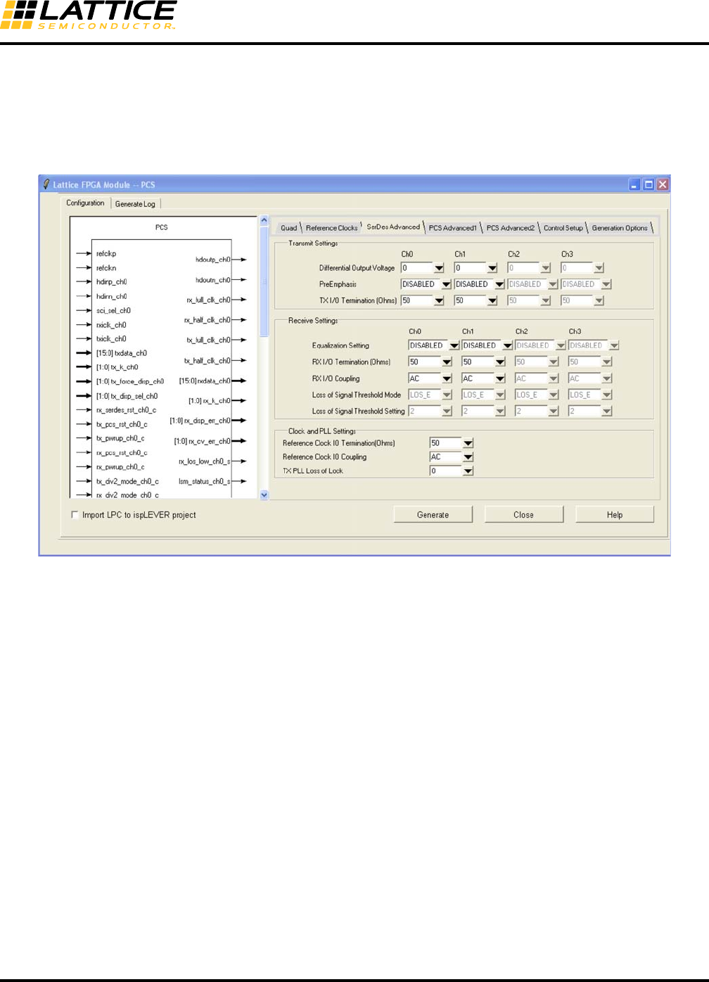
SERDES Advance Setup
This tab is used to access the advanced attributes of the transmit and receive SERDES for all four channels. Trans-
mit attributes such as PreEmphasis, Termination, Differential Output Voltage selection are selected. Receive attri-
butes such as Equalization, Termination, I/O Coupling are selected. Attributes for Transmit SERDES Clock and PLL
are also selected.
Figure 8-22. Configuration GUI - SERDES Advanced Setup Tab

8-34
LatticeECP3 SERDES/PCS
Usage Guide
Table 8-13. SERDES_PCS GUI Attributes – SERDES Advanced Setup Tab
GUI Text Attribute Name Value
Default
Value
Differential Output Voltage CHx_TDRV8
-4 (640mV)5, -3 (780mV), -2 (870mV), -1 (920mV),
0 (1040mV:default), 1 (1130mV)6, 2 (1260mV)7,
3 (1350mV)7, 4 (1440mV)7
0
PreEmphasis CHx_TX_PRE Disabled, 0 (0%), 1 (5%), 2 (12%), 3 (18%), 4 (25%),
5 (33%), 6 (40%), 7 (48%) DISABLED
TX I/O Termination
(Ohms)3CHx_RTERM_TX 50, 75, 5K 50
Equalization1CHx_RX_EQ Disabled, Mid_Low, Mid_Med, Mid_High, Long_Low,
Long_Med, Long_High DISABLED
RX I/O Termination
(Ohms)3CHx_RTERM_RX 50, 60, 75, High 50
RX I/O Coupling CHx_RX_DCC AC, DC AC2
Loss of Signal Threshold CHx_LOS_THRESHOLD_LO 2 (+15%),3 (+25%) 24
TX PLL Reference Clock
I/O Termination (Ohms)3PLL_TERM 50, 2K 50
TX PLL Reference Clock
I/O Coupling PLL_DCC AC, DC AC10
PLL Loss of Lock PLL_LOL_SET
0: +/- 1350ppm x29
1: +/- 2400ppm x2
2: +/- 6800ppm
3: +/- 400ppm
0
1. Refer to Table 8-106 for details.
2. The typical capacitor value of the internal on-chip AC coupling is 5 pF.
3. Termination resistors and their usage:
RX I/O Termination:
– 50: So far all of the protocols except SMTPE use a 50-Ohm termination resistor.
– 60: Provided for flexibility.
– 75: SMPTE uses a 75-Ohm termination resistor.
– HIGH: Default value when Rx is not used.
TX I/O Termination:
– 50: So far all of the protocols except SMTPE use a 50-Ohm termination resistor.
– 75: SMPTE uses a 75-Ohm termination resistor.
– 5K: Such as PCI Express electric idle and PCI Express RX detection. User does not set this termination value for RX detection.
Refer to the PCI Express Receiver Detection section.
TX PLL Termination:
– 50: If there is no 50-Ohm termination resistor on the PCB.
– 2K: If there is a 50-Ohm termination resistor on the PCB.
4. PCS configuration, GUI supports only the value 2 for all protocols except PCI Express. For PCI Express, both values 2 and 3 are sup-
ported.
5. TDRV_AMP_BOOST(CH_13[3]) is set to 1 to achieve this amplitude.
6. This setting is the PCI Express default setting. It is recommended to use this default setting with the PCI Express protocol. The IPexpress
GUI TDRV drop-down window is grayed out for this reason. Other settings can still be used by editing the attribute CHn_TDRV in the auto-
config file(.txt file).
7. VCCOB must be 1.5V for these settings.
8. The values are typical numbers. There is about +/-20% of margin for the whole frequency range. Refer to Table 8-105, CHn_TDRV row for
details.
9. ‘x2’ indicates successful double count of ppm in the internal LOL counter.
10. AC-coupling is recommended for most applications. DC-coupling should be used only in conjunction with an external AC-coupling capaci-
tor.
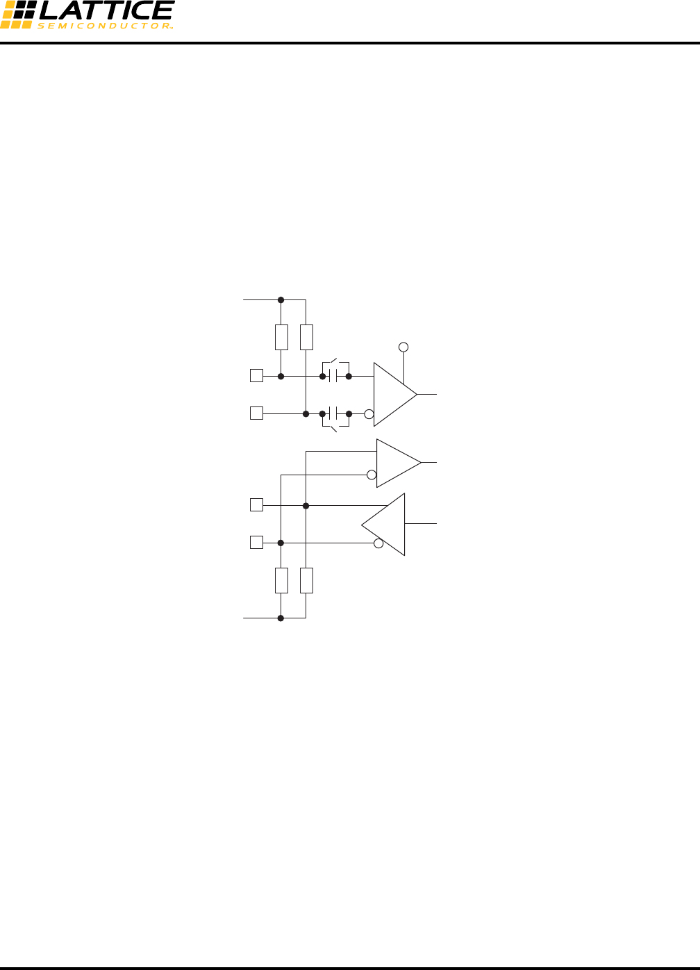
8-35
LatticeECP3 SERDES/PCS
Usage Guide
Assignment of PCS Location
Users can specify their desired location of the PCS quad by writing in the constraint file (.lpf). The preference
“locate” is used. An example of the syntax is shown below.
LOCATE COMP "pcs_inst_name" SITE "PCSB" ;
Quad Name Site Name
Quad A PCSA
Quad B PCSB
Quad C PCSC
Quad D PCSD
High-speed I/O termination topology is shown in Figure 8-23.
Figure 8-23. High-Speed I/O Terminations
EQ
50/60/75/High
VCCA
HDINP
HDINN
VCCIB
5 pF
50/75/5K
HDOUTP
HDOUTN
VCCOB
50/60/75/High
50/75/5K
PCI Receiver Detect
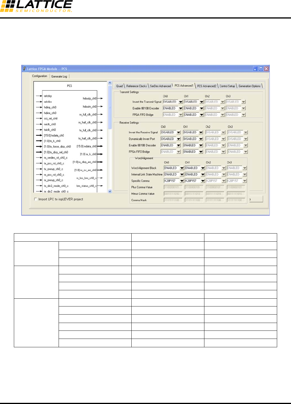
8-36
LatticeECP3 SERDES/PCS
Usage Guide
PCS Advanced1 Setup
This tab is used to access the advanced attributes of the transmit and receive PCS for all four channels. The polar-
ity and operating mode (e.g. 8b10b) of each individual TX and RX channel can be individually selected. In addition,
word alignment values such as comma values, comma mask and comma align can be selected.
Figure 8-24. Configuration GUI - PCS Advanced1 Setup Tab
Table 8-14. SERDES/PCS GUI – PCS Advanced1 Setup Tab
GUI Text Attribute Name Default
Transmitter
Invert the Transmit Signal CHx_TX_SB DISABLED
Enable 8b10b Encoder CHx_TX_8B10B Protocol Dependent
FPGA FIFO Bridge CHx_TX_FIFO Protocol Dependent
Receiver
Invert the Receive Signal CHx_RX_SB DISABLED
Dynamically Invert Port N/A DISABLED
Enable 8b10b Decoder CHx_RX_8B10B Protocol Dependent
FPGA FIFO Bridge CHx_RX_FIFO Protocol Dependent
Word Alignment
Word Alignment Block CHx_RXWA Protocol Dependent
Internal Link CHx_ILSM Protocol Dependent
Specific Comma #CHx_SCOMMA Protocol Dependent
Plus Comma Value CHx_COMMA_A11100000101
Minus Comma Value CHx_COMMA_B 0011111010
Comma Mask CHx_COMMA_M Protocol Dependent2
1. By definition, COMMA_A and COMM_B are one set of 8b10b-encoded control characters with positive and negative running
disparities. Users must provide the proper IDLE sequence per the protocol in order to get the link state machine synchroniza-
tion. For example, 1 GbE protocol needs K28.5+D5.6 or D16.2 as IDLE (word alignment and sync state machine). The default
values are in little endian format.
2. In most applications, K28.5 is used as the comma character. The default value of the mask is 1111111111. In G8B10B mode,
any comma can be used so the mask will be 1111111100 to detect any of the three comma characters, K28.1, 28.5, 28.7.
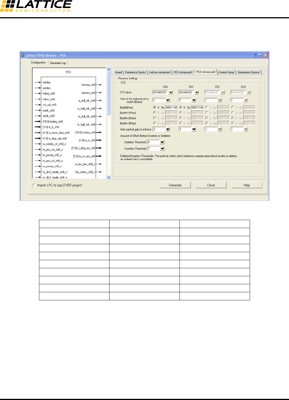
8-37
LatticeECP3 SERDES/PCS
Usage Guide
PCS Advanced2 Setup
This tab is used for setting values for the Clock Tolerance Compensation block.
Figure 8-25. Configuration GUI – PCS Advanced2 Setup Tab
Table 8-15. SERDES/PCS GUI – PCS Advanced2 Setup Tab
GUI Text Attribute Name Default
CTC block CHx_CTC Protocol Dependent1
Size of ordered set CHx_CC_MATCH_MODE Protocol Dependent
Byte N CHx_CC_MATCH1 Protocol Dependent
Byte N+1 CHx_CC_MATCH2 Protocol Dependent
Byte N+2 CHx_CC_MATCH3 Protocol Dependent
Byte N+3 CHx_CC_MATCH4 Protocol Dependent
Interpacket gap CHx_CC_MIN_IPG Protocol Dependent
Deletion threshold CCHMARK 9
Insertion threshold CCLMARK 7
1. Always disabled: XAUI, SDI, CPRI, OBSAI, Serial Rapid IO, 10-bit SERDES, 8-bit SERDES
All other modes: Disabled by default. Most of the CTC features are provided in IP.
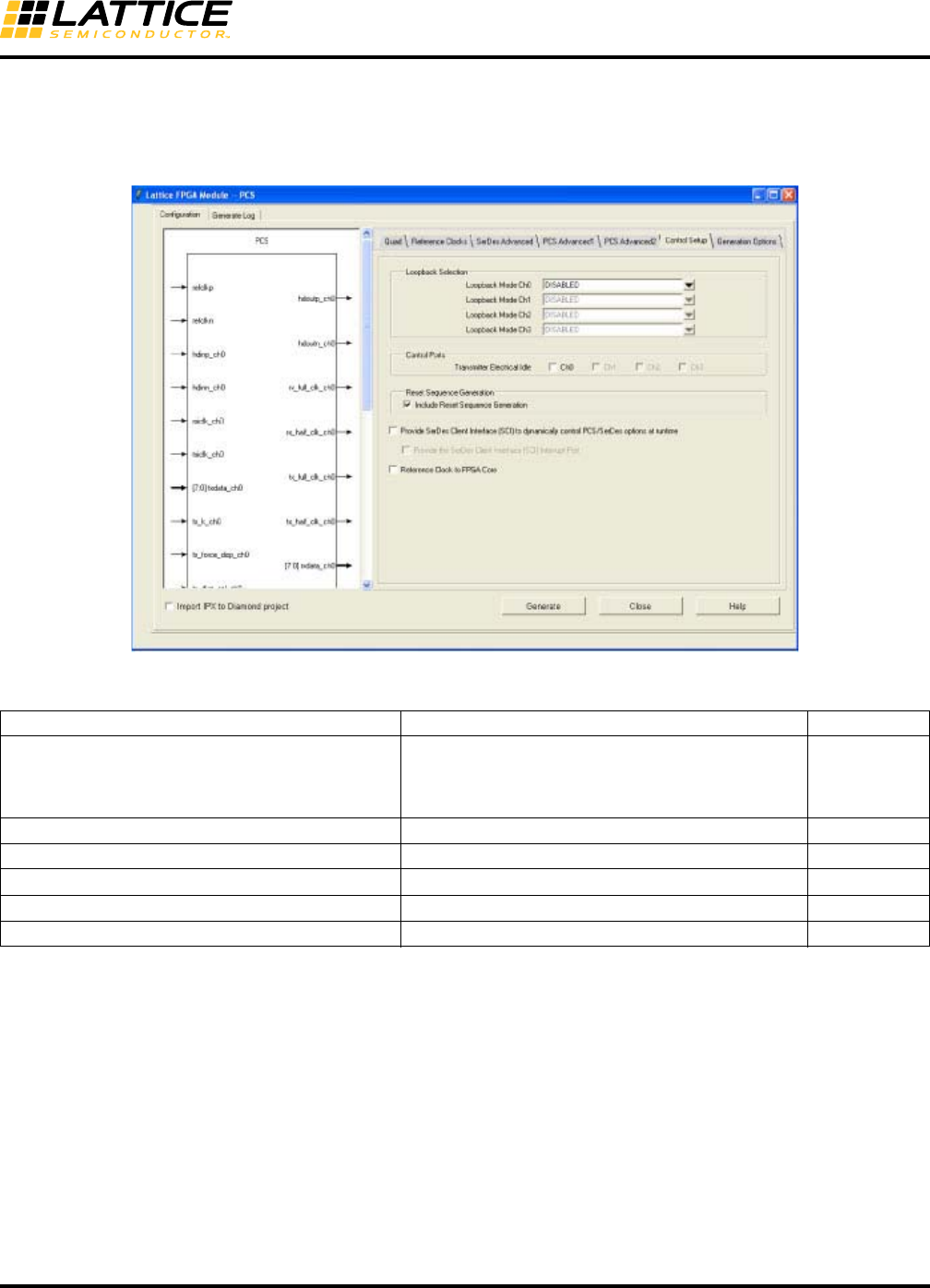
8-38
LatticeECP3 SERDES/PCS
Usage Guide
Control Setup
This tab is used to select the SCI interface and other debug and control options. In addition, users can enable the
SCI, error reporting, PLL quarter clock, and loopback capability.
Figure 8-26. Configuration GUI – Control Setup Tab
Table 8-16. Tab 5, SERDES_PCS GUI Attributes – Control Setup Tab
Reference Clock to FPGA Core and Reset Sequence
The reset sequence uses a reference clock in the Reset State Machine.
If “Internal” is selected as the Tx Refclk source, the Reset State Machine uses the internal reference clock.
If “External” is selected as the Tx Refclk source, the Reset State Machine uses the Reference Clock to FPGA Core
signal transparent to the user (Control Register bit, QD_0A[1] is set). The REFCLK2FPGA signal will be included in
the wrapper module only when “Reference Clock to FPGA Core” is selected.
GUI Text Attribute Name Default
Loopback Mode (Ch0, Ch1, Ch2, Ch3)
DISABLED
Loopback serial data after equalizer
Loopback serial data after transmit driver
Loopback parallel data after de_serializer
DISABLED1
Transmitter Electrical Idle signal tx_idle_ch0_c is provided DISABLED
Include Reset Sequence Generation2Include the TX and RX Reset Sequence ENABLED
Provide SERDES Client Interface N/A
Provide the SERDES Client Interface Interrupt Port INT_ALL DISABLED
Reference Clock to FPGA core QD_REFCK2CORE DISABLED
1. When loopback mode is in default mode (DISABLED), the two SERDES Bridge Parallel loopback control signals (sb_felb_ch[3:0]_c and
sb_felb_rst_ch[3:0]_c) are available in the HDL module for users to turn on and off the loopback mode dynamically. These signals should be
tied to ground if loopback mode is not used.
2. Reset Sequence Generation is described in the SERDES/PCS RESET section of this document.
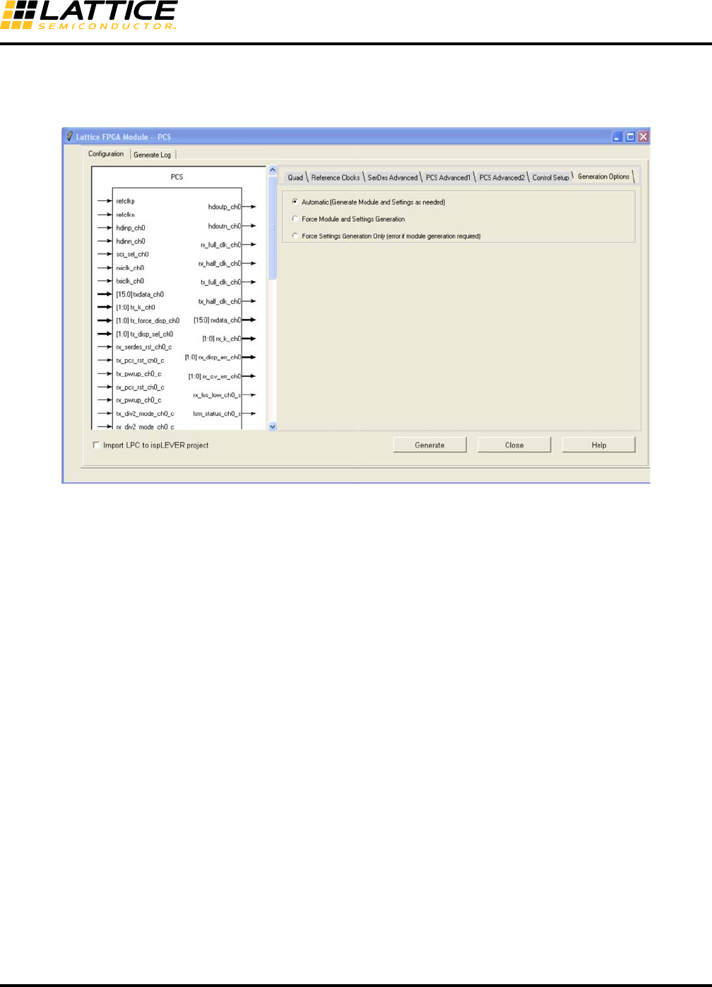
8-39
LatticeECP3 SERDES/PCS
Usage Guide
Generation Options
This tab provides options for users to select the PCS module generation output files of their choice.
Figure 8-27. Configuration GUI – Generation Options Tab
When migrating an older project created in a previous version of Diamond to the latest version for the first time, it is
highly recommended to regenerate the PCS module in the latest version even if no configuration changes are
required. This will ensure the most current set of primitive library elements is used. If this is not done, it is possible
that the design may either fail in the flow or go through the flow but show unexpected behavior on the board.
When regenerating the PCS module in an existing project, often the HDL file remains the same and only the config-
uration file must be regenerated. In this case, users can run the “Generate Bitstream Data” and “Force One Level”
option to save compile time.
•Automatic – When selected, IPexpress will generate only the necessary files. This can include both the HDL
and TXT files or just the TXT file. This is the default setting.
•Force Module and Settings Generation – When selected, both the HDL and TXT files will be generated. This
forces the Project Navigator processes to be reset back to synthesis.
•Force Settings Generation Only – When selected, only the TXT file will be generated. If HDL generation is nec-
essary, an error message will be provided.
•Flow Definitions – The generation option works differently between the two module flows.
–HDL Source Flow: HDL File in Project Navigator
The existing LPC file can be opened from IPexpress for regeneration. In this case, the reset point set by the
GUI will be the new starting point. So, when the user double-clicks a process or runs the “Force One Level”
option, it will start at that reset point.
–LPC Source Flow: LPC File in Project Navigator
Opening the LPC file and regenerating the PCS module will reset the whole process whether or not the HDL
module is regenerated.
In either case, the checkmarks in the Processes window will remain unchanged but will be updated as soon
as the user starts the process.

8-40
LatticeECP3 SERDES/PCS
Usage Guide
Configuration File Description
IPexpress generates this file which contains attribute-level map information. This file is used by the simulation
model as well as the bitstream generation process to automatically initialize the PCSD quad to the mode selected
in IPexpress.
The configuration file uses “txt” as the file type extension.
Below is an example of the configuration file.
# This file is used by the simulation model as well as the bitstream
# generation process to automatically initialize the PCSD quad to the mode
# selected in the IPexpress. This file is expected to be modified by the
# end user to adjust the PCSD quad to the final design requirements.
DEVICE_NAME "LFE3-95E"
CH0_MODE "RXTX"
CH1_MODE "DISABLED"
CH2_MODE "DISABLED"
CH3_MODE "DISABLED"
TX_DATARATE_RANGE "HIGH"
PLL_SRC "REFCLK_EXT"
REFCK_MULT "10X"
#REFCLK_RATE 250.0
CH0_PROTOCOL "G8B10B"
CH0_LDR "RXTX"
CH0_RX_DATARATE_RANGE "HIGH"
CH0_TX_DATA_RATE "FULL"
CH0_TX_DATA_WIDTH "8"
CH0_TX_FIFO "DISABLED"
CH0_CDR_SRC "REFCLK_EXT"
#CH0_TX_FICLK_RATE 250.0
CH0_RX_DATA_RATE "FULL"
CH0_RX_DATA_WIDTH "8"
CH0_RX_FIFO "DISABLED"
#CH0_RX_FICLK_RATE 250.0
CH0_TDRV "0"
CH0_TX_PRE "DISABLED"
CH0_RTERM_TX "50"
CH0_RX_EQ "DISABLED"
CH0_RTERM_RX "50"
CH0_RX_DCC "AC"
CH0_LOS_THRESHOLD_LO "2"
CH0_TX_SB "DISABLED"
CH0_TX_8B10B "ENABLED"
CH0_RX_SB "DISABLED"
CH0_RX_8B10B "ENABLED"
CH0_RXWA "ENABLED"
CH0_ILSM "ENABLED"
#CH0_SCOMMA "1111111111"
CH0_COMMA_A "1100000101"
CH0_COMMA_B "0011111010"
CH0_COMMA_M "1111111100"
CH0_CTC "ENABLED"

8-41
LatticeECP3 SERDES/PCS
Usage Guide
CH0_CC_MATCH_MODE "2"
CH0_CC_MATCH1 "0000000000"
CH0_CC_MATCH2 "0000000000"
CH0_CC_MIN_IPG "3"
CH0_SSLB "DISABLED"
CH0_SPLBPORTS "DISABLED"
CH0_PCSLBPORTS "DISABLED"
PLL_TERM "50"
PLL_DCC "AC"
PLL_LOL_SET "0"
CCHMARK "9"
CCLMARK "7"
INT_ALL "DISABLED"
QD_REFCK2CORE "ENABLED"
8-Bit and 10-Bit SERDES-Only Modes
This section describes the operation of the two modes of the SERDES/PCS block, 8-bit SERDES-Only and 10-bit
SERDES-Only. These modes are intended for applications requiring access to a high-speed I/O interface without
the protocol-based manipulation provided in the LatticeECP3 PCS logic.
Transmit Path
• Serializer: Conversion of 8-bit or 10-bit parallel data to serial data.
Receive Path
• Deserializer: Conversion of serial data to 8-bit or 10-bit parallel data.
• Optional word alignment to user-defined alignment pattern.
Generic 8b10b Mode
The Generic 8b10b mode of the SERDES/PCS block is intended for applications requiring 8b10b encoding/decod-
ing without the need for additional protocol-specific data manipulation. The LatticeECP3 SERDES/PCS block can
support Generic 8b10b applications up to 3.2 Gbps per channel. In Generic 8b10b mode, the word aligner can be
controlled from the embedded PCS Link State Machine (LSM).
When the embedded Link State Machine is selected and enabled, the lsm_status_ch[3:0]_s status signal will go
high upon successful link synchronization.
To achieve link synchronization in this mode, the following conditions need to be satisfied on the 8b10b patterns
received at the SERDES channel’s receiver input (hdinp_ch[0-3]/hdinn_ch[0-3]):
• Periodic 8b10b encoded comma characters need to be present in the serial data. Periodicity is required to allow
the LSM to re-synchronize to commas upon loss of sync. The comma characters should correspond to the “Spe-
cific Comma” value shown in Figure 8-24. For example, when the Specific Comma is set to K28P157, the comma
value on the serial link can be the 8b10b encoded version of any of K28.1 (k=1, Data=0x3C), K28.5 (k=1,
Data=0xBC), or K28.7 (k=1, Data=0xFC). Note though that K28.5 is most commonly used.
• A comma character has to be followed by a data character
• Two comma characters have to be an even number of word clock cycles apart
8-42
LatticeECP3 SERDES/PCS
Usage Guide
Additional information:
• It takes roughly four good comma/data pairs for the LSM to reach link synchronization
• It takes four consecutive errors (illegal 8b10b encoded characters, code violations, disparity errors, uneven num-
ber of clock cycles between commas) to cause the LSM to unlock
• A CDR loss of lock condition will cause the LSM to unlock by virtue of the many code violation and disparity
errors that will result
• When the internal reset sequence state machine is used, a CDR loss of lock (rx_cdr_lol_ch[3:0]_s) or a loss of
signal (rx_los_low_ch[3:0]_s ) condition will cause the RX reset sequence state machine to reset the SERDES
and cause the LSM to unlock
The two examples below illustrate the difference between a valid and an invalid even clock cycle boundary between
COMMA occurrences (Note: C = comma, D = data).
Valid (even) comma boundary:
Invalid (odd) comma boundary:
In the invalid (odd) comma boundary case above, the comma occurrences on cycles 9 and 11 are invalid since they
do not fall on an even boundary apart from the previous comma.
Alternatively, the LSM can be disabled, and the word aligner is controlled from the fabric word_align_en_ch[3:0]_c
input pin. See “External Link State Machine Option” on page 21 and “PCS Advanced1 Setup” on page 36 for more
information.
Transmit Path
• Serializer
• 8b10b encoder
Receive Path
• Deserializer
• Word alignment to a user-defined word alignment character or characters from embedded GbE Link State
Machine
• 8b10b decoding
• Clock Tolerance Compensation (optional)
Word Clock Cycle 0 1 2 3 4 5 6 7 8 9 10 11
CHARACTER C D C D C D D D D D C D
Word Clock Cycle 0 1 2 3 4 5 6 7 8 9 10 1112
CHARACTER C D C D C D D D D C D CD

8-43
LatticeECP3 SERDES/PCS
Usage Guide
LatticeECP3 PCS in Gigabit Ethernet and SGMII Modes
The Gigabit Ethernet mode of the LatticeECP3 SERDES/PCS block supports full compatibility, from the Serial I/O
to the GMII/SGMII interface of the IEEE 802.3-2002 1000 BASE-X Gigabit Ethernet standard.
Transmit Path
• Serializer
• 8b10b encoding
Receive Path
• Deserializer
• Word alignment based on IEEE 802.3-2002 1000 BASE-X defined alignment characters.
• 8b10b decoding
• The Gigabit Ethernet Link State Machine is compliant to Figure 36-9 (Synchronization State Machine,
1000BASE-X) of IEEE 802.3-2002 with one exception. Figure 36-9 requires that four consecutive good code
groups are received in order for the LSM to transition from one SYNC_ACQUIRED_{N} (N=2,3,4) to
SYNC_ACQUIRED_{N-1}. Instead, the actual LSM implementation requires five consecutive good code groups
to make the transition.
• Gigabit Ethernet Carrier Detection: Section 36.2.5.1.4 of IEEE 802.3-2002 (1000BASE-X) defines the
carrier_detect function. In Gigabit Ethernet mode, this feature is not included in the PCS and a carrier_detect sig-
nal is not provided to the FPGA fabric.
• Clock Tolerance Compensation logic capable of accommodating clock domain differences.
Gigabit Ethernet (1000BASE-X) Idle Insert
This is required for Clock Compensation and Auto-negotiation. Auto-negotiation is done in FPGA logic. The Lattice
Gigabit Ethernet PCS IP core provides the auto-negotiation discussed below.
Idle pattern insertion is required for clock compensation and auto-negotiation. Auto-negotiation is done in FPGA
logic. This module automatically inserts /I2/ symbols into the receive data stream during auto-negotiation. While
auto-negotiating, the link partner will continuously transmit /C1/ and /C2/ ordered sets. The clock-compensator will
not delete these ordered sets as it is configured to only insert/delete /I2/ ordered sets. In order to prevent overruns
and underruns in the clock-compensator, /I2/ ordered sets must be periodically inserted to provide insertion/dele-
tion opportunities for the clock compensator.
While performing auto-negotiation, this module will insert a sequence of eight /I2/ ordered sets (two bytes each)
every 2048 clock cycles. As this module is after the 8b10b decoder, this operation will not introduce any running
disparity errors. These /I2/ ordered sets will not be passed on to the FPGA receive interface as the GMII interface
is driven to IDLE by the RX state machine during auto-negotiation. Once auto-negotiation is complete, /I2/ insertion
is disabled to prevent any corruption of the received data.
Note that this state machine is active only during auto-negotiation. The auto-negotiation state machine and the
GbE receive state machines are implemented in the soft logic. This state machine depends on the signal
xmit_ch[3:0] from the auto-negotiation state machine. This signal is provided on the TX data bus. Though this sig-
nal is relatively static (especially after auto-negotiation) it is included in the TX data bus.
Table 8-17. GbE IDLE State Machine Control and Status Signals
Gigabit Ethernet Idle Insert and correct_disp_ch[3:0] Signals
Module Signal Direction Description
xmit_ch[3:0] In From FPGA logic Auto-Negotiation State Machine

8-44
LatticeECP3 SERDES/PCS
Usage Guide
The correct_disp_ch[3:0] signal is used on the transmit side of the PCS to ensure that an interpacket gap begins in
the negative disparity state. Note that at the end of an Ethernet frame, the current disparity state of the transmitter
can be either positive or negative, depending on the size and data content of the Ethernet frame.
However, from the FPGA soft-logic side of the PCS, the current disparity state of the PCS transmitter is unknown.
This is where the correct_disp_ch[3:0] signal comes into play. If the correct_disp_ch[3:0] signal is asserted for one
clock cycle upon entering an interpacket gap, it will force the PCS transmitter to insert an IDLE1 ordered-set into
the transmit data stream if the current disparity is positive. However, if the current disparity is negative, then no
change is made to the transmit data stream.
From the FPGA soft-logic side of the PCS, the interpacket gap is typically characterized by the continuous trans-
mission of the IDLE2 ordered set which is as follows: tx_k_ch=1, txdata= 0xBC tx_k_ch=0, txdata=0x50.
Note that in the PCS channel, IDLE2s mean that current disparity is to be preserved. IDLE1s mean that the current
disparity state should be flipped. Therefore, it is possible to ensure that the interpacket gap begins in a negative
disparity state. If the disparity state before the interpacket gap is negative, then a continuous stream of IDLE2s are
transmitted during the interpacket gap. If the disparity state before the interpacket gap is positive, then a single
IDLE1 is transmitted followed by a continuous stream of IDLE2s.
In the FPGA soft-logic side of the PCS, the interpacket gap is always driven with IDLE2s into the PCS. The
correct_disp_ch[3:0] signal is asserted for one clock cycle, k_cntrl=0, data=0x50 when the interpacket gap first
begins. If necessary, the PCS will convert this IDLE2 into an IDLE1. For the remainder of the interpacket gap,
IDLE2s should be driven into the PCS and the correct_disparity_chx signal should remain deasserted.
For example, if a continuous stream of 512 bytes of Ethernet frames and 512 bytes of /I/ are sent, it can be
observed that:
• During the first interpacket gap, all negative disparity /I2/s are seen (K28.5(-) D16.2(+))
• During the next interpacket gap, the period begins with positive disparity /I1/ (K28.5 (+), D5.6 (+/- are the same)),
then all remaining ordered sets are negative disparity /I2/s
• During the next interpacket gap, all negative disparity /I2/s are seen
• During the next interpacket gap, the period begins with positive disparity /I1/ (K28.5 (+), D5.6 (+/- are the same)),
then all remaining ordered sets are negative disparity /I2/s
A number of programmable options are supported within the encoder module. These are:
• Ability to force negative or positive disparity on a per-word basis
• Ability to input data directly from the FIFO Bridge - external multiplexer
• Ability to replaced code words dependant upon running disparity (100BASE-X and FC)
• Software register controlled bypass mode
XAUI Mode
With the Lattice XAUI IP Core, the XAUI mode of the SERDES/PCS block supports full compatibility from Serial I/O
to the XGMII interface of the IEEE 802.3-2002 XAUI standard. XAUI Mode supports 10 Gigabit Ethernet.
Transmit Path
• Serializer
• Transmit State Machine which performs translation of XGMII idles to proper ||A||, ||K||, ||R|| characters according
to the IEEE 802.3ae-2002 specification
• 8b10b Encoding

8-45
LatticeECP3 SERDES/PCS
Usage Guide
Receive Path
• Deserializer
• Word alignment based on IEEE 802.3-2002 defined alignment characters.
• 8b10b Decoding
• The XAUI Link State Machine is compliant to Figure 48-7 - PCS synchronization state diagram of IEEE 802.3ae-
2002 with one exception. Figure 48-7 requires that four consecutive good code groups be received in order for
the LSM to transition from one SYNC_ACQUIRED_{N} (N=2,3,4) to SYNC_ACQUIRED_{N-1}. Instead, the
actual LSM implementation requires five consecutive good code groups to make the transition.
• Clock Tolerance Compensation logic in PCS is disabled in XAUI mode. MCA (Multi-Channel Alignment) and CTC
are done in the XAUI IP core.
• x4 multi-channel alignment should be done in FPGA core logic.
LatticeECP3 PCS in PCI Express Revision 1.1 (2.5Gpbs) Mode
The PCI Express mode of the SERDES/PCS block supports x1, x2, and x4 PCI Express applications.
Transmit Path
• Serializer
• 8b10b Encoding
• Receiver Detection
• Electrical Idle
Receive Path
• Deserializer
• Word alignment based on the Sync Code
• 8b10b Decoding
• Link Synchronization State Machine functions incorporating operations defined in the PCS Synchronization
State Machine (Figure 48-7) of the IEEE 802.3ae-2002 10GBASE-X Specification.
• x2 or x4 PCI Express operation with one PCS quad set to PCI Express mode.
• Clock Tolerance Compensation logic capable of accommodating clock domain differences.
• x2 or x4 multi-channel alignment should be done in FPGA core logic.
Table 8-18 describes the PCI Express mode specific ports.
8-46
LatticeECP3 SERDES/PCS
Usage Guide
Table 8-18. PCI Express Mode Specific Ports
The status signal, rxstatus, is an encoded status of the receive data path. The encoding is as follows.
Table 8-19. rxstatus Encoding
PCI Express Termination
At the electrical level, PCI Express utilizes two uni-directional low voltage differential signaling pairs at 2.5Gbps for
each lane. Transmit and receive are separate differential pairs, for a total of four data wires per lane. An input
receiver with programmable equalization and output transmitters with programmable pre-emphasis permits optimi-
zation of the link. The PCI Express specification requires that the differential line must be common mode termi-
nated at the receiving end. Each link requires a termination resistor at the far (receiver) end. The nominal resistor
values used are 100 ohms. This is accomplished by using the embedded termination features of the CML inputs as
shown in Figure 8-28. The specification requires AC coupling capacitors (CTX) on the transmit side of the link. This
eliminates potential common-mode bias mismatches between transmit and receive devices. The capacitors must
be added external to the Lattice CML outputs.
PCI Express L2 State
For the PCI Express L2 state, the rx_pwrup_c signal should not be de-asserted to power-down the rx channel. This
will force the RX termination to high impedance and will not allow the far-end to detect the receiver. Rather, the
rx_pcs_rst_c signal should be used to hold the channel in reset to save power.
Signal Direction Class Description
pcie_done_ch[3:0]_s Out Channel 1 = Far-end receiver detection complete
0 = Far-end receiver detection incomplete
pcie_con_ch[3:0]_s Out Channel
Result of far-end receiver detection
1 = Far-end receiver detected
0 = Far-end receiver not detected
pcie_det_en_ch[3:0]_c In Channel
FPGA logic (user logic) informs the SERDES block that it will request a PCI
Express Receiver Detection operation.
1 = Enable PCI Express Receiver Detect
0 = Normal Operation
pcie_ct_ch[3:0]_c In Channel 1 = Request transmitter to do far-end receiver detection
0 = Normal data operation
rxstatus[2:0] Out Channel Per-channel PCI Express receive status port. RxStatus# is an encoded sta-
tus of the receive data path. 2 bits wide if in 16-bit data bus mode.
rxstatus[2:0] Description Priority
0 0 0 Received data OK 8
0 0 1 1 byte inserted by CTC 7
0 1 0 1 byte deleted by CTC 6
0 1 1 Receiver detected (pcie_done, pcie_con) 1
1 0 0 8b10b decode error (code violation - rx_cv_err) 2
1 0 1 CTC FIFO overflow (ctc_orun) 3
1 1 0 CTC FIFO underflow (ctc_urun) 4
1 1 1 Receive disparity error (rx_disp_err) 5
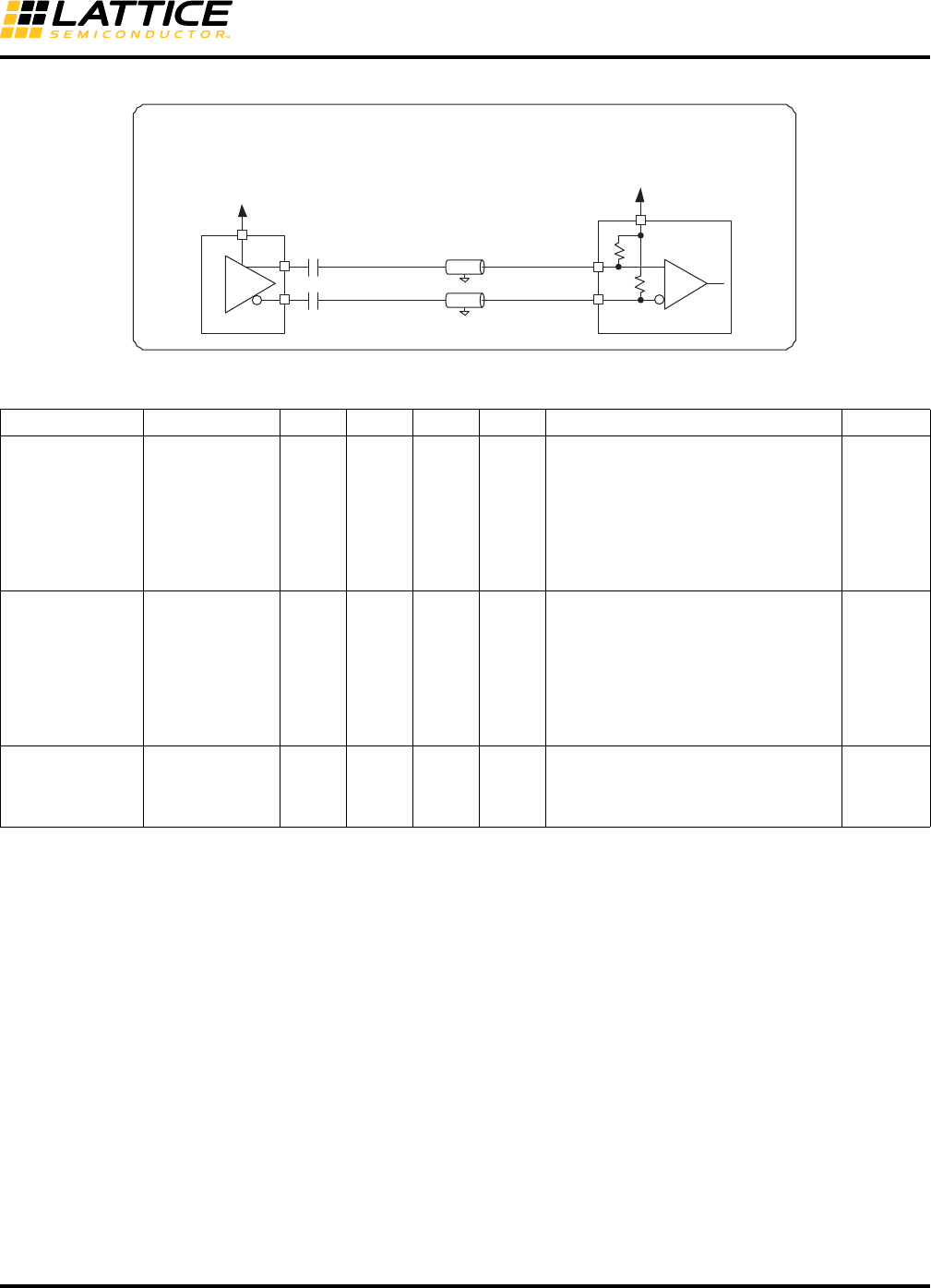
8-47
LatticeECP3 SERDES/PCS
Usage Guide
Figure 8-28. PCI Express Interface Diagram
Table 8-20. Differential PCI Express Specifications
PCI Express Electrical Idle Transmission
Electrical Idle is a steady state condition where the transmitter P and N voltages are held constant at the same
value (i.e., the Electrical Idle Differential Peak Output Voltage, VTX-IDLE-DIFFp, is between 0 and 20mV). Electri-
cal Idle is primarily used in power saving and inactive states.
Per the PCI Express base specification, before a transmitter enters Electrical Idle, it must always send the Electri-
cal Idle Ordered Set (EIOS), a K28.5 (COM) followed by three K28.3 (IDL). After sending the last symbol of the
Electrical Idle Ordered Set, the transmitter must be in a valid Electrical Idle state as specified by TTX-IDLE-SET-
TO-IDLE is less than 20UI.
To achieve this, the Electrical Idle Enable (tx_idle_chx_c) from the FPGA core logic to the PCS is sent in along with
each transmit data. This signal is pipelined similarly all the way to the PCS-SERDES boundary. For all valid data
this signal is LOW. To initiate Electrical Idle, the FPGA logic pulls this signal HIGH on the clock after it transmits the
last K28.3 (IDL) symbol. As the signal is pipelined to the PCS-SERDES boundary, the relationship between the
transmit data and this signal is exactly the same as on the FPGA-PCS boundary.
14UI after the rising edge of the Electrical Idle enable signal at the PCS-SERDES boundary the last bit (bit7) of the
last K28.3 (IDL) symbol is transmitted. 16UI (<20UI) later the transmit differential buffer achieves Electrical Idle
state.
Symbol Parameter Min. Nom. Max. Units Comments Location
ZTX-DIFF-DC DC Differential
TX Impedance 80 100 120 Ohm
TX DC Differential mode low imped-
ance. ZTX-DIFF-DC is the small signal
resistance of the transmitter measured
at a DC operating point that is equiva-
lent to that established by connecting a
100 Ohm resistor from D+ and D- while
the TX is driving a static logic one or
logic zero.
Internal
ZRX-DIFF-DC DC Differential
Input Impedance 80 100 120 Ohm
RX DC Differential mode impedance
during all LTSSM states. When trans-
mitting from a Fundamental Reset to
Detect, (the initial state of the LTSSM),
there is a 5 ms transition time before
receiver termination values must be
met on all un-configured lanes of a
port.
Internal
CTX AC Coupling
Capacitor 75 200 nF
All transmitters shall be AC coupled.
The AC coupling is required either
within the media or within the transmit-
ting component itself.
External
Zo = 50
VCCOB = 1.2V
LatticeECP3
CML Driver
75 to 200 nF
PCI Express Application LatticeECP3
CML Receiver
VCCIB = 1.2V
50
50
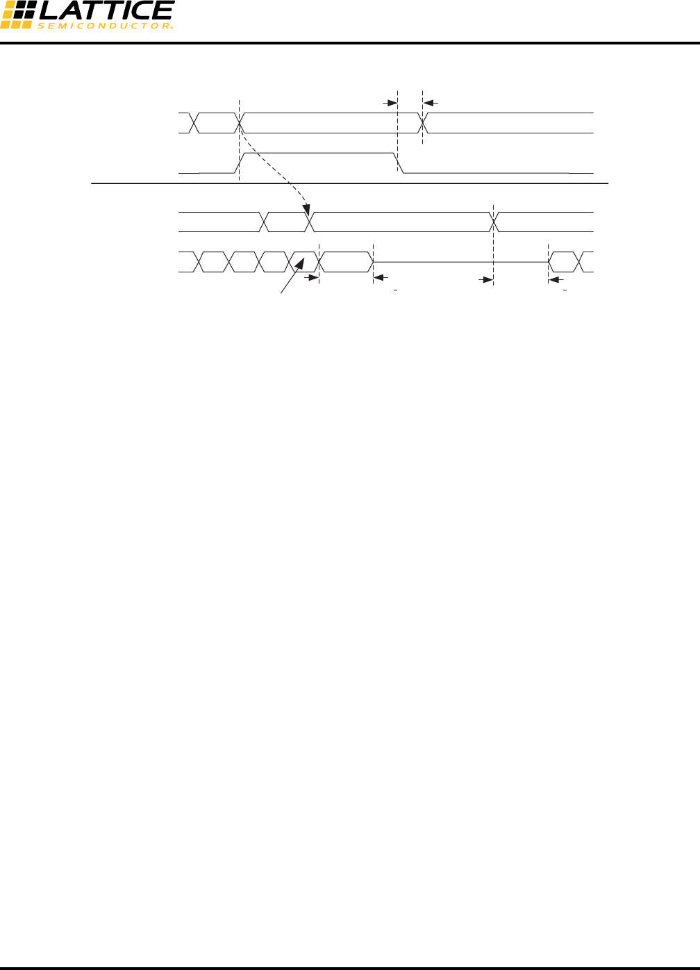
8-48
LatticeECP3 SERDES/PCS
Usage Guide
Figure 8-29. Transmit Electrical Idle
As long as the FPGA core logic deems that the transmitter needs to stay in Electrical Idle state it needs to clock in
data (preferably all zeros) along with the Electrical Idle Enable (tx_idle_chx_c) signal active (HIGH). The transmitter
is required to stay in the Electrical Idle state for a minimum of 50UI (20ns) (TTX-IDLE-MIN).
PCI Express Electrical Idle Detection
Each channel in the quad has a loss-of-signal detector. The Electrical Idle is detected once two out of the three
K28.3 (IDL) symbols in the Electrical Idle Ordered Set (EOS) have been received. After the Electrical Idle Ordered
Set is received, the receiver should wait for a minimum of 50ns (TTX-IDLE-MIN) before enabling its Electrical Idle
Exit detector.
These signals (one per channel, four per quad) should be routed through the PCS, and should be made available
to the FPGA core. The required state machine(s) to support electrical idle can then be constructed in the FPGA
core.
PCI Express Receiver Detection
Figure 8-30 shows a Receiver Detection sequence. A Receiver Detection test can be performed on each channel
of a quad independently. Before starting a Receiver Detection test, the transmitter must be put into electrical idle by
setting the tx_idle_ch#_c input high. The Receiver Detection test can begin 120 ns after tx_elec_idle is set high by
driving the appropriate pci_det_en_ch#_c high. This puts the corresponding SERDES Transmit buffer into receiver
detect mode by setting the driver termination to high impedance and pulling both differential outputs to VCCOB
through the high impedance driver termination.
Setting the SERDES Transmit buffer into receiver detect state takes up to 120 ns. After 120 ns, the receiver detect
test can be initiated by driving the channel’s pcie_ct_ch#_c input high for four byte (word) clock cycles. The corre-
sponding channel’s pcie_done_ch#_s is then cleared asynchronously. After enough time for the receiver detect test
to finish has elapsed (determined by the time constant on the transmit side), the pcie_done_ch#_s receiver detect
status port will go high and the Receiver Detect status can be monitored at the pcie_con_ch#_s port. If at that time
the pcie_con_ch#_s port is high, then a receiver has been detected on that channel. If, however, the
pcie_con_ch#_s port is low, then no receiver has been detected for that channel. Once the Receiver Detect test is
complete, tx_idle_ch#_c can be deasserted.
TxElecIdle_chx
TxData_chx
HDOUTP/N
EOS 00 Data
2 word clocks
TxData_chx EOS 00 Data
TTX-IDLE-TO-DIIF-DATA-MIN
< 20 UI
TTX-IDLE-SET-TO-IDLE
Bit 0
Bit 7 of last K28.3 character
TX FIFOs and Pipeline Delay
FPGA-PCS Boundary
PCS-SERDES Boundary
< 20 UI
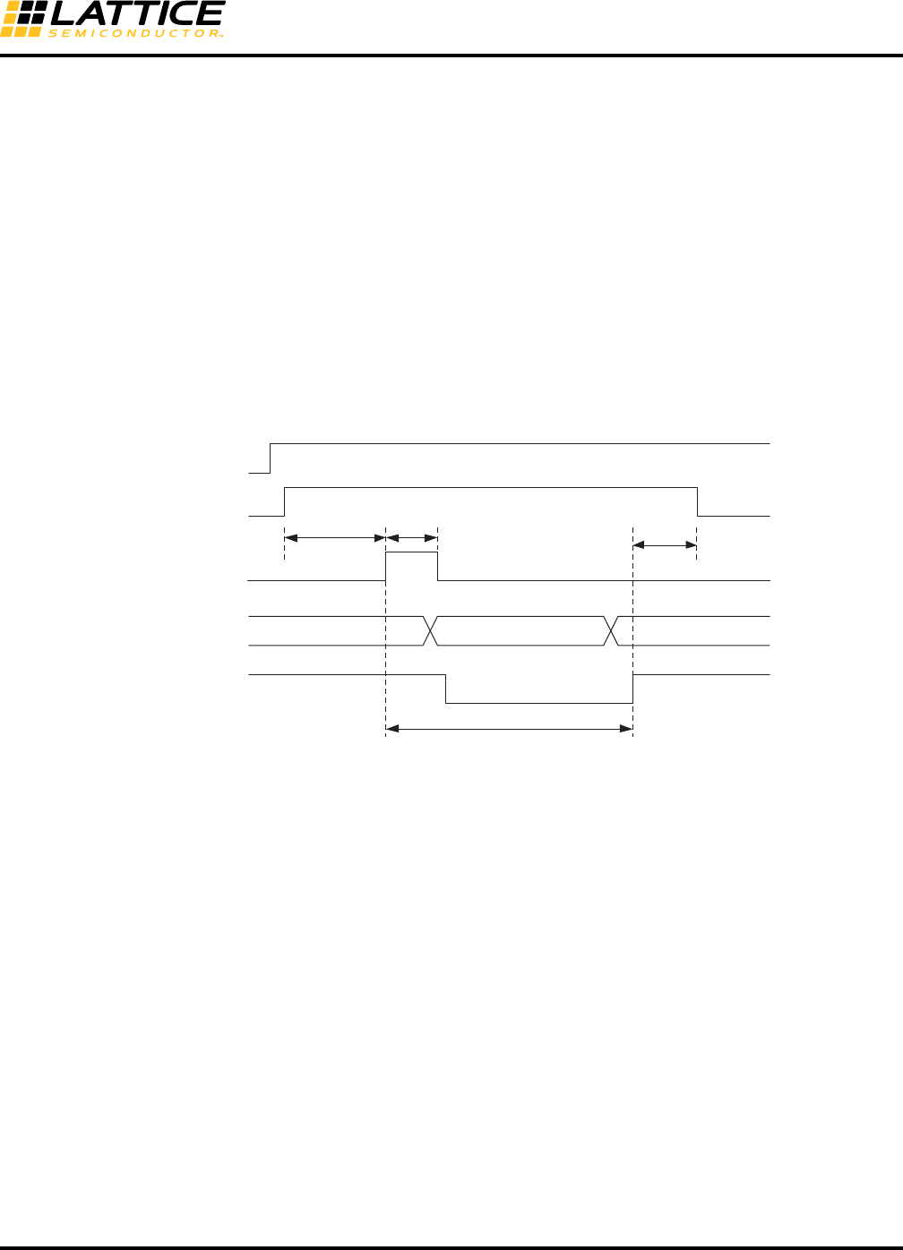
8-49
LatticeECP3 SERDES/PCS
Usage Guide
Receiver detection proceeds as follows:
1. The user drives pcie_det_en high, putting the corresponding TX driver into receiver detect mode. This sets
the driver termination to high-impedance (5K ohm) and pulls both outputs of the differential driver toward
common mode through the high-impedance driver termination. The TX driver takes some time to enter this
state so the pcie_det_en must be driven high for at least 120ns before pcie_ ct is asserted.
2. The user drives pcie_ct high for four byte clocks.
3. SERDES drives the corresponding pcie_done low.
4. SERDES drives the internal signal (corresponding to pcie_ct) for as long as it is required (based on the
time constant) to detect the receiver.
5. SERDES drives the corresponding pcie_con connection status.
6. SERDES drives the corresponding pcie_done high.
7. The user can use this asserted stated of pcie_done to sample the pcie_con status to determine if the
receiver detection was successful.
Figure 8-30. PCI Express Mode Receiver Detection Sequence
PCI Express Power Down Mode
rx_serdes_rst_ch[3:0] reset signal should be used instead of rx_pwrup_ch[3:0] signal. This allows the RX termina-
tion to remain enabled at 50 Ohms so that the far-end transmitter can detect that a receiver is connected.
PCI Express Beacon Support
This section highlights how the LatticeECP3 PCS can support Beacon detection and transmission. The PCI
Express requirements for Beacon detection are presented with the PCS support for Beacon transmission and
detection.
Beacon Detection Requirements
• Beacon is required for exit from L2 (P2) state.
• Beacon is a DC-balanced signal of periodic arbitrary data, which is required to contain some pulse widths 2ns
(500 MHz) and < 16us (30 KHz).
• Maximum time between pulses should be < 16 us.
• DC balance must be restored within < 32 us.
• For pulse widths > 500 ns, the output beacon voltage level must be 6 db down from VTX-DIFFp-p (800 mV to 1200 mV).
• For pulse widths < 500 ns, the output beacon voltage level must be VTX-DIFFp-p and 3.5 db down from VTX-
DIFFp-p.
pcie_con[0:3]
pcie_done[0:3]
pcie_ct[0:3]
pcie_det_en[0:3]
tx_elec_idle
previous statusinvalid detected status
tdone > 2us
tdeth
tdetwtdets (4 byte clocks)

8-50
LatticeECP3 SERDES/PCS
Usage Guide
PCS Beacon Detection Support
• The signal loss threshold detection circuit senses if the specified voltage level exists at the receiver buffer.
• This is indicated by the rlos_lo_ch(0-3) signal.
• This setting can be used both for PCI Express Electrical Idle Detection and PCI Express beacon detection (when
in power state P2).
• The remote transmitting device can have a beacon output voltage of 6 db down from VTX-DIFFpp (i.e., 201 mV).
If this signal can be detected, then the beacon is detected.
PCS Beacon Transmission Support
Sending the K28.5 character (IDLE) (5 ones followed by 5 zeroes) provides a periodic pulse with of 2 ns occurring
every 2 ns (1.0 UI = 400 ps, multiplied by 5 = 2 ns). This meets the lower requirement. The output beacon voltage
level can then be VTX-DIFFp-p. This is a valid beacon transmission.
SDI (SMPTE) Mode
The SDI mode of the LatticeECP3 SERDES/PCS block supports all three SDI modes, SD-SDI, HD-SDI and 3G-
SDI.
Transmit Path
• Serializer
Receive Path
• Deserializer
• Optional word alignment to user-defined alignment pattern.
The following data rates are the most popular in the broadcast video industry.
• SD-SDI (SMPTE259M): 270Mbps
• HD-SDI (SMPTE292M): 1.485Gbps, 1.485Gbps/1.001 = 1.4835Gbps
• 3G-SDI (SMPTE424M): 2.97Gbps, 2.97Gbps/1.001 = 2.967Gbps
Most designers have indicated that they would like to see support for all these rates. The reason is that in a broad-
cast studio, or a satellite head-end or cable head-end, they do not necessarily have prior knowledge of what the RX
data rate will be.
The switchover time between different rates should be as low as possible. The time to re-lock the CDR is unavoid-
able. In the LatticeECP3 SERDES, the PLL does not have to be re-locked. This is possible because the
LatticeECP3 has per RX and TX dividers. Video links generally have a uni-directional nature (i.e., different chan-
nels can run at different rates, and more importantly, the RX and TX in the same channel can run at different rates).
Also, depending on the geography where the equipment is deployed, either the full HD/3G-SDI rates (Europe/Asia)
are used while transmitting video or the fractional rates (North America - NTSC). This allows us to develop two
potential solution example cases for multi-rate SMPTE support with high quad utilization.
Please note that simultaneous support of 3G/HD Full TX Rate(s) and Fractional TX Rate(s) is not possible in the
same SERDES quad. In general, based on the above, geographically partitioned usage is an acceptable limitation.
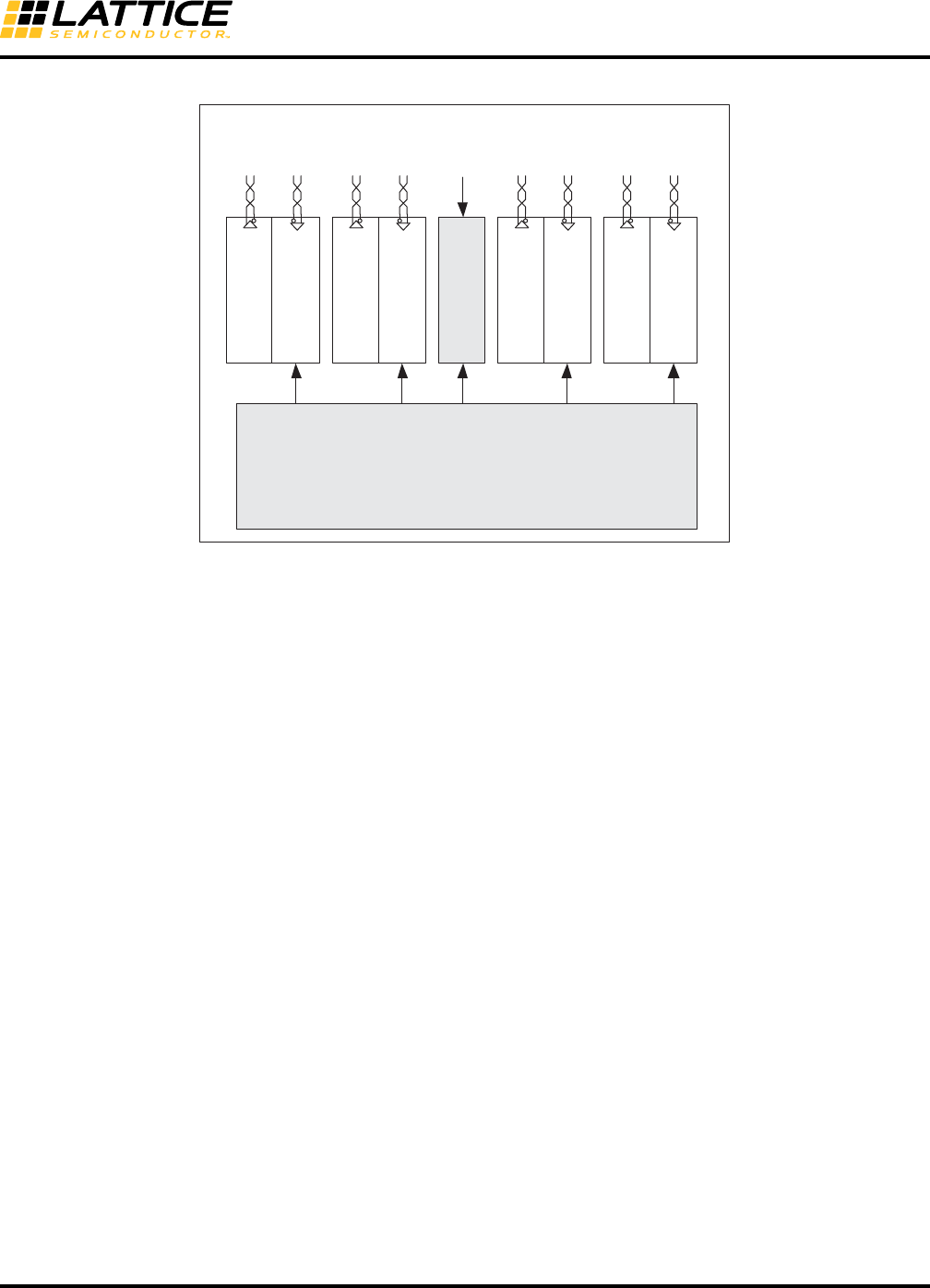
8-51
LatticeECP3 SERDES/PCS
Usage Guide
Figure 8-31. Example A: 3G/HD/SD Full RX/TX Rate Support and 3G/HD Fractional TX Rate Support
To support the major application requirements, a selectable DIV per RX and TX is supported. In LatticeECP3,
DIV11 has been added. One potential multi-rate configuration is to provide a 148.5MHz REFCLK from the primary
pins to the TX PLL. The TX PLL would be in the x20 mode. The resulting output clock would be 2.97GHz. Then, by
using the DIV2 for 1.485Gbps and DIV11 for 270Mbps, a very quick switchover can be achieved without having to
re-train and lock the PLL.
Serial RapidIO (SRIO) Mode
This section describes the operation of the Serial RapidIO mode of the SERDES/PCS block. The LatticeECP3 sup-
ports 1x and 4x Serial RapidIO applications with one PCS quad. SRIO1.0 highlights multiple frequency support,
3.125Gbps, 2.5Gbps and 1.25Gbps. The ratio of these rates is 2.5:2:1. Supporting all of these rates with integer
dividers in the same quad is not possible, but the ratio of 2.5 Gbps to 1.25 Gbps is 2:1 (full rate : half rate).
Transmit Path
• Serializer
• 8b10b encoding
Receive Path
• Deserializer
• Word alignment based on the Sync Code Group as defined in the RapidIO Physical Layer 1x/4x LP-Serial speci-
fication.
• 8b10b decoding
• Clock Tolerance Compensation logic capable of accommodating clock domain differences
SERDES/PCS Quad
FPGA Core
Ch 3
Tx
1.485
Gbps
(DIV2)
Ch 3
Rx
270
Mbps
(DIV11)
Ch 2
Tx
2.97
Gbps
(DIV1)
Ch 2
Rx
1.485
Mbps
(DIV2)
Ch 1
Tx
270
Mbps
(DIV11)
Ch 1
Rx
2.97
Gbps
(DIV1)
Ch 0
Tx
2.97
Gbps
(DIV1)
Ch 0
Rx
1.485
Gbps
(DIV2)
AUX
PLL
(x20)
RX3
Core
Clock
TX
Core
Clock
RX2
Core
Clock
(74.175
MHz)
RX1
Core
Clock
RX0
Core
Clock
External Clock
148.5 MHz
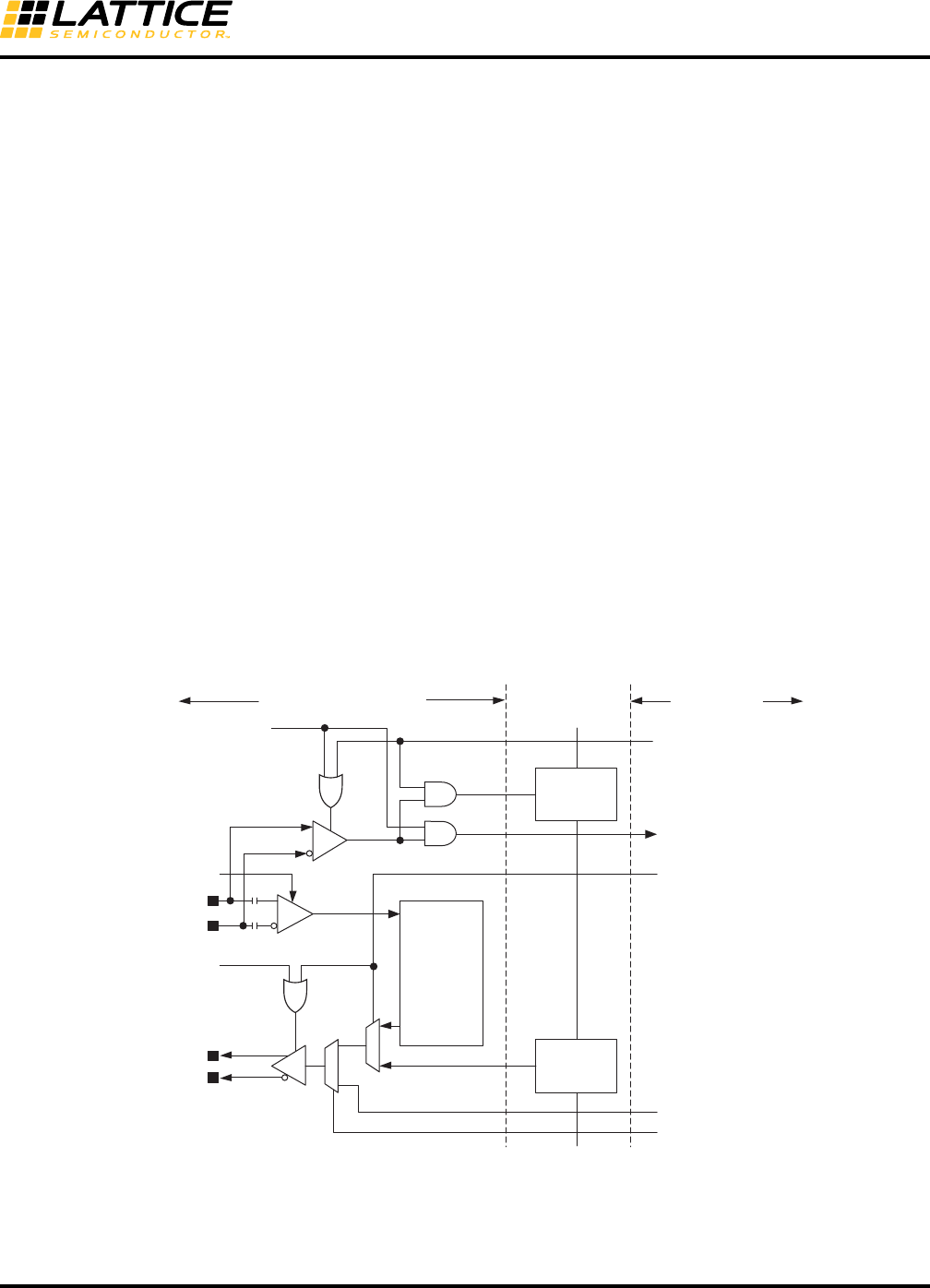
8-52
LatticeECP3 SERDES/PCS
Usage Guide
Serial Digital Video and Out-Of-Band Low Speed SERDES Operation
The LatticeECP3 SERDES/PCS supports any data rates that are slower than what the SERDES TX PLL and RX
CDR natively support (<250Mbps: Out-Of-Band signal, OOB), by bypassing the receiver CDR and associated
SERDES/PCS logic (e.g., 100Mbps Fast Ethernet, SD-SDI at 143Mbps or 177Mbps). Though these out-of-band
paths primarily use low data rates, higher rates can be used for other functional reasons. See the Multi-Rate
SMPTE Support section of this document for more information.
In addition, for SD-SDI, these rates sometimes must co-exist on the same differential RX pair with HD-SDI rates
(i.e., SD-SDI rates may be active and then the data rate may switch over to HD-SDI rates). Since there is no way to
predict which of these two rates will be in effect, it is possible to send the input data stream to two SERDES in par-
allel, a high-speed SERDES (already in the quad) and a lower-speed SERDES (implemented outside the quad).
One possible implementation is shown in Figure 8-32.
There is an input per channel RXD_LDR, low data rate single-ended input from the RX buffer to the FPGA core. In
the core a low-speed Clock Data Recovery (CDR) block or a Data Recovery Unit (DRU) can be built using soft
logic. A channel register bit, RXD_LDR_EN, can enable this data path. If enabled by another register bit, a signal
from the FPGA can also enable this in LatticeECP3.
In the transmit direction, it is also possible to use a serializer built in soft logic in the FPGA core and use the
TXD_LDR pin to send data into the SERDES. It will be muxed in at a point just before the pre-emphasis logic near
where the regular high-speed SERDES path is muxed with the boundary scan path. This is shown conceptually in
Figure 8-32. The low data rate path can be selected by setting a channel register bit, TX_LDR_EN.
Alternatively, on the output side, the high-speed SERDES is used to transmit either high-speed data, or lower
speed data using decimation (the SERDES continues to run at high-speed, but the output data can only change
every nth clock where n is the decimation factor).
Figure 8-32. Possible Implementation of Serial Digital Video Support
0
1
EQ
HDINP
HDINN
RXD_LDR
RXD_LDR_EN
BSRPAD
from JTAG config logic
Input Data
SERDES
Output Data
HDOUTP
HDOUTN
RX power up
TX power up
BSCAN
Output Cell
BSCAN
Input Cell
FPGA CoreSERDES/PCS Block
0
1
Quad Top
TXD_LDR
BSTPAD
from JTAG config logic
TXD_LDR_EN

8-53
LatticeECP3 SERDES/PCS
Usage Guide
Open Base Station Architecture Initiative (OBSAI)
OBSAI is an open forum that is aimed at an open market for cellular base stations.
The LatticeECP3 SERDES/PCS supports most of the OBSAI features except the 3.84Gbps rate.
Transmit Path
• Serializer
• Transmit State Machine is set to Gigabit Ethernet Mode
• 8b10b Encoding
Receive Path
• Deserializer
• Word alignment based on IEEE 802.3-2002 1000 BASE-X defined alignment characters
• 8b10b Decoding
A Basestation Transceiver System (BTS) has four main components/modules and there are three major interfaces,
or Reference Points (RPs), between them.
•RP3 – RF Module receives signals from portable devices (terminals) and down converts it to digital data.
•RP2 – The baseband module takes the encoded signal and processes it and sends it to the transport module,
which will send it over the terrestrial network.
•RP1 – A control module maintains coordination between these three functions.
Currently, most of the focus in the industry revolves around providing lower RF modules and power amplifiers and
hence OBSAI’s primary effort has been to define Reference Point 3 (RP3). In fact, the specification of interest is
RP3-01, which is focused on Remote Radio Heads (RRHs).
The OBSAI RP3 electrical specification is based on the XAUI electrical specification and customized to the needs
of a Base Transceiver System. The XAUI electrical interface is specified in Clause 47 of IEEE 802.3ae-2002. RP3
version 3.1 specifies the following electrical rates 3.84Gbps, 3.072Gbps, 2.304Gbps, 1.536Gbps and 0.736Gbps
out of which the last four are supported.
The RP3 electrical specification defines a receiver compliance mask and provides a sample transmitter output
mask. The BER should be better than 1 x 10-15, which is more stringent than XAUI requirement of 1 x 10-12. The
RP3 electrical specification also differs from the XAUI specification in the definition of the UI. XAUI allows for a dif-
ference of +/- 100ppm. This difference does not apply to OBSAI systems since the BTSes are fully synchronous
systems.
Since a BTS is a synchronous system, it is imperative to measure and calibrate the delay across any bus. OBSAI
has carefully considered this and, as a result, come up with a method for synchronizing the master frame across
the RP3 link. Delay calibration takes into account all factors, including processing, and buffer delay, in transmit and
receive modules, as well as the latency across the link.
Another major item in the data-link layer is the synchronization between the transmitter and receiver. Synchroniza-
tion ensures the actual data can be decoded successfully over the link. The frequency of errors as well as the syn-
chronization status is constantly monitored.
RP3-01 has gone further and specified line rates that are integer multiples of 768Mbps, up to 3.84Gbps, and are
considered OBSAI compatible line rates. Due to the number of line rates available, auto-negotiation between the
remote RF units and the local units is defined. This extension of the specification includes Ethernet transmission
between two RP3-01 nodes, mapping of RP1 information into the RP3 link because the RRH does not have a

8-54
LatticeECP3 SERDES/PCS
Usage Guide
physical RP1 link, delay measurement, synchronization between RP3-01 units, and data multiplexing across the
RP3-01 link.
The delay of each functional block in the LatticeECP3 SERDES/PCS is described in the CPRI section.
Common Public Radio Interface (CPRI)
The goal of CPRI is to allow base station manufacturers and component vendors to share a common protocol and
more easily adapt platforms from one user to another.
Transmit Path
• Serializer
• Transmit State Machine is set to Gigabit Ethernet Mode
• 8b10b Encoding
Receive Path
• Deserializer
• Word alignment based on IEEE 802.3-2002 1000 BASE-X defined alignment characters
• 8b10b Decoding
Unlike OBSAI, CPRI does not specify mechanical or electrical interface requirements. In terms of scope, CPRI has
a much narrower focus than OBSAI. CPRI looks solely at the link between the RRH and the baseband module(s).
In CPRI nomenclature, those modules are known as Radio Equipment (RE) and Radio Equipment Control (REC),
respectively. In other words, CPRI is specifying the same interface as the OBSAI RP3 specification. CPRI primarily
covers the physical and data link layer of the interface. It also specifies how to transfer the user plane data, control
and management (C&M) plane data and the synchronization plane data.
CPRI has had better “traction” for two reasons - the muscle of the companies backing it and the focus on just one
interface link (between the RF modules and the Baseband modules) and even at that focusing primarily on the
physical and data link layers.
CPRI allows four line bit rate options; 614.4Mbps, 1.2288Gbps, 2.4576Gbps and 3.072Gbps; at least one of these
rates needs to be supported. The higher line rate is always compared to the one that is immediately lower.
CPRI does not have a mandatory physical layer protocol, but the protocol used must meet the BER requirement of
1 x 10-12, which is less stringent than OBSAI. It also specifies the clock stability and the phase noise requirements.
CPRI also recommends two electrical variants: high voltage (HV) and low voltage (LV). HV is guided by 1000Base-
CX specifications in IEEE 802.3-2002 clause 39 with 100-ohm impedance. LV is guided by XAUI. LV is recom-
mended for all rates and will be the focus for this device.
It is important to understand two link layer requirements when dealing with the CPRI and OBSAI specifications:
• Link delay accuracy and cable delay calibration
• Startup synchronization
Link Delay Accuracy and Cable Delay Calibration
Though the following discussion largely leverages from the CPRI requirements, the same requirements also apply
to OBSAI implementations.
The REs or RRHs are frequency locked to the REC or BTS. Thus, in this synchronous system it is necessary to
calibrate all delays between RRHs and the BTS to meet air-interface timing requirements. The interface requires
the support of the basic mechanisms to enable calibrating the cable delay on links and the round trip delay on sin-
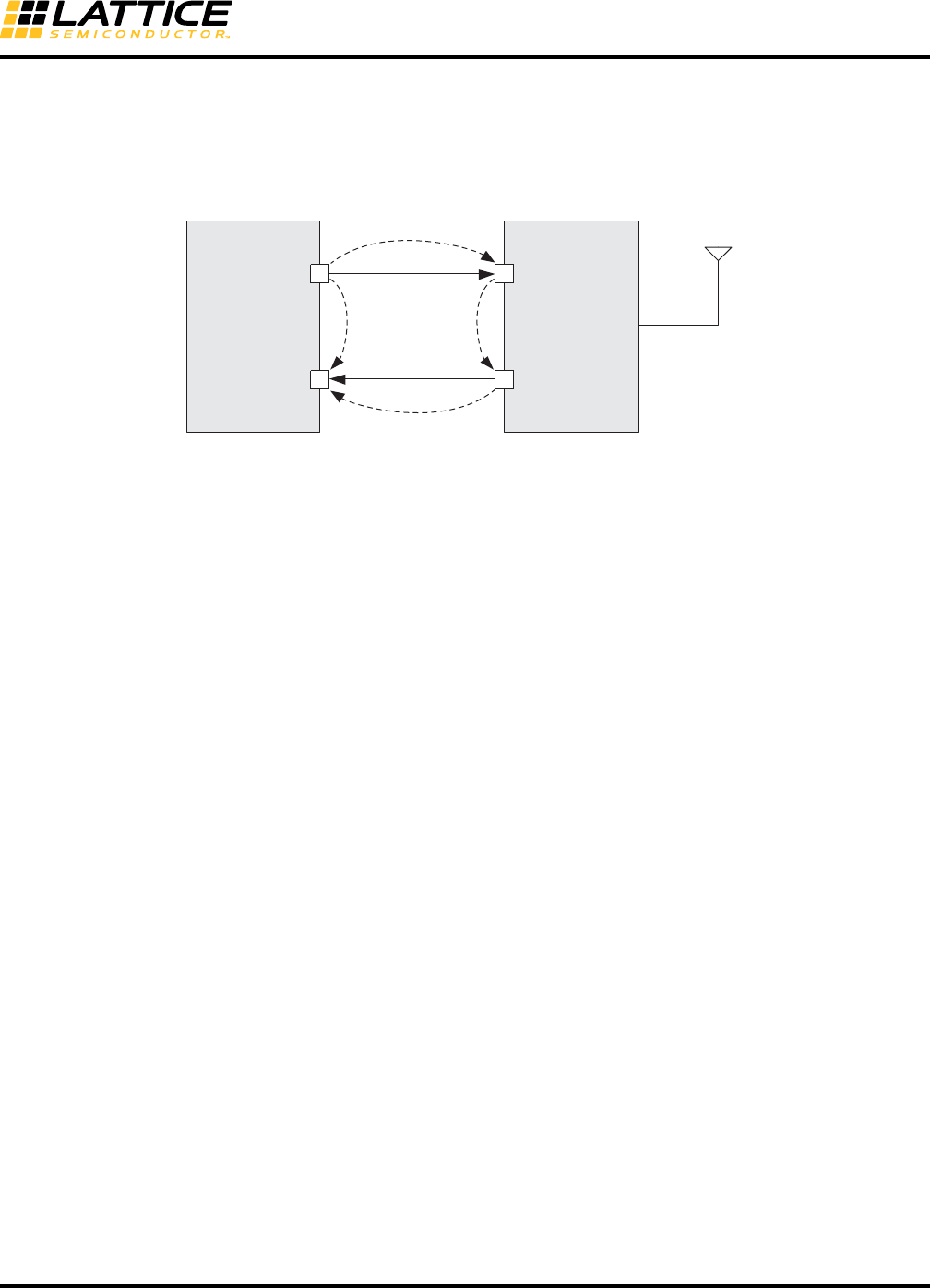
8-55
LatticeECP3 SERDES/PCS
Usage Guide
gle- and multi-hop connections. Specifically, the reference points for delay calibration and the timing relationship
between input and output signals at RE (Radio Equipment) are defined. All definitions and requirements are
described for a link between REC Master Port and RE Slave Port in the single-hop scenario as shown in Figure 8-
33.
Figure 8-33. Link Between REC Master Port and RE Slave Port (Single Hop Scenario)
Reference points R1-4 correspond to the output point (R1) and the input point (R4) of REC, and the input point (R2)
and the output point (R3) of an RE terminating a particular logical connection. The antenna is shown as Ra for ref-
erence.
• T12 is the delay of the downlink signal from the output point of REC (R1) to the input point of RE (R2), essentially
the downlink cable delay.
• T34 is the delay of the uplink signal from the output point of RE (R3) to the input point of the REC (R4), essen-
tially the uplink cable delay.
• Toffset is the frame offset between the input signal at R2 and the output signal at R3.
• T14 is the frame timing difference between the output signal at R1 and the input signal at R4 (i.e., the round trip
delay - RTT).
Delay measurement is accomplished using frame timing. CPRI has a 10ms frame based on the UMTS radio frame
number or Node B Frame Number, also known as BFN. Each UMTS Radio Frame has 150 hyperframes (i.e., each
HyperFrame is 66.67us) with the corresponding hyperframe number (HFN = 0<=Z<=149). Each hyperframe has
256 (0<=W<=255) basic frames (i.e. each basic frame is 260.42ns = Tchip or Tc).
An RE determines the frame timing of its output signal (uplink) to be the fixed offset (Toffset) relative to the frame
timing of its input signal (downlink). Toffset is an arbitrary value, which is greater than or equal to 0 and less than
256 Tc (it cannot slip beyond a hyperframe). Different REs may use different values for Toffset. REC knows the
value of Toffset of each RE in advance (pre-defined value or RE informs REC by higher layer message).
To determine T14, the downlink BFN and HFN from REC to RE is given back in uplink from the RE to the REC. In
the case of an uplink-signaled error condition, the REC treats the uplinks BFN and HFN as invalid. So, T14 = T12 +
Toff se t + T3 4.
As stated earlier the system is synchronous. Further, assuming that hyperframes are of fixed length and the RRH-
BTS interconnect (cable length) is equal in both directions (i.e.,T12 = T34, both optical fibers are in one bundle),
the interconnect delay devolves down to (T14 - Toffset)/2. The method for determining T14 has been discussed
earlier. So the major component that affects delay calibration is Toffset. Thus, the interconnect delay is the differ-
ence in hyperframe arrival and departure times measured at each side of the link.
Delay calibration requirements are driven by 3GPP and UTRAN requirements specifically requirements R-21 in the
CPRI specification (CPRI v3.0 page 20), which states that the accuracy of the round trip delay measurement of the
cable delay of one link is +/- Tc/16. Additionally, requirement R-20 states that the round trip time absolute accuracy
of the interface, excluding the round trip group delay on the transmission medium (excluding the cable length), shall
Radio Equipment
Control (REC)
Radio
Antenna
R1 R2
R3R4
T12
T14 Toffset
T34
Radio Equipment
(RE)

8-56
LatticeECP3 SERDES/PCS
Usage Guide
meet a similar requirement (+/- Tc/16 for T14). Taking into account the previous discussion, the absolute link delay
accuracy in the downlink between REC master port and RE slave port excluding the cable length is half of the
above requirement (+/- Tc/32 or approximately 8ns (8.138ns)). Thus, both T14 and Toffset need absolute accuracy
less than +/- 8ns.
Next it is important to determine how many bits of uncertainty can be acceptable for the different rates. Essentially,
the various CPRI and OBSAI bit rates can be multiplied by 8.138ns to determine the number of bits worth of inde-
terminism/variance is acceptable. The impact of this will become clear subsequently when the SERDES serial/par-
allel data path is discussed.
Most SERDES have a certain level of uncertainty that is introduced in the serializing and de-serializing process.
Thus, a SERDES with 16-bit bus architecture may have twice the delay uncertainty as a SERDES with a 8-bit
architecture because the number of bits per word is doubled.
TX and RX latency respectively in Table 8-23 is listed. The table also lists the variability between the latency. This
variability directly contributes to the absolute delay accuracy required from earlier discussion. The variability comes
from three sources: TX FPGA Bridge FIFO, RX FPGA Bridge FIFO and RX Clock Tolerance Compensation FIFO.
Since the CPRI system is a synchronous system, the RX CTC FIFO is bypassed and the RX recovered clock is
used.
The remaining contributors to the latency variability are the FPGA Bridge FIFO. This FIFO can be bypassed if the
interface to the FPGA is 8-bit bus mode. In 16-bit interface mode, the FPGA Bridge FIFO cannot be bypassed
because the 2:1 gearing is done via the FIFO.
SONET/SDH
Synchronous Optical Networking (SONET) and Synchronous Digital Hierarchy (SDH) are standardized multiplex-
ing protocols that transfer data over optical fiber or via an electrical interface. SONET generic criteria are detailed in
the Telcordia Technologies Generic Requirements document GR-253-CORE. Generic criteria applicable to SONET
and other transmission systems (e.g., asynchronous fiber optic systems or digital radio systems) are found in Tel-
cordia GR-499-CORE. SONET and SDH were originally designed to transport circuit mode communications (e.g.,
T1, T3) from a variety of different sources. The primary difficulty in doing this prior to SONET was that the synchro-
nization sources of these different circuits were different. This meant each circuit was operating at a slightly differ-
ent rate and with different phase. SONET allowed for the simultaneous transport of many different circuits of
differing origin within a single framing protocol.
The LatticeECP3 SERDES/PCS offers transceivers capable of supporting three SONET/SDH data rates, STS-
3/STM-1 (155.52 Mbps), STS-12/STM-4 (622.08 Mbps) and STS-48/STM-16 (2.488 Gbps). 8-bit SERDES mode is
used for SONET/SDH applications.
In order to be SONET/SDH line-compliant, external components are required with the LatticeECP3. An external
line driver is required on the output of the SERDES. To filter out high frequency jitter from the incoming data
stream, a jitter cleaner can be applied to the recovered clock before using it as the transmit reference clock.
For chip-to-chip or backplane applications, the external line driver and the clock jitter cleaner are not required.
Figure 8-34 shows the line-side solution using external components.
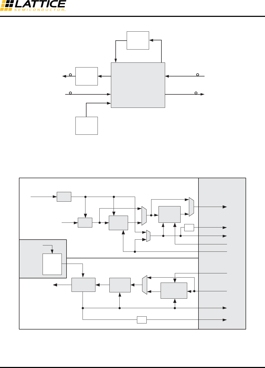
8-57
LatticeECP3 SERDES/PCS
Usage Guide
Figure 8-34. SONET/SDH Line Interface
FPGA Interface Clocks
Figure 8-35 shows a conceptual diagram of the later stage of the PCS core and the FPGA Bridge and the major
clocks that cross the boundary between PCS and the FPGA.
Figure 8-35. Conceptual PCS/FPGA Clock Interface Diagram
In the above diagram and in the subsequent clock diagrams in this section, please note that suffix “i” indicates the
index [3:0] i.e., one for each channel.
Line
Driver Client
Interface
Line
Interface
Jitter
Cleaner
VCXO
LatticeECP3
Line
TX Clock
RX Reference
Clock
Client Recovered
Clock
rxdata_ch0
rxiclk_ch0
TX FIFO
Recovered Clock
REFCLK
BYPASS
rx_full_clk_ch0
/2
/2
TX
RX FPGA
AUX
RX FIFO
rx_half_clk_ch0
txiclk_ch0
ebrd_clk_ch0
tx_full_clk_ch0
tx_half_clk_ch0
CTC
FIFO
CDR
DEC
TX PLL
PCS
txdata_ch0
REFCLK
BYPASS
SER 8b10b
Encoder
BYPASS

8-58
LatticeECP3 SERDES/PCS
Usage Guide
It is a requirement that if any of the selectors to the clock muxes are changed by writes to register bits, the software
agent will reset the logic clocked by that muxed clock.
The PCS outputs 16 clocks. There are two transmit clocks (per channel) and two receive clocks (per channel). The
two transmit clocks provide full rate and half rate clocks and are all derived from the TX PLL. There are also two
clocks (full and half) per receive channel. All 16 clocks can be used as local (secondary) or global (primary) clocks
for the FPGA logic as required. tx_half_clks are used when the gearing is in 2:1 mode. As described in Table 8-5,
only tx_full_clk_ch0 and tx_half_clk_ch0 can drive the primary clock routing directly. Other channel clocks can also
drive the primary clock net but general routing is used. All of the tx_full_clk_ch[3:0] and tx_half_clk_ch[3:0] signals
can drive the secondary clock net by applying a USE SECONDARY clocking preference. General routing is also
used to drive Secondary clock net.
The transmit clock is used on the write port of the TX FIFO (or Phase Shift FIFO, depending on the case). One of
the two receive clocks is connected to the read clock of the RX FIFO. The other clock is used on the read port of
the CTC FIFO and potentially on the write port of the RX FIFO (depending on the case). Based on the whether the
CTC and the TX FIFO are bypassed and whether the PCS is in 8bit/10bit interface mode or 16bit/20bit interface
mode, four use cases are possible. The active paths are highlighted with weighted lines. It is also indicated how
many and what kind of clock trees are required. There are some modes that would more commonly be preferred by
the user.
This section describes the operation of the six supported cases. The cases are outlined in Table 8-21.
Table 8-21. Six Interface Cases Between the SERDES/PCS Quad and the FPGA Core
2:1 Gearing
For guaranteed performance of the FPGA global clock tree, it is recommended to use a 16/20-bit wide interface for
SERDES line rates greater than 2.5Gbps. In this interface, the FPGA interface clocks are running at half the byte
clock frequency.
Even though the 16/20-bit wide interface running at half the byte clock frequency can be used with all SERDES line
rates, the 8/10-bit wide interface is preferred when the SREDES line rate is low enough to allow it (2.5Gbps and
below) because this results in the most efficient implementation of IP in the FPGA core.
The decision matrix for the six interface cases is explained in Table 8-22.
Interface Data Width RX CTC FIFO
RX Phase-Shift/
Down-Sample FIFO
TX Phase-Shift/
Up-Sample FIFO
Case I-a28/10 bit Yes Yes Yes
Case I-b28/10 bit Bypass Yes Yes
Case I-c28/10 bit Yes Bypass Bypass
Case I-d28/10 bit Bypass Bypass Bypass
Case II-a1, 2 16/20 bit Yes Yes Yes
Case II-b1, 2 16/20 bit Bypass Yes Yes
1. When using a 16/20-bit datapath width, the TX phase-shift (upsample) FIFO and the RX phase-shift FIFO (downsample) are always used.
They cannot be bypassed. It is not required that both RX and TX have the same FPGA interface datapath width simultaneously. There is
independent control available. For the sake of brevity, they have been represented together in the same use case.
2 The TX phase-shift (upsample) FIFO and the RX phase-shift FIFO (downsample) don’t need to be bypassed together. They are indepen-
dently controllable. Again, for the sake of brevity, they have been represented here in the same case.
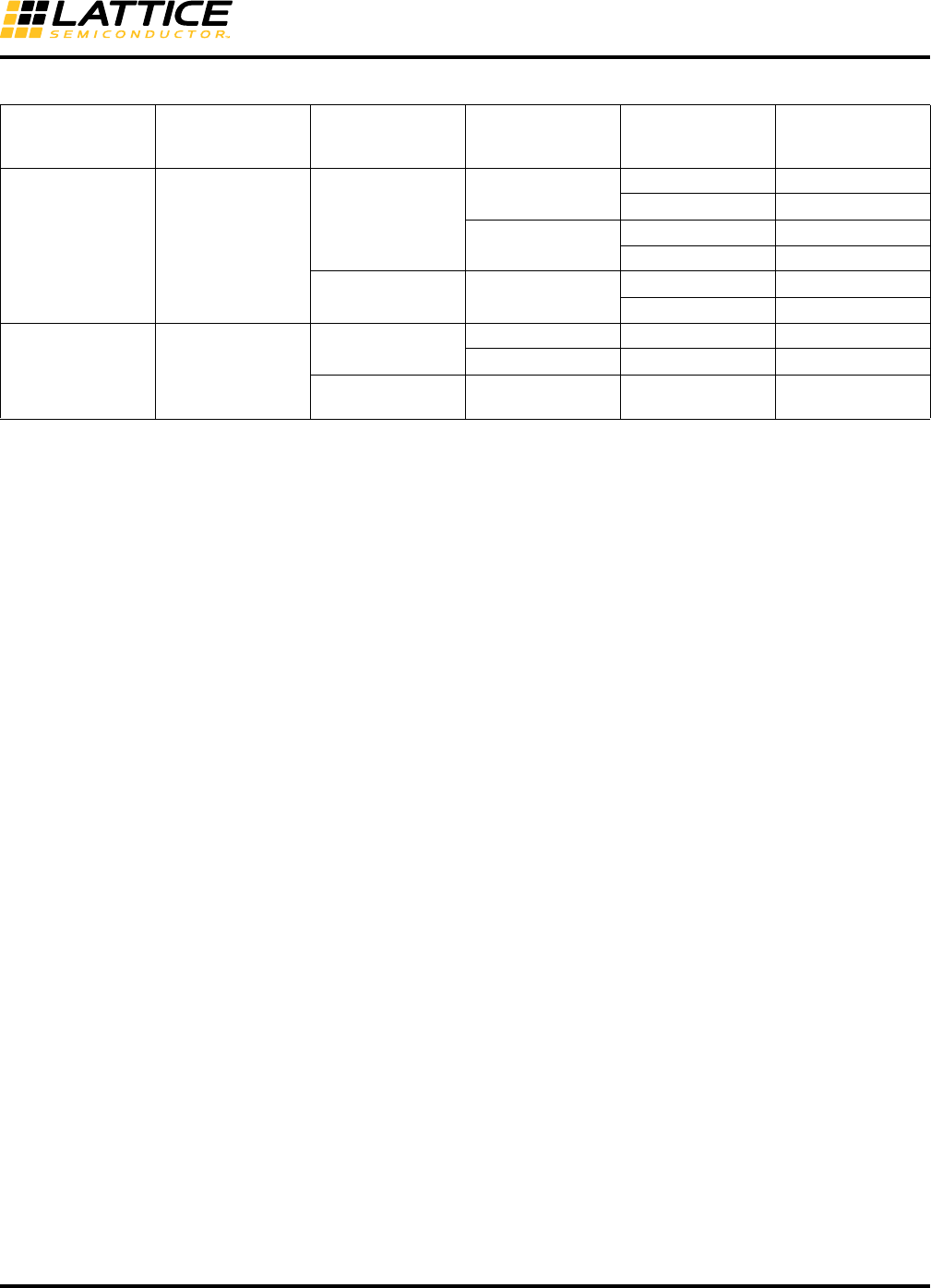
8-59
LatticeECP3 SERDES/PCS
Usage Guide
Table 8-22. Decision Matrix for Six Interface Cases
SERDES Line Rate Datapath Width
Multi-Channel
Alignment
Required? CTC Required?
RX FIFO
Required? Interface Case
2.5 Gbps and below 8/10 bit
(1:1 gearing)
No, single-channel
link
Ye s Yes Case I_a1
No Case I_c1
No Yes Case I_b2
No Case I_d2
Yes, multi-channel
link
Must bypass, not
available
Yes Case I_b3
No Case I_d3
3.2 Gbps and below 16/20 bit
(2:1 gearing)
No, single-channel
link
Ye s Ye s C a s e I I _ a 4
No Yes Case II_b5
Yes, multi-channel
link
Must bypass, not
available Yes Case II_b6
1. This case is intended for single-channel links at line rates of 2.5 Gbps and lower (8/10-bit wide interface) that require clock tolerance com-
pensation in the quad. CTC is required when both ends of the link have separate reference clock sources that are within +/- 300ppm of each
other. Case I_a is used if the IP in the core requires the RX phase-shift FIFO. Case I_b is used if the IP does not require this FIFO.
2. This case is intended for single-channel links at line rates of 2.5Gbps and lower (8/10-bit wide interface) that do NOT require clock tolerance
compensation in the quad. CTC is not required when both ends of the link are connected to the same reference clock source. This is often
the case for chip-to-chip links on the same circuit board. There is exactly 0ppm difference between the reference clocks and so CTC is not
required and can be bypassed. CTC is also not required in the quad when this function is performed by the IP in the core.
3. This case is intended for multi-channel links at line rates of 2.5Gbps and lower (8/10-bit wide interface). Multi-channel alignment MUST be
done in the FPGA design. Since multi-channel alignment must be done prior to CTC, the CTC FIFO in the quad MUST be bypassed when
multi-channel alignment is required and so both multi-channel alignment and CTC (if required) are done by the FPGA design.
4. This case is intended for single-channel links at line rates of 3.2Gbps and lower that require a 2:1 gearbox between the quad and the FPGA
core (16/20 bit wide interface). Clock tolerance compensation is included in the quad. CTC is required when both ends of the link have sep-
arate reference clock sources that are within +/- 300ppm of each other.
5. This case is intended for single-channel links at line rates of 3.2Gbps and lower that require a 2:1 gearbox between the quad and the FPGA
core (16/20-bit wide interface). Clock tolerance compensation is NOT included in the quad. CTC is not required when both ends of the link
are connected to the same reference clock source. This is often the case for chip-to-chip links on the same circuit board. There is exactly
0ppm difference between the reference clocks and so CTC is not required and can be bypassed. CTC is also not required in the quad when
this function is performed by the FPGA design.
6. This case is intended for multi-channel links at line rates of 3.2Gbps and lower that require a 2:1 gearbox between the quad and the FPGA
core (16/20-bit wide interface). Multi-channel alignment MUST be done by the FPGA design. Since multi-channel alignment must be done
prior to CTC, the CTC FIFO in the quad MUST be bypassed when multi-channel alignment is required and so both multi-channel alignment
and CTC (if required) are done by the FPGA design.

8-60
LatticeECP3 SERDES/PCS
Usage Guide
Case I_a: 8/10-Bit, CTC FIFO and RX/TX FIFOs Not Bypassed
Figure 8-36. 8/10-Bit, CTC FIFO and RX/TX FIFOs NOT Bypassed
1. The TX FIFO acts as a Phase Shift FIFO only in this case.
2. The RX FIFO acts as a Phase Shift FIFO only in this case.
3. The quad-level full rate clock from the TX PLL (tx_full_clk) has direct access to the FPGA center clock
mux. This is a relatively higher performance path. A Global Clock Tree out of the Center Clock Mux is used
to clock the user’s interface logic in the FPGA. Some leaf nodes of the clock tree are connected to the
FPGA Transmit Input clock (txiclk), the CTC FIFO Read Clock per Channel (ebrd_clk) through the FPGA
Receive Input clock (rxiclk). This case is possibly the most common single-channel use case.
Example of Clock and Data Signals Interface in FPGA Logic (Case I_a)
Below is a portion of the SERDES/PCS module instantiation in the top module which describes how clock and data
ports are mapped in Verilog.
.txiclk_ch0(txclk),
.rxiclk_ch0(txclk),
.rx_full_clk_ch0(),
.tx_full_clk_ch0(txclk),
.tx_half_clk_ch0(),
.txdata_ch0(txdata_2_pcs),
.rxdata_ch0(rxdata_from_pcs),
.tx_k_ch0(txkcntl_2_pcs),
.rx_k_ch0(rxkcntl_from_pcs),
ebrd_clk_ch0 is routed automatically by the software, depending on the case.
Note that tx_full_clk_ch0 uses wire name 'txclk' and feeds both txi_clk_ch0 and rxi_clk_ch0, as shown in Figure 8-
36.
rxdata_ch0
rxiclk_ch0
TX
FIFO
Recovered Clock
REFCLK
BYPASS
rx_full_clk_ch0
TX
RX FPGA
AUX
RX
FIFO
rx_half_clk_ch0
txiclk_ch0
ebrd_clk_ch0
tx_full_clk_ch0
tx_half_clk_ch0
CTC
FIFO
CDR
DEC
TX PLL
PCS
txdata_ch0
REFCLK
BYPASS
SER 8b10b
Encoder
BYPASS
/2
/2
FPGA
Clock
Tree
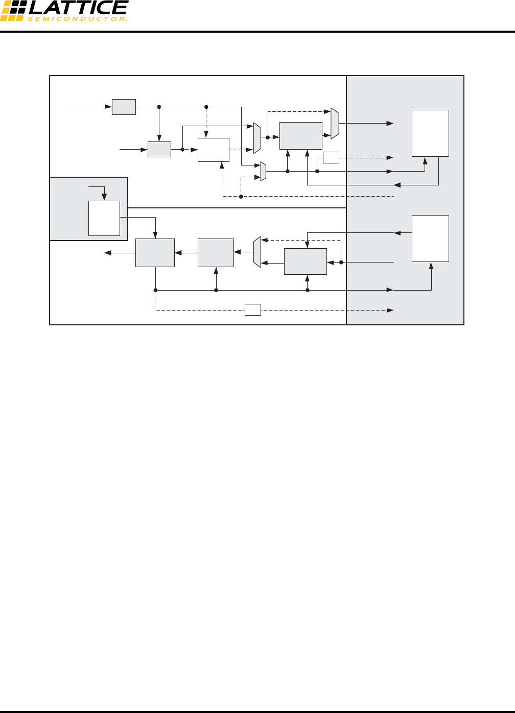
8-61
LatticeECP3 SERDES/PCS
Usage Guide
Case I_b: 8/10-Bit, CTC FIFO Bypassed
Figure 8-37. 8b/10-Bit, CTC FIFO Bypassed
1. The TX FIFO acts as a Phase Shift FIFO only in this case.
2. The RX FIFO acts as a Phase Shift FIFO only in this case.
3. The TX FPGA Channel input clock is clocked similarly as in the previous case using a clock tree driven by
a direct connection of the full rate transmit FPGA output clock to the FPGA center clock mux. Once the
CTC FIFO is bypassed, the recovered clock needs to control the write port of the RX FIFO. The recovered
clock of each channel may need to drive a separate local or global clock tree (i.e., up to four local or global
clock trees per quad). The clock tree will then drive the FPGA receive clock input to control the read port of
the RX FIFO. The reason for bypassing the CTC FIFO in this case is most likely for doing multi-channel
alignment in the FPGA core. It implies that CTC using an elastic buffer will be done in the FPGA core. The
CTC FIFOs can be written by either the recovered clocks or by a master recovered clock. The read of the
CTC FIFO will be done using the TX clock via the TX clock tree.
rxdata_ch0
rxiclk_ch0
TX
FIFO
Recovered Clock
REFCLK
BYPASS
rx_full_clk_ch0
TX
RX FPGA
AUX
RX
FIFO
rx_half_clk_ch0
txiclk_ch0
ebrd_clk_ch0
tx_full_clk_ch0
tx_half_clk_ch0
CTC
FIFO
CDR
DEC
TX PLL
PCS
txdata_ch0
REFCLK
BYPASS
SER 8b10b
Encoder
BYPASS
/2
/2
FPGA
Clock
Tree
FPGA
Clock
Tree
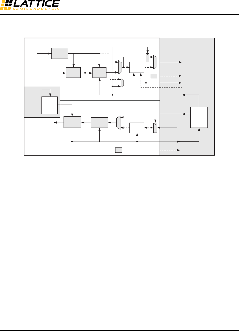
8-62
LatticeECP3 SERDES/PCS
Usage Guide
Case I_c: 8/10-Bit, RX/TX FIFO Bypassed
Figure 8-38. 8/10-Bit, RX/TX FIFO Bypassed
1. The TX channel clocking is similar to the previous two cases. On the RX channel, the FPGA input clock is
now ebrd_clki. The FPGA TX clock tree drives this clock. In this case, ebrd_clki is automatically routed by
the software.
8b10b
Encoder
SER
TX
FIFO
FPGA
Clock
Tree
REFCLK
AUX TX PLL
8b10b
Decoder
CDR
RX
FIFO
CTC
FIFO
REFCLK
RX
rxdata_ch0
rx_half_clk_ch0
rx_full_clk_ch0
rxiclk_ch0
ebrd_clk_ch0
AGPFSCP
txiclk_ch0
tx_full_clk_ch0
tx_half_clk_ch0
txdata_ch0
BYPASS
BYPASS
BYPASS
Recovered Clock
TX /2
/2
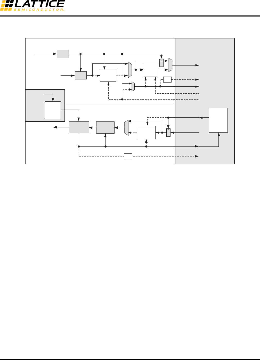
8-63
LatticeECP3 SERDES/PCS
Usage Guide
Case I_d: 8/10-Bit, CTC FIFO and RX/TX FIFOs Bypassed
Figure 8-39. 8b/10-Bit, CTC FIFO and RX/TX FIFOs Bypassed
1. FPGA clock trees can be interchangeably thought of as clock domains in this case. The TX channel clock-
ing is similar to the previous three cases. On the RX channel, the recovered channel RX clock is sent out to
the FPGA. This case is useful for supporting video applications.
TX
FIFO
TX
txiclk_ch0
tx_full_clk_ch0
tx_half_clk_ch0
txdata_ch0
SER 8b10b
Encoder
BYPASS
rxdata_ch0
rxiclk_ch0
Recovered Clock
REFCLK
BYPASS
rx_full_clk_ch0
RX FPGA
AUX
RX
FIFO
rx_half_clk_ch0
ebrd_clk_ch0
CTC
FIFO
CDR
DEC
TX PLL
PCS
REFCLK
BYPASS
/2
/2
FPGA
Clock
Tree
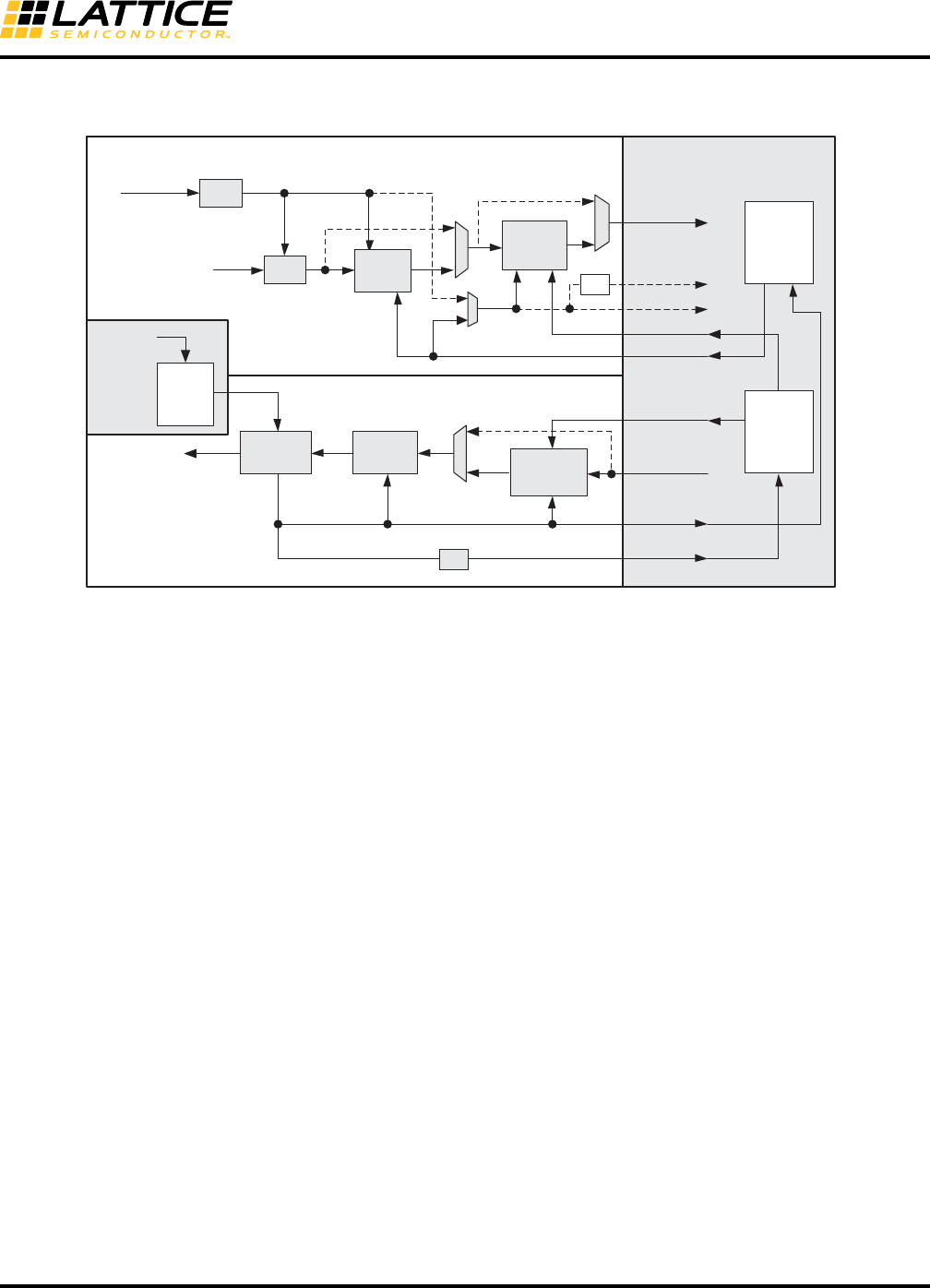
8-64
LatticeECP3 SERDES/PCS
Usage Guide
Case II_a: 16/20-bit, CTC FIFO and RX/TX FIFOs NOT Bypassed
Figure 8-40. 16/20-bit, CTC FIFO and RX/TX FIFOs NOT Bypassed
1. The TX FIFO acts both as a Phase Shift FIFO and Upsample FIFO in this case.
2. The RX FIFO acts both as a Phase Shift FIFO and Downsample FIFO in this case.
3. This is a very common single channel use case when the FPGA is unable to keep up with full byte fre-
quency. Two clock trees are required. These clock trees are driven by direct access of transmit full-rate
clock and transmit half-rate clock to the FPGA clock center mux. The full-rate clock tree drives the CTC
FIFO read port and the RX FIFO write port. The half-rate clock tree drives the RX FIFO and the FPGA
logic.
rxdata_ch0
rxiclk_ch0
TX
FIFO
Recovered Clock
REFCLK
BYPASS
rx_full_clk_ch0
/2
TX
RX FPGA
AUX
RX
FIFO
rx_half_clk_ch0
txiclk_ch0
ebrd_clk_ch0
tx_full_clk_ch0
tx_half_clk_ch0
CTC
FIFO
CDR
DEC
TX PLL
PCS
txdata_ch0
REFCLK
BYPASS
SER 8b10b
Encoder
BYPASS
/2
FPGA
Clock
Tree
FPGA
Clock
Tree
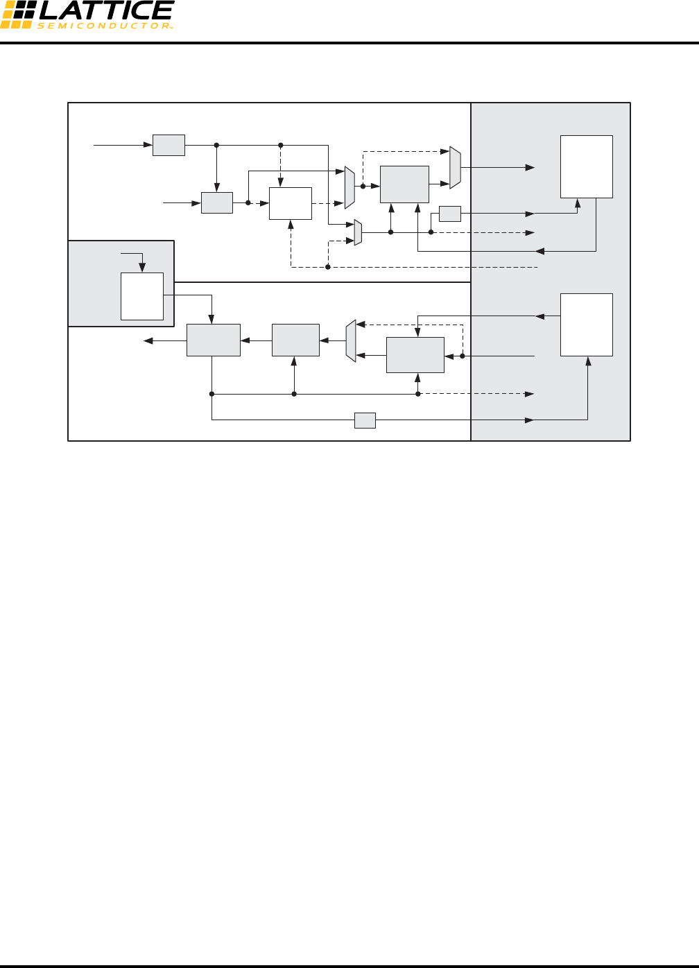
8-65
LatticeECP3 SERDES/PCS
Usage Guide
Case II_b: 16/20-bit, CTC FIFO Bypassed
Figure 8-41. 16/20-bit, CTC FIFO Bypassed
1. The TX FIFO acts both as a Phase Shift FIFO and Upsample FIFO in this case.
2. The RX FIFO is acting both as a Phase Shift FIFO and Downsample FIFO in this case.
3. This is a very common multi-channel alignment use case when the FPGA is unable to keep up with full
byte frequency. The receive clock trees (up to four) can be local or global. They are running a half-rate
clock. The transmit clock tree is driven by direct access of the transmit half-rate clock to the FPGA clock
center mux.
Case II_b
rxdata_ch0
rxiclk_ch0
TX
FIFO
Recovered Clock
REFCLK
BYPASS
rx_full_clk_ch0
/2
/2
TX
RX FPGA
AUX
RX
FIFO
rx_half_clk_ch0
txiclk_ch0
ebrd_clk_ch0
tx_full_clk_ch0
tx_half_clk_ch0
CTC
FIFO
CDR
DEC
TX PLL
PCS
txdata_ch0
REFCLK
SER 8b10b
Encoder
BYPASS
BYPASS FPGA
Clock
Tree
FPGA
Clock
Tree
8-66
LatticeECP3 SERDES/PCS
Usage Guide
SERDES/PCS Block Latency
Table 8-23 describes the latency of each functional block in the transmitter and receiver. Latency is given in parallel
clock cycles. Figure 8-42 shows the location of each block.
Table 8-23. SERDES/PCS Latency Breakdown
Table 8-24. Word Aligner Latency vs. Offset
Item Description Min. Avg. Max. Fixed Bypass Units
Transmit Data Latency1
T1
FPGA Bridge – 1:1 gearing with different clocks 1 3 5 — 1 byte clk
FPGA Bridge – 1:1 gearing with the same clocks — — — 3 1 byte clk
FPGA Bridge – 2:1 gearing 1 3 5 — — word clk
T2 8b10b Encoder — — — 2 1 byte clk
T3 SERDES Bridge transmit — — — 2 1 byte clk
T4 Serializer: 8-bit mode — — — 15 + 1— UI + ps
Serializer: 10-bit mode — — — 18 + 1— UI + ps
T5 Pre-emphasis ON — — — 1 + 2—UI + ps
Pre-emphasis OFF — — — 0 + 3—UI + ps
Receive Data Latency2
R1 Equalization ON — — — 1—UI + ps
Equalization OFF — — — 2—UI + ps
R2 Deserializer: 8-bit mode — — — 10 + 3— UI + ps
Deserializer: 10-bit mode — — — 12 + 3— UI + ps
R3 SERDES Bridge receive — — — 2 1 byte clk
R4 Word alignment33.1 — 4 — — byte clk
R5 8b10b decoder — — — 1 1 byte clk
R6 Clock Tolerance Compensation 7 15 23 1 1 byte clk
R7
FPGA Bridge – 1:1 gearing with different clocks 1 3 5 — 1 byte clk
FPGA Bridge – 1:1 gearing with same clocks — — — 3 1 byte clk
FPGA Bridge – 2:1 gearing 1 3 5 — — word clk
1. 1 = -245ps, 2 = +88ps, 3 = +112ps.
2. 1 = +118ps, 2 = +132ps, 3 = +700ps.
3. Table 8-24 shows word aligner latency depending on word alignment offset. The exact offset can be found in channel status register,
CH_22, bit [3:0].
wa_offset[3:0] (CH_22[3:0]) Latency (Word Clock)
04.0
13.9
23.8
33.7
43.6
53.5
63.4
73.3
83.2
93.1
8-67
LatticeECP3 SERDES/PCS
Usage Guide
Figure 8-42. Transmitter and Receiver Latency Block Diagram
SERDES Client Interface
The SCI allows the SERDES/PCS quad to be controlled by registers as opposed to the configuration memory cells.
It is a simple register configuration interface. The block diagram of the SCI that resides in the FPGA core is shown
in Figure 8-43.
Figure 8-43. SCI Interface Block Diagram
The interface logic that resides in the FPGA core should be developed by users per their interface scheme. Contact
Lattice Technical Support for example code.
HDOUTP
HDOUTN
Deserializer
1:8/1:10
Polarity
Adjust
CTC
FIFO
Encoder
SERDES PCS
BYPASS
Transmitter
Receiver
Recovered Clock
FPGA
Receive Clock
FPGA
Transmit Clock
Receive Data
Transmit Data
CDR
REFCLK
HDINP
HDINN
EQ
Polarity
Adjust
TX
FIFO
SERDES BridgeFPGA Bridge
Serializer
8:1/10:1
WADEC
FPGA
EBRD Clock
Transmit Clock
TX PLL
REFCLK
FPGA Core
RX
FIFO
BYPASS
BYPASS
BYPASS
BYPASS
BYPASS
BYPASS
R1 R2 R3
R4 R5 R6
R7
T4
T3
T2 T1
T5
SCI
SCI
Address
Decoder
(Soft)
Quad SERDES/PCS (Hard)
SCI_ADDR[5:0]
SCI_INT
SCI_SEL_CH0
SCI_SEL_CH1
SCI_SEL_CH2
SCI_SEL_CH3
SCI_SEL_QUAD
SCI_SEL_CH0
SCI_SEL_CH1
SCI_SEL_CH2
SCI_SEL_CH3
SCI_SEL_QUAD
SCI_ADDR[5:0]
SCI_INT
CLK
SCI_WRATA[7:0]
SCI_ADDR[9:0]
SCI_WRN
SCI_RD
SCI_RDDATA[7:0]
SCI_RDATA[7:0]
SCI_RDDATA[7:0]
Quad SERDES/PCS (Hard)
Address
Decoder
(Soft)
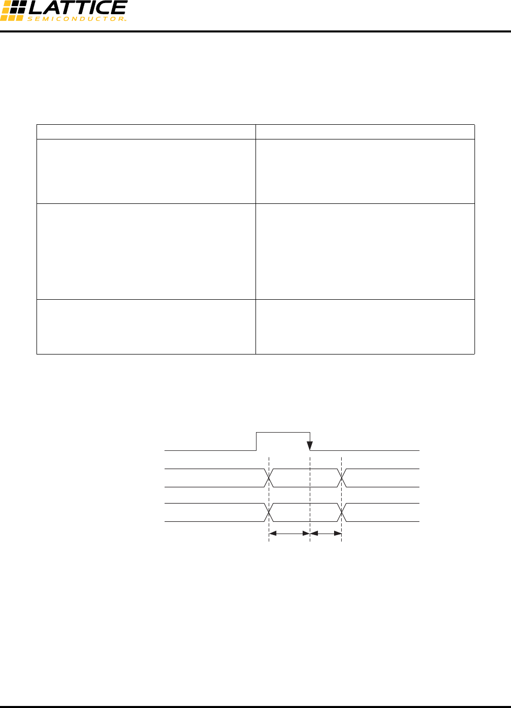
8-68
LatticeECP3 SERDES/PCS
Usage Guide
The SCI_ADDR bus is six bits wide within the block. The bus width at the block boundary is 11 bits. The upper five
bits are used for quad block selection and channel selection. Table 8-25 shows the SCI address map for the
SERDES quad.
Refer to Appendix A and Appendix B for SERDES/PCS register address and bit descriptions.
Table 8-25. SCI Address Map for Up to Four SERDES/PCS Quads
Read and write operations through this interface are asynchronous. In the WRITE cycle the write data and write
address must be set up and held in relation to the falling edge of the SCI_WR. In the READ cycle the timing has to
be in relation with the SCI_RD pulse. Figures 8-44 and 8-45 show the WRITE and READ cycles, respectively.
Figure 8-44. SCI WRITE Cycle, Critical Timing
Address Bits Description
SCI_ADDR[5:0]
Register address bits
000000 = select register 0
000001 = select register 1
...
111110 = select register 62
111111 = select register 63
SCI_ADDR[8:6]
Channel address bits
000 = select channel 0
001 = select channel 1
010 = select channel 2
011 = select channel 3
100 = select Quad
101 = Unused
110 = Unused
111 = Unused
SCI_ADDR[10:9]
Quad address bits
00 = select Quad A
01 = select Quad B
10 = select Quad C
11 = select Quad D
SCI_SEL
tsu1th2
SCI_WRN
SCI_ADDR[9:0]
SCI_WRDATA[7:0]
1. tsu is the setup time for address and write data prior to the falling edge of the write strobe.
2. th is the hold time for address and write data after the falling edge of the write strobe.
Note: To avoid accidental writing to control registers, registers should be used at the SCI input
ports to drive them low at power-up reset.
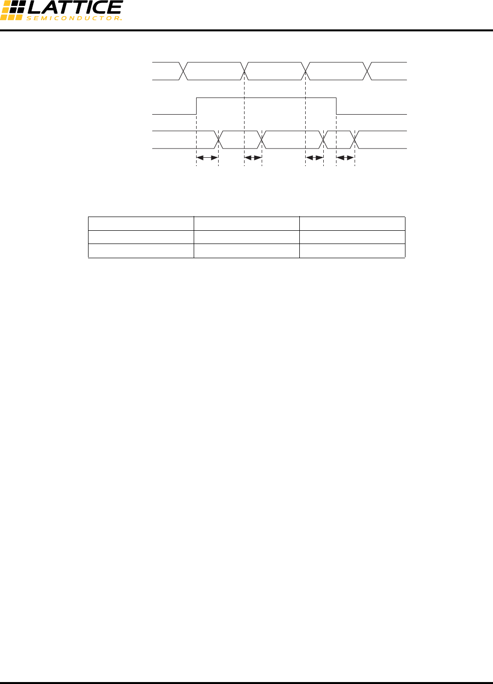
8-69
LatticeECP3 SERDES/PCS
Usage Guide
Figure 8-45. SCI READ Cycle, Critical Timing
Table 8-26. Timing Parameters
The SCI interface is as simple as memory read/write. Here is an example of the pseudo code:
Write:
• Cycle 1: Set sci_addr[5:0], sciw_data[7:0], sci_sel = 1’b1
• Cycle 2: Set sci_wrn from 0 1
• Cycle 3: Set sci_wrn from 1 0, sci_sel = 1’b0
Read:
• Cycle 1: Set sci_addr[5:0], sci_sel = 1’b1
• Cycle 2: Set sci_rd from 0 1
• Cycle 3: Obtain reading data from sci_rddata[7:0]
• Cycle 4: Set sci_rd from 1 0
Interrupts and Status
The status bit may be read via the SCI, which is a byte wide and thus reads the status of eight interrupt status sig-
nals at a time. The SCI_INT signal goes high to indicate that an interrupt event has occurred. The user is then
required to read the QIF status register that indicates whether the interrupt came from the quad or one of the chan-
nels. This register is not cleared on read. It is cleared when all interrupt sources from the quad or channel are
cleared. Once the aggregated source of the interrupt is determined, the user can read the registers in the associ-
ated quad or channel to determine the source of the interrupt. Tables 8-27 and 8-28 list all the sources of interrupt.
Parameter Typical Value Units
tsu, trddv, taddv 1.127 ns
th, trdde 0.805 ns
trddvtaddv
SCI_ADDR[9:0]
SCI_SEL_QUAD
SCI_SEL_CH
SCI_RDDATA[7:0]
trdde
taddv
SCI_RD
8-70
LatticeECP3 SERDES/PCS
Usage Guide
Table 8-27. Quad Interrupt Sources
Table 8-28. Channel Interrupt Sources
SERDES Client Interface Application Example
Lattice ORCAstra FPGA configuration software is a PC-based GUI that allows users to configure the operational
mode of a Lattice FPGA by programming control bits in the FPGA registers.
SERDES/PCS status information is displayed on-screen in real time, and any configuration can be saved to control
registers for additional testing. Use of the GUI does not interfere with the programming of the FPGA core portion.
More information and downloadable files for ORCAstra can be found on the Lattice Semiconductor website at
www.latticesemi.com/products/designsoftware/orcastra.cfm.
Users can get a complete LatticeECP3 ORCAstra interface design from IPexpress. In addition to the HDL file that
contains the ORCAstra interface, a file called “chip.v” (for Verilog) that wraps the ORCAstra interface is also pro-
vided.
Dynamic Configuration of the SERDES/PCS Quad
The SERDES/PCS quad can be controlled by registers that are accessed through the optional SERDES Client
Interface.
When controlled by the configuration memory cells, it is a requirement that the SERDES/PCS quads must reach a
functional state after configuration is complete, without further intervention from the user. This means that any spe-
cial reset sequences that are required to initialize the SERDES/PCS quad must be handled automatically by the
hardware. In other words, use of the SCI is optional. The SERDES/PCS quad does NOT assume that the soft IP is
present in the FPGA core.
SERDES Debug Capabilities
PCS Loopback Modes
The LatticeECP3 family provides three loopback modes controlled by control signals at the PCS/FPGA interface for
convenient testing of the external SERDES/board interface and the internal PCS/FPGA logic interface. Two loop-
back modes are provided to loop received data back onto the transmit data path. The loopback modes are useful
Quad SCI_INT Source Description Register Name
int_qd_out
Quad Interrupt. If there is an interrupt event anywhere in
the quad this register bit will be active. This register bit is
cleared when all interrupt events have been cleared.
PCS Quad Status Register QD_20
int_ch_out[0:3]
Channel Interrupt. If there is an interrupt event anywhere
in the respective channel this register bit will be active.
These register bits are cleared when all interrupt sources
in the respective channel have been cleared.
PCS Quad Status Register QD_20
ls_sync_statusn_[0:3]_int
ls_sync_status_[0:3]_int
Link Status Low (out of sync) channel interrupt Link Sta-
tus High (in sync) channel interrupt
PCS Quad Interrupt Status Register
QD_22
~PLOL, PLOL Interrupt generated on ~PLOL and PLOL - PLL Loss of
Lock SERDES Quad Status Register QD_25
Channel SCI_INT Source Description Register Name
fb_tx_fifo_error_int
fb_rx_fifo_error_int
cc_overrun_int
cc_underrun_int
FPGA Bridge TX FIFO Error Interrupt
FPGA Bridge RX FIFO Error Interrupt
CTC FIFO Overrun and Underrun Interrupts
PCS Channel General Interrupt Status
Register CH_23
pci_det_done_int
rlos_lo_int
~rlos_lo_int
rlol_int
~rlol_int
Interrupt generated for pci_det_done
Interrupt generated for rlos_lo
Interrupt generated for ~rlos_lo
Interrupt generated for rlol
Interrupt generated for ~rlol
SERDES Channel Interrupt Status
Register CH_2A
8-71
LatticeECP3 SERDES/PCS
Usage Guide
for checking the high-speed serial SERDES package pin connections as well as the embedded SERDES and/or
PCS logic.
RX-to-TX Serial Loopback Mode
Loops serial receive data back onto the transmit buffer without passing through the CDR or de-serializer. Selecting
the RX-to-TX Serial Loopback option in the IPexpress GUI will set both the LB_CTL[1:0] to '10' and
TDRV_DAT_SEL[1:0] register bits to '11' (see Tables 8-81 and 8-84).
TX-to-RX Serial Loopback Mode
This mode loops back serial transmit data back onto the receiver CDR block. Selecting the TX-to-RX Serial Loop-
back option in the IPexpress GUI will set LB_CTL[1:0] to '01' (see Table 8-81).
SERDES Parallel Loopback Mode
Loops parallel receive data back onto the transmit data path without passing through the PCS logic. When disabled
in the IPexpress GUI, the parallel loopback mode can be dynamically controlled from the FPGA core control signals
sb_felb_ch[3:0]_c and sb_felb_rst_ch[3:0]_c.
If the dynamic feature of this loopback mode is not used, the two control signals should be tied to ground.
When enabled in the loopback mode in the IPexpress GUI, the control register bit sb_pfifo_lp(CH_03[5]) is set and
the loopback mode is set. The control signals from the FPGA core, sb_felb_ch[3:0]_c and sb_felb_rst_ch[3:0]_c,
are not available in the PCS module.
Refer to the Figure 8-46 for the discussion above.
Figure 8-46. Three Loopback Modes
Figure 8-47. Loopback Enable Signals
SERDES PCS Core
LSM
SER
8:1/10:1 8b10b
Encoder
EQ
hdinp_ch0
hdinn_ch0
hdoutp_ch0
hdoutn_ch0
PD/
Sampler
REFCLK CDR
DES
1:8/1:10
Serial Loopback
Rx to Tx
Serial Loopback
Tx to Rx
WA
INV
INV
CK
DATA
DATA
CK
PLB_R2T
SLB_EQ2T
SLB_R2T_CK
SERDES Parallel Loopback
SLB_R2T_D
TDRV_DAT_SEL[1:0]
LB_CTL[1:0]
LB_CTL[3:0]
SERDES PLB EN
SERDES
Bridge
FPGA Bridge
(FB)
FIFO
8b10b
Decoder
CTC
FIFO
RX
FIFO
TX
FIFO
rx_data_ch0[23:0]
txdata_ch0[23:0]
sb_felb_ch[3:0]_c
sb_pfifo_lp(CH_03[5])
SERDES Bridge Far End Parallel
Loopback Enable
LB_CTL[1:0](CH_11[5:4] = ‘10’)
TDRV_DAT_SEL[1:0](CH_14[6:5] = ‘11’) RX-to-TX Serial Loopback Enable
LB_CTL[1:0](CH_11[5:4] = ‘01’) TX-to-RX Serial Loopback Enable
8-72
LatticeECP3 SERDES/PCS
Usage Guide
ORCAstra
Lattice ORCAstra software helps you quickly explore configuration options without going through a lengthy re-com-
pile process or making changes to your board. Configurations created in the GUI can be saved to memory and re-
loaded for later use. To use ORCAstra, the ORCASTRA module from IPexpress must be created and used in the
FPGA design.
A macro capability is also available to support script-based configuration and testing. The GUI can also be used to
display system status information in real time. Use of the ORCAstra software does not interfere with the program-
ming of the FPGA.
Figure 8-48 shows the ORCAstra GUI top-level window. Users can read and write in this window without going
through the subwindows for each PCS channel by read and write data at the address cell. When invoked, ORCAs-
tra will automatically recognize the device type. Or, device types can be selected under the device pull-down menu.
Figure 8-48. ORCAstra Top-Level Screen Shot
By default, the data box shown in Figure 8-48 follows Big Endian byte order (i.e., the most significant bit is placed
on the left). Users can change to Little Endian order by selecting Display Data Reversed in Data Box under the
Options tab.
Click on the tab Interface=None and select 1 ispVM JTAG Hub USB Interface from the drop-down list.
Then select the C2 0A 80 80 from the Select Target JTAG Device window.
8-73
LatticeECP3 SERDES/PCS
Usage Guide
Figure 8-49. JTAG Device Selection
Then click OK in the ORCAstra Hub I/O window.
Figure 8-50. Hub ID Selection
The figure shows there are activities on channel 0 and channel 1. In this example, we assume that the PCS SCI
address is mapped to Quad 0 in the design.
Double-clicking on the PCS0 (Quad 0) button will open the main window as shown in Figure 8-51.
These standard Windows menus control the selection of the device and interface. They also support various con-
figuration options, including setting up and saving configurations with stored files.
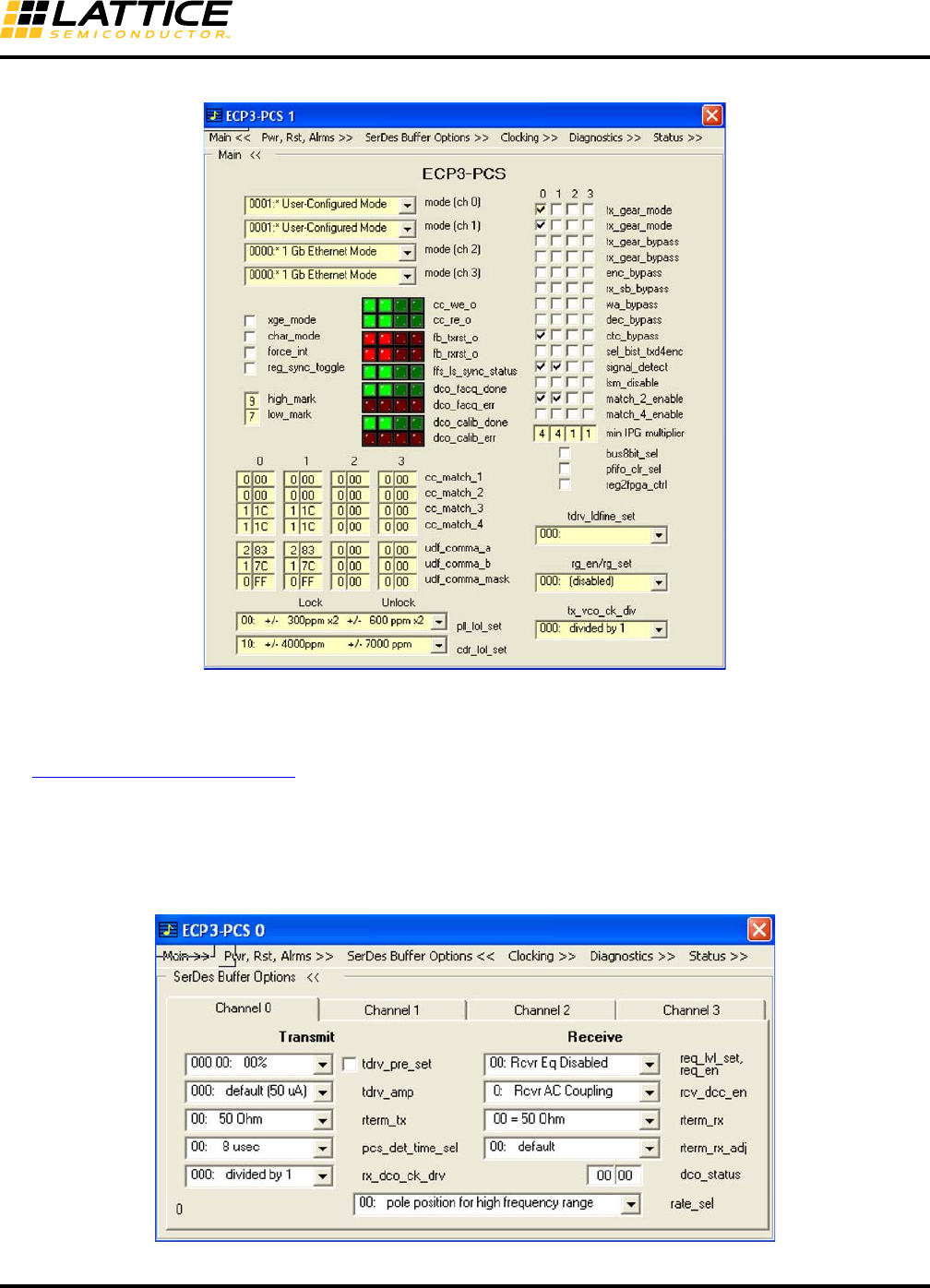
8-74
LatticeECP3 SERDES/PCS
Usage Guide
Figure 8-51. ORCAstra Main Window
Control Boxes and Buttons, Status Boxes and the Text Window
Moving the cursor over a control box and clicking the left mouse button sets the control bits. Both the bit location
and function for the selected box are displayed in the text window and will match those of the register map tables in
the LatticeECP3 Family Data Sheet. Only the function is displayed when the cursor is over the bit name. Status
boxes are similar to control boxes but have an LED appearance and a colored background.
Figure 8-52 shows the SERDES Buffer Options window. Configuration options can be selected from the pull-down
menu.
Figure 8-52. SERDES Buffer Options Window

8-75
LatticeECP3 SERDES/PCS
Usage Guide
More information and downloadable files for ORCAstra can be found on the Lattice Semiconductor website at the
following address: www.latticesemi.com/products/designsoftware/orcastra.cfm.
Other Design Considerations
Simulation of the SERDES/PCS
Table 8-29. Simulation Model Locations
16/20-Bit Word Alignment
The PCS receiver cannot recognize the 16-bit word boundary. When Word Aligner is enabled, the PCS can only do
BYTE alignment. The 16-bit word alignment should be done in the FPGA fabric and is fairly straight forward. The
simulation model works in the same way. It can be enhanced if users implement an alignment scheme as
described below.
For example, if transmit data at the FPGA interface are:
YZABCDEFGHIJKLM... (each letter is a byte, 8-bit or 10-bit)
Then the incoming data in PCS after 8b10b decoder and before rx_gearbox are:
YZABCDEFGHIJKLM...
After rx_gearbox, they can become:
1. {ZY}{BA}{DC}{FE}{HG}{JI}{LK}....
or
2. {AZ}{CB}{ED}{GF}{IH}{KJ}{ML}...
Clearly, sequence 2 is not aligned. It has one byte offset, but 16/20-bit alignment is needed. Let’s say the special
character ‘A’ should be always placed in the lower byte.
Flopping one 20-bit data combines with the current 16/20-bit data to form 32/40-bit data as shown below:
1. {DCBA}{HGFE}{LKJI}...
^
| **Found the A in lower 10-bit, set the offset to ‘0’, send out aligned
data ‘BA’
Next clock cycle:
{FEDC}{JIHG}{NMLK}...
^
| **send out aligned data ‘DC’
etc.
After the 16/20-bit alignment, the output data are:
{ZY}{BA}{DC}{FE}{HG}{JI}{LK}...
Simulator Model Location
Active-HDL ispTOOLS\cae_library\simulation\blackbox\pcsc-aldec.zip
ModelSim ispTOOLS\cae_library\simulation\blackbox\pcsd-mti_6.0-V1-1.zip
NC-Verilog ispTOOLS\cae_library\simulation\blackbox\pcsd-ncv.zip
VCS ispTOOLS\cae_library\simulation\blackbox\PCSD_sim.vp.zip

8-76
LatticeECP3 SERDES/PCS
Usage Guide
2. {CBAZ}{GFED}{KJIH}....
^
| **Found the A in upper 10-bit, set the offset to ‘10’, send out aligned
data ‘BA’
Next clock cycle:
{EDCB}{IHGF}{MLKJ}...
^
| **send out aligned data ‘DC’
etc.
After the 20-bit alignment, the output data are:
{ZY}{BA}{DC}{FE}{HG}{JI}{LK}...
Note: The LSB of a 8/10-bit byte or a 16/20-bit word is always transmitted first and received first.
For sample 16/20-bit word alignment code, send your request to techsupport@latticesemi.com.
Unused Quad/Channel and Power Supply
On unused quads and channels, VCCA should be powered up. VCCIB, VCCOB, HDINP/N, HDOUTP/N and REF-
CLKP/N should be left floating. Unused channel outputs are tristated, with approximately 10 KOhm internal resistor
connecting between the differential output pair. During configuration, HDOUTP/N are pulled high to VCCOB.
Even when a channel is used as Rx Only mode or Tx Only mode, both the VCCOB and VCCIB of the channel must
be powered up. Unused SERDES is configured in power down mode by default.
Reset and Power-Down Control
The SERDES quad has reset and power-down controls for the entire macro and also for each transmitter and
receiver as shown in Figure 8-53. The reset signals are active high and the power-down is achieved by driving the
pwrup signals low. The operation of the various reset and power-down controls are described in the following sec-
tions.
Note: When the device is powering up and the chip level power-on-reset is active, the SERDES control bits (in the
PCS) will be cleared (or will take on their default value). This will put the SERDES quad into the power-down state.
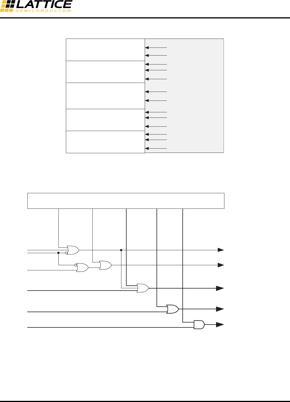
8-77
LatticeECP3 SERDES/PCS
Usage Guide
Figure 8-53. SERDES/PCS Quad Reset and Power-Down Controls
Typically, all resets are via power-on reset and various FPGA fabric resets. The reset logic is shown in Figure 8-54
and Table 8-30.
Figure 8-54. SERDES/PCS Reset Diagram
rx_pwrup_ch0
RX
CH0 -------------------------------------------
TX
rx_serdes_rst_ch0
tx_pwrup_ch0
RX
CH2 -------------------------------------------
TX
AUX Channel tx_serdes_rst
RX
CH1 -------------------------------------------
TX
RX
CH3 -------------------------------------------
TX
serdes_rst_qd
FPGA CoreSERDES/PCS Quad
rx_pwrup_ch1
rx_serdes_rst_ch1
tx_pwrup_ch1
rx_pwrup_ch2
rx_serdes_rst_ch2
tx_pwrup_ch2
rx_pwrup_ch3
rx_serdes_rst_ch3
tx_pwrup_ch3
tx_pcs_rst_ch[3:0]
rx_pcs_rst_ch[3:0]
rx_serdes_rst_ch[3:0]
tx_serdes_rst
tx_pwrup_ch[3:0]
rx_pwrup_ch[3:0]
ffc_quad_rst
quad_rst
(default=0)
(default=0)
(default=0)
(default=0)
(default=0)
serdes_rst
lane_tx_rst_ch[3:0]
lane_rx_rst_ch[3:0]
tpwrup_ch[3:0]
rpwrup_ch[3:0]
rrst_ch[3:0]
trst
TRI_ION
serdes_rst_qd
Configuration Register Block
resets selected digital
logic in the SERDES
4RX and 4TX PCS
channels digital logic
resets the complete
SERDES Quad
resets all PCS logic
sets selected channel to
power down mode
8-78
LatticeECP3 SERDES/PCS
Usage Guide
Table 8-30. SERDES/PCS Reset Table
Table 8-31. Reset Controls Description1, 2, 3
Table 8-32. Reset Pulse Specification
Power-Down Control Description
Each RX and TX channel can be individually powered-down by a software register bit or a control signal from the
FPGA. The individual channel power-down control bits will only power-down selected blocks within the SERDES
macro and the high-speed I/O buffers.
Reset Signals
PCS1
TX
PCS1
RX
SERDES
TX
SERDES
RX
PCS
CTRL
Registers
TX
PLL
CDR
PLLFPGA Control Register
tx_pcs_rst_ch[3:0]_c lane_tx_rst[3:0] X
rx_pcs_rst_ch[3:0]_c lane_rx_rst[3:0] X
rst_qd_c quad_rst XXXX XX
serdes_rst_qd_c serdes_rst X X X X
rx_serdes_rst_ch[3:0]_c rrst[3:0]2XX
tx_serdes_rst_c trst X3
TRI_ION (configuration) XXXX X
1. Includes SB (SERDES Bridge), PCS core and FB (FPGA Bridge) sub-blocks.
2. For internal use only. This reset should always be tied to '0' unless there is a need to reset the CDR PLL.
3. tx_serdes_rst_c reset does not reset the TX PLL. It only forces tx_pll_lol_qd_s to go high.
Rest Signal
DescriptionFPGA Control Register
rst_qd_c quad_rst
Active-high, asynchronous input. Resets all SERDES channels including the
auxiliary channel and PCS. This reset includes serdes_rst, txpll, cdr, lane_tx_rst,
and lane_rx_rst.
serdes_rst_qd_c serdes_rst
Active-high, asynchronous input to the SERDES quad. Gated with software reg-
ister bit. This reset is for the SERDES block only and TXPLL and CDRPLL are
included.
tx/rx_pcs_rst_ch[3:0]_c lane_tx/rx_rst[0:3] Active-high, asynchronous input. Resets individual TX/RX channel in SB, PCS
core and FB blocks.
rx_serdes_rst_ch[3:0]_c rrst[0:3] Resets loss-of-lock (rlol), loss-of-signal and calibration circuits.
tx_serdes_rst_c trst Resets the loss-of-lock of AUX PLL (plol).
1. For all channels in the quad running in full-data-rate mode, parallel side clocks are guaranteed to be in-phase.
2. For all channels in the quad running in half-data-rate mode, each channel has a separate divide-by-two circuit. Since there is no mechanism
in the quad to guarantee that these divide-by-two circuits are in phase after de-assertion of “serdes_rst”, the PCS design should assume
that the dividers (and therefore the parallel side clocks) are NOT in phase.
3. In half-data-rate mode, since there is no guarantee that the parallel side clocks are in phase, this may add channel-to-channel skew to both
transmit and receive sides of a multi-channel link.
Parameter Description Min. Typ. Max. Units
tSERDES_RST_QD Quad SERDES Reset high time 1 us
tRX_PCS_RST Channel RX PCS Reset high time 3 ns
tTX_PCS_RST Channel TX PCS Reset high time 3 ns
tRX_SERDES_RST Channel RX SERDES reset high time 3 ns
tTX_SERDES_RST Quad TX SERDES reset high time 3 ns
8-79
LatticeECP3 SERDES/PCS
Usage Guide
Table 8-33. Power-Down Control Description
Table 8-34. Power-Down/Power-Up Timing Specification
Signal
DescriptionFPGA Register
serdes_pd
Active-low asynchronous input to the SERDES quad, acts on all channels includ-
ing the auxiliary channel. When driven low, it powers down the whole macro includ-
ing the transmit PLL. All clocks are stopped and the macro power dissipation is
minimized. After release, both the TX and RX reset sequences should be followed.
tx_pwrup_ch[0:3]_c tpwrup[0:3] Active-high transmit channel power-up – Powers up the serializer and output
driver. After release, the TX reset sequence should be followed.
rx_pwrup_ch[0:3]_c rpwrup[0:3]
Active-high receive channel power-up – Powers up CDR, input buffer (equalizer
and amplifier) and loss-of-signal detector. After release, the RX reset sequence
should be followed.
Parameter Description Min. Typ. Max. Units
tPWRDN Power-down time after serdes_pd 20 ns
tPWRUP Power-up time after serdes_pd 20 ns

8-80
LatticeECP3 SERDES/PCS
Usage Guide
SERDES/PCS RESET
Reset Sequence and Reset State Diagram
After power-up and configuration, all SERDES resets and FPGA resets are applied.
Reset Sequence Generation
Reset Sequence is included in the IPexpress GUI (available in Diamond 1.1 and later versions).
We recommend to select the reset sequence generation option in IPexpress as described in the Control Setup tab
section. The HDL file generated for the SERDES/PCS will include the Tx Reset State Machine and Rx Reset State
Machine.
Lock Status Signals Definitions
tx_pll_lol_qd_s: : 1 = TX PLL loss of lock
: 0 = TX PLL lock
It takes 1,400,000 UI to declare the lock of TX PLL
rx_cdr_lol_ch[3:0]_s : 1 = CDR loss of lock
: 0 = Lock maintained
It takes 400,000 reference clock cycles (worst case) to declare the lock of CDR
PLL
rx_los_low_ch[3:0]_s : 1 = Loss of signal detection for each channel
: 0 = Signal detected
The rx_cdr_lol_ch[3:0]_s status signal is an indicator of the CDR lock status as defined above. However, during the
CDR locking process the CDR PLL will lock to a reference clock when there is no input data present. This avoids
ignoring the input data when it is restored.
In order to ensure the presence of input data during CDR lock status checking, it is recommended to use the
rx_los_low_ch[3:0]_s signal in conjunction with the rx_cdr_lol_ch[3:0]_s signal.
TX Reset Sequence
1. QUAD_RESET: At power up, assert rst_qd_c and tx_pcs_rst_ch[3:0]_c.
2. WAIT_FOR_TIMER1: Start TIMER1. Wait for a minimum 20 ns.
3. CHECK_PLOL: Release rst_qd_c.
4. WAIT_FOR_TIMER2: Start TIMER2. If TIMER2 expires and the TX PLL is not locked, go to step 1.
5. NORMAL: Release tx_pcs_rst_ch#_c. If tx_pll_lol_qd_s goes high during normal operation,
go to step 1.
RX Reset Sequence
1. WAIT_FOR_PLOL: Wait until the TX PLL locks and receive data is present. rx_serdes_rst_ch[3:0]_c is
set to 0 because rx_los_low[3:0]_s goes high when it is asserted.
2. RX_SERDES_RESET: Assert rx_serdes_rst_ch[3:0]_c and rx_pcs_rst_ch[3:0]_c.
3. WAIT_FOR_TIMER1: Wait for a minimum of 3 ns.
4. CHECK_LOL_LOS: Release rx_serdes_rst_ch_c. Reset TIMER2.
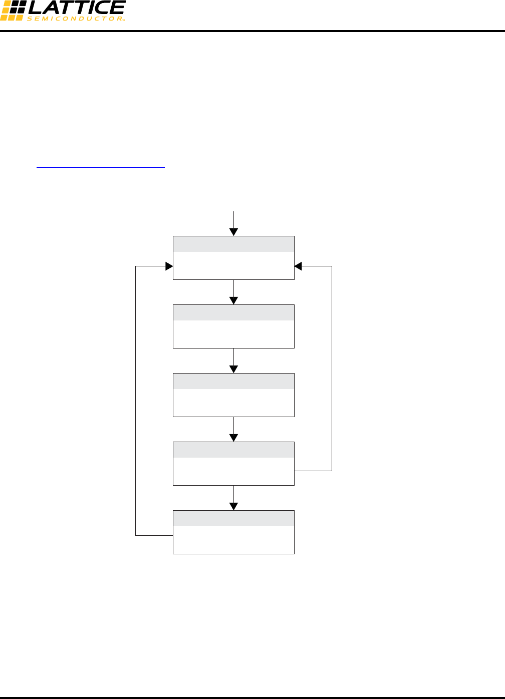
8-81
LatticeECP3 SERDES/PCS
Usage Guide
5. WAIT_FOR_TIMER2: Wait for both cdr_lol_ch[3:0]_s and rx_los_low_ch[3:0] to go low. If there is a transi-
tion in rx_lol_los (rx_cdr_lol_ch_s || rx_los_low_ch_s), go to step 4. If TIMER2
expires with rx_lol_los = 1, go to step 1.
6. NORMAL: Release rx_pcs_rst_ch_c. If rx_lol_los goes high, go to step 1.
Note: The RX reset sequence provides the CDR re-locking feature when the input data source is interrupted
during normal operation. The RX reset can be applied by channel base.
The reset sequence state diagrams are described in Figures 8-55 and 8-56.
A set of sample reset sequence code is available on the Lattice web site.
Figure 8-55. TX Reset State Diagram
Quad Reset
Power Up
TIMER1
TIMER2 & tx_pll_lol_qd_s
Notes:
TIMER 1: rst_qd_c asserted for a minimum of 20 ns.
TIMER 2: Time to declare TX PLL lock: 1,400,000 UI.
tx_pll_lol_qd_s
tx_pcs_rst_ch[3:0]_c <= 1
rst_qd_c <= 1
Wait for TIMER1
tx_pcs_rst_ch[3:0]_c <= 1
rst_qd_c <= 1
Wait for TIMER2
tx_pcs_rst_ch[3:0]_c <= 1
rst_qd_c <= 0
Normal
tx_pcs_rst_ch[3:0]_c <= 0
rxt_qd_c <= 0
Check PLOL
tx_pcs_rst_ch[3:0]_c <= 1
rst_qd_c <= 0
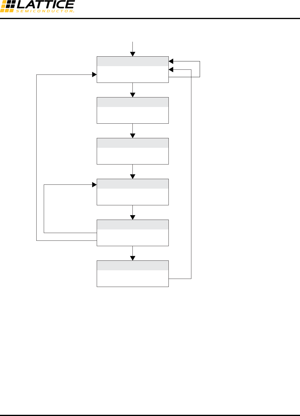
8-82
LatticeECP3 SERDES/PCS
Usage Guide
Figure 8-56. RX Reset State Diagram
Wait for PLOL
Power Up
TIMER1
TIMER2 & ~rx_lol_los
rising edge (rx_lol_los)
falling edge (rx_lol_los)
rx_lol_los
tx_pll_lol_qd_s || rx_los_low_ch[3:0]_s
TIMER2 & rx_lol_los rx_pcs_rst_ch[3:0]_c <= 1
rx_serdes_rst_ch[3:0]_c <= 0
RX_SERDES_RESET
rx_pcs_rst_ch[3:0]_c <= 1
rx_serdes_rst_ch[3:0]_c <= 1
Check LOL_LOS
rx_pcs_rst_ch[3:0]_c <= 1
rx_serdes_rst_ch[3:0]_c <= 0
rx_pcs_rst_ch[3:0]_c <= 1
rx_serdes_rst_ch[3:0]_c <= 0
rx_pcs_rst_ch[3:0]_c <= 0
rx_serdes_rst_ch[3:0]_c <= 0
Wait for TIMER2
Wait for TIMER1
rx_pcs_rst_ch[3:0]_c <= 1
rx_serdes_rst_ch[3:0]_c <= 1
Normal
Notes:
TIMER 1: rx_serdes_rst_ch[3:0]_c asserted for minimum 3 ns.
TIMER 2: Time for rx_lol_los signal to stay low (400,000 reference clock cycles). Any FPGA clock can be used to satisfy the timer requirement.
In the diagram above, rx_lol_los is defined as rx_cdr_lol_ch[3:0]_s || rx_los_low_ch[3:0]_s.
The tx_pll_lol_qd_s input to the state diagram RTL code should be tied low in Rx Only mode or when the recovered clock is used as the Tx PLL
reference clock, as in SDI applications.
When multiple receiver channels rx_serdes_rst_ch[3:0]_c are to be asserted, it is recommended to activate the reset signals one channel at a time.
Simultaneous resetting of multiple receiver SERDES channels may cause a current surge in the SERDES/PCS quad.
The rx_los_low output from SERDES may be triggered for some input streams with continuous zeros, like the SDI pathological pattern. For such
applications, the rx_los_low input to the reset state machine must be connected to the carrier detect output (must be inverted) of the cable equalizer
if available. In general, CD=1 means carrier is present. So this signal must be inverted to replace rx_los_low. If a cable equalizer is not available, users
may tie it to zero but in this case, the CDR can lock to a local reference clock when there is no input data present.

8-83
LatticeECP3 SERDES/PCS
Usage Guide
Power Supply Sequencing Requirements
When using the SERDES with 1.5V VCCIB or VCCOB, the SERDES should not be left in a steady state condition
with the 1.5V power applied and the 1.2V power not applied. Both the 1.2V and the 1.5V power should be applied
to the SERDES at nominally the same time. The normal variation in ramp_up times of power supplies and voltage
regulators is not a concern.
References
• TN1033, High-Speed PCB Design Considerations
• TN1114, Electrical Recommendations for Lattice SERDES
• HB1009, LatticeECP3 Family Handbook
• DS1021, LatticeECP3 Family Data Sheet
Technical Support Assistance
e-mail: techsupport@latticesemi.com
Internet: www.latticesemi.com
Revision History
Date Version Change Summary
February 2009 01.0 Initial release.
March 2009 01.1 Updated Data Bus Usage for Each Mode table.
Updated Reference Clock Usage Block Diagram.
June 2009 01.2 tdrv_amp attribute setting changed to tdrv attribute.
Added External Link State Machine Option section.
Added Idle Insert for Gigabit Ethernet Mode section.
GUI screen shots updated.
Word alignment latency updated.
November 2009 01.3 Updated Reset Sequence State Diagrams are provided, tx and rx side
separately.
los settings are updated.
Added SONET support.
Removed Far End Parallel Loopback feature.
Data rate ranges are re-defined.
Reduced minimum data rate to 150 Mbps.
February 2010 01.4 Reset sequence state diagram updated.
March 2010 01.5 Added Generation Options tab in IPexpress GUI.
June 2010 01.6 Updated for Lattice Diamond design software support.
refclk_to/from_nq signals removed from clock diagram.
December 2010 01.7 Added Reset Sequence Generation option in the IPexpress GUI.
Added detailed information about comma mask.
July 2011 01.8 Standards Supported by SERDES table – updated information for Giga-
bit Ethernet, SGMII, 10-Bit SERDES, 8-Bit SERDES, Generic 8b10b.
Transmit Data Bus section updated.
Receive Data Bus section updated.
Updated footnotes for Loss of Signal Detector figure.

8-84
LatticeECP3 SERDES/PCS
Usage Guide
July 2011(cont.) 01.8 (cont.) SERDES_PCS GUI Attributes - Quad Tab Setup table – Added SGMII
to Protocol Range.
SERDES/PCS Latency Breakdown table – updated gearing information.
Simulation Model Locations table – Added VCS row.
Updated SERDES/PCS Reset Diagram.
Updated footnotes of the Rx Reset State Diagram.
Updated information for bit 5 in the SERDES Control Register QD_0A
table.
Updated information for bits 3 and 2:0 in the SERDES Control Register
CH_13 table.
Added footnote to PCS Status Register CH_21 table.
Attribute Cross Reference Table – Updated attribute values for
TX_DATARATE_RANGE and CHn_RX_DATARATE_RANGE. Updated
first footnote.
September 2011 01.9 SERDES Control Register CH_14, corrected default value of tpwrup
register bit.
Attribute Cross-Reference Table, removed all int_all reserved bits and
los hi bits.
PCS Control Register QD_02, updated default values.
November 2011 02.0 SERDES_PCS I/O Descriptions table – Updated descriptions for
tx_full_clk_ch[3:0] and tx_half_clk_ch[3:0].
Updated Tx Lane-to-Lane Skew text section.
Updated word alignment control bullet in the Word Alignment (Byte
Boundary Detect) section.
Updated External Link State Machine Option text section.
Power-Down Control Description table – Updated description for
tx_pwrup_ch[0:3]_c signal.
Appendix A, SERDES Control Register QD_0B table – Updated
description for Bit 7.
Appendix A, PCS Control Register CH_01 table – Updated description
for Bit 7.
Appendix C, Attribute Cross-Reference table – Updated attribute value
for {CHn_RXWA, CHn_ILSM}.
February 2012 02.1 Updated document with new corporate logo.
April 2012 02.2 Updated Number of SERDES/PCS Quads per LatticeECP3 Device
table for 328-ball csBGA.
SERDES_PCS I/O Descriptions table – Updated description for
refclk2fpga.
SERDES_PCS GUI Attributes – SERDES Advanced Setup Tab table –
Updated footnote 3.
Added new Reference Clock to FPGA Core and Reset Sequence text
section.
Updated Generic 8b10b Mode text section.
Updated FPGA Interface Clocks text section.
Appendix A, Channel Interface Registers Map table – Updated informa-
tion for CH_16, CH_17 and CH_23.
Appendix A, SERDES Control Register CH_11 table – Changed Bit 3:2
to “Reserved”.
Revision History (Continued)
Date Version Change Summary

8-85
LatticeECP3 SERDES/PCS
Usage Guide
May 2012 02.3 Clarified data pattern requirements for LSM synchronization in generic
8b10b mode.
August 2012 02.4 Added LatticeECP3-17EA 328 csBGA limited channels availability.
SERDES_PCS I/O Descriptions table – Added footnote 3.
RX Reset State Diagram footnote updated.
June 2013 02.5 Added note on possible lsm_status_ch(0:3)_s glitches.
Updated note on the SERDES/PCS GUI – PCS Advanced2 Setup Tab
table.
Updated the Protocol-Specific SERDES Setup Options table.
Updated the SERDES Control Register CH_10 table.
Added information on the SERDES Equalizer and Pre-Emphasis set-
tings.
Updated Technical Support Assistance information.
March 2014 02.6 Updated Table 8-23, SERDES/PCS Latency Breakdown. Revised units.
Updated Table 8-49, PCS Control Register QD_0D. Revised
PLL_LOL_SET[1:0] description.
April 2014 02.7 Updated Table 8-5, SERDES_PCS I/O Descriptions. Revised control
comma aligner description.
Updated External Link State Machine Option section. Revised word
aligner and Link State Machine options information.
August 2014 2.8 Updated Rate Modes, section. Revised information on SERDES set-
tings in Note.
Updated Generic 8b10b Mode section. Changed K28.1 (k=1,
Data=0xFC) to K28.7 (k=1, Data=0xFC) in the example.
Updated PCI Express Electrical Idle Transmission section. Changed
K28.5 (IDL) to K28.3 (IDL).
Revision History (Continued)
Date Version Change Summary
8-86
LatticeECP3 SERDES/PCS
Usage Guide
Appendix A. Configuration Registers
Quad Registers Overview
Table 8-35. Quad Interface Registers Map
Per Quad PCS Control Registers Details
Table 8-36. PCS Control Register QD_00
Table 8-37. PCS Control Register QD_01
BA
Register
Name D7 D6 D5 D4 D3 D2 D1 D0
Per Quad PCS Control Registers
00 QD_00 reg_sync_toggle force_int char_mode xge_mode
01 QD_01 internal use only
02 QD_02 high_mark[3] high_mark[2] high_mark[1] high_mark[0] low_mark[3] low_mark[2] low_mark[1] low_mark[0]
03 QD_03 pfifo_clr_sel internal use only internal use only
04 QD_04 internal use only
05 QD_05 internal use only
06 QD_06 internal use only
07 QD_07 internal use only
08 QD_08 internal use only
09 QD_09 ls_sync_status_3_int_ctl ls_sync_status_2_int_ctl ls_sync_status_1_int_ctl ls_sync_status_0_int_ctl ls_sync_statusn_3_int_ctl ls_sync_statusn_2_int_ctl ls_sync_statusn_1_int_ctl ls_sync_statusn_0_int_ctl
Per Quad SERDES Control Registers
0A QD_0A internal use only reserved tx_refck_sel refck_dcc_en refck_rterm refck_out_sel[1] refck_out_sel[0]
0B QD_0B refck25x bus8bit_sel reserved reserved reserved reserved refck_mode[1] refck_mode[0]
0C QD_0C reserved reserved reserved reserved reserved reserved cdr_lol_sel[1] cdr_lol_sel[0]
0D QD_0D internal use only internal use only internal use only pll_lol_sel[1] pll_lol_sel[0] tx_vco_ck_div[2] tx_vco_ck_div[1] tx_vco_ck_div[0]
0E QD_0E internal use only internal use only internal use only internal use only internal use only internal use only internal use only internal use only
0F QD_0F plol_int_ctl -plol_int_ctl reserved reserved reserved reserved reserved reserved
Per Quad Clock Reset Registers
10 QD_10 reserved reserved reserved reserved serdes_pd serdes_rst quad_rst trst
11 QD_11 reserved reserved reserved reserved reserved reserved reserved reserved
Per Quad PCS Status Registers
20 QD_20 int_qd_out int_ch[3] int_ch[2] int_ch[1] int_ch[0]
21 QD_21 ls_sync_status_3 ls_sync_status_2 ls_sync_status_1 ls_sync_status_0 ls_sync_statusn_3 ls_sync_statusn_2 ls_sync_statusn_1 ls_sync_statusn_0
22 QD_22 ls_sync_status_3_int ls_sync_status_2_int ls_sync_status_1_int ls_sync_status_0_int ls_sync_statusn_3_int ls_sync_statuns_2_int ls_sync_statusn_1_int ls_sync_statusn_0_int
23 QD_23 internal use only internal use only internal use only internal use only internal use only internal use only internal use only internal use only
24 QD_24 internal use only internal use only internal use only internal use only internal use only internal use only internal use only internal use only
Per Quad SERDES Status Registers
25 QD_25 plol -plol reserved reserved reserved reserved reserved reserved
26 QD_26 plol_int -plol_int reserved reserved reserved reserved reserved reserved
27 QD_27 reserved reserved reserved reserved reserved reserved reserved reserved
28 QD_28 reserved reserved reserved reserved reserved reserved reserved reserved
Bit Name Description Type Default
7 reg_sync_toggle
Transition = Reset the four TX serializers to minimize
TX lane-to-lane skew
Level = Normal operation of TX serializers
RW 0
6 force_int 1 = Force to generate interrupt signal
0 = Normal operation RW 0
5 char_mode 1 = Enable SERDES characterization mode
0 = Disable SERDES characterization mode RW 0
4 xge_mode 1 = Selects 10Gb Ethernet
0 = Depends on Channel Mode Selection RW 0
3:0 Reserved
Bit Name Description Type Default
7:0 Internal use only

8-87
LatticeECP3 SERDES/PCS
Usage Guide
Table 8-38. PCS Control Register QD_02
Table 8-39. PCS Control Register QD_03
Table 8-40. PCS Control Register QD_04
Table 8-41. PCS Control Register QD_05
Table 8-42. PCS Control Register QD_06
Table 8-43. PCS Control Register QD_07
Table 8-44. PCS Control Register QD_08
Bit Name Description Type Default
7:4 high_mark[3:0] Clock compensation FIFO high water mark. Mean is
4’b1000. RW 4’b1001
3:0 low_mark[3:0] Clock compensation FIFO low water mark. Mean is
4’b1000. RW 4’b0111
Bit Name Description Type Default
7:3 Reserved
2 pfifo_clr_sel
1 = pfifo_clr signal or channel register bit clears the
FIFO
0 = pfifo_error internal signal self clears the FIFO
RW 0
1 Internal use only
0 Internal use only
Bit Name Description Type Default
7:0 Internal use only
Bit Name Description Type Default
7:0 Internal use only
Bit Name Description Type Default
7:0 Internal use only
Bit Name Description Type Default
7:0 Internal use only
Bit Name Description Type Default
7:0 Internal use only

8-88
LatticeECP3 SERDES/PCS
Usage Guide
Table 8-45. PCS Control Register QD_09
Per Quad PCS Control Registers Details
Table 8-46. SERDES Control Register QD_0A
Note: Refer to Figure 8-9 for Reference Clock Select Control signals.
Bit Name Description Type Default
7 ls_sync_status_3_int_ctl 1 = Enable interrupt for ls_sync_status_3 (in sync)
0 = Disable interrupt for ls_sync_status_3 (in sync) RW 0
6 ls_sync_status_2_int_ctl 1 = Enable interrupt for ls_sync_status_2 (in sync)
0 = Disable interrupt for ls_sync_status_2 (in sync) RW 0
5 ls_sync_status_1_int_ctl 1 = Enable interrupt for ls_sync_status_1 (in sync)
0 = Disable interrupt for ls_sync_status_1 (in sync) RW 0
4 ls_sync_status_0_int_ctl 1 = Enable interrupt for ls_sync_status_0 (in sync)
0 = Disable interrupt for ls_sync_status_0 (in sync) RW 0
3 ls_sync_statusn_3_int_ctl
1 = Enable interrupt for ls_sync_status_3 when it
goes low (out of sync)
0 = Disable interrupt for ls_sync_status_3 when it
goes low (out of sync)
RW 0
2 ls_sync_statusn_2_int_ctl
1 = Enable interrupt for ls_sync_status_2 when it
goes low (out of sync)
0 = Disable interrupt for ls_sync_status_2 when it
goes low (out of sync)
RW 0
1 ls_sync_statusn_1_int_ctl
1 = Enable interrupt for ls_sync_status_1 when it
goes low (out of sync)
0 = Disable interrupt for ls_sync_status_1 when it
goes low (out of sync)
RW 0
0 ls_sync_statusn_0_int_ctl
1 = Enable interrupt for ls_sync_status_0 when it
goes low (out of sync)
0 = Disable interrupt for ls_sync_status_0 when it
goes low (out of sync)
RW 0
Bit Name Description Type Default
7 Internal use only
6 Reserved RW 0
5 TX_REFCK_SEL
TxPLL reference clock select
0 = REFCLKP/N
1 = FPGA core
RW 0
4 Reserved
3 REFCK_RTERM
Termination at reference clock input buffer
0 = High impedance
1 = 50 OHm
RW 1
2 Reserved RW 0
1 REFCLK_OUT_SEL[1] 0 = refclk2fpga output disable
1 = refclk2fpga output enable RW 0
0 REFCLK_OUT_SEL[0] 0 = tx_refck_local output enable
1 = tx_refck_local_output disable RW 0

8-89
LatticeECP3 SERDES/PCS
Usage Guide
Table 8-47. SERDES Control Register QD_0B
Table 8-48. PCS Control Register QD_0C
Table 8-49. PCS Control Register QD_0D
Table 8-50. PCS Control Register QD_0E
Bit Name Description Type Default
7 REFCK25X 1 = Internal high-speed bit clock is 25x
0 = See REFCK_MODE RW 0
6 BUS8BIT_SEL 1 = Select 8-bit bus width
0 = Select 10-bit bus width RW 0
5 Reserved RW 0
4 Reserved RW 0
3 Reserved RW 0
2 Reserved RW 0
1:0 REFCK_MODE[1:0]
If REFCK25X = 0, then:
00 = Internal high-speed bit clock is 20x
01 = Internal high-speed bit clock is 10x
10 = Internal high-speed bit clock is 16x
11 = Internal high-speed bit clock is 8x
If REFCLK25X = 1, then:
xx = Internal high-speed bit clock is 25x
RW 00
Bit Name Description Type Default
7:2 Reserved
1:0 CDR_LOL_SET[1:0]
CDR loss-of-lock setting
Lock Unlock
00 = +/-1000ppm x2 +/-1500ppm x2
01 = +/-2000ppm x2 +/-2500ppm x2
10 = +/-4000ppm +/-7000ppm
11 = +/-300ppm +/-450ppm
RW 00
Bit Name Description Type Default
7:6 Internal use only
5 Internal use only
4:3 PLL_LOL_SET[1:0]
Lock Unlock
RW 0
00 = +/- 300ppm x2
01 = +/- 300ppm
10 = +/- 1500ppm
11 = +/- 4000ppm
+/- 600ppm x2
+/- 2000ppm
+/- 2200ppm
+/- 6000ppm
2:0 TX_VCO_CK_DIV[2:0]
VCO output frequency select
00x = Divided by 1 01x = Divided by 2
100 = Divided by 4 101 = Divided by 8
110 = Divided by 16 111 = Divided by 32
RW 0
Bit Name Description Type Default
7:0 Internal use only

8-90
LatticeECP3 SERDES/PCS
Usage Guide
Table 8-51. PCS Control Register QD_0F
Per Quad Reset and Clock Control Registers Details
Table 8-52. PCS Control Register QD_10
Table 8-53. PCS Control Register QD_11
Per Quad PCS Status Registers Details
Table 8-54. PCS Status Register QD_20
Bit Name Description Type Default
7 PLOL_INT_CTL 1 = Interrupt enabled for loss of lock on PLOL
0 = Interrupt disabled for loss of lock on PLOL RO CR 0
6 -PLOL_INT_CTL 1 = Interrupt enabled for obtaining lock on PLOL
0 = Interrupt disabled for obtaining lock on PLOL RO CR 0
5:0 Reserved
Bit Name Description Type Default
7:4 Reserved
3 serdes_pd 0 = Assert power down RW 1
2 serdes_rst 1 = Assert serdes reset RW 0
1 quad_rst 1 = Assert quad reset RW 0
0 trst 1 = TX reset RW 0
Bit Name Description Type Default
7:0 Reserved
Bit Name Description Type Int?
7:6 Reserved
5 ion_delay 0 = Delayed global resetn from tri_ion RO No
4 int_qd_out 1 = Per quad interrupt status RO No
3:0 int_ch_out[3:0] 1 = Per channel interrupt status RO No

8-91
LatticeECP3 SERDES/PCS
Usage Guide
Table 8-55. PCS Status Register QD_21
Table 8-56. PCS Interrupt Status Register QD_22
Bit Name Description Type Int?
7 ls_sync_status_3 1 = Alarm generated on sync_status_3
0 = Alarm not generated on sync_status_3 RO Yes
6 ls_sync_status_2 1 = Alarm generated on sync_status_2
0 = Alarm not generated on sync_status_2 RO Yes
5 ls_sync_status_1 1 = Alarm generated on sync_status_1
0 = Alarm not generated on sync_status_1 RO Yes
4 ls_sync_status_0 1 = Alarm generated on sync_status_0
0 = Alarm not generated on sync_status_0 RO Yes
3 ls_sync_statusn_3
1 = Alarm generated on sync_status_3 when it goes
low (out of sync)
0 = Alarm not generated on sync_status_3 when it
goes low (out of sync)
RO Yes
2 ls_sync_statusn_2
1 = Alarm generated on sync_status_2 when it goes
low (out of sync)
0 = Alarm not generated on sync_status_2 when it
goes low (out of sync)
RO Yes
1 ls_sync_statusn_1
1 = Alarm generated on sync_status_1 when it goes
low (out of sync)
0 = Alarm not generated on sync_status_1 when it
goes low (out of sync)
RO Yes
0 ls_sync_statusn_0
1 = Alarm generated on sync_status_0 when it goes
low (out of sync)
0 = Alarm not generated on sync_status_0 when it
goes low (out of sync)
RO Yes
Bit Name Description Type Int?
7 ls_sync_status_3_int 1 = Interrupt generated on sync_status_3
0 = Interrupt not generated on sync_status_3
RO
CR Ye s
6 ls_sync_status_2_int 1 = Interrupt generated on sync_status_2
0 = Interrupt not generated on sync_status_2
RO
CR Ye s
5 ls_sync_status_1_int 1 = Interrupt generated on sync_status_1
0 = Interrupt not generated on sync_status_1
RO
CR Ye s
4 ls_sync_status_0_int 1 = Interrupt generated on sync_status_0
0 = Interrupt not generated on sync_status_0
RO
CR Ye s
3 ls_sync_statusn_3_int
1 = Interrupt generated on sync_status_3 when it
goes low (out of sync)
0 = Interrupt not generated on sync_status_3 when it
goes low (out of sync)
RO
CR Ye s
2 ls_sync_statusn_2_int
1 = Interrupt generated on sync_status_2 when it
goes low (out of sync)
0 = Interrupt not generated on sync_status_2 when it
goes low (out of sync)
RO
CR Ye s
1 ls_sync_statusn_1_int
1 = Interrupt generated on sync_status_1 when it
goes low (out of sync)
0 = Interrupt not generated on sync_status_1 when it
goes low (out of sync)
RO
CR Ye s
0 ls_sync_statusn_0_int
1 = Interrupt generated on sync_status_0 when it
goes low (out of sync)
0 = Interrupt not generated on sync_status_0 when it
goes low (out of sync)
RO
CR Ye s
8-92
LatticeECP3 SERDES/PCS
Usage Guide
Table 8-57. PCS Status Register QD_23
Table 8-58. PCS Status Register QD_24
Per Quad SERDES Status Registers Details
Table 8-59. SERDES Status Register QD_25
Table 8-60. SERDES Interrupt Status Register QD_26
Table 8-61. SERDES Status Register QD_27
Table 8-62. SERDES Status Register QD_28
Bit Name Description Type Default
7:0 Internal use only
Bit Name Description Type Default
7:0 Internal use only
Bit Name Description Type Int?
7 PLOL 1 = PLL loss-of-lock RO Yes
6 -PLOL 1 = PLL lock obtained RO Yes
5:0 Reserved
Bit Name Description Type Int?
7 PLOL_INT 1 = Interrupt generated on PLOL
0 = Interrupt not generated on PLOL
RO
CR Y
6 -PLOL_INT 1 = Interrupt generated on -PLOL
0 = Interrupt not generated on -PLOL
RO
CR Y
5:0 Reserved
Bit Name Description Type Default
7:0 Reserved
Bit Name Description Type Default
7:0 Reserved

8-93
LatticeECP3 SERDES/PCS
Usage Guide
Channel Registers Overview
Table 8-63. Channel Interface Registers Map
BA
Register
Name D7 D6 D5 D4 D3 D2 D1 D0
Per Channel General Control Registers
00 CH_00 rio_mode pcie_mode fc_mode uc_mode
01 CH_01 word_align_enable internal use only internal use only ge_an_enable internal use only invert_tx invert_rx
02 CH_02 pfifo_clr pcie_ei_en pcs_det_time_sel[1] pcs_det_time_sel[0] rx_gear_mode tx_gear_mode rx_ch tx_ch
03 CH_03 sb_bypass sb_pfifo_lp internal use only enc_bypass internal use only tx_gear_bypass fb_loopback
04 CH_04 lsm_sel ilsm_en rx_gear_bypass ctc_bypass dec_bypass wa_bypass rx_sb_bypass sb_loopback
05 CH_05 min_ipg_cnt[1] min_ipg_cnt[0] match_4_enable match_2_enable
06 CH_06 cc_match_1[7] cc_match_1[6] cc_match_1[5] cc_match_1[4] cc_match_1[3] cc_match_1[2] cc_match_1[1] cc_match_1[0]
07 CH_07 cc_match_2[7] cc_match_2[6] cc_match_2[5] cc_match_2[4] cc_match_2[3] cc_match_2[2] cc_match_2[1] cc_match_2[0]
08 CH_08 cc_match_3[7] cc_match_3[6] cc_match_3[5] cc_match_3[4] cc_match_3[3] cc_match_3[2] cc_match_3[1] cc_match_3[0]
09 CH_09 cc_match_4[7] cc_match_4[6] cc_match_4[5] cc_match_4[4] cc_match_4[3] cc_match_4[2] cc_match_4[1] cc_match_4[0]
0A CH_0A cc_match_4[9] cc_match_4[8] cc_match_3[9] cc_match_3[8] cc_match_2[9] cc_match_2[8] cc_match_1[9] cc_match_1[8]
0B CH_0B udf_comma_mask[7] udf_comma_mask[6] udf_comma_mask[5] udf_comma_mask[4] udf_comma_mask[3] udf_comma_mask[2] udf_comma_mask[1] udf_comma_mask[0]
0C CH_0C udf_comma_a[7] udf_comma_a[6] udf_comma_a[5] udf_comma_a[4] udf_comma_a[3] udf_comma_a[2] udf_comma_a[1] udf_comma_a[0]
0D CH_0D udf_comma_b[7] udf_comma_b[6] udf_comma_b[5] udf_comma_b[4] udf_comma_b[3] udf_comma_b[2] udf_comma_b[1] udf_comma_b[0]
0E CH_0E udf_comma_a[9] udf_comma_a[8] udf_comma_b[9] udf_comma_b[8] udf_comma_mask[9] udf_comma_mask[8]
0F CH_0F cc_underrun_int_ctl cc_overrun_int_ctl fb_rx_fifo_error_int_ctl fb_tx_fifo_error_int_ctl
Per Channel SERDES Control Registers
10 CH_10 req_en req_lvl_set rcv_dcc_en rate_sel[1] rate_sel[0] rx_dco_ck_div[2] rx_dco_ck_div[1] rx_dco_ck_div[0]
11 CH_11 internal use only internal use only lb_ctl[1] lb_ctl[0] internal use only internal use only rterm_rx[1] rterm_rx[0]
12 CH_12 tdrv_amp[2] tdrv_amp[1] tdrv_amp[0] tdrv_pre_set[4] tdrv_pre_set[3] tdrv_pre_set[2] tdrv_pre_set[1] tdrv_pre_set[0]
13 CH_13 ldr_core2tx_sel internal use only internal use only internal use only internal use only
14 CH_14 tx_div11_sel tdrv_dat_sel[1] tdrv_dat_sel[0] tdrv_ppre_en rterm_tx[1] rterm_tx[0] rate_mode_tx tpwrup
15 CH_15 internal use only internal use only internal use only internal use only ldr_rx2core_en rx_refck_sel rate_mode_rx rpwrup
16 CH_16 rx_div11_sel rlos_sel rlos_lset[2] rlos_lset[1] rlos_lset[0]
17 CH_17 pci_det_done_int_ctl rlos_lo_int_ctl -rlos_lo_int_ctl rlol_int_ctl ~rlol_int_ctl
Per Channel Clock Reset Registers
18 CH_18 internal use only internal use only rrst lane_rx_rst lane_tx_rst
19 CH_19 tx_f_clk_dis tx_h_clk_en rx_f_clk_dis rx_h_clk_en sel_sd_rx_clk
Per Channel General Status Registers
20 CH_20 cc_underrun cc_overrun fb_rx_fifo_error fb_tx_fifo_error
21 CH_21 prbs_error_cnt[7] prbs_error_cnt[6] prbs_error_cnt[5] prbs_error_cnt[4] prbs_error_cnt[3] prbs_error_cnt[2] prbs_error_cnt[1] prbs_error_cnt[0]
22 CH_22 wa_offset[3] wa_offset[2] wa_offset[1] wa_offset[0]
23 CH_23 cc_underrun_int cc_overrun_int fb_rx_fifo_error_int fb_tx_fifo_error_int
24 CH_24 ffs_ls_sync_status fb_rxrst_o fb_txrst_o cc_re_o cc_we_o
25 CH_25
Per Channel SERDES Status Registers
26 CH_26 pcie_det_done rlos_lo -rlos_lo rlos_hi -rlos_hi rlol -rlol
27 CH_27 internal use only internal use only internal use only internal use only cdr_traine_done pci_connect
28 CH_28 internal use only internal use only internal use only internal use only internal use only internal use only internal use only internal use only
29 CH_29 internal use only internal use only internal use only internal use only internal use only internal use only internal use only internal use only
2A CH_2A pci_det_done_int rlos_lo_int -rlos_lo_int rlos_hi_int -rlos_hi_int rlol_int -rlol_int
2B CH_2B
2C CH_2C

8-94
LatticeECP3 SERDES/PCS
Usage Guide
Per Channel PCS Control Registers Details
Table 8-64. PCS Control Register CH_00
Table 8-65. PCS Control Register CH_01
Bit Name Description Type Default
7:4 Reserved
3 rio_mode 1 = Selects RapidIO mode
0 = Selects other mode (10GbE, 1GbE) RW 0
2 pcie_mode 1 = Selects PCI Express mode
0 = Selects other mode (RapidIO, 10GbE, 1GbE) RW 0
1 fc_mode
1 = Selects Fibre Channel mode
0 = Selects other mode (PCI Express, RapidIO,
10GbE, 1GbE)
RW 0
0uc_mode
1 = Selects User Configured (G8B10B, 8BSER only,
10BSER only) mode
0 = Selects other mode (Fibre Channel, PCI Express,
RapidIO, 10GbE, 1GbE)
RW 0
Bit Name Description Type Default
7 word_align_enable 1 = Enable continuous comma alignment
0 = Disable continuous comma alignment RW 0
6 Internal use only
5 Internal use only
4 ge_an_enable 1 = Enable GbE Auto-negotiation
0 = Disable GbE Auto-negotiation RW 0
3 Reserved
2 Internal use only
1 invert_tx 1 = Invert transmit data
0 = Don’t invert transmit data RW 0
0invert_rx 1 = Invert received data
0 = Don’t invert received data RW 0

8-95
LatticeECP3 SERDES/PCS
Usage Guide
Table 8-66. PCS Control Register CH_02
Table 8-67. PCS Control Register CH_03
Bit Name Description Type Default
7pfifo_clr
1 = Clears PFIFO if quad register bit pfifo_clr_sel is
set to 1. This signal is or’ed with interface signal
pfifo_clr.
0 = Normal operation
RW 0
6 pcie_ei_en 1 = PCI Express Electrical Idle enabled
0 = Normal operation RW 0
5:4 pcs_det_time_sel[1:0]
PCS connection detection time
11 = 16us
10 = 4us
01 = 2us
00 = 8us
RW 0
3 rx_gear_mode
1 = Enable 2:1 gearing for receive path on selected
channels
0 = Disable 2:1 gearing for receive path on selected
channels
2 tx_gear_mode
1 = Enable 2:1 gearing for transmit path on selected
channels
0 = Disable 2:1 gearing for transmit path on selected
channels
RW 0
1 rx_ch
1 = Received output can be monitored on the test
characterization pins. The test characterization mode
(bit 6 in PCS controller register QD_03) should be set
to ‘1’.
RW 0
0 tx_ch
1 = Transmit PCS inputs are sourced from test char-
acterization ports. The test characterization mode
should be enabled.
RW 0
Bit Name Description Type Default
7 Reserved
6 sb_bypass 1 = Bypass TX SERDES Bridge
0 = Normal operation RW 0
5 sb_pfifo_lp
1 = Enable parallel loopback from RX to TX via paral-
lel FIFO
0 = Normal operation
RW 0
4 internal use only
3 enc_bypass 1 = Bypass 8b10b encoder
0 = Normal operation
2 internal use only
1 tx_gear_bypass 1 = Bypass PCS TX gear
0 = Normal operation RW 0
0 internal use only
8-96
LatticeECP3 SERDES/PCS
Usage Guide
Table 8-68. PCS Control Register CH_04
Table 8-69. PCS Control Register CH_05
Table 8-70. PCS Control Register CH_06
Table 8-71. PCS Control Register CH_07
Table 8-72. PCS Control Register CH_08
Table 8-73. PCS Control Register CH_09
Bit Name Description Type Default
7lsm_sel 1 = Select external RX link state machine
0 = Select internal link state machine RW 0
6ilsm_en 1 = Force enabling the RX link state machine
0 = Force disabling the RX link state machine. RW 0
5 rx_gear_bypass 1 = Bypass PCS RX gear
0 = Normal operation RW 0
4 ctc_bypass 1 = Bypass clock tolerance compensation
0 = Select Normal data RW 0
3 dec_bypass 1 = Bypass 8b10b decoder
0 = Normal operation
2 wa_bypass 1 = Bypass word alignment
0 = Normal operation RW 0
1 rx_sb_bypass 1 = Bypass RX SERDES bridge
0 = Normal operation RW 0
0 sb_loopback
1 = Enable loopback in the PCS from TX to RX in
SERDES bridge
0 = Normal operation
RW 0
Bit Name Description Type Default
7:6 min_ipg_cnt[1:0] Minimum IPG to enforce RW 11
5 match_4_enable 1 = Enable four character skip matching (using match
4, 3, 2, 1) RW 0
4 match_2_enable 1 = Enable two character skip matching (using match
4, 3) RW 1
3:0 Reserved
Bit Name Description Type Default
7:0 cc_match_1[7:0] Lower bits of user-defined clock compensator skip
pattern 1 RW 8’h00
Bit Name Description Type Default
7:0 cc_match_2[7:0] Lower bits of user-defined clock compensator skip
pattern 2 RW 8’h00
Bit Name Description Type Default
7:0 cc_match_3[7:0] Lower bits of user-defined clock compensator skip
pattern 3 RW 8’hBC
Bit Name Description Type Default
7:0 cc_match_4[7:0] Lower bits of user-defined clock compensator skip
pattern 4 RW 8’h50
8-97
LatticeECP3 SERDES/PCS
Usage Guide
Table 8-74. PCS Control Register CH_0A
Table 8-75. PCS Control Register CH_0B
Table 8-76. PCS Control Register CH_0C
Table 8-77. PCS Control Register CH_0D
Table 8-78. PCS Control Register CH_0E
Bit Name Description Type Default
7:6 cc_match_4[9:8]
Upper bits of user-defined clock compensator skip
pattern 4
[9] = Disparity error
[8] = K control
RW 2’b01
5:4 cc_match_3[9:8]
Upper bits of user-defined clock compensator skip
pattern 3
[9] = Disparity error
[8] = K control
RW 2’b01
3:2 cc_match_2[9:8]
Upper bits of user-defined clock compensator skip
pattern 2
[9] = Disparity error
[8] = K control
RW 2’b00
1:0 cc_match_1[9:8]
Upper bits of user-defined clock compensator skip
pattern 1
[9] = Disparity error
[8] = K control
RW 2’b00
Bit Name Description Type Default
7:0 udf_comma_mask[7:0] Lower bits of user-defined comma mask RW 8’hFF
Bit Name Description Type Default
7:0 udf_comma_a[7:0] Lower bits of user-defined comma character ‘a’ RW 8’h83
Bit Name Description Type Default
7:0 udf_comma_b[7:0] Lower bits of user-defined comma character ‘b’ RW 8’h7C
Bit Name Description Type Default
7:6 udf_comma_a[9:8] Upper bits of user-defined comma character ‘a’ RW 2’b10
5:4 udf_comma_b[9:8] Upper bits of user-defined comma character ‘b’ RW 2’b01
3:2 udf_comma_mask[9:8] Upper bits of user-defined comma mask RW 2’b111
1:0 Reserved
1. In most applications, K28.5 is used as the comma character. The default value of the mask is 1111111111. In G8B10B mode, any comma
can be used so the mask will be 1111111100 to detect any of the three comma characters, K28.1, 28.5, 28.7.

8-98
LatticeECP3 SERDES/PCS
Usage Guide
Table 8-79. PCS Interrupt Control Register CH_0F
Per Channel SERDES Control Registers Details
Unless indicated, all channels must be reset after writing any SERDES Control Register.
Table 8-80. SERDES Control Register CH_10
Table 8-81. SERDES Control Register CH_11
Bit Name Description Type Default
7:4 Reserved
3 cc__underrun_int_ctl 1 = Enable interrupt for cc_underrun
0 = Disable interrupt for cc_underrun RW 0
2 cc_overrun_int_ctl 1 = Enable interrupt for cc_overrun
0 = Disable interrupt for cc_overrun RW 0
1 fb_rx_fifo_error_int_ctl 1 = Enable interrupt on empty/full condition in the
receive FPGA bridge FIFO RW 0
0 fb_tx_fifo_error_int_ctl 1 = Enable interrupt on empty/full condition in the
transmit FPGA bridge FIFO RW 0
Bit Name Description Type Default
7REQ_EN 1= Enable receiver equalization
0 = Disable receiver equalization RW 0
6 REQ_LVL_SET
Level setting for equalization
1 = Long-reach equalization
0 = Mid-length route equalization
RW 0
5 RCV_DCC_EN 1 = Enable receiver DC coupling
0 = Enable receiver AC coupling RW 0
4:3 RATE_SEL[1:0]
Equalizer pole position select:
00 = HIGH Equalization
01 = MED Equalization
10 = LOW Equalization
11 = Reserved
RW 00
2:0 RX_DCO_CK_DIV[2:0]
VCO output frequency select:
00x = Divide by 1
01x = Divide by 2 100 = divide by 4
101 = Divide by 8 110 = divide by 16
111 = Divide by 32
RW 000
Bit Name Description Type Default
7:4 LB_CTL[3:0]
Loop back control:
[3] = internal use only
[2] = internal use only
[1] = slb_eq2t_en, serial LB from equalizer to driver
enable
[0] = slb_t2r_en, serial tx to rx LB enable
R/W 4'h0
3:2 Reserved
1:0 RTERM_RX[1:0] 00 = HiZ, 01 = 50 Ohm, 10 = 60 Ohm, 11 = 75 Ohm R/W 2'b01

8-99
LatticeECP3 SERDES/PCS
Usage Guide
Table 8-82. SERDES Control Register CH_12
Table 8-83. SERDES Control Register CH_13
Bit Name Description Type Default
7:5 TDRV_AMP[2:0]
CML driver amplitude setting:
000 = 0%
001 = +8%
010 = +11%
011 = +20%
100 = -17%
101 = -12%
110 = -10%
111 = -6%
RW 000
4:0 TDRV_PRE_SET[4:0]
TX drive pre-emphasis level setting [2:0]
000 = 0%
001 = 5%
010 = 12%
011 = 18%
100 = 25%
101 = 33%
110 = 40%
111 = 48%
[4:3] Fine tune (added to any value chosen by
bits[2:0] settings above)
00 = 0%
01 = 2%
10 = 3%
11 = 5%
RW 5’b00000
Bit Name Description Type Default
7 ldr_core2tx_sel 1 = Select low speed serial data from FPGA core RW 0
6 pden_sel Reserved RW 0
5:4 Reserved
3 TDRV_AMP_BOOST
TX Drive amplitude boost
0 = 0%
1 = -25%
RW 0
2:0 TDRV_DRVCUR_SET[2:0]
000 = 48%
001 = 30%
010 = 60%
011 = 50%
100 = 0%
101 = -7%
110 = 19%
111 = 8%
RW 100

8-100
LatticeECP3 SERDES/PCS
Usage Guide
Table 8-84. SERDES Control Register CH_14
Table 8-85. SERDES Control Register CH_15
Table 8-86. SERDES Control Register CH_16
Bit Name Description Type Default
7 TX_DIV11_SEL
0 = Full-rate selection for transmit (high definition SMPTE)
1 = Divide-by-11 selection for transmit (standard definition
SMPTE)
RW 0
6:5 TDRV_DAT_SEL [1:0]
Driver output select:
00 = Data from Serializer muxed to driver (normal operation)
11 = Serial LB from equalizer to driver if slb_eq2t_en=’1’
RW 00
4 TDRV_PRE_EN 1 = TX driver pre-emphasis enable
0 = TX driver pre-emphasis disable RW 0
3:2 RTERM_TX[1:0]
TX resistor termination select. Disable when PCI Express
mode is selected.
0x = 5K OHm
10 = 50 Ohm
11 = 75 OHm
RW 10
1RATE_MODE_TX 0 = Full-rate selection for transmit
1 = Half-rate selection for transmit RW 0
0tpwrup 0 = Power-down transmit channel
1 = Power-up transmit channel RW 0
Bit Name Description Type Default
7 Internal use only
6 Internal use only
5 Internal use only
4 Internal use only
3 ldr_rx2core_en
1 = Enables boundary scan input path for routing the
high-speed receive inputs to a lower-speed SERDES
in the FPGA (for out-of-band applications)
RW 0
2 rx_refck_sel
RX CDR reference clock select
0 = REFCLKP/N
1 = FPGA core
RW 0
1RATE_MODE_RX 0 = Full-rate selection for receive
1 = Half-rate selection for receive RW 0
0rpwrup 0 = Power-down receive channel
1 = Power-up receive channel RW 0
Bit Name Description Type Default
7 RX_DIV11_SEL
0 = Full-rate selection for receive (high-definition
SMPTE)
1 = Divide by 11 selection for receive (standard-defi-
nition SMPTE)
RW 0
6 rlos_sel 1 = Select rlos_hi
0 = Select rlos_lo RW 0
5:3 Reserved RW 000
2:0 RLOS_LSET[2:0]
LOS detector reference current adjustment for
smaller swing
000 = default
010 = +15%
011 = +25%
RW 010
8-101
LatticeECP3 SERDES/PCS
Usage Guide
Table 8-87. SERDES Interrupt Control Register CH_17
Per Channel Reset and Clock Control Registers Details
Table 8-88. Reset and Clock Control Register CH_18
Table 8-89. Reset and Clock Control Register CH_19
Bit Name Description Type Default
7 Reserved
6 pci_det_done_int_ctl 1 = Enable interrupt for detection of far-end receiver
for PCI Express RW 0
5 rlos_lo_int_ctl
1 = Enable interrupt for RX loss of signal when input
levels fall below the programmed LOW threshold
(using rlos_set)
RW 0
4 -rlos_lo_int_ctl
1 = Enable interrupt for RX loss of signal when input
level meets or is greater than programmed LOW
threshold
RW 0
3 Reserved
2 Reserved
1 rlol_int_ctl 1 = Enable interrupt for receiver loss of lock RW 0
0 -rlol_int_ctl 1 = Enable interrupt when receiver recovers from loss
of lock RW 0
Bit Name Description Type Default
7 Internal use only
6 Internal use only
5:3 Reserved
2 rrst 1 = RX reset RW 0
1 lane_rx_rst 1 = Assert reset signal to receive logic RW 0
0 lane_tx_rst 1 = Assert reset signal to transmit logic RW 0
Bit Name Description Type Default
7:5 Reserved
4 tx_f_clk_dis 1 = Disable tx_f_clk RW 0
3 tx_h_clk_en 1 = Enable tx_h_clk RW 0
2 rx_f_clk_dis 1 = Disable rx_f_clk RW 0
1 rx_h_clk_en 1 = Enable rx_h_clk RW 0
0 sel_sd_rx_clk 1 = Select sd_rx_clk RW 0
8-102
LatticeECP3 SERDES/PCS
Usage Guide
Per Channel PCS Status Registers Details
Table 8-90. PCS Status Register CH_20
Table 8-91. PCS Status Register CH_21
Table 8-92. PCS Status Register CH_22
Table 8-93. PCS Interrupt Status Register CH_23
Bit Name Description Type Int?
7:5 Reserved
4 pfifo_error 1 = Parallel FIFO error
0 = No parallel FIFO error RO Yes
3 cc_underrun 1 = CTC FIFO underrun
0 = CTC FIFO not underrun RO Yes
2 cc_overrun 1 = CTC FIFO overrun
0 = CTC FIFO not overrun RO Yes
1 fb_rx_fifo_error 1 = FPGA bridge (FB) RX FIFO overrun
0 = FB RX FIFO not overrun RO Yes
0 fb_tx_fifo_error 1 = FPGA bridge (FB) TX FIFO overrun
0 = FB TX FIFO not overrun RO Yes
Bit Name Description Type Int?
7:0 prbs_errors1Count of the number of PRBS errors. Clears to zero
on read. Sticks at flip-flop.
RO
CR No
1. Built-in PRBS generator and checker are for internal use only.
Bit Name Description Type Int?
7:4 Reserved
3:0 wa_offset[3:0] Word aligner offset RO No
Bit Name Description Type Int?
7:4 Reserved
3 cc_underrun_int 1 = Interrupt generated on cc_underrun
0 = Interrupt not generated on cc_underrun
RO
CR Ye s
2 cc_overrun_int 1= Interrupt generated on cc_overrun
0 = Interrupt not generated on cc_overrun
RO
CR Ye s
1 fb_rx_fifo_error_int 1 = Interrupt generated on fb_rx_fifo_error
0 = Interrupt not generated fb_rx_fifo_error
RO
CR Ye s
0 fb_tx_fifo_error_int 1 = Interrupt generated on fb_tx_fifo_error
0 = Interrupt not generated on fb_tx_fifo_error
RO
CR Ye s

8-103
LatticeECP3 SERDES/PCS
Usage Guide
Table 8-94. PCS Status Register CH_24
Table 8-95. PCS Status Register CH_25
Per Channel SERDES Status Registers Details
Table 8-96. SERDES Status Register CH_26
Bit Name Description Type Int?
7 Reserved
6 ffs_ls_sync_status 1 = Sync in the link state machine
0 = Not sync in the LSM RO No
5 fb_rxrst_o 1 = FPGA bridge RX normal operation
0 = FPGA bridge RX reset RO No
4 fb_txrst_o 1 = FPGA bridge TX normal operation
0 = FPGA bridge TX reset RO No
3 Reserved
2 Reserved
1 cc_re_o 1 = CTC FIFO read enable
0 = CTC FIFO read disable RO No
0 cc_we_o 1 = CTC FIFO write enable
0 = CTC FIFO write disable RO No
Bit Name Description Type Int?
7Reserved
Bit Name Description Type Int?
7 Reserved
6 pci_det_done
1 = Receiver detection process not completed by
SERDES transmitter
0 = Receiver detection process completed by
SERDES transmitter
RO
CR Ye s
5rlos_lo 1 = Indicates that the input signal detected by
receiver is below the programmed LOW threshold
RO
CR Ye s
4-rlos_lo
1 = Indicates that the input signal detected by
receiver is greater or equal to the programmed LOW
threshold
RO
CR Ye s
3 Reserved RO
CR Ye s
2 Reserved RO
CR Ye s
1rlol 1 = Indicates CDR loss of lock to data. CDR is locked
to reference clock RO Yes
0 -rlol 1 = Indicates that CDR has locked to data RO Yes
8-104
LatticeECP3 SERDES/PCS
Usage Guide
Table 8-97. SERDES Status Register CH_27
Table 8-98. SERDES Status Register CH_28
Table 8-99. SERDES Status Register CH_29
Table 8-100. SERDES Interrupt Status Register CH_2A
Table 8-101. PCS Status Register CH_2B
Table 8-102. PCS Status Register CH_2C
Bit Name Description Type Int?
7 Internal use only
6 Internal use only
5 Internal use only
4 Internal use only
3:2 Reserved
1 cdr_trained 1 = Indicates CDR training is done RO No
0 pci_connect
1 = Receiver detected by SERDES transmitter (at the
transmitter device)
0 = Receiver not detected by SERDES transmitter (at
the transmitter device)
RO No
Bit Name Description Type Int?
7:0 Internal use only
Bit Name Description Type Int?
7:0 Internal use only
Bit Name Description Type Int?
7 Reserved
6 pci_det_done_int 1 = Interrupt generated for pci_det_done RO CR Yes
5 rlos_lo_int 1 = Interrupt generated for rlos_lo RO CR Yes
4 -rlos_lo_int 1 = Interrupt generated for -rlos_lo RO CR Yes
3 Reserved RO CR Yes
2 Reserved RO CR Yes
1 rlol_int 1 = Interrupt generated for rlol RO CR Yes
0 -rlol_int 1 = Interrupt generated for -rlol RO CR Yes
Bit Name Description Type Int?
7Reserved
Bit Name Description Type Int?
7Reserved
8-105
LatticeECP3 SERDES/PCS
Usage Guide
Appendix B. Register Settings for Various Standards
Per Channel Register Settings for Various Standards
Table 8-103. Per Channel Register Settings for Various Standards
Per Quad Register Settings for Various Standards
Table 8-104. Per Quad Register Settings for Various Standards
Character 1GbE 10GbE 1GFC PCI-Ex RapidIO
K23.7 (F7) Carrier extend PAD
K27.7 (FB) SOP ST Start TLP A (align)
K28.0 (1C) SKIP R SKIP SC
K28.1 (3C) FTS
K28.2 (5C) SoS Start DLP
K28.3 (7C) ALIGN A IDLE PD
K28.4 (9C) SEQ
K28.5 (BC) +D5.6 or D16.2
= IDLE SYNC K +D21.4+D21.5
+D21.5 = IDLE
COMMA
(used for alignment) K
K28.6 (DC)
K28.7 (FC) R (skip)
K29.7 (FD) EOP T END
K30.7 (FE) ERR ERR END BAD
Register 1GbE 10GbE 1G, 2G FC PCI-Ex 1x PCI-Ex 4x RapidIO 1x RapidIO 4x
comma_a_lo hex 03 hex 03 hex 03 hex 03 hex 03 hex 03 hex 03
comma_b_lo hex FC hex FC hex FC hex FC hex FC hex FC hex FC
comma_mask_lo hex 7F hex 7F hex 7F hex 7F hex 7F hex 7F hex 7F

8-106
LatticeECP3 SERDES/PCS
Usage Guide
Appendix C. Attribute Cross Reference Table
Table 8-105. Attribute Cross-Reference Table
Independent Attribute Name Dependent Attribute Name Attribute Value Register Map
QUAD_MODE {Qn_REFCK_NQ_EN}8SINGLE :{0}
MASTER :{1}
SLAVE :{1}
SLAVE_END :{0}
{QD_0b[2]}
CHn_PROTOCOL {10G_MODE,
CHn_PROT_MODE,
CHn_RX_DET,
CHn_GE_AN_EN}
GIGE :{0,
0000,00,1}
FC :{0,0010,00,0}
XAUI :{1,0000,00,0}
SRIO :{0,1000,00,0}
PCIE :{0,0100,00,0}
SDI :{0,0001,00,0}
G8B10B :{0,0001,00,0}
10BSER :{0,0001,00,0}
8BSER :{0,0001,00,0}
CPRI :{0,0001,00,0}
OBSAI :{0,0001,00,0}
{QD_00[4],
CH_00[3:0],
CH_02[5:4],
CH_01[4]}
CHn_MODE {CHn_TXPWDNB,
CHn_RXPWDNB}
RXTX :{11}
RXONLY :{01}
TXONLY :{10}
DISABLED :{00}
{CH_14[0],
CH_15[0]}
TX_DATARATE_RANGE {PLL_DIV} LOWLOW :{110}
LOW :{101}
MEDLOW :{100}
MED :{010}
MEDHIGH :{010}
HIGH :{000}
{QD_0D[2:0]}
CHn_RX_DATARATE_
RANGE
{CHn_CDR_DIV} LOWLOW :{110}
LOW :{101}
MEDLOW :{100}
MED :{010}
MEDHIGH :{000}
HIGH :{000}
{CH_10[2:0]}
REFCK_MULT {REFCK25X,
REFCK_MODE}
8X :{0,11}
10X:{0,01}
16X:{0,10}
20X:{0,00}
25X:{1,00}
{QD_0b[7],
QD_0b[1:0]}
CHn_RX_DATA_RATE {CHn_RX_RATE_MODE,
CHn_RX_DIV11}
FULL :{00}
DIV2 :{10}
DIV11:{01}
{CH_15[1],
CH_16[7]}
CHn_TX_DATA_RATE {CHn_TX_RATE_MODE,
CHn_TX_DIV11}
FULL :{00}
DIV2 :{10}
DIV11:{01}
{CH_14[1],
CH_14[7]}
CHn_TX_DATA_WIDTH {CHn_TXCLKF,
CHn_TXCLKH,
CHn_TX_GEAR}
8 :{0,1,0}
10:{0,1,0}
16:{0,1,1}
20:{0,1,1}
{CH_19[4],
CH_19[3],
CH_02[2]}
CHn_RX_DATA_WIDTH {CHn_RXCLKF,
CHn_RXCLKH,
CHn_RX_GEAR}
8 :{0,0,0}
10:{0,0,0}
16:{1,1,1}
20:{1,1,1}
{CH_19[2],
CH_19[1],
CH_02[3]}
CHn_TX_FIFO DISABLED:{1}
ENABLED :{0}
{CH_03[1]}
CHn_RX_FIFO DISABLED:{1}
ENABLED :{0}
{CH_04[5]}

8-107
LatticeECP3 SERDES/PCS
Usage Guide
PLL_SRC {TXREFCK_NQ_SEL,
TXREFCK_SEL}
REFCLK_EXT :{0,0}
REFCLK_CORE:{0,1}
REFCLK_NQ :{1,0}8
{QD_0B[3],
QD_0A[5]}
CHn_CDR_SRC {RXREFCK_NQ_SEL,
CHn_RXREFCK_SEL,
CHn_TRAIN_EN,
CHn_TRAIN_DIV }
REFCLK_EXT :{0,0,0,0}
REFCLK_CORE:{0,1,0,0}
REFCLK_NQ :{1,0,0,0}8
TRAIN_DIV4 :{0,0,1,0}8
TRAIN_DIV8 :{0,0,1,1}8
{QD_0B[4],
CH_15[2],
CH_15[7],
CH_15[6]}
CHn_TDRV7{CHn_TDRV_AMP,
CHn_TDRV_DRVCUR_SET,
CHn_TDRV_AMP_BOOST}
-4: {110,100,1}
-3: {100,101,0}
-2: {100,100,0}
-1: {101,100,0}
0: {000,100,0}
1: {001,100,0}
2: {011,100,0}
3: {100,000,0}
4: {000,000,0}
{CH_12[7:5],
CH_13[2:0],
CH_13[3]}
CHn_TDRV
(for PCI Express Protocol
only)
{CHn_TDRV_AMP,
CHn_TDRV_DRVCUR_SET,
CHn_TDRV_AMP_BOOST,
CHn_TDRV_PRE_EN,
CHn_TDRV_PRE_SET}
2: {100,000,0,1,00101} {CH_12[7:5],
CH_13[2:0],
CH_13[3],
CH_14[4],
CH_12[4:0]}
CHn_TX_PRE {CHn_TDRV_PRE_EN,
CHn_TDRV_PRE_SET}
DISABLED:{0,00000}
0:{1,00000}
1:{1,00001}
2:{1,00010}
3:{1,00011}
4:{1,00100}
5:{1,00101}
6:{1,00110}
7:{1,00111}
{CH_14[4],
CH_12[4:0]}
CHn_RTERM_TX 50:{10}
75:{11}
5K:{0X}
{CH_14[3:2]}
CHn_RX_EQ {CHn_REQ_EN,
CHn_REQ_LVL_SET,
CHn_RATE_SEL}
DISABLED :{0,0,00}
MID_LOW :{1,0,10}
MID_MED :{1,0,01}
MID_HIGH :{1,0,00}
LONG_LOW :{1,1,10}
LONG_MED :{1,1,01}
LONG_HIGH:{1,1,00}
{CH_10[7],
CH_10[6],
CH_10[4:3]}
CHn_RTERM_RX {CHn_RX_RTERM} 50 :{01}
60 :{10}
75 :{11}
HIGH:{00}
{CH_11[1:0]}
CHn_RX_DCC AC:{0}
DC:{1}
{CH_10[5]}
CHn_LOS_THRESHOLD_LO1{CHn_RLOS_E} 0:{0000}
1:{0001}
2:{0010}
3:{0011}
4:{0100}
5:{0101}
6:{0110}
7:{0111}
{mc1_ser_ctl_chN[75],
CH_16[2:0]}
PLL_TERM 50:{1}
2K:{0}
{QD_0A[3]}
Table 8-105. Attribute Cross-Reference Table (Continued)
Independent Attribute Name Dependent Attribute Name Attribute Value Register Map

8-108
LatticeECP3 SERDES/PCS
Usage Guide
PLL_DCC AC:{0}
DC:{1}
{QD_0A[4]}
PLL_LOL_SET 0:{00}
1:{01}
2:{10}
3:{11}
{QD_0D[4:3]}
CHn_TX_SB {CHn_TXPOL,
CHn_TXSBBYP}
DISABLED:{0,0}
ENABLED :{1,0}
{CH_01[1],
CH_03[6]}
CHn_RX_SB {CHn_RXPOL,
CHn_RXSBBYP}
DISABLED:{0,0}
ENABLED :{1,0}
{CH_01[0],
CH_04[1]}
CHn_TX_8B10B ENABLED :{0}
DISABLED:{1}
{CH_03[3]}
CHn_RX_8B10B ENABLED :{0}
DISABLED:{1}
{CH_04[3]}
CHn_COMMA_A Note 2 {QD_0C[0:7],
QD_0E[6:7]}
CHn_COMMA_B Note 2 {QD_0D[0:7],
QD_0E[4:5]}
CHn_COMMA_M Note 2 {QD_0B[0:7],
QD_0E[2:3]}
CHn_RXWA DISABLED:{1}
ENABLED :{0}
{CH_04[2]}
CHn_ILSM DISABLED:{1}
ENABLED :{0}
{CH_04[7]}
CHn_CTC {CHn_RXRECCLK} ENABLED :{0,0}
DISABLED{1,1}
{CH_19[0] ,
CH_04[4]}
CHn_CC_MATCH1 Note 2 {QD_0A[1:0],
CH_06[7:0]}
CHn_CC_MATCH2 Note 2 {QD_0A[3:2],
CH_07[7:0]}
CHn_CC_MATCH3 Note 2 {QD_0A[5:4],
CH_08[7:0]}
CHn_CC_MATCH4 Note 2 {QD_0A[7:6],
QD_09[7:0]}
CHn_CC_MATCH_MODE {CHn_MATCH_2_EN,
CHn_MATCH_4_EN}
1:{0,0}
2:{1,0}
4:{0,1}
{CH_05[4],
CH_05[5]}
CHn_CC_MIN_IPG 0:{00}
1:{01}
2:{10}
3:{11}
{CH_05[7:6]}
Table 8-105. Attribute Cross-Reference Table (Continued)
Independent Attribute Name Dependent Attribute Name Attribute Value Register Map

8-109
LatticeECP3 SERDES/PCS
Usage Guide
CCHMARK 0 :{0000}
1 :{0001}
2 :{0010}
3 :{0011}
4 :{0100}
5 :{0101}
6 :{0110}
7 :{0111}
8 :{1000}
9 :{1001}
10:{1010}
11:{1011}
12:{1100}
13:{1101}
14:{1110}
15:{1111}
{QD_02[7:4]}
CCLMARK 0 :{0000}
1 :{0001}
2 :{0010}
3 :{0011}
4 :{0100}
5 :{0101}
6 :{0110}
7 :{0111}
8 :{1000}
9 :{1001}
10:{1010}
11:{1011}
12:{1100}
13:{1101}
14:{1110}
15:{1111}
{QD_02[3:0]}
CHn_SSLB DISABLED :{0000, 00}
ENABLED_EQ2T:{0010, 11}
ENABLED_T2R :{0001, 00}
{CH_11[7:4],
CH_14[6:5]}
CHn_SPLBPORTS4{PFIFO_CLR_SEL,
CHn_SB_PFIFO_LP}
DISABLED:{0,0}
ENABLED :{1,1}
{QD_03[2],
CH_03[5]}
QD_REFCK2CORE DISABLED:{0}
ENABLED :{1}
{QD_0a[1]}
INT_ALL {PLOLINT,
PLOLNINT,
CHn_PCIDETINT,
CHn_RLOSLINT,
CHn_RLOSLNINT,
CHn_RLOLINT,
CHn_RLOLNINT,
CHn_LSSYNCINT,
CHn_LSSYNCNINT,
CHn_TXFIFOINT,
CHn_RXFIFOINT,
CHn_CCORUNINT,
CHn_CCURUNINT}
DISABLED:{
0,0,0,0,0,0,0,0000,0000,
0,0,0,0}
ENABLED:{
1,1,1,1,1,1,1,1111,1111,
1,1,1,1}
{QD_0F[7],
QD_0F[6],
CH_17[6],
CH_17[5],
CH_17[4],
CH_17[1],
CH_17[0],
QD_09[7:4],
QD_09[3:0],
CH_0F[0],
CH_0F[1],
CH_0F[2],
CH_0F[3]}
CHn_LDR {CHn_LDR_RX_EN,
CHn_LDR_TX_SEL}
DISABLED:{0,0}
RXTX :{1,1}
RXONLY :{1,0}
TXONLY :{0,1}
{CH_15[3],
CH_13[7]}
{PLL_SRC, CHn_CDR_SRC} {REFCKLOCAL} Note 5 {QD_0A[0]}
Table 8-105. Attribute Cross-Reference Table (Continued)
Independent Attribute Name Dependent Attribute Name Attribute Value Register Map

8-110
LatticeECP3 SERDES/PCS
Usage Guide
Table 8-106. Protocol-Specific SERDES Setup Options
{CHn_TX_8B10B,
CHn_RX_8B10B}
{BUS8BIT_SEL} Note 6 {QD_0B[6]}
{CHn_RXWA, CHn_ILSM} {CHn_SIG_DET} {DISABLED, X}3 {0}
{ENABLED, DISABLED}{0}
{ENABLED, ENABLED} {1}
{CH_04[6]}
{CHn_RXWA, CHn_ILSM} {CHn_C_ALIGN} {DISABLED, X}23 {0}
{ENABLED, DISABLED}{0}
{ENABLED, ENABLED}{0}
{CH_01[7]}
1. rx_los_low will only show that a signal has been detected for data rates above 1 Gbps with a maximum CID (Consecutive Identical Digits) of 7
bits (i.e., a minimum input signal transition density as is sent by 8b10b). rx_los_low is only supported with a default setting of rlos_lset[2:0] = 2
for all protocols except PCI Express and SDI. For PCI Express, 2 and 3 are supported. In SDI mode, it is recommended to use the carrier
detect output signal (/CD) from the external SDI cable equalizer. rlos_hset is not supported.
2. 10-bit symbol code default / populated by the user in the “PCS Advanced Setup” configuration GUI. Since the 10-bit symbol code representa-
tion in the GUI is LSB to MSB, the bit representation is swapped appropriately in the table for software use.
3. X = don't care.
4. If any of the channels is enabled, the quad bit will be set to 1.
5. If PLL_SRC and all of the enabled CHn_CDR_SRC is set to REFCLK_CORE then this bit should be 1, else this bit should be 0.
6. If any of the enabled channels CHn_TX_8B10B or CHn_RX_8B10B are DISABLED then this bit should be 1 or else this bit should be set to 0.
7. The TDRV_AMP attribute has been replaced by TDRV. When the .lpc file is opened, the software will automatically replace the TDRV_AMP
attribute with TDRV. If the user attempts to re-compile without re-generating the PCS module, the software will generate an error in the auto-
make.log file. Users should either edit the .txt file or re-generate the PCS module using IPexpress.
8. refclk_to/from_nq signals are for internal use only.
Protocol DATARATE
DATARATE
Range REFCK Multiplier Data Width RX Equalization1
GbE 1.25G MED 10x, 20x, 25x 8, 16 DISABLE,
MID_MED,
LONG_MED
SGMII 1.25G MED 10x, 20x, 25x 8
PCI Express 2.5G HIGH 25x, 20x 8, 16 MID_LOW,
DISABLE,
MID_HIGH,
LONG_HIGH
XAUI 3.125 HIGH 20x, 10X 16
CPRI
614.4M,
1.2288G,
2.4576G,
3.072G
MEDLOW,
MED,
MEDHIGH,
HIGH
10x, 20x, 25x 8, 16
DISABLE,
MID_LOW,
MID_MED,
MID_HIGH,
LONG_LOW,
LONG_MED,
LONG_HIGH
SDI
270M,
1.485G,
2.97G
LOW,
MED,
HIGH
20x 10, 20
DISABLE,
MID_LOW,
MID_MED,
MID_HIGH,
LONG_LOW,
LONG_MED,
LONG_HIGH
G8B10B
ANY_VALUE
LOWLOW,
LOW,
MEDLOW,
MED,
MEDHIGH,
HIGH
10x, 20x, 25x 8, 16 DISABLE,
MID_LOW,
MID_MED,
MID_HIGH,
LONG_LOW,
LONG_MED,
LONG_HIGH
8-Bit SERDES 8x, 16x 8, 16
10-Bit SERDES 10x, 20x, 25x 8, 16
USER_DEF 8x, 10x, 16x, 20x, 25x 8, 16
1. Rx Equalization is based on user signal traces. MID ~20", LONG ~40". LOW/MED/HIGH is amount of equalization user needs to test out.
Table 8-105. Attribute Cross-Reference Table (Continued)
Independent Attribute Name Dependent Attribute Name Attribute Value Register Map
8-111
LatticeECP3 SERDES/PCS
Usage Guide
Appendix D. Lattice Diamond Overview
This appendix discusses the use of Lattice Diamond design software for projects that include the LatticeECP2M
SERDES/PCS module.
For general information about the use of Lattice Diamond, refer to the Lattice Diamond User Guide.
If you have been using ispLEVER software for your FPGA design projects, Lattice Diamond may look like a big
change. But if you look closer, you will find many similarities because Lattice Diamond is based on the same toolset
and work flow as ispLEVER. The changes are intended to provide a simpler, more integrated, and more enhanced
user interface.
Converting an ispLEVER Project to Lattice Diamond
Design projects created in ispLEVER can easily be imported into Lattice Diamond. The process is automatic
except for the ispLEVER process properties, which are similar to the Diamond strategy settings, and PCS modules.
After importing a project, you need to set up a strategy for it and regenerate any PCS modules.
Importing an ispLEVER Design Project
Make a backup copy of the ispLEVER project or make a new copy that will become the Diamond project.
1. In Diamond, choose File > Open > Import ispLEVER Project.
2. In the ispLEVER Project dialog box, browse to the project’s .syn file and open it.
3. If desired, change the base file name or location for the Diamond project. If you change the location, the
new Diamond files will go into the new location, but the original source files will not move or be copied. The
Diamond project will reference the source files in the original location.
The project files are converted to Diamond format with the default strategy settings.
Adjusting PCS Modules
PCS modules created with IPexpress have an unusual file structure and need additional adjustment when import-
ing a project from ispLEVER. There are two ways to do this adjustment. The preferred method is to regenerate the
module in Diamond. However this may upgrade the module to a more recent version. An upgrade is usually desir-
able but if, for some reason, you do not want to upgrade the PCS module, you can manually adjust the module by
copying its .txt file into the implementation folder. If you use this method, you must remember to copy the .txt file
into any future implementation folders.
Regenerate PCS Modules
1. Find the PCS module in the Input Files folder of File List view. The module may be represented by an .lpc,
.v, or .vhd file.
2. If the File List view shows the Verilog or VHDL file for the module, and you want to regenerate the module,
import the module’s .lpc file:
a. In the File List view, right-click the implementation folder ( ) and choose Add > Existing File.
b. Browse for the module’s .lpc file, <module_name>.lpc, and select it.
c. Click Add. The .lpc file is added to the File List view.
d. Right-click the module’s Verilog or VHDL file and choose Remove.
3. In File List, double-click the module’s .lpc file. The module’s IPexpress dialog box opens.
4. In the bottom of the dialog box, click Generate. The Generate Log tab is displayed. Check for errors and
close.
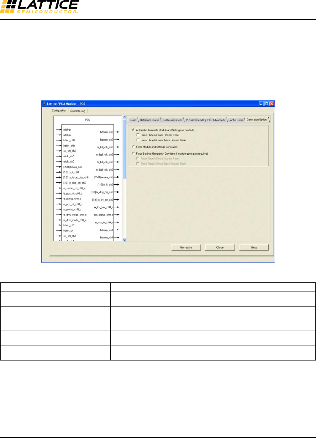
8-112
LatticeECP3 SERDES/PCS
Usage Guide
In File List, the .lpc file is replaced with an .ipx file. The IPexpress manifest (.ipx) file is new with Diamond. The .ipx
file keeps track of the files needed for complex modules.
Using IPexpress with Lattice Diamond
Using IPexpress with Lattice Diamond is essentially the same as with ispLEVER.
The configuration GUI tabs are all the same except for the Generation Options tab. Figure 8-57 shows the Genera-
tion Options tab window.
Figure 8-57. Generation Options Tab
Table 8-107. SERDES_PCS GUI Attributes – Generation Options Tab
GUI Text Description
Automatic Automatically generates the HDL and configuration(.txt) files as needed. Some
changes do not require regenerating both files.
Force Module and Settings Generation Generates both the HDL and configuration files.
Force Settings Generation Only Generates only the attributes file. You get an error message if the HDL file also
needs to be generated.
Force Place & Route Process Reset Resets the Place & Route Design process, forcing it to be run again with the
newly-generated PCS module.
Force Place & Route Trace Process Reset Resets the Place & Route Trace process, forcing it to be run again with the newly-
generated PCS module.
Note:
Automatic is set as the default option. If either Automatic or Force Settings Generation Only and no sub-options (Process Reset Options) are
checked and the HDL module is not generated, the reset pointer is set to Bitstream generation automatically.
After the Generation is finished, the reset marks in the process window will be reset accordingly.

8-113
LatticeECP3 SERDES/PCS
Usage Guide
Creating a New Simulation Project Using Simulation Wizard
This section describes how to use the Simulation Wizard to create a simulation project (.spf) file so you can import
it into a standalone simulator.
1. In Project Navigator, click Tools > Simulation Wizard. The Simulation Wizard opens.
2. In the Preparing the Simulator Interface page click Next.
3. In the Simulator Project Name page, enter the name of your project in the Project Name text box and
browse to the file path location where you want to put your simulation project using the Project Location
text box and Browse button.
When you designate a project name in this wizard page, a corresponding folder will be created in the file
path you choose. Click Yes in the pop-up dialog that asks you if you wish to create a new folder.
4. Click either the Active-HDL® or ModelSim® simulator check box and click Next.
5. In the Process Stage page choose which type of Process Stage of simulation project you wish to create
Valid types are RTL, Post-Synthesis Gate-Level, Post-Map Gate-Level, and Post-Route Gate-level+Timing.
Only those process stages that are available are activated.
Note that you can make a new selection for the current strategy if you have more than one defined in your
project.
The software supports multiple strategies per project implementation which allow you to experiment with
alternative optimization options across a common set of source files. Since each strategy may have been
processed to different stages, this dialog allows you to specify which stage you wish to load.
6. In the Add Source page, select from the source files listed in the Source Files list box or use the browse
button on the right to choose another desired source file. Note that if you wish to keep the source files in
the local simulation project directory you just created, check the Copy Source to Simulation Directory
option.
7. Click Next and a Summary page appears and provides information on the project selections including the
simulation libraries. By default, the Run Simulator check box is enabled and will launch the simulation tool
you chose earlier in the wizard in the Simulator Project Name page.
8. Click Finish.
The Simulation Wizard Project (.spf) file and a simulation script DO file are generated after running the wizard. You
can import the DO file into your current project if desired. If you are using Active-HDL, the wizard will generate an
.ado file and if you are using ModelSim, it creates and .mdo file.
Note: PCS configuration file, (.txt) must be added in step 6.
