TN FC 35: E·MMC PCB Design Guide TNFC35 E MMC
User Manual:
Open the PDF directly: View PDF ![]() .
.
Page Count: 8
Technical Note
e·MMC PCB Design Guide
Introduction
This document is intended as guide for PCB designers using Micron e·MMC devices
and will discuss the primary issues affecting design and layout.
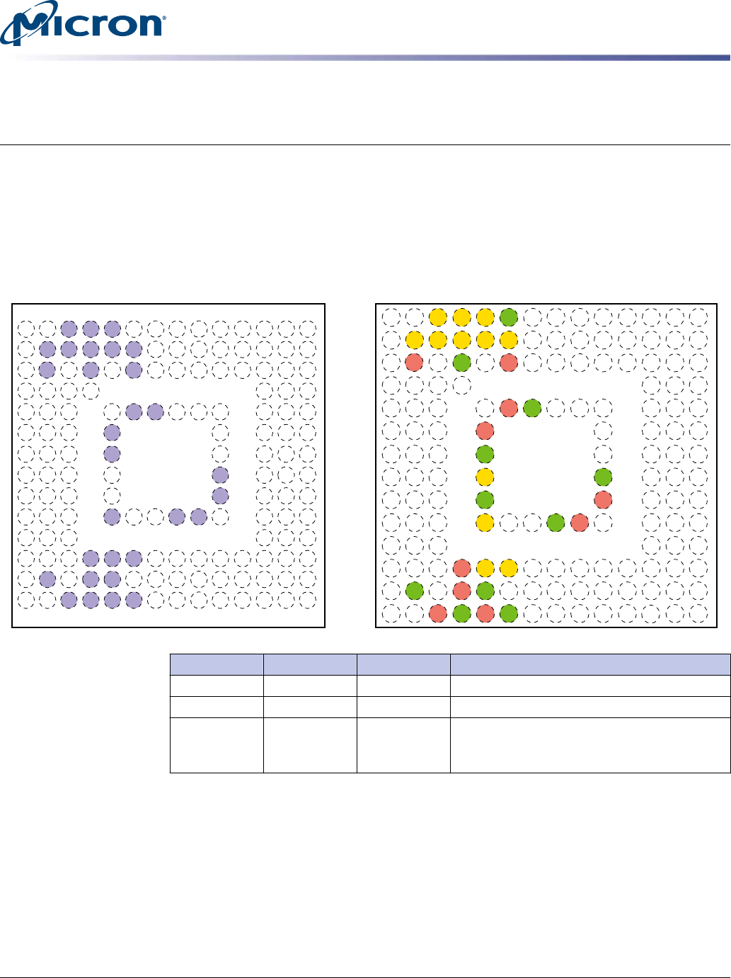
Figure 1: e·MMC 4.5 and 5.0 Package Compatibility
RFU
DAT7
VCCQ
VCC
RFU
CLK
NC
VSSQ
NC
NC
NC
NC
NC
NC
NC
NC
NC
NC
NC
NC
NC
NC
A
B
C
D
E
F
G
H
J
K
L
M
N
P
NC
DAT3
VDDIM
NC
NC
NC
NC
NC
NC
NC
NC
NC
VSSQ
NC
DAT0
DAT4
NC
NC
NC
NC
RFU
NC
NC
NC
NC
NC
NC
VCCQ
DAT1
DAT5
VSSQ
NC
VCCQ
VCCQ
VSSQ
DAT2
DAT6
RFU
RFU
VCC
VSS
RFU
RFU
RST_n
CMD
VSSQ
VCCQ
NC
NC
NC
NC
NC
NC
NC
NC
NC
NC
NC
NC
NC
NC
RFU
NC
NC
VSS
RFU
NC
NC
RFU
NC
NC
NC
RFU
VSS
NC
NC
NC
NC
NC
NC
RFU
VCC
NC
NC
NC
NC
NC
NC
RFU
RFU
RFU
VSS
VCC
RFU
NC
NC
RFU
NC
NC
NC
NC
NC
NC
NC
NC
NC
NC
NC
NC
NC
NC
NC
NC
NC
NC
NC
NC
NC
NC
NC
NC
NC
NC
NC
NC
NC
NC
NC
NC
NC
NC
1 2 3 4 5 6 7 8 9 10 11 12 13 14
A
B
C
D
E
F
G
H
J
K
L
M
N
P
A
B
C
D
E
F
G
H
J
K
L
M
N
P
1
NC
NC
NC
NC
NC
NC
NC
NC
NC
NC
NC
NC
NC
NC
1
2
NC
DAT3
V
DDI
NC
NC
NC
NC
NC
NC
NC
NC
NC
V
SSQ
NC
2
3
DAT0
DAT4
NC
NC
NC
NC
NC
NC
NC
NC
NC
NC
NC
V
CCQ
3
4
DAT1
DAT5
V
SSQ
NC
V
CCQ
V
CCQ
V
SSQ
4
5
DAT2
DAT6
NC
RFU
V
CC
V
SS
DS
V
SS
RST_n
CMD
V
SSQ
V
CCQ
5
6
V
SS
DAT7
V
CCQ
V
CC
RFU
CLK
NC
V
SSQ
6
7
RFU
NC
NC
V
SS
RFU
NC
NC
NC
7
8
NC
NC
NC
RFU
V
SS
NC
NC
NC
8
9
NC
NC
NC
RFU
V
CC
NC
NC
NC
9
10
NC
NC
NC
RFU
RFU
RFU
V
SS
V
CC
RFU
NC
NC
RFU
10
11
NC
NC
NC
NC
NC
NC
11
12
NC
NC
NC
NC
NC
NC
NC
NC
NC
NC
NC
NC
NC
NC
12
13
NC
NC
NC
NC
NC
NC
NC
NC
NC
NC
NC
NC
NC
NC
13
14
NC
NC
NC
NC
NC
NC
NC
NC
NC
NC
NC
NC
NC
NC
14
Ball e·MMC 4.51 e·MMC 5.0 Comment
H5 RFU DS DS can be floating if HS400 is not used.
A6, J5 RFU VSS VSS can be floating if HS400 is not used.
C5 RFU NC Used for routing in this technical note only
because it is NC internally, and JEDEC rede-
fined it as NC for e·MMC 5.0.
TN-FC-35: e·MMC PCB Design Guide
Introduction
PDF: 09005aef85c3dc13
tnfc35_eMMC_pcb_design_guide.pdf - Rev. B 01/15 EN 1Micron Technology, Inc. reserves the right to change products or specifications without notice.
© 2014 Micron Technology, Inc. All rights reserved.
Products and specifications discussed herein are for evaluation and reference purposes only and are subject to change by
Micron without notice. Products are only warranted by Micron to meet Micron's production data sheet specifications. All
information discussed herein is provided on an "as is" basis, without warranties of any kind.
Figure 2: Host to Micron e·MMC 5.0 Connection
VCCQ
VCC
VCCQ
CLK
CMD
DS
DAT0
DAT1
DAT2
DAT3
DAT4
DAT5
DAT6
DAT7
RST_n
CLK
CMD
DS
DAT0
DAT1
DAT2
DAT3
DAT4
DAT5
DAT6
DAT7
RST_n VCC
VCCQ
VDDiM
VDDiM
VCC
R_CMD
R_DS
SR_DS
C1 C2
SR_CLK
GND
GND
U2
Host controller
U1
e·MMC
R_DAT R_DAT R_DAT R_DAT R_DAT R_DAT R_DAT R_RST_nR_DAT
C3
C4
C5 C6
TN-FC-35: e·MMC PCB Design Guide
Introduction
PDF: 09005aef85c3dc13
tnfc35_eMMC_pcb_design_guide.pdf - Rev. B 01/15 EN 2Micron Technology, Inc. reserves the right to change products or specifications without notice.
© 2014 Micron Technology, Inc. All rights reserved.
Signal and Capacitor Placement
SR_CLK should be close to the host device, and SR_DS should be close to the e·MMC
device. e·MMC signals can be fanned out through NC pins. No internal connection is
present for NC pins. Micron recommends that e·MMC signals not be fanned out
through RFU pins.
The recommended decoupling capacitors should be placed on the bottom side of the
PCB across the BGA escape vias in order to minimize the connection inductance seen
by the capacitor. The capacitor pad should be connected to the power and ground
plane with a larger via to minimize the inductance in decoupling capacitors and allow
for maximum current flow. The recommended capacitor values are shown in Table 1
(page 4). Wide, short traces between the via and capacitor pads should be used, or
the via placed adjacent to the capacitor pad. Figure 4 (page 4) shows how to connect
capacitor pads to the power and ground plane. Method 1 is not recommended, while
the others are recommended.
Figure 3: Capacitor Placement and Signal PCB Layout
D0 D1 D2 VSS
VCCQ
VCC
VSSQ
VSS
CMDCLK
DS
RST_n
VDDi
D3 D4 D5 D6 D7
TN-FC-35: e·MMC PCB Design Guide
Signal and Capacitor Placement
PDF: 09005aef85c3dc13
tnfc35_eMMC_pcb_design_guide.pdf - Rev. B 01/15 EN 3Micron Technology, Inc. reserves the right to change products or specifications without notice.
© 2014 Micron Technology, Inc. All rights reserved.
Table 1: Component Parameter Values
Parameter Symbol Min Max
Recom-
mended Unit Comments
Pull-up resistance for CMD R_CMD 4.7 50 10 KΩTo prevent bus floating
Pull-up resistance for DAT[7:0] R_DAT 10 50 50 KΩTo prevent bus floating
Pull-up resistance for RST_n R_RST_n 4.7 50 50 KΩIt is not necessary to put pull-up
resistance on RST_n line if the
host does not use H/W reset.
Pull-down resistance for R_DS R_DS 4.7 50 50 KΩ
Impedance of CLK/CMD/DS/
DAT[7:0]
– 45 55 50 ΩImpedance match
Serial resistance on CLK line SR_CLK 0 47 22 ΩTo stabilize CLK signal
Serial resistance on DS line SR_DS 0 47 22 ΩTo stabilize DS signal
VCCQ capacitor value C1, C2 2.2 + 0.1 4.7 + 0.22 2.2 + 0.1 µF Decoupling capacitor should be
connected with VCCQ and VSSQ as
closely as possible.
VCC capacitor value (≤8GB) C3, C4 2.2 + 0.1 4.7 + 0.22 2.2 + 0.1 µF Decoupling capacitor should be
connected to VCC and VSS as close-
ly as possible.
VCC capacitor value (>8GB) 4.7 + 0.22 µF
VDDIM capacitor value C5, C6 1 + 0.1 4.7 + 0.1 1 + 0.1 µF Decoupling capacitor should be
connected to VDDIM and VSSQ as
closely as possible.
Figure 4: Connecting Capacitor Pads
Absolutely not!
1
Even better
3
Better still
4
The best!
Solid via within pad
5
Better
2
TN-FC-35: e·MMC PCB Design Guide
Signal and Capacitor Placement
PDF: 09005aef85c3dc13
tnfc35_eMMC_pcb_design_guide.pdf - Rev. B 01/15 EN 4Micron Technology, Inc. reserves the right to change products or specifications without notice.
© 2014 Micron Technology, Inc. All rights reserved.
PCB Topology and Layout
The PCB board must have at least four layers.
CLK, CMD, DQ and DS signals should be treated as transmission lines with controlled
impedance from 45Ω to 55Ω. The skew of propagation time of these signals should be
minimized and the PCB trace length difference kept within ±50 mil. The following figure
shows two commonly used PCB transmission line topologies.
Figure 5: Transmission Line Topologies
PCB Trace
Stripline
Ground Plane
Dielectric
Microstrip
The e·MMC signals' trace length should be as short as possible; it is best kept to less
than 2000 mil.
The transmission line should be designed so that the conductor is as close to the
ground plane as possible. This technique will couple the transmission line tightly to the
ground plane and help decouple it from adjacent signals. It's best to widen spacing be-
tween signal lines as much as routing restrictions will allow, trying not to bring traces
closer than three times the trace width.
Figure 6: Trace Width Example
W
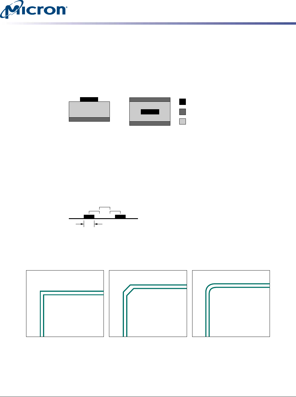
Arc-shaped traces should be used instead of right-angle bends.
Figure 7: Trace Shape
Recommended RecommendedNot recommended
There should be NO breaks or voids in the ground plane under or over the high speed
signals.
TN-FC-35: e·MMC PCB Design Guide
PCB Topology and Layout
PDF: 09005aef85c3dc13
tnfc35_eMMC_pcb_design_guide.pdf - Rev. B 01/15 EN 5Micron Technology, Inc. reserves the right to change products or specifications without notice.
© 2014 Micron Technology, Inc. All rights reserved.
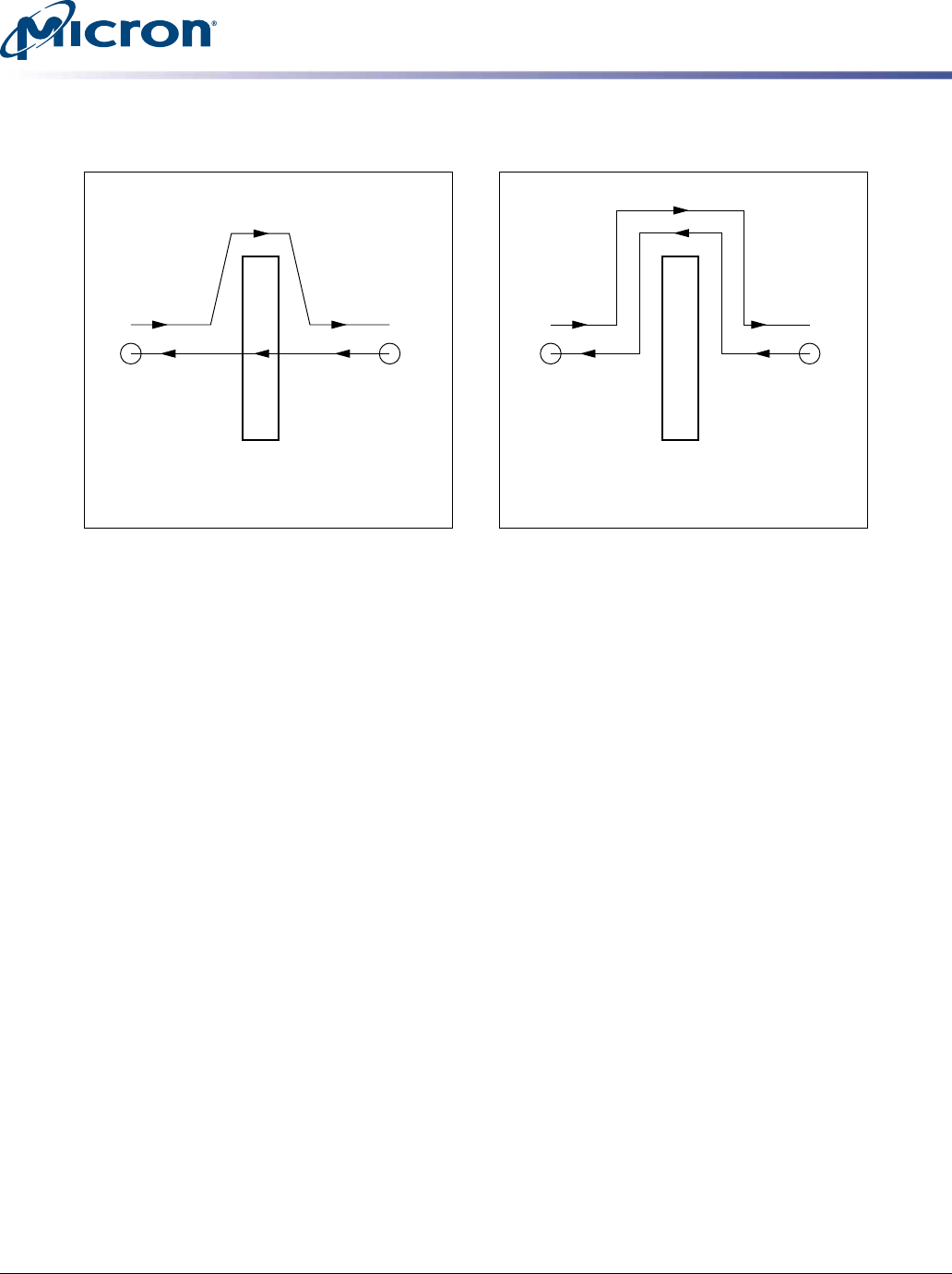
Figure 8: Avoiding Breaks and Voids
Bad
Slot in image plane
Return
current
Better
Slot in image plane
Return
current
The best signaling is obtained when a constant reference plane is maintained. If a refer-
ence plane transition cannot be avoided, we recommend using the following techni-
ques.
• If the signal reference plane changes from ground plane to power plane, adding ca-
pacitors near the via transition site will help support a good return path.
• If the signal reference plane changes from ground plane to another ground plane,
ground vias should surround all high-speed signals (two ground vias per clock via;
one ground via per high speed signal via).
TN-FC-35: e·MMC PCB Design Guide
PCB Topology and Layout
PDF: 09005aef85c3dc13
tnfc35_eMMC_pcb_design_guide.pdf - Rev. B 01/15 EN 6Micron Technology, Inc. reserves the right to change products or specifications without notice.
© 2014 Micron Technology, Inc. All rights reserved.
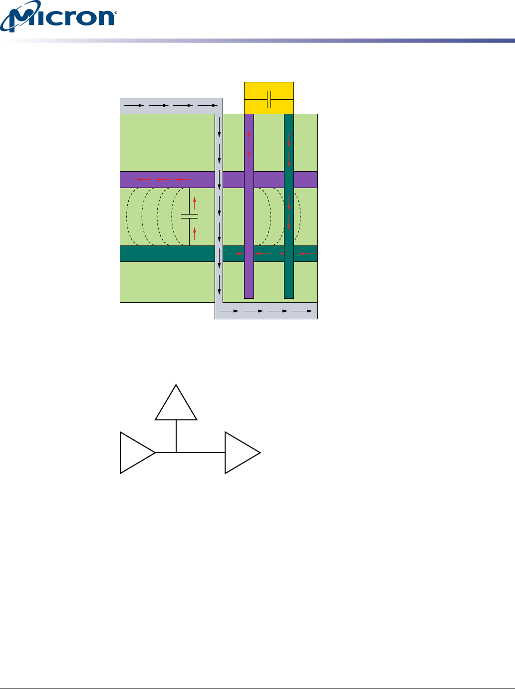
Figure 9: Additional Capacitor for Return Current
MLCC
Ground
plane
Power plane
Trace
Trace
Stubs should be kept short to avoid reflections. Stub propagation delay should be kept
to <20% of the rise time of the signal.
Figure 10: Typical Stub Case
Branch
TN-FC-35: e·MMC PCB Design Guide
PCB Topology and Layout
PDF: 09005aef85c3dc13
tnfc35_eMMC_pcb_design_guide.pdf - Rev. B 01/15 EN 7Micron Technology, Inc. reserves the right to change products or specifications without notice.
© 2014 Micron Technology, Inc. All rights reserved.

Revision History
Rev. B – 01/15
• Updated the Host to Micron e·MMC 5.0 Connection figure
Rev. A – 08/14
• Initial release
8000 S. Federal Way, P.O. Box 6, Boise, ID 83707-0006, Tel: 208-368-4000
www.micron.com/products/support Sales inquiries: 800-932-4992
Micron and the Micron logo are trademarks of Micron Technology, Inc.
All other trademarks are the property of their respective owners.
TN-FC-35: e·MMC PCB Design Guide
Revision History
PDF: 09005aef85c3dc13
tnfc35_eMMC_pcb_design_guide.pdf - Rev. B 01/15 EN 8Micron Technology, Inc. reserves the right to change products or specifications without notice.
© 2014 Micron Technology, Inc. All rights reserved.
