P6209 4 GHz 5X Active Probe Instruction Manual T_P6209 T
User Manual: T_P6209
Open the PDF directly: View PDF ![]() .
.
Page Count: 74

Instruction Manual
P6209
4 GHz 5X Active Probe
071-0634-04
Warning
The servicing instructions are for use by qualified
personnel only. To avoid personal injury, do not
perform any servicing unless you are qualified to
do so. Refer to all safety summaries prior to
performing service.
www.tektronix.com
Copyright ©Tektronix, Inc. All rights reserved.
Tektronix products are covered by U.S. and foreign patents, issued and
pending. Information in this publication supercedes that in all previously
published material. Specifications and price change privileges reserved.
Tektronix, Inc., P.O. Box 500, Beaverton, OR 97077
TEKTRONIX, TEK, TEKPROBE, and SureFoot are registered trademarks,
and SureToe, FlexLead, and KlipChip are trademarks of Tektronix, Inc.
WARRANTY
Tektronix warrants that this product will be free from defects in materials and
workmanship for a period of one (1) year from the date of shipment. If any such
product proves defective during this warranty period, Tektronix, at its option,
either will repair the defective product without charge for parts and labor, or will
provide a replacement in exchange for the defective product.
In order to obtain service under this warranty, Customer must notify Tektronix of
the defect before the expiration of the warranty period and make suitable
arrangements for the performance of service. Customer shall be responsible for
packaging and shipping the defective product to the service center designated
by Tektronix, with shipping charges prepaid. Tektronix shall pay for the return of
the product to Customer if the shipment is to a location within the country in
which the Tektronix service center is located. Customer shall be responsible for
paying all shipping charges, duties, taxes, and any other charges for products
returned to any other locations.
This warranty shall not apply to any defect, failure or damage caused by im-
proper use or improper or inadequate maintenance and care. Tektronix shall not
be obligated to furnish service under this warranty a) to repair damage resulting
from attempts by personnel other than Tektronix representatives to install, repair
or service the product; b) to repair damage resulting from improper use or
connection to incompatible equipment; or c) to service a product that has been
modified or integrated with other products when the effect of such modification
or integration increases the time or difficulty of servicing the product.
THIS WARRANTY IS GIVEN BY TEKTRONIX WITH RESPECT TO THIS
PRODUCT IN LIEU OF ANY OTHER WARRANTIES, EXPRESSED OR IM-
PLIED. TEKTRONIX AND ITS VENDORS DISCLAIM ANY IMPLIED WARRAN-
TIES OF MERCHANTABILITY OR FITNESS FOR A PARTICULAR PURPOSE.
TEKTRONIX’ RESPONSIBILITY TO REPAIR OR REPLACE DEFECTIVE
PRODUCTSISTHESOLEANDEXCLUSIVEREMEDYPROVIDEDTOTHE
CUSTOMER FOR BREACH OF THIS WARRANTY. TEKTRONIX AND ITS
VENDORS WILL NOT BE LIABLE FOR ANY INDIRECT, SPECIAL, INCIDEN-
TAL, OR CONSEQUENTIAL DAMAGES IRRESPECTIVE OF WHETHER
TEKTRONIX OR THE VENDOR HAS ADVANCE NOTICE OF THE POSSIBIL-
ITY OF SUCH DAMAGES.

P6209 4 GHz Probe Instruction Manual i
Table of Contents
General Safety Summary v..............................
Service Safety Summary vii..............................
Contacting Tektronix viii.................................
Product Description
Options 1............................................
Features and Standard Accessories 2......................
Optional Accessories 7.................................
Configuration
Probe Offset 9........................................
Functional Check
Operating Basics
Handling the Probe 13..................................
Maximum Nondestructive Input Voltage 13.................
Input Linear Dynamic Range 13..........................
Ground Lead Length 14.................................
Helpful Hints
Low-inductance Grounding 17............................
SureFoot Grounding 18.................................
Probe Tip Test Points 19.................................
Specifications

Table of Contents
ii P6209 4 GHz Probe Instruction Manual
Theory of Operation
Probe Head and Cable Assembly 30.......................
Compensation Box 30...................................
Offset Amplifier 30.....................................
Probe Identification EEPROM 30.........................
TEKPROBE SMA Interface 31...........................
VCC, +7 V Regulator 31................................
Performance Verification
Equipment Required 33.................................
Equipment Setup 34....................................
Output Zero 35........................................
DC Attenuation Accuracy 36.............................
Rise Time 38..........................................
Adjustments
Removing the Compensation Box Bottom Cover 43...........
Adjustment Locations 44................................
Offset Zero 44.........................................
Offset Scale 46........................................
Maintenance
Inspection and Cleaning 49..............................
Replacement Parts 49...................................
Preparation for Shipment 49..............................
Troubleshooting
Replaceable Parts
Parts Ordering Information 55............................
Using the Replaceable Parts List 56........................

Table of Contents
P6209 4 GHz Probe Instruction Manual iii
List of Figures
Figure 1: Dynamic and offset limitations 10.................
Figure 2: Probe functional check connections 11.............
Figure 3: Ground lead equivalent circuit 14.................
Figure 4: Low-inductance grounding 17....................
Figure 5: Using a SureFoot adapter for grounding 18..........
Figure 6: Using a probe tip as a test point 19.................
Figure 7: Typical input impedance and phase versus frequency 24
Figure 8: Typical bandwidth 24...........................
Figure 9: Dimensions of probe head and compensation box 26..
Figure 10: P6209 simplified schematic diagram 29............
Figure 11: TEKPROBE SMA Interface pin assignments 31.....
Figure 12: P6209 output zero setup 35......................
Figure 13: P6209 DC attenuation accuracy setup 37...........
Figure 14: Test system rise time setup 38...................
Figure 15: Test system and probe rise time setup 39...........
Figure 16: Removing the compensation box bottom cover 43...
Figure 17: P6209 adjustment and measurement locations 44....
Figure 18: P6209 offset zero setup 45......................
Figure 19: P6209 offset range setup 47.....................
Figure 20: Compensation box test point locations 52..........
Figure 21: TEKPROBE SMA Interface pin assignments 52.....
Figure 22: P6209 replaceable parts 57......................
Figure 23: P6209 standard accessories 58...................
Figure 24: P6209 optional accessories 60...................

Table of Contents
iv P6209 4 GHz Probe Instruction Manual

P6209 4 GHz Probe Instruction Manual v
General Safety Summary
Review the following safety precautions to avoid injury and prevent
damage to this product or any products connected to it. To avoid
potential hazards, use this product only as specified.
Only qualified personnel should perform service procedures.
To Avoid Fire or Personal Injury
Connect and Disconnect Properly. Connect the probe outputs to the
measurement instrument before connecting the probe to the circuit
under test. Disconnect the probe input and the probe ground from the
circuit under test before disconnecting the probe from the measure-
ment instrument.
Observe All Terminal Ratings. To avoid fire or shock hazard, observe
all ratings and markings on the product. Consult the product manual
for further ratings information before making connections to the
product.
Connect the ground lead of the probe to earth ground only.
Do Not Operate Without Covers. Do not operate this product with
covers or panels removed.
Do Not Operate With Suspected Failures. If you suspect there is
damage to this product, have it inspected by qualified service
personnel.
Do Not Operate in Wet/Damp Conditions.
Do Not Operate in an Explosive Atmosphere.
Keep Product Surfaces Clean and Dry.
General Safety Summary
vi P6209 4 GHz Probe Instruction Manual
Safety Terms and Symbols
Terms in This Manual. These terms may appear in this manual:
WARNING. Warning statements identify conditions or practices that
could result in injury or loss of life.
CAUTION. Caution statements identify conditions or practices that
could result in damage to this product or other property.
Terms on the Product. These terms may appear on the product:
DANGER indicates an injury hazard immediately accessible as you
read the marking.
WARNING indicates an injury hazard not immediately accessible as
you read the marking.
CAUTION indicates a hazard to property including the product.
Symbols on the Product. These symbols may appear on the product:
CAUTION
Refer to Manual

P6209 4 GHz Probe Instruction Manual vii
Service Safety Summary
Only qualified personnel should perform service procedures. Read
this Service Safety Summary and the General Safety Summary before
performing any service procedures.
Do Not Service Alone. Do not perform internal service or adjustments
of this product unless another person capable of rendering first aid
and resuscitation is present.

Service Safety Summary
viii P6209 4 GHz Probe Instruction Manual
Contacting Tektronix
Phone 1-800-833-9200*
Address Tektronix, Inc.
Department or name (if known)
14200 SW Karl Braun Drive
P.O. Box 500
Beaverton, OR 97077
USA
Web site www.tektronix.com
Sales
support
1-800-833-9200, select option 1*
Service
support
1-800-833-9200, select option 2*
Technical
support
Email: techsupport@tektronix.com
1-800-833-9200, select option 3*
6:00 a.m. -- 5:00 p.m. Pacific time
*This phone number is toll free in North America. After office
hours, please leave a voice mail message.
Outside North America, contact a Tektronix sales office or
distributor; see the Tektronix web site for a list of offices.

P6209 4 GHz Probe Instruction Manual 1
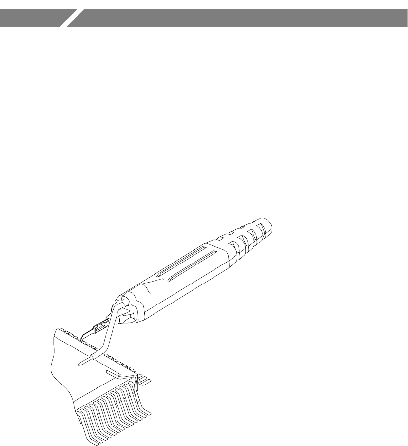
Product Description
The Tektronix P6209 is a 4 GHz (probe only), 5X active FET probe
with 1 pF input capacitance. The probe is designed primarily for use
with sampling oscilloscopes, such as the CSA/TDS8000. The P6209
has a low input capacitance and high input resistance, which
minimize circuit loading over a wide bandwidth range.
The small profile and low-mass head of the P6209 make manual
probing of crowded circuits fast and easy. The accessory tips and
adapters enable the P6209 to be used on a wide variety of circuit
architectures.
The P6209 is powered through a TEKPROBE SMA interface
between the probe compensation box and the oscilloscope.
Options
The following options are available when ordering the P6209 probe:
HOption D1 -- Calibration Data
HOption C3 -- 3 years Calibration Service
HOption D3 -- 3 years Calibration Data
HOption R3 -- 3 years Extended Warranty
Product Description
2P6209 4 GHz Probe Instruction Manual
Features and Standard Accessories
The P6209 probe is provided with several features and accessories
designed to make probing and measurement a simpler task. Please
familiarize yourself with these items and their uses. For part number
information and quantities of standard and optional accessories, refer
to Replaceable Parts on page 55.
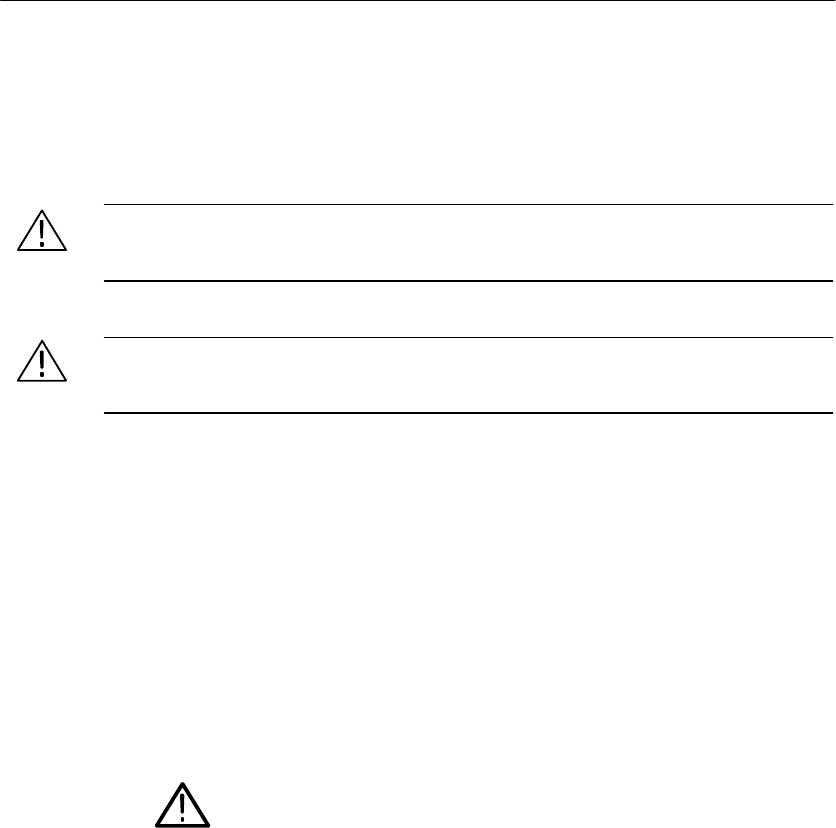
Probe tip
socket
Ground
socket
Stabilization
notch
Probe head assembly. The probe head is
designed for ease of use and high performance.
Its small size makes it easy to handle in tight
areas.
The probe tip socket is sized to easily press onto
0.025 inch pins for direct access. The ground
socket provides a short ground path for high
fidelity ground connections.
The stabilization notch permits you to use
adjacent pins to reduce stresses on the probe
and pins.
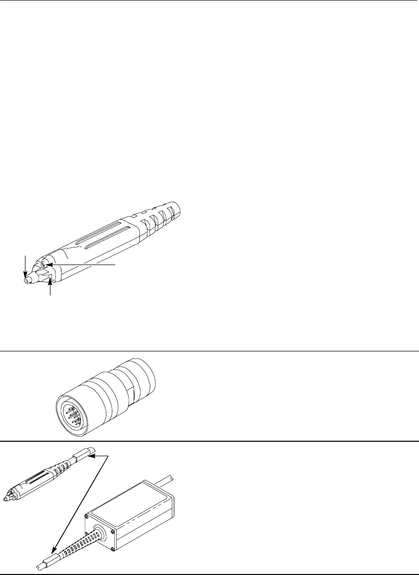
TEKPROBE SMA interface. The TEKPROBE
SMA interface provides a communication path
between the probe and the oscilloscope. Contact
pins provide power, offset, and probe characteris-
tic data transfer. See page 31 for more informa-
tion.
Color marker
bands
Color marker bands. Attach matching pairs of
the color marker bands onto the cable at the head
and compensation box of each probe. The marker
bands enable quick verification of which probe is
connected to which instrument channel.
Product Description
P6209 4 GHz Probe Instruction Manual 3
SureToe probe tip. The SureToe tip is a pointed
probe tip useful for probing in dense circuitry.
Attach the SureToe adapters the same way as
the push-in probe tips. Do not force the tip.Also,
be careful not to injure yourself with the sharp
probe tip. They can be used with any of the
socketed accessory leads.
Push-in probe tip
Push-in probe tip. Use the push-in probe tip
for general purpose probing by hand. The tip may
also be used as a temporary test point. See
page 19 for more information.
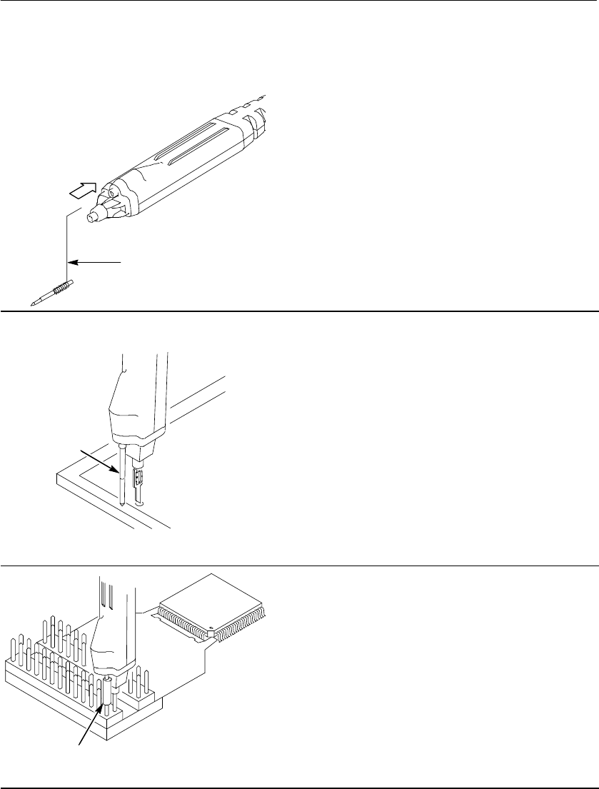
The push-in probe tip may also be used with the
other socketed leads and adapters.
Installing the push-in probe tip. Attach the
push-in probe tip by seating the tip into the probe
tip socket and pushing the tip in until it is seated.
Either end of the tip may be used.
Do not force the tip. Also, be careful not to injure
yourself with the sharp probe-tip. To remove the
tip, gently grab the tip with small pliers and pull
the tip out.
Right
angle
adapter
Right-angle adapter. Use the right-angle
adapter for low-profile probing of 0.025 inch
square pins.
The right-angle adapter allows the probe to lie flat
against a circuit board. This enables probing in
vertical circuits, such as computer or communica-
tions backplanes, or in tight areas, such as
between circuit cards.
The right-angle adapter can be used directly with
the probe head or attached to the Y-lead adapter
or ground leads.
The right-angle adapter is attached the same way
as the push-in probe tip and can be easily
removed by hand.
Product Description
4P6209 4 GHz Probe Instruction Manual
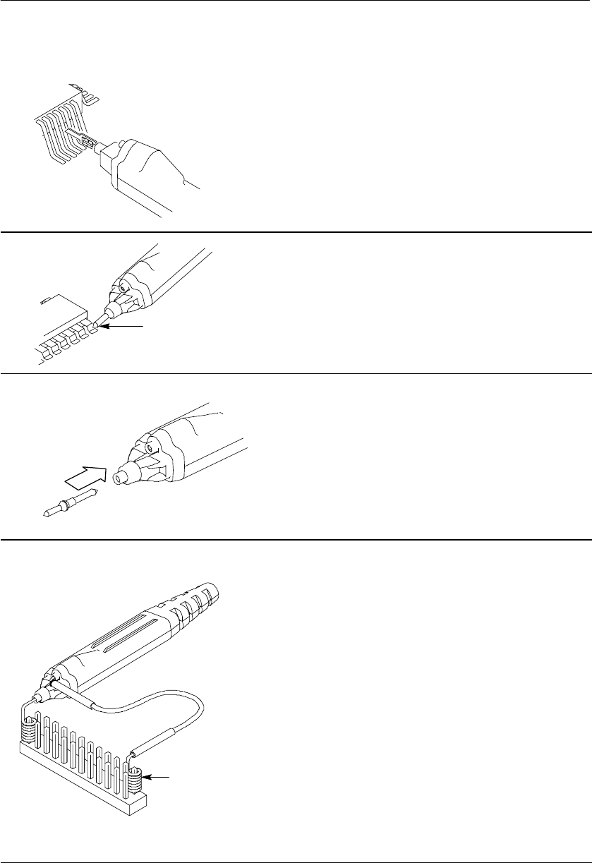
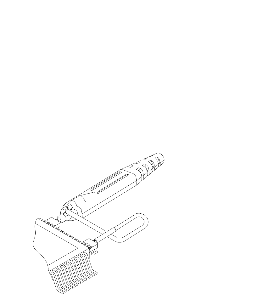
Y-lead
adapter
Y-lead adapter. Use the Y-lead adapter to
extend the physical reach of the probe and
ground when necessary. The Y-lead adapter
accepts any of the probe tips or adapters and
can be pushed directly onto 0.025 inch pins.
When selecting the grounding connection,
maintain as short a ground path as possible.
Refer to page 14 for more information.
Y-lead
adapter
To attach the Y-lead adapter, gently press the
lead pins into the probe head tip and ground
receptacles. Using the black lead for ground is
recommended.
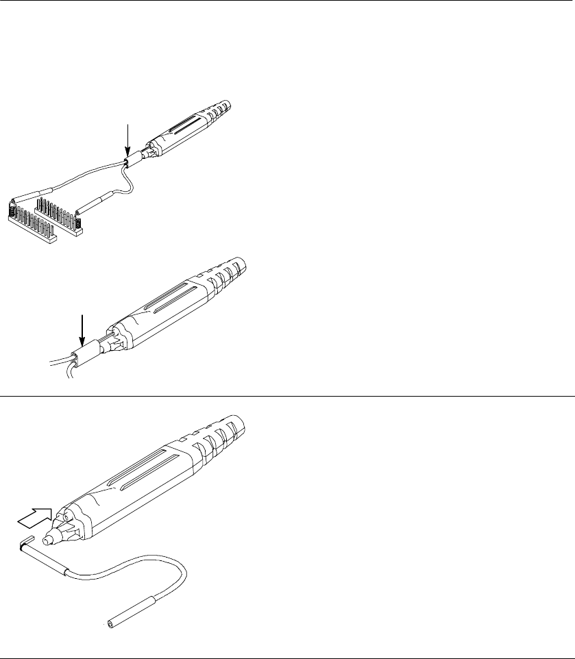
Three-inch ground lead. Use the three-inch
ground lead for general probing. The socketed
end of the lead may be connected to any of the
probe tips and adapters or fitted onto 0.025 inch
pins.
To attach the ground lead, press and rotate the
lead pin connector into the ground socket on the
probe head. The lead may be removed by simply
pulling the pin out by hand.
When selecting the grounding connection,
maintain as short a ground path as possible.
Refer to page 14 for more information.
Product Description
P6209 4 GHz Probe Instruction Manual 5
Customizable
ground lead
Customizable ground lead.This ground lead
wire can be bent or cut shorter.
NOTE: To ease insertion into the ground socket
of the probe, cut the tip of this ground lead wire at
a 30 to 60 degree angle.
To maintain signal fidelity while probing, use as
short a ground path as possible. Refer to page 14
for more grounding information.
Pogo pin
Low-inductance ground pogo pin. Use the
low-inductance ground pogo pin to substantially
reduce ground lead inductance. Because the
pogo pin simply touches the ground reference,
you can easily move the probe to different points
on the circuit under test.
To attach, press the pogo pin into the probe head
ground socket.
When selecting the grounding connection,
maintain as short a ground path as possible.
Refer to page 14 for more information.
Signal-ground
adapter
Signal-ground adapter. The signal-ground
adapter is ideal for use with signal/ground pairs
on 0.100 inch header pins.
Attach the signal-ground adapter by gently
pressing it into the ground socket on the probe
head.
Be sure to use the stabilization notch whenever
possible to avoid slipping and damaging the
probe or circuitry under test.
Product Description
6P6209 4 GHz Probe Instruction Manual
KlipChip
Y-lead adapter
SMT KlipChip. Use the SMT KlipChip test clips
to access fragile, dense circuitry.
KlipChip test clips can be connected to the Y-lead
or three-inch ground leads. Simply press the lead
socket into the KlipChip handle.
The KlipChip body freely turns, allowing better
probe orientation. To reduce stress and provide a
lower profile on components being tested, the
flexible sleeve of the KlipChip bends up to a
35 degree angle.
When selecting the grounding connection,
maintain as short a ground path as possible.
Refer to page 14 for more information.
SMA adapter jack. Use the SMA adapter jack
with the SMT KlipChips to gain access to
calibration signals from SMA connectors on the
oscilloscope front panel.
Male SMA termination. Protect the probe input
circuitry by connecting the termination to the
probe input connector when the probe is not in
use.
Product Description
P6209 4 GHz Probe Instruction Manual 7
Optional Accessories
The following accessories are available for the probe. See the
Replaceable Parts List on page 55 for ordering information.
SureFoot probe tips. The SureFoot tip is an
integral probe tip and miniature guide that
enables fault-free probing of fine-pitch SMD
packages. Attach SureFoot adapters the same
way as the push-in probe tips. They can be used
with any of the socketed accessory leads.
The orange, 0.050 inch SureFoot tip is compatible
with 50 mil JEDEC packages such as SOIC,
PLCC, and CLCC.
The blue, 0.025 inch SureFoot tip is compatible
with 0.65 mm JEDEC and EIAJ packages.
The red, 0.5 mm SureFoot tip is compatible with
EIAJ packages.
SMK4 Micro KlipChip adapters. Use the
Micro KlipChip adapters to probe the leads on
integrated circuits that are surface-mounted.
SMA-to-probe tip adapter. Use the adapter to
connect the probe to SMA cables. The adapter
includes a 50-ohm SMA termination.

Product Description
8P6209 4 GHz Probe Instruction Manual
P6209 4 GHz Probe Instruction Manual 9
Configuration
The P6209 provides the oscilloscope with the probe model number,
serial number, and attenuation factor. When connected to the
oscilloscope, the display readouts are corrected for the probe
attenuation factor.
The probe offset control is controlled by the oscilloscope.
CAUTION. To prevent damage to your probe, do not apply a voltage
outside the Maximum Input Voltage rating. See Specifications on
page 21.
To prevent electrostatic damage to the instrument and sampling
modules, follow the precautions described in the manuals
accompanying your instrument.
Always use a wrist strap (provided with your probe) when handling
the probe and sampling modules, and when making signal
connections.
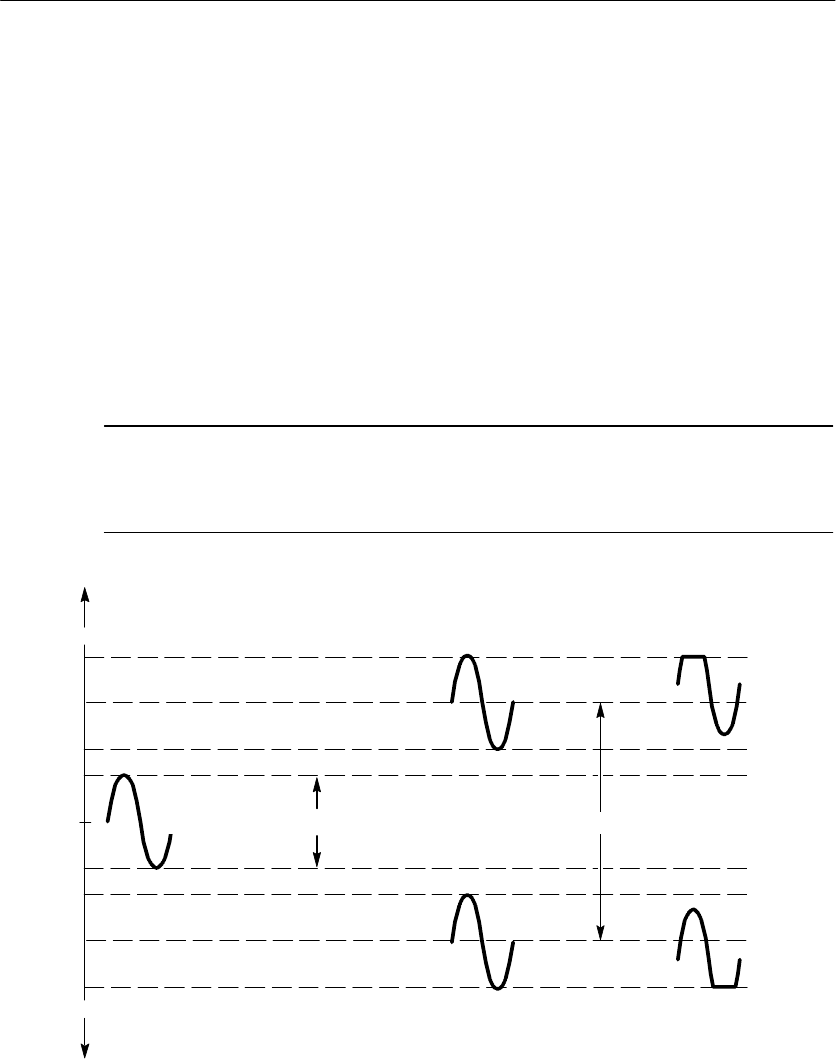
Probe Offset
The purpose of the offset capability is to permit the input signal to be
positioned in the center of the dynamic range of the probe amplifier,
to obtain the best transient response. Using the offset to cancel DC
signal components enables optimal probe performance. See Figure 1
on page 10 for more information.
NOTE. If the offset is not correctly positioned, clipping or distortion
of the displayed signal may occur. See your oscilloscope manual for
specific instructions on its operation and offset control.
Configuration
10 P6209 4 GHz Probe Instruction Manual
To set the probe offset, follow these steps:
1. Set the oscilloscope vertical scale to the least sensitive V/div
setting (500 mV/div on the CSA/TDS8000).
2. Attach the probe to the circuit.
3. Adjust the probe offset to bring the trace onto the oscilloscope
screen.
4. Change the volts/division setting to the desired range, adjusting
theoffsettokeepthetraceonscreen.
NOTE.TheP6209 has a ±5.0 V offset range. The linear operating
range is ±2.00 V. See Figure 1. Also, see page 13 for more informa-
tion.
0V
+5.00 V
--5.00 V
+2.00 V
--2.00 V
Nonoperating range (+30 V maximum nondestructive input voltage )
Nonoperating range (--30 V maximum nondestructive input voltage )
Maximum Offset RangeMaximum AC Signal Amplitude
+7.00 V
--7.00 V
+5.00 V
--5.00 V
+3.00 V
--3.00 V
Figure 1: Dynamic and offset limitations
P6209 4 GHz Probe Instruction Manual 11
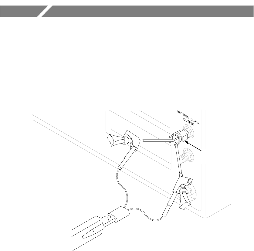
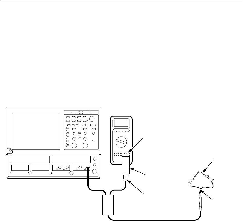
Functional Check
After installing the probe on the CSA/TDS8000 oscilloscope, a
functional check may be performed using the INTERNAL CLOCK
OUTPUT connection on the front panel of the oscilloscope. See
Figure 2.
SMA
adapter jack
Figure 2: Probe functional check connections
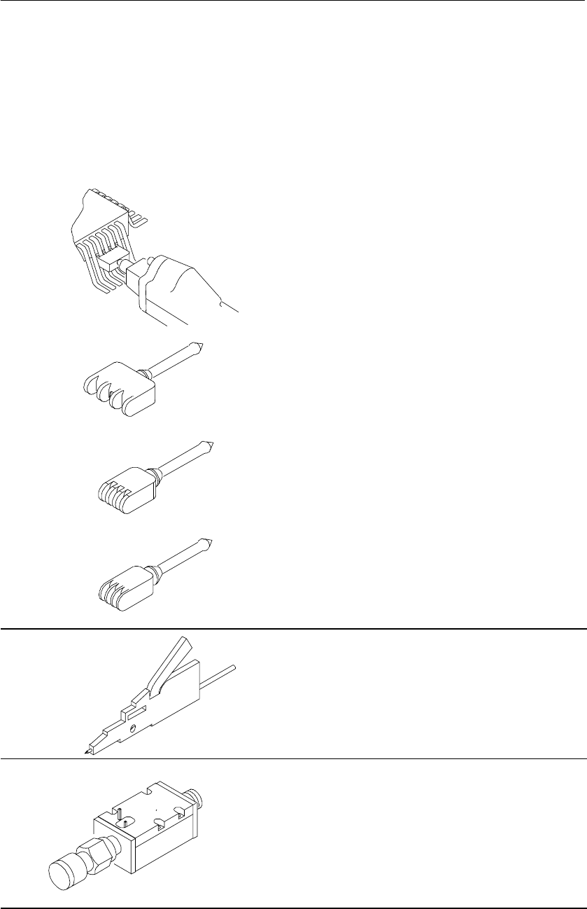
1. Set the oscilloscope to display the probe channel.
2. Using the Y-lead connector, SMT KlipChips and the SMA
adapter jack accessories, connect the probe to the INTERNAL
CLOCK OUTPUT connection on the oscilloscope, as shown in
Figure 2.
3. In the setup menu, set the trigger source to internal clock and the
frequency to 200 kHz.

Functional Check
12 P6209 4 GHz Probe Instruction Manual
4. Set the offset to 1V, the vertical scale to 500 mV/div, and the
horizontal scale to 2s/div.
5. The observed waveform should be a 200 kHz square wave with
an amplitude of approximately 2 V (the clock output is
unterminated), and have an offset of approximately 1 V.
If the probe does not pass this functional check, go to Troubleshoot-
ing on page 51.
P6209 4 GHz Probe Instruction Manual 13
Operating Basics
Please follow these operating guidelines to get optimum performance
from your P6209 probe.
Handling the Probe
Exercise care when using and storing the P6209 probe. The probe
and cable are susceptible to damage caused by careless use. Always
handle the probe using the compensation box and probe head,
avoiding undue physical strain to the probe cable, such as kinking,
excessive bending, or pulling. Visible dents in the cable will increase
signal aberrations. Do not drop the probe or subject it to physical
shock. Damage to the probe may result.
CAUTION. To prevent damage to your probe, do not apply a voltage
outside the Maximum Nondestructive Input Voltage for the probe.
Always use a wrist strap (provided with your probe) when
handling the probe and sampling modules, and when making
signal connections.
Maximum Nondestructive Input Voltage
Applying voltages above the P6209 design limits may damage the
probe tip amplifier. Please refer to Specifications on page 21 for the
maximum operating voltage and frequency derating information.
Input Linear Dynamic Range
The probe head amplifier used by the P6209 has a limited linear
operating range. To keep the input linearity error less than 0.1%, you
must limit the apparent signal input voltage to ±1.75 V.
Operating Basics
14 P6209 4 GHz Probe Instruction Manual
Use the DC offset adjustment to maintain the probe within its
dynamic range. The nominal offset adjustment range of the P6209 is
±5.0 VDC. For example: to offset a +2 VDC level in a circuit, set the
offset to +2 V.
NOTE. The probe can tolerate input voltages of ±30 V (≤5 minutes)
without damage; however, the linearity error specification does not
apply to input voltages outside the linear dynamic range of the
probe. See Figure 1 on page 10.
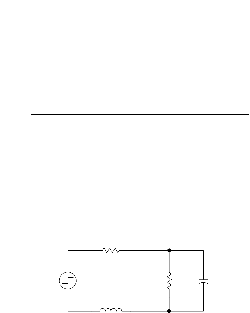
Ground Lead Length
When you are probing a circuit, you should always use as short a
ground lead as possible between the probe head and circuit ground.
The series inductance added by the probe tip and ground lead can
result in a resonant circuit; this circuit may cause parasitic ringing
within the bandwidth of your oscilloscope. When you touch your
probe tip to a circuit element, you are introducing a new resistance,
capacitance, and inductance into the circuit. Refer to Figure 3.
Rsource
Vsource
Probe C in
1pF
Probe R in
20 KΩ
Lgl (Ground Lead)
Figure 3: Ground lead equivalent circuit
Ringing and rise time degradation can be masked if the frequency
content of the signal degradation is beyond the bandwidth of the
oscilloscope.

Operating Basics
P6209 4 GHz Probe Instruction Manual 15
You can determine if ground lead effects may be a problem in your
application if you know the self-inductance (L) and capacitance (C)
of your probe and ground lead. Calculate the approximate resonant
frequency (f0) at which this parasitic circuit will resonate with the
following formula:
f0=1
2πLC
The preceding equation shows that reducing the ground lead
inductance will raise the resonant frequency. If your measurements
are affected by ringing, your goal is to lower the inductance of your
ground path until the resulting resonant frequency is well above the
frequency of your measurements.
The low-inductance ground contacts described in Accessories can
help you reduce the effects of ground lead inductance on your
measurements.

Operating Basics
16 P6209 4 GHz Probe Instruction Manual
P6209 4 GHz Probe Instruction Manual 17
Helpful Hints
Follow these helpful hints to make probing easier and noise free.
Low-inductance Grounding
Placing a ground plane on top of a package being probed can
minimize ground lead length and inductance. See Figure 4.
Figure 4: Low-inductance grounding
Attach a small piece of copper clad on top of the package and
connect it to the package ground connection. Use the low-inductance
ground lead provided with the P6209 to keep the ground lead length
as short as possible.
Helpful Hints
18 P6209 4 GHz Probe Instruction Manual
This method is very useful when making many measurements on the
same package. Using a ground plane on the package makes probing
the package easier and avoids adding unnecessary ground lead length
and distortion.
SureFoot Grounding
If you cannot use the recommended low-inductance grounding
method, you may ground the probe to the package under test using a
SureFoot adapter. Refer to Figure 5.
Figure 5: Using a SureFoot adapter for grounding
Use a SureFoot adapter at the end of a short ground lead to connect
directly to the package ground. This method is preferred over using
an adjacent circuit ground because it is the shortest ground path
possible.
Helpful Hints
P6209 4 GHz Probe Instruction Manual 19
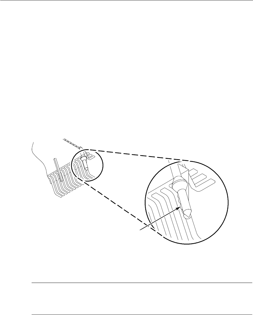
Probe Tip Test Points
You can solder the push-in probe tip or a 0.025 square pin to a circuit
to be used as a temporary test point. See Figure 6.
Solder the tip onto a lead or pin with a low-power soldering iron.
Press the probe head onto the tip to make a measurement, and then
pull the probe head off when you are done.
The probe tip may be removed and reused by desoldering it from the
circuit and soldering it into another circuit in the future.
Solder
Figure 6: Using a probe tip as a test point
NOTE. Do not use pieces of solid-core copper wire as test points. If
the wire breaks off in the probe tip socket, it may be impossible to
remove the wire, and it will prevent insertion of other accessory tips.

Helpful Hints
20 P6209 4 GHz Probe Instruction Manual
P6209 4 GHz Probe Instruction Manual 21
Specifications
These specifications apply to a P6209 probe when used with a
CSA/TDS8000 oscilloscope, and other oscilloscopes with a
TEKPROBE SMA interface.
The probe and oscilloscope must first be allowed to warm up for
20 minutes before measurements are taken.
CAUTION. Do not apply voltages beyond the nondestructive input
voltage range to the probe. Damage to the probe or circuit under test
may result.
Table 1: Warranted electrical specifications
DC Gain Accuracy (probe only) 0.2 ±2% (excludes offset error)
Rise Time (small signal, probe only) ≤120 ps (≤250 mV, 20--30°C)
Output Zero ±7.5 mV or less at output of probe (does not
include oscilloscope offset control voltage
error) (20--30°C)
±37.5 mV or less displayed on screen with
TEKPROBE SMA interface (does not
include oscilloscope offset control voltage
error) (20--30°C)
Delay Time 5.95 ns ±0.2 ns (includes SMA output cable)
System Noise 300 V rms or less at output of probe with
probe tip grounded

Specifications
22 P6209 4 GHz Probe Instruction Manual
Table 2: Typical electrical characteristics
Bandwidth, (probe only) 4 GHz (See Figure 8)
Linear Input Dynamic Range --2.00 V to +2.00 V.
(Equivalent to --0.40 V to +0.40 V
at the output of the probe.)
Linearity
Maximum deviation from linear regression
expressed as a percentage of the specified
full-scale dynamic range
ᐔ0.1% over a dynamic range of --1.75 V to
+1.75 V (±3.5 mV)
ᐔ1.0% over a dynamic range of --2.00 V to
+2.00 V (±40 mV)
Nondestructive Input Voltage Range --30 V to +30 V (DC + peak AC) (5 minutes
maximum continuous exposure)
Input Resistance 20 kΩat DC. (See Figure 7)
Input Capacitance 0.85 pF @100 MHz
Offset Range --5.0 V to +5.0 V
DC Offset Drift 150 V/°C or less at output of probe
0.75 mV/°C or less displayed on screen with
TEKPROBE SMA interface
DC Offset Scale Accuracy
(gain of offset signal path)
ᐔ2.0% (of 5X actual probe gain)
DC Voltage Measurement Accuracy
(referred to input)
ᐔ[2% of input + (2% of offset) + 37.5*mV +
(3.5 mV or 40 mV†)]
*Worst case value.
†Worst case values - see linearity specification.

Specifications
P6209 4 GHz Probe Instruction Manual 23
Calculating DC Voltage Measurement Accuracy:
DC Voltage Measurement Accuracy (referred to input)
=[2% of input + (2% of offset) + 37.5 mV + 3.5 mV]
where:
gain error =2% of input voltage (relative to offset voltage)
offset gain error =2% of effective offset at probe tip
output zero =37.5 mV effective at probe tip (worst case, but
does not include any oscilloscope offset control voltage error)
linearity error1=0.1% of 1.75 V (3.5 V full scale)=3.5 mV
High Error Example. To determine the maximum specified DC error
when measuring a PECL logic high of approximately 4.1 V with
probe offset set to 3.7 V:
(2% of input voltage =8mV,+
2% of offset voltage =74 mV, +
output zero =37.5 mV (worst case value), +
linearity error =3.5 mV)
=123 mV
Low Error Example. To determine the maximum specified DC error
when measuring a LVDS low of approximately 1.0 V without any
probe offset (0 V):
(2% of input voltage =20 mV, +
2% of offset voltage =0mV,+
output zero =5 mV (effective offset at probe tip due to typical
offset value of 1 mV at probe output), +
linearity error =3.5 mV)
=28.5 mV
1The linearity specification is rated with a segmented range (see page 22).
The linearity error is higher at the extreme ends of the dynamic range.
Specifications
24 P6209 4 GHz Probe Instruction Manual
90°
54°
36°
72°
18°
-- 1 8 °
-- 3 6 °
-- 5 4 °
-- 7 2 °
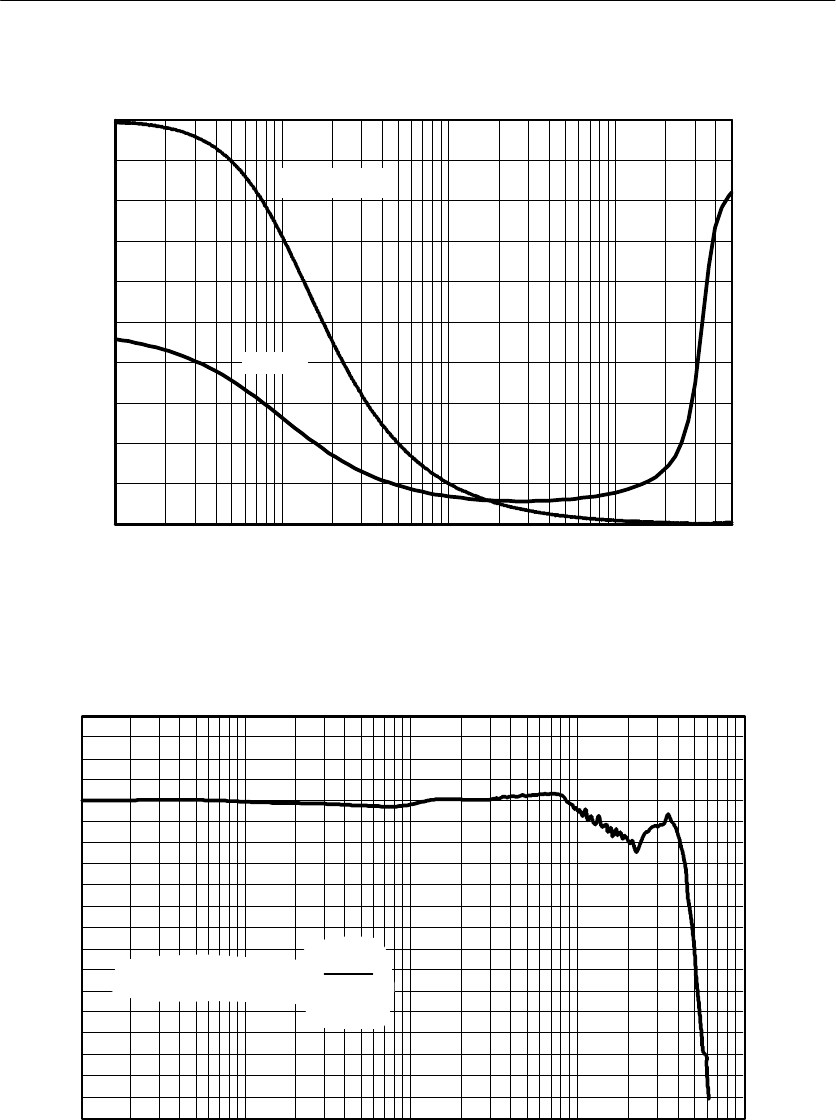
-- 9 0 °
Phase (degrees)
0
20 K
18 K
16 K
14 K
12 K
10 K
8K
6K
4K
2K
Magnuitude (ohms)
1 M 10 M 100 M 1 G 5 G
Frequency
Magnitude
Phase
0°
Figure 7: Typical input impedance and phase versus frequency
-- 1 0
Frequency
10 MHz1MHz 100MHz 10GHz
-- 1 2
-- 1 4
-- 1 6
-- 1 8
-- 2 0
-- 2 2
-- 2 4
-- 2 6
-- 2 8
1GHz
Gain =20 Log ᏋVOUT
VIN Ꮠ
Gain dB
Figure 8: Typical bandwidth

Specifications
P6209 4 GHz Probe Instruction Manual 25
Table 3: Environmental characteristics
Operating Temperature 0°Cto+40°C
The environmental exposure procedure used as
stated in Tektronix Design Standard 062-2847-00 for
Class 5 equipment.
Nonoperating Temperature -- 4 0 °Cto+71°C
The environmental exposure procedure used as
stated in Tektronix Design Standard 062-2847-00 for
Class 5 equipment.
Humidity 80% RH at 40°C
The environmental exposure procedure used as
stated in Tektronix Design Standard, 062-2847-00 for
Class 5 equipment.
Altitude Operating: 15,000 ft.
NonOperating: 50,000 ft.
Specifications
26 P6209 4 GHz Probe Instruction Manual
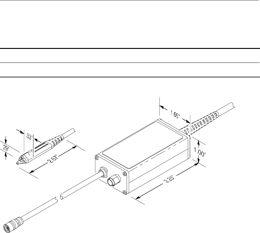
Table 4: Physical Characteristics
Net Shipping Weight 3.1lb(1.4kg)
Cable Length (probe tip to SMA) (1.37 meters)
Figure 9: Dimensions of probe head and compensation box

The following servicing instructions are for use only by
qualified personnel. To avoid injury, do not perform any
servicing other than that stated in the operating instructions
unless you are qualified to do so. Refer to all safety
summaries before performing any service.
WARNING
P6209 4 GHz Probe Instruction Manual 29
Theory of Operation
There are no user replaceable parts within the probe or the
compensation box; however, this theory of operation is provided to
assist you in isolating failures to either the probe or the host
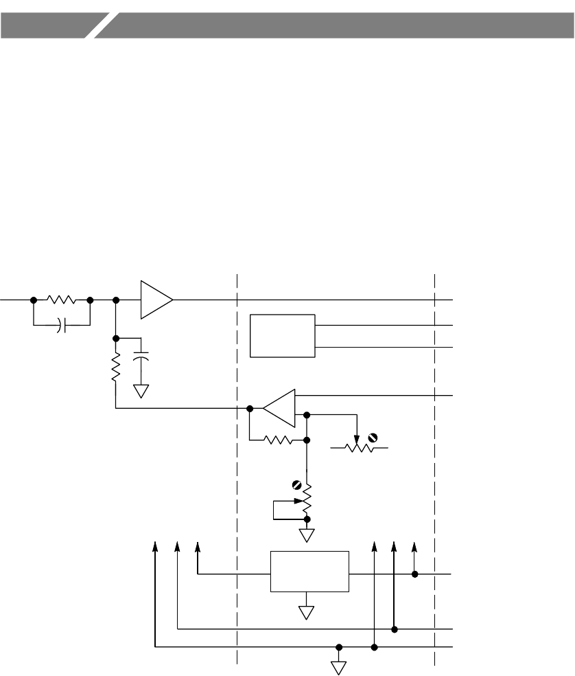
oscilloscope. Refer to Figure 10 for the simplified schematic.
Offset
gain
Offset
zero
Offset ampifier
EEPROM
Offset to probe
Probe tip
amplifier
Signal Out
Probe tip
±1VOffset
Probe ID Out
+15 V
-- 5 V
Ground
Probe
cable
TEKPROBE
SMA interface
Probe head Compensation box Oscilloscope
Clock In
+5 -- 5
Linear
regulator
+7 V
Figure 10: P6209 simplified schematic diagram

Theory of Operation
30 P6209 4 GHz Probe Instruction Manual
Probe Head and Cable Assembly
The probe head assembly contains an active amplifier circuit that
buffers and amplifies the input signal. The amplifier receives power
and an offset level from the compensation box assembly via the
cable assembly.
All signal amplification and buffering is performed in the probe head
assembly. No further amplification takes place in the compensation
box.
Compensation Box
The compensation box contains the following circuits:
HOffset amplifier
HProbe identification EEPROM
HTEKPROBE SMA interface
HVCC, +7 V linear regulator
Offset Amplifier
The offset amplifier is used to offset the input signal DC component
so that it stays at the optimal point of the probe linear dynamic
range. For more information on the linear dynamic range characteris-
tic, refer to Input Linear Dynamic Range on page 13.
The offset amplifier receives offset information as a ±1 VDC voltage
from the oscilloscope. The amplfier then amplifies it to match the
probe characteristics and applies it to the probe head circuit.
The offset amplifier has two adjustments: offset zero and offset scale.
These adjustments rarely need attention; however, detailed
adjustment instructions are in the Adjustment sectiononpage43.
Probe Identification EEPROM
The probe identification EEPROM is used to configure the
oscilloscope to the probe. The EEPROM receives a clock input from
Theory of Operation
P6209 4 GHz Probe Instruction Manual 31
the oscilloscope, and information about the probe is passed to the
oscilloscope.
TEKPROBE SMA Interface
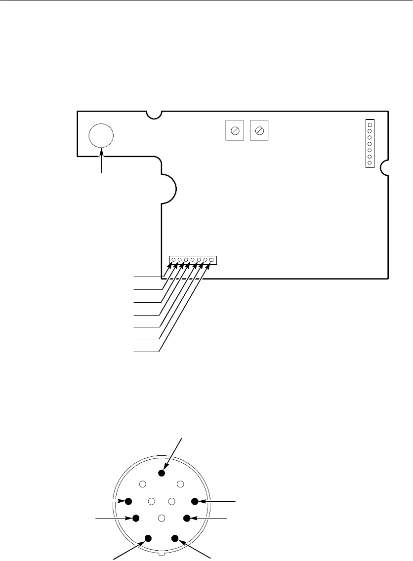
The TEKPROBE SMA interface provides a communication path
between the probe and the oscilloscope. Contact pins provide power,
signal, offset, and data transfer for the probe identification
EEPROM.
Figure 11 shows the probe interface pin functions. Refer to your
oscilloscope service documentation for more detailed specifications.
12 11
10
9
8
7
6
5
4
3
2
1
-- 5 V
DATA
CLK
+5 V
GND
--15 V
+15 V
Figure 11: TEKPROBE SMA Interface pin assignments
VCC, +7 V Regulator
The +15 V input is regulated to +7 V to supply the IC, VCC.

Theory of Operation
32 P6209 4 GHz Probe Instruction Manual

P6209 4 GHz Probe Instruction Manual 33
Performance Verification
Use the following procedures to verify the warranted specifications
of the P6209 probe. Before beginning these procedures, refer to
page 41 and photocopy the test record and use it to record the
performance test results. The recommended calibration interval is
one year.
These procedures test the following specifications:
HOutput offset voltage
HDC attenuation accuracy
HRise time
Equipment Required
Refer to Table 5 for a list of the equipment required to verify the
performance of your probe.
NOTE. These procedures use a CSA/TDS8000 as the host instrument.
If you are using a TDS 820, the procedures will vary slightly.
Table 5: Equipment required for performance verification and adjustment
Item description
Performance
requirement Recommended example
Oscilloscope TEKPROBE SMA interface Tektronix CSA/TDS8000
with a 80E00 Series
Sampling Module, or
TDS 820
Calibration Step Generator 067-1338-XX
DC Power Supply11VDCat1mA Tektronix PS280
DMM 0.5% accuracy at 2 VDC Tektronix TX3

Performance Verification
34 P6209 4 GHz Probe Instruction Manual
Table 5: Equipment required for performance verification and adjustment (Cont.)
Item description Recommended example
Performance
requirement
Feedthrough Termination BNC, 50 Ω±0.05 Ω011-0129-00
Coaxial cables (2) Male-to-Male SMA, 20 in 174-1427-00
Adapter High Frequency Probe tip
adapter w/50 ΩTermination
015-0678-00
Adapter SMA Female-to-Female 015-1012-00
Adapter SMA Female-to-BNC Male 015-0572-00
Adapter SMA Male jack 131-7128-00
Adapter BNC Female-to-Dual
Banana
103-0090-00
Adapter Y-lead adapter 196-3457-00
Adapters (2) KlipChip adapter 206-0364-XX
1Provides DC stimulus if using a TDS 820
Equipment Setup
Use this procedure to set up the equipment to test the probe.
1. Connect the probe to the oscilloscope.
2. Connect a Y-lead adapter with KlipChip adapters attached to the
probe.
3. Turn on the oscilloscope and enable the channel.
4. Allow 20 minutes for the equipment to warm up.
Performance Verification
P6209 4 GHz Probe Instruction Manual 35
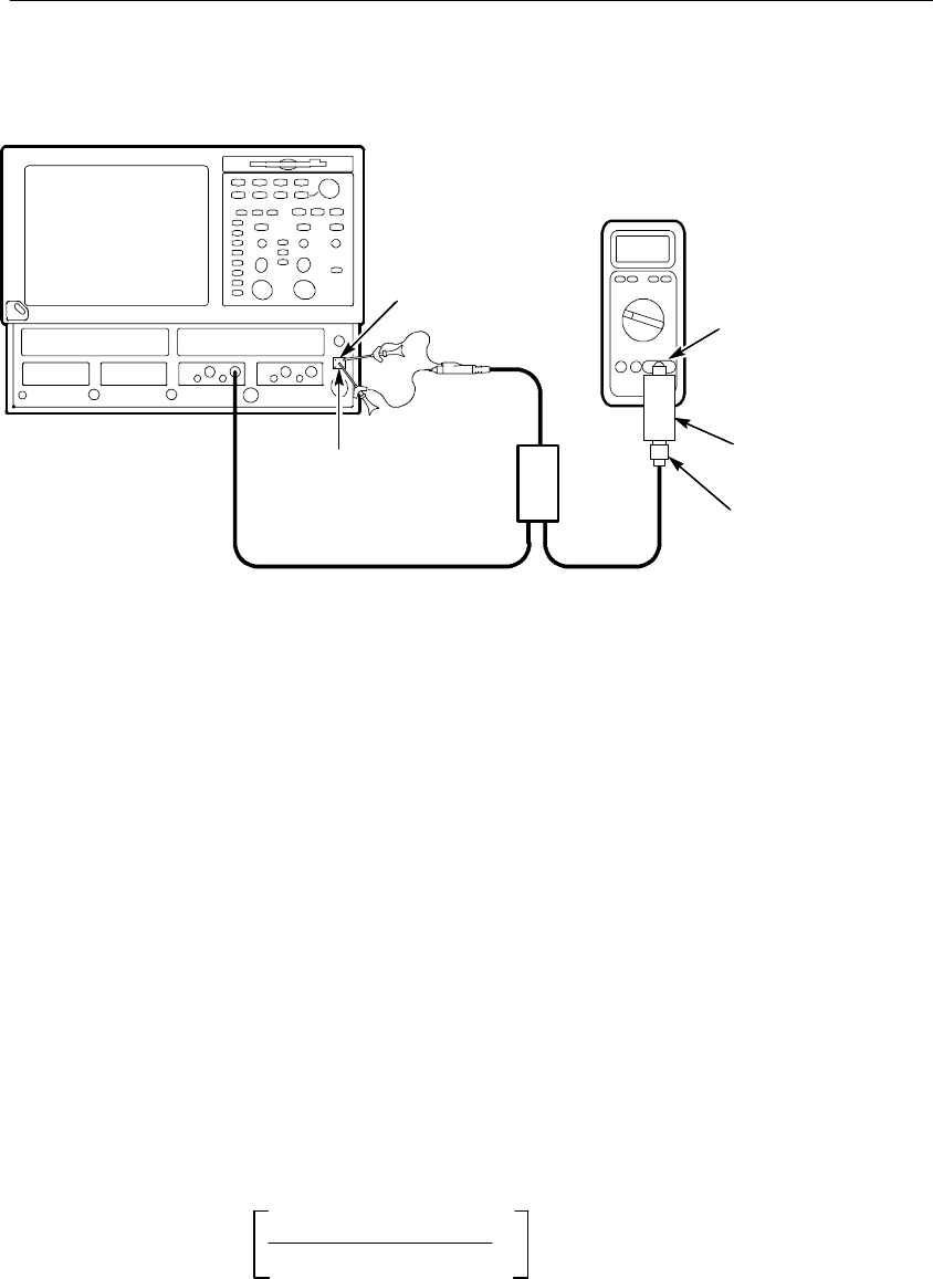
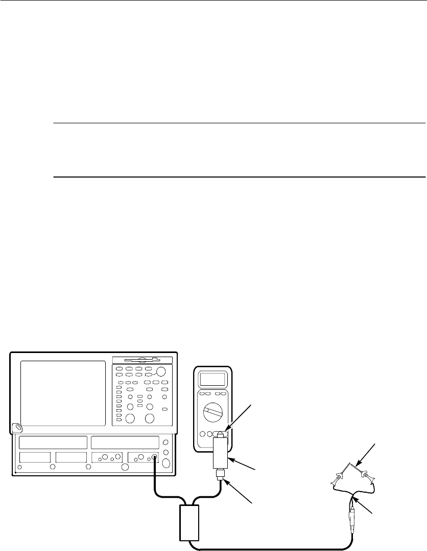
Output Zero
Use this procedure to verify the probe output zero.
1. Connect the test equipment as shown in Figure 12.
2. Ground the probe tip by connecting the two KlipChips together.
Digital
multimeter
BNC-to-dual
banana adapter
50 ΩPrecision
termination
CSA/TDS8000
SMA F-to-BNC M
adapter Y-lead
adapter
KlipChip
adapter
P6209 Probe
Figure 12: P6209 output zero setup
3. Set the oscilloscope trigger source to internal clock.
4. Set the oscilloscope channel vertical offset to 0.00 V.
5. Set the multimeter to read DC volts.
6. Record the multimeter reading on the test record.
The measured DC level should be 0.00 V ±10 mV for
the CSA/TDS8000.

Performance Verification
36 P6209 4 GHz Probe Instruction Manual
NOTE. The P6209 probe is guaranteed to have less than 7.5 mV
offset. However, the CSA/TDS8000 and TDS 820 will have some
residual voltage remaining when set to 0.00 V offset that will appear
in this test as additional offset at the probe output.
DC Attenuation Accuracy
Use this procedure to verify the probe DC attenuation accuracy.
1. Set the oscilloscope trigger to internal clock.
2. Set the oscilloscope channel vertical offset to 0.00 V.
3. Set the multimeter to read DC volts.
4. Connect the probe tip and ground to the DC calibrator output of
the CSA/TDS8000, using the Y-lead adapter, KlipChips and SMA
adapter jack.
If the probe is being used with a TDS 820 oscilloscope, a separate
DC power supply is needed to provide the stimulus. In this case,
connect the probe to the power supply using the Y-lead adapter
and KlipChips.
Record the results of steps 5 through 11 separately. Use the results to
calculate the DC accuracy of the probe in step 12.
5. Set the DC calibration output of the CSA/TDS8000 (or external
power supply if using a TDS 820), to +1.000 V. Use the
multimeter to verify the DC voltage is as close to +1.000 V as
possible. Record this measurement as Vmax.
6. Connect the multimeter as shown in Figure 13 on page 37.
Performance Verification
P6209 4 GHz Probe Instruction Manual 37
BNC-to-dual
banana adapter
50 ΩPrecision
termination
CSA/TDS8000
SMA F-to-BNC M
adapter
P6209 Probe
Digital multimeter
DC
CALIBRATION
OUTPUT
SMA adapter jack
Figure 13: P6209 DC attenuation accuracy setup
7. Measure and record the multimeter reading as M1.
8. Disconnect the multimeter.
9. Set the DC calibration output of the CSA/TDS8000 (or external
power supply if using a TDS 820), to --1.000 V. Use the
multimeter to verify the DC voltage is as close to --1.000 V as
possible. Record this measurement as Vmin.
10. Reconnect the multimeter as shown in Figure 13.
11. Measure and record the multimeter reading as M2.
12. Determine the percent error by using the formula below:
%Error =M1–M2
(Vmax–Vmin)×.2 –1×100%
The calculated error should be ≤2%.
13. Record the results on the test record.
Performance Verification
38 P6209 4 GHz Probe Instruction Manual
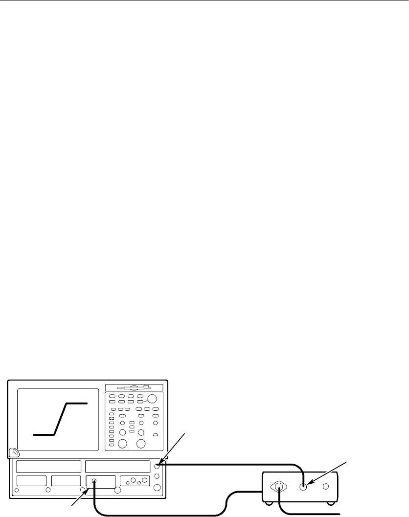
Rise Time
This procedure verifies that the probe meets rise time specifications.
The probe rise time is calculated from rise times obtained by
measuring the test system without the probe attached, and the test
system plus the probe.
1. Connect the test equipment as shown in Figure 14.
2. Set the oscilloscope to the following settings:
HTrigger to internal clock
HVerticalscaleto50mV/div
HHorizontal scale to 100 ps/div
HHorizontal record length to 4000 points
HAcquisition Mode to average at least 16 samples
3. Adjust the oscilloscope horizontal and vertical position controls
to display a signal similar to that shown in Figure 14.
Calibration
step generator
CSA/TDS8000
Generator
remote head
INTERNAL
CLOCK
OUTPUT
SMA cable
Trigger
input
To power
supply
Figure 14: Test system rise time setup
Performance Verification
P6209 4 GHz Probe Instruction Manual 39
4. Use the oscilloscope measurement capability to calculate and
display rise time. Rise time is determined from the 10% and 90%
amplitude points on the waveform. Record the rise time as ts.
The system rise time (ts) that you measured in step 4 represents the
rise time of the test system without the probe.
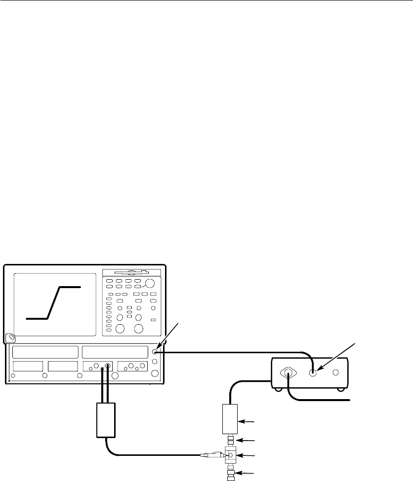
The following steps instruct you to assemble the test system that
includes the probe, as shown in Figure 15. The system and probe rise
time (ts+p) that you measure in step 8 is used to calculate the probe
rise time (tp)instep9.
5. Connect the test equipment as shown in Figure 15.
Calibration
step generator Trigger
input
INTERNAL
CLOCK
OUTPUT
CSA/TDS8000
Generator remote head
50 ΩTermination
HF probe tip adapter
P6209 Probe
SMA F-to-F
SMA cable
To power
supply
Figure 15: Test system and probe rise time setup
6. Set the vertical to 50 mV/div and horizontal to 500 ps/div.
7. Adjust the oscilloscope horizontal and vertical position controls
to display a signal similar to that shown in Figure 15.

Performance Verification
40 P6209 4 GHz Probe Instruction Manual
NOTE. Do not touch the probe tip adapter when making calibration
measurements. Measurement accuracy is degraded when the probe
tip adapter is handled.
8. Use the oscilloscope measurement capability to calculate and
display rise time. Rise time is determined from the 10% and 90%
amplitude points on the waveform. Record the rise time as ts+p.
9. Calculate the probe only rise time using the following formula:
tp=t(s+p)
2−ts
2
Ꭹ
10. Check that the calculated rise time meets the probe specification.
The rise time (tp) must be ≤120 ps.
11. Record the results on the test record.

Performance Verification
P6209 4 GHz Probe Instruction Manual 41
Test record
Probe Model:
Serial Number:
Certificate Number:
Temperature:
RH %:
Date of Calibration:
Technician:
Performance test Minimum Incoming Outgoing Maximum
Output zero voltage
(at probe output)
±10 mV (20_Cto30_C)1-- 1 0 m V ________ ________ +10mV
DC attenuation accuracy -- 2 % ________ ________ +2%
Rise time N/A ________ ________ ≤120 ps
1CSA/TDS8000 only

Performance Verification
42 P6209 4 GHz Probe Instruction Manual
P6209 4 GHz Probe Instruction Manual 43
Adjustments
The P6209 has two internal controls: offset zero and offset scale.
These controls rarely need to be adjusted and only should be changed
after a probe performance verification and functional check has been
performed on the oscilloscope.
To make adjustments to the probe, the compensation box bottom
cover must be removed and the equipment allowed to warm up for
20 minutes. Use the optional adjustment tool for making any
adjustments. Refer to Table 5 on page 33 for a list of the equipment
required to adjust your probe.
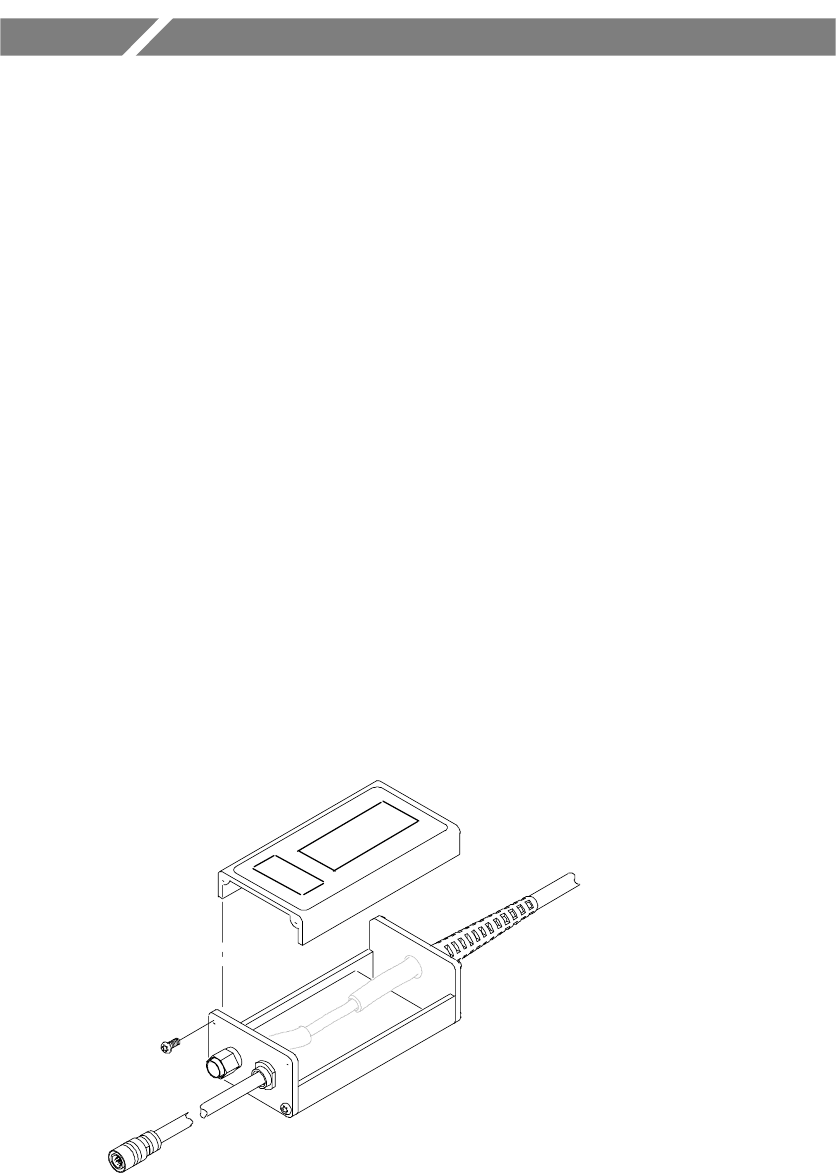
Removing the Compensation Box Bottom Cover
Follow these steps to gain access to the adjustment controls.
1. Using a Pozidrive screwdriver, remove the four screws that attach
the bottom cover to the compensation box. Gently remove the
cover. Refer to Figure 16.
Figure 16: Removing the compensation box bottom cover
Adjustments
44 P6209 4 GHz Probe Instruction Manual
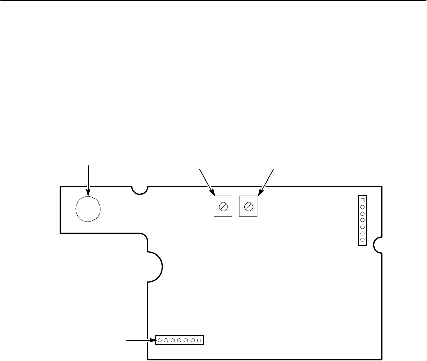
Adjustment Locations
Refer to Figure 17 for the location of the offset adjustments and
measurement test points.
J1
J2
Offset zero
adjust
Offset scale
adjust
Gnd lug
Offset test point
(white wire)
R3 R2
Figure 17: P6209 adjustment and measurement locations
Offset Zero
Use this procedure to adjust the probe offset zero.
1. Connect the probe power cable to the oscilloscope.
2. Ground the probe tip by connecting the two KlipChip leads
together.
3. Set the oscilloscope trigger source to internal clock.
4. Set the channel vertical offset to 0.00 V.
5. Using the (--) lead of the DMM, probe the ground lug in the probe
comp box. Refer to Figure 17 on page 44.
Adjustments
P6209 4 GHz Probe Instruction Manual 45
6. Using the (+) lead of the DMM, carefully probe pin 7 of J2 (white
wire) in the probe compensation box. Refer to Figure 17 on
page 44.
NOTE. The offset voltage measured on pin 7 will be of opposite
polarity and approximately one fifth of the offset value displayed on
the oscilloscope.
7. Adjust the oscilloscope offset so that the voltage measures
0.000 V on the DMM. Set the offset as close to 0 V as possible.
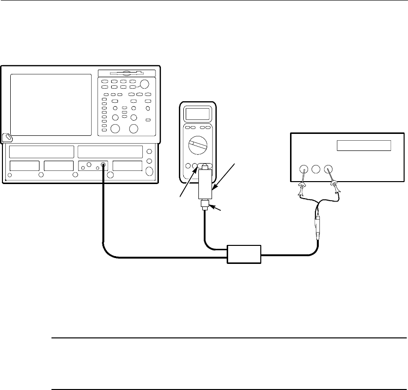
8. Connect the equipment as shown in Figure 18.
9. Adjust Offset Zero (R2) in the probe compensation box for
0.00 V, ±1mVontheDMM.RefertoFigure17onpage44for
the adjustment location.
Digital
multimeter
BNC-to-dual
banana adapter
50 ΩPrecision
termination
CSA/TDS8000
SMA F-to-BNC M
adapter Y-lead
adapter
KlipChip
adapter
P6209 Probe
Figure 18: P6209 offset zero setup

Adjustments
46 P6209 4 GHz Probe Instruction Manual
Offset Scale
Use this procedure to adjust the offset scale of the probe. The offset
zero of the probe should be checked before making any adjustment
to the offset scale. Refer to Figure 17 on page 44 for the location of
the test points and adjustments.
1. Connect the probe power cable to the oscilloscope.
2. Set the oscilloscope trigger source to internal clock.
3. Set the oscilloscope channel vertical offset to +2.5 V.
4. Ground the probe tip by connecting the two KlipChip leads
together.
5. Using the (--) lead of the DMM, probe the ground lug in the probe
compensation box.
6. Using the (+) lead of the DMM, carefully probe pin 7 of J2 (white
wire) in the probe compensation box.
NOTE. The offset voltage measured on pin 7 will be of opposite
polarity and approximately one fifth of the offset value displayed on
the oscilloscope.
7. Adjust the oscilloscope offset so that pin 7 of J2 measures
--0.50 V on the DMM.
8. Set the DC power supply to +2.5 V, as measured on the DMM.
9. Connect the equipment as shown in Figure 19. Take care not to
disturb the offset level setting.
10. Adjust the Offset Scale (R3) in the probe compensation box so
the output measures 0.000 V, ±1mVontheDMM.
Adjustments
P6209 4 GHz Probe Instruction Manual 47
-- +
Power supply
CSA/TDS8000
Digital
multimeter
50 ΩPrecision
termination
P6209 Probe
SMA F-to-BNC M
adapter
BNC-to-Dual
Banana Adapter
Figure 19: P6209 offset range setup
NOTE. After the offset adjustments have been made, use the
Performance Verification procedures beginning on page 33 to verify
your probe meets specifications.

Adjustments
48 P6209 4 GHz Probe Instruction Manual

P6209 4 GHz Probe Instruction Manual 49
Maintenance
This section describes the maintenance procedures for the P6209.
Inspection and Cleaning
To prevent damage to probe materials, avoid using chemicals that
contain benzine, benzene, toluene, xylene, acetone, or similar
solvents.
Do not immerse the probe or use abrasive cleaners.
Dirt may be removed with a soft cloth dampened with a mild
detergent and water solution or isopropyl alcohol.
Replacement Parts
Refer to Replaceable Parts on page 55 for a list of customer
replaceable parts. Due to the sophisticated design of the P6209
probe, there are no user replaceable parts within the probe.
Preparation for Shipment
If the original packaging is unfit for use or not available, use the
following packaging guidelines:
1. Use a corrugated cardboard shipping carton having inside
dimensions at least one inch greater than the probe dimensions.
The box should have a carton test strength of at least 200 pounds.
2. Put the probe into a plastic bag or wrap to protect it from
dampness.
3. Place the probe into the box and stabilize it with light packing
material.
4. Seal the carton with shipping tape.

Maintenance
50 P6209 4 GHz Probe Instruction Manual

P6209 4 GHz Probe Instruction Manual 51
Troubleshooting
This troubleshooting documentation details isolation to either the
probe or the oscilloscope.
To troubleshoot the P6209, the probe must be attached to an
operating TEKPROBE SMA interface oscilloscope with the bottom
cover of the compensation box removed. Refer to page 43 for
instructions on opening the compensation box.
WARNING. Operating voltages will be present. Observe caution when
probing in the compensation box. Be careful not to touch or ground
energized components.
Work at a Level 1 ESD workstation when performing troubleshoot-
ing. The compensation box contains static sensitive devices.
Troubleshooting
52 P6209 4 GHz Probe Instruction Manual
Refer to Table 6 on page 53 for troubleshooting procedures and
Figures 20 and 21 for troubleshooting test points.
J1
J2
Ground
Offset (white)
NC
DATA (yellow)
CLOCK (orange)
+5 V (red)
+15 V (brown)
--5 V (green)
Figure 20: Compensation box test point locations
12 11
10
9
8
7
6
5
4
3
2
1
-- 5 V
DATA
CLK
+5 V
GND
--15 V
+15 V
Figure 21: TEKPROBE SMA Interface pin assignments

Troubleshooting
P6209 4 GHz Probe Instruction Manual 53
Table 6: Troubleshooting guide
Symptom Checks Result Action
No signal out Check known signal
Go to No Probe
Power
No signal.
Probe power OK.
Continue checks
Replace probe.
Distorted or
nonlinear signal
Is the signal within
linear dynamic
range? See page 13.
No Set channel vertical
offset to match signal
characteristic.
No Offset Adjust
(Signal present)
Go to Probe Power
row
Probe power OK Continue checks
Check variation of
offset input from host
instrument. See
Figure 20. Offset
control voltage at pin
7 of J2 should vary
between +1 V and
-- 1 V.
Offset input OK Replace probe.
No Probe Power Check the power
test points in the
compensation box.
See Figure 20.
Power OK Continue checks.
Power bad Check for continuity
between the
TEKPROBE SMA
connector pins and
the test points in the
compensation box.
See Figures 20 and
21 on page 52.
Try an adjacent
channel.
Repair host
instrument

Troubleshooting
54 P6209 4 GHz Probe Instruction Manual

P6209 4 GHz Probe Instruction Manual 55
Replaceable Parts
This section contains a list of replaceable parts for the P6209 probe.
Use this list to identify and order replacement parts.
Parts Ordering Information
Replacement parts are available from or through your local
Tektronix, Inc. service center or representative.
Changes to Tektronix instruments are sometimes made to accommo-
date improved components as they become available and to give you
the benefit of the latest circuit improvements. Therefore, when
ordering parts, it is important to include the following information in
your order:
HPart number
HInstrument type or model number
HInstrument serial number
HInstrument modification number, if applicable
If a part you order has been replaced with a different or improved
part, your local Tektronix service center or representative will
contact you concerning any change in the part number.

Replaceable Parts
56 P6209 4 GHz Probe Instruction Manual
Using the Replaceable Parts List
The tabular information in the Replaceable Parts List is arranged for
quick retrieval. Understanding the structure and features of the list
will help you find the information you need for ordering replacement
parts.
Item Names
In the Replaceable Parts List, an Item Name is separated from the
description by a colon (:). Because of space limitations, an Item
Name may sometimes appear as incomplete. For further Item Name
identification, U.S. Federal Cataloging Handbook H6-1 can be used
where possible.
Indentation System
This parts list is indented to show the relationship between items.
The following example is of the indentation system used in the
Description column:
12345 Name&Description
Assembly and/or Component
Attaching parts for Assembly and/or Component
(END ATTACHING PARTS)
Detail Part of Assembly and/or Component
Attaching parts for Detail Part
(END ATTACHING PARTS)
Parts of Detail Part
Attaching parts for Parts of Detail Part
(END ATTACHING PARTS)
Attaching parts always appear at the same indentation as the item it
mounts, while the detail parts are indented to the right. Indented
items are part of, and included with, the next higher indentation.
Attaching parts must be purchased separately, unless otherwise
specified.
Abbreviations
Abbreviations conform to American National Standards Institute
(ANSI) standard Y1.1
Replaceable Parts
P6209 4 GHz 5X Active Probe 57
1
2
3
4
Figure 22: P6209 replaceable parts
Fig. &
index no.
Tektronix
part no.
Serial no.
Effective Dscont Qty 12345 name & description
Mfr.
code Mfr. part no.
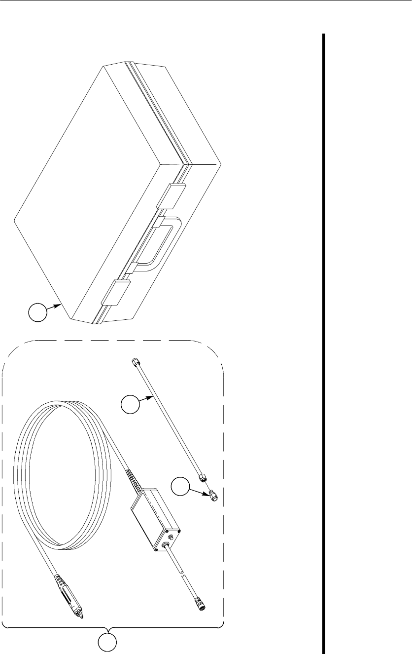
22--1 010--0638--00 1 PROBE ASSEMBLY:SERVICE REPLACEMENT, SERIALIZED 80009 010--0638--00
--2 015--1021--00 1 TERMN,COAXIAL:SHORT CIRCUIT,SMA,FEMALE 26805 2020--5353--00
--3 174--1120--00 1 CA ASSY,RF:COAXIAL,RFD,50 OHM,8.5 L,SMA,MALE 060D9 174--1120--00
--4 016--1879--01 1 CASE,STORAGE:PLASTIC,W/CND FOAM TK6108 016--1879--01
Replaceable Parts
P6209 4 GHz 5X Active Probe58
12 3 4 5 6 7
89 10 11 12
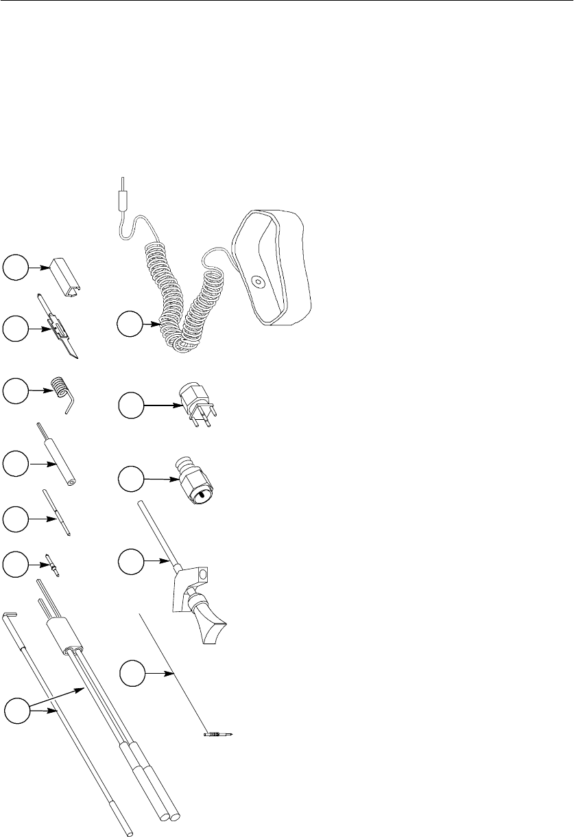
Figure 23: P6209 standard accessories

Replaceable Parts
P6209 4 GHz 5X Active Probe 59
Fig. &
index no.
Tektronix
part no.
Serial no.
Effective Dscont Qty 12345 name & description
Mfr.
code Mfr. part no.
STANDARD ACCESSORIES
23--1 196-3456-00 1 LEAD SET:ACCESSORY KIT, INCL THREE 3.0 INCH
GROUND LEAD, TWO DIFFERENTIAL LEAD
80009 196-3456-00
--2 131-5638-11 1 PROBE,TIP:PACKAGE OF 10 80009 131-5638-11
--3 016-1772-10 1 ACCESSORY KIT:POGO PIN,PKG OF 10 80009 016-1772-10
--4 016-1773-10 1 ACCESSORY KIT:GND PIN LENGTH ADAPTER,PKG OF 10 80009 016-1773-10
--5 016-1774-00 1 ACCESSORY KIT:ADAPTER SPRING,PKG OF 10 80009 016-1774-00
--6 -------------------- 1 PROBE,TIP,SURETOE:PACKAGE OF 4 (REORDER ST501,
PACKAGE OF 12)
80009 --------------------
--7 016-1315-00 1 MARKER KIT,ID:CABLE MARKER BAND,2 EA, VAR COLRS 80009 016-1315-00
--8 196-3482-XX 1 CUSTOMIZABLE GROUND LEAD, SET OF 5 80009 196-3482-XX
--9 206-0364-XX 2 TIP,PROBE:MICROCKT TEST,SMT KLIPCHIP 80009 206-0364-XX
--10 015--1020--00 1 TERMN,COAXIAL:SHORT CIRCUIT,SMA,MALE 0GZV8 64SMA--50--0--1
--11 131--7128--00 1 CONN,RF JACK:COAX,SMA,50 OHM,MALE,GOLD PL 74868 901--9895--RFX
--12 006-3415-04 1 STRAP,WRIST:3M TYPE 2214, ADJUSTABLE,6 FT COILED
CORD
TK0623 RTI 8454001829
071-0634-XX 1 MANUAL,TECH:INSTRUCTION,P6209 80009 071-0634-XX
Replaceable Parts
P6209 4 GHz 5X Active Probe60
1234 5 6
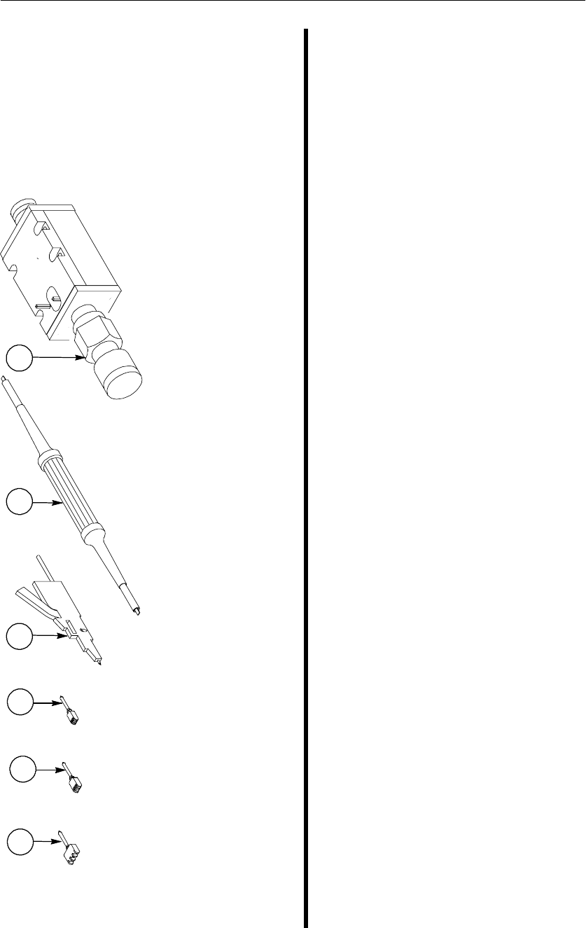
Figure 24: P6209 optional accessories
Fig. &
index no.
Tektronix
part no.
Serial no.
Effective Dscont Qty 12345 name & description
Mfr.
code Mfr. part no.
OPTIONAL ACCESSORIES
2 4 --- 1 SF503 1 ADPTR,SUREFOOT:0.5 MM EIAJ,PKG OF 12 80009 SF503
--2 SF502 1 ADPTR,SUREFOOT:25 MIL JEDEC,PKG OF 12 80009 SF502
--3 SF501 1 ADPTR,SUREFOOT:50 MIL JEDEC,PKG OF 12 80009 SF501
--4 SMK4 1 TIP,PROBE:MICROCKT TEST,PKG OF 4 80009 SMK4
-5 003--1433--02 1 TOOL:ADJUSTMENT TOOL,PLASTIC,BLACK TK2565 003--1433--02
--6 015-0678-00 1 ADAPTER, PROBE:TIP,SMA 2 COMPACT
SIZE,TERMINATED INTO 50 OHM TEST FIXTURE
80009 015-0678-00
SMG50 1 MICROCKT TEST,SMT KLIPCHIP,PKG OF 20 (SEE 23--9) 80009 SMG50

Replaceable Parts
P6209 4 GHz 5X Active Probe 61
CROSS INDEX - MFR. CODE NUMBER TO MANUFACTURER
Mfr. code Manufacturer Address City, state, zip code
060D9 UNITREK CORPORATION 3000 COLUMBIA HOUSE BLVD, SUITE 120 VANCOUVER, WA 98661
0GZV8 HUBER & SUHNER INC 19 THOMPSON DRIVE ESSEX JUNCTION, VT
05452--3408
26805 M/A COM OMNI SPECTRA INC MICROWAVE CONNECTOR DIV 140 4TH AVE WALTHAM, MA 02254
80009 TEKTRONIX INC 14150 SW KARL BRAUN DR
PO BOX 500
BEAVERTON, OR 97077--0001
TK0623 GENERAL TOOL & SUPPLY CO 2705 NW NICOLAI ST PORTLAND, OR 97210
TK2565 VISION PLASTICS INC 26000 SW PARKWAY CENTER DRIVE WILSONVILLE, OR 97070
TK6108 KENT H LANDSBERG CO 27929 SW 95TH, SUITE 101 WILSONVILLE, OR 97070

Replaceable Parts
P6209 4 GHz 5X Active Probe62
