The Design Warrior's Guide To FPGAs Warriors
User Manual:
Open the PDF directly: View PDF ![]() .
.
Page Count: 560 [warning: Documents this large are best viewed by clicking the View PDF Link!]
- Cover
- Title Page
- Copyright Page
- Dedication
- What's on the CD-ROM?
- Contents (hyperlinked)
- Preface
- Acknowledgments
- Chapter 1: Introduction
- Chapter 2: Fundamental Concepts
- Chapter 3: The Origin of FPGAs
- Chapter 4: Alternative FPGA Architectures
- A word of warning
- A little background information
- Antifuse versus SRAM versus …
- Fine-, medium-, and coarse-grained architectures
- MUX- versus LUT-based logic blocks
- CLBs versus LABs versus slices
- Fast carry chains
- Embedded RAMs
- Embedded multipliers, adders, MACs, etc.
- Embedded processor cores (hard and soft)
- Clock trees and clock managers
- General-purpose I/O
- Gigabit transceivers
- Hard IP, soft IP, and firm IP
- System gates versus real gates
- FPGA years
- Chapter 5: Programming (Configuring) an FPGA
- Chapter 6: Who Are All the Players?
- Chapter 7: FPGA Versus ASIC Design Styles
- Chapter 8: Schematic-Based Design Flows
- Chapter 9: HDL-Based Design Flows
- Chapter 10: Silicon Virtual Prototyping for FPGAs
- Chapter 11: C/C++ etc.–Based Design Flows
- Chapter 12: DSP-Based Design Flows
- Chapter 13: Embedded Processor-Based Design Flows
- Chapter 14: Modular and Incremental Design
- Chapter 15: High-Speed Design and Other PCB Considerations
- Chapter 16: Observing Internal Nodes in an FPGA
- Chapter 17: Intellectual Property
- Chapter 18: Migrating ASIC Designs to FPGAs and Vice Versa
- Chapter 19: Simulation, Synthesis, Verification, etc. Design Tools
- Chapter 20: Choosing the Right Device
- Chapter 21: Gigabit Transceivers
- Chapter 22: Reconfigurable Computing
- Chapter 23: Field-Programmable Node Arrays
- Chapter 24: Independent Design Tools
- Chapter 25: Creating an Open-Source-Based Design Flow
- Chapter 26: Future FPGA Developments
- Appendix A: Signal Integrity 101
- Appendix B: Deep-Submicron Delay Effects 101
- Appendix C: Linear Feedback Shift Registers 101
- The Ouroboras
- Many-to-one implementations
- More taps than you know what to do with
- Seeding an LFSR
- FIFO applications
- Modifying LFSRs to sequence 2n values
- Accessing the previous value
- Encryption and decryption applications
- Cyclic redundancy check applications
- Data compression applications
- Built-in self-test applications
- Pseudorandom-number-generation applications
- Last but not least
- Glossary
- About the Author
- Index
LICENSE INFORMATION: This is a single-user copy of this eBook. It may not be
copied or distributed.
Unauthorized reproduction or distribution of this eBook may result in severe criminal penalties.
The Design Warrior’s
Guide to FPGAs

The Design Warrior’s
Guide to FPGAs
Clive “Max” Maxfield

Newnes is an imprint of Elsevier
200 Wheeler Road, Burlington, MA 01803, USA
Linacre House, Jordan Hill, Oxford OX2 8DP, UK
Copyright © 2004, Mentor Graphics Corporation and Xilinx, Inc.
All rights reserved.
Illustrations by Clive “Max” Maxfield
No part of this publication may be reproduced, stored in a retrieval system, or trans-
mitted in any form or by any means, electronic, mechanical, photocopying,
recording, or otherwise, without the prior written permission of the publisher.
Permissions may be sought directly from Elsevier’s Science & Technology Rights
Department in Oxford, UK: phone: (+44) 1865 843830, fax: (+44) 1865 853333,
e-mail: permissions@elsevier.com.uk. You may also complete your request on-line
via the Elsevier homepage (http://elsevier.com), by selecting “Customer Support”
and then “Obtaining Permissions.”
Recognizing the importance of preserving what has been written, Elsevier prints its
books on acid-free paper whenever possible.
Library of Congress Cataloging-in-Publication Data
A catalog record for this book is available from the Library of Congress.
ISBN: 0-7506-7604-3
British Library Cataloguing-in-Publication Data
A catalogue record for this book is available from the British Library.
For information on all Newnes publications
visit our Web site at www.newnespress.com
040506070809 10987654321
Printed in the United States of America
To my wife Gina—the yummy-scrummy caramel, chocolate fudge,
and rainbow-colored sprinkles on the ice cream sundae of my life
Also, to my stepson Joseph and my grandchildren Willow, Gaige, Keegan, and Karma,
all of whom will be tickled pink to see their names in a real book!
For your delectation and delight, the CD accompanying this book contains a fully-
searchable copy of The Design Warrior’s Guide to FPGAs in Adobe®Acrobat®
(PDF) format. You can copy this PDF to your computer so as to be able to access
The Design Warrior’s Guide to FPGAs as required (this is particularly useful if you
travel a lot and use a notebook computer).
The CD also contains a set of Microsoft®PowerPoint®files—one for each chapter
and appendix—containing copies of the illustrations that are festooned throughout
the book. This will be of particular interest for educators at colleges and universities
when it comes to giving lectures or creating handouts based on The Design Warrior’s
Guide to FPGAs
Last but not least, the CD contains a smorgasbord of datasheets, technical articles,
and useful web links provided by Mentor and Xilinx.

Preface ...............ix
Acknowledgments ..........xi
Chapter 1
Introduction ..........1
What are FPGAs? .........1
Why are FPGAs of interest? ....1
What can FPGAs be used for?. . . 4
What’s in this book? ........6
What’s not in this book?......7
Who’s this book for? ........8
Chapter 2
Fundamental Concepts .....9
The key thing about FPGAs....9
A simple programmable function . 9
Fusible link technologies .....10
Antifuse technologies ......12
Mask-programmed devices ....14
PROMs ..............15
EPROM-based technologies . . . 17
EEPROM-based technologies . . 19
FLASH-based technologies . . . 20
SRAM-based technologies ....21
Summary .............22
Chapter 3
The Origin of FPGAs ......25
Related technologies .......25
Transistors ............26
Integrated circuits ........27
SRAMs, DRAMs, and
microprocessors.........28
SPLDs and CPLDs ........28
ASICs (gate arrays, etc.) .....42
FPGAs ..............49
Chapter 4
Alternative FPGA Architectures 57
A word of warning ........57
A little background information . 57
Antifuse versus SRAM
versus … ............59
Fine-, medium-, and coarse-grained
architectures ..........66
MUX- versus LUT-based
logic blocks ...........68
CLBs versus LABs versus slices. . 73
Fast carry chains .........77
Embedded RAMs.........78
Embedded multipliers, adders,
MACs, etc. ...........79
Embedded processor cores
(hard and soft) .........80
Clock trees and clock managers . 84
General-purpose I/O .......89
Gigabit transceivers .......92
Hard IP, soft IP, and firm IP . . . 93
System gates versus real gates . . 95
FPGA years ............98
Contents
Chapter 5
Programming (Configuring)
an FPGA ............99
Weasel words ...........99
Configuration files, etc. .....99
Configuration cells .......100
Antifuse-based FPGAs .....101
SRAM-based FPGAs ......102
Using the configuration port . . 105
Using the JTAG port ......111
Using an embedded processor. . 113
Chapter 6
Who Are All the Players? ...115
Introduction...........115
FPGA and FPAA vendors . . . 115
FPNA vendors .........116
Full-line EDA vendors .....116
FPGA-specialist and independent EDA
vendors ............117
FPGA design consultants with special
tools ..............118
Open-source, free, and low-cost design
tools ..............118
Chapter 7
FPGA Versus ASIC
Design Styles .........121
Introduction...........121
Coding styles ..........122
Pipelining and levels of logic . . 122
Asynchronous design practices . 126
Clock considerations ......127
Register and latch considerations129
Resource sharing (time-division multi-
plexing) ............130
State machine encoding ....131
Test methodologies .......131
Chapter 8
Schematic-Based Design Flows 133
In the days of yore........133
The early days of EDA .....134
A simple (early) schematic-driven
ASIC flow...........141
A simple (early) schematic-driven
FPGA flow ..........143
Flat versus hierarchical schematics
................148
Schematic-driven FPGA
design flows today.......151
Chapter 9
HDL-Based Design Flows ...153
Schematic-based flows
grind to a halt .........153
The advent of HDL-based flows 153
Graphical design entry lives on . 161
A positive plethora of HDLs . . 163
Points to ponder.........172
Chapter 10
Silicon Virtual Prototyping
for FPGAs ..........179
Just what is an SVP? ......179
ASIC-based SVP approaches . . 180
FPGA-based SVPs .......187
Chaper 11
C/C++ etc.–Based Design Flows
................193
Problems with traditional
HDL-based flows .......193
C versus C++ and concurrent
versus sequential .......196
SystemC-based flows ......198
Augmented C/C++-based flows 205
Pure C/C++-based flows ....209
Different levels of synthesis
abstraction ..........213
viii ■The Design Warrior's Guide to FPGAs
Mixed-language design and
verification environments . . 214
Chapter 12
DSP-Based Design Flows ...217
Introducing DSP ........217
Alternative DSP implementations
................218
FPGA-centric design flows
for DSPs ............225
Mixed DSP and VHDL/
Verilog etc. environments . . 236
Chapter 13
Embedded Processor-Based
Design Flows .........239
Introduction...........239
Hard versus soft cores ......241
Partitioning a design into its
hardware and software components
245
Hardware versus software views
of the world ..........247
Using an FPGA as its own
development environment . . 249
Improving visibility in
the design ...........250
A few coverification alternatives 251
A rather cunning design
environment .........257
Chapter 14
Modular and Incremental
Design ............259
Handling things as one
big chunk ...........259
Partitioning things into
smaller chunks ........261
There’s always another way . . . 264
Chapter 15
High-Speed Design and Other
PCB Considerations .....267
Before we start..........267
We were all so much younger
then ..............267
The times they are a-changing . 269
Other things to think about . . 272
Chapter 16
Observing Internal Nodes in
an FPGA ...........277
Lack of visibility.........277
Multiplexing as a solution . . . 278
Special debugging circuitry . . . 280
Virtual logic analyzers......280
VirtualWires ..........282
Chapter 17
Intellectual Property .....287
Sources of IP ..........287
Handcrafted IP .........287
IP core generators ........290
Miscellaneous stuff .......291
Chapter 18
Migrating ASIC Designs to FPGAs
and Vice Versa ........293
Alternative design scenarios . . 293
Chapter 19
Simulation, Synthesis, Verification,
etc. Design Tools .......299
Introduction...........299
Simulation (cycle-based,
event-driven, etc.) ......299
Synthesis (logic/HDL versus
physically aware) .......314
Timing analysis (static
versus dynamic) ........319
Verification in general .....322
Formal verification .......326
Contents ■ix
Miscellaneous ..........338
Chapter 20
Choosing the Right Device . . 343
So many choices ........343
If only there were a tool.....343
Technology ...........345
Basic resources and packaging . 346
General-purpose I/O interfaces . 347
Embedded multipliers,
RAMs, etc. ..........348
Embedded processor cores....348
Gigabit I/O capabilities .....349
IP availability ..........349
Speed grades...........350
On a happier note........351
Chapter 21
Gigabit Transceivers .....353
Introduction...........353
Differential pairs ........354
Multiple standards .......357
8-bit/10-bit encoding, etc. . . . 358
Delving into the transceiver
blocks .............361
Ganging multiple transceiver
blocks together ........362
Configurable stuff ........364
Clock recovery, jitter, and
eye diagrams..........367
Chaper 22
Reconfigurable Computing. . 373
Dynamically reconfigurable logic 373
Dynamically reconfigurable
interconnect .........373
Reconfigurable computing . . . 374
Chapter 23
Field-Programmable
Node Arrays .........381
Introduction...........381
Algorithmic evaluation .....383
picoChip’s picoArray technology384
QuickSilver’s ACM technology 388
It’s silicon, Jim, but not
as we know it! .........395
Chapter 24
Independent Design Tools . . 397
Introduction...........397
ParaCore Architect .......397
The Confluence system
design language ........401
Do you have a tool? .......406
Chapter 25
Creating an Open-Source-Based
Design Flow .........407
How to start an FPGA design
shop for next to nothing . . . 407
The development platform: Linux
................407
The verification environment . 411
Formal verification .......413
Access to common IP components
................416
Synthesis and implementation
tools ..............417
FPGA development boards . . . 418
Miscellaneous stuff .......418
Chapter 26
Future FPGA Developments . 419
Be afraid, be very afraid .....419
Next-generation architectures
and technologies .......420
Don’t forget the design tools . . 426
Expect the unexpected .....427
Appendix A:
Signal Integrity 101 .....429
Before we start..........429
x■The Design Warrior's Guide to FPGAs
Capacitive and inductive coupling
(crosstalk) ..........430
Chip-level effects ........431
Board-level effects........438
Appendix B:
Deep-Submicron Delay Effects 101
................443
Introduction...........443
The evolution of delay
specifications .........443
A potpourri of definitions....445
Alternative interconnect models 449
DSM delay effects ........452
Summary ............464
Appendix C:
Linear Feedback Shift
Registers 101 ........465
The Ouroboras .........465
Many-to-one implementations . 465
More taps than you know
what to do with ........468
Seeding an LFSR ........470
FIFO applications ........472
Modifying LFSRs to sequence
2nvalues ............474
Accessing the previous value . . 475
Encryption and decryption
applications ..........476
Cyclic redundancy check
applications ..........477
Data compression applications . 479
Built-in self-test applications . . 480
Pseudorandom-number-generation
applications ..........482
Last but not least ........482
Glossary ..............485
About the Author .........525
Index ...............527
Contents ■xi

This is something of a curious, atypical book for the tech-
nical genre (and as the author, I should know). I say this
because this tome is intended to be of interest to an unusually
broad and diverse readership. The primary audience comprises
fully fledged engineers who are currently designing with field
programmable gate arrays (FPGAs) or who are planning to do so
in the not-so-distant future. Thus, Section 2: Creating FPGA-
Based Designs introduces a wide range of different design flows,
tools, and concepts with lots of juicy technical details that
only an engineer could love. By comparison, other areas of the
book—such as Section 1: Fundamental Concepts—cover a vari-
ety of topics at a relatively low technical level.
The reason for this dichotomy is that there is currently a
tremendous amount of interest in FPGAs, especially from peo-
ple who have never used or considered them before. The first
FPGA devices were relatively limited in the number of equiva-
lent logic gates they supported and the performance they
offered, so any “serious” (large, complex, high-performance)
designs were automatically implemented as application-specific
integrated circuits (ASICs) or application-specific standard parts
(ASSPs). However, designing and building ASICs and ASSPs
is an extremely time-consuming and expensive hobby, with
the added disadvantage that the final design is “frozen in sili-
con” and cannot be easily modified without creating a new
version of the device.
By comparison, the cost of creating an FPGA design is
much lower than that for an ASIC or ASSP. At the same
time, implementing design changes is much easier in FPGAs
and the time-to-market for such designs is much faster. Of par-
ticular interest is the fact that new FPGA architectures
Preface

containing millions of equivalent logic gates, embedded proc-
essors, and ultra-high-speed interfaces have recently become
available. These devices allow FPGAs to be used for applica-
tions that would—until now—have been the purview only of
ASICs and ASSPs.
With regard to those FPGA devices featuring embedded
processors, such designs require the collaboration of hardware
and software engineers. In many cases, the software engineers
may not be particularly familiar with some of the nitty-gritty
design considerations associated with the hardware aspects of
these devices. Thus, in addition to hardware design engineers,
this book is also intended to be of interest to those members
of the software fraternity who are tasked with creating embed-
ded applications for these devices.
Further intended audiences are electronics engineering
students in colleges and universities; sales, marketing, and
other folks working for EDA and FPGA companies; and ana-
lysts and magazine editors. Many of these readers will
appreciate the lower technical level of the introductory mate-
rial found in Section 1 and also in the “101-style” appendices.
Last but not least, I tend to write the sort of book that I
myself would care to read. (At this moment in time, I would
particularly like to read this book—upon which I’m poised to
commence work—because then I would have some clue as to
what I was going to write … if you see what I mean.) Truth to
tell, I rarely read technical books myself anymore because they
usually bore my socks off. For this reason, in my own works I
prefer to mix complex topics with underlying fundamental
concepts (“where did this come from” and “why do we do it
this way”) along with interesting nuggets of trivia. This has
the added advantage that when my mind starts to wander in
my autumn years, I will be able to amaze and entertain myself
by rereading my own works (it’s always nice to have some-
thing to look forward to <grin>).
Clive “Max” Maxfield, June 2003—January 2004
xiv ■The Design Warrior's Guide to FPGAs

I’ve long wanted to write a book on FPGAs, so I was
delighted when my publisher—Carol Lewis at Elsevier Science
(which I’m informed is the largest English-language publisher
in the world)—presented me with the opportunity to do so.
There was one slight problem, however, in that I’ve spent
much of the last 10 years of my life slaving away the days at my
real job, and then whiling away my evenings and weekends
penning books. At some point it struck me that it would be
nice to “get a life” and spend some time hanging out with my
family and friends. Hence, I was delighted when the folks at
Mentor Graphics and Xilinx offered to sponsor the creation of
this tome, thereby allowing me to work on it in the days and to
keep my evenings and weekends free.
Even better, being an engineer by trade, I hate picking up a
book that purports to be technical in nature, but that some-
how manages to mutate into a marketing diatribe while I’m
not looking. So I was delighted when both sponsors made it
clear that this book should not be Mentor-centric or Xilinx-
centric, but should instead present any and all information I
deemed to be useful without fear or favor.
You really can’t write a book like this one in isolation, and
I received tremendous amounts of help and advice from people
too numerous to mention. I would, however, like to express my
gratitude to all of the folks at Mentor and Xilinx who gave me
so much of their time and information. Thanks also to Gary
Smith and Daya Nadamuni from Gartner DataQuest and
Richard Goering from EETimes, who always make the time to
answer my e-mails with the dread subject line “Just one more
little question ...”
Acknowledgments

I would also like to mention the fact that the folks at 0-In,
AccelChip, Actel, Aldec, Altera, Altium, Axis, Cadence,
Carbon, Celoxica, Elanix, InTime, Magma, picoChip, Quick-
Logic, QuickSilver, Synopsys, Synplicity, The MathWorks,
Hier Design, and Verisity were extremely helpful.1It also
behooves me to mention that Tom Hawkins from Launchbird
Design Systems went above and beyond the call of duty in
giving me his sagacious observations into open-source design
tools. Similarly, Dr. Eric Bogatin at GigaTest Labs was kind
enough to share his insights into signal integrity effects at the
circuit board level.
Last, but certainly not least, thanks go once again to my
publisher—Carol Lewis at Elsevier Science—for allowing me
to abstract the contents of appendix B from my book Designus
Maximus Unleashed (ISBN 0-7506-9089-5) and also for allow-
ing me to abstract the contents of appendix C from my book
Bebop to the Boolean Boogie (An Unconventional Guide to Elec-
tronics), Second Edition (ISBN 0-7506-7543-8).
xvi ■The Design Warrior's Guide to FPGAs
1. If I’ve forgotten anyone, I’m really sorry (let me know, and I’ll add you
into the book for the next production run).

What are FPGAs?
Field programmable gate arrays (FPGAs) are digital integrated
circuits (ICs) that contain configurable (programmable) blocks
of logic along with configurable interconnects between these
blocks. Design engineers can configure (program) such devices
to perform a tremendous variety of tasks.
Depending on the way in which they are implemented,
some FPGAs may only be programmed a single time, while
others may be reprogrammed over and over again. Not surpris-
ingly, a device that can be programmed only one time is
referred to as one-time programmable (OTP).
The “field programmable” portion of the FPGA’s name
refers to the fact that its programming takes place “in the field”
(as opposed to devices whose internal functionality is hard-
wired by the manufacturer). This may mean that FPGAs are
configured in the laboratory, or it may refer to modifying the
function of a device resident in an electronic system that has
already been deployed in the outside world. If a device is capa-
ble of being programmed while remaining resident in a
higher-level system, it is referred to as being in-system program-
mable (ISP).
Why are FPGAs of interest?
There are many different types of digital ICs, including
“jelly-bean logic” (small components containing a few simple,
fixed logical functions), memory devices, and microprocessors
(µPs). Of particular interest to us here, however, are program-
FPGA is pronounced
by spelling it out as
“F-P-G-A.”
IC is pronounced by
spelling it out as “I-C.”
OTP is pronounced
by spelling it out as
“O-T-P.”
ISP is pronounced
by spelling it out as
“I-S-P.”
Pronounced “mu” to
rhyme with “phew,” the
“µ” in “µP” comes from
the Greek micros, mean-
ing “small.”
Introduction
Chapter
1

mable logic devices (PLDs),application-specific integrated circuits
(ASICs),application-specific standard parts (ASSPs), and—of
course—FPGAs.
For the purposes of this portion of our discussion, we shall
consider the term PLD to encompass both simple programmable
logic devices (SPLDs) and complex programmable logic devices
(CPLDs).
Various aspects of PLDs, ASICs, and ASSPs will be intro-
duced in more detail in chapters 2 and 3. For the nonce, we
need only be aware that PLDs are devices whose internal
architecture is predetermined by the manufacturer, but which
are created in such a way that they can be configured (pro-
grammed) by engineers in the field to perform a variety of
different functions. In comparison to an FPGA, however,
these devices contain a relatively limited number of logic
gates, and the functions they can be used to implement are
much smaller and simpler.
At the other end of the spectrum are ASICs and ASSPs,
which can contain hundreds of millions of logic gates and can
be used to create incredibly large and complex functions.
ASICs and ASSPs are based on the same design processes and
manufacturing technologies. Both are custom-designed to
address a specific application, the only difference being that
an ASIC is designed and built to order for use by a specific
company, while an ASSP is marketed to multiple customers.
(When we use the term ASIC henceforth, it may be assumed
that we are also referring to ASSPs unless otherwise noted or
where such interpretation is inconsistent with the context.)
Although ASICs offer the ultimate in size (number of
transistors), complexity, and performance; designing and
building one is an extremely time-consuming and expensive
process, with the added disadvantage that the final design is
“frozen in silicon” and cannot be modified without creating a
new version of the device.
Thus, FPGAs occupy a middle ground between PLDs and
ASICs because their functionality can be customized in the
2■The Design Warrior's Guide to FPGAs
PLD is pronounced by
spelling it out as “P-L-D.”
SPLD is pronounced
by spelling it out as
“S-P-L-D.”
CPLD is pronounced
by spelling it out as
“C-P-L-D.”
ASIC is pronounced
“A-SIC.” That is, by spell-
ing out the “A” to rhyme
with “hay,” followed by
“SIC” to rhyme with “tick.”
ASSP is pronounced
by spelling it out as
“A-S-S-P.”

field like PLDs, but they can contain millions of logic gates1
and be used to implement extremely large and complex func-
tions that previously could be realized only using ASICs.
The cost of an FPGA design is much lower than that of an
ASIC (although the ensuing ASIC components are much
cheaper in large production runs). At the same time, imple-
menting design changes is much easier in FPGAs, and the
time-to-market for such designs is much faster. Thus, FPGAs
make a lot of small, innovative design companies viable
because—in addition to their use by large system design
houses—FPGAs facilitate “Fred-in-the-shed”–type operations.
This means they allow individual engineers or small groups of
engineers to realize their hardware and software concepts on
an FPGA-based test platform without having to incur the
enormous nonrecurring engineering (NRE) costs or purchase the
expensive toolsets associated with ASIC designs. Hence, there
were estimated to be only 1,500 to 4,000 ASIC design starts2
and 5,000 ASSP design starts in 2003 (these numbers are fal-
ling dramatically year by year), as opposed to an educated
“guesstimate” of around 450,000 FPGA design starts3in the
same year.
Introduction ■3
NRE is pronounced by
spelling it out as “N-R-E.”
1The concept of what actually comprises a “logic gate” becomes a little
murky in the context of FPGAs. This topic will be investigated in
excruciating detail in chapter 4.
2This number is pretty vague because it depends on whom you talk to (not
surprisingly, FPGA vendors tend to proclaim the lowest possible estimate,
while other sources range all over the place).
3Another reason these numbers are a little hard to pin down is that it’s
difficult to get everyone to agree what a “design start” actually is. In the
case of an ASIC, for example, should we include designs that are canceled
in the middle, or should we only consider designs that make it all the way
to tape-out? Things become even fluffier when it comes to FPGAs due to
their reconfigurability. Perhaps more telling is the fact that, after pointing
me toward an FPGA-centric industry analyst’s Web site, a representative
from one FPGA vendor added, “But the values given there aren’t very
accurate.” When I asked why, he replied with a sly grin, “Mainly because
we don’t provide him with very good data!”

What can FPGAs be used for?
When they first arrived on the scene in the mid-1980s,
FPGAs were largely used to implement glue logic,4medium-
complexity state machines, and relatively limited data proc-
essing tasks. During the early 1990s, as the size and
sophistication of FPGAs started to increase, their big markets
at that time were in the telecommunications and networking
arenas, both of which involved processing large blocks of data
and pushing that data around. Later, toward the end of the
1990s, the use of FPGAs in consumer, automotive, and indus-
trial applications underwent a humongous growth spurt.
FPGAs are often used to prototype ASIC designs or to
provide a hardware platform on which to verify the physical
implementation of new algorithms. However, their low devel-
opment cost and short time-to-market mean that they are
increasingly finding their way into final products (some of the
major FPGA vendors actually have devices that they specifi-
cally market as competing directly against ASICs).
By the early-2000s, high-performance FPGAs containing
millions of gates had become available. Some of these devices
feature embedded microprocessor cores, high-speed input/out-
put (I/O) interfaces, and the like. The end result is that
today’s FPGAs can be used to implement just about anything,
including communications devices and software-defined
radios; radar, image, and other digital signal processing (DSP)
applications; all the way up to system-on-chip (SoC)5compo-
nents that contain both hardware and software elements.
4■The Design Warrior's Guide to FPGAs
I/O is pronounced
by spelling it out as “I-O.”
SoC is pronounced by
spelling it out as “S-O-C.”
4The term glue logic refers to the relatively small amounts of simple logic
that are used to connect (“glue”)—and interface between—larger logical
blocks, functions, or devices.
5Although the term system-on-chip (SoC) would tend to imply an entire
electronic system on a single device, the current reality is that you
invariably require additional components. Thus, more accurate
appellations might be subsystem-on-chip (SSoC) or part of a system-on-chip
(PoaSoC).

To be just a tad more specific, FPGAs are currently eating
into four major market segments: ASIC and custom silicon,
DSP, embedded microcontroller applications, and physical
layer communication chips. Furthermore, FPGAs have created
a new market in their own right: reconfigurable computing (RC).
■ASIC and custom silicon: As was discussed in the pre-
vious section, today’s FPGAs are increasingly being
used to implement a variety of designs that could previ-
ously have been realized using only ASICs and custom
silicon.
■Digital signal processing: High-speed DSP has tradi-
tionally been implemented using specially tailored
microprocessors called digital signal processors (DSPs).
However, today’s FPGAs can contain embedded multi-
pliers, dedicated arithmetic routing, and large amounts
of on-chip RAM, all of which facilitate DSP operations.
When these features are coupled with the massive par-
allelism provided by FPGAs, the result is to outperform
the fastest DSP chips by a factor of 500 or more.
■Embedded microcontrollers: Small control functions
have traditionally been handled by special-purpose
embedded processors called microcontrollers. These low-
cost devices contain on-chip program and instruction
memories, timers, and I/O peripherals wrapped around a
processor core. FPGA prices are falling, however, and
even the smallest devices now have more than enough
capability to implement a soft processor core combined
with a selection of custom I/O functions. The end result
is that FPGAs are becoming increasingly attractive for
embedded control applications.
■Physical layer communications: FPGAs have long
been used to implement the glue logic that interfaces
between physical layer communication chips and high-
level networking protocol layers. The fact that today’s
high-end FPGAs can contain multiple high-speed
transceivers means that communications and network-
Introduction ■5
RC is pronounced
by spelling it out as
“R-C.”
DSP is pronounced by
spelling it out as “D-S-P.”
RAM is pronounced to
rhyme with “ham.”

ing functions can be consolidated into a single device.
■Reconfigurable computing: This refers to exploiting
the inherent parallelism and reconfigurability
provided by FPGAs to “hardware accelerate”
software algorithms. Various companies are currently
building huge FPGA-based reconfigurable
computing engines for tasks ranging from hardware
simulation to cryptography analysis to discovering
new drugs.
What’s in this book?
Anyone involved in the electronics design or electronic
design automation (EDA) arenas knows that things are becom-
ing evermore complex as the years go by, and FPGAs are no
exception to this rule.
Life was relatively uncomplicated in the early days—circa
the mid-1980s—when FPGAs had only recently leaped onto
the stage. The first devices contained only a few thousand
simple logic gates (or the equivalent thereof), and the flows
used to design these components—predominantly based on
the use of schematic capture—were easy to understand and
use. By comparison, today’s FPGAs are incredibly complex,
and there are more design tools, flows, and techniques than
you can swing a stick at.
This book commences by introducing fundamental con-
cepts and the various flavors of FPGA architectures and
devices that are available. It then explores the myriad of
design tools and flows that may be employed depending on
what the design engineers are hoping to achieve. Further-
more, in addition to looking “inside the FPGA,” this book
also considers the implications associated with integrating the
device into the rest of the system in the form of a circuit
board, including discussions on the gigabit interfaces that
have only recently become available.
Last but not least, electronic conversations are jam-packed
with TLAs, which is a tongue-in-cheek joke that stands for
6■The Design Warrior's Guide to FPGAs
EDA is pronounced by
spelling it out as “E-D-A.”

“three-letter acronyms.” If you say things the wrong way when
talking to someone in the industry, you immediately brand
yourself as an outsider (one of “them” as opposed to one of
“us”). For this reason, whenever we introduce new TLAs—or
their larger cousins—we also include a note on how to pro-
nounce them.6
What’s not in this book?
This tome does not focus on particular FPGA vendors or
specific FPGA devices, because new features and chip types
appear so rapidly that anything written here would be out of
date before the book hit the streets (sometimes before the
author had completed the relevant sentence).
Similarly, as far as possible (and insofar as it makes sense to
do so), this book does not mention individual EDA vendors or
reference their tools by name because these vendors are con-
stantly acquiring each other, changing the names of—or
otherwise transmogrifying—their companies, or varying the
names of their design and analysis tools. Similarly, things
evolve so quickly in this industry that there is little point in
saying “Tool A has this feature, but Tool B doesn’t,” because
in just a few months’ time Tool B will probably have been
enhanced, while Tool A may well have been put out to
pasture.
For all of these reasons, this book primarily introduces dif-
ferent flavors of FPGA devices and a variety of design tool
concepts and flows, but it leaves it up to the reader to research
which FPGA vendors support specific architectural constructs
and which EDA vendors and tools support specific features
(useful Web addresses are presented in chapter 6).
Introduction ■7
TLA is pronounced by
spelling it out as “T-L-A.”
6In certain cases, the pronunciation for a particular TLA may appear in
multiple chapters to help readers who are “cherry-picking” specific topics,
rather than slogging their way through the book from cover to cover.

Who’s this book for?
This book is intended for a wide-ranging audience, which
includes
■Small FPGA design consultants
■Hardware and software design engineers in larger sys-
tem houses
■ASIC designers who are migrating into the FPGA
arena
■DSP designers who are starting to use FPGAs
■Students in colleges and universities
■Sales, marketing, and other guys and gals working for
EDA and FPGA companies
■Analysts and magazine editors
8■The Design Warrior's Guide to FPGAs
2,400,000 BC:
Hominids in Africa
The key thing about FPGAs
The thing that really distinguishes an FPGA from an
ASIC is … the crucial aspect that resides at the core of their
reason for being is … embodied in their name:
All joking aside, the point is that in order to be program-
mable, we need some mechanism that allows us to configure
(program) a prebuilt silicon chip.
A simple programmable function
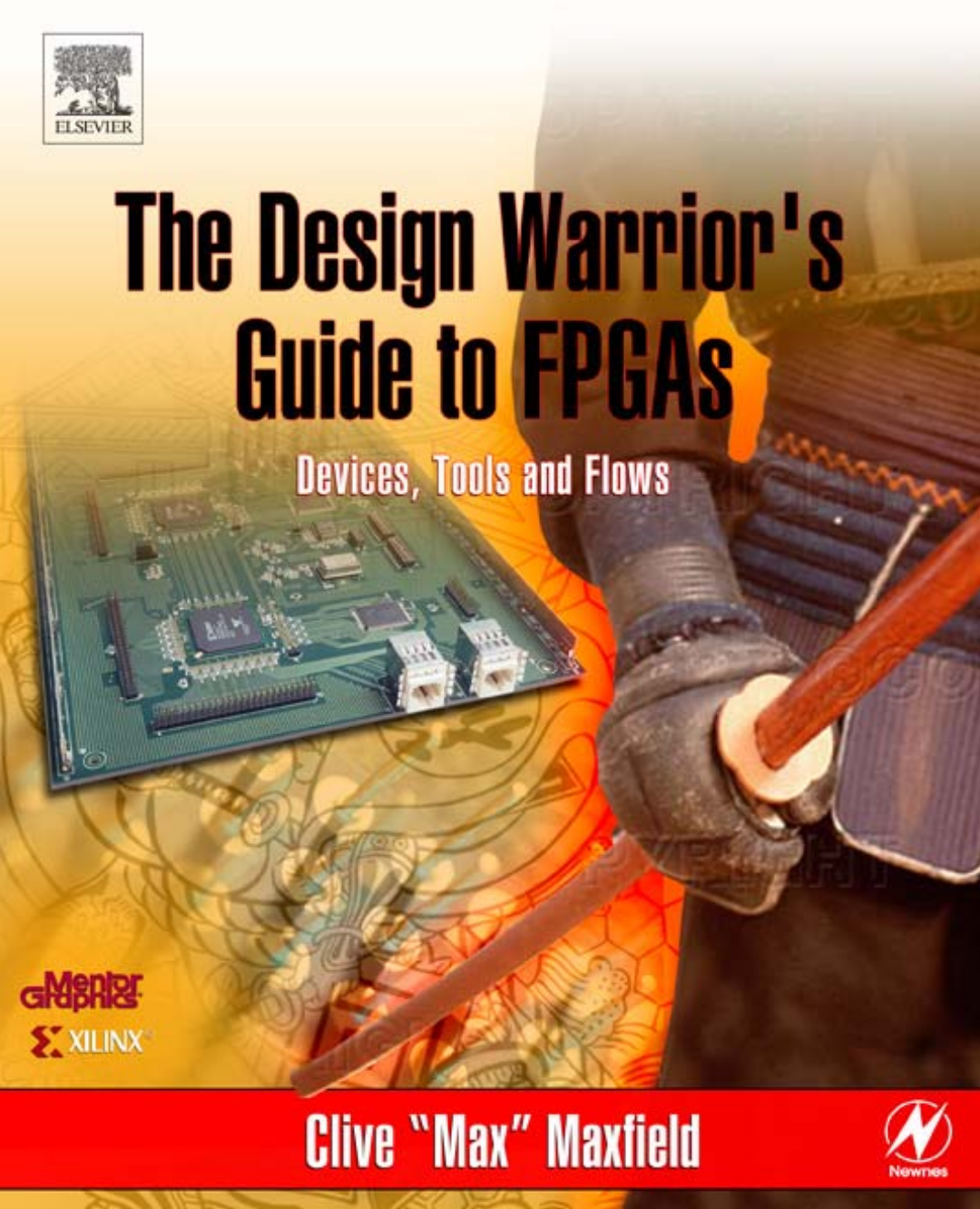
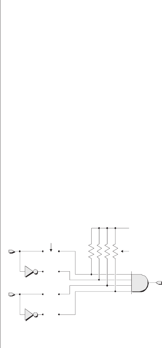
As a basis for these discussions, let’s start by considering a
very simple programmable function with two inputs called a
and band a single output y(Figure 2-1).
Fundamental Concepts
Chapter
2
a
Logic 1
y = 1 (N/A)
&
b
Pull-up resistors
Potential links
NOT
NOT
AND
Figure 2-1. A simple programmable function.
The inverting (NOT) gates associated with the inputs
mean that each input is available in both its true (unmodified)
and complemented (inverted) form. Observe the locations of
the potential links. In the absence of any of these links, all of
the inputs to the AND gate are connected via pull-up resistors
to a logic 1 value. In turn, this means that the output ywill
always be driving a logic 1, which makes this circuit a very
boring one in its current state. In order to make our function
more interesting, we need some mechanism that allows us to
establish one or more of the potential links.
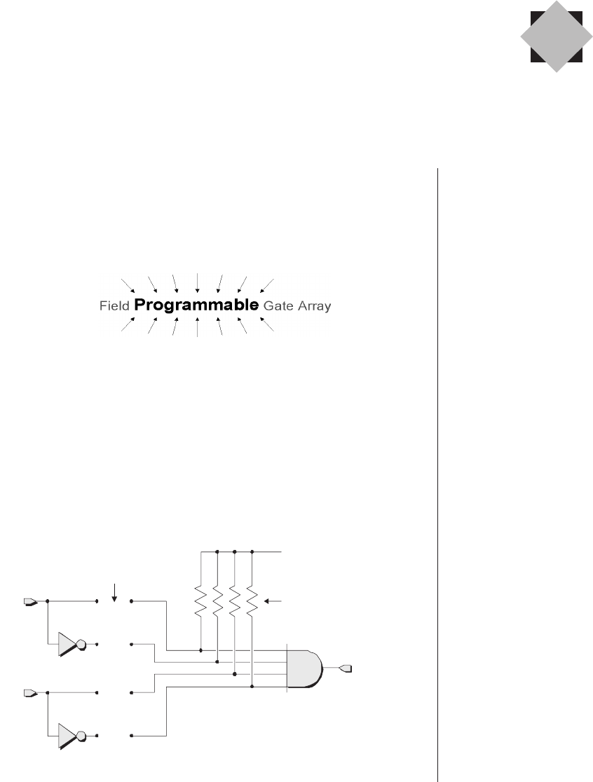
Fusible link technologies
One of the first techniques that allowed users to program
their own devices was—and still is—known as fusible-link
technology. In this case, the device is manufactured with all
of the links in place, where each link is referred to as a fuse
(Figure 2-2).
These fuses are similar in concept to the fuses you find in
household products like a television. If anything untoward
occurs such that the television starts consuming too much
power, its fuse will burn out. This results in an open circuit (a
break in the wire), which protects the rest of the unit from
10 ■The Design Warrior's Guide to FPGAs
a
Fat
Logic 1
y = 0 (N/A
)
&
Faf
b
Fbt
Fbf
Pull-up resistors
NOT
NOT
AND
Fuses
Figure 2-2. Augmenting the device with unprogrammed
fusible links.
25,000 BC:
The first boomerang is
used by people in what
is now Poland, 13,000
years before the
Australians.
harm. Of course, the fuses in a silicon chip are formed using
the same processes that are employed to create the transistors
and wires on the chip, so they are microscopically small.
When an engineer purchases a programmable device based
on fusible links, all of the fuses are initially intact. This means
that, in its unprogrammed state, the output from our example
function will always be logic 0. (Any 0 presented to the input
of an AND gate will cause its output to be 0, so if input ais 0,
the output from the AND will be 0. Alternatively, if input ais
1, then the output from its NOT gate—which we shall call
!a—will be 0, and once again the output from the AND will
be 0. A similar situation occurs in the case of input b.)
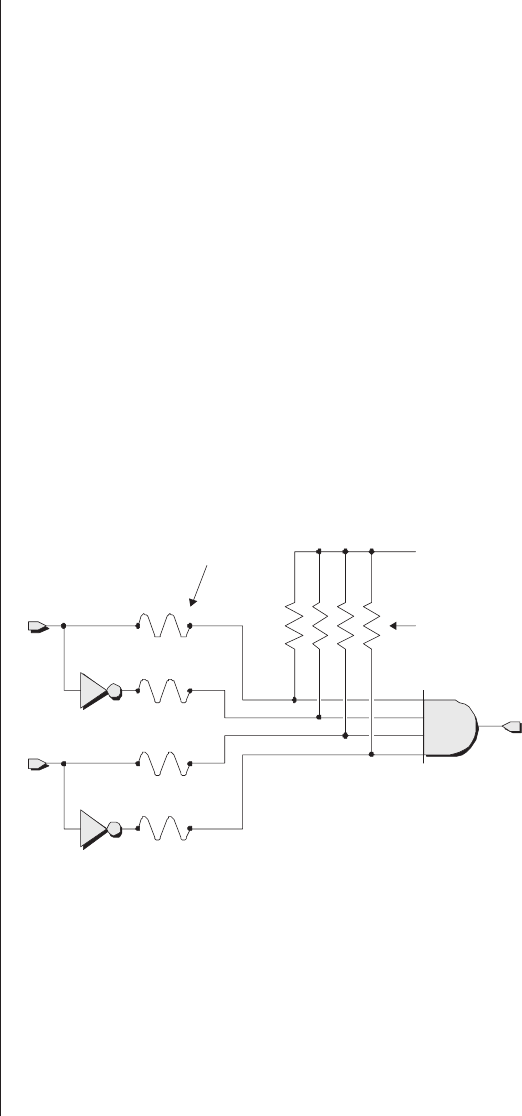
The point is that design engineers can selectively remove
undesired fuses by applying pulses of relatively high voltage
and current to the device’s inputs. For example, consider what
happens if we remove fuses Faf and Fbt (Figure 2-3).
Removing these fuses disconnects the complementary ver-
sion of input aand the true version of input bfrom the AND
gate (the pull-up resistors associated with these signals cause
their associated inputs to the AND to be presented with logic
1 values). This leaves the device to perform its new function,
which is y=a&!b. (The “&” character in this equation is
Fundamental Concepts ■11
a
Fat
Logic 1
y=a&!b
&
b
Fbf
Pull-up resistors
NOT
NOT
AND
Figure 2-3. Programmed fusible links.
2,500 BC:
Soldering is invented in
Mesopotamia, to join
sheets of gold.
used to represent the AND, while the “!” character is used to
represent the NOT. This syntax is discussed in a little more
detail in chapter 3). This process of removing fuses is typically
referred to as programming the device, but it may also be
referred to as blowing the fuses or burning the device.
Devices based on fusible-link technologies are said to be
one-time programmable, or OTP, because once a fuse has been
blown, it cannot be replaced and there’s no going back.
As fate would have it, although modern FPGAs are based
on a wide variety of programming technologies, the fusible-
link approach isn’t one of them. The reasons for mentioning it
here are that it sets the scene for what is to come, and it’s rele-
vant in the context of the precursor device technologies
referenced in chapter 3.
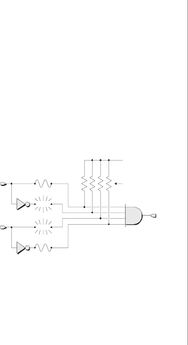
Antifuse technologies
As a diametric alternative to fusible-link technologies, we
have their antifuse counterparts, in which each configurable
path has an associated link called an antifuse. In its unpro-
grammed state, an antifuse has such a high resistance that it
may be considered an open circuit (a break in the wire), as
illustrated in Figure 2-4.
12 ■The Design Warrior's Guide to FPGAs
OTP is pronounced by
spelling it out as “O-T-P.”
a
Logic 1
y = 1 (N/A
)
&
b
Pull-up resistors
Unprogrammed
antifuses
NOT
NOT
AND
Figure 2-4. Unprogrammed antifuse links.
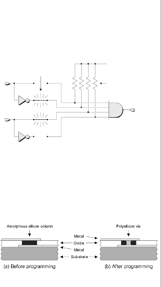
This is the way the device appears when it is first pur-
chased. However, antifuses can be selectively “grown”
(programmed) by applying pulses of relatively high voltage and
current to the device’s inputs. For example, if we add the anti-
fuses associated with the complementary version of input aand
the true version of input b, our device will now perform the
function y=!a &b(Figure 2-5).
An antifuse commences life as a microscopic column of
amorphous (noncrystalline) silicon linking two metal tracks.
In its unprogrammed state, the amorphous silicon acts as an
insulator with a very high resistance in excess of one billion
ohms (Figure 2-6a).
Fundamental Concepts ■13
a
Logic 1
y=!a&b
&
b
Pull-up resistors
Programmed
antifuses
NOT
NOT
AND
Figure 2-5. Programmed antifuse links.
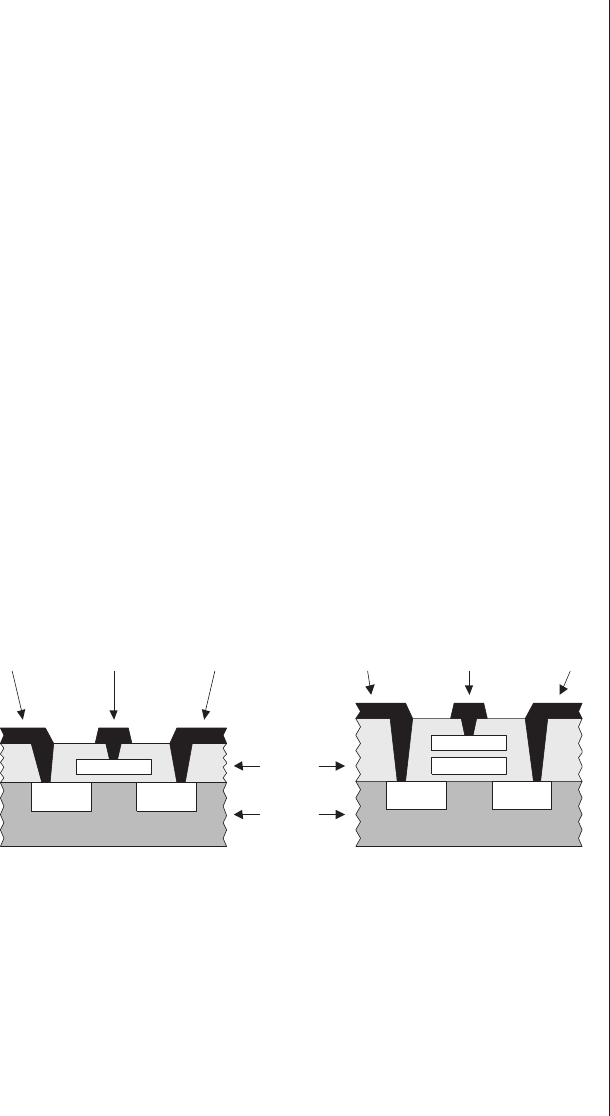
Figure 2-6. Growing an antifuse.
260 BC:
Archimedes works
out the principle of
the lever.

The act of programming this particular element effectively
“grows” a link—known as a via—by converting the insulating
amorphous silicon into conducting polysilicon (Figure 2-6b).
Not surprisingly, devices based on antifuse technologies
are OTP, because once an antifuse has been grown, it cannot
be removed, and there’s no changing your mind.
Mask-programmed devices
Before we proceed further, a little background may be
advantageous in order to understand the basis for some of the
nomenclature we’re about to run into. Electronic systems in
general—and computers in particular—make use of two major
classes of memory devices: read-only memory (ROM) and
random-access memory (RAM).
ROMs are said to be nonvolatile because their data remains
when power is removed from the system. Other components
in the system can read data from ROM devices, but they can-
not write new data into them. By comparison, data can be
both written into and read out of RAM devices, which are
said to be volatile because any data they contain is lost when
the system is powered down.
Basic ROMs are also said to be mask-programmed because
any data they contain is hard-coded into them during their
construction by means of the photo-masks that are used to
create the transistors and the metal tracks (referred to as the
metallization layers) connecting them together on the silicon
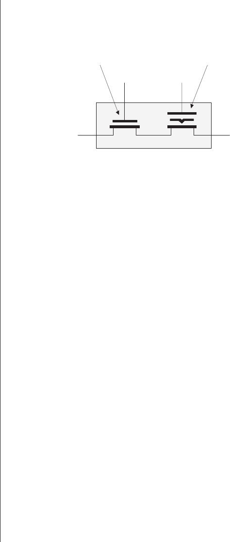
chip. For example, consider a transistor-based ROM cell that
can hold a single bit of data (Figure 2-7).
The entire ROM consists of a number of row (word) and
column (data) lines forming an array. Each column has a single
pull-up resistor attempting to hold that column to a weak
logic 1 value, and every row-column intersection has an asso-
ciated transistor and, potentially, a mask-programmed
connection.
The majority of the ROM can be preconstructed, and the
same underlying architecture can be used for multiple custom-
ers. When it comes to customizing the device for use by a
14 ■The Design Warrior's Guide to FPGAs
ROM is pronounced to
rhyme with “bomb.”
RAM is pronounced to
rhyme with “ham.”
The concept of photo-
masks and the way in
which silicon chips are
created are described in
more detail in Bebop to
the Boolean Boogie (An
Unconventional Guide to
Electronics), ISBN
0-7506-7543-8
The term bit (meaning
“binary digit”) was coined
by John Wilder Tukey, the
American chemist, turned
topologist, turned statisti-
cian in the 1940s.
particular customer, a single photo-mask is used to define
which cells are to include a mask-programmed connection and
which cells are to be constructed without such a connection.
Now consider what happens when a row line is placed in
its active state, thereby attempting to activate all of the tran-
sistors connected to that row. In the case of a cell that includes
a mask-programmed connection, activating that cell’s transis-
tor will connect the column line through the transistor to logic
0, so the value appearing on that column as seen from the out-
side world will be a 0. By comparison, in the case of a cell that
doesn’t have a mask-programmed connection, that cell’s tran-
sistor will have no effect, so the pull-up resistor associated with
that column will hold the column line at logic 1, which is the
value that will be presented to the outside world.
PROMs
The problem with mask-programmed devices is that creat-
ing them is a very expensive pastime unless you intend to
produce them in extremely large quantities. Furthermore, such
components are of little use in a development environment in
which you often need to modify their contents.
For this reason, the first programmable read-only memory
(PROM) devices were developed at Harris Semiconductor in
1970. These devices were created using a nichrome-based
Fundamental Concepts ■15
Tukey had initially con-
sidered using “binit” or
“bigit,” but thankfully he
settled on “bit,” which is
much easier to say and
use.
The term software is also
attributed to Tukey.
PROM is pronounced
just like the high school
dance of the same name.
Logic 1
Pull-up resistor
Row
(word) line
Column
(data) line
Mask-programmed
connection
Transistor
Logic 0
Figure 2-7. A transistor-based mask-programmed ROM cell.
fusible-link technology. As a generic example, consider a
somewhat simplified representation of a transistor-and-
fusible-link–based PROM cell (Figure 2-8).
In its unprogrammed state as provided by the manufac-
turer, all of the fusible links in the device are present. In this
case, placing a row line in its active state will turn on all of
the transistors connected to that row, thereby causing all of
the column lines to be pulled down to logic 0 via their respec-
tive transistors. As we previously discussed, however, design
engineers can selectively remove undesired fuses by applying
pulses of relatively high voltage and current to the device’s
inputs. Wherever a fuse is removed, that cell will appear to
contain a logic 1.
It’s important to note that these devices were initially
intended for use as memories to store computer programs and
constant data values (hence the “ROM” portion of their
appellation). However, design engineers also found them use-
ful for implementing simple logical functions such as lookup
tables and state machines. The fact that PROMs were rela-
tively cheap meant that these devices could be used to fix
bugs or test new implementations by simply burning a new
device and plugging it into the system.
16 ■The Design Warrior's Guide to FPGAs
Logic 1
Pull-up resistor
Row
(word) line
Column
(data) line
Fusible link
Transistor
Logic 0
Figure 2-8. A transistor-and-fusible-link–based PROM cell.
15 BC:
The Chinese invent the
belt drive.
Over time, a variety of more general-purpose PLDs based
on fusible-link and antifuse technologies became available
(these devices are introduced in more detail in chapter 3).
EPROM-based technologies
As was previously noted, devices based on fusible-link or
antifuse technologies can only be programmed a single
time—once you’ve blown (or grown) a fuse, it’s too late to
change your mind. (In some cases, it’s possible to incremen-
tally modify devices by blowing, or growing, additional fuses,
but the fates have to be smiling in your direction.) For this rea-
son, people started to think that it would be nice if there were
some way to create devices that could be programmed, erased,
and reprogrammed with new data.
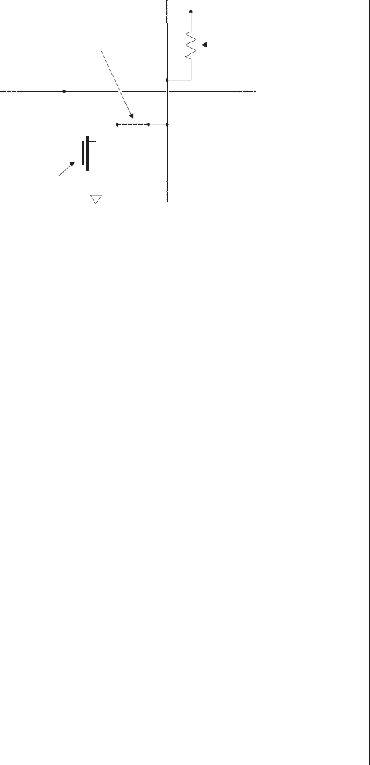
One alternative is a technology known as erasable program-
mable read-only memory (EPROM), with the first such
device—the 1702—being introduced by Intel in 1971. An
EPROM transistor has the same basic structure as a standard
MOS transistor, but with the addition of a second polysilicon
floating gate isolated by layers of oxide (Figure 2-9).
In its unprogrammed state, the floating gate is uncharged
and doesn’t affect the normal operation of the control gate. In
order to program the transistor, a relatively high voltage (the
order of 12V) is applied between the control gate and drain
Fundamental Concepts ■17
EPROM is pronounced
by spelling out the “E”
to rhyme with “bee,”
followed by “PROM.”
control gate
source drain
control gate
floating gate
source drain
(a) Standard MOS transistor (b) EPROM transistor
Silicon
substrate
Silicon
dioxide
Source
terminal
Control gate
terminal
Drain
terminal
Source
terminal
Control gate
terminal
Drain
termina
l
Figure 2-9. Standard MOS versus EPROM transistors.
terminals. This causes the transistor to be turned hard on,
and energetic electrons force their way through the oxide into
the floating gate in a process known as hot (high energy) elec-
tron injection. When the programming signal is removed, a
negative charge remains on the floating gate. This charge is
very stable and will not dissipate for more than a decade under
normal operating conditions. The stored charge on the float-
ing gate inhibits the normal operation of the control gate
and, thus, distinguishes those cells that have been pro-
grammed from those that have not. This means we can use
such a transistor to form a memory cell (Figure 2-10).
Observe that this cell no longer requires a fusible-link,
antifuse, or mask-programmed connection. In its unpro-
grammed state, as provided by the manufacturer, all of the
floating gates in the EPROM transistors are uncharged. In this
case, placing a row line in its active state will turn on all of
the transistors connected to that row, thereby causing all of
the column lines to be pulled down to logic 0 via their respec-
tive transistors. In order to program the device, engineers can
use the inputs to the device to charge the floating gates associ-
ated with selected transistors, thereby disabling those
18 ■The Design Warrior's Guide to FPGAs
Logic 1
Pull-up resistor
Row
(word) line
Column
(data) line
EPROM
Transistor
Logic 0
Figure 2-10. An EPROM transistor-based memory cell.
60 AD:
Hero, an Alexandrian
Greek, builds a toy
powered by stream.

transistors. In these cases, the cells will appear to contain
logic 1 values.
As they are an order of magnitude smaller than fusible
links, EPROM cells are efficient in terms of silicon real estate.
Their main claim to fame, however, is that they can be erased
and reprogrammed. An EPROM cell is erased by discharging
the electrons on that cell’s floating gate. The energy required
to discharge the electrons is provided by a source of ultraviolet
(UV) radiation. An EPROM device is delivered in a ceramic
or plastic package with a small quartz window in the top,
where this window is usually covered with a piece of opaque
sticky tape. In order for the device to be erased, it is first
removed from its host circuit board, its quartz window is
uncovered, and it is placed in an enclosed container with an
intense UV source.
The main problems with EPROM devices are their expen-
sive packages with quartz windows and the time it takes to
erase them, which is in the order of 20 minutes. A foreseeable
problem with future devices is paradoxically related to
improvements in the process technologies that allow transis-
tors to be made increasingly smaller. As the structures on the
device become smaller and the density (number of transistors
and interconnects) increases, a larger percentage of the surface
of the die is covered by metal. This makes it difficult for the
EPROM cells to absorb the UV light and increases the
required exposure time.
Once again, these devices were initially intended for use as
programmable memories (hence the “PROM” portion of their
name). However, the same technology was later applied to
more general-purpose PLDs, which therefore became known as
erasable PLDs (EPLDs).
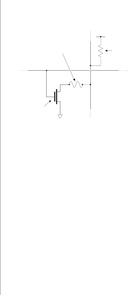
EEPROM-based technologies
The next rung up the technology ladder appeared in the
form of electrically erasable programmable read-only memories
(EEPROMs or E2PROMs).AnE
2PROM cell is approximately
2.5 times larger than an equivalent EPROM cell because it
Fundamental Concepts ■19
UV is pronounced by
spelling it out as “U-V.”
EPLD is pronounced by
spelling it out as
“E-P-L-D.”
EEPROM is pronounced
by spelling out the “E-E”
to rhyme with “bee-bee,”
followed by “PROM.”
comprises two transistors and the space between them
(Figure 2-11).
The E2PROM transistor is similar to that of an EPROM
transistor in that it contains a floating gate, but the insulating
oxide layers surrounding this gate are very much thinner. The
second transistor can be used to erase the cell electrically.
E2PROMs first saw the light of day as computer memories,
but the same technology was subsequently applied to PLDs,
which therefore became known as electrically erasable PLDs
(EEPLDs or E2PLDs).
FLASH-based technologies
A development known as FLASH can trace its ancestry to
both the EPROM and E2PROM technologies. The name
“FLASH” was originally coined to reflect this technology’s
rapid erasure times compared to EPROM. Components based
on FLASH can employ a variety of architectures. Some have a
single floating gate transistor cell with the same area as an
EPROM cell, but with the thinner oxide layers characteristic
of an E2PROM component. These devices can be electrically
erased, but only by clearing the whole device or large portions
thereof. Other architectures feature a two-transistor cell simi-
lar to that of an E2PROM cell, thereby allowing them to be
erased and reprogrammed on a word-by-word basis.
20 ■The Design Warrior's Guide to FPGAs
In the case of the alterna-
tive E2PROM designation,
the “E2” stands for “E to
the power of two,” or
“E-squared.” Thus,
E2PROM is pronounced
“E-squared-PROM.”
EEPLD is pronounced by
spelling it out as
“E-E-P-L-D.”
E2PLD is pronounced
“E-squared-P-L-D.”
E2PROM Cell
Normal
MOS transistor
E2PROM
transistor
Figure 2-11. An E2PROM-–cell.
Initial versions of FLASH could only store a single bit of
data per cell. By 2002, however, technologists were experi-
menting with a number of different ways of increasing this
capacity. One technique involves storing distinct levels of
charge in the FLASH transistor’s floating gate to represent two
bits per cell. An alternative approach involves creating two
discrete storage nodes in a layer below the gate, thereby sup-
porting two bits per cell.
SRAM-based technologies
There are two main versions of semiconductor RAM
devices: dynamic RAM (DRAM) and static RAM (SRAM).In
the case of DRAMs, each cell is formed from a transistor-
capacitor pair that consumes very little silicon real estate. The
“dynamic” qualifier is used because the capacitor loses its
charge over time, so each cell must be periodically recharged if
it is to retain its data. This operation—known as refreshing—is
a tad complex and requires a substantial amount of additional
circuitry. When the “cost” of this refresh circuitry is amortized
over tens of millions of bits in a DRAM memory device, this
approach becomes very cost effective. However, DRAM tech-
nology is of little interest with regard to programmable logic.
By comparison, the “static” qualifier associated with
SRAM is employed because—once a value has been loaded
into an SRAM cell—it will remain unchanged unless it is spe-
cifically altered or until power is removed from the system.
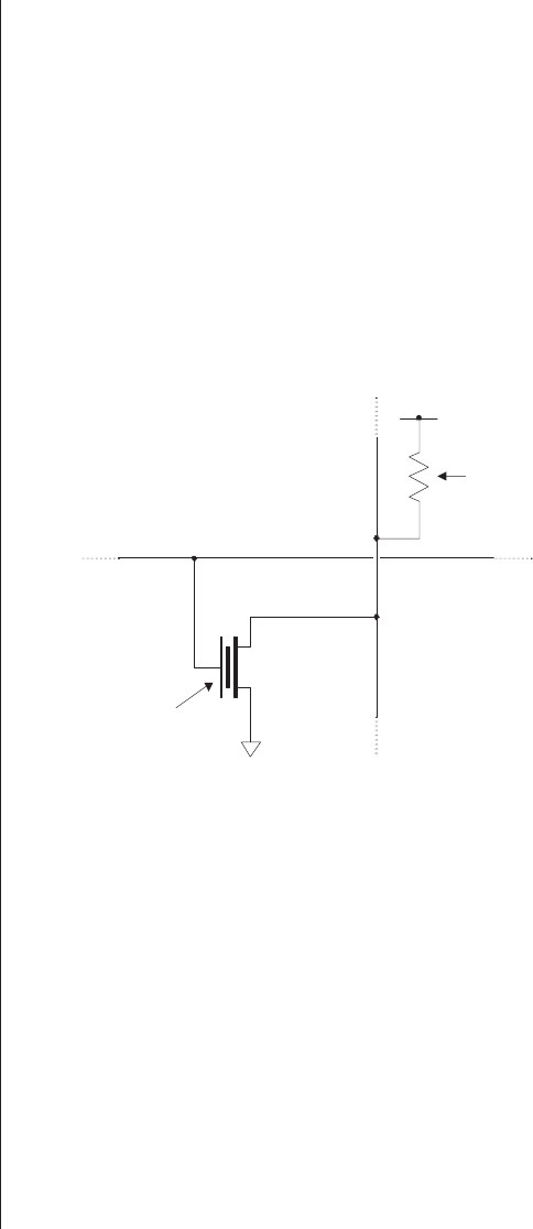
Consider the symbol for an SRAM-based programmable cell
(Figure 2-12).
Fundamental Concepts ■21
DRAM is pronounced by
spelling out the “D” to
rhyme with “knee,” fol-
lowed by “RAM” to
rhyme with “spam.”
SRAM is pronounced by
spelling out the “S” to
rhyme with “less,” fol-
lowed by “RAM” to
rhyme with “Pam.”
SRAM
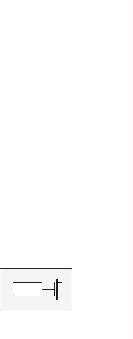
Figure 2-12. An SRAM-based programmable cell.

The entire cell comprises a multitransistor SRAM storage
element whose output drives an additional control transistor.
Depending on the contents of the storage element (logic 0 or
logic 1), the control transistor will either be OFF (disabled) or
ON (enabled).
One disadvantage of having a programmable device based
on SRAM cells is that each cell consumes a significant
amount of silicon real estate because these cells are formed
from four or six transistors configured as a latch. Another dis-
advantage is that the device’s configuration data (programmed
state) will be lost when power is removed from the system. In
turn, this means that these devices always have to be repro-
grammed when the system is powered on. However, such
devices have the corresponding advantage that they can be
reprogrammed quickly and repeatedly as required.
The way in which these cells are used in SRAM-based
FPGAs is discussed in more detail in the following chapters.
For our purposes here, we need only note that such cells could
conceptually be used to replace the fusible links in our exam-
ple circuit shown in Figure 2-2, the antifuse links in Figure
2-4, or the transistor (and associated mask-programmed con-
nection) associated with the ROM cell in Figure 2-7 (of
course, this latter case, having an SRAM-based ROM, would
be meaningless).
Summary
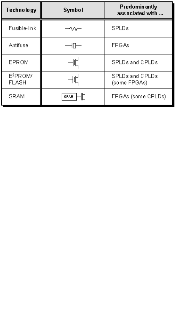
Table 2-1 shows the devices with which the various pro-
gramming technologies are predominantly associated.
Additionally, we shouldn’t forget that new technologies
are constantly bobbing to the surface. Some float around for a
bit, and then sink without a trace while you aren’t looking;
others thrust themselves onto center stage so rapidly that you
aren’t quite sure where they came from.
For example, one technology that is currently attracting a
great deal of interest for the near-term future is magnetic RAM
(MRAM). The seeds of this technology were sown back in
1974, when IBM developed a component called a magnetic
22 ■The Design Warrior's Guide to FPGAs
MRAM is pronounced by
spelling out the “M” to
rhyme with “hem,” fol-
lowed by “RAM” to rhyme
with “clam.”
tunnel junction (MJT). This comprises a sandwich of two ferro-
magnetic layers separated by a thin insulating layer. An
MRAM memory cell can be created at the intersection of two
tracks—say a row (word) line and a column (data) line—with
an MJT sandwiched between them.
MRAM cells have the potential to combine the high speed
of SRAM, the storage capacity of DRAM, and the
nonvolatility of FLASH, all while consuming a miniscule
amount of power. MRAM-based memory chips are predicted
to become available circa 2005. Once these memory chips do
reach the market, other devices—such as MRAM-based
FPGAs—will probably start to appear shortly thereafter.
Fundamental Concepts ■23
MJT is pronounced by
spelling it out as “M-J-T.”
Table 2-1. Summary of Programming Technologies
Related technologies
In order to get a good feel for the way in which FPGAs
developed and the reasons why they appeared on the scene in
the first place, it’s advantageous to consider them in the con-
text of other related technologies (Figure 3-1).
The white portions of the timeline bars in this illustration
indicate that although early incarnations of these technologies
may have been available, for one reason or another they wer-
en’t enthusiastically received by the engineers working in the
trenches during this period. For example, although Xilinx
introduced the world’s first FPGA as early as 1984, design
engineers didn’t really start using these little scamps with gusto
and abandon until the early 1990s.
The Origin of FPGAs
Chapter
3
1945 1950 1955 1960 1965 1970 1975 1980 1985 1990 1995 2000
FPGAs
ASICs
CPLDs
SPLDs
Microprocessors
SRAMs & DRAMs
ICs (General)
Transistors
Figure 3-1. Technology timeline (dates are approximate).

Transistors
On December 23, 1947, physicists William Shockley,
Walter Brattain, and John Bardeen, working at Bell Laborato-
ries in the United States, succeeded in creating the first
transistor: a point-contact device formed from germanium
(chemical symbol Ge).
The year 1950 saw the introduction of a more sophisti-
cated component called a bipolar junction transistor (BJT),
which was easier and cheaper to build and had the added
advantage of being more reliable. By the late 1950s, transistors
were being manufactured out of silicon (chemical symbol Si)
rather than germanium. Even though germanium offered cer-
tain electrical advantages, silicon was cheaper and more
amenable to work with.
If BJTs are connected together in a certain way, the result-
ing digital logic gates are classed as transistor-transistor logic
(TTL). An alternative method of connecting the same tran-
sistors results in emitter-coupled logic (ECL). Logic gates
constructed in TTL are fast and have strong drive capability,
but they also consume a relatively large amount of power.
Logic gates built in ECL are substantially faster than their
TTL counterparts, but they consume correspondingly more
power.
In 1962, Steven Hofstein and Fredric Heiman at the RCA
research laboratory in Princeton, New Jersey, invented a new
family of devices called metal-oxide semiconductor field-effect
transistors (MOSFETs). These are often just called FETs for
short. Although the original FETs were somewhat slower than
their bipolar cousins, they were cheaper, smaller, and used
substantially less power.
There are two main types of FETs, called NMOS and
PMOS. Logic gates formed from NMOS and PMOS transis-
tors connected together in a complementary manner are
known as a complementary metal-oxide semiconductor (CMOS).
Logic gates implemented in CMOS used to be a tad slower
than their TTL cousins, but both technologies are pretty
26 ■The Design Warrior's Guide to FPGAs
BJT is pronounced by
spelling it out as “B-J-T.”
TTL is pronounced by
spelling it out as “T-T-L.”
ECL is pronounced by
spelling it out as “E-C-L.”
FET is pronounced to
rhyme with “bet.”
NMOS, PMOS, and CMOS
are pronounced by spell-
ing out the “N,” “P,” “or
“C” to rhyme with “hen,”
“pea,” or “sea,” respec-
tively, followed by “MOS”
to rhyme with “boss.”

much equivalent in this respect these days. However, CMOS
logic gates have the advantage that their static (nonswitching)
power consumption is extremely low.
Integrated circuits
The first transistors were provided as discrete components
that were individually packaged in small metal cans. Over
time, people started to think that it would be a good idea to
fabricate entire circuits on a single piece of semiconductor.
The first public discussion of this idea is credited to a British
radar expert, G. W. A. Dummer, in a paper presented in 1952.
But it was not until the summer of 1958 that Jack Kilby, work-
ing for Texas Instruments (TI), succeeded in fabricating a
phase-shift oscillator comprising five components on a single
piece of semiconductor.
Around the same time that Kilby was working on his pro-
totype, two of the founders of Fairchild Semiconductor—the
Swiss physicist Jean Hoerni and the American physicist Robert
Noyce—invented the underlying optical lithographic tech-
niques that are now used to create transistors, insulating layers,
and interconnections on modern ICs.
During the mid-1960s, TI introduced a large selection of
basic building block ICs called the 54xx (“fifty-four hundred”)
series and the 74xx (“seventy-four hundred”) series, which
were specified for military and commercial use, respectively.
These “jelly bean” devices, which were typically around 3/4"
long, 3/8" wide, and had 14 or 16 pins, each contained small
amounts of simple logic (for those readers of a pedantic dispo-
sition, some were longer, wider, and had more pins). For
example, a 7400 device contained four 2-input NAND gates, a
7402 contained four 2-input NOR gates, and a 7404 contained
six NOT (inverter) gates.
TI’s 54xx and 74xx series were implemented in TTL. By
comparison, in 1968, RCA introduced a somewhat equivalent
CMOS-based library of parts called the 4000 (“four thousand”)
series.
The Origin of FPGAs ■27
IC is pronounced
by spelling it out as “I-C.”

SRAMs, DRAMs, and microprocessors
The late 1960s and early 1970s were rampant with new
developments in the digital IC arena. In 1970, for example,
Intel announced the first 1024-bit DRAM (the 1103) and
Fairchild introduced the first 256-bit SRAM (the 4100).
One year later, in 1971, Intel introduced the world’s first
microprocessor (µP)—the 4004—which was conceived and
created by Marcian “Ted” Hoff, Stan Mazor, and Federico
Faggin. Also referred to as a “computer-on-a-chip,” the 4004
contained only around 2,300 transistors and could execute
60,000 operations per second.
Actually, although the 4004 is widely documented as
being the first microprocessor, there were other contenders. In
February 1968, for example, International Research Corpora-
tion developed an architecture for what they referred to as a
“computer-on-a-chip.” And in December 1970, a year before
the 4004 saw the light of day, one Gilbert Hyatt filed an
application for a patent entitled “Single Chip Integrated Circuit
Computer Architecture” (wrangling about this patent continues
to this day). What typically isn’t disputed, however, is the fact
that the 4004 was the first microprocessor to be physically
constructed, to be commercially available, and to actually per-
form some useful tasks.
The reason SRAM and microprocessor technologies are of
interest to us here is that the majority of today’s FPGAs are
SRAM-based, and some of today’s high-end devices incorpo-
rate embedded microprocessor cores (both of these topics are
discussed in more detail in chapter 4).
SPLDs and CPLDs
The first programmable ICs were generically referred to as
programmable logic devices (PLDs). The original components,
which started arriving on the scene in 1970 in the form of
PROMs, were rather simple, but everyone was too polite to
mention it. It was only toward the end of the 1970s that sig-
nificantly more complex versions became available. In order
28 ■The Design Warrior's Guide to FPGAs
SRAM and DRAM are pro-
nounced by spelling out
the “S” or “D” to rhyme
with “mess” or “bee,”
respectively, followed by
“RAM” to rhyme with
“spam.”
PLD and SPLD are pro-
nounced by spelling
them out as “P-L-D” and
“S-P-L-D,” respectively.
to distinguish them from their less-sophisticated ancestors,
which still find use to this day, these new devices were referred
to as complex PLDs (CPLDs). Perhaps not surprisingly, it subse-
quently became common practice to refer to the original,
less-pretentious versions as simple PLDs (SPLDs).
Just to make life more confusing, some people understand
the terms PLD and SPLD to be synonymous, while others
regard PLD as being a superset that encompasses both SPLDs
and CPLDs (unless otherwise noted, we shall embrace this lat-
ter interpretation).
And life just keeps on getting better and better because
engineers love to use the same acronym to mean different
things or different acronyms to mean the same thing (listening
to a gaggle of engineers regaling each other in conversation
can make even the strongest mind start to “throw a wobbly”).
In the case of SPLDs, for example, there is a multiplicity of
underlying architectures, many of which have acronyms
formed from different combinations of the same three or four
letters (Figure 3-2).
Of course there are also EPLD, E2PLD, and FLASH ver-
sions of many of these devices—for example, EPROMs and
E2PROMs—but these are omitted from figure 3-2 for purposes
of simplicity (these concepts were introduced in chapter 2).
The Origin of FPGAs ■29
PLDs
SPLDs CPLDs
PLAsPROMs PALs GALs etc.
Figure 3-2. A positive plethora of PLDs.
1500: Italy.
Leonard da Vinci
sketches details
of a rudimentary
mechanical calculator.
PROMs
The first of the simple PLDs were PROMs, which
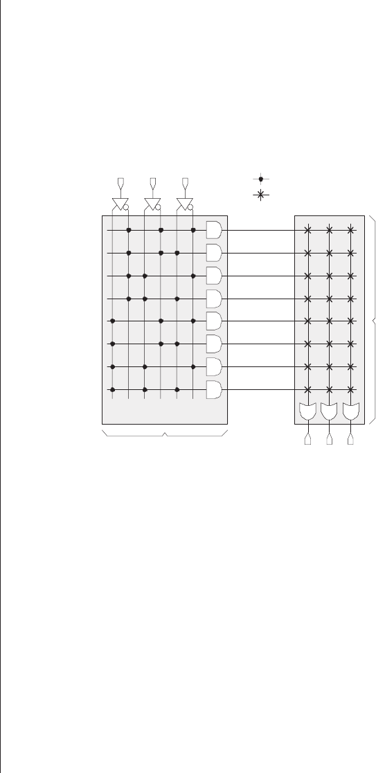
appeared on the scene in 1970. One way to visualize how
these devices perform their magic is to consider them as con-
sisting of a fixed array of AND functions driving a
programmable array of OR functions. For example, consider a
3-input, 3-output PROM (Figure 3-3).
The programmable links in the OR array can be imple-
mented as fusible links, or as EPROM transistors and E2PROM
cells in the case of EPROM and E2PROM devices, respec-
tively. It is important to realize that this illustration is
intended only to provide a high-level view of the way in
which our example device works—it does not represent an
actual circuit diagram. In reality, each AND function in the
AND array has three inputs provided by the appropriate true
or complemented versions of the a,b, and cdevice inputs.
Similarly, each OR function in the OR array has eight inputs
provided by the outputs from the AND array.
30 ■The Design Warrior's Guide to FPGAs
PROM is pronounced like
the high school dance of
the same name.
a b c
l
l
l
Address 0 &
Address 1 &
Address 2 &
Address 3 &
Address 4 &
Address 5 &
Address 6 &
Address 7 &
a !a b !b c !c
!a !c!b&&
!a c!b&&
!a !cb&&
!a cb&&
a!c!b&&
ac!b&&
a!cb&&
acb&&
Predefined AND array
Programmable OR array
w x y
Predefined link
Programmable link
Figure 3-3. Unprogrammed PROM
(predefined AND array, programmable OR array).
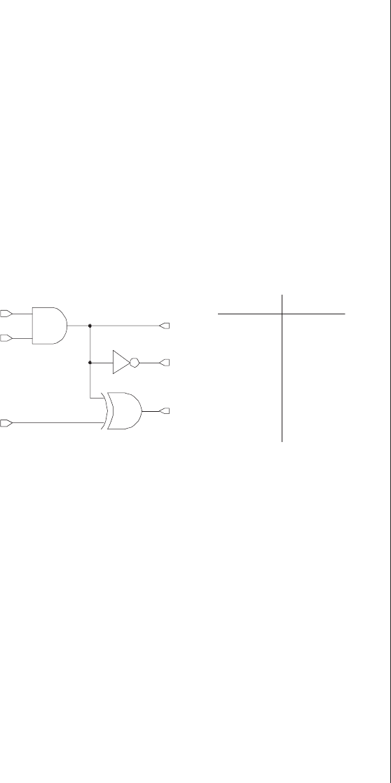
As was previously noted, PROMs were originally intended
for use as computer memories in which to store program
instructions and constant data values. However, design engi-
neers also used them to implement simple logical functions
such as lookup tables and state machines. In fact, a PROM can
be used to implement any block of combinational (or combi-
national) logic so long as it doesn’t have too many inputs or
outputs. The simple 3-input, 3-output PROM shown in Figure
3-3, for example, can be used to implement any combinatorial
function with up to 3 inputs and 3 outputs. In order to under-
stand how this works, consider the small block of logic shown
in Figure 3-4 (this circuit has no significance beyond the pur-
poses of this example).
We could replace this block of logic with our 3-input,
3-output PROM. We would only need to program the appro-
priate links in the OR array (Figure 3-5).
With regard to the equations shown in this figure, “&” rep-
resents AND, “|” represents OR, “^” represents XOR, and “!”
represents NOT. This syntax (or numerous variations thereof)
was very common in the early days of PLDs because it allowed
logical equations to be easily and concisely represented in text
files using standard computer keyboard characters.
The above example is, of course, very simple. Real PROMs
can have significantly more inputs and outputs and can, there-
fore, be used to implement larger blocks of combinational
logic. From the mid-1960s until the mid-1980s (or later),
The Origin of FPGAs ■31
Some folks prefer to say
“combinational logic,”
while others favor “com-
binatorial logic.”
The ‘&’ (ampersand) char-
acter is commonly
referred to as an “amp” or
“amper.”
The ‘|’ (vertical line) char-
acter is commonly
referred to as a “bar,” “or,”
or “pipe.”
abc wxy
000 010
001 011
010 010
011 011
100 010
101 011
110 101
111 100
l
&
a
b
c
w
x
y
Figure 3-4. A small block of combinational logic.
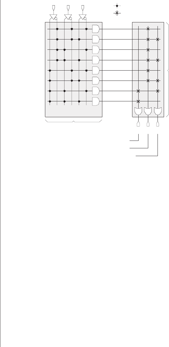
combinational logic was commonly implemented by means of
jelly bean ICs such as the TI 74xx series devices.
The fact that quite a large number of these jelly bean
chips could be replaced with a single PROM resulted in cir-
cuit boards that were smaller, lighter, cheaper, and less prone
to error (each solder joint on a circuit board provides a poten-
tial failure mechanism). Furthermore, if any logic errors were
subsequently discovered in this portion of the design (if the
design engineer had inadvertently used an AND function
instead of a NAND, for example), then these slipups could
easily be fixed by blowing a new PROM (or erasing and repro-
gramming an EPROM or E2PROM). This was preferable to
the ways in which errors had to be addressed on boards based
on jelly bean ICs. These included adding new devices to the
board, cutting existing tracks with a scalpel, and adding wires
by hand to connect the new devices into the rest of the
circuit.
32 ■The Design Warrior's Guide to FPGAs
The ‘^’ (circumflex) char-
acter is commonly
referred to as a “hat,”
“control,” “up-arrow,” or
“caret.” More rarely it
may be referred to as a
“chevron,” “power of” (as
in “to the power of”), or
“shark-fin.”
The ‘!’ (exclamation
mark) character is com-
monly referred to as a
“bang,” “ping,” or
“shriek”.
a b c
l
l
l
Address 0 &
Address 1 &
Address 2 &
Address 3 &
Address 4 &
Address 5 &
Address 6 &
Address 7 &
a !a b !b c !c
!a !c!b&&
!a c!b&&
!a !cb&&
!a cb&&
a!c!b&&
ac!b&&
a!cb&&
acb&&
Predefined AND array
Programmable OR array
w x y
Predefined link
Programmable link
w=(a&b)
x=!(a&b)
y
=(a&b)^c
Figure 3-5. Programmed PROM.

In logical terms, the AND (“&”) operator is known as a
logical multiplication or product, while the OR (“|”) operator is
known as a logical addition or sum. Furthermore, when we have
a logical equation in the form
y=(a&!b &c)|(!a &b&c)|(a&!b &!c)|(a&!b &c)
then the term literal refers to any true or inverted variable (a,
!a,b,!b, etc.), and a group of literals linked by “&” operators is
referred to as a product term. Thus, the product term (a&!b &
c) contains three literals—a,!b, and c—and the above equa-
tion is said to be in sum-of-products form.
The point is that, when they are employed to implement
combinational logic as illustrated in figures 3-4 and 3-5,
PROMs are useful for equations requiring a large number of
product terms, but they can support relatively few inputs
because every input combination is always decoded and used.
PLAs
In order to address the limitations imposed by the PROM
architecture, the next step up the PLD evolutionary ladder was
that of programmable logic arrays (PLAs), which first became
available circa 1975. These were the most user configurable of
the simple PLDs because both the AND and OR arrays were
programmable. First, consider a simple 3-input, 3-output PLA
in its unprogrammed state (Figure 3.6).
Unlike a PROM, the number of AND functions in the
AND array is independent of the number of inputs to the
device. Additional ANDs can be formed by simply introducing
more rows into the array.
Similarly, the number of OR functions in the OR array is
independent of both the number of inputs to the device and
the number of AND functions in the AND array. Additional
ORs can be formed by simply introducing more columns into
the array.
The Origin of FPGAs ■33
PLA is pronounced by
spelling it out as “P-L-A.”
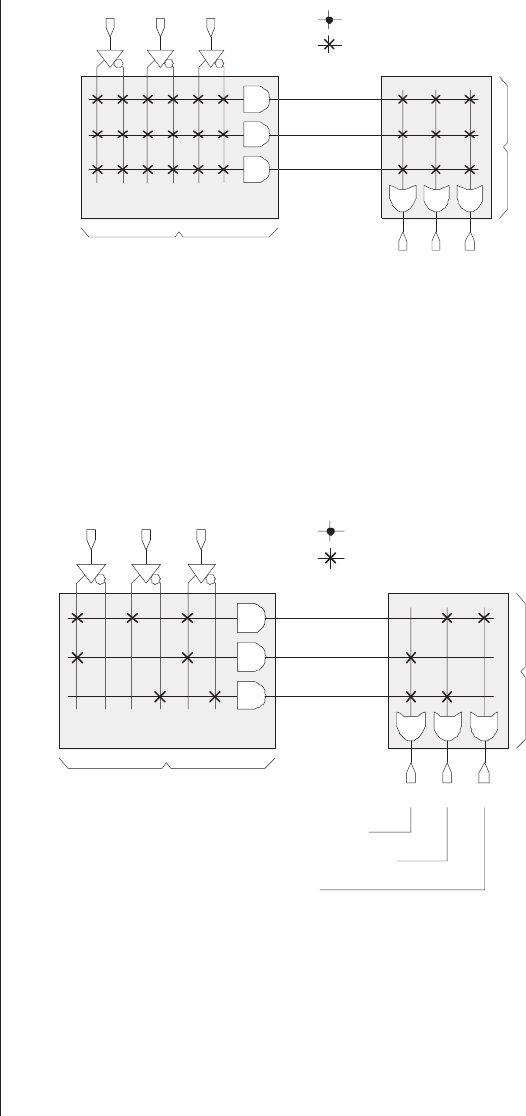
Now assume that we wish our example PLA to implement
the three equations shown below. We can achieve this by pro-
gramming the appropriate links as illustrated in Figure 3-7.
w=(a&c)|(!b &!c)
x=(a&b&c)!(!b &!c)
y=(a&b&c)
34 ■The Design Warrior's Guide to FPGAs
a b c
&
&
&
a !a b !b c !c
N/A
Predefined AND array
Programmable
OR array
Predefined link
Programmable link
l
l
l
w x y
N/A
N/A
Figure 3-6. Unprogrammed PLA
(programmable AND and OR arrays).
a b c
&
&
&
a !a b !b c !c
acb&&
ac&
!b !c&
Predefined AND array
Programmable
OR ar ra y
Predefined link
Programmable link
l
l
l
w x y
w=(a&c)|(!b&!c)
x=(a&b&c)|(!b&!c)
y=(a&b&c)
Figure 3-7. Programmed PLA.
1600:
John Napier invents a
simple multiplication
table called Napier’s
Bones.

As fate would have it, PLAs never achieved any significant
level of market presence, but several vendors experimented
with different flavors of these devices for a while. For example,
PLAs were not obliged to have AND arrays feeding OR arrays,
and some alternative architectures such as AND arrays feeding
NOR arrays were occasionally seen strutting their stuff. How-
ever, while it would be theoretically possible to field
architectures such as OR-AND, NAND-OR, and
NAND-NOR, these variations were relatively rare or nonex-
istent. One reason these devices tended to stick to AND-OR1
(and AND-NOR) architectures was that the sum-of-products
representations most often used to specify logical equations
could be directly mapped onto these structures. Other equa-
tion formats—like product-of-sums—could be accommodated
using standard algebraic techniques (this was typically per-
formed by means of software programs that could perform
these techniques with their metaphorical hands tied behind
their backs).
PLAs were touted as being particularly useful for large
designs whose logical equations featured a lot of common
product terms that could be used by multiple outputs; for
example, the product term (!b &!c) is used by both the wand
xoutputs in Figure 3-7. This feature may be referred to as
product-term sharing.
On the downside, signals take a relatively long time to pass
through programmable links as opposed to their predefined
counterparts. Thus, the fact that both their AND and OR
arrays were programmable meant that PLAs were significantly
slower than PROMs.
The Origin of FPGAs ■35
1Actually, one designer I talked to a few moments before penning these
words told me that his team created a NOT-NOR-NOR-NOT
architecture (this apparently offered a slight speed advantage), but they
told their customers it was an AND-OR architecture (which is how it
appeared to the outside world) because “that was what they were
expecting.” Even today, what device vendors say they build and what they
actually build are not necessarily the same thing.
1614:
John Napier invents
logarithms.
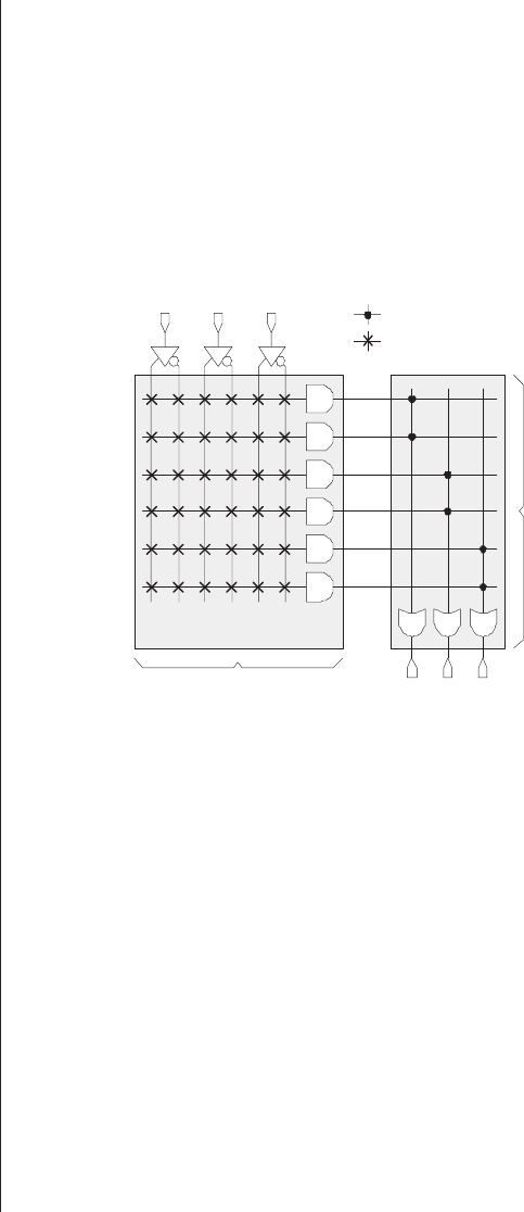
PALs and GALs
In order to address the speed problems posed by PLAs, a
new class of device called programmable array logic (PAL) was
introduced in the late 1970s. Conceptually, a PAL is almost
the exact opposite of a PROM because it has a programmable
AND array and a predefined OR array. As an example, con-
sider a simple 3-input, 3-output PAL in its unprogrammed
state (Ffigure 3-8).
The advantage of PALs (as compared to PLAs) is that
they are faster because only one of their arrays is programma-
ble. On the downside, PALs are more limited because they
only allow a restricted number of product terms to be ORed
together (but engineers are cunning people, and we have lots
of tricks up our sleeves that, to a large extent, allow us to get
around this sort of thing).
Additional programmable options
The PLA and PAL examples shown above were small and
rudimentary for the purposes of simplicity. In addition to
being a lot larger (having more inputs, outputs, and internal
36 ■The Design Warrior's Guide to FPGAs
PAL, which is a regis-
tered trademark of
Monolithic Memories,
Inc., is pronounced the
same way you’d greet a
buddy (“Hiya pal”).
Created by Lattice Semi-
conductor Corporation in
1983, generic array logic
(GAL) devices offered
sophisticated CMOS elec-
trically erasable (E2)
variations on the PAL
concept.
GAL is pronounced the
same way a guy thinks
of his wife or girlfriend
(“What a gal!”).
a b c
l
l
l
&
&
&
&
&
&
a !a b !b c !c
Programmable
AND array
Predefined OR array
w x y
Predefined link
Programmable link
Figure 3-8. Unprogrammed PAL
(programmable AND array, predefined OR array).

signals), real devices can offer a variety of additional program-
mable options, such as the ability to invert the outputs or to
have tristatable outputs, or both.
Furthermore, some devices support registered or latched
outputs (with associated programmable multiplexers that allow
the user to specify whether to use the registered or nonregis-
tered version of the output on a pin-by-pin basis). And some
devices provide the ability to configure certain pins to act as
either outputs or additional inputs, and the list of options
goes on.
The problem here is that different devices may provide dif-
ferent subsets of the various options, which makes selecting
the optimum device for a particular application something of a
challenge. Engineers typically work around this by (a) restrict-
ing themselves to a limited selection of devices and then
tailoring their designs to these devices, or (b) using a software
program to help them decide which devices best fit their
requirements on an application-by-application basis.
CPLDs
The one truism in electronics is that everyone is always
looking for things to get bigger (in terms of functional capabil-
ity), smaller (in terms of physical size), faster, more powerful,
and cheaper—surely that’s not too much to ask, is it? Thus,
the tail end of the 1970s and the early 1980s began to see the
emergence of more sophisticated PLD devices that became
known as complex PLDs (CPLDs).
Leading the fray were the inventors of the original PAL
devices—the guys and gals at Monolithic Memories Inc.
(MMI)—who introduced a component they called a Mega-
PAL. This was an 84-pin device that essentially comprised four
standard PALs with some interconnect linking them together.
Unfortunately, the MegaPAL consumed a disproportionate
amount of power, and it was generally perceived to offer little
advantage compared to using four individual devices.
The big leap forward occurred in 1984, when newly formed
Altera introduced a CPLD based on a combination of CMOS
The Origin of FPGAs ■37
CPLD is pronounced
by spelling it out as
“C-P-L-D.”

and EPROM technologies. Using CMOS allowed Altera to
achieve tremendous functional density and complexity while
consuming relatively little power. And basing the programma-
bility of these devices on EPROM cells made them ideal for
use in development and prototyping environments.
Having said this, Altera’s claim to fame wasn’t due only to
the combination of CMOS and EPROM. When engineers
started to grow SPLD architectures into larger devices like the
MegaPAL, it was originally assumed that the central intercon-
nect array (also known as the programmable interconnect
matrix) linking the individual SPLD blocks required 100 per-
cent connectivity to the inputs and outputs associated with
each block. The problem was that a twofold increase in the
size of the SPLD blocks (equating to twice the inputs and
twice the outputs) resulted in a fourfold increase in the size
of the interconnect array. In turn, this resulted in a huge
decrease in speed coupled with higher power dissipation and
increased component costs.
Altera made the conceptual leap to using a central inter-
connect array with less than 100 percent connectivity (see the
discussions associated with figure 3-10 for a tad more informa-
tion on this concept). This increased the complexity of the
software design tools, but it kept the speed, power, and cost of
these devices scalable.
Although every CPLD manufacturer fields its own unique
architecture, a generic device consists of a number of SPLD
blocks (typically PALs) sharing a common programmable
interconnection matrix (Figure 3-9).
In addition to programming the individual SPLD blocks,
the connections between the blocks can be programmed by
means of the programmable interconnect matrix.
Of course, figure 3-9 is a high-level representation. In real-
ity, all of these structures are formed on the same piece of
silicon, and various additional features are not shown here.
For example, the programmable interconnect matrix may con-
tain a lot of wires (say 100), but this is more than can be
38 ■The Design Warrior's Guide to FPGAs
1621:
William Oughtred
invents the slide rule
(based on John Napier’s
Logarithms).
handled by the individual SPLD blocks, which might only be
able to accommodate a limited number of signals (say 30).
Thus, the SPLD blocks are interfaced to the interconnect
matrix using some form of programmable multiplexer
(Figure 3-10).
Depending on the manufacturer and the device family, the
CPLD’s programmable switches may be based on EPROM,
E2PROM, FLASH, or SRAM cells. In the case of SRAM-based
devices, some variants increase their versatility by allowing the
SRAM cells associated with each SPLD block to be used either
as programmable switches or as an actual chunk of memory.
The Origin of FPGAs ■39
100 wires
30 wires
Programmable
multiplexer
Figure 3-10. Using programmable multiplexers.
Programmable
Interconnect
matrix
Input/output pins
SPLD-like
blocks
Figure 3-9. A generic CPLD structure.
1623:
Wilhelm Schickard
invents the first
mechanical calculator.
ABEL, CUPL, PALASM, JEDEC, etc.
In many respects, the early days of PLDs were the design
engineers’ equivalent of the Dark Ages. The specification for
a new device typically commenced life in the form of a sche-
matic (or state machine) diagram. These diagrams were
created using pencil and paper because computer-aided elec-
troni design capture tools, in the form we know them today,
really didn’t exist at that time.
Once a design had been captured in diagrammatic form, it
was converted by hand into a tabular equivalent and subse-
quently typed into a text file. Among other things, this text
file defined which fuses were to be blown or which antifuses
were to be grown. In those days of yore, the text file was typed
directly into a special box called a device programmer, which
was subsequently used to program the chip. As time pro-
gressed, however, it became common to create the file on a
host computer, which downloaded it into—and con-
trolled—the device programmer as required (Figure 3-11).
Creating this programming file required the engineer to
have an intimate knowledge of the device’s internal links and
the file format used by the device programmer. Just to increase
the fun, every PLD vendor developed its own file format that
typically worked only with its own devices. It was obvious to
everyone concerned that this design flow was time-consuming
and prone to error, and it certainly didn’t facilitate locating
and fixing any mistakes.
40 ■The Design Warrior's Guide to FPGAs
The Dark Ages refers to
the period of history
between classical antiq-
uity and the Italian
Renaissance. (Depending
on the source, the start-
ing point for the Dark
Ages can vary by several
hundred years.)
(a) Host computer (b) Device programmer
Unprogrammed
device
Programmed
device
Figure 3-11. Programming a physical PLD.

In 1980, a committee of the Joint Electron Device Engineer-
ing Council (JEDEC)—part of the Electronics Industry
Association—proposed a standard format for PLD program-
ming text files. It wasn’t long before all of the device
programmers were modified to accept this format.
Around the same time, John Birkner, the man who con-
ceived the first PALs and managed their development, created
PAL Assembler (PALASM). PALASM referred to both a rudi-
mentary hardware description language (HDL) and a software
application. In its role as an HDL, PALASM allowed design
engineers to specify the function of a circuit in the form of a
text source file containing Boolean equations in sum-of-
products form. In its role as a software application (what we
would now refer to as an EDA tool), PALASM—which was
written in only six pages of FORTRAN code—read in the text
source file and automatically generated a text-based program-
ming file for use with the device programmer.
In the context of its time, PALASM was a huge leap for-
ward, but the original version only supported PAL devices
made by MMI, and it didn’t perform any minimization or opti-
mization. In order to address these issues, Data I/O released its
Advanced Boolean Expression Language (ABEL) in 1983.
Around the same time, Assisted Technology released its
Common Universal tool for Programmable Logic (CUPL). ABEL
and CUPL were both HDLs and software applications. In addi-
tion to supporting state machine constructs and automatic
logic minimization algorithms, they both worked with multiple
PLD types and manufacturers.
Although PALASM, ABEL, and CUPL are the best
known of the early HDLs, there were many others, such as
Automated Map and Zap of Equations (AMAZE) from Signetics.
These simple languages and associated tools paved the way for
the higher-level HDLs (such as Verilog and VHDL) and tools
(such as logic synthesis) that are used for today’s ASIC and
FPGA designs.
The Origin of FPGAs ■41
JEDEC is pronounced
“jed-eck”; that is, “jed” to
rhyme with “bed” and
“eck” to rhyme with
“deck.”
PALASM is pronounced
“pal-as-em.”
HDL is pronounced
by spelling it out as
“H-D-L.”
Developed at IBM in the
mid 1950s, FORTRAN,
which stands for
FORmula TRANslation
language, was the first
computer programming
language higher than the
assembly level.
ABEL is pronounced to
rhyme with “fable.”
CUPL is pronounced
“koo-pel”; that is, “koo”
to rhyme with “loo” and
“pel” to rhyme with
“bell.”
ASICs (gate arrays, etc.)
At the time of this writing, four main classes of application-
specific integrated circuit (ASIC) deserve mention. In increasing
order of complexity, these are gate arrays,structured ASICs,
standard cell devices, and full-custom chips (Figure 3-12).
Although it would be possible to introduce these ASIC
types in the order of increasing complexity reflected in this
figure, it actually makes more sense to describe them in the
sequence in which they appeared on the scene, which was
full-custom chips, followed by gate arrays, then standard cell
devices, and finally structured ASICs. (Note that it’s arguable
whether structured ASICs are more or less complex than tra-
ditional gate arrays.)
Full custom
In the early days of digital ICs, there were really only two
classes of devices (excluding memory chips). The first were
relatively simple building block–type components that were
created by companies like TI and Fairchild and sold as stan-
dard off-the-shelf parts to anyone who wanted to use them.
The second were full-custom ASICs like microprocessors,
which were designed and built to order for use by a specific
company.
42 ■The Design Warrior's Guide to FPGAs
ASIC is pronounced
by spelling out the “A” to
rhyme with “hay,” fol-
lowed by “SIC” to rhyme
with “tick.”
ASICs
Structured
ASICs
Gate
Arrays
Standard
Cell
Full
Custom
Increasin
g
complexity
Figure 3-12. Different types of ASIC.

In the case of full-custom devices, design engineers have
complete control over every mask layer used to fabricate the
silicon chip. The ASIC vendor does not prefabricate any com-
ponents on the silicon and does not provide any libraries of
predefined logic gates and functions.
By means of appropriate tools, the engineers can handcraft
the dimensions of individual transistors and then create
higher-level functions based on these elements. For example, if
the engineers require a slightly faster logic gate, they can alter
the dimensions of the transistors used to build that gate. The
design tools used for full-custom devices are often created
in-house by teh engineers themselves.
The design of full-custom devices is highly complex and
time-consuming, but the resulting chips contain the maximum
amount of logic with minimal waste of silicon real estate.
The Micromatrix and Micromosaic
Some time in the mid-1960s, Fairchild Semiconductor
introduced a device called the Micromatrix, which comprised a
limited number (around 100) of noninterconnected bare-
bones transistors. In order to make this device perform a useful
function, design engineers hand-drew the metallization layers
used to connect the transistors on two plastic sheets.
The first sheet—drawn using a green pen—represented the
Y-axis (north-south) tracks to be implemented on metal layer
1, while the second sheet—drawn using a red pen—repre-
sented the X-axis (east-west) tracks to be implemented on
metal layer two. (Additional sheets were used to draw the vias
(conducting columns) linking metal layer 1 to the transistors
and the vias linking metal layers 1 and 2 together.)
Capturing a design in this way was painfully time-
consuming and prone to error, but at least the hard, expensive,
and really time-consuming work—creating the transis-
tors—had already been performed. This meant that the
Micromatrix allowed design engineers to create a custom
device for a reasonable (though still expensive) cost in a rea-
sonable (though still long) time frame.
The Origin of FPGAs ■43
1642:
Blaise Pascal invents a
mechanical calculator
called the Arithmetic
Machine.

A few years later, in 1967, Fairchild introduced a device
called the Micromosaic, which contained a few hundred
noninterconnected transistors. These transistors could subse-
quently be connected together to implement around 150
AND, OR, and NOT gates. The key feature of the Micromo-
saic was that design engineers could specify the function the
device was required to perform by means of a text file contain-
ing Boolean (logic) equations, and a computer program then
determined the necessary transistor interconnections and con-
structed the photo-masks required to complete the device.
This was revolutionary at the time, and the Micromosaic is
now credited as being the forerunner of the modern gate array
form of ASIC and also the first real application of computer-
aided design CAD.
Gate arrays
The gate array concept originated in companies like IBM
and Fujitsu as far back as the late 1960s. However, these early
devices were only available for internal consumption, and it
wasn’t until the mid-1970s that access to CMOS-based gate
array technology became available to anyone willing to pay
for it.
Gate arrays are based on the idea of a basic cell consisting
of a collection of unconnected transistors and resistors. Each
ASIC vendor determines what it considers to be the optimum
mix of components provided in its particular basic cell
(Figure 3-13).
The ASIC vendor commences by prefabricating silicon
chips containing arrays of these basic cells. In the case of
channeled gate arrays, the basic cells are typically presented as
either single-column or dual-column arrays; the free areas
between the arrays are known as the channels (Figure 3-14).
By comparison, in the case of channel-less or channel-free
devices, the basic cells are presented as a single large array.
The surface of the device is covered in a “sea” of basic cells,
and there are no dedicated channels for the interconnections.
44 ■The Design Warrior's Guide to FPGAs
CAD is pronounced to
rhyme with “bad.”
Early gate arrays were
sometimes known as
uncommitted logic arrays
(ULAs), but this term has
largely fallen into disuse.
Thus, these devices are popularly referred to as sea-of-gates or
sea-of-cells.
The ASIC vendor defines a set of logic functions such as
primitive gates, multiplexers, and registers that can be used by
the design engineers. Each of these building block functions is
referred to as a cell—not to be confused with a basic cell—and
the set of functions supported by the ASIC vendor is known as
the cell library.
The means by which ASICs are actually designed is
beyond the scope of this book. Suffice it to say that the design
engineers eventually end up with a gate-level netlist, which
describes the logic gates they wish to use and the connections
between them. Special mapping, placement, and routing soft-
ware tools are used to assign the logic gates to specific basic
The Origin of FPGAs ■45
(a) Single-column arrays (b) Dual-column arrays
I/O cells/pads
Channels
Basic cells
Figure 3-14. Channeled gate array architectures.
(a) Pure CMOS basic cell (b) BiCMOS basic cell
Figure 3-13. Examples of simple gate array basic cells.
1671:
Baron Gottfried von
Leibniz invents a
mechanical calculator
called the Step
Reckoner.

cells and define how the cells will be connected together. The
results are used to generate the photo-masks that are in turn
used to create the metallization layers that will link the com-
ponents inside the basic cells and also link the basic cells to
each other and to the device’s inputs and outputs.
Gate arrays offer considerable cost advantages in that the
transistors and other components are prefabricated, so only
the metallization layers need to be customized. The disadvan-
tage is that most designs leave significant amounts of internal
resources unutilized, the placement of gates is constrained,
and the routing of internal tracks is less than optimal. All of
these factors negatively impact the performance and power
consumption of the design.
Standard cell devices
In order to address the problems associated with gate
arrays, standard cell devices became available in the early
1980s. These components bear many similarities to gate
arrays. Once again, the ASIC vendor defines the cell library
that can be used by the design engineers. The vendor also sup-
plies hard-macro and soft-macro libraries, which include
elements such as processors, communication functions, and a
selection of RAM and ROM functions. Last but not least, the
design engineers may decide to reuse previously designed
functions or to purchase blocks of intellectual property (IP).
Once again, by one means or another (which today
involves incredibly sophisticated software tools), the design
engineers end up with a gate-level netlist, which describes the
logic gates they wish to use and the connections between
them.
Unlike gate arrays, standard cell devices do not use the
concept of a basic cell, and no components are prefabricated
on the chip. Special tools are used to place each logic gate
individually in the netlist and to determine the optimum way
in which the gates are to be routed (connected together). The
results are then used to create custom photo-masks for every
layer in the device’s fabrication.
46 ■The Design Warrior's Guide to FPGAs
When a team of electron-
ics engineers is tasked
with designing a complex
integrated circuit, rather
than reinventing the
wheel, they may decide
to purchase the plans for
one or more functional
blocks that have already
been created by someone
else. The plans for these
functional blocks are
known as intellectual
property, or IP.
IP is pronounced by spell-
ing it out as “I-P.”
IP blocks can range all the
way up to sophisticated
communications func-
tions and
microprocessors. The
more complex functions,
like microprocessors,
may be referred to as
“cores.”

The standard cell concept allows each logic function to be
created using the minimum number of transistors with no
redundant components, and the functions can be positioned so
as to facilitate any connections between them. Standard cell
devices, therefore, provide a closer-to-optimal utilization of
the silicon than do gate arrays.
Structured ASICs
It’s often said that there’s nothing new under the sun. Ever
since the introduction of standard cell devices, industry
observers have been predicting the demise of gate arrays, but
these little rascals continue to hold on to their market niche
and, indeed, have seen something of a resurgence in recent
years.
Structured ASICs (although they weren’t called that at the
time) spluttered into life around the beginning of the 1990s,
slouched around for a while, and then returned to the nether
regions from whence they came. A decade later—circa 2001 to
2002—a number of ASIC manufacturers started to investigate
innovative ways of reducing ASIC design costs and develop-
ment times. Not wishing to be associated with traditional gate
arrays, everyone was happy when someone came up with the
structured ASIC moniker somewhere around the middle of
2003.
As usual, of course, every vendor has its own proprietary
architecture, so our discussions here will provide only a generic
view of these components. Each device commences with a fun-
damental element called a module by some and a tile by others.
This element may contain a mixture of prefabricated generic
logic (implemented either as gates, multiplexers, or a lookup
table), one or more registers, and possibly a little local RAM
(Figure 3-15).
An array (sea) of these elements is then prefabricated
across the face of the chip. Alternatively, some architectures
commence with a base cell (or base tile or base module,or…)
containing only generic logic in the form of prefabricated
The Origin of FPGAs ■47
1746: Holland.
The Leyden jar is
invented at University
of Leyden.
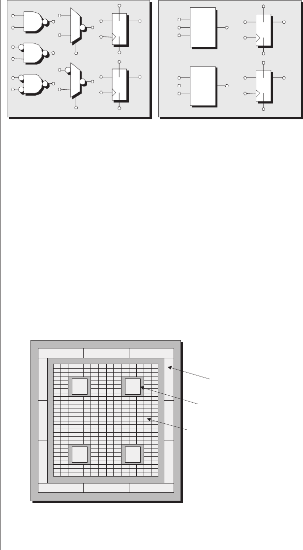
gates, multiplexers, or lookup tables. An array of these base
units (say 4 ×4,8×8, or 16 ×16)—in conjunction with some
special units containing registers, small memory elements, and
other logic—then make up a master cell (or master tile or master
module or …). Once again, an array (sea) of these master units
is then prefabricated across the face of the chip.
Also prefabricated (typically around the edge of the
device) are functions like RAM blocks, clock generators,
boundary scan logic, and so forth (Figure 3-16).
48 ■The Design Warrior's Guide to FPGAs
LUT
LUT
(a) Gate, mux, and flop-based (b) LUT and flop-based
Figure 3-15. Examples of structured ASIC tiles.
Prefabricated I/O,
cores, etc.
Embedded RAM
Sea-of-tiles
Figure 3-16. Generic structured ASIC.
1752: America.
Benjamin Franklin
performs his notorious
kite experiment.

The idea is that the device can be customized using only
the metallization layers (just like a standard gate array). The
difference is that, due to the greater sophistication of the struc-
tured ASIC tile, most of the metallization layers are also
predefined.
Thus, many structured ASIC architectures require the cus-
tomization of only two or three metallization layers (in one
case, it is necessary to customize only a single via layer). This
dramatically reduces the time and costs associated with creat-
ing the remaining photo-masks used to complete the device.
Although it’s difficult to assign an exact value, the prede-
fined and prefabricated logic associated with structured ASICs
results in an overhead compared to standard cell devices in
terms of power consumption, performance, and silicon real
estate. Early indications are that structured ASICs require
three times the real estate and consume two to three times the
power of a standard cell device to perform the same function.
In reality, these results will vary architecture-by-architecture,
and also different types of designs may well favor different
architectures. Unfortunately, no evaluations based on
industry-standard reference designs have been performed
across all of the emerging structured ASIC architectures at the
time of this writing.
FPGAs
Around the beginning of the 1980s, it became apparent
that there was a gap in the digital IC continuum. At one end,
there were programmable devices like SPLDs and CPLDs,
which were highly configurable and had fast design and modi-
fication times, but which couldn’t support large or complex
functions.
At the other end of the spectrum were ASICs. These could
support extremely large and complex functions, but they were
painfully expensive and time-consuming to design. Further-
more, once a design had been implemented as an ASIC it was
effectively frozen in silicon (Figure 3-17).
The Origin of FPGAs ■49
1775: Italy.
Count Alessandro
Giuseppe Antonio
Anastasio Volta invents
a static electricity
generator called the
Electrophorus.
In order to address this gap, Xilinx developed a new class
of IC called a field-programmable gate array, or FPGA, which
they made available to the market in 1984.
The various FPGAs available today are discussed in detail
in chapter 4. For the nonce, we need only note that the first
FPGAs were based on CMOS and used SRAM cells for con-
figuration purposes. Although these early devices were
comparatively simple and contained relatively few gates (or
the equivalent thereof) by today’s standards, many aspects of
their underlying architecture are still employed to this day.
The early devices were based on the concept of a program-
mable logic block, which comprised a 3-input lookup table
(LUT), a register that could act as a flip-flop or a latch, and a
multiplexer, along with a few other elements that are of little
interest here. Figure 3-18 shows a very simple programmable
logic block (the logic blocks in modern FPGAs can be signifi-
cantly more complex—see chapter 4 for more details).
Each FPGA contained a large number of these program-
mable logic blocks, as discussed below. By means of
appropriate SRAM programming cells, every logic block in
the device could be configured to perform a different function.
Each register could be configured to initialize containing a
logic 0 or a logic 1 and to act as a flip-flop (as shown in Figure
3-18) or a latch. If the flip-flop option were selected, the regis-
ter could be configured to be triggered by a positive- or
50 ■The Design Warrior's Guide to FPGAs
FPGA is pronounced
by spelling it out as
“F-P-G-A.”
LUT is pronounced to
rhyme with “nut.”
PLDs ASICs
Standard Cell
Full Custom
Gate Arrays
Structured ASICs*
SPLDs
CPLDs
*Not available circa early 1980s
The
GAP
Figure 3-17. The gap between PLDs and ASICs.
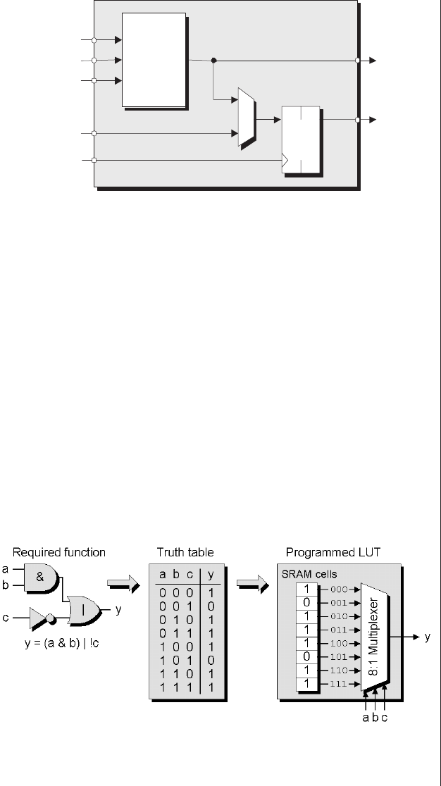
negative-going clock (the clock signal was common to all
of the logic blocks). The multiplexer feeding the flip-flop
could be configured to accept the output from the LUT or a
separate input to the logic block, and the LUT could be con-
figured to represent any 3-input logical function.
For example, assume that a LUT was required to perform
the function
y=(a&b)|!c
This could be achieved by loading the LUT with the
appropriate output values (figure 3-19).
The Origin of FPGAs ■51
3-input
LUT
a
b
cflip-flop
clock
mux
y
q
d
Figure 3-18. The key elements forming a simple
programmable logic block.
Figure 3-19. Configuring a LUT.
1777:
Charles Stanhope
invents a mechanical
calculating machine.
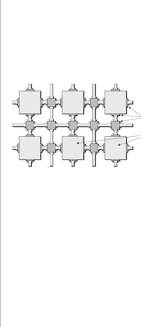
Note that the 8:1-multiplexer-based LUT illustrated in
Figure 3-19 is used for purposes of simplicity; a more realistic
implementation is shown in chapter 4. Furthermore,
Chapter 5 presents in detail the ways in which FPGAs are
actually programmed.
The complete FPGA comprised a large number of pro-
grammable logic block “islands” surrounded by a “sea” of
programmable interconnects (Figure 3-20).
As usual, this high-level illustration is merely an abstract
representation. In reality, all of the transistors and intercon-
nects would be implemented on the same piece of silicon
using standard IC creation techniques.
In addition to the local interconnect reflected in figure
3-20, there would also be global (high-speed) interconnection
paths that could transport signals across the chip without hav-
ing to go through multiple local switching elements.
The device would also include primary I/O pins and pads
(not shown here). By means of its own SRAM cells, the inter-
connect could be programmed such that the primary inputs to
the device were connected to the inputs of one or more pro-
grammable logic blocks, and the outputs from any logic block
could be used to drive the inputs to any other logic block, the
primary outputs from the device, or both.
52 ■The Design Warrior's Guide to FPGAs
I/O is pronounced by
spelling it out as “I-O.”
Programmable
interconnect
Programmable
logic blocks
Figure 3-20. Top-down view of simple,
generic FPGA architecture.

The end result was that FPGAs successfully bridged the
gap between PLDs and ASICs. On the one hand, they were
highly configurable and had the fast design and modification
times associated with PLDs. On the other hand, they could be
used to implement large and complex functions that had previ-
ously been the domain only of ASICs. (ASICs were still
required for the really large, complex, high-performance
designs, but as FPGAs increased in sophistication, they started
to encroach further and further into ASIC design space.)
Platform FPGAs
The concept of a reference design or platform design has long
been used at the circuit board level. This refers to creating a
base design configuration from which multiple products can be
derived.
In addition to tremendous amounts of programmable logic,
today’s high-end FPGAs feature embedded (block) RAMs,
embedded processor cores, high-speed I/O blocks, and so forth.
Furthermore, designers have access to a wide range of IP. The
end result is the concept of the platform FPGA. A company
may use a platform FPGA design as a basis for multiple prod-
ucts inside that company, or it may supply an initial design to
multiple other companies for them to customize and differenti-
ate.
FPGA-ASIC hybrids
It would not make any sense to embed ASIC material
inside an FPGA because designs created using such a device
would face all of the classic problems (high NREs, long lead
times, etc.) associated with ASIC design flows. However, there
are a number of cases in which one or more FPGA cores have
been used as part of a standard cell ASIC design.
One reason for embedding FPGA material inside an ASIC
is that it facilitates the concept of platform design. The plat-
form in this case would be the ASIC, and the embedded
FPGA material could form one of the mechanisms used to cus-
tomize and differentiate subdesigns.
The Origin of FPGAs ■53
Late 1700s:
Charles Stanhope
invents a logic machine
called the Stanhope
Demonstrator.
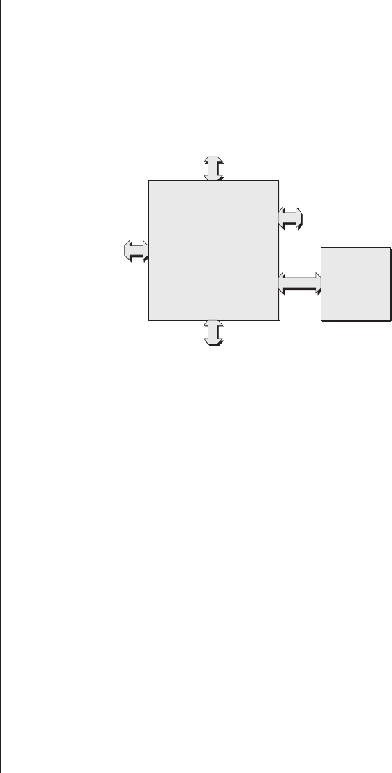
Another reason is that the last few years have seen an
increasing incidence of FPGAs being used to augment ASIC
designs. In this scenario, a large, complex ASIC has an
associated FPGA located in close proximity on the board
(Figure 3-21).
The reason for this scenario is that it’s incredibly time-
consuming and expensive to fix a bug in the ASIC or to mod-
ify its functionality to accommodate any changes to its
original design specification. If the ASIC is designed in the
right way, however, its associated FPGA can be used to imple-
ment any downstream modifications and enhancements. One
problem with this approach is the time taken for signals to
pass back and forth between the ASIC and the FPGA. The
solution is to embed the FPGA core inside the ASIC, thereby
resulting in an FPGA-ASIC hybrid.
One concern that has faced these hybrids, however, is that
ASIC and FPGA design tools and flows have significant
underlying differences. For example, ASICs are said to be
fine-grained because (ultimately) they are implemented at the
level of primitive logic gates. This means that traditional
design technologies like logic synthesis and implementation
54 ■The Design Warrior's Guide to FPGAs
ASIC
FPGA
To other chips
on the board
To other chips
on the board
To other chips
on the board
To other chips
on the board
Figure 3-21. Using an FPGA to augment an ASIC design.
1800: Italy.
Count Alessandro
Giuseppe Antonio
Anastasio Volta invents
the first battery.

technologies like place-and-route are also geared toward fine-
grained architectures.
By comparison, FPGAs are said to be medium-grained (or
coarse-grained depending on whom you are talking to) because
they are physically realized using higher-level blocks like the
programmable logic blocks introduced earlier in this chapter.
In this case, the best design results are realized when using
FPGA-specific synthesis and place-and-route technologies that
view their world in terms of these higher-level blocks.
One area of interest for FPGA-ASIC hybrids is that of
structured ASICs because they too may be considered to be
block based. This means that, when looking around for design
tools, structured ASIC vendors are talking to purveyors of
FPGA-centric synthesis and place-and-route technology rather
than their traditional ASIC counterparts. In turn, this means
that FPGA-ASIC hybrids based on structured ASICs would
automatically tend toward a unified tool and design flow
because the same block-based synthesis and place-and-route
engines could be used for both the ASIC and FPGA portions
of the design.
How FPGA vendors design their chips
Last but not least, one question that is commonly
asked—but is rarely (if ever) addressed in books on
FPGAs—is, how do FPGA vendors actually go about design-
ing a new generation of devices?
To put this another way, do they handcraft each transistor
and track using a design flow similar to that of a full-custom
ASIC, or do they create an RTL description, synthesize it into
a gate-level netlist, and then use place-and-route software
along the lines of a classic ASIC (gate array or standard cell)
design flow (the concepts behind these tools are discussed in
more detail in Section 2).
The short answer is yes! The slightly longer answer is that
there are some portions of the device, like the programmable
logic blocks and the basic routing structure, where the FPGA
vendors fight tooth and nail for every square micron and every
The Origin of FPGAs ■55
1801: France.
Joseph-Marie Jacquard
invents a loom
controlled by punch
cards.

fraction of a nanosecond. These sections of the design are
handcrafted at the transistor and track level using full-custom
ASIC techniques. On the bright side, these portions of the
design are both relatively small and highly repetitive, so once
created they are replicated thousands of times across the face
of the chip.
Then there are housekeeping portions of the device, such
as the configuration control circuitry, that only occur once
per device and are not particularly size or performance critical.
These sections of the design are created using standard cell
ASIC-style techniques.
56 ■The Design Warrior's Guide to FPGAs
1820: France.
Andre Ampere
investigates the force
of an electric current
in a magnetic field.

A word of warning
In this chapter we introduce a plethora of architectural fea-
tures. Certain options—such as using antifuse versus SRAM
configuration cells—are mutually exclusive. Some FPGA ven-
dors specialize in one or the other; others may offer multiple
device families based on these different technologies. (Unless
otherwise noted, the majority of these discussions assume
SRAM-based devices.)
In the case of embedded blocks such as multipliers, adders,
memory, and microprocessor cores, different vendors offer
alternative “flavors” of these blocks with different “recipes” of
ingredients. (Much like different brands of chocolate chip
cookies featuring larger or smaller chocolate chips, for exam-
ple, some FPGA families will have bigger/better/badder
embedded RAM blocks, while others might feature more mul-
tipliers, or support more I/O standards, or …)
The problem is that the features supported by each vendor
and each family change on an almost daily basis. This means
that once you’ve decided what features you need, you then
need to do a little research to see which vendor’s offerings cur-
rently come closest to satisfying your requirements.
A little background information
Before hurling ourselves into the body of this chapter, we
need to define a couple of concepts to ensure that we’re all
marching to the same drumbeat. For example, you’re going to
see the term fabric used throughout this book. In the context of
Alternative FPGA Architectures
Chapter
4
The word “fabric” comes
from the Middle English
fabryke, meaning “some-
thing constructed.”

a silicon chip, this refers to the underlying structure of the
device (sort of like the phrase “the fabric of civilized society”).
When you first hear someone using “fabric” in this way, it
might sound a little snooty or pretentious (in fact, some engi-
neers regard it as nothing more than yet another marketing
term promoted by ASIC and FPGA vendors to make their
devices sound more sophisticated than they really are). Truth
to tell, however, once you get used to it, this is really quite a
useful word.
When we talk about the geometry of an IC, we are refer-
ring to the size of the individual structures constructed on the
chip—such as the portion of a field-effect transistor (FET)
known as its channel. These structures are incredibly small. In
the early to mid-1980s, devices were based on 3 µm geome-
tries, which means that their smallest structures were 3
millionths of a meter in size. (In conversation, we would say,
“This IC is based on a three-micron technology.”)
Each new geometry is referred to as a technology node.By
the 1990s, devices based on 1 µm geometries were starting to
appear, and feature sizes continued to plummet throughout
the course of the decade. As we moved into the twenty-first
century, high-performance ICs had geometries as small as 0.18
µm. By 2002, this had shrunk to 0.13 µm, and by 2003,
devices at 0.09 µm were starting to appear.
Any geometry smaller than around 0.5 µm is referred to as
deep submicron (DSM). At some point that is not well defined
(or that has multiple definitions depending on whom one is
talking to), we move into the ultradeep submicron (UDSM)
realm.
Things started to become a little awkward once geometries
dropped below 1 µm, not the least because it’s a pain to keep
having to say things like “zero point one three microns.” For
this reason, when conversing it’s becoming common to talk in
terms of nano, where one nano (short for nanometer) equates
to a thousandth of a micron—that is, one thousandth of a
millionth of a meter. Thus, instead of mumbling, “point zero
nine microns” (0.09 µm), one can simply proclaim, “ninety
58 ■The Design Warrior's Guide to FPGAs
The “µ” symbol stands for
“micro” from the Greek
micros, meaning “small”
(hence the use of “µP” as
an abbreviation for micro-
processor.”)
In the metric system, “µ”
stands for “one millionth
part of,” so 1 µm repre-
sents “one millionth of a
meter.”
DSM is pronounced
by spelling it out as
“D-S-M.”
UDSM is pronounced
by spelling it out as
“U-D-S-M.”

nano” (90 nano) and have done with it. Of course, these both
mean exactly the same thing, but if you feel moved to regale
your friends on these topics, it’s best to use the vernacular of
the day and present yourself as hip and trendy rather than as
an old fuddy-duddy from the last millennium.
Antifuse versus SRAM versus …
SRAM-based devices
The majority of FPGAs are based on the use of SRAM
configuration cells, which means that they can be configured
over and over again. The main advantages of this technique
are that new design ideas can be quickly implemented and
tested, while evolving standards and protocols can be accom-
modated relatively easily. Furthermore, when the system is first
powered up, the FPGA can initially be programmed to perform
one function such as a self-test or board/system test, and it can
then be reprogrammed to perform its main task.
Another big advantage of the SRAM-based approach is
that these devices are at the forefront of technology. FPGA
vendors can leverage the fact that many other companies spe-
cializing in memory devices expend tremendous resources on
research and development (R&D) in this area. Furthermore, the
SRAM cells are created using exactly the same CMOS tech-
nologies as the rest of the device, so no special processing steps
are required in order to create these components.
In the past, memory devices were often used to qualify the
manufacturing processes associated with a new technology
node. More recently, the mixture of size, complexity, and regu-
larity associated with the latest FPGA generations has resulted
in these devices being used for this task. One advantage of
using FPGAs over memory devices to qualify the manufactur-
ing process is that, if there’s a defect, the structure of FPGAs is
such that it’s easier to identify and locate the problem (that is,
figure out what and where it is). For example, when IBM and
UMC were rolling out their 0.09 µm (90 nano) processes,
Alternative FPGA Architectures ■59
R&D is pronounced by
spelling it out as
“R-and-D.”

FPGAs from Xilinx were the first devices to race out of the
starting gate.
Unfortunately, there’s no such thing as a free lunch. One
downside of SRAM-based devices is that they have to be
reconfigured every time the system is powered up. This either
requires the use of a special external memory device (which
has an associated cost and consumes real estate on the board)
or of an on-board microprocessor (or some variation of these
techniques—see also chapter 5).
Security issues and solutions with SRAM-based
devices
Another consideration with regard to SRAM-based
devices is that it can be difficult to protect your intellectual
property, or IP, in the form of your design. This is because the
configuration file used to program the device is stored in some
form of external memory.
Currently, there are no commercially available tools that
will read the contents of a configuration file and generate a
corresponding schematic or netlist representation. Having
said this, understanding and extracting the logic from the
configuration file, while not a trivial task, would not be
beyond the bounds of possibility given the combination of
clever folks and computing horsepower available today.
Let’s not forget that there are reverse-engineering compa-
nies all over the world specializing in the recovery of “design
IP.” And there are also a number of countries whose govern-
ments turn a blind eye to IP theft so long as the money keeps
rolling in (you know who you are). So if a design is a high-
profit item, you can bet that there are folks out there who are
ready and eager to replicate it while you’re not looking.
In reality, the real issue here is not related to someone
stealing your IP by reverse-engineering the contents of the
configuration file, but rather their ability to clone your design,
irrespective of whether they understand how it performs its
magic. Using readily available technology, it is relatively easy
60 ■The Design Warrior's Guide to FPGAs
IP is pronounced by spell-
ing it out as “I-P.”

for someone to take a circuit board, put it on a “bed of nails”
tester, and quickly extract a complete netlist for the board.
This netlist can subsequently be used to reproduce the board.
Now the only task remaining for the nefarious scoundrels is to
copy your FPGA configuration file from its boot PROM (or
EPROM, E2PROM, or whatever), and they have a duplicate of
the entire design.
On the bright side, some of today’s SRAM-based FPGAs
support the concept of bitstream encryption. In this case, the
final configuration data is encrypted before being stored in the
external memory device. The encryption key itself is loaded
into a special SRAM-based register in the FPGA via its JTAG
port (see also Chapter 5). In conjunction with some associated
logic, this key allows the incoming encrypted configuration
bitstream to be decrypted as it’s being loaded into the device.
The command/process of loading an encrypted bitstream
automatically disables the FPGA’s read-back capability. This
means that you will typically use unencrypted configuration
data during development (where you need to use read-back)
and then start to use encrypted data when you move into pro-
duction. (You can load an unencrypted bitstream at any time,
so you can easily load a test configuration and then reload the
encrypted version.)
The main downside to this scheme is that you require a
battery backup on the circuit board to maintain the contents
of the encryption key register in the FPGA when power is
removed from the system. This battery will have a lifetime of
years or decades because it need only maintain a single register
in the device, but it does add to the size, weight, complexity,
and cost of the board.
Antifuse-based devices
Unlike SRAM-based devices, which are programmed while
resident in the system, antifuse-based devices are programmed
off-line using a special device programmer.
The proponents of antifuse-based FPGAs are proud to
point to an assortment of (not-insignificant) advantages. First
Alternative FPGA Architectures ■61
JTAG is pronounced
“J-TAG”; that is, by spell-
ing out the ‘J’ followed
by “tag” to rhyme with
“bag.”

of all, these devices are nonvolatile (their configuration data
remains when the system is powered down), which means that
they are immediately available as soon as power is applied to
the system. Following from their nonvolatility, these devices
don’t require an external memory chip to store their configu-
ration data, which saves the cost of an additional component
and also saves real estate on the board.
One noteworthy advantage of antifuse-based FPGAs is the
fact that their interconnect structure is naturally “rad hard,”
which means they are relatively immune to the effects of
radiation. This is of particular interest in the case of military
and aerospace applications because the state of a configura-
tion cell in an SRAM-based component can be “flipped” if
that cell is hit by radiation (of which there is a lot in space).
By comparison, once an antifuse has been programmed, it
cannot be altered in this way. Having said this, it should also
be noted that any flip-flops in these devices remain sensitive
to radiation, so chips intended for radiation-intensive envi-
ronments must have their flip-flops protected by triple
redundancy design. This refers to having three copies of each
register and taking a majority vote (ideally all three registers
will contain identical values, but if one has been “flipped”
such that two registers say 0 and the third says 1, then the 0s
have it, or vice versa if two registers say 1 and the third
says 0).
But perhaps the most significant advantage of antifuse-
based FPGAs is that their configuration data is buried deep
inside them. By default, it is possible for the device program-
mer to read this data out because this is actually how the
programmer works. As each antifuse is being processed, the
device programmer keeps on testing it to determine when that
element has been fully programmed; then it moves onto the
next antifuse. Furthermore, the device programmer can be
used to automatically verify that the configuration was per-
formed successfully (this is well worth doing when you’re
talking about devices containing 50 million plus programma-
ble elements). In order to do this, the device programmer
62 ■The Design Warrior's Guide to FPGAs
Radiation can come in
the form of gamma rays
(very high-energy pho-
tons), beta particles
(high-energy electrons),
and alpha particles.
It should be noted that
rad-hard devices are not
limited to antifuse tech-
nologies. Other
components, such as
those based on SRAM
architectures, are avail-
able with special
rad-hard packaging and
triple redundancy
design.

requires the ability to read the actual states of the antifuses and
compare them to the required states defined in the configura-
tion file.
Once the device has been programmed, however, it is pos-
sible to set (grow) a special security antifuse that subsequently
prevents any programming data (in the form of the presence or
absence of antifuses) from being read out of the device. Even if
the device is decapped (its top is removed), programmed and
unprogrammed antifuses appear to be identical, and the fact
that all of the antifuses are buried in the internal metallization
layers makes it almost impossible to reverse-engineer the
design.
Vendors of antifuse-based FPGAs may also tout a couple of
other advantages relating to power consumption and speed,
but if you aren’t careful this can be a case of the quickness of
the hand deceiving the eye. For example, they might tease you
with the fact that an antifuse-based device consumes only 20
percent (approximately) of the standby power of an equivalent
SRAM-based component, that their operational power con-
sumption is also significantly lower, and that their
interconnect-related delays are smaller. Also, they might casu-
ally mention that an antifuse is much smaller and thus
occupies much less real estate on the chip than an equivalent
SRAM cell (although they may neglect to mention that anti-
fuse devices also require extra programming circuitry,
including a large, hairy programming transistor for each anti-
fuse). They will follow this by noting that when you have a
device containing tens of millions of configuration elements,
using antifuses means that the rest of the logic can be much
closer together. This serves to reduce the interconnect delays,
thereby making these devices faster than their SRAM cousins.
And both of the above points would be true … if one were
comparing two devices implemented at the same technology
node. But therein lies the rub, because antifuse technology
requires the use of around three additional process steps after
the main manufacturing process has been qualified. For this
(and related) reasons, antifuse devices are always at least
Alternative FPGA Architectures ■63
It’s worth noting that
when the MRAM tech-
nologies introduced in
Chapter 2 come to frui-
tion, these may well
change the FPGA
landscape.
This is because MRAM
fuses would be much
smaller than SRAM cells
(thereby increasing com-
ponent density and
reducing track delays),
and they would also con-
sume much less power.
Furthermore,
MRAM-based devices
could be prepro-
grammed like
antifuse-based devices
(great for security) and
reprogrammed like
SRAM-based components
(good for prototyping).

one—and usually several—generations (technology nodes)
behind SRAM-based components, which effectively wipes out
any speed or power consumption advantages that might other-
wise be of interest.
Of course, the main disadvantage associated with
antifuse-based devices is that they are OTP, so once you’ve
programmed one of these little scallywags, its function is set in
stone. This makes these components a poor choice for use in a
development or prototyping environment.
EPROM-based devices
This section is short and sweet because no one currently
makes—or has plans to make—EPROM-based FPGAs.
E2PROM/FLASH-based devices
E2PROM- or FLASH-based FPGAs are similar to their
SRAM counterparts in that their configuration cells are con-
nected together in a long shift-register-style chain. These
devices can be configured off-line using a device programmer.
Alternatively, some versions are in-system programmable, or
ISP, but their programming time is about three times that of
an SRAM-based component.
Once programmed, the data they contain is nonvolatile,
so these devices would be “instant on” when power is first
applied to the system. With regard to protection, some of
these devices use the concept of a multibit key, which can
range from around 50 bits to several hundred bits in size.
Once you’ve programmed the device, you can load your user-
defined key (bit-pattern) to secure its configuration data.
After the key has been loaded, the only way to read data out
of the device, or to write new data into it, is to load a copy of
your key via the JTAG port (this port is discussed later in this
chapter and also in chapter 5). The fact that the JTAG port
in today’s devices runs at around 20 MHz means that it would
take billions of years to crack the key by exhaustively trying
every possible value.
64 ■The Design Warrior's Guide to FPGAs
1821: England.
Michael Faraday invents
the first electric motor.

Two-transistor E2PROM and FLASH cells are approxi-
mately 2.5 times the size of their one-transistor EPROM
cousins, but they are still way smaller than their SRAM coun-
terparts. This means that the rest of the logic can be much
closer together, thereby reducing interconnect delays.
On the downside, these devices require around five addi-
tional process steps on top of standard CMOS technology,
which results in their lagging behind SRAM-based devices by
one or more generations (technology nodes). Last but not
least, these devices tend to have relatively high static power
consumption due to their containing vast numbers of internal
pull-up resistors.
Hybrid FLASH-SRAM devices
Last but not least, there’s always someone who wants to
add yet one more ingredient into the cooking pot. In the case
of FPGAs, some vendors offer esoteric combinations of pro-
gramming technologies. For example, consider a device where
each configuration element is formed from the combination of
a FLASH (or E2PROM) cell and an associated SRAM cell.
In this case, the FLASH elements can be preprogrammed.
Then, when the system is powered up, the contents of the
FLASH cells are copied in a massively parallel fashion into
their corresponding SRAM cells. This technique gives you the
nonvolatility associated with antifuse devices, which means
the device is immediately available when power is first applied
to the system. But unlike an antifuse-based component, you
can subsequently use the SRAM cells to reconfigure the device
while it remains resident in the system. Alternatively, you can
reconfigure the device using its FLASH cells either while it
remains in the system or off-line by means of a device pro-
grammer.
Summary
Table 4.1 briefly summarizes the key points associated with
the various programming technologies described above:
Alternative FPGA Architectures ■65
1821: England.
Michael Faraday plots
the magnetic field
around a conductor.
Fine-, medium-, and coarse-grained architectures
It is common to categorize FPGA offerings as being either
fine grained or coarse grained. In order to understand what this
means, we first need to remind ourselves that the main feature
that distinguishes FPGAs from other devices is that their
underlying fabric predominantly consists of large numbers of
relatively simple programmable logic block “islands” embed-
ded in a “sea” of programmable interconnect. (Figure 4-1).
In the case of a fine-grained architecture, each logic block
can be used to implement only a very simple function. For
example, it might be possible to configure the block to act as
any 3-input function, such as a primitive logic gate (AND,
OR, NAND, etc.) or a storage element (D-type flip-flop,
D-type latch, etc.).
66 ■The Design Warrior's Guide to FPGAs
Table 4-1. Summary of programming technologies
In reality, the vast major-
ity of the configuration
cells in an FPGA are asso-
ciated with its
interconnect (as opposed
to its configurable logic
blocks). For this reason,
engineers joke that FPGA
vendors actually sell only
the interconnect, and
they throw in the rest of
the logic for free!
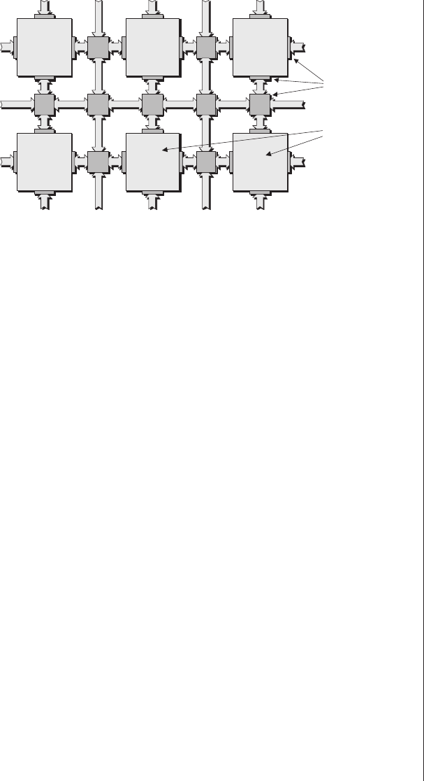
In addition to implementing glue logic and irregular struc-
tures like state machines, fine-grained architectures are said to
be particularly efficient when executing systolic algorithms
(functions that benefit from massively parallel implementa-
tions). These architectures are also said to offer some
advantages with regard to traditional logic synthesis technol-
ogy, which is geared toward fine-grained ASIC architectures.
The mid-1990s saw a lot of interest in fine-grained FPGA
architectures, but over time the vast majority faded away into
the sunset, leaving only their coarse-grained cousins. In the
case of a coarse-grained architecture, each logic block contains
a relatively large amount of logic compared to their fine-
grained counterparts. For example, a logic block might contain
four 4-input LUTs, four multiplexers, four D-type flip-flops,
and some fast carry logic (see the following topics in this chap-
ter for more details).
An important consideration with regard to architectural
granularity is that fine-grained implementations require a rela-
tively large number of connections into and out of each block
compared to the amount of functionality that can be supported
by those blocks. As the granularity of the blocks increases to
medium-grained and higher, the amount of connections into
the blocks decreases compared to the amount of functionality
Alternative FPGA Architectures ■67
Programmable
interconnect
Programmable
logic blocks
Figure 4-1. Underlying FPGA fabric.
1821: England.
Sir Charles Wheatstone
reproduces sound.

they can support. This is important because the programmable
interblock interconnect accounts for the vast majority of the
delays associated with signals as they propagate through an
FPGA.
One slight fly in the soup is that a number of companies
have recently started developing really coarse-grained device
architectures comprising arrays of nodes, where each node is a
highly complex processing element ranging from an algo-
rithmic function such as a fast Fourier transform (FFT) all the
way up to a complete general-purpose microprocessor core
(see also Chapters 6 and 23). Although these devices aren’t
classed as FPGAs, they do serve to muddy the waters. For this
reason, LUT-based FPGA architectures are now often classed
as medium-grained, thereby leaving the coarse-grained appel-
lation free to be applied to these new node-based devices.
MUX- versus LUT-based logic blocks
There are two fundamental incarnations of the program-
mable logic blocks used to form the medium-grained
architectures referenced in the previous section: MUX (multi-
plexer) based and LUT (lookup table) based.
MUX-based
As an example of a MUX-based approach, consider one
way in which the 3-input function y=(a&b)|ccould be
implemented using a block containing only multiplexers
(Figure 4-2).
The device can be programmed such that each input to
the block is presented with a logic 0, a logic 1, or the true or
inverse version of a signal (a,b,orcin this case) coming from
another block or from a primary input to the device. This
allows each block to be configured in myriad ways to imple-
ment a plethora of possible functions. (The xshown on the
input to the central multiplexer in figure 4-2 indicates that we
don’t care whether this input is connected toa0ora1.)
68 ■The Design Warrior's Guide to FPGAs
MUX is pronounced to
rhyme with “flux.”
LUT is pronounced to
rhyme with “nut.”
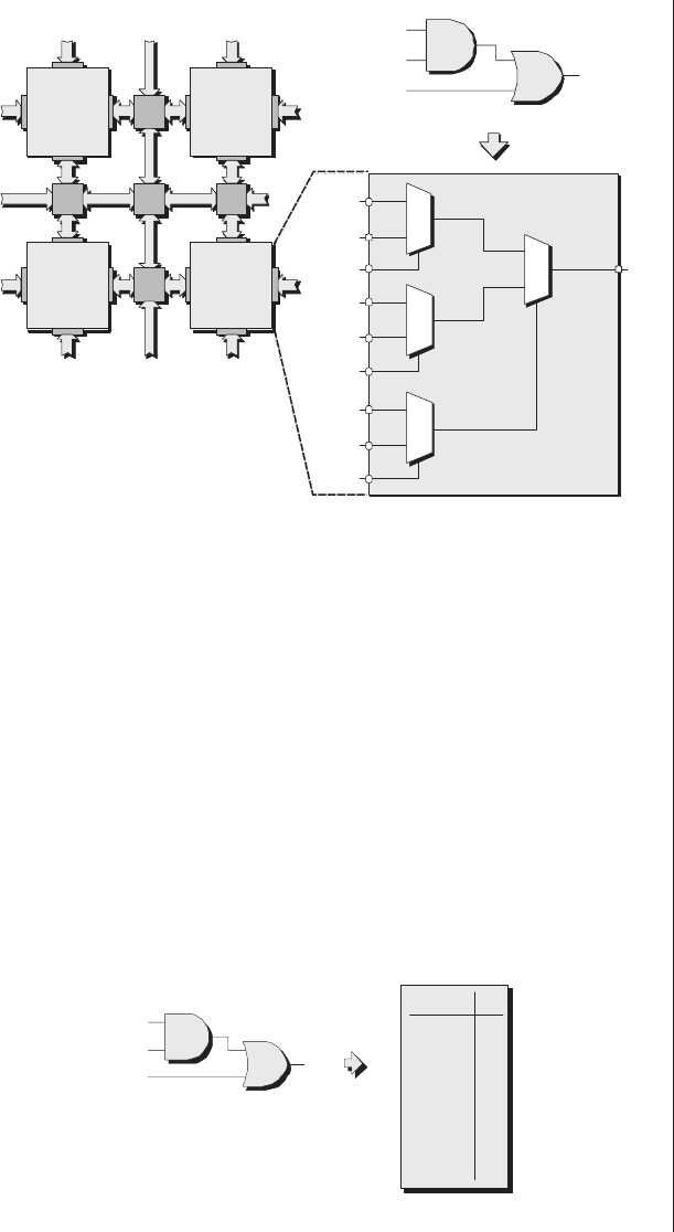
LUT-based
The underlying concept behind a LUT is relatively simple.
A group of input signals is used as an index (pointer) to a
lookup table. The contents of this table are arranged such that
the cell pointed to by each input combination contains the
desired value. For example, let’s assume that we wish to imple-
ment the function:
y=(a&b)|c
Alternative FPGA Architectures ■69
&
|
a
b
cy
AND
OR
y=(a&b)|c
0
1
0
1
0
1
MUX
MUX
MUX
0
b
a
1
x
0
y
0
1
MUX
0
1
c
Figure 4-2. MUX-based logic block.
Required function Truth table
ab c y
0
0
0
0
1
1
1
1
0
0
1
1
0
0
1
1
0
1
0
1
0
1
0
1
0
1
0
1
0
1
1
1
y=(a&b)|c
&
|
a
b
cy
AND
OR
Figure 4-3. Required function and associated truth table.
If you take a group of
logic gates several layers
deep, then a LUT
approach can be very
efficient in terms of
resource utilization and
input-to-output delays.
(In this context, “deep”
refers to the number of
logic gates between the
inputs and the outputs.
Thus, the function illus-
trated in figure 4-3
would be said to be two
layers deep.)
However, one downside
to a LUT-based architec-
ture is that if you only
want to implement a
small function—such as
a 2-input AND gate—
somewhere in your
design, you’ll end up
using an entire LUT to do
so. In addition to being
wasteful in terms of
resources, the resulting
delays are high for such
a simple function.
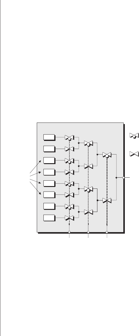
This can be achieved by loading a 3-input LUT with the
appropriate values. For the purposes of the following exam-
ples, we shall assume that the LUT is formed from SRAM
cells (but it could be formed using antifuses, E2PROM, or
FLASH cells, as discussed earlier in this chapter). A com-
monly used technique is to use the inputs to select the desired
SRAM cell using a cascade of transmission gates as shown in
Figure 4-4. (Note that the SRAM cells will also be connected
together in a chain for configuration purposes—that is, to
load them with the required values—but these connections
have been omitted from this illustration to keep things
simple.)
If a transmission gate is enabled (active), it passes the sig-
nal seen on its input through to its output. If the gate is
disabled, its output is electrically disconnected from the wire
it is driving.
The transmission gate symbols shown with a small circle
(called a “bobble” or a “bubble”) indicate that these gates will
be activated by a logic 0 on their control input. By compari-
70 ■The Design Warrior's Guide to FPGAs
0
1
1
1
0
1
1
1
0
1
1
1
0
1
1
1
abc
y
SRAM
cells
Transmission gate
(active low)
Transmission gate
(active high)
Figure 4-4. A transmission gate-based LUT (programming
chain omitted for purposes of clarity).
By comparison, in the
case of mux-based archi-
tectures containing a
mixture of muxes and
logic gates, it’s often
possible to gain access
to intermediate values
from the signals linking
the logic gates and the
muxes. In this case, each
logic block can be bro-
ken down into smaller
fragments, each of which
can be used to imple-
ment a simple function.
Thus, these architectures
may offer advantages in
terms of performance
and silicon utilization for
designs containing large
numbers of independent
simple logic functions.

son, symbols without bobbles indicate that these gates will be
activated by a logic 1. Based on this understanding, it’s easy to
see how different input combinations can be used to select the
contents of the various SRAM cells.
MUX-based versus LUT-based?
Once upon a time—when engineers handcrafted their cir-
cuits prior to the advent of today’s sophisticated CAD
tools—some folks say that it was possible to achieve the best
results using MUX-based architectures. (Sad to relate, they
usually don’t explain exactly how these results were better, so
this is largely left to our imaginations.) It is also said that
MUX-based architectures have an advantage when it comes to
implementing control logic along the lines of “if this input is
true and this input is false, then make that output true …”1
However, some of these architectures don’t provide high-speed
carry logic chains, in which case their LUT-based counterparts
are left as the leaders in anything to do with arithmetic
processing.
Throughout much of the 1990s, FPGAs were widely used
in the telecommunications and networking markets. Both of
these application areas involve pushing lots of data around, in
which case LUT-based architectures hold the high ground.
Furthermore, as designs (and device capacities) grew larger and
synthesis technology increased in sophistication, handcrafting
circuits largely became a thing of the past. The end result is
that the majority of today’s FPGA architectures are LUT-
based, as discussed below.
3-, 4-, 5-, or 6-input LUTs?
The great thing about an n-input LUT is that it can imple-
ment any possible n-input combinational (or combinatorial)
Alternative FPGA Architectures ■71
1Some MUX-based architectures—such as those fielded by QuickLogic
(www.quicklogic.com)—feature logic blocks containing multiple layers of
MUXes preceded by primitive logic gates like ANDs. This provides them
with a large fan-in capability, which gives them an advantage for address
decoding and state machine decoding applications.
As was noted in Chapter
3, some folks prefer to
say “combinational
logic,” while others favor
“combinatorial logic.”

logic function. Adding more inputs allows you to represent
more complex functions, but every time you add an input, you
double the number of SRAM cells.
The first FPGAs were based on 3-input LUTs. FPGA ven-
dors and university students subsequently researched the
relative merits of 3-, 4-, 5-, and even 6-input LUTs into the
ground (whatever you do, don’t get trapped in conversation
with a bunch of FPGA architects at a party). The current
consensus is that 4-input LUTs offer the optimal balance of
pros and cons.
In the past, some devices were created using a mixture of
different LUT sizes, such as 3-input and 4-input LUTs,
because this offered the promise of optimal device utilization.
However, one of the main tools in the design engineer’s treas-
ure chest is logic synthesis, and uniformity and regularity are
what a synthesis tool likes best. Thus, all of the really success-
ful architectures are currently based only on the use of 4-input
LUTs. (This is not to say that mixed-size LUT architectures
won’t reemerge in the future as design software continues to
increase in sophistication.)
LUT versus distributed RAM versus SR
The fact that the core of a LUT in an SRAM-based device
comprises a number of SRAM cells offers a number of inter-
esting possibilities. In addition to its primary role as a lookup
table, some vendors allow the cells forming the LUT to be
used as a small block of RAM (the 16 cells forming a 4-input
LUT, for example, could be cast in the role of a 16 ×1 RAM).
This is referred to as distributed RAM because (a) the LUTs are
strewn (distributed) across the surface of the chip, and (b) this
differentiates it from the larger chunks of block RAM (intro-
duced later in this chapter).
Yet another possibility devolves from the fact that all of
the FPGA’s configuration cells—including those forming
the LUT—are effectively strung together in a long chain
(Figure 4-5).
72 ■The Design Warrior's Guide to FPGAs
1822: England.
Charles Babbage starts
to build a mechanic
calculating machine
called the Difference
Engine.
This aspect of the architecture is discussed in more detail
in chapter 5. The point here is that, once the device has been
programmed, some vendors allow the SRAM cells forming a
LUT to be treated independently of the main body of the
chain and to be used in the form of a shift register. Thus, each
LUT may be considered to be multifaceted (figure 4-6).
CLBs versus LABs versus slices
“Man can not live by LUTs alone,” as the Bard would
surely say if he were to be reincarnated accidentally as an
FPGA designer. For this reason, in addition to one or more
LUTs, a programmable logic block will contain other ele-
ments, such as multiplexers and registers. But before we delve
Alternative FPGA Architectures ■73
0
1
From the previous
cell in the chain
0
0
To the next cell
in the chain
SRAM
cells
Figure 4-5. Configuration cells linked in a chain.
16-bit SR
16 x 1 RAM
4-input LUT
Figure 4-6. A multifaceted LUT.
1822: France.
Andre Ampere
discovers that two
wires carrying electric
currents attract
each other.
into this topic, we first need to wrap our brains around some
terminology.
A Xilinx logic cell
One niggle when it comes to FPGAs is that each vendor
has its own names for things. But we have to start somewhere,
so let’s kick off by saying that the core building block in a
modern FPGA from Xilinx is called a logic cell (LC). Among
other things, an LC comprises a 4-input LUT (which can also
act as a 16 ×1 RAM or a 16-bit shift register), a multiplexer,
and a register (Figure 4-7).
It must be noted that the illustration presented in Figure
4-7 is a gross simplification, but it serves our purposes here.
The register can be configured to act as a flip-flop, as shown in
Figure 4-7 or as a latch. The polarity of the clock (rising-edge
triggered or falling-edge triggered) can be configured, as can
the polarity of the clock enable and set/reset signals (active-high
or active-low).
In addition to the LUT, MUX, and register, the LC also
contains a smattering of other elements, including some spe-
74 ■The Design Warrior's Guide to FPGAs
16-bit SR
flip-flop
clock
mux
y
q
e
a
b
c
d
16x1 RAM
4-input
LUT
clock enable
set/reset
Figure 4-7. A simplified view of a Xilinx LC.
1827: England.
Sir Charles Wheatstone
constructs a
microphone.
cial fast carry logic for use in arithmetic operations (this is
discussed in more detail a little later).
An Altera logic element
Just for reference, the equivalent core building block in an
FPGA from Altera is called a logic element (LE). There are a
number of differences between a Xilinx LC and an Altera LE,
but the overall concepts are very similar.
Slicing and dicing
The next step up the hierarchy is what Xilinx calls a slice
(Altera and the other vendors doubtless have their own
equivalent names). Why “slice”? Well, they had to call it
something, and—whichever way you look at it—the term slice
is “something.” At the time of this writing, a slice contains two
logic cells (Figure 4-8).
The reason for the “at the time of this writing” qualifier is
that these definitions can—and do—change with the seasons.
Alternative FPGA Architectures ■75
16-bit SR
16x1 RAM
4-input
LUT
LUT MUX REG
Logic Cell (LC)
16-bit SR
16x1 RAM
4-input
LUT
LUT MUX REG
Logic Cell (LC)
Slice
Figure 4-8. A slice containing two logic cells.
1827: Germany.
Georg Ohm
investigates electrical
resistance and defines
Ohm’s Law.
The definition of what
forms a CLB varies from
year to year. In the early
days, a CLB consisted of
two 3-input LUTs and
one register. Later
versions sported two
4-input LUTs and two
registers.
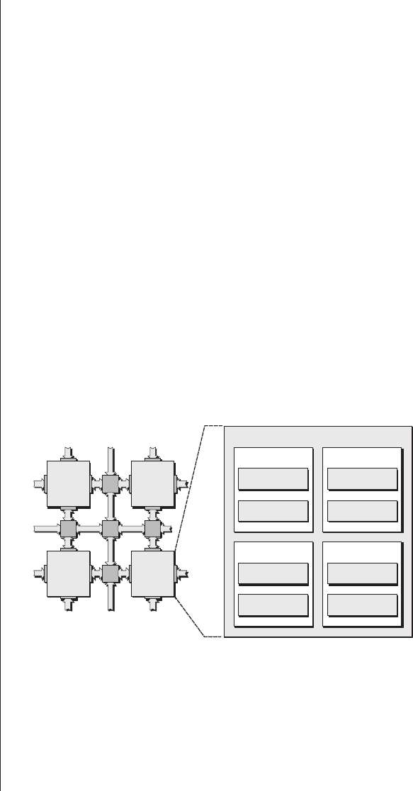
The internal wires have been omitted from this illustration to
keep things simple; it should be noted, however, that
although each logic cell’s LUT, MUX, and register have their
own data inputs and outputs, the slice has one set of clock,
clock enable, and set/reset signals common to both logic cells.
CLBs and LABs
And moving one more level up the hierarchy, we come to
what Xilinx calls a configurable logic block (CLB) and what
Altera refers to as a logic array block (LAB). (Other FPGA
vendors doubtless have their own equivalent names for each
of these entities, but these are of interest only if you are actu-
ally working with their devices.)
Using CLBs as an example, some Xilinx FPGAs have two
slices in each CLB, while others have four. At the time of this
writing, a CLB equates to a single logic block in our original
visualization of “islands” of programmable logic in a “sea” of
programmable interconnect (Figure 4-9).
There is also some fast programmable interconnect within
the CLB. This interconnect (not shown in Figure 4-9 for rea-
sons of clarity) is used to connect neighboring slices.
76 ■The Design Warrior's Guide to FPGAs
CLB CLB
CLB CLB
Logic cell
Slice
Logic cell
Logic cell
Slice
Logic cell
Logic cell
Slice
Logic cell
Logic cell
Slice
Logic cell
Configurable logic block (CLB)
Figure 4-9. A CLB containing four slices (the number of slices
depends on the FPGA family).
Now, each CLB can
contain two or four
slices, where each slice
contains two 4-input
LUTS and two registers.
And as for the morrow
… well, it would take a
braver man than I even
to dream of speculating.
The point where a set of
data or control signals
enters or exits a logic
function is commonly
referred to as a “port.
”In the case of a
single-port RAM, data is
written in and read out of
the function using a
common data bus.

The reason for having this type of logic-block hierar-
chy—LC→Slice (with two LCs)→CLB (with four slices)—is
that it is complemented by an equivalent hierarchy in the
interconnect. Thus, there is fast interconnect between the LCs
in a slice, then slightly slower interconnect between slices in a
CLB, followed by the interconnect between CLBs. The idea is
to achieve the optimum trade-off between making it easy to
connect things together without incurring excessive
interconnect-related delays.
Distributed RAMs and shift registers
We previously noted that each 4-bit LUT can be used as a
16 ×1 RAM. And things just keep on getting better and better
because, assuming the four-slices-per-CLB configuration illus-
trated in figure 4-9, all of the LUTs within a CLB can be
configured together to implement the following:
■Single-port 16 × 8 bit RAM
■Single-port 32 × 4 bit RAM
■Single-port 64 × 2 bit RAM
■Single-port 128 × 1 bit RAM
■Dual-port 16 × 4 bit RAM
■Dual-port 32 × 2 bit RAM
■Dual-port 64 × 1 bit RAM
Alternatively, each 4-bit LUT can be used as a 16-bit shift
register. In this case, there are special dedicated connections
between the logic cells within a slice and between the slices
themselves that allow the last bit of one shift register to be
connected to the first bit of another without using the ordinary
LUT output (which can be used to view the contents of a
selected bit within that 16-bit register). This allows the LUTs
within a single CLB to be configured together to implement a
shift register containing up to 128 bits as required.
Fast carry chains
A key feature of modern FPGAs is that they include the
special logic and interconnect required to implement fast carry
Alternative FPGA Architectures ■77
In the case of a dual-port
RAM, data is written into
the function using one
data bus (port) and read
out using a second data
bus (port). In fact, the
read and write
operations each have an
associated address bus
(used to point to a word
of interest inside the
RAM). This means that
the read and write
operations can be
performed
simultaneously.
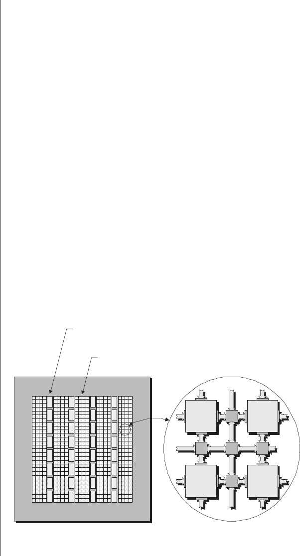
chains. In the context of the CLBs introduced in the previous
section, each LC contains special carry logic. This is comple-
mented by dedicated interconnect between the two LCs in
each slice, between the slices in each CLB, and between the
CLBs themselves.
This special carry logic and dedicated routing boosts the
performance of logical functions such as counters and arith-
metic functions such as adders. The availability of these fast
carry chains—in conjunction with features like the shift regis-
ter incarnations of LUTs (discussed above) and embedded
multipliers and the like (introduced below)—provided the
wherewithal for FPGAs to be used for applications like DSP.
Embedded RAMs
A lot of applications require the use of memory, so FPGAs
now include relatively large chunks of embedded RAM called
e-RAM or block RAM. Depending on the architecture of the
component, these blocks might be positioned around the
periphery of the device, scattered across the face of the chip
in relative isolation, or organized in columns, as shown in
Figure 4-10.
78 ■The Design Warrior's Guide to FPGAs
Columns of embedded
RAM blocks
Arrays of
programmable
logic blocks
Figure 4-10. Bird’s-eye view of chip with columns of
embedded RAM blocks.
DSP is pronounced by
spelling it out as “D-S-P.”
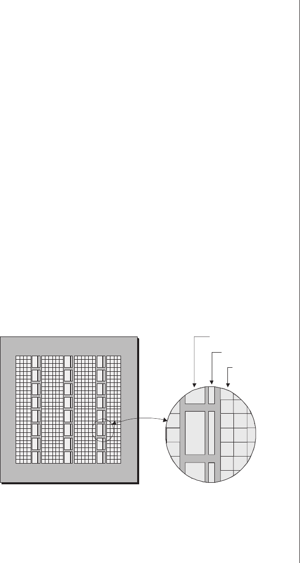
Depending on the device, such a RAM might be able to
hold anywhere from a few thousand to tens of thousands of
bits. Furthermore, a device might contain anywhere from tens
to hundreds of these RAM blocks, thereby providing a total
storage capacity of a few hundred thousand bits all the way up
to several million bits.
Each block of RAM can be used independently, or multi-
ple blocks can be combined together to implement larger
blocks. These blocks can be used for a variety of purposes, such
as implementing standard single- or dual-port RAMs, first-in
first-out (FIFO) functions, state machines, and so forth.
Embedded multipliers, adders, MACs, etc.
Some functions, like multipliers, are inherently slow if they
are implemented by connecting a large number of programma-
ble logic blocks together. Since these functions are required by
a lot of applications, many FPGAs incorporate special hard-
wired multiplier blocks. These are typically located in close
proximity to the embedded RAM blocks introduced in the
previous point because these functions are often used in con-
junction with each other (Figure 4-11).
Similarly, some FPGAs offer dedicated adder blocks. One
operation that is very common in DSP-type applications is
Alternative FPGA Architectures ■79
RAM blocks
Multipliers
Logic blocks
Figure 4-11. Bird’s-eye view of chip with columns of
embedded multipliers and RAM blocks.
FIFO is pronounced “fi”
to rhyme with “hi,”
followed by “fo” to
rhyme with “no” (like the
“Hi-Ho” song in “Snow
White and the Seven
Dwarfs”).
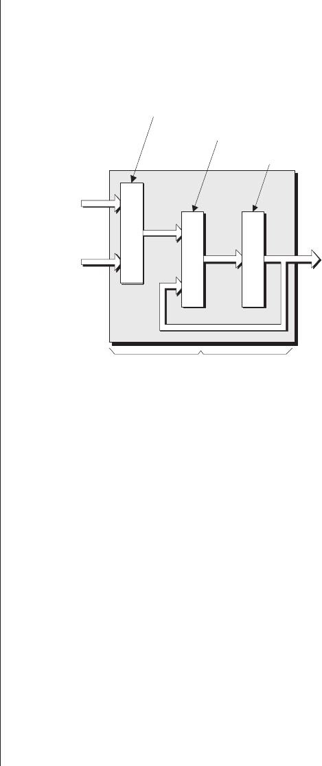
called a multiply-and-accumulate (MAC) (Figure 4-12). As
its name would suggest, this function multiplies two numbers
together and adds the result to a running total stored in an
accumulator.
If the FPGA you are working with supplies only embedded
multipliers, you will have to implement this function by com-
bining the multiplier with an adder formed from a number of
programmable logic blocks, while the result is stored in some
associated flip-flops, in a block RAM, or in a number of dis-
tributed RAMs. Life becomes a little easier if the FPGA also
provides embedded adders, and some FPGAs provide entire
MACs as embedded functions.
Embedded processor cores (hard and soft)
Almost any portion of an electronic design can be realized
in hardware (using logic gates and registers, etc.) or software
(as instructions to be executed on a microprocessor). One of
the main partitioning criteria is how fast you wish the various
functions to perform their tasks:
80 ■The Design Warrior's Guide to FPGAs
x
+
x
+
A[n:0]
B[n:0] Y[(2n - 1):0]
Multiplier
Adder
Accumulator
MAC
Figure 4-12. The functions forming a MAC.
1829: England.
Sir Charles Wheatstone
invents the concertina.

■Picosecond and nanosecond logic: This has to run insanely
fast, which mandates that it be implemented in hard-
ware (in the FPGA fabric).
■Microsecond logic: This is reasonably fast and can be
implemented either in hardware or software (this type
of logic is where you spend the bulk of your time decid-
ing which way to go).
■Millisecond logic: This is the logic used to implement
interfaces such as reading switch positions and
flashing light-emitting diodes (LEDs). It’s a pain
slowing the hardware down to implement this sort of
function (using huge counters to generate delays, for
example). Thus, it’s often better to implement these
tasks as microprocessor code (because processors give
you lousy speed—compared to dedicated
hardware—but fantastic complexity).
The fact is that the majority of designs make use of micro-
processors in one form or another. Until recently, these
appeared as discrete devices on the circuit board. Of late,
high-end FPGAs have become available that contain one or
more embedded microprocessors, which are typically referred
to as microprocessor cores. In this case, it often makes sense to
move all of the tasks that used to be performed by the external
microprocessor into the internal core. This provides a number
of advantages, not the least being that it saves the cost of hav-
ing two devices; it eliminates large numbers of tracks, pads,
and pins on the circuit board; and it makes the board smaller
and lighter.
Hard microprocessor cores
A hard microprocessor core is implemented as a dedicated,
predefined block. There are two main approaches for integrat-
ing such a core into the FPGA. The first is to locate it in a
strip (actually called “The Stripe”) to the side of the main
FPGA fabric (Figure 4-13).
Alternative FPGA Architectures ■81
1831: England.
Michael Faraday
creates the first
electric dynamo.
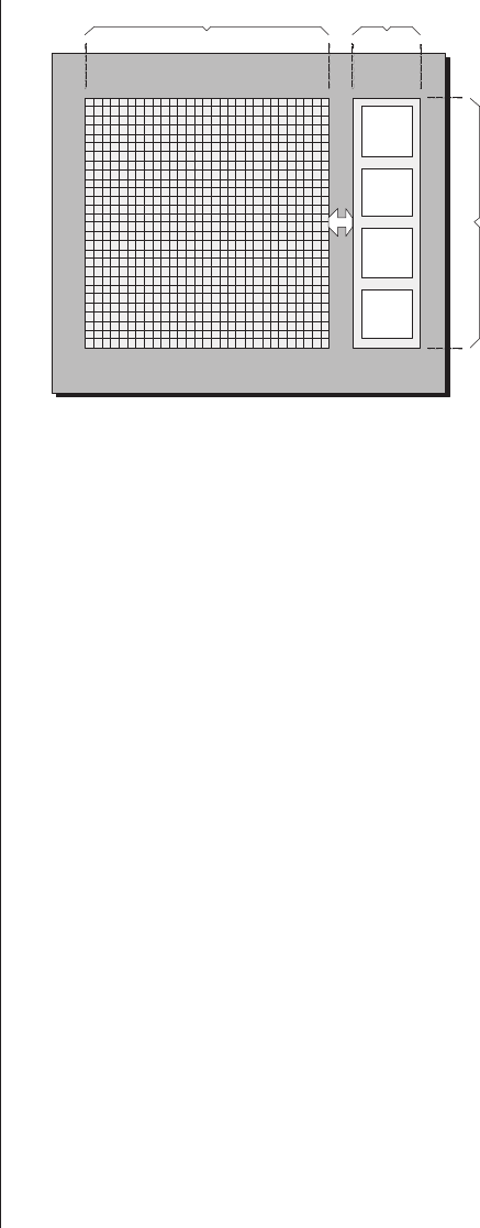
In this scenario, all of the components are typically
formed on the same silicon chip, although they could also be
formed on two chips and packaged as a multichip module
(MCM). The main FPGA fabric would also include the
embedded RAM blocks, multipliers, and the like introduced
earlier, but these have been omitted from this illustration to
keep things simple.
One advantage of this implementation is that the main
FPGA fabric is identical for devices with and without the
embedded microprocessor core, which can help make things
easier for the design tools used by the engineers. The other
advantage is that the FPGA vendor can bundle a whole load
of additional functions in the strip to complement the micro-
processor core, such as memory, special peripherals, and so
forth.
An alternative is to embed one or more microprocessor
cores directly into the main FPGA fabric. One, two, and even
four core implementations are currently available as I pen
these words (Figure 4-14).
Once again, the main FPGA fabric would also include the
embedded RAM blocks, multipliers, and the like introduced
82 ■The Design Warrior's Guide to FPGAs
uP
RAM
I/O
etc.
Main FPGA fabric
Microprocessor
core, special RAM,
peripherals and
I/O, etc.
The “Stripe”
Figure 4-13. Birds-eye view of chip with embedded core
outside of the main fabric.
MCM is pronounced by
spelling it out as “M-C-M.”
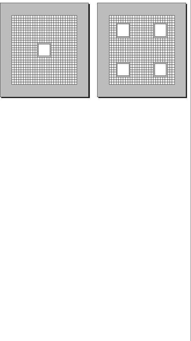
earlier, but these have been omitted from this illustration to
keep things simple.
In this case, the design tools have to be able to take
account of the presence of these blocks in the fabric; any mem-
ory used by the core is formed from embedded RAM blocks,
and any peripheral functions are formed from groups of
general-purpose programmable logic blocks. Proponents of this
scheme will argue that there are inherent speed advantages to
be gained from having the microprocessor core in intimate
proximity to the main FPGA fabric.
Soft microprocessor cores
As opposed to embedding a microprocessor physically into
the fabric of the chip, it is possible to configure a group of pro-
grammable logic blocks to act as a microprocessor. These are
typically called soft cores, but they may be more precisely cate-
gorized as either “soft” or “firm” depending on the way in
which the microprocessor’s functionality is mapped onto the
logic blocks (see also the discussions associated with the hard
IP, soft IP, and firm IP topics later in this chapter).
Alternative FPGA Architectures ■83
uP
(a) One embedded core (b) Four embedded cores
uP uP
uP uP
Figure 4-14. Bird’s-eye view of chips with embedded cores
inside the main fabric.
1831: England.
Michael Faraday creates
the first electrical
transformer.
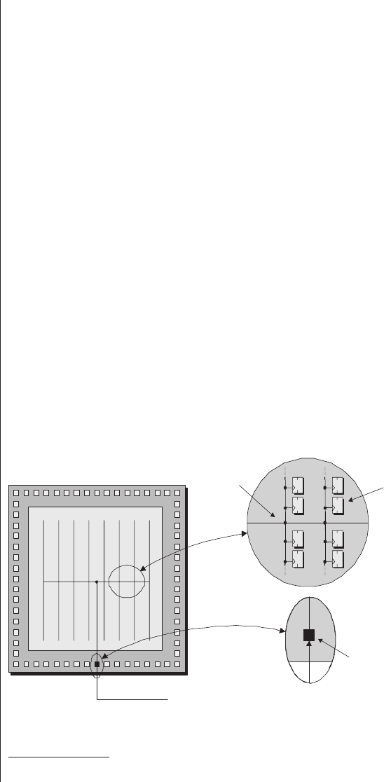
Soft cores are simpler (more primitive) and slower than
their hard-core counterparts.2However, they have the advan-
tage that you only need to implement a core if you need it and
also that you can instantiate as many cores as you require until
you run out of resources in the form of programmable logic
blocks.
Clock trees and clock managers
All of the synchronous elements inside an FPGA—for
example, the registers configured to act as flip-flops inside the
programmable logic blocks—need to be driven by a clock sig-
nal. Such a clock signal typically originates in the outside
world, comes into the FPGA via a special clock input pin, and
is then routed through the device and connected to the
appropriate registers.
Clock trees
Consider a simplified representation that omits the pro-
grammable logic blocks and shows only the clock tree and the
registers to which it is connected (Figure 4-15).
84 ■The Design Warrior's Guide to FPGAs
Clock signal from
outside world
Clock
tree Flip-flop
s
Special clock
pin and pad
Figure 4-15. A simple clock tree.
2A soft core typically runs at 30 to 50 percent of the speed of a hard core.
1831: England.
Michael Faraday
discovers magnetic
lines of force.
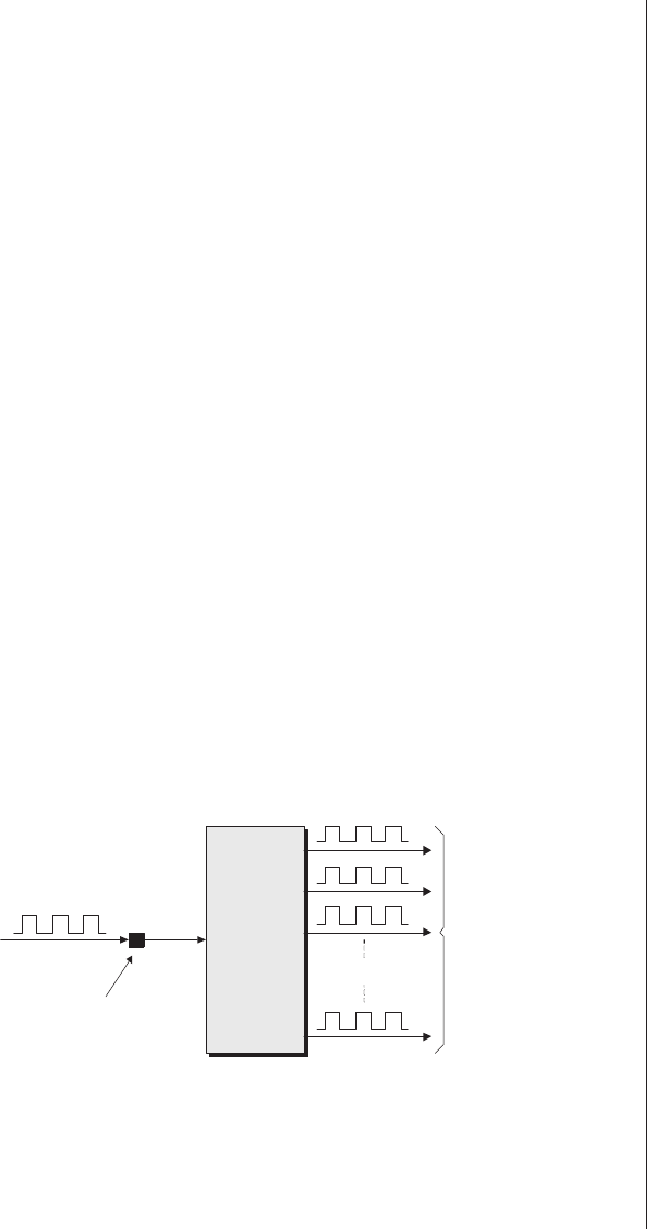
This is called a “clock tree” because the main clock signal
branches again and again (the flip-flops can be consider, to be
the “leaves” on the end of the branches). This structure is used
to ensure that all of the flip-flops see their versions of the clock
signal as close together as possible. If the clock were distrib-
uted as a single long track driving all of the flip-flops one after
another, then the flip-flop closest to the clock pin would see
the clock signal much sooner than the one at the end of the
chain. This is referred to as skew, and it can cause all sorts of
problems (even when using a clock tree, there will be a certain
amount of skew between the registers on a branch and also
between branches).
The clock tree is implemented using special tracks and is
separate from the general-purpose programmable interconnect.
The scenario shown above is actually very simplistic. In real-
ity, multiple clock pins are available (unused clock pins can be
employed as general-purpose I/O pins), and there are multiple
clock domains (clock trees) inside the device.
Clock managers
Instead of configuring a clock pin to connect directly into
an internal clock tree, that pin can be used to drive a special
hard-wired function (block) called a clock manager that gener-
ates a number of daughter clocks (Figure 4-16).
These daughter clocks may be used to drive internal clock
trees or external output pins that can be used to provide clock-
Alternative FPGA Architectures ■85
Clock signal from
outside world
Special clock
pin and pad
Daughter clocks
used to drive
internal clock trees
or output pins
Clock
Manager
etc.
Figure 4-16. A clock manager generates daughter clocks.
A clock manager as
described here is
referred to as a digital
clock manager (DCM) in
the Xilinx world.DCM is
pronounced by spelling
it out as “D-C-M.”
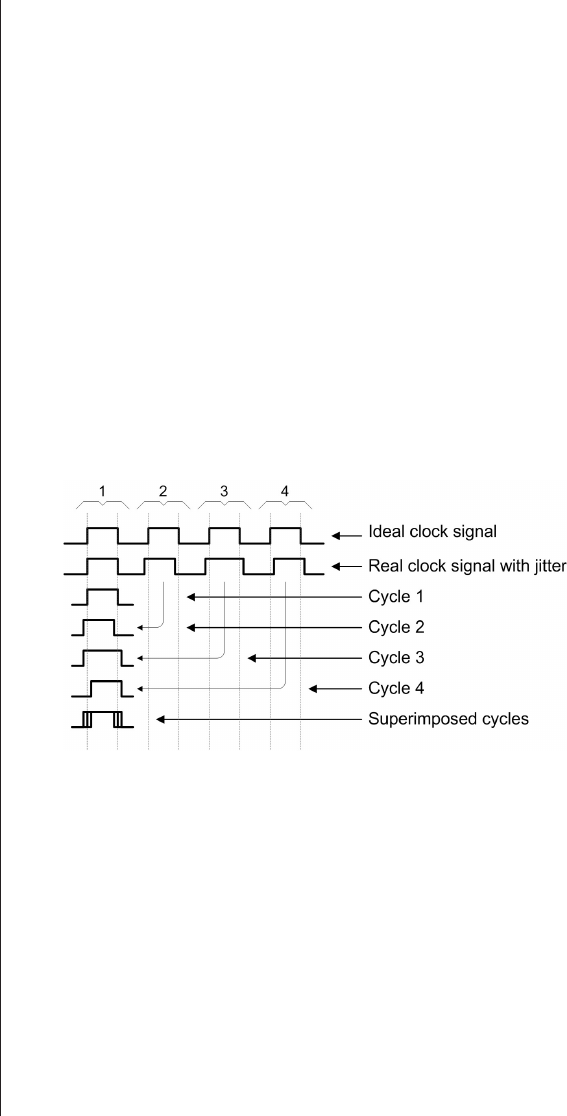
ing services to other devices on the host circuit board. Each
family of FPGAs has its own type of clock manager (there may
be multiple clock manager blocks in a device), where different
clock managers may support only a subset of the following
features:
Jitter removal: For the purposes of a simple example,
assume that the clock signal has a frequency of 1 MHz (in
reality, of course, this could be much, much higher). In an
ideal environment each clock edge from the outside world
would arrive exactly one millionth of a second after its prede-
cessor. In the real world, however, clock edges may arrive a
little early or a little late.
As one way to visualize this effect—known as jitter—imag-
ine if we were to superimpose multiple edges on top of each
other; the result would be a “fuzzy” clock (Figure 4-17).
The FPGA’s clock manager can be used to detect and cor-
rect for this jitter and to provide “clean” daughter clock
signals for use inside the device (Figure 4-18).
Frequency synthesis: It may be that the frequency of the
clock signal being presented to the FPGA from the outside
world is not exactly what the design engineers wish for. In this
case, the clock manager can be used to generate daughter
clocks with frequencies that are derived by multiplying or
dividing the original signal.
86 ■The Design Warrior's Guide to FPGAs
Figure 4-17. Jitter results in a fuzzy clock.
The term hertz was
taken from the name of
Heinrich Rudolf Hertz, a
professor of physics at
Karlsruhe Polytechnic in
Germany, who first
transmitted and received
radio waves in a
laboratory environment
in 1888.
One hertz (Hz) equates
to “one cycle per
second,” so MHz stands
for megahertz or “million
Hertz.”
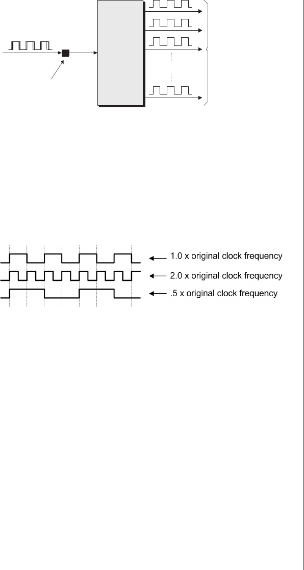
As a really simple example, consider three daughter clock
signals: the first with a frequency equal to that of the original
clock, the second multiplied to be twice that of the original
clock, and the third divided to be half that of the original
clock (Figure 4-19).
Once again, Figure 4-19 reflects very simple examples. In
the real world, one can synthesize all sorts of internal clocks,
such as an output that is four-fifths the frequency of the origi-
nal clock.
Phase shifting: Certain designs require the use of clocks that
are phase shifted (delayed) with respect to each other. Some
clock managers allow you to select from fixed phase shifts of
common values such as 120°and 240°(for a three-phase
clocking scheme) or 90°, 180°, and 270°(if a four-phase clock-
ing scheme is required). Others allow you to configure the
exact amount of phase shift you require for each daughter
clock.
For example, let’s assume that we are deriving four internal
clocks from a master clock, where the first is in phase with the
Alternative FPGA Architectures ■87
Figure 4-19. Using the clock manager to
perform frequency synthesis.
Clock signal from
outside world
with jitter
Special clock
pin and pad
“Clean” daughter
clocks used to drive
internal clock trees
or output pins
Clock
Manager
etc.
Figure 4-18. The clock manager can remove jitter.
1831: England.
Michael Faraday
discovers the principal
of electro-magnetic
induction.
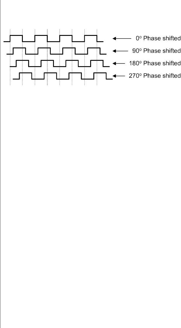
original clock, the second is phase shifted by 90°, the third by
180°, and so forth (Figure 4-20).
Auto-skew correction: For the sake of simplicity, let’s
assume that we’re talking about a daughter clock that has
been configured to have the same frequency and phase as the
main clock signal coming into the FPGA. By default, how-
ever, the clock manager will add some element of delay to the
signal as it performs its machinations. Also, more significant
delays will be added by the driving gates and interconnect
employed in the clock’s distribution. The result is that—if
nothing is done to correct it—the daughter clock will lag
behind the input clock by some amount. Once again, the dif-
ference between the two signals is known as skew.
Depending on how the main clock and the daughter clock
are used in the FPGA (and on the rest of the circuit board),
this can cause a variety of problems. Thus, the clock manager
may allow a special input to feed the daughter clock. In this
case, the clock manager will compare the two signals and spe-
cifically add additional delay to the daughter clock sufficient
to realign it with the main clock (Figure 4-21).
To be a tad more specific, only the prime (zero phase-
shifted) daughter clock will be treated in this way, and all of
the other daughter clocks will be phase aligned to this prime
daughter clock.
Some FPGA clock managers are based on phase-locked
loops (PLLs), while others are based on digital delay-locked loops
88 ■The Design Warrior's Guide to FPGAs
Figure 4-20. Using the clock manager to phase-shift the
daughter clocks.
PLL is pronounced by
spelling it out as “P-L-L.
”DLL is pronounced by
spelling it out as “D-L-L.”
At this time, I do not
know why digital
delay-locked loop is not
abbreviated to “DDLL.”
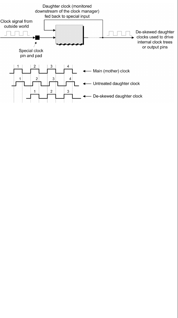
(DLLs). PLLs have been used since the 1940s in analog imple-
mentations, but recent emphasis on digital methods has made
it desirable to match signal phases digitally. PLLs can be
implemented using either analog or digital techniques, while
DLLs are by definition digital in nature. The proponents of
DLLs say that they offer advantages in terms of precision, sta-
bility, power management, noise insensitivity, and jitter
performance.
General-purpose I/O
Today’s FPGA packages can have 1,000 or more pins,
which are arranged as an array across the base of the package.
Similarly, when it comes to the silicon chip inside the pack-
age, flip-chip packaging strategies allow the power, ground,
clock, and I/O pins to be presented across the surface of the
chip. Purely for the purposes of these discussions (and illustra-
tions), however, it makes things simpler if we assume that all
of the connections to the chip are presented in a ring around
the circumference of the device, as indeed they were for
many years.
Alternative FPGA Architectures ■89
Figure 4-21. Deskewing with reference to the mother clock.
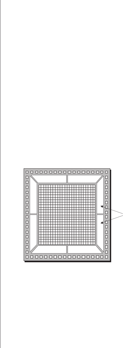
Configurable I/O standards
Let’s consider for a moment an electronic product from
the perspective of the architects and engineers designing the
circuit board. Depending on what they are trying to do, the
devices they are using, the environment the board will oper-
ate in, and so on, these guys and gals will select a particular
standard to be used to transfer data signals. (In this context,
“standard” refers to electrical aspects of the signals, such as
their logic 0 and logic 1 voltage levels.)
The problem is that there is a wide variety of such stan-
dards, and it would be painful to have to create special FPGAs
to accommodate each variation. For this reason, an FPGA’s
general-purpose I/O can be configured to accept and generate
signals conforming to whichever standard is required. These
general-purpose I/O signals will be split into a number of
banks—we’ll assume eight such banks numbered from 0 to 7
(Figure 4-22).
The interesting point is that each bank can be configured
individually to support a particular I/O standard. Thus, in
addition to allowing the FPGA to work with devices using
multiple I/O standards, this allows the FPGA to actually be
used to interface between different I/O standards (and also to
90 ■The Design Warrior's Guide to FPGAs
01
54
6
7
3
2
General-purpose I/O
banks 0 through 7
Figure 4-22. Bird’s-eye view of chip showing general-purpose
I/O banks.
1831: England.
Michael Faraday
discovers that a
moving magnet
induces an electric
current.

translate between different protocols that may be based on par-
ticular electrical standards).
Configurable I/O impedances
The signals used to connect devices on today’s circuit
board often have fast edge rates (this refers to the time it takes
the signal to switch between one logic value and another). In
order to prevent signals reflecting back (bouncing around), it
is necessary to apply appropriate terminating resistors to the
FPGA’s input or output pins.
In the past, these resistors were applied as discrete compo-
nents that were attached to the circuit board outside the
FPGA. However, this technique became increasingly problem-
atic as the number of pins started to increase and their pitch
(the distance between them) shrank. For this reason, today’s
FPGAs allow the use of internal terminating resistors whose
values can be configured by the user to accommodate different
circuit board environments and I/O standards.
Core versus I/O supply voltages
In the days of yore—circa 1965 to 1995—the majority of
digital ICs used a ground voltage of 0V and a supply voltage of
+5V. Furthermore, their I/O signals also switched between 0V
(logic 0) and +5V (logic 1), which made life really simple.
Over time, the geometries of the structures on silicon chips
became smaller because smaller transistors have lower costs,
higher speed, and lower power consumption. However, these
processes demanded lower supply voltages, which have contin-
ued to fall over the years (Table 4.2).
The point is that this supply (which is actually provided
using large numbers of power and ground pins) is used to
power the FPGA’s internal logic. For this reason, this is known
as the core voltage. However, different I/O standards may use
signals with voltage levels significantly different from the core
voltage, so each bank of general-purpose I/Os can have its own
additional supply pins.
Alternative FPGA Architectures ■91
1832: England.
Charles Babbage
conceives the first
mechanical computer,
the Analytical Engine.
It’s interesting to note that—from the 350 nm node
onwards—the core voltage has scaled fairly linearly with the
process technology. However, there are physical reasons not
to go much below 1V (these reasons are based on technology
aspects such as transistor input switching thresholds and volt-
age drops), so this “voltage staircase” might start to tail off in
the not-so-distant future.
Gigabit transceivers
The traditional way to move large amounts of data
between devices is to use a bus, a collection of signals that
carry similar data and perform a common function
(Figure 4-23).
Early microprocessor-based systems circa 1975 used 8-bit
buses to pass data around. As the need to push more data
around and to move it faster grew, buses grew to 16 bits in
width, then 32 bits, then 64 bits, and so forth. The problem is
that this requires a lot of pins on the device and a lot of tracks
92 ■The Design Warrior's Guide to FPGAs
FPGA
Other
device
n-bit bus
Figure 4-23: Using a bus to communicate between devices.
Year Supply (Core
Voltage (V))
Technology
Node (nm)
1998 3.3 350
1999 2.5 250
2000 1.8 180
2001 1.5 150
2003 1.2 130
Table 4.2. Supply voltages versus technology nodes.
1832: England
Joseph Henry
discovers self-induction
or inductance.
connecting the devices together. Routing these tracks so that
they all have the same length and impedance becomes increas-
ingly painful as boards grow in complexity. Furthermore, it
becomes increasingly difficult to manage signal integrity issues
(such as susceptibility to noise) when you are dealing with
large numbers of bus-based tracks.
For this reason, today’s high-end FPGAs include special
hard-wired gigabit transceiver blocks. These blocks use one
pair of differential signals (which means a pair of signals that
always carry opposite logical values) to transmit (TX) data and
another pair to receive (RX) data (Figure 4-24).
These transceivers operate at incredibly high speeds, allow-
ing them to transmit and receive billions of bits of data per
second. Furthermore, each block actually supports a number
(say four) of such transceivers, and an FPGA may contain a
number of these transceiver blocks.
Hard IP, soft IP, and firm IP
Each FPGA vendor offers its own selection of hard,firm,
and soft IP. Hard IP comes in the form of preimplemented
blocks such as microprocessor cores, gigabit interfaces, multi-
pliers, adders, MAC functions, and the like. These blocks are
designed to be as efficient as possible in terms of power con-
sumption, silicon real estate, and performance. Each FPGA
family will feature different combinations of such blocks.
together with various quantities of programmable logic blocks.
Alternative FPGA Architectures ■93
FPGA
Differential pairs
Transceiver block
Figure 4-24: Using high-speed transceivers to communicate
between devices.
1833: England.
Michael Faraday defines
the laws of electrolysis.
IP is pronounced by
spelling it out as “I-P.”
HDL is pronounced by
spelling it out as “H-D-L.”
VHDL is pronounced by
spelling it out as
“V-H-D-L.”
RTL is pronounced by
spelling it out as “R-T-L.”

At the other end of the spectrum, soft IP refers to a
source-level library of high-level functions that can be
included to the users’ designs. These functions are typically
represented using a hardware description language, or HDL,
such as Verilog or VHDL at the register transfer level (RTL) of
abstraction. Any soft IP functions the design engineers decide
to use are incorporated into the main body of the design—
which is also specified in RTL—and subsequently synthesized
down into a group of programmable logic blocks (possibly
combined with some hard IP blocks like multipliers, etc.).
Holding somewhat of a middle ground is firm IP, which
also comes in the form of a library of high-level functions.
Unlike their soft IP equivalents, however, these functions
have already been optimally mapped, placed, and routed into
a group of programmable logic blocks (possibly combined with
some hard IP blocks like multipliers, etc.). One or more copies
of each predefined firm IP block can be instantiated (called
up) into the design as required.
The problem is that it can be hard to draw the line
between those functions that are best implemented as hard IP
and those that should be implemented as soft or firm IP (using
a number of general-purpose programmable logic blocks). In
the case of functions like the multipliers, adders, and MACs
discussed earlier in this chapter, these are generally useful for a
wide range of applications. On the other hand, some FPGAs
contain dedicated blocks to handle specific interface protocols
like the PCI standard. It can, of course, make your life a lot
easier if this happens to be the interface with which you wish
to connect your device to the rest of the board. On the other
hand, if you decide you need to use some other interface, a
dedicated PCI block will serve only to waste space, block traf-
fic, and burn power in your chip.
Generally speaking, once FPGA vendors add a function
like this into their device, they’ve essentially placed the com-
ponent into a niche. Sometimes you have to do this to
achieve the desired performance, but this is a classic problem
94 ■The Design Warrior's Guide to FPGAs
PCI is pronounced by
spelling it out as “P-C-I.”

because the next generation of the device is often fast enough
to perform this function in its main (programmable) fabric.
System gates versus real gates
One common metric used to measure the size of a device in
the ASIC world is that of equivalent gates. The idea is that dif-
ferent vendors provide different functions in their cell
libraries, where each implementation of each function requires
a different number of transistors. This makes it difficult to
compare the relative capacity and complexity of two devices.
The answer is to assign each function an equivalent gate
value along the lines of “Function A equates to five equivalent
gates; function B equates to three equivalent gates …” The
next step is to count all of the instances of each function, con-
vert them into their equivalent gate values, sum all of these
values together, and proudly proclaim, “My ASIC contains 10
million equivalent gates, which makes it much bigger than your
ASIC!”
Unfortunately, nothing is simple because the definition of
what actually constitutes an equivalent gate can vary depend-
ing on whom one is talking to. One common convention is for
a 2-input NAND function to represent one equivalent gate.
Alternatively, some vendors define an equivalent gate as
equaling an arbitrary number of transistors. And a more eso-
teric convention defines an ECL equivalent gate as being
“one-eleventh the minimum logic required to implement a
single-bit full adder” (who on earth came up with this one?).
As usual, the best policy here is to make sure that everyone is
talking about the same thing before releasing your grip on your
hard-earned money.
And so we come to FPGAs. One of the problems FPGA
vendors run into occurs when they are trying to establish a
basis for comparison between their devices and ASICs. For
example, if someone has an existing ASIC design that con-
tains 500,000 equivalent gates and he wishes to migrate this
design into an FPGA implementation, how can he tell if his
design will fit into a particular FPGA. The fact that each
Alternative FPGA Architectures ■95
1837: America.
Samual Finley Breese
Morse exhibits an
electric telegraph.

4-input LUT can be used to represent anywhere between one
and more than twenty 2-input primitive logic gates makes
such a comparison rather tricky.
In order to address this issue, FPGA vendors started talk-
ing about system gates in the early 1990s. Some folks say that
this was a noble attempt to use terminology that ASIC
designers could relate to, while others say that it was purely a
marketing ploy that didn’t do anyone any favors.
Sad to relate, there appears to be no clear definition as to
exactly what a system gate is. The situation was difficult
enough when FPGAs essentially contained only generic pro-
grammable logic in the form of LUTs and registers. Even
then, it was hard to state whether or not a particular ASIC
design containing xequivalent gates could fit into an FPGA
containing ysystem gates. This is because some ASIC designs
may be predominantly combinatorial, while others may make
excessively heavy use of registers. Both cases may result in a
suboptimal mapping onto the FPGA.
The problem became worse when FPGAs started contain-
ing embedded blocks of RAM, because some functions can be
implemented much more efficiently in RAM than in general-
purpose logic. And the fact that LUTs can act as distributed
RAM only serves to muddy the waters; for example, one ven-
dor’s system gate count values now include the qualifier,
“Assumes 20 percent to 30 percent of LUTs are used as
RAM.” And, of course, the problems are exacerbated when
we come to consider FPGAs containing embedded processor
cores and similar functions, to the extent that some vendors
now say, “System gate values are not meaningful for these
devices.”
Is there a rule of thumb that allows you to convert system
gates to equivalent gates and vice versa? Sure, there are lots of
them! Some folks say that if you are feeling optimistic, then
you should divide the system gate value by three (in which
case three million FPGA system gates would equate to one
million ASIC equivalent gates, for example). Or if you’re feel-
ing a tad more on the pessimistic side, you could divide the
96 ■The Design Warrior's Guide to FPGAs
1837: England
Sir Charles Wheatstone
and Sir William
Fothergill Cooke patent
the five-needle electric
telegraph.

system gates by five (in which case three million system gates
would equate to 600,000 equivalent gates).
However, other folks would say that the above is only true
if you assume that the system gates value encompasses all of
the functions that you can implement using both the general-
purpose programmable logic and the block RAMs. These folks
would go on to say that if you remove the block RAMs from
the equation, then you should divide the system gates value by
ten (in which case, three million system gates would equate to
only 300,000 equivalent gates), but in this case you still have
the block RAMs to play with … arrggghhhh!
Ultimately, this topic spirals down into such a quagmire
that even the FPGA vendors are trying desperately not to talk
about system gates any more. When FPGAs were new on the
scene, people were comfortable with the thought of equivalent
gates and not so at ease considering designs in terms of LUTs,
slices, and the like; however, the vast number of FPGA designs
that have been undertaken over the years means that engi-
neers are now much happier thinking in FPGA terms. For this
reason, speaking as someone living in the trenches, I would
prefer to see FPGAs specified and compared using only simple
counts of:
■Number of logic cells or logic elements or whatever
(which equates to the number of 4-input LUTs and
associated flip-flops/latches)
■Number (and size) of embedded RAM blocks
■Number (and size) of embedded multipliers
■Number (and size) of embedded adders
■Number (and size) of embedded MACs
■etc.
Why is this so hard? And it would be really useful to take a
diverse suite of real-world ASIC design examples, giving their
equivalent gate values, along with details as to their
flops/latches, primitive gates, and other more complex func-
tions, then to relate each of these examples to the number of
Alternative FPGA Architectures ■97
1842: England
Joseph Henry
discovers that an
electrical spark
between two
conductors is able to
induce magnetism in
needles—this effect is
detected at a distance
of 30 meters.

LUTs and flip-flops/latches required in equivalent FPGA
implementations, along with the amount of embedded RAM
and the number of other embedded functions.
Even this would be less than ideal, of course, because one
tends to design things differently for FPGA and ASIC targets,
but it would be a start.
FPGA years
We’ve all heard it said that each year for a dog is equiva-
lent to seven human years, the idea being that a 10-year-old
pooch would be 70 years old in human terms. Thinking like
this doesn’t actually do anyone much good. On the other
hand, it does provide a useful frame of reference so that when
your hound can no longer keep up with you on a long walk,
you can say, “Well, it’s only to be expected because the poor
old fellow is almost 100 years old” (or whatever).
Similarly, in the case of FPGAs, it may help to think that
one of their years equates to approximately 15 human years.
Thus, if you’re working with an FPGA that was only intro-
duced to the market within the last year, you should view it as
a teenager. On the one hand, if you have high hopes for the
future, he or she may end up with a Nobel Peace Prize or as
the President of the United States. On the other hand, the
object of your affections will typically have a few quirks that
you have to get used to and learn to work around.
By the time an FPGA has been on the market for two
years (equating to 30 years in human terms), you can start to
think of it as reasonably mature and a good all-rounder at the
peak of its abilities. After three years (45 years old), an FPGA
is becoming somewhat staid and middle-aged, and by four
years (60 years old). you should treat it with respect and make
sure that you don’t try to work it like a carthorse!
98 ■The Design Warrior's Guide to FPGAs
1842: Scotland.
Alexander Bail
demonstrates first
electromechanical
means to capture,
transmit, and reproduce
an image.

Weasel words
Before plunging headfirst into this topic, it’s probably
appropriate to preface our discussions with a few “weasel
words” (always remember the saying, “Eagles may soar, but
weasels rarely get sucked into jet engines at 10,000 feet!”).
The point is that each FPGA vendor has its own unique
terminology and its own techniques and protocols for doing
things. To make life even more exciting, the detailed mecha-
nisms for programming FPGAs can vary on a family-by-family
basis. For these reasons, the following discussions are intended
to provide only a generic introduction to this subject.
Configuration files, etc.
Section 2 of this book describes a variety of tools and flows
that may be used to capture and implement FPGA designs.
The end result of all of these techniques is a configuration file
(sometimes called a bit file), which contains the information
that will be uploaded into the FPGA in order to program it to
perform a specific function.
In the case of SRAM-based FPGAs, the configuration file
contains a mixture of configuration data (bits that are used to
define the state of programmable logic elements directly) and
configuration commands (instructions that tell the device what
to do with the configuration data). When the configuration
file is in the process of being loaded into the device, the infor-
mation being transferred is referred to as the configuration
bitstream.
Programming (Configuring)
an FPGA
Chapter
5
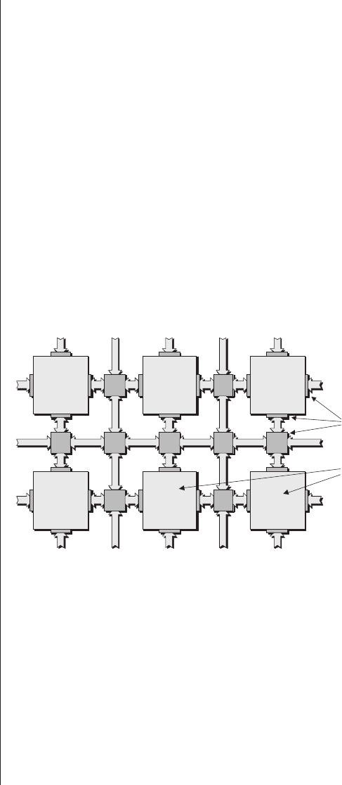
E2-based and FLASH-based devices are programmed in a
similar manner to their SRAM-based cousins. By comparison,
in the case of antifuse-based FPGAs, the configuration file
predominantly contains only a representation of the configu-
ration data that will be used to grow the antifuses.
Configuration cells
The underlying concept associated with programming an
FPGA is relatively simple (i.e., load the configuration file into
the device). It can, however, be a little tricky to wrap one’s
brain around all of the different facets associated with this
process, so we’ll start with the basics and work our way up.
Initially, let’s assume we have a rudimentary device consisting
only of an array of very simple programmable logic blocks sur-
rounded by programmable interconnect (Figure 5-1).
Any facets of the device that may be programmed are
done so by means of special configuration cells. The majority
of FPGAs are based on the use of SRAM cells, but some
employ FLASH (or E2) cells, while others use antifuses.
Irrespective of the underlying technology, the device’s
interconnect has a large number of associated cells that can be
used to configure it so as to connect the device’s primary
inputs and outputs to the programmable logic blocks and
100 ■The Design Warrior's Guide to FPGAs
Programmable
interconnect
Programmable
logic blocks
Figure 5-1. Top-down view of simple FPGA architecture.
1843: England.
Augusta Ada Lovelace
publishes her notes
explaining the concept
of a computer.
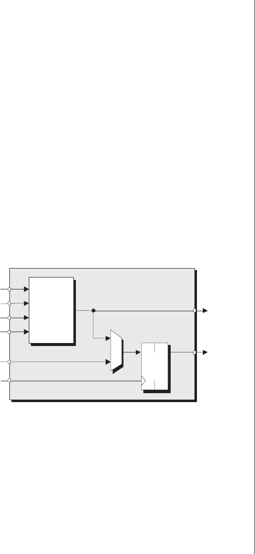
these logic blocks to each other. (In the case of the device’s
primary I/Os, which are not shown in Figure 5-1, each has a
number of associated cells that can be used to configure them
to accommodate specific I/O interface standards and so forth.)
For the purpose of this portion of our discussions, we shall
assume that each programmable logic block comprises only a
4-input LUT, a multiplexer, and a register (Figure 5-2). The
multiplexer requires an associated configuration cell to specify
which input is to be selected. The register requires associated
cells to specify whether it is to act as an edge-triggered flip-flop
(as shown in Figure 5-2) or a level-sensitive latch, whether it is
to be triggered by a positive- or negative-going clock edge (in
the case of the flip-flop option) or an active-low or active-high
enable (if the register is instructed to act as a latch), and
whether it is to be initialized with a logic 0 or a logic 1. Mean-
while, the 4-input LUT is itself based on 16 configuration
cells.
Antifuse-based FPGAs
In the case of antifuse-based FPGAs, the antifuse cells can
be visualized as scattered across the face of the device at strate-
gic locations. The device is placed in a special device
programmer, the configuration (bit) file is uploaded into the
device programmer from the host computer, and the device
programmer uses this file to guide it in applying pulses of rela-
Programming (Configuring) an FPGA ■101
LUT is pronounced to
rhyme with “nut.”
4-input
LUT
flip-flop
clock
mux
y
q
e
a
b
c
d
Figure 5-2. A very simple programmable logic block.

tively high voltage and current to selected pins to grow each
antifuse in turn.
A very simplified way of thinking about this is that each
antifuse has a “virtual” x-y location on the surface of the chip,
where these x-y values are specified as integers. Based on this
scenario, we can visualize using one group of I/O pins to repre-
sent the xvalue associated with a particular antifuse and
another group of pins to represent the yvalue. (Things are
more complicated in the real world, but this is a nice way to
think about things that doesn’t tax our brains too much.)
Once all of the fuses have been grown, the FPGA is
removed from the device programmer and attached to a cir-
cuit board. Antifuse-based devices are, of course, one-time
programmable (OTP) because once you’ve started the program-
ming process, you’re committed and it’s too late to change
your mind.
SRAM-based FPGAs
For the remainder of this chapter we shall consider only
SRAM-based FPGAs. Remember that these devices are vola-
tile, which means that they have to be programmed in-system
(on the circuit board), and they always need to be repro-
grammed when power is first applied to the system.
From the outside world, we can visualize all of the SRAM
configuration cells as comprising a single (long) shift register.
Consider a simple bird’s-eye view of the surface of the chip
showing only the I/O pins/pads and the SRAM configuration
cells (Figure 5-3).
As a starting point, we shall assume that the beginning
and end of this register chain are directly accessible from the
outside world. However, it’s important to note that this is
only the case when using the configuration port programming
mechanism in conjunction with the serial load with FPGA as
master or serial load with FPGA as slave programming modes, as
discussed below.
Also note that the configuration data out pin/signal shown
in Figure 5-3 is only used if multiple FPGAs are to be config-
102 ■The Design Warrior's Guide to FPGAs
FLASH (and E2)–based
devices are typically pro-
grammed in a similar
manner to their SRAM
cousins.
Unlike SRAM-based
FPGAs, FLASH-based
devices are nonvolatile.
They retain their configu-
ration when power is
removed from the sys-
tem, and they don’t need
to be reprogrammed
when power is reapplied
to the system (although
they can be if required).
Also, FLASH-based
devices can be pro-
grammed in-system (on
the circuit board) or
outside the system by
means of a device
programmer.
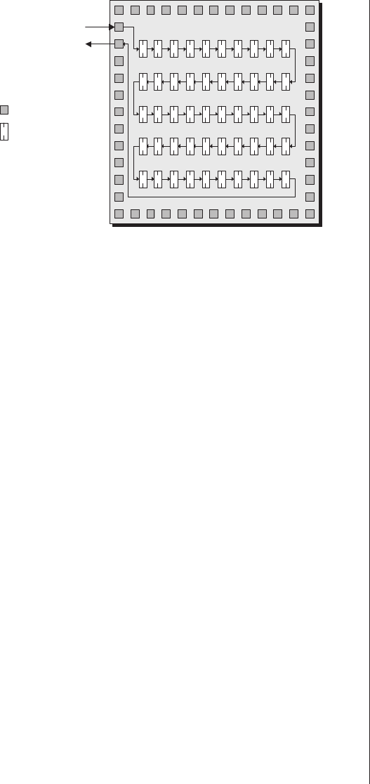
ured by cascading (daisy-chaining) them together or if it is
required to be able to read the configuration data back out of
the device for any reason.
The quickness of the hand deceives the eye
It isn’t really necessary to know this bit, so if you’re in a
hurry, you can bounce over into the next section, but I found
this interesting and thought you might find it to be so also. As
figure 5-3 shows, the easiest way to visualize the internal
organization of the SRAM programming cells is as a long shift
register. If this were really the case, then each cell would be
implemented as a flip-flop, and all of the flop-flops in the
chain would be driven by a common clock.
The problem is that an FPGA can contain a humongous
number of configuration cells. By 2003, for example, a reasona-
bly high-end device could easily contain 25 million such cells!
The core of a flip-flop requires eight transistors, while the core
of a latch requires only four transistors. For this reason, the
configuration cells in an SRAM-based FPGA are formed from
latches. (In our example device with 25 million configuration
cells, this results in a saving of 100 million transistors, which is
nothing to sneeze at.)
Programming (Configuring) an FPGA ■103
Programming an FPGA
can take a significant
amount of time. Consider
a reasonably high-end
device containing 25 mil-
lion SRAM-based
configuration cells. Pro-
gramming such a device
using a serial mode and a
25 MHz clock would take
one second. This isn’t too
bad when you are first
powering up a system,
but it means that you
really don’t want to keep
on reconfiguring the
FPGA when the system is
in operation.
Configuration data in
Configuration data out
= I/O pin/pad
= SRAM cell
Figure 5-3. Visualizing the SRAM cells as a long shift register.

The problem is that you can’t create a shift register out of
latches (well, actually you can, as is discussed a little later in
this chapter, but not one that’s 25 million cells long). The
way the FPGA vendors get around this is to have a group of
flip-flops—say 1,024—sharing a common clock and config-
ured as a classic shift register. This group is called a frame.
The 25 million configuration cells/latches in our example
device are also divided up into frames, each being the same
length as the flip-flop frame. From the viewpoint of the out-
side world, you simply clock the 25 million bits of
configuration data into the device. Inside the device, how-
ever, as soon as the first 1,024 bits have been serially loaded
into the flop-flop frame, special-purpose internal circuitry
automatically parallel copies/loads this data into the first latch
frame. When the next 1,024 bits have been loaded into the
flip-flop frame, they are automatically parallel copied/loaded
into the second latch frame, and so on for the rest of the
device. (The process is reversed when data is read out of
the device.)
Programming embedded (block) RAMs, distributed
RAMs, etc.
In the case of FPGAs containing large blocks of embedded
(block) RAM, the cores of these blocks are implemented out
of SRAM latches, and each of these latches is a configuration
cell that forms a part of our “imaginary” register chain (as dis-
cussed in the previous section).
One interesting point is that each 4-input LUT (see
Figure 5-2) can be configured to act as a LUT, as a small
(16 ×1) chunk of distributed RAM, or as a 16-bit shift regis-
ter. All of these manifestations employ the same group of 16
SRAM latches, where each of these latches is a configuration
cell that forms a part of our imaginary register chain.
“But what about the 16-bit shift register incarnation,” you
cry. “Doesn’t this need to be implemented using real flip-
flops?” Well, that’s a good question—I’m glad you asked. In
fact, a trick circuit is employed using the concept of a capaci-
104 ■The Design Warrior's Guide to FPGAs
1843: England.
Sir Charles Wheatstone
and Sir William
Fothergill Cooke patent
the 2-needle electrical
telegraph.

tive latch that prevents classic race conditions (this is pretty
much the same way designers built flip-flops out of discrete
transistors, resistors, and capacitors in the early 1960s).
Multiple programming chains
Figure 5-3 shows the configuration cells presented as a sin-
gle programming chain. As there can be tens of millions of
configuration cells, this chain can be very long indeed. Some
FPGAs are architected so that the configuration port actually
drives a number of smaller chains. This allows individual por-
tions of the device to be configured and facilitates a variety of
concepts such as modular and incremental design (these con-
cepts are discussed in greater detail in Section 2).
Quickly reinitializing the device
As was previously noted, the register in the programmable
logic block has an associated configuration cell that specifies
whether it is to be initialized with a logic 0 or a logic 1. Each
FPGA family typically provides some mechanism such as an
initialization pin that, when placed in its active state, causes all
of these registers to be returned to their initialization values
(this mechanism does not reinitialize any embedded [block] or
distributed RAMs).
Using the configuration port
The early FPGAs made use of something called the
configuration port. Even today, when more sophisticated tech-
niques are available (like the JTAG interface discussed later in
this chapter), the configuration port is still widely used because
it’s relatively simple and is well understood by stalwarts in the
FPGA fraternity.
We start with a small group of dedicated configuration mode
pins that are used to inform the device which configuration
mode is going to be used. In the early days, only two pins were
employed to provide four modes, as shown in Table 5-1.
Note that the names of the modes shown in this
table—and also the relationship between the codes on the
Programming (Configuring) an FPGA ■105
1844: America.
Morse Telegraph
connects Washington
and Baltimore.
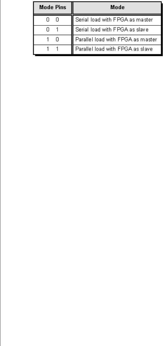
mode pins and the modes themselves—are intended for use
only as an example. The actual codes and mode names vary
from vendor to vendor.
The mode pins are typically hardwired to the desired logic
0 and logic 1 values at the circuit board level. (These pins can
be driven from some other logic that allows the programming
mode to be modified, but this is rarely done in practice.)
In addition to the hard-wired mode pins, an additional pin
is used to instruct the FPGA to actually commence the con-
figuration, while yet another pin is used by the device to
report back when it’s finished (there are also ways to deter-
mine if an error occurred during the process). This means that
in addition to configuring the FPGA when the system is first
powered up, the device may also be reinitialized using the
original configuration data, if such an occurrence is deemed
necessary.
The configuration port also makes use of additional pins to
control the loading of the data and to input the data itself.
The number of these pins depends on the configuration mode
selected, as discussed below. The important point here is that
once the configuration has been completed, most of these pins
can subsequently be used as general-purpose I/O pins (we will
return to this point a little later).
Serial load with FPGA as master
This is perhaps the simplest programming mode. In the
early days, it involved the use of an external PROM. This was
subsequently superceded by an EPROM, then an E2PROM,
106 ■The Design Warrior's Guide to FPGAs
Table 5-1. The four original configuration modes
1845: England.
Michael Faraday
discovers the rotation of
polarised light by
magnetism.
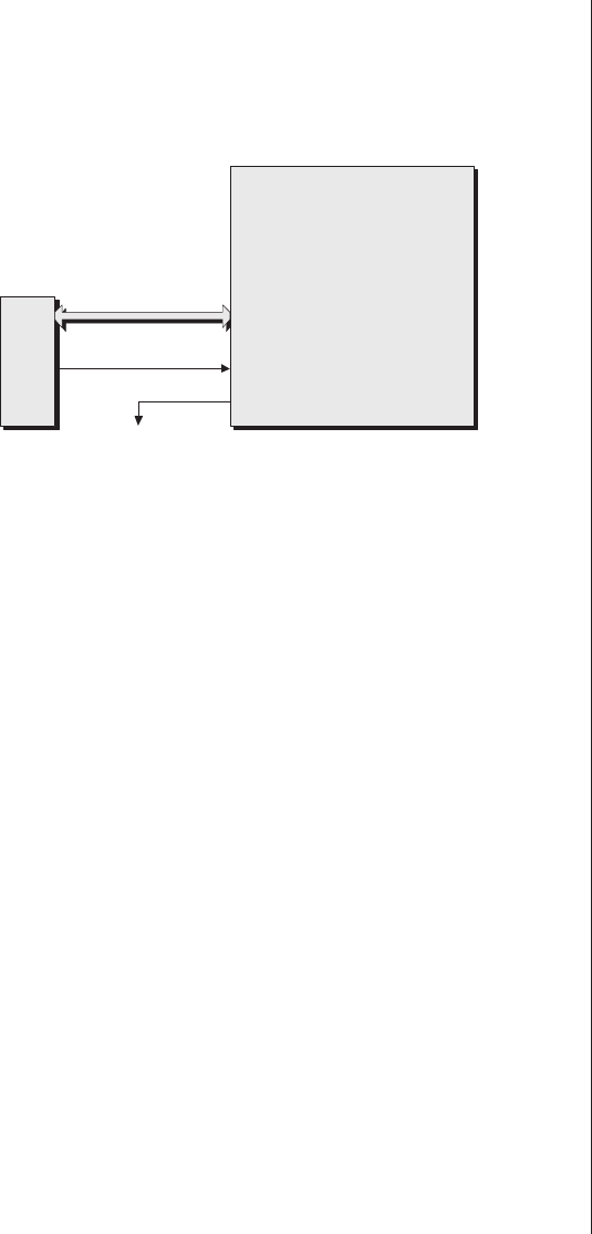
and now—most commonly—a FLASH-based device. This
special-purpose memory component has a single data output
pin that is connected to a configuration data in pin on the
FPGA (Figure 5-4).
The FPGA also uses several bits to control the external
memory device, such as a reset signal to inform it when the
FPGA is ready to start reading data and a clock signal to clock
the data out.
The idea with this mode is that the FPGA doesn’t need to
supply the external memory device with a series of addresses.
Instead, it simply pulses the reset signal to indicate that it
wishes to start reading data from the beginning, and then it
sends a series of clock pulses to clock the configuration data
out of the memory device.
The configuration data out signal coming from the FPGA
need only be connected if it is required to read the configura-
tion data from the device for any reason. One such scenario
occurs when there are multiple FPGAs on the circuit board. In
this case, each could have its own dedicated external
memory device and be configured in isolation, as shown in
Figure 5-4. Alternatively, the FPGAs could be cascaded
(daisy-chained) together and share a single external memory
(Figure 5-5).
Programming (Configuring) an FPGA ■107
Configuration data in
Memory
Device
Control
Configuration
da
t
a
o
u
t
FPGA
Cdata In
Cdata Out
Figure 5-4. Serial load with FPGA as master.
1845: England.
First use of the
electronic telegraph to
help apprehend a
criminal.
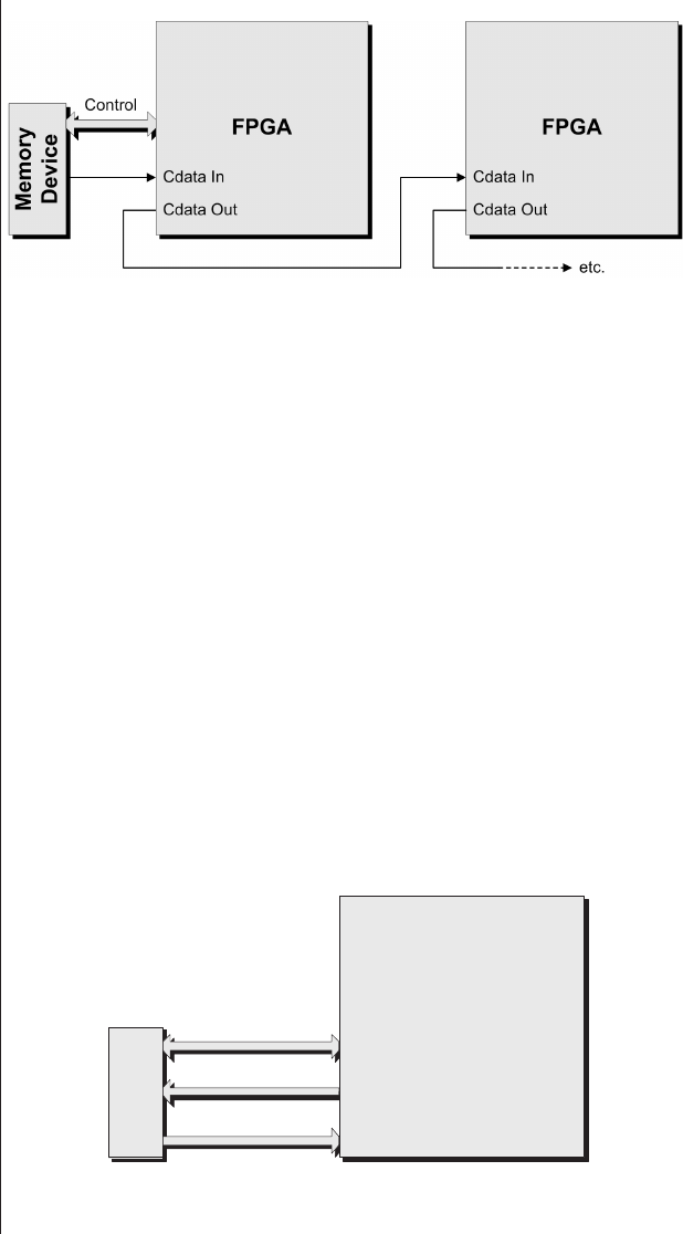
In this scenario, the first FPGA in the chain (the one con-
nected directly to the external memory) would be configured
to use the serial master mode, while the others would be serial
slaves, as discussed later in this chapter.
Parallel load with FPGA as master
In many respects, this is very similar to the previous mode,
except that the data is read in 8-bit chunks from a memory
device with eight output pins. Groups of eight bits are very
common and are referred to as bytes. In addition to providing
control signals, the original FPGAs also supplied the external
memory device with an address that was used to point to
whichever byte of configuration data was to be loaded next
(Figure 5-6).
108 ■The Design Warrior's Guide to FPGAs
Groups of four bits are
also common and are
given the special name
of nybble (sometimes
nibble). The idea is that
“two nybbles make a
byte,” which is a (little)
joke. This goes to show
that engineers do have a
sense of humor; it’s just
not very sophisticated.
When electronics and
computing first started,
defining things was
something of a free-for-
all. The end result was
that different companies
had their own definitions
for things like bytes, and
it was common to see 5-,
6-, 7-, 8-, and even 9-bit
bytes. It was quite some
time before the consen-
sus settled on 8-bit
bytes, at which time eve-
ryone was happy (apart
from those who weren’t,
but they don’t count).
Figure 5-5. Daisy-chaining FPGAs.
Configuration data [7:0]
Memory
Device
Control FPGA
Cdata In[7:0]
Address
Figure 5-6. Parallel load with FPGA as master
(original technique).

The way this worked was that the FPGA had an internal
counter that was used to generate the address for the external
memory. (The original FPGAs had 24-bit counters, which
allowed them to address 16 million bytes of data.) At the
beginning of the configuration sequence, this counter would
be initialized with zero. After the byte of data pointed to by
the counter had been read, the counter would be incremented
to point to the next byte of data. This process would continue
until all of the configuration data had been loaded.
It’s easy to assume that this parallel-loading technique
offers speed advantages, but it didn’t for quite some time. This
is because—in early devices—as soon as a byte of data had
been read into the device, it was clocked into the internal con-
figuration shift register in a serial manner. Happily, this
situation has been rectified in more modern FPGA families.
On the other hand, although the eight pins can be used as
general-purpose I/O pins once the configuration data has been
loaded, in reality this is less than ideal. This is because these
pins still have the tracks connecting them to the external
memory device, which can cause a variety of signal integrity
problems.
The real reason why this technique was so popular in the
days of yore is that the special-purpose memory devices used in
the serial load with FPGA as master mode were quite expensive.
By comparison, this parallel technique allowed design engi-
neers to use off-the-shelf memory devices, which were much
cheaper.
Having said this, special-purpose memory devices created
for use with FPGAs are now relatively inexpensive (and being
FLASH-based, they are also reusable). Thus, modern FPGAs
now use a new variation on this parallel-loading technique. In
this case, the external memory is a special-purpose device that
doesn’t require an external address, which means that the
FPGAs no longer requires an internal counter for this purpose
(Figure 5-7).
As for the serial mode discussed earlier, the FPGA simply
pulses the external memory device’s reset signal to indicate
Programming (Configuring) an FPGA ■109
1845: England/France.
First telegraph cable is
laid across the English
Channel.
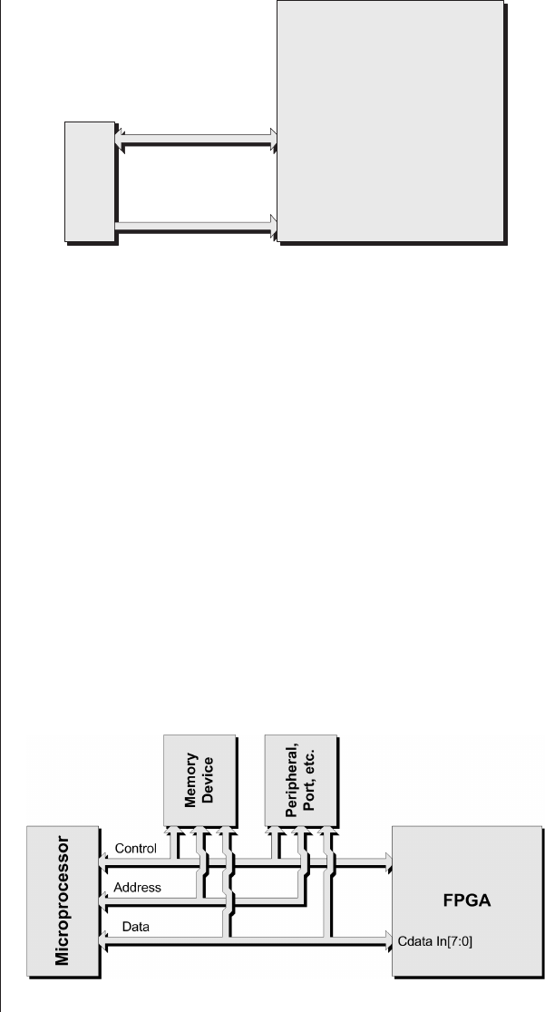
that it wishes to start reading data from the beginning, and
then it sends a series of clock pulses to clock the configuration
data out of the memory device.
Parallel load with FPGA as slave
The modes discussed above, in which the FPGA is the
master, are attractive because of their inherent simplicity and
also because they only require the FPGA itself, along with a
single external memory device.
However, a large number of circuit boards also include a
microprocessor, which is typically already used to perform a
wide variety of housekeeping tasks. In this case, the design
engineers might decide to use the microprocessor to load the
FPGA (Figure 5-8).
110 ■The Design Warrior's Guide to FPGAs
Configuration data [7:0]
Memory
Device
Control FPGA
Cdata In[7:0]
Figure 5-7. Parallel load with FPGA as the master
(modern technique).
Figure 5-8. Parallel load with FPGA as slave.
1846: Germany.
Gustav Kirchhoff
defines Kirchoff’s laws
of electrical networks.

The idea here is that the microprocessor is in control. The
microprocessor informs the FPGA when it wishes to com-
mence the configuration process. It then reads a byte of data
from the appropriate memory device (or peripheral, or what-
ever), writes that data into the FPGA, reads the next byte of
data from the memory device, writes that byte into the FPGA,
and so on until the configuration is complete.
This scenario conveys a number of advantages, not the
least being that the microprocessor might be used to query the
environment in which its surrounding system resides and to
then select the configuration data to be loaded into the FPGA
accordingly.
Serial load with FPGA as slave
This mode is almost identical to its parallel counterpart,
except that only a single bit is used to load data into the
FPGA (the microprocessor still reads data out of the memory
device one byte at a time, but it then converts this data into a
series of bits to be written to the FPGA).
The main advantage of this approach is that it uses fewer
I/O pins on the FPGA. This means that—following the con-
figuration process—only a single I/O pin has the additional
track required to connect it to the microprocessor’s data bus.
Using the JTAG port
Like many other modern devices, today’s FPGAs are
equipped with a JTAG port. Standing for the Joint Test Action
Group and officially known to engineers by its IEEE 1149.1
specification designator, JTAG was originally designed to
implement the boundary scan technique for testing circuit
boards and ICs.
A detailed description of JTAG and boundary scan is
beyond the scope of this book. For our purposes here, it is suffi-
cient to understand that the FPGA has a number of pins that
are used as a JTAG port. One of these pins is used to input
JTAG data, and another is used to output that data. Each of
the FPGAs remaining I/O pins has an associated JTAG regis-
Programming (Configuring) an FPGA ■111
JTAG is pronounced by
spelling out the “J,” fol-
lowed by “tag” to rhyme
with “bag.”
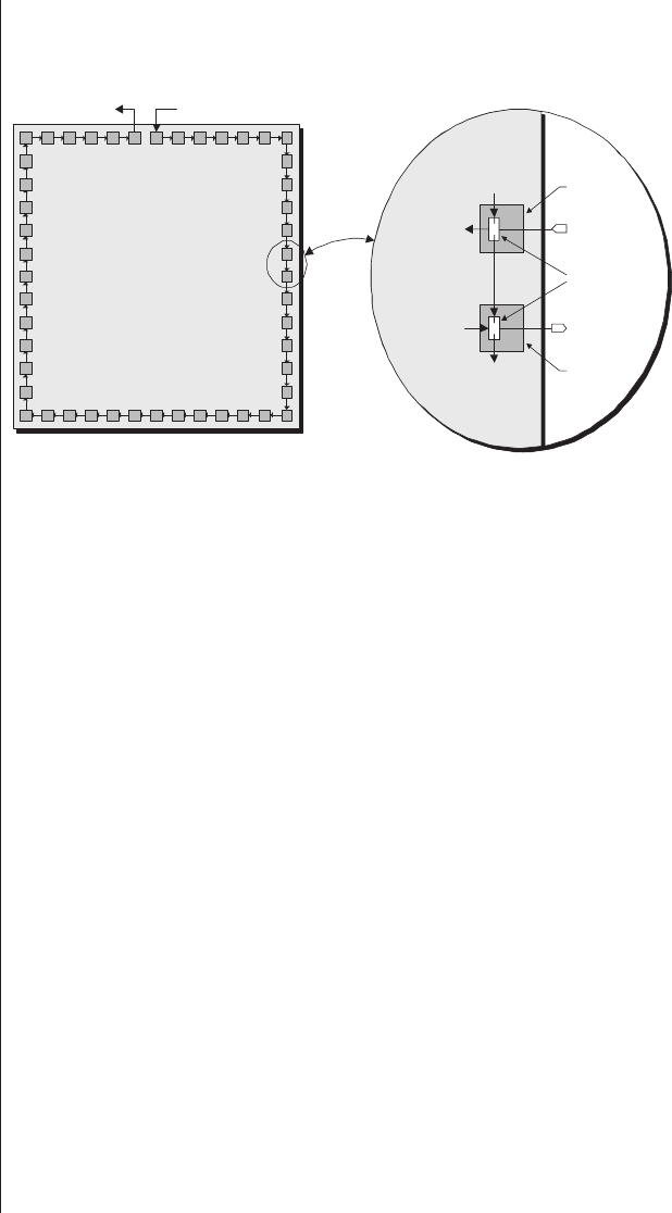
ter (a flip-flop), where these registers are daisy-chained
together (Figure 5-9).
The idea behind boundary scan is that, by means of the
JTAG port, it’s possible to serially clock data into the JTAG
registers associated with the input pins, let the device (the
FPGA in this case) operate on that data, store the results from
this processing in the JTAG registers associated with the out-
put pins, and, ultimately, to serially clock this result data back
out of the JTAG port.
However, JTAG devices also contain a variety of addi-
tional JTAG-related control logic, and, with regard to
FPGAs, JTAG can be used for much more than boundary
scans. For example, it’s possible to issue special commands
that are loaded into a special JTAG command register (not
shown in Figure 5-9) by means of the JTAG port’s data-in
pin. One such command instructs the FPGA to connect its
internal SRAM configuration shift register to the JTAG scan
chain. In this case, the JTAG port can be used to program the
FPGA. Thus, today’s FPGAs now support five different pro-
gramming modes and, therefore, require the use of three mode
pins, as shown in Table 5-2 (additional modes may be added
in the future).
112 ■The Design Warrior's Guide to FPGAs
JTAG data in
Input pin from
outside world
Output pin to
outside world
To internal
logic
From internal
logic
From previous
JTAG flip-flop
To next
JTAG flip-flop
Input pad
Output pad
JTAG flip-flops
JTAG data out
Figure 5-9. JTAG boundary scan registers.
1847: England.
George Boole publishes
his first ideas on
symbolic logic.
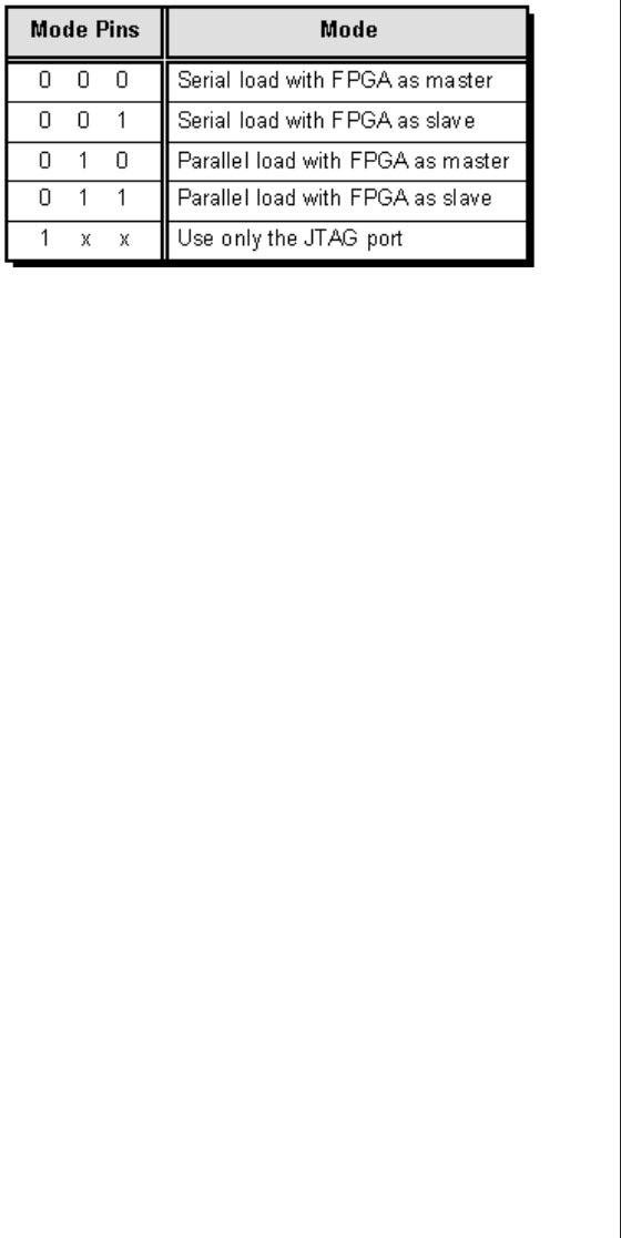
Note that the JTAG port is always available, so the device
can initially be configured via the traditional configuration
port using one of the standard configuration modes, and it can
subsequently be reconfigured using the JTAG port as required.
Alternately, the device can be configured using only the
JTAG port.
Using an embedded processor
But wait, there’s more! In chapter 4, we discussed the fact
that some FPGAs sport embedded processor cores, and each of
these cores will have its own dedicated JTAG boundary scan
chain. Consider an FPGA containing just one embedded proc-
essor (Figure 5-10).
The FPGA itself would only have a single external JTAG
port. If required, a JTAG command can be loaded via this port
that instructs the device to link the processor’s local JTAG
chain into the device’s main JTAG chain. (Depending on the
vendor, the two chains could be linked by default, in which
case a complementary command could be used to disengage
the internal chain.)
The idea here is that the JTAG port can be used to
initialize the internal microprocessor core (and associated
peripherals) to the extent that the main body of the
configuration process can then be handed over to the core. In
Programming (Configuring) an FPGA ■113
Table 5-2. Today’s five configuration modes
1850: England.
Francis Galton invents
the Teletype printer.
some cases, the core might be used to query the environment
in which the FPGA resides and to then select the
configuration data to be loaded into the FPGA accordingly.
114 ■The Design Warrior's Guide to FPGAs
JTAG data inJTAG data out
FPGA
Core
Primary scan chain
Internal (core) scan chain
Figure 5-10. Embedded processor boundary scan chain.

Introduction
As was noted in chapter 1, this tome does not focus on par-
ticular FPGA vendors or specific FPGA devices because new
features and chip types are constantly becoming available.
Insofar as is possible, the book also tries not to mention indi-
vidual EDA vendors or reference their tools by name because
this arena is so volatile that tool names and feature sets can
change from one day to the next.
Having said this, this chapter offers pointers to some of the
key FPGA and EDA vendors associated with FPGAs or related
areas.
FPGA and FPAA vendors
The bulk of this book focuses on digital FPGAs. It is inter-
esting to note, however, that field-programmable analog arrays
(FPAAs) are also available. Furthermore, as opposed to supply-
ing FPGA devices, some companies specialize in providing
FPGA IP cores to be employed as part of standard cell ASIC or
structured ASIC designs.
Company Web site Comment
Actel Corp. www.actel.com FPGAs
Altera Corp. www.altera.com FPGAs
Anadigm Inc. www.anadigm.com FPAAs
Atmel Corp. www.atmel.com FPGAs
Lattice Semiconductor Corp. www.latticesemi.com FPGAs
Leopard Logic Inc. www.leopardlogic.com Embedded FPGA cores
QuickLogic Corp. www.quicklogic.com FPGAs
Xilinx Inc. www.xilinx.com FPGAs
FPGA is pronounced
by spelling it out as
“F-P-G-A.”
FPAA is pronounced
by spelling it out as
“F-P-A-A.”
Who Are All the Players?
Chapter
6

FPNA vendors
This is a bit of a tricky category, not the least because the
name field programmable nodal arrays (FPNAs) was invented
just a few seconds ago by the author as he penned these words
(he’s just that sort of a fellow). The idea here is that each of
these devices features a mega-coarse-grained architecture
comprising an array of nodes, where each node is a complex
processing element ranging from an ALU-type operation, to
an algorithmic function such as a FFT, all the way up to a
complete general-purpose microprocessor core.
These devices aren’t FPGAs in the classic sense. Yet, the
definition of what is and what isn’t an FPGA is a bit fluffy
around the edges on a good day, to the extent that it would be
fair to say that modern FPGAs with embedded RAMs, embed-
ded processors, and gigabit transceivers aren’t FPGAs in the
“classic sense.” In the case of FPNAs, these devices are both
digital and field programmable, so they deserve at least some
mention here.
At the time of this writing, 30 to 50 companies are seri-
ously experimenting with different flavors of FPNAs; a
representative sample of the more interesting ones is as fol-
lows (see also Chapter 23):
Company Web site Comment
Exilent Ltd. www.elixent.com ALU-based nodes
IPflex Inc www.ipflex.com Operation-based nodes
Motorola www.motorola.com Processor-based nodes
PACT XPP Technologies AG www.pactxpp.com ALU-based nodes
picoChip Designs Ltd. www.picochip.com Processor-based nodes
QuickSilver Technology Inc. www.qstech.com Algorithmic element
nodes
Full-line EDA vendors
Each FPGA, FPAA, and FPNA vendor supplies a selec-
tion of design tools associated with its particular devices. In
the case of FPGAs, these tools invariably include the place-
and-route engines. The FPGA vendor may also OEM tools
(often “lite” versions) from external EDA companies. (In this
context, OEM means that the FPGA vendors license this soft-
116 ■The Design Warrior's Guide to FPGAs
FPNA is pronounced
by spelling it out as
“F-P-N-A.” (These are not
to be confused with field
programmable neural
arrays, which share the
FPNA acronym.)
FFT is pronounced
by spelling it out as
“F-F-T.”
EDA is pronounced
by spelling it out as
“E-D-A.”
OEM, which stands for
“original equipment
manufacturer,” is
pronounced by spelling
it out as “O-E-M.”

ware from a third party and then package it and provide it as
part of their own environments.)
First of all, we have the big boys—the full-line EDA ven-
dors who can supply complete solutions from soup to nuts (in
certain cases, these solutions may include OEM’d point tools
from the specialist EDA vendors discussed in the next
section).
Company Web site Comment
Altium Ltd. www.altium.com System-on-FPGA
hardware-software design
environment
Cadence Design Systems www.cadence.com FPGA design entry and
simulation (OEM synthesis)
Mentor Graphics Corp. www.mentor.com FPGA design entry,
simulation, and synthesis
Synopsys Inc. www.synopsys.com FPGA design entry,
simulation, and synthesis
Nothing is simple in this life. For example, it may seem
strange to group a relatively small company like Altium with
comparative giants like the “big three.” In the context of
FPGAs, however, Altium supplies a complete hardware and
software codesign environment for system-on-FPGA develop-
ment. This includes design entry, simulation, synthesis,
compilation/assembly, and comprehensive debugging facilities,
along with an associated multi-FPGA vendor-capable develop-
ment board.
FPGA-specialist and independent EDA vendors
As opposed to purchasing an existing solution, some design
teams prefer to create their own customized environments
using point tools from a number of EDA vendors. In many
cases, these tools are cheaper than their counterparts from the
full-line vendors, but they may also be less sophisticated and
less powerful. At the same time, smaller vendors sometimes
come out with incredibly cool and compelling offerings, and
they may be more accessible and responsive to their customers.
Who Are All the Players? ■117
1850:
The paper bag is
invented.

(“You pay your money and you make your choice,” as the old
saying goes.)
Company Web site Comment
0-In Design Automation www.0-In.com Assertion-based
verification
AccelChip Inc. www.accelchip.com FPGA-based DSP design
Aldec Inc. www.aldec.com Mixed-language
simulation
Celoxica Ltd. www.celoxica.com FPGA-based system
design and synthesis
Elanix Inc. www.elanix.com DSP design and
algorithmic verification
Fintronic USA Inc. www.fintronic.com Simulation
First Silicon Solutions Inc. www.fs2.com On-chip instrumentation
and debugging for FPGA
logic and embedded
processors
Green Hills Software Inc. www.ghs.com RTOS and embedded
software specialists
Hier Design Inc. www.hierdesign.com FPGA-based silicon
virtual prototyping (SVP)
Novas Software Inc. www.novas.com Verification results
analysis
Simucad Inc. www.simucad.com Simulation
Synplicity Inc. www.synplicity.com FPGA-based synthesis
The MathWorks Inc. www.mathworks.com System design and
algorithmic verification
TransEDA PLC www.transeda.com Verification IP
Verisity Design Inc. www.verisity.com Verification languages
and environments
Wind River Systems Inc. www.windriver.com RTOS and embedded
software specialists
FPGA design consultants with special tools
There are a lot of small design houses specializing in
FPGA designs. Some of these boast rather cunning internally
developed design tools that are well worth taking a look at.
Company Web site Comment
Dillon Engineering Inc. www.dilloneng.com ParaCore Architect
Launchbird Inc. www.launchbird.com Confluence system design
language and compiler
Open-source, free, and low-cost design tools
Last but not least, let’s assume that you wish to establish a
small FPGA design team or to set yourself up as a small FPGA
design consultant, but you are a little short of funds just at the
118 ■The Design Warrior's Guide to FPGAs
RTOS, which stands for
“real-time operating sys-
tem,” is pronounced by
spelling out the “R,” fol-
lowed by “toss” to rhyme
with “boss.”
You could probably get
through the rest of your
day without hearing this,
but on the off chance
you are interested, a
groat was an English sil-
ver coin (worth four old
pennies) that was used
between the fourteenth
and seventeenth
centuries.

moment (trust me, I can relate to this). In this case, it is possi-
ble to use a variety of open-source, free, and low-cost
technologies to get a new FPGA design house off the ground
without paying more than a few groats for design tools.
Company Website Comment
Altera Corp. www.altera.com Synthesis and place-and-route
Gentoo www.gentoo.com Linux development platform
Icarus http://icarus.com/eda/verilog Verilog simulator
Xilinx Inc. www.xilinx.com Synthesis and place-and-route
—— www.cs.man.ac.uk/apt/tools/gtkwa
ve/
GTKWave waveform viewer
—— www.opencores.org Open-source hardware cores and
EDA tools
—— www.opencollector.org Database of open-source
hardware cores and EDA tools
—— www.python.org Python programming language
(for custom tooling and DSP
programming)
—— www.veripool.com/dinotrace Dinotrace waveform viewer
—— www.veripool.com/verilator.html Verilator (Verilog to
cycle-accurate C translator)
With regard to using Linux as the development platform,
the two main FPGA vendors—Xilinx and Altera—are now
porting their tools to Linux. Xilinx and Altera also offer free
versions of their ISE and Quartus-II FPGA design environ-
ments, respectively (and even the full-up versions of these
environments are within the budgets of most startups).
Who Are All the Players? ■119
1853:
Scotland/Ireland.
Sir Charles Tilston
Bright lays the first
deepwater cable
between Scotland and
Ireland.

Introduction
My mother is incredibly proud of the fact that “I R an elec-
tronics engineer.” This comes equipped with an absolute and
unshakable faith that I can understand—and fix—any piece of
electronic equipment (from any era) on the planet. In reality,
of course, the truth is far less glamorous because very few
among us are experts at everything.1
In a similar vein, some design engineers have spent the
best years of their young lives developing a seemingly endless
series of ASICs, while others have languished in their cubicles
learning the arcane secrets that are the province of the FPGA
maestro.
The problem arises when an engineer steeped in one of
these implementation technologies is suddenly thrust into the
antipodal domain. For example, a common scenario these days
is for engineers who bask in the knowledge that they know
everything there is to know about ASICs to be suddenly
tasked with creating a design targeted toward an FPGA
implementation.
This is a tricky topic because there are so many facets to it;
the best we can hope for here is to provide an overview as to
some of the more significant differences between ASIC and
FPGA design styles.
Meaning a direct or dia-
metrical opposite, the
word “antipodal” comes
to us from the Greek,
from the plural of anti-
pous, meaning “with the
feet opposite.”
FPGA Versus ASIC Design Styles
Chapter
7
1Only the other day, for example, I ran into an old Wortsel Grinder Mark 4
(with the filigreed flanges and reverberating notchet tattles). I didn’t have
a clue what to do with it, so you can only imagine how foolish I felt.

Coding styles
When it comes to the language-driven design flows dis-
cussed in chapter 9, ASIC designers tend to write very
portable code (in VHDL or Verilog) and to make the mini-
mum use of instantiated (specifically named) cells.
By comparison, FPGA designers are more likely to instan-
tiate specific low-level cells. For example, FPGA users may
not be happy with the way the synthesis tool generates some-
thing like a multiplexer, so they may handcraft their own
version and then instantiate it from within their code.
Furthermore, pure FPGA users tend to use far more
technology-specific attributes with regard to their synthesis
engine than do their ASIC counterparts.
Pipelining and levels of logic
What is pipelining?
One tends to hear the word pipelining quite a lot, but this
term is rarely explained. Of course, engineers know what this
means, but as this book is intended for a wide audience, we’ll
take a few seconds to make sure that we’re all tap-dancing to
the same tune.2Let’s suppose that we’re building something
like a car, and we have all of the parts lying around at hand.
Let’s further assume that the main steps in the process are as
follows:
1. Attach the wheels to the chassis.
2. Attach the engine to the chassis.
3. Attach the seats to the chassis.
4. Attach the body to the chassis.
5. Paint everything.
122 ■The Design Warrior's Guide to FPGAs
2As a young man, my dad and his brothers used to be tap-dancers in the
variety halls of England before WW II (but I bet they never expected to
find this fact noted in an electronics book in the 21st Century).
1854: Crimea.
Telegraph used in the
Crimea War.

Yes … I know, I know. For all of you engineers out there
whom I can hear moaning and groaning (you know who you
are), I’m aware that we haven’t got a steering wheel or lights,
etc., but this is just an example for goodness’ sake!
Now let’s assume that we require a specialist to perform
each of these tasks. One approach would be for everyone to be
sitting around playing cards. The first guy (or gal, of course)3
gets up and attaches the wheels to the chassis, and then
returns to the game. On his return, the second guy gets up and
adds the engine, then he returns to the game. Now the third
guy wanders over to attach the seats. Upon the third guy’s
return, the fourth guy ambles over to connect the body, and so
forth. Once the first car has been completed, they start all
over again.
Obviously, this is a very inefficient scenario. If, for exam-
ple, we assume that each step takes one hour, then the whole
process will take five hours. Furthermore, for each of these
hours, only one man is working, while the other four are hang-
ing around amusing themselves. It would be much more
efficient to have five cars on the assembly line at any one time.
In this case, as soon as the first guy has attached the wheels to
the first chassis, the second guy would start to add the engine
to that chassis while the first guy would begin to add the
wheels to the second chassis. Once the assembly line is in full
flow, everyone will be working all of the time and a new car
will be created every hour.
Pipelining in electronic systems
The point is that we can often replicate this scenario in
electronic systems. For example, let’s assume that we have a
design (or a function forming part of a design) that can be
implemented as a series of blocks of combinational (or combi-
natorial) logic (Figure 7-1).
FPGA Versus ASIC Design Styles ■123
3Except where such interpretation is inconsistent with the context, the
singular shall be deemed to include the plural, the masculine shall be
deemed to include the feminine, and the spelling (and the punctuation)
shall be deemed to be correct!
1855: England.
James Clerk Maxwell
explains Faraday’s
lines of force using
mathematics.
Let’s say that each block takes Ynanoseconds to perform
its task and that we have five such blocks (of which only three
are shown in Figure 7-1, of course). In this case, it will take
5×Ynanoseconds for a word of data to propagate through the
function, starting with its arrival at the inputs to the first
block and ending with its departure from the outputs of the
last block.
Generally speaking, we wouldn’t want to present a new
word of data to the inputs until we have stored the output
results associated with the first word of data.4This means that
we end up with the same result as our inefficient car assembly
scenario in that it takes a long time to process each word of
data, and the majority of the workers (logic blocks) are sitting
around twiddling their metaphorical thumbs for most of the
time. The answer is to use a pipelined design technique in
which “islands” of combinational logic are sandwiched
between blocks of registers (Figure 7-2).
All of the register banks are driven by a common clock
signal. On each active clock edge, the registers feeding a block
of logic are loaded with the results from the previous stage.
These values then propagate through that block of logic until
they arrive at its outputs, at which point they are ready to be
loaded into the next set of registers on the next clock.
124 ■The Design Warrior's Guide to FPGAs
Data In
Combinatorial
Logic
Combinatorial
Logic
Combinatorial
Logic
etc.
Figure 7-1. A function implemented using only
combinatorial logic.
4There is a technique called wave-pipelining in which we might have
multiple “waves” of data passing through the logic at the same time.
However, this is beyond the scope of this book (and it would not be
applicable to an FPGA implementation in any case).
1858: America
Cunard agents in
New York send first
commercial telegraph
message to report a
collision between two
steam ships.
In this case, as soon as “the pump has been primed” and
the pipeline is fully loaded, a new word of data can be proc-
essed every Ynanoseconds.
Levels of logic
All of this boils down to the design engineer’s having to
perform a balancing act. Partitioning the combinational logic
into smaller blocks and increasing the number of register stages
will increase the performance of the design, but it will also
consume more resources (and silicon real estate) on the chip
and increase the latency of the design.
This is also the point where we start to run into the con-
cept of levels of logic, which refers to the number of gates
between the inputs and outputs of a logic block. For example,
Figure 7-3 would be said to comprise three levels of logic
because the worst-case path involves a signal having to pass
through three gates before reaching the output.
FPGA Versus ASIC Design Styles ■125
In the context of an elec-
tronic system, the term
latency refers to the time
(clock cycles) it takes for
a specific block of data
to work its way through
a function, device, or
system.
One way to think of
latency is to return to the
concept of an automo-
bile assembly line. In this
case, the throughput of
the system might be one
car rolling off the end of
the line every minute.
However, the latency of
the system might be a
full eight-hour shift since
it takes hundreds of
steps to finish a car
(where each of these
steps corresponds to a
logic/register stage in a
pipelined design).
&
|
AND
OR
|
NOR
From previous
bank of registers
To next bank
of registers
Three levels of logic
Figure 7-3. Levels of logic.
Clock
Data In
Registers Registers RegistersCombinatorial
Logic
Combinatorial
Logic
etc.
Figure 7-2. Pipelining the design.

In the case of an ASIC, a group of gates as shown in
Figure 7-3 can be placed close to each other such that their
track delays are very small. This means that, depending on the
design, ASIC engineers can sometimes be a little sloppy about
this sort of thing (it’s not unheard of to have paths with, say,
15 or more levels of logic).
By comparison, if this sort of design were implemented on
an FPGA with each of the gates implemented in a separate
LUT, then it would “fly like a brick” (go incredibly slowly)
because the track delays on FPGAs are much more significant,
relatively speaking. In reality, of course, a LUT can actually
represent several levels of logic (the function shown in
Figure 7-3 could be implemented in a single 4-input LUT),
so the position isn’t quite as dire as it may seem at first.
Having said this, the bottom line is that in order to bring
up (or maintain) performance, FPGA designs tend to be more
highly pipelined than their ASIC counterparts. This is facili-
tated by the fact that every FPGA logic cell tends to comprise
both a LUT and a register, which makes registering the output
very easy.
Asynchronous design practices
Asynchronous structures
Depending on the task at hand, ASIC engineers may
include asynchronous structures in their designs, where these
constructs rely on the relative propagation delays of signals in
order to function correctly. These techniques do not work in
the FPGA world as the routing (and associated delays) can
change dramatically with each new run of the place-and-route
engines.
Combinational loops
As a somewhat related topic, a combinational loop occurs
when the generation of a signal depends on itself feeding back
through one or more logic gates. These are a major source of
critical race conditions where logic values depend on routing
126 ■The Design Warrior's Guide to FPGAs
Of course, every latch is
based on internal feed-
back—and every flip-flop
is essentially formed from
two latches—but this
feedback is very tightly
controlled by the device
manufacturer.

delays. Although the practice is frowned upon in some circles,
ASIC engineers can be little rapscallions when it comes to
using these structures because they can fix track routing (and
therefore the associated propagation delays) very precisely.
This is not the case in the FPGA domain, so all such feedback
loops should include a register element.
Delay chains
Last but not least, ASIC engineers may use a series of
buffer or inverter gates to create a delay chain. These delay
chains may be used for a variety of purposes, such as addressing
race conditions in asynchronous portions of the design. In
addition to the delay from such a chain being hard to predict
in the FPGA world, this type of structure increases the design’s
sensitivity to operating conditions, decreases its reliability, and
can be a source of problems when migrating to another archi-
tecture or implementation technology.
Clock considerations
Clock domains
ASIC designs can feature a huge number of clocks (one
hears of designs with more than 300 different clock domains).
In the case of an FPGA, however, there are a limited number
of dedicated global clock resources in any particular device. It
is highly recommended that designers budget their clock sys-
tems to stay within the dedicated clock resources (as opposed
to using general-purpose inputs as user-defined clocks).
Some FPGAs allow their clock trees to be fragmented into
clock segments. If the target technology does support this fea-
ture, it should be identified and accounted for while mapping
external or internal clocks.
Clock balancing
In the case of ASIC designs, special techniques must be
used to balance clock delays throughout the device. By com-
parison, FPGAs feature device-wide, low-skew clock routing
FPGA Versus ASIC Design Styles ■127
1858: Atlantic.
First transatlantic
telegraph cable is laid
(and later failed).
resources. This makes clock balancing unnecessary by the
design engineer because the FPGA vendor has already taken
care of it.
Clock gating versus clock enabling
ASIC designs often use the technique of gated clocks to
help reduce power dissipation, as shown in Figure 7-4a. How-
ever, these tend to give the design asynchronous
characteristics and make it sensitive to glitches caused by
inputs switching too closely together on the gating logic.
By comparison, FPGA designers tend to use the technique
of enabling clocks. Originally this was performed by means of
an external multiplexer as illustrated in Figure 7-4b; today,
however, almost all FPGA architectures have a dedicated
clock enable pin on the register itself, as shown in Figure 7-4c.
PLLs and clock conditioning circuitry
FPGAs typically include PLL or DLL functions—one
for each dedicated global clock (see also the discussions in
Chapter 4). If these resources are used for on-chip clock gen-
eration, then the design should also include some mechanism
for disabling or bypassing them so as to facilitate chip testing
and debugging.
128 ■The Design Warrior's Guide to FPGAs
Figure 7-4. Clock gating versus clock enabling.
(c)
1858:
Queen Victoria
exchanges transatlantic
telegraph messages
with President Buchanan
in America.

Reliable data transfer across multiclock domains
In reality, this topic is true for both ASIC and FPGA
designs, the point being that the exchange of data between
two independent clock domains must be performed very care-
fully so as to avoid losing or corrupting data. Bad
synchronization may lead to metastability issues and tricky
timing analysis problems. In order to achieve reliable transfers
across domains, it is recommended to employ handshaking,
double flopping, or asynchronous FIFO techniques.
Register and latch considerations
Latches
ASIC engineers often make use of latches in their designs.
As a general rule-of-thumb, if you are designing an FPGA, and
you are tempted to use a latch, don’t!
Flip-flops with both “set” and “reset” inputs
Many ASIC libraries offer a wide range of flip-flops,
including a selection that offer both set and reset inputs (both
synchronous and asynchronous versions are usually available).
By comparison, FPGA flip-flops can usually be configured
with either a set input or a reset input. In this case, implement-
ing both set and reset inputs requires the use of a LUT, so
FPGA design engineers often try to work around this and
come up with an alternative implementation.
Global resets and initial conditions
Every register in an FPGA is programmed with a default
initial condition (that is, to contain a logic 0 or a logic 1). Fur-
thermore, the FPGA typically has a global reset signal that will
return all of the registers (but not the embedded RAMs) to
their initial conditions. ASIC designers typically don’t imple-
ment anything equivalent to this capability.
FPGA Versus ASIC Design Styles ■129
1859: Germany.
Hittorf and Pucker
invent the cathode ray
tube (CRT).

Resource sharing (time-division multiplexing)
Resource sharing is an optimization technique that uses a
single functional block (such as an adder or comparator) to
implement several operations. For example, a multiplier may
first be used to process two values called A and B, and then
the same multiplier may be used to process two other values
called C and D. (A good example of resource sharing is pro-
vided in Chapter 12.)
Another name for resource sharing is time-division multi-
plexing (TDM). Resources on an FPGA are more limited
than on an ASIC. For this reason, FPGA designers tend to
spend more effort on resource sharing than do their ASIC
counterparts.
Use it or lose it!
Actually, things are a little subtler than the brief note
above might suggest because there is a fundamental use-it-or-
lose-it consideration with regard to FPGA hardware. This
means that FPGAs only come in certain sizes, so if you can’t
drop down to the next lower size, then you might as well use
everything that’s available on the part you have.
For example, let’s assume that you have a design that
requires two embedded hard processor cores. In addition to
these processors, you might decide that by means of resource
sharing, you could squeeze by with say 10 multipliers and
2 megabytes of RAM. But if the only FPGA containing two
processors also comes equipped with 50 multipliers and
10 megabytes of RAM, you can’t get a refund, so you might
as well make full use of the extra capabilities.
But wait, there’s more
In the case of FPGAs, getting data from LUTs/CLBs to
and from special components like multipliers and MACs is
usually more expensive (in terms of connectivity) than con-
necting with other LUTs/CLBs. Since resource sharing
increases the amount of connectivity, you need to keep a
watchful eye on this situation.
130 ■The Design Warrior's Guide to FPGAs
TDM is pronounced by
spelling it out as “T-D-M.”
In the context of commu-
nications, TDM refers to a
method of taking multiple
data streams and combin-
ing them into a single
signal by dividing the
streams into many seg-
ments (each having a
very short duration) and
multiplexing between
them.
By comparison, in the
context of resource shar-
ing, TDM refers to sharing
a resource like a multi-
plier by multiplexing its
inputs and letting differ-
ent data paths use the
resource at different
times.

In addition to the big components like multipliers and
MACs, you can also share things like adders. Interestingly
enough, in the carry-chain technologies (such as those fielded
by Altera and Xilinx), as a first-order approximation, the cost
of building an adder is pretty much equivalent to the cost of
building a data bus’s worth of sharing logic. For example,
implementing two adders “as is” with completely independent
inputs and outputs will cost you two adders and no resource-
sharing multiplexers. But if you share, you will have one adder
and two multiplexers (one for each set of inputs). In FPGA
terms, this will be more expensive rather than less (in ASICs,
the cost of a multiplexer is far less than the cost of an adder, so
you would have a different trade-off point).
In the real world, the interactions between “using it or los-
ing it” and connectivity costs are different for each technology
and each situation; that is, Altea parts are different from Xil-
inx parts and so on.
State machine encoding
The encoding scheme used for state machines is a good
example of an area where what’s good for an ASIC design
might not be well suited for an FPGA implementation.
As we know, every LUT in an FPGA has a companion
flip-flop. This usually means that there are a reasonable
number of flip-flops sitting around waiting for something to do.
In turn, this means that in many cases, a “one-hot” encoding
scheme will be the best option for an FPGA-based state
machine, especially if the activities in the various states are
inherently independent.
Test methodologies
ASIC designers typically spend a lot of time working with
tools that perform SCAN chain insertion and automatic test
pattern generation (ATPG). They may also include logic in
their designs to perform built-in self-test (BIST). A large propor-
tion of these efforts are intended to test the device for
FPGA Versus ASIC Design Styles ■131
The “one-hot” encoding
scheme refers to the fact
that each state in a state
machine has its own
state variable in the form
of a flip-flop, and only
one state variable may
be active (“hot”) at any
particular time.

manufacturing defects. By comparison, FPGA designers typi-
cally don’t worry about this form of device testing because
FPGAs are preverified by the vendor.
Similarly, ASIC engineers typically expend a lot of effort
inserting and boundary scan (JTAG) into their designs and
verifying them. By comparison, FPGAs already contain
boundary scan capabilities in their fabric.
132 ■The Design Warrior's Guide to FPGAs
JTAG is pronounced
“J-TAG”; that is, by spell-
ing out the ‘J’ followed by
“tag” to rhyme with “nag.”

In the days of yore
In order to set the stage, let’s begin by considering the way
in which digital ICs were designed in the days of old—circa
the early 1960s. This information will interest nontechnical
readers, as well as newbie engineers who are familiar with cur-
rent design tools and flows, but who may not know how they
evolved over time. Furthermore, these discussions establishe
an underlying framework that will facilitate understanding the
more advanced design flows introduced in subsequent
chapters.
In those days, electronic circuits were crafted by hand.
Circuit diagrams—also known as schematic diagrams or just
schematics—were hand-drawn using pen, paper, and stencils
(or the occasional tablecloth should someone happen to have
a brilliant idea while in a restaurant). These diagrams showed
the symbols for the logic gates and functions that were to be
used to implement the design, along with the connections
between them.
Each design team usually had at least one member who was
really good at performing logic minimization and optimization,
which ultimately boils down to replacing one group of gates
with another that will perform the same task faster or using
less real estate on the silicon.
Checking that the design would work as planned insofar as
its logical implementation—functional verification—was typi-
cally performed by a group of engineers sitting around a table
working their way through the schematics saying, “Well, that
looks OK.” Similarly, timing verification—checking that the
The wires connecting the
logic gates on an inte-
grated circuit may be
referred to as wires,
tracks,orinterconnect,
and all of these terms
may be used inter-
changeably.
In certain cases, the term
metallization may also
be used to refer to these
tracks because they are
predominantly formed
by means of the IC’s
metal (metallization)
layers.
Schematic-Based Design Flows
Chapter
8

design met its required input-to-output and internal path
delays and that no violation times (such as setup and hold
parameters) associated with any of the internal registers were
violated—was performed using a pencil and paper (if you were
really lucky, you might also have access to a mechanical or
electromechanical calculator).
Finally, a set of drawings representing the structures used
to form the logic gates (or, more accurately, the transistors
forming the logic gates) and the interconnections between
them were drawn by hand. These drawings, which were
formed from groups of simple polygons such as squares and
rectangles, were subsequently used to create the photo-masks,
which were themselves used to create the actual silicon chip.
The early days of EDA
Front-end tools like logic simulation
Not surprisingly, the handcrafted way of designing dis-
cussed above was time-consuming and prone to error.
Something had to be done, and a number of companies and
universities leapt into the fray in a variety of different direc-
tions. In the case of functional verification, for example, the
late 1960s and early 1970s saw the advent of special programs
in the form of rudimentary logic simulators.
In order to understand how these work, let’s assume that
we have a really simple gate-level design whose schematic dia-
gram has been hand-drawn on paper (Figure 8-1).
By “gate-level” we mean that the design is represented as a
collection of primitive logic gates and functions and the con-
nections between them. In order to use the logic simulator,
the engineers first need to create a textual representation of
the circuit called a gate-level netlist. In those far-off times, the
engineers would typically have been using a mainframe com-
puter, and the netlist would have been captured as a set of
punched cards called a deck (“deck of cards” … get it?). As
computers (along with storage devices like hard disks) became
134 ■The Design Warrior's Guide to FPGAs
1865: England.
James Clerk Maxwell
predicts the existence of
electromagnetic waves
that travel in the same
way as light.
more accessible, netlists began to be stored as text files
(Figure 8-2).
It was also possible to associate delays with each logic gate.
These delays—which are omitted here in order to keep things
simple—were typically referenced as integer multiples of some
core simulation time unit (see also Chapter 19).
Note that the format shown in Figure 8-2 was made up
purely for the purposes of this example. This was in keeping
with the times because—just to keep everyone on their
toes—anyone who created a tool like a logic simulator also
tended to invent his or her own proprietary netlist language.
Schematic-Based Design Flows ■135
BEGIN CIRCUIT=TEST
INPUT SET_A, SET-B, DATA, CLOCK, CLEAR_A, CLEAR_B;
OUTPUT Q, N_Q;
WIRE SET, N_DATA, CLEAR;
GATE G1=NAND (IN1=SET_A, IN2=SET_B, OUT1=SET);
GATE G2=NOT (IN1=DATA, OUT1=N_DATA);
GATE G3=OR (IN1=CLEAR_A, IN2=CLEAR_B, OUT1=CLEAR);
GATE G4=DFF (IN1=SET, IN2=N_DATA, IN3=CLOCK,
IN4=CLEAR, OUT1=Q, OUT2=N_Q);
END CIRCUIT=TEST;
Figure 8-2. A simple gate-level netlist (text file).
G1 = NAND
G2=NOT
G3=OR
SET_A
SET_B
DATA
CLOCK
CLEAR_A
CLEAR_B
CLEAR
SET
N_DATA
Q
N-Q
G4 = DFF
Figure 8-1. A simple schematic diagram (on paper).
1865:
Atlantic cable links
Valencia (Ireland) and
Trinity Bay
(Newfoundland).

All of the early logic simulators had internal representa-
tions of primitive gates like AND, NAND, OR, NOR, etc.
These were referred to as simulation primitives. Some simulators
also had internal representations of more sophisticated
functions like D-type flip-flops. In this case, the G4=DFF
function in Figure 8-2 would map directly onto this internal
representation.
Alternatively, one could create a subcircuit called DFF,
whose functionality was captured as a netlist of primitive
AND, NAND, etc. gates. In this case, the G4=DFF function
in Figure 8-2 would actually be seen by the simulator as a call
to instantiate a copy of this subcircuit.
Next, the user would create a set of test vectors—also
known as stimulus—which were patterns of logic 0 and logic 1
values to be applied to the circuit’s inputs. Once again, these
test vectors were textual in nature, and they were typically
presented in a tabular form looking something like that shown
in Figure 8-3 (anything after a “;” character is considered to be
a comment).
136 ■The Design Warrior's Guide to FPGAs
Instead of calling our test
vectors “stimulus,” we
really should have said
“stimuli,” but we were
engineers, not English
majors!
CC
LL
SS CEE
EEDLAA
TTAORR
__TC__
TIME ABAKAB
----- -----------
0111000 ;Setupinitial values
500111100 ;Rising edge on clock (load 0)
1000 111000 ;Falling edge on clock
1500 110000 ;Setdata to 0 (N_data = 1)
2000 110100 ;Rising edge on clock (load 1)
2500 110101 ;Clear_B goes active (load 0)
:
etc.
Figure 8-3. A simple set of test vectors (text file).

The times at which the stimulus values were to be applied
were shown in the left-hand column. The names of the input
signals are presented vertically to save space.
As we know from Figures 8-1 and 8-2, there is an inverting
(NOT) gate between the DATA input and the D-type flip-
flop. Thus, when the DATA input is presented with 1 at time
zero, this value will be inverted to a 0, which is the value that
will be loaded into the register when the clock undergoes a ris-
ing (0-to-1) edge at time 500. Similarly, when the DATA
input is presented with 0 at time 1,500, this value will be
inverted to a 1, which is the value that will be loaded into the
register when the clock undergoes its next rising (0-to-1) tran-
sition at time 2,000.
In today’s terminology, the file of test vectors shown in
Figure 8-3 would be considered a rudimentary testbench. Once
again, time values were typically specified as integer multiples
of some core simulation time unit.
The engineer would then invoke the logic simulator,
which would read in the gate-level netlist and construct a vir-
tual representation of the circuit in the computer’s memory.
The simulator would then read in the first test vector (the first
line from the stimulus file), apply those values to the appropri-
ate virtual inputs, and propagate their effects through the
circuit. This would be repeated for each of the subsequent test
vectors forming the testbench (Figure 8-4).
The simulator would also use one or more control files (or
online commands) to tell it which internal nodes (wires) and
output pins to monitor, how long to simulate for, and so forth.
The results, along with the original stimulus, would be stored
in tabular form in a textual output file.
Let’s assume that we’ve just travelled back in time and
run one of the old simulators using the circuit represented
in Figures 8-1 and 8-2 along with the stimulus shown in
Figure 8-3. We will also assume that the NOT gate has a delay
of five simulator time units associated with it, which means
that a change on that gate’s input will take five time units to
propagate through the gate and appear on its output. Similarly,
Schematic-Based Design Flows ■137
1866: Ireland/USA.
First permanent
transatlantic telegraph
cable is laid.
we’ll assume that both the NAND and OR gates have associ-
ated delays of 10 time units, while the D-type flip-flop has
associated delays of 20 time units.
In this case, if the simulator were instructed to monitor all
of the internal nodes and output pins, the output file contain-
ing the simulation results would look something like that
shown in figure 8-5.
For the purposes of our discussions, any changes to a sig-
nal’s value are shown in bold font in this illustration, but this
was not the case in the real world.
In this example, the initial values are applied to the input
pins at time 0. At this time, all of the internal nodes and out-
put pins show Xvalues, which indicates unknown states.
After five time units, the initial logic 1 that was applied to the
DATA input propagates through the inverting NOT gate and
appears as a logic 0 on the internal N_DATA node. Similarly,
at time 10, the initial values that were applied to the SET_A
and SET_B inputs propagate through the NAND gate to the
internal SET node, while the values on the CLEAR_A and
CLEAR_B inputs propagate through the OR gate to the inter-
nal CLEAR node.
138 ■The Design Warrior's Guide to FPGAs
BEGIN CIRCUIT=TEST
INPUT SET_A, SET-B,
DATA, CLOCK,
CLEAR_A, CLEAR_B;
OUTPUT Q, N_Q;
WIRE SET, N_DATA, CLEAR;
GATE G1=NAND (IN1=SET_A,
IN2=SET_B,
OUT1=SET);
GATE G2=NOT (IN1=DATA,
OUT1=N_DATA);
GATE G3=OR (IN1=CLEAR_A,
IN2=CLEAR_B,
OUT1=CLEAR);
GATE G4=DFF (IN1=SET, IN2=N_DATA,
IN3=CLOCK, IN4=CLEAR,
OUT1=Q, OUT2=N_Q);
END CIRCUIT=TEST;
Textual gate-level netlist
Textual (tabular) stimulus
CC
LL
SS CEE
EEDLAA
TTAORR
__TC__
TIMEABAKAB
----- -----------
0111000 ;Setup
500111100 ;Rising edge
1000111000 ;Falling edge
1500110000 ;Setdata
2000110100 ;Rising edge
2500110101 ;Clear active
:
etc.
Logic
Simulator
CC
LL N
SS CEE _C
EEDLAA DL
TTAORR SAE N
__TC__ ETA _
TIME ABAKAB TAR QQ
----- ----------- ----- ---
0111000 XXX XX
5111000 X0XXX
10111000 000XX
500 1 1 1 100 000 XX
520111100 000 01
1000 1 1 1 000 000 01
1500 1 1 0000 000 01
1505 110000 01001
2000 1 1 0 100 010 01
2020110100 010 10
2500 110101010 10
2510 1 1 0 1 0 1 0 1 110
2530110101 011 01
:
etc.
Textual (tabular) results file
(stimulus and response)
Figure 8-4. Running the logic simulator.
1869:
William Stanley Jevons
invents the Logic Piano.

At time 500, a rising (0-to-1) edge on the CLOCK input
causes the D-type flip-flop to load the value from the
N_DATA node. The result appears on the Q and N_Q output
pins 20 time units later. And so it goes.
Blank lines in the output file, such as the one shown
between time 10 and time 500, were used to separate related
groups of actions. For example, setting the initial values at
time 0 caused signal changes at times 5 and 10. Then the tran-
sition on the CLOCK input at time 500 caused signal changes
at time 520. As these two groups of actions were totally inde-
pendent of each other, they were separated by a blank line.
It wasn’t long before engineers were working with circuits
that could contain thousands of gates and internal nodes along
with simulation runs that could encompass thousands of time
steps. (Oh, the hours I spent poring over files like this (a) try-
ing to see if a circuit was working as expected, and (b)
Schematic-Based Design Flows ■139
CC
LL N
SS CEE _C
EEDLAA DL
TTAORR SAE N
__TC__ ETA _
TIME A BAKAB TAR QQ
----- ----------- ----- ---
0111000 XXX XX ;Setupinitial values
5111000 X 0XXX
10111000 000XX
500 1 1 1 10 0 0 0 0 X X ; Rising edge on clock
520111100 000 01
1000 1 1 1 00 0 0 0 0 0 1 ; Falling edge on clock
1500 1 1 00 0 0 0 0 0 0 1 ; Set data to 0
1505 1 10000 0 1001
2000 1 1 0 10 0 0 1 0 0 1 ; Rising edge on clock
2020 1 1 0 1 0 0 0 1 0 10
2500 1 1010 10 1 0 1 0 ; Clear_B goes active
2510 1 1 0 1 0 1 0 1 110
2530 1 1 0 1 0 1 0 1 1 01
:
etc.
Figure 8-5. Output results (text file).
1872:
First simultaneous
transmission from both
ends of a telegraph
wire.

desperately attempting to track down the problem if it
wasn’t!)
Back-end tools like layout
As opposed to tools like logic simulators that were
intended to aid the engineers who were defining the function
of ICs (and circuit boards), some companies focused on creat-
ing tools that would help in the process of laying the ICs out.
In this context, “layout” refers to determining where to place
the logic gates (actually, the transistors forming the logic
gates) on the surface of the chip and how to route the wires
between them.
In the early 1970s, companies like Calma, ComputerVi-
sion, and Applicon created special computer programs that
helped personnel in the drafting department capture digital
representations of hand-drawn designs. In this case, a design
was placed on a large-scale digitizing table, and then a
mouse-like tool was used to digitize the boundaries of the
shapes (polygons) used to define the transistors and the inter-
connect. These digital files were subsequently used to create
the photo-masks, which were themselves used to create the
actual silicon chip.
Over time, these early computer-aided drafting tools
evolved into interactive programs called polygon editors that
allowed users to draw the polygons directly onto the computer
screen. Descendants of these tools eventually gained the
ability to accept the same netlist used to drive the logic simu-
lator and to perform the layout (place-and-route) tasks
automatically.
CAE + CAD = EDA
Tools like logic simulators that were used in the front-end
(logical design capture and functional verification) portion of
the design flow were originally gathered together under the
umbrella name of computer-aided engineering (CAE).Bycom
-
parison, tools like layout (place-and-route) that were used in
140 ■The Design Warrior's Guide to FPGAs
The drafting department
is referred to as the
“drawing office” in the UK.
CAE is pronounced
by spelling it out as
“C-A-E.”
CAD is pronounced to
rhyme with “bad.”

the back-end (physical) portion of the design flow were origi-
nally gathered together under the name of computer-aided
design (CAD).
For historical reasons that are largely based on the origins
of the terms CAE and CAD, the term design engineer—or sim-
ply engineer—typically refers to someone who works in the
front-end of the design flow; that is, someone who performs
tasks like conceiving and describing (capturing) the function-
ality of an IC (what it does and how it does it). By comparison,
the term layout designer—or simply designer—commonly refers
to someone who is ensconced in the back-end of the design
flow; that is, someone who performs tasks such as laying out an
IC (determining the locations of the gates and the routes of
the tracks connecting them together).
Sometime during the 1980s, all of the CAE and CAD tools
used to design electronic components and systems were gath-
ered under the name of electronic design automation, or EDA,
and everyone was happy (apart from the ones who weren’t,
but no one listened to their moaning and groaning, so that
was alright).
A simple (early) schematic-driven ASIC flow
Toward the end of the 1970s and the beginning of the
1980s, companies like Daisy, Mentor, and Valid started pro-
viding graphical schematic capture programs that allowed
engineers to create circuit (schematic) diagrams interactively.
Using the mouse, an engineer could select symbols represent-
ing such entities as I/O pins and logic gates and functions from
a special symbol library and place them on the screen. The
engineer could then use the mouse to draw lines (wires) on the
screen connecting the symbols together.
Once the circuit had been entered, the schematic capture
package could be instructed to generate a corresponding gate-
level netlist. This netlist could first be used to drive a logic
simulator in order to verify the functionality of the design. The
same netlist could then be used to drive the place-and-route
software (Figure 8-6).
Schematic-Based Design Flows ■141
The term CAD is also
used to refer to
computer-aided design
tools used in a variety
of other engineering
disciplines, such as
mechanical and
architectural design.
EDA is pronounced
by spelling it out as
“E-D-A.”
Any timing information that was initially used by the
logic simulator would be estimated—particularly in the case of
the tracks—and accurate timing analysis was only possible
once all of the logic gates had been placed and the tracks con-
necting them had been routed. Thus, following
place-and-route, an extraction program would be used to calcu-
late the parasitic resistance and capacitance values associated
with the structures (track segments, vias, transistors, etc.)
forming the circuit. A timing analysis program would then
use these values to generate a timing report for the device.
In some flows, this timing information was also fed back to
the logic simulator in order to perform a more accurate
simulation.
The important thing to note here is that, when creating
the original schematic, the user would access the symbols for
the logic gates and functions from a special library that was
associated with the targeted ASIC technology.1Similarly, the
142 ■The Design Warrior's Guide to FPGAs
Gate-level
netlist
BEGIN CIRCUIT=TEST
INPUT SET_A, SET-B,
DATA, CLOCK,
CLEAR_A, CLEAR_B;
OUTPUT Q, N_Q;
WIRE SET, N_DATA, CLEAR;
GATE G1=NAND (IN1=SET_A,
IN2=SET_B,
OUT1=SET);
GATE G2=NOT (IN1=DATA,
OUT1=N_DATA);
GATE G3=OR (IN1=CLEAR_A,
IN2=CLEAR_B,
OUT1=CLEAR);
GATE G4=DFF (IN1=SET, IN2=N_DATA,
IN3=CLOCK, IN4=CLEAR,
OUT1=Q, OUT2=N_Q);
END CIRCUIT=TEST;
Logic
Simulator
Place-and-
Route
Functional
verification
Extraction and
timing analysis
Detect and fix problems
Detect and fix problems
Schematic
capture
Figure 8-6. Simple (early) schematic-driven ASIC flow.
1There are always different ways to do things. For example, some flows
were based on the concept of using a generic symbol library containing
a subset of logic functions common to all ASIC cell libraries. The netlist
1873: England
James Clerk Maxwell
describes the
electromagnetic nature
of light and publishes
his theory of radio
waves.

simulator would be instructed to use a corresponding library of
simulation models with the appropriate logical functionality2
and timing for the targeted ASIC technology. The end result
was that the gate-level netlist presented to the place-and-route
software directly mapped onto the logic gates and functions
being physically implemented on the silicon chip (this is a tad
different from the FPGA flow, as is discussed in the following
topic).
A simple (early) schematic-driven FPGA flow
When the first FPGAs arrived on the scene in 1984, it was
natural that their design flows would be based on existing
schematic-driven ASIC flows. Indeed, the early portions of the
flows were very similar in that, once again, a schematic capture
package was used to represent the circuit as a collection of
primitive logic gates and functions and to generate a corre-
sponding gate-level netlist. As before, this netlist was
subsequently used to drive the logic simulator in order to per-
form the functional verification.
The differences began with the implementation portion of
the flow because the FPGA fabric consisted of an array of con-
figurable logic blocks (CLBs), each of which was formed from a
number of LUTs and registers. This required the introduction
of some additional steps called mapping and packing into the
flow (Figure 8-7).
Schematic-Based Design Flows ■143
generated from the schematic capture application could then be run
through a translator that converted the generic cell names to their
equivalents in the targeted ASIC library.
2With regard to functionality, one might expect a primitive logical entity
like a 2-input AND gate to function identically across multiple libraries.
This is certainly the case when “good” (logic 0 and 1) values are applied
to the inputs, but things may vary when high-impedance ‘Z’ values or
unknown ‘X’ values are applied to the inputs. And even with good 0 and
1 values applied to their inputs, more complex functions like D-type
latches and flip-flops can behave very differently for “unusual” cases such
as the set and clear inputs being driven active at the same time.
1874: America.
Alexander Graham Bell
conceives the idea of
the telephone.
Mapping
In this context, mapping refers to the process of associating
entities such as the gate-level functions in the gate-level net-
list with the LUT-level functions available on the FPGA. Of
course, this isn’t a one-for-one mapping because each LUT
can be used to represent a number of logic gates (Figure 8-8).
144 ■The Design Warrior's Guide to FPGAs
Portion of gate-level netlist Contents of 3-input LUT
abc y
0
0
0
0
1
1
1
1
0
0
1
1
0
0
1
1
0
1
0
1
0
1
0
1
0
1
1
0
1
0
0
1
a
XOR
|
NOT
b
c
XNOR
|
d
e
y
Figure 8-8. Mapping logic gates into LUTs.
Gate-level
netlist
BEGIN CIRCUIT=TEST
INPUT SET_A, SET-B,
DATA, CLOCK,
CLEAR_A, CLEAR_B;
OUTPUT Q, N_Q;
WIRE SET, N_DATA, CLEAR;
GATE G1=NAND (IN1=SET_A,
IN2=SET_B,
OUT1=SET);
GATE G2=NOT (IN1=DATA,
OUT1=N_DATA);
GATE G3=OR (IN1=CLEAR_A,
IN2=CLEAR_B,
OUT1=CLEAR);
GATE G4=DFF (IN1=SET, IN2=N_DATA,
IN3=CLOCK, IN4=CLEAR,
OUT1=Q, OUT2=N_Q);
END CIRCUIT=TEST;
Fully-routed physical
(CLB-level) netlist
Schematic
capture
Mapping
Packing
Place-and-
Route Timing analysis
and timing report
Gate-level netlist
for simulation
SDF (timing info)
for
s
im
u
l
a
tion
Figure 8-7. Simple (early) schematic-driven FPGA flow.
1875: America.
Edison invents the
Mimeograph.
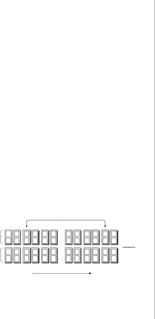
Mapping (which is still performed today, but elsewhere in
the flow, as will be discussed in later chapters) is a nontrivial
problem because there are a large number of ways in which the
logic gates forming a netlist can be partitioned into the smaller
groups to be mapped into LUTs. As a simple example, the
functionality of the NOT gate shown in Figure 8-8 might have
been omitted from this LUT and instead incorporated into the
upstream LUT driving wire c.
Packing
Following the mapping phase, the next step was packing,in
which the LUTs and registers were packed into the CLBs.
Once again, packing (which is still performed today, but else-
where in the flow, as will be discussed in later chapters) is a
nontrivial problem because there are myriad potential combi-
nations and permutations. For example, assume an incredibly
simple design comprising only a couple of handfuls of logic
gates that end up being mapped onto four 3-input LUTs that
we’ll call A, B, C, and D. Now assume that we’re dealing with
an FPGA whose CLBs can each contain two 3-input LUTs. In
this case we’ll need two CLBs (called 1 and 2) to contain our
four LUTs. As a first pass, there are 4! (factorial four = 4 3 2
1 = 24) different ways in which our LUTs can be packed into
the two CLBs (Figure 8-9).
Only 12 of the 24 possible permutations are shown here
(the remainder are left as an exercise for the reader). Further-
Schematic-Based Design Flows ■145
CLB 1 A
B
CLB 2 C
D
A
B
D
C
A
C
B
D
A
C
D
B
A
D
B
C
A
D
C
B
B
A
C
D
B
A
D
C
B
C
A
D
B
C
D
A
B
D
A
C
B
D
C
A
etc.
Different permutations
Functionally equivalent
Figure 8-9. Packing LUTs into CLBs.
1875: England.
James Clerk Maxwell
states that atoms must
have a structure.
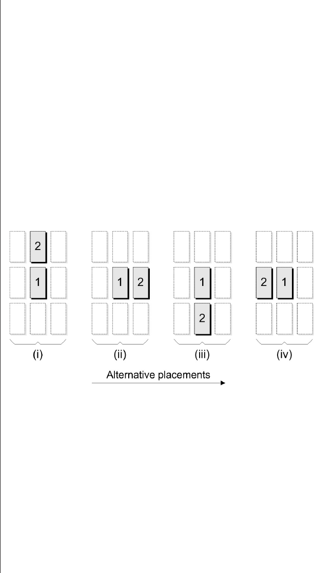
more, in reality there are actually only 12 permutations of
significance because each has a “mirror image” that is func-
tionally its equivalent, such as the AC-BD and BD-AC pairs
shown in Figure 8-9. The reason for this is that when we come
to place-and-route, the relative locations of the two CLBs can
be exchanged.
Place-and-route
Following packing, we move to place-and-route. With
regard to the previous point, let’s assume that our two CLBs
need to be connected together, but that—purely for the pur-
poses of this portion of our discussions—they can only be
placed horizontally or vertically adjacent to each other, in
which case there are four possibilities (Figure 8-10).
In the case of placement (i) for example, if CLB 1 con-
tained LUTs A-C and CLB 2 contained LUTs B-D, then this
would be identical to swapping the positions of the two CLBs
and exchanging their contents.
If we only had the two CLBs shown in figure 8-10, it
would be easy to determine their optimal placement with
respect to each other (which would have to be one of the four
options shown above) and the absolute placement of this
two-CLB group with respect to the entire chip.
146 ■The Design Warrior's Guide to FPGAs
Prior to the advent of
FPGAs, the equivalent
functionality to place-
and-route in “CPLD land”
was performed by an
application known as a
“fitter.”
When FPGAs first arrived
on the scene, people used
the same “fitter” appella-
tion, but over time they
migrated to using the
term “place-and-route”
because this more accu-
rately reflected what was
actually occurring.
As opposed to using a
symbol library of primi-
tive logic gates and
registers, an interesting
alternative circa the early
1990s was to use a sym-
bol library corresponding
to slightly more complex
logical functions (say
around 70 functions). The
output from the sche-
matic was a netlist of
functional blocks that
were already de facto
mapped onto LUTs and
packed into CLBs.
This had the advantage of
giving a better idea of the
number of levels of logic
between register stages,
but it limited such activi-
ties as optimization and
swapping.
Figure 8-10. Placing the CLBs.

The placement problem is much more complex in the real
world because a real design can contain extremely large num-
bers of CLBs (hundreds or thousands in the early days, and
hundreds of thousands by 2004). In addition to CLBs 1 and 2
being connected together, they will almost certainly need to
be connected to other CLBs. For example, CLB 1 may also
need to be connected to CLBs 3, 5 and 8, while CLB 2 may
need to be connected to CLBs 4, 6, 7, and 8. And each of
these new CLBs may need to be connected to each other or to
yet more CLBs. Thus, although placing CLBs 1 and 2 next to
each other would be best for them, it might be detrimental to
their relationships with the other CLBs, and the most optimal
solution overall might actually be to separate CLBs 1 and 2 by
some amount.
Although placement is difficult, deciding on the optimal
way to route the signals between the various CLBs poses an
even more Byzantine problem. The complexity of these tasks is
mind-boggling, so we’ll leave it to those guys and gals who
write the place-and-route algorithms (they are the ones sport-
ing size-16 extra-wide brains with go-faster stripes) and quickly
move onto other things.
Timing analysis and post-place-and-route
simulation
Following place-and-route, we have a fully routed physical
(CLB-level) netlist, as was illustrated in Figure 8-7. At this
point, a static timing analysis (STA) utility will be run to calcu-
late all of the input-to-output and internal path delays and also
to check for any timing violations (setup, hold, etc.) associated
with any of the internal registers.
One interesting point occurs if the design engineers wish
to resimulate their design with accurate (post-place-and-route)
timing information. In this case, they have to use the FPGA
tool suite to generate a new gate-level netlist along with asso-
ciated timing information in the form of an industry-standard
file format called—perhaps not surprisingly—standard delay
format (SDF). The main reason for generating this new gate-
Schematic-Based Design Flows ■147
STA is pronounced by
spelling it out as “S-T-A”
(see also Chapter 19).
SDF is pronounced by
spelling it out as “S-D-F”
(see also Chapter 10).

level netlist is that—once the original netlist has been
coerced into its CLB-level equivalent—it simply isn’t possible
to relate the timings associated with this new representation
back into the original gate-level incarnation.
Flat versus hierarchical schematics
Clunky flat schematics
The very first schematic packages essentially allowed a
design to be captured as a humongous, flat circuit diagram
split into a number of “pages.” In order to visualize this, let’s
assume that you wish to draw a circuit diagram comprising
1,000 logic gates on a piece of paper. If you created a single
large diagram, you would end up with a huge sheet of paper
(say eight-feet square) with primary inputs to the circuit on
the left, primary outputs from the circuit on the right, and the
body of the circuit in the middle.
Carrying this circuit diagram around and showing it to
your friends would obviously be a pain. Instead, you might
want to cut it up into a number of pages and store them all
together in a folder. In this case, you would make sure that
your partitioning was logical such that each page contained all
of the gates relating to a particular function in the design.
Also, you would use interpage connectors (sort of like pseudo
inputs and outputs) to link signals between the various pages.
This is the way the original schematic capture packages
worked. You created a single flat schematic as a series of pages
linked together by interpage connector symbols, where the
names you gave these symbols told the system which ones
were to be connected together. For example, consider a simple
circuit sketched on a piece of paper (Figure 8-11).
Assume that the gates on the left represent some control
logic, while the four registers on the right are implementing a
4-bit shift register. Obviously, this is a trivial example, and a
real circuit would have many more logic gates. We’re just try-
ing to tie down some underlying concepts here, such as the
fact that when you entered this circuit into your schematic
148 ■The Design Warrior's Guide to FPGAs
1876: America.
10th March. Intelligible
human speech heard
over Alexander Graham
Bell’s telephone for the
first time.
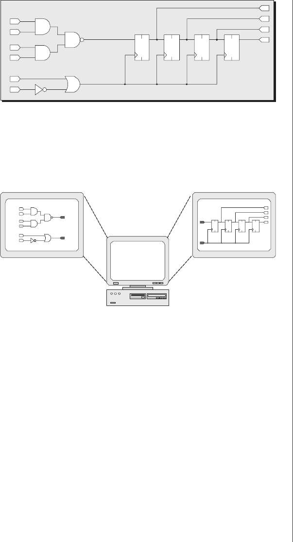
capture system, you might split it into two pages (Figure 8-12).
Sleek hierarchical (block-based) schematics
There were a number of problems associated with the flat
schematics discussed above, especially when dealing with real-
world circuits requiring 50 or more pages:
■It was difficult to visualize a high-level, top-down view
of the design.
■It was difficult to save and reuse portions of the design
in future projects.
■In the case of designs in which some portion of the
circuit was repeated multiple times (which is very
common), that portion would have to be redrawn or
copied onto multiple pages. This became really
Schematic-Based Design Flows ■149
Schematic
capture
system
Page 1
(Control logic)
Page 2
(Shift register)
Figure 8-12. Simple two-page flat schematic.
Figure 8-11. Simple schematic drawn on a piece of paper.
1876: America.
Alexander Graham Bell
patents the telephone.
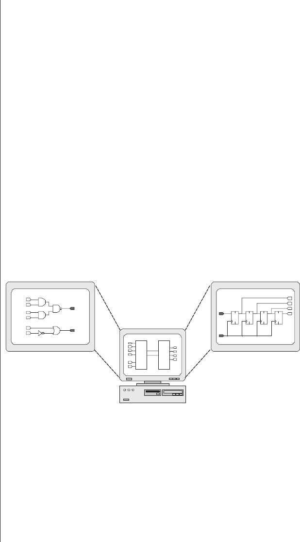
painful if you subsequently realized that you had to
make a change because you would have to make the
same change to all of the copies.
The answer was to enhance schematic capture packages to
support the concept of hierarchy. In the case of our shift regis-
ter circuit, for example, you might start with a top-level page
in which you would create two blocks called control and shift,
each with the requisite number of input and output pins. You
would then connect these blocks to each other and also to
some primary inputs and outputs.
Next, you would instruct the system to “push down” into
the control block, which would open up a new schematic
page. If you were lucky, the system would automatically pre-
populate this page with input and output connector symbols
(and with associated names) corresponding to the pins on its
parent block. You would then create the schematic corre-
sponding to that block as usual (Figure 8-13).
In fact, each block could contain a further block-level
schematic, or a gate-level schematic, or (very commonly) a
mixture of both. These hierarchical block-based schematics
answered the problems associated with flat schematics:
150 ■The Design Warrior's Guide to FPGAs
Top-level page
Contents of
“control” block
Contents of
“Shift” block
Control
Shift
Figure 8-13. Simple hierarchical schematic.
1877: America.
First commercial
telephone service goes
into operation.

■They made it easier to visualize a high-level, top-down
view of the design and to work one’s way through the
design.
■They made it easier to save and reuse portions of the
design in future projects.
■In the case of designs in which some portion of the
circuit was repeated multiple times, it was only
necessary to create that portion—as a discrete
block—once and then to instantiate (call) that block
multiple times. This made things easy if you
subsequently realized that you had to make a change
because you would only have to modify the contents
of the initial block.
Schematic-driven FPGA design flows today
All of the original schematic, mapping, packing, and
place-and-route applications were typically created and owned
by the FPGA companies themselves. However, the general
feeling is that a company can either be good at creating EDA
tools or it can be good at creating silicon chips, but not both.
Another facet of the problem is that design tools were
originally extremely expensive in the ASIC world (even tools
like schematic capture, which today are commonly regarded as
commodity products). By comparison, the FPGA vendors were
focused on selling chips, so right from the get-go they offered
their tools at a very low cost (in fact, if you were a big enough
customer, they’d give you the entire design tool suite for free).
While this had its obvious attractions to the end user, the
downside was that the FPGA vendors weren’t too keen
spending vast amounts of money enhancing tools for which
they received little recompense.
Over time, therefore, external EDA vendors started to sup-
ply portions of the puzzle, starting with schematic capture and
then moving into mapping and packing (via logic synthesis as
discussed in Chapters 9 and 19). Having said this, the FPGA
vendors still typically provide internally developed, less sophis-
ticated (compared to the state-of-the-art) versions of tools like
Schematic-Based Design Flows ■151
1877: America.
Thomas Watson
devises a “thumper” to
alert users of incoming
telephone calls.

schematic capture as part of their basic tool suite, and they
also maintain a Vulcan Death Grip on their crown jewels (the
place-and-route software).
For many engineers today, driving a design using
schematic capture at the gate-level of abstraction is but a
distant memory. In some cases, FPGA vendors offer little
support for this type of flow for their latest devices to the
extent that they only provide schematic libraries for older
component generations. However, schematic capture does
still find a role with some older engineers and also with folks
who need to make minor functional changes to legacy designs.
Furthermore, graphical entry mechanisms that are descended
from early schematic capture packages still find a place in
modern design flows, as is discussed in the next chapter.
152 ■The Design Warrior's Guide to FPGAs
1878: America.
First public long-
distance telephone lines
between Boston and
Providence become
operational.

Schematic-based flows grind to a halt
Toward the end of the 1980s, as designs grew in size and
complexity, schematic-based ASIC flows began to run out of
steam. Visualizing, capturing, debugging, understanding, and
maintaining a design at the gate level of abstraction became
increasingly difficult and inefficient when juggling 5,000 or
more gates and reams of schematic pages.
In addition to the fact that capturing a large design at the
gate level of abstraction is prone to error, it is also extremely
time-consuming. Thus, some EDA vendors started to develop
design tools and flows based on the use of hardware description
languages, or HDLs.
The advent of HDL-based flows
The idea behind a hardware description language is, per-
haps not surprisingly, that you can use it to describe hardware.
In a wider context, the term hardware is used to refer to any of
the physical portions of an electronics system, including the
ICs, printed circuit boards, cabinets, cables, and even the nuts
and bolts holding the system together. In the context of an
HDL, however, “hardware” refers only to the electronic por-
tions (components and wires) of ICs and printed circuit
boards. (The HDL may also be used to provide limited repre-
sentations of the cables and connectors linking circuit boards
together.)
In the early days of electronics, almost anyone who created
an EDA tool created his or her own HDL to go with it. Some
of these were analog HDLs in that they were intended to rep-
EDA is pronounced
by spelling it out as
“E-D-A.”
HDL is pronounced
by spelling it out as
“H-D-L.”
HDL-Based Design Flows
Chapter
9
resent circuits in the analog domain, while others were
focused on representing digital functionality. For the purposes
of this book, we are interested in HDLs only in the context of
designing digital ICs in the form of ASICs and FPGAs.
Different levels of abstraction
Some of the more popular digital HDLs are introduced
later in this chapter. For the nonce, however, let’s focus more
on how a generic digital HDL is used as part of a design flow.
The first thing to note is that the functionality of a digital cir-
cuit can be represented at different levels of abstraction and
that different HDLs support these levels of abstraction to a
greater or lesser extent (figure 9-1).
The lowest level of abstraction for a digital HDL would be
the switch level, which refers to the ability to describe the cir-
cuit as a netlist of transistor switches. A slightly higher level
of abstraction would be the gate level, which refers to the abil-
ity to describe the circuit as a netlist of primitive logic gates
and functions. Thus, the early gate-level netlist formats gener-
154 ■The Design Warrior's Guide to FPGAs
Largely self-taught,
George Boole made sig-
nificant contributions in
several areas of mathe-
matics, but was
immortalized for two
works published in 1847
and 1854 in which he
represented logical
expressions in a mathe-
matical form now known
as Boolean algebra.
In 1938, Claude Shannon
published an article based
on his master’s thesis at
MIT, in which he showed
how Boole’s concepts
could be used to repre-
sent the functions of
switches in electronic
circuits.
RTL
Boolean
Loops
Processes
Structural
Functional
Behavioral
(Algorithmic)
Gate
Switch
Figure 9-1. Different levels of abstraction.

ated by schematic capture packages as discussed in the
previous chapter were in fact rudimentary HDLs.
Both switch-level and gate-level netlists may be classed as
structural representations. It should be noted, however, that
“structural” can have different connotations because it may
also be used to refer to a hierarchical block-level netlist in
which each block may have its contents specified using any of
the levels of abstraction shown in Figure 9-1.
The next level of HDL sophistication is the ability to sup-
port functional representations, which covers a range of
constructs. At the lower end is the capability to describe a
function using Boolean equations. For example, assuming that
we had already declared a set of signals called Y, SELECT,
DATA-A, and DATA-B, we could capture the functionality
of a simple 2:1 multiplexer using the following Boolean
equation:
Y = (SELECT & DATA-A) | (!SELECT & DATA-B);
Note that this is a generic syntax that does not favor any
particular HDL and is used only for the purposes of this exam-
ple. (As we discussed in chapter 3, the “&” character
represents a logical AND, the “|” character represents an OR,
and the “!” character represents a NOT.)
The functional level of abstraction also encompasses regis-
ter transfer level (RTL) representations. The term RTL covers a
multitude of manifestations, but the easiest way to wrap one’s
brain around the underlying concept is to consider a design
formed from a collection of registers linked by combinational
logic. These registers are often controlled by a common clock
signal, so assuming that we have already declared two signals
called CLOCK and CONTROL, along with a set of registers
called REGA, REGB, REGC, and REGD, then an RTL-type
statement might look something like the following:
HDL-Based Design Flows ■155
RTL is pronounced
by spelling it out as
“R-T-L.”

when CLOCK rises
if CONTROL == “1"
then REGA = REGB & REGC;
else REGA = REGB | REGD;
end if;
end when;
In this case, symbols like when,rises,if,then,else, and the
like are keywords whose semantics are defined by the owners
of the HDL. Once again, this is a generic syntax that does not
favor any particular HDL and is used only for the purposes of
this example.
The highest level of abstraction sported by traditional
HDLs is known as behavioral, which refers to the ability to
describe the behavior of a circuit using abstract constructs like
loops and processes. This also encompasses using algorithmic
elements like adders and multipliers in equations; for example:
Y = (DATA-A + DATA-B) * DATA-C;
We should note that there is also a system level of abstrac-
tion (not shown in figure 9-1) that features constructs
intended for system-level design applications, but we’ll worry
about this level a little later.
Many of the early digital HDLs supported only structural
representations in the form of switch or gate-level netlists.
Others such as ABEL, CUPL, and PALASM were used to
capture the required functionality for PLD devices. These lan-
guages (which were introduced in chapter 3) supported
different levels of functional abstraction, such as Boolean
equations, text-based truth tables, and text-based finite state
machine (FSM) descriptions.
The next generation of HDLs, which were predominantly
targeted toward logic simulation, supported more sophisti-
cated levels of abstraction such as RTL and some behavioral
constructs. It was these HDLs that formed the core of the first
true HDL-based design flows as discussed below.
156 ■The Design Warrior's Guide to FPGAs
FSM is pronounced
by spelling it out as
“F-S-M.”
A simple (early) HDL-based ASIC flow
The key feature of HDL-based ASIC design flows is their
use of logic synthesis technology, which began to appear on the
market around the mid-1980s. These tools could accept an
RTL representation of a design along with a set of timing con-
straints. In this case, the timing constraints were presented in a
side-file containing statements along the lines of “the maxi-
mum delay from input Xto output Yshould be no greater than
Nnanoseconds” (the actual format would be a little drier and
more boring).
The logic synthesis application automatically converted
the RTL representation into a mixture of registers and Boolean
equations, performed a variety of minimizations and optimiza-
tions (including optimizing for area and timing), and then
generated a gate-level netlist that would (or at least, should)
meet the original timing constraints (Figure 9-2).
There were a number of advantages to this new type of
flow. First of all, the productivity of the design engineers rose
dramatically because it was a lot easier to specify, understand,
HDL-Based Design Flows ■157
Register
transfer level
RTL
Logic
Simulator
RTL functional
verification
Logic
Synthesis
Gate-level
netlist
Logic
Simulator
Place-and-
Route
Gate-level functional
verification
Figure 9-2. Simple HDL-based ASIC flow.
1878: England.
Sir Joseph Wilson Swan
demonstrates a true
incandescent light
bulb.

discuss, and debug the required functionality of the design
at the RTL level of abstraction as opposed to working with
reams of gate-level schematics. Also, logic simulators could
run designs described in RTL much more quickly than their
gate-level counterparts.
One slight glitch was that logic simulators could work
with designs specified at high levels of abstraction that
included behavioral constructs, but early synthesis tools could
only accept functional representations up to the level of RTL.
Thus, design engineers were obliged to work with a synthesiz-
able subset of their HDL of choice.
Once the synthesis tool had generated a gate-level netlist,
the flow became very similar to the schematic-based ASIC
flows discussed in the previous chapter. The gate-level netlist
could be simulated to ensure its functional validity, and it
could also be used to perform timing analysis based on esti-
mated values for tracks and other circuit elements. The
netlist could then be used to drive the place-and-route
software, following which a more accurate timing analysis
could be performed using extracted resistance and linefeed
capacitance values.
A simple (early) HDL-based FPGA flow
It took some time for HDL-based flows to flourish within
the ASIC community. Meanwhile, design engineers were still
coming to grips with the concept of FPGAs. Thus, it wasn’t
until the very early 1990s that HDL-based flows featuring
logic synthesis technology became fully available in the
FPGA world (Figure 9-3).
As before, once the synthesis tool had generated a gate-
level netlist, the flow became very similar to the schematic-
based FPGA flows discussed in the previous chapter. The
gate-level netlist could be simulated to ensure its functional
validity, and it could also be used to perform timing analysis
based on estimated values for tracks and other circuit ele-
ments. The netlist could then be used to drive the FPGA’s
mapping, packing, and place-and-route software, following
158 ■The Design Warrior's Guide to FPGAs
1878: England.
William Crookes invents
his version of a cathode
ray tube called the
Crookes’ Tube.
which a more accurate timing report could be generated using
real-world (physical) values.
Architecturally aware FPGA flows
The main problem besetting the original HDL-based
FPGA flows was that their logic synthesis technologies were
derived from the ASIC world. Thus, these tools “thought” in
terms of primitive logic gates and registers. In turn, this meant
that they output gate-level netlists, and it was left to the
FPGA vendor to perform the mapping, packing, and place-
and-route functions.
Sometime around 1994, synthesis tools were equipped with
knowledge about different FPGA architectures. This meant
that they could perform mapping—and some level of packing
—functions internally and output a LUT/CLB-level netlist.
This netlist would subsequently be passed to the FPGA ven-
dor’s place-and-route software. The main advantage of this
approach was that these synthesis tools had a better idea about
timing estimations and area utilization, which allowed them to
generate a better quality of results (QoR). In real terms, FPGA
designs generated by architecturally aware synthesis tools were
HDL-Based Design Flows ■159
QoR is pronounced
by spelling it out as
“Q-o-R.”
Register
transfer level
RTL
Logic
Simulator
RTL functional
verification
Logic
Synthesis
Gate-level
netlist
Logic
Simulator
Mapping
Packing
Place-and-
Route
Gate-level functional
verification
Figure 9-3. Simple HDL-based FPGA flow.

15 to 20 percent faster than their counterparts created using
traditional (gate-level) synthesis offerings.
Logic versus physically aware synthesis
We’re jumping a little bit ahead of ourselves here, but this
is as good a place as any to briefly introduce this topic. The
original logic synthesis tools were designed for use with the
multimicron ASIC technologies of the mid-1980s. In these
devices, the delays associated with the logic gates far out-
weighed the delays associated with the tracks connecting
those gates together. In addition to being relatively small in
terms of gate-count (by today’s standards), these designs fea-
tured relatively low clock frequencies and correspondingly
loose design constraints. The combination of all of these fac-
tors meant that early logic synthesis tools could employ
relatively simple algorithms to estimate the track delays, but
that these estimations would be close enough to the real
(post-place-and-route) values that the device would work.
Over the years, ASIC designs increased in size (number of
gates) and complexity. At the same time, the dimensions of
the structures on the silicon chip were shrinking with two
important results:
■Delay effects became more complex in general.
■The delays associated with tracks began to outweigh
the delays associated with gates.
By the mid-1990s, ASIC designs were orders of magnitude
larger—and their delay effects were significantly more sophis-
ticated—than those for which the original logic synthesis
tools had been designed. The result was that the estimated
delays used by the logic synthesis tool had little relation to the
final post-place-and-route delays. In turn, this meant that
achieving timing closure (tweaking the design to make it
achieve its original performance goals) became increasingly
difficult and time-consuming.
160 ■The Design Warrior's Guide to FPGAs
1878: Ireland.
Denis Redmond
demonstrates capturing
an image using
selenium photocells.

For this reason, ASIC flows started to see the use of physi-
cally aware synthesis somewhere around 1996. The ways in
which physically aware synthesis performs its magic are dis-
cussed in more detail in chapter 19. For the moment, we need
only note that, during the course of performing its machina-
tions, the physically aware synthesis engine makes initial
placement decisions for the logic gates and functions. Based
on these placements, the tool can generate more accurate
timing estimations.
Ultimately, the physically aware synthesis tool outputs a
placed (but not routed) gate-level netlist. The ASIC’s physical
implementation (place-and-route) tools use this initial place-
ment information as a starting point from which to perform
local (fine-grained) placement optimizations followed by
detailed routing. The end result is that the estimated delays
used by the physically aware synthesis application more closely
correspond to the post-place-and-route delays. In turn, this
means that achieving timing closure becomes a less taxing
process.
“But what of FPGAs,” you cry. Well, these devices were
also increasing in size and complexity throughout the 1990s.
By the end of the millennium, FPGA designers were running
into significant problems with regard to timing closure. Thus,
around 2000, EDA vendors started to provide FPGA-centric,
physically aware synthesis offerings that could output a
mapped, packed, and placed LUT/CLB-level netlist. In this
case, the FPGA’s physical implementation (place-and-route)
tools use this initial placement information as a starting point
from which to perform local (fine-grained) placement optimi-
zations followed by detailed routing.
Graphical design entry lives on
When the first HDL-based flows appeared on the scene,
many folks assumed that graphical design entry and visualiza-
tion tools, such as schematic capture systems, were poised to
exit the stage forever. Indeed, for some time, many design
engineers prided themselves on using text editors like VI
HDL-Based Design Flows ■161
In an expert’s hands, the
VI editor (pronounced by
spelling it out as “V-I”)
was (and still is) an
extremely powerful tool,
but it can be very frus-
trating for new users.

(from Visual Interface) or EMACS as their only design entry
mechanism.
But a picture tells a thousand words, as they say, and
graphical entry techniques remain popular at a variety of lev-
els. For example, it is extremely common to use a block-level
schematic editor to capture the design as a collection of high-
level blocks that are connected together. The system might
then be used to automatically create a skeleton HDL frame-
work with all of the block names and inputs and outputs
declared. Alternatively, the user might create a skeleton
framework in HDL, and the system might use this to create a
block-level schematic automatically.
From the user’s viewpoint, “pushing” down into one of
these schematic blocks might automatically open an HDL
editor. This could be a pure text-and-command–based editor
like VI, or it might be a more sophisticated HDL-specific
editor featuring the ability to show language keywords in dif-
ferent colors, automatically complete statements, and
so forth.
Furthermore, when pushing down into a schematic block,
modern design systems often give you a choice between enter-
ing and viewing the contents of that block as another,
lower-level block-level schematic, raw HDL code, a graphical
state diagram (used to represent an FSM), a graphical flow-
chart, and so forth. In the case of the graphical
representations like state diagrams and flowcharts, these can
subsequently be used to generate their RTL equivalents auto-
matically (Figure 9-4).
Furthermore, it is common to have a tabular file contain-
ing information relating to the device’s external inputs and
outputs. In this case, both the top-level block diagram and the
tabular file will (hopefully) be directly linked to the same data
and will simply provide different views of that data. Making a
change in any view will update the central data and be
reflected immediately in all of the views.
162 ■The Design Warrior's Guide to FPGAs
1879: America
Thomas Alva Edison
invents an incandescent
light bulb (a year after
Sir Joseph Wilson Swan
in England).
A positive plethora of HDLs
Life would be so simple if there were only a single HDL to
worry about, but no one said that living was going to be easy.
As previously noted, in the early days of digital IC electronics
design (circa the 1970s), anyone who created an HDL-based
design tool typically felt moved to create his or her own lan-
guage to accompany it. Not surprisingly, the result was a
morass of confusion (you had to be there to fully appreciate
the dreadfulness of the situation). What was needed was an
industry-standard HDL that could be used by multiple EDA
tools and vendors, but where was such a gem to be found?
Verilog HDL
Sometime around the mid-1980s, Phil Moorby (one of the
original members of the team that created the famous HILO
logic simulator) designed a new HDL called Verilog. In 1985,
the company he was working for, Gateway Design Automa-
tion, introduced this language to the market along with an
accompanying logic simulator called Verilog-XL.
HDL-Based Design Flows ■163
PLI is pronounced
by spelling it out as
“P-L-I.”
API is pronounced by
spelling it out as
“A-P-I.”
Graphical State Diagram
Graphical Flowchart
When clock rises
If (s == 0)
theny=(a&b)|c;
elsey=c&!(d^e);
Textual HDL
Top-level
block-level
schematic
Block-level schematic
Figure 9-4. Mixed-level design capture environment.

One very cool concept that accompanied Verilog and
Verilog-XL was the Verilog programming language interface
(PLI). The more generic name for this sort of thing is applica-
tion programming interface (API). An API is a library of
software functions that allow external software programs to
pass data into an application and access data from that appli-
cation. Thus, the Verilog PLI is an API that allows users
to extend the functionality of the Verilog language and
simulator.
As one simple example, let’s assume that an engineer is
designing a circuit that makes use of an existing module to
perform a mathematical function such as an FFT. A Verilog
representation of this function might take a long time to
simulate, which would be a pain if all the engineer really
wanted to do was verify the new portion of the circuit. In this
case, the engineer might create a model of this function in the
C programming language, which would simulate, say, 1,000
times faster than its Verilog equivalent. This model would
incorporate PLI constructs, allowing it to be linked into the
simulation environment. The model could subsequently be
accessed from the Verilog description of the rest of the circuit
by means of a PLI call providing a bidirectional link to pass
data back and forth between the main circuit (represented in
Verilog) and the FFT (captured in C).
Yet one more really useful feature associated with Verilog
and Verilog-XL was the ability to have timing information
specified in an external text file known as a standard delay for-
mat (SDF) file. This allowed tools like post-place-and-route
timing analysis packages to generate SDF files that could be
used by the simulator to provide more accurate results.
As a language, the original Verilog was reasonably strong
at the structural (switch and gate) level of abstraction (espe-
cially with regard to delay modeling capability); it was very
strong at the functional (Boolean equation and RTL) level of
abstraction; and it supported some behavioral (algorithmic)
constructs (Figure 9-5).
164 ■The Design Warrior's Guide to FPGAs
FFT is pronounced
by spelling it out as
“F-F-T.”
SDF is pronounced by
spelling it out as
“S-D-F.”
In 1989, Gateway Design Automation along with Verilog
(the HDL) and Verilog-XL (the simulator) were acquired by
Cadence Design Systems. The most likely scenario at that time
was for Verilog to remain as just another proprietary HDL.
However, with a move that took the industry by surprise,
Cadence put the Verilog HDL, Verilog PLI, and Verilog SDF
specifications into the public domain in 1990.
This was a very daring move because it meant that any-
body could develop a Verilog simulator, thereby becoming a
potential competitor to Cadence. The reason for Cadence’s
largesse was that the VHDL language (introduced later in this
section) was starting to gain a significant following. The upside
of placing Verilog in the public domain was that a wide variety
of companies developing HDL-based tools, such as logic syn-
thesis applications, now felt comfortable using Verilog as their
language of choice.
Having a single design representation that could be used by
simulation, synthesis, and other tools made everyone’s life a lot
easier. It is important to remember, however, that Verilog was
originally conceived with simulation in mind; applications like
HDL-Based Design Flows ■165
Structural
(Gate, Switch)
Functional
(RTL,
Boolean)
Behavioral
(Algorithmic)
System
Verilog
Figure 9-5. Levels of abstraction (Verilog).
1879: England.
William Crookes
postulates that cathode
rays may be negative
charged particles.

synthesis were something of an afterthought. This means that
when creating a Verilog representation to be used for both
simulation and synthesis, one is restricted to using a synthesiz-
able subset of the language (which is loosely defined as
whatever collection of language constructs your particular
logic synthesis package understands and supports).
The formal definition of Verilog is encapsulated in a docu-
ment known as the language reference manual (LRM), which
details the syntax and semantics of the language. In this con-
text, the term syntax refers to the grammar of the
language—such as the ordering of the words and symbols in
relation to each other—while the term semantics refers to the
underlying meaning of the words and symbols and the rela-
tionships between the things they denote … phew!
In an ideal world, an LRM would define things so rigor-
ously that there would be no chance of any misinterpretation.
In the real world, however, there were some ambiguities with
respect to the Verilog LRM. Admittedly, these were corner-
case conditions along the lines of “if a control signal on this
register goes inactive at the same time as the clock signal trig-
gers, which signal will be evaluated by the simulator first?” But
the end result was that different Verilog simulators might gen-
erate different results, which is always somewhat disconcerting
to the end user.
Verilog quickly became very popular. The problem was
that different companies started to extend the language in dif-
ferent directions. In order to curtail this sort of thing, a
nonprofit body called Open Verilog International (OVI) was
established in 1991. With representatives from all of the
major EDA vendors of the time, OVI’s mandate was to man-
age and standardize Verilog HDL and the Verilog PLI.
The popularity of Verilog continued to rise exponentially,
with the result that OVI eventually asked the IEEE to form a
working committee to establish Verilog as an IEEE standard.
Known as IEEE 1364, this committee was formed in 1993.
May 1995 saw the first official IEEE Verilog release, which is
166 ■The Design Warrior's Guide to FPGAs
LRM is pronounced
by spelling it out as
“L-R-M.”
OVI is pronounced by
spelling it out as “O-V-I.”

formally known as IEEE 1364-1995, and whose unofficial des-
ignation has come to be Verilog 95.
Minor modifications were made to this standard in 2001;
hence, it is often referred to as the Verilog 2001 (or Verilog
2K1) release. At the time of this writing, the IEEE 1364 com-
mittee is working feverishly on a forthcoming Verilog 2005
offering, while the design world holds its breath in dread
anticipation (see also the section on “Superlog and System-
Verilog” later in this chapter).
VHDL and VITAL
In 1980, the U.S. Department of Defense (DoD) launched
the very high speed integrated circuit (VHSIC) program, whose
primary objective was to advance the state of the art in digital
IC technology.
This program sought to address, among other things, the
fact that it was difficult to reproduce ICs (and circuit boards)
over the long life cycles of military equipment because the
function of the parts wasn’t documented in a rigorous fashion.
Furthermore, different components forming a system were
often designed and verified using diverse and incompatible
simulation languages and design tools.
In order to address these issues, a project to develop a new
hardware description language called VHSIC HDL (or VHDL
for short) was launched in 1981. One unique feature of this
process was that industry was involved from a very early stage.
In 1983, a team comprising Intermetrics, IBM, and Texas
Instruments was awarded a contract to develop VHDL, the
first official release of which occurred in 1985.
Also of interest is the fact that in order to encourage
acceptance by the industry, the DoD subsequently donated all
rights to the VHDL language definition to the IEEE in 1986.
After making some modifications to address a few known prob-
lems, VHDL was released as official standard IEEE 1076 in
1987. The language was further extended in a 1993 release
and again in 1999.
HDL-Based Design Flows ■167
Don’t ask me how VHSIC
is pronounced (it’s been
a long day).
VHDL is pronounced
by spelling it out as
”V-H-D-L.”
As a language, VHDL is very strong at the functional
(Boolean equation and RTL) and behavioral (algorithmic)
levels of abstraction, and it also supports some system-level
design constructs. However, VHDL is a little weak when it
comes to the structural (switch and gate) level of abstraction,
especially with regard to its delay modeling capability.
It quickly became apparent that VHDL had insufficient
timing accuracy to be used as a sign-off simulator. For this rea-
son, the VITAL initiative was launched at the Design
Automation Conference (DAC) in 1992. VHDL Initiative
toward ASIC Libraries (VITAL) was an effort to enhance
VHDL’s abilities for modeling timing in ASIC and FPGA
design environments. The end result encompassed both a
library of ASIC/FPGA primitive functions and an associated
method for back-annotating delay information into these
library models, where this delay mechanism was based on the
same underlying tabular format used by Verilog (Figure 9-6).
168 ■The Design Warrior's Guide to FPGAs
Initially, VHDL didn’t have
an equivalent to Verilog’s
PLI. Today, different
simulators have their own
ways of doing this sort of
thing, such as ModelSim’s
foreign language inter-
face (FLI). We can but
hope that these diverse
offerings will eventually
converge on a common
standard.
DAC may be pronounced
to rhyme with “sack,” or it
may be spelled out as
“D-A-C.”
Structural
(Gate, Switch)
Functional
(RTL,
Boolean)
Behavioral
(Algorithmic)
System
Verilog
VHDL
VITAL
- Relatively easy to learn
- Fixed data types
- Interpreted constructs
- Good gate-level timing
- Limited design reusability
- Limited design management
- No structure replication
- Relatively difficult to learn
- Abstract data types
- Compiled constructs
- Less good gate-level timing
- Good design reusability
- Good design management
- Supports structure replication
Figure 9-6. Levels of abstraction (Verilog versus VHDL).

Mixed-language designs
Once upon a time, it was fairly common for an entire
design to be captured using a single HDL (Verilog or VHDL).
As designs increased in size and complexity, however, it
became more common for different portions of the design to be
created by different teams. These teams might be based in dif-
ferent companies or even reside in different countries, and it
was not uncommon for the different groups to be using differ-
ent design languages.
Another consideration was the increasing use of legacy
design blocks or third-party IP, where the latter refers to a
design team purchasing a predefined function from an external
supplier. As a general rule of thumb related to Murphy’s Law,
if you were using one language, then the IP you wanted was
probably available only in the other language.
The early 1990s saw a period known as the HDL Wars, in
which the proponents of one language (Verilog or VHDL) stri-
dently predicted the imminent demise of the other … but the
years passed and both languages retained strong followings.
The end result was that EDA vendors began to support
mixed-language design environments featuring logic simula-
tors, logic synthesis applications, and other tools that could
work with designs composed from a mixture of Verilog and
VHDL blocks (or modules, depending on your language roots).
UDL/I
As previously noted, Verilog was originally designed with
simulation in mind. Similarly, VHDL was created as a design
documentation and specification language that took simula-
tion into account. As a result one can use both of these
languages to describe constructs that can be simulated, but
not synthesized.
In order to address these problems, the Japan Electronic
Industry Development Association (JEIDA) introduced its own
HDL, the unified design language for integrated circuits (UDL/I)
in 1990.
HDL-Based Design Flows ■169
Murphy’s Law—if any-
thing can go wrong, it
will—is attributed to
Capt. Edward Murphy, an
engineer working at
Edwards Air Force Base
in 1949.

The key advantage of UDL/I was that it was designed from
the ground up with both simulation and synthesis in mind.
The UDL/I environment includes a simulator and a synthesis
tool and is available for free (including the source code).
However, by the time UDL/I arrived on the scene, Verilog
and VHDL already held the high ground, and UDL/I never
really managed to attract much interest outside of Japan.
Superlog and SystemVerilog
In 1997, things started to get complicated because that’s
when a company called Co-Design Automation was formed.
Working away furiously, the folks at Co-Design developed a
“Verilog on steroids” called Superlog.
Superlog was an amazing beast that combined the simplic-
ity of Verilog with the power of the C programming language.
It also included things like temporal logic, sophisticated
design verification capabilities, a dynamic API, and the
concept of assertions that are key to the formal verification
strategy known as model checking. (VHDL already had a simple
assert construct, but the original Verilog had nothing to boast
about in this area.)
The two main problems with Superlog were (a) it was
essentially another proprietary language, and (b) it was so
much more sophisticated than Verilog 95 (and later Verilog
2001) that getting other EDA vendors to enhance their tools
to support it would have been a major feat.
Meanwhile, while everyone was scratching their heads
wondering what the future held, the OVI group linked up
with their equivalent VHDL organization called VHDL Inter-
national to form a new body called Accellera. The mission of
this new organization was to focus on identifying new stan-
dards and formats, to develop these standards and formats, and
to foster the adoption of new methodologies based on these
standards and formats.
In the summer of 2002, Accellera released the specifica-
tion for a hybrid language called SystemVerilog 3.0 (don’t
even ask me about 1.0 and 2.0). The great advantage to this
170 ■The Design Warrior's Guide to FPGAs
1880: America.
Alexander Graham Bell
patents an optical
telephone system called
the Photophone.

language was that it was an incremental enhancement to the
existing Verilog, rather than the death-defying leap repre-
sented by a full-up Superlog implementation. Actually,
SystemVerilog 3.0 featured many of Superlog’s language con-
structs donated by Co-Design. It included things like the
assertion and extended synthesis capabilities that everyone
wanted and, being an Accellera standard, it was well placed to
quickly gain widespread adoption.
The current state of play (at the time of this writing) is
that Co-Design was acquired by Synopsys in the fall of 2002.
Synopsys maintained the policy of donating language con-
structs from Superlog to SystemVerilog, but no one is really
talking about Superlog as an independent language anymore.
After a little pushing and pulling, all of the mainstream EDA
vendors officially endorsed SystemVerilog and augmented
their tools to accept various subsets of the language, depending
on their particular application areas and requirements. System-
Verilog 3.1 hit the streets in the summer of 2003, followed by a
3.1a release (to add a few enhancements and fix some annoy-
ing problems) around the beginning of 2004. Meanwhile, the
IEEE is set to release the next version of Verilog in 2005. In
order to avert a potential schism between Verilog 2005 and
SystemVerilog, Accellera has promised to donate their Sys-
temVerilog copyright to the IEEE by the summer of 2004.
SystemC
And then we have SystemC, which some design engineers
love and others hate with a passion. SystemC—discussed in
more detail in chapter 11—can be used to describe designs at
the RTL level of abstraction.1These descriptions can subse-
quently be simulated 5 to 10 times faster than their Verilog or
VHDL counterparts, and synthesis tools are available to con-
vert the SystemC RTL into gate-level netlists.
HDL-Based Design Flows ■171
1SystemC can support higher levels of abstraction than RTL, but those
levels are outside the scope of this chapter; instead, they are discussed in
more detail in chapter 11.
1880: France.
Pierre and Jacques
Currie discover
piezoelectricity.

One big argument for SystemC is that it provides a more
natural environment for hardware/software codesign and co-
verification. One big argument against it is that the majority
of design engineers are very familiar with Verilog or VHDL,
but they are not familiar with the object-orientated aspects of
SystemC. Another consideration is that the majority of
today’s synthesis offerings represent hundreds of engineer
years of development in translating Verilog or VHDL into
gate-level netlists. By comparison, there are far fewer
SystemC-based synthesis tools, and those that are available
tend to be somewhat less sophisticated than their more tradi-
tional counterparts.
In reality, SystemC is more applicable to a system-level
versus an RTL design environment. Having said this, Sys-
temC seems to be gaining a lot of momentum in Asia and
Europe, and the debate on SystemC versus SystemVerilog ver-
sus VHDL will doubtless be with us for quite some time.
Points to ponder
Be afraid, be very afraid
Most software engineers throw up their hands in horror
when they look at another programmer’s code, and they
invariably start a diatribe as to the lack of comments, consis-
tency, whatever … you name it, and they aren’t happy
about it.
They don’t know how lucky they are because the RTL
source code for a design often sets new standards for awful-
ness! Sad to relate, the majority of designs described in RTL
are almost unintelligible to another designer. In an ideal
world, the RTL description of a design should read like a
book, starting with a “table of contents” (an explanation of
the design’s structure), having a logical flow partitioned into
“chapters” (logical breaks in the design), and having lots of
“commentary” (comments explaining the structure and opera-
tion of the design).
172 ■The Design Warrior's Guide to FPGAs
1881:
Alan Marquand invents
a graphical technique of
representing logic
problems.
It’s also important to note that coding style can impact
performance (this typically affects FPGAs more than ASICs).
One reason for this is that, although they might be logically
equivalent, different RTL statements can yield different
results. Also, tools are part of the equation because different
tools can yield different results.
The various FPGA vendors and EDA vendors are in a posi-
tion to provide their customers with reams of information on
particular coding styles and considerations with regard to their
chips and tools, respectively. However, the following points
are reasonably generic and will apply to most situations.
Serial versus parallel multiplexers
When creating RTL code, it is useful to understand what
your synthesis tool is going to do in certain circumstances. For
example, every time you use an if-then-else statement, the
result will be a 2:1 multiplexer. This becomes interesting in
the case of nested if-then-else statements, which will be syn-
thesized into a priority structure. For example, assume that we
have already declared signals Y, A, B, C, D, and SEL (for
select) and that we use them to create a nested if-then-else
(Figure 9-7).
HDL-Based Design Flows ■173
if SEL == 00“ then Y = A;
elseif SEL == 01“ then Y = B;
elseif SEL == 10“ then Y = C;
else Y = D;
end if;
A
B
C
D2:1 MUX
2:1 MUX
2:1 MUX
SEL == 00
SEL == 01
SEL == 10
Y
Figure 9-7. Synthesizing nested if-then-else statements.
1883: America.
William Hammer and
Thomas Alva Edison
discover the “Edison
Effect”.
As before, the syntax used here is a generic one that
doesn’t really reflect any of the mainstream languages. In this
case, the innermost if-then-else will be the fastest path, while
the outermost if-then-else will be the critical signal (in terms
of timing). Having said this, in some FPGAs all of the paths
through this structure will be faster than using a case state-
ment. Speaking of which, a case statement implementation of
the above will result in a 4:1 multiplexer, in which all of the
timing paths associated with the inputs will be (relatively)
equal (Figure 9-8).
Beware of latch inference
Generally speaking, it’s a good idea to avoid the use of
latches in FPGA designs unless you really need them. One
other thing to watch out for: If you use an if-then-else state-
ment, but neglect to complete the “else” portion, then most
synthesis tools will infer a latch.
Use constants wisely
Adders are the most used of the more complex operators
in a typical design. In certain cases, ASIC designers some-
times employ special versions using combinations of
half-adders and full-adders. This may work very efficiently in
the case of a gate array device, for example, but it will typi-
cally result in a very bad FPGA implementation.
When using an adder with constants, a little thought goes
a long way. For example, “A + 2” can be implemented more
174 ■The Design Warrior's Guide to FPGAs
case SEL of;
00“: Y = A;
01“: Y = B;
10“: Y = C;
otherwise:Y = D;
end case;
B
A
4:1 MUX
SEL
C
D
Y
00
01
10
11
Figure 9-8. Synthesizing a case statement.
1884: Germany.
Paul Gottleib Nipkow
uses spinning disks to
scan, transmit, and
reproduce images.

efficiently as “A + 1 with carry-in,” while “A – 2” would be
better implemented as “A – 1 with carry-in.”
Similarly, when using multipliers, “A * 2” can be imple-
mented much more efficiently as “A SHL 1” (which translates
to “A shifted left by one bit”), while “A * 3” would be better
implemented as “(A SHL 1) + A.”
In fact, a little algebra also goes a long way in FPGAs. For
example, replacing “A * 9” with “(A SHL 3) + A” results in at
least a 40 percent reduction in area.
Consider resource sharing
Resource sharing is an optimization technique that uses a
single functional block (such as an adder or comparator) to
implement several operators in the HDL code.
If you do not use resource sharing, then each RTL opera-
tion is built using its own logic. This results in better
performance, but it uses more logic gates, which equates to sili-
con real estate. If you do decide to use resource sharing, the
result will be to reduce the gate-count, but you will typically
take a hit in performance. For example, consider the statement
illustrated in Figure 9-9.
Note that frequency values shown in Figure 9-9 are of
interest only for the purposes of this comparison, because these
values will vary according to the particular FPGA architecture,
and they will change as new process nodes come online.
The following operators can be shared with other instances
of the same operator or with related operators on the same
line:
*
+ –
> < >= <=
For example, a + operator can be shared with instances of
other + operators or with – operators, while a * operator can
be shared only with other * operators.
HDL-Based Design Flows ■175
1886:
Reverend Charles
Lutwidge Dodgson
(Lewis Carrol) publishes
a diagrammatic
technique for logic
representation in The
Game of Logic.
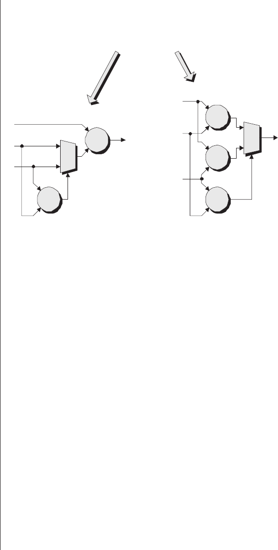
If nothing else, it’s a good idea to check whether or not
your synthesis application has resource sharing enabled or dis-
abled by default. And one final point is that resource sharing
in ASICs can alleviate routing congestion, but it may actually
cause routing problems in FPGAs.
Last but not least
Internal tri-state buses are slow in most FPGAs and should
be avoided unless you are 100 percent confident that you
know what you’re doing. If at all possible, use tri-state buffers
only at the top-most level of the design. If you do wish to use
internal tri-state buffers, then in the case of FPGA families
that don’t support these gates, the majority of today’s synthe-
sis tools provide automatic tri-state-to-multiplexer conversion
(this basically involves converting the tri-state buffers speci-
fied in the RTL into corresponding LUT/CLB-based logic.)
176 ■The Design Warrior's Guide to FPGAs
For not-so-technical read-
ers, the circles with “>”
symbols indicate com-
parators (circuits that
compare two numbers to
determine which is the
larger); the circles with
“+” symbols indicate
adders; and the wedge-
shaped blocks are 2:1
multiplexers that select
between their inputs
based on the value of the
control signals coming
out of the comparators.
if (B > C)
thenY=A+B;
elseY=A+C;
end if;
A
+
>
B
CY
>
C
B
+
+
A
Y
Resource
Sharing = ON
(one adder)
Resource
Sharing = OFF
(two adders)
Total LUTs =
Clock frequency =
32
87.7 MHz
Total LUTs =
Clock frequency =
64
133.3 MHz (+52% !
)
Figure 9-9. Resource sharing.

Also, bidirectional buffers can cause timing loop problems,
so if you use them, make sure that any false paths are clearly
marked.
HDL-Based Design Flows ■177

Just what is an SVP?
Before we leap headfirst into the concept of silicon virtual
prototyping for FPGAs, it’s probably worth reminding our-
selves how the silicon virtual prototype (SVP) concept originated
in the ASIC world, some of the alternative SVP manifesta-
tions one might see in that world, and some of the problems
associated with those manifestations.
As high-end ASIC devices containing tens of millions of
logic gates appeared on the scene, capacity and complexity
issues associated with these megadesigns caused design flows to
become a little wobbly around the edges.
The problem is that, with traditional flows, many design
issues do not become apparent until accurate timing analysis
can be performed following extraction of realistic physical val-
ues (capacitance, resistance, and sometimes inductance), based
on the results from place-and-route. This requires the engi-
neers to go all of the way through the flow (including synthesis
and place-and-route) before they discover a major problem
that would have been better detected and resolved earlier in
the process.
This is extremely irritating, and the end result often
involves numerous time-consuming iterations that can so
delay a design that it completely misses its time-to-market
window. (In many cases there is only room in the market for
the winner, and there’s no such thing as second place!)
One solution is to create an SVP, which is a representation
of the design that can be generated relatively quickly, but
which (hopefully) contains sufficient information to allow the
SVP is pronounced by
spelling it out as “S-V-P.”
Silicon Virtual Prototyping
for FPGAs
Chapter
10

designers to identify and address a large proportion of poten-
tial problems before they undergo the time-consuming
portions of the design flow. In theory, the time taken to iter-
ate a design using an SVP can be measured in hours, as
opposed to days or weeks using conventional design flows.
ASIC-based SVP approaches
As was discussed in the previous chapter, the role of logic
synthesis is to accept an RTL representation of a design along
with a set of timing constraints. The logic synthesis applica-
tion automatically converts this RTL representation into a
mixture of registers and Boolean equations, performs a variety
of minimizations and optimizations (including optimizing for
area and timing), and then generates a gate-level netlist that
hopefully meets the original timing constraints.
Conventional logic synthesis solutions operate in the
gate-size versus delay plane, which means they are constantly
making trade-offs with regard to the size of gates and the
delays associated with those gates. Due to their underlying
modus operandi, these tools perform tremendous amounts of
compute-intensive, time-consuming evaluations. Even worse,
many of the optimization decisions performed by the synthesis
tool are often rendered meaningless when the design is
handed over to the physical implementation (place-and-
route) portion of the flow.
Gate-level SVPs (from fast-and-dirty synthesis)
One key aspect of an SVP is the ability to generate it
quickly and easily. The majority of current ASIC SVPs are
based on the use of a gate-level netlist representation of the
design that is subsequently placed using a rough-and-ready
placement algorithm. Unfortunately, conventional synthesis
tools consume too much time and computational resources to
meet the speed demands of prototyping. Thus, some ASIC-
based SVP flows make use of a fast-and-dirty synthesis engine
(Figure 10-1).
180 ■The Design Warrior's Guide to FPGAs
1887: England.
J. Thomson discovers
the electron.
This fast-and-dirty engine is typically based on completely
different algorithms from the main synthesis application, for
example, direct RTL mapping. Thus, the ensuing gate-level
netlist used to form the SVP is not as accurate a representation
of the design’s final implementation as one might hope for.
In turn, this means that once the SVP has been used to
perform RTL exploration and timing analysis, engineers still
have to perform a full-up logic synthesis (or physically aware
synthesis) step using a completely different synthesis engine in
order to generate the real netlist to be passed on to the physi-
cal implementation (place-and-route) tools.
So, the big problem with this SVP-based approach is that
the prototyping tools and their methodologies are separate and
distinct from the implementation tools and their methodolo-
gies. This leads to unpredictability of design convergence due
to lack of correlation, which can result in time-consuming
back-end–to–front-end iterations, which sort of defeats the
whole purpose of using an SVP in the first place!
Gate-level SVPs (from gain-based synthesis)
As opposed to conventional logic synthesis that is based in
the gate-size versus delay plane, a concept known as gain-based
Silicon Virtual Prototyping for FPGAs ■181
Iterations take days/weeks
Iterations take hours
Place & Route
Timing Analysis
Logic
Synthesis
RTL
Fast & Dirty
Synthesis
Prototype
Exploration
Timing Analysis
Different
Engines
Place & Route
Timing Analysis
Logic
Synthesis
RTL
Fast & Dirty
Synthesis
Prototype
Exploration
Timing Analysis
SVP World Implementation World
Figure 10-1. SVP based on fast-and-dirty synthesis.
1887: England.
William Crookes
demonstrates that
cathode rays travel in a
straight line.

synthesis1is a kettle of fish of a different color (I never meta-
phor I didn’t like).
This form of synthesis is derived from ideas put forward by
Ivan Sutherland, Bob Sproull, and David Harris in their 1999
book Logical Effort: Designing Fast CMOS Circuits.2In this
case, the synthesis engine uses logical effort concepts to estab-
lish a fixed-timing plane, and the physical implementation
(place-and-route) tools subsequently work within this plane.
This means that all timing optimizations are completed
and all circuit delays are determined and frozen by the end of
the synthesis step. When the placement engine performs its
task, it uses a size-driven algorithm in which all of the cells are
dynamically sized to meet their timing budgets based on the
actual loads they see. Following placement, a load-driven
routing engine is used to tune the width and spacing of the
tracks so as to maintain the original timing budgets and to
ensure signal integrity.
One interesting point with regard to the gain-based
approach is that the amount of computer memory and compu-
tational effort required to perform this type of synthesis are a
fraction of that demanded by conventional synthesis tools.
This means that a gain-based synthesis engine claims an order
of magnitude increase in capacity over conventional synthesis
approaches.
Another interesting point is that the gain-based synthesis
engine automatically uses up any slack in path delays. This
means that the smallest possible sizes are used for each gate
that will just meet the timing budget. Thus, the resulting
implementation occupies the smallest amount of silicon real
estate, which significantly reduces congestion, power con-
sumption, and noise problems.
182 ■The Design Warrior's Guide to FPGAs
1At the time of this writing, one of the chief proponents of gain-based
synthesis is Magma Design Automation (www.magma-da.com).
2Ivan Sutherland is internationally renowned for his pioneering work on
logic design.
1887: Germany.
Heinrich Hertz
demonstrates the
transmission, reception,
and reflection of radio
waves.
“But,” you cry, “what does all of this have to do with
SVPs?” Well, the speed and capacity inherent to gain-based
synthesis means that the same synthesis engine can be used for
both prototyping and implementation (Figure 10-2).
Basing both the prototyping and implementation environ-
ments on the same algorithms, tools, and methodologies
provides high correlation and predictable design convergence
and significantly reduces time-consuming back-end–to–front-
end iterations.
Cluster-level SVPs
As discussed earlier, the majority of today’s SVPs are based
on full-blown gate-level netlist representations of the design.
Even though these representations may be generated using
fast-and-dirty synthesis, they can still contain millions upon
millions of logic gates, which can strain the capacity of the
SVP’s placement and analysis engines.
One solution is to use the concept of clustering as a basis for
the SVP’s placement decisions and track-delay estimations. In
this case the cells (gates and registers) generated by fast-and-
dirty or gain-based synthesis are automatically gathered into
groups called clusters. Each cluster typically consists of tens to
Silicon Virtual Prototyping for FPGAs ■183
Iterations take days/weeks
Iterations take hours
Place & Route
Timing Analysis
Logic
Synthesis
RTL
Fast & Dirty
Synthesis
Prototype
Exploration
Timing Analysis
Identical
Engines
Place & Route
Timing Analysis
Gain-based
Synthesis
RTL
Gain-based
Synthesis
Prototype
Exploration
Timing Analysis
SVP World Implementation World
Figure 10-2. SVP based on gain-based synthesis.
1888: America.
First coin-operated
public telephone
invented.
hundreds of cells, which means that they are small enough to
preserve overall placement quality; however, the number of
clusters is orders of magnitude smaller than the number of
cells, providing extremely significant run-time improvements.
The actual number of cells may vary from cluster to cluster
so as to keep the areas of the clusters as uniform as possible. In
order to streamline computational complexity and capacity
requirements, optimization and analysis are performed on the
clustered data. Furthermore, in cases where two clusters are
linked by multiple wires (which is a common occurrence),
these wires are considered to be a single “weighted” wire for
the purposes of estimating routing resource utilization, which
has an effect on cluster placement.
RTL-based SVPs
A well-accepted engineering rule of thumb states that
detecting, isolating, and resolving a problem at any stage of
the design, implementation, or deployment process costs 10
times more than addressing the same problem at the previous
stage in the process. In the case of digital ICs, there are three
major breakpoints in the design flow with respect to analyzing
area, timing, and so forth. (Figure 10-3).
184 ■The Design Warrior's Guide to FPGAs
RTL
(Pre-synthesis)
Gate
(Post-IPO)
Gate
(Post-layout)
Level of Design
Abstraction
1x
~10x
~100x
Relative cost of timing
analysis and debug
Figure 10-3. Major breakpoints with respect to analyzing
area, timing, and so forth.
1889: America.
Almon Brown Strowger
invents the first
automatic telephone
exchange.

The term timing closure refers to analyzing a design or archi-
tecture to detect and correct any problematic timing paths.
Irrespective of the level it is performed at, timing closure is an
iterative process, which means that the analyze-detect-correct
steps typically need to be run a number of times in order to
achieve convergence.
With regard to the levels of abstraction shown in
Figure 10-3, postlayout timing analysis is the most accurate by
far, but it is extremely expensive with regard to cost and time.
Iterating at the postlayout level is a painful proposition, and
design teams try very hard to avoid making changes at this
level.
In the case of conventional flows, the first breakpoint for
relatively accurate timing analysis occurs at the gate level fol-
lowing synthesis and in-place optimization (IPO). The problem
is that getting to this post-IPO breakpoint using conventional
flows requires the use of physically aware synthesis to provide a
placed gate-level netlist. This approach is therefore extremely
compute-intensive and time-consuming, and large blocks can
take days to go through the full physical synthesis and timing
analysis process. Not only does this stretch out the design and
timing closure process, but it also ties up expensive EDA tools
that could be being used for implementing chips rather than
analyzing their timing.
One alternative is to use a gate-level SVP as discussed
above; but, once again, these representations have their own
problems, including requiring the use of some form of
compute-intensive and time-consuming synthesis and
placement.
Another approach is to work with an RTL-based SVP,3
which allows engineers to quickly identify and address paths
that will cause downstream timing problems. In order to wrap
one’s brain around how this works, it’s first necessary to under-
stand that there’s a related application that takes the logical
Silicon Virtual Prototyping for FPGAs ■185
IPO means that, after the
placement algorithm has
performed its initial pass,
it is possible to make
certain “tweaks” (optimi-
zations), such as
changing the size of cells
based on updated esti-
mates of the length of
the tracks they will see.
3At the time of this writing, one of the chief proponents of RTL-based
SVPs is InTime Software (www.intimesw.com).
and physical (LEF and DEF) definition files associated with an
ASIC cell library and generates a corresponding design kit
database to be used by the RTL-based SVP (Figure 10-4).
It’s important to note that such a design kit is not a library
of characterized gates, but is instead a database of character-
ized logical functions (such as counters, XOR trees, etc.). The
design kit generator captures the behavior of these logical
functions, including timing and area estimations.
The RTL-based SVP generator and analysis engine subse-
quently accepts the RTL code for the design, the time
constraints associated with the design block (in industry-
standard SDF format), and the design kit associated with the
target cell library. As the SVP generator reads in the RTL, it
converts it into a netlist of entities called work functions. Each
work function is an abstraction that directly maps onto an
equivalent function in the design kit.
Once the RTL has been converted into a netlist of work
functions, the SVP generator performs identical logical opera-
tions to those that are typically performed at the gate level,
including common subexpression elimination, constant
propagation, loop unraveling, the removal of all redundant
functional computations, and so forth.
The SVP generator and analysis engine uses the resulting
minimal irredundant network of work functions to perform a
“virtual placement” of these functions. This placement is
then used to generate accurate area estimates, which are
subsequently used to generate accurate time estimates. In con-
186 ■The Design Warrior's Guide to FPGAs
LEF stands for “logical
exchange format,” where
this file details the logical
functionality of the cells
in the library.
Similarly, DEF stands for
“design exchange for-
mat,” where this file
details the physical
aspects of the cells in the
library, such as their
resistance and capaci-
tance values and their
physical dimensions.
Design Kit
Generator
LEF
DEF
Design Kit
Figure 10-4. Generating a design kit.

junction with the design kit, the SVP generator and analysis
engine understands how the various synthesis engines will
weight various factors and modify their implementation strate-
gies (such as swapping counter realizations) in order to meet
the specified timing constraints. All of these factors are taken
into account when performing the analysis.
Proponents of RTL-based SVPs claim a 40-fold speed
increase as compared to generating a post-IPO, pre-place-and-
route gate-level netlist using a physically aware synthesis
approach. In an example 4.5-million-gate design circa 2003,
this equated to a 2.5-hour iteration to generate and analyze an
RTL-based SVP as compared to 99 hours to generate and ana-
lyze a post-IPO gate-level netlist.
Of course the big question is, just how accurate are RTL-
based SVPs? The supporters of this form of SVP claim that its
timing analysis results typically correlate to post-IPO delays
with an error of 20 percent or less (worst-case errors may rise
to 30 percent). Although this may sound pretty dire, the latest
generation of synthesis tools is capable of closing timing on
RTL that is within 20 to 30 percent of the desired timing (it’s
the paths that are off by 80, 150, 200 percent, and higher that
cause problems). Thus, RTL-based SVPs are accurate enough
to allow design engineers to generate RTL code that can subse-
quently be fully implemented by the downstream syntheses
and layout engines.
I know, I know. We’ve digressed again, although you have
to admit that this is all interesting stuff! But now let’s return to
pondering FPGAs.
FPGA-based SVPs
Not surprisingly, multimillion-gate FPGA designs are hit-
ting the same problems that befell ASICs, including the fact
that it takes ages to place, route, and perform timing analysis
on the little rascals.
One particularly painful aspect of this process is that,
although the original RTL representation of the design is
Silicon Virtual Prototyping for FPGAs ■187
1890: America
Census is performed
using Herman
Hollerith’s punched
cards and automatic
tabulating machines.

almost invariably hierarchical,4the FPGA’s place-and-route
tools typically end up working on flattened representations of
the design. This means that even if you make the smallest of
changes to a single block of RTL code and resynthesize only
that block, you end up having to rerun place-and-route on the
entire design. In turn, this means that you can grow to be old
and gray before you finally get to achieve timing closure on
your design.
In order to address these problems, some EDA vendors
have started to provide tools that support the concept of an
FPGA SVP by providing a mixture of floor planning and pre-
place-and-route timing analysis. This is coupled with the abil-
ity to perform place-and-route on individual design blocks,
which dramatically speeds up the implementation process.5
This form of SVP commences with a graphical top-down
view of the target FPGA device showing all of the internal
logical resources, such as LUTs, registers, slices, CLBs, embed-
ded RAMs, multipliers, and so forth.
Following the logic synthesis step (using the synthesizer of
your choice), the SVP generator loads the ensuing hierarchi-
cal LUT/CLB-level netlist, along with any associated timing
and physical constraints, and automatically creates an initial
floor plan. This auto-generated floor plan shows a collection
of square and/or rectangular blocks, each of which corresponds
to a top-level module in the design. Furthermore, if any of
these top-level modules itself contains submodules, then these
are shown as embedded blocks in the floor plan (and so on
down through the hierarchy).
The SVP generator performs its own initial placement of
the resources (LUTs, registers, RAMs, multipliers, etc.) used
by each block. These resources are also shown in the top-
down view of the device, along with graphical representations
188 ■The Design Warrior's Guide to FPGAs
4By “hierarchical,” we mean that the top level of the design is typically
formed from a number of functional modules, which may themselves call
submodules and so forth.
5At the time of this writing, one of the chief proponents of FPGA SVPs,
in the form described here, is Hier Design (www.hierdesign.com).
1890s:
John Venn proposes
logic representation
using circles and
eclipses.

as to the amount of routing resources required to link the vari-
ous blocks together.
Interactive manipulation
The initial placement of the design in the SVP allows it to
provide accurate timing estimations on a block-by-block basis
prior to running place-and-route. If any potential problem
areas are detected, you can interactively modify the floor plan
in order to address them.
The simplest form of manipulation is to reshape the rec-
tangular blocks in the floor plan by pulling their sides to make
them taller, thinner, shorter, or fatter. Alternatively, you can
create more complex outlines such as “L,” “U,” and “T” shapes
(pretty much any contour you can form out of squares and
rectangles).
Next, you can move the blocks around. When you grab a
block and start to drag it across the face of the device, the sys-
tem will provide a graphical indication as to whether or not
there are the necessary resources required to implement that
block at its current location (you can only drop the block in an
area where there are sufficient resources). Furthermore, as you
manipulate a block by reshaping it or moving it around, the
system dynamically displays the utilization of resources (LUTs,
registers, RAMs, multipliers, etc.) inside that block relative to
the total amount of each resource type currently encompassed
by that block.
You can also split existing blocks into two or more sub-
blocks, which you can then manipulate independently.
Alternatively, you can merge two or more blocks into a single
block. Also, in some cases (say, areas of control logic), you
might wish to pull one or more subblocks out of their parent
blocks and move them up to the top level of the design, at
which point you can reshape them, merge them together,
move them around, and so forth. Much of this reflects a differ-
ent philosophy of how one might use an ASIC floor-planning
tool. In the case of an ASIC, for example, if you have two
Silicon Virtual Prototyping for FPGAs ■189
1892: America.
First automatic
telephone switchboard
comes into service.

blocks with lots of interconnect between them, you would
typically place them side by side. By comparison, in the case
of an FPGA, merging the blocks (thereby allowing the place-
and-route tools to do a much better job of optimization using
local versus global routing resources) might provide a more
efficacious solution.
Furthermore, you aren’t limited to manipulating blocks
only as described in the original RTL hierarchy. You can actu-
ally manipulate individual FPGA resources like LUTs,
registers, slices, CLBs, and the like. This includes dragging
them around and repositioning them within their current
hierarchical block, dragging them from one hierarchical block
to another, creating new blocks, and dragging groups of LUTs
from one or more existing blocks into this new block, and
so forth.
Where things start to get really clever is that, if you go
back to make changes to your original RTL and resynthesize
those modules, then when you reimport the resulting
LUT/CLB-level netlist(s), the SVP generator sorts everything
out for you and loads the right logic into the appropriate
floor-plan blocks. (How do they do it? I don’t have a clue!)
Incremental place-and-route
As soon as you are ready to rock and roll, you can select
one or more floor-plan blocks and kick off the FPGA vendor’s
place-and-route software. Each block is treated as an individ-
ual entity, so once you’ve laid out a block, it will remain
untouched unless you decide you want to change it. This has
a number of advantages. First of all, place-and-route run times
for individual blocks are extremely small compared to the
traditional times associated with full-up multimillion-gate
designs.
And even if you add up the place-and-route times for run-
ning all of the blocks individually, the total elapsed time is
much less than it would be if one were performing place-and-
route on the design in its entirety. This is because the com-
plexity (and associated run times) of place-and-route increases
190 ■The Design Warrior's Guide to FPGAs
1894: Germany.
Heinrich Hertz discovers
that radio waves travel
at the speed of light and
can be refracted and
polarised.

in a nonlinear manner as the size of the block being processed
increases. Furthermore, once you’ve run place-and-route on all
of the blocks, you can make changes to individual blocks and
rerun place-and-route only on those blocks without affecting
the rest of the chip.
An additional advantage associated with this SVP
approach is that it lends itself to creating and preserving IP.
That is, once a block has undergone place-and-route, you can
lock it down and export it as a new structural LUT/CLB-level
netlist along with its associated physical and timing con-
straints. This block can subsequently be used in other designs
(its placement is relative, which means that it can be dragged
around the chip and relocated as discussed above).
RTL-based FPGA SVPs
In an ideal world, it would be nice to be able to work with
RTL-based FPGA SVPs. The various FPGA and EDA vendors
do provide RTL-level floor-planning tools with varying
degrees of sophistication. At the time of this writing, however,
there is no FPGA equivalent to the state-of-the-art in RTL-
based ASIC SVP technology (but we will doubtless see such a
beast in the not-so-distant future).
Silicon Virtual Prototyping for FPGAs ■191
1894: Italy.
Guglielmo Marconi
invents wireless
telegraphy.

Problems with traditional HDL-based flows
With regard to the traditional HDL-based flows introduced
in chapter 9, a design commences with an original concept,
whose high-level definition is determined by system architects
and system designers. It is at this stage that macro-
architecture decisions are made, such as partitioning the design
into hardware and software components (see also chapter 13).
The resulting specification is then handed over to the
hardware design engineers, who commence their portion of
the development process by performing microarchitecture defini-
tion tasks such as detailing control structures, bus structures,
and primary data path elements. These microarchitecture defi-
nitions, which are often performed in brainstorming sessions
on a whiteboard, may include performing certain operations in
parallel versus sequential, pipelining portions of the design
versus nonpipelining, sharing common resources (for example,
two operations sharing a single multiplier, versus using dedi-
cated resources) and so forth.
Eventually, the design intent is captured by writing RTL
VHDL/Verilog. Following verification via simulation, this
RTL is then synthesized down to a structural netlist suitable
for use by the target technology’s place-and-route applications
(Figure 11-1).
At the time of this writing, these VHDL or Verilog-based
flows account for around 95 percent of all ASIC and FPGA
designs; however, there are a number of problems associated
with these flows:
Note that this chapter
focuses on C/C++ flows
in the context of generic
digital designs. Consid-
erations such as
quantization (commenc-
ing with floating-point
representations which
are subsequently
coerced into their fixed-
point counterparts) are
covered in the discus-
sions on DSP-centric
designs in chapter 12.
C/C++ etc.–Based Design Flows
Chapter
11
■Capturing the RTL is time-consuming: Even though Ver-
ilog and VHDL are intended to represent hardware, it
is still time-consuming to use these languages to cap-
ture the functionality of a design.
■Verifying RTL is time-consuming: Using simulation to
verify large designs represented in RTL is computation-
ally expensive and time-consuming.
■Evaluating alternative implementations is difficult: Modify-
ing and reverifying RTL to perform a series of what-if
evaluations of alternative microarchitecture implemen-
tations is difficult and time-consuming. This means
that the number of evaluations the design team can
perform may be limited, which can result in a less-
than-optimal implementation.
■Accommodating specification changes is difficult: If any
changes to the specification are made during the course
of the project, folding these changes into the RTL and
performing any necessary reverification can be painful
and time-consuming. This is a significant consideration
in certain application areas, such as wireless projects,
because broadcast standards and protocols are con-
stantly evolving and changing.
■The RTL is implementation specific: Realizing a design in
an FPGA typically requires a different RTL coding
style from that used for an ASIC implementation (see
also the discussions in Chapters 7, 9, and 18). This
194 ■The Design Warrior's Guide to FPGAs
In the case of an FPGA
target, the LUT/CLB-level
netlist may be presented
in EDIF, VHDL, or Verilog
depending on the FPGA
vendor.
With regards to physi-
cally aware synthesis-
based flows, EDIF
remains the “netlist of
choice.” In this case, the
placement information
may be incorporated in
the EDIF itself or pre-
sented in an external
“constraints” side-file.
Implementation-specific RTL
(time-consuming to create, slow
to simulate, difficult to modify)
FPGA
target
Gate-level
netlist
LUT/CLB-
level netlist
ASIC
target
Original
Concept
Capture
RTL Simulate Synthesize
Capture
RTL Simulate Synthesize
uA
Definition
uA
Definition
Implementation-specific
micro-architecture
definition
Figure 11-1. Traditional (simplified) HDL-based flows.

means that it can be extremely difficult to retarget a
complex design represented in RTL from one imple-
mentation technology to another. This is of concern
when one is migrating an existing ASIC design into an
FPGA equivalent or creating an FPGA design to be
used as a prototype for a future ASIC implementation.
One way to view this is that all of the implementa-
tion intelligence associated with the design is hard-
coded into the RTL, which therefore becomes imple-
mentation specific. It’s important to understand that
this implementation specificity goes beyond the coarse
ASIC-versus-FPGA boundary, which dictates that RTL
intended for an FPGA implementation is not suitable
for an optimal ASIC realization, and vice versa. Even
assuming a single target device architecture, the way in
which a set of algorithms is used to process data may re-
quire a number of different micro-
architecture implementations, depending on the target
application areas.
Actually, to be scrupulously fair, we should probably
note that the same RTL may be used to drive both
ASIC and FPGA implementations. The reason for do-
ing this is to avoid the risk of introducing a functional
bug into the RTL when retargeting the code, but there
is typically a penalty to be paid. That is, if code origi-
nally targeted toward an FPGA implementation is sub-
sequently used to drive an ASIC implementation, the
resulting ASIC will typically require more silicon real
estate and have higher power consumption as compared
to using RTL created with an ASIC architecture in
mind. Similarly, if code originally targeted toward an
ASIC implementation is subsequently used to drive an
FPGA implementation, the ensuing FPGA will typi-
cally take a significant performance hit as compared to
using RTL created with an FPGA architecture in mind.
■RTL is less than ideal for hardware-software codesign:
System-on-chip (SoC) devices are generally under-
C/C++ etc.–Based Design Flows ■195
1895: America.
Dial telephones go into
Milwaukee’s city hall.

stood to be those that include microprocessor cores.
Irrespective of whether these designs are to be
realized using ASICs or FPGAs, today’s SoCs are
exhibiting an ever-increasing amount of software
content. When coupled with increased design reuse
on the hardware side, in many cases it is necessary to
verify the software and hardware concurrently so as
to completely validate such things as the system
diagnostics, RTOS, device drivers, and embedded
application software. Generally speaking, it can be
painful verifying (simulating) the hardware
represented in VHDL or Verilog in conjunction with
the software represented in C/C++ or assembly
language.
One approach that addresses the issues enumerated above
is to perform the initial design capture at a higher level of
abstraction than can be achieved with RTL VHDL/Verilog.
The first such level is to use some form of C/C++, but as usual
nothing is simple because there are a variety of alternatives,
including SystemC, augmented C/C++, and pure C/C++.
C versus C++ and concurrent versus sequential
Before we leap into the fray, we should tie down a couple
of points to ensure that we’re all marching in step to the same
beat. First, there is a wide variety of programming languages
available, but—excepting specialist application areas—the
most commonly used by far are traditional C and its object-
oriented offspring C++. For our purposes here, we will refer to
these collectively as C/C++.
The next point of import is that, by default, statements in
languages like C/C++ are executed sequentially. For example,
assuming that we have already declared three integer variables
called a,b, and c, then the following statements
a = 6; /* Statement in C/C++ program */
b = 2; /* Statement in C/C++ program */
c = 9; /* Statement in C/C++ program */
196 ■The Design Warrior's Guide to FPGAs
RTOS is pronounced
“R-tos.” That is, by spell-
ing out the “R” followed
by “TOS” to rhyme with
“boss.”
Real-time systems are
those in which the cor-
rectness of a
computation or action
depends not only on how
it is performed
but also when it is
performed.

would, perhaps not surprisingly, occur one after the other.
However, this has certain implications; for example, if we now
assume that the following statements occur sometime later in
the program
a = b; /* Statement in C/C++ program */
b = a; /* Statement in C/C++ program */
then a(which initially contained 6) will be loaded with the
value currently stored in b(which is 2). Next, b(which ini-
tially contained 2) will be loaded with the value currently
stored in a(which is now 2), so both aand bwill end up con-
taining the same value.
The sequential nature of programming languages is the way
in which software engineers think. However, hardware design
engineers have quite a different view of the world. Let’s assume
that a piece of hardware contains two registers called aand b
that are driven by a common clock signal. Let’s further assume
that these registers have previously been loaded with values of
6 and 2, respectively. Finally, let’s assume that at some point in
the HDL code, we see the following statements:
a = b; /* Statement in VHDL/Verilog Code */
b = a; /* Statement in VHDL/Verilog Code */
As usual, the above syntax doesn’t actually represent
VHDL or Verilog; it’s just a generic syntax used only for the
purposes of this example. Generally speaking, hardware engi-
neers would expect both of these statements to be executed
concurrently (at the same time). This means that a(which ini-
tially contained 6) will be loaded with the value stored in b
(which was 2) while—at the same time—b(which initially
contained 2) will be loaded with the value stored in a(which
was 6). The end result is that the initial contents of a and b
will be exchanged.
As usual, of course, the above is something of a simplifica-
tion. However, it’s fair to say that HDL statements will
C/C++ etc.–Based Design Flows ■197
1895: Germany.
Wilhelm Kohnrad
Roentgen discovers
X-rays.

execute concurrently by default, unless sequential behavior
is forced by means of techniques like blocking assignments.
Thus, by default, RTL-based logic simulators will execute the
statements shown above in this concurrent manner; similarly
RTL-based logic synthesis tools will generate hardware that
handles these two activities simultaneously. By comparison,
unless explicitly directed to do otherwise (by means of the
techniques introduced later in this chapter), C/C++ state-
ments will execute sequentially.
SystemC-based flows
What is SystemC (and where did it come from)?
Before we come to consider SystemC-based flows, it is
probably a good idea to briefly summarize just what SystemC
is, because there is typically some confusion on this point (not
the least in the mind of the author).
SystemC 1.0
One of the underlying concepts behind SystemC is that it
is an open-source environment to which everyone contrib-
utes. As an example, consider Linux, which was rough around
the edges at first. Based on contributions from different folks,
however, Linux eventually became a real operating system
(OS) with the potential to challenge Microsoft.
In this spirit, a relatively undocumented SystemC 1.0 was
let loose to roam wild and free circa 2000. SystemC 1.0 was a
C++ class library that facilitated the representation of notions
such as concurrency (things happening at the same time),
timing, and I/O pins. By means of this class library, engineers
could capture designs at the RTL level of abstraction.
One advantage of this early incarnation was that it facili-
tated hardware/software codesign environments. Another was
that SystemC representations at the RTL level of abstraction
might simulate 5 to 10 times faster than their VHDL and Ver-
198 ■The Design Warrior's Guide to FPGAs
SystemC is “managed” by
the Open SystemC Initia-
tive (OSCI). This is an
independent not-for-
profit organization com-
posed of companies,
universities, and indi-
viduals dedicated to
promoting SystemC as
an open-source standard
for system-level design.
The code for SystemC—
along with an integrated
simulator and design
environment—is
available from
www.systemc.org.
ilog counterparts.1On the downside, it was harder and more
time-consuming to capture an RTL-level design in SystemC
1.0 than with VHDL or Verilog. Furthermore, there was a
scarcity of design tools that could synthesize SystemC 1.0 rep-
resentations into netlist-level equivalents with any degree of
sophistication.
SystemC 2.0
Later, in 2002, SystemC 2.0 arrived on the scene. This
augmented the 1.0 release with some high-level modeling con-
structs such as FIFOs (a form of memory that can accept and
subsequently make available a series of words of data and that
operates on a first-in first-out principle). The 2.0 release also
included a variety of behavioral, algorithmic, and system-level
modeling capabilities, such as the concepts of transactions and
channels (which are used to describe the communication of
data between blocks at an abstract level).
In order to gain a little perspective on all of this, let’s first
consider a typical scenario of how things would have worked
using the original SystemC 1.0. As a simple example, let’s
assume that we have two functions called f(x) and g(x) that
have to communicate with each other. (Figure 11-2).
C/C++ etc.–Based Design Flows ■199
Two functions captured
in high-level C/C++
f(x) g(x)
Interface between
functions has to be
defined as pins
Figure 11-2. Interfacing in SystemC 1.0.
1This is design-dependent; in reality, some SystemC RTL-level simulation
run times are at parity with their HDL counterparts.
1895: Russia.
Alexander Popov
(also spelled Popoff)
constructs a receiver
for natural electricity
waves and tries to
detect thunderstorms.
In this case, the interface between the blocks would have
to be defined at the pin level. The real problem with this
approach occurs when you are in the early stages of a design,
because you are already defining implementation details such
as bus widths. This makes things difficult to change if you
wish to experiment with different what-if architectural scenar-
ios. This aspect of things became much easier with SystemC
2.0, which allowed abstract interfaces to be declared between
the blocks (Figure 11-3).
Now, the interfacing between the blocks can be performed
at the level of abstract records on the basis that, in the early
stages of the design cycle, we don’t really care how data gets
from point a to point b, just that it does get there somehow.
These abstract interfaces facilitate performing architec-
tural evaluation early in the design cycle. Once the
architecture starts to firm up, you can start refining the inter-
face by using high-level constructs such as a FIFO to which
one would assign attributes like width and depth and charac-
teristics like blocking write, nonblocking read, and how to
behave when empty or full. Still later, this logical interface
can be replaced by a completely specified (pin-level) interface
that binds the functional blocks together at a more physical
level.
200 ■The Design Warrior's Guide to FPGAs
Two functions captured
in high-level C/C++
f(x)
Interface can be at the
l
e
v
e
lof
abs
tr
ac
tr
ec
or
ds
g(x)
Interfaces
Figure 11-3. Interfacing in SystemC 2.0.
1897: England.
Guglielmo Marconi
transmits a Morse code
message “let it be so”
across the Bristol
Channel.
Levels of abstraction
Truth to tell, this is where things start to become a little
fuzzy around the edges, not the least because one runs into dif-
ferent definitions depending on to whom one is talking. As a
first pass, however, we might take a stab at capturing the dif-
ferent levels of SystemC abstraction, as shown in Figure 11-4.
This is why things become confusing, because SystemC
can mean all things to all people. To some it’s a replacement
for RTL VHDL/Verilog, while to others it’s a single language
that can be used for system-level specification, algorithmic and
architectural analysis, behavioral design, and testbenches for
use in verification.
One area of confusion comes when you start to talk about
behavioral synthesis. This encompasses certain aspects of both
the algorithmic and transactional levels (in the latter case,
however, you have to be careful as to how to define your
transactions).
SystemC-based design-flow alternatives
This is a tricky one because one might go various ways
here. For example, many of today’s designs begin life as com-
C/C++ etc.–Based Design Flows ■201
SystemC 2.0
SystemC
1.0
RTL
Behavioral/
Transaction-
level
Algorithmic
System
Timed
Untimed
Figure 11-4. Levels of SystemC abstraction.
1897: England.
Marconi establishes the
first Marconi-station
at the Needles (Isle
of Wight, England),
sending a signal over
22 km to the English
coast.

plex algorithms. In this case, it is very common to start off by
creatingaCorC++representation. This representation can
be used to validate the algorithms by compiling it into a form
that can be run (simulated) 1,000 or more times faster than an
RTL equivalent.
In the case of the HDL-based flows discussed in chapter 9,
this C/C++ representation of the algorithms would then be
hand-translated into RTL VHDL/Verilog. The C/C++ repre-
sentation will typically continue to be used as a golden model,
which means it can be linked into the RTL simulator and run
in parallel with the RTL simulation. The results from the
C/C++ and RTL models can be compared so as to ensure that
they are functionally equivalent.
Alternatively, in one flavor of a SystemC-based flow, the
original C/C++ model could be incrementally modified by
adding timing, concurrency, pin definitions, and so forth to
transform it to a level at which it would be amenable to
SystemC-based RTL or behavioral synthesis.
In another flavor of a SystemC-based flow, the design
might be initially captured in SystemC using system, algo-
rithmic, or transaction-level constructs that could be used for
verification at a high level of abstraction. This representation
could then be incrementally modified to bring it down to a
level at which it would be amenable to SystemC-based RTL
or behavioral synthesis.
Irrespective of the actual route by which one might get
there, let’s assume that we are in possession of a SystemC rep-
resentation of a design that is suitable for SystemC-based
behavioral or RTL synthesis. In this case, there are two main
design-flow alternatives, which are (1) to translate the System
C into RTL VHDL/Verilog automatically and then to use
conventional RTL synthesis technology, or (2) to use
SystemC-based synthesis to generate an implementation-level
netlist directly.
There are two schools of thought here. One says that syn-
thesizing the SystemC directly into the implementation-level
netlist offers the cleanest, fastest, and most efficient route.
202 ■The Design Warrior's Guide to FPGAs
1901:
Hubert Booth invents
the first vacuum
cleaner.
However, another view is that it’s better to translate the Sys-
temC into RTL VHDL/Verilog first because RTL is the way
design engineers really visualize their world; that this level is a
natural staging point for integrating design blocks (including
third-party IP) originating from multiple sources; and that
Verilog/VHDL synthesis technology is extremely mature
and powerful (as compared to SystemC-based synthesis
technology).
But we digress. Both of these flows can be applied to ASIC
or FPGA targets (Figure 11-5).
The first SystemC synthesis applications were predomi-
nantly geared toward ASIC flows, so they didn’t do a very
good job at inferring FPGA-specific entities such as embedded
RAMs, embedded multipliers, and so forth. More recent incar-
nations do a much better job of this, but the level of
sophistication exhibited by different tools is a moving target,
so the prospective user is strongly advised to perform some in-
depth evaluations before slapping a bundle of cash onto the
bargaining table.
Note that figure 11-5 shows the use of implementation-
specific SystemC to drive the ASIC versus FPGA flows. As
soon as you start coding at the RTL level and adding timing
C/C++ etc.–Based Design Flows ■203
FPGA target
Implementation-
specific code
ASIC target Auto-RTL
Translation
RTL
Synthesis
SystemC Gate-level
netlist
SystemC
Synthesis
Verilog /
VHDL RTL
Auto-RTL
Translation
RTL
Synthesis
SystemC LUT/CLB-
level netlist
SystemC
Synthesis
Verilog /
VHDL RTL
Figure 11-5. Alternative SystemC flows.
1901:
Marconi sends a radio
signal across the
Atlantic.

concepts, be it in VHDL, Verilog, or SystemC, then achieving
an optimal implementation requires that the code be written
with a specific target architecture in mind.
Once again, having said this, the same SystemC can be
used to drive both ASIC and FPGA flows, but there is typi-
cally a penalty to be paid. If SystemC code originally targeted
toward an FPGA implementation is subsequently used to
drive an ASIC flow, the resulting ASIC will typically require
more silicon real estate and have higher power consumption
as compared to using code created with an ASIC architecture
in mind. Similarly, if code originally targeted toward an ASIC
implementation is subsequently used to drive an FPGA flow,
the ensuing FPGA will typically take a significant perform-
ance hit as compared to using code created with an FPGA
architecture in mind. This is primarily a result of hard-coding
the microarchitecture definition in the source.
Love it or loath it
Depending on whom you are talking to, folks either love
SystemC or they loath it. Most would agree that SystemC 2.0
is very promising and that there’s no other language that pro-
vides the same capabilities (some of these capabilities are
being added into SystemVerilog, but not all of them).
On the downside, a lot of design engineers are reasonably
proficient at writing C, but most of them are significantly less
familiar with the object-oriented aspects of C++. So requiring
them to use SystemC means giving them more power on the
one hand, while thrusting them into a world they don’t like or
understand on the other. It’s also true that while SystemC can
be very useful for verification and high-level system modeling,
in some respects it’s still relatively immature toolwise with
regard to actual implementation flows.
One school of thought says that, although SystemC is dif-
ficult to write by hand and also difficult to synthesize, which
makes it a somewhat clumsy specification language, it does
provide a powerful framework for simulation across languages
and levels of abstraction.
204 ■The Design Warrior's Guide to FPGAs
1902:
America. Millar
Hutchinson invents
the first electrical
hearing aid.

At the time of this writing, a number of companies that
were strong supporters of SystemC in the United States have
grown somewhat less vocal over the last few years. On the
other hand, SystemC is gaining some ground in Europe and
Asia. What does the future hold? Wait a few years, and I’ll be
happy to tell you!
Augmented C/C++-based flows
What do we mean by augmented C/C++?
There are two ways in which standard C/C++ can be aug-
mented to extend its capabilities and the things it can be used
to represent. The first is to include special comments, known
by some as commented directives or pragmas, into the pure
C/C++ code. These comments can subsequently be recognized
and interpreted by parsers, precompilers, compilers, and other
tools and used to add constructs to the code or modify the way
in which it is processed.2One significant drawback to this
approach is that simulation requires the use of proprietary
C/C++ compilers as opposed to using standard off-the-shelf
compilers. This limits the options customers have and is only
viable if standards are developed for multiple EDA vendors
to leverage.
The other way in which C/C++ can be augmented is to
add special keywords and statements into the language. This is
a very popular technique, and there are a veritable plethora of
such language variants roaming wild and free around the
world, each tailored toward a different application area. One
downside of this approach is that, once again, it requires pro-
prietary C/C++ compilers; otherwise, tools such as simulators
that have not been enhanced to understand these new key-
words and statements will crash and burn. A common solution
C/C++ etc.–Based Design Flows ■205
2One example of this form of C/C++ augmentation is demonstrated by
0-In Design Automation (www.0in.com) for use with its assertion-based
verification (ABV) technology. Another example of particular relevance
here is Future Design Automation (www.future-da.com), which employs
this technique with its C/C++ to RTL synthesis engine.
1902:
Robert Bosch invents
the first spark plug.

to this problem is to wrap standard #ifdef directives around the
new keywords and statements such that a precompiler can be
used to discard them as required (this is somewhat inelegant,
but it works).
In the case of capturing the functionality of hardware for
ASIC and FPGA designs, it is necessary to augment standard
C/C++ with special statements to support such concepts as
clocks,pins,concurrency,synchronization, and resource sharing.3
Assuming that you have an initial model represented in
pure C/C++, the first step would be to augment it with clock
statements, along with interface statements used to define the
input and output pins. You could then use an appropriate syn-
thesis tool to generate an implementation (as discussed
below). However, because C/C++ is by nature sequential, the
resulting hardware can be horribly slow and inefficient if the
synthesis tool is not capable of locating potential parallelisms
and exploiting them.
For example, assume that we have the following state-
ments in a C/C++ representation of the design:
a = 6; /* Standard C/C++ statement */
b = 2; /* Standard C/C++ statement */
c = 9; /* Standard C/C++ statement */
d = a + b; /* Standard C/C++ statement */
:
etc
By default, each = sign is assumed by the synthesis applica-
tion to represent one clock cycle. Thus, if the above code
were left as is, the augmented C/C++ synthesis tool would
generate hardware that loaded variable (register) awith 6 on
the first clock, then bwith 2 on the next clock, then cwith 9
on the next clock, and so forth. Thus, by hardware standards,
this would run horribly slowly.
206 ■The Design Warrior's Guide to FPGAs
3A big player in this form of C/C++ augmentation for ASIC and FPGA
design capture, simulation, and synthesis is Celoxica
(www.celoxica.com) with its Handel-C language.
1902:
Transpacific cable links
Canada and Australia.

Of course, most synthesis tools would be capable of locat-
ing and exploiting the potential parallelisms in the above
example, but they might well miss more complex cases that
require human consideration and intervention. For the pur-
poses of these discussions, however, we shall continue to work
with this simple test case. The point is that an augmented
C/C++ language will have keywords like “parallel” (or “par”)
and “sequential” (or “seq”) that will instruct the downstream
synthesis application as to which statements should be exe-
cuted in parallel, and so forth. For example:
parallel; /* Augmented C/C++ statement */
a = 6; /* Standard C/C++ statement */
b = 2; /* Standard C/C++ statement */
c = 9; /* Standard C/C++ statement */
sequential; /* Augmented C/C++ statement */
d = a + b; /* Standard C/C++ statement */
:
etc
In this case, the parallel statement instructs the synthesis
tool that the following statements can be implemented con-
currently, while the sequential statement implies that the
preceding operations must occur prior to any subsequent
actions taking place. Of course, these parallel and sequential
statements can be nested as required.
Things become more complex in the case of loops, depend-
ing on whether the designer wishes to unravel them partially
or fully. Just to give a point of reference, we might visualize a
loop as being something like “fori=1to10inincrements of 1
do xxxx, yyyy, and zzzz”. In some cases, it may be possible to sim-
ply associate a parallel or sequential statement with the loop,
but if more subtlety is required, the designer may be obliged to
completely rewrite these constructs.
It may also be necessary to add “share” statements if
resource sharing is required, and “channel” statements to share
signals between expressions, and the list goes on.
C/C++ etc.–Based Design Flows ■207
As was previously noted,
tools such as simulators
that have not been
enhanced to understand
these new keywords and
statements will “crash-
and-burn” when pre-
sented with this
representation. One solu-
tion is to “wrap” standard
“#ifdef” directives around
the new keywords and
statements such that a
precompiler can be used
to discard them as
required. However, this
means that the simulator
and synthesis engines
will be working on differ-
ent views of the design,
which is typically not a
good idea. The other
solution is to use a pro-
prietary simulator, but
this may not have the
power, capacity, or capa-
bilities of your existing
simulation technology.

Augmented C/C++ design-flow alternatives
As usual, one might go various ways here. As we previ-
ously discussed, in the case of a design that begins life as a
suite of algorithms, it is very common to start off by creating a
C or C++ representation. Following verification, this C/C++
model can be incrementally modified by adding statements for
clocks, pins, concurrency, synchronization, and resource shar-
ing so as to make the model suitable for the appropriate
synthesis utility. Alternatively, the design might be captured
using the augmented C/C++ language from the get-go.
Irrespective of the actual route we might take to get there,
let’s assume that we are in possession of an augmented C/C++
representation of a design that is suitable for synthesis. Once
again, there are two main design-flow alternatives, which are
(1) to translate the augmented C/C++ into Verilog or VHDL
at the RTL level of abstraction automatically and to then use
conventional RTL synthesis technology, or (2) to use an
appropriate augmented C/C++ synthesis engine.
And, once again, one school of thought says that synthe-
sizing the augmented C/C++ directly into the
implementation- level netlist offers the cleanest, fastest, and
most efficient route. Others say that the RTL Verilog/VHDL
level is the natural staging post for design integration and that
today’s RTL synthesis technology is extremely mature and
powerful.
Both of these flows can be applied to ASIC or FPGA tar-
gets (Figure 11-6). The first augmented C/C++ synthesis
applications were predominantly geared toward ASIC flows.
This meant that these early incarnations didn’t do a tremen-
dous job when it came to inferring FPGA-specific entities
such as embedded RAMs, embedded multipliers, and so forth.
More recent versions of these tools do a much better job at
this, but, as usual, the prospective user is strongly advised to
perform some in-depth evaluations before handing over any
hard-earned cash.
Note that figure 11-6 shows the use of implementation-
specific code to drive the ASIC versus FPGA flows because
208 ■The Design Warrior's Guide to FPGAs
1902:
US Navy installs
radiotelephones aboard
ships.
achieving an optimal implementation requires that the code
be written with a specific target architecture in mind. In real-
ity, the same code can be used to drive both ASIC and FPGA
flows, but there is usually a penalty to be paid (see the discus-
sions on SystemC for more details).
Pure C/C++-based flows
Last, but not least, we come to pure C/C++-based flows.4
In reality, the term pure C/C++ actually refers to industry-
standard C/C++ that is minimally augmented with SystemC
data types to allow specific bit widths to be associated with
variables and constants.
Although relatively new, pure C/C++-based flows offer a
number of advantages as compared to other C-based flows and
traditional Verilog-/VHDL-based flows:
■Creating pure C/C++ is fast and efficient: Pure untimed
C/C++ representations are more compact and easier to
C/C++ etc.–Based Design Flows ■209
FPGA target
Implementation-
specific code
ASIC target Auto-RTL
Translation
RTL
Synthesis
Augmented
C/C++
Gate-level
netlist
Augmented C/C++
Synthesis
Verilog /
VHDL RTL
Auto-RTL
Translation
RTL
Synthesis
Augmented
C/C++
LUT/CLB-
level netlist
Augmented C/C++
Synthesis
Verilog /
VHDL RTL
Figure 11-6. Alternative augmented C/C++ flows.
4At the time of this writing, perhaps the best example of a pure C/C++
based flow is provided by Precision C Synthesis from Mentor
(www.mentor.com). Also of interest is the SPARK C-to-VHDL synthesis
tool developed at the Center for Embedded Computer Systems,
University of California, San Diego and Irvine
(www.cecs.uci.edu/~spark).
1904: England.
John Ambrose Fleming
invents the vacuum
tube diode rectifier.

create and understand than equivalent SystemC and
augmented C/C++ representations (and they are much
more compact than their RTL equivalents, requiring
perhaps 1/10th to 1/100th of the code).
■Verifying C/C++ is fast and efficient: A pure untimed
C/C++ representation will simulate significantly faster
than a timed SystemC or augmented C/C++ model and
100 to 10,000 times faster than an equivalent RTL rep-
resentation. In fact, pure C/C++ models are already
widely created and used by system designers for algo-
rithm and system validation.
■Evaluating alternative implementations is fast and efficient:
Modifying and reverifying pure untimed C/C++ to per-
form a series of what-if evaluations of alternative
microarchitecture implementations is fast and efficient.
This facilitates the design team’s ability to arrive at
fundamentally superior microarchitecture solutions. In
turn, this can result in significantly smaller and faster
designs as compared to flows based on traditional
hand-coded RTL methods.
■Accommodating specification changes is relatively easy:
If any changes to the specification are made during
the course of the project, it’s relatively easy to
implement and evaluate these changes in a pure
untimed C/C++ representation, thereby allowing the
changes to be folded into the resulting
implementation.
Furthermore, as noted earlier in this chapter, one of the
most significant problems associated with existing SystemC
and augmented C/C++-based design flows is that the imple-
mentation intelligence associated with the design has to be
hard-coded into the model, which therefore becomes imple-
mentation specific.
A key aspect associated with a pure untimed C/C++-based
design flow is that the code presented to the synthesis engine
is just what someone would write if he or she didn’t have any
210 ■The Design Warrior's Guide to FPGAs
1904:
First practical
photoelectric cell is
developed.
preconceived hardware implementation or target device archi-
tecture in mind. This means that the C/C++ code that system
designers write today is an ideal input to this form of synthesis.
The only modification typically required to use a pure C/C++
model with the synthesis engine is to add a single special com-
ment to the source code to indicate the top of the functional
portion of the design (anything conceptually above this point
is considered to form part of the testbench).
As opposed to adding intelligence to the source code
(thereby locking it into a target implementation), all of the
intelligence is provided by the user controlling and guiding the
synthesis engine itself (Figure 11-7).
Once the synthesis engine has parsed the source code, the
user can use it to perform microarchitecture trade-offs and
evaluate their effects in terms of size and speed. The synthesis
engine analyzes the code, identifies its various constructs and
operators, along with their associated data and memory
dependencies, and automatically provides for parallelism wher-
ever possible. The engine also provides a graphical interface
that allows the user to specify how different elements should
be handled. For example, the interface allows the user to
associate ports with registers or RAM blocks; it identifies con-
structs like loops and allows the user to specify on an
C/C++ etc.–Based Design Flows ■211
- Non-implementation-specific
- Easy to create
- Fast to simulate
- Easy to modify
Pure C/C++
Gate-level
netlist
Verilog /
VHDL RTL
LUT/CLB-
level netlist
ASIC
target
Pure C/C++
Synthesis
User interaction
and guidence
Verilog /
VHDL RTL
RTL
Synthesis
RTL
Synthesis
FPGA
target
Auto-generated,
implementation-specific
Figure 11-7. A pure untimed C/C++-based design flow.
1904:
First ultraviolet lamps
are introduced.

individual basis whether they should be fully unraveled, par-
tially unraveled, or left alone; it allows the user to specify
whether or not loops and other constructs should be pipe-
lined; it allows the user to perform resource sharing on specific
entities; and so forth.
These evaluations are performed on the fly, and the syn-
thesis engine reports total size/area and latency in terms of
clock cycles and I/O delays (or throughput time/cycles in the
case of pipelined designs). The user-defined configuration
associated with each what-if scenario can be named, saved,
and reused as required (it would be almost impossible to per-
form these trade-offs in a timely manner using a conventional
hand-coded RTL-based flow).
The fact that the pure untimed C/C++ source code used
by the synthesis engine is not required to contain any imple-
mentation intelligence and that all such intelligence is
supplied by controlling the engine itself means that the same
source code can be easily retargeted to alternative microarchi-
tectures and different implementation technologies.
Once the user’s evaluations are completed, clicking the
“Go” button causes the synthesis engine to generate corre-
sponding RTL VHDL. This code can subsequently be used by
conventional logic synthesis or physically aware synthesis
applications to generate the netlist used to drive the down-
stream implementation (place-and-route, etc.) tools.
As usual, it would be possible to synthesize the pure unti-
med C/C++ directly into a gate-level netlist (this alternative
is not shown in figure 11-7). However, generating the inter-
mediate RTL provides a comfort zone for the engineers by
allowing them to check that they are satisfied with the imple-
mentation decisions that have been made during the course of
the C/C++ to RTL translation.
Furthermore, generating intermediate RTL is useful
because this is the level of abstraction where hardware design
engineers generally stitch together the various functional
blocks forming their designs. Large portions of today’s designs
212 ■The Design Warrior's Guide to FPGAs
1904:
Telephone answering
machine is invented.

are typically presented in the form of IP blocks represented in
RTL. This means that the intermediate RTL step shown in fig-
ure 11-7 is a useful point in the design flow for integrating and
verifying the entire hardware system. The design engineers can
then take full advantage of their existing RTL synthesis tech-
nology, which is mature, robust, and well understood.
Different levels of synthesis abstraction
The fundamental difference between the various
C/C++-based flows presented in this chapter is the level of
synthesis abstraction each can support. For example, although
SystemC offers significant system-level, algorithmic, and
transaction-level modeling capabilities, its synthesizable subset
is at a relatively low level of abstraction. Similarly, although
augmented C/C++ representations are closer to pure C/C++
than are their SystemC counterparts, which means that they
simulate much more quickly, their synthesizable subset remains
significantly lower than would be ideal.
This lack of synthesis abstraction causes the timed
SystemC and augmented C/C++ representations to be imple-
mentation specific. In turn, this makes them difficult to create
and modify and significantly reduces their flexibility with
regard to performing what-if evaluations and retargeting
them toward alternative implementation technologies
(Figure 11-8).
By comparison, the latest generation of pure untimed
C/C++ synthesis technology supports a high level of synthesis
abstraction. Non-implementation-specific C/C++ models are
very compact and can be quickly and easily created and modi-
fied. By means of the synthesis engine itself, the user can
quickly and easily perform what-if evaluations and retarget the
design toward alternative implementation technologies. The
end result is that a pure C/C++-based design flow can dramati-
cally speed implementation and increase design flexibility as
compared to other C/C++-based flows.
C/C++ etc.–Based Design Flows ■213
Before anyone starts to
pen irate letters claiming
the author is anti-
SystemC, it should be
reiterated that the discus-
sions presented here are
focused on the use of the
various flavors of C/C++
in the context of FPGA
implementation flows.
In this case, the tool-chain
used to progress SystemC
representations through
to actual implementations
is relatively immature and
unsophisticated.
When it comes to
system-level modeling
and verification applica-
tions, however, SystemC
can be extremely effica-
cious (many observers
see SystemC and System-
Verilog being used in
conjunction with each
other, with SystemC
being employed for the
initial system-level design
representation, and then
SystemVerilog being used
to “flesh out” the
implementation-level
details).
Mixed-language design and verification
environments
Last, but not least, we should note that a number of EDA
companies can provide mixed-level design and verification
environments that can support the cosimulation of models
specified at multiple levels of abstraction.
In some cases, this may simply involve linking a C/C++
model to a Verilog simulator via its programming language inter-
face (PLI) or to a VHDL simulator via its foreign language
interface (FLI). Alternatively, one might find a SystemC envi-
ronment with the ability to accept blocks represented in
Verilog or VHDL.
And then there are very sophisticated environments that
start off with a graphical block-based editor showing the
design’s major functional units, where the contents of each
block can be represented using the following:
■VHDL
■Verilog
■SystemVerilog
■SystemC
214 ■The Design Warrior's Guide to FPGAs
Similarly, if one is com-
ing from a software
background and is work-
ing on embedded
software applications
and hardware/software
co-design and co-
verification, then Sys-
temC is considered by
many to be “the bees
knees” as it were.
One point that we
haven’t really considered
is that, when you create
a representation of your
design in one of the fla-
vors of C/C++ discussed
here, you often create a
testbench in the same
language.
Such a testbench typi-
cally employs language
constructs that aren’t
understood by any of the
downstream tools like
C/C++ to RTL genera-
tors. So in the past, you
typically had to hand-
translate the testbench
from your C/C++ repre-
sentation into an RTL
equivalent for use with
your VHDL/Verilog
simulator.
More abstract, less
implementation-
specific
Less abstract, more
implementation-
specific
RTL Domain
(Implementation-specific)
Timed C Domain
(Implementation-specific)
Untimed C Domain
(Non-implementation-specific)
Verilog
and VHDL
SystemC
Augmented
C/C++
Pure C/C++
Figure 11-8. Different levels of C/C++ synthesis abstraction.

■Handel-C
■Pure C/C++
The top-level design might be in a traditional HDL that
calls submodules in the various HDLs and in one or more fla-
vors of C/C++. Alternatively, the top-level design might be in
one of the flavors of C/C++ that calls submodules in the vari-
ous languages.
In this type of environment, the VHDL, Verilog, and Sys-
temVerilog representations are usually handled by a
single-kernel simulation engine. This engine is then cosimu-
lated with appropriate engines for the various flavors of
C/C++. Furthermore, this type of environment will incorpo-
rate source-code debuggers that support the various flavors of
C/C++; it will allow testbenches to be created using any of the
languages; and supporting tools like graphical waveform dis-
plays will be capable of displaying signals and variables
associated with any of the language blocks.5
In reality, the various mixed-language design and verifica-
tion environment solution combinations and permutations
change on an almost weekly basis, so you need to take a good
look at what’s out there before you leap into the fray.
C/C++ etc.–Based Design Flows ■215
One advantage of a
mixed-language design
and verification environ-
ment is that you can
continue to use your
original C/C++ testbench
to drive the downstream
version of your design in
VHDL/Verilog at the RTL
and gate levels of
abstraction. (You may
need to “tweak” a few
things, but that’s a lot
better than rewriting
everything from the
ground up.)
5A good example of a mixed-language simulation and verification
environment of this type that is focused on FPGA—and, to a lesser
extent, ASIC—designs is offered by Aldec Inc. (www.aldec.com).
Another good example is ModelSim® from Mentor; this includes native
SystemC support, thereby allowing single-kernel simulation between
VHDL, Verilog, and SystemC.
Introducing DSP
The term digital signal processing,orDSP, refers to the
branch of electronics concerned with the representation and
manipulation of signals in digital form. This form of processing
includes compression, decompression, modulation, error cor-
rection, filtering, and otherwise manipulating audio (voice,
music, etc.), video, image, and silimar data for such applica-
tions as telecommunications, radar, and image processing
(including medical imaging).
In many cases, the data to be processed starts out as a sig-
nal in the real (analog) world. This analog signal is
periodically sampled, with each sample being converted into a
digital equivalent by means of an analog-to-digital (A/D) con-
verter (Figure 12-1).
These samples are then processed in the digital domain. In
many cases, the processed digital samples are subsequently
DSP is pronounced
by spelling it out as
“D-S-P.”
Analog is spelled “ana-
logue” in England (and it
is also pronounced with
a really cool accent over
there).
Analog-to-digital (A/D)
converters may also be
referred to as ADCs.
Digital-to-analog (D/A)
converters may also be
referred to as DACs.
DSP-Based Design Flows
Chapter
12
A/D DSP D/A
Analog input
signal
Digital input
samples
Modified output
samples
Analog output
signal
Analog domain Digital domain Analog domain
Figure 12-1. What is DSP?

converted into an analog equivalent by means of a digital-to-
analog (D/A) converter.
DSP occurs all over the place—in cell phones and tele-
phone systems; CD, DVD, and MP3 players; cable desktop
boxes; wireless and medical equipment; electronic vision sys-
tems; … the list goes on. This means that the overall DSP
market is huge; in fact, some estimates put it at $10 billion in
2003!
Alternative DSP implementations
Pick a device, any device, but don’t let me see
which one
As usual, nothing is simple because DSP tasks can be
implemented in a number of different ways:
■A general-purpose microprocessor (µP): This may also be
referred to as a central processing unit (CPU) or a
microprocessor unit (MPU). The processor can perform
DSP by running an appropriate DSP algorithm.
■A digital signal processor (DSP): This is a special form of
microprocessor chip (or core, as discussed below) that
has been designed to perform DSP tasks much faster
and more efficiently than can be achieved by means of
a general-purpose microprocessor.
■Dedicated ASIC hardware: For the purposes of these dis-
cussions, we will assume that this refers to a custom
hardware implementation that executes the DSP task.
However, we should also note that the DSP task could
be implemented in software by including a microproc-
essor or DSP core on the ASIC.
■Dedicated FPGA hardware: For the purposes of these
discussions, we will assume that this refers to a
custom hardware implementation that executes the
DSP task. Once again, however, we should also note
that the DSP functionality could be implemented in
software by means of an embedded microprocessor
218 ■The Design Warrior's Guide to FPGAs
The term CODEC is often
bandied around by folks
working in the DSP arena.
This sometimes stands
for COmpressor/ DECom-
pressor; that is,
something that com-
presses and
decompresses data.
In telecommunications,
however, it typically
stands for COder/
DECoder; that is, some-
thing that encodes and
decodes a signal.
CODECs can be imple-
mented in software,
hardware, or as a mixture
of both.

core on the FPGA (at the time of this writing,
dedicated DSP hard cores do not exist for FPGAs).
System-level evaluation and algorithmic
verification
Irrespective of the final implementation technology (µP,
DSP, ASIC, FPGA), if one is creating a product that is to be
based on a new DSP algorithm, it is common practice to first
perform system-level evaluation and algorithmic verification
using an appropriate environment (we consider this in more
detail later in this chapter).
Although this book attempts to avoid focusing on compa-
nies and products as far as possible, it would be rather coy of us
not to mention that—at the time of this writing—the de facto
industry standard for DSP algorithmic verification is
MATLAB®1 from The MathWorks (www.mathworks.com).2
For the purposes of these discussions, therefore, we shall
refer to MATLAB as necessary. However, it should be noted
that there are a number of other very powerful tools and envi-
ronments available to DSP developers. For example, Simulink®
from The MathWorks has a certain following; the Signal Proc-
essing Worksystem (SPW) environment from CoWare3
(www.coware.com) is very popular, especially in telecom mar-
kets; and tools from Elanix (www.elanix.com) also find favor
with many designers.
Software running on a DSP core
Let’s assume that our new DSP algorithm is to be imple-
mented using a microprocessor or DSP chip (or core). In this
case, the flow might be as shown in Figure 12-2.
DSP-Based Design Flows ■219
1MATLAB and Simulink are registered trademarks of The MathWorks
Inc.
2It should be noted that MATLAB and Simulink can be used for a wide
range of tasks, including control system design and analysis, image
processing, financial modeling, and so forth.
3EDA is a fast-moving beast. For example, SPW came under the auspices
of Cadence when I first started penning this chapter, but it fell under the
purview of CoWare by the time I was half-way through!
1904:
Telephone answering
machine is invented.
The process commences with someone having an idea for
a new algorithm or suite of algorithms. This new concept typi-
cally undergoes verification using tools such as MATLAB as
discussed above. In some cases, one might leap directly from
the concept into handcrafting C/C++ (or assembly language).
Once the algorithms have been verified, they have to be
regenerated in C/C++ or in assembly language. MATLAB can
be used to generate C/C++ tuned for the target DSP core
automatically, but in some cases, design teams may prefer to
perform this translation step by hand because they feel that
they can achieve a more optimal representation this way. As
yet another alternative, one might first auto-generate C/C++
code from the algorithmic verification environment, analyze
and profile this code to determine any performance bottle-
necks, and then recode the most critical portions by hand.
(This is a good example of the old 80:20 rule, in which you
spend 80 percent of your time working on the most critical 20
percent of the design.)
Once you have your C/C++ (or assembly language) repre-
sentation, you compile it (or assemble it) into the machine
code that will ultimately be executed by the microprocessor or
DSP core.
This type of implementation is very flexible because any
desired changes can be addressed relatively quickly and easily
by simply modifying and recompiling the source code. How-
ever, this also results in the slowest performance for the DSP
algorithm because microprocessor and DSP chips are both
220 ■The Design Warrior's Guide to FPGAs
Original
Concept
Handcrafted
Assembly
Compile /
Assemble
Auto C/C++
Generation
Handcrafted
C/C++
Machine
Code
Algorithmic
Verification
Figure 12-2. A simple design flow for a software DSP
realization.
1906: America.
First radio program of
voice and music is
broadcast.

classed as Turing machines. This means that their primary role
in life is to process instructions, so both of these devices oper-
ate as follows:
■Fetch an instruction.
■Decode the instruction.
■Fetch a piece of data.
■Perform an operation on the data.
■Store the result somewhere.
■:
■Fetch another instruction and start all over again.
Of course, the DSP algorithm actually runs on hardware in
the form of the microprocessor or DSP, but we consider this to
be a software implementation because the actual (physical)
manifestation of the algorithm is the program that is executed
on the chip.
Dedicated DSP hardware
There are myriad ways in which one might implement a
DSP algorithm in an ASIC or FPGA—the latter option being
the focus of this chapter, of course. But before we hurl our-
selves into the mire, let’s first consider how different
architectures can affect the speed and area (in terms of silicon
real estate) of the implementation.
DSP algorithms typically require huge numbers of multipli-
cations and additions. As a really simple example, let’s assume
that we have a new DSP algorithm that contains an expression
something like the following:
Y = (A * B) + (C * D) + (E * F) + (G * H);
As usual, this is a generic syntax that does not favor any
particular HDL and is used only for the purposes of these dis-
cussions. Of course, this would be a minuscule element in a
horrendously complex algorithm. But, at the end of the day,
DSP algorithms tend to contain a lot of this type of thing.
DSP-Based Design Flows ■221
In 1937, while still a
graduate student, the
eccentric English genius
Alan Turing wrote his
ground-breaking paper
“On Computable Num-
bers with an Application
to the Entscheidung-
sproblem.” Since Turing
did not have access to a
real computer (not
unreasonably as they did
not exist at the time), he
invented his own as an
abstract “paper exercise.”
This theoretical model,
which became known as
aTuring machine, subse-
quently inspired many
“thought experiments.”
For the nontechnical
reader, each of the vari-
able names (A, B, C, etc.)
in this equation is
assumed to represent a
bus (group) of binary sig-
nals. Also, when you
multiply two binary val-
ues of the same width
together, the result is
twice the width (so if A
and B are each 16 bits
wide, the result of multi-
plying them together will
be 32 bits wide).
The point is that we can exploit the parallelism inherent
in hardware to perform DSP functions much more quickly
than can be achieved by means of software running on a DSP
core. For example, suppose that all of the multiplications were
performed in parallel (simultaneously) followed by two stages
of additions (Figure 12-3).
Remembering that multipliers are relatively large and
complex and that adders are sort of large, this implementation
will be very fast, but will consume a correspondingly large
amount of chip resources.
As an alternative, we might employ resource sharing (shar-
ing some of the multipliers and adders between multiple
operations) and opt for a solution that is a mixture of parallel
and serial (Figure 12-4).
This solution requires the addition of four 2:1 multiplexers
and a register (remember that each of these will be the same
multibit width as their respective signal paths). However,
multiplexers and registers consume much less area than the
222 ■The Design Warrior's Guide to FPGAs
B
A
Y
D
C
F
E
x
H
G
x
x
x
+
+
+
Speed =
Area =
Figure 12-3. A parallel implementation of the function.
1906:
Dunwoody and Pickard
build a crystal-and-cat-
whisker-radio.
two multipliers and adder that are no longer required as com-
pared to our initial solution.
On the downside, this approach is slower, because we must
first perform the (A * B) and (C * D) multiplications, add the
results together, add this total to the existing contents of the
register (which will have been initialized to contain zero), and
store the result in the register. Next, we must perform the (E *
F) and (G * H) multiplications, add these results together, add
this total to the existing contents of the register (which cur-
rently contains the results from the first set of multiplications
and additions), and store this result in the register.
As yet another alternative, we might decide to use a fully
serial solution (Figure 12-5).
This latter implementation is very efficient in terms of area
because it requires only a single multiplier and a single adder.
This is the slowest implementation, however, because we must
first perform the (A * B) multiplication, add the result to the
existing contents of the register (which will have been initial-
DSP-Based Design Flows ■223
The process of trading
off different datapath
and control implementa-
tions is commonly
known as micro-
architecture exploration
(see also chapter 11 for
more discussions on this
point).
x
+
Speed =
Area =
A
E
B
F
C
G
D
H
sel
x
+
clock
DQ Y
Register
2:1
muxes
Figure 12-4. An in-between implementation of the function.
ized to contain zero), and store the total in the register. Next,
we must perform the (C * D) multiplication, add this result to
the existing contents of the register, and store this new total
in the register. And so forth for the remaining multiplication
operations. (Note that when we say “this is the slowest imple-
mentation,” we are referring to these hardware solutions, but
even the slowest hardware implementation remains much,
much faster than a software equivalent running on a micro-
processor or DSP.)
DSP-related embedded FPGA resources
As previously discussed in chapter 4, some functions like
multipliers are inherently slow if they are implemented by
connecting a large number of programmable logic blocks
together inside an FPGA. Because these functions are
required by a lot of applications, many FPGAs incorporate
special hard-wired multiplier blocks. (These are typically
located in close proximity to embedded RAM blocks because
these functions are often used in conjunction with each
other.)
Similarly, some FPGAs offer dedicated adder blocks. One
operation that is very common in DSP-type applications is
called a multiply-and-accumulate. As its name would suggest,
224 ■The Design Warrior's Guide to FPGAs
x
sel
+
clock
DQ Y
Register
4:1
muxes
A
G
C
E
B
H
D
F
Area =
Speed =
Figure 12-5. A serial implementation of the function.
1906:
First tungsten-filament
lamps are introduced.
this function multiplies two numbers together and adds the
result into a running total stored in an accumulator (register).
Hence, it is commonly referred to as a MAC, which stands for
multiply, add, and accumulate (Figure 12-6).
Note that the multiplier, adder, and register portions of the
serial implementation of our function shown in figure 12-5
offer a classic example of a MAC. If the FPGA you are work-
ing with supplies only embedded multipliers, you would be
obliged to implement this function by combining the multi-
plier with an adder formed from a number of programmable
logic blocks, while the result would be stored in a block RAM
or in a number of distributed RAMs. Life becomes a little eas-
ier if the FPGA also provides embedded adders, and some
FPGAs provide entire MACs as embedded functions.
FPGA-centric design flows for DSPs
Arrgggh! I’m quivering with fear (but let’s call it anticipa-
tion) as I’m poised to pen these words. This is because, at the
time of this writing, the idea of using FPGAs to perform DSP
is still relatively new. Thus, there really are no definitive
design flows or methodologies here—everyone seems to have
DSP-Based Design Flows ■225
x
+
x
+
A[n:0]
B[n:0] Y[(2n - 1):0]
Multiplier
Adder
Accumulator
MAC
Figure 12-6. The functions forming a MAC.
1907: America.
Lee de Forest creates a
three-element vacuum
tube amplifier (the
triode).

his or her unique way of doing things, and whichever option
you choose, you’ll almost certainly end up breaking new
ground one way or another.
Domain-specific languages
The way of the world is that electronic designs increase in
size and complexity over time. In order to manage this prob-
lem while maintaining—or, more usually, increasing—
productivity, it is necessary to keep raising the level of
abstraction used to capture the design’s functionality and
verify its intent.
For this reason the gate-level schematics discussed in
chapter 8 were superceded by the RTL representations in
VHDL and Verilog discussed in chapter 9. Similarly, the drive
toward C-based flows as discussed in chapter 11 is powered by
the desire to capture complex concepts quickly and easily
while facilitating architectural analysis and exploration.
In the case of specialist areas such as DSPs, system archi-
tects and design engineers can achieve a dramatic
improvement in productivity by means of domain-specific lan-
guages (DSLs), which provide more concise ways of
representing specific tasks than do general-purpose languages
such as C/C++ and SystemC.
One such language is MATLAB, which allows DSP
designers to represent a signal transformation, such as an FFT,
that can potentially take up an entire FPGA, using a single
line of code4along the lines of
y = fft(x);
Actually, the term MATLAB refers both to a language
and an algorithmic-level simulation environment. In order to
avoid confusion, it is common to talk about M-code (meaning
“MATLAB code”) and M-files (files containing MATLAB
code). Some engineers in the trenches occasionally refer to
226 ■The Design Warrior's Guide to FPGAs
DSL is pronounced by
spelling it out as “D-S-L.”
FFT is pronounced by
spelling it out as “F-F-T.”
The input stimulus to a
MATLAB simulation might
come from one or more
mathematical functions
such as a sine-wave gen-
erator, or it might be
provided in the form of
real-world data (for
example, an audio or
video file).
4Note that the semicolon shown in this example MATLAB statement is
optional. If present, it serves to suppress the output display.

the “M language,” but this is not argot favored by the folks at
The MathWorks.
In addition to sophisticated transformation operators like
the FFT shown above, there are also much simpler transforma-
tions like adders, subtractors, multipliers, logical operators,
matrix arithmetic, and so forth. The more complex transfor-
mations like an FFT can be formed from these fundamental
entities if required. The output from each transformation can
be used as the input to one or more downstream transforma-
tions, and so forth, until the entire system has been
represented at this high level of abstraction.
One important point is that such a system-level representa-
tion does not initially imply a hardware or software
implementation. In the case of DSP core, for example, it could
be that the entire function is implemented in software as dis-
cussed earlier in this chapter. Alternatively, the system
architects could partition the design such that some functions
are implemented in software, while other performance-critical
tasks are implemented in hardware using dedicated ASIC or
FPGA fabric. In this case, one typically needs to have access to
a hardware or software codesign environment (see also chapter
13). For the purposes of these discussions, however, we shall
assume pure hardware implementations.
System-level design and simulation environments
System-level design and simulation environments are con-
ceptually at a higher level than DSLs. One well-known
example of this genre is Simulink from The MathWorks.
Depending on whom one is talking to, there may be a percep-
tion that Simulink is simply a graphical user interface to
MATLAB. In reality, however, it is an independent dynamic
modeling application that works with MATLAB.
If you are using Simulink, you typically commence the
design process by creating a graphical block diagram of your
system showing a schematic of functional blocks and the con-
nections between them. Each of these blocks may be user-
DSP-Based Design Flows ■227
M-files can contain
scripts (actions to
be performed) or trans-
formations or a mixture
of both. Also M-files can
call other M-files in a
hierarchical manner.
The primary (top-level)
M-file typically contains a
script that defines the
simulation run. This
script might prompt the
user for information like
the values of filter coeffi-
cients that are to be
used, the name of an
input stimulus file, and
so forth, and then call
other M-files and pass
them these user-defined
values as required.

defined, or they may originate in one of the libraries supplied
with Simulink (these include DSP, communications, and con-
trol function block sets). In the case of a user-defined block,
you can “push” into that block and represent its contents as a
new graphical block diagram. You can also create blocks con-
taining MATLAB functions, M-code, C/C++, FORTRAN …
the list goes on.
Once you’ve captured the design’s intent, you use Sim-
ulink to simulate and verify its functionality. As with MAT-
LAB, the input stimulus to a Simulink simulation might come
from one or more mathematical functions, such as sine-wave
generators, or it might be provided in the form of real-world
data such as audio or video files. In many cases, it comes as a
mixture of both; for example, real-world data might be aug-
mented with pseudorandom noise supplied by a Simulink
block.
The point here is that there’s no hard-and-fast rule. Some
DSP designers prefer to use MATLAB as their starting point,
while others opt for Simulink (this latter case is much rarer in
the scheme of things). Some folks say that this preference
depends on the user’s background (software DSP development
versus ASIC/FPGA designs), but others say that this is a load
of tosh. And it really doesn’t matter, because, if the truth is
told, the reasons behind who does what in this regard pale
into insignificance compared to the horrors that are to come.
Floating-point versus fixed-point representations
Irrespective as to whether one opts for Simulink or
MATLAB (or a similar environment from another vendor) as
a starting point, the first-pass model of the system is almost
invariably described using floating-point representations. In the
context of the decimal number system, this refers to numbers
like 1.235 ×10³(that is, a fractional number raised to some
power of 10). In the context of applications like MATLAB,
equivalent binary values are represented inside the computer
using the IEEE standard for double-precision floating-point
numbers.
228 ■The Design Warrior's Guide to FPGAs
First developed in 1962,
FORTRAN (whose name
was derived from its
original use: formula
translation) was one of
the earliest high-level pro-
gramming languages.

Floating-point numbers of this type have the advantage of
providing extremely accurate values across a tremendous
dynamic range. However, implementing floating-point calcu-
lations of this type in dedicated FPGA or ASIC hardware
requires a humongous amount of silicon resources, and the
result is painfully slow (in hardware terms). Thus, at some
stage, the design will be migrated over to use fixed-point repre-
sentations, which refers to numbers having a fixed number of
bits to represent their integer and fractional portions. This
process is commonly referred to as quantization.
This is totally system/algorithm dependent, and it may take
some considerable amount of experimentation to determine
the optimum balance between using the fewest number of bits
to represent a set of values (thereby decreasing the amount of
silicon resources required and speeding the calculations), while
maintaining sufficient accuracy to perform the task in hand.
(One can think of this trade-off in terms of how much noise
the designer is willing to accept for a given number of bits.) In
some cases, designers may spend days deciding “should we use
14, 15, or 16 bits to represent these particular values?” And,
just to increase the fun, it may be best to vary the number of
bits used to represent values at different locations in the sys-
tem/algorithm.
Things start to get really fun in that the conversion from
floating-point to fixed-point representations may take place
upstream in the system/algorithmic design and verification
environment, or downstream in the C/C++ code. This is
shown in more detail in the “System/algorithmic level to
C/C++” section below. Suffice it to say that if one is working
in a MATLAB environment, these conversions can be per-
formed by passing the floating-point signals through special
transformation functions called quantizers. Alternatively, if one
is working in a Simulink environment, the conversions can be
performed by running the floating-point signals through spe-
cial fixed-point blocks.
DSP-Based Design Flows ■229
1907:
Lee de Forest begins
regular radio music
broadcasts.
System/algorithmic level to RTL (manual
translation)
At the time of this writing, many DSP design teams com-
mence by performing their system-level evaluations and
algorithmic validation in MATLAB (or the equivalent) using
floating-point representations. (It is also very common to
include an intermediate step in which a fixed-point C/C++
model is created for use in rapid simulation/validation.) At
this point, many design teams bounce directly into hand-
coding fixed-point RTL equivalents of the design in VHDL or
Verilog (figure 12-7a). Alternatively, they may first transition
the floating-point representations into their fixed-point coun-
terparts at the system/algorithmic level, and then hand-code
the RTL in VHDL or Verilog (Figure 12-7b).
There are, of course, a number of problems with this flow,
not the least being that there is a significant conceptual and
representational divide between the system architects working
at the system/algorithmic level and the hardware design engi-
neers working with RTL representations in VHDL or Verilog.
230 ■The Design Warrior's Guide to FPGAs
Original
Concept
Handcraft Verilog/VHDL RTL
(Fixed-point)
System/Algorithmic Verification
(Floating-point)
To standard RTL-based
simulation and synthesis
System/Algorithmic Verification
(Fixed-point)
(a) (b)
Figure 12-7. Manual RTL generation.
1908:
Charles Fredrick Cross
invents cellophane.

Because the system/algorithmic and RTL domains are so
different, manual translation from one to the other is time-
consuming and prone to error. There is also the fact that the
resulting RTL is implementation specific because realizing the
optimal design in an FPGA requires a different RTL coding
style from that used for an optimal ASIC implementation.
Another consideration is that manually modifying and
reverifying RTL to perform a series of what-if evaluations of
alternative microarchitecture implementations is extremely
time-consuming (such evaluations may include performing
certain operations in parallel versus sequential, pipelining por-
tions of the design versus nonpipelining, sharing common
resources—for example, two operations sharing a single multi-
plier—versus using dedicated resources, etc.)
Similarly, if any changes are made to the original specifica-
tion during the course of the project, it’s relatively easy to
implement and evaluate these changes in the system-/
algorithmic-level representations, but subsequently folding
these changes into the RTL by hand can be painful and time-
consuming.
Of course, once an RTL representation of the design has
been created, we can assume the use of the downstream logic-
synthesis-based flows that were introduced in chapter 9.
System/algorithmic level to RTL
(automatic-generation)
As was noted in the previous section, performing system-/
algorithmic-level-to -RTL translation manually is time-
consuming and prone to error. There are alternatives, how-
ever, because some system-/algorithmic-level design
environments offer direct VHDL or Verilog RTL code genera-
tion (Figure 12-8).
As usual, the system-/algorithmic-level design would com-
mence by using floating-point representations. In one version
of the flow, the system/algorithmic environment is used to
migrate these representations into their fixed-point counter-
DSP-Based Design Flows ■231
1909:
General Electric
introduces the world’s
first electrical toaster.
parts and then to generate the equivalent RTL in VHDL or
Verilog automatically (Figure 12-8a)5.
Alternatively, a third-party environment might be used to
take the floating-point system-/algorithmic-level representa-
tion, autointeractively quantize it into its fixed-point
counterpart, and then automatically generate the equivalent
RTL in VHDL or Verilog (figure 12-8b)6.
As before, once an RTL representation of the design has
been created, we can assume the use of the downstream logic-
synthesis-based flows that were introduced in chapter 9.
232 ■The Design Warrior's Guide to FPGAs
System/Algorithmic Environment
Original
Concept
To standard RTL-based
simulation and synthesis
System/Algorithmic Environment
System/Algorithmic Verification
(Fixed-point)
Auto-generate Verilog/VHDL RTL
(Fixed-point)
System/Algorithmic Verification
(Floating-point)
Auto-generate Verilog/VHDL RTL
(Fixed-point)
Auto-interactive quantization
(Fixed-point)
System/Algorithmic Verification
(Floating-point)
Third-party Environment
(a) (b)
(a) (b)
Figure 12-8. Direct RTL generation.
5A good example of this type of environment is offered by Elanix Inc.
(www.elanix.com).
6An example of this type of environment is offered by AccellChip Inc.
(www.accelchip.com), whose environment can accept floating-point
MATLAB M-files, output their fixed-point equivalents for verification,
and then use these new M-files to auto-generate RTL.
1909:
Leo Baekeland patterns
an artificial plastic that
he calls Bakelite.
System/algorithmic level to C/C++ etc.
Due to the problems associated with exploring the design
at the RTL level, there is an increasing trend to use a
stepping-stone approach. This involves transitioning from the
system-/algorithmic-level domain into to some sort of C/C++
representation, which itself is subsequently migrated into an
RTL equivalent. One reason this is attractive is that the
majority of DSP design teams already generate a C/C++ model
for use as a golden (reference) model, in which case this sort of
comes for free as far as the downstream RTL design engineer is
concerned.
Of course, the first thing to decide is when and where in
the flow one should transition from floating-point to fixed-
point representations (Figure 12-9).
Frighteningly enough, Figure 12-9 shows only a subset of
the various potential flows. For example, in the case of the
handcrafted options, as opposed to first hand-coding the
DSP-Based Design Flows ■233
It is somewhat difficult to
qualify the relative effort
associated with alterna-
tive paths through these
flows. As a rule of
thumb, one might make
the following points:
a) Manual MATLAB to
C/C++ translation is rela-
tively easy, being in the
order of hours to days
(automatic translation is
typically used only for
simulation or DSP code
generation depending on
how critical the perform-
ance is).
b) Manual exploration of
quantization effects is
relatively easy, especially
for experienced system
designers (auto-
interactive quantization
is used less frequently).
Also, many designers
rely on noise analysis to
guide them in this
process.
c) Manual MATLAB or
C/C++ to RTL translation
is relatively hard, being
in the order of weeks to
months. Automation in
this area provides a lot of
value assuming it is pos-
sible to achieve sufficient
quality of results.
Original
Concept
Handcraft C/C++
(Floating-point)
System/Algorithmic Verification
(Fixed-point)
Simulink/MATLAB
(or equivalent)
Auto-generate C/C++
(Floating-point)
Handcraft C/C++
(Fixed-point)
Auto-generate C/C++
(Fixed-point)
System/Algorithmic Verification
(Floating-point)
Hand-convert C/C++
(Fixed-point)
Direct to pure C/C++ synthesis,
or hand-convert to Handel-C then Handel-C synthesis,
or hand-convert to SystemC then SystemC synthesis, or ...
Figure 12-9. Migrating from floating point to fixed point.

C/C++ and then gradually transmogrifying this representation
into Handel-C or SystemC, one could hand-code directly into
these languages.
However, the main thing to remember is that once we
have a fixed-point representation in one of the flavors of
C/C++, we can assume the use of the downstream C/C++
flows introduced in chapter 11 (one flow of particular interest
in this area is the pure untimed C/C++ approach used by
Precision C from Mentor).
Block-level IP environments
Nothing is simple in this world because there is always
just one more way to do things. As an example, one might
create a library of DSP functional blocks at the system/
algorithmic level of abstraction along with a one-to-one
equivalent library of blocks at the RTL level of abstraction
in VHDL or Verilog.
The idea here is that you could then capture and verify
your design using a hierarchy of functional blocks specified at
the system/algorithmic level of abstraction. Once you were
happy with your design, you could then generate a structural
netlist instantiating the RTL-level blocks, and use this to
drive downstream simulation and synthesis tools. (These
blocks would have to be parameterized at all levels of abstrac-
tion so as to allow you to specify such things as bus widths and
so forth.)
As an alternative, the larger FPGA vendors typically offer
IP core generators (in this context, the term core is considered
to refer to a block that performs a specific logical function; it
does not refer to a microprocessor or DSP core). In several
cases, these core generators have been integrated into system-/
algorithmic-level environments. This means that you can cre-
ate a design based on a collection of these blocks in the
system-/algorithmic-level environment, specify any parame-
ters associated with these blocks, and perform your
system-/algorithmic-level verification.
234 ■The Design Warrior's Guide to FPGAs
d) MATLAB/Simulink-
based automated flows
that rely on IP core gen-
eration are typically not
well suited to designs
that include substantal
original content.

Later, when you’re ready to rock and roll, the core
generator will automatically generate the hardware models
corresponding to each of these blocks.7(The system-/
algorithmic-level models and the hardware models ensuing
from the core generator are bit identical and cycle identical.)
In some cases the hardware blocks will be generated as synthe-
sizable RTL in VHDL or Verilog. Alternatively, they may be
presented as firm cores at the LUT/CLB level of abstraction,
thereby making the maximum use of the targeted FPGA’s
internal resources.
One big drawback associated with this approach is that, by
their very nature, IP blocks are based on hard-coded micro-
architectures. This means that the ability to create highly
tuned implementations to address specific design goals is some-
what diminished. The end result is that IP-based flows may
achieve an implementation faster with less risk, but such an
implementation may be less optimal in terms of area, perform-
ance, and power as compared to a custom hardware
implementation.
Don’t forget the testbench!
One point that the folks selling you DSP design tools often
neglect to mention is the test bench. For example, let’s assume
that your flow involves taking your system-/algorithmic-level
design and hand-translating it into RTL. In that case, you are
going to have to do the same with your testbench. In many
cases, this is a nontrivial task that can take days or weeks!
Or let’s say that your flow is based on taking your floating-
point system-/algorithmic-level design and hand-translating it
into floating-point C/C++, at which point you will wish to
verify this new representation. Then you might take your
floating-point C/C++ and hand-translate it into fixed-point
C/C++, at which point you will wish to verify this representa-
tion. And then you might take your fixed-point C/C++ and
DSP-Based Design Flows ■235
7A good example of this type of approach is the integration of Simulink
with the System Generator utility from Xilinx (www.xilinx.com).
1909:
Marconi shares Noble
prize in physics for his
contribution to
telegraphy.

(hopefully) automatically synthesize an equivalent RTL repre-
sentation, at which point … but you get my drift.8
The problem is that at each stage you are going to have to
do the same thing with your testbench9(unless you do some-
thing cunning as discussed in the next (and last—hurray!)
section.
Mixed DSP and VHDL/Verilog etc. environments
In the previous chapter, we noted that a number of EDA
companies can provide mixed-level design and verification
environments that can support the cosimulation of models
specified at multiple levels of abstraction. For example, one
might start off with a graphical block-based editor showing
the design’s major functional units, where the contents of
each block can be represented using
■VHDL
■Verilog
■SystemVerilog
■SystemC
■Handel-C
■Pure C/C++
In this case, the top-level design might be in a traditional
HDL that calls submodules represented in the various HDLs
and in one or more flavors of C/C++. Alternatively, the top-
level design might be in one of the flavors of C/C++ that calls
submodules in the other languages.
More recently, integrations between system-/algorithmic-
level and implementation-level environments have become
available. The way in which this works depends on who is
doing what and what that person is trying to do (sorry, I don’t
236 ■The Design Warrior's Guide to FPGAs
8Don’t laugh, because I personally know of one HUGE system house that
does things in just this way!
9With regards to the C/C++ to RTL stage of the process, even if you have
a C/C++ to RTL synthesis engine, your testbench will typically contain
language constructs are aren’t amenable to synthesis, which means that
you’re back to doing things by hand.
1909:
Radio distress signals
save 1900 lives after
two ships collide.

mean to be cryptic). For example, a system architect working
at the system/algorithmic level (e.g., in MATLAB) might
decide to replace one or more blocks with equivalent represen-
tations in VHDL or Verilog at the RTL level of abstraction.
Alternatively, a design engineer working in VHDL or Verilog
at the RTL level of abstraction might decide to call one or
more blocks at the system/algorithmic level of abstraction.
Both of these cases require cosimulation between the
system-/algorithmic-level environment and the VHDL/Verilog
environment, the main difference being who calls whom. Of
course, this sounds easy if you say it quickly, but there is a
whole host of considerations to be addressed, such as synchro-
nizing the concept of time between the two domains and
specifying how different signal types are translated as they pass
from one domain to the other (and back again).
This really is a case of treating any canned demonstration
with a healthy amount of suspicion. If you are planning on
doing this sort of thing, you need to sit down with the vendor’s
engineer and work your own example through from beginning
to end. Call me an old cynic if you will, but my advice is to let
their engineer guide you, while keeping your hands firmly on
the keyboard and mouse. (You’d be amazed how much activity
can go on in just a few seconds should you turn your head in
response to the age-old question, “Good grief! Did you see
what just flew by the window?”)
DSP-Based Design Flows ■237
1910: America.
First installation of
teleprinters on postal
lines between New
York City and Boston.
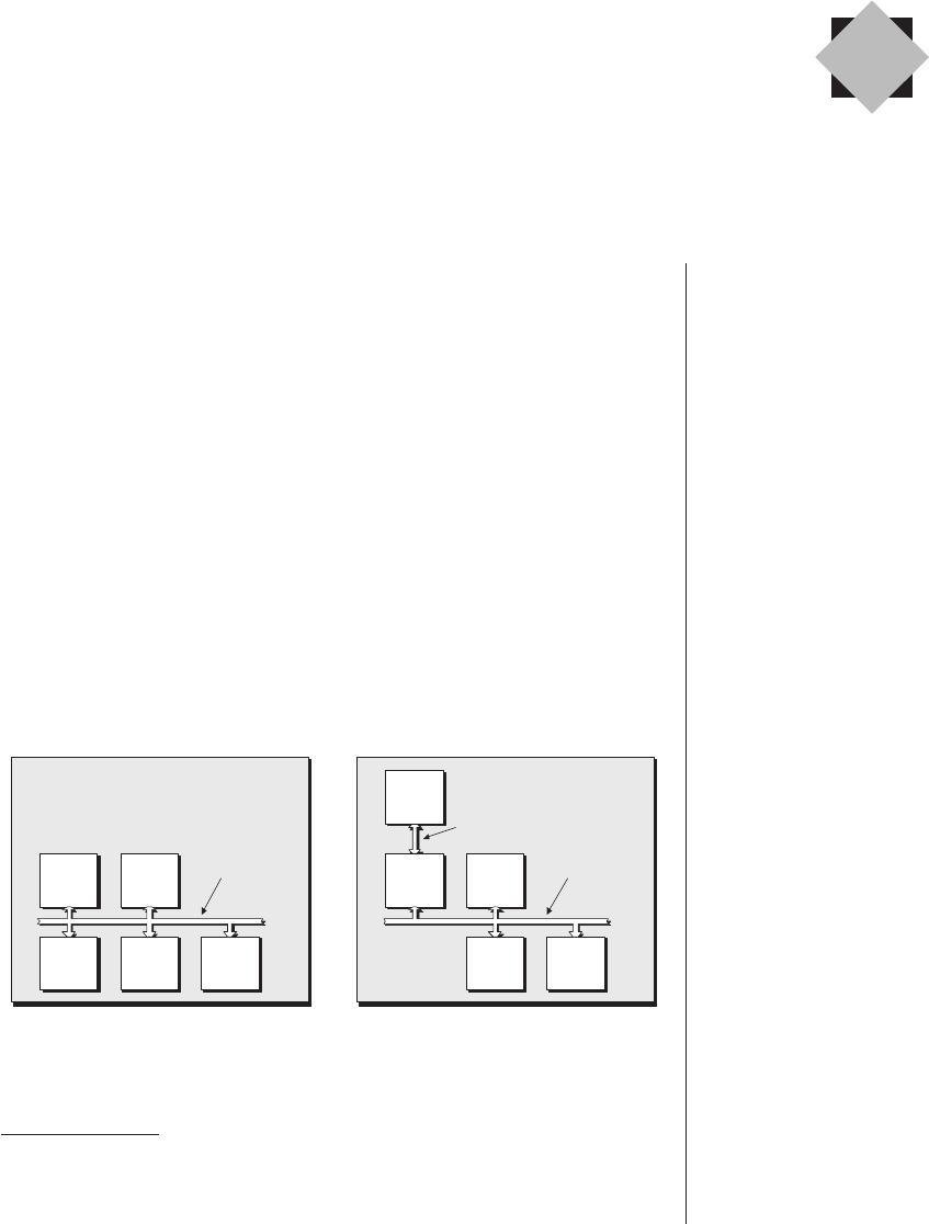
Introduction
For the purposes of this book, we are concerned only with
electronic systems that include one or more FPGAs on the
printed circuit board (PCB). The vast majority of such systems
also make use of a general-purpose microprocessor, or µP, to
perform a variety of control and data-processing applications.1
This is often referred to as the central processing unit (CPU) or
microprocessor unit (MPU).
Until recently, the CPU and its peripherals typically
appeared in the form of discrete chips on the circuit board.
There are an almost infinite number of possible scenarios here,
but the two main ones involve the way in which the CPU is
connected to its memory (Figure 13-1).
PCB is pronounced
by spelling it out as
“P-C-B.”
CPU and MPU are pro-
nounced by spelling
them out as “C-P-U” and
“M-P-U,” respectively.
Embedded Processor-Based
Design Flows
Chapter
13
CPU FPGA
“Stuff”MEM
CPU FPGA
Circuit Board
CPU FPGA
MEM
FPGA
Circuit Board
CPU
MEM
(TCM) Dedicated
memory bus
(a) Memory connected to CPU via
general-purpose processor bus
(b) Tightly-coupled memory (TCM)
connected to CPU via dedicated bus
“Stuff”
More
“Stuff” “Stuff”
More
“Stuff”
Some
“Stuff”
MEM “Stuff”
Some
“Stuff”
Processor
bus
Processor
bus
Figure 13-1. Two scenarios at the circuit board level.
1Alternatively, one might use a microcontroller (µC) device, which
combines a CPU core with selected peripherals and specialized inputs
and outputs.
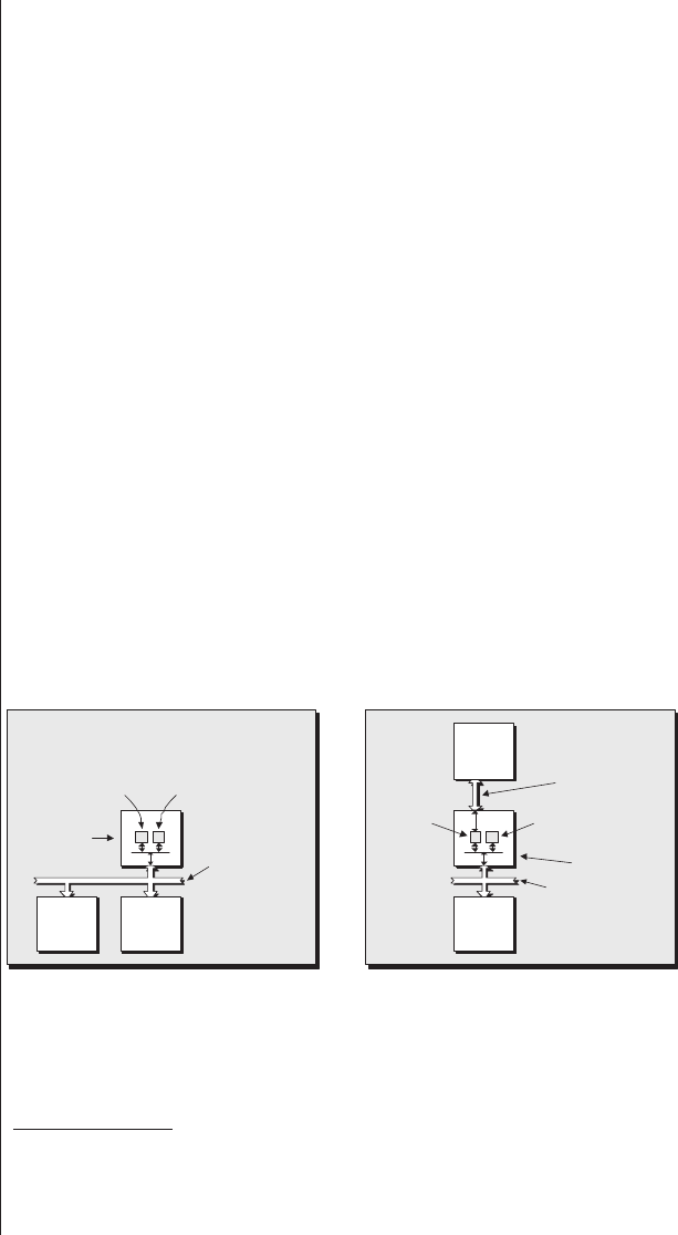
In both of these scenarios, the CPU is connected to an
FPGA and some other stuff via a general-purpose processor
bus. (By “stuff” we predominantly mean peripheral devices
such as counter timers, interrupt controllers, communications
devices, etc.)
In some cases, the main memory (MEM) will also be con-
nected to the CPU by means of the main processor bus, as
shown in figure 13-1a (actually, this connection will be via a
special peripheral called a memory controller, which is not
shown here because we’re trying to keep things simple).
Alternatively, the memory may be connected directly to the
CPU by means of a dedicated memory bus, as shown in
Figure 13-1b).
The point is that presenting the CPU and its various
peripheral devices in the form of dedicated chips on the cir-
cuit board costs money and occupies real estate. It also
impacts the reliability of the board because every solder joint
(connection point) is a potential failure mechanism.
One alternative is to embed the CPU along with some of
its peripherals in the FPGA itself (Figure 13-2).2
240 ■The Design Warrior's Guide to FPGAs
MEM
Circuit Board
MEM
Circuit Board
MEM
(TCM) Dedicated
memory bus
(a) Memory connected to CPU via
general-purpose processor bus
(b) Tightly-coupled memory (TCM)
connected to CPU via dedicated bu
s
“Stuff”
More
“Stuff” “Stuff”
More
“Stuff”
MEM
FPGA Processor
bus
FPGA
Embedded
CPU
Embedded
“stuff”
FPGA
Processor bus
FPGA
Embedded
CPU Embedded “stuff”
Figure 13-2. Two scenarios at the FPGA level.
2Another alternative would be to embed a microprocessor core in an
ASIC, but that’s a tale for another book!
1910:
First electric washing
machines are
introduced.

It is common for a relatively small amount of memory used
by the CPU to be included locally in the FPGA. At the time
of this writing, however, it is rare for all of the CPU’s memory
to be included in the FPGA.
Creating an FPGA design of this type brings a whole slew
of new problems to the table. First of all, the system architects
have to decide which functions will be implemented in soft-
ware (as instructions to be executed by the CPU) and which
functions will be implemented in hardware (using the main
FPGA fabric). Next, the design environment must support the
concept of coverification, in which the hardware and embed-
ded software portions of the system can be verified together to
ensure that everything works as it should. Both of these topics
are considered in more detail later in this chapter.
Hard versus soft cores
Hard cores
A hard microprocessor core is one that is implemented as a
dedicated, predefined (hardwired) block (these cores are only
available in certain device families). Each of the main FPGA
vendors has opted for a particular processor type to implement
its hard cores. For example, Altera offer embedded ARM proc-
essors, QuickLogic have opted for MIPS-based solutions, and
Xilinx sports PowerPC cores.
Of course, each vendor will be delighted to explain at great
length why its implementation is far superior to any of the oth-
ers (the problem of deciding which one actually is better is
only compounded by the fact that different processors may be
better suited to different tasks).
As noted in chapter 4, there are two main approaches for
integrating such cores into the FPGA. The first is to locate it
in a strip to the side of the main FPGA fabric (Figure 13-3).
In this scenario, all of the components are typically formed
on the same silicon chip, although they could also be formed
on two chips and packaged as a multichip module (MCM).
Embedded Processor-Based Design Flows ■241
In addition to the micro-
processor core itself,
each FPGA vendor also
supports an associated
processor bus. For exam-
ple, Altera and
QuickLogic both support
the AMBA bus from ARM
(this is an open specifica-
tion that can be
downloaded from
www.arm.com free of
any charges).
By comparison, Xilinx
embedded cores make
use of the CoreConnect
bus from IBM.
CoreConnect has two fla-
vors. The main 64-bit
bus is known as the
processor local bus (PLB).
This can be used in con-
junction with one or
more 32-bit on-chip
peripheral busses (OPBs).
MCM is pronounced by
spelling it out as
“M-C-M.”
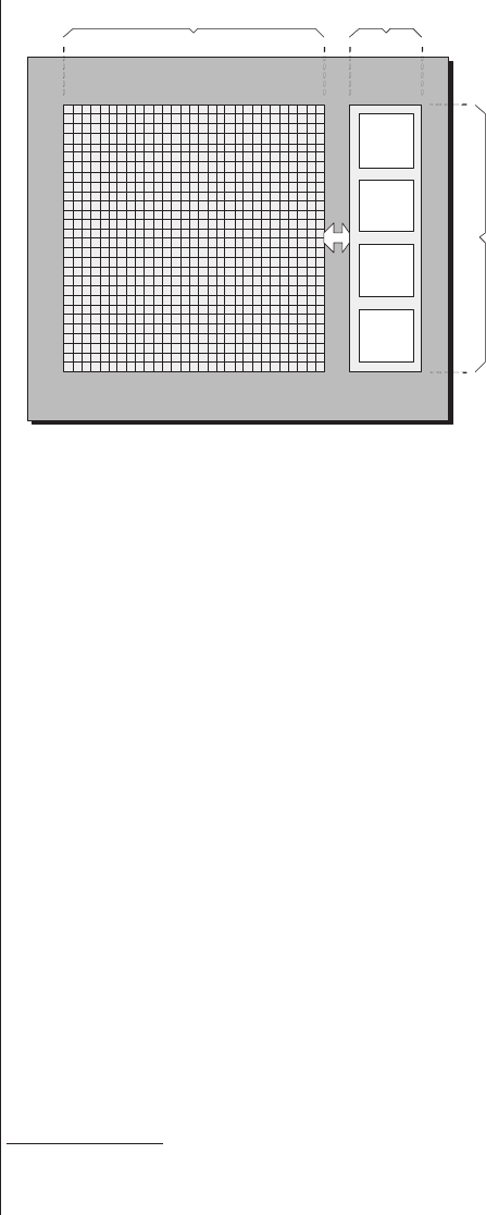
One advantage of this implementation is that the main
FPGA fabric is identical for devices with and without the
embedded microprocessor core, which can make things easier
for the design tools used by the engineers. The other advan-
tage is that the FPGA vendor can bundle a whole load of
additional functions in the strip to complement the micro-
processor core, such as memory and special peripherals.3
An alternative is to embed one or more microprocessor
cores directly into the main FPGA fabric. One, two, and even
four core implementations are currently available at the time
of this writing (Figure 13-4).
In this case, the design tools have to be able to take
account of the presence of these blocks in the fabric; any
memory used by the core is formed from embedded RAM
blocks, and any peripheral functions are formed from groups of
general-purpose programmable logic blocks. Proponents of
this scheme can argue that there are inherent speed advan-
242 ■The Design Warrior's Guide to FPGAs
uP
RAM
I/O
etc.
Main FPGA fabric
Microprocessor
core, special RAM,
peripherals and
I/O, etc.
The “Stripe”
Figure 13-3. Bird’s-eye view of chip with embedded core
outside of the main fabric.
3This approach is favored by vendors such as Altera (www.altera.com) and
QuickLogic (www.quicklogic.com).
1910: France.
George Claude
introduces neon lamps.
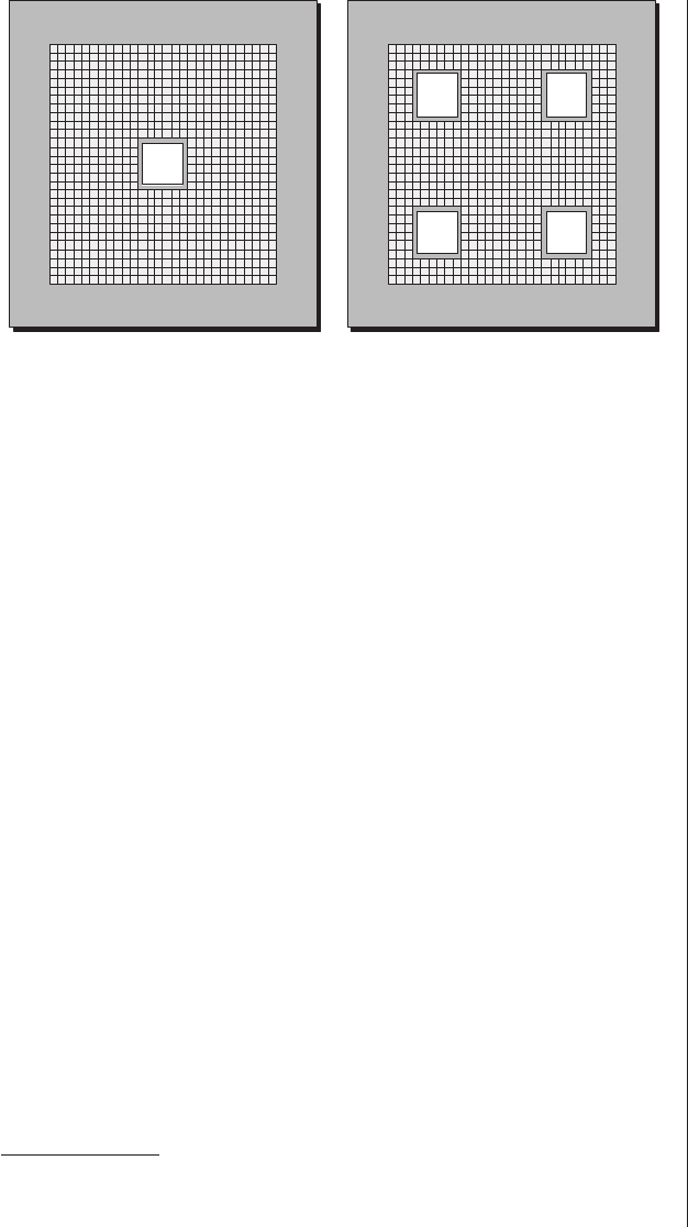
tages to be gained from having the microprocessor core in
intimate proximity to the main FPGA fabric.4
Soft microprocessor cores
As opposed to embedding a microprocessor physically into
the fabric of the chip, it is possible to configure a group of pro-
grammable logic blocks to act as a microprocessor. These are
typically called “soft cores,” but they may be more precisely
categorized as either soft or firm, depending on the way in
which the microprocessor’s functionality is mapped onto the
logic blocks. For example, if the core is provided in the form of
an RTL netlist that will be synthesized with the other logic,
then this truly is a soft implementation. Alternatively, if the
core is presented in the form of a placed and routed block of
LUTs/CLBs, then this would typically be considered a firm
implementation.
In both of these cases, all of the peripheral devices like
counter timers, interrupt controllers, memory controllers, com-
munications functions, and so forth are also implemented as
Embedded Processor-Based Design Flows ■243
One tool of interest in
the soft core arena is
LisaTek from CoWare Inc.
(www.coware.com).
Using a special language
you define a required
instruction set and
microarchitecture
(resources, pipelining,
cycle timing) associated
with a desired micro-
processor. LisaTek takes
this definition generates
the corresponding RTL
for your soft core, along
with associated software
tools such as a C
compiler, assembler,
linker, and instruction
set simulator (ISS).
uP
(a) One embedded core (b) Four embedded cores
uP uP
uP uP
Figure 13-4. Bird’s-eye view of chips with embedded cores
inside the main fabric.
4This approach is favored by Xilinx (www.xilinx.com), who also provide a
multitude of peripherals in the form of soft IP cores.

soft or firm cores (the FPGA vendors are typically able to sup-
ply a large library of such cores).
Soft cores are slower and simpler than their hard-core
counterparts (of course they are still incredibly fast in human
terms). However, in addition to being practically free, they
also have the advantages that you only have to implement a
core if you need it and that you can instantiate as many cores
as you require until you run out of resources in the form of
programmable logic blocks.
Once again, each of the main FPGA vendors has opted for
a particular processor type to implement its soft cores. For
example, Altera offers the Nios, while Xilinx sports the Micro-
Blaze. The Nios has both 16-bit and 32-bit architectural
variants, which operate on 16-bit or 32-bit chunks of data,
respectively (both variants share the same 16-bit-wide instruc-
tion set). By comparison, the MicroBlaze is a true 32-bit
machine (that is, it has 32-bit-wide instruction words and per-
forms its magic on 32-bit chunks of data). Once again, each of
the vendors will be more than happy to tell you why its soft
core rules and how its competitors’ offerings fail to make the
grade (sorry, you’re on your own here).
One cool thing about the integrated development environ-
ment (IDE) fielded by Xilinx is that it treats the PowerPC
hard core and the MicroBlaze soft core identically. This
includes both processors being based on the same CoreCon-
nect processor bus and sharing common soft peripheral IP
cores. All of this makes it relatively easy to migrate from one
processor to the other.
Also of interest is the fact that Xilinx offers a small 8-bit
soft core called the PicoBlaze, which can be implemented
using only 150 logic cells (give or take a handful). By com-
parison, the MicroBlaze requires around 1,000 logic cells5
244 ■The Design Warrior's Guide to FPGAs
The Nios is based on a
SPARC architecture using
the concept of register
windows, while the
MicroBlaze is based
on a classical RISC
architecture.
IDE is pronounced by
spelling it out as
“I-D-E.”
Depending on who you
are talking to and the
FPGA or RTOS vendor in
question, the ‘D’ in IDE
can stand for “design” or
“development.”
QuickLogic offer a 9-bit
soft microcontroller that
goes under the catchy
name of Q90C1xx. (Hav-
ing a 9-bit data word can
be useful for certain
communication
functions.)
5For the purposes of these discussions, a logic cell can be assumed to
contain a 4-input LUT, a register element, and various other bits and
pieces like multiplexers and fast carry logic.

(which is still extremely reasonable for a 32-bit processor
implementation, especially when one is playing with FPGAs
that can contain 70,0006or more such cells.)
Partitioning a design into its hardware and
software components
As noted in chapter 4, almost any portion of an electronic
design can be realized in hardware (using logic gates and regis-
ters, etc.) or software (as instructions to be executed on a
microprocessor). One of the main partitioning criteria is how
fast you wish the various functions to perform their tasks:
■Picosecond and nanosecond logic: This has to run insanely
fast, which mandates that it be implemented in hard-
ware (in the FPGA fabric).
■Microsecond logic: This is reasonably fast and can be
implemented either in hardware or software (this type
of logic is where you spend the bulk of your time decid-
ing which way to go).
■Millisecond logic: This is the logic used to implement
interfaces such as reading switch positions and
flashing light-emitting diodes, or LEDs. It’s a pain
slowing the hardware down to implement this sort of
function (using huge counters to generate delays, for
example). Thus, it’s often better to implement these
tasks as microprocessor code (because processors give
you lousy speed—compared to dedicated
hardware—but fantastic complexity).
The trick is to solve every problem in the most cost-
effective way. Certain functions belong in hardware, others cry
out for a software realization, and some functions can go either
way depending on how you feel you can best use the resources
Embedded Processor-Based Design Flows ■245
Some cynics say that
those aspects of the
design that are well
understood are imple-
mented in hardware,
while any portions of the
design that are some-
what undefined at the
beginning of the design
process are often rele-
gated to a software
realization (on the basis
that the software can be
“tweaked” right up until
the last minute).
6This 70,000 value was true when I ate my breakfast this morning, but it
will doubtless have increased by the time you come to read this book.

(both chip-level resources and hardware/software engineers)
available to you.
It is possible to envisage an “ideal” electronic system level
(ESL) environment in which the system architects initially
capture the design via a graphical interface as a collection of
functional blocks that are connected together. Each of these
blocks could then be provided with a system-/algorithmic-
level SystemC representation, for example, and the entire
design could be verified prior to any decisions being made as
to which portions of the design were to be implemented in
hardware and software.
When it comes to the partitioning process itself, we might
dream of having the ability to tag each graphical block with
the mouse and select a hardware or software option for its
implementation. All we would then have to do would be to
click the “Go” button, and the environment would take care
of synthesizing the hardware, compiling the software, and
pulling everything together.
And then we return to the real world with a resounding
thud. Actually, a number of next-generation design environ-
ments show promise, and new tools and techniques are
arriving on an almost daily basis. At the time of this writing,
however, it is still very common for system architects to parti-
tion a design into its hardware and software portions by hand,
and to then pass these top-level functions over to the appro-
priate engineers and hope for the best.
With regard to the software portion of the design, this
might be something as simple as a state machine used to con-
trol a human-level interface (reading the state of switches and
controlling display devices). Although the state machine itself
may be quite tricky, this level of software is certainly not
rocket science. At the other end of the spectrum, one might
have incredibly complex software requirements, including
■System initialization routines and a hardware abstrac-
tion layer
■A hardware diagnostic test suite
246 ■The Design Warrior's Guide to FPGAs
RTOS is pronounced by
spelling it out as
“R-T-O-S.”
Real-time systems are
those in which the
correctness of a computa-
tion or action depends
not only on how it is per-
formed but also when it is
performed.

■A real-time operating system (RTOS)
■RTOS device drivers
■Any embedded application code
This code will typically be captured in C/C++ and then
compiled down to the machine instructions that will be run on
the processor core (in extreme cases where one is attempting
to squeeze the last drop of performance out of the design, cer-
tain routines may be handcrafted in assembly code).
At the same time, the hardware design engineers will
typically be capturing their portions of the design at the
RTL level of abstraction using VHDL or Verilog (or
SystemVerilog).
Today’s designs are so complex that their hardware and
software portions have to be verified together. Unfortunately,
wrapping one’s brain around the plethora of coverification
alternatives and intricacies can make a grown man (well, me
actually) break down and weep.
Hardware versus software views of the world
One of the biggest problems to overcome when it comes to
the coverification of the hardware and software portions of a
design is the two totally different worldviews of their
creators.
The hardware folks typically visualize their portion of the
design as blocks of RTL representing such things as registers,
logical functions, and the wires connecting them together.
When hardware engineers are debugging their portion of the
design, they think in terms of an editor showing their RTL
source code, a logic simulator, and a graphical waveform dis-
play showing signals changing values at specific times. In a
typical hardware design environment, clicking on a particular
event in the waveform display will automatically locate the
corresponding line of RTL code that caused this event to
occur.
By comparison, the software guys and gals think in terms of
C/C++ source code, of registers in the CPU (and in the
Embedded Processor-Based Design Flows ■247
1911:
Dutch physicist Heike
Kamerlingh Onnes
discovers
superconductivity.

peripherals), and of the contents of various memory locations.
When software engineers are debugging a program, they often
wish to single-step through the code one line at a time and
watch the values in the various registers changing. Or they
might wish to set one or more breakpoints (this refers to plac-
ing markers at specific points in the code), run the program
until they hit one of those breakpoints, and then pause to see
what’s going on. Alternatively, they might wish to specify cer-
tain conditions such as a register containing a particular
value, then run the program until this condition is met, and
once again pause to see what’s happening.
When a software developer is writing application code
such as a game, he or she has the luxury of being reasonably
confident that the hardware (say, a home computer) is rea-
sonably robust and bug-free. However, it’s a different ball
game when one is talking about a software engineer creating
embedded applications intended to run on hardware that’s
being designed at the same time. When a problem occurs, it
can be mega tricky determining if it was a fault in the software
or if the hardware was to blame. The classic joke is a conver-
sation between the two camps:
Software Engineer: “I think I may have hit a hardware
problem while running my embedded application.”
Hardware Engineer: “At what time did the error occur?
Can you give me a test case that isolates the problem?”
Software Engineer: “The error occurred at 9:30 this
morning, and the test case is my application!”
In the case of today’s state-of-the-art coverification envi-
ronments, the hardware and software worlds are tightly
coupled. This means that if the software engineers detect a
potential hardware bug, identifying the particular line of code
being executed will take the hardware engineers directly to
the corresponding simulation time frame in the graphical
waveform display. Similarly, if the hardware engineers detect
a potential software bug (such as code requesting an illegal
248 ■The Design Warrior's Guide to FPGAs
1912: America.
Dr Sidney Russell
invents the electric
blanket.
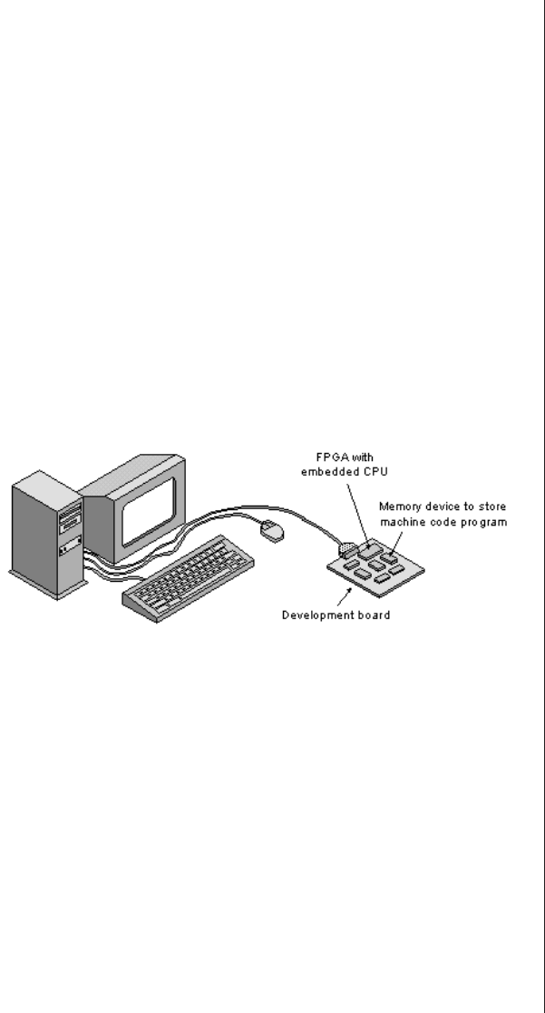
hardware transaction), they can use their interface to guide the
software team to the corresponding line of source code. Unfor-
tunately, this type of environment can cost a lot of money, so
sometimes you have to opt for a less sophisticated solution.
Using an FPGA as its own development
environment
Perhaps the simplest place to start is the scenario where
the FPGA is used as its own development environment. The
idea here is that you have an SRAM-based FPGA with an
embedded processor (hard or soft) mounted on a development
board that’s connected to your computer. In addition to the
FPGA, this development board will also have a memory device
that will be used to store the software programs that are to be
run by the embedded CPU (figure 13-5).
Once the system architects have determined which por-
tions of the design are to be implemented in hardware and
software, the hardware engineers start to capture their RTL
blocks and functions and synthesize them down to a LUT/
CLB-level netlist. Meanwhile, the software engineers start to
capture their C/C++ programs and routines and compile them
down to machine code. Eventually, the LUT/CLB-level netlist
will be loaded into the FPGA via a configuration file, the
linked machine code image will be loaded into the memory
device, and then you let the system run wild and free
(Figure 13-6).
Embedded Processor-Based Design Flows ■249
Figure 13-5. Using an FPGA as its own development
environment.
1912:
Feedback and
heterodyne systems
usher in modern radio
reception.
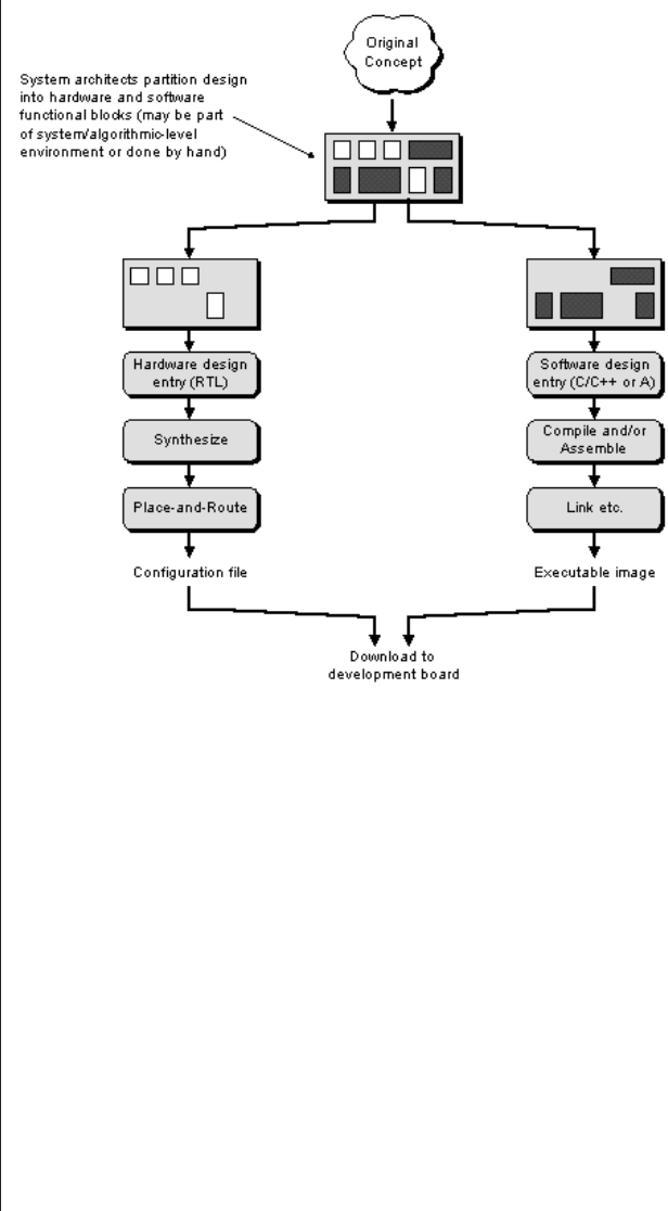
Also, any of the machine code that is to be embedded in
the FPGA’s on-chip RAM blocks would actually be loaded via
the configuration file.
Improving visibility in the design
The main problem with the scenario discussed in the
previous section is lack of “visibility” as to what is happening
in the hardware portion of the design. One way to mitigate
this is to use a virtual logic analyzer to observe what’s happen-
ing in the hardware (this is discussed in more detail in
Chapter 16).
Things can be a little trickier when it comes to determin-
ing what’s happening with the software. One point to
250 ■The Design Warrior's Guide to FPGAs
Figure 13-6. A (very) simple design flow.
1912:
The Titanic sends out
radio distress signals
when it collides with an
iceberg and sinks on its
maiden voyage.
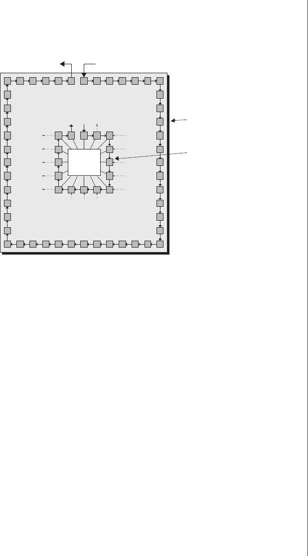
remember is that—as discussed in chapter 5—an embedded
CPU core will have its own dedicated JTAG boundary scan
chain (Figure 13-7).
This is true of both hard cores and the more sophisticated
soft cores. In this case, the coverification environment can use
the scan chain to monitor the activity on the buses and con-
trol signals connecting the CPU to the rest of the system. The
CPU’s internal registers can also be accessed via the JTAG
port, thereby allowing an external debugger to take control of
the device and single-step through instructions, set break-
points, and so forth.
A few coverification alternatives
If you really want to get visibility into what’s happening in
the hardware portions of design, one approach is to use a logic
simulator. In this case, the majority of the system will be mod-
eled and simulated in VHDL or Verilog/SystemVerilog at the
RTL level of abstraction. When it comes to the CPU core,
however, there are various ways in which to represent this
(Figure 13-8).
Embedded Processor-Based Design Flows ■251
JTAG data inJTAG data out
FPGA
CPU
Primary scan chain
Internal (core) scan chain
Figure 13-7. Embedded processor JTAG boundary scan chain.
1913:
William D.Coolidge
invents the
hot-tungsten filament
X-ray tube. This
Coolidge Tube
becomes the standard
generator for medical
X-rays.
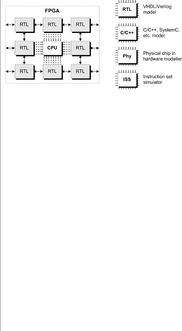
Irrespective of the type of model used to represent the
CPU, the embedded software (machine code) portion of the
design will be loaded into some form of memory—either
embedded memory in the FPGA or external memory
devices—and the CPU model will then execute those
machine code instructions.
Note that figure 13-8 shows a high-level representation of
the contents of the FPGA only. If the machine code is to be
stored in external memory devices, then these devices would
also have to be part of the simulation. In fact, as a general rule
of thumb, if the software talks to any stuff, then that stuff
needs to be part of the coverification environment.
RTL (VHDL or Verilog)
Perhaps the simplest option here is when one has an RTL
model of the CPU, in which case all of the activity takes place
in the logic simulator. One disadvantage of this approach is
that a CPU performs tremendous numbers of internal opera-
tions in order to perform the simplest task, which equates to
incredibly slow simulation runs (you’ll be lucky to be able to
simulate 10 to 20 system clocks per second in real time).
The other disadvantage is that you have no visibility into
what the software is doing at the source code level. All you’ll
252 ■The Design Warrior's Guide to FPGAs
Figure 13-8. Alternative representations of the CPU.
1914: America.
Traffic lights are used
for the first time (in
Cleveland, Ohio)

be able to do is to observe logic values changing on wires and
inside registers.
And there’s always the fact that whoever supplies the real
CPU doesn’t want you to know how it works internally
because that supplier may be using cunning proprietary tricks
and wish to preserve their IP. In this case, you may well find it
very difficult to lay your hands on an RTL model of the CPU
at all.
C/C++, SystemC, etc.
As opposed to using an RTL model, it is very common to
have access to some sort of C/C++ model of the CPU. (The
proponents of SystemC have a vision of a world in which the
CPU and the main peripheral devices all have SystemC
models provided as standard for use in this type of design
environment.)
The compiled version of this CPU model would be linked
into the simulation via the programming language interface
(PLI) in the case of a Verilog simulator or the foreign language
interface (FLI)—or equivalent—in the case of a VHDL
simulator.
The advantages of such a model are that it will run much
faster than its RTL counterpart; that it can be delivered in
compiled form, thereby preserving any secret IP; and that, at
least in FPGA circles, such a model is usually provided for free
(the FPGA vendors are trying to sell chips, not models).
One disadvantage of this approach is that the C/C++
model may not provide a 100 percent cycle-accurate represen-
tation of the CPU, which has the potential to cause problems
if you aren’t careful. But, once again, the main disadvantage of
such a model is that its only purpose is to provide an engine to
execute the machine code program, which means that you
have no visibility into what the software is doing at the source
code level. All you’ll be able to do is observe logic values
changing on wires and inside registers.
Embedded Processor-Based Design Flows ■253
Way back in the mists of
time, the Logic Modeling
Corporation (LMC)—
which was subsequently
acquired by Synopsys—
defined an interface for
connecting behavioral
models of hardware
blocks to logic simula-
tors. This is known as
the SWIFT interface, and
models—such as
CPUs—that comply with
this specification may be
referred to as SWIFT
models.

Physical chip in hardware modeler
Yet another possibility is to use a physical device to repre-
sent a hard CPU core. For example, if you are using a
PowerPC core in a Xilinx FPGA, you can easily lay your
hands on a real PowerPC chip. This chip can be installed in a
box called a hardware modeler, which can then be linked into
the logic simulation system.
The advantage of this approach is that you know the
physical model (chip) is going to functionally match your
hard core as closely as possible. Some disadvantages are that
hardware modelers aren’t cheap and they can be a pain to use.
The majority of hardware-modeler-based solutions don’t
support source-level debugging, which, once again, means
that you have no visibility into what the software is doing at
the source code level.7All you’ll be able to do is to observe
logic values changing on wires and inside registers.
Instruction set simulator
As previously noted, in certain cases, the role of the soft-
ware portion of a design may be somewhat limited. For
example, the software may be acting as a state machine used
to control some interface. Alternatively, the software’s role
may be to initialize certain aspects of the hardware and then
sit back and watch the hardware do all of the work. If this is
the case, then a C/C++ model or a physical model is probably
sufficient—at least as far as the hardware design engineer is
concerned.
At the other extreme, the hardware portions of the design
may exist mainly to act as an interface with the outside world.
For example, the hardware may read in a packet of data and
store it in the FPGA’s memory, and then the CPU may per-
form huge amounts of complex processing on this data. In
254 ■The Design Warrior's Guide to FPGAs
ISS is pronounced by
spelling it out as “I_S_S.”
7Actually, some hardware modelers do provide a certain amount of
source-level debug capability, for example, Simpod Inc.
(www.simpod.com) offers an interesting solution.
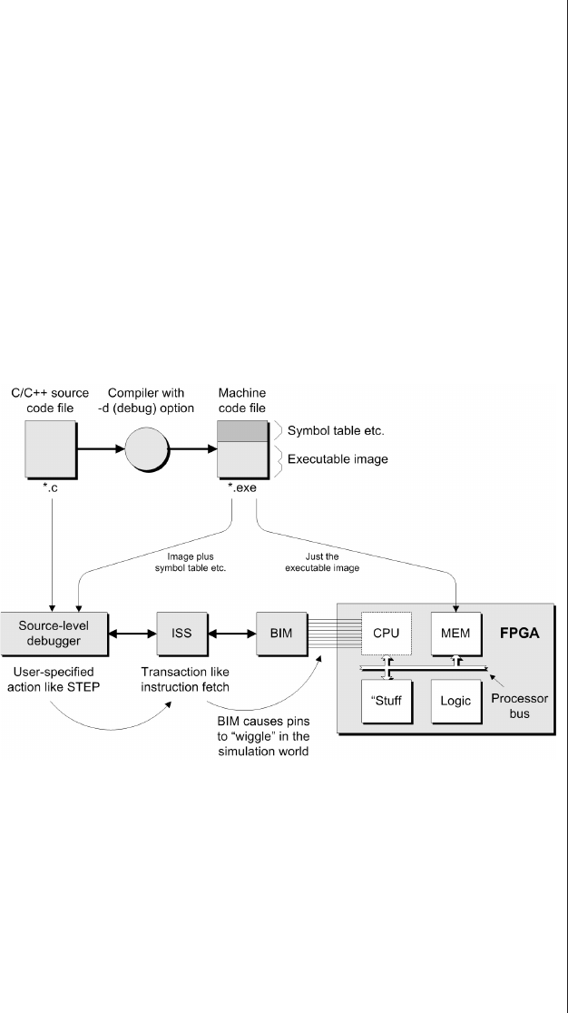
cases like these, it is necessary for the software engineer to
have sophisticated source-level debugging capabilities. This
requires the use of an instruction set simulator (ISS), which pro-
vides a virtual representation of the CPU.
Although an ISS will almost certainly be created in
C/C++, it will be architected very differently from the C/C++
models of the CPU discussed earlier in this section. This is
because the ISS is created at a very high level of abstraction; it
thinks in terms of transactions like “get me a word of data from
location xin the memory,” and it doesn’t concern itself with
details like how signals will behave in the real world. The easi-
est way to explain how this works is by means of an illustration
(Figure 13-9).
First of all, the software engineers capture their program as
C/C++ source code. This is then compiled using the -d
(debug) option, which generates a symbol table and other
debug-specific information along with the executable machine
code image.
Embedded Processor-Based Design Flows ■255
Figure 13-9. How an ISS fits into the picture.
1914:
Better triode improves
radio reception.

When we come to perform the coverification, there are
a number of pieces to the puzzle. At one end we have the
source-level debugger, whose interface is used by the software
engineer to talk to the environment. At the other end we
have the logic simulator, which is simulating representations
of the memory, stuff like peripheral devices, general-purpose
logic, and so forth (for the sake of simplicity, this illustration
assumes that all of the program memory resides in the FPGA
itself).
In the case of the CPU, however, the logic simulator
essentially sees a hole where this function should be. To be
more precise, the simulator actually sees a set of inputs and
outputs corresponding to the CPU. These inputs and outputs
are connected to an entity called a bus interface model
(BIM), which acts as a translator between the simulator
and the ISS.
Both the source code and the executable image (along
with the symbol table and other debug-centric information)
are loaded into the source-level debugger. At the same time,
the executable image is loaded into the MEM block. When
the user requests the source-level debugger to perform an
action like stepping through a line of source code, it issues
commands to the ISS. In turn, the ISS will execute high-level
transactions such as an instruction fetch, or a memory
read/write, or an I/O command. These transactions are passed
to the BIM, which causes the appropriate pins to “wiggle” in
the simulation world.
Similarly, when something connected to the processor bus
in the FPGA attempts to talk to the CPU, it will cause the
pins driving the BIM to “wriggle.” The BIM will translate
these low-level actions into high-level transactions that it
passes to the ISS, which will in turn inform the source-level
debugger what’s happening. The source-level debugger will
then display the state of the program variables, the CPU
registers, and other information of this ilk.
256 ■The Design Warrior's Guide to FPGAs
1914:
First trans-continental
telephone call.

There are a variety of incredibly sophisticated (often
frighteningly expensive) environments of this type on the mar-
ket.8Each has its own cunning tricks and capabilities, and
some are more appropriate for ASIC designs than FPGAs or
vice versa. As usual, however, this is a moving target, so you
need to check around to see who is doing what before putting
any of your precious money on the table.
A rather cunning design environment
As far as possible (and insofar as makes sense), this book
attempts to steer away from discussing specific companies and
products. But there’s an exception to every rule, and this is it,
because a company called Altium Ltd. (www.altium.com) has
come up with a rather cunning FPGA design environment
called Nexar that deserves mention.
It’s difficult to know where to start, so let’s kick off by say-
ing that we’re talking about a complete FPGA hardware/
software codesign and coverification environment for around
$7,995.9This environment targets engineers designing things
like simple controllers for domestic appliances like washing
machines and is based on the fact that you can now purchase
FPGAs containing more than 1 million system gates for
around $20.10
Nexar includes a hardware development board that plugs
into the back of your PC. This development board comes
equipped with two daughter cards: one carrying a Xilinx FPGA
and the other equipped with an Altera device. Nexar also fea-
tures a number of soft microprocessor cores that replicate the
functionality of industry-standard 8-bit devices like the 8051,
Z80, and PIC microcontrollers (a range of 16-bit and 32-bit
processor and DSP cores are planned for the future). Also
Embedded Processor-Based Design Flows ■257
8For example, Seamless from Mentor (www.mentor.com), Incisive from
Cadence (www.cadence.com), and XoC from Axis Systems
(www.axissystems.com).
9This price was true circa November 2003.
10 Again, this gate-count and price are circa November 2003.
1914: Radio message
is sent from the ground
to an airplane.

included are a library of peripheral devices, a library of around
1,500 component blocks that range from simple gates to more
complex functions such as counters, and a small RTOS.
By means of a schematic capture interface, the user places
blocks representing the processors, peripherals, and various
logic functions and wires them together. All of the blocks sup-
plied with Nexar are provided royalty-free. These blocks have
been presynthesized, so when you are ready to rock and roll,
they can be directly downloaded into the FPGA on the devel-
opment board. (If necessary, you can also create your own
blocks and capture their contents in RTL. These will subse-
quently be processed by the synthesis engine bundled with
Nexar.)
Clicking on a processor block allows you to enter the
C/C++ source code program to be associated with that
processor. This will subsequently be processed by one of the
compilers bundled with Nexar.
The idea is that everything associated with the
design—hardware and software—will be downloaded into the
FPGA on the development board. In order to see what’s hap-
pening in the hardware, you can include a variety of virtual
instrument blocks in your schematic, including logic analyz-
ers, frequency counters, frequency generators, and so forth.
When it comes to the software, Nexar provides a source-level
debugger that allows you to perform all of the usual tasks like
setting breakpoints, specifying watch expressions, single-
stepping, stepping over, stepping into, and so on.
What can I say? I’ve actually seen one of these little ras-
cals performing its magic, and I was impressed. I really like the
fact that this is essentially a turnkey solution, and you get eve-
rything (no costly add-ons required) in a package the size of a
shoebox. And for the class of designs it is targeting, I person-
ally think that Nexar is going to be a hard act to follow for
some time to come.
258 ■The Design Warrior's Guide to FPGAs
1915:
First trans-atlantic radio
telephone conversation
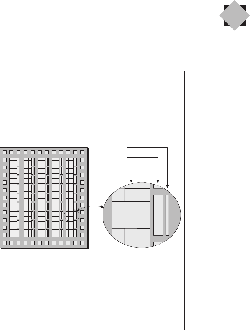
Handling things as one big chunk
In order to provide a basis for these discussions, let’s con-
sider an FPGA as containing a series of columns, each of
which comprises large numbers of programmable logic blocks
along with some blocks of RAM and other hard-wired ele-
ments such as multipliers or MACs (Figure 14-1).
Of course, this illustration is a gross simplification, because
a modern device can contain more columns than you can
swing a stick at and each column can contain humongous
amounts of programmable logic, and so forth.
Modular and Incremental
Design
Chapter
14
RAM blocks
Multipliers
Configurable
logic blocks
Figure 14-1. A column-based architecture.
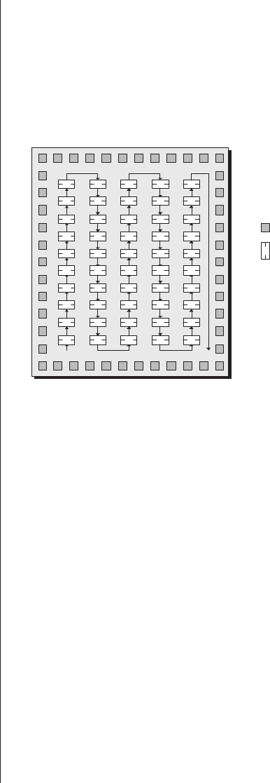
When we initially discussed the programming of SRAM-
based FPGAs in chapter 5, we stated that we could visualize
all of the SRAM configuration cells as comprising a single
(long) shift register. For example, consider a simple bird’s-eye
view of the surface of the chip showing only the I/O pins/pads
and the SRAM configuration cells (Figure 14-2).
Once again, we can think of the SRAM configuration
cells as a series of columns, each of which maps onto one of
the columns of programmable logic shown in figure 14-1.
This, too, is a grossly simplified representation because an
FPGA can contain tens of millions of these configuration
cells, but it will serve our purposes here. The ways in which
the two ends of this register chain are made accessible to the
outside world will depend on the selected programming mode
(this is not relevant to these discussions).
In the early days of FPGA-based designs—circa the mid to
late 1980s—devices were relatively small in terms of their
logic capacity. One by-product of this was that a single design
engineer was typically in charge of creating all of the RTL for
the device. This RTL was subsequently synthesized, and the
ensuing netlist was passed to the place-and-route software,
which processed the design in its entirety.
260 ■The Design Warrior's Guide to FPGAs
= I/O pin/pad
= SRAM configuration cell
Figure 14-2. SRAM configuration cells presented
as a single (long) register chain.
1917:
Clarence Birdseye
preserves food by
means of freezing.

The result was a monolithic configuration file that defined
the function of the entire device and would be loaded as one
big chunk. This obviously worked well with having the con-
figuration cells presented as a single long register chain, so
everyone was happy.
Partitioning things into smaller chunks
Over time, FPGAs have grown larger and more sophisti-
cated, while the size and complexity of designs have increased
by leaps and bounds. One way to address this is to partition the
design into functional blocks and to give each block to one or
more design engineers.
Each of these blocks can be synthesized in isolation. At the
end of the day, however, all of the netlists associated with the
blocks are gathered back together before being handed over to
the place-and-route applications. Once again, place-and-route
typically works on the design in its entirety, which can require
an overnight run when you’re talking about multimillion-gate
designs.
Somewhere around 2002, some FPGA vendors started to
offer larger devices in which the SRAM configuration cells
are presented as multiple (relatively short) register chains
(Ffigure 14-3).
The idea of presenting the device with these multiple
chains may have been conceived with the concepts of modular
and incremental design practices in mind. Alternatively, it
may have come about for some mundane hardware-related rea-
son, and then some bright spark said, “Just a minute, now that
we have these multiple chains, what if we started to support
the concepts of modular and incremental design?”
If I were a betting man, I’d probably put my money on the
latter option, but let’s be charitable and assume that someone
somewhere actually knew what he or she was doing (hey, it
could happen). However it came about, the end result of this
architecture is that, along with associated software applica-
tions, it can support the concepts of modular and incremental
design.
Modular and Incremental Design ■261
1917: Frank Conrad
builds a radio station
that eventually
becomes KDKA (this
call sign is still used to
this day).
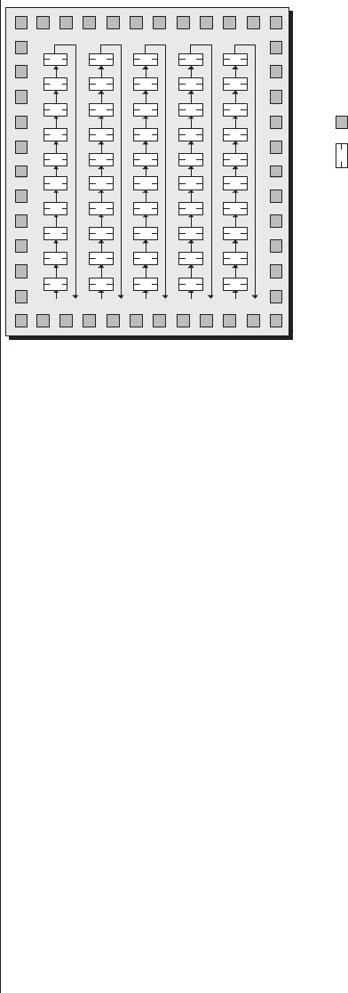
Modular design
Known as team design by some, this refers to the concept of
partitioning a large design into functional blocks and giving
each block, along with its associated timing constraints, to a
different design engineer or group of engineers. The RTL for
each model is captured and synthesized independently, and
the final physical netlist is handed over to a system integrator.
Ultimately, each block (or a small group of blocks) will be
assigned to a specific area in the device. The system integrator
is responsible for “stitching” all of these areas together. In a
way, this is similar to having a design split across multiple
FPGAs, except that everything is in the same device.
The primary advantage of this scenario is that the netlist
for each area can be run through the place-and-route applica-
tions in isolation (these tools will be given constraints
restricting them to specific, predefined areas). This means
that each team member can complete his or her portion of the
design to the point that it fully meets its timing requirements
after implementation, not just after synthesis.
262 ■The Design Warrior's Guide to FPGAs
The terms “block-based”
and “bottom-up” may
also be associated with
modular design.
= I/O pin/pad
= SRAM configuration cel
l
Figure 14-3. SRAM configuration cells presented as
multiple (relatively short) register chains.

Incremental design
This refers to the fact that, so long as you’ve tied down the
interfaces between blocks/columns, you can modify the RTL
associated with a particular block, resynthesize that block, and
rerun place-and-route on that block in isolation. This is much,
much faster than having to rerun place-and-route on the
entire design.
Actually, the term isolation as used in the previous para-
graph is possibly a tad misleading. It may be more appropriate
to say that the incremental design tools “freeze” all of the
unchanged blocks in place, and they only reimplement the
changed block(s) in the context of the entire design. This pro-
vides an advantage over modular design in which the other
blocks aren’t present (of course, the modular and incremental
design techniques may be used in conjunction with each
other).
On the downside
One problem with the techniques described here is that
they can lead to substantial waste of resources because, at the
time of this writing, the finest resolution is that of an entire
column, so if a particular functional block only occupies, say,
75 percent of the logic in that column, the remaining 25 per-
cent will remain unused and go to waste. (FPGA vendors who
support these architectures are talking about providing mecha-
nisms to support finer resolutions in the future.)
Another problem is that the methodology described here is
almost bound to result in “tall-and-thin” implementations for
each functional block because you are essentially restricting
the blocks to one or more vertical columns. This is obviously a
pain in the case of those functional blocks that would benefit
from a “short-and-fat” realization (spanning multiple columns
and using small portions of those columns).
Perhaps the most significant problem with the early
releases of tools and flows using these architectures to support
Modular and Incremental Design ■263
1918:
First radio link between
UK and Australia.
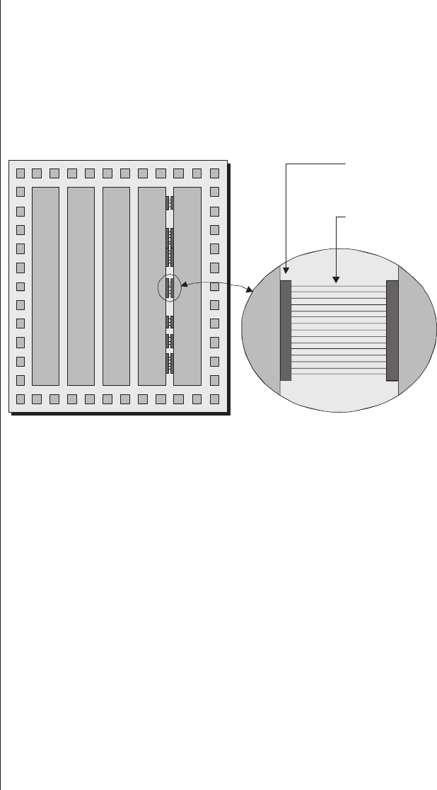
modular and incremental design practices is that someone
(say the system integrator) is obliged to create a floor plan by
hand. This poor soul also has to define and place special inter-
face blocks called bus macros that are used to link buses and
individual signals crossing from one block to another
(Figure 14-4).
The initial implementation of the tools made creating the
floor plan and defining and locating the bus macros awkward
to say the least. The rumor on the streets is that changes to
the software are in the offing that will greatly simplify this
process (on the bright side, it couldn’t get any harder).
There’s always another way
Way back in chapter 10, we introduced the concept of
FPGA-centric silicon virtual prototypes, or SVPs. At that
time, we noted that some EDA vendors have started to pro-
vide tools that support the concept of an FPGA SVP by
providing a mixture of floor planning and pre-place-and-route
264 ■The Design Warrior's Guide to FPGAs
Inter-block
connections
Bus macros
Figure 14-4. Placing bus macros.
1919:
People can dial their
own telephone
numbers.

timing analysis. This is coupled with the ability to perform
place-and-route on individual design blocks, which dramati-
cally speeds up the implementation process.1
The point is, if you go back and reread that chapter, you’ll
find that the implementation of an FPGA SVP described there
fully supports the concepts of modular and incremental design
without any of the problems associated with the techniques
presented in this chapter. The only problem is that, being
much more sophisticated, the tools from an EDA vendor will
be substantially more expensive than the offerings from the
FPGA vendors. As always, it’s a case of “you pay your money
and you make your choice.”
Modular and Incremental Design ■265
1At the time of writing, one of the chief proponents of FPGA SVPs—in
the form described in this book—is Hier Design (www.hierdesign.com).
1919:
Short-wave radio is
invented.

Before we start
If you are desperately seeking information on FPGAs con-
taining gigabit serial I/O transceivers, then you’re in the wrong
place, and you need to bounce over to chapter 21.
We were all so much younger then
In many respects, life was so much simpler for FPGA
design engineers in the not-so-distant past (let’s say 1990, just
to stick a stake in the ground). In those halcyon days, no one
gave much thought to the lot of the poor old layout designer
tasked with creating the PCB.
Here’s the way things went. First of all, even the highest-
end FPGAs only had around 200 pins, which is relatively few
by today’s standards. If these pins were presented in a pin grid
array (PGA) package, the pin pitch (the distance between
pins) on these devices was around 1/10 inch (2.5 mm), which
is absolutely huge by today’s standards. Last but not least, sig-
nal delays through devices like FPGAs were massively large
compared to the signal delays along circuit board tracks. All of
these points led to a fairly simplistic design flow.
The process would commence with the system architects
creating a very rough floor plan of the circuit board by
hand—usually on a whiteboard or a scrap of paper. In fact,
“floor plan” is probably too strong a term for what we’re talk-
ing about, which was really more of a sketch showing the
major components and the major connection paths between
them (Figure 15-1).
PGA is pronounced
by spelling it out as
“P-G-A.”
A PGA package has an
array of pins presented
across the bottom face
of the device. The circuit
board is created with a
corresponding set of
holes or vias. These
devices are attached to
the circuit board by
pushing each pin
through a corresponding
hole or via in the board.
Circa 1990s, FPGAs pre-
sented in PGA packages
were predominantly
used for military applica-
tions; the norm for
commercial applications
was the plastic quad flat
package (PQFP) with pins
presented around the
perimeter of the device.
High-Speed Design and Other
PCB Considerations
Chapter
15
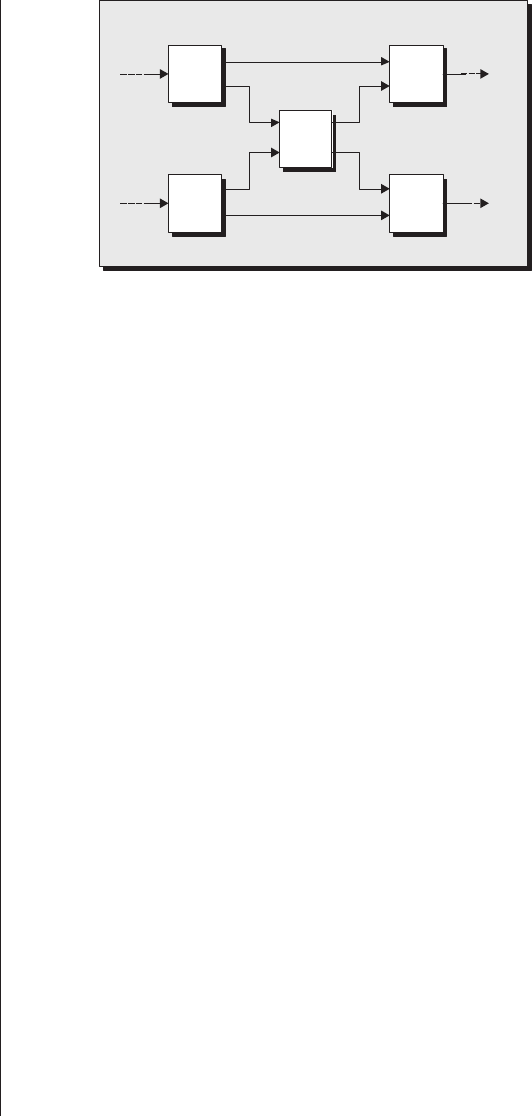
Based on this floor plan, the system architects would wave
their hands around, make educated guesses about a whole
range of things, and eventually pull some input-to-output
timing constraints for the FPGA out of the air.
Armed with these timing constraints and a specification of
the function the FPGA was to perform, the design engineer
(remember, there was typically only one engineer per device)
would wander off into the sunset to perform his or her
machinations.
Generally speaking, it was relatively rare for design engi-
neers to worry too much about FPGA pin assignments. To a
large extent, they would let the place-and-route software run
wild and free, and they would accept any pin assignments it
decided upon.
Once the FPGA design, including the pin assignments,
had been finalized, someone would be tasked with creating a
graphical symbol of the device for use with schematic capture,
along with a graphical representation of the device’s physical
footprint for use in the circuit board layout environment.
These symbols would include details as to the signal names
associated with the physical pins (and the physical locations
of the pins in the case of the layout representation).
Meanwhile, the circuit board designer would have been
working away in the background placing the other devices
and, as far as possible, routing them. It was only after the
268 ■The Design Warrior's Guide to FPGAs
FPGA
Other
Chip
Other
Chip
Other
Chip
Other
Chip
Circuit Board
Figure 15-1. The system architects sketch a rough floor plan.
1919:
The concept of flip-flop
(memory) circuits is
invented.

FPGA design had been finalized and the symbol created that
the FPGA could be fully integrated into the circuit board envi-
ronment and the routing completed. This meant that, at the
end of the day, it was largely left up to the circuit board
designer to make everything work.
The bad news was that when we said that the FPGA
design had been “finalized,” we really meant that hopefully it
was getting close. In the real world, it was almost invariably
the case that as soon as the circuit board designer had routed
the final track, the FPGA engineer remembered a tweak that
just had to be made. Implementing this tweak often ended up
modifying the pin assignments, which left the circuit board
designer feeling somewhat blue (it was not unknown for strong
words to ensue).
The times they are a-changing
Frightening as it may seem, the simplistic flow discussed
above persisted throughout most of the 1990s, but the size and
complexity of today’s FPGA devices means that this flow sim-
ply can’t stand up under the strain.
At the time of this writing, we’re talking about high-end
FPGAs containing as many as 1,700 pins presented in ball grid
array (BGA) packages with pin pitches of only 1 mm. Further-
more, today’s ICs (including FPGAs) are as fast as lightning
compared to their ancestors, which makes the delays associ-
ated with the circuit board tracks much more significant.
The bottom line is that it is no longer acceptable for the
system architects to assign timing constraints to the FPGA in
a fairly arbitrary manner and then leave it up to the circuit
board designer to make things work at the end of the day. This
scenario just won’t fly. Instead, the process needs to start at
the board level with the FPGA being treated as a black box
(Figure 15-2).
In this case, the circuit board layout designer performs
board-level timing based on a preliminary placement, and this
information is used to calculate realistic constraints to feed to
the FPGA design engineer. In the case of modern designs,
High-Speed Design and Other PCB Considerations ■269
BGA is pronounced
by spelling it out as
“B-G-A.”
A BGA package has an
array of pads presented
across the bottom face
of the device. The circuit
board is created with a
corresponding set of
pads. Each pad on the
FPGA has a small ball of
solder attached to it.
These devices are
attached to the circuit
board by placing them in
the correct location and
then melting the solder
balls to form good ball-
to-pad connections.
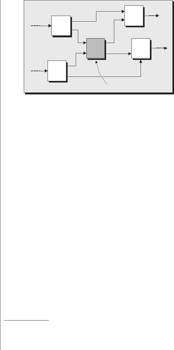
there could be hundreds or thousands of such timing con-
straints, and it simply wouldn’t be possible to generate and
prioritize them without performing this board-level analysis.
But wait; we have to go farther than this. In order to
ensure that the FPGA can be routed successfully, it’s now the
board designer who has to perform the initial assignments of
signals to the FPGA’s I/O pins. In order to do this, new tools
are becoming available to the board designer. These tools pro-
vide a graphical representation of the physical footprint for
the device along with an interactive interface that allows the
user to declare signal names and associate them with specific
device pins.1
These tools also provide for the auto-generation of the
schematic symbol. In the case of devices with 1,000 or more
pins, the tool can partition the symbol into multiple parts.
One popular push-button option is to create these partitions
based on the FPGA’s I/O banks, but it’s also possible to define
partitions by hand on a pin-by-pin basis.
270 ■The Design Warrior's Guide to FPGAs
Other
Chip
Other
Chip
Other
Chip
Other
Chip
Circuit Board
FPGA as “black box”
Figure 15-2. The circuit board designer performs preliminary
placement.
1At the time of this writing, a good example of the current state-of-the-art
is the BoardLink Pro application from Mentor (www.mentor.com).
1919:
Walter Schottky invents
the Tetrode (the first
multiple-grid vacuum
tube).

Once the circuit board designer has performed this up-
front work, it’s necessary to have some mechanism by which to
transfer these pin assignments over to the FPGA design engi-
neer, who will use them as physical constraints to guide the
FPGA’s place-and-route applications. In the real world, there
may still be a number of iterations if the FPGA engineer finds
it necessary to make modifications to the original pin assign-
ments, but these tend to be minor compared to the horrors
seen when using the flow of yesteryear as was introduced ear-
lier in this chapter.
FPGA Xchange
Until recently, the passing of data back and forth between
the board designer and the FPGA design engineer has typically
involved a substantial amount of hands-on tweaking to get
things to work. That is set to change because a new ASCII file
format called FPGA Xchange is being defined by Mentor in
conjunction with Altera, Xilinx, and the other major FPGA
players.
This format will allow the circuit board tools and the
FPGA tools to share common definitions of device aspects,
such as how signal names have been assigned to physical
device pins. This will allow board designers and FPGA engi-
neers to pass data between their two domains quickly and
easily.
For example, the board designer may create the original
pin assignments and use the associated FPGA Xchange file to
pass these as constraints to the FPGA engineer’s place-and-
route tools. The board designer can then proceed to layout the
circuit board.
Meanwhile, the FPGA engineer may find it necessary to
modify some of the pin assignments. These changes would be
incorporated into the original FPGA Xchange file, which
would subsequently be used by the board-level layout software
to rip up any tracks associated with pins that had changed.
These tracks can then be rerouted automatically or auto-
interactively.
High-Speed Design and Other PCB Considerations ■271
1921:
Albert hull invents the
Magnetron (a
microwave generator).

Other things to think about
High-speed designs
There is a common misconception that the term high-speed
design means having a fast system clock. In reality, high-speed
effects are associated with the speed of edges (the rate at
which signals transition from logic 0 to logic 1, and vice
versa). The faster the edge, the more significant are signal
inegrity (SI) issues such as noise, crosstalk, and the like. Now
it’s certainly true that as the frequency of the system clock
increases, the speed of edges also has to increase, but you
can run into high-speed design problems with even a one
megahertz clock if your signals have fast edge rates (and the
vast majority of signals have fast edge rates these days).
SI analysis
One of the nice things about FPGAs is that the vendor
has already dealt with the vast majority of SI issues inside the
chip; however, it is becoming increasingly important to per-
form SI analysis at the board level. The best tools aren’t
cheap, but neither is creating a board that doesn’t work. So
you have to choose whether to perform the SI analysis or just
roll the dice and see what happens.
SPICE versus IBIS
Performing SI analysis at the board level using SPICE
models can be time-consuming. In the early 1990s, Intel
created and promoted the input/output buffer information speci-
fication (IBIS), which is a modeling format that describes the
analog characteristics of drivers and receivers.
The reason for Intel’s largesse was that they didn’t want to
give detailed SPICE models to customers because these mod-
els are at the transistor-capacitor-resistor level, and they can
provide a lot of information that a component vendor might
not wish its competitors to be aware of.
IBIS models are behavioral in nature and any process-
related information is hidden. However, these models are only
272 ■The Design Warrior's Guide to FPGAs
SI is pronounced by spell-
ing it out as “S-I.”
SPICE, which is
pronounced like the sea-
soning, stands for
simulation program with
integrated circuit empha-
sis. This analog
simulation program was
developed by the Univer-
sity of California at
Berkeley and was made
available for widespread
use around the beginning
of the 1970s.

accurate up to some maximum frequency, which can range
from 500 megahertz to 1 gigahertz, depending on who you are
talking to. After that point you are obliged to use a more accu-
rate model such as SPICE.
Another problem is that the language has to be extended
in order to accommodate new technologies. For example, IBIS
has no mechanism to model the effects of pre-emphasis (see
also chapter 21). However, the IBIS syntax is not inherently
extensible, and augmenting the language via the various open
forum committees is a long-winded process (by the time you
get anything done, there’s a new technology to worry about).
In late 2002, a proposal was made to augment the IBIS
standard (this proposal was called BIRD75, where “BIRD”
stands for buffer information resolution document). This proposal
would allow calls to external models on a pin-by-pin basis. If
adopted, this will allow extensibility, because the external
models can be represented in languages such as SPICE,
VHDL-AMS, Verilog-A, and so forth.
Startup power
Some FPGAs can have substantial power supply require-
ments due to high transient startup currents. Board-level
designers need to check with the FPGA team to determine
these requirements so as to ensure that the board can supply
sufficient power to avoid any problems.
Use of internal termination impedances
Nearly all modern high-speed I/O standards require that
the tracks on the circuit board have specific impedances and
associated termination resistors (having the correct values
eliminates the reflection and ringing effects that degrade SI
and affect system performance).
Using termination resistors that are external to the device
may necessitate additional layers in the board, resulting in
higher costs and longer development times. In the case of
FPGAs with hundreds or thousands of pins, it is almost impos-
sible to place these termination resistors within reasonable
High-Speed Design and Other PCB Considerations ■273
IBIS is prononuced
“eye-bis.”

proximity to the device (distances greater than 1 cm from the
pin cause problems). For these reasons, some FPGAs include
digitally controlled impedance (DCI) capability.
Available on both inputs and outputs, DCI termination
can be configured to support parallel and series termination
schemes. These on-chip resistor values are completely user
definable, and the digital implementation of this technology
means that their values do not vary with changes in tempera-
ture or supply voltages.
A simple rule of thumb is that for any signals with rise/fall
times of 500 picoseconds or less, external termination resistors
cause discontinuities in the signal, in which case you should
be using their on-chip counterparts.
Pushing data around in parallel versus serial
It is common in electronic systems to process groups of
bits—called words—in parallel, where the width of the word
depends on the system. In the case of 8-bit microprocessors
and microcontrollers, for example, words are, perhaps not
surprisingly, 8 bits wide.
In the days of yore, when device manufacturers agonized
over every additional pin on an IC package, it was common
for chips to include a function called a universal asynchronous
receiver transmitter (UART). Assuming 8-bit words, if the chip
wished to send information to the outside world, the UART
would convert an 8-bit byte of data from the internal bus into
a series of pulses for transmission. Similarly, if the chip wished
to access information from the outside world, the UART
would accept that information as a series of pulses, collect it
into an 8-bit byte, and place that byte on the internal bus.
Thus, chips using this technique required only two pins to
write and read data: transmit data (TXD) and receive data
(RXD).
As packaging technologies improved, increasing the
number of pins became less of a burden, so it became more
and more common to pass entire words of data around. In the
case of an 8-bit system, this would require eight tracks on the
274 ■The Design Warrior's Guide to FPGAs
DCI is pronounced by
spelling it out as “D-C-I.”

circuit board and eight pins on each chip that was connected
to this bus.
Over time, it became necessary to push more information
around the system and to do so faster. Thus, bus widths
increased to 16 bits, then 32 bits, then 64 bits, and so on. At
the same time, clock speeds increased from integer multiples of
megahertz, to tens of megahertz, to hundreds of megahertz, to
thousands of megahertz, where 1,000 megahertz equates to
1 gigahertz.
As the speed of the system clock increases, it becomes
more and more problematic to route wide buses around a cir-
cuit board with any hope of getting the signals where you want
them to be, at the time you want them to be there, without
running into all sorts of SI problems in the form of noise and
crosstalk.2Thus, for the highest bandwidth applications,
designers are turning back to serial data transmission in the
form of gigabit transceivers. These are introduced in more
detail in Chapter 21.
High-Speed Design and Other PCB Considerations ■275
2I know this is a long sentence, but that’s appropriate because it’s been a
long day!
1921:
Canadian-American
John Augustus Larson
invents the polygraph
lie detector.
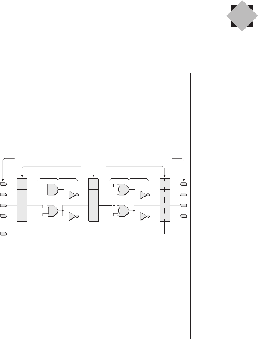
Lack of visibility
One of the problems associated with debugging any chip
design—be it an ASIC or an FPGA—is the lack of visibility as
to what activity is taking place inside the device. Purely for the
sake of these discussions, let’s assume that we have a really
simple pipelined design comprising a few registers and logic
gates (Figure 16-1).
Obviously, this is something of a nonsense circuit (you’d be
amazed how tricky it can be to make something up that
doesn’t cloud the issue), but it will serve our purposes here.
The problem is that we only have access to the chip’s pri-
mary inputs and outputs, so we can’t see what’s happening
inside. This isn’t particularly important when the design has
been completed and verified, but it’s a pain when we are trying
Observing Internal Nodes in
an FPGA
Chapter
16
clock
&
|
|
|
Logic Logic
Registers
Primary Inputs Primary Outputs
Figure 16-1. A very simple pipelined circuit.
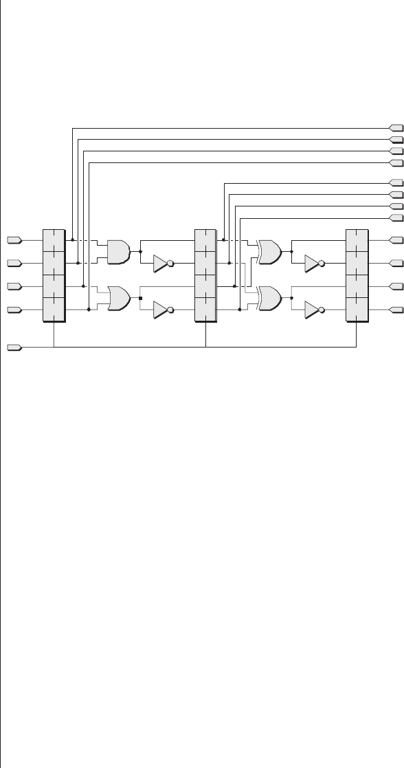
to debug the chip to determine why it isn’t doing what we
expected it to.
One obvious solution would be to make the internal nodes
visible by connecting them to primary output pins from the
device (Figure 16-2).
The downside to this scheme is that most designs are “I/O
limited,” which means that the bottleneck is the number of
primary I/O pins available on the package. In fact, even if we
don’t use any I/O pins to access internal nodes, many FPGA
designs already leave a pile of internal resources unused
because there aren’t enough I/O pins available to convey all
of the required control and data signals into and out of the
device.
Multiplexing as a solution
One simple alternative is to multiplex the main outputs
with the internal signals and bring them all out through the
same set of output pins (Figure 16-3).
Of course, the select control would also require the use of
some primary I/O pins. In the example shown here, the sim-
plest case would be to bring the two select control signals
directly to the outside world, which would therefore require
278 ■The Design Warrior's Guide to FPGAs
clock
&
|
|
RA0
RA1
RA2
RA3
RB0
RB1
RB2
RB3
RC0
RC1
RC2
RC3
RB0
RB1
RB2
RB3
RC0
RC1
RC2
RC3
|
RA0
RA1
RA2
RA3
Figure 16-2. Connecting internal nodes to primary outputs.
1921:
Czech author Karal
Capek coins the term
robot in his play R.U.R.
1921:
First use of quartz
crystals to keep radios
from wandering off
station.
two I/O pins. Alternatively, we might use a small portion of
logic to implement a simple state machine that required only a
single I/O to act as a sort of clock to cycle between states, each
of which would cause the multiplexer to select a different set
of signals (see also the discussions on VirtualWires later in this
chapter).
The main advantages of this scheme are that it offers great
visibility and it’s relatively fast. The main disadvantages are
that it’s relatively inflexible and time-consuming to implement
because if you wish to change the internal pins that are being
monitored, you have to modify the design’s source code and
then resynthesize it. Similarly, if you wish to change any trig-
ger conditions that might be used by a state machine to
determine which set of signals is to be selected by the multi-
plexer at any particular time, you once again have to change
the design source code.
Another point to consider is that if, once you’ve debugged
everything, you delete these test structures from your source
code, you may introduce new problems into the design, not the
least of which is that the routing will change, along with its
associated delays.
Observing Internal Nodes in an FPGA ■279
RB0
RB1
RB2
RB3
RA0
RA1
RA2
RA3
RC0
RC1
RC2
RC3
Internal signals
Original outputs
Out0
Out1
Out2
Out3
Primary
output pins
Multiplexer
S
elect control
Figure 16-3. Multiplexing signals.
1922:
First commercial
broadcast ($100 for a
10-minute advert).
1923:
First neon advertising
signs are introduced.

Special debugging circuitry
Some FPGAs include special debugging circuitry that
allows you to observe internal nodes. For example, FPGAs
from Actel feature two special pins called PRA (“Probe A” )
and PRB (“Probe B”). By means of the embedded debugging
circuitry combined with the use of a special debugging utility,1
any internal signal can be connected to either of these pins,
allowing the values on that node to be observed and analyzed.
The big advantage of this type of scheme is that you don’t
need to touch your source code. The disadvantage is that hav-
ing only two probe pins might be considered a tad limiting
when you have potentially hundreds of thousands of internal
signals to worry about.
Virtual logic analyzers
Although the schemes discussed above are useful, it is
often desirable to have access to more extensive logic analyzer
instrumentation to allow for the tracing and debugging of
groups of embedded signals, along with the ability to analyze
signals in the context of other related signals or under specific
triggering events.
On-chip instrumentation (OCI) is an analysis approach that
facilitates logic debugging by allowing the user to embed diag-
nostic IP blocks such as virtual logic analyzer applications into
their designs. The idea here is to use some of the FPGA’s
resources to implement one or more virtual logic analyzer
blocks that capture the activity of selected signals. This data
will be stored in one or more of the FPGA’s embedded RAM
blocks, from whence it can be accessed by the external logic
analyzer software by means of the device’s JTAG port
(Ffigure 16-4).
A portion of the virtual logic analyzer will be devoted to
detecting trigger conditions on specific signals, where these
280 ■The Design Warrior's Guide to FPGAs
OCI is prononcued by
spelling it out as “O-C-I.”
1This used to be called Actionprobe®. Then a “new and improved” version
called Silicon Explorer became available. At the time of this writing, Silicon
Explorer II is the flavor of the day, and as for tomorrow …
conditions will be used to start and stop the data capture on
the signals being monitored.
Depending on the particular virtual logic analyzer imple-
mentation you are working with, you may or may not have to
modify your design’s source code to include this functionality.
The big advantage of this type of scheme is that, even if you do
have to include special macros in your source code, it’s rela-
tively easy to implement extremely sophisticated debugging
capabilities in your design.
In some cases, the FPGA vendor will offer this sort of capa-
bility. Good examples of debugging tools of this ilk are
Chipscope™ Pro from Xilinx (www.xilinx.com) and SignalTap®
II from Altera (www.altera.com). Alternatively, if you are
working with devices from a vendor who doesn’t offer this
capability, one option is to go to a third party such as First Sili-
con Solutions (www.fs2.com), which specializes in OCI and
debugging for FPGA logic and embedded processors.
With regard to a virtual logic analyzer for use in tracing,
analyzing, and debugging embedded signals in FPGAs, First
Silicon Solutions boasts its configurable logic analyzer module
(CLAM). This little scallywag consists of an OCI block (avail-
able in both Verilog and VHDL) that is configured and
Observing Internal Nodes in an FPGA ■281
Virtual Logic
Analyzer
Control
Logic
Signals we wish
to monitor
Start/Stop
conditions to
trigger on
Embedded
RAM Block
JTAG (from external virtual logic
analyzer program or another
internal logic analyzer block)
JTAG (to external virtual logic
analyzer program or another
internal logic analyzer block)
Figure 16-4. Virtual logic analyzers.
1923:
First photoelectric cell
is introduced.
1923: First ship-to-ship
communications
(people on one ship can
talk to people on
another).

synthesized as part of the design. This block (or blocks if you
use more than one) is used in conjunction with control,
probe, and display software that resides on your host PC.
VirtualWires
Sometime around the early 1990s, a company called
Virtual Machine Works introduced a technology they called
VirtualWires™. Originally intended as a technique for imple-
menting massive multi-FPGA systems, VirtualWires provided
a basis for a variety of FPGA-based emulation systems. One
reason for mentioning it here is that it bears some similarities
to the multiplexing solutions discussed earlier in this chapter.
Another reason is that it’s a really cool idea.
The problem
The starting point for the VirtualWires concept is that
you have a large design that is too big to fit into a single
FPGA, so you wish to split it across a number of devices. As a
simple example, let’s assume we have a design that equates to
some number of system gates, but that the largest FPGA avail-
able offers only half this number of gates. Thus, an initial
knee-jerk solution would almost certainly be to split the
design across two devices (Figure 16-5).
Note that the logic in this figure is shown as comprising a
number of subblocks labeled Athrough H. This is intended
only to provide an aid in visualizing the way in which the
logic might be partitioned across the devices.
The problem is that the chips typically won’t have enough
I/O pins to satisfy the requirements of the main inputs and
outputs to the design along with the signals linking the two
portions of the design. Prior to VirtualWires (or any similar
concept), the only option was to further partition the design
across more devices (Figure 16-6).
But now we have a new problem in that we are wasting
huge amounts of each FPGA’s logic resources, with the result
that we are using way too many chips.
282 ■The Design Warrior's Guide to FPGAs
1925: America.
Scientist, engineer, and
politician Vannevar Bush
designs an analogue
computer called the
Product Intergraph.
1925:
First commercial
picture/facsimile radio
service across the USA.
The VirtualWires solution
In order to see how the VirtualWires concept addresses our
problem, let’s first assume an extreme case in which we have
access to some very strange FPGAs that can boast only three
pins (two inputs and one output, where one of the inputs
Observing Internal Nodes in an FPGA ■283
Logic for the design
Primary inputs
to the design
Primary outputs
from the design
Primary inputs
to the design
Primary outputs
from the design
Not enough pins
ACEG
BDFH
AC
BD
EG
FH
FPGA 1 FPGA 2
Figure 16-5. Not enough pins if we try to split the design
across two devices.
Figure 16-6. Lots of wasted FPGA logic resources when
partitioning across multiple devices.
1926: America.
Dr. Julius Edgar
Lilienfield from New
York files a patent for
what we would now
recognize as an npn
junction transistor
being used in the role
of an amplifier.
assumes the role of a clock). In this case, we would probably
end up using only a very small amount of each FPGA’s logic
resources (Figure 16-7).
The idea behind VirtualWires is that, since we are wasting
so much of each device’s internal resources anyway, we might
as well use some of these resources to implement some special
circuitry that allows our single data input to be latched into a
number of registers, each of which can be used to drive its
own block of logic. Similarly, the outputs from each of the
blocks of logic can be multiplexed together and registered
(Figure 16-8).
284 ■The Design Warrior's Guide to FPGAs
FPGA (n)
Unused logic Unused logic
FPGA (n + 1)
Data from
previous FPGA
Data to
next FPGA
System clock
Used
logic
Used
logic
Figure 16-7. An extreme case in which each
FPGA has only three pins.
FPGA (n) FPGA (n + 1)
Data from
previous FPGA
Data to
next FPGA
Virtual clock
Virtual clock
System clock
Registers
Mux
Logic
Logic
Logic
Logic
Registers
Mux
Logic
Logic
Logic
Logic
State machine State machine
Figure 16-8. A simple example of VirtualWires.
1926: America.
First pop-up bread
toaster is introduced.
1926:
First commercial
picture/facsimile radio
service across the
Atlantic.

Note that our original system clock has been superceded by
a virtual clock, which subdivides each “beat” of the system
clock into some number of “ticks.” Also note that a state
machine is implemented inside each FPGA. These state
machines are used to enable and disable individual registers
and also to control the multiplexers and so forth. (Of course,
figure 16-8 is not to scale—the state machines and other Vir-
tualWires structures would actually consume relatively little of
the logic resources in each device compared to the number of
logic blocks that are actually implementing the real design.)
On each tick of the virtual clock, the state machine inside
each FPGA will enable a register driving one of the logic
blocks, thereby allowing the data from the input pin to be
loaded into that register. At the same time, the state machine
will cause the multiplexer to select the output from one of the
logic blocks, and it will store that data in a register driving the
output pin, which in turn drives the input to the next FPGA
in the chain.
In the real world, of course, our FPGAs will have hundreds
or thousands of pins. Each input may be used to drive several
blocks of logic, and each output will be driven by its own Vir-
tualWires multiplexer that selects data from a number of
blocks of logic. To cut a long story short, things will become
much more complicated, but the underlying principle remains
the same.
Last but not least, a key element to the VirtualWires con-
cept is a compiler that takes the original design in the form of
a gate-level netlist, partitions this design across multiple
FPGAs, automatically creates the state machines and other
VirtualWires-related structures, and then generates the con-
figuration files that will be used to load each of the FPGAs.
Observing Internal Nodes in an FPGA ■285
1926:
John Logie Baird
demonstrates an
electromechanical TV
system.
1927:
First five-electrode
vacuum tube (the
Pentrode) is
introduced.

Sources of IP
Today’s FPGA designs are so big and complex that it
would be impractical to create every portion of the design from
scratch. One solution is to reuse existing functional blocks for
the boring stuff and spend the bulk of your time and resources
creating the cunning new portions of the design that feature
your “secret sauce” and that will differentiate your design from
any competitor offerings.
Any existing functional blocks are typically referred to as
IP. The three main sources of such IP are (1) internally created
blocks from previous designs, (2) FPGA vendors, and (3)
third-party IP providers. For the purposes of these discussions,
we shall concentrate on the latter two categories.
Handcrafted IP
One scenario is that the IP provider has handcrafted an IP
block starting with an RTL description (the provider might
also have used an IP block/core generator application, as dis-
cussed later in this chapter). In this case, there are several ways
in which the end user might purchase and use such a block
(Figure 17-1).
IP at the unencrypted RTL level
In certain cases, FPGA designers can purchase IP at the
RTL level as blocks of unencrypted source code. These blocks
can then be integrated into the RTL code for the body of the
design (Figure 17-1a). (Note that the IP provider would
IP is pronounced by
spelling it out as “I-P.”
Intellectual Property
Chapter
17
already have simulated, synthesized, and verified the IP blocks
before handing over the RTL source code).
Generally speaking, this is an expensive option because IP
providers typically don’t want anyone to see their RTL source
code. Certainly, FPGA vendors are usually reluctant to pro-
vide unencrypted RTL because they don’t want anyone to
retarget it toward a competitor’s device offering. So if you
really wish to go this route, whoever is providing the IP will
charge you an arm and a leg, and you’ll end up signing all sorts
of licensing and nondisclosure agreements (NDAs).
Assuming you do manage to lay your hands on unen-
crypted RTL, one advantage of this approach is that you can
modify the code to remove any functions you don’t require in
your design (or in some cases you might add new functions).
Another advantage, assuming that you purchase the IP from a
third party rather than from an FPGA vendor, is that you can
quickly and easily retarget the IP across different device fami-
lies and FPGA vendors. The big disadvantage is that the
resulting implementation will typically be less efficient in
288 ■The Design Warrior's Guide to FPGAs
NDA is pronounced by
spelling it out as “N-D-A.”
Create RTL
forIPblock
IP Provider FPGA Designer
Incorporate
IP block(s)
Unplaced-and-
unrouted netlist
Synthesis
Create RTL for
body of design
Unplaced-and-
unrouted netlist
Synthesis
Incorporate
IP block(s)
Place-and-Route Place-and-Route
Placed-and-routed
netlist
Placed-and-routed
netlist
(a)
(b)
(c)
Figure 17-1. Alternative potential IP acquisition points.

terms of resource requirements and performance when com-
pared to an optimized version delivered at the netlist level as
discussed below.
IP at the encrypted RTL level
Unfortunately, at the time of this writing, there is no
industry-standard encryption technique for RTL that has
popular tool support. This has led companies like Altera and
Xilinx to develop their own encryption schemes and tools.
RTL encrypted by a particular FPGA vendor’s tools can only
be processed by that vendor’s own synthesis tools (or some-
times by a third-party synthesis tool that has been OEM’d by
the FPGA vendor).
IP at the unplaced-and-unrouted netlist level
Perhaps the most common scenario is for FPGA designers
to purchase IP at the unplaced-and-unrouted LUT/CLB netlist
level (Figure 17-1b). Such netlists are typically provided in
encrypted form, either as encrypted EDIF or using some FPGA
vendor-specific format.
In this case, the IP vendor may also provide a compiled
cycle-accurate C/C++ model to be used for functional verifica-
tion because such a model will simulate much faster than the
LUT/CLB netlist-level model.
The main advantage of this scenario is that the IP provider
has often gone to a lot of effort tuning the synthesis engine
and handcrafting certain portions of the function so as to
achieve an optimal implementation in term of resource utiliza-
tion and performance. One disadvantage is that the FPGA
designer doesn’t have any ability to remove unwanted func-
tionality. Another disadvantage is that the IP block is tied to a
particular FPGA vendor and device family.
IP at the placed-and-routed netlist level
In certain cases, the FPGA designer may purchase IP at the
placed-and-routed LUT/CLB netlist level (Figure 17-1c).
Once again, such netlists are typically provided in encrypted
Intellectual Property ■289
EDIF is pronounced
“E-DIF;” that is, by spell-
ing out the ‘E’ followed
by “dif” to rhyme with
“miff.”

form, either as encrypted EDIF or using some FPGA vendor-
specific format.
The reason for having placed-and-routed representations
is to obtain the highest levels of performance. In some cases
the placements will be relative, which means that the loca-
tions of all of the LUT, CLB, and other elements forming the
block are fixed with respect to each other, but the block as a
whole may be positioned anywhere (suitable) within the
FPGA. Alternatively, in the case of IP blocks such as commu-
nications or bus protocol functions with specific I/O pin
requirements, the placements of the elements forming the
block may be absolute, which means that they cannot be
changed in any way.
Once again, the IP vendor may also provide a compiled
cycle-accurate C/C++ model to be used for functional verifi-
cation because such a model will simulate much faster than
the LUT/CLB netlist-level model.
IP core generators
Another very common practice is for FPGA vendors
(sometimes EDA vendors, IP providers, and even small, inde-
pendent design houses) to provide special tools that act as IP
block/core generators. These generator applications are almost
invariably parameterized, thereby allowing you to specify the
widths and depths, or both of buses and functional elements.
First, you get to select from a list of different blocks/cores,
and then you get to specify the parameters to be associated
with each. Furthermore, in the case of some blocks/cores, the
generator application may allow you to select from a list of
functional elements that you wish to be included or excluded
from the final representation. In the case of a communications
block, for example, it might be possible to include or exclude
certain error-checking logic. Or in the case of a CPU core, it
might be possible to omit certain instructions or addressing
modes. This allows the generator application to create the
most efficient IP block/core in terms of its resource require-
ments and performance.
290 ■The Design Warrior's Guide to FPGAs
1927:
First public
demonstration of
long-distance television
transmission (basically a
Nipkow disk).
Depending on the origin of the generator application (or
sometimes the licensing option you’ve signed up for), its out-
put may be in the form of encrypted or unencrypted RTL
source code, an unplaced-and-unrouted netlist, or a placed-
and-routed netlist. In some cases, the generator may also
output a cycle-accurate C/C++ model for use in simulation
(Figure 17-2).
Miscellaneous stuff
There is currently a push by the main FPGA vendors to
provide special system generator utilities. These tools are essen-
tially IP integrators that allow you to quickly build up very
sophisticated designs using the various IP building blocks
available from the respective FPGA vendor.
These system generator tools essentially spit out netlists for
systems defined in some abstract form (as opposed to detailed
end-user RTL coding.) These tools aim to change the FPGA
design model by providing a system-level design paradigm that
sits on top of the standard RTL-based design flow. This con-
cept is of particular interest for designers who don’t write RTL
or who prefer to work at a higher level of abstraction (see also
Chapter 12).
In addition to providing system generators, FPGA vendors
are also working to simplify the use of IP by incorporating IP-
based design-flow capabilities into their independent develop-
ment environments (IDEs).
Intellectual Property ■291
IDE is pronounced by
spelling it out as
“I-D-E.”
RTL
forIPblock
FPGA Designer Input
Unplaced-and-
unrouted netlist
Placed-and-
routed netlist
Cycle-accurate
C/C++ model
IP block/core
generator
Figure 17-2. IP block/core generator.

Last, but not least, some IP that used to be “soft” is now
becoming “hard.” For example, the most current generation of
FPGAs contains hard processor, clock manager, Ethernet, and
gigabit I/O blocks, among others. These help bring high-end
ASIC functionality into standard FPGAs. Over time, it is
likely that additional functions of this ilk will be incorporated
into the FPGA fabric.
292 ■The Design Warrior's Guide to FPGAs
Depending on whom you
are talking to, the ‘D’ in
IDE can stand for “design”
or “development.”
Alternative design scenarios
When it comes to creating an FPGA design, there are a
number of possible scenarios depending on what you are trying
to do (Figure 18-1).
FPGA only
This refers to a design that is intended for an FPGA imple-
mentation only. In this case, one might use any of the design
flows and tools introduced elsewhere in this book.
FPGA-to-FPGA
This refers to taking an existing FPGA-based design and
migrating it to a new FPGA technology (the new technology
is often presented in the form of a new device family from the
same FPGA vendor you used to implement the original design,
but you may be moving to a new vendor also).
Migrating ASIC Designs to
FPGAs and Vice Versa
Chapter
18
Existing design New design Final implementation
N/A FPGA FPGAFPGA Only
FPGA-to-FPGA FPGA FPGA FPGA
FPGA-to-ASIC FPGA ASIC
ASIC-to-FPGA ASIC FPGA FPGA
N/A
Figure 18-1. Alternative design scenarios.

With this scenario, it is rare that you will be performing a
simple one-to-one migration, which means taking the con-
tents of an existing component and migrating them directly to
a new device. It is much more common to migrate the func-
tionality from multiple existing FPGAs to a single new FPGA.
Alternatively, you might be gathering the functionality of one
or more existing FPGAs, plus a load of surrounding discrete
logic, and bundling it all into a new device.
In these cases, the typical route is to gather all of the RTL
code describing the original devices and discrete logic into a
single design. The code may be tweaked so as to take advan-
tage of any new features available in the targeted device and
then resynthesized.
FPGA-to-ASIC
This refers to using one or more FPGAs to prototype an
ASIC design. One big issue here is that, unless you’re working
with a small to medium ASIC, it is often necessary to parti-
tion the design across multiple FPGAs. Some EDA and FPGA
vendors either have (or used to have) applications that will
perform this partitioning automatically,1but tools like this
come and go with the seasons. Also, their features and capa-
bilities, along with the quality of their results, can change on
an almost weekly basis (which is my roundabout way of telling
you that you’ll have to evaluate the latest offerings for
yourself).
Another consideration is that functions like RAMs con-
figured to act as FIFO memories or dual-port memories have
specific realizations when they are implemented using embed-
ded RAM blocks in FPGAs. These realizations are typically
different from the way in which these functions will be imple-
mented in an ASIC, which may cause problems. One solution
is to create your own RTL library of ASIC functions for such
things as multipliers, comparators, memory blocks, and the
294 ■The Design Warrior's Guide to FPGAs
Literally as this book
was heading to press,
Synopsys
(www.synopsys.com)
made a rather interesting
announcement. Using its
well-known Design
Compiler® ASIC synthesis
engine as a base, they’ve
created an
FPGA-optimized version
called Design Compiler
FPGA. Among other
things, DC FPGA features
some innovative new
Adaptive Optimization™
Technology that looks to
be very interesting. 1A good example of an application that provides this sort of functionality
is Certify®from Synplicity (www.synplicity.com).
like that will give you a one-for-one mapping with their FPGA
counterparts. Unfortunately, this means instantiating these
elements in the RTL code for your design, as opposed to using
generic RTL and letting the synthesis engine handle every-
thing (so it’s a balancing act like everything else in
engineering).
As we discussed in Chapter 7, a design intended for an
FPGA implementation typically contains fewer levels of logic
between register stages than would a pure ASIC design. In
some cases, it’s best to create the RTL code associated with the
design with the final ASIC implementation in mind and just
take the hit with regard to reduced performance in the FPGA
prototype.
Alternatively, one might generate two flavors of the
RTL—one for use with the FPGA prototype and the other to
provide the final ASIC. But this is generally regarded to be a
horrible way to do things because it’s easy for the two represen-
tations to lose synchronization and end up going in two totally
different directions.
One way around this might be to use the pure C/C++
based tools introduced in chapter 11. As you may recall, the
idea here is that, as opposed to adding intelligence to the RTL
source code by hand (thereby locking it into a target imple-
mentation), all of the intelligence is provided by your
controlling and guiding the C/C++ synthesis engine itself
(Figure 18-2).
Migrating ASIC Designs to FPGAs and Vice Versa ■295
But the main point is that
DC ASIC and DC FPGA
can use the same RTL
source code, constraints,
etc. to create both ASIC
and FPGA
implementations of the
same design. (Each
engine can be instructed
to use different
microarchitecture
schemes such as
resource sharing and the
number of pipeline
stages. Furthermore, DC
FPGA can perform
automatic transformation
on any ASIC-centric
clock-gating embedded
in the RTL.) All of this
makes the combination
of DC FPGA and DC ASIC
very interesting in the
context of using FPGAs
as prototypes for final
ASIC implementations.
- Non-implementation-specific
- Easy to create
- Fast to simulate
- Easy to modify
Pure C/C++ Pure C/C++
Synthesis
User interaction
and guidence
Gate-level
netlist
Verilog /
VHDL RTL
LUT/CLB-
level netlist
ASIC
target
Verilog /
VHDL RTL
RTL
Synthesis
RTL
Synthesis
FPGA
target
Auto-generated,
implementation-specific
Figure 18-2. A pure C/C++–based design flow.

Once the synthesis engine has parsed the C/C++ source
code, you can use it to perform microarchitecture tradeoffs
and evaluate their effects in terms of size and speed. The
user-defined configuration associated with each “what-if”
scenario can be named, saved, and reused as required. Thus,
you could first create a configuration for use as an FPGA pro-
totype and, once this had been verified, you could create a
second configuration to be used for the final ASIC implemen-
tation. The key point is that the same C/C++ source code is
used to drive both flows.
Another point to ponder is that a modern ASIC design
can contain an unbelievable number of clock domains and
subdomains (we’re talking about hundreds of domains/subdo-
mains here). By comparison, an FPGA has a limited number
of primary clock domains (on the order of 10). This means
that if you’re using one or more FPGAs to prototype your
ASIC, you’re going to have to put a lot of thought into how
you handle your clocks.
Last but not least, there’s an interesting European Patent
numbered EP0437491 (B1), which, when you read it—and,
good grief, it’s soooo boring—seems to lock down the idea of
using multiple programmable devices like FPGAs to temporar-
ily realize a design intended for final implementation as an
ASIC. In reality, I think this patent was probably targeted
toward using FPGAs to create a logic emulator, but the way
it’s worded would prevent anyone from using two or more
FPGAs to prototype an ASIC.
ASIC-to-FPGA
This refers to taking an existing ASIC design and migrat-
ing it to an FPGA. The reasons for doing this are wide and
varied, but they often involve the desire to tweak an existing
ASIC’s functionality without spending vast amounts of
money. Alternatively, the original ASIC technology may
have become obsolete, but parts might still be required to sup-
port ongoing contracts (this is often the case with regard to
military programs). One point of interest is that the latest
296 ■The Design Warrior's Guide to FPGAs
1927:
Harold Stephen Black
conceives the idea of
negative feedback,
which, amongst other
things makes Hi-Fi
amplifiers possible.

generation of FPGAs has usually jumped so far so fast that it’s
possible to place an entire ASIC design from just a few years
ago into a single modern FPGA (if you do have to partition
the design across multiple FPGAs, then there are tools to aid
you in this task, as discussed in the “FPGA-to-ASIC” section
above).
First of all, you are going to have to go through your RTL
code with a fine-tooth comb to remove (or at least evaluate)
any asynchronous logic, combinatorial loops, delay chains, and
things of this ilk (see also Chapter 7). In the case of flip-flops
with both set and reset inputs, you might wish to recode these
to use only one or the other (see also Chapter 7). You might
also wish to look for any latches and redesign the circuit to use
flip-flops instead. Also, you should keep a watchful eye open
for statements like if-then-else without the else clause because,
in these cases, synthesis tools will infer latches (see also
Chapter 9).
In the case of clocks, you will have to ensure that your tar-
get FPGA provides enough clock domains to handle the
requirements of the original ASIC design—otherwise, you’ll
have to redesign your clock circuitry. Furthermore, if your
original ASIC design made use of clock-gating techniques, you
will have to strip these out and possibly replace them with
clock-enable equivalents (see also Chapter 7). Once again,
some FPGA and EDA vendors provide synthesis tools that can
automatically convert an ASIC design using gated clocks to an
equivalent FPGA design using clocks with enables.2
In the case of complex functional elements such as mem-
ory blocks (e.g., FIFOs and dual-port RAMs), it will probably
be necessary to tweak the RTL code to fit the design into the
FPGA. In some cases, this will involve replacing generic RTL
statements (that will be processed by the synthesis engine)
with calls to instantiate specific subcircuits or FPGA elements.
Migrating ASIC Designs to FPGAs and Vice Versa ■297
2A good example of an application that provides this sort of functionality
is Amplify®from Synplicity (www.synplicity.com).
1927: America.
Philo Farnsworth
assembles a complete
electronic TV system.

Last, but not least, the original pipelined ASIC design
probably had more levels of logic between register elements
than you would like in the FPGA implementation if you wish
to maintain performance. Most modern logic synthesis and
physically aware tools provide retiming capability, which
allows them to move logic back and forth across pipeline reg-
ister boundaries to achieve better timing (the physically aware
synthesis engines typically do a much better job at this; see
also chapter 19).
It’s also true that your modern FPGA is probably based on
a later technology node (say, 130 nano) than your original
ASIC design (say, 250 nano). This gives the FPGA an
inherent speed advantage, which serves to offset its inherent
track-delay disadvantages. At the end of the day, however,
you may still end up having to hand-tweak the code to add in
more pipeline stages.
298 ■The Design Warrior's Guide to FPGAs
1928: America.
First quartz crystal clock
is introduced.

Introduction
Design engineers typically need to use a tremendous vari-
ety of tools to capture, verify, synthesize, and implement their
designs. Introducing all of these tools would require a book in
itself,1so this chapter focuses on some of the more significant
contenders in the context of FPGA designs (along with a
couple I threw in for interest’s sake):
■Simulation (cycle-based, event-driven, etc.)
■Synthesis (logic/HDL versus physically aware)
■Timing analysis (static versus dynamic)
■Verification in general
■Formal verification
■Miscellaneous
Simulation (cycle-based, event-driven, etc.)
What are event-driven logic simulators?
Logic simulation is currently one of the main verification
tools in the design (or verification) engineer’s arsenal. The
most common form of logic simulation is known as event driven
because, perhaps not surprisingly, these tools see the world as a
series of discrete events. As an example, consider a very simple
circuit comprising an OR gate driving both a BUF (buffer)
gate and a brace of NOT (inverting) gates, as shown in
Figure 19-1.
Simulation, Synthesis,
Verification, etc. Design Tools
Chapter
19
1I’d be more than happy to write such a book if anyone would be prepared
to fund the effort!
Just to keep things simple, let’s assume that NOT gates
have a delay of 5 picoseconds (ps), BUF gates have a delay of
10 ps, and OR gates have a delay of 15 ps. On this basis, let’s
consider what will happen when a signal change occurs on
one of the input pins (Figure 19-2).
Internally, the simulator maintains something called an
event wheel onto which it places events that are to be
“actioned” at some time in the future. When the first event
occurs on input in1 at a time we might refer to as t1, the simu-
300 ■The Design Warrior's Guide to FPGAs
|
in1
in2
out
2
w1
out1
g1
g2
g3
OR
BUF
NOT
g4
NOT
w2
Figure 19-1. An example circuit.
in1
in2
w1
w2
out1
out2
15 ps 5 ps 5ps
t1t2t3t4
Figure 19-2. Results from an event-driven simulation.
1928:
John Logie Baird
demonsrates colr TV on
an electronic TV system.

lator looks to see what this input is connected to, which
happens to be our OR gate. We are assuming that the OR gate
has a delay of 15 ps, so the simulator schedules an event on the
output of the OR gate—a rising (0 to 1) transition on wire
w1—for 15 ps in the future at time t2.
The simulator then checks if any further actions need to be
performed at the current time (t1), then it looks at the event
wheel to see what is to occur next. In the case of our example,
the next event happens to be the one we just scheduled at
time t2, which was for a rising transition on wire w1.Atthe
same time as the simulator is performing this action, it looks to
see what wire w1 is connected to, which is BUF gate g2 and
NOT gate g3.
As NOT gate g3 has a delay of 5 ps, the simulator sched-
ules a falling (1 to 0) transition on its output, wire w2,for5ps
in the future at time t3. Similarly, as BUF gate g2 has a delay of
10 ps, the simulator schedules a rising (0 to 1) transition on its
output, output out1, for 10 ps in the future at time t4. And so it
goes until all of the events triggered by the initial transition on
input in1 have been satisfied.
The advantage of this event-driven approach is that simu-
lators based on this technique can be used to represent almost
any form of design, including synchronous and asynchronous
circuits, combinatorial feedback loops, and so forth. These
simulators also offer extremely good visibility into the design
for debugging purposes, and they can evaluate the effects of
delay-related narrow pulses and glitches that are very difficult
to find using other techniques (see also the discussions on
delays in the next section). The big disadvantage associated
with these simulators is that they are extremely compute-
intensive and correspondingly slow.
A brief overview of the evolution of event-driven
logic simulators
As we discussed in chapter 8, the first event-driven digital
logic simulators (circa the late 1960s and early 1970s) were
based on the concept of simulation primitives. At a minimum,
Simulation, Synthesis, Verification, etc. Design Tools ■301
1928:
John Logie Baird
invents a videodisc to
record television
programs.
these primitive elements would include logic gates such as
BUF, NOT, AND, NAND, OR, NOR, XOR, and XNOR,
along with a number of tri-state buffers. Some simulators also
offered a selection of registers and latches as primitive ele-
ments, while others required you to create these functions as
subcircuits formed from a collection of the more primitive
logic gates.
At that time, the functionality of the design would be cap-
tured using a standard text editor as a gate-level netlist.
Similarly, the testbench would be captured as a textual (tabu-
lar) stimulus file. The simulator would accept the netlist and
testbench along with any control files and command-line
instructions; it would use the netlist to build a model of the
circuit in the computer’s memory; it would apply the stimulus
from the testbench to this model; and it would output results
in the form of a textual (tabular) file (Figure 19-3).
Over time things started to become a little more sophisti-
cated. First, schematic capture packages were used to capture
the design and to generate the gate-level netlist. Next, special
302 ■The Design Warrior's Guide to FPGAs
RTL is pronounced by
spelling it out as “R-T-L.”
BEGIN CIRCUIT=TEST
INPUT SET_A, SET-B,
DATA, CLOCK,
CLEAR_A, CLEAR_B;
OUTPUT Q, N_Q;
WIRE SET, N_DATA, CLEAR;
GATE G1=NAND (IN1=SET_A,
IN2=SET_B,
OUT1=SET);
GATE G2=NOT (IN1=DATA,
OUT1=N_DATA);
GATE G3=OR (IN1=CLEAR_A,
IN2=CLEAR_B,
OUT1=CLEAR);
GATE G4=DFF (IN1=SET, IN2=N_DATA,
IN3=CLOCK, IN4=CLEAR,
OUT1=Q, OUT2=N_Q);
END CIRCUIT=TEST;
Textual gate-level netlist
Textual (tabular) stimulus
CC
LL
SS CEE
EEDLAA
TTAORR
__TC__
TIMEABAKAB
----- -----------
0111000 ;Setup
500111100 ;Risingedge
1000111000 ;Fallingedge
1500110000 ;Setdata
2000110100 ;Risingedge
2500110101 ;Clearactive
:
etc.
Logic
Simulator
CC
LL N
SS CEE _C
EEDLAA DL
TTAORR SAE N
__TC__ ETA _
TIMEABAKAB TAR QQ
----- ----------- ----- ---
0111000 XXX XX
5111000 X0XXX
10111000 000XX
500111100 000 XX
520111100 000 01
1000 1 1 1 000 000 01
1500 1 1 0000 000 01
1505110000 01001
2000 1 1 0 100 010 01
2020110100 010 10
2500110101010 10
2510110101 01110
2530110101 011 01
:
etc.
Textual (tabular) results fil
e
(stimulus and response)
Figure 19-3. Running a logic simulator.
1929:
Joseph Schick invents
the electric razor.

display tools were used to read in the textual results files and to
present the results as graphical waveforms. In some cases, these
waveform tools were also used to capture the testbench in a
graphical manner and to generate the tabular stimulus file.
Still later, the creators of digital simulators started to
experiment with more sophisticated languages that could
describe logical functions at higher levels of abstraction such
as the register transfer level, or RTL. A good example of such
a language was the GenRad Hardware Description Language
(GHDL) used by the System HILO simulator.
Similarly, more sophisticated testbench languages started
to evolve, such as the GenRad Waveform Description Language
(GWDL). Languages of this type could support complex con-
structs like loops, and they could even access the current state
of the circuit and vary their tests accordingly (along the lines
of,“ If this output is a logic 0, then jump to Test B or else jump
to Test C”).
In some respects, these early languages were ahead of their
time. For example, GWDL had a really useful feature in that,
in addition to specifying the input stimulus (e.g., “input-A =
0”), you could also specify the expected output response (e.g.,
“output-Y == 1”). (Note the use of one equals sign to assign a
value to an input and of a pair of equal signs to indicate an
expected response.) If you then used a special STROBE state-
ment, the simulator would check to see if the actual response
(from the circuit) matched the expected response (specified in
the waveform) and generate a warning if there was a discrep-
ancy between the two.
As the years passed by, industry-standard HDLs such as
Verilog and VHDL started to appear. These had the advantage
that the same language could be used to represent both the
functionality of the circuit and the testbench.2(See also the
discussions on special verification languages like ein the
“Verification in general” section later in this chapter.)
Simulation, Synthesis, Verification, etc. Design Tools ■303
VCD is pronounced by
spelling it out as “V-C-D.”
FSDB is pronounced by
spelling it out as
“F-S-D-B.”
2The chief architect of the Verilog language—Phil Moorby—was also one
of the designers of the original HILO language and simulator.

Also, standard file formats for capturing simulation output
results, such as the value change dump (VCD) format, started
to appear on the scene. This facilitated third-party EDA com-
panies creating sophisticated waveform display and analysis
tools that could work with the outputs from multiple simula-
tors. (A more recent entry here is the Fast Signal Database™
(FSDB) format from Novas Software (www.novas.com),
which provides much smaller file sizes than VCD while offer-
ing extremely fast information-retrieval capabilities.)
Similarly, innovations like the standard delay format (SDF)
specification facilitated third-party EDA companies’ creating
sophisticated timing analysis tools that could evaluate circuits,
generate timing reports highlighting potential problems, and
output SDF files that could be used to provide more accurate
timing simulations (see also the discussion on alternative
delay formats below).
Logic values and different logic value systems
The overwhelming majority of today’s digital electronics
systems are based on binary logic with digits called bits; that is,
logic gates using two different voltages to represent the binary
digits 0 and 1 or the Boolean logic values True and False.
Some experiments have been performed on tertiary logic,
which is based on three different logic levels and whose digits
are referred to as trits. Thus far, however, this technology
hasn’t made any inroads into commercial applications (for
which what’s left of my brain is truly thankful).
But we digress. The minimum set of logic values required
to represent the operation of binary logic gates is 0 and 1. The
next step is the ability to represent unknown values, for which
we typically use the character X. These unknown values may
be used to represent a variety of conditions, such as the con-
tents of an uninitialized register or the clash resulting from
two gates driving the same wire with opposing logical values.
And it’s also nice to be able to represent high-impedance val-
ues driven by the outputs of tri-state gates, for which we
typically use the character Z.
304 ■The Design Warrior's Guide to FPGAs
SDF is pronounced
by spelling it out as
“S-D-F.”
As opposed to using the
‘X’ character to represent
“unknown” or “don’t
know,” data books typi-
cally use it to represent
“don’t care.” By compari-
son, hardware description
languages tend to use ‘?’
or ‘-’ to represent “don’t
care” values.
Also, “don’t care” values
cannot be assigned to
outputs as driven states.
Instead, they are used to
specify how a model’s
inputs should respond to
different combinations of
signals.
Digital simulation logic
value systems (such as
the cross-product versus
interval-value
approaches) and various
aspects of unknown X
values are introduced in
more detail in my book
Designus Maximus
Unleashed (Banned in Ala-

But the 0, 1, X, and Z states are only the tip of the iceberg.
More advanced logic simulators have ways to associate differ-
ent drive strengths with the outputs of different gates. This is
combined with ways in which to resolve and represent situa-
tions where multiple gates are driving the same wire with
different logic values of different strengths. Just to make life
fun, of course, VHDL and Verilog handle this sort of thing in
somewhat different ways.
Mixed-language simulation
The problem with having two industry-standard languages
like Verilog and VHDL is that it’s not long before you find
yourself with different portions of a design represented in dif-
ferent languages. Anything you design from scratch will
obviously be written in the language du jour favored by your
company. However, problems can arise if you wish to reuse leg-
acy code that is in the other language. Similarly, you may wish
to purchase blocks of IP from a third party, but this IP may be
available only in the language you aren’t currently using your-
self. And there’s also the case where your company merges
with, commences a joint project with, another company,
where the two companies are entrenched in design flows using
disparate languages.
This leads to the concept of mixed-language simulation,of
which there have historically been several flavors. One tech-
nique used in the early days was to translate the “foreign”
language (the one you weren’t using) into the language you
were working with. This was painful to say the least because
the different languages supported different logic states and lan-
guage constructs (even similar language statements had
different semantics). The end result was that when you simu-
lated the translated design, it rarely behaved the way you
expected it to, so this approach is rarely used today.
Another technique was to have both a VHDL simulator
and a Verilog simulator and to cosimulate the two simulation
kernels. In this case the performance of the ensuing simulation
was sadly lacking because each kernel was forever stopping
Simulation, Synthesis, Verification, etc. Design Tools ■305
bama), ISBN
0-7506-9089-5

while it waited for the other to complete an action. Thus,
once again, this approach is rarely used today.
The optimum solution is to have a single-kernel simulator
that supports designs represented as a mixture of VHDL and
Verilog blocks. All of the big boys in EDA have their own
version of such a tool, and some go far beyond anything envis-
aged in the past because they can support multiple languages
such as Verilog, SystemVerilog, VHDL, SystemC, and PSL
(where PSL is introduced in more detail in the “Formal verifi-
cation” section in this chapter).3
Alternative delay formats
How you decide to represent delays in the models you are
creating for use with an event-driven simulator depends on
two things: (a) the delay modeling capabilities of the simula-
tor itself and (b) where in the flow (and with what tools) you
intend to perform your timing analysis.
A very common scenario is for static timing analysis (STA)
to be performed externally from the simulation (this is dis-
cussed in more detail later in this chapter). In this case, logic
gates (and more complex statements) may be modeled with
zero (0 timebase unit) delays or unit (1 timebase unit) delays,
where the term timebase unit refers to the smallest time seg-
ment recognized by the simulator.
Alternatively, we might associate more sophisticated
delays with logic gates (and more complex statements) for use
in the simulation itself. The first level of complexity is to
separate rising delays from falling delays at the output from
the gate (or more complex statement). For historical reasons,
a rising (0-to-1) delay is often referred to as LH (standing for
“low-to-high”). Correspondingly, a falling (1-to-0) delay may
be referred to as HL (meaning “high-to-low”). For example,
consider what happens if we were to apply a 12 ps positive-
306 ■The Design Warrior's Guide to FPGAs
STA is pronounced by
spelling it out as “S-T-A.”
3A good example of this type of single-kernel solution is ModelSim® from
Mentor Graphics (www.mentor.com).
going (0-1-0) pulse to the input of a simple buffer gate with
delays of LH=5psandHL=8ps(Figure 19-4).
Not surprisingly, the output of the gate rises 5 ps after the
rising edge is applied to the input, and it falls 8 ps after the fal-
ling edge is applied to the input. The really interesting point is
that, due to the unbalanced delays, the 12 ps input pulse has
been stretched to 15 ps at the output of the gate, where the
additional 3 ps reflect the difference between the LH and HL
values. Similarly, if a negative-going 12 ps (1-0-1) pulse were
applied to the input of this gate, the corresponding pulse at the
output would shrink to only 9 ps (try sketching this out on a
piece of paper for yourself).
In addition to LH and HL delays, simulators also support
minimum:typical:maximum (min:typ:max) values for each
delay. For example, consider a positive-going pulse of 16 ps
presented to the input of a buffer gate with rising and falling
delays specified as 6:8:10 ps and 7:9:11 ps, respectively
(Figure 19-5).
Simulation, Synthesis, Verification, etc. Design Tools ■307
15 ps
in1 out1
BUF
out1
5ps
in1
LH=5ps
HL=8ps
12 ns
8ps
Figure 19-4. Separating LH and HL delays.
1929:
British mechanical TVs
roll off the production
line.
This range of values is intended to accommodate varia-
tions in the operating conditions such as temperature and
voltage. It also covers variations in the manufacturing process
because some chips may run slightly faster or slower than oth-
ers of the same type. Similarly, gates in one area of a chip
(e.g., an ASIC or an FPGA) may switch faster or slower than
identical gates in another area of the chip. (See also the dis-
cussions on timing analysis, particularly dynamic timing
analysis, later in this chapter).
In the early days, all of the input-to-output delays associ-
ated with a multi-input gate (or more complex statement)
were identical. For example, consider a 3-input AND gate
with an output called yand inputs a,b, and c. In this case, any
LH and HL delays would be identical for the paths a-to-y,
b-to-y, and c-to-y. Initially, this didn’t cause any problems
because it matched the way in which delays were specified in
data books. Over time, however, data books began to specify
308 ■The Design Warrior's Guide to FPGAs
TTL (which is pronounced
by spelling it out as
“T-T-L”) refers to bipolar
junction transistors (BJTs)
connected together in a
certain fashion.
BJT is pronounced
by spelling it out as
“B-J-T.”
in1 out1
BUF
out1 (min)
6ps
in1
LH = 6:8:10 ps
HL = 7:9:11 ps
16 ps
7ps
out1 (typ)
8ps 9ps
out1 (max)
10 ps 11 ps
Figure 19-5. Supporting min:typ:max delays.
individual input-to-output delays, so simulators had to be
enhanced to support this capability.
Another point to consider is what will happen when a nar-
row pulse is applied to the input of a gate (or more complex
statement). By “narrow” we mean a pulse that is smaller than
the propagation delay of the gate. The first logic simulators
were largely targeted toward simple ICs implemented in
transistor-transistor logic (TTL) being used at the circuit board
level. These chips typically rejected narrow pulses, so that’s
what the simulators did. This became known as the inertial
delay model. As a simple example, consider two positive-going
pulses of 8 ps and 4 ps applied to a buffer gate whose
min:typ:max rising and falling delays are all set to 6 ps
(Figure 19-6).
By comparison, logic gates implemented in later technolo-
gies such as emitter-coupled logic (ECL) would pass pulses that
were narrower than the propagation delay of the gate. In order
to accommodate this, some simulators were equipped with a
mode called the transport delay model. Once again, consider
Simulation, Synthesis, Verification, etc. Design Tools ■309
ECL (which is pro-
nounced by spelling it
out as “E-C-L”) refers to
bipolar junction transis-
tors connected together
in a different fashion to
TTL. Logic gates imple-
mented in ECL switch
faster than their TTL
counterparts, but they
also consume more
power (and thus dissi-
pate more heat).
in1 out1
BUF
out1
6ps
in1
LH = 6:6:6 ps
HL = 6:6:6 ps
8ps
6ps
4ps
Passes Rejected
Figure 19-6. The inertial delay model rejects any pulse that
is narrower than the gate’s propagation delay.
two positive-going pulses of 8 ps and 4 ps applied to a buffer
gate whose min:typ:max rising and falling delays are all set to
6 ps (Figure 19-7).
The problem with both the inertial and transport delay
models is that they only provide for extreme cases, so the
creators of some simulators started to experiment with more
sophisticated narrow-pulse handling techniques, such as the
three-band delay model.4In this case, each delay may be quali-
fied with two values called r(for “reject”) and p(for “pass),
specified as percentages of the total delay. For example,
assume we have a buffer gate whose min:typ:max delays have
all been set to 6 ps qualified by rand pvalues of 33 percent
and 66 percent, respectively (Figure 19-8).
Any pulses presented to the input that are greater than or
equal to the pvalue will propagate; any pulses that are less
than the rvalue will be completely rejected; and any pulses
that fall between these two extremes will be propagated as a
310 ■The Design Warrior's Guide to FPGAs
in1 out1
BUF
out1
6ps
in1
LH = 6:6:6 ps
HL = 6:6:6 ps
8ps
6ps
4ps
Passes Passes
6ps 6ps
Figure 19-7. The transport delay model propagates any
pulse, irrespective of its width.
4The System HILO simulator from GenRad started to employ the 3-band
delay model shortly before it disappeared off the face of the planet.
1929:
Experiments begin on
electronic colour
television.
pulse with an unknown Xvalue to indicate that they are
ambiguous because we don’t know whether or not they will
propagate through the gate in the real world. (Setting both r
and pto 100 percent equates to an inertial delay model, while
setting them both to 0 percent reflects a pure transport delay
model.)
Cycle-based simulators
An alternative to the event-driven approach is to use a
cycle-based simulation technique. This is particularly well
suited to pipelined designs in which “islands” of combinational
logic are sandwiched between blocks of registers (Figure 19-9).
In this case, a cycle-based simulator will throw away any
timing information associated with the gates forming the com-
binational logic and convert this logic into a series of Boolean
operations that can be directly implemented using the CPU’s
logical machine code instructions.
Given an appropriate circuit with appropriate activity,
cycle-based simulators may offer significant run-time advan-
tages over their event-driven counterparts. The downside,
Simulation, Synthesis, Verification, etc. Design Tools ■311
in1 out1
BUF
out1
6ps
in1
LH = 6:6:6 ps (33:66%)
HL = 6:6:6 ps (33:66%)
5ps
6ps
3ps
Rejected
1ps
6ps
6ps
X
Pass
Ambiguous
Figure 19-8. The three-band delay model.
1929:
First ship-to shore
communications
(passenger can call
relatives at home …
at a price).
however, is that they typically only work with 0 and 1 logic
values (no Xor Zvalues, and no drive strength representa-
tions). Also, cycle-based simulators can’t represent
asynchronous logic or combinatorial feedback loops.
These days it’s rare to see anyone using a pure cycle-based
simulator. However, several event-driven simulators have
been augmented to have hybrid capabilities. In this case, if
you instruct the simulator to aim for extreme performance (as
opposed to timing accuracy), it will automatically handle
some portions of the circuit using an event-driven approach
and other portions using cycle-based techniques.
Choosing the best logic simulator in the world!
Choosing a logic simulator is, as with anything else in
engineering, a balancing act. If you are a small startup and
cost is your overriding metric, for example, then bounce over
to the discussions on creating an open-source-based flow in
Chapter 25.
One point to consider is whether or not you require
mixed-language capability. If you are a small startup, you may
be planning on using only one language, but remember that
any IP you decide to purchase down the road may not be
available in this language. Having a solution that can work
with VHDL, Verilog, and SystemVerilog would be a good
start, and if it can also handle SystemC along with one or
more formal verification languages, then it will probably stand
you in good stead for some time to come.
312 ■The Design Warrior's Guide to FPGAs
Clock
Data In
Registers Registers RegistersCombinatorial
Logic
Combinatorial
Logic
etc.
Figure 19-9. A simple pipelined design.
1929: Germany.
Magnetic sound
recording on plastic
tape.

Generally speaking, performance is the number-one crite-
rion for most folks. The trick here is how to determine the
performance of a simulator without being bamboozled. The
only way to really do this is to have your own benchmark
design and to run it on a number of simulators. Creating a
good benchmark design is a nontrivial exercise, but it’s way
better than using a design supplied by an EDA vendor
(because such a design will be tuned to favor their solution,
while delivering a swift knee to the metaphorical groins of
competing tools).
However, there’s more to life than raw performance. You
also need to look for a good interactive debugging solution
such that when you detect a problem, you can stop the simula-
tor and poke around the design. All simulators are not created
equal in this department. Different tools have different levels
of capability; in some cases, even if the simulator does let you
do what you want, you may have to jump through hoops to get
there. So the trick here is—after running your performance
benchmark—bring up the same circuit with a known bug and
see how easy it is (and how long it takes) to detect and isolate
the little rapscallion. In reality, some simulators that give you
the performance you require do such a poor job in this depart-
ment that you are obliged to use third-party postsimulation
analysis tools.5
Another thing to consider is the capacity of the simulator.
The tools supplied by the big boys in EDA essentially have no
capacity limitations, but simulators from smaller vendors might
be based on ported 32-bit code if you were to look under the
hood. Of course, if you are only going to work with smaller
designs (say, equivalent to 500,000 gates or less), then you will
probably be okay with the simulators supplied by the FPGA
vendors (these are typically “lite” versions of the tools supplied
by the big EDA vendors).
Simulation, Synthesis, Verification, etc. Design Tools ■313
5Novas Software Inc. (www.novas.com) are at the top of the pile here with
their Debussy®and Verdi™ tools.
1929:
The first car radio is
installed.

Of course, you will have your own criteria in addition to
the topics raised above, such as the quality of the code cover-
age and performance analysis provided by the various tools.
These used to be the province of specialist third-party tools,
but most of the larger simulators now provide some level of
integrated code coverage and performance analysis in the
simulation environment itself. However, different simulators
offer different feature sets (see also the discussions on code
coverage and performance analysis in the “Miscellaneous” sec-
tion later in this chapter).
Synthesis (logic/HDL versus physically aware)
Logic/HDL synthesis technology
Traditional logic synthesis tools appeared on the scene
around the early to mid-1980s. Depending on whom you are
talking to, these tools are now often referred to as HDL syn-
thesis technology.
The role of the original logic/HDL synthesis tools was to
take an RTL representation of an ASIC design along with a
set of timing constraints and to generate a corresponding
gate-level netlist. During this process, the synthesis applica-
tion performed a variety of minimizations and optimizations
(including optimizing for area and timing).
Around the middle of the 1990s, synthesis tools were
augmented to understand the concept of FPGA architectures.
These architecturally aware applications could output a
LUT/CLB-level netlist, which would subsequently be
passed to the FPGA vendor’s place-and-route software
(Figure 19-10).
In real terms, the FPGA designs generated by architectur-
ally aware synthesis tools were 15 to 20 percent faster than
their counterparts created using traditional gate-level synthe-
sis offerings.
Physically aware synthesis technology
The problem with traditional logic/HDL synthesis is that
it was developed when logic gates accounted for most of the
314 ■The Design Warrior's Guide to FPGAs
1930:
America. Sliced bread is
introduced.
delays in a timing path, while track delays were relatively
insignificant. This meant that the synthesis tools could use
simple wire-load models to evaluate the effects of the track
delays. (These models were along the lines of, One load gate
on a wire equates to xpF of capacitance; two load gates on a
wire equates to ypF of capacitance; etc.) The synthesis tool
would then estimate the delay associated with each track as
a function of its load and the strength of the gate driving
the wire.
This technique was adequate for the designs of the time,
which were implemented in multimicron technologies and
which contained relatively few logic gates by today’s standards.
By comparison, modern designs can contain tens of millions of
logic gates, and their deep submicron feature sizes mean that
track delays can account for up to 80 percent of a delay path.
When using traditional logic/HDL synthesis technology on
this class of design, the timing estimations made by the synthe-
sis tool bear so little resemblance to reality that achieving
timing closure can be well-nigh impossible.
For this reason, ASIC flows started to see the use of physi-
cally aware synthesis somewhere around 1996, and FPGA flows
began to adopt similar techniques circa 2000 or 2001. Of
course there are a variety of different definition, as to exactly
what the term physically aware synthesis implies. The core con-
cept is to use physical information earlier in the synthesis
process, but what does this actually mean? For example, some
companies have added interactive floor-planning capabilities
Simulation, Synthesis, Verification, etc. Design Tools ■315
Architecturally-aware
logic/HDL synthesis
Place-and-Route
(FPGA Vendor)
RTL
Unplaced-and-unrouted
L
U
T
/C
LB netlist
Placed-and-routed
L
U
T
/C
LB netlist
Figure 19-10. Traditional logic/HDL synthesis.
1930:
America. Vannevar
Bush designs an
analogue computer
called a Differential
Analyzer.
to the front of their synthesis engines, and they class this as
being physical synthesis or physically aware synthesis. For
most folks, however, physically aware synthesis means taking
actual placement information associated with the various logi-
cal elements in the design, using this information to estimate
accurate track delays, and using these delays to fine-tune the
placement and perform other optimizations. Interestingly
enough, physically aware synthesis commences with a first-
pass run using a relatively traditional logic/HDL synthesis
engine (Figure 19-11).
Retiming, replication, and resynthesis
There are a number of terms that one tends to hear in the
context of physical synthesis, including retiming,replication,
and resynthesis.6The first, retiming, is based on the concept of
balancing out positive and negative slacks throughout the
design. In this context, positive slack refers to a path with some
delay available that you are not using, while negative slack
refers to a path that is using more delay than is available to it.
For example, let’s assume a pipelined design whose clock
frequency is such that the maximum register-to-register delay
is 15 ps. Now let’s assume that we have a situation as shown
in Figure 19-12a, whereby the longest timing path in the first
block of combinational logic is 10 ps (which means it has a
316 ■The Design Warrior's Guide to FPGAs
Architecturally-aware
logic/HDL synthesis
Place
(FPGA Vendor)
RTL
Unplaced-and-unrouted
LUT/CLB netlist
Placed
LUT/CLB netlist
Physically-aware
synthesis
Place-and-Route
(FPGA Vendor)
Placed-and-routed
LUT/CLB netlist
Placed/optimized
LUT/CLB netlist
Figure 19-11. Physically aware synthesis.
6These concepts may also be used with traditional logic/HDL synthesis,
but they are significantly more efficacious when applied in the context of
physically aware synthesis.
1933:
Edwin Howard
Armstrong conceives a
new system for radio
communication:
wideband frequency’s
modulation (FM).
positive slack of 5 ps), while the longest path in the next block
of combinational logic is 20 ps (which means it has a negative
slack of 5ps).
Once the initial path timing, including routing delays, has
been calculated, combinational logic is moved across register
boundaries (or vice versa, depending on your point of view) to
steal from paths with positive slack and donate to paths with
negative slack (Figure 19-12b). Retiming is very common in
physically aware FPGA design flows because registers are plen-
tiful in FPGA devices.
Replication is similar to retiming, but it focuses on break-
ing up long interconnect. For example, let’s assume that we
have a register with 4 ps of positive slack on its input. Now
let’s assume that this register is driving three paths, whose
loads each see negative slack (Figure 19-13a).
By replicating the register and placing the copies close to
each load, we can redistribute the slack so as to make all of the
timing paths work (Figure 19-13b).
Simulation, Synthesis, Verification, etc. Design Tools ■317
Clock
Data In
Data In
Registers
Clock
Registers Registers
etc.
(a) Before retiming
etc.
(b) After retiming
10 ps 20 ps
15 ps 15 ps
“Push” some logic across
the register boundary
Figure 19-12. Retiming.
1934:
Half the homes in the
USA have radios.
Last, but not least, the concept of resynthesis is based on
the fact that there are many different ways of implementing
(and placing) different functions. Resynthesis uses the physi-
cal placement information to perform local optimizations on
critical paths by means of operations like logic restructuring,
reclustering, substitution, and possible elimination of gates
and wires.
Choosing the best synthesis tool in the world!
Come on, be serious, you didn’t really expect to find the
answer to this here, did you? In the real world, the capabilities
of the various synthesis engines, along with associated features
like autointeractive floor planning, change on an almost daily
basis, and the various vendors are constantly leapfrogging
each other.
There’s also the fact that different engines may work bet-
ter (or worse) with different FPGA vendors’ architectures.
One thing to look for is the ability (or lack thereof) of the
engine to infer things automatically, like clocking elements
and embedded functions, from your source code or constraints
files without your having to define them explicitly. At the end
of the day, however, you are on your own when it comes to
evaluating and ranking the various offerings (but please feel
free to e-mail me to let me know how you get on at
max@techbites.com.
318 ■The Design Warrior's Guide to FPGAs
STA is pronounced by
spelling it out as “S-T-A.”
+4 ps
-2 ps
-1 ps
-1 ps
Register
+1 ps
+2 ps
+2 ps
+1 ps
+1 ps
+1 ps
(a) Before replication (b) After replication
Figure 19-13. Replication.
1935:
All-electronic VHF
television comes out of
the lab.

Timing analysis (static versus dynamic)
Static timing analysis
The most common form of timing verification in use today
is classed as STA. Conceptually, this is quite simple, although
in practice things are, as usual, more complex than they might
at first appear.
The timing analyzer essentially sums all of the gate and
track delays forming each path to give you the total input-to-
output delays for each path. (In the case of pipelined designs,
the analyzer calculates delays from one bank of registers to the
next.)
Prior to place-and-route, the analyzer may make estima-
tions as to track delays. Following place-and-route, the
analyzer will employ extracted parasitic values (for resistance
and capacitance) associated with the physical tracks to provide
more accurate results. The analyzer will report any paths that
fail to meet their original timing constraints, and it will also
warn of potential timing problems (e.g., setup and hold viola-
tions) associated with signals being presented to the inputs of
any registers or latches.
STA is particularly well suited to classical synchronous
designs and pipelined architectures. The main advantages of
STA are that it is relatively fast, it doesn’t require a test bench,
and it exhaustively tests every possible path into the ground.
On the other hand, static timing analyzers are little rascals
when it comes to detecting false paths that will never be exer-
cised during the course of the design’s normal operation. Also,
these tools aren’t at their best with designs employing latches,
asynchronous circuits, and combinational feedback loops.
Statistical static timing analysis
STA is a mainstay of modern ASIC and FPGA design
flows, but it’s starting to run into problems with the latest
process technology nodes. At the time of this writing, the 90-
nano node is coming online, with the 45-nano node expected
around 2007.
Simulation, Synthesis, Verification, etc. Design Tools ■319

As previously discussed, in the case of modern silicon
chips, interconnect delays dominate logic delays, especially
with respect to FPGA architectures. In turn, interconnect
delays are dependent on parasitic capacitance, resistance, and
inductance values, which are themselves functions of the
topology and cross-sectional shape of the wires.
The problem is that, in the case of the latest technology
process nodes, photolithographic processes are no longer capa-
ble of producing exact shapes. Thus, as opposed to working
with squares and rectangles, we are now working with circles
and ellipsoids. Feature sizes like the widths of tracks are now
so small that small variations in the etching process cause
deviations that, although slight, are significant with relation
to the main feature size. (These irregularities are made more
significant by the fact that in the case of high-frequency
designs, the so-called skin-effect comes into play, which refers
to the fact that high-frequency signals travel only through the
outer surface, or skin, of the conductor.) Furthermore, there
are variations in the vertical plane of the track’s cross section
caused by processes like chemical mechanical polishing (CMP).
As an overall result, it’s becoming increasingly difficult to
calculate track delays accurately. Of course, it is possible to
use the traditional engineering fallback of guard-banding
(using worst-case estimations), but excessively conservative
design practices result in device performance significantly
below the silicon’s full potential, which is an extremely unat-
tractive option in today’s highly competitive marketplace. In
fact, the effects of geometry variations are causing the prob-
ability distributions of delays to become so wide that
worst-case numbers may actually be slower than in an earlier
process technology!
One potential solution is the concept of the statistical static
timing analyzer (SSTA). This is based on generating a prob-
ability function for the delay associated with each signal for
each segment of a track, then evaluating the total delay prob-
ability functions of signals as they propagate through entire
paths. At the time of this writing, there are no commercially
320 ■The Design Warrior's Guide to FPGAs
CMP is pronounced by
spelling it out as “C-M-P.”
SSTA is so new at the
time of writing that no
one knows how to pro-
nounce it, but my guess
is that folks will say “Sta-
tistical S-T-A” (or spell it
out as “S-S-T-A.”)
DTA is pronounced by
spelling it out as “D-T-A”.
deliverable SSTA products, but a number of folks in EDA and
the academic arena are looking into this technology.
Dynamic timing analysis
Another form of timing verification, known as dynamic
timing analysis (DTA), really isn’t seen much these days, but it
is mentioned here for the sake of interest. This form of verifi-
cation is based on the use of an event-driven simulator, and it
does require the use of a testbench. The key difference
between a standard event-driven simulator and a dynamic tim-
ing analyzer is that the former only uses a single minimum
(min), typical (typ), or maximum (max) delay for each path,
while the latter uses a delay pair (either min:typ, typ:max, or
min:max). For example, consider how the two simulators
would evaluate a simple buffer gate (Figure 19-14).
In the case of the standard simulator, a signal change at the
input to the gate will cause an event to be scheduled for some
specific time in the future. By comparison, in the case of the
dynamic timing analyzer, assuming a min:max delay pair, the
gate’s output will begin to transition after the minimum delay,
Simulation, Synthesis, Verification, etc. Design Tools ■321
in1 out1
BUF
out1
5ps
in1
LH = 3:5:7 ps
HL = 3:5:7 ps
5ps
Standard simulator
using ‘typ’ delay
out1
3ps 3ps
DTA simulator using
‘min:max’ delay pair
7ps 7ps
Figure 19-14. Standard event-driven simulator versus
dynamic timing analyzer.

but it won’t end its transition until it reaches the maximum
delay.
The ambiguity between these two values is different from
an unknown Xstate, because we know that a good 0-to-1 or a
1-to-0 transition is going to take place, we just don’t know
when. For this reason, we introduce two new states called
“Gone high, but don’t know when” and “Gone low, but don’t
know when.”7
DTA can detect subtle, potential problems that are almost
impossible to find using any other form of timing analysis.
Unfortunately, these tools are so compute intensive that you
don’t really see them around much these days, but who knows
what the future holds?
Verification in general
Verification IP
As designs increase in complexity, verifying their func-
tionality consumes more and more time and resources. Such
verification includes implementing a verification environ-
ment, creating a testbench, performing logic simulations,
analyzing the results to detect and isolate problems, and so
forth. In fact, verifying one of today’s high-end ASIC, SoC,
or FPGA designs can consume 70 percent or more of the
total development effort from initial concept to final
implementation.
One way to alleviate this problem is to make use of verifi-
cation IP. The idea here is that the design, which is referred to
as the device under test (DUT) for the purposes of verification,
typically communicates with the outside world using standard
interfaces and protocols. Furthermore, the DUT is typically
communicating with devices such as microprocessors, periph-
erals, arbiters, and the like.
322 ■The Design Warrior's Guide to FPGAs
DUT is pronounced by
spelling it out as “D-U-T”.
7Dynamic timing analysis is discussed in a tad more detail in my book
Designus Maximus Unleashed (Banned in Alabama), ISBN 0-7506-9089-5
The most commonly used technique for performing func-
tional verification is to use an industry-standard event-driven
logic simulator. One way to test the DUT would be to create a
testbench describing the precise bit-level signals to be applied
to the input pins and the bit-level responses expected at the
outputs. However, the protocols for the various interfaces and
buses are now so complex that it is simply not possible to cre-
ate a test suite in this manner.
Another technique would be to use RTL models of all of
the external devices forming the rest of the system. However,
many of these devices are extremely proprietary and RTL mod-
els may not be readily available. Furthermore, simulating an
entire system using fully functional models of all of the proces-
sor and I/O devices would be prohibitively expensive in terms
of time and computing requirements.
The solution is to use verification IP in the form of bus
functional models (BFMs) to represent the processors and the
I/O agents forming the system under test (Figure 19-15).8
Simulation, Synthesis, Verification, etc. Design Tools ■323
BFM is pronounced by
spelling it out as “B-F-M.”
BFMs of processors,
I/O agents, arbiters, etc.
Complex signals at
the “bit twiddling” level
These could be
the same BFM
DUT
(RTL)
BFM
BFM
High-level
transaction
request from
testbench or
verification
environment
High-level
transaction
result to
testbench o
r
verification
environment
Figure 19-15. Using verification IP in the form of BFMs.
8One source of very sophisticated verification IP is TransEDA PLC
(www.transeda.com).

A BFM doesn’t replicate the entire functionality of the
device it represents; instead, it emulates the way the device
works at the bus interface level by generating and accepting
transactions. In this context, the term transaction refers to a
high-level bus event such as performing a read or write cycle.
The verification environment (or testbench) can instruct a
BFM to perform a specific transaction like a memory write.
The BFM then generates the complex low-level (“bit-
twiddling”) signal interactions on the bus driving the DUT’s
interface transparently to the user.
Similarly, when the DUT (the design) responds with a
complex pattern of signals, another BFM (or maybe the origi-
nal BFM) can interpret these signals and translate them back
into corresponding high-level transactions. (See also the dis-
cussions on verification environments and creating test-
benches below.)
It should be noted that, although they are much smaller
and simpler (and hence simulate much faster) than fully func-
tional models of the devices they represent, BFMs are by no
means trivial. For example, sophisticated BFMs, which are
often created as cycle-accurate, bit-accurate C/C++ models,
may include internal caches (along with the ability to initial-
ize them), internal buffers, configuration registers, write-back
queues, and so forth. Also, BFMs can provide a tremendous
range of parameters that provide low-level control of such
things as address timing, snoop timing, data wait states for dif-
ferent memory devices, and the like.
Verification environments and creating
testbenches
When I was a young man starting out in simulation, we
created test vectors (stimulus and response) to be used with
our simulations as tabular ASCII text files containing logic 0
and 1 values (or hexadecimal values if you were lucky). At
that time, the designs we were trying to test were incredibly
simple compared to today’s monsters, so an English translation
of our tests would be something along the lines of
324 ■The Design Warrior's Guide to FPGAs
1935:
Audio tape recordings
go on sale.

At time 1,000 make the reset signal go into its active state.
At time 2,000 make the reset signal go into its inactive state.
At time 2,500 check to see that the 8-bit data bus is 00000000.
At time … and so it went.
Over time, designs became more complex, and the way in
which they could be verified became more sophisticated with
the advent of high-level languages that could be used to spec-
ify stimulus and expected response. These languages sported a
variety of features such as loop constructs and the ability to
vary the tests depending on the state of the outputs (e.g., “If
the status bus has a value of 010, then jump to test xyz”). At
some stage, folks started referring to these tests as testbenches.9
The current state of play is that many of today’s designs are
now so complex that it’s well nigh impossible to create an ade-
quate test bench by hand. This has paved the way for
sophisticated verification environments and languages. Per-
haps the most sophisticated of the languages, known by some
as hardware verification languages (HVLs), is the aspect-oriented
eoffering from Verisity Design (www.verisity.com).10
In case you were wondering, edoesn’t actually stand for
anything now, but originally it was intended to reflect the idea
of “English-like” in that it has a natural language feel to it. You
can use eto specify directed tests if you wish, but you would
typically only wish to do this for special cases. Instead, the
concept behind e, which you can think of as a blend of C and
Verilog with a hint of Pascal, is more about declaring valid
ranges and sequences of input values (along with their invalid
counterparts) and high-level verification strategies. This e
description is then used by an appropriate verification environ-
Simulation, Synthesis, Verification, etc. Design Tools ■325
HVL is pronounced by
spelling it out as “H-V-L.”
9To be a tad more pedantic, the term “testbench” really refers to the
infrastructure supporting test execution.
10 By and large, the industry tends to view proprietary languages with
suspicion, so Verisity are working with the IEEE to make ean
industry-standard language. At the time of this writing, the IEEE working
group P1647 has been established and the elanguage reference manual
(LRM) has been published.

ment to guide the simulations.
Speaking of which, the first (and only, at the time of this
writing) verification environment to make full use of the
power of eis Verisity’s Specman Elite®. We can think of Spec-
man as being a cross between a compiler and an event-driven
simulator that links to and controls the standard HDL event-
driven simulators you are already using. Specman uses your e
program to generate stimuli that are applied to your design
(via your HDL simulator) on the fly. It also monitors the
results and the functional coverage of the simulations and
reacts to what it sees by dynamically retargeting subsequent
stimuli to address any remaining coverage holes.
Analyzing simulation results
Almost every simulator comes equipped with a graphical
waveform viewer that can be used to display results interac-
tively (as the simulator runs) or to accept and display
postsimulation results from a value change dump (VCD) file.
Sad to relate, however, some of these tools are not as
effective as one might hope when it comes to really analyzing
this information and tracking down problems. In this case,
you might wish to use a tool from a third-party vendor.11
Formal verification
Although large computer and chip companies like IBM,
Intel, and Motorola have been developing and using formal
tools internally for decades (since around the mid-1980s), the
whole field of formal verification (FV) is still relatively new to a
lot of folks. This is particularly true in the FPGA arena, where
the adoption of formal verification is lagging behind its use in
326 ■The Design Warrior's Guide to FPGAs
VCD is pronounced by
spelling it out as “V-C-D.”
In conversation, one
almost invariably says
“formal verification”
(I’ve never heard anyone
spelling it out as “F-V”).
11 In the context of classical waveform analysis, debugging, and display
tools, one of the acknowledged industry leaders is Novas Software Inc.
(www.novas.com) with its Debussy®offering. Another tool from Novas
that is well worth looking at is Verdi™, which provides an extremely
innovative and powerful way of extracting, visualizing, analyzing,
exploring, and debugging a design’s temporal behavior across multiple
clock cycles.

ASIC design flows. Having said this, formal verification can be
such an incredibly powerful tool that more and more folks are
starting to use it in earnest.
One big problem is that formal verification is still so new
to mainstream usage that there are a lot of players, all of whom
are happily charging around in a bewildering variety of differ-
ent directions. Also, as opposed to a lack of standards, there
are now so many different offerings that the mind boggles. The
confusion is only increased by the fact that almost everyone
you talk to puts his or her unique spin on things (if, for exam-
ple, you ask 20 EDA vendors to define and differentiate the
terms assertion and property, your brains will leak out of your
ears at the diametrically opposing responses).12
Trying to unravel this morass is a daunting task to say the
least. However, there is nothing to fear but fear itself, as my
dear old dad used to say, so let’s take a stab at rending the veils
asunder and describing formal verification in a way that we
can all understand.
Different flavors of formal verification
In the not-so-distant past, the term formal verification was
considered synonymous with equivalency checking for the
majority of design engineers. In this context, an equivalency
checker is a tool that uses formal (rigorous mathematical)
techniques to compare two different representations of a
design—say an RTL description with a gate-level netlist—to
determine whether or not they have the same input-to-output
functionality.
In fact, equivalency checking may be considered a subclass
of formal verification called model checking, which refers to
techniques used to explore the state-space of a system to test
whether or not certain properties, typically specified in the
form of assertions, are true. (Definitions of terms like property
and assertion are presented a little later in this section.)
Simulation, Synthesis, Verification, etc. Design Tools ■327
Formal tools were origi-
nally developed for
internal use by large
computer and chip com-
panies. One of the first
commercially available
formal tools to be widely
accepted was an equiva-
lency checker called
Design VERIFYer®, which
was introduced in 1993
by Chrysalis Symbolic
Design Inc.
Model checking tools
were also first developed
by large companies for
internal use. The intro-
duction of Design
inSIGHT® by Chrysalis in
1996 signaled the first
commercial rollout of
model checking
technology.
12 I speak from painful experience on this point!

For the purposes of the remainder of our discussions here,
we shall understand formal verification to refer to model
checking. It should be noted, however, that there is another
category of formal verification known as automated reasoning,
which uses logic to prove, much like a formal mathematical
proof, that an implementation meets an associated
specification.
But just what is formal verification, and why is it
so cool?
In order to provide a starting point for our discussions, let’s
assume we have a design comprising a number of subblocks
and that we are currently working with one of these blocks,
whose role in life is to perform some specific function. In addi-
tion to the HDL representation that defines the functionality
of this block, we can also associate one or more asser-
tions/properties with that block (these assertions/properties
may be associated with signals at the interface to the block or
with signals and registers internal to the block).
A very simple assertion/property might be along the lines
of “Signals Aand Bshould never be active (low) at the same
time.” But these statements can also extend to extremely
complex transaction-level constructs, such as “When a PCI
write command is received, then a memory write command of
type xxxx must be issued within 5 to 36 clock cycles.”
Thus, assertions/properties allow you to describe the
behavior of a time-based system in a formal and rigorous man-
ner that provides an unambiguous and universal
representation of the design’s intent (try saying that quickly).
Furthermore, assertions/properties can be used to describe
both expected and prohibited behavior.
The fact that assertions/properties are both human- and
machine-readable makes them ideal for the purposes of cap-
turing an executable specification, but they go far beyond this.
Let’s return to considering a very simple assertion/property
such as “Signals A and B should never be active (low) at the
same time.” One term you will hear a lot is assertion-based veri-
328 ■The Design Warrior's Guide to FPGAs
ABV is pronounced by
spelling it out as “A-B-V.”

fication (ABV), which comes in several flavors: simulation,
static formal verification, and dynamic formal verification. In
the case of static formal verification, an appropriate tool reads in
the functional description of the design (typically at the RTL
level of abstraction) and then exhaustively analyzes the logic
to ensure that this particular condition can never occur. By
comparison, in the case of dynamic formal verification, an appro-
priately augmented logic simulator will sum up to a certain
point, then pause and automatically invoke an associated for-
mal verification tool (this is discussed in more detail below).
Of course, assertions/properties can be associated with the
design at any level, from individual blocks, to the interfaces
linking blocks, to the entire system. This leads to a very impor-
tant point, that of verification reuse. Prior to formal verification,
there was very little in the way of verification reuse. For exam-
ple, when you purchase an IP core, it will typically come
equipped with an associated testbench that focuses on the I/O
signals at the core’s boundary. This allows you to verify the
core in isolation, but once you’ve integrated the core into
the middle of your design, its testbench is essentially useless
to you.
Now consider purchasing an IP core that comes equipped
with a suite of predefined assertions/properties, like “Signal A
should never exhibit a rising transition within three clocks of
Signal B going active.” These assertions/properties provide an
excellent mechanism for communicating interface assumptions
from the IP developer to downstream users. Furthermore, these
assertions/properties remain true and can be evaluated by the
verification environment, even when this IP core is integrated
into your design.
With regard to assertions/properties associated with the
system’s primary inputs and outputs, the verification environ-
ment may use these to automatically create stimuli to drive the
design. Furthermore, you can use assertions/properties through-
out the design to augment code and functional coverage
analysis (see also the “Miscellaneous” section below) so as to
Simulation, Synthesis, Verification, etc. Design Tools ■329
1935: England.
First demonstration of
Radar at Daventry.

ensure that specific sequences of actions or conditions have
been performed.
Terminology and definitions
Now that we’ve introduced the overall concept of the
model checking aspects of formal verification, we are better
equipped to wade through some terminology and definitions.
To be fair, this is relatively uncharted water (“Here be drag-
ons”); the following was gleaned from talking with lots of
folks and then desperately trying to rationalize the discrepan-
cies between the tales they told.
■Assertions/properties: The term property comes from the
model checking domain and refers to a specific func-
tional behavior of the design that you want to (for-
mally) verify (e.g., “after a request, we expect a grant
within 10 clock cycles”). By comparison, the term
assertion stems from the simulation domain and refers
to a specific functional behavior of the design that you
want to monitor during simulation (and flag a violation
if that assertion “fires”).
Today, with the use of formal tools and simulation
tools in unified environments and methodologies, the
terms property and assertion tend to be used inter-
changeably; that is, a property is an assertion and vice
versa. In general, we understand an assertion/property
to be a statement about a specific attribute associated
with the design that is expected to be true. Thus, asser-
tions/properties can be used as checkers/monitors or as
targets of formal proofs, and they are usually used to
identify/trap undesirable behavior.
■Constraints: The term constraint also derives from the
model checking space. Formal model checkers consider
all possible allowed input combinations when perform-
ing their magic and working on a proof. Thus, there is
often a need to constrain the inputs to their legal
behavior; otherwise, the tool would report false nega-
330 ■The Design Warrior's Guide to FPGAs
1936: America.
Efficiency expert August
Dvorak invents a new
typewriter layout called
the Dvorak Keyboard.

tives, which are property violations that would not nor-
mally occur in the actual design.
As with properties, constraints can be simple or
complex. In some cases, constraints can be interpreted
as properties to be proven. For example, an input con-
straint associated with one module could also be an out-
put property of the module driving this input. So,
properties and constraints may be dual in nature. (The
term constraint is also used in the “constrained random
simulation” domain, in which case the constraint is
typically used to specify a range of values that can be
used to drive a bus.)
■Event: An event is similar to an assertion/property, and
in general events may be considered a subset of asser-
tions/properties. However, while assertions/properties
are typically used to trap undesirable behavior, events
may be used to specify desirable behavior for the pur-
poses of functional coverage analysis.
In some cases, assertions/properties may consist of a
sequence of events. Also, events can be used to specify
the window within which an assertion/property is to be
tested (e.g., “After a,b,c, we expect dto be true, until e
occurs,” where a,b,c, and eare all events, and dis the
behavior being verified).
Measuring the occurrence of events and asser-
tions/properties yields quantitative data as to which cor-
ner cases and other attributes of the design have been
verified. Statistics about events and assertions/proper-
ties can also be used to generate functional coverage
metrics for a design.
■Procedural: The term procedural refers to an asser-
tion/property/event/constraint that is described within
the context of an executing process or set of sequential
statements, such as a VHDL process or a Verilog
“always” block (thus, these are sometimes called “in-
context” assertions/properties). In this case, the asser-
tion/property is built into the logic of the design and
Simulation, Synthesis, Verification, etc. Design Tools ■331
1936: America.
Psychologist Benjamin
Burack constructs the
first electrical logic
machine (but he
doesn’t publish
anything about it
until 1949).

will be evaluated based on the path taken through a set
of sequential statements.
■Declarative: The term declarative refers to an asser-
tion/property/event/constraint that exists within the
structural context of the design and is evaluated along
with all of the other structural elements in the design
(for example, a module that takes the form of a struc-
tural instantiation). Another way to view this is that a
declarative assertion/property is always “on/active,”
unlike its procedural counterpart that is only
“on/active” when a specific path is taken/executed
through the HDL code.
■Pragma: The term pragma is an abbreviation for “prag-
matic information,” which refers to special pseudocom-
ment directives that can be interpreted and used by
parsers/compilers and other tools. (Note that this is a
general-purpose term, and pragma-based techniques are
used in a variety of tools in addition to formal verifica-
tion technology.)
Alternative assertion/property specification
techniques
This is where the fun really starts, because there are vari-
ous ways in which assertions/properties and so forth can be
implemented, as summarized below.
■Special languages: This refers to using a formal prop-
erty/assertion language that has been specially con-
structed for the purpose of specifying assertions/
properties with maximum efficiency. Languages of this
type, of which Sugar, PSL, and OVA are good exam-
ples, are very powerful in creating sophisticated, regu-
lar, and temporal expressions, and they allow complex
behavior to be specified with very little code (Sugar,
PSL, and OVA are introduced in more detail later in
this chapter).
Such languages are often used to define assertions/
properties in “side-files” that are maintained outside
332 ■The Design Warrior's Guide to FPGAs
1936:
First electronic speech
synthesis (Vodar).

the main HDL design representation. These side-files
may be accessed during parser/compile time and imple-
mented in a declarative fashion. Alternatively, a
parser/compiler/simulator may be augmented so as to al-
low statements in the special language to be embedded
directly in the HDL as in-line code or as pragmas (see
the definition of “pragma” in the previous section); in
both of these cases, the statements may be implemented
in a declarative and/or procedural manner (see the defi-
nitions of “declarative” and “procedural” in the previous
section).
■Special statements in the HDL itself: Right from the
get-go, VHDL came equipped with a simple assert state-
ment that checks the value of a Boolean expression and
displays a user-specified text string if the expression
evaluates False. The original Verilog did not include
such a statement, but SystemVerilog has been aug-
mented to include this capability.
The advantage of this technique is that these state-
ments are ignored by synthesis engines, so you don’t
have to do anything special to prevent them from being
physically implemented as logic gates in the final de-
sign. The disadvantage is that they are relatively sim-
plistic compared to special assertion/property languages
and are not well equipped to specify complex temporal
sequences (although SystemVerilog is somewhat better
than VHDL in this respect).
■Models written in the HDL and called from within the
HDL: This concept refers to having access to a library
of internally or externally developed models. These
models represent assertions/properties using standard
HDL statements, and they may be instantiated in the
design like any other blocks. However, these instantia-
tions will be wrapped by synthesis OFF/ON pragmas to
ensure that they aren’t physically implemented. A good
example of this approach is the open verification library
(OVL) from the Accellera standards committee
Simulation, Synthesis, Verification, etc. Design Tools ■333
1936:
Fluorescent lighting is
introduced.

(www.accellera.org), as discussed in the next section.
■Models written in the HDL and accessed via pragmas: This
is similar in concept to the previous approach in that it
involves a library of models that represent asser-
tions/properties using standard HDL statements. How-
ever, as opposed to instantiating these models directly
from the main design code, they are pointed to by prag-
mas. A good example of this technique is the Checker-
Ware®library from 0-In Design Automation
(www.0-In.com). For example, consider a design con-
taining the following line of Verilog code:
reg [5:0] STATE_VAR; // 0in one_hot
The left-hand side of this statement declares a 6-bit
register called STATE_VAR, which we can assume is
going to be used to hold the state variables associated
with an FSM. Meanwhile, the right-hand side
(“0in one–hot”) is a pragma. Most tools will simply
treat this pragma as a comment and ignore it, but 0-In’s
tools will use it to call a corresponding “one-hot” asser-
tion/property model from their CheckerWare library.
Note that the 0-In implementation means that you
don’t need to specify the variable, the clocking, or the
bit-width of the assertion; this type of information is all
picked up automatically. Also, depending on a prag-
ma’s position in the code, it may be implemented in a
declarative or procedural manner.
Static formal versus dynamic formal
This is a little tricky to wrap one’s brain around, so let’s
take things step by step. First of all, you can use asser-
tions/properties in a simulation environment. In this case, if
you have an assertion/property along the lines of “Signals A
and B should never be active (low) at the same time,” then if
this illegal case occurs during the course of a simulation, a
334 ■The Design Warrior's Guide to FPGAs
1936:
The Munich Olympics
are televised

warning flag will be raised, and the fact this happened can be
logged.
Simulators can cover a lot of ground, but they require some
sort of testbench or a verification environment that is dynami-
cally generating stimulus. Another consideration is that some
portions of a design are going to be difficult to verify via simu-
lation because they are deeply buried in the design, making
them difficult to control from the primary inputs. Alterna-
tively, some areas of a design that have large amounts of
complex interactions with other state machines or external
agents will be difficult to control.
At the other end of the spectrum is static formal verification.
These tools are incredibly rigorous and they examine 100 per-
cent of the state space without having to simulate anything.
Their disadvantage is that they can typically be used for small
portions of the design only, because the state space increases
exponentially with complex properties, and one can quickly
run into a “state space explosion.” By comparison, logic simu-
lators, which can also be used to test for assertions, can cover a
lot of ground, but they do require stimuli, and they don’t cover
every possible case.
In order to address these issues, some solutions combine
both techniques. For example, they may use simulation to
reach a corner condition and then automatically pause the
simulator and invoke a static formal verification engine to
exhaustively evaluate that corner condition. (In this context, a
general definition of a “corner condition” or “corner case” is a
hard-to-exercise or hard-to-reach functional condition associ-
ated with the design.) Once the corner condition has been
evaluated, control will automatically be returned to the simu-
lator, which will then proceed on its merry way. This
combination of simulation and traditional static formal verifi-
cation is referred to as dynamic formal verification.
As one simple example of where this might be applicable,
consider a FIFO memory, whose “Full” and “Empty” states may
be regarded as corner cases. Reaching the “Full” state will
require a lot of clock cycles, which is best achieved using simu-
Simulation, Synthesis, Verification, etc. Design Tools ■335
1937: American.
George Robert Stibitz, a
scientist at Bell Labs,
builds a simple digital
calculator machine
based on relays called
the Model K.

lation. But exhaustively evaluating attributes/properties
associated with this corner case, such as the fact that it should
not be possible to write any more data while the FIFO is full,
is best achieved using static techniques.
Once again, a good example of this dynamic formal verifi-
cation approach is provided by 0-In. Corner cases are
explicitly defined as such in their CheckerWare library mod-
els. When a corner case is reached during simulation, the
simulator is paused, and a static tool is used to analyze that
corner case in more detail.
Summary of different languages, etc.
This is where things could start to get really confusing if
we’re not careful (so let’s be careful). We’ll begin with some-
thing called Vera®, which began life with work done at Sun
Microsystems in the early 1990s. It was provided to Systems
Science Corporation somewhere around the mid-1990s,
which was in turn acquired by Synopsys in 1998.
Vera is essentially an entire verification environment,
similar to, but perhaps not as sophisticated as, the everifica-
tion language/environment introduced earlier in this chapter.
Vera encapsulates testbench features and assertion-based
capabilities, and Synopsys promoted it as a stand-alone prod-
uct (with integration into the Synopsys logic simulator).
Sometime later, due to popular demand, Synopsys opened
things up to for third-party use by making OpenVera™ and
OpenVera Assertions (OVA) available.
Somewhere around this time, SystemVerilog was equipped
with its first pass at an assert statement. Meanwhile, due to the
increasing interest in formal verification technology, one of
the Accellera standards committees started to look around for
a formal verification language it could adopt as an industry
standard. A number of languages were evaluated, including
OVA, but in 2002, the committee eventually opted for the
Sugar language from IBM. Just to add to the fun and frivolity,
Synopsys then donated OVA to the Accellera committee in
336 ■The Design Warrior's Guide to FPGAs
OVA is pronounced by
spelling it out as “O-V-A.”
With regards to OVA, the
original version drew on
Synopsys’s strength in
simulation technologies.
The folks at Synopsys
subsequently desired to
extend OVA to support
formal property verifica-
tion, so they partnered
with the guys and gals at
Intel to build on their
experience in formal veri-
fication with their
internally developed For-
Spec assertion language.
The result was OVA 2.0,
which included powerful
constructs for both static
and dynamic formal
verification.
OVL is pronounced by
spelling it out as “O-V-L.”
PSL is pronounced by
spelling it out as “P-S-L.”
charge of SystemVerilog (this was a different committee from
the one evaluating formal property languages).
Yet another Accellera committee ended up in charge of
something called the open verification library, or OVL, which
refers to a library of assertion/property models available in both
VHDL and Verilog 2K1.
So now we have the assert statements in VHDL and Sys-
temVerilog, OVL (the library of models), OVA (the assertion
language), and the property specification language (PSL), which
is the Accellera version of IBM’s Sugar language (Figure
19-16).13 The advantage of PSL is that it has a life of its own in
that it can be used independently of the languages used to rep-
resent the functionality of the design itself. The disadvantage
Simulation, Synthesis, Verification, etc. Design Tools ■337
Black
Box
Gray
Box
White
Box
Verification
Style
Cone of influence of
SystemVerilog
with OVA
SystemVerilog
(White box at
the block level)
OVL
PSL
(Black box at
the system level)
IP
A lot of this middle ground is
covered by IP and interface
protocols in the form of verification
IP monitors and protocol checkers
The effects start to diminish as
we approach the system level,
but they are persistent
Block Level
(Design Engineer)
Sub-system Level System Level
(Verification Engineer)
Figure 19-16. Trying to put everything into
context and perspective.
13 Don’t make the common mistake of referring to “PSL/Sugar” as a
single/combined language. There’s PSL and there’s Sugar and they’re not
the same thing. PSL is the Accellera standard, while Sugar is the
language used inside IBM.
1937: England.
Graduate student Alan
Turing invents a
theoretical (thought
experiment) computer
called the Turing
Machine.

is that it doesn’t look like anything the hardware description
languages design engineers are familiar with, such as VHDL,
Verilog, C/C++, and the like. There is some talk of spawning
various flavors of PSL, such as a VHDL PSL, a Verilog PSL, a
SystemC PSL, and so forth; the syntax would differ among
these flavors so as to match the target language, but their
semantics would be identical.
It’s important to note that figure 19-16 just reflects one
view of the world, and not everyone will agree with it (some
folks will consider this to be a brilliant summation of an
incredibly confusing situation, while others will regard it as
being a gross simplification at best and utter twaddle at worst).
Miscellaneous
HDL to C conversion
As we discussed in chapter 11, there is an increasing push
toward capturing designs at higher levels of abstraction such
as C/C++. In addition to facilitating architectural explora-
tion, high-level (behavioral and/or algorithmic) C/C++
models can simulate hundreds or thousands of times faster
than can their HDL/RTL counterparts.
Having said this, many design engineers still prefer to
work in their RTL comfort zone. The problem is that when
you are simulating an entire SoC with an embedded processor
core, memory, peripherals, and other logic all represented in
RTL, you are lucky to achieve simulation speeds of more than
a couple of hertz (that is, a few cycles of the main system
clock for each second in real time).
In order to address this problem, some EDA companies are
starting to offer ways to translate your “Golden RTL” models
into faster-simulating alternatives that can achieve kilohertz
simulation speeds.14 This is fast enough to allow you to run
338 ■The Design Warrior's Guide to FPGAs
14 One interesting solution is the VTOC™ (Verilog-to-C) translator from
Tenison Technology Ltd. (www.tenison.com). Another is the
SPEEDCompiler™ and DesignPlayer™ concept from Carbon Design
Systems Inc. (www.carbondesignsystems.com).
1937: England.
Graduate student Alan
Turing writes his
groundbreaking paper
On Computable
Numbers with an
Application to the
Entscheidungsproblem.

software on your hardware representation for milliseconds of
real run time. In turn, this allows you to test critical founda-
tion software, such as drivers, diagnostics, and firmware,
thereby facilitating system validation and verification to occur
much faster than with traditional methods.
Code coverage, etc.
In the not-so-distant past, code coverage tools were spe-
cialist items provided by third-party EDA vendors. However,
this capability is now considered important enough that all of
the big boys have code coverage integrated into their verifica-
tion (simulation) environments, but, of course, the feature sets
vary among offerings.
By now, it may not surprise you to learn that there are a lot
of different flavors of code coverage, summarized briefly in
order of increasing sophistication as follows:
■Basic code coverage: This is just line coverage; that is,
how many times each line in the source code is hit
(executed).
■Branch coverage: This refers to conditional statements
like if-then-else; how many times do you go down the
then path and how many down the else path.
■Condition coverage: This refers to statements along the
lines of “if (a OR b == TRUE) then.” In this case, we
are interested in the number of times the then path was
taken because variable awas TRUE compared to the
number of times variable bwas TRUE.
■Expression coverage: This refers to expressions like
“a = (b AND c) OR !d”. In this case, we are interested
in analyzing the expression to determine all of the possi-
ble combinations of input values and also which combi-
nations triggered a change in the output and which
variables were never tested.
■State coverage: This refers to analyzing state machines to
determine which states were visited and which ones
were neglected, as well as which guard conditions and
Simulation, Synthesis, Verification, etc. Design Tools ■339
1937:
Pulse-code modulation
points the way towards
digital radio
transmission.

paths between states are taken, and which aren’t, and
so forth. You can derive this sort of information from
line coverage, but you have to read between the lines
(pun intended).
■Functional coverage: This refers to analyzing which
transaction-level events (e.g., memory-read and
memory-write transactions) and which specific combi-
nations and permutations of these events have been
exercised.
■Assertion/property coverage: This refers to a verification
environment that can gather, organize, and make avail-
able for analysis the results from all of the different
simulation-driven, static formal, and dynamic formal
assertion-/property-based verification engines.
This form of coverage can actually be spilt into two
camps: specification-level coverage and implementation-
level coverage. In this context, specification-level cover-
age measures verification activity with respect to items
in the high-level functional or macroarchitecture defi-
nition. This includes the I/O behaviors of the design,
the types of transactions that can be processed (includ-
ing the relationships of different transaction types to
each other), and the data transformations that must oc-
cur. By comparison, implementation-level coverage
measures verification activity with respect to microar-
chitectural details of the actual implementation. This
refers to design decisions that are embedded in the
RTL that result in implementation-specific corner
cases, for example, the depth of a FIFO buffer and the
corner cases for its “high-water mark” and “full” condi-
tions. Such implementation details are rarely visible at
the specification level.
Performance analysis
One final feature that’s important in a modern verification
environment is its ability to perform performance analysis. This
refers to having some way of analyzing and reporting exactly
340 ■The Design Warrior's Guide to FPGAs
1938:
American Claude E.
Shannon publishes an
article (based on his
master’s thesis at MIT)
showing how Boolean
Algebra can be used to
design digital circuits.

where the simulator is spending its time. This allows you to
focus on high-activity areas of your design, which may reap
huge rewards in terms of final system performance.
Simulation, Synthesis, Verification, etc. Design Tools ■341
1938: Argentina.
Hungarian Lazro Biro
invents and patterns
the first ballpoint pen.
1938: Germany.
Konrad Zuse finishes
the construction of the
first working
mechanical digital
computer (the ZI)
1938:
John Logie Baird
demonstrated live TV in
colour.
1938: America.
Radio drama War of the
Worlds causes wide
spread panic.
1938:
Television broadcasts
can be taped and
edited.
1938:
Walter Schottky
discovers the existence
of holes in the band
structure of
semiconductors
and explains metal/
semiconductor
interface rectification.

So many choices
Many aspects of life would be so much simpler if we were
presented with fewer alternatives. For example, ordering a
seemingly simple American Sunday brunch comprising eggs,
bacon, hash browns (fried potatoes), and toast can take an
inordinate amount of time because there are so many options
to choose from.
First, your waitress is going to ask you how you want your
eggs (sunny-side up, over-easy, over-medium, over-hard,
scrambled, poached, hard-boiled, in an omelet, etc.). Next,
you will be asked if you want American or Canadian bacon;
should your hash browns be complemented by onions, toma-
toes, cheese, ham, chili, or any combination thereof; would
you like the bread for your toast to be white, rye, whole wheat,
stone ground, sourdough ...
The frightening thing is that the complexity of ordering
brunch pales in comparison to choosing an FPGA because
there are so many product families from the different vendors.
Product lines and families from the same vendor overlap; prod-
uct lines and families from different vendors both overlap and,
at the same time, sport different features and capabilities; and
things are constantly changing, seemingly on a daily basis.
If only there were a tool
Before we start, it’s worth noting that size isn’t everything
in the FPGA design world. You really need to base your FPGA
selection on your design needs, such as number of I/O pins,
Choosing the Right Device
Chapter
20

available logic resources, availability of special functional
blocks, and so forth.
Another consideration is whether you already have deal-
ings with a certain FPGA vendor and product family, or
whether you are plunging into an FPGA design for the very
first time. If you already have a history with a vendor and are
familiar with using its components, tools, and design flows,
then you will typically stay within that vendor’s offerings
unless there’s an overriding reason for change.
For the purposes of the remainder of these discussions,
however, we’ll assume that we are starting from ground zero
and have no particular affiliation with any vendor. In this
case, choosing the optimum device for a particular design is a
daunting task.
Becoming familiar with the architectures, resources, and
capabilities associated with the various product families from
the different FPGA vendors demands a considerable amount
of time and effort. In the real world, time-to-market pressures
are so intense that design engineers typically have sufficient
time to make only high-level evaluations before settling on a
particular vendor, family, and device. In this case, the selected
FPGA is almost certainly not the optimum component for the
design, but this is the way of the world.
Given a choice, it would be wonderful to have access to
some sort of FPGA selection wizard application (preferably
Web based). This would allow you to choose a particular ven-
dor, a selection of vendors, or make the search open to all
vendors.
For the purposes of a basic design, the wizard should then
prompt you to enter estimates for such things as ASIC equiva-
lent gates or FPGA system gates (assuming there are good
definitions as to what equivalent gates and system gates
are—see also chapter 4). The wizard should also prompt for
details on I/O pin requirements, I/O interface technologies,
acceptable packaging options, and so forth.
In the case of a more advanced design, the wizard should
prompt you for any specialist options such as gigabit transceiv-
344 ■The Design Warrior's Guide to FPGAs
1939: America.
George Robert Stibitz
builds a digital
calculator called the
Complex Number
Calculator.
1939: America
John Vincent Atanasoff
(and Clifford Berry) may
or may not have
constructed the first
truly electronic
special-purpose digital
computer called the ABC
(but it didn’t work till
1942).

ers or embedded functions like multipliers, adders, MACs,
RAMs (both distributed and block RAM), and so forth. The
wizard should also allow you to specify if you need access to
embedded processor cores (hard or soft) along with selections
of associated peripherals.
Last, but not least, it would be nice if the wizard would
prompt you as to any IP requirements (hey, since we’re dream-
ing, let’s dream on a grand scale). Finally, clicking the “Go”
button would generate a report detailing the leading contend-
ers and their capabilities (and costs).
Returning to the real world with a sickening thump, we
remember that no such utility actually exists at this time1,so
we have to perform all of these evaluations by hand, but
wouldn’t it be nice … Of course, creating this sort of applica-
tion would be nontrivial, and maintaining it would be
demanding and time-consuming, but I’m sure that system
houses or design engineers would happily pay some sort of fee
for such a service should anyone be brave enough to pick up
the challenge and run with it.
Technology
One of your first choices is going to be deciding on the
underlying FPGA technology. Your main options are as
follows:
■SRAM based: Although very flexible, this requires an
external configuration device and can take up to a few
seconds to be configured when the system is first pow-
ered up. Early versions of these devices could have sub-
stantial power supply requirements due to high transient
startup currents, but this problem has been addressed in
the current generation of devices. One key advantage of
this option is that it is based on standard CMOS tech-
nology and doesn’t require any esoteric process steps.
Choosing the Right Device ■345
1There used to be tools like this to aid in selecting PLDs, but that was a
significantly less complex solution space.
1939:
Bell Labs begin testing
high-frequency radar.
1939:
Light-emitting diodes
(LEDs) are patented by
Messers Bay and
Szigeti.

This means that SRAM-based FPGAs are at the fore-
front of the components available with the most cur-
rent technology node.
■Antifuse based: Considered by many to offer the most
security with regard to design IP, this also provides
advantages like low power consumption, instant-on
availability, and no requirement for any external con-
figuration devices (which saves circuit board cost,
space, and weight). Antifuse-based devices are also
more radiation hardened than any of the other tech-
nologies, which makes them of particular interest for
aerospace-type applications. On the downside, this
technology is a pain to prototype with because it’s
OTP. Antifuse devices are also typically one or more
generations behind the most current technology node
because they require additional process steps compared
to standard CMOS components.
■FLASH based: Although considered to be more
secure than SRAM-based devices, these are slightly
less secure than antifuse components with regard to
design IP. FLASH-based FPGAs don’t require any
external configuration devices, but they can be
reconfigured while resident in the system if required.
In the same way as antifuse components,
FLASH-based devices provide advantages like
instant-on capability, but are also typically one or
more generations behind the most current
technology node because they require additional
process steps compared to standard CMOS
components. Also, these devices typically offer a
much smaller logic (system) gate-count than their
SRAM-based counterparts.
Basic resources and packaging
Once you’ve decided on the underlying technology, you
need to determine which devices will satisfy your basic
346 ■The Design Warrior's Guide to FPGAs
1939: England.
Regular TV broadcasts
begin.
1940: America.
George Robert Stibitz
performs first example
of remote computing
between New York and
New Hampshire.

resource and packaging requirements. In the case of core
resources, most designs are pin limited, and it’s typically only
in the case of designs featuring sophisticated algorithmic proc-
essing like color space conversion that you will find yourself
logic limited. Regardless of the type of design, you will need to
decide on the number of I/O pins you are going to require and
the approximate number of fundamental logical entities
(LUTs and registers).
As discussed in chapter 4, the combination of a LUT, reg-
ister, and associated logic is called a logic element (LE) by some
and a logic cell (LC) by others. It is typically more useful to
think in these terms as opposed to higher-level structures like
slices and configurable logic blocks (CLBs) or logic array blocks
(LABs) because the definition of these more sophisticated
structures can vary between device families.
Next, you need to determine which components contain a
sufficient number of clock domains and associated PLLs, DLLs,
or digital clock managers (DCMs).
Last, but not least, if you have any particular packaging
requirements in mind, it would be a really good idea to ensure
that the FPGA family that has caught your eye is actually
available in your desired package. (I know this seems obvious,
but would you care to place a bet that no one ever slipped up
on this point before?)
General-purpose I/O interfaces
The next point to ponder is which components have con-
figurable general-purpose I/O blocks that support the signaling
standard(s) and termination technologies required to interface
with the other components on the circuit board.
Let’s assume that way back at the beginning of the design
process, the system architects selected one or more I/O stan-
dards for use on the circuit board. Ideally, you will find an
FPGA that supports this standard and also provides all of
the other capabilities you require. If not, you have several
options:
Choosing the Right Device ■347
1940:
Bell Labs conceives the
idea of cell phones (but
the technology won’t
exist to bring them to
market for another 30
years).
1941:
First microwave
transmissions.

■If your original FPGA selection doesn’t provide any
must-have capabilities or functionality, you may decide
to opt for another family of FPGAs (possibly from
another vendor).
■If your original FPGA selection does provide some
must-have capabilities or functionality, you may
decide to use some external bridging devices (this is
expensive and consumes board real estate).
Alternatively, in conjunction with the rest of the
system team, you may decide to change the circuit
board architecture (this can be really expensive if
the system design has progressed to any significant
level).
Embedded multipliers, RAMs, etc.
At some stage you will need to estimate the amount of dis-
tributed RAM and the number of embedded block RAMs you
are going to require (along with the required widths and
depths of the block RAMs).
Similarly, you will need to muse over the number of spe-
cial embedded functions (and their widths and capabilities)
like multipliers and adders. In the case of DSP-centric designs,
some FPGAs may contain embedded functions like MACs
that will be particularly useful for this class of design problem
and may help to steer your component selection decisions.
Embedded processor cores
If you wish to use an embedded processor core in your
design, you will need to decide whether or not a soft core will
suffice (such a core may be implemented across a number of
device families) or if a hard core is the order of the day (see
also the discussion in Chapter 13).
In the case of a soft core, you may decide to use the offer-
ing supplied by an FPGA vendor. In this case, you are going
to become locked into using that vendor, so you need to
evaluate the various alternatives carefully before taking the
plunge. Alternatively, you may decide to use a third-party
348 ■The Design Warrior's Guide to FPGAs
1941:
First touch-tone phone
system (too expensive
for general use).
1942:
Germany between 1942
and 1945/6, Konrad
Zuse develops the idea
for a high-level
computer programming
language called
Plankakul.

soft-core solution that can be implemented using devices from
multiple vendors.2
If you decide on a hard core, you have little option but to
become locked into a particular vendor. One consideration
that may affect your decision process is your existing experi-
ence with different types of processors. Let’s say that you hold
a black belt in designing systems based around the PowerPC,
for example. In such a case, you would want to preserve your
investment in PowerPC design tools and flows (and your expe-
rience and knowledge in using such tools and flows). Thus, you
would probably decide on an FPGA offering from Xilinx
because they support the PowerPC. Alternatively, if you are a
guru with respect to ARM or MIPS processors, then selecting
devices from Altera or QuickLogic, respectively, may be the
way to go.
Gigabit I/O capabilities
If your system requires the use of gigabit transceivers, then
points to consider are the number of such transceivers in the
device and the particular standard that’s been selected by
your system architects at the circuit board level (see also
Chapter 21).
IP availability
Each of the FPGA vendors has an IP portfolio. In many
cases there will be significant overlap between vendors, but
more esoteric functions may only be available from selected
vendors, which may have an impact on your component
selection.
Alternatively, you may decide to purchase your IP from a
third-party provider. In such a case, this IP may be available
for use with multiple FPGAs from different vendors, or it may
only be available for use with a subset of vendors (and a subset
of device families from those vendors).
Choosing the Right Device ■349
2An example of this type of solution is the Nexar offering from Altium
Ltd. (www.altium.com), which was introduced in Chapter 13.
1943: Germany.
Konrad Zuse starts
work on his
general-purpose
relay-based computer
called the Z4.
1944: America.
Howard Aiken and
team finish building an
electromechanical
.computer called the
Harvard Mark I (also
known as the IBM
ASCC).

One further point: We commonly think of IP in terms of
hardware design functions, but some IP may come in the form
of software routines.3For example, consider a communications
function that might be realized as a hardware implementation
in the FPGA fabric or as a software stack running on the
embedded processor. In the latter case, you might decide to
purchase the software stack routines from a third party, in
which case you are essentially acquiring software IP.
Speed grades
Once you’ve decided on a particular FPGA component for
your design, one final decision is the speed grade of this
device. The FPGA vendors’ traditional pricing model makes
the performance (speed grade) of a device a major factor with
regard to the cost of that device.
As a rule of thumb, moving up a speed grade will increase
performance by 12 to 15 percent, but the cost of the device
will increase by 20 to 30 percent. Conversely, if you can
manipulate the architecture of your design to improve per-
formance by 12 to 15 percent (say, by adding additional
pipelining stages), then you can drop a speed grade and save
20 to 30 percent on the cost of your silicon (FPGA).
If you are only contemplating a single device for prototyp-
ing applications, then this may not be a particularly
significant factor for you. On the other hand, if you are going
to be purchasing hundreds or thousands of these little rascals,
than you should start thinking very seriously about using the
lowest speed grade you can get away with.
The problem is that modifying and reverifying RTL to per-
form a series of what-if evaluations of alternative
implementations is difficult and time-consuming. (Such
evaluations may include performing certain operations in par-
allel versus sequentially, pipelining portions of the design
versus nonpipelining, resource sharing, etc.) This means that
350 ■The Design Warrior's Guide to FPGAs
3There’s also Verification IP, as discussed in chapter 19.
1945: America.
Hungarian/American
mathematician Johann
(John) Von Neumann
publishes a paper
entitled First draft on a
report on the EDVAC.
1945:
Percy L Spensor invents
the Microwave Oven
(the first units go on
sale in 1947)

the design team may be limited to the number of evaluations it
can perform, which can result in a less-than-optimal
implementation.
As discussed in chapter 11, one alternative is to use a pure
untimed C/C++-based flow. Such a flow should feature a
C/C++ analysis and synthesis engine that allows you to per-
form microarchitecture trade-offs and evaluate their effects in
terms of size/area and speed/clock cycles. Such a flow facilitates
improving the performance of a design, thereby allowing it to
make use of a slower speed grade if required.
On a happier note
My friend Tom Dillon said that after scaring everyone with
the complexities above, I should end on a happier note. So, on
the bright side, once a design team has selected an FPGA
vendor and become familiar with a product family, it tends to
stick with that family for quite some time, which makes life (in
the form of the device selection process) a lot easier for
subsequent projects.
Choosing the Right Device ■351
1945:
Sci-fi author Arthur C.
Clark envisions
geo-synchronous
communications
satellites.
1946: America.
John William Mauchly, J.
Presper Eckert and
team finish building a
general-purpose
electronic computer
called ENIAC.
1946:
Automobile
radiotelephones
connect to the
telephone network.
1947: America.
Physicists William
Shockley, Walter
Brattain, and John
Bardeen create the
first point-contact
germanium Transistor
on the 23rd December.
Introduction
As we discussed in chapter 4, the traditional way to move
large amounts of data between two (or more) devices on the
same circuit board is to use a bus, which refers to a collection
of signals that carry similar data and perform a common func-
tion (Figure 21-1).
Early microprocessor-based systems circa 1975 used 8-bit
buses to pass data around. As the need to push more data
around and to move it faster grew, buses increased to 16 bits in
width, then 32 bits, then 64 bits, and so forth. The problem is
that this consumes a lot of pins on each device and requires a
lot of tracks to connect the devices together. Routing these
tracks such that they are all the same length and impedance
and so forth becomes increasingly painful as boards grow in
complexity. Furthermore, it becomes increasingly difficult to
manage SI issues (such as susceptibility to noise and crosstalk
effects) when you are dealing with large numbers of bus-based
tracks.
Gigabit Transceivers
Chapter
21
FPGA
Other
device
n-bit bus
Figure 21-1. Using a bus to communicate between devices.
For this reason, today’s high-end FPGAs include special
hard-wired gigabit transceiver blocks. These high-speed serial
interfaces use one pair of differential signals to transmit (TX)
data and another pair to receive (RX) data (Figure 21-2).
Note that, unlike a traditional data bus in which you can
have lots of devices hanging off the bus, these high-speed
serial interfaces are point-to-point connections, which means
that each transceiver can only talk to a single transceiver on
one other device.
At the time of this writing, relatively few designs (proba-
bly only a few percent of total design starts) make use of these
high-speed serial interfaces, but this number is expected to
rise dramatically over the next few years. Using these gigabit
transceivers is something of an art form, but each FPGA ven-
dor will provide detailed user guides and application notes for
its particular technology.
One problem with these interfaces is that there are so
many nitty-gritty details to wrap one’s brain around. For the
purposes of this book, however, we shall introduce only
enough of the main concepts to give the unwary sufficient
information to make them dangerous!
Differential pairs
The reason for using differential pairs (which refers to a
pair of tracks that always carry complementary logical levels)
is that these signals are less susceptible to noise from an exter-
nal source, such as radio interference or another signal
354 ■The Design Warrior's Guide to FPGAs
FPGA
Differential
pairs
Transceiver block
Transmit (TX) to other device
Receive (RX) from other device
Figure 21-2. Using high-speed transceivers to
communicate between devices.
1948: America.
Airplane re-broadcasts
TV signals to nine
states.
switching in close proximity to these tracks. In order to illus-
trate this, consider the same amount of noise applied to both a
single wire and a differential pair (Figure 21-3).
In the case of the standard input, we have a pin called IN
connected to a buffer gate. For the purposes of this example,
we aren’t particularly interested in the first noise spike (a), but
the second spike (b) could cause problems. If this noise spike
crosses the input switching threshold of the buffer gate, it
could cause a glitch (pulse) on the output of the gate. In turn,
this glitch could cause some undesired activity (such as regis-
ters loading incorrect values) inside the FPGA.
Things were somewhat easier in the not-so-distant past
when the difference between logic 0 and logic 1 values was 5
volts because a noise spike of, say, 1 volt wouldn’t cause any
problems. But the sands of time have slipped through the
hourglass as is their wont, and depending on the I/O standard
you are using, the difference between a logic 0 and a logic 1
may now be only 1.8 volts, 1.5 volts, or even less. In this case,
a noise spike much smaller than 1 volt could be devastating.1
Gigabit Transceivers ■355
IN
Standard
Input
Differential
Pair
RXN
RXP
FPGA
Outside
World
IN
RXN
RXP
0
1
Noise spikes
Noise spikes
0
1
(a) (b)
Figure 21-3. Using high-speed transceivers to
communicate between devices.
1In the case of differential pairs, one standard has a differential voltage—
the difference between a logic 0 and a logic 1—of only 0.175 volts (175
millivolts)!
1948:America.
Work starts on what
is supposed to be
the first commercial
computer, UNIVAC-1.
Now consider the differential pair, whose signals are gen-
erated by a special type of driving gate in the transmitting
device (Figure 21-4). For the purists among us, we should note
that the positive (true) halves of the differential pairs (RXP
and TXP in Figures 21-3 and 21-4, respectively) are usually
drawn on the top, while the negative (inverse or complemen-
tary) halves (RXN and TXN)—along with the bobbles
(circles) on their buffer symbols—are usually drawn on the
bottom. The reason we drew them the other way round was to
make the RXP signal match up with the IN signal in Figure
21-3, thereby making this figure a little easier to follow.
Remember that the two signals on a differential pair
always carry complementary logical values. So when RXP in
Figure 21-3 is a logic 0, RXN will be a logic 1, and vice versa.
The point is that, as we see in Figure 21-3, the fact that the
two tracks forming the differential pair are routed very closely
together means that any noise spikes will affect both tracks
identically. The receiving buffer gate is essentially interested
only in the difference between the two signals, which means
that differential pairs are much less susceptible to the effects
of noise than are connections formed from individual wires.
The end result is that, assuming the circuit board is
designed appropriately, these transceivers can operate at
incredibly high speeds. Furthermore, each FPGA may contain
a number of these transceiver blocks and, as we shall see, sev-
356 ■The Design Warrior's Guide to FPGAs
Transmitting
Device
Outside
World
TXN
TXP
Figure 21-4. Generating a differential pair.
1948:
First atomic clock is
constructed.

eral transceivers can be “ganged together” to provide even
higher data transfer rates.
Multiple standards
Of course, electronics wouldn’t be electronics if there wer-
en’t a variety of standards for this sort of thing. Each standard
defines things from the high-level protocols all the way down
to the physical layer (PHY). A few of the more common stan-
dards are as follows:
■Fibre Channel
■InifiniBand®
■PCI Express (started and pushed by Intel Corporation)
■RapidIO™
■SkyRail™ (from Mindspeed Technologies™)
■10-gigabit Ethernet
This situation is further complicated by the fact that, in
the case of some of these standards, like PCI Express and Sky-
Rail, device vendors might use the same underlying concepts,
but rebrand things using their own names and terminology.
Also, implementing some standards requires the use of multi-
ple transceiver blocks (see also the “Ganging multiple
transceiver blocks together” section later in this chapter).
Let’s assume that we are building a circuit board and wish
to use some form of high-speed serial interface. In this case,
the system architects will determine which standard is to be
used. Each of the gigabit transceiver blocks in an FPGA can
generally be configured to support a number of different stan-
dards, but usually not all of them. This means that the system
architects will either select a standard that is supported by the
FPGAs they intend to use, or they will select FPGAs that will
support the interface standard they wish to employ.
If the system under consideration includes creating one or
more ASICs, we can of course implement the standard of our
choice from the ground up (or, more likely, we would purchase
an appropriate block of IP from a third-party vendor). Off-
Gigabit Transceivers ■357
1949: America.
MIT’s first real-time
computer called
Whirlwind is launched.
the-shelf (ASSP-type) devices, however, will typically support
only one, or a subset, of the above standards. In this case, an
FPGA may be used to act as an interface between two (or
more) standards (Figure 21-5).
8-bit/10-bit encoding, etc.
One problem that rears its ugly head when you are talking
about signals with data rates of gigabits per second is that the
circuit board and its tracks absorb a lot of the high-frequency
content of the signal, which means that the receiver only gets
to see a drastically attenuated version of that signal.
Unfortunately, this is something that doesn’t make much
sense in words, so let’s take a peek at some illustrations. First,
let’s consider an ideal signal that’s alternating between logic 0
and logic 1 values (Figure 21-6).
358 ■The Design Warrior's Guide to FPGAs
Chip BChip A FPGA
“Stuff”
Transceiver
blocks
Gigibit interface
standard A
Gigibit interface
standard B
Figure 21-5. Using an FPGA to interface between
multiple standards.
Signal sent from
transmitter
Signal “seen”
by receiver
101010101
Figure 21-6. An ideal signal.
1949: America.
Start of network TV.
Full-blown engineers will immediately spot some errors in
this diagram. For example, the signal generated by the trans-
mitting chip is shown as being a pure digital square wave, but
in the real world such a signal would actually have significant
analog characteristics. In reality, the best you can say at these
frequencies is that the signal is horrible coming out (from the
transmitting chip), and it’s even worse going in (to the receiv-
ing chip). Also, the signal seen by the receiver would be phase
shifted from that shown in Figure 21-6, but we’ve aligned the
two signals so that we can see which bits at the transmitting
and receiving ends of the track are associated with each other.
As this illustration shows, the signal seen at the receiving
end of the track has been severely attenuated, but it still oscil-
lates above and below some median level, which will allow the
receiver to detect it and pull useful information out of it. Now,
let’s consider what would happen if we were to modify the pre-
vious sequence such that it commenced by transmitting a
series of three consecutive logic 1 values (Figure 21-7).
In this case (and remembering that this is an over-the-top,
pessimistic scenario intended purely for the purposes of provid-
ing an example for us to talk about), the signal seen by the
receiver continues to rise throughout the course of the first
three bits. This takes the signal above the median value, which
Gigabit Transceivers ■359
Signal sent from
transmitter
Signal “seen”
by receiver
111010101
Figure 21-7. The effects of transmitting a series of identical
bit values.
1949: England.
EDSAC computer uses
first assembly language
called Initial Orders.

means that when the sequence eventually returns to its origi-
nal 010101… sequence, the receiver will actually continue to
see it as a sequence of logic 1 values.
In the context of data communications, the individual
binary digits (or sometimes words formed from a collection of
digits) are referred to as symbols. The spreading or “smearing”
of symbols where the energy from one symbol affects subse-
quent (downstream) symbols such that the received signal
might be interpreted incorrectly is referred to as intersymbol
interference (ISI).
Another term that you often hear in conjunction with this
is consecutive identical digits (CIDs), which refers to occur-
rences such as our three logic 1 values shown in Figure 21-7.
As we noted earlier, the example shown in Figure 21-7 is
overly pessimistic. In reality, it is only necessary to ensure that
we never send more than five identical bits in a row. Thus,
our high-speed transceiver blocks have to include some form
of encoding—such as the 8-bit/10-bit (abbreviated to 8b/10b
or 8B/10B) standard—in which each 8-bit chunk of data is
augmented by two extra bits to ensure that we never send
more than five 0s or five 1s in a row. Furthermore, this stan-
dard ensures that the signal is always DC-balanced (that is, it
has the same amount of energy above and below the median)
over the course of 20 bits (two chunks).
There are alternative encoding schemes to the 8B/10B
standard, including 64B/66B (or 64b/66b) and SONET Scram-
bling. The “scrambling” portion of the latter appellation comes
from the fact that, like all of the schemes discussed here, this
standard serves to randomize (“scramble”) the patterns of 0s
and 1s to prevent long strings of all 0s or all 1s.
One last point worth noting while we are here is that, in
addition to addressing the problem presented in Figure 21-7,
one of the main reasons for using these encoding schemes is to
ease the task of recovering the clock signal from the data
stream (see also the discussions on “Clock recovery, jitter, and
eye diagrams” later in this chapter).
360 ■The Design Warrior's Guide to FPGAs
ISI is pronounced by
spelling it out as “I-S-I.”
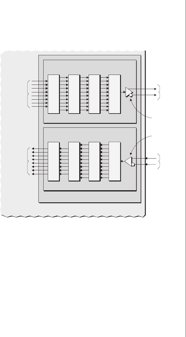
Delving into the transceiver blocks
Now that we’ve introduced the concept of 8B/10B encod-
ing, we’re in a better position to take a slightly closer look
at the main elements comprising a transceiver block
(Figure 21-8).
As usual, this is a highly simplified representation that
omits a lot of bits and pieces, but it serves to cover the points
of interest to us here. With regard to the annotations on “pre-
emphasis” and “equalization,” these topics are introduced later
in this chapter.
On the transmitter side, bytes of data are presented to the
transceiver from user-defined logic in the main FPGA fabric
via an 8-bit bus. This is passed through an 8B/10B encoder and
handed over into a FIFO buffer, which is used to store data
temporarily when too many words arrive too closely together.
Gigabit Transceivers ■361
8-bit bus
from main
FPGA fabric
8b/10b
Encoder FIFO
Polarity
flipper Serializer
TXP
TXN
8-bit bus
to main
FPGA fabric
8b/10b
Deccoder
FIFO
Polarity
flipper Deserializer
RXP
RXN
Transmitter
Receiver
To
another
device
From
another
device
Transceiver Block
FPGA
This is where
pre-emphasis
takes place
This is where
equalization
takes place
Figure 21-8. The main elements composing
a transceiver block.
1949: England.
Cambridge University.
Small experimental
computer called EDSAC
performs its first
calculation.

The output from the FIFO passes through a polarity flipper,
which may be used to pass the data through unmodified or to
flip each bit froma0toa1andvice versa (polarity flipping
will only be required if the device we’re passing data to is
expecting to see flipped data). In turn, the output from the
polarity flipper is passed to a serializer, which converts the
parallel input data into a serial stream of bits. This serial
stream is then handed over to a special output driver/buffer
that generates a differential signal pair.
Similarly, on the receiver side, a serial data stream pre-
sented as a differential signal pair is passed through a special
input buffer into a deserializer, which converts the serial data
into 10-bit words. These words are passed into a polarity flip-
per, which may be used to pass the data through unmodified
or to flip each bit froma0toa1andvice versa (polarity flip-
ping will only be required if the device we’re receiving data
from is sending us flipped data). The output from the polarity
flipper is handed over to an 8B/10B decoder, which descram-
bles the data. The resulting 8-bit bytes are passed via a FIFO
buffer into the main FPGA fabric, where they can be proc-
essed by whatever logic the design engineers decide to
implement.
Note that, depending on the FPGA technology you are
using, some transceiver blocks may support a variety of encod-
ing standards, such as 8B/10B, 64B/66B, SONET Scrambling,
and so forth. Others may support only a single standard like
8B/10B, but in this case it may be possible to switch out these
blocks and implement your own encoding scheme in the main
FPGA fabric if required.
Ganging multiple transceiver blocks together
The term baud rate refers to the number of times a signal
in a communications link changes (or can change) per sec-
ond. Depending on the encoding technique used, a
communications link can transmit one data bit—or fewer or
more bits—with each baud, or change in state.
362 ■The Design Warrior's Guide to FPGAs
1950: America.
Jay Forrester at MIT
invents magnetic core
store.
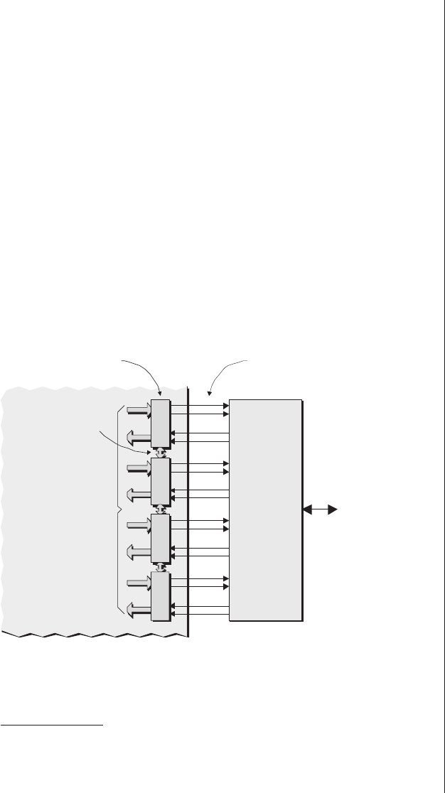
At the time of this writing, the current state of play is that
each transceiver channel can transmit and receive 8B/10B-
encoded data (or data encoded using a similar scheme) at baud
rates up to 3.125 gigabits per second (Gbps).2This translates to
2.5 Gbps of real, raw data if we ignore the overhead of the
additional bits added by the 8B/10B-encoding scheme (that is,
a baud rate of 3.125 Gbps divided by 10 bits and multiplied by
8 bits equals a true data rate of 2.5 Gbps).
The problem is that, by definition, standards such as 10-
gigabit Ethernet have data transfer requirements of 10 Gbps.
For this reason, there are additional standards like the 10-
gigabit attachment unit interface (XAUI) approach that defines
how to achieve 10 Gbps of data throughput using four differen-
tial signal pairs in each direction (Figure 21-9).
Gigabit Transceivers ■363
XAUI is pronounced
“zow-ee.”
To/from
the main
FPGA fabric
FPGA
Four gigabit
transceiver
blocks
Channel bonding
control signals
Special external
interface chip
Optical cable/signal
(10 gigabits/second
)
4x electrical differential
signal TX and RX pairs at
2.5 gigabits/second each
Figure 21-9. Ganging multiple transceiver blocks together.
2Once we go over baud rates of 3.175 Gbps, the overhead associated with
the 8B/10B-encoding scheme becomes too high, which means we have to
go to another scheme such as 64B/66B encoding.

In this case, the four transceiver blocks are linked using
special channel bonding control signals so that each block
knows what it is supposed to do and when it is supposed to
do it.
At some stage in the future—largely dictated by the rate
of adoption of high-speed serial interface technology at the
circuit board level—it is likely that the functions currently
embodied by the external interface chip will be incorporated
into the FPGA itself, which will then have the ability to
transmit and receive optical signals directly (see also the dis-
cussions in Chapter 26).
Configurable stuff
The gigabit transceiver blocks embedded in FPGAs typi-
cally have a number of configurable (programmable) features.
Different vendors and device families may support different
subsets of these features, a selection of the main ones being as
follows.
Comma detection
The 8B/10B-encoding scheme (and other schemes)
includes special comma characters. These are null characters
that may be transmitted to keep the line “alive” or to initiate
a data transfer by indicating to the receiver that things are
about to start happening and it needs to wake up and prepare
itself for action.
Another point is that these high-speed serial interfaces are
asynchronous in nature, which means that the clock is
embedded in the data signal (see also the discussions on
“Clock recovery, jitter, and eye diagrams” later in this chap-
ter). So when a transceiver block is ready to initiate a transfer,
it will send a whole series of comma characters (several hun-
dred bits) to allow the receiver at the other end of the line to
synchronize itself. (Comma characters are also employed
when aligning multiple bitstreams as discussed in the previous
section.)
364 ■The Design Warrior's Guide to FPGAs
1950: America.
Physicist William
Shockley invents the
first bipolar junction
translator.

The point is that some transceiver blocks allow the comma
character that will be transmitted (and received) to be config-
ured to be any 10-bit value, thereby allowing the transceiver to
support a variety of communications protocols.
Output differential swing
Different standards support different differential output
swings, which refers to the peak-to-peak difference in voltage
between logic 0 and logic 1 values. Thus, transceiver blocks
typically allow the differential output voltage swing to be con-
figured across a range of values so as to support compatibility
with a variety of serial system voltage levels.
On-chip termination resistors
The data rates supported by high-speed serial interfaces
mean that using external termination resistors can cause dis-
continuities in the signals, so it’s typically recommended to use
the on-chip termination resistors provided in the FPGA. The
values of these on-chip terminating resistors are typically con-
figurable (they can usually be set to 50 ohms or 75 ohms) so as
to support a variety of different interface standards and circuit
board environments.
Pre-emphasis
As was noted in the discussion associated with Figure 21-6,
signals traveling across a high-speed serial interface are
severely distorted (attenuated) by the time they arrive at the
receiver because the circuit board and its tracks absorb a lot of
the high-frequency content of the signal, leaving only the
lower-frequency (more slowly changing) portions of the signal.
One technique that may be used to mitigate this effect is
pre-emphasis, in which the first 0 in a string of 0s and the first
1 in a string of 1s is given a bit of a boost with a slightly higher
voltage (in this context, we will consider “string” to refer to
one or more bits). In a way, we can think of this as applying
our own distortion in the opposite direction to the distortion
coming from the circuit board (Figure 21-10).
Gigabit Transceivers ■365
1950:
Maurice Karnaugh
invents Karnaugh Maps
(circa 1950), which
quickly become one of
the mainstays of the
logic designer’s
tool-chest.
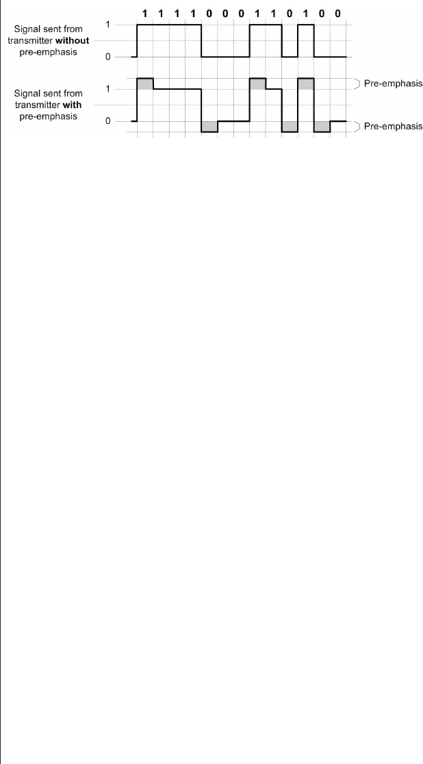
Once again, this illustration shows the signal generated by
the transmitting chip as being an ideal representation (with
sharp edges), but in the real world such a signal would actually
have strong analog chracteristics.
The amount of pre-emphasis to be applied is typically con-
figurable so as to accommodate different circuit board
environments. The amount of pre-emphasis required for a
given high-speed link is a function of the position of the
FPGA in relation to other components (which equates to
track lengths), a variety of board characteristics, and the
high-speed standard being employed. Working out the
amount of pre-emphasis to use may be determined by simula-
tion runs or by rule of thumb.
Equalization
This is somewhat related to pre-emphasis as discussed
above, except that it takes place at the receiver end of the
high-speed interface (Figure 21-11).
Equalization refers to a special amplification stage that
boosts higher frequencies more than lower ones. As for pre-
emphasis, we can think of this as applying our own distortion
in the opposite direction to the distortion coming from the
circuit board.
The amount of equalization to be applied is typically
configurable to accommodate different circuit board environ-
ments. Depending on the particular design, we might wish to
use pre-emphasis, equalization, or a mixture of both.
366 ■The Design Warrior's Guide to FPGAs
Figure 21-10. Applying pre-emphasis.
1950:
Konrad Zuse’s Z4 is sold
to a bank in Zurich,
Switzerland, thereby
making the Z4 the
world’s first
commercially available
computer.
1951: America.
The first UNIVAC 1 is
delivered.
One point worth noting is that, in the case of really long
high-speed interface tracks on the circuit board (say, around
40 inches and above), it may be desirable to disable the inter-
nal equalization and to use an external equalizer device
because the quality of equalization is typically better in a dedi-
cated analog device than in an FPGA. Having said this,
FPGAs are increasing in sophistication with regard to this sort
of thing—the different vendors are constantly leapfrogging
each other with regard to technology—and the quality of fac-
tors such as the quality of on-chip equalization may affect your
device selection.
Clock recovery, jitter, and eye diagrams
Clock recovery
High-speed serial interfaces are asynchronous in nature,
which means that the clock is embedded in the data signal.
Thus, the receiver portion of the transceiver includes clock and
data recovery (CDR) circuitry that keys off the rising and fal-
ling edges of the incoming signal and automatically derives a
clock that is representative of the incoming data rate. As you
can imagine, this would not be a major feat if the incoming
signal were toggling back and forth between logic 0 and logic 1
Gigabit Transceivers ■367
Chip A CHIP B
Pre-emphasis
applied to outputs
Equalization
applied to inputs
Pre-emphasis
applied to outputs
Equalization
applied to inputs
Transceiver Transceiver
Figure 21-11. Applying equalization.
1952: America.
John William Mauchly, J,
Persper Eckert and
team finish building a
general-purpose
(stored program)
electronic computer
called EDVAC.
1952: England.
First public discussion
of the concept of
integrated circuits is
credited to a British
radar expert, G.W.A.
Dummer.

values, in which case the clock and the data would effectively
be identical (Figure 21-12a).
Things get a little trickier when the signal becomes more
complex (Figure 21-12b). For example, if the incoming signal
commenced with three 1s followed by three 0s, we couldn’t
fault the clock recovery function for making an initial guess
that the clock frequency was only one third of its true value.
As more data (and more transitions) arrive, however, the
clock recovery function will refine its assumptions until it has
derived the correct frequency.
Once the receiver has locked down the clock, it uses this
information to sample the incoming data stream at the center
point of each bit in order to determine whether that bit is a
logic 0 or a logic 1 (Figure 21-13).
This is why, as we discussed earlier, a data transmission
will commence with several hundred bits of comma characters
to allow the receiver to lock on the clock and prepare itself for
action.
The clock recovery function will continue to monitor
edges and constantly tweak the clock value to accommodate
368 ■The Design Warrior's Guide to FPGAs
(a) Simple signal
Real edges
101010101010
(b) More complex signa
l
Real edges
111000101101
Derived edges
Figure 21-12. Recovering the clock signal.
1952:
Sony demonstrates the
first miniature transistor
radio, which is
produced commercially
in 1954.
1953: Americas.
First TV dinner is
marketed by the
Swanson Company.
1954:
Launch of giant balloon
called Echo 1—used to
bounce telephone calls
coast-to-coast in the
USA.
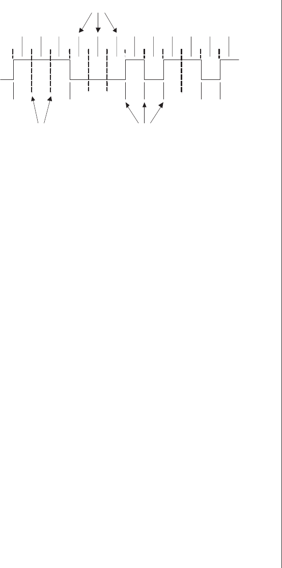
slight back-and-forth drifts in the clock caused by environ-
mental conditions such as temperature and voltage variations.
Jitter and eye diagrams
The term jitter refers to short-term variations of signal
transitions from their ideal positions in time. For example,
if we were to take an incoming signal that was oscillating
between logic 0 and logic 1 values (Figure 21-14a, b) and
overlay the data associated with each clock cycle on top of the
preceding cycles, we would start to see some fuzziness appear-
ing (Figure 21-14c–f).
This fuzziness is caused by a variety of factors, including
the clock wandering slightly in the transmitting device and
also the ISI effects we noted earlier (see also the discussion
associated with Figure 21-7).
In fact, we can go one step further, which is conceptually
to fold each clock cycle in half, thereby overlaying the positive
0–1–0 pulses from the first half of the cycle with the negative
1–0–1 pulses from the second half of the cycle (Figure 21-14g).
Once again, the waveforms shown in Figure 21-14 are
unrealistic because they feature razor-sharp edges. Real-world
signals would have analog characteristics. If we were to look at
a real waveform in its folded form, it would look something
like that shown in Figure 21-15.
Gigabit Transceivers ■369
Derived edges
Data sample times
Real edges
Figure 21-13. Sampling the incoming signal.
1954:
The number of radio
sets in the world
out-numbers
newspapers sold
everyday.
1954:
First silicon transistor
manufactured.
1955:
Velcro is patented.
1956: America.
John Backus and team
at IBM introduced the
first widely used
high-level computer
language, FORTRAN.
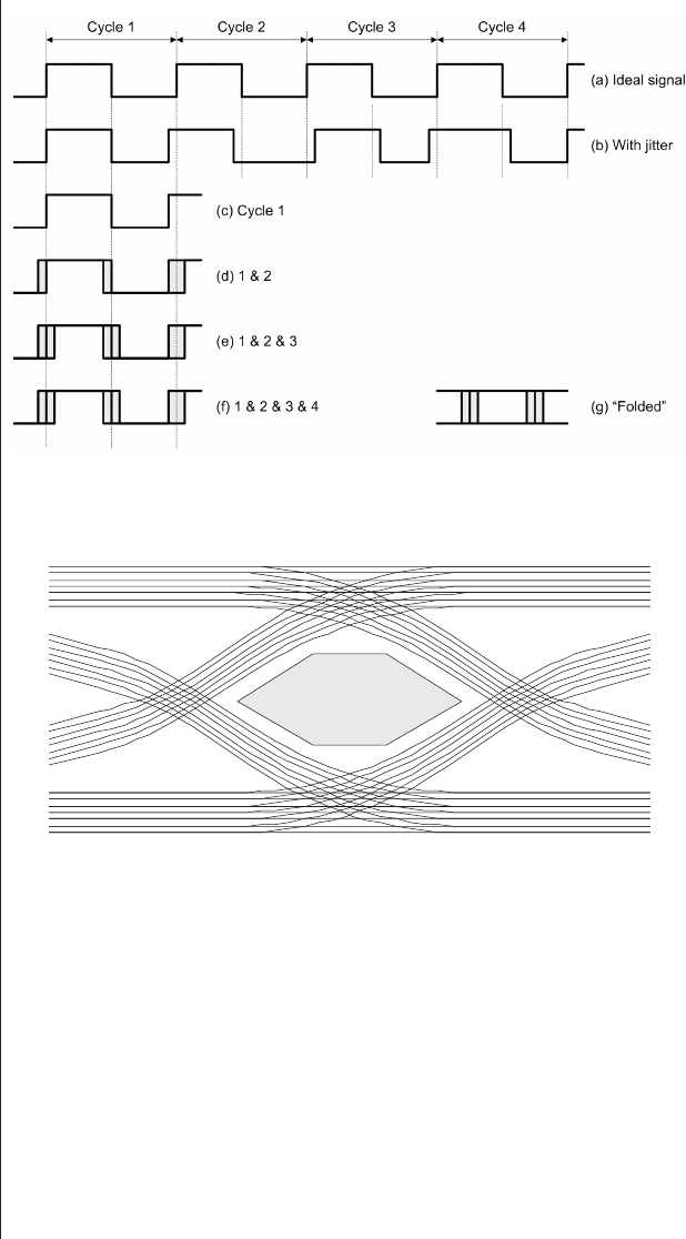
The result is a diagram whose center looks something like
a human eye, so, perhaps not surprisingly, it’s referred to as an
eye diagram. As jitter, attenuation, and other distortions
increase, the center of the eye closes more and more. Thus, a
lot of specifications define a geometric shape called the eye
mask. This mask, which may be rectangular or hexagonal as
shown here, represents the data valid window. As long as all of
the curves fall outside of the eye mask, the high-speed inter-
face will work.
370 ■The Design Warrior's Guide to FPGAs
Eye Mask
Figure 21-15. Eye diagram and eye mask.
Figure 21-14. Jitter.
1956: America.
John McCarthy develops
a computer language
called LISP for artificial
intelligence
applications.
1956: America
MANIAC 1 is the first
computer program to
beat a human in a game
(a simplified version
of chess).
1956:
First transatlantic
telephone cable goes
into operation.

The point of all of this is that if you are planning on using
one of these high-speed serial communications interfaces, then
you need to make sure that you have access to SI analysis
tools that have been augmented to support the concept of eye
diagrams.
Gigabit Transceivers ■371
1957: America.
Gordon Gould
conceives the idea of
the Laser.
1957: America.
IBM 610 Auto-Point
computer is
introduced.
1957:
Russia launches the
Sputnik 1 satellite.

Dynamically reconfigurable logic
The advent of SRAM-based FPGAs presented a new capa-
bility to the electronics fraternity: dynamically reconfigurable
logic, which refers to designs that can be reconfigured on the
fly while remaining resident in the system.
Just to recap, FPGAs contain a large amount of program-
mable logic and registers, which can be connected together in
different ways to realize different functions. SRAM-based vari-
ants allow the main system to download new configuration
data into the device. Although all of the logic gates, registers,
and SRAM cells forming the FPGA are created on the surface
of a single piece of silicon substrate, it is sometimes useful to
visualize the device as comprising two distinct strata: the logic
gates/registers and the programmable SRAM configuration
cells (Figure 22-1).
The versatility of these devices opened the floodgates to a
wealth of possibilities. For example, when the system is first
powered up, the FPGAs can be configured to perform a variety
of system-test (and even self-test) operations. Once the system
checks out, the FPGAs can be reconfigured to perform their
main function in life.
Dynamically reconfigurable interconnect
Although it’s great to be able to reconfigure the function of
the individual devices on a circuit board, there are occasions
when design engineers would like to create board-level systems
that can be reconfigured to perform a variety of radically differ-
ent functions.
Reconfigurable Computing
Chapter
22
1957:
Russia launches the
Sputnik 1 satellite.
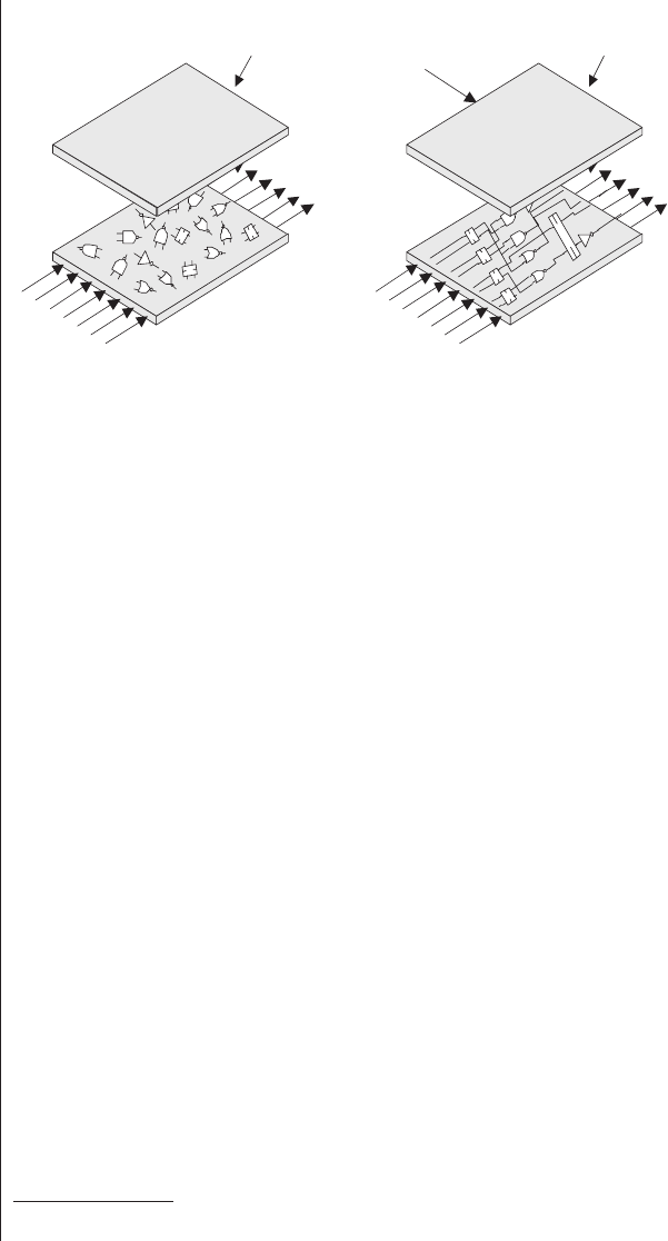
The solution is to be able to configure the board-level
connections between devices dynamically. A breed of devices
offer just this capability: field-programmable interconnect devices
(FPIDs), which may also be known as field-programmable inter-
connect chips (FPICs).1These devices, which are used to
connect logic devices together, can be dynamically reconfig-
ured in the same way as standard SRAM-based FPGAs.
Because each FPID may have 1,000 or more pins, only a few
such devices are typically required on a circuit board
(Figure 22-2).
One interesting point is that the concepts discussed here
are not limited to board-level implementations. Any of the
technologies discussed thus far may also potentially be imple-
mented in hybrids, multichip modules (MCMs), and SoC
devices.
Reconfigurable computing
As with many things in electronics, the term reconfigurable
computing (RC) can mean different things to different people.
374 ■The Design Warrior's Guide to FPGAs
XXXXXXXXXXX
XXXXXXXXXXX
XXXXXXXXXXX
XXXXXXXXXXX
XXXXXXXXXXX
XXXXXXXXXXX
Primary
inputs
Primary
outputs
Uninitialized
SRAM cells
(a) Unconfigured
Configuration
data stream
Primary
inputs
Primar
y
outputs
SRAM cells
loaded with 0s and 1s
(b) Configured
001101101001
101101001011
110100100001
011001101000
000110110011
101100111101
Figure 22-1. Dynamically reconfigurable logic:
SRAM-based FPGAs.
1FPIC is a trademark of Aptix Corporation (www.aptix.com).
1958: America.
Computer data is
transmitted over regular
telephone circuits.
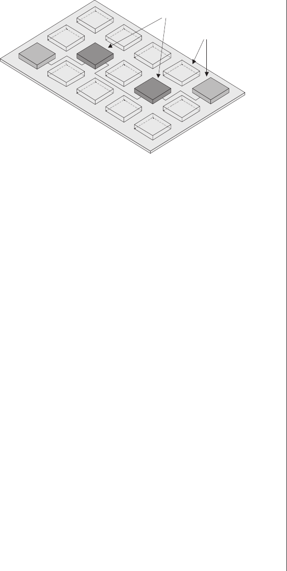
For some, it refers to special microprocessors whose instruction
sets can be augmented or modified on the fly. For our purposes
here, however, we understand RC to refer to a piece of
general-purpose hardware—such as an FPGA (what a sur-
prise)—that can be configured to perform a specific task, but
that can subsequently be reconfigured on demand to carry out
other tasks.
One limitation with the majority of SRAM-based FPGAs
is the time it takes to reconfigure them. This is because they
are typically programmed using a serial data stream (or a paral-
lel stream only 8 bits wide). When we start to talk about
high-end devices with tens of millions of SRAM configuration
cells, it can take up to a couple of seconds to reprogram these
beasts. There have been some FPGAs that address this issue by
using large numbers of general-purpose I/O pins to provide a
wide configuration bus (say, 256 bits) before reverting to their
main I/O functionality (see also chapter 26). Also, some fla-
vors of field-programmable node arrays (FPNAs) have dedicated
wide programming buses (see also Chapter 23).
Another limitation with traditional FPGA architectures is
that, when you wish to reconfigure any part of the device, you
typically have to reprogram the entire device (some recent
architectures do allow you to reconfigure them on a column-
by-column basis, as discussed in chapter 14, but this offers only
Reconfigurable Computing ■375
FPIDs
FPGAs (and other
components)
Figure 22-2. Dynamically reconfigurable interconnect:
SRAM-based FPIDs.
1958: America.
Jack Kilby, working for
Texas Instruments,
succeeds in fabricating
multiple components
on a single piece of
semiconductor (the
first integrated circuit).

a rather coarse level of granularity). Furthermore, it is usually
necessary to halt the operation of the entire circuit board
while these devices are being reconfigured. Additionally, the
contents of any registers in the FPGAs are irretrievably lost
during the process.
In order to address these issues, an interesting flavor
of FPGA was introduced by Atmel Corporation
(www.atmel.com) circa 1994. In addition to supporting the
dynamic reconfiguration of selected portions of the internal
logic, these devices also featured:
■No disruption to the device’s inputs and outputs
■No disruption to the system-level clocking
■The continued operation of any portions of the device
that are not undergoing reconfiguration
■No disruption to the contents of internal registers
during reconfiguration, even in the area being
reconfigured
The latter point is of particular interest because it allows
one instantiation of a function to hand over data to the next
function. For example, a group of registers may initially be
configured to act as a binary counter. Then, at some time
determined by the main system, the same registers may be
reconfigured to operate as a linear feedback shift register (LFSR)2
whose seed value is determined by the final contents of the
counter before it is reconfigured.
Although these devices were evolutionary in terms of
technology, they were revolutionary in terms of their poten-
tial. To reflect their new capabilities, appellations such as
“virtual hardware” and “cache logic”3were quickly coined.
The term virtual hardware is derived from its software
equivalent, virtual memory, and both are used to imply some-
thing that is not really there. In the case of virtual memory, a
376 ■The Design Warrior's Guide to FPGAs
2LFSRs are introduced in detail in Appendix C.
3Cache Logic is a trademark of Atmel Corporation, San Jose, CA, USA.
1959: America.
COBOL computer
language is introduced
for business
applications.

computer’s operating system pretends that it has access to
more memory than is actually available. For example, a pro-
gram running on the computer may require 500 megabytes to
store its data, but the computer may have only 128 megabytes
of memory available. To get around this problem, whenever
the program attempts to access a memory location that does
not physically exist, the operating system performs a sleight
of hand and exchanges some of the contents in the memory
with data on the hard disk. Although this practice, known
as swapping, tends to slow things down, it does allow the
program to perform its tasks without having to wait while
someone runs down to the store to buy some more memory
chips.
Similarly, the term cache logic is derived from its similarity
to the concept of cache memory, in which high-speed, expen-
sive SRAM is used to store active data, while the bulk of the
data resides in slower, lower-cost memory devices such as
DRAM. (In this context, “active data” refers to data or
instructions that a program is currently using or that the oper-
ating system believes the program will want to use in the
immediate future.)
In fact, the concepts behind virtual hardware are actually
quite easy to understand. Each large macrofunction in a device
is usually formed by the combination of a number of smaller
microfunctions, such as counters, shift registers, and multiplex-
ers. Two things become apparent when a group of
macrofunctions is divided into their respective microfunctions.
First, functionality overlaps, and an element such as a counter
may be used several times in different places. Second, there is a
substantial amount of functional latency, which means that at
any given time only a portion of the microfunctions are active.
Put another way, relatively few micro- functions are in use dur-
ing any given clock cycle. Thus, the ability to reconfigure
individual portions of a virtual hardware device dynamically
means that a relatively small amount of logic can be used to
implement a number of different macrofunctions.
Reconfigurable Computing ■377
1959: America.
Robert Noyce invents
techniques for creating
microscopic aluminum
wires on silicon,
which leads to the
development of
modern integrated
circuits.
By tracking the occurrence and usage of each microfunc-
tion, then consolidating functionality and eliminating
redundancy, virtual hardware devices can perform far more
complex tasks than they would appear to have logic gates
available. For example, in a complex function requiring
100,000 equivalent gates, only 10,000 gates may be active at
any one time. Thus, by storing, or caching, the functions
implemented by the extra 90,000 gates, a small, inexpensive
10,000-gate device can be used to replace a larger, more
expensive 100,000-gate component (Figure 22-3).
Theoretically, it would be possible to compile new design
variations in real time, which may be thought of as dynami-
cally creating subroutines in hardware!
RC was a big buzz in the latter half of the 1990s, and there
are still some who are waving the RC banner (and wearing
the T-shirts). Sad to relate, however, nothing really came of
this with the exception of highly specialized applications. The
core problem is that traditional FPGA architectures are too
378 ■The Design Warrior's Guide to FPGAs
Active tasks
Inactive tasks
Unused resources
Function A
Function B
Configuration data
stored in memory device
Function A
Function B
Function C
Overwrite function B
with new function C
Figure 22-3. Virtual hardware.
1959:
Swiss physicist Jean
Hoerni invents the
planar process, in which
optical lithographic
techniques are used to
create transistors.

fine grained, so reconfiguring them takes too long (in com-
puter terms). In order to support true RC, one would need
access to devices that could be reconfigured hundreds of
thousands of times per second. The answer may be the coarser-
grained architectures fielded by the FPNAs introduced in
Chapter 23.
Reconfigurable Computing ■379
1960: America.
Theodore Maimen
creates the first Laser.
1960: America.
The Defense Advanced
Research Projects
Agency (DARPA) begins
work on what will
become the Internet.

Introduction
Before we throw ourselves into this topic with wild aban-
don, it’s probably only fair to note that the term field-
programmable node array,orFPNA, was coined by the author
and is not industry-standard terminology (yet).
Fine-, medium-, and coarse-grained architectures
When it comes to categorizing different IC architectures,
ASICs are usually said to be fine grained, because design engi-
neers can specify their functionality down to the level of
individual logic gates. By comparison, the majority of today’s
FPGAs may be classed as medium grained because they consist
of small blocks (“islands”) of programmable logic (where each
block represents a number of logic gates and registers) in a
“sea” of programmable interconnect. (Even though today’s
FPGA offerings typically include processor cores, blocks of
memory, and embedded functions like multipliers, the main
underlying architecture is as described above.)
Truth to tell, many engineers would actually refer to
FPGAs as being coarse grained, but classing them as medium
grained makes much more sense when we start to bring FPNAs
into the picture because these boast really coarse-grained
architectures. The underlying concept behind FPNAs is that
they are formed from an array of nodes, each of which is a
sophisticated processing element (Figure 23-1).
Of course, this is a very simplified representation of an
FPNA, not the least because it omits any I/O. Furthermore,
we’ve only shown relatively few processing nodes, but such a
Field-Programmable
Node Arrays
Chapter
23
device can potentially contain hundreds or thousands of
nodes. Depending on the vendor, each node might be an algo-
rithmic logic unit (ALU), a complete microprocessor CPU, or
an algorithmic processing element (this latter case is discussed
in more detail later in this chapter). At the time of this writ-
ing, 30 to 50 companies are seriously experimenting with
different flavors of FPNAs; a representative sample of the
more interesting ones is as follows:
Company Web site Comment
Exilent www.elixent.com ALU-based nodes
IPflex www.ipflex.com Operation-based nodes
Motorola www.motorola.com Processor-based nodes
PACT XPP Technologies AG www.pactxpp.com ALU-based nodes
picoChip Designs www.picochip.com Processor-based nodes
QuickSilver Technology www.qstech.com Algorithmic element
nodes
For the purposes of these discussions, we shall concentrate
on just two of these vendors—picoChip and QuickSilver—
who are conceptually at opposite ends of the spectrum:
picoChip’s picoArray devices are formed from arrays of proc-
essors. Their key application area is large, fixed installations
such as base stations for wireless networks in which power
consumption is not a major consideration. Furthermore, these
chips are intended to be reconfigured now and again (for
382 ■The Design Warrior's Guide to FPGAs
Processing
nodes Interconnect
Figure 23-1. Generic representation of an FPNA.
1960:
NASA and Bell Labs
launch the first
commercial
communications
satellite.

example, every hour or so as cellular phone usage profiles
change throughout the day).
By comparison, QuickSilver’s adaptive computing machine
(ACM) devices are formed from clusters of algorithmic ele-
ment nodes. Their key application area is small, low-power,
handheld products like cameras and cell phones (although
they are of interest for a wide variety of other applications).
Furthermore, these chips can be reconfigured (QuickSilver
prefers the term adapted) hundreds of thousands of times per
second.
Algorithmic evaluation
FPNAs are mainly intended to execute sophisticated,
compute-intensive algorithms. This means that before we go
any further, we should spend a few moments ruminating on
these algorithms to set the scene for what is to come.
At one end of the spectrum are word-oriented algorithms,
such as the extremely compute-intensive time division multiple
access (TDMA) algorithm used in digital wireless transmission.
Any variants such as Sirius,XM Radio,EDGE, and so forth
form a subset of this algorithmic class, so an architecture that
can handle high-end TDMA should also be able to handle its
less-sophisticated cousins (figure 23-2).
At the other end of the continuum, we find bit-oriented
algorithms, such as wideband code division multiple access
(W-CDMA), and its subvariants, such as CDMA2000,
IS-95A, and the like. (W-CDMA is used for the wideband
digital radio communications of Internet, multimedia, video,
and other capacity-demanding applications.)
And then there are algorithms that exhibit different mixes
of word-oriented and bit-oriented components, such as the
various flavors of MPEG, voice and music compression, and
so forth.
When one evaluates these various algorithms, it soon
becomes quickly apparent that conventional RC approaches
tend to attack the problem at inappropriate levels (RC con-
cepts were introduced in chapter 22). For example, some RC
Field-Programmable Node Arrays ■383
1961:
Time-sharing
computing is
developed.
approaches engage problems at too micro of a level, that is, at
the level of individual gates or FPGA blocks. Coupled with
hideously difficult application programming, this power-
hungry approach results in relatively long reconfiguration
times, thereby making it unsuitable for some applications. By
comparison, other approaches tackle the problem at too
macro of a level, that is, at the level of entire applications or
algorithms, which results in inefficient use of resources.
Perhaps not surprisingly, it soon becomes apparent that
algorithms are heterogeneous in nature, which means that if
you take a bunch of diverse algorithms, their constituent ele-
ments are wildly different. Based on this, the obvious solution
is to use heterogeneous architectures that fully address the
heterogeneous nature of the algorithms they are required to
implement, but what might these little scamps look like?
picoChip’s picoArray technology
In order to address the processing requirements of the
algorithms discussed above, picoChip came up with a device
called a picoArray. The heterogeneous node-based architec-
384 ■The Design Warrior's Guide to FPGAs
GSM
GPRS
TDMA
EDGE
XM Radio
Sirius
CDMA2000
IS-95A
GPS
MPEG2
MPEG4
W-CDMA
WLAN
Voice
Compression
Music
Compression
Bit-
orientated
Word-
orientated
Figure 23-2. A simplified view of algorithm space.
1962: America.
Steve Hofstein and
Fredric Heiman at RCA
Research Lab invent
field effect transistors
(FETS).

ture of the picoArray features a matrix of different flavors of
reduced instruction set computing (RISC) processors. These 16-
bit devices are optimized in a variety of different ways: for
example, one processor type may have lots of memory, while
another will support special algorithmic instructions that can
perform operations like “spread” and “despread” from the
CDMA wireless standard using a single clock cycle (as opposed
to 40 cycles using a general-purpose processor).
In the first incarnation of these devices, each processor
node was approximately equivalent (in processing capability,
not in architecture) to an ARM9 for control-style applications
oraTIC54xx for DSP-style applications. When you take into
account the fact that a single picoArray can contain hundreds
of such nodes, the result is a truly ferocious amount of process-
ing power.
As one example, when I first became aware of the picoAr-
ray technology around December 2002, one of the absolute
top-of-the-line dedicated DSP chips in the world at that time
was the TMS320C6415 from Texas Instruments. That bad boy
could perform such a humongous number of calculations at
such a breathtaking speed that it made your eyes water. How-
ever, picoChip claims that a single picoArray running at
only 160 megahertz could deliver almost 20 times more
processing power (measured in 16-bit ALU MOPS) than a
TMS320C6415 running at 600 megahertz. Wow!
An ideal picoArray application: Wireless base
stations
Cell phone companies spend billions and billions of dollars
every year on wireless infrastructure, and a large portion of
these funds is devoted to developing the digital baseband proc-
essing portions of wireless base stations. Depending on its
location, each base station has to be capable of processing tens
or hundreds of channels simultaneously.
Not surprisingly, there is a huge drive to reduce the cost of
implementing each channel. The fact that a single picoArray
Field-Programmable Node Arrays ■385
RISC is pronounced to
rhyme with “lobster
bisque.”
can replace a number of traditional ASICs, FPGAs, and DSPs
offers a way of dramatically reducing the cost of each base sta-
tion channel.
In fact, one of the problems with conventional solutions is
that they require at least three design environments: ASIC
and/or FPGA, DSP, and RISC (where the latter refers to some
microprocessor-type functionality). All of this complicates
development and test and slows the base station’s time-to-
market, which is not considered to be a good thing (Figure
23-3a). By comparison, a major advantage of a picoArray-
based solution is that it largely consolidates everything into a
single design environment (Figure 23-3b).
Furthermore, in the case of conventional solutions,
although ASICs can provide extremely high performance,
they are very expensive to develop and they have long design
cycles. Even worse, algorithms implemented in ASICs are
effectively “frozen in silicon.” This is a major problem because
wireless standards are evolving so quickly that, by the time an
ASIC design has actually been implemented, it may already
386 ■The Design Warrior's Guide to FPGAs
Figure 23-3. Conventional devices versus a
picoArray approach.
1962: America.
Unimation introduces
the first industrial robot.

be obsolete (honestly, this happens way more often than you
might imagine).
By comparison, in the case of the picoArray-based
approach, the fact that every processor node on the device is
fully programmable means that each channel can be easily
reconfigured to adapt to hourly changes in usage profiles, to
weekly enhancements and bug fixes, and to monthly evolu-
tions in wireless protocols. Thus, a base station based on
picoArray technology will have a much longer life in the field,
thereby reducing operating costs.
The picoArray design environment
The underlying functionality to be mapped onto the proc-
essor nodes in a picoArray is captured in pure C code or in
assembly language. As we discussed in chapter 11, C is a
sequential language, so we need some way to describe any par-
allel processing requirements. As opposed to using one of the
augmented C/C++ techniques mentioned in chapter 11, the
folks at picoChip have taken another approach, which is to
employ a VHDL framework to capture the structure of the
design, including any parallel processing requirements, and to
connect design modules together at the block level. C or
assembly code is then used to implement the internals of each
module.
Another interesting aspect of the picoChip solution is the
fact that they provide a complete library of programming/con-
figuration modules that can be hooked together to implement
a fully functioning base station (users can also tweak individ-
ual modules to implement their own algorithm variations,
thereby gaining a competitive advantage). Around May 2003,
picoChip announced that they had achieved a “world first” by
using this library to implement a 3GPP-compliant carrier-class
base station and to make a 3G call on that base station! Since
that time, they have continued to progress in leaps and
bounds, so you’ll have to visit their Web site at
www.picochip.com to apprise yourself of the current state
of play.
Field-Programmable Node Arrays ■387
1962:
First commercial
communications
satellite (Telstar)
launched and
operational.
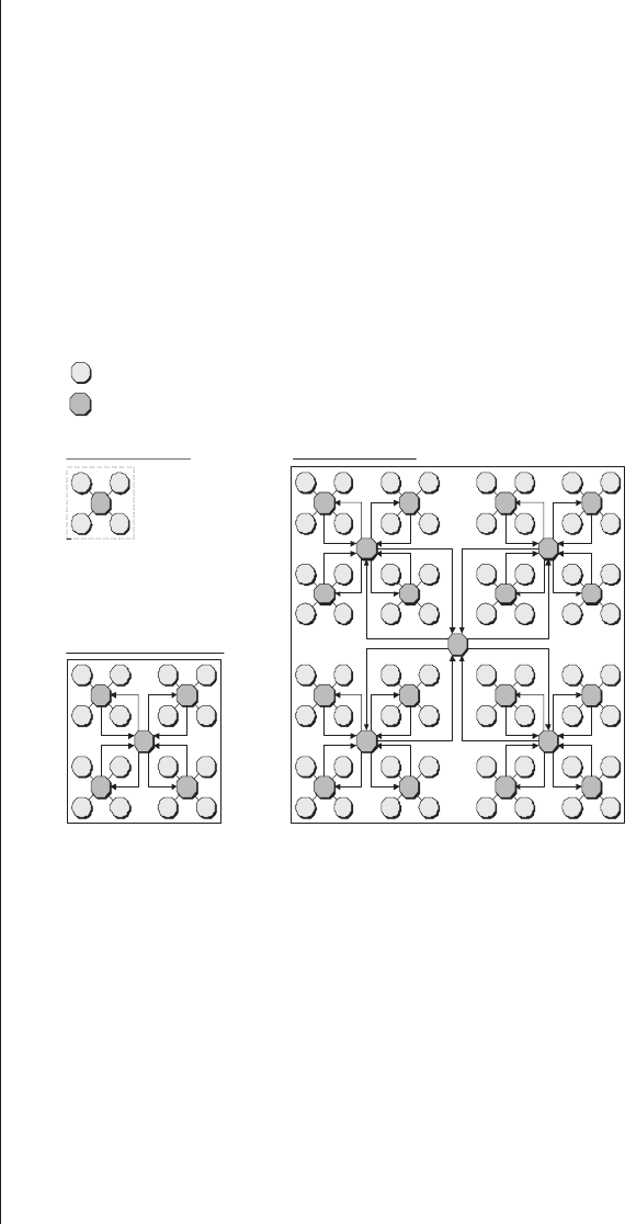
QuickSilver’s ACM technology
For several years now, the guys and gals at QuickSilver
have been in “secret squirrel” mode working on their version
of an FPNA (although I’m sure they are going to moan and
groan about this appellation). Based on what I know (which is
more than they think I know … at least I think it is), it’s fair
to say that QuickSilver’s technology, which they call an adap-
tive computing machine,orACM, boasts a truly revolutionary
heterogeneous node-based architecture and interconnect
structure (Figure 23-4).
At the lowest level we have an algorithmic element node.
Four of these nodes, forming a “quad,” are gathered together
with a matrix interconnect network (MIN) to form what we
might call a Level 1 cluster. Four of these Level 1 clusters can
be grouped to form a Level 2 cluster, and so forth.
At the time of this writing, there are a variety of different
types of algorithmic element nodes (we’ll talk about how
these node types are mapped into the quads in a little while).
We aren’t going to delve into the guts of every node here, but
388 ■The Design Warrior's Guide to FPGAs
ACM is pronounced by
spelling it out as “A-C-M.”
Level 3 ClusterLevel 1 Cluster
LEVEL 2 CLUSTER
Matrix Interconnect Network (MIN)
Algorithmic Element Node
Figure 23-4. The ACM’s architecture.

it’s important to understand that each such node performs
tasks at the level of complete algorithmic elements. For exam-
ple, an arithmetic node can be used to implement different
(variable-width) linear arithmetic functions such as a FIR fil-
ter, a discrete cosign transform (DCT), an FFT, and so forth.
Such a node can also be used to implement (variable-width)
nonlinear arithmetic functions such as ((1/sine A) (1/x)) to
the 13th power.
Similarly, a bit-manipulation node can be used to implement
different (variable-width) bit-manipulation functions, such as
alinear feedback shift register (LRSR), Walsh code generator,
GOLD code generator, TCP/IP packet discriminator, and so
forth.
Each node is surrounded by a wrapper, which makes all of
the nodes appear to be identical to the outside world (that is,
to the world outside the node). This wrapper is in charge of
accepting packets of information (instructions, raw data, con-
figuration data, etc.) from the outside world, unpacking this
data, distributing it throughout the node, managing tasks,
gathering and packing the results together, and presenting
these results back to the outside world.
The concept of the wrapper isolating the node from the
outside world and making all of the nodes appear to be identi-
cal is of especial interest when we come to realize that each
node is “Turing complete.” This means that you can present
any node with any problem—say, an arithmetic node with a
bit-manipulation task—and that node will solve the problem,
although less efficiently than would a more appropriate type of
node. Furthermore, QuickSilver also allows you to create your
own types of nodes, where you define the core of the node and
surround it with QuickSilver’s wrapper.
Good grief! Trying to work out how best to wend our
weary way through the complexities of all of this is making my
brain ache. One key point is that any part of the device, from a
few nodes all the way up to the full chip, can be adapted blaz-
ingly fast, in many cases within a single clock cycle. Also of
interest is the fact that approximately 75 percent of each node
Field-Programmable Node Arrays ■389
1962:
First commercial
touch-tone phone
system.

is in the form of local memory. This allows for a radical
change in the way in which algorithms are implemented. As
opposed to passing data from function to function, the data
can remain resident in a node while the function of the node
changes on a clock-by-clock basis. It also means that, unlike
an ASIC implementation in which each algorithm requires its
own dedicated silicon, the ACM’s ability to be adapted tens
or hundreds of thousands of times per second means that only
those portions of an algorithm that are actually being exe-
cuted need to be resident in the device at any one time (see
also the discussions on SATS later in this chapter). This pro-
vides for tremendous reductions in silicon area and power
consumption.
You define the mix of nodes
I’m not quite sure where to squeeze this topic in, so we’ll
give it a whirl here to see how well it flies. Just a little while
ago, we noted that there are various types of algorithmic ele-
ment nodes. We also noted that each cluster is formed from a
quad of these nodes gathered together with a MIN. Based on
this, I’m sure that you are wondering how the node types are
assigned across multiple clusters.
Well, the point is that the folks at QuickSilver don’t actu-
ally make and sell chips themselves (apart from proof-of-
concept and evaluation devices of course). Instead, they
license their ACM technology to anyone who is interested in
playing with it, thereby allowing you (the end user) to deter-
mine the optimum mix of node types for your particular
application and then have chips fabricated to your custom
specifications. The fact that their wrappers make each node
appear identical to the outside world makes it easy to
exchange one type of node for another!
The system controller node, input/
output nodes, etc.
In addition to the structure shown in figure 23-4, each
ACM also includes a gaggle of special-purpose nodes, such as
390 ■The Design Warrior's Guide to FPGAs
1963: America.
The LINC computer is
designed at MIT.

system controller, external memory controller, internal mem-
ory controller, and I/O nodes. In the case of the latter, each
I/O node can be used to implement I/O tasks in such forms as a
UART or bus interfaces such as PCI, USB, Firewire, and the
like (as for the algorithmic element nodes, the I/O nodes can
be reconfigured on a clock-by-clock basis as required). Further-
more, the I/O nodes are also used to import configuration data,
which means that each ACM can have as wide a configuration
bus as the total number of input pins if required.
We will consider how applications are created for, and exe-
cuted on, ACMs shortly. For the nonce, it is only important to
note that almost everything that makes life difficult with other
implementation technologies is handled transparently to the
ACM design engineer. For example, each ACM has an on-
chip operating system (OS), which is distributed across the sys-
tem controller node and the wrappers associated with each of
the algorithmic element nodes. The individual algorithmic
element nodes take care of scheduling their tasks and any
internode communications. This leaves the system controller
node relatively unloaded because its primary responsibilities
are limited to knowing which nodes are currently free and to
allocating new tasks to those nodes.
From figure 23-4, it is obvious that the core ACM archi-
tecture is extremely scalable. Things start to get really clever if
you have multiple ACMs on a board, their operating systems
link up, and, to the rest of the system, they appear to function
as a single device.
Spatial and temporal segmentation
One of the most important features of the ACM architec-
ture is its ability to be reconfigured hundreds of thousands of
times per second while consuming very little power. This
allows ACMs to support the concept of spatial and temporal seg-
mentation (SATS).
In many cases, different algorithms, and even different por-
tions of the same algorithm, can be performed at different
times. SATS refers to the process of reconfiguring dynamic
Field-Programmable Node Arrays ■391
OS is pronounced by
spelling it out as “O-S.”
SATS is pronounced to
rhyme with “bats.”
1963:
PDP-8 becomes the
first popular
microcomputer.

hardware resources to rapidly perform the various portions of
the algorithm in different segments of time and in different
locations (nodes) on the ACM.
As a simple example, consider that some operations on a
wireless phone are modal, which means they only need to be
performed some of the time. The three main modes are acqui-
sition,idle, and traffic. The acquisition mode refers to the cell
phone locating the nearest base station. When in idle mode,
the phone keeps track of the base station it’s hooked up to
and monitors the paging channel, looking for a signal that
says, “Wake up because a call is being initiated.” The traffic
mode has two variations: receiving or transmitting. Although
you may think you are talking and listening simultaneously,
you actually are only doing one or the other at any particular
time on a digital phone.
In the case of a wireless phone based on conventional IC
technologies, each of these baseband processing functions
requires its own silicon chip or some area on a common chip.
This means that even when a function isn’t being used, it still
occupies silicon real estate, which translates into high cost
and high power consumption that drains your battery faster.
By comparison, a phone based on ACM technology would
require only a single chip that can be adapted on the fly to
perform each baseband function as required.
But this is only the beginning. In many cases, each of
these major functions is composed of a suite of algorithms,
which can themselves be performed at different times. For
example, consider a highly simplified representation of a wire-
less phone receiving and processing a signal (figure 23-5).
The incoming signal consists of a series of highly com-
pressed blocks of data, each occupying a tiny segment of time.
This data proceeds through a series of algorithms, each of
which performs some processing on the data and downshifts it
to a lower frequency.
A key feature of this process is that each algorithmic stage
occupies a different fragment of time. In traditional ASIC
implementations, each function would occupy its own chip or
392 ■The Design Warrior's Guide to FPGAs
1963:
Philips introduces first
audio cassette.
its own area of silicon real estate on a common device. This
results in a significant waste of available resources (space and
power consumption) because only a limited number of func-
tions are actually being exercised at any particular time.
Once again, the solution is the ACM, which can be
adapted on the fly to perform each algorithm as required. This
concept of on-demand hardware results in the most efficient use
of hardware in terms of cost, size (silicon real estate), perform-
ance, and power consumption (ACMs are claimed to provide
10 to 100 times or more performance increase over comparable
solutions at only 1/2 to 1/20 of the power consumption).
Creating and running applications on an ACM
Of course, the next big question is how would one go about
creating applications for one of these little rapscallions? Well,
QuickSilver’s design flow is built on a C-based system-design
Field-Programmable Node Arrays ■393
Time
Algorithm 1 Agorithm 3 Algorithm ‘n’Algorithm 2
Time Time Time
One frame
etc.
RF to IF
and IF to
Baseband
Conversion
Traffic
(Receive)
Baseband
Processing
RF
IF
= Radio Frequency
= Intermediate Frequency
Figure 23-5. Highly simplified representation of a wireless
phone receiving and processing a signal.
1965:
John Kemeny and
Thomas Kurtz develop
the BASIC computer
language.

language called SilverC (this language is similar in concept to
the augmented C/C++ languages introduced in chapter 11).
SilverC preserves traditional C syntax and control struc-
tures, which makes it easy for C programmers and DSP
designers to use and simplifies legacy C code conversion.
SilverC also includes special module,pipe, and process key-
words/extensions that facilitate dataflow representations and
support parallel programming. Furthermore, SilverC provides
special extensions for DSP programming, such as circular
pointers for efficient use of DAG resources, fixed-width inte-
ger and fixed-point data types, support for saturated and
nonsaturated types, and so forth.
SilverC representations can be captured and simulated
much faster than the equivalent HDL representations (Ver-
ilog and VHDL) used in traditional ASIC and FPGA design
flows. Once a SilverC representation has been simulated and
verified, it is compiled into an executable (binary) Silverware
application. The ACM’s on-chip operating system only loads
whatever portions of a Silverware application are required at
any particular time, and multiple Silverware applications can
be running concurrently on an ACM at any particular time.
It’s important to note that when a Silverware application
is created, it doesn’t need to know which type of ACM chip is
being used (including the mix of node types, etc.) or, indeed,
how many ACM chips are available on the board. The on-
chip ACM operating system takes care of handling any pesky
details of this sort.
But wait, there’s more
In our discussions on DSP-based design flows in chapter
12, we introduced the concept of system-level design and
simulation environments such as Simulink from The Math-
Works (www.mathworks.com). This tool, which has a wide
base of users, encourages dataflow-oriented design and pro-
vides an excellent mapping to the ACM architecture.
Well, the lads and lasses at QuickSilver have been work-
ing furiously on integrating SilverC with Simulink. At the
394 ■The Design Warrior's Guide to FPGAs
1967: America.
Fairchild introduce an
integrated circuit called
the Micromosaic (the
forerunner of the
modern ASIC).

simplest level, you can use Simulink to describe the various
blocks and the dataflow connections between them, and then
automatically output a top-level framework of the design con-
taining the module instantiations and the pipes connecting
them together. In this case, you would then go into the frame-
work to code the SilverC processes by hand.
Alternatively, QuickSilver has developed a library of Sil-
verC modules that map onto existing Simulink blocks. This
library includes widely used DSP components, filters, encoders,
decoders, and bit and word manipulators. These SilverC mod-
ules can be used for functional and cycle-accurate simulation,
and, on compilation into a Silverware executable, they can be
mapped directly onto the ACM’s dynamic hardware resources.
It’s silicon, Jim, but not as we know it!
As you have probably surmised, I’m quite excited about the
possibilities of FPNAs in general and QuickSilver’s offering in
particular. So, does this mean the end of ASICs and FPGAs as
we know them? Of course not!
FPNAs are particularly well suited to a variety of applica-
tion areas, but there is no such thing as an “all-singing,
all-dancing, one-size-fits-all” chip architecture that can do
everything well (and makes your teeth whiter as a by-product).
In the real world, FPNAs are just one more weapon in the sys-
tem architect’s arsenal.
On the other hand, based on everything that has gone
before, it wouldn’t surprise me to see both ASICs and FPGAs
with embedded FPNA cores appearing on the scene at some
time in the not-so-distant future. Alternatively, as was noted
earlier, QuickSilver allows you to create your own types of
nodes, where you define the core of the node and surround it
with QuickSilver’s wrapper. So, another alternative is to use
the main ACM fabric as supplied by QuickSilver, but to
include some nodes implemented as FPGA fabric.
And if and when any of this comes to pass, you can bet
your little cotton socks that I’ll be there, gesticulating furiously
and shouting, “I told you so!”
Field-Programmable Node Arrays ■395
1967:
Dolby eliminates
audio hiss.

Introduction
When it comes to design tools such as logic simulators,
synthesis technology, and so forth, we mostly look to the big,
full-line EDA companies, to smaller EDA companies who are
focused on a particular aspect of the design flow, or to the
FPGA vendors themselves.
However, we shouldn’t forget the guys and gals working in
the open-source arena (see also Chapter 25). Furthermore,
small FPGA design consultancy firms often spend some con-
siderable time and effort creating niche tools to help with their
internal development projects. Occasionally, these tools are so
useful that they end up being productized and become avail-
able to the outside world. In this chapter, we briefly introduce
a brace of such tools.
ParaCore Architect
Dillon Engineering (www.dilloneng.com) offers a variety of
custom design services, with particular emphasis on FPGA-
based DSP algorithms and high-bandwidth, real-time digital
signal and image processing applications.
Toward the end of the 1990s, their engineers became con-
scious that they were constantly reinventing and
reimplementing things like floating-point libraries, convolu-
tion kernels, and FFT processors. Thus, in order to make their
lives easier, they developed a tool called ParaCore Archi-
tect™, which facilitates the design of IP cores.
The process begins by creating a source file containing a
highly parameterized description of the design at an extremely
Independent Design Tools
Chapter
24
high level of abstraction using a Python-based language
(Python is introduced in more detail in chapter 25). ParaCore
Architect takes this description, combines it with parameter
values specified by the user, and generates an equivalent HDL
representation, a cycle-accurate C/C++ model to speed up
verification in the form of simulation, and an associated test-
bench (Figure 24-1).
The ensuing HDL is guaranteed suitable for use with any
simulation and synthesis environment, so it isn’t necessary to
run any form of HDL rule-checking program. The beauty of
this type of highly parameterized representation is that it’s
extremely easy to target it toward a new application or an
alternative device.
Generating floating-point processing functions
As one simple example of the use of ParaCore Architect, a
number of FPGA vendors now supply devices containing
embedded microprocessor cores. Sad to relate, these typically
do not come equipped with an associated floating-point unit
(FPU). This means that, should the designers wish to perform
floating-point operations on floating-point representations,
they either have to do this in software (which is horrendously
time-consuming) or they have to do it in hardware. In the lat-
ter case, this will take a lot of effort that could be better spent
creating the fun part of the design.
398 ■The Design Warrior's Guide to FPGAs
FPU is pronounced by
spelling it out as “F-P-U.”
- Non-implementation-specific
- Easy to create
- Easy to modify
LUT/CLB-
level netlis
t
ParaCore
Architect
User specified
parameters
Testbench
Synthesis
Logic
Simulation
Simulation
results
VHDL RTL
Highly-parameterized
description of design
C/C++
model
Figure 24-1. ParaCore Architect generates RTL, C/C++, and an
associated testbench.
For this reason, one of the ParaCore Architect design
descriptions can be used to generate corresponding floating-
point cores. Different parameters can be used to define what-
ever exponent and mantissa precisions are required, how many
pipeline stages to use, whether or not to handle IEEE floating-
point special cases like infinity (some applications don’t
require these special cases), the type of microprocessor core
being used (so as to create an appropriate interface block), and
so forth.
Generating FFT functions
A good example of the power of ParaCore Architect is
demonstrated by the design description used to generate FFT
cores. The smallest computational element used to generate an
FFT is called a butterfly which consists of a complex multiplica-
tion, a complex addition, and a complex subtraction
(Figure 24-2).
In turn, the complex multiplication requires four simple
multiplications and two simple additions, while the complex
addition and complex subtraction each require two simple
additions. Thus, each butterfly requires a total of four simple
multiplications and six simple additions.
Independent Design Tools ■399
FFT is pronounced by
spelling it out as “F-F-T,”
Twiddle Factor
Generator
X
+
-
Complex Multiply Complex Subtraction
Complex Addition
Butterfly Inputs
Butterfly Outputs
Butterfly
Figure 24-2. The butterfly is the smallest computational
element in an FFT.

One real-world image-processing application for this core
involved generating a two-dimensional 2k ×2k–point FFT
that could handle 120 frames-per-second (fps). Processing a
single 2,048 (2k) pixel row requires a total of 11,256 butter-
flies organized in eleven ranks, where the outputs from the
butterflies forming the first rank are used to drive the butter-
flies forming the second rank, and so forth. Thus, processing a
single row requires 45,025 simple multiplications and 67,536
simple additions. In order to generate the FFT for an entire
2k ×2k frame, this process has to be repeated for each of the
2,048 (2k) rows forming the frame. This means that in order
to achieve a frame rate of 120 fps, the processing associated
with each row must be completed within 4 microseconds.
(This leads to a time budget of 90 picoseconds per simple mul-
tiplication and 60 picoseconds per simple addition.)
Let’s consider the 11,256 butterfly operations required to
implement a 2k-point FFT. If execution time were not a major
factor, it would be necessary to use only a relatively small
FPGA device—such as a Xilinx Virtex-II XC2V40—with four
multiplier blocks, to create a single butterfly structure (four
simple multipliers and six simple adders), and to cycle all of
the butterfly operations through this function. The resulting
structure would take 90 microseconds to generate each 2k-
point FFT. Although this is extremely respectable, it falls well
short of the 4-microsecond time budget required by the
image-processing application discussed above.
The easiest way to increase the speed of this algorithm is
to increase the number of butterfly structures instantiated in
hardware and to perform more of the processing in parallel. In
the case of Xilinx XC2V6000 devices with six million system
gates, 144 ×18-bit multipliers, and 144 ×18-kilobit RAM
blocks, it’s possible to perform an entire 2k ×2k–point FFT
fast enough to achieve a system that can process 120 fps.
The point is that targeting these different devices requires
setting only a single ParaCore Architect parameter to specify
the number of butterfly structures required to be instantiated
in hardware.
400 ■The Design Warrior's Guide to FPGAs
1967: America.
First handheld
electronic calculator
invented by Jack Kilby
of Texas Instruments.

As another example, if one were to decide to change the
length of the FFT from 2K to 1K points, setting a single
parameter takes care of all of the details, including resizing the
RAMS used to store any internal results. Similarly, another
parameter can be used to select between fixed-point and
floating-point math formats (in the latter case, two further
parameters are used to specify the size of the exponent and
the mantissa).
In early 2002, the folks at Dillon Engineering used Para-
Core Architect to create what was possibly the world’s fastest
FFT processor at that time. This processor subsequently found
use in a variety of environments, such as the SETI project,
where it is used to process huge amounts of data from radio
telescopes in the search for extraterrestrial intelligence!
A Web-based interface
What is really cool is that Dillon Engineering has made
ParaCore Architect available for its clients to use over the
Internet. When you’re creating something like an FFT, you
often want to experiment with different trade-offs, such as how
many bits to store for each point. Now Dillon Engineering cli-
ents can visit the www.dilloneng.com Web site, select the type
of core they’re interested in, specify a set of parameters, and
press the “Go” button to generate the equivalent HDL, C/C++
model, and testbench.
The Confluence system design language
Like most design engineers, I quake when faced with yet
another software programming or hardware design language,
but Launchbird Design Systems (www.launchbird.com) has
come up with a system design language called Confluence—
along with an associated Confluence Compiler—that is well
worth looking at.
It’s hard to wrap your brain around the many facets to
Confluence, but we’ll give it a try. First of all, Confluence is an
incredibly compact language that can be used to create repre-
sentations of both hardware and embedded software. In the
Independent Design Tools ■401
1969:
First radio signal
transmitted by “man on
the moon.”
case of hardware, the Confluence Compiler then takes these
descriptions and generates the corresponding RTL in VHDL
or Verilog (Figure 24-3).
One way to think about this is that you use an HDL (like
VHDL or Verilog) to describe a specific circuit, but you use
Confluence to describe an algorithm that can generate an
entire class of circuits. The point is that you can express more
in Confluence using far fewer lines of code (you can reduce
your source code by 3 to 10 times, which makes designs
quicker to produce, easier to manage, and faster to verify).
Also, the result is “guaranteed clean” RTL, which prevents
common errors and bad design practices.
In programming terms, Confluence offers recursion, high-
order data types, lexical scoping, and referential transparency
(more than enough to make any system designer’s toes curl up
in excitement).
A simple example
As a simple hardware example, consider a Confluence
component that cascades any single-input-single-output ele-
ment for any number of stages:
component Cascade +Stages +SisoComp +Input -Output
is
if Stages <= 0
Output <- Input
else
Output <- {Cascade (Stages - 1) SisoComp
{SisoComp Input $} $}
end
end
402 ■The Design Warrior's Guide to FPGAs
- Non-implementation-specific
- Easy to create
- Eas
y
to modif
y
LUT/CLB-
level netlist
Confluence
Compiler
Verilog
RTL
Synthesis
Confluence design
description
VHDL
RTL
Figure 24-3. A highly simplified representation of the
outputs from the Confluence Compiler.
1970: America.
Ethernet developed at
Palo Alto Research
center by Bob Metcalf
and David Boggs.

Although nonprogrammers may initially regard the above
as being a tad scary, it’s really not all that bad. The first line
declares a new component we’ve decided to call Cascade,
which has four parameters associated with it: Stages (the
number of stages you require), SisoComp (the name of some
subcomponent you wish to cascade), Input (the name of the
input signal, or signals in the case of a bus), and Output (the
name of the output signal, or signals in the case of a bus).
Note that the only language keywords in this line are
“component” and “is”; by comparison, Stages,SisoComp,Input,
and Output are all user-defined variable names. (The “+” and
“-” characters in this line indicate whether the associated
user-defined variables are to be regarded as input or output
ports, respectively.)
Furthermore, when we said that this component cascades
any single-input–single-output element, both the Input and
the Output variables could actually be multibit buses. In fact.
these signals don’t even have to be bit vectors; they could be
lists of bit vectors or lists of lists of bit vectors (or any data type
for that matter).
As a simple example of the use of our new Cascade compo-
nent, let’s assume that for some wild reason we wish to string
1,024 NOT gates together (don’t ask me why) such that the
output from the first drives the input to the second, the output
from the second drives the input to the third, and so forth. In
this case, we could do this with a single line that calls our Cas-
cade component and passes in the appropriate parameters:
{Cascade 1024 (‘~’) Input Output}
In this case, the Confluence Compiler understands “~” to
be a primitive logical inversion (NOT) function.
As a slightly more interesting example, let’s assume that we
wish to cascade sixteen 8-bit registers such that the outputs
from the first register drive the inputs to the second, the out-
puts from the second drive the inputs to the third, and so
forth. In this case, we would first need to declare a component
Independent Design Tools ■403
1970: America.
Fairchild introduced the
first 256-bit static RAM
called the 4100.

called something like Reg8 to represent the 8-bit register, and
then use our Cascade component to replicate this 16 times:
component Reg8 +A -X is
{VectorReg 8 A X}
end
{Cascade 16 Reg8 Input Output}
Pretty cool, huh? But it gets better! How about squaring a
signal’s values four times with a pipeline register between each
stage? We can quickly and easily represent this as follows:
component RegisteredPowerOfTwo +A -X is
{Delay 1 (A ‘*’ A) X}
end
{Cascade 4 RegisteredPowerOfTwo Input Output}
As we see, our Cascade component provides a perfect illus-
tration of recursion and the use of higher-order datatypes, the
two main characteristics of functional programming that pro-
vide higher levels of abstraction and increased design reuse.
And things get better and better because there’s no restric-
tion that our subcomponent variable SisoComp is obliged to
have input and output ports of the same width. In fact, this
variable can be associated with any user-defined function; it
can even input a component and then output a component,
or it could input a system (an instantiated component) and
then output another system. Similarly, there is no restriction
that SisoComp can operate only on bit vectors; it can just as
well operate on integers, floats, lists, components, systems, or
any other Confluence datatype.
As one final example, SisoComp could be used to concate-
nate a bit vector onto itself, thereby doubling the number of
bits. In order to illustrate this, let’s assume that we create a
new component called SelfConcat:
component SelfConcat +A -X is
X = A ‘++’ A
end
404 ■The Design Warrior's Guide to FPGAs
1970: America.
Intel announced the first
1024-bit dynamic RAM
called the 1103.
where “++” is the concatenation operator. When SelfConcat is
used in conjunction with Cascade, the bit vector grows by a
factor of two at each stage. For example, assume that we start
with a 2-bit vector set to 01 and pass SelfConcat into Cascade:
{Cascade 4 SelfConcat ‘01’ Output}
In this case, the output will be a 32-bit vector with a value
of 01010101010101010101010101010101.
Of course, VHDL has always had a generate statement, and
Verilog was augmented with this capability in the 2K1 release,
but Confluence blows these statements away.
But wait, there’s more
As I said earlier, it’s hard to wrap your brain around the
many facets of Confluence. Perhaps the best way to summarize
things is by means of an illustration (Figure 24-4).
On the input side, you can use the Confluence language to
create a representation of a piece of hardware or a chunk of
embedded software. In the case of a hardware description, you
can instruct the Confluence Compiler to generate VHDL or
Verilog RTL for use with simulation and synthesis tools.
You can also use the Confluence Compiler to output ANSI
C or Python or Java representations (again, the Python lan-
guage is introduced in more detail in Chapter 25). If your
input source represented hardware, then these outputs may be
Independent Design Tools ■405
Confluence
Compiler
Confluence digital
logic design
description
VHDL and/or
Verilog RTL
Confluence
embedded software
design description
C and/or Python
and/or Java
Promela
and/or NuSMV
RTL descriptions used
for ASIC and/or FPGA
synthesis
Hardware models or
software code
Formal verification
Figure 24-4. A more accurate representation of the outputs
from the Confluence Compiler.
1970:
First floppy disk (8.5
inch) is used for storing
computer data.

considered to be cycle-accurate and bit-accurate high-
performance simulation models, which can be linked into
your custom verification environment. Alternatively, if your
input source represented software, then these outputs may be
considered to be executable code for use in your hard-
ware/software coverification environment.
Last, but not least, the Confluence Compiler can be
instructed to generate representations in the PROMELA or
NuSMV languages for formal verification purposes using the
open-source SPIN model checker and NuSMV symbolic
model checker, respectively (formal verification is discussed in
chapter 19, while PROMELA, SPIN, and NuSMV are intro-
duced in more detail in Chapter 25).
Free evaluation copy
If you visit the Launchbird Web site at www.launch-
bird.com, you’ll find a lot of Confluence source code
examples. One really “cool beans” idea is that anyone can
download and use a single unlimited license for free. Subse-
quent licenses will cost you for commercial purposes
(academic usage is free), but prices are always subject to
change, so you’ll have to get the latest info from Launchbird
on this.
What is really cool is that you own everything you
develop with your free license (that is, any Confluence source
code models and any ensuing VHDL, Verilog, C, etc. repre-
sentations), and you can do with them what you wish,
including sell them, which has to be a good deal, whichever
way you look at it!
Do you have a tool?
Should you run into a useful tool from a small design
house on your travels, or if you have created a tool of this
type, please feel free to contact me at max@techbites.com for
possible inclusion in the next edition of this tome or maybe
an article in my bimonthly “Max Bytes” column at
www.eedesign.com.
406 ■The Design Warrior's Guide to FPGAs
1970:
Researchers at Corning
Glass develop first
commercial/feasible
optical fiber.

How to start an FPGA design shop for next to
nothing
Something you don’t really see a lot of are small two-guys-
in-a-garage-type design houses focused on developing ASICs.
This isn’t particularly surprising because the design tools
required to develop this class of device tend to be horrendously
expensive at $100,000 and up on a good day. (Of course, the
fact that it costs millions of dollars to actually have a chip fab-
ricated is also a bit of a showstopper.)
By comparison, the combination of modern FPGAs and
recent developments in open-source EDA and IP technology
have brought the cost of starting an FPGA design outfit down
to practically zero. This has paved the way for folks ranging
from college graduates to full-blown professionals setting up
shop in their basements.
In addition to actually knowing what you are doing with
regard to creating digital logic designs, starting a successful
FPGA design house requires a few fundamental pieces:
■A development platform
■A verification environment
■Formal verification (optional)
■Access to common IP components
■Synthesis and implementation tools
■FPGA development boards (optional)
The development platform: Linux
Created by the Swedish engineer Linus Torvalds (and
friends) starting around 1990, Linux is quickly becoming the
Note that it is not my
purpose to recommend
the use of less well-
supported tools. Low-
cost FPGA vendor-
supplied tools are pre-
ferred for cost-sensitive
setups, while more pow-
erful tools from the
larger and/or specialist
EDA vendors are pre-
ferred as designs
increase in size and
complexity.
However, if you are try-
ing to create an FPGA
design “shop” at home
on a limited (or non-
existent) budget, the
open-source tools pre-
sented here may well be
of interest.
Creating an Open-Source-Based
Design Flow
Chapter
25

predominant platform for ASIC and FPGA development.
Even though the majority of FPGA synthesis and implemen-
tation tools originated on Microsoft Windows®, most are
starting to be, or already have been, ported to Linux.
Linux and GNU provide many invaluable tools for hard-
ware and software development. Some common Linux tools
(in no particular order, excepting one that pleased the author)
include the following:
■gcc: C remains the fastest modeling language around for
simulation and verification. If your designs are so large
that they choke your HDL (Verilog or VHDL) simula-
tion capability, you might consider creating a cycle-
accurate C model and compiling it using the open-
source GNU C compiler (gcc).
■make: The make utility is used to automate your build
process. In the context of hardware, “build” can refer to
anything from simulation, HDL-code generation, and
logic synthesis to place-and-route. In order to tell make
which files you wish to process and which files depend
on other files, you have to define these files and their
relationships in a file called a makefile.
■gvim: Derived from “visual interface,” VI is the classic
UNIX text editor. The vim utility is an enhanced ver-
sion of VI, and gvim isagraphical user interface (GUI)
version of vim. The gvim utility extends VI with syntax
highlighting features and all sorts of other cool macros.
With built-in support for both Verilog and VHDL,
gvim is an ultrafast, never-take-your-fingers-off-the-
keyword design-entry tool.
■EMACS: Considered by many hackers to be the ulti-
mate editor, EMACS (from “Editing MACroS”) is a
programmable text editor with an entire LISP inter-
preter system inside it. More powerful and more com-
plex than VI, EMACS now has modules available
for use in developing Verilog and VHDL-based
representations.
408 ■The Design Warrior's Guide to FPGAs
Linux is either pro-
nounced “lee-nuks” (“lee”
to rhyme with “see”) or
“li-nuks” (“li” to rhyme
with the “li” in “lit”, but
NOT the “li” in “light”).
GNU is pronounced
“G-noo” by taking the gut-
tural ‘g’ sound from
“great” and following it
with “noo” to rhyme with
“boo” or “pooh.”
LISP offocially stands for
List Processor (although
it’s detractors say it
really means “Lots of
Irritating, Superfluous
Parentheses.”)

■cvs: The Concurrent Versions System (CVS) is the domi-
nant open-source, network-transparent, version-control
system and is applicable to everyone from individual
developers to large, distributed teams. CVS supports
branching, multiple users, and remote collaboration. It
maintains a history of all changes made to the directory
(folder) tree and files it is instructed to manage. Using
this history, CVS can recreate past states of the tree and
show you when, why, and by whom a given change was
made. So, if you accidentally mess up your RTL code or
decide you want to resynthesize a version of your design
from three months ago, no problem; CVS will help you
deal with this type of thing.
■PERL: Scripting languages are often used for one-off
programming jobs and for prototyping. In the context of
electronic designs, they are also used to tie a number of
tools in the flow together by controlling the ways in
which the tools work and by organizing how data is
passed between them. The Practical Extraction and
Report Language (PERL) is historically one of the more
widely used scripting languages. Developed by Larry
Wall, PERL has jokingly been described as “The Swiss
Army chainsaw” of UNIX (and Linux) programming,
and many hardware design flows are still glued together
using PERL scripts.
■Python: Arguably more powerful than PERL, the Python
language is an “all-singing-all-dancing” scripting lan-
guage that has evolved into a full-fledged programming
language. Invented by Guido Van Rossum in 1990 and
named after Monty Python due to Guido’s love of the
Flying Circus, Python can be used for anything from glu-
ing together the design flow, to high-level modeling and
verification, to creating custom EDA tools (see also the
additional discussions on Python later in this chapter).
■diff: A relatively simple, but incredibly useful, utility,
diff is used to quickly compare source files and detect
and report differences between them.
Creating an Open-Source-Based Design Flow ■409
1971: America.
The Datapoint 2200
computer is introduced
by CTC.

■grep: Standing for globally search for a regular expression
and print the lines containing matches to it (phew!), grep is
used to quickly search a file or group of files to locate
and report on instances of a particular text string or
pattern.
■OpenSSL: Whether you are a large or small company, it
pays to ensure the security of your IP. One aspect of
this comes when you wish to transmit your IP over a
network or over the Internet to your collaborators or
customers. In this case, you really should consider
encrypting the IP before waving it a fond farewell. One
solution is the open-source OpenSSL project, which
features a commercial-grade, full-featured toolkit
implementing the Secure Sockets Layer (SSL) and
Transport Layer Security (TLS) protocols, as well as an
industrial-strength general-purpose cryptography
library.
■OpenSSH: Is your design team spread across the planet?
The Secure SHell (ssh) utility is a program for logging
into a remote machine and for executing commands on
a remote machine while providing secure encrypted
communications between two untrusted hosts over an
insecure network. An open-source version of the ssh
suite, OpenSSH encrypts all traffic (including pass-
words) to effectively eliminate eavesdropping, connec-
tion hijacking, and other network-level attacks.
OpenSSH also provides a variety of secure tunneling
capabilities and authentication methods.
■tar,gzip,bzip2: These are different utilities that can
be used to compress and archive your work.
Obtaining Linux
Until recently, the leading distributors of Linux have been
Red Hat (www.redhat.com) and MandrakeSoft (www.man-
drakesoft.com). However, Gentoo Linux™ (www.gentoo.org)
is rapidly becoming a favorite among developers. Gentoo has
a unique package distribution system that automatically
410 ■The Design Warrior's Guide to FPGAs
1971: America.
Ted Hoff designs (and
Intel releases) the first
computer-on-a-chip, the
4004 microprocessor.

downloads, compiles, and installs packages to your Linux
machines. Want Icarus Verilog? Just type
$ emerge iverilog
and in a few minutes you’ll find that Icarus has been installed
on your system and is ready to rock and roll!
The verification environment
You can argue about this back and forth, but many would
say that the verification environment is the most critical part
of the design flow. Anyone can bang away on the keyboard
and produce HDL, but it’s the verification tools that provide
designers with feedback to steer the design toward a correct
implementation.
Icarus Verilog
The predominant open-source verification tool is a Verilog
compiler known as Icarus (http://icarus.com/eda/verilog). In its
basic form, Icarus compiles a Verilog design into an executable
that can be run as a simulation. Truth to tell, Icarus is primar-
ily used as an event-based simulator, but it can also handle
basic logic synthesis for Xilinx FPGAs.
Verilog is a complex language, and Icarus’s author, Ste-
phen Williams, has done an excellent job with his Verilog
implementation. In fact, Icarus Verilog’s language coverage
and performance exceeds that of some commercial simulators.
Dinotrace and GTKWave
Icarus Verilog, discussed above, is strictly a command-line
tool. (Command-line tools are preferred in UNIX and Linux
environments because they are easy to glue together with
makefiles.)
Icarus does not provide a GUI to display simulation results.
Rather, it can produce industry-standard value change dump
(VCD) files that can be used downstream in the design flow by
stand-alone waveform viewing applications.
Creating an Open-Source-Based Design Flow ■411
1971:
CTC’s Kenbak-1
computer is
introduced.

Enter Dinotrace and GTKWave, which are GUI utilities
that can be used to display simulation results in VCD format.
Both of these waveform viewers can scroll through a simula-
tion, add trace lines, and search for patterns. Dinotrace
(www.veripool.com/dinotrace) is a solid tool, but with limited
functionality. By comparison, GTKWave
(www.cs.man.ac.uk/apt/tools/gtkwave) started out a little
rough around the edges, but has seen modest development in
recent months.
Covered code coverage
When verifying a design, access to functional coverage
metrics is important to ensure that your test vectors are hit-
ting the corner cases in your design.
Covered (http://covered.sourceforge.net) is a Verilog
code-coverage utility that produces the code-coverage metrics
associated with a simulation. More specifically, Covered ana-
lyzes Verilog source and the VCD data produced from an
Icarus Verilog simulation to determine the level of functional
coverage.
Covered currently handles four types of coverage metrics:
line coverage, toggle coverage, combinational coverage, and
finite-state-machine coverage.
Verilator
The hot design issue these days is how to handle SoC
designs, which require the integration of hardware and
embedded software on a single chip. Many FPGAs host
embedded hard processor cores or have access to soft processor
cores (see also chapter 13).
The real trick in an SoC design involves verifying the
hardware and software integration. Enter Verilator (www.veri-
pool.com/verilator.html), which converts Verilog into
cycle-accurate C++ models. The ability to autogenerate
C/C++ models from RTL source code is a powerful verifica-
tion tool. This allows the software to integrate directly with
the C/C++ version of the RTL for simulation purposes.
412 ■The Design Warrior's Guide to FPGAs
Another useful tool is
VTOC from Tenison EDA
(www.tenison.com). This
tool generates C++ or
SystemC models from
RTL source code.

In addition to hardware-software coverification, Verilator
can also be used for general-purpose Verilog simulation
because simulating with cycle-accurate C gives much faster run
times than can be obtained with an event-based HDL simula-
tor. All you have to do is compile the output C code using gcc
(see “The development platform: Linux” section above) and
run.1
Python
Python (www.python.org) is a very useful high-level script-
ing and programming language becoming world renowned for
its rapid implementation capabilities. Not surprisingly, Python
is shaping up as a power tool for digital design and verification
engineers, particularly for tasks such as system modeling, test-
bench construction, and general design management.
In fact, many design firms are starting to discover that it’s
easier and faster to begin by creating Python models rather
than Verilog or VHDL representations. Once these Python
models have been verified via simulation, the design team can
undertake the RTL coding process constantly referencing their
“golden” Python models.
MyHDL (www.jandecaluwe.com/Tools/MyHDL/Over-
view.html) is a Python framework for high-level system
modeling. It uses recent feature additions to the Python lan-
guage (generators) to mimic concurrent operations. MyHDL
also has the ability to connect to Icarus Verilog for mixed
Python/Verilog simulation.
Formal verification
As the Dutch mathematician and computer pioneer Edsger
Wybe Dijkstra once said, “Program testing can be used to show
the presence of bugs, but never to show their absence.”
Although hardware simulation remains the predominant
means for system testing, one can only ensure a system is cor-
rect by means of formal verification (see also Chapter 19).
Creating an Open-Source-Based Design Flow ■413
1Note that Icarus also has C code-generation capabilities.
1971:
First direct telephone
dialing between the
USA and Europe.

Unlike simulation, formal verification mathematically
proves that a system’s implementation meets some form of
specification.
The two main types of formal verification are model check-
ing and automated reasoning. Model checking is a technique
that explores the state space of a system to ensure that certain
properties, typically specified as “assertions,” are true. A sub-
discipline called equivalence checking, which compares two
representations of a system (for example, RTL and a gate-level
netlist) to determine whether or not they have the same
input-to-output functionality, is a form of model checking.
By comparison, automated reasoning uses logic to prove
(much like a formal mathematical proof) that an implementa-
tion meets an associated specification.
Open-source model checking
The predominant open-source model checker is SPIN
(http://spinroot.com), which has been under development for
almost 20 years by Dr. Gerard J. Holzmann at Bell Labs. A
rather cunning beast, SPIN recently received the Software
and System Award by the Association for Computing Machinery
(ACM). This is no small honor as previous award recipients
have been UNIX, SmallTalk, TCP/IP, and the World Wide
Web.
SPIN accepts an input specification with an integrated
system model using a language called PROMELA. By means
of this language, users can create complex assertions in the
form of never-claims, which define a series of events that
should never occur in the system. Given a model and a speci-
fication, SPIN exhaustively searches the state-space for
violations.
The main drawback with SPIN is that it’s primarily
intended for asynchronous software verification and, thus,
employs a technique called explicit verification. Although
explicit verification is ideal for verifying software protocols,
the technique tends to be inefficient for large hardware-based
designs.
414 ■The Design Warrior's Guide to FPGAs
1971:
Niklaus Wirth develops
the PASCAL computer
language (named after
Blaise Pascal).

For moderately sized hardware designs, a symbolic model
checker is the way to go. Unlike explicit verification, symbolic
model checking uses binary decision diagrams (BDDs) and
propositional satisfiability algorithms (SATs)2to contain the prob-
lem and, if possible, avoid state-space explosion. Fortunately,
there is a high-quality open-source symbolic model checker
called NuSMV (http://nusmv.irst.itc.it).
Open-source automated reasoning
The advantage of the model-checking approach discussed
in the previous section is that it’s an automated process: click
the button, then wait for the result. The drawback is that you
may have to wait for a very long time.
Even though the symbolic representation used by NuSMV
provides a leg up on explicit model checkers, state-space
explosion is still an imminent threat. It doesn’t take long
before a system’s size grows beyond the practical limitations of
a model checker. Another problem associated with model
checking is that it’s limited in expression to the extent that
some complex assertions simply can’t be specified in a model-
checking environment. Enter automated reasoning, otherwise
known as automated theorem proving.
Automated reasoning does not share the limitations of
model checking. For example, system size is not as relevant
because automated reasoning does not search the state-space.
More importantly, automated reasoning supports a much
higher level of expression for accurately modeling complex and
intricate specifications.
Unfortunately, what is gained in some areas is lost in oth-
ers. Despite its name, automated reasoning is not a fully
automatic process. In the real world, the verification engineer
conducts the proofing process with the assistance of the tools.
Furthermore, in order to use the tools effectively, the verifica-
Creating an Open-Source-Based Design Flow ■415
2The abbreviation “SAT” comes from the first three letters of
“satisfiability.”
1972: America.
Intel introduce the
8008 microprocessor.

tion engineer needs to be well versed in proof strategies,
mathematical logic, and the tools themselves. This is a non-
trivial learning curve, but if you’re willing to invest the time
and effort, automated reasoning is arguably the most powerful
form of verification.
Unlike model checking, where open-source tools struggle
to compete with commercial applications, the open-source
tools for automated reasoning are at the world’s leading edge.
Three of the most popular are HOL (http://hol.source-
forge.net), TPS (http://gtps.math.cmu.edu/tps.html), and
MetaPRL (http://cvs.metaprl.org:12000/metaprl/default.html).
What actually is the problem?
Like any tool, formal verification is only as good as the
engineers using it. Even on a good day, formal verification can
only answer the question, Does my implementation meet the
specification? But the critical question remains: Is my specifi-
cation correct?
Evaluations of real-world designs show that most system
failures are not due to a faulty implementation per se. Even
without the use of formal verification, designs tend to imple-
ment the requirements correctly more often than not. The
root causes of most failures are usually the requirements
themselves.
Open communication and collaboration are the best ways
to ensure a correct specification, and, at the time of this writ-
ing, the only known tool that can tackle this problem is the
cerebral cortex.
Access to common IP components
A useful rule of thumb if you are a small design house (or
even a large design house) is to avoid reinventing the wheel.
Over time, every design firm acquires a library of frequently
used components that it can pull from to speed up the design
process. In fact, a design firm’s capabilities are sometimes
judged by its IP portfolio.
416 ■The Design Warrior's Guide to FPGAs
1973: America.
Scelbi Computer
Consulting Company
introduces the Scelbi-8H
microcomputer-based
do-it-yourself computer
kit.

OpenCores
Fortunately for aspiring designers, they already have access
to a vast IP library in the form of OpenCores (www.open-
cores.org). As the industry’s premier open-source hardware IP
repository, OpenCores collects projects with cores ranging
across arithmetic units, communication controllers, coproces-
sors, cryptography, DSP, forward error correction coding, and
embedded microprocessors. Furthermore, OpenCores also
stewards Wishbone, which is a standardized bus protocol for
use in SoC projects.
OVL
Designers can spend as much as 70 percent of a design’s
total development time in the verification portion of the flow.
This has created the need for access to libraries of verification
IP. For this reason, Accellera (www.accellera.org) started the
Open Verification Library, or OVL, to address the need for
common IP verification components.
Synthesis and implementation tools
Synthesis (both logic synthesis and physically aware syn-
thesis) is one major step in the FPGA design flow not
completely addressed by open-source technology. Unfortu-
nately, this situation is unlikely to change in the immediate
future due to the complexity of the FPGA synthesis problem.
At the time of this writing, Icarus (see “The verification
environment” section above) is the only open-source tool
known to synthesize HDL to FPGA primitives. The only other
low-cost options are the synthesis and implementation tools
from the FPGA vendors themselves (these should be the pri-
mary choice for a low-cost setup).
When a design approaches the capacity of a top-of-the-line
device, however, even FPGA-vendor-provided synthesis tools
start to become inadequate for the task. This means that in the
case of large, bleeding-edge designs, you may have no choice
but to fork out the cash for a high-end synthesis tool.
Creating an Open-Source-Based Design Flow ■417
1973: America.
Xerox Alto computer
is introduced.

FPGA development boards
If a design firm decides to get involved with physical hard-
ware, FPGA development boards are a must.
OpenCores (see the “Access to common IP components”
section above) does offer a few FPGA development board
projects, but most designers would be better served by pur-
chasing professional development boards.
On the bright side, money spent on boards can be saved in
other areas. For example, a clever engineer can turn a small
FPGA evaluation board into a highly capable logic analyzer
(hmmm, this sounds like a potential OpenCores project!).
Miscellaneous stuff
Some other odds and sods that might be of interest are as
follows:
■www.easics.be Click the “WebTools” link to find a
CRC utility that allows you to select standard or cus-
tom polynomials and generate associated Verilog or
VHDL modules
■www.linuxeda.com EDA tools for Linux
■http://geda.weul.org A collection of open-source EDA
tools
■www.veripool.com A collection of Verilog-based tools
(this is the home of Dinotrace and Verilator)
■http://ghdl.free.fr An open-source VHDL front end to
gcc
■http://asics.ws Some more open-source IP cores
While surfing the Web, one can meander into a lot of
other open-source projects related to EDA and FPGAs.
Unfortunately, most are dormant or have been abandoned
without achieving a useful level of functionality. Having said
this, should you run into something useful, or if you have
created something useful, please feel free to contact me at
max@techbites.com for possible inclusion in the next edition
of this tome.
418 ■The Design Warrior's Guide to FPGAs
1973: May, France.
8008-based Micral
microcomputer is
introduced.

Be afraid, be very afraid
This is the scary bit, because past experience has shown
that whatever I thought was coming down the pike was but a
pale imitation of what actually ended up sneaking up behind
me and leaping out with gusto and abandon when I was least
expecting it.
You have to remember that when I started my career
designing CPUs for mainframe computers back in 1980 (which
really isn’t all that long ago when you come to think about it),
we didn’t have access to any of the technologies and tools that
are around today. We didn’t have schematic capture packages,
so we used a pencil and paper to draw gate-level circuit dia-
grams. We didn’t have logic simulators (early versions were
available, but we didn’t have one), so we verified our designs
by peer review, which boils down to other engineers looking at
your schematics and saying, “That looks OK to me.”
Sophisticated HDLs like Verilog and VHDL were a long
way off in the future, and the possibility that tools like logic
synthesis might one day exist simply never occurred to us.
When it came to logic optimization and minimization, we had
a Chinese engineer on our team who was incredible at this sort
of thing; we gave him our designs and he returned optimized
versions a day or so later. In the case of timing analysis, once
again we were back to pencil and paper, calculating delay
paths by hand (no one I knew could afford even the most rudi-
mentary of electronic calculators).
In those days, we were working with multimicron ASIC
technologies containing only a few thousand logic gates
Future FPGA Developments
Chapter
26

(FPGAs had not yet been invented). If you had told me that
by 2003 we’d be designing ASICs and SoCs at the 90-
nanometer technology node containing tens to hundreds of
millions of logic gates and that we’d have reconfigurable
devices like today’s SRAM-based FPGAs, I would have
laughed my socks off. Similarly, if you’d told me that I’d one
day have a personal computer on my desktop with hundreds of
megabytes of RAM, a clock running at 2 or more gigahertz,
and a hard disk with a capacity of 60 gigabytes and that I’d
have access to the EDA tools that are around today, I’d have
calmly smiled while furtively looking for the nearest exit.1
The point is that electronics is going so fast that any pre-
dictions we might make are probably going to be of interest
only for the purposes of saying, “Well, we didn’t see that com-
ing, did we?” But what the heck, I’m game for a laugh, so let’s
throw the dice and see how well we do.
Next-generation architectures and technologies
Billion-transistor devices
One thing I feel very confident in predicting is that the
next generation of FPGAs will contain a billion or more tran-
sistors (the reason I’m so self-assured on this point is that
Xilinx recently announced devices of this ilk). These chips
will be fabricated at the 90-nanometer technology node in
late 2003 or early 2004, followed by even larger devices cre-
ated at the 65- to 70-nanometer node in 2004 or 2005.
Super-fast I/O
When it comes to the gigabit transceivers discussed in
chapter 21, today’s high-end FPGA chips typically sport one
or more of these transceiver blocks, each of which has multi-
ple channels. Each channel can carry 2.5 Gbps of real data; so
four channels have to be combined to achieve 10 Gbps. Fur-
thermore, an external device has to be employed to convert
an incoming optical signal into the four channels of electrical
420 ■The Design Warrior's Guide to FPGAs
In Britain, the term “bil-
lion” traditionally used to
mean “a million million”
(1012). For reasons
unknown, however, the
Americans decided that
“billion” should mean “a
thousand million” (109). In
order to avoid the confu-
sion that would otherwise
ensue, most countries in
the world (including Brit-
ain) have decided to go
along with the Americans
on this one.
1The first IBM PC wouldn’t see the light of day until 1981.

data that are passed to the FPGA. Conversely, this device will
accept four channels of electrical data from the FPGA and
convert them into a single outgoing optical signal. At the time
of this writing, some FPGAs are coming online that can accept
and generate these 10 Gbps optical signals internally.
Another technology that may come our way at some stage
in the future is FPGA-to-FPGA and FPGA-to-ASIC wireless
or wireless-like interchip communications. With regard to my
use of the term wireless-like, I’m referring to techniques such as
the experimental work currently being performed by Sun
Microsystems on interchip communication based on extremely
fast, low-powered capacitive coupling. This requires the
affected chips to be mounted very (VERY) close to each other
on the circuit board, but should offer interchip signal speeds 60
times higher than the fastest board-level interconnect tech-
nologies available today.
Super-fast configuration
The vast majority of today’s FPGAs are configured using a
serial bit-stream or a parallel stream only 8 bits wide. This
severely limits the way in which these devices can be used in
reconfigurable computing-type applications. Quite some time
ago (somewhere around the mid-1990s), a team at Pilkington
Microelectronics (PMEL) in the United Kingdom came up with
a novel FPGA architecture in which the device’s primary I/O
pins were also used to load the configuration data. This pro-
vided a superwide bus (256 or more pins/bits) that could
program the device in a jiffy.2
Future FPGA Developments ■421
Founded in 1826, Pilk-
ington is one of the
world’s largest manufac-
turers of glass products.
Pilkington is widely
recognized as the
world’s technological
leader in glass. For
example, in 1952, Sir
Alastair Pilkington
invented the float
process in which molten
glass, at approximately
1000ºC, is poured con-
tinuously from a furnace
onto one end of a shal-
low bath of molten tin.
The glass floats on the
tin, which gives it an
incredibly smooth sur-
face. The glass cools and
solidifies as it progresses
across the bath, and is
pulled off the far end in a
continuous sheet.
Having said all of this, I
have no idea why Pilk-
ington became involved
in microelectronics.
2The official definition of “jiffy” is “a short space of time,” “a moment,” or
“an instant.” Engineers may use “jiffy” to refer to the duration of one tick
of a computer’s system clock. This is often based on one cycle of the
mains power supply, which is 1/60 of a second in the U.S. and Canada
and 1/50 of a second in England and most other places. More recently,
equating a jiffy to 1/100 of a second has started to become common. Just
to add to the fun, physicists sometimes use “jiffy” to refer to the time
required for light to travel one foot in a vacuum (this is close to one
nanosecond).
As an example of where this sort of architecture might be
applicable, consider the fact that there are a wide variety of
compressor/decompressor (CODEC) algorithms that can be
used to compress and decompress audio and video data. If you
have a system that needs to decompress different files that
were compressed using different algorithms, then you are
going to need to support a variety of different CODECs.
Assuming that you wished to perform this decompression
in hardware using an FPGA, then with traditional devices you
would either have to implement each CODEC in its own
device or as a separate area in a larger device. You wouldn’t
wish to reprogram the FPGA to perform the different algo-
rithms on the fly because this would take from 1 to 2.5
seconds with a large component, which is too long for an end
user to wait (we demand instant gratification these days). By
comparison, in the case of the PMEL architecture, the recon-
figuration data could be appended to the front of the file to be
processed (Figure 26-1).
The idea was that the configuration data would flood
through the wide bus, program the device in a fraction of a
second, and be immediately followed by the main audio or
video data file to be decompressed. If the next file to be proc-
422 ■The Design Warrior's Guide to FPGAs
Files containing configuration data
for different CODEC algorithms
Audio and video files compressed
using different CODEC algorithms
PMEL
FPGA
Figure 26-1. A wide configuration bus.
1973:
June, the term
microcomputer first
appears in print in
reference to the
8008-based Micral
microcomputer.

essed required a different CODEC, then the appropriate
configuration file could be used to reprogram the device.
This concept was applicable to a wide variety of applica-
tions. Unfortunately, the original incarnation of this
technology fell by the wayside, but it’s not beyond the bounds
of possibility that something like this could reappear in the
not-so-distant future.3
More hard IP
In the case of technology nodes of 90 nanometers and
below, it’s possible to squeeze so many transistors onto a chip
that we are almost certainly going to see an increased amount
of hard IP blocks for such things as communications functions,
special-purpose processing functions, microprocessor peripher-
als, and the like.
Analog and mixed-signal devices
Traditional digital FPGA vendors have a burning desire to
grab as many of the functions on a circuit board as possible and
to suck these functions into their devices. In the short term,
this might mean that FPGAs start to include hard IP blocks
with analog content such as analog-to-digital (A/D) and digital-
to-analog (D/A) converters. Such blocks would be programma-
ble with regard to such things as the number of quanta (width)
and the dynamic range of the analog signals they support.
They might also include amplification and some filtering and
signal conditioning functions.
Furthermore, over the years a number of companies have
promoted different flavors of field-programmable analog arrays
(FPAAs).4Thus, there is more than a chance that predomi-
nantly digital FPGAs will start to include areas of truly
programmable analog functionality similar to that provided in
pure FPAA devices.
Future FPGA Developments ■423
3A wide-bus configuration scheme is used by some of the field programmable
node array (FPNA) devices introduced in chapter 23.
4For example, Anadigm (www.anadigm.com) have some interesting
devices.
1974: America.
Intel introduces the
8080 microprocessor,
the first true
general-purpose
device.
ASMBL and other architectures
Just as I started penning the words for this chapter, Xilinx
formally announced their forthcoming Application Specific
Modular BLock (ASMBL™) architecture. The idea here is
that you have an underlying column-based architecture,
where the folks at Xilinx have put a lot of effort into design-
ing different flavors of columns for such things as
■General-purpose programmable logic
■Memory
■DSP-centric functions
■Processing functions
■High-speed I/O functions
■Hard IP functions
■Mixed-signal functions
Xilinx will provide a selection of off-the-shelf devices,
each with different mixes of column types targeted toward dif-
ferent application domains (Figure 26-2).
424 ■The Design Warrior's Guide to FPGAs
ASMBL is pronounced like
the word “assemble.”
Figure 26-2. Using the underlying ASMBL architecture to
create a variety of off-the-shelf devices with domain-specific
functionality.

Of course, the other FPGA vendors are doubtless working
on their own next-generation offerings, and we can expect to
see a flurry of new architectures over the coming years.
Different granularity
As we discussed in chapter 4, FPGA vendors and univer-
sity students have spent a lot of time researching the relative
merits of 3-, 4-, 5-, and even 6-input LUTs.
In the past, some devices were created using a mixture of
different LUT sizes, such as 3-input and 4-input LUTs, because
this offered the promise of optimal device utilization. For a
variety of reasons, the vast majority of today’s FPGAs contain
only 4-input LUTs, but it’s not beyond the range of possibility
that future offerings will sport a mixture of different LUT sizes.
Embedding FPGA cores in ASIC fabric
The cost of developing a modern ASIC at the 90-
nanometer technology node is horrendous. This problem is
compounded by the fact that once you’ve completed a design
and built the chip, your algorithms and functions are effec-
tively “frozen in silicon.” This means that if you have to make
any changes in the future, you’re going to have to regenerate
the design, create a new set of photo-masks (costing around $1
million), and build a completely new chip.
In order to address these issues, some users are interested in
creating ASICs with FPGA cores embedded into the fabric.
Apart from anything else, this means that you can use the
same design for multiple end applications without having to
create new mask sets. At the time of this writing, the latest
incarnation of this technology is the XBlue architecture
announced by IBM and Xilinx. Created using the 90-
nanometer technology node, these devices are expected to
start shipping in 2004.
I also think that we are going to see increased deployment
of structured ASICs and that these will lend themselves to
sporting embedded FPGA cores because their design styles and
tools will exhibit a lot of commonality.
Future FPGA Developments ■425
1974: America.
Motorola introduces
the 6800
microcomputer.

Embedding FPNA cores in ASIC and FPGA fabric
and vice versa
In Chapter 23, we discussed the concept of embedding
FPNA cores in FPGA and ASIC fabric or embedding FPGA-
based nodes in FPNA fabric. Should this come to pass, it’s not
beyond the bounds of possibility that one day we’ll be design-
ing an ASIC with an embedded FPGA core, which itself has
an embedded FPNA core, which, in turn, contains FPGA-
based nodes. The mind boggles!
MRAM-based devices
In Chapter 2, we introduced the concept of MRAM.
MRAM cells have the potential to combine the high speed of
SRAM, the storage capacity of DRAM, and the nonvolatility
of FLASH, all while consuming a miniscule amount of power.
MRAM-based memory chips are predicted to become
available circa 2005. Once these memory chips do reach the
market, other devices, such as MRAM-based FPGAs, will
probably start to appear shortly thereafter.
Don’t forget the design tools
As we discussed above, the next generation of FPGAs will
contain 1 billion transistors or more. Existing HDL-based
design flows in which designs are captured at the RTL-level of
abstraction are already starting to falter with the current gen-
eration of devices, and it won’t be long before they essentially
grind to a halt.
One useful step up the ladder will be increasing the level
of design abstraction by using the pure C/C++-based flows
introduced in Chapter 11. Really required, however, are true
system-level design environments that help users explore the
design space at an extremely high level of abstraction. In addi-
tion to algorithmic modeling and verification, these
environments will aid in partitioning the design into its hard-
ware and software components.
These system-level environments will also need to provide
performance analysis capabilities to aid users in evaluating
426 ■The Design Warrior's Guide to FPGAs
1974: America.
Radio Electronic
Magazine publishes an
article by Jonathon (Jon)
Titus on building an
8008-based
microcomputer called
the Mark-8.

which blocks are too slow when realized in software and, thus,
need to be implemented in hardware, and which blocks real-
ized in hardware should really be implemented in software so
as to optimize the use of the chip’s resources.
People have been talking about this sort of thing for ages,
and various available environments and tools go some way
toward addressing these issues. In reality, however, such appli-
cations have a long way to go with regard to their capabilities
and ease of use.
Expect the unexpected
That’s it, the end of this chapter and the end of this book.
Phew! But before closing, I’d just like to reiterate that
anything you or I might guess at for the future is likely to be a
shallow reflection of what actually comes to pass. There are
device technologies and design tools that have yet to be
conceived, and when they eventually appear on the stage (and
based on past experience, this will be sooner than we think),
we are all going to say, “WOW! What a cool idea!” and “Why
didn’t I think of that?” Good grief, I LOVE electronics!
Future FPGA Developments ■427
1975: America.
Microcomputer in kit
form reaches U.S. home
market.

Before we start
Before leaping into this topic, it’s important to note that
signal integrity (SI) is an incredibly complicated and convoluted
subject that can quickly make your brain ache and your eyes
water if you’re not careful. For this reason, the discussions in
this appendix are intended only to introduce some of the more
significant SI concepts. If you are interested in learning more,
you could do a lot worse than reading Signal Integrity—Simpli-
fied by SI expert Dr. Eric Bogatin, ISBN: 0130669466, and
High Speed Signal Propagation: Advanced Black Magic by Howard
W. Johnson, ISBN: 013084408X.
SI encompasses a wide range of different aspects, including
the way in which the “shape” of a signal degrades as it passes
through a wire, and also the way signals can effectively
“bounce back” off the end of a wire that is incorrectly termi-
nated (like a ball thrown down a corridor bouncing off the
wall at the end). For our purposes here, however, we shall con-
centrate on those SI effects that are gathered together under
the umbrella appellation of crosstalk.
Crosstalk-induced noise (glitches) and delays are domi-
nated by different issues inside silicon chips from those seen
at the circuit board level. For this reason, we shall commence
by introducing the root causes of these effects and then con-
sider their chip-level and board-level manifestations
independently.
SI is pronounced
by spelling it out as “S-I.”
The amount by which a
material impedes the
flow of electric current is
referred to as resistance
(R), which is measured in
units of ohms.
The term “ohm” (repre-
sented by the Greek
letter omega “Ω”) is
named after the German
physicist Georg Simon
Ohm, who defined the
relationship between
voltage, current, and
resistance in 1827.
Signal Integrity 101
Appendix
A
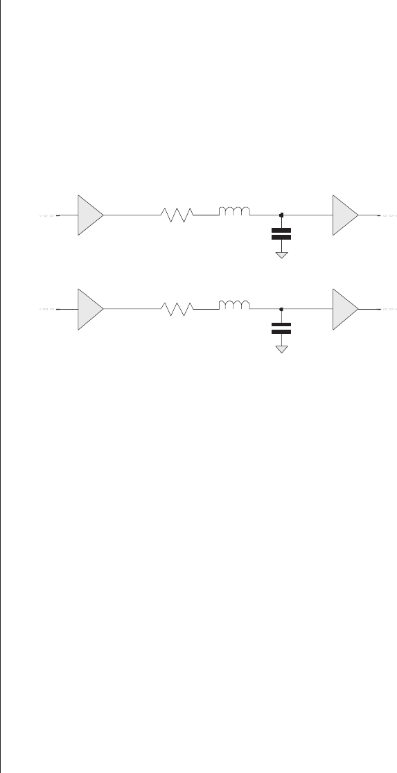
Capacitive and inductive coupling (crosstalk)
Consider two signal wires called Wire1 and Wire2, each of
which is driven by a single gate and drives a single load. In an
ideal—and somewhat simplified—world, both wires would be
perfectly straight with no awkward bends or discontinuities,
and each could be represented by a single series resistance,
series inductance, and capacitance (Figure A-1).
For the purposes of this minimalist example, the capaci-
tances CW1 and CW2 are considered with respect to a ground
plane. In its simplest form, a capacitor consists of two metal
plates separated by an insulating layer called the dielectric.
This means that if our two signal wires run in close proximity
to each other, then from the perspective of an outside
observer they would actually appear to form a rudimentary
capacitor. This may be represented by adding a symbol CM
to reflect this mutual capacitance into our circuit diagram
(Figure A-2).
When one of the signal wires is in the process of transi-
tioning between logic values, the coupling capacitance
between the wires causes a transfer of charge into the other
wire, which may result in noise (glitch) and delay effects, as
discussed in the following sections.
As was previously noted, each wire also has some amount
of inductance associated with it. In its simplest terms, induc-
430 ■The Design Warrior's Guide to FPGAs
The property of an
electric conductor that
characterizes its ability
to store an electric
charge is referred to as
capacitance (C), which is
measured in units of
Farads (F).
The term “Farad” is
named after the British
scientist Michael Fara-
day, who constructed the
first electric motor in
1821.
RW1
CW1
RW2
CW2
Receiver
(Load)
LW1
LW2
Receiver
(Load)
Driver
Driver
Wire1
Wire2
Figure A-1. Two signal wires in an ideal (simplified) world.
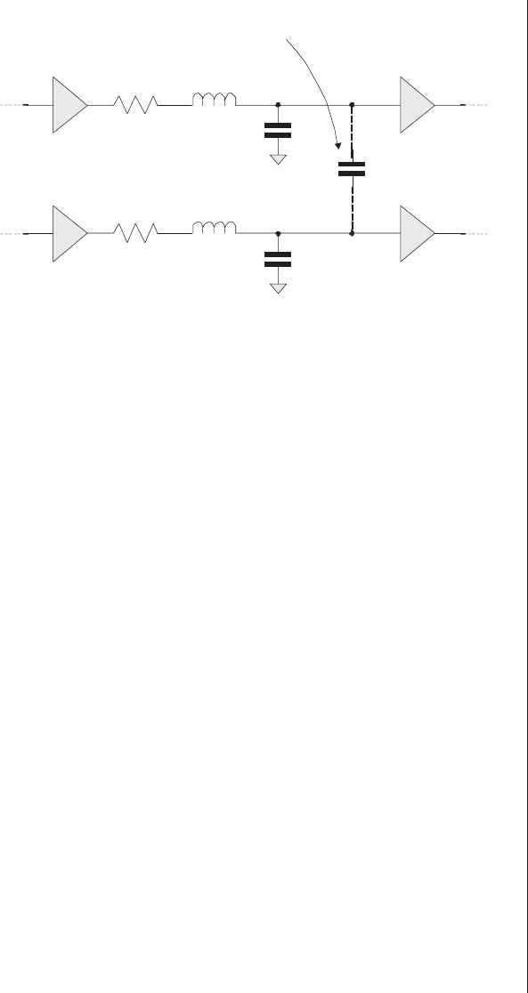
tance is the property associated with conductors by which
changes in the current flowing through a conductor creates a
magnetic field surrounding that conductor. Correspondingly,
any changes in the magnetic field surrounding a conductor
induce a response in that conductor.
This means that when one of our signal wires is in the
process of transitioning between logic values, the change in
current flowing through the wire combined with the induc-
tance associated with that wire causes a magnetic field to build
up around the wire. As it expands, this field interacts with the
inductances associated with any wires in close proximity,
which, once again, may result in noise and delay effects as dis-
cussed in the following sections. This mutual inductance is
indicated by adding a dot to each of the inductor symbols
(Figure A-3).
Chip-level effects
Chip-level effects are RC (resistance-capacitance)
dominated
Early ICs had tracks that were formed from aluminum
(chemical symbol Al), which has a relatively high resistance.
Signal Integrity 101 ■431
In 1831, the British sci-
entist Michael Faraday
discovered that a chang-
ing electromagnetic field
induced a current in a
nearby conductor. This
effect subsequently
became known as
inductance (L).
The symbol for induc-
tance is the capital letter
L in honor of the Russian
physicist Heinrich Lenz,
who discovered the rela-
tionships between the
forces, voltages, and cur-
rents associated with
electromagnetic induc-
tion in 1833.
Inductance is measured
in units of Henries (H).
The term “Henry” is
named after the Ameri-
can scientist Joseph
Henry, who independ-
ently discovered
inductance around the
same time as Faraday.
Pronounced “al-oo-mi-
num” in America, alumi-
num is spelled (and
pronounced) “al-u-min-
ium in the UK.
RW1
CW1
RW2
CW2
Receiver
(Load)
LW1
LW2
Receiver
(Load)
Driver
Driver
CM
The two wires are coupled
by a mutual capacitance
Figure A-2. Two wires in close proximity are coupled by a
mutual capacitance.
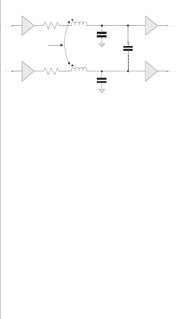
As device feature sizes continued to shrink with each new
technology node, the resistance associated with the aluminum
tracks started to increase to unacceptable levels.
IC manufacturers had long wanted to use copper tracks
(chemical symbol Cu) because copper is one of the best con-
ductors known to man, especially for high-frequency
applications. However, copper also has some awkward proper-
ties, not the least of which is that it can easily diffuse into the
silicon chip, thereby rendering the device useless. It was not
until the late 1990s that IBM solved this problem by the
inclusion of special barrier layers.
Even though copper has a much lower resistance than alu-
minum, signal tracks on ICs are so fine that their resistance is
still extremely significant. The result is that, thus far, delay
effects associated with signals propagating through IC tracks
have tended to be dominated by their resistive and capacitive
(RC) characteristics.
At this time, inductive (L) effects are typically ignored in
signal tracks and are only considered with respect to the
power grid. This grid employs wider tracks with correspond-
ingly lower resistance, such that resistance, inductance, and
capacitance (RLC) characteristics all need to be accounted
for.
432 ■The Design Warrior's Guide to FPGAs
Aluminium was also the
accepted spelling in
America until 1925. At
that time, the American
Chemical Society offi-
cially decided to use the
name aluminum in their
publications.
Dating back more than
10,000 years, copper is
the oldest metal worked
by man.
Most creatures on earth
have blood, whose red
color is caused by the
iron-based pigment
hemoglobin. However,
some primitive creatures
have green, copper-
based blood, whose pig-
ment is called
cuproglobin.
RC is pronounced
by spelling it out as
“R-C.”
RLC is pronounced
by spelling it out as
“R-L-C.”
RW1
CW1
RW2
CW2
Receiver
(Load)
LW1
LW2
Receiver
(Load)
CM
The two wires
are coupled by a
mutual inductance
Figure A-3. Two wires in close proximity are coupled by a
mutual inductance.
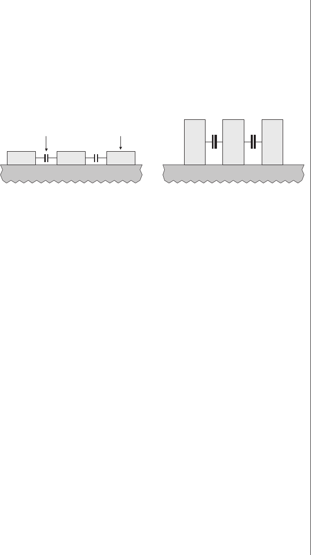
Increased sidewall capacitive coupling
In the case of early IC implementation technologies, the
aspect ratio of tracks was such that their width was signifi-
cantly greater than their height (figure A-4a). As feature sizes
continue to shrink, however, the processes used to create these
devices result in track aspect ratios in which height predomi-
nates over width (Figure A-4b).
The result is a dramatic increase in coupling capacitance
(CSIDE) between the sidewalls of adjacent tracks relative to the
substrate capacitances CAREA (track base to substrate) and
CFRINGE (sidewall to substrate). Furthermore, the high integra-
tion densities associated with today’s devices, which can
support eight or more metalization layers, result in significant
capacitive coupling between adjacent layers. This is repre-
sented by CCROSSOVER (Figure A-5).
The combination of these factors leads to a tremendous
increase in the complexity of crosstalk noise and timing
effects, as discussed below.
Crosstalk-induced glitches
When signals in neighboring wires transition between
logic values, the coupling capacitance between the wires
causes a transfer of charge. Depending on the slew of the sig-
nals (the speed of switching in terms of rise and fall times) and
the amount of mutual crosstalk capacitance (CM), there can be
significant crosstalk-induced glitches (Figure A-6).
Signal Integrity 101 ■433
The term “glitch” possi-
bly comes from the
Yiddish word glitsh,
meaning “a slip or lapse.”
IC Substrate
Cross-sectional view
of interconnect
Sidewall coupling
capacitance ( CSIDE )
(a) 1.0 micron circa 1990
(small CSIDE values)
IC Substrate
(b) 0.13 micron circa 2003
(large CSIDE values)
Figure A-4. Sidewall capacitance effects increase with
shrinking feature sizes (not to scale—illustrates relative
aspect ratios only).
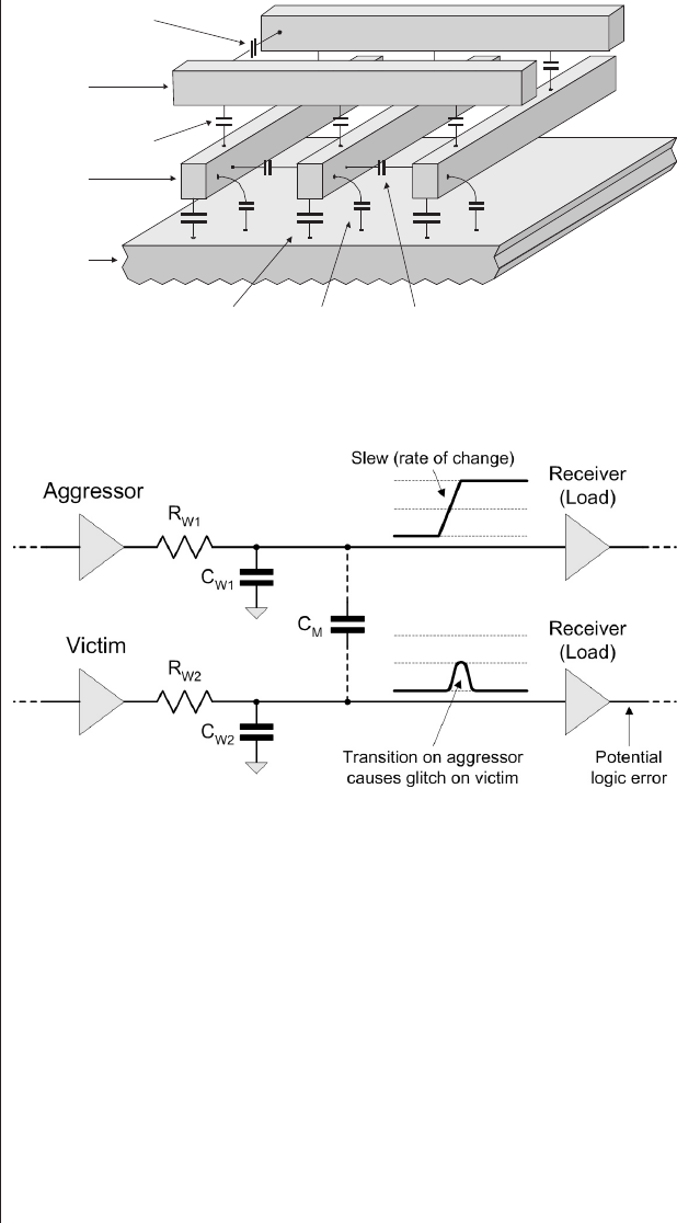
In this example, a transition on the fast aggressor net
causes a glitch to be presented to the input of the receiver
(load) of an adjacent victim net. Of course, this illustration
presents a very simplistic view. In reality, each track may be
formed from multiple segments occupying multiple levels of
metalization. Thus, the resistances (RW1 and RW2) and capaci-
tances (CW1 and CW2) will each consist of multiple elements
associated with the different segments. Similarly, the mutual
coupling crosstalk capacitance (CM) may consist of multiple
elements.
434 ■The Design Warrior's Guide to FPGAs
Substrate
Metal 1
Metal 2
CAREA CFRINGE CSIDE
CCROSSOVER
CSIDE
Figure A-5. Capacitance effects associated with
the interconnect.
Figure A-6. A crosstalk-induced glitch.
1975: America.
MOS Technology
introduces the
6502-based KIM-1
microcomputer.
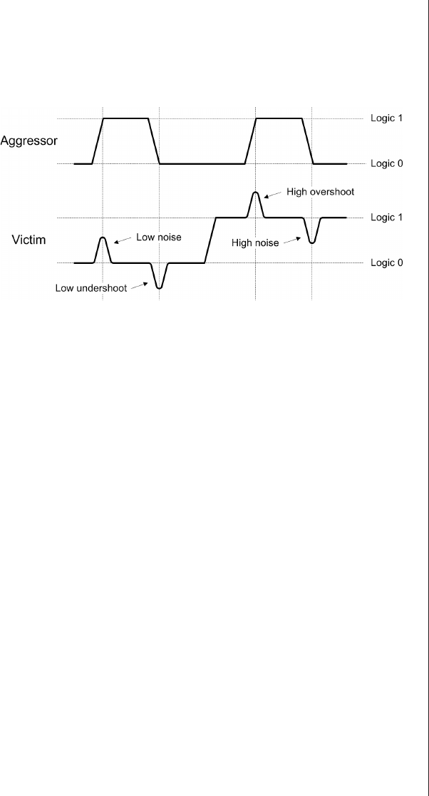
The example glitch illustrated in figure A-6 represents only
one of four generic possibilities based on the fact that a rising
or falling transition on the aggressor net may be coupled with a
logic 0 or logic 1 on the victim net (Figure A-7).
If the ensuing low-noise or high-noise glitches on the vic-
tim net cross the input switching threshold of its receiver, a
functional (logic) error may occur. In some cases this error
may manifest itself as an incorrect data value that is subse-
quently loaded into a register or latch. In other cases, the error
may cause a latch to perform an unintended load, set, or reset.
The low-undershoot and high-overshoot glitches on the vic-
tim net pose a different problem because they can cause
undesirable charge carriers to be trapped in the transistors
forming the logic gates, which can degrade circuit perform-
ance. Although these effects, commonly known as hot electron
effects, are not a major threat in the context of current IC
implementation technologies, they will become increasingly
significant as device geometries progress furter into the deep-
submicron (DSM) and ultra-deep-submicron (UDSM) realms.
Crosstalk-induced delay effects
The situation becomes even more complex when simulta-
neous switching occurs on both the aggressor and victim nets.
Signal Integrity 101 ■435
Any IC implementation
technology below 0.5
µm is referred to as
being deep submicron
(DSM).
DSM is pronounced
by spelling it out as
“D-S-M.”
At some point that isn’t
particularly well defined
(or is defined differently
depending on whom you
are talking to), we move
into the UDSM realm.
UDSM is pronounced
by spelling it out as
“U-D-S-M” or by saying
“ultra-D-S-M.”
Figure A-7. Types of crosstalk-induced glitches.
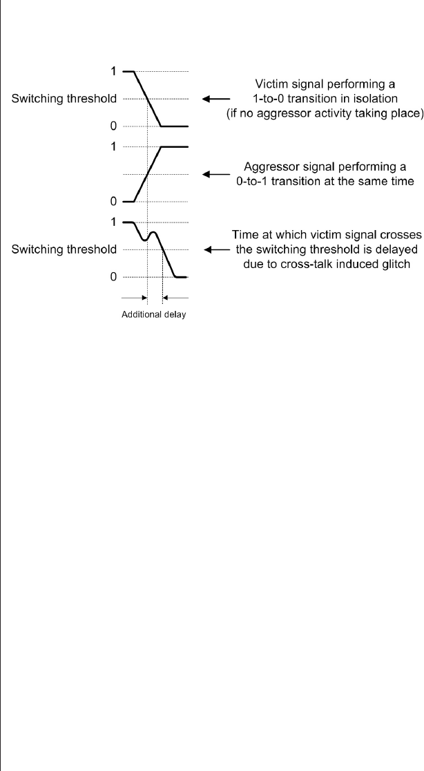
For example, in the case of opposing transitions, the signal on
the victim net may be slowed down (Figure A-8).
If the signal on the victim net were transitioning in isola-
tion, it would take a certain amount of time to cross its
receiver’s switching threshold (which, for the purposes of
these discussions, may be assumed to be 50 percent of the
value between a logic 0 and a logic 1). However, the glitch
caused by a simultaneous transition on the aggressor net holds
the victim’s signal above the receiver’s switching threshold for
an additional amount of time. This can result in a downstream
setup violation.
An alternative scenario occurs when a transition on the
victim is complemented by a simultaneous transition on the
aggressor in the same direction, in which case the signal on
the victim may speed up (Figure A-9).
In this case, the glitch caused by a simultaneous transition
on the aggressor net causes the victim’s signal to cross the
load/receiver’s switching threshold earlier than expected. This
can result in a downstream hold violation.
436 ■The Design Warrior's Guide to FPGAs
Figure A-8. Crosstalk-induced signal delay.
1975: America.
Sphere Corporation
introduces the
6800-based Sphere
1 microcomputer.
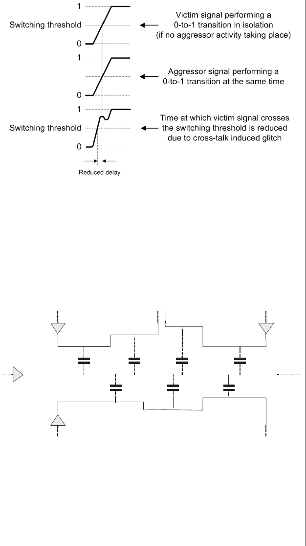
Multiaggressor scenarios
In reality, the examples shown above are extremely sim-
plistic. In the case of real-world designs, each victim net may
be affected by multiple aggressors (Figure A-10).
Accurate analysis of today’s designs requires that each
aggressor’s contribution be individually analyzed and
accounted for.
Signal Integrity 101 ■437
Figure A-9. Crosstalk-induced signal speed up.
Aggressor A Aggressor B
Aggressor C
Victim
Figure A-10. Multiaggressor scenario.
1975: America.
Bill Gates and Paul
Allen found Microsoft.

And let’s not forget the Miller effect
The Miller effect, which is of particular significance at the
chip level, states that the simultaneous switching of both ter-
minals of a capacitor will modify the effective capacitance
between the terminals.
What this means in real terms becomes apparent when we
consider one of the signals in the middle of a bus, for example.
If one or more of the surrounding signals in the bus are
switching with the same polarity (in the same direction) as
the signal of interest, then the capacitance associated with
this signal will appear to be reduced, and its propagation delay
will decrease (this is in addition to the crosstalk-induced delay
effects introduced earlier).
By comparison, if one or more of the surrounding signals
in the bus are switching with the opposite polarity to the sig-
nal of interest, then the capacitance associated with this
signal will appear to be larger and its propagation delay will
increase.
The reason we commenced with the chip-level effects
introduced above is that these provide a familiar starting point
for IC design engineers. In reality, however, on-chip SI effects
(excluding packaging considerations) are of little interest to
engineers using FPGAs because these effects are handled
behind the scenes by the device vendor. By comparison,
board-level SI effects are extremely pertinent when it comes
to integrating FPGAs into a circuit board environment.
Board-level effects
Board-level effects are LC (inductance-
capacitance) dominated
When it comes to PCBs, the resistance of their copper
tracks is almost negligible in the context of coupling effects.
This is because at around 125 microns wide and 18 microns
thick, board-level tracks have a huge cross-sectional area com-
pared to their chip-level counterparts (the larger the cross
section of a conductor, the lower its resistance). By compari-
438 ■The Design Warrior's Guide to FPGAs
In the context of an elec-
tronic circuit, the term
“bus” (sometimes “buss”)
refers to a set of signals
performing a common
function and carrying
similar data.
LC is pronounced by
spelling it out as “L-C.”
PCB is pronounced by
spelling it out as “P-C-B.”
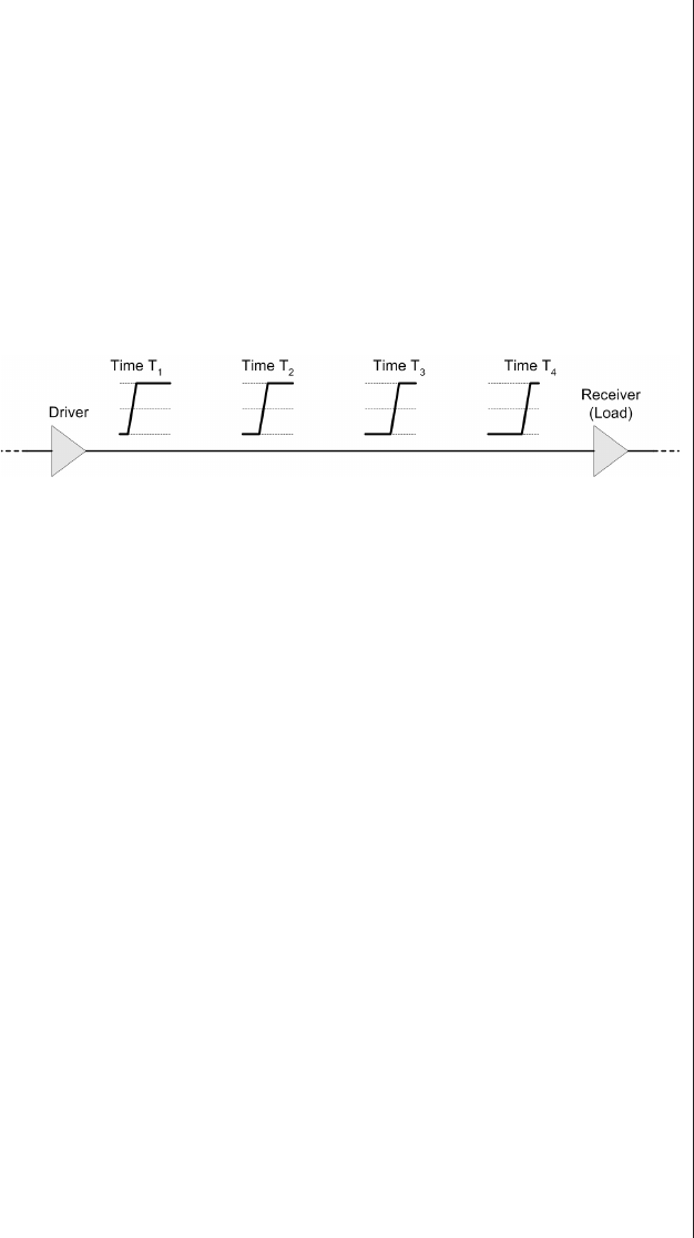
son, both inductive and capacitive coupling effects are
significant, so circuit board signal tracks are predominantly
considered to be LC-coupled.
A different way of thinking about things
In the case of today’s high-speed, high-performance PCBs,
the tracks almost invariably act like transmission lines. This
means we have to visualize a signal edge as a moving wave
propagating down the wire through time (Figure A-11).
With regard to this transmission line view, in which the
delay down the wire is long in comparison to the signal’s tran-
sition times, the only place any capacitive or inductive
coupling occurs is at the current location of the moving edge.
This means that we have to consider the track in terms of a
series of small RLC segments (which are not shown in these
figures for reasons of simplicity).
Capacitive and inductive coupling effects
Things really start to get interesting when we consider two
of these board-level tracks in close proximity to each other.
Let’s assume that we are looking at a moving edge that is in
the process of propagating down an aggressor track that is
inductively and capacitively coupled to a neighboring victim
track (Figure A-12).
In the case of the capacitive coupling effect, the moving
edge on the aggressor net induces positive-going current pulses
on the victim net in both the forward and reverse directions.
By comparison, in the case of the inductive coupling effect,
Signal Integrity 101 ■439
An alternative name for
PCB is printed wire board
(PWB), which is pro-
nounced by spelling it
out as “P-W-B.”
The most commonly
used board material is
FR4, which is pro-
nounced by spelling it
out as “F-R-4” (the “FR”
stands for “flame
retardant”).
Figure A-11. A signal edge moving through time.
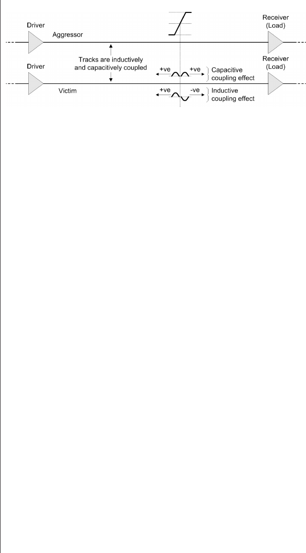
the moving edge on the aggressor net induces a negative-going
current pulse on the victim net in the forward direction and a
positive-going current pulse on the victim net in the reverse
direction.
This means that the capacitive and inductive coupling
effects tend to augment each other when it comes to near-end
noise (noise as seen at the driver end of the track). However,
they tend to cancel each other out when it comes to far-end
noise (noise as seen at the receiver end of the track). This
means that the best-case scenario one can ever hope for is
when the capacitive and inductive coupling effects are of
comparable magnitudes, because they will cancel each other
out at the far end. Unfortunately, this will only ever happen if
the dielectric (insulating) layer around the signals is homoge-
neous, such as with a stripline stackup. In the real world, the
dielectric around signals is typically inhomogeneous, such as
surface traces, which have air above and FR4 below. In this
case, the inductive coupling does not change, but the capaci-
tive coupling decreases. This increases the relative amount of
inductive coupling and gives rise to the generation of far-end
noise at the receiver. In a typical circuit board environment,
the inductive noise can be as much as two to four times the
capacitive noise.
If anything occurs to degrade the return path, the induc-
tive coupling can increase dramatically to as much as ten to
thirty times the capacitive. In such a regime, where the
440 ■The Design Warrior's Guide to FPGAs
Figure A-12. Capacitive and inductive coupling effects.
1975: England.
First liquid crystal
displays (LCDs) are used
for pocket calculators
and digital clocks.

crosstalk is dominated by inductive coupling, we call the ensu-
ing noise switching noise. In the case where multiple signal
paths share the same return path, the switching noise we get
across the return (ground) connection is called ground bounce.
The anti-Miller effect
In our chip-level discussions, we introduced the concept of
the Miller effect, which says that if one or more signals are
switching with the same polarity (in the same direction) in
close proximity to a signal of interest, then the capacitance
associated with this signal will appear to be reduced, and its
propagation delay will decrease.
As was previously noted, however, the propagation delays
of chip-level signals are predominantly RC dependent, while
the propagation delays of board-level signals are predomi-
nantly LC dependent. This means that if one or more
board-level signals are switching with the same polarity in
close proximity to a signal of interest, then the inductance
associated with this signal will appear to be larger. In an inho-
mogeneous dielectric stackup, the relative inductive coupling
is larger than the capacitive coupling, and the increased induc-
tance of the signal trace causes the propagation delay
to increase.
By comparison, if one or more board-level signals are
switching with the opposite polarity to the signal of interest,
then the inductance associated with this signal will appear to
be reduced and its propagation delay will decrease.
Transmission line effects
In addition to the effects presented above, there are, of
course, classical transmission line effects with associated termi-
nation considerations such as using series termination on
outputs and parallel termination on inputs, but this sort of
thing is beaten into the ground in standard textbooks, so we
will skip over it here.
Signal Integrity 101 ■441
1975: America.
Ed Roberts and his
MIT’s company
introduce the
8800-based Altair 8800
microcomputer.

Things you can do to make life easier
Unfortunately, 70 to 80 percent of the SI problems associ-
ated with connecting an FPGA to a circuit board are not
related to the board per se, but rather to the FPGA’s package.
Ideally, the package should have as large a number of
power-ground pad pairs as possible, and these pad pairs should
be uniformly distributed across the base of the package so as to
provide the I/O pads with plenty of adjacent return paths. In
reality, the power and ground pads tend to be clustered
together leaving groups of I/O pads to do the best they can
with the return paths available to them.
You can make life easier by making it a rule, if you have
the option to use differential output pairs for your I/O, espe-
cially in the case of buses and high-speed interconnections, to
do so. Of course, this doubles the number of pins you use for
the affected I/Os, but it’s well worth your time if you can
afford the overhead in pins.
Another point to consider relates to the internal,
programmable termination resistors provided in some FPGAs.
The use of these is optional in that you can either use discrete
components at the board level or enable these internal
equivalents as required. These internal terminations are
predominantly considered in the context of easing routing
congestion at the board level, but they also have SI
implications. The rule of thumb is that for any signals with
rise/fall times of 500 picoseconds or less, external termination
resistors cause discontinuities in the signal, so you should
always use their on-chip counterparts.
442 ■The Design Warrior's Guide to FPGAs
I/O is pronounced
by spelling it out
as “I-O.”

Introduction
When one is designing ASICs and ASSPs, the timing
effects one needs to account for are extremely complex. As
each new technology process node comes online, these effects
become ever-more horrendous. At some point—which isn’t
particularly well defined (or which is defined differently by dif-
ferent people), but which we will take to be somewhere around
the 0.5-micron (500 nanometer) node—we start to move into
an area rife with what are known as deep-submicron (DSM)
delay effects.
The great thing about working with FPGAs, of course, is
that the folks who create these devices handle the bulk of the
problems associated with DSM delay effects, leaving them
largely transparent to the end users (design engineers). On this
basis, it’s fair to say that we really don’t need to discuss DSM
timing issues here. On the other hand, this is the sort of thing
you tend to hear about all the time, but I’ve never run across
an introduction to these effects that is comprehensible to any-
one sporting anything less than a size-16 brain with go-faster
stripes! It is for this reason that the following overview is pre-
sented for your delectation and delight.
The evolution of delay specifications
Way back in the mists of time, sometime after the Jurassic
period when dinosaurs ruled the earth—say, around the late
1970s and early 1980s—the lives of ASIC design engineers
were somewhat simpler than they are today. Delay specifica-
tions for the early (multimicron) technologies were
The contents of this
appendix are abstracted
from my book Designus
Maximus Unleashed
(ISBN 0-7506-9089-5)
with the kind permission
of the publisher.
Deep-Submicron Delay
Effects 101
Appendix
B
rudimentary at best. Consider the case of a simple 2-input
AND gate, for which input-to-output databook delays were
originally specified as being identical for all of the inputs
and for both rising and falling transitions at the output
(Figure B-1i).
As device geometries shrank, however, delay specifica-
tions became increasingly complex. The next step was to
differentiate delays for rising and falling output transitions
(Figure B-1ii), and this was followed by associating different
delays with each input-to-output path (Figure B-1iii).
All of these early delays were typically specified in the
form ?ns + ?ns/pF. The first portion (?ns) indicates a fixed
delay specified in nanoseconds1associated with the gate itself.
This is combined with some additional delay specified as
nanoseconds per picofarad (?ns/pF) caused by capacitive load-
ing.2As we will see, this form of specification simply cannot
handle the delay effects characteristic of DSM technologies,
444 ■The Design Warrior's Guide to FPGAs
Early 2000s
Late 1970s
Increasing
complexity
of delay
specifications
? ->? =?+ ?
a -> y (LH) = ?ns + ?ns/pF
a -> y (HL) = ?ns + ?ns/pF
b -> y (LH) = ?ns + ?ns/pF
b -> y (HL) = ?ns + ?ns/pF
a,b -> y (LH) = ?ns + ?ns/pF
a,b -> y (HL) = ?ns + ?ns/pF
a,b -> y (LH, HL) = ?ns + ?ns/pF
ay
b&
(i)
(ii)
(iii)
(iv)
Figure B-1. Delay specifications become increasingly complex
over time.
1Today’s devices are much faster, so their delays would be measured in
picoseconds.
2The basic unit of capacitance is the Farad. This was named after the
British scientist, Michael Faraday, who constructed the first electric
motor in 1821.
1975: America.
MOS Technology
introduces the 6502
microprocessor.
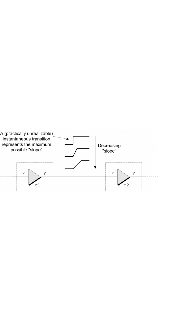
not the least in the area of RLC interconnect delays, as dis-
cussed below.
A potpourri of definitions
Before plunging headfirst into the mire of DSM delays, it
is first necessary to introduce a number of definitions as
follows.
Signal slopes
The slope (or slew) of a signal is its rate of change when
transitioning from a logic 0 value to a logic 1, or vice versa. An
instantaneous transition, which cannot be achieved in the real
world, would be considered to represent the maximum possible
slope value (Figure B-2).
The slope of the signal is a function of the output charac-
teristics of the driving gate combined with the characteristics
of the interconnect (track) and the input characteristics of any
load gate(s).
Input switching thresholds
An input switching threshold is the point at which an input
to a load gate first sees a transition as occurring; that is, the
point at which the signal presented to the input crosses some
threshold value, at which point the downstream gate deigns to
notice that something is happening. Input switching thresh-
Deep-Submicron Delay Effects 101 ■445
Figure B-2. The slope of a signal is the time taken to
transition between logic values.
1975: America.
Microsoft releases
BASIC 2.0 for the Altair
8800 microcomputer.
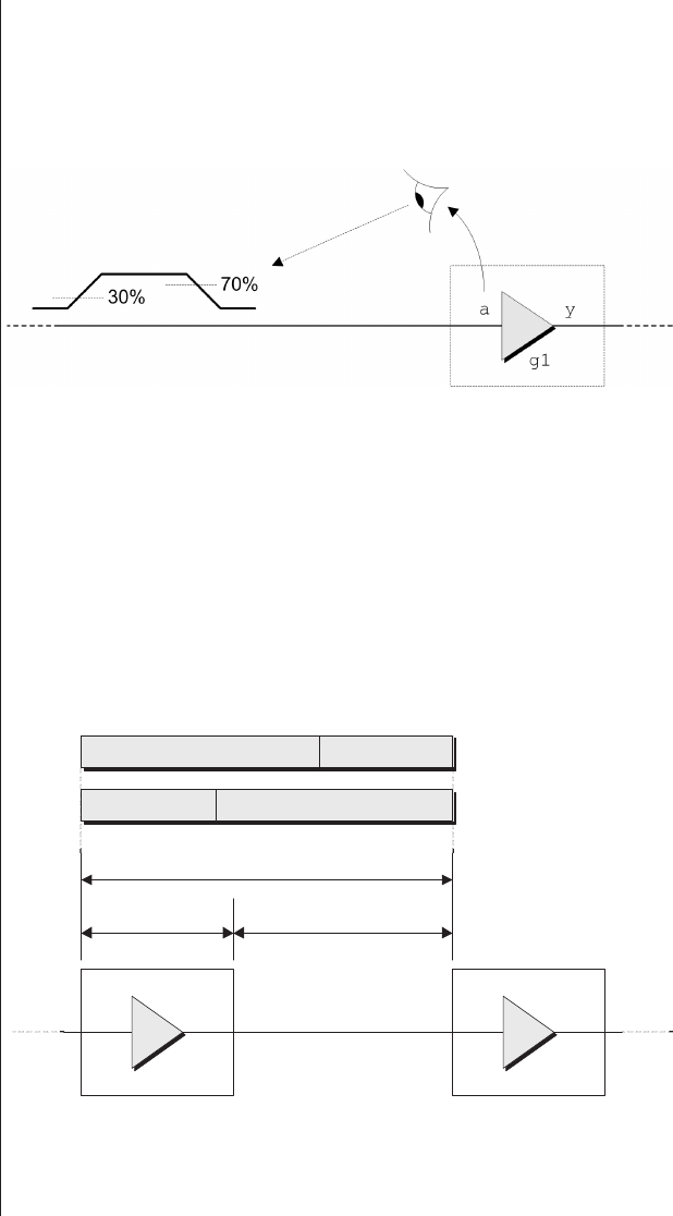
olds are usually specified as a percentage of the value (voltage
differential) between a logic 0 and a logic 1, and each input
may have different switching thresholds for rising and falling
transitions (Figure B-3).
Intrinsic versus extrinsic delays
The term intrinsic refers to any delay effects that are
internal to a logic function, while the term extrinsic refers to
any delay effects that are associated with the interconnect
(Figure B-4).
446 ■The Design Warrior's Guide to FPGAs
Figure B-3: Input switching thresholds may differ for rising
and falling transitions.
ay ay
g1 g2
“Intrinsic”
Gate delay
“Extrinsic”
Interconnect (inc. fan-in)
Total delay = 100%
Intrinsic (66%) Extrinsic (34%)
Intrinsic (34%) Extrinsic (66%)
(i)
(ii)
2.0 micron
1.0 micron
Figure B-4. Intrinsic versus extrinsic delays.
1976: America.
Zilog introduces the Z80
microprocessor.
In the early multimicron technologies, intrinsic delays
dominated over their extrinsic counterparts. In the case of
devices with 2.0-micron geometries, for example, the intrinsic
delay typically accounted for approximately two-thirds of the
total delay (Figure B-4a). But extrinsic delays became increas-
ingly important with shrinking geometries. By the time that
devices with 1.0-micron geometries became available, the rela-
tive domination of the intrinsic and extrinsic delays had
effectively reversed (Figure B-4b).
This trend is destined to continue because the geometry
of the interconnect is not shrinking at the same rate as the
transistors and logic gates. In the case of today’s DSM tech-
nologies, extrinsic delays can account for 80 percent or more
of the total path delays.
Pn-Pn and Pt-Pt delays
To a large extent, pin-to-pin (Pn-Pn) and point-to-point
(Pt-Pt) delays are more modern terms for intrinsic and extrin-
sic delays, respectively. A Pn-Pn delay is measured between a
transition occurring at the input to a gate and a corresponding
transition occurring at the output from that gate, while a Pt-Pt
delay is measured between the output from a driving gate to
the input of a load gate (Figure B-5).3
Deep-Submicron Delay Effects 101 ■447
ay
g1
ay
g2
Pn-Pn Pt-Pt g1.a
Pn-Pn Pt-Pt
g1.y
g2.a
Figure B-5. Pn-Pn versus Pt-Pt delays.
3It should be noted that circuit board layout designers don’t tend to worry
too much about what happens inside devices, which they usually
consider to be “black boxes.” The reason for mentioning this is that the
board designers may use the term “pin-to-pin” to refer to track delays at
the board level.
1976: America.
Steve Wozniak and
Steve Jobs introduce
the 6502-based Apple
1 microcomputer.

To be more precise, a Pn-Pn delay is the time between a
signal on a gate’s input reaching that input’s switching thresh-
old to a corresponding response beginning at its output, while a
Pt-Pt delay is the time from the output of a driving gate
beginning its transition to a corresponding load gate perceiving
that transition as crossing its input switching threshold.
Good Grief!
There are a number of reasons why we’re emphasizing the
fact that we consider the time when the output begins to
respond as marking the end of the Pn-Pn delay and the start
of the Pt-Pt delay. In the past, these delays were measured
from the time when the output reached 50 percent of the
value between a logic 0 and a logic 1. This was considered to be
acceptable, because load gates were all assumed to have input
switching thresholds of 50 percent. But consider a rising tran-
sition on the output and assume that the load gate’s input
switching threshold for a rising transition is 30 percent. If
we’re assuming that delays are measured from the time the
output crosses its 50 percent value, then it’s entirely possible
that the load gate will see the transition before we consider
the output to have changed. Also, when we come to consider
mixed-signal (analog and digital) simulation, then the only
meaningful time to pass an event from a gate’s output transi-
tioning in the digital realm into the analog domain is the
point at which the gate’s output begins its transition.
State and slope dependency
Any attribute associated with an input to a gate (including
a Pn-Pn delay) that is a function of the logic values on other
inputs to that gate is said to be state dependent. Similarly, any
attribute associated with an input to a gate (including a Pn-Pn
delay) that is a function of the slope of the signal presented to
that input is said to be slope dependent. These state- and
slope-dependency definitions might not appear to make much
sense at the moment, but they’ll come to the fore in the not-
so-distant future as we progress through this chapter.
448 ■The Design Warrior's Guide to FPGAs
1976: America.
Steve Wozniak and
Steve Jobs form the
Apple Computer
Company (on April 1st).
Alternative interconnect models
As the geometries of structures on the silicon shrink and
the number of gates in a device increase, interconnect delays
assume a greater significance, and increasingly sophisticated
algorithms are required to accurately represent the effects asso-
ciated with the interconnect as follows.
The lumped-load model
As was noted earlier, the Pn-Pn gate delays in early multi-
micron technologies dominated over Pt-Pt interconnect
delays. Additionally, the rise and fall times associated with sig-
nals were typically greater than the time taken for the signals
to propagate through the interconnect. In these cases, a repre-
sentation of the interconnect known as the lumped-load model
was usually sufficient (Figure B-6).
The idea here is that all of the capacitances associated with
the track and with the inputs to the load gates are added
together to give a single, equivalent capacitance. This capaci-
tance is then multiplied by the drive capability of the driving
gate (specified in terms of nanoseconds per picofarad, or
equivalent) to give a resulting Pt-Pt delay. The lumped-load
model is characterized by the fact that all of the nodes on the
track are considered to commence transitioning at the same
Deep-Submicron Delay Effects 101 ■449
ay
g1 a
y
g2
a
y
g3
Equivalent
capacitance
Figure B-6. The lumped-load interconnect model.
1977: America.
Apple introduces
the Apple II
microcomputer.
time and with the same slope. This model may also be referred
to as a pure RC model.
The distributed RC model
The shrinking device geometries of the mid-1980s began
to mandate a more accurate representation of the intercon-
nect than was provided by the lumped-load model. Thus, the
distributed RC model was born (where R and C represent resis-
tance and capacitance, respectively) (Figure B-7).
In the distributed RC model, each segment of the track is
treated as an RC network. The distributed RC model is char-
acterized by the fact that all of the nodes on the track are
considered to commence transitioning at the same time but
with different slopes. Another way to view this is that the sig-
nal’s edge is collapsing (or deteriorating) as it propagates
down the track.
The pure LC model
At the circuit board level, high-speed interconnects start
to take on the characteristics of transmission lines. This pure
LC model (where L and C represent inductance and capaci-
450 ■The Design Warrior's Guide to FPGAs
ay
g1 a
y
g2
a
y
g3
Figure B-7. The distributed RC interconnect model.
1977: America.
Commodore Business
Machines present their
6502-based
Commodore PET
microcomputer.
tance, respectively) can be represented as a sharp transition
propagating down the track as a wavefront (Figure B-8).
Pure transmission line effects do not occur inside silicon
chips, but large submicron devices do begin to exhibit certain
aspects of these delay effects, as discussed below.
The RLC model
In the case of large devices with DSM geometries, the
speed of the signals coupled with relatively long traces results
in the interconnect exhibiting some transmission-line-type
effects. However, the resistive nature of on-chip interconnect
does not support pure LC effects; instead, these traces may be
described as exhibiting RLC effects (Figure B-9).
The RLC model is characterized as a combination of a dis-
crete wavefront, supplied by the interconnect’s LC
constituents, and a collapsing (or deteriorating) signal edge
caused by the interconnect’s RC components.
Deep-Submicron Delay Effects 101 ■451
ay
g1 a
y
g2
a
y
g3
Figure B-8. The pure LC interconnect model.
1977: America.
Tandy/Radio Shack
announce their
Z80-based TRS-80
microcomputer.
DSM delay effects
Path-specific Pn-Pn delays
Each input-to-output path typically has its own Pn-Pn
delay. In the case of a 2-input OR gate, for example, a change
on input acausing a transition on output y(Figure B-10a)
would have a different delay from that of a change on input b
causing a similar transition on output y(Figure B-10b).
452 ■The Design Warrior's Guide to FPGAs
a
b
y
|
a
y
g1
b
a
b
y
(i) Input ato output y(ii) Input bto output y
Figure B-10. Path-specific Pn-Pn delays.
ay
g1 a
y
g2
a
y
g3
Figure B-9. The RLC interconnect model.
1977:
First implementation
of optical light-waves
in operating telephone
company.

Similarly, each rising and falling transition at the output
typically has its own Pn-Pn delay. In the case of our OR gate,
for example, a change on input acausing a rising transition on
output ywould have a different delay from that of a change on
input acausing a falling transition on output y.
Note that this example assumes input switching thresholds
of 50 percent, and remember that Pn-Pn delays are measured
from the time when a signal presented to an input crosses that
input’s switching threshold to the time when the output first
begins to respond.
Path- and transition-specific Pn-Pn delays are not limited
to DSM technologies, and they should come as no surprise, but
they are presented here to prepare the stage for the horrors
that are to come.
Threshold-dependent Pn-Pn delays
Pn-Pn delays depend on the switching thresholds associ-
ated with inputs, at least to the extent that the delay through
the gate doesn’t actually commence until the signal presented
to the input crosses the threshold. For example, if the input
switching threshold for a rising transition on input awere 30
percent of the value between the logic 0 and logic 1 levels
(Figure B-11a), then the input would see the transition earlier
than it would if its input switching threshold were 70 percent
(Figure B-11b).
Additionally, the slope of a signal being presented to an
input affects the time that signal crosses the input switching
threshold. For the purposes of presenting a simple example,
let’s assume that input ahas a switching threshold of 50 per-
cent. If a signal with a steep slope is presented to input a
(Figure B-12a), then the input will see the signal as occurring
earlier than it would if the slope of the signal were decreased
(Figure B-12b).
Although this affects the time at which the Pn-Pn delay
commences, it is NOT the same as the slope-dependent Pn-Pn
delays presented in the next section.
Deep-Submicron Delay Effects 101 ■453
1978: America.
Apple introduces the
first hard disk drive for
use with personal
computers.
Slope-dependent Pn-Pn delays
Speaking of which … the previous example was somewhat
simplistic in that it showed two Pn-Pn delays as being identi-
cal, irrespective of the slope of the incoming signal. Some
vendors of computer-aided design tools refer to the previous
case as “slope dependency,” but this is not a correct usage of
the term. As it happens, a variety of delay effects in DSM
technologies may be truly slope dependent, which means that
they may be directly modified by the slope of an incoming
signal.
454 ■The Design Warrior's Guide to FPGAs
50%a
b
y
|
a
y
g1
b
50%a
b
y
n ticks n ticks
(i) Fast transition
presented to input a
(ii) Slower transition
presented to input a
Figure B-12. The slope of an incoming signal affects the
time at which the input sees that signal.
30%
a
b
y
|
a
y
g1
b
70%
a
b
y
n ticks n ticks
(i) 30% switching
threshold on input a
(ii) 70% switching
threshold on input a
Figure B-11. Threshold-dependent Pn-Pn delays.
1979:
ADA programming
language is named after
Augusta Ada Lovelace
(now credited as being
the first computer
programmer).
Let’s consider what happens from the point at which the
signal presented to an input crosses that input’s switching
threshold. The Pn-Pn delay from this point may be a function
of the rate of change of the incoming signal. For example, a
fast slope presented to the input may result in a short Pn-Pn
delay (Figure B-13a), while a slower slope may result in a
longer delay (Figure B-13b).
Actually, the effect illustrated in Figure B-13, in which a
decreasing slope causes an increasing Pn-Pn delay, is only one
possible scenario. This particular case applies to gates or tech-
nologies where the predominant effect is that the switching
speeds of the transistors forming the gate are directly related to
the rate of change of charge applied to their inputs. By com-
parison, in the case of certain technologies, a decreasing slope
actually results in faster Pn-Pn delays (as measured from the
switching threshold of the input). This latter case results from
the fact that a sufficiently long slope permits internal transis-
tors to become precharged almost to the point of switching.
Thus, when the input signal actually crosses the input’s switch-
ing threshold, the gate is poised at the starting blocks and
appears to switch faster than it would if a sharp edge had been
applied to the input.
To further increase your pleasure and double your fun, both
effects may be present simultaneously. In this case, applying a
Deep-Submicron Delay Effects 101 ■455
50%a
b
y
|
a
y
g1
b
50%a
b
y
(i) Fast transition
presented to input a
(ii) Slower transition
presented to input a
Figure B-13. Slope-dependent Pn-Pn delays.
1979: America.
The first true
commercial
microcomputer
program, the VisiCalc
spreadsheet, is made
available for the
Apple II.
sharp edge to the input may result in a certain Pn-Pn delay,
and gradually decreasing the slope of the applied signal could
cause a gradual increase in the Pn-Pn delay. At some point,
however, further decreasing the slope of the applied input will
cause a reduction in the Pn-Pn delay, possibly to the point
where it becomes smaller than the Pn-Pn delay associated
with our original sharp edge!4
State-dependent Pn-Pn delays
In addition to being slope-dependent, Pn-Pn delays are
often state dependent, which means that they depend on the
logic values of other inputs (Figure B-14).
This example illustrates two cases in which a signal pre-
sented to the ainput causes an identical response (in terms of
logic values) at the co output. However, even assuming that
the slopes of the signals presented to aand the switching
thresholds on aare identical in both cases, the Pn-Pn delays
may be different due to the logic values present on inputs b
and ci.
456 ■The Design Warrior's Guide to FPGAs
co
ci
+
a
y
g1
b
Full adder
a
ci
co
b
1
0
a
ci
co
b
1
0
(i) b=1,ci = 0 (ii) b=0,ci =1
Figure B-14. State-dependent Pn-Pn delays.
4And there are those who would say that electronics is dull and
boring—go figure!
1980:
Cordless and cell
phones are developed.
Path-dependent drive capability
This is where life really starts to get interesting (trust me,
have I ever lied to you before?).5Up to this point, we have
only considered effects that impact Pn-Pn delays through a
gate, but many of these effects also influence the gate’s ability
to drive signal at its output(s). For example, the driving capa-
bility of a gate may be path dependent (Figure B-15).
In this case, in addition to the fact that inputs aand bhave
different Pn-Pn delays, the driving capability of the gate (and
hence the slope of the output signal) is dependent on which
input caused the output transition to occur. This phenomenon
was originally associated only with MOS technologies and was
not generally linked to bipolar technologies such as TTL. As
the plunge into DSM continues, however, many of the more
esoteric delay effects are beginning to manifest themselves
across technologies with little regard for traditional
boundaries.
Slope-dependent drive capability
In addition to being dependent on which input causes an
output transition to occur (as discussed in the previous point),
the driving capability of the gate (and hence the slope of the
Deep-Submicron Delay Effects 101 ■457
a
b
y
|
a
y
g1
b
a
b
y
(i) Input acauses fast
transition on y
(ii) Input bcauses
slower transition on y
Figure B-15. Path-dependent drive capability.
5Don’t answer that!
1980:
Development of the
World Wide Web
begins.
output signal) may also be dependent on the slope of the sig-
nal presented to the input. For example, a fast transition on
input amay cause a fast slope at the output (Figure B-16a),
while a slower transition on the same input may impact the
gate’s driving capability and cause the slope of the output sig-
nal to decrease (Figure B-16b). Are we having fun yet?
State-dependent drive capability
Yet another factor that can influence the drive capability
of an output is the logic values present on inputs other than
the one actually causing the output transition to occur. This
effect is known as state-dependent drive capability (Figure B-17).
458 ■The Design Warrior's Guide to FPGAs
co
ci
+
a
y
g1
b
Full adder
a
ci
co
b
1
0
a
ci
co
b
1
0
(i) b=1,ci = 0 (ii) b=0,ci =1
Figure B-17. State-dependent drive capability.
50%a
b
y
|
a
y
g1
b
50%a
b
y
(i) Fast transition on a
gives higher drive on y
(ii) Slow transition on a
gives lower drive on y
Figure B-16. Slope-dependent drive capability.
1980:
Faxes can be sent over
regular phone lines.
Figure B-17 illustrates two cases in which a signal pre-
sented to the ainput causes an identical response (in terms of
logic values) at the co output. However, even assuming that
the slopes of the signals presented to aand the switching
thresholds on aare identical in both cases, the driving capabil-
ity of the gate (and hence the slope of the output signal) may
be different due to the logic values present on inputs band ci.
State-dependent switching thresholds
As you doubtless observed, the previous point on state-
dependent drive capability included the phrase “assuming that
the input switching thresholds on input aare identical in both
cases.” If this caused a few alarm bells to start ringing in your
mind, then, if nothing else, at least these discussions are serv-
ing to hone your abilities to survive the dire and dismal depths
of the DSM domain.
The point is that by some strange quirk of fate, an input’s
switching threshold may be state dependent; that is, it
may depend on the logic values present on other inputs
(Figure B-18).
Deep-Submicron Delay Effects 101 ■459
co
ci
+
a
y
g1
b
30%
0
1
co
ci
+
a
y
g1
b
70%
1
0
(i) b=0,ci = 1, switching
threshold on input a= 30%
(ii) b=1,ci = 0, switching
threshold on input a= 70%
Figure B-18. State-dependent input switching thresholds.
1981:
America. First IBM PC
is launched.
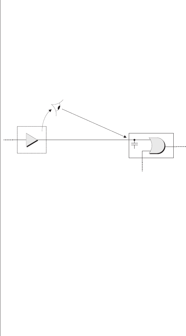
In this example, the switching threshold of input a
(the point at which this input sees a transition as occurring)
depends on the logic values presented to inputs band ci.
State-dependent terminal parasitics
In addition to an input’s switching threshold being state
dependent, further characteristics associated with that input
(such as its parasitic values) may also depend on the logic val-
ues presented to other inputs. For example, consider a 2-input
OR gate (Figure B-19).
The terminal capacitance of input g2.a (as seen by the
driving output g1.y) may depend on the logic value presented
to input g2.b. If input g2.b is a logic 0, a transition on input
g2.a will cause the output of the OR gate to switch. In this
case, g1.y (the output of the gate driving g2.a) will see a rela-
tively high capacitance. However, if input g2.b is a logic 1, a
transition on input g2.a will not cause the output of the OR
gate to switch. In this case, g1.y will see a relatively small
capacitance.
At this point you may be asking, “In the case where the
OR gate isn’t going to switch, do we really care if the parasitic
capacitance on input ais different? Can’t we just set the value
of the capacitance to be that for when the OR gate will
switch?” In fact, this would be okay if the output g1.y were
460 ■The Design Warrior's Guide to FPGAs
|
a
y
g2
b
ay
g1
Figure B-19. State-dependent terminal parasitics.
1981: America.
First mouse pointing
device is created.
only driving input g2.a, but problems obviously arise if we
modify the circuit such that g1.y starts to drive two or more
load gates.
This particular effect first manifested itself in ECL tech-
nologies. In fact, as far back as the late 1980s, I was made
aware of one ECL gate-array technology in which the terminal
capacitance of a load gate (as perceived by the driving gate)
varied by close to 100 percent due to this form of state depend-
ency. But this effect is no longer confined to ECL; once again,
delay effects are beginning to manifest themselves across tech-
nologies with scant regard for traditional boundaries as we sink
further into the DSM domain.
The effect of multi-input transitions on Pn-Pn
delays
Prior to this point, we have only considered cases in which
a signal presented to a single input causes an output response.
Not surprisingly, the picture becomes more complex when
multi-input transitions are considered. For example, take the
case of a 2-input OR gate (Figure B-20).
For the sake of simplicity, we will assume that both the a
and binputs are fully symmetrical; that is, both have identical
input switching thresholds and Pn-Pn delays.
Deep-Submicron Delay Effects 101 ■461
a
b
y
|
a
y
g1
b
a
b
y
(i) Input atransitions
in isolation
(ii) Inputs aand b
transition simultaneously
Figure B-20. The effect of multi-input transitions
on Pn-Pn delays.
1981:
First laptop computer
is introduced.
First, consider the case where a transition applied to a sin-
gle input (for example, input a) causes a response at the
output (Figure B-20a). The resulting Pn-Pn delay is the one
that is usually specified in the databook for this cell. However,
if both inputs transition simultaneously (Figure B-20b), the
resulting Pn-Pn delay may be reduced to close to 50 percent of
the value specified in the databook.
These two cases (a single input transition occurring in iso-
lation versus multi-input transitions occurring simultaneously)
provide us with worst-case endpoints. However, it is also nec-
essary to consider those cases where the inputs don’t
transition simultaneously, but do transition close together. For
example, take the OR gate shown in figure B-20 and assume
that both inputs are initially at logic 0. Now assume that
input ais presented with a rising transition, which initiates
the standard databook Pn-Pn delay, but before this delay has
fully completed, input bis also presented with a rising transi-
tion. The result is that the actual Pn-Pn delay could occur
anywhere between the two worst-case endpoints.
The effect of multi-input transitions on drive
capability
In addition to modifying Pn-Pn delays, multi-input transi-
tions may also affect the driving capability of the gate, and
hence the slope of the output signal (Figure B-21).
462 ■The Design Warrior's Guide to FPGAs
a
b
y
|
a
y
g1
b
a
b
y
(i) Input atransitions
in isolation
(ii) Inputs aand b
transition simultaneously
Figure B-21. The effect of multi-input transitions
on drive capability.
1983:
Apple’s Lisa is the first
personal computer to
use a mouse and
pull-down menus.
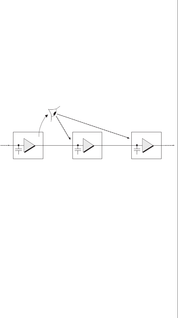
All of these multi-input transition effects can be estimated
with simple linear approximations. Unfortunately, today’s veri-
fication tools—such as STA and digital logic simulation—are
not well equipped to perform on-the-fly calculations of this
type.
Reflected parasitics
With the technologies of yesteryear, it was fairly safe to
assume that parasitic effects had limited scope and were gener-
ally only visible to logic gates in their immediate vicinity. For
example, consider the three gates shown in Figure B-22.
Traditionally, it was safe to assume that gate g2 would
buffer the output of g1 from wire w2 and gate g3. Thus, the
output g1.y would only see any parasitics such as the capaci-
tances associated with wire w1 and gate terminal g2.a.
These assumptions become less valid in the DSM domain.
Returning to the three gates shown in figure B-22, it is now
possible for some proportion of the parasitics associated with
wire w2 and gate terminal g3.a to be reflected back through
gate g2 and made visible to output g1.y. Additionally, if gate
g2 were a multi-input gate such as a 2-input XOR, then the
proportion of these parasitics reflected back through g2 might
well be state dependent; that is, they might vary depending on
the logic value presented to the other input of g2.
At the time of this writing, reflected parasitics remain rela-
tively low-order effects in the grander scheme of things. If
Deep-Submicron Delay Effects 101 ■463
ay
g1
ay
g2
ay
g3
w1 w2
Figure B-22: Reflected parasitics.
1983:
Time magazine names
the computer as Man of
the year.

history has taught us anything, however, it is to be afraid (very
afraid), because it’s not beyond the bounds of possibility that
these effects will assume a much greater significance as we
continue to meander our way through new technology nodes.
Summary
The majority of the delay effects introduced in this chap-
ter have always been present, even in the case of multimicron
technologies, but many of these effects have traditionally been
fourth or third order and were therefore considered to be rela-
tively insignificant. As device geometries plunged through the
0.5-micron barrier to 0.35 microns, some of these effects
began to assume second- and even first-order status, and their
significance continues to increase with new technology nodes
operating at lower voltage levels.
Unfortunately, many design verification tools are not
keeping pace with silicon technology. Unless these tools are
enhanced to account fully for DSM effects, designers will be
forced to use restrictive design rules to ensure that their
designs actually function. Thus, design engineers may find it
impossible to fully realize the potential of the new and excit-
ing technology developments that are becoming available.
464 ■The Design Warrior's Guide to FPGAs
1984:
1 megabyte memory
chips available for the
first time.

The Ouroboras
The Ouroboros, a symbol of a serpent or dragon devouring
its own tail and thereby forming a circle, has been employed by
a variety of ancient cultures around the world to depict eter-
nity or renewal.1The equivalent of the Ouroboros in the
electronics world would be the linear feedback shift register
(LFSR), in which outputs from a standard shift register are
cunningly manipulated and fed back into its input in such a
way as to cause the function to cycle endlessly through a
sequence of patterns.
Many-to-one implementations
LFSRs are simple to construct and are useful for a wide
variety of applications. One of the more common forms of
LFSR is formed from a simple shift register with feedback
from two or more points, called taps, in the register chain
(Figure C-1).
The taps in this example are at bit 0 and bit 2, and an easy
way to represent this is to use the notation [0,2]. All of the reg-
ister elements share a common clock input, which is omitted
from the symbol for reasons of clarity. The data input to the
LFSR is generated by XOR-ing or XNOR-ing the tap bits,
while the remaining bits function as a standard shift register.
The contents of this
appendix are abstracted
from my book Bebop to
the Boolean Boogie (An
Unconventional Guild to
Electronics, Edition 2
(ISBN 0-7506-7543-8)
with the kind permission
of the publisher.
LFSR is pronounced by
spelling it out as
“L-F-S-R.”
Linear Feedback Shift
Registers 101
Appendix
C
1Not to be confused with the Amphisbaena, a serpent in classical
mythology having a head at each end and being capable of moving in
either direction.
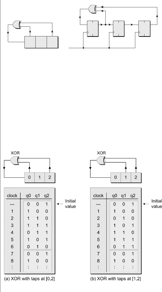
The sequence of values generated by an LFSR is deter-
mined by its feedback function (XOR versus XNOR) and tap
selection. For example, consider two 3-bit LFSRs using an
XOR feedback function, the first with taps at [0,2] and the
second with taps at [1,2] (Figure C-2).
Both LFSRs start with the same initial value, but due to
the different taps, their sequences rapidly diverge as clock
pulses are applied. In some cases, an LFSR will end up cycling
466 ■The Design Warrior's Guide to FPGAs
(a) Symbol
XOR
0 1 2
(b) Implementation
qd
dff0
qd
dff1
qd
dff2
XOR
clock
q0 q1 q2
Figure C-1. LFSR with XOR feedback path.
Figure C-2. Comparison of alternative tap selections.
1985:
CD-ROMs are used to
store computer data for
the first time.
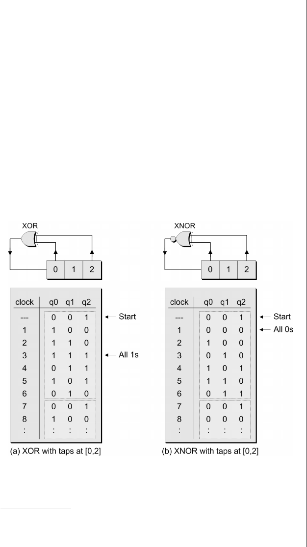
round a loop comprising a limited number of values. However,
both of the LFSRs shown in figure C-2 are said to be of maxi-
mal length because they sequence through every possible value
(excluding all of the bits being 0) before returning to their ini-
tial values.
A binary field with nbits can assume 2nunique values, but
a maximal-length LFSR with nregister bits will only sequence
through (2n– 1) values. For example, a 3-bit field can support
23= 8 values, but the 3-bit LFSRs in figure C-2 sequence
through only (23– 1) = 7 values. This is because LFSRs with
XOR feedback paths will not sequence through the “forbid-
den” value where all the bits are 0, while their XNOR
equivalents will not sequence through the value where all the
bits are 1 (Figure C-3).2
Linear Feedback Shift Registers 101 ■467
Figure C-3. Comparison of XOR versus XNOR feedback paths.
2If an LFSR somehow finds itself containing its “forbidden value,” it will
lock-up in this value until some external event occurs to extract it from
its predicament.
1989:
Pacific fiber-optic
link/cable opens
(supports 40,000
simultaneous
conversation).

More taps than you know what to do with
Each LFSR supports a number of tap combinations that
will generate maximal-length sequences. The problem is
weeding out the ones that do from the ones that don’t,
because badly chosen taps can result in the register entering a
loop comprising only a limited number of states.
Purely for my own amusement, I created a simple C pro-
gram to determine the taps for maximal-length LFSRs with 2
to 32 bits. These values are presented for your delectation and
delight in Figure C-4 (the * annotation indicates a sequence
whose length is a prime number).
The taps are identical for both XOR-based and XNOR-
based LFSRs, although the resulting sequences will, of course,
differ. As was previously noted, alternative tap combinations
468 ■The Design Warrior's Guide to FPGAs
# Bits Loop Length Taps
2
3
4
5
6
7
8
9
10
11
12
13
14
15
16
17
18
19
20
21
22
23
24
25
26
27
28
29
30
31
32
3
7
15
31
63
127
255
511
1,023
2,047
4,095
8,191
16,383
32,767
65,535
131,071
262,143
524,287
1,048,575
2,097,151
4,194,303
8,388,607
16,777,215
33,554,431
67,108,863
134,217,727
268,435,455
536,870,911
1,073,741,823
2,147,483,647
4,294,967,295
*
*
*
*
*
*
*
*
[0,1]
[0,2]
[0,3]
[1,4]
[0,5]
[0,6]
[1,2,3,7]
[3,8]
[2,9]
[1,10]
[0,3,5,11]
[0,2,3,12]
[0,2,4,13]
[0,14]
[1,2,4,15]
[2,16]
[6,17]
[0,1,4,18]
[2,19]
[1,20]
[0,21]
[4,22]
[0,2,3,23]
[2,24]
[0,1,5,25]
[0,1,4,26]
[2,27]
[1,28]
[0,3,5,29]
[2,30]
[1,5,6,31]
Figure C-4. Taps for maximal length LFSRs with 2 to 32 bits.
1990: Switzerland.
British physicist Tim
Berners-Lee sets up the
world’s first World Wide
Web server.

may also yield maximum-length LFSRs, although once again
the resulting sequences will vary. For example, in the case of a
10-bit LFSR, there are two 2-tap combinations that result in a
maximal-length sequence: [2,9] and [6,9]. There are also
twenty 4-tap combinations, twenty-eight 6-tap combinations,
and ten 8-tap combinations that satisfy the maximal-length
criteria.3
VIP! It’s important to note that the taps shown in figure
C-4 may not be the best ones for the task you have in mind
with regard to attributes such as being primitive polynomials
and having their sequences evenly distributed in “random”
space; they just happened to be the ones I chose out of the
results I generated. If you are using LFSRs for real-world tasks,
one of the best sources for determining optimum tap points is
the book Error-Correcting Codes by W. Wesley Peterson and E.
J. Weldon Jr. (published by MIT Press). Also, the CRC utility
referenced under the “Miscellaneous Stuff” section at the end
of chapter 25 might be of some interest.
One-to-many implementations
Consider the case of an 8-bit LFSR, for which the mini-
mum number of taps that will generate a maximal-length
sequence is four. In the real world, XOR gates only have two
inputs, so a 4-input XOR function has to be created using
three XOR gates arranged as two levels of logic. Even in those
cases where an LFSR does support a minimum of two taps,
there may be special reasons for you to use a greater number
such as eight (which would result in three levels of XOR
logic).
However, increasing the levels of logic in the combina-
tional feedback path can negatively impact the maximum
clocking frequency of the function. One solution is to trans-
pose the many-to-one implementations discussed above into their
one-to-many counterparts (Figure C-5).
Linear Feedback Shift Registers 101 ■469
3A much longer table (covering LFSRs with up to 168 bits) is presented in
application note XAPP052 from Xilinx.
1993:
The MOSAIC web
browser becomes
available.
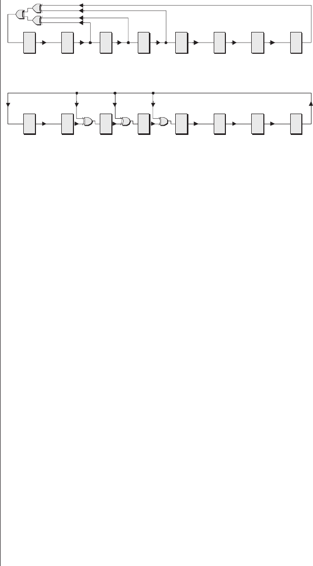
The traditional many-to-one implementation for the
eight-bit LFSR has taps at [1,2,3,7]. To convert this into its
one-to-many counterpart, the most significant tap, which is
always the most significant bit (bit 7 in this case), is fed back
directly into the least significant bit. This bit is also individu-
ally XOR’d with the other original taps (bits [1,2,3] in this
example).
Although both of these approaches result in maximal-
length LFSRs, the actual sequences of values will differ
between them. But the main point is that using the one-to-
many technique means that there is never more than one
level of combinational logic in the feedback path, irrespective
of the number of taps being employed.
Of course, FPGAs have the additional consideration that
a 4-input LUT will have the same delay for 2-, 3-, and 4-input
XOR trees. In this case, the many-to-one approach only starts
to offer advantages when you are dealing with an LFSR that
requires more than four taps.
Seeding an LFSR
One quirk with XOR-based LFSRs is that, if one happens
to find itself in the all-0s value, it will happily continue to
shift all 0s indefinitely (similarly for XNOR-based LFSRs and
470 ■The Design Warrior's Guide to FPGAs
7654320 1
(a) Many-to-one implementation
7654320 1
(b) One-to-many implementation
Figure C-5: Many-to-one versus one-to-many
implementations.
1999:
First 1 GHz
microprocessor created
by Intel.
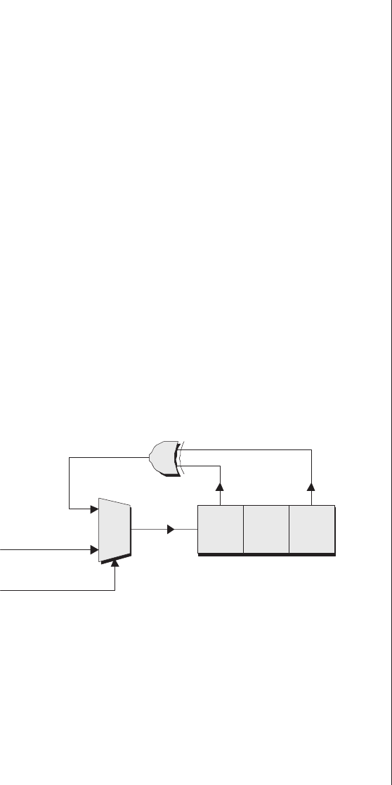
the all-1s value). This is of particular concern when power is
first applied to the circuit. Each register bit can randomly ini-
tialize containing either a logic 0 or a logic 1, and the LFSR
can therefore “wake up” containing its “forbidden” value.
For this reason, it is necessary to initialize LFSRs with a seed
value.
An interesting aspect of an LFSR based on an XNOR feed-
back path is that it does allow an all-0s value. This means that
a common clear signal to all of the LFSR’s registers can be used
to provide an XNOR LFSR with a seed value of all 0s.
One method for loading a specific seed value is to use regis-
ters with reset or set inputs. A single control signal can be
connected to the reset inputs on some of the registers and the
set inputs on others. When this control signal is placed in its
active state, the LFSR will load with a hard-wired seed value.
With regard to certain applications, however, it is desirable to
be able to vary the seed value. One technique for achieving
this is to include a multiplexer at the input to the LFSR
(Figure C-6).
When the multiplexer’s seed-data input is selected, the
device functions as a standard shift register, and any desired
seed value can be loaded. After loading the seed value, the
feedback path is selected and the device returns to its LFSR
mode of operation.
Linear Feedback Shift Registers 101 ■471
XOR
0 1 2
seed-data
select
MUX
Figure C-6. Circuit for loading alternative seed values.
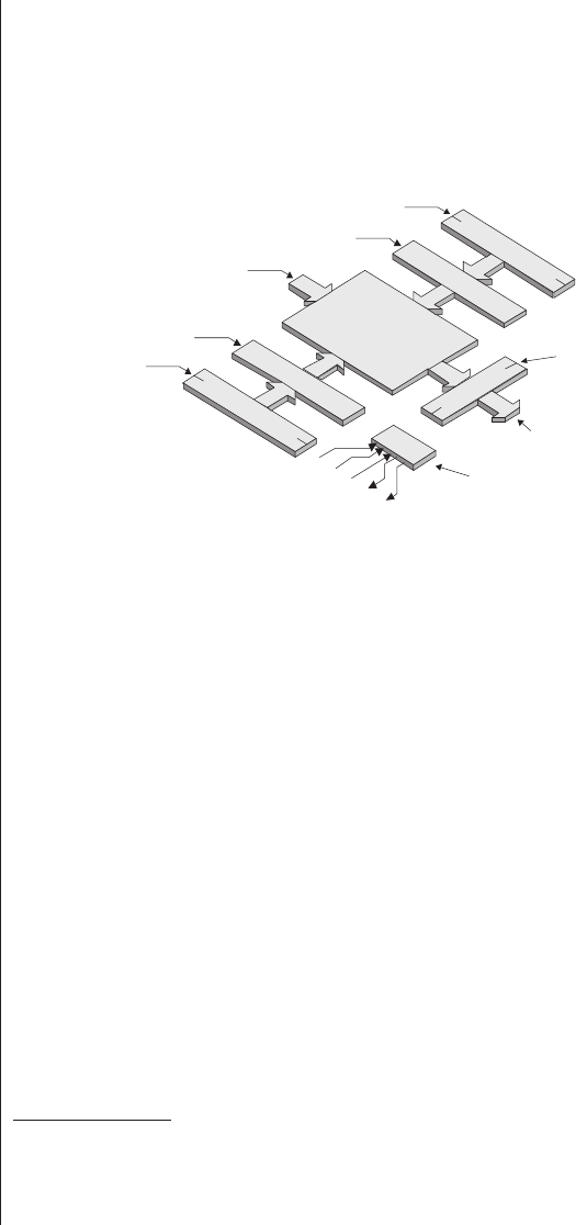
FIFO applications
The fact that an LFSR generates an unusual sequence of
values is irrelevant in many applications. For example, let’s
consider a 4-bit-wide, 16-word-deep FIFO memory function
(Figure C-7).
In addition to some control logic and an output register,
the FIFO contains a read pointer and a write pointer. These
pointers are 4-bit registers whose outputs are processed by 4:16
decoders to select one of the 16 words in the memory array.
The read and write pointers chase each other around the
memory array in an endless loop. An active edge on the write
input causes any data on the input bus to be written into the
word pointed to by the write pointer; the write pointer is then
incremented to point to the next empty word. Similarly, an
active edge on the read input causes the data in the word
pointed to by the read pointer to be copied into the output
register; the read pointer is then incremented to point to the
next word containing data.4(There would also be some logic
472 ■The Design Warrior's Guide to FPGAs
write
read
reset
full
empty
16-Word
RAM
Array
Data-In[3:0]
4:16 Decoder
Write Pointer
Data-Out[3:0]
Control Logic
4:16 Decoder
Read Pointer
Output
Register
Figure C-7. A 16-word FIFO function.
4These discussions assume write-and-increment and read-and-increment
techniques however, some FIFOs employ an increment-and-write and
increment-and-read approach.
to detect when the FIFO is full or empty, but this is irrelevant
to our discussions here.)
The write and read pointers for a 16-word FIFO are often
implemented using 4-bit binary counters. However, a
moment’s reflection reveals that there is no intrinsic advan-
tage to a binary sequence for this particular application, and
the sequence generated by a 4-bit LFSR will serve equally well.
In fact, the two functions operate in a very similar manner as is
illustrated by their block diagrams (Figure C-8).
It doesn’t take more than a few seconds before we realize
that the only difference between these two diagrams is their
names. The point is that the combinational feedback logic for
the 4-bit binary counter requires a number of AND and OR
gates, while the feedback logic for the 4-bit LFSR consists of
a single, 2-input XOR gate. This means that the LFSR requires
fewer tracks and is more efficient in terms of silicon real
estate.
Additionally, the LFSR’s feedback only passes through a
single level of logic, while the binary counter’s feedback passes
through multiple levels of logic. This means that the new data
value is available sooner for the LFSR, which can therefore be
Linear Feedback Shift Registers 101 ■473
Clock
Registers
Feedback
Logic
Current
Value
Next
Value
(a) 4-bit binar
y
counter
Clock
Registers
Feedback
Logic
Current
Value
Next
Value
(b) 4-bit LFSR
Figure C-8. Binary counter versus LFSR.
clocked at a higher frequency. These differentiations become
even more pronounced for FIFOs with more words requiring
pointers with more bits. Thus, LFSR’s provide an interesting
option for the discerning designer of FIFOs.5
Modifying LFSRs to sequence 2nvalues
The sole downside to using 4-bit LFSRs in the FIFO sce-
nario above is that they will sequence through only 15 values
(24– 1), as compared to the binary counter’s sequence of 16
values (24). Depending on the application, the design engi-
neers may not regard this to be a major problem, especially in
the case of larger FIFOs. However, if it is required for an LFSR
to sequence through every possible value, then there is a sim-
ple solution (Figure C-9).
For the value where all of the bits are 0 to appear, the pre-
ceding value must have comprised a logic 1 in the
474 ■The Design Warrior's Guide to FPGAs
Figure C-9. LFSR modified to sequence 2nvalues.
5So do Gray Counters, but that will have to be a topic for another time.

most significant bit (MSB)6and logic 0s in the remaining bit
positions. In an unmodified LFSR, the next clock would result
in a logic 1 in the least significant bit (LSB) and logic 0s in the
remaining bit positions. However, in the modified LFSR shown
in figure C-9, the output from the NOR is a logic 0 for every
case but two: the value preceding the one where all the bits are
0 and the value where all the bits are 0. These two values force
the NOR’s output to a logic 1, which inverts the usual output
from the XOR. This in turn causes the sequence first to enter
the all-0s value and then to resume its normal course. (In the
case of LFSRs with XNOR feedback paths, the NOR can be
replaced with an AND, which causes the sequence to cycle
through the value where all of the bits are 1.)
Accessing the previous value
In some applications, it is required to make use of a regis-
ter’s previous value. For example, in certain FIFO
implementations, the “full” condition is detected when the
write pointer is pointing to the location preceding the location
pointed to by the read pointer.7This implies that a comparator
must be used to compare the current value in the write pointer
with the previous value in the read pointer. Similarly, the
“empty” condition may be detected when the read pointer is
pointing to the location preceding the location pointed to by
the write pointer. This implies that a second comparator must
be used to compare the current value in the read pointer with
the previous value in the write pointer.
In the case of binary counters (assuming that, for some rea-
son, we decided to use them for a FIFO application), there are
two techniques by which the previous value in the sequence
may be accessed. The first requires the provision of an addi-
Linear Feedback Shift Registers 101 ■475
MSB and LSB are pro-
nounced by spelling
them out as “M-S-B” and
“L-S-B”, respectively.
6As is often the case with any form of shift register, the MSB in these
examples is taken to be on the right-hand side of the register and the LSB
is taken to be on the left-hand side (this is opposite to the way we usually
do things).
7Try saying that quickly!
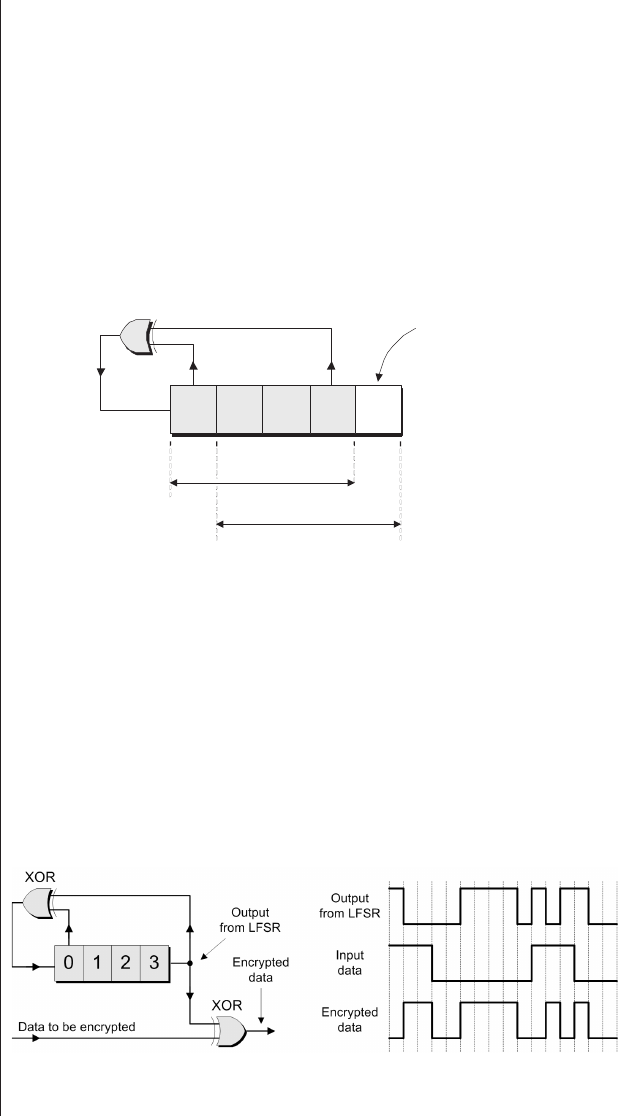
tional set of shadow registers. Every time the counter is
incremented, its current contents are first copied into the
shadow registers. Alternatively, a block of combinational logic
can be used to decode the previous value from the current
value. Unfortunately, both of these techniques involve a sub-
stantial overhead in terms of additional logic. By comparison,
LFSRs inherently remember their previous value. All that is
required is the addition of a single register bit appended to
the MSB (Figure C-10).
Encryption and decryption applications
The unusual sequence of values generated by an LFSR can
be gainfully employed in the encryption (scrambling) and
decryption (unscrambling) of data. A stream of data bits can
be encrypted by XOR-ing them with the output from an LFSR
(Figure C-11).
476 ■The Design Warrior's Guide to FPGAs
XOR
0 1 2 3
Current Value
Previous Value
Additional register
bit appended to
MSB of main LFSR
Figure C-10. Accessing an LFSR’s previous value.
Figure C-11. Data encryption using an LFSR.
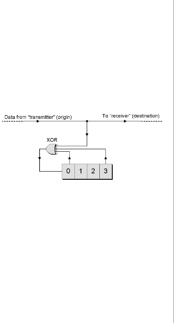
The stream of encrypted data bits seen by a receiver can be
decrypted by XOR-ing them with the output of an identical
LFSR. This is obviously a very trivial form of encryption that
isn’t very secure, but it’s cheap and cheerful, and it may be use-
ful in certain applications.
Cyclic redundancy check applications
A traditional application for LFSRs is in cyclic redundancy
check (CRC) calculations, which can be used to detect errors
in data communications. The stream of data bits being trans-
mitted is used to modify the values being fed back into an
LFSR (Figure C-12).
The final CRC value stored in the LFSR, known as a
checksum, is dependent on every bit in the data stream. After
all of the data bits have been transmitted, the transmitter
sends its checksum value to the receiver. The receiver contains
an identical CRC calculator and generates its own checksum
value from the incoming data. Once all of the data bits have
arrived, the receiver compares its internally generated check-
sum value with the checksum sent by the transmitter to
determine whether any corruption occurred during the course
of the transmission.
This form of error detection is very efficient in terms of the
small number of bits that have to be transmitted in addition to
the data. However, the downside is that you don’t know if
Linear Feedback Shift Registers 101 ■477
CRC is pronounced
by spelling is out as
“C-R-C.”
Figure C-12. CRC calculations.

there was an error until the end of the transmission (and if
there was an error, you have to repeat the entire
transmission).
In the real world, a 4-bit CRC calculator would not be
considered to provide sufficient confidence in the integrity of
the transmitted data because it can only represent (24–1)=
15 unique values. This leads to a problem called aliasing,in
which the final CRC value is the same as was expected, but
this value was actually caused by multiple errors canceling
each other out. As the number of bits in a CRC calculator
increases, however, the probability that multiple errors will
cause identical checksum values approaches zero. For this rea-
son, CRC calculators typically use 16 bits (which can
accommodate 65,535 unique values) or more.
There are a variety of standard communications protocols,
each of which specifies the number of bits employed in their
CRC calculations and the taps to be used. The taps are
selected such that an error in a single data bit will cause the
maximum possible disruption to the resulting checksum value.
Thus, in addition to being referred to as maximal length, these
LFSRs may also be qualified as maximal displacement.
In addition to checking data integrity in communications
systems, CRCs find a wide variety of other uses, for example,
the detection of computer viruses. For the purposes of this dis-
cussion, a computer virus may be defined as a self-replicating
program released into a computer system for a number of pur-
poses. These purposes range from the simply mischievous,
such as displaying humorous or annoying messages, to the
downright nefarious, such as corrupting data or destroying (or
subverting) the operating system.
One mechanism by which a computer virus may both hide
and propagate itself is to attach itself to an existing program.
Whenever that program is executed, it first triggers the virus
to replicate itself, yet a cursory check of the system shows only
the expected files to be present. In order to combat this form
of attack, a unique checksum can be generated for each pro-
gram on the system, where the value of each checksum is
478 ■The Design Warrior's Guide to FPGAs

based on the binary instructions forming the program with
which it is associated. At some later date, an antivirus program
can be used to recalculate the checksum values for each pro-
gram and to compare them to the original values. A difference
in the two values associated with a program may indicate that
a virus has attached itself to that program.8
Data compression applications
The CRC calculators discussed above can also be used in a
data compression role. One such application is found in the
circuit board test strategy known as functional test. The board,
which may contain thousands of components and tracks, is
plugged into a functional tester by means of its edge connec-
tor, which may contain hundreds of pins.
The tester applies a pattern of signals to the board’s inputs,
allows sufficient time for any effects to propagate around the
board, and then compares the actual values seen on the out-
puts with a set of expected values stored in the system. This
process is repeated for a series of input patterns, which may
number in the tens or hundreds of thousands.
If the board fails the preliminary tests, a more sophisticated
form of analysis known as guided probe may be employed to
identify the cause of the failure. In this case, the tester
instructs the operator to place the probe at a particular loca-
tion on the board, and then the entire sequence of test
patterns is rerun. The tester compares the actual sequence of
values seen by the probe with a sequence of expected values
that are stored in the system. This process (placing the probe
and running the tests) is repeated until the tester has isolated
the faulty component or track.
Linear Feedback Shift Registers 101 ■479
8Unfortunately, the creators of computer viruses are quite sophisticated,
and some viruses are armed with the ability to perform their own CRC
calculations. When a virus of this type attaches itself to a program, it can
pad itself with dummy binary values, which are selected so as to cause an
antivirus program to return a checksum value identical to the original.

A major consideration when supporting a guided probe
strategy is the amount of expected data that must be stored.
Consider a test sequence comprising 10,000 patterns driving a
board containing 10,000 tracks. If the data were not com-
pressed, the system would have to store 10,000 bits of
expected data per track, which amounts to 100 million bits of
data for the board. Additionally, for each application of the
guided probe, the tester would have to compare the 10,000
data bits observed by the probe with the 10,000 bits of
expected data stored in the system. Thus, using data in an
uncompressed form is an expensive option in terms of storage
and processing requirements.
One solution to these problems is to employ LFSR-based
CRC calculators. The sequence of expected values for each
track can be passed through a 16-bit CRC calculator imple-
mented in software. Similarly, the sequence of actual values
seen by the guided probe can be passed through an identical
CRC calculator implemented in hardware. In this case, the
calculated checksum values are also known as signatures, and a
guided probe process based on this technique is known as sig-
nature analysis. Irrespective of the number of test patterns
used, the system has to store only two bytes of data for each
track. Additionally, for each application of the guided probe,
the tester has to compare only the two bytes of data gathered
by the probe with two bytes of expected data stored in the sys-
tem. Thus, compressing the data results in storage
requirements that are orders of magnitude smaller and com-
parison times that are orders of magnitude faster than the
uncompressed data approach.
Built-in self-test applications
One test strategy that may be employed in complex ICs is
that of built-in self-test (BIST). Devices using BIST contain
special test-generation and result-gathering circuits, both of
which may be implemented using LFSRs (Figure C-13).
The LFSR forming the test generator is used to create a
sequence of test patterns, while the LFSR forming the results
480 ■The Design Warrior's Guide to FPGAs
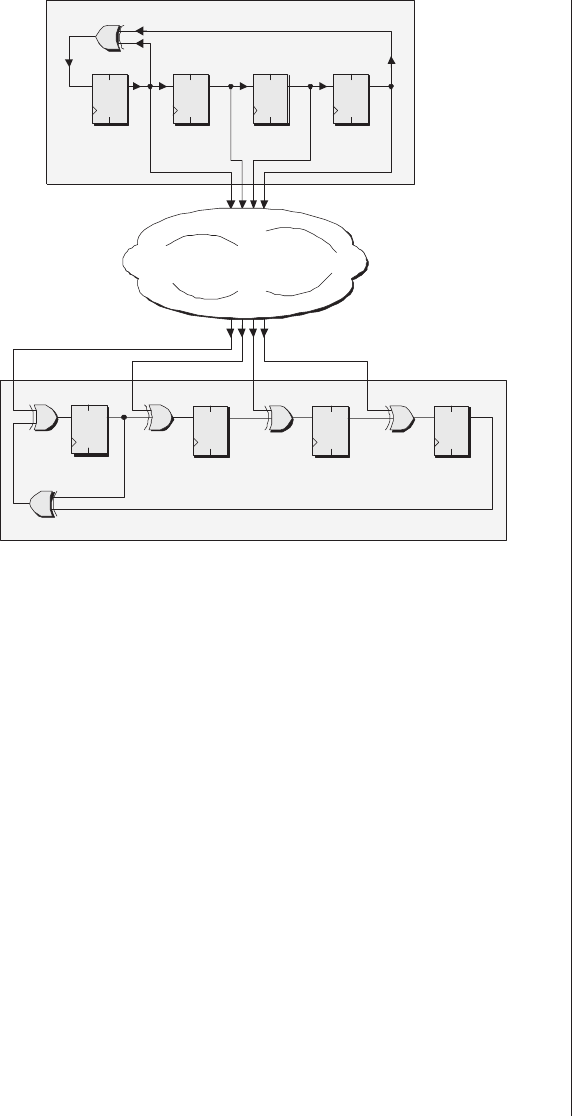
gatherer is used to capture the results. Observe that the
results-gathering LFSR features modifications that allow it to
accept parallel data.
Additional circuitry would be required to provide a way to
load new seed values into the test generator and to access the
final values in the results gatherer. This logic is not shown
here for purposes of simplicity.
Note that the two LFSRs are not obliged to contain the
same number of bits because the number of inputs to the logic
being tested may be different to the number of outputs coming
from that logic.
Also note that all of the flip-flops in the test generator
would share a common clock. Similarly, all of the flip-flops in
the results gatherer would also share a common clock. These
two clocks might be common or they might be distinct (in the
latter case they would be synchronized in some way). The
Linear Feedback Shift Registers 101 ■481
qd qd
Dff-TG1 Dff-TG2
qd
Dff-TG3
qd
Dff-TG0
XOR Test Generator
XOR
qd
Dff-RG0
XOR XOR
qd
Dff-RG1
XOR
qd
Dff-RG2
XOR
qd
Dff-RG3
Results Gatherer
Logic Being Tested
Clock signals to
flip-flops omitted
for purposes of
simplicity
*
****
****
Figure C-13. BIST.

clock signals are not shown in figure C-13 so as to keep things
simple.
Pseudorandom-number-generation applications
Many computer programs rely on an element of random-
ness. Computer games such as Space Invaders employ random
events to increase the player’s enjoyment. Graphics programs
may exploit random numbers to generate intricate patterns.
All forms of computer simulation may utilize random numbers
to represent the real world more accurately. For example, digi-
tal logic simulations (see also Chapter 19) may benefit from
the portrayal of random stimulus such as external interrupts.
Random stimulus can result in more realistic design verifica-
tion, which can uncover problems that may not be revealed
by more structured tests.
Random-number generators can be constructed in both
hardware and software. The majority of these generators are
not truly random, but they give the appearance of being ran-
dom and are therefore said to be pseudorandom. In reality,
pseudorandom numbers have an advantage over truly random
numbers because the majority of computer applications typi-
cally require repeatability. For example, a designer repeating a
digital simulation would expect to receive identical answers to
those from the previous run. However, designers also need the
ability to modify the seed value of the pseudorandom-number
generator so as to spawn different sequences of values as
required.
There are a variety of methods available for generating
pseudorandom numbers, one of which is to use an LFSR
whose tap values have been selected so as to provide a rea-
sonably good pseudorandom source.
Last but not least
LFSRs are simple to construct and are useful for a wide
variety of applications, but be warned that choosing the
optimal polynomial (which ultimately boils down to selecting
the tap points) for a particular application is a task that is
482 ■The Design Warrior's Guide to FPGAs

usually reserved for a master of the mystic arts, not to mention
that the maths can be hairy enough to make a grown man
break down and cry (and don’t even get me started on the
subject of cyclotomic polynomials,9which are key to the
tap-selection process).
Linear Feedback Shift Registers 101 ■483
9Mainly because I haven’t got the faintest clue what a cyclotomic polynomial
is!

ACM (adaptive computing machine)—A revolutionary new
form of digital integrated circuit (IC) featuring a coarse-
grained algorithmic element node-based architecture that
can be reconfigured (adapted) hundreds of thousands of
times a second.
Adaptive computing machine—see ACM
Address bus—A unidirectional set of signals used by a proces-
sor (or similar device) to point to memory locations in
which it is interested.
A/D (analog to digital)—The process of converting an analog
value into its digital equivalent.
Analog—A continuous value that most closely resembles the
real world and can be as precise as the measuring technique
allows.
Analog circuit—A collection of components used to process
or generate analog signals.
Analog to digital—see A/D
Analogue—The way they spell “analog” in England.
Antifuse technology—A technology used to create program-
mable integrated circuits (ICs) whose programmable
elements are based on conductive links called antifuses.
When an engineer purchases a programmable device based
on antifuses, none of the links is initially intact. Individual
links can be selectively “grown” by applying pulses of rela-
tively high voltage and current to the device’s inputs.
Application-specific integrated circuit—see ASIC
Glossary

Application-specific standard part—see ASSP
ASIC (application-specific integrated circuit)—A custom-
built integrated circuit (IC) designed to address a specific
application. Such a device can contain hundreds of mil-
lions of logic gates and can be used to create incredibly
large and complex functions. Similar to an ASSP, except
that an ASIC is designed and built to order for use by a
specific company.
ASIC cell—A logic function in the cell library defined by the
manufacturer of an ASIC.
Assertions/properties—The term property comes from the
model-checking domain and refers to a specific functional
behavior of the design that you want to (formally) verify
(e.g., “after a request, we expect a grant within 10 clock
cycles”). By comparison, the term assertion stems from the
simulation domain and refers to a specific functional
behavior of the design that you want to monitor during
simulation (and flag violations if that assertion “fires”).
Today, with the use of formal tools and simulation tools in
unified environments and methodologies, the terms prop-
erty and assertion tend to be used interchangeably.
ASSP (application-specific standard part)—A custom-built
integrated circuit (IC) designed to address a specific applica-
tion. Such a device can contain hundreds of millions of
logic gates and can be used to create incredibly large and
complex functions. Similar to an application-specific inte-
grated circuit (ASIC), except that an ASSP is marketed to
multiple customers for inclusion in their products.
Asynchronous—A signal whose data is acknowledged or
acted upon immediately and does not depend on a clock
signal.
Ball grid array—see BGA
Bare die—An unpackaged integrated circuit (IC).
486 ■The Design Warrior's Guide to FPGAs

Basic cell—A predefined group of unconnected transistors and
resistors. This group is replicated across the surface of a
gate-array form of ASIC.
Bebop—A form of music characterized by fast tempos and agi-
tated rhythms that became highly popular in the decade
following World War II.
BGA (ball grid array)—A packaging technology similar to a
pad grid array (PGA), in which a device’s external connec-
tions are arranged as an array of conducting pads on the
base of the package. In the case of a ball grid array, how-
ever, small balls of solder are attached to the conducting
pads.
BiCMOS (bipolar-CMOS)—(1) A technology in which the
logical function of each logic gate is implemented using
low-power CMOS, while the output stage of each logic
gate is implemented using high-drive bipolar transistors.
(2) A device whose internal logic gates are implemented
using low-power CMOS, but whose output pins are driven
by high-drive bipolar transistors.
Binary digit—A numeral in the binary scale of notation. A
binary digit (typically abbreviated to “bit”) can adopt one
of two values: 0 or 1.
Binary encoding—A form of state assignment for state
machines that requires the minimum number of state vari-
ables.
Binary logic—Digital logic gates based on two distinct voltage
levels. The two voltages are used to represent the binary
values 0 and 1 along with their logical equivalents False
and True.
Bipolar junction transistor—see BJT
BIST (built-in self-test)—A test strategy in which additional
logic is built into a component, thereby allowing it to test
itself.
Bit—Abbreviation of binary digit. A binary digit can adopt one
of two values: 0 or 1.
Glossary ■487

Bit file—see Configuration file
BJTs (bipolar junction transistors)—A family of transistors.
Bobble—A small circle used on the inputs to a logic-gate
symbol to indicate an active low input or control or on the
outputs to indicate a negation (inversion) or complemen-
tary signal. Some engineers prefer to use the term bubble.
Boolean algebra—A mathematical way of representing logical
expressions.
Built-in self-test—see BIST
Bus—A set of signals performing a common function and car-
rying similar data. Typically represented using vector
notation: for example, an 8-bit database might be named
data[7:0].
Byte—A group of eight binary digits, or bits.
Cache memory—A small, high-speed memory (usually imple-
mented in SRAM) used to buffer the central processing
unit from any slower, lower-cost memory devices such as
DRAM. The high-speed cache memory is used to store the
active instructions and data1associated with a program,
while the bulk of the instructions and data resides in the
slower memory.
Capacitance—A measure of the ability of two adjacent con-
ductors separated by an insulator to hold a charge when a
voltage differential is applied between them. Capacitance
is measured in units of farads.
Cell—see ASIC cell, Basic cell, Cell library, and Memory cell
Cell library—The collective name for the set of logic func-
tions defined by the manufacturer of an application-specific
integrated circuit (ASIC). The designer decides which types
of cells should be realized and connected together to make
the device perform its desired function.
488 ■The Design Warrior's Guide to FPGAs
1In this context, “active” refers to data or instructions that a program is
currently using, or which the operating system believes that the program
will want to use in the immediate future.

Central processing unit—see CPU
Ceramic—An inorganic, nonmetallic material, such as alu-
mina, beryllia, steatite, or forsterite, which is fired at a high
temperature and is often used in electronics as a substrate
(base layer) or to create component packages.
CGA (column grid array)—A packaging technology similar
toapad grid array (PGA), in which a device’s external con-
nections are arranged as an array of conducting pads on the
base of the package. In the case of a column grid array,
however, small columns of solder are attached to the con-
ducting pads.
Channel—(1) The area between two arrays of basic cells in a
channeled gate array. (2) The gap between the source and
drain regions in a MOSFET transistor.
Channeled gate array—An application-specific integrated circuit
(ASIC) organized as arrays of basic cells. The areas
between the arrays are known as channels.
Channelless gate array—An application-specific integrated circuit
(ASIC) organized as a single large array of basic cells. May
also be referred to as a “sea-of-cells” or a “sea-of-gates”
device.
Checksum—The final cyclic-redundancy check (CRC) value
stored in a linear feedback shift register (LFSR) (or software
equivalent). Also known as a “signature” in the guided-
probe variant of a functional test.
Chemical mechanical polishing—see CMP
Chip—Popular name for an integrated circuit (IC).
Chip scale package—see CSP
Circuit board—The generic name for a wide variety of inter-
connection techniques, which include rigid, flexible, and
rigid-flex boards in single-sided, double-sided, multilayer,
and discrete wired configurations.
CLB (configurable logic block)—The Xilinx term for the
next logical partition/entity above a slice. Some Xilinx
Glossary ■489

FPGAs have two slices in each CLB, while others have
four. See also LAB,LC,LE, and Slice.
Clock tree—This refers to the way in which a clock signal is
routed throughout a chip. This is called a “clock tree”
because the main clock signal branches again and again
(register elements like flip-flops can be considered the
“leaves” on the end of the branches). This structure is used
to ensure that all of the flip-flops see the clock signal as
close together as possible.
CMOS (complementary metal oxide semiconductor)—Logic
gates constructed using a mixture of NMOS and PMOS
transistors connected together in a complementary man-
ner.
CMP (chemical mechanical polishing)—A process used to
replanarize a wafer—smoothing and flattening the surface
by polishing out the “bumps” caused by adding a metaliza-
tion (tracking) layer.
Column grid array—see CGA
Combinatorial logic—see Combinational logic
Combinational logic—A digital logic function formed from a
collection of primitive logic gates (AND, OR, NAND,
NOR, etc.), where any output values from the function
are directly related to the current combination of values
on its inputs. That is, any changes to the signals being
applied to the inputs to the function will immediately start
to propagate (ripple) through the gates forming the func-
tion until their effects appear at the outputs from the
function. Some folks prefer to say “combinatorial logic.”
See also Sequential logic.
Complementary output—Refers to a function with two out-
puts carrying complementary (opposite) logical values.
One output is referred to as the true output and the other
as the complementary output.
Complex programmable logic device—see CPLD
Conditioning—see Signal conditioning
490 ■The Design Warrior's Guide to FPGAs

Configurable logic block—see CLB
Configuration commands—Instructions in a configuration file
that tell the device what to do with the associated configu-
ration data. See also Configuration data and Configuration
file.
Configuration data—Bits in a configuration file that are used
to define the state of programmable logic elements directly.
See also Configuration commands and Configuration file.
Configuration file—A file containing the information that
will be uploaded into the FPGA in order to program (con-
figure) it to perform a specific function. In the case of
SRAM-based FPGAs, the configuration file contains a
mixture of configuration data and configuration commands.
When the configuration file is in the process of being
loaded into the device, the information being transferred is
referred to as the configuration bitstream. See also Configura-
tion commands and Configuration data.
Constraints—In the context of formal verification, the term
constraint derives from the model-checking space. Formal
model checkers consider all possible allowed input combi-
nations when performing their magic and working on a
proof. Thus, there is often a need to constrain the inputs to
their legal behavior; otherwise, the tool would report false
negatives, which are property violations that would not
normally occur in the actual design.
Core—see Hard core and Soft core
Corner condition—see Corner case
Corner case—A hard-to-exercise or hard-to-reach functional
condition associated with the design.
CPLD (complex PLD)—A device that contains a number of
SPLD (typically PAL) functions sharing a common pro-
grammable interconnection matrix.
CPU (central processing unit)—The brain of a computer
where all of the decision making and number crunching
are performed.
Glossary ■491

CRC (cyclic redundancy check)—A calculation used to
detect errors in data communications, typically performed
using a linear feedback shift register (LFSR). Similar calcula-
tions may be used for a variety of other purposes such as
data compression.
CSP (chip scale package)—An integrated circuit (IC) packag-
ing technique in which the package is only fractionally
larger than the silicon die.
Cyclic redundancy check—see CRC
D/A (digital to analog)—The process of converting a digital
value into its analog equivalent.
Data bus—A bidirectional set of signals used by a computer
to convey information from a memory location to the cen-
tral processing unit and vice versa. More generally, a set of
signals used to convey data between digital functions.
Data-path function—A well-defined function such as an
adder, counter, or multiplier used to process digital data.
DCM (digital clock manager)—Some FPGA clock managers
are based on phase-locked loops (PLLs), while others are
based on digital delay-locked loops (DLLs). The term DCM
is used by Xilinx to refer to an advanced clock manager
that is a superset of a DLL. See also DLL and PLL.
Declarative—In the context of formal verification, the term
declarative refers to an assertion/property/event/constraint
that exists within the structural context of the design and
is evaluated along with all of the other structural elements
in the design (for example, a module that takes the form
of a structural instantiation). Another way to view this is
that a declarative assertion/property is always “on/active,”
unlike its procedural counterpart that is only “on/active”
when a specific path is taken/executed through the HDL
code.
Deep submicron—see DSM
Delay-locked loop—see DLL
492 ■The Design Warrior's Guide to FPGAs

DeMorgan transformation—The transformation of a Boolean
expression into an alternate, and often more convenient,
form.
Die—An unpackaged integrated circuit (IC). In this case, the
plural of die is also die (in much the same way that “a shoal
of herring” is the plural of “herring”).
Digital—A value represented as being in one of a finite
number of discrete states called quanta. The accuracy of a
digital value is dependent on the number of quanta used to
represent it.
Digital circuit—A collection of logic gates used to process or
generate digital signals.
Digital clock manager—see DCM
Digital delay-locked loop—see DLL
Digital signal processing/processor—see DSP
Digital to analog—see D/A
Diode—A two-terminal device that conducts electricity in
only one direction; in the other direction it behaves like
an open switch. These days the term diode is almost
invariably taken to refer to a semiconductor device,
although alternative implementations such as vacuum
tubes are available.
Discrete device—Typically taken to refer to an electronic
component such as a resistor, capacitor, diode, or transistor
that is presented in an individual package. More rarely, the
term may be used in connection with a simple integrated
circuit (IC) containing a small number of primitive logic
gates.
DLL (digital delay-locked loop)—Some FPGA clock manag-
ers are based on phase-locked loops (PLLs), while others are
based on digital delay-locked loops (DLLs). DLLs are, by defi-
nition, digital in nature. The proponents of DLLs say that
they offer advantages in terms of precision, stability, power
management, noise insensitivity, and jitter performance. I
Glossary ■493

have no clue as to why these aren’t called DDLLs. See
also PLL.
DSM (deep submicron)—Typically taken to refer to inte-
grated circuit (ICs) containing structures that are smaller
than 0.5 microns (one half of one millionth of a meter).
DSP (1) (digital signal processing)—The branch of electron-
ics concerned with the representation and manipulation of
signals in digital form. This form of processing includes
compression, decompression, modulation, error correction,
filtering, and otherwise manipulating audio (voice, music,
etc.), video, image, and other such data for such applica-
tions like telecommunications, radar, and image
processing (including medical imaging). (2) (digital signal
processor)—A special form of microprocessor that has
been designed to perform a specific processing task on a
specific type of digital data much faster and more effi-
ciently than can be achieved using a general-purpose
microprocessor.
Dynamic formal verification—Some portions of a design are
going to be difficult to verify via simulation because they
are deeply buried in the design, making them difficult to
control from the primary inputs. In order to address this,
some verification solutions use simulation to reach a cor-
ner case and then automatically pause the simulator and
invoke a static formal verification engine to evaluate that
corner case exhaustively. This combination of simulation
and traditional static formal verification is referred to as
dynamic formal verification. See also Corner case,Formal
verification, and Static formal verification.
Dynamic RAM—see DRAM
ECL (emitter-coupled logic)—Logic gates implemented using
particular configurations of Bipolar junction transistors
(BJTs).
494 ■The Design Warrior's Guide to FPGAs

Edge sensitive—An input to a logic function that only affects
the function when it transitions from one logic value to
another.
EEPROM or E2PROM (electrically erasable programmable
read-only memory)—A memory integrated circuit (IC)
whose contents can be electrically programmed by the
designer. Additionally, the contents can be electrically
erased, allowing the device to be reprogrammed.
Electrically erasable programmable read-only memory—see
EEPROM
Emitter-coupled logic—see ECL
EPROM (erasable programmable read-only memory)—A
memory integrated circuit (IC) whose contents can be elec-
trically programmed by the designer. Additionally, the
contents can be erased by exposing the die to ultraviolet
(UV) light through a quartz window mounted in the top of
the component’s package.
Equivalency checking—see Formal verification
Equivalent gate—An ASIC-based concept in which each type
of logic function is assigned an equivalent gate value for
the purposes of comparing functions and devices. However,
the definition of an equivalent gate varies depending on
whom you’re talking to.
Erasable programmable read-only memory—see EPROM
Event—In the context of formal verification, an event is simi-
lar to an assertion/property, and in general events may be
considered a subset of assertions/properties. However,
while assertions/properties are typically used to trap unde-
sirable behavior, events may be used to specify desirable
behavior for the purposes of functional coverage analysis.
Falling edge—see Negative edge
FET (field-effect transistor)—A transistor whose control (or
“gate”) signal is used to create an electromagnetic field
that turns the transistor on or off.
Glossary ■495

Field-effect transistor—see FET
Field-programmable gate array—see FPGA
Field-programmable interconnect chip—see FPIC2
Field-programmable interconnect device—see FPID
FIFO (first in first out)—A special memory device or func-
tion in which data is read out in the same order that it was
written in.
Finite state machine—see FSM
Firm IP—In the context of an FPGA, the term firm IP refers
to a library of high-level functions. Unlike their soft IP
equivalents, however, these functions have already been
optimally mapped, placed, and routed into a group of pro-
grammable logic blocks (possibly combined with some
hard IP blocks like multipliers, etc.). One or more copies
of each predefined firm IP block can be instantiated
(called up) into the design as required. See also Hard IP
and Soft IP.
Firmware—Refers to programs or sequences of instructions
that are loaded into nonvolatile memory devices.
First in first out—see FIFO
FLASH memory—An evolutionary technology that com-
bines the best features of the EPROM and E2PROM
technologies. The name FLASH is derived from the tech-
nology’s fast reprogramming time compared to EPROM.
Formal verification—In the not-so-distant past, the term
formal verification was considered synonymous with equiva-
lency checking for the majority of design engineers. In this
context, an equivalency checker is a tool that uses formal
(rigorous mathematical) techniques to compare two differ-
ent representations of a design—say an RTL description
with a gate-level netlist—to determine whether or not
they have the same input-to-output functionality. In fact,
496 ■The Design Warrior's Guide to FPGAs
2FPIC is a trademark of Aptix Corporation.

equivalency checking may be considered to be a subclass of
formal verification called model checking, which refers to
techniques used to explore the state space of a system to
test whether or not certain properties, typically specified as
“assertions,” are true. See also Static formal verification and
Dynamic formal verification.
FPGA (field-programmable gate array)—A type of digital
integrated circuit (IC) that contains configurable (program-
mable) blocks of logic along with configurable
interconnect between these blocks. Such a device can be
configured (programmed) by design engineers to perform a
tremendous variety of different tasks.
FPIC (field-programmable interconnect chip)3—An alter-
nate, proprietary name for a field-programmable interconnect
device (FPID).
FPID (field-programmable interconnect device)—A device
used to connect logic devices together that can be dynami-
cally reconfigured in the same way as standard
SRAM-based FPGAs. Because each FPID may have
around 1,000 pins, only a few such devices are typically
required on a circuit board.
FR4—The most commonly used insulating base material for
circuit boards. FR4 is made from woven glass fibers that are
bonded together with an epoxy. The board is cured using a
combination of temperature and pressure, which causes the
glass fibers to melt and bond together, thereby giving the
board strength and rigidity. The first two characters stand
for “flame retardant,” and you can count the number of
people who know what the “4” stands for on the fingers of
one hand. FR4 is technically a form of fiberglass, and some
people do refer to these composites as fiberglass boards or
fiberglass substrates, but not often.
Full custom—An application-specific integrated circuit (ASIC) in
which the design engineers have complete control over
Glossary ■497
3FPIC is a trademark of Aptix Corporation.

every mask layer used to fabricate the device. The ASIC
vendor does not provide a cell library or prefabricate any
components on the substrate.
Functional latency—Refers to the fact that, at any given
time, only a portion of the logic functions in a device or
system are typically active (doing anything useful).
Fuse—see Fusible link technology and Antifuse technology
Fusible-link technology—A technology used to create pro-
grammable integrated circuits (ICs) whose programmable
elements are based on microscopically small fusible links.
When an engineer purchases a programmable device based
on fusible links, all of the fuses are initially intact. Individ-
ual fuses can be selectively removed by applying pulses of
relatively high voltage and current to the device’s inputs.
FSM (finite state machine)—The actual implementation (in
hardware or software) of a function that can be considered
to consist of a finite set of states through which it
sequences.
GAL (generic array logic)—A variation on a PAL device
from a company called Lattice Semiconductor Corpora-
tion.4
Garbage in garbage out—see GIGO
Gate array—An application-specific integrated circuit (ASIC) in
which the manufacturer prefabricates devices containing
arrays of unconnected components (transistors and resis-
tors) organized in groups called basic cells. The designer
specifies the function of the device in terms of cells from
the cell library and the connections between them, and
the manufacturer then generates the masks used to create
the metalization layers.
Generic array logic—see GAL
Geometry—Refers to the size of structures created on an inte-
grated circuit (IC). The structures typically referenced are
498 ■The Design Warrior's Guide to FPGAs
4GAL is a registered trademark of Lattice Semiconductor Corporation.

the width of the tracks and the length of the transistor’s
channels; the dimensions of other features are derived as
ratios of these structures.
Giga—Unit qualifier (symbol = G) representing one thousand
million, or 109. For example, 3 GHz stands for 3 ×10⁹
hertz.
GIGO (garbage in garbage out)—An electronic engineer’s
joke, also familiar to the writers of computer programs.
Glue logic—The relatively small amounts of simple logic that
are used to connect (“glue”) together—and interface
between—larger logical blocks, functions, or devices.
Gray code—A sequence of binary values in which each pair of
adjacent values differs by only a single bit: for example, 00,
01, 11, 10.
Ground plane—A conducting layer in, or on, a substrate pro-
viding a grounding, or reference, point for components.
There may be several ground planes separated by insulating
layers.
Guard condition—A Boolean expression associated with a
transition between two states in a state machine. Such an
expression must be satisfied for that transition to be exe-
cuted.
Guided probe—A form of functional test in which the opera-
tor is guided in the probing of a circuit board to isolate a
faulty component or track.
Hard core—In the context of digital electronics, the term core
is typically used to refer to a relatively large, general-
purpose logic function that may be used as a building block
forming a portion of a much larger chip design. For exam-
ple, if an ASIC contains an embedded microprocessor, that
microprocessor would be referred to as a “microprocessor
core.” Other functions that might fall into this category are
microcontroller cores, digital signal processor (DSP) cores,
communication function cores (e.g., a UART), and so
forth. Such cores may be developed internally by the
Glossary ■499

design team, but they are typically purchased from third-
party intellectual property (IP) vendors.
There is some difference in how the term hard core is
perceived depending on the target implementation tech-
nology: ASIC or FPGA. In the case of an ASIC, the hard
core will be presented as a block of logic gates whose
physical locations (relative to each other) and intercon-
nections have already been defined (that is, hard-wired
and set in stone). This block will be treated as a black box
by the place-and-route software that is used to process the
rest of the design; that is, the location of the block as a
whole may be determined by the place-and-route software,
but it’s internal contents are completely locked down. The
output from the place-and-route software will subse-
quently be used to generate the photo-masks that will in
turn be used to fabricate the silicon chip. By comparison,
in the case of an FPGA, any hard cores have already been
physically implemented as hard-wired blocks that are
embedded into the FPGA’s fabric.
A design may comprise one or more hard cores com-
bined with one or more soft cores along with other blocks
of user-defined logic. See also Soft core.
Hardware—Generally understood to refer to any of the physi-
cal portions constituting an electronic system, including
components, circuit boards, power supplies, cabinets, and
monitors.
Hard IP—In the context of an FPGA, the term hard IP refers
to preimplemented blocks, such as microprocessor cores,
gigabit interfaces, multipliers, adders, MAC functions, and
the like. These blocks are designed to be as efficient as
possible in terms of power consumption, silicon real estate
requirements, and performance. Each FPGA family will
feature different combinations of such blocks together
with various quantities of programmable logic blocks. See
also Soft IP and Firm IP.
Hardware description language—see HDL
500 ■The Design Warrior's Guide to FPGAs

HDL (hardware description language)—Today’s digital inte-
grated circuits (ICs) can end up containing hundreds of
millions of logic gates, and it simply isn’t possible to cap-
ture and manage designs of this complexity at the
schematic (circuit-diagram) level. Thus, as opposed to
using schematics, the functionality of a high-end IC is now
captured in textual form using an HDL. Popular HDLs are
Verilog, SystemVerilog, VHDL, and SystemC.
HDL synthesis—A more recent name for logic synthesis. See
also Logic synthesis and Physically aware synthesis.
Hertz—see Hz
High-impedance state—The state associated with a signal that
is not currently being driven by anything. A high-
impedance state is typically indicated by means of the “Z”
character.
Hz (hertz)—Unit of frequency. One hertz equals one cycle, or
one oscillation, per second.
IC (integrated circuit)—A device in which components such
as resistors, diodes, and transistors are formed on the sur-
face of a single piece of semiconducting material.
ICR (in-circuit reconfigurable)—An SRAM-based or similar
component that can be dynamically reprogrammed on the
fly while remaining resident in the system.
Impedance—The resistance to the flow of current caused by
resistive, capacitive, and/or inductive devices (or undesired
parasitic elements) in a circuit.
Implementation-based verification coverage—This measures
verification activity with respect to microarchitecture
details of the actual implementation. This refers to design
decisions that are embedded in the RTL that result in
implementation-specific corner cases, for example, the
depth of a FIFO buffer and the corner cases for its “high-
water mark” and “full” conditions. Such implementation
details are rarely visible at the specification level. See also
Macroarchitecture definition,Microarchitecture definition, and
Glossary ■501

Specification-level coverage.
In-circuit reconfigurable—see ICR
Inductance—A property of a conductor that allows it to store
energy in a magnetic field which is induced by a current
flowing through it. The base unit of inductance is the
henry.
In-system programmable—see ISP
Integrated circuit—see IC
Intellectual property—see IP
IP (intellectual property)—When a team of electronics engi-
neers is tasked with designing a complex integrated circuit
(IC), rather than reinvent the wheel, they may decide to
purchase the plans for one or more functional blocks that
have already been created by someone else. The plans for
these functional blocks are known as intellectual property,
or IP.IP blocks can range all the way up to sophisticated
communications functions and microprocessors. The more
complex functions, like microprocessors, may be referred
to as “cores.” See also Hard IP,Soft IP, and Firm IP.
ISP (in-system programmable)—An E2-based, FLASH-based,
SRAM-based, or similar integrated circuit (IC) that can be
reprogrammed while remaining resident on the circuit
board.
JEDEC (Joint Electronic Device Engineering Council)—A
council that creates, approves, arbitrates, and oversees
industry standards for electronic devices. In programmable
logic, the term JEDEC refers to a textual file containing
information used to program a device. The file format is a
JEDEC-approved standard and is commonly referred to as
a “JEDEC file.”
Jelly-bean logic—Small integrated circuits (ICs) containing a
few simple, fixed logical functions, for example, four
2-input AND gates.
Joint Electronic Device Engineering Council—see JEDEC
502 ■The Design Warrior's Guide to FPGAs

Kilo—Unit qualifier (symbol = K) representing one thousand,
or 103. For example, 3 KHz stands for 3 ×10³hertz.
LAB (logic array block)—The Altera name for a programma-
ble logic block containing a number of logic elements (LEs).
See also CLB,LC,LE, and Slice.
LC (logic cell)—The core building block in a modern FPGA
from Xilinx is called a logic cell (LC). Among other things,
an LC comprises a 4-input LUT, a multiplexer, and a regis-
ter. See also CLB,LAB,LE, and Slice.
LE (logic element)—The core building block in a modern
FPGA from Altera is called a logic element (LE). Among
other things, an LE comprises a 4-input LUT, a multi-
plexer and a register. See also CLB,LAB,LC, and Slice.
Least-significant bit—see LSB
Least-significant byte—see LSB
Level sensitive—An input to a logic function whose effect on
the function depends only on its current logic value or
level and is not directly related to its transitioning from
one logic value to another.
LFSR (linear feedback shift register)—A shift register whose
data input is generated as an XOR or XNOR of two or
more elements in the register chain
Linear feedback shift register—see LFSR
Literal—A variable (either true or inverted) in a Boolean
equation.
Logic function—A mathematical function that performs a
digital operation on digital data and returns a digital value.
Logic array block—see LAB
Logic cell—see LC
Logic element—see LE
Logic gate—The physical implementation of a simple or
primitive logic function.
Logic synthesis—A process in which a program is used to
automatically convert a high-level textual representation
Glossary ■503

of a design (specified using a hardware description language
(HDL) at the register transfer level (RTL) of abstraction)
into equivalent registers and Boolean equations. The syn-
thesis tool automatically performs simplifications and
minimizations and eventually outputs a gate-level netlist.
See also HDL synthesis and Physically aware synthesis.
Lookup table—see LUT
LSB—(1) (least-significant bit) The binary digit, or bit, in a
binary number that represents the least-significant value
(typically the right-hand bit). (2) (least-significant
byte)—The byte in a multibyte word that represents the
least-significant values (typically the right-hand byte).
LUT (lookup table)—There are two fundamental incarna-
tions of the programmable logic blocks used to form the
medium-grained architectures featured in FPGAs: MUX
(multiplexer) based and LUT (lookup table) based. In the
case of a LUT, a group of input signals is used as an index
(pointer) into a lookup table. See also CLB,LAB,LC,LE,
and Slice.
Macroarchitecture definition—A design commences with an
original concept, whose high-level definition is deter-
mined by system architects and system designers. It is at
this stage that macroarchitecture decisions are made, such
as partitioning the design into hardware and software
components, selecting a particular microprocessor core
and bus structure, and so forth. The resulting specification
is then handed over to the hardware design engineers,
who commence their portion of the development process
by performing microarchitecture definition tasks. See also
Microarchitecture definition.
Magnetic random-access memory—see MRAM
Magnetic tunnel junction—see MTJ
Mask—see Photo-mask
504 ■The Design Warrior's Guide to FPGAs

Mask programmable—A device such as a read-only memory
(ROM) that is programmed during its construction using a
unique set of photo-masks.
Maximal displacement—A linear feedback shift register (LFSR)
whose taps are selected such that changing a single bit in
the input data stream will cause the maximum possible dis-
ruption to the register’s contents.
Maximal length—A linear feedback shift register (LFSR) with n
bits that sequences through 2n– 1 states before returning to
its original value.
Maxterm—The logical OR of the inverted variables associated
with an input combination to a logical function.
MCM (multichip module)—A generic name for a group of
advanced interconnection and packaging technologies fea-
turing unpackaged integrated circuits (ICs) mounted directly
onto a common substrate.
Mega—Unit qualifier (symbol = M) representing one million,
or 106. For example, 3 MHz stands for 3 ×10⁶hertz.
Memory cell—A unit of memory used to store a single binary
digit, or bit, of data.
Memory word—A number of memory cells logically and
physically grouped together. All the cells in a word are
typically written to, or read from, at the same time.
Metalization layer—A layer of conducting material on an inte-
grated circuit (IC) that is selectively deposited or etched to
form connections between logic gates. There may be sev-
eral metalization layers separated by dielectric (insulating)
layers.
Metal-oxide semiconductor field-effect transistor—see
MOSFET
Microarchitecture definition—A design commences with an
original concept, whose high-level definition is determined
by system architects and system designers. The resulting
specification is then handed over to the hardware design
engineers, who commence their portion of the develop-
Glossary ■505

ment process by performing microarchitecture definition
tasks such as detailing control structures, bus structures,
and primary datapath elements. A simple example would
be an element such as a FIFO, to which one would assign
attributes like width and depth and characteristics like
blocking write,nonblocking read, and how to behave when
empty or full. Microarchitecture definitions, which are
often performed in brainstorming sessions on a white-
board, may include performing certain operations in
parallel verses sequentially, pipelining portions of the
design versus nonpipelining, sharing common
resources—for example, two operations sharing a single
multiplier—versus using dedicated resources, and so forth.
Micro—Unit qualifier (symbol = µ) representing one mil-
lionth, or 10–6. For example, 3 µS stands for 3 ×10⁻⁶
seconds.
Microcontroller—see µC
Microprocessor—see µP
Milli—Unit qualifier (symbol = m) representing one thou-
sandth, or 10–3. For example, 3 mS stands for 3 ×10⁻³
seconds.
Minimization—The process of reducing the complexity of a
Boolean expression.
Minterm—The logical AND of the variables associated with
an input combination to a logical function.
Mixed signal—Typically refers to an integrated circuit (IC)
that contains both analog and digital elements.
Model checking—see Formal verification
Moore’s law—In 1965, Gordon Moore (who was to cofound
Intel Corporation in 1968) noted that new generations of
memory devices were released approximately every 18
months and that each new generation of devices con-
tained roughly twice the capacity of its predecessor. This
observation subsequently became known as Moore’s Law,
506 ■The Design Warrior's Guide to FPGAs

and it has been applied to a wide variety of electronics
trends.
MOSFET (metal-oxide semiconductor field-effect transistor)
—A family of transistors.
Most-significant bit—see MSB
Most-significant byte—see MSB
MRAM (magnetic RAM)—A form of memory expected to
come online circa 2005 that has the potential to combine
the high speed of SRAM, the storage capacity of DRAM,
and the nonvolatility of FLASH, while consuming very lit-
tle power.
MSB—(1) (most-significant bit) The binary digit, or bit, in a
binary number that represents the most-significant value
(typically the left-hand bit). (2) (most-significant byte)
The byte in a multibyte word that represents the most-
significant values (typically the left-hand byte).
MTJ (magnetic tunnel junction)—A sandwich of two ferro-
magnetic layers separated by a thin insulating layer. An
MRAM memory cell is created by the intersection of two
wires (say, a “row” line and a “column” line) with an MJT
sandwiched between them.
Multichip module—see MCM
Multiplexer (digital)—A logic function that uses a binary
value, or address, to select between a number of inputs and
conveys the data from the selected input to the output.
Nano—Unit qualifier (symbol = n) representing one thou-
sandth of one millionth, or 10–9. For example, 3 nS stands
for 3 ×10⁻⁹ seconds.
Negative edge—A signal transition from a logic 1 to a logic 0.
Nibble—see Nybble
NMOS (N-channel MOS)—Refers to the order in which the
semiconductor is doped in a MOSFET device, that is,
which structures are constructed as N-type versus P-type
material.
Glossary ■507

Noise—The miscellaneous rubbish that gets added to an elec-
tronic signal on its journey through a circuit. Noise can be
caused by capacitive or inductive coupling or by externally
generated electromagnetic interference.
Nonrecurring engineering—see NRE
Nonvolatile—A memory device that does not lose its data
when power is removed from the system.
NPN (N-type–P-type–N-type)—Refers to the order in
which the semiconductor is doped in a bipolar junction
transistor (BJT).
NRE (nonrecurring engineering)—In the context of this
book, this refers to the costs associated with developing an
ASIC, ASSP, or FPGA design.
N-type—A piece of semiconductor doped with impurities
that make it amenable to donating electrons.
Nybble—A group of four binary digits, or bits.
Ohm—Unit of resistance. The Greek letter omega, Ω, is often
used to represent ohms; for example, 1 MΩindicates one
million ohms.
One-hot encoding—A form of state assignment for state
machines in which each state is represented by an individ-
ual state variable, and only one such variable may be
“on/active” (“hot”) at any particular time.
One-time programmable—see OTP
OpenVera Assertions—see OVA
Open Verification Library—see OVL
Operating system—The collective name for the set of master
programs that control the core operation and the base-
level user interface of a computer.
OTP (one-time programmable)—A programmable device,
such as an SPLD, CPLD, or FPGA, that can be configured
(programmed) only a single time.
OVA (OpenVera Assertions)—A formal verification lan-
guage that has been specially constructed for the purpose
508 ■The Design Warrior's Guide to FPGAs

of specifying assertions/properties with maximum effi-
ciency. OVA is very powerful in creating complex regular
and temporal expressions, and it allows complex behavior
to be specified with very little code. This language was
donated to Accellera’s SystemVerilog committee, which is
controlled by the Accellera organization (www.accel-
lera.org), and is based on IBM’s Sugar language. See also
PSL,Sugar, and SVA.
OVL (Open Verification Library)—A library of asser-
tion/property models available in both VHDL and Verilog
2K1 that is managed under the auspices of the Accellera
organization (www.accellera.com).
Pad grid array—see PGA
PAL (programmable array logic)5—A programmable logic
device in which the AND array is programmable, but the
OR array is predefined (see also PLA, PLD, and PROM).
Parasitic effects—The effects caused by undesired resistive,
capacitive, or inductive elements inherent in the material
or topology of a track or component.
PCB (printed circuit board)—A type of circuit board that has
conducting tracks superimposed, or “printed,” on one or
both sides and may also contain internal signal layers and
power and ground planes. An alternative name—printed
wire board (PWB)—is commonly used in America.
Peta—Unit qualifier (symbol = P) representing one thousand
million million, or 1015. For example, 3 PHz stands for
3×10¹⁵ hertz.
PGA (1) (pad grid array)—A packaging technology in which
a device’s external connections are arranged as an array of
conducting pads on the base of the package. (2) (pin grid
array)—A packaging technology in which a device’s exter-
nal connections are arranged as an array of conducting
leads, or pins, on the base of the package.
Glossary ■509
5PAL is a registered trademark of Monolithic Memories

Phase-locked loop—see PLL
Physically aware synthesis—For most folks, physically aware
synthesis means taking actual placement information asso-
ciated with the various logical elements in the design,
using this information to estimate accurate track delays,
and using these delays to fine-tune the placement and per-
form other optimizations. Interestingly enough, physically
aware synthesis commences with a first-pass run using a
relatively traditional logic/HDL synthesis engine. See also
logic synthesis.
Photo-mask—A sheet of material carrying patterns that are
either transparent or opaque to the ultraviolet (UV) light
used to create structures on the surface of an integrated
circuit (IC).
Pico—Unit qualifier (symbol = p) representing one millionth
of one millionth, or 10–12. For example, 3 pS stands for
3×10–12 seconds.
Pin grid array —see PGA
PLA (programmable logic array)—The most user configur-
able of the traditional programmable logic devices because
both the AND and OR arrays are programmable (see also
PAL, PLD, and PROM).
PLD (programmable logic device)—An integrated circuit (IC)
whose internal architecture is predetermined by the manu-
facturer, but which is created in such a way that it can be
configured (programmed) by engineers in the field to per-
form a variety of different functions. For the purpose of
this book, the term PLD is assumed to encompass both
simple PLDs (SPLDs) and complex PLDs (CPLDs).Incom
-
parison to an FPGA, these devices contain a relatively
limited number of logic gates, and the functions they can
be used to implement are much smaller and simpler.
PLI (programming-language interface)—One very cool con-
cept that accompanied Verilog (the language) and
Verilog-XL (the simulator) was the Verilog
510 ■The Design Warrior's Guide to FPGAs

programming-language interface, or PLI. The more generic
name for this sort of thing is application programming inter-
face (API). An API is a library of software functions that
allow external software programs to pass data into an appli-
cation and access data from that application. Thus, the
Verilog PLI is an API that allows users to extend the func-
tionality of the Verilog language and simulator.
PLL (phase-locked loop)—Some FPGA clock managers are
based on phase-locked loops (PLLs). PLLs have been used
since the 1940s in analog implementations, but recent
emphasis on digital methods has made it desirable to
process signals digitally. Today’s PLLs can be implemented
using either analog or digital techniques. See also DLL.
PMOS (P-channel MOS)—Refers to the order in which the
semiconductor is doped in a MOSFET device, that is,
which structures are constructed as P-type versus N-type
material.
PNP (P-type–N-type–P-type)—Refers to the order in which
the semiconductor is doped in a bipolar junction transistor
(BJT).
Positive edge—A signal transition from a logic 0 to a logic 1.
Power plane—A conducting layer in or on the substrate pro-
viding power to the components. There may be several
power planes separated by insulating layers.
Pragma—An abbreviation for “pragmatic information” that
refers to special pseudocomment directives inserted in
source code (including C/C++ and HDL code) that can be
interpreted and used by parsers/compilers and other tools.
(Note that this is a general-purpose term, and pragma-
based techniques are used by a variety of tools in addition
to formal verification technology.)
Primitives—Simple logic functions such as BUF, NOT, AND,
NAND, OR, NOR, XOR, and XNOR. These may also be
referred to as primitive logic gates.
Printed circuit board—see PCB
Glossary ■511

Printed wire board—see PWB
Procedural: In the context of formal verification, the term
procedural refers to an assertion/property/event/constraint
that is described within the context of an executing
process or set of sequential statements such as a VHDL
process or a Verilog “always” block (thus, these are some-
times called “in-context” assertions/properties). In this
case, the assertion/property is built into the logic of the
design and will be evaluated based on the path taken
through a set of sequential statements.
Product-of-sums—A Boolean equation in which all of the
maxterms corresponding to the lines in the truth table for
which the output is a logic 0 are combined using AND
operators.
Product term—A set of literals linked by an AND operator.
Programmable array logic—see PAL
Programmable logic array—see PLA
Programmable logic device—see PLD
Programmable read-only memory—see PROM
Programming-language interface—see PLI
PROM (programmable read-only memory)—A programma-
ble logic device in which the OR array is programmable,
but the AND array is predefined. Usually considered to be
a memory device whose contents can be electrically pro-
grammed (once) by the designer (see also PAL, PLA, and
PLD).
Properties/assertions—see Assertions/properties
Property-specification language—see PSL
Pseudorandom—An artificial sequence of values that give the
appearance of being random, but which are also repeat-
able.
PSL (property-specification language)—A formal verifica-
tion language that has been specially constructed for the
purpose of specifying assertions/properties with maximum
512 ■The Design Warrior's Guide to FPGAs

efficiency. PSL is very powerful in creating complex regular
and temporal expressions, and it allows complex behavior
to be specified with very little code. This industry standard
language, which is controlled by the Accellera organization
(www.accellera.org), is based on IBM’s Sugar language. See
also OVA,Sugar, and SVA.
P-type—A piece of semiconductor doped with impurities that
make it amenable to accepting electrons.
PWB (printed wire board)—A type of circuit board that has
conducting tracks superimposed, or “printed,” on one or
both sides and may also contain internal signal layers and
power and ground planes. An alternative name—printed
circuit board (PCB)—is predominantly used in Europe and
Asia.
QFP (quad flat pack)—The most commonly used package in
surface mount technology to achieve a high lead count in a
small area. Leads are presented on all four sides of a thin
square package.
Quad flat pack—see QFP
Quantization—(1) Part of the process by which an analog sig-
nal is converted into a series of digital values. First of all
the analog signal is sampled at specific times. For each
sample, the complete range of values that the analog signal
can assume is divided into a set of discrete bands or quanta.
Quantization refers to the process of determining which
band the current sample falls into. See also Sampling. (2)
The process of changing floating-point representations into
their fixed-point equivalents.
RAM (random-access memory)—A data-storage device from
which data can be read out and into which new data can
be written. Unless otherwise indicated, the term RAM is
typically taken to refer to a semiconductor device in the
form of an integrated circuit (IC).
Random-access memory—see RAM
Read-only memory—see ROM
Glossary ■513

Read-write memory—see RWM
Real estate—Refers to the amount of area available on a
substrate.
Register transfer level—see RTL
Rising edge—see Positive edge
ROM (read-only memory)—A data storage device from
which data can be read out, but into which new data can-
not be written. Unless otherwise indicated, the term ROM
is typically taken to refer to a semiconductor device in the
form of an integrated circuit (IC).
RTL (register transfer level)—A hardware description lan-
guage (HDL) is a special language that is used to capture
(describe) the functionality of an electronic circuit. In the
case of an HDL intended to represent digital circuits, such
a language may be used to describe the functionality of the
circuit at a variety of different levels of abstraction. The
simplest level of abstraction is that of a gate-level netlist,
in which the functionality of the digital circuit is
described as a collection of primitive logic gates (AND,
OR, NAND, NOR, etc.) and the connections between
them. A more sophisticated (higher) level of abstraction is
referred to as register transfer level (RTL). In this case, the
circuit is described as a collection of storage elements
(registers), Boolean equations, control logic such as
if-then-else statements, and complex sequences of events
(e.g., “If the clock signal goes from 0 to 1, then load regis-
ter A with the contents of register B plus register C”). The
most popular languages used for capturing designs in RTL
are VHDL and Verilog (with SystemVerilog starting to
gain a larger following).
RWM (read-write memory)—An alternative (and possibly
more appropriate) name for a random-access memory
(RAM).
Sampling—Part of the process by which an analog signal is
converted into a series of digital values. Sampling refers to
514 ■The Design Warrior's Guide to FPGAs

observing the value of the analog signal at specific times.
See also Quantization.
Schematic—Common name for a circuit diagram.
Sea of cells—Popular name for a channelless gate array.
Sea of gates—Popular name for a channelless gate array.
Seed value—An initial value loaded into a linear feedback shift
register (LFSR) or random-number generator.
Semiconductor—A special class of material that can exhibit
both conducting and insulating properties.
Sequential logic—A digital function whose output values
depend not only on its current input values, but also on
previous input values. That is, the output value depends on
a “sequence” of input values. See also Combinational logic.
Signal conditioning—Amplifying, filtering, or otherwise proc-
essing a (typically analog) signal.
Signature—Refers to the checksum value from a cyclic redun-
dancy check (CRC) when used in the guided-probe form of
functional test.
Signature analysis—A guided-probe functional-test technique
based on signatures.
Silicon chip—Although a variety of semiconductor materials
are available, the most commonly used is silicon, and inte-
grated circuits (ICs) are popularly known as “silicon chips,”
or simply “chips.”
Simple PLD—see SPLD
Single sided—A printed circuit board (PCB) with tracks on one
side only.
Skin effect—The phenomenon where, in the case of high-
frequency signals, electrons only propogate on the outer
surface (the “skin”) of a conductor.
Slice—The Xilinx term for an intermediate logical parti-
tion/entity between a logic cell (LC) and a configurable logic
block (CLB). Why “slice”? Well, they had to call it some-
thing, and—whichever way you look at it—the term slice is
Glossary ■515

“something.” At the time of this writing, a slice contains
two LCs. See also CLB,LAB,LC, and LE.
SoC (system on chip)—As a general rule of thumb, a SoC is
considered to refer to an integrated circuit (IC) that con-
tains both hardware and embedded software elements. In
the not-so-distant past, an electronic system was typically
composed of a number of ICs, each with its own particular
function (say a microprocessor, a communications func-
tion, some memory devices, etc.). For many of today’s
high-end applications, however, all of these functions may
be combined on a single device, such as an ASIC or
FPGA, which may therefore be referred to as a system
on chip.
Soft core—In the context of digital electronics, the term core
is typically used to refer to a relatively large, general-
purpose logic function that may be used as a building
block forming a portion of a much larger chip design. For
example, if an ASIC contains an embedded microproces-
sor, that microprocessor would be referred to as a
“microprocessor core.” Other functions that might fall
into this category are microcontroller cores, digital signal
processor (DSP) cores, communication function cores
(e.g., a UART), and so forth. Such cores may be devel-
oped internally by the design team, but they are often
purchased from third-party intellectual property (IP)
vendors.
In the case of a soft core, the logical functionality of
the core is often provided as RTL VHDL/Verilog. In this
case, the core will be synthesized and then placed-and-
routed along with the other blocks forming the design. (In
some cases the core might be provided in the form of a
gate-level netlist or as a schematic, but these options are
rare and extremely rare, respectively). One advantage of a
soft core is that it may be customizable by the end user; for
example, it may be possible to remove or modify certain
subfunctions if required.
516 ■The Design Warrior's Guide to FPGAs

There is some difference in how the term soft core is
perceived, depending on the target implementation tech-
nology: ASIC or FPGA. In the case of an ASIC, and
assuming that the soft core is provided in RTL, the core is
synthesized into a gate-level netlist along with the other
RTL associated with the design. The logic gates forming
the resulting gate-level netlist are then placed-and-routed,
the results being used to generate the photo-masks that
will, in turn, be used to fabricate the silicon chip. This
means that the ultimate physical realization of the core
will be in the form of hard-wired logic gates (themselves
formed from transistors) and the connections between
them. By comparison, in the case of an FPGA, the result-
ing netlist will be used to generate a configuration file that
will be used to program the lookup tables and configurable
logic blocks inside the device.
A design may comprise one or more soft cores com-
bined with one or more hard cores, along with other blocks
of user-defined logic. See also Hard core.
Soft IP—In the context of a FPGA, the term soft IP refers to a
source-level library of high-level functions that can be
included in users’ designs. These functions are typically
represented using a hardware description language (HDL)
such as Verilog or VHDL at the register transfer level (RTL)
of abstraction. Any soft IP functions the design engineers
decide to use are incorporated into the main body of the
design, which is also specified in RTL, and subsequently
synthesized down into a group of programmable logic
blocks (possibly combined with some hard IP blocks like
multipliers, etc.). See also Hard IP and Firm IP.
Software—Refers to programs, or sequences of instructions,
that are executed by hardware.
Solder—An alloy of tin and lead with a comparatively low
melting point used to join less fusible metals. Typical sol-
der contains 60 percent tin and 40 percent lead; increasing
the proportion of lead results in a softer solder with a lower
Glossary ■517

melting point, while decreasing the proportion of lead
results in a harder solder with a higher melting point.
Specification-based verification coverage—This measures
verification activity with respect to items in the high-level
functional or macroarchitecture definition. This includes
the I/O behaviors of the design, the types of transactions
that can be processed (including the relationships of dif-
ferent transaction types to each other), and the data
transformations that must occur. See also Macroarchitec-
ture definition,Microarchitecture definition, and
Implementation-level coverage.
SPLD (simple PLD)—Originally all PLDs contained a mod-
est number of equivalent logic gates and were fairly
simple. These devices include PALs, PLAs, PROMs, and
GALs. As more complex PLDs (CPLDs) arrived on the
scene, however, it became common to refer to their sim-
pler cousins as simple PLDs (SPLDs).
SRAM (static RAM)—A memory device in which the core
of each cell is formed from four or six transistors config-
ured as a latch or a flip-flop. The term static is used
because, once a value has been loaded into an SRAM cell,
it will remain unchanged until it is explicitly altered or
until power is removed from the device.
Standard cell—A form of application-specific integrated circuit
(ASIC), which, unlike a gate array, does not use the con-
cept of a basic cell and does not have any prefabricated
components. The ASIC vendor creates custom photo-
masks for every stage of the device’s fabrication, allowing
each logic function to be created using the minimum
number of transistors.
State diagram—A graphical representation of the operation
ofastate machine.
State machine—see FSM
State variable—One of a set of registers whose values repre-
sent the current state occupied by a state machine.
518 ■The Design Warrior's Guide to FPGAs

Static formal verification—Formal verification tools that
examine 100 percent of the state space without having to
simulate anything. Their disadvantage is that they can
typically be used for small portions of the design only
because the state space increases exponentially with com-
plex properties and one can quickly run into “state space
explosion” problems. See also Formal verification and
dynamic formal verification.
Static RAM—see SRAM
Structured ASIC—A form of application-specific integrated cir-
cuit (ASIC) in which an array of identical modules (or
tiles) is prefabricated across the surface of the device.
These modules may contain a mixture of generic logic
(implemented either as gates, multiplexers, or lookup
tables), one or more registers, and possibly a little local
RAM. Due to the level of sophistication of the modules,
the majority of the metallization layers are also predefined.
Thus, many structured ASIC architectures require the cus-
tomization of only two or three metallization layers (in one
case, it is necessary to customize only a single via layer).
This dramatically reduces the time and cost associated with
creating the remaining photo-masks used to complete the
device.
Sum-of-products—A Boolean equation in which all of the
minterms corresponding to the lines in the truth table for
which the output is a logic 1 are combined using OR
operators.
SVA (SystemVerilog Assertions)—The original Verilog did
not include an assert statement, but SystemVerilog has
been augmented to include this capability. Furthermore, in
2002, Synopsys donated its OpenVera Assertions (OVA) to
the Accellera committee in charge of SystemVerilog. The
SystemVerilog folks are taking what they want from OVA
and mangling the syntax and semantics a tad. The result of
this activity may be referred to as SystemVerilog Asser-
tions, or SVA.
Glossary ■519

Synchronous—(1) A signal whose data is not acknowledged
or acted upon until the next active edge of a clock signal.
(2) A system whose operation is synchronized by a clock
signal.
Synthesis—see Logic synthesis and Physically aware synthesis.
Synthesizable subset—When hardware description languages
(HDLs) such as Verilog and VHDL were first conceived, it
was with tasks like simulation and documentation in
mind. One slight glitch was that logic simulators could
work with designs specified at high levels of abstraction
that included behavioral constructs, but early synthesis
tools could only accept functional representations up to
the level of RTL. Thus, design engineers are obliged to
work with a synthesizable subset of their HDL of choice.
See also HDL and RTL.
System gate—One of the problems FPGA vendors run into
occurs when they are trying to establish a basis for com-
parison between their devices and ASICs. For example,
if someone has an existing ASIC design that contains
500,000 equivalent gates, and they wish to migrate this
design into an FPGA implementation, how can they tell
if their design will “fit” into a particular FPGA. In order
to address this issue, FPGA vendors started talking about
“system gates” in the early 1990s. Some folks say that this
was a noble attempt to use terminology that ASIC design-
ers could relate to, while others say that it was purely a
marketing ploy that doesn’t do anyone any favors.
System on chip—see SoC
SystemVerilog—A hardware description language (HDL) that,
at the time of this writing, is an open standard managed by
the Accellera organization (www.accellera.com).
SystemVerilog Assertions—see SVA
Tap—A register output used to generate the next data input
toalinear feedback shift register (LFSR).
520 ■The Design Warrior's Guide to FPGAs

Tera—Unit qualifier (symbol = T) representing one million
million, or 1012. For example, 3 THz stands for 3 ×10¹²
hertz.
Tertiary—Base-3 numbering system.
Tertiary digit—A numeral in the tertiary scale of notation.
Often abbreviated to “trit,” a tertiary digit can adopt one of
three states: 0, 1, or 2.
Tertiary logic—An experimental technology in which logic
gates are based on three distinct voltage levels. The three
voltages are used to represent the tertiary digits 0, 1, and 2
and their logical equivalents False, True, and Maybe.
Time of flight—The time taken for a signal to propagate from
one logic gate, integrated circuit (IC), or optoelectronic
component to another.
Toggle—Refers to the contents or outputs of a logic function
switching to the inverse of their previous logic values.
Trace—see Track
Track—A conducting connection between electronic compo-
nents. May also be called a trace orasignal. In the case of
integrated circuits (ICs), such interconnections are often
referred to collectively as metallization.
Transistor—A three-terminal semiconductor device that, in
the digital world, can be considered to operate like a
switch.
Tri-state function—A function whose output can adopt three
states: 0, 1, and Z(high impedance). The function does
not drive any value in the Zstate and, when in this state,
the function may be considered to be disconnected from
the rest of the circuit.
Trit—Abbreviation of tertiary digit. A tertiary digit can adopt
one of three values: 0, 1, or 2.
Truth table—A convenient way to represent the operation of
a digital circuit as columns of input values and their corre-
sponding output responses.
Glossary ■521

TTL (transistor-transistor logic)—Logic gates implemented
using particular configurations of bipolar junction transistors
(BJTs).
Transistor-transistor logic—see TTL
UDL/I—In the case of the popular HDLs, Verilog was origi-
nally designed with simulation in mind, while VHDL was
created as a design documentation and specification lan-
guage with simulation being taken into account. The end
result is that one can use both of these languages to
describe constructs that can be simulated, but not synthe-
sized. In order to address these problems, the Japan
Electronic Industry Development Association (JEIDA) intro-
duced its own HDL called the Unified Design Language for
Integrated Circuits (UDL/I) in 1990. The key advantage of
UDL/I was that it was designed from the ground up with
both simulation and synthesis in mind. The UDL/I envi-
ronment includes a simulator and a synthesis tool and is
available for free (including the source code). However, by
the time UDL/I arrived on the scene, Verilog and VHDL
already held the high ground, and this language never
really managed to attract much interest outside of Japan.
µC (microcontroller)—A microprocessor augmented with
special-purpose inputs, outputs, and control logic like
counter timers.
µP (microprocessor)—A general-purpose computer imple-
mented on a single integrated circuit (IC) (or sometimes on
a group of related chips called a chipset).
ULA (uncommitted logic array)—One of the original names
used to refer to gate-array devices. This term has largely
fallen into disuse.
Uncommitted logic array—see ULA
Vaporware—Refers to either hardware or software that exists
only in the minds of the people who are trying to sell it
to you.
522 ■The Design Warrior's Guide to FPGAs

Verilog—A hardware description language (HDL) that was
originally proprietary, but which has evolved into an open
standard under the auspices of the IEEE.
VHDL—A hardware description language (HDL) that came out
of the American Department of Defense (DoD) and has
evolved into an open standard. VHDL is an acronym for
VHSIC HDL (where VHSIC is itself an acronym for “very
high-speed integrated circuit”).
Via—A hole filled or lined with a conducting material, which
is used to link two or more conducting layers in a substrate.
VITAL—The VHDL language is great at modeling digital cir-
cuits at a high level of abstraction, but it has insufficient
timing accuracy to be used in sign-off simulation. For this
reason, the VITAL initiative was launched at the Design
Automation Conference (DAC) in 1992. Standing for
VHDL Initiative toward ASIC Libraries, VITAL was an
effort to enhance VHDL’s abilities for modeling timing in
ASIC and FPGA design environments. The end result
encompassed both a library of ASIC/FPGA primitive func-
tions and an associated method for back-annotating delay
information into these library models.
Volatile—Refers to a memory device that loses any data it
contains when power is removed from the system, for
example, random-access memory in the form of SRAM or
DRAM.
Word—A group of signals or logic functions performing a
common task and carrying or storing similar data; for
example, a value on a computer’s data bus can be referred
to as a “data word” or “a word of data.”
Glossary ■523

Clive “Max” Maxfield is 6'1" tall, outrageously handsome,
English, and proud of it. In addition to being a hero, trendset-
ter, and leader of fashion, he is widely regarded as an expert in
all aspects of electronics (at least by his mother).
After receiving his B.Sc. in control engineering in 1980
from Sheffield Polytechnic (now Sheffield Hallam University),
England, Max began his career as a designer of central process-
ing units for mainframe computers. To cut a long story short,
Max now finds himself president of TechBites Interactive
(www.techbites.com). A marketing consultancy, TechBites
specializes in communicating the value of technical products
and services to nontechnical audiences through such mediums
as Web sites, advertising, technical documents, brochures, col-
laterals, books, and multimedia.
In his spare time (Ha!), Max is coeditor and copublisher of
the Web-delivered electronics and computing hobbyist maga-
zine EPE Online (www.epemag.com) and a contributing editor
to www.eedesign.com. In addition to writing numerous techni-
cal articles and papers that have appeared in magazines and at
conferences around the world, Max is also the author of Bebop
to the Boolean Boogie (An Unconventional Guide to Electronics)
and Designus Maximus Unleashed (Banned in Alabama) and
coauthor of Bebop BYTES Back (An Unconventional Guide to
Computers) and EDA: Where Electronics Begins.
On the off-chance that you’re still not impressed, Max was
once referred to as an “industry notable” and a “semiconductor
design expert” by someone famous, who wasn’t prompted,
coerced, or remunerated in any way!
About the Author

& (AND) 31
^ (XOR) 31
| (OR) 31
! (NOT) 31
? (don’t care) 304
0-In Design Automation xvi, 118, 205, 334
1076 (IEEE VHDL standard) 167
10-gigabit Ethernet 357
1364 (IEEE Verilog standard) 166
4004 microprocessor 28
4000-series ICs 27
5400-series ICs 27
64-bit/66-bit (64b/66b) encoding 360
7400-series ICs 27
8-bit/10-bit (8b/10b) encoding 358
A
ABEL 41, 156
ABV 205, 329
AccelChip Inc. xvi, 118, 232
Accellera 170
Accidental reincarnation 73
ACM 388
Actel Corp. xvi, 115
Actionprobe 280
Adaptive Computing Machine – see ACM
Adder, embedded 79
Alan Turing 221
Alastair Pilkington 421
Aldec Inc. xvi, 118, 215
Algorithms, systolic 67
Altera Corp. xvi, 37, 115, 119
LAB 76
LE 75
Altium Ltd. Xvi, 117, 257
AMAZE 41
AMBA 241
Amphisbaena 466
Amplify 297
Anadigm Inc. 115
Analog-to-digital 217
Antifuse(s) 12
-based FPGAs 61, 101
Anti-Miller Effect 441
API 164
Application
Programming interface—see API
-specific
integrated circuit—see ASIC
standard part—see ASSP
Applicon 140
Architectural definition
Macroarchitecture 193
Microarchitecture 193
Architecturally-aware design flow 159
Architectures (FPGA) 57
ARM 241
ARM9 385
ASIC 2, 42
-based SVP 180
gate-level 180, 181
cluster-level 183
RTL-level 184
cell 45
design flow
HDL-based 157
Index
ASIC (continued)
schematic-based 141
-FPGA hybrids 53
full custom 42
gate arrays 44
channeled 44
channel-less 44
sea-of-cells 45
sea-of-gates 45
standard cell devices 46
structured ASIC 47
-to-FPGA migration 296
versus FPGA design styles 121
ASMBL 424
Assertion-based verification—see ABV
Assertion/property coverage 340
Assertions versus properties 330
Assisted Technology 41
ASSP 2
design starts 3
Asynchronous structures 126
Atmel Corp. 115, 376
ATPG 131
Augmented C/C++ based design flow 205
Automatic test pattern generation—see ATPG
Automobile (pipelining example) 122
Auto-skew correction 88
Axis Systems xvi, 257
B
Ball grid array—see BGA
Bardeen, John 26
Bard, The 73
Basic cell 44
Baud rate 362
BDD 415
Bell Labs 26
BFM 323
BGA 269
Bigit 15
Billion 420
BIM 256
Binary
Decision diagrams—see BDD
digit 14
Binit 15
BIRD75 273
Birkner, John 41
BIST 131, 480
Bit 14
file 99
Bitstream
configuration bitstream 99
encryption 61
BJT 26
Block
-based design 262
(embedded) RAMs 78
BoardLink Pro 270
Bob Sproull 182
Bogatin, Dr. Eric xvi, 429
Boolean Algebra 154
Boole. George 154
Boundry scan 112
Branch coverage 339
Brattain, Walter 26
Built-in self-test—see BIST
Bus
functional model—see BFM
interface model—see BIM
C
C54xx 385
C/C++
-based design flows 193
augmented C/C++ based 205
pure C/C++ based 209
SystemC-based 198
model of CPU 253
Cache logic 376
CAD 44, 141
Cadence Design Systems xvi, 117, 165, 257
CAE 140
Calma 140
Capt. Edward Murphy 169
Car (pipelining example) 122
Carbon Design Systems Inc. xvi, 338
528 ■The Design Warrior's Guide to FPGAs
Carol Lewis xv
Carry chains, fast 77
Cell—see ASIC cell and Basic cell
Cell library 45
Celoxica Ltd. Xvi, 118, 206
Certify 294
Channeled ASICs 44
Channel-less ASICs 44
CheckerWare Library 334, 336
Chemical mechanical polishing—see CMP
Chipscope 281
Chrysalis Symbolic Design Inc. 327
CIDs 360
CLAM 281
Claude Shannon 154
CLB 76
Clock
balancing 127
domains 127
enabling 128
gating 128
managers 85
recovery 367
trees 84
Cluster-level SVP 183
clusters/clustering 183
CMOS 26
CMP 320
Coarse-grained 55, 66, 381
CODEC 218, 422
Code coverage 339, 412
assertion/property coverage 340
branch coverage 339
condition coverage 339
Covered (utility) 412
expression coverage 339
functional coverage 340
implementation-level coverage 340
property/assertion coverage 340
specification-level coverage 340
state coverage 339
Co-Design Automation 170
Combinational
logic 31, 71
loops 126
Comma characters/detection 364
ComputerVision 140
Condition coverage 339
Constraints (formal verification) 330
Combinatorial logic—see combinational logic
Commented directives 205
Complementary metal-oxide semiconductor—
see CMOS
Complex PLD—see CPLD
Computer-aided
design—see CAD
engineering—see CAE
Configurable
I/O 90
impedances 91, 273
logic analyzer module—see CLAM
logic block—see CLB
stuff 364
Configuration
bitstream 99
cells 99
commands 99
data 99
file 99
modes 105, 106, 113
port 102, 105
Configuring/programming FPGAs 99
bit file 99
configuration
bitstream 99
cells 99
commands 99
data 99
file 99
modes 105, 106, 113
port 102, 105
JTAG port 111
parallel load
(FPGA as master) 108
(FPGA as slave) 110
serial load
(FPGA as master) 106
(FPGA as slave) 111
Index 529
Configuring/programming FPGAs (continued)
via embedded processor 113
Confluence 401
Consecutive identical digits—see CIDs
Constants (using wisely) 174
Core 46
generators 290
hard cores 81, 241
ARM 241
MIPS 241
PowerPC 241
soft cores 83, 243
MicroBlaze 244
Nios 244
PicoBlaze 244
Q90C1xx 244
voltage 91
CoreConnect 241
Covered (utility) 412
CoWare 219, 243
CPLD 2, 28, 37
first CPLD 37
CRC 477
Crosstalk 430
induced
delay effects 435
glitches 433
CUPL 41, 156
Cuproglobin 432
CVS 409
Cycle-based simulation 311
Cyclic redundancy check—see CRC
D
Daisy 141
Dark ages 40
Data I/O 41
David Harris 182
Daya Nadamuni xv
DCM 85
Debussy 313, 326
Deck (of cards) 134
Declarative 332
Deep submicron—see DSM 58
DEF 186
Delay
chains 127
formats/models 306
3-band delays 310
inertial delays 309
transport delays 309
-locked loop—see DLL
Design
capture/entry (graphical) 161
Compiler FPGA 294
exchange format—see DEF
flows
architecturally-aware 159
C/C++ based 193
augmented C/C++ based 205
pure C/C++ based 209
SystemC-based 198
DSP-based 218
embedded processor-based 239
HDL/RTL-based 154
ASIC (early) 157
FPGA
(early) 158
schematic-based 134
ASIC (early) 141
FPGA
(early) 143
(today) 151
inSIGHT 327
starts
ASIC 3
FPGA 3
under test—see DUT
VERIFYer 327
DesignPlayer 338
Device selection (FPGA) 343
diff 409
Differential pairs 354
Digital
clock manager—see DCM
delay-locked loop—see DLL
signal processing/processor—see DSP
-to-analog 218
530 ■The Design Warrior's Guide to FPGAs
Dijkstra, Edsger Wybe 413
Dillon
Engineering Inc. 118, 397
Tom 351
Dinotrace 412
Distributed
RAM 72
RC model 450
DLL 88, 128
Domain-specific language—see DSL
DRAM 21,28
first DRAM 28
Dr. Eric Bogatin xvi, 429
Dr. Gerard Holzmann 414
DSL 226
DSM 58, 435, 443
delay effects 443
DSP
-based design flows 217
hardware implementation 221
software implementation 219
DTA 321
Dual-port RAM 77
Dummer, G.W.A 27
DUT 322
Dynamic
formal 329, 335
RAM—see DRAM
timing analysis—see DTA
Dynamically reconfigurable
interconnect 373
logic 373
E
e(verification language/environment) 325
Eagles (and jet engines) 99
ECL 26, 309
EDGE 383
EDIF 194, 289
Edsger Wybe Dijkstra 413
Edward Murphy, Capt. 169
EEPLD 20,29
EEPROM 19
-based FPGAs 64
EETimes xv
Elanix Inc. xvi, 118, 219, 232
Electrically erasable
PLD—see EEPLD
programmable read-only memory—
see EEPROM
Electronic system level—see ESL
EMACS 162, 408
Embedded
adders 79
MACs 79
multipliers 79
processor
-based design flow 239
cores 80
hard cores 81
soft cores 83
RAMs 78
Emitter-coupled logic—see ECL
Encoding schemes
64-bit/66-bit (64b/66b) 360
8-bit/10-bit (8b/10b) 358
SONET Scrambling 360
Encryption 476
EPLD 19,20
EPROM 17
-based FPGAs 64
Equalization 366
Equivalency checking 327
Equivalent gates 95
Erasable
PLD—see EPLD
programmable read-only memory—see EPROM
Error-Correcting Codes (book) 469
ESL 246
Event
-driven simulation 299
wheel 300
Events (formal verification) 331
Exilent Ltd. 116, 382
Expression coverage 339
Eye
diagrams 369
mask 370
Index 531
F
Fabric 57
Faggin, Frederica 28
Fairchild Semiconductor 27, 43
Fast
-and-dirty synthesis 180
carry chains 77
Fourier Transform—see FFT
Signal Database—see FSDB
FET—see MOSFET
FFT 68, 389, 399
Fibre Channel 357
Field
-effect transistor—see MOSFET
programmable
analog array—see FPAA
gate array—see FPGA
interconnect
chips—see FPIC
devices—see FPID
node array—see FPNA
FIFO 335
LFSR applications 472
Fine
-grained 54, 66, 381
-tooth comb 297
Fintronic USA Inc. 118
First
CPLD 37
DRAM 28
FPGA 25
-in first-out—see FIFO
Integrated circuit 27
Microprocessor 28
PLD 28
Silicon Solutions Inc. 118, 281
SRAM 28
Transistor 26
Fixed-point representations 229
FLASH
-based FPGAs 64
memory 20
PLD 29
Flat schematics 148
Floating
gate 17
-point
representations 228
unit—see FPU
Flows, design
architecturally-aware 159
C/C++ based 193
augmented C/C++ based 205
pure C/C++ based 209
SystemC-based 198
DSP-based 218
embedded processor-based 239
HDL/RTL-based 154
ASIC (early) 157
FPGA
(early) 158
schematic-based 134
ASIC (early) 141
FPGA
(early) 143
(today) 151
Flying Circus 409
Formal verification 326, 413
assertions versus properties 330
constraints 330
declarative 332
dynamic formal 329, 335
equivalency checking 327
events 331
model checking 327
procedural 331
properties versus assertions 330
special languages 332
OVA 336
PSL 337
Sugar 336
static formal 329, 334
FORTRAN 41, 228
FPAA 115, 423
FPGA 1, 49
antifuse-based 61, 101
applications 4
architectures 57
532 ■The Design Warrior's Guide to FPGAs
-ASIC hybrids 53
-based SVP 187
bitstream encryption 61
CLB 76
clock
managers 85
trees 84
configurable I/O 90
impedances 91, 273
configuring 99
bit file 99
configuration
bitstream 99
cells 99
commands 99
data 99
file 99
modes 105, 106, 113
port 102, 105
JTAG port 111
parallel load
(FPGA as master) 108
(FPGA as slave) 110
serial load
(FPGA as master) 106
(FPGA as slave) 111
via embedded processor 113
DCM 85
design flow
HDL-based 158
schematic-based 143, 151
device selection 343
EEPROM-based 64
EPROM-based 64
Exchange 271
first FPGAs 25
FLASH-based 64
future developments 420
general-purpose I/O 90
gigabit transceivers 92, 354
hard cores 81
Hybrid FLASH-SRAM-based 65
I/O 90
LAB 76
LC 74
LE 75
LUT 69, 101
-based 69
mux-based 68
origin of FPGAs 25
platform FPGAs 53
programming—see configuring
rad hard 62
security issues 60
slice 75
soft cores 83
speed grades 350
SRAM-based 59, 102
-to-ASIC migration 294
-to-FPGA migration 293
versus ASIC design styles 121
years 98
FPIC 374
FPID 374
FPNA 116, 381
ACM 388
PicoArray 384
FPU 397
FR4 439
Frederica Faggin 28
Fred-in-the-shed 3
Fredric Heiman 26
Frequency synthesis 86
FSDB 304
Full custom ASICs 42
Functional
coverage 340
representations 155
verification 133
Fusible links 10
Future Design Automation 205
G
Gain-based synthesis 181
GAL 36
Gartner DataQuest xv
Gary Smith xv
Gated clocks 128
Index 533
Gate
Array ASICs 44
-level
abstraction 154
netlist 134
SVP 180, 181
Gates
equivalent gates 95
system gates 95
Gateway Design Automation 163
gcc 408
General-purpose I/O 90
Generic array logic—see GAL
GenToo 119
Linux 410
Geometry 58
George Boole 154
Germanium 26
GHDL 303
Gigabit transceivers 92, 354
clock recovery 367
comma characters/detection 364
configurable stuff 364
differential pairs 354
encoding schemes
64-bit/66-bit (64b/66b) 360
8-bit/10-bit (8b/10b) 358
SONET Scrambling 360
equalization 366
eye diagrams 369
ganging multiple blocks 362
jitter 369
pre-emphasis 365
standards 357
10-gigabit Ethernet 357
Fibre Channel 357
InfiniBand 357
PCI Express 357
RapidIO 357
SkyRail 357
Giga Test Labs xvi
Gilbert Hyatt 28
Glitch 433
Global reset/initialization 129
Glue logic 4
GNU 408
Goering, Richard xv
GOLD code generator 389
Graphical design entry 161
Granularity
coarse-grained 55, 66, 381
fine-grained 54, 66, 381
medium-grained 55, 381
Green Hills Software Inc. 118
grep 410
Groat 119
GTKWave 412
Guided probe 479
Guido Van Rossum 409
gvim 408
G.W.A Dummer 27
H
Handel-C 206
Hard cores 81, 241
ARM 241
MIPS 241
PowerPC 241
Hardware
description language—see HDL
modeler 254
verification language—see HVL
Harris, David 182
Harris Semiconductor 15
Hawkins, Tom xvi
HDL 153
RTL 155, 303
Superlog 170
SystemC 171, 198
SystemVerilog 170
assert statement 336
UDL/I 169
Verilog 163
VHDL 165, 167
VITAL 167
wars 169
HDL/logic synthesis 160, 314
534 ■The Design Warrior's Guide to FPGAs
HDL/RTL-based design flow 154
ASIC (early) 157
FPGA
(early) 158
Heiman, Fredric 26
Heinrich Rudolf Hertz 86
Hemoglobin 432
Hertz 86
Heinrich Rudolf 86
Hierarchical schematics 149
Hier Design Inc. xvi, 118, 188, 265
High-impedance 304
HILO logic simulator 163
Hoerni, Jean 27
Hoff, Marcian “Ted” 28
Hofstein, Steven 26
HOL 416
Holzmann, Dr. Gerard 414
Hot (high energy) electron injection 18
HVL 325
Hyatt, Gilbert 28
Hybrid FLASH-SRAM-based FPGAs 65
I
IBIS (versus SPICE) 272
IC 27
first IC 27
Icarus 119
Verilog 411
IDE 244
IEEE 1076 167
IEEE 1364 166
Implementation-level coverage 340
Incisive 257
Incremental
design 263
place-and-route 190
Inertial delay model 309
InfiniBand 357
In-place optimization—see IPO
Instruction set simulator—see ISS
In-system programmable—see ISP
Integrated
circuit—see IC
development environment—see IDE
Intel 17, 28
Intellectual property—see IP
International Research Corporation 28
Inter-symbol interference—see ISI
InTime Software xvi, 185
I/O 90
IP 46, 287
core generators 290
ParaCore Architect 397
System Generator 235, 291
firm IP 94
hard IP 93
open source IP 417
soft IP 94
sources of IP 287
IPflex Inc. 116, 382
IPO 185
ISI 360
ISP 1
ISS 254
Italian Renaissance 40
Ivan Sutherland 182
J
Jack Kilby 27
Japan Electronic Industry Development
Association—see JEIDA
Jean Hoerni 27
JEDEC 41
JEIDA 169
Jelly-bean
devices 27
logic 1
Jiffy 421
Jitter 86, 369
John
Bardeen 26
Birkner 41
Wilder Tukey 14, 15
JTAG 132, 251
port 111
Jurassic 443
Index 535
K
Kilby, Jack 27
L
LAB 76
Language reference manual—see LRM
Latches 129
Latch inference 174
Latency 125
Lattice Semiconductor Corp. 115
Launchbird Design Systems Inc. xvi, 118, 401
LC 74
LE 75
LEF 186
Leopard Logic Inc. 115
Levels of logic 125
Lewis, Carol xv
LFSR 389, 465
BIST applications 480
CRC applications 477
encryption applications 476
many-to-one 465
maximal length 467
one-to-many 469
previous value 475
pseudo-random numbers 482
seeding 470
taps 465
Library
cell library 45
symbol library 141
Linear feedback shift register—see LFSR
Linus Torvalds 407
Linux 407
LISP 408
Literal 33
Logic
analyzers (virtual) 280
array block—see LAB
cell—see LC
element—see LE
levels 125
simulation 134
cycle-based 311
event-driven 299
HILO 163
Verilog-XL 163
synthesis 160, 314
Logical
effort (the book) 182
exchange format—se LEF
Logic/HDL synthesis 160, 314
Lookup table—see LUT
Loops, combinational 126
LRM 166
Lumped load model 449
LUT 50, 69, 101
3, 4, 5, or 6-input 71
as distributed RAM 72
as shift register 73
-based FPGAs 69
M
MAC 80
Macroarchitecture definition 193
Magma Design Automation xvi, 182
Magnetic
RAM—see MRAM
tunnel junction—see MJT
make (utility) 408
MandrakeSoft 410
Many-to-one LFSRs 465
Mapping 144
Marcian “Ted” Hoff 28
Mask-programmed devices 14
Mask—see photo-mask
MATLAB 219, 226
M-code 226
M-files 226
Maximal length LFSRs 467
Mazor, Stan 28
MCM 82, 241
M-code 226
Medium-grained 55, 381
MegaPAL 37
Memory devices 14
Mentor Graphics Corp. xv, 117, 141, 209, 257
536 ■The Design Warrior's Guide to FPGAs
Metalization layers 14, 134
Metal-oxide semiconductor field-effect
transistor—see MOSFET
MetaPRL 416
M-files 226
Micromatrix 43
Micromosaic 43
Microarchitecture definition/exploration 193,
223
MicroBlaze 244
Microprocessor 28
first microprocessor 28
Micros 1
Miller Effect 438
MIPS 241
Mixed-language
designs 169
environments/simulation 214, 236, 305
MJT 23
Model checking 327
ModelSim 215, 306
Modes, configuration 105, 106, 113
Modular design 262
Monolithic Memories Inc. 36, 37
Monty Python 409
Moorby, Phil 163
MOSFET 26
Motorola 116, 382
MPEG 383
MRAM 22, 63, 426
Multichip module—see MCM
Multipliers, embedded 79
Multiply-and-accumulate—see MAC
Murphy, Capt. Edward 169
Murphy’s Law 169
Mux-based FPGAs 68
N
Nadamuni, Daya xv
Nano 58
Negative slack 317
Netlist, gate-level
Nexar 257
Nibble—see nybble
Nios 244
NMOS 26
Nobel Peace Prize 98
Non-
recurring engineering—see NRE
volatile 14
Novas Software Inc. 118, 304, 313, 326
Noyce, Robert 27
NRE 3
Nibble 108
NuSMV 406, 415
O
OCI 280
OEM 116
On-chip instrumentation—see OCI
One
-hot encoding 131, 334
-time programmable—see OTP
-to-many LFSRs
OpenCores 417
Open
Source
IP 417
tools 407
SystemC Initative—see OSCI
Vera Assertions—see OVA
Verification Library—see OVL
Verilog International—see OVI
OpenSSH 410
OpenSSL 410
Original equipment manufacturer—see OEM
Origin of FPGAs 25
OSCI 198
OTP 1, 12
Ouroboros 465
OVA 336
OVI 166
OVL 337, 417
P
Packing 145
PACT XPP Technologies AG 116, 382
Index 537
PAL 36
MegaPAL 37
PALASM 41, 156
ParaCore Architect 397
Parallel load
(FPGA as master) 108
(FPGA as slave) 110
Patent (EP0437491-B1) 296
PCB 239, 267
PCI 94
Express 357
Performance analysis 340
PERL 409
PGA 267
Phase
-locked loop—see PLL
shifting 87
Phil Moorby 163
Physically-aware synthesis 161, 314
Photo-mask 14
PHY 357
Physical layer—see PHY
PicoBlaze 244
PicoArray 384
PicoChip Designs Ltd. Xvi, 116, 382, 384
Pilkington 421
Alastair 421
Microelectronics—see PMEL
Pin grid array—see PGA
Pipelining 122, 123
wave pipelining 124
PLA 33
Place-and-route 146
incremental 190
Platform FPGAs 53
PLD 2
GAL 36
PAL 36
PLA 33
PROM 15, 30
PLI 164
PLL 88, 128
PMEL 421
PMOS 26
Point-contact transistor 26
Positive slack 317
PowerPC 241
Pragma 205, 332
Pragmatic information—see pragma
Precision C 209
Pre-emphasis 365
Printed circuit board—see PCB
Procedural 331
Processor cores, embedded 80
hard cores 81
soft cores 83
Process (technology) node 58
Product term 33
sharing 35
Programmable
array logic—see PAL
logic
array—see PLA
device—see PLD
read-only memory—see PROM
Programming FPGAs—see configuring
programming language interface—see PLI
PROMELA 404, 414
Property/assertion coverage 340
Properties versus assertions 330
Property specification language—see PSL
Pseudo-random numbers 482
PSL 337
Pure
C/C++ based design flow 209
LC model 450
Python 405, 409, 413
Q
Q90C1xx 244
QoR 159
Quagmire (system gates) 97
Quality-of-Results—see QoR
Quantization 229
Quartz window 19
QuickLogic Corp. 71, 115
QuickSilver Technology Inc. xvi, 116, 382, 388
538 ■The Design Warrior's Guide to FPGAs
R
Rad-hard 62
Radiation 62
RAM 14
block (embedded) RAM 78
dual-port RAM 77
embedded (block) RAM 78
single-port RAM 77
Random access memory—see RAM (also
DRAM, MRAM, and SRAM)
RapidIO 357
RC 5, 374
cache logic 376
dynamically reconfigurable
interconnect 373
logic 373
virtual hardware 376
RCA 26, 27
Read-only memory—see ROM
Real-time operating system—see RTOS
Reconfigurable computing—see RC
Red Hat 410
Register transfer level—see RTL
Reincarnation (accidental) 73
Renaissance 40
Replication 316
Resource sharing 130, 175,222
Resynthesis 316
Retiming 316
Reverberating notchet tattles 121
Richard Goering xv
RLC model 451
Robert Noyce 27
ROM 14
Rossum, Guido Van 409
RTL 155, 303
-level SVP 184
RTOS 196, 246
S
SATS 391
Schematic(s)
-based design flow 134
ASIC (early) 141
FPGA
(early) 143
(today) 151
flat 148
hierarchical 149
SDF 147, 164, 304
Seamless 257
Sea-of-cells/gates 45
Security issues 60
Secret squirrel mode 388
Seeding LFSRs 470
Serial load
(FPGA as master) 106
(FPGA as slave) 111
Shadow registers 476
Shannon, Claude 154
Shockley, William 26
SI 272, 429
Signal integrity—see SI
SignalTap 281
Signatures 480
Signetics 41
Silicon 26
Explorer II 280
virtual prototype—see SVP
SilverC 394
Silverware 394
Simple PLD—see SPLD
Simpod Inc. 254
Simucad Inc 118
Simulation
cycle-based 311
event-driven 299
primitives 301
Simulink 219, 394
Single-port RAM 77
Sirius 383
SkyRail 357
Slack 182, 317
Slice 75
Smith, Gary xv
SoC 4
Index 539
Soft cores 83, 243
MicroBlaze 244
Nios 244
PicoBlaze 244
Q90C1xx 244
Software 15
SONET Scrambling 360
SPARK C-to-VHDL 209
Spatial and temporal segmentation—see SATS
Special formal verification languages 332
OVA 336
PSL 337
Sugar 336
Specification-level coverage 340
Specman Elite 326
SPEEDCompiler 338
Speed grades (FPGAs) 350
SPICE (versus IBIS) 272
SPIN (model checker) 406, 414
SPLD 2, 28
Sproull, Bob 182
SRAM 21,28
-based FPGAs 59, 102
first SRAM 28
SSTA 319
STA 147, 306, 319
Standard
cell ASICs 46
delay format—see SDF
Stan Mazor 28
State
coverage 339
machine encoding 131
one-hot 131
Static
formal 329, 334
RAM—see SRAM
timing analysis—see STA
Statistical static timing analysis—see SSTA
Stephen Williams 411
Steven Hofstein 26
Stripe, The 81
Structural representations 155
Structured ASICs 47
Sugar 336
Sum-of-products 33
Superlog 170
Sutherland, Ivan 182
SVP
ASIC-based 180
gate-level 180, 181
cluster-level 183
RTL-level 184
FPGA-based 187
SWIFT interface/models 253
Switch-level 154
Symbol library 141
Symbols (in data transmission) 360
Synopsys Inc. xvi, 117, 294
Synplicity Inc. xvi, 118, 294, 297
Synthesis
fast-and-dirty 180
gain-based 181
HDL/logic 160, 314
logic/HDL 160, 314
physically-aware 161, 314
replication 316
resynthesis 316
retiming 316
Synthesizable subset 166
System
gates 95
Generator 235, 291
HILO 310
-level
design environments 227
representations 156
-on-Chip—see SoC
SystemC 171, 198
-based design flow 198
model of CPU 253
SystemVerilog 170
assert statement 336
Systolic algorithms 67
T
Tap-dancers 122
Taps 465
540 ■The Design Warrior's Guide to FPGAs
TDM 130
TDMA 383
Technology node 58
Tenison Technology Ltd. 338, 412
Tertiary logic 304, 325
Testbench 235
Texas Instruments 27
The Mathworks Inc. xvi, 118, 219
Three-letter acronym—see TLA
Throw a wobbly 29
Timed C domain 214
Time-division
multiple access—see TDMA
multiplexing—see TDM
Timing analysis/verification 133
dynamic timing analysis—see DTA
static timing analysis—see STA
TLA 6
Tom
Dillon 351
Hawkins xvi
Torvalds, Linus 407
TPS 416
TransEDA PLC 118, 323
Transistor 26
bipolar junction transistor—see BJT
field-effect transistor—see MOSFET
-transistor logic—see TTL
Transmission line effects 441
Transport delay model 309
Triple redundancy design 62
Tri-state buffers 176
Trit 304
TTL 26, 309
Tukey, John Wilder 14, 15
Turing
Alan 221
-complete 389
Machine 221
U
UDL/I 169
UDSM 58, 435, 443
delay effects 443
ULA 44
Ultradeep submicron—see UDSM
Ultraviolet—see UV
Uncommitted logic array—see ULA
Untimed C domain 214
UV 19
V
Valid 141
Value change dump—see VCD
Variety halls 122
VCD 304, 326, 411
Vera 336
Verdi 313, 326
Verification
environments 324
e 325
OpenVera 336
Vera 336
formal—see formal verification
functional 133
IP 322
Reuse 329
timing 133
Verilator 412
Verilog
Icarus Verilog 411
OVI 166
the language 163
the simulator 163
Verilog 2001 (2K1) 167
Verilog 2005 167
Verilog 95 167
Verilog-XL 163
Verisity Design Inc. xvi, 118, 325
VHDL 165, 167
International 170
VITAL 167
VHSIC 167
VI 161, 408
Virtual
hardware 376
logic analyzers 280
Machine Works 282
Index 541
VirtualWires 282
Visibility into the design 250, 277
multiplexing 278
special circuitry 280
virtual logic analyzers 280
VirtualWires 282
Visual interface—see VI
VITAL 167
Volatile 14
VTOC 338, 412
W
Walsh code generator 389
Walter Brattain 26
Wave pipelining 124
W-CDMA 383
Weasels (and jet engines) 99
Wideband code division multiple access—see
W-CDMA
William Shockley 26
Williams, Stephen 411
Wind River Systems Inc. 118
Work functions 186
Wortsel Grinder Mark 4 121
Wrapper (node) 389
X
X (unknown) 304
XAUI 363
Xblue architecture 425
Xilinx Inc. xv, 25, 115, 119, 235, 424
CLB 76
DCM 85
LC 74
slice 75
XM Radio 383
XoC 257
Y
Years, FPGA years 98
Z
Z(high-impedance) 3–4
542 ■The Design Warrior's Guide to FPGAs
ELSEVIER SCIENCE CD-ROM LICENSE AGREEMENT
PLEASE READ THE FOLLOWING AGREEMENT CAREFULLY BEFORE USING THIS CD-ROM PRODUCT. THIS CD-ROM PRODUCT
IS LICENSED UNDER THE TERMS CONTAINED IN THIS CD-ROM LICENSE AGREEMENT (“Agreement”). BY USING THIS CD-
ROM PRODUCT, YOU, AN INDIVIDUAL OR ENTITY INCLUDING EMPLOYEES, AGENTS AND REPRESENTATIVES (“You” or
“Your”), ACKNOWLEDGE THAT YOU HAVE READ THIS AGREEMENT, THAT YOU UNDERSTAND IT, AND THAT YOU AGREE
TO BE BOUND BY THE TERMS AND CONDITIONS OF THIS AGREEMENT. ELSEVIER SCIENCE INC. (“Elsevier Science”) EX-
PRESSLY DOES NOT AGREE TO LICENSE THIS CD-ROM PRODUCT TO YOU UNLESS YOU ASSENT TO THIS AGREEMENT. IF
YOU DO NOT AGREE WITH ANY OF THE FOLLOWING TERMS, YOU MAY, WITHIN THIRTY (30) DAYS AFTER YOUR RECEIPT
OF THIS CD-ROM PRODUCT RETURN THE UNUSED CD-ROM PRODUCT AND ALL ACCOMPANYING DOCUMENTATION TO
ELSEVIER SCIENCE FOR A FULL REFUND.
DEFINITIONS
As used in this Agreement, these terms shall have the following meanings:
“Proprietary Material” means the valuable and proprietary information content of this CD-ROM Product including all indexes
and graphic materials and software used to access, index, search and retrieve the information content from this CD-ROM
Product developed or licensed by Elsevier Science and/or its affiliates, suppliers and licensors.
“CD-ROM Product” means the copy of the Proprietary Material and any other material delivered on CD-ROM and any other
human-readable or machine-readable materials enclosed with this Agreement, including without limitation documentation
relating to the same.
OWNERSHIP
This CD-ROM Product has been supplied by and is proprietary to Elsevier Science and/or its affiliates, suppliers and licensors.
The copyright in the CD-ROM Product belongs to Elsevier Science and/or its affiliates, suppliers and licensors and is protected
by the national and state copyright, trademark, trade secret and other intellectual property laws of the United States and
international treaty provisions, including without limitation the Universal Copyright Convention and the Berne Copyright
Convention. You have no ownership rights in this CD-ROM Product. Except as expressly set forth herein, no part of this CD-
ROM Product, including without limitation the Proprietary Material, may be modified, copied or distributed in hardcopy or
machine-readable form without prior written consent from Elsevier Science. All rights not expressly granted to You herein are
expressly reserved. Any other use of this CD-ROM Product by any person or entity is strictly prohibited and a violation of this
Agreement.
SCOPE OF RIGHTS LICENSED (PERMITTED USES)
Elsevier Science is granting to You a limited, non-exclusive, non-transferable license to use this CD-ROM Product in accor-
dance with the terms of this Agreement. You may use or provide access to this CD-ROM Product on a single computer or
terminal physically located at Your premises and in a secure network or move this CD-ROM Product to and use it on another
single computer or terminal at the same location for personal use only, but under no circumstances may You use or provide
access to any part or parts of this CD-ROM Product on more than one computer or terminal simultaneously.
You shall not (a) copy, download, or otherwise reproduce the CD-ROM Product in any medium, including, without limitation,
online transmissions, local area networks, wide area networks, intranets, extranets and the Internet, or in any way, in whole
or in part, except that You may print or download limited portions of the Proprietary Material that are the results of discrete
searches; (b) alter, modify, or adapt the CD-ROM Product, including but not limited to decompiling, disassembling, reverse
engineering, or creating derivative works, without the prior written approval of Elsevier Science; (c) sell, license or otherwise
distribute to third parties the CD-ROM Product or any part or parts thereof; or (d) alter, remove, obscure or obstruct the
display of any copyright, trademark or other proprietary notice on or in the CD-ROM Product or on any printout or download
of portions of the Proprietary Materials.
RESTRICTIONS ON TRANSFER
This License is personal to You, and neither Your rights hereunder nor the tangible embodiments of this CD-ROM Product,
including without limitation the Proprietary Material, may be sold, assigned, transferred or sub-licensed to any other person,
including without limitation by operation of law, without the prior written consent of Elsevier Science. Any purported sale,
assignment, transfer or sublicense without the prior written consent of Elsevier Science will be void and will automatically
terminate the License granted hereunder.
TERM
This Agreement will remain in effect until terminated pursuant to the terms of this Agreement. You may terminate this
Agreement at any time by removing from Your system and destroying the CD-ROM Product. Unauthorized copying of the CD-
ROM Product, including without limitation, the Proprietary Material and documentation, or otherwise failing to comply with
the terms and conditions of this Agreement shall result in automatic termination of this license and will make available to
Elsevier Science legal remedies. Upon termination of this Agreement, the license granted herein will terminate and You must
immediately destroy the CD-ROM Product and accompanying documentation. All provisions relating to proprietary rights shall
survive termination of this Agreement.
LIMITED WARRANTY AND LIMITATION OF LIABILITY
NEITHER ELSEVIER SCIENCE NOR ITS LICENSORS REPRESENT OR WARRANT THAT THE INFORMATION CONTAINED IN THE
PROPRIETARY MATERIALS IS COMPLETE OR FREE FROM ERROR, AND NEITHER ASSUMES, AND BOTH EXPRESSLY DISCLAIM,
ANY LIABILITY TO ANY PERSON FOR ANY LOSS OR DAMAGE CAUSED BY ERRORS OR OMISSIONS IN THE PROPRIETARY
MATERIAL, WHETHER SUCH ERRORS OR OMISSIONS RESULT FROM NEGLIGENCE, ACCIDENT, OR ANY OTHER CAUSE. IN
ADDITION, NEITHER ELSEVIER SCIENCE NOR ITS LICENSORS MAKE ANY REPRESENTATIONS OR WARRANTIES, EITHER EX-
PRESS OR IMPLIED, REGARDING THE PERFORMANCE OF YOUR NETWORK OR COMPUTER SYSTEM WHEN USED IN
CONJUNCTION WITH THE CD-ROM PRODUCT.
If this CD-ROM Product is defective, Elsevier Science will replace it at no charge if the defective CD-ROM Product is returned
to Elsevier Science within sixty (60) days (or the greatest period allowable by applicable law) from the date of shipment.
Elsevier Science warrants that the software embodied in this CD-ROM Product will perform in substantial compliance with the
documentation supplied in this CD-ROM Product. If You report significant defect in performance in writing to Elsevier Science,
and Elsevier Science is not able to correct same within sixty (60) days after its receipt of Your notification, You may return this
CD-ROM Product, including all copies and documentation, to Elsevier Science and Elsevier Science will refund Your money.
YOU UNDERSTAND THAT, EXCEPT FOR THE 60-DAY LIMITED WARRANTY RECITED ABOVE, ELSEVIER SCIENCE, ITS AFFILI-
ATES, LICENSORS, SUPPLIERS AND AGENTS, MAKE NO WARRANTIES, EXPRESSED OR IMPLIED, WITH RESPECT TO THE
CD-ROM PRODUCT, INCLUDING, WITHOUT LIMITATION THE PROPRIETARY MATERIAL, AN SPECIFICALLY DISCLAIM ANY
WARRANTY OF MERCHANTABILITY OR FITNESS FOR A PARTICULAR PURPOSE.
If the information provided on this CD-ROM contains medical or health sciences information, it is intended for professional
use within the medical field. Information about medical treatment or drug dosages is intended strictly for professional use,
and because of rapid advances in the medical sciences, independent verification f diagnosis and drug dosages should be
made.
IN NO EVENT WILL ELSEVIER SCIENCE, ITS AFFILIATES, LICENSORS, SUPPLIERS OR AGENTS, BE LIABLE TO YOU FOR ANY
DAMAGES, INCLUDING, WITHOUT LIMITATION, ANY LOST PROFITS, LOST SAVINGS OR OTHER INCIDENTAL OR CONSE-
QUENTIAL DAMAGES, ARISING OUT OF YOUR USE OR INABILITY TO USE THE CD-ROM PRODUCT REGARDLESS OF WHETHER
SUCH DAMAGES ARE FORESEEABLE OR WHETHER SUCH DAMAGES ARE DEEMED TO RESULT FROM THE FAILURE OR
INADEQUACY OF ANY EXCLUSIVE OR OTHER REMEDY.
U.S. GOVERNMENT RESTRICTED RIGHTS
The CD-ROM Product and documentation are provided with restricted rights. Use, duplication or disclosure by the U.S.
Government is subject to restrictions as set forth in subparagraphs (a) through (d) of the Commercial Computer Restricted
Rights clause at FAR 52.22719 or in subparagraph (c)(1)(ii) of the Rights in Technical Data and Computer Software clause at
DFARS 252.2277013, or at 252.2117015, as applicable. Contractor/Manufacturer is Elsevier Science Inc., 655 Avenue of the
Americas, New York, NY 10010-5107 USA.
GOVERNING LAW
This Agreement shall be governed by the laws of the State of New York, USA. In any dispute arising out of this Agreement,
you and Elsevier Science each consent to the exclusive personal jurisdiction and venue in the state and federal courts within
New York County, New York, USA.
