V1751/VX1751 UM3356 V1751 User Manual Rev16
User Manual:
Open the PDF directly: View PDF ![]() .
.
Page Count: 70
- Purpose of this Manual
- Change document record
- Symbols, abbreviated terms and notation
- Reference Documents
- Safety Notices
- Introduction
- Block Diagram
- Technical Specifications
- Packaging and Compliancy
- Power Requirements
- Temperature Protection
- Panels Description
- Functional Description
- Analog Input Stage
- Clock Distribution
- PLL Mode
- Reducing the Sampling Frequency
- Trigger Clock
- Output Clock
- DES Mode
- Acquisition Modes
- Trigger Management
- Multi-board Synchronization
- Front Panel LVDS I/Os
- Analog Monitor
- Test Pattern Generator
- Reset, Clear and Default Configuration
- VMEBus Interface
- Data Transfer Capabilities and Events Readout
- Optical Link Access
- Drivers & Libraries
- Software Tools
- HW Installation
- Firmware and Upgrades
- Technical Support
User Manual UM3350
V1751/VX1751
4/8 Channels 10bit 2/1 GS/s Digitizer
Rev. 16 - June 12th, 2017

Purpose of this Manual
This document contains the full hardware descripon of the V1751 and VX1751 CAEN digizers and their principle of
operang as Waveform Recording Digizer (basing on the hereaer called ”waveform recording firmware”).
The reference firmware revision is: 4.14_0.7.
For any reference to registers in this user manual, please refer to document [RD1] on the digizer web page.
For any reference to DPP firmware in this user manual, please refer to documents [RD2] and [RD3] present on the
firmware web page.
Change Document Record
Date Revision Changes
- 00-15 Old manuals are available on request (see
Chap. Technical Support).
June 12th, 2017 16 Revised layout and improved text.
Symbols, Abbreviated Terms and Notation
ADC Analog-to-Digital Converter
AMC ADC & Memory Controller
DAQ Data Acquision
DAC Digital-to-Analog Converter
DC Direct Current
LVDS Low-Voltage Differenal Signal
PLL Phase-Locked Loop
ROC ReadOut Controller
TTT Trigger Time Tag
USB Universal Serial Bus
Reference Documents
[RD1] UM6009 – 751 Registers Descripon.
[RD2] UM2088 – DPP-PSD User Manual.
[RD3] UM2764 – DPP-ZLEplus User Manual.
[RD4] UM1935 – CAENDigizer User & Reference Manual.
[RD5] UM2091 – CAEN WaveDump User Manual.
[RD6] GD2817 – How to make coincidences with CAEN digizers.
[RD7] AN2086 – Synchronizaon of a mul-board acquision systems with CAEN digizers.
[RD8] AN2472 – CONET1 to CONET2 migraon.
[RD9] GD2512 – CAENUpgrader QuickStart Guide.
[RD10] GD2484 – CAENScope Quick Start Guide.
[RD11] UM5960 – CoMPASS User Manual.
All CAEN documents can be downloaded at: hp://www.caen.it/csite/LibrarySearch.jsp
CAEN S.pA.
Via Vetraia, 11 55049 Viareggio (LU) - ITALY
Tel. +39.0584.388.398 Fax +39.0584.388.959
info@caen.it
www.caen.it
©CAEN SpA – 2017
Disclaimer
No part of this manual may be reproduced in any form or by any means, electronic, mechanical, recording, or
otherwise, without the prior wrien permission of CAEN SpA.
The informaon contained herein has been carefully checked and is believed to be accurate; however, no responsi-
bility is assumed for inaccuracies. CAEN SpA reserves the right to modify its products specificaons without giving
any noce; for up to date informaon please visit www.caen.it.
MADE IN ITALY: We remark that all our boards have been designed and assembled in Italy. In a challenging environ-
ment where a compeve edge is oen obtained at the cost of lower wages and declining working condions, we
proudly acknowledge that all those who parcipated in the producon and distribuon process of our devices were
reasonably paid and worked in a safe environment (this is true for the boards marked ”MADE IN ITALY”, while we
cannot guarantee for third-party manufactures).
UM3350 - V1751/VX1751 User Manual rev. 16 3

Index
Purpose of this Manual ............................................... 2
Change document record .............................................. 2
Symbols, abbreviated terms and notaon ..................................... 2
Reference Documents ............................................... 2
Safety Noces .................................................... 8
1 Introducon ................................................... 9
2 Block Diagram .................................................. 11
3 Technical Specificaons ............................................. 12
4 Packaging and Compliancy ........................................... 14
5 Power Requirements .............................................. 16
6 Temperature Protecon ............................................ 17
ADCchipstemperaturereadout...................................... 17
ADC chips over temperature protecon . . . . . . . . . . . . . . . . . . . . . . . . . . . . . . . . . . 17
7 Panels Descripon ............................................... 18
FrontPanel................................................. 19
InternalComponents ........................................... 22
8 Funconal Descripon ............................................. 23
AnalogInputStage............................................. 23
DCOffsetIndividualSeng ..................................... 23
ClockDistribuon ............................................. 24
PLLMode ................................................. 25
ReducingtheSamplingFrequency .................................... 25
TriggerClock................................................ 25
OutputClock................................................ 25
DESMode ................................................. 26
AcquisionModes............................................. 26
ChannelCalibraon ......................................... 26
AcquisionRun/Stop......................................... 29
Acquision Triggering: Samples and Events . . . . . . . . . . . . . . . . . . . . . . . . . . . . . 29
Mul-EventMemoryOrganizaon.................................. 31
Customsizeevents ....................................... 31
Eventstructure............................................ 32
Header.............................................. 32
Data ............................................... 33
EventFormatExamples ..................................... 33
AcquisionSynchronizaon ..................................... 34
TriggerManagement ........................................... 35
SowareTrigger ........................................... 35
ExternalTrigger............................................ 35
Self-Trigger .............................................. 36
LVDSI/OTrigger ........................................... 36
Triggercoincidencelevel....................................... 37
4 UM3350 - V1751/VX1751 User Manual rev. 16

TRG-INasGate............................................ 40
Triggerdistribuon.......................................... 40
Example............................................. 41
Mul-boardSynchronizaon ....................................... 42
FrontPanelLVDSI/Os ........................................... 43
Mode0:REGISTER.......................................... 45
Mode1:TRIGGER .......................................... 45
Mode2:nBUSY/nVETO........................................ 45
Mode3:LEGACY........................................... 46
AnalogMonitor .............................................. 47
TriggerMajorityMode........................................ 47
TestMode .............................................. 48
BufferOccupancyMode ....................................... 48
VoltageLevelMode ......................................... 48
TestPaernGenerator........................................... 49
Reset, Clear and Default Configuraon . . . . . . . . . . . . . . . . . . . . . . . . . . . . . . . . . . 50
GlobalReset ............................................. 50
MemoryReset ............................................ 50
TimerReset.............................................. 50
VMEBusInterface ............................................. 51
AddressingCapabilies........................................ 51
AddressRelocaon.......................................... 52
Data Transfer Capabilies and Events Readout . . . . . . . . . . . . . . . . . . . . . . . . . . . . . . 53
Block Transfer D32/D64, 2eVME, and 2eSST . . . . . . . . . . . . . . . . . . . . . . . . . . . . . 53
Chained Block Transfer D32/D64 . . . . . . . . . . . . . . . . . . . . . . . . . . . . . . . . . . . 54
SingleD32Transfer.......................................... 54
OpcalLinkAccess............................................. 55
9 Drivers &Libraries ............................................... 56
Drivers................................................... 56
Libraries .................................................. 56
10 Soware Tools ................................................. 58
CAENUpgrader............................................... 58
CAENCommDemo............................................. 59
DPP-ZLEplus ControlSoware....................................... 60
CAENWaveDump ............................................. 61
CAENScope ................................................ 62
DPP-PSDControlSoware......................................... 63
CoMPASS.................................................. 64
11 HW Installaon ................................................. 65
Power-onSequence............................................ 66
Power-onStatus.............................................. 66
12 Firmware and Upgrades ............................................ 67
FirmwareUpgrade............................................. 67
FirmwareFileDescripon ...................................... 68
Troubleshoong.............................................. 68
13 Technical Support ................................................ 69
ReturnsandRepairs............................................ 69
TechnicalSupportService......................................... 69
UM3350 - V1751/VX1751 User Manual rev. 16 5

List of Figures
Fig. 2.1 BlockDiagram............................................. 11
Fig. 4.1 V1751modelview........................................... 14
Fig. 7.1 FrontpanelviewofV1751 ...................................... 18
Fig. 7.2 Rotary and dip switches locaon . . . . . . . . . . . . . . . . . . . . . . . . . . . . . . . . . . . 22
Fig. 8.1 Analoginputdiagram ......................................... 23
Fig. 8.2 Clockdistribuondiagram ...................................... 24
Fig. 8.3 Diagram of the ADCcalibraon flow. . . . . . . . . . . . . . . . . . . . . . . . . . . . . . . . . . 26
Fig. 8.4 Automac calibraon at WaveDump first run . . . . . . . . . . . . . . . . . . . . . . . . . . . . . 27
Fig. 8.5 Temperature monitoring with manual calibraon in WaveDump soware . . . . . . . . . . . . . 28
Fig. 8.6 Channel calibraon in DPP-PSD Control Soware . . . . . . . . . . . . . . . . . . . . . . . . . . . 28
Fig. 8.7 TriggerOverlap ............................................ 30
Fig. 8.8 EventFormatinNormalMode .................................... 33
Fig. 8.9 Block diagram of Trigger management. . . . . . . . . . . . . . . . . . . . . . . . . . . . . . . . . 35
Fig. 8.10 Self-triggergeneraon. ........................................ 36
Fig. 8.11 Self-trigger relaonship with Majority level = 0. . . . . . . . . . . . . . . . . . . . . . . . . . . . 37
Fig. 8.12 Self-trigger relaonship with Majority level = 1 and TTVAW ̸=0. ................... 38
Fig. 8.13 Self-trigger relaonship with Majority level = 1 and TTVAW =0. ................... 39
Fig. 8.14 Trigger configuraon of TRG-OUT front panel connector. . . . . . . . . . . . . . . . . . . . . . . . 40
Fig. 8.15 Majority logic (2 channels over-threshold; bit[6]=0 register address 0x8000). . . . . . . . . . . . . 47
Fig. 8.16 FPGATestWaveform. ......................................... 49
Fig. 8.17 A24addressing. ............................................ 51
Fig. 8.18 A32addressing. ............................................ 51
Fig. 8.19 CR/CSRaddressing. .......................................... 51
Fig. 8.20 Soware relocaon of base address . . . . . . . . . . . . . . . . . . . . . . . . . . . . . . . . . 52
Fig. 8.21 ExampleofBLTreadout........................................ 54
Fig. 9.1 Driversandsowarelayers....................................... 57
Fig. 10.1 CAENUpgrader Graphical User Interface . . . . . . . . . . . . . . . . . . . . . . . . . . . . . . . 58
Fig. 10.2 CAENComm Demo Java and LabVIEW graphical interface . . . . . . . . . . . . . . . . . . . . . . 59
Fig. 10.3 Screen-shots of DPP-ZLEplus Control Soware. . . . . . . . . . . . . . . . . . . . . . . . . . . . . 60
Fig. 10.4 CAENWaveDump ........................................... 61
Fig. 10.5 CAENScopemainframe......................................... 62
Fig. 10.6 CAEN DPP-PSD Control Soware. . . . . . . . . . . . . . . . . . . . . . . . . . . . . . . . . . . . 63
Fig. 10.7 CoMPASSsowaretool......................................... 64
Fig. 11.1 Front panel LEDs status at power-on. . . . . . . . . . . . . . . . . . . . . . . . . . . . . . . . . . 66
6 UM3350 - V1751/VX1751 User Manual rev. 16

List of Tables
Tab. 1.1 Table of models and related items. Note that the memory size is expressed as MS/ch, where M =
1000 ·1000............................................... 10
Tab. 3.1 Specificaontable........................................... 13
Tab. 5.1 Powerrequirementstable....................................... 16
Tab. 8.1 Buffer organizaon of 751 family series. For each value of buffer size it is reported the memory
size and the number of samples of one buffer, where k = 1024 and M = 1024 ·1024. . . . . . . . . 31
Tab. 8.2 Paern/Trg Opons configuraon table. . . . . . . . . . . . . . . . . . . . . . . . . . . . . . . . 32
Tab. 8.3 Front Panel LVDS I/Os default sengs. . . . . . . . . . . . . . . . . . . . . . . . . . . . . . . . . 43
Tab. 8.4 Features descripon when LVDS group is configured as INPUT . . . . . . . . . . . . . . . . . . . . 44
Tab. 8.5 Features descripon when LVDS group is configured as OUTPUT . . . . . . . . . . . . . . . . . . 44
UM3350 - V1751/VX1751 User Manual rev. 16 7
Safety Noces
CAUTION: this product needs proper cooling.
USE ONLY CRATES WITH FORCED COOLING AIR FLOW SINCE
OVERHEATING THE BOARD MAY DEGRADE ITS PERFORMANCES!
CAUTION: this product needs proper handling.
V1751/VX1751 DO NOT SUPPORT LIVE INSERTION (HOT SWAP)!
REMOVE OR INSERT THE BOARD WHEN THE VME CRATE IS
POWERED OFF!
ALL CABLES MUST BE REMOVED FROM THE FRONT PANEL BEFORE
EXTRACTING THE BOARD FROM THE CRATE!
8 UM3350 - V1751/VX1751 User Manual rev. 16

1 Introducon
The V1751 is a 1-unit wide VME 6U module housing a 8 Channel 10 bit 1 GS/s Flash ADC Waveform Digi-
zer with 1 Vpp input dynamic range on single ended MCX coaxial connectors (see Tab. 1.1). Versions with
200 mVpp single ended customizaon is also available (see Tab. 1.1). The DC offset is adjustable via a 16-bit
DAC on each channel in the ±0.5 V (@1 Vpp), ±100 mV (@200 mVpp) range. The digizer can work in Dual
Edge Sampling (DES mode) at 2 GS/s. In this mode only half of the channels are enabled for acquision.
Considering the sampling frequency and bit number, these 751 digizer family is well suited for fast sig-
nals as the ones coming from fast organic, inorganic and liquid scinllators coupled with PMTs or Silicon
Photomulplier, Diamond detectors and others.
A common acquision trigger signal (common to all the channels) can be fed externally via the front panel
TRG-IN input connector or via soware. Alternavely, each channel is able to generate a self-trigger when
the input signal goes under/over a programmable threshold. The trigger from one board can be propagated
out of the board through the front panel TRG-OUT connector.
During the acquision, data stream is connuously wrien in a circular memory buffer. When the trigger
occurs, the digizer writes addional samples for the post trigger and freezes the buffer that can be read
by one of the provided readout links.
Each channel has a SRAM digital memory (see Tab. 1.1 for the available memory size opons) divided into
buffers of programmable size (1 ÷1024). The size of the memory doubles when working in DES mode. The
readout (from VMEbus or Opcal link) of a frozen buffer is independent from the write operaons in the
acve circular buffer (ADC data storage).
V1751 features front panel CLK-IN connector as well as an internal PLL for clock synthesis from inter-
nal/external references. Mul-board synchronizaon is supported, so all V1751 can be synchronized to a
common clock source ensuring Trigger Time Stamps alignment. Once synchronized, all data will be aligned
and coherent across mulple V1751 boards. CLK-IN / CLK-OUT connectors allow for a Daisy-chained clock
distribuon.
16 general purpose LVDS I/Os FPGA-controlled can be programmed for Busy, Data Ready, Memory Full, or
Individual Trig-Out management. An Input Paern (external signal) can be provided on the LVDS I/Os to be
latched to each trigger as an event marker (see Sec. Front Panel LVDS I/Os).
An analog output (MON/Σ) from internal 12-bit 125-MHz DAC, controlled by the FPGA, allows the user to
reproduce four types of outgoing informaon: Trigger Majority, Test Pulses, Memory Occupancy, Voltage
Level (see Sec. Analog Monitor).
V1751 is equipped with a VME64 interface (VM64X in case of VX1751) where the data readout can be
performed in Single Data Transfer (D32), 32/64-bit Block Transfer (BLT, MBLT, 2eVME. 2eSST) and 32/64-bit
Chained Block Transfer (CBLT).
The module houses Opcal Link interface (CAEN proprietary CONET protocol) supporng transfer rate up
to 80 MB/s and offers daisy chain capability. Therefore, it is possible to connect up to 8 ADC modules to
a single A2818 Opcal Link Controller, or up to 32 using a 4-link A3818 version (Mod. A2818/A3818, see
Tab. 1.1). VME and Opcal Link accesses take place on independent paths and are handled by the on-board
controller, therefore when accessed through Opcal Link the board can be operated outside the VME Crate.
In addion to the waveform recording firmware, CAEN provides for this digizer two types of Digital Pulse
Processing firmware (DPP):
• Pulse Shape Discriminaon (DPP-PSD) [RD2], which combines the funconalies of a digital QDC
(charge integraon) and discriminator of different shapes for parcle idenficaon.
• Zero Length Encoding (DPP-ZLEplus)[RD3], for the Zero suppression and data reducon.
These special firmware make the digizer an enhanced system for Physics Applicaons.
UM3350 - V1751/VX1751 User Manual rev. 16 9
Board Model Descripon
V1751 4/8 Ch. 10 bit 2/1 GS/s Digizer: 3.6/1.8MS/ch, EP3C16, SE
V1751C 4/8 Ch. 10 bit 2/1 GS/s Digizer: 28.8/14.4MS/ch, EP3C16, SE
WPERS0175102 x751 Customizaon - 200mVpp Input Range, SE
DPP Firmware Descripon
DDP-PSD 8ch DDP-PSD Digital Pulse Processing for Pulse Shape Discriminaon (8ch x751)
DDP-ZLE 8ch Digital Pulse Processing Zero Length Encoding for (8ch x 751)
Related Products Descripon
A2818 A2818 – PCI Opcal Link (Rhos compliant)
A3818A A3818A – PCIe 1 Opcal Link
A3818B A3818B – PCIe 2 Opcal Link
A3818C A3818C – PCIe 4 Opcal Link
V1718 V1718 - VME-USB 2.0 Bridge
V1718LC V1718LC - VME-USB 2.0 Bridge (Rohs Compliant)
VX1718 VX1718 - VME-USB 2.0 Bridge
VX1718LC VX1718LC - VME-USB 2.0 Bridge (Rohs Compliant)
V2718 V2718 - VME-PCI Bridge
V2718LC V2718LC - VME-PCI Bridge (Rohs compliant)
VX2718 VX2718 - VME-PCI Bridge
VX2718LC VX2718LC - VME-PCI Bridge
V2718LC KIT V2718KITLC - VME-PCI Bridge (V2718)+PCI Opcal Link (A2818)+Opcal Fibre 5m
duplex (AY2705) (Rohs)
V2718 KIT V2718KIT - VME-PCI Bridge (V2718) + PCI OpcalLink (A2818) + Opcal Fibre 5m
duplex (AY2705)
V2718 KIT-B V2718KITB - VME-PCI Bridge (V2718) + PCIe Opcal Link (A3818A) + Opcal Fibre 5m
duplex (AY2705)
VX2718LC KIT VX2718KITLC - VME-PCI Bridge (VX2718)+PCI Opcal Link (A2818)+Opcal Fibre 5m
duplex (AY2705) (Rohs)
VX2718 KIT VX2718KIT - VME-PCI Bridge (VX2718) + PCI OpcalLink (A2818) + Opcal Fibre 5m
duplex (AY2705)
VX2718 KIT-B VX2718KITB - VME-PCI Bridge (VX2718) + PCIe Opcal Link (A3818A) + Opcal Fibre
5m duplex (AY2705)
Accessories Descripon
A317 Clock Distribuon Cable
A318 SE to Differenal Clock Adapter
A654 Single Channel MCX to LEMO Cable Adapter
A654 KIT4 4 MCX TO LEMO Cable Adapter
A654 KIT8 8 MCX TO LEMO Cable Adapter
A659 Single Channel MCX to BNC Cable Adapter
A659 KIT4 4 MCX TO BNC Cable Adapter
A659 KIT8 8 MCX TO BNC Cable Adapter
AI2730 Opcal Fibre 30 m simplex
AI2720 Opcal Fibre 20 m simplex
AI2705 Opcal Fibre 5 m simplex
AI2703 Opcal Fibre 30 cm simplex
AY2730 Opcal Fibre 30 m duplex
AY2720 Opcal Fibre 20 m duplex
AY2705 Opcal Fibre 5 m duplex
Tab. 1.1: Table of models and related items. Note that the memory size is expressed as MS/ch, where M = 1000 ·1000.
10 UM3350 - V1751/VX1751 User Manual rev. 16
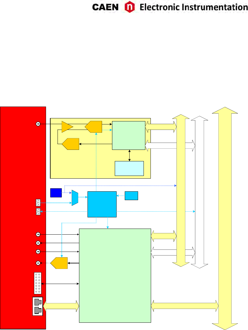
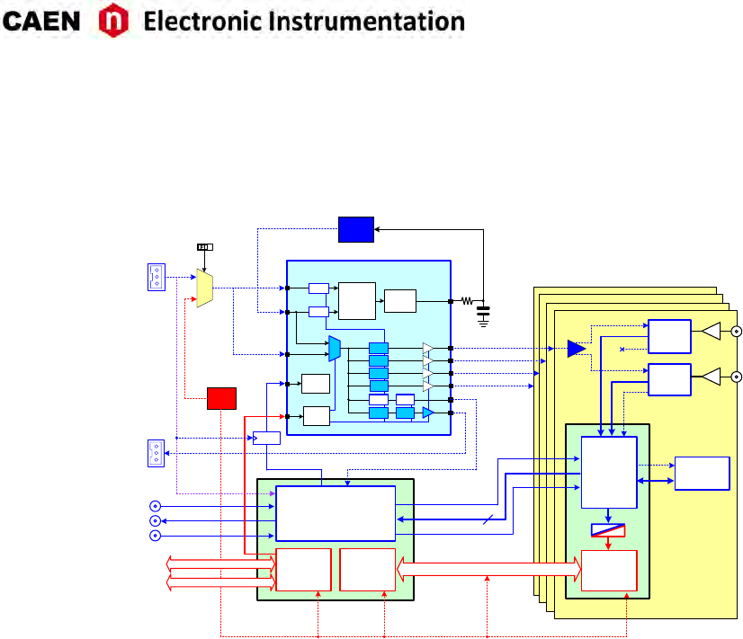
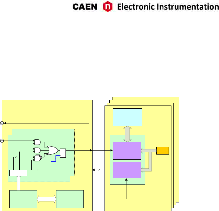
2 Block Diagram
DAC
AMC [FPGA]
ADC &
MEMORY
CONTROLLER
ADC
BUFFERS
x8 (8 channels)
ROC [FPGA]
- Readout control
- VME interface control
- Optical link control
- Trigger control
- External interface control
VME
MUX
OSC
CLOCK
MANAGER
(AD9510)
VCXO
TRIGGERS & SYNC
LOCAL BUS
CLK IN
CLK OUT
TRG IN
TRG OUT
S IN
DIGITAL I/Os
MON DAC
OPTICAL LINK
INPUTS
FRONT PANEL
1GHz
Fig. 2.1: Block Diagram
UM3350 - V1751/VX1751 User Manual rev. 16 11
3 Technical Specificaons
GENERAL Form Factor
1-unit wide, 6U VME64 (V1751) and VME64X (VX1751)
Weight
535 g
ANALOG INPUT
Channels
8 channels
Single ended
Note: EVEN channels must
be disconnected in DES
mode
Connector
MCX
Bandwidth
500 MHz
Impedance (Zin)
50 Ω
Full Scale Range (FSR)
1 Vpp or customizable to
200 mVpp
Offset
Programmable DAC for DC
offset adjustment on each
channel in the full range
Abs Max Rang
@1Vpp: 3 Vpp (with Vrail
max +3 V or –3 V for any
DAC offset value)
@200 mVpp: 2 Vpp (with
Vrail max +2 V or –2 V for
any DAC offset value)
DIGITAL
CONVERSION
Resoluon
10 bits
Sampling Rate
1 GS/s (2 GS/s DES mode) simultaneously on each channel
ADC SAMPLING
CLOCK GENERATION
Clock source: internal/external
On-board programmable PLL provides generaon of the main board clocks from an
internal (50 MHz local Oscillator) or external (front panel CLK-IN connector) reference.
DIGITAL I/O
CLK-IN (AMP Modu II)
AC coupled differenal
input clock
LVDS, ECL, PECL, LVPECL,
CML, Zdiff = 100 Ω
CLK-OUT (AMP Modu IV)
DC coupled differenal
LVDS clock output locked
to ADC sampling clock,
Zdiff = 100 Ω
S-IN (LEMO)
SYNC/START
front panel digital input
NIM/TTL, Zin = 50 Ω
TRG-IN (LEMO)
External trigger digital
input
NIM/TTL, Zin = 50 Ω
TRG-OUT (LEMO)
Trigger digital output
NIM/TTL, Rt= 50 Ω
MEMORY
1.835 MS/ch (3.6 MS/ch in DES mode) or 14.4 MS/ch (28.8 MS/ch in DES mode) (see
Tab. 1.1)
Mul Event Buffer divisible into 1 ÷ 1024
Independent read and write access
Programmable event size and pre/post trigger
TRIGGER
Trigger Source
-Self-trigger: channel over/under-threshold
for common (waveform recording firmware) or
individual (DPP firmware only) trigger
generaon
-External-trigger: common trigger by TRG IN
connector or individual by LVDS connector
(DPP firmware only)
-Soware-trigger: common trigger by
soware command
Trigger Propagaon
TRG-OUT programmable digital output
Trigger Time Stamp
Waveform recording FW/DPP-ZLEplus:
31-bit counter – 16 ns resoluon - 17 s
range; 48 bit fw extension
DPP-PSD: 32-bit counter – 1 ns
resoluon (1 ps fine me stamp
resoluon with dCFD) - 4 s range; 48
bit fw extension; 64 bit sw extension
12 UM3350 - V1751/VX1751 User Manual rev. 16
SYNCHRONIZATION
Clock Propagaon
Daisy chain: through CLK-IN/CLK-OUT
connectors
One-to-many: clock distribuon from an
external clock source on CLK-IN connector
Clock Cable delay compensaon
Acquision Synchronizaon
Sync, Start/Stop through digital I/O
(S-IN or TRG-IN input / TRG-OUT
output)
Trigger Time Stamps Alignment
By S-IN input connector
ADC & MEMORY
CONTR. Altera Cyclone EP1C20 (one FPGA serves 1 channel)
COMMUNICATION
INTERFACE
Opcal Link
CAEN CONET proprietary protocol
Up to 80 MB/s transfer rate
Daisy-chain: it is possible to connect up to 8 or
32 ADC modules to a single Opcal Link
Controller (respecvely A2818 or A3818)
VME
VME 64X compliant
Data transfer mode: BLT32, MBLT64
(70 MB/s using CAEN Bridge),
CBLT32/64, 2eVME, 2eSST (up to 200
MB/s)
ANALOG MONITOR
12-bit / 125 MHz DAC FPGA controlled; four operang modes:
- Test pulses: 1 Vpp ramp generator
- Majority signal: proporonal to the nr. Of channels under/over threshold (steps
of 125 mV)
- Memory Occupancy signal: proporonal to the Mul Event Buffer Occupancy (1
buffer 1mV)
- Voltage level: programmable output voltage level
LVDS I/O
16 general purpose LVDS I/O controlled by the FPGA: Busy, Data Ready, Memory full,
Individual Trig-Out and other funcons can be programmed
An Input Paern from the LVDS I/O can be associated to each trigger as an event marker
SUPPORTED DPP
FIRMWARE
DPP-PSD for the Pulse Shape Discriminaon
DPP-ZLEplus for the Zero Length Encoding
FIRMWARE
UPGRADE Firmware can be upgraded via VMEbus/Opcal Link
SOFTWARE General purpose C libraries, configuraon tools, readout soware (Windows® and
Linux® support). LabVIEW™ VIs and demos for Windows® only
POWER
CONSUMPTIONS 6.5 A @ +5V; 200 mA @ +12V, 300 mA @ -12V
Tab. 3.1: Specificaon table
UM3350 - V1751/VX1751 User Manual rev. 16 13
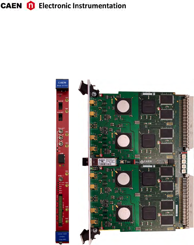
4 Packaging and Compliancy
V1751/VX1751 modules are 1-unit wide, 6U VME64/VME64X boards.
Fig. 4.1: V1751 model view
14 UM3350 - V1751/VX1751 User Manual rev. 16
CAUTION: to manage the product, consult the operang instrucons provided.
A POTENTIAL RISK EXISTS IF THE OPERATING INSTRUCTIONS ARE
NOT FOLLOWED!
CAUTION: this product needs proper cooling.
USE ONLY CRATES WITH FORCED COOLING AIR FLOW SINCE
OVERHEATING THE BOARD MAY DEGRADE ITS PERFORMANCES!
CAUTION: this product needs proper handling.
V1751/VX1751 DO NOT SUPPORT LIVE INSERTION (HOT SWAP)!
REMOVE OR INSERT THE BOARD WHEN THE VME CRATE IS
POWERED OFF!
ALL CABLES MUST BE REMOVED FROM THE FRONT PANEL BEFORE
EXTRACTING THE BOARD FROM THE CRATE!
CAEN provides the specific document “Precauons for Handling, Storage and Installa-
on”, available in the documentaon tab of the product’s web page, that is mandatory
to read before operating with CAEN equipment.
UM3350 - V1751/VX1751 User Manual rev. 16 15
5 Power Requirements
The table below resumes the V1751/VX1751 power consumpons per relevant power supply rail.
MODULE SUPPLY VOLTAGE
+5 V +12 V -12 V
V1751/VX1751 6.5 A 200 mA 300 mA
Tab. 5.1: Power requirements table
16 UM3350 - V1751/VX1751 User Manual rev. 16

6 Temperature Protecon
ADC chips temperature readout
The V1751 features an internal ADC temperature monitoring system, useful in order to esmate the steady
thermal state of the ADCs and to perform the calibraon procedure (see Sec. Channel Calibraon). Since
each ADC manages two channels (0-1, 2-3. 4-5, 6-7) idencal temperature values will be found for couples
of channels; such values can be readout using register 0x1nA8.
ADC chips over temperature protection
Each ADC will be automacally powered off whenever the core temperature reaches 90°C. The relevant
channels will not therefore parcipate any more to data event, and bit[7] and bit[8] of register 0x1n88 will
set to 1 (channel power down and over-temperature flags respecvely).
When the ADC core temperature decreases under 65°C, the bit[8] will return to 0, and the relevant channels
can be restored to normal operaon following these steps:
• Wait unl bit 8 of 0x1n88 register returns to 0
• Set bit[0] = 0 of 0x1n9C; bit[7] of 0x1n88 will return to 0.
• Perform a calibraon procedure on the restored channels (see Sec. Channel Calibraon)
´
UM3350 - V1751/VX1751 User Manual rev. 16 17
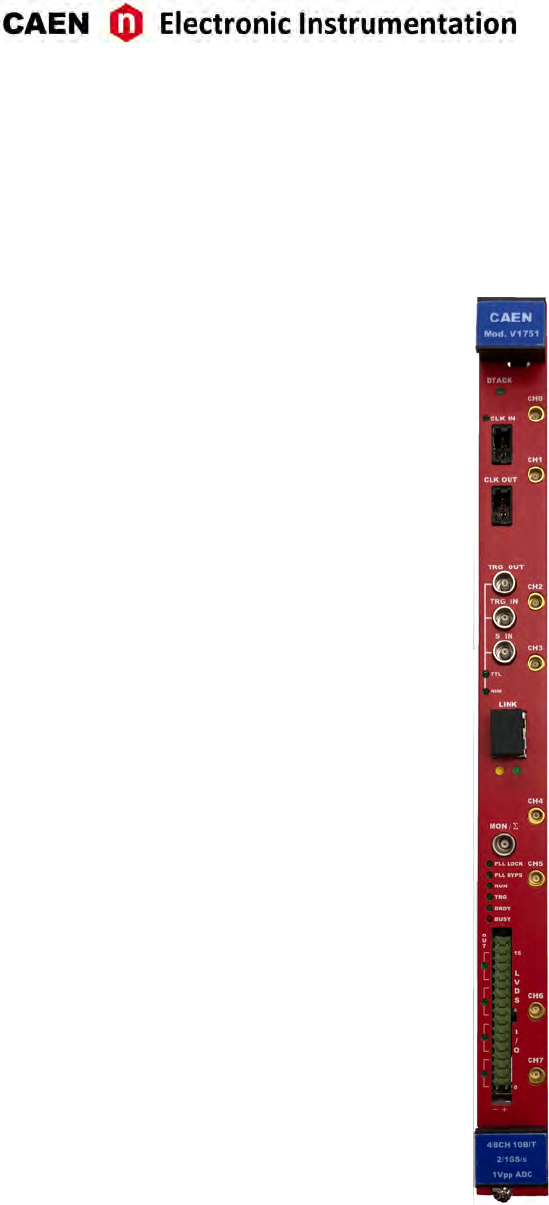
7 Panels Descripon
Fig. 7.1: Front panel view of V1751
18 UM3350 - V1751/VX1751 User Manual rev. 16
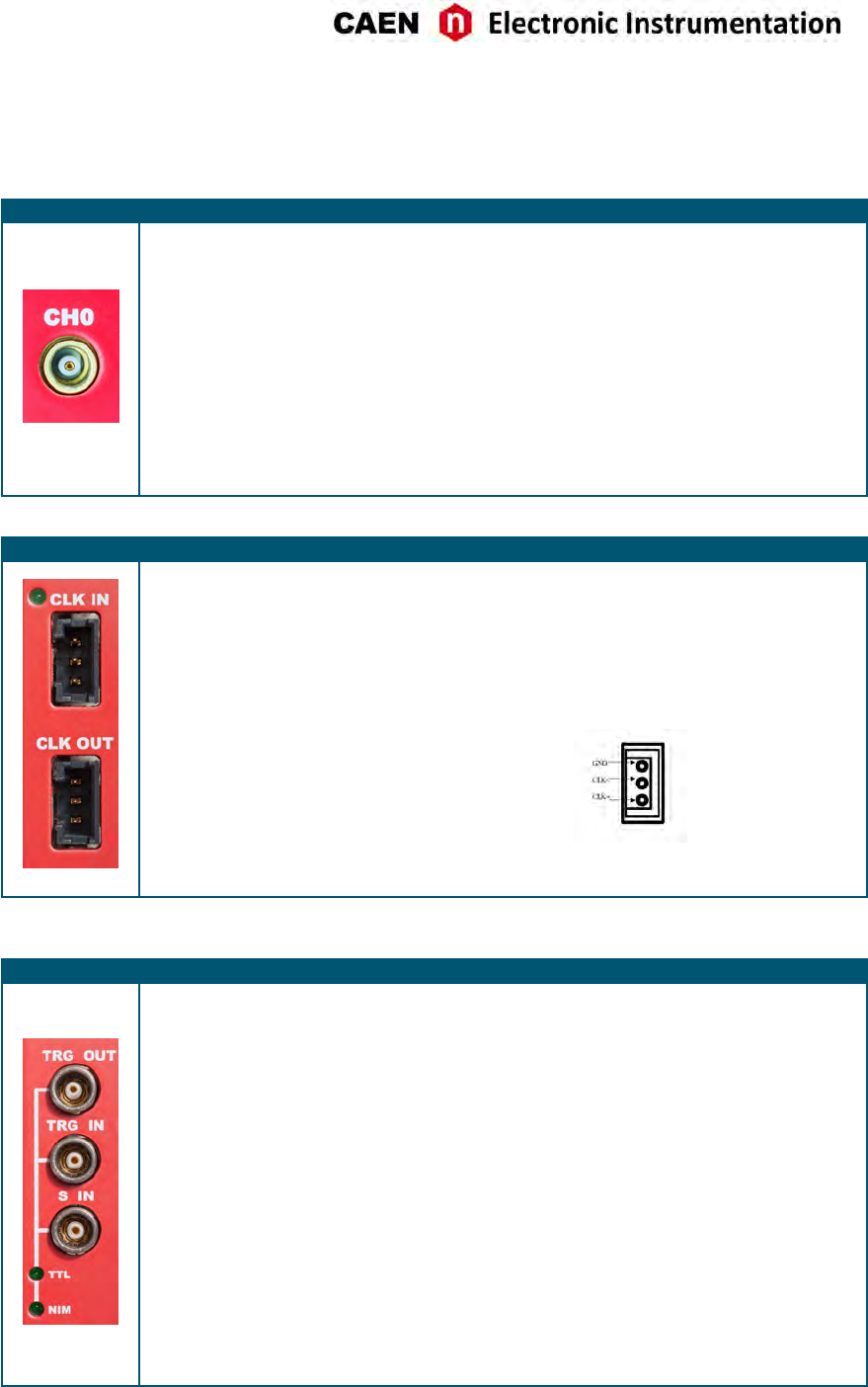
Front Panel
ANALOG INPUT
FUNCTION
Input connectors from CH0 to CH7 receive
the input analog signals.
ELECTRICAL SPECS
Input dynamics: 1 Vpp
Input impedance (Zin): 50 Ω.
Absolute max analog input voltage:
@1 Vpp: 3 Vpp (with Vrail max +3 V or -3 V)
@200 mVpp: 2 Vpp (with Vrail max +2 V or
–2 V) for any DAC offset value.
Note: 200 (50 Ω) mVpp input range is
available by ordering opon (see Tab. 1.1).
MECHANICAL SPECS
Series: MCX connectors.
Type: CS 85MCX-50-0-16.
Manufacturer: SUHNER
Suggested plug: MCX-50-2-16 type.
Suggested cable: RG174 type.
CLOCK IN/CLOCK OUT
FUNCTION
Input and output connectors for the external
clock.
ELECTRICAL SPECS
Sign. type: differenal (LVDS, ECL, PECL,
LVPECL, CML). CAEN provides single
ended-to-differenal A318 cable adapter
(see Tab. 1.1) for CLK-IN.
Coupling: AC (CLK-IN); DC (CLK-OUT).
Zdiff: 100 Ω.
MECHANICAL SPECS
Series: AMPMODU connectors.
Type: 3-102203-4 (3-pin).
Manufacturer: AMP Inc.
PINOUT
CLK IN LED (GREEN): indicates the external clock is enabled.
TRG-IN / TRG-OUT / S-IN
FUNCTION
• TRG-OUT: digital output connector to
propagate:
- probes from the mezzanines;
- S-IN signal.
• TRG-IN: digital input connector for the
external trigger.
• S-IN: SYNC/START/STOP digital input
connector configurable as reset of the
me stamp (see Sec. Reset, Clear and
Default Configuraon) or to start/stop
the acquision (see Sec. Acquision
Run/Stop).
ELECTRICAL SPECS
Signal level: NIM or TTL.
TRG-IN/S-IN Input impedance (Zin): 50 Ω
TRG-OUT requires 50 Ω terminaon.
MECHANICAL SPECS
Series: 101 A 004 connectors.
Type: DLP 101 A 004-28.
Manufacturer: FISCHER.
Alternavely:
Type: EPL 00 250 NTN.
Manufacturer: LEMO.
TTL (GREEN), NIM (GREEN): indicate the standard TTL or NIM set for TRG-OUT, TRG-IN, and S-IN.
UM3350 - V1751/VX1751 User Manual rev. 16 19
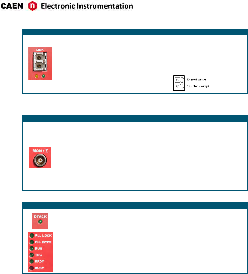
OPTICAL LINK PORT
FUNCTION
Opcal LINK connector for data readout and
flow control. Daisy chainable. Compliant
with Mulmode 62.5/125 μm cable featuring
LC connectors on both sides.
MECHANICAL SPECS
Series: SFF Transceivers.
Type: FTLF8519F-2KNL (LC connectors).
Manufacturer: FINISAR.
ELECTRICAL SPECS
Transfer rate: up to 80 MB/s.
PINOUT
LINK LEDs (GREEN/YELOW): right LED (GREEN) indicates the network presence, while le LED (YELLOW) signals the
data transfer acvity.
MON / Σ
FUNCTION
Analog Monitor output connector with 4
programmable modes (see Sec. Analog
Monitor):
- Trigger Majority
- Test Pulses
- Memory Occupancy
- Voltage Level
ELECTRICAL SPECS
12-bit (125 MHz) DAC output.
1 Vpp on Rt= 50 Ω
MECHANICAL SPECS
Series: 101 A 004 connectors.
Type: DLP 101 A 004-28.
Manufacturer: FISCHER.
Alternavely:
Type: EPL 00 250 NTN.
Manufacturer: LEMO.
DIAGNOSTICS LEDs
DTACK (GREEN): indicates there is a VME read/write access to the board;
PLL LOCK (GREEN): indicates the PLL is locked to the reference clock;
PLL BYPS (GREEN): not used;
RUN (GREEN): indicates the acquision is running (data taking). See Sec. Acquision
Run/Stop;
TRG (GREEN): indicates the trigger is accepted;
DRDY (GREEN): indicates the event/data is present in the Output Buffer;
BUSY (RED): indicates all the buffers are full for at least one channel.
20 UM3350 - V1751/VX1751 User Manual rev. 16
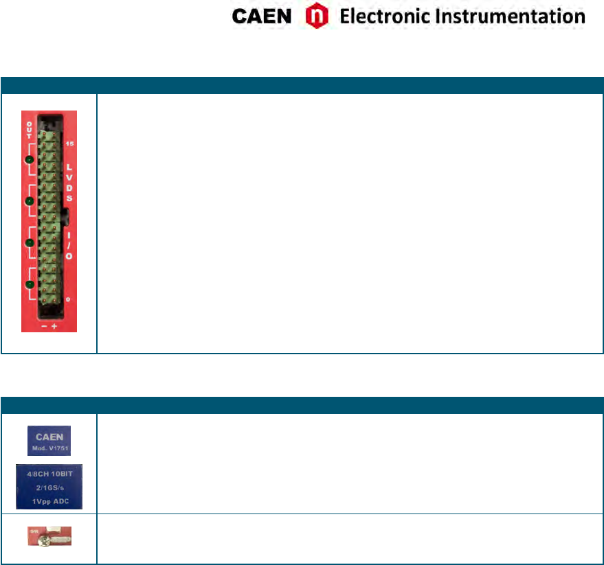
LVDS I/Os CONNECTOR
FUNCTION
16-pin connector with programmable
general purpose LVDS I/O signals organized
in 4 independent signal groups: 0÷3; 4÷7;
8÷11; 12÷15.
In/Out direcon is soware controlled.
Different selectable modes (see Sec. Front
Panel LVDS I/Os):
- Register
- Trigger
- nBusy/nVeto
- Legacy
ELECTRICAL SPECS
Level: differenal LVDS
Zdiff: 100 Ω
MECHANICAL SPECS
Series : TE - AMPMODU Mod II Series
Type: 5-826634-0 34 pin (lead spacing: 2.54
mm; row pitch: 2.54 mm)
Manufacturer: AMP Inc.
LVDS I/O LEDs (GREEN): Each LED close to a 4-pin group lights on if the pins are set as outputs.
LABELS
Two blue labels on each inseron/extracon handle on the VME front panel report:
- Manufacturer name and board’s model
- Brief funconal descripon of the module
A lile silver label on the boom of the VME board’s front panel reports:
- 4-digit Serial Number (S/N)
UM3350 - V1751/VX1751 User Manual rev. 16 21
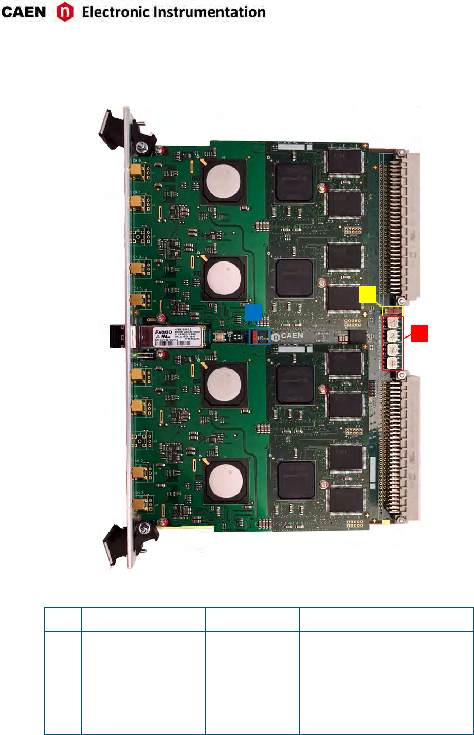
Internal Components
B
C
A
Fig. 7.2: Rotary and dip switches locaon
ASW3,4,5,6:
”Base Address [31:16]”
Type:
Rotary Switches
Funcon:
Set the VME Base Address of the module
BSW2:
“CLOCK SOURCE” INT/EXT
Type:
Dip Switch
Funcon:
Selects the clock source (External or
Internal)
CSW7:
”FW” BKP/STD
Type:
Dip Switch
Funcon:
Selects ”Standard” (STD) or ”Backup” (BKP)
FLASH page as first to be read at power-on
to load the FW on the FPGAs (default
posion is STD); see Sec. Firmware
Upgrade
22 UM3350 - V1751/VX1751 User Manual rev. 16
8 Funconal Descripon
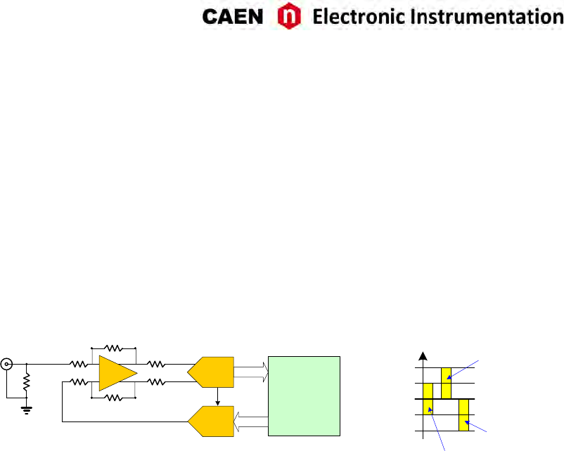
Analog Input Stage
Input dynamic is 1 Vpp; 200 mVpp version is available upon request (see Tab. 1.1). In order to preserve the
full dynamic range with unipolar input signal, posive or negave, it is possible to add a DC offset by means
of a 16 bit DAC, which is up to ±0.5 V @ 1 Vpp and ±0.1 V @ 200 mVppṪhe input bandwidth ranges from
DC to 500 MHz (with 2nd order linear phase an-aliasing low pass filter).
MCX
OpAmp
50
DAC
Vref
10 bit
ADC
Input
FPGA
+0.50
0
+1.00
-0.50
-1.00
Input Dynamic Range: 1 Vpp
Positive Unipolar
DAC = FSR
16 bit Negative Unipolar
DAC = 0
Bipolar
DAC = FSR/2
Fig. 8.1: Analog input diagram
DC Oset Individual Setting
Seng the DC offset for channel n requires a write access at register addresses 0x1n98. Wring at 0x8098,
the DC offset will apply to all channels at once. Refer to [RD1] for more details.
UM3350 - V1751/VX1751 User Manual rev. 16 23
Clock Distribution
MUX
OSC
CLK-IN
CLK-OUT
50MHz
VCXO
1 GHz
REF-CLK
Trigger & Sync
Logic
Optical Link/
VME
Interface
TRG IN
TRG OUT
S IN
LOCAL BUS Local Bus
Interface
Acquisition
& Memory
Control
Logic
MEZZANINES (x4)
Feedback loop
TRIGGER
SYNC
SELF-TRGs
MUX
Phase
Detector
AD9510
CLK1 Sdiv
Sdiv
CLK2
Rdiv
REFIN
Charge
Pump
INTCLK
CTRL
SPI
Ldiv
Odiv
Ndiv
SAMP-CLK0
FPGA (AMC)
ADC CH1
SCLK
DATA
SYNC
SRAM
FIFO
ADC CH0
SCLK
DATA
Ldel
Odel
Local Bus
Interface
VME
FPGA (ROC)
SYNCB
TRG-CLK
SyncB
OUT-CLK
CLK Source
DIP-SW
EXT INT
RAMCLK
DATA
FANOUT
VCXO-CLK
OSC-CLK
8
DFF
SAMP-CLK1
CLKOUT
CLKOUT
Sdiv
Sdiv
SAMP-CLK2
SAMP-CLK3
Optical Link
Fig. 8.2: Clock distribuon diagram
The clock distribuon of the module takes place on two domains: OSC-CLK and REF-CLK.
OSC-CLK is a fixed 50-MHz clock coming from a local oscillator which handles VMEbus, Opcal Link and
Local Bus, that takes care of the communicaon between motherboard and mezzanines (see red traces in
Fig. 8.2).
REF-CLK handles ADC sampling, trigger logic, and acquision logic (samples storage into RAM, buffer freez-
ing on trigger) through a clock chain. REF-CLK can be either an external (via the front panel CLK-IN connec-
tor) or an internal (via the 50-MHz local oscillator) source. In the laer mode, OSC-CLK and REF-CLK will be
synchronous (the operaon mode remains the same).
REF-CLK clock source selecon can be done by an on-board dedicated dip switch (see Fig. 7.2) between the
following modes:
• INT mode (default) means REF-CLK is the 50 MHz of the local oscillator (REF-CLK = OSC-CLK);
• EXT mode means REF-CLK source is the external frequency fed on CLK-IN connector.
The external clock signal must be differenal (LVDS, ECL, PECL, LVPECL, CML) with a jier lower than
100 ppm (see Chap. Technical Specificaons). CAEN provides the A318 cable to adapt single ended signals
coming from an external clock unit into the differenal CLK-IN connector (see Tab. 1.1).
The V1751 is equipped with a phase-locked-loop (PLL) and clock distribuon device, AD9510. It receives
the REF-CLK and generates the sampling clock for ADCs and the mezzanine FPGA (SAMP-CLK0 up to SAMP-
CLK3), as well as the trigger logic synchronizaon clock (TRG-CLK) and the output clock (CLK-OUT).
AD9510 configuraon can be changed and stored into non-volale memory. Changing the AD9510 con-
figuraon is primarily intended to be used for external PLL reference clock frequency change (see Sec. PLL
Mode). The V1751 locks to an external 50 MHz reference clock with default AD9510 configuraon.
Refer to the AD9510 datasheet for more details:
hp://www.analog.com/UploadedFiles/Data_Sheets/AD9510.pdf
(in case the acve link above does not work, copy and paste it on the internet browser)
24 UM3350 - V1751/VX1751 User Manual rev. 16
PLL Mode
The Phase Detector within the AD9510 device allows to couple REF-CLK with an external VCXO, which
provides the nominal ADCs frequency (1 GS/s).
As introduced in Sec. Clock Distribuon, the source of the REF-CLK signal (see Fig. 8.2) can be external
on CLK-IN front panel connector or internal from the 50 MHz local oscillator. Programming the REF-CLK
source internal or external can be performed by acng on the on-board dip switch SW2 (see Sec. Internal
Components).
The following opons are allowed:
1. 50 MHz internal clock source - this is the standard operaon mode: the AD9510 dividers do not
require to be reprogrammed (the digizer works in the AD9510 default configuraon). The clock
source selecon dip switch SW2 is in default INT mode. REF-CLK = OSC-CLK.
2. 50 MHz external clock source - in this case, the clock source is taken from an external device; the
AD9510 dividers do not need to be reprogrammed as the external frequency is the same as the default
one. The clock source selecon dip switch must be set in EXT mode. CLK-IN = REF-CLK = OSC-CLK.
3. External clock source different from 50 MHz - the clock source is externally provided as in point 2, but
the AD9510 dividers must now be reprogrammed to lock the the VCXO to the new REF-CLK in order
to provide out the nominal sampling frequency at 1 GS/s. The clock source selecon dip switch must
be set in EXT mode. CLK-IN = REF-CLK ̸= OSC-CLK.
If the digizer is locked, the PLL-LOCK front panel LED must be on.
Note: the user can configure the clock parameters, generate the PLL programming file and load it on the
board by using the CAENUpgrader soware tool (see Chap. Soware Tools).
Reducing the Sampling Frequency
In case the board is required to work at a sampling frequency (SAMP-CLK) lower than the nominal, it can
be achieved by reprogramming the AD9510 dividers. REF-CLK can be configured as in Sec. PLL Mode.
Not all the frequencies are admied and a lower frequency limit must be considered, due to the internal
electronics. Please contact CAEN (see Sec. Technical Support) to check the feasibility.
Trigger Clock
The TRG-CLK logic works at 125 MHz, equal to 1
/8of the sampling frequency: TRG-CLK = 1
/8·SAMPL-CLK.
Eight samples of trigger “uncertainty” occurs over the acquision window (16 samples uncertainty in DES
mode).
Output Clock
The AD9510 output can be available on the front panel CLK-OUT connector (see Fig. 8.2). This opon
is parcularly useful in case of mul-board synchronizaon to propagate the clock reference source in
Daisy Chain. This opon can be enabled by the user while configuring the PLL programming file in the
CAENUpgrader soware.
UM3350 - V1751/VX1751 User Manual rev. 16 25
DES Mode
The board can be programmed to operate in Dual Edge Sampling (DES) mode, at 2 GS/s.
DES Mode is configurable by seng bit[12] = 1 of register 0x8000 (see [RD1]).
Note: Only even channels are managed when operang the digizer in DES mode.
Acquisition Modes
Channel Calibration
The module performs a self-calibraon of the ADCs at its power-on. Anyway, in order to achieve the best
performance, the calibraon procedure is recommended to be executed by the user, on command, aer
the ADCs have stabilized their operang temperature. The calibraon will not need to be repeated at each
run unless the operang temperature changes significantly, or clock sengs are modified (e.g. switching
from internal to external clock).
The diagram below synthesises the flow for a proper calibraon:
BOARD
CONFIGURATION
Temperature or Clock
variation Acquisition sessions
(n cycles)
POWER-ON
TEMPERATURE
STABILIZATION
LOOP
CALIBRATE
START RUN
STOP RUN
Fig. 8.3: Diagram of the ADCcalibraon flow.
• At low level, the ADCs temperature can be read at the register address 0x1nA8 [RD1], while the cali-
braon must be performed through register address 0x809C. The following steps are required:
– set bit[1] = 0 of register 0x809C;
26 UM3350 - V1751/VX1751 User Manual rev. 16
– set bit[1] = 1 of register 0x809C. The self calibraon process will start simultaneously on each
channel of the board and bit[6] of register 0x1n88 will be set to 0;
– poll bit[6] of register 0x1n88 unl it returns to 1 (few milliseconds);
– set again bit[1] = 0 of register 0x809C.
Steps in case of DES mode are:
– make sure that EVEN channels are disconnected;
– disable EVEN channels;
– enable DES mode by seng bit[12] = 1 of register 0x8000;
– set bit[1] = 0 of register 0x809C;
– set bit[1] = 1 of register 0x809C. The self calibraon process will start simultaneously on each
channel of the board and bit[6] of register 0x1n88 will be set to 0;
– poll bit[6] of register 0x1n88 unl it returns to 1 (few milliseconds);
– set again bit[1] = 0 of register 0x809C.
Note: Whenever switching from Normal mode to DES mode and vice-versa, the ADC calibraon
must be repeated.
Note: It is normally not required to calibrate aer a board reset but, if a Reset command is inten-
onally issued to the digizer (write access at register address 0xEF24) to be directly followed by a
calibraon procedure, it is recommended to wait for the board to reach stable condions (indica-
vely 100 ms) before starng the calibraon.
Note: At power-on, a Sync command is also issued by the firmware to the ADCs to synchronize all of
them to the board’s clock. In the standard operang, this command is not required to be repeated
by the user. If a Sync command is intenonally issued (write access at register address 0x813C), the
user must consider that a new calibraon procedure is needed for a correct board operang.
• At the library level, developers can exploit the CAENDigizer library (see Sec. Libraries) dedicated
rounes which are ReadTemperature() funcon for temperature readings and the Calibrate() funcon
which executes the channel calibraon steps above described.
Note: Starng from CAENDigizer release 2.6.1, the Reset() funcon has been modified so that
it no longer includes the channel calibraon roune implemented in the code. This calibraon
must be performed on command by the dedicated Calibrate() funcon. Please, see the Library
user manual for reference ([RD4]).
• At soware level, CAEN manages the command channel calibraon in different readout soware
(please, refer the relevant soware User Manual for details).
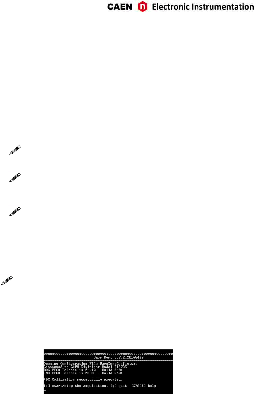
♢WaveDump
1. Lauch WaveDump. This soware performs an automac ADC calibraon and displays a mes-
sage when it is completed (see Fig. 8.4). This allows the user to start using the program sure
Fig. 8.4: Automac calibraon at WaveDump first run
that the digizer has been calibrated at least once.
UM3350 - V1751/VX1751 User Manual rev. 16 27
NOTE THAT: If SKIP_STARTUP_CALIBRATION parameter is set to YES in WaveDump
configuraon file, the automac start-up calibraon is not performed and no mes-
sage is displayed
2. At any me, the user can check the channel temperatures (with the acquision not running)
by issuing mulple “m” commands from the keyboard.
3. In case of significant variaons, issuing a “c” command provokes a manual channel calibraon
to be executed (see Fig. 8.5).
Fig. 8.5: Temperature monitoring with manual calibraon in WaveDump soware
4. A new acquision can start.
Please, refer to WaveDump User Manual for complete soware descripon ([RD5]).
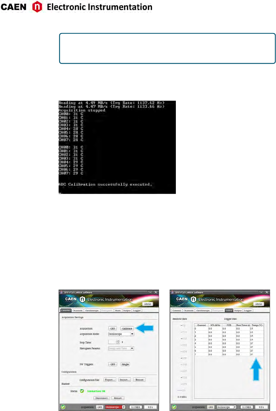
♢DPP-PSD Control Soware
1. Launch DPP-PSD Control Soware
2. Connect to the digizer
3. Before to start the acquision, go to the “Stats” tab and monitor the channel temperatures
displayed in the relevant column unl you see they don’t vary significantly
4. Go to the “General” tab and press the “Calibrate” buon
5. Start the acquision
Fig. 8.6: Channel calibraon in DPP-PSD Control Soware
28 UM3350 - V1751/VX1751 User Manual rev. 16

Acquisition Run/Stop
The acquision can be started and stopped in different ways, according to bits[2:0] of register 0x8100
[RD1]:
- SW CONTROLLED (bits[1:0] = 00): Start and Stop take place by soware command. Bit[2] = 0 means
stopped, while bit[2] = 1 means running.
- S-IN CONTROLLED (bits[1:0] = 01): bit[2] = 1 arms the acquision and the Start is issued as the S-IN
signal is set high and the Stop occurs when it is set low. If bit[2] = 0 (disarmed), the acquision is
always off.
- FIRST TRIGGER CONTROLLED (bits[1:0] = 10): bit[2] = 1 arms the acquision and the Start is issued on
the first trigger pulse (rising edge) on the TRG-IN connector. This pulse is not used as a trigger; actual
triggers start from the second pulse on TRG-IN. The Stop acquision must be SW controlled (i.e. reset
of bit[2]).
- LVDS I/Os CONTROLLED: this mode acts like the S-IN CONTROLLED (bits[1:0] = 01), but using the con-
figurable features of the signals on the LVDS I/Os connector (see Sec. Front Panel LVDS I/Os).
Acquisition Triggering: Samples and Events
When the acquision is running, a trigger signal allows to:
- store a 31-bit counter value of the Trigger Time Tag (TTT).
The counter (represenng a me reference), like the Trigger Logic Unit (see Fig. 8.2), operates at a
frequency of 125 MHz (i.e. 8 ns, that is to say 8 ADC clock cycles). Due to the way acquired data is
wrien into the board internal memory (i.e. in 4-sample bunches), the TTT counter is read every 2
trigger logic clock cycles, which means the trigger me stamp resoluon results in 16 ns (i.e. 62.5
MHz). Basing on that, the LSB of the TTT is always “0”;
- increment the EVENT COUNTER;
- fill the acve buffer with the pre/post-trigger samples, whose number is programmable via register
address 0x8114 [RD1]; the acquision window width (also referred to as record length) is determined
via register addresses 0x800C and 0x8020; then, the buffer is frozen for readout purposes, while the
acquision connues on another buffer.
An event is therefore composed by the trigger me tag, pre- and post-trigger samples and the event
counter.
Overlap between “acquision windows” may occur (a new trigger occurs while the board is sll storing the
samples related to the previous trigger); this overlap can be either rejected or accepted (programmable
via soware).
If the board is programmed to accept the overlapping triggers (by wring at register address 0x8000 [RD1]),
as the overlapping trigger arrives, the current acve buffer is filled up, then the samples storage connues
on the subsequent one. In this case, not all events will have the same size (see Fig. 8.7).
A trigger can be refused for the following causes:
- Acquision is not acve.
- Memory is FULL and therefore there are no available buffers.
- The required number of samples for building the event pre-trigger is not reached yet; this happens
typically as the trigger occurs too early either with respect to the RUN Acquision command (see
Sec. Acquision Run/Stop) or with respect to a buffer emptying aer a Memory FULL status (see
Sec. Acquision Synchronizaon).
- The trigger overlaps the previous one and the board is not enabled for accepng overlapped triggers.
As a trigger is refused, the current buffer is not frozen and the acquision connues wring on it. The
EVENT COUNTER can be programmed in order to be either incremented or not. If this funcon is enabled,
UM3350 - V1751/VX1751 User Manual rev. 16 29
TRIGGER
PRE POST
ACQUISITION WINDOW
Recorded
Not Recorded
Overlapping Triggers
EVENT n EVENT n+1 EVENT n+2
Fig. 8.7: Trigger Overlap
the EVENT COUNTER value idenfies the trigger number sent (but the event number sequence is lost); if
the funcon is not enabled, the EVENT COUNTER value coincides with the sequence of buffers saved and
readout.
30 UM3350 - V1751/VX1751 User Manual rev. 16
Multi-Event Memory Organization
Each channel of the V1751 features a SRAM memory to store the acquired events. The memory size in the
standard event storage mode is 1.75 MS or 13.73 MS1, where M = 1024 ·1024, according to the board
version (see Tab . 1.1). The channel memory can be divided in a programmable number of buffers, Nb(Nb
from 1 up to 1024), by the register address 0x800C [RD1], as described in Tab. 8.1.
Note: in case of DES mode, values must be mulplied by 2.
Register Value Number of Buffers Size of one Buffer
BUFFER_CODE (Nb)SRAM 2.33 MB/ch
(1.75 MS)
SRAM 18.3 MB/ch
(13.73 MS)
0x00 1 2.333 MB/ch (1.75 MS) 18.3 MB/ch (13.73 MS)
0x01 2 1.167 MB/ch (896 kS) 9.1 MB/ch (6.8 MS)
0x02 4 597.2 kB/ch (448 kS) 4.6 MB (3.4 MS)
0x03 8 298.6 kB/ch (224 kS) 2.3 MB/ch (1.7 MS)
0x04 16 149.3 kB/ch (112 kS) 1.1 MB/ch (878.7 kS)
0x05 32 74.6 kB/ch (56 kS) 586.2 kB/ch (439.3 kS)
0x06 64 37.3 kB/ch (28 kS) 293.1 kB/ch (219.7 kS)
0x07 128 18.7 kB/ch (14 kS) 146.6 kB/ch (109.8 kS)
0x08 256 9.3 kB/ch (7 kS) 73.3 kB/ch (54.9 kS)
0x09 512 4.7 kB/ch (3.5 kS) 36.6 kB/ch (27.4 kS)
0x0A 1024 2.3 kB/ch (1.75 kS) 18.3 kB/ch (13.7 kS)
Tab. 8.1: Buffer organizaon of 751 family series. For each value of buffer size it is reported the memory size and the
number of samples of one buffer, where k = 1024 and M = 1024 ·1024.
Having 1.75 MS memory size as reference, this means that each buffer contains 1.75M
/Nbsamples (e.g.
Nb= 1024 means 1.75k samples in each buffer).
Custom size events
In case an event size less than the buffer size is needed, the user can set the N_LOC value at register address
0x8020 [RD1], where N_LOC is the number of memory locaons. The size of the event is so forced to be
according to the formula:
1·N_LOC = 7 ·NSample (normal mode)
1·N_LOC = 14 ·NSample (DES mode)
When N_LOC = 0 the custom size is disabled.
Note: The value of N_LOC must be set in order that the relevant number of samples does not exceed the
buffer size and it must not be modified while the acquision is running. Even using the custom size seng,
the number of buffers and the buffer size are not affected by N_LOC, but they are sll determined by Nb.
The concepts of buffer organizaon and custom size directly affect the width of the acquision window (i.e.
number of the digized waveform samples per event). The Record Length parameter defined in CAEN so-
ware (such as WaveDump and CAENScope introduced in Chap. Soware Tools) and the Set/GetRecordLength()
funcons of the CAENDigizer library (see Sec. Libraries) rely on these concepts.
1Memory size is 1.8 MS and 14.4 MS in case of M = 1000 ·1000
UM3350 - V1751/VX1751 User Manual rev. 16 31
Event structure
The event can be readout via VMEbus or Opcal Link; data format is 32-bit long word (see Fig. 8.8).
An event is structured as:
•Header (four 32-bit words)
•Data (variable size and format)
Header
The Header consists of four words including the following informaon:
•EVENT SIZE (bits[27:0] of 1st header word) is the total size of the event, i.e. the number of 32-bit long
words to be read.
•BOARD ID (bits[31:27] of 2nd header word) is the GEO address, meaningful for VME64X modules.
•BOARD FAIL FLAG (bit[26] of 2nd header word) implemented from ROC FPGA firmware revision 4.5 on
(reserved otherwise), it is set to “1” in consequence of a hardware problem (e.g. PLL unlocking). The
user can collect more informaon about the cause by reading at register address 0x8104 and contact
CAEN Support Service if necessary (see Chap. Technical Support).
•PATTERN (bits[23:8] of 2nd header word) is the 16-bit PATTERN latched on the LVDS I/Os as the trigger
arrives.
Note: Starng from revision 4.6 of the ROC FPGA firmware, these 16 bits can be programmed to provide
trigger informaon according to the seng of the bits[22:21] at register address 0x811C (see Tab 8.2).
REGISTER 0x811C
Bits[22:21]
FUNCTIONAL
DESCRIPTION
PATTERN /TRG OPTIONS INFORMATION
(16 bits in the 2nd header word)
00
(default) PATTERN Paern of the 16 LVDS signals .
01 Event Trigger Source
Indicates the trigger source causing the
event acquision:
Bits[23:19] = 00000
Bit[18] = Soware Trigger
Bit[17] = External Trigger
Bit[16] = Trigger from LVDS connector
Bits[15:8] = Channel self-trigger (refer to
Sec. Self-Trigger).
10 Extended Trigger Time Tag
(ETTT)
A 48-bit Trigger Time Tag (ETTT) informa-
on is configured, where Bits[23:8] con-
tributes as the 16 most significant bits to-
gether to the 32-bit TTT field (4th header
word).
Note: in the ETTT opon, the overflow bit
is not provided.
11 Not used If configured, it acts like “00” seng.
Tab. 8.2: Paern/Trg Opons configuraon table.
•CHANNEL MASK (bits[7:0] of 2nd header word) is the mask of the channels parcipang in the event
(e.g. CH5 and CH7 parcipang → Channel Mask = 0xA). This informaon must be used by the so-
ware to acknowledge from which channel the samples are coming (the first event contains the sam-
ples from the channel with the lowest number).
32 UM3350 - V1751/VX1751 User Manual rev. 16
Note: in DES mode even channels are automacally disabled.
•EVENT COUNTER (bits[23:0] of 3rd header word) is the trigger counter; it can count either accepted
triggers only, or all triggers (bit[3] of register address 0x8100).
•TRIGGER TIME TAG (bits[31:0] of 4th header word) is the 31-bit Trigger Time Tag (TTT) informaon
(31 bit counter and 32nd bit as roll-over flag), which is the trigger me reference. If the ETTT opon
is enabled, then this field becomes the 32 less significant bits of the 48-bit Extended Trigger Time Tag
informaon in addion to the 16 bits (MSB) of the TRG OPTIONS field (2nd event word). Note that, in
the ETTT case, the roll-over flag is no more provided. The trigger me tag is reset either at the start
of acquision, or via front panel signal on S-IN or LVDS I/O connectors, and increments with 250 MHz
frequency (i.e. every 8 ADC clock cycles). The TTT value is read at half the frequency (i.e. 125 MHz)
so that the specificaons are 16 ns resoluon and 17 s range (8 ns ×(231 – 1)), which can be extended
to 625 h (8 ns ×(248 – 1)) if ETTT is enabled.
Data
Data are the stored samples. Data from masked channels are not read. When operang in DES mode the
EVEN channels are automacally disabled. Bits[31:30] of the data words idenfies how many samples are
stored in the corresponding word. The example in Sec. Event Format Examples shows the case of two
samples in the last word.
Event Format Examples
The event format is shown in the following figure (case of 8 channels enabled):
31 30 29 28 27 26 25 24 23 22 21 20 19 18 17 16 15 14 13 12 11 10 9 8 7 6 5 4 3 2 1 0
EVENT SIZE1 0 1 0
CHANNEL MASKPATTERN/TRG OPTIONS1BOARD ID BF
EVENT COUNTERRESERVED
TRIGGER TIME TAG
…..
…..
HEADER DATA CH0
…..
RES
1 1 SAMPLE [1] - CH[0] SAMPLE [0] - CH[0]
DATA CH1 DATA CH7
SAMPLE [2] - CH[0]
1 1 SAMPLE [4] - CH[0] SAMPLE [3] - CH[0]SAMPLE [5] - CH[0]
1 0 SAMPLE [N-1] - CH[0] SAMPLE [N-2] - CH[0]
…..
1 1 SAMPLE [1] - CH[1] SAMPLE [0] - CH[1]SAMPLE [2] - CH[1]
1 1 SAMPLE [4] - CH[1] SAMPLE [3] - CH[1]SAMPLE [5] - CH[1]
1 0 SAMPLE [N-1] - CH[1] SAMPLE [N-2] - CH[1]
…..
1 1 SAMPLE [1] - CH[7] SAMPLE [0] - CH[7]SAMPLE [2] - CH[7]
1 1 SAMPLE [4] - CH[7] SAMPLE [3] - CH[7]SAMPLE [5] - CH[7]
1 0 SAMPLE [N-1] - CH[7] SAMPLE [N-2] - CH[7]
Fig. 8.8: Event Format in Normal Mode
UM3350 - V1751/VX1751 User Manual rev. 16 33
Acquisition Synchronization
Each channel of the digizer is provided with a SRAM memory that can be organized in a programmable
number Nbof circular buffers (Nb= [1 : 1024], see Tab. 8.1). When the trigger occurs, the FPGA writes
further a programmable number of samples for the post-trigger and freezes the buffer, so that the stored
data can be read via VME or Opcal Link. The acquision can connue in a new buffer.
When all buffers are filled, the board is considered FULL: no trigger is accepted and the acquision stops
(i.e. the samples coming from the ADC are not wrien into the memory, so they are lost). As soon as one
buffer is read out and freed, the board exits the FULL condion and acquision restarts.
IMPORTANT: When the acquision restarts, no trigger is accepted unl at least the enre buffer
is wrien. This means that the dead me is extended for a certain me (depending on the size
of the acquision window) aer the board exits the FULL condion.
A way to eliminate this extra dead me is by seng bit[5] = 1 at register address 0x8100 [RD1]. The board
is so programmed to enter the FULL condion when Nb– 1 buffers are filled: no trigger is then accepted,
but samples wring connues in the last available buffer. As soon as one buffer is read out and becomes
free, the boards exits the FULL condion and can immediately accept a new trigger. This way, the FULL
reflects the BUSY condion of the board (i.e. inability to accept triggers).
Note: when bit[5] = 1, the minimum number of circular buffers to be programmed is Nb= 2.
In some cases, the BUSY propagaon from the digizer to other parts of the system has some latency and
it can happen that one or more triggers occur while the digizer is already FULL and unable to accept those
triggers. This condion causes event loss and it is parcularly unsuitable when there are mulple digizers
running synchronously, because the triggers accepted by one board and not by other boards cause event
misalignment.
In these cases, it is possible to program the BUSY signal to be asserted when the digizer is close to FULL
condion, but it has sll some free buffers (Almost FULL condion). In this mode, the digizer remains
able to accept some more triggers even aer the BUSY asseron and the system can tolerate a delay in
the inhibit of the trigger generaon. When the Almost FULL condion is enabled by seng the Almost
FULL level to “X” (register address 0x816C [RD1]), the BUSY signal is asserted as soon as X buffers are filled,
although the board sll goes FULL (and rejects triggers) when the number of filled buffers is Nbor Nb– 1,
depending on bit[5] at register address 0x8100 as above described.
It is possible to provide the BUSY signal on the digizer front panel TRG-OUT output (bit[20], bits[19:18]
and bits[17:16] at register address 0x811C are involved [RD1]). In case of mul-board setup, the BUSY
signal can be propagated among boards through the front panel LVDS I/O connector (see Sec. Front Panel
LVDS I/Os).
34 UM3350 - V1751/VX1751 User Manual rev. 16
Trigger Management
When operang the waveform recording firmware, all board channels share the same trigger (board com-
mon trigger), so they acquire an event simultaneously and in the same way (determined number of samples
according to buffer organizaon and custom size sengs, as well as posion with respect to the trigger de-
fined by the post-trigger).
VME
Interface
TRG IN
Enable Mask
x8
8
8
TRIGGER
SW TRG
TRG OUT
LOCAL TRG
D Q
SCLK
Acquisition
Logic
Memory
Buffers
ADC
Digital
Thresholds
8
Local Bus
Interface
Mother Board x4 mezzanines
x2 channels
Fig. 8.9: Block diagram of Trigger management.
•Soware Trigger
•External Trigger
•Self-trigger
•Coincidences
•TRG-IN as Gate
•LVDS I/O Trigger
Software Trigger
Soware triggers are internally produced via soware command (write access at register address 0x8108)
through VMEbus or Opcal Link.
External Trigger
A TTL or NIM external signal can be provided to the front panel TRG-IN connector (configurable at register
address 0x811C). If the external trigger is not synchronized with the internal clock, a 1-clock period jier
occurs.
UM3350 - V1751/VX1751 User Manual rev. 16 35
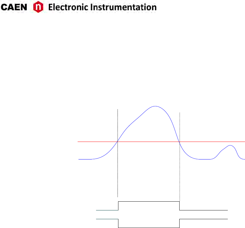
Self-Trigger
Each channel can generate a self-trigger signal (SELF-TRG) when the digized input pulse exceeds a confi-
gurable threshold set through the register address 0x1n80 [RD1].
The individual self-triggers from all channels are propagated to the central trigger logic on the mother-
board (see Fig. 8.9) where they parcipate in logic OR to produce the board common trigger, which is
finally distributed back to all channels on the mezzanines causing the event acquision (see Sec. Trigger
distribuon).
CH0 IN
THRESHOLD
Local Trigger CH0 (Channel
Configuration register <6> =0)
Local Trigger CH0 (Channel
Configuration register <6> =1)
Fig. 8.10: Self-trigger generaon.
Bits[7:0] of register 0x810C allows the user to program which channel parcipates to the global trigger
generaon.
LVDS I/O Trigger
LVDS I/O specific pins on the front panel dedicated connector can be programmed as trigger inputs and
enabled to parcipate in the common trigger generaon with other trigger sources. Refer to Sec. Front
Panel LVDS I/Os for details.
36 UM3350 - V1751/VX1751 User Manual rev. 16
Trigger coincidence level
Operang the waveform recording firmware, the acquision trigger is common to the whole board. This
common trigger allows the coincidence acquision mode to be performed through the Majority operaon.
Enabling the coincidences is possible by wring at register address 0x810C :
• Bits[7:0] enable a specific channel self-trigger to parcipate in the coincidence;
• Bits[23:20] set the coincidence window (TTVAW) linearly in steps of the Trigger clock (8 ns);
• Bits[26:24] set the Majority (i.e. Coincidence) level; the coincidence takes place when:
Number of enabled channels > Majority level
Supposing that bits[7:0] = FF (i.e. all channels are enabled) and bits[26:24] = 01 (i.e. Majority level = 1), a
common trigger is issued whenever at least two of the enabled self-triggers are in coincidence within the
programmed TTVAW.
The Majority level must be smaller than the number of channels enabled via bits[7:0] mask. By default,
bits[26:24] = 00 (i.e. Majority level = 0), which means the coincidence acquision mode is disabled and the
TTVAW is meaningless. In this case, the common trigger is simple OR of the enabled channel self-triggers.
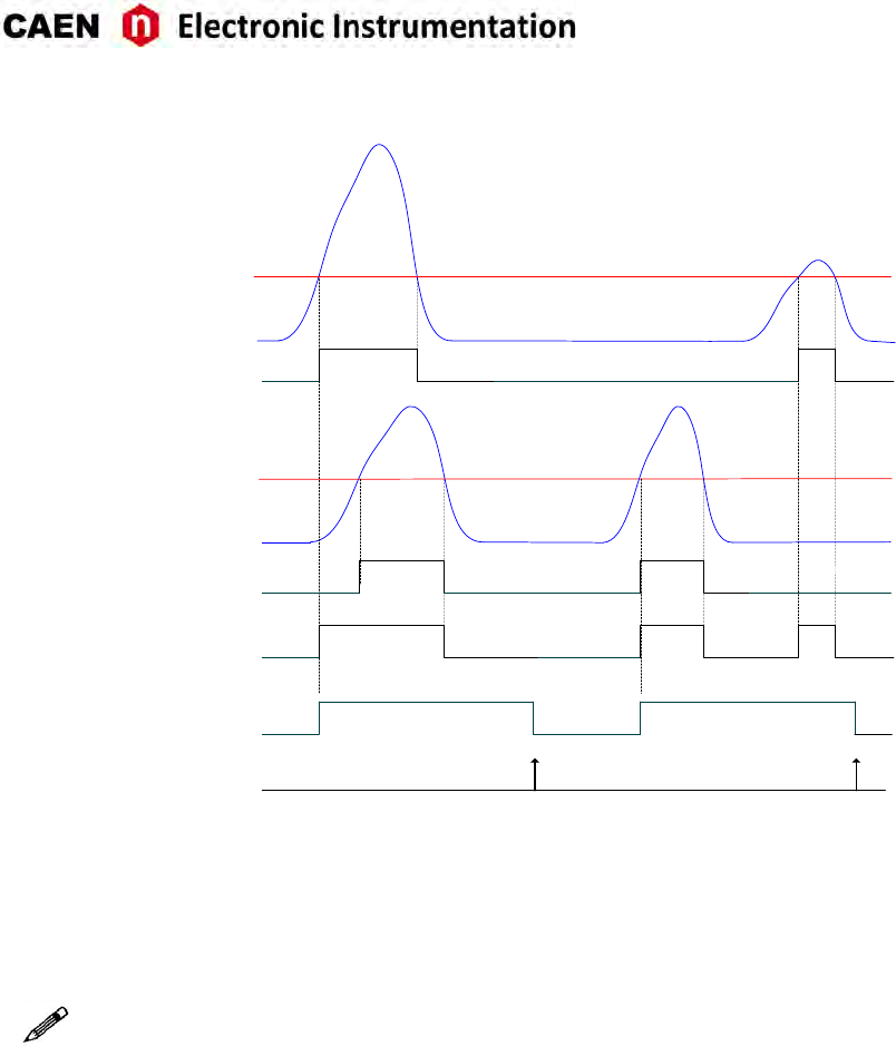
Note: in order not to overload the plots but preserve the clearness of concept, only CH0 and CH1 are
supposed to be fed with input pulses in the following figures.
Fig. 8.11 shows the trigger management in case the coincidences are disabled.
CH1 THRESHOLD
CH0(enabled) IN
CH0 THRESHOLD
TRIGGER
(Maj.lev = 0)
CH1(enabled) IN
OR signal
SELF-TRG[CH0]
SELF-TRG[CH0]
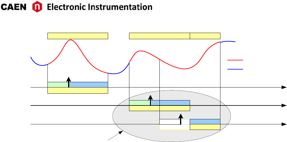
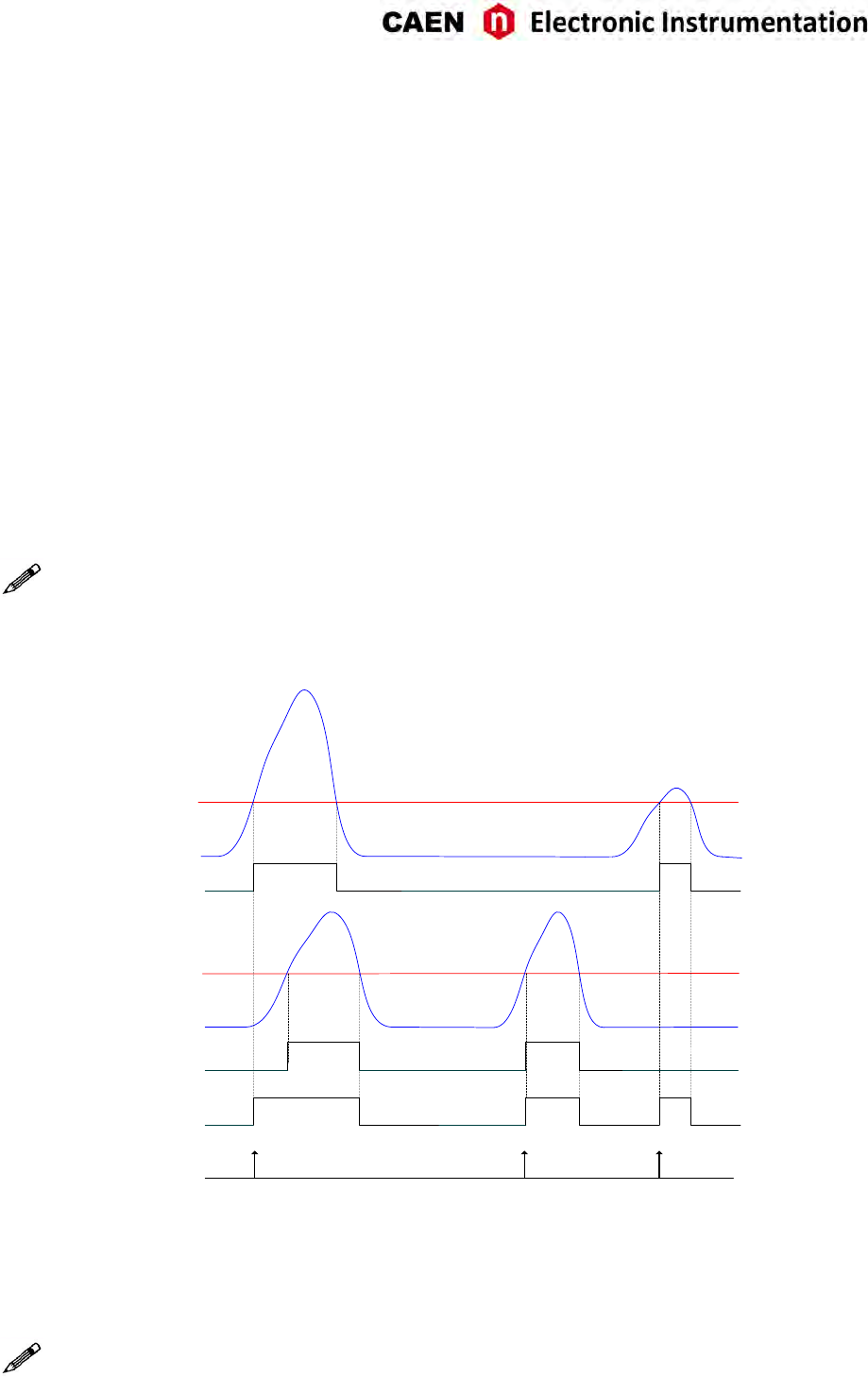
Fig. 8.11: Self-trigger relaonship with Majority level = 0.
Fig. 8.12 shows the trigger management in case the coincidences are enabled with Majority level = 1 and
TTVAW is a value different from 0.
Note: with respect to the posion where the common trigger is generated, the poron of input signal
stored depends on the programmed length of the acquision window and on the post trigger seng.
UM3350 - V1751/VX1751 User Manual rev. 16 37
CH1 THRESHOLD
SELF-TRG[CH0]
SELF-TRG[CH1]
CH0(enabled) IN
CH0 THRESHOLD
TRIGGER
(Maj.lev = 1)
CH1(enabled) IN
OR signal
TTVAW
Fig. 8.12: Self-trigger relaonship with Majority level = 1 and TTVAW ̸= 0.
Fig. 8.13 shows the trigger management in case the coincidences are enabled with Majority level = 1 and
TTVAW = 0 (i.e. 1 clock cycle).
Note: CAEN provides a guide to coincidences including a praccal example of making coincidences with
the waveform recording firmware [RD6].
38 UM3350 - V1751/VX1751 User Manual rev. 16
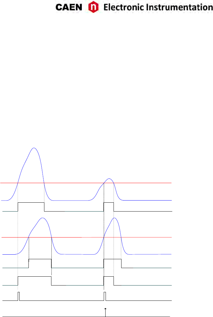
CH1 THRESHOLD
SELF-TRG[CH0]
SELF-TRG[CH1]
CH0(enabled) IN
CH0 THRESHOLD
TRIGGER
(Maj.lev = 1)
CH1(enabled) IN
OR signal
TTVAW
Fig. 8.13: Self-trigger relaonship with Majority level = 1 and TTVAW = 0.
UM3350 - V1751/VX1751 User Manual rev. 16 39
TRG-IN as Gate
It is possible to configure TRG-IN as a gate for trigger an-veto funcon. The common acquision trigger
is then issued upon the AND between the external signal on TRG-IN and the other trigger sources but the
soware trigger (i.e. the soware trigger cannot parcipate in the Trigger as Gate mode).
This mode is enabled by seng bit[27] = 1 of register 0x810C and bit[10] = 1 of register 0x811C . The trigger
sources parcipang in AND with TRG-IN are configurable through register 0x810C as well.
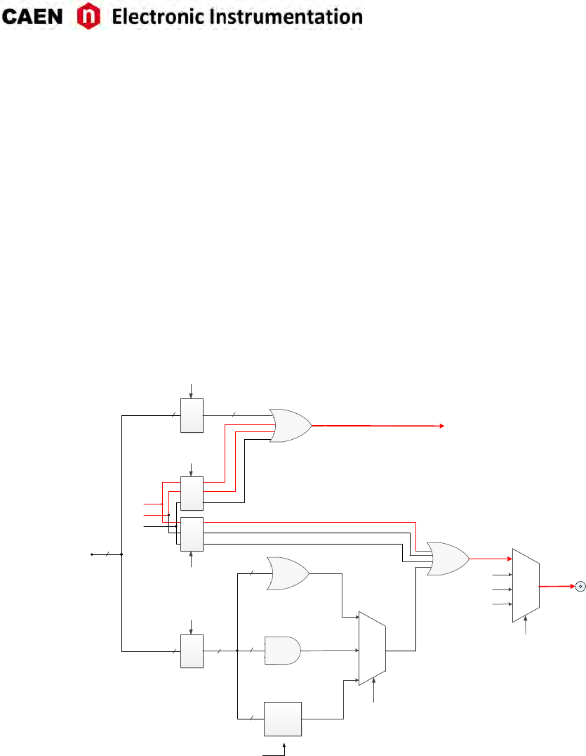
Trigger distribution
As described in Sec. Trigger Management, the OR of all the enabled trigger sources, synchronized with the
internal clock, becomes the common trigger of the board that is fed in parallel to all channels, consequently
causing the capture of an event. By default, only the Soware Trigger and the External Trigger parcipate
in the common acquision trigger (refer to the red path on top of Fig. 8.14).
SELF-TRG[7:0]
TRG-OUT
0x8110
Bits[9:8]
00
01
10
TO THE CHANNELS
COMMON ACQUISITON TRIGGER
0x811C
Bits[17:16]
8
8
00
01
MB PROBES
10
PB PROBES
11
S-IN
8
SW TRG
EXT TRG
MASK 1
0x810C
Bits[7:0]
MASK 4
0x8110
Bits[7:0]
OR
AND
MAJORITY
OR
MASK 2
MASK 3
0x810C
Bits[31:29]
0x8110
Bits[31:29]
EXT TRG
SW TRG
EXT TRG
OR
LVDS I/O
LVDS I/O
TRG SOURCES
0x8110
Bits[12:10]
SW TRG
LVDS I/O
8
8
8
8
8
Fig. 8.14: Trigger configuraon of TRG-OUT front panel connector.
A Trigger Out signal is also generated on the relevant front panel TRG-OUT connector (NIM or TTL), and
allows to extend the trigger signal to other boards. Thanks to its configurability, TRG-OUT can propagate
out:
- the OR of all the enabled trigger sources (only the Soware Trigger is provided by default, as in the
red path of Fig. 8.14);
- the OR, AND or MAJORITY exclusively of the channel self-triggers.
The registers involved in the TRG-OUT programming are:
- Register address 0x8110;
- Register address 0x811C.
40 UM3350 - V1751/VX1751 User Manual rev. 16

Example
It could be required to start the acquision on all the channels of a mul-board system as soon as one of
the board channels (board “n”) crosses its threshold. Trigger Out signal is then fed to an external Fan Out
logic unit (e.g. CAEN V2495 board); the obtained signal has then to be provided to the external trigger
input TRG-IN of all the boards in the system (including the board which generated the Trigger Out signal).
In this case, the programming steps to perform are thereaer described.
1. Register 0x8110 on board “n”:
- Enable the desired self-trigger as Trigger Out signal on board “n” (by bits[7:0] mask).
- Disable Soware Trigger, External Trigger and LVDS I/O Trigger as Trigger Out signal on board “n”
(bits[31:29] = 000).
- Set Trigger Out signal as the OR of the enabled self-trigger on board “n” (bits[9:8] = 00).
2. Register 0x811C on board “n”:
- Configure the digizer to propagates on TRG-OUT the internal trigger sources according to the
0x8110 sengs (i.e. the enabled self-trigger, in the specific case) on board “n” (bits[17:16] = 00).
3. Register 0x810C on all the boards in the system (including board “n”):
- Enable External Trigger to parcipate in the board common acquision trigger, disable Soware
Trigger , LVDS I/O Trigger and the channel self-triggers (bits[31:29] = 010; bits[7:0] = 00000000)
UM3350 - V1751/VX1751 User Manual rev. 16 41

Multi-board Synchronization
When mul-board systems are involved in an experiment, it is necessary to synchronize different boards.
In this way, the user can acquire from N boards with Y channel each, like if they were just one board with
(N x Y) channels.
The main issue synchronizing a mul-board system is to propagate the sampling clock among the boards.
This is made through input/output daisy chain connecons among the digizers. One board must be chosen
to be the “master” board that propagates its own clock to the others. A programmable phase shi can
adjust possible delays in the clock propagaon. This allows to have both the ADC sampling clock and the
me reference in common for all boards. Having the same me reference means that the acquision
starts/stops at the same me, and that the me stamps of different boards are aligned to the same absolute
me.
There are several ways to implement the trigger logic. The synchronizaon tool allows to propagate the
trigger to all boards and acquire the events accordingly. Moreover, in case of busy state of one or more
boards, the acquision is inhibited for all boards.
As a detailed guide to mul-board synchronizaon, CAEN provides a dedicated Applicaon Note [RD7].
42 UM3350 - V1751/VX1751 User Manual rev. 16
Front Panel LVDS I/Os
The V1751 is provided with 16 general purpose programmable LVDS I/O signals (see Chap. Panels Descrip-
on). From the ROC FPGA firmware revision 3.8 on, a more flexible configuraon management has been
introduced, which allows these signals to be programmed in terms of direcon (INPUT/OUTPUT) and func-
onality by groups of 4.
THE USER MUST SET BIT[8] = 1 AT 0x811C IN ORDER TO ENABLE THE NEW LVDS I/Os CONFIGURATION
MODES
NOTE ABOUT LVDS I/Os CONFIGURATIONS IMPLEMENTED IN ROC FW RELEASES <3.8
THE WAVEFORM RECORDING FIRMWARE MAKES ALSO AVAILABLE THE OLD CONFIGURATIONS
(bit[8] = 0). USERS WHOSE SOFTWARE BASES ON THE OLD LVDS I/Os CONFIGURATION MAN-
AGEMENT CAN REFER TO THE USER MANUAL OF THE RELEVANT DIGITIZER OR CAN CONTACT
CAEN FOR INFORMATION (see Chap. Technical Support).
SINCE THIS COULD BE NO LONGER GUARANTEED IN THE FUTURE, THE USER IS HEARTLY REC-
OMMENDED TO TAKE THE NEW CONFIGURATION MANAGEMENT AS REFERENCE!
The direcon of the signals are set by the bits[5:2] at register address 0x811C:
Bit[2] → LVDS I/O[3:0]
Bit[3] → LVDS I/O[7:4]
Bit[4] → LVDS I/O[11:8]
Bit[5] → LVDS I/O[15:12]
Where seng the bit to 0 enables the relevant signals in the group as INPUT, while 1 enables them as
OUTPUT.
By default, the new modes are disabled (i.e. bit[8] = 0) and the status of the LVDS I/O signals is congruent
with the old Programmed I/O mode (see Tab. 8.3).
Nr. Direcon Funcon Descripon
0 out Ch 0 self-trigger
The over-threshold informaon
from the relevant channel
1 out Ch 1 self-trigger
2 out Ch 2 self-trigger
3 out Ch 3 self-trigger
4 out Ch 4 self-trigger
5 out Ch 5 self-trigger
6 out Ch 6 self-trigger
7 out Ch 7 self-trigger
8 out Memory Full Memory full flag
9 out Event Data Ready Board event data ready flag
10 out Channels Trigger OR of the new event to be read signal
11 out RUN Status Board run flag
12 in Trigger Time Tag Reset (acve low) Reset of the trigger me tag counter
13 in Memory Clear (acve low) Clear command of all channel memories
14 - reserved N.A.
15 - reserved N.A.
Tab. 8.3: Front Panel LVDS I/Os default sengs.
UM3350 - V1751/VX1751 User Manual rev. 16 43
When enabled (i.e. bit[8] = 1), the new management allows each group of 4 signals of the LVDS I/O 16-pin
connector to be configured in one of the 4 following modes (according to bits[15:0] at register address
0x81A0):
- Mode 0 (bits[n+3:n] = 0000): REGISTER
- Mode 1 (bits[n+3:n] = 0001): TRIGGER
- Mode 2 (bits[n+3:n] = 0010): nBUSY/nVETO
- Mode 3 (bits[n+3:n] = 0011): LEGACY
where n = 0, 4, 8, 12.
Note: Whatever opon is set, the LVDS I/Os are always latched with the trigger and the relevant status of
the 16 signals is always wrien into the header Paern field (see Sec. Event structure); the user can then
choose to read it out or not.
REGISTER TRIGGER nBUSY/nVETO LEGACY
LVDS IN [15:12] Reg[15:12] Not available
15: nRunIn
14: nTriggerIn
13: nVetoIn
12: nBusyIn
15: reserved
14: reserved
13: reserved
12: nClear_TTT
LVDS IN [11:8] Reg[11:8] Not available
11: nRunIn
10: nTriggerIn
9: nVetoIn
8: nBusyIn
11: reserved
10: reserved
9: reserved
8: nClear_TTT
LVDS IN [7:4] Reg[7:4] Not available
7: nRunIn
6: nTriggerIn
5: nVetoIn
4: nBusyIn
7: reserved
6: reserved
5: reserved
4: nClear_TTT
LVDS IN [3:0] Reg[3:0] Not available
3: nRunIn
2: nTriggerIn
1: nVetoIn
0: nBusyIn
3: reserved
2: reserved
1: reserved
0: nClear_TTT
Tab. 8.4: Features descripon when LVDS group is configured as INPUT
REGISTER TRIGGER nBUSY/nVETO LEGACY
LVDS OUT [15:12] Reg[15:12] TrigOut_Ch[7:4]
15: nRun
14: nTrigger
13: nVeto
12: nBusy
15: Run
14: Trigger
13: DataReady
12: Busy
LVDS OUT [11:8] Reg[11:8] TrigOut_Ch[3:0]
11: nRun
10: nTrigger
9: nVeto
8: nBusy
11: Run
10: Trigger
9: DataReady
8: Busy
LVDS OUT [7:4] Reg[7:4] TrigOut_Ch[7:4]
7: nRun
6: nTrigger
5: nVeto
4: nBusy
7: Run
6: Trigger
5: DataReady
4: Busy
LVDS OUT [3:0] Reg[3:0] TrigOut_Ch[3:0]
3: nRun
2: nTrigger
3: nVeto
0: nBusy
3: Run
2: Trigger
1: DataReady
0: Busy
Tab. 8.5: Features descripon when LVDS group is configured as OUTPUT
44 UM3350 - V1751/VX1751 User Manual rev. 16

Mode 0: REGISTER
Direcon is INPUT: the logic level of the LVDS I/O signals can be read at register address 0x8118.
Direcon is OUTPUT: the logic level of the LVDS I/O signals can be wrien at register address 0x8118.
Mode 1: TRIGGER
Direcon is INPUT: Not available.
Direcon is OUTPUT: the TrgOut_Ch[(n + 3) : n] signals (n = 0, 4) consist of the channel self-triggers coming
directly from the mezzanines.
Mode 2: nBUSY/nVETO
nBusy Signal
nBusyIn (INPUT) is an acve low signal which, if enabled, is used to generate the nBusy signal (OUTPUT) as
below.
The Busy signal (fed out on LVDS I/Os or TRG-OUT LEMO connector) is:
Almost_Full OR (LVDS_BusyIn AND BusyIn_enable)
where
-Almost_Full indicates the filling of the Buffer Memory up to a programmable level (12-bit range) set
at register address 0x816C;
-LVDS_BusyIn is available in nBUSY/nVETO configuraon (see Tab. 8.5);
-BusyIn_enable is set at register address 0x8100, bit[8].
nVETO Signal
Direcon is INPUT: nVETOIn is an acve low signal which, if enabled (register address 0x8100, bit[9] = 1), is
used to veto the generaon of the common trigger propagated to the channels for the event acquision.
Direcon is OUTPUT: the nVETO signal is the copy of nVETOIn.
nTrigger Signal
Direcon is INPUT: nTriggerIn is an acve low signal which, if enabled, is a real trigger able to cause the
event acquision. It can be propagated to TRG-OUT LEMO connector or to the individual triggers.
Direcon is OUTPUT: nTrigger signal is the copy of the trigger signal propagated to the TRG-OUT LEMO
connector or copy of the acquision common trigger. This is selected by bit[16] of the 0x81A0 register.
nRun Signal
Direcon is INPUT: nRunIn is an acve low signal which can be used as Start for the digizer (register address
0x8100, bits[1:0] = 11). It is possible to program the Start on the level or on the edge of the nRunIn signal
(register address 0x8100, bit[11]).
Direcon is OUTPUT: nRun signal is the inverse of the internal Run of the board.
UM3350 - V1751/VX1751 User Manual rev. 16 45

Mode 3: LEGACY
Legacy Mode has been introduced in order the LVDS connector (properly programmed) to be able to fea-
ture the same I/O signals available in the ROC FPGA firmware revisions lower than 3.8.
nClear_TTT Signal
It is the only signal available as INPUT. It is the Trigger Time Tag (TTT) reset, like in the old configuraon.
Busy Signal
The Busy signal is acve high and it is exactly the inverse of the nBusy signal (see Sec. Mode 2: nBUSY/nVETO).
In case register address 0x816C is set to 0x0 and the BusyIn signal is disabled, the Busy is the FULL signal
present in the old configuraon.
DataReady Signal
The DataReady is an acve high signal indicang that the board has data available for readout (the same
as the DataReady front panel LED does).
Trigger Signal
The acve high Trigger signal is the copy of the acquision trigger (common trigger) sent from the moth-
erboard to the mezzanines (it is neither the signal provided out on the TRG-OUT LEMO connector nor the
inverse of the signal sent to the LVDS connector).
Run Signal
The Run signal is acve high and represents the inverse of the nRun signal (see Sec. Mode 2: nBUSY/nVETO).
46 UM3350 - V1751/VX1751 User Manual rev. 16
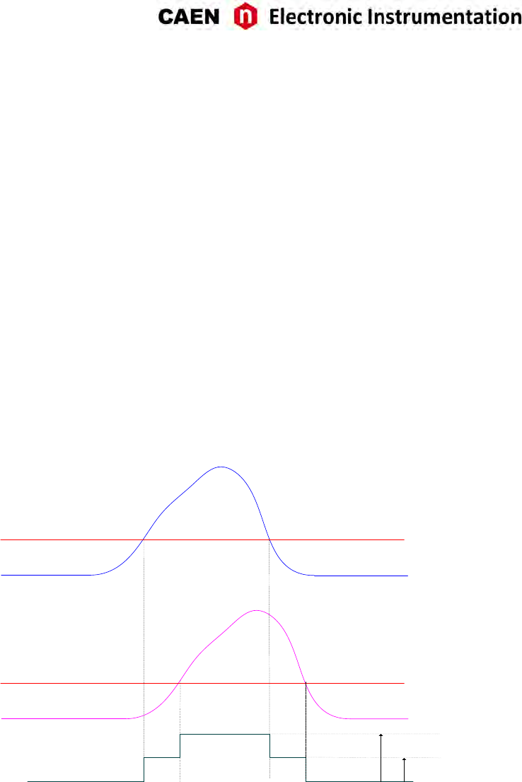
Analog Monitor
The board houses a 12bit (125 MHz) DAC with 0 ÷1 V dynamics on a 50 Ωload (see Fig. 2.1), whose
input is controlled by the ROC FPGA and the signal output (driving 50 Ω) is available on the MON/Σ output
connector. MON output of more boards can be summed by an external Linear Fan In.
The DAC control logic implements four operang modes according to the value of bits[2:0] at register ad-
dress 0x8144:
- Trigger Majority Mode (0x8144 = 0x0)
- Test Mode (0x8144 = 0x1)
- Buffer Occupancy Mode (0x8144 = 0x3)
- Voltage Level Mode (0x8144 = 0x4)
Trigger Majority Mode
It is possible to generate a Majority signal with the DAC: a voltage signal whose amplitude is proporonal
to the number of channels under/over threshold (1 step = 125 mV); this allows, via an external discrimina-
tor, to produce a common trigger signal, as the number of triggering channels has exceeded a parcular
threshold.
CH0 IN
CH1 IN
THRESHOLD
THRESHOLD
MAJORITY
125mV
250mV
Fig. 8.15: Majority logic (2 channels over-threshold; bit[6]=0 register address 0x8000).
In the example depicted in Fig. 8.15, the MON output provides a signal whose amplitude is proporonal to
the number of channels over the trigger threshold.
UM3350 - V1751/VX1751 User Manual rev. 16 47

Test Mode
In this mode the MON output provides a sawtooth signal with 1 V amplitude and 30.52 kHz frequency.
Buer Occupancy Mode
In this mode, MON output connector provides a voltage value increasing, proporonally with the number
of buffers filled with events, in fixed steps of 0.976 mV given by:
Vmax
Nbmax
where Vmax ≈1 V and Nbmax = 1024 is the Maximum_Number_of_Buffers (i.e. the value of the register
address 0x800C, as introduced in Sec. Mul-Event Memory Organizaon).
Example: if 0x800C = 0x4 (i.e. 16 buffers), the maximum Buffer Occupancy output voltage level is given by
0.976 mV ×16.
This mode allows to test the readout efficiency: in fact, if the average event readout throughput is as fast as
trigger rate, then MON out value remains constant; otherwise if MON out value grows in me, this means
that readout rate is slower than trigger rate.
Starng from revision 4.9 of the ROC FPGA (motherboard) firmware, it is possible to apply a digital gain
to the fixed step, parcularly when the memory is organized in a small number of buffers. The gain can
be set as powers of two ranging between 20= 1 (no gain, which is the default seng) and 2A, where the
exponent is the value to write at register address 0x81B4.
Voltage Level Mode
In this mode, MON out provides a voltage value programmable via the 12-bit ’N’ parameter wrien in the
0x8138 register, with: Vmon =1
/4096 ×N (Volt).
48 UM3350 - V1751/VX1751 User Manual rev. 16
Test Pattern Generator
The FPGA AMC can emulate the ADC and write into memory a sawtooth signal for test purposes. It can be
enabled via register 0x8000. Fig. 8.16 shows the test ramps for even and odd channels respecvely.
0
200
400
600
800
1000
1200
0 200 400 600 800 1000 1200 1400
0
200
400
600
800
1000
1200
0 200 400 600 800 1000 1200 1400
1023
1023
Even channel test wave
Odd channel test wave
-0
200
400
600
800
1000
1021 1022 1023 1024 1025 1026 1027 1028 1029 1030
1023
255
63 15 3 0
Even channel ramp down zoom
-0
200
400
600
800
1000
1021 1022 1023 1024 1025 1026 1027 1028 1029 1030
1023
768
960 1008 1020
Odd channel ramp up zoom
Fig. 8.16: FPGA Test Waveform.
UM3350 - V1751/VX1751 User Manual rev. 16 49

Reset, Clear and Default Conguration
Global Reset
Global Reset is performed at power-on of the module or via soware by write access at register address
0xEF24 . It allows to clear the data off the Output Buffer, the event counter and performs a FPGAs global
reset, which restores the FPGAs to the default configuraon. It inializes all counters to their inial state
and clears all detected error condions.
Memory Reset
The Memory Reset clears the data off the Output Buffer.
The Memory Reset can be forwarded via a write access at register address 0xEF28 . In the old LVDS I/O
configuraon (ROC FPGA revision before 3.8), it is also possible to perform a memory clear by sending a
pulse to the front panel dedicated Memory Clear input (see Tab. 8.3).
Timer Reset
The Timer Reset allows to inialize the mer which tags an event. The Timer Reset can be forwarded with
a pulse sent either to the LVDS I/O dedicated input (see Tab. 8.3 and Sec. Mode 3: LEGACY) or to the S-IN
input (leading edge sensive).
50 UM3350 - V1751/VX1751 User Manual rev. 16
VMEBus Interface
The module is provided with a fully compliant VME64/VME64X interface, whose main features are:
• EUROCARD 9U Format
• J1/P1 and J2/P2 with either 160 pins (5 rows) or 96 (3 rows) connectors
• A24, A32 and CR-CSR address modes
• D32, BLT/MBLT, 2eVME, 2eSST data modes
• MCST write capability
• CBLT data transfers
• RORA interrupter
• Configuraon ROM
Addressing Capabilities
• Base address: the module works in A24/A32 mode The Base Address of the module is selected through
four rotary switches (see Fig. 7.2), then it is validated only with either a power-ON cycle or a System
Reset (see Sec. Reset, Clear and Default Configuraon).
ADDRESS MODE ADDRESS RANGE NOTES
A24 [0x000000:0xFF0000] SW2 and SW3 ignored
OFFSET
31 16 15 0
2324
2
7
3
5
6
4
1
0
A
B
C
D
E
F
8
9
2
7
3
5
6
4
1
0
A
B
C
D
E
F
8
9
SW4 SW5
Fig. 8.17: A24 addressing.
ADDRESS MODE ADDRESS RANGE NOTES
A32 [0x00000000:0xFFFF0000]
OFFSET
31 16 15 0
2324
2
7
3
5
6
4
1
0
A
B
C
D
E
F
8
9
2
7
3
5
6
4
1
0
A
B
C
D
E
F
8
9
2
7
3
5
6
4
1
0
A
B
C
D
E
F
8
9
2
7
3
5
6
4
1
0
A
B
C
D
E
F
8
9
SW5SW4SW3SW2
Fig. 8.18: A32 addressing.
• CR/CSR address: the addressing is based on the slot number taken from the relevant backplane lines.
The recognised Address Modifier for this cycle is 2F. This feature is implemented only on versions with
160-pin connectors.
OFFSET
31 16 15 0
2324
GEO
19 18
Fig. 8.19: CR/CSR addressing.
UM3350 - V1751/VX1751 User Manual rev. 16 51
Address Relocation
The bit[15:0] of register address 0xEF10 allow to set via soware the board Base Address (valid values ≠ 0).
Such register allows to overwrite the rotary switches sengs; its seng is enabled via bit[6] of the register
address 0xEF00. The used addresses are:
OFFSET
31 16 15 0
2324
ADER H ADER L software
relocation
OFFSET
31 16 15 0
2324
ADER L
A32
A24
software
relocation
Fig. 8.20: Soware relocaon of base address
52 UM3350 - V1751/VX1751 User Manual rev. 16

Data Transfer Capabilities and Events Readout
The board features a Mul-Event digital memory per channel, configurable by the user to be divided into
1 up to 1024 buffers, as detailed in Sec. Mul-Event Memory Organizaon. Once they are wrien in the
memory, the events become available for readout via VMEbus or Opcal Link. During the memory readout,
the board can store other events (independently from the readout) on the available free buffers.
The events are read out sequenally and completely, starng from the Header of the first available event,
followed by the samples of the enabled channels (from 0 to 7) as reported in . Once an event is completed,
the relevant memory buffer becomes free and ready to be wrien again (old data are lost). Aer the last
word in an event, the first word (Header) of the subsequent event is readout. It is not possible to read out
an event parally.
The size of an event (EVENT SIZE) is configurable and depends on register addresses 0x8020 and 0x800C ,
as well as on the number of enabled channels. The board supports D32 single data readout, Block Transfer
BLT32 and MBLT64, 2eVME and 2eSST cycles. Sustained readout rate is up to 60 MB/s with MBLT64, up to
100 MB/s with 2eVME and up to 160 MB/s with 2eSST.
Block Transfer D32/D64, 2eVME, and 2eSST
The Block Transfer readout mode allows to read N complete events sequenally, where N is set at register
address 0xEF1C , or by using the SetMaxNumEventsBLT funcon of the CAENDigizer library [RD4].
When developing programs, the readout process can be implemented on different basis :
• Using Interrupts: as soon as the programmed number of events is available for readout, the board
sends an interrupt to the PC over the opcal communicaon link (not supported by USB).
• Using Polling (interrupts disabled): by performing periodic read accesses to a specific register of the
board it is possible to know the number of events present in the board and perform a BLT read of the
specific size to read them out.
• Using Connuous Read (interrupts disabled): connuous data read of the maximum allowed size (e.g.
total memory size) is performed by the soware without polling the board. The actual size of the block
read is determined by the board that terminates the BLT access at the end of the data, according to
the configuraon of register address 0xEF1C, or the library funcon SetMaxNumEventsBLT menoned
above. If the board is empty, the BLT access is immediately terminated and the “Read Block” funcon
will return 0 bytes (it is the ReadData funcon in the CAENDigizer Library).
The event is configurable as indicated in the introducon of the paragraph, namely:
[Event Size] = [8*(Buffer Size)] + [16 bytes]
Then, it is necessary to perform as many cycles as required in order to readout the programmed number
of events.
It is suggested to enable BERR signal during BLT32 cycles, in order to end the cycle avoiding filler readout.
The last BLT32 cycle will not be completed, it will be ended by BERR aer the #N event in memory is
transferred (see example in the figure below).
Since some 64-bit CPU cut off the last 32- bit word of a transferred block, if the number of words composing
such block is odd, it is necessary to add a dummy word (which has then to be removed via soware) in order
to avoid data loss. This can be achieved by seng the ALIGN64 bit (bit[5]) at register address 0xEF00.
MBLT64 cycle is similar to the BLT32 cycle, except that the address and data lines are mulplexed to form
64 bit address and data buses.
The 2eVME allows to achieve higher transfer rates thanks to the requirement of only two edges of the two
control signals (DS and DTACK) to complete a data cycle
UM3350 - V1751/VX1751 User Manual rev. 16 53
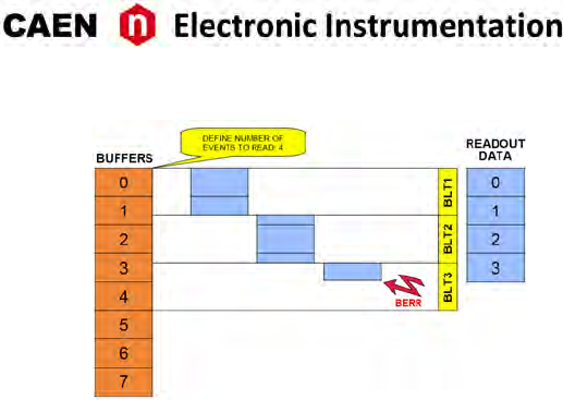
Fig. 8.21: Example of BLT readout
Chained Block Transfer D32/D64
The V1751 allows to readout events from more daisy chained boards (Chained Block Transfer mode).
The technique which handles the CBLT is based on the passing of a token between the boards; it is necessary
to verify that the used VME crate supports such cycles.
Several conguous boards, in order to be Daisy chained, must be configured as “first”, “intermediate” or
“last” via register address 0xEF0C. A common Base Address is then defined via the same register; when a
BLT cycle is executed at the address CBLT_Base + 0x0000 ÷ 0x0FFC, the “first” board starts to transfer its
data, driving DTACK properly; once the transfer is completed, the token is passed to the second board via
the IACKIN-IACKOUT lines of the crate, and so on unl the “last” board, which completes the data transfer
and asserts BERR (which has to be enabled): the Master then ends the cycle and the slave boards are
rearmed for a new acquision.
If the size of the BLT cycle is smaller than the events size, the board which has the token waits for another
BLT cycle to begin (from the point where the previous cycle has ended).
Single D32 Transfer
This mode allows the user to readout a word per me, from the header (actually 4 words) of the first
available event, followed by all the words unl the end of the event, then the second event is transferred.
The exact sequence of the transferred words is shown in Sec. Event structure.
It is suggested, aer the 1st word is transferred, to check the EVENT SIZE informaon and then do as many
cycles as necessary (actually EVENT SIZE -1) in order to read completely the event.
54 UM3350 - V1751/VX1751 User Manual rev. 16
Optical Link Access
The board houses a daisy chainable Opcal Link (communicaon path which uses opcal fiber cables as
physical transmission line) able to transfer data at 80 MB/s, therefore it is possible to connect up to eight
V1751 to a single Opcal Link Controller by using the A2818 PCI card or up to thirty-two V1751 with the
A3818 PCIe card.
Detailed informaon on CAEN PCI/PCIe Controllers can be find at www.caen.it:
Home / Products / Modular Pulse Processing Electronics / PCI/PCIe / Opcal Controller
The parameters for read/write accesses via Opcal Link are the same used by VME cycles (Address Modifier,
Base Address, data Width, etc); wrong parameter sengs cause Bus Error.
Bit[3] at register address 0xEF00 enables the module to broadcast an interrupt request on the Opcal
Link; the enabled Opcal Link Controllers propagate the interrupt on the PCI bus when a request from the
Opcal Link is sensed. Interrupts can also be managed at the CAENDigizer library level (see “Interrupt
Configuraon” [RD4]).
VME and Opcal Link accesses take place on independent paths and are handled by board internal con-
troller, with VME having higher priority; anyway it is beer to avoid accessing the board via VME and
Opcal Link simultaneously.
Note: CONET2 is CAEN proprietary serial protocol developed to allow the opcal link communicaon be-
tween the host PC, equipped with a A2818 or a A3818 Controller, and a CAEN CONET slave. CONET2 is 50%
more efficient in the data rate transfer than the previous CONET1 version. The two protocol versions are
not compliant to eachother and before to migrate from CONET1 to CONET2 it is recommended to read the
instrucons provided by CAEN in the dedicated Applicaon Note [RD8].
UM3350 - V1751/VX1751 User Manual rev. 16 55

9 Drivers &Libraries
Drivers
In order to interface with the board, CAEN provides the drivers for the supported physical communicaon
channels and compliant with Windows® and Linux® OS:
•CONET Opcal Link, managed by the A2818 PCI card or the A3818 PCIe card. The driver installaon
package is available on CAEN website in the “Soware/Firmware” tab at the A2818 or A3818 page
(login required).
Note: For the installaon of the Opcal Link driver, refer to the User Manual of the specific card.
•USB 2.0 Drivers are managed by the V1718 USB-to-VME Bridge. The driver installaon package is
available on CAEN website in the “Soware/Firmware” area at the V1718 page (login required).
Note: For the installaon of the USB driver, refer to the User Manual of the V1718 Bridge.
Libraries
CAEN libraries are a set of middleware soware required by CAEN soware tools for a correct funconing.
These libraries, including also demo and example programs, represent a powerful base for users who want
to develop customized applicaons for the digizer control (communicaon, configuraon, readout, etc.):
•CAENDigizer is a library of funcons designed specifically for the Digizer families supporng both
waveform recording firmware and DPP firmware. The CAENDigizer library is based on the CAEN-
Comm library. For this reason, the CAENComm libraries must be already installed on the host PC
before installing the CAENDigizer.
The CAENDigizer installaon package and relevant documentaon [RD4] are available on CAEN web-
site in the ”Download” tab at the CAENDigizer Library page.
•CAENComm library manages the communicaon at low level (read and write access). The purpose
of the CAENComm is to implement a common interface to the higher soware layers, masking the
details of the physical channel and its protocol, thus making the libraries and applicaons that rely
on the CAENComm independent from the physical layer. Moreover, the CAENComm requires the
CAENVMELib library (access to the VME bus) even in the cases where the VME is not used. This is the
reason why CAENVMELib has to be already installed on your PC before installing the CAENComm.
The CAENComm installaon package, the relevant documentaon and the link to the required CAEN-
VMELib, are available on CAEN website in the ”Download” tab at the CAENComm Library page.
CAENComm (and other libraries here described) supports the following communicaon channels (Fig. 9.1):
PC → USB (V1718) → VMEbus → V1751(VX1751)
PC → PCI/PCIe (A2818/A3818) → CONET → V1751(VX1751)
PC → PCI/PCIe (A2818/A3818) → CONET (V2718) → VMEbus → V1751(VX1751)
56 UM3350 - V1751/VX1751 User Manual rev. 16
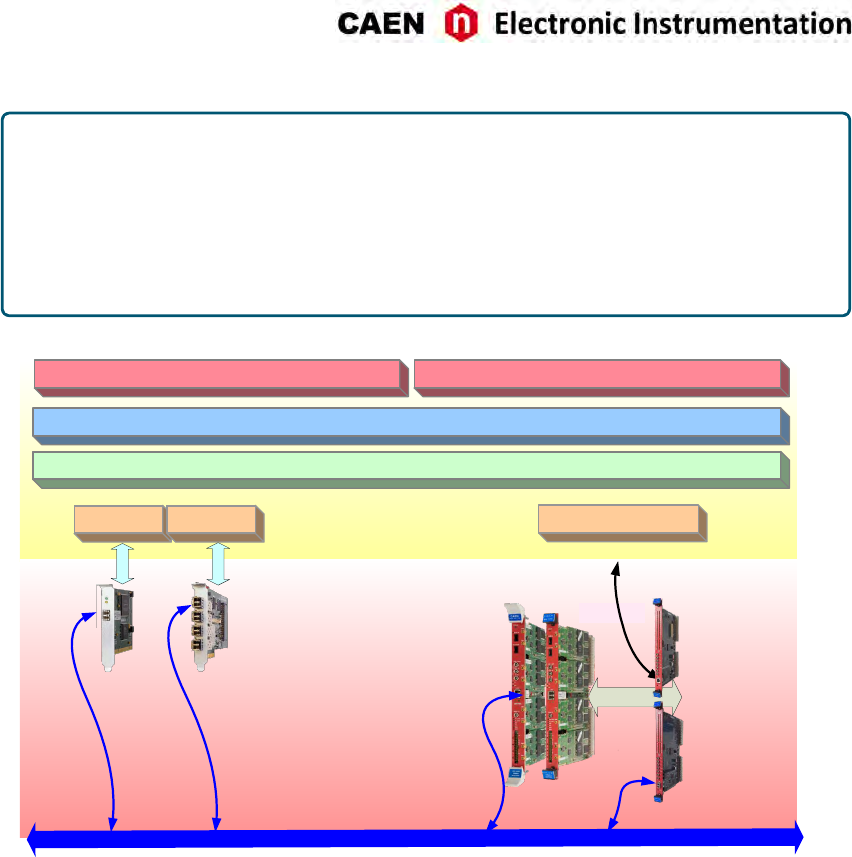
WHEN TO INSTALL CAEN LIBRARIES:
WINDOWS® compliant CAEN soware = NOT. CAEN soware for Windows® OS are stand-alone,
which means the program locally installs the DLL files of the required libraries.
LINUX® compliant CAEN soware = YES. CAEN soware for Linux® OS is not stand-alone. The
user must install the required libraries apart to run the soware.
WINDOWS® and LINUX® compliant customized soware = YES. The user must install the re-
quired libraries apart in case of custom soware development.
CONET2 (Optical Link)
A2818 A3818
CAEN SW Tools
USB 2.0
VME64/VME64X
Digitizers
A2818 driver A3818 driver V1718 USB driver
VMEbus
V1718
V2718
PCI
PCIe
User’s custom software
CAENDigitizer Library
CAENComm Library
Fig. 9.1: Drivers and soware layers.
UM3350 - V1751/VX1751 User Manual rev. 16 57
10 Soware Tools
CAEN provides soware tools to interface the 751 digizer family, which are available for free download at
www.caen.it following the path:
Home / Products / Firmware/Soware / Digizer Soware
CAENUpgrader
CAENUpgrader is free soware composed of command line tools together with a Java Graphical User In-
terface.
CAENUpgrader, for the V1751 , allows in few easy steps to:
• Upload different FPGA firmware versions on the digizer
• Read the firmware release of the digizer and the bridge (when included in the communicaon chain)
• Manage the firmware license, in case of DPP firmware
• Generate a programming file to configure the internal PLL
• Upgrade the internal PLL
• Get the Board Info file, useful in case of support
The soware relies on the CAENComm and CAENVMELib libraries (see Chap. Drivers &Libraries) and re-
quires third-party Java™ SE 8 update 40 (or later) to be installed.
Fig. 10.1: CAENUpgrader Graphical User Interface
CAENUpgrader installaon package can be downloaded on CAEN web site (login required) at:
Home / Products / Firmware/Soware / Digizer Soware / Configuraon Tools / CAENUpgrader
CAEN provides a guide to the soware features and usage [RD9], free downloadable at the web page above.
Note: CAENUpgrader is available for Windows® plaorms (32 and 64-bit) as stand-alone version (all the
required CAEN libraries are installed locally with the program). Only the drivers for the specific commu-
nicaon link must be installed apart by the user. The CAENUpgrader version for Linux® plaorm is not
stand-alone, so it needs the required libraries to be installed apart by the user.
58 UM3350 - V1751/VX1751 User Manual rev. 16
CAENComm Demo
CAENComm Demo is simple soware developed in C/C++ source code and provided both with Java™ and
LabVIEW™ GUI interface. The demo mainly allows for a full board configuraon at low level by direct
read/write access to the registers and may be used as a debug instrument.
Fig. 10.2: CAENComm Demo Java and LabVIEW graphical interface
The Demo is included in the CAENComm library installaon Windows package, which can be downloaded
on CAEN web site (login required) at:
Home / Products / Firmware/Soware / Digizer Soware / Soware Libraries / CAENComm Library
CAEN provides the Demo descripon in the CAENComm library User Manual, free downloadable at the
web page above.
Note: CAENComm Demo is available for Windows® plaorms (32 and 64-bit) and requires CAENComm and
CAENVMELib as addional soware to be installed by the user (see Chap. Drivers &Libraries).
UM3350 - V1751/VX1751 User Manual rev. 16 59
DPP-ZLEplus Control Software
DPP-ZLEplus Control Soware is a demo applicaon introducing the user to understand the principle of
operaon of the Digital Pulse Processing for the Zero Length Encoding (DPP-ZLEplus).
The user can make an enre acquision through this soware, as well use the source code to develop
his/her customized readout program. Indeed, the package includes the C source files and the Visual Studio
project (compliant with Visual Studio Professional 2010).
The DPP-ZLEplus Control Soware is a C-based applicaon that programs the Digizer according to a set of
parameters in the configuraon text file, starts/stops the acquision and manages the data readout. The
waveforms elaborated by the DPP-ZLEplus algorithm are ploed using gnuplot, an external plong tool,
or saved to output text files.
Fig. 10.3: Screen-shots of DPP-ZLEplus Control Soware.
The installaon package can be downloaded on CAEN web site (login required) at:
Home / Products / Firmware/Soware / Digizer Soware / Readout Soware / DPP-ZLEplus Control So-
ware
CAEN provides the soware User Manual [RD3], free downloadable at the web page above.
DPP-ZLEplus Control Soware does not work with waveform recording firmware.
60 UM3350 - V1751/VX1751 User Manual rev. 16
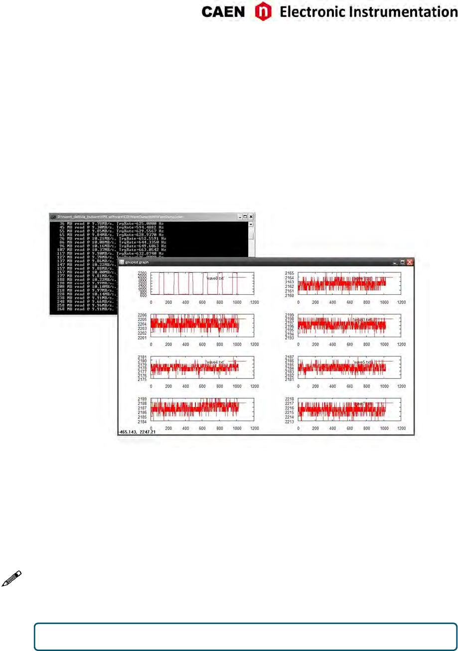
CAEN WaveDump
WaveDump is a basic console applicaon, with no graphics, supporng only CAEN digizers running the
waveform recording firmware. It allows the user to program a single board (according to a text config-
uraon file containing a list of parameters and instrucons), to start/stop the acquision, read the data,
display the readout and trigger rate, apply some post-processing (e.g. FFT and amplitude histogram), save
data to a file and also plot the waveforms using Gnuplot (third-party graphing ulity: www.gnuplot.info).
WaveDump is a very helpful example of C code demonstrang the use of libraries and methods for an
efficient readout and data analysis. Thanks to the included source files and the VS project, starng with
this demo is strongly recommended to all those users willing to write the soware on their own.
Fig. 10.4: CAEN WaveDump
The installaon packages can be downloaded on CAEN web site (login required) at:
Home / Products / Firmware/Soware / Digizer Soware / Readout Soware / CAEN WaveDump
CAEN provides the soware User Manual [RD5] and a guide for geng started with it, free downloadable
at the web page above.
Note: CAEN WaveDump can operate with Windows® and Linux® plaorms (32 and 64 bits); the soware
relies on the CAENDigizer, CAENComm and CAENVMELib libraries (see Chap. Drivers &Libraries). Win-
dows® versions of WaveDump are stand-alone (all required libraries are present within the soware pack-
age), while the Linux® versions need the required libraries to be previously installed by the user. Moreover
Linux® users are required to install the third-party Gnuplot.
CAEN WaveDump does not work with digizers running DPP firmware.
UM3350 - V1751/VX1751 User Manual rev. 16 61
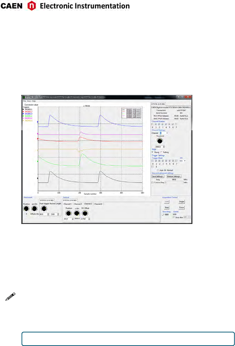
CAEN Scope
In a brand new framework, CAENScope soware allows to manage the CAEN digizers running the wave-
form recording firmware.
CAENScope user friendly interface presents different secons to easily manage the digizer configuraon
and plot the waveforms. Once connected, the program retrieves the digizer informaon. Different pa-
rameters can be set for the channels, trigger and trace visualizaon (up to 12 traces) can be simultaneously
ploed. Signals can be recorded to files in two different formats: Binary (SQLite db) and Text (XML). It is
also possible to save and restore the program sengs.
Fig. 10.5: CAENScope main frame.
CAENScope installaon packages can be downloaded on CAEN web site (login required) at:
Home / Products / Firmware/Soware / Digizer Soware / Readout Soware / CAENSCOPE
CAEN provides the soware User Manual [RD10], free downloadable at the web page above.
Note: Windows® and Linux® versions are stand-alone. The soware downloads the required CAENDigizer,
CAENComm and CAENVMELib libraries.
Linux users are required to install the following packages:
- sharuls;
- libX;
- libXss (specifically for Debian derived distribuons, e.g. Debian, Ubuntu, etc.);
- libXScrnSaver (specifically for RedHat derived distribuons, e.g. RHEL, Fedora, Centos, etc.).
CAENScope does not work with digizers running DPP firmware.
62 UM3350 - V1751/VX1751 User Manual rev. 16
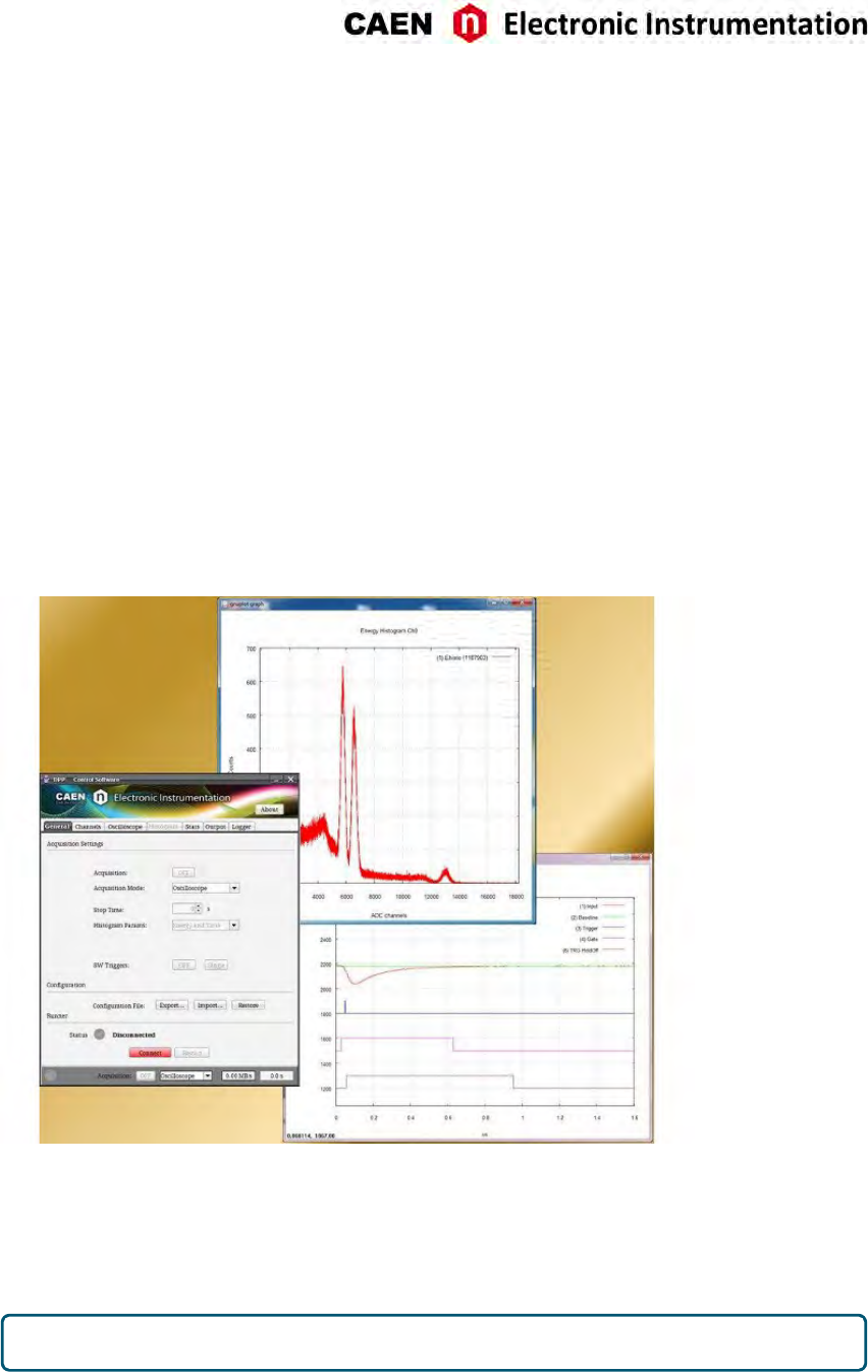
DPP-PSD Control Software
DPP-PSD Control Soware is a demo applicaon introducing the user to understand the principle of oper-
aon of the Digital Pulse Processing for the Pulse Shape Discriminaon (DPP-PSD). It can manage single-
board communicaon and acquision of CAEN 720, 725, 730, and 751 Digizer series running DPP-PSD
firmware and the DT5790 Digital Pulse Analyzer.
DPP-PSD Control Soware is based on a Java Graphical User Interface for the parameters seng (connec-
on, DPP algorithm, acquision, etc.), a C console applicaon working as an acquision engine (DPPRun-
ner) and a third-party graphing ulity (Gnuplot: www.gnuplot.info). The GUI directly handles the acqui-
sion engine through run me commands and generates also a textual configuraon file that contains all
the selected parameters values. This file is read by DPPRunner, which programs the Digizer according to
the parameters, starts the acquision and manages the data readout.
The soware can operate in the Oscilloscope mode, where digized input waveforms and digital signals
from the internal filters are monitored in order to beer tune the DPP parameters, and in the Histogram
mode, where energy (i.e. charge) and me histograms (built by the soware) can be monitored.
According to the operang mode, raw data like waveforms or charges, PSD and me stamp lists, as well as
energy or me histograms can be saved to output files for off-line analysis.
Fig. 10.6: CAEN DPP-PSD Control Soware.
The installaon package can be downloaded on CAEN web site (login required) at:
Home / Products / Firmware/Soware / Digizer Soware / Readout Soware / DPP-PSD Control Soware
CAEN provides the soware User Manual [RD2], free downloadable at the web page above.
CAEN DPP-PSD Control Soware does not work with waveform recording firmware.
UM3350 - V1751/VX1751 User Manual rev. 16 63
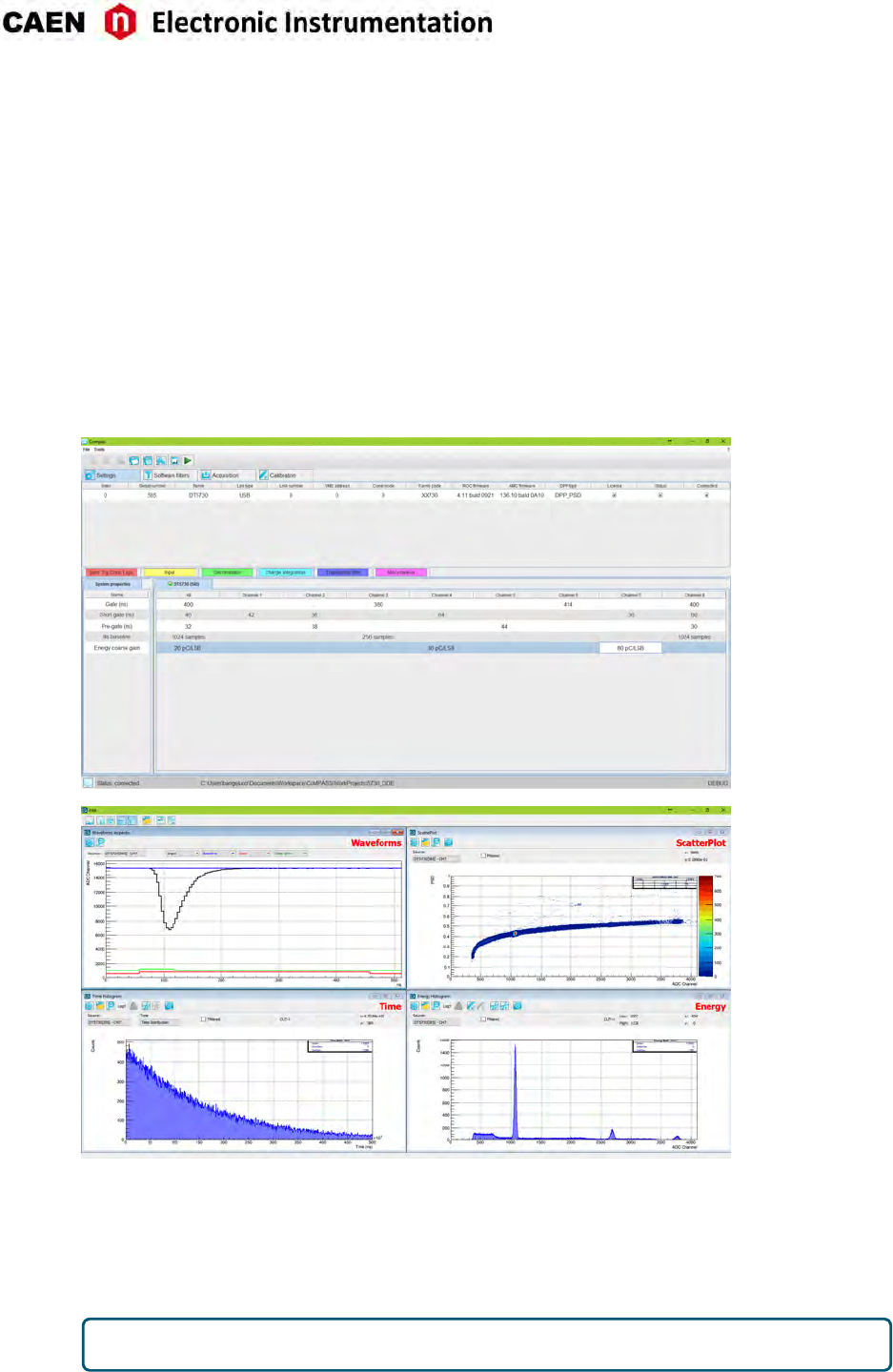
CoMPASS
CoMPASS (CAEN Mul-PArameter Spectroscopy Soware) is the new soware from CAEN able to imple-
ment a Mul-parametric DAQ for Physics Applicaons, where the detectors can be connected directly to
the digizers inputs and the soware acquires energy, ming, and PSD spectra.
CoMPASS soware has been designed as a user-friendly interface to manage the acquision with all the
CAEN DPP algorithm. CoMPASS can manage mulple boards, even in synchronized mode, and the event
correlaon between different channels (hardware and/or soware), apply energy and PSD cuts, calculate
and show the stascs (trigger rates, data throughput, etc...), save the output data files (raw data, lists,
waveforms, spectra) and use the saved files to run off-line with different processing parameters.
CoMPASS Soware supports CAEN x720, x724, x725, x730, x740D, x751 digizer families running the DPP-
PSD, DPP-PHA and DPP-QDC firmware, and the x781 MCA family.
Fig. 10.7: CoMPASS soware tool.
The installaon package can be downloaded on CAEN web site (login required) at:
Home / Products / Firmware/Soware / Digizer Soware / Readout Soware / CoMPASS
CAEN provides the soware User Manual [RD11], free downloadable at the web page above.
CoMPASS does not work with waveform recording firmware.
64 UM3350 - V1751/VX1751 User Manual rev. 16
11 HW Installaon
• The V1751 fits into 6U VME crates.
• VX1751 versions require VME64X compliant crates
• Use only crates with forced cooling air flow
• Turn the crate OFF before board inseron/removal
• Remove all cables connected to the front panel before board inseron/removal
CAUTION: this product needs proper cooling.
USE ONLY CRATES WITH FORCED COOLING AIR FLOW SINCE
OVERHEATING THE BOARD MAY DEGRADE ITS PERFORMANCES!
CAUTION: this product needs proper handling.
V1751/VX1751 DO NOT SUPPORT LIVE INSERTION (HOT SWAP)!
REMOVE OR INSERT THE BOARD WHEN THE VME CRATE IS
POWERED OFF!
ALL CABLES MUST BE REMOVED FROM THE FRONT PANEL BEFORE
EXTRACTING THE BOARD FROM THE CRATE!
UM3350 - V1751/VX1751 User Manual rev. 16 65
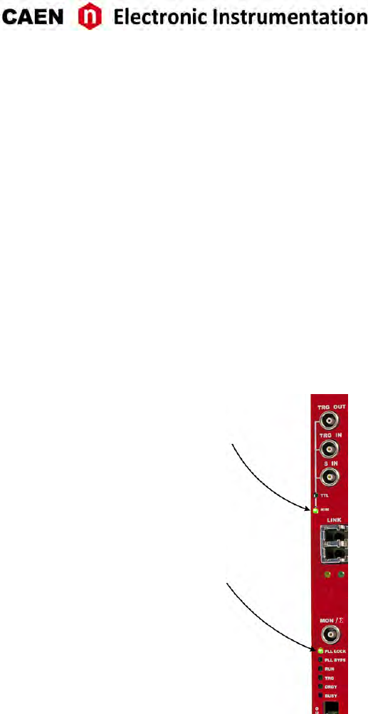
Power-on Sequence
To power on the board, perform the following steps:
1. Insert the V1751 into the crate;
2. power up the crate.
Power-on Status
At power-on, the module is in the following status:
• the Output Buffer is cleared;
• registers are set to their default configuraon
Aer the power-on, only the NIM and PLL LOCK LEDs must stay ON (see Fig. 11.1).
Fig. 11.1: Front panel LEDs status at power-on.
66 UM3350 - V1751/VX1751 User Manual rev. 16

12 Firmware and Upgrades
The board hosts one FPGA on the mainboard and two FPGAs per mezzanine (i.e. one FPGA per channel).
The channel FPGAs firmware is idencal. A unique file is provided that will update all the FPGAs at the
same me.
ROC FPGA MAINBOARD FPGA (Readout Controller + VME interface):
FPGA Altera Cyclone EP1C20
AMC FPGA MEZZANINE FPGA (ADC readout/Memory Controller):
FPGA Altera Cyclone EP1C20
The firmware is stored onto the on-board FLASH memory. Two copies of the firmware are stored in two
different pages of the FLASH, referred to as Standard (STD) and Backup (BKP). In case of waveform recording
firmware, the board is delivered equipped with the same firmware version on both pages.
At power-on, a micro-controller reads the FLASH memory and programs the module automacally loading
the first working firmware copy, that is the STD one in normal operang.
The on-board dedicated SW7 dip switch, set on STD posion by default, allows to select the first FLASH
page to be read at power-on (see Sec. Internal Components).
It is possible to upgrade the board firmware via VMEbus or Opcal Link by wring the FLASH with the
CAENUpgrader soware (see Chap. Soware Tools).
IT IS STRONGLY SUGGESTED TO OPERATE THE DIGITIZER UPON THE STD COPY OF THE
FIRMWARE. UPGRADES ARE SO RECOMMENDED ONLY ON THE STD PAGE OF THE FLASH. THE
BKP COPY IS TO BE INTENDED ONLY FOR RECOVERY USAGE. IF BOTH PAGES RESULT COR-
RUPTED, THE USER WILL NO LONGER BE ABLE TO UPLOAD THE FIRMWARE VIA VMEbus OR
OPTICAL LINK AGAIN AND THE BOARD NEEDS TO BE SENT TO CAEN FOR REPAIR!
Firmware Upgrade
All firmware updates are available for download on CAEN website www.caen.it (login required) at the
following path:
Home / Products / Modular Pulse Processing Electronics / VME / Digizers / V1751
Different firmware are available for the 751 family:
• The waveform recording firmware;
• The special DPP firmware for Physics Applicaons:
–DPP-PSD firmware to use the digizer as a digital replacement Dual Gate QDC, Discriminator and
Gate Generator.
–DPP-ZLEplus firmware to transfer the waveform in a compact format performing an advanced
Zero Suppression algorithm.
DPP firmware updates can also be found at the relevant DPP firmware web page:
Home /Products / Firmware/Soware / DPP Firmware/Soware Tools (Digizer) / DPP Firmware / <DPP-
FIRMWARE>
UM3350 - V1751/VX1751 User Manual rev. 16 67
Firmware File Description
The programming file has the extension .CFA (CAEN Firmware Archive). It is an archiving file format that ag-
gregates all the programming files of the same firmware kind which are compable with the same digizer
family.
The CFA naming convenon follows this general scheme:
• x751_rev_X.Y_W.Z.CFA for the waveform recording firmware
where x751 are all the supported boards (the 751 family includes DT5751, N6751, V1751, VX1751), X.Y is
the major/minor revision number of the mainboard FPGA, and W.Z is the major/minor revision number of
the channel FPGA.
The major revision number of the channel FPGA is a fixed number specific for each DPP and digizer family,
and it can be equal or grater than 128 (for example, ). The waveform recording firmware major revision
number is not fixed and it is less than 128.
Note: DPP special firmware is a pay firmware requiring a license to be purchased. If not licensed, the
firmware can be loaded but it will run fully funconal with a me limitaon per power cycle (30 minutes).
Details on the license ordering procedure are included in the CAENUpgrader guide [RD9].
Troubleshooting
In case of upgrade failure (e.g. STD FLASH page is corrupted), the user can try to reboot the board: aer
a power cycle, the system programs the board automacally from the alternave FLASH page (e.g. BKP
FLASH page), if this is not corrupted as well. The user can so perform a further upgrade aempt on the
STD page to restore the firmware copy.
BECAUSE OF AN UPGRADE FAILURE, THE SW7 DIP SWITCH POSITION MAY NOT CORRESPOND
TO THE FLASH PAGE FIRMWARE COPY LOADED ON THE BOARD FPGAs.
Note: old versions of the digizer motherboard have a slightly different FLASH management. Use CAENUp-
grader 1.6.0 or later to get the BoardInfoFile (using the ”Get Informaon” funcon) and check that the
FLASH_TYPE=0. Alternavely, use a soware ulity like CAENComm Demo to read at register address
0xF050 and check that bit[7]=0.
In this case, at power-on, the micro-controller loads exactly the firmware copy from the FLASH page se-
lected through the SW7 dip switch (e.g. STD by default) .
When a failure occurs during the upgrade of the STD page of the FLASH, which compromises the commu-
nicaon with the V1751 , the user can perform the following recovering procedure as first aempt:
- force the board to reboot loading the copy of the firmware stored on the BKP page of the FLASH. For
this purpose, power off the crate, switch the dedicated SW1 switch to BKP posion and power on the
crate .
- use CAENUpgrader to read the firmware revision (in this case the one of the BKP copy). If this suc-
ceeds, it is so possible to communicate again with the board;
- use CAENUpgrader to load the proper firmware file on the STD page, then power off the crate, switch
SW7 back to STD posion and power on the crate.
If neither of the procedures here described succeeds, it is recommended to send the board back to CAEN
in repair (see Chap. Technical Support).
68 UM3350 - V1751/VX1751 User Manual rev. 16

13 Technical Support
CAEN support services are available for the user by accessing the Support &Services area on CAEN website
at hp://www.caen.it.
Returns and Repairs
Users who need for product(s) return and repair have to fill and send the Product Return Form (PRF) in the
Returns and Repairs area at Home / Support &Services, describing the specific failure. A printed copy of
the PRF must also be included in the package to be shipped.
Contacts for shipping are reported on the website at Home / Contacts.
Technical Support Service
CAEN experts can provide technical support at the e-mail addresses below:
support.nuclear@caen.it
(for quesons about the hardware)
support.compung@caen.it
(for quesons about soware and libraries)
UM3350 - V1751/VX1751 User Manual rev. 16 69
UM3350 - V1751/VX1751 User Manual rev. 16- June 12th , 2017
00000-00-02827-GXXX
Copyright ©CAEN SpA. All rights reserved. Informaon in this publicaon supersedes all earlier versions. Specificaons subject to change without noce.
