UltraScale FPGA Product Tables And Selection Guide Ultra Scale FPGAs
User Manual:
Open the PDF directly: View PDF ![]() .
.
Page Count: 12
© Copyright 2013–2016 Xilinx
.
© Copyright 2013–2016 Xilinx
.
Page 2
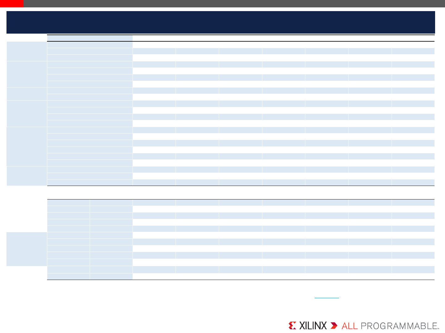
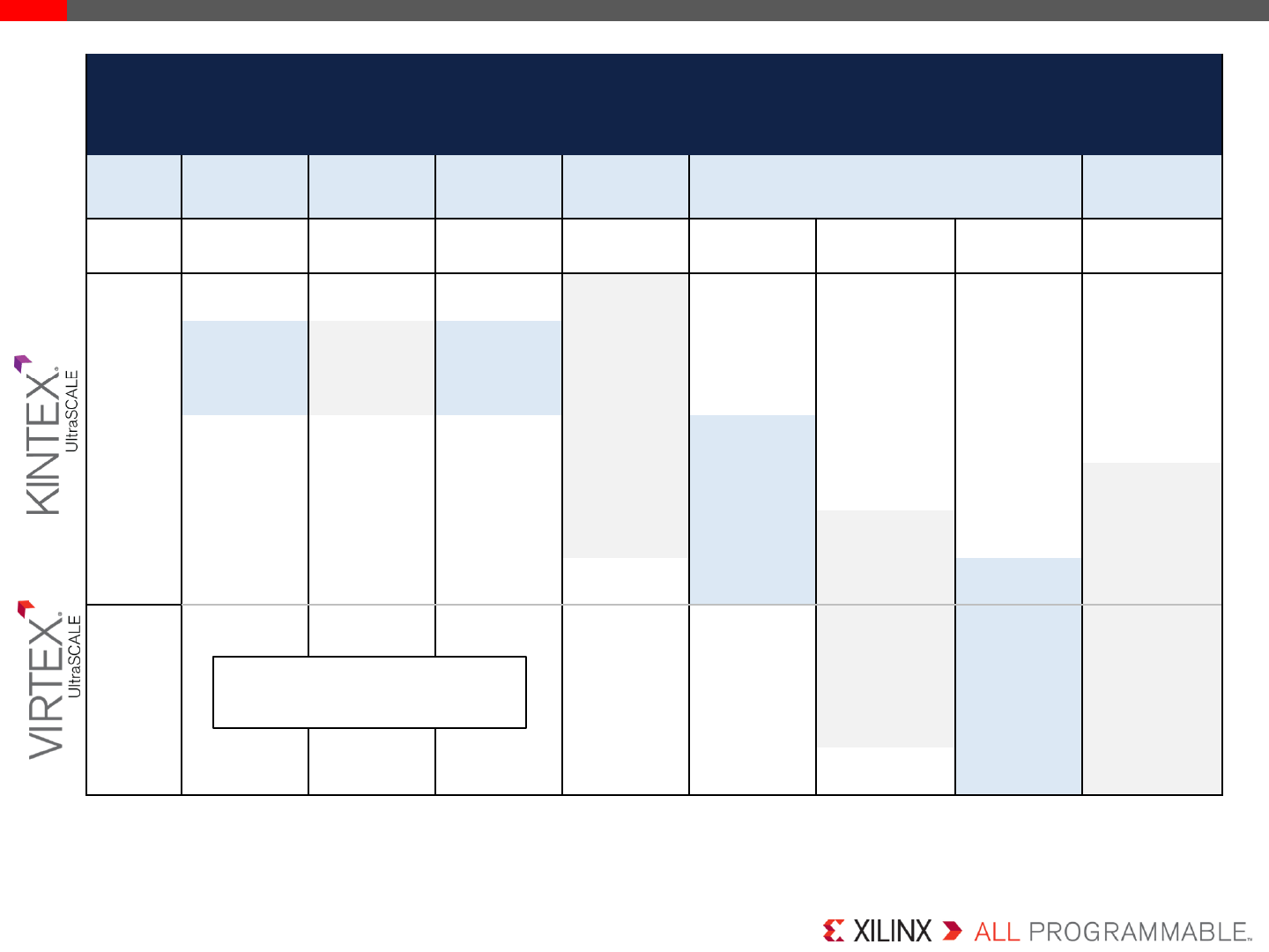
Kintex® UltraScale™ FPGAs
Device Name
KU025(1) KU035 KU040 KU060 KU085 KU095 KU115
Logic Resources
System Logic Cells (K)
318 444 530 726 1,088 1,176 1,451
CLB Flip-
Flops
290,880 406,256 484,800 663,360 995,040 1,075,200 1,326,720
CLB LUTs
145,440 203,128 242,400 331,680 497,520 537,600 663,360
Memory Resources
Maximum Distributed RAM
(Kb)
4,230 5,908 7,050 9,180 13,770 4,800 18,360
Block RAM/FIFO w/ECC (36Kb
each)
360 540 600 1,080 1,620 1,680 2,160
Block RAM/FIFO (18Kb
each)
720 1,080 1,200 2,160 3,240 3,360 4,320
Total Block RAM
(Mb)
12.7 19.0 21.1 38.0 56.9 59.1 75.9
Clock Resources CMT (1 MMCM, 2
PLLs)
610 10 12 22 16 24
I/O DLL
24 40 40 48 56 64 64
I/O Resources
Maximum Single-
Ended HP I/Os
208 416 416 520 572 650 676
Maximum Differential HP I/O Pairs
96 192 192 240 264 288 312
Maximum Single-
Ended HR I/Os
104 104 104 104 104 52 156
Maximum Differential HR I/O Pairs
48 48 48 48 56 24 72
Integrated IP
Resources
DSP Slices
1,152 1,700 1,920 2,760 4,100 768 5,520
System Monitor
1 1 1 1 212
PCIe® Gen1/2/3
12 3 3 4 4 6
Interlaken
00 0 0 020
100G Ethernet
0 0 0 0 020
16.3Gb/s Transceivers (GTH/GTY)
12 16 20 32 56 64(2) 64
Speed Grades
Commercial
-1 -1 -1 -1 -1 -1 -1
Extended
-2 -2 -3 -2 -3 -2 -3 -2 -3 -2 -2 -3
Industrial
-1 -2 -1 -1L -2 -1 -1L -2 -1 -1L -2 -1 -1L -2 -1 -2 -1 -1L -2
Package
Footprint(3, 4, 5, 6)
Package Dimensions
(mm) HR I/O, HP I/O, GTH/GTY
A784(7) 23x23(8) 104, 364, 8 104, 364, 8
A676(7) 27x27 104, 208, 16 104, 208, 16
A900(7) 31x31 104, 364, 16 104, 364, 16
A1156 35x35 104, 208, 12 104, 416, 16 104, 416, 20 104, 416, 28 52, 468, 28
A1517 40x40 104, 520, 32 104, 520, 48 104, 520, 48
Footprint
Compatible with
Virtex® UltraScale
Devices
C1517 40x40 52, 468, 40
D1517 40x40 104, 234, 64
B1760 42.5x42.5 104, 572, 44 52, 650, 48 104, 598, 52
A2104 47.5x47.5 156, 676, 52
B2104 47.5x47.5 52, 650, 64 104, 598, 64
D1924 45x45 156, 676, 52
F1924 45x45 104, 520, 56 104, 624, 64
Notes:
1. Certain advanced configuration features are not supported in the KU025. Refer to the Configuring FPGAs section in DS890, UltraScale Architecture and Product Overview.
2. GTY transceivers in KU095 devices support data rates up to 16.3Gb/s.
3. Packages with the same package footprint designator, e.g., A2104, are footprint compatible with all other UltraScale devices with the same sequence. See the migration table for details on inter-family migration.
4. Maximum achievable performance is device and package dependent; consult the associated data sheet for details.
5. For full part number details, see the Ordering Information section in DS890, UltraScale Architecture and Product Overview.
6. See UG575, UltraScale Architecture Packaging and Pinouts User Guide for more information.
7. GTH transceivers in A784, A676, and A900 packages support data rates up to 12.5Gb/s.
8. 0.8mm ball pitch. All other packages listed 1mm ball pitch.
© Copyright 2013–2016 Xilinx
.
Page 3
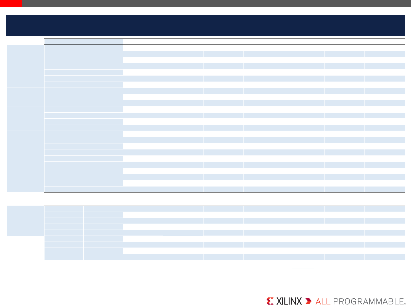
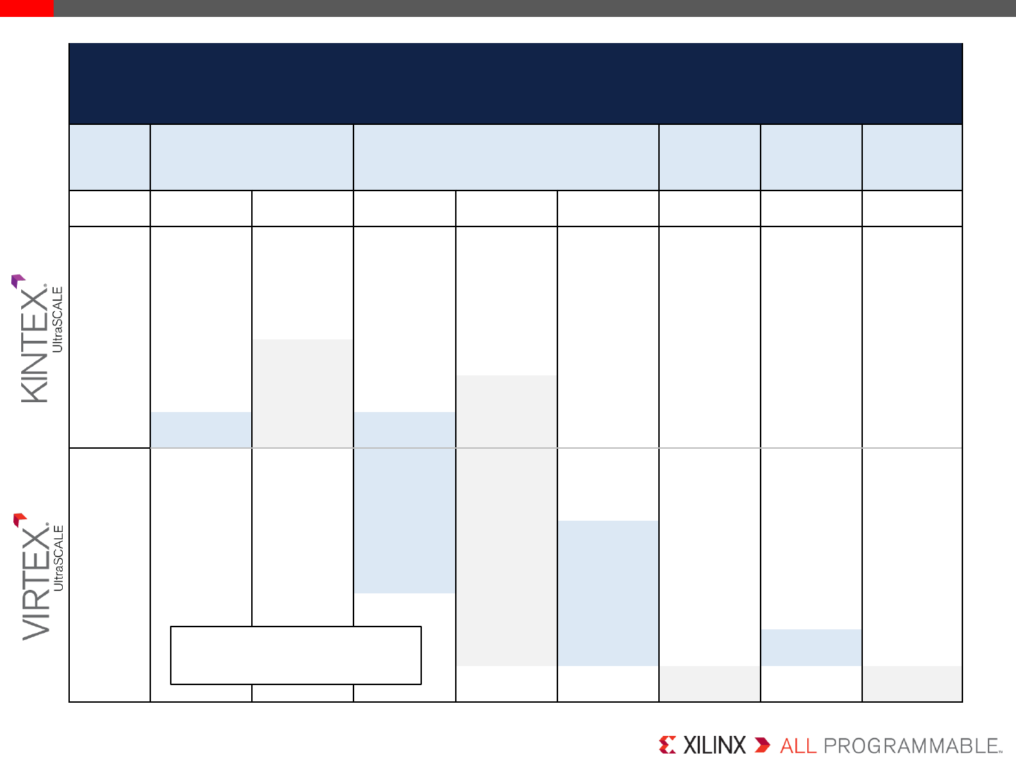
Virtex® UltraScale™ FPGAs
Device Name
XCVU065 XCVU080 XCVU095 XCVU125 XCVU160 XCVU190 XCVU440
Logic Resources
System Logic Cells (K)
783 975 1,176 1,567 2,027 2,350 5,541
CLB Flip-
Flops
716,160 891,424 1,075,200 1,432,320 1,852,800 2,148,480 5,065,920
CLB LUTs
358,080 445,712 537,600 716,160 926,400 1,074,240 2,532,960
Memory Resources
Maximum Distributed RAM (Kb)
4,830 3,980 4,800 9,660 12,690 14,490 28,710
Block RAM/FIFO w/ECC (36Kb
each)
1,260 1,421 1,728 2,520 3,276 3,780 2,520
Block RAM/FIFO (18Kb
each)
2,520 2,842 3,456 5,040 6,552 7,560 5,040
Total Block RAM (Mb)
44.3 50.0 60.8 88.6 115.2 132.9 88.6
Clock Resources
CMT (1 MMCM, 2 PLLs)
10 16 16 20 28 30 30
I/O DLL
40 64 64 80 120 120 120
Transceiver Fractional
PLL
58810 13 15 0
I/O Resources
Maximum Single-
Ended HP I/Os
468 780 780 780 650 650 1,404
Maximum Differential HP I/O Pairs
216 360 360 360 300 300 648
Maximum Single-
Ended HR I/Os
52 52 52 52 52 52 52
Maximum Differential HR I/O Pairs
24 24 24 24 24 24 24
Integrated IP
Resources
DSP Slices
600 672 768 1,200 1,560 1,800 2,880
System Monitor
1112333
PCIe® Gen1/2/3
2444466
Interlaken
3666890
100G
Ethernet
3446993
GTH 16.3Gb/s
Transceivers
20 32 32 40 52 60 48
GTY 30.5Gb/s
Transceivers
20 32 32 40 52 60 0
Speed Grades
Commercial
––––––-1
Extended
-1H -2 -3 -1H -2 -3 -1H -2 -3 -1H -2 -3 -1H -2 -3 -1H -2 -3 -2 -3
Industrial
-1 -2 -1 -2 -1 -2 -1 -2 -1 -2 -1 -2 -1 -2
Package
Footprint(1, 2, 3)
Package Dimensions
(mm) HR I/O, HP I/O, GTH 16.3Gb/s, GTY 30.5Gb/s
Footprint
Compatible with
Kintex® UltraScale
Devices
C1517 40x40 52, 468, 20, 20 52, 468, 20, 20 52, 468, 20, 20
D1517 40x40 52, 286, 32, 32 52, 286, 32, 32 52, 286, 40, 32
B1760 42.5x42.5 52, 650, 32, 16 52, 650, 32, 16 52, 650, 36, 16
A2104 47.5x47.5 52, 780, 28, 24 52, 780, 28, 24 52, 780, 28, 24
B2104 47.5x47.5 52, 650, 32, 32 52, 650, 32, 32 52, 650, 40, 36 52, 650, 40, 36 52, 650, 40, 36
C2104 47.5x47.5 52, 364, 32, 32 52, 364, 40, 40 52, 364, 52, 52 52, 364, 52, 52
B2377 50x50 52, 1248, 36, 0
A2577 52.5x52.5 0, 448, 60, 60
A2892 55x55 52, 1404, 48, 0
Notes:
1. Packages with the same package footprint designator, e.g., A2104, are footprint compatible with all other UltraScale devices with the same sequence. See the migration table for details on inter-family migration.
2. For full part number details, see the Ordering Information section in DS890, UltraScale Architecture and Product Overview.
3. See UG575, Kintex UltraScale and Virtex UltraScale FPGAs Packaging and Pinouts User Guide for more information.
© Copyright 2013–2016 Xilinx
.
Page 4
UltraScale Device Ordering Information
Xilinx
Commercial
UltraScaleV: Virtex
K: Kintex
F: Lid
L: Lid SSI
B: Lidless
Value Index F: Flip-Chip
(1.0mm)
S: Flip-Chip
(0.8mm)
V: RoHS 6/6
G: RoHS 6/6
w/exemption 15
Package
Designator
Speed Grade
-1 = Slowest
-L1 = Low Power
(Kintex only)
-H1 = Slowest or Mid
(Virtex only)
-2 = Mid
-3 = Fastest
Footprint
Temperature
Grade
(C, E, I)
C = Commercial (Tj = 0°C to +85°C)
E = Extended (Tj = 0°C to +100°C)
I = Industrial (Tj = –40°C to +100°C)
Package
Pin Count
XC V U ### -1 F L V A #### C
Important: Verify all data in this document with the device data sheets found at www.xilinx.com
For valid part/package combinations,
go to DS890, UltraScale Architecture and Product Overview: Device-Package Combinations and Maximum I/Os Tables
© Copyright 2013–2016 Xilinx
.
UltraScale
™ Device Footprint Compatibility
HR I/O, HP I/O, GTH 16.3Gb/s; GTY 30.5Gb/s
Package
Dimensions
(mm)
23x23 27x27 31x31 35x35 40x40 42.5x42.5
Package
Footprint
A784 A676 A900 A1156 A1517 C1517 D1517 B1760
XCKU025
104, 208, 12, 0
XCKU035
104, 364, 8, 0
104, 208, 16, 0
104, 364, 16, 0
104, 416, 16, 0
XCKU040
104, 364, 8, 0
104, 208,16, 0
104, 364, 16, 0
104, 416, 20, 0
XCKU060
104, 416, 28, 0
104, 520, 32, 0
XCKU085
N/A
104, 520, 48, 0
104, 572, 44, 0
XCKU095
52, 468, 20, 8(1)
N/A
52, 468, 20, 20(1)
52, 650, 32, 16(1)
XCKU115
104, 520, 48, 0
N/A
104, 234, 64, 0
104, 598, 52, 0
XCVU065
52, 468, 20, 20
N/A N/A
XCVU080
52, 468, 20, 20
52, 286, 32, 32
52, 650, 32, 16
XCVU095
52, 468, 20, 20
52, 286, 32, 32
52, 650, 32, 16
XCVU125
52, 286, 40, 32
52, 650, 36, 16
Page 5
23mm–42.5mm
Important: Verify all data in this document with the device data sheets found at www.xilinx.com
Notes:
1. GTY transceivers in KU095 devices support data rates up to 16.3Gb/s. Refer to data sheet for details.
Footprint compatibility is
indicated by shading per column.
© Copyright 2013–2016 Xilinx
.
UltraScale™ Device
Footprint Compatibility
HR I/O, HP I/O, GTH 16.3Gb/s; GTY 30.5Gb/s
Package
Dimensions
(mm)
45x45 47.5x47.5 50x50 52.5x52.5 55x55
Package
Footprint
D1924 F1924 A2104 B2104 C2104 B2377 A2577 A2892
XCKU035
XCKU040
XCKU060
XCKU085
104, 520, 56, 0
XCKU095
N/A
52, 650, 32, 32(1)
XCKU115
156, 676, 52, 0
104, 624, 64, 0
156, 676, 52, 0
104, 598, 64, 0
XCVU065
N/A N/A
XCVU080
52, 780, 28, 24
52, 650, 32, 32
XCVU095
52, 780, 28, 24
52, 650, 32, 32
52, 364, 32, 32
XCVU125
52, 780, 28, 24
52, 650, 40, 36
52, 364, 40, 40
XCVU160
52, 650, 40, 36
52, 364, 52, 52
XCVU190
52, 650, 40, 36
52, 364, 52, 52
0, 448, 60, 60
XCVU440
52, 1248, 36, 0
52, 1404, 48, 0
Page 6
45mm–55mm
Notes:
1. GTY transceivers in KU095 devices support data rates up to 16.3Gb/s. Refer to data sheet for details.
Important: Verify all data in this document with the device data sheets found at www.xilinx.com
Footprint compatibility is
indicated by shading per column.
© Copyright 2013–2016 Xilinx
.
Page 7
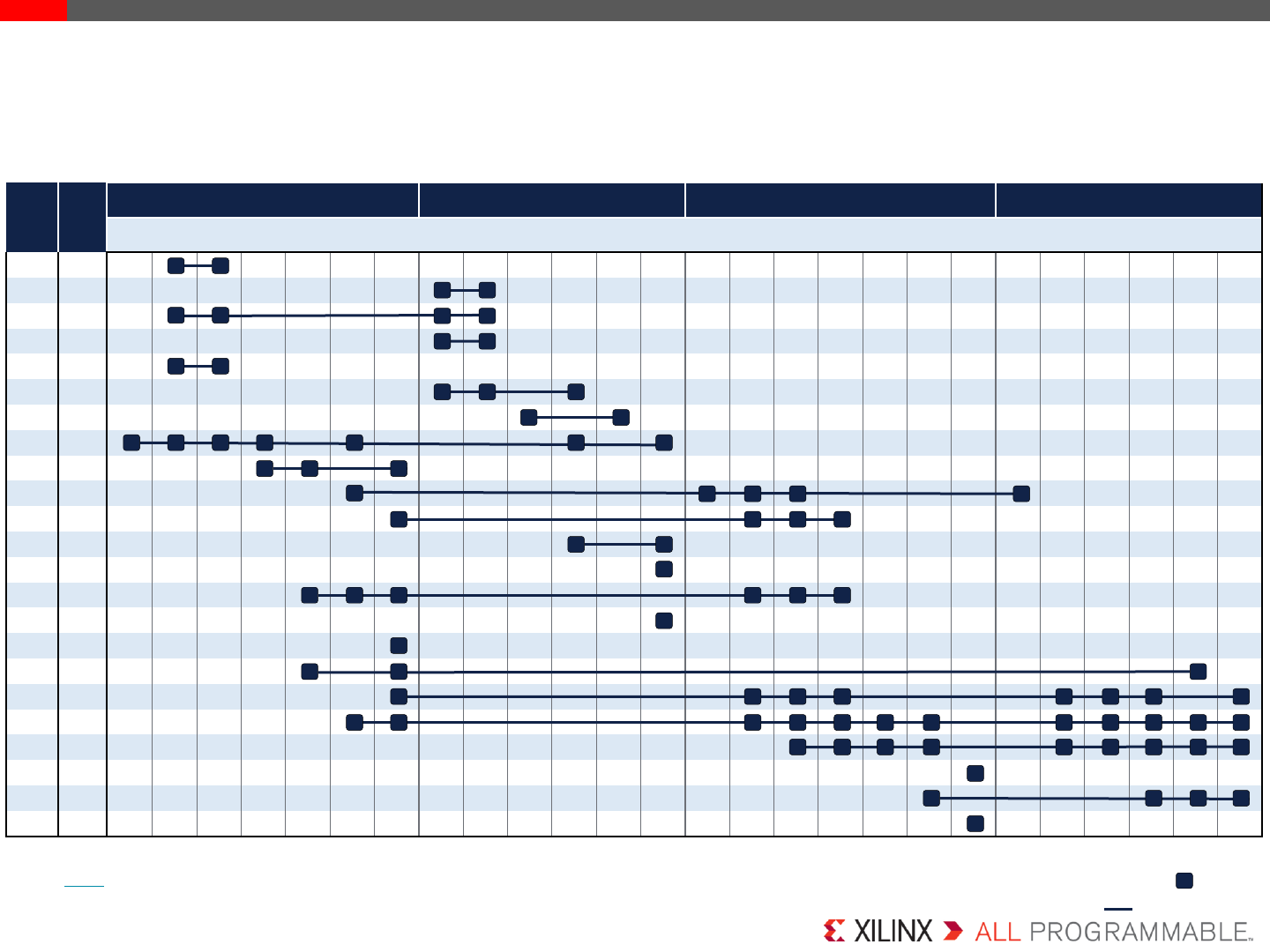
UltraScale Architecture Migration Table
Pkg mm
Kintex® UltraScale™ Kintex UltraScale+™ Virtex® UltraScale Virtex UltraScale+
KU025
KU035
KU040
KU060
KU085
KU095
KU115
KU3P
KU5P
KU9P
KU11P
KU13P
KU15P
VU065
VU080
VU095
VU125
VU160
VU190
VU440
VU3P
VU5P
VU7P
VU9P
VU11P
VU13P
A784 23 X X
B784 23 X X
A676 27 X X
B676 27 X X
A900 31 X X
D900 31 X X X
E900 31 X X
A1156 35 X X X X X X X
A1517 40 X X X
C1517 40 X X X X X
D1517 40 X X X X
E1517 40 X X
A1760 42.5 X
B1760 42.5 X X X X X X
E1760 42.5 X
D1924 45 X
F1924 45 X X X
A2104 47.5(1) X X X X X X X X
B2104 47.5(1) XX XXXXX XXXXX
C2104 47.5(1) XXXX XXXXX
B2377 50 X
A2577 52.5 X X X X
A2892 55 X
Legend
Device
Migration Path
Notes:
1. The body size of the VU13P device in the A2104, B2104, and C2104 packages is 52.5mm. These packages are footprint compatible with the corresponding 47.5mm body size packages.
See UG583, UltraScale Architecture PCB Design User Guide for important migration details.
UltraScale and UltraScale+ families provide footprint compatibility to enable users to migrate designs from one
device or family to another. Any two packages with the same footprint identifier code are footprint compatible.
© Copyright 2013–2016 Xilinx
.
Page 8
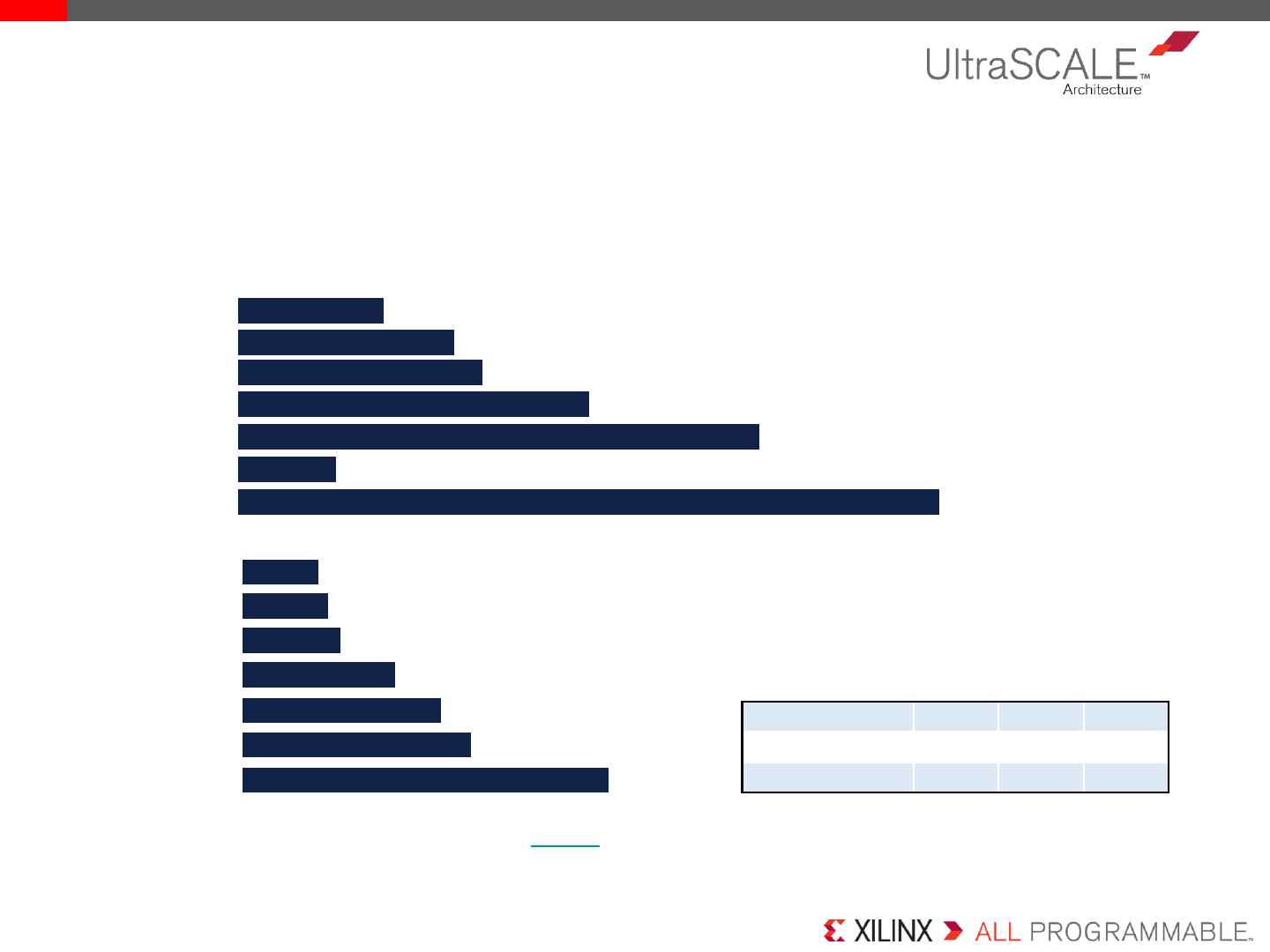
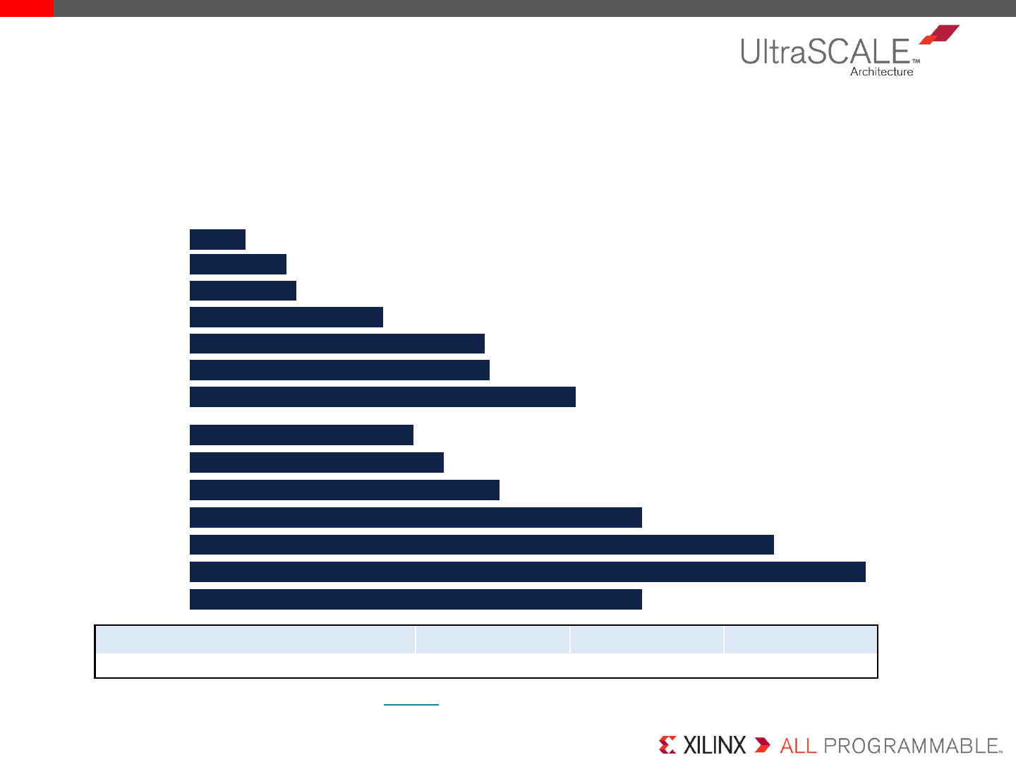
Digital Signal Processing Metrics
UltraScale architecture further enhances the Xilinx DSP48 slice with features designed to allow users to
do more calculations in fewer DSP resources, enhancing both device utilization and performance.
Examples include wider multipliers for floating point calculations, wide XOR functions for ECC, CRC, and
EFEC, and pre-adder squaring for rounding algorithms.
Speed grade
-1 -2 -3
F
MAX [MHz] 594 661 741
Max GMAC/s
6558 7297 8181
1920
1700
2760
4100
5520
600
672
768
1200
1560
1800
768
XCKU035
XCKU040
XCKU060
XCKU085
XCKU095
XCKU115
XCVU065
XCVU080
XCVU095
XCVU125
XCVU160
XCVU190
DSP Slice Count
For more information, refer to: UG579, UltraScale Architecture DSP Slice User Guide
Important: Verify all data in this document with the device data sheets found at www.xilinx.com
2880
XCVU440
1152
XCKU025
© Copyright 2013–2016 Xilinx
.
Page 9
Block RAM Metrics
UltraScale architecture block RAM adds new features to increase performance, device utilization, and
power efficiency. These new features are designed to provide highly efficient solutions for applications in
the Wireless, Wired, Video, and Signal Processing markets by offering hardened memory cascade to
reduce fabric use and increase performance, and flexible hard FIFO and user accessible dynamic power
control to reduce power.
Speed grade
-1 -2 -3
True dual
-port Block RAM FMAX [MHz] 525 585 660
For more information, refer to: UG573, UltraScale Architecture Memory Resources User Guide
Important: Verify all data in this document with the device data sheets found at www.xilinx.com
21
19
38
57
76
44
50
61
89
115
89
59
XCKU035
XCKU040
XCKU060
XCKU085
XCKU095
XCKU115
XCVU065
XCVU080
XCVU095
XCVU125
XCVU160
XCVU440
Block RAM Capacity (Mb)
133
XCVU190
13
XCKU025
© Copyright 2013–2016 Xilinx
.
Page 10
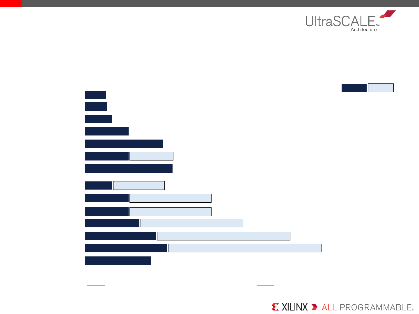
High-Speed Serial Transceivers
For high bandwidth applications, including 500Gb/s, 400Gb/s, and 100Gb/s line cards, serial data transmission
across backplanes and longer distances is becoming increasingly important. UltraScale architecture serial
transceivers include the proven on-chip circuits required to provide optimal signal integrity in real world
environments, at data rates up to 16.3Gb/s (GTH) and 30.5Gb/s (GTY).
For more information, refer to UG576,UltraScale Architecture GTH Transceivers User Guide and UG578,UltraScale Architecture GTY Transceivers User Guide
Important: Verify all data in this document with the device data sheets found at www.xilinx.com
16
64
32
60
48
XCKU035
XCKU040
XCKU060
XCKU085
XCKU095
XCKU115
XCVU065
XCVU080
XCVU095
XCVU125
XCVU160
XCVU190
XCVU440
60
52 52
4040
32
32 32
20 20
56
32
20
Total Transceiver Count GTH GTY
GTH = 16.3Gb/s
GTY = 30.5Gb/s
32 32(1)
Notes:
1. GTY up to 16.3Gb/s. Refer to data sheet for details.
12
XCKU025
© Copyright 2013–2016 Xilinx
.
Page 11
For high bandwidth applications, including 500Gb/s, 400Gb/s, and 100Gb/s line cards, serial data transmission
across backplanes and longer distances is becoming increasingly important. UltraScale architecture serial
transceivers include the proven on-chip circuits required to provide optimal signal integrity in real world
environments, at data rates up to 16.3Gb/s (GTH) and 30.5Gb/s (GTY).
Important: Verify all data in this document with the device data sheets found at www.xilinx.com
For more information, refer to UG576, UltraScale Architecture GTH Transceivers User Guide and UG578, UltraScale Architecture GTY Transceivers User Guide
Transceiver Aggregate Bandwidth
522
2086
1043
1956
1565
XCKU035
XCKU040
XCKU060
XCKU085
XCKU095
XCKU115
XCVU065
XCVU080
XCVU095
XCVU125
XCVU160
XCVU190
XCVU440
3660
1695 3172
24401304
1952
1043 1952
652 1220
1043
1826
1043
652
Transceiver Aggregate Bandwidth (Gb/s)
Transceiver Aggregate Bandwidth (Gb/s) = # of Transceivers x Maximum Line Rate x 2 (Full Duplex)
GTH GTY
GTH = 16.3Gb/s
GTY = 30.5Gb/s
1043(1)
Notes:
1. GTY up to 16.3Gb/s. Refer to data sheet for details.
391
XCKU025
© Copyright 2013–2016 Xilinx
.
DS890,UltraScale Architecture and Product Overview
DS892,Kintex UltraScale FPGA Data Sheet: DC and AC Switching Characteristics
DS893, Virtex UltraScale FPGA Data Sheet: DC and AC Switching Characteristics
UG570,UltraScale Architecture Configuration User Guide
UG571,UltraScale Architecture SelectIO Resources User Guide
UG572,UltraScale Architecture Clocking Resources User Guide
UG573,UltraScale Architecture Memory Resources User Guide
UG574,UltraScale Architecture Configurable Logic Block User Guide
UG575, Kintex UltraScale and Virtex UltraScale FPGAs Packaging and Pinout User Guide
UG576,UltraScale Architecture GTH Transceivers User Guide
UG578, UltraScale Architecture GTY Transceivers User Guide
UG579, UltraScale Architecture DSP Slice User Guide
UG580, UltraScale Architecture System Monitor User Guide
UG583,UltraScale Architecture PCB and Pin Planning User Guide
PG150, LogiCORE IP UltraScale Architecture-Based FPGAs Memory Interface Solutions
Page 12
Important: Verify all data in this document with the device data sheets found at www.xilinx.com
References
XMP102 (v1.7)
