Discovery Kit With STM32F429ZI MCU User Manual
User%20Manual%20STM32F429ZI
User Manual:
Open the PDF directly: View PDF ![]() .
.
Page Count: 36
- Figure 1. STM32F429 Discovery board
- 1 Features
- 2 Product marking
- 3 Ordering information
- 4 Conventions
- 5 Quick start
- 6 Hardware layout
- Figure 2. Hardware block diagram
- 6.1 STM32F429 Discovery board layout
- 6.2 Mechanical drawing
- 6.3 Embedded ST-LINK/V2 (or V2-B)
- 6.4 Power supply and power selection
- 6.5 LEDs
- 6.6 Push-buttons
- 6.7 USB OTG supported
- 6.8 Gyroscope MEMS (ST-MEMS L3GD20)
- 6.9 TFT LCD (Thin-film-transistor liquid-crystal display)
- 6.10 64-Mbit SDRAM (1Mbit x 16-bit x 4-bank)
- 6.11 JP3 (Idd)
- 6.12 OSC clock
- 6.13 Solder bridges
- 6.14 Extension connectors
- 7 Electrical schematics
- 8 Revision history
September 2017 DocID025175 Rev 3 1/36
1
UM1670
User manual
Discovery kit with STM32F429ZI MCU
Introduction
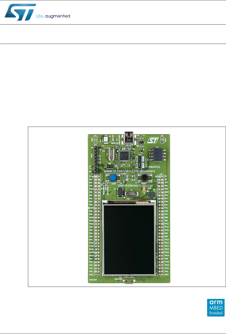
The 32F429IDISCOVERY Discovery kit allows users to easily develop applications with the
STMicroelectronics Arm® Cortex®-M4 core-based STM32F429 high-performance
microcontroller. It includes an ST-LINK/V2 or ST-LINK/V2-B embedded debug tool, a 2.4"
QVGA TFT LCD, an external 64-Mbit SDRAM, an ST MEMS gyroscope, a USB OTG
Micro-AB connector, LEDs and push-buttons.
The board comes with the STM32 comprehensive free software libraries and examples
available with the STM32Cube package, as well as a direct access to the Arm® Mbed
Enabled™ resources at the http://mbed.org website.
Figure 1. STM32F429 Discovery board
1. Picture is not contractual.
www.st.com

Contents UM1670
2/36 DocID025175 Rev 3
Contents
1 Features . . . . . . . . . . . . . . . . . . . . . . . . . . . . . . . . . . . . . . . . . . . . . . . . . . . 6
2 Product marking . . . . . . . . . . . . . . . . . . . . . . . . . . . . . . . . . . . . . . . . . . . . 7
3 Ordering information . . . . . . . . . . . . . . . . . . . . . . . . . . . . . . . . . . . . . . . . 7
4 Conventions . . . . . . . . . . . . . . . . . . . . . . . . . . . . . . . . . . . . . . . . . . . . . . . . 7
5 Quick start . . . . . . . . . . . . . . . . . . . . . . . . . . . . . . . . . . . . . . . . . . . . . . . . . 8
5.1 Getting started . . . . . . . . . . . . . . . . . . . . . . . . . . . . . . . . . . . . . . . . . . . . . . 8
5.2 System requirements . . . . . . . . . . . . . . . . . . . . . . . . . . . . . . . . . . . . . . . . . 8
5.3 Development toolchains supporting the STM32F429 Discovery kit . . . . . . 8
6 Hardware layout . . . . . . . . . . . . . . . . . . . . . . . . . . . . . . . . . . . . . . . . . . . . 9
6.1 STM32F429 Discovery board layout . . . . . . . . . . . . . . . . . . . . . . . . . . . . 10
6.2 Mechanical drawing . . . . . . . . . . . . . . . . . . . . . . . . . . . . . . . . . . . . . . . . . 12
6.3 Embedded ST-LINK/V2 (or V2-B) . . . . . . . . . . . . . . . . . . . . . . . . . . . . . . 13
6.3.1 Drivers . . . . . . . . . . . . . . . . . . . . . . . . . . . . . . . . . . . . . . . . . . . . . . . . . . 14
6.3.2 ST-LINK/V2 (or V2-B) firmware upgrade . . . . . . . . . . . . . . . . . . . . . . . . 14
6.3.3 VCP configuration . . . . . . . . . . . . . . . . . . . . . . . . . . . . . . . . . . . . . . . . . 14
6.3.4 Using ST-LINK/V2 (or V2-B) to program/debug
the STM32F429ZIT6 on board . . . . . . . . . . . . . . . . . . . . . . . . . . . . . . . 15
6.3.5 Using ST-LINK/V2 (or V2-B) to program/debug
an external STM32 application . . . . . . . . . . . . . . . . . . . . . . . . . . . . . . . 16
6.4 Power supply and power selection . . . . . . . . . . . . . . . . . . . . . . . . . . . . . . 17
6.5 LEDs . . . . . . . . . . . . . . . . . . . . . . . . . . . . . . . . . . . . . . . . . . . . . . . . . . . . 17
6.6 Push-buttons . . . . . . . . . . . . . . . . . . . . . . . . . . . . . . . . . . . . . . . . . . . . . . 17
6.7 USB OTG supported . . . . . . . . . . . . . . . . . . . . . . . . . . . . . . . . . . . . . . . . 18
6.8 Gyroscope MEMS (ST-MEMS L3GD20) . . . . . . . . . . . . . . . . . . . . . . . . . 18
6.9 TFT LCD (Thin-film-transistor liquid-crystal display) . . . . . . . . . . . . . . . . 18
6.10 64-Mbit SDRAM (1Mbit x 16-bit x 4-bank) . . . . . . . . . . . . . . . . . . . . . . . . 18
6.11 JP3 (Idd) . . . . . . . . . . . . . . . . . . . . . . . . . . . . . . . . . . . . . . . . . . . . . . . . . . 18
6.12 OSC clock . . . . . . . . . . . . . . . . . . . . . . . . . . . . . . . . . . . . . . . . . . . . . . . . 19
6.12.1 OSC clock supply . . . . . . . . . . . . . . . . . . . . . . . . . . . . . . . . . . . . . . . . . 19

DocID025175 Rev 3 3/36
UM1670 Contents
3
6.12.2 OSC 32 KHz clock supply . . . . . . . . . . . . . . . . . . . . . . . . . . . . . . . . . . . 19
6.13 Solder bridges . . . . . . . . . . . . . . . . . . . . . . . . . . . . . . . . . . . . . . . . . . . . . 20
6.14 Extension connectors . . . . . . . . . . . . . . . . . . . . . . . . . . . . . . . . . . . . . . . . 21
7 Electrical schematics . . . . . . . . . . . . . . . . . . . . . . . . . . . . . . . . . . . . . . . 28
8 Revision history . . . . . . . . . . . . . . . . . . . . . . . . . . . . . . . . . . . . . . . . . . . 35

List of tables UM1670
4/36 DocID025175 Rev 3
List of tables
Table 1. List of the order codes . . . . . . . . . . . . . . . . . . . . . . . . . . . . . . . . . . . . . . . . . . . . . . . . . . . . . 7
Table 2. ON/OFF conventions . . . . . . . . . . . . . . . . . . . . . . . . . . . . . . . . . . . . . . . . . . . . . . . . . . . . . . 7
Table 3. Jumper states . . . . . . . . . . . . . . . . . . . . . . . . . . . . . . . . . . . . . . . . . . . . . . . . . . . . . . . . . . . 13
Table 4. Debug connector CN2 (SWD) . . . . . . . . . . . . . . . . . . . . . . . . . . . . . . . . . . . . . . . . . . . . . . 16
Table 5. Solder bridges. . . . . . . . . . . . . . . . . . . . . . . . . . . . . . . . . . . . . . . . . . . . . . . . . . . . . . . . . . . 20
Table 6. STM32 pin description versus board functions . . . . . . . . . . . . . . . . . . . . . . . . . . . . . . . . . . 21
Table 7. Document revision history . . . . . . . . . . . . . . . . . . . . . . . . . . . . . . . . . . . . . . . . . . . . . . . . . 35

DocID025175 Rev 3 5/36
UM1670 List of figures
5
List of figures
Figure 1. STM32F429 Discovery board . . . . . . . . . . . . . . . . . . . . . . . . . . . . . . . . . . . . . . . . . . . . . . . . 1
Figure 2. Hardware block diagram . . . . . . . . . . . . . . . . . . . . . . . . . . . . . . . . . . . . . . . . . . . . . . . . . . . . 9
Figure 3. Top layout . . . . . . . . . . . . . . . . . . . . . . . . . . . . . . . . . . . . . . . . . . . . . . . . . . . . . . . . . . . . . . 10
Figure 4. Bottom layout . . . . . . . . . . . . . . . . . . . . . . . . . . . . . . . . . . . . . . . . . . . . . . . . . . . . . . . . . . . 11
Figure 5. STM32F429 Discovery board mechanical drawing . . . . . . . . . . . . . . . . . . . . . . . . . . . . . . 12
Figure 6. Updating the list of drivers in Device Manager . . . . . . . . . . . . . . . . . . . . . . . . . . . . . . . . . . 14
Figure 7. STM32F429 Discovery board connections. . . . . . . . . . . . . . . . . . . . . . . . . . . . . . . . . . . . . 15
Figure 8. ST-LINK/V2 connections . . . . . . . . . . . . . . . . . . . . . . . . . . . . . . . . . . . . . . . . . . . . . . . . . . 16
Figure 9. STM32F429I-DISC1 Discovery board . . . . . . . . . . . . . . . . . . . . . . . . . . . . . . . . . . . . . . . . 28
Figure 10. ST-LINK/V2 (SWD only) . . . . . . . . . . . . . . . . . . . . . . . . . . . . . . . . . . . . . . . . . . . . . . . . . . . 29
Figure 11. USB OTG FS . . . . . . . . . . . . . . . . . . . . . . . . . . . . . . . . . . . . . . . . . . . . . . . . . . . . . . . . . . . 30
Figure 12. 64-Mbit SDRAM . . . . . . . . . . . . . . . . . . . . . . . . . . . . . . . . . . . . . . . . . . . . . . . . . . . . . . . . . 31
Figure 13. STM32F429ZIT6 MCU . . . . . . . . . . . . . . . . . . . . . . . . . . . . . . . . . . . . . . . . . . . . . . . . . . . . 32
Figure 14. Peripherals . . . . . . . . . . . . . . . . . . . . . . . . . . . . . . . . . . . . . . . . . . . . . . . . . . . . . . . . . . . . . 33
Figure 15. LCD 2.4. . . . . . . . . . . . . . . . . . . . . . . . . . . . . . . . . . . . . . . . . . . . . . . . . . . . . . . . . . . . . . . . 34

Features UM1670
6/36 DocID025175 Rev 3
1 Features
The STM32F429 Discovery board offers the following features:
•STM32F429ZIT6 microcontroller featuring 2 Mbytes of Flash memory, 256 Kbytes of
RAM in an LQFP144 package
•2.4" QVGA TFT LCD
•USB OTG
•64-Mbit SDRAM
•L3GD20, ST-MEMS motion sensor 3-axis digital output gyroscope
•Six LEDs:
– LD1 (red/green) for USB communication
– LD2 (red) for 3.3 V power-on
– Two user LEDs: LD3 (green), LD4 (red)
– Two USB OTG LEDs: LD5 (green) VBUS and LD6 (red) OC (overcurrent)
•Two push-buttons (user and reset)
•USB OTG with Micro-AB connector
•Extension header for LQFP144 I/Os for a quick connection to the prototyping board
and an easy probing
•Flexible power-supply options: ST-LINK USB VBUS or external sources
•On-board ST-LINK/V2 on 32F429IDISCOVERY or ST-LINK/V2-B on
STM32F429I-DISC1 with USB re-enumeration capability: mass storage (with ST-
LINK/V2-B only), virtual COM port (with ST-LINK/V2-B only) and debug port
•Comprehensive free software including a variety of examples, part of the
STM32CubeF4 package or STSW-STM32138 for legacy standard libraries usage
•Arm® Mbed Enabled™ compliant only for ST-LINK/V2-B only
DocID025175 Rev 3 7/36
UM1670 Product marking
35
2 Product marking
Evaluation tools marked as "ES" or "E" are not yet qualified and therefore they are not ready
to be used as reference design or in production. Any consequences deriving from such
usage will not be at ST charge. In no event, ST will be liable for any customer usage of
these engineering sample tools as reference design or in production.
"E" or "ES" marking examples of location:
•On the targeted STM32 that is soldered on the board (for illustration of STM32 marking,
refer to the section “Package information” of the STM32 datasheet available at
www.st.com).
•Next to the evaluation tool ordering part number that is stuck or silk-screen printed on
the board.
3 Ordering information
To order the Discovery kit for the STM32F429 line of microcontrollers, refer to Table 1.
4 Conventions
Table 2 provides the definition of some conventions used in the present document.
Table 1. List of the order codes
Order code ST-LINK version
32F429IDISCOVERY ST-LINK/V2
STM32F429I-DISC1 ST-LINK/V2-B (Mbed Enabled)
Table 2. ON/OFF conventions
Convention Definition
Jumper JPx ON Jumper fitted
Jumper JPx OFF Jumper not fitted
Solder bridge SBx ON SBx connections closed by solder
Solder bridge SBx OFF SBx connections left open

Quick start UM1670
8/36 DocID025175 Rev 3
5 Quick start
The STM32F429 Discovery is a low-cost and easy-to-use development kit to quickly
evaluate and start a development with an STM32F4 microcontroller.
Before installing and using the product, accept the Evaluation Product License Agreement
from www.st.com/stm32f4-discovery.
For more information on the STM32F429 Discovery board and for demonstration software,
visit www.st.com/stm32f4-discovery.
5.1 Getting started
Follow the sequence below to configure the STM32F429 Discovery board and launch the
DISCOVER application:
1. Ensure that the jumpers JP3 and CN4 are set to "ON" (Discovery mode).
2. Connect the STM32F429 Discovery board to a PC using a USB cable Type-A/Mini-B
through the USB ST-LINK connector CN1, to power the board, the LEDs LD2 (PWR)
and LD1 (COM).
3. The following applications are available on the screen:
– Clock/Calendar and Game
– Video Player and Image Browser (play videos and view images from the USB
mass storage connected to CN6)
– Performance monitor (watch the CPU load and run a graphical benchmark)
– System Info
4. The demo software, as well as other software examples are available at the
www.st.com/stm32f4-discovery webpage.
5. Develop applications starting from the examples.
5.2 System requirements
•Windows® OS (XP, 7,8 and 10), Linux® 64-bit or macOS™
•USB Type-A to Mini-B cable
5.3 Development toolchains supporting the STM32F429
Discovery kit
•Keil® MDK-ARM(a)
•IAR® EWARM(a)
•GCC-based IDEs including free SW4STM32 from AC6
•Arm® Mbed online (see http://mbed.org)
a. On Windows only.
DocID025175 Rev 3 9/36
UM1670 Hardware layout
35
6 Hardware layout
The STM32F429 Discovery board has been designed around the STM32F429ZIT6
microcontroller in a 144-pin LQFP package.
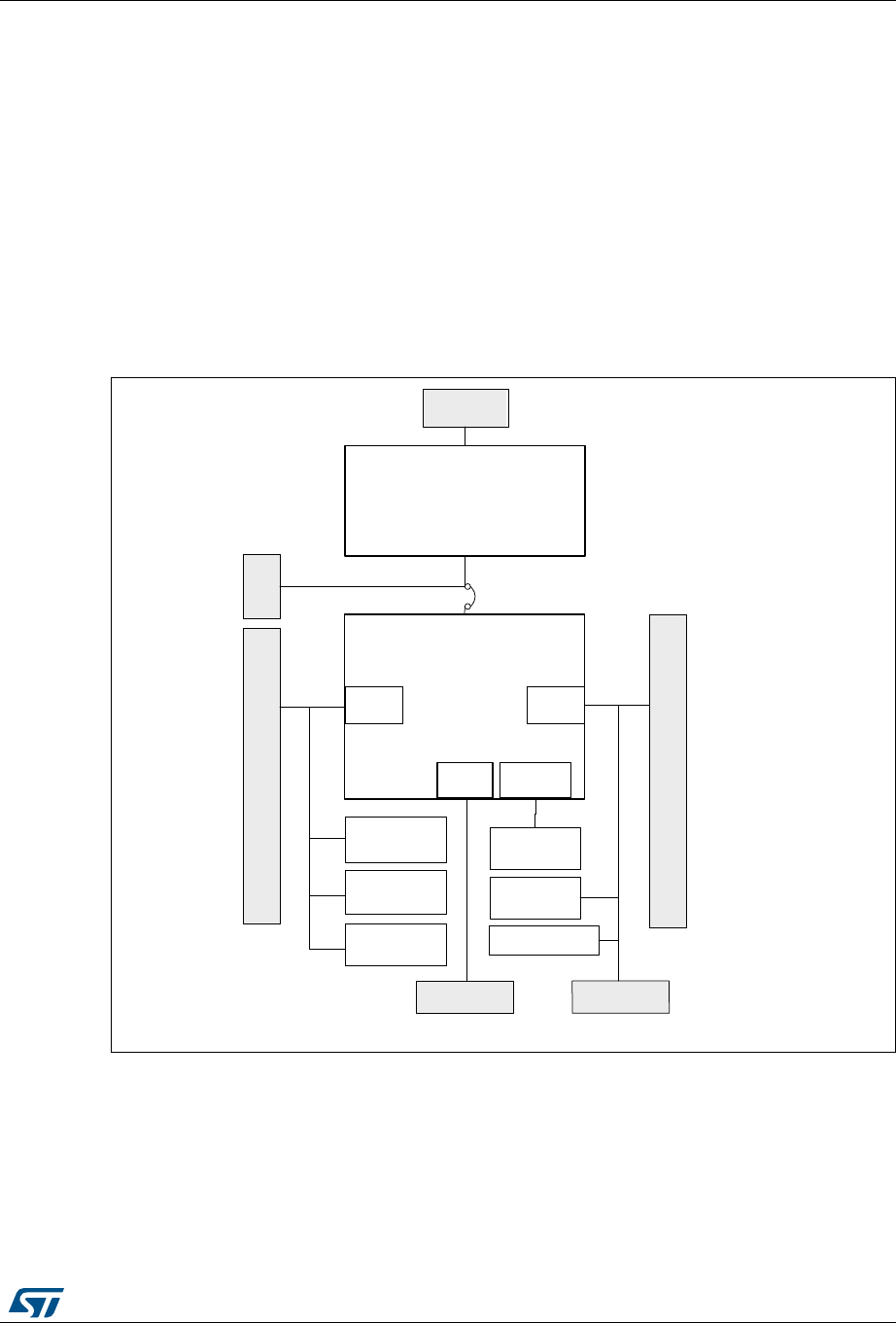
Figure 2 illustrates the connections between the STM32F429ZIT6 and its peripherals
(ST-LINK/V2 or ST-LINK/V2-B, push-buttons, LED, USB OTG, ST-MEMS Gyroscope,
Accelerometer, Magnetometer and connectors).
Figure 3 and Figure 4 show the location of these features on the STM32F429 Discovery
board.
Figure 5 shows the mechanical dimensions of the STM32F429 Discovery board.
Figure 2. Hardware block diagram
06Y9
(PEHGGHG
67/,1.9RU67/,1.9%
670)=,7
,2 ,2
,2 5(6(7
/('V
/'/'
6'5$0
0ELWV
%
5(6(7
%
86(5
/*'
0LFUR86%
0LQL86%
6:'
+HDGHU
+HDGHU
49*$
7)7/&'
,&H[W
Hardware layout UM1670
10/36 DocID025175 Rev 3
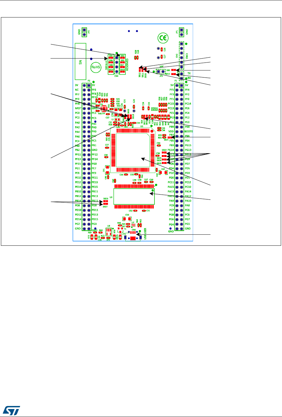
6.1 STM32F429 Discovery board layout
Figure 3. Top layout
DocID025175 Rev 3 11/36
UM1670 Hardware layout
35
Figure 4. Bottom layout
D^ϯϮϯϲϰsϭ
^ϰ͕^ϲ͕^ϴ͕^ϭϰ
;&h>dͿ
^ϭϬ;^dDͺZ^dͿ
^ϯ͕^ϱ͕^ϳ͕^ϭϯ
;Z^ZsͿ
^ϭϴ;DKͿ
^ϭϵ͕ϮϬ;yϯĐƌLJƐƚĂůͿ
^ZD
^Ϯϭ;KKdϭͿ
^ϮϮ͕Ϯϯ͕Ϯϰ͕Ϯϱ
^Ϯϲ͕Ϯϳ;h^Kd'Ϳ
^ϭϭ;Zy͕dyͿ
^ϭϮ;EZ^dͿ
^ϵ;^tKͿ
^ϭϱ;Zy͕dyͿ
^ϭϲ͕ϭϳ;yϮĐƌLJƐƚĂůͿ
h^Kd'ŵŝĐƌŽͲ
^dDϯϮ&ϰϮϵ/dϲ
Hardware layout UM1670
12/36 DocID025175 Rev 3
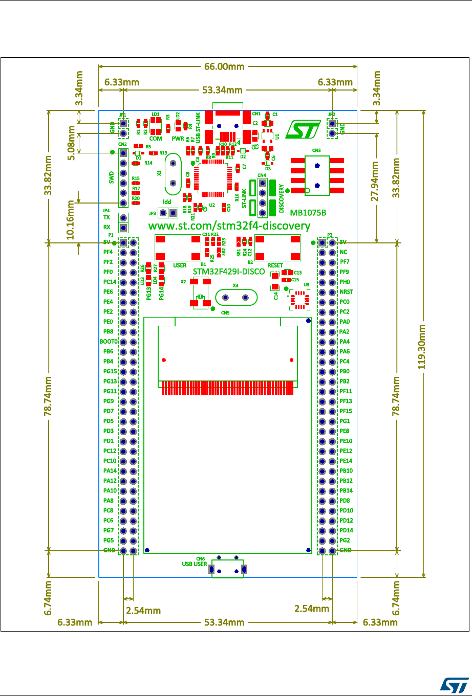
6.2 Mechanical drawing
Figure 5. STM32F429 Discovery board mechanical drawing

DocID025175 Rev 3 13/36
UM1670 Hardware layout
35
6.3 Embedded ST-LINK/V2 (or V2-B)
The ST-LINK/V2 on 32F429IDISCOVERY or the ST-LINK/V2-B on STM32F429I-DISC1 is
embedded as programming and debugging tool. Virtual COM port and USB mass storage
features are supported by the ST-LINK/V2-B only for Mbed compatibility.
The ST-LINK/V2-B makes the STM32F4429I-DISC1 boards Mbed Enabled. The embedded
ST-LINK/V2 (or V2-B) supports only SWD for STM32 devices. For information about
debugging and programming features refer to ST-LINK/V2 in-circuit debugger/programmer
for STM8 and STM32, User manual (UM1075), which describes in detail all the
ST-LINK/V2 features.
The changes on ST-LINK/V2-B versus ST-LINK/V2 version are listed below.
New features supported on ST-LINK/V2-B are:
•Virtual COM port interface on USB
•Mass storage interface on USB
Features not supported on ST-LINK/V2-B are:
•SWIM interface
•Minimum supported application voltage limited to 3 V
•USB power management request for more than 100 mA power on USB
Known limitation:
•Activating the readout protection on the ST-LINK/V2-B target, prevents the target
application from running afterwards. The target readout protection must be kept
disabled on the ST-LINK/V2-B boards.
There are two different ways to use the embedded ST-LINK/V2-B, depending on the jumper
states (see Table 3):
•Programming/debugging the STM32 on board (refer to Section 6.3.4: Using ST-
LINK/V2 (or V2-B) to program/debug the STM32F429ZIT6 on board to program/debug
the STM32F429ZIT6 on board)
•Programming/debugging the STM32 in an external application board, using a cable
connected to SWD connector CN2 (refer to chapter: Section 6.3.5: Using ST-LINK/V2
(or V2-B) to program/debug an external STM32 application)
Table 3. Jumper states
Jumper state Description
Both CN4 jumpers ON ST-LINK/V2 (or V2-B) functions enabled for on-board programming
(default)
Both CN4 jumpers OFF ST-LINK/V2 (or V2-B) functions enabled for application through
external CN3 connector (SWD supported)
Hardware layout UM1670
14/36 DocID025175 Rev 3
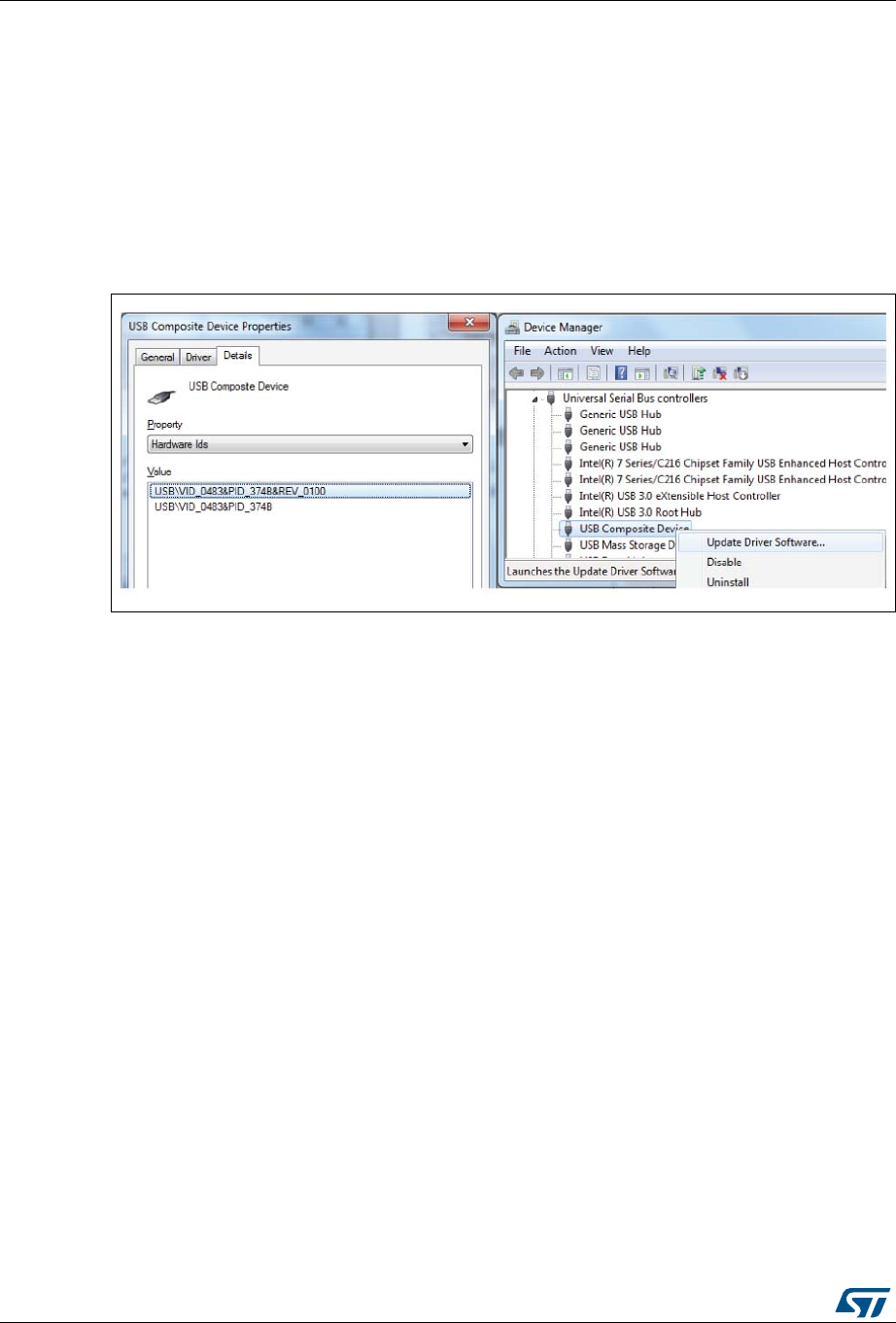
6.3.1 Drivers
The ST-LINK/V2 (or V2-B) requires a dedicated USB driver, which, for Windows® 7, 8 and
10 can be found at the www.st.com website. In case the STM32 Discovery is connected to
the PC before the driver is installed, some Discovery interfaces may be declared as
“Unknown” in the PC device manager. In this case the user must install the driver files (see
Figure 6: Updating the list of drivers in Device Manager) and update the driver of the
connected device from the device manager.
Note: Prefer using the “USB Composite Device” handle for a full recovery.
Figure 6. Updating the list of drivers in Device Manager
6.3.2 ST-LINK/V2 (or V2-B) firmware upgrade
The ST-LINK/V2 (or V2-B) embeds a firmware upgrade mechanism for in-situ upgrade
through the USB port. As the firmware may evolve during the life time of the ST-LINK/V2 (or
V2-B) product (for example new functionalities, bug fixes, support for new microcontroller
families), it is recommended to visit the www.st.com website, before starting to use the
Discovery board and periodically, to stay up-to-date with the latest firmware version.
6.3.3 VCP configuration
The ST-LINK/V2-B on STM32F429I-DISC1 supports virtual COM port (VCP) on U2 pin 12
(ST-LINK_TX) and U2 pin 13 (ST-LINK_RX), which are connected to the STM32F429 target
STM32 USART1 (PA9, PA10) for Mbed support, thanks to the SB11 and SB15 solder
bridges.
The SB11 (PA9) and SB15 (PA10) default configurations for 32F429IDISCOVERY and
STM32F429I-DISC1 are given in Table 5: Solder bridges.
DocID025175 Rev 3 15/36
UM1670 Hardware layout
35
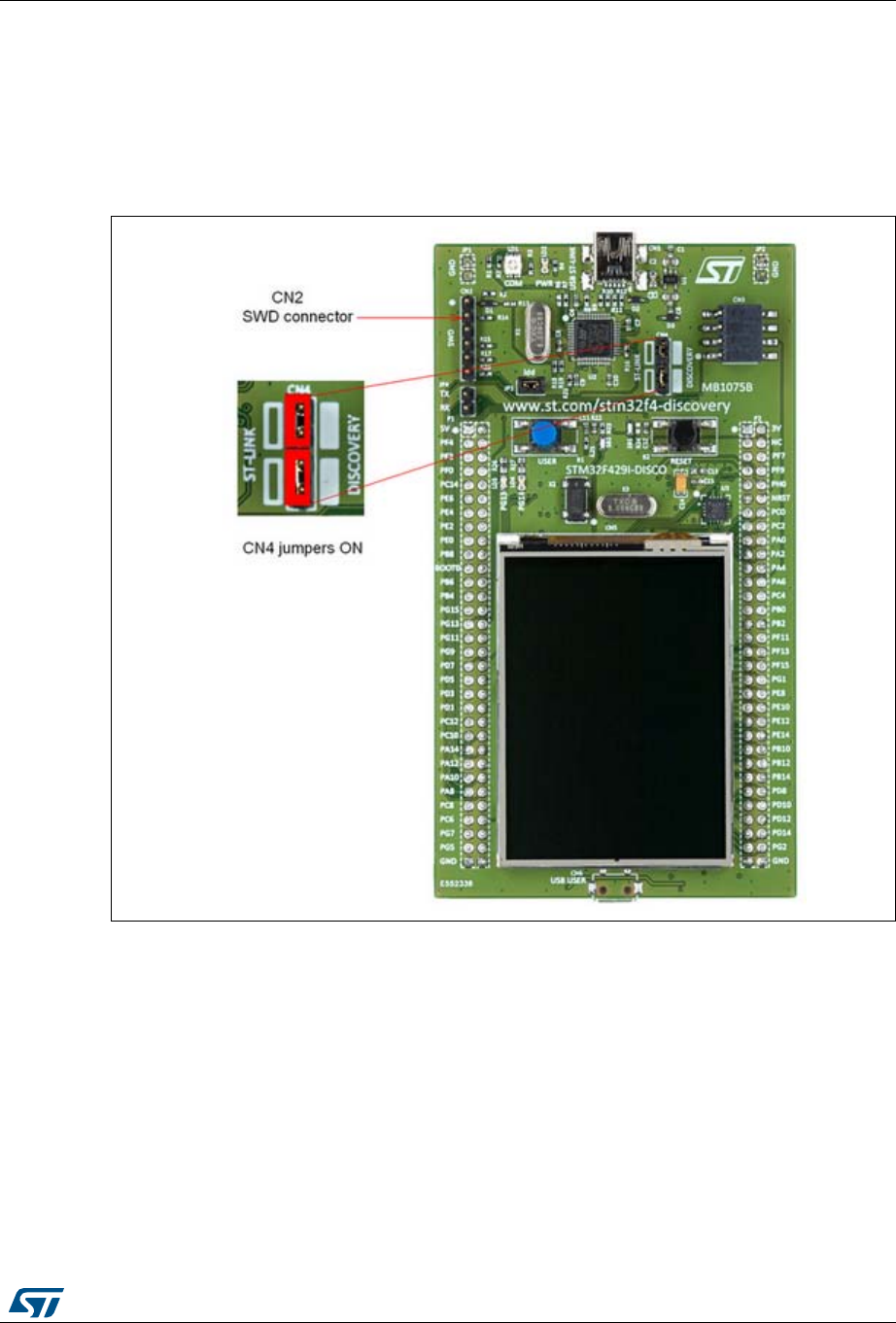
6.3.4 Using ST-LINK/V2 (or V2-B) to program/debug
the STM32F429ZIT6 on board
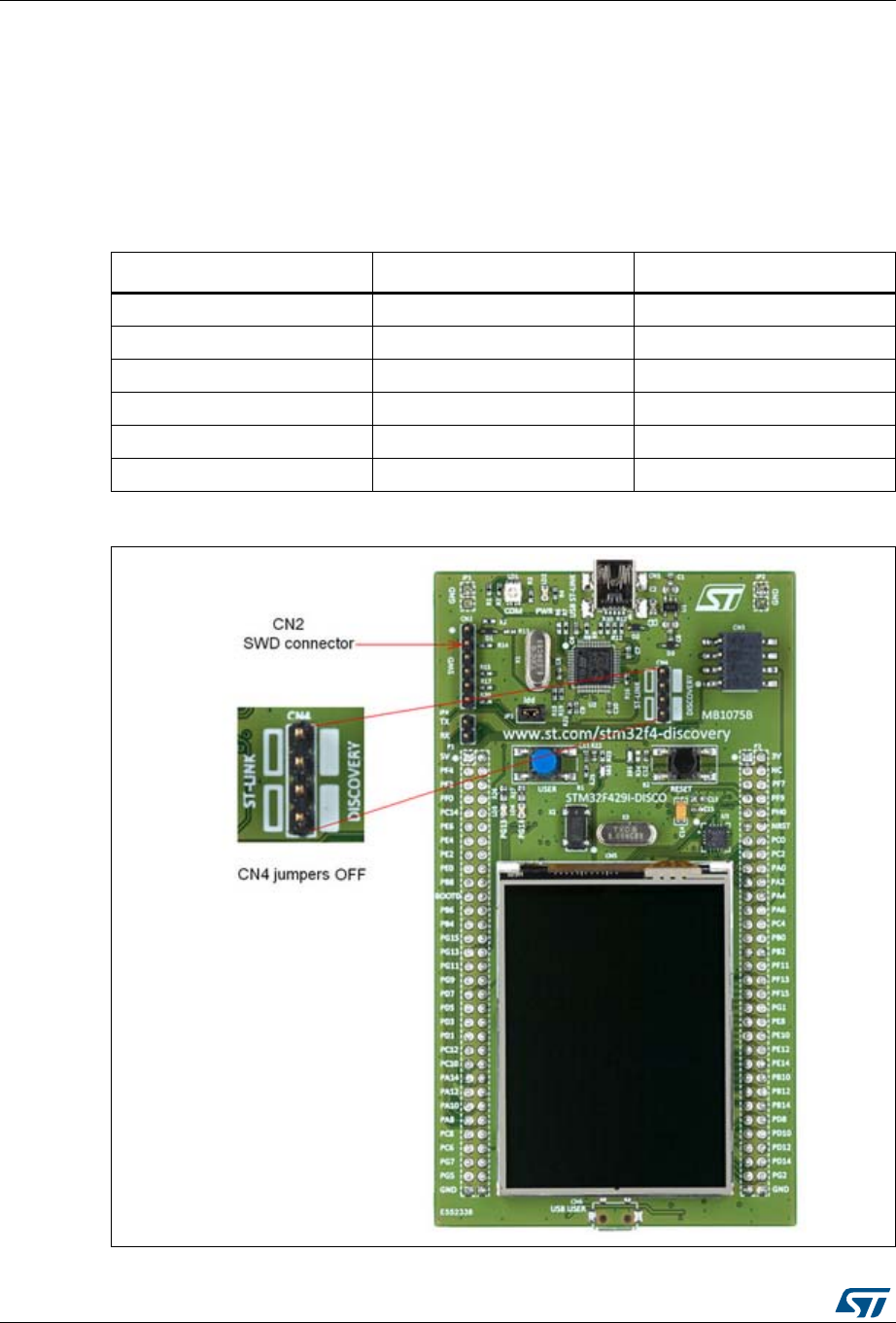
To program the STM32F429ZIT6 on board, simply plug in the two jumpers on CN4, as
shown marked in red in Figure 7, but do not use the CN3 connector as it could disturb the
communication with the STM32F429ZIT6 of the STM32F429 Discovery board.
Figure 7. STM32F429 Discovery board connections
Hardware layout UM1670
16/36 DocID025175 Rev 3
6.3.5 Using ST-LINK/V2 (or V2-B) to program/debug
an external STM32 application
It is very easy to use the ST-LINK/V2 (or V2-B) to program the STM32 on an external
application. Simply remove the two jumpers from CN4 as shown in Figure 8 and connect the
application to the CN3 debug connector according to Table 4.
Note: SB7 must be OFF if CN2 pin 5 is used in an external application.
Figure 8. ST-LINK/V2 connections
Table 4. Debug connector CN2 (SWD)
Pin CN2 Designation
1 VDD_TARGET VDD from application
2 SWCLK SWD clock
3 GND Ground
4 SWDIO SWD data input/output
5 NRST RESET of target STM32
6 SWO Reserved

DocID025175 Rev 3 17/36
UM1670 Hardware layout
35
6.4 Power supply and power selection
The power supply is provided either by the host PC through the USB cable or by an external
5 V power supply.
The D1 and D2 diodes protect the 5 V and 3 V pins from external power supplies:
•5 V and 3 V can be used as output power supplies when another application board is
connected to pins P1 and P2.
In this case, the 5 V and 3 V pins deliver a 5 V or 3 V power supply and the power
consumption must be lower than 100 mA.
•5 V and 3 V can also be used as input power supply, e.g. when the USB connectors are
not connected to the PC.
In this case, the STM32F429 Discovery board must be powered by a power supply unit
or by an auxiliary equipment complying with the standard EN-60950-1:
2006+A11/2009, and must be Safety Extra Low Voltage (SELV) with limited power
capability.
Note: The board can also be powered through the USB USER connector and it is protected by D4
and D5 diodes when both USBs are connected (in this case the 5 V power is around
4.4 volts).
6.5 LEDs
•LD1 COM:
LD1 default status is red. LD1 turns to green to indicate that communications are in
progress between the PC and the ST-LINK/V2.
•LD2 PWR:
The red LED indicates that the board is powered.
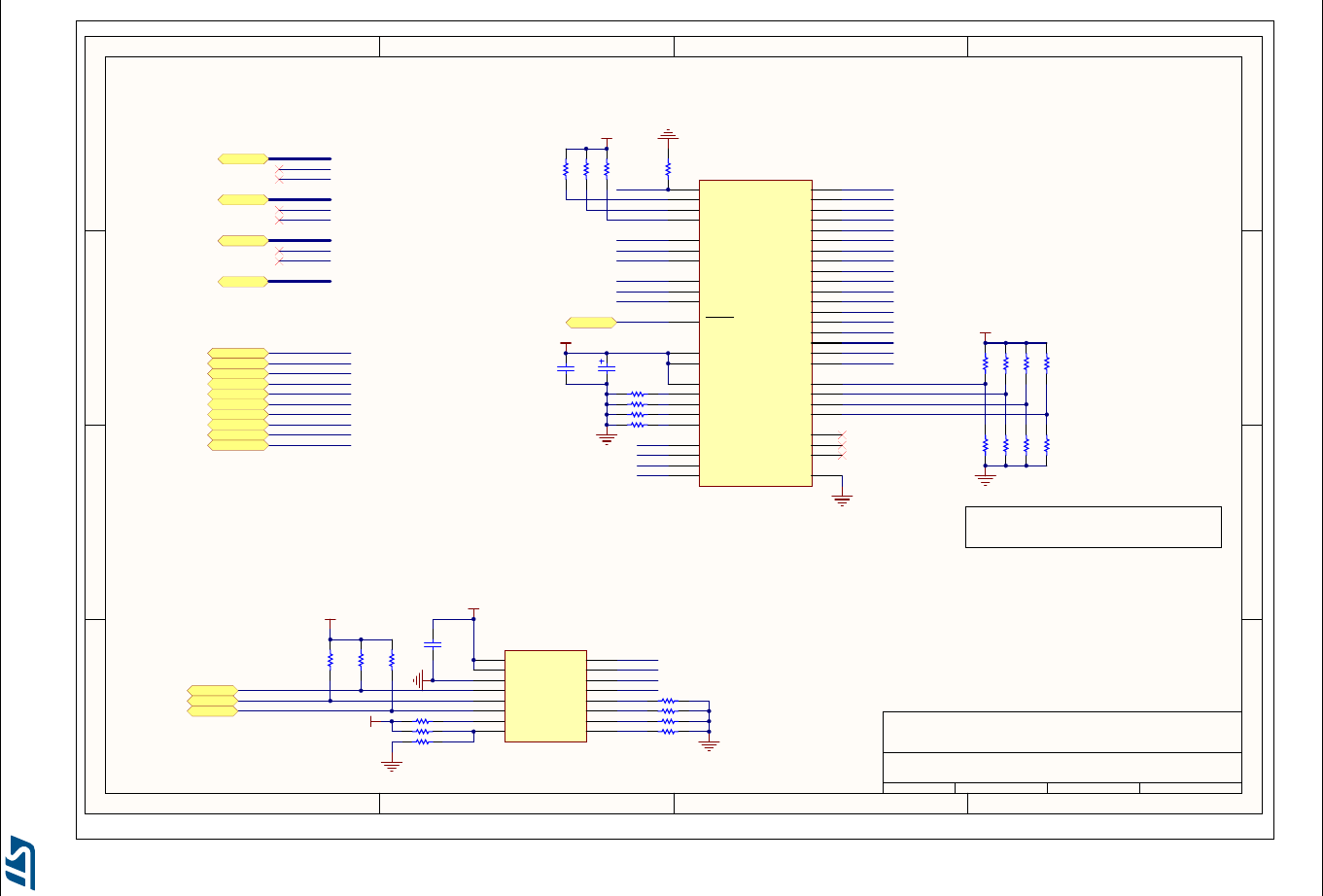
•User LD3:
The green LED is a user LED connected to the I/O PG13 of the STM32F429ZIT6.
•User LD4:
The red LED is a user LED connected to the I/O PG14 of the STM32F429ZIT6.
•User LD5:
The green LED indicates when VBUS is present on CN6 and is connected to PB13 of
the STM32F429ZIT6.
•User LD6:
The red LED indicates an overcurrent from VBUS of CN6 and is connected to the I/O
PC5 of the STM32F429ZIT6.
6.6 Push-buttons
•B1 USER:
User and Wake-Up button connected to the I/O PA0 of the STM32F429ZIT6.
•B2 RESET:
The push-button connected to NRST is used to RESET the STM32F429ZIT6.

Hardware layout UM1670
18/36 DocID025175 Rev 3
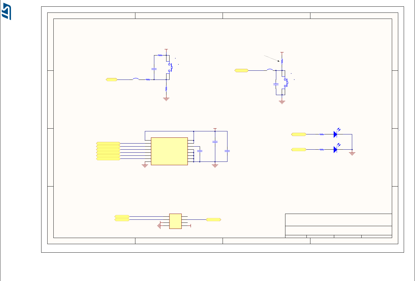
6.7 USB OTG supported
The STM32F429ZIT6 is used to drive only the USB OTG full speed on this board. The USB
Micro-AB connector (CN6) allows the user to connect a host or device component, such as
a USB key, a mouse and so on.
Two LEDs are dedicated to this module:
•LD5 (green LED) indicates when VBUS is active
•LD6 (red LED) indicates an overcurrent from a connected device
6.8 Gyroscope MEMS (ST-MEMS L3GD20)
The L3GD20 is an ultra-compact, low-power, three-axis angular rate sensor. It includes a
sensing element and an IC interface able to provide the measured angular rate to the
external world through the I2C/SPI serial interface.
The L3GD20 has a full-scale of ±245/±500/±2000 dps and is capable of measuring rates
with a user-selectable bandwidth.
The STM32F429ZIT6 controls this motion sensor through the SPI interface.
6.9 TFT LCD (Thin-film-transistor liquid-crystal display)
The TFT LCD is a 2.41" display of 262 K colors. Its definition is QVGA (240 x 320 dots) and
is directly driven by the STM32F429ZIT6 using the RGB protocol. It includes the ILI9341
LCD controller and can operate with a 2.8 ±0.3 V voltage.
6.10 64-Mbit SDRAM (1Mbit x 16-bit x 4-bank)
The 64-Mbit SDRAM is a high speed CMOS, dynamic random-access memory designed to
operate in 3.3 V memory systems containing 67,108,864 bits. It is internally configured as a
quad-bank DRAM with a synchronous interface. Each 16,777,216-bit bank is organized as
4,096 rows by 256 columns by 16 bits. The 64-Mbit SDRAM includes an auto-refresh, a
power-saving and a power-down modes. All signals are registered on the positive edge of
the clock signal, CLK.
The STM32F429ZIT6 reads and writes data at 80 MHz.
6.11 JP3 (Idd)
Jumper JP3, labeled Idd, allows the consumption of STM32F429ZIT6 to be measured by
removing the jumper and connecting an ammeter.
•Jumper on: STM32F429ZIT6 is powered (default).
•Jumper off: an ammeter must be connected to measure the STM32F429ZIT6 current,
(if there is no ammeter, the STM32F429ZIT6 is not powered).

DocID025175 Rev 3 19/36
UM1670 Hardware layout
35
6.12 OSC clock
6.12.1 OSC clock supply
The following information indicates all configurations for clock supply selection.
•MCO from ST-LINK (from MCO of the STM32F429ZIT6)
This frequency cannot be changed, it is fixed at 8 MHz and connected to PH0-OSC_IN
of the STM32F429ZIT6. The configuration needed is:
– SB18 closed, SB19 open, R56 removed
– SB20, R57, C20, C21, X3 = do not care
•Oscillator on board (from X3 crystal)
For typical frequencies and its capacitors and resistors, refer to the STM32F429ZIT6
datasheet. The configuration needed is:
– SB18, SB19, SB20 open
– R56, R57, C20, C21, X3 soldered
•Oscillator from external PH0 (from external oscillator through pin 10 of the P2
connector)
The configuration needed is:
– SB19 closed, SB18 open, R56 removed
– SB20, R57, C20, C21, X3 = do not care
•No external oscillator (from internal oscillator HSI only).
PH0 and PH1 can be used as GPIO. The configuration needed is:
– SB18 open, SB19 closed, SB20 closed, R56 removed, R57 removed
– C20, C21, X3 = do not care
6.12.2 OSC 32 KHz clock supply
The following information indicates all configurations for the 32 KHz clock supply selection.
•Oscillator on board (from X2 Crystal, not provided).
The configuration needed is:
– SB16 open, SB17 open
– R53, R54, C23, C24, X2 soldered
•Oscillator from external PC14 (from external oscillator through pin 9 of P1 connector)
The configuration needed is:
– SB16 closed, R53 removed
– SB17, R54, C23, C24, X2 = do not care
•No external oscillator (PC14 and PC15 can be used as GPIO.
The configuration needed is:
– SB16 closed, SB17 closed, R53 removed, R54 removed
– C23, C24, X2 = do not care
Hardware layout UM1670
20/36 DocID025175 Rev 3
6.13 Solder bridges
Table 5. Solder bridges
Bridge State (1)
1. Default SBx state is shown in bold.
Description
SB19, 20 (X3 crystal)
OFF X3, C20, C21, R56 and R57 provide a clock. PH0, PH1 are disconnected from
P2.
ON PH0, PH1 are connected to P2. Remove only R56 and R57.
SB4, 6, 8,14 (default) ON Reserved, do not modify.
SB3, 5, 7,13 (reserved) OFF Reserved, do not modify.
SB22, 23, 24, 25 OFF Reserved, do not modify.
SB16, 17 (X2 crystal)
OFF X2, C23, C24, R53 and R54 deliver a 32 KHz clock.
PC14, PC15 are not connected to P2
ON PC14, PC15 are only connected to P2.
Remove only R53 and R54.
SB1 (B2-RESET)
ON B2 push-button is connected to NRST of STM32F429ZIT6.
OFF B2 push-button is not connected to NRST of STM32F429ZIT6.
SB2 (B1-USER)
ON B1 push-button is connected to PA0.
OFF B1 push-button is not connected to PA0.
SB11, 15 (RX,TX)
OFF STM32F429 USART1 is not connected to ST-LINK, so VCP is disabled
(Default configuration on 32F429IDISCOVERY).
ON STM32F429 USART1 is connected to ST-LINK, so VCP is enabled (default
configuration on STM32F429I-DISC1).
SB12 (NRST)
ON NRST signal of connector CN2 is connected to NRST of STM32F429ZIT6.
OFF NRST signal is not connected.
SB9 (SWO)
OFF SWO signal is not connected.
ON SWO signal of connector CN3 is connected to PB3.
SB10 (STM_RST)
OFF No incidence on NRST signal of STM32F429ZIT6.
ON NRST signal of STM32F429ZIT6 is connected to GND.
SB21 (BOOT0)
ON BOOT0 signal of STM32F429ZIT6 is at level "0" through 510 Ω pull-down.
OFF BOOT0 signal of STM32F429ZIT6 is at level "1" through 10 KΩ pull-up (not
provided).
SB26, 27 (USB OTG)
OFF PB14 and PB15 are only used for USB OTG and not connected to P2 to avoid
noise.
ON PB14 and PB15 are connected to P2.
SB18 (MCO)
OFF MCO signal of STM32F429ZIT6 is not used.
ON MCO clock signal from STM32F429ZIT6 is connected to OSC_IN of
STM32F429ZIT6.
DocID025175 Rev 3 21/36
UM1670 Hardware layout
35
6.14 Extension connectors
The male headers P1 and P2 can connect the STM32F429 Discovery board to a standard
prototyping/wrapping board. STM32F429ZIT6 GPIOs are available on these connectors. P1
and P2 can also be probed by an oscilloscope, a logical analyzer or a voltmeter.
Table 6. STM32 pin description versus board functions
STM32 pin Board functions
Main function
LQFP144
System
VCP
SDRAM
LCD-TFT
LCD-RGB
LCD-SPI
L3GD20
USB
LED
Push-button
I2C Ext
Touch panel
Free I/O
Power supply
CN2
CN3
CN6
P1
P2
BOOT0 138
BOOT0
---------------- 21-
NRST 25
NRST
--
RESET
RESET
RESET
---
B2
----5---12
PA0 34 ---------
B1
--------18
PA1 35 ------
INT1
-----------17
PA2 36 ------
INT2
-----------20
PA3 37 - - -
DB3
B5
-------------19
PA4 40 - - -
VSYNC
VSYNC
-------------22
PA5 41 ------------------21
PA6 42 - - -
DB6
G2
-------------24
PA7 43 ----------
I2C_EXT_RST
----4--23
PA8 100----------
SCL
SCL
---3-53-
PA9 101 -
USART1_TX
---------------52-
PA10 102 -
USART1_RX
---------------51-
Hardware layout UM1670
22/36 DocID025175 Rev 3
PA11 103 - - -
DB14
R4
------------50-
PA12 104 - - -
DB15
R5
------------49-
PA13 105
SWDIO
- ----------- 4--48-
PA14 109
SWCLK
-------------2--47-
PA15 110-----------
INT
-----46-
PB0 46 - - -
DB13
R3
-------------28
PB1 47 - - -
DB16
R6
-------------27
PB2 48
BOOT1
-----------------30
PB3 133
SWO
-------------6--28-
PB4 134-----------------25-
PB5 135 - -
SDCKE1
--------------26-
PB6 136 - -
SDNE1
--------------23-
PB7 137-----------------24-
PB8 139 - - -
DB4
B6
------------19-
PB9 140 - - -
DB5
B7
------------20-
PB10 69 - - -
DB8
G4
-------------48
PB11 70 - - -
DB9
G5
-------------47
PB12 73 -------
ID
--------4-50
Table 6. STM32 pin description versus board functions (continued)
STM32 pin Board functions
Main function
LQFP144
System
VCP
SDRAM
LCD-TFT
LCD-RGB
LCD-SPI
L3GD20
USB
LED
Push-button
I2C Ext
Touch panel
Free I/O
Power supply
CN2
CN3
CN6
P1
P2
DocID025175 Rev 3 23/36
UM1670 Hardware layout
35
PB13 74 -------
VBUS
Green
-------1-49
PB14 75 -------
DM
--------2-
52
(1)
PB15 76 -------
DP
--------3-
51
(2)
PC0 26 - -
SDNWE
---------------14
PC1 27 ------
CS
-----------13
PC2 28 - - -
CSX
CSX
CSX
------------16
PC3 29 ------------------15
PC4 44 -------
PSO
----------26
PC5 45 -------
QC
Red
---------25
PC6 96 - - -
HSYNC
HSYNC
------------57-
PC7 97 - - -
DB10
G6
------------56-
PC8 98 -----------------55-
PC9 99 ----------
SDA
SDA
---1-54-
PC10 111 - - -
DB12
R2
------------45-
PC11 112-----------------44-
PC12 113-----------------43 -
PC13 7 - --------------12 -
PC14 8
OSC32_IN
---------------- 9-
Table 6. STM32 pin description versus board functions (continued)
STM32 pin Board functions
Main function
LQFP144
System
VCP
SDRAM
LCD-TFT
LCD-RGB
LCD-SPI
L3GD20
USB
LED
Push-button
I2C Ext
Touch panel
Free I/O
Power supply
CN2
CN3
CN6
P1
P2
Hardware layout UM1670
24/36 DocID025175 Rev 3
PC15 9
OSC32_OUT
- -------------- 10-
PD0 114 - -
D2
-------------- 42-
PD1 115 - -
D3
-------------- 41-
PD2 116-- --------------40 -
PD3 117 - -
DB11
G7
------------ 39-
PD4 118----------------- 38-
PD5 119-- -------------- 37-
PD6 122 - -
DB0
B2
------------ 36-
PD7 123----------------- 35-
PD8 77 - -
D13
---------------54
PD9 78 - -
D14
---------------53
PD10 79 - -
D15
---------------56
PD11 80 - -
TE
--------------55
PD12 81 - -
RDX
--------------58
PD13 82 - -
WRX
-
DCX
------------57
PD14 85 - -
D0
---------------60
PD15 86 - -
D1
---------------59
PE0 141 - -
NBL0
--------------17-
PE1 142 - -
NBL1
--------------18-
PE2 1 -- --------------15-
PE3 2 -----------------16-
PE4 3 -----------------13-
PE5 4 -----------------14-
Table 6. STM32 pin description versus board functions (continued)
STM32 pin Board functions
Main function
LQFP144
System
VCP
SDRAM
LCD-TFT
LCD-RGB
LCD-SPI
L3GD20
USB
LED
Push-button
I2C Ext
Touch panel
Free I/O
Power supply
CN2
CN3
CN6
P1
P2
DocID025175 Rev 3 25/36
UM1670 Hardware layout
35
PE6 5 -----------------11-
PE7 58 - -
D4
---------------37
PE8 59 - -
D5
---------------40
PE9 60 - -
D6
---------------39
PE10 63 - -
D7
---------------42
PE11 64 - -
D8
---------------41
PE12 65 - -
D9
---------------44
PE13 66 - -
D10
---------------43
PE14 67 - -
D11
---------------46
PE15 68 - -
D12
---------------45
PF0 10 - -
A0
--------------7-
PF1 11 - -
A1
--------------8-
PF2 12 - -
A2
--------------5-
PF3 13 - -
A3
--------------6-
PF4 14 - -
A4
--------------3-
PF5 15 - -
A5
--------------4-
PF6 18 ------------------3
PF7 19 - - -
DCX
-
SCL
SCK
-----------6
PF8 20 ------
MISO
-----------5
PF9 21 - - -
SDA
-
SDI/SDO
MOSI
-----------8
PF10 22 - - -
ENABLE
DE
-------------7
PF11 49 - -
SDNRAS
---------------32
PF12 50 - -
A6
---------------31
PF13 53 - -
A7
---------------34
Table 6. STM32 pin description versus board functions (continued)
STM32 pin Board functions
Main function
LQFP144
System
VCP
SDRAM
LCD-TFT
LCD-RGB
LCD-SPI
L3GD20
USB
LED
Push-button
I2C Ext
Touch panel
Free I/O
Power supply
CN2
CN3
CN6
P1
P2
Hardware layout UM1670
26/36 DocID025175 Rev 3
PF14 54 - -
A8
---------------33
PF15 55 - -
A9
---------------36
PG0 56 - -
A10
---------------35
PG1 57 - -
A11
---------------38
PG2 87 ------------------62
PG3 88 ------------------61
PG4 89 - -
BA0
--------------62-
PG5 90 - -
BA1
--------------61-
PG6 91 - - -
DB17
R7
------------60-
PG7 92 - - -
DOTLCK
CLK
------------59-
PG8 93 - -
SDCLK
--------------58-
PG9 124-----------------33-
PG10 125 - - -
DB7
G3
------------34-
PG11 126 - - -
DB1
B3
------------31-
PG12 127 - - -
DB2
B4
------------32-
PG13 128--------
Green
--------29-
PG14 129--------
Red
--------30-
PG15 132 - -
SDNCAS
--------------27-
PH0 23
OSC_IN
-----------------10
Table 6. STM32 pin description versus board functions (continued)
STM32 pin Board functions
Main function
LQFP144
System
VCP
SDRAM
LCD-TFT
LCD-RGB
LCD-SPI
L3GD20
USB
LED
Push-button
I2C Ext
Touch panel
Free I/O
Power supply
CN2
CN3
CN6
P1
P2
DocID025175 Rev 3 27/36
UM1670 Hardware layout
35
PH1 24
OSC_OUT
-----------------9
- - -------------
VDD
---22-
- - -------------
3 V
-5--1
- - -------------
3 V
----2
- - -------------
5 V
-8-1-
- - -------------
5 V
---2-
- - -------------
GND
3 7 5 63 11
- - -------------
GND
---6429
- - -------------
GND
----63
- - -------------
GND
-----
1. If SB27 is ON.
2. If SB26 is ON.
Table 6. STM32 pin description versus board functions (continued)
STM32 pin Board functions
Main function
LQFP144
System
VCP
SDRAM
LCD-TFT
LCD-RGB
LCD-SPI
L3GD20
USB
LED
Push-button
I2C Ext
Touch panel
Free I/O
Power supply
CN2
CN3
CN6
P1
P2
Electrical schematics UM1670
28/36 DocID025175 Rev 3
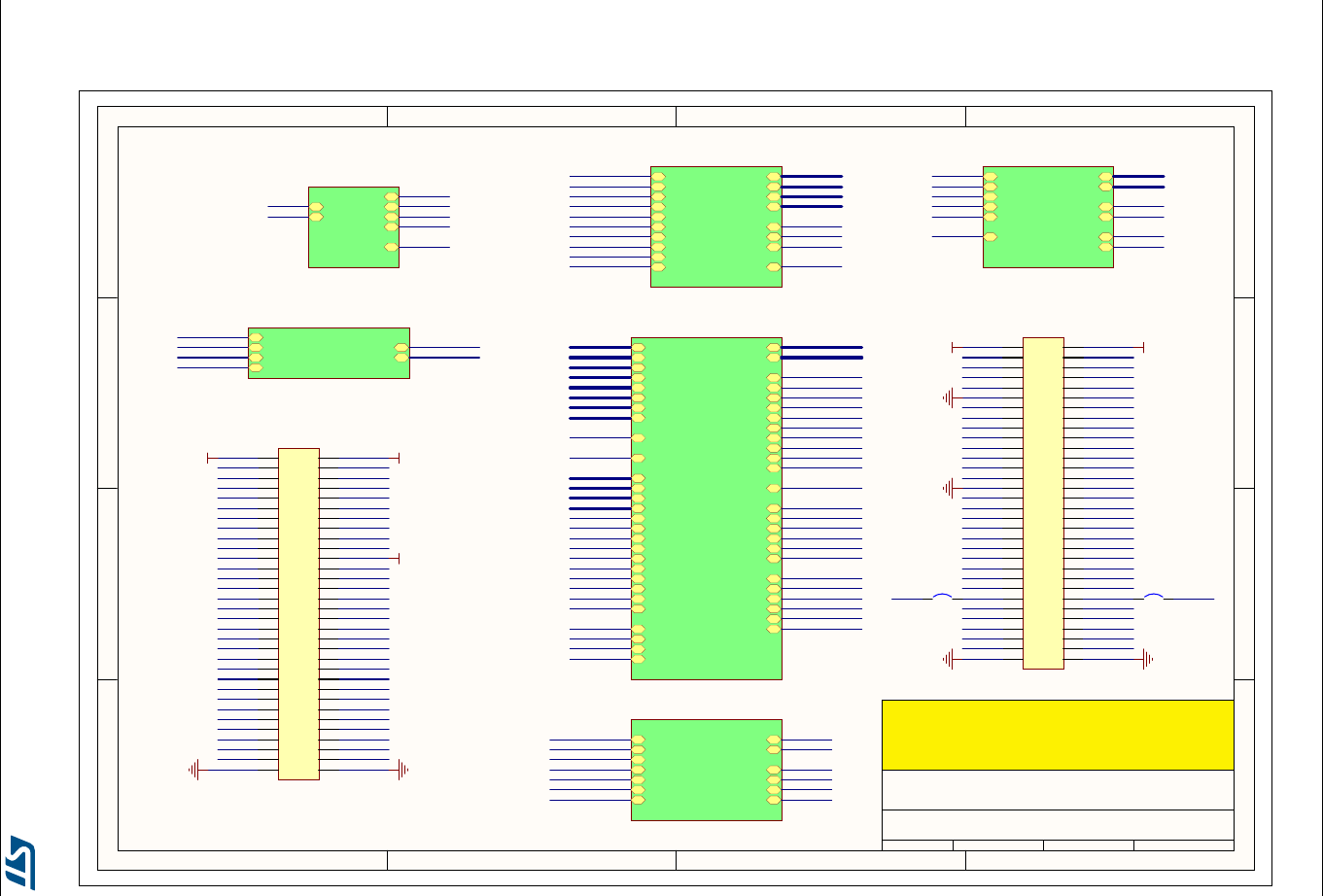
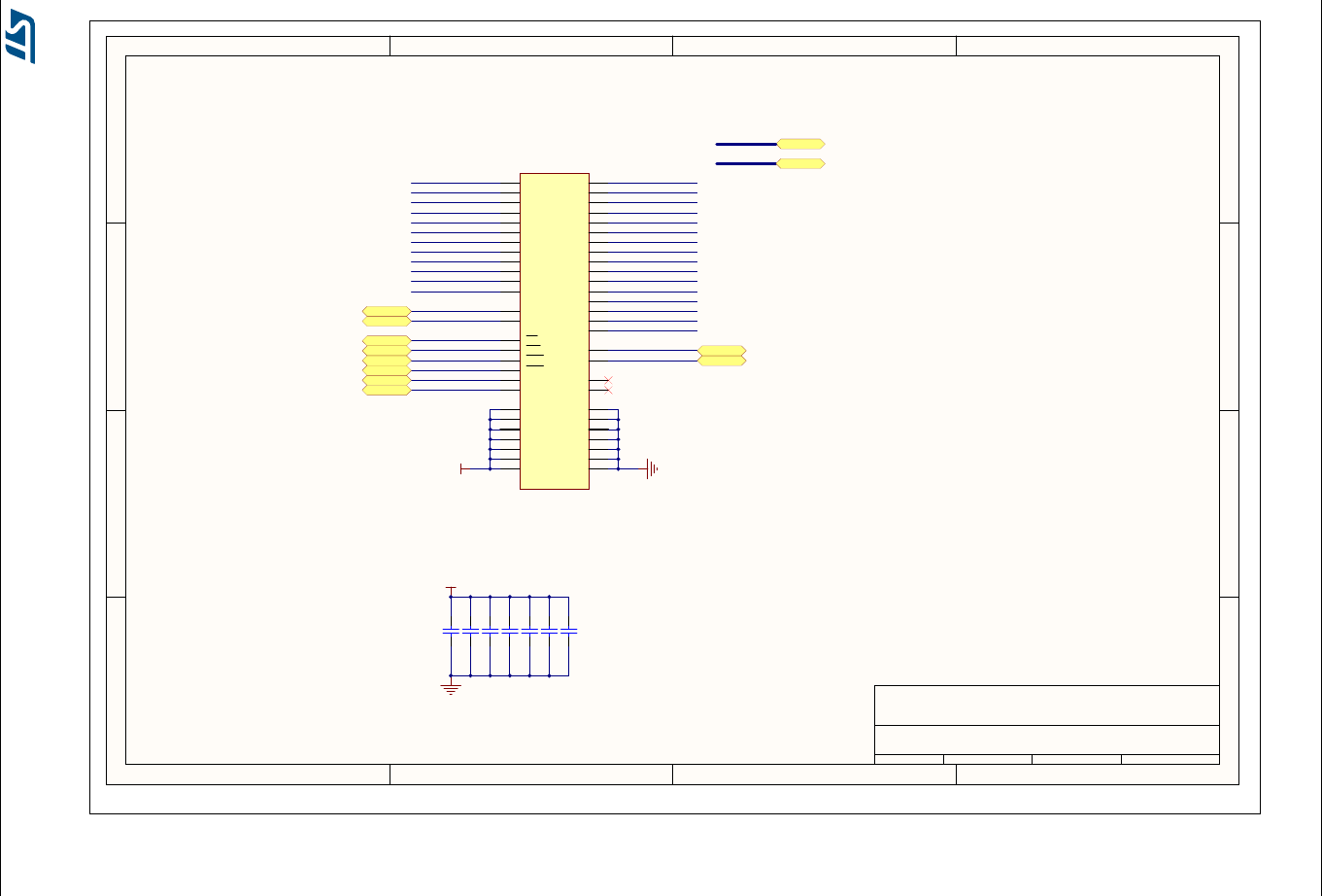
7 Electrical schematics
Figure 9. STM32F429I-DISC1 Discovery board
1
1
2
2
3
3
4
4
D D
C C
B B
A A
STMicroelectronics
Title:
Number: Rev: Sheet of
C.01 Date:9/24/2015
MB1075 1 7
STM32F429I-DISC1
NRST
A[0..11]
D[0..15]
SDNE1
NBL1
NBL0
SDNWE
SDNRAS
SDNCAS
SDCLK
SDCKE1
BA0
BA1
U_SDRAM
SDRAM.SchDoc
PA0
NRST
MEMS_INT1
NCS_MEMS_SPI
MEMS_INT2
SPI5_SCK
SPI5_MISO
SPI5_MOSI
ACP_RST
I2C3_SCL
I2C3_SDA
PG13 PG14
U_IO Peripherals
IO Peripherals.SchDoc
BOOT0
NRST
MCO
D[0..15]
A[0..11]
SDCKE1
SDNE1
SDNWE
NBL0
SDNRAS
NBL1
SDCLK
SDNCAS
BA0
BA1
PA[0..15]
PB[0..15]
PC[0..15]
PD[0..15]
PE[0..15]
PH[0..2]
PF[0..15]
PG[0..15]
R[0..7]
G[0..7]
B[0..7]
IM[0..3]
TP_INT1
VSYNC
CSX
HSYNC
TE
WRX_DCX
RDX
ENABLE
DCX_SCL
SDA
I2C3_SCL
I2C3_SDA
ACP_RST
MEMS_INT1
NCS_MEMS_SPI
MEMS_INT2
SPI5_SCK
SPI5_MISO
SPI5_MOSI
OTG_FS_ID
OTG_FS_DM
OTG_FS_DP
OTG_FS_PSO
OTG_FS_OC
VBUS_FS
DOTCLK
U_STM32Fx
STM32Fx.SchDoc
OTG_FS_PSO
OTG_FS_OCOTG_FS_DM
OTG_FS_DP
OTG_FS_ID
VBUS_FS
U_USB_OTG_FS
USB_OTG_FS.SchDoc
MCO
BOOT0
NRST
SDNWE
PA0
NRST
PE7
PE8PE9
PE10PE11
PE12PE13
PE14PE15
PA1
PA2PA3
PA4PA5
PA6PA7
PA0
PB1
PB2
PB10PB11
PB12PB13
PB14PB15
PB0
PC1
PC2PC3
PC4PC5
PC0
PD8PD9
PD10PD11
PD12PD13
PD14PD15
PH1 PH0
BOOT1 / PB2
NC
3V 3V 3V 3V
Rev A.0 --> PCB label MB1075 A-00
Rev B.1 --> PCB label MB1075 B-01,
PA8 - I2C3_SCL, PC9 - I2C3_SDA, PG7 - DOTCLK, YU<->YD
Rev C.01 --> PCB label MB1075 C-01, mbed-enabled, SB11 and SB15 closed,
STM32F103C8T6 replaced by STM32F103CBT6, ST-LINK/V2-B
PA13
PA14
NRST
PB3
MCO
PA10
PA9
U_ST_LINK
ST_LINK_V2.SCHDOC
PA13
PA14 TCK/SWCLK
TMS/SWDIO
MCO
NRST
T_SWO
T_NRST
STM32F4_USART1_TX
STM32F4_USART1_RX
PA9
PA10
PB3
D[0..15]
A[0..11]
PA[0..15]
PB[0..15]
PC[0..15]
PD[0..15]
PE[0..15]
PH[0..2]
PF[0..15]
PG[0..15]
D[0..15]
A[0..11]
NBL0
NBL1
BA0
BA1
SDNRAS
SDNCAS
SDCLK
SDCKE1
SDNE1
SDNWE
SDNRAS
SDNCAS
SDCLK
SDCKE1
SDNE1
NBL0
NBL1
BA0
BA1
NRST
B[0..7]
G[0..7]
R[0..7]
IM[0..3]
TP_INT1
VSYNC
CSX
HSYNC
TE
WRX_DCX
RDX
ENABLE
DCX_SCL
SDA
I2C3_SCL
I2C3_SDA
DOTCLK
U_LCD-24
LCD-24.SchDoc
VSYNC
CSX
HSYNC
TE
RDX
WRX_DCX
DCX_SCL
SDA
ENABLE
DOTCLK
VSYNC
HSYNC
CSX
TE
RDX
SDA
ENABLE
DOTCLK
DCX_SCL
WRX_DCX
B[0..7]
G[0..7]
R[0..7]
IM[0..3]
TP_INT1
I2C3_SDA
I2C3_SCL
NRST
B[0..7]
G[0..7]
R[0..7]
IM[0..3]
TP_INT1
I2C3_SDA
I2C3_SCL
SPI5_SCK
MEMS_INT1
NCS_MEMS_SPI
SPI5_MISO
SPI5_MOSI
MEMS_INT2
I2C3_SDA
I2C3_SCL
ACP_RST
1 2
3 4
5 6
7 8
9 10
11 12
13 14
15 16
17 18
19 20
21 22
23 24
25 26
27 28
29 30
31 32
33 34
35 36
37 38
39 40
41 42
43 44
45 46
47 48
49 50
51 52
53 54
55 56
57 58
59 60
61 62
6463
P2
Header 32X2
ACP_RST
SPI5_SCK
MEMS_INT1
NCS_MEMS_SPI
SPI5_MISO
SPI5_MOSI
MEMS_INT2
VBUS_FS
OTG_FS_ID
OTG_FS_DM
OTG_FS_DP OTG_FS_PSO
OTG_FS_OC
PF6
PF7PF8
PF9PF10
PF11PF12
PF13PF14
PF15PG0
PG1
PG2PG3
VBUS_FS
OTG_FS_ID
OTG_FS_DM
OTG_FS_DP
OTG_FS_PSO
OTG_FS_OC
PG13 PG14
SB27SB26
BOOT0
PE1
PE2 PE3
PE4 PE5
PE6
PE0
PA8
PA9
PA13PA14
PA15
PB3
PB4 PB5
PB6 PB7
PB8 PB9
PC6
PC7PC8
PC9
PC10
PC11PC12
PC14 PC15
PD1
PD2PD3
PD4
PD6PD7
PD0
VDD
PA10
PD5
PC13
5V
5V 5V
5V 1 2
3 4
5 6
7 8
9 10
11 12
13 14
15 16
17 18
19 20
21 22
23 24
25 26
27 28
29 30
31 32
33 34
35 36
37 38
39 40
41 42
43 44
45 46
47 48
49 50
51 52
53 54
55 56
57 58
59 60
61 62
6463
P1
Header 32X2
PF0 PF1
PF2 PF3
PF4 PF5
PG4PG5
PG6PG7
PG8
PG9 PG10
PG11 PG12
PG13 PG14
PG15
PA11PA12
UM1670 Electrical schematics
DocID025175 Rev 3 29/36
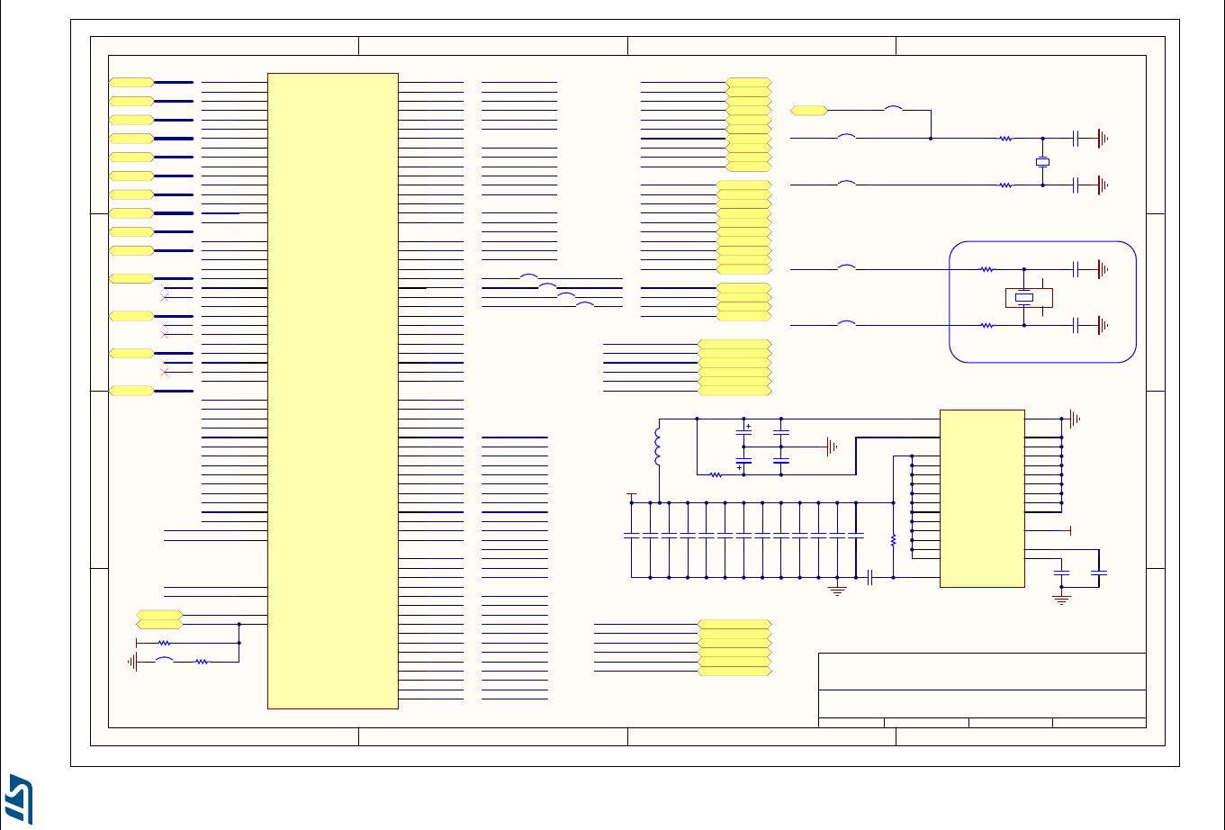
Figure 10. ST-LINK/V2 (SWD only)
1
1
2
2
3
3
4
4
D D
C C
B B
A A
STMicroelectronics
Title:
Number: Rev: Sheet of
C.01
Date:
9/24/2015
1 2
X1
8MHz
3V
USB_DM
USB_DP
STM_RST
T_JTCK
T_JTCK
T_JTDO
T_JTDI
T_JTMS
STM_JTMS
STM_JTCK
OSC_IN
OSC_OUT
T_NRST
AIN_1
3V
3V
3V
SWIM_IN
SWIM_IN
SWIM_IN
SWIM
SWIM
SWIM_RST_IN
SWIM_RST
MB1075 2 7
STM32F429I-DISC1 ST-LINK/V2-B (SWD only)
USB ST-LINK
U5V
COM
5VU5V
3V
PWR
5V
JP1
Wired on Solder Side
JP2
3V
Jumpers ON --> DISCOVERY Selected
Jumpers OFF --> ST-LINK Selected
Board Ident: PC13=0
T_JTCK
T_JTMS
SWD
3V
1
2
3
4
CN4
SB4 SB3
SB6 SB5
SB8 SB7
SB14 SB13
STM_JTMS
STM_JTCK SWCLK
SWDIO
SWD
RESERVED
DEFAULT
3V
T_SWDIO_IN
LED_STLINK
LED_STLINK
3V
PA13
PA14
TCK/SWCLK
TMS/SWDIO
VDD3V
Not Fitted
MCO
C2
1μF_X5R_0603
C3
10nF_X7R_0603
C5
1μF_X5R_0603
MCO
Not Fitted
T_JRST
1
2
3
4
5
6
CN2
Header 6
AIN_1
T_NRST
T_SWO
NRST
SB12
T_NRST
SB10
RC Must be very close to STM32F103 pin 29
JP3
51
2
GND
3
4
BYPASS
INH
Vin Vout
U1
LD3985M33R
D2
BAT60JFILM
D3
BAT60JFILM
D1
BAT60JFILM
Idd
EXT_5V, Input only
JP4
TX
RX
STLINK_RX
Not Fitted
SB15
SB11
PA10
PA9
STM32F4_USART1_TX
STM32F4_USART1_RX
STLINK_TX
USB_DM
USB_DP
3VVCC 1
D- 2
D+ 3
ID 4
GND 5
SHELL 6
CN1
USB-MINI-typeB
T_SWO
PB3
SB9
T_SWO
EXT_3V, Input only
Red
_Green
2 1
3 4
LD1
LD_BICOLOR_CMS
R10 1K5
R12 0
R11 0
R9 100K
R4
1K
R2
100
R1
100
R3
0
R13 [NA]
R14 22
R15 22
R17 22
R20 22
R28
100
R16
100
R5
10K
R6 10K
R21
100K
R8
100K
R7 10K
R18 4K7
R19 4K7
C27
100nF
C4
100nF
C46
100nF
C47
100nF
C18
20pF
C16
20pF
C17
20pF
C9
100nF
C1
100nF
C6
100nF
LD2
LED, red
VBAT
1
PA7
17
PC13
2
PA12 33
PC14
3
PB0
18
PC15
4JTMS/SWDIO 34
OSCIN
5
PB1
19
OSCOUT
6
VSS_2 35
NRST
7
PB2/BOOT1
20
VSSA
8
VDD_2 36
VDDA
9
PB10
21
PA0
10
JTCK/SWCLK 37
PA1
11
PB11
22
PA2
12
PA15/JTDI 38
PA3
13
VSS_1
23
PA4
14
PB3/JTDO 39
PA5
15
VDD_1
24
PA6
16
PB4/JNTRST 40
PB12 25
PB5 41
PB13 26
PB6 42
PB14 27
PB7 43
PB15 28
BOOT0 44
PA8 29
PB8 45
PA9 30
PB9 46
PA10 31
VSS_3 47
PA11 32
VDD_3 48
U2
STM32F103CBT6
Electrical schematics UM1670
30/36 DocID025175 Rev 3
Figure 11. USB OTG FS
1
1
2
2
3
3
4
4
D D
C C
B B
A A
STMicroelectronics
Title:
Number: Rev: Sheet of
C.01 Date:9/24/2015
MB1075
37
STM32F429I-DISC1 USB_OTG_FS
5V
OTG_FS_PSO
OTG_FS_OC
3V
12
LD6
Red
OTG_FS_DM
OTG_FS_DP
OTG_FS_ID
C53
4.7uF
OTG_FS_PowerSwitchOn
OTG_FS_OverCurrent
12
LD5
Green
3V
3V
Dz
A2
ID A3
Pd1 B1
Pup
B2
Vbus
B3
D+in C1
Pd2 C2
D+out
C3
D-in D1
GND D2
D-out
D3
U7
EMIF02-USB03F2
GND
2
IN
5
EN
4OUT 1
FAULT 3
U8
STMPS2141STR
VBUS_FS
OTG_FS_ID
OTG_FS_DM
OTG_FS_DP
OTG_FS_PSO
VBUS_FS
OTG_FS_OC
R66
[N/A]
R69 0
R73
620
R68
47K
R71
10K
R72 0
R64 22
R63 22
R67 0
R65
47K
R70
330
3
1
2
T1
9013-SOT23
VBUS
1
DM
2
DP
3
ID
4
GND
5
Shield
6
USB_Micro-AB receptacle
CN6
USB-MICRO-AB
UM1670 Electrical schematics
DocID025175 Rev 3 31/36
Figure 12. 64-Mbit SDRAM
1
1
2
2
3
3
4
4
D D
C C
B B
A A
STMicroelectronics
Title:
Number: Rev: Sheet of
C.01 Date:9/24/2015
MB1075 47
STM32F429I-DISC1 SDRAM 64Mbits
WE
16
DQ14 51
GNDQ 6
GNDQ 12
DQ13 50
DQ12 48
DQ8 42
DQ1 4
RAS
18
DQ9 44
GNDQ 52
DQ7 13
DQ4 8
DQ11 47
DQ10 45
DQ3 7
UDQM 39
DQ15 53
VDD
27
DQ0 2
BA1
21
DQ5 10
DQ6 11
CLK
38
CS
19
DQ2 5
GND 28
GND 41
A9
34
VDD
1
VDD
14
CAS
17
A7
32
A11
35
A8
33
BA0
20
A0
23
A1
24
GNDQ 46
A10
22
A6
31
CKE
37
A4
29
A5
30
A2
25
A3
26
GND 54
VDDQ
3VDDQ
9VDDQ
43 VDDQ
49
LDQM 15
NC 36
NC 40
U6
IS42S16400J
A[0..11]
A0
A1
A2
A3
A4
A5
A6
A7
A8
A9
A10
A11
D0
D1
D2
D3
D4
D5
D6
D7
D8
D9
D10
D11
D12
D13
D14
D15
D[0..15]
3V
Place close SDRAM
SDNWE
SDNRAS
BA0
BA1
SDCLK
SDNCAS
SDCKE1
SDNE1
NBL0
NBL1
3V
SDNE1
SDNWE
SDNRAS
SDNCAS
SDCLK
SDCKE1
NBL0
NBL1
BA0
BA1
D[0..15]
A[0..11]
C50100nF
C7100nF
C8100nF
C51100nF
C10100nF
C15100nF
C22100nF
Electrical schematics UM1670
32/36 DocID025175 Rev 3
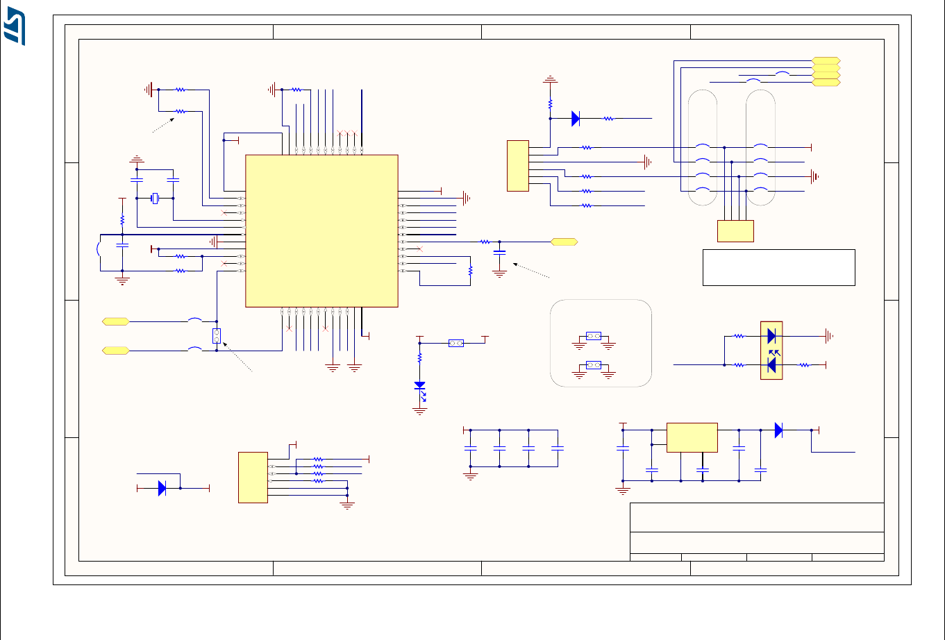
Figure 13. STM32F429ZIT6 MCU
1
1
2
2
3
3
4
4
D D
C C
B B
A A
STMicroelectronics
Title:
Number: Rev: Sheet of
C.01
Date:
9/24/2015
MB1075 5 7
STM32F429I-DISC1 - STM32F429ZIT6 MCU
PB5
PB6
PB7
PA4
PA5
PA6
PA7
VDD
PA11
PA12
PA9
PA10
PB12
PB13
PB14
PB15
PB10
PB11
PB8
PA0
PB9
PA1
PB1
PB2
PA15
PB3
PB0
PA3
PA13
PA14
PB4
PA2
PA8
BOOT0
NRST
BOOT0
SB21
NRST
L1
BEAD
C26
1uF
VDD
C25
1uF
PC0
PE0
PD0
PC14-OSC32_IN
PC15-OSC32_OUT
PE2 1
PE3 2
PE4 3
PE5 4
PE6 5
PH0-OSC_IN
23
PH1-OSC_OUT
24
NRST
25
PA0-WKUP1
34
PA1
35
PA2
36
PA3
37
PA4
40
PA5
41
PA6
42
PA7
43
PB0
46
PB1
47
PB2/BOOT1
48
PE7 58
PE8 59
PE9 60
PE10 63
PE11 64
PE12 65
PE13 66
PE14 67
PE15 68
PB10
69
PB11
70
PB12
73
PB13
74
PB14
75
PB15
76
PD8 77
PD9 78
PD10 79
PD11 80
PD12 81
PD13 82
PD14 85
PD15 86
PA8
100
PA9
101
PA10
102
PA11
103
PA12
104
PA13
105
PA14
109
PA15
110
PD0 114
PD1 115
PD2 116
PD3 117
PD4 118
PD5 119
PD6 122
PD7 123
PB3
133
PB4
134
PB5
135
PB6
136
PB7
137
BOOT0
138
PB8
139
PB9
140
PE0 141
PE1 142
PC13-WKUP2
7
PC14-OSC32_IN
8
PC15-OSC32_OUT
9
PC0
26
PC1
27
PC2
28
PC3
29
PC4
44
PC5
45
PC6
96
PC7
97
PC8
98
PC9
99
PC10
111
PC11
112
PC12
113
PF2 12
PF3 13
PF4 14
PF5 15
PF6 18
PF7 19
PF8 20
PF9 21
PF10 22
PF11 49
PF12 50
PF13 53
PF14 54
PF15 55
PF0 10
PF1 11
PG2 87
PG3 88
PG4 89
PG5 90
PG6 91
PG7 92
PG8 93
PG9 124
PG10 125
PG11 126
PG12 127
PG13 128
PG14 129
PG15 132
PG0 56
PG1 57
U5A
STM32F429ZIT6
VBAT
6
VSS_5 16
VDD_5
17
VSSA 31
VDD_12
30
VREF+
32
VDDA
33
VSS_4 38
VDD_4
39
VCAP1 71
VDD_1
72
VSS_2 107
VDD_2
108
PDR_ON 143
VDD_3
144
VDD_10
121 VDD_9
95
VDD_6
52
VDD_7
62
VDD_8
84
VDD_11
131
VSS_10 120
VSS_9 94
VSS_6 51
VSS_7 61
VSS_8 83
VSS_11 130
VCAP2 106
U5B
STM32F429ZIT6
PD1
PD2
PD3
PD4
PD5
PD6
PD7
PD8
PD9
PD10
PD11
PD12
PD13
PD14
PD15
PE1
PE2
PE3
PE4
PE5
PE6
PE7
PE8
PE9
PE10
PE11
PE12
PE13
PE14
PE15
PC1
PC2
PC3
PC4
PC5
PC6
PC7
PC8
PC9
PC10
PC11
PC12
PC13
PF0
PF1
PF2
PF3
PF4
PF5
PF6
PF7
PF8
PF9
PF10
PF11
PF12
PF13
PF14
PF15
PG0
PG1
PG2
PG3
PG4
PG5
PG6
PG7
PG8
PG9
PG10
PG11
PG12
PG13
PG14
PG15
PH0-OSC_IN
PH1-OSC_OUT
MCO
PH1-OSC_OUT
SB20
SB19
MCO
1 2
X3
8MHz
Not Fitted
PC14-OSC32_IN
PC15-OSC32_OUT
SB17
SB16
SB18
PH0-OSC_IN
C42
2.2uF
C41
2.2uF
PA[0..15]
PA[0..15]
PB[0..15]
PB[0..15]
PC[0..15]
PC[0..15]
PD[0..15]
PD[0..15]
PE[0..15]
PE[0..15]
PH[0..2]
PH[0..2]
PF[0..15]
PF[0..15]
PG[0..15]
PG[0..15]
D[0..15]
A[0..11]
D[0..15]
A[0..11]
VDD
A0
A1
A2
A3
A4
A5
A6
A7
A8
A9
A10
A11
SDNWE
SDNRAS
BA0
BA1
SDCLK
SDNCAS
SDCKE1
SDNE1
PF0
PF1
PF2
PF3
PF4
PF5
PF12
PF13
PF14
PF15
PG0
PG1
PC0
PF11
PG8
PG15
PB5
PG4
PG5
PB6
D0
D1
D2
D3
D4
D5
D6
D7
D8
D9
D10
D11
D12
D13
D14
D15
NBL0
NBL1
PE0
PD14
PE7
PD8
PE8
PE9
PE10
PE11
PE12
PE13
PE14
PE15
PD9
PD10
PD15
PD0
PD1
PE1
SDCKE1
SDNE1
SDNWE
NBL0
SDNRAS
NBL1
SDCLK
SDNCAS
BA0
BA1
PH0
PH1
PC14
PC15
PA3
PA4
PA6
PA11
PB1
PB8
PB9
PB10
PC6
PC7
PC10
PD2
PA12
PB0
PB11
PC2PD3
PD4
B5
VSYNC
G2
R4
R6
B6
B7
G4
HSYNC
G6
R2
IM0
R5
R3
G5
CSXG7
IM1
PD5
PD6
PD7
PD11
PD12
PD13
PF7
PF9
PF10
PG6
PG7
IM2
B2
IM3
TE
RDX
SDA
ENABLE
R7
DOTCLK
PG10 G3
PG11 B3
PG12 B4
DCX_SCL
WRX_DCX
R[0..7]
R[0..7]
G[0..7]
G[0..7]
B[0..7]
B[0..7]
R0
R1
G0
G1
B0
B1
IM[0..3]
IM[0..3]
VSYNC
CSX
HSYNC
TE
WRX_DCX
RDX
ENABLE
DOTCLK
DCX_SCL
SDA
I2C3_SDA
I2C3_SCL
TP_INT1PA15
PA8
PC9
TP_INT1
I2C3_SCL
I2C3_SDA
ACP_RST
PA7 ACP_RST
MEMS_INT1
SPI5_SCK
MEMS_INT1
NCS_MEMS_SPI NCS_MEMS_SPI
MEMS_INT2
SPI5_SCK
SPI5_MISO
SPI5_MOSI
SPI5_MISO
SPI5_MOSI
MEMS_INT2
PC1
PF7
PF8
PF9
PA1
PA2
SB25
SB24
SB23
SB22
VBUS_FS
OTG_FS_ID
OTG_FS_DM
OTG_FS_DP
PB14
PB12
PB15
PB13
OTG_FS_PSOPC4
PC5 OTG_FS_OC
OTG_FS_ID
OTG_FS_DM
OTG_FS_DP
OTG_FS_PSO
OTG_FS_OC
VBUS_FS
C20
20pF
C21
20pF
C23
6.8pF
C24
6.8pF
R56 0
R57 220
R53 0
R54 0
C34100nF
C35100nF
C36100nF
C37100nF
C38100nF
C39100nF
C40100nF
C29100nF
C32100nF
C43100nF
C44100nF
C45100nF
C33100nF
C28
1uF
R520
C31
100nF
C30
100nF
R58 0
R59 [N/A]
R61 510
41
32
X2
MC306-G-06Q-32.768
UM1670 Electrical schematics
DocID025175 Rev 3 33/36
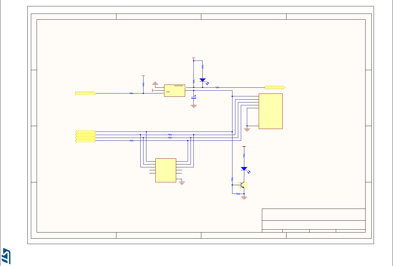
Figure 14. Peripherals
1
1
2
2
3
3
4
4
D D
C C
B B
A A
STMicroelectronics
Title:
Number: Rev: Sheet of
C.01 Date:9/24/2015
MB1075 67
STM32F429I-DISC1 Peripherals
MEMS
VDD
SB2
PA0
USER & WAKE-UP Button
NRST
NRST
RESET Button
VDD
SB1
Not Fitted
PA0
MEMS_INT1
3V
SPI5_SCK
MEMS_INT1
NCS_MEMS_SPI
NCS_MEMS_SPI
VDD_IO
1
GND 13
C1 14
GND
8GND 9
VDD 16
CS_I2C/SPI
5
INT1
7DRDY/INT2
6
GND 10
GND 11
SA0/SDO
4SDA/SDI/SDO
3SCL/SPC
2VDD 15
GND 12
U3
L3GD20
C13
10uF
C19
10nF/25V
MEMS_INT2
SPI5_SCK
SPI5_MISO
SPI5_MOSI SPI5_MISO
SPI5_MOSI
1 2
3 4
5 6
7 8
CN3
SSM-104-L-DH
3V
ACP/RF E2P Connector
5V
ACP_RST
I2C3_SDA
I2C3_SCL ACP_RSTI2C3_SCL
I2C3_SDA
MEMS_INT2
R24
100K
R22
220K
R23
330
R25
100
1 2
LD4
Red
1 2
LD3
Green
PG13
LEDs
PG13
PG14
PG14
R26
510
R27
680
C12
100nF
C11
100nF
C48
100nF
12
3 4
B2
SW-PUSH-CMS_BLACK
12
3 4
B1
SW-PUSH-CMS_BLUE
Electrical schematics UM1670
34/36 DocID025175 Rev 3
Figure 15. LCD 2.4
1
1
2
2
3
3
4
4
D D
C C
B B
A A
STMicroelectronics
Title:
Number: Rev: Sheet of
C.01
Date:
9/15/2015
MB1075
77
STM32F429I-DISC1 LCD 2.4"
SPI5_MOSI
SPI5_SCK
3V
3V
3V
TP_INT1
XR
YD
YU
XL
Default I2C Address:1000001
Y- 1
INT
2
A0/Data Out
3
SCLK
4
SDAT
5
VCC
6
Data in
7
IN0 8
IN1 9
GND
10
IN2 11
IN3 12
X+ 13
Vio
14
Y+ 15
X- 16
U4
STMPE811QTR
TP_INT1
3V
HSYNC
VSYNC
DOTCLK
3V
C14
4.7uF
VDD
ENABLE
32
DOTCLK
31
HSYNC
33
VSYNC
34
CSX
38
DCX/SCL
37
TE
11
WRX/DCX
36
RDX
35
RESET
39
DB0/B0 29
DB1/B1 28
DB2/B2 27
DB3/B3 26
DB4/B4 25
DB5/B5 24
DB6/G0 23
DB7/G1 22
VDD3_P(nc) 8
BC_CTRL(nc) 9
BC(nc) 10
VDD3
7
IM3 43
IM2 42
IM1 41
IM0 40
SDA
30
VCI
6
LEDA
44
LEDK1
45
LEDK2
46
LEDK3
47
LEDK4
48
YD
3
XL
2
YU
1
XR
4GND 5
DB8/G2 21
DB9/G3 20
DB10/G4 19
DB11/G5 18
DB12/R0 17
DB13/R1 16
DB14/R2 15
DB15/R3 14
DB16/R4 13
DB17/R5 12
CN5
SF-TC240T-9370-T
XR
YD
YU
XL
B2
B3
B4
B5
G2
G3
G4
G5
R2
R3
R4
R5
ENABLE
CSX
RDX
TE
DCX_SCL
WRX_DCX
SDA
NRST
IM0
IM1
IM2
IM3
B[0..7]
G[0..7]
R[0..7]
NRST
B6
B7
G6
G7
R6
R7
B0
B1
G0
R0
G1
R1
IM[0..3] = 0110 --> 4-wire 8-bit serial I, SDA:In/Out
VSYNC
HSYNC
CSX
TE
RDX
SDA
ENABLE
DOTCLK
IM[0..3] IM[0..3]
DCX_SCL
WRX_DCX
R[0..7]
G[0..7]
B[0..7]
VSYNC
CSX
HSYNC
TE
WRX_DCX
RDX
ENABLE
DOTCLK
DCX_SCL
SDA
I2C3_SDA
I2C3_SCL
I2C3_SCL
I2C3_SDA R46 100K
R29
4K7
R30
4K7
R45
4K7
R34 100K
R31 4K7 R33 100K
R39 [N/A] R32 100K
R40 0
R50 0
R51
4K7
R62
4K7
R60
4K7
R55
4K7
R35
[N/A]
R36
4K7
R37
4K7
R38
[N/A]
R42
[N/A]
R43
[N/A]
R41
4K7
R44
4K7
C52
100nF
R49 0
R48 0
R47 0
C49
100nF

DocID025175 Rev 3 35/36
UM1670 Revision history
35
8 Revision history
Table 7. Document revision history
Date Revision Changes
10-Sep-2013 1 Initial release.
04-Mar-2016 2
New revision to introduce STM32F429I-DISC1 additional CPN that
corresponds to Mbed-Enabled Discovery Kit.
Updated: Section : Introduction, Figure 1: STM32F429 Discovery
board, Section 5: Quick start, Section 6: Hardware layout, Figure 2:
Hardware block diagram, Figure 3: Top layout, Section 6.3:
Embedded ST-LINK/V2 (or V2-B), Table 5: Solder bridges, Table 6:
STM32 pin description versus board functions, Section 7: Electrical
schematics.
20-Sep-2017 3 Updated Section 6.9: TFT LCD (Thin-film-transistor liquid-crystal
display).

UM1670
36/36 DocID025175 Rev 3
IMPORTANT NOTICE – PLEASE READ CAREFULLY
STMicroelectronics NV and its subsidiaries (“ST”) reserve the right to make changes, corrections, enhancements, modifications, and
improvements to ST products and/or to this document at any time without notice. Purchasers should obtain the latest relevant information on
ST products before placing orders. ST products are sold pursuant to ST’s terms and conditions of sale in place at the time of order
acknowledgement.
Purchasers are solely responsible for the choice, selection, and use of ST products and ST assumes no liability for application assistance or
the design of Purchasers’ products.
No license, express or implied, to any intellectual property right is granted by ST herein.
Resale of ST products with provisions different from the information set forth herein shall void any warranty granted by ST for such product.
ST and the ST logo are trademarks of ST. All other product or service names are the property of their respective owners.
Information in this document supersedes and replaces information previously supplied in any prior versions of this document.
© 2017 STMicroelectronics – All rights reserved
