User Manual TEF6686
User Manual:
Open the PDF directly: View PDF ![]() .
.
Page Count: 101 [warning: Documents this large are best viewed by clicking the View PDF Link!]
- 1. Introduction
- 2. Control interface
- 3. Write commands
- 3.1 FM / AM cmd 1 Tune_To
- 3.2 FM cmd 2 Set_Tune_Options
- 3.3 FM / AM cmd 10 Set_Bandwidth
- 3.4 FM / AM cmd 11 Set_RFAGC
- 3.5 AM cmd 12 Set_Antenna
- 3.6 AM cmd 14 Set_CoChannelDet
- 3.7 FM cmd 20 Set_MphSuppression
- 3.8 FM cmd 22 Set_ChannelEqualizer
- 3.9 FM cmd 23 Set_NoiseBlanker
- 3.10 FM cmd 24 Set_NoiseBlanker_Options
- 3.11 AM cmd 23 Set_NoiseBlanker
- 3.12 AM cmd 24 Set_NoiseBlanker_Audio
- 3.13 FM / AM cmd 30 Set_DigitalRadio
- 3.14 FM cmd 31 Set_Deemphasis
- 3.15 FM cmd 32 Set_StereoImprovement
- 3.16 FM / AM cmd 38 Set_LevelStep
- 3.17 FM / AM cmd 39 Set_LevelOffset
- 3.18 FM / AM cmd 40 … 45 Set_Softmute
- 3.19 FM / AM cmd 50 … 59 Set_Highcut
- 3.20 FM cmd 60 … 66 Set_Stereo
- 3.21 FM cmd 70 … 76 Set_StHiBlend
- 3.22 FM / AM cmd 80 Set_Scaler
- 3.23 FM cmd 81 Set_RDS
- 3.24 FM / AM cmd 82 Set_QualityStatus
- 3.25 FM / AM cmd 83 Set_DR_Blend
- 3.26 FM / AM cmd 84 Set_DR_Options
- 3.27 FM / AM cmd 85 Set_Specials
- 3.28 FM cmd 86 Set_Bandwidth_Options
- 3.29 FM cmd 90 … 92 Set_StereoBandBlend
- 3.30 AUDIO cmd 10 Set_Volume
- 3.31 AUDIO cmd 11 Set_Mute
- 3.32 AUDIO cmd 12 Set_Input
- 3.33 AUDIO cmd 13 Set_Output_Source
- 3.34 AUDIO cmd 21 Set_Ana_Out
- 3.35 AUDIO cmd 22 Set_Dig_IO
- 3.36 AUDIO cmd 23 Set_Input_Scaler
- 3.37 AUDIO cmd 24 Set_WaveGen
- 3.38 APPL cmd 1 Set_OperationMode
- 3.39 APPL cmd 3 Set_GPIO
- 3.40 Idle state - APPL cmd 4 Set_ReferenceClock
- 3.41 Idle state - APPL cmd 5 Activate
- 4. Read commands
- 4.1 FM / AM cmd 128 / 129 Get_Quality
- 4.2 FM cmd 130 / 131 Get_RDS
- 4.3 FM / AM cmd 132 Get_AGC
- 4.4 FM / AM cmd 133 Get_Signal_Status
- 4.5 FM / AM cmd 134 Get_Processing_Status
- 4.6 FM / AM cmd 135 Get_Interface_Status
- 4.7 APPL cmd 128 Get_Operation_Status
- 4.8 APPL cmd 129 Get_GPIO_Status
- 4.9 APPL cmd 130 Get_Identification
- 4.10 APPL cmd 131 Get_LastWrite
- 5. I²C bus protocol
- 6. Device start-up
- 7. Overview of available commands
- 8. Legal information
- 9. List of figures
- 10. List of tables
- 11. Contents

TEF668X User Manual
Device version /V102
Rev. 1.6 — 17 February 2015
User Manual
Document information
Info
Content
Keywords
Lithio, TEF6686, TEF6687, TEF6688, TEF6689, /V102, firmware 2.00,
API, I²C bus, control, car radio
Abstract
Overview of TEF668X series device control

NXP Semiconductors
TEF668X User Manual
TEF6686, TEF6687, TEF6688 and TEF6689, /V102
doc
All information provided in this document is subject to legal disclaimers.
© NXP B.V. 2015. All rights reserved.
User Manual
Rev. 1.6 — 17 February 2015
2 of 101
Contact information
For more information, please visit: http://www.nxp.com
For sales office addresses, please send an email to: salesaddresses@nxp.com
Revision history
Rev
Date
Description
‘Lithio’ TEF6686, TEF6687, TEF6688 and TEF6689, device version V102, user manual
Description of the TEF668X/V102 control interface (API) and related information
1.6
20150217
Change bars indicate changes from V102 user manual Rev. 1.5
3.33, 3.37, 4.6 corrected example and table content
3.40 changed 55.4667 to 55.46667 MHz reference frequency for consistency with other
documentation (no control change required)
6.2.1, 6.2.2, 6.2.3 updated with V102 required initialization p2.22
1.5
20141219
3.9, 3.10, 3.11, 3.12 added extended API noise blanker control (p2.21)
6.2.1, 6.2.2, 6.2.3 updated with V102 required initialization p2.21
1.4
20141124
6.2.1, 6.2.2, 6.2.3 updated with V102 required initialization p2.19
1.2
20140415
3.3 improved description of min_bandwidth parameter
6.2.1, 6.2.2, 6.2.3 updated with V102 required initialization p2.15
1.1
20140324
6.2.1, 6.2.2, 6.2.3 updated with V102 required initialization p2.14
1.0
20140306
3.3 added FM PACS minimum bandwidth option (p2.13)
6.2.1, 6.2.2, 6.2.3 updated with V102 required initialization p2.13
0.8
20140129
4.2.3 increased allowed times using RDS data buffer
6.2.1, 6.2.2, 6.2.3 updated with V102 required initialization p2.12
0.6
20131210
6.2.1, 6.2.2, 6.2.3 updated with V102 required initialization p2.10
0.5
20131106
3.6 added AM co-channel detection control command (p2.09)
4.1 added AM noise detector and AM co-channel detector quality read (p2.09)
6.2.1, 6.2.2, 6.2.3 updated with V102 required initialization p2.09
7 updated command tables

NXP Semiconductors
TEF668X User Manual
TEF6686, TEF6687, TEF6688 and TEF6689, /V102
doc
All information provided in this document is subject to legal disclaimers.
© NXP B.V. 2015. All rights reserved.
User Manual
Rev. 1.6 — 17 February 2015
3 of 101
Contact information
For more information, please visit: http://www.nxp.com
For sales office addresses, please send an email to: salesaddresses@nxp.com
Revision history
Rev
Date
Description
0.4
20131018
Generic changes from the device version V101 user manual:
- changed version identification and references to V102 (= firmware version 2.00)
- added TEF6687 and TEF6689 variants with FMSI system
Changes from V101 user manual Rev 1.8 (V101 p01.24):
3.15 added FMSI enable command
3.19 removed attention note regarding FM_Highcut_Options special control (resolved)
3.20 added note regarding stereo control ‘off’ as suggested for FMSI use
3.20 FM_Set_Stereo_Max corrected table head (parameters)
3.26 FM/AM_Set_DR_Options corrected table head (parameters)
3.29 added FMSI control commands
3.40 APPL_Set_ReferenceClock renamed parameters to frequency_msb, frequency_lsb
4.5 added FMSI processing status read
6.2.1, 6.2.2, 6.2.3 updated with V102 required initialization (p2.06)
7 Table 1 consistency corrections on listed commands and parameters
Template update

NXP Semiconductors
TEF668X User Manual
TEF6686, TEF6687, TEF6688 and TEF6689, /V102
doc
All information provided in this document is subject to legal disclaimers.
© NXP B.V. 2015. All rights reserved.
User Manual
Rev. 1.6 — 17 February 2015
4 of 101
1. Introduction
TEF668X (‘Lithio’) is a series of novel single-chip car radio devices with an upper
mainstream to high-end performance and feature set.
The Lithio series consists of four variants; TEF6686, TEF6687, TEF6688 and TEF6689.
All Lithio variants offer worldwide FM band reception as well as full AM band reception up
to 27 MHz. In addition to the TEF6686 feature set the variants TEF6687 and TEF6689
(Lithio FMSI and Lithio FMSI DR) offer the added performance of extended FM stereo
reception and the variants TEF6688 and TEF6689 (Lithio DR and Lithio FMSI DR) offer
connectivity and support for digital radio reception in the AM and FM bands.
This user manual describes the TEF668X series control interface or API (Application
Programming Interface). The document describes the available write and read
commands with parameter and data definitions.
This document version contains limited background information regarding the feature
functionality and the offered control options so some general knowledge of car radio
functions is required.
This user manual describes the functionality and control of the TEF668X device version
V102 specifically (TEF668X/V102).
2. Control interface
2.1 Overview
The TEF668X devices are equipped with an I²C bus interface for control of the device.
Full control of the device functions and features is available using this single interface.
The I²C bus supports bit rates of up to 400 kbit/s in accordance with the ‘fast mode’ I²C
bus specification.
The control interface is described in this document on an abstract ‘application’ level as
well as on I²C protocol level.
The TEF668X interface definition is compatible with the TEF665X (Atomic-2) and
TEF701X (Sabre) series of devices, although differing in available commands reflecting
the available functionality. The interface is compatible with the TEA685X (Tiger-2) series
as well.
Future NXP car radio devices will employ the same interface allowing compatible control
between device types, versions and variants.
Via the I²C bus commands and parameters can be written to the device and information
can be read from the device.
TEF668X control is organized in modules. Modules are independent functional blocks
that can be regarded sub-devices within the device.
NXP Semiconductors
TEF668X User Manual
TEF6686, TEF6687, TEF6688 and TEF6689, /V102
doc
All information provided in this document is subject to legal disclaimers.
© NXP B.V. 2015. All rights reserved.
User Manual
Rev. 1.6 — 17 February 2015
5 of 101
The TEF668X consists of four modules:
module 32 : FM = FM radio reception
module 33 : AM = LW, MW and SW radio reception
module 48 : AUDIO = Audio processing
module 64 : APPL = System and application control
Different modules can be controlled independently even when the addressed module
itself is inactive at the time of control. This means modules can be prepared and
initialized before use.
Compatible command definitions have been used for the modules of FM and AM radio
where applicable. Defaults and range definitions may differ in some cases to fit the
different band properties.
Module commands have one or more parameters for control of the module behavior and
option selections.
The control is organized in such a way that future devices may support writing of a single
parameter up to writing of all parameters available for a given command.
Device version V102 however does not offer this flexibility and requires all command
parameters described in this document to be transmitted. This behavior is equal to
device version V101.
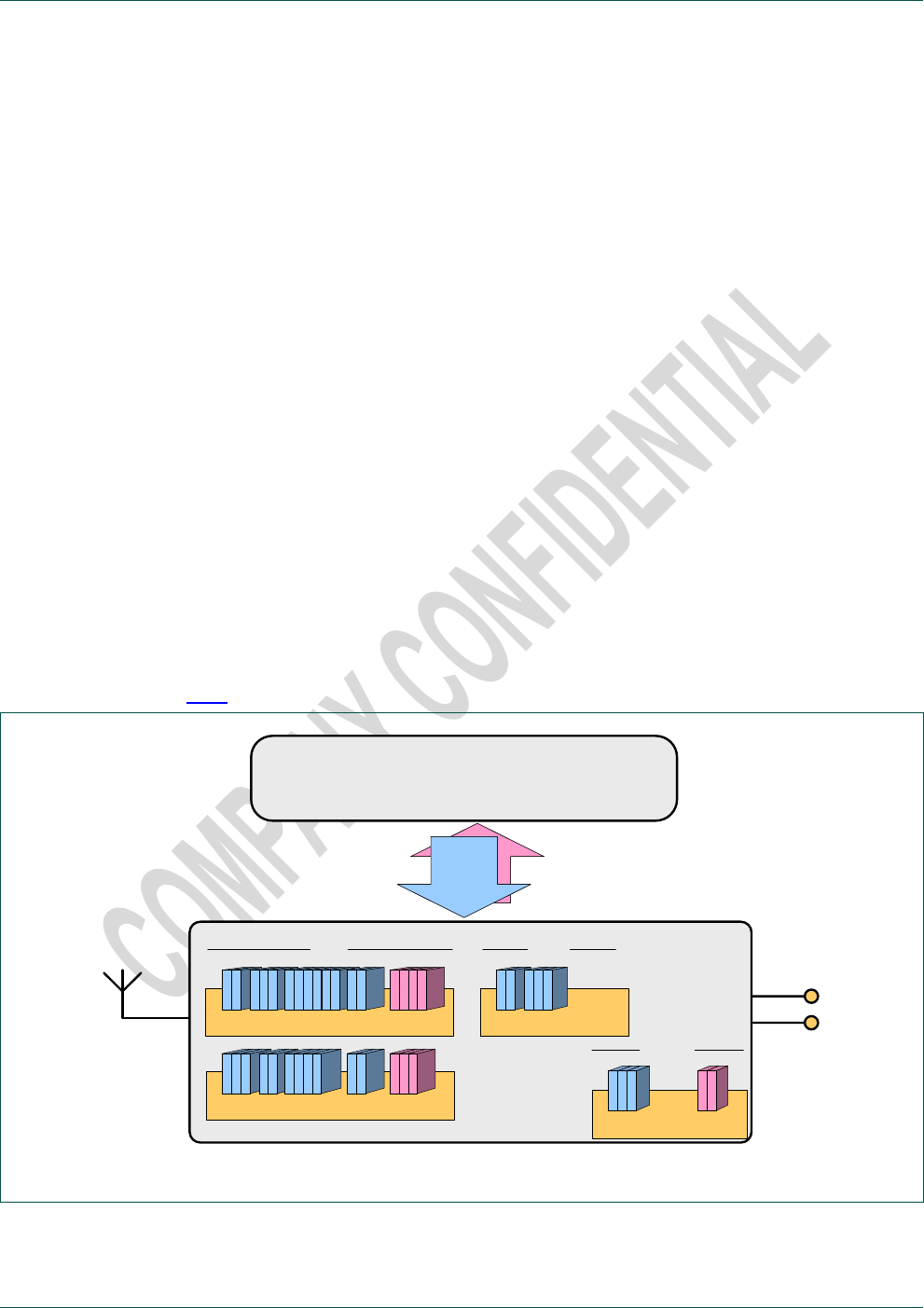
Fig 1 represents the TEF668X control interface as seen from the host controller.
HOST uC
radio
I²C
Module 32 = FM
Module 33 = AM
audio
generic
Module 48 = AUDIO
module 64 = APPL
Fig 1. I²C control –TEF668X

NXP Semiconductors
TEF668X User Manual
TEF6686, TEF6687, TEF6688 and TEF6689, /V102
doc
All information provided in this document is subject to legal disclaimers.
© NXP B.V. 2015. All rights reserved.
User Manual
Rev. 1.6 — 17 February 2015
6 of 101
TEF668X device variants are fully control compatible, although differing in available
features. Future derivatives of these devices will remain compatible also but possibly with
a different variation and extension in supported functions and features.
The API template of TEF668X and compatible devices will be used in future NXP car-
radio developments also, offering compatible control with additional variation in
supported functions and features.
The parameter ranges as depicted in this document are the guaranteed ranges for
operation. Control outside of these ranges is not allowed for application.
The command parameters in general allow for a higher range and granularity than what
is available from TEF668X. Parameters can be set to any value within the documented
range even where the actual number of available settings is less than offered by the
parameter. In these cases the TEF668X will realize the nearest available setting.
Information regarding the actual available granularity is limited in this document but will
be extended in future user manual updates.
2.2 History
The control interface of the TEF668X has been improved over previous product
generations in order to ensure and offer:
Extendibility: Extension of modules, commands and parameters allowing addition
and extension of control options, features and functionality for future car radio
devices from low-end to high-end.
Granularity and range: The parameter definition allows for extremely detailed
parameter setting and range extension where needed in the future.
Reduced control effort: Although not supported for device version V102 the
interface definition allows for single parameter manipulation simplifying user
control software.
Although no direct compatibility is present it should be noted that the TEF668X command
interface shares most of its API functionality with previous products. A translation from
previous generation style control to the TEF668X control can therefore be made with little
effort. Description semantics and description units have been maintained between
generations to support easy transfer of settings.

NXP Semiconductors
TEF668X User Manual
TEF6686, TEF6687, TEF6688 and TEF6689, /V102
doc
All information provided in this document is subject to legal disclaimers.
© NXP B.V. 2015. All rights reserved.
User Manual
Rev. 1.6 — 17 February 2015
7 of 101
3. Write commands
Write commands allow control or setting of specific features. Writing consists of a
module, a command and an index value generally followed by one or more parameter
values.
The module value defines the processing part that is addressed. Modules are integral
functional parts of the device that can be regarded sub-devices. Available modules in the
TEF668X are 32 ‘FM’ for FM radio’, 33 ‘AM’ for AM radio, 48 ‘AUDIO’ for audio
processing and I/O selection and 64 ‘APPL’ for application and system settings.
The command value defines a control function, a feature setting or a set of feature
settings.
The index value is present for future use to allow writing of certain specific parameter
parts out of the available command parameters.
Device version V102 requires index = 1 to be used and requires all command parameters
described in this user manual to be transmitted. This behavior is equal to device version
V101.
The first parameter starts from index = 1.
Write commands are only available in the device ‘active state’ operation modes with the
exception of certain APPL commands available during ‘idle state’.
Independent from the selected ‘active state’ operation mode (‘radio standby’, ‘FM’ or
‘AM’) the write commands of every module are available for writing so full device
initialization is possible in any of the ‘active state’ operation modes.
Note: FM radio and AM radio are never available together. Enabling of one radio module
(by a tuning action command on that module) will disable the other radio module but
control to the disabled radio module remains available for initialization purposes.
For detailed information on the I²C protocol for write commands see 5.2 Write control.

NXP Semiconductors
TEF668X User Manual
TEF6686, TEF6687, TEF6688 and TEF6689, /V102
doc
All information provided in this document is subject to legal disclaimers.
© NXP B.V. 2015. All rights reserved.
User Manual
Rev. 1.6 — 17 February 2015
8 of 101
3.1 FM / AM cmd 1 Tune_To
Tuning within the active radio band or tuning to a different radio band with selection of
FM / AM operation.
module
32 / 33
FM / AM
cmd
1
Tune_To
mode, frequency
index
1
mode
[ 15:0 ]
tuning actions
0 = no action (reserved)
1 = Preset
Tune to new program with short mute time
Enable radio and FM/AM change where applicable
2 = Search
Tune to new program and stay muted
Enable radio and FM/AM change where applicable
FM
3 = AF-Update
Tune to alternative frequency, store quality
and tune back with inaudible mute
4 = Jump
Tune to alternative frequency with inaudible
mute
5 = Check
Tune to alternative frequency and stay
muted
AM
3 … 5 = reserved
6 = reserved
7 = End
Release the mute of a Search or Check action
(frequency is not required and ignored)
2
frequency
[ 15:0 ]
tuning frequency
FM
6500 … 10800
65.00 … 108.00 MHz / 10 kHz step size
AM
LW
144 … 288
144 … 288 kHz / 1 kHz step size
MW
522 … 1710
522 … 1710 kHz / 1 kHz step size
SW
2300 … 27000
2.3 … 27 MHz / 1 kHz step
Application example
FM_Tune_To (1, 1, 8930)
AM_Tune_To (1, 2, 990)
AM_Tune_To (1, 7)
Preset tuning to FM 89.3 MHz
Search tuning (from FM) to AM 990 kHz
End (release mute of AM Search action)
I²C example (hex)
[ w 20 01 01 0001 22E2 ]
[ w 21 01 01 0002 03DE ]
[ w 21 01 01 0007 ]
Preset tuning to FM 89.3 MHz
Search tuning (from FM) to AM 990 kHz
End (release mute of Search action)
3.1.1 radio tuning actions with setting of band and frequency
The mode control parameter allows for execution of different radio tuning actions.
The tuning actions take care of every detail of radio tuning; next to the obvious tuner
functions of band switching and frequency adjustment additional control is active for
inaudible audio mute, reset of quality detectors, reset or hold of weak signal processing
control and suppression of pop noise. All this functionality is an integrated part of

NXP Semiconductors
TEF668X User Manual
TEF6686, TEF6687, TEF6688 and TEF6689, /V102
doc
All information provided in this document is subject to legal disclaimers.
© NXP B.V. 2015. All rights reserved.
User Manual
Rev. 1.6 — 17 February 2015
9 of 101
TEF668X tuning. The set of tuning actions offered by TEF668X is an NXP standard and
found in car radio devices for many generations.
The set of tuning actions frees the controlling C from all non-essential timing and control
complexity, however control flexibility is not limited in any way because the full ‘decision
intelligence’ remains at the C side. The tuning actions can be regarded building blocks
for creating the desired radio tuning control. Tuning actions can be chained together to
build complete tuning routines or realize a single basic routine by themselves.
A total of six mode tuning actions are defined for different types of tuning.
mode = 1 ; Preset
mode = 1 performs a complete ‘Preset-change’ tuning for tuning to a new program or
possibly to a new band. For a Preset-change it is desired to start the new program
immediately with the best quality possible, therefore time constants of the weak signal
handling and AM demodulator AGC are controlled for fast settling to the new signal
conditions within a small preset mute time of approx. 32 ms for FM and 60 ms for AM
bands.
mode = 2 ; Search:
mode = 2 performs a tuning action to create a search to a new program (previous / next
search) or searching for several programs (auto-store).
Search is equal in function to a Preset action however the mute is not released
automatically. This allows signal conditions to be checked while muted and when
insufficient reception quality is found a new Search action can be activated again and
again for a new frequency until a valid search stop condition is found.
Mute can then be released by an End action (mode = 7).
Also a Preset may be used as the last ‘search’ tuning action to release mute.
Preset and Search employ a 10 ms mute and de-mute slope timing for gentle program
switching, so actual tuning is delayed by 10 ms. In case mute is already active (like from
a previous Search action) no mute delay is present and tuning is started instantly.
A Preset and Search tuning action also allows for band switching between FM and AM.
An AM Preset or AM Search will disable ‘radio standby’ or ‘FM’ operation and enable AM
module operation. Equally an FM Preset or FM Search will enable FM module operation.
Note the 10 ms mute delay time should also be taken into account when switching
between FM and AM module operation.
mode = 3 ; AF_Update:
mode = 3 performs a complete ‘alternative frequency update’ tuning cycle for inaudible
testing of the quality of alternative frequencies in the background. AF_Update tunes to an
alternative frequency, gathers signal quality information and returns to the original
frequency within a very short time.

NXP Semiconductors
TEF668X User Manual
TEF6686, TEF6687, TEF6688 and TEF6689, /V102
doc
All information provided in this document is subject to legal disclaimers.
© NXP B.V. 2015. All rights reserved.
User Manual
Rev. 1.6 — 17 February 2015
10 of 101
Inaudible mute is employed and the measured AF quality information is stored for easy
read-out by I²C. Time constants of the weak signal handling and DC decoupling are
controlled so they are not disturbed by the AF signal conditions.
A default AF_Update cycle finishes within 6 ms for the complete action including mute
enabling and disabling.
For AF_Update options like the bandwidth used during AF_Update tuning see 3.2 FM
cmd 2 Set_Tune_Options.
mode = 4 ; Jump:
mode = 4 performs a complete tuning action for switching to a ‘known’ alternative
frequency. Jump performs a tuning with a minimum mute time, only intended to suppress
PLL tuning disturbances. Starting from the control setting of the previous frequency the
weak signal handling will change gradually to the new signal conditions using the
standard weak signal timings, as desired for an inaudible switching to an alternative
frequency with the same program.
Since Jump releases mute automatically it must be assumed that the new frequency
indeed contains the same program. Should it later be found this is not the case (e.g. by
reading the RDS PI code) a new Jump is the designated tuning action for a fast return to
the original frequency.
mode = 5 ; Check:
mode = 5 performs a tuning action for switching to an ‘unknown’ alternative frequency.
Check is equal in function to a Jump action however the mute is not released
automatically. During the Check mute an RDS PI code can be searched for and verified
and if a valid program is found mute can be released by an End action (mode = 7).
During mute the weak signal handling is not disturbed by the new signal conditions and
after mute release the weak signal handling will gradually change to the new conditions
using the standard weak signal timings. In case an invalid program is found a Jump is the
designated tuning action for a fast return to the original frequency.
It is possible to string several Check transmissions together to create an AF_Update like
routine for checking several AF signal conditions in a row. Such a string of Check
transmissions may be finished by mode = End or Jump or, alternatively, by mode =
AF_Update in which case a ‘standard’ AF_Update is executed with quality data hold
while returning to the original frequency as present before the string of Check tunings.
Note: AF_Update, Jump and Check employ a 1 ms mute and de-mute slope timing for
fast inaudible switching, so actual tuning is delayed by 1 ms. In case mute is already
active (presumably by a previous Check action) no mute delay is present and tuning is
started instantly.
mode = 7 ; End:
mode = 7 ends a currently active tuning action. End releases the sustained mute of a
Search (mode = 2) or Check (mode = 5) tuning action.

NXP Semiconductors
TEF668X User Manual
TEF6686, TEF6687, TEF6688 and TEF6689, /V102
doc
All information provided in this document is subject to legal disclaimers.
© NXP B.V. 2015. All rights reserved.
User Manual
Rev. 1.6 — 17 February 2015
11 of 101
An End action does not require any additional data, so only the mode parameter needs
to be transmitted. In case the frequency is included it is ignored. End is only effective for
the currently active radio band (module setting).
3.2 FM cmd 2 Set_Tune_Options
Settings used during a tuning action (FM AF_Update).
module
32
FM
cmd
2
Set_Tune_Options
afu_bw_mode, afu_bandwidth, afu_mute_time, afu_sample_time
index
1
afu_bw_mode
[ 15:0 ]
IF bandwidth control mode during AF_Update
0 = fixed (default)
1 = automatic bandwidth
2
afu_bandwidth
[ 15:0 ]
fixed IF bandwidth during AF_Update
560 … 3110 [*0.1 kHz] = IF bandwidth 56 … 311 kHz; narrow … wide
2360 = 236 kHz (default)
3
afu_mute_time
[ 15:0 ]
AF_update inaudible mute slope time
250 … 1000 [* 1 us] = 0.25 … 1 ms
1000 = 1 ms (default)
4
afu_sample_time
[ 15:0 ]
AF_update sampling time
1000 … 20000 [* 1 us] = 1 … 20 ms
2000 = 2 ms (default)
Application example
FM_Set_Tune_Options (1, 0, 1680, 1000, 2000)
168 kHz bandwidth during AFU
I²C example (hex)
[ w 20 02 01 0000 0690 03E8 07D0 ]
168 kHz bandwidth during AFU
Note: afu_sample_time is accurate to 1 ms intervals and a minimum of 2 ms is advised
for sufficient settling of all quality detectors.

NXP Semiconductors
TEF668X User Manual
TEF6686, TEF6687, TEF6688 and TEF6689, /V102
doc
All information provided in this document is subject to legal disclaimers.
© NXP B.V. 2015. All rights reserved.
User Manual
Rev. 1.6 — 17 February 2015
12 of 101
3.3 FM / AM cmd 10 Set_Bandwidth
Fixed bandwidth selection of the radio selectivity filter.
For FM automatic bandwidth control can be selected with control sensitivity options.
module
32 / 33
FM / AM
cmd
10
Set_Bandwidth
FM : mode, bandwidth, control_sensitivity, low_level_sensitivity,
(min_bandwidth, nominal_bandwidth, control_attack.)
AM : mode, bandwidth
index
1
mode
[ 15:0 ]
IF bandwidth control mode
FM
0 = fixed
1 = automatic (default)
AM
0 = fixed (default)
2
bandwidth
[ 15:0 ]
fixed IF bandwidth
FM
560 … 3110 [*0.1 kHz] = IF bandwidth 56 … 311 kHz; narrow … wide
2360 = 236 kHz (default)
AM
30 … 80 [*0.1 kHz] = IF bandwidth 3 … 8 kHz; narrow … wide
40 = 4.0 kHz (default)
3
control_sensitivity
[ 15:0 ]
FM automatic IF bandwidth control sensitivity
500 … 1500 [*0.1 %] = 50 … 150 % relative adjacent channel sensitivity
1000 = 100 % (default)
4
low_level_sensitivity
[ 15:0 ]
FM automatic IF bandwidth control sensitivity for low level conditions
500 … 1500 [*0.1 %] = 50 … 150 % relative adjacent channel sensitivity
1000 = 100 % (default)
5
min_bandwidth
[ 15:0 ]
extended API: FM minimum IF bandwidth
560 … 1140 [*0.1 kHz] = IF bandwidth 56 … 114 kHz; narrow … wide
560 = 56 kHz (default)
6
nominal_bandwidth
[ 15:0 ]
extended API: FM automatic IF bandwidth control nominal bandwidth
1510 … 2360 [*0.1 kHz] = IF bandwidth 151 … 236 kHz; narrow … wide
bandwidth in use during no disturbance and low modulation condition
2360 = 236 kHz (default)
7
control_attack
[ 15:0 ]
extended API: FM automatic IF bandwidth control attack timing
150 … 450 [*1 us] = 150 … 450 us attack time
attack time (from wide to narrow bandwidth)
300 = 300 us (default)
Application example
FM_Set_Bandwidth (1, 1, 2360, 1000, 1000)
AM_Set_Bandwidth (1, 0, 40)
FM_Set_Bandwidth (1, 0, 2360, 1000, 1000)
FM_Set_Bandwidth (1, 1, 2360, 800, 1000)
FM_Set_Bandwidth (1, 1, 2360, 1000, 800)
standard parameters with FM default
All parameters with AM default value
bandwidth = fixed 236 kHz
control_sensitivity = 80 %
control+low_level sensitivity = 80 %
I²C example (hex)
[ w 20 0A 01 0001 0938 03E8 03E8 ]
[ w 21 0A 01 0000 0028 ]
[ w 20 0A 01 0000 0938 03E8 03E8 ]
All parameters with FM default value
All parameters with AM default value
FM bandwidth = fixed 236 kHz

NXP Semiconductors
TEF668X User Manual
TEF6686, TEF6687, TEF6688 and TEF6689, /V102
doc
All information provided in this document is subject to legal disclaimers.
© NXP B.V. 2015. All rights reserved.
User Manual
Rev. 1.6 — 17 February 2015
13 of 101
[ w 20 0A 01 0001 0938 0320 03E8 ]
[ w 20 0A 01 0001 0938 03E8 0320 ]
control_sensitivity = 80 %
control+low_level sensitivity = 80 %
Note: For FM the following sixteen bandwidth settings are supported: 56 / 64 / 72 / 84 /
97 / 114 / 133 / 151 / 168 / 184 / 200 / 217 / 236 / 254 / 287 / 311 kHz.
For AM the following four bandwidth settings are supported: 3 / 4 / 6 / 8 kHz.
Other bandwidth parameter values are rounded to the nearest supported bandwidth.
Note: Extended API control parameters 5, 6 and 7 are available for additional
performance tuning. Adaptation of these default values is not advised in general but
allows for performance fine-tuning on specific conditions. Feature innovation may cause
extended API defaults and control to change with firmware release.
Min_bandwidth allows for limitation of the minimum bandwidth. Adaptation of the
minimum bandwidth default value reduces the achievable adjacent channel suppression
but might be considered for areas with 200 kHz FM grid. Please note that also the fixed
IF bandwidth control is limited by the min_bandwidth setting.
Transmission of the minimum bandwidth parameter 5 is optional and not required.
The minimum bandwidth option requires initialization version p2.13 or higher.
Nominal_bandwidth allows for selection of the bandwidth in use for the equilibrium state
of the system, i.e. for a condition with no adjacent channel disturbance and low
modulation index. Adaptation of the nominal_bandwidth default value should be used
with care and may impair modulation handling and stereo channel separation
performance.
Control_attack allows for selection of the bandwidth control attack time. Control_attack
defines control sensitivity in addition to the control_sensitivity parameter which primarily
controls the decay time. A smaller control_attack setting (i.e. shorter time) will show a
higher sensitivity, a longer time will show a decrease in sensitivity.
The nominal_bandwidth and control_attack option require initialization version p2.17 or
higher.
Use of the special control parameters 5, 6 and 7 is optional and transmission is not
required. Parameters that are not transmitted are set to their default value.
Modulation boost control is available from 3.28 FM cmd 86 Set_Bandwidth_Options.

NXP Semiconductors
TEF668X User Manual
TEF6686, TEF6687, TEF6688 and TEF6689, /V102
doc
All information provided in this document is subject to legal disclaimers.
© NXP B.V. 2015. All rights reserved.
User Manual
Rev. 1.6 — 17 February 2015
14 of 101
3.4 FM / AM cmd 11 Set_RFAGC
Start level of the tuner front-end AGC.
Performance balancing of desensitization (high start level) against inter-modulation (low
start level).
Optional extension of the FM RF AGC range with one step by external application use.
module
32 / 33
FM / AM
cmd
11
Set_RFAGC
FM: start, extension
AM: start
index
1
start
[ 15:0 ]
RF AGC start
FM
840 … 920 [*0.1 dBV) = 84 … 92 dBV
920 = 92 dBV (default)
AM
940 … 1020 (*0.1 dBV) = 94 … 102 dBV
1000 = 100 dBV (default)
2
extension
[ 15:0 ]
RF AGC step extension
FM
0 = integrated steps only (default)
1 = AGC step extension from control output (GPIO feature ‘AGC’)
AM
reserved
Application example
FM_Set_RFAGC (1, 890, 0)
AM_Set_RFAGC (1, 970)
FM RF AGC start at 89 dBV, no ext.
AM RF AGC start at 97 dBV
I²C example (hex)
[ w 20 0B 01 037A 0000 ]
[ w 21 0B 01 03CA ]
FM RF AGC start at 89 dBV, no ext.
AM RF AGC start at 97 dBV
Note: FM RF AGC step extension requires GPIO pin assignment; see 3.39 Set_GPIO
APPL cmd = 3.

NXP Semiconductors
TEF668X User Manual
TEF6686, TEF6687, TEF6688 and TEF6689, /V102
doc
All information provided in this document is subject to legal disclaimers.
© NXP B.V. 2015. All rights reserved.
User Manual
Rev. 1.6 — 17 February 2015
15 of 101
3.5 AM cmd 12 Set_Antenna
AM antenna attenuation control (RF AGC attenuation limit).
In case of an AM active antenna application part of the required level correction can be
located in the front-end.
module
33
AM
cmd
12
Set_Antenna
attenuation
1
attenuation
[ 15:0 ]
LNA gain reduction
0 / 60 / 120 / 180 / 240 / 300 / 360 (*0.1 dB) = 0 … 36 dB antenna
attenuation (6 dB step size)
0 = no attenuation (default)
Application example
AM_Set_Antenna (1, 180)
AM 18 dB antenna attenuation
I²C example (hex)
[ w 21 0C 01 00B4 ]
AM 18 dB antenna attenuation

NXP Semiconductors
TEF668X User Manual
TEF6686, TEF6687, TEF6688 and TEF6689, /V102
doc
All information provided in this document is subject to legal disclaimers.
© NXP B.V. 2015. All rights reserved.
User Manual
Rev. 1.6 — 17 February 2015
16 of 101
3.6 AM cmd 14 Set_CoChannelDet
Control of the AM co-channel detector.
The AM co-channel detector searches for sub-sonic audio content as may be found
during conditions where the AM channel is disturbed by the signal from a different station
transmitting on the same channel but with a slightly different carrier frequency.
module
33
AM
cmd
14
Set_CoChannelDet
mode, restart, sensitivity, count
index
1
mode
[ 15:0 ]
co-channel detector operation
1 = on (default)
2
restart
[ 15:0 ]
co-channel detector restart
1 = manual restart; reset detector result and start looking for co-channel
(note: returns to restart = 2; automatic restart after tuning remains enabled)
2 = automatic restart after tuning (default); start looking for new co-channel
after Preset and Search tuning action (see AM cmd = 1 TuneTo)
3
sensitivity
[ 15:0 ]
co-channel detection sensitivity
500 … 1500 [*0.1 %] = 50 … 150 % relative detection sensitivity
1000 = 100 % (default)
4
count
[ 15:0 ]
co-channel detection count threshold
1 … 15 = 1 … 15 detection counts until signaling of co-channel detected
3 = (default)
Application example
AM_Set_CoChannelDet (1, 1, 2, 1200, 3)
AM_Set_CoChannelDet (1, 1, 2, 1000, 5)
Set sensitivity to 120 %
Set count = 5 for higher reliability
I²C example (hex)
[ w 21 0E 01 0001 0002 04B0 0003 ]
[ w 21 0E 01 0001 0002 03E8 0005 ]
Set sensitivity to 120 %
Set count = 5 for higher reliability
See 4.1 FM / AM cmd 128 / 129 Get_Quality for co-channel detection read.
Note: AM co-channel detection and control requires initialization version p2.09 or higher.

NXP Semiconductors
TEF668X User Manual
TEF6686, TEF6687, TEF6688 and TEF6689, /V102
doc
All information provided in this document is subject to legal disclaimers.
© NXP B.V. 2015. All rights reserved.
User Manual
Rev. 1.6 — 17 February 2015
17 of 101
3.7 FM cmd 20 Set_MphSuppression
Optional use of the ‘iMS’ FM multipath suppression system.
module
32
FM
cmd
20
Set_MphSuppression
mode
index
1
mode
[ 15:0 ]
FM multipath suppression
0 = off (default)
1 = on
Application example
FM_Set_MphSuppression (1, 1)
FM_Set_MphSuppression (1, 0)
Enable the multipath suppression
Disable the multipath suppression
I²C example (hex)
[ w 20 14 01 0001 ]
[ w 20 14 01 0000 ]
Enable the multipath suppression
Disable the multipath suppression
Note: The advised setting is ‘on’ for improved field performance.
3.8 FM cmd 22 Set_ChannelEqualizer
Optional use of the FM channel equalizer.
module
32
FM
cmd
22
Set_ChannelEqualizer
mode
index
1
mode
[ 15:0 ]
FM channel equalizer
0 = off (default)
1 = on
Application example
FM_Set_ChannelEqualizer (1, 1)
FM_Set_ChannelEqualizer (1, 0)
Enable the channel equalizer
Disable the channel equalizer
I²C example (hex)
[ w 20 16 01 0001 ]
[ w 20 16 01 0000 ]
Enable the channel equalizer
Disable the channel equalizer
Note: The advised setting is ‘on’ for improved field performance

NXP Semiconductors
TEF668X User Manual
TEF6686, TEF6687, TEF6688 and TEF6689, /V102
doc
All information provided in this document is subject to legal disclaimers.
© NXP B.V. 2015. All rights reserved.
User Manual
Rev. 1.6 — 17 February 2015
18 of 101
3.9 FM cmd 23 Set_NoiseBlanker
Noise blanker options and sensitivity setting.
module
32
FM
cmd
23
Set_NoiseBlanker
mode, sensitivity (, -, modulation, offset, attack, decay)
index
1
mode
[ 15:0 ]
noise blanker
0 = off
1 = on (default)
2
sensitivity
[ 15:0 ]
trigger sensitivity
500 … 1500 [*0.1 %] = 50 … 150 % relative trigger sensitivity
1000 = 100 % (default)
3
-
[ 15:0 ]
reserved
0 = don’t care
4
modulation
[ 15:0 ]
extended API: modulation dependency on trigger sensitivity
160 … 1660 [*0.1 %] = 16 … 166 % modulation (= 12 … 125 kHz FM dev.)
Modulation index where minimum pulse detection sensitivity is reached;
trigger sensitivity is controlled between maximum sensitivity for no
modulation and minimum sensitivity at set modulation index.
900 = 90 % (default)
5
offset
[ 15:0 ]
extended API: sensitivity offset
0 … 250 [*0.1 %] = 0 … 25 % fixed sensitivity threshold
Pulse detection offset; prevent false triggering in good signal conditions
1 = 0.1 % (default)
6
attack
[ 15:0 ]
extended API: trigger reference attack time
15 … 1200 [*1 µs] = 15 … 1200 µs
Attack time of noise average filter used as reference for pulse detection
140 = 140 µs (default)
7
decay
[ 15:0 ]
extended API: trigger reference decay time
300 … 6000 [*1 µs] = 300 µs … 6 ms
Decay time of noise average filter used as reference for pulse detection
2800 = 2.8 ms (default)
Application example
FM_Set_NoiseBlanker (1, 1, 1000)
FM_Set_NoiseBlanker (1, 1, 1000, 0, 900, 1, 140, 2800)
FM default values
FM defaults extended API
I²C example (hex)
[ w 20 17 01 0001 03E8 ]
[ w 20 17 01 0001 03E8 0000 0384 0001 008C 0AFO ]
FM default values
FM defaults extended API
Note: Extended API control parameters 4 to 7 are available for additional performance
tuning. Changing default values is not advised in general but allows for performance fine-
tuning on specific conditions. Defaults and control may change over firmware releases.
Use of the special control parameters 4 to 7 is optional and transmission is not required.
In case of a standard transmission (parameters 1 and 2) extended API changes remain.
For AM cmd 23 Set_NoiseBlanker see chapter 3.11.

NXP Semiconductors
TEF668X User Manual
TEF6686, TEF6687, TEF6688 and TEF6689, /V102
doc
All information provided in this document is subject to legal disclaimers.
© NXP B.V. 2015. All rights reserved.
User Manual
Rev. 1.6 — 17 February 2015
19 of 101
3.10 FM cmd 24 Set_NoiseBlanker_Options
Extended API control options of the FM noise blanker.
module
32
FM
cmd
24
Set_NoiseBlanker_Options
blank_time, blank_time2, blank_modulation
index
1
blank_time
[ 15:0 ]
FM noise blanker blank time on low modulation
75 … 300 [*1 us] = 75 … 300 us pulse stretch time
Blank time for low modulation; compared to parameter ‘blank_time2’ an
equal or longer value is suggested optimized for noise pulse suppression.
210 = 210 us (default)
2
blank_time2
[ 15:0 ]
FM noise blanker blank time on high modulation
75 … 300 [*1 us] = 75 … 300 us pulse stretch time
Blank time for high modulation; compared to parameter ‘blank time’ an
equal or smaller value is suggested optimized for modulation fidelity.
210 = 210 us (default)
3
blank_modulation
[ 15:0 ]
FM modulation dependent blank time
160 … 1660 [*0.1 %] = 16 … 166 % modulation (= 12 … 125 kHz FM dev.)
Modulation index threshold for which the blank time is adapted;
the ‘blank_time’ setting is used below the set modulation index and the
‘blank_time2’ setting is used above the set modulation index.
250 = 25 % (default)
Application example
FM_Set_NoiseBlanker_Options (1, 210, 210, 250)
Extended API default values
I²C example (hex)
[ w 20 18 01 00D2 00D2 00FA ]
Extended API default values
Note: Extended API control is available for additional performance tuning. Adaptation of
these default values is not advised in general but allows for performance fine-tuning on
specific conditions. Feature innovation may cause extended API defaults and control to
change with firmware release.
Note: Noise blanker extended API control requires initialization version p2.21 or higher.

NXP Semiconductors
TEF668X User Manual
TEF6686, TEF6687, TEF6688 and TEF6689, /V102
doc
All information provided in this document is subject to legal disclaimers.
© NXP B.V. 2015. All rights reserved.
User Manual
Rev. 1.6 — 17 February 2015
20 of 101
3.11 AM cmd 23 Set_NoiseBlanker
Noise blanker options and sensitivity setting.
module
33
AM
cmd
23
Set_NoiseBlanker
mode, sensitivity (, gain, blank_time)
index
1
mode
[ 15:0 ]
noise blanker
0 = off
1 = on (default)
2
sensitivity
[ 15:0 ]
trigger sensitivity
500 … 1500 [*0.1 %] = 50 … 150 % relative trigger sensitivity
1000 = 100 % (default)
3
gain
[ 15:0 ]
extended API: AM trigger sensitivity for noise conditions
600 … 1600 [*0.1 %] = 60 … 160 % relative trigger sensitivity
Pulse detection gain; allows balancing of lower RF level trigger sensitivity
with the parameter 2 trigger sensitivity for higher RF level.
1000 = 100 % (default)
4
blank_time
[ 15:0 ]
extended API: AM noise blanker blank time
25 … 250 [*1 µs] = 25 … 250 us pulse stretch time
Blanker pulse extension time
56 = 56 µs (default)
Application example
AM_Set_NoiseBlanker (1, 1, 1000)
AM_Set_NoiseBlanker (1, 1, 1000, 1000, 56)
AM_Set_NoiseBlanker (1, 1, 1200)
AM default values
AM defaults extended API
sensitivity 120% for more suppression
I²C example (hex)
[ w 21 17 01 0001 03E8 ]
[ w 21 17 01 0001 03E8 03E8 0038 ]
[ w 21 17 01 0001 04B0 ]
AM default values
AM defaults extended API
sensitivity 120% for more suppression
Note: Extended API control parameters 3 and 4 are available for additional performance
tuning. Changing default values is not advised in general but allows for performance fine-
tuning on specific conditions. Defaults and control may change over firmware releases.
Use of the special control parameters 3 to 4 is optional and transmission is not required.
In case of a standard transmission (parameters 1 and 2) extended API changes remain.
Note: Noise blanker extended API control requires initialization version p2.21 or higher.
For FM cmd 23 Set_NoiseBlanker see chapter 3.9.

NXP Semiconductors
TEF668X User Manual
TEF6686, TEF6687, TEF6688 and TEF6689, /V102
doc
All information provided in this document is subject to legal disclaimers.
© NXP B.V. 2015. All rights reserved.
User Manual
Rev. 1.6 — 17 February 2015
21 of 101
3.12 AM cmd 24 Set_NoiseBlanker_Audio
AM Audio noise blanker options and sensitivity setting.
module
33
AM
cmd
24
Set_NoiseBlanker_Audio
mode, sensitivity (, -, blank_time)
index
1
mode
[ 15:0 ]
AM audio noise blanker (audio frequency detection)
0 = off
1 = on (default)
2
sensitivity
[ 15:0 ]
AM audio noise blanker trigger sensitivity
500 … 1500 [*0.1 %] = 50 … 150 % relative trigger sensitivity
1000 = 100 % (default)
3
-
[ 15:0 ]
reserved
0 = don’t care
4
blank_time
[ 15:0 ]
extended API: AM noise blanker blank time
400 … 1200 [*1 µs] = 400 … 1200 us pulse stretch time
Blanker pulse extension time
800 = 800 µs (default)
Application example
AM_Set_NoiseBlanker_Audio (1, 1, 1000)
AM_Set_NoiseBlanker_Audio (1, 1, 1000, 0, 800)
AM_Set_NoiseBlanker_Audio (1, 1, 1200)
AM default values
AM defaults extended API
sensitivity 120%; more suppression
I²C example (hex)
[ w 21 18 01 0001 03E8 ]
[ w 21 18 01 0001 03E8 0000 0320 ]
[ w 21 18 01 0001 04B0 ]
AM default values
AM defaults extended API
sensitivity 120%; more suppression
Note: Extended API control is available for additional performance tuning. Adaptation of
these default values is not advised in general but allows for performance fine-tuning on
specific conditions. Feature innovation may cause extended API defaults and control to
change with firmware release.
Use of the special control parameter 4 is optional and transmission is not required. In
case of a standard transmission (parameters 1 and 2) extended API changes remain.
Note: Noise blanker extended API control requires initialization version p2.21 or higher.

NXP Semiconductors
TEF668X User Manual
TEF6686, TEF6687, TEF6688 and TEF6689, /V102
doc
All information provided in this document is subject to legal disclaimers.
© NXP B.V. 2015. All rights reserved.
User Manual
Rev. 1.6 — 17 February 2015
22 of 101
3.13 FM / AM cmd 30 Set_DigitalRadio
Available for TEF6688 and TEF6689 only.
Enabling of I/O signal lines for external digital radio processor; DR I²S output and DR
Blend input (enabling DR audio input from IIS_SD_0).
Note: See 3.26 FM / AM cmd 84 Set_DR_Options for additional digital radio options.
module
32 / 33
FM / AM
cmd
30
Set_DigitalRadio
mode
index
1
mode
[ 15:0 ]
digital radio
0 = off (default)
1 = on
Application example
FM_Set_DigitalRadio (1, 1)
AM_Set_DigitalRadio (1, 1)
Enable digital radio for FM use
Enable digital radio for AM use
I²C example (hex)
[ w 20 1E 01 0001 ]
[ w 21 1E 01 0001 ]
Enable digital radio for FM use
Enable digital radio for AM use
3.14 FM cmd 31 Set_Deemphasis
Selection of FM deemphasis time constant
module
32
FM
cmd
31
Set_Deemphasis
timeconstant
index
1
timeconstant
[ 15:0 ]
deemphasis time constant
0 = off; for evaluation purposes only
500 = 50 s deemphasis (default)
750 = 75 s deemphasis
Application example
FM_Set_Deemphasis (1, 750)
75 s deemphasis
I²C example (hex)
[ w 20 1F 01 02EE ]
75 s deemphasis

NXP Semiconductors
TEF668X User Manual
TEF6686, TEF6687, TEF6688 and TEF6689, /V102
doc
All information provided in this document is subject to legal disclaimers.
© NXP B.V. 2015. All rights reserved.
User Manual
Rev. 1.6 — 17 February 2015
23 of 101
3.15 FM cmd 32 Set_StereoImprovement
Available for TEF6687 and TEF6689 only.
Selection of extended stereo weak signal handling; stereo high blend (default operation)
or special FMSI (FM stereo improvement) blend system for improved sound quality.
module
32
FM
cmd
32
Set_StereoImprovement
mode
index
1
mode
[ 15:0 ]
FM stereo extended weak signal handling
0 = stereo high blend (default)
1 = FMSI stereo band blend system
Application example
FM_Set_StereoImprovement (1, 1)
enable FMSI stereo improvement
I²C example (hex)
[ w 20 20 01 0001 ]
enable FMSI stereo improvement
Note: The default stereo high blend is controlled from FM cmd 70 … 76 Set_StHiBlend,
settings from this command range are in use during active stereo high blend processing.
FMSI stereo improvement is controlled from FM cmd 90 … 92 Set_StereoBandBlend,
settings from this command range are in use during active FMSI signal processing.
Note: With FMSI enabled the stereo high blend function is disabled but the standard
stereo weak signal handling remains. FM cmd 60 … 66 Set_Stereo should be defined
with disabled settings (or reduced sensitivity settings) to demonstrate the full FMSI stereo
performance.
Note: The advised setting is ‘FMSI’ for improved field performance

NXP Semiconductors
TEF668X User Manual
TEF6686, TEF6687, TEF6688 and TEF6689, /V102
doc
All information provided in this document is subject to legal disclaimers.
© NXP B.V. 2015. All rights reserved.
User Manual
Rev. 1.6 — 17 February 2015
24 of 101
3.16 FM / AM cmd 38 Set_LevelStep
Selection of level correction as a function of the tuner front-end AGC.
The level step offset is included in the weak signal handling and the level read value of
Get_Quality (4.1 FM / AM cmd 128 / 129 Get_Quality).
A setting of 0 dB will show no level change by full compensation of the actual -6 dB AGC
attenuation step. Instead a setting of -6 dB will show the actual AGC attenuation step.
module
32 / 33
FM / AM
cmd
38
Set_LevelStep
step1, step2, step3, step4, step5, step6, step7
index
1
step1
[ 15:0 ]
level offset for an AGC step from 0 to 1
-60 … 0 (*0.1 dB) = -6 … 0 dB
-20 = -2 dB (FM default) / -10 = -1 dB (AM default)
2
step2
[ 15:0 ]
level offset for an AGC step from 1 to 2
-60 … 0 (*0.1 dB) = -6 … 0 dB
-30 = -3 dB (FM default) / -20 = -2 dB (AM default)
3
step3
[ 15:0 ]
level offset for an AGC step from 2 to 3
-60 … 0 (*0.1 dB) = -6 … 0 dB
-40 = -4 dB (FM default) / -30 = -3 dB (AM default)
4
step4
[ 15:0 ]
level offset for an AGC step from 3 to 4
-60 … 0 (*0.1 dB) = -6 … 0 dB
-50 = -5 dB (FM default) / -40 = -4 dB (AM default)
5
step5
[ 15:0 ]
level offset for an AGC step from 4 to 5
-60 … 0 (*0.1 dB) = -6 … 0 dB
-60 = -6 dB (FM default) / -50 = -5 dB (AM default)
6
step6
[ 15:0 ]
level offset for an AGC step from 5 to 6
-60 … 0 (*0.1 dB) = -6 … 0 dB
-60 = -6 dB (default)
7
step7
[ 15:0 ]
level offset for an AGC step from 6 to 7 (or higher)
-60 … 0 (*0.1 dB) = -6 … 0 dB
-60 = -6 dB (default)
Application example
AM_Set_LevelStep(1, 0, -10, -20, -30, -40, -50, -60)
AM_Set_LevelStep(1, -20, -30, -40, -50, -60, -60, -60)
AM increased level extension
AM decreased level extension
I²C example (hex)
[ w 21 26 01 0000 FFF6 FFEC FFE2 FFD8 FFCE FFC4 ]
[ w 21 26 01 FFEC FFE2 FFD8 FFCE FFC4 FFC4 FFC4 ]
AM increased level extension
AM decreased level extension
Note: Adaptation of the LevelStep default values is not advised in general but allows for a
specific fine-tuning of the weak signal handling in high signal conditions.
Note: The indicated steps are the added values of feedback and input AGC steps.
Note: AGC steps higher than step 7 will employ the step 7 setting.

NXP Semiconductors
TEF668X User Manual
TEF6686, TEF6687, TEF6688 and TEF6689, /V102
doc
All information provided in this document is subject to legal disclaimers.
© NXP B.V. 2015. All rights reserved.
User Manual
Rev. 1.6 — 17 February 2015
25 of 101
3.17 FM / AM cmd 39 Set_LevelOffset
Selection of level correction.
The level offset can be used as an overall correction for antenna noise level and is
included in the weak signal handling and the level read value of Get_Quality (4.1 FM /
AM cmd 128 / 129 Get_Quality). A standard use case is the compensation for AM
active antenna circuits (typical offset setting = -30 dB).
module
32 / 33
FM / AM
cmd
39
Set_LevelOffset
offset
index
1
offset
[ 15:0 ] signed
level offset
-480 … +150 (*0.1 dB) = -48 … +15 dB
0 = 0 dB (default)
Application example
AM_Set_LevelOffset (1, -300)
-30 dB level correction
I²C example (hex)
[ w 21 27 01 FED4 ]
-30 dB level correction

NXP Semiconductors
TEF668X User Manual
TEF6686, TEF6687, TEF6688 and TEF6689, /V102
doc
All information provided in this document is subject to legal disclaimers.
© NXP B.V. 2015. All rights reserved.
User Manual
Rev. 1.6 — 17 February 2015
26 of 101
3.18 FM / AM cmd 40 … 45 Set_Softmute
Timing and quality sensitivity settings for the Softmute weak signal handling.
‘Set_Softmute_Time’ defines the weak signal handling response times active for the level
detector and FM noise and multipath detectors. Fast and slow response times are
available for dual timer functionality, with enable options at the level, noise and mph
commands.’
‘Set_Softmute_Mod’ enables modulation dependency and sets sensitivity (AM only).
‘Set_Softmute_Level’ sets the level sensitivity and enables slow and fast timing.
‘Set_Softmute_Noise’ and ‘Set_Softmute_Mph’ set the noise and multipath sensitivity
and enables slow and fast timing (FM only)
‘Set_Softmute_Max’ enables and defines the maximum amount of softmute attenuation
(as realized for poor signal conditions).
module
32 / 33
FM / AM
cmd
40
Set_Softmute_Time
slow_attack, slow_decay, fast_attack, fast_decay
index
1
slow_attack
[ 15:0 ]
slow attack time of weak signal handling
60 … 2000 (ms) = 60 ms … 2 s slow attack time
120 = 120 ms (default)
2
slow_decay
[ 15:0 ]
slow decay time of weak signal handling
120 … 12500 (ms) = 120 ms … 12.5 s slow attack time
500 = 500 ms (default)
3
fast_attack
[ 15:0 ]
fast attack time of weak signal handling
10 … 1200 (*0.1 ms) = 1 ms … 120 ms fast attack time
20 = 2 ms (FM default) / 120 = 12 ms (AM default)
4
fast_decay
[ 15:0 ]
fast decay time of weak signal handling
20 … 5000 ( *0.1 ms) = 2 ms … 500 ms fast attack time
20 = 2 ms (FM default) / 500 = 50 ms (AM default)
Application example
FM_Set_Softmute_Time (1, 120, 500, 10, 20)
AM_Set_Softmute_Time (1, 500, 4000, 100,
500)
Slow 120 / 500 ms, fast 1 / 2 ms
Slow 500 / 4000 ms, fast 10 / 50 ms
I²C example (hex)
[ w 20 28 01 0078 01F4 000A 0014 ]
[ w 21 28 01 01F4 0FA0 0064 01F4 ]
Slow 120 / 500 ms, fast 1 / 2 ms
Slow 500 / 4000 ms, fast 10 / 50 ms
Note: Suggested FM setting is 1 ms fast_attack for improved field performance.
module
33
AM
cmd
41
Set_Softmute_ Mod
mode, start, slope, shift
index
1
mode
[ 15:0 ]
modulation dependent weak signal handling
0 = off (default)

NXP Semiconductors
TEF668X User Manual
TEF6686, TEF6687, TEF6688 and TEF6689, /V102
doc
All information provided in this document is subject to legal disclaimers.
© NXP B.V. 2015. All rights reserved.
User Manual
Rev. 1.6 — 17 February 2015
27 of 101
1 = on
2
start
[ 15:0 ]
weak signal handling modulation start
100 … 1000 [*0.1 %] = control when modulation falls below 10% … 100%
210 = 21% (default)
3
slope
[ 15:0 ]
weak signal handling modulation range
30 … 1000 (*0.1 %) = control over modulation range of 3% … 100%
120 = 12% (default)
4
shift
[ 15:0 ]
weak signal handling control shift
50 … 1000 (*0.1 %) = maximum weak signal control shift of 5% … 100%
260 = 26% (default)
(percentage of the linear control range from 0 dB to _Max limit)
module
32 / 33
FM / AM
cmd
42
Set_Softmute_Level
mode, start, slope
index
1
mode
[ 15:0 ]
timer selection
0 = off (only for evaluation)
1 = fast timer control
2 = slow timer control (default)
3 = dual timer control; combined fast and slow timer control
2
start
[ 15:0 ]
weak signal handling level start
0 … 500 [*0.1 dBV] = control when level falls below 0 dBV … 50 dBV
150 = 15 dBV (FM default) / 280 = 28 dBV (AM default)
3
slope
[ 15:0 ]
weak signal handling level range
60 … 300 [*0.1 dB] = control over level range of 6 dB … 30 dB
220 = 22 dB (FM default) / 250 = 25 dB (AM default)
Note: Suggested AM setting for LW band is 34 dBV start and 30 dB slope for improved
field performance.
module
32
FM
cmd
43
Set_Softmute_Noise
mode, start, slope
index
1
mode
[ 15:0 ]
timer selection
0 = off (default)
1 = fast timer control
2 = slow timer control
3 = dual timer control; combined fast and slow timer control
2
start
[ 15:0 ]
FM weak signal handling noise start
0 … 800 [*0.1 %] = control when noise above 0… 80% of USN detector
500 = 50% (default)
3
slope
FM weak signal handling noise range

NXP Semiconductors
TEF668X User Manual
TEF6686, TEF6687, TEF6688 and TEF6689, /V102
doc
All information provided in this document is subject to legal disclaimers.
© NXP B.V. 2015. All rights reserved.
User Manual
Rev. 1.6 — 17 February 2015
28 of 101
[ 15:0 ]
100 … 1000 [*0.1 %] = control over range of 10… 100% of USN detector
1000 = 100% (default)
module
32
FM
cmd
44
Set_Softmute_Mph
mode, start, slope
index
1
mode
[ 15:0 ]
timer selection
0 = off (default)
1 = fast timer control
2 = slow timer control
3 = dual timer control; combined fast and slow timer control
2
start
[ 15:0 ]
FM weak signal handling multipath start
0 … 800 [*0.1 %] = control when mph above 0… 80% of WAM detector
500 = 50% (default)
3
slope
[ 15:0 ]
FM weak signal handling multipath range
100 … 1000 [*0.1 %] = control over range of 10… 100% of WAM detector
1000 = 100% (default)
module
32 / 33
FM / AM
cmd
45
Set_Softmute_Max
mode, limit
index
1
mode
[ 15:0 ]
weak signal handling (dynamic control)
0 = off (for evaluation only)
1 = on; maximum dynamic control defined by limit parameter (default)
2
limit
[ 15:0 ]
softmute dynamic attenuation limit
0 … 400 [*0.1 dB] = 0 … 40 dB softmute maximum attenuation
200 = 20 dB (FM default) / 250 = 25 dB (AM default)
Application example
FM_Set_Softmute_Max (1, 1, 240)
AM_Set_Softmute_Max (1, 1, 300)
FM 24 dB max. softmute attenuation
AM 30 dB max. softmute attenuation
I²C example (hex)
[ w 20 2D 01 0001 00F0 ]
[ w 21 2D 01 0001 012C ]
FM 24 dB max. softmute attenuation
AM 30 dB max. softmute attenuation
Suggested AM setting for LW band is 33 dB limit.

NXP Semiconductors
TEF668X User Manual
TEF6686, TEF6687, TEF6688 and TEF6689, /V102
doc
All information provided in this document is subject to legal disclaimers.
© NXP B.V. 2015. All rights reserved.
User Manual
Rev. 1.6 — 17 February 2015
29 of 101
3.19 FM / AM cmd 50 … 59 Set_Highcut
Timing and quality sensitivity settings for the Highcut weak signal handling.
‘Set_Highcut_Time’ defines the weak signal handling response times active for the level
detector and FM noise and multipath detectors. Fast and slow response times are
available for dual timer functionality, with enable options at the level, noise and mph
commands.’
‘Set_Highcut_Mod’ enables modulation dependency and sets sensitivity
‘Set_Highcut_Level’ sets the level sensitivity and enables slow and fast timing.
‘Set_Highcut_Noise’ and ‘Set_Highcut_Mph’ set the noise and multipath sensitivity and
enables slow and fast timing (FM only)
‘Set_Highcut_Max’ enables and defines the maximum amount of Highcut attenuation (as
realized for poor signal conditions).
‘Set_Highcut_Min’ optionally defines a minimum amount of Highcut attenuation (as
realized for good signal conditions).
‘Set_Lowcut_Max’ enables and defines the maximum dynamic Lowcut attenuation and
‘Set_Lowcut_Min’ optionally defines a minimum attenuation for low signal frequencies.
Dynamic ‘Lowcut’ (as set by Set_Lowcut_Max) is part of the ‘Highcut’ control and shares
the HighCut time and sensitivity settings.
‘Set_Highcut_Options’ allows selection between three different Highcut control
characteristics (FM only).
module
32 / 33
FM / AM
cmd
50
Set_Highcut_Time
slow_attack, slow_decay, fast_attack, fast_decay
index
1
slow_attack
[ 15:0 ]
slow attack time of weak signal handling
60 … 2000 (ms) = 60 ms … 2 s slow attack time
500 = 500 ms (default)
2
slow_decay
[ 15:0 ]
slow decay time of weak signal handling
120 … 12500 (ms) = 120 ms … 12.5 s slow attack time
2000 = 2 s (default)
3
fast_attack
[ 15:0 ]
fast attack time of weak signal handling
10 … 1200 (*0.1 ms) = 1 ms … 120 ms fast attack time
20 = 2 ms (FM default) / 120 = 12 ms (AM default)
4
fast_decay
[ 15:0 ]
fast decay time of weak signal handling
20 … 5000 ( *0.1 ms) = 2 ms … 500 ms fast attack time
20 = 2 ms (FM default) / 500 = 50 ms (AM default)
Application example
FM_Set_Highcut_Time (1, 200, 500, 10, 80)
AM_Set_Highcut_Time (1, 500, 4000, 100, 500)
Slow 200 / 500 ms, fast 1 / 8 ms
Slow 500 / 4000 ms, fast 10 / 50 ms
I²C example (hex)
[ w 20 32 01 00C8 01F4 000A 0050 ]
[ w 21 32 01 01F4 0FA0 0064 01F4 ]
Slow 200 / 500 ms, fast 1 / 8 ms
Slow 500 / 4000 ms, fast 10 / 50 ms

NXP Semiconductors
TEF668X User Manual
TEF6686, TEF6687, TEF6688 and TEF6689, /V102
doc
All information provided in this document is subject to legal disclaimers.
© NXP B.V. 2015. All rights reserved.
User Manual
Rev. 1.6 — 17 February 2015
30 of 101
Note: Suggested FM settings are 200 ms slow_attack, 1 ms fast_attack and 8 ms fast_
decay for improved field performance.
module
32 / 33
FM / AM
cmd
51
Set_Highcut_ Mod
mode, start, slope, shift
index
1
mode
[ 15:0 ]
modulation dependent weak signal handling
0 = off (default)
1 = on (independent modulation timer)
2
start
[ 15:0 ]
weak signal handling modulation start
100 … 1000 [*0.1 %] = control when modulation falls below 10% … 100%
250 = 25% (default)
(note: for FM band 100% modulation equals 75 kHz deviation)
3
slope
[ 15:0 ]
weak signal handling modulation range
30 … 1000 (*0.1 %) = control over modulation range of 3% … 100%
130 = 13% (default)
4
shift
[ 15:0 ]
weak signal handling control shift
50 … 1000 (*0.1 %) = maximum weak signal control shift of 5% … 100%
500 = 50% (default)
(percentage of the linear control range from _Min limit to _Max limit)
module
32 / 33
FM / AM
cmd
52
Set_Highcut_Level
mode, start, slope
index
1
mode
[ 15:0 ]
timer selection
0 = off (only for evaluation)
1 = fast timer control
2 = slow timer control (AM default)
3 = dual timer control; combined fast and slow timer control (FM default)
2
start
[ 15:0 ]
weak signal handling level start
200 … 600 [*0.1 dBV] = control when level is below 20 dBV … 60 dBV
360 = 36 dBV (FM default) / 400 = 40 dBV (AM default)
3
slope
[ 15:0 ]
weak signal handling level range
60 … 300 [*0.1 dB] = control over level range of 6 dB … 30 dB
300 = 30 dB (FM default) / 200 = 20 dB (AM default)
Note: Suggested AM setting for MW and SW band is 47 dBV start for improved field
performance. Suggested for AM LW band is 52 dBV start.
module
32
FM
cmd
53
Set_Highcut_Noise
mode, start, slope

NXP Semiconductors
TEF668X User Manual
TEF6686, TEF6687, TEF6688 and TEF6689, /V102
doc
All information provided in this document is subject to legal disclaimers.
© NXP B.V. 2015. All rights reserved.
User Manual
Rev. 1.6 — 17 February 2015
31 of 101
index
1
mode
[ 15:0 ]
timer selection
0 = off
1 = fast timer control
2 = slow timer control (default)
3 = dual timer control; combined fast and slow timer control
2
start
[ 15:0 ]
FM weak signal handling noise start
0 … 800 [*0.1 %] = control when noise above 0… 80% of USN detector
360 = 36% (default)
3
slope
[ 15:0 ]
FM weak signal handling noise range
100 … 1000 [*0.1 %] = control over range of 10… 100% of USN detector
300 = 30% (default)
Note: Suggested is ‘dual timer’ mode, 15% start and 20% slope for improved field
performance.
module
32
FM
cmd
54
Set_Highcut_Mph
mode, start, slope
index
1
mode
[ 15:0 ]
timer selection
0 = off (only for evaluation)
1 = fast timer control
2 = slow timer control (default)
3 = dual timer control; combined fast and slow timer control
2
start
[ 15:0 ]
FM weak signal handling multipath start
0 … 800 [*0.1 %] = control when mph above 0… 80% of WAM detector
360 = 36% (default)
3
slope
[ 15:0 ]
FM weak signal handling multipath range
100 … 1000 [*0.1 %] = control over range of 10… 100% of WAM detector
300 = 30% (default)
Note: Suggested is ‘dual timer’ mode, 12% start and 16% slope for improved field
performance.
module
32 / 33
FM / AM
cmd
55
Set_Highcut_Max
mode, limit
index
1
mode
[ 15:0 ]
weak signal handling (dynamic control)
0 = off; for evaluation only
1 = on; maximum dynamic control set by limit parameter (default)
2
limit
[ 15:0 ]
Highcut attenuation limit
FM
Highcut corner frequency for maximum -3 dB attenuation
4000 = 4 kHz (default)
1500 … 7000 [*1 Hz] = 1.5 … 7 kHz ‘IIR’ filter (Options ‘1’ (default))

NXP Semiconductors
TEF668X User Manual
TEF6686, TEF6687, TEF6688 and TEF6689, /V102
doc
All information provided in this document is subject to legal disclaimers.
© NXP B.V. 2015. All rights reserved.
User Manual
Rev. 1.6 — 17 February 2015
32 of 101
700 … 3000 [*1 Hz] = 0.7 … 3 kHz ‘deemphasis’ mode (Options ‘2’)
2700 … 7000 [*1 Hz] = 2.7 … 7 kHz ‘FIR’ highcut filter (Options ‘3’)
AM
1350 … 7000 [*1 Hz] = 1.35 … 7 kHz Highcut maximum -3 dB att.
1800 = 1.8 kHz (default)
Application example
FM_Set_Highcut_Max (1, 1, 2400)
AM_Set_Highcut_Max (1, 1, 1500)
FM 2.4 kHz max. Highcut attenuation
AM 1.5 kHz max. Highcut attenuation
I²C example (hex)
[ w 20 37 01 0001 0960 ]
[ w 21 37 01 0001 05DC ]
FM 2.4 kHz max. Highcut attenuation
AM 1.5 kHz max. Highcut attenuation
Note: For FM different limit ranges apply for the different Highcut control characteristics
as available from FM Set_Highcut_Options (cmd = 59).
Note: Suggested FM setting is 2.4 kHz limit for improved ‘IIR’ filter field performance.
module
32 / 33
FM / AM
cmd
56
Set_Highcut_Min
mode, limit
index
1
mode
[ 15:0 ]
strong signal handling
0 = off; high audio frequency bandwidth is not limited (FM default)
1 = on; minimum control limit set by limit parameter (AM default)
2
limit
[ 15:0 ]
Highcut fixed attenuation limit
FM
Highcut corner frequency for minimum -3 dB attenuation
10000 = 10 kHz (default)
2700 … 15000 [*1 Hz] = 2.7 … 15 kHz ‘IIR’ filter (Options ‘1’ (default))
1500 … 3183 [*1 Hz] = 1.5 … 3.18 kHz ‘deemphasis’ (Options ‘2’)
2122 = 75 s deemphasis / 3183 = 50 s deemphasis
2700 … 15000 [*1 Hz] = 2.7 … 15 kHz ‘FIR’ highcut filter (Options ‘3’)
AM
2700 … 15000 [*1 Hz] = 2.7 … 15 kHz -3 dB att. for min. Highcut
6000 = 6 kHz (default)
Application example
FM_Set_Highcut_Min (1, 1, 10000)
AM_Set_Highcut_Min (1, 1, 3000)
FM 10 kHz min. Highcut attenuation
AM 3 kHz min. Highcut attenuation
I²C example (hex)
[ w 20 38 01 0001 2710 ]
[ w 21 38 01 0001 0BB8 ]
FM 10 kHz min. Highcut attenuation
AM 3 kHz min. Highcut attenuation
Note: In case of characteristic ‘deemphasis’ from FM cmd 59 Set_Highcut_Options
mode = 2, the FM cmd 31 Set_Deemphasis setting is ignored and 50 s or 75 s
deemphasis is defined by FM_Set_Highcut_Min parameters mode = 1, and limit instead.
Note: For a normal control behavior Set_Highcut_Min always should set a weaker signal
handling limit (i.e. a higher frequency) than Set_Highcut_Max.

NXP Semiconductors
TEF668X User Manual
TEF6686, TEF6687, TEF6688 and TEF6689, /V102
doc
All information provided in this document is subject to legal disclaimers.
© NXP B.V. 2015. All rights reserved.
User Manual
Rev. 1.6 — 17 February 2015
33 of 101
module
32 / 33
FM / AM
cmd
57
Set_Lowcut_ Max
mode, limit
index
1
mode
[ 15:0 ]
weak signal handling (dynamic control)
0 = off
1 = on; maximum dynamic control defined by limit parameter (default)
2
limit
[ 15:0 ]
Lowcut dynamic attenuation limit
30 … 500 [Hz] = 30 … 500 Hz -3 dB attenuation for maximum Lowcut
120 = 120 Hz (default)
Application example
FM_Set_Lowcut_Max (1, 1, 100)
AM_Set_Lowcut_Max (1, 1, 300)
FM 100 Hz max. Lowcut attenuation
AM 300 Hz max. Lowcut attenuation
I²C example (hex)
[ w 20 39 01 0001 0064 ]
[ w 21 39 01 0001 012C ]
FM 100 Hz max. Lowcut attenuation
AM 300 Hz max. Lowcut attenuation
Note: Suggested FM setting is 100 Hz limit for improved field performance.
module
32 / 33
FM / AM
cmd
58
Set_Lowcut_Min
mode, limit
index
1
mode
[ 15:0 ]
strong signal handling
0 = off; low audio frequency bandwidth is not limited (FM default)
1 = on; minimum control limit set by limit parameter (AM default)
2
limit
[ 15:0 ]
Lowcut fixed attenuation limit
10 … 200 [Hz] = 10 … 200 Hz Lowcut minimum -3 dB attenuation
20 = 20 Hz (default)
Application example
FM_Set_Lowcut_Min (1, 1, 10)
AM_Set_Lowcut_Min (1, 1, 30)
FM 10 Hz min. Lowcut attenuation
AM 30 Hz min. Lowcut attenuation
I²C example (hex)
[ w 20 3A 01 0001 000A ]
[ w 21 3A 01 0001 001E ]
FM 10 Hz min. Lowcut attenuation
AM 30 Hz min. Lowcut attenuation
Note: For a normal control behavior Set_Lowcut_Min always should set a weaker signal
handling limitation (i.e. a lower frequency) than Set_Lowcut_Max.

NXP Semiconductors
TEF668X User Manual
TEF6686, TEF6687, TEF6688 and TEF6689, /V102
doc
All information provided in this document is subject to legal disclaimers.
© NXP B.V. 2015. All rights reserved.
User Manual
Rev. 1.6 — 17 February 2015
34 of 101
module
32
FM
cmd
59
Set_Highcut_Options
mode
index
1
mode
[ 15:0 ]
FM Highcut control characteristics
1 = IIR; ‘analog’ first order lowpass filter with controlled frequency (default)
2 = deemphasis; controlled frequency of the 50 / 75 s deemphasis filter
3 = FIR; ‘digital’ high order lowpass filter with controlled frequency
Application example
FM_Set_Highcut_Options (1, 2)
FM ‘deemphasis’ type Highcut control
I²C example (hex)
[ w 20 3B 01 0002 ]
FM ‘deemphasis’ type Highcut control
Note: Different FM Highcut control characteristics are available for selection of sound
taste.
Note: In addition to the _Options selection of the Highcut filter type appropriate values
should be written to FM_Set_Highcut_Min and FM_Set_Highcut_Max.
Note: In case of ‘deemphasis’ characteristics the FM_Set_Deemphasis setting is ignored
and selection of 50 s or 75 s deemphasis is defined by FM_Set_Highcut_Min instead.

NXP Semiconductors
TEF668X User Manual
TEF6686, TEF6687, TEF6688 and TEF6689, /V102
doc
All information provided in this document is subject to legal disclaimers.
© NXP B.V. 2015. All rights reserved.
User Manual
Rev. 1.6 — 17 February 2015
35 of 101
3.20 FM cmd 60 … 66 Set_Stereo
Timing and quality sensitivity settings for the FM Stereo weak signal handling.
‘Set_Stereo_Time’ defines the weak signal handling response times active for the level
detector and noise and multipath detectors. Fast and slow response times are available
for dual timer functionality, with enable options at the level, noise and mph commands.’
‘Set_Stereo_Mod’ enables modulation dependency and sets sensitivity
‘Set_Stereo_Level’ sets the level sensitivity and enables slow and fast timing.
‘Set_Stereo_Noise’ and ‘Set_Stereo_Mph’ set the noise and multipath sensitivity and
enables slow and fast timing.
‘Set_Stereo_Max’ allows disabling the dynamic stereo control for evaluation purposes.
‘Set_Stereo_Min’ optionally defines a minimum amount of Stereo attenuation (as realized
for good signal conditions).
module
32
FM
cmd
60
Set_Stereo_Time
slow_attack, slow_decay, fast_attack, fast_decay
index
1
slow_attack
[ 15:0 ]
slow attack time of weak signal handling
60 … 2000 (ms) = 60 ms … 2 s slow attack time
1000 = 1 s (default)
2
slow_decay
[ 15:0 ]
slow decay time of weak signal handling
120 … 12500 (ms) = 120 ms … 12.5 s slow attack time
4000 = 4 s (default)
3
fast_attack
[ 15:0 ]
fast attack time of weak signal handling
10 … 1200 (*0.1 ms) = 1 ms … 120 ms fast attack time
80 = 8 ms
4
fast_decay
[ 15:0 ]
fast decay time of weak signal handling
20 … 5000 ( *0.1 ms) = 2 ms … 500 ms fast attack time
80 = 8 ms
Application example
FM_Set_Stereo_Time (1, 200, 4000, 20, 80)
Slow 200 / 4000 ms, fast 2 / 8 ms
I²C example (hex)
[ w 20 3C 01 00C8 0FA0 0014 0050 ]
Slow 200 / 4000 ms, fast 2 / 8 ms
Note: Suggested is 200 ms slow_attack and 2 ms fast_attack for improved field
performance.
module
32
FM
cmd
61
Set_Stereo_ Mod
mode, start, slope, shift
index
1
mode
[ 15:0 ]
modulation dependent weak signal handling
0 = off (default)
1 = on (independent modulation timer)

NXP Semiconductors
TEF668X User Manual
TEF6686, TEF6687, TEF6688 and TEF6689, /V102
doc
All information provided in this document is subject to legal disclaimers.
© NXP B.V. 2015. All rights reserved.
User Manual
Rev. 1.6 — 17 February 2015
36 of 101
2
start
[ 15:0 ]
weak signal handling modulation start
100 … 1000 [*0.1 %] = control when modulation falls below 10% … 100%
210 = 21% (default)
( note: for FM band 100% modulation equals 75 kHz deviation )
3
slope
[ 15:0 ]
weak signal handling modulation range
30 … 1000 (*0.1 %) = control over modulation range of 3% … 100%
90 = 9% (default)
4
shift
[ 15:0 ]
weak signal handling control shift
50 … 1000 (*0.1 %) = maximum weak signal control shift of 5% … 100%
500 = 50% (default)
(percentage of the linear control range from _Min limit to ‘mono’)
module
32
FM
cmd
62
Set_Stereo_Level
mode, start, slope
index
1
mode
[ 15:0 ]
timer selection
0 = off (only for evaluation)
1 = fast timer control
2 = slow timer control
3 = dual timer control; combined fast and slow timer control (default)
2
start
[ 15:0 ]
weak signal handling level start
300 … 600 [*0.1 dBV] = control when level below 30 dBV … 60 dBV
460 = 46 dBV (default)
3
slope
[ 15:0 ]
weak signal handling level range
60 … 300 [*0.1 dB] = control over level range of 6 dB … 30 dB
240 = 24 dB (default)
module
32
FM
cmd
63
Set_Stereo_Noise
mode, start, slope
index
1
mode
[ 15:0 ]
timer selection
0 = off
1 = fast timer control
2 = slow timer control
3 = dual timer control; combined fast and slow timer control (default)
2
start
[ 15:0 ]
FM weak signal handling noise start
0 … 800 [*0.1 %] = control when noise above 0… 80% of USN detector
240 = 24% (default)
3
slope
[ 15:0 ]
FM weak signal handling noise range
100 … 1000 [*0.1 %] = control over range of 10… 100% of USN detector
200 = 20% (default)
Note: Suggested is 12% start and 16% slope for improved field performance.

NXP Semiconductors
TEF668X User Manual
TEF6686, TEF6687, TEF6688 and TEF6689, /V102
doc
All information provided in this document is subject to legal disclaimers.
© NXP B.V. 2015. All rights reserved.
User Manual
Rev. 1.6 — 17 February 2015
37 of 101
module
32
FM
cmd
64
Set_Stereo_Mph
mode, start, slope
index
1
mode
[ 15:0 ]
timer selection
0 = off
1 = fast timer control
2 = slow timer control
3 = dual timer control; combined fast and slow timer control (default)
2
start
[ 15:0 ]
FM weak signal handling multipath start
0 … 800 [*0.1 %] = control when mph above 0… 80% of WAM detector
240 = 24% (default)
3
slope
[ 15:0 ]
FM weak signal handling multipath range
100 … 1000 [*0.1 %] = control over range of 10… 100% of WAM detector
200 = 20% (default)
Note: Suggested is 10% start and 15% slope for improved field performance.
module
32
FM
cmd
65
Set_Stereo_Max
mode
index
1
mode
[ 15:0 ]
weak signal handling (dynamic control)
0 = off (for evaluation only)
1 = on; maximum dynamic control is 0 dB channel sep, i.e. mono (default)
Note: _Max mode ‘off’ is not suitable to disable Stereo handling as may be desired for
FMSI operation. Setting ‘off’ on _Mod, _Level, _Usn and _Mph should be used instead.
module
32
FM
cmd
66
Set_Stereo_Min
mode, limit
index
1
mode
[ 15:0 ]
strong signal handling
0 = off; channel separation is not limited (default)
1 = on; minimum control limit set by limit parameter
2 = forced mono
2
limit
[ 15:0 ]
Stereo fixed attenuation limit
60 … 400 [0.1* dB] = 6 … 40 dB Stereo minimum channel separation
400 = 40 dB (default)
Application example
FM_Set_Stereo_Min (1, 1, 200)
FM_Set_Stereo_Min (1, 2, 200)
FM 20 dB min. Stereo channel sep.
FM forced mono
I²C example (hex)
[ w 20 42 01 0001 00C8 ]
[ w 20 42 01 0002 00C8 ]
FM 20 dB min. Stereo channel sep.
FM forced mono

NXP Semiconductors
TEF668X User Manual
TEF6686, TEF6687, TEF6688 and TEF6689, /V102
doc
All information provided in this document is subject to legal disclaimers.
© NXP B.V. 2015. All rights reserved.
User Manual
Rev. 1.6 — 17 February 2015
38 of 101
3.21 FM cmd 70 … 76 Set_StHiBlend
Timing and quality sensitivity settings for the FM StHiBlend weak signal handling.
‘Set_StHiBlend_Time’ defines the weak signal handling response times active for the
level detector and noise and multipath detectors. Fast and slow response times are
available for dual timer functionality, with enable options at the level, noise and mph
commands.’
‘Set_StHiBlend_Mod’ enables modulation dependency and sets sensitivity
‘Set_StHiBlend_Level’ sets the level sensitivity and enables slow and fast timing.
‘Set_StHiBlend_Noise’ and ‘Set_StHiBlend_Mph’ set the noise and multipath sensitivity
and enables slow and fast timing.
‘Set_StHiBlend_Max’ enables and defines the maximum amount of StHiBlend
attenuation (as realized for very poor signal conditions).
‘Set_StHiBlend_Min’ optionally defines a minimum amount of StHiBlend attenuation (as
realized for good signal conditions).
module
32
FM
cmd
70
Set_StHiBlend_Time
slow_attack, slow_decay, fast_attack, fast_decay
index
1
slow_attack
[ 15:0 ]
slow attack time of weak signal handling
60 … 2000 (ms) = 60 ms … 2 s slow attack time
500 = 500 ms (default)
2
slow_decay
[ 15:0 ]
slow decay time of weak signal handling
120 … 12500 (ms) = 120 ms … 12.5 s slow attack time
2000 = 2 s (default)
3
fast_attack
[ 15:0 ]
fast attack time of weak signal handling
10 … 1200 (*0.1 ms) = 1 ms … 120 ms fast attack time
20 = 2 ms (default)
4
fast_decay
[ 15:0 ]
fast decay time of weak signal handling
20 … 5000 ( *0.1 ms) = 2 ms … 500 ms fast attack time
20 = 2 ms (default)
Application example
FM_Set_StHiBlend_Time (1, 120, 500, 80, 160)
Slow 120 / 500 ms, fast 8 / 16 ms
I²C example (hex)
[ w 20 46 01 0078 01F4 0050 00A0 ]
Slow 120 / 500 ms, fast 8 / 16 ms
module
32
FM
cmd
71
Set_StHiBlend_ Mod
mode, start, slope, shift
index
1
mode
[ 15:0 ]
modulation dependent weak signal handling
0 = off (default)
1 = on (independent modulation timer)
2
start
weak signal handling modulation start

NXP Semiconductors
TEF668X User Manual
TEF6686, TEF6687, TEF6688 and TEF6689, /V102
doc
All information provided in this document is subject to legal disclaimers.
© NXP B.V. 2015. All rights reserved.
User Manual
Rev. 1.6 — 17 February 2015
39 of 101
[ 15:0 ]
100 … 1000 [*0.1 %] = control when modulation falls below 10% … 100%
240 = 24% (default)
( note: for FM band 100% modulation equals 75 kHz deviation )
3
slope
[ 15:0 ]
weak signal handling modulation range
30 … 1000 (*0.1 %) = control over modulation range of 3% … 100%
120 = 12% (default)
4
shift
[ 15:0 ]
weak signal handling control shift
50 … 1000 (*0.1 %) = maximum weak signal control shift of 5% … 100%
670 = 67% (default)
(percentage of the control range from _Min limit to _Max limit)
module
32
FM
cmd
72
Set_StHiBlend_ Level
mode, start, slope
index
1
mode
[ 15:0 ]
timer selection
0 = off (only for evaluation)
1 = fast timer control
2 = slow timer control
3 = dual timer control; combined fast and slow timer control (default)
2
start
[ 15:0 ]
weak signal handling level start
300 … 660 [*0.1 dBV] = control when level below 30 dBV … 66 dBV
600 = 60 dBV (default)
3
slope
[ 15:0 ]
weak signal handling level range
60 … 300 [*0.1 dB] = control over level range of 6 dB … 30 dB
240 = 24 dB (default)
module
32
FM
cmd
73
Set_StHiBlend_ Noise
mode, start, slope
index
1
mode
[ 15:0 ]
timer selection
0 = off
1 = fast timer control
2 = slow timer control
3 = dual timer control; combined fast and slow timer control (default)
2
start
[ 15:0 ]
FM weak signal handling noise start
0 … 800 [*0.1 %] = control when noise above 0… 80% of USN detector
160 = 16% (default)
3
slope
[ 15:0 ]
FM weak signal handling noise range
100 … 1000 [*0.1 %] = control over range of 10… 100% of USN detector
140 = 14% (default)
Note: Suggested is 8% start for improved field performance.

NXP Semiconductors
TEF668X User Manual
TEF6686, TEF6687, TEF6688 and TEF6689, /V102
doc
All information provided in this document is subject to legal disclaimers.
© NXP B.V. 2015. All rights reserved.
User Manual
Rev. 1.6 — 17 February 2015
40 of 101
module
32
FM
cmd
74
Set_StHiBlend_ Mph
mode, start, slope
index
1
mode
[ 15:0 ]
timer selection
0 = off
1 = fast timer control
2 = slow timer control
3 = dual timer control; combined fast and slow timer control (default)
2
start
[ 15:0 ]
FM weak signal handling multipath start
0 … 800 [*0.1 %] = control when mph above 0… 80% of WAM detector
160 = 16% (default)
3
slope
[ 15:0 ]
FM weak signal handling multipath range
100 … 1000 [*0.1 %] = control over range of 10… 100% of WAM detector
140 = 14% (default)
Note: Suggested is 8% start for improved field performance.
module
32
FM
cmd
75
Set_StHiBlend_ Max
mode, limit
index
1
mode
[ 15:0 ]
weak signal handling (dynamic control)
0 = off
1 = on; maximum dynamic control defined by limit parameter (default)
2
limit
[ 15:0 ]
StHiBlend dynamic attenuation limit
2700 … 7000 [Hz] = 2.7 kHz … 7 kHz StHiBlend max. reduction of
channel separation bandwidth
4000 = 4 kHz (default)
Application example
FM_Set_StHiBlend_Max (1, 1, 3000)
3 kHz maximum reduction of channel
separation bandwidth
I²C example (hex)
[ w 20 4B 01 0001 0BB8 ]
3 kHz maximum reduction of channel
separation bandwidth
module
32
FM
cmd
76
Set_StHiBlend_ Min
mode, limit
index
1
mode
[ 15:0 ]
strong signal handling
0 = off; channel separation bw is not limited (default)
1 = on; minimum control limit set by limit parameter
2
limit
[ 15:0 ]
StHiBlend fixed attenuation limit
3000 … 15000 [Hz] = 3 kHz … 15 kHz StHiBlend min. reduction of
channel separation bandwidth
7000 = 7 kHz (default)

NXP Semiconductors
TEF668X User Manual
TEF6686, TEF6687, TEF6688 and TEF6689, /V102
doc
All information provided in this document is subject to legal disclaimers.
© NXP B.V. 2015. All rights reserved.
User Manual
Rev. 1.6 — 17 February 2015
41 of 101
Application example
FM_Set_StHiBlend_Min (1, 1, 7000)
fixed 7 kHz channel separation
bandwidth
I²C example (hex)
[ w 20 4C 01 0001 1B68 ]
fixed 7 kHz channel separation
bandwidth
Note: For a normal control behavior Set_StHiBlend_Min always should set a weaker
signal handling limit (i.e. a higher frequency) than Set_StHiBlend_Max.

NXP Semiconductors
TEF668X User Manual
TEF6686, TEF6687, TEF6688 and TEF6689, /V102
doc
All information provided in this document is subject to legal disclaimers.
© NXP B.V. 2015. All rights reserved.
User Manual
Rev. 1.6 — 17 February 2015
42 of 101
3.22 FM / AM cmd 80 Set_Scaler
Fine tuning of sound amplitude between FM and AM analog radio sound.
module
32 / 33
FM / AM
cmd
80
Set_Scaler
gain
index
1
gain
[ 15:0 ] (signed)
channel gain
-120 … +60 [*0.1 dB] = -12 … +6 dB analog radio signal gain
0 = 0 dB (default)
Application example
FM_Set_Scaler (1, -30)
FM analog radio -3 dB gain scaling
I²C example (hex)
[ w 20 50 01 FFE2 ]
FM analog radio -3 dB gain scaling
Note: For fine tuning of FM and AM digital radio sound amplitude see 3.25 FM / AM cmd
83 Set_DR_Blend.

NXP Semiconductors
TEF668X User Manual
TEF6686, TEF6687, TEF6688 and TEF6689, /V102
doc
All information provided in this document is subject to legal disclaimers.
© NXP B.V. 2015. All rights reserved.
User Manual
Rev. 1.6 — 17 February 2015
43 of 101
3.23 FM cmd 81 Set_RDS
Control of the FM Radio Data System demodulator and decoder system.
module
32
FM
cmd
81
Set_RDS
mode, restart, interface
index
1
mode
[ 15:0 ]
RDS operation control
0 = off (RDS function disabled)
1 = decoder mode (default); output of RDS group data (block A, B, C, D)
from Get_RDS_Status/Get_RDS_Data; FM cmd = 130/131
2 = demodulator mode; output of raw demodulator data from
Get_RDS_Status/Get_RDS_Data; FM cmd = 130/131
2
restart
[ 15:0 ]
RDS decoder restart
0 = no control
1 = manual restart; start looking for new RDS signal immediately
2 = automatic restart after tuning (default); start looking for new RDS signal
after Preset, Search, Jump or Check tuning action (see FM cmd = 1)
3
interface
[ 15:0 ]
RDS pin signal functionality
0 = no pin interface (default)
2 = data-available status output; active low (GPIO feature ‘DAVN’)
4 = legacy 2-wire demodulator data and clock output (‘RDDA’ and ‘RDCL’)
Application example
FM_Set_RDS (1, 1, 2, 2)
Enable data-available status signal pin
I²C example (hex)
[ w 20 51 01 0001 0002 0002 ]
Enable data-available status signal pin
See 4.2 FM cmd 130 / 131 Get_RDS for information on RDS data read.
Note: RDS ‘DAVN’ signal (interface = 2) can be output at any of the available GPIO pins.
To receive raw demodulator data use of ‘demodulator mode’ is advised (mode = 2), the
2-wire output option (interface = 4) is available for legacy use only and not suggested for
new designs.
For pin signals a GPIO pin assignment is required; see 3.39 APPL cmd 3 Set_GPIO.

NXP Semiconductors
TEF668X User Manual
TEF6686, TEF6687, TEF6688 and TEF6689, /V102
doc
All information provided in this document is subject to legal disclaimers.
© NXP B.V. 2015. All rights reserved.
User Manual
Rev. 1.6 — 17 February 2015
44 of 101
3.24 FM / AM cmd 82 Set_QualityStatus
Enable and define interrupt use or status pin output for quality detector status flag.
module
32 / 33
FM / AM
cmd
82
Set_QualityStatus
mode, interface
index
1
mode
[ 15:0 ]
quality status flag after tuning ready
0 = no flag set after tuning (default)
[ 8:0 ] : 10 … 320 (* 0.1 ms) = set flag at 1 … 32 ms after tuning ready
[15] : 1 = set flag when FM AF_Update quality result is available
2
interface
[ 15:0 ]
quality status pin signal functionality
0 = no pin interface (default)
2 = quality status output; active low (‘QSI’)
Application example
FM_Set_QualityStatus (1, 32968, 2)
Set status pin at 20 ms or AFU result
I²C example (hex)
[ w 20 52 01 80C8 0002 ]
Set status pin at 20 ms or AFU result
For pin signals a GPIO pin assignment is required; see 3.39 APPL cmd 3 Set_GPIO.
Note: the mode parameter timer setting is rounded to 1 ms step size.

NXP Semiconductors
TEF668X User Manual
TEF6686, TEF6687, TEF6688 and TEF6689, /V102
doc
All information provided in this document is subject to legal disclaimers.
© NXP B.V. 2015. All rights reserved.
User Manual
Rev. 1.6 — 17 February 2015
45 of 101
3.25 FM / AM cmd 83 Set_DR_Blend
Available for TEF6688 and TEF6689 only.
Control of digital radio blend functionality and digital radio scaler.
module
32 / 33
FM / AM
cmd
83
Set_DR_Blend
mode, in_time, out_time, gain
index
1
mode
[ 15:0 ]
blend pin use (DR_BL input)
0 = Standard pin use : DR Blend pin High = digital radio (default)
1 = Inverted pin use : DR Blend pin Low = digital radio
2 = No pin use; Force blend to digital radio
3 = No pin use; Force blend to analog radio
2
in_time
[ 15:0 ]
blend time from analog radio to digital radio
10 … 5000 [*0.1 ms] = 1 … 500 ms
50 = 5 ms (default)
3
out_time
[ 15:0 ]
blend time from digital radio to analog radio
10 … 5000 [*0.1 ms] = 1 … 500 ms
50 = 5 ms (default)
4
gain
[ 15:0 ] (signed)
digital radio channel gain
-180 … +60 [*0.1 dB] = -18 … +6 dB digital radio signal gain
0 = 0 dB (default)
Application example
FM_Set_DR_Blend (1, 2, 50, 50, -60)
force 5 ms blend to digital (-6 dB)
I²C example (hex)
[ w 20 53 01 0002 0032 0032 FFC4 ]
force 5 ms blend to digital (-6 dB)
Note: blend is functional only when digital radio is enabled (see 3.13 FM / AM cmd 30
Set_DigitalRadio) and radio is selected as an audio input source (see 3.32 AUDIO cmd
12 Set_Input).

NXP Semiconductors
TEF668X User Manual
TEF6686, TEF6687, TEF6688 and TEF6689, /V102
doc
All information provided in this document is subject to legal disclaimers.
© NXP B.V. 2015. All rights reserved.
User Manual
Rev. 1.6 — 17 February 2015
46 of 101
3.26 FM / AM cmd 84 Set_DR_Options
For TEF6688 and TEF6689 only.
Control of digital radio I/O functionality. Note: DR output is functional only when digital
radio is enabled (see 3.13 FM / AM cmd 30 Set_DigitalRadio).
module
32 / 33
FM / AM
cmd
84
Set_DR_Options
samplerate, mode, format
index
1
samplerate
[ 15:0 ]
baseband digital radio sample rate (DR_I2S output)
0 = automatic frequency selection based on tuning frequency (default)
6500 = 650 kHz (not for normal application use)
6750 = 675 kHz (not for normal application use)
2
mode
[ 15:0 ]
baseband digital radio pin mode
[ 15:8 ] =
BCK and WS pin mode
34 = standard operation, voltage output (default)
[ 7:0 ] =
Data pin(s) mode
2 = voltage output
4 = open drain (‘pull down’) (default)
3
format
[ 15:0 ]
baseband digital radio format select
16 = I2S 16 bit, ‘3 wire’ interface with single I/Q signal line (DR_I_DATA)
(fDR_BCK = 32 * sample rate)
4112 = I2S 16 bit, ‘4 wire’ interface with independent I and Q signal lines
(fDR_BCK = 16 * sample rate) (default)
Application example
FM_Set_DR_Options (1, 0)
FM_Set_DR_Options (1, 0, 8706, 16)
automatic DR sample rate selection
3-wire bus with voltage output data
I²C example (hex)
[ w 20 54 01 0000 ]
[ w 20 54 01 0000 2202 0010 ]
automatic DR sample rate selection
3-wire bus with voltage output data
Note: writing of parameters mode and format is optional
Note: Digital radio audio I/O is defined by AUDIO cmd 22 Set_Dig_IO (see 3.35); signal
= 32; IIS_SD_0.
Note: samplerate parameter setting changes are executed at the next tuning action.

NXP Semiconductors
TEF668X User Manual
TEF6686, TEF6687, TEF6688 and TEF6689, /V102
doc
All information provided in this document is subject to legal disclaimers.
© NXP B.V. 2015. All rights reserved.
User Manual
Rev. 1.6 — 17 February 2015
47 of 101
3.27 FM / AM cmd 85 Set_Specials
Special radio options for evaluation and extended application use.
module
32 / 33
FM / AM
cmd
85
Set_Specials
ana_out
index
1
ana_out
[ 15:0 ]
audio output use
0 = normal operation (default)
1 = DAC_L : FM MPX wideband (DARC) signal / DAC_R : FM mono audio
2 = L : digital radio left channel / R : analog radio left channel
Application example
FM_Set_Specials (1, 1)
FM_Set_Specials (1, 2)
DARC/VICS output mode
digital radio time alignment test
I²C example (hex)
[ w 20 55 01 0001 ]
[ w 20 55 01 0002 ]
DARC/VICS output mode
digital radio time alignment test
Note: setting ana_out = 1 acts on the DAC output and is available for FM only. FM stereo
signal remains available from the digital audio I2S output (IIS_SD_1).
Note: setting ana_out = 2 acts on both the DAC and the digital audio I2S output. DAC
source selection or I2S output source selection override this digital radio test option.
Device version V102 note:
Setting ana_out = 2 requires an audio input selection of ‘radio’ and digital radio must be
disabled (or the blend signal in inactive state). Digital radio gain scaling is not included.
This behavior is equal to device version V101.

NXP Semiconductors
TEF668X User Manual
TEF6686, TEF6687, TEF6688 and TEF6689, /V102
doc
All information provided in this document is subject to legal disclaimers.
© NXP B.V. 2015. All rights reserved.
User Manual
Rev. 1.6 — 17 February 2015
48 of 101
3.28 FM cmd 86 Set_Bandwidth_Options
Additional control option of the FM automatic bandwidth radio selectivity filter.
module
32
FM
cmd
86
Set_Bandwidth_Options
modulation
index
1
modulation
[ 15:0 ]
extended API: FM automatic bandwidth boost on modulation
660 … 1330 (*0.1 %) = 66 … 133 % modulation (= 50 … 100 kHz FM dev.)
Modulation index where bandwidth is boosted to maximum bandwidth.
950 = 95 % (default)
Application example
FM_Set_Bandwidth_Options (1, 900)
Set 90 % modulation for max. boost
I²C example (hex)
[ w 20 56 01 0384 ]
Set 90 % modulation for max. boost
Note: Adaptation of the default value is not advised in general but allows for specific
performance fine-tuning on specific conditions. Feature innovation may cause extended
API defaults and control to change with firmware release
For main FM automatic bandwidth control and additional control options see 3.3 FM / AM
cmd 10 Set_Bandwidth.
The modulation control option requires initialization version p2.17 or higher.

NXP Semiconductors
TEF668X User Manual
TEF6686, TEF6687, TEF6688 and TEF6689, /V102
doc
All information provided in this document is subject to legal disclaimers.
© NXP B.V. 2015. All rights reserved.
User Manual
Rev. 1.6 — 17 February 2015
49 of 101
3.29 FM cmd 90 … 92 Set_StereoBandBlend
For TEF6687 and TEF6689 only.
Control of the FMSI stereo improvement and extension system.
To enable the FMSI system see FM cmd 32 Set_StereoImprovement.
‘Set_StBandBlend_Time’ defines the weak signal handling response times.
‘Set_StBandBlend_Gain’ defines the weak signal handling sensitivity for the four
available audio bands.
‘Set_StBandBlend_Bias’ defines the system operation on the condition of good quality
reception with low modulation.
module
32
FM
cmd
90
Set_StBandBlend_Time
attack, decay
index
1
attack
[ 15:0 ]
attack time of FMSI weak signal handling
10 … 1000 (ms) = 10 ms … 1 s attack time (control time towards mono)
50 = 50 ms (default)
2
decay
[ 15:0 ]
decay time of FMSI weak signal handling
10 … 1000 (ms) = 10 ms … 1 s attack time (control time towards stereo)
50 = 50 ms (default)
Application example
FM_Set_StBandBlend_Time (1, 100, 30)
FMSI 100 ms attack, 30 ms decay
I²C example (hex)
[ w 20 5A 01 0064 001E ]
FMSI 100 ms attack, 30 ms decay
Note: Because the FMSI weak signal handling is dominantly defined by modulation best
results can be found with equal time settings or maybe even slow attack with fast decay
as shown in the example.
module
32
FM
cmd
91
Set_StBandBlend_Gain
band1, band2, band3, band4
index
1
band1
[ 15:0 ]
control sensitivity for low frequency audio band
500 … 1500 [*0.1 %] = 50% … 150% weak … strong control to mono
1000 = 100% (default)
2
band2
[ 15:0 ]
control sensitivity for audio band around 2 kHz
500 … 1500 [*0.1 %] = 50% … 150% weak … strong control to mono
1000 = 100% (default)
3
band3
[ 15:0 ]
control sensitivity for audio band around 5 kHz
500 … 1500 [*0.1 %] = 50% … 150% weak … strong control to mono
1000 = 100% (default)
4
band4
[ 15:0 ]
control sensitivity for high frequency audio band
500 … 1500 [*0.1 %] = 50% … 150% weak … strong control to mono
1000 = 100% (default)

NXP Semiconductors
TEF668X User Manual
TEF6686, TEF6687, TEF6688 and TEF6689, /V102
doc
All information provided in this document is subject to legal disclaimers.
© NXP B.V. 2015. All rights reserved.
User Manual
Rev. 1.6 — 17 February 2015
50 of 101
Application example
FM_Set_StBandBlend_Gain (1, 1000, 1000,
1000, 1000)
FMSI sensitivity control
I²C example (hex)
[ w 20 5B 01 03E8 03E8 03E8 03E8 ]
FMSI sensitivity control
module
32
FM
cmd
92
Set_StBandBlend_Bias
band1, band2, band3, band4
index
1
band1
[ 15:0 ] signed
control bias for low frequency audio band
-250 … +250 [*0.1 %] = -25% … +25% stereo … mono bias
-75 = -7.5% (default)
2
band2
[ 15:0 ] signed
control bias for audio band around 2 kHz
-250 … +250 [*0.1 %] = -25% … +25% stereo … mono bias
-35 = -3.5% (default)
3
band3
[ 15:0 ] signed
control bias for audio band around 5 kHz
-250 … +250 [*0.1 %] = -25% … +25% stereo … mono bias
-25 = -2.5% (default)
4
band4
[ 15:0 ] signed
control bias for high frequency audio band
-250 … +250 [*0.1 %] = -25% … +25% stereo … mono bias
-25 = -2.5% (default)
Application example
FM_Set_StBandBlend_Bias (1, 0, 0, 0, 0)
FMSI bias control
I²C example (hex)
[ w 20 5C 01 0000 0000 0000 0000 ]
FMSI bias control
Note: The control bias settings determine the blending for good quality conditions with
low modulation.

NXP Semiconductors
TEF668X User Manual
TEF6686, TEF6687, TEF6688 and TEF6689, /V102
doc
All information provided in this document is subject to legal disclaimers.
© NXP B.V. 2015. All rights reserved.
User Manual
Rev. 1.6 — 17 February 2015
51 of 101
3.30 AUDIO cmd 10 Set_Volume
Setting of audio volume.
module
48
AUDIO
cmd
10
Set_Volume
volume
index
1
volume
[ 15:0 ] (signed)
audio volume
-599 … +240 = -60 … +24 dB volume
0 = 0 dB (default)
Application example
AUDIO_Set_Volume (1, -100)
Set -10 dB volume gain
I²C example (hex)
[ w 30 0A 01 FF9C ]
Set -10 dB volume gain
Note: Depending on the source signal a volume setting over 0 dB may introduce signal
clipping.
Note: TEF668X volume settings down to volume = -40 dB are accurate within 1 dB, lower
volume shows increasing inaccuracy and step size. Setting -60 dB and lower sets mute.
3.31 AUDIO cmd 11 Set_Mute
Enable and disable of the audio mute.
module
48
AUDIO
cmd
11
Set_Mute
mode
index
1
mode
[ 15:0 ]
audio mute
0 = mute disabled
1 = mute active (default)
Application example
AUDIO_Set_Mute (1, 0)
Disable mute, allow audio output
I²C example (hex)
[ w 30 0B 01 0000 ]
Disable mute, allow audio output

NXP Semiconductors
TEF668X User Manual
TEF6686, TEF6687, TEF6688 and TEF6689, /V102
doc
All information provided in this document is subject to legal disclaimers.
© NXP B.V. 2015. All rights reserved.
User Manual
Rev. 1.6 — 17 February 2015
52 of 101
3.32 AUDIO cmd 12 Set_Input
Input select; selection of audio input source signal.
module
48
AUDIO
cmd
12
Set_Input
source
index
1
source
[ 15:0 ]
audio source select
0 = radio (default)
(analog radio or digital radio when enabled and available)
32 = I²S digital audio input IIS_SD_0
240 = sine wave generator
Application example
AUDIO_Set_Input (1, 32)
AUDIO_Set_Input (1, 240)
Select external I²S audio source
Select sine wave generator
I²C example (hex)
[ w 30 0C 01 0020 ]
[ w 30 0C 01 00F0 ]
Select external I²S audio source
Select sine wave generator
3.33 AUDIO cmd 13 Set_Output_Source
Output select; selection of source signal for audio output.
module
48
AUDIO
cmd
13
Set_Output_Source
signal, source
index
1
signal
[ 15:0 ]
audio output
33 = I²S digital audio output IIS_SD_1
128 = DAC L/R output
2
source
[ 15:0 ]
source
4 = analog radio
32 = I²S digital audio input IIS_SD_0
224 = audio processor (default)
240 = sine wave generator
Application example
AUDIO_Set_Output_Source (1, 33, 04)
Select analog radio on I2S output
I²C example (hex)
[ w 30 0D 01 0011 00F0 ]
Select analog radio on I2S output
By default both the DAC output and the IIS_SD_1 output signal are taken from the audio
processor, i.e. with signal defined by AUDIO_Set_Input, _Set_Volume and _Set_Mute.
Set_Output_Source allows for an alternative output signal selection, directly connecting
to one of the available source signals without processing.
Note: Command Set_Output_Source requires a signal definition, i.e. include index = 1

NXP Semiconductors
TEF668X User Manual
TEF6686, TEF6687, TEF6688 and TEF6689, /V102
doc
All information provided in this document is subject to legal disclaimers.
© NXP B.V. 2015. All rights reserved.
User Manual
Rev. 1.6 — 17 February 2015
53 of 101
3.34 AUDIO cmd 21 Set_Ana_Out
Definition of analog output signals.
module
48
AUDIO
cmd
21
Set_Ana_Out
signal, mode
index
1
signal
[ 15:0 ]
analog audio output
128 = DAC L/R output
2
mode
[ 15:0 ]
output mode
0 = off (power down)
1 = output enabled (default)
Application example
AUDIO_Set_Ana_Out (1, 128, 0)
Disable DAC output
I²C example (hex)
[ w 30 15 01 0080 0000 ]
Disable DAC output
3.35 AUDIO cmd 22 Set_Dig_IO
Definition of digital input and output audio signals.
module
48
AUDIO
cmd
22
Set_Dig_IO
signal, mode, format, operation, samplerate
index
1
signal
[ 15:0 ]
digital audio input / output
32 = I²S digital audio IIS_SD_0 (input)
33 = I²S digital audio IIS_SD_1 (output)
2
mode
[ 15:0 ]
I/O mode
0 = off (default)
1 = input (only available for signal = 32)
2 = output (only available for signal = 33)
3
format
[ 15:0 ]
digital audio format select
16 = I²S 16 bits (fIIS_BCK = 32 * samplerate)
32 = I²S 32 bits (fIIS_BCK = 64 * samplerate) (default)
272 = lsb aligned 16 bit (fIIS_BCK = 64 * samplerate)
274 = lsb aligned 18 bit (fIIS_BCK = 64 * samplerate)
276 = lsb aligned 20 bit (fIIS_BCK = 64 * samplerate)
280 = lsb aligned 24 bit (fIIS_BCK = 64 * samplerate)
4
operation
[ 15:0 ]
operation mode
0 = slave mode; IIS_BCK and IIS_WS input defined by source (default)
256 = master mode; IIS_BCK and IIS_WS output defined by device
5
samplerate
[ 15:0 ]
audio sample rate select
3200 = 32.0 kHz

NXP Semiconductors
TEF668X User Manual
TEF6686, TEF6687, TEF6688 and TEF6689, /V102
doc
All information provided in this document is subject to legal disclaimers.
© NXP B.V. 2015. All rights reserved.
User Manual
Rev. 1.6 — 17 February 2015
54 of 101
4410 = 44.1 kHz (default)
4800 = 48.0 kHz
Application example
AUDIO_Set_Dig_IO (1, 33, 2, 32, 256, 4800)
Dig. output 32 bit I²S, master, 48 kHz.
I²C example (hex)
[ w 30 16 01 0021 0002 0020 0100 12C0 ]
Dig. output 32 bit I²S, master, 48 kHz.
Note: Command Set_Dig_IO requires a signal definition, i.e. include index = 1.
Note: A TEF668X digital audio signal always employs 16 active (msb) bits.
Note: In some cases settings of ‘operation’ or ‘samplerate’ are not independently
selectable, e.g. because of shared BCK and WS pins. The control setting is based on the
signal with lowest enumeration value in such a case.
Note: fIIS_BCK indicates the output frequency in master mode operation and the required
input frequency for slave mode operation of lsb aligned formatted output signals. Slave
mode operation of input signals and I²S formatted output signals also allows for other bit
clock rates of (16 … 32) * 2 * samplerate.
3.36 AUDIO cmd 23 Set_Input_Scaler
Fine tuning of sound amplitude of external sources. For each of the available external
sources a separate sound amplitude correction can be programmed for use when the
audio input is selected (see 3.32 AUDIO cmd 12 Set_Input).
module
48
AUDIO
cmd
23
Set_Input_Scaler
source, gain
index
1
source
[ 15:0 ]
audio source
32 = I²S digital audio input : IIS_SD_0
2
gain
[ 15:0 ] (signed)
external source channel gain
-120 … +60 [*0.1 dB] = -12 … +6 dB external source signal gain
0 = 0 dB (default)
Application example
AUDIO_Set_Input_Scaler (1, 32, -60)
Scale I²S input 0 by -6 dB
I²C example (hex)
[ w 30 17 01 0020 FFC4 ]
Scale I²S input 0 by -6 dB
Note: Command Set_Input_Scaler requires a source definition, i.e. include index = 1.
Note: Scaling of digital radio signal from IIS_SD_0 is defined by radio control FM / AM
cmd 83 Set_DR_Blend (see 3.25).

NXP Semiconductors
TEF668X User Manual
TEF6686, TEF6687, TEF6688 and TEF6689, /V102
doc
All information provided in this document is subject to legal disclaimers.
© NXP B.V. 2015. All rights reserved.
User Manual
Rev. 1.6 — 17 February 2015
55 of 101
3.37 AUDIO cmd 24 Set_WaveGen
Definition of the internal sine wave and offset generator signal.
The wave generator can be selected as an audio source (see 3.32 AUDIO cmd 12
Set_Input) and is intended for test purposes only.
module
48
AUDIO
cmd
24
Set_WaveGen
mode, offset, amplitude1, frequency1, amplitude2, frequency2
index
1
mode
[ 15:0 ]
mode
0 = wave signal off (default)
1 = wave 1 signal on Left channel
2 = wave 2 signal on Right channel
3 = wave 1 signal on Left channel and wave 2 signal on Right channel
5 = wave 1 signal on Left and Right channel
6 = wave 2 signal on Left and Right channel
7 = wave 1 + wave 2 signal on Left and Right channel
2
offset
[ 15:0 ]
DC offset
-32768 … + 32767 (* 1 LSB of 16 bit) = max negative … max positive.
0 = no offset (default)
3
amplitude1
[ 15:0 ] signed
wave 1 amplitude
-300 … 0 (*0.1 dB) = -30 … 0 dB
-200 = -20 dB (default)
4
frequency1
[ 15:0 ]
wave 1 frequency
10 … 20000 (*1 Hz) = 10 Hz … 20 kHz
400 = 400 Hz (default)
5
amplitude2
[ 15:0 ] signed
wave 2 amplitude
-300 … 0 (*0.1 dB) = -30 … 0 dB
-200 = -20 dB (default)
6
frequency2
[ 15:0 ]
wave 2 frequency
10 … 20000 (*1 Hz) = 10 Hz … 20 kHz
1000 = 1 kHz (default)
Application example
AUDIO_Set_WaveGen (1, 0, 128, -200, 1000, -200, 1000))
Set offset to +128 LSB
AUDIO_Set_WaveGen (1, 5, 0, -100, 400, -200, 1000)
Set -10 dB, 400 Hz sine
I²C example (hex)
[ w 30 18 01 0000 0080 FF38 03E8 FF38 03E8 ]
[ w 30 18 01 0005 0000 FF9C 0190 FF38 03E8 ]
Set offset to +128 LSB
Set -10 dB, 400 Hz sine
Note: The reference for amplitude is digital full scale peak to peak (FSPP); i.e. 0 dB
represents a maximum undistorted sine wave signal when no offset is applied.
The DC offset is available on both Left and Right channel for all mode settings.
For mode = 7 the signals of wave 1 and wave 2 are added together, for undistorted
signal the combined amplitudes of wave 1 and wave 2 should not exceed 0 dB.

NXP Semiconductors
TEF668X User Manual
TEF6686, TEF6687, TEF6688 and TEF6689, /V102
doc
All information provided in this document is subject to legal disclaimers.
© NXP B.V. 2015. All rights reserved.
User Manual
Rev. 1.6 — 17 February 2015
56 of 101
3.38 APPL cmd 1 Set_OperationMode
Device power control.
module
64
APPL
cmd
1
Set_OperationMode
mode
index
1
mode
[ 15:0 ]
device operation mode
0 = normal operation
1 = radio standby mode (low-power mode without radio functionality)
(default)
Application example
APPL_Set_OperationMode (1, 1)
Put device in radio standby mode
I²C example (hex)
[ w 40 01 01 0001 ]
Put device in radio standby mode
Note: FM and AM commands are available during both operation modes allowing for
radio initialization of both FM and AM operation during radio standby mode.
Mode = ‘normal operation’ will return to the radio operation as defined before standby
(unless other selections were made during radio standby mode).
Alternatively a radio tuning action of Preset or Search (see 3.1 FM / AM cmd 1
Tune_To) will enable normal operation.

NXP Semiconductors
TEF668X User Manual
TEF6686, TEF6687, TEF6688 and TEF6689, /V102
doc
All information provided in this document is subject to legal disclaimers.
© NXP B.V. 2015. All rights reserved.
User Manual
Rev. 1.6 — 17 February 2015
57 of 101
3.39 APPL cmd 3 Set_GPIO
Define general purpose and application pin use.
module
64
APPL
cmd
3
Set_GPIO
pin, module, feature
index
1
pin
[ 15:0 ]
GPIO number
0 … 2 = GPIO number
2
module
[ 15:0 ]
module
32 = FM
33 = AM
3
feature
[ 15:0 ]
feature
0 = no use (default) (FM / AM)
1 = general purpose input (FM / AM)
2 = general purpose output ‘0’ (FM / AM)
3 = general purpose output ‘1’ (FM / AM)
257 = output RDS (FM : see cmd 81 ‘DAVN’)
258 = output QSI (FM / AM : see cmd 82 ‘timer and AF_Update flag’)
259 = output QSI + RDS (active ‘low’ if ‘DAVN’ is active or ‘QSI’ is active)
260 = output RDDA (FM : see cmd 81 ‘RDDA, RDCL legacy option’)
261 = output RDCL (FM : see cmd 81 ‘RDDA, RDCL legacy option’)
262 = output AGC (FM : see cmd 11 ‘AGC step extension’)
Application example
APPL_Set_GPIO (1, 0, 32, 257)
APPL_Set_GPIO (1, 0, 33, 3)
Output ‘DAVN’ at GPIO 0 for FM
Output ‘high’ at GPIO 0 for AM
I²C example (hex)
[ w 40 03 01 0000 0020 0101 ]
[ w 40 03 01 0000 0021 0003 ]
Output ‘DAVN’ at GPIO 0 for FM
Output ‘high’ at GPIO 0 for AM
Note: Command Set_GPIO requires a GPIO number definition, i.e. include index = 1.
Note: General purpose input use is limited to GPIO 0.
Note: A module setting of FM or AM is active for the appropriate radio mode only,
allowing independent feature definitions for FM and AM.
Note: Feature signals RDS, QSI and AGC are all ‘active low’.
Note: Definition and enabling of assigned features is available
from FM cmd 81 Set_RDS for ‘RDS’, ‘RDDA’ and ‘RDCL’ (see 3.23),
from FM / AM cmd 82 Set_QualityStatus for ‘QSI’ (see 3.24) and
from FM / AM cmd 11 Set_RFAG for ‘AGC’ (see 3.4).

NXP Semiconductors
TEF668X User Manual
TEF6686, TEF6687, TEF6688 and TEF6689, /V102
doc
All information provided in this document is subject to legal disclaimers.
© NXP B.V. 2015. All rights reserved.
User Manual
Rev. 1.6 — 17 February 2015
58 of 101
3.40 Idle state - APPL cmd 4 Set_ReferenceClock
This command is only available during ‘idle state’.
Several different frequencies can be used for the crystal oscillator or the external
reference clock. For proper functioning the reference frequency must be entered before
activation of the device, the command is therefore available during ‘idle’ state only.
module
64
APPL
cmd
4
Set_ReferenceClock
frequency_msb, frequency_lsb, type
index
1
frequency_msb
[ 15:0 ]
MSB part of the reference clock frequency
[ 31:16 ]
2
frequency_lsb
[ 15:0 ]
LSB part of the reference clock frequency
[ 15:0 ]
frequency [*1 Hz]
(default = 9216000 )
3
type
[ 15:0 ]
clock type
0 = crystal oscillator operation (default)
1 = external clock input operation
Application example
APPL_Set_ReferenceClock (1, 846, 23214, 1)
APPL_Set_ReferenceClock (1, 61, 2304, 0)
APPL_Set_ReferenceClock (1, 140, 40960, 0)
APPL_Set_ReferenceClock (1, 183, 6912, 0)
Set external reference 55466670 Hz
Set crystal reference 4 MHz
Set crystal reference 9.216 MHz
Set crystal reference 12 MHz
I²C example (hex)
[ w 40 04 01 034E 5AAE 0001 ]
[ w 40 04 01 003D 0900 0000 ]
[ w 40 04 01 008C A000 0000 ]
[ w 40 04 01 00B7 1B00 0000 ]
Set external reference 55466670 Hz
Set crystal reference 4 MHz
Set crystal reference 9.216 MHz
Set crystal reference 12 MHz
TEF668X supported frequencies: 4.000 MHz, 9.216 MHz, 12.000 MHz, 55.46667 MHz.
Note: Supported frequencies for digital radio use are 9.216, 12.000 and 55.46667 MHz.
Note: 55.46667 MHz is for clock input use only and not supported as a crystal frequency.
Accuracy of the reference clock frequency setting is not critical, approximate values are
translated to actual supported frequencies.

NXP Semiconductors
TEF668X User Manual
TEF6686, TEF6687, TEF6688 and TEF6689, /V102
doc
All information provided in this document is subject to legal disclaimers.
© NXP B.V. 2015. All rights reserved.
User Manual
Rev. 1.6 — 17 February 2015
59 of 101
3.41 Idle state - APPL cmd 5 Activate
This command is only available during ‘idle state’.
After the reference clock frequency has been defined the device must be put in active
state to allow for further initialization and control. After activation the device will be in
operational mode ‘radio standby’.
module
64
APPL
cmd
5
Activate
mode
index
1
mode
[ 15:0 ]
1 = goto ‘active’ state with operation mode of ‘radio standby’
Application example
APPL_Activate (1, 1)
Go from ‘idle state’ to ‘active state’.
I²C example (hex)
[ w 40 05 01 0001 ]
Go from ‘idle state’ to ‘active state’.
Note: Setting mode = 1 is the only available setting.

NXP Semiconductors
TEF668X User Manual
TEF6686, TEF6687, TEF6688 and TEF6689, /V102
doc
All information provided in this document is subject to legal disclaimers.
© NXP B.V. 2015. All rights reserved.
User Manual
Rev. 1.6 — 17 February 2015
60 of 101
4. Read commands
Read commands make certain specific information available for read-out. Reading
consists of writing a module, a command and an index value (i.e. similar to a write
command) followed by a read of the requested data.
The module defines the processing part that is addressed. Modules are integral
functional parts of the device that can be regarded sub-devices. Modules in the TEF668X
offering read data are 32 ‘FM’ for FM radio, 33 ‘AM’ for AM radio and 64 ‘APPL’ for
application and system information.
The command value defines the set of read data of interest.
The index value is present for future use to allow reading of certain specific data parts
out of the available command read data.
Device version V102 requires index = 1 to be used. (I.e. equal to device version V101.)
For evaluation purposes also index = 0 is supported.
The first actual read data starts from index = 1.
For evaluation purposes reading may also start from index = 0 in which case the first
data word contains a confirmation of the data following (see 5.7.1).
Read commands are only available in the device ‘active state’ operation modes (with the
exception of certain APPL read commands) and only available for enabled modules.
idle state: valid read data from ‘APPL’ read of operation status,
device identification and I²C write checking.
active state = radio standby: valid read data from ‘AUDIO’ and ‘APPL’ module.
active state = FM: valid read data from ‘AM’, ‘AUDIO’ and ‘APPL’.
active state = AM: valid read data from ‘FM’, ‘AUDIO’ and ‘APPL’.
For detailed information on the I²C protocol for read commands see 5.3 Read control.

NXP Semiconductors
TEF668X User Manual
TEF6686, TEF6687, TEF6688 and TEF6689, /V102
doc
All information provided in this document is subject to legal disclaimers.
© NXP B.V. 2015. All rights reserved.
User Manual
Rev. 1.6 — 17 February 2015
61 of 101
4.1 FM / AM cmd 128 / 129 Get_Quality
Read status of the tuner reception quality information
Get_Quality_Status will read status and possibly data with the status and any frozen
data (like e.g. available after AF_Update tuning) remaining unchanged.
Get_Quality_Status is intended for status read only (i.e. status polling) but data may be
sampled when desired.
Get_Quality_Data will read status and data with the status and any frozen data (like e.g.
available after AF_Update tuning) released after read, allowing for new data updates.
Get_Quality_Data is intended for data reading with status informing about data content
and validity.
module
32 / 33
FM / AM
cmd
128
129
Get_Quality_Status
Get_Quality_Data
FM : | status, level, usn, wam, offset, bandwidth, modulation
AM : | status, level, noise, co_channel, offset, bandwidth, modulation
index
1
status
[ 15:0 ]
quality detector status
[15] =
AF_update flag
0 = continuous quality data with time stamp
1 = AF_Update sampled data
[14:10] =
reserved
[9:0] =
quality time stamp
0 = tuning is in progress, no quality data available
1 … 320 (* 0.1 ms) = 0.1 … 32 ms after tuning,
quality data available, reliability depending on time stamp
1000 = > 32 ms after tuning
quality data continuously updated
2
level
[ 15:0 ] (signed)
level detector result
-200 … 1200 (0.1 * dBV) = -20 … 120 dBV RF input level
actual range and accuracy is limited by noise and agc
3
usn / noise
[ 15:0 ]
noise detector
FM
ultrasonic noise detector
0 … 1000 (*0.1 %) = 0 … 100% relative usn detector result
AM
high frequency noise detector
0 … 50000 (*0.1 %) = 0 … 5000% noise relative to wanted signal
1000 = 100% is approximate equal noise and wanted signal
4
wam / co-channel
[ 15:0 ]
FM multipath detector / AM co-channel detector
FM
‘wideband-AM’ multipath detector
0 … 1000 (*0.1 %) = 0 … 100% relative wam detector result
AM
co-channel detector
0 = no co-channel detected
1 = co-channel detected (based on selected criteria)
5
offset
[ 15:0 ] (signed)
radio frequency offset
-1200 … 1200 (*0.1 kHz) = -120 kHz … 120 kHz radio frequency error

NXP Semiconductors
TEF668X User Manual
TEF6686, TEF6687, TEF6688 and TEF6689, /V102
doc
All information provided in this document is subject to legal disclaimers.
© NXP B.V. 2015. All rights reserved.
User Manual
Rev. 1.6 — 17 February 2015
62 of 101
actual range and accuracy is limited by noise and bandwidth
6
bandwidth
[ 15:0 ]
IF bandwidth
FM
560 … 3110 [*0.1 kHz] = IF bandwidth 56 … 311 kHz; narrow … wide
AM
30 … 80 [*0.1 kHz] = IF bandwidth 3 … 8 kHz; narrow … wide
7
modulation
[ 15:0 ]
modulation detector
FM
0 … 1000 [*0.1 %] = 0 … 100% modulation = 0 … 75 kHz FM dev.
1000 … 2000 [*0.1 %] = 100% … 200% over-modulation range
(modulation results are an approximate indication of actual FM dev.)
AM
0 … 1000 [*0.1 %] = 0 … 100% AM modulation index
1000 … 2000 [*0.1 %] = 100% … 200% peak modulation range
(peak modulation results vary depending on the modulation setup)
Application example
FM_Get_Quality_Status (1, (status))
FM_Get_Quality_Data (1, (status .. modulation))
Poll status
Read status and all available data
I²C example (hex)
[ w 20 80 01 [ r 0014]
[ w 20 81 01 [ r ???? ???? … ???? ]
Poll status (2 ms after tuning)
Read status and all available data
Note: A tuning action will reset the status information and release the frozen AF_Update
sampled quality data should the AF data not have been read before.
The status quality time stamp starts updating as soon as tuning is established and new
sampled data becomes available for an AF_Update tuning action (see 3.1 FM / AM cmd
1 Tune_To : mode = 3) and new continuous data becomes available for Preset, Search,
Jump or Check tuning actions (mode = 1, 2, 4 or 5.)
The AM co-channel criteria can be defined from 3.6 AM cmd 14 Set_CoChannelDet.

NXP Semiconductors
TEF668X User Manual
TEF6686, TEF6687, TEF6688 and TEF6689, /V102
doc
All information provided in this document is subject to legal disclaimers.
© NXP B.V. 2015. All rights reserved.
User Manual
Rev. 1.6 — 17 February 2015
63 of 101
4.2 FM cmd 130 / 131 Get_RDS
Poll status (and data) or read status and data of the FM RDS demodulator and decoder.
Get_RDS_Status returns status (and data). The status and stored data (when complete
data is available) will remain unchanged. Get_RDS_Status use is suggested for status
read only (i.e. status polling) but data can be sampled when desired.
Get_RDS_Data returns status and data. The status and stored data (when complete
data is available) will be released allowing data updating. Get_RDS_Data is intended for
data reading including status information.
4.2.1 RDS read modes
The radio data system feature of FM RDS and RBDS data reception can operate in two
distinctive modes as defined by the FM cmd 81 Set_RDS mode parameter.
The mode setting defines the type of data available from the Get_RDS_Status and
Get_RDS_Data commands and the timing associated with ‘data-available’ signaling.
Decoder mode is the default mode (mode = 1) where the received RDS data is
additionally decoded and output in RDS group format as defined by the RDS standard.
Error correction is executed and error detection allows for discriminating between data
results judged reliable, less reliable and not reliable by the RDS error detection scheme.
The optional demodulator mode (mode = 2) allows for output of ‘raw’ RDS bit data
taken directly after demodulation. The data is output in 32 bit chunks for easy read-out.
Additional data processing is required in the connected C for RDS synchronization,
decoding and error handling.
In both modes RDS data is output through an internal data buffer capable of storing
multiple sets of output data for relaxed requirements on read timing.
4.2.2 Read data definition for RDS decoder mode
FM cmd 81 Set_RDS; mode = 1.
module
32
FM
cmd
130
131
Get_RDS_Status
Get_RDS_Data
| status, A_block, B_block, C_block, D_block, dec_error
index
1
status
[ 15:0 ]
FM RDS reception status
[15] =
data available flag
0 = no data available (incomplete group or no first PI)
1 = RDS group data or first PI data available
[14] =
data loss flag
0 = no data loss
1 = previous data was not read, replaced by newer data
[13] =
data available type
0 = group data; continuous operation
1 = first PI data; data with PI code following decoder sync.
[12] =
group type

NXP Semiconductors
TEF668X User Manual
TEF6686, TEF6687, TEF6688 and TEF6689, /V102
doc
All information provided in this document is subject to legal disclaimers.
© NXP B.V. 2015. All rights reserved.
User Manual
Rev. 1.6 — 17 February 2015
64 of 101
0 = type A; A-B-C-D group (with PI code in block A)
1 = type B; A-B-C’-D group (with PI code in block A and C’)
[11:10] =
reserved
[9] =
synchronization status
0 = RDS decoder not synchronized; no RDS data found
1 = RDS decoder synchronized; RDS data reception active
[8: 0] =
reserved
2
A_block
[ 15:0 ]
A block data
3
B_block
[ 15:0 ]
B block data
4
C_block
[ 15:0 ]
C block data
5
D_block
[ 15:0 ]
D block data
6
dec_error
[ 15:0 ]
error code (determined by decoder)
[15:14] =
A block error code
[13:12] =
B block error code
[11:10] =
C block error code
[9:8] =
D block error code
0 : no error; block data was received with matching data and syndrome
1 : small error; possible 1 bit reception error detected; data is corrected
2 : large error; theoretical correctable error detected; data is corrected
3 : uncorrectable error; no data correction possible
[7:0] =
reserved
Application example
FM_Get_RDS_Status (1, (status))
FM_Get_RDS_Data (1, (status … dec_error))
Poll status
Read status and all available data
I²C example
[ w 20 82 01 [ r 8200 ]
[ w 20 83 01 [ r ???? ???? … ???? ]
Poll status (RDS available, sync’d)
Read status and all available data

NXP Semiconductors
TEF668X User Manual
TEF6686, TEF6687, TEF6688 and TEF6689, /V102
doc
All information provided in this document is subject to legal disclaimers.
© NXP B.V. 2015. All rights reserved.
User Manual
Rev. 1.6 — 17 February 2015
65 of 101
4.2.3 RDS read operation for decoder mode
The availability of RDS decoder data is signaled by the status bit 15.
If new and complete information is available this is signaled by status[15] = 1 and RDS
group status and data is stored for C read. RDS status and data can be read from
commands Get_RDS_Status and Get_RDS_Data equally but only the command
Get_RDS_Data clears the information from the internal storage buffer.
Optional an interrupt (‘DAVN’) can be generated at the occurrence of RDS data
available, see 3.23 FM cmd 81 Set_RDS to enable this option (interface = 2) and 3.39
APPL cmd 3 Set_GPIO for output pin selection of the data available interrupt signal.
The interrupt is set and released at the same conditions as the status[15] bit.
The RDS system includes an RDS data buffer capable of storing up to 22 RDS data sets
of group data allowing for a delayed read action on the data available signaling.
RDS data can be read from the device using Get_RDS_Data repeatedly with the data
available signal remaining active until the RDS data storage buffer is empty.
In the unlikely case that available data was not read in time causing the RDS data buffer
to become full and new group data is available then the oldest data will be overwritten by
new data. This loss of buffered data is indicated by the status bit 14 = 1.
Depending on the desired setup of the C control software three ways of operation are
suggested for the reading of RDS decoder data.
1. Non synchronized operation (data polling):
Repeated Get_RDS_Data read of RDS status and data.
When status[15] = 1 then the RDS data is used, otherwise the data is ignored.
To avoid data loss a single Get_RDS_Data read should be executed at least
every 87 ms. or a burst of up to 22 Get_RDS_Data reads should be executed at
least every 1.90 sec. taking advantage of the RDS data buffer.
2. Status synchronized operation (status polling):
Repeated Get_RDS_Status read of status[15].
When status[15] = 1 (i.e. data available) is found perform a Get_RDS_Data read
of RDS status and data.
To avoid data loss Get_RDS_Status the polling should be executed at least
every 87 ms. allowing for inclusion of a single Get_RDS_Data read or at least
every 1.90 sec. allowing for inclusion of up to 22 Get_RDS_Data reads taking
advantage of the RDS data buffer.
3. Interrupt synchronized operation (interrupt pin):
Setting of ‘DAVN’ interrupt output option and GPIO pin connected to C.
When interrupt active is found (pin low) perform a Get_RDS_Data read of RDS
status and data.
To avoid data loss a single Get_RDS_Data read should be performed within
87 ms. after interrupt or a burst of up to 22 Get_RDS_Data reads should be
executed within 1.92 sec. after interrupt taking advantage of the RDS data buffer.

NXP Semiconductors
TEF668X User Manual
TEF6686, TEF6687, TEF6688 and TEF6689, /V102
doc
All information provided in this document is subject to legal disclaimers.
© NXP B.V. 2015. All rights reserved.
User Manual
Rev. 1.6 — 17 February 2015
66 of 101
4.2.4 Read data definition for RDS demodulator mode
FM cmd 81 Set_RDS; mode = 2.
module
32
FM
cmd
130
131
Get_RDS_Status
Get_RDS_Data
| status, raw_data_high, raw_data_low
index
1
status
[ 15:0 ]
FM RDS reception status
[15] = 0 : no data available
[15] = 1 : 32 bit of raw demodulator data available
[14] = 0 : no data loss
[14] = 1 : previous data was not read, replaced by newer data
[13 … 0] = reserved
2
raw_data_high
[ 15:0 ]
MSB part of the 32 bit raw demodulator data ([31:16])
3
raw_data_low
[ 15:0 ]
LSB part of the 32 bit raw demodulator data ([15:0]).
Application example
FM_Get_RDS_Status (1, (status))
FM_Get_RDS_Data (1, (status, raw_data))
Poll status
Read status and available data
I²C example
[ w 20 82 01 [ r 8000 ]
[ w 20 83 01 [ r ???? ???? ???? ]
Poll status (RDS raw data available)
Read status and available data
4.2.5 RDS read for demodulator mode operation
Except for the different data content and associated timings the read operation for
demodulator mode equals the operation for decoder mode.
C0D0A1B1C1D1A2B2C2D2A3B3C3D3A4B4
‘DAVN’ (optional),
e.g. GPIO 0. Data_av. (PI) Data_av. (1)
Get_RDS
Get_RDS_Data
Data available = 0
Data loss = 0
Data type = 0
X X X X
Get_RDS_Data
Data available = 1
Data loss = 0
Data type = 1 (first-PI)
A1 X X X
Get_RDS_Data
Data available = 1
Data loss = 0
Data type = 0
A1 B1 C1 D1
Get_RDS_Data
Data available = 0
Data loss = 0
Data type = 0
A2 B2 C2 X
Data_av. (2)
Get_RDS_Status
Data available = 1
Data loss = 0
Data type = 0
Get_RDS_Data
Data available = 1
Data loss = 0
Data type = 0
A2 B2 C2 D2
Get_RDS_Data
Data available = 1
Data loss = 0
Data type = 0
A3 B3 C3 D3
(2, 3)*
C4D4
(3)
* RDS buffer stores max. 22 sets
of ‘first-PI’ and RDS group data
87.57 ms
Fig 2. Example of RDS decoder status and data by I²C bus read and optional GPIO ‘DAVN’ interrupt use.

NXP Semiconductors
TEF668X User Manual
TEF6686, TEF6687, TEF6688 and TEF6689, /V102
doc
All information provided in this document is subject to legal disclaimers.
© NXP B.V. 2015. All rights reserved.
User Manual
Rev. 1.6 — 17 February 2015
67 of 101
The availability of 32 bit of RDS demodulator data is signaled by the status bit.
If new and complete information is available this is signaled by status[15] = 1 and 32 bit
of raw RDS data is stored for C read. RDS status and data can be read from commands
Get_RDS_Status and Get_RDS_Data equally but only the command Get_RDS_Data
clears the information from the internal storage buffer.
Optional an interrupt (‘DAVN’) can be generated at the occurrence of RDS data
available, see 3.23 FM cmd 81 Set_RDS to enable this option (interface = 2) and 3.39
APPL cmd 3 Set_GPIO for output pin selection of the data available interrupt signal.
The interrupt is set and released at the same conditions as the status[15] bit.
The RDS system includes an RDS data buffer capable of storing up to 50 RDS data sets
of 32 bit raw data allowing for a delayed read action on the data available signaling.
RDS data can be read from the device using Get_RDS_Data repeatedly with the data
available signal remaining active until the RDS data storage buffer is empty.
In the unlikely case that the controlling C has not read the available data in time causing
the RDS data buffer to become full and again 32 bits of new data are available then the
oldest data will be overwritten by the new data. This loss of buffered data is indicated by
the status bit 14 = 1.
Depending on the desired setup of the C control software three ways of operation are
suggested for the reading of RDS demodulator data.
1. Non synchronized operation (data polling):
Repeated Get_RDS_Data read of RDS status and data.
If status[15] = 1 then the RDS data is used, otherwise the data is ignored.
To avoid data loss a single Get_RDS_Data read should be executed at least
every 26 ms. or a burst of up to 50 Get_RDS_Data reads should be executed at
least every 1.34 sec. taking advantage of the RDS data buffer.
2. Status synchronized operation (status polling):
Repeated Get_RDS_Status read of status[15].
When status[15] = 1 (i.e. data available) is found perform a Get_RDS_Data read
of RDS status and data.
To avoid data loss Get_RDS_Status the polling should be executed at least
every 26 ms. allowing for inclusion of a single Get_RDS_Data read or at least
every 1.34 sec. allowing for inclusion of up to 50 Get_RDS_Data reads taking
advantage of the RDS data buffer.
3. Interrupt synchronized operation (interrupt pin):
Setting of ‘DAVN’ interrupt output option and GPIO pin connected to C.
When interrupt active is found (pin low) perform a Get_RDS_Data read of RDS
status and data.
To avoid data loss a single Get_RDS_Data read should be performed within
26 ms. after interrupt or a burst of up to 50 Get_RDS_Data reads should be
executed within 1.34 sec. after interrupt taking advantage of the RDS data buffer.
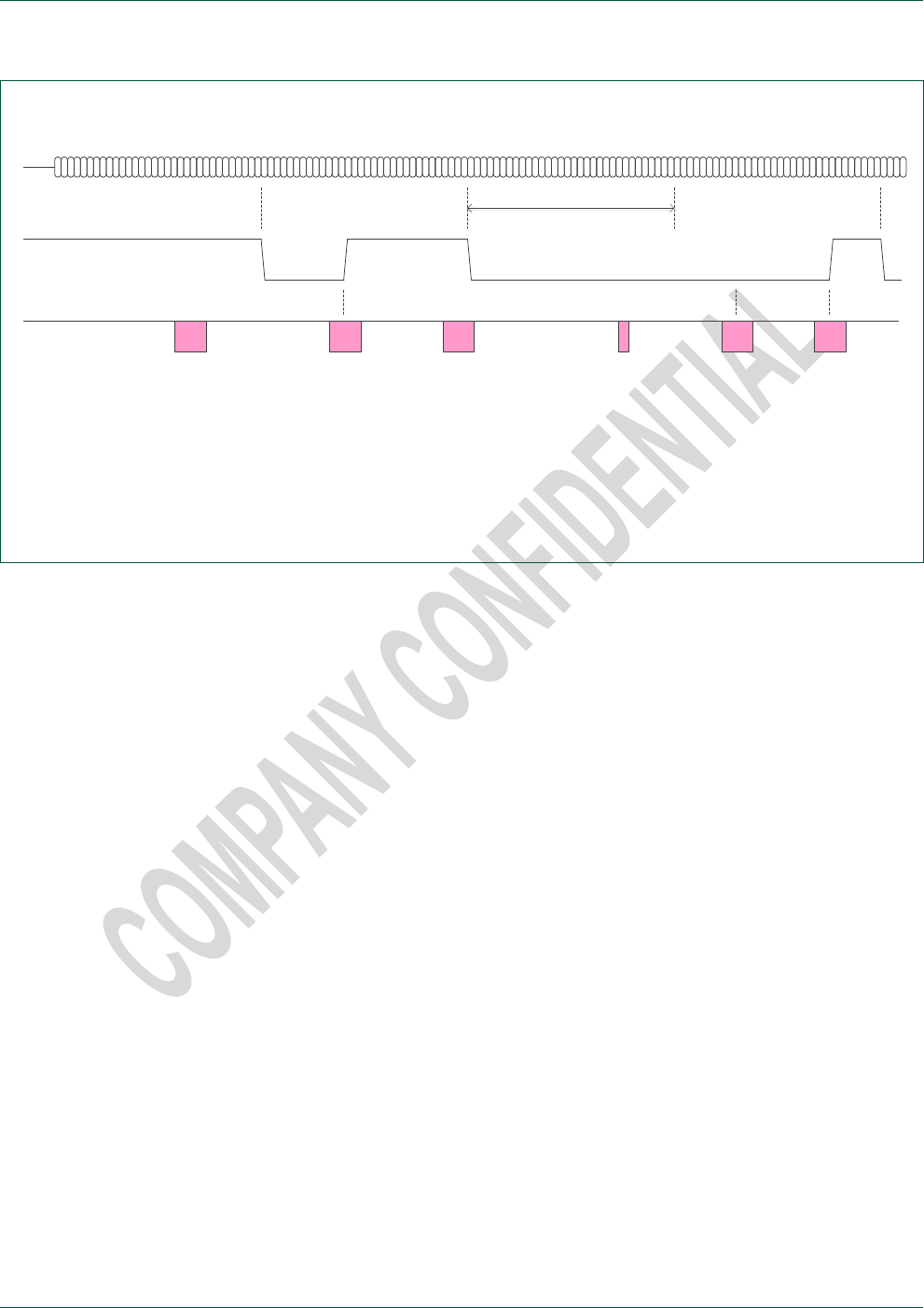
NXP Semiconductors
TEF668X User Manual
TEF6686, TEF6687, TEF6688 and TEF6689, /V102
doc
All information provided in this document is subject to legal disclaimers.
© NXP B.V. 2015. All rights reserved.
User Manual
Rev. 1.6 — 17 February 2015
68 of 101
‘DAVN’ (optional),
e.g. GPIO 0 Data_av. (1)
Get_RDS_Status
/ Get_RDS_Data
Get_RDS_Data
Data available = 0
Data loss = 0
(Data invalid)
Get_RDS_Data
Data available = 1
Data loss = 0
32 bit data (1)
Get_RDS_Data
Data available = 0
Data loss = 0
(Data invalid)
Data_av. (2)
Get_RDS_Status
Data available = 1
Data loss = 0
Get_RDS_Data
Data available = 1
Data loss = 0
32 bit data (2)
Get_RDS_Data
Data available = 1
Data loss = 0
32 bit data (3)
(2, 3)* (3)
* RDS buffer stores max. 50 sets
of 32 bit raw data
Set_RDS mode = 2 (demodulator mode)
26.94 ms
Fig 3. Example of RDS demodulator status and data by I²C bus read and optional GPIO ‘DAVN’ interrupt use.

NXP Semiconductors
TEF668X User Manual
TEF6686, TEF6687, TEF6688 and TEF6689, /V102
doc
All information provided in this document is subject to legal disclaimers.
© NXP B.V. 2015. All rights reserved.
User Manual
Rev. 1.6 — 17 February 2015
69 of 101
4.3 FM / AM cmd 132 Get_AGC
Read attenuation setting of the RF AGC. The overall antenna signal attenuation is found
by addition of the input_att and feedback_att value.
module
32 / 33
FM / AM
cmd
132
Get_AGC
| input_att, feedback_att
index
1
input_att
[ 15:0 ]
RF AGC input attenuation
FM
0 … 420 (0.1* dB) = 0 … 42 dB attenuation
AM
0 … 420 (0.1* dB) = 0 … 42 dB attenuation
2
feedback_att
[ 15:0 ]
RF AGC feedback attenuation
FM
0 … 60 (0.1* dB) = 0 … 6 dB attenuation
AM
0 … 180 (0.1* dB) = 0 … 18 dB attenuation
Application example
FM_Get_AGC (1, (input_att, feedback_att))
Read AGC attenuation settings
I²C example
[ w 20 84 01 [ r 00B4 003C ]
Read AGC attenuation settings
(18 dB + 6 dB RF attenuation)
Note: The TEF668X RF AGC employs 6 dB step size, i.e. read values of 0, 60, 120…
Note: The maximum FM input attenuation of 42 dB can be realized only by means of FM
RF AGC extension (see 3.4 FM / AM cmd 11 Set_RFAG).
4.4 FM / AM cmd 133 Get_Signal_Status
Read information about the received radio signal.
module
32 / 33
FM / AM
cmd
133
Get_Signal_Status
| status
index
1
status
[ 15:0 ]
Radio signal information
[15] = 0 : mono signal
[15] = 1 : FM stereo signal (stereo pilot detected)
[14] = 0 : analog signal
[14] = 1 : digital signal (blend input activated by digital processor or control)
(TEF6688 and TEF6689 only)
Application example
FM_Get_Signal_Status (1, (status))
Read availability of stereo and digital
I²C example
[ w 20 85 01 [ r 8000 ]
Read availability of stereo and digital
(stereo signal found)

NXP Semiconductors
TEF668X User Manual
TEF6686, TEF6687, TEF6688 and TEF6689, /V102
doc
All information provided in this document is subject to legal disclaimers.
© NXP B.V. 2015. All rights reserved.
User Manual
Rev. 1.6 — 17 February 2015
70 of 101
4.5 FM / AM cmd 134 Get_Processing_Status
Read information about the internal processing status (weak signal handling).
This information is intended for evaluation use only.
module
32/33
FM / AM
cmd
134
Get_Processing_Status
| softmute, highcut, stereo, sthiblend
index
1
softmute
[ 15:0 ]
Softmute control state
0 … 1000 (*0.1%) = 0 % minimum … 100 % max. softmute attenuation
2
highcut
[ 15:0 ]
Highcut control state
0 … 1000 (*0.1%) = 0 % minimum … 100 % max. audio freq. limitation
3
stereo
[ 15:0 ]
FM Stereo blend control state
0 … 1000 (*0.1%) = 0 % minimum … 100 % max. stereo att. (= mono)
4
sthiblend
[ 15:0 ]
FM Stereo high blend control state
0 … 1000 (*0.1%) = 0 % minimum … 100 % max. stereo freq. limitation
5
stband_1_2
[ 15:0 ]
FMSI band 1 and band 2 (TEF6687 and TEF6689 only)
[ 15:8 ]
FMSI control state band 1, low band
0 … 100 (%) = 0% (stereo) … 100% (mono) band 1
[ 7:0 ]
FMSI control state band 2, 2 kHz band
0 … 100 (%) = 0% (stereo) … 100% (mono) band 2
6
stband_3_4
[ 15:0 ]
FMSI band 3 and band 4 (TEF6687 and TEF6689 only)
[ 15:8 ]
FMSI control state band 3, 5 kHz band
0 … 100 (%) = 0% (stereo) … 100% (mono) band 3
[ 7:0 ]
FMSI control state band 4, high band
0 … 100 (%) = 0% (stereo) … 100% (mono) band 4
Application example
FM_Get_Processing_Status (1, (softmute, …))
Read weak signal processing status
I²C example
[ w 20 86 01 [ r 0000 019A 03B6 03E8 ]
[ w 20 86 01 [ r 0000 019A 0000 0000
0014 3284 ]
Read weak signal processing status
(sm 0%, hc 41%, st 95%, shb 100%)
Read weak signal processing status
(sm 0%, hc 41%, stereo 0%, shb 0%,
fmsi 0%, 20%, 50%, 100%)
Note: 0 % equals minimum control, as defined by the weak signal ‘_Min’ setting.
100 % equals maximum control, as defined by the weak signal ‘_Max’ setting.

NXP Semiconductors
TEF668X User Manual
TEF6686, TEF6687, TEF6688 and TEF6689, /V102
doc
All information provided in this document is subject to legal disclaimers.
© NXP B.V. 2015. All rights reserved.
User Manual
Rev. 1.6 — 17 February 2015
71 of 101
4.6 FM / AM cmd 135 Get_Interface_Status
Available for TEF6688 and TEF6689 only.
Information about radio I/O functionality; DR I²S output.
module
32 / 33
FM / AM
cmd
135
Get_Interface_Status
| samplerate
index
1
samplerate
[ 15:0 ]
Baseband digital radio sample rate (DR_I2S output)
0 = interface disabled (digital radio disabled)
6500 = 650 kHz
6750 = 675 kHz
Application example
FM_Get_Interface_Status (1, (samplerate))
automatic DR sample rate selection
I²C example (hex)
[ w 20 87 01 [ r 1A5E ]
automatic DR sample rate selection
(675 kHz)

NXP Semiconductors
TEF668X User Manual
TEF6686, TEF6687, TEF6688 and TEF6689, /V102
doc
All information provided in this document is subject to legal disclaimers.
© NXP B.V. 2015. All rights reserved.
User Manual
Rev. 1.6 — 17 February 2015
72 of 101
4.7 APPL cmd 128 Get_Operation_Status
This read command is also available during ‘boot state’ and during ‘idle state’.
Read information about the operation state.
module
64
APPL
cmd
128
Get_Operation_Status
| status
index
1
status
[ 15:0 ]
Device operation status
0 = boot state; no command support
1 = idle state
2 = active state; radio standby
3 = active state; FM
4 = active state; AM
Application example
APPL_Get_Operation_Status (1, (status))
Read operation status
I²C example
[ w 40 80 01 [ r 0003 ]
Read operation status
(active state FM)
Note: The value 0 indicates boot state (reset state after power-on, power dip or reference
frequency disruption). Actually all get commands will return 0 values during boot state
and no command support is available.
See chapter 6 Device start-up on start-up device control and initialization.
4.8 APPL cmd 129 Get_GPIO_Status
Read information about the input state of designated input pins (see 3.39 APPL cmd 3
Set_GPIO).
module
64
APPL
cmd
129
Get_GPIO_Status
| status
index
1
status
[ 15:0 ]
input state (when assigned for input use)
[2] = input state of GPIO_2 (no input use suggested for TEF668X)
[1] = input state of GPIO_1 (no input use suggested for TEF668X)
[0] = input state of GPIO_0 (0 = low, 1 = high)
Application example
APPL_Get_GPIO_Status (1, (status))
Read input state of GPIO input pins
I²C example
[ w 40 81 01 [ r 0001 ]
Read input state of GPIO input pins
(input GPIO_0 high)
Note: Because of the TEF668X designated input use of GPIO_1 and GPIO_2 during
power-up only GPIO_0 is suggested for application as a general purpose input.

NXP Semiconductors
TEF668X User Manual
TEF6686, TEF6687, TEF6688 and TEF6689, /V102
doc
All information provided in this document is subject to legal disclaimers.
© NXP B.V. 2015. All rights reserved.
User Manual
Rev. 1.6 — 17 February 2015
73 of 101
4.9 APPL cmd 130 Get_Identification
This read command is also available during ‘idle state’.
Read information about the device type and variant.
module
64
APPL
cmd
130
Get_Identification
| device, hw_version, sw_version
index
1
device
[ 15:0 ]
device type and variant
[ 15:8 ]
type identifier
9 = TEF668X ‘Lithio’ series
[ 7:0 ]
variant identifier
14 = TEF6686 ‘Lithio’
1 = TEF6687 ‘Lithio FMSI’
9 = TEF6688 ‘Lithio DR’
3 = TEF6689 ‘Lithio FMSI DR’
2
hw_version
[ 15:0 ]
hardware version
[ 15:8 ]
major number
1
[ 7:0 ]
minor number
0
3
sw_version
[ 15:0 ]
firmware version
[ 15:8 ]
major number
2 = ‘2’
[ 7:0 ]
minor number
0 = ‘.00’
Application example
APPL_Get_Identification (1, (device..))
Read device identification
I²C example
[ w 40 82 01 [ r 090E 0100 0200 ]
Read device identification
(TEF6688, hw 1.0, sw 2.00)
Note: The type number version designation ‘/V102’ is derived from the major hw_version
and the major sw_version number.

NXP Semiconductors
TEF668X User Manual
TEF6686, TEF6687, TEF6688 and TEF6689, /V102
doc
All information provided in this document is subject to legal disclaimers.
© NXP B.V. 2015. All rights reserved.
User Manual
Rev. 1.6 — 17 February 2015
74 of 101
4.10 APPL cmd 131 Get_LastWrite
This read command is also available during ‘idle state’.
Read data content of the last write transmission.
module
64
APPL
cmd
131
Get_LastWrite
| size/module, cmd/ index, parameter1, parameter2, parameter3, …
index
1
size/module
[ 15:0 ]
transmission size (number of parameters) and module number
[ 15:8 ] = 0 … 6 : number of parameters of the last write transmission
[ 7:0 ] = 0 … 255 : module value of the last write transmission
2
cmd/index
[ 15:0 ]
command byte number and index byte value
[ 15:8 ] = 0 … 255 : cmd value of the last write transmission
[ 7:0 ] = 0 ... 255 : index value of the last write transmission
3
parameter1
[ 15:0 ]
first parameter
0 … 65535 = value of the first parameter (when available)
4
parameter2
[ 15:0 ]
second parameter
0 … 65535 = value of the second parameter (when available)
5
parameter3
[ 15:0 ]
third parameter
0 … 65535 = value of the third parameter (when available)
6
parameter4
[ 15:0 ]
fourth parameter
0 … 65535 = value of the fourth parameter (when available)
7
parameter5
[ 15:0 ]
fifth parameter
0 … 65535 = value of the fifth parameter (when available)
Application example
APPL_Get_LastWrite (1, (size...parameter))
Read back last write transmission
I²C example
[ w 40 83 01 [ r 0120 1F01 02EE 0000…0000 ]
Read back last write transmission
(FM_Set_Deemphasis = ’75 µs’)
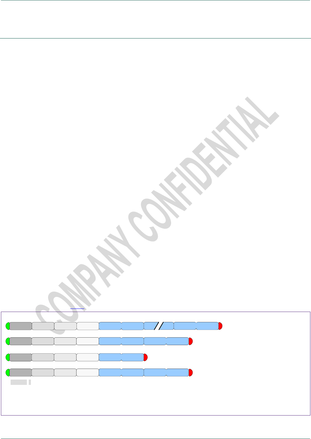
NXP Semiconductors
TEF668X User Manual
TEF6686, TEF6687, TEF6688 and TEF6689, /V102
doc
All information provided in this document is subject to legal disclaimers.
© NXP B.V. 2015. All rights reserved.
User Manual
Rev. 1.6 — 17 February 2015
75 of 101
5. I²C bus protocol
5.1 I²C protocol
TEF668X control parameters are 16 bit wide. The I²C bus native unit is the byte, multi-
byte values like 16 bit parameters are transmitted MSB byte first.
With external application of a pull down resistor at GPIO_2 (10 kto ground) the I²C
device address for TEF668X is C8h for write and C9h for read operations.
Alternatively application of a pull-up resistor (10 kto Vdd) at pin GPIO_2 allows for use
of device address CAh for write and CBh for read instead.
Note: GPIO_1 must be pulled low (10 k
to ground) during power-on to ensure proper
operation.
Note: GPIO_2 must be pulled low or high (10 k
) during power-on and activation for a
defined I2C address. Pin open is not a defined state.
5.2 Write control
Standard write transmissions to the TEF668X consist of an I²C start condition and an 8
bit hardware device address for write as depicted by the I²C standard.
Next an 8 bit module identifier is transmitted that can be regarded as a kind of internal
device address for function blocks like FM radio, AM radio, audio and system.
Control is then indicated by an 8 bit command identifier and an 8 bit parameter index
allows for sub-addressing within the command parameter space, followed by one or
more 16 bit parameters for actual control.
The end of transmission is indicated by an I²C standard stop condition. Because the I²C
bus format includes this explicit stop condition no ‘size’ indication is needed as may be
required by certain other bus formats.
Note: Device version V102 only supports the use of index = 1 and all parameters
described in this user manual need to be transmitted.
This behavior is equal to device version V101.
In Fig 4 examples of these transmissions are shown.
ADDR w
ADDR w module Set cmd index = 1
ADDR w
Write all cmd parameters
110010x 0
parameter 1
module Set cmd index = i parameter i
parameter n
Write indexed parameter(s)
note : not supported by /V102
module Set cmd index = i parameter i parameter i+1
2 n-1
ADDR w module Set cmd index = 1 parameter 1 parameter 2 Write only first parameters
[ 7:0 ] [ 7:0 ] [ 7:0 ] [ 15:8 ] [ 7:0 ] [ 15:8 ] [ 7:0 ]
‘ADDR w’ is the I²C device address for write (C8h or CAh) depending on the address select pin application.
Fig 4. Examples of I²C write control; set command
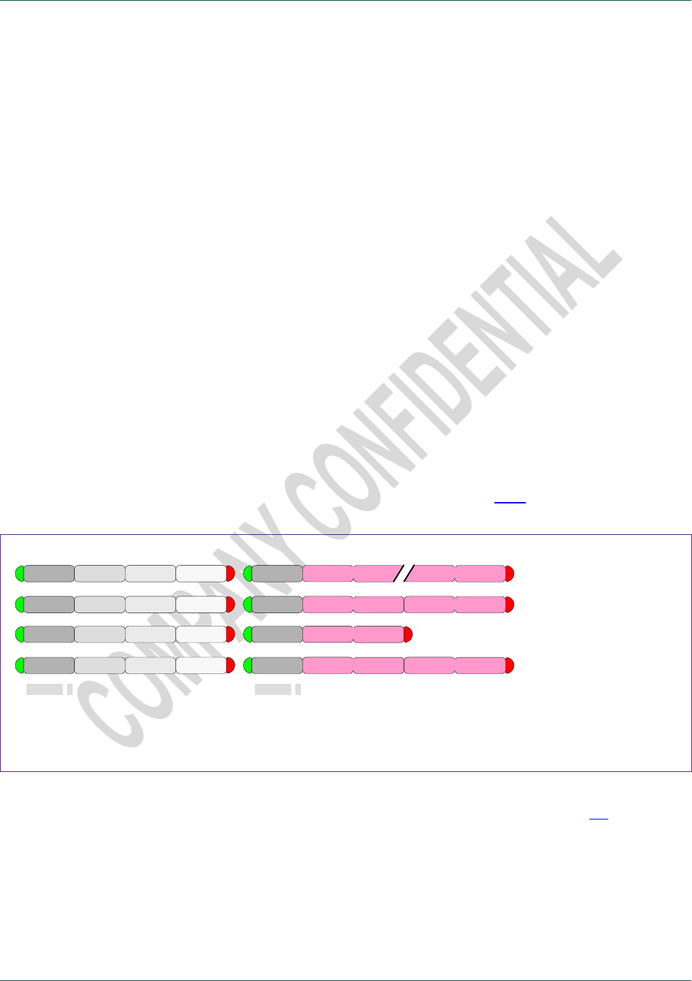
NXP Semiconductors
TEF668X User Manual
TEF6686, TEF6687, TEF6688 and TEF6689, /V102
doc
All information provided in this document is subject to legal disclaimers.
© NXP B.V. 2015. All rights reserved.
User Manual
Rev. 1.6 — 17 February 2015
76 of 101
TEF668X uses only a fraction of the possible number of modules, commands and
parameters. The choice for a 24 bit wide parameter address space is for future
extendibility.
Writing to disabled modules is supported and will store the data for later use. Enabling of
modules (where applicable) is supported by specific module commands which may imply
automatic disabling of other module(s) as e.g. is the case when switching between FM
and AM radio module operation.
5.3 Read control
Standard reading from the TEF668X consists of a write transmission for definition of the
requested data followed by the actual read transmission for obtaining the data.
Note: this is normal practice because the I²C specification does not support read
addressing within a read transmission.
Read data is 16 bit wide (or multiples of 16 bit) transmitted with the MSB byte first.
For reading of received data or status information special ‘get’ commands are defined.
For future extendibility and reading of data parts within larger data blocks an index
setting is included similar to the write definition.
Index = 1 is the standard case with read data starting from the first data word.
Note: Device version V102 only supports the use of index = 1, it is allowed however to
read less than the number of data words described in this user manual.
This behavior is equal to device version V101.
For evaluation purposes index = 0 is supported also (see 5.7.1).
ADDR w module Get cmd index = 1 Read all cmd data
110010x 0
Read indexed data
note : not supported by /V102
ADDR r data 1 data n
ADDR w module Get cmd index = i ADDR r data i
ADDR w module Get cmd index = i ADDR r data i data i+1
110010x 1
ADDR w module Get cmd index = 1 ADDR r data 1 data 2 Read only first data
[ 7:0 ] [ 7:0 ] [ 7:0 ] [ 15:8 ] [ 7:0 ] [ 15:8 ] [ 7:0 ]
‘ADDR r’ is the I²C device address for read (C9h or CBh) depending on the address select pin application.
Fig 5. Examples of I²C read control; get command
Certain timing requirements exist for TEF668X read control; see chapter 5.6 for details.
TEF668X ‘Get’ commands as published in this user manual are without parameter use.
For future extensions the protocol however allows for ‘Get’ commands with parameters.
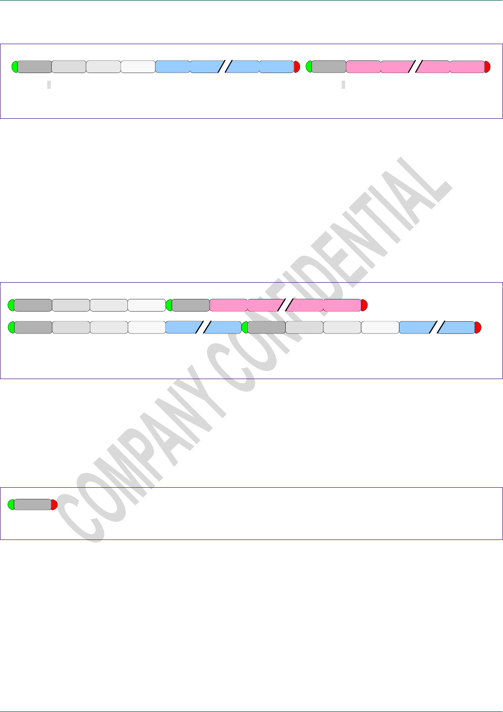
NXP Semiconductors
TEF668X User Manual
TEF6686, TEF6687, TEF6688 and TEF6689, /V102
doc
All information provided in this document is subject to legal disclaimers.
© NXP B.V. 2015. All rights reserved.
User Manual
Rev. 1.6 — 17 February 2015
77 of 101
0 1
ADDR w module Get cmd index = i parameter 1 parameter m ADDR r data i data n
Fig 6. Example of a possible get command with parameter(s)
5.4 I²C repeated start
The I²C specification allows the joining of multiple I²C transmissions by use of I²C
‘repeated start’. This way of operation ensures the set of I²C transmissions will not be
interrupted by another transmission from a second microcontroller on the bus (multi-
master setup).
TEF668X supports the use of I²C ‘repeated start’ without restriction. This means
TEF668X handles I²C transmissions separated by an I²C stop and start condition in
exactly the same way as I²C transmissions ‘joined’ by an I²C repeated start condition.
ADDR w module cmd index A2 r data 1 data n
ADDR w module cmd index ADDR w module cmd index
Fig 7. Examples of I²C transmissions with repeated start
5.5 Polling device presence
Checking for presence of the device on the I²C bus without any data transfer is possible
by only writing of the device write address. The I²C standard acknowledge will signal
device presence.
ADDR w Device presence check
Fig 8. Example of testing device presence.
5.6 I²C read timing requirements
The TEF668X supports I²C clock speeds up to 400 kHz in accordance with the I²C ‘fast
mode’ specification. TEF668X write operations require no special attention, read
operations however require a minimum of 50 us time to guarantee read data setup.
The 50 us timing requirement is measured from the write transmission finish to the first
read data; i.e. from the I²C ‘stop’ or ‘repeated start’ condition ( = SDA edge) to the end of
the device address ‘acknowledge’ ( = falling edge of the 9th SCL clock pulse)

NXP Semiconductors
TEF668X User Manual
TEF6686, TEF6687, TEF6688 and TEF6689, /V102
doc
All information provided in this document is subject to legal disclaimers.
© NXP B.V. 2015. All rights reserved.
User Manual
Rev. 1.6 — 17 February 2015
78 of 101
For 400 kHz bus operation the special control option of index = 0 offers a simple solution
to meet this read timing requirement:
A setting of index = 0 will add an additional read word in front of the standard read data.
This read word allows for special transmission evaluation options (see chapter 5.7
Special control ) but can be ignored for normal operation. For 400 kHz operation the
special index 0 read word ensures a proper setup timing for the required read data of
index = 1 and higher. The special index 0 word itself however must be ignored.
ADDR w module Get cmd index = 0 400 kHz I2C bus
Ensured data setup for
read data 1 and higher
ADDR r data 0 to be ignored data 1 data n
ADDR w module Get cmd index = 0 ADDR r data 0 to be ignored data 1 data n
Fig 9. Example of I²C read control with guaranteed 400 kHz operation; get command index = 0
Use of index = 0 is probably the most convenient way to ensure proper read data settling
for I2C fast mode bus operation.
Three alternative operation means are depicted below that may be of use, e.g. when
reliable index = 0 read data is desired at high speed:
Alternative 1 : Maximum I²C bus speed limit.
A bus speed setting of 184 kHz or lower will guarantee the required data setup time.
Microcontrollers generally do not employ the ‘fast mode’ worst-case timing for the full
device address transmission meaning a microcontroller ‘200 kHz’ bus speed setting will
ensure safe read operation in many cases.
Alternative 2 : 400 kHz I²C bus speed with microcontroller delay.
Use of separate transmissions and a timed delay of 27 us or higher between the write
transmission ‘stop’ condition and the read transmission ‘start’ will guarantee the required
read data setup time.
Alternative 3 : 400 kHz I²C bus speed with dual ‘repeated-start’.
In case use of ‘repeated-start’ is desired as well as 400 kHz bus operation a ‘dummy’
write address transmission can be inserted between the functional write and read
transmission.
NXP Semiconductors
TEF668X User Manual
TEF6686, TEF6687, TEF6688 and TEF6689, /V102
doc
All information provided in this document is subject to legal disclaimers.
© NXP B.V. 2015. All rights reserved.
User Manual
Rev. 1.6 — 17 February 2015
79 of 101
ADDR w module cmd index ADDR r data 1
ADDR w mod cmd index ADDR r data 1 data n
data n
ADDR w mod cmd index ADDR w ADDR r data 1 data n
>= 27 us
>= 50 us
<< 200 kHz
400 kHz Stop – Start with delay
400 kHz Repeated-start with dummy
Fig 10. Examples of alternative I²C read control with guaranteed read data setup
5.7 Special control
To support evaluation and debugging of the device control special control options are
available.
5.7.1 Set command confirmation; special evaluation read control
For standard operation data reading is limited to status and information read data
requested by a preceding ‘get’ command.
To this purpose TEF668X puts the requested data in its output registers after reception
and evaluation of a valid ‘get’ command. TEF668X however also places a data word in
its output registers after reception of a ‘set’ command, either offering confirmation of the
command reception by returning the module and cmd value or delivering an error code in
case of an invalid control. This data field is not intended for generic use but can be read
during control software development for debugging purposes.
Condition : Read data word :
Valid command module / cmd
No command received 00 00h
Invalid command value FF FFh
Invalid module value FF FEh
Invalid index value FF FDh (note: currently only index = 0 or 1 is permitted)
Invalid parameter value FF FCh (note: not available in general)
Invalid state FF FAh (= command not available in current state)
Example of confirmation read
after set-command
ADDR w module Set cmd index = i parameter i parameter n ADDR r module Set cmd
110010x 0 110010x 1
Fig 11. Example of write command with evaluation data read
NXP Semiconductors
TEF668X User Manual
TEF6686, TEF6687, TEF6688 and TEF6689, /V102
doc
All information provided in this document is subject to legal disclaimers.
© NXP B.V. 2015. All rights reserved.
User Manual
Rev. 1.6 — 17 February 2015
80 of 101
5.7.2 Get command confirmation; special evaluation read control
For standard operation read command data reading is limited to application status and
information data.
However similar to write commands also read commands can optionally deliver
confirmation of the read command reception or an error in case of invalid control.
To this purpose use of index = 0 with a ‘get’ command has a special meaning where as
the first data word the module and cmd value are returned or an error code in case of
invalid control.
Condition : Read data word :
Get command data available module / cmd
No command received 00 00h
Get command data not available yet FF F8h*
Invalid command value FF FFh
Invalid module value FF FEh
Invalid index value FF FDh (note: currently only 0 and 1 are allowed)
Invalid state FF FAh (= command not available in current state)
* All TEF668X read commands show ‘instant’ data delivery, therefore error value FF F8h
shall never be found as long as the read timing requirement of 50 us is met (see 5.6).
In case of not meeting the read timing requirement also error value 00 00h may be found
occasionally.
ADDR w module Get cmd index = 0 valid get cmd
ADDR r module Get cmd data 1 data n
ADDR w module Get cmd index = 0 ADDR r FFh FFh undefined undefined unknown get cmd
Fig 12. Examples of I²C read control with confirmation; get command index = 0
Note: The 00 00h and FF FFh … FF F8h error codes are also returned as the first data
word in case of index = 1 use but may be confused with standard expected return data.
NXP Semiconductors
TEF668X User Manual
TEF6686, TEF6687, TEF6688 and TEF6689, /V102
doc
All information provided in this document is subject to legal disclaimers.
© NXP B.V. 2015. All rights reserved.
User Manual
Rev. 1.6 — 17 February 2015
81 of 101
6. Device start-up
6.1 Introduction
The TEF668X is powered by a single supply voltage. No supply power-up requirements
are known to exist.
After power-on the device is found in a pre-defined reset state (boot state). A sequence
of control transmissions will bring the device into idle state followed by active state to
realize the desired user operation mode, function and performance.
Write required initialization
Start
Power on reset
Set application reference clock
Operation status = 1
Operation status = 0
radio standby
AM
FM standby
FM
AM standby
Activate
Initialize and control any module FM, AM, Audio, Application
Operation status = 2
Idle state
Operation status = 3 / 4
Read from enabled modules Audio, Application
Audio
Appl.
Active state
Boot state
Appl.
Enable (Tune To) FM / AM radio
Initialize and control any module FM, AM, Audio, Application
Read from enabled modules FM / AM, Audio, Application
Fig 13. Block diagram of device start-up control sequence
Boot state and idle state have no function other than offering the minimum set of controls
required for proper active state operation.
State transitions take a small amount of time and care should be taken to ensure a
certain state is entered before any of the belonging control transmissions is started. After
transmission of a ‘Start’ or ‘Activate’ state transition command it is advised to check the
operation status by I2C read until the new state is found.
TEF668X state transition times will fall within the following limits:
Power-on Boot state : power supply voltage settling + 5 ms.
(or clock active + 5 ms in case of external clock application)
Boot state Idle state : 50 ms.
Idle state Active state : 100 ms.

NXP Semiconductors
TEF668X User Manual
TEF6686, TEF6687, TEF6688 and TEF6689, /V102
doc
All information provided in this document is subject to legal disclaimers.
© NXP B.V. 2015. All rights reserved.
User Manual
Rev. 1.6 — 17 February 2015
82 of 101
6.2 Start-up I2C control transmission sequence
Supply power on
Wait until device is found present on the I2C bus (‘boot state’) :
Repeat APPL_Get_Operation_Status read until I2C acknowledge from device;
status = 0 (‘boot state’) is found.
[ w 40 80 01 [ r 0000 ]
Alternatively Wait radio supply power settling time + 5 ms.
In case of external clock application wait for clock active + 5 ms.
Send required initializations :
See 6.2.1 Required initialization I2C transmission – I2C example
and 6.2.2 Required initialization I2C transmission – C code include file
Start :
[ w 14 0001 ]
Wait until device is found in ‘idle state’ :
Repeat APPL_Get_Operation_Status read until status = 1 (‘idle state’) is found.
[ w 40 80 01 [ r 0001 ]
Alternatively Wait 50 ms.
Set reference frequency
APPL_Set_ReferenceClock freq. = 55466670/9216000/4000000, type = 0/1.
[ w 40 04 01 034E 5AAE 0001 ]
: 55.46667 MHz external reference.
[ w 40 04 01 003D 0900 0000 ]
: 4 MHz crystal reference.
Not required for default 9.216 MHz crystal use.
Activate :
APPL_Activate mode = 1.
[ w 40 05 01 0001 ]
Wait until device is found in ‘active state radio standby’ :
Repeat APPL_Get_Operation_Status read until status = 2 (‘radio standby
state’) is found.
[ w 40 80 01 [ r 0002 ]
Alternatively Wait 100 ms.
Full API control is available from here for all modules.
Audio and Application are on, FM and AM radio are in low-power standby.
Example FM_, AM_, AUDIO_ and APLL_ desired user settings: module
initialization.
Example AUDIO_Set_Mute mode = 0 : disable mute.
[ w 30 0B 01 0000 ]
Example FM_Tune_To mode = 1, frequency = 8930 : FM radio 89.3 MHz.
[ w 20 01 01 0001 22E2 ]

NXP Semiconductors
TEF668X User Manual
TEF6686, TEF6687, TEF6688 and TEF6689, /V102
doc
All information provided in this document is subject to legal disclaimers.
© NXP B.V. 2015. All rights reserved.
User Manual
Rev. 1.6 — 17 February 2015
83 of 101
6.2.1 Required initialization I2C transmission – I2C example
The following I2C transmissions (version p2.22) are a required part of the V102 boot state
device initialization.
Use of these I2C transmissions is required for proper and full function and performance
as described in this user manual. Version p2.22 is a minor update over p2.21.
Note: The transmission example below shows a data content of 12 words for every ‘1B’
data transmission. The data stream can be split in any desired length on (2-byte) word
boundaries with every data transmission starting with hex value 1B.
[ w 1C 00 00 ]
[ w 1C 00 74 ]
[ w 1B F000 3838 D080 F000 3840 D080 43B2 3843 D080 F000 7000 C2F7 ]
[ w 1B F000 3874 D080 80FC 3917 D080 C238 2011 40B7 9FA7 391C D280 ]
[ w 1B 9FA7 3926 D280 F000 392D D080 F000 3930 D080 9041 3952 DD80 ]
[ w 1B F000 3A29 D080 F000 3956 D080 F000 3A2B D080 C4A2 0216 6004 ]
[ w 1B F000 39C3 D080 F000 39EB D080 9001 3958 D080 F000 38F9 D080 ]
[ w 1B F000 395F D280 F000 3963 D080 4384 396D D080 F000 3970 D080 ]
[ w 1B F000 3974 D080 9E30 18F9 D280 F000 397A D080 F000 397D D080 ]
[ w 1B 3077 39E2 D080 F000 3980 D080 3200 3982 D080 F000 3984 D080 ]
[ w 1B F000 39CB D080 F000 39F9 D080 A801 3A17 D080 F000 3A36 D080 ]
[ w 1B F000 3A3D D080 F000 3A3F D080 F000 3A53 D080 F000 3A56 D080 ]
[ w 1B F000 3A59 D080 F000 3A5C D080 F000 7000 F000 F000 3A61 D080 ]
[ w 1B F000 3A22 D280 F000 3A6F D080 0043 3A7E D980 F000 3A88 D080 ]
[ w 1B F000 3ADE D080 F000 3AE1 D080 F000 3AF2 D080 2E40 3B90 D080 ]
[ w 1B F000 3B9A D080 F000 0E3F 6000 5010 28D8 D280 9101 0136 6000 ]
[ w 1B F000 7000 A018 F000 7000 A0D8 F000 7000 A0F9 F000 7000 A1B5 ]
[ w 1B F000 7000 A209 F000 7000 A234 F000 7000 A24C F000 2031 D080 ]
[ w 1B F000 04C1 6008 F000 0101 D280 F000 0030 D080 007F 6002 E200 ]
[ w 1B F000 0E22 600A F000 00FF 6003 F000 0142 D280 9003 4002 F000 ]
[ w 1B 9043 0170 D180 F000 0169 D080 0E69 600A A352 2023 0001 6001 ]
[ w 1B F000 7000 F000 C4CB 7000 F000 CA09 3023 F000 C2CB 7000 F000 ]
[ w 1B F000 3023 D008 8200 0D50 6008 F000 0D51 6009 3000 2180 6001 ]
[ w 1B F000 4032 F000 3011 45F3 F000 3092 2D30 6004 3113 2D40 6005 ]
[ w 1B 3194 7FFF 6006 3215 0D61 600A 3296 0D6B 600B 3310 0D50 6001 ]
[ w 1B 3390 0D5C 6002 3021 0D63 6003 3031 0D75 600C 30A2 8D00 6001 ]
[ w 1B 30B3 0173 6002 3041 0025 6003 30C2 4044 F000 3143 4035 F000 ]
[ w 1B 31C4 6400 6006 3245 1F40 6007 32C6 7000 F000 3347 1EBC 600D ]
[ w 1B 33C0 0122 6001 3440 FDEE 6002 3051 7B8F 6003 30D2 C429 6004 ]
[ w 1B 3151 1EC2 600E 3253 FF0D 6002 32D4 7D2E 6003 3061 C19A 6004 ]
[ w 1B 30E2 7000 F000 3161 7000 F000 3263 7000 F000 32E4 7000 D008 ]
[ w 1B F000 0370 D280 F000 7000 A002 F000 7000 A059 F000 0215 D080 ]
[ w 1B F000 0D51 600F F000 0517 600E 23F6 7000 F000 F000 2163 41F5 ]
[ w 1B 918F 21F8 4074 C3EF 21E0 F000 C3A4 33F7 F000 D85B 7000 F000 ]
[ w 1B 8218 7000 F000 9FAF 1800 F000 9F0F 31F8 9002 F000 7000 9028 ]
[ w 1B F000 7000 D008 F000 2278 F000 16D3 6009 A07F 35F0 1EBC 600D ]
[ w 1B F000 0D61 6008 F000 03A5 D280 F000 1EC2 600D F000 0D6B 6008 ]
[ w 1B F000 03A5 D280 F000 2100 F000 836D 22F1 F000 F000 2377 F000 ]
[ w 1B 9041 3670 F000 9E79 7000 9001 F000 32F1 D008 91C7 3375 F000 ]
[ w 1B F000 3470 E600 F000 34F0 E600 F000 2474 F000 F000 24F3 F000 ]
[ w 1B 8C24 26F2 4016 8A1B 3474 4FF5 82B7 34F3 F000 F000 2071 9005 ]
[ w 1B 8304 7000 F000 8E67 7000 F000 F000 7000 9002 F000 36F6 F000 ]
[ w 1B F000 34F0 8006 82AF 7000 F000 821B 7000 D009 8E5F 7000 F000 ]
[ w 1B F000 7000 D009 F000 36F5 F000 F000 3470 F000 4011 2772 A2F5 ]
[ w 1B 908A 20F3 A2F4 8ED7 3772 F000 F000 37F1 E600 F000 7000 D008 ]
[ w 1B F000 227A F000 16C3 6009 A058 F000 1820 F000 F000 3570 F000 ]
[ w 1B F000 327A D008 8200 0D51 6008 4003 7000 F000 3380 7000 F000 ]
[ w 1B 2106 7000 F000 3700 7000 F000 3780 4015 F000 3683 7000 F000 ]
[ w 1B 3305 0D61 6009 3286 0D6B 600A 3210 7000 F000 3290 7000 F000 ]
[ w 1B 3310 7000 F000 3390 7000 F000 3410 7000 F000 3490 7000 F000 ]
[ w 1B 3110 7000 F000 3190 7000 F000 3220 7000 F000 32A0 7000 F000 ]
[ w 1B 3320 7000 F000 33A0 7000 F000 3420 7000 F000 34A0 7000 F000 ]
[ w 1B 3120 7000 F000 31A0 7000 F000 8200 0D30 600A 0D40 600B C010 ]
[ w 1B F000 1020 F000 0D51 600C C010 F000 1030 F000 F000 35C0 D008 ]
[ w 1B F000 0D75 600F F000 0563 600E 24F7 051D 600D 2576 7000 F000 ]
[ w 1B 91C7 20E8 4015 918F 21E9 D409 C3EF 2000 4012 9FBE 2011 5803 ]
[ w 1B A080 3577 9001 F000 7000 D008 F000 21F5 F000 A0CA 2254 F000 ]

NXP Semiconductors
TEF668X User Manual
TEF6686, TEF6687, TEF6688 and TEF6689, /V102
doc
All information provided in this document is subject to legal disclaimers.
© NXP B.V. 2015. All rights reserved.
User Manual
Rev. 1.6 — 17 February 2015
84 of 101
[ w 1B CC09 0517 600C 832C 7000 F000 8A61 7000 F000 AE48 2245 A2BD ]
[ w 1B A228 2078 F000 F000 35F0 F000 F000 1800 F000 F000 3078 F000 ]
[ w 1B 16E3 6009 A027 8901 23F4 F000 F000 20F2 F000 8261 2173 F000 ]
[ w 1B A050 3670 F000 A058 2372 E140 A801 22F3 F000 9049 2275 E040 ]
[ w 1B 8061 7000 F000 8A51 33F1 F000 A058 7000 F000 AF48 7000 F000 ]
[ w 1B F000 3470 D008 8200 0D75 6008 9009 0D00 6009 F000 3500 F000 ]
[ w 1B F000 3380 C028 F000 1010 F000 F000 3481 D008 8249 0D75 6008 ]
[ w 1B F000 7000 8FFD 0400 6000 A2A3 8EC0 4000 6005 6000 6005 E600 ]
[ w 1B C81B 7000 F000 D8DB 0D51 6008 835B 7000 F000 9EBA 3003 F000 ]
[ w 1B F000 3084 D409 F000 7000 8FAF F000 0D75 6008 F000 0D51 6009 ]
[ w 1B F000 2403 F000 F000 2794 D008 A003 7000 F000 0011 0800 F000 ]
[ w 1B 0011 0800 C00E A009 0011 0800 A009 7000 F000 A408 7000 D008 ]
[ w 1B A003 7000 F000 0011 0800 F000 0011 0800 C026 A009 0011 0800 ]
[ w 1B A009 7000 F000 A408 7000 D008 F000 1D01 6008 F000 0A2C 6000 ]
[ w 1B F000 011A 6001 3100 7000 F000 3181 7000 D008 A801 7FFF 6006 ]
[ w 1B CC0A 7000 F000 8EA1 3106 F000 F000 3206 D409 AEE8 04DF D080 ]
[ w 1B 9087 7000 9807 F000 0FB1 D280 9E08 4189 6006 1492 6000 9004 ]
[ w 1B A198 1D01 6008 AA56 7000 F000 A220 3206 F000 F000 3280 F000 ]
[ w 1B 91C2 069A 6008 41E6 0600 D080 8213 7000 D809 F000 0FB1 D280 ]
[ w 1B 9E08 1062 6001 051F 6005 D009 F000 06E6 6008 A365 7000 F000 ]
[ w 1B F000 3085 D008 1000 6003 A26F 3023 0773 D280 F000 07C6 D080 ]
[ w 1B 0800 6003 A002 0E6F 6009 F000 0200 6003 8000 F000 0773 D080 ]
[ w 1B 40E0 001F 6001 13D5 6007 A011 9040 7000 F000 13FB 6006 A00E ]
[ w 1B 1405 6006 A00D 140F 6006 A00C 4560 003A 6001 13B6 6007 A00B ]
[ w 1B 9040 7000 F000 13F7 6006 A008 1401 6006 A007 140B 6006 A006 ]
[ w 1B 4180 003B 6001 13B6 6007 A005 9040 7000 F000 13F7 6006 A002 ]
[ w 1B 1401 6006 A001 140B 6006 8000 F000 0D28 D080 D7CA 00FF 6004 ]
[ w 1B 81D7 0CF7 6009 D056 7000 F000 8276 3017 F000 D0F6 4083 F000 ]
[ w 1B C1A4 2019 F000 82F6 7000 F000 C180 2017 A24E C3E7 7000 F000 ]
[ w 1B C5C7 7000 F000 F000 3017 D008 9A78 7000 F000 9A70 7000 90DE ]
[ w 1B F000 7000 90DE F000 0D67 D080 F000 7000 A114 F000 7000 80CD ]
[ w 1B 1EC8 6008 A244 F000 2000 A243 9000 7000 F000 F000 7000 D409 ]
[ w 1B F000 7000 8FA5 1EC8 6008 A23F F000 3000 D008 0028 6000 A23D ]
[ w 1B 9E38 0EF4 6009 9E38 7000 9FFF F000 7000 D008 4040 0C8A D580 ]
[ w 1B F000 0C8B D280 F000 0FB1 D280 9C39 7000 F000 9C31 7000 9003 ]
[ w 1B F000 7000 9002 4010 7000 AFF3 41F1 4040 800D 4000 7000 AFF1 ]
[ w 1B 41F1 4040 800C 03E8 6002 A22F 9083 1044 D180 F000 1042 D080 ]
[ w 1B 4071 4020 A008 43A1 4030 A007 43B1 4030 A006 F000 1075 D080 ]
[ w 1B 4071 4020 A004 43A1 4030 A002 43B1 4030 A001 F000 1081 D080 ]
[ w 1B F000 0C92 D080 F000 0C94 D080 F000 0BC9 6008 F000 1D8D D280 ]
[ w 1B F000 16D5 D080 F000 0BC9 6008 F000 1D8F D280 F000 16DA D080 ]
[ w 1B 3E91 1F5F D280 F000 238A D080 0D85 6008 A21A F000 3000 D008 ]
[ w 1B F000 0F88 600B F000 0230 6003 F000 0938 6004 9F98 012C 6005 ]
[ w 1B F000 2EB3 EE00 F000 0FB1 D280 9E09 0D87 600C 9F90 7000 9002 ]
[ w 1B 9F88 2F34 EE00 F000 2FB5 EE00 3043 0B42 6008 F000 30C4 F000 ]
[ w 1B F000 3145 F000 F000 2CB1 4017 F000 2D32 F000 C679 2205 F000 ]
[ w 1B F000 3D81 F000 F000 3D01 F000 DD6D 1B93 D280 9046 0D85 600A ]
[ w 1B 2042 1B93 D280 DAC9 2025 A203 8C69 2DB3 F000 DD49 3201 F000 ]
[ w 1B 8D89 7000 F000 3C81 FE35 6000 3581 0016 6001 A018 2146 F000 ]
[ w 1B AA07 012D 6000 81CF 7000 F000 8F80 7000 F000 F000 7000 9402 ]
[ w 1B 4045 574B 6000 E000 6001 8002 4065 4000 6000 C666 6001 8000 ]
[ w 1B A030 4000 6004 AF4E 00A4 6005 818E 0B75 6008 F000 1474 D280 ]
[ w 1B F000 1B90 D280 2E34 0400 6006 20C2 1B93 D280 D2C9 03E9 6005 ]
[ w 1B 818E 0B59 6008 8F2D 31C6 F000 F000 7000 9402 4045 B15C 6003 ]
[ w 1B 4666 6007 8002 4065 AACE 6003 C666 6007 8000 A0E0 0038 6004 ]
[ w 1B AF48 001D 6005 81C7 3184 F000 3105 1474 D280 F000 1B90 D280 ]
[ w 1B F000 D800 6000 F000 0B67 6008 21C6 2000 6004 F000 1333 6005 ]
[ w 1B 8186 3184 4007 3105 1474 D280 F000 1B90 D080 F000 6E6C 6003 ]
[ w 1B 4007 00E5 6005 A058 FFFF 6003 AA24 0B52 6008 811C 7000 F000 ]
[ w 1B 3105 7FDF 6006 3184 1474 D280 F000 1B90 D080 9183 2E85 F000 ]
[ w 1B F000 2F06 F000 F000 2F87 F000 0BC9 6009 A1CE 3E11 0D82 600A ]
[ w 1B F000 2711 A1CC A050 2792 F000 AA41 0BB4 600C 8052 2021 A1C9 ]
[ w 1B 9ECB 3592 F000 9041 7000 D809 882D 7000 D409 F000 3615 F000 ]
[ w 1B F000 3695 F000 9100 30A6 F000 3127 1462 D280 9004 31C0 F000 ]
[ w 1B 2145 8CCD 6006 F000 FF55 6007 F000 1474 D280 F000 3240 F000 ]
[ w 1B F000 32C1 F000 F000 3342 8000 F000 0D82 6009 F000 0BC9 600A ]
[ w 1B F000 2015 A1B8 9145 7FEC 6006 4047 7000 D409 2090 1447 D280 ]
[ w 1B F000 34A0 F000 2110 1447 D280 F000 3520 D008 0A3D 6007 A1B1 ]
[ w 1B A279 0BC9 6009 A2BA 7000 F000 90C0 3B91 F000 3B12 1462 D280 ]
[ w 1B F000 3C10 D008 F000 0B60 600E F000 0004 6003 40A7 3FFC 6004 ]
[ w 1B 3263 8008 6005 32E4 199A 6006 3365 0D86 600F 31E6 7000 F000 ]

NXP Semiconductors
TEF668X User Manual
TEF6686, TEF6687, TEF6688 and TEF6689, /V102
doc
All information provided in this document is subject to legal disclaimers.
© NXP B.V. 2015. All rights reserved.
User Manual
Rev. 1.6 — 17 February 2015
85 of 101
[ w 1B 3077 7000 D008 0D82 600A A1A3 F000 3020 F000 00D2 6001 940B ]
[ w 1B F000 00D2 6002 00FA 6003 AFED F000 BE77 6006 F000 4B00 6007 ]
[ w 1B 3706 0001 6001 3787 03E8 6002 F000 0384 6004 F000 0001 6005 ]
[ w 1B F000 008C 6006 F000 0AF0 6007 F000 7000 8FC7 F000 0BB4 6009 ]
[ w 1B F000 0011 6005 F000 0011 6006 3B05 1000 6007 3B86 0004 6000 ]
[ w 1B 3C07 AD84 6001 3210 01FD 6002 3291 0B5E 6003 3312 0C80 6004 ]
[ w 1B 3193 00A0 6005 3484 FFD0 6006 3505 E354 6007 3606 3400 6000 ]
[ w 1B 3686 0001 6001 3707 03E8 6002 3780 7000 8FB7 80E5 7FFF 6000 ]
[ w 1B CC0A 7000 F000 8EA9 3370 F000 AF20 3470 D409 AEE8 7000 F000 ]
[ w 1B A805 0080 6007 A8F6 3375 F000 C386 7000 F000 8F7F 33F6 F000 ]
[ w 1B A885 1DE4 D180 F000 3475 D008 0D86 6009 A17A 2012 1F32 D280 ]
[ w 1B F000 3582 D008 9082 0D86 6009 40A7 4077 E640 F000 7000 F000 ]
[ w 1B F000 3017 D008 0BB4 6008 A173 F000 3182 D008 F000 0961 6008 ]
[ w 1B F000 09C9 6009 F000 2180 F000 F000 2091 A16E A208 7000 D008 ]
[ w 1B 00CF 6002 A001 0151 6002 8001 0D8B 6008 8001 0D8C 6008 8000 ]
[ w 1B F000 7000 F000 F000 3002 D008 0FF2 6009 A166 2011 0D8B 600A ]
[ w 1B F000 2C92 F000 9041 2011 F000 F000 7000 93FE F000 7000 F200 ]
[ w 1B 3122 2031 D080 0D8B 6008 A003 F000 2022 D080 0D8C 6008 A001 ]
[ w 1B F000 201E D080 F000 7000 F000 2000 0E69 6008 F000 01D0 6001 ]
[ w 1B F000 3080 F000 F000 3001 D008 836D 0C35 6008 4060 3A51 6001 ]
[ w 1B 41E2 2196 6003 3300 4144 F000 3381 7000 F000 3402 7000 F000 ]
[ w 1B 3483 0C29 6009 3504 3A5F 6000 3585 3A64 6003 3090 7000 F000 ]
[ w 1B 3393 7000 8FDF F000 7000 AE5F F000 7000 8EA4 F000 7000 AE9D ]
[ w 1B F000 0C51 D280 F000 21A0 D080 F000 052E D280 F000 7000 A00E ]
[ w 1B F000 21B7 D080 F000 1F32 D280 F000 1E84 D280 F000 21E0 D080 ]
[ w 1B F000 1EA4 D280 F000 07F7 D280 F000 2215 D080 F000 07FB D280 ]
[ w 1B F000 228F D080 4040 22E1 D280 4080 22E2 D280 F000 229C D080 ]
[ w 1B F000 07FB D280 F000 22B6 D080 F000 20F0 D280 9002 27DF D280 ]
[ w 1B 9E69 7000 F000 F000 0700 D180 F000 2320 D080 9082 0C29 6009 ]
[ w 1B 4017 4067 E640 F000 7000 F000 F000 3217 D008 F000 07F7 D280 ]
[ w 1B F000 27EA D280 F000 11B5 D080 4055 1517 6008 F000 1D40 6000 ]
[ w 1B 3105 1E60 6001 3185 7000 F000 3205 7000 F000 3285 7000 F000 ]
[ w 1B 3300 7000 F000 3381 0D8E 6009 3400 0254 6002 3481 3880 6003 ]
[ w 1B 3012 7000 F000 3093 7000 D008 170B 600C A11E 0040 4005 F000 ]
[ w 1B 0041 243F D080 F000 0C83 6008 9000 0C6B 600B F000 700C E600 ]
[ w 1B F000 2003 F000 F000 2204 F000 F000 3BB3 F000 F000 3C34 D008 ]
[ w 1B F000 7000 ADC1 F000 0C8D 6008 F000 260A D080 83FF 0D9B 6008 ]
[ w 1B F000 01F4 6000 F000 03B1 6001 1000 03B2 6002 1001 040E 6000 ]
[ w 1B 1002 040F 6001 1000 045C 6002 1001 045D 6000 1002 1380 6001 ]
[ w 1B 1000 0DAB 6009 1001 02EE 6000 1007 4306 6001 1010 0469 6002 ]
[ w 1B 1011 4487 6000 1012 05E3 6001 1010 4608 6002 1011 06AE 6000 ]
[ w 1B 1012 0DA4 6008 1010 9E3C 6000 1017 0DB3 6009 1000 25DA 6000 ]
[ w 1B 1007 803D 6001 1010 2882 6002 1011 C03D 6000 1012 2887 6001 ]
[ w 1B 1010 C03B 6002 1011 288C 6000 1012 C03B 6001 1010 2891 6002 ]
[ w 1B 1011 C03B 6000 1012 2896 6001 1010 C03B 6002 1011 289B 6000 ]
[ w 1B 1012 C03B 6001 1010 28A0 6002 1011 403C 6000 1012 28A5 6001 ]
[ w 1B 1010 C03C 6002 1011 28AA 6000 1012 C03C 6001 1010 28AF 6002 ]
[ w 1B 1011 C03C 6000 1012 28B4 6001 1010 C03C 6002 1011 28B9 6000 ]
[ w 1B 1012 C03C 6001 1010 28BE 6002 1011 C03C 6000 1012 29CC 6001 ]
[ w 1B 1010 0037 6002 1011 29D1 6000 1012 0037 6001 1010 29D6 6002 ]
[ w 1B 1011 0037 6000 1012 29DB 6001 1010 0037 6002 1011 0DD8 6008 ]
[ w 1B 1012 2715 6000 1017 403E 6001 1000 271A 6002 1001 803C 6000 ]
[ w 1B 1002 2864 6001 1000 403C 6002 1001 2869 6000 1002 403C 6001 ]
[ w 1B 1000 286E 6002 1001 803A 6000 1002 2873 6001 1000 803A 6002 ]
[ w 1B 1001 28A0 6000 1002 403C 6001 1000 29CC 6002 1001 0037 6000 ]
[ w 1B 1002 29D1 6001 1000 0037 6002 1001 29D6 6000 1002 0037 6001 ]
[ w 1B 1000 29DB 6002 1001 0037 6000 1002 0DEF 6009 1000 7000 F000 ]
[ w 1B 1007 7000 F000 1017 7000 D008 0CDF 600B A0BE 3030 23D6 D280 ]
[ w 1B F000 26E8 D080 0D9B 6008 A0BB F000 0002 A0BA 9082 7000 F000 ]
[ w 1B 828A 7000 9003 908A 7000 9001 F000 7000 8FFB 82BF 7000 F000 ]
[ w 1B F000 0199 D280 F000 0D9A 6008 F000 26C1 F000 F000 0002 A0B1 ]
[ w 1B 9082 7000 F000 828A 7000 9003 908A 7000 9001 F000 7000 8FFB ]
[ w 1B 8280 7000 F000 F000 7000 D008 F000 0DAB 600D F000 3FFF 6002 ]
[ w 1B F000 0051 A0A8 C253 7000 F000 8EC4 7000 9001 F000 7000 97FC ]
[ w 1B D48F 0199 D280 4005 0DA4 600D 4017 3FFF 6002 9F7D 0051 A0A1 ]
[ w 1B C253 7000 F000 82C4 271C D180 F000 7000 97FC 9146 2720 D080 ]
[ w 1B 4007 0199 D280 F000 0D8E 600E 4007 25C1 A09A 9E79 2E40 4014 ]
[ w 1B 4036 3167 9019 2F45 1964 6002 4FF0 1A5E 6003 8354 4036 F000 ]
[ w 1B 835C 4000 E200 F000 4010 E200 F000 7000 F000 9000 7000 F000 ]
[ w 1B F000 7000 9C11 F000 0DD8 600D 4036 22F0 D280 0DB3 600D E600 ]
[ w 1B 4014 2140 F000 F000 2051 A08B 9041 7000 F000 8245 7000 901D ]

NXP Semiconductors
TEF668X User Manual
TEF6686, TEF6687, TEF6688 and TEF6689, /V102
doc
All information provided in this document is subject to legal disclaimers.
© NXP B.V. 2015. All rights reserved.
User Manual
Rev. 1.6 — 17 February 2015
86 of 101
[ w 1B F000 7000 9001 F000 70DC 8FFB 20D1 3FFF 6002 F000 0CDF 600B ]
[ w 1B C253 3161 F000 D48E 3033 F000 D44A 37C6 F000 C6A2 7000 F000 ]
[ w 1B C3A0 3D42 F000 F000 31E0 D008 C624 31E0 F000 9000 3D44 F000 ]
[ w 1B 83B6 7000 E040 40D5 2141 A07B CC0B 4000 F000 80ED 23EA D280 ]
[ w 1B BF60 2060 F000 F000 20E1 F000 F000 23EA D280 90C6 23DE D280 ]
[ w 1B 4F95 4014 A074 8175 7000 F000 AF43 7000 F000 C2E0 7000 F000 ]
[ w 1B 80C3 0CDF 600B F000 3363 F000 F000 34E3 F000 F000 3033 A041 ]
[ w 1B F000 7000 8012 40D5 2141 A06B CC0B 4000 F000 80ED 23EA D280 ]
[ w 1B BF60 2060 F000 F000 20E1 F000 F000 23EA D280 90C6 23DE D280 ]
[ w 1B 4F95 4014 A064 8175 7000 4006 AF43 7000 F000 C2E0 0CDF 600B ]
[ w 1B F000 31E0 F000 80C3 4036 E600 C624 3033 F000 F000 3363 F000 ]
[ w 1B F000 34E3 F000 F000 3D44 F000 F000 37C6 A02E F000 2366 A031 ]
[ w 1B 8292 0BB8 6003 47F4 23E0 D280 5208 6005 9803 8292 5208 6003 ]
[ w 1B 47F4 23E0 D280 5208 6005 9823 F000 33E4 F000 F000 3465 F000 ]
[ w 1B F000 3564 F000 F000 35E5 F000 F000 2366 A04E 918E 7000 F000 ]
[ w 1B F000 3366 A024 8292 5208 6003 F000 23E0 D280 F000 7000 9C05 ]
[ w 1B 8292 0BB8 6003 F000 23E0 D280 F000 7000 9BF7 0D94 600D A02B ]
[ w 1B F000 7000 8FF5 F000 24E6 A043 9FBE 7000 F000 F000 34E6 A019 ]
[ w 1B 8292 5208 6003 F000 23E0 D280 F000 7000 9C05 8292 0BB8 6003 ]
[ w 1B F000 23E0 D280 F000 7000 9BF7 0D97 600D A020 F000 7000 8FF5 ]
[ w 1B 4014 23E1 A038 C263 2562 F000 F000 2465 9007 C2A3 25E6 F000 ]
[ w 1B 9080 7000 9002 8377 7000 F000 2560 23E0 EBC0 0CDF 600B A031 ]
[ w 1B F000 3030 F000 F000 21E0 D008 C2A3 25E6 F000 F000 7000 93F9 ]
[ w 1B 9040 7000 8FFA F000 21E0 AF0F F000 2462 D280 F000 3260 F000 ]
[ w 1B F000 32E1 D008 F000 23ED D280 B868 2260 F000 F000 22E1 F000 ]
[ w 1B F000 23EA D280 F000 23DE D280 A988 7000 F000 ABF8 23E4 D280 ]
[ w 1B 4643 2142 A020 A098 7000 F000 F000 23E7 D280 F000 23C6 D280 ]
[ w 1B 9000 7000 F000 F000 7000 DC09 F000 23CE D080 47E5 7000 F000 ]
[ w 1B 4016 20D3 A018 835D 2052 F000 C2F5 2154 9807 C2B6 7000 9002 ]
[ w 1 B F000 7000 9005 F000 7000 8002 C2B6 7000 F000 F000 7000 D409 ]
[ w 1B 8264 7000 F000 F000 7000 DC09 F000 3151 F000 F000 30D2 D008 ]
[ w 1B 0DEF 600B A00C 9E79 2036 F000 F000 2045 F000 9FBC 7000 E040 ]
[ w 1B 9145 7000 D009 2644 272D D580 9186 7000 F000 F000 2732 D580 ]
[ w 1B F000 7000 AF67 2F41 2736 D080 F000 2915 D280 F000 3B9E D280 ]
[ w 1B F000 2888 D080 F000 7000 D008 F000 16C3 6008 F000 009A 6000 ]
[ w 1B F000 02E3 6000 1000 04F4 6000 1000 06FF 6000 1000 0907 6000 ]
[ w 1B 1000 0B10 6000 1000 0D1F 6000 1000 0F65 6000 1000 0F65 6000 ]
[ w 1B 1000 0D1F 6000 1000 0B10 6000 1000 0907 6000 1000 06FF 6000 ]
[ w 1B 1000 04F4 6000 1000 02E3 6000 1000 009A 6000 F000 1000 F000 ]
[ w 1B F000 1000 F000 F000 16D3 6008 F000 FF93 6000 F000 FE37 6000 ]
[ w 1B 1000 FDD9 6000 1000 FE9F 6000 1000 0385 6000 1000 0D6B 6000 ]
[ w 1B 1000 1684 6000 1000 1E49 6000 1000 1E49 6000 1000 1684 6000 ]
[ w 1B 1000 0D6B 6000 1000 0385 6000 1000 FE9F 6000 1000 FDD9 6000 ]
[ w 1B 1000 FE37 6000 1000 FF93 6000 F000 1000 F000 F000 1000 F000 ]
[ w 1B F000 16E3 6008 F000 0064 6000 F000 FFA8 6000 1000 FFA6 6000 ]
[ w 1B 1000 FFDF 6000 1000 0001 6000 1000 0128 6000 1000 012F 6000 ]
[ w 1B 1000 FD23 6000 1000 FDA1 6000 1000 0389 6000 1000 0254 6000 ]
[ w 1B 1000 FE7D 6000 1000 008C 6000 1000 FBE1 6000 1000 F942 6000 ]
[ w 1B 1000 0C47 6000 1000 0EA2 6000 1000 EC43 6000 1000 EACE 6000 ]
[ w 1B 1000 1746 6000 1000 1746 6000 1000 EACE 6000 1000 EC43 6000 ]
[ w 1B 1000 0EA2 6000 1000 0C47 6000 1000 F942 6000 1000 FBE1 6000 ]
[ w 1B 1000 008C 6000 1000 FE7D 6000 1000 0254 6000 1000 0389 6000 ]
[ w 1B 1000 FDA1 6000 1000 FD23 6000 1000 012F 6000 1000 0128 6000 ]
[ w 1B 1000 0001 6000 1000 FFDF 6000 1000 FFA6 6000 1000 FFA8 6000 ]
[ w 1B 1000 0064 6000 F000 1000 F000 F000 1000 F000 F000 170B 6008 ]
[ w 1B F000 0003 6000 F000 54C0 6000 1000 0005 6000 1000 0005 6000 ]
[ w 1B 1000 000F 6000 1000 000F 6000 1000 09C0 6000 1000 0A20 6000 ]
[ w 1B 1000 1D40 6000 1000 1E60 6000 F000 1000 F000 F000 1000 F000 ]
[ w 1B F000 70 00 D0 08 ]
[ w 1C 00 00 ]
[ w 1C 00 75 ]
[ w 1B 4013 402F 4168 41C1 4214 44DE 44E9 45FB 4611 47C5 47FC 4D5D ]
[ w 1B 4E56 4E58 4E5B 4D83 4E0A 4E0B 4E49 4E53 4F92 4FEA 5041 5074 ]
[ w 1B 5080 5660 56D4 56D9 5829 59B4 5A3A 5B79 5BA2 5BEF 5DDC 603A ]
[ w 1B 6088 60A8 619F 61B6 61DF 6214 6259 629B 62A1 6369 643B 6609 ]
[ w 1B 66E7 670B 671A 6729 6887 6899 68A7 68B2 ]
[ w 1C 00 00 ]

NXP Semiconductors
TEF668X User Manual
TEF6686, TEF6687, TEF6688 and TEF6689, /V102
doc
All information provided in this document is subject to legal disclaimers.
© NXP B.V. 2015. All rights reserved.
User Manual
Rev. 1.6 — 17 February 2015
87 of 101
6.2.2 Required initialization I2C transmission – C code include file
The following data sets (p2.22) are a required part of boot state device initialization.
The C code in this chapter can be included in C program code of a host C and
describes the same data as the I2C script example of chapter 6.2.1.
The C code may be copied from this document but the C code include file can also be
found as part of the PC GUI control program installation (.../documentation/PATCH.c).
/*
* C o p y r i g h t C a t e n a / N X P s e m i c o n d u c t o r s
* C r e a t i o n d a t e : 2 0 1 5 0 2 1 6 9 : 5 7 : 3 6
* V e r s i o n : 2 . 0 0 - p 2 . 2 2
*
* U s a g e :
* Compile and link this C-file and declare in the source-file for required initialization transmissions the following:
*
* e x t e r n c o n s t s i z e _ t L u t S i z e ;
* e x t e r n c o n s t u n s i g n e d c h a r * p L u t B y t e s ;
*
* e x t e r n c o n s t s i z e _ t P a t c h S i z e ;
* e x t e r n c o n s t u n s i g n e d c h a r * p P a t c h B y t e s ;
*
* The source for required initialization transmissions should create the following set of I2C transmissions:
*
* [ w 1 C 0 0 0 0 ] s c r i p t e x a m p l e : S C 8 1 C 0 0 0 0 P
* [ w 1 C 0 0 7 4 ] s c r i p t e x a m p l e : S C 8 1 C 0 0 7 4 P
* [ w 1 B < p P a t c h B y t e s > ] s c r i p t e x a m p l e : S C 8 1 B F 0 0 0 . . . . P
* PatchSize of pPatchBytes can be divided (on a 2 byte boundary) in separate transmissions all starting with command identifier 0x1B.
* [ w 1 C 0 0 0 0 ] s c r i p t e x a m p l e : S C 8 1 C 0 0 0 0 P
* [ w 1 C 0 0 7 5 ] s c r i p t e x a m p l e : S C 8 1 C 0 0 7 5 P
* [ w 1 B < p L u t B y t e s > ] s c r i p t e x a m p le : S C 8 1 B 4 0 1 3 . . . . P
* LutSize of pLutBytes can be divided (on a 2 byte boundary) in separate transmissions all starting with command identifier 0x1B.
* [ w 1 C 0 0 0 0 ] s c r i p t e x a m p l e : S C 8 1 C 0 0 0 0 P
*
*/
# i n c l u d e < s t d l i b . h >
e x t e r n c o n s t s i z e _ t P a t c h S i z e ;
e x t e r n c o n s t u n s i g n e d c h a r * p P a t c h B y t e s ;
static const unsigned char PatchByteValues[] =
{
0xF0, 0x00, 0x38, 0x38, 0xD0, 0x80, 0xF0, 0x00, 0x38, 0x40, 0xD0, 0x80, 0x43, 0xB2, 0x38, 0x43, 0xD0, 0x80, 0xF0, 0x00, 0x70, 0x00, 0xC2, 0xF7,
0xF0, 0x00, 0x38, 0x74, 0xD0, 0x80, 0x80, 0xFC, 0x39, 0x17, 0xD0, 0x80, 0xC2, 0x38, 0x20, 0x11, 0x40, 0xB7, 0x9F, 0xA7, 0x39, 0x1C, 0xD2, 0x80,
0x9F, 0xA7, 0x39, 0x26, 0xD2, 0x80, 0xF0, 0x00, 0x39, 0x2D, 0xD0, 0x80, 0xF0, 0x00, 0x39, 0x30, 0xD0, 0x80, 0x90, 0x41, 0x39, 0x52, 0xDD, 0x80,
0xF0, 0x00, 0x3A, 0x29, 0xD0, 0x80, 0xF0, 0x00, 0x39, 0x56, 0xD0, 0x80, 0xF0, 0x00, 0x3A, 0x2B, 0xD0, 0x80, 0xC4, 0xA2, 0x02, 0x16, 0x60, 0x04,
0xF0, 0x00, 0x39, 0xC3, 0xD0, 0x80, 0xF0, 0x00, 0x39, 0xEB, 0xD0, 0x80, 0x90, 0x01, 0x39, 0x58, 0xD0, 0x80, 0xF0, 0x00, 0x38, 0xF9, 0xD0, 0x80,
0xF0, 0x00, 0x39, 0x5F, 0xD2, 0x80, 0xF0, 0x00, 0x39, 0x63, 0xD0, 0x80, 0x43, 0x84, 0x39, 0x6D, 0xD0, 0x80, 0xF0, 0x00, 0x39, 0x70, 0xD0, 0x80,
0xF0, 0x00, 0x39, 0x74, 0xD0, 0x80, 0x9E, 0x30, 0x18, 0xF9, 0xD2, 0x80, 0xF0, 0x00, 0x39, 0x7A, 0xD0, 0x80, 0xF0, 0x00, 0x39, 0x7D, 0xD0, 0x80,
0x30, 0x77, 0x39, 0xE2, 0xD0, 0x80, 0xF0, 0x00, 0x39, 0x80, 0xD0, 0x80, 0x32, 0x00, 0x39, 0x82, 0xD0, 0x80, 0xF0, 0x00, 0x39, 0x84, 0xD0, 0x80,
0xF0, 0x00, 0x39, 0xCB, 0xD0, 0x80, 0xF0, 0x00, 0x39, 0xF9, 0xD0, 0x80, 0xA8, 0x01, 0x3A, 0x17, 0xD0, 0x80, 0xF0, 0x00, 0x3A, 0x36, 0xD0, 0x80,
0xF0, 0x00, 0x3A, 0x3D, 0xD0, 0x80, 0xF0, 0x00, 0x3A, 0x3F, 0xD0, 0x80, 0xF0, 0x00, 0x3A, 0x53, 0xD0, 0x80, 0xF0, 0x00, 0x3A, 0x56, 0xD0, 0x80,
0xF0, 0x00, 0x3A, 0x59, 0xD0, 0x80, 0xF0, 0x00, 0x3A, 0x5C, 0xD0, 0x80, 0xF0, 0x00, 0x70, 0x00, 0xF0, 0x00, 0xF0, 0x00, 0x3A, 0x61, 0xD0, 0x80,
0xF0, 0x00, 0x3A, 0x22, 0xD2, 0x80, 0xF0, 0x00, 0x3A, 0x6F, 0xD0, 0x80, 0x00, 0x43, 0x3A, 0x7E, 0xD9, 0x80, 0xF0, 0x00, 0x3A, 0x88, 0xD0, 0x80,
0xF0, 0x00, 0x3A, 0xDE, 0xD0, 0x80, 0xF0, 0x00, 0x3A, 0xE1, 0xD0, 0x80, 0xF0, 0x00, 0x3A, 0xF2, 0xD0, 0x80, 0x2E, 0x40, 0x3B, 0x90, 0xD0, 0x80,
0xF0, 0x00, 0x3B, 0x9A, 0xD0, 0x80, 0xF0, 0x00, 0x0E, 0x3F, 0x60, 0x00, 0x50, 0x10, 0x28, 0xD8, 0xD2, 0x80, 0x91, 0x01, 0x01, 0x36, 0x60, 0x00,
0xF0, 0x00, 0x70, 0x00, 0xA0, 0x18, 0xF0, 0x00, 0x70, 0x00, 0xA0, 0xD8, 0xF0, 0x00, 0x70, 0x00, 0xA0, 0xF9, 0xF0, 0x00, 0x70, 0x00, 0xA1, 0xB5,
0xF0, 0x00, 0x70, 0x00, 0xA2, 0x09, 0xF0, 0x00, 0x70, 0x00, 0xA2, 0x34, 0xF0, 0x00, 0x70, 0x00, 0xA2, 0x4C, 0xF0, 0x00, 0x20, 0x31, 0xD0, 0x80,
0xF0, 0x00, 0x04, 0xC1, 0x60, 0x08, 0xF0, 0x00, 0x01, 0x01, 0xD2, 0x80, 0xF0, 0x00, 0x00, 0x30, 0xD0, 0x80, 0x00, 0x7F, 0x60, 0x02, 0xE2, 0x00,
0xF0, 0x00, 0x0E, 0x22, 0x60, 0x0A, 0xF0, 0x00, 0x00, 0xFF, 0x60, 0x03, 0xF0, 0x00, 0x01, 0x42, 0xD2, 0x80, 0x90, 0x03, 0x40, 0x02, 0xF0, 0x00,
0x90, 0x43, 0x01, 0x70, 0xD1, 0x80, 0xF0, 0x00, 0x01, 0x69, 0xD0, 0x80, 0x0E, 0x69, 0x60, 0x0A, 0xA3, 0x52, 0x20, 0x23, 0x00, 0x01, 0x60, 0x01,
0xF0, 0x00, 0x70, 0x00, 0xF0, 0x00, 0xC4, 0xCB, 0x70, 0x00, 0xF0, 0x00, 0xCA, 0x09, 0x30, 0x23, 0xF0, 0x00, 0xC2, 0xCB, 0x70, 0x00, 0xF0, 0x00,
0xF0, 0x00, 0x30, 0x23, 0xD0, 0x08, 0x82, 0x00, 0x0D, 0x50, 0x60, 0x08, 0xF0, 0x00, 0x0D, 0x51, 0x60, 0x09, 0x30, 0x00, 0x21, 0x80, 0x60, 0x01,
0xF0, 0x00, 0x40, 0x32, 0xF0, 0x00, 0x30, 0x11, 0x45, 0xF3, 0xF0, 0x00, 0x30, 0x92, 0x2D, 0x30, 0x60, 0x04, 0x31, 0x13, 0x2D, 0x40, 0x60, 0x05,
0x31, 0x94, 0x7F, 0xFF, 0x60, 0x06, 0x32, 0x15, 0x0D, 0x61, 0x60, 0x0A, 0x32, 0x96, 0x0D, 0x6B, 0x60, 0x0B, 0x33, 0x10, 0x0D, 0x50, 0x60, 0x01,
0x33, 0x90, 0x0D, 0x5C, 0x60, 0x02, 0x30, 0x21, 0x0D, 0x63, 0x60, 0x03, 0x30, 0x31, 0x0D, 0x75, 0x60, 0x0C, 0x30, 0xA2, 0x8D, 0x00, 0x60, 0x01,
0x30, 0xB3, 0x01, 0x73, 0x60, 0x02, 0x30, 0x41, 0x00, 0x25, 0x60, 0x03, 0x30, 0xC2, 0x40, 0x44, 0xF0, 0x00, 0x31, 0x43, 0x40, 0x35, 0xF0, 0x00,
0x31, 0xC4, 0x64, 0x00, 0x60, 0x06, 0x32, 0x45, 0x1F, 0x40, 0x60, 0x07, 0x32, 0xC6, 0x70, 0x00, 0xF0, 0x00, 0x33, 0x47, 0x1E, 0xBC, 0x60, 0x0D,
0x33, 0xC0, 0x01, 0x22, 0x60, 0x01, 0x34, 0x40, 0xFD, 0xEE, 0x60, 0x02, 0x30, 0x51, 0x7B, 0x8F, 0x60, 0x03, 0x30, 0xD2, 0xC4, 0x29, 0x60, 0x04,
0x31, 0x51, 0x1E, 0xC2, 0x60, 0x0E, 0x32, 0x53, 0xFF, 0x0D, 0x60, 0x02, 0x32, 0xD4, 0x7D, 0x2E, 0x60, 0x03, 0x30, 0x61, 0xC1, 0x9A, 0x60, 0x04,
0x30, 0xE2, 0x70, 0x00, 0xF0, 0x00, 0x31, 0x61, 0x70, 0x00, 0xF0, 0x00, 0x32, 0x63, 0x70, 0x00, 0xF0, 0x00, 0x32, 0xE4, 0x70, 0x00, 0xD0, 0x08,
0xF0, 0x00, 0x03, 0x70, 0xD2, 0x80, 0xF0, 0x00, 0x70, 0x00, 0xA0, 0x02, 0xF0, 0x00, 0x70, 0x00, 0xA0, 0x59, 0xF0, 0x00, 0x02, 0x15, 0xD0, 0x80,
0xF0, 0x00, 0x0D, 0x51, 0x60, 0x0F, 0xF0, 0x00, 0x05, 0x17, 0x60, 0x0E, 0x23, 0xF6, 0x70, 0x00, 0xF0, 0x00, 0xF0, 0x00, 0x21, 0x63, 0x41, 0xF5,
0x91, 0x8F, 0x21, 0xF8, 0x40, 0x74, 0xC3, 0xEF, 0x21, 0xE0, 0xF0, 0x00, 0xC3, 0xA4, 0x33, 0xF7, 0xF0, 0x00, 0xD8, 0x5B, 0x70, 0x0 0 , 0 x F 0 , 0 x 00 ,
0x82, 0x18, 0x70, 0x00, 0xF0, 0x00, 0x9F, 0xAF, 0x18, 0x00, 0xF0, 0x00, 0x9F, 0x0F, 0x31, 0xF8, 0x90, 0x02, 0xF0, 0x00, 0x70, 0x00, 0x90, 0x28,
0xF0, 0x00, 0x70, 0x00, 0xD0, 0x08, 0xF0, 0x00, 0x22, 0x78, 0xF0, 0x00, 0x16, 0xD3, 0x60 , 0x09, 0xA0, 0x7F, 0x35, 0xF0, 0x1E, 0xBC, 0x60, 0x0D,
0xF0, 0x00, 0x0D, 0x61, 0x60, 0x08, 0xF0, 0x00, 0x03, 0xA5, 0xD2, 0x80, 0xF0, 0x00, 0x1E, 0xC2, 0x60, 0x0D, 0xF0, 0x00, 0x0D, 0x6B, 0x60, 0x08,
0xF0, 0x00, 0x03, 0xA5, 0xD2, 0x80, 0xF0, 0x00, 0x21, 0x00, 0xF0, 0x00, 0x83, 0x6D, 0x22, 0xF1, 0xF0, 0x00, 0xF0, 0x00, 0x23, 0x77, 0xF0, 0x00,
0x90, 0x41, 0x36, 0x70, 0xF0, 0x00, 0x9E, 0x79, 0x70, 0x00, 0x90, 0x01, 0xF0, 0x00, 0x32, 0xF1, 0xD0, 0x08, 0x91, 0xC7, 0x33, 0x75, 0xF0, 0x00,
0xF0, 0x00, 0x34, 0x70, 0xE6, 0x00, 0xF0, 0x00, 0x34, 0xF0, 0xE6, 0x00, 0xF0, 0x00, 0x24, 0x74, 0xF0, 0x00, 0xF0, 0x00, 0x24, 0xF3, 0xF0, 0x00,
0x8C, 0x24, 0x26, 0xF2, 0x40, 0x16, 0x8A, 0x1B, 0x34, 0x74, 0x4F, 0xF5, 0x82, 0xB7, 0x34, 0xF3, 0xF0, 0x00, 0xF0, 0x00, 0x20, 0x71, 0x90, 0x05,
0x83, 0x04, 0x70, 0x00, 0xF0, 0x00, 0x8E, 0x67, 0x70, 0x00, 0xF0, 0x00, 0xF0, 0x00, 0x70, 0x00, 0x90, 0x02, 0xF0, 0x00, 0x36, 0xF6, 0xF0, 0x00,
0xF0, 0x00, 0x34, 0xF0, 0x80, 0x06, 0x82, 0xAF, 0x70, 0x00, 0xF0, 0x00, 0x82, 0x1B, 0x70, 0x00, 0xD0, 0x09, 0x8E, 0x5F, 0x70, 0x00, 0xF0, 0x00,
0xF0, 0x00, 0x70, 0x00, 0xD0, 0x09, 0xF0, 0x00, 0x36, 0xF5, 0xF0, 0x00, 0xF0, 0x00, 0x34, 0x70, 0xF0, 0x00, 0x40, 0x11, 0x27, 0x72, 0xA2, 0xF5,
0x90, 0x8A, 0x20, 0xF3, 0xA2, 0xF4, 0x8E, 0xD7, 0x37, 0x72, 0xF0, 0x00, 0xF0, 0x00, 0x37, 0xF1, 0xE6, 0x00, 0xF0, 0x00, 0x70, 0x00, 0xD0, 0x08,
0xF0, 0x00, 0x22, 0x7A, 0xF0, 0x00, 0x16, 0xC3, 0x60, 0x09, 0xA0, 0x58, 0xF0, 0x00, 0x18, 0x20, 0xF0, 0x00, 0xF0, 0x00, 0x35, 0x70, 0xF0, 0x00,
0xF0, 0x00, 0x32, 0x7A, 0xD0, 0x08, 0x82, 0x00, 0x0D, 0x51, 0x60, 0x08, 0x40, 0x03, 0x70, 0x00, 0xF0, 0x00, 0x33, 0x80, 0x70, 0x00, 0xF0, 0x00,
0x21, 0x06, 0x70, 0x00, 0xF0, 0x00, 0x37, 0x00, 0x70, 0x00, 0xF0, 0x00, 0x37, 0x80, 0x40, 0x15, 0xF0, 0x00, 0x36, 0x83, 0x70, 0x00, 0xF0, 0x00,
0x33, 0x05, 0x0D, 0x61, 0x60, 0x09, 0x32, 0x86, 0x0D, 0x6B, 0x60, 0x0A, 0x32, 0x10, 0x70, 0x00, 0xF0, 0x00, 0x32, 0x90, 0x70, 0x00, 0xF0, 0x00,
0x33, 0x10, 0x70, 0x00, 0xF0, 0x00, 0x33, 0x90, 0x70, 0x00, 0xF0, 0x00, 0x34, 0x10, 0x70, 0x00, 0xF0, 0x00, 0x34, 0x90, 0x70, 0x00, 0xF0, 0x00,
0x31, 0x10, 0x70, 0x00, 0xF0, 0x00, 0x31, 0x90, 0x70, 0x00, 0xF0, 0x00, 0x32, 0x20, 0x70, 0x00, 0xF0, 0x00, 0x32, 0xA0, 0x70, 0x00, 0xF0, 0x00,
0x33, 0x20, 0x70, 0x00, 0xF0, 0x00, 0x33, 0xA0, 0x70, 0x00, 0xF0, 0x00, 0x34, 0x20, 0x70, 0x00, 0xF0, 0x00, 0x34, 0xA0, 0x70, 0x00, 0xF0, 0x00,
0x31, 0x20, 0x70, 0x00, 0xF0, 0x00, 0x31, 0xA0, 0x70, 0x00, 0xF0, 0x00, 0x82, 0x00, 0x0D, 0x30, 0x60, 0x0A, 0x0D, 0x40, 0x60, 0x0B, 0xC0, 0x10,
0xF0, 0x00, 0x10, 0x20, 0xF0, 0x00, 0x0D, 0x51, 0x60, 0x0C, 0xC0, 0x10, 0xF0, 0x00, 0x10, 0x30, 0xF0, 0x00, 0xF0, 0x00, 0x35, 0xC0, 0xD0, 0x08,
0xF0, 0x00, 0x0D, 0x75, 0x60, 0x0F, 0xF0, 0x00, 0x05, 0x63, 0x60, 0x0E, 0x24, 0xF7, 0x05, 0x1D, 0x60, 0x0D, 0x25, 0x76, 0x70, 0x00, 0xF0, 0x00,
0x91, 0xC7, 0x20, 0xE8, 0x40, 0x15, 0x91, 0x8F, 0x21, 0xE9, 0xD4, 0x09, 0xC3, 0xEF, 0x20, 0x00, 0x40, 0x12, 0x9F, 0xBE, 0x20, 0x11, 0x58, 0x03,
0xA0, 0x80, 0x35, 0x77, 0x90, 0x01, 0xF0, 0x00, 0x70, 0x00, 0xD0, 0x08, 0xF0, 0x00, 0x21, 0xF5, 0xF0, 0x00, 0xA0, 0xCA, 0x22, 0x54, 0xF0, 0x00,
0xCC, 0x09, 0x05, 0x17, 0x60, 0x0C, 0x83, 0x2C, 0x70, 0x00, 0xF0, 0x00, 0x8A, 0x61, 0x70, 0x00, 0xF0, 0x00, 0xAE, 0x48, 0x22, 0x45, 0xA2, 0xBD,
0xA2, 0x28, 0x20, 0x78, 0xF0, 0x00, 0xF0, 0x00, 0x35, 0xF0, 0xF0, 0x00, 0xF0, 0x00, 0x18, 0x00, 0xF0, 0x00, 0xF0, 0x00, 0x30, 0x78, 0xF0, 0x00,
0x16, 0xE3, 0x60, 0x09, 0xA0, 0x27, 0x89, 0x01, 0x23, 0xF4, 0xF0, 0x00, 0xF0, 0x00, 0x20, 0xF2, 0xF0, 0x00, 0x82, 0x61, 0x21, 0x73, 0xF0, 0x00,
0xA0, 0x50, 0x36, 0x70, 0xF0, 0x00, 0xA0, 0x58, 0x23, 0x72, 0xE1, 0x40, 0xA8, 0x01, 0x22, 0xF3, 0xF0, 0x00, 0x90, 0x49, 0x22, 0x75, 0xE0, 0x40,
0x80, 0x61, 0x70, 0x00, 0xF0, 0x00, 0x8A, 0x51, 0x33, 0xF1, 0xF0, 0x00, 0xA0, 0x58, 0x70, 0x00, 0xF0, 0x00, 0xAF, 0x48, 0x70, 0x00, 0xF0, 0x00,
0xF0, 0x00, 0x34, 0x70, 0xD0, 0x08, 0x82, 0x00, 0x0D, 0x75, 0x60, 0x08, 0x90, 0x09, 0x0D, 0x00, 0x60, 0x09, 0xF0, 0x00, 0x35, 0x00, 0xF0, 0x00,
0xF0, 0x00, 0x33, 0x80, 0xC0, 0x28, 0xF0, 0x00, 0x10, 0x10, 0xF0, 0x00, 0xF0, 0x00, 0x34, 0x81, 0xD0, 0x08, 0x82, 0x49, 0x0D, 0x75, 0x60, 0x08,
0xF0, 0x00, 0x70, 0x00, 0x8F, 0xFD, 0x04, 0x00, 0x60, 0x00, 0xA2, 0xA3, 0x8E, 0xC0, 0x40, 0x00, 0x60, 0x05, 0x60, 0x00, 0x60, 0x05, 0xE6, 0x00,
0xC8, 0x1B, 0x70, 0x00, 0xF0, 0x00, 0xD8, 0xDB, 0x0D, 0x51, 0x60, 0x08, 0x83, 0x5B, 0x70, 0x00, 0xF0, 0x00, 0x9E, 0xBA, 0x30, 0x03, 0xF0, 0x00,
0xF0, 0x00, 0x30, 0x84, 0xD4, 0x09, 0xF0, 0x00, 0x70, 0x00, 0x8F, 0xAF, 0xF0, 0x00, 0x0D, 0x75, 0x60, 0x08, 0xF0, 0x00, 0x0D, 0x51, 0x60, 0x09,
0xF0, 0x00, 0x24, 0x03, 0xF0, 0x00, 0xF0, 0x00, 0x27, 0x94, 0xD0, 0x08, 0xA0, 0x03, 0x70, 0x00, 0xF0, 0x00, 0x00, 0x11, 0x08, 0x00, 0xF0, 0x00,
0x00, 0x11, 0x08, 0x00, 0xC0, 0x0E, 0xA0, 0x09, 0x00, 0x11, 0x08, 0x00, 0xA0, 0x09, 0x70, 0x00, 0xF0, 0x00, 0xA4, 0x08, 0x70, 0x00, 0xD0, 0x08,
0xA0, 0x03, 0x70, 0x00, 0xF0, 0x00, 0x00, 0x11, 0x08, 0x00, 0xF0, 0x00, 0x00, 0x11, 0x08, 0x00, 0xC0, 0x26, 0xA0, 0x09, 0x00, 0x11, 0x08, 0x00,
0xA0, 0x09, 0x70, 0x00, 0xF0, 0x00, 0xA4, 0x08, 0x70, 0x00, 0xD0, 0x08, 0xF0, 0x00, 0x1D, 0x01, 0x60, 0x08, 0xF0, 0x00, 0x0A, 0x2C, 0x60, 0x00,
0xF0, 0x00, 0x01, 0x1A, 0x60, 0x01, 0x31, 0x00, 0x70, 0x00, 0xF0, 0x00, 0x31, 0x81, 0x70, 0x00, 0xD0, 0x08, 0xA8, 0x01, 0x7F, 0xFF, 0x60, 0x06,
0xCC, 0x0A, 0x70, 0x00, 0xF0, 0x00, 0x8E, 0xA1, 0x31, 0x06, 0xF0, 0x00, 0xF0, 0x00, 0x32, 0x06, 0xD4, 0x09, 0xAE, 0xE8, 0x04, 0xDF, 0xD0, 0x80,
0x90, 0x87, 0x70, 0x00, 0x98, 0x07, 0xF0, 0x00, 0x0F, 0xB1, 0xD2, 0x80, 0x9E, 0x08, 0x41, 0x89, 0x60, 0x06, 0x14, 0x92, 0x60, 0x00, 0x90, 0x04,
0xA1, 0x98, 0x1D, 0x01, 0x60, 0x08, 0xAA, 0x56, 0x70, 0x00, 0xF0, 0x00, 0xA2, 0x20, 0x32, 0x06, 0xF0, 0x00, 0xF0, 0x00, 0x32, 0x80, 0xF0, 0x00,
0x91, 0xC2, 0x06, 0x9A, 0x60, 0x08, 0x41, 0xE6, 0x06, 0x00, 0xD0, 0x80, 0x82, 0x13, 0x70, 0x00, 0xD8, 0x09, 0xF0, 0x00, 0x0F, 0xB1, 0xD2, 0x80,
0x9E, 0x08, 0x10, 0x62, 0x60, 0x01, 0x05, 0x1F, 0x60, 0x05, 0xD0, 0x09, 0xF0, 0x00, 0x06, 0xE6, 0x60, 0x08, 0xA3, 0x65, 0x70, 0x00, 0xF0, 0x00,
0xF0, 0x00, 0x30, 0x85, 0xD0, 0x08, 0x10, 0x00, 0x60, 0x03, 0xA2, 0x6F, 0x30, 0x23, 0x07, 0x73, 0xD2, 0x80, 0xF0, 0x00, 0x07, 0xC6, 0xD0, 0x80,
0x08, 0x00, 0x60, 0x03, 0xA0, 0x02, 0x0E, 0x6F, 0x60, 0x09, 0xF0, 0x00, 0x02, 0x00, 0x60, 0x03, 0x80, 0x00, 0xF0, 0x00, 0x07, 0x73, 0xD0, 0x80,
0x40, 0xE0, 0x00, 0x1F, 0x60, 0x01, 0x13, 0xD5, 0x60, 0x07, 0xA0, 0x11, 0x90, 0x40, 0x70, 0x00, 0xF0, 0x00, 0x13, 0xFB, 0x60, 0x06, 0xA0, 0x0E,
0x14, 0x05, 0x60, 0x06, 0xA0, 0x0D, 0x14, 0x0F, 0x60, 0x06, 0xA0, 0x0C, 0x45, 0x60, 0x00, 0x3A, 0x60, 0x01, 0x13, 0xB6, 0x60, 0x07, 0xA0, 0x0B,
0x90, 0x40, 0x70, 0x00, 0xF0, 0x00, 0x13, 0xF7, 0x60, 0x06, 0xA0, 0x08, 0x14, 0x01, 0x60, 0x06, 0xA0, 0x07, 0x14, 0x0B, 0x60, 0x06, 0xA0, 0x06,
0x41, 0x80, 0x00, 0x3B, 0x60, 0x01, 0x13, 0xB6, 0x60, 0x07, 0xA0, 0x05, 0x90, 0x40, 0x70, 0x00, 0xF0, 0x00, 0x13, 0xF7, 0x60, 0x06, 0xA0, 0x02,
0x14, 0x01, 0x60, 0x06, 0xA0, 0x01, 0x14, 0x0B, 0x60, 0x06, 0x80, 0x00, 0xF0, 0x00, 0x0D, 0x28, 0xD0, 0x80, 0xD7, 0xCA, 0x00, 0xFF, 0x60, 0x04,
0x81, 0xD7, 0x0C, 0xF7, 0x60, 0x09, 0xD0, 0x56, 0x70, 0x00, 0xF0, 0x00, 0x82, 0x76, 0x30, 0x17, 0xF0, 0x00, 0xD0, 0xF6, 0x40, 0x83, 0xF0, 0x00,
0xC1, 0xA4, 0x20, 0x19, 0xF0, 0x00, 0x82, 0xF6, 0x70, 0x00, 0xF0, 0x00, 0xC1, 0x80, 0x20, 0x17, 0xA2, 0x4E, 0xC3, 0xE7, 0x70, 0x00, 0xF0, 0x00,

NXP Semiconductors
TEF668X User Manual
TEF6686, TEF6687, TEF6688 and TEF6689, /V102
doc
All information provided in this document is subject to legal disclaimers.
© NXP B.V. 2015. All rights reserved.
User Manual
Rev. 1.6 — 17 February 2015
88 of 101
0xC5, 0xC7, 0x70, 0x00, 0xF0, 0x00, 0xF0, 0x00, 0x30, 0x17, 0xD0, 0x08, 0x9A, 0x78, 0x70, 0x00, 0xF0, 0x00, 0x9A, 0x70, 0x70, 0x00, 0x90, 0xDE,
0xF0, 0x00, 0x70, 0x00, 0x90, 0xDE, 0xF0, 0x00, 0x0D, 0x67, 0xD0, 0x80, 0xF0, 0x00, 0x70, 0x00, 0xA1, 0x14, 0xF0, 0x00, 0x70, 0x00, 0x80, 0xCD,
0x1E, 0xC8, 0x60, 0x08, 0xA2, 0x44, 0xF0, 0x00, 0x20, 0x00, 0xA2, 0x43, 0x90, 0x00, 0x70, 0x00, 0xF0, 0x00, 0xF0, 0x00, 0x70, 0x00, 0xD4, 0x09,
0xF0, 0x00, 0x70, 0x00, 0x8F, 0xA5, 0x1E, 0xC8, 0x60, 0x08, 0xA2, 0x3F, 0xF0, 0x00, 0x30, 0x00, 0xD0, 0x08, 0x00, 0x28, 0x60, 0x00, 0xA2, 0x3D,
0x9E, 0x38, 0x0E, 0xF4, 0x60, 0x09, 0x9E, 0x38, 0x70, 0x00, 0x9F, 0xFF, 0xF0, 0x00, 0x70, 0x00, 0xD0, 0x08, 0x40, 0x40, 0x0C, 0x8A, 0xD5, 0x80,
0xF0, 0x00, 0x0C, 0x8B, 0xD2, 0x80, 0xF0, 0x00, 0x0F, 0xB1, 0xD2, 0x80, 0x9C, 0x39, 0x70, 0x00, 0xF0, 0x00, 0x9C, 0x31, 0x70, 0x00, 0x90, 0x03,
0xF0, 0x00, 0x70, 0x00, 0x90, 0x02, 0x40, 0x10, 0x70, 0x00, 0xAF, 0xF3, 0x41, 0xF1, 0x40, 0x40, 0x80, 0x0D, 0x40, 0x00, 0x70, 0x00, 0xAF, 0xF1,
0x41, 0xF1, 0x40, 0x40, 0x80, 0x0C, 0x03, 0xE8, 0x60, 0x02, 0xA2, 0x2F, 0x90, 0x83, 0x10, 0x44, 0xD1, 0x80, 0xF0, 0x00, 0x10, 0x42, 0xD0, 0x80,
0x40, 0x71, 0x40, 0x20, 0xA0, 0x08, 0x43, 0xA1, 0x40, 0x30, 0xA0, 0x07, 0x43, 0xB1, 0x40, 0x30, 0xA0, 0x06, 0xF0, 0x00, 0x10, 0x75, 0xD0, 0x80,
0x40, 0x71, 0x40, 0x20, 0xA0, 0x04, 0x43, 0xA1, 0x40, 0x30, 0xA0, 0x02, 0x43, 0xB1, 0x40, 0x30, 0xA0, 0x01, 0xF0, 0x00, 0x10, 0x81, 0xD0, 0x80,
0xF0, 0x00, 0x0C, 0x92, 0xD0, 0x80, 0xF0, 0x00, 0x0C, 0x94, 0xD0, 0x80, 0xF0, 0x00, 0x0B, 0xC9, 0x60, 0x08, 0xF0, 0x00, 0x1D, 0x8D, 0xD2, 0x80,
0xF0, 0x00, 0x16, 0xD5, 0xD0, 0x80, 0xF0, 0x00, 0x0B, 0xC9, 0x60, 0x08, 0xF0, 0x00, 0x1D, 0x8F, 0xD2, 0x80, 0xF0, 0x00, 0x16, 0xD A , 0 x D 0 , 0 x 80 ,
0x3E, 0x91, 0x1F, 0x5F, 0xD2, 0x80, 0xF0, 0x00, 0x23, 0x8A, 0xD0, 0x80, 0x0D, 0x85, 0x60, 0x08, 0xA2, 0x1A, 0xF0, 0x00, 0x30, 0x00, 0xD0, 0x08,
0xF0, 0x00, 0x0F, 0x88, 0x60, 0x0B, 0xF0, 0x00, 0x02, 0x30, 0x60, 0x03, 0xF0, 0x00, 0x09 , 0x38, 0x60, 0x04, 0x9F, 0x98, 0x01, 0x2C, 0x60, 0x05,
0xF0, 0x00, 0x2E, 0xB3, 0xEE, 0x00, 0xF0, 0x00, 0x0F, 0xB1, 0xD2, 0x80, 0x9E, 0x09, 0x0D, 0x87, 0x60, 0x0C, 0x9F, 0x90, 0x70, 0x00, 0x90, 0x02,
0x9F, 0x88, 0x2F, 0x34, 0xEE, 0x00, 0xF0, 0x00, 0x2F, 0xB5, 0xEE, 0x00, 0x30, 0x43, 0x0B, 0x42, 0x60, 0x08, 0xF0, 0x00, 0x30, 0xC4, 0xF0, 0x00,
0xF0, 0x00, 0x31, 0x45, 0xF0, 0x00, 0xF0, 0x00, 0x2C, 0xB1, 0x40, 0x17, 0xF0, 0x00, 0x2D, 0x32, 0xF0, 0x00, 0xC6, 0x79, 0x22, 0x05, 0xF0, 0x00,
0xF0, 0x00, 0x3D, 0x81, 0xF0, 0x00, 0xF0, 0x00, 0x3D, 0x01, 0xF0, 0x00, 0xDD, 0x6D, 0x1B, 0x93, 0xD2, 0x80, 0x90, 0x46, 0x0D, 0x85, 0x60, 0x0A,
0x20, 0x42, 0x1B, 0x93, 0xD2, 0x80, 0xDA, 0xC9, 0x20, 0x25, 0xA2, 0x03, 0x8C, 0x69, 0x2D, 0xB3, 0xF0, 0x00, 0xDD, 0x49, 0x32, 0x01, 0xF0, 0x00,
0x8D, 0x89, 0x70, 0x00, 0xF0, 0x00, 0x3C, 0x81, 0xFE, 0x35, 0x60, 0x00, 0x35, 0x81, 0x00, 0x16, 0x60, 0x01, 0xA0, 0x18, 0x21, 0x46, 0xF0, 0x00,
0xAA, 0x07, 0x01, 0x2D, 0x60, 0x00, 0x81, 0xCF, 0x70, 0x00, 0xF0, 0x00, 0x8F, 0x80, 0x70, 0x00, 0xF0, 0x00, 0xF0, 0x00, 0x70, 0x00, 0x94, 0x02,
0x40, 0x45, 0x57, 0x4B, 0x60, 0x00, 0xE0, 0x00, 0x60, 0x01, 0x80, 0x02, 0x40, 0x65, 0x40, 0x00, 0x60, 0x00, 0xC6, 0x66, 0x60, 0x01, 0x80, 0x00,
0xA0, 0x30, 0x40, 0x00, 0x60, 0x04, 0xAF, 0x4E, 0x00, 0xA4, 0x60, 0x05, 0x81, 0x8E, 0x0B, 0x75, 0x60, 0x08, 0xF0, 0x00, 0x14, 0x74, 0xD2, 0x80,
0xF0, 0x00, 0x1B, 0x90, 0xD2, 0x80, 0x2E, 0x34, 0x04, 0x00, 0x60, 0x06, 0x20, 0xC2, 0x1B, 0x93, 0xD2, 0x80, 0xD2, 0xC9, 0x03, 0xE9, 0x60, 0x05,
0x81, 0x8E, 0x0B, 0x59, 0x60, 0x08, 0x8F, 0x2D, 0x31, 0xC6, 0xF0, 0x00, 0xF0, 0x00, 0x70, 0x00, 0x94, 0x02, 0x40, 0x45, 0xB1, 0x5C, 0x60, 0x03,
0x46, 0x66, 0x60, 0x07, 0x80, 0x02, 0x40, 0x65, 0xAA, 0xCE, 0x60, 0x03, 0xC6, 0x66, 0x60, 0x07, 0x80, 0x00, 0xA0, 0xE0, 0x00, 0x38, 0x60, 0x04,
0xAF, 0x48, 0x00, 0x1D, 0x60, 0x05, 0x81, 0xC7, 0x31, 0x84, 0xF0, 0x00, 0x31, 0x05, 0x14, 0x74, 0xD2, 0x80, 0xF0, 0x00, 0x1B, 0x90, 0xD2, 0x80,
0xF0, 0x00, 0xD8, 0x00, 0x60, 0x00, 0xF0, 0x00, 0x0B, 0x67, 0x60, 0x08, 0x21, 0xC6, 0x20, 0x00, 0x60, 0x04, 0xF0, 0x00, 0x13, 0x33, 0x60, 0x05,
0x81, 0x86, 0x31, 0x84, 0x40, 0x07, 0x31, 0x05, 0x14, 0x74, 0xD2, 0x80, 0xF0, 0x00, 0x1B, 0x90, 0xD0, 0x80, 0xF0, 0x00, 0x6E, 0x6C, 0x60, 0x03,
0x40, 0x07, 0x00, 0xE5, 0x60, 0x05, 0xA0, 0x58, 0xFF, 0xFF, 0x60, 0x03, 0xAA, 0x24, 0x0B, 0x52, 0x60, 0x08, 0x81, 0x1C, 0x70, 0x00, 0xF0, 0x00,
0x31, 0x05, 0x7F, 0xDF, 0x60, 0x06, 0x31, 0x84, 0x14, 0x74, 0xD2, 0x80, 0xF0, 0x00, 0x1B, 0x90, 0xD0, 0x80, 0x91, 0x83, 0x2E, 0x85, 0xF0, 0x00,
0xF0, 0x00, 0x2F, 0x06, 0xF0, 0x00, 0xF0, 0x00, 0x2F, 0x87, 0xF0, 0x00, 0x0B, 0xC9, 0x60, 0x09, 0xA1, 0xCE, 0x3E, 0x11, 0x0D, 0x82, 0x60, 0x0A,
0xF0, 0x00, 0x27, 0x11, 0xA1, 0xCC, 0xA0, 0x50, 0x27, 0x92, 0xF0, 0x00, 0xAA, 0x41, 0x0B, 0xB4, 0x60, 0x0C, 0x80, 0x52, 0x20, 0x21, 0xA1, 0xC9,
0x9E, 0xCB, 0x35, 0x92, 0xF0, 0x00, 0x90, 0x41, 0x70, 0x00, 0xD8, 0x09, 0x88, 0x2D, 0x70, 0x00, 0xD4, 0x09, 0xF0, 0x00, 0x36, 0x15, 0xF0, 0x00,
0xF0, 0x00, 0x36, 0x95, 0xF0, 0x00, 0x91, 0x00, 0x30, 0xA6, 0xF0, 0x00, 0x31, 0x27, 0x14, 0x62, 0xD2, 0x80, 0x90, 0x04, 0x31, 0xC0, 0xF0, 0x00,
0x21, 0x45, 0x8C, 0xCD, 0x60, 0x06, 0xF0, 0x00, 0xFF, 0x55, 0x60, 0x07, 0xF0, 0x00, 0x14, 0x74, 0xD2, 0x80, 0xF0, 0x00, 0x32, 0x40, 0xF0, 0x00,
0xF0, 0x00, 0x32, 0xC1, 0xF0, 0x00, 0xF0, 0x00, 0x33, 0x42, 0x80, 0x00, 0xF0, 0x00, 0x0D, 0x82, 0x60, 0x09, 0xF0, 0x00, 0x0B, 0xC9, 0x60, 0x0A,
0xF0, 0x00, 0x20, 0x15, 0xA1, 0xB8, 0x91, 0x45, 0x7F, 0xEC, 0x60, 0x06, 0x40, 0x47, 0x70, 0x00, 0xD4, 0x09, 0x20, 0x90, 0x14, 0x47, 0xD2, 0x80,
0xF0, 0x00, 0x34, 0xA0, 0xF0, 0x00, 0x21, 0x10, 0x14, 0x47, 0xD2, 0x80, 0xF0, 0x00, 0x35, 0x20, 0xD0, 0x08, 0x0A, 0x3D, 0x60, 0x07, 0xA1, 0xB1,
0xA2, 0x79, 0x0B, 0xC9, 0x60, 0x09, 0xA2, 0xBA, 0x70, 0x00, 0xF0, 0x00, 0x90, 0xC0, 0x3B, 0x91, 0xF0, 0x00, 0x3B, 0x12, 0x14, 0x62, 0xD2, 0x80,
0xF0, 0x00, 0x3C, 0x10, 0xD0, 0x08, 0xF0, 0x00, 0x0B, 0x60, 0x60, 0x0E, 0xF0, 0x00, 0x00, 0x04, 0x60, 0x03, 0x40, 0xA7, 0x3F, 0xFC, 0x60, 0x04,
0x32, 0x63, 0x80, 0x08, 0x60, 0x05, 0x32, 0xE4, 0x19, 0x9A, 0x60, 0x06, 0x33, 0x65, 0x0D, 0x86, 0x60, 0x0F, 0x31, 0xE6, 0x70, 0x00, 0xF0, 0x00,
0x30, 0x77, 0x70, 0x00, 0xD0, 0x08, 0x0D, 0x82, 0x60, 0x0A, 0xA1, 0xA3, 0xF0, 0x00, 0x30, 0x20, 0xF0, 0x00, 0x00, 0xD2, 0x60, 0x01, 0x94, 0x0B,
0xF0, 0x00, 0x00, 0xD2, 0x60, 0x02, 0x00, 0xFA, 0x60, 0x03, 0xAF, 0xED, 0xF0, 0x00, 0xBE, 0x77, 0x60, 0x06, 0xF0, 0x00, 0x4B, 0x00, 0x60, 0x07,
0x37, 0x06, 0x00, 0x01, 0x60, 0x01, 0x37, 0x87, 0x03, 0xE8, 0x60, 0x02, 0xF0, 0x00, 0x03, 0x84, 0x60, 0x04, 0xF0, 0x00, 0x00, 0x01, 0x60, 0x05,
0xF0, 0x00, 0x00, 0x8C, 0x60, 0x06, 0xF0, 0x00, 0x0A, 0xF0, 0x60, 0x07, 0xF0, 0x00, 0x70, 0x00, 0x8F, 0xC7, 0xF0, 0x00, 0x0B, 0xB4, 0x60, 0x09,
0xF0, 0x00, 0x00, 0x11, 0x60, 0x05, 0xF0, 0x00, 0x00, 0x11, 0x60, 0x06, 0x3B, 0x05, 0x10, 0x00, 0x60, 0x07, 0x3B, 0x86, 0x00, 0x04, 0x60, 0x00,
0x3C, 0x07, 0xAD, 0x84, 0x60, 0x01, 0x32, 0x10, 0x01, 0xFD, 0x60, 0x02, 0x32, 0x91, 0x0B, 0x5E, 0x60, 0x03, 0x33, 0x12, 0x0C, 0x80, 0x60, 0x04,
0x31, 0x93, 0x00, 0xA0, 0x60, 0x05, 0x34, 0x84, 0xFF, 0xD0, 0x60, 0x06, 0x35, 0x05, 0xE3, 0x54, 0x60, 0x07, 0x36, 0x06, 0x34, 0x00, 0x60, 0x00,
0x36, 0x86, 0x00, 0x01, 0x60, 0x01, 0x37, 0x07, 0x03, 0xE8, 0x60, 0x02, 0x37, 0x80, 0x70, 0x00, 0x8F, 0xB7, 0x80, 0xE5, 0x7F, 0xFF, 0x60, 0x00,
0xCC, 0x0A, 0x70, 0x00, 0xF0, 0x00, 0x8E, 0xA9, 0x33, 0x70, 0xF0, 0x00, 0xAF, 0x20, 0x34, 0x70, 0xD4, 0x09, 0xAE, 0xE8, 0x70, 0x00, 0xF0, 0x00,
0xA8, 0x05, 0x00, 0x80, 0x60, 0x07, 0xA8, 0xF6, 0x33, 0x75, 0xF0, 0x00, 0xC3, 0x86, 0x70, 0x00, 0xF0, 0x00, 0x8F, 0x7F, 0x33, 0xF6, 0xF0, 0x00,
0xA8, 0x85, 0x1D, 0xE4, 0xD1, 0x80, 0xF0, 0x00, 0x34, 0x75, 0xD0, 0x08, 0x0D, 0x86, 0x60, 0x09, 0xA1, 0x7A, 0x20, 0x12, 0x1F, 0x32, 0xD2, 0x80,
0xF0, 0x00, 0x35, 0x82, 0xD0, 0x08, 0x90, 0x82, 0x0D, 0x86, 0x60, 0x09, 0x40, 0xA7, 0x40, 0x77, 0xE6, 0x40, 0xF0, 0x00, 0x70, 0x00, 0xF0, 0x00,
0xF0, 0x00, 0x30, 0x17, 0xD0, 0x08, 0x0B, 0xB4, 0x60, 0x08, 0xA1, 0x73, 0xF0, 0x00, 0x31, 0x82, 0xD0, 0x08, 0xF0, 0x00, 0x09, 0x61, 0x60, 0x08,
0xF0, 0x00, 0x09, 0xC9, 0x60, 0x09, 0xF0, 0x00, 0x21, 0x80, 0xF0, 0x00, 0xF0, 0x00, 0x20, 0x91, 0xA1, 0x6E, 0xA2, 0x08, 0x70, 0x00, 0xD0, 0x08,
0x00, 0xCF, 0x60, 0x02, 0xA0, 0x01, 0x01, 0x51, 0x60, 0x02, 0x80, 0x01, 0x0D, 0x8B, 0x60, 0x08, 0x80, 0x01, 0x0D, 0x8C, 0x60, 0x08, 0x80, 0x00,
0xF0, 0x00, 0x70, 0x00, 0xF0, 0x00, 0xF0, 0x00, 0x30, 0x02, 0xD0, 0x08, 0x0F, 0xF2, 0x60, 0x09, 0xA1, 0x66, 0x20, 0x11, 0x0D, 0x8B, 0x60, 0x0A,
0xF0, 0x00, 0x2C, 0x92, 0xF0, 0x00, 0x90, 0x41, 0x20, 0x11, 0xF0, 0x00, 0xF0, 0x00, 0x70, 0x00, 0x93, 0xFE, 0xF0, 0x00, 0x70, 0x00, 0xF2, 0x00,
0x31, 0x22, 0x20, 0x31, 0xD0, 0x80, 0x0D, 0x8B, 0x60, 0x08, 0xA0, 0x03, 0xF0, 0x00, 0x20, 0x22, 0xD0, 0x80, 0x0D, 0x8C, 0x60, 0x08, 0xA0, 0x01,
0xF0, 0x00, 0x20, 0x1E, 0xD0, 0x80, 0xF0, 0x00, 0x70, 0x00, 0xF0, 0x00, 0x20, 0x00, 0x0E, 0x69, 0x60, 0x08, 0xF0, 0x00, 0x01, 0xD0, 0x60, 0x01,
0xF0, 0x00, 0x30, 0x80, 0xF0, 0x00, 0xF0, 0x00, 0x30, 0x01, 0xD0, 0x08, 0x83, 0x6D, 0x0C, 0x35, 0x60, 0x08, 0x40, 0x60, 0x3A, 0x51, 0x60, 0x01,
0x41, 0xE2, 0x21, 0x96, 0x60, 0x03, 0x33, 0x00, 0x41, 0x44, 0xF0, 0x00, 0x33, 0x81, 0x70, 0x00, 0xF0, 0x00, 0x34, 0x02, 0x70, 0x00, 0xF0, 0x00,
0x34, 0x83, 0x0C, 0x29, 0x60, 0x09, 0x35, 0x04, 0x3A, 0x5F, 0x60, 0x00, 0x35, 0x85, 0x3A, 0x64, 0x60, 0x03, 0x30, 0x90, 0x70, 0x00, 0xF0, 0x00,
0x33, 0x93, 0x70, 0x00, 0x8F, 0xDF, 0xF0, 0x00, 0x70, 0x00, 0xAE, 0x5F, 0xF0, 0x00, 0x70, 0x00, 0x8E, 0xA4, 0xF0, 0x00, 0x70, 0x00, 0xAE, 0x9D,
0xF0, 0x00, 0x0C, 0x51, 0xD2, 0x80, 0xF0, 0x00, 0x21, 0xA0, 0xD0, 0x80, 0xF0, 0x00, 0x05, 0x2E, 0xD2, 0x80, 0xF0, 0x00, 0x70, 0x00, 0xA0, 0x0E,
0xF0, 0x00, 0x21, 0xB7, 0xD0, 0x80, 0xF0, 0x00, 0x1F, 0x32, 0xD2, 0x80, 0xF0, 0x00, 0x1E, 0x84, 0xD2, 0x80, 0xF0, 0x00, 0x21, 0xE0, 0xD0, 0x80,
0xF0, 0x00, 0x1E, 0xA4, 0xD2, 0x80, 0xF0, 0x00, 0x07, 0xF7, 0xD2, 0x80, 0xF0, 0x00, 0x22, 0x15, 0xD0, 0x80, 0xF0, 0x00, 0x07, 0xFB, 0xD2, 0x80,
0xF0, 0x00, 0x22, 0x8F, 0xD0, 0x80, 0x40, 0x40, 0x22, 0xE1, 0xD2, 0x80, 0x40, 0x80, 0x22, 0xE2, 0xD2, 0x80, 0xF0, 0x00, 0x22, 0x9C, 0xD0, 0x80,
0xF0, 0x00, 0x07, 0xFB, 0xD2, 0x80, 0xF0, 0x00, 0x22, 0xB6, 0xD0, 0x80, 0xF0, 0x00, 0x20, 0xF0, 0xD2, 0x80, 0x90, 0x02, 0x27, 0xDF, 0xD2, 0x80,
0x9E, 0x69, 0x70, 0x00, 0xF0, 0x00, 0xF0, 0x00, 0x07, 0x00, 0xD1, 0x80, 0xF0, 0x00, 0x23, 0x20, 0xD0, 0x80, 0x90, 0x82, 0x0C, 0x29, 0x60, 0x09,
0x40, 0x17, 0x40, 0x67, 0xE6, 0x40, 0xF0, 0x00, 0x70, 0x00, 0xF0, 0x00, 0xF0, 0x00, 0x32, 0x17, 0xD0, 0x08, 0xF0, 0x00, 0x07, 0xF7, 0xD2, 0x80,
0xF0, 0x00, 0x27, 0xEA, 0xD2, 0x80, 0xF0, 0x00, 0x11, 0xB5, 0xD0, 0x80, 0x40, 0x55, 0x15, 0x17, 0x60, 0x08, 0xF0, 0x00, 0x1D, 0x40, 0x60, 0x00,
0x31, 0x05, 0x1E, 0x60, 0x60, 0x01, 0x31, 0x85, 0x70, 0x00, 0xF0, 0x00, 0x32, 0x05, 0x70, 0x00, 0xF0, 0x00, 0x32, 0x85, 0x70, 0x00, 0xF0, 0x00,
0x33, 0x00, 0x70, 0x00, 0xF0, 0x00, 0x33, 0x81, 0x0D, 0x8E, 0x60, 0x09, 0x34, 0x00, 0x02, 0x54, 0x60, 0x02, 0x34, 0x81, 0x38, 0x80, 0x60, 0x03,
0x30, 0x12, 0x70, 0x00, 0xF0, 0x00, 0x30, 0x93, 0x70, 0x00, 0xD0, 0x08, 0x17, 0x0B, 0x60, 0x0C, 0xA1, 0x1E, 0x00, 0x40, 0x40, 0x0 5 , 0 x F 0 , 0 x 00 ,
0x00, 0x41, 0x24, 0x3F, 0xD0, 0x80, 0xF0, 0x00, 0x0C, 0x83, 0x60, 0x08, 0x90, 0x00, 0x0C, 0x6B, 0x60, 0x0B, 0xF0, 0x00, 0x70, 0x0C, 0xE6, 0x00,
0xF0, 0x00, 0x20, 0x03, 0xF0, 0x00, 0xF0, 0x00, 0x22, 0x04, 0xF0, 0x00, 0xF0, 0x00, 0x3B , 0xB3, 0xF0, 0x00, 0xF0, 0x00, 0x3C, 0x34, 0xD0, 0x08,
0xF0, 0x00, 0x70, 0x00, 0xAD, 0xC1, 0xF0, 0x00, 0x0C, 0x8D, 0x60, 0x08, 0xF0, 0x00, 0x26, 0x0A, 0xD0, 0x80, 0x83, 0xFF, 0x0D, 0x9B, 0x60, 0x08,
0xF0, 0x00, 0x01, 0xF4, 0x60, 0x00, 0xF0, 0x00, 0x03, 0xB1, 0x60, 0x01, 0x10, 0x00, 0x03, 0xB2, 0x60, 0x02, 0x10, 0x01, 0x04, 0x0E, 0x60, 0x00,
0x10, 0x02, 0x04, 0x0F, 0x60, 0x01, 0x10, 0x00, 0x04, 0x5C, 0x60, 0x02, 0x10, 0x01, 0x04, 0x5D, 0x60, 0x00, 0x10, 0x02, 0x13, 0x80, 0x60, 0x01,
0x10, 0x00, 0x0D, 0xAB, 0x60, 0x09, 0x10, 0x01, 0x02, 0xEE, 0x60, 0x00, 0x10, 0x07, 0x43, 0x06, 0x60, 0x01, 0x10, 0x10, 0x04, 0x69, 0x60, 0x02,
0x10, 0x11, 0x44, 0x87, 0x60, 0x00, 0x10, 0x12, 0x05, 0xE3, 0x60, 0x01, 0x10, 0x10, 0x46, 0x08, 0x60, 0x02, 0x10, 0x11, 0x06, 0xAE, 0x60, 0x00,
0x10, 0x12, 0x0D, 0xA4, 0x60, 0x08, 0x10, 0x10, 0x9E, 0x3C, 0x60, 0x00, 0x10, 0x17, 0x0D, 0xB3, 0x60, 0x09, 0x10, 0x00, 0x25, 0xDA, 0x60, 0x00,
0x10, 0x07, 0x80, 0x3D, 0x60, 0x01, 0x10, 0x10, 0x28, 0x82, 0x60, 0x02, 0x10, 0x11, 0xC0, 0x3D, 0x60, 0x00, 0x10, 0x12, 0x28, 0x87, 0x60, 0x01,
0x10, 0x10, 0xC0, 0x3B, 0x60, 0x02, 0x10, 0x11, 0x28, 0x8C, 0x60, 0x00, 0x10, 0x12, 0xC0, 0x3B, 0x60, 0x01, 0x10, 0x10, 0x28, 0x91, 0x60, 0x02,
0x10, 0x11, 0xC0, 0x3B, 0x60, 0x00, 0x10, 0x12, 0x28, 0x96, 0x60, 0x01, 0x10, 0x10, 0xC0, 0x3B, 0x60, 0x02, 0x10, 0x11, 0x28, 0x9B, 0x60, 0x00,
0x10, 0x12, 0xC0, 0x3B, 0x60, 0x01, 0x10, 0x10, 0x28, 0xA0, 0x60, 0x02, 0x10, 0x11, 0x40, 0x3C, 0x60, 0x00, 0x10, 0x12, 0x28, 0xA5, 0x60, 0x01,
0x10, 0x10, 0xC0, 0x3C, 0x60, 0x02, 0x10, 0x11, 0x28, 0xAA, 0x60, 0x00, 0x10, 0x12, 0xC0, 0x3C, 0x60, 0x01, 0x10, 0x10, 0x28, 0xAF, 0x60, 0x02,
0x10, 0x11, 0xC0, 0x3C, 0x60, 0x00, 0x10, 0x12, 0x28, 0xB4, 0x60, 0x01, 0x10, 0x10, 0xC0, 0x3C, 0x60, 0x02, 0x10, 0x11, 0x28, 0xB9, 0x60, 0x00,
0x10, 0x12, 0xC0, 0x3C, 0x60, 0x01, 0x10, 0x10, 0x28, 0xBE, 0x60, 0x02, 0x10, 0x11, 0xC0, 0x3C, 0x60, 0x00, 0x10, 0x12, 0x29, 0xCC, 0x60, 0x01,
0x10, 0x10, 0x00, 0x37, 0x60, 0x02, 0x10, 0x11, 0x29, 0xD1, 0x60, 0x00, 0x10, 0x12, 0x00, 0x37, 0x60, 0x01, 0x10, 0x10, 0x29, 0xD6, 0x60, 0x02,
0x10, 0x11, 0x00, 0x37, 0x60, 0x00, 0x10, 0x12, 0x29, 0xDB, 0x60, 0x01, 0x10, 0x10, 0x00, 0x37, 0x60, 0x02, 0x10, 0x11, 0x0D, 0xD8, 0x60, 0x08,
0x10, 0x12, 0x27, 0x15, 0x60, 0x00, 0x10, 0x17, 0x40, 0x3E, 0x60, 0x01, 0x10, 0x00, 0x27, 0x1A, 0x60, 0x02, 0x10, 0x01, 0x80, 0x3C, 0x60, 0x00,
0x10, 0x02, 0x28, 0x64, 0x60, 0x01, 0x10, 0x00, 0x40, 0x3C, 0x60, 0x02, 0x10, 0x01, 0x28, 0x69, 0x60, 0x00, 0x10, 0x02, 0x40, 0x3C, 0x60, 0x01,
0x10, 0x00, 0x28, 0x6E, 0x60, 0x02, 0x10, 0x01, 0x80, 0x3A, 0x60, 0x00, 0x10, 0x02, 0x28, 0x73, 0x60, 0x01, 0x10, 0x00, 0x80, 0x3A, 0x60, 0x02,
0x10, 0x01, 0x28, 0xA0, 0x60, 0x00, 0x10, 0x02, 0x40, 0x3C, 0x60, 0x01, 0x10, 0x00, 0x29, 0xCC, 0x60, 0x02, 0x10, 0x01, 0x00, 0x37, 0x60, 0x00,
0x10, 0x02, 0x29, 0xD1, 0x60, 0x01, 0x10, 0x00, 0x00, 0x37, 0x60, 0x02, 0x10, 0x01, 0x29, 0xD6, 0x60, 0x00, 0x10, 0x02, 0x00, 0x37, 0x60, 0x01,
0x10, 0x00, 0x29, 0xDB, 0x60, 0x02, 0x10, 0x01, 0x00, 0x37, 0x60, 0x00, 0x10, 0x02, 0x0D, 0xEF, 0x60, 0x09, 0x10, 0x00, 0x70, 0x00, 0xF0, 0x00,
0x10, 0x07, 0x70, 0x00, 0xF0, 0x00, 0x10, 0x17, 0x70, 0x00, 0xD0, 0x08, 0x0C, 0xDF, 0x60, 0x0B, 0xA0, 0xBE, 0x30, 0x30, 0x23, 0xD6, 0xD2, 0x80,
0xF0, 0x00, 0x26, 0xE8, 0xD0, 0x80, 0x0D, 0x9B, 0x60, 0x08, 0xA0, 0xBB, 0xF0, 0x00, 0x00, 0x02, 0xA0, 0xBA, 0x90, 0x82, 0x70, 0x00, 0xF0, 0x00,
0x82, 0x8A, 0x70, 0x00, 0x90, 0x03, 0x90, 0x8A, 0x70, 0x00, 0x90, 0x01, 0xF0, 0x00, 0x70, 0x00, 0x8F, 0xFB, 0x82, 0xBF, 0x70, 0x00, 0xF0, 0x00,
0xF0, 0x00, 0x01, 0x99, 0xD2, 0x80, 0xF0, 0x00, 0x0D, 0x9A, 0x60, 0x08, 0xF0, 0x00, 0x26, 0xC1, 0xF0, 0x00, 0xF0, 0x00, 0x00, 0x02, 0xA0, 0xB1,
0x90, 0x82, 0x70, 0x00, 0xF0, 0x00, 0x82, 0x8A, 0x70, 0x00, 0x90, 0x03, 0x90, 0x8A, 0x70, 0x00, 0x90, 0x01, 0xF0, 0x00, 0x70, 0x00, 0x8F, 0xFB,
0x82, 0x80, 0x70, 0x00, 0xF0, 0x00, 0xF0, 0x00, 0x70, 0x00, 0xD0, 0x08, 0xF0, 0x00, 0x0D, 0xAB, 0x60, 0x0D, 0xF0, 0x00, 0x3F, 0xFF, 0x60, 0x02,
0xF0, 0x00, 0x00, 0x51, 0xA0, 0xA8, 0xC2, 0x53, 0x70, 0x00, 0xF0, 0x00, 0x8E, 0xC4, 0x70, 0x00, 0x90, 0x01, 0xF0, 0x00, 0x70, 0x00, 0x97, 0xFC,
0xD4, 0x8F, 0x01, 0x99, 0xD2, 0x80, 0x40, 0x05, 0x0D, 0xA4, 0x60, 0x0D, 0x40, 0x17, 0x3F, 0xFF, 0x60, 0x02, 0x9F, 0x7D, 0x00, 0x51, 0xA0, 0xA1,
0xC2, 0x53, 0x70, 0x00, 0xF0, 0x00, 0x82, 0xC4, 0x27, 0x1C, 0xD1, 0x80, 0xF0, 0x00, 0x70, 0x00, 0x97, 0xFC, 0x91, 0x46, 0x27, 0x20, 0xD0, 0x80,
0x40, 0x07, 0x01, 0x99, 0xD2, 0x80, 0xF0, 0x00, 0x0D, 0x8E, 0x60, 0x0E, 0x40, 0x07, 0x25, 0xC1, 0xA0, 0x9A, 0x9E, 0x79, 0x2E, 0x40, 0x40, 0x14,
0x40, 0x36, 0x31, 0x67, 0x90, 0x19, 0x2F, 0x45, 0x19, 0x64, 0x60, 0x02, 0x4F, 0xF0, 0x1A, 0x5E, 0x60, 0x03, 0x83, 0x54, 0x40, 0x36, 0xF0, 0x00,
0x83, 0x5C, 0x40, 0x00, 0xE2, 0x00, 0xF0, 0x00, 0x40, 0x10, 0xE2, 0x00, 0xF0, 0x00, 0x70, 0x00, 0xF0, 0x00, 0x90, 0x00, 0x70, 0x00, 0xF0, 0x00,
0xF0, 0x00, 0x70, 0x00, 0x9C, 0x11, 0xF0, 0x00, 0x0D, 0xD8, 0x60, 0x0D, 0x40, 0x36, 0x22, 0xF0, 0xD2, 0x80, 0x0D, 0xB3, 0x60, 0x0D, 0xE6, 0x00,
0x40, 0x14, 0x21, 0x40, 0xF0, 0x00, 0xF0, 0x00, 0x20, 0x51, 0xA0, 0x8B, 0x90, 0x41, 0x70, 0x00, 0xF0, 0x00, 0x82, 0x45, 0x70, 0x00, 0x90, 0x1D,
0xF0, 0x00, 0x70, 0x00, 0x90, 0x01, 0xF0, 0x00, 0x70, 0xDC, 0x8F, 0xFB, 0x20, 0xD1, 0x3F, 0xFF, 0x60, 0x02, 0xF0, 0x00, 0x0C, 0xDF, 0x60, 0x0B,
0xC2, 0x53, 0x31, 0x61, 0xF0, 0x00, 0xD4, 0x8E, 0x30, 0x33, 0xF0, 0x00, 0xD4, 0x4A, 0x37, 0xC6, 0xF0, 0x00, 0xC6, 0xA2, 0x70, 0x00, 0xF0, 0x00,
0xC3, 0xA0, 0x3D, 0x42, 0xF0, 0x00, 0xF0, 0x00, 0x31, 0xE0, 0xD0, 0x08, 0xC6, 0x24, 0x31, 0xE0, 0xF0, 0x00, 0x90, 0x00, 0x3D, 0x44, 0xF0, 0x00,
0x83, 0xB6, 0x70, 0x00, 0xE0, 0x40, 0x40, 0xD5, 0x21, 0x41, 0xA0, 0x7B, 0xCC, 0x0B, 0x40, 0x00, 0xF0, 0x00, 0x80, 0xED, 0x23, 0xEA, 0xD2, 0x80,
0xBF, 0x60, 0x20, 0x60, 0xF0, 0x00, 0xF0, 0x00, 0x20, 0xE1, 0xF0, 0x00, 0xF0, 0x00, 0x23, 0xEA, 0xD2, 0x80, 0x90, 0xC6, 0x23, 0xDE, 0xD2, 0x80,
0x4F, 0x95, 0x40, 0x14, 0xA0, 0x74, 0x81, 0x75, 0x70, 0x00, 0xF0, 0x00, 0xAF, 0x43, 0x70, 0x00, 0xF0, 0x00, 0xC2, 0xE0, 0x70, 0x00, 0xF0, 0x00,
0x80, 0xC3, 0x0C, 0xDF, 0x60, 0x0B, 0xF0, 0x00, 0x33, 0x63, 0xF0, 0x00, 0xF0, 0x00, 0x34, 0xE3, 0xF0, 0x00, 0xF0, 0x00, 0x30, 0x33, 0xA0, 0x41,
0xF0, 0x00, 0x70, 0x00, 0x80, 0x12, 0x40, 0xD5, 0x21, 0x41, 0xA0, 0x6B, 0xCC, 0x0B, 0x40, 0x00, 0xF0, 0x00, 0x80, 0xED, 0x23, 0xEA, 0xD2, 0x80,
0xBF, 0x60, 0x20, 0x60, 0xF0, 0x00, 0xF0, 0x00, 0x20, 0xE1, 0xF0, 0x00, 0xF0, 0x00, 0x23, 0xEA, 0xD2, 0x80, 0x90, 0xC6, 0x23, 0xDE, 0xD2, 0x80,
0x4F, 0x95, 0x40, 0x14, 0xA0, 0x64, 0x81, 0x75, 0x70, 0x00, 0x40, 0x06, 0xAF, 0x43, 0x70, 0x00, 0xF0, 0x00, 0xC2, 0xE0, 0x0C, 0xDF, 0x60, 0x0B,
0xF0, 0x00, 0x31, 0xE0, 0xF0, 0x00, 0x80, 0xC3, 0x40, 0x36, 0xE6, 0x00, 0xC6, 0x24, 0x30, 0x33, 0xF0, 0x00, 0xF0, 0x00, 0x33, 0x63, 0xF0, 0x00,
0xF0, 0x00, 0x34, 0xE3, 0xF0, 0x00, 0xF0, 0x00, 0x3D, 0x44, 0xF0, 0x00, 0xF0, 0x00, 0x37, 0xC6, 0xA0, 0x2E, 0xF0, 0x00, 0x23, 0x66, 0xA0, 0x31,
0x82, 0x92, 0x0B, 0xB8, 0x60, 0x03, 0x47, 0xF4, 0x23, 0xE0, 0xD2, 0x80, 0x52, 0x08, 0x60, 0x05, 0x98, 0x03, 0x82, 0x92, 0x52, 0x08, 0x60, 0x03,
0x47, 0xF4, 0x23, 0xE0, 0xD2, 0x80, 0x52, 0x08, 0x60, 0x05, 0x98, 0x23, 0xF0, 0x00, 0x33, 0xE4, 0xF0, 0x00, 0xF0, 0x00, 0x34, 0x65, 0xF0, 0x00,
0xF0, 0x00, 0x35, 0x64, 0xF0, 0x00, 0xF0, 0x00, 0x35, 0xE5, 0xF0, 0x00, 0xF0, 0x00, 0x23, 0x66, 0xA0, 0x4E, 0x91, 0x8E, 0x70, 0x00, 0xF0, 0x00,
0xF0, 0x00, 0x33, 0x66, 0xA0, 0x24, 0x82, 0x92, 0x52, 0x08, 0x60, 0x03, 0xF0, 0x00, 0x23, 0xE0, 0xD2, 0x80, 0xF0, 0x00, 0x70, 0x00, 0x9C, 0x05,
0x82, 0x92, 0x0B, 0xB8, 0x60, 0x03, 0xF0, 0x00, 0x23, 0xE0, 0xD2, 0x80, 0xF0, 0x00, 0x70, 0x00, 0x9B, 0xF7, 0x0D, 0x94, 0x60, 0x0D, 0xA0, 0x2B,
0xF0, 0x00, 0x70, 0x00, 0x8F, 0xF5, 0xF0, 0x00, 0x24, 0xE6, 0xA0, 0x43, 0x9F, 0xBE, 0x70, 0x00, 0xF0, 0x00, 0xF0, 0x00, 0x34, 0xE6, 0xA0, 0x19,
0x82, 0x92, 0x52, 0x08, 0x60, 0x03, 0xF0, 0x00, 0x23, 0xE0, 0xD2, 0x80, 0xF0, 0x00, 0x70, 0x00, 0x9C, 0x05, 0x82, 0x92, 0x0B, 0xB8, 0x60, 0x03,
0xF0, 0x00, 0x23, 0xE0, 0xD2, 0x80, 0xF0, 0x00, 0x70, 0x00, 0x9B, 0xF7, 0x0D, 0x97, 0x60, 0x0D, 0xA0, 0x20, 0xF0, 0x00, 0x70, 0x00, 0x8F, 0xF5,
0x40, 0x14, 0x23, 0xE1, 0xA0, 0x38, 0xC2, 0x63, 0x25, 0x62, 0xF0, 0x00, 0xF0, 0x00, 0x24, 0x65, 0x90, 0x07, 0xC2, 0xA3, 0x25, 0xE6, 0xF0, 0x00,
0x90, 0x80, 0x70, 0x00, 0x90, 0x02, 0x83, 0x77, 0x70, 0x00, 0xF0, 0x00, 0x25, 0x60, 0x23, 0xE0, 0xEB, 0xC0, 0x0C, 0xDF, 0x60, 0x0B, 0xA0, 0x31,
0xF0, 0x00, 0x30, 0x30, 0xF0, 0x00, 0xF0, 0x00, 0x21, 0xE0, 0xD0, 0x08, 0xC2, 0xA3, 0x25, 0xE6, 0xF0, 0x00, 0xF0, 0x00, 0x70, 0x00, 0x93, 0xF9,
0x90, 0x40, 0x70, 0x00, 0x8F, 0xFA, 0xF0, 0x00, 0x21, 0xE0, 0xAF, 0x0F, 0xF0, 0x00, 0x24, 0x62, 0xD2, 0x80, 0xF0, 0x00, 0x32, 0x60, 0xF0, 0x00,
0xF0, 0x00, 0x32, 0xE1, 0xD0, 0x08, 0xF0, 0x00, 0x23, 0xED, 0xD2, 0x80, 0xB8, 0x68, 0x22, 0x60, 0xF0, 0x00, 0xF0, 0x00, 0x22, 0xE1, 0xF0, 0x00,
0xF0, 0x00, 0x23, 0xEA, 0xD2, 0x80, 0xF0, 0x00, 0x23, 0xDE, 0xD2, 0x80, 0xA9, 0x88, 0x70, 0x00, 0xF0, 0x00, 0xAB, 0xF8, 0x23, 0xE4, 0xD2, 0x80,
0x46, 0x43, 0x21, 0x42, 0xA0, 0x20, 0xA0, 0x98, 0x70, 0x00, 0xF0, 0x00, 0xF0, 0x00, 0x23, 0xE7, 0xD2, 0x80, 0xF0, 0x00, 0x23, 0xC 6 , 0 x D 2 , 0 x 80 ,
0x90, 0x00, 0x70, 0x00, 0xF0, 0x00, 0xF0, 0x00, 0x70, 0x00, 0xDC, 0x09, 0xF0, 0x00, 0x23, 0xCE, 0xD0, 0x80, 0x47, 0xE5, 0x70, 0x00, 0xF0, 0x00,
0x40, 0x16, 0x20, 0xD3, 0xA0, 0x18, 0x83, 0x5D, 0x20, 0x52, 0xF0, 0x00, 0xC2, 0xF5, 0x21 , 0x54, 0x98, 0x07, 0xC2, 0xB6, 0x70, 0x00, 0x90, 0x02,

NXP Semiconductors
TEF668X User Manual
TEF6686, TEF6687, TEF6688 and TEF6689, /V102
doc
All information provided in this document is subject to legal disclaimers.
© NXP B.V. 2015. All rights reserved.
User Manual
Rev. 1.6 — 17 February 2015
89 of 101
0xF0, 0x00, 0x70, 0x00, 0x90, 0x05, 0xF0, 0x00, 0x70, 0x00, 0x80, 0x02, 0xC2, 0xB6, 0x70, 0x00, 0xF0, 0x00, 0xF0, 0x00, 0x70, 0x00, 0xD4, 0x09,
0x82, 0x64, 0x70, 0x00, 0xF0, 0x00, 0xF0, 0x00, 0x70, 0x00, 0xDC, 0x09, 0xF0, 0x00, 0x31, 0x51, 0xF0, 0x00, 0xF0, 0x00, 0x30, 0xD2, 0xD0, 0x08,
0x0D, 0xEF, 0x60, 0x0B, 0xA0, 0x0C, 0x9E, 0x79, 0x20, 0x36, 0xF0, 0x00, 0xF0, 0x00, 0x20, 0x45, 0xF0, 0x00, 0x9F, 0xBC, 0x70, 0x00, 0xE0, 0x40,
0x91, 0x45, 0x70, 0x00, 0xD0, 0x09, 0x26, 0x44, 0x27, 0x2D, 0xD5, 0x80, 0x91, 0x86, 0x70, 0x00, 0xF0, 0x00, 0xF0, 0x00, 0x27, 0x32, 0xD5, 0x80,
0xF0, 0x00, 0x70, 0x00, 0xAF, 0x67, 0x2F, 0x41, 0x27, 0x36, 0xD0, 0x80, 0xF0, 0x00, 0x29, 0x15, 0xD2, 0x80, 0xF0, 0x00, 0x3B, 0x9E, 0xD2, 0x80,
0xF0, 0x00, 0x28, 0x88, 0xD0, 0x80, 0xF0, 0x00, 0x70, 0x00, 0xD0, 0x08, 0xF0, 0x00, 0x16, 0xC3, 0x60, 0x08, 0xF0, 0x00, 0x00, 0x9A, 0x60, 0x00,
0xF0, 0x00, 0x02, 0xE3, 0x60, 0x00, 0x10, 0x00, 0x04, 0xF4, 0x60, 0x00, 0x10, 0x00, 0x06, 0xFF, 0x60, 0x00, 0x10, 0x00, 0x09, 0x07, 0x60, 0x00,
0x10, 0x00, 0x0B, 0x10, 0x60, 0x00, 0x10, 0x00, 0x0D, 0x1F, 0x60, 0x00, 0x10, 0x00, 0x0F, 0x65, 0x60, 0x00, 0x10, 0x00, 0x0F, 0x65, 0x60, 0x00,
0x10, 0x00, 0x0D, 0x1F, 0x60, 0x00, 0x10, 0x00, 0x0B, 0x10, 0x60, 0x00, 0x10, 0x00, 0x09, 0x07, 0x60, 0x00, 0x10, 0x00, 0x06, 0xFF, 0x60, 0x00,
0x10, 0x00, 0x04, 0xF4, 0x60, 0x00, 0x10, 0x00, 0x02, 0xE3, 0x60, 0x00, 0x10, 0x00, 0x00, 0x9A, 0x60, 0x00, 0xF0, 0x00, 0x10, 0x00, 0xF0, 0x00,
0xF0, 0x00, 0x10, 0x00, 0xF0, 0x00, 0xF0, 0x00, 0x16, 0xD3, 0x60, 0x08, 0xF0, 0x00, 0xFF, 0x93, 0x60, 0x00, 0xF0, 0x00, 0xFE, 0x37, 0x60, 0x00,
0x10, 0x00, 0xFD, 0xD9, 0x60, 0x00, 0x10, 0x00, 0xFE, 0x9F, 0x60, 0x00, 0x10, 0x00, 0x03, 0x85, 0x60, 0x00, 0x10, 0x00, 0x0D, 0x6B, 0x60, 0x00,
0x10, 0x00, 0x16, 0x84, 0x60, 0x00, 0x10, 0x00, 0x1E, 0x49, 0x60, 0x00, 0x10, 0x00, 0x1E, 0x49, 0x60, 0x00, 0x10, 0x00, 0x16, 0x84, 0x60, 0x00,
0x10, 0x00, 0x0D, 0x6B, 0x60, 0x00, 0x10, 0x00, 0x03, 0x85, 0x60, 0x00, 0x10, 0x00, 0xFE, 0x9F, 0x60, 0x00, 0x10, 0x00, 0xFD, 0xD9, 0x60, 0x00,
0x10, 0x00, 0xFE, 0x37, 0x60, 0x00, 0x10, 0x00, 0xFF, 0x93, 0x60, 0x00, 0xF0, 0x00, 0x10, 0x00, 0xF0, 0x00, 0xF0, 0x00, 0x10, 0x00, 0xF0, 0x00,
0xF0, 0x00, 0x16, 0xE3, 0x60, 0x08, 0xF0, 0x00, 0x00, 0x64, 0x60, 0x00, 0xF0, 0x00, 0xFF, 0xA8, 0x60, 0x00, 0x10, 0x00, 0xFF, 0xA6, 0x60, 0x00,
0x10, 0x00, 0xFF, 0xDF, 0x60, 0x00, 0x10, 0x00, 0x00, 0x01, 0x60, 0x00, 0x10, 0x00, 0x01, 0x28, 0x60, 0x00, 0x10, 0x00, 0x01, 0x2F, 0x60, 0x00,
0x10, 0x00, 0xFD, 0x23, 0x60, 0x00, 0x10, 0x00, 0xFD, 0xA1, 0x60, 0x00, 0x10, 0x00, 0x03, 0x89, 0x60, 0x00, 0x10, 0x00, 0x02, 0x54, 0x60, 0x00,
0x10, 0x00, 0xFE, 0x7D, 0x60, 0x00, 0x10, 0x00, 0x00, 0x8C, 0x60, 0x00, 0x10, 0x00, 0xFB, 0xE1, 0x60, 0x00, 0x10, 0x00, 0xF9, 0x42, 0x60, 0x00,
0x10, 0x00, 0x0C, 0x47, 0x60, 0x00, 0x10, 0x00, 0x0E, 0xA2, 0x60, 0x00, 0x10, 0x00, 0xEC, 0x43, 0x60, 0x00, 0x10, 0x00, 0xEA, 0xCE, 0x60, 0x00,
0x10, 0x00, 0x17, 0x46, 0x60, 0x00, 0x10, 0x00, 0x17, 0x46, 0x60, 0x00, 0x10, 0x00, 0xEA, 0xCE, 0x60, 0x00, 0x10, 0x00, 0xEC, 0x43, 0x60, 0x00,
0x10, 0x00, 0x0E, 0xA2, 0x60, 0x00, 0x10, 0x00, 0x0C, 0x47, 0x60, 0x00, 0x10, 0x00, 0xF9, 0x42, 0x60, 0x00, 0x10, 0x00, 0xFB, 0xE1, 0x60, 0x00,
0x10, 0x00, 0x00, 0x8C, 0x60, 0x00, 0x10, 0x00, 0xFE, 0x7D, 0x60, 0x00, 0x10, 0x00, 0x02, 0x54, 0x60, 0x00, 0x10, 0x00, 0x03, 0x89, 0x60, 0x00,
0x10, 0x00, 0xFD, 0xA1, 0x60, 0x00, 0x10, 0x00, 0xFD, 0x23, 0x60, 0x00, 0x10, 0x00, 0x01, 0x2F, 0x60, 0x00, 0x10, 0x00, 0x01, 0x28, 0x60, 0x00,
0x10, 0x00, 0x00, 0x01, 0x60, 0x00, 0x10, 0x00, 0xFF, 0xDF, 0x60, 0x00, 0x10, 0x00, 0xFF, 0xA6, 0x60, 0x00, 0x10, 0x00, 0xFF, 0xA8, 0x60, 0x00,
0x10, 0x00, 0x00, 0x64, 0x60, 0x00, 0xF0, 0x00, 0x10, 0x00, 0xF0, 0x00, 0xF0, 0x00, 0x10, 0x00, 0xF0, 0x00, 0xF0, 0x00, 0x17, 0x0B, 0x60, 0x08,
0xF0, 0x00, 0x00, 0x03, 0x60, 0x00, 0xF0, 0x00, 0x54, 0xC0, 0x60, 0x00, 0x10, 0x00, 0x00, 0x05, 0x60, 0x00, 0x10, 0x00, 0x00, 0x05, 0x60, 0x00,
0x10, 0x00, 0x00, 0x0F, 0x60, 0x00, 0x10, 0x00, 0x00, 0x0F, 0x60, 0x00, 0x10, 0x00, 0x09, 0xC0, 0x60, 0x00, 0x10, 0x00, 0x0A, 0x20, 0x60, 0x00,
0x10, 0x00, 0x1D, 0x40, 0x60, 0x00, 0x10, 0x00, 0x1E, 0x60, 0x60, 0x00, 0xF0, 0x00, 0x10, 0x00, 0xF0, 0x00, 0xF0, 0x00, 0x10, 0x00, 0xF0, 0x00,
0 x F 0 , 0 x 0 0 , 0 x 7 0 , 0 x 0 0 , 0 x D 0 , 0 x 0 8
};
c o n s t s i z e _ t P a t c h S i z e = s i z e o f ( P a t c h B y t e V a l u e s ) ;
const unsigned char * pPatchBytes = &PatchByteValues[0];
e x t e r n c o n s t s i z e _ t L u t S i z e ;
e x t e r n c o n s t u n s i g n e d c h a r * p L u t B y t e s ;
s t a t i c u n s i g n e d c h a r L u t B y t e V a l u e s [ ] =
{
0 x 4 0 , 0 x 1 3 , 0 x 4 0 , 0 x 2 F , 0 x 4 1 , 0 x 6 8 , 0 x 4 1 , 0 x C 1 ,
0 x 4 2 , 0 x 1 4 , 0 x 4 4 , 0 x D E , 0 x 4 4 , 0 x E 9 , 0 x 4 5 , 0 x F B ,
0 x 4 6 , 0 x 1 1 , 0 x 4 7 , 0 x C 5 , 0 x 4 7 , 0 x F C , 0 x 4 D , 0 x 5 D ,
0 x 4 E , 0 x 5 6 , 0 x 4 E , 0 x 5 8 , 0 x 4 E , 0 x 5 B , 0 x 4 D , 0 x 8 3 ,
0 x 4 E , 0 x 0 A , 0 x 4 E , 0 x 0 B , 0 x 4 E , 0 x 4 9 , 0 x 4 E , 0 x 5 3 ,
0 x 4 F , 0 x 9 2 , 0 x 4 F , 0 x E A , 0 x 5 0 , 0 x 4 1 , 0 x 5 0 , 0 x 7 4 ,
0 x 5 0 , 0 x 8 0 , 0 x 5 6 , 0 x 6 0 , 0 x 5 6 , 0 x D 4 , 0 x 5 6 , 0 x D 9 ,
0 x 5 8 , 0 x 2 9 , 0 x 5 9 , 0 x B 4 , 0 x 5 A , 0 x 3 A , 0 x 5 B , 0 x 7 9 ,
0 x 5 B , 0 x A 2 , 0 x 5 B , 0 x E F , 0 x 5 D , 0 x D C , 0 x 6 0 , 0 x 3 A ,
0 x 6 0 , 0 x 8 8 , 0 x 6 0 , 0 x A 8 , 0 x 6 1 , 0 x 9 F , 0 x 6 1 , 0 x B 6 ,
0 x 6 1 , 0 x D F , 0 x 6 2 , 0 x 1 4 , 0 x 6 2 , 0 x 5 9 , 0 x 6 2 , 0 x 9 B ,
0 x 6 2 , 0 x A 1 , 0 x 6 3 , 0 x 6 9 , 0 x 6 4 , 0 x 3 B , 0 x 6 6 , 0 x 0 9 ,
0 x 6 6 , 0 x E 7 , 0 x 6 7 , 0 x 0 B , 0 x 6 7 , 0 x 1 A , 0 x 6 7 , 0 x 2 9 ,
0 x 6 8 , 0 x 8 7 , 0 x 6 8 , 0 x 9 9 , 0 x 6 8 , 0 x A 7 , 0 x 6 8 , 0 x B 2
};
const size_t LutSize = sizeof(LutByteValues);
const unsigned char * pLutBytes = &LutByteValues[0];

NXP Semiconductors
TEF668X User Manual
TEF6686, TEF6687, TEF6688 and TEF6689, /V102
doc
All information provided in this document is subject to legal disclaimers.
© NXP B.V. 2015. All rights reserved.
User Manual
Rev. 1.6 — 17 February 2015
90 of 101
6.2.3 Required initialization I2C transmission – version p2.22
Initialization version p2.22 is a required part of the V102 device startup.
Initialization version p2.22 offers the following updates over earlier releases:
Performance
Improved performance at FM 104 MHz for digital radio = off
Improved performance for FM 96.9 MHz HD radio reception
Corrected level extension for maximum AM RF AGC step
Initialization version p2.22 includes all the advantages offered from earlier versions:
Fix
p2.19: Supporting manual selection of the digital radio sample rate (3.26 FM /
AM cmd 84 Set_DR_Options); not supported for p2.17.
p2.15: AM Shortwave use: resolved failing reception after switching from FM
94.1 MHz to AM Shortwave band
p2.15: External FM AGC application and AFU, Jump or Check tuning: resolved
wrong mute slope after internal FM AGC step
p2.14: Radio tuning robustness, resolving issue of wrong quality read and muted
audio after > 65000 tunings with less than 32 ms between tuning actions
p2.14: Erroneous level result in high signal conditions (in certain cases
depending on RF AGC threshold, level step correction and level offset settings)
p2.14: Resolved potential issue of boot state robustness
p2.13: Tuning action sequence FM Check – FM Preset and FM Check – FM
Search; resolved issue of frozen weak signal handling
p2.13: Tuning action sequence FM Check – FM Jump – … – FM Check; proper
weak signal handling start at closing of FM Check (by Jump, AFU or End action)
p2.12: Resolved critical issue of muted FM radio after temperature change
p2.12: Resolved critical issue on variant read
p2.12: Resolved issue concerning AM noise blanker false triggering on specific
condition of 30 kHz adjacent signal with HD radio digital modulation
p2.12: Improved digital radio large signal handling
New feature
p2.21: Extension of noise blanker control options (3.9, 3.10, 3.11, 3.12)
p2.17: Extension of FM automatic bandwidth control options (3.3 FM / AM cmd
10 Set_Bandwidth
p2.13: Minimum IF bandwidth control (3.3 FM / AM cmd 10 Set_Bandwidth)
p2.09: AM noise detector (4.1 FM / AM cmd 128 / 129 Get_Quality)
p2.09: AM co-channel detector (3.6 AM cmd 14 Set_CoChannelDet and 4.1)

NXP Semiconductors
TEF668X User Manual
TEF6686, TEF6687, TEF6688 and TEF6689, /V102
doc
All information provided in this document is subject to legal disclaimers.
© NXP B.V. 2015. All rights reserved.
User Manual
Rev. 1.6 — 17 February 2015
91 of 101
Performance
p2.19: Avoidance of digital radio BCK harmonics in FM digital radio bandwidth.
p2.17: Improved spurious performance for multiple tuner application, particularly
with SAF775X.
p2.15: FM multipath suppression and AFU, Jump tuning: resolved audio
amplitude disturbance after Jump / AFU tuning from high to low signal condition
p2.13: Optimized digital radio large signal handling timing and adapted threshold
p2.10: Reduction of potential whistle in the AM SW band at the crystal frequency
p2.10: Improved digital radio high level signal response and fast settling at tuning
p2.09: Avoidance of potential whistle at 77.40 MHz
Next to the above published advantages the behavior is otherwise equivalent to the
previous device version V101 with p01.24 initialization but including:
Resolved control issue regarding disabling of FM Highcut ‘deemphasis’ option

NXP Semiconductors
TEF668X User Manual
TEF6686, TEF6687, TEF6688 and TEF6689, /V102
doc
All information provided in this document is subject to legal disclaimers.
© NXP B.V. 2015. All rights reserved.
User Manual
Rev. 1.6 — 17 February 2015
92 of 101
6.3 Operation state description
6.3.1 Boot state
After power-on the device is found in ‘boot state’, controlled by the integrated power-on-
reset detection.
Parallel to the supply power detection a clock signal detector is present which ensures
boot state is entered only when a clock signal is present in order to safeguard the
external clock application case.
In case of a harmful disruption of the power supply voltage (power dip) or reference clock
signal the present operation state will be reset and boot state will be available after
power supply voltage and reference signal are re-established.
In boot state the device functionality is reduced to the bare minimum defined by
hardware only.
Required additions to the built-in firmware can be loaded up from the host C to the
internal RAM of the device.
‘Boot state’ is identified by
The I²C bus is active; I²C transmissions are acknowledged by the device.
(Note: the I²C device address has been determined during power-on).
The device is in full power-down.
GPIO and digital output pins are ‘open’.
No API commands are available; only hardware support.
API commands are ignored and do not harm the boot state operation.
Reading APPL_Get_Operation_Status returns ‘boot state’ (0).
Note: This API read operation is defined by the fact that any API read will return ‘0’ here.
This property can be used by the radio system C to detect an unforeseen power dip
occurrence or unforeseen disruption of the (external) clock reference signal.
The device can receive certain dedicated hardware commands and data;
Device version V102 requires an initialization at this point for function and
performance.
Command ‘Start’ will bring the device into ‘idle state’.
Note: The ‘Start’ command is made up of I2C data byte values “14h 00h 01h”.
In API definition style this equals a transmission of module = 20, cmd = 0, index = 1 and
no parameters.
6.3.2 Idle state
Changing ‘boot state’ to ‘idle state’ takes a time of less than 50 ms.
Presence of ‘idle state’ can be verified by APPL_Get_Operation_Status returning ‘idle
state’ (status = 1).
In ‘idle state’ very limited control functionality is available, only specific API commands
required for system definition are available here.
‘Idle state’ is identified by
The I²C bus is active; I²C transmissions are acknowledged by the device.

NXP Semiconductors
TEF668X User Manual
TEF6686, TEF6687, TEF6688 and TEF6689, /V102
doc
All information provided in this document is subject to legal disclaimers.
© NXP B.V. 2015. All rights reserved.
User Manual
Rev. 1.6 — 17 February 2015
93 of 101
The device is in power-down.
GPIO and digital output pins are ‘open’.
Reading APPL_Get_Operation_Status will return ‘idle state’ (1).
The device can receive certain API commands for application definition purposes
(APPL_Set_ReferenceClock).
The device can return certain API status information (APPL_Get_Identification,
APPL_Get_Last_Write).
Command APPL_Activate will bring the device into ‘active state’ = radio standby.
6.3.3 Active state
Changing ‘idle state’ to ‘active state’ takes a time of less than 100 ms.
Presence of ‘active state’ can be verified by APPL_Get_Operation_Status returning the
radio standby ‘active state’ (2).
On first activation pin states do not change and the device enters the reduced power
state of ‘radio standby’.
The full set of API commands is available now allowing initialization of the different
modules including the disabled modules of ‘FM’ and ‘AM’. The operation mode can be
completed now by enabling either FM or AM radio operation and releasing the audio
mute.
‘Active state’ is identified by
The I²C bus is active; I²C transmissions are acknowledged by the device.
The device is in operation (initial operation mode is ‘radio standby’)
At initial ‘radio standby’ operation the DR and GPIO pins are ‘open’.
In FM / AM operation the DR and GPIO pins are in their selected FM / AM state
(and default state ‘open’ when not initialized).
In ‘radio standby’ operation, after FM or AM, the DR pins remain in their previous
radio state (with invalid data) and GPIO radio features are disconnected (i.e.
GPIO pins are ‘open’).
Reading APPL_Get_Operation_Status will return one of the ‘active’ states; radio
standby (2), FM (3) or AM (4).
The device can handle API commands for all modules for additional initialization
and control including disabled modules like FM and/or AM.
API get commands result in valid read data for enabled modules only.

NXP Semiconductors
TEF668X User Manual
TEF6686, TEF6687, TEF6688 and TEF6689, /V102
doc
All information provided in this document is subject to legal disclaimers.
© NXP B.V. 2015. All rights reserved.
User Manual
Rev. 1.6 — 17 February 2015
94 of 101
7. Overview of available commands
Table 1. Command overview - write
Module
Cmd
1
2
3
4
3.1
FM/AM
1
Tune_To
mode
frequency [kHz]
3.2
FM
2
Set_Tune_Options
afu_bw_mode
afu_bandw [kHz]
mute_time [ms]
sample_time [ms]
3.3
FM/AM
10
Set_Bandwidth
mode
bandwidth [kHz]
sensitivity [%]
lo_sensitivity [%]
min_bandwidth
nom._bandwidth
control_attack
3.4
FM/AM
11
Set_RFAGC
start [dBuV]
extension
3.5
AM
12
Set_Antenna
attenuation [dB]
3.6
AM
14
Set_CoChannelDet
mode
restart
sensitivity
count
3.7
FM
20
Set_MphSuppression
mode
3.8
FM
22
Set_ChannelEqualizer
mode
3.9
FM
23
Set_NoiseBlanker
mode
sensitivity [%]
modulation
offset
attack
decay
3.10
FM
24
Set_NoiseBlanker_Options
blank_time
blank_time2
blank_mod.
3.11
AM
23
Set_NoiseBlanker
mode
sensitivity [%]
gain
blank_time
3.12
AM
24
Set_NoiseBlanker_Audio
mode
sensitivity [%]
blank_time
3.13
FM/AM
30
Set_DigitalRadio
mode
3.14
FM
31
Set_Deemphasis
timeconstant [us]
3.15
FM
32
Set_StereoImprovement
mode
3.16
FM/AM
38
Set_LevelStep
step1 [dB]
step2 [dB]
step3 [dB]
step4 [dB]
step5 [dB]
step6 [dB]
step7 [dB]
3.17
FM/AM
39
Set_LevelOffset
offset [dB]
3.18
FM/AM
40
Set_SoftMute_Time
slow_attack [ms]
slow_decay [ms]
fast_attack [ms]
fast_decay [ms]
AM
41
Set_SoftMute_Mod
mode
start [mod %]
slope [mod %]
shift [control %]
FM/AM
42
Set_SoftMute_Level
mode
start [dBuV]
slope [dB]
FM
43
Set_SoftMute_Noise
mode
start [%]
slope [%]
FM
44
Set_SoftMute_Mph
mode
start [%]
slope [%]
FM/AM
45
Set_SoftMute_Max
mode
limit [dB]
3.19
FM/AM
50
Set_HighCut_Time
slow_attack [ms]
slow_decay [ms]
fast_attack [ms]
fast_decay [ms]
FM/AM
51
Set_HighCut_Mod
mode
start [mod %]
slope [mod %]
shift [control %]
FM/AM
52
Set_HighCut_Level
mode
start [dBuV]
slope [dB]

NXP Semiconductors
TEF668X User Manual
TEF6686, TEF6687, TEF6688 and TEF6689, /V102
doc
All information provided in this document is subject to legal disclaimers.
© NXP B.V. 2015. All rights reserved.
User Manual
Rev. 1.6 — 17 February 2015
95 of 101
Module
Cmd
1
2
3
4
FM
53
Set_HighCut_Noise
mode
start [%]
slope [%]
FM
54
Set_HighCut_Mph
mode
start [%]
slope [%]
FM/AM
55
Set_HighCut_Max
mode
limit [Hz]
FM/AM
56
Set_HighCut_Min
mode
limit [Hz]
FM/AM
57
Set_LowCut_Max
mode
limit [Hz]
FM/AM
58
Set_LowCut_Min
mode
limit [Hz]
FM/AM
59
Set_HighCut_Options
mode
3.20
FM
60
Set_Stereo_Time
slow_attack [ms]
slow_decay [ms]
fast_attack [ms]
fast_decay [ms]
FM
61
Set_Stereo_Mod
mode
start [mod %]
slope [mod %]
shift [control %]
FM
62
Set_Stereo_Level
mode
start [dBuV]
slope [dB]
FM
63
Set_Stereo_Noise
mode
start [%]
slope [%]
FM
64
Set_Stereo_Mph
mode
start [%]
slope [%]
FM
65
Set_Stereo_Max
mode
FM
66
Set_Stereo_Min
mode
limit [dB]
3.21
FM
70
Set_StHiBlend_Time
slow_attack [ms]
slow_decay [ms]
fast_attack [ms]
fast_decay [ms]
FM
71
Set_StHiBlend_Mod
mode
start [mod %]
slope [mod %]
shift [control %]
FM
72
Set_StHiBlend_Level
mode
start [dBuV]
slope [dB]
FM
73
Set_StHiBlend_Noise
mode
start [%]
slope [%]
FM
74
Set_StHiBlend_Mph
mode
start [%]
slope [%]
FM
75
Set_StHiBlend_Max
mode
limit [Hz]
FM
76
Set_StHiBlend_Min
mode
limit [Hz]
3.22
FM/AM
80
Set_Scaler
gain [dB]
3.23
FM
81
Set_RDS
mode
restart
interface
3.24
FM/AM
82
Set_QualityStatus
mode
interface
3.25
FM/AM
83
Set_DR_Blend
mode
in_time [ms]
out_time [ms]
gain [dB]
3.26
FM/AM
84
Set_DR_Options
samplerate
mode
format
3.27
FM/AM
85
Set_Specials
ana_out
3.28
FM
86
Set_Bandwidth_Options
modulation [%]
3.29
FM
90
Set_StBandBlend_Time
attack
decay
FM
91
Set_StBandBlend_Gain
band1
band2
band3
band4
FM
92
Set_StBandBlend_Bias
band1
band2
band3
band4
3.30
AUDIO
10
Set_Volume
volume [dB]
3.31
AUDIO
11
Set_Mute
mode
3.32
AUDIO
12
Set_Input
source
3.33
AUDIO
13
Set_Output_Source
signal
source

NXP Semiconductors
TEF668X User Manual
TEF6686, TEF6687, TEF6688 and TEF6689, /V102
doc
All information provided in this document is subject to legal disclaimers.
© NXP B.V. 2015. All rights reserved.
User Manual
Rev. 1.6 — 17 February 2015
96 of 101
Module
Cmd
1
2
3
4
3.34
AUDIO
21
Set_Ana_Out
signal
mode
3.35
AUDIO
22
Set_Dig_IO
signal
mode
format
operation
samplerate
3.36
AUDIO
23
Set_Input_Scaler
source
gain [dB]
3.37
AUDIO
24
Set_WaveGen
mode
offset
amplitude1
frequency1
amplitude2
frequency2
3.38
APPL
1
Set_OperationMode
mode
3.39
APPL
3
Set_GPIO
pin
module
feature
3.40
APPL
4
Set_ReferenceClock
frequency_msb
frequency_lsb
type
3.41
APPL
5
Activate
mode
Table 2. Command overview - read
Module
Cmd
1
2
3
4
4.1
FM/AM
128
Get_Quality_Status
status
level
usn / noise
wam / co_channel
offset
bandwidth
modulation
FM/AM
129
Get_Quality_Data
status
level
usn / noise
wam / co_channel
offset
bandwidth
modulation
4.2
FM
130
Get_RDS_Status
status
a_block
b_block
c_block
d_block
dec_error
FM
131
Get_RDS_Data
status
a_block
b_block
c_block
d_block
dec_error
4.3
FM/AM
132
Get_AGC
input_att
feedback_att
4.4
FM/AM
133
Get_Signal_Status
status
(stereo, digital)
4.5
FM/AM
134
Get_Processing_Status
softmute
highcut
stereo
sthiblend
stband_1_2
stband_3_4
4.6
FM/AM
135
Get_Interface_Status
samplerate
4.7
APPL
128
Get_Operation_Status
status
4.8
APPL
129
Get_GPIO_Status
status
(pin state)
4.9
APPL
130
Get_Identification
device
(type, variant)
hw_version
(main, sub)
sw_version
4.10
APPL
131
Get_LastWrite
size / module
cmd / index
parameter
parameter
parameter
parameter
parameter
parameter

Error!
Unknow
n
docume
nt
property
name.
Error! Unknown document property name.
Error! Unknown document property
name.
NXP Semiconductors
TEF668X User Manual
TEF6686, TEF6687, TEF6688 and TEF6689, /V102
doc
All information provided in this document is subject to legal disclaimers.
© NXP B.V. 2015. All rights reserved.
User Manual
Rev. 1.6 — 17 February 2015
97 of 101
8. Legal information
8.1 Definitions
Draft — The document is a draft version only. The content is still under
internal review and subject to formal approval, which may result in
modifications or additions. NXP Semiconductors does not give any
representations or warranties as to the accuracy or completeness of
information included herein and shall have no liability for the consequences
of use of such information.
8.2 Disclaimers
Limited warranty and liability — Information in this document is believed to
be accurate and reliable. However, NXP Semiconductors does not give any
representations or warranties, expressed or implied, as to the accuracy or
completeness of such information and shall have no liability for the
consequences of use of such information.
In no event shall NXP Semiconductors be liable for any indirect, incidental,
punitive, special or consequential damages (including - without limitation -
lost profits, lost savings, business interruption, costs related to the removal
or replacement of any products or rework charges) whether or not such
damages are based on tort (including negligence), warranty, breach of
contract or any other legal theory.
Notwithstanding any damages that customer might incur for any reason
whatsoever, NXP Semiconductors’ aggregate and cumulative liability
towards customer for the products described herein shall be limited in
accordance with the Terms and conditions of commercial sale of NXP
Semiconductors.
Right to make changes — NXP Semiconductors reserves the right to make
changes to information published in this document, including without
limitation specifications and product descriptions, at any time and without
notice. This document supersedes and replaces all information supplied prior
to the publication hereof.
Suitability for use — NXP Semiconductors products are not designed,
authorized or warranted to be suitable for use in life support, life-critical or
safety-critical systems or equipment, nor in applications where failure or
malfunction of an NXP Semiconductors product can reasonably be expected
to result in personal injury, death or severe property or environmental
damage. NXP Semiconductors accepts no liability for inclusion and/or use of
NXP Semiconductors products in such equipment or applications and
therefore such inclusion and/or use is at the customer’s own risk.
Applications — Applications that are described herein for any of these
products are for illustrative purposes only. NXP Semiconductors makes no
representation or warranty that such applications will be suitable for the
specified use without further testing or modification.
Customers are responsible for the design and operation of their applications
and products using NXP Semiconductors products, and NXP
Semiconductors accepts no liability for any assistance with applications or
customer product design. It is customer’s sole responsibility to determine
whether the NXP Semiconductors product is suitable and fit for the
customer’s applications and products planned, as well as for the planned
application and use of customer’s third party customer(s). Customers should
provide appropriate design and operating safeguards to minimize the risks
associated with their applications and products.
NXP Semiconductors does not accept any liability related to any default,
damage, costs or problem which is based on any weakness or default in the
customer’s applications or products, or the application or use by customer’s
third party customer(s). Customer is responsible for doing all necessary
testing for the customer’s applications and products using NXP
Semiconductors products in order to avoid a default of the applications and
the products or of the application or use by customer’s third party
customer(s). NXP does not accept any liability in this respect.
Export control — This document as well as the item(s) described herein
may be subject to export control regulations. Export might require a prior
authorization from competent authorities.
8.3 Trademarks
Notice: All referenced brands, product names, service names and
trademarks are property of their respective owners.

NXP Semiconductors
TEF668X User Manual
TEF6686, TEF6687, TEF6688 and TEF6689, /V102
doc
All information provided in this document is subject to legal disclaimers.
© NXP B.V. 2015. All rights reserved.
User Manual
Rev. 1.6 — 17 February 2015
98 of 101
9. List of figures
Fig 1. I²C control –TEF668X ....................................... 5
Fig 4. Examples of I²C write control; set command ... 75
Fig 5. Examples of I²C read control; get command ... 76
Fig 6. Example of a possible get command with
parameter(s) ................................................... 77
Fig 7. Examples of I²C transmissions with repeated
start ................................................................. 77
Fig 8. Example of testing device presence. .............. 77
Fig 9. Example of I²C read control with guaranteed
400 kHz operation; get command index = 0 .... 78
Fig 10. Examples of alternative I²C read control with
guaranteed read data setup ............................ 79
Fig 11. Example of write command with evaluation data
read ................................................................. 79
Fig 12. Examples of I²C read control with confirmation;
get command index = 0 ................................... 80
Fig 13. Block diagram of device start-up control
sequence ........................................................ 81

NXP Semiconductors
TEF668X User Manual
TEF6686, TEF6687, TEF6688 and TEF6689, /V102
doc
All information provided in this document is subject to legal disclaimers.
© NXP B.V. 2015. All rights reserved.
User Manual
Rev. 1.6 — 17 February 2015
99 of 101
10. List of tables
Table 1. Command overview - write.............................. 94
Table 2. Command overview - read .............................. 96

NXP Semiconductors
TEF668X User Manual
TEF6686, TEF6687, TEF6688 and TEF6689, /V102
Please be aware that important notices concerning this document and the product(s)
described herein, have been included in the section 'Legal information'.
© NXP B.V. 2015. All rights reserved.
For more information, please visit: http://www.nxp.com
For sales office addresses, please send an email to: salesaddresses@nxp.com
Date of release: 17 February 2015
Document identifier: doc
11. Contents
1. Introduction ......................................................... 4
2. Control interface .................................................. 4
2.1 Overview ............................................................ 4
2.2 History ................................................................ 6
3. Write commands ................................................. 7
3.1 FM / AM cmd 1 Tune_To.................................. 8
3.1.1 radio tuning actions with setting of band and
frequency ........................................................... 8
3.2 FM cmd 2 Set_Tune_Options ........................ 11
3.3 FM / AM cmd 10 Set_Bandwidth .................... 12
3.4 FM / AM cmd 11 Set_RFAGC ........................ 14
3.5 AM cmd 12 Set_Antenna ............................... 15
3.6 AM cmd 14 Set_CoChannelDet ..................... 16
3.7 FM cmd 20 Set_MphSuppression .................. 17
3.8 FM cmd 22 Set_ChannelEqualizer ................. 17
3.9 FM cmd 23 Set_NoiseBlanker ........................ 18
3.10 FM cmd 24 Set_NoiseBlanker_Options .......... 19
3.11 AM cmd 23 Set_NoiseBlanker ....................... 20
3.12 AM cmd 24 Set_NoiseBlanker_Audio ............. 21
3.13 FM / AM cmd 30 Set_DigitalRadio ................. 22
3.14 FM cmd 31 Set_Deemphasis ......................... 22
3.15 FM cmd 32 Set_StereoImprovement ............. 23
3.16 FM / AM cmd 38 Set_LevelStep ..................... 24
3.17 FM / AM cmd 39 Set_LevelOffset .................. 25
3.18 FM / AM cmd 40 … 45 Set_Softmute ............. 26
3.19 FM / AM cmd 50 … 59 Set_Highcut ............... 29
3.20 FM cmd 60 … 66 Set_Stereo ......................... 35
3.21 FM cmd 70 … 76 Set_StHiBlend ................... 38
3.22 FM / AM cmd 80 Set_Scaler .......................... 42
3.23 FM cmd 81 Set_RDS ..................................... 43
3.24 FM / AM cmd 82 Set_QualityStatus ............... 44
3.25 FM / AM cmd 83 Set_DR_Blend .................... 45
3.26 FM / AM cmd 84 Set_DR_Options ................. 46
3.27 FM / AM cmd 85 Set_Specials ....................... 47
3.28 FM cmd 86 Set_Bandwidth_Options .............. 48
3.29 FM cmd 90 … 92 Set_StereoBandBlend ....... 49
3.30 AUDIO cmd 10 Set_Volume ........................... 51
3.31 AUDIO cmd 11 Set_Mute ............................... 51
3.32 AUDIO cmd 12 Set_Input ............................... 52
3.33 AUDIO cmd 13 Set_Output_Source ............... 52
3.34 AUDIO cmd 21 Set_Ana_Out ......................... 53
3.35 AUDIO cmd 22 Set_Dig_IO............................ 53
3.36 AUDIO cmd 23 Set_Input_Scaler ................... 54
3.37 AUDIO cmd 24 Set_WaveGen ....................... 55
3.38 APPL cmd 1 Set_OperationMode .................. 56
3.39 APPL cmd 3 Set_GPIO .................................. 57
3.40 Idle state - APPL cmd 4 Set_ReferenceClock 58
3.41 Idle state - APPL cmd 5 Activate .................... 59
4. Read commands ................................................ 60
4.1 FM / AM cmd 128 / 129 Get_Quality .............. 61
4.2 FM cmd 130 / 131 Get_RDS .......................... 63
4.2.1 RDS read modes .............................................. 63
4.2.2 Read data definition for RDS decoder mode .... 63
4.2.3 RDS read operation for decoder mode ............. 65
4.2.4 Read data definition for RDS demodulator mode
......................................................................... 66
4.2.5 RDS read for demodulator mode operation ...... 66
4.3 FM / AM cmd 132 Get_AGC ........................... 69
4.4 FM / AM cmd 133 Get_Signal_Status ............ 69
4.5 FM / AM cmd 134 Get_Processing_Status ..... 70
4.6 FM / AM cmd 135 Get_Interface_Status ........ 71
4.7 APPL cmd 128 Get_Operation_Status ........... 72
4.8 APPL cmd 129 Get_GPIO_Status .................. 72
4.9 APPL cmd 130 Get_Identification ................... 73
4.10 APPL cmd 131 Get_LastWrite ........................ 74
5. I²C bus protocol ................................................. 75
5.1 I²C protocol ....................................................... 75
5.2 Write control ..................................................... 75
5.3 Read control ..................................................... 76
5.4 I²C repeated start ............................................. 77
5.5 Polling device presence.................................... 77
5.6 I²C read timing requirements ............................ 77
5.7 Special control .................................................. 79
5.7.1 Set command confirmation; special evaluation
read control ...................................................... 79
5.7.2 Get command confirmation; special evaluation
read control ...................................................... 80
6. Device start-up ................................................... 81
6.1 Introduction ....................................................... 81
6.2 Start-up I2C control transmission sequence ..... 82
6.2.1 Required initialization I2C transmission – I2C
example ............................................................ 83
6.2.2 Required initialization I2C transmission – C code
include file ........................................................ 87
6.2.3 Required initialization I2C transmission – version
p2.22 ................................................................ 90
6.3 Operation state description ............................... 92
6.3.1 Boot state ......................................................... 92
6.3.2 Idle state ........................................................... 92
6.3.3 Active state ....................................................... 93
7. Overview of available commands .................... 94

NXP Semiconductors
TEF668X User Manual
TEF6686, TEF6687, TEF6688 and TEF6689, /V102
Please be aware that important notices concerning this document and the product(s)
described herein, have been included in the section 'Legal information'.
© NXP B.V. 2015. All rights reserved.
For more information, please visit: http://www.nxp.com
For sales office addresses, please send an email to: salesaddresses@nxp.com
Date of release: 17 February 2015
Document identifier: doc
8. Legal information .............................................. 97
8.1 Definitions ........................................................ 97
8.2 Disclaimers....................................................... 97
8.3 Trademarks ...................................................... 97
9. List of figures ..................................................... 98
10. List of tables ...................................................... 99
11. Contents ........................................................... 100
