CRT3452 XDVM8357
User Manual: XDVM8357
Open the PDF directly: View PDF ![]() .
.
Page Count: 118 [warning: Documents this large are best viewed by clicking the View PDF Link!]
- SAFETY INFORMATION
- CONTENTS
- 1. SPECIFICATIONS
- 2. EXPLODED VIEWS AND PARTS LIST
- 2.1 EXTERIOR
- 2.2 DVD/CD MECHANISM UNIT
- 3. BLOCK DIAGRAM AND SCHEMATIC DIAGRAM
- 3.1 BLOCK DIAGRAM
- 3.2 DVD/CD MECHANISM UNIT, MAIN PCB(SERVO SECTION)(GUIDE PAGE)
- 3.3 MAIN PCB(DECODER SECTION)(GUIDE PAGE)
- 3.4 EXTENSION UNIT
- 3.5 KEYBOARD PCB
- 3.6 MF UNIT
- 4. PCB CONNECTION DIAGRAM
- 4.1 MAIN PCB
- 4.2 EXTENSION UNIT
- 4.3 KEYBOARD PCB
- 4.4 MF UNIT
- 4.5 DVD/CD MECHANISM UNIT
- 5. ELECTRICAL PARTS LIST
- 6. ADJUSTMENT
- 6.1 JIG CONNECTION DIAGRAM
- 6.2 MAIN UNIT ADJUSTMENT
- 6.3 SKEW ADJUSTMENT
- 6.4 ELEVATION ADJUSTMENT
- 6.5 TEST MODE
- 7. GENERAL INFORMATION
- 7.1 DIAGNOSIS
- 7.1.1 DISASSEMBLY
- 7.1.2 CONNECTOR FUNCTION DESCRIPTION
- 7.2 IC
- 7.3 EXPLANATION
- 7.3.1 OPERATIONAL FLOW CHART
- 7.3.2 SYSTEM BLOCK DIAGRAM
- 8. OPERATIONS
ORDER NO.
CRT3452
LX470
CRT3452
PUB.NO.
Manufactured for TOYOTA
by PIONEER CORPORATION
LAND CRUISER 100
AUDIO SYSTEM
DVD/CD COMPATIBLE
CHANGER
VEHICLE DESTINATION PRODUCED
AFTER OEM PARTS No. ID No. PIONEER MODEL No.
LEXUS LX470,
LAND CRUISER
100
U.S.A., CANADA, GUAM,
PUERTO RICO, BRAZIL May 2005 86270-60114 ••••• XDV-M8357ZT/UC,
XDV-M8357ZT-91/UC
XDV-M8357ZT/UC
2
1234
1234
C
D
F
A
B
E
Notes
CD-Rs may not
be playable in
this compact
disc player.
The supplementary models are identical with the original ones except for the following items.
XDV-M8357ZT/UC and XDV-M8357ZT-91/UC have adopted AVC-LAN.
Manufactured under license from Dolby Laboratories. "Dolby" and the double-D symbol are trademarks
of Dolby Laboratories.
Description
Polyethylene Bag
* Air Cap
Carton
Contain Box(x1/2)
Protector
Protector
XDV-M8357ZT-91/UC
CEG1181(Unit)
CEG1288(Connector)
CHG4170
CHL5166
CHP2341(TOP)
CHP2342(BOTTOM)
* : Non spare part
This service manual should be used together with the following manual(s):
Model No. Order No. Mech. Module Remarks
CX-692 CRT2533 MM-1 DVD/CD Mech. Unit : Circuit Description, Mech. Description, Disassembly
For details, refer to "Important Check Points for Good Servicing".

XDV-M8357ZT/UC 3
5678
5678
C
D
F
A
B
E
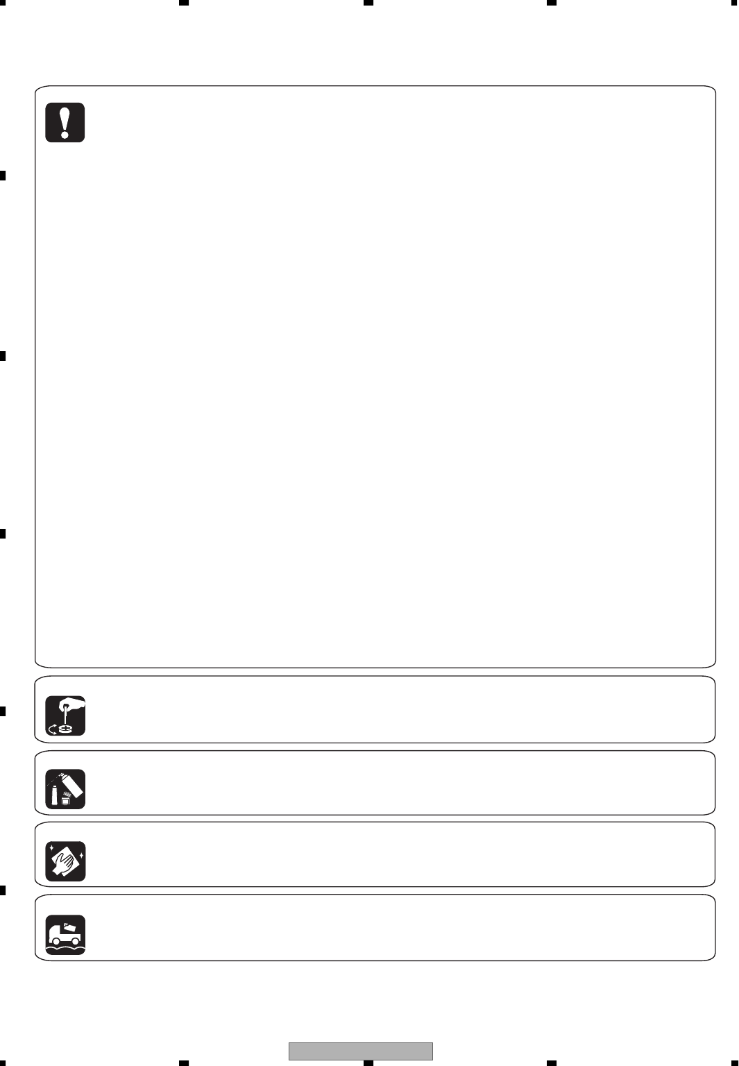
SAFETY INFORMATION
CAUTION
This service manual is intended for qualified service technicians; it is not meant for the casual do-it-yourselfer.
Qualified technicians have the necessary test equipment and tools, and have been trained to properly and safely repair
complex products such as those covered by this manual.
Improperly performed repairs can adversely affect the safety and reliability of the product and may void the warranty.
If you are not qualified to perform the repair of this product properly and safely, you should not risk trying to do so
and refer the repair to a qualified service technician.
WARNING
This product contains lead in solder and certain electrical parts contain chemicals which are known to the state of
California to cause cancer, birth defects or other reproductive harm.
Health & Safety Code Section 25249.6 - Proposition 65
- DVD Player Service Precautions
1. You should conform to the regulations governing the
product (safety, radio and noise, and other regulations),
and should keep the safety during servicing by following
the safety instructions described in this manual.
2. Never adjust the LD VR in the pickup unit to protect
the pickup from electrical damages.
3. For pickup unit(CGY2020) handling, please refer to
"Disassembly".
During replacement, handling precautions shall be
taken to prevent an electrostatic discharge(set the short
switch of the pickup unit to the SHORT side).
4. During disassembly, be sure to turn the power off since
an internal IC might be destroyed when a connector
is plugged or unplugged.
5. Please adjusting the skew after changing the pickup
unit.
is a trademark of DVD Format/Logo Licensing Corporation.
XDV-M8357ZT/UC
4
1234
1234
C
D
F
A
B
E
[Important Check Points for Good Servicing]
In this manual, procedures that must be performed during repairs are marked with the below symbol.
Please be sure to confirm and follow these procedures.
1. Product safety
Please conform to product regulations (such as safety and radiation regulations), and maintain a safe servicing environment by
following the safety instructions described in this manual.
1 Use specified parts for repair.
Use genuine parts. Be sure to use important parts for safety.
2 Do not perform modifications without proper instructions.
Please follow the specified safety methods when modification(addition/change of parts) is required due to interferences such as
radio/TV interference and foreign noise.
3 Make sure the soldering of repaired locations is properly performed.
When you solder while repairing, please be sure that there are no cold solder and other debris.
Soldering should be finished with the proper quantity. (Refer to the example)
4 Make sure the screws are tightly fastened.
Please be sure that all screws are fastened, and that there are no loose screws.
5 Make sure each connectors are correctly inserted.
Please be sure that all connectors are inserted, and that there are no imperfect insertion.
6 Make sure the wiring cables are set to their original state.
Please replace the wiring and cables to the original state after repairs.
In addition, be sure that there are no pinched wires, etc.
7 Make sure screws and soldering scraps do not remain inside the product.
Please check that neither solder debris nor screws remain inside the product.
8 There should be no semi-broken wires, scratches, melting, etc. on the coating of the power cord.
Damaged power cords may lead to fire accidents, so please be sure that there are no damages.
If you find a damaged power cord, please exchange it with a suitable one.
9 There should be no spark traces or similar marks on the power plug.
When spark traces or similar marks are found on the power supply plug, please check the connection and advise on secure
connections and suitable usage. Please exchange the power cord if necessary.
0 Safe environment should be secured during servicing.
When you perform repairs, please pay attention to static electricity, furniture, household articles, etc. in order to prevent injuries.
Please pay attention to your surroundings and repair safely.
2. Adjustments
To keep the original performance of the products, optimum adjustments and confirmation of characteristics within specification.
Adjustments should be performed in accordance with the procedures/instructions described in this manual.
4. Cleaning
For parts that require cleaning, such as optical pickups, tape deck heads, lenses and mirrors used in projection monitors, proper
cleaning should be performed to restore their performances.
3. Lubricants, Glues, and Replacement parts
Use grease and adhesives that are equal to the specified substance.
Make sure the proper amount is applied.
5. Shipping mode and Shipping screws
To protect products from damages or failures during transit, the shipping mode should be set or the shipping screws should be
installed before shipment. Please be sure to follow this method especially if it is specified in this manual.

XDV-M8357ZT/UC 5
5678
5678
C
D
F
A
B
E
CONTENTS
SAFETY INFORMATION......................................................................................................................................3
1. SPECIFICATIONS.............................................................................................................................................6
2. EXPLODED VIEWS AND PARTS LIST.............................................................................................................8
2.1 EXTERIOR .................................................................................................................................................8
2.2 DVD/CD MECHANISM UNIT....................................................................................................................10
3. BLOCK DIAGRAM AND SCHEMATIC DIAGRAM ..........................................................................................12
3.1 BLOCK DIAGRAM....................................................................................................................................12
3.2 DVD/CD MECHANISM UNIT, MAIN PCB(SERVO SECTION)(GUIDE PAGE).........................................16
3.3 MAIN PCB(DECODER SECTION)(GUIDE PAGE)...................................................................................26
3.4 EXTENSION UNIT....................................................................................................................................32
3.5 KEYBOARD PCB .....................................................................................................................................38
3.6 MF UNIT ...................................................................................................................................................39
4. PCB CONNECTION DIAGRAM ......................................................................................................................40
4.1 MAIN PCB ................................................................................................................................................40
4.2 EXTENSION UNIT....................................................................................................................................44
4.3 KEYBOARD PCB .....................................................................................................................................48
4.4 MF UNIT ...................................................................................................................................................49
4.5 DVD/CD MECHANISM UNIT....................................................................................................................50
5. ELECTRICAL PARTS LIST .............................................................................................................................54
6. ADJUSTMENT ................................................................................................................................................65
6.1 JIG CONNECTION DIAGRAM .................................................................................................................65
6.2 MAIN UNIT ADJUSTMENT ......................................................................................................................67
6.3 SKEW ADJUSTMENT..............................................................................................................................68
6.4 ELEVATION ADJUSTMENT.....................................................................................................................70
6.5 TEST MODE.............................................................................................................................................74
7. GENERAL INFORMATION .............................................................................................................................92
7.1 DIAGNOSIS..............................................................................................................................................92
7.1.1 DISASSEMBLY......................................................................................................................................92
7.1.2 CONNECTOR FUNCTION DESCRIPTION ..........................................................................................95
7.2 IC ..............................................................................................................................................................96
7.3 EXPLANATION.......................................................................................................................................115
7.3.1 OPERATIONAL FLOW CHART ...........................................................................................................115
7.3.2 SYSTEM BLOCK DIAGRAM...............................................................................................................116
8. OPERATIONS ...............................................................................................................................................117

XDV-M8357ZT/UC
6
1234
1234
C
D
F
A
B
E
1. SPECIFICATIONS
General
System .................................... DVD-Video, Video CD,
Compact disc audio system
Usable discs .... DVD-Video, Video CD, Compact disc
Signal format
1.Linear PCM
.................... Sampling frequency: 44.1/48/96 kHz
Number of quantization bits: 16/20/24; linear
2.Dolby digital
3.MPEG
Power source ...... 13.2 V DC (10.5 – 16.1 V allowable)
Grounding system .................................. Negative type
Rated current ................ 1.0 A or less(DVD regenerate)
Region Number
.............................................................................. 1
Backup current ...........................................5mA or less
Audio
Frequency response .................... ±1.5dB(20Hz,20kHz)
Signal-to-noise ratio
.......................................................... 80dB or more
Residual distortion .................................... 0.1% or less
Output Level ............................ 1000 mV (1 kHz, 0 dB)
Number of channels ...................................... 2 (stereo)
Max. output power supply ..........................2Vrms±2dB
Separation..................................................65dB or more
The difference between right output and left output
............................................................1.5dB or less
Player
Weight ................................................................ 2660 g
Video
Output level .......................... 1000 mVp-p±0.2 V/75 Ω

XDV-M8357ZT/UC 7
5678
5678
C
D
F
A
B
E
XDV-M8357ZT/UC
8
1234
1234
C
D
F
A
B
E
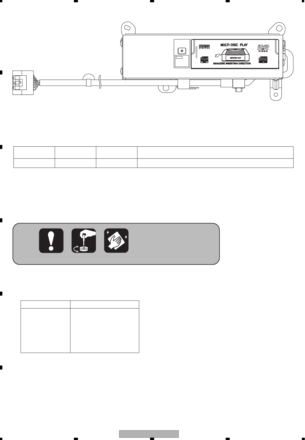
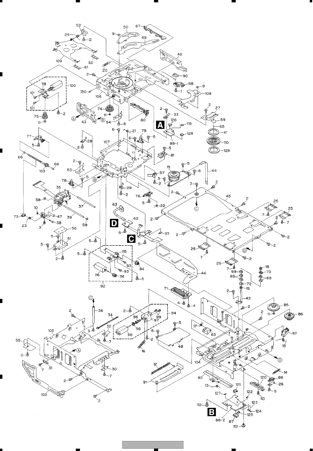
2. EXPLODED VIEWS AND PARTS LIST
2.1 EXTERIOR
N
OTES : • Parts marked by " * " are generally unavailable because they are not in our Master Spare Parts List.
• The > mark found on some component parts indicates the importance of the safety factor of the part.
Therefore, when replacing, be sure to use parts of identical designation.
• Screw adjacent to mark on the product are used for disassembly.
• For the applying amount of lobricants or glue, follow the instructions in this manual.
(In the case of no amount instructions,apply as you think it appropriate.)
"

XDV-M8357ZT/UC 9
5678
5678
C
D
F
A
B
E
EXTERIOR SECTION PARTS LIST
Mark No. Description Part No.
1 Screw BSZ30P055FTC
2 Screw(M2x4) CBA1676
3 Screw(M3x12) CBA1819
4 Screw(M2x3.5) CBA1966
5 Spring CBH2335
6 Connector CDE6302
7 Cord Assy CDE6983
8 Clamper CNV7278
9 Clamper CNV7279
10 Upper Case CNB2496
11 Holder CNC8612
12 Bracket CNC8831
13 Bracket CNC8832
14 Shield CNC9089
15 Insulator CNM6337
16 Insulator CNM6405
17 Filter CNM6600
18 Insulator CNM6735
19 Cushion CNM6743
* 20 Insulator CNM6906
21 Insulator CNM6985
22 Cushion CNM7037
* 23 Insulator CNM7090
24 Cushion CNM7347
25 Cushion CNM7872
26 PCB CNP5534
27 PCB CNP5535
28 PCB CNP5604
29 Panel CNS8228
30 Damper CNV5833
31 Holder CNV6181
32 Holder CNV8121
33 MF Unit CWM6518
34 Plug(CN2903) CKS1051
35 Connector(CN2901) CKS3563
36 Holder CNC2218
37 Shield CNC8898
38 Insulator CNM6836
39 Main Unit CWX3187
40 Terminal(CN1603) CKF1064
41 Terminal(CN1604) CKF1064
42 Terminal(CN1605) CKF1064
43 Terminal(CN1607) CKF1064
44 Connector(CN1601) CKS1953
45 Connector(CN101) CKS1964
46 Connector(CN312) CKS2191
47 Connector(CN2000) CKS2193
48 Connector(CN302) CKS3480
49 Connector(CN1600) CKS3749
50 Connector(CN310) CKS3767
51 Connector(CN301) CKS4358
52 Connector(CN1000) CKS4374
53 Extension Unit CWX3198
54 Screw BMZ26P050FTC
55 Cord CDE6446
56 Terminal(CN3810) CKF1064
57 Terminal(CN3811) CKF1064
58 Terminal(CN3812) CKF1064
59 Terminal(CN3813) CKF1064
60 Connector(CN3951) CKS1953
61 Connector(CN3891) CKS2191
62 Connector(CN3301) CKS2619
63 Connector(CN3302) CKS2619
64 Plug(CN3802) CKS3535
65 Connector(CN3961) CKS3749
66 Connector(CN3801) CKS4320
67 Connector(CN3803) CKS4356
68 Holder CNC8400
69 Shield CNC8899
70 Shield CNC8900
71 Insulator CNM6834
72 Insulator CNM6835
73 Arm Unit CXA8606
74 Rear Frame Unit CXB6364
75 Lower Case Unit CXB6365
76 Button(EJECT) CAC6152
77 Door CAT2385
78 Spring CBH2336
79 Spring CBH2337
80 Spring CBH2363
81 Connector CDE6022
82 Holder CNC8402
83 Holder CNC8409
84 Cushion CNM6407
85 Cushion CNM6842
86 Cushion CNM6843
* 87 Insulator CNM6907
88 Lever CNV5831
89 Lever CNV6104
90 Damper Unit CXB4206
91 Screw IMS20P035FTB
92 Screw IMS26P040FTC
93 DVD/CD Mechanism Unit(MM-1)CXK7020
94 Fan Motor CXM1195
95 Grille CNS6472
96 Screw IMS30P060FTB
97 Screw ISS30P060FTC
98 Screw PMB26P050FTC
99 Screw TMZ50P060FTC
* 100 Tape CNM7273
101 IC(IC3821) BA00AST
102 Transistor(Q3811) 2SB942A
Mark No. Description Part No.
XDV-M8357ZT/UC
10
1234
1234
C
D
F
A
B
E
2.2 DVD/CD MECHANISM UNIT

XDV-M8357ZT/UC 11
5678
5678
C
D
F
A
B
E
DVD/CD MECHANISM UNIT SECTION PARTS LIST
Mark No. Description Part No.
1 Screw(M2x4) CBA1026
2 Screw(M2x2.5) CBA1651
3 Screw(M2x2.5) CBA1041
4 Screw(M2x3.5) CBA1674
5 Screw(M2x3) CBA1154
6 Screw(M2x2) CBA1243
7 Screw(M2x1.4) CBA1687
8 Screw(M2x2.2) CBA1965
9 Washer CBF1002
10 Washer CBF1037
11 Washer CBF1038
12 Spring CBH2368
13 Spring CBH1827
14 Spring CBH1828
15 Spring CBH1829
16 Spring CBH1830
17 Spring CBH1919
18 Spring CBH1930
19 Spring CBH2070
20 Spring CBH2091
21 Spring CBH2159
22 Spring CBH2227
23 Spring CBH2238
24 Spring CBH2279
25 Spring CBL1307
26 Spring CBL1362
27 Spring CBL1388
28 Spring CBL1416
29 Spring CBL1417
30 Spring CBL1418
31 Spring CBL1419
32 Spring CBL1420
33 Spring CBL1422
34 Connector CDE6156
35 PU Unit CGY2020
36 Shaft CLA2803
37 Shaft CLA3428
* 38 Shaft CLA3431
39 Shaft CLA3562
40 Lever CNC6194
41 Plate CNC6847
42 Holder CNC7448
43 Lever CNC7975
44 Lever CNC8065
45 Frame CNC8068
46 Lever CNC8097
47 Bracket CNC8106
48 Cover CNC8129
49 Arm CNC8335
50 Arm CNC8336
* 51 Cover CNC8347
52 Holder CNC8476
53 Cover CNC8921
54 Cover CNC8922
55 Cover CNC8923
56 Plate CNC9010
57 Cover CNC9083
58 Cushion CNM6301
59 Spacer CNM6334
60 Sheet CNM6385
61 Sheet CNM6581
62 PCB CNP5371
63 PCB CNP5380
64 PCB CNP5381
65 Ball CNR1189
66 Bearing CNR1415
67 Rail CNV4420
68 Lever CNV4422
69 Guide CNV4597
70 Guide CNV4722
71 Rack CNV4828
72 Guide CNV5193
* 73 Rack CNV5451
74 Gear CNV5658
75 Gear CNV5659
76 Holder CNV5661
77 Holder CNV5662
78 Guide CNV5663
79 Guide CNV5664
80 Rail CNV5668
81 Guide CNV5671
82 Arm CNV5868
83 Arm CNV6158
84 Gear CNV6226
85 Gear CNV6242
86 Gear CNV6285
87 Connector(CN301) CKS3476
88 PCB CNX3040
89 Damper Unit CXA7159
90 Plate Unit CXB2262
91 Lever Unit CXB2266
92 Motor Unit(Carriage)(M1) CXC1552
93 Screw JFZ20P025FNI
94 Motor Unit(ELV)(M4) CXC1540
* 95 Gear CNV6239
96 Gear CNV6240
* 97 Bracket Unit CXB5838
* 98 Motor CXM1220
99 Screw JFZ20P025FNI
100 Motor Unit(Tray)(M2) CXC1541
101 Screw JFZ20P025FNI
102 Lever Unit CXB3933
103 Screw Unit(-D) CXB3934
104 Magazine Holder Unit CXC5000
105 Frame Unit CXB3970
106 Chassis Unit CXB3972
107 Chassis Unit CXB3975
108 Lever Unit CXB3976
109 Arm Unit CXB4318
110 Clamper CNV5667
111 Motor(Spindle)(M3) CXM1282
112 Screw IMS26P040FMC
113 Screw JFZ17P020FNI
* 114 Gear CNV6225
* 115 Bracket Unit CXB4003
* 116 Motor CXM1221
117 Photo Transistor(Q851) PT4800
* 118 Bracket Unit CXB3971
119 LED(D851) CN504-2
120 Resistor(VR301) CCW1021
121 Switch(S301) CSN1044
122 Capacitor(C301) CKSRYB104K16
123 Resistor(R301) RS1/16S562J
124 Resistor(R302) RS1/16S622J
125 Semi-fixed(VR302) CCP1338
126 Switch(S852) CSN1052
127 Capacitor(C302) CKSRYB103K50
128 Switch(S851) CSN1051
129 Sheet CNM9776
130 Screw ZMK30H025FZB
Mark No. Description Part No.
XDV-M8357ZT/UC
12
1234
1234
C
D
F
A
B
E
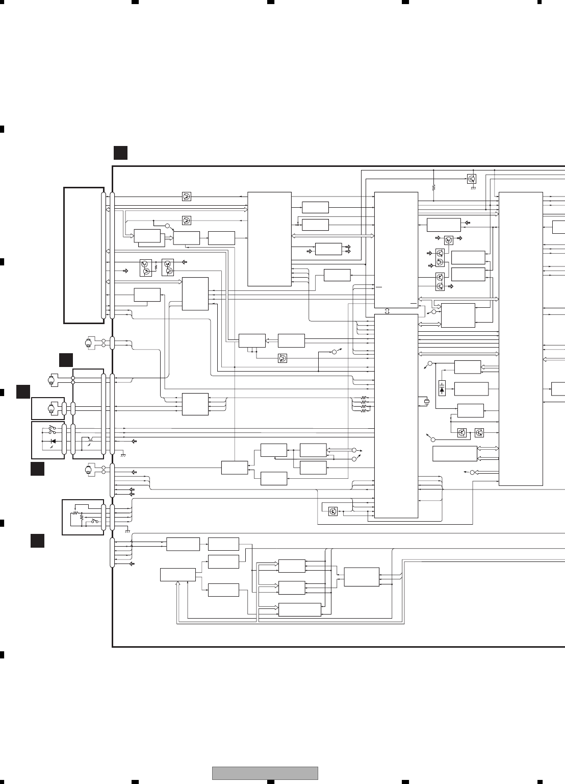
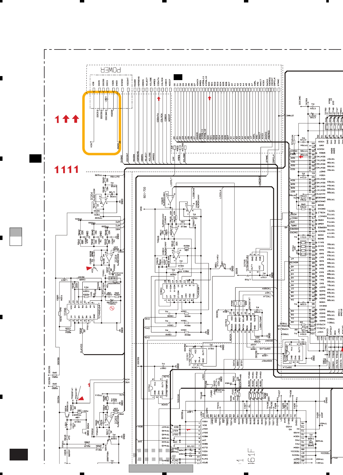
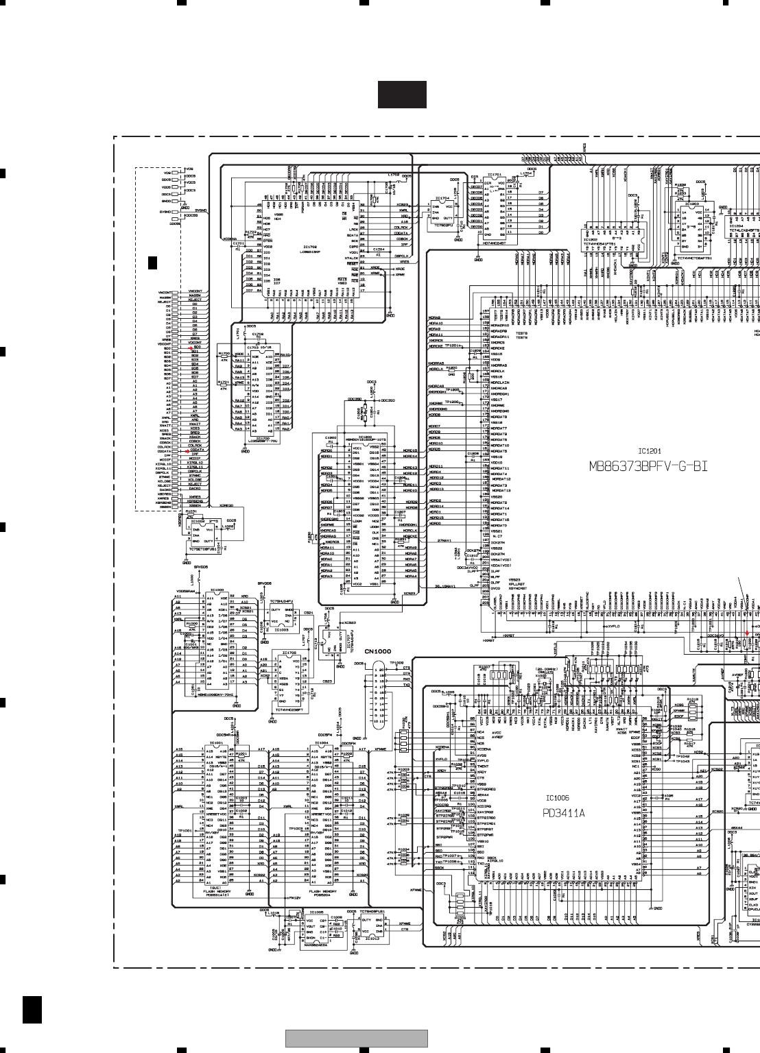
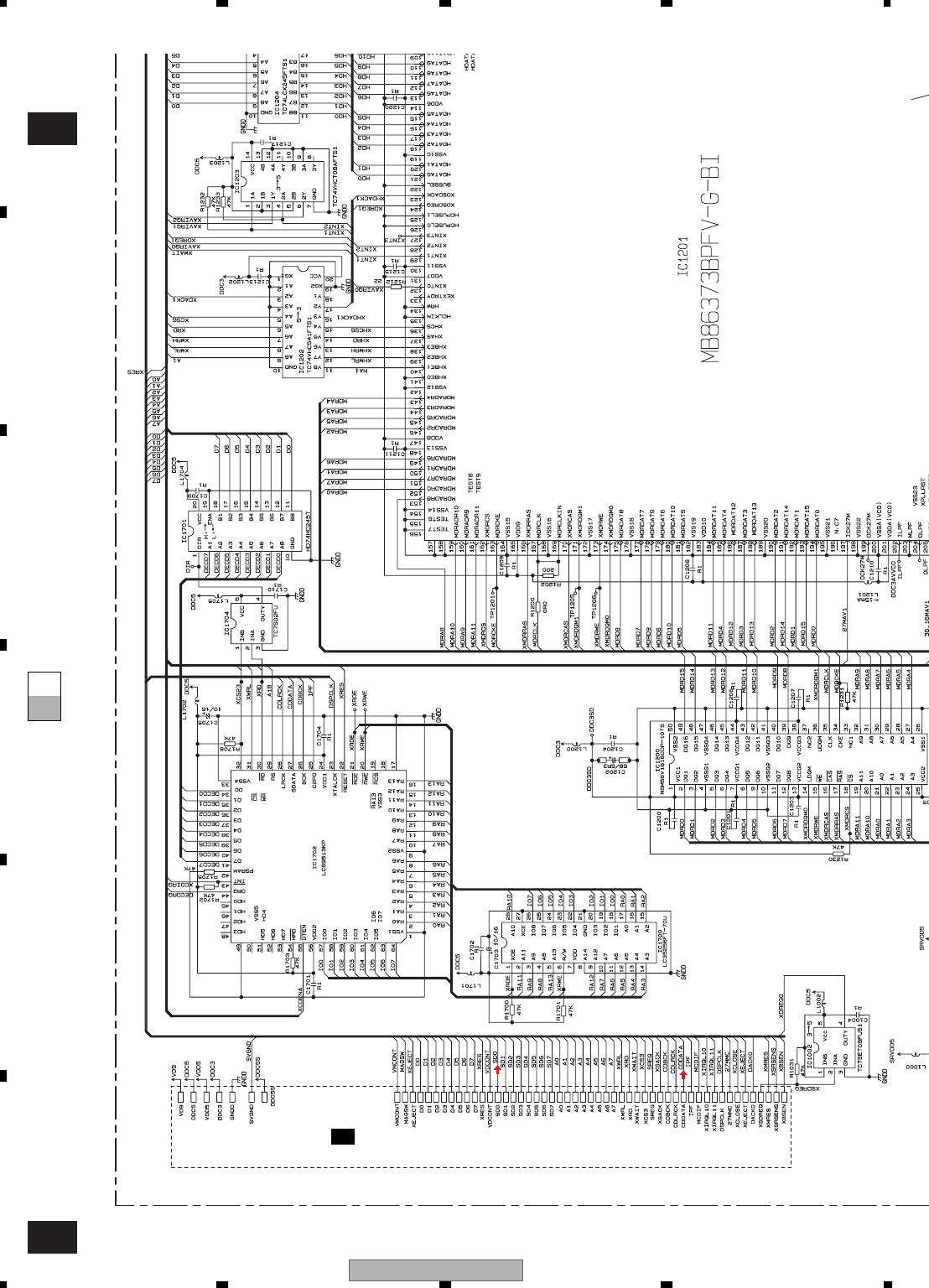
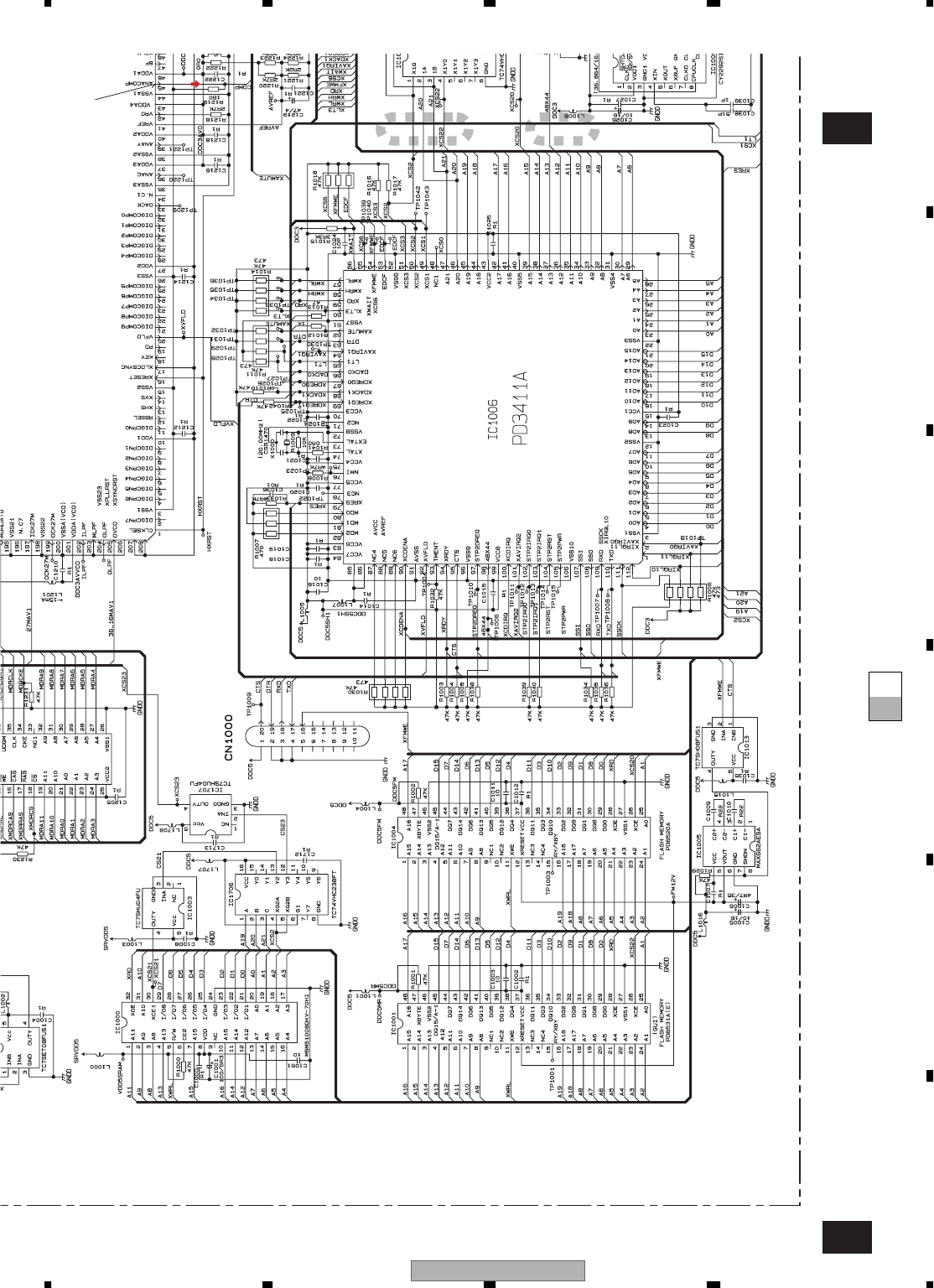
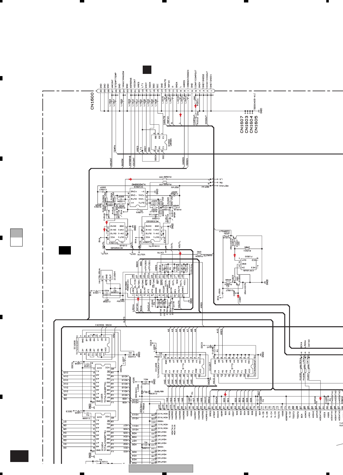
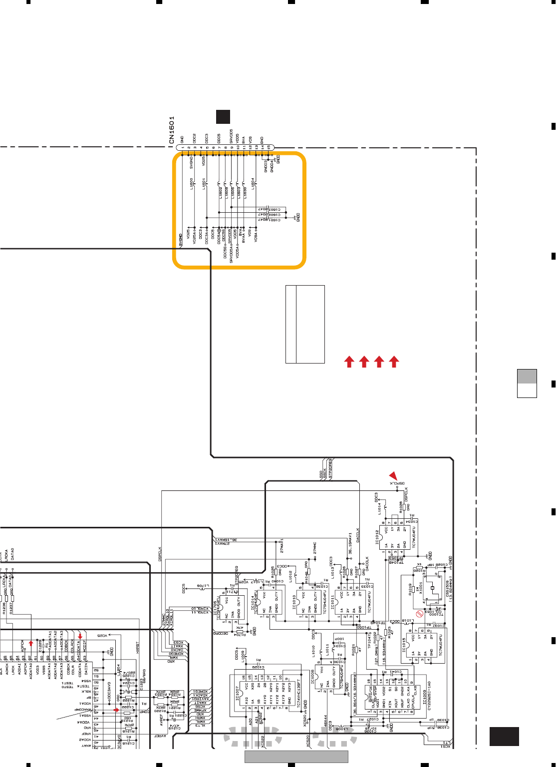
3. BLOCK DIAGRAM AND SCHEMATIC DIAGRAM
3.1 BLOCK DIAGRAM
CN101 Q104
Q165
IC107
PA0065AM 19 IC108(1/2)
NJM3404AM
IC106
2461
IC109
TC7WU04FU
Q168Q101
Q102
IC101
IR3C07N
1
1
2
5
19
CRG+
CRG-
24
4
9
10
1
7
12
3
5
9
6
6
10911
5
7
6
2
1
14
3
3,5
13
2
6
3
IC305
LB1836M
IC304
BA6797FM
IC601
TC4053BFT IC604, 605
NJM3414AV
IC105
NJM3404AM
21
IC108(2/2)
NJM3404AM
67
IC102
NJM2904M
31
57
DDC5S
P1TN
41 RFA
44 MDI1
45 LDO1 RFO 28
FEO 21
TEO 20
VRD 7
VRCK 16
PSC 35
SCB 13
SCL 14
SCD 15
FEB
ELV+
ELV-
34
VR25
VR21
SBAD,FLGB,RFCT,RFPR
IC402
NJM2904M
12
CN312
1
CN302
7
6
4
5
1
2
9
3
8
16 78LD
78MPD
RFA
RFA
B1I-B4I
B1I-B4I
CH1,CH2,CH3
F+,F-,T+,T-
LD
MPD
TEMP
1/2SW
I4
I3
I1
I2
ELV+
2ELV-
CRG+
CRG-
TRY+
TRY-
DSP
TRP
DISC
VLED
GND
GND
EC
ECR
FG
HOME
ST/SP
ST/SP
FPWM,VPWM
PPWM,RPWM
FPWM,VPWM
PPWM,RPWM
DCAS,DWE
DOE,DRAS
DD0-7
DA0-10
EREF
EVREF
EPVO
MAGSW
VSHF
15
22
12
11
5
6
2
4
VREF
7
20
19
9
13
M
M3
ELV
MOTOR
CN301
CN310
6
7
4
1
5
2
3
M
M4
SPDL
MOTOR
VD9
VR25
IC301
TC4W53F
IC352
MC33202D
IC303
NJM2904M
IC353
MC33202D
IC351
TC4S66F
CTS
DTR
RXD
TXD
CN1000
20
19
18
1
17
XFMWE
16
Q501
Q601
DDC5S
Q401
Q402
Q403
Q404
VRA
2VREF
DDC5S
DOUT,LRCK,AOUT
VR21
DATA,SFSY,SBSY
IC702
MSM5117800F-60JS
IC704
TC7SET08FUS1
IC706
TC7SET08FUS1
IC707
TC7SET04FUS1
IC703
LC89170MP
27MMC
Q103
B
IC204
NJM2100M
IC206
TC74VHCU04FT
IC203
NJM2100M
Q203 Q204
VREF
DDC5S
IC103
TA1254AF
RF AMP
F JUMP
PU UNIT IC401
TC9461F
IC501
PEG114A
IC701
PD4995A
ASIC
33 RFI 4
4
DXTKI
120 EXCK
114 CDBCK
107 CKCD
116 C2F1
38
4
FEI
41 TEI
43 FOO
2RFSCB
SCD
FEB
SCL
SCB
SCD
FEB
SCL
SCB
VCOCLK
ATC
VRC
AIN
100 RFSLC
1RFSCD
22 FEB
3LCDBIAS
4LCDTLT
26 LCDCLK
50 7
5
6
2
4
2
4
1
1,5
5
12,13
7
181
186
172
170
FGPL
162
CD/DVD
84 DCONT
97 TEMP
21 OEIC
5LDCONT
80 I4
79 I2
78 I3
I4
I2
I3
I1
87
Xout
Xin
95 TRP
DSP
92 DISK
10 DSCSIZ
7FG
81 HOME
83 SPCONT
EREF
FG
MAGSW
EPVO
94 ELVREF
86 ADENA
93 ELVPVO
18
98
EVREF
A20
A21
XMAG
Vref
44 TRO
92 CCE
91 BUCK
BUCK
/CCE
BUCK
DCONT /CCE
48 FMO
50 DMO
BCK BCK
2
139 ASTB
ASTB ASTBM
40
140 XMCS
XCS XMCS
49
141 XIRQ2
XIRQ XIRQ2
20
142 XMWR
XWR XMWR
46
143 XMRD
XRD XMRD
44
XRESET 165
SA6 85
2
XCSLI 72
XIRQ11 103
XIRQ10 102
XSACK 55
XSWAIT 73
SREQ 56
DIFOUT 108
XSWR 75
XSRD 74
BCK 109
LRCK 110
ADATAO
IP
F
DSPCL
K
CDBC
K
CDLRC
K
CDDAT
A
XCS
3
XIRQL11
XIRQL1
0
XSAC
K
SRE
Q
MCDI
F
XWRL
MAD0-MAD7 XRD
ASC,AFC
APC
111
XI 73
IPF 6
CLCK 81
2
TESIO1 67
XSYSRST
FLGA,FLGB,FLGC,FLGD
85
TXDT,TXCLK
PSC
BUS0-3
6
4
6
TESIO0 19
RST 95
13
15
X501
10MHz
I
C
TC7S
H
SDACK 77
XSDREQ76 I
C
TC7S
E
VMCONT 11
VDCONT 82
BSENS 74
VMCONT
VDCONT
XBSEN
SRSENS 75 XSRSENS
XMRES XMRES
MAGSW
12
48
2
1IC1013
TC7SH08FUS1 6
IC1005
MAX662AESA
12
4
10
26
28
11
IC1001
PD6531A
12
26
28
5
32
11
IC1004
PD6520A
30 IC1000
M5M51008DKV-70HI
2
2
4
12
4,5
IC1706
TC74VHC238FT
IC1707
TC7SHU04FU
4
IC1003
TC7SHU04FU
B
IC1007
TC74VHC139FT
MOTOR DRIVER
ADDRESS DECODER ADDRESS DECODER
FLASH RAM
FLASH RAM
SDRAM
MOTOR DRIVER
MECHANISM
CONTROLLER
DSP
SPDL
SELECTOR
CD SPDL
DVD SPDL DRAM
5
4
1
2
3
A
A
C
RFA
D0-D7,A0-A
7
2
1,15
3,13
CS23
CS21
A19-A21
D0-15
A1-19
D0-15
A1-19
D0-7
A0-16
XCS21 XCS2
XCS22
XCS23
XWRL
XRD
XCS2
XCS20
5
EMAIN PCB
.
.
.
-
23
26
-
47 TEBC
VM
VCC VD9
DDC5S
VCC DDC5
56 XCCE
57 BUCK
DUTY50
189
3
DDC5S
C
D
D
TXDQSY
7
6
4
5
1
2
9
3
8
S852
DSP
S851
TRP
M
M
M1
CRG
MOTOR
M2
TRAY
MOTOR
11
22
Q851
44
11
22
33
5
4
1
2
3
S301
MAG
VR301
VR302
BPCB UNIT(B)
A
PCB UNIT(A)
DPCB(B)
CPCB(A)
XDV-M8357ZT/UC 13
5678
5678
C
D
F
A
B
E
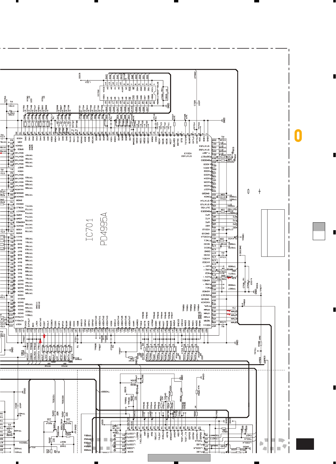
IC701
PD4995A
ASIC
4
K
XRESET 165
SA6 85 1
24
2
XCSLI 72
XIRQ11 103
XIRQ10 102
XSACK 55
XSWAIT 73
SREQ 56
DIFOUT 108
XSWR 75
XSRD 74
BCK 109
LRCK 110
ADATAO
IPF
DSPCLK
CDBCK
CDLRCK
CDDATA
XCS3
A6
XCS3
XIRQL11
XIRQL10
XSACK
SREQ
MCDIF
CDBCK
CDLRCK
CDDATA
XWRL
XRD
111
IC705
TC7SH32FUS1
SDACK 77
XSDREQ76 IC1002
TC7SET08FUS1
XRES
XRES
56
55
54
31
IC1700
LC35256FT-70U
IC1702
LC89513KP
IC1200
MSM56V16160DP-10TS
IC1701
HD74HC245T
IC1704
TC7S02FU
CDBCK
CDLRCK
CDDATA
26
1
28
27
BCK
LRCK
SDATA
IPF 25 C2PO
DSPCLK 23 XTALCK cs 32
1
4
rd 30
XCS23
D0-7
HD8-15
HD0-7
HA10
HA2-9
D8-15
D0-7
A10
A2-9
DECD0-DECD7
IO0-7,RA0-13,
XROE,XRWE
XRD
wr 31 XWRL
RS
29
A18
reset 22
dten 55 XCDENA
DRQ 44
56
DECDRQ
int 43 XCDIRQ
IC1504
HA178L05UA
REF4V
8VA DAC5V
3
5
3
5
5
6
1
18
2128 22
7
16
1
7
F1500
CTF1515
IC1503
NJM2068MD
IC1501
MC33202D
IC1500
PE8001A1
Q1500 Q1503
5
2
12
COMPOUT
DIGOUT
L
XAMUTE
VDCONT
(XMBSEN)XBSEN
XRES
XLT3
LT1
SSCK
SSO,SSCK
SSI
3
4
5
6
9
13
7
XMRES
LT1
SSCK
SSI
8
19
17
15
16
3
2
1
5
4
6
7
8
9
10
11
12
13
VD25 DDC2
XRDY
DDC3 DDC3
DDC5 DDC5
SRVDD5
VDD5
8VA
VD9
DDC5S
SRVDD5
VDD5
8VA
VD9
IC1208
TC74VHC00FTS1
IC1202
TC74VHC541FTS1
IC1006
PD3411A
CLOCK GENERATOR
IC1201
MB86373BPFV-G-BI
MPEG DECODER
CDBCK
SREQ 91 SREQ
XSACK 89 XSACK
16 XRESET
1CLKSEL
133 XEXTRDY
205 OVCO
197 ICK27M
XHRD,XHWRL,XHWRH
XHCS6,XHDACK1
XRD,XWRL,
XWRH,XCS6,
XDACK1
XINT1,XINT2XAVIRQ1,XAVIRQ2
XVFLD,XAVIRQ0,XDREQ1
MCDIF 53 DAIIN
CDLR
CDDATA
XIRQL11
XIRQL10
1
112 XIRQL11
XIRQL10
CTS 95 CTS
DTR 63 DTR
67 XDREQ0
66 DACK0
XCS3
OVCO
ICK27M
27MMC
SSI,SSO,SSCK,XRDY,LT1
SSI,SSO,SSCK,XRDY,LT1
DSPCLK
51 XCS3
97 STP2DREQ
42
IC1705
TC7SHU04FU
XWRL
XDACK1
XCS6
HA2-10,HD0-15
BCKA
LRCKA
DATA0
XRD
XRD
XWAIT
XCDENA
90
XCDENA
62
XAMUTE
98
48X44
XTAL
EXTAL
74
73
X1000
20.000MHz
RXD 109 RXD
TXD 110 TXD
CN1600
CN1601
ANACOMP 45
AODAI 64
3
16,7
5
IC1011
TC7WU04FU
Q1600
1
35
IC1012
TC7WU04FU
24
IC1014
TC7SHU04FU
24
IC1010
TC7SHU04FU
410
8
9
IC1009
CY2292SI-1A0
7
15
IC1015
TC7WU04FU
24
IC1008
TC7SHU04FU
X1001
13.824MHz
IC1203
TC74VHCT08AFTS1
XRD
XWRL
XCS23
XCDIRQ
100
XCDIRQ
SDRAM
BUS BUFFER
5V-3V LEVEL SHIFT
5V-3V LEVEL SHIFT
3V-5V LEVEL SHIFT
DAC LPF
21
VMCONT 27
XSRSENS 22
(XMAG)MAGSW 24
XRES 20
12
12 13 2,9
1
86
19
19
1
1
8
XRES
DACCLK
SD0-SD7
D0-D7,A0-A7
D0-D15,A0-A21
D0-D15,A0-A21
XRES XRES
XLT3 XLT3
XCS2 XCS2
0
XFMWE 54
60 79 50
XFMWE
A1 HA1
FCN3961
FCN3951
IC1206
TC74VHC541FTS1
IC1207
TC74VHC541FTS1
IC1204
TC74LCX245FTS1
IC1205
TC74LCX245FTS1
B2
E2
E1
B1
C2
C1
SSO SSO
11 140 XHBE1
2
XDV-M8357ZT/UC
14
1234
1234
C
D
F
A
B
E
CN3961
26
CN3951
CN3302CN3301
13 DDC2
DDC2
12
11 DDC3
DDC3
10
COMP COMPO+
COMPI+
L+
22 L
18
CN3801
1
CN2903 CN2000
XEJ
XCLOSE
XEJECT
XCLOSE
S2001
EJECT
SW
S2000
CLOSE
SW
ILLB ILLB
9
MUTE 10
TX+ 12
ACC 13
TX- 14
3
XAMUTE
10 VDCONT
4VMCONT
4
5
8
42
1
3
1
IC3301
NJM2235V
IC3311
NJM2267V
2
1IC3131
TC74HC4066AF
1
4
7
7
2IC3101
NJM2068MD
2
1
13
4
IC3821
BA00AST VD9
Q3155 Q3153
24
12
16
XMBSEN
BVD
AV8
9DDC5
DDC5
SRVDD5
VDD5
8VA
VD9
VD9
8
7
6
5
4
3
1
24 8
28
9
11
3IC3871
PQ20VZ11
2.6V REGULATOR
3.3V REGULATOR
5V REGULATOR
DC-DC
CONVERTER
Q3851
Q3852
IC3851
BA9706K
Q3853
VDD5
AV8
VD9
40
AV8CONT
10
11-13,
15,47
VADCONT
27
ANSW
56
IEDO
57
IEDI
55
IEPW
63
XMBSEN
64
XBSEN
62
XASEN
60
XRST
XRST
70
X1
AVREF0
75
XADEN
6
AVREF1
7
FANPW1
52
FANPW2
53
69
X2
65
66
XCLOSE
9
XILL
XEJ
XBMUTE
SWREG
Q3821
Q3301
Q3201
5
8
6
2
9
2
1
610
5
12
11
4
7
1
Q3813Q3814
IC3631
HA12187FP
IC3811
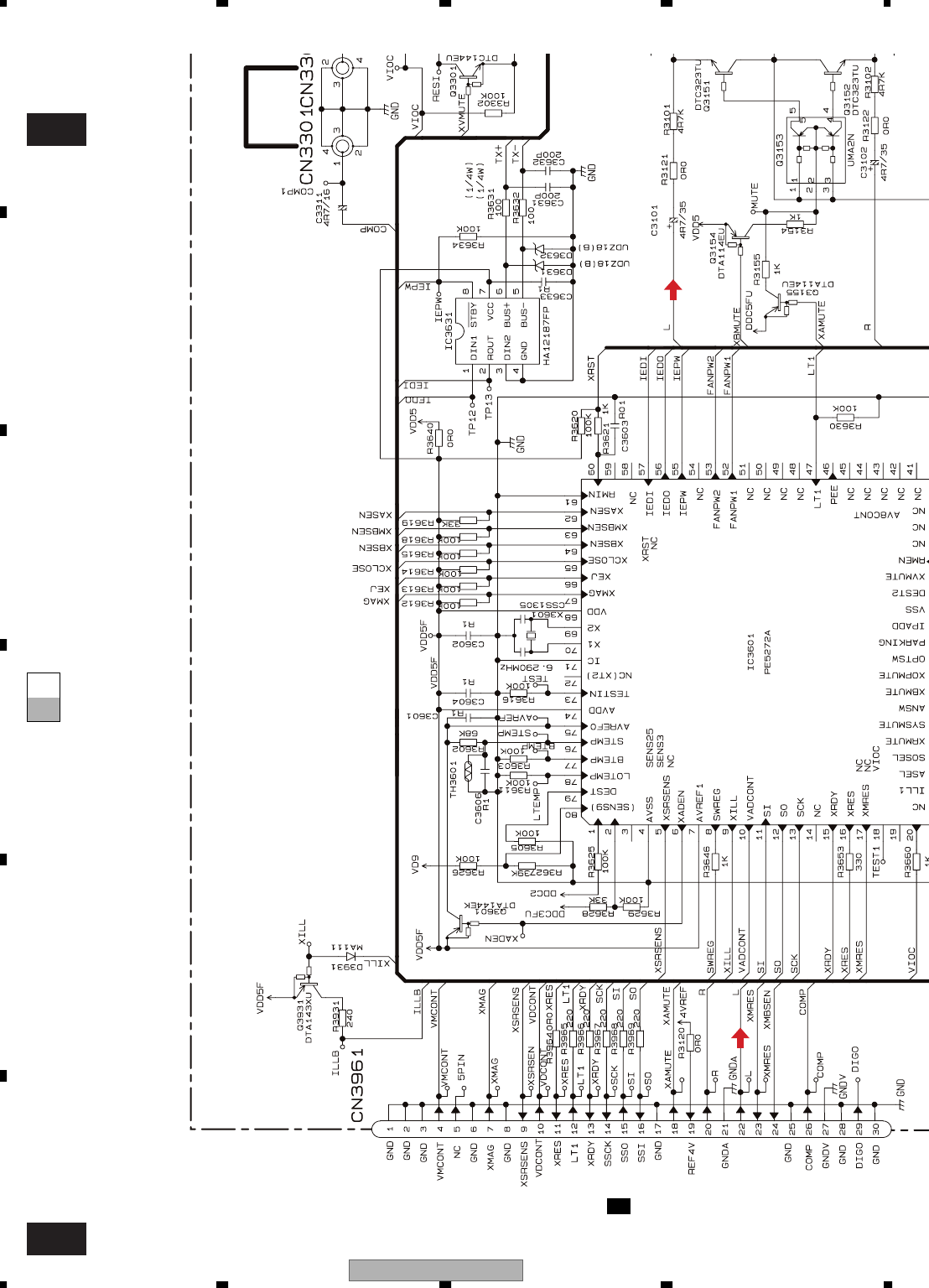
PAJ002A
SYSTEM CONTROLLER
IC3601
PE5272A
X3601
6.290MHZ
1
2
3
1
2
3
CN2901
XEJ
XCLOSE
ILLB
6
BVDD
9
BVD
10
7
8
Q3601
EXTERNAL CONNECTOR
IP-BUS DRIVER
VDD5V,ASENSE,BSENSE,RESET
BSR
4
+B
5
+B
3
+B
XEJ
XCLOSE
ILLB
BVDD
BVD
BSR
+B
+B
+B
+B
2
EF3801
EF3802
BVDD
BVD
BSR
CN3802
CN3803
5
2
1
4
3
7
6
8
9
2
Q3931
Q3812
VDD5
3
Q3151
Q3154
35
XVMUTE
26
SYSMUTE
20
VIOC
Q3131
2
1
4
IC3831
BA08SFP AV8
BVD
4VREF
Q3880
BVDD
Q3811
COAXIAL CABLE
AUDIO CIRCUIT
9V REGULATOR
VIDEO CIRCUIT
SYS MUTE
FAN+1
CN3891
12
3
4
IC3891
PQ20VZ11
FAN POWER SUPPLY
8V REGULATOR
4V REGULATOR
Q3891
1BVD
1BSR
1BSR
ILLMI
FAN
MOTOR
EF3831
EXTERNAL CONNECTOR
SSI,SSO,SCK,XRDY,LT1
-
L- 11
3
COMPOUT
COMPIN
5
OUT3
OUT2
OUT1
IN3
RSTIN
FBIN
IN1
CONT
IN2
OCD
RSTOUT
LP
LM
5
REF4V
19 4VREF
DIGO
29 DIGO
23 XMRES XMRES
17
11 XRES XRES
16
7XMAG XMAG
67
9XSRSENS XSRSENS
5
FEXTENSION UNIT
G
KEYBOARD PCB
HMF UNIT
ECN1600
ECN1601

XDV-M8357ZT/UC 15
5678
5678
C
D
F
A
B
E
XDV-M8357ZT/UC
16
1234
1234
C
D
F
A
B
E
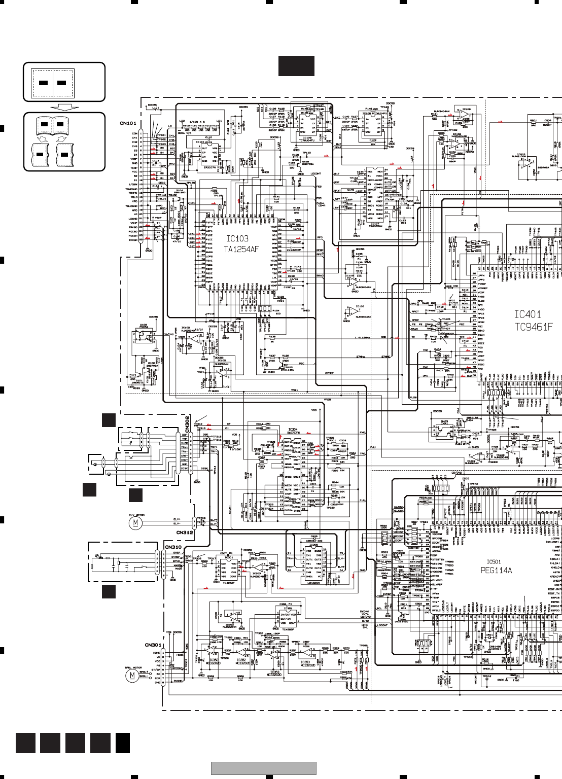
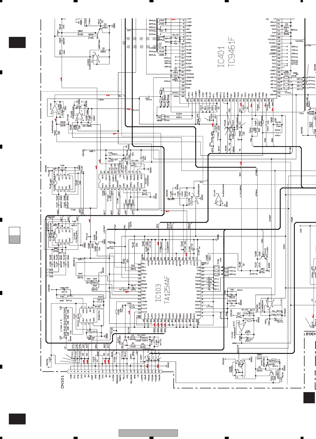
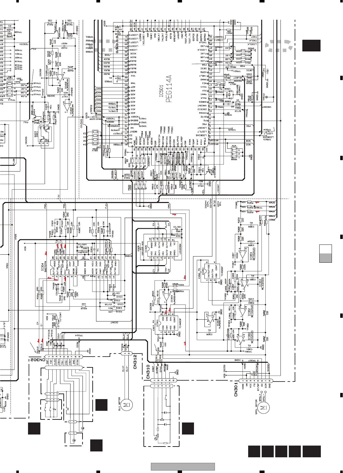
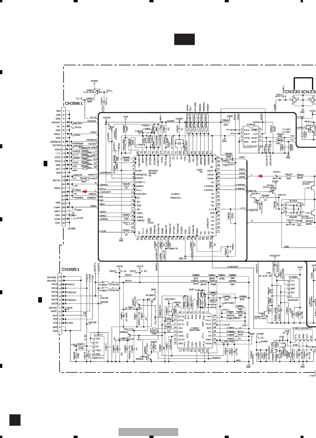
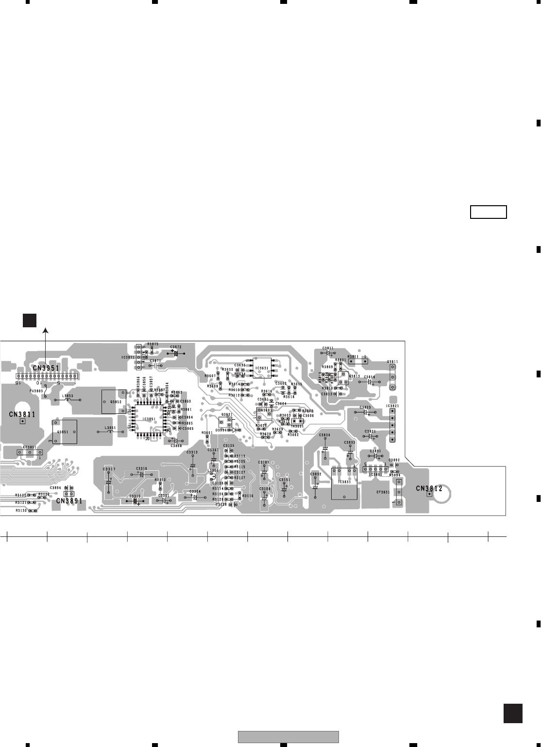
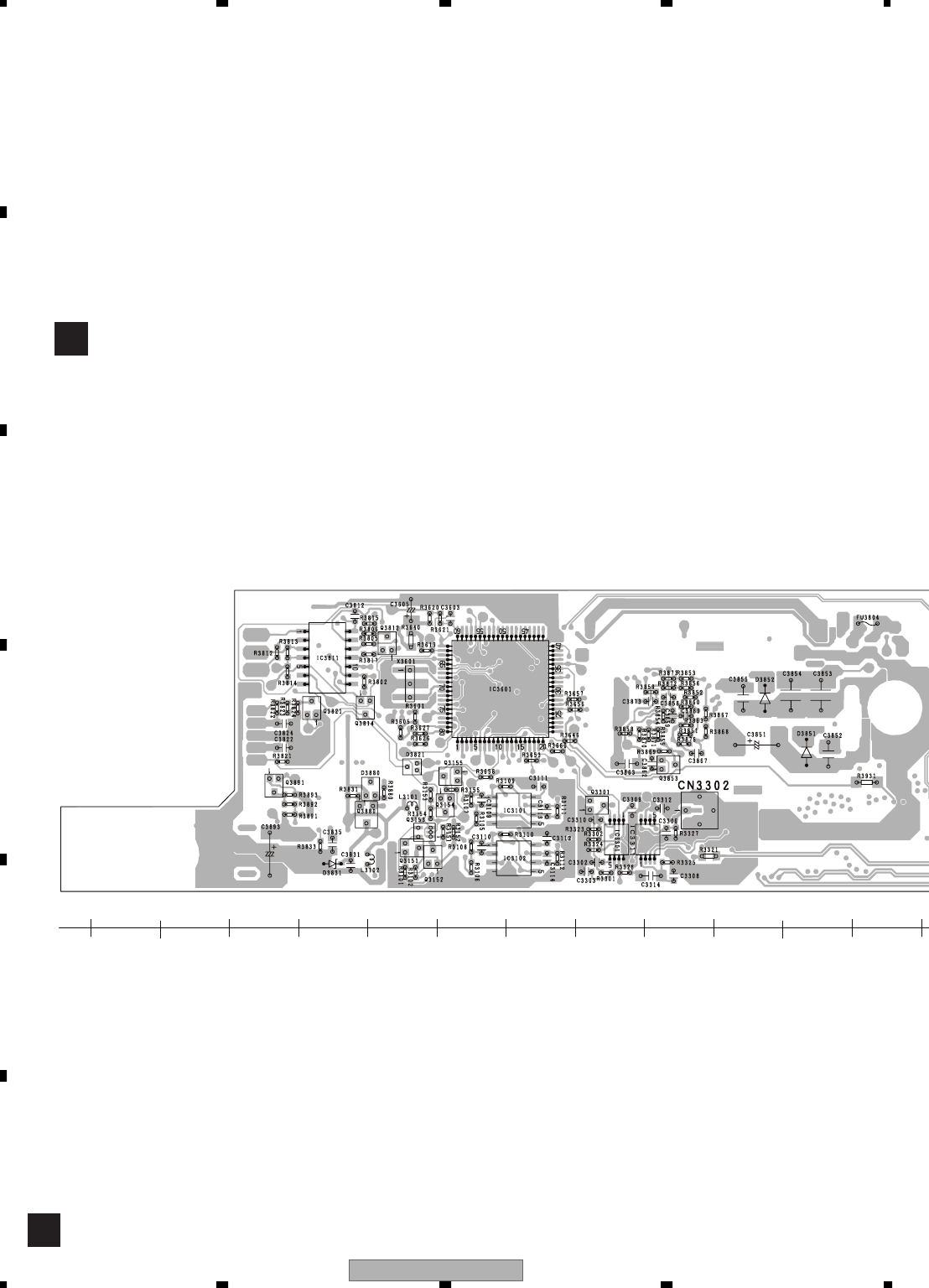
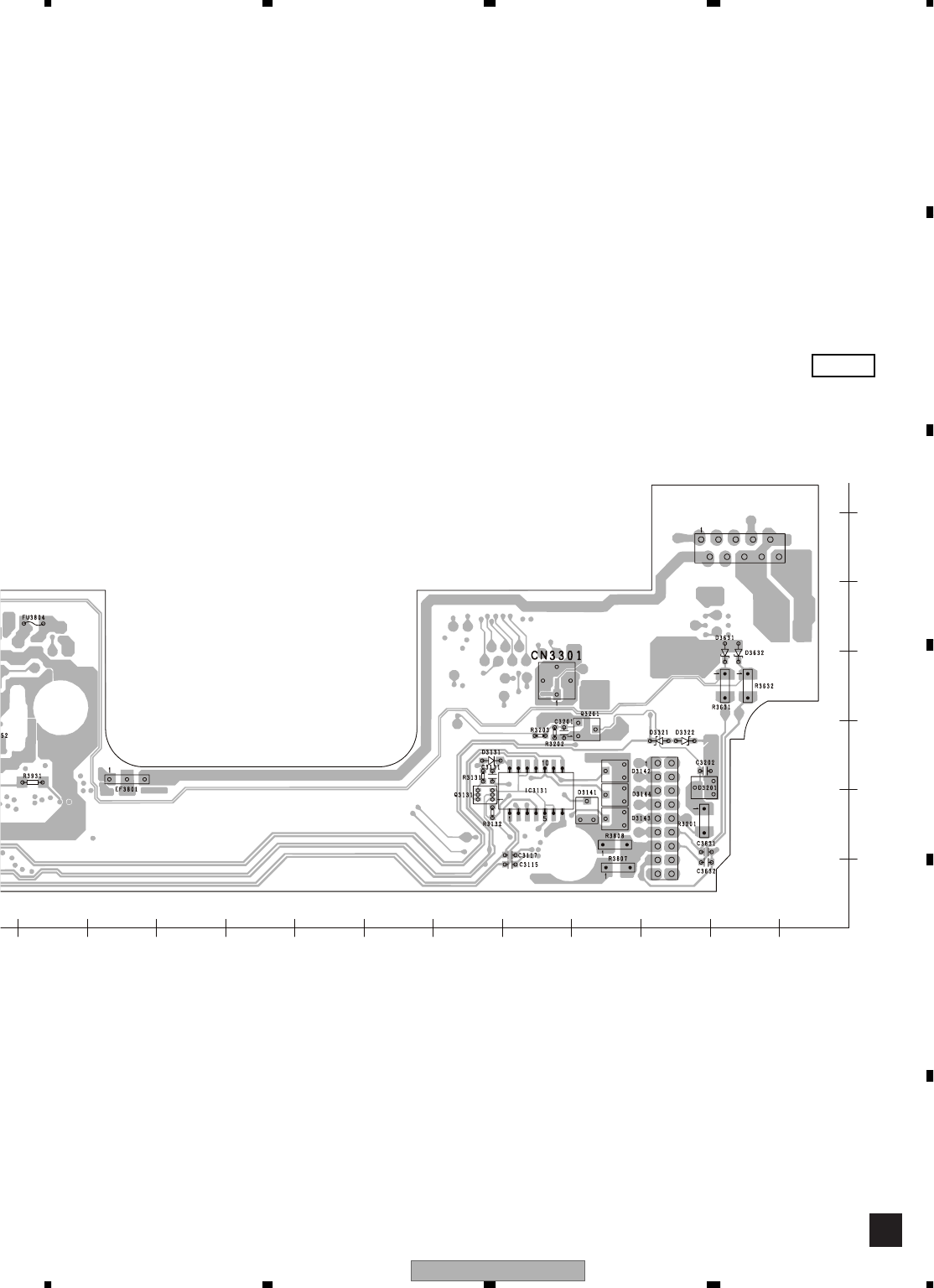
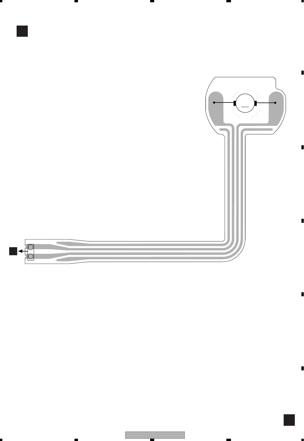
3.2 DVD/CD MECHANISM UNIT, MAIN PCB(SERVO SECTION)(GUIDE PAGE)
A-a A-b
A-a A-b
A-b
A-a
Large size
SCH diagram
Guide page
Detailed page
Note: When ordering service parts, be sure to refer to " EXPLODED VIEWS AND PARTS LIST" or
"ELECTRICAL PARTS LIST". E-a
A B C D
1/2
E
1/2
SERVO DSP
EREF
EVREF
EPVO
MAGSW
GND0
S301
CSN1044
MAG
C302
R01
VR301
CCW1021
C301
R1
R302
6R2K
VR302
CCP1338
1K(B) 10K
R301
5R6K
CN301
DSP
TRP
VLED
TRY+
TRY-
CRG-
CRG+
GND
DISC
D851
CN504-2
S851
CSN1051
DSP
S852
CSN1052
TRP
CARRIAGE
M2
CXC1541
TRAY
Q851
PT4800
PCB UNIT(A)
A
PCB UNIT(B)
B
PCB(B)
DPCB(A)
C
R
MECHANISM
CONTROLLER
SPDL
M3
CXM1282
M1
CXC1552
M4 CXC1540
PU UNIT
RF AMP
%
$#
R
R
R
R
T
T
3
2
R
R
R
R
R(CD)
R(CD)
R(DVD)
R(DVD)
R(DVD)
R(DVD)
T
T
T
T
T
T
T
T
T
T
T
T
T
T
C
C
CC
C
C
C
S(CD)
S(CD)
S(CD)
S(DVD)
S(CD)
S(DVD)
S(DVD)
S(DVD)
8
4
^
@
0
56
!
1
7
XDV-M8357ZT/UC 17
5678
5678
C
D
F
A
B
E
E-b
A-a A-b
A-a A-b
A-b
A-a
1/2
E
1/2
LCD DRIVE
SERVO DSP
MAIN PCB(SERVO SECTION)
Main Unit
Consists of
Main PCB
Keyboard PCB
2/2
E
1/2
E
VCO
RF EQUALIZER
DRAM
ASIC
: The power supply is shown with the marked box.
F JUMP
N
ISM
L
LER
Decimal points for resistor
and capacitor fixed values
are expressed as :
2.2 2R2
0.022 R022
←
←
The > mark found on some component parts indicates
the importance of the safety factor of the part.
Therefore, when replacing, be sure to use parts of
identical designation.
Symbol indicates a resistor.
No differentiation is made between chip resistors and
discrete resistors.
NOTE :
Symbol indicates a capacitor.
No differentiation is made between chip capacitors and
discrete capacitors.
R(DVD)
R(DVD)
S(DVD)
S(DVD)
ROM
ROM
ROM
ROM
AUDIO
AUDIO
@
0
&
9
FF.ACT DRIVEF.ACT DRIVE
TT.ACT DRIVET.ACT DRIVE
RRFRF
CCRG DRIVECRG DRIVE
SSPDL DRIVESPDL DRIVE
AUDIO AUDIO(ANALOG) SIGNALAUDIO(ANALOG) SIGNAL
ROM ROM DATA SIGNALROM DATA SIGNAL
XDV-M8357ZT/UC 19
5678
5678
C
D
F
A
B
E
A-a E-b
E-a
E-b 1/2
E-a 1/2
A B C D
23
EREF
EVREF
EPVO
MAGSW
GND0
S301
CSN1044
MAG
C302
R01
VR301
CCW1021
C301
R1
R302
6R2K
VR302
CCP1338
1K(B) 10K
R301
5R6K
CN301
DSP
TRP
VLED
TRY+
TRY-
CRG-
CRG+
GND
DISC
D851
CN504-2
S851
CSN1051
DSP
S852
CSN1052
TRP
CARRIAGE
M2
CXC1541
TRAY
Q851
PT4800
PCB UNIT(A)
A
PCB UNIT(B)
B
PCB(B)
DPCB(A)
C
MECHANISM
CONTROLLER
SPDL
M3
CXM1282
M1
CXC1552
M4 CXC1540
T
T
T
C
C
CC
C
C
S(CD)
S(CD)
S(DVD)
S(CD)
S(DVD)
S(DVD)
S(DVD)
8
4
^
@
0
XDV-M8357ZT/UC
20
1234
1234
C
D
F
A
B
E
E-a E-b
E-b 1/2
1
LCD DRIVE
O
DSP
MAIN PCB(SERVO SECTION)
2/2
E
1/2
E
VCO
RF EQUALIZER
F JUMP
R(DVD)
ROM
ROM
ROM
AUDIO
&
9
FF.ACT DRIVEF.ACT DRIVE
TT.ACT DRIVET.ACT DRIVE
RRFRF
CCRG DRIVECRG DRIVE
SSPDL DRIVESPDL DRIVE
AUDIO AUDIO(ANALOG) SIGNALAUDIO(ANALOG) SIGNAL
ROM ROM DATA SIGNALROM DATA SIGNAL
XDV-M8357ZT/UC 21
5678
5678
C
D
F
A
B
E
E-a E-b
E-b 1/2
23
Main Unit
Consists of
Main PCB
Keyboard PCB
DRAM
ASIC
: The power supply is shown with the marked box.
F JUMP
Decimal points for resistor
and capacitor fixed values
are expressed as :
2.2 2R2
0.022 R022
←
←
The > mark found on some component parts indicates
the importance of the safety factor of the part.
Therefore, when replacing, be sure to use parts of
identical designation.
Symbol indicates a resistor.
No differentiation is made between chip resistors and
discrete resistors.
NOTE :
Symbol indicates a capacitor.
No differentiation is made between chip capacitors and
discrete capacitors.
R(DVD)
S(DVD)
S(DVD)
ROM
ROM
AUDIO
XDV-M8357ZT/UC
22
1234
1234
C
D
F
A
B
E
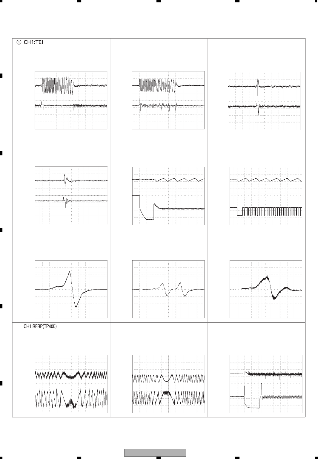
5
C
H1:FE
I
500mV
/
d
i
v.
2ms
/
di
v
.
2 la
y
er DVD:S curve chec
k
Servo ad
j
ustment mod
e
-
W
a
v
e
f
o
rm
s
1
C
H1:TE
I
1V
/
d
i
v.
2
C
H2
:
T-
2V
/
d
i
v.
C
D:32 tracks
j
um
p
2ms
/
di
v
.
1
C
H1:TE
I
1V
/
d
i
v.
2
C
H2
:
T-
2V
/
d
i
v.
DVD:1 track
j
um
p
2
m
s
/
di
v
.
3
C
H1:F
-
2V
/
d
i
v.
4
CH2:EC
(
TP308
)
1V
/
d
i
v.
DVD:
S
cu
rv
e
c
h
eck
Servo ad
j
ustment mod
e
500ms
/
d
i
v.
3
C
H1:F
-
2V
/
d
i
v.
4
C
H2:EC
(
TP308
)
1V
/
d
i
v.
C
D:
S
cu
rv
e
c
h
eck
Servo ad
j
ustment mo
d
e
500ms
/
d
i
v.
1
C
H1:TE
I
1V
/
d
i
v.
2
C
H2
:
T-
2V
/
d
i
v.
CD:1 track
j
um
p
2ms
/
di
v
.
1V
/
d
i
v.
2
CH2:T
-
T
-
T
2V
/
d
i
v.
DVD:32 tracks
j
um
p
2ms
/
di
v
.
5
C
H1:FE
I
500mV
/
d
i
v.
2ms
/
div
.
DVD:
S
cu
rv
e
c
h
eck
Servo ad
j
ustment mod
e
5
C
H1:FE
I
5
00m
V/di
v.
2ms
/div
.
C
D:S curve chec
k
Servo ad
j
ustment mo
d
e
6
500m
V/di
v.
1
C
H2:TE
I
1V
/
d
i
v.
C
D:RFRP w
a
v
e
f
or
m
F
ocus
c
l
ose
s
i
tuat
i
o
n
2ms
/
di
v
.
6
C
H1
:
RFRP
(
TP405
)
500m
V/di
v.
1
C
H2:TE
I
1V
/
d
i
v.
C
D:RFRP w
a
v
e
f
or
m
F
ocus
c
l
ose
s
i
tuat
i
o
n
3
C
H1:F
-
1V
/
d
i
v.
4
C
H2
:
EC
(
TP308
)
1V
/
d
i
v.
DVD:F
ocus
c
l
ose
s
i
tuat
i
on
500ms
/
d
i
v.
5ms
/
di
v
.
c
h1 VR21
→
c
h2 VR21
→
c
h1 VR21
→
c
h2 VR21
→
c
h1 VR21
→
c
h2 VR21
→
c
h1 VR21
→
c
h2 VR21
→
c
h1 VR21
→
c
h2 VR21
→
c
h1 VR21
→
c
h2 VR21
→
c
h1 VR21
→
c
h1 VR21
→
c
h1 VR21
→
c
h1 VR21
→
c
h2 VR21
→
c
h1 VR21
→
c
h2 VR21
→
ch
1
VR
21
→
c
h2 VR21
→
N
ote
:1
.
The encircled numbers denote measurin
g
pointes in the circuit dia
g
ram
.
2.
Reference volta
ge
VR21:2.1V
XDV-M8357ZT/UC 23
5678
5678
C
D
F
A
B
E
5
C
H1:FE
I
500mV/div
.
v
.
v
7
C
H2
:
SBAD
(
TP407
)
500mV/div
.
v
.
v
DVD:f
ocus
c
l
ose
10ms
/
d
i
v.
5
C
H1:FE
I
500mV/div
.
v
.
v
7
C
H2
:
SBAD
(
TP407
)
500mV/div
.
v
.
v
C
D:f
ocus
c
l
ose
v.
8
C
H1
:
C-
(
TP313
)
2V
/
d
i
v.
4
C
H2
:
E
C(
TP308
)
1V
/
d
i
v.
C
D:
C
R
G
in
s
i
de
→
outs
i
de
500m
/
di
v
.
9
C
H1
:
Ain
(
TP210
)
1V
/
d
i
v.
0
C
H2
:
FLGB
(
TP413
)
5V
/
d
i
v.
DVD:passin
g
black dot (1mm
)
500
µ
s
/
di
v
.
8
C
H1
:
C-
(
TP313
)
2V
/
d
i
v.
4
C
H2
:
EC
(
TP308
)
1V
/
d
i
v.
DVD:
C
R
G
in
s
i
de
→
outs
i
de
500m
/
di
v
.
3
C
H1:F
-
1V
/
d
i
v.
4
C
H2
:
EC
(
TP308
)
1
V/di
v.
C
D:f
ocus
c
l
ose
500
m
s
/
di
v
.
3
C
H1:F
-
2V
/
d
i
v.
2
C
H2
:
T-
2V
/
d
i
v.
C
D:passin
g
black dot (1mm
)
50
0
µ
s
/
di
v
.
9
CH1:Ain
(
TP210
)
500mV
/
d
i
v.
100ns
/
d
i
v.
DVD:durin
g
playback Ain wavefo
r
m
5
C
H1:FE
I
200mV
/
d
i
v.
3
C
H2:F
-
1V
/
d
i
v.
DVD:durin
g
playback FEI wavefo
r
m
1ms
/
di
v
.
0
C
H1:RF
OI
1V
/
d
i
v.
500ns
/
d
i
v.
CD:during playback RFOI wavefo
r
m
3
C
H1:F
-
2V
/
d
i
v.
2
C
H2
:
T-
2V
/
d
i
v.
DVD:passin
g
black dot (1mm
)
2
00
µ
s
/
di
v
.
!
C
H1:RF
OI
1V
/
d
i
v.
0
C
H2
:
FLGB
(
TP413
)
5V
/
d
i
v.
CD:passin
g
black dot (1mm
)
500
µ
s
/
di
v
.
c
h1 VR21
→
c
h2 VR21
→
c
h1 VR21
→
c
h2 VR21
→
c
h1 VR21
→
c
h2 VR21
→
c
h1 VR21
→
c
h2 VR21
→
c
h1 VR21
→
c
h2 VR21
→
c
h1 VR21
→
c
h2 VR21
→
c
h1 VR21
→
c
h2 VR21
→
c
h1 VR21
→
c
h2 VR21
→
c
h1 VR21
→
c
h2 VR21
→
ch1
G
N
D
→
c
h1 VR21
→
c
h1 VR21
→
c
h2 VR21
→
XDV-M8357ZT/UC
24
1234
1234
C
D
F
A
B
E
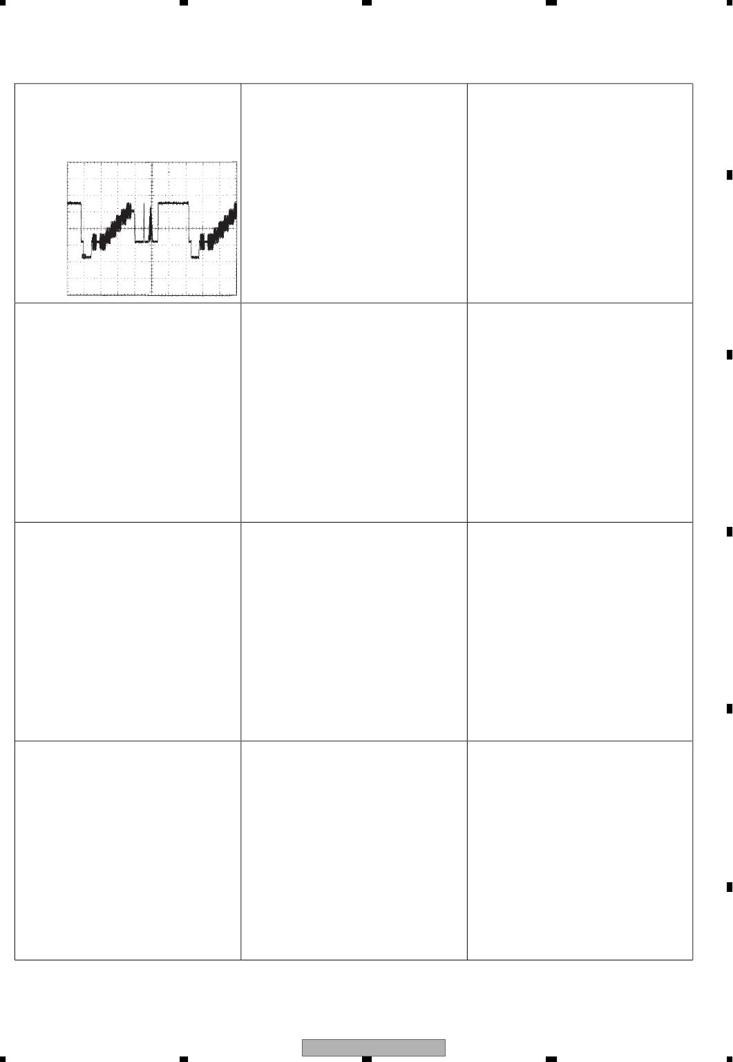
5
C
H1:FE
I
500mV/div
.
v
.
v
@
C
H2
:
FEB
(
TP522
)
500mV/div
.
v
.
v
CD:focus balance ad
j
ustmen
t
1
C
H1:TE
I
200mV
/
d
i
v.
2
C
H2
:
T-
1V
/
d
i
v.
DVD:durin
g
playback TEI wavefo
r
m
1ms
/
di
v
.
5
C
H1:FE
I
500mV
/
d
i
v.
1
CH2:TE
I
1V
/
d
i
v.
DVD:setu
p
500
m
s
/
di
v
.
5
C
H1:FE
I
500mV
/
d
i
v.
1
C
H2:TE
I
1V
/
d
i
v.
CD:setu
p
500ms
/
d
i
v.
5
C
H1:FE
I
500mV/div
.
v
.
v
@
C
H2
:
FEB
(
TP522
)
200mV/div
.
v
.
v
DVD:focus balance ad
j
ustmen
t
500ms
/
d
i
v.
5
C
H1:FE
I
500mV
/
d
i
v.
1
C
H2:TE
I
1V
/
d
i
v.
2 la
y
er DVD:setu
p
1s
/
d
i
v.
5
C
H1:FE
I
200mV
/
d
i
v.
3
C
H2:F
-
1V
/
d
i
v.
CD:durin
g
playback FEI wavefo
r
m
1ms
/
di
v
.
5
C
H1:FE
I
500mV/div
.
v
.
v
@
C
H2
:
FEB
(
TP522
)
200mV/div
.
v
.
v
2 la
y
er DVD:focus balance ad
j
ustmen
t
500ms
/
d
i
v.
500ms
/
d
i
v.
#
C
H1:TP1
01
5V
/
d
i
v.
$
C
H2:TP1
02
5V
/
d
i
v.
%
C
H
3
:TP1
03
5
V/di
v.
DVD:L
C
D
t
il
t
se
rv
o
1ms
/
di
v
.
#
C
H1:TP1
01
200mV/div
.
v
.
v
^
C
H4
:
LCDTIL
T(TP504)
L
T(TP504)
L
100mV/div
.
v
.
v
DVD:L
C
D
t
il
t
se
rv
o
C
H1, CH4:offset volta
g
e 2.5
V
1s
/
d
i
v.
&
C
H1:V
CO
500mV
/
d
i
v.
200ns
/
d
i
v.
DVD:V
CO
1
C
H1:TE
I
200m
V/di
v.
2
C
H2
:
T-
1V
/
d
i
v.
CD:durin
g
playback TEI wavefo
r
m
1ms
/
di
v
.
c
h1 VR21
→
c
h2 VR21
→
c
h1 VR21
→
c
h2 VR21
→
ch
1
VR
21
→
c
h2 VR21
→
ch1
G
N
D
→
ch2
G
N
D
→
ch1
G
N
D
→
ch2
G
N
D
→
ch1
G
N
D
→
ch2
G
N
D
→
c
h1 VR21
→
c
h2 VR21
→
c
h1 VR21
→
c
h2 VR21
→
c
h1 VR21
→
c
h2 VR21
→
ch1
G
N
D
→
ch2
G
N
D
→
ch
3
G
N
D
→
ch1
G
N
D
→
ch4
G
N
D
→
ch1
G
N
D
→
XDV-M8357ZT/UC 25
5678
5678
C
D
F
A
B
E
*
IC1201
p
in 4
5
200mV
/
d
i
v.
1
0
µ
s
/
di
v
.
Composite si
g
nal outpu
t
ch1
G
N
D
→
XDV-M8357ZT/UC 27
5678
5678
C
D
F
A
B
E
E-b
2/2
E
2/2
F
CN3951
F
CN3961
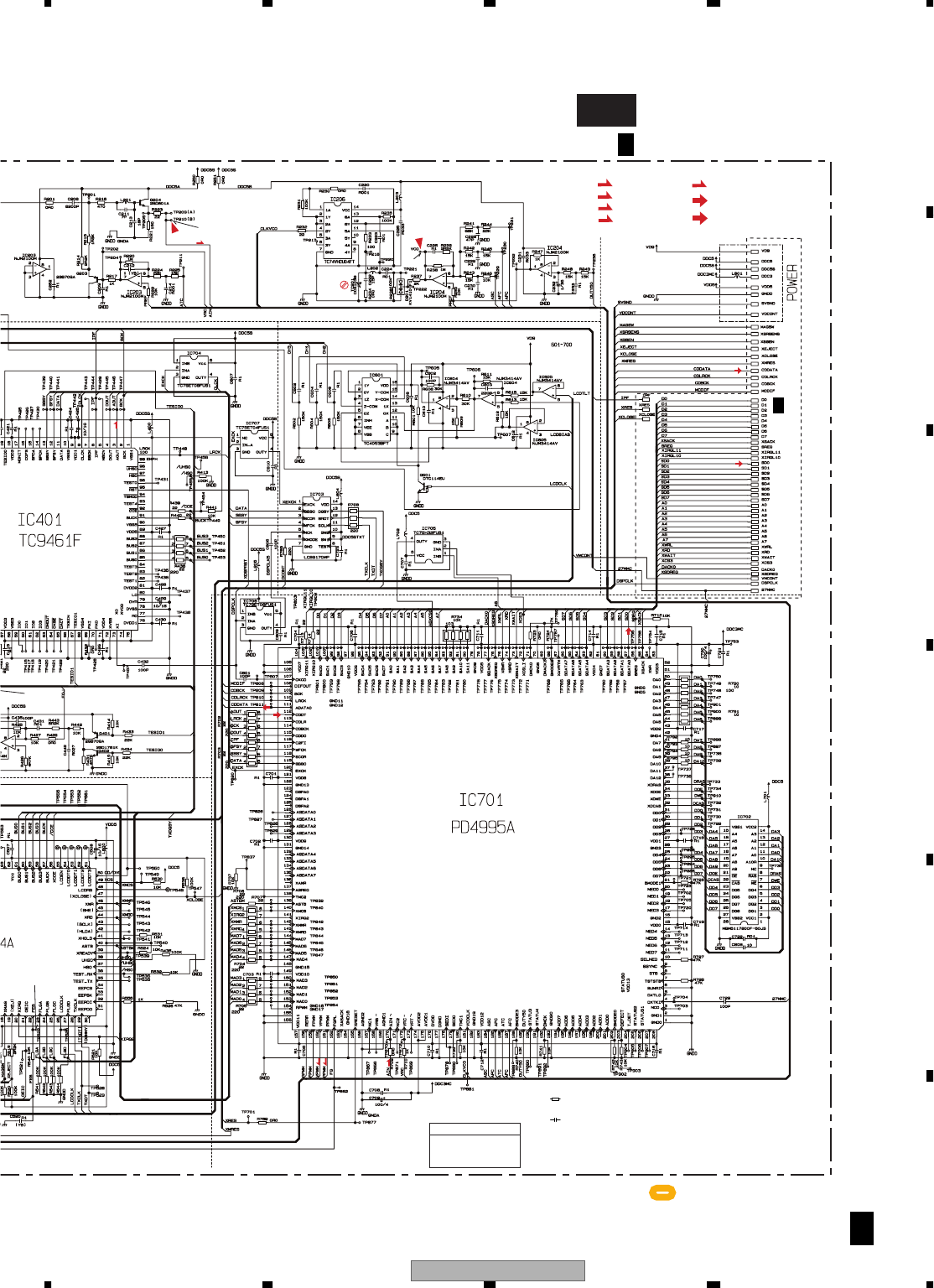
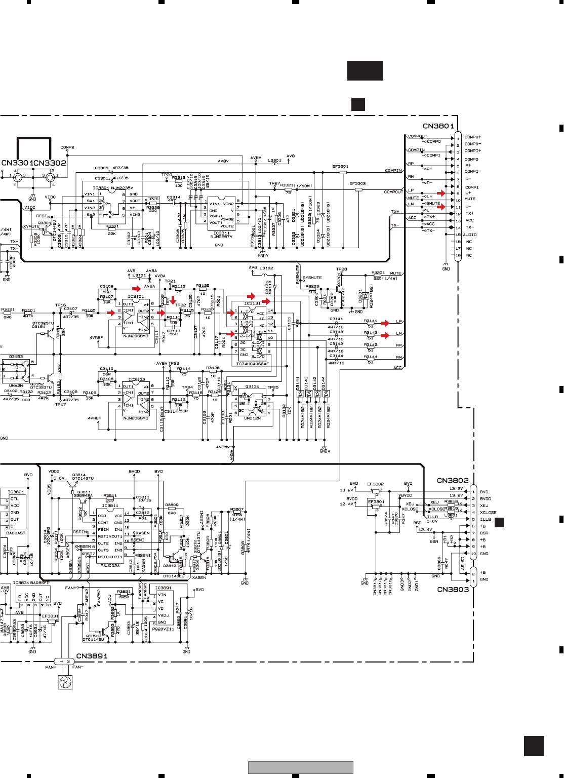
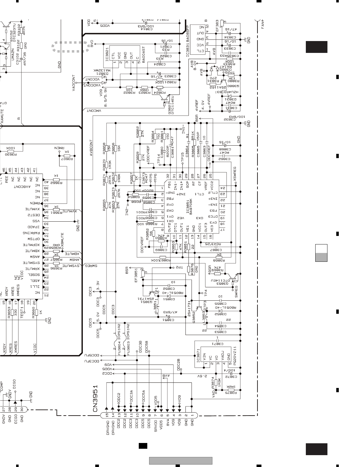
MAIN PCB(DECODER SECTION)
2/2
E
Main Unit
Consists of
Main PCB
Keyboard PCB
ROM
AU
VIDEO
VIDEO
VIDEO
VIDEO
AU
AU
AU
AU AU
AU
AU
**
ROM ROM DATA SIGNALROM DATA SIGNAL
VIDEO VIDEO SIGNAL(COMPOSITE)VIDEO SIGNAL(COMPOSITE)
AU AUDIO SIGNALAUDIO SIGNAL
AU(D) AUDIO SIGNAL(DIGITAL)AUDIO SIGNAL(DIGITAL)
XDV-M8357ZT/UC
32
1234
1234
C
D
F
A
B
E
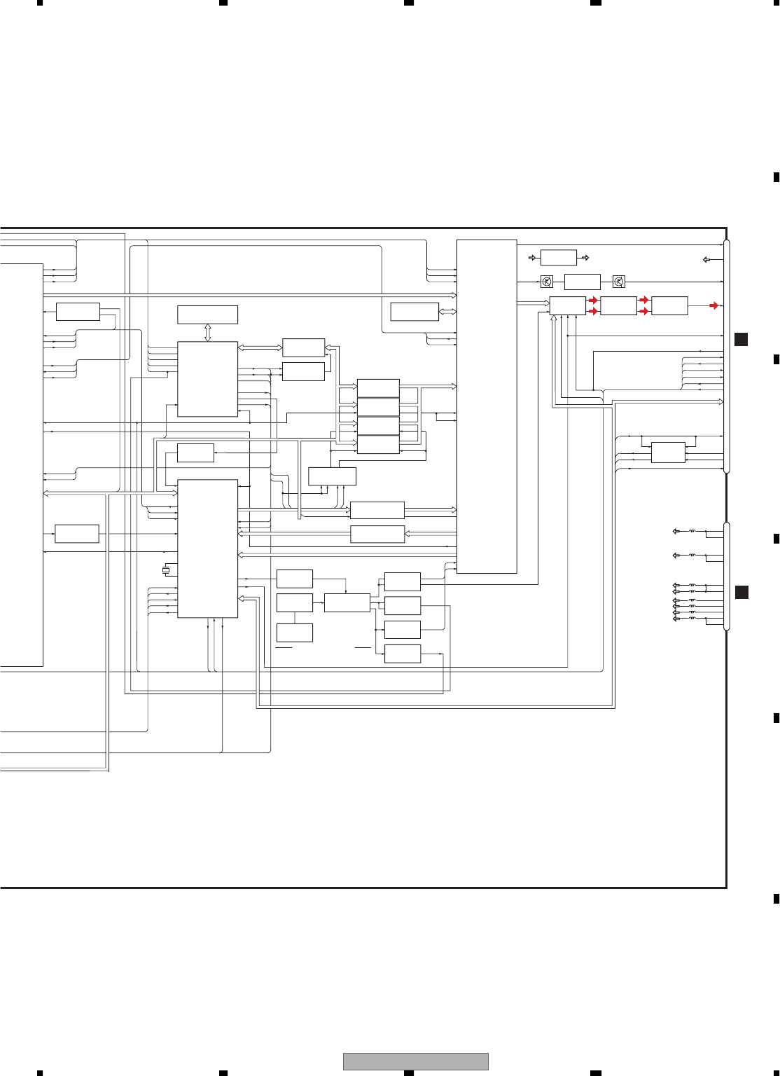
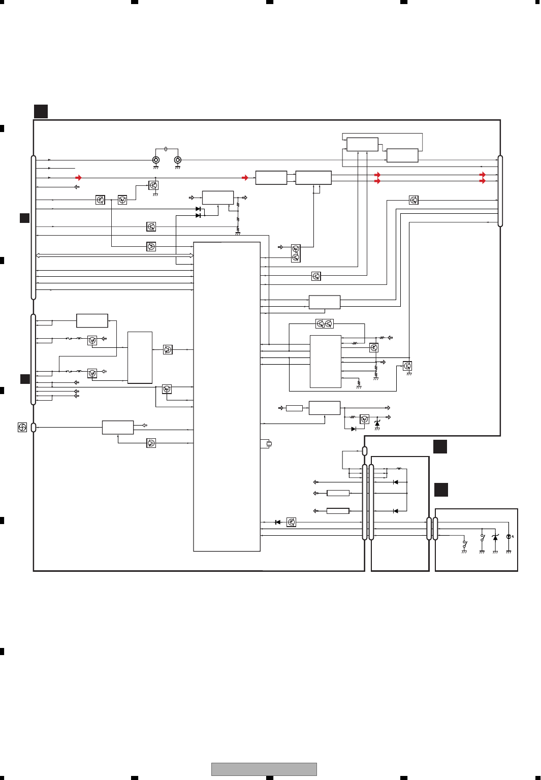
3.4 EXTENSION UNIT
F-a
F
CABLE
1.5A
1.5A
>
>
CN1601
CN1600
E2/2
SYSTEM CONTROL
E2/2
The > mark found on some component parts indicates
the importance of the safety factor of the part.
Therefore, when replacing, be sure to use parts of
identical designation.
DDC2(2.6V) DDC5(5V), DDC3(3.3V) POWER SUPPLY FOR
AUDIO AND VIDEO
XDV-M8357ZT/UC 35
5678
5678
C
D
F
A
B
E
A-a F-b
F-a
F-a
F-b
1
1.5A
1.5A
>
>
CN1601
E
2/2
The > mark found on some component parts indicates
the importance of the safety factor of the part.
Therefore, when replacing, be sure to use parts of
identical designation.
DDC2(2.6V) DDC5(5V), DDC3(3.3V) POWER SUPPLY FOR
AUDIO AND VIDEO
XDV-M8357ZT/UC
38
1234
1234
C
D
F
A
B
E
3.5 KEYBOARD PCB
GKEYBOARD PCB
G
CN2903
H
EJECT
CLOSE
Main Unit
Consists of
Main PCB
Keyboard PCB

XDV-M8357ZT/UC 39
5678
5678
C
D
F
A
B
E
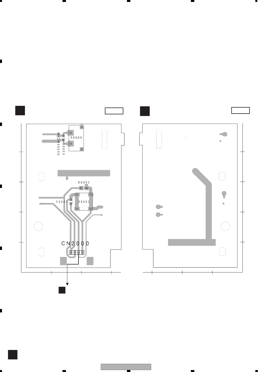
3.6 MF UNIT
H
HMF UNIT
3300/16
3300/16
3300/16
2200/16
2200/16
ERA15-02VH
Filter of +B
Maintenance of BSR
Maintenance of VDD
2 1
CN2902
Earth Plate
G
F
CN2000
CN3802
XDV-M8357ZT/UC
40
1234
1234
C
D
F
A
B
E
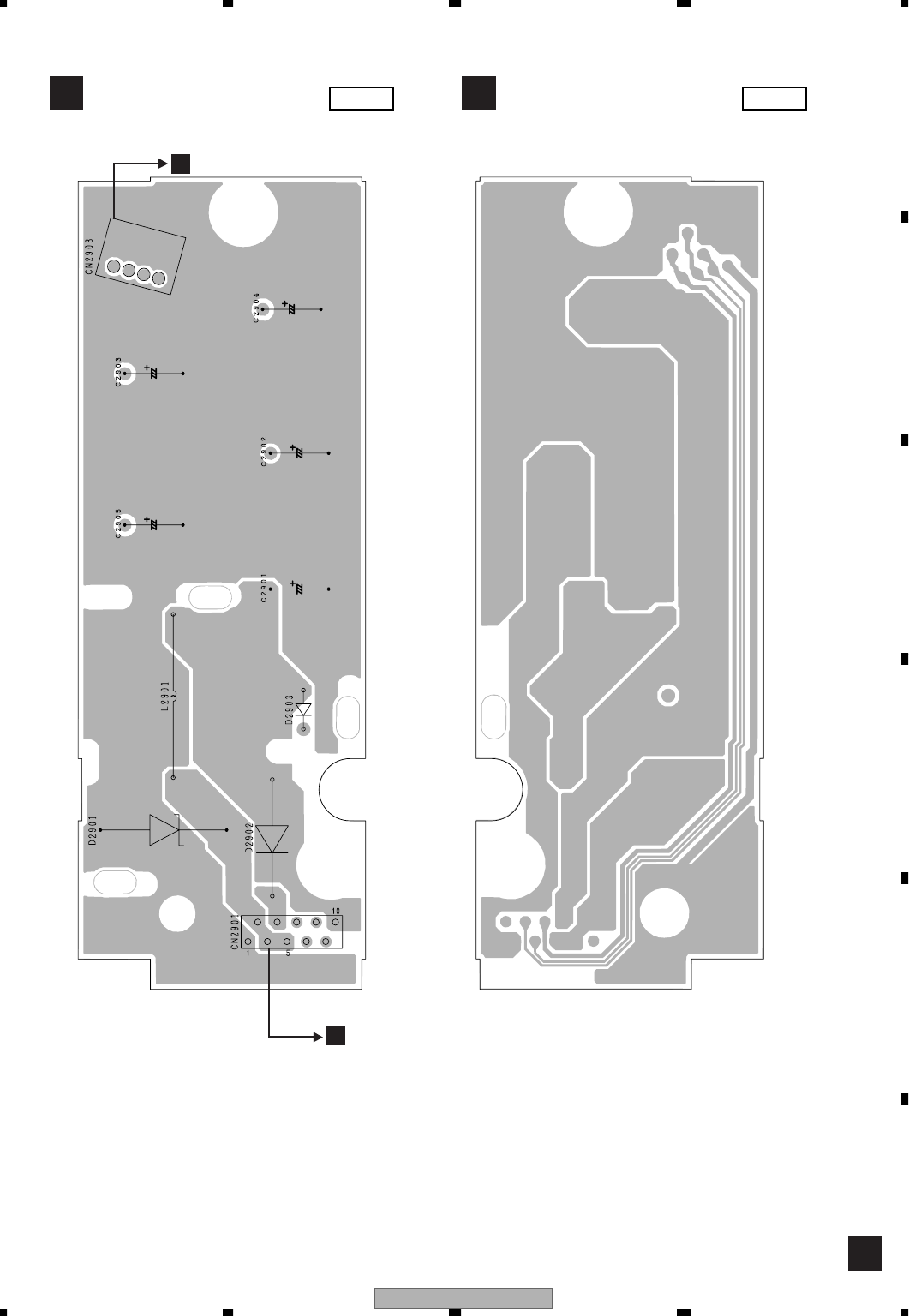
4. PCB CONNECTION DIAGRAM
4.1 MAIN PCB
Capacitor
Connector
P.C.Board Chip Part
E
EMAIN PCB
SIDE B
SIDE A
NOTE FOR PCB DIAGRAMS
1.The parts mounted on this PCB
include all necessary parts for
several destination.
For further information for
respective destinations, be sure
to check with the schematic dia-
gram.
2.Viewpoint of PCB diagrams
10 20 30 40 50 60 70 80 90 100 110
10
20
30
40
50
0
Y
X
XDV-M8357ZT/UC
48
1234
1234
C
D
F
A
B
E
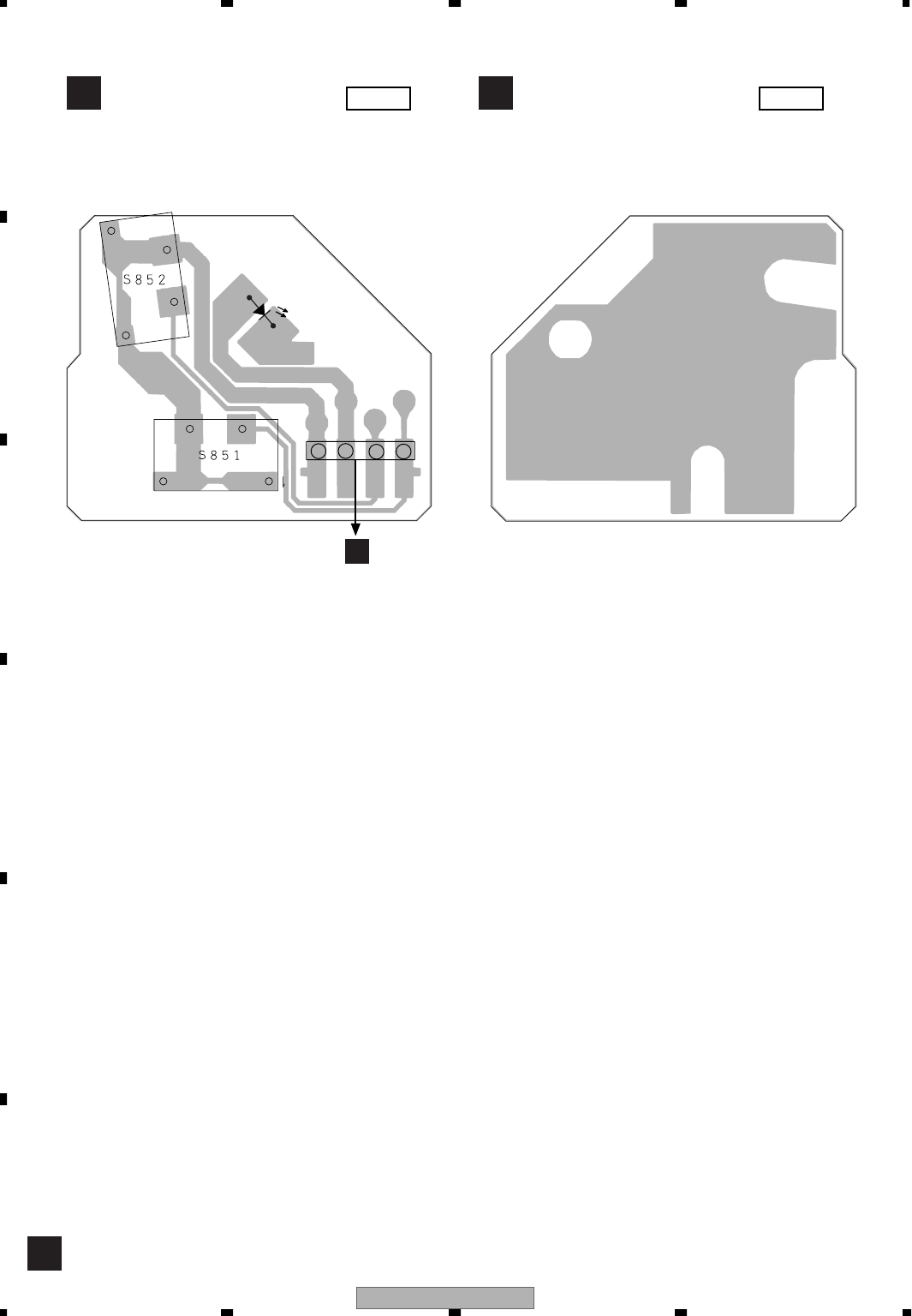
4.3 KEYBOARD PCB
G
GKEYBOARD PCB GKEYBOARD PCB
SIDE A SIDE B
10
20
30
40
20
10 30
0X
Y
10
20
30
40
20
30 10
0X
Y
HCN2903
CLOSE
EJECT
XDV-M8357ZT/UC 49
5678
5678
C
D
F
A
B
E
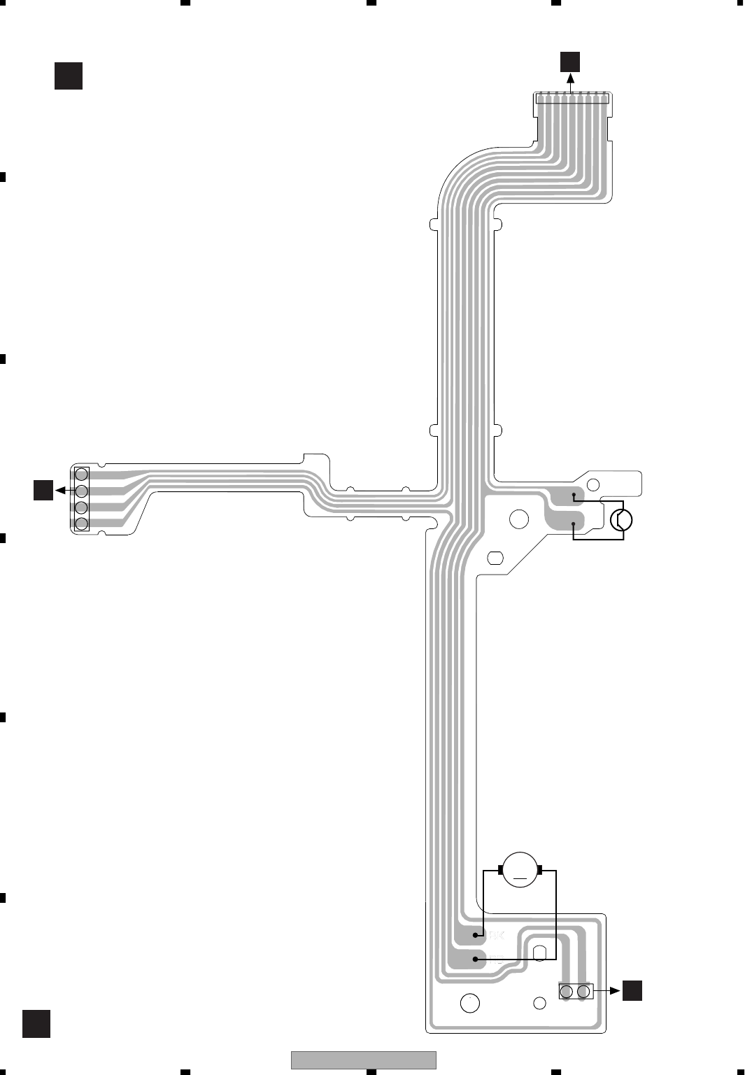
4.4 MF UNIT
SIDE A SIDE B
HMF UNIT
HMF UNIT
H
F
CN3802
G
CN2000
XDV-M8357ZT/UC
50
1234
1234
C
D
F
A
B
E
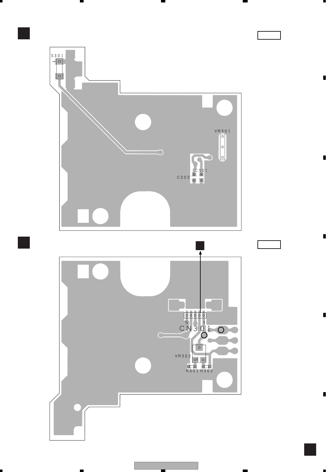
4.5 DVD/CD MECHANISM UNIT
SIDE A SIDE B
APCB UNIT(A)
APCB UNIT(A)
A
1
4
TRP
DSP
D851
C
XDV-M8357ZT/UC 51
5678
5678
C
D
F
A
B
E
SIDE A
BPCB UNIT(B)
SIDE B
BPCB UNIT(B)
B
MAG
EREF
EPVO
ECN310
XDV-M8357ZT/UC
52
1234
1234
C
D
F
A
B
E
CPCB(A)
C
Q851
2
1
9
1
4
1
M
M1
CARRIAGE
D
A
ECN302
XDV-M8357ZT/UC 53
5678
5678
C
D
F
A
B
E
DPCB(B)
D
1
2
M
M2
TRAY
C

XDV-M8357ZT/UC
54
1234
1234
C
D
F
A
B
E
5. ELECTRICAL PARTS LIST
N
OTE:
• Parts whose parts numbers are omitted are subject to being not supplied.
• The part numbers shown below indicate chip components.
Chip Resistor
RS1/_S___J,RS1/__S___J
Chip Capacitor (except for CQS.....)
CKS....., CCS....., CSZS.....
• The > mark found on some component parts indicates the importance of the safety factor of the part.
Therefore, when replacing, be sure to use parts of identical designation.
• Meaning of the figures and others in the parentheses in the parts list.
Example) IC 301 is on the point (face A, 91 of x-axis, and 111 of y-axis) of the corresponding
PC board.
IC 301 (A, 91, 111) IC NJM2068V
Circuit Symbol and No. Part No.
Unit Number:CWX3187
Unit Name:Main Unit
Unit Number:CWX3198
Unit Name:Extension Unit
Unit Number:CWM6518
Unit Name:MF Unit
Unit Number:
Unit Name:PCB Unit(A)
Unit Number:
Unit Name:PCB Unit(B)
Unit Number:
Unit Name:PCB(A)
Unit Number:
Unit Name:PCB(B)
Main Unit
Consists of
Main PCB
Keyboard PCB
EG
Unit Number:CWX3187
Unit Name:Main Unit
MISCELLANEOUS
IC 101 (A,19,35) IC IR3C07N
IC 102 (B,29,71) IC NJM2904M
IC 103 (B,31,56) IC TA1254AF
IC 105 (B,46,47) IC NJM3404AM
IC 106 (A,47,52) IC TC7WU04FU
IC 107 (A,44,65) IC PA0065AM
IC 108 (B,52,50) IC NJM3404AM
IC 109 (A,39,55) IC TC7WU04FU
IC 203 (A,43,40) IC NJM2100M
IC 204 (B,63,11) IC NJM2100M
IC 206 (B,62,28) IC TC74VHCU04FT
IC 301 (B,16,103) IC TC4W53F
IC 303 (B,22,96) IC NJM2904M
IC 304 (B,43,91) IC BA6797FM
IC 305 (B,25,18) IC LB1836M
IC 351 (B,12,82) IC TC4S66F
IC 352 (B,14,92) IC MC33202D
IC 353 (B,58,40) IC MC33202D
IC 401 (B,34,34) IC TC9461F
IC 402 (A,41,82) IC NJM2904M
IC 501 (A,40,17) IC PEG114A
IC 601 (B,26,88) IC TC4053BFT
IC 604 (B,26,81) IC NJM3414AV
IC 605 (B,26,77) IC NJM3414AV
IC 701 (A,74,22) IC PD4995A
IC 702 (B,80,16) IC MSM5117800F-60JS
IC 703 (A,17,27) IC LC89170MP
IC 704 (A,21,21) IC TC7SET08FUS1
IC 705 (B,77,27) 1 chip OR gate TC7SH32FUS1
IC 706 (A,23,27) IC TC7SET08FUS1
IC 707 (A,19,21) IC TC7SET04FUS1
IC 1000 (B,76,50) IC M5M51008DKV-70HI
IC 1001 (B,95,51) IC PD6531A
IC 1002 (B,82,30) IC TC7SET08FUS1
IC 1003 (B,70,44) IC TC7SHU04FU
IC 1004 (B,85,73) IC PD6520A
IC 1005 (B,79,34) IC MAX662AESA
IC 1006 (B,64,72) IC PD3411A
IC 1007 (A,57,63) IC TC74VHC139FT
IC 1008 (A,66,99) IC TC7SHU04FU
IC 1009 (B,87,92) IC CY2292SI-1A0
IC 1010 (B,95,89) IC TC7SHU04FU
IC 1011 (B,75,98) IC TC7WU04FU
IC 1012 (B,99,97) IC TC7WU04FU
IC 1013 (B,63,91) IC TC7SH08FUS1
IC 1014 (B,98,89) IC TC7SHU04FU
IC 1015 (B,84,100) IC TC7WU04FU
IC 1200 (B,99,73) IC MSM56V16160DP-10TS
Circuit Symbol and No. Part No.

XDV-M8357ZT/UC 55
5678
5678
C
D
F
A
B
E
IC 1201 (A,85,80) IC MB86373BPFV-G-BI
IC 1202 (A,90,54) IC TC74VHC541FTS1
IC 1203 (A,83,54) IC TC74VHCT08AFTS1
IC 1204 (A,77,54) IC TC74LCX245FTS1
IC 1205 (A,69,52) IC TC74LCX245FTS1
IC 1206 (A,62,70) IC TC74VHC541FTS1
IC 1207 (A,62,78) IC TC74VHC541FTS1
IC 1208 (A,97,45) IC TC74VHC00FTS1
IC 1500 (B,66,105) IC PE8001A1
IC 1501 (A,52,87) IC MC33202D
IC 1502 (B,59,96) IC MC33202D
IC 1503 (A,52,111) IC NJM2068MD
IC 1504 (B,54,108) IC HA178L05UA
IC 1700 (A,106,21) IC LC35256FT-70U
IC 1701 (A,100,31) IC HD74HC245T
IC 1702 (B,99,28) IC LC89513KP
IC 1704 (A,106,29) IC TC7S02FU
IC 1705 (A,97,37) IC TC7SHU04FU
IC 1706 (A,66,62) IC TC74VHC238FT
IC 1707 (A,102,37) IC TC7SHU04FU
Q 101 (A,13,47) Transistor 2SD601A
Q 102 (A,17,47) Transistor 2SB709A
Q 103 (B,43,63) Transistor DTC114EU
Q 104 (A,24,65) Transistor 2SB1260
Q 165 (A,39,45) Transistor 2SB709A
Q 168 (A,22,51) Transistor FMC5A
Q 203 (A,50,43) Transistor 2SB709A
Q 204 (A,53,33) Transistor 2SD601A
Q 401 (A,34,79) Transistor 2SB709A
Q 402 (A,34,84) Transistor 2SD1781K
Q 403 (A,44,76) Transistor IMX1
Q 404 (A,38,76) Transistor 2SB1132
Q 501 (B,51,20) Transistor DTA114EU
Q 601 (B,28,93) Transistor DTC114EU
Q 1500 (A,72,103) Transistor 2SA1037K
Q 1503 (A,75,113) Transistor 2SA1037K
Q 1600 (A,76,120) Transistor UMH8N
D 201 (B,68,20) Diode KV1410-F1
D 305 (A,26,7) Diode 1SR154-400
D 2000 (A,12,45) Diode UDZ18(B)
D 2001 (A,21,28) LED SML-210FT(JK)
L 101 (A,13,35) Inductor CTF1473
L 120 (A,44,53) Inductor CTF1473
L 121 (B,47,59) Inductor CTF1473
L 122 (A,37,71) Inductor CTF1473
L 123 (B,44,53) Inductor CTF1473
L 201 (A,53,37) Inductor LCTC4R7K2125
L 202 (B,73,27) Chip Coil LCTAW1R5J2520
L 203 (B,61,32) Inductor CTF1473
L 400 (A,26,33) Inductor CTF1473
L 500 (A,36,35) Inductor CTF1473
L 701 (B,94,15) Inductor CTF1473
L 702 (B,77,29) Inductor CTF1473
L 801 (A,89,41) Inductor CTF1453
L 804 (A,16,22) Inductor CTF1473
L 805 (A,22,25) Ferrite Bead CTF1528
L 1000 (B,80,60) Inductor CTF1473
L 1001 (B,82,54) Inductor CTF1473
L 1002 (B,79,31) Inductor CTF1473
L 1003 (B,68,44) Inductor CTF1473
Circuit Symbol and No. Part No.
L 1004 (B,80,87) Inductor CTF1473
L 1005 (B,62,55) Inductor CTF1473
L 1007 (B,54,86) Inductor CTF1473
L 1008 (B,78,96) Inductor CTF1473
L 1009 (A,56,59) Inductor CTF1473
L 1010 (A,64,99) Inductor CTF1473
L 1011 (A,69,100) Inductor CTF1470
L 1012 (B,92,87) Inductor CTF1473
L 1013 (B,77,103) Inductor CTF1473
L 1014 (B,98,99) Inductor CTF1473
L 1015 (B,61,92) Inductor CTF1473
L 1016 (B,79,39) Inductor CTF1473
L 1017 (B,98,85) Inductor CTF1473
L 1018 (B,80,100) Inductor CTF1473
L 1200 (B,103,60) Inductor CTF1453
L 1201 (A,104,89) Inductor CTF1473
L 1202 (A,94,55) Inductor CTF1473
L 1203 (A,82,50) Inductor CTF1473
L 1204 (A,97,110) Inductor CTF1473
L 1205 (A,75,60) Inductor CTF1473
L 1206 (A,97,101) Inductor CTF1453
L 1207 (A,92,42) Inductor CTF1473
L 1208 (A,66,57) Inductor CTF1473
L 1209 (A,57,75) Inductor CTF1473
L 1210 (A,63,82) Inductor CTF1473
L 1500 (A,79,107) Inductor CTF1473
L 1503 (B,51,107) Inductor CTF1473
L 1600 (B,35,125) Inductor CTF1453
L 1601 (B,31,125) Inductor CTF1453
L 1602 (B,28,125) Inductor CTF1453
L 1603 (B,23,125) Inductor CTF1453
L 1604 (B,10,115) Inductor CTF1453
L 1606 (B,26,124) Inductor CTF1473
L 1607 (A,70,122) Inductor CTF1470
L 1608 (B,10,112) Inductor CTF1453
L 1609 (A,77,125) Inductor CTF1470
L 1610 (A,78,125) Inductor CTF1470
L 1611 (A,80,125) Inductor CTF1470
L 1612 (A,89,125) Inductor CTF1470
L 1613 (A,90,125) Inductor CTF1470
L 1615 (A,85,120) Inductor CTF1470
L 1616 (A,84,125) Inductor CTF1470
L 1617 (A,85,125) Inductor CTF1470
L 1618 (A,87,125) Inductor CTF1470
L 1622 (A,70,121) Inductor CTF1470
L 1624 (A,75,125) Inductor CTF1470
L 1630 (B,20,125) Inductor CTF1453
L 1631 (A,80,122) Inductor CTF1470
L 1632 (A,81,125) Inductor CTF1470
L 1633 (A,80,121) Inductor CTF1470
L 1634 (A,82,125) Inductor CTF1470
L 1635 (A,80,119) Inductor CTF1470
L 1701 (A,114,23) Inductor CTF1473
L 1702 (B,104,41) Inductor CTF1473
L 1704 (A,100,27) Inductor CTF1473
L 1705 (A,107,32) Inductor CTF1473
L 1706 (A,100,39) Inductor CTF1473
L 1707 (A,61,59) Inductor CTF1473
L 1708 (A,104,37) Inductor CTF1473
TC201 (B,70,31) Trimmer CCG1039
Circuit Symbol and No. Part No.

XDV-M8357ZT/UC
56
1234
1234
C
D
F
A
B
E
TC1000 (B,90,100)
Trimmer Condenser
CCL1053
X 501 (A,41,31) Radiator 10.00MHz CSS1428
X 1000 (B,47,74) Radiator 20.00MHz CSS1470
X 1001 (A,89,106)
Radiator 13.824MHz
CSS1509
S 2000 (A,20,45) Switch(CLOSE) CSN1051
S 2001 (A,21,23) Switch(EJECT) CSG1110
F 1500 (A,75,108) Filter CTF1515
RESISTORS
R 101 (A,12,51) RS1/16S0R0J
R 102 (A,13,51) RS1/16S102J
R 103 (A,15,51) RS1/16S122J
R 104 (A,18,51) RS1/16S182J
R 106 (A,44,59) RS1/16S0R0J
R 108 (B,26,48) RS1/16S0R0J
R 109 (A,23,61) RS1/10S1R5J
R 110 (A,23,58) RS1/10S1R5J
R 111 (A,23,55) RS1/10S1R5J
R 112 (A,22,48) RS1/10S1R5J
R 113 (B,32,75) RS1/16S103J
R 114 (B,38,74) RS1/16S103J
R 115 (A,35,57) RS1/16S222J
R 116 (A,25,60) RS1/16S0R0J
R 118 (B,37,50) RS1/16S0R0J
R 119 (A,35,56) RS1/16S222J
R 120 (B,39,51) RS1/16S0R0J
R 121 (B,52,42) RS1/16S393J
R 122 (A,13,33) RS1/10S3R9J
R 123 (A,15,41) RS1/16S104J
R 124 (A,24,46) RS1/10S1R5J
R 125 (A,35,55) RS1/16S222J
R 126 (B,45,65) RS1/16S122J
R 127 (A,43,50) RS1/16S222J
R 133 (B,31,47) RS1/16S0R0J
R 134 (B,37,65) RA3C101J
R 136 (B,41,62) RS1/16S331J
R 137 (B,43,65) RS1/16S112J
R 138 (B,41,64) RS1/16S302J
R 139 (A,27,49) RS1/16S0R0J
R 140 (A,29,47) RS1/16S103J
R 141 (B,35,48) RS1/16S101J
R 143 (B,44,57) RS1/16S103J
R 144 (B,46,53) RS1/16S103J
R 145 (A,38,57) RS1/16S223J
R 146 (A,40,52) RS1/16S223J
R 147 (A,43,55) RS1/16S223J
R 148 (A,45,51) RS1/16S223J
R 149 (A,49,53) RS1/16S103J
R 150 (A,51,53) RS1/16S222J
R 154 (B,49,53) RS1/16S123J
R 155 (B,53,55) RS1/16S182J
R 156 (B,54,55) RS1/16S123J
R 157 (B,55,45) RS1/16S822J
R 158 (B,51,54) RS1/16S182J
R 159 (B,52,43) RS1/16S203J
R 160 (A,33,50) RS1/16S101J
R 164 (A,27,50) RS1/16S203J
R 165 (A,38,47) RS1/16S101J
R 166 (A,41,48) RS1/16S222J
Circuit Symbol and No. Part No.
R 170 (A,23,71) RS1/8S100J
R 171 (A,26,71) RS1/8S120J
R 172 (A,27,62) RS1/16S470J
R 201 (A,50,50) RS1/16S0R0J
R 214 (A,46,44) RS1/16S222J
R 215 (A,50,47) RS1/16S152J
R 216 (A,55,37) RS1/16S471J
R 217 (A,49,46) RS1/16S102J
R 220 (A,48,39) RS1/16S105J
R 221 (A,49,33) RS1/16S161J
R 222 (A,48,37) RS1/16S103J
R 223 (A,51,31) RS1/16S220J
R 224 (A,52,40) RS1/16S223J
R 225 (A,55,40) RS1/16S153J
R 230 (B,63,24) RS1/8S0R0J
R 231 (B,59,24) RS1/16S104J
R 232 (B,57,26) RS1/16S220J
R 233 (B,71,27) RS1/16S101J
R 234 (B,68,28) RS1/16S0R0J
R 235 (B,68,26) RS1/16S104J
R 236 (B,68,23) RS1/16S104J
R 237 (B,66,21) RS1/16S202J
R 238 (B,63,16) RS1/16S105J
R 239 (B,65,18) RS1/16S222J
R 240 (B,67,10) RS1/16S103J
R 241 (B,63,17) RS1/16S683J
R 242 (B,63,19) RS1/16S153J
R 243 (B,63,20) RS1/16S153J
R 244 (B,60,17) RS1/16S223J
R 245 (B,60,19) RS1/16S153J
R 246 (B,60,20) RS1/16S103J
R 247 (B,64,6) RS1/16S102J
R 248 (B,60,10) RS1/16S153J
R 249 (B,60,13) RS1/16S153J
R 250 (A,55,34) RS1/10S0R0J
R 251 (B,63,34) RS1/10S0R0J
R 301 (B,33,99) RS1/16S622J
R 302 (B,59,34) RS1/16S473J
R 303 (B,53,38) RS1/16S434J
R 304 (B,47,10) RS1/16S104J
R 306 (B,14,107) RS1/16S101J
R 308 (A,14,19) RS1/10S201J
R 310 (A,11,20) RS1/10S221J
R 315 (B,50,85) RS1/16S103J
R 316 (B,49,87) RS1/16S103J
R 317 (B,24,103) RS1/16S822J
R 318 (B,53,98) RS1/16S0R0J
R 322 (B,51,94) RS1/16S1002D
R 323 (B,51,96) RS1/16S1002D
R 324 (B,48,103) RS1/16S0R0J
R 325 (B,46,102) RS1/16S0R0J
R 326 (B,52,98) RS1/16S1002D
R 328 (B,20,102) RS1/16S822J
R 329 (B,22,103) RS1/16S822J
R 331 (B,21,103) RS1/16S822J
R 337 (B,37,101) RS1/16S0R0J
R 338 (B,36,99) RS1/16S0R0J
R 339 (B,34,82) RS1/16S0R0J
R 340 (B,37,81) RS1/16S0R0J
R 344 (B,33,86) RS1/16S1002D
Circuit Symbol and No. Part No.

XDV-M8357ZT/UC 57
5678
5678
C
D
F
A
B
E
R 345 (B,34,88) RS1/16S1002D
R 346 (B,34,84) RS1/16S1002D
R 348 (B,33,97) RS1/16S1202D
R 349 (B,32,95) RS1/16S1202D
R 350 (B,34,94) RS1/16S1202D
R 352 (B,17,93) RS1/16S103J
R 354 (B,31,97) RS1/16S0R0J
R 355 (B,13,97) RS1/16S103J
R 356 (B,10,92) RS1/16S103J
R 358 (B,13,86) RS1/16S103J
R 359 (B,17,91) RS1/16S103J
R 360 (B,13,85) RS1/16S114J
R 361 (B,15,83) RS1/16S153J
R 362 (B,15,87) RS1/16S243J
R 364 (A,59,39) RS1/16S624J
R 365 (B,52,41) RS1/16S624J
R 366 (A,61,41) RS1/16S104J
R 368 (B,63,37) RS1/16S333J
R 369 (B,60,36) RS1/16S333J
R 370 (B,54,36) RS1/16S101J
R 372 (B,55,34) RS1/16S103J
R 373 (B,53,34) RS1/16S333J
R 374 (B,58,34) RS1/16S103J
R 401 (A,33,47) RS1/16S101J
R 402 (A,35,47) RS1/16S101J
R 404 (B,29,99) RS1/16S1202D
R 405 (B,31,100) RS1/16S3300D
R 406 (B,39,44) RS1/16S332J
R 407 (B,52,100) RS1/16S1002D
R 408 (A,29,44) RS1/16S0R0J
R 409 (B,40,44) RS1/16S153J
R 410 (B,25,44) RS1/16S225J
R 411 (A,40,73) RS1/16S272J
R 412 (B,25,46) RS1/16S333J
R 413 (A,25,23) RS1/16SS104J
R 414 (A,31,78) RS1/16S103J
R 416 (B,23,44) RS1/16SS473J
R 417 (B,24,42) RS1/16S225J
R 418 (B,26,42) RS1/16S104J
R 419 (A,31,84) RS1/16S103J
R 420 (B,23,41) RS1/16S103J
R 421 (B,46,40) 22ΩCCN1111
R 423 (A,45,88) RS1/16S1002D
R 424 (A,46,79) RS1/16S272J
R 425 (A,42,89) RS1/16S103J
R 426 (A,38,88) RS1/16S472J
R 427 (A,39,91) RS1/16S103J
R 428 (A,41,76) RS1/16S472J
R 429 (A,39,92) RS1/16S0R0J
R 430 (A,44,79) RS1/16S472J
R 431 (A,37,86) RS1/16S472J
R 432 (B,45,31) RS1/16S0R0J
R 433 (A,31,79) RS1/16S223J
R 434 (A,30,84) RS1/16S223J
R 435 (A,24,25) RS1/16SS104J
R 436 (B,37,13) 22ΩCCN1111
R 439 (B,31,24) RS1/16S220J
R 440 (B,32,24) RS1/16S220J
R 441 (B,30,24) RS1/16S103J
R 442 (A,36,87) RS1/16S103J
Circuit Symbol and No. Part No.
R 443 (A,37,89) RS1/16S622J
R 448 (A,35,42) RS1/16S221J
R 450 (A,36,42) RS1/16S103J
R 501 (B,56,16) RS1/16S3902D
R 502 (B,49,19) RS1/16S1502D
R 503 (B,44,17) RS1/16SS473J
R 504 (B,41,17) RS1/16S683J
R 505 (B,51,18) RS1/16SS473J
R 506 (B,43,17) RS1/16S103J
R 507 (B,46,15) RS1/16S222J
R 508 (B,41,18) RS1/16S222J
R 509 (B,50,16) RS1/16S222J
R 510 (B,54,18) RS1/16S1002D
R 511 (B,33,13) 3.3kΩCCN1122
R 512 (A,48,30) RS1/16S104J
R 514 (B,46,17) RS1/16S682J
R 515 (A,45,28) RS1/16S102J
R 516 (B,38,20) RS1/16S102J
R 517 (A,37,29) RS1/16S222J
R 518 (A,36,33) RS1/16S104J
R 519 (A,35,30) RS1/16S222J
R 520 (A,35,33) RS1/16S104J
R 521 (B,37,20) RS1/16S103J
R 522 (B,42,14) RA3C104J
R 524 (B,32,17) RS1/16S103J
R 526 (A,21,16) RS1/16SS473J
R 527 (B,46,12) 22ΩCCN1111
R 528 (B,45,22) RA3C473J
R 529 (B,46,18) RS1/16S682J
R 530 (B,28,13) RS1/16S103J
R 531 (B,31,16) RS1/16S103J
R 532 (B,34,17) RS1/16S103J
R 534 (B,44,9) RS1/16S104J
R 535 (B,46,9) RS1/16S104J
R 536 (A,24,13) RS1/16S104J
R 537 (B,52,27) RS1/16S104J
R 540 (B,35,20) RS1/16S103J
R 541 (A,33,31) RS1/16S104J
R 542 (A,32,31) RS1/16S104J
R 543 (A,33,34) RS1/16S104J
R 544 (A,32,36) RS1/16S104J
R 551 (B,49,27) RS1/16S220J
R 556 (A,22,18) RS1/16SS102J
R 601 (B,26,95) RS1/16S103J
R 602 (B,20,88) RS1/16S154J
R 604 (B,20,87) RS1/16S154J
R 606 (B,20,85) RS1/16S154J
R 608 (B,32,82) RS1/16S303J
R 609 (B,31,79) RS1/16S153J
R 610 (B,28,84) RS1/16S303J
R 611 (B,20,82) RS1/16S153J
R 612 (B,21,78) RS1/16S153J
R 613 (B,20,78) RS1/16S153J
R 615 (B,21,80) RS1/16S153J
R 702 (A,84,40) 22ΩCCN1111
R 703 (A,80,40) 22ΩCCN1111
R 704 (B,41,9) 22ΩCCN1111
R 705 (B,51,7) 22ΩCCN1111
R 707 (A,70,40) RS1/16S220J
R 708 (B,52,13) 22ΩCCN1111
Circuit Symbol and No. Part No.

XDV-M8357ZT/UC
58
1234
1234
C
D
F
A
B
E
R 709 (A,56,29) RS1/16S0R0J
R 710 (A,53,26) RS1/16S102J
R 712 (A,93,10) RS1/16S103J
R 713 (A,92,37) RS1/16S220J
R 714 (A,90,37) RS1/16S220J
R 723 (A,91,18) RS1/16S0R0J
R 724 (A,94,16) RS1/16SS473J
R 726 (A,70,4) RS1/16SS473J
R 727 (A,66,4) RS1/16SS473J
R 728 (A,64,5) RS1/16SS473J
R 734 (A,93,24) 10kΩCCN1125
R 737 (A,72,39) RS1/16S103J
R 739 (A,57,24) RS1/16S103J
R 740 (A,57,20) RS1/16S103J
R 741 (A,57,14) RS1/16S103J
R 742 (A,55,10) RS1/16S103J
R 743 (A,57,12) RS1/16S103J
R 768 (A,12,26) RA3C221J
R 769 (A,25,29) RS1/16SS221J
R 789 (B,53,30) RS1/16S0R0J
R 790 (B,84,25) 10ΩCCN1133
R 791 (B,87,6) RA3C100J
R 792 (B,84,7) RS1/16S100J
R 793 (B,82,7) RS1/16S100J
R 794 (B,77,8) RS1/16S100J
R 795 (B,81,24) RS1/16S100J
R 1000 (B,75,58) RS1/16SS473J
R 1001 (B,83,55) RS1/16SS473J
R 1002 (B,90,85) RS1/16SS473J
R 1003 (B,62,86) RS1/16SS473J
R 1004 (B,62,88) RS1/16SS473J
R 1005 (B,64,87) RS1/16SS473J
R 1006 (B,76,86) 47kΩCCN1131
R 1007 (B,49,79) RA3C471J
R 1008 (A,53,76) RS1/16S472J
R 1009 (B,50,73) RS1/16S103J
R 1010 (B,50,70) RS1/16SS473J
R 1011 (B,48,68) 47kΩCCN1131
R 1012 (A,54,69) RS1/16S102J
R 1013 (B,48,65) RS1/16S470J
R 1014 (B,48,63) 47kΩCCN1131
R 1015 (A,56,55) RS1/16S332J
R 1016 (B,58,57) RS1/16SS473J
R 1017 (B,59,55) RS1/16SS473J
R 1018 (B,57,55) RA3C473J
R 1019 (A,83,104) RS1/16S105J
R 1020 (A,86,103) RS1/16S102J
R 1021 (B,79,91) RS1/8S470J
R 1022 (B,95,92) RS1/8S470J
R 1023 (B,95,94) RS1/8S470J
R 1025 (B,101,88) RS1/16S0R0J
R 1026 (B,75,92) RS1/16S0R0J
R 1027 (B,73,102) RS1/16S0R0J
R 1028 (B,102,99) RS1/16S0R0J
R 1029 (B,79,38) RS1/16SS473J
R 1030 (B,57,87) 47kΩCCN1131
R 1031 (B,85,31) RS1/16SS473J
R 1032 (B,60,88) RS1/16SS473J
R 1033 (A,56,78) RS1/16S472J
R 1034 (B,70,85) RS1/16SS473J
Circuit Symbol and No. Part No.
R 1035 (B,71,85) RS1/16SS473J
R 1036 (B,73,86) RS1/16SS473J
R 1038 (B,64,89) RS1/16SS473J
R 1039 (B,66,87) RS1/16SS473J
R 1040 (B,68,88) RS1/16SS473J
R 1041 (B,50,74) RS1/16S0R0J
R 1042 (A,56,71) RS1/16SS473J
R 1046 (B,94,86) RS1/16S0R0J
R 1200 (A,104,71) RS1/16S0R0J
R 1202 (A,102,73) RS1/16S201J
R 1212 (A,85,60) RS1/16S220J
R 1218 (A,76,98) RS1/16S2701D
R 1219 (A,73,101) RS1/16S1600D
R 1220 (A,85,100) RS1/16S2701D
R 1221 (A,81,100) RS1/16S2201D
R 1222 (A,85,99) RS1/16S0R0J
R 1223 (A,84,100) RS1/16S2701D
R 1224 (A,83,100) RS1/16S2201D
R 1230 (A,104,69) RS1/16SS473J
R 1231 (B,92,70) RS1/16SS473J
R 1232 (A,84,59) RS1/16SS473J
R 1233 (A,82,59) RS1/16SS473J
R 1235 (A,65,93) RS1/16S0R0J
R 1236 (B,72,99) RS1/16S0R0J
R 1237 (B,69,98) RS1/16S0R0J
R 1500 (A,75,104) RS1/16S222J
R 1501 (A,71,109) RS1/16S152J
R 1503 (A,71,106) RS1/16S3300D
R 1506 (B,66,112) RS1/16S0R0J
R 1507 (A,72,111) RS1/16S101J
R 1510 (A,78,111) RS1/16S222J
R 1513 (A,45,110) RS1/16S622J
R 1514 (A,49,106) RS1/16S622J
R 1515 (A,62,114) RS1/16S622J
R 1516 (A,59,113) RS1/16S622J
R 1517 (A,48,115) RS1/16S622J
R 1518 (A,49,107) RS1/16S622J
R 1519 (A,46,112) RS1/16S622J
R 1520 (A,48,110) RS1/16S622J
R 1521 (A,58,107) RS1/16S622J
R 1522 (A,57,114) RS1/16S622J
R 1523 (A,58,109) RS1/16S622J
R 1524 (A,59,111) RS1/16S622J
R 1525 (A,86,120) RS1/16S101J
R 1526 (A,88,120) RS1/16S101J
R 1611 (A,92,121) RS1/16S0R0J
R 1612 (A,92,120) RS1/16S0R0J
R 1700 (A,112,16) RS1/16SS473J
R 1701 (A,114,20) RS1/16SS473J
R 1702 (B,89,31) RS1/16SS473J
R 1703 (B,97,39) RS1/16SS473J
R 1704 (A,95,37) RS1/16SS473J
R 1705 (B,89,29) RS1/16SS473J
R 1708 (B,94,17) RS1/16SS473J
CAPACITORS
C 101 (A,11,51) CKSRYB333K16
C 102 (A,19,47) CKSRYB333K16
C 103 (B,21,66) CKSSYB104K10
C 104 (B,35,69) CSZSR100M16
Circuit Symbol and No. Part No.

XDV-M8357ZT/UC 59
5678
5678
C
D
F
A
B
E
C 105 (B,38,68) CKSRYB103K50
C 106 (A,23,42) CEVW220M6R3
C 107 (A,20,39) CKSRYB103K50
C 108 (B,30,75) CKSRYB103K50
C 109 (B,35,75) CSZSR100M16
C 110 (A,23,34) CKSRYB333K16
C 111 (A,17,39) CKSRYB183K25
C 112 (B,23,73) CSZSR470M6R3
C 113 (A,10,36) CKSRYB103K50
C 114 (B,28,67) CKSRYB103K50
C 115 (A,12,39) CEVW220M6R3
C 116 (B,31,68) CKSSYB104K10
C 117 (B,24,63) CSZSR2R2M20
C 119 (A,28,58) CSZSR470M6R3
C 120 (B,29,66) CKSRYB103K50
C 121 (A,28,54) CSZSR1R0M35
C 122 (B,30,64) CKSSYB104K10
C 123 (B,31,64) CKSSYB104K10
C 124 (B,22,66) CKSRYB105K6R3
C 125 (B,31,66) CKSRYB102K50
C 126 (B,33,48) CKSSYB104K10
C 127 (B,33,66) CKSRYB102K50
C 128 (B,37,62) CKSRYB102K50
C 129 (B,41,52) CSZSR100M16
C 130 (B,41,55) CKSRYB222K50
C 131 (B,41,56) CKSRYB222K50
C 132 (B,42,59) CSZSR100M16
C 133 (B,38,61) CKSSYB104K10
C 134 (A,32,63) CEVW101M10
C 135 (B,43,45) CKSSYB104K10
C 136 (B,47,55) CCSRCH101J50
C 137 (A,32,57) CKSRYB222K50
C 138 (A,32,56) CKSRYB222K50
C 139 (A,32,55) CKSRYB222K50
C 140 (A,33,53) CKSRYB222K50
C 141 (A,47,55) CKSRYB103K50
C 142 (A,52,53) CKSRYB332K50
C 143 (A,49,61) CKSRYB333K16
C 144 (A,40,59) CCSRCH121J50
C 145 (A,41,59) CCSRCH121J50
C 146 (A,43,59) CCSRCH121J50
C 147 (A,46,59) CCSRCH121J50
C 148 (A,47,59) CCSRCH121J50
C 149 (A,45,72) CCSRCH471J50
C 150 (A,46,72) CKSRYB333K16
C 151 (A,37,67) CSZSR100M16
C 152 (A,51,67) CKSRYB103K50
C 153 (A,51,70) CKSRYB103K50
C 154 (A,40,71) CKSRYB103K50
C 155 (B,51,56) CCSRCH821J50
C 156 (B,52,45) CCSRCH151J50
C 157 (B,50,44) CKSRYB333K16
C 158 (A,44,57) CKSRYB103K50
C 159 (A,28,71) CKSSYB104K10
C 160 (A,32,72) CEVW470M10
C 162 (A,49,74) CSZSR220M10
C 163 (A,28,68) CKSRYB102K50
C 208 (A,52,48) CKSRYB822K50
C 209 (A,46,45) CKSSYB104K10
C 211 (A,51,36) CCSRCH7R0D50
Circuit Symbol and No. Part No.
C 212 (A,50,40) CKSQYB105K16
C 213 (A,49,35) CCSRCH180J50
C 214 (A,52,42) CKSRYB102K50
C 220 (B,67,26) CKSRYB102K50
C 222 (B,71,28) CCSRCH150J50
C 223 (B,71,26) CKSRYB103K50
C 224 (B,71,24) CKSRYB103K50
C 225 (B,63,31) CKSRYB333K16
C 226 (B,66,16) CKSRYB104K16
C 228 (B,60,16) CCSRCH470J50
C 229 (B,63,21) CKSRYB104K16
C 230 (B,60,21) CKSRYB104K16
C 231 (B,67,13) CKSRYB333K16
C 232 (B,58,6) CSZSR1R0M35
C 233 (B,58,12) CKSRYB104K16
C 262 (A,44,44) CKSSYB104K10
C 301 (B,36,88) CKSRYB104K16
C 302 (B,32,97) CKSRYB224K10
C 306 (B,25,97) CKSSYB104K10
C 307 (B,19,105) CKSSYB104K10
C 309 (B,51,87) CKSRYB103K50
C 310 (B,53,90) CSZSR100M16
C 311 (B,22,101) CKSRYB123K25
C 312 (B,50,84) CKSRYB103K50
C 313 (B,42,79) CSZSR100M16
C 314 (B,50,98) CKSRYB153K25
C 319 (B,36,93) CKSRYB103K50
C 320 (A,44,94) CEVW101M10
C 322 (B,35,85) CCSRCH101J50
C 323 (B,24,13) CKSQYB224K16
C 324 (B,35,97) CKSRYB472K50
C 350 (A,22,8) CEVW220M10
C 351 (B,17,95) CKSSYB104K10
C 352 (B,15,98) CCSRCH101J50
C 353 (B,13,88) CKSRYB103K50
C 354 (B,51,38) CKSQYB334K16
C 355 (A,60,39) CCSRCH161J50
C 356 (B,13,80) CKSSYB104K10
C 357 (B,62,39) CKSRYB223K25
C 358 (B,63,42) CKSRYB472K50
C 359 (B,57,36) CKSRYB104K16
C 360 (B,64,39) CKSSYB104K10
C 370 (B,12,105) CKSRYB104K16
C 401 (A,42,45) CKSRYB333K16
C 402 (A,31,42) CKSRYB103K50
C 403 (A,36,71) CKSRYB103K50
C 404 (B,37,44) CKSRYB333K16
C 406 (B,29,101) CKSRYB273K25
C 409 (B,26,46) CKSRYB153K25
C 410 (A,30,39) CKSRYB103K50
C 411 (A,31,39) CKSRYB102K50
C 412 (B,36,45) CKSRYB104K16
C 414 (B,32,44) CKSSYB104K10
C 415 (B,22,42) CCSRCH470J50
C 417 (A,44,82) CKSRYB103K50
C 418 (A,33,41) CCSRCH101J50
C 419 (B,43,37) CKSSYB104K10
C 421 (B,24,36) CKSSYB104K10
C 422 (B,24,37) CKSSYB104K10
C 424 (B,25,33) CKSSYB104K10
Circuit Symbol and No. Part No.

XDV-M8357ZT/UC
60
1234
1234
C
D
F
A
B
E
C 425 (B,21,32) CSZSR100M16
C 426 (B,44,30) CKSSYB104K10
C 427 (B,34,24) CKSSYB104K10
C 428 (B,38,24) CKSSYB104K10
C 429 (B,41,24) CSZSR100M16
C 430 (B,41,26) CKSSYB104K10
C 431 (A,40,89) CKSRYB103K50
C 432 (B,46,28) CCSRCH101J50
C 435 (A,42,88) CCSRCH101J50
C 442 (A,34,88) CKSRYB273K25
C 450 (A,35,38) CKSRYB152K50
C 501 (B,55,22) CKSRYB103K50
C 502 (A,54,22) CKSSYB104K10
C 503 (A,55,18) CKSRYB473K16
C 504 (A,54,19) CKSRYB473K16
C 505 (A,47,31) CKSRYB103K50
C 506 (B,39,20) CKSSYB104K10
C 507 (A,37,6) CKSSYB104K10
C 508 (B,37,7) CSZSR100M16
C 510 (B,45,19) CKSRYB103K50
C 511 (B,56,18) CKSRYB103K50
C 512 (B,42,21) CKSRYB102K50
C 520 (B,38,18) CKSRYB104K16
C 602 (B,20,90) CKSRYB104K16
C 604 (B,20,91) CKSRYB104K16
C 606 (B,22,84) CKSRYB104K16
C 608 (B,25,91) CKSRYB104K16
C 610 (B,25,84) CKSRYB104K16
C 612 (B,26,75) CKSRYB104K16
C 701 (A,78,38) CKSSYB104K10
C 702 (A,74,38) CKSSYB104K10
C 703 (A,64,39) CKSSYB104K10
C 704 (A,91,34) CKSSYB104K10
C 705 (A,57,35) CKSSYB104K10
C 706 (A,90,31) CKSSYB104K10
C 707 (B,75,27) CKSSYB104K10
C 708 (A,57,26) CKSSYB104K10
C 709 (A,58,45) CEVW101M4
C 710 (A,57,25) CKSSYB104K10
C 711 (A,93,21) CKSSYB104K10
C 712 (A,56,21) CKSSYB104K10
C 714 (A,91,13) CKSSYB104K10
C 715 (A,90,8) CKSSYB104K10
C 716 (A,57,8) CKSSYB104K10
C 717 (A,82,5) CKSSYB104K10
C 718 (A,73,5) CKSSYB104K10
C 719 (A,68,4) CKSSYB104K10
C 720 (A,66,45) CEVW101M4
C 721 (A,67,41) CKSSYB104K10
C 722 (B,70,17) CKSRYB103K50
C 723 (A,13,23) CKSSYB104K10
C 729 (A,59,4) CCSRCH101J50
C 801 (A,88,38) CCSRCH101J50
C 802 (B,31,82) CCSRCH101J50
C 803 (B,22,82) CCSRCH221J50
C 806 (A,22,29) CCSSCH101J50
C 807 (A,16,21) CKSSYB104K10
C 808 (B,91,13) CKSYB106K6R3
C 809 (A,23,25) CKSSYB104K10
C 810 (A,17,20) CKSSYB104K10
Circuit Symbol and No. Part No.
C 1000 (B,76,59) CKSSYB104K10
C 1001 (A,77,46) CEVW101M6R3
C 1002 (B,83,51) CKSSYB104K10
C 1003 (B,82,48) CKSYB106K6R3
C 1004 (B,82,29) CKSSYB104K10
C 1005 (B,84,39) CSZSR100M16
C 1006 (A,85,46) CEVW4R7M35
C 1007 (B,84,36) CKSSYB104K10
C 1008 (B,70,42) CKSSYB104K10
C 1009 (B,75,36) CKSQYB224K25
C 1010 (B,75,33) CKSQYB224K25
C 1011 (B,82,86) CKSYB106K6R3
C 1012 (B,86,85) CKSSYB104K10
C 1014 (B,54,84) CKSSYB104K10
C 1015 (B,65,87) CKSSYB104K10
C 1016 (B,65,56) CKSYB106K6R3
C 1018 (B,52,82) CKSSYB104K10
C 1019 (B,51,81) CKSSYB104K10
C 1020 (B,50,76) CKSSYB104K10
C 1021 (B,50,75) CKSSYB104K10
C 1022 (B,50,71) CKSSYB104K10
C 1023 (B,78,72) CKSSYB104K10
C 1024 (A,56,57) CCSRCH100D50
C 1025 (B,65,58) CKSSYB104K10
C 1026 (B,80,96) CSZSR100M16
C 1027 (B,85,97) CKSSYB104K10
C 1028 (A,94,106) CCSRCH180J50
C 1029 (A,54,59) CKSSYB104K10
C 1030 (A,68,98) CKSSYB104K10
C 1031 (A,69,98) CCSRCH101J50
C 1032 (B,94,88) CKSSYB104K10
C 1033 (B,77,101) CKSSYB104K10
C 1034 (B,101,95) CKSSYB104K10
C 1035 (B,63,93) CKSSYB104K10
C 1036 (A,56,77) CKSRYB103K50
C 1037 (B,81,100) CKSSYB104K10
C 1038 (B,86,97) CCSRCH510J50
C 1039 (B,88,97) CCSRCK1R0C50
C 1040 (B,98,87) CKSSYB104K10
C 1041 (B,86,88) CKSSYB104K10
C 1061 (B,79,58) CKSYB106K6R3
C 1200 (A,103,82) CKSSYB104K10
C 1201 (A,103,78) CKSSYB104K10
C 1202 (A,101,60) 68µF/6.3V CCH1385
C 1203 (A,103,75) CKSSYB104K10
C 1204 (A,101,64) CKSSYB104K10
C 1205 (B,100,61) CKSSYB104K10
C 1206 (B,92,78) CKSSYB104K10
C 1207 (B,92,74) CKSSYB104K10
C 1208 (A,102,80) CKSSYB104K10
C 1209 (A,101,71) CKSSYB104K10
C 1210 (A,102,88) CKSSYB104K10
C 1211 (A,94,63) CKSSYB104K10
C 1212 (A,94,97) CKSSYB104K10
C 1213 (A,88,60) CKSSYB104K10
C 1214 (A,86,97) CKSSYB104K10
C 1215 (A,85,63) CKSSYB104K10
C 1216 (A,80,97) CKSSYB104K10
C 1217 (A,85,50) CKSSYB104K10
C 1218 (A,78,98) CKSSYB104K10
Circuit Symbol and No. Part No.

XDV-M8357ZT/UC 61
5678
5678
C
D
F
A
B
E
C 1219 (A,90,100) CEVW470M4
C 1220 (A,77,63) CKSSYB104K10
C 1221 (A,78,100) CKSSYB104K10
C 1222 (A,74,97) CKSSYB104K10
C 1223 (A,85,113) 68µF/6.3V CCH1385
C 1224 (A,73,99) CKSQYB105K16
C 1225 (A,92,114) CEVW221M4
C 1226 (A,73,59) CKSSYB104K10
C 1227 (A,67,70) CKSSYB104K10
C 1228 (A,68,80) CKSSYB104K10
C 1229 (A,68,90) CKSSYB104K10
C 1230 (A,102,102) 68µF/6.3V CCH1385
C 1231 (A,98,104) CKSRYB103K50
C 1232 (A,66,55) CKSSYB104K10
C 1233 (A,97,41) CKSSYB104K10
C 1234 (A,65,74) CKSSYB104K10
C 1235 (A,66,80) CKSSYB104K10
C 1500 (A,64,104) CKSSYB104K10
C 1501 (A,65,104) CKSSYB104K10
C 1502 (A,62,103) CSZSR100M16
C 1503 (A,68,103) CSZSR100M16
C 1504 (B,59,101) CSZSR100M16
C 1505 (B,56,104) CKSSYB104K10
C 1507 (A,78,104) CKSRYB104K16
C 1510 (A,66,109) CSZSR100M16
C 1511 (B,65,110) CKSSYB104K10
C 1512 (A,63,110) CSZSR100M16
C 1513 (B,63,111) CKSSYB104K10
C 1514 (B,59,105) CSZSR100M16
C 1515 (A,51,84) CKSRYB104K16
C 1516 (B,63,95) CKSRYB104K16
C 1517 (A,54,101) CEVWNP4R7M16
C 1518 (A,55,94) CEVWNP4R7M16
C 1519 (A,50,94) CEVWNP4R7M16
C 1520 (A,49,101) CEVWNP4R7M16
C 1521 (A,53,114) CKSRYB104K16
C 1522 (A,46,110) CCSRCH331J50
C 1523 (A,59,114) CCSRCH331J50
C 1524 (A,48,112) CCSRCH221J50
C 1525 (A,57,111) CCSRCH221J50
C 1526 (A,52,107) CCSRCH221J50
C 1527 (A,55,107) CCSRCH221J50
C 1531 (B,53,104) CKSQYB334K16
C 1532 (B,53,102) CKSYB475K10
C 1601 (A,30,125) CKSRYB473K25
C 1602 (A,28,125) CKSRYB473K25
C 1603 (A,27,125) CKSRYB473K25
C 1701 (B,100,19) CKSSYB104K10
C 1702 (A,115,21) CKSSYB104K10
C 1703 (A,115,17) CSZSR100M16
C 1704 (B,98,39) CKSSYB104K10
C 1705 (B,100,41) CSZSR100M16
C 1709 (A,98,27) CKSSYB104K10
C 1710 (A,105,31) CKSSYB104K10
C 1711 (A,97,39) CKSSYB104K10
C 1712 (A,63,59) CKSSYB104K10
C 1713 (A,102,39) CKSSYB104K10
C 2000 (A,14,45) CKSRYB104K16
C 2001 (A,17,23) CKSRYB104K16
Circuit Symbol and No. Part No.
F
Unit Number:CWX3198
Unit Name:Extension Unit
MISCELLANEOUS
IC 3101 (B,169,17) IC NJM2068MD
IC 3102 (B,169,10) IC NJM2068MD
IC 3131 (B,45,20) IC TC74HC4066AF
IC 3301 (B,154,13) IC NJM2235V
IC 3311 (B,150,13) IC NJM2267V
IC 3601 (B,171,34) IC PE5272A
IC 3631 (A,174,42) IC HA12187FP
IC 3811 (B,196,39) IC PAJ002A
IC 3821 (A,206,28) IC BA00AST
IC 3831 (A,194,12) IC BA08SFP
IC 3851 (A,145,29) IC BA9706K
IC 3871 (A,138,45) IC PQ20VZ11
IC 3891 (A,202,12) IC PQ20VZ11
Q 3131 (B,53,19) Transistor UMD12N
Q 3151 (B,184,12) Transistor DTC323TU
Q 3152 (B,181,10) Transistor DTC323TU
Q 3153 (B,182,14) Transistor UMA2N
Q 3154 (B,179,18) Transistor DTA114EU
Q 3155 (B,178,22) Transistor DTA114EU
Q 3201 (B,38,29) Transistor 2SC2712
Q 3301 (B,157,18) Transistor DTC144EU
Q 3601 (A,174,31) Transistor DTA144EK
Q 3811 (A,206,40) Transistor 2SB942A
Q 3812 (B,187,41) Transistor DTC143TU
Q 3813 (A,194,39) Transistor DTC143EU
Q 3814 (B,190,32) Transistor DTC143TU
Q 3821 (B,198,32) Transistor DTC114EU
Q 3851 (A,127,26) Transistor 2SA1731
Q 3852 (A,134,34) Transistor 2SA1731
Q 3853 (B,147,24) Transistor DTC114EU
Q 3880 (B,190,16) Transistor 2SA1162
Q 3891 (B,204,21) Transistor DTC114EU
Q 3931 (A,164,28) Transistor DTA143XU
D 3131 (B,52,24) Diode MA113
D 3141 (B,38,17) Diode RD24M(B2)
D 3142 (B,34,23) Diode RD24M(B2)
D 3143 (B,34,16) Diode RD24M(B2)
D 3144 (B,34,19) Diode RD24M(B2)
D 3201 (B,21,20) Diode RD24M(B2)
D 3321 (B,27,27) Diode UDZ18(B)
D 3322 (B,24,27) Diode UDZ18(B)
D 3323 (A,33,34) Diode UDZ18(B)
D 3324 (A,30,36) Diode UDZ18(B)
D 3631 (B,18,40) Diode UDZ18(B)
D 3632 (B,16,40) Diode UDZ18(B)
D 3801 (A,51,8) Diode UDZ18(B)
D 3821 (B,184,23) Diode MA132WK
D 3831 (B,195,9) Diode HZU4R3(B3)
D 3851 (B,127,25) Diode RB051L-40
D 3852 (B,133,33) Diode RB051L-40
D 3880 (B,190,20) Diode MA147
D 3931 (A,167,27) Diode MA111
L 3101 (B,184,17) Inductor CTF1473
L 3102 (B,190,10) Inductor CTF1473
Circuit Symbol and No. Part No.

XDV-M8357ZT/UC
62
1234
1234
C
D
F
A
B
E
L 3301 (A,161,15) Inductor CTF1473
L 3801 (A,19,42) Inductor CTF1473
L 3851 (A,136,26) Coil CTH1238
L 3853 (A,125,34) Coil CTH1238
TH3601 (A,182,29) Thermistor CCX1055
X 3601 (B,184,35)
Ceramic Resonator 6.290MHz
CSS1305
>FU3803 (A,120,36) Fuse 1.5A ICPS1R2
>FU3804 (B,118,44) Fuse 1.5A ICPS1R2
EF3301 (A,32,28) EMI Filter CCG1076
EF3302 (A,29,28) EMI Filter CCG1076
EF3801 (B,104,21) EMI Filter CCG1051
EF3802 (A,104,21) EMI Filter CCG1051
EF3831 (A,208,11) EMI Filter CCG1051
EF3851 (A,116,21) EMI Filter CCG1051
RESISTORS
R 3101 (B,185,8) RS1/16S472J
R 3102 (B,183,8) RS1/16S472J
R 3105 (B,174,16) RS1/16S103J
R 3106 (B,175,9) RS1/16S103J
R 3107 (B,175,18) RS1/16S163J
R 3108 (B,175,12) RS1/16S163J
R 3109 (B,170,20) RS1/16S103J
R 3110 (B,170,13) RS1/16S103J
R 3111 (B,163,17) RS1/16S103J
R 3112 (B,163,10) RS1/16S103J
R 3113 (A,165,20) RS1/16S750J
R 3114 (A,165,12) RS1/16S750J
R 3115 (A,165,17) RS1/16S750J
R 3116 (A,168,10) RS1/16S750J
R 3120 (A,119,10) RS1/16S0R0J
R 3121 (A,116,9) RS1/16S0R0J
R 3122 (A,116,10) RS1/16S0R0J
R 3125 (A,165,19) RS1/16S100J
R 3126 (A,165,11) RS1/16S100J
R 3127 (A,165,15) RS1/16S100J
R 3128 (A,165,9) RS1/16S100J
R 3131 (B,53,22) RS1/16S102J
R 3132 (B,51,17) RS1/16S103J
R 3141 (A,34,18) RS1/8S510J
R 3142 (A,34,22) RS1/8S510J
R 3143 (A,34,16) RS1/8S510J
R 3144 (A,34,20) RS1/8S510J
R 3151 (B,179,14) RS1/16S223J
R 3152 (B,178,14) RS1/16S223J
R 3154 (B,181,16) RS1/16S102J
R 3155 (B,178,20) RS1/16S102J
R 3201 (B,21,15) RS1/4S221J
R 3202 (B,42,28) RS1/16S103J
R 3203 (B,45,28) RS1/16S103J
R 3301 (B,156,8) RS1/16S223J
R 3302 (B,157,13) RS1/16S104J
R 3312 (A,148,13) RS1/16S101J
R 3321 (B,141,10) RS1/10S750J
R 3322 (A,30,34) RS1/10S750J
R 3323 (B,157,14) RS1/16S105J
R 3324 (B,157,11) RS1/16S105J
R 3325 (B,147,9) RS1/16S105J
R 3326 (B,153,8) RS1/16S221J
Circuit Symbol and No. Part No.
R 3327 (B,146,14) RS1/16S105J
R 3602 (A,182,31) RS1/16S683J
R 3603 (A,179,29) RS1/16S104J
R 3605 (B,185,28) RS1/16S104J
R 3607 (A,163,40) RS1/16S102J
R 3611 (A,179,28) RS1/16S104J
R 3612 (A,169,35) RS1/16S104J
R 3613 (A,169,37) RS1/16S104J
R 3614 (A,169,38) RS1/16S104J
R 3615 (A,182,36) RS1/16S104J
R 3616 (A,175,35) RS1/16S104J
R 3618 (A,180,36) RS1/16S104J
R 3619 (B,182,40) RS1/16S333J
R 3620 (B,181,45) RS1/16S104J
R 3621 (B,180,45) RS1/16S102J
R 3625 (A,173,27) RS1/16S104J
R 3626 (B,182,27) RS1/16S104J
R 3627 (B,182,28) RS1/16S393J
R 3628 (A,174,25) RS1/16S333J
R 3629 (A,177,26) RS1/16S104J
R 3630 (A,165,40) RS1/16S104J
R 3631 (B,18,35) RS1/4S101J
R 3632 (B,15,35) RS1/4S101J
R 3634 (A,168,40) RS1/16S104J
R 3640 (B,184,42) RS1/10S0R0J
R 3646 (B,161,27) RS1/16S102J
R 3653 (B,166,24) RS1/16S331J
R 3656 (B,160,31) RS1/16S102J
R 3657 (B,160,33) RS1/16S102J
R 3658 (B,173,22) RS1/16S0R0J
R 3660 (B,163,25) RS1/16S102J
R 3661 (A,160,24) RS1/16S102J
R 3662 (A,181,26) RS1/16S102J
R 3801 (A,193,42) RS1/16S184J
R 3802 (B,191,36) RS1/16S7502D
R 3803 (A,192,40) RS1/16S2203D
R 3804 (A,190,40) RS1/16S1103D
R 3805 (B,190,41) RS1/16S2203D
R 3806 (B,190,42) RS1/16S1103D
R 3807 (B,33,9) RS1/4S152J
R 3808 (B,34,12) RS1/4S472J
R 3809 (A,192,42) RS1/16S0R0J
R 3810 (A,193,37) RS1/16S0R0J
R 3811 (A,198,44) RS1/4S2R7J
R 3812 (B,203,40) RS1/16S102J
R 3813 (B,202,40) RS1/16S104J
R 3814 (B,202,37) RS1/16S104J
R 3815 (B,190,44) RS1/16S133J
R 3816 (A,189,40) RS1/16S133J
R 3817 (B,190,39) RS1/16S334J
R 3818 (A,19,45) RS1/16S102J
R 3819 (A,19,44) RS1/16S102J
R 3821 (B,202,24) RS1/16S104J
R 3822 (B,203,32) RS1/16S1002D
R 3823 (B,202,32) RS1/16S1601D
R 3824 (B,200,32) RS1/16S1001D
R 3831 (B,192,19) RS1/16S271J
R 3833 (B,197,12) RS1/16S104J
R 3851 (B,144,28) RS1/16S220J
R 3852 (B,143,33) RS1/16S560J
Circuit Symbol and No. Part No.

XDV-M8357ZT/UC 63
5678
5678
C
D
F
A
B
E
R 3853 (B,144,36) RS1/16S2702D
R 3854 (B,147,31) RS1/16S151J
R 3855 (B,148,28) RS1/16S4702D
R 3856 (B,144,35) RS1/16S1602D
R 3857 (A,148,35) RS1/16S102J
R 3858 (B,153,28) RS1/16S1502D
R 3859 (B,149,34) RS1/16S273J
R 3860 (B,144,32) RS1/16S473J
R 3861 (A,153,32) RS1/16S151J
R 3862 (A,152,35) RS1/16S273J
R 3863 (B,144,29) RS1/16S473J
R 3864 (A,150,34) RS1/16S751J
R 3865 (A,152,28) RS1/16S512J
R 3866 (A,143,36) RS1/16S101J
R 3867 (B,141,31) RS1/16S104J
R 3868 (B,141,28) RS1/16S202J
R 3869 (B,147,25) RS1/16S473J
R 3870 (B,151,28) RS1/16S132J
R 3871 (B,149,28) RS1/16S272J
R 3872 (B,147,35) RS1/16S182J
R 3873 (B,147,36) RS1/16S272J
R 3874 (A,145,45) RS1/16S1301D
R 3875 (A,146,46) RS1/16S1201D
R 3876 (B,144,27) RS1/16S0R0J
R 3880 (B,188,19) RS1/16S133J
R 3891 (B,201,16) RS1/16S7501D
R 3892 (B,201,18) RS1/16S1001D
R 3893 (B,201,19) RS1/16S4700D
R 3894 (A,207,16) RS1/16S104J
R 3931 (B,118,21) RS1/8S241J
R 3964 (A,56,38) RS1/16S0R0J
R 3965 (A,54,37) RS1/16S221J
R 3966 (A,53,39) RS1/16S221J
R 3967 (A,51,39) RS1/16S221J
R 3968 (A,50,37) RS1/16S221J
R 3969 (A,49,40) RS1/16S221J
CAPACITORS
C 3101 (A,46,30) CEVW4R7M35
C 3102 (A,51,30) CEVW4R7M35
C 3107 (A,174,16) CEVW4R7M35
C 3108 (A,174,9) CEVW4R7M35
C 3109 (B,174,18) CCSRCH560J50
C 3110 (B,174,12) CCSRCH560J50
C 3111 (B,165,20) CKSRYB473K16
C 3112 (B,164,13) CKSRYB473K16
C 3113 (B,164,17) CCSRCH560J50
C 3114 (B,164,10) CCSRCH560J50
C 3115 (B,49,9) CCSRCH102J25
C 3116 (A,51,12) CCSRCH102J25
C 3117 (B,49,10) CCSRCH102J25
C 3118 (A,52,10) CCSRCH102J25
C 3125 (A,165,21) CCSRCH471J50
C 3126 (A,165,13) CCSRCH471J50
C 3127 (A,165,16) CCSRCH471J50
C 3128 (A,166,8) CCSRCH471J50
C 3131 (B,51,22) CKSRYB224K16
C 3141 (A,40,18) CEVWNP4R7M16
C 3142 (A,40,23) CEVWNP4R7M16
Circuit Symbol and No. Part No.
C 3143 (A,47,15) CEVWNP4R7M16
C 3144 (A,45,20) CEVWNP4R7M16
C 3201 (B,41,28) CKSRYB102K50
C 3301 (A,149,9) CEVW4R7M35
C 3302 (B,157,9) CKSRYB104K16
C 3303 (B,158,8) CKSRYB102K50
C 3304 (A,157,10) CEVW101M10
C 3305 (A,37,28) CEVW4R7M35
C 3306 (B,147,14) CCSRCH470J50
C 3307 (A,162,19) CSZSR1R0M35
C 3308 (B,146,7) CCSRCH470J50
C 3309 (B,152,17) CCSRCH470J50
C 3310 (B,157,16) CCSRCH470J50
C 3311 (A,44,37) CEVWNP4R7M16
C 3312 (B,147,17) CKSRYB102K50
C 3313 (A,156,18) CEVW101M10
C 3314 (B,149,7) CKSYB475K10
C 3315 (A,142,9) CEVW220M16
C 3316 (A,144,15) CEVW101M10
C 3317 (A,135,13) CEVW101M10
C 3601 (A,174,33) CKSRYB104K16
C 3602 (A,179,36) CKSRYB104K16
C 3603 (B,178,45) CKSRYB103K50
C 3604 (A,176,33) CKSRYB104K16
C 3606 (A,182,30) CKSRYB104K16
C 3631 (B,21,11) CCSRCH201J50
C 3632 (B,21,9) CCSRCH201J50
C 3633 (A,168,41) CKSRYB104K16
C 3801 (A,47,9) CEVW1R0M50
C 3811 (A,190,46) CEVW100M16
C 3812 (B,192,45) CKSRYB103K50
C 3813 (A,192,36) CKSRYB103K50
C 3814 (A,200,39) CEHVW101M6R3
C 3821 (A,201,25) CEHVW100M16
C 3822 (B,202,26) CKSQYB334K16
C 3823 (A,199,31) CEHVW470M16
C 3824 (B,202,29) CKSQYB334K16
C 3831 (B,192,9) CKSRYB473K16
C 3832 (A,187,12) CEHVW101M6R3
C 3833 (A,196,21) CEHVW100M16
C 3834 (A,189,22) CEHVW470M16
C 3835 (B,195,12) CKSQYB334K16
C 3851 (B,134,26) 47µF/6.3V CCH1372
C 3852 (B,123,25) 10µF CCG1138
C 3853 (B,125,34) 22µF CCG1139
C 3854 (B,129,34) 22µF CCG1139
C 3855 (B,136,33) 10µF CCG1138
C 3856 (A,144,36) CKSRYB102K50
C 3857 (A,146,36) CKSRYB102K50
C 3858 (B,147,33) CKSRYB683K16
C 3859 (B,146,31) CKSRYB822K50
C 3860 (A,152,34) CKSRYB822K50
C 3861 (A,152,32) CKSRYB473K16
C 3862 (B,149,24) CKSRYB473K25
C 3863 (B,153,24) CKSYB106K6R3
C 3864 (A,152,30) CKSRYB104K16
C 3865 (A,152,27) CCSRCH151J50
C 3866 (A,15,47) CKSRYB473K25
C 3867 (B,143,25) CKSRYB473K25
C 3868 (A,152,24) CEHVW100M16
Circuit Symbol and No. Part No.

XDV-M8357ZT/UC
64
1234
1234
C
D
F
A
B
E
C 3869 (B,144,31) CKSRYB105K6R3
C 3870 (A,15,51) CKSRYB473K25
C 3871 (A,147,43) CKSYB105K16
C 3872 (A,152,46) 100µF/4V CCH1400
C 3873 (B,149,33) CKSRYB473K16
C 3874 (A,15,49) CKSRYB473K25
C 3891 (A,202,20) CEHVW100M16
C 3892 (A,207,18) CKSRYB473K25
C 3893 (B,204,11) 22µF/12V CCH1359
C 3894 (A,125,12) CKSRYB473K16
H
Unit Number:CWM6518
Unit Name:MF Unit
MISCELLANEOUS
D 2901 Diode 5KP24A
D 2902 Diode GP30ML-6373
D 2903 Diode ERA15-02VH
L 2901 Coil CTH1113
CAPACITORS
C 2901 2200µF/16V CCH1383
C 2902 2200µF/16V CCH1383
C 2903 3300µF/16V CCH1384
C 2904 3300µF/16V CCH1384
C 2905 3300µF/16V CCH1384
A
Unit Number:
Unit Name:PCB Unit(A)
D 851 LED CN504-2
S 851 Switch(DSP) CSN1051
S 852 Spring Switch(TRP) CSN1052
B
Unit Number:
Unit Name:PCB Unit(B)
S 301 Spring Switch(MAG) CSN1044
VR301 Volume 10kΩCCW1021
VR302 Semi-fixed 1kΩ(B) CCP1338
R 301 RS1/16S562J
R 302 RS1/16S622J
C 301 CKSRYB104K16
C 302 CKSRYB103K50
C
Unit Number:
Unit Name:PCB(A)
Q 851 Photo-transistor PT4800
D
Unit Number:
Unit Name:PCB(B)
Circuit Symbol and No. Part No.
M 2 Motor Unit(TRAY) CXC1541
Miscellaneous Parts List
Fan Motor CXM1195
PU Unit CGY2020
M 1 Motor Unit(Carriage) CXC1552
M 3 Motor(Spindle) CXM1282
M 4 Motor Unit(ELV) CXC1540
Circuit Symbol and No. Part No.
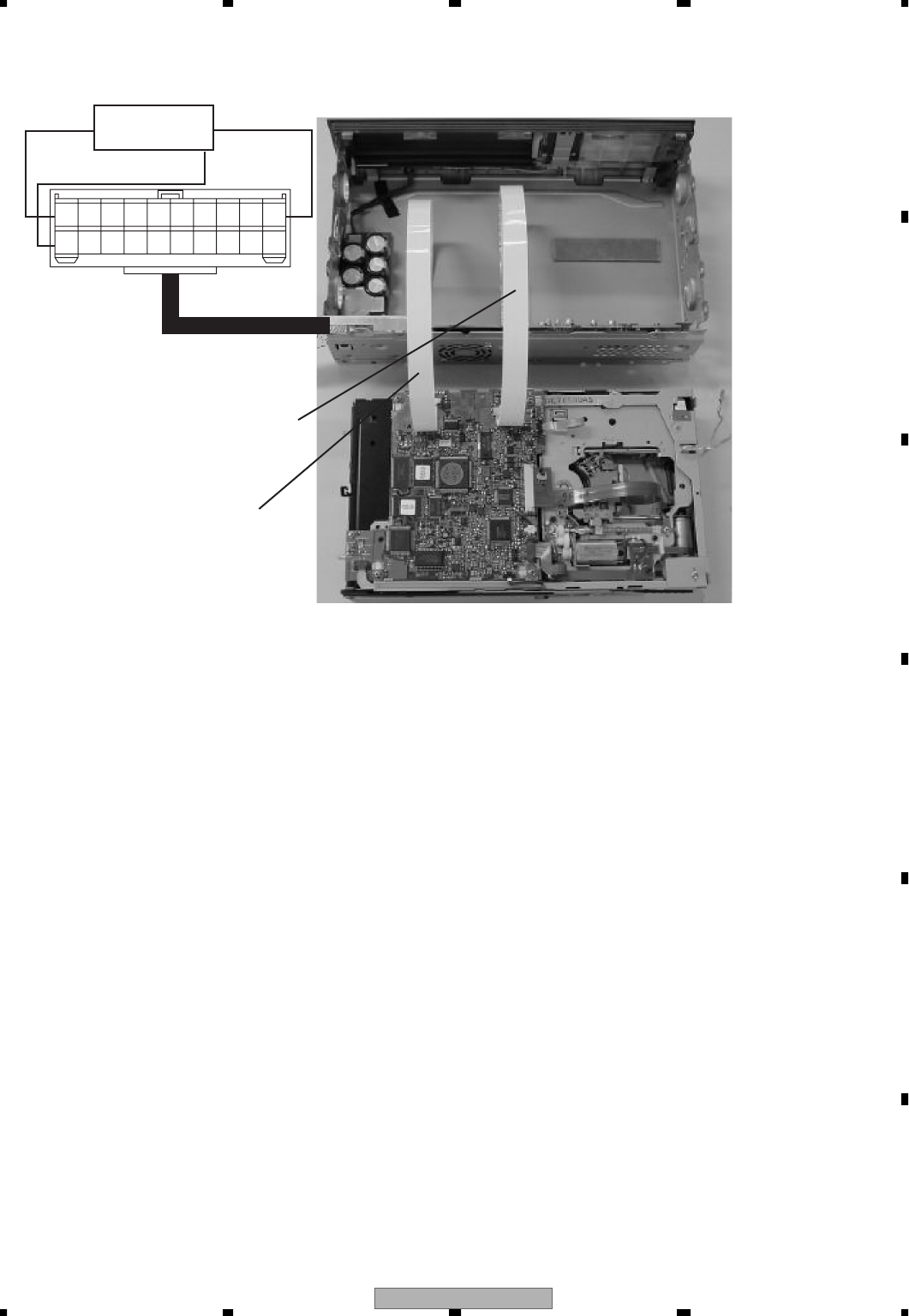
XDV-M8357ZT/UC 65
5678
5678
C
D
F
A
B
E
6. ADJUSTMENT
6.1 JIG CONNECTION DIAGRAM
30P EXTENSION CABLE
GGD1171
15P EXTENSION CABLE
GGD1177
Head Unit of TOYOTA
KEX-M9137ZT-02/UC, KEX-M9737ZT-02/UC
DC Regulated
Power Supply
+14.4V +14.4V
0V
On your service benches, the mechanism should be placed with
the magazine-slot side up unlike that shown in the photo.
This photo is XDV-M8006ZT.
12345678910
11 12 13 14 15 16 17 18 19 20
1. +B
2. NTSO
3. SG
4. SGND
5. CDL+
6. CDR+
7. NC
8. TXM+
9. NC
10. ACC
11. GND
12. NC
13. NC
14. NC
15. CDL-
16. CDR-
17. SGND
18. TXM-
19. NC
20. MUTE
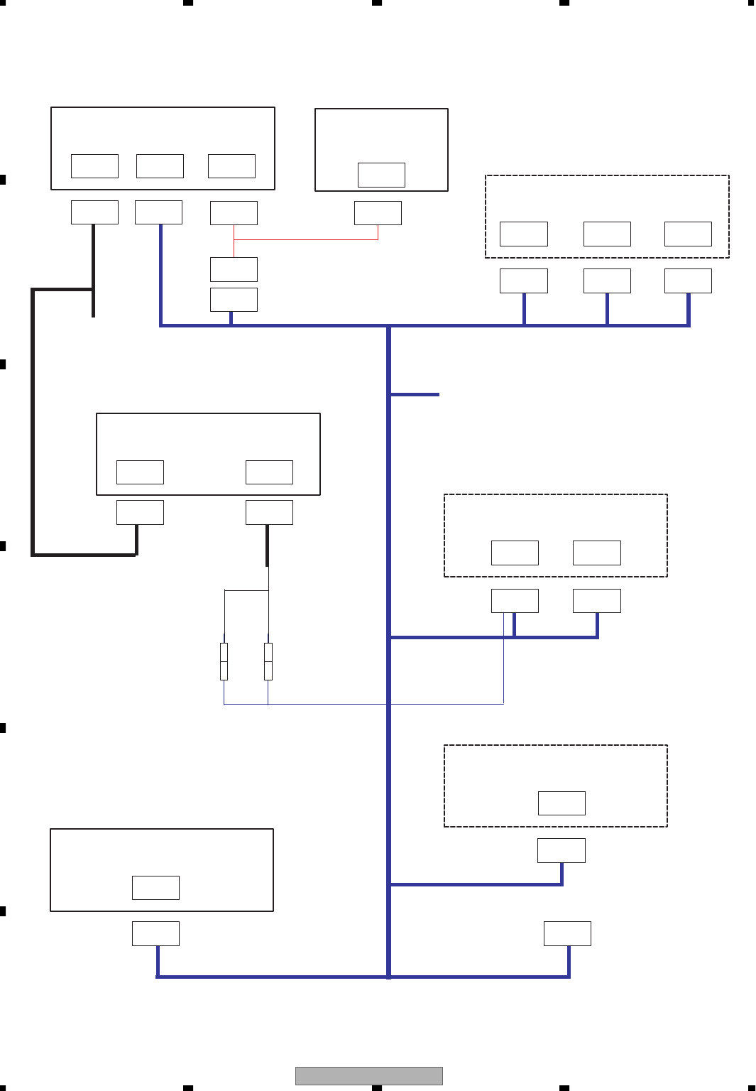
XDV-M8357ZT/UC
66
1234
1234
C
D
F
A
B
E
RSA Controller
GGD1169
GGD1348
Bullet connector
(To DC Regulated Power Supply)
Bullet connector
SP Line
Bullet connector
(To DC Regulated Power Supply)
KEX-M9137ZT-02/UC(Pioneer AMP)
KEX-M9737ZT-02/UC(Mraklevinson AMP)
XDV-M8357ZT/UC
GM-9027ZT-02/E
Marklevinson AMP
H/U
EMV(DENSO)
GGD1240
AUI+AUI-
FR+FR-
AMP
MDVD
NAVI ECU(DENSO)
*MCD
*Please don't connect the MCD and MDVD at the same time
*MCD or MDVD does not operate if RSA controller is not connected.
- Connection Diagram EMV SYSTEM MODEL(/UC)
XM
TUNER
GEX-M8087XMZT/XU/UC
GGD1398
12P20P20P
20P 20P 12P
12P
12P
12P
12P
6P 28P 26P
6P 28P 26P
25P 16P
16P25P
10P18P
18P 10P
24P
24P
32P
20P
20P
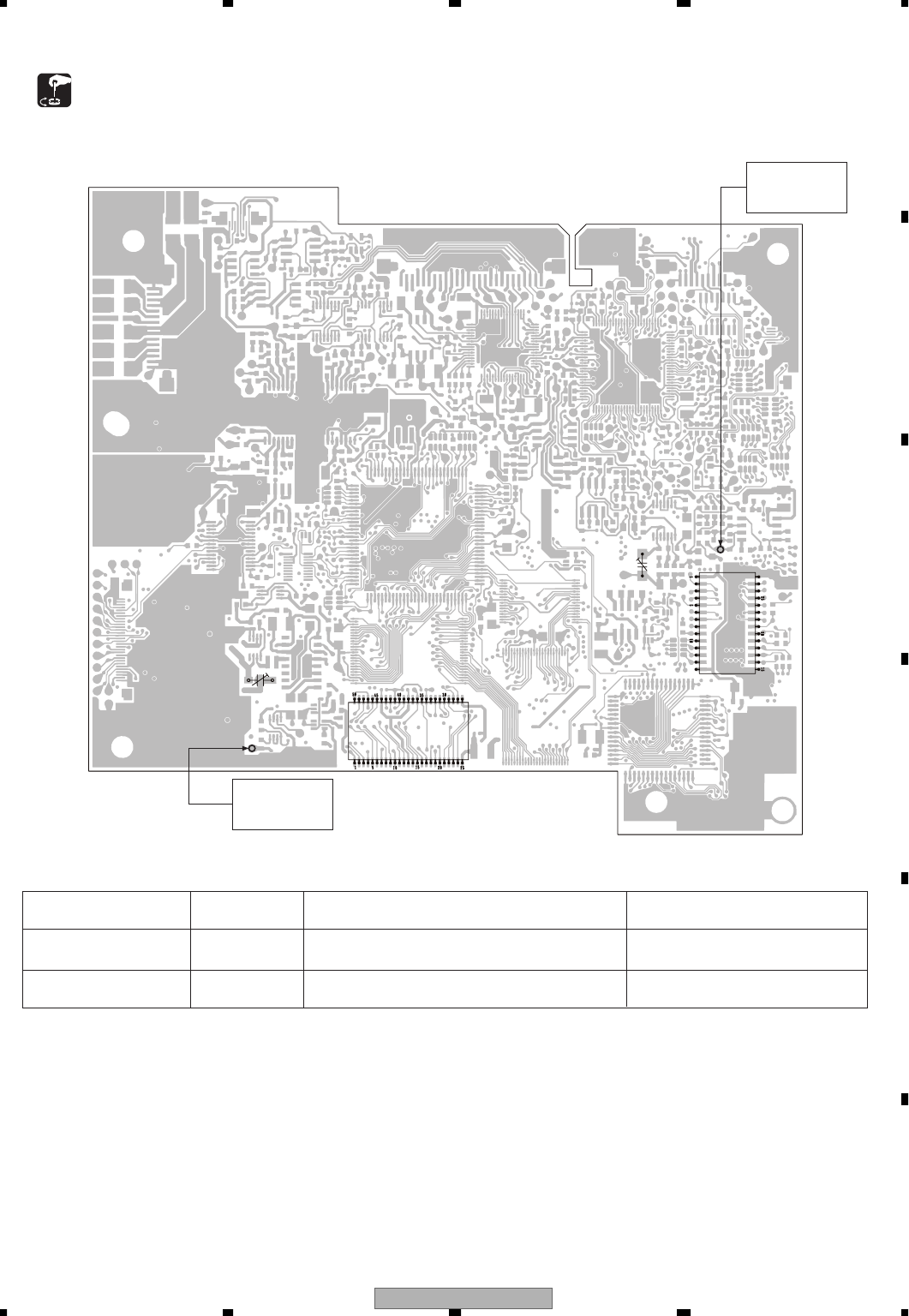
XDV-M8357ZT/UC 67
5678
5678
C
D
F
A
B
E
6.2 MAIN UNIT ADJUSTMENT
IC1200
TC1000
TC201
IC702
DSPCLK
VCO
Setting state : Normal Mode, Without magazine
Item Adjustment Adjustment Symptoms at incomplete
point Method adjustment
16MHz Master Clock TC1000 Frequency Counter :16.934400MHz ±80Hz An image turns from a colored
one to a monochromatic one.
VCO Offset TC201 DC V Meter : 1.4V ±0.2V Too much misalignment will
result in no playback.
DC V Meter
MAIN PCB(SIDE B)
-Connection Diagram
Frequency
Counter
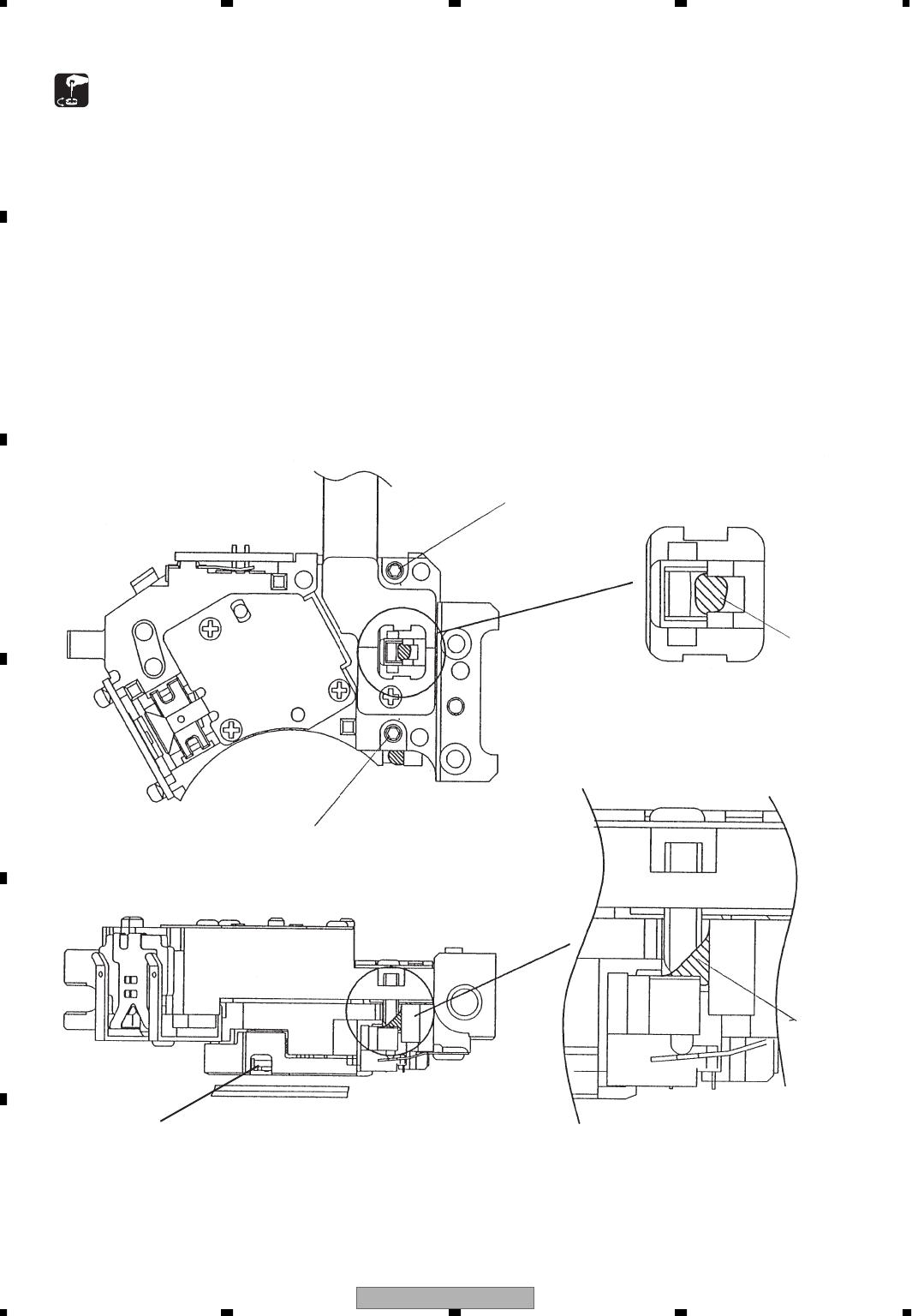
XDV-M8357ZT/UC
68
1234
1234
C
D
F
A
B
E
6.3 SKEW ADJUSTMENT
-If skew adjustment is necessary:
1) Replace the pickup unit by a new one.
2) Replace the spindle motor by a new one.
3) Replace the CRG chassis by a new one.
4) Replace the main shaft of the pickup unit by a new one.
5) Replace the sub shaft of the pickup unit by a new one.
* No skew adjustment is necessary for replacement of the CRG motor and the like.
-Procedures (Fig.1)
1) Remove the adhesive of the pickup unit with a pair of tweezers (above 2) to 5) only).
* Take care at this time that no fragments of the adhesive will be scattered, and that no unnatural force will apply
to the actuator.
2) Monitor the test point of the TP210 (RF waveform monitor) on the basis of GND in the product state with an
oscilloscope.
3) Clamp adjusting disc (GGV1018).
Skew adjusting screw
Skew adjusting screw B
Adhesive
Adhesive
Coat the shaded portion (two locations)
with (adhesives).
Fig.1
Actuator
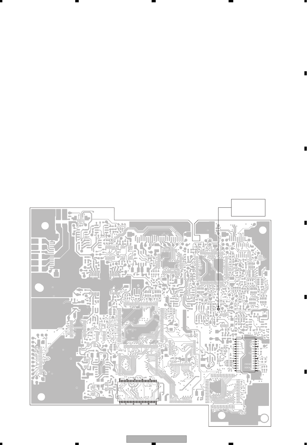
XDV-M8357ZT/UC 69
5678
5678
C
D
F
A
B
E
IC1200
IC702
TP210
4) Turn on the power in the test mode (F. Offset adjustment is found) and move the pickup to the vicinity of the
center of the disc.
5) Turn on the DVD LD and perform Focus Close.
6) Automatically adjust Tracking Balance and perform Tracking Close.
7) Observing RF waveform levels of an oscilloscope, slightly turn skew adjusting screw A and adjust the
oscilloscope so that the levels can be maximized. Repeat this operation three times and fix the levels where
they are maximized.
8) Mix agents A and B of adhesive 601 at a ratio of 1 to 1 and coat a specified part with both agents of the
adhesive. The adhesive is cured about 15 minutes. The coating position is shown in Fig.1.
Note) Do not apply the adhesive to the pickup section and the mechanical unit section other than the specified
part. Because heat is generated, do not mix a great number of adhesives at a time. Use the same number
of adhesives as the original one. Do not apply vibration until the adhesive is fixed.
9) Apply the screw lock to the head of the skew screw and secure it.
-Symptoms at incomplete adjustment
1) Deterioration of error rates
2) Large RF jitters: Waveforms are distorted.
3) Unstable tracking servo: There are such effects as leading-in and unstable servo.
Oscilloscope
MAIN PCB(SIDE B)
-Connection Diagram
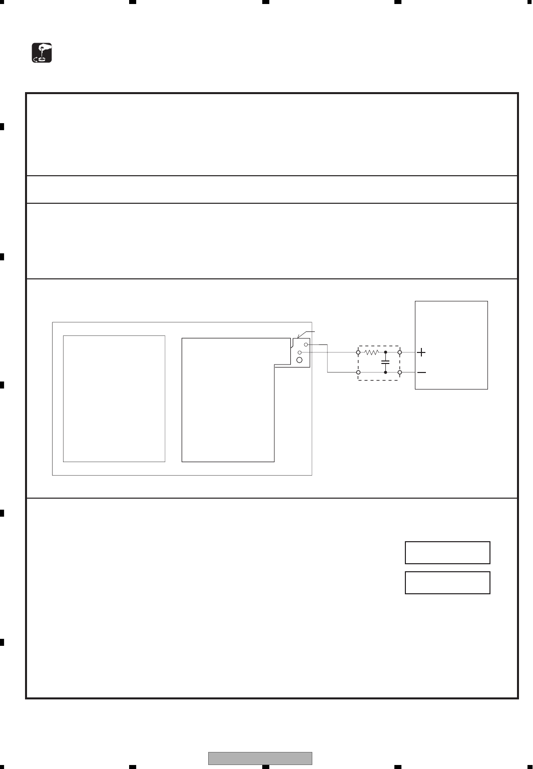
XDV-M8357ZT/UC
70
1234
1234
C
D
F
A
B
E
6.4 ELEVATION ADJUSTMENT
• Precautions
This mechanism unit uses a slide variable resistor to detect the height of the stage.
To absorb misalignment of the stage height due to unevenness of the DVD/CD mechanism unit and main unit,
the adjustment for each mechanism unit needs to be performed using semi-fixed resistors.
Because adjustment is performed on the production line, readjustment is not necessary usually. However, if an
elevation error occurs or when the slide variable resistor, spindle motor and CRG
chassis are replaced, elevation needs to be adjusted in the following procedures:
• Purpose
Adjust and check that the operation of elevation is normal.
• Adjustment method
• Measuring apparatus Oscilloscope, L.P.F. (one piece)
• Measuring point EREF or EPVO
• Setting state Without magazine, test mode
Place the DVD/CD mechanism unit facedown (place the DVD/CD mechanism unit so
that the main unit may be set to the upper side).
• Check procedures
For the flowchart of the test mode.
1. Enter the test mode and select a multiple DVD/CD player.
2. Set the mechanism unit test mode.
-This adjustment shall be performed when an error code 84 is displayed for an elevation error.
00800000
EREF
EPVO
Oscilloscope
MAIN UNIT
L.P.F.
47kΩ
1µF
VR302
PCB UNIT(B)
20400000
Display on head unit
XDV-M8357ZT/UC 71
5678
5678
C
D
F
A
B
E
3. Move to the ELV/tray selection mode and press DISC key to select the ELV mode.
4. Move to the operation mode selection.
5. When the DISC key is pressed, travel varies.
Note: If travel is set to Major, the stage
mechanical unit continues moving as
long as the DISC key is pressed.
If travel is set to Intermediate and
Minor, the stage mechanical unit
moves whenever the DISC key is
pressed once.
6. Move to the motor forward revolution mode or motor reverse revolution
mode and align the magazine slot to graduations on the fourth disc (Fig. 2).
7. Adjustment
Adjust the potential difference between EREF and EPVO of PCB (B)
to 380 ±20 mV with VR302.
8. Termination of adjustment
Move to the mechanism-unit test termination mode and terminate
the mechanism-unit test mode.
↓
ELV/Tray select mode
↓
Key DISC
↓
Tray select
↓
Key DISC
↓
ELV/Tray select mode
↓
Key DISC
↓
ELV select
Display on head unit
Tray
ELV
70430000
70440000
Reverse
revolution
Forward
revolution
70450000
70410000
00000001
00000000
↑
Key DISC
70410000
70420000
00000001
00000002
↓
Operation mode select
↓
Key DISC
↓
Middle movement
↓
Key DISC
↓
Operation mode select
↓
Key DISC
↓
Maximum movement
↓
Key DISC
↓
Operation mode select
↓
Key DISC
↓
Minimum movement
70420000
00000000
70420000
↑
Key DISC
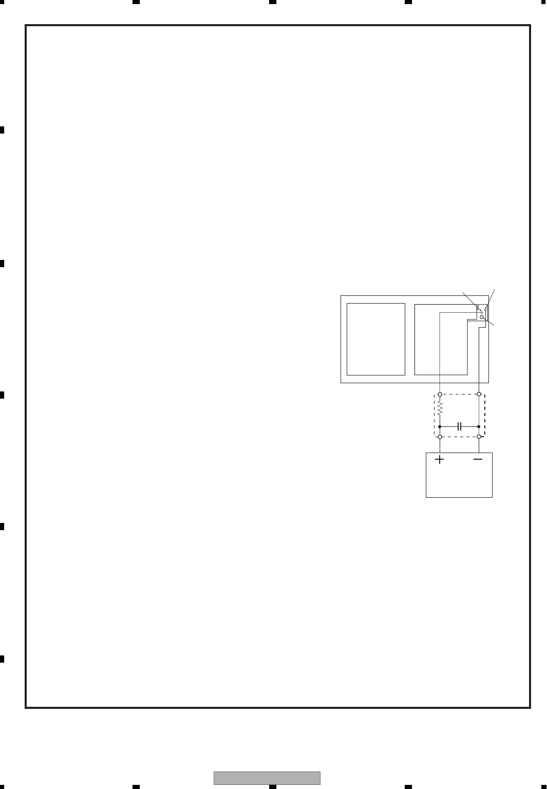
XDV-M8357ZT/UC
72
1234
1234
C
D
F
A
B
E
9. Operation check
Terminate the test mode.
Place the mechanism unit horizontally (set the main unit to the drop side). At this time, take care of
short-circuiting of the PCB.
10. Check the height of the stage.
Press the DISC ±key to select DISC 4.
Check that the stopper bend of the clamping lever is fitted in the
groove of the frame stopper
section. (Fig. 3 to 5)
• Precautions
• The stopper bend to be clamped finally is clamped under the groove.
Check the stopper bend at
the position where it is fitted in the groove.
• Adjustment is completed if the stopper bend enters the center and is
clamped under the groove. Go to 14).
• If the stopper bend is dislocated, check misalignment. Go to 11).
11. If the mechanism unit is dislocated:
Place the mechanism unit facedown.
When the mechanism unit is dislocated to the direction of the first disc,
turn VR302 counterclockwise. (Fig. 3)
Drop the voltage of EREF by 20 mV which was adjusted in 7.
to descend the stage to the direction of the sixth disc by 0.1 mm.
When the mechanism unit is dislocated to the direction of
the sixth disc, turn VR302 clockwise. (Fig. 5)
Raise the voltage of EREF by 20 mV which was adjusted in 7.
to ascend the stage to the direction of the first disc by 0.1 mm.
12. Place the mechanism unit horizontally and recheck from 10.
13. After adjustment has been completed,
14. Press the EJECT switch.
15. After the operation of the mechanism unit has stopped, turn off the power.
16. After the power has be turned off, turn on the power in one minute or more
and insert the magazine.
17. Check that the mechanism unit operates normally for the first and fourth discs.
18. Terminate all adjustment for OK (normal operation) and readjust for NG (abnormal operation).
GND
EREF
VR302
1µF
47kΩ
Oscilloscope
L.P.F.
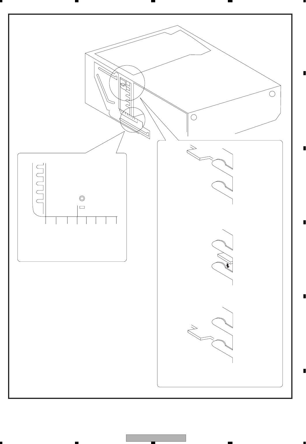
XDV-M8357ZT/UC 73
5678
5678
C
D
F
A
B
E
R
65 E
NG
OK
NG
Stopper bend of the
clamp lever.
Engaged in the center and pressed downward.
Fig. 2
Dislocated toward the first DVD.
Adjust the insertion gate of magazine to
the fourth scale.
Dislocated toward the sixth DVD.
Fig. 3
Fig. 4
Fig. 5

XDV-M8357ZT/UC
74
1234
1234
C
D
F
A
B
E
6.5 TEST MODE
1) Precautions on Adjustment
• Because this equipment uses a single voltage (+5 V)
in the regulator, the reference voltage of a signal is
not GND, but is REFO (VR21, VR25, PREF). If REFO
and GND are mixed and touched at product
adjustment, correct potential cannot be measured
but also the servo malfunctions and an strong
shock applies to the pickup. So, note the following
items. REFO and GND must not be mixed on the
negative side of the probe of the measuring
apparatus. In particular, do not connect the
negative side of the ch1 probe of the oscilloscope to
REFO and the negative side of the ch2 probe to
GND. Further, in general, because most main units
of measuring apparatuses reach the same potential
as the negative side of the probe, make the main
unit of the measuring apparatus enter the floating
state. If REFO and GND are incorrectly connected,
immediately turn off the power.
• Be sure to turn off the power when attaching and
detaching the various filters and wire materials
required for measurement.
• For the adjustment and measurement after power-
on, adjust or measure after having performed
running for about one minute until the circuit
becomes stable.
• Because various types of protection do not operate
by software in the test mode, do not apply a
mechanical and electrical shock during adjustment.
• This equipment uses a photo transistor to detect a
disc when inserting and removing it to and from the
tray. Accordingly, if strong light enters this
equipment with the case remove at repair and
adjustment, the following malfunctions may occur.
* Although there is a disc, play is disabled because
the disc cannot be used.
* A disc of 12 cm is incorrectly detected for a disc
of 8 cm.
When a malfunction occurred, take action such as
changing the position of the light source, changing
the orientation of this equipment or covering a
photo transistor.
• In the test mode, after having executed carriage
movement during focus search, immediately turn
off the power. (The lens is stuck up or down and
the actuator may be damaged by fire.)
• During disc replacement, press the key of the disc to
be replaced by a new one.
2) Test Mode
Because this machine is adjusted by combining a
pet unit, each adjustment key operation is also
performed by the pet unit. For reference purposes,
how to enter the test mode and key operation for
KEX-M9737ZT-02/UC are described. Besides, the key in this
adjustment text is also an KEX-M9737ZT-02/UC key.
• How to enter the test mode
• How to reset the test mode
Enter ACC and backup OFF.
• After having executed carriage movement during
focus search, immediately turn off the power.
(Because the lens is stuck, the actuator may be
damaged by fire.)
• The TR Jump below 255 TR continues operation
even if the key is detached. Other TR Jumps enter
the T Close state when the key is detached.
• As soon as the power is turned on/off, the Jump
Mode is reset to Single TR and the automatic
adjustment value returns to the initial value.
• During disc replacement, press the key of the disc to
be replaced by a new one.
• Be sure to load a DVD disc on the first tray of the
magazine.
Normal mode
Test mode
Press the AM and SEEK/TRACK DOWN key.
Press the DISC key three times while
pressing the 1 key and 6 key.
Diagnosis mode
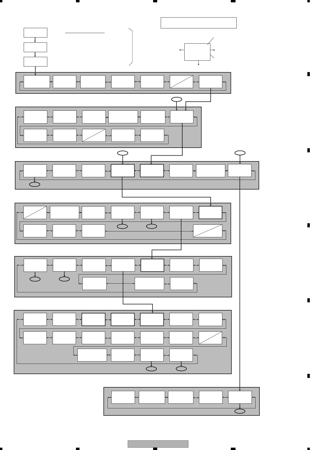
XDV-M8357ZT/UC 75
5678
5678
C
D
F
A
B
E
Normal
mode
Diagnosis
mode
Test mode
Press the DISC key three times while
pressing the 1 key and 6 key.
Press the AM and SEEK/TRACK DOWN key.
Bus-con
version display
00800000
Detailed error
code display
00810000
Power ON and
system check
00820000
Power OFF
00830000
Clear all
memories
00840000
Debug mode
00850000
Sys-con,
mecha-con
test start
00860000
EJECT
10030000
Play state
display
10040000
Try select
10211000
Auto adjustment
value display
10240000
Apply version
display
10000000
Test
start
10940000
EDC mode
start
10690000
EDC mode 1
10700000
EDC mode 2
10710000
DVD error
rate check
10720000
EDC mode
end
10730000
Return to
stage1
20020000
EJECT
20030000
Play state
display
20040000
Servo. to
initial value
20060000
Disc type
decision
20070000
Try select
20211000
Auto adjustment
value display
20240000
Mech. test
mode
20400000
Switch the
gain of OEIC
30330000
Auto adjustment
value display
30240000
Play state
display
30040000
Return to
stage 1
30020000
Return to
stage 2
30050000
Focus
close
30080000
S curve
mode IN
30090000
Carriage
outer move
30100000
Carriage
inner move
30110000
EQ measurement
mode
30220000
LD ON
30130000
Return to
stage 1
40020000
Return to
stage 2
40050000
S curve
mode OFF
40130000
Tracking
close mode
40140000
TB auto
adjustment
40280000
Carriage
outer move
40100000
Disc type
discrimination
40160000
Auto adjustment
value display
40240000
Play state
display
40040000
Carriage
inner move
40110000
Track jump
(inner)
50180000
Track jump
(outer)
50190000
FT gain
adjustment
50260000
FB auto
adjustment
50270000
RF auto
adjustment
50250000
Tracking
open
50170000
Carrige
inner move
50110000
Carrige
outer move
50100000
Tilt servo
move start
50350000
Tilt servo
move start
50360000
Focus
jump
50150000
Tracking
close
50140000
CD error
rate check
50200000
Spindel
CAV move
50300000
Auto adjustment
value display
50240000
Play state
display
50040000
Return to
stage 1
50020000
Return to
stage 2
50050000
Mechanism
test end
70450000
Motor negative
rotation
70440000
Motor positive
rotation
70430000
Operation
mode select
70420000
ELV/Try
select
70410000
Test mode IN
Stage 0:System check mode
Stage 1:EDC measurement
Stage 2:Disc type decision mode
Stage 3: Focus close mode
Stage 4:Tracking close mode
Stage 5:Wave of servo condirmation mode
Stage 6:Mechamism test mode
Test mode operation flow
Test contents
Command
Number
Key operation for FX-MG8606ZT/UC
1 key press 2 key press
DISC key press
Test contents execute : DISC key press
Test contents select : TRACK UP/DOWN
Oblique line : NC(Factory mode)
Bold line : Forgetting execution is noted
1
2
1
12
12
12
3
3
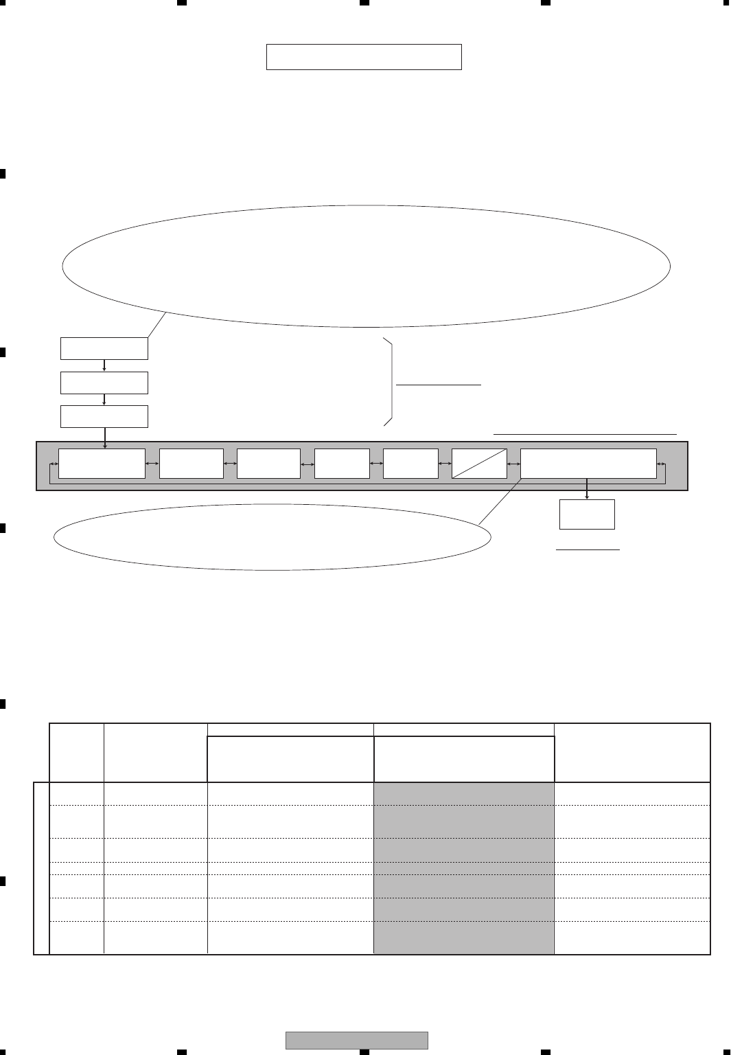
XDV-M8357ZT/UC
76
1234
1234
C
D
F
A
B
E
Test Mode
Start
Diagnostic
Mode
DVD Changer
Test Mode
While doubly pressing the [1] and [8] keys,
press the [DISC] key three times.
Doubly press the [AM] key and the
[SEEK/TRACK DOWN] key.
Bus Microcomputer
Version Display
00800000
Detailed Error
Display
00810000
Power ON and
System Check
00820000
Power OFF
00830000
All Memory
Clear
00840000
Debug Mode
00850000
System Controller - Mechanical-
Unit Controller Test Start
00860000
Test Mode IN
Stage 0 System Check Mode
Test Mode IN, Stage 0
-Outline
[Test Mode IN]
• [Test Mode IN] is a procedure for entering the DVD changer in the test mode.
• Once the DVD changer has exited from the test mode, restart the test mode from [Test Mode IN]
[Stage 0]
• This stage displays a version number of the bus microcomputer, checks the contents of detailed errors and
performs a system check.
-Operation Flow of [Test Mode IN] and [Stage 0]
!! To prevent a malfunction and damage !!
• When performing the test mode of [Stages 1 to 6], be sure to insert a DVD video disc in Tray 1
of the magazine. (If DISC1 is not a DVD video disc, the test mode does not function normally.
• When performing the test mode of [Stage 7], be sure to remove all the trays of the magazine and
use a magazine in which no tray is inserted. (If a tray is inserted in the magazine,
a mechanical unit may be damaged.
Test Start
10940000
If [00800000] is executed when no disc is not inserted
in the magazine and the door opens, return value [00870000] is reached and
no more operation is enabled. At that time, turn off/on ACC once and restart
the test mode from [Test Mode IN] after having inserted the magazine.
To Stage 1
-Example of Test Execution
• Check a detailed error code.
1) Check the contents of an error
which is currently occurring. : Execute [00810000].
2) Newly obtain error contents. : Execute [00840000], [00830000], [00820000] and [00810000] in this order.
• Go to the next stage. : Execute [00860000].
-Contents of Test
Command
Test name Test contents Test contents selection item setting Return value
number Execute test contents: Selection switching: Pressing the
Press the DISC key. TRACK UP/DOWN key
Return to the command number
display: Re-press the DISC key.
00800000
Bus microcomputer
Displays a bus microcomputer Version number
version display version.
00810000 Detailed Displays a detailed error code. OOO_XX (XX: error code)
error display For error contents, refer to the
error code table.
00820000 Power ON and Turns on the power. None
system check
00830000 Power OFF Turns off the power. None
00840000 All memory clear
Clears error histories recorded in
00800001
the system microcomputer.
00850000 Debug mode ** Factory Mode ** 00800001
Displays debug.
00860000 System controller - Moves to the test mode. None
mechanical-unit
controller test start
← Press the 2 key Press the 1 key →
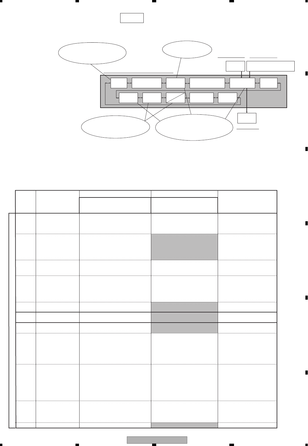
XDV-M8357ZT/UC 77
5678
5678
C
D
F
A
B
E
Stage 1
- Outline
[Stage 1] displays an application program version number and measures (DVD) an error rate.
- Operation Flow of [Stage 1]
- Example of Test Execution
• DVD error rate measurement:
Collectively execute [10690000], [10700000], [10720000] Measurement and [10730000] in this order (normally less than 0.1%).
For the details of the DVD error rate measurement method, refer to the appended table.
The CD error rate is enabled at [Stage 5].
• Display an automatic adjustment value of servo
Execute [10690000], [10240000] Display and [10730000] in this order. Only when [10690000] is executed, a normal value is displayed.
The initial value of automatic adjustment is displayed.
• Go to the next step: Execute [10940000].
Eject
10030000
Replayed Status
Display
10040000
Tray
Selection
10211000
Automatic Adjustment
Value Display
10240000
Application
Version Display
10000000
Test Start
10940000
EDC Mode
Start
10690000
EDC Mode 1
10700000
EDC Mode 2
10710000
DVD Error Rate
Measurement
10720000
EDC Mode
Termination
10730000
Stage 1 EDC Measurement Mode
After the [10030000] magazine has
been ejected, the test mode cannot be
continued.Turn off/on ACC once and restart
the test mode from [Test Mode IN].
Only the tray in which a
disc is inserted can be selected
for the [10211000] tray
selection.
[10700000] and [10710000] are factory
verification modes. They are not used
usually. For incorrect execution,
terminate with [10790000].
∗∗ After execution of the [10690000] EDC
mode, be sure to execute [10730000] EDC mode
termination before executing [10211000] and
[10940000]. The test mode does not
function normally.
Return to
Stage 1
X0020000
System Controller - Mechanical-
Unit Controller Test Start
00860000
Disc Type
Decision
20070000
To Stage 1
From
Stage 2
Stage 3
Stage 4 and
Stage 5 From Stage 0
- Contents of Test
Command Test name Test contents Test contents selection item setting Return value
number Execute test contents: Press the DISC key. Selection switching: Pressing the
Return to command number display: TRACK UP/DOWN key
Re-press the DISC key.
10030000 EJECT Ejects the magazine. Whether carriage returns the home
position or not is selected at ejection
.
[10030000] With carriage home
00000000(With carriage home)
[10031000] Without carriage home
00000001(Without carriage home)
10040000 Replayed status Displays a replayed status. 00000000(at servo OFF)
display
01010101(Servo initialization state)
02020202(at focus servo ON)
ID No. (at DVD replay)
MSF No. (at CD replay)
10211000 Tray selection Clamps an optional disc A tray number is selected.
Executes [1021X000] "X" matching
0000000X("X" is a tray number.)
an optional tray number.
Toggle-selects an adjustment value
to be displayed. Display at selection
10240000 Automatic adjustment Displays an automatic adjustment "0"[10240XXX]
Refer to the appended table.
value display result of a servo system. "1"[10241XXX]
"2"[10242XXX]
10000000 Application version Displays a version of an application
Application program version number
display program.
10940000 Test start
Goes to Stage 2. (Starts the mechanical-
00000000
unit controller/microcomputer test mode.)
10690000 EDC mode start Starts normal replay after control data
TOC-RDX ("X" is a tray number.)
read for DVD, and after TOC read for CD.
10700000 EDC test mode 1 Specifies a replay start position and
A replay start position is set.(For DVD)
EDC10000(for DVD)
performs solid replay.
ID number, and (for CD) MSF number.
EDC1XXXX(for CD) and
Sets an MSF number after having X is a minute and second
executed 10711000.
Sets an ID number after having 10700000
executed 10700000.
10710000 EDC test mode 2 ** Factory Mode ** A replay start position is set EDC10000(for DVD)
(For DVD) Starts the replay which (For DVD) ID number, EDC1XXXX(for CD) and
repeats the operation of 1-block and (for CD) MSF number. X is a minute and second
read/pause. (For CD) Starts the Sets an MSF number after having
same operation as EDC mode 1 executed 10711000.
Sets an ID number after having
executed 10700000.
10720000 Error rate Measures a C1 error rate of DVD.
Selects
between 1 and 64 of the
measurement number of sampling blocks. A C1 error rate is exponentially
(Usually 32 blocks)
displayed.
···Refer to the appended table.
10730000 EDC mode end Terminates the EDC mode. None
Press the 1 key
Press the 2 key
↓
↓
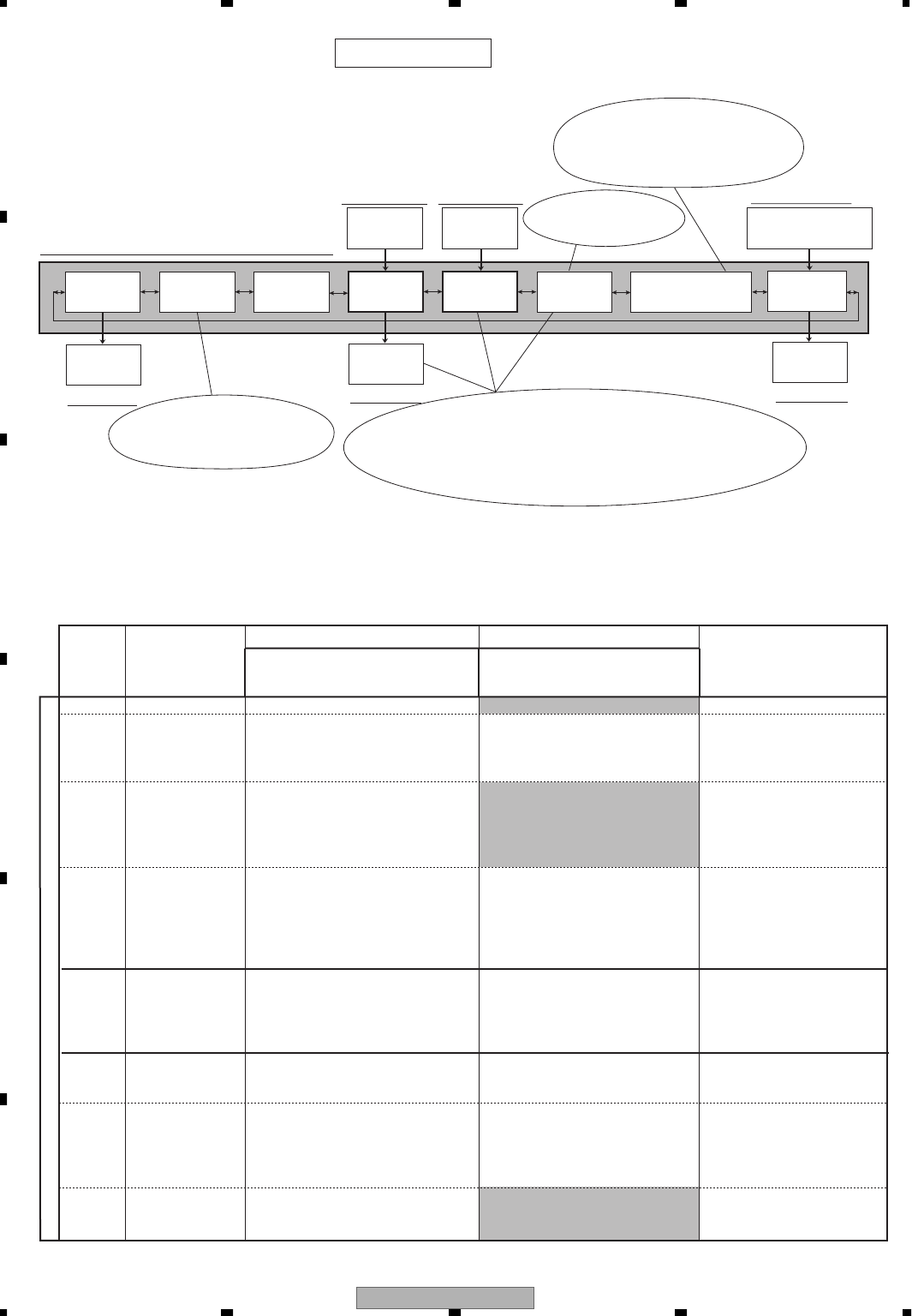
XDV-M8357ZT/UC
78
1234
1234
C
D
F
A
B
E
Stage 2
- Outline
[Stage 2] sets and selects a disc type and test mode.
- Operation Flow of [Stage 2]
- Example of Test Execution
• Go to [Stage 3]: Execute [20211000], [20211000] and [2006000] in this order.
• Go to [Stage 7]: Execute [20240000].
When the mechanical unit test mode is executed, the [20070000] Execution is unnecessary
because there is no disc in the magazine.
After the [20030000] magazine has
been ejected, the test mode cannot be
continued.Turn off/on ACC once and restart
the test mode from [Test Mode IN].
Only the tray in which a
disc is inserted can be selected
for the [10211000] tray
selection.
∗∗ For the [20070000] Disk Type
~ [20070000] = [20211000] = [30130000] ~
When the test enters [Stage 2], be sure to execute [20070000].
If it is not executed, the test mode does not function normally.
A disc type selected for [20070000] must match that selected for [20211000].
Similarly, a type of an LD (laser diode) selected for [30130000] of [Stage 3] needs to
match a disc type selected for [20070000].(If it does not match,
the test mode does not function normally.)
From Stage 1
From
Stage 3,
Stage 4 and
Stage 5 From Stage 7
- Contents of Test
Command Test name Test contents Test contents selection item setting Return value
number Execute test contents: Press the DISC key. Selection switching: Pressing the
Return to command number display: TRACK UP/DOWN key
Re-press the DISC key
20020000 Return to Stage 1 Returns to Stage 1. 00000000
20030000 EJECT Ejects the magazine
Whether carriage returns to the home
position is selected at ejection.
[2003000] With home carriage
00000000 (With carriage home)
[2031000] Without carriage home
00000001 (Without carriage home)
20040000 Replayed Status Displays a replayed status. 00000000 (at servo OFF)
Display
01010101(Servo initialization state)
02020202(at focus servo ON)
ID number (at DVD replay)
MSF number (at CD replay)
20060000 Servo Initialization Initializes a servo system. Whether a servo system automatic
adjustment is performed or
not is selected at servo initialization.
[20610000] With offset adjustment
(Usually set to offset adjustment) 00000000(Irrespective of
[
20060000
]
Without offset adjustment
a selection result)
20070000 Disc Type Decision Decides a disc type to set a servo A disc type is decided.
gain in accordance with the disc type [20070000] CD setting 00000000(at CD selection)
used for test. [20071000] DVD1 layer setting
00000001(at DVD1 layer selection)
[20072000] DVD2 layer setting
00000002(at DVD2 layer selection)
[20073000] Reserved 00000003(Reserved)
20211000 Tray Selection Clamps an optional disc A tray number is selected.
Executes [2021X000] "X"
0000000X("X" is a tray number.)
matching an optional tray number
Toggle-selects an adjustment value
to be displayed.Display at selection
20240000 Automatic Toggle-selects an adjustment value "0" [20240XXX] Refer to the appended table.
Adjustment Value to be displayed. "1" [20241XXX]
Display "2" [20242XXX]
20400000 Mechanical-Unit Moves to the mechanical-unit 00000000
Controller Test controller test mode.
Mode
Press the 1 key
Press the 2 key
Return to
Stage 1.
20020000
EJECT
20030000
Replayed
Status Display
20040000
Servo
Initialization
20060000
Disc Type
Decision
20070000
Tray
Selection
20211000
Automatic Adjustment
Value Display
20240000
Mechanical Unit
Test Mode
20400000
Stage 2 Disc Type Decision Mode
Return to
Stage 2
X0050000
Test Start
10940000
Mechanical-Unit
Controller Test End
70450000
ELV/Tray
Selection
70410000
To Stage 7
LD ON
30130000
To Stage 3
Test Mode
10940000
To Stage 1
∗∗ When executing [20400000] and
performing the mechanical-unit controller test
mode of [Stage 7], be sure to remove all the
trays from the magazine and use a magazine
in which no tray is inserted. (A mechanical
unit may be damaged.)
↓
↓
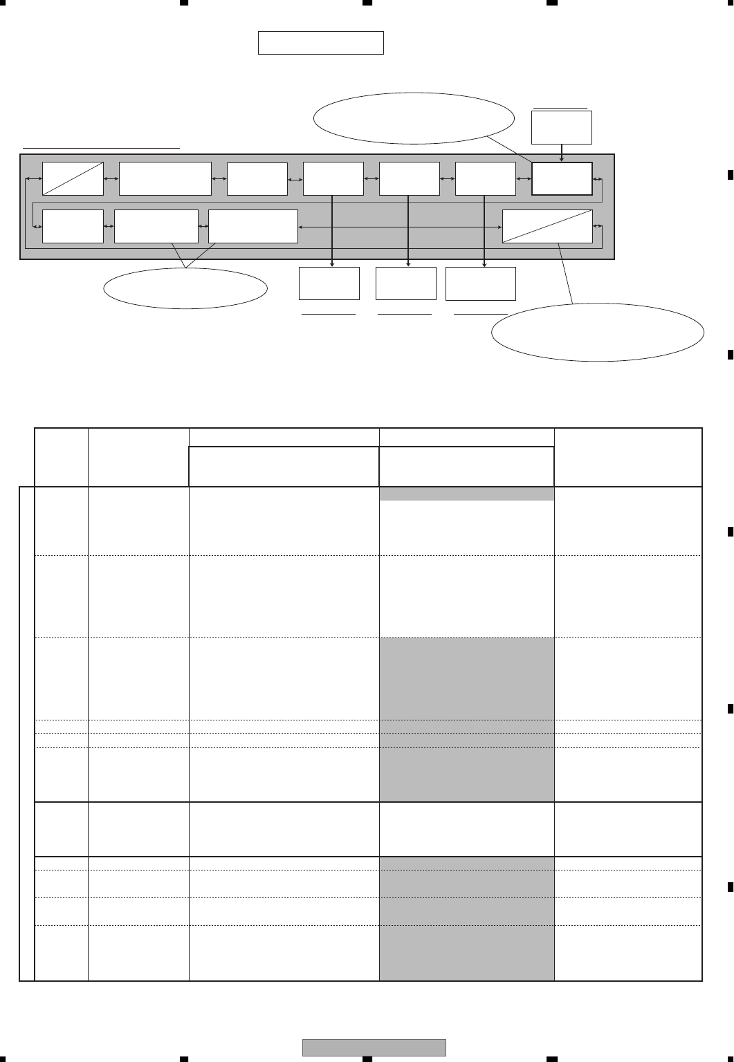
XDV-M8357ZT/UC 79
5678
5678
C
D
F
A
B
E
Stage 3
- Outline
[Stage 3] is used for measuring a servo system. (LD ON to focal close)
- Operation Flow of [Stage 3]
- Example of Test Execution
• S curve measurement:
Enter the [30130000] to [30090000] Measurement Mode.
→ [30080000] Measurement (An up and down movement is repeated at a fixed cycle in the S curve mode.)
→ Turn off the S curve mode for [40130000] of [Stage 4].
• Focus servo system measurement/Go to the next stage: Execute [30130000] and [300080000] in this order.
From Stage 2
- Contents of Test
Press the 1 key
Press the 2 key
Servo
Initialization
20060000
∗∗ At [30220000] Execution, because the
pickup may be damaged, remove pickup
connector (CN101).Besides, because this mode
is a factory verification mode, it is
not used usually.
OEIC Gain
Switching
30330000
Automatic Adjustment
Value Display
30240000
Replayed
Status Display
30040000
Return to
Stage 1
30020000
Return to
Stage 2
30050000
Focal Close
30080000
S Curve
Mode IN
30090000
Carriage Move to
Outer Circumference
30100000
Carriage Move on
Inner Circumference
30110000
EQ Measurement
Mode
30220000
LD ON
30130000
Stage 3 Focal Close Mode
TB Automatic
Adjustment
40280000
Servo Start
20060000
Test Start
10940000
To Stage 1 To Stage 2 To Stage 4
[30100000] and [30110000] move
while the execution key (DISC key)
is being pressed.
LD which turns on for [30130000]
Select an LD (laser diode) which matches
a disc type selected for [Stage 2]
[20070000].
Command Test name Test contents Test contents selection item setting Return value
number Execute test contents:Press the DISC key. Selection switching:Pressing the
Return to command number display: TRACK UP/DOWN key
Re-press the DISC key.
30330000 OEIC gain switching ** Factory Mode ** A High/Low gain is selected.
Switch an OEIC gain. [30331000] gain High 00000000(for Low gain)
[30330000] gain Low 00000001(for Low gain)
30240000 Automatic Displays an automatic adjustment An adjustment value to be Refer to the appended
adjustment value result of a servo system. displayed is toggle-selected. table.
display Display at selection
"0"[30240XXX]
"1"[30241XXX]
"2"[30242XXX]
30040000 Replayed status Displays a replayed status. 00000000(at Servo OFF)
display 01010101
(Servo initialization state)
02020202(at focus servo ON)
ID number (at DVD replay)
MSF number (at CD replay)
30020000 Return to Stage 1 Returns to Stage 1. 00000000
30050000 Return to Stage 2 Returns to Stage 2. 00000000
30080000 Folcal close Moves up and down the actuator 00000000
to the focus direction.
When a focal close condition is .
satisfied, turn on focal servo
30130000 Turn on the LD Executes the ON/OFF of laser diode An LD to be turned on/off is 00007801 (at CD LD ON)
(LD). selected. 00007800(at CD LD OFF)
[30130000] DVD LD (650 mm) 00006501(at DVD LD OFF)
[30131000] CD LD (780 mm) 00006500(at DVD LD OFF)
30090000 S curve mode IN
Turn on/off the S curve confirmation mode.
00000000
30100000 Carriage move to Moves the carriage to the outer 32100000
outer circumference circumference
30110000 Carriage move to Moves the carriage to the inner 32110000
inner circumference circumference.
30220000 EQ measurement ** Factory Mode ** 00000000
mode Forcibly turn on the servo of focus
and tracking and check the
characteristics of servo ED.
↓
↓
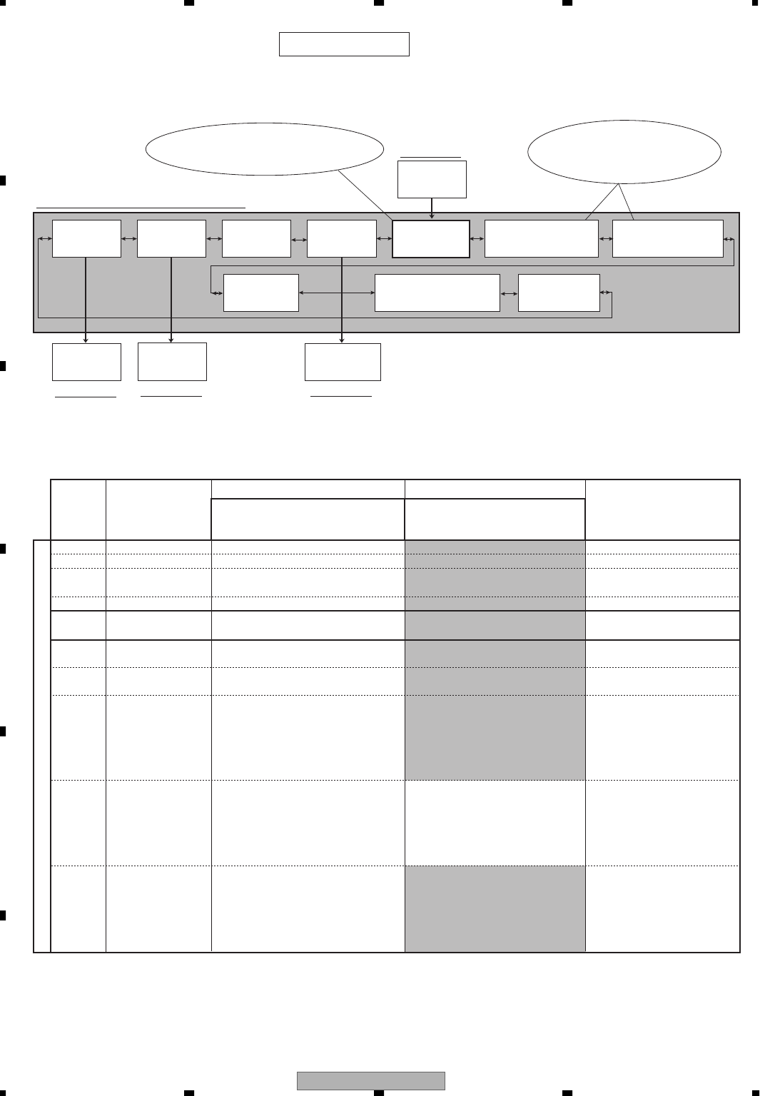
XDV-M8357ZT/UC
80
1234
1234
C
D
F
A
B
E
Stage 4
- Outline
[Stage 4] is used for measuring a servo system. (Tracking close)
- Operation Flow of [Stage 4]
- Execution of Test Execution
• Tracking servo system measurement/Go to the next stage: Execute [40280000] and [40140000] in this order.
From Stage 3
- Contents of Test
↓
Press the 1 key
Press the 2 key
Servo
Initialization
20060000
[40100000] and [40110000] move
while the execution key (DISC key) is
being pressed. Both are valid
when the tracking servo is OFF
(opens).
Return to
Stage 1.
40020000
Return to
Stage 2.
40050000
S Curve
Mode OFF
40130000
Tracking
Close
40140000
TB Automatic
Adjustment
40280000
Carriage Move to
Outer Circumference
40100000
Disc Type
Confirmation
40160000
Automatic Adjustment
Value Display
40240000
Replayed
Status Display
40040000
Carriage Move to
Inner Circumference
40110000
Stage 4 Tracking Close Mode
Test Start
10940000 RF Automatic
Adjustment
50250000
Focus Close
30080000
Test Start To Stage 2 To Stage 5
∗∗ Be sure to execute the [40800000] TB
(tracking balance) automatic adjustment.
[40140000] may not be able to be executed
normally.
↓
Command Test name Test contents Test contents selection item setting Return value
number Execute test contents: Press the DISC key. Selection switching: Pressing the
Return to command number display: TRACK UP/DOWN key
Re-press the DISC key.
40020000 Return to Stage 1 Returns to Stage 1. 00000000
40050000 Return to Stage 2 Returns to Stage 2. 00000000
40130000 S curve mode OFF Turns off the S curve confirmation 00006500
mode.
40140000 Tracking close Turns on the tracking servo. 00000000
40280000 TB automatic Automatically executes a tracking 00000000
adjustment balance adjustment.
40100000 Carriage move to Moves the carriage to the outer 42100000
outer circumference. circumference.
40110000 Carriage move to Moves the carriage to the inner 42110000
inner circumference circumference.
40160000 Disc type A disc type selected for 00000000(at CD selection)
confirmation [disc type (2007000)] can be 00000001
checked. (at DVD1 layer selection)
00000002
(at DVD2 layer selection)
00000003(Reserved)
40240000 Automatic Displays an automatic adjustment Toggle-selects an adjustment Refer to the appended table.
adjustment value result of a servo system. value to be displayed.
display Display at selection
"0"[40240XXX]
"1"[40241XXX]
"2"[40242XXX]
40040000 Replayed status Displays a replayed status. 00000000(at servo OFF)
display 01010101
(Servo intitialization state)
02020202(at focus servo ON)
ID No. (at DVD replay)
MSF No. (at CD replay)
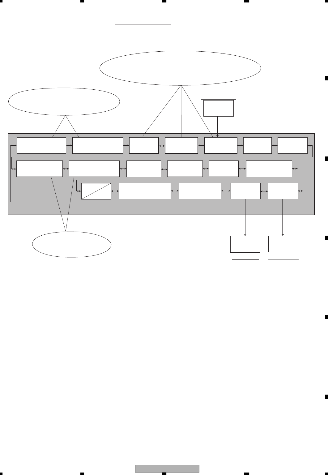
XDV-M8357ZT/UC 81
5678
5678
C
D
F
A
B
E
Stage 5
- Outline
[Stage 5] is used for measuring a servo system.
- Operation Flow of [Stage 5]
- Example of Test Execution
• CD error rate measurement:
Execute [50250000]→[5027000]→[50260000]→[50250000] and [50200000] Measurement in this order.
• Tilt servo measurement:
Execute [50250000]→[5027000]→[50260000]→[50250000]→[50350000] Measurement and [50360000] in this order.
• Focus Jump measurement:
Execute [50250000]→[5027000]→[50260000]→[50250000] and [50150000] Measurement in this order.
• Track jump measureme:
Execute [50250000]→[5027000]→[50260000]→[50250000]→[50180000] or [50190000] Measurement in this order.
Servo
Initialization
20060000
[50100000] and [50110000] move
while the execution key (DISC key) is
being pressed. Both are valid when
the tracking servo is OFF.
Test Start
10940000
Tracking
Close
40140000
To Stage 1 To Stage 2
From Stage 4
Track Jump
(Inner Circumference)
50180000
Track Jump
(Outer Circumference)
50190000
FT Gain
Adjustment
50260000
FB Automatic
Adjustment
50270000
RF Automatic
Adjustment
50250000
Tracking
Open
50170000
Carriage Move To
Inner Circumference
50110000
Carriage Move to
Outer Circumference
50100000
Tilt Servo
Operation Start
50350000
Tilt Servo
Operation Stop
50360000
Focus Jump
50150000
Tracking
Close
50140000
CD Error
Rate Measurement
50200000
Spindle CAV
Operation
50300000
Automatic Adjustment
Value Display
50240000
Replayed Status
Display
50040000
Return to
Stage 1
50020000
Return to
Stage 2
50050000
Stage 5
Servo Waveform Confirmation Mode
If less than 255 track jumps are executed in
the track jumps of [50180000] and [50190000],
the track jumps are repeated at regular intervals.
When they must be stopped, they can
be stopped with [50170000].
∗∗ Be sure to execute [50250000], [50260000] and [50270000].
If they are not executed, a servo system is not stable,
and [50180000] and [50190000] may not be able to be executed normally.
The execution procedure is [5025] to [5027] to [5026] to [5025].
Execute [5025] once at the beginning and end respectively.
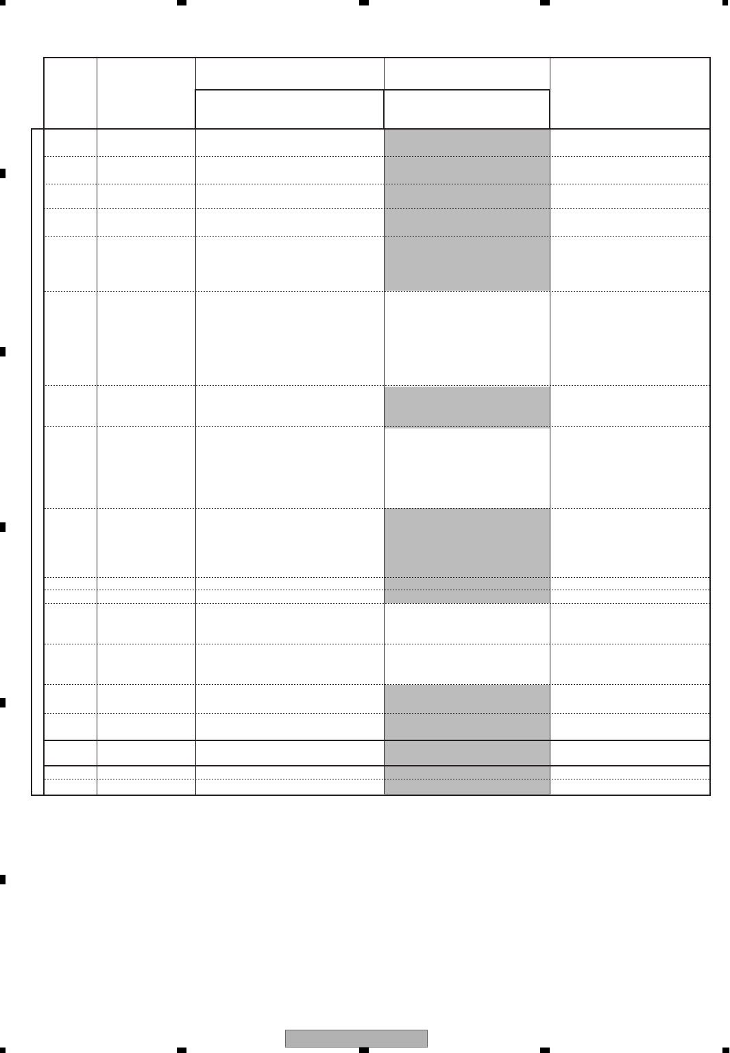
XDV-M8357ZT/UC
82
1234
1234
C
D
F
A
B
E
- Contents of Test
Command Test name Test contents Test contents selection item Return value
number setting
Execute test contents: Press the DISC key. Selection switching: Pressing the
Return to command number display: TRACK UP/DOWN key
Re-press the DISC key.
50110000 Carriage move to Moves the carriage to the inner 52110000
inner circumference circumference side.
50100000 Carriage move to Moves the carriage to the outer 52100000
outer circumference circumference side.
50350000
Tilt servo operation
Turns on the liquid crystal tilt servo. 00000000
start
50360000
Tilt servo operation
Turns off the liquid crystal tilt servo 00000000
stop
50150000 Focus jump
Executes the focal jump of the a
00000000(at Layer 0 after jump)
DVD2 layer disc.
(Swith the layer for 00000001(at Layer 1 after jump)
which focus is adjusted(between the
first and second layes)).
50200000 CD error rate Measures a C1 error rate of CD. A sampling time of 1 to
measurement (Usually five seconds) 30 seconds is set.
Once the execution key has been
pressed, the test enters the 52200000(during sampling)
number of sampling items setting ↓
mode with return value 51200100. A C1 error rate is exponentially
···Refer to theappended table. displayed.
50300000 Spindle CAV ** Factory Mode ** 00000000
operation Rotates a spindle at a constant speed
at 10 Hz for DVD.
50240000 Automatic Displays an automatic adjustment Toggle-selects an adjustment Refer to the appended table.
adjustment value result of a servo system. value to be displayed.
display Display at selection
"0"[50240XXX]
"1"[50241XXX]
"2"[50242XXX]
50040000 Replayed status Displays a replayed status. 00000000(at servo OFF)
display
01010101(Servo intitialization state)
02020202(at focus servo ON)
ID number (at DVD replay)
MSF number (at CD replay)
50020000 Return to Stage 1 Returns to Stage 1. 00000000
50050000 Return to Stage 2 Returns to Stage 2. 00000000
50180000 Track jump (Inner Executes a track jump having the The number of tracks to jump is The number of specified tracks
circumference) specified number of tracks to the specified. is displayed in hexadecimal
outer circumference.
Refer to the appended table.
notation.
50190000 Track jump Executes a track jump having the The number of tracks to jump is The number of specified tracks
circumference. specified. ) is displayed in hexadecimal
Refer to the appended table.
notation.
50260000 FT gain adjustment Executes focus and tracking gain 00000000
adjustments. (Automatic adjustment)
50270000 FB automatic Exceutes a focus balance 00000000
adjustment adjustment. (Automatic adjustment)
50250000 RF automatic Executes an RF gain adjustment. 00000000
adjustment (Automatic adjustment)
50170000 Tracking open Turns off tracking servo. 00000000
50140000 Tracking close Turns on tracking servo. 00000000
↓
Press the 1 key
Press the 2 key
↓
XDV-M8357ZT/UC 83
5678
5678
C
D
F
A
B
E
Stage 6
- Outline
[Stage 6] is used for checking the ELV (elevation)/tray operation of a mechanical unit.
- Operation Flow of [Stage 6]
- Example of Test Execution
• Mechanical-unit controller test: Execute [70410000], [70420000] and [70430000 (or 70440000)] in this order.
From Stage 2
- Contents of Test
Command Test name Test contents Test contents selection item setting Return value
number
Execute test contents: Press the DISC key.
Selection switching: Pressing the
Return to command number TRACK UP/DOWN key
display:Re-press the DISC key.
70450000 Mechanical-unit Terminates the mechanical-unit 00000000
controller test end controller test mode.
70440000 Motor backward Executes motor drive. 72440000
revolution
7043000 Motor forward Executes motor drive. 72430000
revolution
70420000 Operation mode - Sets an amount of moror drive. An amount of drive is switched.
selection (Switched to (Pressing the DISC
key) every execution) 00000000(at Minor amount
[70420000]An amount drive is Minor.
of drive)
[70410000]An amount fo drive is
00000001(at Intermediate
Intermediate. amount of drive)
[70422000]An amount of drive is 00000002(at Major amount
Major. of drive)
70410000 ELV/tray selection Selects a motor to be operated. Either the ELV motor or tray motor
is swithed.
(Switched to (Pressing the DISC
key) every execution)
[70410000]ELV motor selection 00000000(at ELV motor
[70411000]Tray motor selection selection)
00000001(at tray motor
selection)
Press the 1 key
Press the 2 key
If an amount of drive
is set to[Intermediate or Minor]
for [70420000], [70430000 (or 70440000)]
operates once at its execution each time
the execution key (DISC key) is pressed.
If an amount of drive is set to
[Major], it operates while
it is being pressed.
Mechanical-Unit
Controller Test Mode
20400000
Mechanical-Unit
Controller Test Mode
20400000
From Stage 2
∗∗ When performing the trest mode
of [Stage 6], be sure to all the trays in the magazine
and usea magazine in which no tray is inserted.
(The mechanical unit may be damaged.)
Mechanical-Unit
Controller Test End
70450000
Motor backward
revolution
70440000
Motor forward
revolution
70430000
Operation Mode
Selection
70420000
ELV/Tray
Selection
70410000
Stage 6
Mechanical-Unit Controller Test Mode
[70430000]: (When driving
ELV), operate it in the direction of Tray
6. (Tray operation) Operate the tray in the
direction where it is accommodated
in the magazine.
[70440000]: (When driving ELV), operate
it in the direction of Tray 6.(Tray operation)
Operate the tray in the direction where it is
accommodated in the magazine.
→
→
XDV-M8357ZT/UC
84
1234
1234
C
D
F
A
B
E
- [X0240000]Return Value Table of Automatic Adjustment Values. <Normal Values after Replay>
- DVD Error Rate Measurement Method
[Outline procedures] [10690000]→[10700000]→[10720000]Measurement→[10730000]
∗ It is recommended that DVD error rates be measured according to the following settings
For DVD For CD
65 : F offset adjustment value - -
"0" [00654321] 43 : T offset adjustment value 00h 00h
21 : F. BAL adjustment value - -
65 : F. AGC adjustment value E7h~1Fh E7h~1Fh
"1" [00654321] 43 : T. AGC adjustment value E7h~1Fh E7h~1Fh
2 : F. AGC status adjustment value 1 1
1 : T. AGC status adjustment value 1 1
65 : RF gain adjustment value 07h~0Fh 0Ah~12h
"2" [00654321] 43 : Tilt servo adjustment value 7Bh~85h
21 : T. BAL adjustment value - -
- [50200000] CD Error Rate Measurement Method
∗ It is recommended that DVD error rates be measured according to the following settings.
- [50180000] or [50190000] Number of Track Jumps Measurement Method
TEST MODE APPENDED TABLE
1 [10690000] EDC mode start Starts replay.
2 [10700000] EDC mode 1 Moves the pickup to the position where an error rate is measured (an ID No. is specified).
Operation 1. Execute [10700000] (press the DISC key).→Return value: 11700100
Operation 2. Then, operate the [TRACK UP/DOWN key] and the [1] [2] keys,
display [11700601] or [117050F] and execute it (press the DISC key).
.... Points of the following ID Nos. are indicated respectively
601 = The sixth digit is 1 = 100000h.
50F = The fifth digit is F = F0000h.
.... (Application) If other ID Nos. must be specified, values can be set in the same manner as the following
number of track jumps setting method.
3 [10720000] Measurement Sets the number of sampling items and measures an error rate.
Operation 1. Execute [10720000] (press the DISC key). Return value: 11720100
Operation 2. Then, operate the [TRACK UP/DOWN key] and the [1] and [2] keys,
sequentially display [11720203] and [11720102] and execute them (press the DISC key).
.... [11720(1)0(2)] Enter (1) and (2) in this order. Both [11720203] and [117200102] can be entered previously.
.... The number of sampling items is set according to Operation 2.
203 = The two digit is 3 = 30, 102 = The first digit is 2 = 2 and the result is "32" in total.
.... (Application) If other ID Nos. must be specified, values can be set in the same manner as the following number
of track jumps setting method.
[50200000] Measurement Sets a sampling time and measures an error rate.
Operation 1. Execute [50200000] (press the DISC key). Return value: 51200100
Operation 2. Then, operate the[TRACK UP/DOWN key] and the [1] and [2] keys,
display [51200105] and execute it (press the DISC key).
.... The sampling time is set to"five seconds" according to Operation 2.
105 = The first digit is 5 = 5 seconds
.... If other ID Nos. must be specified, values can be set in the same manner as the following number
of track jumps setting method.
[50180000] Jump Sets the number of jumps and performs a track jump.
Operation 1. Execute [50180000] (press the DISC key). Return value: 51180100
Operation 2. Then, operate the [TRACK UP/DOWN key] and the [1]and [2] keys,
enter (1) and (2) of [51180(1)0(2)] and execute them (press the DISC key).
.... First enter (1) (the "number of digits" of a value set). Then enter (2) (the value of the number of
digitsset for (1)). The value of each digit can be corrected even any times until the execution key is
pressed. Example) [511810105] [511810205] [511810306] [511810103] Execute (Press the DISC key).
The 653 track jump is executed. (Before execution, the first digit is changed from 5 to 3.)
.... If a track jump of less than 255 is specified, the track jump is repeated at regular intervals until
tracking open [50170000].
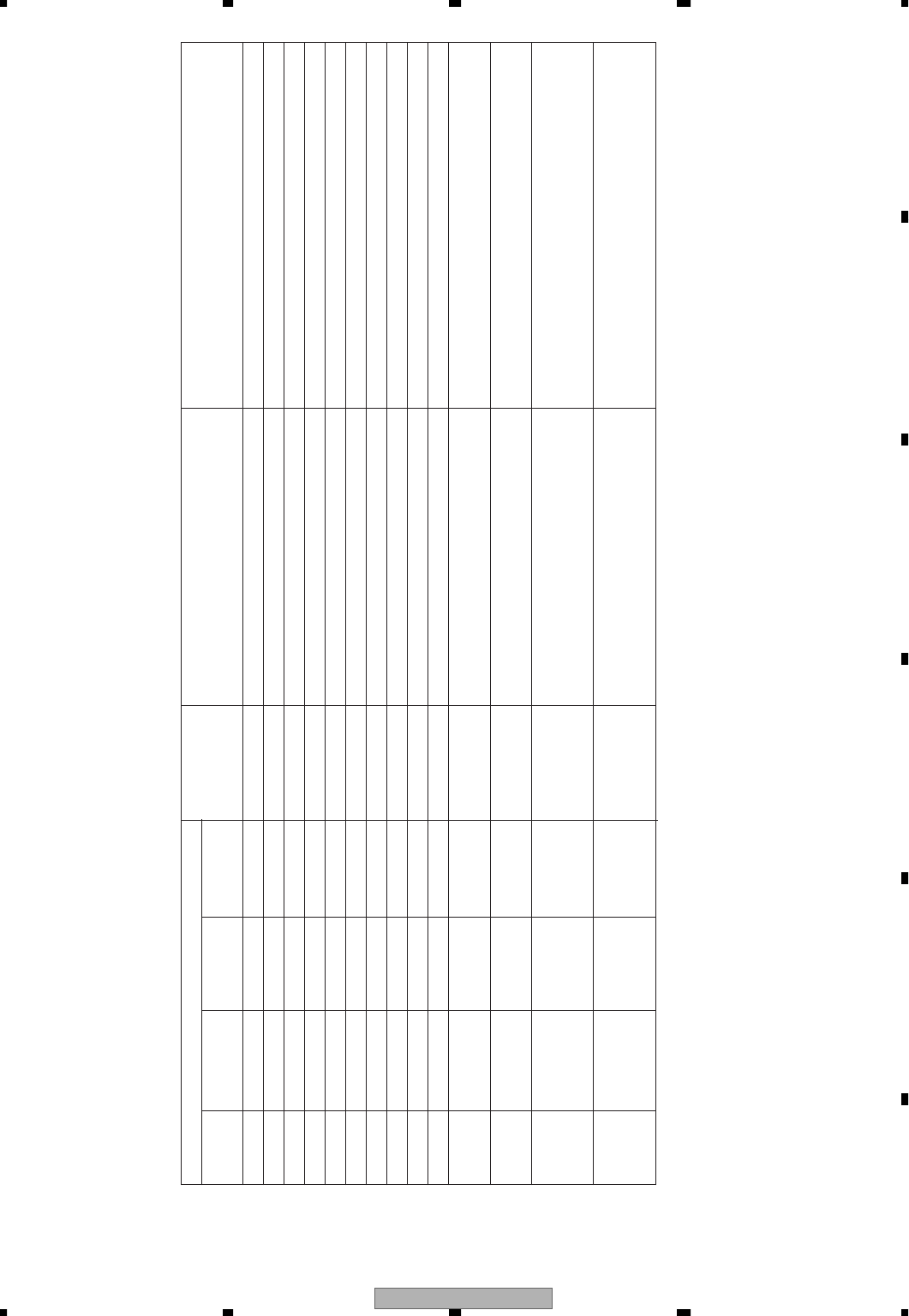
XDV-M8357ZT/UC 85
5678
5678
C
D
F
A
B
E
-Error No. Display
When the DVD cannot operate or if it stopped due to an error during operation, an error mode occurs and the cause of the error is displayed in numerals.
An object of this error No. display is to reduce the nonsense call of the user and aid in the analysis/repair in the service.
1) Summary of error display
* If major classification error codes are blank, no detailed error codes are not displayed in normal use. Check them for the detailed error codes of the test
mode.
Error code
Diagnosis EMV on- Major Detailed code Type Contents Details and cause
mode screen display classification
01 Electricity System Controller Peripheral Check Error SRAM access check error * 1
02 Electricity System Controller Peripheral Check Error A0-A16 address line check error * 1
03 Electricity System Controller Peripheral Check Error Program flash ROM read access check error * 1
04 Electricity System Controller Peripheral Check Error GUI flash ROM read access check error * 1
05 Electricity System Controller Peripheral Check Error MPEG decoder read access check error * 1
06 Electricity System Controller Peripheral Check Error MY-CHIP access check error * 1
07 Electricity System Controller Peripheral Check Error Track buffer access check error * 1
08 Electricity System Controller Peripheral Check Error Track buffer address line check error * 1
09 Electricity System Controller Peripheral Check Error CD-ROM error correction IC access check error * 1
0A Electricity System Controller Peripheral Check Error Pull up/down check error * 1
11 Electricity Flash ROM Error Flash ROM ID code differs
→Flash ROM contents are damaged
12 Electricity Flash ROM Error Flash ROM ID code differs
→Flash ROM contents are damaged
13 Electricity Flash ROM Error Flash ROM silicone signature differs
→Flash ROM contents are damaged.Wiring between
flash ROM and system controller is disconnected
14 Electricity Flash ROM Error Flash ROM size differs
→Flash ROM contents are damaged.Wiring between
flash ROM and system controller is disconnected

XDV-M8357ZT/UC
86
1234
1234
C
D
F
A
B
E
Error code
Diagnosis EMV on- Major Detailed Type Contents Details and cause
mode screen display classification code
15 Electricity Flash ROM Error Flash ROM checksum differs
→Flash ROM contents are damaged
16 Electricity Flash ROM Error Write protection is not applied to flash ROM
→Flash ROM contents are damaged.Wiring between
flash ROM and system controller is disconnected.
17 Electricity Flash ROM Error No reset vector is written to the first address of flash ROM
→Flash ROM contents are damaged
31 Electricity CPU Peripheral Hardware Fault Undefined interrupt occurs in ROM
→Wiring is disconnected or short-circuited on main unit
32 Electricity CPU Peripheral Hardware Fault General invalid instruction occurs in ROM
→Wiring is disconnected and short-circuited on main unit
33 Electricity CPU Peripheral Hardware Fault Slot invalid instruction interrupt occurs in ROM
→Wiring is disconnected and short-circuited on main unit
34 Electricity CPU Peripheral Hardware Fault CPU address error interrupt
→Wiring is disconnected and short-circuited on main unit.
35 Electricity CPU Peripheral Hardware Fault Undefined interrupt occurs in flash ROM
→Wiring is disconnected and short-circuited on main unit
36 Electricity CPU Peripheral Hardware Fault General invalid interrupt occurs in flash ROM
→Wiring is disconnected and short-circuited on main unit.
37 Electricity CPU Peripheral Hardware Fault Slot invalid instruction occurs in flash ROM
→Wiring is disconnected and short-circuited on main unit.
38 Electricity CPU Peripheral Hardware Fault CPU address error occurs in flash ROM
→Wiring is disconnected and short-circuited on main unit.
39 Electricity CPU Peripheral Hardware Fault DMA address error is detected in flash ROM
→Wiring is disconnected and short-circuited on main unit.
44 The DVD is stopping Error2 or 5 80 Mechanism Address Not Found Mechanism controller error code F2 XXXX
due to error detection
47 The DVD is stopping Error3 81 Electricity Heat Error Pickup section is excessively heated.
due to error detection
45 The DVD is stopping Error5 82 Mechanism Eject Error MAG switch disconnection wait timeout
due to error detection Elevation timeout at ejection
50 The DVD is stopping Error5 83 Mechanism Tray Existence/Nonexistence Tray withdrawal or insertion operation timeout
due to error detection Error Tray is hooked at tray withdrawal
51 The DVD is stopping Error5 84 Mechanism Elevation Error Timeout at elevation operation
due to error detection
46 Check the X-th discError2 90 Electricity Focus Search Error Focus is disabled
→Disc upside down, scratches, dirt and vibration
are strong
46 Check the X-th discError5 91 Electricity Spindle Lock Error Because spindle lock is not done, subcode cannot be read
→Spindle is faulty and disc scratches, dirt and vibration
are strong.
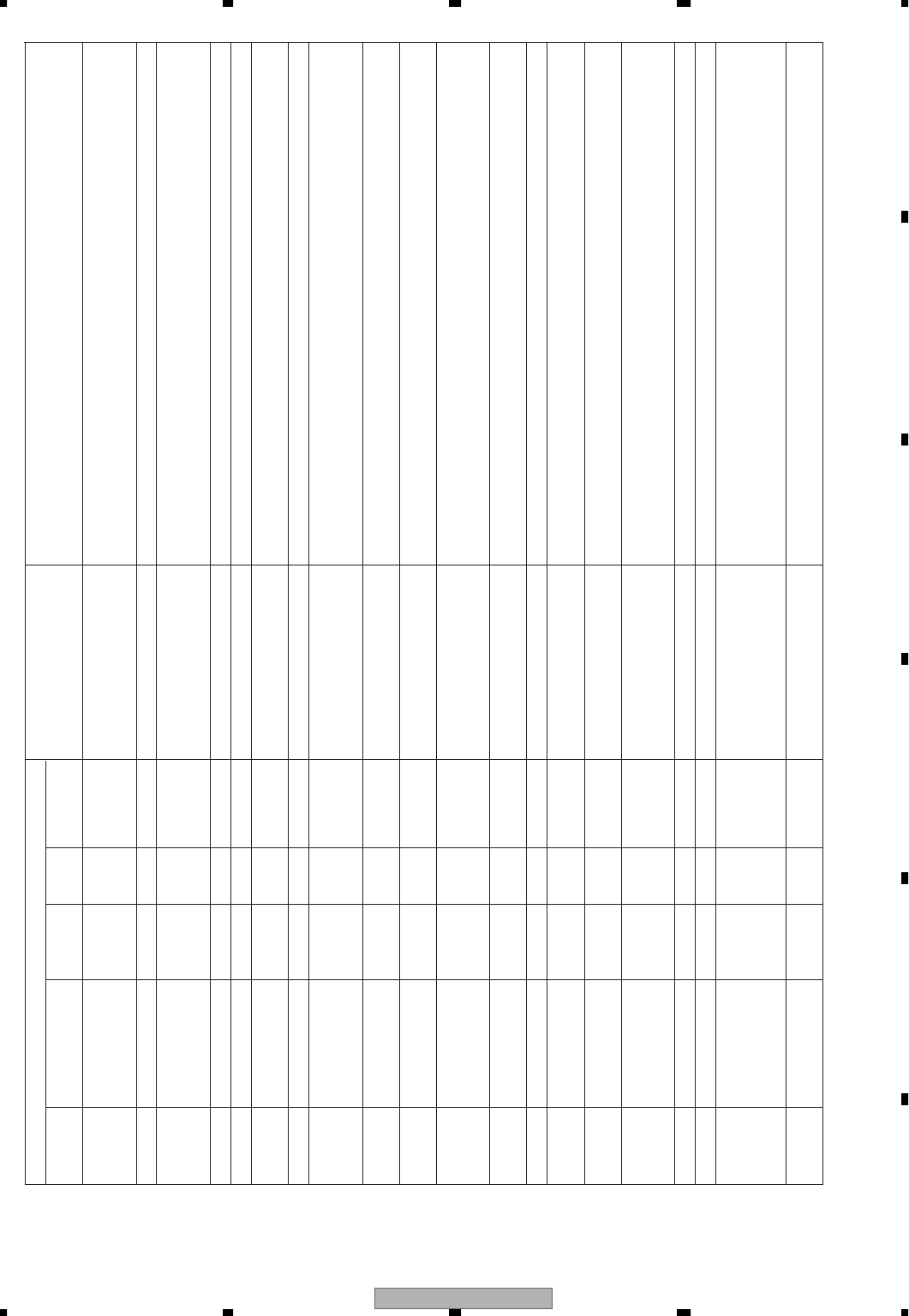
XDV-M8357ZT/UC 87
5678
5678
C
D
F
A
B
E
Error code
Diagnosis EMV on- Major Detailed Type Contents Details and cause
mode screen display classification code
44 Check the X-th discError2 92 Electricity Carriage Home Error Movement is disabled to inner circumference and
movement is disabled from inner circumference
→Home SW is faulty and carriage movement is faulty
46 Check the X-th discError2 93 FOK Error Mechanism error code F8 0013
46 Check the X-th discError2 94 Electricity ID/SUBCODE Error Subcode cannot be read
→Spindle is faulty and disc scratches, dirt and vibration
are strong.
46 Check the X-th discError2 95 Mechanism Spindle High Revolution Error Mechanism error code F8 0015
46 Check the X-th discError2 96 Mechanism Spindle Low Revolution Error Mechanism error code F8 0016
The DVD is stopping Error6 97 Electricity Mechanism Unit Reference Elevation positioning is disabled
due to error detection Voltage Error →Power fault and control volume resistor is faulty.
98 Electricity TOC Error Mechanism error code FA XXXX
B0 Electricity Mechanism controller Communication is disabled between mechanism
Communication Error controller and system controller.
→Wiring is disconnected and short-circuited on main unit.
B1 Electricity Mechanism controller Mechanism controller does not respond.
Communication Timeout →Wiring is disconnected and short-circuited on main unit.
B2 Electricity Unexpected Error in Mechanism
Controller Communication
B3 Electricity Communication Error between No communication is done from BUS microcomputer.
BUS Microcomputer →Wiring between main unit and extension unit is
and System Controller disconnected and short-circuited.
Region code error Error09 A0 Electricity Region Code Error DVD disc having region code which cannot be played
back
Check the X-th disc A1 Electricity Digital Copy Guard Error DVD disc violated against digital copy guard
Check the X-th disc A2 Electricity DVD File System Read Error DVD data read error
→Defective carriage/tracking and disc scratches
Check the X-th disc A3 Electricity DVD Search Timeout Error Target address could not be reached.
→Defective carriage/tracking and disc scratches
46 Check the X-th disc A4 Electricity CD-ROM Read Error Disc data cannot be read
→Spindle is faulty and disc scratches, dirt and vibration
are strong.
46 Check the X-th disc A5 Electricity DVD Read Error Disc scratches
46 Check the X-th disc A6 Electricity Video CD Read Error Disc scratches
C0 Electricity System Controller Communication is disabled between system controller
Communication Error and BUS microcomputer.
→Wiring between main unit and extension unit is
disconnected and short-circuited.
47 The DVD is stopping C1 Electricity Low Temperature Detection Equipment temperature is lower than operable
due to error detection ... temperature.
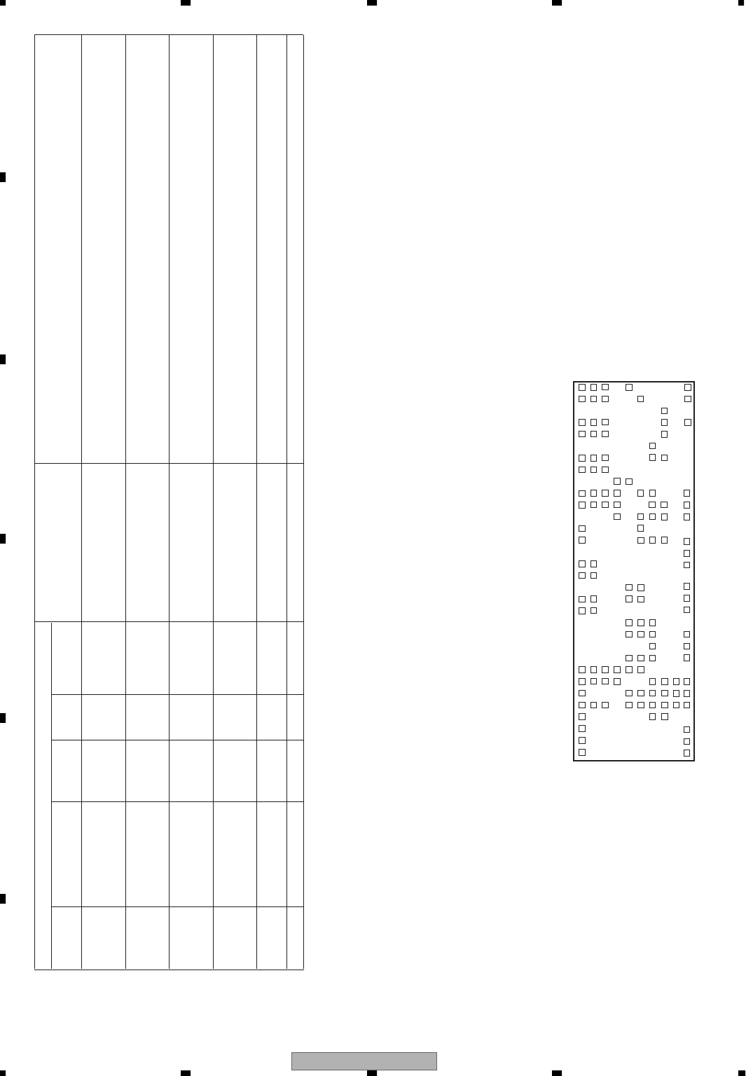
XDV-M8357ZT/UC
88
1234
1234
C
D
F
A
B
E
→R: ←
→TGT- E: OE: ←
→NOW-
→STATS- V- ←
→MC T - AV 1=''FLSH: ←
F: / REG: Y←
→ER- V: . ←
S: . / . ←
→
→
DSC-
AV: . ←
→MM-
(1)Address
(3)Target operating state
(6)Current operating state
(7)Current state
(9)Command history to
mechanism microcomputer
(14)DVD error rates
(17)System microcomputer disc judgment
(18)Mechanism microcomputer disc judgment
(19)Disc type in a magazine
(2)Receiving code
(5)Error history
(8)Output video format
(10)AV1 chip version and (11)Flash ROM size
(12)Destination setting and (13)region code of player
V:(15)Flash ROM version R and (13)region code
(16)Flash ROM version 2 and system controller version
(20)AV1 chip revision
* 1: This code is detected only when the system controller peripheral test was executed in the test mode.
-Debug Mode
An object of this debug mode is to aid in the analysis/repair in the service by displaying the version display, error rate and error history of the
microcomputer when this equipment was stopped due to a fault.
• How to enter the debug mode
Follow the procedures below.
1. Enter the test mode.
2. Set the normal mode debug screen (00850000).
3. Set AccON to OFF.
4. Continue pressing the EJECT key for five seconds with the door closed.
5. Set AccOFF to ON without releasing the EJECT key as is.
• Debug mode reset
Acc OFF.
• Screen configuration
Error code
Diagnosis EMV on- Major Detailed Type Contents Details and cause
mode screen display classification code
The DVD is stopping Error-06 C4 Electricity Power Supply Fault Higher or lower than specified voltage in 9 V-system
due to error detection power supply, otherwise no power is issued.
→Defective switching transistor and power supply fault
The DVD is stopping Error-06 C5 Electricity Power Supply Fault Higher or lower than specified voltage in 3.3 V-system
due to error detection power supply, otherwise no power is issued.
→Defective switching transistor and power supply fault
The DVD is stopping Error-06 C6 Electricity Power Supply Fault Higher or lower than specified voltage in 2.5 V-system
due to error detection power supply, otherwise no power is issued.
→Defective switching transistor and power supply fault
The DVD is stopping Error-06 C7 Electricity Power Supply Fault Higher or lower than specified voltage, otherwise no
due to error detection power is issued.
→Defective switching transistor and power supply fault
The lid of the DVD Error-01 Mechanism Door Opens. Because door opens, this equipment mechanism stops
is opening
No disc is loaded Mechanism Empty Magazine Insertion There is no disc.

XDV-M8357ZT/UC 89
5678
5678
C
D
F
A
B
E
-Explanation of Display Contents by Item
(1) Address display
This item displays the address which is being traced currently.
DVD ******* ID display (8 hexadecimal digits)
CD/VCD 0000**** A-TIME (minutes and seconds)
CD 00000000 Fixed
(2) Receiving code R: ** ** **
This item displays the command transferred from the BUS microcomputer to the system controller.
(3) Target operating state TGT: * **
This item displays the number of the tray to which playback operation is being attempted and the
internal state of the player.
Number of tray 1-6
Internal state of player 01 Disc changing
02 Waiting for power-off
03 Stopping
04 Disc being detected
05 During setup
06 TOC being read
07 During playback
08 Searching
(4) Error number E : ** **
This item displays the current error number.
(5) Error history OE : ** ** ** **
This item displays the past error history. ** ** ** **
The upper left is the latest error number. The same number as the current error number is displayed in an error state.
This error history is stored in flash ROM and will not be cleared even for backup OFF.
(6) Current operating state NOW : * **
This item displays the number of the current tray and the internal state of the player.
Number of tray 1-6
Internal state of player 01 Disc changing
02 Waiting for power-off
03 Stopping
04 Disc being detected
05 During setup
06 TOC being read
07 During playback
08 Searching
(7) Status display STATS- **
This item displays the internal state of the current player.
00 No tray is selected.
01 Tray 1 is selected.
02 Tray 2 is selected.
03 Tray 3 is selected.
04 Tray 4 is selected.
05 Tray 5 is selected.
06 Tray 6 is selected.
81 Tray 1 disc is changing.
82 Tray 2 disc is changing.
83 Tray 3 disc is changing.
84 Tray 4 disc is changing.
85 Tray 5 disc is changing.
86 Tray 6 disc is changing.
TOC information read step information. TOC:
(8) Output video formats V-****
NTSC (National Television System Committee) method [NTSC]
PAL (Programmable Array Logic) method [PAL]
Automatic setting [AUTO]

XDV-M8357ZT/UC
90
1234
1234
C
D
F
A
B
E
(9) Command history to mechanical-unit microcomputer MCT : ** ** ** **
This item displays past commands from ** ** ** **
left to right and from up to down.
Commands
01 Communication Start
02 Stop
03 Seek
04 Read
05 Pause
06 Fast Forward
07 Reverse
08 Disc Replacement
09 Get Address
0A Get Power Startup State
0B Get Disc Information
0C Get Final Mechanism Controller
Error Status
0D Communication Reset
0E Test Mode ON
10 Get Control Data
11 Get TOC Information (CD Only)
12 Get Magazine Information
14 Get CD Address
15 EJECT
16 Power-Off Processing
17 EJECT Interrupt
(10) AV1 chip revision AV1 = '*'
This item displays a revision of the AV1 chip.
(11) Flash ROM size FLSH : *
This item displays a size of flash ROM.
(12) Destination setting F : *** / *
(13) Region setting REG : *Y
R : *
This item displays the region setting of the player.
(14) Error rate display ER- **** ****
Error rates are displayed for DVD (displayed only for DVD).
C1 error rate for disc playback is displayed.
To ensure calculation accuracy, the number of errors is being counted in a unit of 16 blocks.
(C1 1block) = (182bytes x 208line = 37856bytes)
(C1 16block) = (182bytes x 208line = 16block = 605696bytes)
The minimum resolution is set to 1.65099E-6 .
Usually, an error rate is less than 1.0E-3 .
(15) Flash ROM version 1
Version of the high-level module in flash ROM. V : *. *** *
Flash ROM version. **
(16) Flash ROM version 2 and system controller version display
These items display a version of a low-level module S : *. **
in flash ROM.
The version of the ROM incorporated in the system controller. *. ***

XDV-M8357ZT/UC 91
5678
5678
C
D
F
A
B
E
(17) Disc judgment(System microcomputer) MM : ***
Disc not decided
non No disc
DSC Disc of type not fixed
NG No match etc.
CD CD (format not decided)
CDP CD partial disc
CDC CD combined disc
D DVD (format not decided)
DVD DVD (Region not decided)
DNG DVD (Disc which cannot be played back due to a region error)
DOK For DVD
CDA For CD-DA
CDR For CD-ROM
VC1 For VCD(Ver1.1)
VC2 For VCD(Ver2.0)
(18) Disc judgment(Mechanism microcomputer) DSC : ***
This item displays the type of the disc which is being clamped.
NON No disc
DVD For DVD
CD For CD
VCD For VCD
(19) Disc type in a magazine For six sheets
The display format is the same as the system microcomputer decision results of item 17.
(20) AV1 chip version AV1:*.***
Function description
Clear error histories by pressing the upper left section of the screen ten consecutive times.
XDV-M8357ZT/UC
92
1234
1234
C
D
F
A
B
E
7. GENERAL INFORMATION
7.1 DIAGNOSIS
7.1.1 DISASSEMBLY
Fig.1
Upper Case
-
Removin
g
the Upper Case (Fi
g
.1
)
R
e
m
o
v
e
t
h
e
sc
r
e
w
.
1
22
Remove the ei
g
ht screws and the
n
remove the U
pp
er Case
.
2
Note:
When disassembling a product, be sure to set the PU unit short circuit switch to the short circuit direction.
The vertical and horizontal specifications of a product are switched by switching the spring hooking position using
an arm. At normal assembly and disassembly, the arm switches the position at the position which conforms to the
horizontal specifications. However, because this product conforms to the vertical specifications, take notice not to
forget the changeover.
The changeover position and method are as follows:
Because a changeover arm is provided in the hole near by the center of the product left and right sides, use the
arm to switch the position. For the confirmation of the position, because H and V are marked on the top case.
Accordingly, to assemble a product, adjust H and V conforming to the installation specifications of the product.
1
2
2
2
2
2
2
-
Removin
g
the DVD/CD Mechanism Unit (Fi
g
.2
)
Remove the four dam
p
ers
.
1
remove the two sprin
g
s
.
2
Di
sco
nn
ect
t
h
e
co
nn
ecto
r
a
n
d
t
h
e
n r
e
m
o
v
e
t
h
e
DVD
/
CD Mechanism Unit
.
-
Removin
g
the Grille Assy (Fi
g
.2
)
3
R
e
m
o
v
e
t
h
e
t
w
o
sc
r
e
w
s
.
Fig.2
Grille Assy
DVD/CD Mechanism Unit
33
Di
sco
nn
ect
t
h
e
co
nn
ecto
r
a
n
d
t
h
e
n r
e
m
o
v
e
the Grille Ass
y.
1
1
1
1
22
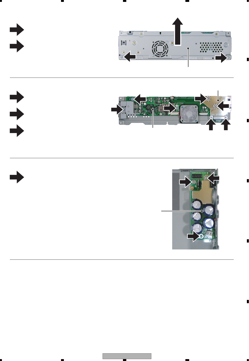
XDV-M8357ZT/UC 93
5678
5678
C
D
F
A
B
E
- Removing the Rear Frame Unit (Fig.3)
1
Fig.3
Rear Frame Unit
1
1
Fig.4
MF Unit
- Removing the Extension Unit (Fig.4)
Remove the two screws and then remove
the Shield.
1
Remove the two screws.
3
3
2
Remove the screw.
2
Remove the four screws.
3
Pull out the Rear Frame Unit in the arrow
indicated direction.
2
2
3
3
11
Extension Unit
Shield
Disconnect the connector and then remove the
Extension Unit.
Fig.5
- Removing the MF Unit (Fig.5)
Remove the three screws and then remove
the MF Unit.
111
1
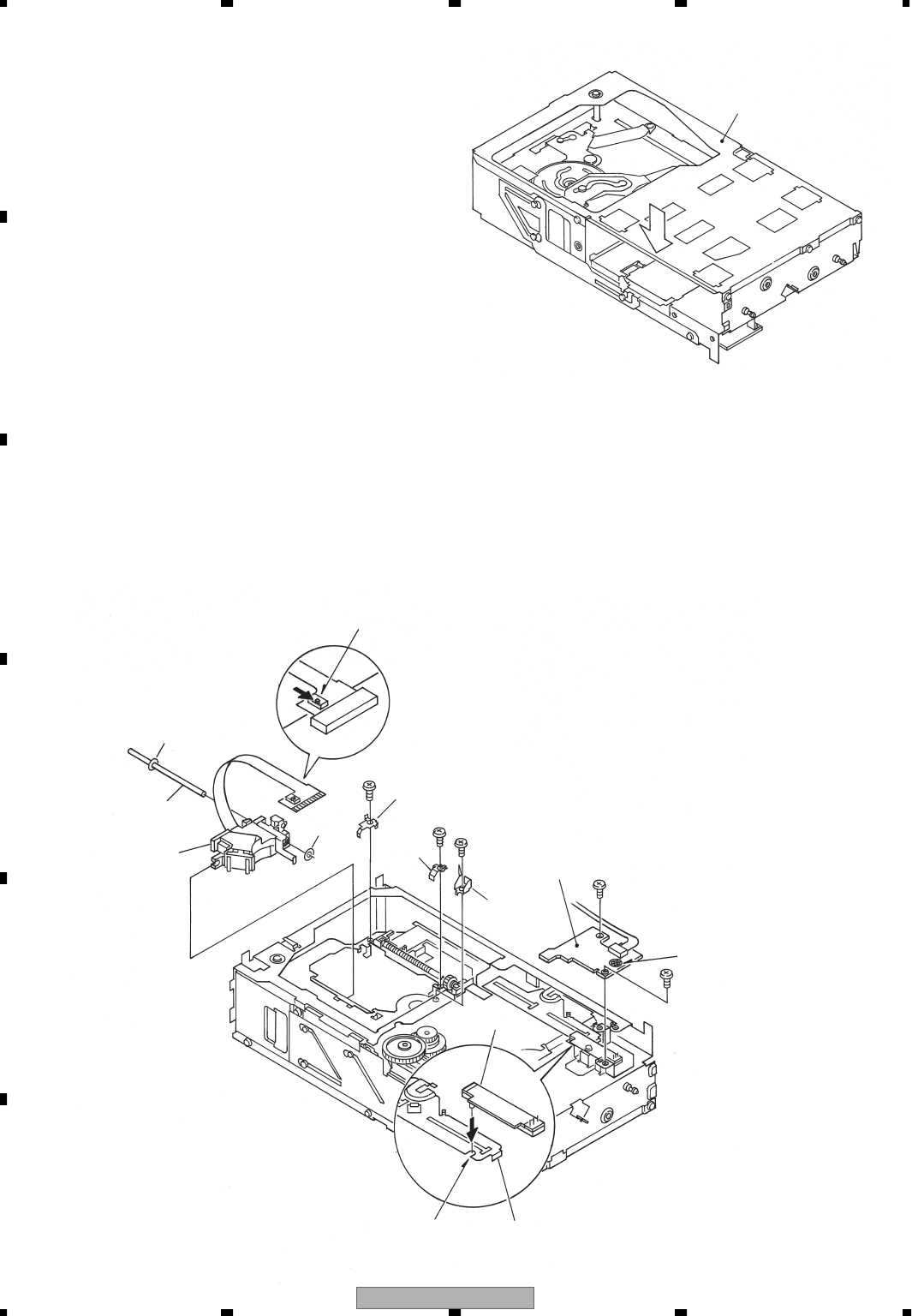
XDV-M8357ZT/UC
94
1234
1234
C
D
F
A
B
E
Fig. 7
DVD/CD Mechanism Unit
Fig. 6
Short Switch
Cushion
Cushion
Main Shaft
Pickup Unit
Plate
Spring B
C
BA
D
D
Plate
Spring A
Grease
Cover
PCB
Unit(B)
Soldering
VR301
U-groove Detection Lever
Precautions when making servicing works
1) Since the upper surface of the arrowed magazine slot
in the DVD/CD mechanism unit can be deformed
comparatively easily, do not hold this section when
making servicing work. (Refer to Fig. 6)
2) The stage mechanism projects downward beyond the
low end of the chassis when it is reset.
Consequently, the stage mechanism may be damaged
to cause functional failures when handled carelessly.
When placing the mechanism, pay great attention not
to damage the gear and the pickup unit.
-Removing the pickup unit(Fig. 7)
1. Set the short switch of the pickup unit to the SHORT
side.
2. Remove the flexible PCB from the connector.
3. Unscrew one screw A to remove the grease cover.
4. Unscrew one screw B to remove the plate spring A.
5. Unscrew one screw C to remove the plate spring B.
6. Remove the pickup unit together with the main shaft.
7. Remove the cushion from one side only to pull out
the main shaft. AT this time, pay attention not to lose
the removed cushion.
-Removing the PCB unit(B)(Fig. 7)
1. Remove soldering from the linear position sensor
(VR301).
2. Unscrew the two screws D to remove the PCB unit(B).
-Precautions when installing the linear position
sensor(Fig. 7)
1. If the linear position sensor (VR301) is not being
properly inserted into the U-groove provided in the
detection lever, elevation movement failures can
occur.
When installing the linear position sensor to the
DVD/CD mechanism unit, be sure to insert it into the
U-groove provided in the detection lever securely.
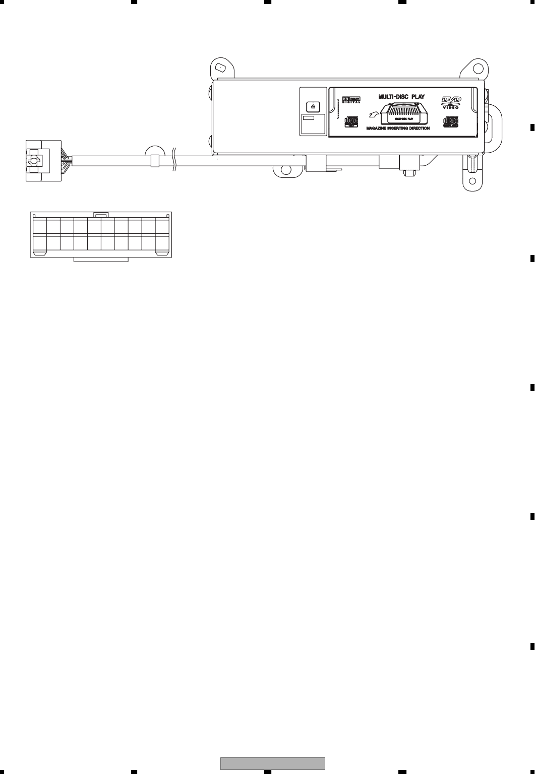
XDV-M8357ZT/UC 95
5678
5678
C
D
F
A
B
E
7.1.2 CONNECTOR FUNCTION DESCRIPTION
1. +B
2. NTSO
3. SG
4. SGND
5. CDL+
6. CDR+
7. NC
8. TXM+
9. NC
10. ACC
11. GND
12. NC
13. NC
14. NC
15. CDL-
16. CDR-
17. SGND
18. TXM-
19. NC
20. MUTE
12345678910
11 12 13 14 15 16 17 18 19 20
Notes
CD-Rs may not
be playable in
this compact
disc player.
XDV-M8357ZT/UC
96
1234
1234
C
D
F
A
B
E
7.2 IC
1 IN B
2 IN A
3 GND 4 OUT Y
5 VCC
IC's marked by * are MOS type.
Be careful in handling them because they are very
liable to be damaged by electrostatic induction.
VCC 28
27
26
25
24
23
22
21
20
19
18
17
16
15
VSS
DQ8
DQ7
DQ1
DQ6
DQ2
DQ5
DQ3
cas
DQ4
we
oeras
A9NC
A8A10R
A7A0
A6A1
A5A2
A4A3
VCC VSS
1
2
3
4
5
6
7
8
9
10
11
12
13
14
A0~A9,A10R :Address input
ras :Row address strobe
cas :Column address strobe
DQ1~DQ8 :Data input/output
oe :Output enable
we :Write enable
VCC :Power supply
VSS :GND
NC :Not used
132
OUT1
IN1
IN1
IN2
IN2
OUT2
4
5678
+
+
VCC
VEE
MC33202D
*TC7SET08FUS1
*TC7SH08FUS1
*MSM5117800F-60JS
MC33202D
MSM5117800F-60JS
TC7SET08FUS1
TC7SH08FUS1
TC9461F
TC7SH32FUS1
PEG114A
LC89170MP
PD4995A
TC7SET04FUS1
M5M51008DKV-70HI
PD6531A
PD6520A
MAX662AESA
PD3411A
TC74VHC00FTS1
TC74VHC139FT
CY2292SI-1A0
MSM56V16160DP-10TS
MB86373BPFV-G-BI
TC74VHC541FTS1
TC74VHCT08AFTS1
TC74LCX245FTS1
LC89513KP
PE5272A
LC35256FT-70U

XDV-M8357ZT/UC 97
5678
5678
C
D
F
A
B
E
-Pin Functions (TC9461F)
Pin No. Pin Name I/O Function and Operation
1 VSS GND
2 BCK O Bit clock (1.4122MHz) output
3 AOUT O Audio data output terminal
4 DOUT O Digital out output terminal
5 MBOV O Buffer memory over signal output terminal
6 IPF O Augment flag output terminal
7 SBOK O CRCC decision result output terminal of subcode Q data
8 CLCK I/O Clock output/input terminal for subcode P-W data reading
9 VDD Positive power supply terminal
10 VSS GND
11 DATA O Subcode P-W data output terminal
12 SFSY O Play group frame synchronous signal output terminal
13 SBSY O Subcode block synchronous output signal
14 SPCK O Clock output terminal for processor status signal reading
15 SPDA O Processor status signal output terminal
16 COFS O Correct group frame clock (7.35 kHz) output terminal
17 MONIT O LSI internal signal monitor terminal
18 VDD Positive power supply terminal
19 TESIO0 I Test input/output terminal
20 P2VREF 2VREF terminal for PLL group only
21 SPDO O VCO center frequency shift terminal
22 PDOS O Phase error signal output terminal of EFM signal and PLCK signal
23 PDO O Phase error signal output terminal of EFM signal and PLCK signal
24 TMAXS O TMAX detection result output terminal
25 TMAX O TMAX detection result output terminal
26 LPFN I Inverted input terminal of low-pass filter amplifier
27 LPFO O Output terminal of low-pass filter amplifier
28 PVREF VREF terminal for PLL group only
29 VCOREF I VCO center frequency reference level terminal
30 VCOF O Filter terminal for VCO
31 AVSS Analog group ground
32 SLCO O Output terminal for data slice level generator DAC
33 RFI I RF signal input terminal
34 AVDD Analog group power supply terminal
35 RFCT I RFRP signal center level input terminal
36 RFZI I Input terminal for RFRP zero cross
37 RFRP I RF ripple signal input terminal
38 FEI I Focus error signal input terminal
39 SBAD I Sub beam summing signal input terminal
40 TSIN I Test input terminal
41 TEI I Tracking error input terminal
42 TEZI I Input terminal for tracking error zero cross
43 FOO O Focus equalizer output terminal
44 TRO O Tracking equalizer output terminal
45 VREF Analog reference power supply terminal
46 RFGC O RF amplitude adjustment control signal output terminal
47 TEBC O Tracking balance control signal output terminal
48 FMO O Feed equalizer output terminal
49 FVO O Speed error or Feed search EQ output terminal
50 DMO O Disk equalizer output terminal
51 2VREF Analog reference power supply terminal
52 SEL O APC circuit ON/OFF signal output terminal
53 FLGA O External flag output terminal for internal signal monitor
54 FLGB O External flag output terminal for internal signal monitor
55 FLGC O External flag output terminal for internal signal monitor
56 FLGD O External flag output terminal for internal signal monitor
57 VDD Digital power supply terminal
58 VSS Digital GND
59-62 IO0-3 I/O General purpose I/O port
XDV-M8357ZT/UC
98
1234
1234
C
D
F
A
B
E
Pin No. Pin Name I/O Function and Operation
63 dmout I A terminal for setting the mode to output binary PWM for a feed equalizer
from I/O terminals 0 and 1, and binary PWM for disc equalizer from I/O
terminal 2 and 3
64 ckse X'tal select terminal
65 dact I
ITest terminal
66 TESIN I
ITest input terminal
67 TESIO1 Test input/output terminal
68 VSS Digital GND
69 PXI I DSP group clock oscillation circuit input terminal
70 PXO O DSP group clock oscillation circuit input terminal
71 VDD Digital power supply terminal
72 XVSS Ground terminal for system clock oscillation circuit
73 XI I System clock oscillation circuit input terminal
74 XO O System clock oscillation circuit output terminal
75 XVDD Power supply terminal for system clock oscillation circuit
76 DVDD D/A converter power supply terminal
77 RO O R channel data positive rotation output terminal
78 DVSS D/A converter analog ground terminal
79 DVR D/A converter reference voltage terminal
80 LO O L channel data positive rotation output terminal
81 DVDD D/A converter power supply terminal
82-84 TEST1-3 I Test terminal
85-88 BUS0-3 I/O Data input/output terminal for microcomputer interface
89 VDD Digital power supply terminal
90 VSS Digital GND
91 BUCK I Clock input terminal for microcomputer interface
92 cce I Chip enable signal input terminal for microcomputer interface
93 TEST4 I Test terminal
94 tsmod I Local test mode select terminal
95 rst I Reset signal input terminal
96 TEST0 I Test terminal
97 hso O Play speed mode flag output terminal
98 uhso Ouhso hso Play speed
H H Once speed play
H L Twice speed play
L H Four times speed play
L L Eight times speed play
99 EMPH O Emphasis flag output terminal of subcode Q data
100 LRCK O Channel clock (44.1 kHz) output terminal
*TC9461F
*TC7SH32FUS1
25
26
50
51
75
76
100
1
1 IN B
2 IN A
3 GND 4 OUT Y
5 VCC

XDV-M8357ZT/UC 99
5678
5678
C
D
F
A
B
E
-Pin Functions (PEG114A)
Pin No. Pin Name I/O Format Function and Operation
1 RFSCD O C TA1254AF serial data
2RFSCB TA1254AF bit clock
3 LCDBIAS Liquid crystal temperature augment output
4 LCDTLT Liquid crystal tilt augmenter control output
5 LDCONT O C LD ON/OFF control output
6 PSC O C VRCK deviding ON/OFF
7FG I FG pulse input
8 BYTE I Connect to VCC
9 CNVSS Connect to VSS
10 DSCSIZ O C 8cm/12cm select
11 VMCONT O C 9V regulator output voltage control output
12 XMRES I Reset input
13 XOUT O Main clock oscillation terminal
14 VSS GND
15 XIN I Main clock oscillation terminal
16 VCC Power supply terminal
17 NC Not used
18 XMAG I Magazine detection switch input
19 NC Not used
20 XIRQ I Interruption input
21 OEIC O C OEIC gain select output
22 FEB FE balance control output
23 FLGA I TC9461 internal signal monitor input
24 FLGB I TC9461 internal signal monitor input
25 FLGC I TC9461 internal signal monitor input
26 LCDCLK Liquid tilt driver clock output
27 FLGD I TC9461 internal signal monitor input
28 TXCLK CD-TEXT clock output
29, 30 NC Not used
31 EEPDO O C
O
O
EEPROM data output
32 EEPDI I EEPROM data input
33 EEPSK C EEPROM clock output
34 EEPCS C EEPROM chip select
35 TEST_TX O C RS232C communication data output
36 TEST_RX I RS232C communication data input
37 HSO I Play speed mode flag
38 UHSO I Play speed mode flag
39 XREADY I
I
Wait signal input
40 ASTB O C
O
Address latch output
41 XHOLD Hold signal input
42, 43 NC Not used
44 XRD O C Read signal output
45 NC Not used
46 XWR O C Write signal input
47 NC Not used
48 LCDRS O C LCD register select
49 XCS O C Chip select signal output
50 CD/DVD O C CD/DVD select output
51-54 LCDDT3-0 C LCD display data
55 LCDEN O C LCD enable
56 XCCE O C Servo processor i/f
57 BUCK O C Servo processor i/f
58-61 BUS3-0 I/O C Servo processor i/f
62 VCC Power supply terminal
63 NC Not used
64 VSS GND
65-72 AD7-0 I/O C Address/data input/output
73 TXDQSY I CD-TEXT sub-code synchronous input
74 BSENS I Backup sense input
75 SRSENS I DDC sense input
XDV-M8357ZT/UC
100
1234
1234
C
D
F
A
B
E
*PEG114A
30
31
50
51
80
81
100
1
Pin No. Pin Name I/O Format Function and Operation
76 OPEN Open
77 SEEKT C SEEK time monitor output
78 I13 OCO CO C
C
C
C
C
C
O
Motor driver control output
79 I2 Motor driver control output
80 I4 Motor driver control output
81 HOME I Home position detection output
82 VDCONT O VD control output
83 SPCONT O Spindle control output
84 DCONT O Driver power ON output
85 XSYSRST O Reset output
86 ADENA O Reference voltage supply output for A/D
87 DSP I Disk detection timing input
88 XTESTIN I Unit check start input
89,90 KEYIN2,1 Key sense
91 VDSENS I VD short detection input
92 DISK Disk/No disk sense, 8/12cm detection
93 ELVPVO I Slide voltage input for ELV detection
94 ELVREF I ELV reference voltage input
95 TRP I Tray position input
96 AVSS Analog ground
97 TEMP I Temperature detection input
98 VREF I Reference voltage input
99 AVCC Analog power supply
100 RFSLC O TA1254AF data latch
Format Meaning
CC
MOS
*LC89170MP

XDV-M8357ZT/UC 101
5678
5678
C
D
F
A
B
E
-Pin Functions (PD4995A)
Pin No. Pin Name I/O Function and Operation
1,2 GND
NC Digital circuit GND
3Not used
4 DXTLI I 27MHz crystal connection terminal which oscillates reference clock signals of
the spindle and PLL
5 DXTLO O Not used
6 BUNRI I Separation test control terminal for internal RAM
7 TSTSTB I Test mode setting input
8 PC2/STB I/O Not used
9 PC3/BSYNC I/O Not used
10 PC4/SELNED I I/O setting terminals for NED (7:0), STM and BSYNC terminals
11 PA7/NED7 I/O Not used
12 PA6/NED6 I/O Not used
13 PA5/NED5 I/O Not used
14 PA4/NED4 I/O Not used
15 VDD Digital circuit power supply
16 GND Digital circuit GND
17 PA3/NED3 I/O Not used
18 PA2/NED2 I/O Not used
19 PA1/NED1 I/O Not used
20 PA0/NED0 I/O Not used
21 BMODE1 I Sets which test is done in the test mode
22-25 DD7-4 I/O DRAM data bus for VBR buffer
26 GND Digital circuit GND
27 VDD Digital circuit power supply
28-31 DD3-0 I/O DRAM data bus for VBR buffer
32 XDCAS O DRAM CAS signal for VBR buffer
33 XDWE O DRAM WE signal for VBR buffer
34 XDOE O DRAM OE signal for VBR buffer
35 XDRAS O DRAM RAS signal for VBR buffer
36-38 DA12-10 O Not used
39-41 DA9-7 O DRAM address signal for VBR buffer
42 GND Digital circuit GND
43 VDD Digital circuit power supply
44-50 DA6-0 O DRAM address signal for VBR buffer
51,52 GND Digital circuit GND
53 VDD Digital circuit power supply
54 XWR O Not used
55 XSACK O Transfer response terminal for VIDEO_DMA channel
56 SREQ I Data transfer request terminal for VIDEO_DMA channel
57-60 SDATA0-3 O Data output bus for VIDEO=DMA channel
61 GND Digital circuit GND
62 VDD Digital circuit power supply
63-66 SDATA4-7 O Data output bus for VIDEO=DMA channel
67 XAVTRM O Signal indicating the head of the sector of the transfer data for VIDEO_DMA
channel
68 BMODE2 I Sets which test is done in the test mode
69 DMACKI I System clock input of DVD/CD ROM data
70 GND Digital circuit GND
71 DMACKO O Outputs reference crystal clock signals of the spindle and PLL
72 XSCL1 I Chip select signal from the main CPU
73 XSWAIT O WAIT output to the main CPU
74 XSRD I RD signal for the main CPU
75 XSWR I WR signal for the main CPU
76 XSDREQ O DMA request for the main CPU
77 SDACK I DMA response signal
78 VDD Digital circuit power supply
79 GND Digital circuit GND
80-91 SA11-0 I Main CPU address
92-95 SAD7-4 I/O Main CPU data bus
96 VDD Digital circuit power supply
97 GND Digital circuit GND
98-101 SAD3-0 I/O Main CPU data bus

XDV-M8357ZT/UC
102
1234
1234
C
D
F
A
B
E
Pin No. Pin Name I/O Function and Operation
102,103 XIRQ10,11 O Interrupt request for the main CPU
104 VDD Digital circuit power supply
105,106 GND Digital circuit GND
107 CKCD I Master clock of audio I/F block
108 DIFOUT O Digital audio output
109 BCK O Bit clock output to DAC
110 LRCK O LRCK signal output to DAC
111 ADATAO O Serial data output to DAC
112 CDDT I Audio data input from CD decoder
113 CDLR I LRCK signal input from CD decoder
114 CDBCK I Bit clock input from CD decoder
115 CDDO I Digital out signal input from CD decoder
116 C2FI I Input terminal for the C2 error flag from CD decoder
117 WFCK I CD frame clock signal
118 SCOR I CD subcode sync input terminal
119 SBSO I CD subcode data input terminal
120 EXCK O Shift clock which generates the timing at which data is sent to the SBSO
terminal
121 VDD Digital circuit power supply
122 GND Digital circuit GND
123 DSPA0 O Not used
ONot used
ONot used
ONot used
124 DSPA1
125 DSPA2
126 ASDATA0/PB0 I/O Not used
127 ASDATA1/PB1 I/O Not used
128 ASDATA2/PB2 I/O Not used
129 ASDATA3/PB3 I/O Not used
130 VDD Digital circuit power supply
131 GND Digital circuit GND
132 ASDATA4/PB4 I/O Not used
133 ASDATA5/PB5 I/O Not used
134 ASDATA6/PB6 I/O Not used
135 ASDATA7/PB7 I/O Not used
136 XAWR
137 ASREQ I Transfer request terminal for AUDIO_DMA channel
138 TMC2 I Terminal test control terminal
139 ASTB I Strobe signal indicating that address information is provided in the address
data bus (7:0) of the sub CPU
140 XMCS I Chip select signal from the sub CPU
141 XIRQ2 O Interrupt request for the sub CPU
142 XMWR I Sub CPU WR signal
143 XMRD I Sub CPU RD signal
144 MAD7/PE7 I/O Connected to the multiplex bus of the sub CPU address data
145 MAD6/PE6 I/O Connected to the multiplex bus of the sub CPU address data
146 MAD5/PE5 I/O Connected to the multiplex bus of the sub CPU address data
147 MAD4/SA16/PE4 I/O Connected to the multiplex bus of the sub CPU address data
148 GND Digital circuit GND
149 VDD Digital circuit power supply
150 MAD3/SA15/PE3 I/O Connected to the multiplex bus of the sub CPU address data
151 MAD2/SA14/PE2 I/O Connected to the multiplex bus of the sub CPU address data
152 MAD1/SA13/PE1 I/O Connected to the multiplex bus of the sub CPU address data
153 MAD0/SA12/PE0 I/O Connected to the multiplex bus of the sub CPU address data
154 RPWM O Not used
155,156 GND Digital circuit GND
157 VDD Digital circuit power supply
158 RERR O Control output for rough servo
159 FPWM O 7-bit PWM output terminal for FG servo
160 VPWM O 5-bit PWM output terminal for velocity servo
161 PPWM O PWM output terminal for phase servo
162 FGPL I Rotational pulse input from the spindle motor
163 XASACK O Not used
XDV-M8357ZT/UC 103
5678
5678
C
D
F
A
B
E
*PD4995A
52
53
104
105
156
157
208
1
Pin No. Pin Name I/O Function and Operation
164 GND Digital circuit GND
165 XRESET I Terminal for initializing the entire LSI system
166 AGND GND for A/D converter
167 NC Not used
168 VRB I Not used
169 AGND GND for A/D converter
170 AIN I Analog RF signal input terminal to A/D converter
171 NC Not used
172 VRC I Reference voltage input terminal for A/D converter
173 VRT I Not used
174,175 AVDD Power supply for A/D converter
176 VDD Digital circuit power supply
177 GND Digital circuit GND
178 SEDI I Serial data input after BITABI decoding
179 SEDO O Serial data output after BITABI decoding
180 TMC1 I Terminal test control terminal
181 VCOCLK I System clock signals of the spindle and demodulator
182 GND Digital circuit GND
183 VDD Digital circuit power supply
184 ASC O Outputs the frequency error of the sync cycle as a PWM pulse
185 APC O Outputs the phase error of the PLL as a PWM pulse
186 ATC O Outputs the DC error of the RF signal as a PWM pulse
187 AFC O Outputs the frequency errors of VCOCLK and reference clock as PWM pulses
188 BMODE3 I Sets which test is done in the test mode
189 DUTY50 O Outputs a duty 50% pulse at any time
190 FSX/STATUS4 I/O Not used
191 EFLG/STATUS3 I/O Not used
192 DMCK/RF_A O Reference clock input terminals of the spindle and PLL for DVD double-speed
playback
193 GND Digital circuit GND
194 ADD7/PD7 I/O Not used
195 ADD6/PD6 I/O Not used
196 ADD5/PD5 I/O Not used
197 ADD4/PD4 I/O Not used
198 ADD3/PD3 I/O Not used
199 ADD2/PD2 I/O Not used
200 ADD1/PD1 I/O Not used
201 ADD0/PD0 I/O Not used
202 BMODE0 I Sets which test is done in the test mode
203 DEFECT I External defect signal input
204 T_DET O Not used
O Not used
O Not used
ONot used
205 PC7/STATUS2
206 PC6/STATUS1
207 PC5/STATUS0
208 VDD Digital circuit power supply
*TC7SET04FUS1
1
2
34
5
GND
VCC
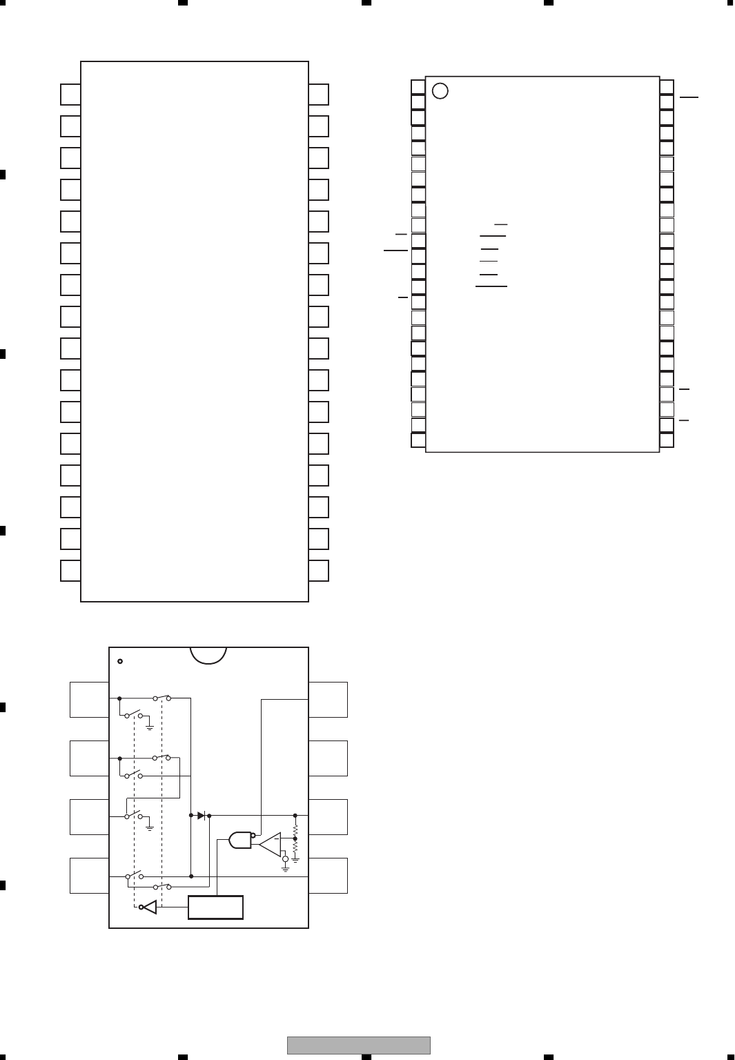
XDV-M8357ZT/UC
104
1234
1234
C
D
F
A
B
E
*M5M51008DKV-70HI
*MAX662AESA
*PD6531A
*PD6520A
1
A15
2
A14
3
A13
4
A12
5
A11
6
A10
7
A9
8
A8
11
WE
12
RESET
13
NC
14
NC
15
16
RY/BY
A18
A0-A18,A-1
RY/BY
BYTE
OE
DQ0-DQ15 :Address input
:Ready/busy output
:8bit,16bit mode select
:Output enable
:Data input/output
WE :Write enable
CE :Chip enable
RESET:Reset
9
NC
10
NC
17
A17
18
A7
19
A6
20
A5
21
A4
22
A3
23
A2
24
A1
A16
BYTE
VSS
DQ15/A-1
DQ7
DQ14
DQ6
DQ13
38 DQ4
37 VCC
36 DQ11
35 DQ3
34
33
DQ10
DQ2
DQ5
39 DQ12
32 DQ9
31 DQ1
30 DQ8
29 DQ0
28 OE
27 VSS
26 CE
25 A0
47
46
45
44
43
42
48
41
40
1
3
2
C1-
C1+
C2-
VCC
VOUT
GND
45
6
7
8SHDN
C2+
+
OSCILLATOR
ERROR
AMP
A8
A13
w
S2
A15
VCC
NC
A16
A14
A12
A7
A6
s!
DQ8
DQ7
DQ6
DQ5
DQ4
DQ3
GND
DQ1
DQ2
A1
A5
A4
A2
A3
A0
A11
A9
oe
A10
1
2
3
4
5
6
7
8
9
10
11
12
13
14
15
16
32
31
30
29
28
27
26
25
24
23
22
21
20
19
18
17
A0~A16 :Address input
DQ1~DQ8 :Data input/output
w :Write control input
s!,S2 :Chip select input
oe :Output enable input
VCC :Power supply
GND :GND
NC :Not used

XDV-M8357ZT/UC 105
5678
5678
C
D
F
A
B
E
-Pin Functions (PD3411A)
Pin No. Pin Name I/O Function and Operation
1 PB14 IMY-Chip interruption #1
2 PB15 I AV Chip interruption #0
3 VSS GND
4-11 AD0-7 I/O Data bus
12 VSS GND
13,14 AD8,9 I/O Data bus
15 VCC Power supply terminal
16-21 AD10-15 I/O Data bus
22 VSS GND
23-30 A0-7 O Address bus
31 VSS GND
32-39 A8-15 O Address bus
40 VSS GND
41,42 A16,17 O Address bus
43 VCC Power supply terminal
44-47 A18-21 O Address bus
48 CS0 Not used
49 CS1 CARNET 4 chip select
50 CS2 External memory area chip select
51 CS3 MY-Chip chip select
52 VSS GND
53 PA0 DVD EDC error detection
54 PA1 Flash ROM write enable
55 PA2 AV Chip chip select
56 PA3 External wait input
57 PA4 Low Byte write pulse
58 PA5 High Byte write pulse
59 PA6 Read pulse
60 PA7 Serial data latch pulse
61 VSS GND
62 PA8 I Audio output last step mute
63 PA9 I RS-232 ready for sending output
64 PA10 I AV Chip interruption #1
65 PA11 I Communication response to BUS microcomputer
66 PA12 O DMA CH0 transfer request
67 PA13 I DMA CH0 transfer request
68 PA14 O DMA CH0 transfer request
69 PA15 I DMA CH0 transfer request
70 VCC Power supply terminal
71 CK O Not used
72 VSS GND
73 EXTAL I Clock oscillator
74 XTAL I Clock oscillator
75 VCC Power supply terminal
76 NMI I Not used
77 VCC Power supply terminal
78 WDTOVF Not used
79 RES I Chip enable of after power on
80-82 MD0-2 I Mode 2
83,84 VCC Power supply terminal
85 AVCC Power supply terminal
86 AVREF Power supply terminal
87-89 PC0-2 Not used
90 PC3 I Data lead enable
91 AVSS GND
92 PC4 I V field discrimination signal input
93 PC5 I Test mode entry
94 PC6 I Communication request from BUS microcomputer
95 PC7 I Request of RS-232 ready for communicating
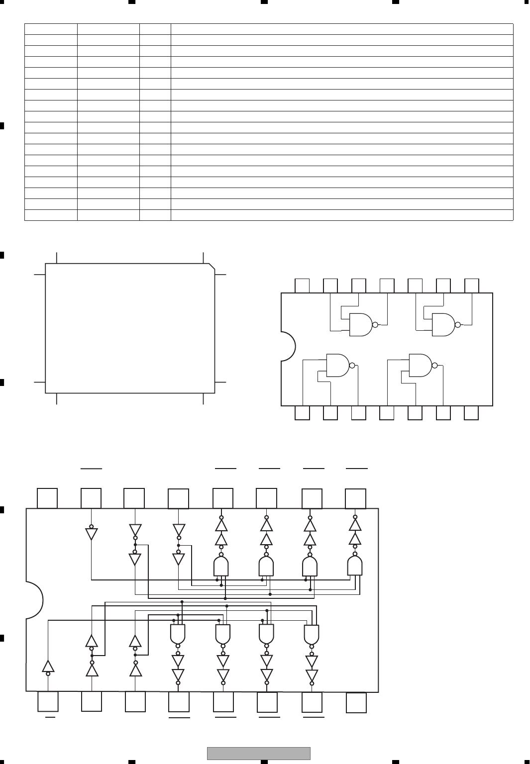
XDV-M8357ZT/UC
106
1234
1234
C
D
F
A
B
E
*PD3411A
*TC74VHC139FT
28
29
56
57
84
85
112
1
Pin No. Pin Name I/O Function and Operation
96 VSS GND
97 PB0 I STEP 2 DMA transfer DREQ
98 PB1 I Power supply terminal
99 VCC Power supply terminal
100 PB2 I Transfer end interruption
101 PB3 I AV Chip interruption #2
102 PB4 I STEP 2 receive interruptio n
103 PB5 I STEP 2 transmit interruption #1
104 PB6 I CARNET4 chip select
105 PB7 I CARNET4 chip power
106 VSS GND
107 PB8 I Serial bus data input
108 PB9 I Serial bus data output
109 PB10 I RS232C RxD
110 PB11 I RS232C TxD
111 PB12 I Serial bus clock input/output
112 PB13 I MY-Chip interruption #0
1G
1
1A
2345 6 78
16 15 14 13 12 11 10 9
1B 1Y0 1Y1 1Y2 1Y3 GND
2Y1 2Y2 2Y3
2A 2B 2Y0VCC 2G
6413 72 5
9
1114 1213 8
10
VCC
4B
4A
3B
3A
3Y
1A
1B
1Y
2A
2B
2Y
GND
4Y
*TC74VHC00FTS1
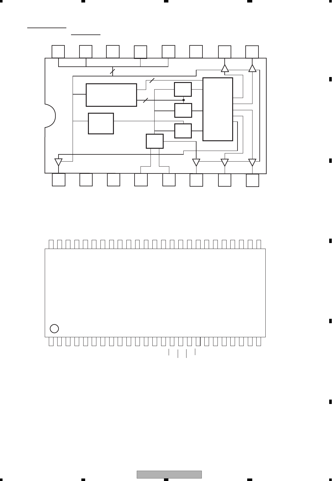
XDV-M8357ZT/UC 107
5678
5678
C
D
F
A
B
E
*CY2292SI-1A0
UTIL
PLL
123 4 567 8
16 15 14 13 12 11 10 9
OUTPUT
MULTIPLEXER
AND
DIVIDERS
SYS
PLL
CPU
PLL
CPU
EPROM
TABLE
CONFIGURATION
EPROM AND
TEST LOGIC
OSC
CLKC VDD GND XTAL
IN XTAL
OUT XBUF CLKD CPU
CLK
CLKBCLKAGNDSOSOSIVDD
S2/
SUSPEND
SHUTDOWN
/OE
*MSM56V16160DP-10TS
DQ1 2
DQ2 3
VssQ 4
DQ3 5
DQ4 6
VccQ 7
DQ5 8
DQ6 9
VssQ 10
DQ7 11
DQ8 12
VccQ 13
LDQM 14
WE 15
CAS 16
RAS 17
CS 18
A11 19
A10 20
A0 21
A1 22
A2 23
A3 24
48 DQ15
47 VssQ
46 DQ14
45 DQ13
44 VccQ
43 DQ12
42 DQ11
41 VssQ
40 DQ10
39 DQ9
38 VccQ
37 NC
36 UDQM
35 CLK
34 CKE
33 NC
32 A9
31 A8
30 A7
29 A6
28 A5
27 A4
26 Vss
Vcc 1
Vcc 25
49 DQ16
50 Vss
CLK : System clock
cs : Chip select
CKE : Clock enable
A0-A10 :Address input
A11 : Bank select address input
ras : Row address strobe
cas : Column address strobe
we : Write enable
UDQM,LDQM : Data input/output mask
DQi : Data input/output

XDV-M8357ZT/UC
108
1234
1234
C
D
F
A
B
E
-Pin Functions (MB86373BPFV-G-BI)
Pin No. Pin Name I/O Function and Operation
1 CLKSEL I ON/OFF signal of PLL
2 DIGCPN7 O Digital component signal output
3 VSS GND
4-9 DIGCPN6-1 O Digital component signal output
10 VDD 2.5V Power supply
11 DIGCPN0 O Digital component signal output
12 RBSEL O Cb, Cr identification signal of during digital component signal output
13 XHS O Horizontal synchronizing output signal
14 XVS O Vertical synchronizing output signal
15 VSS GND
16 XRESET I Reset
17 XLDCSYNC I External synchronizing signal input (LD mode)
18 KEY O KEY signal for LD, OSD overlay (LD mode)
19 PD O Phase comparing result output signal of horizontal synchronous
20 VFLD O Field discrimination signal of digital signal output
21-25 DIGCOMP9-5 O Digital composite signal output
26 VSS GND
27 VDD 2.5V Power supply
28-32 DIGCOMP4-0 O Digital composite signal output
33 DACK O 27MHz clock output terminal
34 NC Not used
35 VSSA3 GND (D/A converter)
36 ANAC O Analog color (C) output signal
37 VDDA3 2.5V power supply (internal D/A converter only)
38 VSSA2 GND (D/A converter)
39 ANAY O Analog brightness (Y) output signal
40 VDDA2 2.5V Power supply (internal D/A converter only)
41 VREF I Reference voltage for D/A converter
42 VRO O D/A converter inner current set terminal
43 VDDA4 2.5V Power supply (internal D/A converter only)
44 VSSA1 GND (D/A converter)
45 ANACOMP O Analog composite output terminal
46 VDDA1 2.5V Power supply (internal D/A converter only)
47 BF O Burst flag signal
48 XBLK O H/V complex blanking signal
49 TEST4 O Open
50 VSS GND
51 TEST0 I Open
52 TEST1 I Test terminal
53 DAIIN I External input digital data input (SPDIF)
54 CDDATA I External input audio data input (for CD)
55 CDLR I External input data channel clock input (for CD)
56 CDBCK I External input data clock input (for CD)
57-59 AODATA3-1 O Audio decode data
60 VSS GND
61 VDD 2.5V Power supply
62 AODATA0 O Audio decode data
63 AOPCM O Digital audio interface output
64 AODAI O Digital audio interface output
65 LRCK O Data channel clock for D/A, digital filter
66 AOMCK O Master clock for D/A, digital filter
67 BCK O Bit clock for D/A, digital filter
68,69 TEST2,3 I open
70 NC Not used
71 XDSPRST I Open
72 VSS GND
73 TEST5 O Open
74-77 NC Not used
78 SD7 I Parallel data input
79 VDD 2.5V Power supply

XDV-M8357ZT/UC 109
5678
5678
C
D
F
A
B
E
Pin No. Pin Name I/O Function and Operation
80-84 SD6-2 I Parallel data input
85 VSS GND
86,87 SD1,0 I Parallel data input
88 XERR I Error input signal
89 XSACK I Acknowledge signal
90 XTEST I Test terminal
91 SREQ O Data request signal
92-95 HADRS10-7 I CPU address bus signal
96 VSS GND
97 VDD 2.5V Power supply
98-102 HADRS6-2 I CPU address bus signal
103-106 HDATA15-12 I/O CPU data bus signal
107 VSS GND
108-113 HDATA11-6 I/O CPU data bus signal
114 VDD 2.5V Power supply
115-118 HDATA5-2 I/O CPU data bus signal
119 VSS GND
120,121 HDATA1,0 I/O CPU data bus signal
122 BUSSEL I Bus width select signal
123 XOSDACK I OSD data acknowledge signal
124 XOSDREQ O OSD data request signal
125,126 HCPUSEL1,0 I CPU select signal
127-129 XINT3-1 O Interruption request signal to CPU
130 VSS GND
131 VDD 2.5V Power supply
132 XINT0 O Interruption request signal to CPU
133 XEXTRDY O Acknowledge signal to CPU
134 HRW I CPU read/write signal
135 HCLKIN I Host clock input
136 XHCS I LSI chip select signal
137 XHAS I CPU address status
138-141 XHBE3-0 I CPU byte enable signal
142 VSS GND
143 MDRADR4 O Address signal for SDRAM
144 MDRADR3 O Address signal for SDRAM
145 MDRADR5 O Address signal for SDRAM
146 MDRADR2 O Address signal for SDRAM
147 VDD 2.5V Power supply
148 VSS GND
149 MDRADR6 O Address signal for SDRAM
150 MDRADR1 O Address signal for SDRAM
151 MDRADR7 O Address signal for SDRAM
152 MDRADR0 O Address signal for SDRAM
153 MDRADR8 O Address signal for SDRAM
154 VSS GND
155-158 TEST6-9 I Test terminal
159 MDRADR10 O Address signal for SDRAM
160 MDRADR9 O Address signal for SDRAM
161 MDRADR11 O Address signal for SDRAM
162 XMDRCS O Chip select signal for SDRAM
163 MDRCKE O Clock enable signal for SDRAM
164 VSS GND
165 VDD 2.5V Power supply
166 XMDRRAS O RAS signal for SDRAM
167 MDRCLK O Clock output signal for SDRAM
168 VSS GND
169 MDRCLKIN I Clock input signal for SDRAM
170 XMDRCAS O CAS signal for SDRAM
XDV-M8357ZT/UC
110
1234
1234
C
D
F
A
B
E
*MB86373BPFV-G-BI
52
53
104
105
156
157
208
1
Pin No. Pin Name I/O Function and Operation
171 XMDRDQM1 O Input mask/output enable signal for SDRAM
172 VSS GND
173 XMDRWE O Write enable signal for SDRAM
174 XMDRDQM0 O Input mask/output enable signal for SDRAM
175 MDRDAT8 I/O Data bus signal for SDRAM
176 VSS GND
177 MDRDAT7 I/O Data bus signal for SDRAM
178 MDRDAT9 I/O Data bus signal for SDRAM
179 MDRDAT6 I/O Data bus signal for SDRAM
180 MDRDAT10 I/O Data bus signal for SDRAM
181 MDRDAT5 I/O Data bus signal for SDRAM
182 VSS GND
183 VDD 2.5V Power supply
184 MDRDAT11 I/O Data bus signal for SDRAM
185 MDRDAT4 I/O Data bus signal for SDRAM
186 MDRDAT12 I/O Data bus signal for SDRAM
187 MDRDAT3 I/O Data bus signal for SDRAM
188 MDRDAT13 I/O Data bus signal for SDRAM
189 VSS GND
190 MDRDAT2 I/O Data bus signal for SDRAM
191 MDRDAT14 I/O Data bus signal for SDRAM
192 MDRDAT1 I/O Data bus signal for SDRAM
193 MDRDAT15 I/O Data bus signal for SDRAM
194 MDRDAT0 I/O Data bus signal for SDRAM
195 VSS GND
196 NC Not used
197 ICK27M I System clock output
198 VSS GND
199 OCK27M O System clock input
200 VSSA GND (VCO only)
201 VDDA 2.5V Power supply (VCO only)
202 ILPF O PLL section inverter output for audio
203 MLPF I PLL section inverter input for audio
204 OLPF O Phase detector output for audio
205 OVCO I VCO input for audio clock
206 VSS GND
207 XPLLRST I PLL section reset signal
208 XSYNCRST Connect to VDD
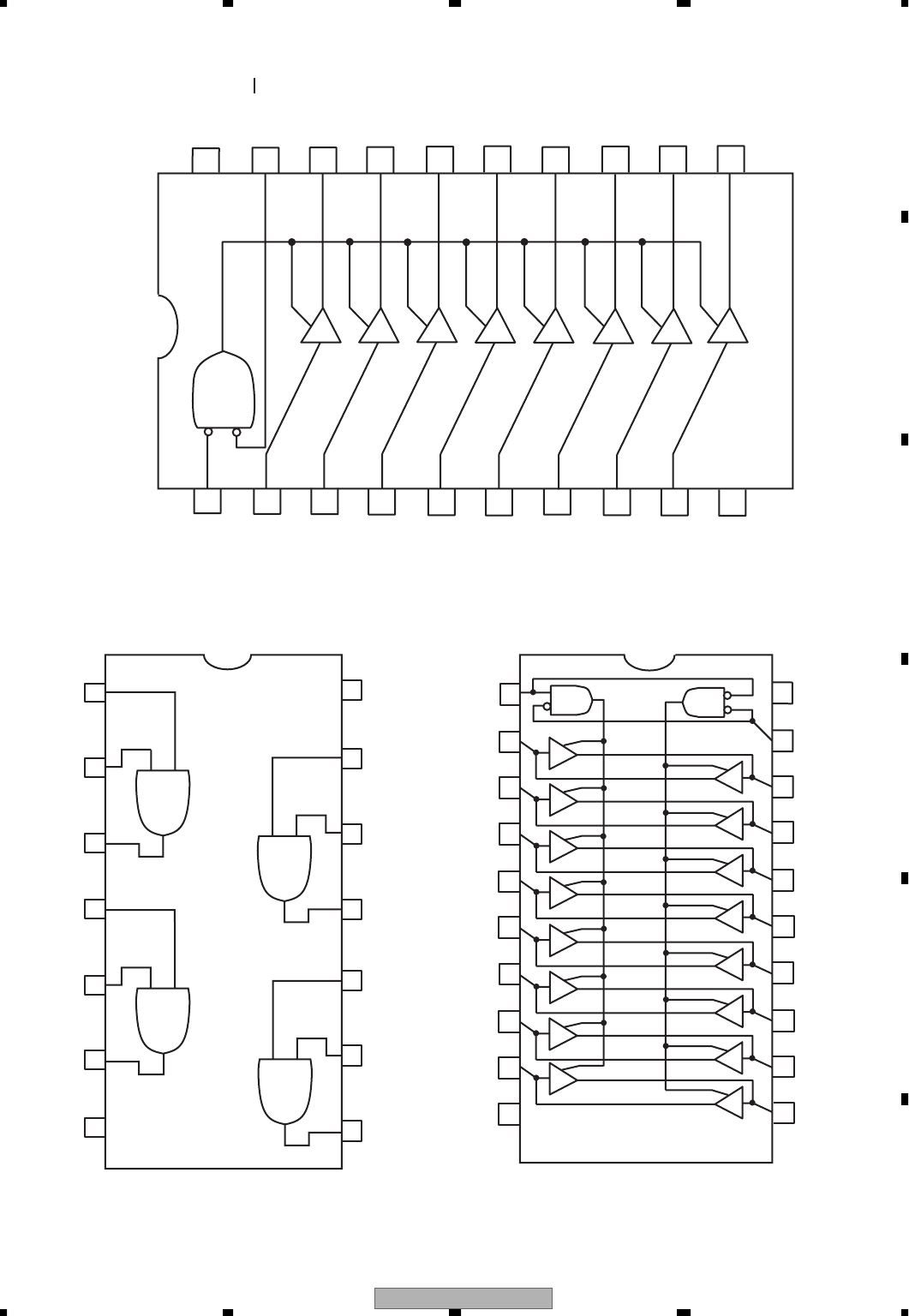
XDV-M8357ZT/UC 111
5678
5678
C
D
F
A
B
E
*TC74LCX245FTS1
14 VCC
13 4B
12 4A
11 4Y
10 3B
9 3A
8 3Y
1 1A
2 1B
3 1Y
4 2A
5 2B
6 2Y
7 GND
*TC74VHC08FTS1
*TC74VHC541FTS1
14 B5
13 B6
12 B7
11 B8
10 GND
9 A8
8 A7
1 DIR
2 A1
3 A2
4 A3
5 A4
6 A5
7 A6
15 B4
16 B3
17 B2
18 B1
19 oe
20 VCC
14 Y5
13 Y6
12 Y7
11 Y8
10 GND
9 A8
8 A7
1 g1
2 A1
3 A2
4 A3
5 A4
6 A5
7 A6
15 Y4
16 Y3
17 Y2
18 Y1
19 G2
20 VCC
XDV-M8357ZT/UC
112
1234
1234
C
D
F
A
B
E
*LC89513KP
64
1
16
17 32
33
48
49
-Pin Functions (LC89513KP)
Pin No. Pin Name I/O Function and Operation
1 VSS GND
2-8 RA0-6 O Address signal output
9 VSS GND
10-16 RA7-13 O Address signal output
17 VSS GND
18 ra!# O Address signal output
19 rcs O Chip select
20 rwe O Data write signal
21 roe O Data read signal
22 reset I Reset input
23 XTALCK I Oscillator input
24 VDD Power supply
25 C2PO I C2 pointer input
26 BCK I Serial data clock input
27 SDATA O Serial data output
28 LRCK I/O 44.1kHz strobe input
29 RS I Register select signal input
30 rd I Data read signal input
31 wr I Data write signal input
32 cs I Chip select
33 VSS GND
34-41 D0-7 CPU data signal
42 PSRAM I SRAM select
43 int O Interrupt request signal output
44 DRQ O DRQ signal output
45-48 HD0-3 O Data output
49 VSS GND
50-53 HD4-7 O Data output
54 hrd I Data reading request input
55 dten O Data enable output
56 VDD Power supply
57-64 IO0-7 Data buffer RAM data signal

XDV-M8357ZT/UC 113
5678
5678
C
D
F
A
B
E
-Pin Functions (PE5272A)
Pin No. Pin Name I/O Format Function and Operation
1 SENS25 I VD short sense 2.5V
2 SENS3 I VD short sense 3V
3NC Open
4 AVSS GND
5 XSRSENS O C
C
C
C
C
C
SWREG information output to mechanism controller
(H : Off, L : On)
6 XADEN O AVREF0 control output
7 AVREF1 D/A converter reference voltage
8 SWREG O System power supply voltage
9XILL Open
10 VADCONT O Servo, liquid tilt power supply, audio power supply control output
11 SI I System controller communication data input
12 SO O System controller communication data output
13 SCK O
C
O
C
OC
O
C
O
C
C
C
C
C
O
System controller communication clock output
14 NC Open
15 XRDY Communication request to system controller
(L : Communication permission)
16 XRES System reset output (L : Reset)
17 XMRES Mechanism controller reset output
18,19 NC Open
20 VIOC Image changeover switch(H:External through hole,L:MMCH output)
21-25 NC Open
26 SYSMUTE Mute output of AVC-LAN
27 ANSW O Analog switch control output
28 XRMUTE O Mute output for rear RCA
29-32 NC Open
33 VSS GND
34 DEST2 I Destination set input
35 XVMUTE O Front video mute output (H : Mute on)
36-39 NC Open
40 AV8CONT O Power supply control output of audio
41-46 NC Open
47 LT1 I Communication response from system controller
(L : Communication permission)
48-51 NC Open
52,53 FANPW1,2 O C
C
C
Power control output of FAN
54 NC Open
55 IEPW O IE-BUS driver STBY control output
56 IEDO O Data output for IE-BUS driver
57 IEDI I Data input for IE-BUS driver
58,59 NC Open
60 XRST I System reset input
61 RMIN I Remote control input
62 XASEN I ACC on/off state detection input (7, 7.5 V sense)
63 XMBSEN I Backup state detection input (8.5 V sense)
64 XBSEN I Backup state detection input (7, 7.5 V sense)
65 XCLOSSEN I Door detection (L : Door close)
66 XEJ I Eject SW detection (L : Eject key)
67 XMAG I Magazine insert detection (L : Magazine)
68 VDD Positive power supply
69 X2 System clock oscillation
70 X1 I System clock oscillation input
71 IC Connect to GND
72 NC Open
73 TESTIN I Chip test mode input
74 AVDD A/D converter analog power supply
75 AVREF0 A/D converter reference voltage
XDV-M8357ZT/UC
114
1234
1234
C
D
F
A
B
E
*LC35256FT-70U
Pin No. Pin Name I/O Format Function and Operation
76 STEMP I System controller section high-temperature sense A/D input
77 BTEMP I BUS microcomputer section high-temperature sense A/D input
78 LOTEMP I Low-temperature sense A/D input
79 DEST I Destination set A/D input
80 SENS9 I VD short sense 9V group
Format Meaning
CC MOS
*PE5272A
80
1
20
21 40
41
60
61
oe 21
20
19
18
17
16
15
14
13
12
11
10
9
8
A10
ce
I/O8
A11
I/O7
A9
I/O6
A8
I/O5
A13
we
I/O4VCC
GNDA14
I/O3A12
I/O2A7
I/O1A6
A0A5
A1A4
A3 A2
22
23
24
25
26
27
28
1
2
3
4
5
6
7
ce :Chip enable input
oe :Output enable input
we :Read/write input
A0~A14 :Address input
VCC :Power supply
VSS :GND
I/O1~I/O8 :Data input/output
XDV-M8357ZT/UC 115
5678
5678
C
D
F
A
B
E
7.3 EXPLANATION
7.3.1 OPERATIONAL FLOW CHART
XBSEN=L
XMBSEN=L
XASEN=L
XBSEN
Pin 64
XASEN
Pin 62
Y
SENS9 > 1V
Pin 80
Y
SENS3 > 1V
Pin 2
IEPW←Hi
Pin 55
SWREG←Hi
Pin 8
XSRSENS(Pin 5)←Low
XRES(Pin 16)←Hi
XMRES(Pin 17)←Hi
VDD=5V
Pin 68
XMBSEN
Pin 63
Y
Y
SENS25 > 1V
Pin 1
Power ON Magazine insertion and door closed state
Subsequently,
AVC-LAN enables
communication.
Subsequently,
communication with
an internal system
controller starts.
A DVD changer
can operate.
150ms
In case of the movement as shown above,
communication with the system controller may
cause an error.
XDV-M8357ZT/UC
116
1234
1234
C
D
F
A
B
E
7.3.2 SYSTEM BLOCK DIAGRAM
H/U PWR
AMP
PWR ANT
ECU
+B, ACC
- (7SP)
KEX-M9137ZT-02/UC
KEX-M9737ZT-02/UC
GM-9027ZT-02/E
DVD
CHANGER
XDV-M8357ZT/UC
POWER SUPPLY(+B, ACC)
BUS
SIGNAL(SOUND)
DISPLAY
(OTHER MAKERS)
(OTHER MAKERS)
VISION
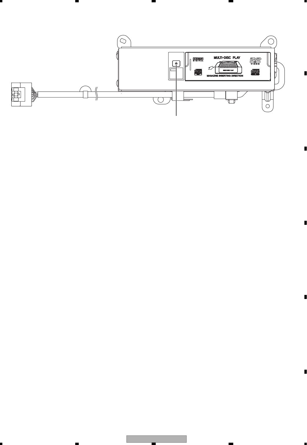
XDV-M8357ZT/UC 117
5678
5678
C
D
F
A
B
E
8. OPERATIONS
Notes
CD-Rs may not
be playable in
this compact
disc player.
EJECT
PIONEER CORPORATION 4-1, Meguro 1-chome, Meguro-ku, Tokyo 153-8654, Japan
PIONEER ELECTRONICS (USA) INC. P.O. Box 1760, Long Beach, CA 90801-1760, U.S.A.
PIONEER EUROPE NV Haven 1087, Keetberglaan 1, 9120 Melsele, Belgium
PIONEER ELECTRONICS ASIACENTRE PTE. LTD. 253 Alexandra Road, #04-01, Singapore 159936
PIONEER CORPORATION 2005 K-ZZA. APR. 2005 Printed in Japan
Before shipping out the product, be sure to clean the following portions by using the prescribed cleaning tools:
Portions to be cleaned Cleaning tools
DVD pickup lenses Cleaning liquid : GEM1004
Cleaning paper : GED-008
Portions to be cleaned Cleaning tools
Fans Cleaning paper : GED-008
- J
i
gs L
i
st
15P Extension cabl
e
30
P Extension cabl
e
Extension cor
d
Extension cor
d
Extension cor
d
E
xtens
i
on cor
d
C
lamp adjusting disc
GG
D1177
GG
D117
1
GG
D139
8
GG
D1
3
4
8
GG
D124
0
GG
D116
9
GG
V101
8
A
d
j
ustmen
t
j
A
d
j
ustmen
t
j
A
d
j
ustmen
t
j
A
d
j
ustmen
t
j
A
d
j
ustmen
t
j
A
d
j
ustmen
t
j
S
kew ad
j
ustmen
t
j
J
ig
No
.
N
ame
R
emarks
