RRV3568 XVDV363
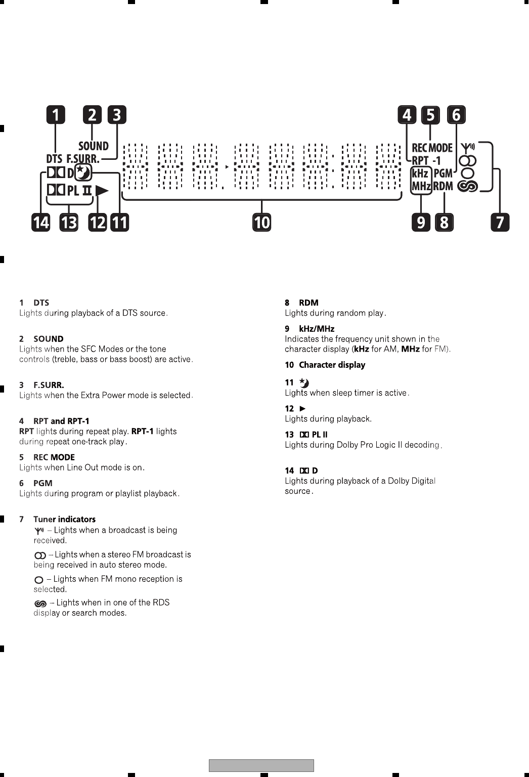
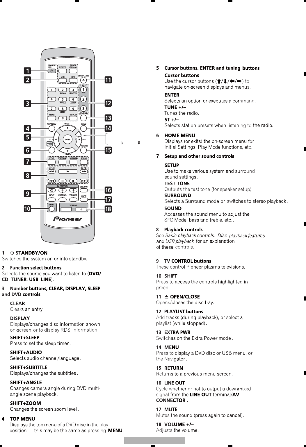
User Manual: XVDV363
Open the PDF directly: View PDF ![]() .
.
Page Count: 103 [warning: Documents this large are best viewed by clicking the View PDF Link!]
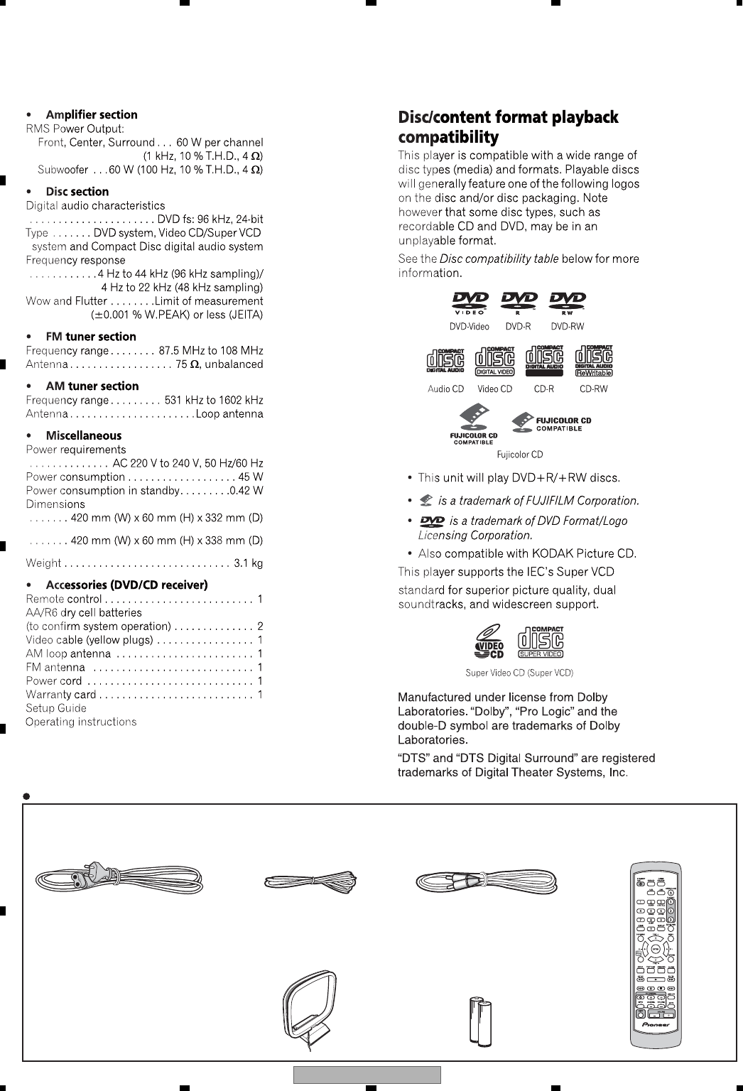
- XV-DV363
- <グラフィック>
- CONTENTS
- CONTENTS
- 1. SERVICE PRECAUTIONS
- 1.1 NOTES ON SOLDERING
- 1.2 CAUTION
- 2. SPECIFICATIONS
- 2.1 SPECIFICATIONS and ACCESORRIES
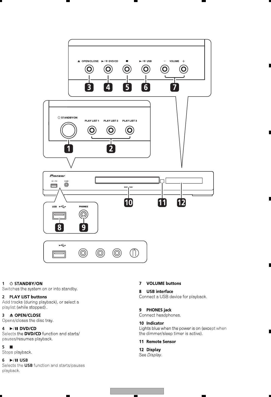
- 2.2 PANEL FACILITIES
- 3. BASIC ITEMS FOR SERVICE
- 3.1 CHECK POINTS AFTER SERVICING
- 3.2 PCB LOCATIONS
- 3.3 JIGS LIST
- 3.4 CLEANING
- 4. BLOCK DIAGRAM
- 4.1 OVERALL WIRING CONNECTION DIAGRAM and LOAB ASSY
- 4.2 OVERALL BLOCK DIAGRAM
- 5. DIAGNOSIS
- 5.1 METHOD FOR DIAGNOSING DEGRADATION OF THE LDS ON THE PICKUP
- 5.2 DVD TROUBLE SHOOTING
- 5.3 CIRCUIT DESCRIPTION OF DIGITAL AMP. SECTION
- 5.4 SPECIFICATIONS FOR THE PROTECTION CIRCUITS FOR THE DIGITAL AMPLIFIER
- 5.5 PASS/FAIL TEST PROCEDURE OF HDMI TRANSMITTER IC
- 6. SERVICE MODE
- 6.1 TEST MODE
- 6.2 DISPLAY SPECIFICATION OF THE TEST MODE
- 6.3 FUNCTIONAL SPECIFICATION OF THE SHORTCUT KEY
- 6.4 SPECIFICATION OF MODEL INFORMATION DISPLAY
- 6.5 FUNCTIONAL SPECIFICATION OF THE SERVICE MODE
- 6.6 SERVICE TEST MODE
- 7. DISASSEMBLY
- 8. EACH SETTING AND ADJUSTMENT
- 8.1 ADJUSTMENT
- 8.1.1 ADJUSTMENT ITEMS AND LOCATION
- 8.1.2 JIGS AND MEASURING INSTRUMENTS
- 8.1.3 NECESSARY ADJUSTMENT POINTS
- 8.1.4 TEST MODE
- 8.1.5 MECHANISM ADJUSTMENT
- 8.2 ID NUMBER AND ID DATA SETTING
- 9. EXPLODED VIEWS AND PARTS LIST
- 9.1 PACKING SECTION
- 9.2 EXTERIOR SECTION
- 9.3 06 LOADER ASSY
- 9.4 TRAVERSE MECHANISM ASSY-S
- 10. SCHEMATIC DIAGRAM
- 10.1 DVD MAIN ASSY (1/5)
- 10.2 DVD MAIN ASSY (2/5)
- 10.3 DVD MAIN ASSY (3/5)
- 10.4 DVD MAIN ASSY (4/5)
- 10.5 DVD MAIN ASSY (5/5)
- 10.6 DAMP ASSY (1/2)
- 10.7 DAMP ASSY (2/2)
- 10.8 DISPLAY, USB, LED and KEY ASSYS
- 10.9 MIC ASSY (XV-DV365K ONLY)
- 10.10 EUROSCART ASSY
- 10.11 POWER SUPPLY UNIT
- 10.12 WAVEFORMS
- 11. PCB CONNECTION DIAGRAM
- 11.1 LOAB ASSY
- 11.2 MIC ASSY (XV-DV365K ONLY)
- 11.3 DVD MAIN ASSY
- 11.4 DAMP ASSY
- 11.5 DISPLAY, USB, LED and KEY ASSYS
- 11.6 POWER SUPPLY UNIT
- 11.7 EUROSCART ASSY
- 12. PCB PARTS LIST
ORDER NO.
PIONEER CORPORATION 4-1, Meguro 1-chome, Meguro-ku, Tokyo 153-8654, Japan
PIONEER ELECTRONICS (USA) INC. P.O. Box 1760, Long Beach, CA 90801-1760, U.S.A.
PIONEER EUROPE NV Haven 1087, Keetberglaan 1, 9120 Melsele, Belgium
PIONEER ELECTRONICS ASIACENTRE PTE. LTD. 253 Alexandra Road, #04-01, Singapore 159936
PIONEER CORPORATION 2007
XV-DV363
RRV3568
DVD/CD RECEIVER
XV-DV363
XV-DV365K
THIS MANUAL IS APPLICABLE TO THE FOLLOWING MODEL(S) AND TYPE(S).
Model Type Power Requirement Regional restriction codes
(Region No.) Remarks
XV-DV363 WYXJ5 AC 220 V to 240 V 2
XV-DV365K WXJ/RE5 AC 220 V to 240 V 5
For details, refer to "Important Check Points for good servicing".
T-IZK APR. 2007 printed in Japan
XV-DV363
2
1234
1 234
C
D
F
A
B
E
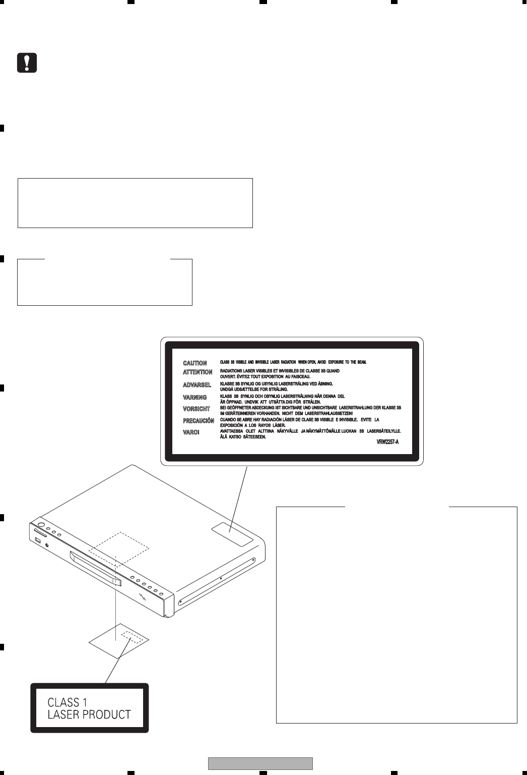
SAFETY INFORMATION
LASER DIODE CHARACTERISTICS
FOR DVD : MAXIMUM OUTPUT POWER : 5 mW
WAVELENGTH : 650 nm
FOR CD : MAXIMUM OUTPUT POWER : 7 mW
WAVELENGTH : 780 nm
Additional Laser Caution
1. Laser Interlock Mechanism
• Loading switch (S101 on the LOAB Assy) is used for interlock
mechanism of the laser.
When this switch turned ON in SW2 (CLOSE) side (OPEN signal is
0 V and CLOSE signal is 3.5 V), a laser becomes the status which
can completely oscillation.
Furthermore, the laser completely oscillates in the disc judgment and
disc playback.
When player is power ON state and laser diode is not completely
oscillating, 780 nm laser diode is always oscillating by half power.
• Laser diode is driving with Q307 (650 nm LD) and Q308 (780 nm
LD) on the DVD MAIN Assy.
Therefore, when short-circuit between the emitter and collector of these
transistors or the base voltage is supplied for transistors turn on, the
laser oscillates. (failure mode)
• In the test mode ∗ , there is the mode that the laser oscillates except
for the disc judgment and playback. LD ON mode in the test mode
oscillates with the laser forcibly.
The interlock mechanism mentioned above becomes invalid in this
mode.
2. When the cover is open, close viewing through the objective lens with
the naked eye will cause exposure to the laser beam.
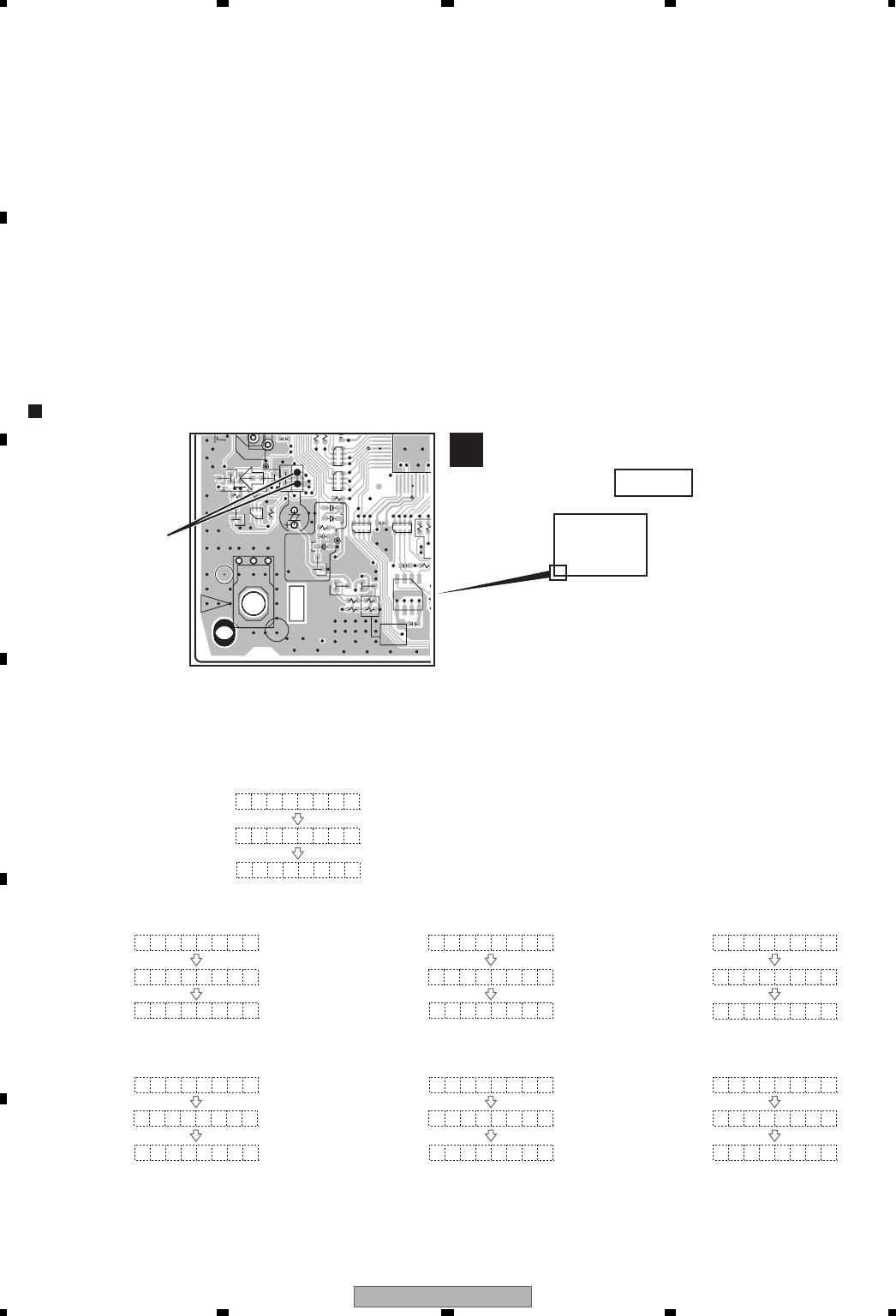
LABEL CHECK
VRW2257
Name Label
∗ : Refer to page 25.
This service manual is intended for qualified service technicians ; it is not meant for the casual do-
it-yourselfer. Qualified technicians have the necessary test equipment and tools, and have been
trained to properly and safely repair complex products such as those covered by this manual.
Improperly performed repairs can adversely affect the safety and reliability of the product and
may void the warranty. If you are not qualified to perform the repair of this product properly and
safely, you should not risk trying to do so and refer the repair to a qualified service technician.
WARNING!
The laser component is capable of emitting radiation exceeding
the limit for CLASS 1. A specially instructed person should do
servicing operation of the apparatus.
XV-DV363 3
5678
5678
C
D
F
A
B
E

XV-DV363
4
1234
1 234
C
D
F
A
B
E
CONTENTS
SAFETY INFORMATION..................................................................................................................................... 2
1. SERVICE PRECAUTIONS............................................................................................................................... 5
1.1 NOTES ON SOLDERING .......................................................................................................................... 5
1.2 CAUTION................................................................................................................................................... 5
2. SPECIFICATIONS............................................................................................................................................ 6
2.1 SPECIFICATIONS and ACCESORRIES ................................................................................................... 6
2.2 PANEL FACILITIES.................................................................................................................................... 7
3. BASIC ITEMS FOR SERVICE........................................................................................................................ 10
3.1 CHECK POINTS AFTER SERVICING..................................................................................................... 10
3.2 PCB LOCATIONS .....................................................................................................................................11
3.3 JIGS LIST ................................................................................................................................................ 12
3.4 CLEANING............................................................................................................................................... 12
4. BLOCK DIAGRAM.......................................................................................................................................... 14
4.1 OVERALL WIRING CONNECTION DIAGRAM and LOAB ASSY ........................................................... 14
4.2 OVERALL BLOCK DIAGRAM.................................................................................................................. 16
5. DIAGNOSIS.................................................................................................................................................... 18
5.1 METHOD FOR DIAGNOSING DEGRADATION OF THE LDS ON THE PICKUP................................... 18
5.2 DVD TROUBLE SHOOTING ................................................................................................................... 19
5.3 CIRCUIT DESCRIPTION OF DIGITAL AMP. SECTION.......................................................................... 22
5.4 SPECIFICATIONS FOR THE PROTECTION CIRCUITS FOR THE DIGITAL AMPLIFIER..................... 23
5.5 PASS/FAIL TEST PROCEDURE OF HDMI TRANSMITTER IC.............................................................. 24
6. SERVICE MODE ............................................................................................................................................ 25
6.1 TEST MODE ............................................................................................................................................ 25
6.2 DISPLAY SPECIFICATION OF THE TEST MODE.................................................................................. 26
6.3 FUNCTIONAL SPECIFICATION OF THE SHORTCUT KEY .................................................................. 27
6.4 SPECIFICATION OF MODEL INFORMATION DISPLAY ........................................................................ 28
6.5 FUNCTIONAL SPECIFICATION OF THE SERVICE MODE ................................................................... 29
6.6 SERVICE TEST MODE ........................................................................................................................... 30
7. DISASSEMBLY .............................................................................................................................................. 33
8. EACH SETTING AND ADJUSTMENT ........................................................................................................... 40
8.1 ADJUSTMENT......................................................................................................................................... 40
8.2 ID NUMBER AND ID DATA SETTING ..................................................................................................... 45
9. EXPLODED VIEWS AND PARTS LIST.......................................................................................................... 48
9.1 PACKING SECTION ................................................................................................................................ 48
9.2 EXTERIOR SECTION.............................................................................................................................. 50
9.3 06 LOADER ASSY................................................................................................................................... 52
9.4 TRAVERSE MECHANISM ASSY-S ......................................................................................................... 54
10. SCHEMATIC DIAGRAM............................................................................................................................... 56
10.1 DVD MAIN ASSY (1/5) .......................................................................................................................... 56
10.2 DVD MAIN ASSY (2/5) .......................................................................................................................... 58
10.3 DVD MAIN ASSY (3/5) .......................................................................................................................... 60
10.4 DVD MAIN ASSY (4/5) .......................................................................................................................... 62
10.5 DVD MAIN ASSY (5/5) .......................................................................................................................... 64
10.6 DAMP ASSY (1/2).................................................................................................................................. 66
10.7 DAMP ASSY (2/2).................................................................................................................................. 68
10.8 DISPLAY, USB, LED and KEY ASSYS.................................................................................................. 70
10.9 MIC ASSY (XV-DV365K ONLY)............................................................................................................. 72
10.10 EUROSCART ASSY ............................................................................................................................ 74
10.11 POWER SUPPLY UNIT ....................................................................................................................... 76
10.12 WAVEFORMS...................................................................................................................................... 78
11. PCB CONNECTION DIAGRAM.................................................................................................................... 80
11.1 LOAB ASSY ........................................................................................................................................... 80
11.2 MIC ASSY (XV-DV365K ONLY) ............................................................................................................. 81
11.3 DVD MAIN ASSY ................................................................................................................................... 82
11.4 DAMP ASSY .......................................................................................................................................... 86
11.5 DISPLAY, USB, LED and KEY ASSYS .................................................................................................. 88
11.6 POWER SUPPLY UNIT ......................................................................................................................... 90
11.7 EUROSCART ASSY .............................................................................................................................. 92
12. PCB PARTS LIST......................................................................................................................................... 93
XV-DV363 5
5678
5678
C
D
F
A
B
E
1. SERVICE PRECAUTIONS
1.1 NOTES ON SOLDERING
1.2 CAUTION
• For environmental protection, lead-free solder is used on the printed circuit boards mounted in this unit.
Be sure to use lead-free solder and a soldering iron that can meet specifications for use with lead-free solders for repairs
accompanied by reworking of soldering.
• Compared with conventional eutectic solders, lead-free solders have higher melting points, by approximately 40 °C.
Therefore, for lead-free soldering, the tip temperature of a soldering iron must be set to around 373 °C in general, although
the temperature depends on the heat capacity of the PC board on which reworking is required and the weight of the tip of
the soldering iron.
Do NOT use a soldering iron whose tip temperature cannot be controlled.
Compared with eutectic solders, lead-free solders have higher bond strengths but slower wetting times and higher melting
temperatures (hard to melt/easy to harden).
The following lead-free solders are available as service parts:
• Parts numbers of lead-free solder:
GYP1006 1.0 in dia.
GYP1007 0.6 in dia.
GYP1008 0.3 in dia.
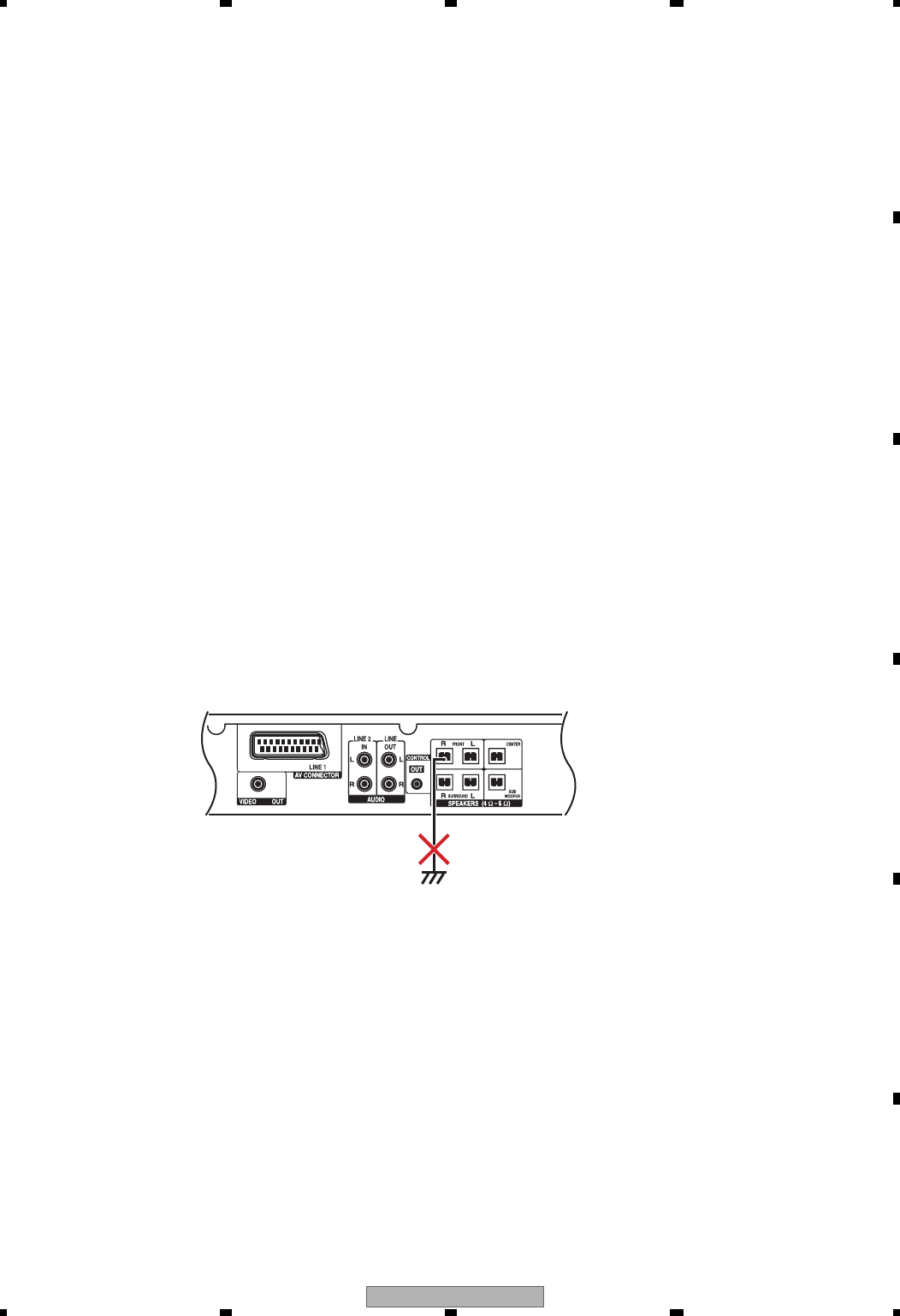
NOTES ON BTL DRIVE
As a signal to drive the BTL is output from the negative speaker terminal, DO NOT short-circuit between the
negative speaker terminal and ground, such as the chassis.
Do not short-circuit between the plus speaker terminal and ground, such as the chassis, too.
Negative Speaker Terminal
Ground (Chassis)
Do not short-circuit
XV-DV363
6
1234
1 234
C
D
F
A
B
E
2. SPECIFICATIONS
2.1 SPECIFICATIONS and ACCESORRIES
Accessories
• Power Cord (ADG1127) • FM Antenna (ADH7030) • Video Cable
(L = 1.5 m) (XDE3046)
• AM Loop Antenna
(ATB7013)
• Dry Cell Battery (AA/R6)
• Remote Control
(XV-DV363 : XXD3121)
(XV-DV365K : XXD3124)
(XV-DV365K)
(XV-DV363)
XV-DV363 7
5678
5678
C
D
F
A
B
E
2.2 PANEL FACILITIES
Front panel
XV-DV365K
XV-DV363
PHONESUSB SUB MIC MAIN MIN VOL MAX
MIC
XV-DV363
8
1234
1 234
C
D
F
A
B
E
Display
XV-DV363 9
5678
5678
C
D
F
A
B
E
Remote control
ECHO
KARAOKE
SHIFT+KARAOKE
(XV-DV356K)
SHIFT+ECHO
SHIFT+ SHIFT+
XV-DV363
10
1234
1 234
C
D
F
A
B
E
3. BASIC ITEMS FOR SERVICE
3.1 CHECK POINTS AFTER SERVICING
Check points after servicing (HTZ and system audio)
To keep the product quality after servicing, confirm recommended check points shown below.
See the table below for the items to be checked regarding video and audio:
Item to be checked regarding video Item to be checked regarding audio
Block noise Distortion
Horizontal noise Noise
Dot noise Volume too low
Disturbed image (video jumpiness) Volume too high
Too dark Volume fluctuating
Too bright Sound interrupted
Mottled color
No. Procedures Check points
1 Confirm the firmware version on Service Mode. The version of the firmware must be latest.
Update firmware to the latest one, if it is not the latest.
2
Confirm whether the customer complain has been solved. If the
customer complain occurs with the specific disc, use it for the
operation check.
The customer complain must not be reappeared.
Video, audio and operations must be normal.
3
Confirm playback error rates at the innermost and outermost
tracks by using the following disc.
DVD test disc (GGV1025)
The error rates must be less than 5.0e-4.
4 Play back a CD. (track search) Audio and operations must be normal.
5Play back a DVD.
(Menu operation, Title/chapter search) Video, audio and operations must be normal.
6 Check the tuner (AM and FM) operations. Audio and operations must be normal.
7 Check the sound from headphone output. Sound must be normal, without noise.
8 Check the appearance of the product. No scratches or dirt on its appearance after receiving it for
service.
XV-DV363 11
5678
5678
C
D
F
A
B
E
3.2 PCB LOCATIONS
LOAB Assy
06 LOADER Assy
Bottom view
Front panel section
Rear view
A
DVD MAIN Assy
B
DISPLAY Assy
D
KEY Assy
G
LED Assy
F
MIC Assy
(XV-DV365K only)
H
USB Assy
E
EUROSCART Assy
I
DAMP Assy
C
POWER SUPPLY Unit
J
FM/AM TUNER Unit
Mark No. Description Part No.
LIST OF ASSEMBLIES
NSP 1..06 LOADER ASSY VWT1226
2..LOAB ASSY VWG2346
1..DAMP ASSY XWK3318
1..DVD MAIN ASSY (XV-DV363) XWM3341
1..DVD MAIN ASSY (XV-DV365K) XWM3342
NSP 1..COMPLEX ASSY XWM3372
2..DISPLAY ASSY XWZ4256
2..USB ASSY XWZ4259
2..KEY ASSY XWZ4261
2..LED ASSY XWZ4263
NSP 1..JACK ASSY AWM8034
2..EUROSCART ASSY AWU8291
1..MIC ASSY (XV-DV365K ONLY) XWM3375
>1..POWER SUPPLY UNIT XWR3012
1..FM/AM TUNER UNIT AXX7248
Mark No. Description Part No.

XV-DV363
12
1234
1 234
C
D
F
A
B
E
3.3 JIGS LIST
3.4 CLEANING
Service Remote Control Unit GGF1381
DVD Test Disc (DVD-Video) GGV1025
adjustment, diagnosis
Name Jig No. Remarks
Check of DVD-Video
CD Test Disc STD-905 Check of CD
DVD Data Disc GGV1269 ID data setting
Jigs list
Lubricating Oil GYA1001
GEM1036
Daifree
Name Lubricants and Glues No. Remarks
refer to "9.3 06 LOADER ASSY"
refer to "9.3 06 LOADER ASSY"
GEM1037Silicone Adhesive refer to "9.4 TRAVERSE MECHANISM ASSY-S"
Speaker Cable with terminal SDS1174 (FL/WHITE)
SDS1175 (FR/RED), SDS1176 (SL/BLUE)
SDS1177 (SR/GRAY), SDS1178 (C/GREEN)
For checking audio at the SP terminal
GYL1001Screw tight refer to "8.1.5 MECHANISM ADJUSTMENT"
Lubricants and Glues list
Before shipping out the product, be sure to clean the following positions by using the prescribed cleaning tools:
Position to be cleaned Cleaning tools
Pickup leneses Cleaning liquid : GEM1004
Cleaning paper : GED-008
CLEANING

XV-DV363 13
5678
5678
C
D
F
A
B
E
XV-DV363
14
1234
1 234
C
D
F
A
B
E
4. BLOCK DIAGRAM
4.1 OVERALL WIRING CONNECTION DIAGRAM and LOAB ASSY
CN602
2
1
LOAB ASSY
(VWG2346)
A
No schematic Diagram
FM/AM
TUNER UNIT
(AXX7248)
K
MIC ASSY
(XWM3375
:
XV-DV365K/WXJ/RE5
)
H
B B B( 1/5- 5/5)
(XWM3341:XV-DV363/WYXJ5)
(XWM3342:XV-DV365K/WXJ/RE5)
POWER
SUPPLY UNIT
(XWR3012)
J
DVD MAIN ASSY
2
1
13
11
12
9
10
13
11
12
9
10
2
1
5
7
8
3
4
6
7
8
5
6
3
4
21
24
22
23
15
14
20
19
16
17
18
55
3
4
1
22
3
1
4
2
4
1
3
2
1
2
1
4
5
3
1
1
2
3
4
11
2
5
3
4
2
5
3
2
6
7
8
11
9
10
11
10
9
8
13
12
2
3
4
5
7
6
1
4
2
1
3
5
9
6
7
10
8
12
11
5
1
2
3
4
7
6
GND
+B
AC POWER CORD
Pwr-ctr
GND
FL DC+
-25.5V
FL DC-
LIVE
NEUTRAL
SW3.3V(A)
GND
SW5.0V
SW3.3V(B)
EV5.0V
SW6.8V
OWY8087-
FOCS DRV
FOCS RTN
TRKG DRV
-25.5V
FL DC+
GND
Pwr-ctr
TRKG RTN
FL DC-
FOCS RTN
FOCS DRV
TRKG RTN
PICK UP ASSY
TRKG DRV
GND
SW3.3V(A)
SW6.8V LD(780)
PD
LD(650)
SW3.3V(B)
GNDD
VSHF
EV5.0V
SW5.0V
GNDD
GNDD
LD(650)
PD
LD(780)
GNDD
VSHF
SW1 SW1
GNDD
SW2
LOAD+
LOAD-
GNDD
LOAD-
LOAD+
SW2
4P FFC
STEPPING MOTOR
ST2+(B)
ST2-(~B~)
ST1-(~A~)
ST1+(A) ST1+(A)
ST1-(~A~)
ST2-(~B~)
ST2+(B)
SW10.5V
AC_DET
PG13KK-F22
ECHOCONT
MIC SW
V+10V
MIC
GND
(XDD3232-)
5P FFC
TXR
GND
RDS
VSM
SW(DVD/CD)
A
VR650
B
RF
VR780
VRCOM
AC_DET
SW10.5V
24P FFC
A
VR650
B
RF
VR780
VRCOM
(ADD7545-)
SW(DVD/CD)
V+10V
D
C
ECHOCONT
MIC SW
F
VCC
E
VS(VREF)
GND
MIC
D
VS(VREF)
E
VCC
F
C
GNDD
DVD LOADER
GNDD
VWT1226-
U-
V+
U+
V+5S
V+
V+5S
U+
U-
V
W+
V-
SPINDLE MOTOR
U
W-
12P FFC
HB
V
W-
U
V-
W+
HB
INSIDE
WW
INSIDE
TXR
VSM
RDS
GND
AM
FM
CLK
DO
DI
CE
GND
TXL
+9V
(ADD7543)
11P FFC
+9V
CLK
CE
DI
DO
TXL
GND
B2P-VH
ADX7480-
PF05PP-B40
S5B-PH-K-S B5B-PH-K-S
VKN1235
B13B-PH-K-S B13B-PH-K-S
AKN7003
RKN1004
CKS3370
TRAVERSE MECHA ASSY
DXB1860-
VKN2045 CN1
OKN8001
VKN1243
CN1 CKS3376-
CN2
CN1
CN601 CN104
CN103
CN3 CN1001
JA3922
JA3921
CN3921 CN5702
CN101 CN102
CN5701
XV-DV363 15
5678
5678
C
D
F
A
B
E
C C C( 1/2- 2/2)
DAMP ASSY
(XWK3318)
EUSB ASSY
(XWZ4259)
FLED ASSY
(XWZ4263)
G
KEY ASSY
(XWZ4261)
I
EURO SCART
ASSY
(AWU8291)
DDISPLAY ASSY
(XWZ4256)
GND
Vout
Vcc
11
4
3
2
4
3
2
6
5
7
6
5
7
10
9
8
10
9
8
13
11
12
13
11
12
15
16
14
15
16
14
19
17
18
19
17
18
2
1
12
11
10
5
8
9
6
7
2
1
3
4
11
3
4
22
4
3
7
6
5
7
6
5
8
10
9
8
10
9
13
11
12
11
12
13
15
16
14
15
16
14
19
17
18
17
19
18
312
312
55
3
44
3
1
2
1
2
3
2
1
4
12
13 11
10
79
108
1311
12
6
5
2
13
2
1
4
553
4
9
6
97
8
7
86
13
10
1311
12
10
11
12
82
513
64
79
246810
12
315971311
15
15
14
14
2323
21
20
8
7
2
1
6
5
4
3
10
911 17
18
15
16
13
14
19
12
20
21
22
20
21
22
19
17
18
19
17
18
14
15
16
15
16
14 11
18
12
17
15
16
19
14
13
13
12
11
13
12
11
9
8
10 10
9
8
7
6
55
7
6
6
5
2
8
7
10
9
4
3
2
3
4
2
3
4
11
1
SDATA 4 SDATA4
S_TVOUT_R
S_TVOUT_L
LIN1_L
GND
GND
GND
GND
RECMUTE
LIN1_R
S_TVOUT_R
RECMUTE
GND
GND
S_TVOUT_L
GND
GND
LIN1_R
LIN1_L
SDATA 3
SDATA 2
LRCLK
MCLK
GND
GND
SCLK
SDATA 1
GND
LRCLK
SCLK
GND
GND
GND
MCLK
SDATA1
SDATA3
SDATA2
SR OUT
GND
+B
SW-
SW+
FL-
RL+
C+
C-
RL-
FL+
6ch SP OUT
FR+
RR-
RR+
FR-
SCL
XSD
XOTW
GND
SROUT
POWER
PLCCONT PLCCONT
POWER
XSD
SROUT
XOTW
GND
SCL
XMUTE
3.3V
SDA
GND
HPR
GND
XPDN
GND
XRST
XMUTE
GND
SDA
3.3V
XRST
XPDN
GND
GND
HPR
HPL
XHPSEL
PCON
XHPSEL
PCON
HPL
EU,RUSSIA,KUC & J
GA UPPER
V+10V
LED
GND
(XDD3229-)
3P FFC
GND
LED
V+10V
5P FFC (XDD3231)
AAV7104(AAV7107)
13P FFC(ADD7541)
FL
15p:CKS3380
HPMUTE
GNDD
HP_L
HP_R
HP_DET
GNDUSB
V5USB
V5USB
USB_DP2
USB_DM2
GNDUSB
KEY2
KEY1
15P FFC (XDD3234)
15p:CKS3380
GNDD
HP_L
HPMUTE
HP_DET
HP_R
GNDUSB
V5USB
V5USB
USB_DP2
GNDUSB
USB_DM2
KEY1
KEY2
S_Y
TVIN_R
LINEOUT_L
LINEOUT_R
IN/OUT
AUDIO
USB
TVIN_L
XKP3086
JA602
HP OUT
V+10
LED
LED
V+10
S_Y
V
GND
NC
(VKB1122) COMPOSITE
VIDEO
OUTPUT
GND
GND
GND
DVDPOWER
GND
S_C
CLOCK SHIELD
CLOCK+
DATA0-
DATA0 SHIELD
DATA0+
DATA1-
DATA1 SHIELD
DATA1+
DATA2-
DATA2 SHIELD
DATA2+
HOT PLUG DETECT
+5V
DDC/CEC GND
HDMISDA
HDMISCL
CEC
CLOCK-
GND
GND
TVOUT_L
SCART_R
SCART_L
TVMUTE
V+5
VSEL2
HDMI OUTPUT
(AKP7211)
TVOUT_R
V+10
NC
VSEL1
SQEEZE
V
GND
GND
V
R
23P FFC
S_C
R
DVDPOWER
G
GND
GND
G
G
NC
R/C
BLANK
GND
GND
GND
GND
V/Y
B
(ADD7544)
VSEL2
V+5
B
GND
SCART_L
SCART_R
TVOUT_R
TVOUT_L
TVMUTE
GND
L OUT
SQUEEZE
NC
GND
R IN
B
GND
GND
L IN
V+10
SQEEZE
VSEL1
EURO CONNECTOR
R OUT
RKN1004
B2P-VH
AKE7121
AKB7114
AKP7199- AKM7077-
AKP7199- AKM7077-
SLR-343BBT
CKS3368 CKS3368
V+10 V+10
LED
KEY1 KEY1
LED
GND
KEY2A KEY2A
GND
GP1UM27XKOVF
CKS3378-
FLCS
FLCK
REMOCON
FLDATA FLDATA
FLCK
FLCS
REMOCON
CKS3378-
CKS3370 CKS3370
KEY2A
VE+5
VFDP
FLDC-
GNDD
GNDD
KEY1
KEY2
FLDC+
KEY2
FLDC-
FLDC+
KEY2A
VFDP
GNDD
VE+5
GNDD
KEY1
CKS3388-
CN3111
HEAD PHONE
AKN7003-
CKS3388-
XKB3060-
AKP7210-
XKB3054-
CN3201
CN3211
CN3002 CN3102
CN3101CN3001
CN5603 CN5909
IC5902
CN5901 CN5602
CN5908 CN5907
CN5906
CN5601
JA5902
CN451 CN461
JA403
CN931
JA451
XV-DV363
16
1234
1 234
C
D
F
A
B
E
4.2 OVERALL BLOCK DIAGRAM
RESET
SCL
SDA
MUTE
PDN
SD
OTW
BE
MT1389
64M
SDRAM
16M
FLASH
64k
EEPROM
MOTOR
DRIVER
LOADER
MECHA
A/D
AK5358AET
A/D
AK5358AET
FL
HP
USB
Display
Driver
KEY
LINE/TV
SCART
MCACC
TUNER
• AUDIO PROCESSING
• Audio Decode
• Bass Management
• Virtual Surround
• Preset EQ
etc.
ALRCK
ACLK
ASDAT1
MCDATA
ASDAT0
ASDAT2
ADLRCK
ADMCK1
ADBCK
ADDATA
12.288M
74HCU04
G,B,R
Y, C
V
+9V
VE+5
LRCKO
MCLK
USB POWER
USB DP
USB DM BCKO
DATAO
MCKO
FL DC+/-
VFDP
PCON (from SMPS or D-A
M
DC DET
1.8V
SW
9V
5V
27M
V+6R8
V+5USB
LINE
MCACC
SCART
ACLK
MCLK
ALRCK
MCDATA
SW+10.5V
DVD POWER
+9V
ADMCK0
PWRCONT
XV-DV365K/WXJ/RE55
ONLY
SW3.3V(A)V+3
VE+5
V+10
VE+5
V+6R8
V+3R3
V+5
V+1R8
SW5.0VV+5V
SW
SW
SYSTEM
UCOM
DVD MAIN ASSY
B
DISPLAY ASSY
D
USB
ASSY
E
LOAB ASSY
A
MIC ASSY
H
K
FM/AM
TUNER
UNIT
XV-DV363 17
5678
5678
C
D
F
A
B
E
SD
HP AMP
SCART (EU)
Composite
MCACC MIC
HDMI OUT
FRONT L
FRONT R
CENTER
SUB WOOFER
REAR L
REAR R
LINE IN
LINE OUT
SR OUT
LPF
G, B, R
G, B, R
Y, C
Y, C
V
V
Y, C
V
Scart
Circuit
+B
+3.3V
MODULATER
TAS5508BPAG
DRIVER
TAS5122DCA
RESET
PWMA P
PWMB P
SD
PWMA M
PWMB M
ch7 ch8 PWM
RESET
SCL
SDA
MUTE
PDN
OTW
PCON (from SMPS or D-AMP)
DC DET
HP SEL
HDMI
Transmitter
TX
LINE
SCART
MCACC
SW
SW
FV5.0V
SW10.5V
SW 6.8V
SW 5.0V
VFDP
FLDC +/-
V+3
V+1R8
AC IN
Video
AMP
DAMP ASSY
C
EUROSCART
ASSY
I
POWER SUPPLY UNIT
J
XV-DV363
18
1234
1 234
C
D
F
A
B
E
5. DIAGNOSIS
5.1 METHOD FOR DIAGNOSING DEGRADATION OF THE LDS ON THE PICKUP
ICT FC1
12
1
4
CONTACT
SIDE
SIDE
CONTACT
24
23
1
2
13
54
23
3
45
1
CN5601
C373
C309
C371
R325
CN101
C372
R375 R373
R372 R371
C310
R326
L308
L309
R374
R315
Q304
R314
R313
R318
Q307
R322
Q308
R321
R310
Q305
C145 C146
R135
C144
C161
R136
R134
C132
C131
C133
C320
C374
C781
C771
L772
C772
IC771
R771
C773R772
R1001
1
XWM
0
10
10
10
1
15
[CN5603]
B1
Case when this diagnosis is required :
When playback of any disc, including a test disc (DVD: GGV1025, CD: STD-905), won't play or doesn't play
How to diagnose
In the case mentioned above, degradation of the laser diodes (LDs) mounted on the 06SD Pickup Assy-S is suspected.
Measure the voltage between the two ends of one of the resistors mentioned below.
Measure the voltage between the both ends of R322 or R325 on the DVD MAIN
Assy. If the voltage is 0.4 V or higher, the 650-nm LD is degraded.
No playback of a DVD :
Measure the voltage between the both ends of R321 or R326 on the DVD MAIN
Assy. If the voltage is 0.4 V or higher, the 780-nm LD is degraded.
No playback of a CD :
If the measurements show degradation
of an LD, replace the 06SD Pickup
Assy-S.
DVD MAIN ASSY
B
SIDE A
Front side
PICKUP ASSY
CN101
XV-DV363 19
5678
5678
C
D
F
A
B
E
5.2 DVD TROUBLE SHOOTING
No. Symptoms Diagnosis Contents Possible Defective Points
1 The power is not turned on. Are wires of output connector (POWER SUPPLY Unit) and CN1001
(DVD MAIN Assy) disconnected or damaged ? Connector / cable
Check that the following voltage is output :
Q1202-source on the DVD MAIN Assy: 3.3V
POWER SUPPLY Unit
2An opening screen is not
displayed on the monitor
(The FL display lights. The
mechanism does not work.)
Are the signals output from IC201-pin 97 (MDATA) and pin 98 (SCLK)
on the DVD MAIN Assy ? (in the range of 0-3V)
DVD MAIN Assy
DVD IC (IC201)
Are the signals input into IC5501-pin 50 (MDATA) and pin 51 (SCLK) on
the DVD MAIN Assy ? (in the range of 0-3V)
DVD MAIN Assy
UCOM (IC5501)
Check that the following voltage are output :
Q1302-collector on the DVD MAIN Assy: 5V
DVD MAIN Assy
5V Regulator IC (IC751)
Is a resonator (X201: 27MHz) on the DVD MAIN Assy oscillating ?
DVD MAIN Assy
Crystal resonator (X201)
DVD IC (IC201)
•
Is a signal input into IC203-pin26 (PCE#) on the DVD MAIN Assy ?
(Is a signal "H" for 80 mS and then "L" after the power is turned on ?)
-> Communication with flash ROM.
• Are the signals input into IC202-pin 16 (DWE#), pin 19 (DCS#)
and pin 38 (SDCLK) on the DVD MAIN Assy ?
(Is a signal fluctuating ?)
-> Communication with SDRAM
DVD MAIN Assy
DVD IC (IC201)
Flash ROM (IC203)
SDRAM (IC202)
Is a signal output from IC203-pin 28 (PRD#) on the DVD MAIN Assy?
(Is a signal fluctuating for several hundred mS after the power is turned
on ?)
DVD MAIN Assy
Flash ROM (IC203)
Is a signal input into IC5501-pin 67 (DVD ACK) on the DVD MAIN
Assy ? (Is a signal fluctuating ?)
-> Communication with FL Control IC
DVD MAIN Assy
DVD IC (IC201)
UCOM (IC5501)
Is a signal output from IC5501-pin 78 (XREADY) on the DVD MAIN
Assy ? (Is a signal fluctuating in the range of 0-5V ?)
DVD MAIN Assy
UCOM (IC5501)
Are the signals output from IC5501-pin 49 (SDATA) on the DVD MAIN
Assy ? (in the range of 0-5V)
DVD MAIN Assy
DVD IC (IC201)
UCOM (IC5501)
Are the signals of IC204-pin 5 (SDA) and pin 6 (SCL) on the DVD MAIN
Assy fluctuating for one or two seconds after the power is turned? DVD MAIN Assy
EEPROM (IC204)
3An opening screen is not
displayed on the monitor
(The FL display lights. The
mechanism works.)
Check the video signal path between DVD IC (DVD MAIN Assy IC201)
and video-out terminal (see the block diagram)
DVD MAIN Assy
Video circuitafter DVD IC
(IC201)

XV-DV363
20
1234
1 234
C
D
F
A
B
E
No. Symptoms Diagnosis Contents Possible Defective Points
4
A tray cannot be opened.
(An opening screen is
displayed on the monitor)
Does the voltage of CN104-pin 3 and pin 5 on the DVD MAIN Assy
change normally ?
Pin 3 (SW2(TRIN)): Tray is fully closed: "L"
Pin 5 (SW1(TROUT)): Tray is fully opened: "L"
LOAB Assy
Tray SW (S101)
Is the signal input into IC101-pin 11 (TROPEN) on the DVD MAIN
Assy? At open: 3.3V, At close: 0V
DVD MAIN Assy
DVD IC (IC201)
Are the signals output from IC101-pin 1 and pin 2 (CN103-pin 1 and
pin 2) on the DVD MAIN Assy ?
Pin 2: Approx. 6V during opening tray approx. 0V during closing tray.
Pin 1: Approx. 0V during opening tray approx. 6V during closing tray.
DVD MAIN Assy
FTS Driver IC (IC101)
Are wires of CN104 and CN103 on the DVD MAIN Assy disconnected
or damaged ? Connector / cable
Does the voltage of CN102-pin 1 on the DVD MAIN Assy change to 0V
by pressing the Inside switch. Inside switch
5Playback impossible
(no focusing)
Are the signals output from IC101-pin 3 (FOCS_DRV) and pin 4
(FOCS_RTN) on the DVD MAIN Assy ?
DVD MAIN Assy
FTS Driver IC (IC101)
Does 650-nm LD emit light ?
Does a pickup lens move up / down ?
Does an actuator spring bend ?
Pickup
Are plastic parts damaged ? Or is a shaft detached ?
Is the turntable detached or tilted ? Mechanism section (motor)
Is flexible cable of CN101 on the DVD MAIN Assy disconnected or
damaged ? Flexible cable / connector
Is signal output from IC201-pin 42 (FOSO) on the DVD MAIN Assy ?
(Device control of about 1.4 V is output usually. It is fluctuated by about
250 mV with focus up / down.)
DVD MAIN Assy
DVD IC (IC201)
6Playback impossible
(Spindle does not turn)
Are the signals output from IC101-pin 30 (W), pin 33 (V) and pin 35 (U)
on the DVD MAIN Assy ?
Is pin 26 (STBY) fixed LOW ? (pin 26 is High at playback: 3V)
DVD MAIN Assy
FTS Driver IC (IC101)
Is there any part detached from the spindle motor ?
Or Is there any foreign object lodged in it ?
Mechanism section
(Spindle motor)
Are wires of CN102 on the DVD MAIN Assy disconnected or
damaged ?
Flexible cable / connector
Is signal output from IC201-pin 37 (DMSO) on the DVD MAIN Assy ? DVD MAIN Assy
DVD IC (IC201)
7Playback impossible
(Playback stops)
Does 650-nm LD deteriorate ?
If the voltage at each both ends of R322 and R325 on the DVD MAIN
Assy is 0.4 V or more, the 650-nm LD is definitely deteriorated.
650-nm LD deteriorated.
(When playback of a DVD is
impossible)
Does 780-nm LD deteriorate ?
If the voltage at each both ends of R321 and R326 on the DVD MAIN
Assy is 0.4 V or more, the 780-nm LD is definitely deteriorated.
780-nm LD deteriorated.
(When playback of a CD is
impossible)
Is there abnormality in FG waveform ? (IC201-pin 50) DVD MAIN Assy
FG output : FTS Driver IC (IC101)
Are there scratches or dirt on the disc ? Disc
8
Picture disturbance during
playback
(block noise, freeze, other)
Are there scratches or dirt on the disc ?
Is there a problem with the format of the disc ?
Check the video signals.
Composite video signal (IC401-pin 25)
S video signal (IC401-pin 21, pin 26)
RGB video signal (IC401-pin 16, pin 18, pin 20)
Disc
9No sound
(Picture is normal)
Check the waveform (ALCK : IC201-pin 212), (ALRCK : IC201-pin 209),
(ABCK : IC201-pin 210), (ASDATA0 : IC201-pin 197). DVD MAIN Assy
DVD IC (IC201)
DVD MAIN Assy
DVD IC (IC201)
Video IC (IC401, IC451)

XV-DV363 21
5678
5678
C
D
F
A
B
E
Symptoms that may occur when any of the following ICs is in failure
IC Symptoms
EEP ROM
(DVD MAIN Assy : IC204)
User's data cannot be stored in memory.
The ID number is lost.
Flash ROM
(DVD MAIN Assy : IC203)
The power cannot be turned on.
Downloading of the firmware cannot be performed.
DVD IC
(DVD MAIN Assy : IC201)
Any kind of symptoms (no power, a failure in any of the servo, video and audio systems, etc.) may be
generated, because the DVD processing is performed by a single chip.
64M SDRAM
(DVD MAIN Assy : IC202)
No power.
Block noise is generated during playback.
XV-DV363
22
1234
1 234
C
D
F
A
B
E
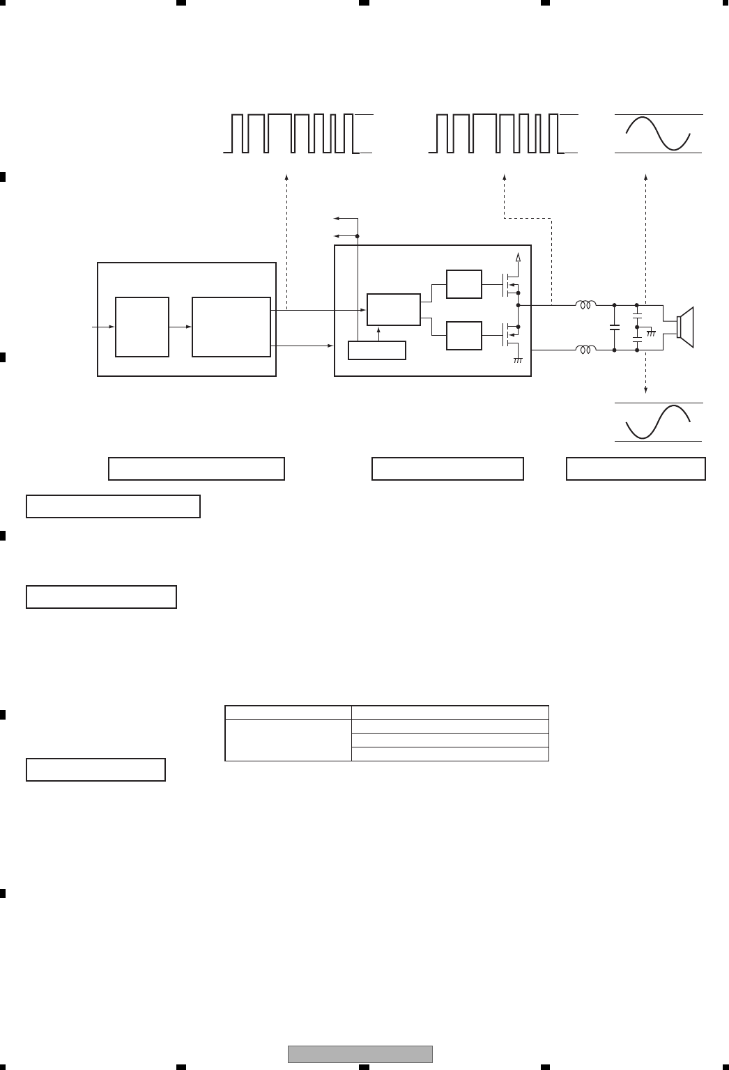
5.3 CIRCUIT DESCRIPTION OF DIGITAL AMP. SECTION
Filter
and
Volume
Timing
Control
Gate
Drive
XSD
To UCOM
PCM Signal
From
DVD or ADC
3.3V
0V
TAS5508BPAG
PWM Processor section
PWM Processor section
Power Stage section
Power Stage section
Output LPF section
Output LPF section
TAS5122DCA
XOTW
Protection
PCM -> PWM Gate
Drive
20V
0V 0V
0V
The PCM signals output from the DVD decoder or AD converter are input to this section, and their volume and sound quality
are digitally adjusted. At the output stage, after conversion from PCM to PWM, the signals are output to the Power stage.
In this section, timing is controlled so that the MOSFETs on the high and low sides will not be turned on simultaneously. The
voltage of the PWM signals are raised to drive the gates of the MOSFET, and the PWM signals to drive the speakers are
output from the MOSFET at the output stage. Detection and protection functions against short-circuiting of the output
signals and temperature exceeding the standard value are also provided.
The carrier elements, high-frequency signals that are unnecessary for these speakers, are eliminated. The signals passed
through the LPF will become sine-wave signals, as shown in the figure above.
Power Stage ICs No. Protection Enable State
IC3201 SD_AB (23pin) => L
IC3301 SD_CD (24pin) => L
IC3401 OTW (25pin) => L
IC3101 IC3201, IC3301, IC3401
*1 XSD : SD_AB (23pin), SD_CD (24pin)
*2 XOTW : OTW (25pin)
*1
*2
If the detection and protection work, the ports of the power stage ICs become the following state.

XV-DV363 23
5678
5678
C
D
F
A
B
E
5.4
SPECIFICATIONS FOR THE PROTECTION CIRCUITS FOR THE DIGITAL AMPLIFIER
The protection circuits for the Digital Amplifier are activated, following the specifications shown below. The error indication on
the FL display shows the reason a protection circuit was activated.
Upon diagnosis of the Digital Amplifier, refer to the specifications for the protection circuits here and the overview of the Digital
Amplifier circuitry.
1. Overview
The system microcomputer monitors the ports for shutdown requests (Pin 23:SD_AB and Pin 24: SD_CD) and the ports for
abnormal-temperature detection (Pin 25: /OTW) of the Power Stage ICs (IC3201, IC3301, and IC3401). As soon as any
abnormality is detected, it shuts the unit down.
To notify the user of the possibility of a too high a volume, when the unit is turned on the next time, the volume level will be set
to 0, and an error message will be displayed on the FL display.
2. Ports on the system microcomputer to be used for detection
Pin 77: SHUTDOWN
Low voltage at this pin means overcurrent or voltage too low (= V+B27) at a Power Stage IC.
Pin 79: XOTW
Low voltage at this pin means the temperature at the Power Stage ICs exceeded 125°C.
Note: As one Power Stage IC is provided with two channels, three Power Stage ICs (in total 6 channels) are mounted in
this unit. For abnormality detection, the unit implements a logical OR operation regarding these three ICs.
Therefore, which IC is abnormal cannot be known directly. To find which IC is abnormal, it is required to check the
PWM outputs (35, 38, 47, 50 pin) of the each power stage ICs (IC3201, IC3301, IC3401).
3. Detection timing
Start : Detection starts 500 ms after the PWRCONT port (Pin 84) of the system microcomputer becomes active by your
pressing the STANDBY/ON key.
Finish : When the STANDBY/ON key is pressed again (when the power-off process starts).
4. Operation of the protection circuits
The following three protection circuits are activated when the conditions shown below are met:
Overcurrent detection: Indication on the FL display: OC ERROR
Conditions: If the SHUTDOWN ports, which are monitored every 10 ms, become low 7 times in succession
Abnormal temperature detection 1: Indication on the FL display: OVERTEMP
Conditions: If the XOTW ports, which are monitored every 10 ms, become low in succession for one minute.
Abnormal temperature detection 2: Indication on the FL display: OVERTEMP
(Prerequisite: The XOTW ports, which are monitored every 10 ms, become low three times in succession.)
Conditions: The above prerequisite is upheld, and the conditions for an overcurrent detection are met.
Abnormal temperature detection 3: Indication on the FL display: OVERTEMP
Conditions: The PCONFIG ports (21-pin), which are monitored every 30 ms, become more than 2Vrms more than 45%
in one minute.
5. Process when the protection circuits are activated
The unit is shut down within 30 ms after abnormality detection then the volume level is set to 0. The unit can be turned on
immediately after the shutdown.

XV-DV363
24
1234
1 234
C
D
F
A
B
E
5.5 PASS/FAIL TEST PROCEDURE OF HDMI TRANSMITTER IC
In a case where the HDMI video signal is not output
1
In a case where the HDMI audio signal is not output
2
Is the analog video signal output?
Ye s
No
OKNG
Malfunctions are caused around IC201 BE IC or in IC201.
Is the signal as described above sent to the input of IC931?
Ye s
Ye s
Is the HDMI image output?
No
Malfunctions are caused in the output line between IC931 and
CN931. Check the HDMI connector, as well.
Check if the HOME MENU or VCD playback picture is displayed
when this unit is connected to a PC monitor equipped with a
DVI input.
Purpose: To check if the HDMI output line, including the terminal,
is in failure.
(An HDMI <-> DVI conversion cable is
required for checking.)
Pass/fail test of BE IC (IC201: DVD MAIN Assy)
Conduct proving of R264, R265, R267 and
R271 (33 ohms x 44 set), and R266 (27 MHz clock) with an
oscilloscope to check whether each signal varies in amplitude
between H (3.3 V) and L at reproducing VCD, and whether
27 MHz clock is correctly output.
Malfunctions are caused in HDMI IC (IC931 : DVD MAIN Assy)
or in the output line between IC931 and CN931. In this regard,
the frequency is around 1 GHz at the CLK and DATA line
between IC931 and CN931, which makes it difficult to observe
the waveform by a general oscilloscope. Check the connection
with the HDMI connector and the HDMI cable, as well.
NG
Ye s
Change mode.
The initial setting provides no sound.
Has HDMI sound been changed in STAND-BY MENU?
No
Is a correct signal found by proving the output of 216 pin
and 211 pin of IC201, R248 (HSPDIF) and
R240 (HCLK : 22/24MHz clock) with an oscilloscope?
Check if the initialization process for HDCP, etc. is OK by
connecting this unit with a Pioneer Plasma Display equipped
with an HDMI input.
Ye s
OK
Ye s Malfunctions in IC931.
No Malfunctions around IC931.
No Malfunctions in IC201.
Malfunctions are caused around IC201 BE IC.
No
The HDMI transmitter IC (HDCP process block) may be in failure.
Change IC201 or IC931.
The customer's monitor may not be compatible
with this unit. Confirm the name of manufacturer
and model of the monitor, and get a specific
description of the failure. Then look for an identical
case in a collection of past cases, or consult the
design section. In some cases, upgrading the
software or firmware for both the DVD player and
the monitor will solve the problem.

XV-DV363 25
5678
5678
C
D
F
A
B
E
6. SERVICE MODE
6.1 TEST MODE
Test Mode Functional Specification
1 Test mode entry
In the power ON state, press the [ESC] (A8-5F) key and [TEST] (A8-5E) key in order of the Test mode remote control
unit.
• OSD displays test mode.
2 LD ON
Enter the test mode.
DVD : Press the [TEST] (A8-5E) and [1] (A8-01) keys in order, and turn on the laser diode (650 nm).
CD : Press the [TEST] (A8-5E) and [4] (A8-04) keys in order, and turn on the laser diode (780 nm).
3 Release the Test mode
• Turn off the power.
• Press the [ESC] (A8-5F) key of the remote control unit and reset it.

XV-DV363
26
1234
1 234
C
D
F
A
B
E
6.2 DISPLAY SPECIFICATION OF THE TEST MODE
Character in bold : Item name
: Information display
1
5
6
10
11
8
9
3
2
12
15
13
14
1 Address indication
The address being traced is displayed in number.
(as for the DVD, indication of decimal number is possible.)
DVD : ID indication (hexadecimal number, 8 digits)
[* * * * * * * *]
CD : ID indication [* * * * * * * *]
2 Code indication of remote control unit [R – * * * *]
In case of double code, display a 2nd code.
3 Main unit keycode indication [K – * *]
5 Tracking status [TRKG – * * *]
Tracking on : [ON]
Tracking off : [OFF]
6 Spindle status [SPDL – * * *]
CLV : [CLV]
Off : [OFF]
7 Mechanism (loading) position value [M – * *]
Unknown : [01] or [41]
Open state : [04]
Close state : [08]
During opening : [12]
During closing : [22]
8 Slider position [S – * * * *]
In Side Switch ON : [01]
In Side Switch OFF : [00]
9 Output video system [V – * * * *]
NTSC system : [NTSC]
PAL system : [PAL]
Automatic setting : [AUTO]
Scart terminal output [SK – * *]
(Display only the WY model which can do the output setting
of scart terminal.)
VIDEO : [00]
S-VIDEO : [01]
RGB : [02]
a Disc sensing [DSC – * * *]
The type of discs loaded is displayed.
[DVD], [CD ]
b Jitter value [J – * * * *]
Note: Don't use it.
c Version of the FL controller [FL: * * * *]
Note: Don't use it.
d Region setting of the player [REG: *]
Setting value : [1] to [6]
e Destination setting of the FL controller
[MDL: * * * * / * * *]
Four characters in the front represent code 01.
Three characters in the back represent the destination code.
J: /J, K: /KU, /KC, /KU/KC, R: /RL/RD, RAM : /RAM,
LB: /LB, WY: /WY
f Version of the flash ROM [V: * *. * *]
Flash ROM size [FLASH = * *]
7
XV-DV363 27
5678
5678
C
D
F
A
B
E
6.3 FUNCTIONAL SPECIFICATION OF THE SHORTCUT KEY
Service mode indication (ESC + CHP/TIM keys)
ID Address
The error rate is always displayed in exponential notation, e.g., *.* * e - *, for both DVDs and CDs.
EDC/ID/AV 1 error history (ID Address, EDC/ID Error, last eight errors)
Calculation of the average error rate (ESC + "5" [Test mode remote control unit] keys)
The average of the last eight error rates is calculated and indicated in exponential notation. After the calculation is completed, "OK" or "NG" is
displayed. If "NG" is displayed, the disc tray will open (for both DVDs and CDs)
For DVDs: OK with 5.0e-4 or less, for CDs: OK with 7.6e-3 or less
Indication of model information (ESC + CHAP keys)
The items from 12 to 15 of the TEST MODE Indications are displayed. However, in the indications, S in the standard test mode is changed to
CHIP VERSION, and M is changed to RF VERSION. For details, see 6.4.
Region confirmation mode (ESC + A.MON [Test mode remote control unit] + "1"-"8" [Test mode remote control unit] keys)
After you press the AUDIO key while holding the ESC key pressed and then input the region number, if the number is different from that set in
the unit, an error message is displayed, and the tray opens.
Command Contents Conditions Remote Control
Key Name
Remote
Control Code
Memory clear and region / revision indication CLEAR (*1) A8-45
Average value measurement of DVD error rate 5 (*1) A8-05
CD error rate measurement 5 (*1) A8-05
Scart terminal output : VIDEO
WY, models equipped with Scart terminal
AUDIO A3-BE
Scart terminal output : S-VIDEO SUBTITLE A3-36
Scart terminal output : RGB ANGLE A3-B5
Progressive OFF Only for progressive models
Only for HDMI models
R_SKIP A3-9D
Progressive ON F_SKIP A3-9C
FL indication of ID number STEREO (*1) A8-4A
ZOOM ON (x4) ZOOM A3-37
Service mode indication (error rate indication, etc.) CHP/TIM (*1) A8-13
Model information indication CHAP (*1) A8-40
Title search Input mode IN
Title No. input
Search execution
SIDE A (*1)
Numbers (*1)
PLAY (*1)
A8-4D
A8-00 to A8-09
A8-17
Region confimation mode A.MON (*1)
Numbers (*1)
A8-1E
A8-01 to A8-08
Only during normal playback, the following shortcut keys can be assigned by pressing a required key after pressing the ESC
key of the remote control unit. To quit, press the ESC key
*1 : Test mode remote control unit
HDMI Resolution : 1920 x 1080i PROGRAM A3-EC
XV-DV363
28
1234
1 234
C
D
F
A
B
E
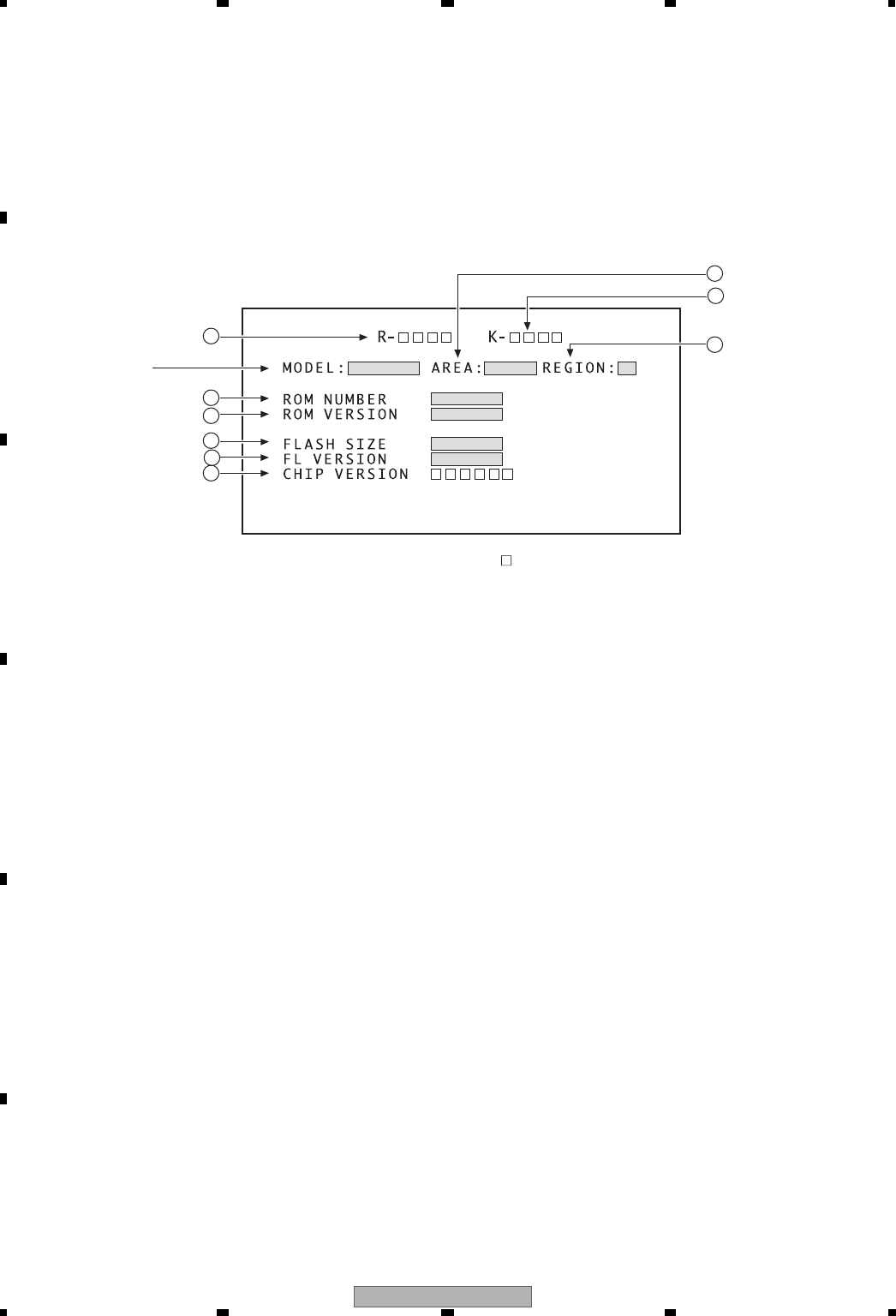
6.4 SPECIFICATION OF MODEL INFORMATION DISPLAY
• Display contents
Character in bold : Item name
: Information display
1
2
3
4
5
6
7
9
10
1 Destination indication
Display it according to model information set from the FL controller.
2 Region No.
3 Part number
4 ROM version
5 Flash size
6 FL controller version
7 CHIP VERSION
9 Remote control code
0 Key code of Main unit
To display model information : Press the ESC key then the CHAP key.
To close the model information display : Press the ESC key.
Don't care.
XV-DV363 29
5678
5678
C
D
F
A
B
E
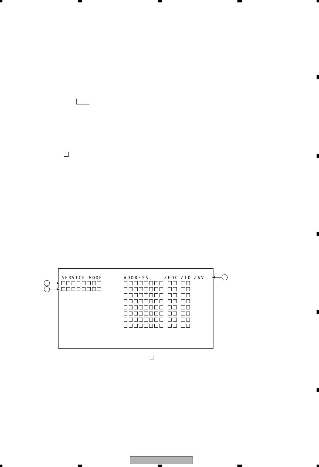
6.5 FUNCTIONAL SPECIFICATION OF THE SERVICE MODE
• Display during Service Mode
To enter Service Mode, press the CHP/TIM key while holding the ESC key pressed.
To quit, press the ESC key.
Service mode display
1 ID Address
2 Error rate (always displayed), in exponential notation
ERROR RATE : ∗ ∗ ∗ ∗ ∗ ∗ ∗
( ∗ ∗ ∗ ∗ )
• Calculation of the average error rate
For DVDs: OK with 5.0e-4 or less, for CDs: OK with 7.6e-3 or less
3 EDC/ID error history (ID Address, EDC/ID errors, last eight errors)
Note:
∗ Error of AV1 is not supported in this player.
Number of error
Indication plan contents
Character in bold : Item name
: Information display
1
2
3
ex) For DVDs
• Step 1
""e -
""e -6 : OK
""e -5 : OK
""e -4 : Refer to Step 2
""e -3 : NG
""e -2 : NG
• Step 2
""e -4
3.0e -4 : OK
4.0e -4 : OK
5.0e -4 : OK
6.0e -4 : NG
7.0e -4 : NG
XV-DV363
30
1234
1 234
C
D
F
A
B
E
6.6 SERVICE TEST MODE
14
85
NP
1
A30C5/C7
[[ G ]]
51
50
KN5601
R5546
R5547
R5548
C5557
IC5502
C5558
R5
R5559
Q5531
R5528
Q5532
R5530
R5541 R5542
R5543 R5545
Q5533
Q5534
Q5535
Q1402
D1403
D1416
D1417
R1415
C1413
R1401
R1402
R1403
R1404
Q1413
D1415
C1415
R5557
C5555
1/2
STEST
UTEST
D
V+10
V+3R3
FLDC+
FLDC-
1. Conditions During Service Test Mode
• During Service Test mode, the unit will not be shut down for an emergency even if one of the failures mentioned below
occurs.
• After the unit has been shut down in Normal mode for an emergency upon detection of one of the failures mentioned below,
you can turn it on immediately, without waiting for one minute, in Service Test mode.
• The accumulated power-on time can be checked during Service Test mode.
2. How to enter Service Test mode
• Connect AC power cord with the STEST port (microcomputer terminal IC5501: 43-pin) at High (5 V).
(See "Service Test mode connecting point".)
Note: Initial function setting is DVD/CD.
• Connect AC power cord while holding both the PLAY LIST 3 and POWER keys on the main unit pressed.
The unit will be turned on, and the following indication will be displayed: Service Test mode starts, as follows:
Note: If the power cord was disconnected immediately before, be sure to wait at least one minute before turning on the
power in the manner mentioned above. Otherwise, the unit may not operate properly.
3. Indications on the FL display when Service Test mode is entered
• Indications on the FL display when Service Test mode is entered differ depending on whether the unit was turned off
normally or shut down for emergency protection, immediately before Service Test mode starts, as follows:
4. How to quit Service Test mode, and conditions for quitting
• To quit Service Test mode, turn the power off or disconnect the AC power cord to turn the power off.
• When Service Test mode is quit, only data on protection in RAM will be initialized, and data on user settings in RAM will not
be initialized.
W E L C O M E
[After a normal power-off]
[After a shutdown caused
by an EEPROM (IC5502) failure]
FL display
VO L 0
V O L 0
FL display
VDD VS E R
V DD VS E R
FL display
EE P E R R
FL display
VO L 0
FL display
VDD VS E R
V O L 0
V DD VS E R
FL display
PR T C T E
FL display
FL display
FL display
OV E R PT E M
FL display
FL display
FL display
[After a shutdown caused
by an AMP-system failure]
[After a shutdown caused
by high-temperature detection]
VO L 0
V DD VS E R
V O L 0
V DD VS E R
D V D P R T C T
FL display
FL display
FL display
OC E 2R R
FL display
FL display
FL display
[After a shutdown caused
by a DVD-system failure]
[After a shutdown 2 caused
by over current detection]
VO L 0
V DD VS E R
O C E 1R R
FL display
FL display
FL display
[After a shutdown 1 caused
by over current detection]
Service Test Mode connecting point
DVD MAIN ASSY
B
Connecting point
SIDE A

XV-DV363 31
5678
5678
C
D
F
A
B
E
6. Failures
• Depending on the types of errors, one of the following error messages will be displayed when the unit is turned on:
E E P E R R
P R T C T E
D V D P R T C T
O C E 2R R
O C E 1R R
A protection circuit was activated:
1. The V+10, V+5 or V+6R8 was short-circuited (See the protection circuit on "10.2 DVD MAIN ASSY (2/5)"),
or the value at V+10, V+5, or V+6R8 exceeded the standard value because of an abnormality in its power section.
2. The XPROTECT port (22-pin) line up to the system-control computer (IC5501) was short-circuited by grounding or was
broken.
Abnormality in the DVD section
1. The V+5V, or V+3 was short-circuited, or the value at V+5V, or V+3 exceeded the standard value because of an
abnormality in its power section.
2. The VDET port (17-pin) line up to the system-control computer (IC5501) was short-circuited by grounding or was broken.
(See VDET circuit on "10.2 DVD MAIN ASSY (2/5)")
• If "OC ERR 1, 2" is not displayed when the unit is turned on in Normal mode, short-circuiting of the speaker terminals
can be suspected. (It causes speaker cable "+", "-" short.)
• If "OC ERR 1, 2" is displayed again when the unit is turned on in Normal mode, the following causes can be suspected:
1. One or more of the ICs among the three digital amplifier ICs (IC3201, IC3301, and IC3401: TAS5122DCA) on the
DAMP Assy is in failure.
2. The line between one of the above digital amplifier ICs and the speaker terminals is short-circuited.
3. The SHUTDOWN port (77-pin) line from one of the above digital amplifier ICs to the system-control computer (IC5501)
is short-circuited by grounding or is broken.
O V E R PT E M
• If "OVERTEMP" is not displayed when the unit is turned on in Normal mode, the unit is normal. The protection circuit
was activated because the temperature at the three digital amplifier ICs (IC3201, IC3301, and IC3401: TAS5122DCA)
had become too high. Because it is likely that this was a temporary temperature rise, lower the volume of the speakers.
• If "OVERTEMP" is displayed again when the unit is turned on in Normal mode, the following causes can be suspected:
1. One or more of the ICs among the three digital amplifier ICs (IC3201, IC3301, and IC3401: TAS5122DCA) on the
DAMP Assy is in failure.
2. The XOTW port (79-pin) line from one of the above digital amplifier ICs to the system-control computer (IC5501) is
short-circuited by grounding or is broken.
1. Breakage or short-circuiting of the communication line between the microcomputer (IC5501) and the EEPROM (IC5502)
can be suspected.
2. A failure in the EEPROM (IC5502) can be suspected.
5. Operations during Service Test Mode
• Basically, operations in Service Test mode are the same as in Normal mode. However, to indicate that the unit is in
Service Test mode, the following are displayed when the functions are changed:
V D S E R
DVD/CD
S B S E R
USB
TX S E R
TUNER
[Functions] [FL display]
N 1 S E R
LINE1
N2
V
V
V
V
V
D
U
L
L S E R
LINE2
When the function is set to LINE2, the Surround setting is fixed
to X-STEREO (5 CH STEREO), which is only for Service Test
mode. (In Normal mode, it is fixed to 2 CH STEREO.) In such a
case, do not check the sound through the headphones, because
headphone operation with X-STEREO (5 CH STEREO) is not
guaranteed. If you wish to check the sound through the
headphones, use a function other than LINE2.
•

XV-DV363
32
1234
1 234
C
D
F
A
B
E
Version of the system-controller
About 3 seconds after
7. Accumulated power-on time display
• Hold the STOP key on the unit pressed for 8 seconds during Service Test mode. After the version for the system-control
computer is displayed, the accumulated power-on time is displayed.
P D C 1 5 3 A
Accumulated power-on time 1 0 H 3 0 M
• Power-on time is always counted while the power is on, regardless of unit's functions and operations.
However, it is not counted during Standby mode.
• The maximum countable power-on time is 255H59M (255 hours 59 minutes.) The indication will not advance beyond that.
• The accumulated power-on time basically cannot be cleared.
XV-DV363 33
5678
5678
C
D
F
A
B
E
7. DISASSEMBLY
1Remove the bonnet by removing the nine screws.
2Press the STANDBY/ON button to turn on the
power.
3Press the OPEN/CLOSE button to open the tray.
4Remove the tray panel.
5Set the test disc.
6Press the OPEN/CLOSE button to close the tray.
(Test disc is clamped.)
7Press the STANDBY/ON button to turn off the
power.
8Pull out the Power cord.
Bonnet, Tray Panel
1
36
5
4
Tray panel
Screwdriver (small)
Screwdriver (small)
06 LOADER Assy
Tray open
Slit
Test disc
Tray
How to open the tray when the power cannot be on
Insert a screwdriver (small) into the slit located at the
bottom of the unit, and slide the projection of the drive
cam in the 06 LOADER Assy in the direction of the
arrow, as indicated in the photo. If the tray pops out a
little, fully pull it out by hand.
Diagnosis of PCB's
Note 1: Do NOT look directly into the pickup lens. The laser beam may cause eye injury.
Note 2: Even if the unit shown in the photos and illustrations in this manual may differ from your product, the procedures
described here are common.
72
Drive cam
Projection
63
Bottom view

XV-DV363
34
1234
1 234
C
D
F
A
B
E
1Disconnect the one flexible cable.
2Remove the MIC knob. (XV-DV365K only)
3Unhook the eight hooks.
4Remove the front panel section.
Front panel section
2
USB Assy
MIC knob
XV-DV365K only
Front panel section
1
2
3
3 3
3 3
A
4
3 3
3
Note A: Do not use an electric screwdriver.
If the screws are over-tightened, the screw
threads may be damaged.
XV-DV363 35
5678
5678
C
D
F
A
B
E
Rear view
06 LOADER Assy
3 3
4
1Short-circuit point by soldering.
2Disconnect the four connectors.
Note: After replacement, connect the flexible cable,
then remove the soldered joint (open).
3Remove the two screws.
4Remove the 06 LOADER Assy.
1
06SD Pickup
Assy-S
DVD MAIN Assy
Removing the Traverse Mechanism Assy-S and 06SD Pickup Assy-S
06 LOADER Assy
1
Note: Do not touch the bottom side of the 06SD
Pickup Assy-S. If touched, the optical axis may
be shifted.
2
2
2
2
1Remove the one screw.
2Remove the bridge 04.
3Pull out the tray, then remove it by pressing the
hook.
1
2
3
Bridge 04
Front side
Hook
Tray
Loading base Triangle
PinDrive cam
-1
3-2
Note when reinserting the tray
When reinserting the tray, first align the triangle
printed on the loading base and the pin of the drive
cam, then insert the tray.
Bridge 04, Tray
2
XV-DV363
36
1234
1 234
C
D
F
A
B
E
1
Traverse Mechanism Assy-S
3
Dislodge the two flexible cables from their factory
placement.
2Unhook the four hooks.
3Remove the Traverse Mechanism Assy-S. ×2
2
×2
2
3
Traverse Mechanism Assy-S
1
1
Front Side
Flexible cable
for the spindle motor
Flexible cable for the pickup
Bottom view
Note: Do not touch the IC for the optical axis. If
touched, the optical axis may be shifted.

XV-DV363 37
5678
5678
C
D
F
A
B
E
3
2
2
Adjustment screw
(skew screw VK1)
Adjustment screw
(skew screw VK1)
Adjustment screw
(skew screw VK1)
Adjustment spring
(skew spring VK1)
06SD Pickup Assy-S
4
Note: The 06SD Pickup Assy-S can be removed
without removing the Traverse Mechanism
Assy-S. (shown as Step 3.)
Note: Be careful not to lose the adjustment spring
(skew spring VK1).
Flexible cable for the pickup
06SD Pickup Assy-S
1
Front Side
1Disconnect the flexible cable for the pickup.
2Remove the two adjustment screws.
3Remove the 06SD Pickup Assy-S.
Bottom view
06SD Pickup Assy-S
Note: Do not touch the IC for the optical axis. If
touched, the optical axis may be shifted.

XV-DV363
38
1234
1 234
C
D
F
A
B
E
Note: The screw is secured with the silicone
adhesive.
Make sure to apply the silicone adhesive after
reattaching the screw.
4Remove the one screw.
4
Silicone Adhesive
GEM1037
06SD Pickup Assy-S
Joint VK1B
Joint spring VK1
Hold spring
: Conductive surface
Arrangement of the flexible cable for the spindle motor
Front Side
Hook
Hook
[Caution]
DO NOT touch the OE IC.
It occurs out of the optical
axis due to the shock.
Bottom view
XV-DV363 39
5678
5678
C
D
F
A
B
E
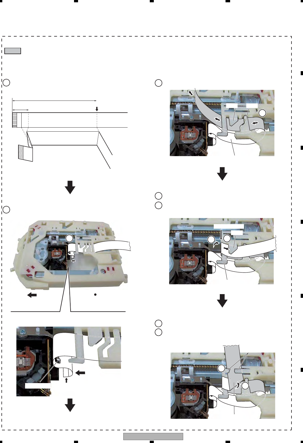
Note:
Be sure to move the 06SD Pickup Assy-S to the innermost perimeter.
: Conductive surface
Arrangement of the flexible cable for the pickup
3
7
2Attach the flexible cable for the pickup to the connector.
6Fold the flexible cable along the hook.
7Pass the flexible cable through the hook.
3
45
5Pass the flexible cable through the hook.
4Hook the part folded in Step 1 to the hook.
Hook
Reference line
6
1Fold the flexible cable for the pickup with the backing outward
in the illustration below.
Hook Hook
Hook
Hook
Hook
Front Side Bottom View
2
Backing
Pass the flexible cable through the hook.
Make sure that the cable is loose
Hold Spring
Reference line
17 mm
88 mm
XV-DV363
40
1234
1 234
C
D
F
A
B
E
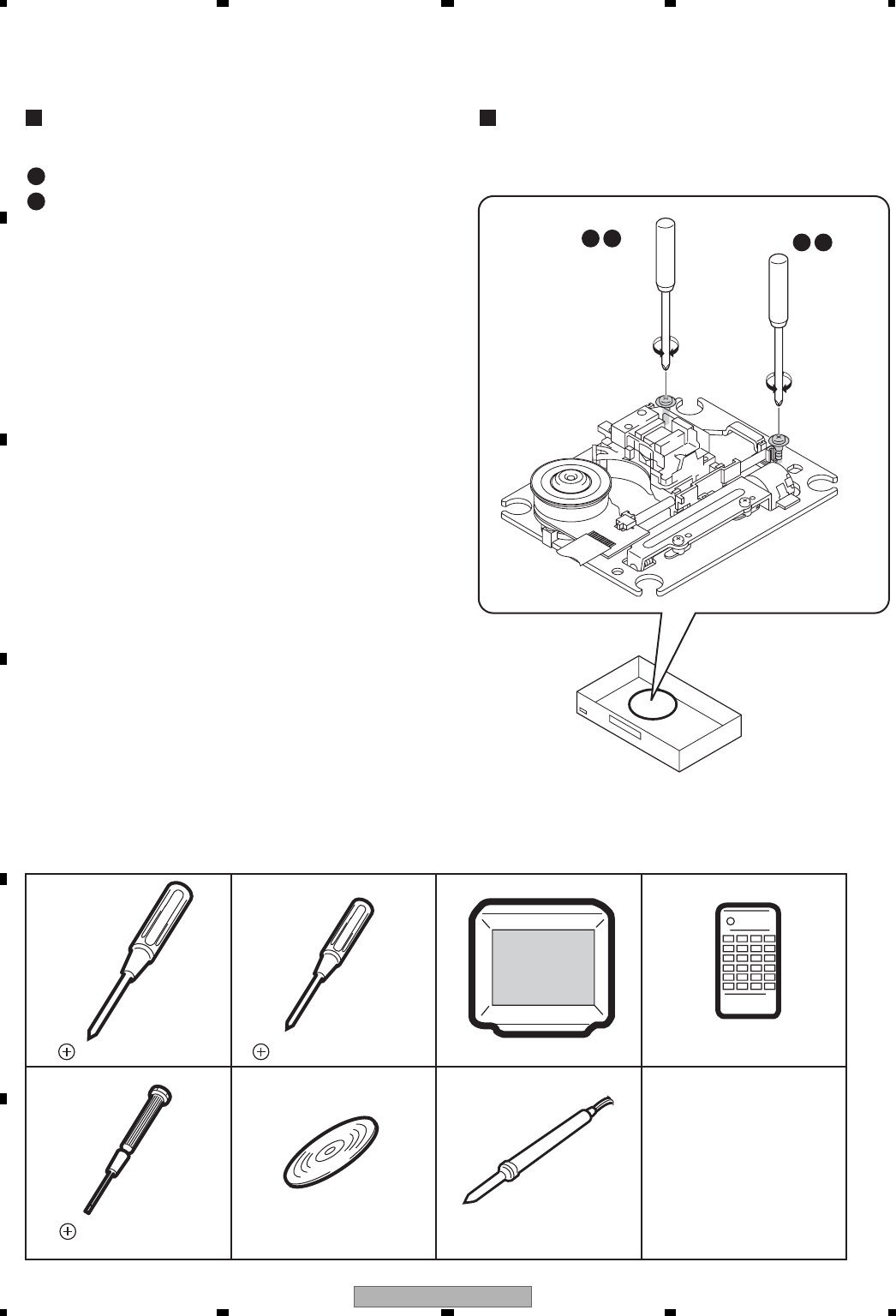
8. EACH SETTING AND ADJUSTMENT
8.1 ADJUSTMENT
8.1.1 ADJUSTMENT ITEMS AND LOCATION
8.1.2 JIGS AND MEASURING INSTRUMENTS
1
2
Adjustment Items
[Mechanism Part]
[Electrical Part]
Tangential and Radial Height Coarse Adjustment
DVD Error Rate Adjustment
Electrical adjustments are not required.
Adjustment Points (Mechanism Part)
Cautions: After adjustment, adjustment screw locks with the
Screw tight.
1 2
Radial
adjustment
screw
1 2
Tangential
adjustment
screw
Screwdriver (large) TV monitor
Precise screwdriver DVD test disc
(GGV1025)
Test mode remote control
unit (GGF1381)
Screw tight
(GYL1001)
Screwdriver (medium)
Soldering iron

XV-DV363 41
5678
5678
C
D
F
A
B
E
8.1.3 NECESSARY ADJUSTMENT POINTS
* After adjustment, screw locks
with the Screw tight.
1,2
Mechanical
point
Electric
point
Mechanical
point
Electric
point
Mechanical
point
Electric
point
LOAB and DVD MAIN ASSYS
Exchange Parts of Mechanism
Exchange PCB Assy
When Adjustment Points
Exchange the 06SD Pickup Assy-S
Exchange the Traverse Mechanism
Assy-S
Exchange PC Board
* After adjustment, screw locks
with the Screw tight.
2
Mechanical
point
Electric
point
Exchange the Spindle Motor

XV-DV363
42
1234
1 234
C
D
F
A
B
E
8.1.4 TEST MODE
POWER ON
DSC -
GGF1381
Test mode
remote control
unit
GGF1381
Test mode
remote control
unit
<TRAY OPEN> <TRAY CLOSE>
OPEN/CLOSE
(Player)
OPEN/CLOSE
Press the play key
( ) of the normal
remote control unit.
(Player)
TEST MODE: PLAY
TEST MODE: OFF
An address is displayed
OR
ESC
<PLAY>
ESC TEST
CHECK
DVD, CD
DVD disc
POWER
ON
OFF
POWER
DISC SET
Notes:
After going into test mode, if you play back the disc, "DISC-NON" is displayed.
The video signal and the audio signal are outputted duvring the test mode.
The SKIP key and the SCAN key are effective during the test mode.
XV-DV363 43
5678
5678
C
D
F
A
B
E
8.1.5 MECHANISM ADJUSTMENT
Remove the 06SD Pickup Assy-S from the Traverse Mechanism Assy-S.
Remove the joint and the joint spring of the 06SD Pickup Assy-S.
Put the joint between the Tangential (or Radial) adjustment scrw and the mechanism base
and turn each screw to adjust the height.
(Refer to "8.1.1 ADJUSTMENT ITEMS AND LOCATION".)
START
Tangential and Radial Height Coarse Adjustment
1
Note:
Before removing the flexible cable for the pickup,
soldering of the pickup circuit is necessary.
For details, see “7. DISASSEMBLY”.
Pass through the guide shaft to a new 06SD Pickup Assy-S.
Attach it to the Traverse Mechanism Assy-S.
Attach the Traverse Mechanism Assy-S to the 06 LOADER Assy.
Turn it over and attach the joint and the joint spring.
Arrange the flexible cables.
(Refer to "7. DISASSEMBLY".)
7.5mm
Joint
Mechanism base
Guide Shaft
06SD Pickup Assy-S
Joint VK1B
Joint spring VK1
Hold spring
06SD Pickup Assy-S
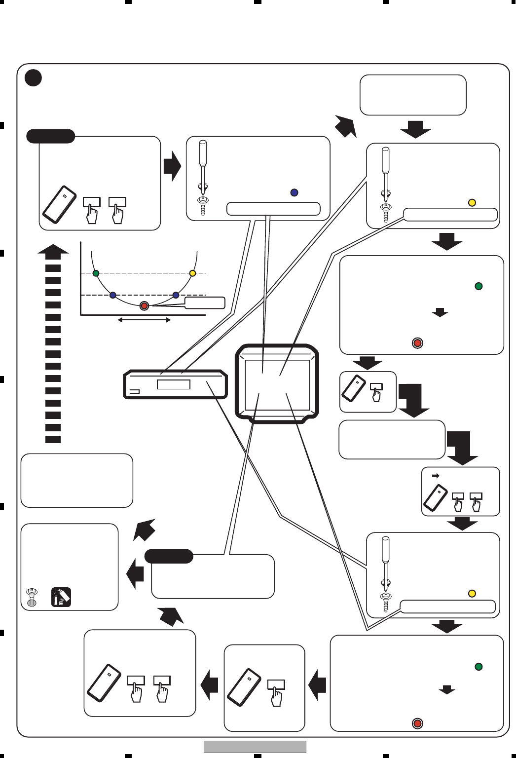
XV-DV363
44
1234
1 234
C
D
F
A
B
E
Player
Monitor
· Play the DVD test disc
at inner track
(around #30000)
· Play the DVD test disc
at outer track
(around #200000)
Traverse Mechanism
Assy-S
Adjust the radial adjustment
screw so that
ERROR RATE becomes
around "5E-4".
Traverse Mechanism
Assy-S
Fasten the radial
adjustment screw so that
ERROR RATE becomes
around "1E-3".
START
DVD Error Rate Adjustment
2
ERROR RATE: - - - -
ERROR RATE : "5E-4" ERROR RATE : "1E-3"
Service mode end
Disc playback normally.
· The measurement of
block error rate
If error rate is OK,
locks a root of
tangential and radial
adjustment screws with
the Screw tight.
Screw tight: GYL1001
Turn the POWER OFF in
case of NG once, and
perform the adjustment
once again.
CHP/TIMESC ESC
Service mode
Service mode end
ESC
NG
OK
· Play the DVD test disc
at inner track
· Display ERROR RATE
on the monitor
CHP/TIMESC
Notes:
· Use disc: GGV1025
· Unfasten the radial adjustment screw
by 90 degrees step till ERROR RATE
becomes around "1E-3" again .
· Record the number of rotation (N1).
(memorizing how much the screw was rotated.)
· Fasten the radial adjustment screw
till the number of rotation becomes
harf of N1.
Traverse Mechanism
Assy-S
Fasten the tangential
adjustment screw so that
ERROR RATE becomes
around "1E-3".
· Unfasten the tangential screw
by 90 degrees step till ERROR RATE
becomes around "1E-3" again .
· Record the number of rotation (N1).
· Fasten the tangential adjustment screw
till the number of rotation becomes
harf of N1.
ERROR RATE : "1E-3"
In this check, the error rate
that is less than "5E-5"is
better.
CHECK
CHP/TIMESC
A
B
B
C
Best Radial point
C
Best tangential point
1E-3
5E-4
Rotation of Radial screw
and Tangential screw
Anticlock wise Clock wise
Best point
AA
BC
ERROR
RATE

XV-DV363 45
5678
5678
C
D
F
A
B
E
8.2 ID NUMBER AND ID DATA SETTING
This display appears when the PLAY key is pressed in Step 4.
Enter a 9-digit number to compare. The number is also
displayed on the FL display.
6
By pressing the CLEAR key without having input a number, the
unit returns to Step 2 without doing anything else. Each press
of this key after a number has been input deletes one digit.
7
After entering all 9 digits, if you press the PLAY key, the unit
compares the numbers input in Steps 2 and 6, and only if the
numbers match, that number is set as the ID. Then the unit
automatically enters ID DATA Input Mode. If the numbers do not
match, the disc tray is opened, and the unit exits ID Number
Input Mode.
8
[Player's ID Number Setting]
ID Number ?
0 0 0 0 0 0 0 0 1
Compare
∗ ∗ ∗ ∗ ∗ ∗ ∗ ∗ ∗
Input ID Number !
6
[Player's ID Number Setting]
ID Number ?
0 0 0 0 0 0 0 0 1
Compare
0 0 0 0 0 0 0 0 1
<PLAY> Enter
Input ID Number !
8
Input ID Number !
After entering all 9 digits, if you press the SEARCH key, the
unit unconditionally sets the input number as the ID number.
Then the unit automatically enters Player's Data Input Mode.
(The SEARCH key is not accepted after all 9 digits have been
entered.)
5
[Player's ID Number Setting]
ID Number ?
0 0 0 0 0 0 0 0 1
<PLAY> Compare Mode
<SEARCH> Enter
4
5
Caution:
For the DVD players compatible with DVD-RW, for playback of a DVD-RW disc (CPRM) and for the DVD players possessing
HDMI output, for HDCP process, it is necessary that an individual ID number and ID data are set for each player. If the ID
number and ID data be not properly set in the manner described below, future operations cannot be guaranteed. The ID
number is written on the yellow label at the rear panel of the player.
If there is no yellow label, before downloading FLASH ROM, take note of the ID number set following the procedures
outlined in "ID Number Confirmation Mode" on the next page.
Note: Enter ID numbers while the unit is in Stop mode so that the values set will be immediately written to the flash ROM.
Note: If you press the PLAY button before inputting a 9-digit ID
number, the unit returns to Step 6 without doing anything
else.
To enter ID Number Input Mode, with no ID number set, such as
in a case of immediately after upgrading the firmware, press the
ESC key then the STEREO key.
Note: If a previous ID number and ID data, such as a factory-
preset ID number and ID data, are maintained, the unit
enters ID Number Confirmation Mode when the above keys
are pressed. However, if only an ID number is maintained,
the unit enters ID Data Input Mode.
ID Number Input Mode
[Player's ID Number Setting]
ID Number ?
- - - - - - - - -
<CLEAR> Exit
Input ID Number !
1
Enter a 9-digit ID number. The ID number is also displayed on
the FL display.
2
By pressing the CLEAR key without having input a number, you
can exit this mode. Each press of this key after a number has
been input deletes one digit.
3
After entering all 9 digits, if you press the PLAY key, the unit
enters Compare mode. Enter the same ID number again. Only
if your two input numbers match, the ID number is set. Compare
mode helps eliminate mistyping of the ID number.
4
2
3
Note: If you press the PLAY button before inputting a 9-digit ID
number, the unit returns to Step 2 without doing anything
else.
Setting an ID number or ID data is required in the
following case:
If "No NUM" or "NO DATA" is displayed on the FL display
for a few seconds immediately after the power to the player
is turned on or during Stop mode.
JIGS AND MEASURING INSTRUMENTS
DVD Data Disc
[GGV1269]
Service Remote Control Unit
[GGF1381]
XV-DV363
46
1234
1 234
C
D
F
A
B
E
To enter ID Number Confirmation Mode after the ID number and
the ID data are set, press the ESC key then the STEREO key.
ID Number Confirmation Mode
1
The ID number already set is displayed.
(It is also displayed on the FL display.)
2
Enter a 9-digit number for comparison. This is not required
when you only wish to check the ID number visually.
(The number is also displayed on the FL display.)
3
By pressing the CLEAR key without having input a number, you
can exit this mode. Each press of this key after a number has
been input deletes one digit.
4
After entering all 9 digits, if you press the PLAY key, the unit
compares the number entered in Step 2 with the ID number
set, and only if the numbers match, the unit automatically exits
ID Number Confirmation Mode. If an ID data has not been
entered, the unit enters ID DATA Input Mode. If the numbers do
not match, the disc tray is opened, and the unit exits ID Number
Confirmation Mode.
5
After entering all 9 digits, if you press the STOP key, the unit
compares the number entered in Step 3 with the ID number
set, and only if the numbers match, the unit automatically
deletes the ID number and exits this mode. If the numbers do
not match, the disc tray is opened, and the unit exits this mode.
(The STOP key is not accepted after all 9 digits have been
entered.)
6
[Player's ID Number Setting]
ID Number ?
0 0 0 0 0 0 0 0 1
Compare
∗ ∗ ∗ ∗ ∗ ∗ ∗ ∗ ∗
<CLEAR> Exit
Input ID Number !
3
2
4
[Player's ID Number Setting]
ID Number ?
0 0 0 0 0 0 0 0 1
Compare
0 0 0 0 0 0 0 0 1
<PLAY> Enter
<STOP> Memory Clear
Input ID Number !
5
6
Note: If you press the PLAY button before inputting a 9-digit ID
number, the unit returns to Step 4 without doing anything
else.
• Indication of an ID number already set
An ID number already set is displayed in the following cases:
1) When the ESC key then the CLEAR key are pressed, user
settings are cleared, then the ID number set is displayed on
the screen. In this case, the ID number is not displayed on the
FL display.
2) When the unit enters ID Number Confirmation Mode by your
pressing the ESC key then the CLEAR key, the ID number set
is displayed. In this case, the ID number is also displayed on
the FL display.
If you only need to confirm the ID number, you can exit
this mode by pressing the CLEAR key or turning off the power.
• Indication when no ID number is set
If no ID number is set, the message "No NUM" flashes on the
screen and FL display for a few seconds after the power is turned
on or during Stop mode.
XV-DV363 47
5678
5678
C
D
F
A
B
E
To enter ID DATA Input Mode, with the ID number set, press the
ESC key then the STEREO key.
ID DATA Input Mode
NOTE: Be sure to use a specified DVD (ID) DATA DISC.
1When writing of the data read from the disc to flash ROM is
completed, "Rom Write OK!" is displayed. After seeing this
message, you can exit this mode by pressing the CLEAR key.
5
If the data cannot be read from the disc, the unit will be exited ID
Data Input Mode and proceed to the display of “Pioneer” logo.
6
When the STEREO key is pressed, the unit enters ID DATA
Input Mode.
2
If the DVD DATA DISC is loaded in this mode, the unit
automatically starts reading the data.
(If the DVD DATA DISC has already been loaded, the unit does
not start reading the data. In this case, open then close the tray.)
3
To exit this mode, press the CLEAR key. While data are being
read from the DVD DATA DISC, you cannot exit this mode.
4
[Player's ID Number Setting]
ID Number ?
[ 0 0 0 0 0 0 0 0 1 ]
Compare
> ∗ ∗ ∗ ∗ ∗ ∗ ∗ ∗ ∗
<CLEAR> Exit
<STEREO> ID Data Setting Mode
Input ID Number !
2
[Player's Data Input Mode]
<CLEAR> Exit
Insert The ID Data Disc !
4
[Player's Data Input Mode]
Rom Write OK!
<CLEAR> Exit
5
Note: Whether or not the data have been written to flash ROM can
be confirmed by watching for the message "Rom Write OK!"
being displayed after the disc is read.
• Indication when the data have not been set
If no ID data are set after the ID number is changed, the message
"NO DATA" flashes on the screen and FL display for a few seconds
after the power is turned on or during Stop mode.
XV-DV363
48
1234
1 234
C
D
F
A
B
E
9. EXPLODED VIEWS AND PARTS LIST
9.1 PACKING SECTION
Parts marked by "NSP" are generally unavailable because they are not in our Master Spare Parts List.
The mark found on some component parts indicates the importance of the safety factor of the part.
Therefore, when replacing, be sure to use parts of identical designation.
Screws adjacent to mark on product are used for disassembly.
For the applying amount of lubricants or glue, follow the instructions in this manual.
(In the case of no amount instructions, apply as you think it appropriate.)
NOTES:
Front side
Joint of Packing
XV-DV363 49
5678
5678
C
D
F
A
B
E
(1) PACKING SECTION PARTS LIST
(2) CONTRAST TABLE
XV-DV363/WYXJ5 and XV-DV365K/WXJ/RE5 are constructed the same except for the following :
Mark No. Description Part No.
>1 Power Cord ADG1127
2 FM Antenna ADH7030
3 AM Loop Antenna ATB7013
4 Video Cable XDE3046
5 Remote Control See Contrast table (2)
6 Battery Cover AZN8018
NSP 7 Dry Cell Battery (AA/R6) XEX3002
NSP 8 Warranty Card ARY7065
9 Label (WEEE) ARW7322
10 Operating Instructions See Contrast table (2)
(English / French)
11 Operating Instructions See Contrast table (2)
(German / Italian)
12 Operating Instructions See Contrast table (2)
(Dutch / Spanish)
13 Operating Instructions See Contrast table (2)
(Russian)
14 Setup Guide See Contrast table (2)
(English / French)
15 Setup Guide See Contrast table (2)
(German / Italian)
16 Setup Guide See Contrast table (2)
(Dutch / Spanish)
17 Setup Guide See Contrast table (2)
(Russian)
NSP 18 Polyethylene Bag AHG7117
19 Packing Sheet AHG7053
20 Pad L AHA7454
21 Pad R AHA7455
22 Packing Case See Contrast table (2)
Mark No. Description Part No.
Mark No. Symbol and Description XV-DV363
/WYXJ5
XV-DV365K
/WXJ/RE5
5 Remote Control XXD3121 XXD3124
10 Operating Instructions (English / French) XRC3292 Not used
11 Operating Instructions (German / Italian) XRC3293 Not used
12 Operating Instructions (Dutch / Spanish) XRC3315 Not used
13 Operating Instructions (Russian) Not used XRC3294
14 Setup Guide (English / French) XRC3281 Not used
15 Setup Guide (German / Italian) XRC3282 Not used
16 Setup Guide (Dutch / Spanish) XRC3283 Not used
17 Setup Guide (Russian) Not used XRC3284
22 Packing Case XHD3704 XHD3705
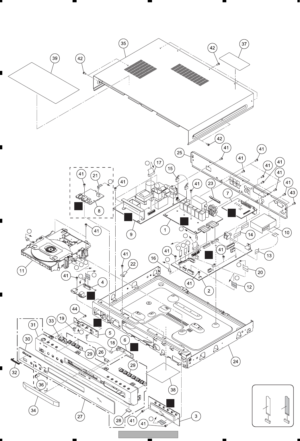
XV-DV363
50
1234
1 234
C
D
F
A
B
E
9.2 EXTERIOR SECTION
E
BC
A
BC
A
F
F
D
D
G
H
H
I
I
G
E
Refer to
"9.3 06 LOADER ASSY".
CONTACT SIDE
NON-CONTACT
SIDE
D
G
E
F
J
H
C
I
B
XV-DV365K Only
(1/2)
(2/2)
XV-DV365K
Only
XV-DV363 51
5678
5678
C
D
F
A
B
E
(1) EXTERIOR SECTION PARTS LIST
(2) CONTRAST TABLE
XV-DV363/WYXJ5 and XV-DV365K/WXJ/RE5 are constructed the same except for the following :
Mark No. Description Part No.
1 DAMP Assy XWK3318
2 DVD MAIN Assy See Contrast table (2)
3 DISPLAY Assy XWZ4256
4 USB Assy XWZ4259
5 KEY Assy XWZ4261
6 LED Assy XWZ4263
7 EUROSCART Assy AWU8291
NSP 8 MIC Assy See Contrast table (2)
>9 POWER SUPPLY Unit XWR3012
10 FM/AM TUNER Unit AXX7248
NSP 11 06 LOADER Assy VWT1226
12 13P Flexible Cable/60V (J1903) ADD7541
13 11P Flexible Cable/60V (J1908) ADD7543
14 23P Flexible Cable/60V (J1909) ADD7544
15 2P Housing Wire Assy (J1901) ADX7480
16 Connector Assy (J1901) PF05PP-B40
17 Connector Assy (J1902) PG13KK-F22
18 3P Flexible Cable/60V (J1906) XDD3229
19 5P Flexible Cable/60V (J1905) XDD3231
20 15P Flexible Cable/60V (J1904) XDD3234
21 5P Flexible Cable/60V See Contrast table (2)
22 Earth Spring W5.1 ABH7240
23 GND Plate W5.1 ABH7241
NSP 24 Chassis ANA7187
25 Rear Panel See Contrast table (2)
26 Diffusion Sheet XAK3577
27 Front Panel Assy See Contrast table (2)
28 Rubber Foot VEB1325
NSP 29 Button XAD3254
NSP 30 Display Window See Contrast table (2)
NSP 31 Front Panel See Contrast table (2)
32 Pioneer Name Plate AAM1107
33 Standby Button XAD3253
34 Tray Panel XAK3573
35 Bonnet (for service) XZN3192
36 MIC Knob See Contrast table (2)
37 Laser Caution VRW2257
NSP 38 Name Label See Contrast table (2)
NSP 39 Getter See Contrast table (2)
40 • • • • •
41 Screw BBZ30P080FNI
42 Screw BBZ30P080FTB
43 Screw BSZ30P060FTC
44 Screw VPZ30P080FNI
Mark No. Description Part No.
Mark No. Symbol and Description XV-DV363
/WYXJ5
XV-DV365K
/WXJ/RE5
2 DVD MAIN Assy XWM3341 XWM3342
NSP 8 MIC Assy Not used XWM3375
21 5P Flexible Cable/60V Not used XDD3232
25 Rear Panel XNC3498 XNC3503
27 Front Panel Assy XXG3302 XXG3304
NSP 30 Display Window XAK3572 XAK3575
NSP 31 Front Panel XMB3271 XMB3275
36 MIC Knob Not used AAK8309
NSP 38 Name Label XAL3260 XAL3279
NSP 39 Getter XAX3610 XAX3611
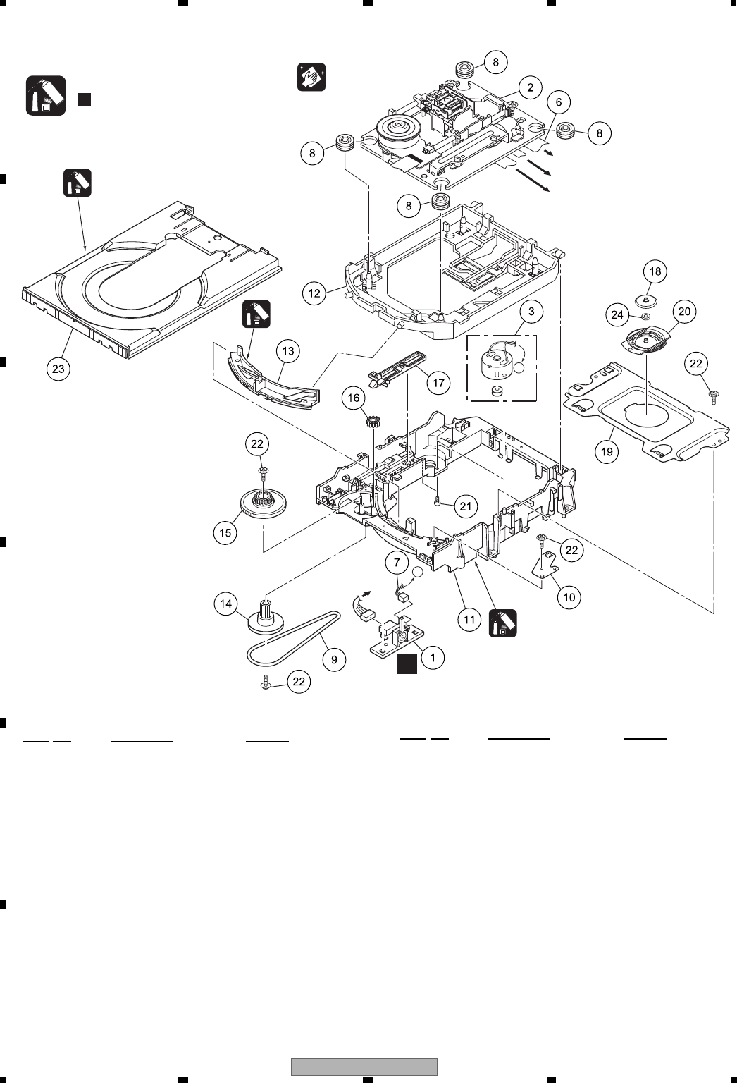
XV-DV363
52
1234
1 234
C
D
F
A
B
E
9.3 06 LOADER ASSY
06 LOADER ASSY PARTS LIST
A
A
To DVD MAIN CN101 (Pickup)
To DVD MAIN CN103 (Stepping Motor)
To DVD MAIN CN102 (Spindle Motor)
To
DVD MAIN CN104
Refer to
"9.4 TRAVERSE MECHANISM ASSY-S".
A
Lubricating Oil
GYA1001
Daifree
GEM1036
Refer to
" Application of Lubricant".
Note :
Lubricating Oil
GYA1001
Pickup leneses
Cleaning liquid
GEM1004
Cleaning paper
GED-008
Mark No. Description Part No.
NSP 1 LOAB Assy VWG2346
2 Traverse Mechanism Assy-S DXX2575
3 Loading Motor Assy VXX2912
4 • • • • •
5 • • • • •
6 Flexible Cable (24P) ADD7545
7 Connector Assy 2P VKP2253
8 Floating Rubber VEB1351
9 Belt VEB1358
10 Stabilizer VNE2253
11 Loading Base VNL1917
12 Float Base 04 VNL1968
13 Drive Cam VNL1919
14 Gear Pulley VNL1921
15 Loading Gear VNL1922
16 Drive Gear VNL1923
17 SW Lever VNL1925
18 Clamper Plate 04 VNE2342
19 Bridge 04 VNE2343
20 Clamper 04 VNL1969
21 Screw JGZ17P028FTC
22 Screw VBA1094
23 Tray VNL1920
24 Clamp Magnet VMG1029
Mark No. Description Part No.
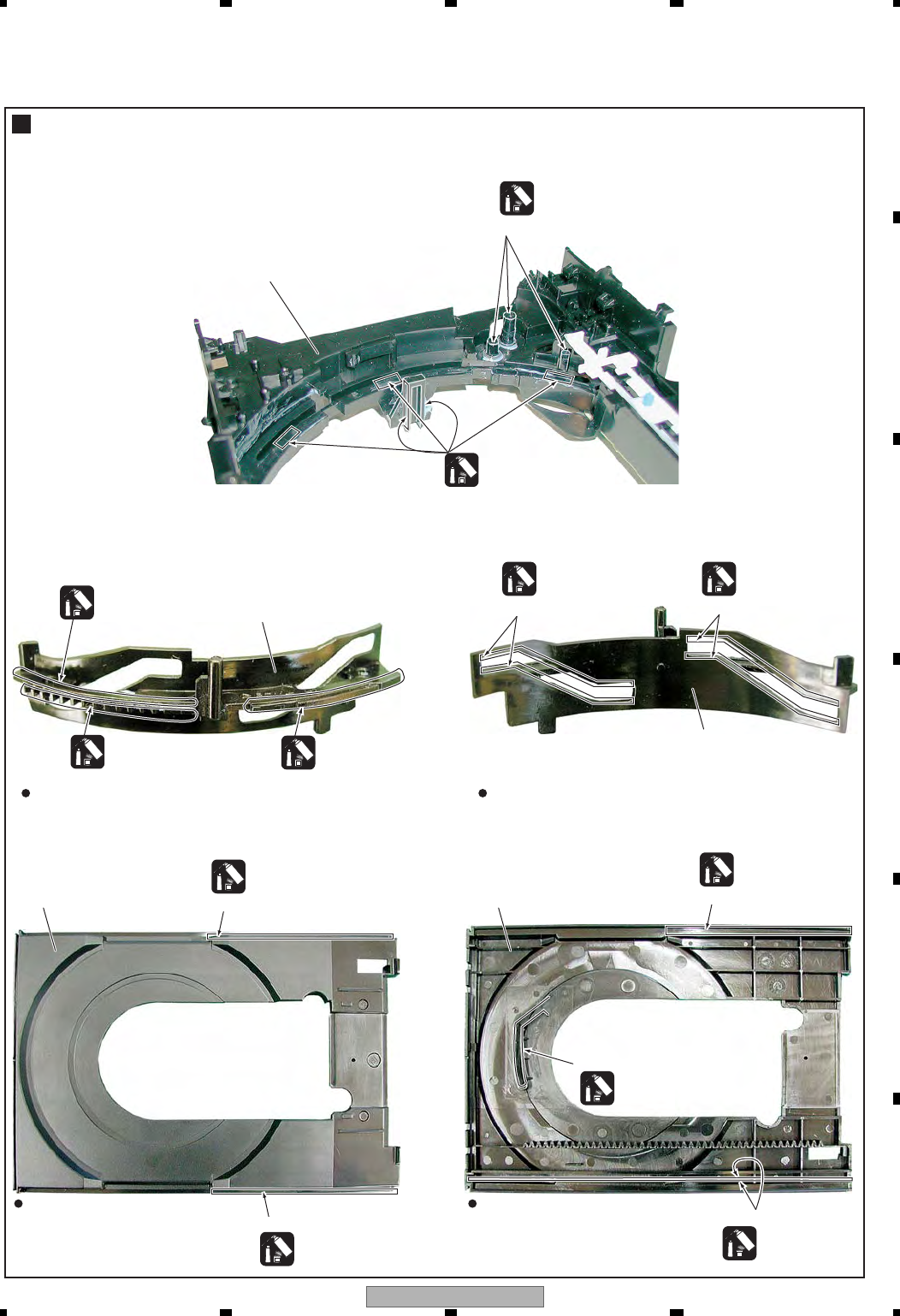
XV-DV363 53
5678
5678
C
D
F
A
B
E
Application of Lubricant
Lubricating Oil
GYA1001
Around the shaft
No. 11
Loading Base
No. 13
Drive Cam
No. 13
Drive Cam
No. 23
Tray No. 23
Tray
Front View Rear View
Daifree
GEM1036
Inner side of a ditch
Concave of unevenness
Top View Bottom View
Daifree
GEM1036
Daifree
GEM1036
Side of the rib
Concave of unevenness
Daifree
GEM1036 Concave of unevenness
Daifree
GEM1036
Inner side of a ditch
Lubricating Oil
GYA1001
Inner side of a ditch
Lubricating Oil
GYA1001
Lubricating Oil
GYA1001
Lubricating Oil
GYA1001
Lubricating Oil
GYA1001
Lubricating Oil
GYA1001
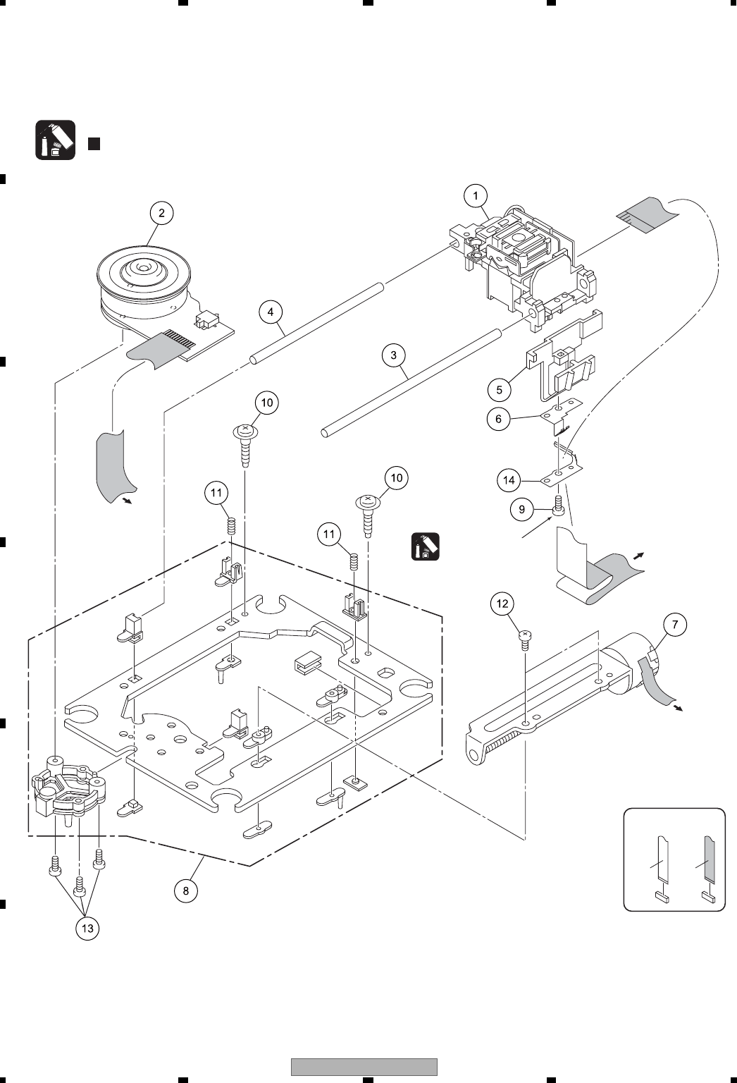
XV-DV363
54
1234
1 234
C
D
F
A
B
E
9.4 TRAVERSE MECHANISM ASSY-S
To
DVD MAIN CN101
(Pickup Assy)
To
DVD MAIN CN103
(Stepping Motor)
To DVD MAIN CN102
(Spindle Motor)
CONTACT SIDE
NON-CONTACT
SIDE
Silicone Adhesive
GEM1037
Note :
When Spindle motor (No. 2) is replaced,
Spindle screw (No.13) also need to be
replaced at the same time.
Note : Spindle screw (DBA1252)(No.13) is the screw which applied special bond.
Therefore the adhesion becomes inteffective when takes it off once. Spindle screw is the part which cannot recycle.
When Spindle motor (No. 2) is replaced, Spindle screw (No.13) also need to be replaced at the same time.
Refer to
" Application of Lubricant".
Note :

XV-DV363 55
5678
5678
C
D
F
A
B
E
TRAVERSE MECHANISM ASSY-S PARTS LIST
Mark No. Description Part No.
>1 06SD Pickup Assy-S OXX8020
2 Spindle Motor N200 DXM1197
NSP 3 Guide Shaft VK1 DLA1940
NSP 4 Sub Guide Shaft VK1 DLA1941
NSP 5 Joint VK1B DNK4272
NSP 6 Joint Spring VK1 DBK1235
7 Stepping Motor VK1 DXM1201
NSP 8 Mechanism Frame VK1 DNK4160
9 Precision Screw VK1 DBA1209
10 Skew Screw VK1 DBA1211
11 Skew Spring VK1 DBH1516
NSP 12 Stepping Screw DBA1205
13 Spindle Screw VK1(for Service) DBA1252
NSP 14 Hold Spring DBK1297
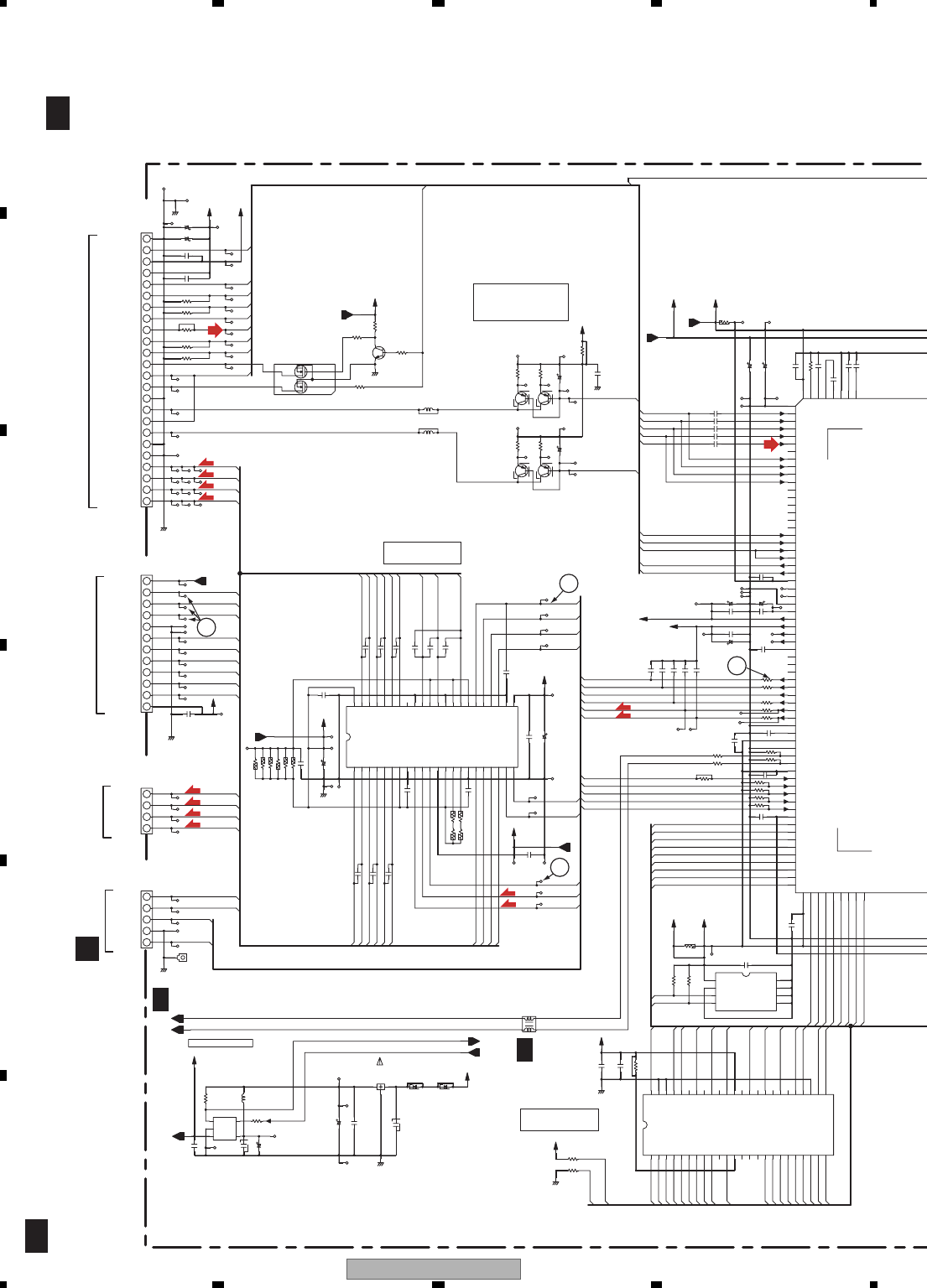
XV-DV363
56
1234
1 234
C
D
F
A
B
E
10. SCHEMATIC DIAGRAM
10.1 DVD MAIN ASSY (1/5)
USB POWER CONTROL
A13
A15
A14
A8
A12
A10
A11
A9
~BYTE~
A16
VSS
D6
D7
D15
D14
~WE~
NC
~RESET~
A19
NC
A18
RY/~BY~
NC
A7
A17
A6
A4
A5
A2
A3
A1
AYW7154
D12
D5
D13
D4
VCC
D10
D3
D11
D2
D9
D0
D8
D1
VSS
~OE~
A0
~CE~
SW1
SW2
GNDD
LOAD-
LOAD+
to LOAB ASSY
ST1-(~A~)
ST1+(A)
ST2+(B)
ST2-(~B~)
FCO+
LDOP
LDON
FCO-
AGND
AVM
TKO+
TKO-
SERVO DRIVER
V+5S
U+
U-
V+
V-
VCC
HU+
HU-
HV+
HV-
HB
HW+
HW-
W-
W+
U
HB
W
V
INSIDE
FOCS RTN
TRKG RTN
FOCS DRV
TRKG DRV
VSHF
LD(650)
GNDD
LD(780)
PD
VR780
GNDD
SDA
SCL
WP
GND
NC
NC
VCC NC
3.3v
1.8v
IOA19 (PU)
IOA18 (PU)
HIGHA0(PU)
HIGHA6(PU)
HIGHA4(PU)
HIGHA3(PU)
HIGHA5(PU)
HIGHA2(PU)
IOA7 (PU)
IOA5 (PU)
IOA6 (PU)
IOA4 (PU)
IOA3 (PU)
IOA2 (PU)
TDO/V_ADIN7 (JTAG)
TCK/V_ADIN6 (JTAG)
DVD D18
65:DVDD3
66:IOWR#
67:A16
68:HIGHA7(PU)
TKIN
FCIN
LDIN
DVC C
SLO1N
SLGND
SLO1P
SLVDD
SLO2N
SLO2P
SLIN2
SLIN1
SLRNF2
SLRNF1
V
SPVM1
U
SPGND1
W
SPGND2
SPVM1
SPRNF
FG
SPIN
CTL1
CTL2
DGND
VC
FG/V_ADIN8 (PU)
TMS/V_ADIN5 (JTAG)
TDI/V_ADIN4 (JTAG)
USB_VDD3
USBM
USBP
USB_VSS
VPLLVDD3
CAPPAD
VPLLVSS
TRO
FOO
TROPENPWM
PWMOUT1/V_ADIN9
FMO
OP_INP
OP_INN
DMO
TEZISILV
TEO
OP_OUT
FEO
VREFO
V2O
V2REFO
RFLV/RFON
SGND
CSO/RFOP
(1/2)
(2/2)
63
2
41
5
(1/2) 63
2
41
5
SVDD3
LDO1
LDO2
MIDI2
MIDI1
TPI
TNI
CDFON
CDFOP
3.3v
SD
SC
SB
MD
MC
SA
DVDRFIN
MB
MA
IREF:255
RFGC:254
AVDD3:256
OSN:253
DVDRFIP
DVD D
DVD C
DVD B
AGND
DVDA
OSP
RFGND
HRFZC
CRTPLP
VR650
VRCOM
A
B
SW
RF
(2SC4081(QR))
C
D
VCC
E
F
VREF
GNDD
(2/2)
1.8v
3.3v
XFLAG
CTL
PWR#
PCE#
A16
A15
A14
A10
A13
A12
A9
A11
A17
AD7
A0
AD6
PWR#
A20
A19
A18
A8
A7
A6
A5
A4
A2
A3
AD4
AD1
AD3
PRD#
AD0
AD2
AD5
PCE#
A1
A16
A15
PWR#
A14
A10
A11
A13
A12
TROUT
TRIN
LOAD-
LOAD+
LOAD-
F-
F+
LOAD+
T-
T+
ST2+
ST1+
ST1-
ST2-
HV-
HU-
HU+
HV+
HW-
U
W
V
HW+
HW-
HV+
HV-
HU-
HU+
HW+
T-
F-
T+
F+
SDA
SCL
ST2-
ST1-
ST1+
ST2+
TRSO
TROPEN
FOSO
A8
A18
A19
PWMOUT1
FMSO
STBY
ENDM
A5
A3
A2
A6
A7
A4
TRIN
FG
TROUT
FOSO
TRSO
PWMOUT1
FMSO
TROPEN
DMSO
DMSO
STBY
ENDM
FG
W
U
V
LDO1
MDI1
LDO2
E
F
LDO2
C
B
RF
A
D
LDO1
MDI1
B
A
IOA
RF
C
D
E
F
IOA
IOA
1
2
43
5
321
2
3
1
8
6
7
4
5
46
47
48
45
44
41
42
43
4
23
1
12
9
11
10
15
16
14
13
21
17
19
18
20
23
24
22
40
38
39
37
36
34
35
33
30
32
29
28
31
27
26
25
5
4
3
2
1
4
2
3
1
1
3
2
4
7
5
6
8
1
2
3
4
5
42
43
44
37
40
41
38
39
6
7
8
9
10
11
12
24
23
22
20
21
18
19
16
17
15
14 51
2
5
7
6
4
3
2
81
64
63
62
66
67
65
68
69
71
70
72
73
59
61
60
57
56
58
55
54
53
10
11
12
9
14
15
16
13
17
18
19
21
20
22
34
36
35
33
29
31
30
32
28
26
27
24
25
23
52
51
50
47
49
48
45
44
46
41
43
42
39
38
40
36
37
35
32
33
34
30
31
29
28
27
26
23
25
24
22
21
20
17
19
18
14
15
16
13
10
11
12
8
9
7
6
5
4
1
3
2
254
256
255
253
252
250
251
249
13
12
11
10
8
9
43
7
6
5
4
2
3
1
V+5USB
USBP
USBN
XFLAG
USBPOWER
V+6R8
LIMIT
V+5M
V+5S
V+1R8
V+3
C772
C773 C771
IC771
R771
R772 L772
C781
C783
C782
IC781
R284
R285
D782 D781
IC203
L761
C289
C296
R282
KN103
CN104
R135
R132
R136
R131
R134
R133
C152
C153
C151
C103
CN103
C133
C101
IC101
C140
C102
C141
C142
C143
CN102
R318
R218
R219
R208
R153
R152
R154
R151
C104
C121
IC204
C290
C220
R210
R211
C217
C131
C132
R214
C144
C161
C209
C212
C145
C146
C210
C211
C208
R213
R212
R770
C216
R768
R769
C218
R767
C219
R205
R206
R204
R202
R201
C206 C200
C204
C205
C213
C203 C215
Q307
Q307
R322
R325
C309
L308
L309
Q308
C310
C347
C344
C345
C346
C343
C207
C201
C202
C269
R371
R373
R372
R374
Q305
R315
R313
Q304
R314
R375
C371
C372
C373
CN101
C374
R321
R326
R310
C320
Q308
C273
R207
C271
C272
R256
0.1/16 1/16
GNDD
STBY
AAT4618IGV-0.5-1-TLB
100k ATL7002-A-T
220
10/50
STBY
2.2
NJM2845DL1-05
V+5USB
GNDD
***
10k
S29AL016D70TFI010
STBY STBY
V+3D
GNDD
FLASH
V+6R8
V+3D
1000p
1
***
S-24CS64A
GNDD STBY
B5B-PH-K-S
0.01
0.01
0.01
YB
YB
YB
GNDM
GNDD
VKN1235
4.7
4.7
4.7
4.7
4.7
4.7
***
1
100/10
BD7995EFS
1
V+5S
1
V+6R8
***
***
***
VKN1243
GNDD
100K
VTH1047
10K
10K
STBY
1
V+3DV+3
1.8
1.8 1
1
V+5M
EEPROM
0.1
0.1
0.1
STBY
STBY
1
0.1
***
***
2200p
1000p
V1P4
0.1
100p
2200p
2200p
2200p
V1P4
2200p
V20
10K
10K
33 15k
0.1
33
0.1
5600p
15k
51k
51k
22k
22K
100p
1.5K
47/35 0.1
0.1
0.1
0.1
47/35 47/35
HN1A01F(YGR)
HN1A01F(YGR)
4.7
4.7
47/35
***
***
HN1A01F(YGR) GNDD
47/35
0.1
1
1
1
1
1
220/6.3
220/6.3
0.033
***
***
***
***
UM5K1N
GNDD
10K
100K
2SC4154(EFG)
10K
***
0.1
STBY
0.1
V+5S
VKN2045-
GNDD
100/6.3
V+5S V20
4.7
4.7
HN1A01F(YGR)
***
V+3
STBY
V+1R8
0.1
STBY
0.1
0.1
15k
V+3
OUT IN
to STEPPING MOTOR
to SPINDLE MOTOR
to PICK UP
B1/5
DVD MAIN ASSY
(XWM3341:WYXJ5)
(XWM3342:WXJ/RE5)
TRAVERSE MECHA ASSY CN1
SPINDLE MOTOR
STEPPING
MOTOR
B
2/5
B
2/5
CN601
A
B1/5
(RF)
(T)
(T)
(F)
(F)
(S)
(S)
(S)
(S)
LD CURRENT
CONTROL
FTS Driver
FLASH
(T)
(F)
(T)
(F)
(RF)
4
2
1
3
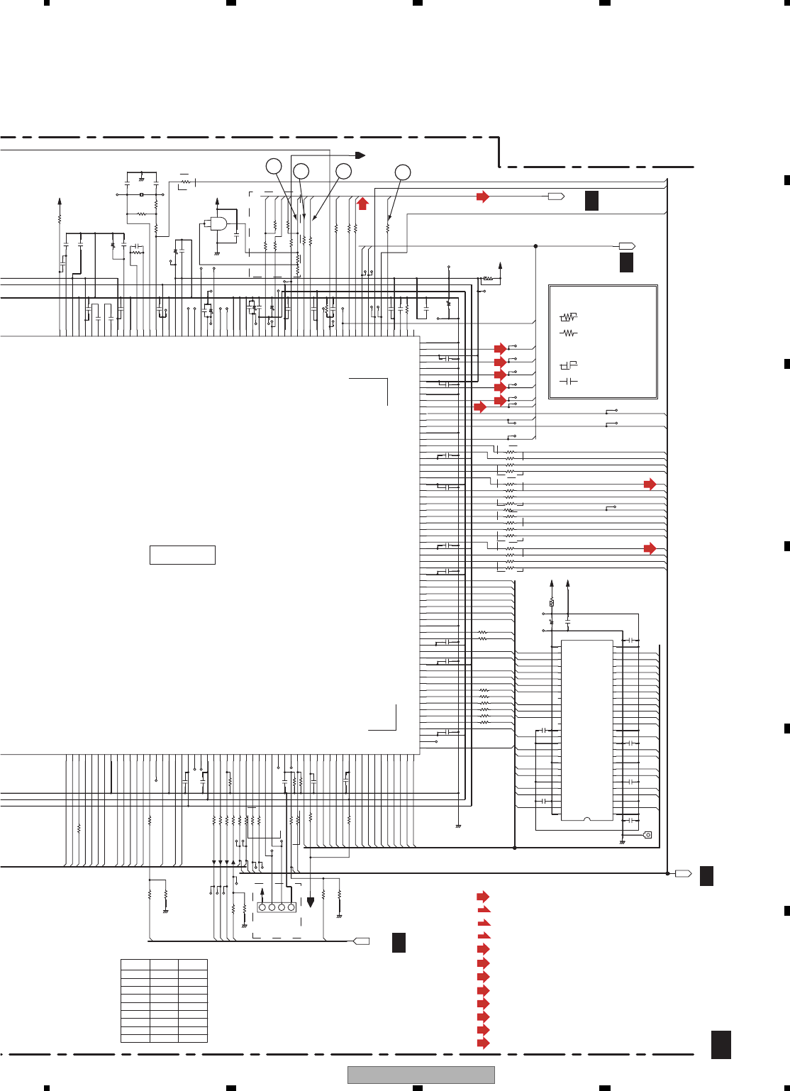
XV-DV363 57
5678
5678
C
D
F
A
B
E
XREADY
MDATA
SCLK
ACK
SDATA
DOWNLOAD
XDVDRST
HIGHA1(PU)
IOA20
XIOCS
IOA1
XIOCE
AD0
AD1
DVS S
AD2
AD4
AD5
AD3
AD6
DVS S
AD7
ALE
IOA21
3.3v
1.8v
*1
*1
1.8v
3.3v
DVD D18
IOA0
A17
URD#
UWR#
UP1_4 (PU)
UP1_3 (PU)
UP1_2 (PU)
DVD D3
UP1_6 (PU)
UP3_0 (PU)
UP1_7 (PU)
UP1_5 (PU)
UP3_4 (PU)
UP3_5 (PU)
UP3_1 (PU)
ICE (PD)
XPRST
IR
XINT0
IO_19
DQM0
RD6
RD7
RD4
RD5
DVD D3
RD3
RD0
RD1
RD2
RD14
RD13
RD15
RD12
DVD D3
RD8
IO_18
126:RD11
127:RD10
DQM1
XCAS
XRWE
XRAS
128:RD9
BA0
BA1
XRCS
RA10
RA0
RA2
RCLK
RA1
DVD D18
DVD D3
RA3
RA11
DVS S
CKE
RA9
RA8
DVD D3
RA4
Y7/IO_16
RA7
RA6
RA5
Y6/IO_16
Y2/IO10
Y1/IO9
YUVCLK/IO_8
C7/IO_7
C6/IO_6
DVD D18
Y5/IO_14
Y4/IO_13
Y3/IO12
Y2/IO11
RFRPAC
RFVDD3
ADCVDD3
RFRPDC
ADCVSS
LPFON
PLLVDD3
LPFIP
LPFOP
LPFIN
JITFO
JITFN
IDACEXLP
PLLVSS
XTALO
RFGND18
RFVDD18
XTALI
DVD D18
C1/IO_1
C5/IO_5
DVD D3
IO_17
C0/IO_0
C2/IO_2
C3/IO_3
C4/IO_4
YUV6/R
YUV5/B
VSYNC/V_ADIN1
DACVSSA
YUV4/G
DACVSSC:192
YUV2/C:189
YUV1/Y:191
DACVDDB:190
DVS S
HSYNC/VADIN2
YUV7
DACVDDA
AL/SDATA2
ALF/(CTR)
ALS/SDATA0
AR/SDATA1
ARS/SDATA3
ADACVDD1
ADACVDD2
ARF(SW)
AVC M
APLLCAP
ADACVSS2
ADACVSS1
APLLCSS
SPDIF
MC_DATA
DVDD18
ASDATA4
APLLVDD3
ACLK
ABCK
ALRCK
ASDATA3
SPBCLK
SPDATA
SPLRCK
DVD D3
ASDATA1/GPO_1
ASDATA2/GPO_0
YUV3/CVBS
RCLKB/GPIO_5
RVREF/GPIO_6
ASDATA0/GPO_2
DACVSSB
SPMCLK
GPIO_4
GPIO_3
DACVDDC
VREF
FS
YUV0/CIN
VSS
DQ14
VSSQ
DQ15
VCC
DQ1
VCCQ
DQ0
DQ12
DQ13
VCCQ
VSSQ
DQ11
DQ10
DQ9
DQ8
VCCQ
DQ3
DQ2
VSSQ
VCCQ
DQ4
DQ5
DQ6
DQ7
VSSQ
VSS
NC
UDQM
CKE
NC
CLK
A11
A9
A8
VCC
LDQM
WE
CS
RAS
CAS
BA0
BA1
A10/AP
A6
A7
A5
VSS
A4
A2
A0
A1
VCC
A3
3.3v
1.8v
CH : CCSRCH~
OTHERS : CKSRYB~
: 1608 Size
: 2125 Size
CKSQ**~
CAPACITOR
: 1608 Size
RS1/10S***J
(F) : RS1/16S****F
OTHERS : RS1/16S***J
1.8v
*1
*1
3.3v
1.8v
3.3v
Chip Size
RESISTOR
: 2125 Size
(Page 2/2)
to VIDEO PART
to AUDIO PART
(Page 2/2)
78
A20
A1
A9
PRD#
PCE#
AD1
AD2
AD0
AD6
AD4
AD3
AD5
A17
AD7
50
67
51
49
80
A0
SDA
SCL
HDMISDA
HDMISCL
INT0#
XDVDRST
HDMIHDMI
TXD
RXD
DQM0
DQ6
DQ5
DQ7
DQ4
DQ3
DQ2
DQ1
DQ0
DQ12
DQ13
DQ15
DQ14
DQ11
DQ10
DQ9
DQ14
DQ15 DQ7
DQ6
DQ8
DQ13
DQ12
DQ11
DQ10
DQ9
DQ8
DQ5
DQ4
DQ3
DQ2
DQ1
DQ0
DQM1
DWE#
DCAS#
DRAS#
DCS#
DBA0
DBA1
MA10
MA0
DQM1
SDCLK
SDCKE
MA8
MA11
MA9
DWE#
DQM0
DRAS#
DCAS#
DCS#
DBA1
DBA0
MA10
MA1
MA2
MA3
SDCLK
SDCKE
MA11
MA5
MA6
MA7
MA4
MA0
MA2
MA1
MA3
MA9
MA8
MA7
MA6
MA4
MA5
Y6
Y7
Y4
Y5
Y3
Y1
Y2
C7
Y0
VCK
C5
C3
C2
C0
C6
C1
C4
VSEL1
R_CR
VSEL2
G_CY
B_CB
HSYNC
VSYNC
CVBS
S_C
S_Y
I/XP
27MHz
SQUEEZE
LETTER
HSPDIF
MCDATA
ASPDIF
ALRCK
ACLK
HCLK
ABCK
ADDATA
ASDAT2
ASDAT1
ASDAT0
PRDN
PUSEL
XO
2
3
1
4
77
75
76
74
80
79
78
81
86
85
84
83
82
88
87
89
90
91
92
94
93
99
95
96
97
98
100
102
101
103
106
105
107
104
109
111
110
108
112
114
116
115
113
120
117
119
118
125
122
123
121
124
128
126
127
131
130
129
133
132
140
138
139
136
134
135
137
145
144
147
146
149
141
142
143
148
158
151
153
152
154
155
156
150
157
167
164
159
160
161
162
163
166
165
248
244
245
247
246
242
241
243
240
236
235
239
237
238
232
233
234
231
174
175
172
176
171
170
169
168
173
177
180
181
186
184
183
185
178
179
182
230
229
228
227
225
224
226
223
222
219
220
218
221
217
214
216
215
212
213
209
210
211
207
208
206
205
189
187
188
192
191
190
204
203
201
202
200
198
196
199
197
194
195
193
54
53
51
52
1
3
4
2
50
49
48
45
47
46
44
42
43
7
5
6
8
10
9
12
11
13
40
41
38
39
37
35
36
34
33
32
16
17
14
15
20
18
19
23
22
21
29
31
30
28
26
25
24
27
4
13
5
2
LIMIT
UCOM
HDMI
XAMUTE
VIDEO
AUDIO
R291
R292
R216
R215
CN204
R294
R293
R233
R224
C224
R221
R237
R234
R263
R262
R260
R258
R259
R222
R223
R261
R272
C225
R235
C226
R236
R220
C227
C229
IC201
C268
C240
C241
C222
R230
C245
C285
KN202
C286
IC202
C287
C288
C230
R225
R226
R227
C284
C231
R228
C232 R229
C281
C282
C283
C233
R281
C234
R266
R271
R267
C235
C236
R265
R264
C244
C243
C266
C267
C259
C258
C260
C238
C256
R255
C264
C265
R254
C255
C262
C254
R252
R251
R253
C251
X201
C252
C242
C261
C223
C228
C239
C247
C248
R243 R269
C246
R279
C250
C270
IC205
R249
R248
R268
R242
R241
R250
R240
R247
R245
R246
R244
R257
C237
R209
GNDD
6.8k
3.3k
GNDD
3.3k
4.7k
B4B-PH-K-S GNDD
V+3DR
3.3k
6.8k
0
33
33
33
33
33
33
33
33
33
33k
0.1
0.1
4.7k
0.01
STBY
220p
0.1
STBY
MT1389FE/H-L
0.1
GNDD
0.1
GNDD STBY
0.1
0.1
64M SD-RAM
0.1
K4S641632K-UC75-K
0.1
0.1 RAB4C330J
33*4
0
33
0.1
0.1 33
33
220/6.3
1
0.1
0.1
0
V+3D V+3DR
RAB4C330J-T
0.1
0
RAB4C330J-T
0.1
0.1
RAB4C330J-T
RAB4C330J-T
0.1
0.1
0.1
1000p
0.047
0.047
0.1
0.1
750K
100K
0.1
22p
10/50
0.47
10/50
1000p
0
100K
680
V1P4
GNDD
VSS1168
9p
12p
STBY
10/50
10/50
STBY
0.1
0.1
10k
0.1
0.1
0.1
10/50
10
0.1
1
2.2k
GNDD
STBY
STBY
STBY0
33
33
STBY
33
33
33
V+3D
0.1
220/6.3
STBY
V+3
-
33
R222
R263 33
-
R243
R247
R240
R249 -
R257 0
33
33
10
0
0
R262
R248
*1 WYXJ5
33
33
33
10
0
0
0
WXJ/RE5
B1/5
B
2/5,3/5,5/5
B
5/5
B
4/5
B
2/5,3/5
: VIDEO SIGNAL ROUTE (S_Y)
: VIDEO SIGNAL ROUTE(C/V)
(S_Y)
: VIDEO SIGNAL ROUTE (S_C)
: AUDIO DATA SIGNAL ROUTE
(S_C)
: VIDEO SIGNAL ROUTE (R/Cr)
(R/Cr)
: VIDEO SIGNAL ROUTE (G/Y)
(G/Y)
: VIDEO SIGNAL ROUTE (B/Cb)
(B/Cb)
(AD)
: VIDEO/AUDIO SIGNAL ROUTE (HDMI)
(HDMI)
: FOCUS SERVO LOOP LINE
: TRACKING SERVO LOOP LINE
: STEPPING SERVO LOOP LINE
(F)
(RF)
: RF SIGNAL ROUTE
(T)
(S)
(C/V)
DVD BE
(S_Y)
(S_C)
(C/V)
(G/Y)
(B/Cb)
(MDMI)
(MDMI)
(R/Cr)
(AD)
(AD)
11 13 12 14
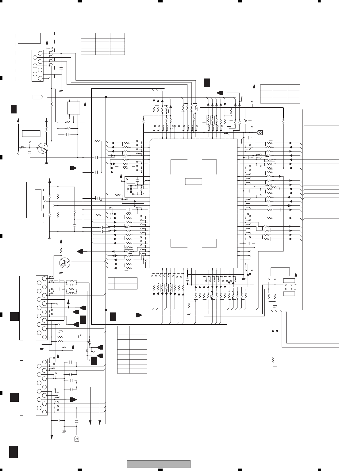
XV-DV363
58
1234
1 234
C
D
F
A
B
E
10.2 DVD MAIN ASSY (2/5)
PDC153A/A8
1
3
2
19
69
36
69
83
31
30
29
27
28
24
25
23
22
21
20
19
17
69
6
7
4
3
2
1
33
35
31
32
34
38
37
41
36
46
45
47
49
48
52
51
50
DSPMUTE
84
72
72
4
57
61
60
58
66
64
65
62 17
67
68
68
60
58
71
70
69
57
74
77
78
79
80
22
DSP
UCOM
97
99
100
98
93
87
86
85
84
83
82
REMOUT
HP_L
HP_R
USBP
USBN
V+5USB
XFLAG
XTVMUTE
REMOCON
UCOM
DVDPOWER
13
12
10
11
9
8
7
6
5
4
3
2
1
15
14
12
13
10
11
8
9
6
7
4
5
2
3
1
E
B
C
E
BC
31
32
34
33
2930 2728
35
37
36
38
40
41
39
44
42
43
45
46
47
48
49
50
5251 5453
26 25 222324 21 20
5655 57 5958 60 61
19 18 17 16 15 14
62 63 64 65 66 67
13 12 1011 9 8
6968 7170 72 73 74
76 43512
7675 7877 79 80
100
97
98
99
93
96
94
95
92
91
90
87
88
89
86
85
84
82
81
83
1
2
3
5
4
7
64
531
2
C5601
KN5601
C5606
C5602
C5603
C5605
R5543
CN5602
C5604
C3952
C3951
R3951
R3952
C3954
L3952
R3954
L3951
CN5601 C3953 R3953
Q3951
R3955
R5527
C5519
C5522
R5525
R5521
R5522
R5516
R5515 R5513
R5514
R5519
C5521
R5518
C5517
R5517
C5518 R5569
X5501
C5509
C5525
Q5525
C5504
C5508 R5507
R5506
R5505
C5524
R5510
C5503 R5508
R5503
R5500
R5501
R5544
R5541
R5542
R5531
R5532
R5533
R5534
R5535
R5537
R5538
R5536
C5539
R5545
R5548
R5546
R5547
C5555
R5557
R5562
R5564
R5565
R5512 IC5501
C5569
C5577
R5600
R5595
C5589
R5587
R5596
R5597
C5578
R5585
R5584
R5586
R5583
R5582
R5581
C5579
R5566
R5563
R5570
R5575
R5571
R5576
R5577
KN5501
C5501
R5502
R5509
IC5503
C5597
CN5501
R5598
R5590
R5574
C5502
CHASSIS GND
FLDATA
FLCK
REMOCON
FLCS
VE+5
VFDP
FLDC-
FLDC+
GNDD
KEY1
GNDD
KEY2
KEY2A
LED
V+10
KEY1
KEY2A
USB_DM2
GNDUSB
USB_DP2
V5USB
GNDUSB
V5USB
HP_R
HP_DET
GNDD
HPMUTE
HP_L
(DTC124EUA)
DESTINATION
MODEL
(DTC143EUA)
EU
RESET
*1
ACDET
PWRCONT
STEST
UTEST
INPUTSELB
DASCK
DASDA
INPUTSELA
DSPMUTE
XDEC MUTE
DSPHREQ
LED
VSS4
VDD4
BUSY
XFLAG
STEST
UTEST
XDSPSS
XDSPRST
SCLK
NC
NC
TXCE
XTVMUTE
DSPCK
*1 DSPDI
DSPDO
XPROTECT
PCONFIG
ADMD
XRECMUTE
XADPDN
XHPMUTE
DSPMODE
DATASEL
SDATA
MDATA
VSS2
VDD2
EEP_DO
EEP_CS
NC
EEP_SK
DIRERR
KEY2
KEY1
VDET
MODEL
VDD1
SIMUKE
TXODATA
TXCLK
RDSPOW
NC
TXIDATA
RDSDATA
TEST POINT
SHORT for
EU
CF2
CF1
XT2
VSS1
XT1
XRESET
XDIRCS
XDIRRST
μ-COM
PWRCONT
ECHO_CONT2
DVDACK
EEP_DI
KEY1
XDARST
XDAPDN
DVDPOWER
USBPOWER
XDAMUTE
REMOCON
RDSCLK
ACDET
P_ON
ECHO_CONT1
FLCLK
XFLCS
DIRDO
FLASHCLK
FLASHDO
FLASHE/D
HPDET BEATCUT2
UTESTMODE
VSS3
VDD3
PLC_CONT
(DMUTECHECK)
HPSEL
MIC_DET
SR+TX
XADPDN(MIC)
BEATCUT1
SR+RX
SHUTDWN
XOTW
XDVDRST
XREADY
FLDAT
CHASSIS GND
XPROTECT
STBY NC
VSS
RST
VCC
WDD
WEN/DI
WCLK
DOWNLOAD
μ-COM
*1
STBY
VFDP
1000p
GNDD
STBY
FLDC- FLDC+
1000p
1000p
STBY
STBY
*1
CKS3378
GNDD
CKS3380
VE+5
100/16
V+10
100/16
47k
47k
STBY
STBY
CTF1346-
V+5USB
STBY
STBY CTF1346-
GNDD
RT1N241M
1.8k
RAB4C221J
220
STBY
GNDD
VE+5
0.01
0.1
0.01
RAB4C221J
220
220
**
**
10k
1M
RAB4C221J
220
0.01
VE+5
VE+5
**
**
0.01
0.1 220
ASS7034
10MHz
VU+5 0.1/16
GNDD
STBY
RT1N431M
10/50
0.01
220
220
220
47k
STBY 2.2K
STBY
STBY
220
RAB4C221J
GNDD
RAB4C221J
RAB4C221J
*1
STBY
STBY
STBY
STBY
*1
220
0.1/16
*1
*1
*2
220
STBY
GNDD
RAB4C221J
GNDD
10k
10k
220
STBY
VE+5
0.1/16
220
RAB4C221J
220
220
220
220
0.01
0.01
STBY
STBY
STBY
15K
0.1
0.01
1000p
220
10k
220
220
RAB4C221J
10k
RAB4C221J
220
STBY
*2
STBY
220
RAB4C221J
STBY
STBY
*2
0
VU+5
STBY
GNDD
VE+5
STBY
52045-0745
VE+5
RAB4C221J
220
RAB4C221J
220
STBY
STBY
STBY
100k
100/10
VE+5
-
68k
47k
15k
15K
68K
82K
15K
R5516
R5515
R5514
R5513
XWM
**
3341
XV-DV363
/WYXJ
3342
XV-DV365K
/WXJ/RE5
R5571 1K
R5502 100K STBY
STBY
WXJ/RE5
*2 WYXJ5
TO USB ASSY
to DISPLAY
R5543
R5598
R5544
0
STBY
0
R5531
R5522
R5542
R5538
R5537
*1
STBY
STBY
0
STBY
STBY
WYXJ5,
WXJ/RE5
R5536
220
*2
B2/5
CN5901
D
CN5906
E
B
4/5,5/5
B
1/5
B
3/5
B
1/5
B
1/5,3/5
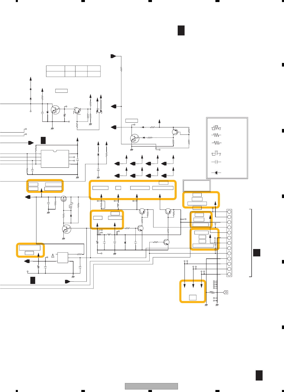
XV-DV363 59
5678
5678
C
D
F
A
B
E
DVDPOWER
V+1R8
V+3
V+3R3 V+6R8 V+10
USBPOWER
V+5V V+5 VE+5
SROUT
REMOCON
V+5M
V+5S
REMOUT
4
5
2
3
E
1
E
CBBC
G
S
D
4
3
2
1
5
6
7
8
E
CB
B
E
C
3
21
9
13
11
12
10
C
E
B
5
7
6
8
3
2
1
4
C
E
B
C1103
C1102
C1101
R1101
IC1101
C1505
C1501
C1502
C1301
D1501
R1307
R1202
Q1201
C1201
R1204
R5558
C5558
D1201
L1501
R1306 Q1304
R1304
R1303
C1204
R1201
Q1202
R1305 L1305 Q1302
C801
R5559
IC5502
D1415
C1415
D1417
R1415
Q1413
C5557
D802
R801
Q5941
R1404
C1413
D5942
R5947
D5941
R5946
R1403
R1401
Q1402
R1402
D1403
R1001
KN1001
Q1303
R1302
R1301
Q1301 CN1001
R5949
R5944
Q5942
R5945
D1416
R5943
PCB BINDER: VEF1040-
BACK END IC
HDMI
(2SC4081(QR))
(DTC114EUA)
SDRAM BACK END IC
HDMI FLASH ROM
DO
μcom FL DRIVER
μcom
FTS DRIVER PU VIDEO DRIVER INPUT SELECTOR
GND
SK
DI
EEPROM
CS
(DTC124EUA)
NC
TEST
VCC
(DTC124EUA)
SR OUT
FL
CHASSIS GND
FL DC-
-25.5V
FL DC+
GND
(2SC4081(QR))
DATA SELECTOR
A/D
MODULATOR
DSP GND
SW6.8V
from POWER SUPPLY
SW3.3V(A)
SW3.3V(B)
Pwr-ctr
FTS DRIVER
USB BUS
HDMI
SW5.0V
AC_DET
EV5.0V
SW10.5V
(2SA1576A(QR))
SCART
AUDIO BUFFER
SUPPLY
TX
MIC
*5
SCART POWER
CKSR**~
(MA111)
(1SS355)
: 1SS352
CAPACITOR
*
: 2125 Size
: 1608 Size
CKSQ**~
R5515, R5516
RD1/4PU~
CCSR**~
(2SA1576A(QR))
Chip Size
RESISTOR
RS1/10S~
: 2125 Size
: R5513, R5514
RS1/16S~
: 1608 Size
PROTECT
GNDM GNDD
47/35
STBY
NJM2846DL3-18
V+1R8
GNDD
1
GNDD
GNDD
220
100/10
0.01
0.1
LAU-TA
22
STBY
1
4.7k
RT1N141-11
GNDD
STBY
1
V+3
47p
47k
CH
470k
VU+5 VE+5
10k 2SC4154(EFG)
560(1/10W)
47k
0.056
10k
RSR015P03
STBY VTL1095
V+5M V+5S
2SA1577(QR)
V+5V
GNDD
V+3R3
STBY
GNDD
V+6R8 V+10
47k
S-93C46BD01-J8T1
GNDD
STBY
*3
*3
1.8k
RT1N241M
0.1/16
4.7k
V+5V
GNDD
V+5 VE+5
RT1N241M
VE+5
39k
GNDD
V+3V+5V
1k
4.7k
VE+5
*3
47K
2SA1602A(EF)
3.3k
MC2846-11
3.9k
FLDC-
STBY
FLDC+ VFDP
STBY
3.9k
2SC4154(BFG)
V+3R3
47k
V+6R8
2SA1602A(EF)
V+5
V+10 B13B-PH-K-S
V+5M
V+5S
10k 3.9k
100k
2SA1602A(EF)
*3
V+3R3
V+10
V+10 V+6R8
V+5
0
WXJ/RE5
WYXJ5
*3
UDZS
4.7B STBY STBY
D1415 C1413 D1416
D1417
B2/5
B2/5
DVD MAIN ASSY
(XWM3341:WYXJ5)
(XWM3342:WXJ/RE5)
CN3
J
B
4/5,5/5
B
1/5
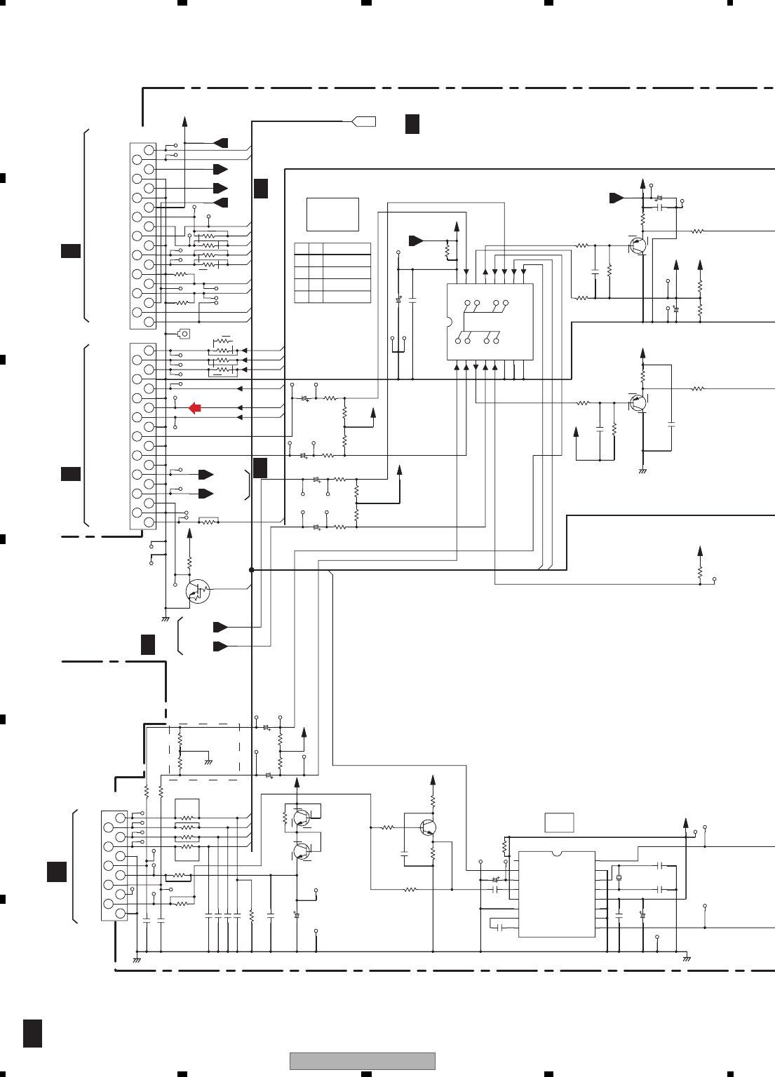
XV-DV363
60
1234
1 234
C
D
F
A
B
E
10.3 DVD MAIN ASSY (3/5)
SCART_L
SCART_R
TVOUT_R
TVOUT_L
SROUT
HP_R
HP_L
V+3R3
V+5
UCOM
V+10
66
62
61
52
32
65
ASDAT3
LRCKO
BCKO
MCKO
ASDAT2
DATA0
ASDAT1
93
84
79
77
29
30
28
71
27
DSPMUTE
70
82
21
11
10
8
9
6
7
5
3
4B2
C2
E2
7
8
6
3
4
5
1
2
9
10
11
14
12
13
16
15
1
2E
B
C
6
5
4
3
2
1
11
12
8
10
9
7
13
15
16
14
19
17
18
5
4
2
1
3
2
4
5
6
1
3
8
7
14
15
16
13
12
11
10
9
B2
C2
E2
11
6
10
9
8
7
17
18
12
15
16
13
14
19
B
C
E
C5705
C5704
C5701
C5709
C5703
C5702
R5719
C5707
R5705
C5708
R5718
R5717 Q5703
C5716
C5713
C5706
Q5701
R5708
R5706
C5719
R5710
IC5701
C5715
C5720
X5701 C5714
C5712
CN5701
R5712
R5713
R5716
R5715
R5714
R5707
Q5703
R5702 R5701
C3020
R3020
C3019
R3019
Q3006
R3006
R3003
C3016 R3016
C3015 R3015
C3012 R3012
C3011 R3011
CN3002 KN3001 R3002
R3082
R5704
R5703
R3018 R3017
R3915
R3014 R3013
C3004
Q3005
R3010
C3001
C3002
IC3001
R3027
R3022
C3022
R3040
R3024
R3026
C3024
R3025
R3081 R3001
CN3001
R3007
C3003
R3009
Q3005
R3021
R3039
R3023
C3023
C3021
GNDD
STBY
STBY
STBY
STBY
100p
100p
STBY
STBY
1000p
47/35
CH
CH
STBY
STBY
STBY
(RT3CLLM(EF))
4700p
560pCH
STBY
STBY
0
STBY
10/50
STBY
LC72725KM
GNDD
0.01
47/35
ASS7004
CH
27p
27p
CKS3376
STBY
STBY
STBY
(RT3CLLM(EF))
V+10
STBY
GNDD
STBY
10/50
10/50
VREF
GNDD
RT1N241M
10k
STBY 10/50
VE+5
10/50
10/50 22k
10/50 22k
AKP7199-A STBY STBY
1M
V+5
STBY
STBY
V+5
22k
22k
22k
22k
VREF
VREF
47k
GNDD
22k 22k
VREF
VREF
1k
Sub:HEF4052BT
(RT3AMMM)
0.01
STBY
47k
STBY
220k
0.1
15k
V+10
1k
1k 1k
1M STBY
AKP7199-A
V+3R3
STBY
V+5
1k
(RT3AMMM)
STBY
220k
VREF
15k
V+5
1k
47/35
V+10
0.1
GND
RDS
VSM
TXR
+9V
TXL
GND
DO
CLK
HN1C01FU
VSSD
VDDD
CIN
FLOUT
T1
MODE
VSSA
VDDA
(2/2)
MPXIN
VREF
XI
XO
RDSDATA
QUAL
RST
RDSCLK
4.322MHz
CE
DI HN1C01FU
STBY
2.7k
2.7k
2.7k
2.7k
RECMUTE
RDS DATA
S_TVOUT_R
S_TVOUT_L
RECMUTE
GND
GND
SDATA4
SCLK
LIN1_R
LIN1_L
GND
GND
GND
LRCLK
MCLK
GND
SDATA1
GND
SDATA3
SDATA2
CHASSIS GND
SROUT
PLCCONT
POWER
XSD
XOTW
PLC_CONT
PWRCONT
LINE
SCART
L
HH
H
(1/2) RDS
MICOUT
INPUTSELA
INPUTSELB
220/6.3
Main:TC4052BFN
INH
Y2
Y0
Y3
Y1
Y(Rch)
HN1A01FU(YGR)
VSS
VEE
VDD
X(Lch)
X1
X2
X0
X3
A
B
(2/2)
XMUTE
XPDN
GND
SCL
SDA
GND
L
H
TUNER
MCACCL
L
A FUNCTIONB
SELECTOR
GND
XRST
HPL
XHPSEL
GND
3.3V
HPR
AUDIO
INPUT
PCON
from Ucom PART
HN1A01FU(YGR)
(1/2)
to TUNER MODULE
TO DAMP/HAMP
B3/5
C1/2
CN3101
C1/2
CN3102
CN1
B4/5
B4/5
B2/5
B2/5
K
(AD)
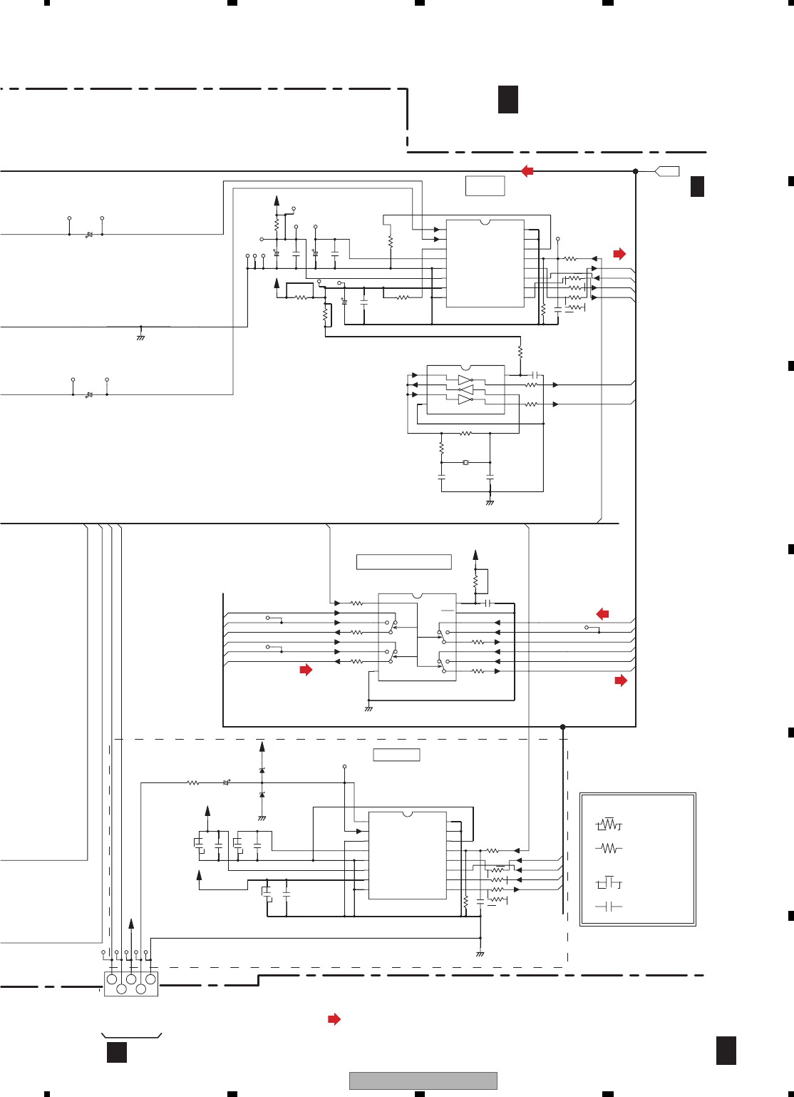
XV-DV363 61
5678
5678
C
D
F
A
B
E
AUDIO
MCDATA
ALRCK
ABCK
ACLK
6
97
64
74
DATA0
ADLRCK
ASDAT0
ALRCK
ADDATA
LRCKO
48
MCKO
ACLK
ADMCK1
ADBCK
ABCK
BCKO
85
34
ADMCK1
ADMCK0
ADLRCK
ADDATA
ADMCK0
ADBCK
1
2
53
4
6
7
5
8
10
9
11
12
2
4
3
1
8
6
7
5
3
4
1
2
4
3
1
2
14
16
13
15
9
11
10
13
12
14
16
15
5
6
8
7
8
107
9
5
6
12
11
4
314
13
2
116
15
CN3961
C3965
C3961
C3963
C3962
C3964
C3966
R3967
C3968
R3969
D3962
IC3961
R3966 C3967
D3961
R3063
R3062
R3061
IC3005
C3056
C3026
R3056
R3046
C3045
R3045
C3046
R3057
R3968
R3066
R3065
C3064
R3064
C3057
X3004
R3055
R3054
R3053
IC3004
C3052
R3052
R3073
C3048
R3049
C3025
C3042
C3041
C3043
C3044
R3041
R3060
R3048
IC3003
CKS3370
V+10
V+3R3
2.2
STBY
1
0.1
0.01
GNDD
RAB4C101J
100
3.3k
1
0.1
V+5
UDZS3R9
GNDD
AK5358AET
V+5
UDZS3R9
1K 22/25
220
GNDD
220
220
TC74VHC157FTS1
27p
CH
10/50
GNDD
100
STBY
10/50
STBY
0.1
1.8k
100
220
0.1
STBY
V+3R3
GNDD
CH
27p
VSS1140
12.288M
1M
100
100
TC7WU04FU
0.1
0
RAB4C101J-T
100
0.01
3.3k
10/50
V+3R3
2.2/50
10/50
0.1
0.1
STBY
V+5
1.8k
AK5358AET
TO MIC ASSY
ECHOCNT
GND
MIC
V+10V
MIC SW
VCOM
SDTO
LRCK
MCLK
SCLK
PDN
DGND
VD
VA
AGND
CKSR**~
CAPACITOR
: 1608 Size
CCSR**~
: 2125 Size
CKSQ**~
RS1/16S~
DIF
CKS2
CKS0
CKS1
AINL
AINR
MIC A/D
GND
RDSCLK
ECHO_CONT
MIC_DET
RDSPOW
VCC
DATASEL
DATA SELECTOR
0
0
GND
RESISTOR
Chip Size
: 2125 Size
: 1608 Size
RS1/10S~
ST
XADPDN(MIC)
XADPDN
VCC
SDTO
LRCK
DGND
VD
AGND
VA MCLK
SCLK
CKS1
VCOM PDN
DIF
AINL
AINR
CKS2
CKS0
A/D
from DVD,DSP PART
XV-DV365K/WXJ/RE5
B3/5
B3/5
DVD MAIN ASSY
(XWM3341:WYXJ5)
(XWM3342:WXJ/RE5)
B1/5,2/5,5/5
CN3921
H
(AD)
(AD)
(AD)
(AD)
(AD)
(AD)
: AUDIO DATA SIGNAL ROUTE
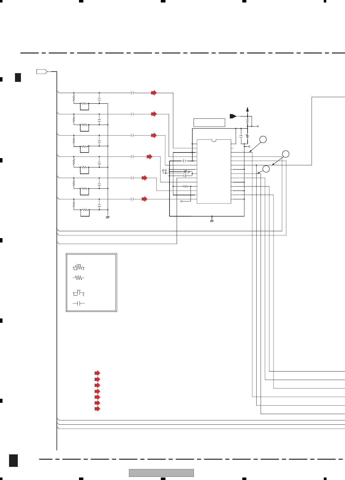
XV-DV363
62
1234
1 234
C
D
F
A
B
E
10.4 DVD MAIN ASSY (4/5)
R416
R436 C457
C416
R415
R435 C455
C415
R414
R434 C453
R413
R433 C451
C414
C405
R401
C404
C403
C402
C401
R412
R432 C449
C413
C412
R431
R411
C447
C411
IC401
R405
VIDEO
V+5V
STBY
150(F)
STBY
GNDD
0.1
150(F)
STBY
STBY
STBY
STBY
0.1
150(F)
STBY
150(F)
STBY
1
1
GNDD
100/16
0.1
STBY
100/16
150(F)
STBY
STBY
1
150(F)
STBY
STBY
0.1
(MM1623BF)
0.1
STBY
V+5V
14
13
15
16
12
11
9
10
7
8
19
17
20
22
18
21
6
5
2
3
4
1
24
23
25
26
27
28
CKSR**~
CCSR**~
: 1608 Size
: 2125 Size
CKSQ**~
RS1/16S~
: 1608 Size
CAPACITOR
RESISTOR
Chip Size
: 2125 Size
RS1/10S~
10k
R/Cr outMUTE2
Cr/R in GND2
CLP
Cb/B in
B/Cb out
I/P
CY/G in
G/CY out
GND1
BIAS
GND2
GND2
GND2
Y out
V in
Y in
YC MIX
C in
MUTE1
VCC1
S1
S2
V out
DC out
C out
VCC2
from DVD PART
(Page 1/4)
MM1758XF
VSEL1
SQUEEZE
VSEL2
SQUEEZE
LETTER
I/XP
R_CR
B_CB
G_CY
S_Y
CVBS
S_C
B4/5
B
1/5
VIDEO AMP
: VIDEO SIGNAL ROUTE (S_Y)
: VIDEO SIGNAL ROUTE(C/V)
(S_Y)
: VIDEO SIGNAL ROUTE (S_C)
: AUDIO DATA SIGNAL ROUTE
(S_C)
(S_C)
(S_Y)
(G)
(B)
(R)
(C/V)
: VIDEO SIGNAL ROUTE (R)
(R)
: VIDEO SIGNAL ROUTE (G)
(G)
: VIDEO SIGNAL ROUTE (B)
(B)
(AD)
(C/V)
10
9
8

XV-DV363 63
5678
5678
C
D
F
A
B
E
R491
C429
R9401
Q491
CN451
JA403
C424
R424
DVDPOWER
XTVMUTE
VE+5
SCART_L
SCART_R
TVOUT_L
TVOUT_R
GNDD
VE+5
1000/6.3
RT1N241M
10k
CKS3388-
V+10 V+5
GNDD
VKB1122
STBY
(F)75
1
7
5
2
3
4
6
9
8
14
13
11
10
12
15
16
17
18
19
20
23
21
22
1
2
S_Y
from u-com 81p DVDPOWER
S_C
R
GND
GND
V
(DTC124EUA)
V+5
VSEL2
G
GND
GND
SCART_L
B
GND
TVOUT_R
TVOUT_L
SCART_R
TVMUTE
GND
VSEL1
V+10
SQEEZE
COMPOSITE
VIDEO
OUTPUT
V
TO EURO SCART ASSY
B4/5
B4/5
DVD MAIN ASSY
(XWM3341:WYXJ5)
(XWM3342:WXJ/RE5)
ICN461
B
1/5,2/5
B
5/5
(B)
(G)
(R)
(S_C)
(C/V)
(S_C)
(C/V)
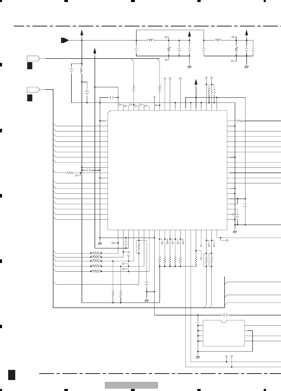
XV-DV363
64
1234
1 234
C
D
F
A
B
E
10.5 DVD MAIN ASSY (5/5)
HDMI
AUDIO
V+3
XO
PRDN
XDVDRST
INT0#
SDA
SCL
Y7
Y6
Y5
Y4
Y3
Y2
Y1
Y0
VCK
C4
C6
C5
C7
C3
C0
C2
C1
HSYNC
VSYNC
PUSEL
HDMISDA
HDMISCL
HSPDIF
HCLK
IC932
C940
R905
R904
R903
R902
R901
C942
R931
C987
R914
R915
C936
R937
R936
R938
R939
R940
C943
R945
R944
R943
R935
C945 C946
IC931
R911
R906
R934
R933
C944
C985
L937
C931
C935
C932
C933
C934
L931
C955
C953
C954
C956
L936
4
3
5
6
1
27
8
22
19
20
21
23
24
28
27
26
25
30
32
33
34
35
31
29
18
15
16
17
10
14
12
13
11
37
38
39
40
36
41
42
45
44
46
43
51
50
47
49
48
7
6
9
8
5
4
3
2
1
80 7879 77 76 75 7374 68 6769707172
52
53
54
55
57
56
58
59
60
66 65 63 6264 61
GNDD
STBY
STBY
00.1
10k
1k
0.1
GNDD
STBY
STBY
STBY
STBY
STBY
STBY
GNDD
0.1
STBY
STBY
STBY
STBY
STBY
STBY
STBY
STBY
MT1392E/C-L
5600p
GNDD
0.1
1000p
0.1
(F)
510
560
0.1
0.1
ATL7010
V+3
10
GNDD
10
V+3R3HD
V+1R8
0.1
47/35
0.1
1000p
ATL7010
V+3R3HD
GNDD
0.1
47/35
0.1
1000p
ATL7010
V+3R3TX
B5/5
B
1/5,2/5,3/5
B
1/5
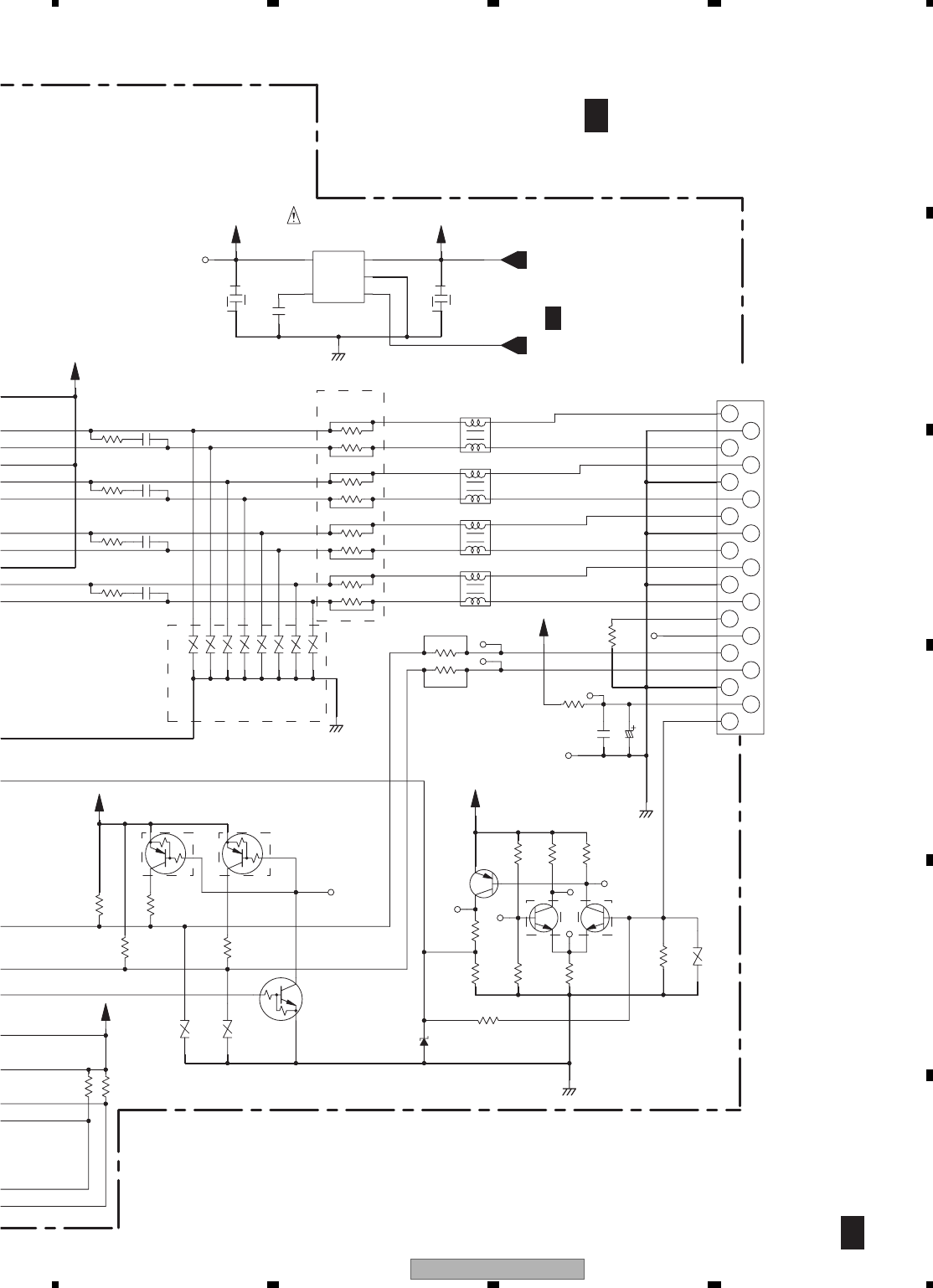
XV-DV363 65
5678
5678
C
D
F
A
B
E
DVDPOWER
V+6R8
R942
R941
VA901
VA902
D933
R970
R961
R959
R960
Q934
R962
Q933
R967
R968
R971
Q935
Q936
R963
Q934
VA931
R950 C950
VA935
VA938
VA933
VA936
VA934
VA932
VA937
R975
R974
R958
R957
R956
L935
R949 C949
R948 C948
C947R947
R955
R954
R953 L933
L934
R952
R951 L932
C982
C984
C983
R969
R966
VA903
Q935
R964
R965 C951
C952
R973
R972
JA931(PCB:CN931)
IC981
41
32
41
32
14
32
4
32
1
19
18
15
16
13
14
17
10
9
11
12
6
5
4
8
7
3
2
1
4
51
2
3
V+3
STBY
STBY
STBY
STBY
UDZS5R1(B)
RT1N144M
1k
GNDD
4.7k
4.7k
2.7k
V+5HD
(UMB1N)
RT3P22M
2.7k
STBY
STBY
STBY
STBY
STBY
STBY
RT3P22M
(UMB1N)
V+5HD
STBY
STBY STBY
STBY STBY
GNDD
STBY
STBY
ATH7022
V+5HD
ATH7022
STBY STBY
STBYSTBY
V+3R3TX
ATH7022
ATH7022
2.2
0.1
GNDD
STBY
STBY
47k
STBY
STBY
STBY
GNDD
0.1
10/50
0
STBY
AKP7210
NJM2872BF05
1
V+5HD V+6R8
STBY
HDMI
Terminal
Output
HDMI
B5/5
B5/5
DVD MAIN ASSY
(XWM3341:WYXJ5)
(XWM3342:WXJ/RE5)
B
2/5,4/5

XV-DV363
66
1234
1 234
C
D
F
A
B
E
10.6 DAMP ASSY (1/2)
LINE_OUT_L
LINE_OUT_R
LINE_IN_L
LINE_IN_R
XSD
XOTW
PCON
+
-
+
-
XRST
SCL
TAS5508
SDA
LRCLK
SCLK
SDATA4
SDATA2
SDATA1
SDATA3
XRST
SCL
SDA
SROUT
PLCCONT
SDATA4
LRCLK
SCLK
SDATA2
SDATA1
SDATA3
SROUT
PLCCONT
XMUTE
SDA
SCL
XPDN
XMUTE
XHPSEL
PWM_M_6
PWM_HPPR
PWM_HPML
PWM_P_6
PWM_HPMR
PWM_HPPL
MCLK
PWM_P_5
PWM_M_5
XPDN
XRST
XHPSEL
AND
STBY
STBY
PCB Binder : VEF1040
R3181
C3182
IC3182
C3181
R3182
IC3181
C3113
C3111
C3110
C3114
R3106
X3101
R3107
C3112
R3108
CN3171
C5981
C5983
C5982
C5984
JA5981
R5982
R5981
CN3102
R3155
R3154
R3105
R3104
C3109
C3108
C3107
R3113
C3106
R3103
C3105
C3104
C3103
R3102
R3101
C3102
C3101
IC3101
R3112
C3120
C3119
R3908
R3912
C3908
C3904 C3902
C3912
R3924
IC3901
C3906
R3910
R3906
R3907
R3914
R3916
R3913
R3915
R3153
CN3101
C3152
C3151
R3151
R3152
C3922
C3924
R3911
C3921
C3923
C3907
C3903
C3911
C3901
R3923
R3921
IC3901
C3905
R3905
R3909
R3901
2
43
15
34
1
2
5
3
5
4
1
2
1
3
2
1
2
4
6
5
3
12
11
10
9
8
7
15
16
13
14
17
18
19
2
3
1
6
10
9
5
4
8
7
16
15
14
13
12
10
11
17 18 2019 21 23 2422 272625 28 29 30
33
31 32
35
34
36
37
9
8
7
643
41
40
42
39
38
5
4
2
1
3
6364 6062 61 59 58 57
45
44
48
46
47
5456 55 53 52 51 50 49
5
4
7
86
15
16
13
14
11
12
19
17
18
3
4
1
82
RESET CONTROL CIRCUIT
5V
RST
GNDD
SCL
SDA
PLC_CONT
SR OUT
RECMUTE
S_TVOUT_R
S_TVOUT_L
GND
GND
SDATA4
LIN1_R
LIN1_L
GND
GND
GND
LRCLK
SCLK
SDATA2
MCLK
GND
SDATA3
SDATA1
GND
XSD
POWER
PLC_CONT
SROUT
GND
XOTW
SCL
SDA
GND
XMUTE
DVS S
XTL_IN
RESERVED
XTL_OUT
RESERVED
SDA
RESERVED
/MUTE
DVD D
/PDN
/HP_SEL
OSC_CAP
VR_DPLL
SCLK
LCRCK
SCL
SDIN3
SDIN4
VR_DIG
DVS S
DVS S
NC
SDIN1
SIND2
/BKND_ERR
DVD D
/RESET
VBGAP
AVDD_PLL
AVSS_PLL
RESERVED
PWM_HPPL
PWM_HPMR
PWM_HPPR
VRD_PLL
AVS S
AVS S
MCLK
DVS S
VALID
PWM_M_1
PWM_P_1
PWM_M_2
PWM_P_2
PWM_M_3
PWM_P_8
PWM_M_8
PWM_P_7
PWM_M_7
PLL_FLTP
PLL_FLTM
PWM_M_6
PWM_P_6
PWM_HPML
VRA_PLL
PLL_FLT_RET
DVDD_PWM
PWM_P_5
PWM_M_5
DVSS_PWM
PWM_P_3
PWM_M_4
PWM_P_4
VR_PWM
(NJM4565M)
(2/2)
XPDN
XRST
3.3V
GND
GND
HPR
HPL
XHPSEL
PCON
(1/2) (NJM4565M)
GNDD
4.7K
0.1/16
T-TPS3825-33DBVR
0
0.1/16
SN74AHC1G04DBV
V+3R3
GNDD
GNDD
18p/50
10/10
0.1/16
STBY
1M
15p/50
13.5MHZ
ASS7062
47
0.1/16
47
B5B-PH-K-S
V+5V
GNDD
0
STBY
STBY
STBY
STBY
GNDD
RKN1004 STBY
AKM7077-
STBY
STBY
V+3R3 220
GNDD GNDA
3.3
10/10
1000p/50
4.7
0.1/16
0.1/16
0.1/16
0.01/50
V+3R3
0.1/16
220
220
0.01/50
0.22/16
TAS5508BPAG
47
10/10
0.1/16
18k
5.6k
680p/50
560p/50
680p/50
STBY
180p/50
10k
18k
NJM4565MD
5.6k
18k 5.6k
4.7k
4.7k
4.7k
4.7k
4.7k
STBY
AKM7077-
STBY
0.1/16
10k
2.2k
V+3R3
10/16
0.1/16
10/25
0.1/25
560p/50
680p/50
STBY
680p/50
10k
8.2
180p/50
5.6k
NJM4565MD
V+BSW
18k
TO DVD MAIN ASSY (3/5)
TO DVD MAIN ASSY (3/5)
C1/2
3/5
CN 3002
3/5
CN 3001
B B
(AD)
(AD)
(AD)
(AD)
(AD)
(AD)
(AD)
(AD)
(AD)
(AD)
(AD)
(AD)
PWM MODULATOR
HP AMP
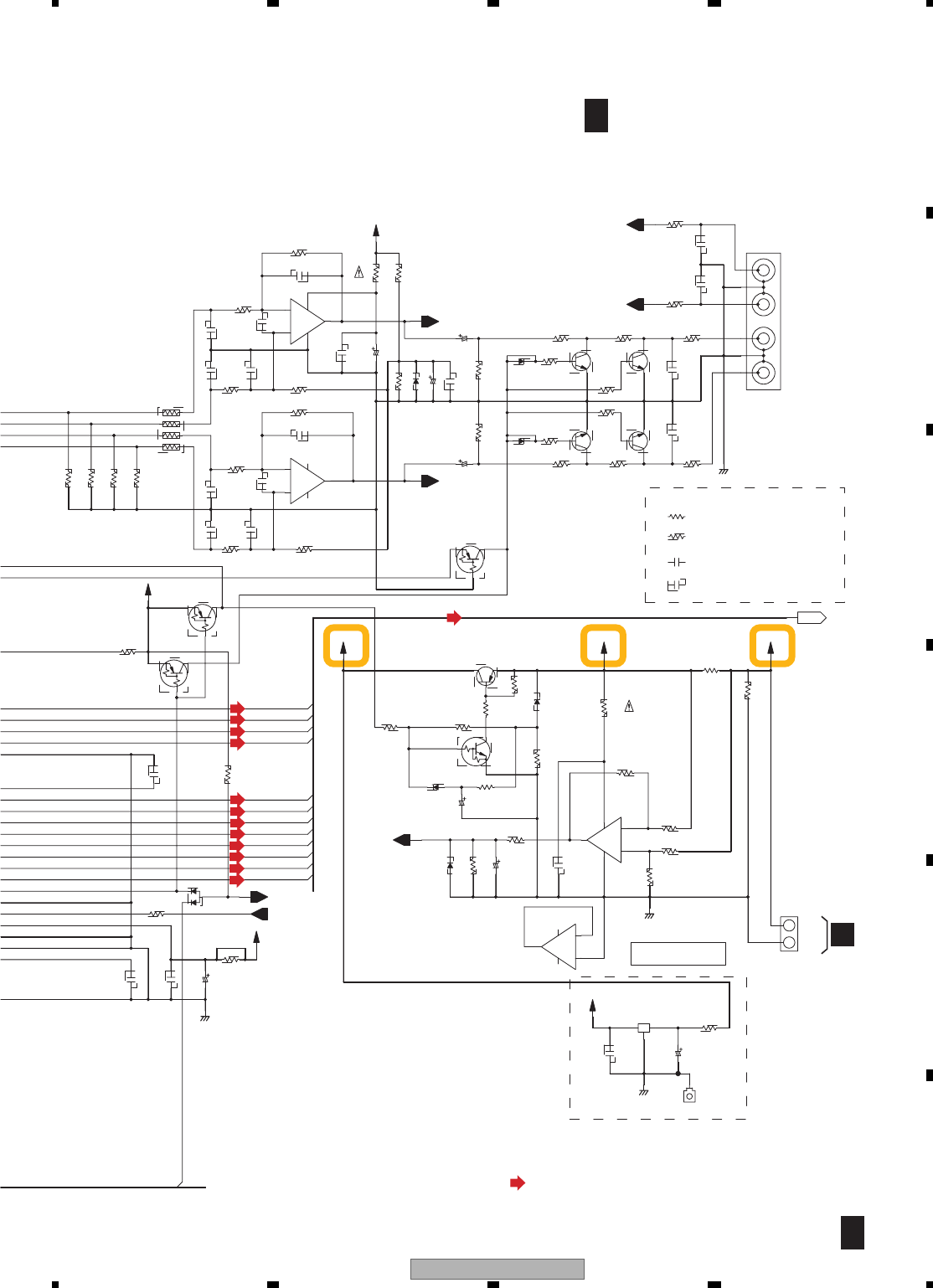
XV-DV363 67
5678
5678
C
D
F
A
B
E
XSD
VALID
PCON
LINE_OUT_R
LINE_OUT_L LINE_IN_R
LINE_IN_L
OUT
COM
IN
+
-
+
+
-
+
-
-
XPDN
PWM_P_2
PWM_M_1
PWM_M_2
PWM_P_1
PWM_M_4
PWM_M_3
PWM_P_4
PWM_P_3
PWM_P_8
PWM_M_8
PWM_P_7
PWM_M_7
PWM
STBY
Power Supply
1608 size CCSR**
CKSR**
2125 size CKSQ**
capacitor
2125 size RS1/10S***
3216 size RS1/8S***
1608 size RS1/16S***
resistor
AKB7114
CN3111
AUDIO IN/OUT
C3115
C3117
C3116
C3172
C3171
IC3171
R3171
R3110 D3101
R3114
C3118
R3109
D3191
R3197
C3191
D3132
C3131
R3196
R3137
R3134
Q3604
R3111
Q3901
Q3132
R3136
R3133
R3132
D3131
R3131
Q3131
R3608 R3612
R3626
R3627
R3625
C3604 C3602
R3628
R3601
C3601C3603
C3608 C3614
Q3602
R3606
IC3601
C3606
R3607
R3610
D3603
R3624
C3622
C3610
R3614
D3602
C3624
C3607
R3611
C3613
C3623
C3621
R3613
D3601
C3609
IC3191
R3195
C3192
R3193
CN3201
IC3191
R3192
R3199
R3194
R3198
R3191
R3616
Q3601
R3630
R3618
R3632
R3620
C3612
Q3603
Q3601
R3631
R3617
R3615 R3629
C3611
Q3603
R3619
IC3601
R3605
R3609
C3605
R3621
R3623
R3142
C3142 C3141
R3141
23
1
E
B
B
C
E
E
C
B
C
B
E
CC
E
B
54
6
7
8
3
1
4
1
8
3
4
22
1
7
45
6
8
B2
C2
E2
E
B
C
2
4
5
28
3
6
1
GND_CHASSIS
VNF1084-
KN3101
(DAP202U)
(DTC143EUA)
(DTA124EUA)
(DTA124EUA)
(2/2)
(NJM4565M)
GND
+B
LINEOUT_L
LINEOUT_R
(NJM4565M)
(1/2) TVIN_L
TVIN_R
GNDD
0.47/10
10/10
0.1/16
0.1/16
GNDD
10/25
NJM78L05UA
V+5V
330
STBY
MC2846-11
0.1/16
STBY
V+3R3
UDZS4.7(B)
10K
STBY
2.2k
10k
STBY
STBY
STBY
RT1P241M
22
V+3R3
STBY
820p/50
STBY
RT1N431M
1k
12k
47k
V+BSW
2SA1036K(QR)
4.7k 10K
330p/50
STBY
STBY
820p/50
STBY
STBY
4.7k
820p/50
820p/50
STBY
RT1P241M
10/16
4.7k
NJM4565MD
330p/50
4.7k
10K
10K
UDZS12(B)
STBY
STBY
0.1/16
10/16
47k
330p/50
4.7k
STBY
0.1/25
10/25
47k
STBY
10/16
BA10358F GNDD
B2P-VH
0.1/25
10K
100k
2.2k
100k
BA10358F
10K
8.2
UDZS18(B)
ACN7112
STBY
V+B
0.1(2W)
V+25
8201k 220
GNDD
4.7k
(2/2)
IMX9
4.7k
4.7k
820p/50
(1/2)
IMX9
4.7k
(2/2)
IMX9
1k 820
820p/50
(1/2)
IMX9
220
NJM4565MD
10K
330p/50
8.2
2.2k
V+BSW
330
220p/50 220p/50
330
FROM POWER SUPPLY UNIT
C1/2
C1/2
DAMP ASSY
(XWK3318)
CN2
J
: AUDIO DATA SIGNAL ROUTE
(AD)
(AD)
(AD)
(AD)
(AD)
(AD)
(AD)
(AD)
(AD)
(AD)
(AD)
(AD)
(AD)
(AD)
XV-DV363
68
1234
1 234
C
D
F
A
B
E
10.7 DAMP ASSY (2/2)
PWM_P_2
PWM_M_2
PWM_M_4
PWM_P_4
PWM_P_1
PWM_M_1
PWM_M_3
PWM_P_3
XOTW
XSD
VALID
XOTW
XSD
VALID
PWM
28 29
21
26
27
23
22
25
24
16
17
19
20
15
18
12
9
10
8
14
13
11
7
6
5
4
3
2
1
28
27
26
25
23
24
22
21
20
19
13
18
14
15
12
16
17
32
31
30
34
33
36
35
32
38
37
40
39
42
41
14
44
43
45
47
46
48
49 4
2
1
3
51
50
53
52
55
54
56
29
30
31
32
33
34
36
35
38
37
3
4
2
1
39
40
42
43
41
44
45
10
11
8
9
6
7
5
4
3
2
1
46
47
49
48
51
50
4
2
1
3
53
52
55
54
56
C3301
R3323
R3325
C3321
C3323
C3325
R3327
C3331
C3333
R3335
C3345
R3331
C3337
R3302
R3303
R3301
C3303
R3304
R3305
R3309
R3308
R3306
C3304
R3307
C3302
IC3301
R3201
C3201
R3202
R3203
R3204
C3203
R3205
R3209
R3315
C3311 R3311
C3341
R3341
C3327
C3315
C3335
R3343
C3343
R3313
C3313
R3317
C3317
L3301
R3316
C3342
R3312
C3312
R3342
R3344
C3316
C3334
R3333
C3339 R3337
C3347 C3346
R3332
R3336
C3344
C3314 R3314
R3318
C3318
C3328
C3332
L3302
R3324
R3326
R3328
C3326
C3324
C3336
R3225
R3223
C3221
C3223
C3225
C3338
R3334
C3340 R3338
C3348
R3215
R3227
C3227
C3231
C3233
C3211 R3211
C3241
R3241
R3243
C3215
C3235
C3243
R3213
C3213
R3216
R3217
C3217 C3216
L3201
R3235
C3245
R3231
C3237
R3233
C3239 R3237
C3247
C3204
R3208 R3207
R3206
C3202
IC3201
C3242
C3212 R3212
R3242
R3244
C3244
C3218
C3234
L3202
C3232
C3214
R3218
R3214
C3228
R3228
C3226
C3236
R3224
R3226
C3224
C3246
R3232
R3236 C3238 C3240
R3234
R3238
C3248
FL/RL
Amplifier
L3353
L3351
Amplifier
FR/RR
L3352
L3354 L3251
L3253
L3254
L3252
GNDD
YB
1/16
V+BSW
820
820
1000/25
YB
0.01/50
1000p/50
YB
3.3
V+B
CFTLA474J50
YB
0.1/25
1
STBY
4.7K
0.01/50
STBY
STBY
STBY
0.1/16
220
10K
STBY
YB
4.7K
100
YB
0.1/16
47K
1/16
YB
TAS5122DCA
GNDD
STBY
YB
V+BSW
1/16
STBY
STBY
220
0.1/16
10K
STBY
YB
0.1/50
330p/50
YB
YB
1.5
0.033/50
0.1/25
2.7
YB
YB
18
0.47/50
ATH7019
YB
330p/50
YB
0.1/50
18
0.033/50
2.7
YB
1.5
YB
10
YB
0.1/50
330p/50
YB
YB
2.7
1.5
0.033/50
YB
18
18 10
ATH7019
YB
4.7K
0.01/50
0.1/25
1
YB
STBY
0.1/25
STBY
1
330p/50
YB
0.1/50 2.7
0.033/50
0.1/25
YB
YB
1.5
CFTLA474J50
YB
0.47/50
820
820
3.3
1000p/50
YB
YB
0.01/50
YB
820
820
V+BSW V+B
0.01/50
1000/25
YB
1000p/50
4.7K
0.01/50 0.01/50
YB
4.7K
0.1/25
YB 1
STBY
0.1/50
YB
3.3
V+B
2.7
1.5
0.033/50
0.1/25
CFTLA474J50
YB
330p/50
YB
YB
YB
330p/50 0.1/50
YB
YB
18
18
0.033/50
10
ATH7019
0.47/50
YB
YB
YB
0.1/50
2.7
YB
1.5
1.5
2.7
0.033/50
0.1/25
1
STBY
4.7K
0.01/50
YB
4.7K
0.01/50
0.1/25
YB 1
STBY
0.1/16
47K4.7K
100
YB
1/16
YB
TAS5122DCA
330p/50
YB
YB
330p/50
YB
0.1/50
YB
18
18
2.7
0.033/50
0.1/25
CFTLA474J50
YB
ATH7019
10
YB
YB
1.5
3.3
1000p/50
0.47/50
YB
820
V+BSW
820
V+B
0.01/50
YB
YB
STBY
4.7K
0.1/25
10.01/50 0.01/50
YB
4.7K
0.1/25
YB 1
STBY
GND
GVDD
GND
GND
R3211 - R3214,R3311 - R3314,R3411 - R3414 : ACN7148-(2.7 Ω)(SUB:ACN7141-(2.7 Ω)) (2W)
NOTICE
BST_D
GND
/OTW
/SD_CD
/SD_AB
PVDD_D
GREG
DP
PVDD_D
OUT_D
DM
OUT_D
PVDD_C
M1
GND
M2
OUT_C
OUT_C
PVDD_C
CP
DREG_RTN
M3
/RESET_CD
CM
BST_B
BST_C
PVDD_B
BM
/RESET_AB
AM
DREG
BP
AP
OUT_B
GND
GND
OUT_B
PVDD_B
GND
DGND OUT_A
OUT_A
DVD D
GND PVDD_A
PVDD_A
GND
GND
GREG
GVDD
GND
BST_A
GVDD
GND
BST_D
PVDD_D/OTW
GREG
GND
GND
GND
GND
CM
/RESET_CD
DM
DP
/SD_AB
OUT_D
OUT_D
/SD_CD
OUT_C
PVDD_D
BP
DREG
M1
M2
M3
DREG_RTN
CP OUT_C
PVDD_C
PVDD_C
BST_C
BST_B
PVDD_B
PVDD_B
/RESET_AB
BM OUT_B
OUT_B
AP
AM GND
GND
DGND
GND
OUT_A
OUT_A
GREG
DVD D
GND
PVDD_A
BST_A
PVDD_A
GND
GND GVDD
GND
C2/2
DIGTAL
AMPLIFIER
(FR)
(FR)
(RL)
(FL)
(RL)
(FL)
(RR)
(RR)
1
2
12
1
2
12
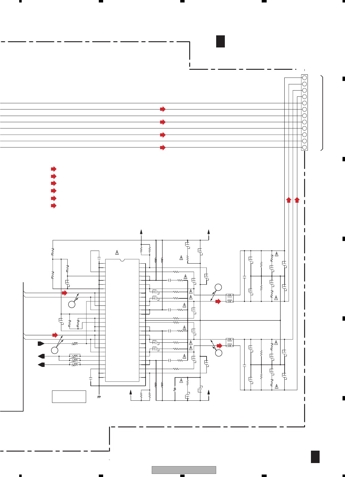
XV-DV363 69
5678
5678
C
D
F
A
B
E
PWM_M_7
PWM_P_7
PWM_M_8
PWM_P_8
XOTW
XSD
VALID
28 29
25
27
26
24
23
22
21
31
30
32
33
34
36
35
20
16
15
19
18
17
37
38
40
39
41
42
14
12
13
8
11
10
9
44
43
46
47
45
49
48
7
6
5
4
3
2
51
50
53
52
55
54
156
32
41
4
2
1
3
3
4
2
1
8
6
5
7
9
12
10
11
C3401
R3423
R3425
C3421
C3423
C3425
R3427
C3433
R3435
C3431
R3431
C3437
C3445
R3401
R3402
R3403
R3404
C3403
R3405
R3409
C3441
R3415
C3427
C3411 R3411
C3415
R3441
C3443
R3443
R3413
C3413
C3417
R3417
C3442
R3416
C3416
C3412 R3412
R3444
R3442
R3408
R3406
C3404
R3407
C3444
C3418
R3414
C3414
C3428
R3418
C3402
IC3401
R3426
R3424
R3428
C3426
C3424
R3433
C3439
C3435
R3437
C3447
L3401
R3432
R3436
C3434
C3446
L3402
C3432
C3438
R3434
C3440
C3436
R3438
C3448
CN3211
Amplifier
C/SW
L3351
L3353 L3352
L3354
FR+
RR-
RR+
FR-
RL+
RL-
FL+
FL-
C+
SW-
SW+
C-
GNDD
YB
1/16
820
820
V+BSW
YB
1000/25
0.01/50
YB
3.3
V+B
1000p/50
0.1/25
1
YB
CFTLA474J50
4.7K
0.01/50
STBY
STBY
STBY
STBY
220
0.1/16
10K
STBY
YB
330p/50
YB
0.1/50 1.5
0.033/50
YB 2.7
YB
18
YB
330p/50
18
0.033/50
0.1/50
YB 2.7
YB
1.5
330p/50
YB
YB
YB
0.1/50 1.5
2.7
0.033/50
YB
18
18
0.1/16
YB
4.7K
100
47K
330p/50
YB
0.1/50 2.7
0.033/50
YB
1.5
TAS5122DCA
YB
1/16
820
820
3.3 YB
0.01/50
YB
V+BSW
0.1/25
YB
ATH7019
YB
0.47/50
4.7K
0.01/50
0.1/25
YB 1
STBY
10
YB
10
ATH7019
0.1/25
1
STBY
0.1/25
YB
YB
CFTLA474J50
4.7K
0.01/50
YB
0.01/50
0.47/50
0.1/25
4.7K
YB
1000p/50
YB
1
STBY
V+B
AKE7121-
GND
GND GVDD
GND
/OTW
GREG
/SD_AB
/SD_CD
DM
DP
BST_D
PVDD_D
PVDD_D
OUT_D
GND
OUT_D
M2
CM
DREG_RTN
M3
CP
/RESET_CD
M1
GND
OUT_C
PVDD_C
OUT_C
PVDD_C
BST_C
BST_B
DREG
BP
/RESET_AB
BM
AP
AM
PVDD_B
PVDD_B
OUT_B
OUT_B
GND
GND
GND
GND
DVD D
GREG
GND
DGND
GND
OUT_A
OUT_A
PVDD_A
PVDD_A
GVDD
GND
BST_A
C2/2
C2/2
DAMP ASSY
(XWK3318)
6ch SP OUT
: AUDIO DATA SIGNAL ROUTE (Rear Lch)
(RL)
: AUDIO DATA SIGNAL ROUTE (Rear Rch)
(RR)
: AUDIO DATA SIGNAL ROUTE (Front Lch)
(FL)
: AUDIO DATA SIGNAL ROUTE (Front Rch)
(FR)
: AUDIO DATA SIGNAL ROUTE (Sub woofer ch)
(SW)
: AUDIO DATA SIGNAL ROUTE (Center ch)
(C)
(FR)
(RL)
(FL)
(RR)
(C)
(SW)
(C)
(SW)
(C)
(SW)
1
2
12
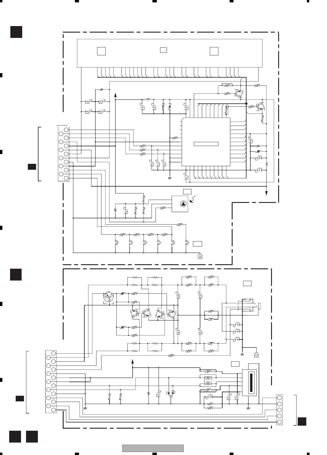
XV-DV363
70
1234
1 234
C
D
F
A
B
E
10.8 DISPLAY, USB, LED and KEY ASSYS
SG1
SG4
SG2
SG3
SG8
SG5
SG9
SG7
SG6
SG13
SG15
SG11
SG10
SG12
SG14
GR1
GR4
GR3
GR2
VEE
SG16
SG17
SG18
GR7
GR6
GR5
GR9
GR8
GR10
GR9
GR1
F-
GR4
GR3
GR2
GR5
GR6
GR8
GR9
GR7
SG17
GR10
SG18
SG16
SG15
SG14
SG13
SG11
SG10
SG12
SG7
SG9
SG8
SG5
SG6
SG3
SG4
SG1
SG2
FL
F+
Vout
GND
Vcc
F-
10G
5G
6G
7G
3G
4G
1G
2G
9G
8G
P18
P17
P16
P15
P14
P13
P7
P10
P12
P11
P8
P9
P6
P5
P3
P4
P2
P1
F+
SHLD
USB
LED
V+10
KEY1
GND
GND
D+
D-
KEY2A
+5V
(2/2)
VOL DOWNVOL UP
(1/2) (1/2) (2/2)
HP
FM/AM STOP /PAUSE
PLAY OPEN/CLOSE
KEY
SR
FL DRIVER
FL
R604
R605
R603
R602
C602
C601
D601
L602
L601
L603
C603
C604
C605
R5990 R5988
CN5907
KN5902
JA602
CN5906
R5972
R5974
D5972 R5978
R5976
D5971 R5975
Q5973
Q5971 R5977
R5973
R5971
S5963
S5962
R5962 R5963
R5953
C5952
C5951
R5903
R5902
CN5901
R5982
R5980
Q5973 Q5974 Q5974
R5984
R5986
C5972 C5974
L5972 C5979
C5978
L5973 C5977
R5989
R5981
R5979
C5971 C5973
R5985
R5983 R5987
L5971
JA5901
S5966
S5965
S5964
S5967
KN5903
R5964 R5965
R5966
R5952
R5954
R5951
IC5902
C5922
C5920
C5921
C5915
R5901
R5904 IC5901
R5910
C5916
L5902
C5917
D5902
C5918
C5919
R5908
C5906
C5904 C5903
C5905
C5907
V5901
C5911
C5912
C5913
L5901
C5914
D5901
Q5901
R5905
R5909
R5906
Q5902
R5907
GNDUSB
STBY
STBY
CK3380 68
220/6.3
UMZU6.2N
STBY
STBY
0.1
0.1
0.1
STBY
STBY
STBY
STBY
V5USB
68
68
68
GNDD
XKP3086
STBY
GNDD
CKS3370
STBY
68
STBY 2.2k
2.2k
STBY 2.2k
IMX9
RT1P241M 2.2k
68
VSG1024
VSG1024
1k
47/6.3
0.022
AL
CK3378
STBY STBY
68
IMX9 IMX9 IMX9
68 CTF1306
1000p 0.047/25
STBY
1000p 0.047/25
STBY
68
68 68
CTF1306
68
68 STBY
STBY
STBY
0.01/50
AKN7003-
VSG1024
VSG1024
VSG1024
STBY
VSG1024
1.2k 1.5k 1.8k
1k
STBY
STBY
100
47
GPIUM27XKOVF
VFDP
220p
220p
220p
GNDD
0.01/50
220
220
220
PT6315
82k
STBY
0.022/50
0.022/50
10 LAU100J
STBY
47/35
AL
STBY
STBY
STBY STBY
JQ
47/35 VE+5
0.022
0.022
AL
47/6.3
22
LAU220J
STBY
STBY
STBY
STBY
STBY
STBY
STBY
STBY
15
13
14
10
7
8
6
11
12
9
5
3
4
2
1
4
1
5
34
2
3
2
1
2
5
3
4
1
6
7
E2
C2
10
13
11
12
3
5
9
4
6
7
8
2
1
B2
B
EEB2
B
C
C
C2
E2
2
3
7
6
1
4
5
13 1412 171615 1918 21 2220
6
8
11
9
7
10
26
25
23
28
27
24
4
5
1
3
2
43 4244 394041
30
29
31
33
32
363738 3435
15876119141312 15 16 17 19 20 22 23 322724 26 3029 33 35 3837 39 40 45
KEY1
V+10
LED
GNDUSB
KEY2A
GNDUSB
V5USB
V5USB
USB_DM2
USB_DP2
HPMUTE
HP_L
GNDD
HP_R
HP_DET
GNDD
KEY1
KEY2
KEY2A
GNDD
VE+5
VFDP
FLDC+
FLDC-
REMOCON
FLCS
FLCK
FLDATA
VSS
VDD
VSS
VDD
VEE
AAV7104-
(AAV7107-)
AEB7367
FL SPACER FL SPACER
AEB7367
From DVD MAIN ASSY (2/5)
From DVD MAIN ASSY (2/5)
TO KEY ASSY
D E
D
DISPLAY
ASSY
(XWZ4256)
E
USB ASSY
(XWZ4259)
CN5602
2/5
B
B
CN5601
2/5
GCN5908

XV-DV363 71
5678
5678
C
D
F
A
B
E
LED
GND
KEY1
KEY2A LED
GND
V+10
V+10
BLUE LED
LAU***J-TA
ALL INDUCTORS ARE IN μH
RS1/10S***J
RS1/16S***J
ALL RESISTORS ARE IN Ω
AT : CEAT**M**
JQ : CEJQ**M**
AL : CEAL**M**
ALL CAPACITORS ARE IN μF
UNLESS OTHERWISE SPECIFIED
CKSRYB**K50
NOTES
CN5908
S5992
R5991 R5992
S5993
S5994
R5993
C5612
R5613
D5612
R5615
R5614
Q5611
C5611
D5611
S5991
CN5909 CN5603
R5611
R5612
CKS3370
VSG1024
2.7k 3.3k
VSG1024
VSG1024
VSG1024
5.6k
CKS3368
STBY
4.7k
CKS3368
GNDLED
DAN217
150
STBY
2SC4081 (QR)
NSPB320BS
0.1 470
470
VA+10
1
3
4
2
1
2
3
3
2
1B
E
C
5
PLAY
LIST1
PLAY
LIST2
PLAY
LIST3
POWER ON
FROM USB ASSY
GF
G
KEY ASSY
(XWZ4261)
F
LED ASSY
(XWZ4263)
ECN5907
XV-DV363
72
1234
1 234
C
D
F
A
B
E
10.9 MIC ASSY (XV-DV365K ONLY)
H
H
MIC ASSY
(XWM3375:WXJ/RE5)
+
-
2
3
1
34
2
1
8
2
3
1
5
6
4
7
C3921
C3926
R3923
R3922
C3922
JA3922
C3925
R3921
C3931
C3932
C3933
R3926
C3927
VR3921
IC3921
R3927
R3925
C3929 C3930
R3929
R3928
JA3921
C3928
RUSSIA
(SUB)
MIC AMP
(1/2)
(MAIN)
XV-DV363 73
5678
5678
C
D
F
A
B
E
H
CN3961
3/5
B
-
+
1
5
3
4
2
7
8
6
54
CN3921
C3935 C3936
C3938
R3930
C3934
R3931
C3937
IC3921
LAU***J-TA
ALL INDUCTORS ARE IN μH
RS1/10S***J
MIC SW
GNDA
NC
V+10V
MIC
(2/2)
ALL RESISTORS ARE IN Ω
RS1/16S***J
JQ : CEJQ**M**
AL : CEAL**M**
AT : CEAT**M**
UNLESS OTHERWISE SPECIFIED
CKSRYB**K50
ALL CAPACITORS ARE IN μF
NOTES
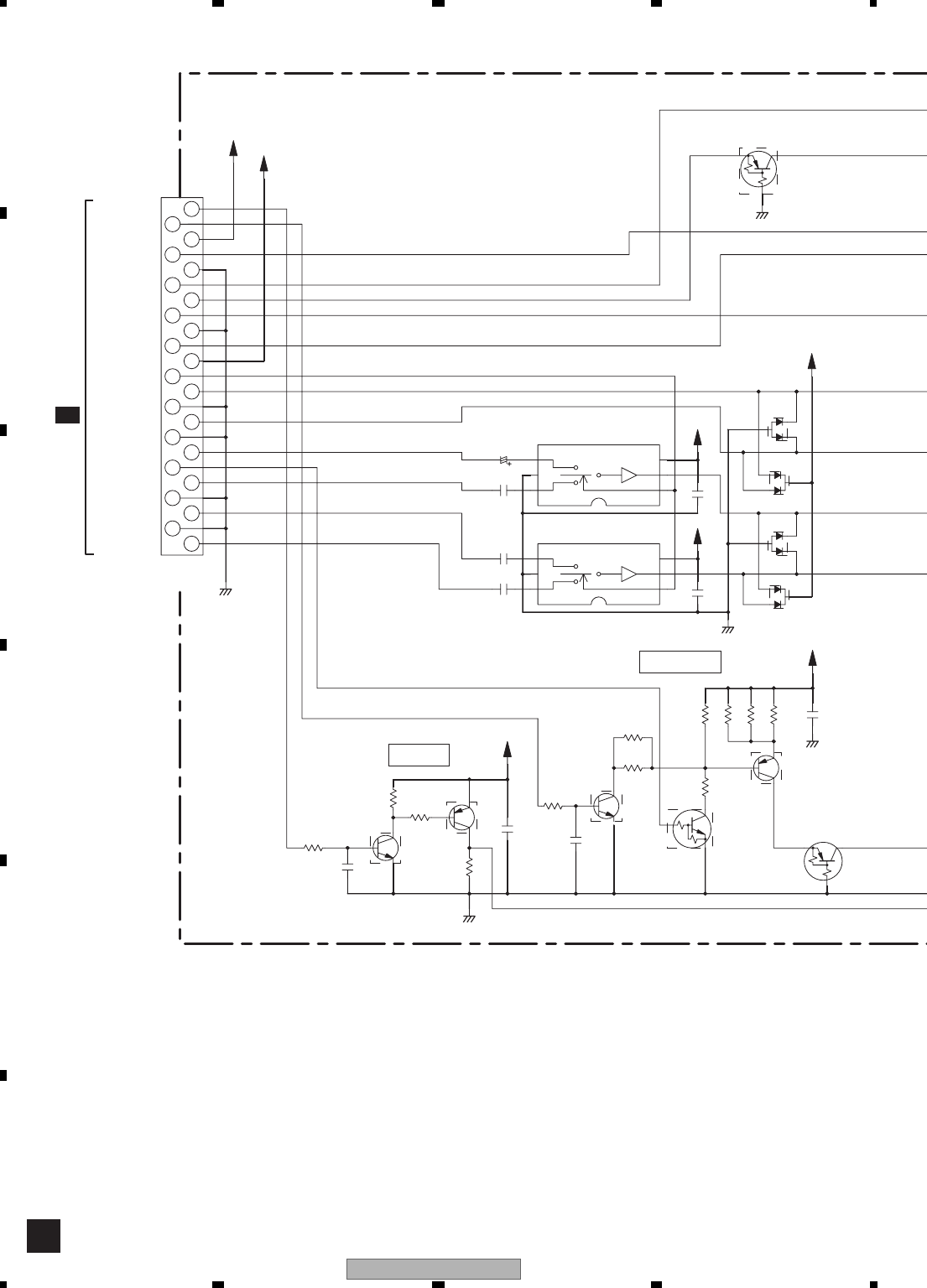
XV-DV363
74
1234
1 234
C
D
F
A
B
E
10.10 EUROSCART ASSY
(2/2)
(1/2)
S_Y
GND
R
S_C
GND
V
DVDPOWER
V+5
VSEL2
G
GND
B
GND
GND
TVOUT_L
TVMUTE
SCART_R
SCART_L
GND
(1/2) (2/2)
L
H
L
H
TVOUT_R
VSEL1
SQEEZE
V+10
R465
C469
R463 Q461
R461
R462
Q461
CN461
C465
Q472 Q463
C464
R464
Q462
R472
R471 Q462
R470
R466
R467
R468
R469
C470
C474
C476
D474
C473
IC472
C472
C475
D473
D472
C471
IC471
D471
Q492
E
B
CB2
20
18
22
19
23
21
17
14
12
16
13
11
15
10
8
6
9
7
5
E
B
C2
E2 B
EB
C
C
B2
E2
C2
C
E
6
5
4
1
3
2
6
5
4
1
3
2
1
2
3
4
4.7k
GNDD
STBY
RT3WLMM
56k
1.2k
RT3WLMM
22k
CKS3388
GNDD
STBY
RT1N241M RT1P441M
0.1
4.7k
RT3WLMM
22k
560 RT3WLMM
GNDD
V+5
820
10k
1.2k
1.2k
1k
0.1
0.1
GNDD
0.1
DAN202U
V+10
DAP202U
0.1 MM1507XN-TRB
0.1
V+5
0.1
DAN202U
10/50
MM1505XN-TRB
V+5
DAP202U
V+5
V+10
V+5
GNDD
RT1P241M
BLACK
SQUEEZE
CN451
4/5
B
I
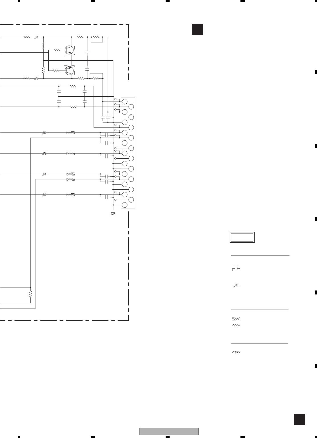
XV-DV363 75
5678
5678
C
D
F
A
B
E
LCYA***J2520
RS1/10S***J
RS1/16S***J
ALL INDUCTORS ARE IN μH
V/Y
GND
NC
V/Y
GND
R/C
SQUEEZE
B
G
BLANK
GND
GND
GND
BLANK
R/C
NC
G
L IN
GND
B
GND
NC
SQUEEZE
EURO CONNECTOR
L OUT
R IN
R OUT
GND
AT : CEAT**M**
ALL RESISTORS ARE IN Ω
AL : CEAL**M**
UNLESS OTHERWISE SPECIFIED
ALL CAPACITORS ARE IN μF
JQ : CEJQ**M**
CKSRYB**K50
NOTES
(2/2)
(1/2)
R473
R478
C492
C480
R477
C479
R476
C491
C490
C489
C478
R475
C477
R474
C488
C487
R495
C495
R496
C496
C493
C494
C486C485
R482
R481
C482
R484
R494
Q493
Q493
R488
JA451
C484
R486
C483
R483
R493
C481 R485 R487
21
20
18
19
17
16
14
15
13
12
11
10
9
8
7
6
5
4
3
1
2
C2
B2
E2
E
B
C
56k
75
1000/6.3
GNDD
47p
(F)
47p
75
470/6.3 75
75(F)
(F)
(F) 47p
47p
470/6.3
75(F)
470/6.3
0.1
47p
STBY
STBYSTBY
330
330
STBY
CH
100p
CH
100p
XKB3054-
1k
1k
10/50
4.7k
47k
IMX9
IMX9
STBY
470
330p
CH
330p
47k
4.7k
10/50
CH
STBY
470
I
I
EURO SCART ASSY
(AWU8291)
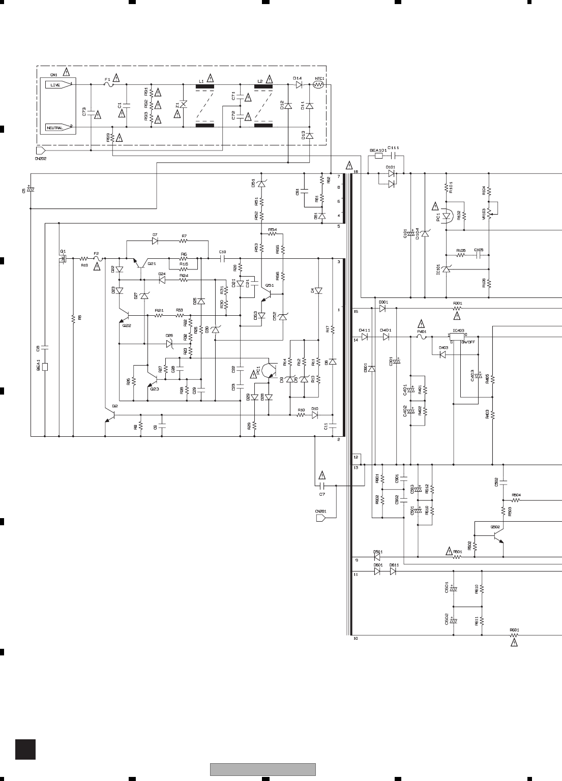
XV-DV363
76
1234
1 234
C
D
F
A
B
E
10.11 POWER SUPPLY UNIT
T1
AC
IN
J
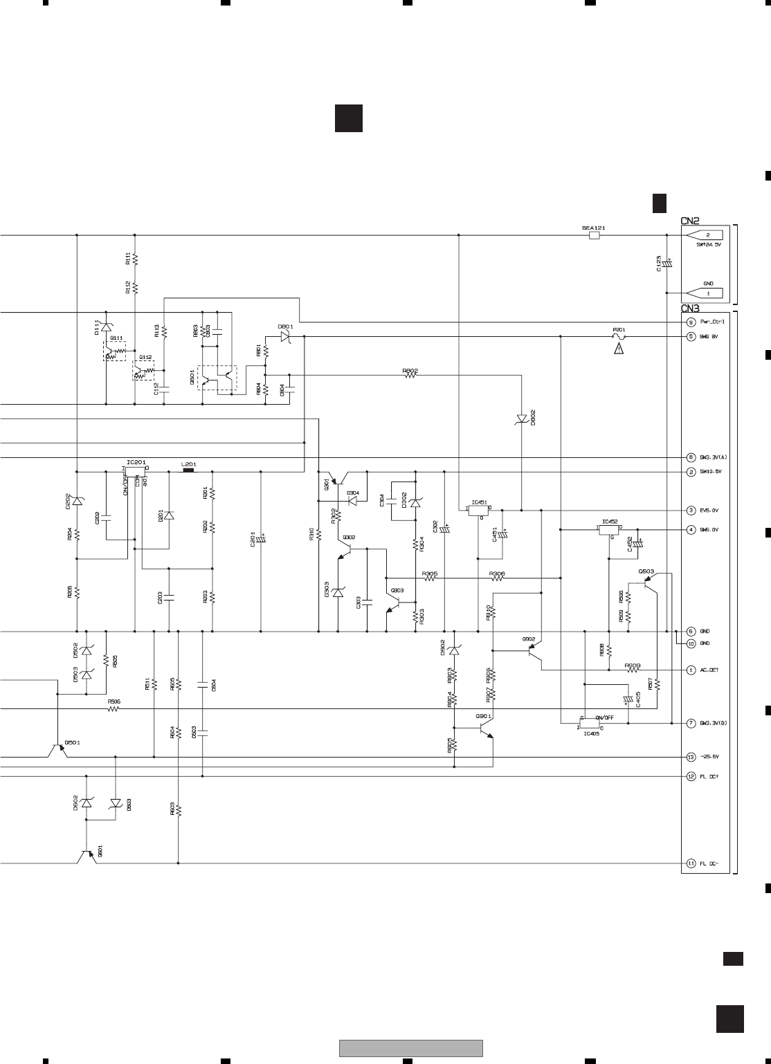
XV-DV363 77
5678
5678
C
D
F
A
B
E
CN1001
B2/5
CN3201
C1/2
POWER SUPPLY UNIT
(XWR3012)
J
J
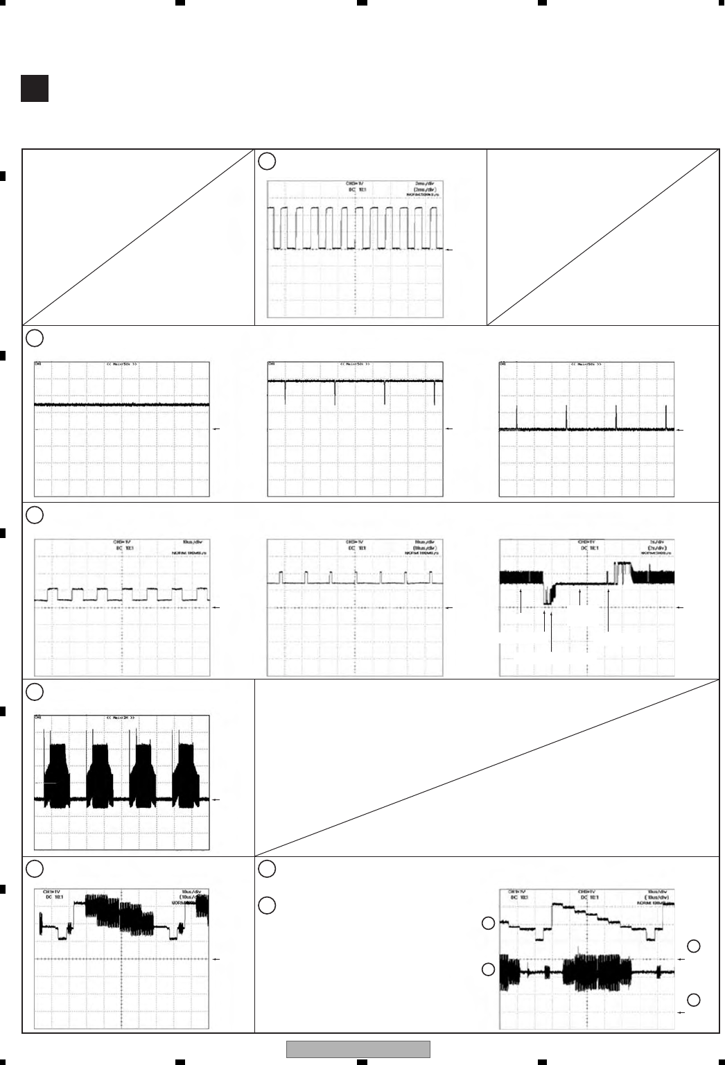
XV-DV363
78
1234
1 234
C
D
F
A
B
E
10.12 WAVEFORMS
DVD MAIN ASSY
B
2IC201-pin 39 [TROPENPWM]
V: 1V/div. H: 5μsec/div.
3IC201-pin37 [DMSO]
V: 1V/div. H: 10μsec/div. V: 1V/div. H: 10μsec/div. V: 1V/div. H: 2sec/div.
1IC201-pin50 [FG]
V: 1V/div. H: 2msec/div.
8IC401-pin23 [CompositeVideo Out]
V: 1V/div. H: 10μsec/div.
4CN102-pin 11, 10, 9 (IC101-pin 30, 33, 36)
[SPINDLE (WVU)]
V: 2V/div. H: 2msec/div.
GND
GND GND GND
GND
GND
GND
GND
GND
PLAY
Tray :
opening
Pless OPEN key Pless PLAY key
Braking a turn of disc
[Tray stops]
[TRAY OPEN] [DVD PLAY] [DMSO]
[Tray is opening] [Tray is closing]
9
9
10
9
10
IC401-pin21 [S VIDEO OUT - Y]
V: 1V/div. H: 10μsec/div.
10 IC401-pin26 [S VIDEO OUT - C]
V: 1V/div. H: 10μsec/div.
GND
GND
Note : The encircled numbers denote measuring point in the schematic diagram.
Measurement condition ;
No. 1 to 10 : reference A1 (DVD), T2-chp 19, Color-bar
No. 11 to 14 : reference A1 (DVD), T1
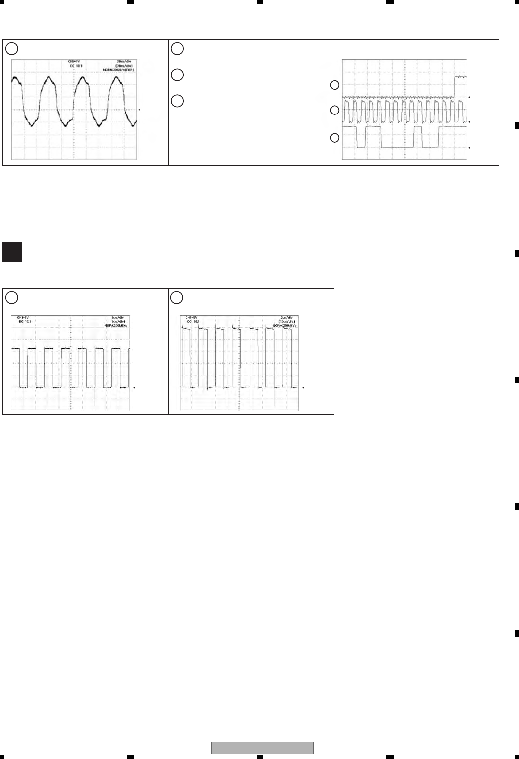
XV-DV363 79
5678
5678
C
D
F
A
B
E
11 IC201-pin212 [ACLK]
V: 1V/div. H: 20nsec/div. 12 IC201-pin209 [ALRCK]
V: 2V/div. H: 500nsec/div.
13 IC201-pin210 [ABCK]
V: 2V/div. H: 500nsec/div.
14 IC201-pin197 [ASDATA0]
V: 2V/div. H: 500sec/div.
1IC3201, IC3301, IC3401 [PWM_M, PWM_P]
V: 1V/div. H: 2μsec/div. 2IC3201, IC3301, IC3401 [OUT_A, B, C, D]
V: 5V/div. H: 2μsec/div.
DAMP ASSY
C
GND
GND GND
GND
GND
GND
12
13
14
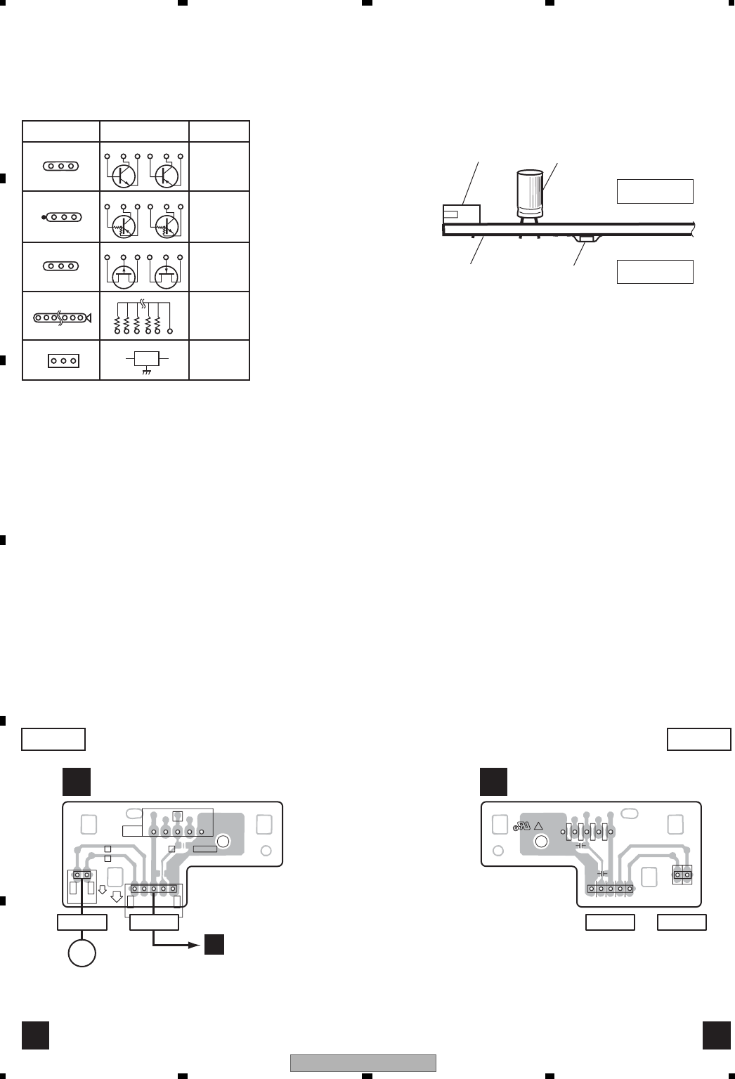
XV-DV363
80
1234
1 234
C
D
F
A
B
E
11. PCB CONNECTION DIAGRAM
11.1 LOAB ASSY
NOTE FOR PCB DIAGRAMS :
1. Part numbers in PCB diagrams match those in the schematic
diagrams.
2. A comparison between the main parts of PCB and schematic
diagrams is shown below.
3. The parts mounted on this PCB include all necessary parts for
several destinations.
For further information for respective destinations, be sure to
check with the schematic diagram.
4. View point of PCB diagrams.
Symbol In PCB
Diagrams
Symbol In Schematic
Diagrams Part Name
BCE
D
D
G
G
S
S
BCE
BCE
DGS
BCEBCE
BCE
Transistor
Transistor
with resistor
Field effect
transistor
Resistor array
3-terminal
regulator
Capacitor
Connector
P.C.Board Chip Part
SIDE A
SIDE B
15
51
SW2
(V+5D)
V+3D
LOAD-
LOAD+
GND
PNE-1B1
C102
C101
CN602
CN601
12
51
VWG2346-
VWG2279-
5
VWG
LOAB
5
1
VNP1836-C
CN602
S101
CN601
SIDE A SIDE B
LOAB ASSY
A
LOAB ASSY
A
CN104
B
(VNP1836-C) (VNP1836-C)
LOADING MOTOR
ASSY
M
CN601CN602 CN601 CN602
A A

XV-DV363 81
5678
5678
C
D
F
A
B
E
11.2 MIC ASSY (XV-DV365K ONLY)
10
20
30
40
50
60
70
80
010 20 30 40 50 60 70 80 90
X
Y
10
20
30
40
50
60
70
80
010 20 30 40 50 60 70 80 90
X
Y
1
5
C7
[[ G ]]
FCICT
C3929
VR3921
W104
C3935
C3931
CN3921
CN3921
JA3921
JA3922
C3937
W101
W109
C3925
W107
C3930
W105
W103
W106
IC3951
1
8
GNDA
MIC ASSY
XWM3375-
GNDA
1.GNDA
2.MIC
3.V+10V
4.ECHOCONT
5.MIC SW
PNE-1B1
R
PRODUCTION CODE
A
CONTACT SIDE
GNDA
1/5
V+10V
15
41
58
LF
R3921
R3926
C3927
R3922
C3936
R3930
C3934
R3927
R3928
R3931
C3922
R3923
C3926
C3933
R3925
C3921
C3928
R3929
C3932
C3938
IC3921
PNE-1B1
1.GNDA
2.MIC
3.V+10V
4.ECHOCONT
5.MIC SW
MIC ASSY
XWM3375-
R1/5
SIDE A
H
SIDE A
H
CN3961
B
CN3921CN3921
SIDE B SIDE B
MIC ASSY
H
MIC ASSY
H
(XNP3115-A)
(XNP3115-A)

XV-DV363
82
1234
1 234
C
D
F
A
B
E
11.3 DVD MAIN ASSY
0 10 20 30 40 50 60 70 80 90 100 110 120 130
0
10
20
30
40
50
60
70
80
90
100
110
120
X
Y
14
85
13
14
SIDE
OPEN
1
NP
NP
4
5
31
51
18
916
1
0123456789
0123
0
01
C
B
A
ICT FC1 FC2
LF
1
13
A30C5/C7
[[ G ]]
SIDE
CONTACT
1
12
1
4
CONTACT
SIDE
SIDE
CONTACT
24
23
1
2
13
54
14
85
124
25
48
54
28
127
64
128
65
129
SIDE
OPEN
14
44 23
122
3
45
1
SIDE
CONTACT
17
80 51
5031
301
10081
CN5601
C5603
C5601 C5602
KN5601
C5606
C5605
C5604 R5536
R5537
R5538
R5546
R5547
R5548
R5565
R5564
R5563
C5557
IC5502
C5558
R5558
CN1002
R5562
R5559
R5575
R5576
R5584
R5587
R5586
R5604
R5602
R5603
R5606
R5601 Q5601
D5601
R5605
C5589
R5590
Q5531
R5528
Q5532
R5530
Q5602
Q1201
Q1304
Q1303
R5534
R5533
R5532
R5531
R1307
R5541 R5542
R5543 R5545
R5566 R5570
R5577
C3961
X3004
R3063
R3062
R3066
R3065
C3962
R3085
R3083
C3963
C3964
C3965
C5504
C5521
C5522
C5578
R291
R292
R293R294
C3966
R3966
R767
R768
C3968
Q5533
R5544
IC5503
R5502
R5503
C5503
CN3961
D3961
D3962
IC3961
Q5534
R3967
R3968
R3969
R5500
C3967
R5571
R5585
R5595
R5600
Q1202
Q1302
R1306
D1201
C1301
C1204
Q5535
R5569
C5518
R5505
D802
R272
R220
CN5602
Q1402
D1403
D1416
D1417
C373
CN102
C309
CN103
CN104
C371
R325
CN101
C372
R375 R373
R372 R371
C344
C345
C346
C140
C310
R326
L308
L309
R374
R315
Q304
R314
R313
R318
Q307
R322
Q308
R321
R310
Q305
R282
C290
R224
IC204
IC203
C289
C224
C225
C226
R225
C231 R227
C285
R226
C286 C287
C232
R228
C288
C233
R229
C284
C234
C283
C282
IC202
C235
C281
C236
IC201
R201
R202
R205
R206
C209
C208
C211
C212
C210
R204
CN204
C202
C201
R223
C203
C204
C205
C206
R210
R219
R218
R233
R285
R284
C207
R234
R235
C213
C220
R207
R208
R236
C200
C215
R221
R237
C227
R211
C217
C296
C229
R281
R258
R259
R260
R261
R212
R213
R214
R154
C103
C153
C151
C121
C145
IC101
R152
R153
C152
R133
C146
R135
C144
C141 C142
C143
C161
R136
R134
C132
C102
R132
C104
R151
C131
R131
C101
R266
C133
C320
C374
C347
C250
C219
C230
R262
R263
R222
R
2
R265
R267
R271
C783
C781
C782
C771
L772
C772
IC771
R771
C773R772
C216
R769
R770
L761
IC781
D782
D781
KN103
C218
R215
R216
R953
VA932VA931
R958
R957
R951
VA936
R952
R955
R954
R956
VA935
VA938VA937VA933 VA934
C5524
C5508
C1501C1502
R5510
R5508
L1501
C1505
R5515
R5513
C5525
C5597
Q5525
R5514
R5516
CN5501
R5597
R5509
R1202
C1201
C1101
IC1101
C1102
R1101
C1103
R1201
R1204
C801
R801
R1301
R1415
C1413
R1401
R1402
R1403
R1404
Q1413
D1415
C1415
R1302
R1304
R1303
C3953C3954
L3951
L3952
C3952 C3951
R3951
R3952
R1305
L1305
R3954
R3953
D1501
R1001
C5519
R5519
Q3951
R3955
Q1301
R5557
R5596
C5555
X5501
R5517
R5507
C5502
R5521
R5581
R5583
R5506
R5582
R5512
C5569
C5501
C5509
C5539
R5598
KN5501
C5579
C5577
R5574
IC5501
R5501
C5517
R5518
R5522
R5525
R5527
R5535
1/2
PCB
BINDER
STEST
UTEST
15
1
B
-A
OPEN SIDE
C
D
E
F
HEATPROOF
PREFLUX
Production code
XWM
0
DVD MAIN ASSY
V+1R8
VE+5
V+3
V+6R8
V+5V
V+10
V+3R3
1
2
3
4
5
6
7
8
9
0
1
2
3
4
5
6
7
8
9
0
1
2
3
4
5
6
7
8
9
0
1
2
3
4
5
6
7
8
9
CN1001
15
[CN5603]
[CN5604]
VFDP FLDC+
FLDC-
D.
C.
B.
A.
D
C
A
B
SW3.3B
SW6.8V
SW10.5V
EV5.0V
B1
SW5.0V
SIDE A
B
DVD MAIN ASSY
B
SPINDLE
MOTOR STEPPING
MOTOR
06SD
PICKUP
ASSY CN5906
E
CN3
J
CN3921
XV-DV365K ON
L
H
CN102 CN101 CN103
CN104CN5602
CN5601 CN1001 CN3961
CN601
A
CN5901
D
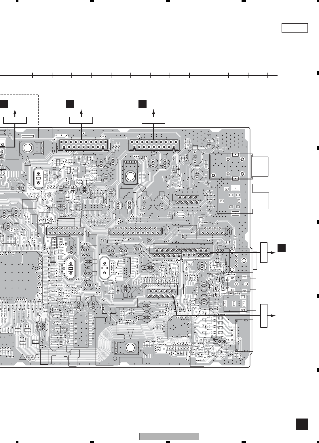
XV-DV363 83
5678
5678
C
D
F
A
B
E
110
120
130
140
150
160
170
180
190
200
210
220
230
240
SIDE
OPEN
1
1
13
1
9
1
19
1
SIDECONTACT
9
CONTACT SIDE
1
23
916
18
18
916
CONTACT
SIDE
11
1
16
1
9
8
18
916
8
1
5
4
119119
NP
NP
8
14
5
54
31
4
5
13
R
14
1
28 15
28
27
1
193
192
256
120
21 40
41 60
61 80
4
1
85
NP
NP
119
45
31
JA5931
L5934
L5933
L5932
L5931D5931
R5931
R5940
D5933R5933
R5942
Q5935
R5935
R5934
R5938
Q5931
R5937
Q5934
R5939
R5936
R5943
CN5532 CN5533
CN5531
C4612
C4613
L4603
C4614
C4615
R4609
R4610
JA4602
C405
C404
C413
C411
C403
C415
C414
C412
C416
C402
C401
C406
R402
JA401
JA402
C426
C421
C425
C424
L421
C430
C431
L422
C429
R426
R421
R425
R424
C427
C428
R423
R422
C422
C423
Q491
C447
R431
R411
Q428
R428
R412
C449
C451
R413
R414
C453
C455
R415
C457
R416
CN401
R432
R433
R434
R435
R436
JA403
R405
R9401
R9402
C3027
CN451
R491
IC3001
C3025
C3026
R3021
R3022
C3002
C3001
IC3003
C3048
R3048
C3044
C3042
C3041
C3046
C3043
CN5701
Q5936
IC5701
R5703 R5706
R5705
C5714
C5720
C5707
C5703
C5702
X5701
C5704
C5706
C5716 R5710
C5712
C5715
R5704
C5701 C5705
C5719
C5713
C3011
C3012
R3013
R3014
R3018
R3017
R3055
C3052
C3057C3056
X3004
R3056
R3052
R3053
R3054
R3049
C3028
C3029
IC3005
C3064
R3061
R3063
R3062
R3066
R3065
C3023
C3021
IC3004
R3046
R5717
R5716
R5715
R5714
R5719
R5712
R5713
R5718
Q5701
R3045
R3064
R3020
C3019
R3019
C3020
R5701
R5702
R3001
R3002
C5708 R5707
R3023 R3024
R3012
R3011
R3015
R3016 C3015
C3016
R3025
C3024
R3007
R3041
CN3001 CN3002
R3026
Q3006
R3006
C3003
C3004
Q5703
C5709
R3073
R3081
R3082
R5708
Q3005
R3009
R3039
R3040
R3010
C3022
KN3001
R3057
R3058
R3085
R3083 R3084
R3903
R3906
R3905
R3902
C3907
C3909
R3908
C3905
JA3901
C3901
C3906
R3059
R3060
R3090
IC3901
C3908
R3907
C3903
C3902
C3910
C3904
C3911
D3901
D3902
D3903
IC3002
L3901
R257
R3027
R3028
R3910
R3911
R3913
R3914
R3915
R914
R915
VA901
VA902
VA903
Q5932
R240
R247
Q5942
R5944
R5945
R5948
R5949
D5941
D5942
Q5941
R249
R268
R3003
Q1202
C
12
0
4
R5946
R5947
R269
C270
IC205
IC401
R401
R406
C5936
C5931
C5932
D5936
C343
C344
C345
C346
C228
C222
C231
C232
R228
C233
R229
C234
C283
0
2
C235
C236
IC201
C240
C239
C252
X201
C251
R251
R252
C254
R254
C258
C256
C255
R253
C261
C260
C259
C264
C265
C266
C267
R255
C268
C269
C271
C272
R256
C273
C202
C237
C204
C205
C206
R241 R242
R243
R244
R245
R246
R248
C207
R279
C213
R209
R207
C244
C245
C246
C215
R266
C347
C250
R264
R265
R267
R271
C243
R250
C262
C223
KN202
C238
C241
C242
C247
C248
R230
IC931
C931
C943
C942
R931
C945
C946
R933
R934
L931
C933
C934
R935
R936
R937
R938
R940
R939
C932
C944
R942 R941
IC932
C940
R947
C947
Q935
R948
C948
R961
R959 R960
R962
R967
C950
R950
C949
R949
Q934
L934
Q933
R964
R965 R969
R966
R968
R963
R971
Q936
L932
L933
L935
CN931
D933
R970
R972
R973
C952
C951
C935
C954
C953
L936
C955
R911
R906
R901
R902
R903
R904
R905
IC981
C982
C983
C984
L937C985
C987
C956
R974
R975
R944
R943
R945
C936
C1101
IC1101
C1102
C1103
L1305
KN1001
C3045
B
C
C
A
A
AB
E
CONTACT SIDE
(for FJ)
(for FJ)
(for FFC)
CN452
SW10.5V
CONTACT SIDE
(for FFC)
CN3003
CN3004
SIDE A
B
(XNP3111-A)
CN3921
V
-DV365K ONLY
H
CN3101
C
CN3102
C
CN461
I
FM/AM
TUNER
UNIT
CN451
CN3961 CN3001 CN3002
CN5701
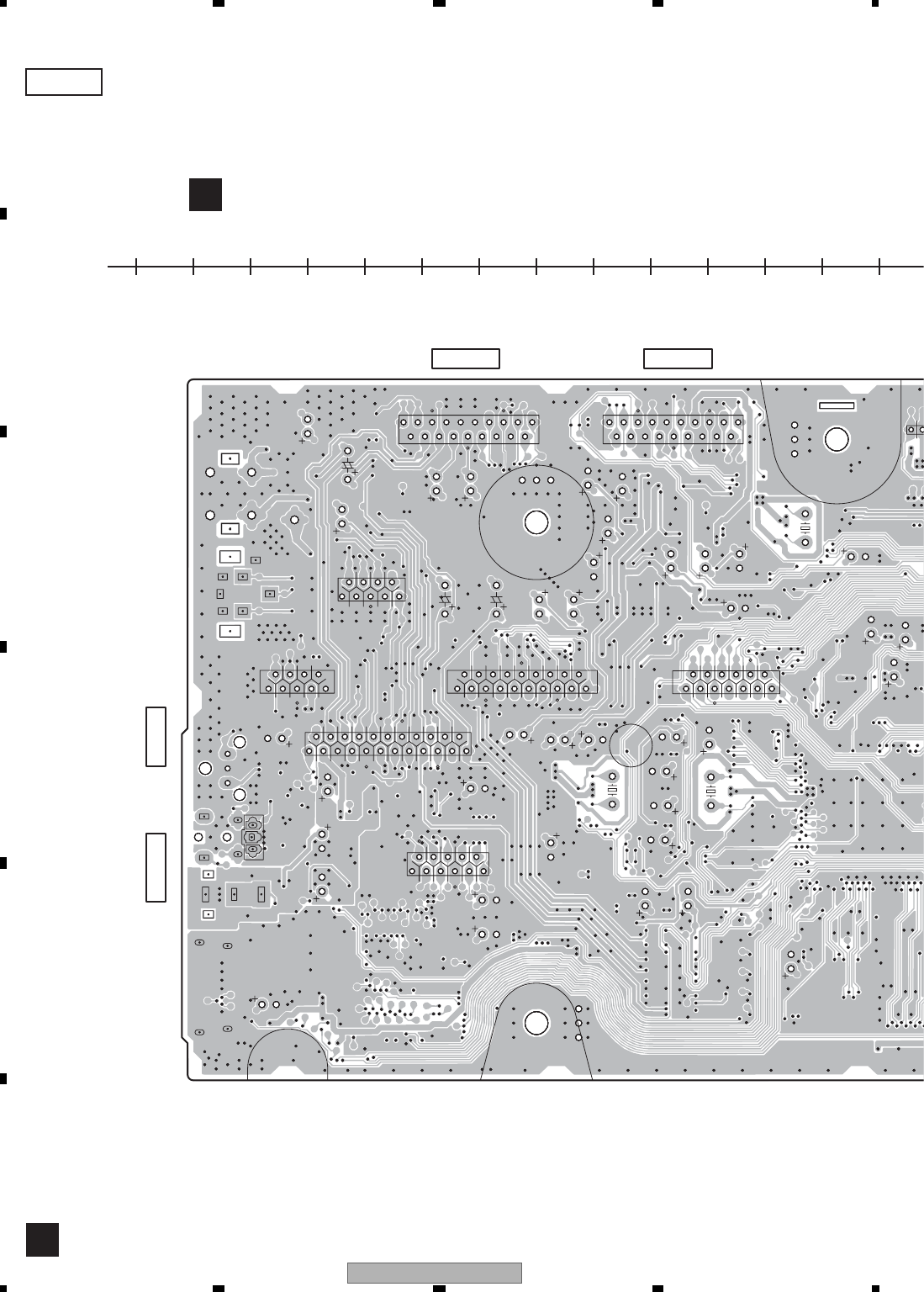
XV-DV363
84
1234
1 234
C
D
F
A
B
E
110
120
130
140
150
160
170
180
190
200
210
220
230
240
1
1
13
1
9
119
1
9
123
1
11
19 119 1
C
CN3001
CN3002
CN5532
CN5533 CN5531
CN401
CN451
CN5701
SIDE B
B
DVD MAIN ASSY
B
CN3001CN3002
CN451CN5701
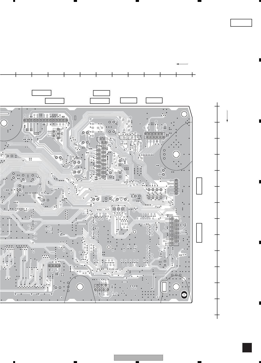
XV-DV363 85
5678
5678
C
D
F
A
B
E
0102030405060708090100110120130
0
10
20
30
40
50
60
70
80
90
100
110
120
X
Y
15 1
114
15
13 1
1
12
1
4
1
5
14
17
CN204
CN5501
CN5602
CN5601
CN104
CN102
CN101
CN103
CN1001
CN3961
SIDE B
B
(XNP3111-A)
CN1001
CN3961 CN102CN101
CN103
CN5601
CN104CN5602
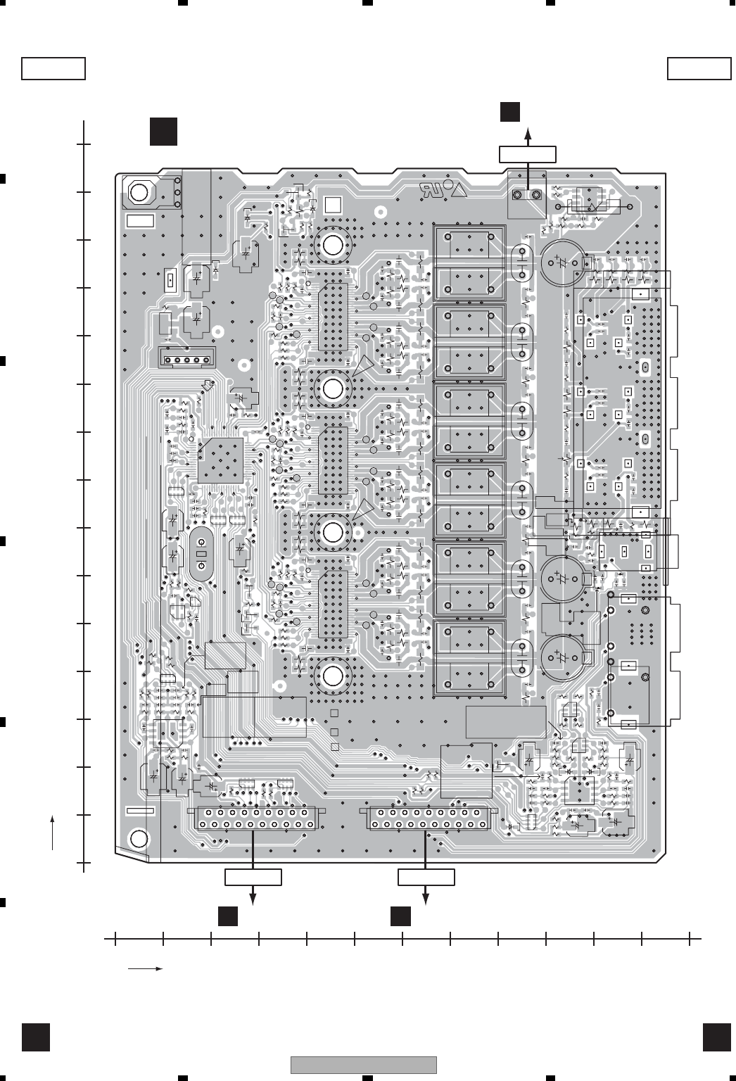
XV-DV363
86
1234
1 234
C
D
F
A
B
E
11.4 DAMP ASSY
0 10 20 30 40 50 60 70 80 90 100 110 120
0
10
20
30
40
50
60
70
80
90
100
110
120
130
140
150
X
Y
1
64
16
17 32
33 48
49
1
54
3
45
13
OUTIN
119 119
4
1
85
1
8
5
4
85
4
1
5
1
NP
56 29
28
11
28
2956 29
28
1
NP
FCICT
LF
R
A30C5/C7
[[ G ]]
C3152
C3151
IC3101
C3101
C3102
R3101
R3102
C3105
C3104C3103
C3106
C3109
C3107
C3108 R3103
R3113
C3111
R3105
C3110
C3112
X3101
R3106
C3113
C3114
C3117
C3116
R3109
C3115
R3110
R3111
C3120
C3119
C3118
R3142
R3141
C3141
IC3181
IC3182
R3181
C3182
C3181
CN3201
IC3171
R3171
C3171
C3172
R3198
CN3102CN3101
R3151
R3153
R3152
R3154
R3155
R3182
R3107
R3108
C3613 C3614
D3602
R3199
CN3111
R3630
C3612
R3618 R3614
IC3601
D3601
C3142
C3601
C3603
C3607
R3612
R3610
R3606
C3602
C3604
C3608
R3624
R3623
C3907
C3903
C3901
C3906
C3924
R3912
IC3901
R3924R3923
R3921
R3911
C3921
R3909
C3905
C3923
R3905
C3908
R3910
C3922
C3904
C3902
R3901
R3907
R3908
R3906
R3601
R3605
R3621
R3609
R3613 R3617
R3615 R3616
R3607 R3608
R3611
R3629
C3605
C3606
C3611
C3621C3622
C3623C3624
C3609
C3610
R3191
IC3191
R3192
R3193
R3194
R3195
C3191
R3197
D3191
C3192
CN3171
R3196
D3603
Q3602
Q3601
IC3201
R3215
C3215
R3211
C3211C3213
R3213
C3212
R3212
C3217
R3217
C3216
R3216
C3218
R3218
R3214
C3214
C3228
C3202
L3202
L3201
Q3604
C3232
R3234
R3238
C3240
R3236
C3238
R3232
R3205
R3206
C3201
C3204
R3207
R3208
R3203
R3202
C3224
C3226
R3228
R3209
R3226
C3227
C3221
R3227
C3225
C3223
R3223
C3237
C3239
R3235
R3231
R3233
R3237
C3231
C3203
R3201
R3224
R3225
R3309
R3311
R3317
C3303
C3314
R3324
C3317
C3324
C3331
R3337
R3326
R3334
L3301
R3302
R3327
C3332
R3301
IC3301
R3315
R3313
R3316
R3325
C3321
R3314
R3332
C3315
R3338 R3331
R3312
R3303
C3338
C3340
C3328
R3333
C3302
R3335
C3337
R3328
C3316
C3311C3313
C3318
R3318
R3323
C3326
C3312
R3305
C3339 R3336
L3302
C3304
R3306
C3327
C3325
C3301
R3308
C3323
R3307
C3402
C3424
R3433
C3417
C3440C3438
C3431
C3428
R3437
C3413 C3411C3414
C3418
R3417
C3403
C3437
R3435
C3416
R3428
R3424
R3427
R3425
C3432
R3414
R3402
C3421
R3413
R3415
R3401
IC3401
R3432
R3412
R3431
R3438
R3403
R3426 R3434
L3401
C3415
R3411
C3439
C3423
R3436
R3405
C3426
C3412
L3402
C3425
C3401
R3408
C3427
C3404
R3416
R3406
R3418
R3407
R3409
R3423
CN3211
KN3101
R3112
R3104
C3911
C3912
R3304
R3204
R3404
C3444 C3442 C3443
R3913
C3441
R3441
C3341
R3443
C3343
R3442
R3343
Q3603
R3444
R3625
R3132
R3131
Q3131
Q3132
R3341
R3626
R3627
R3628
R3914
Q3901
R3344
R3342
C3342C3344
D3101
R3114
R3133
R3134
R3136
D3131
C3233
C3234
C3235
C3236
C3333
C3334
C3335
C3336
C3433
C3434
C3435
C3436
R3915
R3916
R3619
R3620
R3631
R3632
C5984
R3241
R3243
R3242
R3244
C3241C3243C3242C3244
C5983
L5981
L5982
C5981
C5982
JA5981
D3132
R3137
C3131
FR+
FR-SR+
SR-FL+C+ FL-C- SL+SW+ SL-SW-
LOUTRIN LIN ROUT
19.PCON
DAMP ASSY
2.+B
1.GND
5.GND
4.RST
3.+5V
2.SDA
1.SCL
OPEN SIDE
1
56
18.XHPSEL
17.HPL
16.GND
15.HPR
14.GND
13.3.3V
12.XRST
11.XPDN
10.XMUTE
9.GND
8.SDA
7.SCL
6.GND
5.XOTW
4.XSD
3.SROUT
2.POWER
1.PLC_CONT
14.GND
15.MCLK
16.GND
17.SDA3
18.SDA2
19.SDA1
13.SCLK
12.LRCLK
11.GND
10.LINL
9.GND
8.LINR
7.GND
6.SOUTL
5.GND
4.SOUTR
3.RECMUTE
2.GND
1.SDATA4
Production Code
XWK3318
XWK****
XWK****
EL FR4 P
1/2
B2
SIDE A
C
SIDE A
C
DAMP ASSY
C
(XNP3112-A)
CN2
J
CN3201
CN3001
B
CN3101
CN3002
B
CN3102
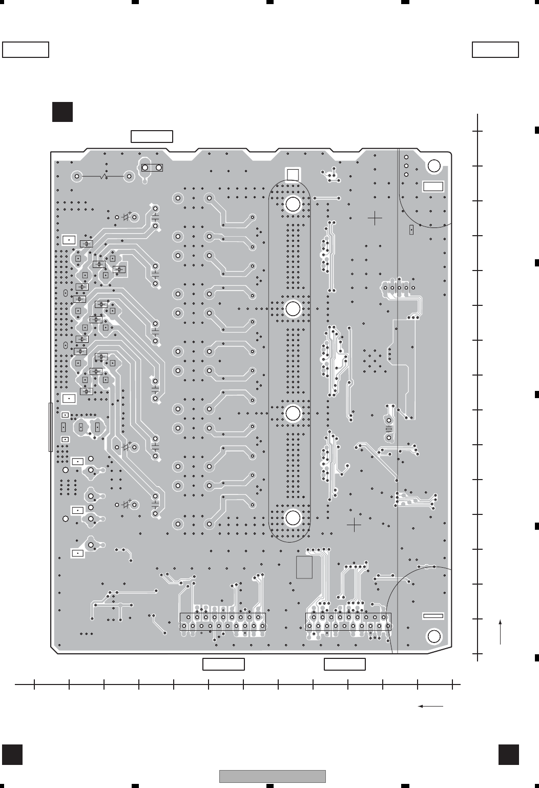
XV-DV363 87
5678
5678
C
D
F
A
B
E
0102030405060708090100110120
0
10
20
30
40
50
60
70
80
90
100
110
120
130
140
150
X
Y
1
19 119 1
1
5
LF
1
2
3
C3245
C3246
C3247
C3248
C3345
C3346
C3347
C3348
C3445
C3446
C3447
C3448
SIDE B
C
SIDE B
C
DAMP ASSY
C
CN3201
CN3101CN3102
CN3201
CN3102 CN3101
(XNP3112-A)
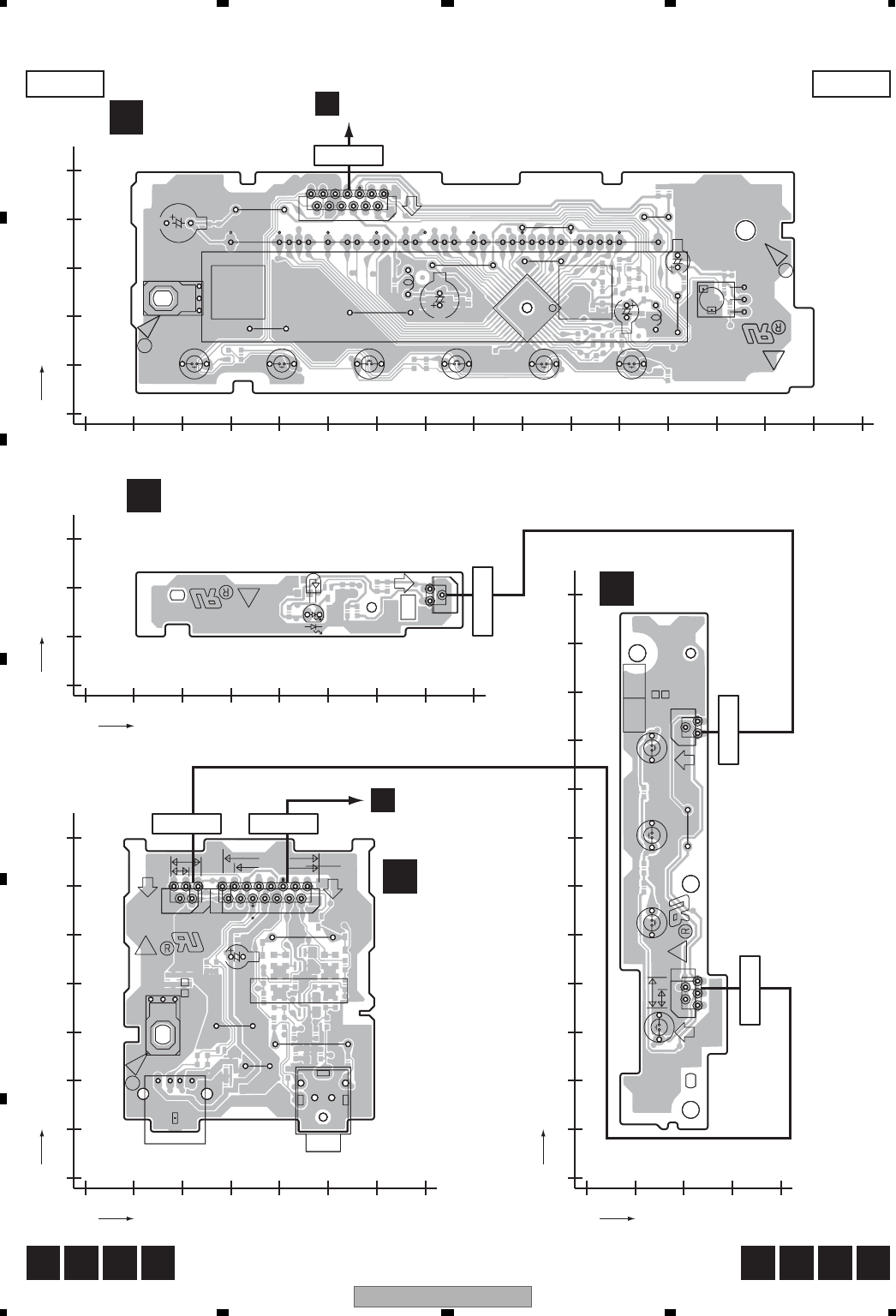
XV-DV363
88
1234
1 234
C
D
F
A
B
E
11.5 DISPLAY, USB, LED and KEY ASSYS
0 10203040506070
0
10
20
30
40
50
60
70
X
Y
190 200 210 220 230
0
10
20
30
40
50
60
70
80
90
100
110
120
X
Y
50 60 70 80 90 100 110 120 130 140 150 160 170 180 190 200 210
20
30
40
50
60
70
X
Y
50 60 70 80 90 100 110 120 130
0
10
20
30
X
Y
31
13
115
1
5
C7
[[ G ]]
C602
JA602
KN5902
JA5901
CN5903 CN5902
CN5906
W5901
W5904
W5902
CN5907
W5913
PNE-1B1
USB ASSY
CONTACT SIDE
XWZ4259
CONTACT SIDE
A
Production Code
GNDUSB
GNDUSB
USB ASSY
CN5902
A
Production Code
GNDUSB
GNDUSB
PNE-1B1
XWZ4260
CN5906
CN5907
CN5903
1/41/4
13 13
1
5
C7
[[ G ]]
S5994
CN5904 S5993
S5992
S5991
W5991
CN5909
CN5908
ICT FC
POWER ON
PLAYLIST3
CONTACT SIDE
PLAY LIST2
PLAYLIST1
XWZ4262
XWZ4261
1/4
V+10
PNE-1B1
CONTACT SIDE
PLAYLIST ASSY
45
1
113
C7
[[ G ]]
C5913
C5918
S5967 S5962
S5965
S5966 S5964 S5963
V5901
KN5903
W5908
W5907
W5906
W5912
W5905
W5910
W5911
L5901
L5902
W5900
C5907
C5952
CN5901
IC5902
PNE-1B1
OPEN/CLOSE STOP
XWZ4256
FL SPACER
PLAY/PAUSE
FL SPACER
CONTACT SIDE
A
B
USB VOL DOWN
FLDC+
FLDC-
GNDD
VEE
DISPLAY ASSY
FL SPACER FL SPACER
A
B
VOL UP
FLDC+
VEE
GNDD
VE+5
PNE-1B1
IC5901
V+10
1/41/4
13
C7
[[ G ]]
CN5603 D5611
LED ASSY
CONTACT SIDE
1/4
PNE-1B1
XWZ4263
DISPLAY ASSY
D
LED ASSY
KEY ASSY
F
USB ASSY
E
G
(XNP3114-B)
(XNP3114-B)
(XNP3114-B) (XNP3114-B)
SIDE A
D E F G D E F G
SIDE A
CN5602
B
CN5901
CN5601
B
CN5603
CN5909
CN5908
CN5906CN5907
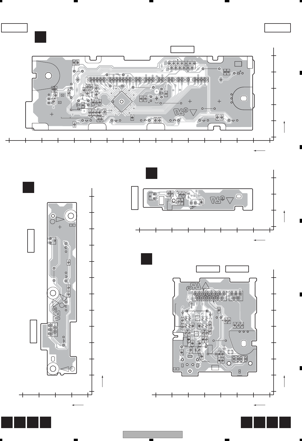
XV-DV363 89
5678
5678
C
D
F
A
B
E
010203040506070
0
10
20
30
40
50
60
70
X
Y
5060708090100110120130
0
10
20
30
X
Y
190200210220230
0
10
20
30
40
50
60
70
80
90
100
110
120
X
Y
5060708090100110120130140150160170180190200210
20
30
40
50
60
70
X
Y
NP
13
LF
113 115
NP
LF
15
L5971
L5972
L602 L601
Q5973
C605
C604
R603
R602
C5979 C5978
C603
C601
D5972
D5971
Q5971
R5985
R5978
R5976
R5977
R5975
R5972
R5974
R5982
R5980
R5979
R5981
R5973
R5971
L5973
C5977
R5990 R5988
C5974
C5973
R5986
R5984
R5983
C5972
C5971
R5987
Q5974
R5989
R605
D601
R604
L603
PNE-1B1
USB ASSY
5.V+10
4.LED
NP
NP
3.GNDD
GNDUSB
GNDUSB
XWZ4260
JA5901
JA602
15.V+10
NP
NP
XWZ4259
5.HP_DET
2.HP_L
1.HPMUTE
2.GND
4.HP_R
6.GNDUSB
7.V5USB
8.V5USB
9.USB_DP2
10.USB_DM2
11.GNDUSB
13.KEY1
12.KEY2A
3.KEY1
GNDUSB
CN5902
JA5901
JA602
14.LED
1.KEY2A
1/41/4
31
Q5611
C5611
R5613
C5612
R5612
R5611
R5614
R5615
D5612
2.GND
1.V+10
3.LED
PNE-1B1
1/4
LED ASSY
3
1
3
1
5
R5993
R5991
R5992
PLAYLIST3
5.V+10
4.LED
B
C
PLAYLIST ASSY
3.KEY1
PNE-1B1
A
PLAYLIST1
PLAY LIST2
3.V+10
POWER ON
1.KEY2A
2.GND
1/4
2.GND
1.LED
XWZ4262
XWZ4261
111
12 22
23 33
34 44
LF
113
LF
R5903
R5901
R5902
C5915
C5919
C5911
C5914
C5912
D5901
C5917
C5916
D5902
R5952
R5951
C5951
R5953
R5963
R5966
R5964
R5965
R5962
R5904
C5905
C5903
IC5901
C5906
R5905
R5906
R5907
Q5902
Q5901
R5909
R5954
R5910
R5908
C5922
C5904 C5920
C5921
DISPLAY ASSY
5.VE+5
6.VFDP
3.FLCS
2.FLCK
PNE-1B1
FLDC+ FLDC-
VFDP
VFDP
VE+5
GNDD
USB STOP PLAY/PAUSE
1
CN5901
11.KEY1
10.GNDD
9.GNDD
8.FLDC+
7.FLDC-
4.REMOCON
1.FLDATA
12.KEY2
13.GNDD
FLDC+
GNDD
VOL UP VOL DOWN
OPEN/CLOSE
CN5901
1/4
D
LED ASSY
KEY ASSY
F
USB ASSY
E
G
DISPLAY ASSY
SIDE B
D E F G D E F G
SIDE B
CN5901
CN5603
CN5909
CN5908
CN5906 CN5907
(XNP3114-B)
(XNP3114-B)
(XNP3114-B)
(XNP3114-B)
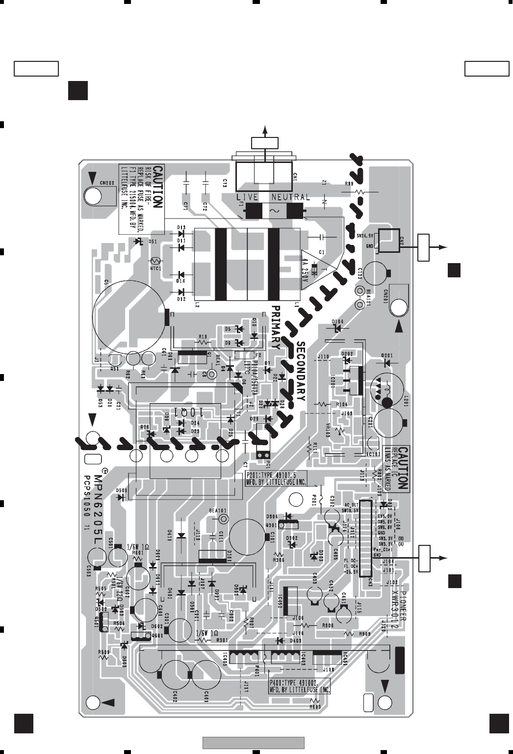
XV-DV363
90
1234
1 234
C
D
F
A
B
E
11.6 POWER SUPPLY UNIT
CN1001
B
SIDE ASIDE A
POWER SUPPLY UNIT
J
J J
To AC POWER CORD
CN3201
C
CN1
CN2
CN3
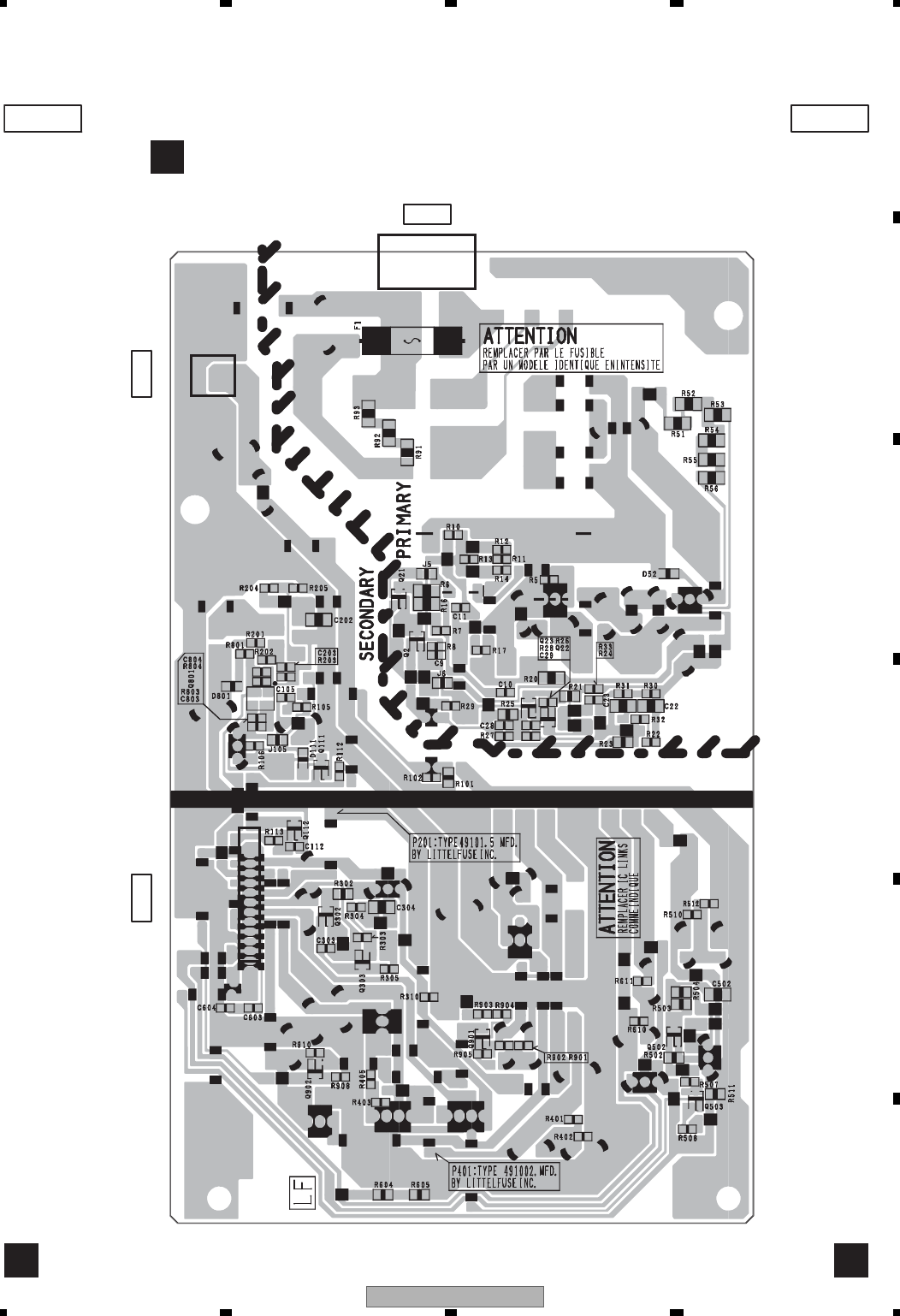
XV-DV363 91
5678
5678
C
D
F
A
B
E
SIDE BSIDE B
POWER SUPPLY UNIT
J
J J
CN1
CN2CN3
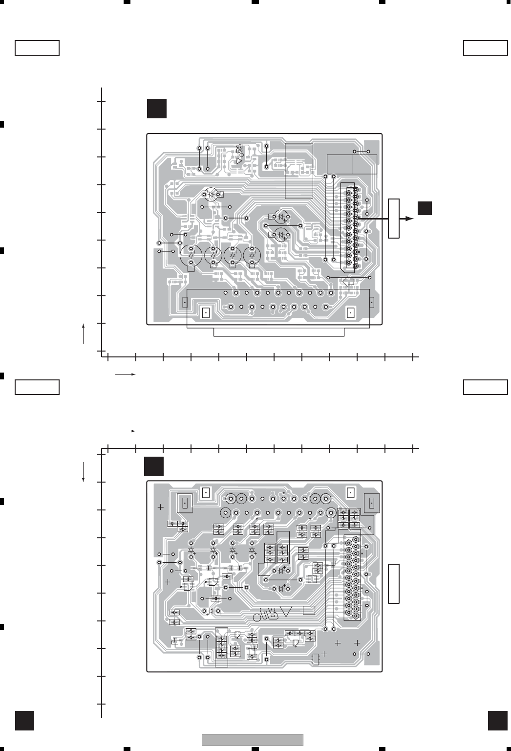
XV-DV363
92
1234
1 234
C
D
F
A
B
E
11.7 EUROSCART ASSY
0 10 20 30 40 50 60 70 80 90 100 110
0
10
20
30
40
50
60
70
80
90
X
X
Y
Y
0 10 20 30 40 50 60 70 80 90 100 110
0
10
20
30
40
50
60
70
80
90
123
FCICT
R
W204
JA451
C477
C480
C482
C481
C471
C478
C479
CN461
CN461
W108
W110
W109
W112
W107
W102
W106
W104
W111
W103
W101
W203
W201
W202
GNDD
V+10
GNDD
VSEL2
VSEL1
SQEEZE
GNDD
V+10
V+5
GNDD
V+5
AWU8291
EUROSCART ASSY
1/4
PRODUCTION CODE
SIDE
CONTACT
PNE-1B1
GNDD
GNDD
GNDD
1
2
20
21
1
6
3
4
1
6
3
4
NP
23 1
20 10
LF
R
R468
Q463
R472
R469
Q461
R463
R462
R473
C469
C465
R464
C464
R471
R465
C470
Q462
R466
R461
R467
R470
C494 C493
C495
C496
D474
D473
D472
C491
C492
R477
R478
C472
IC471
C489
R482
R493
R481
R486
C488
R474
C473
IC472
C475
C474
R496
R494
Q493
R484
C476
D471
C490
C487
R485
R475 R476
C483
C484
C485
C486
R495
R487
R483
R488
Q472
Q492
GNDD
V+10
V+5
V+5
V+10
GNDD
SQEEZE
VSEL1
VSEL2
GNDD
GNDD
DVDPOWER
1.VSEL1
2.SQEEZE
3.V+10
4.TVOUT_R
5.GND
6.TVOUT_L
7.TVMUTE
8.SCART_R
9.GND
10.SCART_L
11.V+5
12.VSEL2
13.B
14.GND
15.G
16.GND
17.R
18.
19.S_C
20.GND
21.V
22.GND
23.S_Y
C
B2
E2
1/4
E
B
C2
PNE-1B1
GNDD
GNDD
EUROSCART ASSY
AWU8291
SIDE A
I
SIDE A
I
CN451
B
CN461CN461
SIDE B SIDE B
EUROSCART ASSY
I
(ANP7569-B)
EUROSCART ASSY
I
(ANP7569-B)
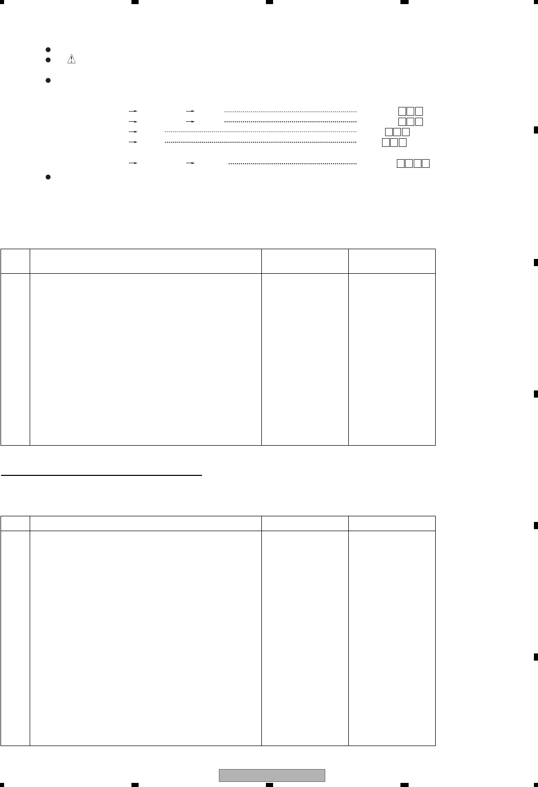
XV-DV363 93
5678
5678
C
D
F
A
B
E
12. PCB PARTS LIST
LIST OF WHOLE PCB ASSEMBLIES
CONTRAST OF PCB ASSEMBLIES
XWM3341 and XWM3342 are constructed the same except for the following :
Parts marked by "NSP" are generally unavailable because they are not in our Master Spare Parts List.
The mark found on some component parts indicates the importance of the safety factor of the part.
Therefore, when replacing, be sure to use parts of identical designation.
When ordering resistors, first convert resistance values into code form as shown in the following examples.
Ex.1 When there are 2 effective digits (any digit apart from 0), such as 560 ohm and 47k ohm (tolerance is shown by J=5%,
and K=10%).
Ex.2 When there are 3 effective digits (such as in high precision metal film resistors).
561
473
R50
1R0
5621
NOTES:
560
Ω
47k
Ω
0.5
Ω
1
Ω
RD1/4PU J
RD1/4PU J
RN2H K
RS1P K
56 x 10
1
47 x 10 3
R50
1R0
561
473
5.62k ΩRN1/4PC F562 x 10 15621
Meaning of the figures and others in the parentheses in the parts list.
Example) IC 301 is on the point (face A, 91 of x-axis, and 111 of y-axis) of the corresponding
PC board.
IC 301 (A, 91, 111) IC NJM2068V
Mark Symbol and Description XV-DV363
/WYXJ5
XV-DV365K
/WXJ/RE5
1..LOAB ASSY VWG2346 VWG2346
1..DAMP ASSY XWK3318 XWK3318
1..DVD MAIN ASSY XWM3341 XWM3342
NSP 1..COMPLEX ASSY XWM3372 XWM3372
2..DISPLAY ASSY XWZ4256 XWZ4256
2..USB ASSY XWZ4259 XWZ4259
2..KEY ASSY XWZ4261 XWZ4261
2..LED ASSY XWZ4263 XWZ4263
NSP 1..JACK ASSY AWM8034 AWM8034
2..EUROSCART ASSY AWU8291 AWU8291
NSP 1..MIC ASSY Not used XWM3375
>1..POWER SUPPLY UNIT XWR3012 XWR3012
1..FM/AM TUNER UNIT AXX7248 AXX7248
BDVD MAIN ASSY
Mark Symbol and Description XWM3341 XWM3342
IC3961 Not used AK5358AET
D3961, D3962 Not used UDZS3R9(B)
C3961 Not used CKSRYB105K16
C3962, C3966 Not used CKSRYB104K16
C3963, C3965 Not used CKSQYB225K10
C3967 Not used CEAT220M25
C3968 Not used CKSRYB103K50
R249 Not used RS1/16S330J
R3966 Not used RS1/16S102J
R3967 Not used RS1/16S332J
R3968 Not used RS1/16S182J
R3969 Not used RAB4C101J
R5502 Not used RS1/16S104J
R5513 Not used RD1/4PU153J
R5515 RD1/4PU473J RD1/4PU823J
R5571 Not used RS1/16S102J
CN3961 Connector Not used CKS3370

XV-DV363
94
1234
1 234
C
D
F
A
B
E
PCB PARTS LIST
Mark No. Description Part No.
ALOAB ASSY
MISCELLANEOUS
S 101 SWITCH VSK1011
CN 602 CONNECTOR S2B-PH-K
CN 601 CONNECTOR S5B-PH-K
BDVD MAIN ASSY
MISCELLANEOUS
IC 101 (A,41,32) 6CH DRIVER IC BD7995EFS
IC 201 (A,77,112) DVD IC MT1389FE/H-L
IC 202 (A,110,99) IC K4S641632K-UC75
IC 203 (A,72,77) FLASH ROM AYW7154
FLASH MEMORY IC S29AL016D70TFI010
IC 204 (A,93,79) EEPROM S-24CS64A0I
IC 401 (A,103,145) DVD VIDEO AMP IC MM1758XF
IC 771 (A,34,50) LOAD SWITCHING AAT4618IGV-0.5-1
>IC 781 (A,51,49) REGULATOR IC NJM2845DL1-05
IC 931 (A,102,195) HDMI IC MT1392E/C-L
>IC 981 (A,84,160) REGULATOR IC NJM2872BF05
>IC 1101 (A,20,110) REGULATOR IC NJM2846DL3-18
IC 3001 (A,41,151) IC TC4052BFN
IC 3003 (A,23,145) AD CONVERTER IC AK5358AET
IC 3004 (A,25,132) IC TC7WU04FU
IC 3005 (A,42,126) IC TC74VHC157FTS1
IC 5501 (A,83,44) SYSTEM CONTROL UCON PDC153A
IC 5502 (A,111,37) EEPROM S-93C46BD0I-J8T1
IC 5701 (A,72,168) RDS DECORDER IC LC72725KM
Q 304 (A,13,35) TRANSISTOR 2SC4154
Q 305 (A,14,41) NMOS FET TRANSISTOR UM5K1N
Q 307 (A,11,61) CHIP TRANSISTOR HN1A01F
Q 308 (A,16,61) CHIP TRANSISTOR HN1A01F
Q 491 (A,46,206) TRANSISTOR RT1N241M
Q 933 (A,114,212) TRANSISTOR RT1N144M
Q 934 (A,115,216) TRANSISTOR RT3P22M
Q 1201 (A,24,101) TRANSISTOR RT1N141M-11
Q 1202 (A,30,106) CHIP TRANSISTOR RSR015P03
Q 1301 (A,13,102) TRANSISTOR(SC-70) 2SA1602A
Q 1302 (A,17,102) TRANSISTOR 2SA1577
Q 1303 (A,13,96) TRANSISTOR 2SC4154
Q 1304 (A,18,92) TRANSISTOR 2SC4154
Q 1402 (A,110,25) TRANSISTOR (SC-70) 2SA1602A
Q 1413 (A,106,21) TRANSISTOR RT1N241M
Q 3005 (A,42,140) CHIP TRANSISTOR HN1A01FU
Q 3006 (A,8,200) TRANSISTOR RT1N241M
Q 3951 (A,46,64) TRANSISTOR RT1N241M
Q 5525 (A,62,59) DIGITAL TR (SC-70) RT1N431M
Q 5703 (A,74,187) CHIP TRANSISTOR HN1C01FU
Q 5941 (A,21,192) TRANSISTOR RT1N241M
Q 5942 (A,27,195) TRANSISTOR (SC-70) 2SA1602A
D 802 (A,61,24) DIODE 1SS352
D 933 (A,112,204) DIODE UDZS5R1(B)
D 1201 (A,27,103) DIODE 1SS352
D 1403 (A,110,30) DIODE MC2846-11
D 1415 (A,103,22) DIODE UDZS4R7(B)
D 5941 (A,21,195) DIODE 1SS352
D 5942 (A,25,188) DIODE 1SS352
L 761 (A,51,98) COIL VTH1047
L 772 (A,39,50) CHIP SOLID INDUCTOR ATL7002
L 931 (A,95,171) CHIP BEADS ATL7010
L 932 (A,97,216) COIL ATH7022
L 933 (A,100,216) COIL ATH7022
L 934 (A,102,216) COIL ATH7022
L 935 (A,105,216) COIL ATH7022
L 936 (A,93,171) CHIP BEADS ATL7010
L 937 (A,100,169) CHIP BEADS ATL7010
L 1305 (A,16,105) INDUCTOR CTF1395
L 1501 (A,58,42) AXIAL INDUCTOR LAU220J
L 3951 (A,40,65) INDUCTOR CTF1346
L 3952 (A,38,65) INDUCTOR CTF1346
JA 403 (A,20,232) JACK VKB1122
JA 931 HDMI CONNECTOR AKP7210
X 201 (A,75,140) CRYSTAL RESONATOR VSS1168
(27 MHz)
X 3004 (A,24,123) CRYSTAL RESONATOR VSS1140
(12.288 MHz)
X 5501 (A,64,44) CERAMIC RESONATOR ASS7034
(10 MHz)
X 5701 (A,74,157) CRYSTAL RESONATOR ASS7004
(4.332 MHz)
CN 101 (A,21,41) CONNECTOR 24P VKN2045
CN 102 (A,19,18) 12P CONNECTOR VKN1243
CN 103 (A,20,57) 4P CONNECTOR VKN1235
CN 104 (A,46,10) CONNECTOR POST B5B-PH
CN 204 (A,99,83) CONNECTOR B4B-PH
CN 451 (A,65,182) CONNECTOR CKS3388
CN 1001 CONNECTOR B13B-PH
CN 3001 (A,8,157) 19P RECEPTACLE AKP7199
CN 3002 (A,8,193) 19P RECEPTACLE AKP7199
CN 5501 (A,114,53) CONNECTOR CKS3372
CN 5601 (A,26,56) CONNECTOR CKS3380
CN 5602 (A,85,12) CONNECTOR CKS3378
CN 5701 (A,86,179) CONNECTOR CKS3376
2 PCB BINDER VEF1040
RESISTORS
R 131 (A,28,24) RS1/10S4R7J
R 132 (A,28,26) RS1/10S4R7J
R 133 (A,28,28) RS1/10S4R7J
R 134 (A,28,30) RS1/10S4R7J
R 135 (A,28,32) RS1/10S4R7J
R 136 (A,28,34) RS1/10S4R7J
R 151 (A,51,37) RS1/10S1R0J
R 152 (A,51,41) RS1/10S1R8J
R 153 (A,49,37) RS1/10S1R0J
R 154 (A,49,41) RS1/10S1R8J
R 201 (A,50,75) RS1/16S152J
R 202 (A,53,75) RS1/16S223J
R 204 (A,53,79) RS1/16S223J
R 205 (A,56,79) RS1/16S513J
R 206 (A,56,75) RS1/16S513J
R 212 (A,56,101) RS1/16S103J
R 213 (A,56,102) RS1/16S103J
R 215 (A,80,86) RS1/16S332J
R 216 (A,79,89) RS1/16S472J
R 218 (A,86,81) RS1/16S103J
Mark No. Description Part No.

XV-DV363 95
5678
5678
C
D
F
A
B
E
R 219 (A,86,82) RS1/16S103J
R 221 (A,76,89) RS1/16S330J
R 223 (A,91,87) RS1/16S330J
R 224 (A,73,89) RS1/16S330J
R 225 (A,99,99) CHIP RESISTOR ARRAY RAB4C330J
R 226 (A,99,102) RS1/16S0R0J
R 227 (A,99,103) RS1/16S330J
R 228 (A,99,105) RS1/16S330J
R 229 (A,99,106) RS1/16S330J
R 230 (A,86,134) RS1/16S103J
R 233 (A,68,92) RS1/16S0R0J
R 234 (A,79,86) RS1/16S330J
R 235 (A,77,86) RS1/16S472J
R 237 (A,77,89) RS1/16S330J
R 240 (A,88,147) RS1/16S0R0J
R 241 (A,83,134) RS1/16S330J
R 242 (A,83,138) RS1/16S330J
R 243 (A,81,134) RS1/16S100J
R 244 (A,88,134) RS1/16S330J
R 245 (A,87,137) RS1/16S330J
R 246 (A,86,138) RS1/16S330J
R 247 (A,88,156) RS1/16S0R0J
R 248 (A,81,138) RS1/16S330J
R 251 (A,70,134) RS1/16S104J
R 252 (A,72,130) RS1/16S0R0J
R 253 (A,73,134) RS1/16S681J
R 254 (A,67,133) RS1/16S754J
R 255 (A,61,134) RS1/16S104J
R 256 (A,57,131) RS1/16S153J
R 257 (A,74,130) RS1/16S0R0J
R 258 (A,80,89) RS1/16S330J
R 259 (A,82,87) RS1/16S330J
R 260 (A,83,87) RS1/16S330J
R 261 (A,95,87) RS1/16S330J
R 262 (A,85,86) RS1/16S330J
R 263 (A,86,86) RS1/16S330J
R 264 (A,110,122) CHIP RESISTOR ARRAY RAB4C330J
R 265 (A,104,118) CHIP RESISTOR ARRAY RAB4C330J
R 266 (A,99,115) RS1/16S0R0J
R 267 (A,110,115) CHIP RESISTOR ARRAY RAB4C330J
R 269 (A,82,142) RS1/16S0R0J
R 271 (A,104,113) CHIP RESISTOR ARRAY RAB4C330J
R 272 (A,96,87) RS1/16S333J
R 279 (A,89,134) CHIP RESISTOR RS1/16S2201F
R 281 (A,107,84) RS1/10S0R0J
R 284 (A,60,80) RS1/16S103J
R 291 (A,72,86) RS1/16S332J
R 292 (A,73,85) RS1/16S682J
R 293 (A,93,84) RS1/16S332J
R 294 (A,90,84) RS1/16S682J
R 313 (A,16,39) RS1/16S104J
R 314 (A,15,37) RS1/16S103J
R 315 (A,12,37) RS1/16S103J
R 318 (A,12,39) RS1/16S104J
R 321 (A,19,61) RS1/16S4R7J
R 322 (A,14,61) RS1/16S4R7J
R 325 (A,10,57) RS1/16S4R7J
R 326 (A,15,57) RS1/16S4R7J
R 401 (A,109,138) RS1/16S103J
R 411 (A,96,131) RS1/16S1500F
Mark No. Description Part No.
R 412 (A,100,131) RS1/16S1500F
R 413 (A,93,130) RS1/16S1500F
R 414 (A,103,131) RS1/16S1500F
R 415 (A,107,130) RS1/16S1500F
R 416 (A,110,130) RS1/16S1500F
R 424 (A,19,209) RS1/10S75R0F
R 491 (A,49,206) RS1/16S103J
R 767 (A,51,104) RS1/16S153J
R 768 (A,52,101) RS1/16S153J
R 769 (A,51,103) RS1/16S330J
R 770 (A,52,100) RS1/16S330J
R 771 (A,37,50) RS1/16S221J
R 772 (A,31,48) RS1/16S104J
R 801 (A,61,28) RS1/16S472J
R 906 (A,91,194) RS1/16S100J
R 911 (A,91,191) RS1/16S100J
R 914 (A,114,184) RS1/16S103J
R 915 (A,116,191) RS1/16S102J
R 931 (A,102,184) RS1/16S0R0J
R 933 (A,92,199) RS1/16S561J
R 934 (A,92,203) CHIP RESISTOR RS1/16S5100F
R 959 (A,117,214) RS1/16S472J
R 960 (A,117,217) RS1/16S272J
R 961 (A,113,219) RS1/16S472J
R 962 (A,115,219) RS1/16S272J
R 966 (A,110,206) RS1/16S473J
R 970 (A,112,209) RS1/16S102J
R 973 (A,109,209) RS1/16S0R0J
R 1101 (A,24,105) RS1/16S221J
R 1201 (A,31,102) RS1/16S103J
R 1202 (A,29,103) RS1/16S474J
R 1301 (A,13,100) RS1/16S473J
R 1302 (A,13,98) RS1/16S392J
R 1303 (A,17,99) RS1/16S473J
R 1304 (A,16,92) RS1/10S561J
R 1306 (A,21,95) RS1/16S103J
R 1307 (A,13,92) RS1/16S472J
R 1401 (A,114,27) RS1/16S392J
R 1402 (A,114,30) RS1/16S332J
R 1403 (A,112,27) RS1/16S473J
R 1404 (A,112,30) RS1/16S393J
R 1415 (A,100,22) RS1/16S182J
R 3006 (A,8,198) RS1/16S103J
R 3009 (A,49,153) RS1/16S102J
R 3010 (A,34,153) RS1/16S102J
R 3011 (A,47,159) RS1/16S223J
R 3012 (A,34,155) RS1/16S223J
R 3013 (A,49,156) RS1/16S223J
R 3014 (A,34,156) RS1/16S223J
R 3015 (A,48,149) RS1/16S223J
R 3016 (A,34,152) RS1/16S223J
R 3017 (A,48,150) RS1/16S223J
R 3018 (A,34,150) RS1/16S223J
R 3019 (A,48,152) RS1/16S272J
R 3020 (A,37,157) RS1/16S272J
R 3021 (A,45,140) RS1/16S224J
R 3022 (A,37,143) RS1/16S224J
R 3023 (A,37,138) RS1/16S102J
R 3024 (A,39,143) RS1/16S102J
R 3025 (A,45,136) RS1/16S102J
Mark No. Description Part No.

XV-DV363
96
1234
1 234
C
D
F
A
B
E
R 3026 (A,44,136) RS1/16S102J
R 3027 (A,49,155) RS1/16S473J
R 3039 (A,36,138) RS1/16S153J
R 3040 (A,42,144) RS1/16S153J
R 3048 (A,17,137) RS1/16S182J
R 3049 (A,22,139) RAB4C101J
R 3052 (A,22,134) RS1/16S0R0J
R 3053 (A,31,131) RS1/16S101J
R 3054 (A,31,128) RS1/16S101J
R 3055 (A,27,129) RS1/16S105J
R 3056 (A,23,129) RS1/16S101J
R 3057 (A,27,150) RS1/16S0R0J
R 3060 (A,29,143) RS1/16S0R0J
R 3061 (A,37,130) RS1/16S221J
R 3062 (A,35,127) RS1/16S221J
R 3063 (A,35,125) RS1/16S221J
R 3065 (A,48,127) RS1/16S221J
R 3066 (A,35,121) RS1/16S101J
R 3073 (A,18,139) RS1/16S332J
R 3081 (A,10,164) RS1/16S105J
R 3082 (A,10,163) RS1/16S105J
R 3915 (A,70,200) RS1/16S473J
R 3951 (A,43,65) RS1/16S473J
R 3952 (A,35,65) RS1/16S473J
R 3955 (A,50,63) RS1/16S182J
R 5501 (A,67,58) RAB4C221J
R 5505 (A,67,55) RS1/16S221J
R 5506 (A,67,54) RS1/16S221J
R 5507 (A,67,53) RS1/16S221J
R 5508 (A,62,55) RS1/16S222J
R 5509 (A,67,61) RS1/16S0R0J
R 5510 (A,62,53) RS1/16S473J
R 5514 (A,57,22) RD1/4PU683J
R 5515 (A,52,27) RD1/4PU473J
R 5516 (A,52,20) RD1/4PU153J
R 5517 (A,66,35) RAB4C221J
R 5518 (A,62,35) RS1/16S105J
R 5519 (A,62,32) RS1/16S103J
R 5521 (A,66,33) RS1/16S221J
R 5527 (A,67,25) RAB4C221J
R 5531 (A,71,25) RS1/16S0R0J
R 5536 (A,79,25) RS1/16S221J
R 5541 (A,87,25) RAB4C221J
R 5543 (A,94,10) RS1/16S0R0J
R 5544 (A,81,22) RS1/16S0R0J
R 5546 (A,84,22) RS1/16S103J
R 5547 (A,84,21) RS1/16S103J
R 5548 (A,100,29) RAB4C221J
R 5557 (A,100,36) RAB4C221J
R 5558 (A,106,40) RS1/16S473J
R 5559 (A,112,41) RS1/16S473J
R 5562 (A,100,39) RS1/16S221J
R 5563 (A,104,46) RS1/16S103J
R 5564 (A,100,40) RS1/16S221J
R 5565 (A,100,42) RS1/16S221J
R 5566 (A,100,45) RAB4C221J
R 5569 (A,66,39) RS1/16S221J
R 5570 (A,100,51) RAB4C221J
R 5574 (A,95,64) RS1/16S104J
R 5577 (A,100,60) RAB4C221J
Mark No. Description Part No.
R 5581 (A,98,64) RS1/16S221J
R 5582 (A,96,64) RS1/16S221J
R 5583 (A,92,64) RS1/16S103J
R 5584 (A,90,64) RS1/16S221J
R 5590 (A,80,63) RAB4C221J
R 5597 (A,82,63) RS1/16S153J
R 5708 (A,75,193) RS1/16S0R0J
R 5712 (A,78,184) RS1/16S272J
R 5713 (A,78,190) RS1/16S272J
R 5943 (A,73,212) RS1/16S0R0J
R 5944 (A,30,195) RS1/16S104J
R 5945 (A,29,192) RS1/16S392J
R 5946 (A,24,195) RS1/16S472J
R 5947 (A,27,188) RS1/16S102J
R 5949 (A,25,192) RS1/16S103J
R 9401 (A,16,196) RS1/16S0R0J
CAPACITORS
C 101 (A,40,18) CEAT101M10
C 102 (A,40,22) CKSRYB105K10
C 103 (A,48,29) CKSRYB105K10
C 104 (A,49,34) CKSRYB105K10
C 121 (A,48,32) CKSRYB105K6R3
C 131 (A,33,41) CKSRYB104K16
C 140 (A,16,15) CKSRYB105K6R3
C 144 (A,32,32) CKSRYB222K50
C 145 (A,34,31) CKSRYB222K50
C 146 (A,34,34) CKSRYB222K50
C 151 (A,49,26) CKSRYB103K50
C 152 (A,49,23) CKSRYB103K50
C 153 (A,46,21) CKSRYB103K50
C 161 (A,32,38) CKSRYB102K50
C 200 (A,58,111) CKSRYB104K16
C 201 (A,59,93) CEAT221M6R3
C 202 (A,45,112) CEAT221M6R3
C 203 (A,46,100) ELECT. CAPACITOR CEAT470M35
C 204 (A,54,113) CKSRYB104K16
C 205 (A,54,111) CKSRYB104K16
C 206 (A,52,108) ELECT. CAPACITOR CEAT470M35
C 207 (A,55,116) CKSRYB104K16
C 208 (A,55,75) CKSRYB222K50
C 209 (A,52,75) CKSRYB104K16
C 210 (A,52,79) CKSRYB222K50
C 211 (A,55,79) CCSRCH101J50
C 212 (A,58,75) CCSRCH101J50
C 213 (A,54,115) CKSRYB104K16
C 215 (A,46,106) ELECT. CAPACITOR CEAT470M35
C 216 (A,58,105) CKSRYB104K16
C 217 (A,59,100) CKSRYB104K16
C 218 (A,58,108) CKSRYB104K16
C 219 (A,58,109) CKSRYB562K50
C 220 (A,63,94) CKSRYB104K16
C 223 (A,63,146) CEAT100M50
C 224 (A,75,93) CKSRYB104K16
C 225 (A,76,93) CKSRYB104K16
C 226 (A,88,87) CKSRYB103K50
C 227 (A,96,89) CCSRCH221J50
C 228 (A,78,134) CKSRYB104K16
Mark No. Description Part No.

XV-DV363 97
5678
5678
C
D
F
A
B
E
C 229 (A,89,92) CKSRYB104K16
C 230 (A,94,99) CKSRYB104K16
C 231 (A,95,104) CKSRYB104K16
C 232 (A,95,106) CKSRYB104K16
C 233 (A,96,111) CKSRYB104K16
C 234 (A,95,113) CKSRYB104K16
C 235 (A,95,116) CKSRYB104K16
C 236 (A,95,118) CKSRYB104K16
C 237 (A,103,126) CEAT221M6R3
C 238 (A,75,130) CKSRYB104K16
C 239 (A,81,131) CKSRYB104K16
C 241 (A,69,147) CEAT100M50
C 242 (A,75,147) CEAT100M50
C 243 (A,94,127) CKSRYB104K16
C 244 (A,95,123) CKSRYB104K16
C 245 (A,88,131) CKSRYB105K6R3
C 246 (A,87,130) CKSRYB104K16
C 247 (A,84,131) CKSRYB104K16
C 248 (A,84,134) CKSRYB104K16
C 250 (A,102,122) CKSRYB104K16
C 251 (A,70,135) CCSRCH9R0D50
C 252 (A,74,135) CCSRCH120J50
C 254 (A,67,135) CKSRYB102K50
C 255 (A,60,137) CKSRYB474K10
C 256 (A,64,140) CEAT100M50
C 258 (A,64,135) CKSRYB473K25
C 259 (A,64,133) CKSRYB473K25
C 260 (A,70,131) CKSRYB104K16
C 261 (A,76,131) CKSRYB104K16
C 262 (A,81,148) CEAT100M50
C 264 (A,66,131) CKSRYB104K16
C 265 (A,57,135) CCSRCH220J50
C 266 (A,68,131) CKSRYB104K16
C 267 (A,58,135) CKSRYB102K50
C 268 (A,62,131) CKSRYB104K16
C 269 (A,60,131) CKSRYB333K16
C 271 (A,64,130) CKSRYB104K16
C 272 (A,59,131) CKSRYB104K16
C 273 (A,64,131) CKSRYB104K16
C 281 (A,113,85) CEAT221M6R3
C 282 (A,109,84) CKSRYB105K6R3
C 283 (A,117,109) CKSRYB104K16
C 284 (A,102,98) CKSRYB104K16
C 285 (A,101,93) CKSRYB104K16
C 286 (A,117,90) CKSRYB104K16
C 287 (A,117,94) CKSRYB104K16
C 288 (A,117,99) CKSRYB104K16
C 289 (A,86,77) CKSRYB105K6R3
C 290 (A,93,75) CKSRYB104K16
C 296 (A,84,77) CKSRYB102K50
C 309 (A,17,66) ELECT. CAPACITOR CEAT470M35
C 310 (A,23,66) ELECT. CAPACITOR CEAT470M35
C 343 (A,58,124) CKSRYB105K6R3
C 344 (A,48,117) CKSRYB105K6R3
C 345 (A,48,118) CKSRYB105K6R3
C 346 (A,55,122) CKSRYB105K6R3
C 347 (A,55,120) CKSRYB105K6R3
C 371 (A,15,44) CKSRYB104K16
C 372 (A,26,46) CKSRYB104K16
C 374 (A,10,49) ELECTR.CAPACITOR CEAT101M6R3
Mark No. Description Part No.
C 401 (A,92,151) CEAT101M16
C 402 (A,91,147) CKSRYB104K16
C 404 (A,92,144) CEAT101M16
C 405 (A,103,138) CKSRYB104K16
C 411 (A,97,137) CKSRYB104K16
C 412 (A,101,136) CKSRYB105K6R3
C 413 (A,95,137) CKSRYB105K6R3
C 414 (A,104,136) CKSRYB105K6R3
C 415 (A,107,135) CKSRYB104K16
C 416 (A,111,135) CKSRYB104K16
C 429 (A,18,203) ELECT. CAPACITOR CEAT102M6R3
C 771 (A,36,53) CKSQYB105K16
C 773 (A,31,51) CKSRYB104K16
C 781 (A,42,45) CEAT100M50
C 782 (A,48,58) CKSQYB225K10
C 931 (A,96,186) CKSRYB104K16
C 932 (A,97,180) ELECT. CAPACITOR CEAT470M35
C 933 (A,94,185) CKSRYB104K16
C 934 (A,94,187) CKSRYB102K50
C 935 (A,96,166) CKSRYB104K16
C 936 (A,113,189) CKSRYB104K16
C 942 (A,102,185) CKSRYB104K16
C 943 (A,108,185) CKSRYB104K16
C 944 (A,92,201) CKSRYB104K16
C 945 (A,110,202) CKSRYB562K50
C 946 (A,108,204) CKSRYB104K16
C 951 (A,109,210) CKSRYB104K16
C 952 (A,109,218) CEAT100M50
C 953 (A,91,180) ELECT. CAPACITOR CEAT470M35
C 954 (A,91,185) CKSRYB104K16
C 955 (A,94,166) CKSRYB104K16
C 956 (A,91,187) CKSRYB102K50
C 982 (A,84,164) CKSQYB225K10
C 983 (A,80,161) CKSQYB105K16
C 984 (A,84,157) CKSRYB104K16
C 985 (A,100,165) CKSRYB104K16
C 987 (A,100,172) CKSRYB102K50
C 1101 (A,27,108) CKSRYB105K6R3
C 1103 (A,31,115) ELECT. CAPACITOR CEAT470M35
C 1201 (A,24,103) CKSRYB105K6R3
C 1204 (A,31,103) CKSRYB563K16
C 1301 (A,18,95) CKSRYB105K6R3
C 1501 (A,61,48) CKSRYB103K50
C 1502 (A,61,43) CKSRYB104K16
C 1505 (A,58,51) CEAT101M10
C 3001 (A,44,157) CKSRYB103K50
C 3011 (A,20,182) CEAT100M50
C 3012 (A,20,188) CEAT100M50
C 3015 (A,39,170) CEAT100M50
C 3016 (A,39,164) CEAT100M50
C 3019 (A,63,165) CEAT100M50
C 3020 (A,62,172) CEAT100M50
C 3021 (A,29,138) CKSRYB104K16
C 3022 (A,42,143) CKSRYB104K16
C 3023 (A,31,135) ELECT. CAPACITOR CEAT470M35
C 3024 (A,40,136) CEAT221M6R3
C 3025 (A,33,141) CEAT100M50
C 3026 (A,33,147) CEAT100M50
C 3041 (A,19,161) CEAT100M50
C 3042 (A,22,151) CKSRYB104K16
Mark No. Description Part No.

XV-DV363
98
1234
1 234
C
D
F
A
B
E
C 3043 (A,27,158) CEAT2R2M50
C 3044 (A,24,151) CKSRYB104K16
C 3045 (A,20,155) CEAT100M50
C 3046 (A,20,151) CKSRYB104K16
C 3048 (A,17,139) CKSRYB103K50
C 3052 (A,25,134) CKSRYB104K16
C 3056 (A,23,127) CCSRCH270J50
C 3057 (A,27,127) CCSRCH270J50
C 3064 (A,43,130) CKSRYB104K16
C 3951 (A,41,73) CEAT101M16
C 3952 (A,35,73) CEAT101M16
C 5502 (A,56,36) CEAT101M10
C 5504 (A,62,56) CKSRYB103K50
C 5508 (A,62,54) CKSRYB103K50
C 5509 (A,68,50) CKSRYB104K16
C 5517 (A,68,41) CKSRYB103K50
C 5518 (A,66,38) CKSRYB104K16
C 5519 (A,62,33) CKSRYB103K50
C 5521 (A,63,28) CKSRYB104K16
C 5522 (A,64,33) CKSRYB103K50
C 5524 (A,58,62) CEAT100M50
C 5539 (A,84,25) CKSRYB104K16
C 5555 (A,99,32) CKSRYB104K16
C 5557 (A,116,38) CKSRYB104K16
C 5558 (A,106,36) CCSRCH470J50
C 5569 (A,100,48) CKSRYB103K50
C 5577 (A,100,57) CKSRYB103K50
C 5578 (A,101,62) CKSRYB103K50
C 5579 (A,93,64) CKSRYB102K50
C 5589 (A,84,63) CKSRYB104K16
C 5601 (A,72,6) CKSRYB102K50
C 5602 (A,77,6) CKSRYB102K50
C 5603 (A,81,6) CKSRYB102K50
C 5701 (A,79,172) CCSRCH101J50
C 5703 (A,78,176) CCSRCH101J50
C 5707 (A,75,185) CKSRYB102K50
C 5708 (A,72,182) ELECT. CAPACITOR CEAT470M35
C 5712 (A,74,161) CCSRCH270J50
C 5713 (A,74,174) CKSRYB472K50
C 5714 (A,70,161) CCSRCH270J50
C 5715 (A,70,163) CKSRYB103K50
C 5716 (A,68,174) CCSRCH561J50
C 5719 (A,81,168) CEAT100M50
C 5720 (A,63,161) ELECT. CAPACITOR CEAT470M35
CDAMP ASSY
MISCELLANEOUS
IC 3101 (A,22,84) 8CH PWM PROCESSOR IC TAS5508BPAG
IC 3191 (A,99,139) OP-AMP IC BA10358F
>IC 3201 (A,46,54) DIGITAL AMP IC TAS5122DCA
>IC 3301 (A,46,84) DIGITAL AMP IC TAS5122DCA
>IC 3401 (A,46,114) DIGITAL AMP IC TAS5122DCA
IC 3601 (A,97,15) DUAL OP-AMP NJM4565MD
IC 3901 (A,11,27) DUAL OP-AMP NJM4565MD
Q 3131 (A,37,140) TRANSISTOR 2SA1036K
Q 3132 (A,36,132) DIGITAL TR (SC-70) RT1N431M
Q 3601 (A,97,25) TRANSISTOR IMX9
Mark No. Description Part No.
Q 3602 (A,81,21) DIGITAL TR (SC-70) RT1P241M
Q 3603 (A,95,32) TRANSISTOR IMX9
Q 3604 (A,29,52) DIGITAL TR (SC-70) RT1P241M
D 3101 (A,28,57) DIODE MC2846-11
D 3131 (A,41,137) DIODE UDZS18(B)
D 3191 (A,21,124) DIODE UDZS4R7(B)
D 3603 (A,83,8) DIODE UDZS12(B)
L 3201 (A,70,37) INDUCTORS ATH7019
L 3202 (A,70,54) INDUCTORS ATH7019
L 3301 (A,70,70) INDUCTORS ATH7019
L 3302 (A,70,87) INDUCTORS ATH7019
L 3401 (A,70,103) INDUCTORS ATH7019
L 3402 (A,70,120) INDUCTORS ATH7019
JA 5981 (A,113,65) JACK RKN1004
X 3101 (A,18,67) CRYSTAL RESONATOR ASS7062
(13.5 MHz)
CN 3101 (A,41,8) 19P PLUG AKM7077
CN 3102 (A,77,8) 19P PLUG AKM7077
CN 3111 (A,116,42) PIN JACK(4P) AKB7114
CN 3201 (A,84,140) 2P CONNECTOR B2P-VH
CN 3211 (A,116,96) 6CH SPEAKER JACK AKE7121
4 PCB BINDER VEF1040
RESISTORS
R 3101 (A,14,95) RS1/16S221J
R 3102 (A,14,92) RS1/16S221J
R 3103 (A,12,58) RS1/16S4R7J
R 3104 (A,13,78) RAB4C221J
R 3106 (A,19,73) RS1/16S105J
R 3107 (A,22,72) RAB4C470J
R 3108 (A,26,72) RAB4C470J
R 3111 (A,28,94) RS1/16S220J
R 3112 (A,18,97) RS1/16S470J
R 3113 (A,15,96) RS1/16S3R3J
R 3114 (A,28,54) RS1/16S103J
R 3131 (A,41,140) RS1/16S473J
R 3132 (A,39,136) RS1/10S123J
R 3133 (A,39,133) RS1/16S102J
R 3134 (A,41,133) RS1/16S222J
R 3141 (A,100,36) RS1/16S331J
R 3142 (A,101,30) RS1/16S331J
R 3151 (A,28,17) RAB4C103J
R 3152 (A,36,17) RAB4C222J
R 3182 (A,16,57) RS1/16S0R0J
R 3191 (A,108,137) RESISTOR (0.1 ohm, 2 W) ACN7112
R 3192 (A,101,135) RS1/16S103J
R 3193 (A,92,140) RS1/16S103J
R 3194 (A,97,133) RS1/16S104J
R 3195 (A,92,141) RS1/16S104J
R 3196 (A,93,133) RS1/16S222J
R 3197 (A,90,132) RS1/16S103J
>R 3199 (A,94,135) RS1/16S8R2J
R 3204 (A,33,51) RS1/16S221J
R 3205 (A,34,56) RS1/16S103J
R 3206 (A,36,60) RS1/16S101J
R 3207 (A,35,60) RS1/16S473J
R 3208 (A,38,60) RS1/16S472J
>R 3211 (A,60,46) RESISTOR (2.7 ohm) ACN7148
>R 3212 (A,60,60) RESISTOR (2.7 ohm) ACN7148
Mark No. Description Part No.

XV-DV363 99
5678
5678
C
D
F
A
B
E
>R 3213 (A,60,48) RESISTOR (2.7 ohm) ACN7148
>R 3214 (A,60,62) RESISTOR (2.7 ohm) ACN7148
R 3215 (A,64,43) CHIP RESISTOR RS1/8S1R5J
R 3216 (A,64,57) CHIP RESISTOR RS1/8S1R5J
R 3217 (A,64,52) CHIP RESISTOR RS1/8S1R5J
R 3218 (A,64,66) CHIP RESISTOR RS1/8S1R5J
R 3223 (A,39,43) RS1/10S821J
R 3224 (A,39,66) RS1/10S821J
R 3225 (A,39,41) RS1/10S821J
R 3226 (A,39,68) RS1/10S821J
>R 3227 (A,86,35) RS1/10S3R3J
>R 3228 (A,86,51) RS1/10S3R3J
R 3231 (A,100,71) RS1/10S472J
R 3232 (A,103,71) RS1/10S472J
R 3233 (A,96,70) RS1/10S472J
R 3234 (A,111,71) RS1/10S472J
>R 3235 (A,99,69) RS1/16S1R0J
>R 3236 (A,99,64) RS1/16S1R0J
>R 3237 (A,96,69) RS1/16S1R0J
>R 3238 (A,108,70) RS1/16S1R0J
>R 3241 (A,58,45) RS1/10S180J
>R 3242 (A,58,59) RS1/10S180J
>R 3243 (A,58,49) RS1/10S180J
>R 3244 (A,58,63) RS1/10S180J
R 3304 (A,33,80) RS1/16S221J
R 3305 (A,34,86) RS1/16S103J
R 3306 (A,36,90) RS1/16S101J
R 3307 (A,35,90) RS1/16S473J
R 3308 (A,38,90) RS1/16S472J
>R 3311 (A,60,76) RESISTOR (2.7 ohm) ACN7148
>R 3312 (A,60,90) RESISTOR (2.7 ohm) ACN7148
>R 3313 (A,60,78) RESISTOR (2.7 ohm) ACN7148
>R 3314 (A,60,92) RESISTOR (2.7 ohm) ACN7148
R 3315 (A,64,73) CHIP RESISTOR RS1/8S1R5J
R 3316 (A,64,87) CHIP RESISTOR RS1/8S1R5J
R 3317 (A,64,82) CHIP RESISTOR RS1/8S1R5J
R 3318 (A,64,96) CHIP RESISTOR RS1/8S1R5J
R 3323 (A,39,73) RS1/10S821J
R 3324 (A,39,96) RS1/10S821J
R 3325 (A,39,71) RS1/10S821J
R 3326 (A,39,98) RS1/10S821J
>R 3327 (A,86,68) RS1/10S3R3J
>R 3328 (A,86,84) RS1/10S3R3J
R 3331 (A,94,98) RS1/10S472J
R 3332 (A,94,84) RS1/10S472J
R 3333 (A,94,94) RS1/10S472J
R 3334 (A,94,108) RS1/10S472J
>R 3335 (A,94,101) RS1/16S1R0J
>R 3336 (A,94,81) RS1/16S1R0J
>R 3337 (A,94,91) RS1/16S1R0J
>R 3338 (A,94,111) RS1/16S1R0J
>R 3341 (A,58,75) RS1/10S180J
>R 3342 (A,58,89) RS1/10S180J
>R 3343 (A,58,79) RS1/10S180J
>R 3344 (A,58,93) RS1/10S180J
R 3404 (A,33,110) RS1/16S221J
R 3405 (A,34,116) RS1/16S103J
R 3406 (A,36,120) RS1/16S101J
R 3407 (A,35,120) RS1/16S473J
R 3408 (A,38,120) RS1/16S472J
Mark No. Description Part No.
>R 3411 (A,60,106) RESISTOR (2.7 ohm) ACN7148
>R 3412 (A,60,120) RESISTOR (2.7 ohm) ACN7148
>R 3413 (A,60,108) RESISTOR (2.7 ohm) ACN7148
>R 3414 (A,60,122) RESISTOR (2.7 ohm) ACN7148
R 3415 (A,64,103) CHIP RESISTOR RS1/8S1R5J
R 3416 (A,64,117) CHIP RESISTOR RS1/8S1R5J
R 3417 (A,64,112) CHIP RESISTOR RS1/8S1R5J
R 3418 (A,64,126) CHIP RESISTOR RS1/8S1R5J
R 3423 (A,39,103) RS1/10S821J
R 3424 (A,39,126) RS1/10S821J
R 3425 (A,39,101) RS1/10S821J
R 3426 (A,39,128) RS1/10S821J
>R 3427 (A,86,101) RS1/10S3R3J
>R 3428 (A,86,117) RS1/10S3R3J
R 3431 (A,100,122) RS1/10S472J
R 3432 (A,107,122) RS1/10S472J
R 3433 (A,104,122) RS1/10S472J
R 3434 (A,110,122) RS1/10S472J
>R 3435 (A,101,124) RS1/16S1R0J
>R 3436 (A,107,124) RS1/16S1R0J
>R 3437 (A,104,124) RS1/16S1R0J
>R 3438 (A,110,124) RS1/16S1R0J
>R 3441 (A,58,105) RS1/10S180J
>R 3442 (A,58,119) RS1/10S180J
>R 3443 (A,58,109) RS1/10S180J
>R 3444 (A,58,123) RS1/10S180J
R 3601 (A,87,9) RAB4C472J
R 3605 (A,87,17) RS1/16S472J
R 3606 (A,107,17) RS1/16S472J
R 3607 (A,90,13) RS1/16S472J
R 3608 (A,104,13) RS1/16S472J
R 3609 (A,91,18) RS1/16S103J
R 3610 (A,103,18) RS1/16S103J
R 3611 (A,90,14) RS1/16S103J
R 3612 (A,104,14) RS1/16S103J
R 3613 (A,92,21) RS1/16S473J
R 3614 (A,102,21) RS1/16S473J
R 3615 (A,92,22) RS1/16S102J
R 3616 (A,102,22) RS1/16S102J
R 3617 (A,95,22) RS1/16S472J
R 3618 (A,99,22) RS1/16S472J
R 3619 (A,94,35) RS1/16S221J
R 3620 (A,97,35) RS1/16S221J
>R 3621 (A,92,6) RS1/16S8R2J
R 3623 (A,92,8) RS1/16S222J
R 3629 (A,92,24) RS1/16S821J
R 3630 (A,102,24) RS1/16S821J
R 3631 (A,94,29) RS1/16S472J
R 3632 (A,97,29) RS1/16S472J
R 3901 (A,11,39) RAB4C472J
R 3905 (A,17,35) RS1/16S562J
R 3906 (A,6,35) RS1/16S562J
R 3907 (A,15,35) RS1/16S562J
R 3908 (A,7,35) RS1/16S562J
R 3909 (A,16,32) RS1/16S183J
R 3910 (A,6,32) RS1/16S183J
R 3911 (A,13,32) RS1/16S183J
R 3912 (A,9,32) RS1/16S183J
R 3913 (A,11,43) RS1/16S472J
R 3914 (A,7,42) RS1/16S472J
Mark No. Description Part No.

XV-DV363
100
1234
1 234
C
D
F
A
B
E
R 3915 (A,12,41) RS1/16S472J
R 3916 (A,8,43) RS1/16S472J
>R 3921 (A,12,24) RS1/16S8R2J
R 3923 (A,12,22) RS1/16S103J
R 3924 (A,15,22) RS1/16S103J
R 5982 RS1/16S0R0J
CAPACITORS
C 3101 (A,16,92) CKSRYB224K16
C 3102 (A,14,93) CKSRYB103K50
C 3103 (A,11,94) CKSRYB104K16
C 3104 (A,11,91) CKSRYB104K16
C 3105 (A,14,90) CKSRYB103K50
C 3106 (A,12,87) CKSRYB104K16
C 3107 (A,12,86) CKSRYB104K16
C 3108 (A,12,72) CEVW100M10
C 3109 (A,12,84) CKSRYB102K50
C 3110 (A,16,77) CKSRYB104K16
C 3111 (A,12,64) CEVW100M10
C 3112 (A,17,76) CKSRYB104K16
C 3113 (A,17,74) CCSRCH180J50
C 3114 (A,17,73) CCSRCH150J50
C 3115 (A,28,76) CKSRYB474K10
C 3116 (A,28,75) CKSRYB104K16
C 3117 (A,26,66) CEVW100M10
C 3118 (A,30,90) CKSRYB104K16
C 3119 (A,25,94) CKSRYB104K16
C 3120 (A,26,97) CEVW100M10
C 3141 (A,101,36) CCSRCH221J50
C 3142 (A,101,33) CCSRCH221J50
C 3151 (A,18,20) CKSRYB104K16
C 3192 (A,98,135) CKSRYB104K25
C 3201 (A,40,45) CKSQYB105K16
C 3202 (A,40,63) CKSQYB105K16
C 3203 (A,35,54) CKSRYB104K16
C 3204 (A,39,60) CKSRYB104K16
C 3211 (A,59,42) CKSQYB104K50
C 3212 (A,59,56) CKSQYB104K50
C 3213 (A,59,52) CKSQYB104K50
C 3214 (A,59,66) CKSQYB104K50
C 3215 (A,65,46) CKSRYB333K50
C 3216 (A,65,60) CKSRYB333K50
C 3217 (A,65,48) CKSRYB333K50
C 3218 (A,65,62) CKSRYB333K50
C 3221 (A,91,43) ELECT. CAPACITOR CEAT102M25
C 3223 (A,86,37) CKSRYB103K50
C 3224 (A,86,54) CKSRYB103K50
C 3225 (A,86,48) CKSRYB102K50
C 3226 (A,86,65) CKSRYB102K50
C 3227 (A,49,45) CKSRYB104K25
C 3228 (A,49,64) CKSRYB104K25
C 3231 (A,85,45) CFTLA474J50
C 3232 (A,85,62) CFTLA474J50
C 3233 (A,102,83) CKSRYB104K25
C 3234 (A,108,81) CKSRYB104K25
C 3235 (A,102,81) CKSRYB104K25
C 3236 (A,108,78) CKSRYB104K25
C 3237 (A,99,66) CKSRYB103K50
Mark No. Description Part No.
C 3238 (A,99,63) CKSRYB103K50
C 3239 (A,96,66) CKSRYB103K50
C 3240 (A,106,70) CKSRYB103K50
C 3241 (A,56,44) CKSRYB331K50
C 3242 (A,56,58) CKSRYB331K50
C 3243 (A,56,50) CKSRYB331K50
C 3244 (A,56,64) CKSRYB331K50
C 3301 (A,40,75) CKSQYB105K16
C 3302 (A,40,93) CKSQYB105K16
C 3303 (A,35,84) CKSRYB104K16
C 3304 (A,39,90) CKSRYB104K16
C 3311 (A,59,72) CKSQYB104K50
C 3312 (A,59,86) CKSQYB104K50
C 3313 (A,59,82) CKSQYB104K50
C 3314 (A,59,96) CKSQYB104K50
C 3315 (A,65,76) CKSRYB333K50
C 3316 (A,65,90) CKSRYB333K50
C 3317 (A,65,78) CKSRYB333K50
C 3318 (A,65,92) CKSRYB333K50
C 3321 (A,91,59) ELECT. CAPACITOR CEAT102M25
C 3323 (A,86,70) CKSRYB103K50
C 3324 (A,86,87) CKSRYB103K50
C 3325 (A,86,81) CKSRYB102K50
C 3326 (A,86,98) CKSRYB102K50
C 3327 (A,49,75) CKSRYB104K25
C 3328 (A,49,94) CKSRYB104K25
C 3331 (A,85,78) CFTLA474J50
C 3332 (A,85,95) CFTLA474J50
C 3333 (A,102,99) CKSRYB104K25
C 3334 (A,107,92) CKSRYB104K25
C 3335 (A,102,96) CKSRYB104K25
C 3336 (A,107,95) CKSRYB104K25
C 3337 (A,94,104) CKSRYB103K50
C 3338 (A,94,78) CKSRYB103K50
C 3339 (A,94,88) CKSRYB103K50
C 3340 (A,94,114) CKSRYB103K50
C 3341 (A,56,74) CKSRYB331K50
C 3342 (A,56,88) CKSRYB331K50
C 3343 (A,56,80) CKSRYB331K50
C 3344 (A,56,94) CKSRYB331K50
C 3401 (A,40,105) CKSQYB105K16
C 3402 (A,40,123) CKSQYB105K16
C 3403 (A,35,114) CKSRYB104K16
C 3404 (A,39,120) CKSRYB104K16
C 3411 (A,59,102) CKSQYB104K50
C 3412 (A,59,116) CKSQYB104K50
C 3413 (A,59,112) CKSQYB104K50
C 3414 (A,59,126) CKSQYB104K50
C 3415 (A,65,106) CKSRYB333K50
C 3416 (A,65,120) CKSRYB333K50
C 3417 (A,65,108) CKSRYB333K50
C 3418 (A,65,122) CKSRYB333K50
C 3421 (A,91,125) ELECT. CAPACITOR CEAT102M25
C 3423 (A,86,103) CKSRYB103K50
C 3424 (A,86,120) CKSRYB103K50
C 3425 (A,86,114) CKSRYB102K50
C 3426 (A,86,131) CKSRYB102K50
C 3427 (A,49,105) CKSRYB104K25
C 3428 (A,49,124) CKSRYB104K25
C 3431 (A,85,111) CFTLA474J50
Mark No. Description Part No.

XV-DV363 101
5678
5678
C
D
F
A
B
E
C 3432 (A,85,128) CFTLA474J50
C 3433 (A,102,113) CKSRYB104K25
C 3434 (A,107,107) CKSRYB104K25
C 3435 (A,102,111) CKSRYB104K25
C 3436 (A,107,110) CKSRYB104K25
C 3437 (A,101,126) CKSRYB103K50
C 3438 (A,107,126) CKSRYB103K50
C 3439 (A,104,126) CKSRYB103K50
C 3440 (A,110,126) CKSRYB103K50
C 3441 (A,56,104) CKSRYB331K50
C 3442 (A,56,118) CKSRYB331K50
C 3443 (A,56,110) CKSRYB331K50
C 3444 (A,56,124) CKSRYB331K50
C 3601 (A,87,16) CCSRCH821J50
C 3602 (A,107,16) CCSRCH821J50
C 3603 (A,87,13) CCSRCH821J50
C 3604 (A,107,13) CCSRCH821J50
C 3605 (A,89,18) CCSRCH331J50
C 3606 (A,105,18) CCSRCH331J50
C 3607 (A,87,14) CCSRCH331J50
C 3608 (A,107,14) CCSRCH331J50
C 3609 (A,87,22) CEVW100M16
C 3610 (A,108,22) CEVW100M16
C 3611 (A,92,25) CCSRCH821J50
C 3612 (A,102,25) CCSRCH821J50
C 3621 (A,105,9) CEVW100M25
C 3622 (A,97,8) CEVW100M16
C 3623 (A,99,11) CKSRYB104K25
C 3624 (A,96,11) CKSRYB104K16
C 3901 (A,13,35) CCSRCH681J50
C 3902 (A,9,35) CCSRCH681J50
C 3903 (A,13,36) CCSRCH681J50
C 3904 (A,9,36) CCSRCH681J50
C 3905 (A,16,33) CCSRCH181J50
C 3906 (A,6,33) CCSRCH181J50
C 3907 (A,13,33) CCSRCH561J50
C 3908 (A,9,33) CCSRCH561J50
C 3921 (A,8,18) CEVW100M25
C 3922 (A,14,18) CEVW100M16
C 3923 (A,9,24) CKSRYB104K25
C 3924 (A,15,24) CKSRYB104K16
DDISPLAY ASSY
MISCELLANEOUS
IC 5901 (B,141,42) FL DRIVER IC PT6315
IC 5902 (A,179,44) REMOTE RECEIVER UNIT GP1UM27XK0VF
>L 5901 (A,168,42) AXIAL INDUCTOR LAU220J
L 5902 (A,117,50) AXIAL INDUCTOR LAU100J
V 5901 (A,168,55) FL TUBE AAV7104
S 5962 (A,75,30) SWITCH VSG1024
S 5963 (A,93,30) SWITCH VSG1024
S 5964 (A,106,30) SWITCH VSG1024
S 5965 (A,124,30) SWITCH VSG1024
S 5966 (A,147,30) SWITCH VSG1024
S 5967 (A,165,30) SWITCH VSG1024
CN 5901 (A,112,65) CONNECTOR CKS3378
5971 FL SPACER AEB7367
Mark No. Description Part No.
RESISTORS
R 5901 (B,161,35) RS1/16S221J
R 5902 (B,157,35) RS1/16S221J
R 5903 (B,159,35) RS1/16S221J
R 5904 (B,152,36) RS1/16S823J
R 5951 (B,173,47) RS1/16S470J
R 5954 (B,183,42) RS1/16S101J
R 5962 (B,80,32) RS1/16S102J
R 5963 (B,82,32) RS1/16S122J
R 5964 (B,118,30) RS1/16S152J
R 5965 (B,120,30) RS1/16S182J
R 5966 (B,170,28) RS1/16S102J
CAPACITORS
C 5907 (A,67,59) ELECT. CAPACITOR CEJQ470M35
C 5911 (B,165,40) CKSRYB223K50
C 5912 (B,159,41) CKSRYB223K50
C 5913 (A,162,42) CEAL470M6R3
C 5915 (B,135,32) CKSRYB103K50
C 5916 (B,114,47) CKSRYB223K50
C 5917 (B,127,44) CKSRYB223K50
C 5918 (A,123,42)
ELECTR. CAPACITOR
CEAL470M35
C 5920 (B,155,35) CCSRCH221J50
C 5921 (B,153,31) CCSRCH221J50
C 5922 (B,155,31) CCSRCH221J50
C 5951 (B,183,49) CKSRYB223K50
C 5952 (A,172,50) CEAL470M6R3
EUSB ASSY
MISCELLANEOUS
Q 5971 (B,48,53) DIGITAL TR (SC-70) RT1P241M
Q 5973 (B,44,45) TRANSISTOR IMX9
Q 5974 (B,45,36) TRANSISTOR IMX9
D 601 (B,28,27) ZENER DIODE UMZU6.2N
L 5971 (B,50,32) INDUCTOR CTF1306
L 5972 (B,41,32) INDUCTOR CTF1306
JA 602 (A,19,7) USB CONNECTOR XKP3086
JA 5901 (A,49,9) JACK AKN7003
CN 5906 (A,46,60) CONNECTOR CKS3380
CN 5907 (A,23,60) CONNECTOR CKS3370
RESISTORS
R 5971 (B,49,45) RS1/10S680J
R 5972 (B,39,45) RS1/10S680J
R 5973 (B,52,45) RS1/10S680J
R 5974 (B,41,45) RS1/10S680J
R 5975 (B,54,44) RS1/16S222J
R 5976 (B,37,41) RS1/16S222J
R 5977 (B,54,40) RS1/16S222J
R 5978 (B,37,37) RS1/16S222J
R 5979 (B,49,40) RS1/10S680J
R 5980 (B,39,40) RS1/10S680J
R 5981 (B,52,40) RS1/10S680J
R 5982 (B,41,40) RS1/10S680J
R 5983 (B,52,36) RS1/16S680J
R 5984 (B,39,36) RS1/16S680J
R 5985 (B,50,36) RS1/16S680J
R 5986 (B,41,36) RS1/16S680J
R 5990 (B,39,32) RS1/16S680J
Mark No. Description Part No.

XV-DV363
102
1234
1 234
C
D
F
A
B
E
CAPACITORS
C 601 (B,31,50) CKSRYB104K50
C 602 (A,30,46) CEAT221M6R3
C 604 (B,29,23) CKSRYB104K50
C 605 (B,29,19) CKSRYB104K50
C 5971 (B,47,40) CKSRYB102K50
C 5972 (B,43,40) CKSRYB102K50
C 5973 (B,48,30) CKSRYB473K25
C 5974 (B,43,30) CKSRYB473K25
C 5977 (B,54,24) CKSRYB103K50
FLED ASSY
MISCELLANEOUS
Q 5611 (B,100,19) TRANSISTOR 2SC4081
D 5611 (A,98,15) LED (BLUE) NSPB320BS-6734
D 5612 (B,95,20) DIODE DAN217
CN 5603 (A,121,20) CONNECTOR CKS3368
RESISTORS
R 5611 (B,112,20) RS1/16S471J
R 5612 (B,110,20) RS1/16S471J
R 5613 (B,106,15) RS1/16S472J
R 5614 (B,105,20) RS1/16S151J
CAPACITORS
C 5611 (B,92,15) CKSRYB104K50
GKEY ASSY
MISCELLANEOUS
S 5991 (A,205,29) SWITCH VSG1024
S 5992 (A,204,55) SWITCH VSG1024
S 5993 (A,204,68) SWITCH VSG1024
S 5994 (A,204,91) SWITCH VSG1024
CN 5908 (A,213,36) CONNECTOR CKS3370
CN 5909 (A,213,92) CONNECTOR CKS3368
RESISTORS
R 5991 (B,202,60) RS1/16S272J
R 5992 (B,202,64) RS1/16S332J
R 5993 (B,202,79) RS1/16S562J
HMIC ASSY
MISCELLANEOUS
IC 3921 (B,54,40) DUAL OP-AMP NJM4565MD
JA 3921 (A,48,15) JACK AKN7003
JA 3922 (A,29,16) JACK RKN1004
VR 3921 (A,68,27) VARIABLE (10K-X1) ACS7042
CN 3921 (A,67,68) CONNECTOR CKS3370
RESISTORS
R 3921 (B,45,35) RS1/16S332J
R 3922 (B,45,31) RS1/16S332J
R 3925 (B,56,32) RS1/16S473J
R 3926 (B,50,35) RS1/16S103J
R 3927 (B,50,48) RS1/16S473J
Mark No. Description Part No.
R 3928 (B,59,48) RS1/16S332J
R 3929 (B,58,52) RS1/16S332J
R 3930 (B,47,48) RS1/16S152J
R 3931 (B,54,48) RS1/16S123J
CAPACITORS
C 3921 (B,47,31) CCSRCH101J50
C 3922 (B,34,23) CCSRCH101J50
C 3925 (A,43,45) CEJQ2R2M50
C 3928 (B,58,32) CCSRCH681J50
C 3929 (A,71,36) CEAT2R2M50
C 3930 (A,64,39) CEAT2R2M50
C 3931 (A,63,52) CEAT470M16
C 3932 (B,56,52) CKSRYB104K16
C 3933 (B,54,52) CCSRCH101J50
C 3935 (A,42,50) CEJQ2R2M50
C 3936 (B,56,48) CKSRYB122K50
C 3938 (B,67,46) CKSRYB104K16
IEUROSCART ASSY
MISCELLANEOUS
IC 471 (B,38,46) VIDEO SW IC MM1505XN
IC 472 (B,29,48) VIDEO SW IC MM1507XN
Q 461 (B,68,68) CHIP TRANSISTOR RT3WLMM
Q 462 (B,47,65) CHIP TRANSISTOR RT3WLMM
Q 463 (B,52,70) DIGITAL TR (SC-70) RT1P441M
Q 472 (B,25,67) TRANSISTOR RT1N241M
Q 492 (B,80,40) DIGITAL TR (SC-70) RT1P241M
Q 493 (B,74,45) TRANSISTOR IMX9
D 471 (B,49,41) DIODE MC2846-11
D 472 (B,43,41) DIODE MC2848-11
D 473 (B,32,41) DIODE MC2846-11
D 474 (B,38,41) DIODE MC2848-11
JA 451 (A,62,8) CONNECTOR XKB3054
CN 461 (A,89,31) CONNECTOR CKS3388
RESISTORS
R 461 (B,62,69) RS1/16S223J
R 462 (B,62,67) RS1/16S122J
R 463 (B,73,65) RS1/16S472J
R 464 (B,52,65) RS1/16S472J
R 465 (B,73,67) RS1/16S563J
R 466 (B,30,66) RS1/16S103J
R 467 (B,41,69) RS1/16S122J
R 468 (B,41,71) RS1/16S122J
R 469 (B,41,67) RS1/16S102J
R 470 (B,46,72) RS1/16S821J
R 471 (B,46,70) RS1/16S561J
R 472 (B,30,64) RS1/16S223J
R 473 (B,52,73) RS1/16S563J
R 474 (B,58,28) CHIP RESISTOR RS1/16S75R0F
R 475 (B,53,28) CHIP RESISTOR RS1/16S75R0F
R 476 (B,47,28) CHIP RESISTOR RS1/16S75R0F
R 477 (B,27,27) CHIP RESISTOR RS1/16S75R0F
R 478 (B,40,28) CHIP RESISTOR RS1/16S75R0F
R 481 (B,71,37) RS1/16S102J
R 482 (B,71,35) RS1/16S102J
Mark No. Description Part No.

XV-DV363 103
5678
5678
C
D
F
A
B
E
R 483 (B,59,38) RS1/16S473J
R 484 (B,63,38) RS1/16S473J
R 485 (B,59,36) RS1/16S471J
R 486 (B,63,36) RS1/16S471J
R 493 (B,76,42) RS1/16S472J
R 494 (B,76,40) RS1/16S472J
R 495 (B,89,23) RS1/16S331J
R 496 (B,85,23) RS1/16S331J
CAPACITORS
C 464 (B,66,65) CKSRYB104K50
C 470 (B,41,73) CKSRYB104K50
C 471 (A,35,57) CEAT100M50
C 472 (B,39,52) CKSRYB104K50
C 473 (B,24,57) CKSRYB104K50
C 474 (B,24,61) CKSRYB104K50
C 475 (B,43,44) CKSRYB104K50
C 476 (B,29,45) CKSRYB104K50
C 477 (A,52,37) ELECT. CAPACITOR CEAT471M6R3
C 478 (A,45,37) ELECT. CAPACITOR CEAT471M6R3
C 479 (A,38,37) ELECT. CAPACITOR CEAT471M6R3
C 480 (A,30,37) ELECT. CAPACITOR CEAT102M6R3
C 481 (A,65,49) CEAT100M50
C 482 (A,65,42) CEAT100M50
C 483 (B,59,34) CCSRCH331J50
C 484 (B,63,34) CCSRCH331J50
C 485 (B,89,21) CCSRCH101J50
C 486 (B,85,21) CCSRCH101J50
C 487 (B,58,26) CCSRCH470J50
C 488 (B,23,25) CKSRYB104K50
C 489 (B,53,26) CCSRCH470J50
C 490 (B,47,26) CCSRCH470J50
C 491 (B,27,25) CCSRCH470J50
C 492 (B,40,26) CCSRCH470J50
JPOWER SUPPLY UNIT
POWER SUPPLY UNIT has no service parts.
KFM/AM TUNER UNIT
FM/AM TUNER UNIT has no service parts.
Mark No. Description Part No.
