RRV2636 XVEV51
User Manual: XVEV51
Open the PDF directly: View PDF ![]() .
.
Page Count: 126 [warning: Documents this large are best viewed by clicking the View PDF Link!]
- XV-EV51
- CONTENTS
- CONTENTS
- 1. SPECIFICATIONS
- 2. EXPLODED VIEWS AND PARTS LIST
- 2.1 PACKING
- 2.2 EXTERIOR SECTION
- 2.3 FRONT PANEL SECTION
- 2.4 LOADING MECHANISM ASSY
- 2.5 TRAVERSE MECHANISM ASSY
- 3. BLOCK DIAGRAM AND SCHEMATIC DIAGRAM
- 3.1 BLOCK DIAGRAM
- 3.2 OVERALL WIRING DIAGAM
- 3.3 FM/AM TUNER MODULE
- 3.4 IF ASSY
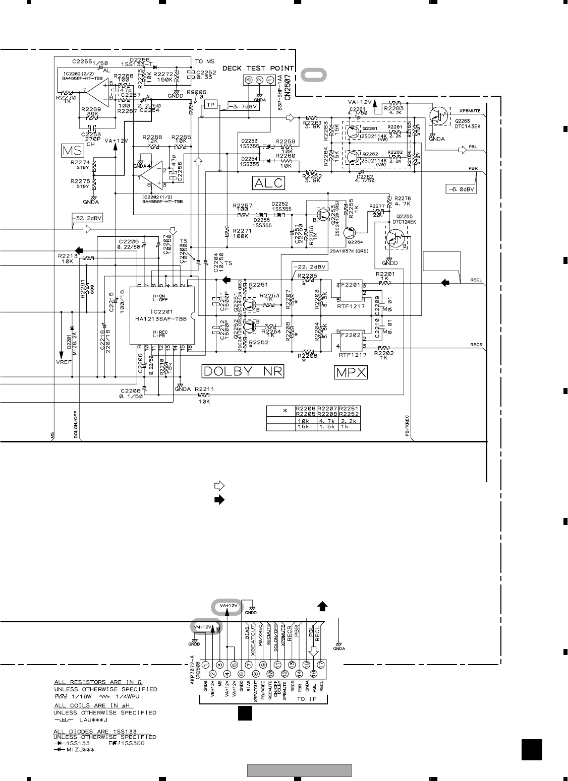
- 3.5 AF ASSY(1/2)
- 3.6 AF ASSY(2/2)
- 3.7 DECK ASSY
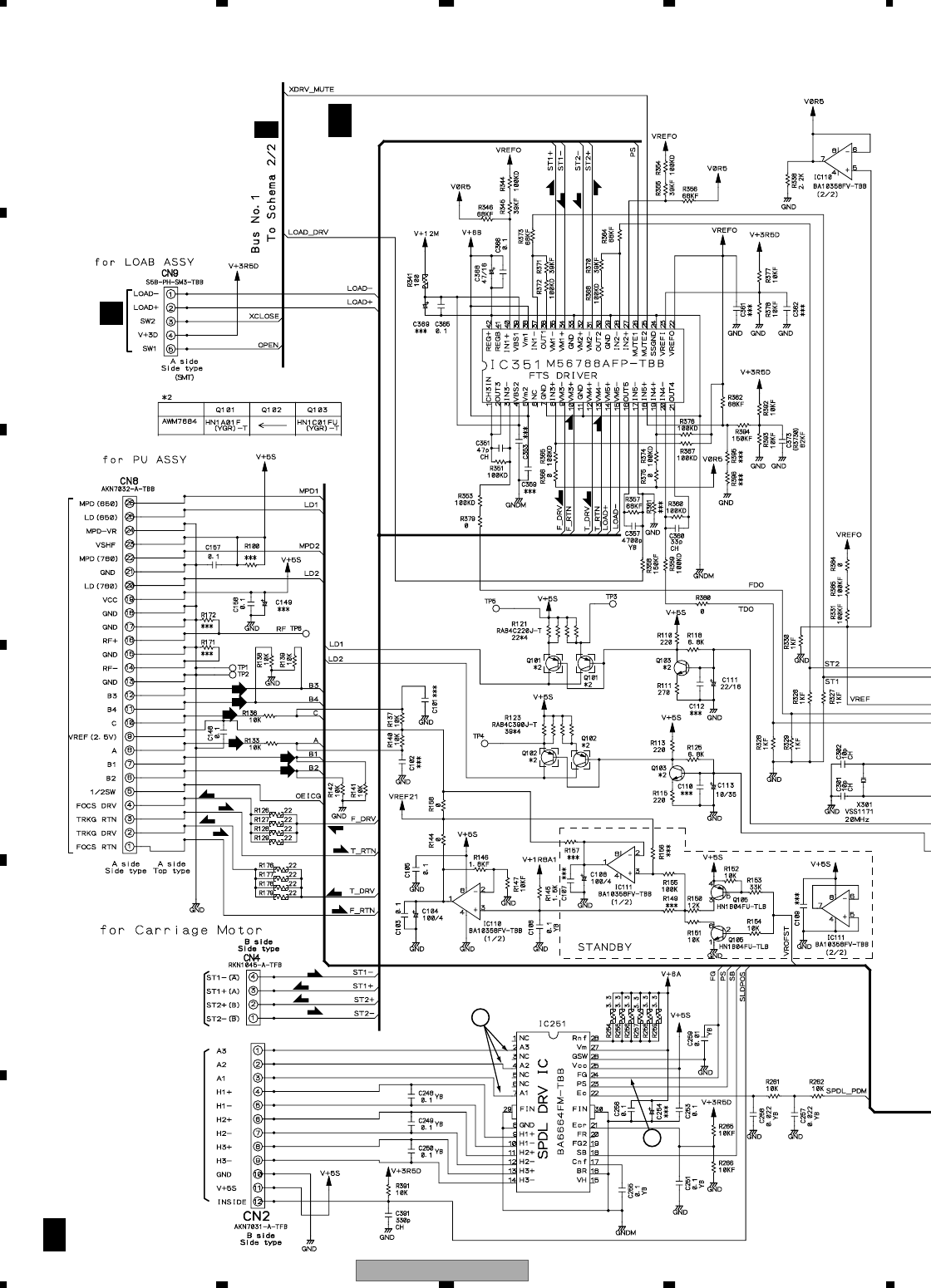
- 3.8 DVDM ASSY(1/2)
- 3.9 DVDM ASSY(2/2)
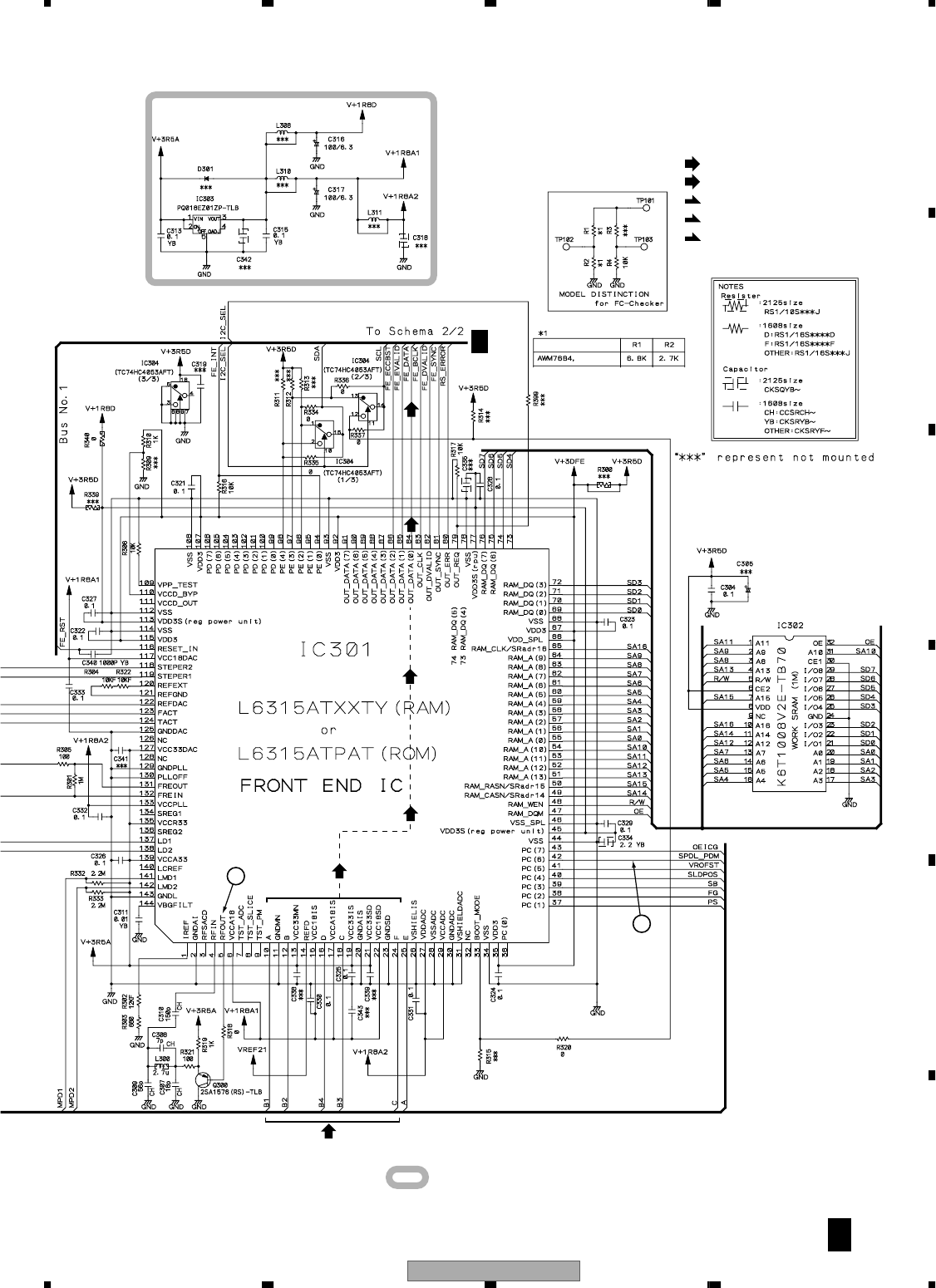
- 3.10 DVD IF ASSY
- 3.11 DISP1, DISP2, DISP3 and LED ASSYS
- 3.12 DSP ASSY
- 3.13 MIC ASSY
- 4. PCB CONNECTION DIAGRAM
- 4.1 LOAB ASSY
- 4.2 FM/AM TUNER MODULE
- 4.3 DVDM ASSY
- 4.4 DVD IF ASSY
- 4.5 IF ASSY
- 4.6 AF ASSY
- 4.7 DECK ASSY
- 4.8 DISP1, DISP2, DISP3 and LED ASSYS
- 4.9 MIC ASSY
- 4.10 DSP ASSY(XV-EV51 Only)
- 5. PCB PARTS LIST
- 6. ADJUSTMENT
- 6.1 DECK SECTION
- 6.1.1 Adjustment condition
- 6.1.2 Playback and Recording section
- 6.2 TUNER SECTION
- 6.3 DVD SECTION ADJUSTMENT ITEMS ana LOCATION
- 6.4 JIGS and MEASURING INSTRUMENTS
- 6.5 NECESSARY ADJUSTMENT POINTS
- 6.6 TEST MODE
- 6.7 MECHANISM ADJUSTMENT
- 7. GENERAL INFORMATION
- 7.1 DIAGNOSIS
- 7.1.1 TEST MODE
- 7.1.2 DISPLAY OF THE MECHANISM ERROR HISTORY
- 7.1.3 TRUBLE SHOOTNG
- 7.1.4 SEQUENCE AFTER POWER ON
- 7.1.5 DISASSEMBLY
- 7.2 PARTS
- 7.3 CLEANING
- 8. PANEL FACILITIES
- <グラフィック>
- <グラフィック>
- <グラフィック>

ORDER NO.
PIONEER CORPORATION 4-1, Meguro 1-chome, Meguro-ku, Tokyo 153-8654, Japan
PIONEER ELECTRONICS (USA) INC. P.O. Box 1760, Long Beach, CA 90801-1760, U.S.A.
PIONEER EUROPE NV Haven 1087, Keetberglaan 1, 9120 Melsele, Belgium
PIONEER ELECTRONICS ASIACENTRE PTE. LTD. 253 Alexandra Road, #04-01, Singapore 159936
PIONEER CORPORATION 2002
SOUND MODE
KARAOKE
VOLUME
ST. MEMORY
TIMER/CLOCK ADJ
DISPLAY
STEREO DVD TUNER DECK
EV51DVD
ENTER
DVD/CD
TUNER
TAPE
LINE
OPEN/CLOSE
DOLBY NR(DEMO)
ASES
MIC VOL
MAX
MIN
MIC
(MAIN)
MIC
(SUB)
REVERSE MODE
REC/STOP
PLAY/PAUSE STOPTUNING – TUNING +
4/1¡/¢
–+
XV-EV51
RRV2636
STEREO DVD TUNER DECK
XV-EV51
XV-EV21
THIS MANUAL IS APPLICABLE TO THE FOLLOWING MODEL(S) AND TYPE(S).
This product does not function properly independently; to avoid malfunctions, be sure
to connect it to the prescribed system component(s), otherwise damage may result.
Model Type Power Requirement Regienal restriction
codes (Region No.) Remarks
XV-EV51 ZLXJ/NC DC Power supplied from other system component 4
XV-EV21 ZLXJ/NC DC Power supplied from other system component 4
Component System System Service manual
MINI SYSTEM EVA-5CH EVA-2CH
Stereo DVD Tuner Deck XV-EV51 XV-EV21 RRV2636(This manual)
Stereo Power Amplifier M-EV51 M-EV21 RRV2663(EV51), RRV2664(EV21)
Speaker System S-EV51V S-EV21V RRV2640(EV51), RRV2641(EV21)
For details, refer to "Important symbols for good services" .
T-ZZR AUG. 2002 printed in Japan
XV-EV51
2
1234
1234
C
D
F
A
B
E
SAFETY INFORMATION
This service manual is intended for qualified service technicians ; it is not meant for the casual do-
it-yourselfer. Qualified technicians have the necessary test equipment and tools, and have been
trained to properly and safely repair complex products such as those covered by this
manual.Improperly performed repairs can adversely affect the safety and reliability of the product
and may void the warranty. If you are not qualified to perform the repair of this product properly and
safely, you should not risk trying to do so and refer the repair to a qualified service technician.
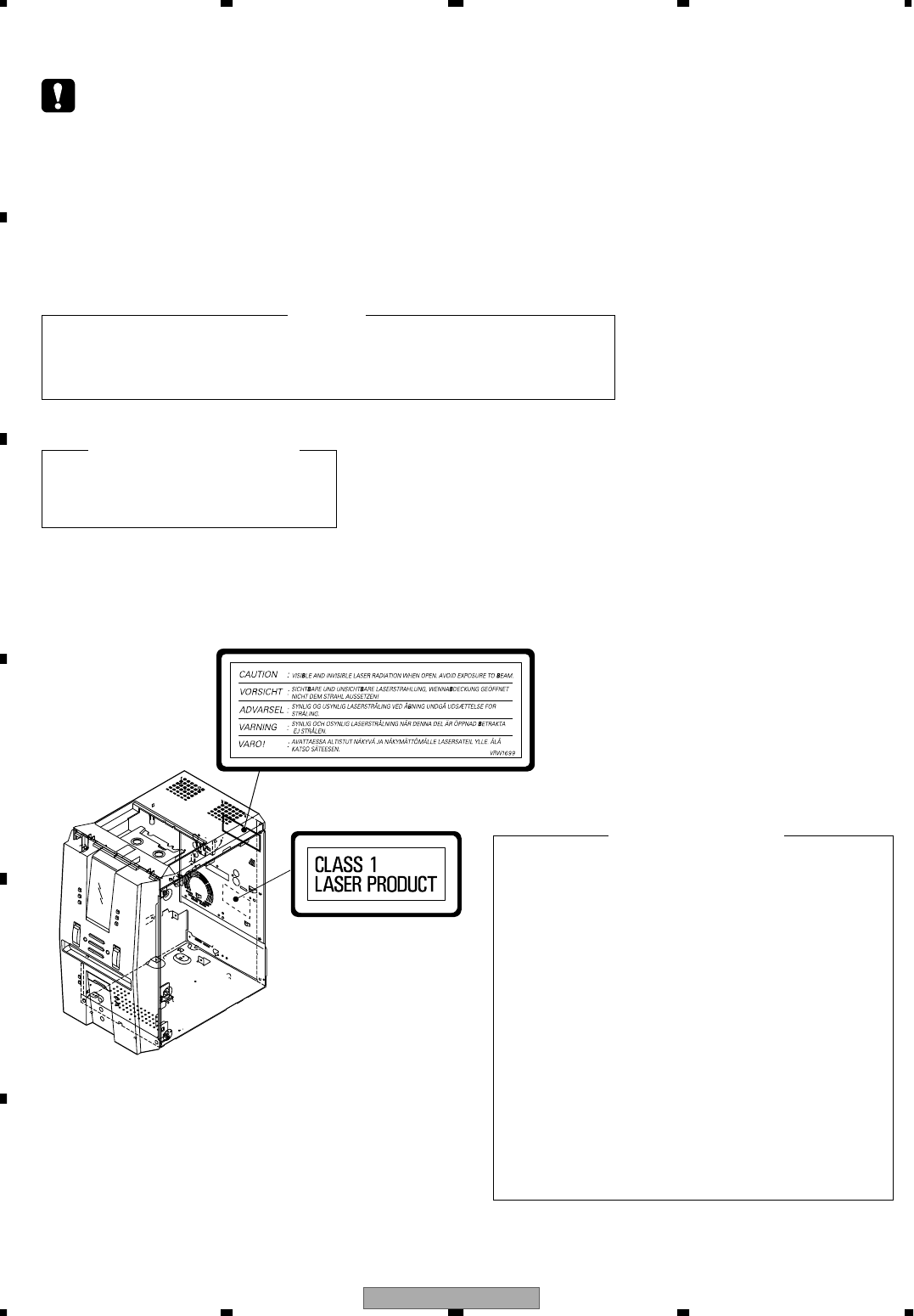
WARNING !
THE AEL (ACCESSIBLE EMISSION LEVEL) OF THE LASER POWER OUTPUT IS LESS THAN CLASS 1
BUT THE LASER COMPONENT IS CAPABLE OF EMITTING RADIATION EXCEEDING THE LIMIT FOR
CLASS 1.
A SPECIALLY INSTRUCTED PERSON SHOULD DO SERVICING OPERATION OF THE APPARATUS.
LASER DIODE CHARACTERISTICS
FOR DVD : MAXIMUM OUTPUT POWER : 5 mW
WAVELENGTH : 650 nm
FOR CD : MAXIMUM OUTPUT POWER : 5 mW
WAVELENGTH : 780 nm
Additional Laser Caution
∗ : See page 80.
1. Laser Interlock Mechanism
•Loading switch (S101 on the LOAB Assy) is used for interlock
mechanism of the laser.
When this switch turned ON in SW2 (XCLOSE) side (OPEN signal is
0V and XCLOSE signal is 3.5V), a laser becomes the status which
can completely oscillation.
Furthermore, the laser completely oscillates in the disc judgment and
disc playback.
When player is power ON state and laser diode is not completely
oscillating, 780nm laser diode is always oscillating by half power.
• Laser diode is driving with Q101 (650nm LD) and Q102 (780nm LD)
on the DVDM Assy.
Therefore, when short-circuit between the emitter and collector of
these transistors or the base voltage is supplied for transistors turn
on, the laser oscillates. (failure mode)
• In the test mode ∗ , there is the mode that the laser oscillates except
for the disc judgment and playback. LD ON mode in the test mode
oscillates with the laser forcibly.
The interlock mechanism mentioned above becomes invalid in this
mode.
2. When the cover is open, close viewing through the objective lens with
the naked eye will cause exposure to the laser beam.
LABEL CHECK
XV-EV51/ZLXJ/NC
(Printed on the Rear Panel A)
XV-EV51 3
5 678
5678
C
D
F
A
B
E
[ Important symbols for good services ]
In this manual, the symbols shown-below indicate that adjustments, settings or cleaning should be made securely.
When you find the procedures bearing any of the symbols, be sure to fulfill them:
2. Adjustments
To keep the original performances of the product, optimum adjustments or specification confirmation is indispensable.
In accordance with the procedures or instructions described in this manual, adjustments should be performed.
3. Cleaning
For optical pickups, tape-deck heads, lenses and mirrors used in projection monitors, and other parts requiring cleaning,
proper cleaning should be performed to restore their performances.
5. Lubricants, glues, and replacement parts
Appropriately applying grease or glue can maintain the product performances. But improper lubrication or applying
glue may lead to failures or troubles in the product. By following the instructions in this manual, be sure to apply the
prescribed grease or glue to proper portions by the appropriate amount.For replacement parts or tools, the prescribed
ones should be used.
4. Shipping mode and shipping screws
To protect the product from damages or failures that may be caused during transit, the shipping mode should be set or
the shipping screws should be installed before shipping out in accordance with this manual, if necessary.
1. Product safety
You should conform to the regulations governing the product (safety, radio and noise, and other regulations), and
should keep the safety during servicing by following the safety instructions described in this manual.
Discs compatible with this
player
Any disc that displays one of the following
logos should play in this player. Other
formats, including DVD-Audio, DVD-RAM,
DVD-ROM, CD-ROM (except those that
contain MP3 files), SACD and Photo CD will
not play.
Audio-CD
DVD-Video
Video-CD
* : Video Mode Only
CD-R *CD-RW *

XV-EV51
4
1234
1234
C
D
F
A
B
E
CONTENTS
SAFETY INFORMATION..................................................................................................................................... 2
1. SPECIFICATIONS ............................................................................................................................................ 5
2. EXPLODED VIEWS AND PARTS LIST ............................................................................................................ 6
2.1 PACKING ................................................................................................................................................... 6
2.2 EXTERIOR SECTION................................................................................................................................ 8
2.3 FRONT PANEL SECTION ....................................................................................................................... 10
2.4 LOADING MECHANISM ASSY ............................................................................................................... 12
2.5 TRAVERSE MECHANISM ASSY............................................................................................................. 14
3. BLOCK DIAGRAM AND SCHEMATIC DIAGRAM..........................................................................................16
3.1 BLOCK DIAGRAM ................................................................................................................................... 16
3.2 OVERALL WIRING DIAGAM ................................................................................................................... 20
3.3 FM/AM TUNER MODULE........................................................................................................................ 24
3.4 IF ASSY ................................................................................................................................................... 26
3.5 AF ASSY(1/2) .......................................................................................................................................... 28
3.6 AF ASSY(2/2) .......................................................................................................................................... 30
3.7 DECK ASSY ............................................................................................................................................ 32
3.8 DVDM ASSY(1/2)..................................................................................................................................... 34
3.9 DVDM ASSY(2/2)..................................................................................................................................... 36
3.10 DVD IF ASSY ......................................................................................................................................... 38
3.11 DISP1, DISP2, DISP3 and LED ASSYS................................................................................................ 40
3.12 DSP ASSY ............................................................................................................................................. 42
3.13 MIC ASSY.............................................................................................................................................. 44
4. PCB CONNECTION DIAGRAM ..................................................................................................................... 46
4.1 LOAB ASSY............................................................................................................................................. 46
4.2 FM/AM TUNER MODULE........................................................................................................................ 47
4.3 DVDM ASSY ............................................................................................................................................ 48
4.4 DVD IF ASSY ........................................................................................................................................... 52
4.5 IF ASSY ................................................................................................................................................... 54
4.6 AF ASSY.................................................................................................................................................. 56
4.7 DECK ASSY ............................................................................................................................................ 58
4.8 DISP1, DISP2, DISP3 and LED ASSYS.................................................................................................. 60
4.9 MIC ASSY................................................................................................................................................ 62
4.10 DSP ASSY(XV-EV51 Only).................................................................................................................... 63
5. PCB PARTS LIST ........................................................................................................................................... 64
6. ADJUSTMENT ............................................................................................................................................... 72
6.1 DECK SECTION ...................................................................................................................................... 72
6.1.1 Adjustment condition ......................................................................................................................... 72
6.1.2 Playback and Recording section ....................................................................................................... 73
6.2 TUNER SECTION.................................................................................................................................... 75
6.3 DVD SECTION ADJUSTMENT ITEMS ana LOCATION.......................................................................... 76
6.4 JIGS and MEASURING INSTRUMENTS ................................................................................................ 76
6.5 NECESSARY ADJUSTMENT POINTS ................................................................................................... 77
6.6 TEST MODE ............................................................................................................................................ 78
6.7 MECHANISM ADJUSTMENT.................................................................................................................. 79
7. GENERAL INFORMATION ............................................................................................................................. 82
7.1 DIAGNOSIS ............................................................................................................................................. 82
7.2 PARTS.................................................................................................................................................... 101
7.3 CLEANING............................................................................................................................................. 120
8. PANEL FACILITIES ...................................................................................................................................... 121
XV-EV51 5
5 678
5678
C
D
F
A
B
E
1. SPECIFICATIONS
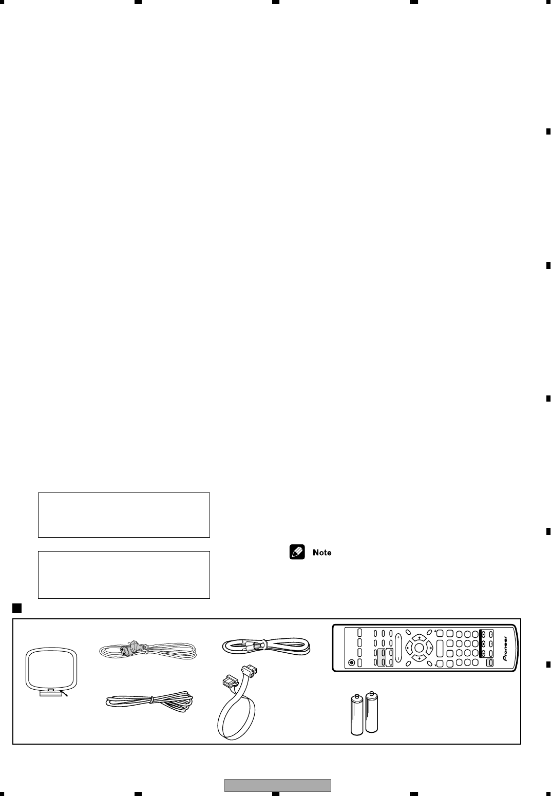
Accessories
(XXD3049)
AM loop antenna
(ATB7009) FM wire antenna
AC Power Cord
(ADH7004)
(XDG3001)
AA size IEC R6P
Dry cell batteries (x2)
Specifications
Amplifier Section
X-EV51DVD model
Continuous Power Output:
Front ...................................80 W per channel
(1kHz, 10 %, 8 Ω)
Center......................33 W (1kHz, 10 %, 8 Ω)
Surround.............................33 W per channel
(1kHz, 10 %, 8 Ω)
X-EV21DVD model
Continuous Power (RMS) .............80 W + 80 W
(1 kHz, THD 10%, 8 Ω)
Disc section
Digital audio
characteristics ................DVD fs: 96 kHz, 24-bit
Type ........... DVD system, Video CD system and
Compact Disc digital audio system
Frequency response ................... 4 Hz to 44 kHz
S/N ratio....................................................95 dB
Dynamic range ......................................... 95 dB
Total harmonic distortion ..................... 0.005 %
Wow and Flutter..................Limit of measurement
( 0.001 % W.PEAK) or less (EIAJ)
Cassette deck section
Systems.........................4 track, 2-channel stereo
Heads.......................Recording/playback head x 1
Erasing head x 1
Motor ................................... DC servo motor x 1
Tape types ...............................
TYPE I (Normal)
FM tuner section
Frequency Range........................
87.5 - 108MHz
Antenna ..................................75 Ω, unbalanced
AM tuner section
FrequencyRange
With 9 kHz step .......... 531 kHz to 1,602 kHz
With 10 kHz step ........ 530 kHz to 1,700 kHz
Antenna ........................................Loop antenna
Manufactured under license from Dolby
Laboratories. “Dolby”, “Pro Logic”, and
the
double-D symbol are trademarks of Dolby
Laboratories.
"DTS" and "DTS Digital Surround" are registered
trademarks of Digital Theater Systems, Inc.
Manufactured under license from Digital Theater
Sy
±
stems, Inc.
Miscellaneous
Power Requirements
Multi voltage model .......
.......
AC 110-127/ 220-230/
Power Consumption
X-EV51DVD model
Singapore, Malaysia, Hong Kong models
....................................
....................................
175 W
All other model 465 W
X-EV21DVD model
Singapore, Malaysia models .................. 150 W
All other model 540 W
Power Consumption in standby mode .............1 W
Dimensions:
DVD Tuner Deck .................. 170 (W) x 292.5 (H)
x 260 (D) mm
Power Amplifier ....................... 170 (W) x 190 (H)
x 254 (D) mm
Weight:
DVD Tuner Deck
XV-EV51 ................................................ 3.6 kg
XV-EV21 ................................................ 3.5 kg
Power Amplifier
M-EV51 .................................................. 5.3 kg
M-EV21 .................................................. 4.8 kg
Accessories (Stereo DVD Tuner Deck)
Operating instructions..........................................2
•Specifications and design subject to
possible modification without notice,
due to improvements.
Accessories (Stereo Power Amplifier)
Remote control .................................................... 1
Power cord
Australian, New Zealand, Central
and South American models........................... 2
All other models ............................................. 1
Power plug adapter (excluding Singapore,
Hong Kong and Malaysian models)..................... 1
Video cord............................................................ 1
System cable (EV51DVD) ................................... 2
System cable (EV21DVD) ................................... 1
FM antenna.......................................................... 1
AM loop antenna.................................................. 1
Dry cell batteries (AA/R6) ................................... 2
Video Cord
(VDE1034)
System Cable ×1
(XDE3053)
Remote control unit
240V(switchable), 50/60 Hz
TV CONTROL
123
456
7890
CLEAR
ENTER
SYSTEM SETUP
DVD SETUP
TOP MENU
DVD MENU
SHIFT CHANNEL VOLUME
INPUT
SELECT
SUBTITLE
VOLUME
ANGLE ZOOM
ADVANCED
MONO
SYSTEM DISP
DVD DISP
ECHO
DSP
AUDIO
DVD/CD TAPE FM/AM LINE
SURROUND
PROGRAM
TEST TONE
REPEAT
CH LEVEL
RANDOM
SLEEP
KARAOKE
I — KEYCON — iTIMER
CLOCK ADJ.
MUTE
RETURN
FOLDER +FOLDER –
SOUND
MODE
ENTER
STANDBY/ON
4
/eE/
1¡
¢
8
7
3
3
3
TUNE +
ST +ST –
TUNE –
XV-EV51
6
1234
1234
C
D
F
A
B
E
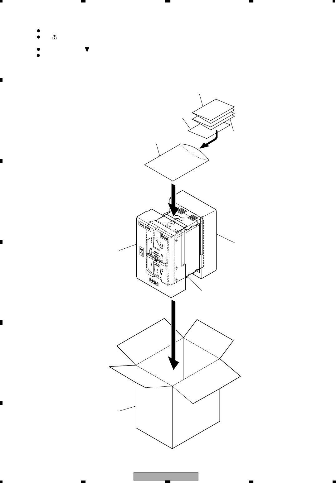
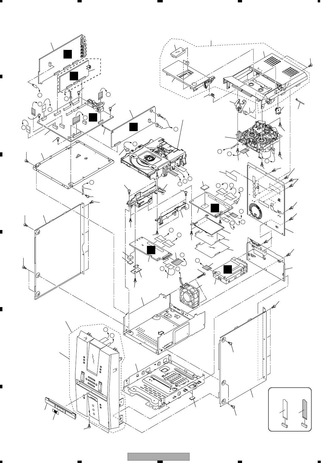
2. EXPLODED VIEWS AND PARTS LIST
2.1 PACKING
Parts marked by "NSP" are generally unavailable because they are not in our Master Spare Parts List.
The mark found on some component parts indicates the importance of the safety factor of the part.
Therefore, when replacing, be sure to use parts of identical designation.
Screws adjacent to mark on product are used for disassembly.
For the applying amount of lubricants or glue, follow the instructions in this manual.
(In the case of no amount instructions, apply as you think it appropriate.)
NOTES:
1
8
3
4
5
6
7
2
XV-EV51 7
5 678
5678
C
D
F
A
B
E
PACKING parts List
(2) CONTRAST TABLE
XV-EV51/ZLXJ/NC and XV-EV21/ZLXJ/NC are constructed the same except for the following :
Mark No. Description Part No.
1 Operating Instructions XRB3017
(English)
2 Operating Instructions XRC3073
(Chinese)
NSP 3 Polyethylene Bag Z21-038
(0.03 x 230 x 340)
4 Packing Sheet AHG7053
5 Front Pad M XHA3130
6 Rear Pad M XHA3131
7 Packing Case See Contrast table (2)
8 Correct Sheet XRH3007
Mark No. Description Part No.
Mark No. Symbol and Description XV-EV51/ZLXJ/NC XV-EV21/ZLXJ/NC
7 Packing Case XHD3305 XHD3308
XV-EV51
8
1234
1234
C
D
F
A
B
E
2.2 EXTERIOR SECTION
B
G
A
C
D
F
E
H
OL
M
M
N
D
E
A
B
F
C
N
G
H
I
L
K
J
K
J
I
O
C
K
B
E
F
A
G
CONTACT SIDE
NON-CONTACT
SIDE
932
8
Refer to
"2.4 LOADING MECHA ASSY".
Refer to
"2.3 FRONT PANEL SECTION".
3
2
21
11
32
27
35
24
23
12
5
613
14
15
22
20
17
33
34
26
31
10
19
18
1
28
25 29
16
4
30
7
XV-EV51
Only
XV-EV51
Only
40
40
40
40
39
39 44
45
48
46
47
50
39
39
39
40
42
40
43
37
39
39
39
39
39
39
39
39
39
52
38 38
38
38
40
51
49
41
36
43
42
39
40
XV-EV51 9
5 678
5678
C
D
F
A
B
E
EXTERIOR SECTION parts List
(2) CONTRAST TABLE
XV-EV51/ZLXJ/NC and XV-EV21/ZLXJ/NC are constructed the same except for the following :
Mark No. Description Part No.
1 FM/AM TUNER Module AXQ7228
2 IF Assy See Contrast table (2)
3 AF Assy See Contrast table (2)
4 DECK Assy See Contrast table (2)
5 DVDM Assy AWM7684
6 DVD IF Assy AWM7677
7 DSP Assy See Contrast table (2)
8 DECK Mechanism Unit XYM3015
NSP 9 LOADING MECHA Assy VWT1203
10 DC Fan Motor AXM7025
NSP 11 Earth Lead Wire DE012VF0
12 11P Flat Flexible Cable XDD3114
13 13P Flat Flexible Cable XDD3115
14 30P Flat Flexible Cable XDD3116
15 16P Flat Flexible Cable XDD3117
16 Connector Assy 5P XDE3055
NSP 17 Chassis XNA3011
18 Rear Panel A See Contrast table (2)
19 Rear Panel B See Contrast table (2)
20 Mecha Frame XNG3082
21 DVD Shield XNG3083
22 GND Plate XNG3084
23 Ratch Spring ABH7130
24 Damper Assy AXA7052
25 Door Spring L XBH3010
26 Leg Cushion XEB3028
27 Deck Lens XAK3327
28 Deck Door XAN3047
29 Ratch Mold XMR3001
30 Side Bonnet L XNE3026
31 Side Bonnet R XNE3027
32 Binder ZCA-SKB90BK
33 Tray Cap XAK3325
34 DVD Badge XAK3331
35 Top Panel XAK3326
NSP 36 Front Panel Assy See Contrast table (2)
NSP 37 Top Panel Assy XXG3131
38 Screw VPZ30P080FZK
39 Screw BBZ30P080FZK
40 Screw BBZ30P080FMC
41 Screw BPZ30P350FZK
42 Screw VPZ30P080FNI
43 Screw BBZ30P080FNI
44 Adapter 02 L ANW7247
45 Adapter 02 R ANW7248
46 Shield Case ANK7108
47 Heat plate ANG7426
48 Radiation Sheet AEB7255
49 Cushion AEB7267
50 FFC Barrier AEC7443
51 FFC Spacer AEC7442
52 Caution Label VRW1699
Mark No. Description Part No.
Mark NO Symbol and Description XV-EV51/ZLXJ/
NC XV-EV21/ZLXJ/NC
2 IF Assy XWZ3617 XWZ3627
3 AF Assy XWZ3618 XWZ3628
4 DECK Assy XWX3067 XWX3066
7 DSP Assy AWX8059 Not used
18 Rear Panel A XNC3160 XNC3180
19 Rear Panel B XNC3161 XNC3176
NSP 37 Front Panel Assy XXG3129 XXG3130

XV-EV51
10
1234
1234
C
D
F
A
B
E
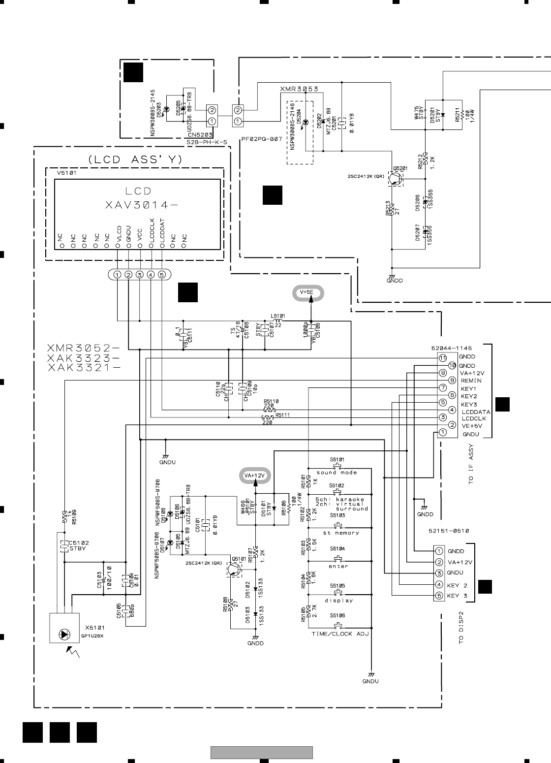
2.3 FRONT PANEL SECTION
A
A
B
B
C
D5108
D5107
CONTACT SIDE
NON-CONTACT
SIDE
J
L
I
H
M
1
6
6
8
9
11
11
13
7
14
21
22
26
35
24
25
29
28
17
16 18
4
19
2
23
27
31
37
32
36
20
10
5
3
30
15
12
34
38
33
33
33
33
33
33
33
33
33
33
39
XV-EV51 11
5 678
5678
C
D
F
A
B
E
FRONT PANEL SECTION parts List
(2) CONTRAST TABLE
XV-EV51/ZLXJ/NC and XV-EV21/ZLXJ/NC are constructed the same except for the following :
Mark No. Description Part No.
1 DISP 1 Assy XWZ3619
2 DISP 2 Assy XWZ3620
3 DISP 3 Assy XWZ3621
4 LED Assy XWZ3622
5 MIC Assy See Contrast table (2)
6 LED (D5107, D5108) NSPWF50BS-9706
7 LCD XAV3016
8 11P Flat Flexible Cable XDD3113
9 LCD Holder XMR3052
10 MIC Knob XAA3024
11 Diffusion Sheet XAK3321
12 Display Window See Contrast table (2)
13 LCD LT Cond XAK3323
14 LCD Cover XAK3324
15 Sensor Cover XAK3330
16 Tray Lens XAK3332
17 FUNC. LT Cond XAK3333
18 LT Cond XAK3334
19 LT Cover XAK3335
20 Jack Door XAN3048
21 Display Button L XAD3149
22 Display Button R XAD3150
23 Play Button XAD3151
24 Dolby Button L XAD3154
25 Dolby Button R XAD3155
26 FUNC. Button L XAD3152
27 FUNC. Cover L XAK3328
28 FUNC. Button R XAD3153
29 FUNC. Cover R XAK3329
30 Front Panel M See Contrast table (2)
31 Damper Assy XXA3029
32 Leg Cushion XEB3028
33 Screw VPZ30P080FZK
34 FUNC. Assy R XAD3158
35 FUNC. Assy L XAD3157
36 Cushion XEB3004
37 Gap Cover XMR3055
38 Magnet XMF3003
39 Screw 2x4 B XBA3011
Mark No. Description Part No.
Mark No. Symbol and Description XV-EV51/ZLXJ/NC XV-EV21/ZLXJ/NC
5 MIC Assy XWZ3626 XWZ3623
12 Display Window XAK3322 XAK3343
30 Front Panel M XMB3084 XMB3089
XV-EV51
12
1234
1234
C
D
F
A
B
E
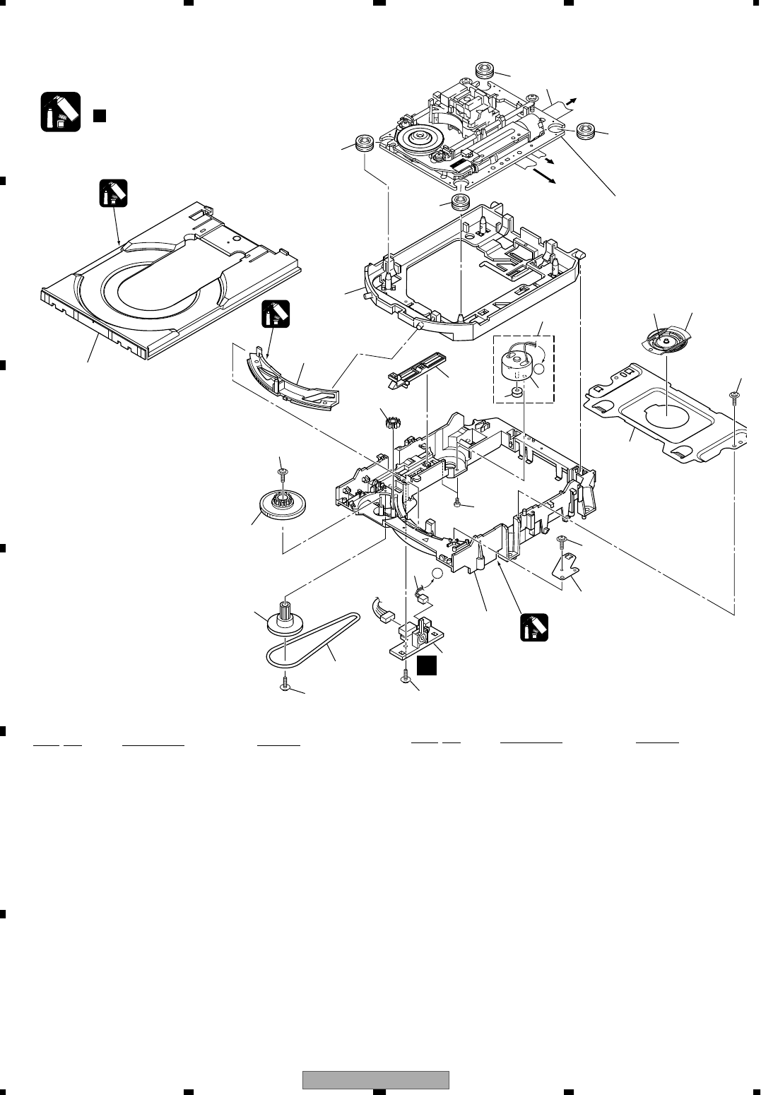
2.4 LOADING MECHANISM ASSY
LOADING MECHANISM ASSY parts List
A
A
To
DVDM
CN8
To DVDM
CN4
To DVDM
CN2 2
3
5
4
12
23
13
17
21
16
22
15
14
22 22
22
2
2
20
18
19
91
7
11
10
6
8
8
8
8
D
Refer to
"2.5 TRAVERSE MECHANISM
ASSY-S".
Lubricating Oil
GYA1001
Daifree
GEM1036
Refer to
" Application of Lubricant".
Note :
Lubricating Oil
GYA1001
Mark No. Description Part No.
NSP 1 LOAB Assy VWG2346
2 Traverse Mechanism Assy-S VXX2858
3 Loading Motor Assy VXX2505
4 Motor Pulley PNW1634
5 Carriage DC Motor / 0.3W PXM1027
6 Flexible Cable (26P) VDA1864
7 Connector Assy 2P VKP2253
8 Float Rubber VEB1327
9 Belt VEB1330
10 Stabilizer VNE2253
11 Loading Base VNL1917
12 Float Base DVD VNL1918
13 Drive Cam VNL1919
14 Gear Pulley VNL1921
15 Loading Gear VNL1922
16 Drive Gear VNL1923
17 SW Lever VNL1925
18 Clamper Plate VNE2251
19 Bridge VNE2252
20 Clamper VNL1924
21 Screw JGZ17P028FMC
22 Screw Z39-019
23 Tray VNL1920
Mark No. Description Part No.
XV-EV51 13
5 678
5678
C
D
F
A
B
E
Application of Lubricant
No. 11
Loading Base
Lubricating Oil
GYA1001
Around the shaft
Concave of unevenness
Concave of unevenness
Concave of unevenness
No. 13
Drive Cam
No. 13
Drive Cam
No. 23
Tray No. 23
Tray
Top View
Rear View Top View
Bottom View
Daifree
GEM1036
Daifree
GEM1036
Daifree
GEM1036
Daifree
GEM1036
Daifree
GEM1036
Side of the rib
Inner side of a ditch
Inner side of a ditch
Lubricating Oil
GYA1001
Lubricating Oil
GYA1001
Inner side of a ditch
Lubricating Oil
GYA1001
Lubricating Oil
GYA1001
Lubricating Oil
GYA1001
XV-EV51
14
1234
1234
C
D
F
A
B
E
2.5 TRAVERSE MECHANISM ASSY
To
DVDM
CN8
To DVDM
CN4
To SSIB
CN1
12
8
3
7
1
18
16
19
18
10
13
18
10
6
5
5
11
15
14
9
16
2
CONTACT SIDE
NON-CONTACT
SIDE
4 (Adjustment Screw)
Screw Tight
GYL1001 Silicone Adhesive
GEM1037
Silicone Adhesive
GEM1037
17 (Torque : 0.12 ± 0.01 N•m)
17 (Torque : 0.12 ± 0.01 N•m)
Silicone Adhesive
GEM1037
17 (Torque : 0.12 ± 0.01 N•m)

XV-EV51 15
5 678
5678
C
D
F
A
B
E
TRAVERSE MECHANISM ASSY parts List
Mark No. Description Part No.
1 Spindle Motor VXM1088
2 Stepping Motor VXM1090
>
3 Pickup Assy-S OXX8004
4 Skew Screw VBA1080
5 Skew Spring VBH1335
6 Guide Bar VLL1514
7 Sub Guide Bar VLL1515
8 Hold Spring VNC1017
9 Joint Spring VNC1019
10 Support Spring VNC1020
NSP 11 Mechanism Chassis VNE2248
12 Slider VNL1811
13 Spacer VNL1913
14 Joint VNL1914
15 FFC Holder VNL1915
16 Screw BBZ20P050FZK
17 Tapping Screw OBA8009
18 Screw PMA26P100FMC
19 Damper Sheet VEB1335
XV-EV51
16
1234
1234
C
D
F
A
B
E
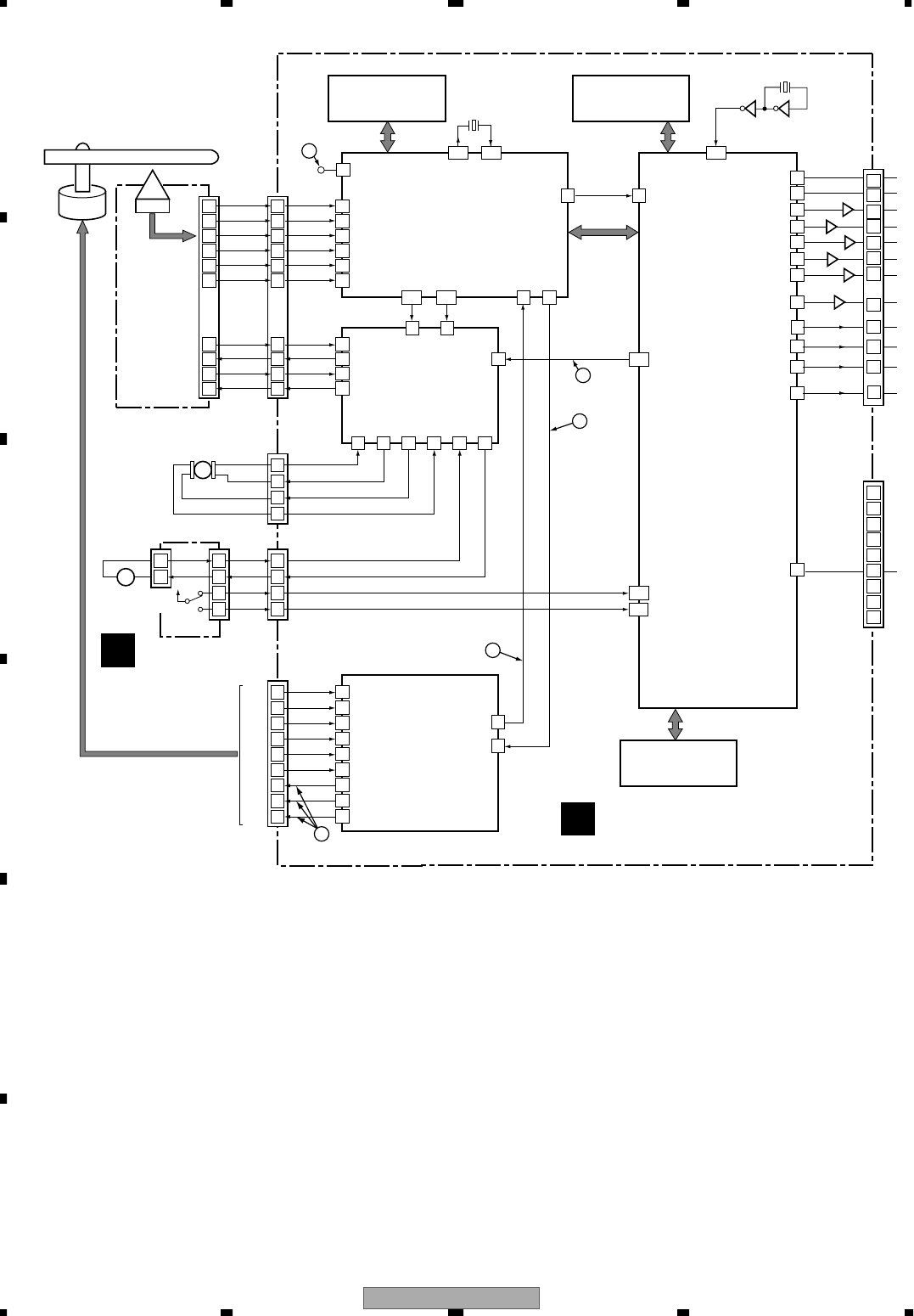
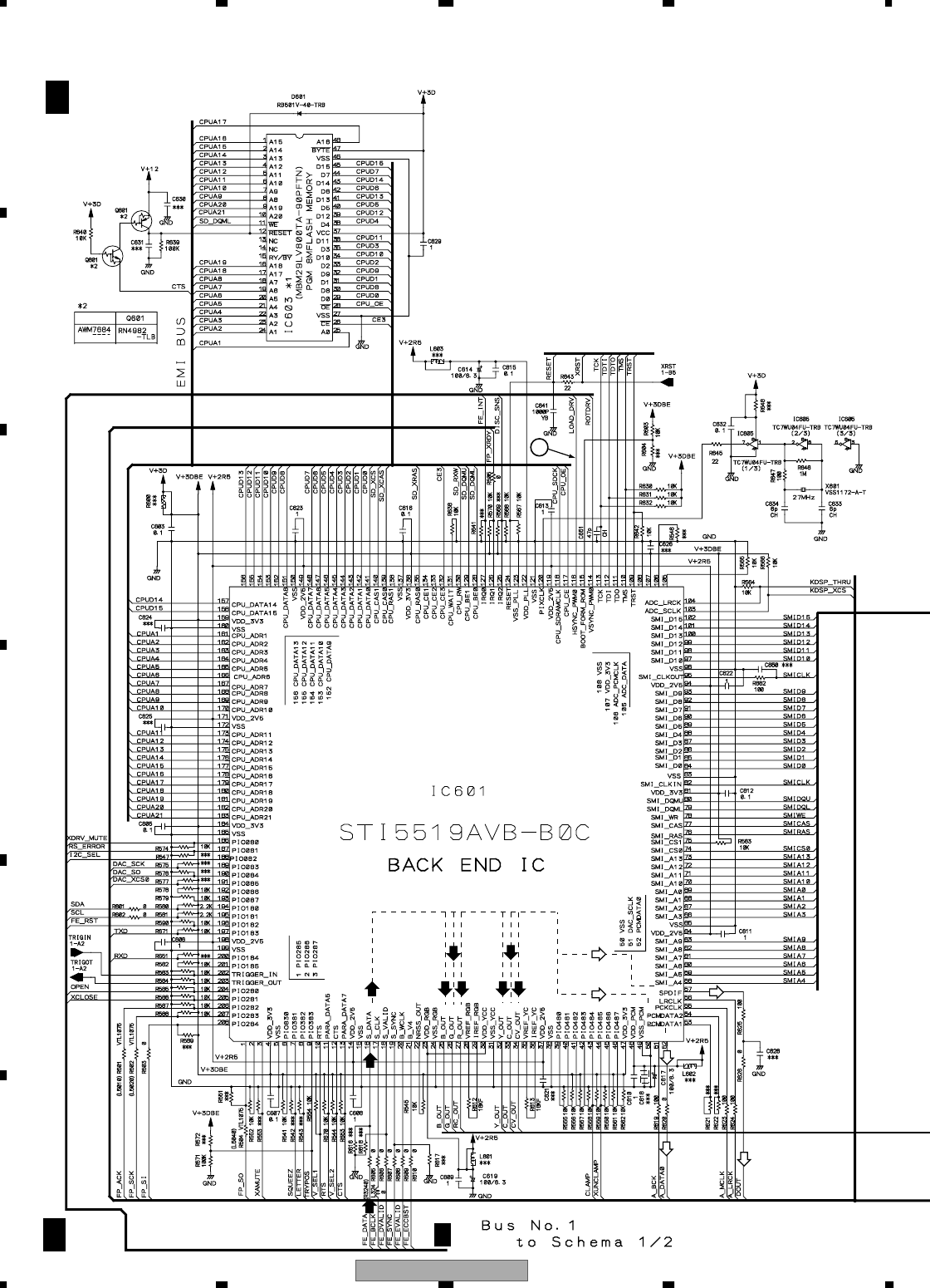
3. BLOCK DIAGRAM AND SCHEMATIC DIAGRAM
3.1 BLOCK DIAGRAM
CN
CN5903
CN5901
EV-51 : PDC093
EV-21 : PDC097
16,17
5,6
5,6
7
73
348
4
8
RECL
PBL
17 16 2
DSP ASSY
XV-EV51 Only
H
DECK ASSY
E
IF ASSY
B
DVDM ASSY
DVD IF ASSY
F
G
DISP1 ASSY
J
(D)
(D)
(V)
(Y)
(C)
3.1.1 SIGNAL ROUTE(1/2)
(REC)
Refer to 3.1.2 SIGNAL ROUTE(2/2)
CN5509
CN5801
CN2506
CN5101
XV-EV51 17
5 678
5678
C
D
F
A
B
E
M-EV51
(POWER AMPLIER)
Service Manual
Order No.RRV2663
CN8701
JA5401
CN3002
CN8901
CN5503
CN5501
MIC ASSY
AF ASSY
CM
FM/AM TUNER
MODULE
A
SIGNAL ROUTE
: PB SIGNAL
: RECORDING SIGNAL
(D)
(PB)
(PB)
(PB)
(PB)
(PB)
(TX)
(REC)
(REC)
: AUDIO SIGNAL (TUNER)
(V)
(V)
(TX)
(TX)
: V SIGNAL VIDEO
(Y)
(Y) : Y SIGNAL VIDEO
(C)
(C) : C SIGNAL VIDEO
(SL)
(FL)
: SL AUDIO SIGNAL
: FL AUDIO SIGNAL
: C AUDIO SIGNAL
(SW)
(C)
: SW AUDIO SIGNAL
: DIGITAL AUDIO ROUTE
J5401
CN8101
CN5504
CN8301
XV-EV51
18
1234
1234
C
D
F
A
B
E
CN4
(4P)
IC301
L6315ATXXTY
FRONT END IC
Spindle
Motor
B1
X301
20MHz
B2
FACT
B3
B4
A
A
RFSACD FREOUT FREIN
OUT_DATA(0) S_DATA
FE_DATA
RF(TP)
B
C
D
E
F
VM4-
VM4+
VM3+
VM3-
C
Stepping
Motor
(Carriage)
FDO
T_DRV
T_RTN
F_RTN
F_DRV
ST1-
ST1+
ST2+
ST2-
PICKUP
ASSY
CN151
(26P)
(26P)
DLOAB ASSY
FDVDM ASSY
M
IC351
M56788AFP
FTS Driver
IC251
BA6664FM
Spindle
Driver
20
21
15
16
19
17
7
6
12
11
8
10
10
3
84
B_OUT 25
16
HSYNC
_PWM0
131
123
TDO FG
LOAD_DRV
SPDL
PDM
FG
SPDL PDM
TACT
IN4-
VM1+
IN5-
IN3-
PC(2) PC(6)
124
116
132
PIXCLK
120
12
18
16
25
24
13
12
H1+
FG
EC
H1+ 9
24
22
10
9
4238
3 20
34
VM1-
35
VM2-
31
VM2+
32
VM5-
15
VM5+
14
17
24
25
26
23
3
2
1
4
4
3
CN2
(12P)
CN22
(30P)
CN25
(26P)
CN401
(13P)
4
2
1
IC302
K6T1008V2E-TB70
1M SRAM
Work RAM for Error Correction
IC604
K4S641632F-TC75
64M SDRAM
Work RAM for MPEG Decode
IC603
VYW1948
8M FLASH ROM
• RF Demodulation
• Servo Control
• Servo Decode
• Error Correction
IC601
STI5519AVB-B0C
BACK END IC
• System Control
• MPEG Video Decode
• Video Encode
• Video DAC
• Audio Decode
(MP3, Dolby)
• Sub-picture Decode
• Spindle Drive
• FG Detection
Focus, Tracking,
Stepper and
Loading Drive
X601
27MHz
Loading
Motor
Assy
+–M
H1-H1- 10
5
H2+H2+ 11
6
H2-H2- 12
7
H3+H3+ 13
8
H3-H3- 14
9
A1A1 7
3
A2A2 4
2
A3A3 2
1
1
3562
IC605 TC7WU04FU
Q607
G_OUT 26 Q606
R_OUT 27
DAC_SCLK 51
PCMDATA0 52
PCKCLK 55
Q605
Y_OUT 32 Q604
C_OUT 33 Q603
CV_OUT 34
SPDIF DOUT
A_BCK
57
Q602
A_DATA0
A_MCLK
LRCLK 56 A_LRCK
PIO381 7
PIO382 8
SQUEEZ
LETTER
LOD+
SW2
SW1
LOD-
3.3V
CN602
(2P)
CN601
(5P) CN9
(5P)
1
2
1
2
1
2
33
55
XCLOSE
OPEN
S101
205
204
XCLOSE
OPEN
3
4
24
5
26
21
7
9
11
13
22
15
5
3
4
2
1
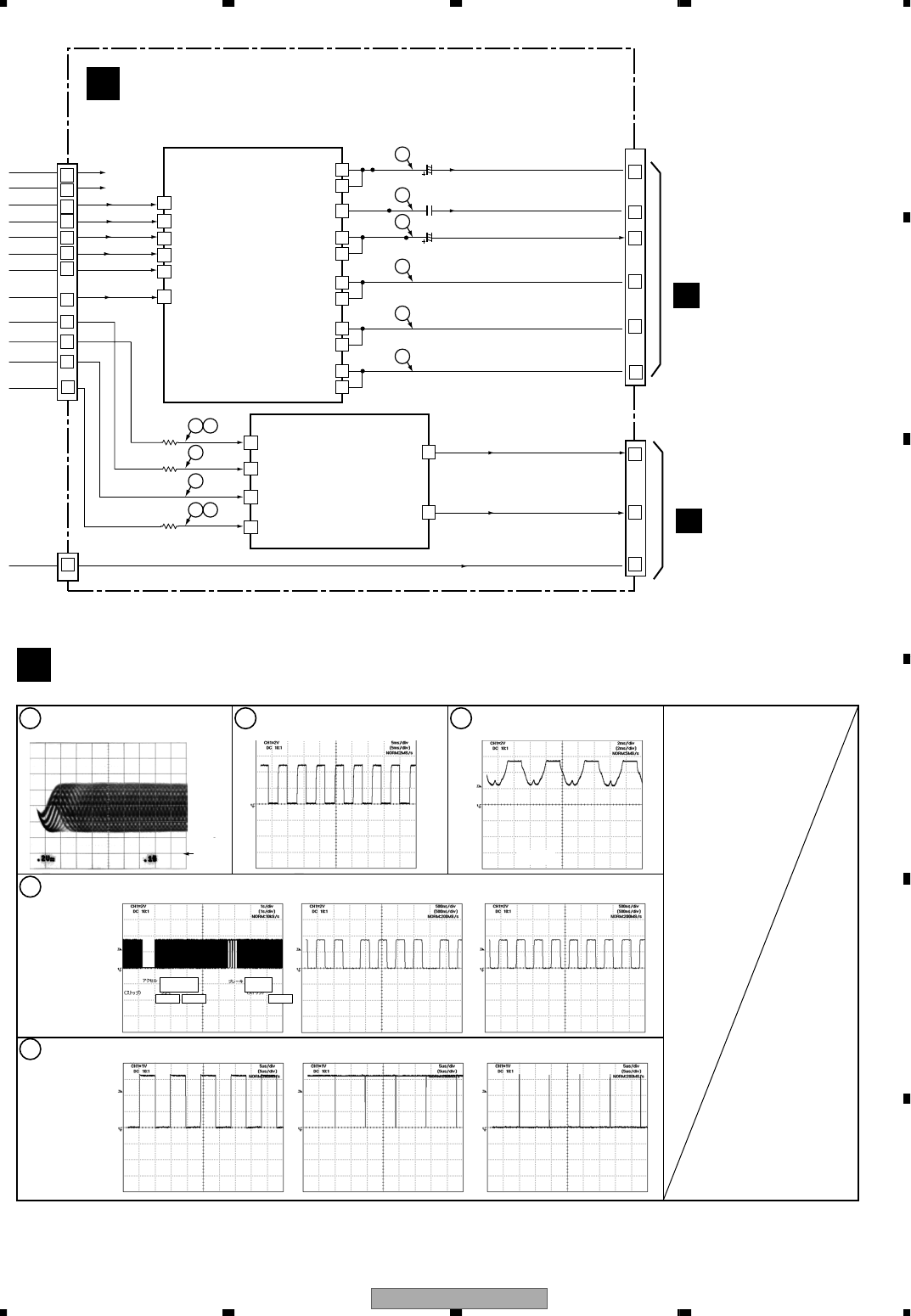
3.1.2 SIGNAL ROUT(2/2)
XV-EV51 19
5 678
5678
C
D
F
A
B
E
GDVD IF ASSY
Cb IN
YOUT b
YOUT a
COUT
VOUT b
VOUT a
CYOUT b
CYOUT a
CrOUT b
CrOUT a
CbOUT b
CbOUT a
Y
14
28
27
V
31
30
G
25
24
R
19
18
B
22
21
C
33
CN1961
(30P)
CN1901
(30P)
CN1962
(26P)
CN1902
(16P)
IC801
MM1567AJ
6 IN • 6 OUT
VIDEO AMP
BCKIN
1
DATA
2
MCLK
16
LRCKIN
3
IC711
PCM1742KE
Audio 2ch DAC
• LPF
• AMP
• Driver
1
B
CY IN
12
G
Cr IN
16
R
Y IN
6
S_Y
C IN
2
S_C
R721
R722
R723
V IN
4
V
DIGITAL
OUT
Vout L LOUT
7
Vout R 8 ROUT
C812
C822
C832
AUDIO
OUT
3
4
24
5
26
21
7
9
11
13
22
15
10
24
14
16
6
8
30
28
12
7
12
11
8
9
10
2 5
6
1
3 4
1– =: Refer to "3.1.3 WAVEFORMS".
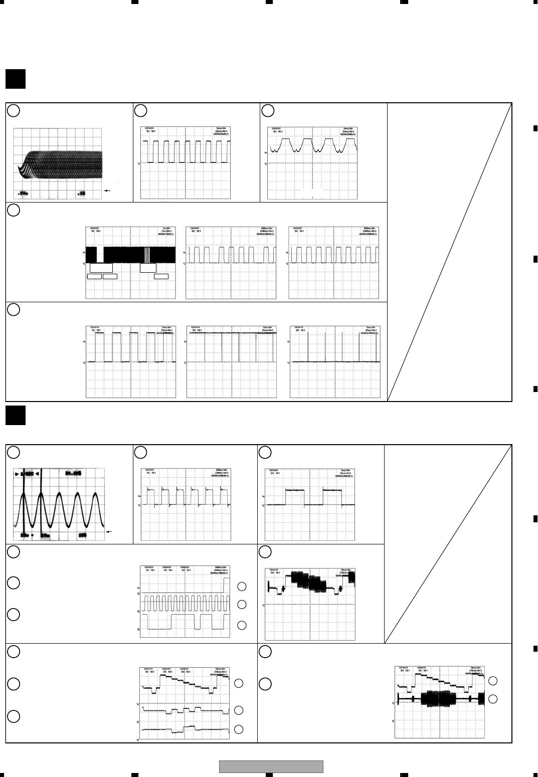
3.1.3 WAVEFORMS
CN5903
B
B
CN5901
1IC301 - pin 3 [RF]
V: 200mV/div. H: 0.1µsec/div. 2IC251 - pin 24 [FG]
V: 1V/div. H: 5msec/div.
GND
5IC601 - pin 116 [LOAD_DRV]
V: 1V/div. H: 5µsec/div.
4IC301 - pin 42 [SPDL_PDM]
DVDM ASSY
F
[Tray stops][Tray is opening][Tray is closing]
[PLAY][STOP→PLAY→STOP] [STOP]
STOP STOPPLAY
Accelertar
ON Brakes
ON
V: 2V/div. H: 500nsec/div. V: 2V/div. H: 500nsec/div.
3IC251 - pin 2, 4, 7
[Spidle driver -A3, A2, A1]
V: 2V/div. H: 2msec/div.
[PLAY]
V: 2V/div. H: 1sec/div.
Note : The encircled numbers denote measuring point in the schematic diagram.
Measurement condition
: No. 1 and 2 : reference A1 (DVD), T2-chp 19, Color-bar
XV-EV51
20
1234
1234
C
D
F
A
B
E
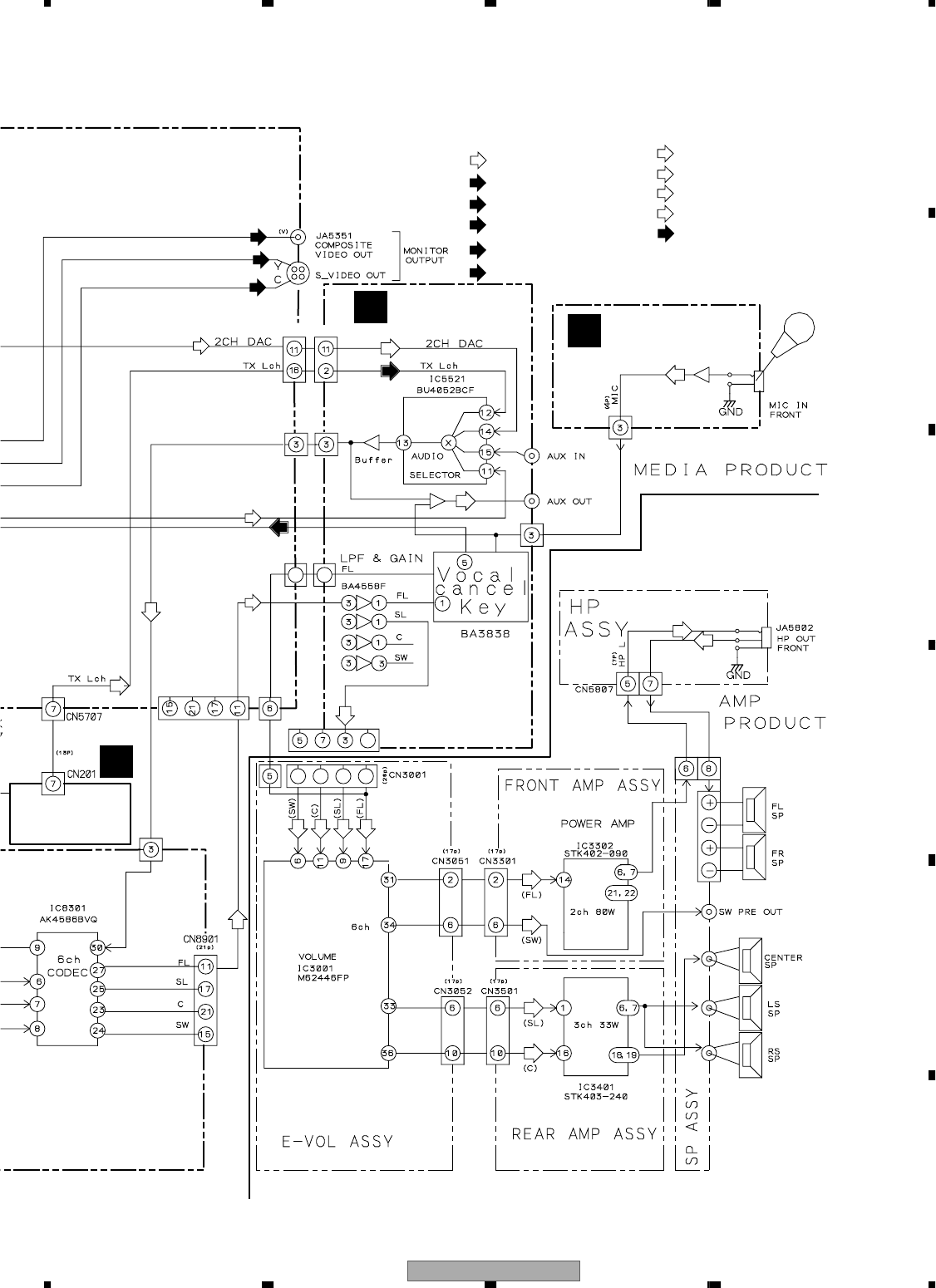
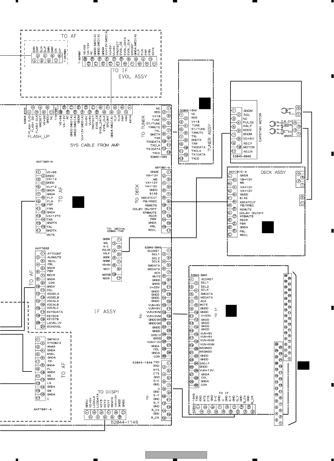
3.2 OVERALL WIRING DIAGAM
XV-EV51
Only
DSPCK
DSPRQ
DSPRO
XDSPRST
DIRRX1
DIRRX2
DIRRX3
DIRRX4
DIRTX
ADCR
ADCL
DSPCS
CDCOVF
AF ASSY
(XWZ3618 / XV-EV51)
(XWZ3628 / XV-EV21)
C1/2 - 2/2
MIC ASSY
(XWZ3626/
XV-EV51)
(XWZ3623/
XV-EV21)
M
J
L
DSP ASSY
(AWZ8059 / XV-EV51)
LED ASSY
(XWZ3622)
K
DISP3 ASSY
(XWZ3621) DISP2 ASSY
(XWZ3620)
DISP1 ASSY
(XWZ3619)
H
I
3.2.1 OVERALL WIRING DIAGRAM(MEDIA PART 1/2)
CN5508
CN5902
CN8751
CN8101
CN8701
CN8901
CN8301J5401
CN5507
CN5506
CN8002
CN8001
CN8003
CN5203
5301 J5202
J5203
J5102
CN5102
CN5101
Note : When ordering service parts, be sure to refer to "EXPLODED VIEWS and PARTS LIST" or "PCB PARTS LIST"
XV-EV51 Only
XV-EV51 21
5 678
5678
C
D
F
A
B
E
DVD IF ASSY
DVD IF ASSY
IF ASSY
(XWZ3617 / XV-EV51)
(XWZ3627 / XV-EV21)
B
A
FM/AM TUNER
MODULE
(AXQ7228)
DECK ASSY
(XWX3067 / XV-EV51)
(XWX3066 / XV-EV21)
DECK
MECHA. (XYM3015)
E
DVD IF ASSY
(AWM7677)
DVDM ASSY
(AWM7684)
G
1/2
F
- 2/2
M-EV51
(STEREO POWER AMPLIFIER)
Service Manual
order no. RRV2663
CN5505
CN5903
CN5802
CN5801
CN2506
CN2301
CN2302
CN5503
CN5501
CN5502
CN5504
CN5509
CN5901
CN1902
CN1962
CN1961
CN1901
XDD3113
XDD3117
XDD3115
REC/PB
HEAD
ERASE
HEAD
XDD3116
CN5701
CN201
CN3001
CN3002
XV-EV51 Only
XV-EV51
22
1234
1234
C
D
F
A
B
E
ABCDE
D
LOAB ASSY
(VWG2346)
DLOADING
MOTOR ASSY
: VXX2505
SPINDLE
MOTOR
: VXX1088
PICKUP ASSY-S
(OXX8003)
STEPPING MOTOR
: VXM1090
: FOCUS SERVO LOOP LINE
: TRACKING SERVO LOOP LINE
(F)
(T)
: SLIDER SERVO LOOP LINE
(S)
(F)
(F)
(F)
(T)
(F)
(F)
(F)
(F)
(F)
(T)
(F)
(T)
(T)
(F)
(S)
(S)
(S)
(S)
DVDM ASSY
(AWM7684)
1/2
F
- 2/2
DVD IF ASSY
(AWM7677)/CN1962
G
DVD IF ASSY
(AWM7677)/CN1961
G
3.2.2 OVERALL WIRING DIAGRAM (MEDIA PART 2/2)
XV-EV51 23
5 678
5678
C
D
F
A
B
E
CDAB
1IC301 - pin 3 [RF]
V: 200mV/div. H: 0.1µsec/div.
3IC711 - pin 3 [AUDIO DAC -LRCK]
V: 2V/div. H: 5µsec/div.
2IC251 - pin 24 [FG]
V: 1V/div. H: 5msec/div.
1 2
IC711 - pin 16 [AUDIO DAC -MCK]
V: 1V/div. H: 20nsec/div.
IC711 - pin 1 [AUDIO DAC -BCK]
V: 2V/div. H: 200nsec/div.
GND
5IC601 - pin 116 [LOAD_DRV]
V: 1V/div. H: 5µsec/div.
4IC301 - pin 42 [SPDL_PDM]
5
4IC711 - pin 3
[AUDIO DAC -LRCK]
V: 2V/div. H: 500nsec/div.
IC711 - pin 1
[AUDIO DAC -BCK]
V: 2V/div. H: 500nsec/div.
6IC711 - pin 2
[AUDIO DAC -DATA]
V: 2V/div. H: 500nsec/div.
8Foot of C842 (IC801 - pin 24, 25)
[Component Video output -Y]
V: 1V/div. H: 10µsec/div.
9Foot of C852 (IC801 - pin 18, 19)
[Component Video output -Cb]
V: 2V/div. H: 10µsec/div.
11 Foot of C832 (IC801 - pin 27, 28)
[S Video output -Y]
V: 1V/div. H: 10µsec/div.
12 Foot of C822 (IC801 - pin 33)
[S Video output -C]
V: 1V/div. H: 10µsec/div.
10 Foot of C862 (IC801 - pin 21, 22)
[Component Video output -Cr]
V: 2V/div. H: 10µsec/div.
7Foot of C812 (IC801 - pin 30, 31)
[Composite Video output]
V: 1V/div. H: 10µsec/div.
DVDM ASSY
F
DVD IF ASSY
G
GND
4
5
6
8
9
11
12
10
[Tray stops][Tray is opening][Tray is closing]
[PLAY][STOP→PLAY→STOP] [STOP]
STOP STOPPLAY
Accelertar
ON Brakes
ON
V: 2V/div. H: 500nsec/div. V: 2V/div. H: 500nsec/div.
3IC251 - pin 2, 4, 7
[Spidle driver -A3, A2, A1]
V: 2V/div. H: 2msec/div.
[PLAY]
V: 2V/div. H: 1sec/div.
Note : The encircled numbers denote measuring point in the schematic diagram.
Measurement condition
: No. 1 and 2 : reference A1 (DVD), T2-chp 19, Color-bar
Measurement condition
: No. 1 to 6 : reference A1 (DVD), T2-chp 1
No. 7 to 12 : reference A1 (DVD), T2-chp 19, Color-bar
3.1.3 WAVEFORMS
XV-EV51
26
1234
1234
C
D
F
A
B
E
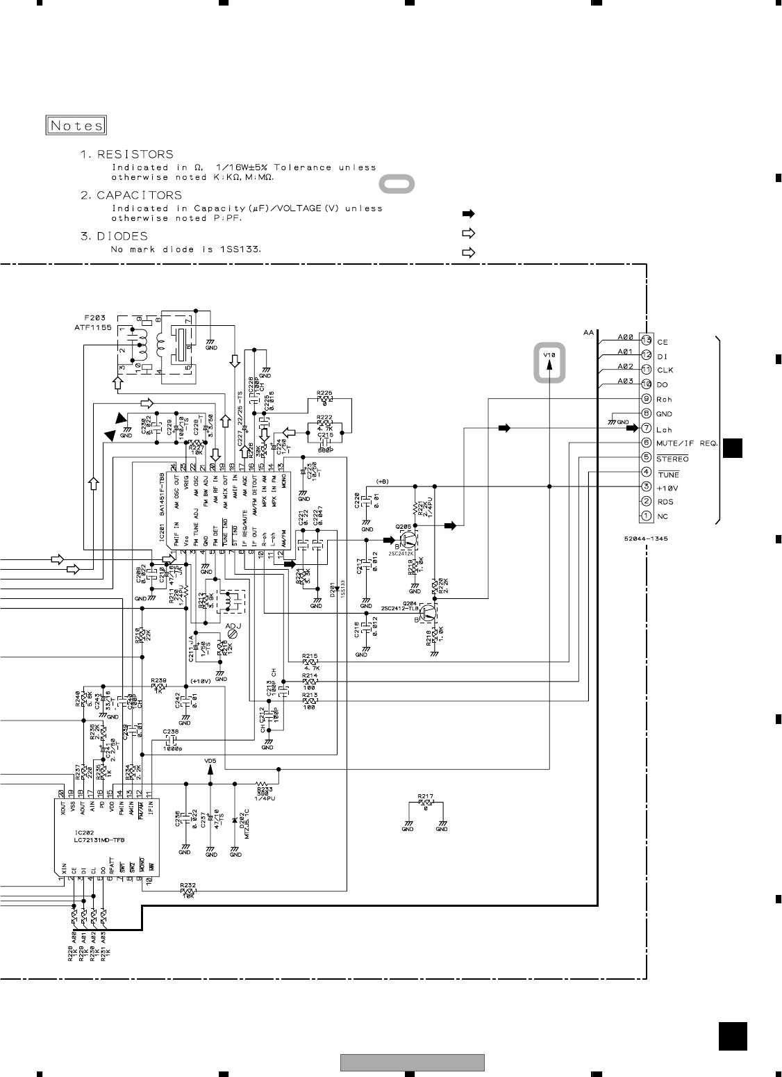
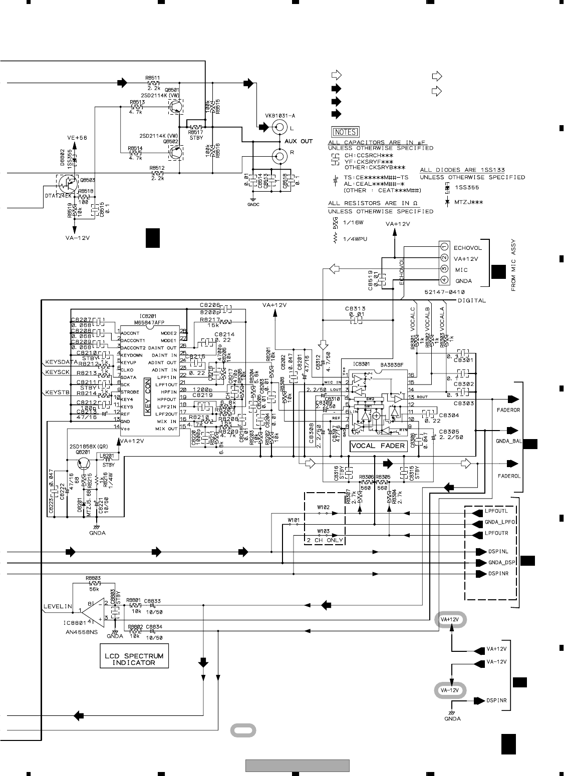
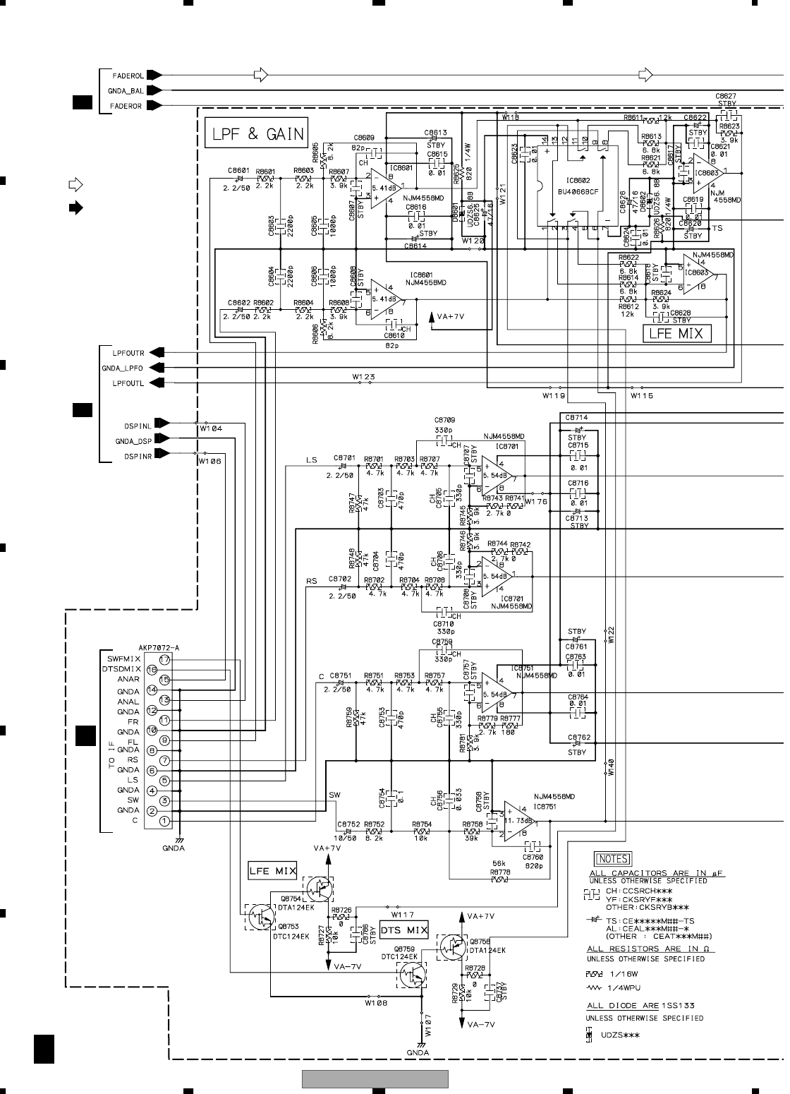
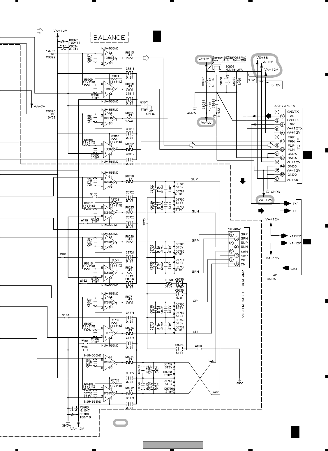
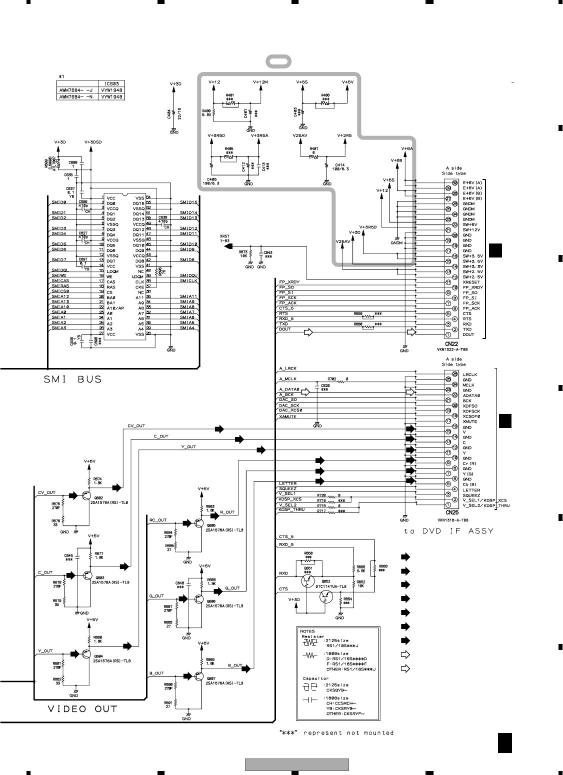
3.4 IF ASSY
B
EV-
51
EV-51
Only
EV-
21
XV-EV51
ONLY
EV-51
EV-21
IF ASSY
(XWZ3617
/ XV-EV51)
(XWZ3627
/ XV-EV21)
B
GCN1902
CN5508
CN5506
CN5505
CN5903
CN5504
CN5503
KCN8002 KCN8001
KCN8003
CN8751
CN8101
C
CN8901
2/2
C
2/2
C
2/2
GCN1902
CN5507
CN5502
CN5902
CN5901
(TX)
(CD)
(D)
(CD)
(CD)
(D)
XV-EV21
Only
(S_Y)
(S_C)
(S_Y)
(S_Y)
(S_C)
(V)
(V)
XV-EV51 27
5 678
5678
C
D
F
A
B
E
B
EV-51
EV-21
EV-51
EV-51
: The power supply is shown with the marked box.
JCN5101
ACN201
E
CN2506
To. Mecha Deck
SIGNAL ROUTE
: CD AUDIO SIGNAL ROUTE
: AUDIO SIGNAL ROUTE (TUNER)
: DIGITAL SIGNAL ROUTE
(TX)
(CD)
CN5802
CN5701
CN5501
CN5509
TO M-EV51 or M-EV21 Power Amplfier
CN5801
(TX)
(D)
XV-EV21
Only
(S_C)
(S_Y)
: S-VIDEO OUT C SIGNAL ROUTE
(V) : V SIGNAL ROUTE
: S-VIDEO OUT Y SIGNAL ROUTE
XV-EV51 29
5 678
5678
C
D
F
A
B
E
C1/2
: The power supply is shown with the marked box.
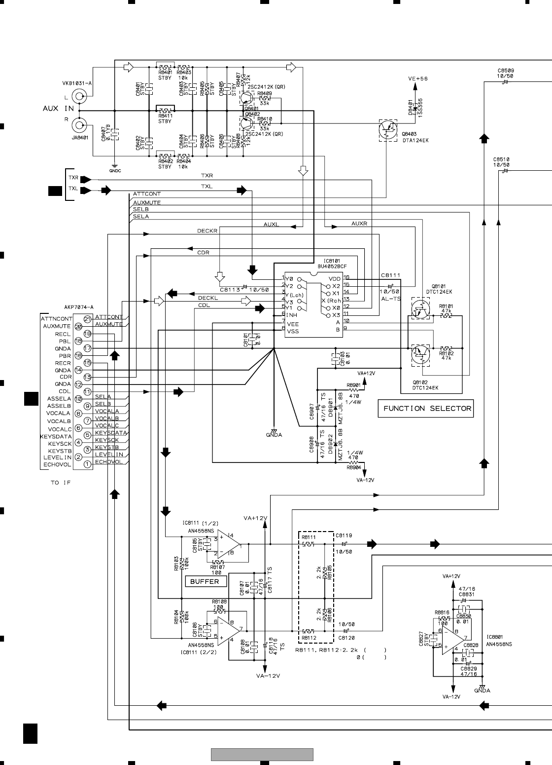
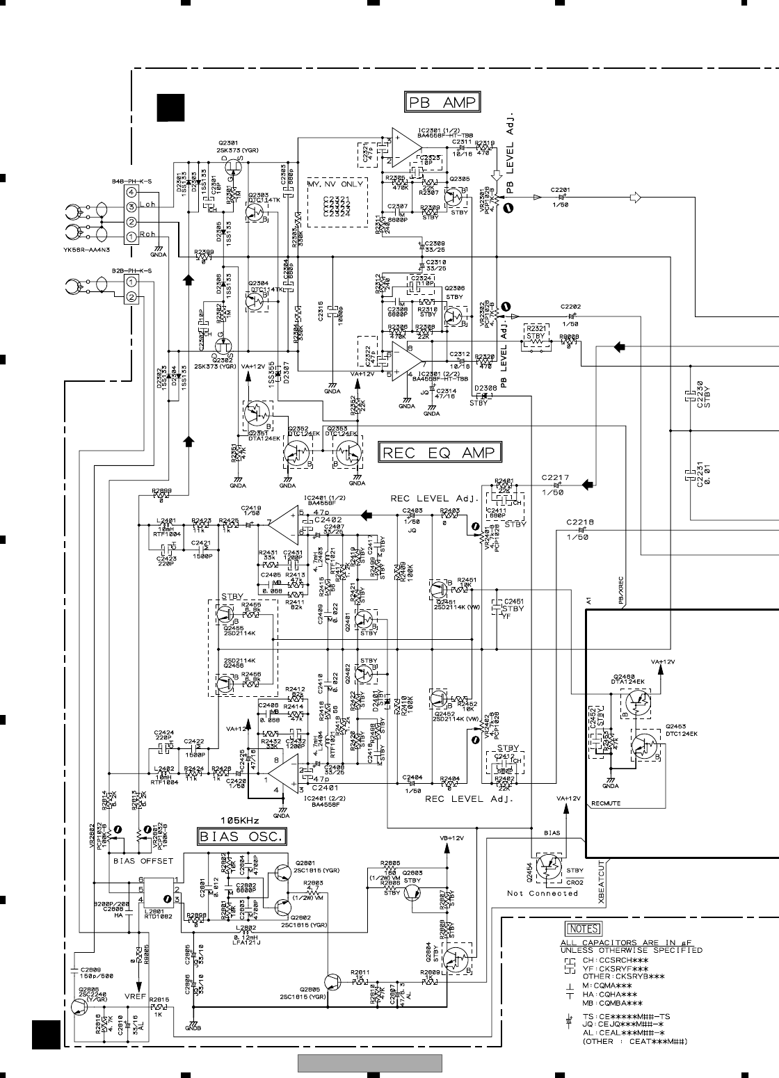
AF ASSY
(XWZ3618 / XV-EV51)
(XWZ3628 / XV-EV21)
C
SIGNAL ROUTE
: PB SIGNAL
: RECORDING SIGNAL
(PB)
CN8301
JA8401
1/2
MJ5401
C
2/2
C
2/2
C
2/2
(REC)
(REC)
(REC)
(REC)
(REC)
(REC) (REC)(TX)
(TX)
(CD) (CD)
(CD)
: AUDIO SIGNAL (TUNER)
(CD)
(TX)
: CD SIGNAL
(AUX) : AUX SIGNAL
(MIC)
(MIC)
(MIC) (MIC)
(MIC)
: MIC OUT SIGNAL
EV21 Only
XV-EV51 Only
XV-EV51 37
5 678
5678
C
D
F
A
B
E
(S_C)
(S_Y)
(R/Cr)
(G/Y)
(B/Cb)
: DATA SIGNAL ROUTE
: S-VIDEO OUT C SIGNAL ROUTE
(V) : V SIGNAL ROUTE
: S-VIDEO OUT Y SIGNAL ROUTE
: R/Cr SIGNAL ROUTE
: G/Y SIGNAL ROUTE
: B/Cb SIGNAL ROUTE
: AUDIO SIGNAL ROUTE
(D) : AUDIO (DIGITAL) SIGNAL ROUTE
(D)
(D)
(G/Y) (G/Y)
(G/Y)
(S_C)
(S_Y)
(R/Cr) (R/Cr)
(R/Cr)
(V)
(B/Cb)
(V)
(V)
(S_C)
(S_C)
(S_Y)
(S_Y)
(V)
(S_C)
(S_Y)
(B/Cb)
(B/Cb)
(G/Y)
(R/Cr)
(B/Cb)
F2/2
CN1961
G
CN1962
G
5: Refer to "3.1.3 WAVEFORMS".
: The power supply is shown with the marked box.
IC604
K4S641632F-TC75
64M SDRAM
XV-EV51 39
5 678
5678
C
D
F
A
B
E
G
: AUDIO SIGNAL ROUTE
(D) : AUDIO (DIGITAL) SIGNAL ROUTE
(D)
(D)
(D) (D)
1
2
6
5
3 4
1, 2, 3, 4, 5, 6: Refer to "3.1.3 WAVEFORMS"
: The power supply is shown with the marked box.
CN5903
B
CN5901
B
(S_C)
(S_Y)
(R/Cr)
(G/Y)
(B/Cb)
: S-VIDEO OUT C SIGNAL ROUTE
(V)
(B/Cb)
(B/Cb) (B/Cb) (B/Cb)
(R/Cr)(R/Cr)(R/Cr)
(R/Cr)
(V)
(V) (V)
: V SIGNAL ROUTE
: S-VIDEO OUT Y SIGNAL ROUTE
(G/Y)
(G/Y) (G/Y)
(S_Y)
(S_Y) (S_Y) (S_Y)
(S_C)
(S_C) (S_C) (S_C)
: R/Cr SIGNAL ROUTE
: G/Y SIGNAL ROUTE
: B/Cb SIGNAL ROUTE
XV-EV51 41
5 678
5678
C
D
F
A
B
E
H I
: The power supply is shown with the marked box.
DISP 3 ASSY
(XWZ3621)
H
DISP 2 ASSY
(XWZ3620)
I
JCN5102
J5102
J5202
J5202
DISP 2 ASSY
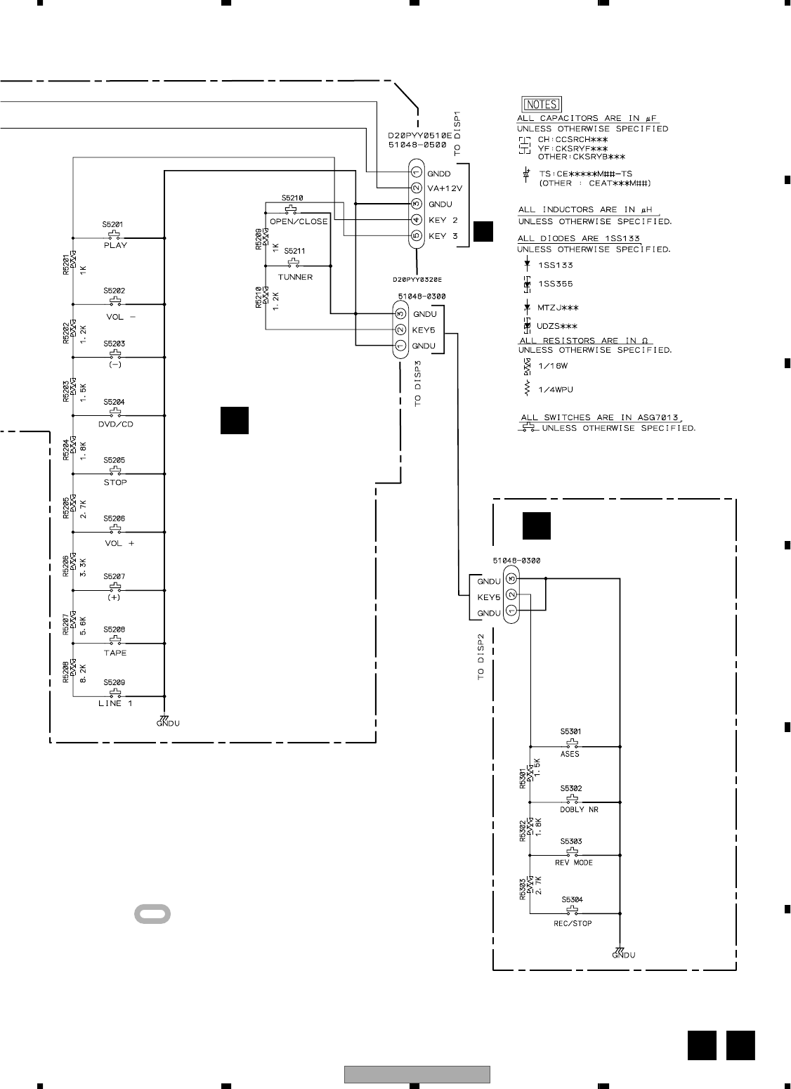
S5201: PLAY
S5202: VOL -
S5203: ( - )
S5204: DVD / CD
S5205: STOP
S5206: VOL +
S5207: ( + )
S5208: TAPE
S5209: LINE 1
S5210: OPEN/CLOSE
S5211: TUNNER
DISP 3 ASSY
S5301: ASES
S5202: DOBLY NR
S5203: REV MODE
S5204: REC/STOP
XV-EV51
46
1234
1234
C
D
F
A
B
E
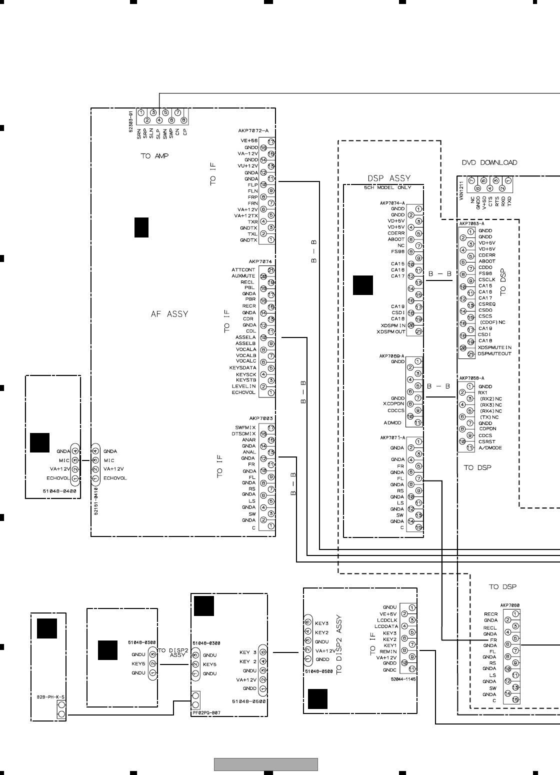
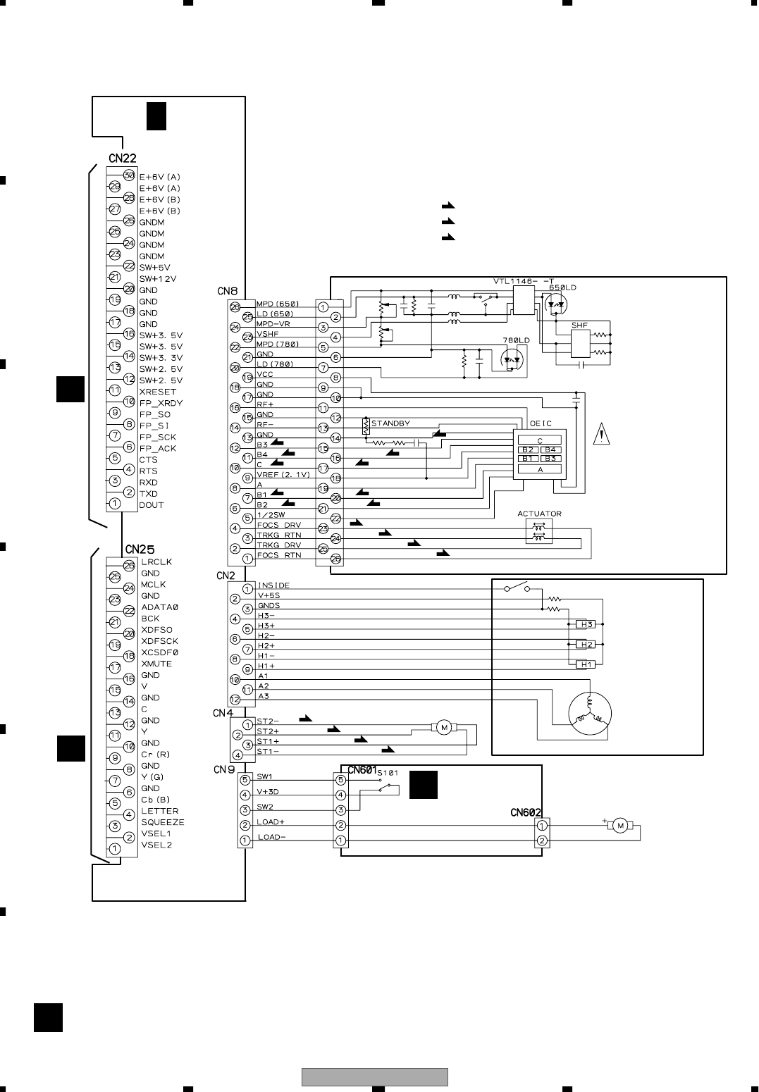
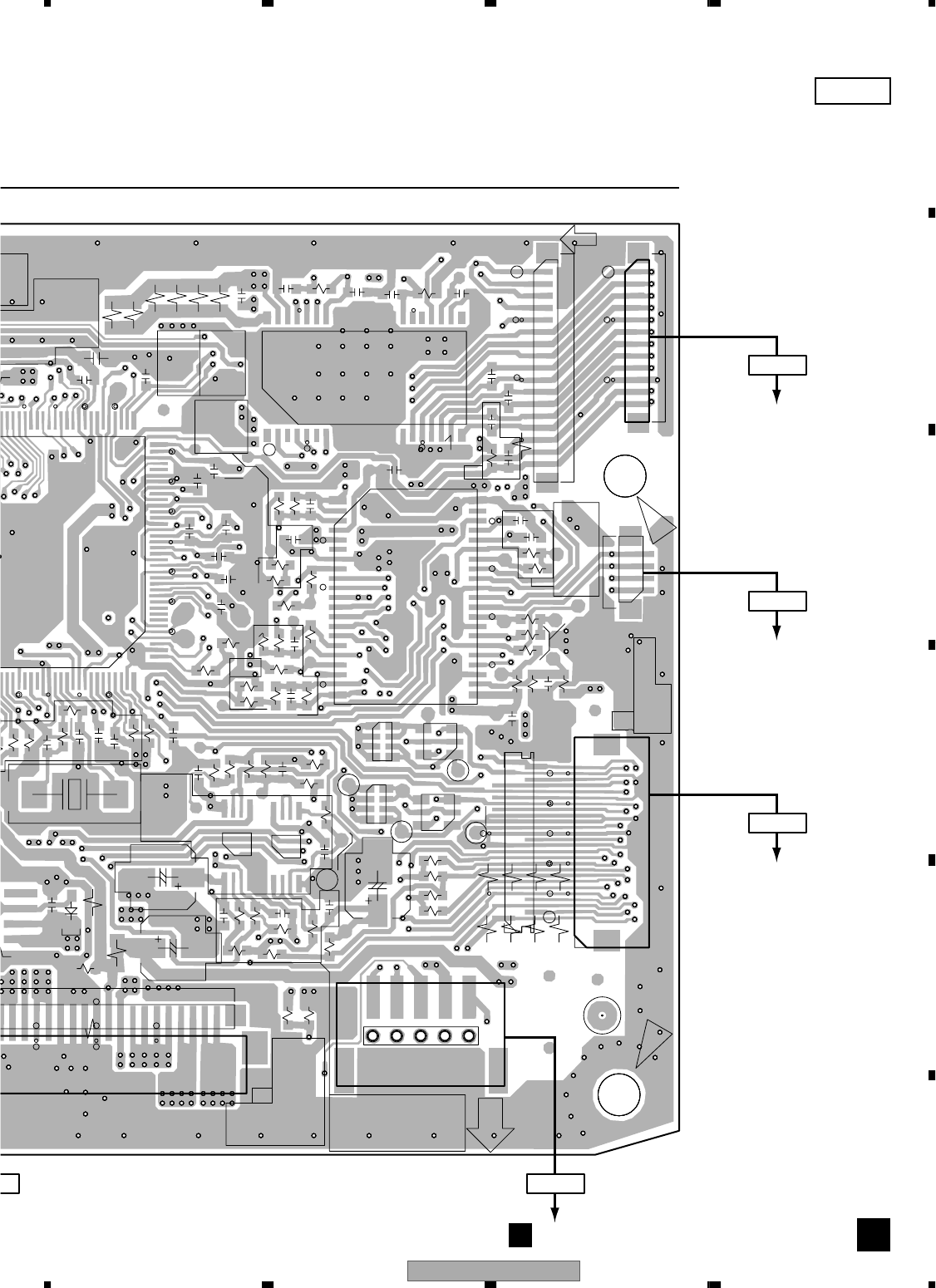
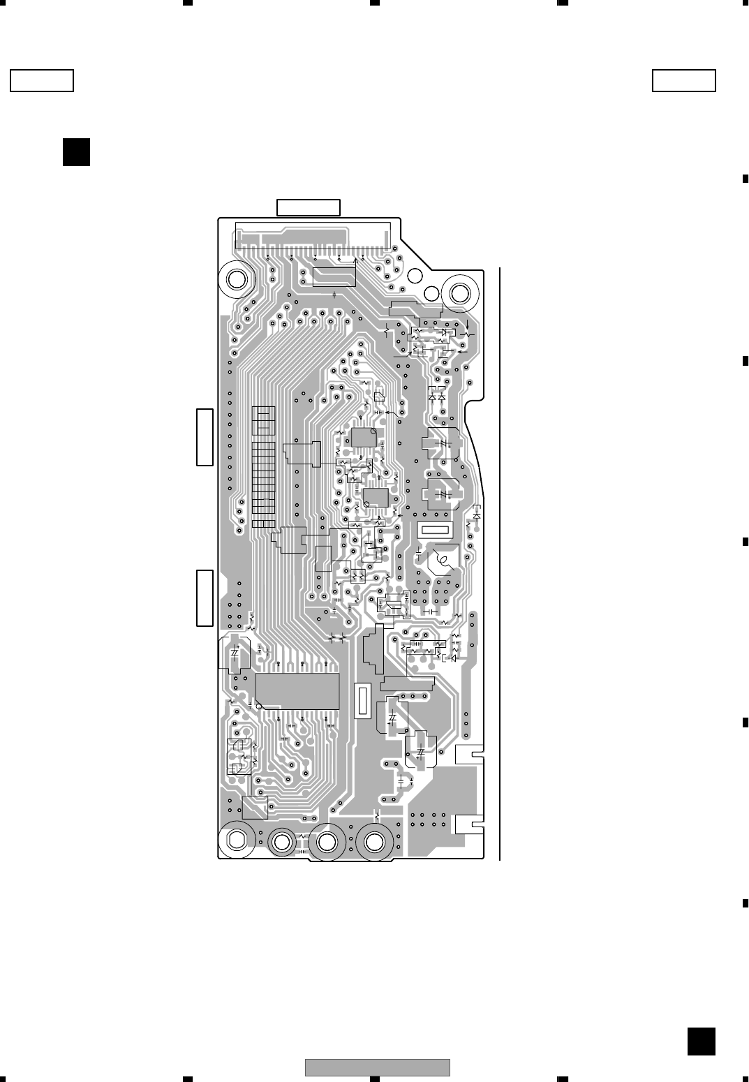
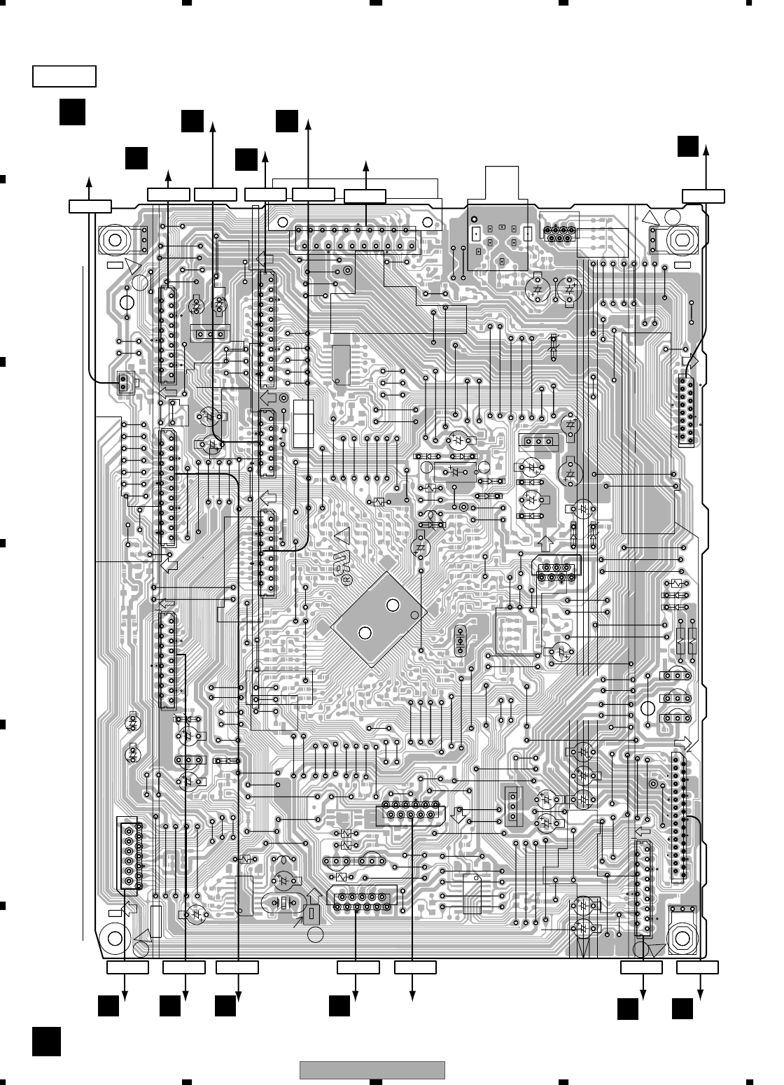
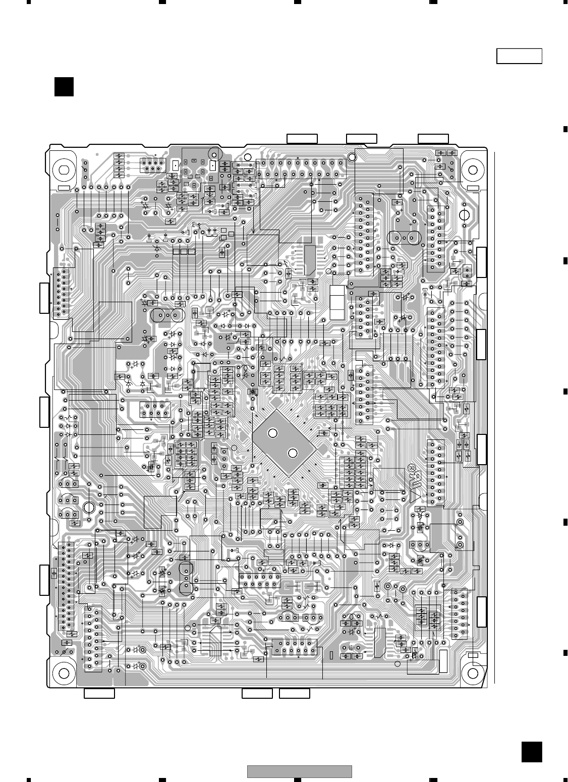
4. PCB CONNECTION DIAGRAM
4.1 LOAB ASSY
NOTE FOR PCB DIAGRAMS :
1. Part numbers in PCB diagrams match those in the schematic
diagrams.
2. A comparison between the main parts of PCB and schematic
diagrams is shown below.
3. The parts mounted on this PCB include all necessary parts for
several destinations.
For further information for respective destinations, be sure to
check with the schematic diagram.
4. View point of PCB diagrams.
Symbol In PCB
Diagrams
Symbol In Schematic
Diagrams Part Name
BCE
D
D
G
G
S
S
BCE
BCE
DGS
BCEBCE
BCE
Transistor
Transistor
with resistor
Field effect
transistor
Resistor array
3-terminal
regulator
Capacitor
Connector
P.C.Board Chip Part
SIDE A
SIDE B
SIDE A SIDE B
LOAB ASSY
D
D
LOAB ASSY
D
CN9
F
(VNP1837-B) (VNP1837-B)
LOADING
MOTOR
ASSY
M
CN601CN602 CN601 CN602
XV-EV51 47
5 678
5678
C
D
F
A
B
E
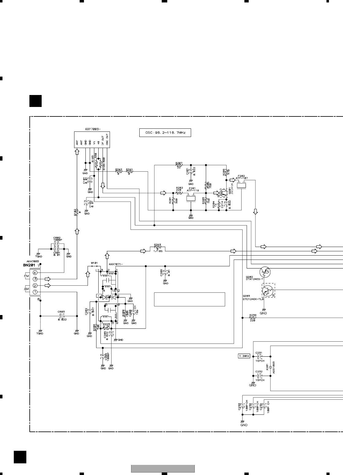
4.2 FM/AM TUNER MODULE
(ANP7338-B)
(ANP7338-B)
CN5701
B
FM/AM TUNER MODULE
A
FM/AM TUNER MODULE
A
IC201 Q205
Q204
Q203
IC202
Q201
Q202
AA
SIDE A
SIDE A
SIDE B
SIDE B
CN201
XV-EV51
48
1234
1234
C
D
F
A
B
E
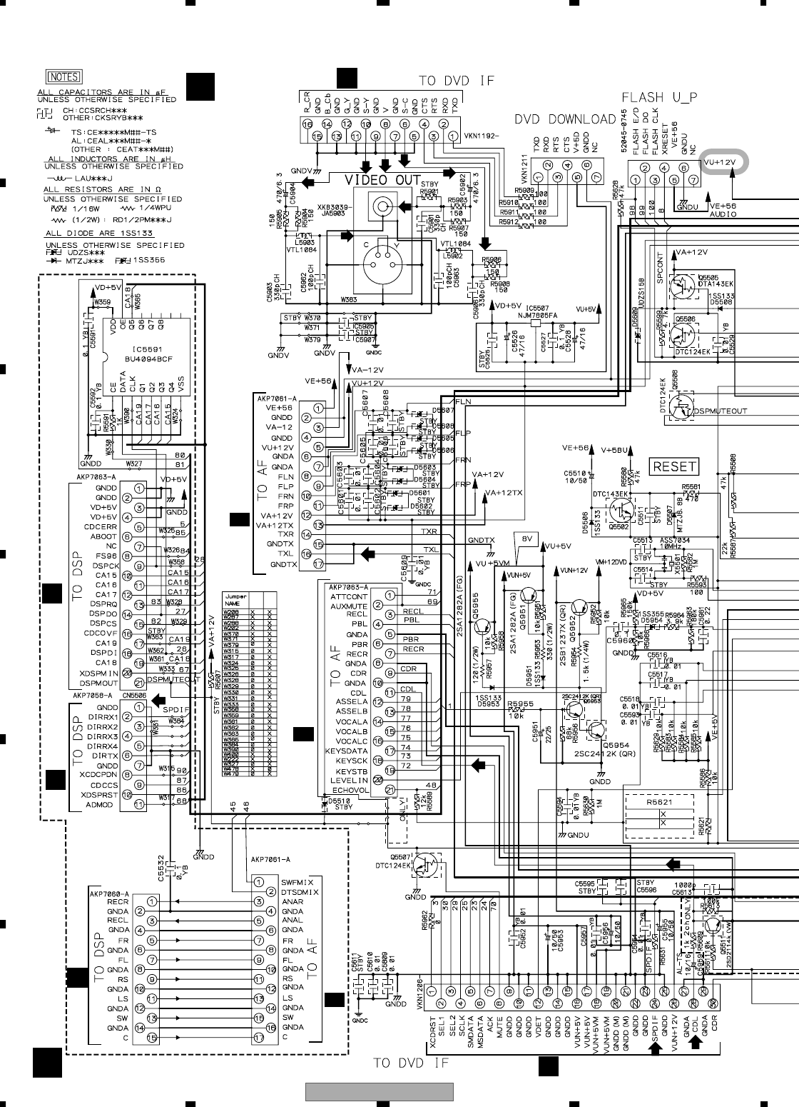
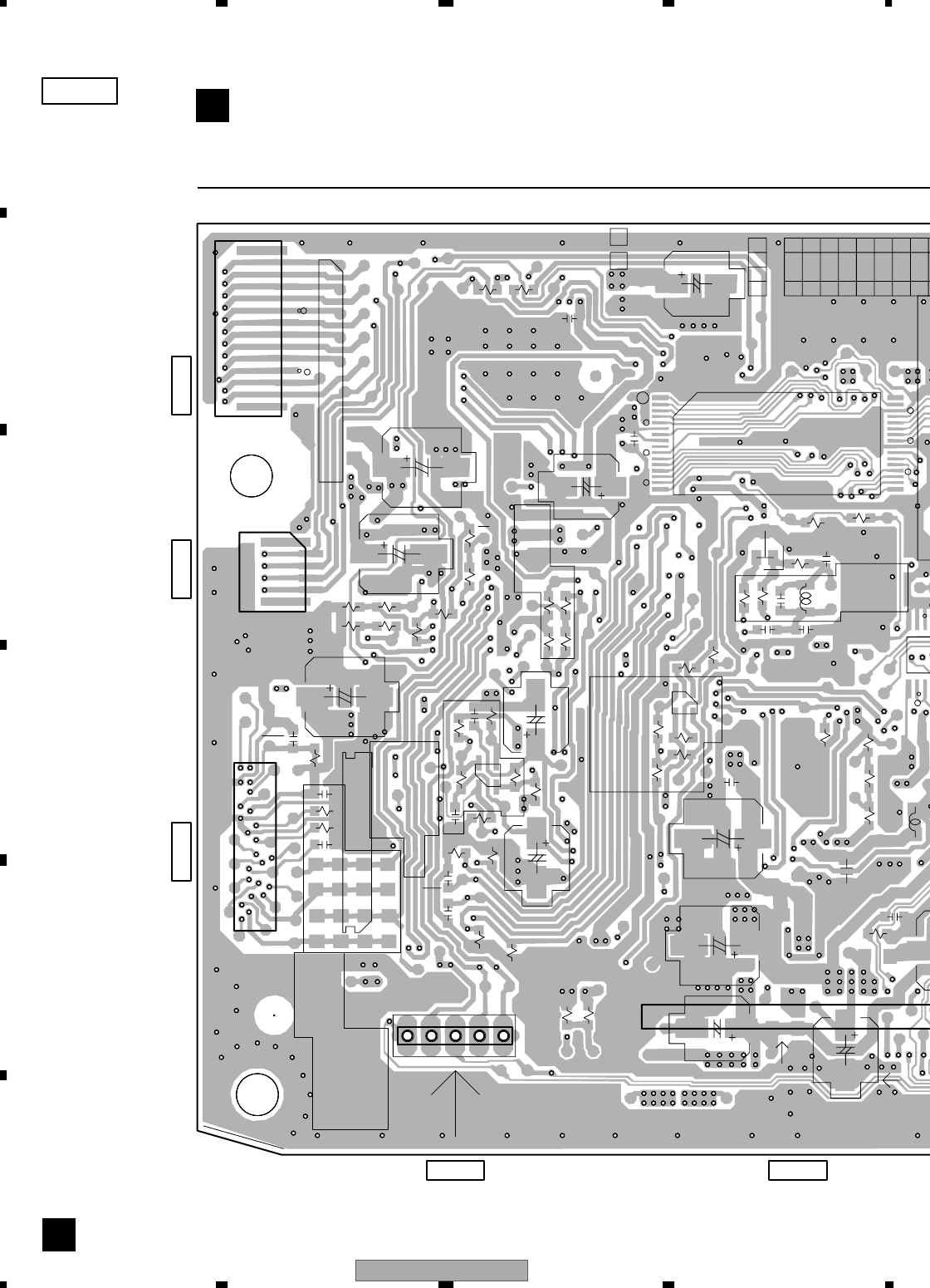
4.3 DVDM ASSY
D
C
V+5V
CONTACT SIDE CONTACT SIDE
ND SIDE
104
1
156
157
1
23
VNP1866
26 1
A
A
B
B
E
E
1
E88558
R501
C641
C628
R316
R541
R546
R317
R399
C340
R306
R503
R502
C335
IC301
0
1
C302
C301
R301
R304
R309
L308
C315
C313
R340
4
R305
L310
C316
C317
C
329 C323
C328
C321
C327
C322
C333
C332
C326
D301
R310
R330
CN11
R300
R401
IC601
C609
C615
R612
R613
R619
R620
R621
R622
R623
R624
R625
C610
C603
C616
C613
C611 C612
C607
C608
C606
C605
Q607
Q606
Q605
Q604Q603
CN21
Q602
R600
CN603
CN602
CN601
R643
R642
R630
R631
R632
CN22
C623
C624
C625
C622
R564
R563
R562
R559
R558
R556
R555
R553
R552
R551
R589
R588
R587
R586
R585
R584
R583
R582
R581
R580
R578
R576
R575
R574
R567
R569
R641
C621
R565
R566
R571
R572
R662
C650
CN23
CN25
C651
R670
R339
R322
R332
R400
CN12
C342
R398
IC303
R545
C626
R617
109
108
73
72
10
1
208157
156
105
53
52
1
1
224
231
224
231
224
231
1
26
1
26 1
4
1
SIDE A
DVDM ASSY
F
Q607 Q606 Q605 Q604 Q603 Q602
IC601 IC301
FCN1962
G
CN25
CN1961
G
CN22
IC303
XV-EV51 49
5 678
5678
C
D
F
A
B
E
1
BA
22
1
21
RF
650
V+5S
780
CON
T
SECOND SID
E
CONTACT SIDE
4
5
1
8
37
DC
FC
GND
C
C
F
F
4
5
1
8
30
CN7
CN9
R4
R3
C256
R257
R353
C353
C359
C365
R358
R372
R258
R259
R368
C361
C357
R359
C360
C334
R357
C366
R360 C351
IC351
R362
R354
R155
C255
R351
R338
R366
R361
R355
R156
R157
C250
C249
C248
C251
IC251
C258
R391
C391
C259
R254
R255
C107
C106
C108
C339
C338
R256
R365
C343
X301
C302
C301
R301
R302
R303
C311
C315
C313
C109
R133
R136
R137
R140
IC110
C104
C103
R123
R121
Q101
Q102
R305
R261 C257
R146
R145
R377
R378
C330
C325
C331
C324
C329
C
C332
C326
C105
CN8
CN5
CN4
CN2
C362
R379
R380
R395
R394
C373
D301
R328
R329
R266
R370
R371
R300
C401
R401
R631
R632
CN2
2
R158
R393
R392
R144
R147
R396
R332
R333
R400
IC111
C342
IC303
CN90
26
25
2
1
5 1
29
30
14
1528
1
144
37
36
1
4
26 1
17
1
4
1
12
1
30
30
4
1
5
SIDE A
(VNP1866-D)
IC301
F
1
961
2
2
CN601
D
CN9
CN4
SPINDLE
MOTOR
STEPPING
MOTOR
PICKUP
ASSY
CN2
CN8
IC110 IC111
IC251 IC351 Q101
Q102
XV-EV51
50
1234
1234
C
D
F
A
B
E
12 1
A
B
C
98765432
6
1
17
32
9
3
V+3R5D
NORMAL SOLDER
SIDE
PRE-FLAX
LEAD FREE SOLDER
V+6B
5
HEAT-RESISTANCE
V+12M
V+5S
GNDM
VREF21
1
C157
R126
R127
R128
R176
C112
C110
R129
R1
R2
CN2
R177
R178
C158
R373
R179
C369
R364
C368
R100
R118
C111
C404
C341
R375
C113
R125
C305
C254
C149
C148
R172
R153
R138
R346
R142
R345
C308
R152
R318
C253
R341
R141
CN4
R367
R344
R376
R315
R320
R139
R356
R154
R374
R150
R321
Q105
R151
C307
R149
C310
C304
R110
R111
R115
R113
C101
C102
IC302
R262
L311
IC304
R384
R385
R326
R327
R331
R265
Q103
R673
C643
C405 C403
R406
C413
C412
R405
4
R407
R171
R
336
R
337
R319 C318
Q300
L300
C309
4
1
3
4
9
8
1
4
6
26
26
25
2
1
1
17 1
30
SIDE B DVDM ASSY
F
F
CN22CN9
CN2 CN4 CN8
Q103 Q105
Q300
IC302
I
C
XV-EV51 51
5 678
5678
C
D
F
A
B
E
1
0
0
321
0
7
654321
0
1
A-
99
88
77
66
55
44
33
22
11
00
9
8
7
6
5
4
3
2
1
0
17
32
9
48
25
124
27
1
54
FIRST SIDE
CN
Q
J
AWM
V+2R5
VWS1
1
1
N
7
R648
C404
R626
R542
R543
R590
R616
C618
C308
Q652
R547
R650
Q651
R318
C696
C637
R320
R505
R618
C307
C699
C617
L311
IC304
R311
R312
R313
R314
C319
R384
R385
R331
L324
C629
IC603
D601
R639
C630
C631
R640
R673
C643
R659
R660
IC604
R718
R720
R689
R691
R688
R690
R686
C648
R687
R683
R685
R684
R679
R677
R676
R678
R674
R682
R675
R680
C645
R681
R601
R602
R605 R606
R607
R608
R609
R610
L601
C619
C614
L603
R638
C635
R695
C632
R647
R646
R645
C633
C634
X601
R702
Q601
R699
C414
R40
R717
R719
R603
R604
R561
R560
R557
R554
R577
R579
R570
C627
C638
C636
R568
R654
R652
R666
R668
R653
R671
R651
IC605
R334
C620
R335
R336
R337
R544
R504
R319 C318
C698
C697
L300
C30
9
L602
16 9
8
1
1
28
3
4
6
8
5
4
1
1
26
1
SIDE B
(VNP1866-D)
F
CN25
IC304 IC604
IC605 IC603
Q651
Q601 Q652
XV-EV51
52
1234
1234
C
D
F
A
B
E
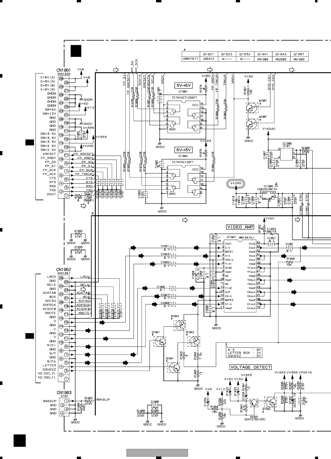
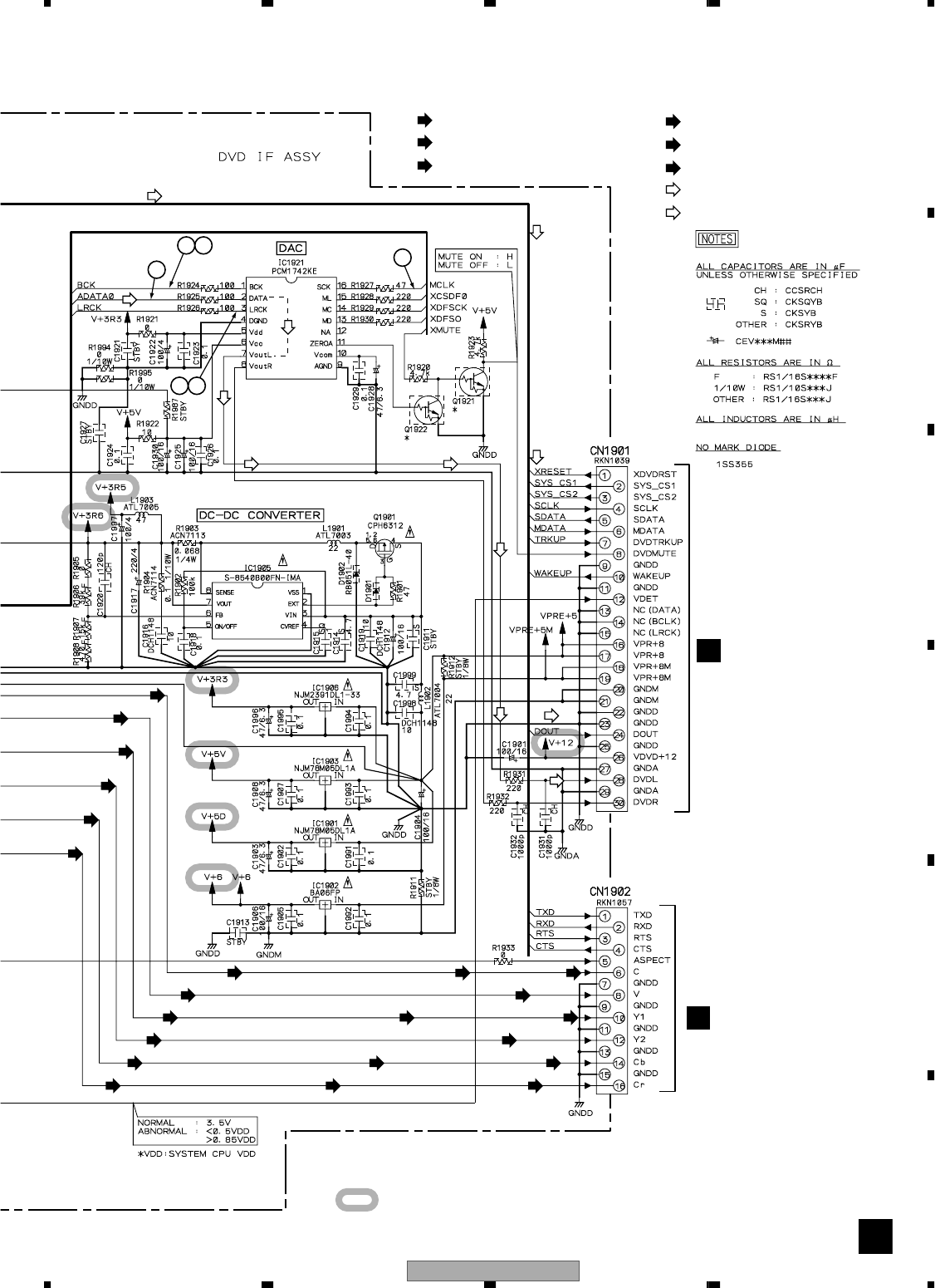
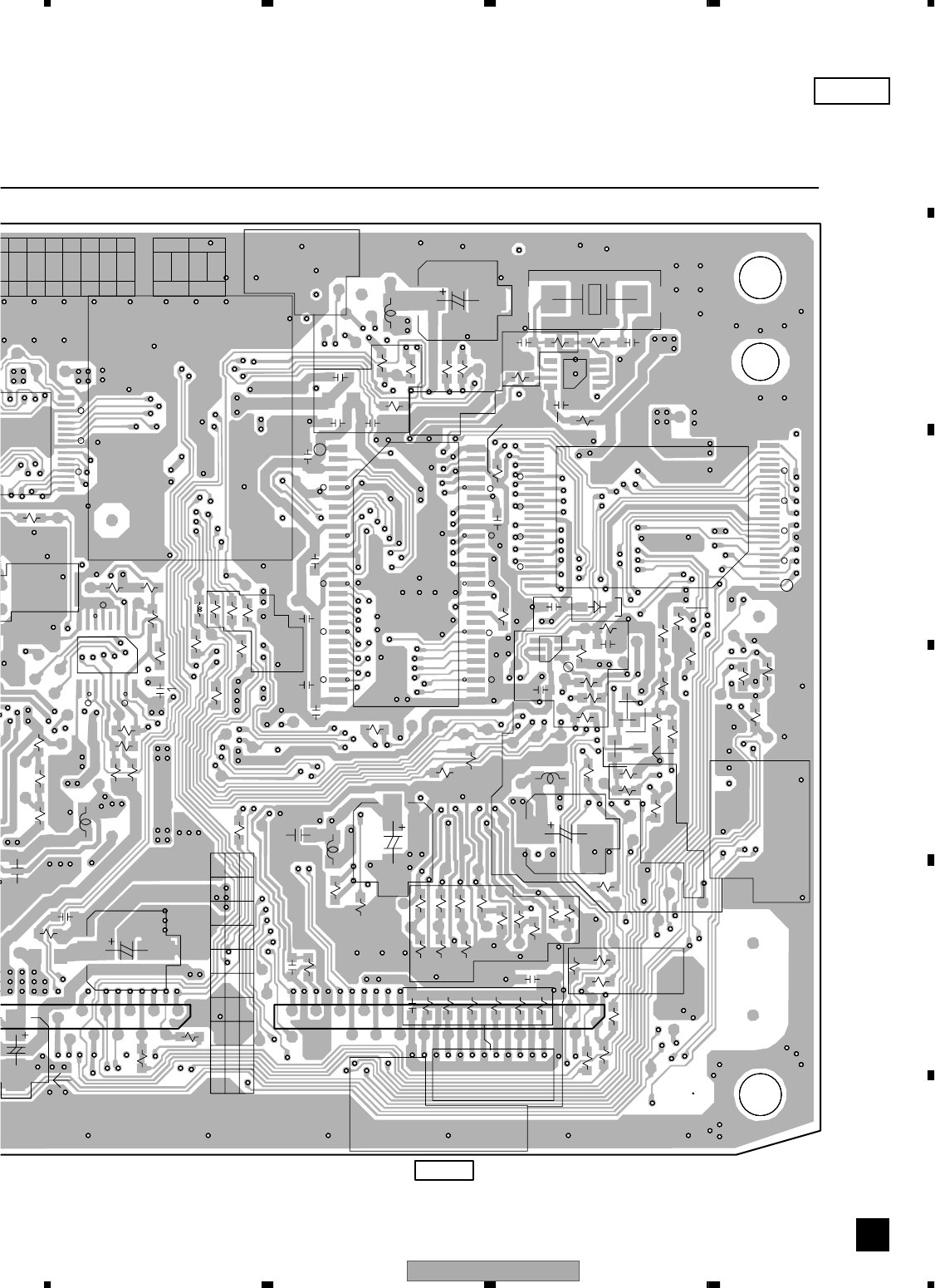
4.4 DVD IF ASSY
C1941
C1945
C1943
C1950
C1947
C1948
CN1961
IC1904
C1955
C1994
IC1921
C1925
C1926
C1922
C1923
C1928
IC1902
C1909
C1907
C1910
C1902
IC1901
C1903
IC1903
C1905
C1906
C1929
C1932
C1931
R1932
C1990
R1931
R1904
Q1901
L1901
C1919
CN1962
CN1902
IC1905
D1902
C1911
C1915
C1914 C1916
C1912
C1917
R1901
D1901
C1993
C1992
C1991
R1927
C1973
R1902
C1996
C1971
R1992
C1918
C1997
R1925
R1929
C1972
C1995
R1982
IC1906
R1903
R1926
R1993
L1903
C1980 C1930
C1979
R1983 C1978
C1977
C1976
C1975
C1981
R1928
R1930
C1908
R1924
L1981
R1981
CN1963
C1974
C
B
A
VPRE+5
VPRE+5M
GNDM
GNDD
V+6M
V+12
V+2.5
V+5D
Rch
Lch
GNDA
DOUT
V+3.5
CONTACT
UPSIDE
UPSIDE
CONTACT
V+3.3
V+5V
D1/4
30 1
16 9
81
26 1
16 1
85
4
1
41
30 1
81
916
ICT
FC
DVD IF UNIT
AWM7677
26
1
16 1
4
5
1
8
E M B1N
41
DVDIF ASSY
G
(ANP7425-A)
CN22
F
CN1961
CN25
F
CN1962
CN5901
BCN1902
SIDE A SIDE A
G
IC1901
IC1904
IC1905
IC1903
IC1906
IC1902
XV-EV51 53
5 678
5678
C
D
F
A
B
E
A
B
C
1
0
0
321
0987654321
0
1
14 8
71
1
30
34 18
171
14 8
71
5
1
UPSIDE
CONTACT
1
1
14 8
71
30 1
34 18
171
14 8
71
D1932
R1908
D1931
R1986
C1999
R1963
R1972
R1906
R1938
R1907
R1933
R1946
R1945
R1939
C1998
R1935
R1936
C1982
C1933
R1934
C1953
R1970
R1961
R1905
C1956
R1962
Q1931
R1994
C1962
R1995
R1942
R1923
IC1962
Q1921
R1940
C1957
Q1922
C1904
Q1942
R1969
R1966
Q1961
R1944
C1951
CN1901
R1968
C1954
R1952
Q1941
C1927
R1965
R1967
R1921
C1921
C1920
L1902
IC1941
C1949
R1964
R1974
C1901
R1985
R1922
R1941
R1971
C1924
C1984
C1913
C1983
C1963
R1937
C1986
C1985
R1975
C1988
C1961
D1934
IC1961
IC1986
Q1932
C1987
R1912
D1933
D1935
R1987
R1920
C1952
C1989
R1943
R1911
R1988
SIDE B SIDE B
G
DVD IF ASSY
G
(ANP7425-A)
CN1961
CN1962
CN1901
Q1941
Q1942
IC1889
IC1941
Q1922
Q1961
IC1962
Q1932
Q1931
Q1921
IC1961
XV-EV51
54
1234
1234
C
D
F
A
B
E
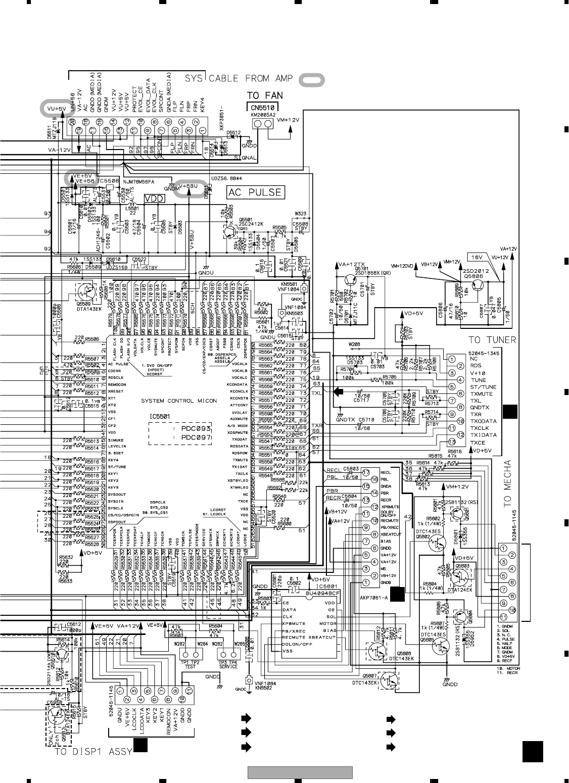
4.5 IF ASSY
B
SIDE A
-+
17
71
30
1
11
1
1
21 115
CMKS-P3X
16
1
2.VB+12V
17
1
6.GNDD
9.PB/XREC
11 1
8.XBEATCUT
PRINTED
V+8V
11.DOLBY ON/OFF
5.V+5D
VA+12V
1
21
1.TXD
1.FLASH E/D
4.CTS
VE+5V
7.BIAS
7.NC
7.NC
4.VA+12V
5.VE+56
GNDM
11
1
IF ASSY
16.PBL
13.RECR
15.GNDA
14.PBR
17.RECL
CONTACT
1
17
DECK FFC
5.VA+12V
DISP FFC
17
1
12.XPBMUTE
3.MS
10.RECMUTE
6.GNDD
1.GNDB
TEST
NJM78M56FA
20
1
SERVICE
4.XRESET
6.GNDU
2.RXD
3.FLASH CLK
3.RTS
2.FLASH DO
1.XCDRST
2.SEL1
3.SEL2
4.SCLK
5.SMDATA
6.MSDATA
7.ACK
8.MUTE
9.GNDD
10.NC
11.VDET
12.GNDD
13.NC
14.NC
15.NC
16.VUN+5V
17.VUN+5V
18.VUN+5VM
19.VUN+5VM
20.GNDD(M)
21.GNDD(M)
22.GNDD
23.GNDD
24.SPDIF
25.GNDD
26.VUN+12V
27.GNDA
28.CDL
29.GNDA
30.CDR
IC5591
IC5701
IC5801
IC5501
CONTACT
SIDE
OPEN
OPEN
CONTACT
SIDE
SIDE
CONTACT
SIDE
CONTACT
OPEN
OPEN
OPEN
OPEN
CONTACT
SIDE
CONTACT
SIDE
SIDE
EB
IN OUT
PRINTED SIDE
2SD2012
NJM7805FA
For Binder
1
19.KEYSTB
(1 RED,2 BLACK)
18.KEYSCK
17.KEYSDATA
14.VOCALA
13.ASSELB
12.ASSELA
11.CDL
10.GNDA
9.CDR
8.GNDA
7.RECR
6.PBR
5.GNDA
4.PBL
3.RECL
AUXMUTE
ATTCONT
15.VOCALB
16.VOCALC
21.ECHOVOL
20.LEVELIN
15.C
14.GNDA
13.SW
12.GNDA
11.LS
10.GNDA
9.RS
8.GNDA
7.FL
6.GNDA
5.FR
4.GNDA
3.RECL
2.GNDA
1.RECR
1.GNDD
2.RX1
3.NC
4.NC
5.NC
6.NC
7.GNDD
8.CDPDN
9.CDCS
10.CSRST
11.A/D MODE
1.GNDD
2.GNDD
3.VD+5V
4.VD+5V
5.CDERR
6.ABOOT
7.CDDO
8.FS96
9.CSCLK
10.CA15
11.CA16
21.DSPMUTEOUT
20.XDSPMUTEIN
19.CA18
18.CSDI
17.CA19
16.NC
15.CSCS
14.CSDO
13.CSREQ
12.CA17
2.
1.
1.KEY4
2.FRN
3.FRP
4.FLN
5.FLP
6.GNDA
7.SPCON
8.EVOL-CLK
9.EVOL-DATA
10.EVOL-CE
11.PROTECT
12.VU+5V
13.VU+5V
14.VU+12V
15.GNDM
16.GNDD
17.GNDD
18.AC
19.VA-12V
20.UN+56
VD+5V
VA+12V
VUN+12V
VM+12V
VUN+5V
VUN+5VM
1
VM+12V
VA+12TX
VE+56
VU+12V
13 1
GNDU
GNDD
GNDA
GNDM
GNDD
GNDM
GNDD
GNDU
GNDU
GNDD
GNDA
GNDM
GNDD
UPPER SIDE
EVOLCLK
SPDIF
VDET
EVOLDATA
VE+5V
GNDU
EVOLCS
DVDCS
EXPCS
SPCONT
PROTECT
GNDU
VE+5V
V+5BU
AC
R5913
PRINTED
SIDE
OUT
R5914
5 CH
123.0
UN+56
VA+12V
VE+56
OPEN
1
IN
A
KEY1
SYSDIN
SYSDOUT
SYSCLK
KEY3
KEY2
VM+12V
ST/TUNE
CDL
GNDA
CDR
DSPMUTE
VD+5V
VA+12V
DSPOUT
DSPCLK
DSPMUTEOUT
KEY4
J4
J3
J2
J1
GNDC
GNDV
VD+5V
A
D
B
C
C5501
W284
C5507
C5508
C5502
C5504
L5501
D5507
D5506
C5510
C5713
L5701
X5701
C5709
D5703
D5701
C5702
C5701
Q5701
D5508
D5501
D5502
D5503
D5504
D5505
X5501
C5904
C5902
C5951
D5951
Q5951
Q5952
C5955
C5953
KN5501
R5954
R5953
W383
W309
C5717
W296
W292
CN5502
CN5902
CN5903
CN5506
D5509
W385
W324
W327
CN5507
CN5508
W315
W323
Q5805
Q5802
R5804
R5807
R5802
CN5901
Q5955
R5957
W393
W306
W237
W206
W205
JA5903
W297
W230
W285
W299
W495
W281
W312
W330
W373
W372
W480
W207
W335
W336
W235
W216
W317
W252
CN5801
W400
W491
W300
W368
CN5802
W316
W279
W334
W325
W277
W275
W246
W326
W242
C5956
D5953
W265
W249
W346
W371
C5806
C5805
W282
W340
W348
W386
W382
W283
W304
W261
W253
W338
W259
W258
W333
CN5504
W255
W257
W228
W318
W260
W290
W287
W341
W399
W278
W339
W484
W273
W362
W270
W481
W276
W352
W359
W357
W311
W380
W314
W220
W361
W226
W244
W225
W227
W269
W313
W369
W223
W248
C5959 C5958
C5718
W381
W262
W308
W224
W294
W289
W321
W272
W291
W295
W298
W395
W201
W379
W378
W374
W377
W375
W376
W266
C5803
W234
W243
W245
W202
W238
W214
W213
W236
C5804
W221
W219
W218
W203
W222
W215
W250
KN5502
W212
W288
W251
W254
W343
W344
W211
W210
W209
W305
W264
W268
W267
W293
W239
W241
W263
W301
W233
R5712
W231
W229
W208
CN5509
W488
W232
W302
W347
W256
W345
W365
W274
W342
W217
C5528 C5526
W396
W353
W388
W204
CN5503
W331
W328
W366
W349
W354
W389
W329
W367
W356
W358
W332
W384
W355
R5606
W322
W351
W497
W350
R5601
W485
CN5505
W397
W247
W271
W337
W286
W493
W478
W390
W387
W364
W490
W360
W489
W479
W370
CN5501
W363
W280
W498
IC5507
CN5701
Q5806
W500
W483
W496
W494
W486
C5531
C5530
IC5508
W499
KN5503
W482
W320
CN5510
D5511
7
1
71
30
1
11
1
21
1
15
14
1
16
1
17
1
11
10
1
21
1
11
10
1
17
1
17
1
20
1
13
10
1
1
(XNP3060-D)
IF ASSY
B
CN2506
To FAN
CN201
A
CN5101
JDECK
MECHA. E
CN8751
C
CN8101
C
CN1901
G
To M-EV51 or M-EV21
Power amplfier
CN1902
G
Q5952
IC5501
IC5591
Q5806
Q5802
Q5805
IC5801
IC5701
Q5701
Q5955
IC5508
Q5951
IC5507
CN8901
C
CN8001
CN8002
K
KCN8003
K
CN5503
CN5510
CN5507 CN5508 CN5501 CN5901
CN5506
CN5701 CN5509 CN5802 CN5801 CN5903CN5505 CN5504
XV-EV51 55
5 678
5678
C
D
F
A
B
E
B
SIDE B
8
1
16 9
81 100
31 50
51
30
80
1
7
1
71
30
1
11
1
8
1
916
1
21
1
15
17 1
111
10
1
21
1
10
11
17 11
17
20
1
113
11.RECR
10.MOTOR 9.RECF
CMKS-P3X
15.SW
11.RS
IC5508
2.DTSDMIX
3.RECR 4.GNDA
6.GNDA5.RECL
GNDM
GNDA
GNDA
GNDM
GNDD
GNDU
GNDA
14.GNDA13.LS
2.RDS
9.FL
8.GNDA
3.V+10
7.FR
Q5701
GNDD
GNDU
GNDD
GNDM
GNDD
GNDU
GNDU
GNDD
XWZ3624
XWZ3617
IF ASSY
1
4.TUNE
14.NC
16.NC
15.GND
11.GND
12.NC
4.CTS
10.S-Y
9.GND
8.V
7.GND
6.S-C
5.GND
13.GND
2.RXD
3.RTS
1.TXD
IC5507
17.MUTE
1.SWFMIX
XWZ3627
12.GNDA
12.TXIDATA
6.KEY2
8.REMOCON
7.KEY1
5.KEY3
4.LCDDATA
3.LCDCLK
2.VE+5V
1.GNDU
9.VA+12V
9.TXR
8.GNDTX
7.TXL
1.GNDM
1.NC
13.TXCE
17.C
Q5806
10.TXODATA
16.GNDA
10.GNDD
11.GNDD
10.GNDA
5.ST/TUNE
6.TXMUTE
11.TXCLK
2.SOL 3.NC
4.PULSE
5.HALF
6.MODE
7.GNDM8.VD+5V
16.TXL
15.GNDA
14.TXR
13.VA+12TX
12. VA+12V
10.FRN
11.FRP
9.FLP
8.FLN
GNDA
6.GNDA
5.VU+12V
4.GNDD
3.VA-12V 2.GNDD
1.VE+56
Q5805
Q5802
Q5952
Q5951
Q5955
VE+56
VU+12V
VA+12TX
VM+12V
VA+12V
VE+5V
VD+5V
VA+12V
VUN+12V
VM+12V
VUN+5V
VUN+5VM
7.
E
B
C
5CH DVD
2CH DVD
1
9
16.VUN+5V
18.VUN+5VM
17.VUN+5V
22.GNDD
21.GNDD(M)
20.GNDD(M)
19.VUN+5VM
16
10.NC
8.MUTE
15.NC
8
1.XCDRST
3.SEL2
2.SEL1
14.NC
16
OUT
E
OUT
B
IN
IN
CDR CDL
TXL
RECR
RECL
TXR
28.CDL
27.GNDA
30.CDR
29.GNDA
12.GNDD
6.MSDATA
7.ACK
4.SCLK
5.SMDATA
13.NC
9.GNDD
11.VDET
23.GNDD
26.VUN+12V
25.GNDD
24.SPDIF
2.VB+12V
3.MS
4.VA+12V
5.VA+12V
6.GNDD 7.BIAS
8.XBEATCUT
9.PB/XREC
1.GNDB
16.PBL
15.GNDA
12.XPBMUTE
11.DOLBY ON/OFF
13.RECR
10.RECMUTE
2.RX1
1.GNDD
3-6.NC
17.RECL
14.PBR
7.GNDD
8.CDPDN
9.CDCS
10.CSRST
11.A/D MODE
15.C
14.GNDA
13.SW
12.GNDA
11.LS
10.GNDA
9.RS
8.GNDA
7.FL
6.GNDA
4.GNDA
5.FR
3.RECL
2.GNDA
1.RECR
21.DSPMUTEOUT
20.XDSPMUTEIN
19.CA18
18.CSDI
17.CA19
16.NC
15.CSCS
14.CSDO
13.CSREQ
12.CA17
11.CA16
9.CSCLK
8.FS96
10.CA15
7.CDDO
6.ABOOT
5.CDERR
4.VD+5V
3.VD+5V
2.GNDD
1.GNDD
1.ATTCONT
2.AUXMUTE
3.RECL
5.GNDA
4.PBL
6.PBR
7.RECR
8.GNDA
9.CDR
10.GNDA
11.CDL
12.ASSELA
13.ASSELB 14.VOCALA 15.VOCALB
16.VOCALC 17.KEYSDATA 18.KEYSCK 19.KEYSTB
20.LEVELIN
21.ECHOVOL
CN5701
CN5508
CN5506
CN5507
CN5503 CN5504
CN5505
CN5903
CN5802
CN5509
CN5801
CN5901
CN5902
CN5502
CN5501
20.UN+56
19.VA-12V
18.AC
17.GNDD
16.GNDD
15.GNDM
14.VU+12V
13.VU+5V
12.VU+5V
11.PROTECT
10.EVOL-CE
9.EVOL-DATA
8.EVOL-CLK
7.SPCON
6.GNDA
5.FLP
4.FLN
2.FRN
3.FRP
1.KEY4
CN5501
Y
V
C
R5706
R5707
R5710
R5709C5706
C5705
C5703
R5708
R5603
R5504
R5502
C5506
R5503
Q5501
R5505
R5501
C5503
C5505
R5581
C5512
Q5502
C5511
R5703
C5714
C5716
C5715
C5708
C5712
C5710 C5711
IC5701
R5711
R5579
R5582
C5514
C5513
R5586
R5585
R5584
R5583 C5518
C5517
C5516
R5705
R5704
R5701
R5702
R5565
R5577
R5570
R5506
R5507
R5509
R5575
R5576
R5571
R5572
R5573
R5574
R5569
R5568
R5567
R5566
R5530
R5531
R5532
R5535
R5538 R5537
R5543
R5542
R5541
R5544
R5536
R5564
R5562
R5563
R5558
R5559
R5560
R5561
R5554
R5553
R5552
R5551
R5555
R5556
R5557
R5546
R5545
R5548
R5547
R5549
R5550
C5509
Q5505
R5510
R5511
R5512
R5516
R5514
R5513
R5520
R5519
R5518
R5517
R5524
R5523
R5522
R5521
R5528
R5527
R5526
R5525
C5515
C5520
C5519
R5578
R5529
R5508
R5602
R5580
R5600
L5902
R5907
C5906
R5908
C5905
L5903
R5905
R5906
R5904
C5901
C5903
R5901
R5903
R5956
Q5953
Q5954
R5955
R5951
R5952
C5954
C5952
R5912
R5909
R5911
R5910
R5604
R5605
R5803
C5801
C5802
IC5801
IC5501
R5534 R5533
R5539
R5540
R5590
R5713
R5714
C5521
C5522
R5596
R5597
R5598
C5610
C5591
IC5591
C5592
R5591
Q5512
R5621
Q5801
R5801
R5805
R5806
Q5804
Q5803
Q5506
R5589
R5958
R5587
R5588
R5592
R5610
R5611 R5612
R5614
R5613
R5809
C5808
Q5508
R5628
R5629
C5529
R5962
C5957
R5609
D5605
D5801
R5966
R5965
R5964
D5603
R5963
C5961
C5593
C5533
C5604
C5601
C5607
R5816
D5608
C5602
C5606
R5630
C5907
R5593
D5952
Q5509
R5810
C5807
R5814
Q5510
C5527
C5960
C5611
D5606
C5609
C5525
R5599
C5614
C5532
D5954
R5607
D5604
C5608
R5608
R5815
C5605
D5607
Q5807
Q5808
R5811
R5812
D5602
C5603
R5813
D5601
R5615
C5962
Q5507
C5612
C5616
C5810
D5512
C5613
D5510
D5611
D5610
Q5511
C5615
C5594
R5631
C5963
D5609
R5594
D5514
D5513
C5596
C5595
C5809
16 9
18
16 9
18
100 81
80 51
50
31
30
1
16 9
18
Q5951
Q5511
Q5510
Q5953
Q5801
Q5805
Q5808
Q5803
Q5507
Q5512
Q5509
IC5591
IC5508
IC5507
Q5952
Q5506
Q5508
Q5804
Q5807
Q5802
Q5801
IC5701
Q5955
Q5701
Q5806
Q5502
Q5501
IC5501
Q5505
Q5529
Q5954
(XNP3060-D)
IF ASSY
B
CN5501
CN5504
CN5505CN5701
CN5509CN5802CN5801
CN5903 CN5502 CN5901
CN5501 CN5507 CN5503
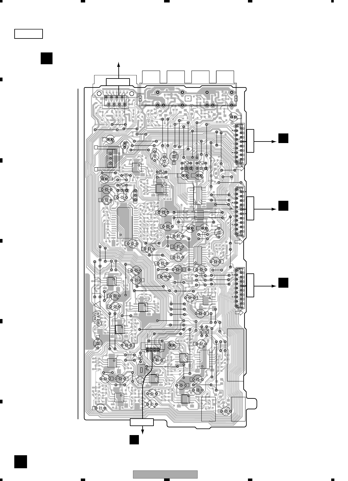
XV-EV51
56
1234
1234
C
D
F
A
B
E
4.6 AF ASSY
C
SIDE A
CMKS-P3X
IC8111
V-12V
V+12V
V-12V
V+12V
NJM7812
171171
4
1
21
1
For Binder
B
PRINTED
SIDE
IC8602
IC8601
IC8703
IC8801
IC8603
IC8301 IC8101
AF ASSY
SRN
SRP
SLN
SWP
SLP
CP
CN
SWN
ICT
FC
PRODUCTION CODE
IC8701
IC8702
IC8751
IC8753
IC8752
IC8803
IC8802
IC8201
11 GNDA
9 FLP
10 FLN
12 GNDA
8 GNDA
7 RS
6 GNDA
5 LS
9 FL
11 FR
12 GNDA
13 ANAL
14 GNDA
15 ANAR
16 DTSMIX
10 GNDA
17 SWFMIX
5 KEYSDATA
1 ECHOLVOL
2 LEVELIN
3 KEYSTB
4 KEYSCK
1 C
2 GNDA
3 SW
4 GNDA
15 RECR
7 VOCALB
8 VOCALA
9 ASSELB
10 ASSELA
11 CDL
12 GNDA
6 VOCALC 14 GNDA
13 CDR
4 TXR
17 GNDA
18 PBL
19 RECL
20 AUXMUTE
21 ATTNCONT
1 GNDTX
16 PBR
3 GNDTX
2 TXL
8 FRN
7 FRP
6 VA+12V
14 GNDD
13 VU+12V
5 VA+12TX
17 VE+56
16 GNDD
15 VA-12V
CONTACT
SIDE CONTACT
SIDE
CONTACT
SIDE
JA8401
R8814
C8905
W128
W108
W181
W125
W133
W109
W130
W170
W146
W157
IC8901
W156
CN8901
W148
W113
W114
W151
W153
CN8751
W158
W121
W152
W135
W132
W141
W169
W139
W120
W144
W110
W129
W143
W116
W101
W154
W117
R8724
W187
W145
W166
W149
W164
W183
W182
W106
W184
W180
W160
W140
C8834
W150
C8833
W105
W155
CN8301
W124
W179
W186
W138
W167
W172
W142
C8626
W175
W190
W168
W127
W147
W176
W185
W131
W119
W162
W178
W159
W134
W189
W137
W107
W161
W104
CN8701
W112
W136
W171
W177
W111
W103
C8622
C8620
W492
W102
W174
CN8101
C8823
C8613
C8822
C8601
C8614
C8826
C8602 C8713
C8701
C8714
C8702
C8751
C8761
C8762
C8752W163
C8789
C8829
C8831
C8312
W126
C8111
C8201
C8309
C8310
C8213
C8307
Q8201
L8201
C8308
C8305
C8222D8201
C8221
R8216
C8509
C8510
W165
C8113
W122
W173
C8907 C8908
D8901
C8117
C8119
C8118
C8120
R8904
R8901
D8902
W123
C8902
W487
C8906
R8626
R8625
C8625
109
753
2
1
17
1
17
1
4
1
21
1
AF ASSY
C
IC8201
IC8111
IC8602
IC8752
IC8801
IC8301
IC8753
IC8751
IC8803
IC8702
IC8603
IC8703
IC8901
IC8701
IC8601
Q8201
IC8802
IC8101
J5401
M
TO. STEREO POWER AMPLIFIER
(M-EV51 CN-3002)
(XNP3060-C)
CN5505
B
CN5504
B
CN5503
B
CN8301
CN8751 CN8101 CN8901
CN8701
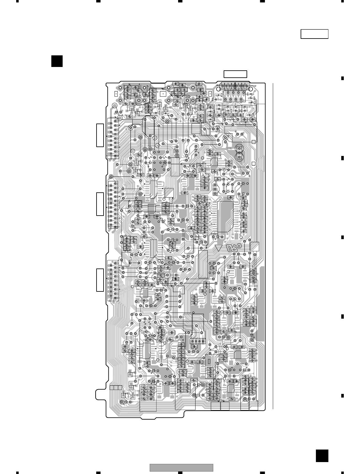
XV-EV51 57
5 678
5678
C
D
F
A
B
E
C
SIDE B
4
5
8
1
85
4
1
16 9
8
1
85
41
14 8
71
17 1 17 1
85
41
8
1
85
41
21
1
85
41
14
58
85
41
14
58
4
1
58
85
41
85
41
141
1528
1
8
916
Q8201
IN OUT
IC8901
VU+12V
XWZ3628
4.GNDA
1
4
1.ECHOVOL
2.VA+12V
3.MIC
VA+12V
5 LS
14 GNDA
12 GNDA
13 ANAL
11 FR
SERVICE
FOR
17 SWFMIX
16 DTSMIX
15 ANAR
9 FL
10 GNDA
4 GNDA
3 SW
1 C
2 GNDA
6 GNDA
8 GNDA
7 RS
CN8301
XWZ3618
CMKS-P3X
AUXMUTE
FADEROL
VA-12V
VE+56
VA-12V
LEVELIN
GNDA GNDA
LPFOR
LPFOL
DSPINR
DSPINL
KEYSCK
KEYSTB
FADEROR
VA-12V
XWZ3625
AF ASSY
KEYSDATA
GNDA
ECHVOL
LFE
LFE
DSPINL
GNDD
GNDA
GNDTX
GNDA
TXR
AUXINR
VA+12V
GNDA(AUXIN)
ATTNCONT
AUXOUTL
AUXOUTR
AUXINL
PBR
GNDA
GNDA
20.AUXMUTE
GNDA
FADEROL
TXL
TXR
PBL
PBR
AUXINL
CDL
CDR
RECR
RECL
FL
RS
LS
SW
FR
C
9.ASSELB
6.VOCALC
11 CDL
18PBL
17GNDA
16PBR
15RECR
14GNDA
12 GNDA
10 ASSELA
20
21.ATTNCONT
19RECL
5.KEYSDATA
8.VOCALA
7.VOCALB
13CDR
3.KEYSTB
4.KEYSCK
2.LEVELIN
1.ECHOLVOL
15 VA-12V
9 FLP
10 FLN
11 GNDA
12 GNDA
13 VU+12V
14 GNDD
17 VE+56
16 GNDD
8 FRN
5 VA+12TX
4 TXR
3 GNDTX
2 TXL
1 GNDTX
7 FRP
6 VA+12V
CN8101
CN8901
CN8751
CN8701
C8516
C8627
C8628
D8762
C8316
IC8801
IC8111
C8517
D8756
R8809
C8903
C8811
IC8101
D8802
R8768
IC8702
D8601
R8308
C8518
IC8602
D8602
IC8803
R8718
D8708
D8760
C8784
Q8753
Q8758 Q8754
Q8759
D8401
R8747
R8748 R8746
R8742
R8744
R8741
R8743
R8745
R8778
R8779
R8781
R8777
R8759
C8624
C8623
C8621
C8619
C8618
C8617
R8623
R8624
R8612
R8614
R8622
R8621
R8613
R8611
IC8603
R8728
R8729
C8737
C8519
C8781
C8779
C8716
R8601
C8609
C8824
C8807
R8813
C8607
R8607
R8605
R8603
C8615
IC8701
R8811
C8313
C8603
C8605
C8616
C8809
R8815
C8813
C8604
C8608
C8606
IC8601
C8806
R8602
R8606
R8608
R8604
C8610
R8808
IC8802
R8810 C8810
C8808
R8812
C8812
C8709
C8715
C8719
R8719
C8703
R8701
C8705 R8703
C8707
R8707
R8717
R8721
C8733
C8729
C8723
C8731
C8727
C8704
C8706
C8708
C8721
R8723
C8725
R8702
R8704
R8708
C8710
C8720
R8720
C8732
C8728
D8711
IC8703
R8722
C8734
C8730
C8724
D8710
C8722
C8726
L8701
C8735
C8736
R8751
R8753
C8757
R8757
C8759
C8763
C8767
R8771
C8775
D8712
D8706
C8753
C8755
C8764
R8767
IC8752
R8773
R8769
C8771
C8783
D8705
D8707
C8754
C8756
IC8751
C8758
C8769
C8773
R8752
R8754
R8758
C8760
C8768
R8772
C8780
C8776
D8755
D8757
R8726
C8770
IC8753
R8774
R8770
C8772
C8782
C8778
D8761
D8759
C8786
R8727
C8788
C8774
C8828
C8827
C8830
R8816
R8312
R8108
R8107
C8407
R8803 C8803
R8305
R8306
R8307
R8304
C8208
C8207
IC8201
C8206
R8217
C8210
C8209
C8216
C8214
C8215
R8206
R8201
C8202
IC8301
R8302
R8301
C8301
R8303
C8212
R8214
C8211
R8212
R8213
C8219
R8207
C8217
R8205
R8204
C8203
C8303
C8302
C8220
R8210
C8205
C8204
R8209
C8218
R8208
C8304
R8211
R8202
R8203
C8306
C8223
R8215
R8401
R8403
Q8503
R8409
Q8401
R8407
C8405
C8403
R8405
R8411 C8401
R8519
C8515
R8518
R8410
Q8402
R8408
C8406
C8404
R8406
R8404
C8402
R8511
R8402
R8513
Q8501
R8515
R8514
Q8502
R8516
R8517
R8512
C8514
C8513
R8801R8802
Q8101
R8101
C8101
C8103
Q8102
R8102
R8103
C8105
C8107
R8106 R8105
R8104
C8106
C8108
C8904
C8785
C8315
C8311
R8111
R8112
Q8403
D8758
D8709
85
14
85
14
16 9
18
14 8
71
28 15
14
1
16 9
18
AF ASSY
C
Q8501
Q8401
IC8301
IC8701
IC8901
IC8803
IC8802
IC8101
IC8111 IC8201
Q8101
Q8102
Q8502
Q8402
IC8602 IC8702
Q8403
Q8503
Q4002
Q3009
Q8201
Q8758
IC8753
IC8601
Q3010
Q301
IC8751
Q8759
Q8753
IC8603 IC8703
IC8801
Q8754
(XNP3060-C)
CN8901CN8101CN8751
CN8701
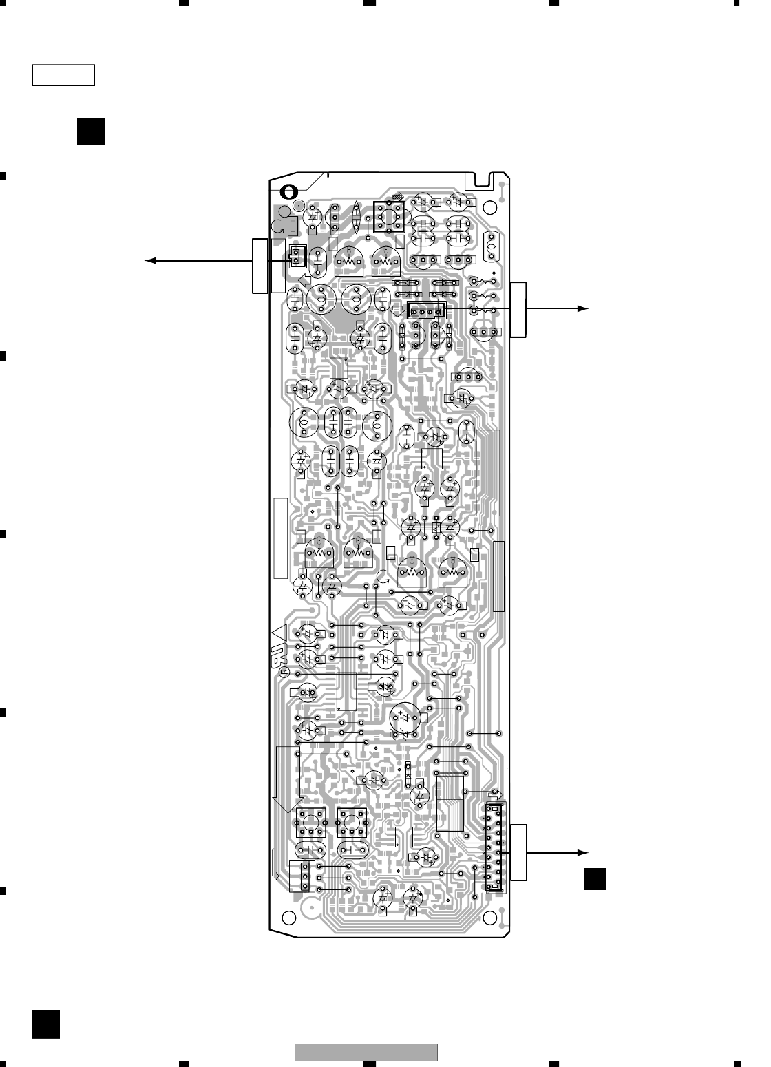
XV-EV51
58
1234
1234
C
D
F
A
B
E
4.7 DECK ASSY
E
SIDE A
IC2202
GNDA
A
21
OPEN
4
CMKS-P3X
RCH LCH
OPEN
Production Code
1
BIG
117
DECK ASSY
IC2401
XNP3061-A
1
3
VA12
15.GNDA
IC2201
SIDE
Lch
P
PBL
VA12
I
R
PRINTED
GNDA
GNDA
VREF
Adj.
Adj.PB
LEVEL
DECK TP
Lch
PRINTED
CONTACT SIDE
ICT FC
REC
L
1.GNDB
VB+12
MS
VA+12
5.VA+12
LEVEL
BIG
VA12
DBIAS
SIDE
VA12
GNDA
Adj.
VA12
Rch
MS
GNDA
SIDEPRINTED
RECR
XPBMUTE
DOL ON\OFF
10.RECMUTE
PB/XREC
XBEATCUT
BIAS
Rch
DGND
Lch
PBR
17.RECL
VREF
GNDA
VREF
VA12
VREF
GNDA
VREF
IC2301
Rch
Q2802
W246
F2201
W248
F2202
W229
C2810
CN2302
C2206
Q2803
C2203
L2802
C2307
C2308
C2309
C2420 C2809
C2421
C2310
C2311
C2312
C2314
C2404
C2208
D2306
C2407
C2403
C2408
C2409
C2425
C2801
C2417
C2802
C2803
C2804
C2410
C2215
C2217
C2405
VR2301
C2805
C2806
C2418
C2807
C2218
C2808
W257
Q2301
Q2805
Q2302
L2801
R2321
C2201
C2205
C2202
CN2506
W253
W255
W240
VR2802
C2207
C2422
C2419
CN2507
W227
W239
W254
C2216
W225
C2204
W263
W230
W222
VR2402
W256
C2406
VR2302
W218
W224
R2803
D2303
D2304
D2256
D2301
D2305
C2251
W247
C2255
R2806
W238
D2201
W244
C2254
VR2801
W243
C2262
W261
C2210
C2209
C2261
W228
Q2806
W242
W250
W249
W236
W220
W259
W223
R2805
VR2401
W219
W241
W260
W235
W252
W251
W258
W221
W237
W232
W234
W262
D2302
W231
W233
L2401
L2402
L2403
L2404
Q2801
CN2301
54
321
54
321
21
6 4
31
17
1
3
1
41
CN5801
BDECK MECHA
IC2202 IC2201
Q2302
Q2806
Q2803
IC2401
Q2805
IC2301
VR2401
VR2402
VR2301
VR2302
VR2802
VR2801
Q2301
Q2801
Q2802
(XNP3061-A)
DECK ASSY
E
DECK MECHA
CN2301
CN2302
CN2506
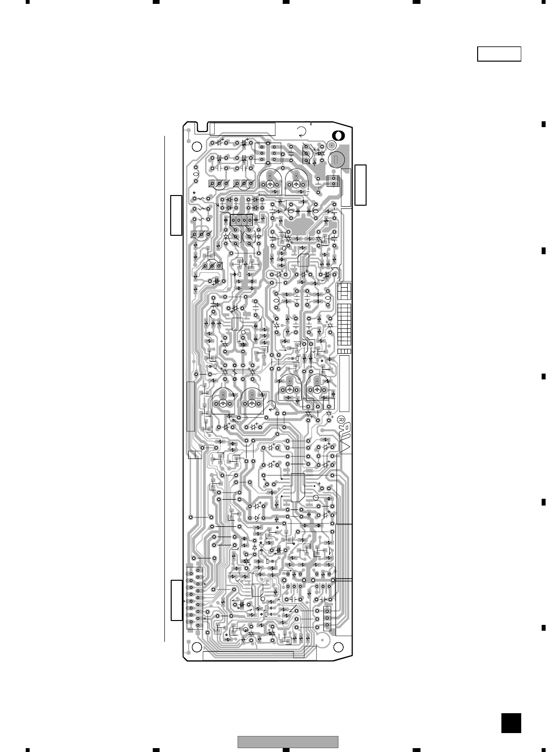
XV-EV51 59
5 678
5678
C
D
F
A
B
E
E
SIDE B
Q2263
Q2352
Q2353
C2302
R2319
C2231
R2320
D2254
D2253
R2815
IC2202
R2801
R2418
R2419
R2816
R2271
C2402
R2204
C2211
IC2301
R2205
R2309
R2163
D2255
R2409
R2898
R2813
C2212
C2230
R2211
D2252
R2425
R2277
C2424
R2814
R2266
R2810
R2811
R2203
R2399
R2308
R2401
R2306
R2307
Q2351
R2415
Q2262
Q2261
R2291
C2257
R2410
D2307
D2401
D2308
Q2460
Q2454
C2256
Q2453
Q2455
Q2402
Q2305
Q2804
Q2255
R2260
Q2304
R2261
R2213
R2255
R2411 Q2401
R2206
Q2306
R2809
R2251
R2281
Q2452
R2807
R2256
C2431
C2451
C2452
C2432
Q2254
R2254
R2808
R2262
R2210
R2252
Q2451
R9008
R2164
R2253
R9006
R2257
R2201
C2401
R9005
IC2401
R2202
Q2253
R2404
R2412
Q2252
Q2303
Q2251
Q2456
R2899
R2423
R2416
R2259
R2263
R2264
R2265
R2274
R2424
R2417
R2413
R2420
R2276
R2414
R2301
C2423
R2421
R2422
R2802
C2304
R2208
C2323
R2310
C2411
R2426
C2412
R2431
R2432
R2402
R2403
R2303
R2304
R2275
R2283
C2324
R2498
R2499
IC2201
R2451
R2311
C2315
R2267
C2321
C2303
R2282
R2351
C2252
R2268
R2269
C2301
R2352
C2253
R2305
R2207
R2452
R2453
C2322
R2455
R2270
R2272
R2273
R2302
R2456
R2312
1
85
41
85
4
1
117
A
B
C
1
0
0
321
0987654321
0
1
5
8
14
18
9
16
GNDA
GNDA
Q2302
13
REC
Adj.
R
L
BIAS
CN2301
CN2302
L2403 CN2507
VR2401
L2801
F2202
F2201
VR2801
L2402
D2304
D2201
D2256
L2802
D2302
D2303
D2301
1
VREF
BIG
R
L
VREF
XWX3066
1
L2404
D2305
D2306
Q2806
Adj.
XNP3061-A
BIG
VA12
VREF
16.PBL
17.RECL
15.GNDA
VREF
GNDA
GNDA
VA12
13.RECR
12.XPBMUTE
11.DOL ON
10.RMUTE
9.PB/XREC
8.XBEATCUT
7.BIAS
6.DGND
5.VA+12
4.VA+12
3.MS
2.VB+12
1.GNDB
VR2402
L2401
Q2805
Q2801 Q2802
TP2
CN2506
XWX3067
VA12
VREF
TP1
Q2803
CMKS-P3X
E
R
VREF
L
VR2302
VR2301
14.PBR
GNDA
VREF
GNDA
MS
VA12
VA12
GNDA
Q2301
VR2802
R
R
LEVEL
LEVEL
Adj.
L
L
PB
18
9
16
Q2801 Q2456 Q2401
Q2455
VR2801 Q2304
Q2303
Q2302
Q2802 Q2302Q2301
Q2305
Q2306
Q2451 VR2402
VR2401
VR2301
VR2302
Q2460
Q2453 Q2454
Q2262
Q2201
Q2263
Q2452 Q2353 Q2352Q2351 Q2252
Q2253
Q2252
Q2251
Q2254
Q2803 Q2804 Q2805
IC2401
IC2201
IC2202
IC2201
VR2801Q2806
(XNP3061-A)
CN2301
CN2302
CN2506
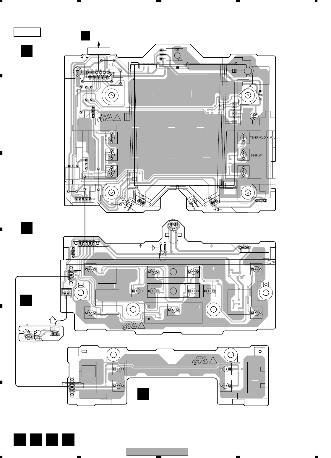
XV-EV51
60
1234
1234
C
D
F
A
B
E
4.8 DISP1, DISP2, DISP3 and LED ASSYS
H I J L
SIDE A
CMKS-P3X
CMKS-P3X
CMKS-P3X
CONTACT ON
MANUAL SOLDER
D5107
MANUAL SOLDER
D5108
|<</<< >>/>> |
2.GRAY
5
1
OPEN
2CH VIRTUAL
1
1
15
4.LCDDATA
5.KEY 3
ST MEMORY
SOUND
4.LCDCLK
5CH
3.VCC
ENTER
LED ASSY
DISPLAY2 ASSY
DISPLAY1 ASSY
SURROUND
1.VLCD
2.GNDU
5.LCDDATA
MODE
TUNER
6.KEY 2
PLAY/PAUSE
5.VA+12V
ASSES
4.KEY 3
1.GNDU REVERSE
3.GNDU
2.KEY 5
REC/STOP
9.VA+12
2.VE+5
10.GNDD
1.GNDD
3.KEY 2
DOBLY NR
3.LCDCLK
8.REMIN
1.GNDU
1
7.KEY 1
VOL + TAPE
OPEN/CLOSE
11.GNDC
5.VA+12V
2.GNDU
4.KEY 3
(DEMO)
3.GNDU
TUNNING -
3.KEY 2
2.KEY 5
1.GNDU
XWZ3622
DVD/CD
1.WHITE
VOL -
OPEN
DISPLAY3 ASSY
11
1
1.GNDD
2.GNDU
STOP
TUNNING +
LINE
KARAOKE
MODE
D5203
MANUAL SOLDER
UPPER SIDE
1
5
2.GRAY
1.WHITE
12
D5107
W471
V5101
CN5203
W473
D5204
S5105
J5203
S5106
D5102
D5103
C5103
S5303
S5211
S5104
S5304
S5103
R5106
D5101
D5105
S5102
S5101
L5101
S5209
J5202
S5202
S5201
S5210
J5102
W466
5101
W468
S5207
W465
W472
W464
S5204
S5203 S5205
D5202
S5208
R5211
D5201
C5108
W462
S5206
D5203
W467
W463
S5302
J5202
S5301
W474
W475
D5108
CN5101
W458
CN5102
51
21
1
31
51
1
31
11
1
5
1
DISP3 ASSY
H
DISP2 ASSY
I
LED ASSY
L
DISP1 ASSY
J
(XNP3060-C)
(XNP3060-C)
(XNP3060-C)
(XNP3060-C)
CN5509
B
CN5101
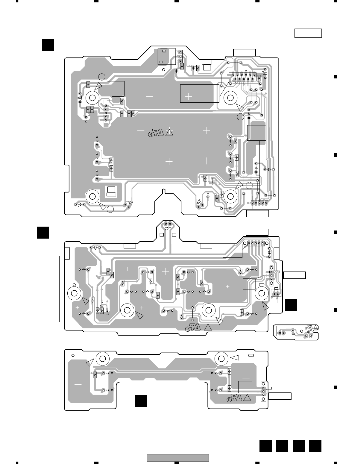
XV-EV51 61
5 678
5678
C
D
F
A
B
E
J LH I
SIDE B
31
51
31
111
15
CMKS-P3X
CMKS-P3X
CMKS-P3X
C
D
B
A
XWZ3621
LED
1
XWZ3620
S5304
S5303
S5302
S5301
S5211
S5210
S5209
S5208
S5207
S5206
S5205
S5204
S5203
S5202
S5201
S5106
S5105
S5104
S5103
ASSES
SOUND MODE
S5102
3.VCC
DISPLAY2 ASSY
CN5203
ST MEMORY
ENTER
5CH:KARAOKE
5
1.GNDU
2.VE+5
3.LCDCLK
4.LCDDATA
5.KEY 3
11.GNDC
10.GNDD
9.VA+12
8.REMIN
7.KEY 1
6.KEY 2
DISPLAY
TIMER/CLOCK ADJ
4.LCDCLK
TUNER
S5101
2.GNDU
1.GNDD
REVERSE MODE
1.GNDU
3.GNDU
2.KEY 5
VOL -
5.VA+12V
XWZ3622
DISPLAY1 ASSY
|<</<< TUNNING -
DOBLY NR(DEMO)
1.VLCD
2CH:VIRTUAL SURROUND
3.KEY 3
4.KEY 2
5.VA+12V
2.GNDU
LINE
STOP PLAY/PAUSE
>>/>>|tunning +
5.LCDDATA
REC/STOP
XWZ3619
1.GNDD
2.GNDU
1.GNDU
4.KEY3
3.GNDU
2.KEY 5
VOL +
ASSY
DVD/CD
CN5102
J5102
J5202
J5202
3.KEY2
DISPLAY3 ASSY
OPEN/CLOSE
TAPE
1
1
J5203
CN5101
CMKS-P3X
V5101
D5207
D5206
D5205
R5105
C5105
Q5101
C5104
R5103
R5107
R5303
C5102
R5102
C5101
R5109
R5101
R5111
R5110
C5109
C5110
C5106 C5107
C5111
D5106
R5208
R5210
R5209
R5201
R5206
R5108
Q5201
R5212
R5202
R5203
R5204
C5201
R5205
R5104
R5207
R5214
R5301
R5302
R5213
C5435
(XNP3060-C)
DISP3ASSY
H
DISP2 ASSY
I
LED ASSY
L
DISP1 ASSY
J
Q5101
Q5201
(XNP3060-C)
(XNP3060-C)
(XNP3060-C)
CN5101
CN5102
J5102
J5202
J5202
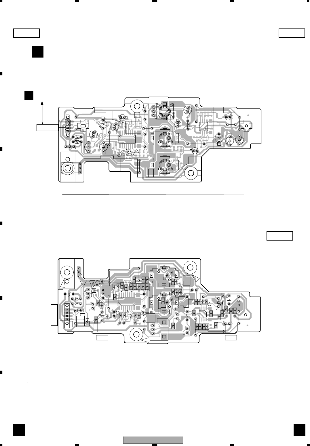
XV-EV51
62
1234
1234
C
D
F
A
B
E
4.9 MIC ASSY
MM
SIDE A SIDE A
SIDE B
CMKS-P3X
4
1
MIC ASSY
1.ECHOVOL
4.GNDA
2.VA+12V
3.MIC
IC5402
IC5401
C5422
C5426
C5416
VR5401
C5420
KN5401
C5413
R5401
L5401
D5401
R5411
C5410
JA5401
W456
JA5402
J5401
C5431
W459
W470
R5413
C5421
W454
W469
W457
C5409
W477
W461
W460
W452
Q5402
C5433
C5401
W453
W476
C5432
132
5
4
3
1
5
4
3
1
41
9
8
16
1
14
85
4
1
4
CMKS-P3X
4
5
3
1
3
2
MIC ASSY
XWZ3623
1
3
5
4
1
XWZ3626
3.MIC
J5401
1.ECHOVOL
2.VA+12V
4.GNDA
C5412
C5423 R5423
R5412
C5419
R5419
R5416
C5417
C5415
R5414
R5418
R5417
C5414
C5427
C5428
IC5401
C5424
R5425
C5430
R5429
C5429
R5415
R5402 C5402
R5408
C5411
R5409
C5425
R5422
C5405
C5404
C5403
C5436
R5403
C5408
R5407
C5407
R5406
R5404
C5406
R5405
C5418
R5426
R5434
R5421 R5424
IC5402
R5420
R5432 R5433
C5434
Q5401
R5430
R5431
18
9
16
(XNP3060-C)
(XNP3060-C)
CN8301
C
MIC ASSY
M
IC5401 IC5402Q5402
IC5401 IC5402Q5401
J5401
J5401
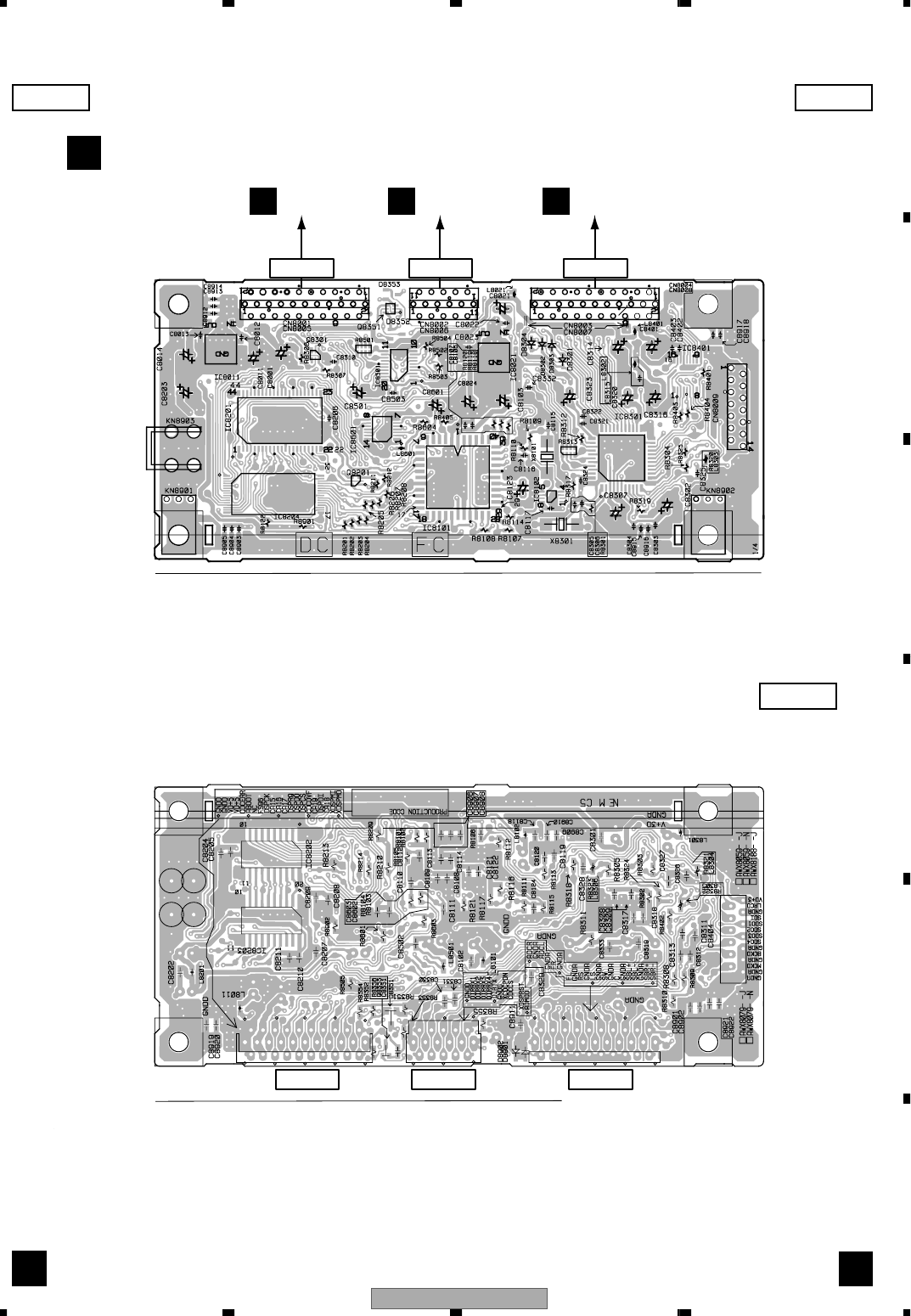
XV-EV51 63
5 678
5678
C
D
F
A
B
E
4.10 DSP ASSY(XV-EV51 Only)
KK
SIDE A SIDE A
SIDE B
CN5507
BCN5506
BCN5508
B
(ANP7442-B)
(ANP7442-B)
DSP ASSY(XV-EV51_Only)
K
IC8201 IC8101 IC8301 IC8401IC8102
IC8021
Q8201 IC8501
IC8601
Q8351
IC8204
Q8301
IC8202 Q8353
IC8203
CN8001 CN8002 CN8003
CN8001 CN8002 CN8003

XV-EV51
64
1234
1234
C
D
F
A
B
E
5. PCB PARTS LIST
Parts marked by "NSP" are generally unavailable because they are not in our Master Spare Parts List.
The mark found on some component parts indicates the importance of the safety factor of the part.
Therefore, when replacing, be sure to use parts of identical designation.
When ordering resistors, first convert resistance values into code form as shown in the following examples.
Ex.1 When there are 2 effective digits (any digit apart from 0), such as 560 ohm and 47k ohm (tolerance is shown by J=5%,
and K=10%).
Ex.2 When there are 3 effective digits (such as in high precision metal film resistors).
561
473
R50
1R0
5621
NOTES:
560 Ω
47k Ω
0.5 Ω
1 Ω
RD1/4PU J
RD1/4PU J
RN2H K
RS1P K
56 x 10
1
47 x 10
3
R50
1R0
561
473
5.62k Ω
RN1/4PC F562 x 10
1
5621
Mark No. Description Part No.
LIST OF ASSEMBLIES
XV-EV51/ZLXJ/NC
1..DSP ASSY AWX8059
NSP 1..MEDIA ASSY XWM3206
2..IF ASSY XWZ3617
2..AF ASSY XWZ3618
2..DISP 1 ASSY XWZ3619
2..DISP 2 ASSY XWZ3620
2..DISP 3 ASSY XWZ3621
2..LED ASSY XWZ3622
2..MIC ASSY XWZ3626
1..DECK ASSY XWZ3067
NSP 1..DVD ASSY AXA7110
2..DVD IF ASSY AWM7677
2..DVDM ASSY AWM7684
NSP 1..LOADING MECHANISM ASSY VWT1203
NSP 2..LOAB ASSY VWG2346
1..FM/AM TUNER MODULE AXQ7228
XV-EV21/ZLXJ/NC
NSP 1..MEDIA ASSY XWM3208
2..IF ASSY XWZ3627
2..AF ASSY XWZ3628
2..DISP 1 ASSY XWZ3619
2..DISP 2 ASSY XWZ3620
2..DISP 3 ASSY XWZ3621
2..LED ASSY XWZ3622
2..MIC ASSY XWZ3623
1..DECK ASSY XWZ3066
NSP 1..DVD ASSY AXA7110
2..DVD IF ASSY AWM7677
2..DVDM ASSY AWM7684
NSP 1..LOADING MECHANISM ASSY VWT1203
NSP 2..LOAB ASSY VWG2346
1..FM/AM TUNER MODULE AXQ7228
Mark No. Description Part No.
K
DSP Assy (EV51 Only)
SEMICONDUCTORS
IC8301 AK4586VQ
IC8101 CS493292
>IC8021 NJM2391DL1-25
>IC8011 NJM2391DL1-33
IC8201 PD8104A
IC8501 TC74LVX244FT
IC8202, IC8203 TC74VHC574F
IC8601 TC74VHCT08AFT
IC8102 TC7WU04FU
Q8351 RN2903
Q8301 UMD2N
Q8353 UN5212
D8301-D8304 1SS355
D8353 DAN202K
D8351, D8352 DAP202K
COILS AND FILTERS
L8011, L8102, L8201 Chip Inductor QTL1013
L8301, L8302, L8501, L8601 QTL1013
L8305 Chip Beads VTL1089
CAPACITORS
C8305, C8306 CCSRCH120J50
C8117 CCSRCH271J50
C8107, C8109, C8113, C8120, C8122 CCSRCH471J50
C8205, C8206, C8209, C8210, C8308 CCSRCH471J50
C8318, C8503, C8603 CCSRCH471J50
C8115, C8116 CCSRCH6R0D50
C8302, C8501, C8601 CEAL100M16
C8001, C8014, C8024, C8103, C8307 CEAL101M10
C8316, C8323 CEAL101M10
C8320 CEAL220M6R3
C8123 CEAL2R2M50
C8011, C8021 CEAL4R7M16
C8906 CKSRYB102K50
C8102, C8106, C8108, C8114 CKSRYB103K50
C8118, C8119, C8121, C8124, C8202 CKSRYB103K50
C8204, C8207, C8208, C8211, C8309 CKSRYB103K50
C8317, C8324, C8502, C8602, C8920 CKSRYB103K50
C8319, C8329-C8332, C8903, C8907 CKSRYB104K25
C8911 CKSRYB104K25
C8301, C8304, C8321 CKSRYB473K25
RESISTORS
R8313, R8501 RAB4C101J
R8312 RS1/16S1802F
Other Resistors RS1/16S###J
OTHERS
CN8002 11P SOCKET AKP7069
CN8003 15P SOCKET AKP7071
Mark No. Description Part No.

XV-EV51 65
5 678
5678
C
D
F
A
B
E
CN8001 21P SOCKET AKP7074
X8301 CRYSTAL RES.(12.28MHz) ASS7046
8903 SCREW PLATE VNE1948
KN8901, KN8902 EARTH METAL FIT. VNF1084
X8101 CRYSTAL RES.(27MHz) VSS1172
A FM/AM TUNER MODULE
SEMICONDUCTORS
IC201 BA1451F
IC202 LC72131MD
Q201, Q204, Q205 2SC2412K
Q202 DTA124ES
Q203 DTC124EK
D201 1SS133
D202 MTZJ5.1C
COILS AND FILTERS
L201 (FM Detector coil) ATE7003
F202 (Ceramic filter) ATF-107
F201 (Ceramic filter) ATF-119
F203 (AM Ceramic filter) ATF1155
CAPACITORS
C206 CCSRCH100D50
C212, C213, C226, C233-C235 CCSRCH101J50
C240 CCSRCH101J50
C231, C232 CCSRCH150J50
C223 CEAT100M50
C229 CEAT101M10
C224 CEAT1R0M50
C227 CEAT220M25
C241 CEAT2R2M50
C243 CEAT330M16
C228 CEAT3R3M50
C237 CEAT470M10
C211 CEJA1R0M50
C210 CEJA470M16
C204, C238, C602 CKSRYB102K50
C101, C102, C208, C220, C239 CKSRYB103K50
C242, C601 CKSRYB103K50
C216, C217 CKSRYB123K50
C225 CKSRYB153K50
C201, C205, C209, C214, C230 CKSRYB223K50
C236, C603 CKSRYB223K50
C221 CKSRYB224K10
C202, C222 CKSRYB473K16
C215 CKSRYB681K50
RESISTORS
R211 RD1/4PU221J
R221 RD1/4PU222J
R233 RD1/4PU391J
R243 RS1/10S0R0J
R103 RS1/10S331J
R104 RS1/10S391J
Other Resistors RS1/16S###J
OTHERS
CN201 13P Connector 52044-1345
BN201 4P Terminal AKA7003
Shield Case T ANK7072
Shield Case B ANK7073
Mark No. Description Part No.
X201 Crystal RES.(7.2MHz) ASS1093
B IF ASSY (XWZ3617)
SEMICONDUCTORS
IC5591, IC5801 BU4094BCF
>IC5507 NJM7805FA
>IC5508 NJM78M56FA
IC5501 PDC093A
Q5951, Q5801, Q5952 2SB1237X
Q5501, Q5953, Q5954 2SC2412K
Q5701 2SD1858X
Q5806 2SD2012
Q5803 DTA124EK
Q5505, Q5509 DTA143EK
Q5506, Q5507, Q5508 DTC124EK
Q5502, Q5807, Q5808, Q5802, Q5805 DTC143EK
D5501, D5502, D5506, D5508, D5509 1SS133
D5703, D5951, D5953, D5801, D5952 1SS133
D5954 1SS355
D5511 MTZJ11B
D5701 MTZJ11C
D5507 MTZJ6.8B
D5609, D5512, D5513, D5514 UDZS6.8B
COILS AND FILTERS
L5501 LAU220J
CAPACITORS
C5502 (0.047F) ACH1246
C5962, C5963, CCSRCH101J50
C5901, C5903, C5906 CCSRCH331J50
C5958, C5959 CEAL100M16
C5531 CEAL100M50
C5530 CEAL1R0M50
C5510, C5702, C5717, C5718, C5803 CEAT100M50
C5804, C5953, C5955, C5956 CEAT100M50
C5526 CEAT101M16
C5507, C5805 CEAT1R0M50
C5951 CEAT220M50
C5501, C5504, C5806 CEAT470M16
C5528 CEAT470M50
C5902, C5904 CEAT471M6R3
C5506, C5612, C5613CKSRYB102K50
C5516, C5517, C5518, C5521, C5529 CKSRYB103K50
C5593, C5594, C5601, C5603, C5605 CKSRYB103K50
C5607, C5609, C5610, C5703, C5808 CKSRYB103K50
C5809, C5810, C5952, C5954, C5957 CKSRYB103K50
C5503, C5505, C5509, C5512, C5515 CKSRYB104K16
C5527, C5532, C5591, C5616, C5802 CKSRYB104K16
C5960 CKSRYB104K16
C5592, C5801 CKSRYB221K50
C5961 CKSRYB224K10
C5807 CKSRYB473K25
C5614 CKSRYF105Z10
RESISTORS
R5957 RD1/2PM121J
R5953 RD1/2PM331J
R5802, R5804, R5807 RD1/4PU102J
R5954 RD1/4PU152J
R5601, R5606 RD1/4PU473J
Mark No. Description Part No.

XV-EV51
66
1234
1234
C
D
F
A
B
E
Other Resistors RS1/16S###J
OTHERS
CN5502 7P Connector 52045-0745
CN5509, CN5802 11P Connector 52045-1145
CN5701 13P Connector 52045-1345
CN5506 11P Plug AKP7058
CN5508 15P Plug AKP7060
CN5503, CN5505, CN5801 17P Plug AKP7061
CN5504, CN5507 21P Plug AKP7063
X5501 Ceramic RES. (10MHz) ASS7034
CN5510 2P Plug KM200SA2
CN5901 16P Connector VKN1192
CN5903 30P Connector VKN1206
CN5902 7P Connector VKN1211
KN5501, KN5502 Earth metal FIT. VNF1084
KN5503 Earth metal FIT. VNF1084
JA5903 2P Pinjack XKB3039
CN5501 20P Socket XKP3051
B IF ASSY(XWZ3627)
SEMICONDUCTORS
IC5801 BU4094BCF
>IC5507 NJM7805FA
>IC5508 NJM78M56FA
IC5501 PDC097A
Q5951, Q5955 2SA1282
Q5801, Q5804 2SB1132
Q59522 SB1237X
Q5501, Q5701 2SD1858X
Q5806 2SD2012
Q5510, Q5511 2SD2114K
Q5512, Q5803 DTA124EK
Q5505, Q5509 DTA143EK
Q5506-Q5508 DTC124EK
Q5502, Q5805 DTC143ES
D5501, D5502, D5504, D5506 1SS133
D5508, D5509, D5703, D5951, D5953 1SS133
D5510, D5801, D5952, D5954 1SS355
D5511 MTZJ11B
D5701 MTZJ11C
D5507 MTZJ6.8B
D5609, D5610 UDZS15B
D5512-D5514 UDZS6.8B
COILSANDFILTERS
L5501 LAU220J
CAPACITORS
C5502 (0.047F) ACH1246
C5962, C5963 CCSRCH101J50
C5901, C5903, C5906 CCSRCH331J50
C5958, C5959 CEAL100M16
C5531 CEAL100M50
C5530 CEAL1R0M50
C5510, C5702, C5717, C5718 CEAT100M50
C5803, C5804, C5953, C5955, C5956 CEAT100M50
C5507, C5805 CEAT1R0M50
C5951 CEAT220M50
Mark No. Description Part No.
C5501, C5504, C5526, C5806 CEAT470M16
C5528 CEAT470M50
C5902, C5904 CEAT471M6R3
C5506, C5612, C5613 CKSRYB102K50
C5516-C5518, C5521, C5529 CKSRYB103K50
C5593, C5594, C5601, C5603, C5605 CKSRYB103K50
C5607, C5609, C5610, C5703 CKSRYB103K50
C5808-C5810, C5952, C5954, C5957 CKSRYB103K50
C5503, C5505, C5509, C5512, C5515 CKSRYB104K16
C5527, C5532, C5616, C5802, C5960 CKSRYB104K16
C5801 CKSRYB221K50
C5961 CKSRYB224K10
C5807 CKSRYB473K25
RESISTORS
R5957 RD1/2PM121J
R5953 RD1/2PM331J
R5802, R5804, R5807 RD1/4PU102J
R5954 RD1/4PU152J
R5601, R5606 RD1/4PU473J
OTHERS
CN5502 7P Connector 52045-0745
CN5509, CN5802 11P Connector 52045-1145
CN5701 13P Connector 52045-1345
CN5503, CN5801 17P Plug AKP7061
CN5504 21P Plug AKP7063
X5501 Ceramic RES. (10MHz) ASS7034
CN5510 2P Plug KM200SA2
CN5901 16P Connector VKN1192
CN5903 30P Connector VKN1206
CN5902 7P Connector VKN1211
KN5501, KN5502 Earth metal FIT. VNF1084
L5902, L5903 VTL1084
JA5903 2P Pinjack XKB3039
CN5501 20P Socket XKP3051
C AF ASSY(XWZ3618)
SEMICONDUCTORS
IC8111, IC8801 AN4558NS
IC8301 BA3838F
IC8101 BU4052BCF
IC8602 BU4066BCF
IC8201 M65847AFP
IC8601, IC8603, IC8701, IC8702, IC8703NJM4558MD
IC8751, IC8752, IC8753, IC8802, IC8803NJM4558MD
IC8901 NJM7812FA
Q8401, Q8402 2SC2412K
Q8201 2SD1858X
Q8501, Q8502 2SD2114K
Q8403, Q8503, Q8754, Q8758 DTA124EK
Q8101, Q8102, Q8753, Q8759 DTC124EK
D8401, D8802 1SS355
D8201 MTZJ5.6B
D8901, D8902 MTZJ6.8B
D8601, D8602 UDZS6.8B
CAPACITORS
C8212 CCSRCH101J50
C8705, C8706, C8709, C8710, C8755 CCSRCH331J50
C8759 CCSRCH331J50
C8217 CCSRCH471J50
Mark No. Description Part No.

XV-EV51 67
5 678
5678
C
D
F
A
B
E
C8609, C8610 CCSRCH820J50
C8111 CEAL100M50
C8113, C8119, C8120, C8221, C8509 CEAT100M50
C8510, C8752, C8752, C8822, C8826 CEAT100M50
C8833, C8834 CEAT100M50
C8789, C8823 CEAT101M16
C8902 CEAT1R0M50
C8305, C8308, C8309, C8310, C8601 CEAT2R2M50
C8602, C8701, C8702, C8751 CEAT2R2M50
C8117, C8118, C8201, C8213, C8222 CEAT470M16
C8307, C8625, C8626, C8829, C8831 CEAT470M16
C8905, C8906, C8907, C8908 CEAT470M16
C8312 CEAT4R7M50
C8903 CKSQYF105Z25
C8220, C8605, C8606 CKSRYB102K50
C8101, C8103, C8107, C8108, C8203 CKSRYB103K50
C8204, C8205, C8218, C8313, C8514 CKSRYB103K50
C8519, C8615, C8616, C8619, C8621 CKSRYB103K50
C8623, C8624, C8715, C8716, C8723 CKSRYB103K50
C8724, C8725, C8726, C8727, C8728 CKSRYB103K50
C8729, C8730, C8736, C8763, C8764 CKSRYB103K50
C8771, C8772, C8773, C8774, C8775 CKSRYB103K50
C8776, C8778, C8779, C8810, C8811 CKSRYB103K50
C8812, C8813, C8828, C8830 CKSRYB103K50
C8301, C8302, C8303, C8407, C8515 CKSRYB104K16
C8518, C8754 CKSRYB104K16
C8219 CKSRYB122K50
C8603, C8604 CKSRYB222K50
C8904 CKSRYB223K50
C8304 CKSRYB224K10
C8756 CKSRYB333K25
C8703, C8704, C8753 CKSRYB471K50
C8216 CKSRYB472K50
C8202, C8223, C8306, C8788, C8824 CKSRYB473K25
C8207, C8208, C8209 CKSRYB683K16
C8760 CKSRYB821K50
C8206 CKSRYB822K50
C8513 CKSRYF105Z10
C8214, C8215 CKSRYF224Z16
RESISTORS
R8216 RD1/4PU102J
R8724, R8814 RD1/4PU470J
R8901, R8904 RD1/4PU471J
R8625, R8626RD1/4PU821J
R8717, R8718, R8721RS1/16S1002F
R8722, R8767, R8768, R8769 RS1/16S1002F
R8770, R8808, R8809, R8810, R8811 RS1/16S1002F
Other Resistors RS1/16S###J
OTHERS
CN8301 4P Jumper connector 52147-0410
CN8751, CN8901 17P Socket AKP7072
CN8101 21P Socket AKP7074
Heat sink ANH-309
Screw BBZ30P080FMC
JA8401 4P Pinjack XKB3040
CN8701 8P Socket XKP3052
C AF ASSY(XWZ3628)
Mark No. Description Part No.
SEMICONDUCTORS
IC8111, IC8801 AN4558NS
IC8301 BA3838F
IC8101 BU4052BCF
IC8201 M65847AFP
IC8802, IC8803 NJM4558MD
IC8901 NJM7812FA
Q8401, Q8402 2SC2412K
Q8201 2SD1858X
Q8501, Q8502 2SD2114K
Q8403, Q8503 DTA124EK
Q8101, Q8102 DTC124EK
D8401, D8802 1SS355
D8201 MTZJ5.6B
D8901, D8902 MTZJ6.8B
CAPACITORS
C8212 CCSRCH101J50
C8217 CCSRCH471J50
C8111 CEAL100M50
C8113, C8119, C8120, C8221 CEAT100M50
C8509, C8510, C8822, C8826 CEAT100M50
C8833, C8834 CEAT100M50
C8789, C8823 CEAT101M16
C8902 CEAT1R0M50
C8305, C8308-C8310 CEAT2R2M50
C8117, C8118, C8201, C8213, C8222 CEAT470M16
C8307, C8829, C8831, C8905-C8908 CEAT470M16
C8312 CEAT4R7M50
C8903 CKSQYF105Z25
C8220 CKSRYB102K50
C8101, C8103, C8107, C8108 CKSRYB103K50
C8203-C8205, C8218, C8313, C8514 CKSRYB103K50
C8519, C8810-C8813, C8828, C8830 CKSRYB103K50
C8301-C8303, C8407, C8515, C8518 CKSRYB104K16
C8219 CKSRYB122K50
C8904 CKSRYB223K50
C8304 CKSRYB224K10
C8216 CKSRYB472K50
C8202, C8223, C8306, C8788, C8824 CKSRYB473K25
C8207-C8209 CKSRYB683K16
C8206 CKSRYB822K50
C8513 CKSRYF105Z10
C8214, C8215 CKSRYF224Z16
RESISTORS
R8216 RD1/4PU102J
R8814 RD1/4PU470J
R8901, R8904 RD1/4PU471J
R8808-R8811 RS1/16S1002F
OTHERS
CN8301 4P Jumper connector 52147-0410
CN8901 17P Socket AKP7072
CN8101 21P Socket AKP7074
Heat sink ANH-309
Screw BBZ30P080FMC
JA8401 4P Pinjack XKB3040
J DISP 1 ASSY
Mark No. Description Part No.

XV-EV51
68
1234
1234
C
D
F
A
B
E
SEMICONDUCTORS
Q5101 2SC2412K
D5102, D5103 1SS133
D5105, D5106 MTZJ6.8B
COILS AND FILTERS
L5101 LAU220J
SWITCHES AND RELAYS
S5101, S5102, S5103, S5104, S5105 ASG7013
CAPACITORS
C5109 CCSRCH100D50
C5110 CCSRCH220J50
C5103 CEAT101M10
C5108 CEAT470M16
C5106 CKSRYB102K50
C5101, C5104 CKSRYB103K50
C5111 CKSRYB104K16
C5105 CKSRYB681K50
RESISTORS
R5106 RD1/4PU101J
Other Resistors RS1/16S###J
OTHERS
CN5101 11P Connector 52044-1145
5101 Remote recevier unit GP1U26X
I DISP 2 ASSY
SEMICONDUCTORS
Q5201 2SC2412K
D5206, D5207 1SS355
D5202, D5204 MTZJ6.8B
SWITCHES AND RELAYS
S5201, S5202, S5203, S5204, S5205 ASG7013
S5206, S5207, S5208, S5209, S5210 ASG7013
S5211 ASG7013
CAPACITORS
C5201 CKSRYB103K50
RESISTORS
R5211 RD1/4PU101J
Other Resistors RS1/16S###J
OTHERS
5202 3P Cable holder 51048-0300
5201 5P Cable holder 51048-0500
J5202 3P Jumper wire D20PYY0320E
J5102 Jumper wire D20PYY0510E
J5203 Connector Assy PF02PG-B07
LED Holder XMR3053
H DISP 3 ASSY
SWITCHES AND RELAYS
S5301, S5302, S5303 ASG7013
RESISTORS
Other Resistors RS1/16S###J
OTHERS
Mark No. Description Part No.
5301 3P Cable holder 51048-0300
L LED ASSY
SEMICONDUCTORS
D5203, D5205 UDZS6.8B
OTHERS
CN5203 KR Connector S2B-PH-K
M MIC ASSY
SEMICONDUCTORS
IC5401 M65855FP
IC5402 NJM4558MD
Q5402 2SJ103
Q5401 DTA143EK
D5401 MTZJ5.1B
COILS AND FILTERS
L5401 LAU100J
CAPACITORS
C5418, C5419, C5427, C5428 CCSRCH101J50
C5409 CEAL220M16
C5416 CEAL2R2M50
C5401 CEAT101M16
C5422 CEAT2R2M50
C5420 CEAT470M16
C5432 CEAT4R7M50
C5433 CEATR22M50
C5421, C5426 CEJQ2R2M50
C5431 CEJQ4R7M50
C5410 CEJQR47M50
C5423 (XWZ3626) CKSRYB102K50
C5423 (XWZ3623) CKSRYB331K50
C5404, C5408, C5411, C5430 CKSRYB103K50
C5402, C5412, C5429, C5436 CKSRYB104K16
C5414 CKSRYB122K50
C5405 CKSRYB123K50
C5406 CKSRYB472K50
C5407 CKSRYB473K25
RESISTORS
R5401 RD1/4PU561J
VR5401 10k-B XCS3007
Other Resistors RS1/16S###J
OTHERS
5401 4P Cable holder 51048-0400
J5401 Jumper wire D20PYY0430E
KN5401 Earth metal FIT. VNF1084
JA5401, JA5402 MIC Jack XKN3012
G DVD IF ASSY
SEMICONDUCTORS
>IC1902 BA06FP
IC1941 MM1567AJ
>IC1906 NJM2391DL1-33
>IC1901, IC1903 NJM78M05DL1A
IC1921 PCM1742KE
>IC1904 PQ025EH01ZP
Mark No. Description Part No.

XV-EV51 69
5 678
5678
C
D
F
A
B
E
>IC1905S-8540 B00FN-IMA
IC1962 TC74VHC125FT
IC1961 TC74VHCT125AFT
Q1931 2SA1576A
>Q1901C PH6312
Q1941, Q1961 RN1903
Q1942 RN2903
Q1921, Q1922, Q1932 UN5212
D1901, D1932-D1935 1SS355
D1902 RB051L-40
D1931 UDZS5.1B
COILSANDFILTERS
L1901 (SMP Power Inductor) ATL7003
L1902 (SMP Power Inductor) ATL7004
L1903 (SMP Power Inductor) ATL7005
CAPACITORS
C1931, C1932 CCSRCH102J50
C1920 CCSRCH121J50
C1901, C1904, C1906, C1912, C1925 CEV101M16
C1930, C1953 CEV101M16
C1910, C1917 CEV221M4
C1903, C1908, C1928, C1950, C1996 CEV470M6R3
C1915 CKSQYB105K16
C1902, C1905, C1907, C1909, C1918 CKSRYB104K16
C1923, C1924, C1926, C1929, C1933 CKSRYB104K16
C1941, C1943, C1945, C1947-C1949 CKSRYB104K16
C1951, C1952, C1955-C1957 CKSRYB104K16
C1961, C1962, C1991-C1995 CKSRYB104K16
C1914, C1999 CKSYB475K16
C1916, C1919, C1998 (Ceramic C) DCH1148
RESISTORS
R1903 (0.068 1/4w) ACN7113
R1904 (0.1 1/10w) ACN7114
R1994, R1995 RS1/10S0R0J
R1907 RS1/16S1502F
R1906 RS1/16S3902F
R1908 RS1/16S4700F
OTHERS
CN1901, CN1961 30P Connector RKN1039
CN1902 16P Connector RKN1057
CN1962 26P Connector RKN1067
F DVDM ASSY
SEMICONDUCTORS
IC110 BA10358FV
IC251 BA6664FM
IC604 K4S641632F-TC75
IC302 K6T1008V2E-TB70
IC301 L6315ATXXTY
IC351 M56788AFP
>IC303 (1.8V) PQ018EZ01ZP
IC601 STI5519AVB-B0C
IC605 TC7WU04FU
IC603 VYW1948
Q300, Q602-Q607 2SA1576A
Q652 DTC114TUA
Q101, Q102 HN1A01F
Q103 HN1C01FU
Q601 RN4982
Mark No. Description Part No.
D601 RB501V-40
COILSANDFILTERS
L6990 (330mH) ATL7007
L300 LCYA2R7J2520
L5010, L5020, L5040 ( Chip 60mH) VTL1075
CAPACITORS
C301, C302 CCSRCH100D50
C310 CCSRCH151J50
C307 CCSRCH180J50
C360 CCSRCH330J50
C391 CCSRCH331J50
C351, C651 CCSRCH470J50
C627, C638, C696 CCSRCH471J50
C309 CCSRCH560J50
C633, C634 CCSRCH6R0D50
C308 CCSRCH7R0D50
C113 CEV100M35
C104 CEV101M4
C316, C317, C405, C617, C619 CEV101M6R3
C111, C404 CEV220M16
C368 CEV470M16
C334 CKSQYB225K10
C340, C641 CKSRYB102K50
C259, C311 CKSRYB103K50
C106, C248-C251, C255, C313 CKSRYB104K16
C315, C636, C637, C697 CKSRYB104K16
C257, C258 CKSRYB223K50
C357 CKSRYB472K50
C103, C105, C148, C157, C158 CKSRYF104Z25
C253, C256, C304, C321-C333 CKSRYF104Z25
C365, C366, C603, C605, C607 CKSRYF104Z25
C612, C615, C616, C632 CKSRYF104Z25
C606, C608-C611, C613 CKSRYF105Z10
C622, C623, C629, C635, C699 CKSRYF105Z10
RESISTORS
R121 RAB4C220J
R123 RAB4C390J
R340, R407 RS1/10S0R0J
R341 RS1/10S101J
R126-R129, R176-R179 RS1/10S220J
R254-R259 RS1/10S3R3J
R326-R330 RS1/16S1001F
R147, R265, R266, R304, R322 RS1/16S1002F
R377, R378, R392, R393 RS1/16S1002F
R344, R351, R353, R354 RS1/16S1003D
R359, R360, R365, R367, R368 RS1/16S1003D
R372, R374, R376 RS1/16S1003D
R331, R385 RS1/16S1003F
R302 RS1/16S1202F
R358, R394 RS1/16S1503F
R146 RS1/16S1801F
R612, R613 RS1/16S1802F
R675, R678, R681, R684, R687 RS1/16S2700F
R690 RS1/16S2700F
R345, R355, R370, R371 RS1/16S3902F
R346, R356, R357, R362, R364 RS1/16S6802F
R373 RS1/16S6802F
R3730 RS1/16S8202F
Mark No. Description Part No.

XV-EV51
70
1234
1234
C
D
F
A
B
E
OTHERS
CN2 12P Connector AKN7031
CN8 26P Connector AKN7032
CN4 4P Connector RKN1045
CN9 PH Connector S5B-PH-SM3
7P Flexible Cable VDA1681
CN25 26P Connector VKN1318
CN22 30P Connector VKN1322
X301 Crystal RES.(20MHz) VSS1171
X601 Crystal RES.(27MHz) VSS1172
D LOAB ASSY
OTHERS
CN602 KR Connector S2B-PH-K
CN601 KR Connector S5B-PH-K
PCB BORD VNP1836
101 Reaf SWITCH VSK1011
E DECK ASSY(XWX3067)
SEMICONDUCTORS
IC2202, IC2301, IC2401 BA4558F-HT
IC2201 HA12136AF
Q2254 2SA1037K
Q2801, Q2802, Q2805 2SC1815
Q2806 2SC2240
Q2251-Q2253 2SC2412K
Q2261, Q2262, Q2301, Q2302 2SK373
Q2351, Q2460 DTA124EK
Q2303, Q2304 DTC114TK
Q2255, Q2352, Q2263 DTC143EK
D2256, D2301-D2306 1SS133
D2252-D2255, D2307 1SS355
D2201 MTZJ6.2A
COILSANDFILTERS
L2802 LFA121J
L2801 (OSC 105kHz) RTD1082
L2401, L2402 (10mH) RTF1004
L2403, L2404 (4.7mH) RTF1021
F2201, F2202 (MPX. Filter) RTF1217
CAPACITORS
C2809 CCCSL151K2H
C2301, C2302 CCSRCH100D50
C2423, C2424 CCSRCH221J50
C2253 CCSRCH271J50
C2256, C2257, C2321-C2324 CCSRCH470J50
C2401, C2402 CCSRCH470J50
C2303, C2304 CCSRCH681J50
C2807 CEAL470M6R3
C2203, C2204, C2207, C2311, C2312 CEAT100M50
C2215 CEAT101M16
C2201, C2202, C2217, C2218, C2255 CEAT1R0M50
C2404, C2419, C2420 CEAT1R0M50
C2251 CEAT220M50
C2216 CEAT221M16
C2254 CEAT2R2M50
C2309, C2310, C2407, C2408 CEAT330M50
C2425 CEAT470M16
C2261, C2262 CEAT4R7M50
Mark No. Description Part No.
C2208 CEATR10M50
C2205, C2206 CEATR22M50
C2403 CEJQ1R0M50
C2805, C2806, C2810 CEJQ330M10
C2314 CEJQ470M16
C2315 CKSRYB102K50
C2231 CKSRYB103K50
C2431, C2432 CKSRYB122K50
C2211, C2212 CKSRYB152K50
C2252 CKSRYB334K10
C2808 CQHA822J2A
C2801 CQMA123J50
C2421, C2422 CQMA152J50
C2409, C2410 CQMA223J50
C2803, C2804 CQMA472J50
C2802 CQMA682J50
C2209, C2210 CQMBA103J50
C2307, C2308 CQMBA682J50
C2405, C2406 CQMBA683J50
RESISTORS
R2805 RD1/2VM161J
R2803 RD1/2VM4R7J
VR2301,VR2302,VR2401,VR2402(4.7k)PCP1028
VR2801, VR2802(100k-B) PCP1032
OTHERS
CN2506 AKP7072
CN2302 B2B-PH-K
CN2507 B3P-SHF-1AA
CN2301 B4B-PH-K
PCB VEF1040
E DECK ASSY(XWX3066)
SEMICONDUCTORS
IC2202, IC2301, IC2401 BA4558F-HT
IC2201 HA12136AF
Q2254 2SA1037K
Q2801, Q2802, Q2805 2SC1815
Q2806 2SC2240
Q2251-Q2253 2SC2412K
Q2261, Q2262, Q2301, Q2302 2SK373
Q2351, Q2460 DTA124EK
Q2303, Q2304 DTC114TK
Q2255, Q2352, Q2263 DTC143EK
D2256, D2301-D2306 1SS133
D2252-D2255, D2307 1SS355
D2201 MTZJ6.2A
COILSANDFILTERS
L2802 LFA121J
L2801 (OSC Coil 105k) RTD1082
L2401, L2402 (10mH) RTF1004
L2403, L2404 (4.7mH) RTF1021
F2201, F2202 (MPX FIL.) RTF1217
CAPACITORS
C2809 CCCSL151K2H
C2301, C2302 CCSRCH100D50
C2423, C2424 CCSRCH221J50
C2253 CCSRCH271J50
C2303, C2304 CCSRCH681J50
Mark No. Description Part No.

XV-EV51 71
5 678
5678
C
D
F
A
B
E
C2807 CEAL470M6R3
C2203, C2204, C2207, C2311, C2312 CEAT100M50
C2215 CEAT101M16
C2201, C2202, C2217, C2218, C2255 CEAT1R0M50
C2404, C2419, C2420 CEAT1R0M50
C2251 CEAT220M50
C2216 CEAT221M16
C2254 CEAT2R2M50
C2309, C2310, C2407, C2408 CEAT330M50
C2425 CEAT470M16
C2261, C2262 CEAT4R7M50
C2208 CEATR10M50
C2205, C2206 CEATR22M50
C2403 CEJQ1R0M50
C2805, C2806, C2810 CEJQ330M10
C2314 CEJQ470M16
C2315 CKSRYB102K50
C2231 CKSRYB103K50
C2431, C2432 CKSRYB122K50
C2211, C2212 CKSRYB152K50
C2252 CKSRYB334K10
C2808 CQHA822J2A
C2801 CQMA123J50
C2421, C2422 CQMA152J50
C2409, C2410 CQMA223J50
C2803, C2804 CQMA472J50
C2802 CQMA682J50
C2209, C2210 CQMBA103J50
C2307, C2308 CQMBA682J50
C2405, C2406 CQMBA683J50
RESISTORS
R2805 RD1/2VM161J
R2803 RD1/2VM4R7J
VR2301,VR2302,VR2401,VR2402(4.7k)PCP1028
VR2801, VR2802 (100k-B) PCP1032
OTHERS
CN2506 17P SOCKET AKP7072
CN2302 CONNECTOR POST B2B-PH-K
CN2507 3P CONNECTOR B3P-SHF-1AA
CN2301 KR CONNECTOR B4B-PH-K
PCB BINDER VEF1040
Mark No. Description Part No.
XV-EV51
72
1234
1234
C
D
F
A
B
E
6. ADJUSTMENT
6.1 DECK SECTION
6.1.1 Adjustment condition
7 Adjustment Condition
(1) The ground at the time of adjustment shall be W166.
(Refer to Fig. 6–3).
(2) Clean the heads and demagnetize them using a head eraser.
(3) Set the measurement level to 0 dBV = 1 Vrms.
(4) Use the specified tape for adjustment. Use the labeled (A) side
of the test tape.
NCT–111 : For Tape Speed adjustment
NCT-112 : For Playback adjustment
STD–633 : Normal blank tape
* As the reference recording level is 250 nwb/m for NCT–
112, the recording level will be higher than 4 dB for NCT–
112 (160nwb/m). When adjusting, pay carefully attention
to the type of tape used.
(5) Provide yourself with the following measuring devides:
÷ AC millivoltmeter
÷ Low-frequency oscillator
÷ Attenuator
÷ Oscilloscope
(6) Adjust both right and left channels unless other wise specified.
(7) Turn the DOLBY NR switch off unless otherwize specified.
(8) Warm up the unit for several minutes before adjustment. In
particular, be sure to warm up the unit in the REC/PLAY mode
for 3 to 5 minutes before starting recording/playback frequency
characteristics adjustment.
(9) Always follow the indicated adjustment order.
Otherwise, a complete adjustment may not be achieved.
7List of Adjustments
¶ Playback Section
(1) Tape Speed Confirmation
(2) Head Azimuth Adjustment
(3) Playback Level Adjustment
¶ Recording Section
(1) Recording Bias Adjustment
(2) Recording Level Adjustment
Dolby noise reduction manufactured under license from Dolby
Laboratories Licensing Corporation.
“DOLBY” and the double-D symbol are trademarks of Dolby
Laboratories Licensing Corporation.
Fig. 6-2 Test Tape NCT– 112
Fig. 6-1 Frequency Characteristics
0 dB
–20 dB
30s 0 dB: 315 Hz, 250 nwb/m
315 Hz
6.3 kHz 10 kHz 315 Hz 14 kHz 12.5
kHz 6.3
kHz 500
Hz 250
Hz 125
Hz
10 kHz 8 kHz 4 kHz 2 kHz 63 Hz 40 Hz
1 kHz
30 s 30 s 30 s 10s 10s .......................................................................................................... 10s
250
3dB
10k 12.5k
3dB 4dB
PLAY BACK
250
3dB
10k 12.5k
3dB 5dB
RECORDING
For adjustment, use the stereo power amplifier (M-EV51 or M-EV21).
XV-EV51 73
5 678
5678
C
D
F
A
B
E
6.1.2 Playback and Recording section
NCT-111 (3 kHz) VR2701 (DECK ASSY)
(Refer to Fig. 6-3)
No. Mode Input Signal/Test Tape Adjustment Points Measurement Points Adjustment Value Remarks
PLAY1P1 R
(CN2507)
(DECK ASSY) 3000 Hz Hz
(1) Tape Speed Confirmation
(1) Recording Bias Adjustment
¶ After the adjustment, caution should be exercised so as not to become under bias by checking the distortion rate.
NCT-110 test tape
(Playback: 10 kHz, –20 dB)
Head azimuth
adjustment Screw
(Refer to Fig. 6-3)
Remarks
PLAY
1
P3 L (CN2507)
P1 R (CN2507)
(DECK ASSY)
Max. Playback
signal level
(2) Head Azimuth Adjustment
¶ This unit is equipped with auto tape selector.
¶ Do not switch between forward and reverse operation with the screwdriver inserted.
+10
–10
Playback Section
After adjustment, apply silicon
bond to the head azimuth
adjustment screw.
VR2301
PLAY
1
(3) Playback Level Adjustment
¶ Since this adjustment determines playback DolbyNR level, Perform it carefully.
L ch
R ch VR2302
P3 L (CN2507)
P1 R (CN2507)
(DECK ASSY)
Recording Section
VR2801
REC/
PAUSE
1Input a 315Hz signal to the LINE -
IN terminal. ∗
L ch
R ch VR2802
P3 L (CN2507)
P1 R (CN2507)
(DECK ASSY)
–3.7 dBV
Input signal level –23.7 dBV
REC =
PLAY
2
Load the STD–633 test tape and
record/playback the 315Hz and
10kHz signals. (see the Note below)
Repeat adjustment until playback level of
the 10kHz signal is within 0dBV ±0.5dB
from that of the 315Hz signal.
(2) Recording Level Adjustment
VR2401
REC/
PAUSE
1
L ch
R ch VR2402
P3 L (CN2507)
P1 R (CN2507)
(DECK ASSY)
Input signal level –7.7 dBV
REC =
PLAY
2
STD–633 test tape and record/
playback the 315Hz signal.
Repeat recording, playback and
adjustment until playback level of the
315Hz signal becomes –
7.7dBV±0.5dB
.
Note: Set the 10kHz input signal level to the same value as the 315Hz input signal level of step 1.
Input a 315Hz signal to the LINE-
IN terminal.∗
No. Mode Input Signal/Test Tape Adjustment Points Measurement
Points
Adjustment
Value
RemarksNo. Mode Input Signal/Test Tape Adjustment Points Measurement
Points
Adjustment
Value
NCT-112 test tape
(Playback: 315 Hz, 4 dB)
Remarks
No. Mode Input Signal/Test Tape Adjustment Points Measurement
Points
Adjustment
Value
Remarks
No. Mode Input Signal/Test Tape Adjustment Points Measurement
Points
Adjustment
Value
FWD adjustment
REV Confirmation
( 3000 Hz Hz )
+40
–40
7
7
XV-EV51
74
1234
1234
C
D
F
A
B
E
REV Azimuth
Adjustment Screw
FWD Azimuth
Adjustment Screw
MECHANISM UNIT
IC2202
GNDA
A
21
OPEN
4
CMKS-P3X
RCH LCH
OPEN
Production Code
1
BIG
117
DECK ASSY
IC2401
XNP3061-A
1
3
VA12
15.GNDA
IC2201
SIDE
Lch
P
PBL
VA12
I
R
PRINTED
GNDA
GNDA
VREF
Adj.
Adj.PB
LEVEL
DECK TP
Lch
PRINTED
CONTACT SIDE
ICT FC
REC
L
1.GNDB
VB+12
MS
VA+12
5.VA+12
LEVEL
BIG
VA12
DBIAS
SIDE
VA12
GNDA
Adj.
VA12
Rch
MS
GNDA
SIDEPRINTED
RECR
XPBMUTE
DOL ON\OFF
10.RECMUTE
PB/XREC
XBEATCUT
BIAS
Rch
DGND
Lch
PBR
17.RECL
VREF
GNDA
VREF
VA12
VREF
GNDA
VREF
IC2301
Rch
Q2802
W246
F2201
W248
F2202
W229
C2810
CN2302
C2206
Q2803
C2203
L2802
C2307
C2308
C2309
C2420 C2809
C2421
C2310
C2311
C2312
C2314
C2404
C2208
D2306
C2407
C2403
C2408
C2409
C2425
C2801
C2417
C2802
C2803
C2804
C2410
C2215
C2217
C2405
C2805
C2806
C2418
C2807
C2218
C2808
W257
Q2301
Q2805
Q2302
L2801
R2321
C2201
C2205
C2202
CN2506
W253
W255
W240
VR2802
C2207
C2422
C2419
CN2507
W227
W239
W254
C2216
W225
C2204
W263
W230
W222 W256
C2406
W218
W224
R2803
D2303
D2304
D2256
D2301
D2305
C2251
W247
C2255
R2806
W238
D2201
W244
C2254
W243
C2262
W261
C2210
C2209
C2261
W228
Q2806
W242
W250
W249
W236
W220
W259
W223
R2805
W219
W241
W260
W235
W252
W251
W258
W221
W237
W232
W234
W262
D2302
W231
W233
L2401
L2402
L2403
L2404
Q2801
CN2301
54
321
54
321
21
6 4
31
17
1
3
1
41
VR2801
VR2401 VR2402
VR2301 VR2302
DECK ASSY E
REC LEVEL
PB LEVEL
BIAS
VR2301
(Lch)
VR2302
(Rch)
VR2402
(Rch)
VR2401
(Lch)
VR2801
(Lch)
VR2802
(Rch)
SIDE A
Fig. 6-3 Adjustment and Measurement Points
CN2507
(DECK TP)
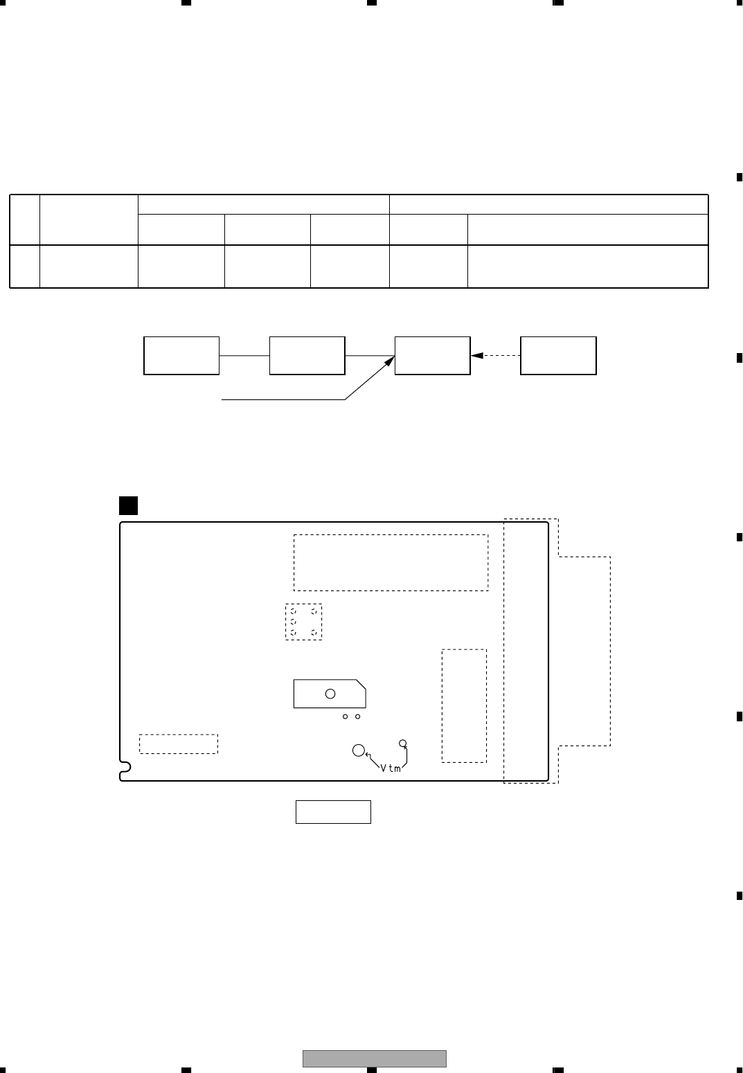
XV-EV51 75
5 678
5678
C
D
F
A
B
E
6.2 TUNER SECTION
MPX SG FM SG PRODUCT DC
Voltmeter
L201
IC201
pin 21 pin 23
FM/AM TUNER UNIT
A
SIDE B
Step
No.
Adjustment
Title
ANT. Input level and signal condition Adjustment
Input Level
(dBµV)
Adjust
point Contents
Frequency
(MHz) Modulation
1T-METER
Adjustment 98 OFF 80 L201 Adjust L201 so that the DC voltage between Pin
21 and Pin 23 of IC201 (Test point Vtm) gets
within 0 ± 50mV.
FM75Ω antenna terminal
Fig.6.5 Adjustment Wiring Diagram
Fig.6.6 Adjustment Point
6.2.1 AM TUNER SECTION
There is no adjustment in the AM tuner.
6.2.2 FM TUNER SECTION
Set the mode selector to FM BAND.
Connect the wiring as shown in Fig. 6-5.
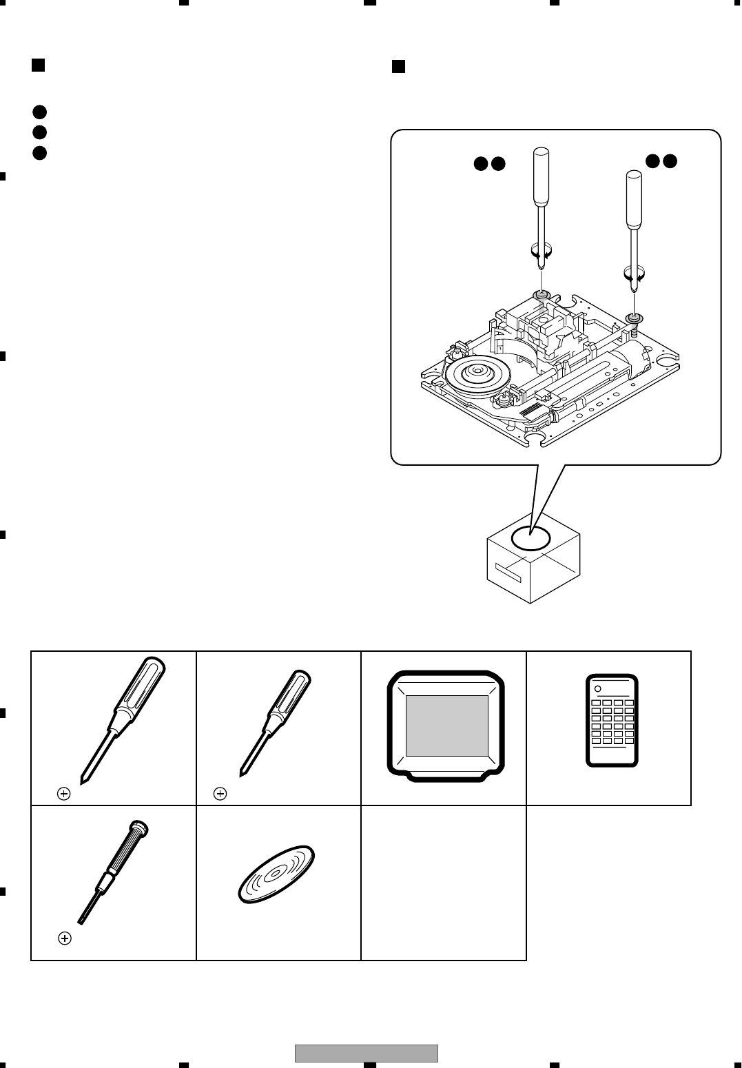
XV-EV51
76
1234
1234
C
D
F
A
B
E
6.3 DVD SECTION ADJUSTMENT ITEMS ana LOCATION
6.4 JIGS and MEASURING INSTRUMENTS
1
1 2
2
3
Tangential
adjustment
screw
1 2
Radial
adjustment
screw
Adjustment Items
[Mechanism Part]
[Electrical Part]
Tangential and Radial Height Coarse Adjustment
DVD Jitter Adjustment
Initialize the Focus Sweep Setting
Electrical adjustments are not required.
Adjustment Points (Mechanism Part)
Cautions: After adjustment, adjustment screw locks with the
Screw tight.
Screwdriver (large) TV monitor
Precise screwdriver DVD test disc
(GGV1025)
Test mode remote control
unit (GGF1067)
Screw tight
(GYL1001)
Screwdriver (medium)
XV-EV51 77
5 678
5678
C
D
F
A
B
E
6.5 NECESSARY ADJUSTMENT POINTS
∗After adjustment, screw locks
with the Screw tight.
∗After adjustment, screw locks
with the Screw tight.
~, Ÿ, !
Ÿ, !
Mechanical
point
Electric
point
!
Mechanical
point
Electric
point
Mechanical
point
Electric
point
Be sure to perform the following step finally when replaced
Pickup, Traverse Mechanism and Spindle Motor.
Purpose: To set the sweep which was correct with the
individual Traverse mechanism.
Mechanical
point
Electric
point
LOAB, DVDIF and DVDM ASSY
∗
GGF1067
Test mode
remote control
unit
ESC CLEAR
Exchange Parts of Mechanism Assy
Exchange PCB Assy
When Adjustment Points
Exchange the Pickup
Exchange the Traverse Mechanism
Exchange the Spindle Motor
Exchange PC Board
(It is necessary when performed adjustment procedure Ÿ.)
XV-EV51
78
1234
1234
C
D
F
A
B
E
6.6 TEST MODE
TEST MODE: ON
TEST MODE: DISC SET
DSC - &&&
GGF1067
Test mode
remote control
unit
GGF1067
Test mode
remote control
unit
POWER
ON
<TRAY OPEN>
OPEN/CLOSE
(Player or Remote
Control Unit)
OPEN/CLOSE
(Player or Remote
Control Unit)
DVD disc
TEST MODE: PLAY
TEST MODE: OFF
An address is displayed
For example, when playback with # 30000
During PLAY Press keys in order
OR
ESC
OFF
POWER
030000
<PLAY>
< When playback with the target address of disc (DVD)>
TV/LDP
+10 3 0 0 0 0 CHP/TIM
ESC TEST
CHECK
DVD, CD
CAUTION:
Perform only trace, video and audio output are
nothing.
Power Amplifier
Power Amplifier
DVD Tuner Deck
XV-EV51 79
5 678
5678
C
D
F
A
B
E
6.7 MECHANISM ADJUSTMENT
• Remove the servo mechanism.
• Remove a Spacer for height adjustment
attached to the back side (shaded area)
of the Servo Mechanism (Float Base) with
nippers.
Cautions:
Because there is not a Spacer for height adjustment in
adjustment after the second time, will keep it at need.
(This parts is Traverse mechanism exclusive use of a model
for 2001 years)
Put a spacer between a Tangential (or Radial) adjustment
screw and Mechanism Base and turn each screw to adjust
the height. (Refer to "6.3 ADJUSTMENT ITEMS AND
LOCATION".)
Note:
Turn the Short switch to Short side when
removing the Pickup Flexible Cable.
(Refer to "7.1.6 DISASSEBLY".)
START
Tangential and Radial Height Coarse Adjustment
1
Servo Mechanism
7.3mm
Turn a flat side
into bottom
Spacer for Height adjustment
Float Base
XV-EV51
80
1234
1234
C
D
F
A
B
E
Player
Monitor
•Test mode
•Play the DVD test disc
at outer track
(around #200000)
•Play the DVD test disc
at inner track
(around #30000)
•Play the DVD test disc
at outer track
(around #200000)
Mechanism Assy
Adjust the Tangential
Adjustment Screw so that
jitter becomes minimum.
Mechanism Assy
Readjust the Tangential
Adjustment Screw so that
jitter becomes minimum.
Mechanism Assy
Adjust the Radial
Adjustment Screw so that
jitter becomes minimum.
Use disc: GGV1025
START
DVD Jitter Adjustment
2
J : - - - -
J : Min
J : Min
Test mode end
J : Min
ESC
Disc playback normally.
• The measurement of block error rate
If error rate is OK,
locks a root of
tangential and radial
adjustment screws with
the Screw tight, and
go to step !.
Screw tight: GYL1001
Turn the POWER OFF in
case of NG once, and
perform the adjustment
once again.
Confirm the error rate that is
displayed "OK"
(Example ERROR RATE: 6.6oe - 6 OK )
5ESC
CHECK
NG
OK
• Playback method of inner and outer address for the purpose is refererd to "6.6 TEST MODE".
• Jitter indication of the monitor is refererd to "7.1.1 TEST MODE (Display Specification of the Test Mode)".
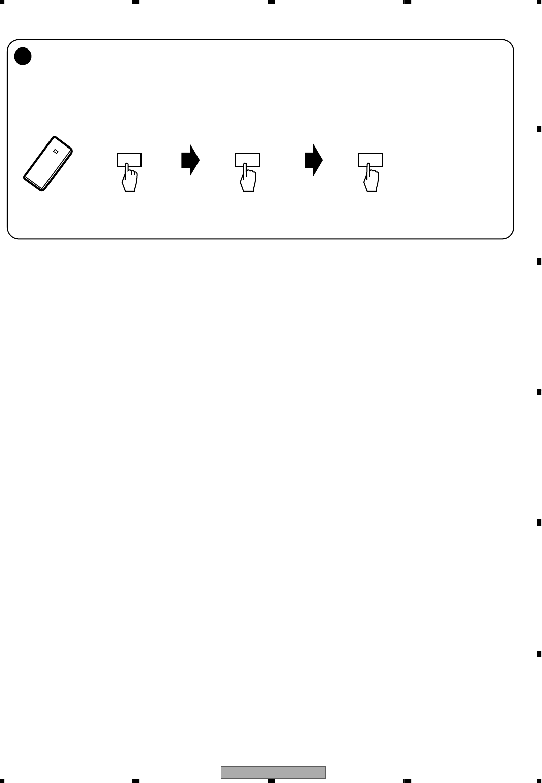
XV-EV51 81
5 678
5678
C
D
F
A
B
E
Initialize the Focus Sweep Setting
3
Turn on the Player
ESC CLEARPOWER
Note: Be sure to perform this step when replaced the Pickup or Traverse mechanism.
Purpose: To set the sweep which was correct with the individual Traverse mechanism.

XV-EV51
82
1234
1234
C
D
F
A
B
E
7. GENERAL INFORMATION
7.1 DIAGNOSIS
7.1.1 TEST MODE
Test Mode Functional Specification
1 How to Enter Test mode
Turn the power on while short-circuiting with TEST jumper (W284) and VE+5 jumper (W282) on the IF Assy.
Indicate with "U-TEST" in this time.
2 Release the test mode
• Turn off the power.
• Press the [ESC] (A8-5F) key of the remote control unit and reset it.
3 Tray open / close
• Press the [REPEAT A-B] (A8 - 48) key of the remote control unit.
• Press the [OPEN / CLOSE] key of the main unit from the stop state.
4 Playback stop
• Press the [REPEAT] (A8 - 44) key of the remote control unit from the playback state.
5 LD ON
DVD : Press the [TEST] (A8-5E) and [1] (A8-01) keys in order, and turn on the laser diode (650n).
CD : Press the [TEST] (A8-5E) and [4] (A8-04) keys in order, and turn on the laser diode (780n).
6 Focus on / sweep
1. Lock the focus by pressing the [TEST] (A8-5E) and [2] (A8-02) keys in order.
2. Repeat focus sweep by pressing the [TEST] (A8-5E) and [3] (A8-03) keys in order.
7 Spindle FG servo
CAV : Press the [TEST] (A8-5E) and [5] (A8-05) keys in order,then rise up the spindle and it becomes FG servo on.
CLV : Press the [TEST] (A8-5E) and [9] (A8-09) keys in order,then rise up the spindle and it becomes FG servo on.
8 Tracking open / close
1. Open tracking by pressing the [STEP FWD] (A8-54) key of the remote control unit in the play state.
2. Close tracking by pressing the [STEP REV] (A8-50) key of the remote control unit in the play state.
9 Slider servo on/off
1. Turn on the slider servo by pressing the [TEST] (A8-5E) and [CX] (A8-0E) keys in order.
2. Turn off the slider servo by pressing the [TEST] (A8-5E) and [TV/LDP] (A8-0F) keys in order.
0 Slider in / out
Slider in : In the tracking off state, press the [SCAN REV] (A8-11) key of the remote control unit.
Slider out : In the tracking off state, press the [SCAN FWD] (A8-10) key of the remote control unit.
- Play (perform only the ID search and trace to the specified location)
Press the [TV/LDP] (A8-0F) key of the remote control unit from the stop state.
Perform only trace, video and audio output are nothing.
= Screen display ON/OFF
1. Turn off the display by pressing the [AUDIO] (A8-1E) key of the remote control unit.
2. Turn on the display by pressing the [DISPLAY] (A8-43) key of the remote control unit.

XV-EV51 83
5 678
5678
C
D
F
A
B
E
~ Search
1. Search address input entry
• It becomes the address input mode when pressing the [+10] (A8-1F) key. (Most significant digit of an address displays ">".)
• In this time, display the last address as the initial state.
2. Search address input
• Press the [0] to [9] (A8-00 to 09) keys of the remote control unit. In the DVD, set an address with hexadecimal.
• In the address input mode, turn to the hexadecimal input by pressing the [PROGRAM] (A8-4C) key (display a "∗" mark)
and [1] to [6]keys are each input as A to F.
• In this time, do not accept the [7],[8],[9] and [0] keys. Hexadecimal input and decimal input can switch with toggle.
• In case of CD, perform only the absolute time search.
3. Search execution
• Press the [CHP/TM] (A8-13) key of the remote control unit.
• After the search, perform only trace and video and audio outputs are nothing.
4. Release the Search address input
• Clear the address by pressing the [CLEAR] (A8-45) key. Release the address input mode when pressing the [CLEAR]
key once again.
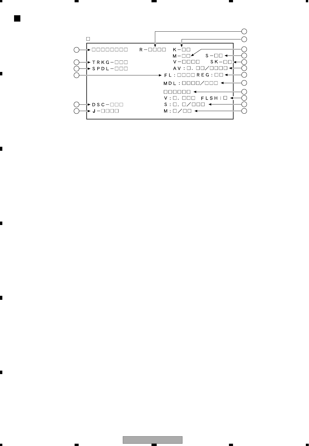
XV-EV51
84
1234
1234
C
D
F
A
B
E
Display Specification of the Test Mode
Character in bold : Item name
: Information display
1
5
6
10
13
11
8
9
3
2
12
17
18
19
16
14
15
1 Address indication
The address being traced is displayed in number.
(as for the DVD, indication of decimal number is possible.)
DVD : ID indication (hexadecimal number, 8 digits)
[∗ ∗ ∗ ∗ ∗ ∗ ∗ ∗]
CD : A-TIME (min. sec.) [0 0 0 0 ∗ ∗ ∗ ∗]
2 Code indication of remote control unit [R – ∗ ∗ ∗ ∗]
In case of double code, display a 2nd code.
3 Main unit keycode indication [K – ∗ ∗]
5 Tracking status [TRKG – ∗ ∗ ∗]
Tracking on : [ON]
Tracking off : [OFF]
6 Spindle status [SPDL – ∗ ∗ ∗]
[OFF], [A/B] (ACC/BRK), [CAV], [CLV]
7 Mechanism (loading) position value [M – ∗ ∗]
Unknown : [01] or [41]
Open state : [04]
Close state : [08]
During opening : [12]
During closing : [22]
8 Slider position [S – ∗ ∗ ∗ ∗]
CD TOC area : [IN ]
CD active area : [CD]
9 Output video system [V – ∗ ∗ ∗ ∗]
NTSC system : [NTSC]
PAL system : [PAL]
Automatic setting : [AUTO]
Scart terminal output [SK – ∗ ∗]
(Display only the WY model which can do the output setting
of scart terminal.)
VIDEO : [00]
S-VIDEO : [01]
RGB : [02]
0 Disc sensing [DSC – ∗ ∗ ∗]
The type of discs loaded is displayed.
[DVD], [CD ], [VCD], [ ]
- Jitter value [J – ∗ ∗ ∗ ∗]
= Version of the AV-1 chip / version of firmware
[AV: ∗ ∗ / ∗ ∗ ∗ ∗ ∗ ∗ ∗ ∗]
~ Version of the FL controller [FL: ∗ ∗ ∗ ∗]
! Region setting of the player [REG: ∗]
Setting value : [1] to [6]
@ Destination setting of the FL controller
[MDL: ∗ ∗ ∗ ∗ / ∗ ∗ ∗]
Four characters in the front represent the type of model.
Three characters in the back represent the destination code.
J: /J, K: /KU, /KC, /KU/KC, R: /RAM/RL/RD, LB: /LB,
WY: /WY
# Part number of the flash ROM
[∗ ∗ ∗ ∗ ∗ ∗]
$ Version of the flash ROM [V: ∗. ∗ ∗ ∗]
Flash ROM size [FLSH = ∗]
% Revision of the system controller [S: ∗ . ∗ / ∗ ∗ ∗ ]
^ Revision of the DVD mechanism controller
[M: ∗ / ∗ ∗]
7

XV-EV51 85
5 678
5678
C
D
F
A
B
E
Command Contents Conditions Remote Control Key Name Remote Control Code
Memory clear & region / revision indication CLEAR (LD remote control unit) A8-45
Average value measurement of DVD error rate 5 (LD remote control unit) A8-05
CD error rate measurement 5 (LD remote control unit) A8-05
Aspect: Pan scan 2 A6-01
Aspect: Letter box 3 A6-02
Aspect: Wide 4 A6-03
Digital: PCM 5 A6-04
Digital: AC-3/PCM 6 A6-05
Virtual Dolby: VDD=OFF Only correspondence model 7 A6-06
Virtual Dolby: VDD=ON Only correspondence model 8 A6-07
Digital output ON REPEAT A A6-A1, AF-E8
Digital output OFF REPEAT B A6-95
DTS Digital Out ON STEP FWD A6-A1, AF-B7
DTS Digital Out OFF STEP REV A6-A1, AF-B8
Scart terminal output: VIDEO WY, Model to include scart AUDIO A6-A1, AF-BE
Scart terminal output: S-VIDEO WY, Model to include scart SUBTITLE A6-A1, AF-36
Scart terminal output: RGB WY, Model to include scart ANGLE A6-A1, AF-B5
Audio 5.1CH ON Only correspondence model KD_ENTER A6-74
FL indication of EDC / ID error CX (LD remote control unit) A8-0E
ZOOM ON Only correspondence model ZOOM A6-A1, AF-37
ZOOM OFF Only correspondence model < X3 (LD remote control unit) A8-59
Service mode indication (error rate indication, etc.) CHP/TIM (LD remote control unit) A8-13
Model information indication CHAP (LD remote control unit) A8-40
Background color change +10 (LD remote control unit) A8-1F
Audio last stage mute ON 9 A6-08
Audio last stage mute OFF 0 A6-09
Title search Input mode IN
Title No. input
Search execution
SIDE A (LD remote control unit)
Numbers (LD remote control unit)
PLAY (LD remote control unit)
A8-4D
A8-00 to A8-09
A8-17
Region confirmation mode AUDIO (LD remote control unit)
Numbers (LD remote control unit)
A8-1E
A8-01 to A8-08
Shortcut key Functional Specification
Only in the normal playback, the following setting can by pressing the required key after having pressed the "TEST" key of
the remote control unit. How to release: Press the "ESC" key. (function with indication)
• Service mode indication
ID Address
Always display error rate. Exponential indication ∗.∗∗e-∗ (with both DVD and CD)
EDC/ID/AV1 error history (ID Address, EDC/ID/AV1 Error, errors of past eight times)
Self-diagnostic function (when mechanism error occurred, display the mechanism error history)
• Error rate average value total (ESC +5)
Calculation number of times displays exponent from average value of eight times.
After the calculation result, display OK/NG. Tray is open in case of NG (with both DVD and CD)
DVD: OK with less than 8.0e-4 CD: OK with less than 7.6e-4
Note: Because an OK/NG judgment cannot be DVD with a static image mode as menu screen, confirm it by an animation.
• Model information indication contents (ESC+CHAP)
Display = to ^ in the test mode indication. However, Change the indication of S as B.E VERSION and it of M as F.E VERSION.
Refer to the "Specification of Model Information Display".
• Background color change (ESC+ +10)
Change black and green with toggle whenever pressing the key (the background color that green is using with SETUP NAVIGATOR).
• Region confirmation mode (ESC+ A.MON + 1to 8)
Input region No. after pressing the ESC+A.MON keys. When it is different from the setting, display and open the tray.
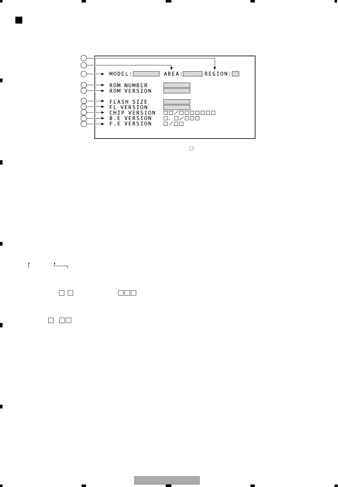
XV-EV51
86
1234
1234
C
D
F
A
B
E
Specification of Model Information Display
• Display contents
Character in bold : Item name
: Information display
1
2
3
4
5
6
7
8
9
10
1 Model name
Display it according to model information set from the FL controller.
2 Destination indication
Display it according to model information set from the FL controller.
3 Region No.
4 Part number
5 ROM version
6 Flash size
7 FL controller version
8 CHIP VERSION
Version of ST CHIP
CUT ID / JTAG ID
(two columns) (eight columns)
9 B.E VERSION
Version of BACK END (version of ST core software)
. /
softwareVersion . softwareRevision / buildNumber
0 F.E VERSION
Version of FRONT END (version of mechanism controller CHIP software)
/
MainVersion / SubVersion
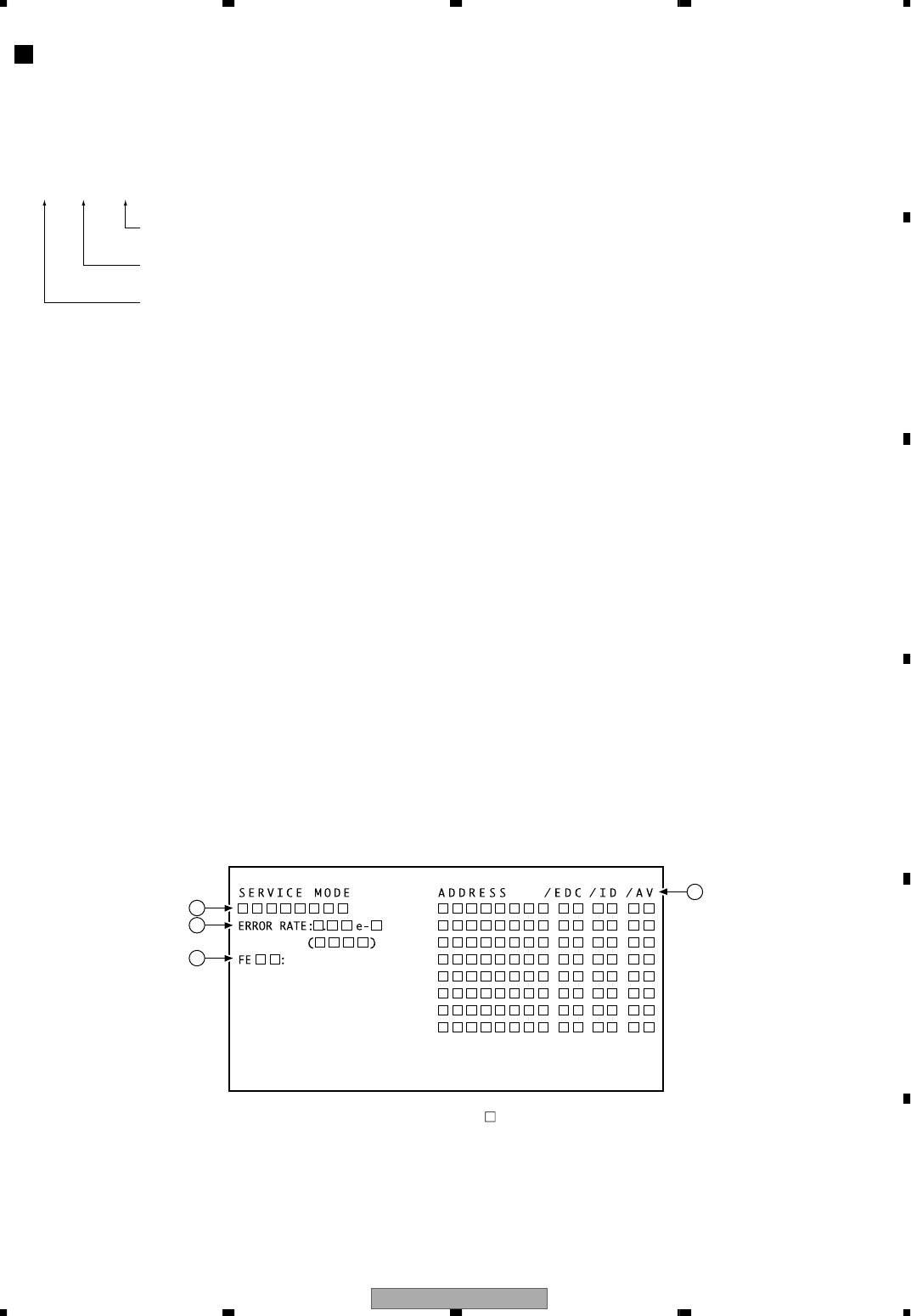
XV-EV51 87
5 678
5678
C
D
F
A
B
E
Functional Specification of the Service Mode
Indication plan contents
Character in bold : Item name
: Information display
1
2
4
• FL indication of EDC / ID error (short cut function)
Display it in FL with ESC+CX keys (LD remote control unit).
Indication is released with ESC key during indication.
FL indication contents
0 0 / 0 0 / 0 1 ∗
• Service mode screen display
Display to the screen with ESC+CHP/TIM keys.
Release the indication with ESC key.
Indication contents
ID Address 1
Always indicate error rate 2 and exponent indication
EDC/ID/AV1 error history (ID Address, EDC/ID/AV1 Error, past eight times) 3
Contents of AV1 error
BIT 0: EDC error, FEC I/F buffer overflow and not valid occur in the BE code (B.E error).
BIT 1: ID is different from the target in the BE code (B.E error).
BIT 2: There is error in the EDC data of 2 bytes which added to the FE (F.E error).
• Self-diagnostic function 4
Check that the F.E is normal or not.
FE OK : Abnormality is not found in the F.E.
FE Error : Abnormality is found in the F.E.
Indicate the mechanism error history by pressing the CHP/TIM key once again.
Change indication by pressing the CHP/TIM key with toggle afterwards.
Refer to the "Display of the Mechanism Error History".
Display number of the location that caused EDC and ID errors
Retry number of times of the latest ID error
Retry number of times of the latest EDC error
∗ mark: When even once causes AV1 error, lights.
3
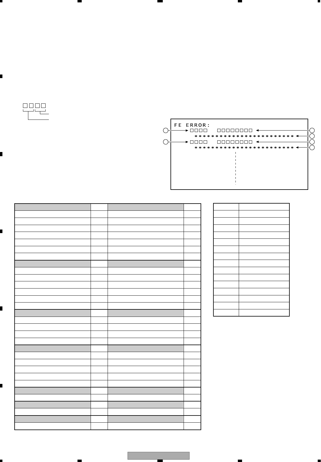
XV-EV51
88
1234
1234
C
D
F
A
B
E
7.1.2 DISPLAY OF THE MECHANISM ERROR HISTORY
Indication contents
• Table of Error Code • Table of Servo State
12
3
When mechanism error (FE error) occurred, the mechanism
error history of maximum past eight times is displayed by
pressing the CHP/TIM key during service mode screen
display.
Indication displayed in the screen upper part is new error.
• Indication contents
1 Error code
Two characters in the front represent the Error Code and
two characters in the back represent the Servo State.
The detail is as follows.
3 Error contents indication
Indicate the error contents which occurred with
character.
Examples: When Error code is 0x13 (Focus lost timeout)
and Servo state is 0x05 (Disc judge),
"Focus lost timeout in Disc judge"
∗ Movement in the error occurrence: open the tray when
SERVO STATE is Disc Judgs, and others stop.
However, error code is exception in the device error of
0xd∗.
2 Error occurrence time
Error indicates the time which occurred after system
turned on the power supply.
∗ When time of new error is short, it becomes assumed
power off once.
Error Code
Servo State
12
3
0x00 Reset
0x01 Stop (inside position)
0x02 Stop (any position)
0x03 Braking for stop
0x04 New disc
0x05 Disc judge
0x06 Reserved 1
0x07 Playing
0x08 Start up
0x09 Seeking
0x0A Pausing
0x0B Reading BCA
0x0C Reserved 2
0x0D
0x0E
0x0F
FOCUS ERROR 0x0∗FOCUS TIMEOUT 0x1∗
Focus on error 0x01 Focus on timeout 0x11
Focus off error 0x02 Focus off timeout 0x12
Focus lost error 0x03 Focus lost timeout 0x13
Focus balance adjust error 0x04 Focus balance adjust timeout 0x14
Focus gain adjust error 0x05 Focus gain adjust timeout 0x15
Focus sweep error 0x06 Focus sweep timeout 0x16
Focus reflection error 0x07 Focus reflection timeout 0x17
TRACKING ERROR 0x2∗TRACKING TIMEOUT 0x3∗
Tracking on error 0x21 Tracking on timeout 0x31
Tracking off error 0x22 Tracking off timeout 0x32
Tracking lost error 0x23 Tracking lost timeout 0x33
Tracking balance adjust error 0x24 Tracking balance adjust timeout 0x34
Tracking gain adjust error 0x25 Tracking gain adjust timeout 0x35
Tracking jump error 0x26 Tracking jump timeout 0x36
STEPPING ERROR 0x4∗STEPPING TIMEOUT 0x5∗
Stepping on error 0x41 Stepping on timeout 0x51
Stepping off error 0x42 Stepping off timeout 0x52
Stepping lost error 0x43 Stepping lost timeout 0x53
Stepping move error 0x44 Stepping move timeout 0x54
SPINDLE ERROR 0x6∗SPINDLE TIMEOUT 0x7∗
Spindle on error 0x61 Spindle on timeout 0x71
Spindle off error 0x62 Spindle off timeout 0x72
Spindle lost error 0x63 Spindle lost timeout 0x73
Spindle CAV error 0x64 Spindle CAV timeout 0x74
Spindle CLV error 0x65 Spindle CLV timeout 0x75
ACQUISITION ERROR 0x8∗ACQUISITION TIMEOUT 0x9∗
PLL lost error 0x83 PLL lost timeout 0x93
DECODER ERROR 0xa∗DECODER TIMEOUT 0xb∗
ID lost error 0xa3 ID lost timeout 0xb3
FAIL SAFE 0xe∗
unexpected error 0xe1
DEVICE ERROR 0xd∗
SRAM error 0xd1
XV-EV51 89
5 678
5678
C
D
F
A
B
E
Error Name No. Causes Check Item Possibility of Trouble
Remarks
FOCUS ERROR (0 x 0∗)
Focus on error 0 x 01 Focus on could not be completed
Are not there a dirt or a scratch in
the Disc? Does LD become weak?
Does the lens move up and down?
1. Pickup
2. Driver
3. L6315 (Front End IC)
Focus off error 0 x 02 Focus off could not be completed Unknown
Focus lost error 0 x 03 Focus servo is lost Are not there a dirt or a scratch in
the Disc? Does LD become weak? 1. Pickup
Focus balance adjust error 0 x 04 AFB on could not be completed
Focus gain adjust error 0 x 05 Focus AGC could not be completed
Focus sweep error 0 x 06
Focus reflection error 0 x 07
Dimensions of S curve did not reach to the aim value
Does LD become weak? 1. Pickup
FOCUS TIMEOUT (0 x 1∗)
Focus on timeout 0 x 11 Did timeout at focus on
Are not there a dirt or a scratch in
the Disc? Does LD become weak?
Does the lens move up and down?
1. Pickup
2. Driver
3. L6315 (Front End IC)
Focus off timeout 0 x 12 Did timeout at focus off
Focus lost timeout 0 x 13 Did timeout at focus backup
Focus balance adjust timeout 0 x 14 Did timeout at AFB
Focus gain adjust timeout 0 x 15 Did timeout at AGC
Focus sweep timeout 0 x 16
TRACKING ERROR (0 x 2∗)
Tracking on error 0 x 21 Tracking on could not be completed
1. Pickup
2. Driver
3. L6315 (Front End IC)
Tracking off error 0 x 22 Tracking off could not be completed
Tracking lost error 0 x 23 Tracking servo is lost 1. Pickup
Tracking balance adjust error 0 x 24 ATB could not be completed 1. Pickup
Tracking gain adjust error 0 x 25 AGC could not be completed 1. Pickup
Tracking jump error 0 x 26 Tracking jump could not be completed
TRACKING TIMEOUT (0 x 3∗)
Tracking on timeout 0 x 31 Did timeout at tracking on Are not there a dirt or a scratch in
the Disc?
1. Pickup
2. Driver
3. L6315 (Front End IC)
Tracking off timeout 0 x 32 Did timeout at tracking off
Tracking lost timeout 0 x 33 Did timeout at tracking backup Are not there a dirt or a scratch in
the Disc? 1. Pickup
Tracking balance adjust timeout 0 x 34 Did timeout at ATB 1. Pickup
Tracking gain adjust timeout 0 x 35 Did timeout at AGC 1. Pickup
Tracking jump timeout 0 x 36 Did timeout at tracking jump
STEPPING ERROR (0 x 4∗)
Stepping on error 0 x 41 Stepping on could not be completed
1. Pickup
2. Driver
3. L6315 (Front End IC)
Stepping off error 0 x 42 Stepping off could not be completed
Stepping lost error 0 x 43 Stepping servo is lost
Stepping move error 0 x 44 Stepping could not move
Do move to inner and outer periphery
of the
stepping
in the test mode?
Do indicate "S-04" at the most inner
periphery of the
stepping
?
1. Stepping motor
2. Inside switch
3. Driver
STEPPING TIMEOUT (0 x 5∗)
Stepping on timeout 0 x 51 Did timeout at stepping on
1. Pickup
2. Driver
3. L6315 (Front End IC)
Stepping off timeout 0 x 52 Did timeout at stepping off
Stepping lost timeout 0 x 53 Did timeout at stepping backup
Stepping move timeout 0 x 54 Did timeout at stepping movement
Do move to inner and outer periphery
of the
stepping
in the test mode?
Do indicate "S-04" at the most inner
periphery of the
stepping
?
1. Stepping motor
2. Inside switch
3. Driver
ERROR CODE TABLE
XV-EV51
90
1234
1234
C
D
F
A
B
E
Error Name No. Causes Check Item Possibility of Trouble
Remarks
SPINDLE ERROR (0 x 6∗)
Spindle on error 0 x 61 Spindle on could not be completed
Spindle off error 0 x 62 Spindle off could not be completed
Spindle lost error 0 x 63 Spindle lost control
Spindle CAV error 0 x 64 CAV on could not be completed
Spindle CLV error 0 x 65 CLV on could not be completed
SPINDLE TIMEOUT (0 x 7∗)
Spindle on timeout 0 x 71 Did timeout at spindle on
Spindle off timeout 0 x 72 Did timeout at spindle stop
Spindle lost timeout 0 x 73 Did timeout at spindle backup
Are not there a dirt or a scratch in
the Disc?
Is FG output from the driver?
1. Spindle motor
2. Spindle driver
Spindle CAV timeout 0 x 74 Did timeout at CAV on
Is spindle rotating?
Is FG output from the driver?
Is the PDM output from L6315?
1. Spindle motor
2. Spindle driver
3. L6315 (Front End IC)
Spindle CLV timeout 0 x 75 Did timeout at CLV on
ACQUISITION ERROR (0 x 8∗)
PLL lost error 0 x 83 PLL is lost Are not there a dirt or a scratch in
the Disc?
1. Pickup
2. L6315 (Front End IC)
ACQUISITION TIMEOUT (0 x 9∗)
PLL lost timeout 0 x 93 Did timeout at PLL backup Are not there a dirt or a scratch in
the Disc?
1. Pickup
2. L6315 (Front End IC)
DECODER ERROR (0 x a∗)
ID lost error 0 x a3 ID is not readable Are not there a dirt or a scratch in
the Disc?
1. Pickup
2. L6315 (Front End IC)
DECODER TIMEOUT (0 x b∗)
ID lost timeout 0xb3 Did timeout at ID backup Are not there a dirt or a scratch in
the Disc?
1. Pickup
2. L6315 (Front End IC)
DEVICE ERROR (0 x d∗)
SRAM error 0 x d1 Cannot access SRAM Power supply of SRAM
Is not bus line short-circuiting?
1. SRAM
2. L6315 (Front End IC)
3. L6315-SRAM bus line
FAILSAFE (0 x e∗)
Unexpected error 0 x e1 Unexpected error 1. software runaway
3. Software bug
XV-EV51 91
5 678
5678
C
D
F
A
B
E
7.1.3 TRUBLE SHOOTNG
Confirm the error history at first.
When a history was not displayed, refer to the following table.
No. Symptoms Diagnosis Contents Defectiveness Assumption
Points
1
Cannot power on Check Voltage of CN8901-17pin(VE+56) on the AF assy. M-EV51(21) , system cable
connection
Check the stand by indicator. If the indicator brinking ,
the protect circuit working. (Stand by indicator brinking)
AMP PROTECT , DVD POWER
SUPPLY
Check IC5501-4pin(AC PULSE). M-EV51(21) , system cable
connection
Check IC5501-12pin,13pin (CF1,CF2)
U-COM
2
Standby indicator brinking
(DVD ERR) Check IC5501-17pin(VDET) is 3.5V 1.Connection of DVDIF assy & IF
assy.
Check FAN connect in M-EV51(21). M-EV51(21) , system cable
connection
Check IC3301,IC3401 in AMP module.
Check connection AF assy & IF assy. AF ASSY & IF ASSY
Check signal waveform of CN8751 1,3,5,7,9,11pin
(C,SW,LS,RS,FL,FR) at DOLBY PROLOGIC mode.
Check signal waveform at CN8701-all pin.,
CN8751-13,15pin(ANAL,ANAR)
DSP ASSY
IF assy & DVD IF assy
connection.
DVD IF ASSY
Are the signals output from IC11-pin 9, 8 and 7 on the FLKB Assy ?
(around 0-3V)
4
Standby indicator brinking
(AMP ERR)
2.DVD power supply,
3.M-EV51(21) POWER SUPPLY
Check FAN connect in M-EV51(21). M-EV51(21) , system cable
connection
M-EV51(21) , system cable
connection
3
Audio is not out put
AF ASSY
VIDEO no out put
XV-EV51
92
1234
1234
C
D
F
A
B
E
No. Symptoms Diagnosis Contents Defectiveness Assumption
Points
4
Cannot open a tray
(An opening screen is
displayed on the monitor)
Does voltage of CN9-pin 3 and 5 on the DVDM Assy change normally ?
pin 3 (XCLOSE) : It is "H" level by the state that has finished doing CLOSE.
pin 5 (OPEN) : It is "H" level by the state that has finished doing OPEN.
Tray switch
Does LOAD_DRV signal come ? BACK END IC (DVDM IC601)
Is a signal output from IC351-pin 14 and 15 (CN9-pin 1 and 2) on the DVDM
Assy ?
(pin 15 : It is about 6V during tray opening, It is about 0V during tray closing)
(pin 14 : It is about 0V during tray opening, It is about 6V during tray closing)
FTS Driver IC
(DVDM IC351)
Are not there wire rod coming out, damage the connectors of CN9 and
CN5 on the DVDM Assy ? Connector / wire rod
Does voltage of CN5-pin 1 on the DVDM Assy change when pressed
the inside switch ? Inside switch
5
Cannot playback
(Focus does not inn) Are the signals output from IC351-pin 9 and 10 on the DVDM Assy ? FTS Driver IC (DVDM IC351)
Does 650 LD emit light ?
Does a pickup lens do up / down ?
Does not an actuator spring bend ?
Pickup
Are not resin part damage, a shaft missing ?
Are not there falling off of turn table, lean abnormality ? Mechanism Assy
Is not flexible cable of CN7 on the DVDM Assy coming off and
damaged ? Flexible cable / connector
Is signal output from IC301-pin 123 (FACT) on the DVDM Assy ?
(Device control of around 500 mV is output usually. It is ± around 100
mV swing by focus up / down.)
FRONT END IC
(DVDM IC301)
6
Cannot playback
(Spindle does not turn) Are the signals output from IC251-pin 2 (A3), pin 4 (A2) and pin 7 (A1)
on the DVDM Assy ?
It is fixed, and is not there pin 18 HIGH whethere it is fixed, and there is
not pin 23 LOW ?
Spindle Driver IC
(DVDM IC251)
Are not there part falling off, alien substance adhesion in spindle motor
part ? Mechanism Assy (Spindle motor)
Is not flexible cable of CN7 on the DVDM Assy coming off and
damaged ? Flexible cable / connector
Is signal output from IC301-pin 123 (SPDL_PDM) on the DVDM Assy ? FRONT END IC (DVDM IC301)
7
Cannot playback
(Playback stops) Does not 650nm LD deteriorate ?
If there is the both ends voltage of R121 on the DVDM Assy more than
0.7V, 650nm LD deteriorates surely.
650nm LD deteriorates.
(Cannot playback DVD)
Does not 780nm LD deteriorate ?
If there is the both ends voltage of R123 on the DVDM Assy more than
1.2V, 780nm LD deteriorates surely.
780nm LD deteriorates.
(Cannot playback CD)
Is not there abnormality in FG waveform ? FG output : Spindle Driver IC
(DVDM IC251)
Are not there scratch and a dirt on the disc ? Disc
8
Picture disturbance during
playback
(block noise, freeze, other)
Are not there scratch and a dirt on the disc ?
Do not you set a disc of standard outside ? Disc
9Audio is not output
(Picture is normal)
Check the waveform (BCK, LRCK, MCLK, DATA). BACK END IC (DVDM IC601)
Is signal output from IC711-pin 7 and 8 on the JCKB Assy ? AUDIO DAC IC (JCKB IC711)
XV-EV51 93
5 678
5678
C
D
F
A
B
E
EVA emergency processing specification
1. About Emergency process
When abnormality of hardware of power supply short circuits and so on occurred, turn the power OFF
without an usual step in a moment. And perform process to limit the later power ON operation.
2. Category of error to perform the Emergency process
As for the error to perform the Emergency process, there are two kinds of the following.
• PROTECT error: Error by power supply of the amplifier section and abnormality of the fan
Overcurrent detection of amplifier
DC voltage detection of amplifier
Fan open and lock detection
Abnormal detection of 8V and 15V
• DVD error: Error by power-failure in the DVD module
3. Condition to enter Emergency process
• PROTECT error: When PROTECT port (pin 92) of the microcomputer was L more than 90 mS (less than
0.15VDD +0.4V).
• DVD error: When 3.3DET port (pin 17) of the microcomputer was more than 90mS, and were less than 2.5V
or more than 4.25V.
* Do not perform the error detection during 1.5 seconds after the power ON operation start at both ports.
4. State after the power OFF
STANDBY LED flashes in case of both of PROTECT and DVD errors
5. Possibility or no of re-power ON
• PROTECT error: Power ON is once again possible after the power OFF 60 seconds later.
Indicates "POW ERR" instead of "WELCOME" in this time.
* When pulled the AC power cord out after the power OFF within 60 seconds, cannot turn the power ON for 60
seconds after inserting the AC power cord once again.
* Flash of STANBY LED is continued even if it passes after the power OFF for 60 seconds.
• DVD error: Power ON is once again possible after the power OFF 60 seconds later.
Indicates "DVD ERR" instead of "WELCOME" in this time.
* When pulled the AC power cord out after the power OFF within 60 seconds, cannot turn the power ON for 60
seconds after inserting the AC power cord once again.
* Flash of STANBY LED is continued even if it passes after the power OFF for 60 seconds.
6. Recovery method of within 60 seconds after PROTECT error, and after DVD error
When turn the power ON once again after turning the power OFF within 60 seconds in the PROTECT error, and
after turned the power OFF in the DVD error, it is necessary to start with the test mode.
To enter the Test mode, turn the power on while short-circuiting with TEST jumper (W284) and VE+5 jumper
(W282) on the IF Assy.
Indicate with "U-TEST" in this time.
In addition, RAM of the microcomputer is reset to the factory shipping state when releasing the service test
mode with the power OFF. Then power ON can normally from the next time.
(When error is left, enter the Emergency process once again.)
1 Diagnosis method when the protection circuit turned to OFF at normal connection (MEDIA-AMP)
2 The release method that "power cannot turn on for 60 seconds"
When enter the individual operation
mode, a protection circuit does not work.
Enter the test mode by supplying AC power
(or DC power in the individual operation) while
short-circuiting the jumpers with "TEST" indication
on the IF ASSY, waiting for 60 seconds is released.
Be because the microcomputer was reset then.
Protection circuit
XV-EV51
94
1234
1234
C
D
F
A
B
E
DC power-
supply
VA
Single purpose operation method.
1
7 SINGLE OPERATION METHOD
Jigs and Measuring instruments
2 Supply a DC power while short-circuiting the jumpers (W282 and W285) with "SERVICE" indication on the IF Assy.
Supply DC power to each point, and all the divided GND short-circuits.
DC apply point
IGND short circuit point
Locations GND Name Assy Name
1 CN8901 16PIN GNDD AF ASSY
2 W132 GNDA AF ASSY
3 W395 GNDM IF ASSY
Voltage Locations Apply Point Name Assy Name
1 8V W497 IC5508 IN IF Assy
2 8V W264 V+8V IF Assy
3 16V C8902 + side VU+12V AF Assy
Individual operation method of XV-EV51,EV21 (MEDIA)
STOP
All Operations
TEST MODE : STOP → CANCEL
The DC power supply
(+8.0V) is turned off.
+8.0V
DC power-
supply
VA
off
Power SW
DC Output (+8.0V)
GND
S
T
.
M
E
M
O
R
Y
·
S
T
O
P
7
IF ASSY
XV-EV51 95
5 678
5678
C
D
F
A
B
E
7.1.4 SEQUENCE AFTER POWER ON
STANDBY
Power on operation by a user
(remote controller key or product key)
FL controller receives a message
[FL controller]
LCD lighting / outputs a power on signal
(POWER ON: "L"→"H")
[FL controller]
Release the reset for BACK END
(XRESET: "L"→"H")
[BACK END]
Accesses flash ROM and 64M SDRAM
[BACK END]
Accesses FRON END
[BACK END]
Request communication to the FL
controller (FP_ACK)
[FL controller]
Outputs the signal which can
communicate to BACK END (FP_XRDY)
BACK END – FL controller
communication
The opening picture output
[FRONT END]
Identifies the following:
• Slider positioning (INSIDE SW)
• Spindle FG stop
Disc detection (Focus control)
Spindle turn
Read ID information code
Various setting
The picture output
Flow chart from power on to the picture output
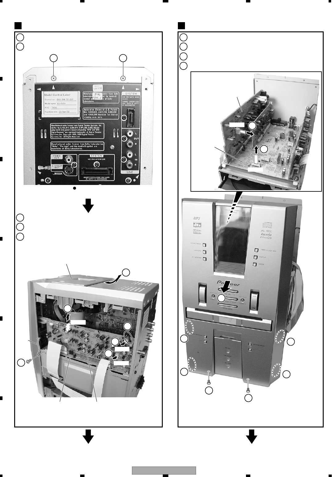
XV-EV51
96
1234
1234
C
D
F
A
B
E
7.1.5 DISASSEMBLY
1Remove the Side Bonnet L and R (screws × 14)
2Remove two screws
3Release two binders
4Remove the earth lead wire (screw × 1)
5Remove the Deck Mechanism Section
(FFC × 1, connectors × 2)
Deck Mechanism Section
1
1Remove two screws
2Remove a FFC and connector
3Unhook × 4
4Remove the Front Panel Section
Front Panel Section
2
DECK AssyIF Assy
Note : Operation check of the main unit is possible
even if removes the Deck Mechanism Section.
Note : Front Panel can removes with the state which
Tray Panel was attached to it.
In this time, remove bottom part of the Front Panel
first so that the Tray Panel is not caught.
Deck Mechanism Section
AF Assy
IF Assy
Earth
Lead
Wire
Rear View
2
1
3
4
3
33
1
3
5
5
5
5
4
2
CN2302
CN5802
CN2301
2
2
CN5509
CN8301
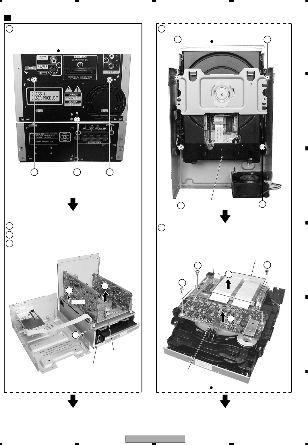
XV-EV51 97
5 678
5678
C
D
F
A
B
E
1Remove three screws 5Remove four screws
6Remove the DVDM and DVD IF Assys (screws × 6)
(with Shield Plate and Plastic Plate)
Caution : Be careful to installation order of
the Shield Plate and Plastic Plate.
2Remove a screw
DVD Shield
DVD Mechanism Section
DVD IF Assy
DVDM Assy
Shield Plate and Plastic Plate
DVD Mechanism Section
3Remove a Fan connector
4Remove the DVD Shield Section
DVD Mechanism Section
3
Rear View
Top View
Bottom View
1
5
5
5
5
5
5
5
11
2
4
3
5
CN5510
5
×2
×3
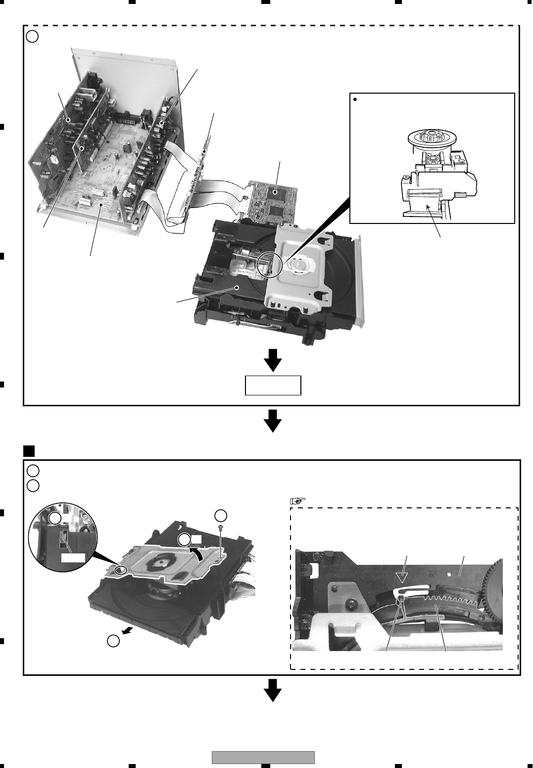
XV-EV51
98
1234
1234
C
D
F
A
B
E
7Styling like figure below.
Diagnosis
AF Assy
DECK Assy
DVD IF Assy
DVDM Assy
IF Assy
LOADING MECHA Assy
DSP Assy
(XV-EV51 Only)
Rear View
Turn the Pickup Short SW
before Pickup Flexible Cable removed.
" before Pickup Flexible cable removed
make short by solder "
Short
1Remove the Bridge (screw ×1).
2Pull out the Tray and remove it while unhooking a hook.
Tray
4
1-1
1-2
2-1
2-2
Loading Base
Triangle Mark
Drive Cam
Pin
Hook
Caution in the Tray Insertion
In the Tray insertion, insert it after matching a triangle mark
of the Loading Base and a position of pin of the Drive Cam.
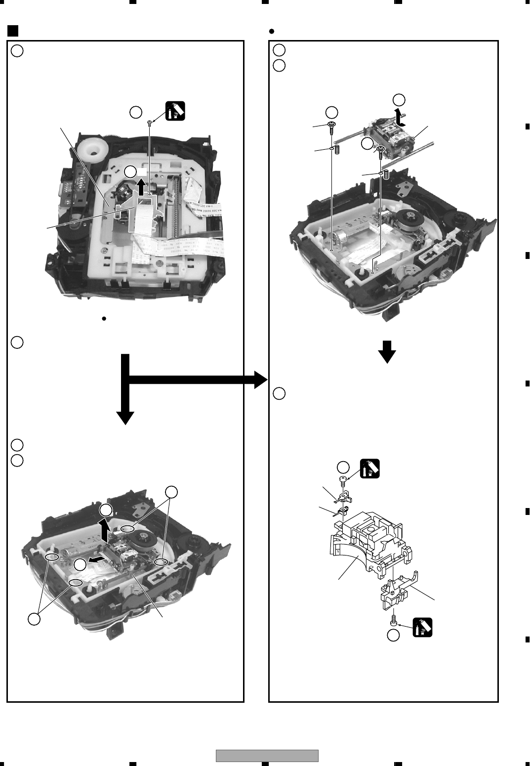
XV-EV51 99
5 678
5678
C
D
F
A
B
E
Traverse Mechanism Assy-S
5When Removing The Pickup Assy-S
1
2
3
4
Remove the FFC Holder with the state which Flexible Cable
was atatched. (Screw × 1)
FFC Holder
Traverse Mechanism Assy-S
Traverse Mechanism Assy-S
Unhook ( × 4)
Remove the Traverse Mechanism Assy-S
3
4
5
Remove two Skew Screws and two Skew Springs
Remove the Pickup Assy-s
Remove the Pickup Flexible Cable
Pickup Assy-S
1
× 2
× 2
Bottom View
Cautions :
Screw is locked with Silicone Adhesive.
Please lock it with Silicone Adhesive when installs it.
Cautions :
Screw is locked with Silicone Adhesive.
Please lock it with Silicone Adhesive when installs it.
Silicone
Adhesuve
GEM1037
-1
-2
1
3
3
5
5
4
4
2
3
3
Skew
Spring Skew
Spring
Skew
Screw
Skew
Screw
Pickup Assy-S
Joint
Slider
Hold Spring
Pickup Assy-S
Remove two Screws
Silicone Adhesive
GEM1037
Silicone Adhesive
GEM1037
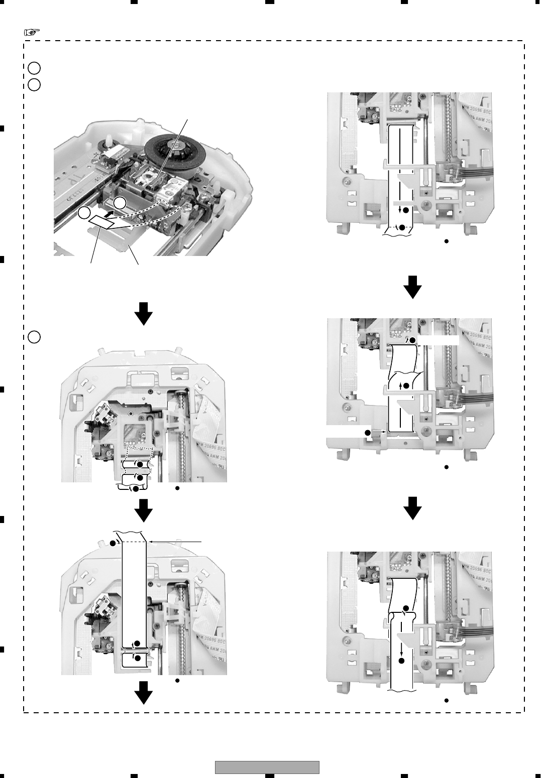
XV-EV51
100
1234
1234
C
D
F
A
B
E
Fold position of step
Lose slack
Bottom View
6
7
8
Bottom View
9
10
Bottom View
11
12
Reference line
Fold at the position
of reference line.
Pickup Assy-S
FFC Holder
Conducting Plane
1
12
2Insert the Pickup Flexible Cable in connector, and lock it surely.
3Perform the styling as shown in figure below.
Caution :
Move the Pickup to the innermost of the disc
FOLD a edge of lining part of the Pickup Flexible Cable.
Bottom View
Bottom View
1
2
3
6
4
5
STYLING THE PICKUP FLEXIBLE CABLE
5
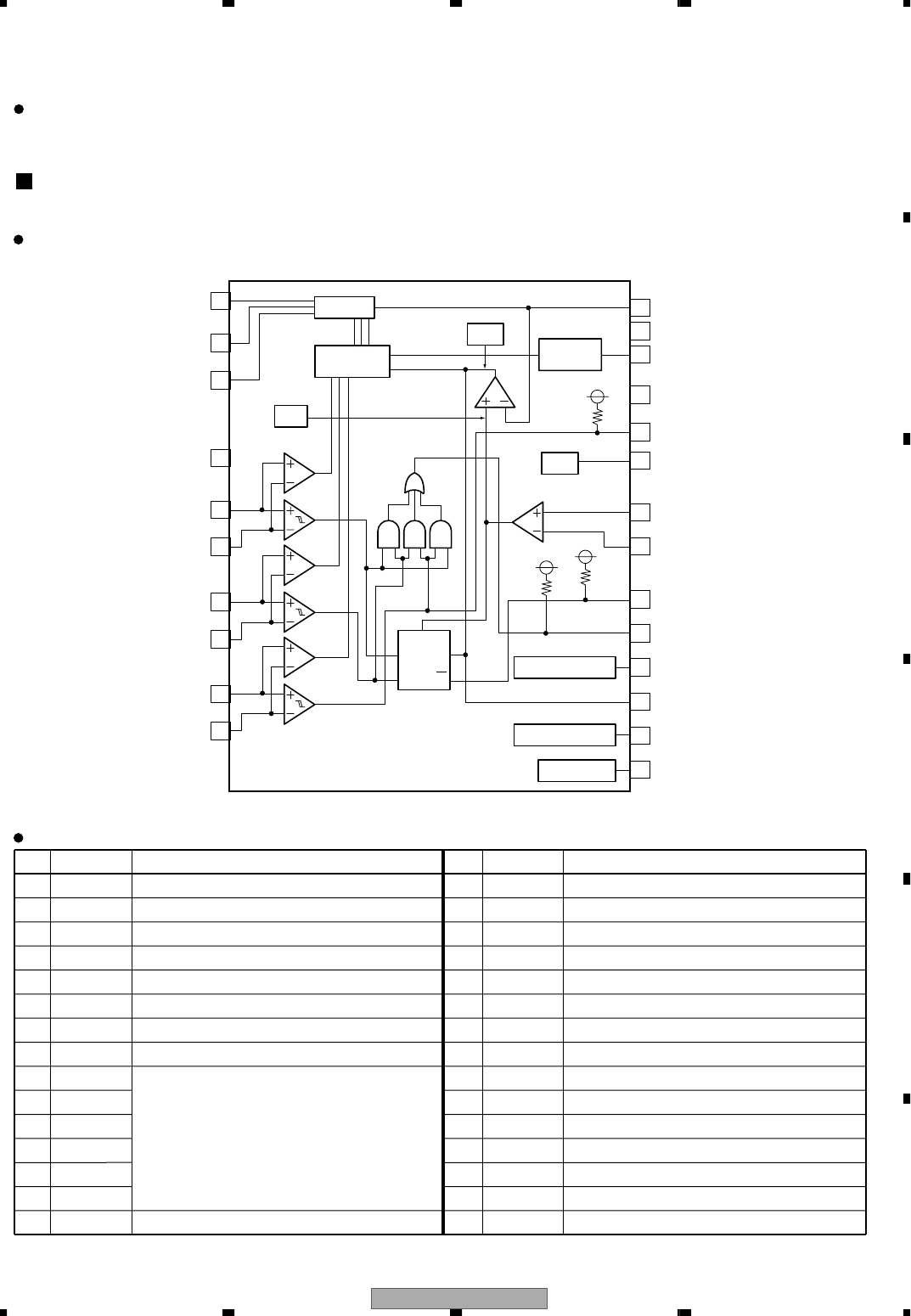
XV-EV51 101
5 678
5678
C
D
F
A
B
E
7.2 PARTS
BA6664FM (DVDM ASSY : IC251)
• Spindle Driver
• The information shown in the list is basic information and may not correspond exactly to that shown in the schematic diagrams.
List of IC
BA6664FM, L6315ATXXTY, M56788AFP, STI5519AVB-B0C, PCM1742KE, MM1567AJ, PDC093
DRIVER
TSD
PS
TORQUE
CURRENT
SENSE AMP
SENSE AMP
SHORT BRAKE
D
R
Q
CK Q
TL
GAIN
CONTROL
GAIN
SWITCH
Vcc
Vcc
Vcc
A3 2
A2 4
A1 7
GND 8
H1+ 9
H1- 10
H2+ 11
H2- 12
H3+ 13
H3- 14
GSW
26
FG
24
VCC
25
RNF
28
VM
27
HALL AMP
PS
23
EC
22
ECR
21
FR
20
FG2
19
SB
18
CNF
17
BR
16
VH
15
BRAKE MODE
HALL BIAS
Block Diagram
Pin Function
No. Pin Name Pin NamePin Function No. Pin Function
1 N.C. N.C. 16 BR Brake mode switching pin
2 A3 Output pin 17 CNF Capacitor connection pin for phase compensation
3 N.C. N.C. 18 SB Short brake pin
4 A2 Output pin 19 FG2 FG 3-phase mix signal output pin
5 N.C. N.C. 20 FR Rotation detecting pin
6 N.C. N.C. 21 ECR Control reference pin of output voltage
7 A1 Output pin 22 EC Output voltage control pin
8 GND GND pin 23 PS Power save pin
9H1+
Hall signal input pins
24 FG FG signal output pin
10 H1- 25 VCC Power supply pin
11 H2+ 26 GSW Gain switching pin
12 H2- 27 VM Motor power pin
13 H3+ 28 RNF
Resistor connection pin for output current detection
14 H3- FIN FIN GND
15 VH Hall bias pin
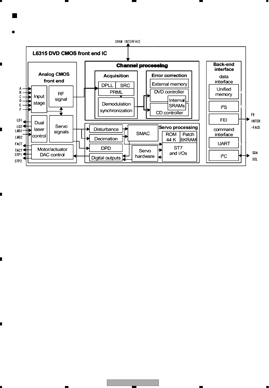
XV-EV51
102
1234
1234
C
D
F
A
B
E
L6315ATXXTY (DVDM ASSY : IC301)
• Front End IC
Block Diagram

XV-EV51 103
5 678
5678
C
D
F
A
B
E
Pin Function
No. Pin Name I/O Pin Function
1 IREF Analog input Bandgap filtering input
2 GNDAI Analog ground Analog power supply ground
3 RFSACD Analog output RF output for SA-CD support
4 RFIN Analog input RF path data input (after AC coupling)
5 RFOUT Analog output RF path data output (before AC coupling)
6 VCCA18 Analog supply Input stage power supply
7 TST_ADC Analog output RF path analog test pin
8 TST_SLICE Analog output PM analog test pin
9 TST_PM Analog output PM analog test pin
10 A Analog input Input stages laser diode A
11 GNDMN Analog ground Input stages ground main
12 B Analog input Input stages laser diode B
13 VCC33MN Analog supply Input stages 3.3 V misc.
14 REFD Analog output Reference voltage for pickup
15 VCC18IS Analog supply Input stages 1.8 V main
16 D Analog input Input stages laser diode D
17 VCCA18IS Analog supply Input stages 1.8 V misc.
18 C Analog input Input stages laser diode C
19 VCC33IS Analog supply Input stages 3.3 V misc.
20 GNDAIS Analog ground Input stages ground misc.
21 VCC33SD Analog supply Input stages 3.3 V side
22 VCC18SD Analog supply Input stages 1.8 V side
23 GNDSD Analog ground Input stages ground side
24 F Analog input Input stages laser diode F
25 E Analog input Input stages laser diode E
26 VSHIELIS Analog ground IS shield
27 VDDADC Analog supply ADC digital power supply
28 VSSADC Analog ground ADC digital ground supply
29 VCCADC Analog supply ADC analog power supply
30 GNDADC Analog ground ADC analog ground supply
31 VSHIELDADC Analog ground ADC shield
32 NC −−
33 BOOT_MODE Digital input Boot mode
34 VSS Digital ground VSS I/O
35 VDD3 Digital supply VDD I/O (3.3 V)
36 PC[0] (NC) Digital I/O −
37 PC[1] (PS) Digital I/O Driver IC power save
38 PC[2] (FG) Digital I/O FG pulse input
39 PC[3] (SB) Digital I/O Spindle short brake
40 PC[4] (SLDPOS) Digital I/O Slider position input
XV-EV51
104
1234
1234
C
D
F
A
B
E
No. Pin Name I/O Pin Function
41 PC[5] (VROFST) Digital I/O VREF offset adjustment (stand-by)
42 PC[6] (SPDL_PDM) Digital I/O Spindle drive output
43 PC[7] (OEICG) Digital I/O OEIC gain sw
44 VSS Digital ground VSS core
45 VDD3S Digital supply VDD core
46 VSS_SPL Digital ground VSS I/O
47 RAM_DQM Digital output SDRAM DQM
48 RAM_WEN Digital output RAM write enable
49 RAM_CASN / Sradr14
Digital output SRAM address
50 RAM_RASN / Sradr15
51 RAM_A[13]
52 RAM_A[12]
53 RAM_A[11]
54 RAM_A[10]
55 RAM_A[0]
56 RAM_A[1]
57 RAM_A[2]
58 RAM_A[3]
59 RAM_A[4]
60 RAM_A[5]
61 RAM_A[6]
62 RAM_A[7]
63 RAM_A[8]
64 RAM_A[9]
65 RAM_CLK / Sradr16
66 VDD_SPL Digital supply VDD I/O
67 VDD3 Digital supply VDD I/O
68 VSS Digital ground VSS I/O
69 RAM_DQ[0]
Digital I/O SRAM data
70 RAM_DQ[1]
71 RAM_DQ[2]
72 RAM_DQ[3]
73 RAM_DQ[4]
74 RAM_DQ[5]
75 RAM_DQ[6]
76 RAM_DQ[7]
77 VDD3S Digital supply VDD core
78 VSS Digital ground VSS core
79 OUT_REQ Reserved Must be set to ground
80 OUT_ERR Digital output Output interface

XV-EV51 105
5 678
5678
C
D
F
A
B
E
No. Pin Name I/O Pin Function
81 OUT_SYNC Digital output Output interface
82 OUT_DVALID Digital output Output interface
83 OUT_CLK Digital output Output interface
84 OUT_DATA[0] (FE_DATA) Digital output Output interface
85 OUT_DATA[1] (FE_EVALID) Digital output Output interface: BW com
86 OUT_DATA[2] (FE_ECCBST) Digital output Output interface: BW com
87 OUT_DATA[3]
Digital output Reserved
88 OUT_DATA[4]
89 OUT_DATA[5]
90 OUT_DATA[6]
91 OUT_DATA[7]
92 VDD3 Digital supply VDD I/O
93 VSS Digital ground VSS I/O
94 PE[0] (FE_INIT) Digital I/O FE initialize input
95 PE[1] (NC) Digital I/O −
96 PE[2] (DMA) Digital I/O DMA input
97 PE[3] (SCL) Digital I/O I2C clock input
98 PE[4] (SDA) Digital I/O I2C data input
99 PD[0] (NC) Digital I/O −
100 PD[1] (NC) Digital I/O −
101 PD[2] (NC) Digital I/O −
102 PD[3] (NC) Digital I/O −
103 PD[4] (NC) Digital I/O −
104 PD[5] (NC) Digital I/O −
105 PD[6] (NC) Digital I/O −
106 PD[7] (NC) Digital I/O −
107 VDD3 Digital supply VDD I/O
108 VSS Digital ground VSS I/O
109 VPP_TEST Digital input Test input
110 VCCD_BYP Digital supply VDD core
111 VCCD_OUT −No voltage to be applied
112 VSS Digital ground VSS core
113 VDD3S Digital supply VDD core
114 VSS Digital ground VSS I/O
115 VDD3 Digital supply VDD I/O
116 RESET_IN Digital input Global reset signal
117 VCC18DAC Analog supply DAC analog power supply
118 STEPER1 Analog output DAC spindle motor
119 STEPER2 Analog output DAC sled motor
120 REFEXT Analog input DAC external reference

XV-EV51
106
1234
1234
C
D
F
A
B
E
No. Pin Name I/O Pin Function
121 REFGND Analog ground DAC analog ground supply
122 REFDAC Analog output DAC reference voltage
123 FACT Analog output DAC focus actuator
124 TACT Digital output DAC tracking actuator
125 GNDDAC Analog ground DAC analog ground
126 NC −−
127 VCCA33 Analog supply DAC analog power supply
128 NC −−
129 GNDPLL Analog ground PM analog ground
130 PLLOFF Analog input PM reference disable PLL
131 FREOUT Analog output PM reference frequency output
132 FREIN Analog input PM reference frequency input
133 VCCPLL Analog supply PM analog power supply
134 SREG1 Analog output External bipolar base
135 VCCR33 Analog supply Analog power supply for regulator
136 SREG2 Analog output External bipolar base
137 LD1 Analog output Laser control laser diode 1
138 LD2 Analog output Laser control laser diode 2
139 VCCA33 Analog supply Analog power supply for input stages +
140 LCREF Analog output Laser control DAC reference
141 LMD1 Analog input Laser control monitor diode 1
142 LMD2 Analog input Laser control monitor diode 2
143 GNDL Analog ground Ground for laser control detection
144 VBGFILT Analog input Bandgap filtering input
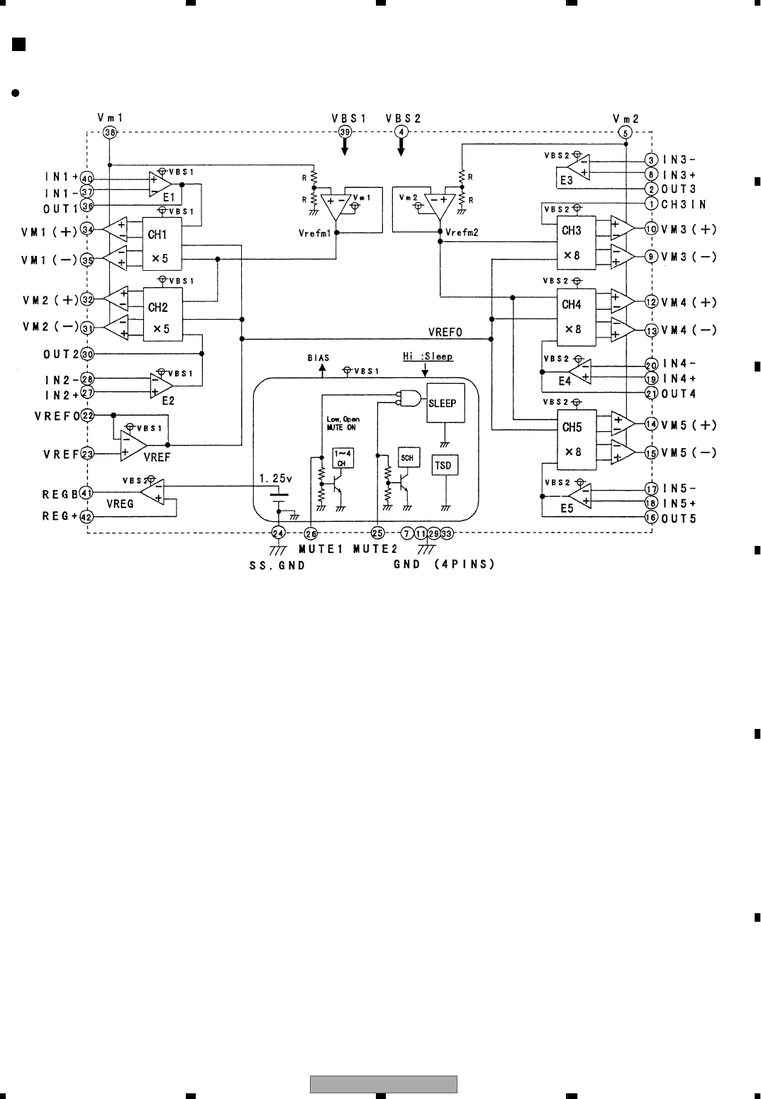
XV-EV51 107
5 678
5678
C
D
F
A
B
E
M56788AFP (DVDM ASSY : IC351)
• FTS Driver IC
Block Diagram
XV-EV51
108
1234
1234
C
D
F
A
B
E
STI5519AVB-B0C (DVDM ASSY : IC601)
• Back End IC
Block Diagram

XV-EV51 109
5 678
5678
C
D
F
A
B
E
Pin Function
No. Pin Name I/O Pin Function
1 FP_SO OUT Front Panel interface. (Soft) Serial transfer data output.
2 A_DATA3 OUT Reserved
3 XAMUTE OUT Analog audio output line muteing output 'L'.
4 VDD_3V3 −3.3 V Power supply
5 VSS −Ground
6 AQE_XCS OUT Reserved
Audio Quality Enhancer IC's chip-select output.
7 SQUEEZ OUT S-Video output S1/S2 control signal at squeez output mode 'H'.
8 LETTER OUT S-Video output S1/S2 control signal & EURO(SCART) connecter (FUNCTION SWITCHING) signal at
letter-box output mode 'H'.
9
TRYPOS OUT In case of NOT carusel 5 disc changer, this port is N.C.(output)
TRYPOS IN
Carousel 5 Disc Chenger only
Tray rotete puls input.
Capture function can be used.
10 V_SEL1 OUT For EURO(SCART) connecter (BLINKING) signal
'L' : RGB output disable 'H' : RGB output enable
11 RTS OUT UART(RS-232C) Request To Send signal output.
12 V_SEL2 OUT For EURO(SCART) connecter V/Y, R/C signal select
'L' : VRGB output = VRGB 'H' : VRGB output = YCGB
13 CTS IN UART(RS-232C) Clear To Send signal input.
14 VDD_2V5 −2.5 V Power supply
15 VSS −Ground
16 FE_DATA IN Front-End L6315 stream interface.
Searial data input.
17 FE_BCLK IN Front-End L6315 stream interface.
Searial clock input.
18 FE_DVALID IN Front-End L6315 stream interface.
Data valid flag input.
19 FE_SYNC IN Front-End L6315 stream interface.
Searial synchronize flag input.
20 FE_EVALID IN Front-End L6315 stream interface.
If STi5588 then RS-SPLIT error valid flag.
21 FE_ECCBST IN Front-End L6315 stream interface.
If STi5588 then RS-SPLIT ECC Block Start flag.
22 TP- ( VQE_XCS ) OUT Reserved
23 VDD_RGB −RGB circuit 2.5 V Power supply
24 VSS_RGB −RGB circuit Ground
25 B_OUT OUT B / Cb
26 G_OUT OUT G / Y
27 RC_OUT OUT R / Cr
28 VREF_RGB IN RGB DAC reference
29 IREF_RGB IN RGB DAC electric current reference
30 VDD/YCC −YC circuit 2.5 V Power supply
31 VSS_YCC −YC circuit Ground
32 Y_OUT OUT Y
33 C_OUT OUT C
34 CV_OUT OUT CV
35 VREF_YC IN YCC DAC reference

XV-EV51
110
1234
1234
C
D
F
A
B
E
No. Pin Name I/O Pin Function
36 IREF_YC IN YCC DAC electric current reference
37 VDD_2V5 −2.5 V Power supply
38 VSS −Ground
39 XAMUTE2 OUT
In case of NOT Karaoke model,
this port is N.C.(output).
Karaoke model
Before MIC mixing stage audio muteing output 'L'.
40 MIC_XON1 OUT
In case of NOT Karaoke model,
this port is N.C.(output).
Karaoke model
MIC mixing chanel control output.
41 MIC_XON2
OUT In case of NOT Karaoke model,
this port is N.C.(output).
OUT
MIC_ON2 : MIC_ON1 : mode
0 0 : Don't use.
0 1 : Mix to Center Speaker
1 0 : Mix to main L/R channel
1 1 : OFF
42 TP-x OUT Reserved
43 CLAMP
OUT In case of NOT carusel 5 disc changer,
this port is N.C.(output)
IN Carousel 5 Disc Chenger only.
'H' show disc clampe complete postion.
44 XUNCLAMP
OUT In case of NOT carusel 5 disc changer,
this port is N.C.(output)
IN Carousel 5 Disc Chenger only.
'H' show disc un-clampe complete postion.
45 KDSP_RST OUT Reserved
46 44X48 OUT
In case of NOT Karaoke model,
this port is N.C.(output)
Karaoke model
KARAOKE-DSP master clock 1/2 mode 'L'.
47 VDD3V3 −3.3 V Power supply
48 VDD_PCM −2.5 V Power supply
49 VSS_PCM −Ground
50 VSS −Ground
51 A_BCK OUT Audio DAC clock
52 A_DATA0 OUT Audio DAC Front L,R data
53 A_DATA1 OUT Audio DAC Center, LFE data
54 A_DATA2 OUT Audio DAC Surround L,R data
55 A_MCLK OUT Audio DAC Master clock
56 A_LRCK OUT Audio DAC L/R clock
57 DOUT OUT S/PDIF(IEC60958) digital audio output.
58 SMI_A4
OUT SMI SDRAM addresss
59 SMI_A5
60 SMI_A6
61 SMI_A7
62 SMI_A8
63 SMI_A9
64 VDD_2V4 −2.5 V Power supply
XV-EV51 111
5 678
5678
C
D
F
A
B
E
No. Pin Name I/O Pin Function
65 VSS −Ground
66 SMI_A3
OUT SMI SDRAM address
67 SMI_A2
68 SMI_A1
69 SMI_A0
70 SMI_A10
71 SMI_A11
72 SMI_A12
73 SMI_A13
74 SMI_CS0 OUT SMI SDRAM chip select
75 SMI_CS1 OUT 2nd SMI SDRAM chip select
76 SMI_RAS OUT SMI SDRAM RAS
77 SMI_CAS OUT SMI SDRAM CAS
78 SMI_WE OUT SMI SDRAM Write Enable
79 SMI_DQML OUT SMI SDRAM Lower DQM
80 SMI_DQMU OUT SMI SDRAM Upper DQM
81 VDD_3V3 −3.3 V Power supply
82 SMI_CLK IN SDRAM clock input.
83 VSS −Ground
84 SMI_D0
I/O SMI SDRAM data
85 SMI_D1
86 SMI_D2
87 SMI_D3
88 SMI_D4
89 SMI_D5
90 SMI_D6
91 SMI_D7
92 SMI_D8
93 SMI_D9
94 VDD_2V5 −2.5 V Power supply
95 SMI_CLK OUT SDRAM clock output.
96 VSS −Ground
97 SMI_D10
I/O SMI SDRAM data
98 SMI_D11
99 SMI_D12
100 SMI_D13
101 SMI_D14
102 SMI_D15
103 KDSP_XCS OUT
In case of NOT Karaoke model,
this port is N.C.(output).
Karaoke model
Exteranal DSP chip select 'L'.
104 KDSP_THRU OUT
In case of NOT Karaoke model,
this port is N.C.(output).
Karaoke model
Exteranal DSP through pass mode 'L'.

XV-EV51
112
1234
1234
C
D
F
A
B
E
No. Pin Name I/O Pin Function
105 LFEON OUT Reserved
for high-quality audio model's LFE control.
106 TP- OUT Not use.
107 VDD_3V3 −3.3 V Power supply
108 VSS −Ground
109 TRST Diagnostic Controle Unit interface
110 TMS Diagnostic Controle Unit interface
111 TDTO Diagnostic Controle Unit interface
112 TDTI Diagnostic Controle Unit interface
113 TCK Diagnostic Controle Unit interface
114 ROTDRV OUT Carousel 5 disc changer model Tray rotation drive PWM output.
115 B_F_ROM IN Boot select
'L' : Boot from DCU. 'H' : Boot form ROM.
116 LOAD_DRV OUT Tray Open/Close drive PWM output (SINGL & CAROUSEL)
117 CPU_OE OUT 8M / 16M bits FLASH memory for firmware.
118 CPU_SDCK OUT 64M bits SDRAM for debugging firmware .
119 VDD_2V5 −2.5 V Power supply
120 CLK27M IN Master 27MHz system clock input.
121 VSS −Ground
122 VDD_PLL −Clock PLL circuit 2.5 V Power supply
123 VSS_PLL −Clock PLL circuit Ground
124 RESET IN Power ON system RESET signal 'L' input.
125 DISC_SNS IN
In case of NOT carusel 5 disc changer,
this port is N.C.(input).
Carousel 5 disc changer model
Disc sense input.
Pull up resistor is in another changer board.
126 FP_XRDY IN Front Panel interface. Hand-shake(request) input.
127 FE_INT IN Front-End L6315
Interrupt request input.
128 SD_DQML OUT Flash memory write enable
'L'. Debug SDRAM Lower DQM.
129 SD_DQMU OUT Debug SDRAM Upper DQM
130 SD_RXW Debug SDRAM Read/~Write
131 CPU_WAIT OUT CPU wait 'H' input
132 CE3 OUT Flash memory Chip Eenable 'L'
133 −OUT TP-x
134 −OUT TP-x
135 SD_XRAS OUT Debug SDRAM RAS 'L'
136 VDD_3V3 −3.3V Vdd
137 VSS −GND
138 −OUT TP-x
139 SD_XCAS OUT Debug SDRAM CAS 'L'
140 SD_XCS OUT Debug SDRAM Chip Select 'L'
XV-EV51 113
5 678
5678
C
D
F
A
B
E
No. Pin Name I/O Pin Function
141 CPU_D0
I/O FLASH, Debug SDRAM DATA
142 CPU_D1
143 CPU_D2
144 CPU_D3
145 CPU_D4
146 CPU_D5
147 CPU_D6
148 CPU_D7
149 VDD_2V5 −2.5 V Power supply
150 VSS −Ground
151 CPU_D8
I/O FLASH, Debug SDRAM DATA
152 CPU_D9
153 CPU_D10
154 CPU_D11
155 CPU_D12
156 CPU_D13
157 CPU_D14
158 CPU_D15
159 VDD_3V3 −3.3 V Power supply
160 VSS −Ground
161 CPU_A1
OUT FLASH, Debug SDRAM address
162 CPU_A2
163 CPU_A3
164 CPU_A4
165 CPU_A5
166 CPU_A6
167 CPU_A7
168 CPU_A8
169 CPU_A9
170 CPU_A10
171 VDD_2V5 −2.5 V Power supply
172 VSS −Ground
173 CPU_A11
OUT FLASH, Debug SDRAM address
174 CPU_A12
175 CPU_A13
176 CPU_A14
177 CPU_A15
178 CPU_A16
179 CPU_A17
180 CPU_A18
181 CPU_A19
182 CPU_A20
183 CPU_A21
184 VDD_3V3 −3.3 V Power supply

XV-EV51
114
1234
1234
C
D
F
A
B
E
No. Pin Name I/O Pin Function
185 VSS −Ground
186 XDRVMUTE OUT Motor driver muting signal 'L'.
187 RS_ERROR IN Front-End L6315 stream interface.
If STi5588 then ECC Error flag.
188 I2C_SEL OUT
Reserved
(Front-End L6315 command interface.)
('L' : I2C bus connect to I2C_DMA)
('H' : I2C bus connect to I2C_COMAND)
189 DAC_SCK OUT Audio DAC serial control clock output.
190 DAC_SO OUT Audio DAC serial control data output.
191 DAC_XCS0 OUT Audio DAC serial control chip select output.
192 DAC_XCS1 OUT Reserved (Audio DAC serial control chip select output. For addition DAC)
193 6CH_MODE OUT
In case of NOT 6ch audio output model,
this port is N.C.(output).
6ch audio output model
Audio quality up control signal output.
194 SDA SDA Front-End L6315 command interface
I2C bus serial data line.
195 SCL SCL Front-End L6315 command interface
I2C bus serial clock line.
196 FE_RST OUT Front-End L6315
Hard reset output.
197 TXD TXD UART(RS-232C) data output
198 VDD_2V5 2.5 V Power supply
199 VSS IN Ground
200 RXD RXD UART(RS-232C) data input
201 TP-x OUT Reserved
202 TRIGIN −Diagnostic Controle Unit interface
203 TRIGOUT −Diagnostic Controle Unit interface
204 OPEN IN 'H' show tray loading "OPEN" complete position.
205 XCLOSE IN 'H' show tray loading "CLOSE" complete position.
206 FP_ACK OUT Front Panel interface.
Hand-shake (acknowledge) output.
207 FP_SCK OUT Front Panel interface.
(Soft) Serial transfer clock output.
208 FP_SI IN Front Panel interface.
(Soft) Serial transfer data input.
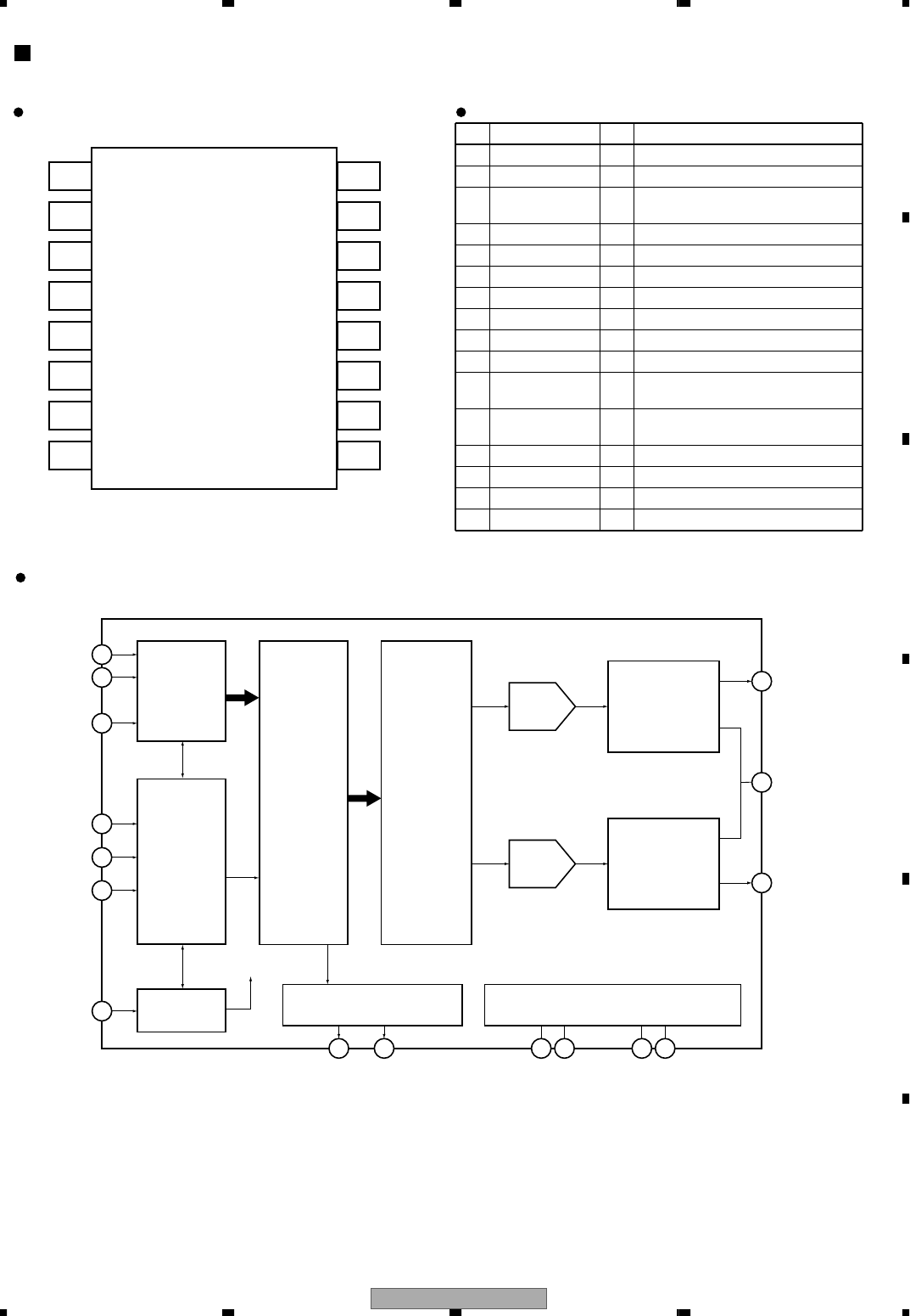
XV-EV51 115
5 678
5678
C
D
F
A
B
E
Pin Arrangement Pin Function
Block Diagram
1BCK 16
SCK
2DATA 15
ML
3LRCK 14
MC
4DGND 13
MD
5VDD 12
ZEROL/NA
6VCC 11
ZEROR/ZEROA
7VOUTL10
VCOM
8VOUTR9
AGND
Audio
Serial
Port
Enhanced
Multi-level
Delta-Sigma
Modulator
4× / 8×
Oversampling
Digital Filter
with
Function
Controller
Serial
Control
Port
System Clock
System Clock
Manager
BCK 1
LRCK 3
DATA 2
ML 15
MC 14
MD 13
SCK 16
DAC Output Amp and
Low-pass Filter
DAC
Power Supply
Output Amp and
Low-pass Filter
VOUTL
7
VOUTR
8
AGND
8
VCC
6
DGND
9
VDD
ZEROR/ZEROA
511
ZEROL/NA
12
VCOM
10
Zero Detect
PCM1742KE (DVD IF ASSY : IC1921)
• D/A Converter
No. Pin Name I/O Pin Function
1 BCK I Audio data bit clock input
2 DATA I Audio data digital input
3 LRCK I L-channel and R-channel Audio data
latch enable input
4 DGND −Digital ground
5V
DD −Digital power supply +3.3V
6V
CC −Analog power supply +5V
7V
OUTL O Analog output for L-channel
8VOUTR O Analog output for R-channel
9 AGND −Analog ground
10 VCOM −Common voltage decoupling
11 ZEROR/ZEROA O Zero flag output for R-channel / Zero
flag output for L/R-channel
12 ZEROL/NA O Zero flag output for L-channel / No
assign
13 MD I Mode control data input
14 MC I Mode control clock input
15 ML I Mode control latch input
16 SCK I System clock input
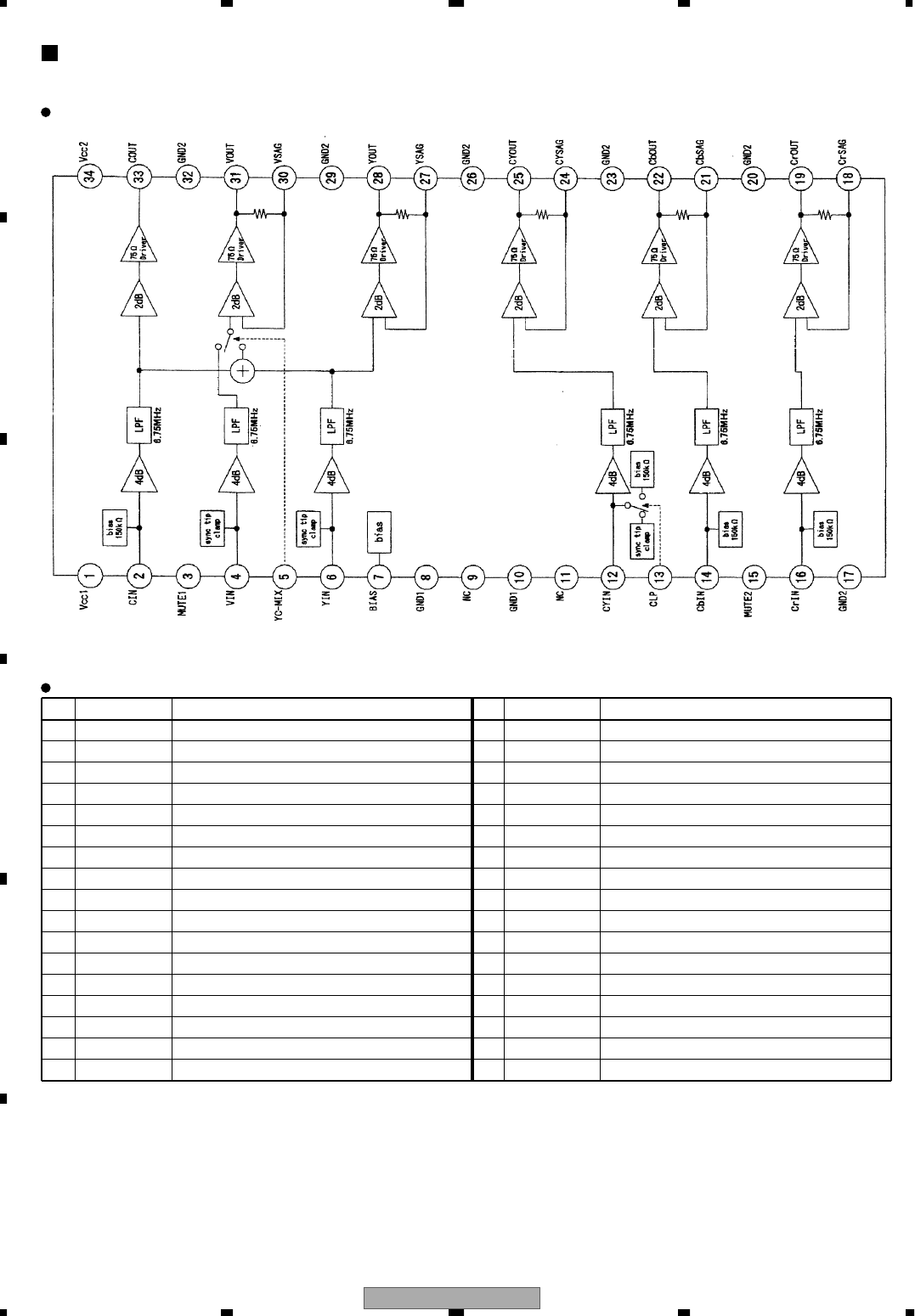
XV-EV51
116
1234
1234
C
D
F
A
B
E
Pin Function
Block Diagram
MM1567AJ (DVD IF ASSY : IC1941)
• DVD Video Amp. IC
No. Pin Name Pin Function No. Pin Name Pin Function
1 VCC1 VCC 18 CrOUT Signal output (Cr)
2 CIN Crroma input 19 CrSAG SAG correction (Cr)
3 MUTE1 Mute select 20 GND2 GND
4 VIN Video input 21 CbOUT Signal output (Cb)
5 YC MIX YC MIX select 22 CbSAG SAG correction (Cb)
6 YIN Video input (Y) 23 GND2 GND
7 BIAS Bias 24 CYOUT Signal output (CY)
8 GND1 GND 25 CYSAG SAG correction (CY)
9 NC NC 26 GND2 GND
10 GND1 GND 27 YOUT Signal output (Y)
11 NC NC 28 YSAG SAG correction (Y)
12 CYIN Luminance input 29 GND2 GND
13 CLP Input clamp select 30 VOUT Signal output (V)
14 CbIN Component input (Cb) 31 VSAG SAG correction (V)
15 MUTE2 Mute select 32 GND2 GND
16 CrIN Component input (Cr) 33 COUT Chromatic output
17 GND2 GND 34 VCC2 VCC
XV-EV51 117
5 678
5678
C
D
F
A
B
E
PDC093 (IF ASSY : IC5501)
• System Control Microcomputer
Pin Function
No. Port Name Pin Name I/O Function
1 PA3/WR# DVD ON/OFF O Control power supply for DVD
2 PA4/RD# (HPDET) O Detect to insert headphone (reserve) → If don't use, set I/O to output
3 PA5/RS XCDRST O Reset for CD / VCD / DVD microcomputer
4 P70 / INT0 / T0LCP / AN8 ACPULSE I AC PULSE input
5 P71 / INT1 / T0HCP / AN9 CDERR I ERR and OVER input from CODEC
6 P72 / INT2 / T0IN RDSCLK I Clock input from RDS decoder (without RDS : Low output)
7 P73 / INT3 / T0IN REMOCON I REMOCON signal input
8 RES# XRESET I Reset input
9 XT1 / AN10 −−
10 XT2 / AN11 −−
11 VSS1 −−
12 CF1 −−
13 CF2 −−
14 VDD1 −−Power supply
15 P80 / AN0 SIMUKE I Destination setting input
16 P81 / AN1 LEVELIN I Level meter signal input
17 P82 / AN2 3.3DETECT I DVD 3.3V detection input
18 P83 / AN3 KEY4 I Key input (for AMP)
19 P84 / AN4 ST/TUNE I STEREO tuned detection input
20 P85 / AN5 KEY1 I Key input
21 P86 / AN6 KEY2 I Key input
22 P87 / AN7 KEY3 I Key input
23 P10/SO0 SYS_DOUT O System bus data output (AMP side output)
24 P11 / SI0 / SB0 SYS_DIN I System bus data input (AMP side input)
25 P12 / SCK0 SYS_CLK I System bus clock input
26 P13 / SO1 DSPDIN O Data output for CODEC + DIR IC, TC9164, EXPAND IC (only for DSP),
CRISTAL's DSP (AMP side output) [DSP core CDDI + CSDI]
27 P14 / SI1 / SB1 DSPDOUT I Data input for CODEC + DIR IC, TC9164, EXPAND IC (only for DSP),
CRISTAL's DSP AMP side input) [DSP core CDDO + CSDO]
28 P15 / SCK1 DSPCLK O Clock for CODEC + DIR IC, TC9164, EXPAND IC (only for DSP), CRISTAL's
DSP [DSP core CDCK + CSCK]
29 P16/T1PWML SYS_CS2 O Chip select 2 for system bus
30 P17/T1PWMH/BUZ SYS_CS1 O Chip select 1 for system bus
31 PE0 TCEXPOE O Output enable to EXPAND IC for deck
32 PE1 TCEXPCLK O Clock to EXPAND IC for deck
33 PE2 TCEXPCE O Chip enable to EXPAND IC for deck
34 PE3 TCEXPDAT O Data to EXPAND IC for deck
35 PE4 TCHALF I Input switch of mecha half
36 PE5 TCMODE I Input switch of mecha mode
37 PE6 TCRECF I Input switch of mecha during recording forward
38 PE7 TCRECR I Input switch of mecha during recording reverse
39 VSS4 −−Ground
40 VDD4 −−Power supply

XV-EV51
118
1234
1234
C
D
F
A
B
E
No. Port Name Pin Name I/O Function
41 PF0 TCMSIN I Input MS signal
42 PF1 TCPULSE I Input pulse of TC reel
43 PF2 XTESTMODE I Set TEST MODE for product line (service) and unit checker
44 PF3 SERVICE I Set SELF CHECK for service
45 PF4 DTSDMIX O Cntrol of gain-up for dts down-mix
46 PF5 SWFMIX O Control for subwoofer mix
47 PF6 ECHCNT1 O Control of echo level 1
48 PF7 ECHCNT2 O Control of echo level 2
49 SI2P0/SO2 LCDDAT O Data for FL (LCD) driver
50 SI2P1/SI2/SB2 LCDCE O Chip enable for FL (LCD) driver
51 SI2P2/SCK2 LCDCLK O Clock for FL (LCD) driver
52 SI2P3/SCK20 LCDRST O Reset for FL (LCD) driver
53 PWM1 −−
54 PWM0 −−
55 VDD2 −−Power supply
56 VSS2 −−Ground
57 P00 TXCE O Chip enable for tuner LSI
58 P01 NC O No connection
59 P02 XTMRLED O Control timer standby LED
60 P03 XSTBYLED O Control standby LED
61 P04 TXCLK O Clock for tuner LSI
62 P05 TXIDAT O Data for tuner LSI
63 P06 TXMUTE O Control mute of tuner
64 P07 RDSPOW O Control power supply of RDS
65 P20/INT4/T1IN RDSDATA I Input RDS data
66 P21/INT4/T1IN TXODAT I Input data from tuner LSI
67 P22/INT4/T1IN XDSPMUTE O Control mute of DSP (board)
68 P23/INT4/T1IN A/D MODE O DSP mute when ANALOG
69 P24/INT5/T1IN AUXMUTE O Control mute of AUX output
70 P25/INT5/T1IN DVDLAT I Input latch signal from DVD connection
71 P26/INT5/T1IN ATTCONT O Control ATT of AUX
72 P27/INT5/T1IN KCONSTB O Strobe for Key Control IC
73 P30 KCONCLK O Clock for Key Control IC
74 P31 KCONDATA O Data for Key Control IC
75 P32 VOCALC O
76 P33 VOCALB O
77 P34 VOCALA O
78 P35 ASSELB O Audio source select B
79 P36 ASSELA O Audio source select A (CD, TUNER, TAPE, AUX) BU4052
80 PB7/D7 DSP EXP CS O Chip select for EXPAND
XV-EV51 119
5 678
5678
C
D
F
A
B
E
No. Port Name Pin Name I/O Function
81 PB6/D6 DSP EXP OE O Output enable for EXPAND (no use)
82 PB5/D5 CSCS O Chip select for CRISTAL's DSP
83 PB4/D4 CSREQ I Request for CRISTAL's DSP
84 PB3/D3 FS96 I 96k input fron CODEC
85 PB2/D2 ABOOT O Chip select for SRAM / P2ROM
86 PB1/D1 CSRST O RESET for CRISTAL's DSP
87 PB0/D0 CDCS O Chip select for CODEC
88 VSS3 −−Ground
89 VDD3 −−Power supply
90 PC7/A7 CDPDN O Power down (RESET) for CODEC
91 PC6/A6 SYSPOW O Control power supply of system
92 PC5/A5 PROTECT I Protection and Fan Error detection input
93 PC4/A4 SPCONT O Control relay of speaker output
94 PC3/A3 SYSMUTE O Control mute of system
95 PC2/A2 VOLCE O Chip enable for E-vol IC
96 PC1/A1 VOLCLK O Clock for E-vol IC
97 PC0/A0 VOLDATA O Data for E-vol IC
98 PA0/CS2# FLASH E/D −for FLASH writing
99 PA1/CS1# FLASH DO −for FLASH writing
100 PA2/CS0# FLASH CLK −for FLASH writing
•Port 0 (P00-P07) can be selected for input or output by each 4 bits (P00-P03, P04-P07).
Set for input when reset. And it can be set C-MOS or Nch-OD by each 1 bit in option.
•Port 1 (P10-P17) can be selected for input or output by each 1 bit. Set for input when reset.
And it can be set C-MOS or Nch-OD by each 1bit in option.
•Port 2 (P20-P27) can be selected for input or output by each 1 bit. Set for input when reset.
And it can be set C-MOS or Nch-OD by each 1 bit in option.
•Port 3 (P30-P36) can be selected for input or output by each 1 bit. Set for input when reset.
And it can be set C-MOS or Nch-OD by each 1 bit in option.
•Port 7 (P70-P73) can be selected for input or output by each 1 bit. Set for input when reset.
•Port 8 (P80-P87) can be selected for input or output by each 1 bit. Set for input when reset.
•Port A (PA0-PA5) can be selected for input or output by each 1 bit. Set for input when reset.
And it can be set C-MOS or Nch-OD by each 1 bit in option.
•Port B (PB0-PB7) can be selected for input or output by each 1 bit.
Set for input when reset. And it can be set C-MOS or Nch-OD by each 1 bit in option.
•Port C (PC0-PC7) can be selected for input or output by each 1 bit.
Set for input when reset. And it can be set C-MOS or Nch-OD by each 1 bit in option.
•Port E and PortF can be selected for input or output by each 2 bits.
•In case of without RDS, it is best that RDSDATA and RDSCLK are assigned as I/O port which can be set output and output low level.
•Port 0 cannot output High level during HALT mode.

XV-EV51
120
1234
1234
C
D
F
A
B
E
7.3 CLEANING
Before shipping out the product, be sure to clean the following positions by using the prescribed cleaning tools:
Position to be cleaned Cleaning tools
Pickup lenses Cleaning liquid : GEM1004
Cleaning paper : GED-008
XV-EV51 121
5 678
5678
C
D
F
A
B
E
8. PANEL FACILITIES
SOUND MODE
KARAOKE
VOLUME
ST. MEMORY
TIMER/CLOCK ADJ
DISPLAY
STEREO DVD TUNER DECK
EV51DVD
ENTER
DVD/CD
TUNER
TAPE
LINE
OPEN/CLOSE
DOLBY NR(DEMO)
ASES
MIC VOL
MAX
MIN
MIC
(MAIN)
MIC
(SUB)
REVERSE MODE
REC/STOP
PLAY/PAUSE STOPTUNING –T UNING +
4/1¡/¢
–+
6 7 8 9 1310 11 12
14 15 16 17 18 19 20 21
Front panel
The front panel controls for the EV51DVD model
are shown in the illustrations below.
1SURROUND (EV51DVD model)
Selects a surround listening mode
SFC (EV21DVD model)
Selects sound modes or custom settings from
the Sound Field Control
2 STANDBY/ON
Switches the player on or into standby
3ADVANCED SURROUND (EV51DVD model)
Selects an advanced listening mode
CENTER SP (ON/OFF) (EV21DVD model)
Switches the center speaker on or off
STANDBY/ON
STANDBY
PHONES
SURROUND
POWER AMPLIFIER EV51DVD
ADVANCED
SURROUND
1235
4

XV-EV51
122
1234
1234
C
D
F
A
B
E
4 STANDBY indicator
Lights when the system is in standby
5 PHONES jack
Headphone jack
6 DVD/CD and TUNER select button
Press to select the source you want to listen to
7SOUND MODE
Adjusts the tone, balance and (EV51DVD model
only ) DSP controls
8 KARAOKE (EV51DVD model)
Selects audio channels for karaoke
VIRTUAL SURROUND (EV21DVD model)
Switches the Virtual Surround effect on or off
9 ST. MEMORY
Use for saving and listening to station presets
10 ENTER
Select an option or execute a command
11 DISPLAY
Changes the information shown in the display
12 TIMER/CLOCK ADJ
Use for setting the clock, as well as for setting and
checking the timers
13 TAPE and LINE select button
Press to select the source you want to listen to
14 ASES
Press for CD-to-tape synchro recording
15 DOLBY NR (DEMO)
Switches Dolby Noise Reduction on or off
16 OPEN/CLOSE
Opens the disc tray
17 MIC VOL
Controls the volume of the karaoke mics
18 MIC input jacks
19 VOLUME, TUNING and playback control
buttons
The TUNING /scan/skip buttons are used for tuning
into stations, skipping or scanning tracks on discs
or tapes. The playback control button is used for
playing, pausing and stopping playback.
20 REVERSE MODE
Selects the playback mode for tapes
21 REC/STOP
Starts/stops recording on the tape deck
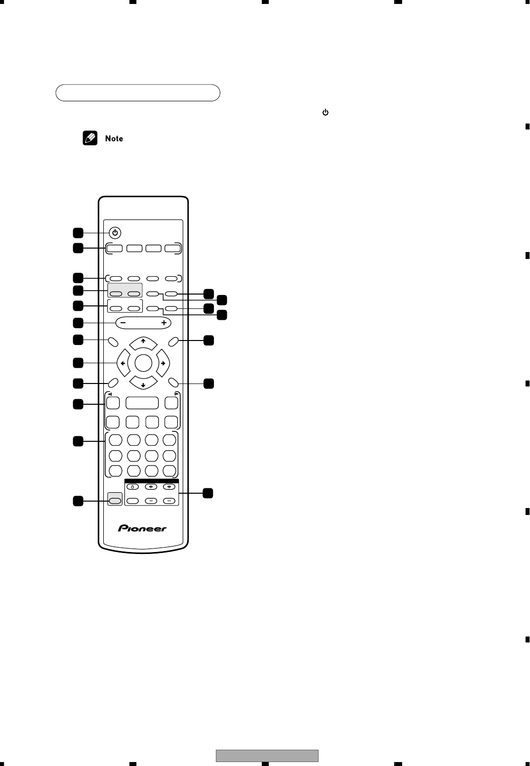
XV-EV51 123
5 678
5678
C
D
F
A
B
E
Controls and displays
Remote control
The remote control for the EV51DVD model is
shown in the illustration below.
1STANDBY/ON
Switches the player on or into standby
2 Function select buttons
Selects the source you want to listenot
3 DVD control buttons
AUDIO
Selects the audio channel or language
SUBTITLE
Selects a subtitle display
ANGLE
Changes the camera angle during DVD multi-
angle scene playback
ZOOM
Changes the zoom level
4 DSP buttons (EV51DVD model)
SURROUND
Selects a surround mode for multi-channel
sound
ADV. SURROUND
Selects a DSP mode for multi-channel sound
Sound Field buttons (EV21DVD model )
SFC
Selects sound modes or custom settings from
the Sound Field Control
VIRTL. SURR.
Switches the Virtual Surround effect on or off
5 KARAOKE buttons
KARAOKE
Selects audio channels for karaoke
ECHO
Changes the echo level on the karaoke mics
KEYCON (SHIFT+KARAOKE/ECHO)
Lowers/raises the pitch of the backing track
123
456
7890
CLEAR
ENTER
SYSTEM SETUP
DVD SETUP
TOP MENU
DVD MENU
SHIFT
CHANNEL VOLUME
INPUT
SELECT
SUBTITLE
VOLUME
ANGLE ZOOM
ADVANCED
MONO
SYSTEM DISP
DVD DISP
ECHO
DSP
AUDIO
DVD/CD
TAPE
FM/AM
LINE
SURROUND
PROGRAM
TEST TONE
REPEAT
CH LEVEL
RANDOM
SLEEP
KARAOKE
I —
KEYCON
— i
TIMER
CLOCK ADJ.
MUTE
RETURN
FOLDER +
FOLDER –
SOUND
MODE
ENTER
STANDBY/ON
4
/eE/
1¡
¢
8
7
3
3
3
TUNE +
ST +ST –
TUNE –
TV CONTROL
1
2
3
6
7
8
9
10
11
12
5
19
18
17
15
13 14
16
4

XV-EV51
124
1234
1234
C
D
F
A
B
E
Controls and displays
6 VOLUME
Adjusts the volume level
7 DVD SETUP
Press to make DVD settings
SYSTEM SETUP (SHIFT+DVD SETUP)
(EV51DVD model)
Press to make DSP settings
8ENTER, TUNE & cursor control buttons
Navigates on-screen displays and menus. ENTER
selects an option or executes a command.
9SOUND MODE
Adjusts the tone, balance and (EV51DVD model
only ) DSP controls
10 Playback controls
3
Starts/resumes playback
1 and
/e
Use for reverse slow motion playback, frame
reverse and reverse scanning
¡ and
E/
Use for forward slow motion playback, frame
advance and forward scanning
4
Jumps to the beginning of the current chapter
or track, then to previous
chapters/tracks
¢Jumps to the next chapter or track
8Pauses playback; press again to restart
7Stops playback
11 Number buttons and SHIFT functions
The number buttons can be used for selecting tracks
directly, the functions above the buttons are
accessed by pressing SHIFT at the same time as the
button.
PROGRAM (SHIFT+1)
Use to program/play a program list
REPEAT (SHIFT+2)
Selects a repeat play mode
RANDOM (SHIFT+3)
Selects a random play mode
TEST TONE (SHIFT+4)
(EV51DVD model only)
Outputs the test tone for speaker setup
CH LEVEL (SHIFT+5)
(EV51DVD model only)
Press to adjust the speaker level
SLEEP (SHIFT+6)
Switches the sleep timer on or off
CLEAR
Clears an entry
ENTER
Selects menu options, etc. (works exactly the
same as the ENTER button in 8 above)
12 SHIFT
Press to access the functions/commands written in
green on the remote
13 SYSTEM DISP
Switches between information and clock displays
DVD DISP (SHIFT+SYSTEM DISP)
Changes the information shown in the display
14 MONO
Press to listen to a stereo FM broadcast in
mono (sound quality is usually improved)
CENTER SP (SHIFT+MONO)
(EV21DVD model only)
Switches the center speaker on or off
15 MUTE
Mutes the volume
16 TIMER/CLOCK ADJ.
Use for setting the clock, as well as for setting and
checking the timers
17 DVD MENU
Displays the DVD menu (for CDs, Video
CDs, and MP3 discs, the Disc Navigator
screen appears)
TOP MENU (SHIFT+DVD MENU)
Displays the top menu of a DVD disc
18 RETURN
Press to return to a previous menu screen
19 TV CONTROL
Refer to Setting the remote to control your TV
on page 27 to use these controls with your TV.
Switches the TV on or into standby
INPUT SELECT
Switches the TV input
CHANNEL +/–
Selects channels
VOLUME +/–
Adjusts the volume on the TV
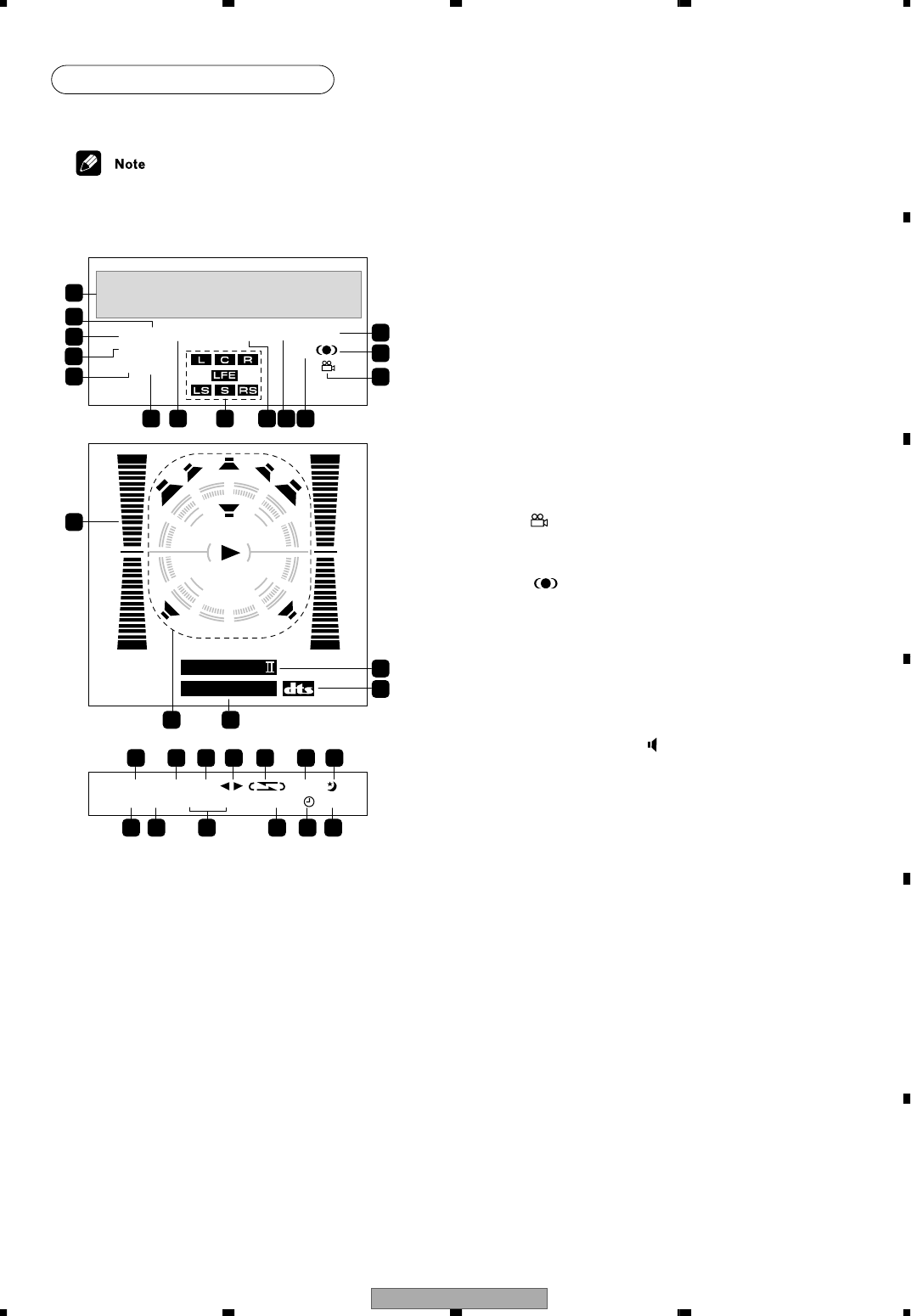
XV-EV51 125
5 678
5678
C
D
F
A
B
E
Controls and displays
Display
The front panel display for the EV51DVD model is
shown in the illustration below.
PGM
ADV.SURR. 96kHz
SFC MP3
RDMF PT-1 MONO TUNED
STEREO
SUB Wf
PRO LOGIC
2
DIGITAL
2
NR B. CUT
2
REC ASES
REC
WAKE–UPKARAOKE L R ECHO
KEY
1
6 7 8 9 10 11
14
13
12
19
18
2
3
4
5
1
5
16
20 21 22 23 24 25 26
27 28 29 30 31 32
17
1 Character display
2 RDM
Lights during random playback
3 PGM
Lights during program play
4 ADV. SURR. (EV51DVD model only)
Lights when one of the Advanced Surround
listening modes is selected
5 SFC (EV21DVD model only)
Lights when one of the Sound Field Control
listening modes is selected
6 MP3
Lights during playback of an MP3 disc
7 RPT-1
RPT lights during repeat play ( RPT-1 lights during
repeat one-track play)
8 Format indicator (EV51DVD model only)
These indicators will light according to which
channels are encoded on the Dolby Digital or DTS
multi-channel disc currently in the player. LFE
lights when the disc has an LFE channel.
9 MONO
Lights when FM mono reception is selected
10 STEREO
Lights when a stereo FM broadcast is being
received in auto stereo mode
11 96 kHz
Lights when a 96kHz source is detected
(wont light if the source is copy-protected)
12
Lights during multi-angle scenes on a DVD disc
13
Lights when Virtual Surround is switched on
14 TUNED
Lights when a broadcast is being received
15 Level meter
Shows the level of the source selected
16 Speaker and playback indicators
The speaker indicators ( ) show the speakers
currently active. The playback indicator (3) lights
during playback.
17 2 DIGITAL
This lights to indicate decoding of a Dolby Digital
signal
18 DTS
This lights to indicate decoding of a DTS signal
19 2 PRO LOGIC II (EV51DVD model only)
This lights to indicate Prologic II decoding
20 2 NR
Lights when Dolby Noise Reduction is on
XV-EV51
126
1234
1234
C
D
F
A
B
E
Controls and displays
19 2 PRO LOGIC II (EV51DVD model only)
This lights to indicate Prologic II decoding
20 2 NR
Lights when Dolby Noise Reduction is on
21 B.CUT
Lights when the beat cut mode has been switched to
B.CUT 2
22 REC
Lights when recording to the tape deck
23 2 3
Indicates the direction of tape playback
24
Indicates the reverse mode:
• - Single side playback
• - Auto-reverse playback: stops after
finishing playback in the reverse
(2)
direction
• - Continuous playback (up to 16
complete plays)
25 ASES
Lights during ASES recording
26
Lights when the sleep timer is active
27 ECHO
Lights when the Karaoke ECHO effect is selected
28 KEY
Lights when the Karaoke pitch control is selected
29 KARAOKE LR
Lights when one of the Karaoke modes is selected:
•KARAOKE (Vocal cancel) - Vocals in the
backing track are partially eliminated using
EQ.
•L - Left channel only. Use for tracks that
have a vocal recorded in the right channel.
•R - Right channel only. Use for tracks that
have a vocal recorded in the left channel.
•L R - Use to put a a single-channel vocal track
into the center of the mix.
30 WAKE-UP
Lights in standby when the wake-up timer is set and
flashes when the wake-up timer activates
31
Lights in standby when either timer is set and
flashes when they activate
32 REC
Lights in standby when the record timer is set and
flashes when the timer starts recording
