Z8601_Z8603_Data_Sheet_Sep82 Z8601 Z8603 Data Sheet Sep82
User Manual: Z8601_Z8603_Data_Sheet_Sep82
Open the PDF directly: View PDF ![]() .
.
Page Count: 24

~
Zilog
Z8®
Family of
Microcomputers
Z8601
•
Z8603
Product
Specification
September
1982

Copyright, 1982
by
2110g,
Inc,
All rights
reserved,
No
part
of
this publication
may
be
reproduced
without the written
permission of Zilog I Inc.
The
information
in
this
publication
is
subject
to
change
wi
thou t notice.
~
Zilog
Features
General
Description
2037
-00
1,
002
•
Complete
microcomputer,
2K
bytes
of ROM,
128
bytes
of
RAM, 32
I/O
lines,
and
up
to
62K bytes
addressable
external
space
each
for
program
and
data
memory.
• 144-byte
register
file,
including
124
general-purpose
registers,
four
I/O
port
registers,
and
16 status
and
control
registers.
•
Average
instruction
execution
time of
2.2
p.s,
maximum of
4.25
p.s.
•
Vectored,
priority
interrupts
for
I/O,
counter/timers,
and
UART.
The
28601
microcomputer
introduces
a
new
level
of
sophistication to Single-chip
architec-
ture.
Compared
to
earlier
single-chip
micro-
computers,
the
Z8601 offers faster
execution;
more
efficient
use
of
memory;
more
sophisti-
cated
interrupt,
input/output
and
bit-manipula-
tion
capabilities;
and
easier
system
expansion.
Under
program
control,
the
Z8601
can
be
tailored
to
the
needs
of
its
user.
It
can
be
con-
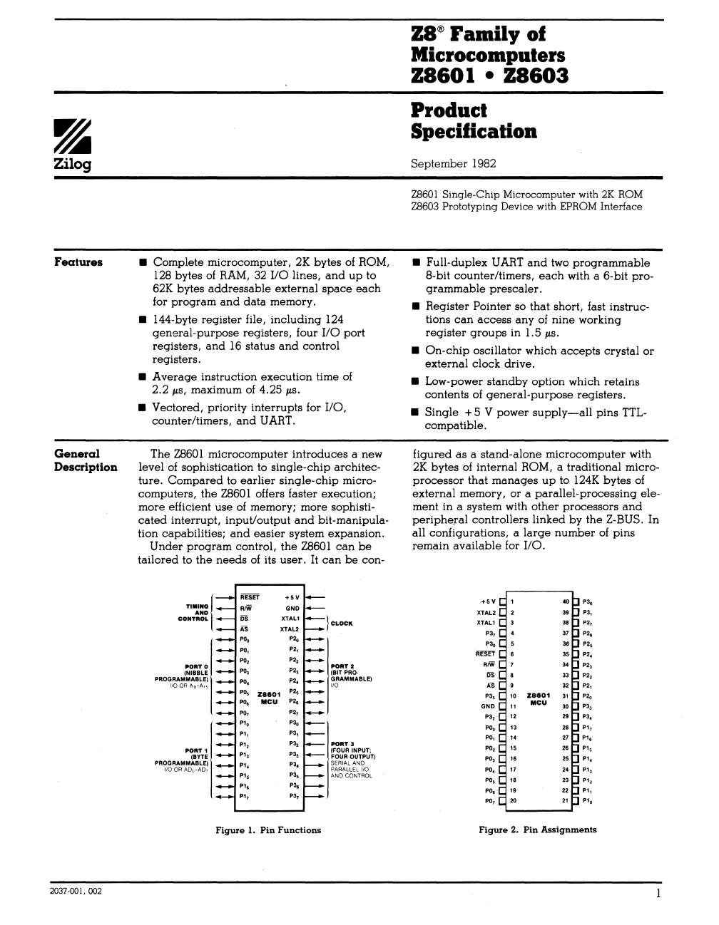
PORT
0
(NIBBLE
PROGRAMMABLE)
110
OR
As-A,.,
PORT
1
(BYTE
PROGRAMMABLE)
110
OR
ADC,-AD)
Figure
I.
Pin
Functions
PORT 2
(BIT
PRO·
GRAMMABLE)
110
PORT
3
(FOUR INPUT;
FOUR
OUTPUT)
SERIAL
AND
PARALLEL
110
AND
CONTROL
Z8®
Family of
Microcomputers
Z8601
•
Z8603
Product
Specification
September
1982
28601
Single-Chip Microcomputer
with
2K
ROM
28603
Prototyping Device
with
EPROM
Interface
•
Full-duplex
UART
and
two
programmable
8-bit
counter/timers,
each
with a 6-bit
pro-
grammable
prescaler.
• Register
Pointer
so
that
short, fast instruc-
tions
can
access
any
of
nine
working
register
groups
in
I.
5
p.s.
•
On-chip
oscillator
which
accepts
crystal
or
external
clock
drive.
• Low-power
standby
option
which
retains
contents
of
general-purpose
registers.
•
Single
+ 5 V
power
supply-all
pins
TTL-
compatible.
figured
as
a
stand-alone
microcomputer
with
2K
bytes
of
internal
ROM, a
traditional
micro-
processor
that
manages
up
to 124K
bytes
of
external
memory,
or
a
parallel-
processing
ele-
ment
in
a system with
other
processors
and
peripheral
controllers
linked
by
the
Z-BUS.
In
all
configurations,
a
large
number
of
pins
remain
available
for
I/O.
+5V
P3,
XTAL2 P3,
XTAL1
P2,
P3, P2,
P3, P2,
REID
P2,
R/Vi
P2,
os
P2,
AS
P2,
P3,
P2,
GND P3,
P3, P3,
po,
PI,
po,
PI,
po,
PI,
po,
PI,
po,
PI,
po,
PI,
po,
PI,
po,
PI,
Figure
2.
Pin
Assignments
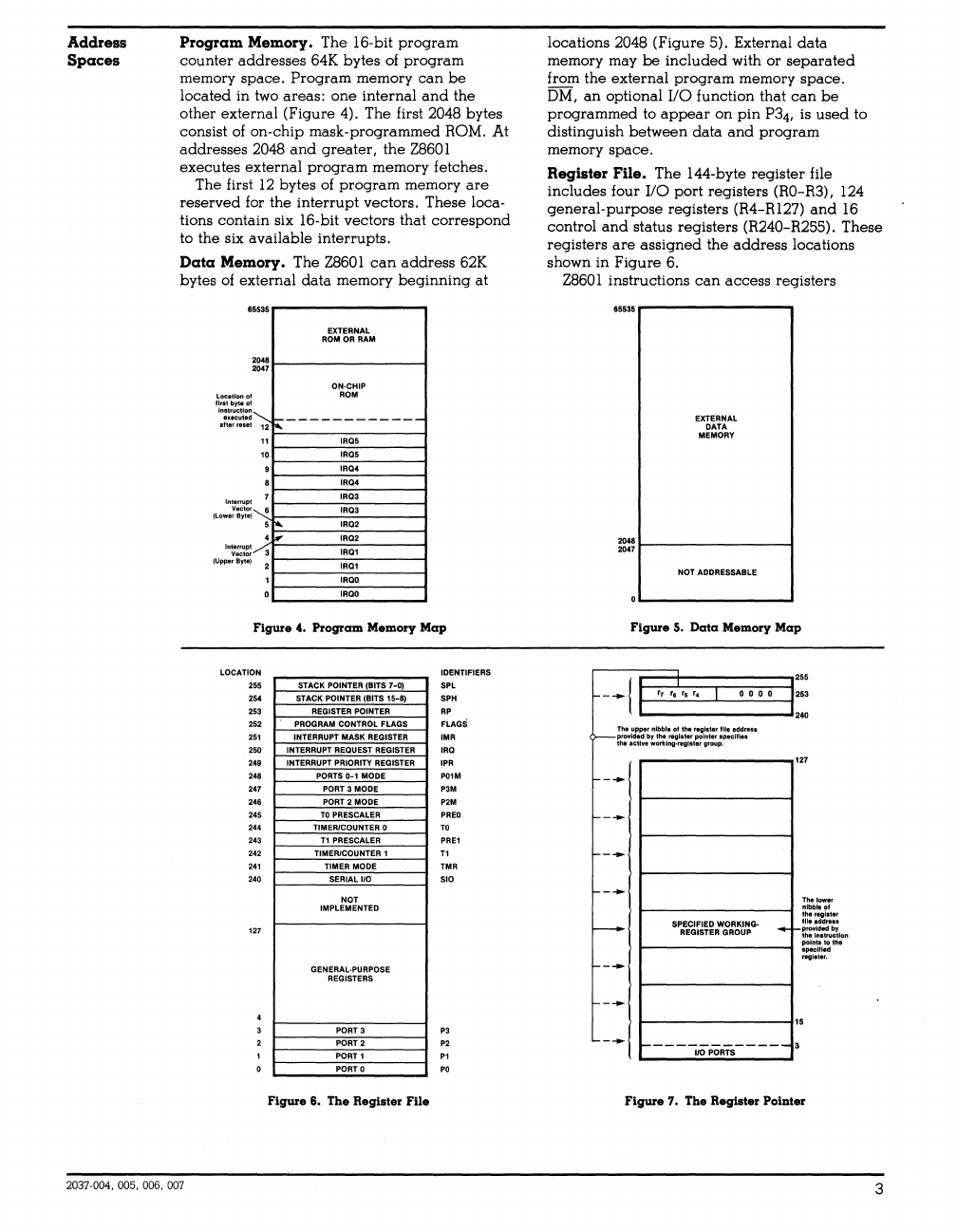
Architecture
Z8601
architecture
is charact.erized
by
a microprocessor
that
can
address
124K bytes of
external
memory.
Pin
Description
2
flexible VO scheme,
an
efficient
register
and
address
space
structure
and
a
number
of
ancillary
features that
are
helpful in
many
applications.
Microcomputer applications
demand
power-
ful
I/O
capabilities. The Z8601 fulfills this with
32
pins
dedicated
to
input
and
output. These
lines
are
grouped
into four ports of
eight
lines
each
and
are
configurable
under
software con-
trol to
provide
timing, status signals, serial
or
parallel
I/O
with
or
without
handshake,
and
an
address/data
bus
for interfacing
external
memory.
Because
the multiplexed
address/data
bus
is
merged
with
the
I/O-oriented
ports,
the
Z8601
can
assume
many different memory
and
I/O
configurations. These configurations
range
from a self-colJ.tained microcomputer to a
OUTPUT
Vee GND
! !
Three
basic
address
spaces
are
available to
support
this wide
range
of configurations: pro-
gram
memory (internal
and
external),
data
memory (external)
and
the
register
file (Inter-
nal). The 144-byte
random-access
register file
is composed of 124
general-purpose
registers,
four
I/O
port
registers,
and
16
control
and
status registers.
To
unburden
the
program
from
coping
with
real-time
problems
such
as serial
data
com-
munication
and
counting/timing,
an
asynchro-
nous receiver/transmitter (UART)
and
two
counter/timers with a
large
number
of user-
selectable
modes
are
offered on-chip. Hard-
ware
support
for
the
UART is minimized
because
one
of
the
on-chip
timers supplies
the
bit rate.
XTAL
As
uo
(BIT
PROGRAMMABLE)
ADDRESS
OR
I/O
(NIBBLE PROGRAMMABLE) ADDRESS/DATA
OR
110
(BYTE
PROGRAMMABLE)
Figure 3. Functional Block Diagram
AS. Address Strobe (output, active Low).
Address
Strobe
is
pulsed
once
at
the
begin-
ning
of
each
machine
cycle.
Addresses
output
via Port 1 for all
external
program
or
data
memory, transfers
are
valid
at
the
trailing
edge
of AS.
Under
program
control, AS
can
be
placed
in
the
high-impedance
state
along
with
Ports 0
and
1,
Data
Strobe
and
Reacl/Write.
DS.
Data Strobe (output,
active
Low). Data
Strobe
is
activated
once
for
each
external
memory transfer.
PDO
..
PO~.Plo-P171
P2o-P~.
P30-P37.
I/O
Port
Lines (inpuVoutputs, TTL-compatible).
These
32
lin~s
are
divided
into four 8-bit
I/O
ports
that
can
be
configured
under
program
control
for
I/O
or
external
memory interface.
RESET.
Reset (input, active Low).
RESET
ini-
tializes
the
Z8601.
When
RESET
is
deactivated,
prograin
execution
begins
from internal pro-
gram
location
OOOCH.
R/W. Read/Write (output). R/W is Low
when
the
Z8601
is writing to
external
program
or
data
memory.
XTALI.
XTAL2.
Crystal],
Crystal 2 (time-base
input
and
output). These pins
connect
a series-
resonant
crystal (8 MHz maximum)
or
an
exter-
nal
single-phase
clock (8 MHz maximum) to
the
on-chip clock oscillator
and
buffer.
2037,003
Address
Spaces
Program Memory. The 16-bit
program
counter
addresses
64K
bytes
of
program
memory
space.
Program
memory
can
be
located
in two
areas:
one
internal
and
the
other
external
(Figure
4).
The
first 2048 bytes
consist of
on-chip
mask-programmed
ROM. At
addresses
2048
and
greater,
the
Z8601
executes
external
program
memory fetches.
The first
12
bytes of
program
memory
are
reserved
for the
interrupt
vectors. These loca-
tions
contain
six 16-bit
vectors
that
correspond
to the six
available
interrupts.
Data
Memory. The Z8601
can
address
62K
bytes of
external
data
memory
beginning
at
5535
2048
2047
,
,
Locotlona
Ilrst
byte 0
Instruction
executed
allerres8
I~
,
Interrup
Veclo
(Lower Byte
I
11
10
9
8
7
6
EXTERNAL
ROM OR
RAM
ON·CHIP
ROM
::-------------
IRQS
IRQS
IRQ4
IRQ4
IRQ3
IRC3
5
,,_
IRQ2
Inl&rrupt
Vector
(Upper Byte
I
4
3
2
1
0
lRQ2
IRQ1
IRQ1
IROO
IROO
Figure 4. Program Memory Map
LOCATION
255
254
253
2S2
251
250
249
248
247
246
245
244
243
242
241
240
127
STACK
POINTER
(BITS
7-0)
STACK
POINTER
(BITS
15-8)
REGISTER
POINTER
PROGRAM
CONTROL
FLAGS
INTERRUPT
MASK
REGISTER
INTERRUPT
REQUEST
REGISTER
INTERRUPT
PRIORITY
REGISTER
PORTS 0-1 MODE
PORT
3
MODe
PORT
2
MODE
TO
PRESCALER
TIMER/COUNTER
a
T1
PRESCALER
TIMER/COUNTER
1
TIMER MODE
SERIAL
110
NOT
IMPLEMENTED
GENERAL·PURPOSE
REGISTERS
PORT
3
PORT
2
PORT
1
PORT
0
Figure 6. The Register File
IDENTIFIERS
.PL
,PH
RP
FLAGS
IMR
IRQ
IPR
P01M
P3M
P2M
PREO
TO
PRE1
T1
TMR
SIO
P3
P2
P1
PO
2037 -004, 005, 006, 007
locations 2048
(Figure
5). External
data
memory may
be
included
with or
separated
from
the
external
program
memory
space.
DM,
an
optional
I/O
function that
can
be
programmed
to
appear
on
pin
P34, is
used
to
distinguish
between
data
and
program
memory
space.
Register
File.
The
144-byte
register
file
includes
four
I/O
port
registers (RO-R3), 124
general-purpose
registers
(R4-RI27)
and
16
control
and
status
registers
(R240-R255).
These
registers
are
assigned
the
address
locations
shown
in
Figure
6.
Z8601
instructions
can
access
registers
65535
r----------,
EXTERNAL
DATA
MEMORY
~~:;
\-----------1
NOT
ADDRESSABLE
Figure 5. Data Memory Map
l-f~=:3==::;:=====125S
___
I L
"'.
'. '. I 0 0 0 0
'253
The upper nibble
01
the regislerlile
address
;>---
proVided by the register pointer spBcllles
the acllve worklng·rBglster group.
240
.---------_..,127
SPECIFIED
WORKING·
REGISTER
GROUP
--
ThBlower
nibble
01
thBregllter
III.
address
proYidedby
Ihelnstructlon
points to
IhB
specified
regllter.
1-----------115
----"OPORTS-----
3
Figure 7. The Register Pointer
3
Address
Spaces
(Continued)
Serial
Input/
Output
Counter/
Timers
4
directly
or
indirectly
with
an
8-bit
address
field. The Z8601
also
allows
short
4-bit
register
addressing
using
the
Register
Pointer
(one
of
the
control
registers).
In
the
4-bit
mode,
the
register
file is
divided
into
nine
working-
register
groups,
each
occupying
16
contiguous
locations
(Figure
7).
The
Register
Pointer
addresses
the
starting
location of
the
active
working-register
group.
Port
3
lines
P30
and
P37
can
be
programmed
as
serial
I/O
lines for full-duplex
serial
asyn-
chronous
receiver/transmitter
operation.
The
bit
rate
is
controlled
by
Counter/Timer
0, with
a
maximum
rate
of
62.5K
bits/second.
The
Z8601 automatically
adds
a
start
bit
and
two
stop
bits to
transmitted
data
(Figure
8).
Odd
parity
is
also
available
as
an
option.
Eight
data
bits
are
always transmitted,
regardless
of
T
Transmitted
Data
(No
Parity)
LSTART
BIT
'------EIGHT
DATA
BITS
TWO
STOP
alTS
Transmitted
Data
(With Parity)
T
''---
_LSTARTBIT
'------SEVEN
DATA
81TS
000
PARITY
TWO
STOP BITS
Stacks. Either
the
internal
register
file
or
the
external
data
memory
can
be
used
for
the
stack. A 16-bit
Stack
Pointer
(R254
and
R255)
is
used
for
the
external
stack, which
can
reside
anywhere
in
data
memory
between
locations
2048
and
65535.
An
8-bit
Stack
Pointer
(R255)
is
used
for
the
internal
stack
that
resides
within
the
124
general-purpose
registers
(R4-RI27).
parity
selection.
If
parity
is
enabled,
the
eighth
bit
is
the
odd
parity
bit.
An
interrupt
request
(IRQ4) is
generated
on
all
transmitted
characters.
Received
data
must
have
a
start
bit,
eight
data
bits
and
at
least
one
stop
bit.
If
parity
is
on,
bit 7 of
the
received
data
is
replaced
by
a
parity
error
flag.
Received
characters
generate
the
IRQ3
interrupt
request.
Received
Data
(No
Parity)
1~1~1~1~1~1~1~1~1~lul
I
LSTART
BIT
'------EIGHT
DATA
BITS
L.
--------ONE
STOP BIT
Received
Data
(With Parity)
II
LSTAAT
BIT
'-----SEVEN
DATA
BITS
L-----
___
PARITy ERROR FLAG
L.
---------DNE
STOP BIT
Figure 8. Serial Data Formats
The Z8601
contains
two 8-bit
programmable
counter/timers
(To
and
TIl,
each
driven
by
its
own 6-bit
programmable
prescaler.
The
TI
prescaler
can
be
driven
by
internal
or
external
clock
sources; however,
the
To
prescaler
is
driven
by
the
internal
clock only.
The
6-bit
prescalers
can
divide
the
input
fre-
quency
of
the
clock
source
by
any
number
from I to 64.
Each
prescaler
drives
its
counter,
which
decrements
the
value
(I to 256)
that
has
been
loaded
into
the
counter.
When
the
counter
reaches
the
end
of
count,
a
timer
interrupt
request-IRQ4
(To)
or
IRQs
(TI)-is
generated.
The
counters
can
be
started,
stopped,
restarted
to
continue,
or
restarted
from
the
initial
value.
The
counters
can
also
be
pro-
grammedto
stop
upon
reaching
zero
(single-
pass
mode) or to
automatically
reload
the
initial
value
and
continue
counting
(modulo-n
continuous
mode). The
counters,
but
not
the
prescalers,
can
be
read
any
time without
disturbing
their
value
or
count
mode.
The clock
source
for T I is
user-definable
and
can
be
the
internal
microprocessor
clock
(4 MHz maximum)
divided
by
four,
or
an
external
signal
input
via
Port
3.
The
Timer
Mode
register
configures
the
external
timer
input
as
an
external
clock
(l
MHz maximum),
a
trigger
input
that
can
be
retriggerable
or
non-retriggerable,
or
as
a
gate
input
for
the
internal
clock. The
counter/timers
can
be
pro-
grammably
cascaded
by
connecting
the
To
out-
put
to
the
input
of T I.
Port
3
line
P36 also
serves
as
a timer
output
(Tour)
through
which
To,
TI
or
the
internal
clock
can
be
output.
2037-009
110
Ports The 28601
has
32 lines
dedicated
to
input
and
output. These lines
are
grouped
into four
ports
of
eight
lines
each
and
are
configurable
as input,
output
or
address/data.
Under
soft-
ware control, the ports
can
be
programmed
to
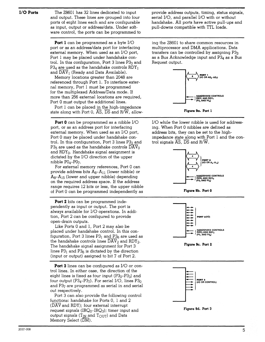
Port 1
can
be
programmed
as a byte
I/O
port
or
as
an
address/data
port
for interfacing
external memory.
When
used
as
an
I/O
port,
Port I may
be
placed
under
handshake
con-
trol. In this configuration, Port 3 lines
P33
and
P34
are
used
as
the
handshake
controls
ROY
1
and
DAVl (Ready
and
Data Available).
Memory locations
greater
than
2048
are
referenced
through
Port
1.
To interface exter-
nal
memory, Port 1 must be
programmed
for
the
multiplexed
Address/Data
mode.
If
more
than
256
external
locations
are
required,
Port 0 must
output
the
additional
lines.
Port I
can
be
placed
in
the
high-impedance
state along with Port 0, AS,
DS
and
RIW, allow-
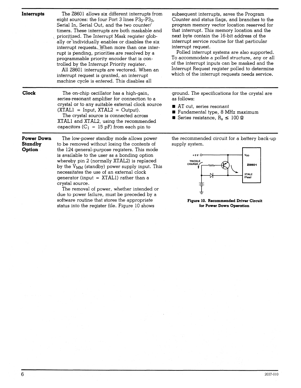
Port 0
can
be
programmed
as
a
nibble
I/O
port, or as
an
address
port
for interfacing
external
memory.
When
used
as
an
I/O
port,
Port 0 may
be
placed
under
handshake
con-
trol. In this configuration, Port 3 lines
P32
and
P35
are
used
as the
handshake
controls
DA
Vo
and
ROYo.
Handshake
signal
assignment
is
dictated
by
the
I/O
direction
of
the
upper
nibble
P04-P07.
For
external
memory
references,
Port 0
can
provide
address
bits
As-All
(lower nibble)
or
As-Al5 (lower
and
upper
nibble)
depending
on the
required
address
space.
If
the
address
range
requires
12
bits
or
less,
the
upper
nibble
of
Port 0
can
be
programmed
independently
as
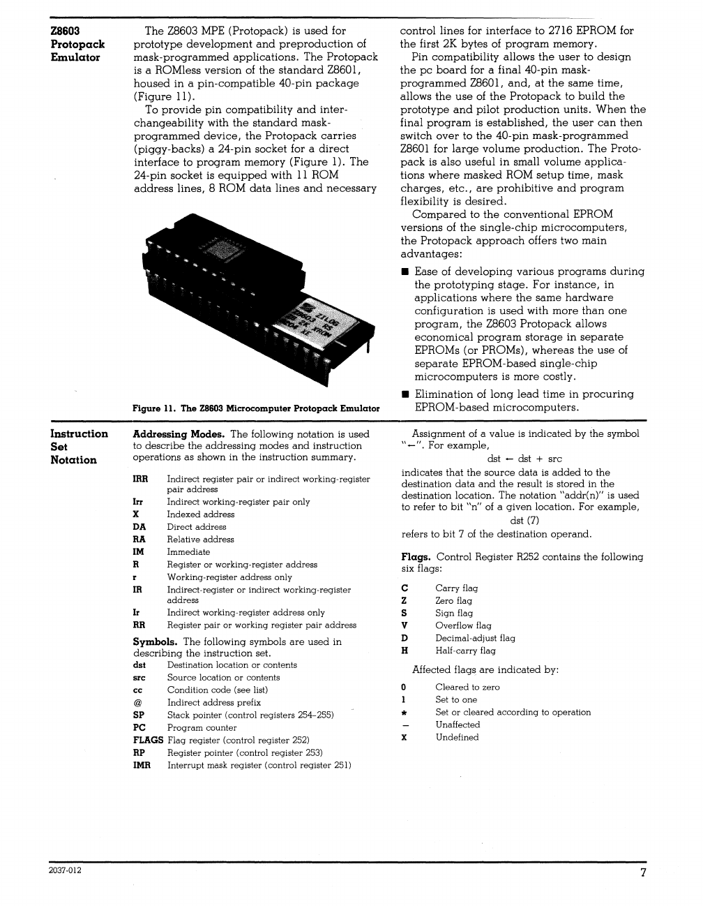
Port 2 bits
can
be
programmed
inde-
pendently
as
input
or output. The
port
is
always available for
I/O
operations. In addi-
tion, Port 2
can
be
configured
to
provide
open-drain
outputs.
Like Ports °
and
1,
Port 2 may also
be
placed
under
handshake
control. In this con-
figuration, Port 3 lines P3l
and
P36
are
used
as
the
handshake
controls lines
DA
V 2
and
ROY
2.
The
handshake
signal
assignment
for Port 3
lines P3l
and
P36
is
dictated
by
the
direction
(input
or
output)
assigned
to bit 7
of
Port 2.
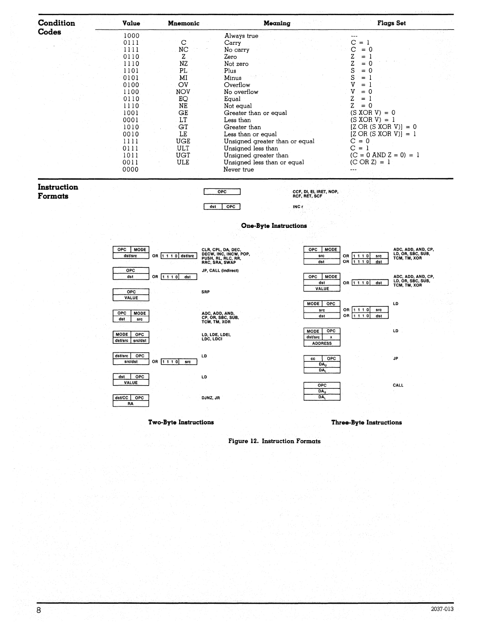
Port 3 lines
can
be
configured
as
I/O
or
con-
trol lines. In
either
case,
the direction
of
the
eight
lines
is
fixed as four
input
(P30-P33)
and
four output (P34-P37). For serial
I/O,
lines P30
and
P37
are
programmed
as serial in
and
serial
au
t respectively.
Port 3
can
also
provide
the following control
functions:
handshake
for Ports 0, I
and
2
(DAVand
RDY);
four
external
interrupt
request
signals (IRQo-IRQ3); timer
input
and
output signals
(TIN
and
TOUT)
and
Data
Memory Select (DM).
provide
address
outputs, timing, status signals,
serial
I/O,
and
parallel
I/O
with
or
without
handshake.
All ports
have
active pull-ups
and
pull-downs compatible with
TTL
loads.
ing
the
2860 I to
share
common
resources
in
multiprocessor
and
DMA applications. Data
transfers
can
be
controlled
by
assigning
P33
as a Bus Acknowledge
input
and
P34
as a Bus
Request output.
PORT 1
(If 0
OR
AD
o-AD1)
}
HANDSHA~~
CONTROLS
DAV1
AND
RDY1
(P33
AND
P3,.)
Figure 9a. Pori 1
I/O
while the lower
nibble
is
used
for
address-
ing.
When
Port 0 nibbles
are
defined
as
address
bits, they
can
be
set to
the
high-
impedance
state along with Port I
and
the
con-
trol signals AS,
DS
and
R/W.
I
PORT 0
(1/0
OR
Aa-Als)
Figure 9b. Pori 0
PORT
2(110)
} !1MiPSHAKE CONTROLS
DAV2
AND
RDY2
(P3, AND
P3
6)
Figure 9c. Pori 2
PORT 3
(110
OR
CONTROl)
Figure 9d. Pori 3
5
Interrupts
Clock
Power Down
Standby
Option
6
The
Z8601
allows six different interrupts from
eight
sources:
the
four Port 3 lines P30-P33,
Serial In, Serial
Out,
and
the two
counter/
timers. These interrupts
are
both maskable
and
:,
prior4~zed.
The
Interrupt
Mask register glob-
ally or 'individually
enables
or disables
the
six
interrupt
requests_When
more
than
one
inter-
rupt
is
~nding,
pri-;rffies-are resolved
by
a
programmable
priority
encoder
that is con-
trolled
by
the
Interrupt
Priority register.
All
Z8601
interrupts
are
vectored.
When
an
interrupt
request
is
granted,
an
interrupt
machine
cycle is
entered.
This disables all
The on-chip oscillator
has
a high-gain,
series-resonant amplifier for connection to a
crystal
or
to
any
suitable external clock
source
(XTALl =
Input,
XTAL2
= Output).
The crystal
source
is
connected
across
XTALl
and
XTAL2,
using the
recommended
capaCitors
(Cj
=
15
pF) from
each
pin
to
The low-power standby mode allows power
to
be
removed
without losing the contents
of
the
124
general-purpose
registers. This
mode
is available to the
user
as
a
bonding
option
whereby
pin
2 (normally
XTAL2)
is
replaced
by
the
VMM
(standby) power supply input. This
necessitates the use of
an
external clock
generator
(input = XTALl)
rather
than
a
crystal
source.
The removal
of
power, whether
intended
or
due
to power failure, must
be
preceded
by
a
software routine that stores
the
appropriate
status into
the
register file.
Figure
10
shows
subsequent
interrupts, saves
the
Program
Counter
and
status flags,
and
branches
to
the
program
memory vector location
reserved
for
that interrupt. This memory location
and
the
next byte contain the 16-bit
address
of
the
interrupt
service routine for
that
particular
interrupt
request.
Polled interrupt systems
are
also supported.
To
accommodate a
polled
structure,
any
or
all
of
the
interrupt
inputs
can
be
masked
and
the
Interrupt
Request register
polled
to determine
which of the interrupt
requests
needs
service.
ground.
The speCifications for the crystal
are
as follows:
•
AT
cut, series
resonant
• Fundamental type, 8 MHz maximum
• Series resistance,
Rs
:s
1000
the recommended circuit for a battery
back-up
supply system.
+5V
0----__.---1
VDD
zae01
J
Figure
10.
RacommeDCled Driver Circuit
for
Power Down Operation
2037-010
Z8603
Protopack
Emulator
Instruction
Set
Notation
2037·012
The Z8603
MPE
(Protopack) is
used
for
prototype
development
and
preproduction
of
mask-programmed
applications.
The
Protopack
is a ROMless version of
the
standard
Z8601,
housed
in
a
pin-compatible
40-pin
package
(Figure
11).
To
provide
pin
compatibility
and
inter-
changeability
with
the
standard
mask-
programmed
device,
the
Protopack
carries
(piggy-backs)
a
24-pin
socket for a
direct
interface
to
program
memory
(Figure
1). The
24-pin
socket
is
equipped
with
11
ROM
address
lines, 8 ROM
data
lines
and
necessary
Figure 11. The
Z8603
Microcomputer Protopack Emulator
Addressing Modes.
The
folloWing
notation
is
used
to
describe
the
addressing
modes
and
instruction
operations
as
shown
in
the
instruction
summary.
IRR
Irr
X
DA
RA
1M
R
IR
Ir
RR
Indirect
register
pair
or
indired
working-register
pair address
Indirect working-register pair
only
Indexed address
Direct
address
Relative address
Immediate
Register or working-register address
Working-register address only
Indirect-register
or
indired
working-register
address
Indirect working-register address only
Register
pair
or
working
register
pair
address
Symbols.
The
follOWing
symbols
are
used
in
describing
the
instruction
set.
dst
Destination location or contents
src
Source
location or contents
cc
Condition code (see list)
@ Indirect address prefix
SP Stack pOinter (control registers 254-255)
PC Program counter
FLAGS
Flag register (control register
252)
RP
Register pointer (control register
253)
IMR
Interrupt mask register (control register 251)
control
lines
for
interface
to
2716 EPROM for
the
first 2K bytes
of
program
memory.
Pin compatibility allows
the
user
to
design
the
pc
board
for a final 40-pin mask-
programmed
Z8601,
and,
at
the
same time,
allows
the
use
of
the
Protopack
to
build
the
prototype
and
pilot
production
units.
When
the
final
program
is
established,
the
user
can
then
switch
over
to
the
40-pin
mask-programmed
Z8601 for
large
volume
production.
The Proto-
pack
is
also
useful
in
small volume
applica-
tions
where
masked
ROM
setup
time, mask
charges,
etc.,
are
prohibitive
and
program
flexibility is
desired.
Compared
to
the
conventional
EPROM
versions
of
the
single-chip
microcomputers,
the
Protopack
approach
offers two
main
advantages:
• Ease of
developing
various
programs
during
the
prototyping
stage.
For
instance, in
applications
where
the
same
hardware
configuration
is
used
with
more
than
one
program,
the
Z8603
Protopack
allows
economical
program
storage
in
separate
EPROMs (or PROMs),
whereas
the
use
of
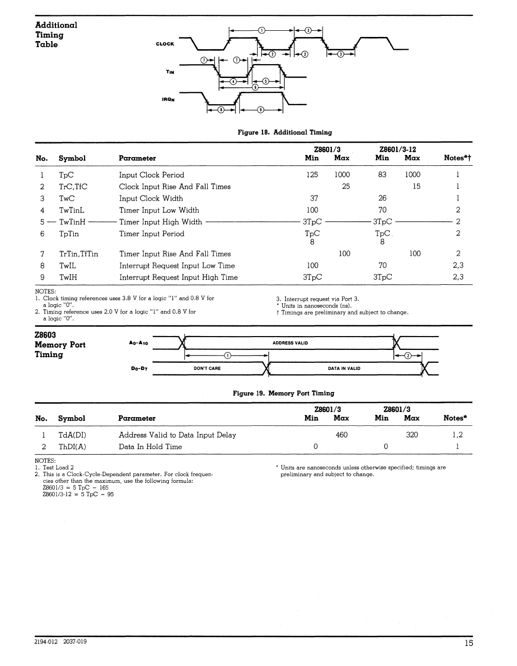
separate
EPROM-based
single-chip
microcomputers
is more costly .
• Elimination of
long
lead
time
in
procuring
EPROM-based
microcomputers.
Assignment
of a
value
is
indicated
by
the
symbol
"_".
For
example,
dst
-
dst
+
src
indicates
that
the
source
data
is
added
to
the
destination
data
and
the
result
is
stored
in
the
destination
location.
The
notation
"addr(n)"
is
used
to
refer
to
bit
"n"
of a
given
location.
For
example,
dst
(7)
refers
to
bit
7 of
the
destination
operand.
Flags.
Control
Register
R252
contains
the
follOWing
six flags:
c
Z
S
V
Carry flag
Zero
flag
Sign flag
Overflow flag
D DeCimal-adjust flag
H Half-carry flag
Affected
flags
are
indicated
by:
o
Cleared
to zero
Set to one
11
Set or
cleared
according
to operation
Unaffected
X Undefined
7
Condition
Codes
Instruction
Formats
8
Value
1000
0111
1111
0110
1110
1101
0101
DIDO
1100
0110
1110
IDOl
0001
1010
0010
IIII
0111
lOll
00
II
0000
ope
MODE
dst/src
ope
."
ope
VALUE
ope
MODe
.ot
MODE
ope
dsUsrc
srcldst
dst/src ope
srcldst
dst
lope
VALUE
I dstlCC
R~
ope
Mnemonic
C
NC
Z
NZ
PL
MI
OV
NOV
EQ
NE
GE
LT
GT
LE
UGE
ULT
UGT
ULE
OR h 1 1
01
dst/src I
I OR
11
1 1
01
.ot
OR
l'
1 1
01
,ro I
Always true
Carry
No
carry
Zero
Not
zero
Plus
Minus
Overflow
No
overflow
Equal
Not
equal
Meaning
Greater
than
or
equal
Less
than
Greater
than
Less than or
equal
Unsigned
greater
than or
equal
Unsigned less than
Unsigned
greater
than
Unsigned less than or
equal
Never
true
ope
CCF,
01,
EI,
IRET,
NOP,
ReF,
RET,
SCF
."
ope
INCr
One-Byte Instructions
eLR,
CPL, CA, DEC, ope
MODE
DECW,
INC,
INeW,
POP,
PUSH, RL,
Rle,
RR,
RRC, SRA,
SWAP
.ot
JP, CALL (Indirect) ope
MODE
.ot
SRP
VALUE
MODE ope
Ace,
ADD, AND,
CP, OR,
sec,
SUB,
.ot
reM,
TM,
XOR
MODE
ope
lO,
LOE,
lOEI,
lDC,
lOCI dstlsrc
ADDRESS
LD
ope
DA,
DA,
LD
ope
DA,
DJNZ,
JR
DA,
OR
OR
C I
C = 0
Z = I
Z = 0
S 0
S = I
V I
V 0
Z I
Z 0
Flags
Set
(S
XOR
V)
= 0
(S
XOR
V)
= I
[Z
OR
(S
XOR
V)] = 0
[Z
OR (S
XOR
V)] = I
C=O
C = I
(C
= 0
AND
Z =
0)
(C
OR
Z)
= I
Ace,
ADD, AND, CP,
til
0
'"
lO,
OR,
SSC,
SUB,
1 1 1 0
.ot
TeM,
TM,
XOR
Ace,
ADD, AND, CP,
OR
11
1 1
01
.ot
LO,
OR,
sec,
sus,
TeM,
TM,
XOR
LD
OR 1 1 1 0
OR 1 1 1 0
.ot
LD
JP
CALL
Two-Byte Instructions Three-Byte Instructions
Figure 12. Instruction.
Formats
2037-013
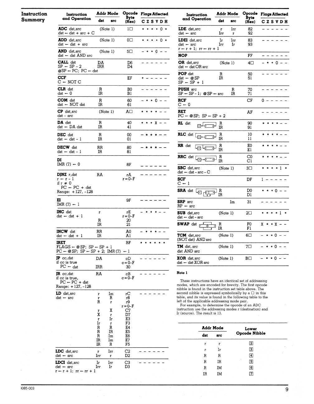
Instruction
laalruction
Addr
Mode
Opcode
Flags
Affected
laalructlon
AddrMode
Opcode
Flags
Affected
Summary
and
Operation
dBt
Byi.
and
Operation
dBt Byte
arc (Hex)
CZSVDH
arc (Hex)
CZSVDH
ADC dBt,Bre (Note
1)
10
·0·
LDE dBt,Bre r
Irr
82
------
dBt-dBt+Bre+C
dBt
-
Bre
Irr
92
ADD dBt,Bre (Note
1)
00
·0·
LDEI dBt,Bre
Ir
Irr
83
------
dBt
-
dBt
+
Bre
dBt
-
Bre
Irr
Ir
93
AND dBt,Bre (Note
1)
50
- * * 0
r-r+
1;
rr-rr+
1
dBt
-
dBt
AND
Bre
NOP
FF
------
CALL
dBt
DA
D6
------
OR
dBt,Bre (Note
1)
40
- * * 0
SP-SP-2
IRR D4
dBt
-
dBt
OR
Bre
@SP -
PC;
PC
-
dBt
POP
dst
R 50
------
CCF
EF . - - - - -
dBt
-
@SP
IR
51
C -
NOTC
SP -
SP
+ 1
CLR
dst
R
BO
------
PUSH
Bre
R
70
------
dBt
- 0 IR
Bl
SP-SP-l;
@SP-Bre
IR
71
COM
dBt
R
60
0--
RCF
CF
0--
- - -
dBt
-NOT
dBt
IR
61
C - 0
CP
dst,Bre (Note
1)
AD
RET
AF
------
dBt
-
Bre
PC
-
@SP;
SP
-
SP
+ 2
DA
dBt
R 40 * • * X - -
RL
dBt
~
R 90
dst
-
DA
dBt
IR
41
IR
91
DEC
dBt
R 00
-***--
RLC
dBt
L:{ri:OOciJ
R
10
dBt
-
dBt-l
IR
01
' , • IR
11
DECW
dBt
RR 80
-***--
RR
dst
1E14!::::::::!J.J
I~
EO
dBt-dst-l
IR 81
El
DI
RRC
dBt
LEHi::3J
R
.'
, • IR
CO
Cl
IMR (7) - 0
8F
------
sac
dBt,Brc (Note 1)
3D
• 1 .
DJNZ r,dBt
RA
rA
dBt
-
dBt-Bre-C
------
r - r - 1
r=O-F
SCF
DF 1 - - - - -
ifr
* 0
C-l
PC-PC
+
dBt
SRA
dBt
lEl~I~
DO
Range:
+ 127,
-128
* * * 0
Dl
EI
9F
------
SRP
sre
1m
31
------
IMR(7)
- 1 RP -
Brc
INC
dBt
rE -* * * - - SUB dBt,Brc (Note
1)
20
* * * * 1 .
dBt-dBt+l
r=O-F
dBt
-
dBt
-
Bre
R
20
IR
21
SWAPds!
~
R
FO
X • * X - -
IR
Fl
INCW
dBt
RR
AO
-* * * - -
dBt
-
dBt
+ IR
Al
TeM
dst,Bre
(Note
1)
60
-•
·0
- -
!RET
BF * * * * * * (NOT
dBt)
AND
Bre
FLAGS
-@SP;
SP
-
SP
+ 1 TM
dBt,
Bre
(Note
I)
7D
-* * 0 - -
PC
-@SP;
SP
-
SP
+ 2;
IMR(7)
-1
dBt
AND
Brc
JP
ee,dBt
DA
cD
------
XOR
dst,Bre (Note
1)
BO
·0
- -
if
co is true
e=O-F
dBt
-
dBt
XOR
arc
PC
-
dBt
IRR 30
JR
ee,dBt RA eB
------
Note I
if
cc
is true,
e=O-F
PC-PC+dBt
These instructions
have
an
identical set
of
addressing
Range:
+ 127,
-128
modes, which
are
encoded
for brevity. The first
opcode
nibble
is
found
in
the
instruction set table above. The
LD
dst,Bre
1m
rC
------
second
nibble
is
expressed
symbolically
by
a D in this
dBt
-
Bre
r R
r8
table,
and
its
value
is found
in
the following table to
the
R
r9
left
of
the
applicable
addressing
mode
pair.
r=O-F
For
example, to
determine
the
opcode
of
an
ADC
r X
C7
instruction use the
addressing
modes r (destination)
and
X r D7 Ir (source). The result
is
13.
r
Ir
E3
Ir
r F3
R R E4
AddrMode
Lower
R IR E5
Opcode
Nibble
R
1m
E6 dBt arc
IR
1m
E7
IR R F5
~
LDC dBt,Bre r
Irr
C2
------
Ir
lID
dBt
-
Bre
Irr
D2 R R ffi
LDCI dst,Bre
Ir
Irr
C3
------
R IR
lID
dBt
-
Bre
Irr
Ir
D3 R
1M
[!]
r-r+
1;
rr-rr+
1 IR
1M
121
1085-003
9

Registers
R240
810
8erlall/0
Regilter
(F~;
Reacl/Write)
L-
____
SERIAL
DATA
(Do =
LSB)
R241
TMR
Timer
Mode
Register
(FlH; Reacl/Write)
NOT
USED
_
00
~
1 =
LOAD
To
foOUT =
01
T, OUT _ 10 0 = DISABLE
To
COUNT
Tour
MODES
J
~~O
-
NO
FUNCTION
INTERNAL CLOCK
OUY
OIl
11
1
...
ENABLE
To
COUNT
T
MODES
0
..
NO
FUNCTION
EXTERNAL
CLOCK
IN~aT
=
00
1 =
LOAD
T 1
GATE
INPUT
=
01
0
""
DISABLE
T,
COUNT
(NON.Rg~1:::~::~~)
•
10
1 = ENABLE T 1 COUNT
TRIGGER
INPUT
=
11
(RETRIGGERABLE)
R242
TI
Counter
Timer 1
Regilter
(F2H;
Reacl/Write)
R243 PREI
Preac:aler 1 Register
(F~;
Write Only)
~L
COUNTMODE
o = T 1 SINGLE·PASS
1 = T 1 MODULO·N
CLOCK
SOURCE
1 = T 1
INTERNAL
o = T 1
EXTERNAL
TIMING
INPUT
(TIN)
MODE
PRESCALER
MODULO
(RANGE:
1~64
DECIMAL
01~OO
HEX)
R244TO
Counter/Timer
0 Register
(F4H; Reacl/Write)
R245
PREO
Preac:aler 0
Regllter
(F5H;
Write Only)
~L
COUNTMODE
o =
To
SINGlE·PASS
1
",,·f
0 MODULO·N
RESERVED
PRESCAlER
MODULO
(RANGE: 1-64 DECIMAL
01-00
HEX)
R246
P2M
Port 2 Mode Register
(FElH;
Write Only)
R247
P3M
Port 3 Mode Register
(F7H;
Write Only)
[gE
LO
PORT
2
PULLoUPS
OPEN
DRAIN
1 PORT 2
PULl·UPS
ACTIVE
RESERVED
o
P32
= INPUT P35 =
OUTPUT
1
P32
=
DAYOIRDYO
P35
=
RDVOIIJAVii
00
P33
= INPUT
P34
=
OUTPUT
~~}
P33
= INPUT
P34
=
OM
1 1
P33
=
DAY11RDY1
P34
= RDY111lm
~
=:~
~
~N:yUJ.g~~
~=
:
~~~~~)
L-
_______
~=:
~
~N:R~lLIN
=:~
~
~~~~~TOUT
L-
________
~
~:=:~
g~F
Figure
13. Control Registers
10
2037-014
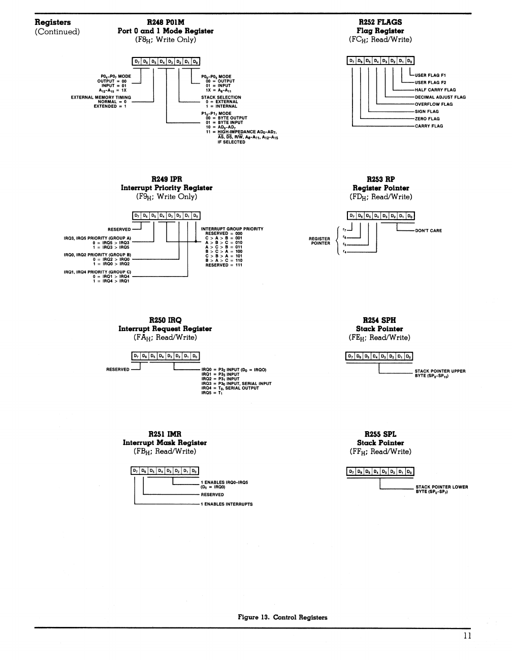
Registers
(Continued)
R248
POIM
Port 0
and
1 Mode
Register
(F~;
Write Only)
OUTPUT =
00
~
L
00
= OUTPUT
INPUT -
01
01
""
INPUT
A12~A1'
=
1X 1X
-
A.~A11
PO
••
PO,MODE:]
~~
Pa.·PO,MODE
EXTERNAL
MEMORY
TIMING
STACK
SELECTION
NORMAL - 0 0 = EXTERNAL
EXTENDED
= 1 1
...
INTERNAL
P10·P17
MODE
00
...
BYTE
OUTPUT
01
""
BYTE
INPUT
to -
A".AI>,
11
-
HIGH·IMPEDANCE
ADo-ADJ.
AS,
DB,
RIW,
At-Au.
A12-A1&
IF
SELECTED
R2491PR
Interrupt
Priority
Register
(F9H;
Write Only)
II>,I~I~I~I~ID,I~I
.. I
~:J
i [
III
~
..
""-~
RESERVED
=
ODD
IRQ3,
IRQ5
PRIORITY
(GROUP
A) C > A
:>
B =
001
0=IRQ5>IRQ3
A>8>C=010
1 =
IRQ3
>
IRQ5
A > C
:>
8 =
011
8>C>A=1oo
IROO,
IRQ2
PRIORITY
(GROUP
8) C
:>
B > A =
101
o = IRQ2 >
IROO
B
:>
A
:>
C = 110
1 =
IROO
:>
IRQ2
RESERVED
=
111
IR01,
IRQ4 PRIORITY (GROUP C)
o = IR01 > IR04
1
""
IRQ4
:>
IR01
R250IRQ
Interrupt
Request
Register
(FAH; Read/Write)
II>,I
.. I ..
I~ID,ID,I~I
.. I
RESERVED T
~
IRQO
-Po, INPUT
(Do
_ IRQO)
IR01 -P3, INPUT
IRQ2
,..
Pa, INPUT
IRQ3 = P30 INPUT, SERIAL INPUT
IRQ4 •
To.
SERIAL OUTPUT
IRQ5 -T,
R2511MR
Interrupt
Mask
Register
(F~;
Read/Write)
Il
___
~
___
1 ENABLES
IRoo-IR05
CDo
-
IROO)
RESERVED
'--------1
ENABLES INTERRUPTS
Figure
13. Control
aegisters
R252
FLAGS
Flag
Register
(FCH; Read/Write)
llI~~
'
LUSER
FLAG
Ft
LUSER
FLAG
F2
HALF CARRY FLAG
DECIMAL ADJUST FLAG
OVERFLOW FLAG
SIGN FLAG
ZERO FLAG
CARRY FLAG
R253
RP
ReglBter
Pointer
(F~;
Read/Write)
LDON'TCARE
8254
SPH
Stack
Pointer
(FE
H; Read/Write)
8255 SPL
Stack
Pointer
(FFH; Read/Write)
II>,I
.. I ..
I~I~!~I~I
.. I
.. 1
____
:~~~S~~=~~R
LOWER
11
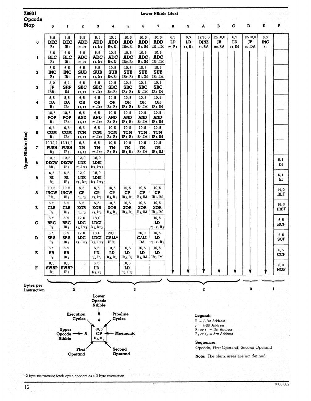
Z8601
Opcode
Map
o
2
3
•
5
..
6
..
e
.!
7
..Q
:9
z;
~
Ilo
8
Ilo
::>
9
A
B
C
D
E
F
Bytes
per
Instruction
Lower
Nibble
(Hex)
o 2 3 4 5 6 7 8 9 A B C D E F
6,5 6,5 6,5
6,5
10,5 10,5
10,5
10,5 6,5 6,5 12/10,5 12/10,0 6,5 12/10,0 6,5
DEC DEC
ADD
ADD
ADD
ADD
ADD ADD
LD
LD
DJNZ
JR
LD
JP INC
Rl IRl
Il,
f2
n,lra
R2,Rl JR2,Rl Rl,IM IRl,iM
II,
Hz
12,
HI
Il,RA
cc,RA rl,iM
cc,DA
fl
-
6,5
6,5 6,5
6,5
10,5
10,5
10,5
10,5
RLC
RLC
ADC
ADC
ADC
ADC ADC ADC
Rl JRl
II,
f2
II,
1r2
R2,Rl JR2,Rl Rl,IM JR"IM -
6,5 6,5
6,5
6,5
10,5 10,5
10,5 10,5
INC
INC
SUB
SUB
SUB SUB SUB SUB
Rl JRl
II,
f2
Il,Il2
R2,Rl IR2,Rl Rl,IM IRl,IM -
8,0
6,1
6,5
6,5
10,5 10,5 10,5
10,5
IP
SRP
SBC
SBC
SBC SBC SBC
SBC
JRRl
1M
II,
[2
II1Ir2
R2,Rl IR2,Rl Rl.IM IRl,IM -
8,5
8,5
6,5
6,5
10,5 10,5 10,5
10,5
DA DA
OR
OR
OR OR OR OR
Rl JRl
Il,
[2
r
1,
Ira R2,Rl IR2,Rl Rl,IM JRl,IM -
10,5
10,5
6,5 6,5
10,5 10,5
10,5 10,5
POP POP
AND AND AND AND AND AND
Rl IRl
II,
[2
Il,IrZ
R2,Rl IR2,Rl Rl,iM IRl,IM -
6,5
6,5 6,5
6,5
10,5 10,5 10,5 10,5
COM
COM
TCM
TCM
TCM TCM TCM TCM
Rl IRl
II,
fa
Il,Irz
R2,Rl IR2,Rl Rl,iM IRl,IM -
10/12,1 12/14,1
6,5 6,5
10,5
10,5
10,5
10,5
PUSH PUSH TM TM TM TM TM TM
R2
JR2
II,
fZ
Il,lrz
R2,Rl IR2,Rl Rl,IM IRl,iM -
10,5
10,5
12,0
18,0
6,1
DECW
DECW
LDE LOEI
DI
RRl IRl
II,
IrI2
Ir
1,
!rIa
-
6,5
6,5
12,0
18,0
6,1
RL
RL
LDE LOE! EI
Rl JRl 12,
lIn
Lu,IrIl
------'--
10,5
10,5
6,5
6,5
10,5 10,5
10,5 10,5
14,0
INCW INCW
CP
CP
CP
CP
CP CP
RET
RRl
IRl
II,
fZ
r
1,
Ira R2,Rl JR2,Rl Rl,iM IRl,IM -
6,5 6,5
6,5 6,5
10,5
10,5
10,5 10,5
16,
°
CLR CLR XOR XOR XOR XOR XOR XOR IRET
Rl JRl
II,
f2
II,
Ira R2,Rl IR2,Rl Rl,IM JRl,iM -
6,5
6,5
12,0
18,0
10,5
6,5
RRC RRC LDC LDCI
LO
RCF
Rl IRl
(1,
!rI2
IrI,IIll
II,
X,
Hz
-
6,5 6,5
12,0
18,0
20,0
20,0
10,5
6,5
SM
SRA LDC LDCI CALL* CALL
LD
SCF
Rl JRl
lZ,IrI}
Irz,
Irn
IRRl
DA
12,
x,
HI
-
6,5
6,5
10,5 10,5
10,5
10,5
6,5
6,5
RR RR LD
LD
LD LD
LD
CCF
Rl JRl
Il,Irz
R2,Rl IR2,Rl Rl,IM IRl,iM -
8,5
8,5
6,5
10,5
6,0
SWAP
SWAP
LD LD
NOP
Rl IRl
In,I2
R2,IRl
~~------~~~~-----'~
~,------~~~------~~
~'----------~~~---------'~
~
~
2 2 3
Lower
Opcode
Nibble
Execution
•
Pipeline
Cycles
•
Cycles
Upper
~0'5
Opcode
_ A CP
Mnemonic
Nibble
R2,
R 1
Ftr~
Second
Operand
Operand
Legend:
R =
8~
Bit Address
r =
4·
Bit Address
Rl
or
rt
= Dst Address
Hz
or
[2
= Src Address
Sequence:
Opcode,
First
Operand,
Second
Operand
Note:
The
blank
areas
are
not
defined.
*2-byte- instruction; fetch cycle
appears
as a 3-byte instruction
12
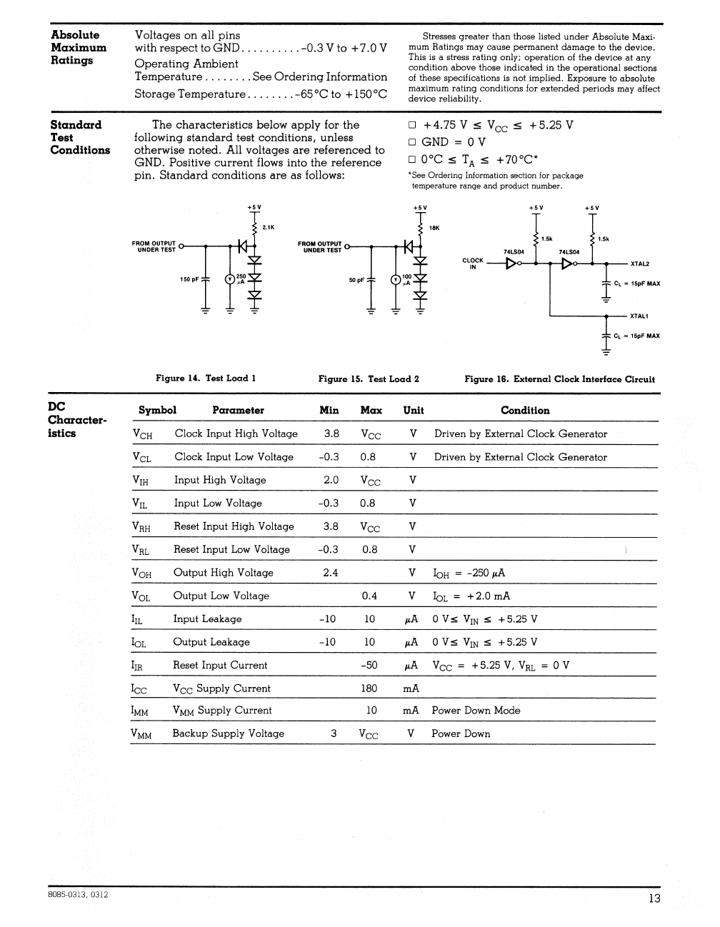
Absolute
Maximum
Ratings
Standard
Test
Conditions
DC
Character-
istics
8085-0313, 0312
Voltages on all pins
withrespecttoGND
..........
-O.3Vto
+7.0V
Operating
Ambient
Temperature
........
See
Ordering
Information
Storage Temperature
........
-65°C
to
+150°C
The characteristics below apply for
the
following
standard
test conditions, unless
otherwise noted. All voltages
are
referenced
to
GND. Positive
current
flows into the reference
pin.
Standard
conditions
are
as follows:
+5V
2.1K
Stresses greater than those listed
under
Absolute Maxi-
mum Ratings may cause permanent
damage
to
the device.
This is a stress rating only; operation of
the
device
at
any
condition above those indicated in the operational sections
of
these specifications is not implied. Exposure
to
absolute
maximum rating conditions for extended periods may affect
device reliability.
D
+4.75
V S Vee S
+5.25
V
D GND = 0 V
D O°C S
TA
S +70°C*
..
See
Ordering Information section for
package
temperature range and product number.
+5V
+5V
,.,
+'V
Uk Uk
74LS04
74LS04
XTAL1
I
CL
= 15pF
MAX
Figure 14. Tast Load 1 Figure 15. Test Load 2 Figure 16. External Clock Interface Circuit
Symbol Parameter
Min
Max Unit Condition
VeH
Clock
Input
High
Voltage 3.8
Vee
V Driven
by
External Clock.
Generator
VeL
Clock
Input
Low Voltage -0.3 0.8 V Driven
by
External
Clock
Generator
VIH
Input
High
Voltage 2.0
Vee
V
V
1L
Input
Low Voltage
-0.3
0.8 V
V
RH
Reset
Input
High
Voltage 3.8
Vee
V
V
RL
Reset
Input
Low Voltage
-0.3
0.8 V
VO
H
Output
High
Voltage 2.4 V
IoH
= -250
p,A
VOL
Output
Low Voltage 0.4 V IoL =
+2.0
rnA
IlL
Input
Leakage
-10 10
p.A
o
Vs
VIN
s +5.25 V
10L
Output
Leakage
-10 10
p,A
o
Vs
V
IN
s +5.25 V
IJR
Reset
Input
Current
-50
p.A
Vee
= +5.25 V,
VRL
= 0 V
lee
Vee
Supply
Current
180
rnA
IMM
V
MM
Supply
Current
10
rnA
Power Down Mode
VMM
Backup
Supply
Voltage 3
Vee
V Power Down
13
External 110
or
Memory
Read and
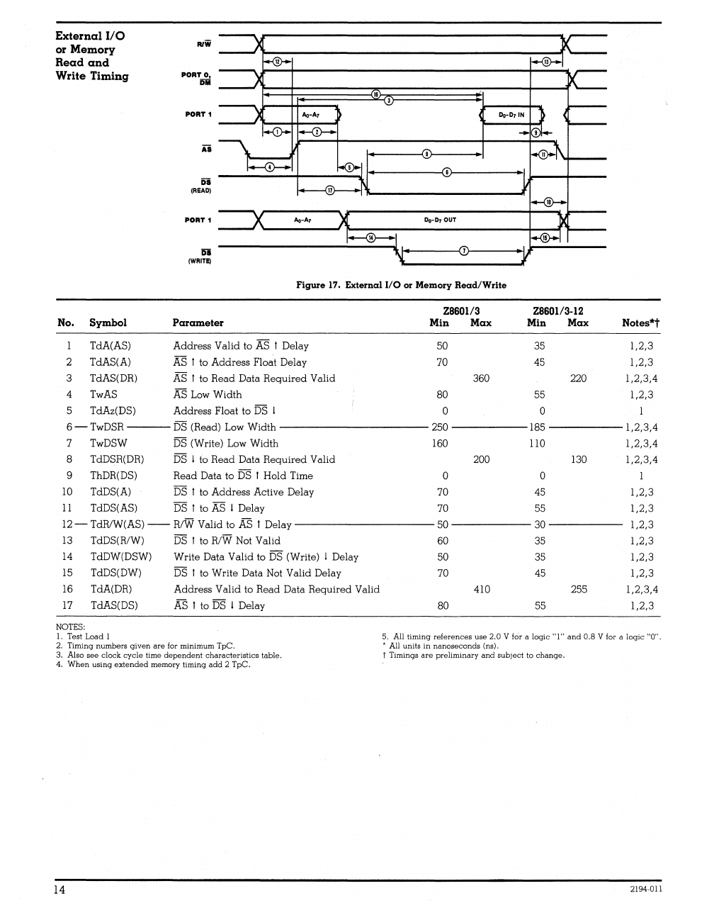
Write Timing
PORT
1
Di
(WRITE)
!la-Dr
OUT
M
Figure
17.
External
I/O
or
Memory Read/Write
ZB60113
ZB60113-12
No.
Symbol Parameter
Min
Max
Min
Max
Notes*t
1 TdA(AS) Address Valid to
AS
f Delay 50
35
1,2,3
2 TdAS(A)
AS
f to Address Floal Delay 70
45
1,2,3
3 TdAS(DR)
AS
f
to
Read Data Required Valid 360 220 1,2,3,4
4
TwAS
AS
Low
Width 80 55 1,2,3
5 TdAz(DS) Address Float to
DS
I 0 0
6-TwDSR
DS
(Read)
Low
Width 250
185
1,2,3,4
7
TwDSW
DS
(Write)
Low
Width
160
110
1,2,3,4
8
TdDSR(DR)
DS
I to Read Data Required Valid 200
130
1,2,3,4
9 ThDR(DS) Read Data
to
DS
f Hold Time 0 0 I
10
TdDS(A)
DS
f to Address Active Delay 70 45 1,2,3
11
TdDS(AS)
DS
f to
AS
I Delay 70
55
1,2,3
12
-TdRlW(AS)
--
RIW
Valid to
AS
f Delay 50 30 1,2,3
13
TdDS(RIW)
DS
f to
RlW
Not
Valid 60
35
1,2,3
14
TdDW(DSW) Write Data Valid to
DS
(Write) I Delay 50
35
1,2,3
15
TdDS(DW)
DS
f
to
Write Data
Not
Valid Delay
70
45
1,2,3
16
TdA(DR) Address Valid
to
Read Data Required Valid 410 255 1,2,3,4
17
TdAS(DS)
AS
f to
DS
I Delay 80
55
1,2,3
NOTES:
I.
Test Load I 5. All timing references use 2.0 V for a logic
\I
1"
and 0.8 V
for
a logic
"0".
2. Timing numbers given are for minimum
TpC.
* All units in nanoseconds (ns),
3. Also
see
clock
cycle
time dependent characteristics table. t Timings are preliminary and subject to change.
4. When using extended memory
t.irning
add 2 TpC.
14
2194-011
Additional
Timing
Table
Figure 18. Additional Timing
ZB601I3
Z8601l3-12
No. Symbol Parameter
Min
Max
Min
Max
Notes*t
2
3
TpC
TrC,TlC
TwC
Input Clock Period
Clock Input Rise And Fall Times
Input Clock Width
4
TwTinL
Timer Input
Low
Width
125
37
100
1000
83
25
26
70
1000
15
1
2
5 -
TwTinH
---
Timer Input High Width
----------
3TpC 3TpC
------2
6 TpTin Timer Input Period
7
8
9
NOTES:
TrTin,TlTin
TwIL
TwIH
Timer Input Rise And Fall Times
Interrupt Request Input
Low
Time
Interrupt Request Input High Time
1.
Clock timing references uses
3.B
V for a
logic
"1"
and
0.8
V for
a logic "0".
2. Timing reference
uses
2.0
V for a
logic
"1"
and
O.S
V for
a
logic
"0",
TpC
8
100
100
3TpC
3. Interrupt request via
Port
3.
..
Units in nanoseconds (ns).
TpC
8
70
3TpC
t Timings are preliminary and
subj
ect to change.
100
Z8603
Memory
Port
Timing
Ao-A.O
~~
________________
~_A_D_D_RE_~
__
VA_L_'D
__________________
~b(
_----J
____
T-~
.•
______
0
___
~.1
T~lr_
Do-D7
DON'T
CARE
~
DATA
IN
VALID
~
Figure
19.
Memory
Port
Timing
Z8601I3
Z8601l3
2
2
2,3
2,3
No. Symbol Parameter
Min
Max
Min
Max
Notes*
TdA(DI)
2 ThDI(A)
NOTES:
I. Test Load 2
Address Valid to Data Input Delay
Data In Hold Time
2. This is a
Clock-eyde-Dependent
parameter. For clock frequen-
cies
other than the maximum,
use
the following formula:
2860113 = 5 TpC -
165
28601/3·12 = 5 TpC -95
2194·012 2037·019
460 320
o o
..
Units are nanoseconds unless otherwise specified; timings are
preliminary and subject to
change.
1,2
15
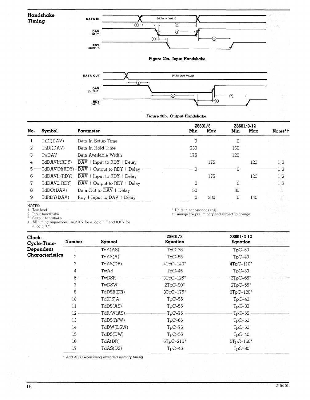
Han4shake
Timing
No.
Symbol
TsDI(DAV)
DA~:~;
____________
~
_____
~.:::;:~.:
~
__________
_
IIDY
(OUTPUT)
Fig\1re 20a.
Inp\1t
Hgncishake
-:::~
~~~~~_1=E
___
, ·
__
1~~~~~~~;2D_"=T_A~OU~TV~AL;,"~~~.~~-~
1>:-,---,
----
(INPUT)
~
Fi9l1re 20b.
O\1tp\1t
Handshake
Z8601l3
Z8601/3-12
Parameter
Min
Max
Min
Max
Data In Setup Time 0 0
2 ThDI(DAV) Data In Hold Time 230
160
3
TwDAV
Data Available Width
175
120
4
TdDAVIf(RDY)
DAV
I Input to
RDY
I Delay
175
5-TdDAVOf(RDY)-DAV
I
OutputtoRDY
I
Delay--------
0 0
120
1.2
------1,3
6 TdDAVIr(RDY)
DAV
I Input to
RDY
I Delay
7
8
9
NOTES:
TdDAVOrRDY)
TdDO(DAV)
TdRDY(DAV)
I.
Test load I
2. Input handshake
3. Output handshake
DAV
I
Output
to
RDY
I Delay
Data Out to
DA
V I Delay
Rdy I Input to
DAV
I Delay
4. All timing regerences use 2.0 V for a logic
"1"
and 0.8 V
for
a
logic
"0",
Clock-
Cycle-
Time-
Number
Symbol
Dependent
1 TdA(AS)
Characterbtics 2 TdAS(A)
3 TdAS(DR)
4
TwAS
6
TwDSR
7 TwDSW
8 TdDSR(DR)
10
Td(DS)A
11
TdDS(AS)
12
TdRlW(AS)
13
TdDS(R/W)
14
TdDW(DSW)
15
TdDS(DW)
16
TdA(DRl
17
TdAS(l)S)
* Add 2l'
pC
when using extended memory timing
16
175 120
0 0
50 30
0 200 0
140
*
Urtits
in nanoseconds (ns).
t Timings are preliminary and subject to change.
Z8601l3
Z8601I3-l2
Equation Equation
TpC-75 TpC-50
TpC-55 TpC-40
4TpC-140* 4TpC-llO*
TpC-45 TpC-30
3TpC-125* 3TpC-65*
2TpC-90* 2TpC-55*
3TpC-175* 3TpC-120*
TpC-55 TpC-40
TpC-55 TpC-30
TpC-75 TpC-55
TpC-65 TpC-50
TpC-75 TpC-50
TpC-55 TpC-40
5TpC-215* 5TpC-160*
TpC-45 TpC-30
1,2
1,3
1
1
2194-0i:
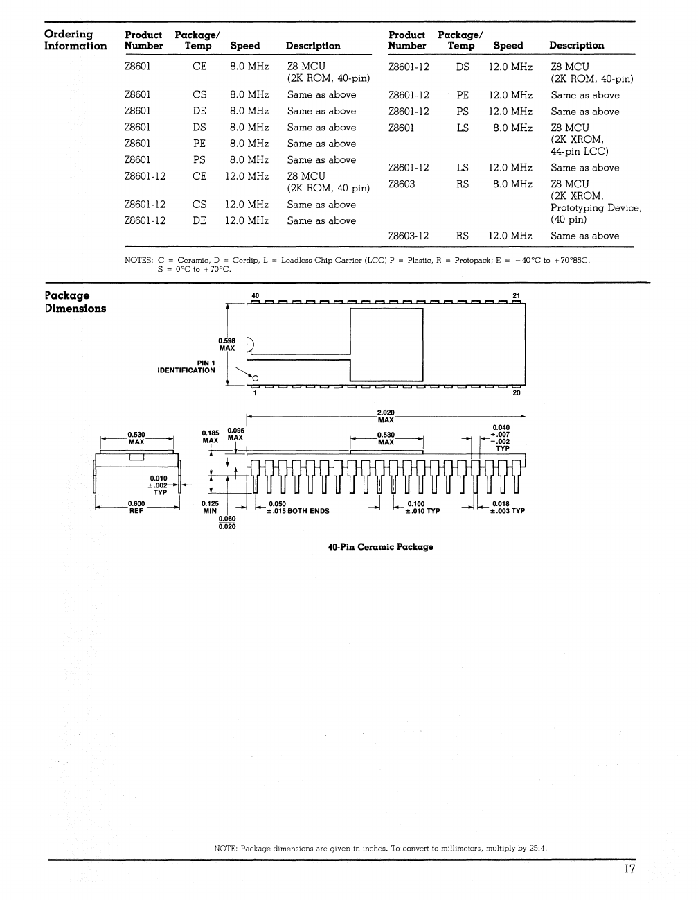
Ordering
Information
Package
Dimensions
Product
Package/
Product
Package/
Number
Temp
Speed
Description Number Temp
Speed
Description
Z8601
CE 8.0
MHz
Z8MCU
Z8601-12
DS
12.0 MHz
Z8MCU
(2K
ROM, 40-pin)
(2K
ROM, 40-pin)
Z8601
CS 8.0
MHz
Same as
above
Z8601-12
PE
12.0 MHz
Same
as above
Z8601
DE
8.0 MHz Same as
above
Z8601-12 PS 12.0 MHz
Same
as
above
Z8601
DS
8.0 MHz
Same
as
above
Z8601
LS
8.0
MHz
Z8MCU
Z8601
PE
8.0 MHz Same as
above
(2K
XROM,
Z8601
PS
8.0 MHz
Same
as
above
44-pin LCC)
Z8601-12
LS
12.0 MHz
Same
as above
Z8601-12 CE 12.0 MHz
Z8MCU
(2K
ROM, 40-pin) Z8603
RS
8.0 MHz
Z8MCU
(2K
XROM,
Z8601-12 CS 12.0 MHz Same as
above
Prototyping Device,
Z8601-12
DE
12.0 MHz
Same
as
above
(40-pin)
Z8603-12
RS
12.0 MHz
Same
as above
NOTES: C = Cera.mic, D =
Cerdip,
L = Leadless
Chip
Carrier
(LCC) P = Plastic, R = Protopack; E = -
40°C
to
+ 70085C,
S
~
GOC
to
+
7GoC.
40
21
r
~
~s:~
)~
PIN
1
~============~
IDENTIFICATION
20
I'
~o:~
0.040
~~~!E~
m
r
II
0.125 0.050 0.100 0.018
MIN
1-±.015
BOTH
ENDS
~
L±.010TYP
~L±.003TYP
0.060
0.020
40-Pin
Ceramic
Package
NOTE:
Package
dimensions
are
given
in
inches.
To
convert
to
millimeters,
multiply
by
25.4.
17
Package
DlmensloDs
(Continued)
18
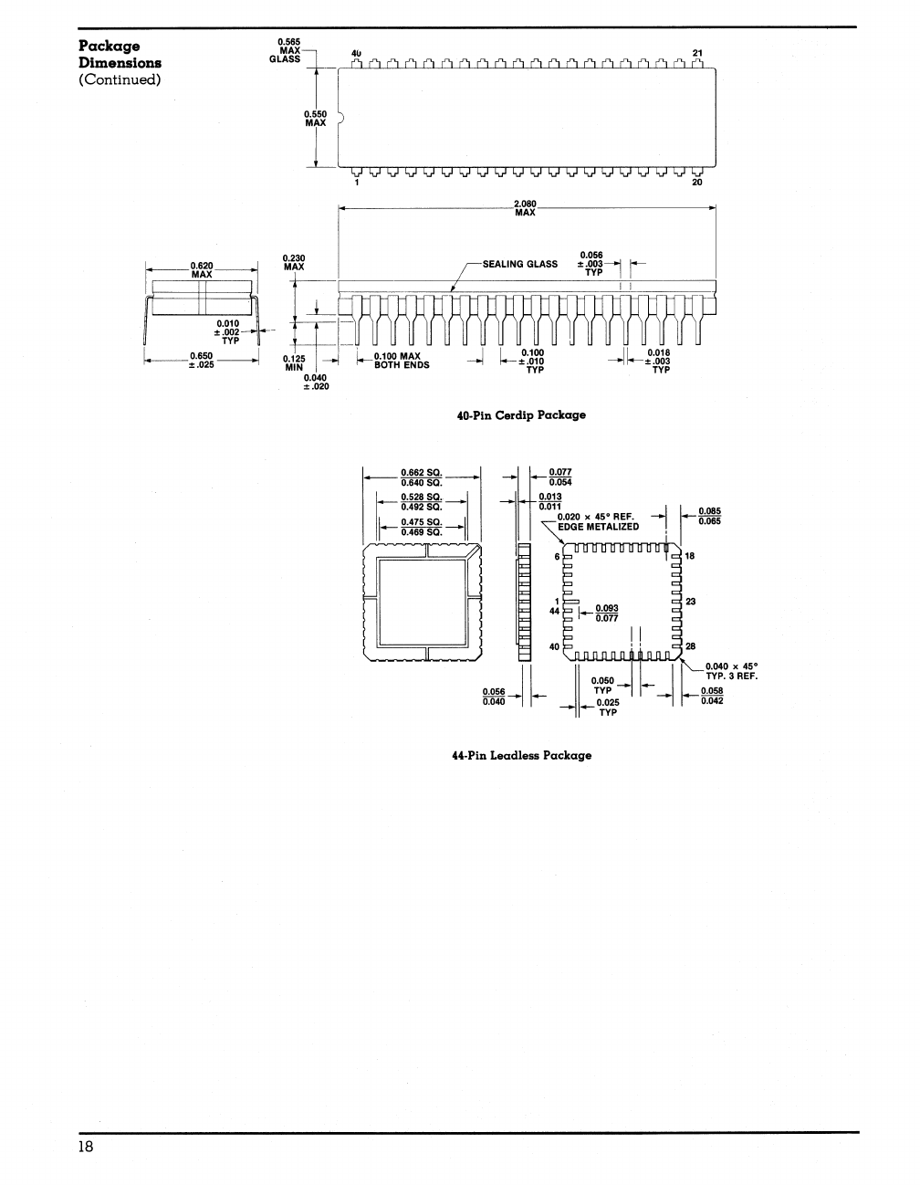
40-Pln Cerdip Package
~=:g-
_0.5288Q,_
II
::::
:~:
II
--
0.489 SQ. -
II
~D
II
0.054
0.013
0.011
*0.077
0.020 •
45°
REF.
1
~"a~"
6
II
~I
0.050
0.056
TYP
0.040 - - _ 0.025
TYP
U-Pin Leadle
••
Package
0.040 x 45°
TYP.
3 REF.
Package
Dimensions
(Continued)
40
21
T
~~~=nrrrT~n=rrTT"=rrr~~n=rrTT"=rrr~~n=~
20
0.&00
MAX
I
·-----------------------~~~----------------------~'~I
1r=
0.62O~
0.lS0
!
~
~
~,----------------------------------H----------~~O
~
~
J
0.009
~
I~~::~~
0.010
-
--±.002
TYP
~OR~-----I
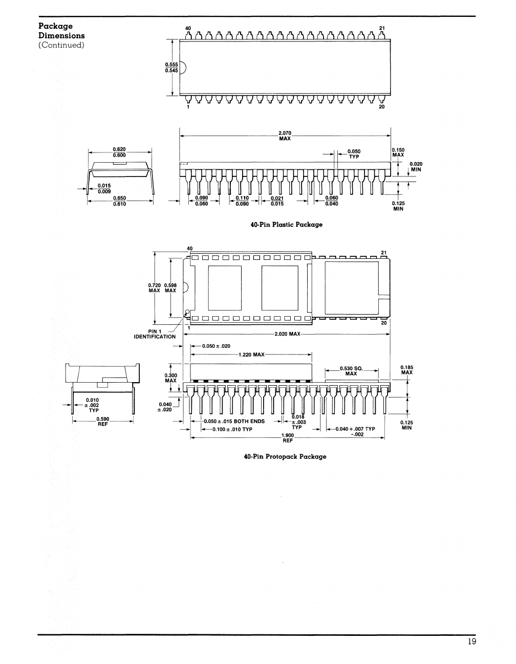
'O-Pin
Plastic
Package
40
ffiDDDDDDDDDDDD
m_)
D D
O.
M
AX
MAX
L~D
0 0 0 0 0 0 0 0 0 0 0
IN
1
..../
P
IDENTIF ICATION
-1 2.020 MAX
FOSO±.020
-------1.220
MAX
'I
~~~
~
F
20
t
r-0.S30
SQ.----j
0.300 MAX
MAX
:~~~Q==~
II
_
1+--0.l00±.010TYP
TYP
_
LO.04O+.007TYP
MIN
•
-------------------lR~~
-.002 ,
'O-Pin Protopack
Package
19

Notes

Zilog
Sales
Offices
West
Sales & Technical
Center
Zilog,
Incorporated
1315 Dell
Avenue
Campbell,
CA
95008
Phone: (408) 370-8120
TWX: 910-338-7621
Sales & Technical
Center
Zilog,
Incorporated
18023 Sky Park Circle
Suite J
Irvine,
CA
92714
Phone: (714) 549-2891
TWX:
910-595-2803
Sales & Technical
Center
Zilog,
Incorporated
15643
Sherman
Way
Suite 430
Van Nuys,
CA
91406
Phone: (213) 989-7485
TWX: 910-495-1765
Sales & Technical
Center
Zilog,
Incorporated
1750 112th Ave. N.E.
Suite Dl61
Bellevue, W A 98004
Phone: (206) 454-5597
Midwest
Sales & Technical
Center
Zilog,
Incorporated
951
North Plum
Grove
Road
Suite F
Schaumburg,
IL
60195
Phone: (312) 885-8080
TWX: 910-291-1064
Sales & Technical
Center
Zilog,
Incorporated
28349
Chagrin
Blvd.
Suite
109
Woodmere,
OH
44122
Phone: (216) 831-7040
FAX: 216-831-2957
South
Sales & Technical
Center
Zilog,
Incorporated
4851 Keller
Springs
Road,
Suite
211
Dallas,
TX
75248
Phone: (214) 931-9090
TWX: 910-860-5850
Zilog,
Incorporated
7113 Burnet Rd.
Suite 207
Austin,
TX
78757
Phone: (512) 453-3216
Zilog, Inc. 1315 Dell Ave.,
Campbell,
California 95008
00-2037-03
East
Sales & Technical
Center
Zilog,
Incorporated
Corporate
Place
99 South Bedford SI.
Burlington,
MA
01803
Phone: (617) 273-4222
TWX: 710-332-1726
Sales & Technical
Center
Zilog,
Incorporated
240
Cedar
Knolls Rd.
Cedar
Knolls,
NJ
07927
Phone: (201) 540-1671
Technical
Center
Zilog,
Incorporated
3300 Buckeye Rd.
Suite
401
Atlanta,
GA
30341
Phone: (404) 451-8425
Sales & Technical
Center
Zilog,
Incorporated
1442 U.S. Hwy
19
South
SUlte
135
Clearwater,
FL
33516
Phone: (813) 535-5571
Zilog, Inc.
613-B Pit! SI.
Cornwall, Ontario
Canada
K6J
3R8
Phone: (613) 938-1121
United Kingdom
Zilog (U.K.) Limited
Zilog House
43-53
Moorbridge
Road
Maidenhead
Berkshire, SL6 8PL
England
Phone: 0628-39200
Telex: 848609
France
Zilog,
Incorporated
Tour Europe
Cedex
7
92080 Paris La Defense
France
Phone:
(I)
778-14-33
Telex: 611445F
West Germany
Zilog
GmbH
Eschenstrasse 8
D-8028 TAUFKIRCHEN
Munich, West
Germany·
Phone: 89-612-6046
Telex: 529110 Zilog
d.
Japan
Zilog,
Japan
K.K.
Konparu Bldg. 5F
2-8 Akasaka 4-Chome
Minato-Ku, Tokyo
107
Japan
Phone: (81) (03) 587-0528
Telex: 2422024
NB:
Zilog J
Telephone (408)370-8000
TWX
910-338-7621
Printed in USA
